RX62T/RX62G Group User’s Manual: Hardware Renesas MCU RX62G T Users Manual
User Manual: Pdf
Open the PDF directly: View PDF ![]() .
.
Page Count: 1489 [warning: Documents this large are best viewed by clicking the View PDF Link!]
- Cover
- Notice
- General Precautions in the Handling of MPU/MCU Products
- How to Use This Manual
- Contents
- Features
- 1. Overview
- 2. CPU
- 2.1 Features
- 2.2 Register Set of the CPU
- 2.2.1 General-Purpose Registers (R0 to R15)
- 2.2.2 Control Registers
- 2.2.2.1 Interrupt Stack Pointer (ISP)/User Stack Pointer (USP)
- 2.2.2.2 Interrupt Table Register (INTB)
- 2.2.2.3 Program Counter (PC)
- 2.2.2.4 Processor Status Word (PSW)
- 2.2.2.5 Backup PC (BPC)
- 2.2.2.6 Backup PSW (BPSW)
- 2.2.2.7 Fast Interrupt Vector Register (FINTV)
- 2.2.2.8 Floating-Point Status Word (FPSW)
- 2.2.2.9 Accumulator (ACC)
- 2.3 Processor Mode
- 2.4 Data Types
- 2.5 Endian
- 2.6 Vector Table
- 2.7 Operation of Instructions
- 2.8 Pipeline
- 3. Operating Modes
- 4. Address Space
- 5. I/O Registers
- 6. Resets
- 7. Voltage Detection Circuit (LVD)
- 8. Clock Generation Circuit
- 9. Low Power Consumption
- 9.1 Overview
- 9.2 Register Descriptions
- 9.2.1 Standby Control Register (SBYCR)
- 9.2.2 Module Stop Control Register A (MSTPCRA)
- 9.2.3 Module Stop Control Register B (MSTPCRB)
- 9.2.4 Module Stop Control Register C (MSTPCRC)
- 9.2.5 Deep Standby Control Register (DPSBYCR)
- 9.2.6 Deep Standby Wait Control Register (DPSWCR)
- 9.2.7 Deep Standby Interrupt Enable Register (DPSIER)
- 9.2.8 Deep Standby Interrupt Flag Register (DPSIFR)
- 9.2.9 Deep Standby Interrupt Edge Register (DPSIEGR)
- 9.2.10 Reset Status Register (RSTSR)
- 9.2.11 Deep Standby Backup Register (DPSBKRy) (y = 0 to 31)
- 9.3 Multi-Clock Function
- 9.4 Module Stop Function
- 9.5 Low Power Consumption Modes
- 9.5.1 Sleep Mode
- 9.5.2 All-Module Clock Stop Mode
- 9.5.3 Software Standby Mode
- 9.5.4 Deep Software Standby Mode
- 9.5.4.1 Transition to Deep Software Standby Mode
- 9.5.4.2 Canceling Deep Software Standby Mode
- 9.5.4.3 Pin States when Deep Software Standby Mode is Canceled
- 9.5.4.4 Setting Oscillation Settling Time after Deep Software Standby Mode is Canceled
- 9.5.4.5 Example of Deep Software Standby Mode Application
- 9.5.4.6 Flowchart to Use Deep Software Standby Mode
- 9.6 Usage Notes
- 9.6.1 I/O Port States
- 9.6.2 Module Stop State of the DTC
- 9.6.3 On-Chip Peripheral Module Interrupts
- 9.6.4 Write-Access to MSTPCRA, MSTPCRB, and MSTPCRC
- 9.6.5 Input Buffer Control by DIRQnE Bit (n = 1, 0)
- 9.6.6 Conflict between Transition to Deep Software Standby Mode and Interrupt
- 9.6.7 Timing of Wait Instructions
- 10. Exceptions
- 11. Interrupt Controller (ICU)
- 11.1 Overview
- 11.2 Register Descriptions
- 11.2.1 Interrupt Request Register i (IRi) (i = interrupt vector number)
- 11.2.2 Interrupt Request Enable Register m (IERm) (m = 02h to 1Fh)
- 11.2.3 Interrupt Priority Register m (IPRm) (m = 00h to 90h)
- 11.2.4 Fast Interrupt Register (FIR)
- 11.2.5 Software Interrupt Activation Register (SWINTR)
- 11.2.6 DTC Activation Enable Register n (DTCERn) (n = interrupt vector number)
- 11.2.7 IRQ Control Register n (IRQCRn) (n = 0 to 7)
- 11.2.8 Non-Maskable Interrupt Status Register (NMISR)
- 11.2.9 Non-Maskable Interrupt Enable Register (NMIER)
- 11.2.10 Non-Maskable Interrupt Clear Register (NMICLR)
- 11.2.11 NMI Pin Interrupt Control Register (NMICR)
- 11.3 Vector Table
- 11.4 Interrupt Operation
- 11.5 Non-Maskable Interrupt Operation
- 11.6 Return from Power-Down States
- 11.7 Usage Notes
- 12. Buses
- 13. Memory-Protection Unit (MPU)
- 13.1 Overview
- 13.2 Register Descriptions
- 13.2.1 Region-n Start Page Number Register (RSPAGEn) (n = 0 to 7)
- 13.2.2 Region-n End Page Number Register (REPAGEn) (n = 0 to 7)
- 13.2.3 Memory-Protection Enable Register (MPEN)
- 13.2.4 Background Access Control Register (MPBAC)
- 13.2.5 Memory-Protection Error Status-Clearing Register (MPECLR)
- 13.2.6 Memory-Protection Error Status Register (MPESTS)
- 13.2.7 Data Memory-Protection Error Address Register (MPDEA)
- 13.2.8 Region Search Address Register (MPSA)
- 13.2.9 Region Search Operation Register (MPOPS)
- 13.2.10 Region Invalidation Operation Register (MPOPI)
- 13.2.11 Instruction-Hit Region Register (MHITI)
- 13.2.12 Data-Hit Region Register (MHITD)
- 13.3 Functions
- 13.4 Procedures for Using Memory Protection
- 14. Data Transfer Controller (DTC)
- 14.1 Overview
- 14.2 Register Descriptions
- 14.2.1 DTC Mode Register A (MRA)
- 14.2.2 DTC Mode Register B (MRB)
- 14.2.3 DTC Transfer Source Address register (SAR)
- 14.2.4 DTC Transfer Destination Address Register (DAR)
- 14.2.5 DTC Transfer Count Register A (CRA)
- 14.2.6 DTC Transfer Count Register B (CRB)
- 14.2.7 DTC Control Register (DTCCR)
- 14.2.8 DTC Vector Base Register (DTCVBR)
- 14.2.9 DTC Address Mode Register (DTCADMOD)
- 14.2.10 DTC Module Start Register (DTCST)
- 14.2.11 DTC Status Register (DTCSTS)
- 14.3 Sources of Activation
- 14.4 Operation
- 14.5 DTC Setting Procedure
- 14.6 Examples of DTC Usage
- 14.7 Interrupt Source
- 14.8 Low-Power Consumption Function
- 14.9 Usage Notes
- 15. I/O Ports
- 15.1 I/O Ports [for 112-Pin LQFP]
- 15.1.1 Overview
- 15.1.2 Register Descriptions
- 15.1.2.1 Data Direction Register (DDR)
- 15.1.2.2 Data Register (DR)
- 15.1.2.3 Port Register (PORT)
- 15.1.2.4 Input Buffer Control Register (ICR)
- 15.1.2.5 Port Function Register 8 (PF8IRQ)
- 15.1.2.6 Port Function Register 9 (PF9IRQ)
- 15.1.2.7 Port Function Register A (PFAADC)
- 15.1.2.8 Port Function Register C (PFCMTU)
- 15.1.2.9 Port Function Register D (PFDGPT)
- 15.1.2.10 Port Function Register F (PFFSCI)
- 15.1.2.11 Port Function Register G (PFGSPI)
- 15.1.2.12 Port Function Register H (PFHSPI)
- 15.1.2.13 Port Function Register J (PFJCAN)
- 15.1.2.14 Port Function Register K (PFKLIN)
- 15.1.2.15 Port Function Register M (PFMPOE)
- 15.1.2.16 Port Function Register N (PFNPOE)
- 15.1.3 Settings of Ports
- 15.1.4 List of Output Enable Settings
- 15.1.5 Treatment of Unused Pins
- 15.2 I/O Port [for 100-Pin LQFP]
- 15.2.1 Overview
- 15.2.2 Register Descriptions
- 15.2.2.1 Data Direction Register (DDR)
- 15.2.2.2 Data Register (DR)
- 15.2.2.3 Port Register (PORT)
- 15.2.2.4 Input Buffer Control Register (ICR)
- 15.2.2.5 Port Function Register 8 (PF8IRQ)
- 15.2.2.6 Port Function Register A (PFAADC)
- 15.2.2.7 Port Function Register C (PFCMTU)
- 15.2.2.8 Port Function Register D (PFDGPT)
- 15.2.2.9 Port Function Register F (PFFSCI)
- 15.2.2.10 Port Function Register G (PFGSPI)
- 15.2.2.11 Port Function Register H (PFHSPI)
- 15.2.2.12 Port Function Register J (PFJCAN)
- 15.2.2.13 Port Function Register K (PFKLIN)
- 15.2.2.14 Port Function Register M (PFMPOE)
- 15.2.2.15 Port Function Register N (PFNPOE)
- 15.2.3 Settings of Ports
- 15.2.4 List of Output Enable Settings
- 15.2.5 Treatment of Unused Pins
- 15.3 I/O Port [for 80-Pin LQFP]
- 15.3.1 Overview
- 15.3.2 Register Descriptions
- 15.3.2.1 Data Direction Register (DDR)
- 15.3.2.2 Data Register (DR)
- 15.3.2.3 Port Register (PORT)
- 15.3.2.4 Input Buffer Control Register (ICR)
- 15.3.2.5 Port Function Register 8 (PF8IRQ)
- 15.3.2.6 Port Function Register A (PFAADC)
- 15.3.2.7 Port Function Register C (PFCMTU)
- 15.3.2.8 Port Function Register D (PFDGPT)
- 15.3.2.9 Port Function Register G (PFGSPI)
- 15.3.2.10 Port Function Register H (PFHSPI)
- 15.3.2.11 Port Function Register J (PFJCAN)
- 15.3.2.12 Port Function Register K (PFKLIN)
- 15.3.2.13 Port Function Register M (PFMPOE)
- 15.3.2.14 Port Function Register N (PFNPOE)
- 15.3.3 Settings of Ports
- 15.3.4 List of Output Enable Settings
- 15.3.5 Treatment of Unused Pins
- 15.4 I/O Port [for 80-Pin LQFP (R5F562TxGDFF)]
- 15.4.1 Overview
- 15.4.2 Register Descriptions
- 15.4.2.1 Data Direction Register (DDR)
- 15.4.2.2 Data Register (DR)
- 15.4.2.3 Port Register (PORT)
- 15.4.2.4 Input Buffer Control Register (ICR)
- 15.4.2.5 Port Function Register 8 (PF8IRQ)
- 15.4.2.6 Port Function Register A (PFAADC)
- 15.4.2.7 Port Function Register C (PFCMTU)
- 15.4.2.8 Port Function Register D (PFDGPT)
- 15.4.2.9 Port Function Register F (PFFSCI)
- 15.4.2.10 Port Function Register G (PFGSPI)
- 15.4.2.11 Port Function Register H (PFHSPI)
- 15.4.2.12 Port Function Register J (PFJCAN)
- 15.4.2.13 Port Function Register K (PFKLIN)
- 15.4.2.14 Port Function Register M (PFMPOE)
- 15.4.2.15 Port Function Register N (PFNPOE)
- 15.4.3 Settings of Ports
- 15.4.4 List of Output Enable Settings
- 15.4.5 Treatment of Unused Pins
- 15.5 I/O Port [for 64-Pin LQFP]
- 15.5.1 Overview
- 15.5.2 Register Descriptions
- 15.5.2.1 Data Direction Register (DDR)
- 15.5.2.2 Data Register (DR)
- 15.5.2.3 Port Register (PORT)
- 15.5.2.4 Input Buffer Control Register (ICR)
- 15.5.2.5 Port Function Register C (PFCMTU)
- 15.5.2.6 Port Function Register D (PFDGPT)
- 15.5.2.7 Port Function Register G (PFGSPI)
- 15.5.2.8 Port Function Register H (PFHSPI)
- 15.5.2.9 Port Function Register J (PFJCAN)
- 15.5.2.10 Port Function Register K (PFKLIN)
- 15.5.2.11 Port Function Register M (PFMPOE)
- 15.5.3 Settings of Ports
- 15.5.4 List of Output Enable Settings
- 15.5.5 Treatment of Unused Pins
- 15.6 I/O Port Configuration
- 15.7 Usage Notes
- 15.1 I/O Ports [for 112-Pin LQFP]
- 16. Multi-Function Timer Pulse Unit 3 (MTU3)
- 16.1 Overview
- 16.2 Register Descriptions
- 16.2.1 Timer Control Register (TCR)
- 16.2.2 Timer Mode Register 1 (TMDR1)
- 16.2.3 Timer Mode Registers 2 (TMDR2A and TMDR2B)
- 16.2.4 Timer I/O Control Register (TIOR)
- 16.2.5 Timer Compare Match Clear Register (TCNTCMPCLR)
- 16.2.6 Timer Interrupt Enable Register (TIER)
- 16.2.7 Timer Status Register (TSR)
- 16.2.8 Timer Buffer Operation Transfer Mode Register (TBTM)
- 16.2.9 Timer Input Capture Control Register (TICCR)
- 16.2.10 Timer Synchronous Clear Register (TSYCR)
- 16.2.11 Timer Counter (TCNT)
- 16.2.12 Timer General Register (TGR)
- 16.2.13 Timer Start Register (TSTR)
- 16.2.14 Timer Synchronous Register (TSYR)
- 16.2.15 Timer Counter Synchronous Start Register (TCSYSTR)
- 16.2.16 Timer Read/Write Enable Registers (TRWERA and TRWERB)
- 16.2.17 Timer Output Master Enable Register (TOER)
- 16.2.18 Timer Output Control Registers 1 (TOCR1A and TOCR1B)
- 16.2.19 Timer Output Control Registers 2 (TOCR2A and TOCR2B)
- 16.2.20 Timer Output Level Buffer Registers (TOLBRA and TOLBRB)
- 16.2.21 Timer Gate Control Register A (TGCRA)
- 16.2.22 Timer Subcounters (TCNTSA and TCNTSB)
- 16.2.23 Timer Cycle Data Registers (TCDRA and TCDRB)
- 16.2.24 Timer Cycle Buffer Registers (TCBRA and TCBRB)
- 16.2.25 Timer Dead Time Data Registers (TDDRA and TDDRB)
- 16.2.26 Timer Dead Time Enable Registers (TDERA and TDERB)
- 16.2.27 Timer Buffer Transfer Set Registers (TBTERA and TBTERB)
- 16.2.28 Timer Waveform Control Registers (TWCRA and TWCRB)
- 16.2.29 Timer A/D Converter Start Request Control Register (TADCR)
- 16.2.30 Timer A/D Converter Start Request Cycle Set Registers (TADCORA and TADCORB)
- 16.2.31 Timer A/D Converter Start Request Cycle Set Buffer Registers (TADCOBRA and TADCOBRB)
- 16.2.32 Timer Interrupt Skipping Mode Registers (TITMRA and TITMRB)
- 16.2.33 Timer Interrupt Skipping Set Registers 1 (TITCR1A and TITCR1B)
- 16.2.34 Timer Interrupt Skipping Counters 1 (TITCNT1A and TITCNT1B)
- 16.2.35 Timer Interrupt Skipping Set Registers 2 (TITCR2A and TITCR2B)
- 16.2.36 Timer Interrupt Skipping Counters 2 (TITCNT2A and TITCNT2B)
- 16.2.37 Bus Master Interface
- 16.3 Operation
- 16.3.1 Basic Functions
- 16.3.2 Synchronous Operation
- 16.3.3 Buffer Operation
- 16.3.4 Cascaded Operation
- 16.3.5 PWM Modes
- 16.3.6 Phase Counting Mode
- 16.3.7 Reset-Synchronized PWM Mode
- 16.3.8 Complementary PWM Mode
- 16.3.9 A/D Converter Start Request Delaying Function
- 16.3.10 Synchronous Operation of MTU0 to MTU4, and MTU6 and MTU7
- 16.3.11 External Pulse Width Measurement
- 16.3.12 Dead Time Compensation
- 16.3.13 TCNT Capture at Crest and/or Trough in Complementary PWM Operation
- 16.4 Interrupt Sources
- 16.5 Operation Timing
- 16.6 Usage Notes
- 16.6.1 Module Stop Function Setting
- 16.6.2 Input Clock Restrictions
- 16.6.3 Note on Cycle Setting
- 16.6.4 Contention between TCNT Write and Clear Operations
- 16.6.5 Contention between TCNT Write and Increment Operations
- 16.6.6 Contention between TGR Write Operation and Compare Match
- 16.6.7 Contention between Buffer Register Write Operation and Compare Match
- 16.6.8 Contention between Buffer Register Write and TCNT Clear Operations
- 16.6.9 Contention between TGR Read Operation and Input Capture
- 16.6.10 Contention between TGR Write Operation and Input Capture
- 16.6.11 Contention between Buffer Register Write Operation and Input Capture
- 16.6.12 Contention between MTU2.TCNT Write Operation and Overflow/Underflow in Cascaded Operation
- 16.6.13 Counter Value when Stopped in Complementary PWM Mode
- 16.6.14 Buffer Operation Setting in Complementary PWM Mode
- 16.6.15 Buffer Operation and Compare Match Flags in Reset-Synchronized PWM Mode
- 16.6.16 Overflow Flags in Reset-Synchronized PWM Mode
- 16.6.17 Contention between Overflow/Underflow and Counter Clearing
- 16.6.18 Contention between TCNT Write Operation and Overflow/Underflow
- 16.6.19 Note on Transition from Normal Operation or PWM Mode 1 to Reset- Synchronized PWM Mode
- 16.6.20 Output Level in Complementary PWM Mode and Reset-Synchronized PWM Mode
- 16.6.21 Simultaneous Input Capture in MTU1.TCNT and MTU2.TCNT in Cascade Connection
- 16.6.22 Interrupt-Skipping Function 2
- 16.6.23 Notes when Complementary PWM Mode Output Protection Function is not Used
- 16.6.24 Points for Caution to Prevent Malfunctions in Synchronous Clearing for Complementary PWM Mode
- 16.6.25 Continuous Output of Interrupt Signal in Response to a Compare Match
- 16.7 MTU3 Output Pin Initialization
- 17. Port Output Enable 3 (POE3)
- 17.1 Overview
- 17.2 Register Descriptions
- 17.2.1 Input Level Control/Status Register 1 (ICSR1)
- 17.2.2 Output Level Control/Status Register 1 (OCSR1)
- 17.2.3 Active Level Setting Register 1 (ALR1)
- 17.2.4 Input Level Control/Status Register 2 (ICSR2)
- 17.2.5 Output Level Control/Status Register 2 (OCSR2)
- 17.2.6 Input Level Control/Status Register 3 (ICSR3)
- 17.2.7 Input Level Control/Status Register 4 (ICSR4)
- 17.2.8 Input Level Control/Status Register 5 (ICSR5)
- 17.2.9 Software Port Output Enable Register (SPOER)
- 17.2.10 Port Output Enable Control Register 1 (POECR1)
- 17.2.11 Port Output Enable Control Register 2 (POECR2)
- 17.2.12 Port Output Enable Control Register 3 (POECR3)
- 17.2.13 Port Output Enable Control Register 4 (POECR4)
- 17.2.14 Port Output Enable Control Register 5 (POECR5)
- 17.2.15 Port Output Enable Control Register 6 (POECR6)
- 17.3 Operation
- 17.3.1 Input Level Detection Operation
- 17.3.2 Output-Level Compare Operation
- 17.3.3 High-Impedance Control Using Registers
- 17.3.4 High-Impedance Control through Detection of Stopped Oscillation
- 17.3.5 High-impedance Control through Detection of the Comparator
- 17.3.6 Additional Functions for Controlling High-Impedance States
- 17.3.7 Release from High-Impedance State
- 17.4 Interrupts
- 17.5 Usage Notes
- 18. General PWM Timer (GPT/GPTa)
- 18.1 Overview
- 18.2 Register Descriptions
- 18.2.1 General PWM Timer Software Start Register (GTSTR)
- 18.2.2 General PWM Timer Hardware Source Start Control Register (GTHSCR)
- 18.2.3 General PWM Timer Hardware Source Clear Control Register (GTHCCR)
- 18.2.4 General PWM Timer Hardware Start Source Select Register (GTHSSR)
- 18.2.5 General PWM Timer Hardware Stop/Clear Source Select Register (GTHPSR)
- 18.2.6 General PWM Timer Write-Protection Register (GTWP)
- 18.2.7 General PWM Timer Sync Register (GTSYNC)
- 18.2.8 General PWM Timer External Trigger Input Interrupt Register (GTETINT)
- 18.2.9 General PWM Timer Buffer Operation Disable Register (GTBDR)
- 18.2.10 General PWM Timer Start Write Protection Register (GTSWP)
- 18.2.11 LOCO Count Control Register (LCCR)
- 18.2.12 LOCO Count Status Register (LCST)
- 18.2.13 LOCO Count Value Register (LCNT)
- 18.2.14 LOCO Count Result Average Register (LCNTA)
- 18.2.15 LOCO Count Result Register n (LCNTn) (n = 00 to 15)
- 18.2.16 LOCO Count Upper/Lower Permissible Deviation Register (LCNTDU, LCNTDL)
- 18.2.17 General PWM Timer I/O Control Register (GTIOR)
- 18.2.18 General PWM Timer Interrupt Output Setting Register (GTINTAD)
- 18.2.19 General PWM Timer Control Register (GTCR)
- 18.2.20 General PWM Timer Buffer Enable Register (GTBER)
- 18.2.21 General PWM Timer Count Direction Register (GTUDC)
- 18.2.22 General PWM Timer Interrupt and A/D Converter Start Request Skipping Setting Register (GTITC)
- 18.2.23 General PWM Timer Status Register (GTST)
- 18.2.24 General PWM Timer Counter (GTCNT)
- 18.2.25 General PWM Timer Compare Capture Register m (GTCCRm) (m = A to F)
- 18.2.26 General PWM Timer Cycle Setting Register (GTPR)
- 18.2.27 General PWM Timer Cycle Setting Buffer Register (GTPBR)
- 18.2.28 General PWM Timer Cycle Setting Double-Buffer Register (GTPDBR)
- 18.2.29 A/D Converter Start Request Timing Register m (GTADTRm) (m = A, B)
- 18.2.30 A/D Converter Start Request Timing Buffer Register m (GTADTBRm) (m = A, B)
- 18.2.31 A/D Converter Start Request Timing Double-Buffer Register m (GTADTDBRm) (m = A, B)
- 18.2.32 General PWM Timer Output Negate Control Register (GTONCR)
- 18.2.33 General PWM Timer Dead Time Control Register (GTDTCR)
- 18.2.34 General PWM Timer Dead Time Value Register m (GTDVm) (m = U, D)
- 18.2.35 General PWM Timer Dead Time Buffer Register m (GTDBm) (m = U, D)
- 18.2.36 General PWM Timer Output Protection Function Status Register (GTSOS)
- 18.2.37 General PWM Timer Output Protection Function Temporary Release Register (GTSOTR)
- 18.2.38 PWM Output Delay Control Register (GTDLYCR)
- 18.2.39 GTIOCA Rising Output Delay Register (GTDLYRA)
- 18.2.40 GTIOCA Falling Output Delay Register (GTDLYFA)
- 18.2.41 GTIOCB Rising Output Delay Register (GTDLYRB)
- 18.2.42 GTIOCB Falling Output Delay Register (GTDLYFB)
- 18.3 Operation
- 18.3.1 Basic Operation
- 18.3.2 Buffer Operation
- 18.3.3 PWM Output Operating Mode
- 18.3.4 Automatic Dead Time Setting Function
- 18.3.5 Count Direction Changing Function
- 18.3.6 Hardware Start/Stop and Clear Operation
- 18.3.7 Synchronized Operation
- 18.3.8 PWM Output Operation Examples
- 18.3.9 Adjustments to the Timing of Rising and Falling Edges in PWM Waveforms
- 18.3.10 Timing for Transfer of GTDLYRA, GTLDYRB, GTDLYFA, and GTDLYFB Register Settings
- 18.4 Interrupt Sources
- 18.5 A/D Converter Start Request
- 18.6 LOCO Count Function
- 18.7 Protection Function
- 18.8 Initialization Method of Output Pins
- 18.9 Usage Notes
- 19. Compare Match Timer (CMT)
- 19.1 Overview
- 19.2 Register Descriptions
- 19.3 Operation
- 19.4 Interrupts
- 19.5 Usage Notes
- 19.5.1 Setting the Module Stop Function
- 19.5.2 Conflict between Write and Compare-Match Processes of Compare Match Timer Counter (CMCNT)
- 19.5.3 Conflict between Write and Count-Up Processes of Compare Match Timer Counter (CMCNT)
- 19.5.4 Notes on Data Write to the Compare-Match Timer Control Register (CMCR)
- 19.5.5 Notes on the Compare-Match Timer Counter (CMCNT) and the Compare-Match Constant Register (CMCOR)
- 20. Watchdog Timer (WDT)
- 20.1 Overview
- 20.2 Register Descriptions
- 20.3 Operation
- 20.4 Interrupt Source
- 20.5 Usage Notes
- 20.5.1 Notes on Register Access
- 20.5.2 Conflict between Timer Counter (TCNT) Write and Increment
- 20.5.3 Changing Values of Bits CKS[2:0]
- 20.5.4 Switching between Watchdog Timer Mode and Interval Timer Mode
- 20.5.5 Internal Reset in Watchdog Timer Mode
- 20.5.6 System Reset by WDTOVF# Signal
- 20.5.7 Transition to Watchdog Timer Mode or Software Standby Mode
- 21. Independent Watchdog Timer (IWDT)
- 22. Serial Communications Interface (SCIb)
- 22.1 Overview
- 22.2 Serial Communications Interface Mode
- 22.2.1 Register Descriptions
- 22.2.1.1 Receive Shift Register (RSR)
- 22.2.1.2 Receive Data Register (RDR)
- 22.2.1.3 Transmit Data Register (TDR)
- 22.2.1.4 Transmit Shift Register (TSR)
- 22.2.1.5 Serial Mode Register (SMR)
- 22.2.1.6 Serial Control Register (SCR)
- 22.2.1.7 Serial Status Register (SSR)
- 22.2.1.8 Smart Card Mode Register (SCMR)
- 22.2.1.9 Bit Rate Register (BRR)
- 22.2.1.10 Serial Extended Mode Register (SEMR)
- 22.2.2 Operation in Asynchronous Mode
- 22.2.3 Multi-Processor Communications Function
- 22.2.4 Operation in Clock Synchronous Mode
- 22.2.5 Simultaneous Serial Data Transmission and Reception (Clock Synchronous Mode)
- 22.2.1 Register Descriptions
- 22.3 Smart Card Interface Mode
- 22.4 Noise Cancellation
- 22.5 Interrupt Sources
- 22.6 Usage Notes
- 22.6.1 Setting the Module Stop Function
- 22.6.2 Break Detection and Processing
- 22.6.3 Mark State and Break Detection
- 22.6.4 Receive Error Flags and Transmit Operations (Clock Synchronous Mode Only)
- 22.6.5 Writing Data to TDR
- 22.6.6 Restrictions on Clock Synchronous Transmission
- 22.6.7 Restrictions on Using DTC
- 22.6.8 SCI Operations during Low Power Consumption State
- 22.6.9 External Clock Input in Clock Synchronous Mode
- 23. CRC Calculator (CRC)
- 24. I2C Bus Interface (RIIC)
- 24.1 Overview
- 24.2 Register Descriptions
- 24.2.1 I2C Bus Control Register 1 (ICCR1)
- 24.2.2 I2C Bus Control Register 2 (ICCR2)
- 24.2.3 I2C Bus Mode Register 1 (ICMR1)
- 24.2.4 I2C Bus Mode Register 2 (ICMR2)
- 24.2.5 I2C Bus Mode Register 3 (ICMR3)
- 24.2.6 I2C Bus Function Enable Register (ICFER)
- 24.2.7 I2C Bus Status Enable Register (ICSER)
- 24.2.8 I2C Bus Interrupt Enable Register (ICIER)
- 24.2.9 I2C Bus Status Register 1 (ICSR1)
- 24.2.10 I2C Bus Status Register 2 (ICSR2)
- 24.2.11 Slave Address Register Ly (SARLy) (y = 0 to 2)
- 24.2.12 Slave Address Register Uy (SARUy) (y = 0 to 2)
- 24.2.13 I2C Bus Bit Rate Low-Level Register (ICBRL)
- 24.2.14 I2C Bus Bit Rate High-Level Register (ICBRH)
- 24.2.15 I2C Bus Transmit Data Register (ICDRT)
- 24.2.16 I2C Bus Receive Data Register (ICDRR)
- 24.2.17 I2C Bus Shift Register (ICDRS)
- 24.2.18 Timeout internal counter (TMOCNT)
- 24.3 Operation
- 24.4 SCL Synchronization Circuit
- 24.5 Facility for Delaying SDA Output
- 24.6 Digital Noise-Filter Circuits
- 24.7 Address Match Detection
- 24.8 Function to Automatically Hold SCL Clock Low
- 24.9 Arbitration-Lost Detection Functions
- 24.10 Start Condition/Restart Condition/Stop Condition Issuing Function
- 24.11 Bus Hanging
- 24.12 SMBus Operation
- 24.13 Interrupt Sources
- 24.14 Reset States
- 24.15 Usage Notes
- 25. CAN Module
- 25.1 Overview
- 25.2 Register Descriptions
- 25.2.1 Control Register (CTLR)
- 25.2.2 Bit Configuration Register (BCR)
- 25.2.3 Mask Register i (MKRi) (i = 0 to 7)
- 25.2.4 FIFO Received ID Compare Registers 0 and 1 (FIDCR0 and FIDCR1)
- 25.2.5 Mask Invalid Register (MKIVLR)
- 25.2.6 Mailbox Register j (MBj) (j = 0 to 31)
- 25.2.7 Mailbox Interrupt Enable Register (MIER)
- 25.2.8 Message Control Register j (MCTLj) (j = 0 to 31)
- 25.2.9 Receive FIFO Control Register (RFCR)
- 25.2.10 Receive FIFO Pointer Control Register (RFPCR)
- 25.2.11 FIFO Control Register (TFCR)
- 25.2.12 Transmit FIFO Pointer Control Register (TFPCR)
- 25.2.13 Status Register (STR)
- 25.2.14 Mailbox Search Mode Register (MSMR)
- 25.2.15 Mailbox Search Status Register (MSSR)
- 25.2.16 Channel Search Support Register (CSSR)
- 25.2.17 Acceptance Filter Support Register (AFSR)
- 25.2.18 Error Interrupt Enable Register (EIER)
- 25.2.19 Error Interrupt Factor Judge Register (EIFR)
- 25.2.20 CAN0 Receive Error Count Register (RECR)
- 25.2.21 Transmit Error Count Register (TECR)
- 25.2.22 Error Code Store Register (ECSR)
- 25.2.23 Time Stamp Register (TSR)
- 25.2.24 Test Control Register (TCR)
- 25.3 Operating Mode
- 25.4 CAN Communication Speed Setting
- 25.5 Mailbox and Mask Register Structure
- 25.6 Acceptance Filtering and Masking Functions
- 25.7 Reception and Transmission
- 25.8 CAN Interrupt
- 26. Serial Peripheral Interface (RSPI)
- 26.1 Overview
- 26.2 Register Descriptions
- 26.2.1 RSPI Control Register (SPCR)
- 26.2.2 RSPI Slave Select Polarity Register (SSLP)
- 26.2.3 RSPI Pin Control Register (SPPCR)
- 26.2.4 RSPI Status Register (SPSR)
- 26.2.5 RSPI Data Register (SPDR)
- 26.2.6 RSPI Sequence Control Register (SPSCR)
- 26.2.7 RSPI Sequence Status Register (SPSSR)
- 26.2.8 RSPI Bit Rate Register (SPBR)
- 26.2.9 RSPI Data Control Register (SPDCR)
- 26.2.10 RSPI Clock Delay Register (SPCKD)
- 26.2.11 RSPI Slave Select Negation Delay Register (SSLND)
- 26.2.12 RSPI Next-Access Delay Register (SPND)
- 26.2.13 RSPI Control Register 2 (SPCR2)
- 26.2.14 RSPI Command Register m (SPCMDm, m = 0 to 7)
- 26.3 Operation
- 26.3.1 Overview of RSPI Operations
- 26.3.2 Controlling RSPI Pins
- 26.3.3 RSPI System Configuration Examples
- 26.3.3.1 Single Master/Single Slave (with This LSI Acting as Master)
- 26.3.3.2 Single Master/Single Slave (with This LSI Acting as Slave)
- 26.3.3.3 Single Master/Multi-Slave (with This LSI Acting as Master)
- 26.3.3.4 Single Master/Multi-Slave (with This LSI Acting as Slave)
- 26.3.3.5 Multi-Master/Multi-Slave (with This LSI Acting as Master)
- 26.3.3.6 Master (Clock Synchronous Operation)/Slave (Clock Synchronous Operation) (with This LSI Acting as Master)
- 26.3.3.7 Master (Clock Synchronous Operation)/Slave (Clock Synchronous Operation) (with This LSI Acting as Slave)
- 26.3.4 Transfer Format
- 26.3.5 Data Format
- 26.3.6 Communications Operating Mode
- 26.3.7 Transmit Buffer Empty/Receive Buffer Full Interrupts
- 26.3.8 Error Detection
- 26.3.9 Initializing RSPI
- 26.3.10 SPI Operation
- 26.3.11 Clock Synchronous Operation
- 26.3.12 Error Handling
- 26.3.13 Loopback Mode
- 26.3.14 Self-Diagnosis of Parity Bit Function
- 26.3.15 Interrupt Sources
- 26.4 Usage Note
- 27. LIN Module (LIN)
- 27.1 Overview
- 27.2 Register Descriptions
- 27.2.1 LIN Wake-Up Baud Rate Select Register (LWBR)
- 27.2.2 LIN Baud Rate Prescaler 0 Register (LBRP0)
- 27.2.3 LIN Baud Rate Prescaler 1 Register (LBRP1)
- 27.2.4 LIN Self-Test Control Register (LSTC)
- 27.2.5 Mode Register (L0MD)
- 27.2.6 Break Field Setting Register (L0BRK)
- 27.2.7 Space Setting Register (L0SPC)
- 27.2.8 Wake-Up Setting Register (L0WUP)
- 27.2.9 Interrupt Enable Register (L0IE)
- 27.2.10 Error Detection Enable Register (L0EDE)
- 27.2.11 Control Register (L0C)
- 27.2.12 Transmission Control Register (L0TC)
- 27.2.13 Mode Status Register (L0MST)
- 27.2.14 Status Register (L0ST)
- 27.2.15 Error Status Register (L0EST)
- 27.2.16 Response Field Set Register (L0RFC)
- 27.2.17 ID Buffer Register (L0IDB)
- 27.2.18 Check Sum Buffer Register (L0CBR)
- 27.2.19 Data n Buffer Register (L0DBn) (n = 1 to 8)
- 27.3 Operating Mode
- 27.4 Operational Overview
- 27.5 Baud Rate Generator
- 27.6 Data Transmission and Reception
- 27.7 Buffer Processing of Data to be Transmitted and Received Data
- 27.8 Wake-up Transmission and Reception
- 27.9 Operating Status
- 27.10 Error Status
- 27.11 Interrupts
- 27.12 LIN Self-Test Mode
- 28. 12-Bit A/D Converter (S12ADA)
- 28.1 Overview
- 28.2 Register Descriptions
- 28.2.1 A/D Data Registers n (ADDRn) (n = 0A, 0B, and 1 to 3) and A/D Data register Diag (ADRD)
- 28.2.2 A/D Control Register (ADCSR)
- 28.2.3 A/D Channel Select Register (ADANS)
- 28.2.4 A/D Control Extended Register (ADCER)
- 28.2.5 A/D Start Trigger Select Register (ADSTRGR)
- 28.2.6 A/D Programmable Gain Amplifier Register (ADPG)
- 28.2.7 Comparator Operating Mode Select Register 0 (ADCMPMD0)
- 28.2.8 Comparator Operating Mode Select Register 1 (ADCMPMD1)
- 28.2.9 Comparator Filter Mode Register 0 (ADCMPNR0)
- 28.2.10 Comparator Filter Mode Register 1 (ADCMPNR1)
- 28.2.11 Comparator Detection Flag Register (ADCMPFR)
- 28.2.12 Comparator Interrupt Select Register (ADCMPSEL)
- 28.2.13 A/D Sampling State Register (ADSSTR)
- 28.3 Operation
- 28.3.1 Single Mode
- 28.3.2 Scan Conversion
- 28.3.3 Analog Input Sampling and A/D Conversion Time
- 28.3.4 Usage Example of ADDRn Register Automatic Clearing Function ( n = 0A, 0B, 1 to 3 )
- 28.3.5 Operation of Double Data Registers (Only for ADDR0)
- 28.3.6 Programmable Gain Amplifier
- 28.3.7 Comparator
- 28.3.8 Starting A/D Conversion with External Trigger
- 28.3.9 Starting A/D Conversion with Trigger from Peripheral Modules
- 28.4 Interrupt Sources and DTC Transfer Request
- 28.5 Usage Notes
- 28.5.1 Module Stop Function Setting
- 28.5.2 Notes on Restarting A/D Conversion
- 28.5.3 Point for Caution Regarding Countermeasures for Noise
- 28.5.4 Notes on Entering Low Power Consumption States
- 28.5.5 Permissible Impedance of Signal Sources
- 28.5.6 Factors Affecting Absolute Accuracy
- 28.5.7 Ranges of Settings for Analog Power Supply and Other Pins
- 28.5.8 Point for Caution Regarding Board Design
- 28.5.9 Point for Caution Regarding Countermeasures for Noise
- 28.5.10 Usage Note when Double Data Registers are Used in 2-Channel Scan Mode
- 29. 10-Bit A/D Converter (ADA)
- 29.1 Overview
- 29.2 Register Descriptions
- 29.2.1 A/D Data Register n (ADDRn) (n = A to L)
- 29.2.2 A/D Control/Status Register (ADCSR)
- 29.2.3 A/D Control Register (ADCR)
- 29.2.4 A/D start trigger select register (ADSTRGR)
- 29.2.5 ADDRn Format Select Register (ADDPR) (n = A to L)
- 29.2.6 A/D Self-Diagnostic Register (ADDIAGR)
- 29.2.7 A/D Sampling State Register (ADSSTR)
- 29.3 Operation
- 29.4 Interrupt Source
- 29.5 A/D Conversion Accuracy Definitions
- 29.6 Usage Notes
- 29.6.1 Module Stop Function Setting
- 29.6.2 Notes on Disabling A/D Conversion
- 29.6.3 Notes on Restarting A/D Conversion
- 29.6.4 Notes on Entering Power-Down States
- 29.6.5 Permissible Impedance of Signal Sources
- 29.6.6 Factors Affecting Absolute Accuracy
- 29.6.7 Ranges of Settings for Analog Power Supply and Other Pins
- 29.6.8 Point for Caution Regarding Board Design
- 29.6.9 Point for Caution Regarding Countermeasures for Noise
- 30. RAM
- 31. ROM (Flash Memory for Code Storage)
- 31.1 Overview
- 31.2 Register Descriptions
- 31.2.1 Flash Mode Register (FMODR)
- 31.2.2 Flash Access Status Register (FASTAT)
- 31.2.3 Flash Access Error Interrupt Enable Register (FAEINT)
- 31.2.4 FCU RAM Enable Register (FCURAME)
- 31.2.5 Flash Status Register 0 (FSTATR0)
- 31.2.6 Flash Status Register 1 (FSTATR1)
- 31.2.7 Flash Ready Interrupt Enable Register (FRDYIE)
- 31.2.8 Flash P/E Mode Entry Register (FENTRYR)
- 31.2.9 Flash Protection Register (FPROTR)
- 31.2.10 Flash Reset Register (FRESETR)
- 31.2.11 FCU Command Register (FCMDR)
- 31.2.12 FCU Processing Switching Register (FCPSR)
- 31.2.13 Flash P/E Status Register (FPESTAT)
- 31.2.14 Peripheral Clock Notification Register (PCKAR)
- 31.2.15 Flash Write Erase Protection Register (FWEPROR)
- 31.3 Configuration of Memory Areas for the ROM
- 31.4 Block Configuration
- 31.5 Operating Modes Associated with the ROM
- 31.6 Programming and Erasing the ROM
- 31.7 Suspending Operation
- 31.8 Protection
- 31.9 Boot Mode
- 31.10 ID Code Protection on Connection of the On-Chip Debugger
- 31.11 ROM Code Protection
- 31.12 Usage Notes
- 32. Data Flash Memory (Flash Memory for Data Storage)
- 32.1 Overview
- 32.2 Register Descriptions
- 32.2.1 Flash Mode Register (FMODR)
- 32.2.2 Flash Access Status Register (FASTAT)
- 32.2.3 Flash Access Error Interrupt Enable Register (FAEINT)
- 32.2.4 Data Flash Read Enable Register 0 (DFLRE0)
- 32.2.5 Data Flash Read Enable Register 1 (DFLRE1)
- 32.2.6 Data Flash Programming/Erasure Enable Register 0 (DFLWE0)
- 32.2.7 Data Flash Programming/Erasure Enable Register 1 (DFLWE1)
- 32.2.8 Flash P/E Mode Entry Register (FENTRYR)
- 32.2.9 Data Flash Blank Check Control Register (DFLBCCNT)
- 32.2.10 Data Flash Blank Check Status Register (DFLBCSTAT)
- 32.3 Configuration of Memory Area for the Data Flash Memory
- 32.4 Block Configuration
- 32.5 Operating Modes Associated with the Data Flash
- 32.6 Programming and Erasing the Data Flash Memory
- 32.7 Protection
- 32.8 Boot Mode
- 32.9 Usage Notes
- 33. Electrical Characteristics
- 33.1 Absolute Maximum Ratings
- 33.2 DC Characteristics
- 33.3 AC Characteristics
- 33.4 A/D Conversion Characteristics
- 33.5 Power-on Reset Circuit, Voltage Detection Circuit Characteristics
- 33.6 Oscillation Stop Detection Timing
- 33.7 ROM (Flash Memory for Code Storage) Characteristics
- 33.8 Data Flash (Flash Memory for Data Storage) Characteristics
- Appendix 1. Port States in Each Processing Mode
- Appendix 2. Package Dimensions
- REVISION HISTORY
- Colophon
- Address List
- Back cover

User’s Manual
www.renesas.com
RX62T Group, RX62G Group
User’s Manual: Hardware
RENESAS 32-Bit MCU
RX Family / RX600 Series
Dec 2013
32
Rev.2.00
All information contained in these materials, including products and product specifications,
represents information on the product at the time of publication and is subject to change by
Renesas Electronics Corp. without notice. Please review the latest information published by
Renesas Electronics Corp. through various means, including the Renesas Electronics Corp.
website (http://www.renesas.com).
Cover

Notice
1. Descriptions of circuits, software and other related information in this document are provided only to illustrate the operation of
semiconductor products and application examples. You are fully responsible for the incorporation of these circuits, software,
and information in the design of your equipment. Renesas Electronics assumes no responsibility for any losses incurred by you
or third parties arising from the use of these circuits, software, or information.
2. Renesas Electronics has used reasonable care in preparing the information included in this document, but Renesas Electronics
does not warrant that such information is error free. Renesas Electronics assumes no liability whatsoever for any damages
incurred by you resulting from errors in or omissions from the information included herein.
3. Renesas Electronics does not assume any liability for infringement of patents, copyrights, or other intellectual property rights of
third parties by or arising from the use of Renesas Electronics products or technical information described in this document. No
license, express, implied or otherwise, is granted hereby under any patents, copyrights or other intellectual property rights of
Renesas Electronics or others.
4. You should not alter, modify, copy, or otherwise misappropriate any Renesas Electronics product, whether in whole or in part.
Renesas Electronics assumes no responsibility for any losses incurred by you or third parties arising from such alteration,
modification, copy or otherwise misappropriation of Renesas Electronics product.
5. Renesas Electronics products are classified according to the following two quality grades: “Standard” and “High Quality”. The
recommended applications for each Renesas Electronics product depends on the product’s quality grade, as indicated below.
“Standard”: Computers; office equipment; communications equipment; test and measurement equipment; audio and visual
equipment; home electronic appliances; machine tools; personal electronic equipment; and industrial robots etc.
“High Quality”: Transportation equipment (automobiles, trains, ships, etc.); traffic control systems; anti-disaster systems; anti-
crime systems; and safety equipment etc.
Renesas Electronics products are neither intended nor authorized for use in products or systems that may pose a direct threat to
human life or bodily injury (artificial life support devices or systems, surgical implantations etc.), or may cause serious property
damages (nuclear reactor control systems, military equipment etc.). You must check the quality grade of each Renesas
Electronics product before using it in a particular application. You may not use any Renesas Electronics product for any
application for which it is not intended. Renesas Electronics shall not be in any way liable for any damages or losses incurred
by you or third parties arising from the use of any Renesas Electronics product for which the product is not intended by Renesas
Electronics.
6. You should use the Renesas Electronics products described in this document within the range specified by Renesas Electronics,
especially with respect to the maximum rating, operating supply voltage range, movement power voltage range, heat radiation
characteristics, installation and other product characteristics. Renesas Electronics shall have no liability for malfunctions or
damages arising out of the use of Renesas Electronics products beyond such specified ranges.
7. Although Renesas Electronics endeavors to improve the quality and reliability of its products, semiconductor products have
specific characteristics such as the occurrence of failure at a certain rate and malfunctions under certain use conditions. Further,
Renesas Electronics products are not subject to radiation resistance design. Please be sure to implement safety measures to
guard them against the possibility of physical injury, and injury or damage caused by fire in the event of the failure of a Renesas
Electronics product, such as safety design for hardware and software including but not limited to redundancy, fire control and
malfunction prevention, appropriate treatment for aging degradation or any other appropriate measures. Because the evaluation
of microcomputer software alone is very difficult, please evaluate the safety of the final products or systems manufactured by
you.
8. Please contact a Renesas Electronics sales office for details as to environmental matters such as the environmental compatibility
of each Renesas Electronics product. Please use Renesas Electronics products in compliance with all applicable laws and
regulations that regulate the inclusion or use of controlled substances, including without limitation, the EU RoHS Directive.
Renesas Electronics assumes no liability for damages or losses occurring as a result of your noncompliance with applicable laws
and regulations.
9. Renesas Electronics products and technology may not be used for or incorporated into any products or systems whose
manufacture, use, or sale is prohibited under any applicable domestic or foreign laws or regulations. You should not use
Renesas Electronics products or technology described in this document for any purpose relating to military applications or use
by the military, including but not limited to the development of weapons of mass destruction. When exporting the Renesas
Electronics products or technology described in this document, you should comply with the applicable export control laws and
regulations and follow the procedures required by such laws and regulations.
10. It is the responsibility of the buyer or distributor of Renesas Electronics products, who distributes, disposes of, or otherwise
places the product with a third party, to notify such third party in advance of the contents and conditions set forth in this
document, Renesas Electronics assumes no responsibility for any losses incurred by you or third parties as a result of
unauthorized use of Renesas Electronics products.
11. This document may not be reproduced or duplicated in any form, in whole or in part, without prior written consent of Renesas
Electronics.
12. Please contact a Renesas Electronics sales office if you have any questions regarding the information contained in this document
or Renesas Electronics products, or if you have any other inquiries.
(Note 1) “Renesas Electronics” as used in this document means Renesas Electronics Corporation and also includes its majority-
owned subsidiaries.
(Note 2) “Renesas Electronics product(s)” means any product developed or manufactured by or for Renesas Electronics.
(2012.4)

General Precautions in the Handling of MPU/MCU Products
The following usage notes are applicable to all MPU/MCU products from Renesas. For detailed usage notes on the
products covered by this document, refer to the relevant sections of the document as well as any technical updates that
have been issued for the products.
1. Handling of Unused Pins
Handle unused pins in accordance with the directions given under Handling of Unused Pins in the
manual.
⎯ The input pins of CMOS products are generally in the high-impedance state. In operation with an
unused pin in the open-circuit state, extra electromagnetic noise is induced in the vicinity of LSI, an
associated shoot-through current flows internally, and malfunctions occur due to the false
recognition of the pin state as an input signal become possible. Unused pins should be handled as
described under Handling of Unused Pins in the manual.
2. Processing at Power-on
The state of the product is undefined at the moment when power is supplied.
⎯ The states of internal circuits in the LSI are indeterminate and the states of register settings and
pins are undefined at the moment when power is supplied.
In a finished product where the reset signal is applied to the external reset pin, the states of pins
are not guaranteed from the moment when power is supplied until the reset process is completed.
In a similar way, the states of pins in a product that is reset by an on-chip power-on reset function
are not guaranteed from the moment when power is supplied until the power reaches the level at
which resetting has been specified.
3. Prohibition of Access to Reserved Addresses
Access to reserved addresses is prohibited.
⎯ The reserved addresses are provided for the possible future expansion of functions. Do not access
these addresses; the correct operation of LSI is not guaranteed if they are accessed.
4. Clock Signals
After applying a reset, only release the reset line after the operating clock signal has become stable.
When switching the clock signal during program execution, wait until the target clock signal has
stabilized.
⎯ When the clock signal is generated with an external resonator (or from an external oscillator)
during a reset, ensure that the reset line is only released after full stabilization of the clock signal.
Moreover, when switching to a clock signal produced with an external resonator (or by an external
oscillator) while program execution is in progress, wait until the target clock signal is stable.
5. Differences between Products
Before changing from one product to another, i.e. to a product with a different part number, confirm
that the change will not lead to problems.
⎯ The characteristics of an MPU or MCU in the same group but having a different part number may
differ in terms of the internal memory capacity, layout pattern, and other factors, which can affect
the ranges of electrical characteristics, such as characteristic values, operating margins, immunity
to noise, and amount of radiated noise. When changing to a product with a different part number,
implement a system-evaluation test for the given product.

How to Use This Manual
1. Objective and Target Users
This manual was written to explain the hardware functions and electrical characteristics of this LSI to the target
users, i.e. those who will be using this LSI in the design of application systems. Target users are expected to
understand the fundamentals of electrical circuits, logic circuits, and microcomputers.
This manual is organized in the following items: an overview of the product, descriptions of the CPU, system
control functions, and peripheral functions, electrical characteristics of the device, and usage notes.
The following documents have been prepared for the RX62T Group, RX62G Group. Before using any of the
documents, please visit our web site to verify that you have the most up-to-date available version of the document.
When designing an application system that includes this LSI, take all points to note into account.
Points to note are given in their contexts and at the final part of each section, and in the section giving usage notes.
The list of revisions is a summary of major points of revision or addition for earlier versions. It does not cover all
revised items. For details on the revised points, see the actual locations in the manual.
Document Type Contents Document Title Document No.
Short Sheet Overview of hardware — —
Data Sheet Overview of hardware and electrical characteristics RX62T Group,
RX62G Group
Data Sheet
—
User’s manual:
Hardware
Hardware specifications (pin assignments, memory
maps, peripheral specifications, electrical
characteristics, and timing charts) and descriptions
of operation
RX62T Group,
RX62G Group
User’s manual:
Hardware
This User’s
manual
User’s manual:
Software
Detailed descriptions of the CPU and instruction set RX Family Series
User’s manual:
Software
REJ09B0435
Application Note Examples of applications and sample programs — —
Renesas
Technical Update
Preliminary report on the specifications of a product,
document, etc.
——
2. Description of Registers
Each register description includes a bit chart, illustrating the arrangement of bits, and a table of bits, describing the
meanings of the bit settings. The standard format and notation for bit charts and tables are described below.
X.X.X ... Register
(1) R/W: The bit or field is readable and writable.
R/(W): The bit or field is readable and writable. However, writing to this bit or field has some
limitations. For details on the limitations, see the description or notes of respective registers.
R: The bit or field is readable. Writing to this bit or field has no effect.
(2) Reserved. Make sure to use the specified value when writing to this bit or field; otherwise, the correct
operation is not guaranteed.
(3) Setting prohibited. The correct operation is not guaranteed if such a setting is performed.
Address xxxx xxxxxh
b7 b6 b5 b4 b3 b2 b1 b0
— ... ... ... — — — ...
Value after reset x0000000
Bit Symbol Bit Name Description R/W
b0 ... 0 ... Bit 0: ......
1: Setting prohibited
R/W
b3 to b1 — Reserved The read value is 0. The write value should always be 0. R/W
b4 ... 4 ... Bit 0: ......
1: ......
R
b6, b5 ... [1:0] ... Bi 0 0: ......
0 1: ......
Settings other than above are prohibited.
R/(W)*
b7 — Reserved The read value is undefined. Writing to this bit has no effect. R
(1)
(3)
(2)
(3)

3. List of Abbreviations and Acronyms
All trademarks and registered trademarks are the property of their respective owners.
Abbreviation Full Form
ACIA Asynchronous Communication Interface Adapter
bps bits per second
CRC Cyclic Redundancy Check
DMA Direct Memory Access
DMAC Direct Memory Access Controller
GSM Global System for Mobile Communications
Hi-Z High Impedance
IEBus Inter Equipment Bus
I/O Input / Output
IrDA Infrared Data Association
LSB Least Significant Bit
MSB Most Significant Bit
NC Non-Connect
PLL Phase Locked Loop
PWM Pulse Width Modulation
SIM Subscriber Identity Module
UART Universal Asynchronous Receiver / Transmitter
VCO Voltage Controlled Oscillator
1. Features.......................................................................................................................................... 36
1. Overview......................................................................................................................................... 37
1.1 Outline of Specifications ....................................................................................................... 37
1.2 List of Products..................................................................................................................... 44
1.3 Block Diagram ...................................................................................................................... 47
1.4 Pin Assignments................................................................................................................... 48
1.5 Pin Functions........................................................................................................................ 67
2. CPU ................................................................................................................................................ 71
2.1 Features................................................................................................................................ 71
2.2 Register Set of the CPU ....................................................................................................... 72
2.2.1 General-Purpose Registers (R0 to R15) ......................................................................................73
2.2.2 Control Registers.........................................................................................................................73
2.2.2.1 Interrupt Stack Pointer (ISP)/User Stack Pointer (USP) ................................................... 74
2.2.2.2 Interrupt Table Register (INTB) ........................................................................................ 74
2.2.2.3 Program Counter (PC) .......................................................................................................74
2.2.2.4 Processor Status Word (PSW) ..........................................................................................75
2.2.2.5 Backup PC (BPC) ..............................................................................................................76
2.2.2.6 Backup PSW (BPSW) .......................................................................................................77
2.2.2.7 Fast Interrupt Vector Register (FINTV) ............................................................................77
2.2.2.8 Floating-Point Status Word (FPSW) .................................................................................78
2.2.2.9 Accumulator (ACC) ..........................................................................................................80
2.3 Processor Mode.................................................................................................................... 81
2.3.1 Supervisor Mode..........................................................................................................................81
2.3.2 User Mode ................................................................................................................................... 81
2.3.3 Privileged Instruction ..................................................................................................................81
2.3.4 Switching Between Processor Modes..........................................................................................81
2.4 Data Types ........................................................................................................................... 82
2.5 Endian................................................................................................................................... 82
2.5.1 Switching the Endian...................................................................................................................82
2.5.2 Access to I/O Registers................................................................................................................86
2.5.3 Notes on Access to I/O Registers ................................................................................................86
2.5.4 Data Arrangement........................................................................................................................87
2.5.4.1 Data Arrangement in Registers .........................................................................................87
2.5.4.2 Data Arrangement in Memory ...........................................................................................87
2.6 Vector Table ......................................................................................................................... 88
2.6.1 Fixed Vector Table......................................................................................................................88
2.6.2 Relocatable Vector Table ............................................................................................................89
2.7 Operation of Instructions....................................................................................................... 90
2.7.1 Data Prefetching by the RMPA Instruction and the String-Manipulation Instructions .............. 90
2.8 Pipeline................................................................................................................................. 91
2.8.1 Overview .....................................................................................................................................91
Contents
2.8.2 Instructions and Pipeline Processing........................................................................................... 92
2.8.2.1 Instructions Converted into Single Micro-Operation and Pipeline Processing ................. 92
2.8.2.2 Instructions Converted into Multiple Micro-Operations and Pipeline Processing ............94
2.8.2.3 Pipeline Basic Operation ...................................................................................................97
2.8.3 Calculation of the Instruction Processing Time ..........................................................................99
2.8.4 Numbers of Cycles for Response to Interrupts.......................................................................... 100
3. Operating Modes .......................................................................................................................... 101
3.1 Operating Mode Types and Selection ................................................................................ 101
3.2 Register Descriptions.......................................................................................................... 102
3.2.1 Mode Monitor Register (MDMONR) .......................................................................................102
3.2.2 Mode Status Register (MDSR).................................................................................................. 103
3.2.3 System Control Register 0 (SYSCR0).......................................................................................104
3.2.4 System Control Register 1 (SYSCR1).......................................................................................105
3.3 Details of Operating Modes ................................................................................................ 106
3.3.1 Single-Chip Mode......................................................................................................................106
3.3.2 Boot Mode.................................................................................................................................106
3.4 Transitions of Operating Modes.......................................................................................... 107
3.4.1 Operating Mode Transitions According to Mode Pin Setting................................................... 107
3.4.2 Operating Mode Transitions According to Register Setting .....................................................108
4. Address Space.............................................................................................................................. 109
4.1 Address Space ................................................................................................................... 109
5. I/O Registers................................................................................................................................. 110
5.1 I/O Register Addresses (Address Order)............................................................................ 113
5.2 I/O Register Bits.................................................................................................................. 138
6. Resets........................................................................................................................................... 168
6.1 Overview............................................................................................................................. 168
6.2 Register Descriptions.......................................................................................................... 171
6.2.1 Reset Status Register (RSTSR) .................................................................................................171
6.2.2 Reset Control/Status Register (RSTCSR) .................................................................................171
6.2.3 IWDT Status Register (IWDTSR).............................................................................................171
6.3 Operation............................................................................................................................ 171
6.3.1 Pin Reset....................................................................................................................................171
6.3.2 Power-On Reset.........................................................................................................................171
6.3.3 Voltage-Monitoring Reset.........................................................................................................173
6.3.4 Deep Software Standby Reset ...................................................................................................173
6.3.5 Independent Watchdog Timer Reset .........................................................................................173
6.3.6 Watchdog Timer Reset.............................................................................................................. 173
6.4 Determination of Reset Generation Source........................................................................ 174
6.5 Usage Notes....................................................................................................................... 174
6.5.1 Notes on Board Design..............................................................................................................174
7. Voltage Detection Circuit (LVD) .................................................................................................... 175
7.1 Overview............................................................................................................................. 175
7.2 Register Descriptions.......................................................................................................... 176
7.2.1 Reset Status Register (RSTSR) .................................................................................................176
7.2.2 Key Code Register for Low-Voltage Detection Control Register (LVDKEYR)......................176
7.2.3 Low-Voltage Detection Control Register (LVDCR).................................................................177
7.3 Voltage Detection Circuit ....................................................................................................179
7.3.1 Voltage Monitoring Reset .........................................................................................................179
7.3.2 Voltage-Monitoring Interrupt....................................................................................................181
7.3.3 Cancellation of Deep Software Standby Mode by the Voltage Detection Circuit....................184
8. Clock Generation Circuit............................................................................................................... 185
8.1 Overview............................................................................................................................. 185
8.2 Register Descriptions.......................................................................................................... 187
8.2.1 System Clock Control Register (SCKCR).................................................................................187
8.2.2 Oscillation Stop Detection Control Register (OSTDCR)..........................................................188
8.3 Main Clock Oscillator.......................................................................................................... 189
8.3.1 Connecting a Crystal Resonator................................................................................................ 189
8.3.2 External Clock Input.................................................................................................................. 190
8.4 IWDT-Dedicated Low-Speed On-Chip Oscillator................................................................ 190
8.5 Oscillation Stop Detection Circuit ....................................................................................... 190
8.6 Internal Oscillation Circuit................................................................................................... 190
8.7 PLL Circuit .......................................................................................................................... 190
8.8 Frequency Divider............................................................................................................... 190
8.9 Internal Clock...................................................................................................................... 191
8.9.1 System Clock (ICLK)................................................................................................................ 191
8.9.2 Peripheral Module Clock (PCLK)............................................................................................. 191
8.9.3 On-Chip Oscillator Clock (IWDTCLK).................................................................................... 191
8.10 Oscillation Stop Detection Function.................................................................................... 192
8.10.1 Detection of Oscillation Stop and Operation after the Detection.............................................. 192
8.10.2 Oscillation Stop Detection Interrupt..........................................................................................192
8.10.3 Note on Release from Deep Software Standby Mode...............................................................192
8.11 Usage Notes....................................................................................................................... 193
8.11.1 Notes on Clock Generation Circuit ...........................................................................................193
8.11.2 Notes on Resonator....................................................................................................................194
8.11.3 Notes on Board Design..............................................................................................................194
9. Low Power Consumption.............................................................................................................. 195
9.1 Overview............................................................................................................................. 195
9.2 Register Descriptions.......................................................................................................... 198
9.2.1 Standby Control Register (SBYCR)..........................................................................................199
9.2.2 Module Stop Control Register A (MSTPCRA)......................................................................... 201
9.2.3 Module Stop Control Register B (MSTPCRB).........................................................................203
9.2.4 Module Stop Control Register C (MSTPCRC).........................................................................204
9.2.5 Deep Standby Control Register (DPSBYCR) ...........................................................................205
9.2.6 Deep Standby Wait Control Register (DPSWCR) ....................................................................206
9.2.7 Deep Standby Interrupt Enable Register (DPSIER)..................................................................207
9.2.8 Deep Standby Interrupt Flag Register (DPSIFR)......................................................................208
9.2.9 Deep Standby Interrupt Edge Register (DPSIEGR)..................................................................209
9.2.10 Reset Status Register (RSTSR) .................................................................................................210
9.2.11 Deep Standby Backup Register (DPSBKRy) (y = 0 to 31).......................................................211
9.3 Multi-Clock Function ........................................................................................................... 212
9.4 Module Stop Function.........................................................................................................212
9.5 Low Power Consumption Modes........................................................................................ 213
9.5.1 Sleep Mode................................................................................................................................213
9.5.1.1 Transition to Sleep Mode ................................................................................................213
9.5.1.2 Canceling Sleep Mode .....................................................................................................213
9.5.2 All-Module Clock Stop Mode...................................................................................................214
9.5.2.1 Transition to All-Module Clock Stop Mode ...................................................................214
9.5.2.2 Canceling All-Module Clock Stop Mode ........................................................................214
9.5.3 Software Standby Mode ............................................................................................................ 215
9.5.3.1 Transition to Software Standby Mode .............................................................................215
9.5.3.2 Canceling Software Standby Mode .................................................................................215
9.5.3.3 Setting Oscillation Settling Time after Software Standby Mode is Canceled .................216
9.5.3.4 Example of Software Standby Mode Application ...........................................................217
9.5.4 Deep Software Standby Mode................................................................................................... 218
9.5.4.1 Transition to Deep Software Standby Mode ...................................................................218
9.5.4.2 Canceling Deep Software Standby Mode ........................................................................219
9.5.4.3 Pin States when Deep Software Standby Mode is Canceled ...........................................219
9.5.4.4 Setting Oscillation Settling Time after Deep Software Standby Mode is Canceled ....... 220
9.5.4.5 Example of Deep Software Standby Mode Application ................................................. 221
9.5.4.6 Flowchart to Use Deep Software Standby Mode ............................................................223
9.6 Usage Notes....................................................................................................................... 224
9.6.1 I/O Port States............................................................................................................................224
9.6.2 Module Stop State of the DTC ..................................................................................................224
9.6.3 On-Chip Peripheral Module Interrupts......................................................................................224
9.6.4 Write-Access to MSTPCRA, MSTPCRB, and MSTPCRC......................................................224
9.6.5 Input Buffer Control by DIRQnE Bit (n = 1, 0)........................................................................224
9.6.6 Conflict between Transition to Deep Software Standby Mode and Interrupt...........................224
9.6.7 Timing of Wait Instructions ......................................................................................................224
10. Exceptions .................................................................................................................................... 225
10.1 Types of Exceptions ........................................................................................................... 225
10.1.1 Undefined Instruction Exception...............................................................................................226
10.1.2 Privileged Instruction Exception ...............................................................................................226
10.1.3 Access Exception.......................................................................................................................226
10.1.4 Floating-Point Exceptions .........................................................................................................226
10.1.5 Reset .......................................................................................................................................... 226
10.1.6 Non-Maskable Interrupt ............................................................................................................ 226
10.1.7 Interrupts....................................................................................................................................226
10.1.8 Unconditional Trap....................................................................................................................226
10.2 Exception Handling Procedure ........................................................................................... 227
10.3 Acceptance of Exceptions ................................................................................................. 229
10.3.1 Timing of Acceptance and Saved PC Values............................................................................ 229
10.3.2 Vector and Site for Saving the Values in the PC and PSW.......................................................229
10.4 Hardware Processing for Accepting and Returning from Exceptions................................. 230
10.5 Hardware Pre-Processing................................................................................................... 231
10.5.1 Undefined Instruction Exception...............................................................................................231
10.5.2 Privileged Instruction Exception ...............................................................................................231
10.5.3 Access Exception.......................................................................................................................231
10.5.4 Floating-Point Exceptions .........................................................................................................231
10.5.5 Reset .......................................................................................................................................... 231
10.5.6 Non-Maskable Interrupt ............................................................................................................ 232
10.5.7 Interrupts....................................................................................................................................232
10.5.8 Unconditional Trap....................................................................................................................232
10.6 Return from Exception Processing Routines..................................................................... 233
11. Interrupt Controller (ICU) .............................................................................................................. 234
11.1 Overview ............................................................................................................................ 234
11.2 Register Descriptions.......................................................................................................... 236
11.2.1 Interrupt Request Register i (IRi) (i = interrupt vector number)...............................................243
11.2.2 Interrupt Request Enable Register m (IERm) (m = 02h to 1Fh)...............................................245
11.2.3 Interrupt Priority Register m (IPRm) (m = 00h to 90h) ............................................................246
11.2.4 Fast Interrupt Register (FIR) .....................................................................................................247
11.2.5 Software Interrupt Activation Register (SWINTR)...................................................................248
11.2.6 DTC Activation Enable Register n (DTCERn) (n = interrupt vector number) .........................249
11.2.7 IRQ Control Register n (IRQCRn) (n = 0 to 7).........................................................................250
11.2.8 Non-Maskable Interrupt Status Register (NMISR)...................................................................251
11.2.9 Non-Maskable Interrupt Enable Register (NMIER) .................................................................252
11.2.10 Non-Maskable Interrupt Clear Register (NMICLR) .................................................................253
11.2.11 NMI Pin Interrupt Control Register (NMICR)..........................................................................254
11.3 Vector Table ....................................................................................................................... 255
11.3.1 Interrupt Vector Table...............................................................................................................255
11.3.2 Fast Interrupt Vector..................................................................................................................261
11.3.3 Non-maskable Interrupt Vector.................................................................................................261
11.4 Interrupt Operation.............................................................................................................. 262
11.4.1 Detecting Interrupts...................................................................................................................262
11.4.1.1 Operation of Status Flags for Edge-Detected Interrupts .................................................262
11.4.1.2 Operation of Status Flags for Level-Detected Interrupts ................................................264
11.4.2 Enabling and Disabling Interrupt Sources.................................................................................265
11.4.3 Selecting Interrupt Request Destinations ..................................................................................265
11.4.4 Determining Priority..................................................................................................................267
11.4.5 Multiple Interrupts.....................................................................................................................267
11.4.6 Fast Interrupt..............................................................................................................................267
11.4.7 External Pin Interrupts............................................................................................................... 267
11.5 Non-Maskable Interrupt Operation ..................................................................................... 268
11.6 Return from Power-Down States....................................................................................... 269
11.6.1 Return from Sleep Mode ...........................................................................................................269
11.6.2 Return from All-Module Clock Stop Mode ..............................................................................269
11.6.3 Return from Software Standby Mode........................................................................................ 269
11.7 Usage Notes....................................................................................................................... 270
11.7.1 Notes on Communication Using DTC Transfer........................................................................ 270
11.7.2 Note on Using the MUT3 Interrupt........................................................................................... 272
12. Buses............................................................................................................................................ 274
12.1 Overview............................................................................................................................. 274
12.2 Description of Buses........................................................................................................... 276
12.2.1 CPU Buses.................................................................................................................................276
12.2.2 Memory Buses...........................................................................................................................276
12.2.3 Internal Main Buses...................................................................................................................276
12.2.4 Internal Peripheral Buses...........................................................................................................277
12.2.5 Parallel Operation......................................................................................................................277
12.2.6 Restrictions................................................................................................................................277
12.3 Register Descriptions.......................................................................................................... 278
12.3.1 Bus Error Status Clear Register (BERCLR)..............................................................................278
12.3.2 Bus Error Monitoring Enable Register (BEREN).....................................................................278
12.3.3 Bus Error Status Register 1 (BERSR1).....................................................................................279
12.3.4 Bus Error Status Register 2 (BERSR2).....................................................................................279
12.4 Bus Error Monitoring Section.............................................................................................. 280
12.4.1 Types of Bus Error .................................................................................................................... 280
12.4.1.1 Illegal Address Access ....................................................................................................280
12.4.2 Operations When a Bus Error Occurs .......................................................................................280
12.4.3 Conditions Leading to Bus Errors.............................................................................................281
13. Memory-Protection Unit (MPU)..................................................................................................... 282
13.1 Overview............................................................................................................................. 282
13.1.1 Types of Access Control............................................................................................................284
13.1.2 Regions for Access Control.......................................................................................................284
13.1.3 Background Region...................................................................................................................284
13.1.4 Overlap between Regions..........................................................................................................284
13.1.5 Instructions and Data that Span Regions...................................................................................284
13.2 Register Descriptions.......................................................................................................... 285
13.2.1 Region-n Start Page Number Register (RSPAGEn) (n = 0 to 7) ..............................................286
13.2.2 Region-n End Page Number Register (REPAGEn) (n = 0 to 7) ...............................................286
13.2.3 Memory-Protection Enable Register (MPEN) ..........................................................................288
13.2.4 Background Access Control Register (MPBAC)......................................................................289
13.2.5 Memory-Protection Error Status-Clearing Register (MPECLR) .............................................. 290
13.2.6 Memory-Protection Error Status Register (MPESTS) .............................................................. 291
13.2.7 Data Memory-Protection Error Address Register (MPDEA).................................................... 292
13.2.8 Region Search Address Register (MPSA).................................................................................293
13.2.9 Region Search Operation Register (MPOPS)............................................................................293
13.2.10 Region Invalidation Operation Register (MPOPI)....................................................................294
13.2.11 Instruction-Hit Region Register (MHITI) .................................................................................295
13.2.12 Data-Hit Region Register (MHITD)..........................................................................................297
13.3 Functions ............................................................................................................................ 299
13.3.1 Memory Protection....................................................................................................................299
13.3.2 Region Search............................................................................................................................299
13.3.3 Protection of Registers Related to the Memory-Protection Unit............................................... 299
13.3.4 Flow for Determination of Access by the Memory-Protection Function..................................300
13.4 Procedures for Using Memory Protection........................................................................... 302
13.4.1 Setting Access-Control Information..........................................................................................302
13.4.2 Enabling Memory Protection..................................................................................................... 302
13.4.3 Transition to User Mode............................................................................................................ 302
13.4.4 Processing in Response to Memory-Protection Errors..............................................................302
14. Data Transfer Controller (DTC)..................................................................................................... 304
14.1 Overview............................................................................................................................. 304
14.2 Register Descriptions.......................................................................................................... 306
14.2.1 DTC Mode Register A (MRA).................................................................................................. 307
14.2.2 DTC Mode Register B (MRB) ..................................................................................................308
14.2.3 DTC Transfer Source Address register (SAR)..........................................................................309
14.2.4 DTC Transfer Destination Address Register (DAR).................................................................309
14.2.5 DTC Transfer Count Register A (CRA)....................................................................................310
14.2.6 DTC Transfer Count Register B (CRB) ....................................................................................311
14.2.7 DTC Control Register (DTCCR)...............................................................................................311
14.2.8 DTC Vector Base Register (DTCVBR) ....................................................................................312
14.2.9 DTC Address Mode Register (DTCADMOD)..........................................................................312
14.2.10 DTC Module Start Register (DTCST).......................................................................................313
14.2.11 DTC Status Register (DTCSTS)................................................................................................314
14.3 Sources of Activation.......................................................................................................... 315
14.3.1 Allocating Transfer Data and DTC Vector Table .....................................................................315
14.3.2 Activation Sources and Vector Address....................................................................................317
14.4 Operation............................................................................................................................ 319
14.4.1 Transfer Data Read Skip Function ............................................................................................ 322
14.4.2 Transfer Data Write-Back Skip Function..................................................................................322
14.4.3 Normal Transfer Mode..............................................................................................................323
14.4.4 Repeat Transfer Mode ...............................................................................................................324
14.4.5 Block Transfer Mode.................................................................................................................325
14.4.6 Chain Transfer...........................................................................................................................326
14.4.7 Operation Timing ......................................................................................................................327
14.4.8 Execution Cycle of the DTC .....................................................................................................330
14.4.9 DTC Bus Mastership Release Timing.......................................................................................330
14.5 DTC Setting Procedure.......................................................................................................331
14.6 Examples of DTC Usage .................................................................................................... 332
14.6.1 Normal Transfer ........................................................................................................................332
14.6.2 Chain Transfer when Counter = 0 ............................................................................................ 333
14.7 Interrupt Source.................................................................................................................. 334
14.8 Low-Power Consumption Function..................................................................................... 334
14.9 Usage Notes....................................................................................................................... 335
14.9.1 Transfer Information Data Start Address ..................................................................................335
14.9.2 Allocating Transfer Data...........................................................................................................335
14.9.3 Setting the DTC Activation Enable Register (ICU.DTCERn) of the Interrupt Controller ....... 336
14.9.4 Selecting Communication Function Interrupt as DTC Activation Source................................336
15. I/O Ports........................................................................................................................................ 337
15.1 I/O Ports [for 112-Pin LQFP]............................................................................................... 337
15.1.1 Overview ...................................................................................................................................337
15.1.2 Register Descriptions................................................................................................................. 342
15.1.2.1 Data Direction Register (DDR) .......................................................................................346
15.1.2.2 Data Register (DR) ..........................................................................................................347
15.1.2.3 Port Register (PORT) ...................................................................................................... 348
15.1.2.4 Input Buffer Control Register (ICR) ...............................................................................349
15.1.2.5 Port Function Register 8 (PF8IRQ) .................................................................................350
15.1.2.6 Port Function Register 9 (PF9IRQ) .................................................................................350
15.1.2.7 Port Function Register A (PFAADC) ..............................................................................351
15.1.2.8 Port Function Register C (PFCMTU) ..............................................................................352
15.1.2.9 Port Function Register D (PFDGPT) ..............................................................................353
15.1.2.10 Port Function Register F (PFFSCI) .................................................................................353
15.1.2.11 Port Function Register G (PFGSPI) ................................................................................354
15.1.2.12 Port Function Register H (PFHSPI) ................................................................................355
15.1.2.13 Port Function Register J (PFJCAN) ................................................................................ 356
15.1.2.14 Port Function Register K (PFKLIN) ...............................................................................356
15.1.2.15 Port Function Register M (PFMPOE) .............................................................................357
15.1.2.16 Port Function Register N (PFNPOE) ..............................................................................358
15.1.3 Settings of Ports.........................................................................................................................359
15.1.4 List of Output Enable Settings...................................................................................................360
15.1.5 Treatment of Unused Pins .........................................................................................................365
15.2 I/O Port [for 100-Pin LQFP] ................................................................................................ 366
15.2.1 Overview ...................................................................................................................................366
15.2.2 Register Descriptions................................................................................................................. 369
15.2.2.1 Data Direction Register (DDR) .......................................................................................373
15.2.2.2 Data Register (DR) ..........................................................................................................374
15.2.2.3 Port Register (PORT) ...................................................................................................... 375
15.2.2.4 Input Buffer Control Register (ICR) ...............................................................................376
15.2.2.5 Port Function Register 8 (PF8IRQ) .................................................................................377
15.2.2.6 Port Function Register A (PFAADC) ..............................................................................377
15.2.2.7 Port Function Register C (PFCMTU) ..............................................................................378
15.2.2.8 Port Function Register D (PFDGPT) ..............................................................................379
15.2.2.9 Port Function Register F (PFFSCI) .................................................................................379
15.2.2.10 Port Function Register G (PFGSPI) ................................................................................380
15.2.2.11 Port Function Register H (PFHSPI) ................................................................................381
15.2.2.12 Port Function Register J (PFJCAN) ................................................................................ 382
15.2.2.13 Port Function Register K (PFKLIN) ...............................................................................382
15.2.2.14 Port Function Register M (PFMPOE) .............................................................................383
15.2.2.15 Port Function Register N (PFNPOE) ..............................................................................383
15.2.3 Settings of Ports.........................................................................................................................384
15.2.4 List of Output Enable Settings...................................................................................................385
15.2.5 Treatment of Unused Pins .........................................................................................................390
15.3 I/O Port [for 80-Pin LQFP] ..................................................................................................391
15.3.1 Overview ...................................................................................................................................391
15.3.2 Register Descriptions................................................................................................................. 394
15.3.2.1 Data Direction Register (DDR) .......................................................................................398
15.3.2.2 Data Register (DR) ..........................................................................................................399
15.3.2.3 Port Register (PORT) ...................................................................................................... 400
15.3.2.4 Input Buffer Control Register (ICR) ...............................................................................401
15.3.2.5 Port Function Register 8 (PF8IRQ) .................................................................................402
15.3.2.6 Port Function Register A (PFAADC) ..............................................................................402
15.3.2.7 Port Function Register C (PFCMTU) ..............................................................................403
15.3.2.8 Port Function Register D (PFDGPT) ..............................................................................404
15.3.2.9 Port Function Register G (PFGSPI) ................................................................................405
15.3.2.10 Port Function Register H (PFHSPI) ................................................................................406
15.3.2.11 Port Function Register J (PFJCAN) ................................................................................ 407
15.3.2.12 Port Function Register K (PFKLIN) ...............................................................................407
15.3.2.13 Port Function Register M (PFMPOE) .............................................................................408
15.3.2.14 Port Function Register N (PFNPOE) ..............................................................................408
15.3.3 Settings of Ports.........................................................................................................................409
15.3.4 List of Output Enable Settings...................................................................................................410
15.3.5 Treatment of Unused Pins .........................................................................................................414
15.4 I/O Port [for 80-Pin LQFP (R5F562TxGDFF)] .................................................................... 415
15.4.1 Overview ...................................................................................................................................415
15.4.2 Register Descriptions................................................................................................................. 418
15.4.2.1 Data Direction Register (DDR) .......................................................................................422
15.4.2.2 Data Register (DR) ..........................................................................................................423
15.4.2.3 Port Register (PORT) ...................................................................................................... 424
15.4.2.4 Input Buffer Control Register (ICR) ...............................................................................425
15.4.2.5 Port Function Register 8 (PF8IRQ) .................................................................................426
15.4.2.6 Port Function Register A (PFAADC) ..............................................................................426
15.4.2.7 Port Function Register C (PFCMTU) ..............................................................................427
15.4.2.8 Port Function Register D (PFDGPT) ..............................................................................428
15.4.2.9 Port Function Register F (PFFSCI) .................................................................................428
15.4.2.10 Port Function Register G (PFGSPI) ................................................................................429
15.4.2.11 Port Function Register H (PFHSPI) ................................................................................430
15.4.2.12 Port Function Register J (PFJCAN) ................................................................................431
15.4.2.13 Port Function Register K (PFKLIN) ...............................................................................431
15.4.2.14 Port Function Register M (PFMPOE) .............................................................................432
15.4.2.15 Port Function Register N (PFNPOE) ..............................................................................432
15.4.3 Settings of Ports.........................................................................................................................433
15.4.4 List of Output Enable Settings...................................................................................................434
15.4.5 Treatment of Unused Pins .........................................................................................................438
15.5 I/O Port [for 64-Pin LQFP] ..................................................................................................439
15.5.1 Overview ...................................................................................................................................439
15.5.2 Register Descriptions................................................................................................................. 442
15.5.2.1 Data Direction Register (DDR) .......................................................................................444
15.5.2.2 Data Register (DR) ..........................................................................................................445
15.5.2.3 Port Register (PORT) ...................................................................................................... 446
15.5.2.4 Input Buffer Control Register (ICR) ...............................................................................447
15.5.2.5 Port Function Register C (PFCMTU) ..............................................................................448
15.5.2.6 Port Function Register D (PFDGPT) ..............................................................................449
15.5.2.7 Port Function Register G (PFGSPI) ................................................................................450
15.5.2.8 Port Function Register H (PFHSPI) ................................................................................451
15.5.2.9 Port Function Register J (PFJCAN) ................................................................................452
15.5.2.10 Port Function Register K (PFKLIN) ...............................................................................452
15.5.2.11 Port Function Register M (PFMPOE) .............................................................................453
15.5.3 Settings of Ports.........................................................................................................................454
15.5.4 List of Output Enable Settings...................................................................................................455
15.5.5 Treatment of Unused Pins .........................................................................................................459
15.6 I/O Port Configuration......................................................................................................... 460
15.7 Usage Notes....................................................................................................................... 462
15.7.1 Setting the Input Buffer Control Register (PORTn.ICR)..........................................................462
15.7.2 Setting the Port Function Register.............................................................................................462
15.7.3 Changing the Output Enable Settings .......................................................................................463
15.7.4 Reading Port Registers (PORT) ................................................................................................ 463
16. Multi-Function Timer Pulse Unit 3 (MTU3).................................................................................... 464
16.1 Overview............................................................................................................................. 464
16.2 Register Descriptions.......................................................................................................... 471
16.2.1 Timer Control Register (TCR) ..................................................................................................477
16.2.2 Timer Mode Register 1 (TMDR1).............................................................................................481
16.2.3 Timer Mode Registers 2 (TMDR2A and TMDR2B)................................................................483
16.2.4 Timer I/O Control Register (TIOR)...........................................................................................483
16.2.5 Timer Compare Match Clear Register (TCNTCMPCLR) ........................................................502
16.2.6 Timer Interrupt Enable Register (TIER) ...................................................................................503
16.2.7 Timer Status Register (TSR) .....................................................................................................507
16.2.8 Timer Buffer Operation Transfer Mode Register (TBTM).......................................................512
16.2.9 Timer Input Capture Control Register (TICCR) .......................................................................513
16.2.10 Timer Synchronous Clear Register (TSYCR)........................................................................... 514
16.2.11 Timer Counter (TCNT) .............................................................................................................514
16.2.12 Timer General Register (TGR)..................................................................................................515
16.2.13 Timer Start Register (TSTR).....................................................................................................516
16.2.14 Timer Synchronous Register (TSYR) .......................................................................................518
16.2.15 Timer Counter Synchronous Start Register (TCSYSTR).......................................................... 520
16.2.16 Timer Read/Write Enable Registers (TRWERA and TRWERB).............................................522
16.2.17 Timer Output Master Enable Register (TOER).........................................................................523
16.2.18 Timer Output Control Registers 1 (TOCR1A and TOCR1B)...................................................525
16.2.19 Timer Output Control Registers 2 (TOCR2A and TOCR2B)...................................................527
16.2.20 Timer Output Level Buffer Registers (TOLBRA and TOLBRB).............................................530
16.2.21 Timer Gate Control Register A (TGCRA)................................................................................ 531
16.2.22 Timer Subcounters (TCNTSA and TCNTSB) ..........................................................................532
16.2.23 Timer Cycle Data Registers (TCDRA and TCDRB) ................................................................532
16.2.24 Timer Cycle Buffer Registers (TCBRA and TCBRB)..............................................................533
16.2.25 Timer Dead Time Data Registers (TDDRA and TDDRB) .......................................................533
16.2.26 Timer Dead Time Enable Registers (TDERA and TDERB).....................................................534
16.2.27 Timer Buffer Transfer Set Registers (TBTERA and TBTERB)...............................................534
16.2.28 Timer Waveform Control Registers (TWCRA and TWCRB)..................................................536
16.2.29 Timer A/D Converter Start Request Control Register (TADCR) .............................................538
16.2.30 Timer A/D Converter Start Request Cycle Set Registers (TADCORA and TADCORB)........542
16.2.31 Timer A/D Converter Start Request Cycle Set Buffer Registers
(TADCOBRA and TADCOBRB).............................................................................................542
16.2.32 Timer Interrupt Skipping Mode Registers (TITMRA and TITMRB).......................................543
16.2.33 Timer Interrupt Skipping Set Registers 1 (TITCR1A and TITCR1B)......................................544
16.2.34 Timer Interrupt Skipping Counters 1 (TITCNT1A and TITCNT1B).......................................547
16.2.35 Timer Interrupt Skipping Set Registers 2 (TITCR2A and TITCR2B)......................................549
16.2.36 Timer Interrupt Skipping Counters 2 (TITCNT2A and TITCNT2B).......................................551
16.2.37 Bus Master Interface..................................................................................................................552
16.3 Operation............................................................................................................................ 553
16.3.1 Basic Functions.......................................................................................................................... 553
16.3.2 Synchronous Operation ............................................................................................................. 559
16.3.3 Buffer Operation........................................................................................................................ 561
16.3.4 Cascaded Operation...................................................................................................................566
16.3.5 PWM Modes ............................................................................................................................. 571
16.3.6 Phase Counting Mode ............................................................................................................... 576
16.3.7 Reset-Synchronized PWM Mode .............................................................................................582
16.3.8 Complementary PWM Mode .................................................................................................... 585
16.3.9 A/D Converter Start Request Delaying Function......................................................................627
16.3.10 Synchronous Operation of MTU0 to MTU4, and MTU6 and MTU7.......................................634
16.3.11 External Pulse Width Measurement..........................................................................................637
16.3.12 Dead Time Compensation .........................................................................................................638
16.3.13 TCNT Capture at Crest and/or Trough in Complementary PWM Operation ...........................640
16.4 Interrupt Sources ................................................................................................................ 641
16.4.1 Interrupt Sources and Priorities.................................................................................................641
16.4.2 DTC Activation .........................................................................................................................643
16.4.3 A/D Converter Activation ......................................................................................................... 644
16.5 Operation Timing ................................................................................................................ 646
16.5.1 Input/Output Timing..................................................................................................................646
16.5.2 Interrupt Signal Timing.............................................................................................................652
16.6 Usage Notes....................................................................................................................... 658
16.6.1 Module Stop Function Setting...................................................................................................658
16.6.2 Input Clock Restrictions............................................................................................................658
16.6.3 Note on Cycle Setting................................................................................................................658
16.6.4 Contention between TCNT Write and Clear Operations...........................................................659
16.6.5 Contention between TCNT Write and Increment Operations...................................................659
16.6.6 Contention between TGR Write Operation and Compare Match .............................................660
16.6.7 Contention between Buffer Register Write Operation and Compare Match.............................660
16.6.8 Contention between Buffer Register Write and TCNT Clear Operations.................................661
16.6.9 Contention between TGR Read Operation and Input Capture..................................................662
16.6.10 Contention between TGR Write Operation and Input Capture ................................................ 663
16.6.11 Contention between Buffer Register Write Operation and Input Capture ................................664
16.6.12 Contention between MTU2.TCNT Write Operation and Overflow/Underflow in
Cascaded Operation................................................................................................................... 665
16.6.13 Counter Value when Stopped in Complementary PWM Mode ................................................666
16.6.14 Buffer Operation Setting in Complementary PWM Mode........................................................666
16.6.15 Buffer Operation and Compare Match Flags in Reset-Synchronized PWM Mode ..................667
16.6.16 Overflow Flags in Reset-Synchronized PWM Mode ............................................................... 668
16.6.17 Contention between Overflow/Underflow and Counter Clearing ............................................669
16.6.18 Contention between TCNT Write Operation and Overflow/Underflow................................... 669
16.6.19 Note on Transition from Normal Operation or PWM Mode 1 to
Reset-Synchronized PWM Mode..............................................................................................670
16.6.20 Output Level in Complementary PWM Mode and Reset-Synchronized PWM Mode ............ 670
16.6.21 Simultaneous Input Capture in MTU1.TCNT and MTU2.TCNT in Cascade Connection....... 670
16.6.22 Interrupt-Skipping Function 2 ...................................................................................................671
16.6.23 Notes when Complementary PWM Mode Output Protection Function is not Used................. 671
16.6.24 Points for Caution to Prevent Malfunctions in Synchronous Clearing for
Complementary PWM Mode.....................................................................................................672
16.6.25 Continuous Output of Interrupt Signal in Response to a Compare Match................................673
16.7 MTU3 Output Pin Initialization ............................................................................................ 674
16.7.1 Operating Modes .......................................................................................................................674
16.7.2 Operation in Case of Re-Setting Due to Error during Operation ..............................................674
16.7.3 Overview of Initialization Procedures and Mode Transitions in Case of
Error during Operation .............................................................................................................. 675
17. Port Output Enable 3 (POE3) ....................................................................................................... 702
17.1 Overview............................................................................................................................. 702
17.2 Register Descriptions.......................................................................................................... 705
17.2.1 Input Level Control/Status Register 1 (ICSR1).........................................................................706
17.2.2 Output Level Control/Status Register 1 (OCSR1) ....................................................................707
17.2.3 Active Level Setting Register 1 (ALR1)...................................................................................708
17.2.4 Input Level Control/Status Register 2 (ICSR2).........................................................................710
17.2.5 Output Level Control/Status Register 2 (OCSR2) ....................................................................711
17.2.6 Input Level Control/Status Register 3 (ICSR3).........................................................................712
17.2.7 Input Level Control/Status Register 4 (ICSR4).........................................................................713
17.2.8 Input Level Control/Status Register 5 (ICSR5).........................................................................714
17.2.9 Software Port Output Enable Register (SPOER) ......................................................................715
17.2.10 Port Output Enable Control Register 1 (POECR1) ................................................................... 717
17.2.11 Port Output Enable Control Register 2 (POECR2) ................................................................... 718
17.2.12 Port Output Enable Control Register 3 (POECR3) ................................................................... 720
17.2.13 Port Output Enable Control Register 4 (POECR4) ................................................................... 721
17.2.14 Port Output Enable Control Register 5 (POECR5) ................................................................... 723
17.2.15 Port Output Enable Control Register 6 (POECR6) ................................................................... 724
17.3 Operation............................................................................................................................ 726
17.3.1 Input Level Detection Operation...............................................................................................731
17.3.2 Output-Level Compare Operation.............................................................................................732
17.3.3 High-Impedance Control Using Registers.................................................................................733
17.3.4 High-Impedance Control through Detection of Stopped Oscillation........................................733
17.3.5 High-impedance Control through Detection of the Comparator...............................................733
17.3.6 Additional Functions for Controlling High-Impedance States..................................................733
17.3.7 Release from High-Impedance State.........................................................................................734
17.4 Interrupts............................................................................................................................. 734
17.5 Usage Notes....................................................................................................................... 734
18. General PWM Timer (GPT/GPTa) ................................................................................................ 735
18.1 Overview............................................................................................................................. 735
18.2 Register Descriptions.......................................................................................................... 740
18.2.1 General PWM Timer Software Start Register (GTSTR)...........................................................745
18.2.2 General PWM Timer Hardware Source Start Control Register (GTHSCR).............................746
18.2.3 General PWM Timer Hardware Source Clear Control Register (GTHCCR) ........................... 747
18.2.4 General PWM Timer Hardware Start Source Select Register (GTHSSR)................................ 748
18.2.5 General PWM Timer Hardware Stop/Clear Source Select Register (GTHPSR)......................750
18.2.6 General PWM Timer Write-Protection Register (GTWP)........................................................751
18.2.7 General PWM Timer Sync Register (GTSYNC) ...................................................................... 752
18.2.8 General PWM Timer External Trigger Input Interrupt Register (GTETINT) ..........................753
18.2.9 General PWM Timer Buffer Operation Disable Register (GTBDR)........................................ 754
18.2.10 General PWM Timer Start Write Protection Register (GTSWP)..............................................755
18.2.11 LOCO Count Control Register (LCCR)....................................................................................756
18.2.12 LOCO Count Status Register (LCST).......................................................................................758
18.2.13 LOCO Count Value Register (LCNT).......................................................................................759
18.2.14 LOCO Count Result Average Register (LCNTA) ....................................................................759
18.2.15 LOCO Count Result Register n (LCNTn) (n = 00 to 15)..........................................................759
18.2.16 LOCO Count Upper/Lower Permissible Deviation Register (LCNTDU, LCNTDL)...............760
18.2.17 General PWM Timer I/O Control Register (GTIOR) ............................................................... 761
18.2.18 General PWM Timer Interrupt Output Setting Register (GTINTAD)...................................... 764
18.2.19 General PWM Timer Control Register (GTCR) ....................................................................... 766
18.2.20 General PWM Timer Buffer Enable Register (GTBER)...........................................................768
18.2.21 General PWM Timer Count Direction Register (GTUDC).......................................................770
18.2.22 General PWM Timer Interrupt and A/D Converter Start Request Skipping Setting Register
(GTITC).....................................................................................................................................771
18.2.23 General PWM Timer Status Register (GTST) .......................................................................... 773
18.2.24 General PWM Timer Counter (GTCNT) .................................................................................. 776
18.2.25 General PWM Timer Compare Capture Register m (GTCCRm) (m = A to F)........................777
18.2.26 General PWM Timer Cycle Setting Register (GTPR) ..............................................................777
18.2.27 General PWM Timer Cycle Setting Buffer Register (GTPBR)................................................777
18.2.28 General PWM Timer Cycle Setting Double-Buffer Register (GTPDBR) ................................778
18.2.29 A/D Converter Start Request Timing Register m (GTADTRm) (m = A, B)............................778
18.2.30 A/D Converter Start Request Timing Buffer Register m (GTADTBRm)
(m = A, B)..................................................................................................................................778
18.2.31 A/D Converter Start Request Timing Double-Buffer Register m (GTADTDBRm)
(m = A, B)..................................................................................................................................779
18.2.32 General PWM Timer Output Negate Control Register (GTONCR).........................................779
18.2.33 General PWM Timer Dead Time Control Register (GTDTCR)...............................................781
18.2.34 General PWM Timer Dead Time Value Register m (GTDVm) (m = U, D).............................782
18.2.35 General PWM Timer Dead Time Buffer Register m (GTDBm) (m = U, D)............................782
18.2.36 General PWM Timer Output Protection Function Status Register (GTSOS)...........................783
18.2.37 General PWM Timer Output Protection Function Temporary Release Register
(GTSOTR).................................................................................................................................784
18.2.38 PWM Output Delay Control Register (GTDLYCR).................................................................785
18.2.39 GTIOCA Rising Output Delay Register (GTDLYRA).............................................................786
18.2.40 GTIOCA Falling Output Delay Register (GTDLYFA) ............................................................ 787
18.2.41 GTIOCB Rising Output Delay Register (GTDLYRB) .............................................................788
18.2.42 GTIOCB Falling Output Delay Register (GTDLYFB).............................................................789
18.3 Operation............................................................................................................................ 790
18.3.1 Basic Operation .........................................................................................................................790
18.3.1.1 Counter Operation ........................................................................................................... 790
18.3.1.2 Waveform Output by Compare Match ............................................................................794
18.3.1.3 Input Capture Function .................................................................................................... 798
18.3.2 Buffer Operation........................................................................................................................ 800
18.3.2.1 GTPR Register Buffer Operation ....................................................................................800
18.3.2.2 Buffer Operation for GTCCRA and GTCCRB ............................................................... 803
18.3.2.3 Buffer Operation for GTADTRA and GTADTRB ......................................................... 808
18.3.3 PWM Output Operating Mode..................................................................................................811
18.3.4 Automatic Dead Time Setting Function....................................................................................823
18.3.5 Count Direction Changing Function..........................................................................................827
18.3.6 Hardware Start/Stop and Clear Operation.................................................................................828
18.3.6.1 Hardware Start Operation ................................................................................................ 828
18.3.6.2 Hardware Stop Operation ................................................................................................ 830
18.3.6.3 Hardware Clear Operation ...............................................................................................834
18.3.7 Synchronized Operation ............................................................................................................837
18.3.7.1 Synchronized Clear Operation ........................................................................................837
18.3.7.2 Synchronized Start Operation ..........................................................................................840
18.3.8 PWM Output Operation Examples............................................................................................846
18.3.9 Adjustments to the Timing of Rising and Falling Edges in PWM Waveforms ........................ 852
18.3.10 Timing for Transfer of GTDLYRA, GTLDYRB, GTDLYFA, and
TDLYFB Register Settings .......................................................................................................853
18.4 Interrupt Sources ................................................................................................................ 855
18.4.1 Interrupt Sources and Priorities ................................................................................................855
18.4.2 DTC Activation .........................................................................................................................859
18.4.3 Interrupt and A/D Conversion Request Skipping Function.......................................................859
18.5 A/D Converter Start Request.............................................................................................. 863
18.6 LOCO Count Function ........................................................................................................ 865
18.7 Protection Function............................................................................................................. 868
18.7.1 Write-Protection for Registers ..................................................................................................868
18.7.2 Disabling of Buffer Operation...................................................................................................868
18.7.3 GTIOC Pin Output Negate Control........................................................................................... 870
18.7.4 Output Protection Function for GTIOC Pin Output..................................................................871
18.7.5 High-Impedance Control of GTIOC Pin Output by POE Function ..........................................876
18.8 Initialization Method of Output Pins .................................................................................... 877
18.8.1 Pin Settings after Reset.............................................................................................................. 877
18.8.2 Pin Initialization Due to Error during Operation.......................................................................877
18.9 Usage Notes....................................................................................................................... 878
18.9.1 Module Stop Function Setting...................................................................................................878
18.9.2 Settings of GTCCRn during Compare Match Operation (n = A, B, C, D, E, F).......................878
18.9.3 Stopping the Timer in the Safe Way ......................................................................................... 879
18.9.4 Low-Power Consumption Setting when the LOCO Count Function is in Use.........................879
18.9.5 Notes on Delay Time Settings for PWM Delay Generation Circuit .........................................880
19. Compare Match Timer (CMT) ....................................................................................................... 881
19.1 Overview............................................................................................................................. 881
19.2 Register Descriptions.......................................................................................................... 882
19.2.1 Compare Match Timer Start Register 0 (CMSTR0) .................................................................883
19.2.2 Compare Match Timer Start Register 1 (CMSTR1) .................................................................884
19.2.3 Compare Match Timer Control Register (CMCR)....................................................................885
19.2.4 Compare Match Timer Counter (CMCNT)...............................................................................886
19.2.5 Compare Match Timer Constant Register (CMCOR)............................................................... 886
19.3 Operation............................................................................................................................ 887
19.3.1 Periodic Count Operation.......................................................................................................... 887
19.3.2 CMCNT Count Timing ............................................................................................................. 887
19.4 Interrupts............................................................................................................................. 888
19.4.1 Interrupt Sources........................................................................................................................ 888
19.4.2 Timing of Compare Match Interrupt Generation ......................................................................888
19.5 Usage Notes....................................................................................................................... 889
19.5.1 Setting the Module Stop Function.............................................................................................889
19.5.2 Conflict between Write and Compare-Match Processes of Compare Match Timer Counter
(CMCNT) ..................................................................................................................................889
19.5.3 Conflict between Write and Count-Up Processes of Compare Match Timer Counter
(CMCNT) ..................................................................................................................................889
19.5.4 Notes on Data Write to the Compare-Match Timer Control Register (CMCR) .......................890
19.5.5 Notes on the Compare-Match Timer Counter (CMCNT) and
the Compare-Match Constant Register (CMCOR) ...................................................................890
20. Watchdog Timer (WDT) ................................................................................................................ 891
20.1 Overview............................................................................................................................. 891
20.2 Register Descriptions.......................................................................................................... 893
20.2.1 Timer Counter (TCNT) .............................................................................................................893
20.2.2 Timer Control/Status Register (TCSR) .....................................................................................894
20.2.3 Reset Control/Status Register (RSTCSR) .................................................................................895
20.2.4 Write Window A Register (WINA)........................................................................................... 896
20.2.5 Write Window B Register (WINB)...........................................................................................896
20.3 Operation............................................................................................................................ 897
20.3.1 Watchdog Timer Mode..............................................................................................................897
20.3.2 Interval Timer Mode..................................................................................................................898
20.4 Interrupt Source.................................................................................................................. 898
20.5 Usage Notes....................................................................................................................... 899
20.5.1 Notes on Register Access..........................................................................................................899
20.5.2 Conflict between Timer Counter (TCNT) Write and Increment............................................... 900
20.5.3 Changing Values of Bits CKS[2:0] ...........................................................................................900
20.5.4 Switching between Watchdog Timer Mode and Interval Timer Mode..................................... 901
20.5.5 Internal Reset in Watchdog Timer Mode ..................................................................................901
20.5.6 System Reset by WDTOVF# Signal ......................................................................................... 901
20.5.7 Transition to Watchdog Timer Mode or Software Standby Mode............................................901
21. Independent Watchdog Timer (IWDT) .......................................................................................... 902
21.1 Overview............................................................................................................................. 902
21.2 Register Descriptions.......................................................................................................... 903
21.2.1 IWDT Refresh Register (IWDTRR)..........................................................................................903
21.2.2 IWDT Control Register (IWDTCR).......................................................................................... 904
21.2.3 IWDT Status Register (IWDTSR).............................................................................................906
21.3 Description of Operation..................................................................................................... 907
21.3.1 Count Operation of the Down-Counter.....................................................................................907
21.3.2 Control over Writing to the IWDT Control Register (IWDTCR)............................................. 908
21.3.3 Control of Refreshing................................................................................................................909
21.3.4 Status Flags................................................................................................................................910
21.4 Usage Notes....................................................................................................................... 910
21.4.1 Limitation on Transitions to Low-Power-Consumption Modes................................................ 910
22. Serial Communications Interface (SCIb).......................................................................................911
22.1 Overview............................................................................................................................. 911
22.2 Serial Communications Interface Mode.............................................................................. 914
22.2.1 Register Descriptions................................................................................................................. 914
22.2.1.1 Receive Shift Register (RSR) .......................................................................................... 915
22.2.1.2 Receive Data Register (RDR) .........................................................................................915
22.2.1.3 Transmit Data Register (TDR) ........................................................................................915
22.2.1.4 Transmit Shift Register (TSR) .........................................................................................915
22.2.1.5 Serial Mode Register (SMR) ........................................................................................... 916
22.2.1.6 Serial Control Register (SCR) ........................................................................................918
22.2.1.7 Serial Status Register (SSR) ............................................................................................ 920
22.2.1.8 Smart Card Mode Register (SCMR) ...............................................................................922
22.2.1.9 Bit Rate Register (BRR) .................................................................................................. 923
22.2.1.10 Serial Extended Mode Register (SEMR) ........................................................................930
22.2.2 Operation in Asynchronous Mode............................................................................................. 931
22.2.2.1 Serial Data Transfer Format ............................................................................................932
22.2.2.2 Receive Data Sampling Timing and Reception Margin in Asynchronous Mode ...........933
22.2.2.3 Clock ................................................................................................................................ 934
22.2.2.4 SCI Initialization (Asynchronous Mode) ........................................................................935
22.2.2.5 Serial Data Transmission (Asynchronous Mode) ............................................................936
22.2.2.6 Serial Data Reception (Asynchronous Mode) .................................................................938
22.2.3 Multi-Processor Communications Function.............................................................................. 941
22.2.3.1 Multi-Processor Serial Data Transmission ......................................................................942
22.2.3.2 Multi-Processor Serial Data Reception ...........................................................................943
22.2.4 Operation in Clock Synchronous Mode ....................................................................................946
22.2.4.1 Clock ................................................................................................................................ 946
22.2.4.2 SCI Initialization (Clock Synchronous Mode) ...............................................................947
22.2.4.3 Serial Data Transmission (Clock Synchronous Mode) ...................................................948
22.2.4.4 Serial Data Reception (Clock Synchronous Mode) .........................................................950
22.2.5 Simultaneous Serial Data Transmission and Reception (Clock Synchronous Mode)............... 952
22.3 Smart Card Interface Mode ................................................................................................ 954
22.3.1 Register Descriptions................................................................................................................. 954
22.3.1.1 Serial Mode Register (SMR) ........................................................................................... 955
22.3.1.2 Serial Control Register (SCR) ......................................................................................... 957
22.3.1.3 Serial Status Register (SSR) ............................................................................................ 959
22.3.1.4 Bit Rate Register (BRR) ..................................................................................................961
22.3.2 Operation in Smart Card Interface Mode..................................................................................963
22.3.2.1 Sample Connection ..........................................................................................................963
22.3.3 Data Format (Except in Block Transfer Mode).........................................................................964
22.3.3.1 Block Transfer Mode .......................................................................................................966
22.3.3.2 Receive Data Sampling Timing and Reception Margin ..................................................966
22.3.3.3 Initialization of the Smart Card Interface ........................................................................968
22.3.3.4 Serial Data Transmission (Except in Block Transfer Mode) ..........................................969
22.3.3.5 Serial Data Reception (Except in Block Transfer Mode) ................................................972
22.3.3.6 Clock Output Control ......................................................................................................974
22.4 Noise Cancellation.............................................................................................................. 975
22.5 Interrupt Sources ................................................................................................................ 976
22.5.1 Interrupts in Serial Communications Interface Mode ...............................................................976
22.5.2 Interrupts in Smart Card Interface Mode................................................................................... 977
22.6 Usage Notes...................................................................................................................... 978
22.6.1 Setting the Module Stop Function.............................................................................................978
22.6.2 Break Detection and Processing................................................................................................978
22.6.3 Mark State and Break Detection................................................................................................978
22.6.4 Receive Error Flags and Transmit Operations (Clock Synchronous Mode Only)....................978
22.6.5 Writing Data to TDR.................................................................................................................978
22.6.6 Restrictions on Clock Synchronous Transmission....................................................................978
22.6.7 Restrictions on Using DTC........................................................................................................978
22.6.8 SCI Operations during Low Power Consumption State............................................................979
22.6.9 External Clock Input in Clock Synchronous Mode................................................................... 982
23. CRC Calculator (CRC).................................................................................................................. 983
23.1 Overview............................................................................................................................. 983
23.2 Register Descriptions.......................................................................................................... 984
23.2.1 CRC Control Register (CRCCR)...............................................................................................984
23.2.2 CRC Data Input Register (CRCDIR) ........................................................................................985
23.2.3 CRC Data Output Register (CRCDOR).................................................................................... 985
23.3 Operation............................................................................................................................ 986
23.4 Usage Notes....................................................................................................................... 989
23.4.1 Module Stop Function Setting...................................................................................................989
23.5 Note on Transmission......................................................................................................... 989
24. I2C Bus Interface (RIIC)................................................................................................................ 990
24.1 Overview............................................................................................................................. 990
24.2 Register Descriptions.......................................................................................................... 993
24.2.1 I2C Bus Control Register 1 (ICCR1) ........................................................................................994
24.2.2 I2C Bus Control Register 2 (ICCR2) ........................................................................................997
24.2.3 I2C Bus Mode Register 1 (ICMR1) ........................................................................................1001
24.2.4 I2C Bus Mode Register 2 (ICMR2) ........................................................................................1002
24.2.5 I2C Bus Mode Register 3 (ICMR3) ........................................................................................1004
24.2.6 I2C Bus Function Enable Register (ICFER) ...........................................................................1006
24.2.7 I2C Bus Status Enable Register (ICSER)................................................................................1008
24.2.8 I2C Bus Interrupt Enable Register (ICIER) ............................................................................1010
24.2.9 I2C Bus Status Register 1 (ICSR1) .........................................................................................1012
24.2.10 I2C Bus Status Register 2 (ICSR2) .........................................................................................1015
24.2.11 Slave Address Register Ly (SARLy) (y = 0 to 2) ................................................................... 1019
24.2.12 Slave Address Register Uy (SARUy) (y = 0 to 2)...................................................................1020
24.2.13 I2C Bus Bit Rate Low-Level Register (ICBRL) ..................................................................... 1021
24.2.14 I2C Bus Bit Rate High-Level Register (ICBRH)....................................................................1022
24.2.15 I2C Bus Transmit Data Register (ICDRT)..............................................................................1024
24.2.16 I2C Bus Receive Data Register (ICDRR) ...............................................................................1024
24.2.17 I2C Bus Shift Register (ICDRS) .............................................................................................1024
24.2.18 Timeout internal counter (TMOCNT).....................................................................................1025
24.3 Operation.......................................................................................................................... 1026
24.3.1 Communication Data Format ..................................................................................................1026
24.3.2 Initial Settings.......................................................................................................................... 1027
24.3.3 Master Transmitter Operation .................................................................................................1028
24.3.4 Master Receiver Operation......................................................................................................1032
24.3.5 Slave Transmitter Operation....................................................................................................1038
24.3.6 Slave Receiver Operation........................................................................................................1041
24.4 SCL Synchronization Circuit............................................................................................. 1044
24.5 Facility for Delaying SDA Output ...................................................................................... 1045
24.6 Digital Noise-Filter Circuits ............................................................................................... 1046
24.7 Address Match Detection.................................................................................................. 1047
24.7.1 Slave-Address Match Detection ............................................................................................. 1047
24.7.2 Detection of the General Call Address....................................................................................1049
24.7.3 Device-ID Address Detection.................................................................................................1050
24.7.4 Host Address Detection...........................................................................................................1052
24.8 Function to Automatically Hold SCL Clock Low................................................................ 1053
24.8.1 Function to Prevent Wrong Transmission of Transmit Data...................................................1053
24.8.2 NACK Reception Transfer Suspension Function...................................................................1054
24.8.3 Function to Prevent Failure to Receive Data........................................................................... 1055
24.9 Arbitration-Lost Detection Functions................................................................................. 1057
24.9.1 Master Arbitration Lost Detection (MALE Bit)...................................................................... 1057
24.9.2 Function to Detect Loss of Arbitration during NACK Transmission (NALE Bit) .................1059
24.9.3 Slave Arbitration Lost Detection (SALE Bit) .........................................................................1060
24.10 Start Condition/Restart Condition/Stop Condition Issuing Function ................................ 1061
24.10.1 Issuing a Start Condition ......................................................................................................... 1061
24.10.2 Issuing a Restart Condition......................................................................................................1061
24.10.3 Issuing a Stop Condition..........................................................................................................1062
24.11 Bus Hanging ..................................................................................................................... 1063
24.11.1 Timeout Function .................................................................................................................... 1063
24.11.2 Extra SCL Clock Cycle Output Function................................................................................1065
24.11.3 RIIC Reset and Internal Reset .................................................................................................1066
24.12 SMBus Operation ............................................................................................................. 1067
24.12.1 SMBus Timeout Measurement................................................................................................ 1067
24.12.2 Packet Error Code (PEC).........................................................................................................1068
24.12.3 SMBus Host Notification Protocol/Notify ARP Master ......................................................... 1068
24.13 Interrupt Sources .............................................................................................................. 1069
24.14 Reset States ..................................................................................................................... 1070
24.15 Usage Notes..................................................................................................................... 1071
24.15.1 Setting Module Stop Function................................................................................................. 1071
24.15.2 Setting Input Buffer Control Register .....................................................................................1071
25. CAN Module................................................................................................................................ 1072
25.1 Overview........................................................................................................................... 1072
25.2 Register Descriptions........................................................................................................ 1075
25.2.1 Control Register (CTLR).........................................................................................................1076
25.2.2 Bit Configuration Register (BCR)...........................................................................................1080
25.2.3 Mask Register i (MKRi) (i = 0 to 7)........................................................................................ 1082
25.2.4 FIFO Received ID Compare Registers 0 and 1 (FIDCR0 and FIDCR1)................................1083
25.2.5 Mask Invalid Register (MKIVLR)..........................................................................................1085
25.2.6 Mailbox Register j (MBj) (j = 0 to 31).................................................................................... 1086
25.2.7 Mailbox Interrupt Enable Register (MIER)............................................................................. 1090
25.2.8 Message Control Register j (MCTLj) (j = 0 to 31) .................................................................1092
25.2.9 Receive FIFO Control Register (RFCR) ................................................................................. 1096
25.2.10 Receive FIFO Pointer Control Register (RFPCR) ..................................................................1099
25.2.11 FIFO Control Register (TFCR) ...............................................................................................1099
25.2.12 Transmit FIFO Pointer Control Register (TFPCR).................................................................1102
25.2.13 Status Register (STR)..............................................................................................................1103
25.2.14 Mailbox Search Mode Register (MSMR) ...............................................................................1106
25.2.15 Mailbox Search Status Register (MSSR) ................................................................................1107
25.2.16 Channel Search Support Register (CSSR)...............................................................................1109
25.2.17 Acceptance Filter Support Register (AFSR) ...........................................................................1110
25.2.18 Error Interrupt Enable Register (EIER)...................................................................................1111
25.2.19 Error Interrupt Factor Judge Register (EIFR).......................................................................... 1113
25.2.20 CAN0 Receive Error Count Register (RECR) ........................................................................1115
25.2.21 Transmit Error Count Register (TECR) ..................................................................................1116
25.2.22 Error Code Store Register (ECSR).......................................................................................... 1116
25.2.23 Time Stamp Register (TSR) ....................................................................................................1118
25.2.24 Test Control Register (TCR) ................................................................................................... 1119
25.3 Operating Mode................................................................................................................ 1121
25.3.1 CAN Reset Mode.....................................................................................................................1122
25.3.2 CAN Halt Mode.......................................................................................................................1123
25.3.3 CAN Sleep Mode.....................................................................................................................1124
25.3.4 CAN Operation Mode (Excluding Bus-Off State) .................................................................. 1124
25.3.5 CAN Operation Mode (Bus-Off State).................................................................................... 1125
25.4 CAN Communication Speed Setting................................................................................. 1126
25.4.1 CAN Clock Setting..................................................................................................................1126
25.4.2 Bit Timing Setting ...................................................................................................................1126
25.4.3 Bit Rate....................................................................................................................................1127
25.5 Mailbox and Mask Register Structure............................................................................... 1128
25.6 Acceptance Filtering and Masking Functions ................................................................... 1129
25.7 Reception and Transmission ............................................................................................ 1132
25.7.1 Reception................................................................................................................................. 1133
25.7.2 Transmission............................................................................................................................ 1135
25.8 CAN Interrupt.................................................................................................................... 1136
26. Serial Peripheral Interface (RSPI)............................................................................................... 1137
26.1 Overview........................................................................................................................... 1137
26.2 Register Descriptions........................................................................................................ 1140
26.2.1 RSPI Control Register (SPCR)................................................................................................ 1141
26.2.2 RSPI Slave Select Polarity Register (SSLP) ...........................................................................1143
26.2.3 RSPI Pin Control Register (SPPCR) .......................................................................................1144
26.2.4 RSPI Status Register (SPSR)...................................................................................................1145
26.2.5 RSPI Data Register (SPDR)....................................................................................................1148
26.2.6 RSPI Sequence Control Register (SPSCR) .............................................................................1149
26.2.7 RSPI Sequence Status Register (SPSSR)................................................................................1149
26.2.8 RSPI Bit Rate Register (SPBR)...............................................................................................1150
26.2.9 RSPI Data Control Register (SPDCR) ....................................................................................1152
26.2.10 RSPI Clock Delay Register (SPCKD).....................................................................................1155
26.2.11 RSPI Slave Select Negation Delay Register (SSLND) ........................................................... 1156
26.2.12 RSPI Next-Access Delay Register (SPND).............................................................................1157
26.2.13 RSPI Control Register 2 (SPCR2)...........................................................................................1158
26.2.14 RSPI Command Register m (SPCMDm, m = 0 to 7)..............................................................1159
26.3 Operation.......................................................................................................................... 1162
26.3.1 Overview of RSPI Operations................................................................................................. 1162
26.3.2 Controlling RSPI Pins ............................................................................................................1164
26.3.3 RSPI System Configuration Examples.................................................................................... 1165
26.3.3.1 Single Master/Single Slave (with This LSI Acting as Master) .....................................1165
26.3.3.2 Single Master/Single Slave (with This LSI Acting as Slave) ........................................ 1166
26.3.3.3 Single Master/Multi-Slave (with This LSI Acting as Master) ......................................1167
26.3.3.4 Single Master/Multi-Slave (with This LSI Acting as Slave) .........................................1168
26.3.3.5 Multi-Master/Multi-Slave (with This LSI Acting as Master) .......................................1169
26.3.3.6 Master (Clock Synchronous Operation)/Slave (Clock Synchronous Operation)
(with This LSI Acting as Master) ..................................................................................1170
26.3.3.7 Master (Clock Synchronous Operation)/Slave (Clock Synchronous Operation)
(with This LSI Acting as Slave) ....................................................................................1171
26.3.4 Transfer Format.......................................................................................................................1172
26.3.4.1 CPHA = 0 ...................................................................................................................... 1172
26.3.4.2 CPHA = 1 (m = 0 to 7) ..................................................................................................1173
26.3.5 Data Format.............................................................................................................................1174
26.3.5.1 MSB First Transfer (32-Bit Data) ................................................................................. 1174
26.3.5.2 MSB First Transfer (24-Bit Data) ................................................................................. 1176
26.3.5.3 LSB First Transfer (32-Bit Data) ..................................................................................1178
26.3.5.4 LSB First Transfer (24-Bit Data) ..................................................................................1180
26.3.6 Communications Operating Mode...........................................................................................1182
26.3.6.1 Full-Duplex Synchronous Serial Communications (SPCR.TXMD = 0) .......................1182
26.3.6.2 Transmit Operations Only (SPCR.TXMD = 1) .............................................................1183
26.3.7 Transmit Buffer Empty/Receive Buffer Full Interrupts ..........................................................1184
26.3.8 Error Detection........................................................................................................................1185
26.3.8.1 Overrun Error ................................................................................................................1186
26.3.8.2 Parity Error ....................................................................................................................1187
26.3.8.3 Mode Fault Error ...........................................................................................................1188
26.3.9 Initializing RSPI......................................................................................................................1189
26.3.9.1 Initialization by Clearing the SPE Bit ...........................................................................1189
26.3.9.2 System Reset .................................................................................................................1189
26.3.10 SPI Operation ..........................................................................................................................1190
26.3.10.1 Master Mode Operation .................................................................................................1190
26.3.10.2 Slave Mode Operation ...................................................................................................1196
26.3.11 Clock Synchronous Operation................................................................................................. 1200
26.3.11.1 Master Mode Operation .................................................................................................1200
26.3.11.2 Slave Mode Operation ...................................................................................................1204
26.3.12 Error Handling.........................................................................................................................1207
26.3.13 Loopback Mode.......................................................................................................................1209
26.3.14 Self-Diagnosis of Parity Bit Function .....................................................................................1210
26.3.15 Interrupt Sources...................................................................................................................... 1211
26.4 Usage Note....................................................................................................................... 1211
26.4.1 Transmit Operation when Parity Function is Enabled in Master Mode..................................1211
27. LIN Module (LIN)......................................................................................................................... 1212
27.1 Overview........................................................................................................................... 1212
27.2 Register Descriptions........................................................................................................ 1214
27.2.1 LIN Wake-Up Baud Rate Select Register (LWBR)................................................................1215
27.2.2 LIN Baud Rate Prescaler 0 Register (LBRP0)........................................................................ 1215
27.2.3 LIN Baud Rate Prescaler 1 Register (LBRP1)........................................................................ 1215
27.2.4 LIN Self-Test Control Register (LSTC)..................................................................................1216
27.2.5 Mode Register (L0MD)...........................................................................................................1217
27.2.6 Break Field Setting Register (L0BRK) ...................................................................................1218
27.2.7 Space Setting Register (L0SPC)..............................................................................................1219
27.2.8 Wake-Up Setting Register (L0WUP)......................................................................................1220
27.2.9 Interrupt Enable Register (L0IE).............................................................................................1221
27.2.10 Error Detection Enable Register (L0EDE)..............................................................................1222
27.2.11 Control Register (L0C)............................................................................................................1223
27.2.12 Transmission Control Register (L0TC)...................................................................................1224
27.2.13 Mode Status Register (L0MST) ..............................................................................................1225
27.2.14 Status Register (L0ST) ............................................................................................................1226
27.2.15 Error Status Register (L0EST) ................................................................................................ 1227
27.2.16 Response Field Set Register (L0RFC)..................................................................................... 1229
27.2.17 ID Buffer Register (L0IDB) ....................................................................................................1230
27.2.18 Check Sum Buffer Register (L0CBR).....................................................................................1231
27.2.19 Data n Buffer Register (L0DBn) (n = 1 to 8)..........................................................................1232
27.3 Operating Mode................................................................................................................ 1233
27.3.1 LIN Reset Mode ......................................................................................................................1234
27.3.2 LIN Operation Mode...............................................................................................................1234
27.3.3 LIN Wake-up Mode.................................................................................................................1234
27.3.4 LIN Self-Test Mode................................................................................................................. 1234
27.4 Operational Overview ....................................................................................................... 1235
27.4.1 Header Transmission............................................................................................................... 1235
27.4.2 Response Transmission ...........................................................................................................1236
27.4.3 Response Reception.................................................................................................................1237
27.5 Baud Rate Generator........................................................................................................ 1238
27.6 Data Transmission and Reception.................................................................................... 1240
27.6.1 Data Transmission...................................................................................................................1240
27.6.2 Data Reception ........................................................................................................................1241
27.7 Buffer Processing of Data to be Transmitted and Received Data .................................... 1242
27.7.1 Transmission of LIN Frame ....................................................................................................1242
27.7.1.1 Frame Separate Mode ....................................................................................................1242
27.7.2 Reception of LIN Frame.......................................................................................................... 1243
27.7.2.1 Data 1 Reception ...........................................................................................................1243
27.8 Wake-up Transmission and Reception............................................................................. 1244
27.8.1 Operation in Wake-up Transmission....................................................................................... 1244
27.8.2 Operation in Wake-up Reception ............................................................................................ 1244
27.8.3 Wake-up Collision................................................................................................................... 1245
27.9 Operating Status............................................................................................................... 1246
27.10 Error Status....................................................................................................................... 1247
27.10.1 Error Status Types ................................................................................................................... 1247
27.10.2 Target Areas for LIN Error Detection..................................................................................... 1248
27.11 Interrupts........................................................................................................................... 1249
27.12 LIN Self-Test Mode........................................................................................................... 1250
27.12.1 Entry into LIN Self-Test Mode ...............................................................................................1251
27.12.2 Transmission in LIN Self-Test Mode...................................................................................... 1251
27.12.3 Reception in LIN Self-Test Mode ...........................................................................................1251
27.12.4 Exit from LIN Self-Test Mode................................................................................................ 1252
28. 12-Bit A/D Converter (S12ADA).................................................................................................. 1253
28.1 Overview........................................................................................................................... 1253
28.2 Register Descriptions........................................................................................................ 1258
28.2.1 A/D Data Registers n (ADDRn) (n = 0A, 0B, and 1 to 3) and
A/D Data register Diag (ADRD).............................................................................................1259
28.2.2 A/D Control Register (ADCSR)..............................................................................................1264
28.2.3 A/D Channel Select Register (ADANS) .................................................................................1266
28.2.4 A/D Control Extended Register (ADCER) .............................................................................1269
28.2.5 A/D Start Trigger Select Register (ADSTRGR) .....................................................................1271
28.2.6 A/D Programmable Gain Amplifier Register (ADPG) ...........................................................1274
28.2.7 Comparator Operating Mode Select Register 0 (ADCMPMD0) ............................................1277
28.2.8 Comparator Operating Mode Select Register 1 (ADCMPMD1) ............................................1279
28.2.9 Comparator Filter Mode Register 0 (ADCMPNR0) ...............................................................1281
28.2.10 Comparator Filter Mode Register 1 (ADCMPNR1) ...............................................................1282
28.2.11 Comparator Detection Flag Register (ADCMPFR) ................................................................1283
28.2.12 Comparator Interrupt Select Register (ADCMPSEL).............................................................1284
28.2.13 A/D Sampling State Register (ADSSTR)................................................................................ 1285
28.3 Operation.......................................................................................................................... 1286
28.3.1 Single Mode............................................................................................................................. 1286
28.3.2 Scan Conversion......................................................................................................................1287
28.3.2.1 Single-Cycle Scan Mode ...............................................................................................1287
28.3.2.2 Continuous Scan Mode .................................................................................................. 1290
28.3.2.3 2-Channel Scan Mode ...................................................................................................1292
28.3.3 Analog Input Sampling and A/D Conversion Time................................................................1293
28.3.4 Usage Example of ADDRn Register Automatic Clearing Function
( n = 0A, 0B, 1 to 3 )................................................................................................................ 1295
28.3.5 Operation of Double Data Registers (Only for ADDR0)........................................................ 1296
28.3.6 Programmable Gain Amplifier................................................................................................1297
28.3.7 Comparator..............................................................................................................................1297
28.3.8 Starting A/D Conversion with External Trigger......................................................................1299
28.3.9 Starting A/D Conversion with Trigger from Peripheral Modules...........................................1299
28.4 Interrupt Sources and DTC Transfer Request.................................................................. 1299
28.4.1 Interrupt Request on Completion of Each A/D Conversion....................................................1299
28.4.2 Interrupt Request on Detection of Comparator .......................................................................1299
28.5 Usage Notes..................................................................................................................... 1300
28.5.1 Module Stop Function Setting.................................................................................................1300
28.5.2 Notes on Restarting A/D Conversion...................................................................................... 1300
28.5.3 Point for Caution Regarding Countermeasures for Noise....................................................... 1300
28.5.4 Notes on Entering Low Power Consumption States ...............................................................1300
28.5.5 Permissible Impedance of Signal Sources...............................................................................1301
28.5.6 Factors Affecting Absolute Accuracy ..................................................................................... 1301
28.5.7 Ranges of Settings for Analog Power Supply and Other Pins ................................................1302
28.5.8 Point for Caution Regarding Board Design.............................................................................1302
28.5.9 Point for Caution Regarding Countermeasures for Noise....................................................... 1303
28.5.10 Usage Note when Double Data Registers are Used in 2-Channel Scan Mode........................ 1303
29. 10-Bit A/D Converter (ADA)........................................................................................................ 1304
29.1 Overview........................................................................................................................... 1304
29.2 Register Descriptions........................................................................................................ 1307
29.2.1 A/D Data Register n (ADDRn) (n = A to L)...........................................................................1308
29.2.2 A/D Control/Status Register (ADCSR)...................................................................................1310
29.2.3 A/D Control Register (ADCR)................................................................................................1312
29.2.4 A/D start trigger select register (ADSTRGR) ......................................................................... 1313
29.2.5 ADDRn Format Select Register (ADDPR) (n = A to L)......................................................... 1316
29.2.6 A/D Self-Diagnostic Register (ADDIAGR)............................................................................ 1317
29.2.7 A/D Sampling State Register (ADSSTR)................................................................................1318
29.3 Operation.......................................................................................................................... 1319
29.3.1 Single Mode............................................................................................................................. 1319
29.3.2 Scan Mode...............................................................................................................................1320
29.3.2.1 Continuous Scan Mode .................................................................................................. 1320
29.3.2.2 One-Cycle Scan Mode ...................................................................................................1321
29.3.3 Input Sampling and A/D Conversion Time............................................................................. 1322
29.3.4 A/D Converter Activation by External Triggers .....................................................................1324
29.3.5 Activation by the MTU3 and GPT Modules ..........................................................................1324
29.4 Interrupt Source................................................................................................................ 1325
29.5 A/D Conversion Accuracy Definitions............................................................................... 1325
29.6 Usage Notes..................................................................................................................... 1327
29.6.1 Module Stop Function Setting.................................................................................................1327
29.6.2 Notes on Disabling A/D Conversion.......................................................................................1327
29.6.3 Notes on Restarting A/D Conversion...................................................................................... 1327
29.6.4 Notes on Entering Power-Down States ................................................................................... 1327
29.6.5 Permissible Impedance of Signal Sources...............................................................................1328
29.6.6 Factors Affecting Absolute Accuracy ..................................................................................... 1328
29.6.7 Ranges of Settings for Analog Power Supply and Other Pins ................................................1329
29.6.8 Point for Caution Regarding Board Design.............................................................................1329
29.6.9 Point for Caution Regarding Countermeasures for Noise....................................................... 1329
30. RAM............................................................................................................................................ 1330
30.1 Overview........................................................................................................................... 1330
30.2 Operation.......................................................................................................................... 1330
30.2.1 Power-Down Function.............................................................................................................1330
31. ROM (Flash Memory for Code Storage) ..................................................................................... 1331
31.1 Overview........................................................................................................................... 1331
31.2 Register Descriptions........................................................................................................ 1333
31.2.1 Flash Mode Register (FMODR).............................................................................................. 1334
31.2.2 Flash Access Status Register (FASTAT) ................................................................................1335
31.2.3 Flash Access Error Interrupt Enable Register (FAEINT) .......................................................1337
31.2.4 FCU RAM Enable Register (FCURAME)..............................................................................1338
31.2.5 Flash Status Register 0 (FSTATR0)........................................................................................1339
31.2.6 Flash Status Register 1 (FSTATR1)........................................................................................1341
31.2.7 Flash Ready Interrupt Enable Register (FRDYIE).................................................................. 1342
31.2.8 Flash P/E Mode Entry Register (FENTRYR) .........................................................................1343
31.2.9 Flash Protection Register (FPROTR)......................................................................................1344
31.2.10 Flash Reset Register (FRESETR)............................................................................................1345
31.2.11 FCU Command Register (FCMDR)........................................................................................ 1346
31.2.12 FCU Processing Switching Register (FCPSR)........................................................................ 1347
31.2.13 Flash P/E Status Register (FPESTAT).................................................................................... 1348
31.2.14 Peripheral Clock Notification Register (PCKAR)...................................................................1349
31.2.15 Flash Write Erase Protection Register (FWEPROR) ..............................................................1350
31.3 Configuration of Memory Areas for the ROM ................................................................... 1351
31.4 Block Configuration........................................................................................................... 1351
31.5 Operating Modes Associated with the ROM..................................................................... 1352
31.6 Programming and Erasing the ROM................................................................................. 1354
31.6.1 FCU Modes..............................................................................................................................1354
31.6.1.1 ROM Read Modes .........................................................................................................1355
31.6.1.2 ROM P/E Modes ...........................................................................................................1355
31.6.2 FCU Commands......................................................................................................................1356
31.6.3 Connections between FCU Modes and Commands ................................................................1358
31.6.4 FCU Command Usage............................................................................................................. 1359
31.6.4.1 Mode Transitions ...........................................................................................................1359
31.6.4.2 Programming and Erasure Procedures .......................................................................... 1362
31.6.4.3 Error Processing ............................................................................................................1372
31.6.4.4 Suspension and Resumption ..........................................................................................1373
31.7 Suspending Operation..................................................................................................... 1376
31.7.1 Suspension during Programming............................................................................................. 1376
31.7.2 Suspension during Erasure (Suspension Priority Mode).........................................................1377
31.7.3 Suspension during Erasure (Erasure Priority Mode)............................................................... 1378
31.8 Protection.......................................................................................................................... 1379
31.8.1 Software Protection .................................................................................................................1379
31.8.2 Error Protection .......................................................................................................................1379
31.9 Boot Mode ........................................................................................................................ 1381
31.9.1 System Configuration.............................................................................................................. 1381
31.9.2 ID Code Protection..................................................................................................................1381
31.9.3 State Transitions in Boot Mode............................................................................................... 1383
31.9.4 Automatic Adjustment of the Bit Rate.................................................................................... 1385
31.9.5 Inquiry/Selection Host Command Wait State .........................................................................1386
31.9.6 ID Code Wait State.................................................................................................................. 1397
31.9.7 Programming/Erasure Host Command Wait State..................................................................1398
31.10 ID Code Protection on Connection of the On-Chip Debugger.......................................... 1405
31.11 ROM Code Protection....................................................................................................... 1406
31.12 Usage Notes..................................................................................................................... 1407
32. Data Flash Memory (Flash Memory for Data Storage) ............................................................... 1409
32.1 Overview........................................................................................................................... 1409
32.2 Register Descriptions........................................................................................................ 1411
32.2.1 Flash Mode Register (FMODR).............................................................................................. 1412
32.2.2 Flash Access Status Register (FASTAT) ................................................................................1413
32.2.3 Flash Access Error Interrupt Enable Register (FAEINT) .......................................................1415
32.2.4 Data Flash Read Enable Register 0 (DFLRE0).......................................................................1416
32.2.5 Data Flash Read Enable Register 1 (DFLRE1).......................................................................1417
32.2.6 Data Flash Programming/Erasure Enable Register 0 (DFLWE0)...........................................1418
32.2.7 Data Flash Programming/Erasure Enable Register 1 (DFLWE1)...........................................1419
32.2.8 Flash P/E Mode Entry Register (FENTRYR) .........................................................................1420
32.2.9 Data Flash Blank Check Control Register (DFLBCCNT)......................................................1421
32.2.10 Data Flash Blank Check Status Register (DFLBCSTAT).......................................................1422
32.3 Configuration of Memory Area for the Data Flash Memory .............................................. 1423
32.4 Block Configuration........................................................................................................... 1423
32.5 Operating Modes Associated with the Data Flash............................................................ 1424
32.6 Programming and Erasing the Data Flash Memory.......................................................... 1425
32.6.1 FCU Modes..............................................................................................................................1425
32.6.1.1 ROM P/E Modes ...........................................................................................................1426
32.6.1.2 ROM/Data Flash Read Mode ........................................................................................1426
32.6.1.3 Data Flash P/E Modes ...................................................................................................1426
32.6.2 FCU Commands......................................................................................................................1427
32.6.3 Connections between FCU Modes and Commands ................................................................1429
32.6.4 FCU Command Usage............................................................................................................. 1430
32.7 Protection.......................................................................................................................... 1434
32.7.1 Software Protection .................................................................................................................1434
32.7.2 Error Protection .......................................................................................................................1435
32.8 Boot Mode ........................................................................................................................ 1436
32.8.1 Inquiry/Selection Host Commands..........................................................................................1436
32.8.2 Programming/Erasing Host Commands.................................................................................. 1438
32.9 Usage Notes..................................................................................................................... 1439
33. Electrical Characteristics............................................................................................................. 1440
33.1 Absolute Maximum Ratings.............................................................................................. 1440
33.2 DC Characteristics............................................................................................................ 1441
33.3 AC Characteristics............................................................................................................ 1446
33.3.1 Clock Timing........................................................................................................................... 1446
33.3.2 Control Signal Timing.............................................................................................................1450
33.3.3 Timing of On-Chip Peripheral Modules.................................................................................. 1451
33.3.4 Timing of PWM Delay Generation Circuit............................................................................. 1459
33.4 A/D Conversion Characteristics........................................................................................ 1460
33.5 Power-on Reset Circuit, Voltage Detection Circuit Characteristics .................................. 1464
33.6 Oscillation Stop Detection Timing..................................................................................... 1466
33.7 ROM (Flash Memory for Code Storage) Characteristics.................................................. 1467
33.8 Data Flash (Flash Memory for Data Storage) Characteristics.......................................... 1468
Appedix 1. Port States in Each Processing Mode ................................................................................ 1470
Appedix 2. Package Dimensions ......................................................................................................... 1471
REVISION HISTORY ........................................................................................................................... 1476
R01UH0034EJ0200 Rev.2.00 Page 36 of 1489
Dec 27, 2013
RX62T Group, RX62G Group
Renesas MCUs
Features
■ 32-bit RX CPU core
Max. operating frequency: 100 MHz
Capable of 165 DMIPS in operation at 100 MHz
Single precision 32-bit IEEE-754 floating point
Accumulator handles 64-bit results (for a single
instruction) from 32- × 32-bit operations
Multiplication and division unit handles 32- × 32-bit
operations (multiplication instructions take one CPU
clock cycle)
Fast interrupt
Divider (fastest instruction execution takes two CPU
clock cycles)
Fast interrupt
CISC Harvard architecture with 5-stage pipeline
Variable-length instructions: Ultra-compact code
Supports the memory protection unit (MPU)
Background JTAG debugging plus high-speed tracing
■ Operating voltage
Single 3.3- or 5-V supply; 5-V analog supply is possible
with 3.3-V products
■ Low-power design and architecture
Four low-power modes
■ On-chip main flash memory, no wait states
100-MHz operation, 10-ns read cycle
No wait states for reading at full CPU speed
64-Kbyte/128-Kbyte/256-Kbyte capacities
For instructions and operands
User code programmable via the SCI or JTAG
■ On-chip data flash memory
Max. 32 Kbytes, reprogrammable up to 30,000 times
Erasing and programming impose no load on the CPU.
■ On-chip SRAM, no wait states
8-Kbyte/16-Kbyte SRAM
For instructions and operands
■ DMA
DTC: The single unit is capable of transfer on multiple
channels
■ Reset and supply management
Power-on reset (POR)
Low voltage detection (LVD) with voltage settings
■ Clock functions
External crystal oscillator or internal PLL for operation at
8 to 12.5 MHz
Internal 125-kHz LOCO for the IWDT
Detection of main oscillator stoppage (for IEC 60730
compliance)
■ Independent watchdog timer
(for IEC60730compliance)
125-kHz LOCO clock operation
Software is incapable of stopping the robust WDT.
■ Up to 7 communications interfaces
1: CAN (compliant with ISO11898-1), incorporating 32
mailboxes
3: SCIs, with asynchronous mode (incorporating noise
cancellation), clock-synchronous mode, and smart-card
interface mode
1: I2C bus interface, capable of SMBus operation
1: RSPI
1: LIN
■ Up to 16 16-bit timers
8: 16-bit MTU3: 100-MHz operation, input capture,
output compare, two three-phase complementary PWM
output channels, complementary PWM imposing no load
on the CPU, phase-counting mode
4: 16-bit GPT: 100-MHz operation, input capture, output
compare, four complementary single-phase PWM output
channels, or one three-phase complementary PWM
output channel and one single-phase complementary
PWM output channel, complementary PWM imposing no
load on the CPU, operation linked with comparator (for
counting and control of PWM-signal negation), detection
of abnormal oscillation frequencies (for IEC 60730
compliance)
4: 16-bit CMT
■ Generation of delays in PWM waveforms (only for
the RX62G Group)
The timing with which signals on the 16-bit GPT PWM
output pin rise and fall can be controlled with an accuracy
of up to 312 ps (in operation at 100 MHz).
■ Three A/D converter units for 1-MHz operation,
for a total of 20 channels
Three units are capable of simultaneous sampling on
seven channels
Self diagnosis (for IEC60730 compliance)
8: Two 12-bit ADC units: three sample-and-hold circuits,
double data registers, amplifier, comparator
12: Single 10-bit ADC unit
■ CRC (cyclic redundancy check) calculation unit
Monitoring of data being transferred (for IEC 60730
compliance)
Monitoring of data in memory (for IEC 60730
compliance)
■ Up to 61 input–output ports and up to 21 input-only
ports
PORT registers: Monitoring of output ports (for IEC
60730 compliance)
■ Operating temp. range
–40C to +85C
–40C to +105C
PLQP0112JA-A 20×20mm, 0.65mm pitch
PLQP0100KB-A 14×14mm, 0.5mm pitch
PLQP0080JA-A 14×14mm, 0.65mm pitch
PLQP0064KB-A 10×10mm, 0.5mm pitch
PLQP0064GA-A 14x14 mm, 0.8mm pitch
100-MHz 32-bit RX MCUs, FPU, 165 DMIPS, 12-bit ADC (3 S/H circuits, double data
register, amplifier, comparator): two units, 10-bit ADC one unit, the three ADC units are
capable of simultaneous 7-ch. sampling, 100-MHz PWM (two three-phase complementary
channels and four single-phase complementary channels or three three-phase
complementary channels and one single-phase complementary channel)
R01UH0034EJ0200
Rev.2.00
Dec 27, 2013

R01UH0034EJ0200 Rev.2.00 Page 37 of 1489
Dec 27, 2013
RX62T Group, RX62G Group 1. Overview
Under development Preliminary document
Specifications in this document are tentative and subject to change.
1. Overview
1.1 Outline of Specifications
Table 1.1 lists the specifications in outline, and Table 1.2 lists the functions of products.
Table 1.1 Outline of Specifications (1 / 5)
Classification Module/Function Description
CPU CPU Maximum operating frequency: 100MHz
32-bit RX CPU
Minimum instruction execution time: One instruction per state (cycle of the system clock)
Address space: 4-Gbyte linear
Register set of the CPU
General purpose: Sixteen 32-bit registers
Control: Nine 32-bit registers
Accumulator: One 64-bit register
Basic instructions: 73
Floating-point instructions: 8
DSP instructions: 9
Addressing modes: 10
Data arrangement
Instructions: Little endian
Data: Selectable as little endian or big endian
On-chip 32-bit multiplier: 32 x 32 64 bits
On-chip divider: 32 / 32 32 bits
Barrel shifter: 32 bits
Memory-protection unit (MPU)
FPU Single precision (32-bit) floating point
Data types and floating-point exceptions in conformance with the IEEE754 standard
Memory ROM ROM capacity: 256 Kbytes (max.)
Two on-board programming modes
Boot mode (The user MAT is programmable via the SCI)
User program mode
Off-board programming
A PROM programmer can be used to program the user mat.
RAM RAM capacity: 16 Kbytes (max.)
Data flash Data flash capacity: 32 Kbytes (max.)
Supports background operations (BGO)
MCU operating mode Single-chip mode
Clock Clock generation
circuit
One circuit: Main clock oscillator
Internal oscillator: Low-speed on-chip oscillator dedicated to IWDT
Structure of a PLL frequency synthesizer and frequency divider for selectable operating
frequency
Oscillation stoppage detection
Independent frequency-division and multiplication settings for the system clock (ICLK)
and peripheral module clock (PCLK)
The CPU and system sections such as other bus masters, MTU3, and GPT run in
synchronization with the system clock (ICLK): 8 to 100 MHz.
Peripheral modules run in synchronization with the peripheral module clock (PCLK):
8 to 50 MHz
Reset Pin reset, power-on reset (automatic power-on reset when the power is turned on),
voltage-monitoring reset, watchdog timer reset, independent watchdog timer reset, and
deep software standby reset
Voltage detection circuit (LVD) When the voltage on VCC falls below the voltage detection level (Vdet), an internal reset or
internal interrupt is generated.
Low power
consumption
Low power
consumption
facilities
Module stop function
Four low power consumption modes
Sleep mode, all-module clock stop mode, software standby mode, and deep software
standby mode

R01UH0034EJ0200 Rev.2.00 Page 38 of 1489
Dec 27, 2013
RX62T Group, RX62G Group 1. Overview
Under development Preliminary document
Specifications in this document are tentative and subject to change.
Interrupt Interrupt controller
(ICU)
Peripheral function interrupts: 101 sources
External interrupts: 9 (NMI and IRQ0 to IRQ7 pins)
Non-maskable interrupts: 3 (the NMI pin, oscillation stop detection interrupt, and voltage-
monitoring interrupt)
16 levels specifiable for the order of priority
Data transfer Data transfer
controller (DTC)
Three transfer modes: Normal transfer, repeat transfer, and block transfer
Activation sources: Software trigger, external interrupts, and interrupt requests from
peripheral functions
I/O ports Programmable I/O
ports
I/O port pins for devices in the 112-pin LQFP/100-pin LQFP/
80-pin LQFP (R5F562TxGDFF)/80-pin LQFP (except R5F562TxGDFF)/64-pin LQFP
I/O: 61/55/44/44/37
Input only: 21/21/13/13/9
Open-drain outputs: 2/2/2/2/2 (I2C bus interface pins)
Large-current outputs: 12/12/12/6/6(0) (MTU3 and GPT pins)
The 5-V version of the 64-pin product does not have large-current outputs.
Reading out the states of pins is always possible.
Timers Multi-function timer
pulse unit 3 (MTU3)
16 bits x 8 channels
Up to 24 pulse inputs/outputs and three pulse inputs
Select from among six to eight counter-input clock signals for each channel (ICLK/1,
ICLK/4, ICLK/16, ICLK/64, ICLK/256, ICLK/1024, MTCLKA, MTCLKB, MTCLKC,
MTCLKD) other than channel 5, for which only four signals are available.
24 output compare or input capture registers
Counter clearing (clearing is synchronizable with compare match or input capture)
Simultaneous writing to multiple timer counters (TCNT)
Input to and output from all registers in synchronization with counter operation
Buffered operation
Cascade-connected operation
38 kinds of interrupt source
Automatic transfer of register data
Pulse output modes
Toggled, PWM, complementary PWM, and reset synchronous PWM
Complementary PWM output mode
Outputs non-overlapping waveforms for controlling 3-phase inverters
Automatic specification of dead times
PWM duty cycle: Selectable as any value from 0% to 100%
Delay can be applied to requests for A/D conversion.
Non-generation of interrupt requests at peak or trough values of counters can be
selected.
Double buffering
Reset-synchronous PWM mode
Three PWM waveforms and corresponding inverse waveforms are output with the
desired duty cycles.
Phase-counting mode
Counter functionality for dead-time compensation
Generation of triggers for A/D converters
Differential timing for initiation of A/D conversion
Port output enable 3
(POE3)
Control of the high-impedance state of the MTU3 and GPT’s waveform output pins
5 pins for input from signal sources: POE0, POE4, POE8, POE10, POE11
Initiation on detection of short-circuited outputs (detection of simultaneous switching of
large-current pins to the active level)
Initiation by comparator-detection of analog level input to the 12-bit A/D converter
Initiation by oscillation-stoppage detection
Initiation by software
Selection of which output pins should be placed in the high-impedance state at the time
of each POE input or comparator detection
Table 1.1 Outline of Specifications (2 / 5)
Classification Module/Function Description

R01UH0034EJ0200 Rev.2.00 Page 39 of 1489
Dec 27, 2013
RX62T Group, RX62G Group 1. Overview
Under development Preliminary document
Specifications in this document are tentative and subject to change.
Timers General PWM timer
(GPT/GPTa)
16 bits x 4 channels
Counting up or down (saw-wave), counting up and down (triangle-wave) selectable for
all channels
Clock sources independently selectable for all channels
2 input/output pins per channel
2 output compare/input capture registers per channel
For the 2 output compare/input capture registers of each channel, 4 registers are
provided as buffer registers and are capable of operating as comparison registers when
buffering is not in use.
In output compare operation, buffer switching can be at peaks or troughs, enabling the
generation of laterally asymmetrically PWM waveforms.
Registers for setting up frame intervals on each channel (with capability for generating
interrupts on overflow or underflow)
Synchronizable operation of the several counters
Modes of synchronized operation (synchronized, or displaced by desired times for phase
shifting)
Generation of dead times in PWM operation
Through combination of three counters, generation of automatic three-phase PWM
waveforms incorporating dead times
Starting, clearing, and stopping counters in response to external or internal triggers
Internal trigger sources: output of the internal comparator detection, software, and
compare-match
The frequency-divided system clock (ICLK) can be used as a counter clock for
measuring timing of the edges of signals produced by frequency-dividing the low-speed
on-chip oscillator clock signal dedicated to IWDT (to detect abnormal oscillation).
PWM delay generation can control the timing with which signals on the two PWM output
pins for each channel rise and fall with an accuracy of up to 1/32 times the period of the
system clock (ICLK) (only for GPTa).
Compare match
timer (CMT)
(16 bits x 2 channels) x 2 units
Select from among four internal clock signals (PCLK/8, PCLK/32, PCLK/128, PCLK/512)
Watchdog timer
(WDT)
8 bits x 1 channel
Select from among eight counter-input clock signals (PCLK/4, PCLK/64, PCLK/128,
PCLK/512, PCLK/2048, PCLK/8192, PCLK/32768, PCLK/131072)
Switchable between watchdog timer mode and interval timer mode
Independent
watchdog
timer (IWDT)
14 bits x 1 channel
Counter-input clock: low-speed on-chip oscillator dedicated to IWDT
Communications Serial
communications
interface (SCIb)
3 channels
Serial communications modes:
Asynchronous, clock synchronous, and smart-card interface
Multiprocessor communications
On-chip baud rate generator allows selection of the desired bit rate
Choice of LSB-first or MSB-first transfer
Noise cancellation (only available in asynchronous mode)
I2C bus interface
(RIIC)
1 channel
Communications formats
I2C bus format/SMBus format
Master/slave selectable
Table 1.1 Outline of Specifications (3 / 5)
Classification Module/Function Description

R01UH0034EJ0200 Rev.2.00 Page 40 of 1489
Dec 27, 2013
RX62T Group, RX62G Group 1. Overview
Under development Preliminary document
Specifications in this document are tentative and subject to change.
Communications CAN module (CAN)
(as an optional
function)
1 channel
32 mailboxes
Serial peripheral
interface (RSPI)
1 unit
RSPI transfer facility
Using the MOSI (master out, slave in), MISO (master in, slave out), SSL (slave select),
and RSPI clock (RSPCK) signals enables serial transfer through SPI operation (four
lines) or clock-synchronous operation (three lines)
Capable of handling serial transfer as a master or slave
Data formats
Switching between MSB first and LSB first
The number of bits in each transfer can be changed to any number of bits from 8 to 16,
or to 20, 24, or 32 bits.
128-bit buffers for transmission and reception
Up to four frames can be transmitted or received in a single transfer operation (with each
frame having up to 32 bits)
Buffered structure
Double buffers for both transmission and reception
LIN module (LIN) 1 channel (LIN master)
Supports revisions 1.3, 2.0, and 2.1 of the LIN protocol
A/D converter 12-bit A/D converter
(S12ADA)
12 bits (2 units x 4 channels)
12-bit resolution
Conversion time:
1.0 s per channel (in operation with A/D conversion clock ADCLK at 50 MHz) for AVCC
= 4.0 to 5.5 V
2.0 s per channel (in operation with A/D conversion clock ADCLK at 25 MHz) for
AVCC0 = 3.0 to 3.6 V
Two basic operating modes
Single mode and scan mode
Scan mode
One-cycle scan mode
Continuous scan mode
2-channel scan mode (Input ports of the A/D unit are divided into two groups in this
mode, and the activation sources are separately selectable for each group.)
Sample-and-hold function
A common sample-and-hold circuit for both units is included.
Additionally, sample-and-hold circuit for each unit is included. (three channels per unit)
A/D-conversion register settings for each input pin.
Two registers for the result of conversion are provided for a single analog input pin of
each unit (AN000 and AN100).
Three ways to start A/D conversion
Conversion can be started by software, a conversion start trigger from a timer (MTU3 or
GPT), or an external trigger signal.
Functionality for 8- or 10-bit precision output
Right-shifting of the results of conversion for output by two or four bits is selectable.
Self-diagnostic function
The self-diagnostic function internally generates three analog input voltages (VREFL0,
VREFH0 x 1/2, VREFH0).
Amplification of input signals by a programmable gain amplifier (three channels per unit)
Amplification rate: 2.0-, 2.5-, 3.077-, 3.636-, 4.0-, 4.444-, 5.0-, 5.714-, 6.667-, 10.0-, or
13.333-times amplification (a total of 11 steps)
Window comparators (three channels per unit)
Table 1.1 Outline of Specifications (4 / 5)
Classification Module/Function Description

R01UH0034EJ0200 Rev.2.00 Page 41 of 1489
Dec 27, 2013
RX62T Group, RX62G Group 1. Overview
Under development Preliminary document
Specifications in this document are tentative and subject to change.
Note 1. Please contact Renesas Electronics sales office for derating of operation under Ta = +85°C to +105°C. Derating is the
systematic reduction of load for the sake of improved reliability.
A/D converter 10-bit A/D converter
(ADA)
10 bits (1 unit x 12 channels)
10-bit resolution
Conversion time:
1.0 s per channel (in operation with A/D conversion clock ADCLK at 50 MHz) for
AVCC0 = 4.0 to 5.5 V
2.0 s per channel (in operation with A/D conversion clock ADCLK at 25 MHz) for AVCC
= 3.0 to 3.6 V
Two basic operating modes
Single mode and scan mode
Scan mode
One-cycle scan mode
Continuous scan mode
Sample-and-hold function
A common sample-and-hold circuit for both units is included.
A/D-conversion register settings for each input pin
Three ways to start A/D conversion
Conversion can be started by software, a conversion start trigger from a timer (MTU3 or
GPT), or an external trigger signal.
Functionality for 8-bit precision output
Right-shifting the results of conversion for output by two bits is selectable.
Self-diagnostic function
The self-diagnostic function internally generates three analog input voltages (AVSS,
VREF x 1/2, VREF).
CRC calculator (CRC) CRC code generation for arbitrary amounts of data in 8-bit units
Select any of three generating polynomials:
X8 + X2 + X + 1, X16 + X15 + X2 + 1, or X16 + X12 + X5 + 1.
Generation of CRC codes for use with LSB-first or MSB-first communications is
selectable.
Operating frequency ICLK: 8 to 100 MHz
PCLK: 8 to 50 MHz
Power supply voltage 3-V version
VCC = PLLVCC = 2.7 to 3.6V
AVCC0 = AVCC = 3.0 to 3.6V, or 4.0 to 5.5V
VREFH0 = 3.0 to AVCC0, or 4.0 to AVCC0
VREF = 3.0 to AVCC, or 4.0 to AVCC
5-V version
VCC = PLLVCC = 4.0 to 5.5V
AVCC0 = AVCC = 4.0 to 5.5V
VREFH0 = 4.0 to AVCC0
VREF = 4.0 to AVCC
Operating temperature D version: -40 to +85C, G version: -40 to +105C*1
Packages 112-pin LQFP (PLQP0112JA-A, 20x20-0.65-mm pitch)
100-pin LQFP (PLQP0100KB-A, 14x14-0.5-mm pitch)
80-pin LQFP (PLQP0080JA-A, 14x14-0.65-mm pitch)
64-pin LQFP (PLQP0064KB-A, 10x10-0.5-mm pitch)
64-pin LQFP (PLQP0064GA-A, 14x14-0.8mm pitch)
Table 1.1 Outline of Specifications (5 / 5)
Classification Module/Function Description
R01UH0034EJ0200 Rev.2.00 Page 42 of 1489
Dec 27, 2013
RX62T Group, RX62G Group 1. Overview
Under development Preliminary document
Specifications in this document are tentative and subject to change.
Table 1.2 Functions of RX62T Group and RX62G Group Products (1 / 2)
Functions RX62G Group RX62T Group
Pin number 112 Pins 100 Pins 112 Pins 100 Pins
80 Pins
(R5F562T
xGDFF) 80 Pins 64 Pins
Data transfer Data transfer
controller (DTC)
√
Interrupt
controller (ICU)
Input on the NMI pin √
Input on the IRQ pins √ (8) √ (4)
Timers Multi-function timer
pulse unit 3 (MTU3)
√√*1
General PWM timer
(GPT)
—√√*1
General PWM timer
(GPTa)
√—
MTU3/GPT
complementary
PWM pin
12 6
Port output enable 3
(POE3)
√
(POE pins: 5)
√
(POE pins:
3)
Compare match
timer (CMT)
√
Watchdog timer
(WDT)
√
Independent
watchdog timer
(IWDT)
√
Communication
function
Serial
communications
interface (SCI)
√
I2C bus interface
(RIIC)
√
CAN module (CAN)
(as an optional
function)
√
LIN module (LIN) √
Serial peripheral
interface (RSPI)
√
12-bit A/D converter (S12ADA) √ (4 ch. x 2 units)
Simultaneous
sampling on three
channels
√ (2 units)
Programmable gain
amplifier
√ (3 ch. x 2 units)
Window comparator √ (3 ch. x 2 units)
10-bit A/D converter (ADA) √
(12 ch.)
√
(4 ch.)
—
CRC calculator (CRC) √
I/O ports I/O pins 61 55 61 55 44 44 37
Input pins 21 21 21 21 13 13 9

R01UH0034EJ0200 Rev.2.00 Page 43 of 1489
Dec 27, 2013
RX62T Group, RX62G Group 1. Overview
Under development Preliminary document
Specifications in this document are tentative and subject to change.
O: Supported, —: Not supported
Note 1. For the MTU and GPT, the number of pins will differ with the package. See the list of pins and pin functions for details.
In addition, the CAN module is an optional function. See Table 1.3 for details.
Package LQFP2020
(0.65-mm
pitch)
LQFP1414
(0.5-mm
pitch)
LQFP2020
(0.65-mm
pitch)
LQFP1414
(0.5-mm
pitch)
LQFP1414
(0.65-mm
pitch)
LQFP1414
(0.65-mm
pitch)
LQFP1010
(0.5-mm
pitch)
LQFP1414
(0.8-mm
pitch)
Table 1.2 Functions of RX62T Group and RX62G Group Products (2 / 2)
Functions RX62G Group RX62T Group
Pin number 112 Pins 100 Pins 112 Pins 100 Pins
80 Pins
(R5F562T
xGDFF) 80 Pins 64 Pins
R01UH0034EJ0200 Rev.2.00 Page 44 of 1489
Dec 27, 2013
RX62T Group, RX62G Group 1. Overview
Under development Preliminary document
Specifications in this document are tentative and subject to change.
1.2 List of Products
Table 1.3 is a list of products, and Figure 1.1 shows how to read the product part no.
Table 1.3 List of Products (1 / 2)
Group Part No. Order Part No. Package ROM
Capacity RAM
Capacity
Data
Flash
Capacity Power Supply
Voltage CAN Operating
Temp. Range
RX62T R5F562TAADFH R5F562TAADFH#V3 PLQP0112JA-A 256
Kbytes 16
Kbytes 32
Kbytes VCC/PLLVCC
4.0 to 5.5 V
AVCC/AVCC0
4.0 to 5.5 V
Support-
ed -40 to +85°C
(D version)
R5F562TAADFP R5F562TAADFP#V3 PLQP0100KB-A
R5F562TAADFF R5F562TAADFF#V3 PLQP0080JA-A
R5F562TAGDFF R5F562TAGDFF#V3 PLQP0080JA-A
R5F562TAADFM R5F562TAADFM#V3 PLQP0064KB-A
R5F562TAADFK R5F562TAADFK#V3 PLQP0064GA-A
R5F562T7ADFH R5F562T7ADFH#V3 PLQP0112JA-A 128
Kbytes 8
Kbytes 8
Kbytes
R5F562T7ADFP R5F562T7ADFP#V3 PLQP0100KB-A
R5F562T7ADFF R5F562T7ADFF#V3 PLQP0080JA-A
R5F562T7GDFF R5F562T7GDFF#V3 PLQP0080JA-A
R5F562T7ADFM R5F562T7ADFM#V3 PLQP0064KB-A
R5F562T7ADFK R5F562T7ADFK#V3 PLQP0064GA-A
R5F562T6ADFF R5F562T6ADFF#V3 PLQP0080JA-A 64
Kbytes 8
Kbytes
R5F562T6ADFM R5F562T6ADFM#V3 PLQP0064KB-A
R5F562T6ADFK R5F562T6ADFK#V3 PLQP0064GA-A
R5F562TABDFH R5F562TABDFH#V3 PLQP0112JA-A 256
Kbytes 16
Kbytes 32
Kbytes VCC/PLLVCC
2.7 to 3.6 V
AVCC/AVCC0
3.0 to 3.6 V
or
4.0 to 5.5 V
R5F562TABDFP R5F562TABDFP#V3 PLQP0100KB-A
R5F562TABDFF R5F562TABDFF#V3 PLQP0080JA-A
R5F562TABDFM R5F562TABDFM#V3 PLQP0064KB-A
R5F562TABDFK R5F562TABDFK#V3 PLQP0064GA-A
R5F562T7BDFH R5F562T7BDFH#V3 PLQP0112JA-A 128
Kbytes 8
Kbytes 8
Kbytes
R5F562T7BDFP R5F562T7BDFP#V3 PLQP0100KB-A
R5F562T7BDFF R5F562T7BDFF#V3 PLQP0080JA-A
R5F562T7BDFM R5F562T7BDFM#V3 PLQP0064KB-A
R5F562T7BDFK R5F562T7BDFK#V3 PLQP0064GA-A
R5F562T6BDFF R5F562T6BDFF#V3 PLQP0080JA-A 64
Kbytes 8
Kbytes
R5F562T6BDFM R5F562T6BDFM#V3 PLQP0064KB-A
R5F562T6BDFK R5F562T6BDFK#V3 PLQP0064GA-A
R5F562TADDFH R5F562TADDFH#V3 PLQP0112JA-A 256
Kbytes 16
Kbytes 32
Kbytes 4.0 to 5.5 V Not
Support-
ed
R5F562TADDFP R5F562TADDFP#V3 PLQP0100KB-A
R5F562TADDFF R5F562TADDFF#V3 PLQP0080JA-A
R5F562TADDFM R5F562TADDFM#V3 PLQP0064KB-A
R5F562TADDFK R5F562TADDFK#V3 PLQP0064GA-A
R5F562T7DDFH R5F562T7DDFH#V3 PLQP0112JA-A 128
Kbytes 8
Kbytes 8
Kbytes
R5F562T7DDFP R5F562T7DDFP#V3 PLQP0100KB-A
R5F562T7DDFF R5F562T7DDFF#V3 PLQP0080JA-A
R5F562T7DDFM R5F562T7DDFM#V3 PLQP0064KB-A
R5F562T7DDFK R5F562T7DDFK#V3 PLQP0064GA-A
R5F562T6DDFF R5F562T6DDFF#V3 PLQP0080JA-A 64
Kbytes 8
Kbytes
R5F562T6DDFM R5F562T6DDFM#V3 PLQP0064KB-A
R5F562T6DDFK R5F562T6DDFK#V3 PLQP0064GA-A
R5F562TAEDFH R5F562TAEDFH#V3 PLQP0112JA-A 256
Kbytes 16
Kbytes 32
Kbytes 2.7 to 3.6 V
R5F562TAEDFP R5F562TAEDFP#V3 PLQP0100KB-A
R5F562TAEDFF R5F562TAEDFF#V3 PLQP0080JA-A
R5F562TAEDFM R5F562TAEDFM#V3 PLQP0064KB-A
R5F562TAEDFK R5F562TAEDFK#V3 PLQP0064GA-A
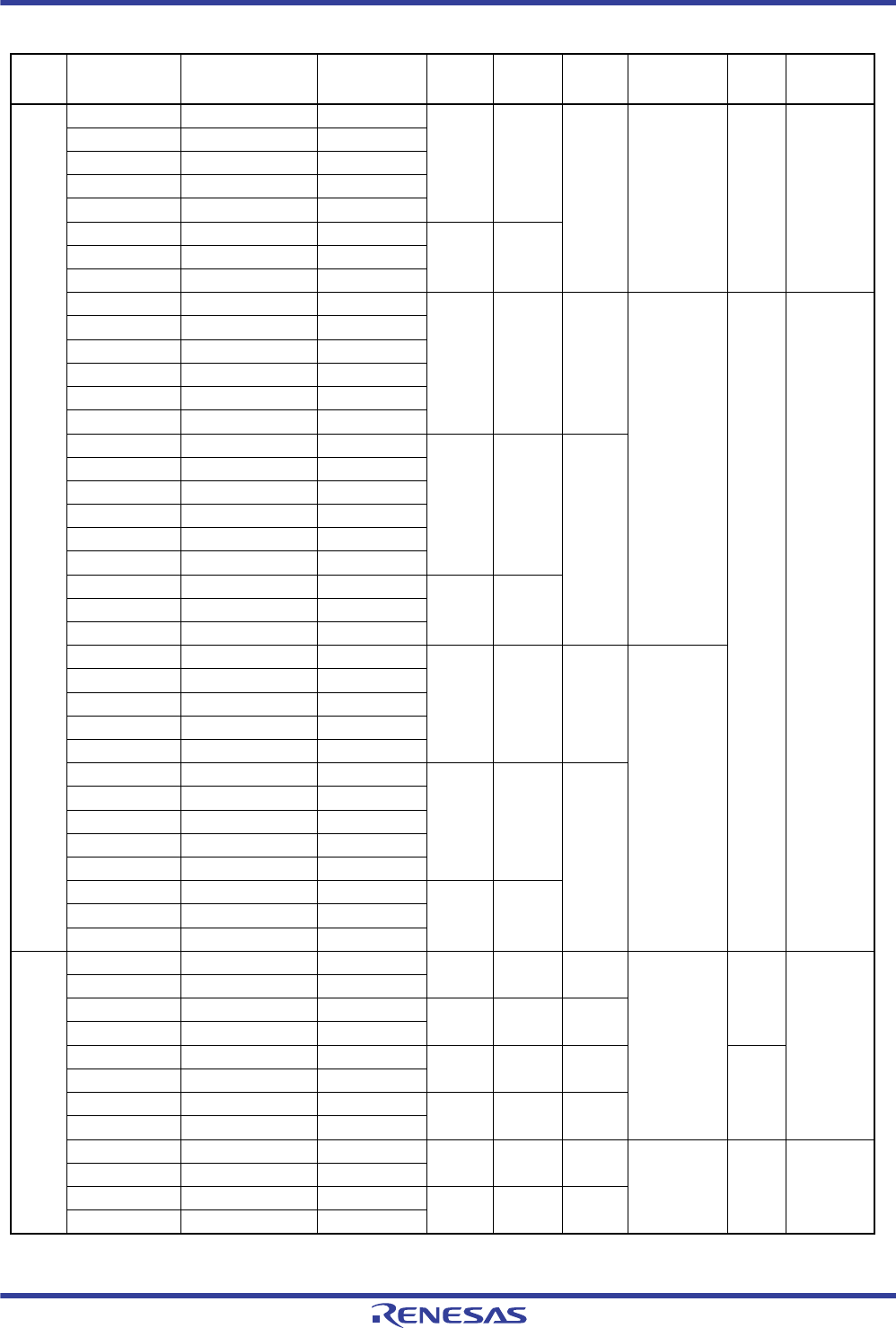
R01UH0034EJ0200 Rev.2.00 Page 45 of 1489
Dec 27, 2013
RX62T Group, RX62G Group 1. Overview
Under development Preliminary document
Specifications in this document are tentative and subject to change.
Note 1. Please contact us if you are using a G version.
RX62T R5F562T7EDFH R5F562T7EDFH#V3 PLQP0112JA-A 128
Kbytes 8
Kbytes 8
Kbytes 2.7 to 3.6 V Not
Support-
ed
-40 to +85°C
(D version)
R5F562T7EDFP R5F562T7EDFP#V3 PLQP0100KB-A
R5F562T7EDFF R5F562T7EDFF#V3 PLQP0080JA-A
R5F562T7EDFM R5F562T7EDFM#V3 PLQP0064KB-A
R5F562T7EDFK R5F562T7EDFK#V3 PLQP0064GA-A
R5F562T6EDFF R5F562T6EDFF#V3 PLQP0080JA-A 64
Kbytes 8
Kbytes
R5F562T6EDFM R5F562T6EDFM#V3 PLQP0064KB-A
R5F562T6EDFK R5F562T6EDFK#V3 PLQP0064GA-A
R5F562TAAGFH R5F562TAAGFH#V3 PLQP0112JA-A 256
Kbytes 16
Kbytes 32
Kbytes VCC/PLLVCC
4.0 to 5.5 V
AVCC/AVCC0
4.0 to 5.5 V
Support-
ed -40 to +105°C
(G version)
*1
R5F562TAAGFP R5F562TAAGFP#V3 PLQP0100KB-A
R5F562TAAGFF R5F562TAAGFF#V3 PLQP0080JA-A
R5F562TAGGFF R5F562TAGGFF#V3 PLQP0080JA-A
R5F562TAAGFM R5F562TAAGFM#V3 PLQP0064KB-A
R5F562TAAGFK R5F562TAAGFK#V3 PLQP0064GA-A
R5F562T7AGFH R5F562T7AGFH#V3 PLQP0112JA-A 128
Kbytes 8
Kbytes 8
Kbytes
R5F562T7AGFP R5F562T7AGFP#V3 PLQP0100KB-A
R5F562T7AGFF R5F562T7AGFF#V3 PLQP0080JA-A
R5F562T7GGFF R5F562T7GGFF#V3 PLQP0080JA-A
R5F562T7AGFM R5F562T7AGFM#V3 PLQP0064KB-A
R5F562T7AGFK R5F562T7AGFK#V3 PLQP0064GA-A
R5F562T6AGFF R5F562T6AGFF#V3 PLQP0080JA-A 64
Kbytes 8
Kbytes
R5F562T6AGFM R5F562T6AGFM#V3 PLQP0064KB-A
R5F562T6AGFK R5F562T6AGFK#V3 PLQP0064GA-A
R5F562TABGFH R5F562TABGFH#V3 PLQP0112JA-A 256
Kbytes 16
Kbytes 32
Kbytes VCC/PLLVCC
2.7 to 3.6 V
AVCC/AVCC0
3.0 to 3.6 V
or
4.0 to 5.5 V
R5F562TABGFP R5F562TABGFP#V3 PLQP0100KB-A
R5F562TABGFF R5F562TABGFF#V3 PLQP0080JA-A
R5F562TABGFM R5F562TABGFM#V3 PLQP0064KB-A
R5F562TABGFK R5F562TABGFK#V3 PLQP0064GA-A
R5F562T7BGFH R5F562T7BGFH#V3 PLQP0112JA-A 128
Kbytes 8
Kbytes 8
Kbytes
R5F562T7BGFP R5F562T7BGFP#V3 PLQP0100KB-A
R5F562T7BGFF R5F562T7BGFF#V3 PLQP0080JA-A
R5F562T7BGFM R5F562T7BGFM#V3 PLQP0064KB-A
R5F562T7BGFK R5F562T7BGFK#V3 PLQP0064GA-A
R5F562T6BGFF R5F562T6BGFF#V3 PLQP0080JA-A 64
Kbytes 8
Kbytes
R5F562T6BGFM R5F562T6BGFM#V3 PLQP0064KB-A
R5F562T6BGFK R5F562T6BGFK#V3 PLQP0064GA-A
RX62G R5F562GAADFH R5F562GAADFH#V3 PLQP0112JA-A 256
Kbytes 16
Kbytes 32
Kbytes VCC/PLLVCC
4.0 to 5.5 V
AVCC/AVCC0
4.0 to 5.5 V
Support-
ed -40 to +85°C
(D version)
R5F562GAADFP R5F562GAADFP#V3 PLQP0100KB-A
R5F562G7ADFH R5F562G7ADFH#V3 PLQP0112JA-A 128
Kbytes 8
Kbytes 8
Kbytes
R5F562G7ADFP R5F562G7ADFP#V3 PLQP0100KB-A
R5F562GADDFH R5F562GADDFH#V3 PLQP0112JA-A 256
Kbytes 16
Kbytes 32
Kbytes Not
Support-
ed
R5F562GADDFP R5F562GADDFP#V3 PLQP0100KB-A
R5F562G7DDFH R5F562G7DDFH#V3 PLQP0112JA-A 128
Kbytes 8
Kbytes 8
Kbytes
R5F562G7DDFP R5F562G7DDFP#V3 PLQP0100KB-A
R5F562GAAGFH R5F562GAAGFH#V3 PLQP0112JA-A 256
Kbytes 16
Kbytes 32
Kbytes VCC/PLLVCC
4.0 to 5.5 V
AVCC/AVCC0
4.0 to 5.5 V
Support-
ed -40 to +105°C
(G versio)
*1
R5F562GAAGFP R5F562GAAGFP#V3 PLQP0100KB-A
R5F562G7AGFH R5F562G7AGFH#V3 PLQP0112JA-A 128
Kbytes 8
Kbytes 8
Kbytes
R5F562G7AGFP R5F562G7AGFP#V3 PLQP0100KB-A
Table 1.3 List of Products (2 / 2)
Group Part No. Order Part No. Package ROM
Capacity RAM
Capacity
Data
Flash
Capacity Power Supply
Voltage CAN Operating
Temp. Range
R01UH0034EJ0200 Rev.2.00 Page 46 of 1489
Dec 27, 2013
RX62T Group, RX62G Group 1. Overview
Under development Preliminary document
Specifications in this document are tentative and subject to change.
Figure 1.1 How to Read the Product Part No.
Indicates the type of memory.
F: Flash memory version
Indicates the package type, number of pins, and pin pitch.
FH: LQFP112-0.65
FP: LQFP100-0.50
FF: LQFP80-0.65
FM: LQFP64-0.50
FK: LQFP64-0.80
Indicates the ROM capacity, RAM capacity, and data flash capacity.
A: 256 Kbytes/16 Kbytes/32 Kbytes
7: 128 Kbytes/8 Kbytes/8 Kbytes
6: 64 Kbytes/8 Kbytes/8 Kbytes
Indicates a group name.
2T: RX62T Group
2G: RX62G Group
Indicates a Renesas MCU.
Indicates a Renesas semiconductor product.
A: 5-V version, CAN × 1 channel
B: 3-V version, CAN × 1 channel
D: 5-V version, CAN not supported
E: 3-V version, CAN not supported
Indicates a series name (RX600 Series)
R 5 F 5 6 2 T A B D F H # V 3
Product ID code
Form of packing/External pin surface finishing (lead-free)
#V: tray/Sn (Tin) only
D: Operating temperature range (-40 to + 85°C)
G: Operating temperature range (-40 to + 105°C)
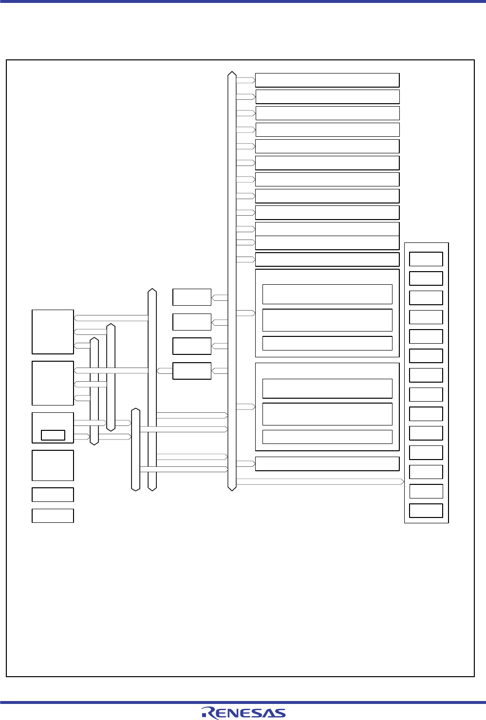
R01UH0034EJ0200 Rev.2.00 Page 47 of 1489
Dec 27, 2013
RX62T Group, RX62G Group 1. Overview
Under development Preliminary document
Specifications in this document are tentative and subject to change.
1.3 Block Diagram
Figure 1.2 shows a block diagram.
Figure 1.2 Block Diagram
ROM
RAM
DTC
POR
Internal peripheral buses 1 to 6
ICU
Port 1
Port 2
Port 3
Port 4
Port 5
Port 6
Port 7
Port 8
Port 9
Port A
Port B
Port D
Port E
Clock
generation
circuit
Internal main bus 2
Operand bus
Instruction bus
RIIC
10-bit A/D converter 12 channels
RSPI
IWDT
SCI 3 channels
MTU3
Port G
CRC
CAN (as an optional function)
POE3
CMT 2 channels (unit 0)
LIN
Notes: 1. The installation of the 10-bit A/D converter and ports 1 to G is different depending on the package.
2. For details on the internal peripheral bus configuration, see section 12, Buses.
*2
12-bit A/D converter 4 channels (unit 0)
Programmable gain amps
3 channels
Sample-and-hold circuits
for the pin section 3 channels
Window comparator 3 channels
WDT
Data flash
LVD
CAN: CAN module
LIN: LIN module
RSPI: Renesas serial peripheral interface
LVD: Voltage detection circuit
ICU: Interrupt controller
WDT: Watchdog timer
IWDT: Independent watchdog timer
CRC: CRC (cyclic redundancy check) calculator
[Legend]
POR: Power-on reset circuit
DTC: Data transfer controller
MTU3: Multi-function timer pulse unit 3
POE3: Port output enable 3
GPT: General PWM timer
CMT: Compare match timer
SCI: Serial communications interface
RIIC: I2C bus interface
MPU: Memory-Protection Unit
GPT
12-bit A/D converter 4 channels (unit 1)
Programmable gain amps
3 channels
Sample-and-hold circuits
for the pin section 3 channels
Window comparator 3 channels
CMT 2 channels (unit 1)
Internal main bus 1
*1
*1
RX CPU
MPU
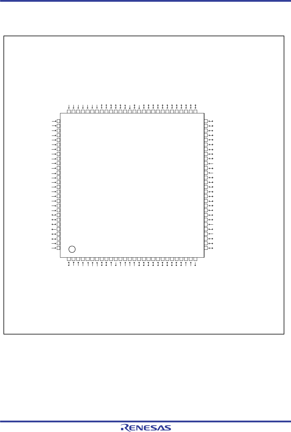
R01UH0034EJ0200 Rev.2.00 Page 48 of 1489
Dec 27, 2013
RX62T Group, RX62G Group 1. Overview
Under development Preliminary document
Specifications in this document are tentative and subject to change.
1.4 Pin Assignments
Figure 1.3 to Figure 1.7 show the pins assignments. Table 1.4 to Table 1.8 show the list of pins and pin functions.
Figure 1.3 Pin Assignment of the 112-Pin LQFP
P62/AN2
P63/AN3
P64/AN4
P65/AN5
P20/ADTRG0#-B/MTCLKB-B/IRQ7
P21/ADTRG1#-B/MTCLKA-B/IRQ6
P22/ADTRG#/CRX-B/LRX/MISO-A
P23/CTX-B/LTX/MOSI-A
P24/RSPCK-A
P30/MTIOC0B-B/MTCLKD-A/SSL0-A
P31/MTIOC0A-B/MTCLKC-A/SSL1-A
P32/MTIOC3C/MTCLKB-A/SSL2-A
P33/MTIOC3A/MTCLKA-A/SSL3-A
VSS
P70/IRQ5/POE0#
VCC
P71/MTIOC3B/GTIOC0A-A
P72/MTIOC4A/GTIOC1A-A
P73/MTIOC4B/GTIOC2A-A
P74/MTIOC3D/GTIOC0B-A
P75/MTIOC4C/GTIOC1B-A
P76/MTIOC4D/GTIOC2B-A
P80/MTIC5W/RXD2-B
P81/MTIC5V/TXD2-B
P82/MTIC5U/SCK2-B
PG0/IRQ0-C/TRSYNC
PG1/IRQ1-C/TRDATA0
PG2/IRQ2-B/TRDATA1
84
83
82
81
80
79
78
77
76
75
74
73
72
71
70
69
68
67
66
65
64
63
62
61
60
59
58
57
AVSS
56 PG3/TRDATA2
VREF
55 PG4/TRDATA3
AVCC
54 PG5/TRCLK
P61/AN1
53 P90/MTIOC7D
P60/AN0
52 P91/MTIOC7C
P55/AN11
51 P92/MTIOC6D
P54/AN10
50 P93/MTIOC7B
P53/AN9
49 P94/MTIOC7A
P52/AN8
48 P95/MTIOC6B
P51/AN7
47 VSS
P50/AN6
46 P96/IRQ4/POE4#
P47/AN103/CVREFH
45 VCC
P46/AN102
44 PA0/MTIOC6C/SSL3-B
P45/AN101
43 PA1/MTIOC6A/SSL2-B
P44/AN100
42 PA2/MTIOC2B/SSL1-B
AVCC0
41 PA3/MTIOC2A/SSL0-B
VREFH0
40 PA4/ADTRG0#-A/MTIOC1B/RSPCK-B
P43/AN003/CVREFL
39 PA5/ADTRG1#-A/MTIOC1A/MISO-B
P42/AN002
38 PB0/MTIOC0D/MOSI-B
P41/AN001
37 PB1/MTIOC0C/RXD0/SCL
P40/AN000
36 PB2/MTIOC0B-A/TXD0/SDA
VREFL0
35 PB3/MTIOC0A-A/SCK0
AVSS0
34 PLLVSS
WDTOVF# 33 PB4/GTETRG/IRQ3/POE8#
P11/MTCLKC-B/IRQ1-A 32 PLLVCC
P10/MTCLKD-B/IRQ0-A 31 PB5/CTX-A/TXD2-A
TRST# 30 PB6/CRX-A/RXD2-A
TMS 29 PB7/SCK2-A
PE5/IRQ0-B
EMLE
VSS
MDE
VCL
MD1
MD0
PE4/MTCLKC-C/IRQ1-B/POE10#-B
PE3/MTCLKD-C/IRQ2-A/POE11#
RES#
XTAL
VSS
EXTAL
VCC
PE2/NMI/POE10#-A
PE1/SSL3-C
PE0/CRX-C/SSL2-C
PD7/GTIOC0A-B/CTX-C/SSL1-C
PD6/GTIOC0B-B/SSL0-C
PD5/GTIOC1A-B/RXD1
PD4/GTIOC1B-B/SCK1
PD3/GTIOC2A-B/TXD1
PD2/GTIOC2B-B/MOSI-C
PD1/GTIOC3A/MISO-C
PD0/GTIOC3B/RSPCK-C
TDI
TCK
TDO
112
110
111
102
103
104
90
91
92
89
86
87
88
18
14
85
27
98
99
100
28
26
RX62T Group
PLQP0112JA-A
(112-pin LQFP)
(Top view)
106
107
108
109
105
101
97
93
94
95
96
1
2
7
8
3
4
5
6
10
11
9
17
15
13
12
16
19
25
24
22
23
20
21
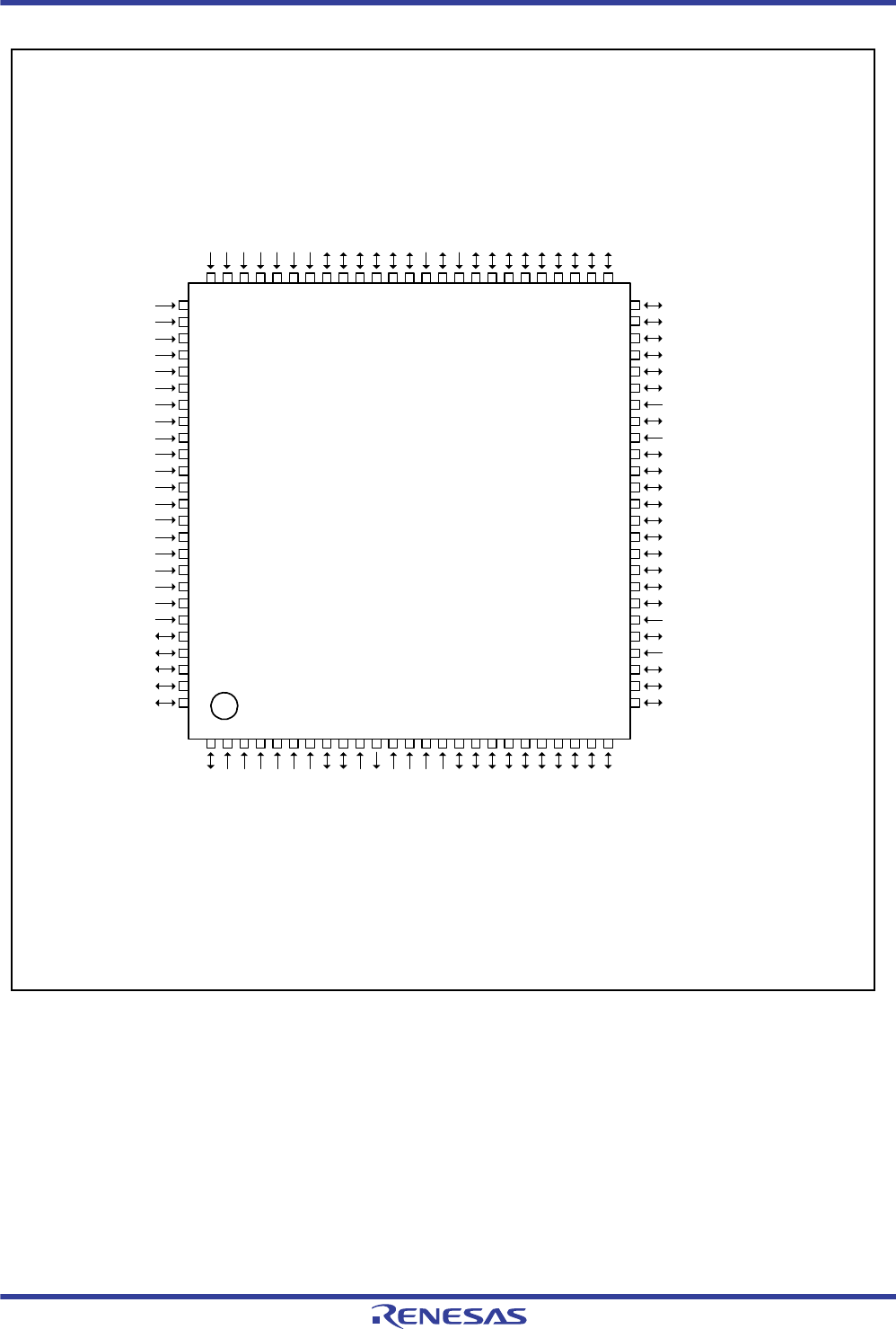
R01UH0034EJ0200 Rev.2.00 Page 49 of 1489
Dec 27, 2013
RX62T Group, RX62G Group 1. Overview
Under development Preliminary document
Specifications in this document are tentative and subject to change.
Figure 1.4 Pin Assignment of the 100-Pin LQFP
PA0/MTIOC6C/SSL3-B
1
2
3
4
5
6
7
8
9
10
11
12
13
14
15
16
17
18
19
20
21
22
23
24
25
75
74
73
72
71
70
69
68
67
66
65
64
63
62
61
60
59
58
57
56
55
54
53
52
51
50
49
48
47
46
45
44
43
42
41
40
39
38
37
36
35
34
33
32
31
30
29
28
27
26
76
77
78
79
80
81
82
83
84
85
86
87
88
89
90
91
92
93
94
95
96
97
98
99
100
P62/AN2
P63/AN3
P64/AN4
P65/AN5
P20/ADTRG0#-B/MTCLKB-B/IRQ7
P21/ADTRG1#-B/MTCLKA-B/IRQ6
P22/ADTRG#/CRX-B/LRX/MISO-A
P23/CTX-B/LTX/MOSI-A
P24/RSPCK-A
P30/MTIOC0B-B/MTCLKD-A/SSL0-A
P31/MTIOC0A-B/MTCLKC-A/SSL1-A
P32/MTIOC3C/MTCLKB-A/SSL2-A
P33/MTIOC3A/MTCLKA-A/SSL3-A
VSS
P70/IRQ5/POE0#
VCC
P71/MTIOC3B/GTIOC0A-A
P72/MTIOC4A/GTIOC1A-A
P73/MTIOC4B/GTIOC2A-A
P74/MTIOC3D/GTIOC0B-A
P75/MTIOC4C/GTIOC1B-A
P76/MTIOC4D/GTIOC2B-A
P80/MTIC5W/RXD2-B
P81/MTIC5V/TXD2-B
P82/MTIC5U/SCK2-B
AVCC
P90/MTIOC7D
VREF
P91/MTIOC7C
AVSS
P92/MTIOC6D
P61/AN1
P93/MTIOC7B
P60/AN0
P94/MTIOC7A
P55/AN11
P95/MTIOC6B
P54/AN10
VSS
P53/AN9
P96/IRQ4/POE4#
P52/AN8
VCC
P51/AN7
P50/AN6
PA1/MTIOC6A/SSL2-B
P47/AN103/CVREFH
PA2/MTIOC2B/SSL1-B
P46/AN102
PA3/MTIOC2A/SSL0-B
P45/AN101
PA4/ADTRG0#-A/MTIOC1B/RSPCK-B
P44/AN100
PA5/ADTRG1#-A/MTIOC1A/MISO-B
AVCC0
PB0/MTIOC0D/MOSI-B
VREFH0
PB1/MTIOC0C/RXD0/SCL
P43/AN003/CVREFL
PB2/MTIOC0B-A/TXD0/SDA
P42/AN002
PB3/MTIOC0A-A/SCK0
P41/AN001
PLLVSS
P40/AN000
PB4/GTETRG/IRQ3/POE8#
VREFL0
PLLVCC
AVSS0
PB5/CTX-A/TXD2-A/TRSYNC
P11/MTCLKC-B/IRQ1-A PB6/CRX-A/RXD2-A/TRDATA0
P10/MTCLKD-B/IRQ0-A PB7/SCK2-A/TRDATA1
PE5/IRQ0-B
EMLE
VSS
MDE
VCL
MD1
MD0
PE4/MTCLKC-C/IRQ1-B/POE10#-B
PE3/MTCLKD-C/IRQ2-A/POE11#
RES#
XTAL
VSS
EXTAL
VCC
PE2/NMI/POE10#-A
PE1/SSL3-C
PE0/CRX-C/SSL2-C
PD7/GTIOC0A-B/CTX-C/SSL1-C/TRST#
PD6/GTIOC0B-B/SSL0-C/TMS
PD5/GTIOC1A-B/RXD1/TDI
PD4/GTIOC1B-B/SCK1/TCK
PD3/GTIOC2A-B/TXD1/TDO
PD2/GTIOC2B-B/MOSI-C/TRCLK
PD1/GTIOC3A/MISO-C/TRDATA3
PD0/GTIOC3B/RSPCK-C/TRDATA2
RX62T Group
PLQP0100KB-A
(100-pin LQFP)
(Top view)
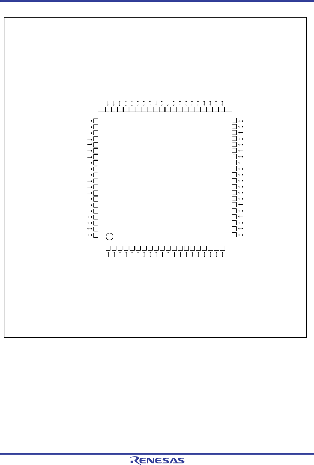
R01UH0034EJ0200 Rev.2.00 Page 50 of 1489
Dec 27, 2013
RX62T Group, RX62G Group 1. Overview
Under development Preliminary document
Specifications in this document are tentative and subject to change.
Figure 1.5 Pin Assignment of the 80-Pin LQFP
P62/AN2
P63/AN3
P20/ADTRG0#-B/MTCLKB-B/IRQ7
P21/ADTRG1#-B/MTCLKA-B/IRQ6
P22/ADTRG#/CRX-B/LRX/MISO-A
P23/CTX-B/LTX/MOSI-A
P24/RSPCK-A
P30/MTIOC0B-B/MTCLKD-A/SSL0-A
P31/MTIOC0A-B/MTCLKC-A/SSL1-A
VSS
P32/MTIOC3C/MTCLKB-A/SSL2-A
VCC
P33/MTIOC3A/MTCLKA-A/SSL3-A
P70/IRQ5/POE0#
P71/MTIOC3B/GTIOC0A-A
P72/MTIOC4A/GTIOC1A-A
P73/MTIOC4B/GTIOC2A-A
P74/MTIOC3D/GTIOC0B-A
P75/MTIOC4C/GTIOC1B-A
P76/MTIOC4D/GTIOC2B-A
60
59
58
57
56
55
54
53
52
51
50
49
48
47
46
45
44
43
42
41
AVSS
40 P91/MTIOC7C
AVCC
39 P92/MTIOC6D
P61/AN1 38 P93/MTIOC7B
P60/AN0 37 P94/MTIOC7A
P47/AN103/CVREFH 36 P95/MTIOC6B
P46/AN102 35 VSS
P45/AN101 34 P96/IRQ4/POE4#
P44/AN100 33 VCC
AVCC0
32 PA2/MTIOC2B/SSL1-B
VREFH0
31 PA3/MTIOC2A/SSL0-B
P43/AN003/CVREFL
30 PB0/MTIOC0D/MOSI-B
P42/AN002
29 PB1/MTIOC0C/RXD0/SCL
P41/AN001
28 PB2/MTIOC0B-A/TXD0/SDA
P40/AN000
27 PB3/MTIOC0A-A/SCK0
VREFL0 26 PLLVSS
AVSS0 25 PB4/GTETRG/IRQ3/POE8#
P11/MTCLKC-B/IRQ1-A 24 PLLVCC
P10/MTCLKD-B/IRQ0-A 23 PB5/CTX-A/TxD2-A
PA5/ADTRG1#-A/MTIOC1A/MISO-B 22 PB6/CRX-A/RXD2-A
PA4/ADTRG0#-A/MTIOC1B/RSPCK-B 21 PB7/SCK2-A
1
2
3
4
5
6
7
8
9
10
11
12
13
14
15
16
17
18
19
20
EMLE
VSS
MDE
VCL
MD1
MD0
PE4/MTCLKC-C/IRQ1-B/POE10#-B
PE3/MTCLKD-C/IRQ2-A/POE11#
RES#
XTAL
VSS
EXTAL
VCC
PE2/NMI/POE10#-A
PE0/CRX-C
PD7/GTIOC0A-B/CTX-C/TRST#
PD6/GTIOC0B-B/TMS
PD5/GTIOC1A-B/RXD1/TDI
PD4/GTIOC1B-B/SCK1/TCK
PD3/GTIOC2A-B/TXD1/TDO
77
73
74
75
76
68
69
80
78
79
72
63
70
71
67
65
66
62
61
64
RX62T Group
PLQP0080JA-A
(80-pin LQFP)
(Top view)
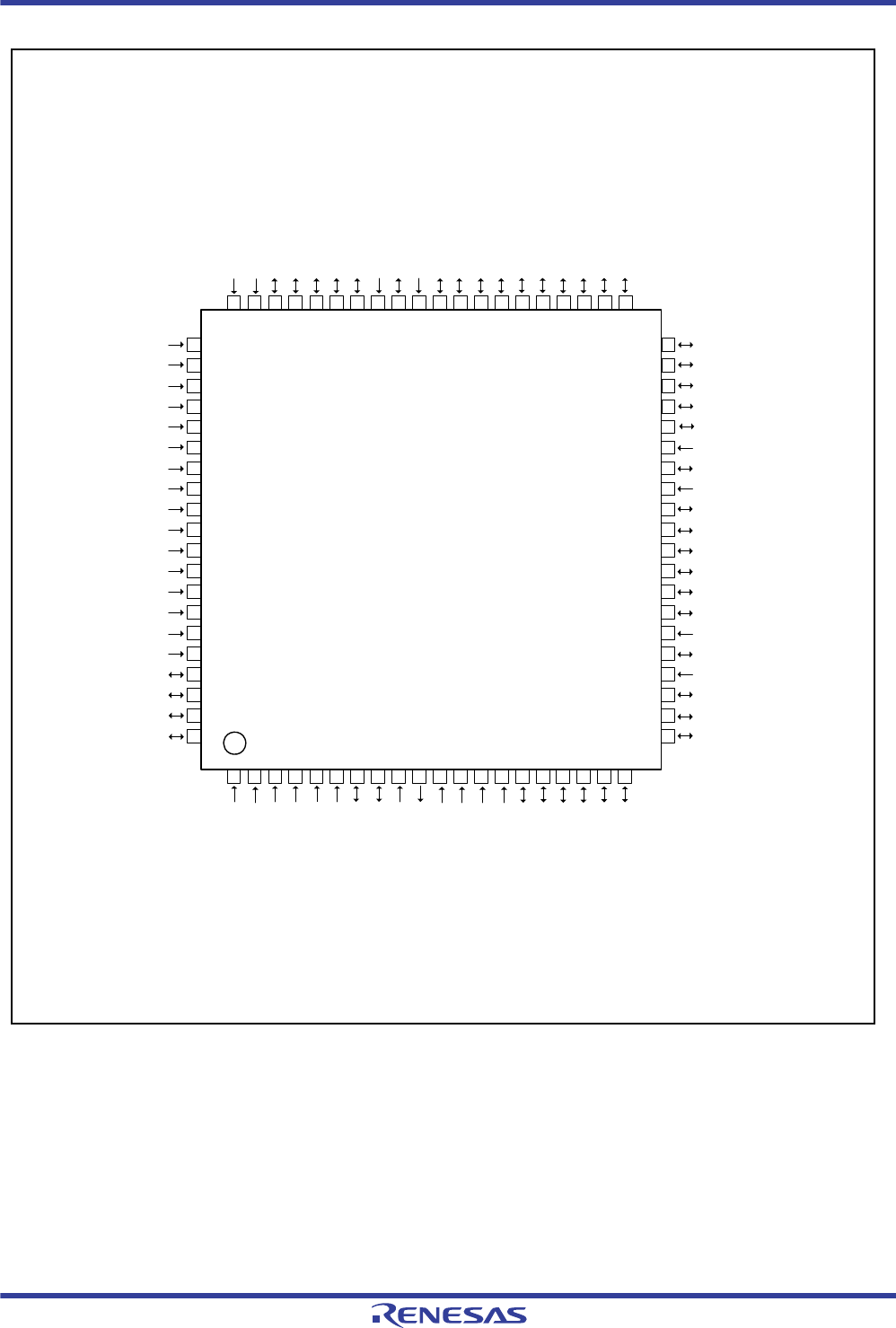
R01UH0034EJ0200 Rev.2.00 Page 51 of 1489
Dec 27, 2013
RX62T Group, RX62G Group 1. Overview
Under development Preliminary document
Specifications in this document are tentative and subject to change.
Figure 1.6 Pin Assignment of the 80-Pin LQFP (Two-Motor Control Supported Version)
P22/ADTRG#/CRX-B/LRX/MISO-A
P23/CTX-B/LTX/MOSI-A
P24/RSPCK-A
P30/MTIOC0B-B/MTCLKD-A/SSL0-A
P31/MTIOC0A-B/MTCLKC-A/SSL1-A
P32/MTIOC3C/MTCLKB-A/SSL2-A
P33/MTIOC3A/MTCLKA-A/SSL3-A
VSS
P70/IRQ5/POE0#
VCC
P71/MTIOC3B/GTIOC0A-A
P72/MTIOC4A/GTIOC1A-A
P73/MTIOC4B/GTIOC2A-A
P74/MTIOC3D/GTIOC0B-A
P75/MTIOC4C/GTIOC1B-A
P76/MTIOC4D/GTIOC2B-A
60
59
58
57
56
55
54
53
52
51
50
49
48
47
46
45
P47/AN103/CVREFH 36
P46/AN102 35
P45/AN101 34
P44/AN100 33
AVCC0
32
P96/IRQ4/POE4#
VREFH0
31
PA3/MTIOC2A
P43/AN003/CVREFL
30 PB0/MTIOC0D
P42/AN002
29 PB1/MTIOC0C/RXD0/SCL
P41/AN001
28 PB2/MTIOC0B-A/TXD0/SDA
P40/AN000
27 PB3/MTIOC0A-A/SCK0
VREFL0 26
PB4/GTETRG/IRQ3/POE8#
AVSS0 25
P82/MTIC5U/SCK2-B 24
PLLVSS
P10/MTCLKD-B/IRQ0-A
23
PA5/ADTRG1#-A/MTIOC1A
22
PLLVCC
21 PB7/SCK2-A
1
2
3
4
5
6
7
8
9
10
11
12
13
14
15
16
EMLE
MDE
VCL
MD1
MD0
RES#
XTAL
VSS
EXTAL
VCC
PE2/NMI/POE10#-A
PD7/GTIOC0A-B/TRST#
70
71
67
65
66
68
69
72
73
74
75
76
77
79
80
78
RX62T Group
PLQP0080JA-A
(R5F562TAGDFF,
R5F562T7GDFF)
(Top view)
17
18
19
20
PD6/GTIOC0B-B/TMS
PD5/GTIOC1A-B/RXD1/TDI
PD4/GTIOC1B-B/SCK1/TCK
PD3/GTIOC2A-B/TXD1/TDO
40 P91/MTIOC7C
39 P92/MTIOC6D
38 P93/MTIOC7B
37 P94/MTIOC7A
44
43
42
41
AN3
AN2
AN1
AN0
63
61
62
64
PE4/MTCLKC-C/IRQ1-B/POE10#-B
PE3/MTCLKD-C/IRQ2-A/POE11#
VSS
PD2/GTIOC2B-B
PB6/CRX-A/RXD2-A
PB5/CTX-A/TXD2-A
VSS
VCC
P95/MTIOC6B
P90/MTIOC7D
P20/ADTRG0#-B/MTCLKB-B/IRQ7
AVSS
AVCC
P81/MTIC5V/TXD2-B
P80/MTIC5W/RXD2-B
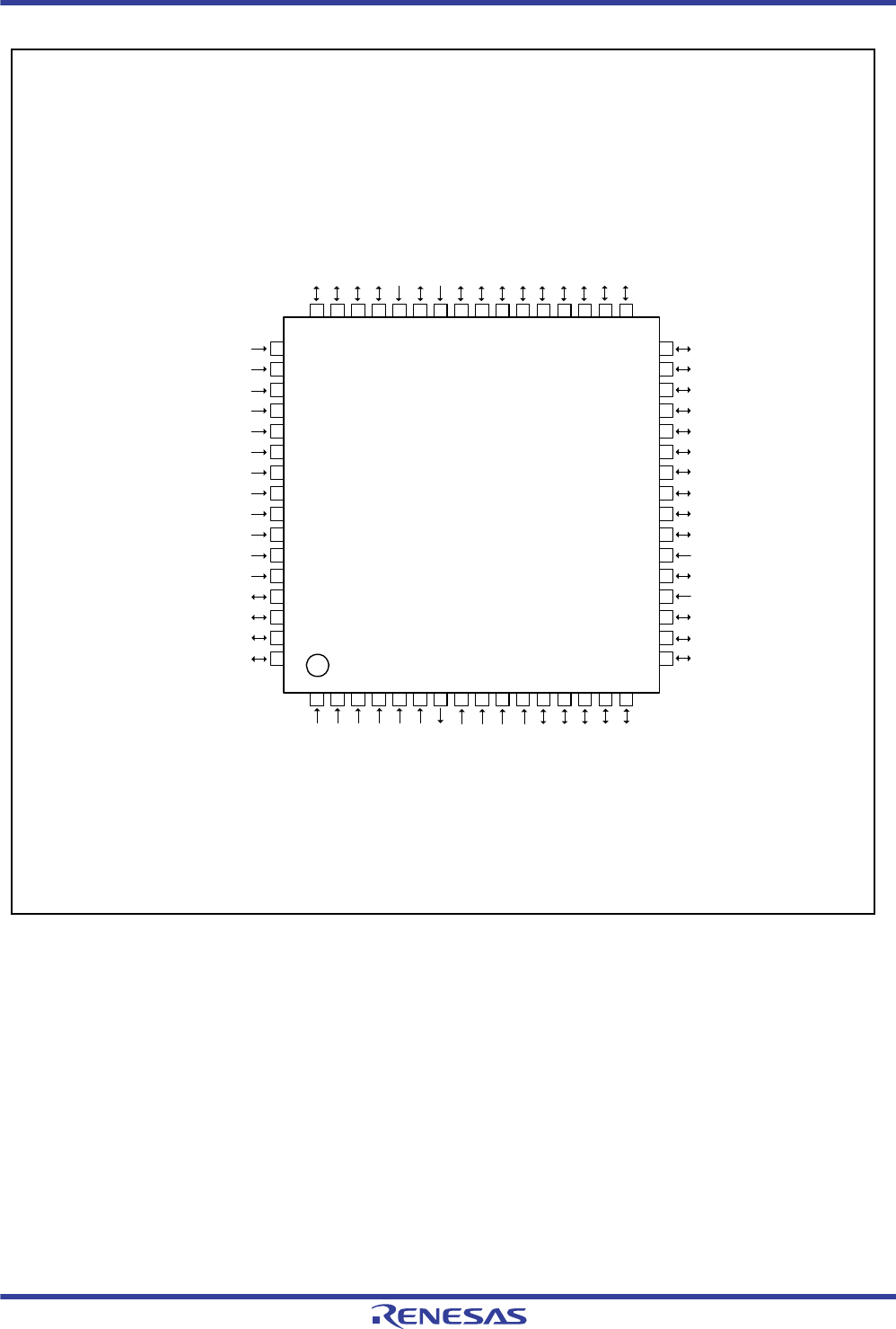
R01UH0034EJ0200 Rev.2.00 Page 52 of 1489
Dec 27, 2013
RX62T Group, RX62G Group 1. Overview
Under development Preliminary document
Specifications in this document are tentative and subject to change.
Figure 1.7 Pin Assignment of the 64-Pin LQFP
P22/CRX-B/LRX/MISO-A
P23/CTX-B/LTX/MOSI-A
P24/RSPCK-A
P30/MTIOC0B-B/MTCLKD-A/SSL0-A
P31/MTIOC0A-B/MTCLKC-A/SSL1-A
P32/MTIOC3C/MTCLKB-A/SSL2-A
P33/MTIOC3A/MTCLKA-A/SSL3-A
VSS
P70/IRQ5/POE0#
VCC
P71/MTIOC3B/GTIOC0A-A
P72/MTIOC4A/GTIOC1A-A
P73/MTIOC4B/GTIOC2A-A
P74/MTIOC3D/GTIOC0B-A
P75/MTIOC4C/GTIOC1B-A
P76/MTIOC4D/GTIOC2B-A
48
47
46
45
44
43
42
41
40
39
38
37
36
35
34
33
P47/AN103/CVREFH 32 P91/MTIOC7C
P46/AN102 31 P92/MTIOC6D
P45/AN101 30 P93/MTIOC7B
P44/AN100 29 P94/MTIOC7A
AVCC0
28 PA2/MTIOC2B/SSL1-B
VREFH0
27 PA3/MTIOC2A/SSL0-B
P43/AN003/CVREFL
26 PB0/MTIOC0D/MOSI-B
P42/AN002
25 PB1/MTIOC0C/RXD0/SCL
P41/AN001
24 PB2/MTIOC0B-A/TXD0/SDA
P40/AN000
23 PB3/MTIOC0A-A/SCK0
VREFL0 22
PB4/GTETRG/IRQ3/POE8#AVSS0 21
PB5/CTX-A/TXD2-A
P11/MTCLKC-B/IRQ1-A 20
PLLVSS
P10/MTCLKD-B/IRQ0-A 19
PB6/CRX-A/RXD2-A
PA5/ADTRG1#-A/MTIOC1A/MISO-B 18
PLLVCC
PA4/ADTRG0#-A/MTIOC1B/RSPCK-B 17 PB7/SCK2-A
1
2
3
4
5
6
7
8
9
10
11
12
13
14
15
16
EMLE
MDE
VCL
MD1
MD0
RES#
XTAL
VSS
EXTAL
VCC
PE2/NMI/POE10#-A
PD7/GTIOC0A-B/TRST#
PD6/GTIOC0B-B/TMS
PD5/GTIOC1A-B/RXD1/TDI
PD4/GTIOC1B-B/SCK1/TCK
PD3/GTIOC2A-B/TXD1/TDO
54
55
51
49
50
52
53
56
57
58
59
60
61
63
64
62
RX62T Group
PLQP0064GA-A
PLQP0064KB-A
(64-pin LQFP)
(Top view)

R01UH0034EJ0200 Rev.2.00 Page 53 of 1489
Dec 27, 2013
RX62T Group, RX62G Group 1. Overview
Under development Preliminary document
Specifications in this document are tentative and subject to change.
Table 1.4 List of Pins and Pin Functions (112-Pin LQFP) (1 / 3)
Pin No.
(112-Pin
LQFP)
Power Supply
Clock
System Control I/O Port Analog Timer Communi-
cation Interrupt POE Debugging
1 PE5 IRQ0-B
2 EMLE
3 VSS
4 MDE
5 VCL
6 MD1
7 MD0
8 PE4 MTCLKC-C IRQ1-B POE10#-B
9 PE3 MTCLKD-C IRQ2-A POE11#
10 RES#
11 XTAL
12 VSS
13 EXTAL
14 VCC
15 PE2 NMI POE10#-A
16 PE1 SSL3-C
17 PE0 CRX-C/ SSL2-C
18 PD7 GTIOC0A-B CTX-C/ SSL1-C
19 PD6 GTIOC0B-B SSL0-C
20 PD5 GTIOC1A-B RXD1
21 PD4 GTIOC1B-B SCK1
22 PD3 GTIOC2A-B TXD1
23 PD2 GTIOC2B-B MOSI-C
24 PD1 GTIOC3A MISO-C
25 PD0 GTIOC3B RSPCK-C
26 TDI
27 TCK
28 TDO
29 PB7 SCK2-A
30 PB6 CRX-A/ RXD2-A
31 PB5 CTX-A/ TXD2-A
32 PLLVCC
33 PB4 GTETRG IRQ3 POE8#
34 PLLVSS
35 PB3 MTIOC0A-A SCK0
36 PB2 MTIOC0B-A TXD0/SDA
37 PB1 MTIOC0C RXD0/SCL
38 PB0 MTIOC0D MOSI-B
39 PA5 ADTRG1#-A MTIOC1A MISO-B
40 PA4 ADTRG0#-A MTIOC1B RSPCK-B
41 PA3 MTIOC2A SSL0-B
42 PA2 MTIOC2B SSL1-B
43 PA1 MTIOC6A SSL2-B

R01UH0034EJ0200 Rev.2.00 Page 54 of 1489
Dec 27, 2013
RX62T Group, RX62G Group 1. Overview
Under development Preliminary document
Specifications in this document are tentative and subject to change.
44 PA0 MTIOC6C SSL3-B
45 VCC
46 P96 IRQ4 POE4#
47 VSS
48 P95 MTIOC6B
49 P94 MTIOC7A
50 P93 MTIOC7B
51 P92 MTIOC6D
52 P91 MTIOC7C
53 P90 MTIOC7D
54 PG5 TRCLK
55 PG4 TRDATA3
56 PG3 TRDATA2
57 PG2 IRQ2-B TRDATA1
58 PG1 IRQ1-C TRDATA0
59 PG0 IRQ0-C TRSYNC
60 P76 MTIOC4D/
GTIOC2B-A
61 P75 MTIOC4C/
GTIOC1B-A
62 P74 MTIOC3D/
GTIOC0B-A
63 P73 MTIOC4B/
GTIOC2A-A
64 P72 MTIOC4A/
GTIOC1A-A
65 P71 MTIOC3B/
GTIOC0A-A
66 P70 IRQ5 POE0#
67 P33 MTIOC3A/
MTCLKA-A
SSL3-A
68 P32 MTIOC3C/
MTCLKB-A
SSL2-A
69 VCC
70 P31 MTIOC0A-B/
MTCLKC-A
SSL1-A
71 VSS
72 P30 MTIOC0B-B/
MTCLKD-A
SSL0-A
73 P24 RSPCK-A
74 P23 CTX-B/ LTX/
MOSI-A
75 P22 ADTRG# CRX-B/ LRX/
MISO-A
76 P21 ADTRG1#-B MTCLKA-B IRQ6
77 P20 ADTRG0#-B MTCLKB-B IRQ7
78 P65 AN5
79 P64 AN4
Table 1.4 List of Pins and Pin Functions (112-Pin LQFP) (2 / 3)
Pin No.
(112-Pin
LQFP)
Power Supply
Clock
System Control I/O Port Analog Timer Communi-
cation Interrupt POE Debugging

R01UH0034EJ0200 Rev.2.00 Page 55 of 1489
Dec 27, 2013
RX62T Group, RX62G Group 1. Overview
Under development Preliminary document
Specifications in this document are tentative and subject to change.
80 AVCC
81 VREF
82 AVSS
83 P63 AN3
84 P62 AN2
85 P61 AN1
86 P60 AN0
87 P55 AN11
88 P54 AN10
89 P53 AN9
90 P52 AN8
91 P51 AN7
92 P50 AN6
93 P47 AN103/
CVREFH
94 P46 AN102
95 P45 AN101
96 P44 AN100
97 P43 AN003/
CVREFL
98 P42 AN002
99 P41 AN001
100 P40 AN000
101 AVCC0
102 VREFH0
103 VREFL0
104 AVSS0
105 P82 MTIC5U SCK2-B
106 P81 MTIC5V TXD2-B
107 P80 MTIC5W RXD2-B
108 WDTOVF#
109 P11 MTCLKC-B IRQ1-A
110 P10 MTCLKD-B IRQ0-A
111 TRST#
112 TMS
Table 1.4 List of Pins and Pin Functions (112-Pin LQFP) (3 / 3)
Pin No.
(112-Pin
LQFP)
Power Supply
Clock
System Control I/O Port Analog Timer Communi-
cation Interrupt POE Debugging

R01UH0034EJ0200 Rev.2.00 Page 56 of 1489
Dec 27, 2013
RX62T Group, RX62G Group 1. Overview
Under development Preliminary document
Specifications in this document are tentative and subject to change.
Table 1.5 List of Pins and Pin Functions (100-Pin LQFP) (1 / 3)
Pin No.
(80-Pin
LQFP)
Power Supply
Clock
System Control I/O Port Analog Timer Communi-
cation Interrupt POE Debugging
1 PE5 IRQ0-B
2 EMLE
3 VSS
4 MDE
5 VCL
6 MD1
7 MD0
8 PE4 MTCLKC-C IRQ1-B POE10#-B
9 PE3 MTCLKD-C IRQ2-A POE11#
10 RES#
11 XTAL
12 VSS
13 EXTAL
14 VCC
15 PE2 NMI POE10#-A
16 PE1 SSL3-C
17 PE0 CRX-C/ SSL2-
C
18 PD7 GTIOC0A-B CTX-C/ SSL1-C TRST#
19 PD6 GTIOC0B-B SSL0-C TMS
20 PD5 GTIOC1A-B RXD1 TDI
21 PD4 GTIOC1B-B SCK1 TCK
22 PD3 GTIOC2A-B TXD1 TDO
23 PD2 GTIOC2B-B MOSI-C TRCLK
24 PD1 GTIOC3A MISO-C TRDATA3
25 PD0 GTIOC3B RSPCK-C TRDATA2
26 PB7 SCK2-A TRDATA1
27 PB6 CRX-A/ RXD2-
A
TRDATA0
28 PB5 CTX-A/ TXD2-A TRSYNC
29 PLLVCC
30 PB4 GTETRG IRQ3 POE8#
31 PLLVSS
32 PB3 MTIOC0A-A SCK0
33 PB2 MTIOC0B-A TXD0/SDA
34 PB1 MTIOC0C RXD0/SCL
35 PB0 MTIOC0D MOSI-B
36 PA5 ADTRG1#-A MTIOC1A MISO-B
37 PA4 ADTRG0#-A MTIOC1B RSPCK-B
38 PA3 MTIOC2A SSL0-B
39 PA2 MTIOC2B SSL1-B
40 PA1 MTIOC6A SSL2-B

R01UH0034EJ0200 Rev.2.00 Page 57 of 1489
Dec 27, 2013
RX62T Group, RX62G Group 1. Overview
Under development Preliminary document
Specifications in this document are tentative and subject to change.
41 PA0 MTIOC6C SSL3-B
42 VCC
43 P96 IRQ4 POE4#
44 VSS
45 P95 MTIOC6B
46 P94 MTIOC7A
47 P93 MTIOC7B
48 P92 MTIOC6D
49 P91 MTIOC7C
50 P90 MTIOC7D
51 P76 MTIOC4D/
GTIOC2B-A
52 P75 MTIOC4C/
GTIOC1B-A
53 P74 MTIOC3D/
GTIOC0B-A
54 P73 MTIOC4B/
GTIOC2A-A
55 P72 MTIOC4A/
GTIOC1A-A
56 P71 MTIOC3B/
GTIOC0A-A
57 P70 IRQ5 POE0#
58 P33 MTIOC3A/
MTCLKA-A
SSL3-A
59 P32 MTIOC3C/
MTCLKB-A
SSL2-A
60 VCC
61 P31 MTIOC0A-B/
MTCLKC-A
SSL1-A
62 VSS
63 P30 MTIOC0B-B/
MTCLKD-A
SSL0-A
64 P24 RSPCK-A
65 P23 CTX-B/ LTX/
MOSI-A
66 P22 ADTRG# CRX-B/ LRX/
MISO-A
67 P21 ADTRG1#-B MTCLKA-B IRQ6
68 P20 ADTRG0#-B MTCLKB-B IRQ7
69 P65 AN5
70 P64 AN4
71 AVCC
72 VREF
73 AVSS
74 P63 AN3
75 P62 AN2
76 P61 AN1
Table 1.5 List of Pins and Pin Functions (100-Pin LQFP) (2 / 3)
Pin No.
(80-Pin
LQFP)
Power Supply
Clock
System Control I/O Port Analog Timer Communi-
cation Interrupt POE Debugging

R01UH0034EJ0200 Rev.2.00 Page 58 of 1489
Dec 27, 2013
RX62T Group, RX62G Group 1. Overview
Under development Preliminary document
Specifications in this document are tentative and subject to change.
77 P60 AN0
78 P55 AN11
79 P54 AN10
80 P53 AN9
81 P52 AN8
82 P51 AN7
83 P50 AN6
84 P47 AN103/
CVREFH
85 P46 AN102
86 P45 AN101
87 P44 AN100
88 P43 AN003/
CVREFL
89 P42 AN002
90 P41 AN001
91 P40 AN000
92 AVCC0
93 VREFH0
94 VREFL0
95 AVSS0
96 P82 MTIC5U SCK2-B
97 P81 MTIC5V TXD2-B
98 P80 MTIC5W RXD2-B
99 P11 MTCLKC-B IRQ1-A
100 P10 MTCLKD-B IRQ0-A
Table 1.5 List of Pins and Pin Functions (100-Pin LQFP) (3 / 3)
Pin No.
(80-Pin
LQFP)
Power Supply
Clock
System Control I/O Port Analog Timer Communi-
cation Interrupt POE Debugging

R01UH0034EJ0200 Rev.2.00 Page 59 of 1489
Dec 27, 2013
RX62T Group, RX62G Group 1. Overview
Under development Preliminary document
Specifications in this document are tentative and subject to change.
Table 1.6 List of Pins and Pin Functions (80-Pin LQFP) (1 / 3)
Pin No.
(80-Pin
LQFP)
Power Supply
Clock
System Control I/O Port Analog Timer Communi-
cation Interrupt POE Debugging
1 EMLE
2 VSS
3 MDE
4 VCL
5 MD1
6 MD0
7 PE4 MTCLKC-C IRQ1-B POE10#-B
8 PE3 MTCLKD-C IRQ2-A POE11#
9 RES#
10 XTAL
11 VSS
12 EXTAL
13 VCC
14 PE2 NMI POE10#-A
15 PE0 CRX-C
16 PD7 GTIOC0A-B CTX-C TRST#
17 PD6 GTIOC0B-B TMS
18 PD5 GTIOC1A-B RXD1 TDI
19 PD4 GTIOC1B-B SCK1 TCK
20 PD3 GTIOC2A-B TXD1 TDO
21 PB7 SCK2-A
22 PB6 CRX-A/
RXD2-A
23 PB5 CTX-A/
TXD2-A
24 PLLVCC
25 PB4 GTETRG IRQ3 POE8#
26 PLLVSS
27 PB3 MTIOC0A-A SCK0
28 PB2 MTIOC0B-A TXD0/SDA
29 PB1 MTIOC0C RXD0/SCL
30 PB0 MTIOC0D MOSI-B
31 PA3 MTIOC2A SSL0-B
32 PA2 MTIOC2B SSL1-B
33 VCC
34 P96 IRQ4 POE4#
35 VSS
36 P95 MTIOC6B
37 P94 MTIOC7A
38 P93 MTIOC7B
39 P92 MTIOC6D
40 P91 MTIOC7C
41 P76 MTIOC4D/
GTIOC2B-A

R01UH0034EJ0200 Rev.2.00 Page 60 of 1489
Dec 27, 2013
RX62T Group, RX62G Group 1. Overview
Under development Preliminary document
Specifications in this document are tentative and subject to change.
42 P75 MTIOC4C/
GTIOC1B-A
43 P74 MTIOC3D/
GTIOC0B-A
44 P73 MTIOC4B/
GTIOC2A-A
45 P72 MTIOC4A/
GTIOC1A-A
46 P71 MTIOC3B/
GTIOC0A-A
47 P70 IRQ5 POE0#
48 P33 MTIOC3A/
MTCLKA-A
SSL3-A
49 P32 MTIOC3C/
MTCLKB-A
SSL2-A
50 VCC
51 P31 MTIOC0A-B/
MTCLKC-A
SSL1-A
52 VSS
53 P30 MTIOC0B-B/
MTCLKD-A
SSL0-A
54 P24 RSPCK-A
55 P23 CTX-B/
LTX/
MOSI-A
56 P22 ADTRG# CRX-B/
LRX/
MISO-A
57 P21 ADTRG1#-B MTCLKA-B IRQ6
58 P20 ADTRG0#-B MTCLKB-B IRQ7
59 AVCC
60 AVSS
61 P63 AN3
62 P62 AN2
63 P61 AN1
64 P60 AN0
65 P47 AN103/
CVREFH
66 P46 AN102
67 P45 AN101
68 P44 AN100
69 P43 AN003/
CVREFL
70 P42 AN002
71 P41 AN001
72 P40 AN000
73 AVCC0
74 VREFH0
75 VREFL0
Table 1.6 List of Pins and Pin Functions (80-Pin LQFP) (2 / 3)
Pin No.
(80-Pin
LQFP)
Power Supply
Clock
System Control I/O Port Analog Timer Communi-
cation Interrupt POE Debugging

R01UH0034EJ0200 Rev.2.00 Page 61 of 1489
Dec 27, 2013
RX62T Group, RX62G Group 1. Overview
Under development Preliminary document
Specifications in this document are tentative and subject to change.
76 AVSS0
77 P11 MTCLKC-B IRQ1-A
78 P10 MTCLKD-B IRQ0-A
79 PA5 ADTRG1#-A MTIOC1A MISO-B
80 PA4 ADTRG0#-A MTIOC1B RSPCK-B
Table 1.6 List of Pins and Pin Functions (80-Pin LQFP) (3 / 3)
Pin No.
(80-Pin
LQFP)
Power Supply
Clock
System Control I/O Port Analog Timer Communi-
cation Interrupt POE Debugging

R01UH0034EJ0200 Rev.2.00 Page 62 of 1489
Dec 27, 2013
RX62T Group, RX62G Group 1. Overview
Under development Preliminary document
Specifications in this document are tentative and subject to change.
Table 1.7 List of Pins and Pin Functions (80-Pin LQFP: R5F562TxGDFF) (1 / 3)
Pin No.
(80-Pin
LQFP)
Power Supply
Clock
System Control I/O Port Analog Timer Communication Interrupt POE Debugging
1EMLE
2 VSS
3MDE
4VCL
5MD1
6MD0
7 PE4 MTCLKC-C IRQ1-B POE10#-B
8 PE3 MTCLKD-C IRQ2-A POE11#
9RES#
10 XTAL
11 VSS
12 EXTAL
13 VCC
14 PE2 NMI POE10#-A
15 PD7 GTIOC0A-B TRST#
16 PD6 GTIOC0B-B TMS
17 PD5 GTIOC1A-B RXD1 TDI
18 PD4 GTIOC1B-B SCK1 TCK
19 PD3 GTIOC2A-B TXD1 TDO
20 PD2 GTIOC2B-B
21 PB7 SCK2-A
22 PB6 CRX-A/ RXD2-A
23 PB5 CTX-A/ TXD2-A
24 PLLVCC
25 PB4 GTETRG IRQ3 POE8#
26 PLLVSS
27 PB3 MTIOC0A-A SCK0
28 PB2 MTIOC0B-A TXD0/SDA
29 PB1 MTIOC0C RXD0/SCL
30 PB0 MTIOC0D
31 PA5 ADTRG1#-A MTIOC1A
32 PA3 MTIOC2A
33 VCC
34 P96 IRQ4 POE4#
35 VSS
36 P95 MTIOC6B
37 P94 MTIOC7A
38 P93 MTIOC7B
39 P92 MTIOC6D
40 P91 MTIOC7C
41 P90 MTIOC7D

R01UH0034EJ0200 Rev.2.00 Page 63 of 1489
Dec 27, 2013
RX62T Group, RX62G Group 1. Overview
Under development Preliminary document
Specifications in this document are tentative and subject to change.
42 P76 MTIOC4D/
GTIOC2B-A
43 P75 MTIOC4C/
GTIOC1B-A
44 P74 MTIOC3D/
GTIOC0B-A
45 P73 MTIOC4B/
GTIOC2A-A
46 P72 MTIOC4A/
GTIOC1A-A
47 P71 MTIOC3B/
GTIOC0A-A
48 P70 IRQ5 POE0#
49 P33 MTIOC3A/
MTCLKA-A
SSL3-A
50 P32 MTIOC3C/
MTCLKB-A
SSL2-A
51 VCC
52 P31 MTIOC0A-B/
MTCLKC-A
SSL1-A
53 VSS
54 P30 MTIOC0B-B/
MTCLKD-A
SSL0-A
55 P24 RSPCK-A
56 P23 CTX-B/ LTX/
MOSI-A
57 P22 ADTRG# CRX-B/ LRX/
MISO-A
58 P20 ADTRG0#-B MTCLKB-B IRQ7
59 AVCC
60 AVSS
61 P63 AN3
62 P62 AN2
63 P61 AN1
64 P60 AN0
65 P47 AN103/
CVREFH
66 P46 AN102
67 P45 AN101
68 P44 AN100
69 P43 AN003/
CVREFL
70 P42 AN002
71 P41 AN001
72 P40 AN000
73 AVCC0
74 VREFH0
75 VREFL0
Table 1.7 List of Pins and Pin Functions (80-Pin LQFP: R5F562TxGDFF) (2 / 3)
Pin No.
(80-Pin
LQFP)
Power Supply
Clock
System Control I/O Port Analog Timer Communication Interrupt POE Debugging

R01UH0034EJ0200 Rev.2.00 Page 64 of 1489
Dec 27, 2013
RX62T Group, RX62G Group 1. Overview
Under development Preliminary document
Specifications in this document are tentative and subject to change.
76 AVSS0
77 P82 MTIC5U SCK2-B
78 P81 MTIC5V TXD2-B
79 P80 MTIC5W RXD2-B
80 P10 MTCLKD-B IRQ0-A
Table 1.7 List of Pins and Pin Functions (80-Pin LQFP: R5F562TxGDFF) (3 / 3)
Pin No.
(80-Pin
LQFP)
Power Supply
Clock
System Control I/O Port Analog Timer Communication Interrupt POE Debugging

R01UH0034EJ0200 Rev.2.00 Page 65 of 1489
Dec 27, 2013
RX62T Group, RX62G Group 1. Overview
Under development Preliminary document
Specifications in this document are tentative and subject to change.
Table 1.8 List of Pins and Pin Functions (64-Pin LQFP) (1 / 2)
Pin No.
(64-Pin
LQFP)
Power Supply
Clock
System Control I/O Port Analog Timer Communi-
cation Interrupt POE Debuggi
ng
1 EMLE
2 MDE
3 VCL
4 MD1
5 MD0
6 RES#
7 XTAL
8 VSS
9 EXTAL
10 VCC
11 PE2 NMI POE10#-A
12 PD7 GTIOC0A-B TRST#
13 PD6 GTIOC0B-B TMS
14 PD5 GTIOC1A-B RXD1 TDI
15 PD4 GTIOC1B-B SCK1 TCK
16 PD3 GTIOC2A-B TXD1 TDO
17 PB7 SCK2-A
18 PB6 CRX-A/ RXD2-A
19 PB5 CTX-A/ TXD2-A
20 PLLVCC
21 PB4 GTETRG IRQ3 POE8#
22 PLLVSS
23 PB3 MTIOC0A-A SCK0
24 PB2 MTIOC0B-A TXD0/SDA
25 PB1 MTIOC0C RXD0/SCL
26 PB0 MTIOC0D MOSI-B
27 PA3 MTIOC2A SSL0-B
28 PA2 MTIOC2B SSL1-B
29 P94 MTIOC7A
30 P93 MTIOC7B
31 P92 MTIOC6D
32 P91 MTIOC7C
33 P76 MTIOC4D/
GTIOC2B-A
34 P75 MTIOC4C/
GTIOC1B-A
35 P74 MTIOC3D/
GTIOC0B-A
36 P73 MTIOC4B/
GTIOC2A-A
37 P72 MTIOC4A/
GTIOC1A-A
38 P71 MTIOC3B/
GTIOC0A-A
39 P70 IRQ5 POE0#

R01UH0034EJ0200 Rev.2.00 Page 66 of 1489
Dec 27, 2013
RX62T Group, RX62G Group 1. Overview
Under development Preliminary document
Specifications in this document are tentative and subject to change.
40 P33 MTIOC3A/
MTCLKA-A
SSL3-A
41 P32 MTIOC3C/
MTCLKB-A
SSL2-A
42 VCC
43 P31 MTIOC0A-B/
MTCLKC-A
SSL1-A
44 VSS
45 P30 MTIOC0B-B/
MTCLKD-A
SSL0-A
46 P24 RSPCK-A
47 P23 CTX-B/
LTX/
MOSI-A
48 P22 CRX-B/
LRX/
MISO-A
49 P47 AN103/
CVREFH
50 P46 AN102
51 P45 AN101
52 P44 AN100
53 P43 AN003/
CVREFL
54 P42 AN002
55 P41 AN001
56 P40 AN000
57 AVCC0
58 VREFH0
59 VREFL0
60 AVSS0
61 P11 MTCLKC-B IRQ1-A
62 P10 MTCLKD-B IRQ0-A
63 PA5 ADTRG1#-A MTIOC1A MISO-B
64 PA4 ADTRG0#-A MTIOC1B RSPCK-B
Table 1.8 List of Pins and Pin Functions (64-Pin LQFP) (2 / 2)
Pin No.
(64-Pin
LQFP)
Power Supply
Clock
System Control I/O Port Analog Timer Communi-
cation Interrupt POE Debuggi
ng

R01UH0034EJ0200 Rev.2.00 Page 67 of 1489
Dec 27, 2013
RX62T Group, RX62G Group 1. Overview
Under development Preliminary document
Specifications in this document are tentative and subject to change.
1.5 Pin Functions
Table 1.9 lists the pin functions.
Table 1.9 Pin Functions (1 / 4)
Classifications Pin Name I/O Description
Power supply VCC Input Power supply pin. Connect it to the system power supply.
VCL Input Connect this pin to VSS via a 0.1-F capacitor. The capacitor
should be placed close to the pin.
VSS Input Ground pin. Connect it to the system power supply (0 V).
PLLVCC Input Power supply pin for the PLL circuit. Connect it to the system
power supply.
PLLVSS Input Ground pin for the PLL circuit.
Clock XTAL Output Pins for a crystal resonator. An external clock signal can be
input through the EXTAL pin.
EXTAL Input
Operating mode control MD0
MD1
MDE
Input Pins for setting the operating mode. The signal levels on these
pins must not be changed during operation.
System control RES# Input Reset signal input pin. This LSI enters the reset state when this
signal goes low.
EMLE Input Input pin for the on-chip emulator enable signal. When the on-
chip emulator is used, this pin should be driven high. When not
used, it should be driven low.
On-chip emulator TRST# Input On-chip emulator pins. When the EMLE pin is driven high,
these pins are dedicated for the on-chip emulator.
TMS Input
TDI Input
TCK Input
TDO Output
TRCLK Output This pin outputs the clock for synchronization with the trace
data. Not included in the 80-/64-pin versions.
TRSYNC Output This pin indicates that output from the TRDATA0 to TRDATA3
pins is valid. Not included in the 80-/64-pin versions.
TRDATA0 to TRDATA3 Output These pins output the trace information. Not included in the 80-
/64-pin versions.
Interrupt (ICU) NMI Input Non-maskable interrupt request signal.
IRQ0-A/IRQ0-B/IRQ0-C
IRQ1-A/IRQ1-B/IRQ1-C
IRQ2-A/IRQ2-B
IRQ3 to IRQ7
Input Interrupt request signals. The IRQ0-C/IRQ1-C/IRQ2-B pin is
not included in the 100-pin version. The IRQ0-B/IRQ0-C/IRQ1-
C/IRQ2-B pin is not included in the 80-pin version. The IRQ0-B/
IRQ0-C/IRQ1-B/IRQ1-/IRQ2-A/IRQ2-B/IRQ4/IRQ6/IRQ7 pin is
not included in the 64-pin version.

R01UH0034EJ0200 Rev.2.00 Page 68 of 1489
Dec 27, 2013
RX62T Group, RX62G Group 1. Overview
Under development Preliminary document
Specifications in this document are tentative and subject to change.
Multi-function timer pulse
unit 3 (MTU3)
MTIOC0A-A/MTIOC0A-B
MTIOC0B-A/MTIOC0B-B
MTIOC0C, MTIOC0D
I/O The MTU0.TGRA to MTU0.TGRD input capture input/output
compare output/PWM output pins.
MTIOC1A, MTIOC1B I/O The MTU1.TGRA and MTU1.TGRB input capture input/output
compare output/PWM output pins.
MTIOC2A, MTIOC2B I/O The MTU2.TGRA and MTU2.TGRB input capture input/output
compare output/PWM output pins.
MTIOC3A, MTIOC3B
MTIOC3C, MTIOC3D
I/O The MTU3.TGRA and MTU3.TGRD input capture input/output
compare output/PWM output pins.
Pins MTIOC3B and MTIOC3D can be used for large-current
output.
MTIOC4A, MTIOC4B
MTIOC4C, MTIOC4D
I/O The MTU4.TGRA and MTU4.TGRD input capture input/output
compare output/PWM output pins.
These pins can be used for large-current output.
MTIC5U, MTIC5V, MTIC5W Input The MTU5.TGRU, MTU5.TGRV, and MTU5.TGRW input
capture input/dead time compensation input pins. Not included
in the 80-/64-pin versions.
MTIOC6A, MTIOC6B
MTIOC6C, MTIOC6D
I/O The MTU6.TGRA to MTU6.TGRD input capture input/output
compare output/PWM output pins.
Pins MTIOC6B and MTIOC6D can be used for large-current
output. The MTIOC6A/MTIOC6C pin is not included in the 80-
pin version. The MTIOC6A/MTIOC6B/MTIOC6C pin is not
included in the 64-pin version.
MTIOC7A, MTIOC7B
MTIOC7C, MTIOC7D
I/O The MTU7.TGRA to MTU7.TGRD input capture input/output
compare output/PWM output pins.
These pins can be used for large-current output. The MTIOC7D
pin is not included in the 80-/64-pin versions.
MTCLKA-A/MTCLKA-B
MTCLKB-A/MTCLKB-B
MTCLKC-A/MTCLKC-B/
MTCLKC-C
MTCLKD-A/MTCLKD-B/
MTCLKD-C
Input Input pins for external clock signals. The MTCLKA-B/MTCLKB-
B/MTCLKC-C/MTCLKD-C pin is not included in the 64-pin
version.
General PWM timer
(GPT)
GTIOC0A-A/GTIOC0A-B
GTIOC0B-A/GTIOC0B-B
I/O The GPT0.GTCCRA and GPT0.GTCCRB CCRB input capture
input/output compare output/PWM output pins.
Pins GTIOC0A-A and GTIOC0B-A can be used for large-
current output.
GTIOC1A-A/GTIOC1A-B
GTIOC1B-A/GTIOC1B-B
I/O The GPT1.GTCCRA and GPT1.GTCCRB input capture input/
output compare output/PWM output pins.
Pins GTIOC1A-A and GTIOC1B-A can be used for large-
current output.
GTIOC2A-A/GTIOC2A-B
GTIOC2B-A/GTIOC2B-B
I/O The GPT2.GTCCRA and GPT2.GTCCRB input capture input/
output compare output/PWM output pins.
Pins GTIOC2A-A and GTIOC2B-A can be used for large-
current output. The GTIOC2B-B pin is not included in the 80-
pin version.
GTIOC3A, GTIOC3B I/O The GPT3.GTCCRA and GPT3.GTCCRB input capture input/
output compare output/PWM output pins. Not included in the
80-/64-pin versions.
GTETRG Input External trigger input pin for the GPT
Port output enable 3
(POE3)
POE0#, POE4#, POE8#
POE10#-A/POE10#-B
POE11#
Input Input pins for request signals to place the MTU3 and GPT
large-current pins in the high impedance state. The POE4#/
POE10#-B/POE11# pin is not included in the 64-pin version.
Watchdog timer (WDT) WDTOVF# Output Output pin for the counter-overflow signal in watchdog-timer
mode. Not included in the 100-/80-/64-pin versions.
Table 1.9 Pin Functions (2 / 4)
Classifications Pin Name I/O Description

R01UH0034EJ0200 Rev.2.00 Page 69 of 1489
Dec 27, 2013
RX62T Group, RX62G Group 1. Overview
Under development Preliminary document
Specifications in this document are tentative and subject to change.
Serial communications
interface (SCIb)
TXD0, TXD1, TXD2-A/TXD2-
B
Output Output pins for data transmission. The TXD2-B pin is not
included in the 80-/64-pin versions.
RXD0, RXD1, RXD2-A/
RXD2-B
Input Input pins for data reception. The RXD2-B pin is not included in
the 80-/64-pin versions.
SCK0, SCK1, SCK2-A/
SCK2-B
I/O Input/output pins for clock signals. The SCK2-B pin is not
included in the 80-/64-pin versions.
I2C bus interface (RIIC) SCL I/O Input/output pin for I2C bus interface clocks. Bus can be directly
driven by the NMOS open drain output.
SDA I/O Input/output pin for I2C bus interface data. Bus can be directly
driven by the NMOS open drain output.
CAN module (CAN)
(as an optional function)
CRX-A/CRX-B/CRX-C Input Input pin for the CAN. The CRX-C pin is not included in the 64-
pin version.
CTX-A/CTX-B/CTX-C Output Output pin for the CAN. The CTX-C pin is not included in the
64-pin version.
LIN module (LIN) LRX Input Input pin for the LIN.
LTX Output Output pin for the LIN.
Serial peripheral interface
(RSPI)
RSPCK-A/RSPCK-B/
RSPCK-C
I/O Clock input/output pin for the RSPI. The RSPCK-C pin is not
included in the 80-/64-pin versions.
MOSI-A/MOSI-B/MOSI-C I/O Inputs or outputs data output from the master for the RSPI. The
MOSI-C pin is not included in the 80-/64-pin versions.
MISO-A/MISO-B/MISO-C I/O Inputs or outputs data output from the slave for the RSPI. The
MISO-C pin is not included in the 80-/64-pin versions.
SSL0-A/SSL0-B/SSL0-C I/O Select the slave for the RSPI. The SSL0-C/SSL1-C/SSL2-C/
SSL3-C pin is not included in the 80-/64-pin versions.
SSL1-A/SSL1-B/SSL1-C
SSL2-A/SSL2-B/SSL2-C
SSL3-A/SSL3-B/SSL3-C
Output
A/D converter AN000 to AN003
AN100 to AN103
Input Input pins for the analog signals to be processed by the 12-bit
A/D converter.
AN0 to AN11 Input Input pins for the analog signals to be processed by the 10-bit
A/D converter. The AN4 to AN11 pins are not included in the
80-pin version. Not included in the 64-pin version.
ADTRG0#-A/ADTRG0#-B
ADTRG1#-A/ADTRG1#-B
ADTRG#
Input Input pins for the external trigger signals that start the A/D
conversion. The ADTRG0#-B/ADTRG1#-B/ADTRG# pin is not
included in the 64-pin version.
CVREFH Input Input pin for the high-level reference voltage to the comparator
CVREFL Input Input pin for the low-level reference voltage to the comparator
Analog power supply AVCC0 Input Analog power supply pin for the 12-bit A/D converter. When the
A/D converter is not in use, connect this pin to the system
power supply.
AVSS0 Input Ground pin for the 12-bit A/D converter. Connect this pin to the
system power supply (0 V).
VREFH0 Input Reference power supply pin for the 12-bit A/D converter. When
the 12-bit A/D converter is not in use, connect this pin to the
system power supply.
VREFL0 Input Ground pin of the reference power supply pin for the 12-bit A/D
converter. When the 12-bit A/D converter is not in use, connect
this pin to the system power supply (0 V).
AVCC Input Analog power supply pin for the 10-bit A/D converter. When the
A/D converter is not in use, connect this pin to the system
power supply. Not included in the 64-pin version.
AVSS Input Ground pin for the 10-bit A/D converter. Connect this pin to the
system power supply (0 V). Not included in the 64-pin version.
VREF Input Reference power supply pin for the 10-bit A/D converter. When
the 10-bit A/D converter is not in use, connect this pin to the
system power supply. Not included in the 80-/64-pin versions.
Table 1.9 Pin Functions (3 / 4)
Classifications Pin Name I/O Description

R01UH0034EJ0200 Rev.2.00 Page 70 of 1489
Dec 27, 2013
RX62T Group, RX62G Group 1. Overview
Under development Preliminary document
Specifications in this document are tentative and subject to change.
Note: • Which pins are and are not incorporated depends on the package.
For details, see the list of pins and pin functions in Table 1.4 to Table 1.8.
I/O ports P10, P11 I/O 2-bit input/output pins.
P20 to P24 I/O 5-bit input/output pins. The P20/P21 pin is not included in the
64-pin version.
P30 to P33 I/O 4-bit input/output pins.
P40 to P47 Input 8-bit input pins.
P50 to P55 Input 6-bit input pins. Not included in the 80-/64-pin versions.
P60 to P65 Input 6-bit input pins. The P64/P6 pin is not included in the 80-pin
version. Not included in the 64-pin version.
P70 to P76 I/O 7-bit input/output pins.
P80 to P82 I/O 3-bit input/output pins. Not included in the 80-/64-pin versions.
P90 to P96 I/O 7-bit input/output pins. The P90 pin is not included in the 80-pin
version. The P90/P95/P96 pin is not included in the 64-pin
version.
PA0 to PA5 I/O 6-bit input/output pins. The PA0/PA1 pin is not included in the
80-/64-pin versions.
PB0 to PB7 I/O 8-bit input/output pins.
PD0 to PD7 I/O 8-bit input/output pins. The PD0/PD1/PD2 pin is not included in
the 80-/64-pin versions.
PE0, PE1, PE3 to PE5 I/O 5-bit input/output pins. The PE1/PE5 pin is not included in the
80-pin version. Not included in the 64-pin version.
PE2 Input 1-bit input pin.
PG0 to PG5 I/O 6-bit input/output pins. Not included in the 100-/80-/64-pin
versions.
Table 1.9 Pin Functions (4 / 4)
Classifications Pin Name I/O Description

R01UH0034EJ0200 Rev.2.00 Page 71 of 1489
Dec 27, 2013
RX62T Group, RX62G Group 2. CPU
Under development Preliminary document
Specifications in this document are tentative and subject to change.
2. CPU
The RX62T and RX62G Groups are MCUs with the high-speed, high-performance RX CPU as its core.
A variable-length instruction format has been adopted for the RX CPU. Allocating the more frequently used instructions
to the shorter instruction lengths facilitates the development of efficient programs that take up less memory.
The CPU has 73 basic instructions and 8 floating-point operation instructions, and 9 DSP instructions, for a total of 90
instructions. It has 10 addressing modes and caters to register–register operations, register–memory operations,
immediate–register operations, immediate–memory operations, memory–memory transfer, and bitwise operations. High-
speed operation was realized by achieving execution in a single cycle not only for register–register operations, but also
for other types of multiple instructions. The CPU includes an internal multiplier and an internal divider for high-speed
multiplication and division.
The RX CPU has a five-stage pipeline for processing instructions. The stages are instruction fetching, instruction
decoding, execution, memory access, and write-back. In cases where pipeline processing is drawn-out by memory
access, subsequent operations may in fact be executed earlier. By adopting "out-of-order completion" of this kind, the
execution of instructions is controlled to optimize numbers of clock cycles.
2.1 Features
High instruction execution rate: One instruction in one clock cycle
Address space: 4-Gbyte linear
Register set of the CPU
General purpose: Sixteen 32-bit registers
Control: Nine 32-bit registers
Accumulator: One 64-bit register
Basic instructions: 73 (arithmetic/logic instructions, data-transfer instructions, branch instructions, bit-manipulation
instructions, string-manipulation instructions, and system-manipulation instructions)
Relative branch instructions to suit branch distances
Variable-length instruction format (lengths from one to eight bytes)
Short formats for frequently used instructions
Floating-point operation instructions: 8
DSP instructions: 9
Supports 16-bit x 16-bit multiplication and multiply-and-accumulate operations.
Rounds the data in the accumulator.
Addressing modes: 10
Five-stage pipeline
Adoption of out-of-order completion
Processor modes
A supervisor mode and a user mode are supported.
Floating-point operation unit
Supports single-precision (32-bit) floating point
Supports data types and exceptions in conformance with the IEEE754 standard
Memory protection unit
Data arrangement
Selectable as little endian or big endian
R01UH0034EJ0200 Rev.2.00 Page 72 of 1489
Dec 27, 2013
RX62T Group, RX62G Group 2. CPU
Under development Preliminary document
Specifications in this document are tentative and subject to change.
2.2 Register Set of the CPU
The RX CPU has sixteen general-purpose registers, nine control registers, and one accumulator used for DSP
instructions.
Figure 2.1 Register Set of the CPU
Note: * The stack pointer (SP) can be the interrupt stack pointer (ISP) or user stack pointer (USP),
according to the value of the U bit in the PSW register.
USP (User stack pointer)
ISP (Interrupt stack pointer)
INTB (Interrupt table register)
PC (Program counter)
PSW (Processor status word)
BPC (Backup PC)
BPSW (Backup PSW)
FINTV (Fast interrupt vector register)
FPSW (Floating-point status word)
R15
R14
R13
R12
R11
R10
R9
R8
R7
R6
R5
R4
R3
R2
R1
R0 (SP) *
General-purpose register
Control register
b31 b0
b31 b0
DSP instruction register
b63 b0
ACC (Accumulator)

R01UH0034EJ0200 Rev.2.00 Page 73 of 1489
Dec 27, 2013
RX62T Group, RX62G Group 2. CPU
Under development Preliminary document
Specifications in this document are tentative and subject to change.
2.2.1 General-Purpose Registers (R0 to R15)
This CPU has sixteen general-purpose registers (R0 to R15). R1 to R15 can be used as data registers or address registers.
R0, a general-purpose register, also functions as the stack pointer (SP). The stack pointer is switched to operate as the
interrupt stack pointer (ISP) or user stack pointer (USP) by the value of the stack pointer select bit (U) in the processor
status word (PSW).
2.2.2 Control Registers
This CPU has the following nine control registers.
Interrupt stack pointer (ISP)
User stack pointer (USP)
Interrupt table register (INTB)
Program counter (PC)
Processor status word (PSW)
Backup PC (BPC)
Backup PSW (BPSW)
Fast interrupt vector register (FINTV)
Floating-point status word (FPSW)
R01UH0034EJ0200 Rev.2.00 Page 74 of 1489
Dec 27, 2013
RX62T Group, RX62G Group 2. CPU
Under development Preliminary document
Specifications in this document are tentative and subject to change.
2.2.2.1 Interrupt Stack Pointer (ISP)/User Stack Pointer (USP)
The stack pointer (SP) can be either of two types, the interrupt stack pointer (ISP) or the user stack pointer (USP).
Whether the stack pointer operates as the ISP or USP depends on the value of the stack pointer select bit (U) in the
processor status word (PSW).
Set the ISP or USP to a multiple of four, as this reduces the numbers of cycles required to execute interrupt sequences
and instructions entailing stack manipulation.
2.2.2.2 Interrupt Table Register (INTB)
The interrupt table register (INTB) specifies the address where the relocatable vector table starts.
Set INTB to a multiple of four.
2.2.2.3 Program Counter (PC)
The program counter (PC) indicates the address of the instruction being executed.
b31 b0
ISP
Value after reset: 00000000000000000000000000000000
b31 b0
USP
Value after reset: 00000000000000000000000000000000
b31 b0
Value after reset: Undefined
b31 b0
Value after reset: Contents of addresses FFFFFFFCh to FFFFFFFFh

R01UH0034EJ0200 Rev.2.00 Page 75 of 1489
Dec 27, 2013
RX62T Group, RX62G Group 2. CPU
Under development Preliminary document
Specifications in this document are tentative and subject to change.
2.2.2.4 Processor Status Word (PSW)
Note 1. In user mode, writing to the IPL[3:0], PM, U, and I bits by an MVTC or a POPC instruction is ignored. Writing to the IPL[3:0] bits
by an MVTIPL instruction generates a privileged instruction exception.
Note 2. In supervisor mode, writing to the PM bit by an MVTC or a POPC instruction is ignored, but writing to the other bits is possible.
Note 3. Switching from supervisor mode to user mode requires execution of an RTE instruction after having set the PM bit in PSW saved
on the stack to 1 or executing an RTFI instruction after having set the PM bit in BPSW to 1.
b31 b30 b29 b28 b27 b26 b25 b24 b23 b22 b21 b20 b19 b18 b17 b16
———— IPL[3:0] ———PM——U I
Value after reset: 0000000000000000
b15 b14 b13 b12 b11 b10 b9 b8 b7 b6 b5 b4 b3 b2 b1 b0
————————————O S Z C
Value after reset: 0000000000000000
Bit Symbol Bit Name Description R/W
b0 C Carry Flag 0: No carry has occurred.
1: A carry has occurred.
R/W
b1 Z Zero Flag 0: Result is non-zero.
1: Result is 0.
R/W
b2 S Sign Flag 0: Result is a positive value or 0.
1: Result is a negative value.
R/W
b3 O Overflow Flag 0: No overflow has occurred.
1: An overflow has occurred.
R/W
b15 to b4 — Reserved These bits are always read as 0. The write value
should be 0.
R/W
b16 I*1 Interrupt Enable 0: Interrupt disabled.
1: Interrupt enabled.
R/W
b17 U*1 Stack Pointer Select 0: Interrupt stack pointer (ISP) is selected.
1: User stack pointer (USP) is selected.
R/W
b19, b18 — Reserved These bits are always read as 0. The write value
should be 0.
R/W
b20 PM*1*2*3Processor Mode Select 0: Supervisor mode is selected.
1: User mode is selected.
R/W
b23 to b21 — Reserved These bits are always read as 0. The write value
should be 0.
R/W
b27 to b24 IPL[3:0]*1 Processor Interrupt Priority Level b27b24
0 0 0 0: Priority level 0 (lowest)
0 0 0 1: Priority level 1
0 0 1 0: Priority level 2
0 0 1 1: Priority level 3
0 1 0 0: Priority level 4
0 1 0 1: Priority level 5
0 1 1 0: Priority level 6
0 1 1 1: Priority level 7
1 0 0 0: Priority level 8
1 0 0 1: Priority level 9
1 0 1 0: Priority level 10
1 0 1 1: Priority level 11
1 1 0 0: Priority level 12
1 1 0 1: Priority level 13
1 1 1 0: Priority level 14
1 1 1 1: Priority level 15 (highest)
R/W
b31 to b28 — Reserved These bits are always read as 0. The write value
should be 0.
R/W

R01UH0034EJ0200 Rev.2.00 Page 76 of 1489
Dec 27, 2013
RX62T Group, RX62G Group 2. CPU
Under development Preliminary document
Specifications in this document are tentative and subject to change.
The processor status word (PSW) indicates results of instruction execution or the state of the CPU.
C Flag (Carry Flag)
This flag indicates whether a carry, borrow, or shift-out has occurred as the result of an operation.
Z Flag (Zero Flag)
This flag indicates that the result of an operation was 0.
S Flag (Sign Flag)
This flag indicates that the result of an operation was negative.
O Flag (Overflow Flag)
This flag indicates that an overflow occurred during an operation.
I Bit (Interrupt Enable)
This bit enables interrupt requests. When an exception is accepted, the value of this bit becomes 0.
U Bit (Stack Pointer Select)
This bit specifies the stack pointer as either the ISP or USP. When an exception request is accepted, this bit is set to 0.
When the processor mode is switched from supervisor mode to user mode, this bit is set to 1.
PM Bit (Processor Mode Select)
This bit specifies the processor mode. When an exception is accepted, the value of this bit becomes 0.
IPL[3:0] Bits (Processor Interrupt Priority Level)
The IPL[3:0] bits specify the processor interrupt priority level as one of sixteen levels from zero to fifteen, wherein
priority level zero is the lowest and priority level fifteen the highest. When the priority level of a requested interrupt is
higher than the processor interrupt priority level, the interrupt is enabled. Setting the IPL[3:0] bits to level fifteen (Fh)
disables all interrupt requests. The IPL[3:0] bits are set to level fifteen (Fh) when a non-maskable interrupt is generated.
When interrupts in general are generated, the bits are set to the priority levels of accepted interrupts.
2.2.2.5 Backup PC (BPC)
The backup PC (BPC) is provided to speed up response to interrupts.
After a fast interrupt has been generated, the contents of the program counter (PC) are saved in the BPC.
b31 b0
Value after reset: Undefined
R01UH0034EJ0200 Rev.2.00 Page 77 of 1489
Dec 27, 2013
RX62T Group, RX62G Group 2. CPU
Under development Preliminary document
Specifications in this document are tentative and subject to change.
2.2.2.6 Backup PSW (BPSW)
The backup PSW (BPSW) is provided to speed up response to interrupts.
After a fast interrupt has been generated, the contents of the processor status word (PSW) are saved in the BPSW. The
allocation of bits in the BPSW corresponds to that in the PSW.
2.2.2.7 Fast Interrupt Vector Register (FINTV)
The fast interrupt vector register (FINTV) is provided to speed up response to interrupts.
The FINTV register specifies a branch destination address when a fast interrupt has been generated.
b31 b0
Value after reset: Undefined
b31 b0
Value after reset: Undefined

R01UH0034EJ0200 Rev.2.00 Page 78 of 1489
Dec 27, 2013
RX62T Group, RX62G Group 2. CPU
Under development Preliminary document
Specifications in this document are tentative and subject to change.
2.2.2.8 Floating-Point Status Word (FPSW)
b31 b30 b29 b28 b27 b26 b25 b24 b23 b22 b21 b20 b19 b18 b17 b16
FSFXFUFZFOFV——————————
Value after reset: 0000000000000000
b15 b14 b13 b12 b11 b10 b9 b8 b7 b6 b5 b4 b3 b2 b1 b0
— EX EU EZ EO EV — DN CE CX CU CZ CO CV RM[1:0]
Value after reset: 0000000100000000
Bit Symbol Bit Name Description R/W
b1, b0 RM[1:0] Floating-Point Rounding-Mode Setting b1b0
0 0: Rounding to the nearest value
0 1: Rounding to 0
1 0: Rounding to +∞
1 1: Rounding to –∞
R/W
b2 CV Invalid Operation Cause Flag 0: No invalid operation has been encountered.
1: Invalid operation has been encountered.
R/(W)*1
b3 CO Overflow Cause Flag 0: No overflow has occurred.
1: Overflow has occurred.
R/(W)*1
b4 CZ Division-by-Zero Cause Flag 0: No division-by-zero has occurred.
1: Division-by-zero has occurred.
R/(W)*1
b5 CU Underflow Cause Flag 0: No underflow has occurred.
1: Underflow has occurred.
R/(W)*1
b6 CX Inexact Cause Flag 0: No inexact exception has been generated.
1: Inexact exception has been generated.
R/(W)*1
b7 CE Un-Implemented Processing Cause Flag 0: No un-implemented processing has been
encountered.
1: Un-implemented process has been
encountered.
R/(W)*1
b8 DN 0 Flush Bit of Denormalized Number 0: A denormalized number is handled as a
denormalized number.
1: A denormalized number is handled as 0.*2
R/W
b9 — Reserved This bit is always read as 0. The write value should
be 0.
R/W
b10 EV Invalid Operation Exception Enable 0: Invalid operation exception is masked.
1: Invalid operation exception is enabled.
R/W
b11 EO Overflow Exception Enable 0: Overflow exception is masked.
1: Overflow exception is enabled.
R/W
b12 EZ Division-by-Zero Exception Enable 0: Division-by-zero exception is masked.
1: Division-by-zero exception is enabled.
R/W
b13 EU Underflow Exception Enable 0: Underflow exception is masked.
1: Underflow exception is enabled.
R/W
b14 EX Inexact Exception Enable 0: Inexact exception is masked.
1: Inexact exception is enabled.
R/W
b25 to b15 — Reserved These bits are always read as 0. The write value
should be 0.
R/W
b26 FV*3 Invalid Operation Flag 0: No invalid operation has been encountered.
1: Invalid operation has been encountered.*8 R/W
b27 FO*4 Overflow Flag 0: No overflow has occurred.
1: Overflow has occurred.*8 R/W
b28 FZ*6 Division-by-Zero Flag 0: No division-by-zero has occurred.
1: Division-by-zero has occurred.*8 R/W

R01UH0034EJ0200 Rev.2.00 Page 79 of 1489
Dec 27, 2013
RX62T Group, RX62G Group 2. CPU
Under development Preliminary document
Specifications in this document are tentative and subject to change.
Note 1. Writing 0 to the bit clears it. Writing 1 to the bit does not affect its value.
Note 2. Positive denormalized numbers are treated as +0, negative denormalized numbers as –0.
Note 3. When the EV bit is set to 0, the FV flag is enabled.
Note 4. When the EO bit is set to 0, the FO flag is enabled.
Note 5. When the EZ bit is set to 0, the FZ flag is enabled.
Note 6. When the EU bit is set to 0, the FU flag is enabled.
Note 7. When the EX bit is set to 0, the FX flag is enabled.
Note 8. Once the bit has been set to 1, this value is retained until it is cleared to 0 by software.
The floating-point status word (FPSW) indicates the results of floating-point operations.
When an exception handling enable bit (Ej) enables the exception handling (Ej = 1), the exception cause can be identified
by checking the corresponding Cj flag in the exception handling routine. If the exception handling is masked (Ej = 0), the
occurrence of exception can be checked by reading the Fj flag at the end of a series of processing. Once the Fj flag has
been set to 1, this value is retained until it is cleared to 0 by software (j = X, U, Z, O, or V).
RM[1:0] bits (Floating-point rounding-mode setting)
These bits specify the floating-point rounding-mode.
Explanation of Floating-Point Rounding Modes
Rounding to the nearest value (the default behavior): An inexact result is rounded to the available value that is
closest to the result which would be obtained with an infinite number of digits. If two available values are equally
close, rounding is to the even alternative.
Rounding towards 0:An inexact result is rounded to the smallest available absolute value, i.e. in the direction of zero
(simple truncation).
Rounding towards +∞: An inexact result is rounded to the nearest available value in the direction of positive
infinity.
Rounding towards –∞: An inexact result is rounded to the nearest available value in the direction of negative
infinity.
Rounding to the nearest value is specified as the default mode and returns the most accurate value.
Modes such as rounding towards 0, rounding towards +∞, and rounding towards –∞ are used to ensure precision when
interval arithmetic is employed.
CV flag (Invalid operation cause flag), CO flag (Overflow cause flag),
CZ flag (Division-by-zero cause flag), CU flag (Underflow cause flag),
CX flag (Inexact cause flag), and CE flag (Unimplemented processing cause flag)
Floating-point exceptions include the five specified in the IEEE754 standard, namely overflow, underflow, inexact,
division-by-zero, and invalid operation. For a further floating-point exception that is generated upon detection of
unimplemented processing, the corresponding flag (CE) is set to 1.
The bit that has been set to 1 is cleared to 0 when the FPU instruction is executed.
When 0 is written to the bit by the MVTC and POPC instructions, the bit is set to 0; the bit retains the previous value
when 1 is written by the instruction.
b29 FU*6 Underflow Flag 0: No underflow has occurred.
1: Underflow has occurred.*8 R/W
b30 FX*7 Inexact Flag 0: No inexact exception has been generated.
1: Inexact exception has been generated.*8 R/W
b31 FS Floating-Point Error Summary Flag This bit reflects the logical OR of the FU, FZ, FO,
and FV flags.
R
Bit Symbol Bit Name Description R/W
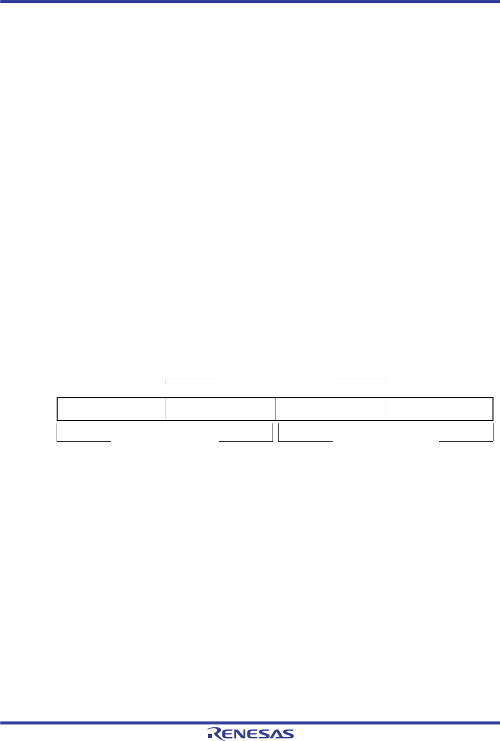
R01UH0034EJ0200 Rev.2.00 Page 80 of 1489
Dec 27, 2013
RX62T Group, RX62G Group 2. CPU
Under development Preliminary document
Specifications in this document are tentative and subject to change.
DN flag (0 flush bit of denormalized number)
When this bit is set to 0, a denormalized number is handled as a denormalized number.
When this bit is set to 1, a denormalized number is handled as 0.
EV bit (Invalid operation exception enable bit), EO bit (Overflow exception enable bit),
EZ bit (Division-by-zero exception enable bit), EU bit (Underflow exception enable bit), and
EX bit (Inexact exception enable bit)
When any of five floating-point exceptions specified in the IEEE754 standard is generated by the FPU instruction, the bit
decides whether the CPU will start handling the exception. When the bit is set to 0, the exception handling is masked;
when the bit is set to 1, the exception handling is enabled.
FV flag (Invalid operation flag), FO flag (Overflow flag), FZ flag (Division-by-zero flag),
FU flag (Underflow flag), and FX flag (Inexact flag)
While the exception handling enable bit (Ej) is 0 (exception handling is masked), if any of five floating-point exceptions
specified in the IEEE754 standard is generated, the corresponding bit is set to 1.
When Ej is 1 (exception handling is enabled), the value of the flag remains.
When the corresponding flag is set to 1, it remains 1 until it is cleared to 0 by software. (Accumulation flag)
FS flag (Floating-point error summary flag)
This bit reflects the logical OR of the FU, FZ, FO, and FV flags.
2.2.2.9 Accumulator (ACC)
The accumulator (ACC) is a 64-bit register used for DSP instructions. The accumulator is also used for the multiply and
multiply-and-accumulate instructions; EMUL, EMULU, FMUL, MUL, and RMPA, in which case the prior value in the
accumulator is modified by execution of the instruction.
Use the MVTACHI and MVTACLO instructions for writing to the accumulator. The MVTACHI and MVTACLO
instructions write data to the higher-order 32 bits (bits 63 to 32) and the lower-order 32 bits (bits 31 to 0), respectively.
Use the MVFACHI and MVFACMI instructions for reading data from the accumulator. The MVFACHI and MVFACMI
instructions read data from the higher-order 32 bits (bits 63 to 32) and the middle 32 bits (bits 47 to 16), respectively.
Range for reading by MVFACMI
b63 b48 b47 b32 b31 b16 b15 b0
Range for reading and writing by
MVTACHI and MVFACHI Range for writing by MVTACLO
Value after reset: Undefined

R01UH0034EJ0200 Rev.2.00 Page 81 of 1489
Dec 27, 2013
RX62T Group, RX62G Group 2. CPU
Under development Preliminary document
Specifications in this document are tentative and subject to change.
2.3 Processor Mode
The RX CPU supports two processor modes, supervisor and user. These processor modes enable the realization of a
hierarchical CPU resource protection.
Each processor mode imposes a level on rights of access to the CPU resource and the instructions that can be executed.
Supervisor mode carries greater rights than those of user mode.
The initial state after a reset is supervisor mode.
2.3.1 Supervisor Mode
In supervisor mode, all CPU resources are accessible and all instructions are available. However, writing to the processor
mode select bit (PM) in the processor status word (PSW) by executing an MVTC or a POPC instruction will be ignored.
For details on how to write to the PM bit, refer to section 2, Processor Status Word (PSW).
2.3.2 User Mode
In user mode, write access to the CPU resources listed below is restricted. The restriction applies to any instruction
capable of write access.
Some bits (bits IPL[3:0], PM, U, and I) in the processor status word (PSW)
Interrupt stack pointer (ISP)
Interrupt table register (INTB)
Backup PSW (BPSW)
Backup PC (BPC)
Fast interrupt vector register (FINTV)
2.3.3 Privileged Instruction
Privileged instructions can only be executed in supervisor mode. Executing a privileged instruction in user mode
produces a privileged instruction exception. Privileged instructions include the RTFI, MVTIPL, RTE, and WAIT
instructions.
2.3.4 Switching Between Processor Modes
Manipulating the processor mode select bit (PM) in the processor status word (PSW) switches the processor mode.
However, rewriting to the PM bit by executing an MVTC or a POPC instruction is prohibited. Switch the processor mode
by following the procedures described below.
(1) Switching from user mode to supervisor mode
After an exception has been generated, the PM bit in the PSW register is set to 0 and the CPU switches to supervisor
mode. The hardware pre-processing is executed in supervisor mode. The state of the processor mode before the
exception was generated is retained in the PM bit in the copy of the PSW register that is saved on the stack.
(2) Switching from supervisor mode to user mode
Executing an RTE instruction when the value of the copy of the PM bit in the PSW that has been preserved on the stack
is "1" or an RTFI instruction when the value of the copy of the PM bit in the PSW that has been preserved in the backup
PSW (BPSW) is "1" causes a transition to user mode. In the transition to user mode, the value of the stack pointer
designation bit (the U bit in the PSW register) becomes "1".
R01UH0034EJ0200 Rev.2.00 Page 82 of 1489
Dec 27, 2013
RX62T Group, RX62G Group 2. CPU
Under development Preliminary document
Specifications in this document are tentative and subject to change.
2.4 Data Types
The RX CPU can handle four types of data: integer, floating-point, bit, and string.
For details, see RX Family Series User's Manual: Software.
2.5 Endian
For the RX CPU, instructions are always little endian, but the treatment of data is selectable as little or big endian.
2.5.1 Switching the Endian
As arrangements of bytes, the RX62T and RX62G Groups support both big endian, where the higher-order byte (MSB)
is at location 0, and little endian, where the lower-order byte (LSB) is at location 0.
The endian is switched by changing the setting on a mode pin (MDE). For details on the endian setting, see section 3,
Operating Modes.
Operations for access differ according to the endian setting and, depending on the instruction, whether 8-, 16- or 32-bit
access has been selected. Operations for access in the various possible cases are described inTable 2.1 to Table 2.12.
In the tables, LL indicates bits D7 to D0 of the general register,
LH indicates bits D15 to D8 of the general register,
HL indicates bits D23 to D16 of the general register, and
HH indicates bits D31 to D24 of the general register.
D31 to D24 D23 to D16 D15 to D8 D7 to D0
General purpose register: Rm HH HL LH LL
Table 2.1 32-Bit Read Operations when Little Endian has been Selected
Operation
Address
of src
Reading a 32-bit
unit from address 0 Reading a 32-bit
unit from address 1 Reading a 32-bit
unit from address 2 Reading a 32-bit
unit from address 3 Reading a 32-bit
unit from address 4
Address 0Transfer to LL————
Address 1 Transfer to LH Transfer to LL — — —
Address 2 Transfer to HL Transfer to LH Transfer to LL — —
Address 3 Transfer to HH Transfer to HL Transfer to LH Transfer to LL —
Address 4 — Transfer to HH Transfer to HL Transfer to LH Transfer to LL
Address 5 — — Transfer to HH Transfer to HL Transfer to LH
Address 6 — — — Transfer to HH Transfer to HL
Address 7————Transfer to HH
Table 2.2 32-Bit Read Operations when Big Endian has been Selected
Operation
Address
of src Reading a 32-bit
unit from address 0 Reading a 32-bit
unit from address 1 Reading a 32-bit
unit from address 2 Reading a 32-bit
unit from address 3 Reading a 32-bit
unit from address 4
Address 0 Transfer to HH — — — —
Address 1 Transfer to HL Transfer to HH — — —
Address 2 Transfer to LH Transfer to HL Transfer to HH — —
Address 3 Transfer to LL Transfer to LH Transfer to HL Transfer to HH —
Address 4 — Transfer to LL Transfer to LH Transfer to HL Transfer to HH
Address 5 — — Transfer to LL Transfer to LH Transfer to HL
Address 6———Transfer to LLTransfer to LH
Address 7————Transfer to LL

R01UH0034EJ0200 Rev.2.00 Page 83 of 1489
Dec 27, 2013
RX62T Group, RX62G Group 2. CPU
Under development Preliminary document
Specifications in this document are tentative and subject to change.
Table 2.3 32-Bit Write Operations when Little Endian has been Selected
Operation
Address
of src Writing a 32-bit
unit to address 0 Writing a 32-bit
unit to address 1 Writing a 32-bit
unit to address 2 Writing a 32-bit
unit to address 3 Writing a 32-bit
unit to address 4
Address 0 Transfer from LL — — — —
Address 1 Transfer from LH Transfer from LL — — —
Address 2 Transfer from HL Transfer from LH Transfer from LL — —
Address 3 Transfer from HH Transfer from HL Transfer from LH Transfer from LL —
Address 4 — Transfer from HH Transfer from HL Transfer from LH Transfer from LL
Address 5 — — Transfer from HH Transfer from HL Transfer from LH
Address 6 — — — Transfer from HH Transfer from HL
Address 7————Transfer from HH
Table 2.4 32-Bit Write Operations when Big Endian has been Selected
Operation
Address
of dest Writing a 32-bit
unit to address 0 Writing a 32-bit
unit to address 1 Writing a 32-bit
unit to address 2 Writing a 32-bit
unit to address 3 Writing a 32-bit
unit to address 4
Address 0 Transfer from HH — — — —
Address 1 Transfer from HL Transfer from HH — — —
Address 2 Transfer from LH Transfer from HL Transfer from HH — —
Address 3 Transfer from LL Transfer from LH Transfer from HL Transfer from HH —
Address 4 — Transfer from LL Transfer from LH Transfer from HL Transfer from HH
Address 5 — — Transfer from LL Transfer from LH Transfer from HL
Address 6 — — — Transfer from LL Transfer from LH
Address 7 — — — — Transfer from LL
Table 2.5 16-Bit Read Operations when Little Endian has been Selected
Operation
Address
of src
Reading a
16-bit unit
from address
0
Reading a
16-bit unit
from address
1
Reading a
16-bit unit
from address
2
Reading a
16-bit unit
from address
3
Reading a
16-bit unit
from address
4
Reading a
16-bit unit
from address
5
Reading a
16-bit unit
from address
6
Address 0Transfer to LL——————
Address 1Transfer to LHTransfer to LL—————
Address 2—Transfer to LHTransfer to LL————
Address 3 — — Transfer to LH Transfer to LL — — —
Address 4 — — — Transfer to LH Transfer to LL — —
Address 5 — — — — Transfer to LH Transfer to LL —
Address 6 — — — — — Transfer to LH Transfer to LL
Address 7——————Transfer to LH

R01UH0034EJ0200 Rev.2.00 Page 84 of 1489
Dec 27, 2013
RX62T Group, RX62G Group 2. CPU
Under development Preliminary document
Specifications in this document are tentative and subject to change.
Table 2.6 16-Bit Read Operations when Big Endian has been Selected
Operation
Address
of src
Reading a 16-
bit unit from
address 0
Reading a 16-
bit unit from
address 1
Reading a 16-
bit unit from
address 2
Reading a 16-
bit unit from
address 3
Reading a 16-
bit unit from
address 4
Reading a 16-
bit unit from
address 5
Reading a 16-
bit unit from
address 6
Address 0Transfer to LH——————
Address 1Transfer to LLTransfer to LH—————
Address 2—Transfer to LLTransfer to LH————
Address 3 — — Transfer to LL Transfer to LH — — —
Address 4———Transfer to LLTransfer to LH——
Address 5————Transfer to LLTransfer to LH—
Address 6—————Transfer to LLTransfer to LH
Address 7——————Transfer to LL
Table 2.7 16-Bit Write Operations when Little Endian has been Selected
Operation
Address
of dest
Writing a 16-
bit unit to
address 0
Writing a 16-
bit unit to
address 1
Writing a 16-
bit unit to
address 2
Writing a 16-
bit unit to
address 3
Writing a 16-
bit unit to
address 3
Writing a 16-
bit unit to
address 5
Writing a 16-
bit unit to
address 6
Address 0 Transfer from
LL
— —————
Address 1 Transfer from
LH
Transfer from
LL
—————
Address 2 — Transfer from
LH
Transfer from
LL
————
Address 3 — — Transfer from
LH
Transfer from
LL
———
Address 4 — — — Transfer from
LH
Transfer from
LL
——
Address 5 — — — — Transfer from
LH
Transfer from
LL
—
Address 6 — — — — — Transfer from
LH
Transfer from
LL
Address 7 — — — — — — Transfer from
LH
R01UH0034EJ0200 Rev.2.00 Page 85 of 1489
Dec 27, 2013
RX62T Group, RX62G Group 2. CPU
Under development Preliminary document
Specifications in this document are tentative and subject to change.
Table 2.8 16-Bit Write Operations when Big Endian has been Selected
Operation
Address
of dest
Writing a 16-
bit unit to
address 0
Writing a 16-
bit unit to
address 1
Writing a 16-
bit unit to
address 2
Writing a 16-
bit unit to
address 3
Writing a 16-
bit unit to
address 4
Writing a 16-
bit unit to
address 5
Writing a 16-
bit unit to
address 6
Address 0 Transfer from
LH
——————
Address 1 Transfer from
LL
Transfer from
LH
—————
Address 2 — Transfer from
LL
Transfer from
LH
————
Address 3 — — Transfer from
LL
Transfer from
LH
———
Address 4 — — — Transfer from
LL
Transfer from
LH
——
Address 5 — — — — Transfer from
LL
Transfer from
LH
—
Address 6 — — — — — Transfer from
LL
Transfer from
LH
Address 7 — — — — — — Transfer from
LL
Table 2.9 8-Bit Read Operations when Little Endian has been Selected
Operation
Address of src Reading an 8-bit unit
from address 0 Reading an 8-bit unit
from address 1 Reading an 8-bit unit
from address 2 Reading an 8-bit unit
from address 3
Address 0 Transfer to LL — — —
Address 1 — Transfer to LL — —
Address 2 — — Transfer to LL —
Address 3 — — — Transfer to LL
Table 2.10 8-Bit Read Operations when Big Endian has been Selected
Operation
Address of src Reading an 8-bit unit
from address 0 Reading an 8-bit unit
from address 1 Reading an 8-bit unit
from address 2 Reading an 8-bit unit
from address 3
Address 0 Transfer to LL — — —
Address 1 — Transfer to LL — —
Address 2 — — Transfer to LL —
Address 3 — — — Transfer to LL
R01UH0034EJ0200 Rev.2.00 Page 86 of 1489
Dec 27, 2013
RX62T Group, RX62G Group 2. CPU
Under development Preliminary document
Specifications in this document are tentative and subject to change.
2.5.2 Access to I/O Registers
The addresses of I/O registers are fixed, and this is regardless of whether the setting is for little endian or big endian.
Accordingly, changes to the endian do not affect access to I/O registers. For the arrangements of I/O registers, refer to the
descriptions of registers in the relevant sections.
2.5.3 Notes on Access to I/O Registers
Ensure that access to I/O registers is in accord with the following rules.
For I/O registers with a bus width of eight bits, use instructions with size specifier (.size) of .B or size extension
specifier (.memex) of .B or .UB.
For I/O registers with a bus width of 16 bits, use instructions with size specifier (.size) of .W or size extension
specifier (.memex) of .W or .UW.
For I/O registers with a bus width of 32 bits, use instructions with size specifier (.size) of .L or size extension
specifier (.memex) of .L.
Table 2.11 8-Bit Write Operations when Little Endian has been Selected
Operation
Address of dest Writing an 8-bit unit to
address 0 Writing an 8-bit unit to
address 1 Writing an 8-bit unit to
address 2 Writing an 8-bit unit to
address 3
Address 0 Transfer from LL — — —
Address 1 — Transfer from LL — —
Address 2 — — Transfer from LL —
Address 3 — — — Transfer from LL
Table 2.12 8-Bit Write Operations when Big Endian has been Selected
Operation
Address of dest Writing an 8-bit unit to
address 0 Writing an 8-bit unit to
address 1 Writing an 8-bit unit to
address 2 Writing an 8-bit unit to
address 3
Address 0 Transfer from LL — — —
Address 1 — Transfer from LL — —
Address 2 — — Transfer from LL —
Address 3 — — — Transfer from LL
R01UH0034EJ0200 Rev.2.00 Page 87 of 1489
Dec 27, 2013
RX62T Group, RX62G Group 2. CPU
Under development Preliminary document
Specifications in this document are tentative and subject to change.
2.5.4 Data Arrangement
2.5.4.1 Data Arrangement in Registers
Figure 2.2shows the relation between the sizes of registers and bit numbers.
Figure 2.2 Data Arrangement in Registers
2.5.4.2 Data Arrangement in Memory
Data in memory have three sizes: byte (8-bit), word (16-bit), and longword (32-bit). The data arrangement is selectable
as little endian or big endian. Figure 2.3 shows the arrangement of data in memory.
Figure 2.3 Data Arrangement in Memory
Longword (32-bit) data
b31 b0
b15 b0
b7 b0
Word (16-bit) data
Byte (8-bit) data
MSB LSB
1-bit data
(Little endian) (Big endian)
Address L
Address L
Byte data
Word data Address M
Address M+1
Address N
Address N+1
Address N+2
Address N+3
Longword data
Data imageData type
b7 b0
LSB
MSB
Data image
Address
7 6 5 4 3 2 1 0
LSB
LSB
MSB
MSB
b7 b0
LSB
MSB
7 6 5 4 3 2 1 0
LSB
LSB
MSB
MSB
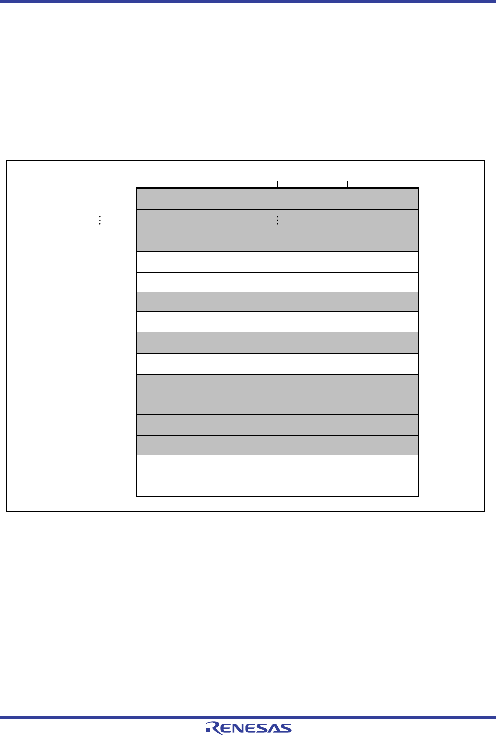
R01UH0034EJ0200 Rev.2.00 Page 88 of 1489
Dec 27, 2013
RX62T Group, RX62G Group 2. CPU
Under development Preliminary document
Specifications in this document are tentative and subject to change.
2.6 Vector Table
There are two types of vector table: fixed and relocatable. Each vector in the vector table consists of four bytes and
specifies the address where the corresponding exception handling routine starts.
2.6.1 Fixed Vector Table
The fixed vector table is allocated to a fixed address range. The individual vectors for the privileged instruction
exception, undefined instruction exception, floating-point exception, non-maskable interrupt, and reset are allocated to
addresses in the range from FFFFFF80h to FFFFFFFFh. Figure 2.4 shows the fixed vector table.
Figure 2.4 Fixed Vector Table
(Reserved)
(Reserved)
FFFFFFDCh
FFFFFFFCh
FFFFFFE0h
FFFFFFE4h
FFFFFFE8h
FFFFFFECh
FFFFFFF0h
FFFFFFF4h
FFFFFFF8h
access exception
Privileged instruction exception
(Reserved)
Undefined instruction exception
(Reserved)
Floating-point exception
(Reserved)
(Reserved)
(Reserved)
LSB
(Reserved)
Non-maskable interrupt
Reset
FFFFFFD0h
FFFFFFD4h
FFFFFFD8h
MSB
FFFFFFCCh
FFFFFF80h
R01UH0034EJ0200 Rev.2.00 Page 89 of 1489
Dec 27, 2013
RX62T Group, RX62G Group 2. CPU
Under development Preliminary document
Specifications in this document are tentative and subject to change.
2.6.2 Relocatable Vector Table
The address where the relocatable vector table is placed can be adjusted. The table is a 1,024-byte region that contains all
vectors for unconditional traps and interrupts and starts at the address (IntBase) specified in the interrupt table register
(INTB). Figure 2.5 shows the relocatable vector table.
Each vector in the relocatable vector table has a vector number from 0 to 255. Each of the INT instructions, which act as
the sources of unconditional traps, is allocated to the vector that has the same number as that of the instruction itself
(from 0 to 255). The BRK instruction is allocated to the vector with number 0. Furthermore, vector numbers within the
set from 0 to 255 may also be allocated to other interrupt sources on a per-product basis. For more on the interrupt vector
numbers, see section 11, Interrupt Controller (ICU).
Figure 2.5 Relocatable Vector Table
INTB
0
IntBase+4
IntBase
b31 b0
IntBase+8
255
IntBase+1020
Interrupt vectors are
allocated in this order.
1
2

R01UH0034EJ0200 Rev.2.00 Page 90 of 1489
Dec 27, 2013
RX62T Group, RX62G Group 2. CPU
Under development Preliminary document
Specifications in this document are tentative and subject to change.
2.7 Operation of Instructions
2.7.1 Data Prefetching by the RMPA Instruction and the String-Manipulation
Instructions
The RMPA instruction and the string-manipulation instructions except the SSTR instruction (that is, SCMPU, SMOVB,
SMOVF, SMOVU, SUNTIL, and SWHILE instructions) may prefetch data from the memory to speed up the read
processing. Data is prefetched from the prefetching start position with three bytes as the upper limit. The prefetching start
positions of each operation are shown below.
RMPA instruction: The multiplicand address specified by R1, and the multiplier address specified by R2
SCMPU instruction: The source address specified by R1 for comparison, and the destination address specified by
R2 for comparison
SUNTIL and SWHILE instructions: The destination address specified by R1 for comparison
SMOVB, SMOVF, and SMOVU instructions: The source address specified by R2 for transfer

R01UH0034EJ0200 Rev.2.00 Page 91 of 1489
Dec 27, 2013
RX62T Group, RX62G Group 2. CPU
Under development Preliminary document
Specifications in this document are tentative and subject to change.
2.8 Pipeline
2.8.1 Overview
The RX CPU has 5-stage pipeline structure. The RX CPU instruction is converted into one or more micro-operations,
which are then executed in pipeline processing. In the pipeline stage, the IF stage is executed in the unit of instructions,
while the D and subsequent stages are executed in the unit of micro-operations.
The operation of pipeline and respective stages is described below.
(1) IF stage (instruction fetch stage)
In the IF stage, the CPU fetches instructions from the memory. As the RX CPU has four 8-byte instruction queues, it
fetches instructions until the instruction queue is full, regardless of the completion of decoding in the D (decoding) stage.
(2) D stage (decoding stage)
The CPU decodes instructions in the D stage and converts them into micro-operations. The CPU reads the register
information (RF) in this stage and executes a bypass process (BYP) if the result of the preceding instruction will be used
in a subsequent instruction. The write of operation result to the register (RW) can be executed with the register reference
by using the bypass process.
(3) E stage (execution stage)
Operations and address calculations (OP) are processed in the E stage.
(4) M stage (memory access stage)
Operand memory accesses (OA) are processed in the M stage. This stage is used only when the memory is accessed, and
is divided into two sub-stages, M1 and M2. The RX CPU enables respective memory accesses for M1 and M2.
M1 stage (memory-access stage 1)
Operand memory access (OA1, OA2) is processed.
Store operation: The pipeline processing ends when a write request is received via the bus.
Load operation: The operation proceeds to the M2 stage when a read request is received via the bus. If a request and
load data are received at the same timing (no-wait memory access), the operation proceeds to the WB stage.
M2 stage (memory-access stage 2)
Operand memory access (OA2) is processed. The CPU waits for the load data in the M2 stage. When the load data
is received, the operation proceeds to the WB stage.
(5) WB stage (write-back stage)
The operation result and the data read from memory are written to the register (RW) in the WB stage. The data read from
memory and the other type of data, such as the operation result, can be written to the register in the same clock cycles.
Figure 2.6 shows the pipeline configuration and its operation.
Figure 2.6 Pipeline Configuration and its Operation
IF DEC OP OA1 OA2
IF stage
BYP
RF
Pipeline stage
Execution processing
D stage E stage M1 stage M2 stage
One cycle
WB stage
RW
M stage

R01UH0034EJ0200 Rev.2.00 Page 92 of 1489
Dec 27, 2013
RX62T Group, RX62G Group 2. CPU
Under development Preliminary document
Specifications in this document are tentative and subject to change.
2.8.2 Instructions and Pipeline Processing
The operands in the table below indicate the following meaning.
#IMM: Immediate
Rs, Rs2, Rd, Rd2, Ri, Rb: General-purpose register, CR: Control register
dsp: dsp5, dsp8, dsp16, dsp24
pcdsp: pcdsp3, pcdsp8, pcdsp16, pcdsp24
2.8.2.1 Instructions Converted into Single Micro-Operation and Pipeline Processing
The table below lists the instructions that are converted into a single micro-operation. The number of cycles in the table
indicates the number of cycles during no-wait memory access.
Note 1. The number of cycles for the dividing instruction varies according to the divisor and dividend.
Note 2. For the number of cycles for throughput and latency, see section 2.8.3, Calculation of the Instruction Processing Time.
Table 2.13 Instructions that are Converted into a Single Micro-Operation
Instruction Mnemonic (indicates the common
operation when the size is omitted) Reference
Figure Number of Cycles
Arithmetic/logic instructions
(register-register, immediate-register)
Except EMUL, EMULU, RMPA, DIV, DIVU,
and SATR
{ABS, ADC, ADD, AND, CMP, MAX, MIN,
MUL, NEG,NOP, NOT, OR, ROLC, RORC,
ROTL, ROTR, SAT,SBB, SHAR, SHLL,
SHLR, SUB, TST, XOR} “#IMM,Rd”/“Rd” /
“Rs, Rd”/“Rs, Rs2, Rd”
Figure 2.7 1
Arithmetic/logic instructions (division) DIV “#IMM, Rd”/“Rs, Rd” Figure 2.7 3 to 20*1
DIVU “#IMM, Rd”/“Rs, Rd” Figure 2.7 2 to 18*1
Data transfer instructions
(register-register, immediate-register)
{MOV, MOVU, REVL, REVW} “#IMM, Rd”/
“Rs, Rd”
SCCnd “Rd”
{STNZ, STZ} “#IMM, Rd”
Figure 2.7 1
Transfer instructions (load operation) {MOV, MOVU} “[Rs], Rd”/“dsp[Rs], Rd” /
“[Rs+], Rd”/“[-Rs], Rd”/“Rs, [Ri, Rb]”
POP “Rd”
Figure 2.8 Throughput: 1
Latency: 2*2
Transfer instructions (store operation) MOV “Rs, [Rd]”/“Rs, dsp[Rd]”/“Rs, [Rd+]” /
“Rs, [-Rd]”/“Rs, [Ri, Rb]”
PUSH “Rs”
PUSHC “CR”
Figure 2.9 1
Bit manipulation instructions (register) {BCLR, BNOT, BSET, BTST} “#IMM, Rd”/
“Rs, Rd”
BMCnd “#IMM, Rd”
Figure 2.7 1
Branch instructions BCnd “pcdsp”
{BRA, BSR} “pcdsp”/“Rs”
{JMP, JSR} “Rs”
Figure 2.18 Branch taken: 3
Branch not taken: 1
Floating-point operation instructions
(register-register, immediate-register)
FCMP “#IMM, Rd”/“Rs, Rd” Figure 2.7 1
System manipulation instructions CLRPSW, SETPSW “#IMM”
MVTC “#IMM, CR”/“Rs, CR”
MVFC “CR, Rd”
MVTIPL “#IMM”
—1
DSP function instructions {MACHI, MACLO, MULHI, MULLO}“Rs, Rs2”
{MVFACHI, MVFACMI}“Rd”
{MVTACHI, MVTACLO}“Rs”
RACW“#IMM”
Figure 2.7 1

R01UH0034EJ0200 Rev.2.00 Page 93 of 1489
Dec 27, 2013
RX62T Group, RX62G Group 2. CPU
Under development Preliminary document
Specifications in this document are tentative and subject to change.
Figure 2.7 to Figure 2.9show the operation of instructions that are converted into a basic single micro-operation.
Figure 2.7 Operation for Register-Register, Immediate-Register
Figure 2.8 Load Operation
Figure 2.9 Store Operation
IF D E WB
ADD R1, R2
4 stages
IF D E WB
DIV R3, R4 E
Note: Multi-cycle instructions (DIV, DIVU) are executed in multiple cycles in the E stage.
IF D E WB
MOV [R1], R2 M1
IF D E WB
MOV [R1], R2 M1 M1
Note: When the load operation is executed to the no-wait memory, the M1 stage is
executed in one cycle. In other cases, the M stage (M1 or M2) is executed in
multiple cycles.
5 stages
M2
IF D E
4 stages
M1
IF D E M1 M1
Note: The M1 stage is executed until a write request is received during the store operation. (If
the store operation is executed to the no-wait memory, the M1 stage is executed in one
cycle.
M1
MOV R2, [R1]

R01UH0034EJ0200 Rev.2.00 Page 94 of 1489
Dec 27, 2013
RX62T Group, RX62G Group 2. CPU
Under development Preliminary document
Specifications in this document are tentative and subject to change.
2.8.2.2 Instructions Converted into Multiple Micro-Operations and Pipeline Processing
The table below lists the instructions that are converted into multiple micro-operations. The number of cycles in the table
indicates the number of cycles during no-wait memory access.
Table 2.14 Instructions that are Converted into Multiple Micro-Operations (1 / 2)
Instruction Mnemonic (indicates the common
operation when the size is omitted) Reference
Figure Number of Cycles
Arithmetic/logic instructions
(memory source operand)
{ADC, ADD, AND, CMP, MAX, MIN,
MUL, OR, SBB, SUB, TST, XOR} “[Rs],
Rd” / “dsp[Rs], Rd”
Figure 2.10 3
Arithmetic/logic instructions (division) DIV “[Rs], Rd/dsp[Rs], Rd” — 5 to 22
DIVU ”[Rs], Rd/dsp[Rs], Rd” — 4 to 20
Arithmetic/logic instructions
(multiplier: 32 x 32 64 bits)
(register-register, register-immediate)
{EMUL, EMULU} “#IMM, Rd”/“Rs, Rd” Figure 2.12 2
Arithmetic/logic instructions
(multiply-and-accumulate operation)
RMPA.B — 6+7×floor(n/4)+4×(n%4)
n: Number of processing
bytes*1
RMPA.W — 6+5×floor(n/2)+4×(n%2)
n: Number of processing
words*1
RMPA.L — 6+4n
n: Number of processing
longwords*1
Arithmetic/logic instructions (64-bit
signed saturation for RMPA instruction)
SATR — 3
Data transfer instructions
(memory-memory transfer)
MOV “[Rs], [Rd]”/“dsp[Rs], [Rd]” /“[Rs],
dsp[Rd]”/“dsp[Rs], [Rd]”
PUSH “[Rs]”/“dsp[Rs]”
Figure 2.11 3
Bit manipulation instructions (memory
source operand)
{BCLR, BNOT, BSET, BTST} “#IMM,
[Rd]” /“#IMM, dsp[Rd]”
BMCnd “#IMM, [Rd]”/“#IMM, dsp[Rd]”
Figure 2.11 3
Transfer instructions (load operation) POPC “CR” — Throughput: 3
Latency: 4*2
Transfer instructions (store operation of
multiple registers)
PUSHM “Rs-Rs2” — n
n: Number of registers*3
Transfer instructions (store operation of
multiple registers)
POPM “Rs-Rs2” — Throughput: n
Latency: n + 1
n: Number of registers*2*4
Transfer instructions (register-register) XCHG “Rs, Rd” Figure 2.13 2
Transfer instructions (memory-register) XCHG “[Rs], Rd”/“dsp[Rs], Rd” Figure 2.14 2
Branch instructions RTS — 5
RTSD “#IMM” — 5
RTSD “#IMM, Rd-Rd2” — Throughput: n<5?5:1+n
Latency: n<4?5:2+n
n: Number of registers*2

R01UH0034EJ0200 Rev.2.00 Page 95 of 1489
Dec 27, 2013
RX62T Group, RX62G Group 2. CPU
Under development Preliminary document
Specifications in this document are tentative and subject to change.
Note 1. floor(x): Max. integer that is smaller than x
Note 2. For the number of cycles for throughput and latency, see section 2.8.3, Calculation of the Instruction Processing Time.
Note 3. The PUSHM instruction is converted into multiple store operations. The pipeline processing is the same as the one for the store
operations of the MOV instruction, where the operation is repeated for the number of specified registers.
Note 4. The POPM instruction is converted into multiple store operations. The pipeline processing is the same as the one for the store
operations of the MOV instruction, where the operation is repeated for the number of specified registers.
Note 5. Each of the SCMPU, SMOVU, SWHILE, and SUNTIL instructions ends the execution regardless of the specified cycles, if the
end condition is satisfied during execution.
String manipulation instructions*5 SCMPU — 2+4×floor(n/4)+4×(n%4)
n: Number of comparison
bytes*1
SMOVB — n>3?
6+3×floor(n/4)+3×(n%4):
2+3n
n: Number of transfer bytes*1
SMOVF, SMOVU — 2+3×floor(n/4)+3×(n%4)
n: Number of transfer bytes*1
SSTR.B — 2+floor(n/4)+n%4
n: Number of transfer bytes*1
SSTR.W — 2+floor(n/2)+n%2
n: Number of transfer words*1
SSTR.L — 2+n
n: Number of transfer
longwords
SUNTIL.B, SWHILE.B — 3+3×floor(n/4)+3×(n%4)
n: Number of comparison
bytes*1
SUNTIL.W, SWHILE.W — 3+3×floor(n/2)+3×(n%2)
n: Number of comparison
words*1
SUNTIL.L, SWHILE.L — 3+3×n
n: Number of comparison
longwords
Floating-point operation instructions
(register-register, immediate-register)
{FADD, FSUB} “#IMM, Rd”/ “Rs, Rd” Figure 2.15 4
FMUL “#IMM, Rd”/“Rs, Rd” — 3
FDIV “#IMM, Rd”/“Rs, Rd” — 16
{FTOI, ROUND, ITOF} “Rs, Rd” — 2
Floating-point operation instructions
(memory source operand)
{FADD, FSUB} “[Rs], Rd”/“dsp[Rs], Rd” — 6
FMUL “[Rs], Rd”/“dsp[Rs], Rd” — 5
FDIV “[Rs], Rd”/“dsp[Rs], Rd” — 18
{FTOI, ROUND, ITOF} “[Rs], Rd” /
“dsp[Rs], Rd”
—4
System manipulation instructions RTE — 6
RTFI — 3
Table 2.14 Instructions that are Converted into Multiple Micro-Operations (2 / 2)
Instruction Mnemonic (indicates the common
operation when the size is omitted) Reference
Figure Number of Cycles
R01UH0034EJ0200 Rev.2.00 Page 96 of 1489
Dec 27, 2013
RX62T Group, RX62G Group 2. CPU
Under development Preliminary document
Specifications in this document are tentative and subject to change.
Figure 2.10 to Figure 2.15 show the operation of instructions that are converted into basic multiple micro-operations.
Small letters in figures below indicate micro-operations.
Note 1. mop: Micro-operation, stall: Pipeline stall
Figure 2.10 Arithmetic/Logic Instruction (Memory Source Operand)
Figure 2.11 MOV Instruction (Memory-Memory), Bit Manipulation Instruction (Memory Source Operand)
Figure 2.12 EMUL, EMULU Instructions (Register- Register, Register-Immediate)
Figure 2.13 XCHG Instruction (Registers)
Figure 2.14 XCHG Instruction (Memory Source Operand)
Figure 2.15 Floating-Point Operation Instruction (Register-Register, Immediate-Register)
IF D E
ADD [R1], R2 M1
stall EWBD
(mop1) load
(mop2) add
Bypass process
IF D E
MOV [R1], [R2] M1
Load data
Bit manipulation, store operation
(mop1) load
(mop2) bit manipulation, store
D E M1
IF D E
EMUL R2, R4 WBD
(mop1) emul-1
(mop2) emul-2
WB Write to R4
Write to R5
E
IF D E
XCHG R1, R2
D
(mop1) xchg-1 Read from/Write to the register
(mop2) xchg-2 Write to the register
WB
EWB
IF D E
XCHG [R1], R2
D
(mop1) load
(mop2) store
WB
EM1
M1
IF D E
FADD R2, R4
D
(mop1) fadd-1
(mop2) fadd-2E
D E
WBD E
(mop3) fadd-3
(mop4) fadd-4 Write to R4
R01UH0034EJ0200 Rev.2.00 Page 97 of 1489
Dec 27, 2013
RX62T Group, RX62G Group 2. CPU
Under development Preliminary document
Specifications in this document are tentative and subject to change.
2.8.2.3 Pipeline Basic Operation
In the ideal pipeline processing, each stage is executed in one cycle, though all instructions may not be pipelined in due
to the processing and the branch execution.
The CPU controls the pipeline stage with the IF stage in the unit of instructions, while the D and subsequent stages in the
unit of micro-operations.
The figures below show the pipeline processing of typical cases. Small letters in figures indicate micro-operations.
Note 1. mop: Micro-operation, stall: Pipeline stall
(1) Pipeline Flow with Stalls
Figure 2.16 When an Instruction which Requires Multiple Cycles is Executed in the E Stage
Figure 2.17 When an Instruction which Requires more than One Cycle for its Operand Access is Executed
Figure 2.18 When a Branch Instruction is Executed (While the Condition is Satisfied for Unconditional/
Conditional Branch Instruction)
IF
DIV R1, R2
ADD R3, R4
D E E E WB
IF Dstall EWB
stall
IF stall EWBD
stall
ADD R5, R6
(mop) div
(mop) add
(mop) add
IF
MOV [R1], R2
MOV [R3], R4
D E M MWB
IF D E M WB
stall
IF DWBE
stall
ADD R5, R6
M
stall
stall
Other than no-wait
memory access
(mop) load
(mop) load
(mop) add
IF D E
Branch
instruction
Branch instruction is executed
IF D E WB
Branch penalty
Two cycles
(mop) jump
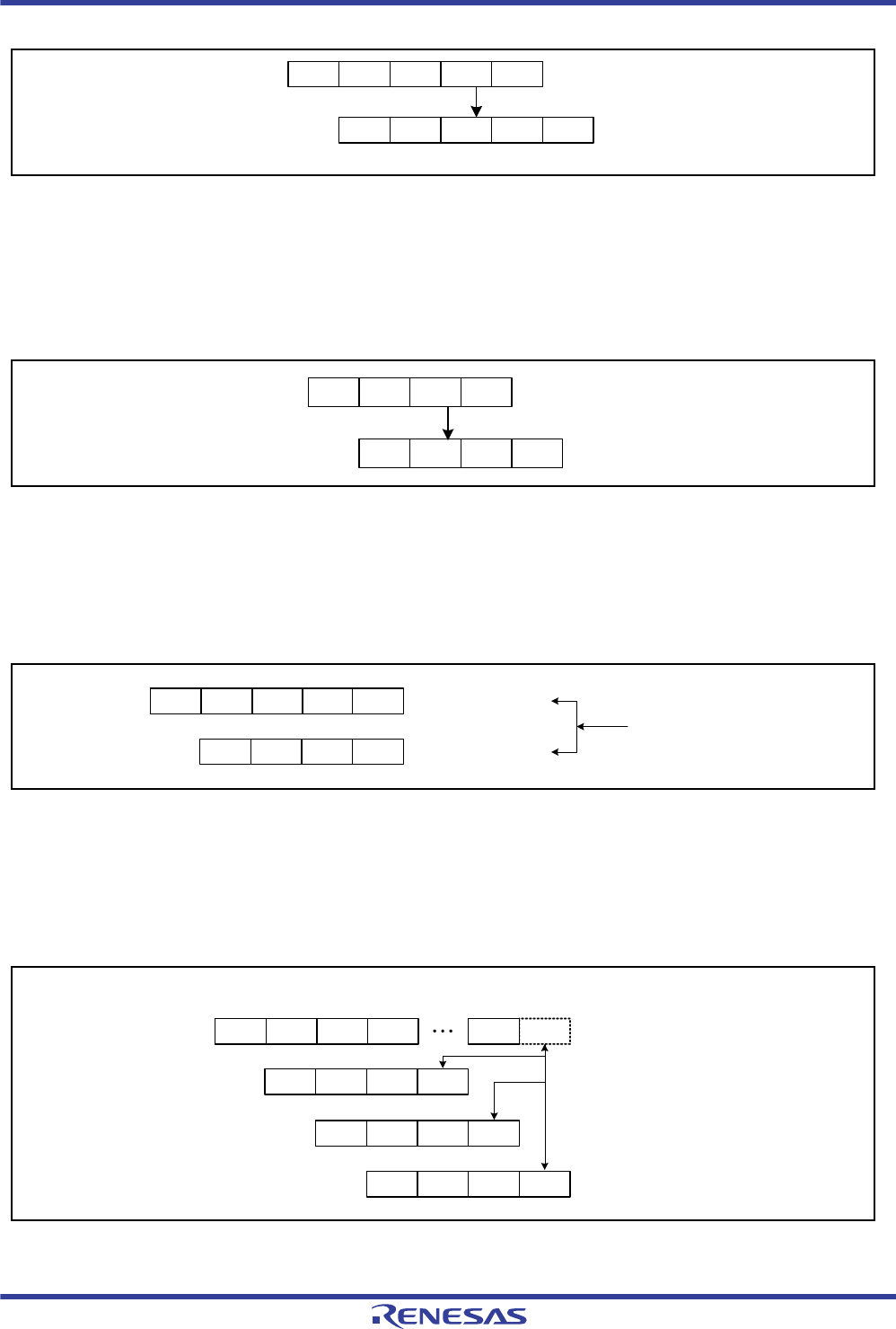
R01UH0034EJ0200 Rev.2.00 Page 98 of 1489
Dec 27, 2013
RX62T Group, RX62G Group 2. CPU
Under development Preliminary document
Specifications in this document are tentative and subject to change.
Figure 2.19 When the Subsequent Instruction Uses an Operand Read from the Memory
(2) Pipeline Flow with no Stall
(a) Bypass process
Even when the result of the preceding instruction will be used in a subsequent instruction, the operation processing
between registers is pipelined in by the bypass process.
Figure 2.20 Bypass Process
(b) When WB stages for the memory load and for the operation are overlapped
Even when the WB stages for the memory load and for the operation are overlapped, the operation processing is
pipelined in, because the load data and the operation result can be written to the register at the same timing.
Figure 2.21 When WB Stages for the Memory Load and for the Operation are Overlapped
(c) When subsequent instruction writes to the same register before the end of memory load
Even when the subsequent instruction writes to the same register before the end of memory load, the operation
processing is pipelined in, because the WB stage for the memory load is canceled.
Figure 2.22 When Subsequent Instruction Writes to the Same Register before the End of Memory Load
IF D E
MOV [R2], R1 MWB
IF Dstall EWB
ADD R2, R1
Bypass process
(mop) load
(mop) add
IF D E
ADD R1, R2
SUB R3, R2
WB
IF D E WB
Bypass process
(mop) add
(mop) sub
IF D E
MOV [R1], R2
IF D E WB
ADD R5, R3
MWB
(mop) add
(mop) load Executed at the same timing
even when the WB stages are
overlapped
IF D E
MOV [R1], R2
IF D E WB
MWBM
IF D E WB
IF D E WB
(mop) load
(Canceled when the register
number matches either of them)
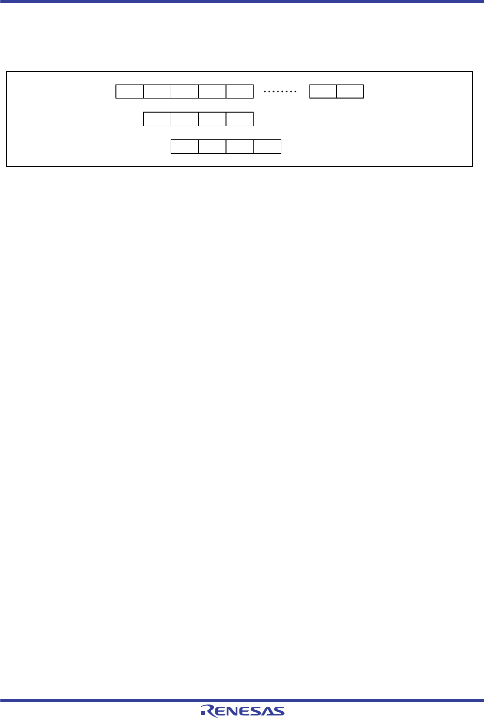
R01UH0034EJ0200 Rev.2.00 Page 99 of 1489
Dec 27, 2013
RX62T Group, RX62G Group 2. CPU
Under development Preliminary document
Specifications in this document are tentative and subject to change.
(d) When the load data is not used by the subsequent instruction
When the load data is not used by the subsequent instruction, the subsequent operations are in fact executed earlier and
the operation processing ends (out-of-order completion).
Figure 2.23 When Load Data is not Used by the Subsequent Instruction
2.8.3 Calculation of the Instruction Processing Time
Though the instruction processing time of the CPU varies according to the pipeline processing, the approximate time can
be calculated in the following methods.
Count the number of cycles (see Figure 2.9 and Figure 2.10)
When the load data is used by the subsequent instruction, the number of cycles described as "latency" is counted as
the number of cycles for the memory load instruction. For the cycles other than the memory load instruction, the
number of cycles described as "throughput" is counted.
If the instruction fetch stall is generated, the number of cycles increments.
Depending on the system configuration, multiple cycles are required for the memory access. The number of
memory access cycles in the RX62T and RX62G Groups is on a per-product basis.
IF D EMOV [R1], R2
IF D E
M M MWB
WB
IF D E WB
ADD R4, R5
SUB R6, R7
(mop) load
(mop) add
(mop) sub

R01UH0034EJ0200 Rev.2.00 Page 100 of 1489
Dec 27, 2013
RX62T Group, RX62G Group 2. CPU
Under development Preliminary document
Specifications in this document are tentative and subject to change.
2.8.4 Numbers of Cycles for Response to Interrupts
Table 2.15 lists numbers of cycles taken by processing for response to interrupts.
Times calculated from the values in Table 2.15 will be applicable when access to memory from the CPU is always
processed with no waiting. The on-chip RAM and ROM in products of the RX62T and RX62G Groups always allows
such access. Numbers of cycles for response to interrupts can be minimized by placing program code (and vectors) in on-
chip ROM and the stack in on-chip RAM. Furthermore, place the addresses where the exception handling routine starts
on eight-byte boundaries.
For information on the number of cycles from notification to acceptance of the interrupt request, indicated by N in the
table above, seeTable 2.13, Instructions that are Converted into a Single Micro-Operation, and Table 2.14,
Instructions that are Converted into Multiple Micro-Operations.
The timing of interrupt acceptance depends on the state of the pipelines. For more information on this, see section
10.3.1, Timing of Acceptance and Saved PC Values.
Table 2.15 Numbers of Cycles for Response to Interrupts
Type of Interrupt Request/Details of Processing Fast Interrupt Other Interrupts
ICU
Judgment of priority order
2 cycles 2 cycles
CPU
Number of cycles from notification to acceptance of the
interrupt request
N cycles (varies with the instruction being executed at the time the
interrupt was received)
CPU—Pre-processing by hardware
Saving the current PC and PSW values in RAM (or in control
registers in the case of the fast interrupt)
Reading of the vector
Branching to the start of the exception handling routine
4 cycles 6 cycles

R01UH0034EJ0200 Rev.2.00 Page 101 of 1489
Dec 27, 2013
RX62T Group, RX62G Group 3. Operating Modes
Under development Preliminary document
Specifications in this document are tentative and subject to change.
3. Operating Modes
3.1 Operating Mode Types and Selection
The RX62T and RX62G Groups have two types of operating modes. Operating modes are specified by the MD1 and
MD0 pins and the ROME bit in the system control register 0 (SYSCR0).
The endian of the RX62T and RX62G Groups can be selected in each operating mode setting. Endian is specified by the
MDE pin. For the endian of the RX62T and RX62G Groups, see section 2.5, Endian.
Note:Do not change the state of pins MDE, MD1, and MD0 while the LSI is working. Do not select any combination
other than those specified in Table 3.1.
Note 1. The on-chip ROM is classified into two flash memories: ROM and data flash. For details, see section 31, ROM (Flash Memory
for Code Storage), and section 32, Data Flash Memory (Flash Memory for Data Storage).
Note 1. The on-chip ROM is classified into two flash memories: ROM and data flash. For details, see section 31, ROM (Flash Memory
for Code Storage), and section 32, Data Flash Memory (Flash Memory for Data Storage).
Table 3.1 Selection of Operating Modes by the Mode Pins
Mode Pin SYSCR0 Initial State
MD1 MD0 ROME Operating Mode On-Chip ROM*1
0 1 1 Boot mode Enabled
1 1 1 Single-chip mode Enabled
Table 3.2 Selection of Operating Modes by Register Setting
SYSCR0
ROME Operating Mode On-Chip ROM*1
0 Single-chip mode Disabled
1 Enabled
Table 3.3 Selection of Endian
Mode Pin
EndianMDE
0 Little endian
1 Big endian
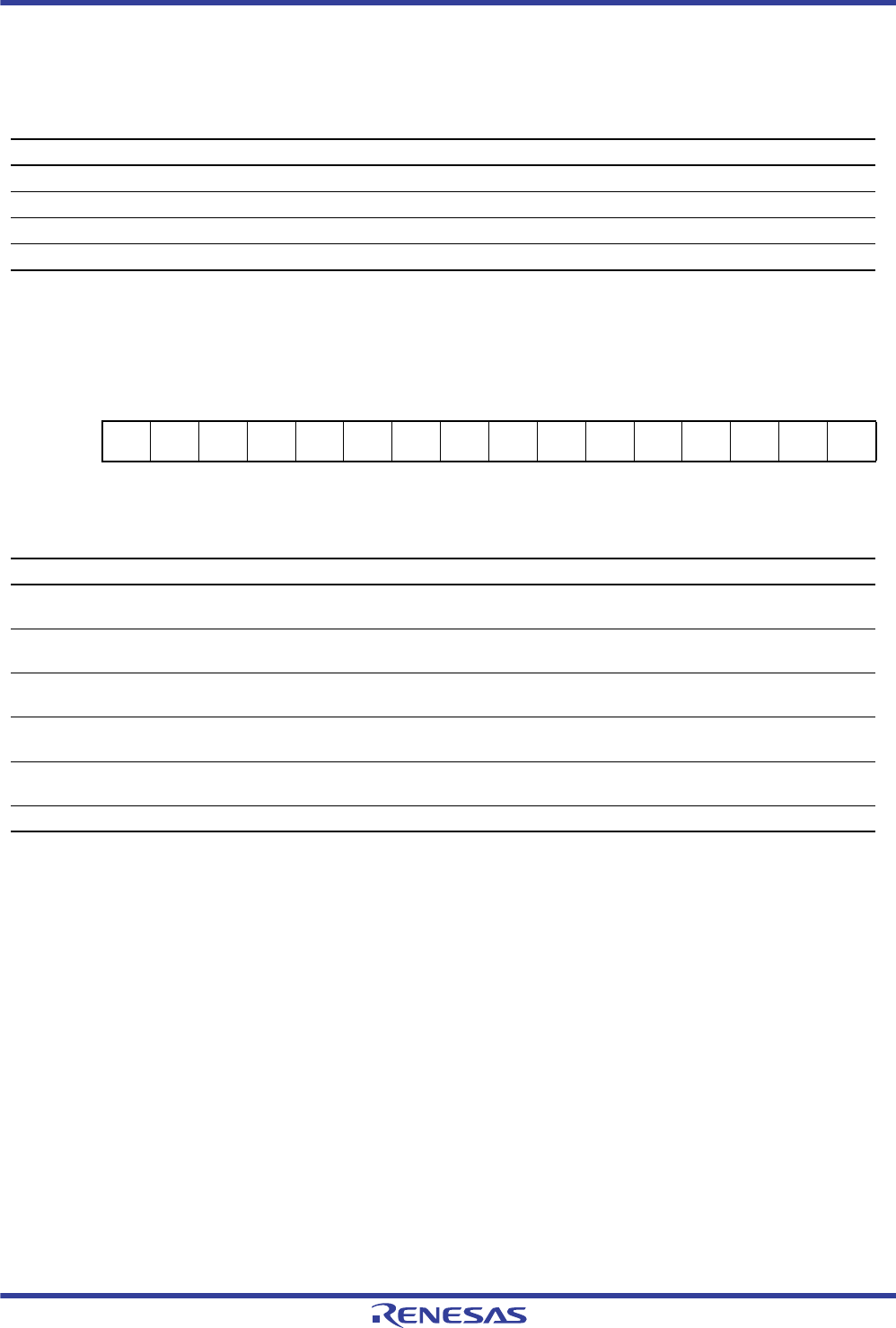
R01UH0034EJ0200 Rev.2.00 Page 102 of 1489
Dec 27, 2013
RX62T Group, RX62G Group 3. Operating Modes
Under development Preliminary document
Specifications in this document are tentative and subject to change.
3.2 Register Descriptions
Table 3.4 lists the registers related to operating modes.
Note: • x:Undefined
3.2.1 Mode Monitor Register (MDMONR)
MDMONR indicates the status of the mode pins.
Table 3.4 Registers Related to Operating Modes
Register Name Symbol Value after Reset Address Access Size
Mode monitor register MDMONR 10000000 x00000xxb 0008 0000h 16
Mode status register MDSR 00000000 00001001b 0008 0002h 16
System control register 0 SYSCR0 00000000 00000001b 0008 0006h 16
System control register 1 SYSCR1 00000000 00000001b 0008 0008h 16
Address: 0008 0000h
b15 b14 b13 b12 b11 b10 b9 b8 b7 b6 b5 b4 b3 b2 b1 b0
————————MDE—————MD1MD0
Value after reset: 00000000
x*1 00000
x*1x*1
Note 1. Depends on the setting of the mode pin (MD). When the MD pin is low, the bit value is 0; otherwise, the bit value is 1.
Bit Symbol Bit Name Description R/W
b0 MD0 MD0 Status Flag 0: The MD0 pin is 0
1: The MD0 pin is 1
R
b1 MD1 MD1 Status Flag 0: The MD1 pin is 0
1: The MD1 pin is 1
R
b6 to b2 — Reserved These bits are always read as 0. Writing to these bits has no
effect.
R
b7 MDE MDE Status Flag 0: The MDE pin is 0 (little endian)
1: The MDE pin is 1 (big endian)
R
b14 to b8 — Reserved These bits are always read as 0. Writing to these bits has no
effect.
R
b15 — Reserved This bit is always read as 1. Writing to this bit has no effect. R

R01UH0034EJ0200 Rev.2.00 Page 103 of 1489
Dec 27, 2013
RX62T Group, RX62G Group 3. Operating Modes
Under development Preliminary document
Specifications in this document are tentative and subject to change.
3.2.2 Mode Status Register (MDSR)
MDSR indicates the internal status of this LSI at startup.
Address: 0008 0002h
b15 b14 b13 b12 b11 b10 b9 b8 b7 b6 b5 b4 b3 b2 b1 b0
———————————BOTS———IROM
Value after reset: 00000000000x1001
Bit Symbol Bit Name Description R/W
b0 IROM On-Chip ROM Startup Status Flag 0: The on-chip ROM is disabled
1: The on-chip ROM is enabled
R
b2, b1 —Reserved These bits are always read as 0. Writing to these bits
has no effect.
R
b3 —Reserved This bit is always read as 1. Writing to this bit has no
effect.
R
b4 BOTS Boot Mode Startup Flag 0: Started with a mode except boot mode
1: Started with boot mode
R
b15 to b5 —Reserved These bits are always read as 0. Writing to these bits
has no effect.
R

R01UH0034EJ0200 Rev.2.00 Page 104 of 1489
Dec 27, 2013
RX62T Group, RX62G Group 3. Operating Modes
Under development Preliminary document
Specifications in this document are tentative and subject to change.
3.2.3 System Control Register 0 (SYSCR0)
SYSCR0 is used to enable or disable the on-chip ROM.
ROME Bit (On-Chip ROM Enable)
The ROME bit enables or disables the on-chip ROM (ROM, data flash).
While this bit is 1, it can be cleared to 0. While this bit is 0, it cannot be set to 1. Once the on-chip ROM is disabled by
clearing this bit to 0, the on-chip ROM can no longer be enabled with the ROME bit. A 0 should not be written to this bit
during access to the on-chip ROM.
After writing a 0 to this bit to disable the on-chip ROM, always make sure that the ROME bit has been changed to 0
before proceeding to the next processing.
KEY[7:0] Bits (SYSCR0 Key Code)
The KEY[7:0] bits enable or disable modifying SYSCR0.
When writing a value to the ROME bit, write 5Ah to the KEY[7:0] bits simultaneously. If SYSCR0 is modified with a
KEY[7:0] value other than 5Ah, the ROME bit value remain unchanged.
Address: 0008 0006h
b15 b14 b13 b12 b11 b10 b9 b8 b7 b6 b5 b4 b3 b2 b1 b0
KEY[7:0] ———————ROME
Value after reset: 0000000000000001
Bit Symbol Bit Name Description R/W
b0 ROME On-Chip ROM Enable 0: The on-chip ROM is disabled
1: The on-chip ROM is enabled
R/W
b7 to b1 — Reserved These bits are always read as 0. The write value should always
be 0.
R/W
b15 to b8 KEY[7:0] SYSCR0 Key Code 5Ah: Modifying SYSCR0 is enabled
Other codes: Modifying SYSCR0 is disabled
These bits are always read as 00h.
R/W

R01UH0034EJ0200 Rev.2.00 Page 105 of 1489
Dec 27, 2013
RX62T Group, RX62G Group 3. Operating Modes
Under development Preliminary document
Specifications in this document are tentative and subject to change.
3.2.4 System Control Register 1 (SYSCR1)
SYSCR1 is used to enable or disable the on-chip RAM.
RAME Bit (RAM Enable)
The RAME bit enables or disables the on-chip RAM.
The RAME bit is initialized to 1 after a reset is released.
A 0 should not be written to this bit during access to the on-chip RAM.
When accessing the on-chip RAM immediately after changing the RAME bit from 0 (on-chip RAM disabled) to 1 (on-
chip RAM enabled), always make sure that the RAME bit is 1 before the access.
Even when the RAME bit is cleared to 0, the on-chip RAM retains its value.
Address: 0008 0008h
b15 b14 b13 b12 b11 b10 b9 b8 b7 b6 b5 b4 b3 b2 b1 b0
———————————————RAME
Value after reset: 0000000000000001
Bit Symbol Bit Name Description R/W
b0 RAME RAM Enable 0: The on-chip RAM is disabled
1: The on-chip RAM is enabled
R/W
b15 to b1 — Reserved These bits are always read as 0. The write value should always be 0. R/W

R01UH0034EJ0200 Rev.2.00 Page 106 of 1489
Dec 27, 2013
RX62T Group, RX62G Group 3. Operating Modes
Under development Preliminary document
Specifications in this document are tentative and subject to change.
3.3 Details of Operating Modes
3.3.1 Single-Chip Mode
In this mode, the on-chip ROM is enabled or disabled, the external bus is disabled, and all I/O ports can be used as input/
output ports.
The on-chip ROM is enabled when this LSI is started. While the on-chip ROM is enabled (ROME bit = 1 in SYSCR0), it
can be disabled by clearing the ROME bit in SYSCR0 to 0. While the on-chip ROM is disabled (ROME bit = 0 in
SYSCR0), it cannot be enabled by setting the ROME bit in SYSCR0 to 1.
3.3.2 Boot Mode
Boot mode is provided for the flash memory. This mode functions in the same manner as single-chip mode except for
data write/erase to the flash memory. For details, see section 31, ROM (Flash Memory for Code Storage), and
section 32, Data Flash Memory (Flash Memory for Data Storage).

R01UH0034EJ0200 Rev.2.00 Page 107 of 1489
Dec 27, 2013
RX62T Group, RX62G Group 3. Operating Modes
Under development Preliminary document
Specifications in this document are tentative and subject to change.
3.4 Transitions of Operating Modes
3.4.1 Operating Mode Transitions According to Mode Pin Setting
Figure 3.1shows operating mode transitions according to the setting of pins MD1 and MD0. Operating modes can shift
in the direction of arrow.
Figure 3.1 Setting of Pins MD1 and MD0 and Operating Modes
Reset* state
Boot mode Single-chip mode
Reset* released
MD1 = 0
MD0 = 1
Mode can shift
Reset* released
MD1 = 1
MD0 = 1 Reset* generated
Reset* generated
Note: *Reset includes the pin reset, power-on reset (POR),
and voltage detection reset (LVD).
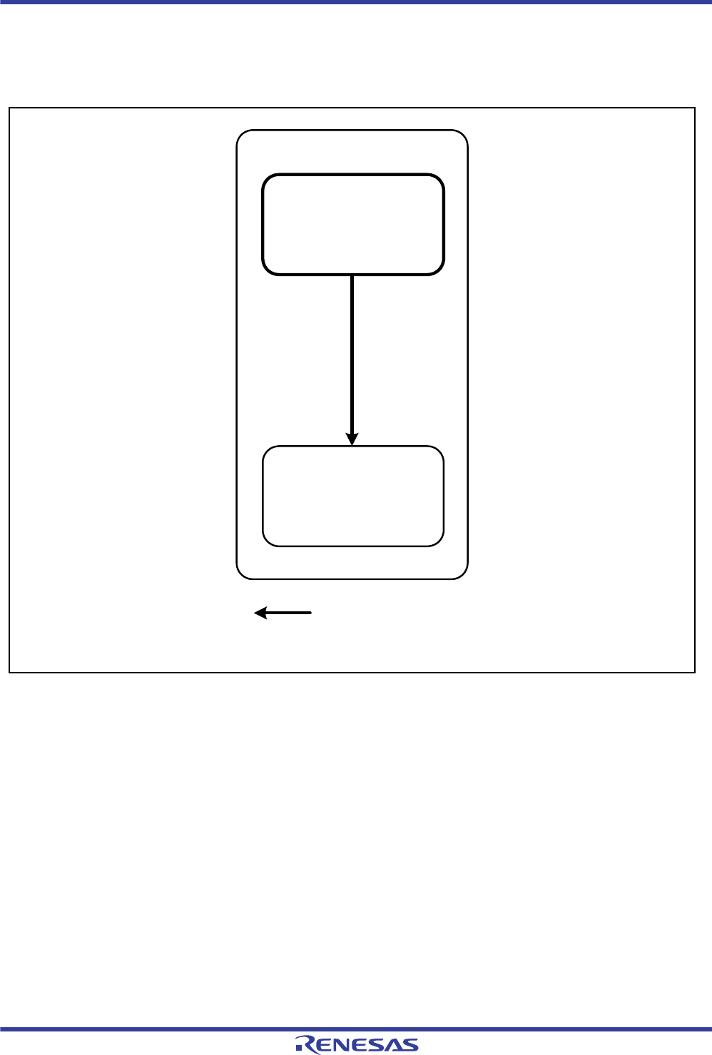
R01UH0034EJ0200 Rev.2.00 Page 108 of 1489
Dec 27, 2013
RX62T Group, RX62G Group 3. Operating Modes
Under development Preliminary document
Specifications in this document are tentative and subject to change.
3.4.2 Operating Mode Transitions According to Register Setting
Figure 3.2 shows operating mode transitions according to the setting of the ROME and EXBE bits in SYSCR0.
Operating modes can shift in the direction of arrow.
Figure 3.2 Setting of Bits ROME and Operating Modes
Single-chip mode
Mode can shift
On-chip ROM: Disabled
ROME = 0
On-chip ROM: Enabled*
ROME = 1
ROME = 0
Note: * Initial state after reset
R01UH0034EJ0200 Rev.2.00 Page 109 of 1489
Dec 27, 2013
RX62T Group, RX62G Group 4. Address Space
Under development Preliminary document
Specifications in this document are tentative and subject to change.
4. Address Space
4.1 Address Space
This LSI has a 4-Gbyte address space, consisting of the range of addresses from 0000 0000h to FFFF FFFFh. That is,
linear access to an address space of up to 4 Gbytes is possible, and this contains both program and data areas.
Figure 4.1 shows the memory maps.
Figure 4.1 Memory Map (RX62T Group)
Reserved area*2
Reserved area*2
0000 0000h
0008 0000h
FFFF FFFFh
Single-chip mode*1
On-chip RAM
Reserved area*2
On-chip ROM (program ROM)
(read only)
0010 0000h
Peripheral I/O registers
0010 8000h
On-chip ROM
(data flash)
0080 0000h
0100 0000h
On-chip ROM (program ROM)
(write only)
FFFC 0000h
FCU-RAM*3
Reserved area*2
Peripheral I/O registers
Reserved area*2
Peripheral I/O registers
007F 8000h
007F A000h
007F C000h
007F C500h
007F FC00h
0000 4000h
Reserved area*2
00FC 0000h
On-chip ROM (FCU firmware)*3
(read only)
Reserved area*2
FEFF E000h
FF00 0000h
R5F562TAxxxx
Reserved area*2
Reserved area*2
0000 0000h
0008 0000h
FFFF FFFFh
Single-chip mode*1
On-chip RAM
Reserved area*2
On-chip ROM (program ROM)
(read only)
0010 0000h
Peripheral I/O registers
0010 2000h
On-chip ROM
(data flash)
0080 0000h
0100 0000h
On-chip ROM (program ROM)
(write only)
FFFE 0000h
FCU-RAM*3
Reserved area*2
Peripheral I/O registers
Reserved area*2
Peripheral I/O registers
007F 8000h
007F A000h
007F C000h
007F C500h
007F FC00h
0000 2000h
Reserved area*2
00FE 0000h
On-chip ROM (FCU firmware)*3
(read only)
Reserved area*2
FEFF E000h
FF00 0000h
R5F562T7xxxx
Reserved area*2
Reserved area*2
0000 0000h
0008 0000h
FFFF FFFFh
Single-chip mode*1
On-chip RAM
Reserved area*2
On-chip ROM (program ROM)
(read only)
0010 0000h
Peripheral I/O registers
0010 2000h
On-chip ROM
(data flash)
0080 0000h
0100 0000h
On-chip ROM (program ROM)
(write only)
FFFF 0000h
FCU-RAM*3
Reserved area*2
Peripheral I/O registers
Reserved area*2
Peripheral I/O registers
007F 8000h
007F A000h
007F C000h
007F C500h
007F FC00h
0000 2000h
Reserved area*2
00FF 0000h
On-chip ROM (FCU firmware)*3
(read only)
Reserved area*2
FEFF E000h
FF00 0000h
R5F562T6xxxx
Notes: 1. The layout of the address space in boot mode is the same as in single-chip mode.
2. Reserved areas should not be accessed, since the correct operation of LSI is not guaranteed
if they are accessed.
3. For details on the FCU, see section 31, ROM (Flash Memory for Code Storage) and section 32, Data
Flash (Flash Memory for Data Storage).

R01UH0034EJ0200 Rev.2.00 Page 110 of 1489
Dec 27, 2013
RX62T Group, RX62G Group 5. I/O Registers
5. I/O Registers
This section gives information on the on-chip I/O register addresses and bit configurations. The information is given as
shown below. Notes on writing to registers are also given at the end.
(1) I/O register addresses (address order)
Registers are listed from the lower allocation addresses.
Registers are classified according to functional modules (abbreviations).
The number of access cycles indicates the number of states based on the specified reference clock.
Among the I/O register area, addresses not listed in the list of registers are reserved. Reserved addresses must not be
accessed. Do not access these addresses; otherwise, the operation when accessing these bits and subsequent
operations cannot be guaranteed.
A unit of access is specified for each register. Access other than in the specified unit is prohibited.
(2) I/O register bits
Bit configurations of the registers are listed in the same order as the register addresses.
Reserved bits are indicated by "—" in the bit name column.
Space in the bit name field indicates that the entire register is allocated to either the counter or data.
For the registers of 16 or 32 bits, the MSB is listed first.
(3) Notes on writing to I/O registers
When writing to an I/O register, the CPU starts executing the subsequent instruction before completing I/O register write.
This may cause the subsequent instruction to be executed before the post-update I/O register value is reflected on the
operation.
As described in the following examples, special care is required for the cases in which the subsequent instruction must be
executed after the post-update I/O register value is actually reflected.
[Examples of cases requiring special care]
The subsequent instruction must be executed while an interrupt request is disabled with the IENj bit in IERm of the
ICU (interrupt request enable bit)*1 cleared to 0.
A WAIT instruction is executed immediately after the preprocessing for causing a transition to the low power
consumption state.
Note 1. See section 11.2.2, Interrupt Request Enable Register m (IERm) (m = 02h to 1Fh).
In the above cases, after writing to an I/O register, wait until the write operation is completed using the following
procedure and then execute the subsequent instruction.

R01UH0034EJ0200 Rev.2.00 Page 111 of 1489
Dec 27, 2013
RX62T Group, RX62G Group 5. I/O Registers
(a) Write to an I/O register.
(b) Read the value from the I/O register to a general register.
(c) Execute the operation using the value read.
(d) Execute the subsequent instruction.
[Instruction examples]
If multiple registers are written to and a subsequent instruction should be executed after the write operations are entirely
completed, only read the I/O register that was last written to and execute the operation using the value; it is not necessary
to read or execute operation for all the registers that were written to.
Byte-size I/O registers
MOV.L #SFR_ADDR, R1
MOV.B #SFR_DATA, [R1]
CMP [R1].UB, R1
;; Next process
Word-size I/O registers
MOV.L #SFR_ADDR, R1
MOV.W #SFR_DATA, [R1]
CMP [R1].W, R1
;; Next process
Longword-size I/O registers
MOV.L #SFR_ADDR, R1
MOV.L #SFR_DATA, [R1]
CMP [R1].L, R1
;; Next process

R01UH0034EJ0200 Rev.2.00 Page 112 of 1489
Dec 27, 2013
RX62T Group, RX62G Group 5. I/O Registers
(4) Number of Access Cycles to I/O Registers
The number of access cycles to I/O registers is obtained by following equation.*
Number of access cycles to I/O registers = Number of bus cycles for internal main bus 1 +
Number of divided cycles for clock synchronization +
Number of bus cycles for internal peripheral buses 1, 2, 4, and 6
The number of bus cycles for internal peripheral buses 1, 2, 4, and 6 differs according to the register to be accessed. For
the number of access cycles to each I/O register, see Table 5.1, List of I/O Registers.
When peripheral functions connected to internal peripheral bus 6 are accessed, the number of divided cycles for clock
synchronization is added.
Although the number of divided cycles for clock synchronization differs depending on the number of frequency ratio
between ICLK and PCLK or bus access timing, the sum of the number of bus cycles for internal main bus 1 and the
number of divided cycles for clock synchronization will be one PCLK at a maximum. Therefore, one PCLK is added to
the number of access cycles shown in Table 5.1.
Note: • This applies to the number of cycles when the access from the CPU does not conflict with the instruction fetching
to the external memory or bus access from the different bus master (DTC).

R01UH0034EJ0200 Rev.2.00 Page 113 of 1489
Dec 27, 2013
RX62T Group, RX62G Group 5. I/O Registers
5.1 I/O Register Addresses (Address Order)
Table 5.1 List of I/O Registers (Address Order) (1 / 25)
Address Module
Abbreviation Register Name Register
Abbreviation Number
of Bits Access
Size
Number of
Access
Cycles
0008 0000h SYSTEM Mode monitor register MDMONR 16 16 3 ICLK
0008 0002h SYSTEM Mode status register MDSR 16 16 3 ICLK
0008 0006h SYSTEM System control register 0 SYSCR0 16 16 3 ICLK
0008 0008h SYSTEM System control register 1 SYSCR1 16 16 3 ICLK
0008 000Ch SYSTEM Standby control register SBYCR 16 16 3 ICLK
0008 0010h SYSTEM Module stop control register A MSTPCRA 32 32 3 ICLK
0008 0014h SYSTEM Module stop control register B MSTPCRB 32 32 3 ICLK
0008 0018h SYSTEM Module stop control register C MSTPCRC 32 32 3 ICLK
0008 0020h SYSTEM System clock control register SCKCR 32 32 3 ICLK
0008 0040h SYSTEM Oscillation stop detection control register OSTDCR 16 16 3 ICLK
0008 1300h BSC Bus error status clear register BERCLR 8 8 2 ICLK
0008 1304h BSC Bus error monitoring enable register BEREN 8 8 2 ICLK
0008 1308h BSC Bus error status register 1 BERSR1 8 8 2 ICLK
0008 130Ah BSC Bus error status register 2 BERSR2 16 16 2 ICLK
0008 2400h DTC DTC control register DTCCR 8 8 2 ICLK
0008 2404h DTC DTC vector base register DTCVBR 32 32 2 ICLK
0008 2408h DTC DTC address mode register DTCADMOD 8 8 2 ICLK
0008 240Ch DTC DTC module start register DTCST 8 8 2 ICLK
0008 240Eh DTC DTC status register DTCSTS 16 16 2 ICLK
0008 6400h MPU Region 0 start page-number register RSPAGE0 32 32 1 ICLK
0008 6404h MPU Region 0 end page-number register REPAGE0 32 32 1 ICLK
0008 6408h MPU Region 1 start page-number register RSPAGE1 32 32 1 ICLK
0008 640Ch MPU Region 1 end page-number register REPAGE1 32 32 1 ICLK
0008 6410h MPU Region 2 start page-number register RSPAGE2 32 32 1 ICLK
0008 6414h MPU Region 2 end page-number register REPAGE2 32 32 1 ICLK
0008 6418h MPU Region 3 start page-number register RSPAGE3 32 32 1 ICLK
0008 641Ch MPU Region 3 end page-number register REPAGE3 32 32 1 ICLK
0008 6420h MPU Region 4 start page-number register RSPAGE4 32 32 1 ICLK
0008 6424h MPU Region 4 end page-number register REPAGE4 32 32 1 ICLK
0008 6428h MPU Region 5 start page-number register RSPAGE5 32 32 1 ICLK
0008 642Ch MPU Region 5 end page-number register REPAGE5 32 32 1 ICLK
0008 6430h MPU Region 6 start page-number register RSPAGE6 32 32 1 ICLK
0008 6434h MPU Region 6 end page-number register REPAGE6 32 32 1 ICLK
0008 6438h MPU Region 7 start page-number register RSPAGE7 32 32 1 ICLK
0008 643Ch MPU Region 7 end page-number register REPAGE7 32 32 1 ICLK
0008 6500h MPU Memory-protection enable register MPEN 32 32 1 ICLK
0008 6504h MPU Background access control register MPBAC 32 32 1 ICLK
0008 6508h MPU Memory-protection error status-clearing register MPECLR 32 32 1 ICLK
0008 650Ch MPU Memory-protection error status register MPESTS 32 32 1 ICLK
0008 6514h MPU Data memory-protection error address register MPDEA 32 32 1 ICLK
0008 6520h MPU Region search address register MPSA 32 32 1 ICLK
0008 6524h MPU Region search operation register MPOPS 16 16 1 ICLK

R01UH0034EJ0200 Rev.2.00 Page 114 of 1489
Dec 27, 2013
RX62T Group, RX62G Group 5. I/O Registers
0008 6526h MPU Region invalidation operation register MPOPI 16 16 1 ICLK
0008 6528h MPU Instruction-hit region register MHITI 32 32 1 ICLK
0008 652Ch MPU Data-hit region register MHITD 32 32 1 ICLK
0008 7010h ICU Interrupt request register 016 IR016 8 8 2 ICLK
0008 7015h ICU Interrupt request register 021 IR021 8 8 2 ICLK
0008 7017h ICU Interrupt request register 023 IR023 8 8 2 ICLK
0008 701Bh ICU Interrupt request register 027 IR027 8 8 2 ICLK
0008 701Ch ICU Interrupt request register 028 IR028 8 8 2 ICLK
0008 701Dh ICU Interrupt request register 029 IR029 8 8 2 ICLK
0008 701Eh ICU Interrupt request register 030 IR030 8 8 2 ICLK
0008 701Fh ICU Interrupt request register 031 IR031 8 8 2 ICLK
0008 702Ch ICU Interrupt request register 044 IR044 8 8 2 ICLK
0008 702Dh ICU Interrupt request register 045 IR045 8 8 2 ICLK
0008 702Eh ICU Interrupt request register 046 IR046 8 8 2 ICLK
0008 702Fh ICU Interrupt request register 047 IR047 8 8 2 ICLK
0008 7038h ICU Interrupt request register 056 IR056 8 8 2 ICLK
0008 7039h ICU Interrupt request register 057 IR057 8 8 2 ICLK
0008 703Ah ICU Interrupt request register 058 IR058 8 8 2 ICLK
0008 703Bh ICU Interrupt request register 059 IR059 8 8 2 ICLK
0008 703Ch ICU Interrupt request register 060 IR060 8 8 2 ICLK
0008 7040h ICU Interrupt request register 064 IR064 8 8 2 ICLK
0008 7041h ICU Interrupt request register 065 IR065 8 8 2 ICLK
0008 7042h ICU Interrupt request register 066 IR066 8 8 2 ICLK
0008 7043h ICU Interrupt request register 067 IR067 8 8 2 ICLK
0008 7044h ICU Interrupt request register 068 IR068 8 8 2 ICLK
0008 7045h ICU Interrupt request register 069 IR069 8 8 2 ICLK
0008 7046h ICU Interrupt request register 070 IR070 8 8 2 ICLK
0008 7047h ICU Interrupt request register 071 IR071 8 8 2 ICLK
0008 7060h ICU Interrupt request register 096 IR096 8 8 2 ICLK
0008 7062h ICU Interrupt request register 098 IR098 8 8 2 ICLK
0008 7066h ICU Interrupt request register 102 IR102 8 8 2 ICLK
0008 7067h ICU Interrupt request register 103 IR103 8 8 2 ICLK
0008 706Ah ICU Interrupt request register 106 IR106 8 8 2 ICLK
0008 7072h ICU Interrupt request register 114 IR114 8 8 2 ICLK
0008 7073h ICU Interrupt request register 115 IR115 8 8 2 ICLK
0008 7074h ICU Interrupt request register 116 IR116 8 8 2 ICLK
0008 7075h ICU Interrupt request register 117 IR117 8 8 2 ICLK
0008 7076h ICU Interrupt request register 118 IR118 8 8 2 ICLK
0008 7077h ICU Interrupt request register 119 IR119 8 8 2 ICLK
0008 7078h ICU Interrupt request register 120 IR120 8 8 2 ICLK
0008 7079h ICU Interrupt request register 121 IR121 8 8 2 ICLK
0008 707Ah ICU Interrupt request register 122 IR122 8 8 2 ICLK
0008 707Bh ICU Interrupt request register 123 IR123 8 8 2 ICLK
0008 707Ch ICU Interrupt request register 124 IR124 8 8 2 ICLK
Table 5.1 List of I/O Registers (Address Order) (2 / 25)
Address Module
Abbreviation Register Name Register
Abbreviation Number
of Bits Access
Size
Number of
Access
Cycles

R01UH0034EJ0200 Rev.2.00 Page 115 of 1489
Dec 27, 2013
RX62T Group, RX62G Group 5. I/O Registers
0008 707Dh ICU Interrupt request register 125 IR125 8 8 2 ICLK
0008 707Eh ICU Interrupt request register 126 IR126 8 8 2 ICLK
0008 707Fh ICU Interrupt request register 127 IR127 8 8 2 ICLK
0008 7080h ICU Interrupt request register 128 IR128 8 8 2 ICLK
0008 7081h ICU Interrupt request register 129 IR129 8 8 2 ICLK
0008 7082h ICU Interrupt request register 130 IR130 8 8 2 ICLK
0008 7083h ICU Interrupt request register 131 IR131 8 8 2 ICLK
0008 7084h ICU Interrupt request register 132 IR132 8 8 2 ICLK
0008 7085h ICU Interrupt request register 133 IR133 8 8 2 ICLK
0008 7086h ICU Interrupt request register 134 IR134 8 8 2 ICLK
0008 7087h ICU Interrupt request register 135 IR135 8 8 2 ICLK
0008 7088h ICU Interrupt request register 136 IR136 8 8 2 ICLK
0008 7089h ICU Interrupt request register 137 IR137 8 8 2 ICLK
0008 708Ah ICU Interrupt request register 138 IR138 8 8 2 ICLK
0008 708Bh ICU Interrupt request register 139 IR139 8 8 2 ICLK
0008 708Ch ICU Interrupt request register 140 IR140 8 8 2 ICLK
0008 708Dh ICU Interrupt request register 141 IR141 8 8 2 ICLK
0008 708Eh ICU Interrupt request register 142 IR142 8 8 2 ICLK
0008 708Fh ICU Interrupt request register 143 IR143 8 8 2 ICLK
0008 7090h ICU Interrupt request register 144 IR144 8 8 2 ICLK
0008 7091h ICU Interrupt request register 145 IR145 8 8 2 ICLK
0008 7092h ICU Interrupt request register 146 IR146 8 8 2 ICLK
0008 7095h ICU Interrupt request register 149 IR149 8 8 2 ICLK
0008 7096h ICU Interrupt request register 150 IR150 8 8 2 ICLK
0008 7097h ICU Interrupt request register 151 IR151 8 8 2 ICLK
0008 7098h ICU Interrupt request register 152 IR152 8 8 2 ICLK
0008 7099h ICU Interrupt request register 153 IR153 8 8 2 ICLK
0008 70AAh ICU Interrupt request register 170 IR170 8 8 2 ICLK
0008 70ABh ICU Interrupt request register 171 IR171 8 8 2 ICLK
0008 70ACh ICU Interrupt request register 172 IR172 8 8 2 ICLK
0008 70ADh ICU Interrupt request register 173 IR173 8 8 2 ICLK
0008 70AEh ICU Interrupt request register 174 IR174 8 8 2 ICLK
0008 70AFh ICU Interrupt request register 175 IR175 8 8 2 ICLK
0008 70B0h ICU Interrupt request register 176 IR176 8 8 2 ICLK
0008 70B1h ICU Interrupt request register 177 IR177 8 8 2 ICLK
0008 70B2h ICU Interrupt request register 178 IR178 8 8 2 ICLK
0008 70B3h ICU Interrupt request register 179 IR179 8 8 2 ICLK
0008 70B4h ICU Interrupt request register 180 IR180 8 8 2 ICLK
0008 70B5h ICU Interrupt request register 181 IR181 8 8 2 ICLK
0008 70B6h ICU Interrupt request register 182 IR182 8 8 2 ICLK
0008 70B7h ICU Interrupt request register 183 IR183 8 8 2 ICLK
0008 70B8h ICU Interrupt request register 184 IR184 8 8 2 ICLK
0008 70BAh ICU Interrupt request register 186 IR186 8 8 2 ICLK
0008 70BBh ICU Interrupt request register 187 IR187 8 8 2 ICLK
Table 5.1 List of I/O Registers (Address Order) (3 / 25)
Address Module
Abbreviation Register Name Register
Abbreviation Number
of Bits Access
Size
Number of
Access
Cycles

R01UH0034EJ0200 Rev.2.00 Page 116 of 1489
Dec 27, 2013
RX62T Group, RX62G Group 5. I/O Registers
0008 70BCh ICU Interrupt request register 188 IR188 8 8 2 ICLK
0008 70BDh ICU Interrupt request register 189 IR189 8 8 2 ICLK
0008 70BEh ICU Interrupt request register 190 IR190 8 8 2 ICLK
0008 70C0h ICU Interrupt request register 192 IR192 8 8 2 ICLK
0008 70C1h ICU Interrupt request register 193 IR193 8 8 2 ICLK
0008 70C2h ICU Interrupt request register 194 IR194 8 8 2 ICLK
0008 70C3h ICU Interrupt request register 195 IR195 8 8 2 ICLK
0008 70C4h ICU Interrupt request register 196 IR196 8 8 2 ICLK
0008 70D6h ICU Interrupt request register 214 IR214 8 8 2 ICLK
0008 70D7h ICU Interrupt request register 215 IR215 8 8 2 ICLK
0008 70D8h ICU Interrupt request register 216 IR216 8 8 2 ICLK
0008 70D9h ICU Interrupt request register 217 IR217 8 8 2 ICLK
0008 70DAh ICU Interrupt request register 218 IR218 8 8 2 ICLK
0008 70DBh ICU Interrupt request register 219 IR219 8 8 2 ICLK
0008 70DCh ICU Interrupt request register 220 IR220 8 8 2 ICLK
0008 70DDh ICU Interrupt request register 221 IR221 8 8 2 ICLK
0008 70DEh ICU Interrupt request register 222 IR222 8 8 2 ICLK
0008 70DFh ICU Interrupt request register 223 IR223 8 8 2 ICLK
0008 70E0h ICU Interrupt request register 224 IR224 8 8 2 ICLK
0008 70E1h ICU Interrupt request register 225 IR225 8 8 2 ICLK
0008 70F6h ICU Interrupt request register 246 IR246 8 8 2 ICLK
0008 70F7h ICU Interrupt request register 247 IR247 8 8 2 ICLK
0008 70F8h ICU Interrupt request register 248 IR248 8 8 2 ICLK
0008 70F9h ICU Interrupt request register 249 IR249 8 8 2 ICLK
0008 70FEh ICU Interrupt request register 254 IR254 8 8 2 ICLK
0008 711Bh ICU DTC activation enable register 027 DTCER027 8 8 2 ICLK
0008 711Ch ICU DTC activation enable register 028 DTCER028 8 8 2 ICLK
0008 711Dh ICU DTC activation enable register 029 DTCER029 8 8 2 ICLK
0008 711Eh ICU DTC activation enable register 030 DTCER030 8 8 2 ICLK
0008 711Fh ICU DTC activation enable register 031 DTCER031 8 8 2 ICLK
0008 712Dh ICU DTC activation enable register 045 DTCER045 8 8 2 ICLK
0008 712Eh ICU DTC activation enable register 046 DTCER046 8 8 2 ICLK
0008 7140h ICU DTC activation enable register 064 DTCER064 8 8 2 ICLK
0008 7141h ICU DTC activation enable register 065 DTCER065 8 8 2 ICLK
0008 7142h ICU DTC activation enable register 066 DTCER066 8 8 2 ICLK
0008 7143h ICU DTC activation enable register 067 DTCER067 8 8 2 ICLK
0008 7144h ICU DTC activation enable register 068 DTCER068 8 8 2 ICLK
0008 7145h ICU DTC activation enable register 069 DTCER069 8 8 2 ICLK
0008 7146h ICU DTC activation enable register 070 DTCER070 8 8 2 ICLK
0008 7147h ICU DTC activation enable register 071 DTCER071 8 8 2 ICLK
0008 7162h ICU DTC activation enable register 098 DTCER098 8 8 2 ICLK
0008 7166h ICU DTC activation enable register 102 DTCER102 8 8 2 ICLK
0008 7167h ICU DTC activation enable register 103 DTCER103 8 8 2 ICLK
0008 716Ah ICU DTC activation enable register 106 DTCER106 8 8 2 ICLK
Table 5.1 List of I/O Registers (Address Order) (4 / 25)
Address Module
Abbreviation Register Name Register
Abbreviation Number
of Bits Access
Size
Number of
Access
Cycles

R01UH0034EJ0200 Rev.2.00 Page 117 of 1489
Dec 27, 2013
RX62T Group, RX62G Group 5. I/O Registers
0008 7172h ICU DTC activation enable register 114 DTCER114 8 8 2 ICLK
0008 7173h ICU DTC activation enable register 115 DTCER115 8 8 2 ICLK
0008 7174h ICU DTC activation enable register 116 DTCER116 8 8 2 ICLK
0008 7175h ICU DTC activation enable register 117 DTCER117 8 8 2 ICLK
0008 7179h ICU DTC activation enable register 121 DTCER121 8 8 2 ICLK
0008 717Ah ICU DTC activation enable register 122 DTCER122 8 8 2 ICLK
0008 717Dh ICU DTC activation enable register 125 DTCER125 8 8 2 ICLK
0008 717Eh ICU DTC activation enable register 126 DTCER126 8 8 2 ICLK
0008 7181h ICU DTC activation enable register 129 DTCER129 8 8 2 ICLK
0008 7182h ICU DTC activation enable register 130 DTCER130 8 8 2 ICLK
0008 7183h ICU DTC activation enable register 131 DTCER131 8 8 2 ICLK
0008 7184h ICU DTC activation enable register 132 DTCER132 8 8 2 ICLK
0008 7186h ICU DTC activation enable register 134 DTCER134 8 8 2 ICLK
0008 7187h ICU DTC activation enable register 135 DTCER135 8 8 2 ICLK
0008 7188h ICU DTC activation enable register 136 DTCER136 8 8 2 ICLK
0008 7189h ICU DTC activation enable register 137 DTCER137 8 8 2 ICLK
0008 718Ah ICU DTC activation enable register 138 DTCER138 8 8 2 ICLK
0008 718Bh ICU DTC activation enable register 139 DTCER139 8 8 2 ICLK
0008 718Ch ICU DTC activation enable register 140 DTCER140 8 8 2 ICLK
0008 718Dh ICU DTC activation enable register 141 DTCER141 8 8 2 ICLK
0008 718Eh ICU DTC activation enable register 142 DTCER142 8 8 2 ICLK
0008 718Fh ICU DTC activation enable register 143 DTCER143 8 8 2 ICLK
0008 7190h ICU DTC activation enable register 144 DTCER144 8 8 2 ICLK
0008 7191h ICU DTC activation enable register 145 DTCER145 8 8 2 ICLK
0008 7195h ICU DTC activation enable register 149 DTCER149 8 8 2 ICLK
0008 7196h ICU DTC activation enable register 150 DTCER150 8 8 2 ICLK
0008 7197h ICU DTC activation enable register 151 DTCER151 8 8 2 ICLK
0008 7198h ICU DTC activation enable register 152 DTCER152 8 8 2 ICLK
0008 7199h ICU DTC activation enable register 153 DTCER153 8 8 2 ICLK
0008 71AEh ICU DTC activation enable register 174 DTCER174 8 8 2 ICLK
0008 71AFh ICU DTC activation enable register 175 DTCER175 8 8 2 ICLK
0008 71B0h ICU DTC activation enable register 176 DTCER176 8 8 2 ICLK
0008 71B1h ICU DTC activation enable register 177 DTCER177 8 8 2 ICLK
0008 71B2h ICU DTC activation enable register 178 DTCER178 8 8 2 ICLK
0008 71B3h ICU DTC activation enable register 179 DTCER179 8 8 2 ICLK
0008 71B4h ICU DTC activation enable register 180 DTCER180 8 8 2 ICLK
0008 71B5h ICU DTC activation enable register 181 DTCER181 8 8 2 ICLK
0008 71B6h ICU DTC activation enable register 182 DTCER182 8 8 2 ICLK
0008 71B7h ICU DTC activation enable register 183 DTCER183 8 8 2 ICLK
0008 71B8h ICU DTC activation enable register 184 DTCER184 8 8 2 ICLK
0008 71BAh ICU DTC activation enable register 186 DTCER186 8 8 2 ICLK
0008 71BBh ICU DTC activation enable register 187 DTCER187 8 8 2 ICLK
0008 71BCh ICU DTC activation enable register 188 DTCER188 8 8 2 ICLK
0008 71BDh ICU DTC activation enable register 189 DTCER189 8 8 2 ICLK
Table 5.1 List of I/O Registers (Address Order) (5 / 25)
Address Module
Abbreviation Register Name Register
Abbreviation Number
of Bits Access
Size
Number of
Access
Cycles

R01UH0034EJ0200 Rev.2.00 Page 118 of 1489
Dec 27, 2013
RX62T Group, RX62G Group 5. I/O Registers
0008 71BEh ICU DTC activation enable register 190 DTCER190 8 8 2 ICLK
0008 71C0h ICU DTC activation enable register 192 DTCER192 8 8 2 ICLK
0008 71C1h ICU DTC activation enable register 193 DTCER193 8 8 2 ICLK
0008 71C2h ICU DTC activation enable register 194 DTCER194 8 8 2 ICLK
0008 71C3h ICU DTC activation enable register 195 DTCER195 8 8 2 ICLK
0008 71C4h ICU DTC activation enable register 196 DTCER196 8 8 2 ICLK
0008 71D7h ICU DTC activation enable register 215 DTCER215 8 8 2 ICLK
0008 71D8h ICU DTC activation enable register 216 DTCER216 8 8 2 ICLK
0008 71DBh ICU DTC activation enable register 219 DTCER219 8 8 2 ICLK
0008 71DCh ICU DTC activation enable register 220 DTCER220 8 8 2 ICLK
0008 71DFh ICU DTC activation enable register 223 DTCER223 8 8 2 ICLK
0008 71E0h ICU DTC activation enable register 224 DTCER224 8 8 2 ICLK
0008 71F7h ICU DTC activation enable register 247 DTCER247 8 8 2 ICLK
0008 71F8h ICU DTC activation enable register 248 DTCER248 8 8 2 ICLK
0008 71FEh ICU DTC activation enable register 254 DTCER254 8 8 2 ICLK
0008 7202h ICU Interrupt request enable register 02 IER02 8 8 2 ICLK
0008 7203h ICU Interrupt request enable register 03 IER03 8 8 2 ICLK
0008 7205h ICU Interrupt request enable register 05 IER05 8 8 2 ICLK
0008 7207h ICU Interrupt request enable register 07 IER07 8 8 2 ICLK
0008 7208h ICU Interrupt request enable register 08 IER08 8 8 2 ICLK
0008 720Ch ICU Interrupt request enable register 0C IER0C 8 8 2 ICLK
0008 720Dh ICU Interrupt request enable register 0D IER0D 8 8 2 ICLK
0008 720Eh ICU Interrupt request enable register 0E IER0E 8 8 2 ICLK
0008 720Fh ICU Interrupt request enable register 0F IER0F 8 8 2 ICLK
0008 7210h ICU Interrupt request enable register 10 IER10 8 8 2 ICLK
0008 7211h ICU Interrupt request enable register 11 IER11 8 8 2 ICLK
0008 7212h ICU Interrupt request enable register 12 IER12 8 8 2 ICLK
0008 7213h ICU Interrupt request enable register 13 IER13 8 8 2 ICLK
0008 7215h ICU Interrupt request enable register 15 IER15 8 8 2 ICLK
0008 7216h ICU Interrupt request enable register 16 IER16 8 8 2 ICLK
0008 7217h ICU Interrupt request enable register 17 IER17 8 8 2 ICLK
0008 7218h ICU Interrupt request enable register 18 IER18 8 8 2 ICLK
0008 721Ah ICU Interrupt request enable register 1A IER1A 8 8 2 ICLK
0008 721Bh ICU Interrupt request enable register 1B IER1B 8 8 2 ICLK
0008 721Ch ICU Interrupt request enable register 1C IER1C 8 8 2 ICLK
0008 721Eh ICU Interrupt request enable register 1E IER1E 8 8 2 ICLK
0008 721Fh ICU Interrupt request enable register 1F IER1F 8 8 2 ICLK
0008 72E0h ICU Software interrupt activation register SWINTR 8 8 2 ICLK
0008 72F0h ICU Fast interrupt set register FIR 16 16 2 ICLK
0008 7300h ICU Interrupt source priority register 00 IPR00 8 8 2 ICLK
0008 7301h ICU Interrupt source priority register 01 IPR01 8 8 2 ICLK
0008 7302h ICU Interrupt source priority register 02 IPR02 8 8 2 ICLK
0008 7303h ICU Interrupt source priority register 03 IPR03 8 8 2 ICLK
0008 7304h ICU Interrupt source priority register 04 IPR04 8 8 2 ICLK
Table 5.1 List of I/O Registers (Address Order) (6 / 25)
Address Module
Abbreviation Register Name Register
Abbreviation Number
of Bits Access
Size
Number of
Access
Cycles

R01UH0034EJ0200 Rev.2.00 Page 119 of 1489
Dec 27, 2013
RX62T Group, RX62G Group 5. I/O Registers
0008 7305h ICU Interrupt source priority register 05 IPR05 8 8 2 ICLK
0008 7306h ICU Interrupt source priority register 06 IPR06 8 8 2 ICLK
0008 7307h ICU Interrupt source priority register 07 IPR07 8 8 2 ICLK
0008 7314h ICU Interrupt source priority register 14 IPR14 8 8 2 ICLK
0008 7318h ICU Interrupt source priority register 18 IPR18 8 8 2 ICLK
0008 7320h ICU Interrupt source priority register 20 IPR20 8 8 2 ICLK
0008 7321h ICU Interrupt source priority register 21 IPR21 8 8 2 ICLK
0008 7322h ICU Interrupt source priority register 22 IPR22 8 8 2 ICLK
0008 7323h ICU Interrupt source priority register 23 IPR23 8 8 2 ICLK
0008 7324h ICU Interrupt source priority register 24 IPR24 8 8 2 ICLK
0008 7325h ICU Interrupt source priority register 25 IPR25 8 8 2 ICLK
0008 7326h ICU Interrupt source priority register 26 IPR26 8 8 2 ICLK
0008 7327h ICU Interrupt source priority register 27 IPR27 8 8 2 ICLK
0008 7340h ICU Interrupt source priority register 40 IPR40 8 8 2 ICLK
0008 7344h ICU Interrupt source priority register 44 IPR44 8 8 2 ICLK
0008 7348h ICU Interrupt source priority register 48 IPR48 8 8 2 ICLK
0008 7349h ICU Interrupt source priority register 49 IPR49 8 8 2 ICLK
0008 7351h ICU Interrupt source priority register 51 IPR51 8 8 2 ICLK
0008 7352h ICU Interrupt source priority register 52 IPR52 8 8 2 ICLK
0008 7353h ICU Interrupt source priority register 53 IPR53 8 8 2 ICLK
0008 7354h ICU Interrupt source priority register 54 IPR54 8 8 2 ICLK
0008 7355h ICU Interrupt source priority register 55 IPR55 8 8 2 ICLK
0008 7356h ICU Interrupt source priority register 56 IPR56 8 8 2 ICLK
0008 7357h ICU Interrupt source priority register 57 IPR57 8 8 2 ICLK
0008 7358h ICU Interrupt source priority register 58 IPR58 8 8 2 ICLK
0008 7359h ICU Interrupt source priority register 59 IPR59 8 8 2 ICLK
0008 735Ah ICU Interrupt source priority register 5A IPR5A 8 8 2 ICLK
0008 735Bh ICU Interrupt source priority register 5B IPR5B 8 8 2 ICLK
0008 735Ch ICU Interrupt source priority register 5C IPR5C 8 8 2 ICLK
0008 735Dh ICU Interrupt source priority register 5D IPR5D 8 8 2 ICLK
0008 735Eh ICU Interrupt source priority register 5E IPR5E 8 8 2 ICLK
0008 735Fh ICU Interrupt source priority register 5F IPR5F 8 8 2 ICLK
0008 7360h ICU Interrupt source priority register 60 IPR60 8 8 2 ICLK
0008 7367h ICU Interrupt source priority register 67 IPR67 8 8 2 ICLK
0008 7368h ICU Interrupt source priority register 68 IPR68 8 8 2 ICLK
0008 7369h ICU Interrupt source priority register 69 IPR69 8 8 2 ICLK
0008 736Ah ICU Interrupt source priority register 6A IPR6A 8 8 2 ICLK
0008 736Bh ICU Interrupt source priority register 6B IPR6B 8 8 2 ICLK
0008 736Ch ICU Interrupt source priority register 6C IPR6C 8 8 2 ICLK
0008 736Dh ICU Interrupt source priority register 6D IPR6D 8 8 2 ICLK
0008 736Eh ICU Interrupt source priority register 6E IPR6E 8 8 2 ICLK
0008 736Fh ICU Interrupt source priority register 6F IPR6F 8 8 2 ICLK
0008 7380h ICU Interrupt source priority register 80 IPR80 8 8 2 ICLK
0008 7381h ICU Interrupt source priority register 81 IPR81 8 8 2 ICLK
Table 5.1 List of I/O Registers (Address Order) (7 / 25)
Address Module
Abbreviation Register Name Register
Abbreviation Number
of Bits Access
Size
Number of
Access
Cycles

R01UH0034EJ0200 Rev.2.00 Page 120 of 1489
Dec 27, 2013
RX62T Group, RX62G Group 5. I/O Registers
0008 7382h ICU Interrupt source priority register 82 IPR82 8 8 2 ICLK
0008 7388h ICU Interrupt source priority register 88 IPR88 8 8 2 ICLK
0008 7389h ICU Interrupt source priority register 89 IPR89 8 8 2 ICLK
0008 738Ah ICU Interrupt source priority register 8A IPR8A 8 8 2 ICLK
0008 738Bh ICU Interrupt source priority register 8B IPR8B 8 8 2 ICLK
0008 7390h ICU Interrupt source priority register 90 IPR90 8 8 2 ICLK
0008 7500h ICU IRQ control register 0 IRQCR0 8 8 2 ICLK
0008 7501h ICU IRQ control register 1 IRQCR1 8 8 2 ICLK
0008 7502h ICU IRQ control register 2 IRQCR2 8 8 2 ICLK
0008 7503h ICU IRQ control register 3 IRQCR3 8 8 2 ICLK
0008 7504h ICU IRQ control register 4 IRQCR4 8 8 2 ICLK
0008 7505h ICU IRQ control register 5 IRQCR5 8 8 2 ICLK
0008 7506h ICU IRQ control register 6 IRQCR6 8 8 2 ICLK
0008 7507h ICU IRQ control register 7 IRQCR7 8 8 2 ICLK
0008 7580h ICU Non-maskable interrupt status register NMISR 8 8 2 ICLK
0008 7581h ICU Non-maskable interrupt enable register NMIER 8 8 2 ICLK
0008 7582h ICU Non-maskable interrupt clear register NMICLR 8 8 2 ICLK
0008 7583h ICU NMI pin interrupt control register NMICR 8 8 2 ICLK
0008 8000h CMT Compare match timer start register 0 CMSTR0 16 16 2, 3 PCLK*3
0008 8002h CMT0 Compare match timer control register CMCR 16 16 2, 3 PCLK*3
0008 8004h CMT0 Compare match timer counter CMCNT 16 16 2, 3 PCLK*3
0008 8006h CMT0 Compare match timer constant register CMCOR 16 16 2, 3 PCLK*3
0008 8008h CMT1 Compare match timer control register CMCR 16 16 2, 3 PCLK*3
0008 800Ah CMT1 Compare match timer counter CMCNT 16 16 2, 3 PCLK*3
0008 800Ch CMT1 Compare match timer constant register CMCOR 16 16 2, 3 PCLK*3
0008 8010h CMT Compare match timer start register 1 CMSTR1 16 16 2, 3 PCLK*3
0008 8012h CMT2 Compare match timer control register CMCR 16 16 2, 3 PCLK*3
0008 8014h CMT2 Compare match timer counter CMCNT 16 16 2, 3 PCLK*3
0008 8016h CMT2 Compare match timer constant register CMCOR 16 16 2, 3 PCLK*3
0008 8018h CMT3 Compare match timer control register CMCR 16 16 2, 3 PCLK*3
0008 801Ah CMT3 Compare match timer counter CMCNT 16 16 2, 3 PCLK*3
0008 801Ch CMT3 Compare match timer constant register CMCOR 16 16 2, 3 PCLK*3
0008 8028h WDT Timer control/status register TCSR 8 8 2, 3 PCLK*3
0008 8028h WDT Write window A register WINA 16 16 2, 3 PCLK*3
0008 8029h WDT Timer counter TCNT 8 8 2, 3 PCLK*3
0008 802Ah WDT Write window B register WINB 16 16 2, 3 PCLK*3
0008 802Bh WDT Reset control/status register RSTCSR 8 8 2, 3 PCLK*3
0008 8030h IWDT IWDT refresh register IWDTRR 8 8 2, 3 PCLK*3
0008 8032h IWDT IWDT control register IWDTCR 16 16 2, 3 PCLK*3
0008 8034h IWDT IWDT status register IWDTSR 16 16 2, 3 PCLK*3
0008 8040h ADA A/D data register A ADDRA 16 16 2, 3 PCLK*3
0008 8042h ADA A/D data register B ADDRB 16 16 2, 3 PCLK*3
0008 8044h ADA A/D data register C ADDRC 16 16 2, 3 PCLK*3
0008 8046h ADA A/D data register D ADDRD 16 16 2, 3 PCLK*3
Table 5.1 List of I/O Registers (Address Order) (8 / 25)
Address Module
Abbreviation Register Name Register
Abbreviation Number
of Bits Access
Size
Number of
Access
Cycles

R01UH0034EJ0200 Rev.2.00 Page 121 of 1489
Dec 27, 2013
RX62T Group, RX62G Group 5. I/O Registers
0008 8048h ADA A/D data register E ADDRE 16 16 2, 3 PCLK*3
0008 804Ah ADA A/D data register F ADDRF 16 16 2, 3 PCLK*3
0008 804Ch ADA A/D data register G ADDRG 16 16 2, 3 PCLK*3
0008 804Eh ADA A/D data register H ADDRH 16 16 2, 3 PCLK*3
0008 8050h ADA A/D control/status register ADCSR 8 8 2, 3 PCLK*3
0008 8051h ADA A/D control register ADCR 8 8 2, 3 PCLK*3
0008 805Bh ADA A/D sampling state register ADSSTR 8 8 2, 3 PCLK*3
0008 805Dh ADA A/D self-diagnostic register ADDIAGR 8 8 2, 3 PCLK*3
0008 8060h ADA A/D data register I ADDRI 16 16 2, 3 PCLK*3
0008 8062h ADA A/D data register J ADDRJ 16 16 2, 3 PCLK*3
0008 8064h ADA A/D data register K ADDRK 16 16 2, 3 PCLK*3
0008 8066h ADA A/D data register L ADDRL 16 16 2, 3 PCLK*3
0008 8070h ADA A/D start trigger select register ADSTRGR 8 8 2, 3 PCLK*3
0008 8072h ADA A/D data placement register ADDPR 8 8 2, 3 PCLK*3
0008 8240h SCI0 Serial mode register SMR*1 8 8 2, 3 PCLK*3
0008 8241h SCI0 Bit rate register BRR 8 8 2, 3 PCLK*3
0008 8242h SCI0 Serial control register SCR*1 8 8 2, 3 PCLK*3
0008 8243h SCI0 Transmit data register TDR 8 8 2, 3 PCLK*3
0008 8244h SCI0 Serial status register SSR*1 8 8 2, 3 PCLK*3
0008 8245h SCI0 Receive data register RDR 8 8 2, 3 PCLK*3
0008 8246h SCI0 Smart card mode register SCMR 8 8 2, 3 PCLK*3
0008 8247h SCI0 Serial extended mode register SEMR 8 8 2, 3 PCLK*3
0008 8240h SMCI0 Serial mode register SMR 8 8 2, 3 PCLK*3
0008 8241h SMCI0 Bit rate register BRR 8 8 2, 3 PCLK*3
0008 8242h SMCI0 Serial control register SCR 8 8 2, 3 PCLK*3
0008 8243h SMCI0 Transmit data register TDR 8 8 2, 3 PCLK*3
0008 8244h SMCI0 Serial status register SSR 8 8 2, 3 PCLK*3
0008 8245h SMCI0 Receive data register RDR 8 8 2, 3 PCLK*3
0008 8246h SMCI0 Smart card mode register SCMR 8 8 2, 3 PCLK*3
0008 8248h SCI1 Serial mode register SMR*1 8 8 2, 3 PCLK*3
0008 8249h SCI1 Bit rate register BRR 8 8 2, 3 PCLK*3
0008 824Ah SCI1 Serial control register SCR*1 8 8 2, 3 PCLK*3
0008 824Bh SCI1 Transmit data register TDR 8 8 2, 3 PCLK*3
0008 824Ch SCI1 Serial status register SSR*1 8 8 2, 3 PCLK*3
0008 824Dh SCI1 Receive data register RDR 8 8 2, 3 PCLK*3
0008 824Eh SCI1 Smart card mode register SCMR 8 8 2, 3 PCLK*3
0008 824Fh SCI1 Serial extended mode register SEMR 8 8 2, 3 PCLK*3
0008 8248h SMCI1 Serial mode register SMR 8 8 2, 3 PCLK*3
0008 8249h SMCI1 Bit rate register BRR 8 8 2, 3 PCLK*3
0008 824Ah SMCI1 Serial control register SCR 8 8 2, 3 PCLK*3
0008 824Bh SMCI1 Transmit data register TDR 8 8 2, 3 PCLK*3
0008 824Ch SMCI1 Serial status register SSR 8 8 2, 3 PCLK*3
0008 824Dh SMCI1 Receive data register RDR 8 8 2, 3 PCLK*3
0008 824Eh SMCI1 Smart card mode register SCMR 8 8 2, 3 PCLK*3
Table 5.1 List of I/O Registers (Address Order) (9 / 25)
Address Module
Abbreviation Register Name Register
Abbreviation Number
of Bits Access
Size
Number of
Access
Cycles

R01UH0034EJ0200 Rev.2.00 Page 122 of 1489
Dec 27, 2013
RX62T Group, RX62G Group 5. I/O Registers
0008 8250h SCI2 Serial mode register SMR*1 8 8 2, 3 PCLK*3
0008 8251h SCI2 Bit rate register BRR 8 8 2, 3 PCLK*3
0008 8252h SCI2 Serial control register SCR*1 8 8 2, 3 PCLK*3
0008 8253h SCI2 Transmit data register TDR 8 8 2, 3 PCLK*3
0008 8254h SCI2 Serial status register SSR*1 8 8 2, 3 PCLK*3
0008 8255h SCI2 Receive data register RDR 8 8 2, 3 PCLK*3
0008 8256h SCI2 Smart card mode register SCMR 8 8 2, 3 PCLK*3
0008 8257h SCI2 Serial extended mode register SEMR 8 8 2, 3 PCLK*3
0008 8250h SMCI2 Serial mode register SMR*1 8 8 2, 3 PCLK*3
0008 8251h SMCI2 Bit rate register BRR 8 8 2, 3 PCLK*3
0008 8252h SMCI2 Serial control register SCR*1 8 8 2, 3 PCLK*3
0008 8253h SMCI2 Transmit data register TDR 8 8 2, 3 PCLK*3
0008 8254h SMCI2 Serial status register SSR*1 8 8 2, 3 PCLK*3
0008 8255h SMCI2 Receive data register RDR 8 8 2, 3 PCLK*3
0008 8256h SMCI2 Smart card mode register SCMR 8 8 2, 3 PCLK*3
0008 8280h CRC CRC control register CRCCR 8 8 2, 3 PCLK*3
0008 8281h CRC CRC data input register CRCDIR 8 8 2, 3 PCLK*3
0008 8282h CRC CRC data output register CRCDOR 16 16 2, 3 PCLK*3
0008 8300h RIIC I2C bus control register 1 ICCR1 8 8 2, 3 PCLK*3
0008 8301h RIIC I2C bus control register 2 ICCR2 8 8 2, 3 PCLK*3
0008 8302h RIIC I2C bus mode register 1 ICMR1 8 8 2, 3 PCLK*3
0008 8303h RIIC I2C bus mode register 2 ICMR2 8 8 2, 3 PCLK*3
0008 8304h RIIC I2C bus mode register 3 ICMR3 8 8 2, 3 PCLK*3
0008 8305h RIIC I2C bus function enable register ICFER 8 8 2, 3 PCLK*3
0008 8306h RIIC I2C bus status enable register ICSER 8 8 2, 3 PCLK*3
0008 8307h RIIC I2C bus interrupt enable register ICIER 8 8 2, 3 PCLK*3
0008 8308h RIIC I2C bus status register 1 ICSR1 8 8 2, 3 PCLK*3
0008 8309h RIIC I2C bus status register 2 ICSR2 8 8 2, 3 PCLK*3
0008 830Ah RIIC Slave address register L0 SARL0 8 8 2, 3 PCLK*3
0008 830Ah RIIC Internal counter L for timeout TMOCNTL 8 8 2, 3 PCLK*3
0008 830Bh RIIC Slave address register U0 SARU0 8 8 2, 3 PCLK*3
0008 830Bh RIIC Internal counter U for timeout TMOCNTU 8 8 2, 3 PCLK*3
0008 830Bh RIIC Slave address register U0 SARU0 8 8 2, 3 PCLK*3
0008 830Ch RIIC Slave address register L1 SARL1 8 8 2, 3 PCLK*3
0008 830Dh RIIC Slave address register U1 SARU1 8 8 2, 3 PCLK*3
0008 830Eh RIIC Slave address register L2 SARL2 8 8 2, 3 PCLK*3
0008 830Fh RIIC Slave address register U2 SARU2 8 8 2, 3 PCLK*3
0008 8310h RIIC I2C bus bit rate low-level register ICBRL 8 8 2, 3 PCLK*3
0008 8311h RIIC I2C bus bit rate high-level register ICBRH 8 8 2, 3 PCLK*3
0008 8312h RIIC I2C bus transmit data register ICDRT 8 8 2, 3 PCLK*3
0008 8313h RIIC I2C bus receive data register ICDRR 8 8 2, 3 PCLK*3
0008 8380h RSPI RSPI control register SPCR 8 8 2, 3 PCLK*3
0008 8381h RSPI RSPI slave select polarity register SSLP 8 8 2, 3 PCLK*3
0008 8382h RSPI RSPI pin control register SPPCR 8 8 2, 3 PCLK*3
Table 5.1 List of I/O Registers (Address Order) (10 / 25)
Address Module
Abbreviation Register Name Register
Abbreviation Number
of Bits Access
Size
Number of
Access
Cycles

R01UH0034EJ0200 Rev.2.00 Page 123 of 1489
Dec 27, 2013
RX62T Group, RX62G Group 5. I/O Registers
0008 8383h RSPI RSPI status register SPSR 8 8 2, 3 PCLK*3
0008 8384h RSPI RSPI data register SPDR 16, 32 16, 32 2, 3 PCLK*3
0008 8388h RSPI RSPI sequence control register SPSCR 8 8 2, 3 PCLK*3
0008 8389h RSPI RSPI sequence status register SPSSR 8 8 2, 3 PCLK*3
0008 838Ah RSPI RSPI bit rate register SPBR 8 8 2, 3 PCLK*3
0008 838Bh RSPI RSPI data control register SPDCR 8 8 2, 3 PCLK*3
0008 838Ch RSPI RSPI clock delay register SPCKD 8 8 2, 3 PCLK*3
0008 838Dh RSPI RSPI slave select negation delay register SSLND 8 8 2, 3 PCLK*3
0008 838Eh RSPI RSPI next-access delay register SPND 8 8 2, 3 PCLK*3
0008 838Fh RSPI RSPI control register 2 SPCR2 8 8 2, 3 PCLK*3
0008 8390h RSPI RSPI command register 0 SPCMD0 16 16 2, 3 PCLK*3
0008 8392h RSPI RSPI command register 1 SPCMD1 16 16 2, 3 PCLK*3
0008 8394h RSPI RSPI command register 2 SPCMD2 16 16 2, 3 PCLK*3
0008 8396h RSPI RSPI command register 3 SPCMD3 16 16 2, 3 PCLK*3
0008 8398h RSPI RSPI command register 4 SPCMD4 16 16 2, 3 PCLK*3
0008 839Ah RSPI RSPI command register 5 SPCMD5 16 16 2, 3 PCLK*3
0008 839Ch RSPI RSPI command register 6 SPCMD6 16 16 2, 3 PCLK*3
0008 839Eh RSPI RSPI command register 7 SPCMD7 16 16 2, 3 PCLK*3
0008 9000h S12AD0 A/D control register ADCSR 8 8 2, 3 PCLK*3
0008 9004h S12AD0 A/D channel select register ADANS 16 16 2, 3 PCLK*3
0008 900Ah S12AD0 A/D programmable gain amplifier register ADPG 16 16 2, 3 PCLK*3
0008 900Eh S12AD0 A/D control extended register ADCER 16 16 2, 3 PCLK*3
0008 9010h S12AD0 A/D start trigger select register ADSTRGR 16 16 2, 3 PCLK*3
0008 9012h S12AD Comparator operating mode select register 0 ADCMPMD0 16 16 2, 3 PCLK*3
0008 9014h S12AD Comparator operating mode select register 1 ADCMPMD1 16 16 2, 3 PCLK*3
0008 9016h S12AD Comparator filter mode register 0 ADCMPNR0 16 16 2, 3 PCLK*3
0008 9018h S12AD Comparator filter mode register 1 ADCMPNR1 16 16 2, 3 PCLK*3
0008 901Ah S12AD Comparator detection flag register ADCMPFR 8 8 2, 3 PCLK*3
0008 901Ch S12AD Comparator interrupt select register ADCMPSEL 16 16 2, 3 PCLK*3
0008 901Eh S12AD0 A/D data register Diag ADRD 16 16 2, 3 PCLK*3
0008 9020h S12AD0 A/D data register 0A ADDR0A 16 16 2, 3 PCLK*3
0008 9022h S12AD0 A/D data register 1 ADDR1 16 16 2, 3 PCLK*3
0008 9024h S12AD0 A/D data register 2 ADDR2 16 16 2, 3 PCLK*3
0008 9026h S12AD0 A/D data register 3 ADDR3 16 16 2, 3 PCLK*3
0008 9030h S12AD0 A/D data register 0B ADDR0B 16 16 2, 3 PCLK*3
0008 9060h S12AD0 A/D sampling state register ADSSTR 8 8 2, 3 PCLK*3
0008 9080h S12AD1 A/D control register ADCSR 8 8 2, 3 PCLK*3
0008 9084h S12AD1 A/D channel select register ADANS 16 16 2, 3 PCLK*3
0008 908Ah S12AD1 A/D programmable gain amplifier register ADPG 16 16 2, 3 PCLK*3
0008 908Eh S12AD1 A/D control extended register ADCER 16 16 2, 3 PCLK*3
0008 9090h S12AD1 A/D start trigger select register ADSTRGR 16 16 2, 3 PCLK*3
0008 909Eh S12AD1 A/D data register Diag ADRD 16 16 2, 3 PCLK*3
0008 90A0h S12AD1 A/D data register 0A ADDR0A 16 16 2, 3 PCLK*3
0008 90A2h S12AD1 A/D data register 1 ADDR1 16 16 2, 3 PCLK*3
Table 5.1 List of I/O Registers (Address Order) (11 / 25)
Address Module
Abbreviation Register Name Register
Abbreviation Number
of Bits Access
Size
Number of
Access
Cycles

R01UH0034EJ0200 Rev.2.00 Page 124 of 1489
Dec 27, 2013
RX62T Group, RX62G Group 5. I/O Registers
0008 90A4h S12AD1 A/D data register 2 ADDR2 16 16 2, 3 PCLK*3
0008 90A6h S12AD1 A/D data register 3 ADDR3 16 16 2, 3 PCLK*3
0008 90B0h S12AD1 A/D data register 0B ADDR0B 16 16 2, 3 PCLK*3
0008 90E0h S12AD1 A/D sampling state register ADSSTR 8 8 2, 3 PCLK*3
0008 C001h PORT1 Data direction register DDR 8 8 2, 3 PCLK*3
0008 C002h PORT2 Data direction register DDR 8 8 2, 3 PCLK*3
0008 C003h PORT3 Data direction register DDR 8 8 2, 3 PCLK*3
0008 C007h PORT7 Data direction register DDR 8 8 2, 3 PCLK*3
0008 C008h PORT8 Data direction register DDR 8 8 2, 3 PCLK*3
0008 C009h PORT9 Data direction register DDR 8 8 2, 3 PCLK*3
0008 C00Ah PORTA Data direction register DDR 8 8 2, 3 PCLK*3
0008 C00Bh PORTB Data direction register DDR 8 8 2, 3 PCLK*3
0008 C00Dh PORTD Data direction register DDR 8 8 2, 3 PCLK*3
0008 C00Eh PORTE Data direction register DDR 8 8 2, 3 PCLK*3
0008 C010h PORTG Data direction register DDR*18 8 2, 3 PCLK*3
0008 C021h PORT1 Data register DR 8 8 2, 3 PCLK*3
0008 C022h PORT2 Data register DR 8 8 2, 3 PCLK*3
0008 C023h PORT3 Data register DR 8 8 2, 3 PCLK*3
0008 C027h PORT7 Data register DR 8 8 2, 3 PCLK*3
0008 C028h PORT8 Data register DR 8 8 2, 3 PCLK*3
0008 C029h PORT9 Data register DR 8 8 2, 3 PCLK*3
0008 C02Ah PORTA Data register DR 8 8 2, 3 PCLK*3
0008 C02Bh PORTB Data register DR 8 8 2, 3 PCLK*3
0008 C02Dh PORTD Data register DR 8 8 2, 3 PCLK*3
0008 C02Eh PORTE Data register DR 8 8 2, 3 PCLK*3
0008 C030h PORTG Data register DR*18 8 2, 3 PCLK*3
0008 C041h PORT1 Data register PORT 8 8 2, 3 PCLK*3
0008 C042h PORT2 Data register PORT 8 8 2, 3 PCLK*3
0008 C043h PORT3 Data register PORT 8 8 2, 3 PCLK*3
0008 C044h PORT4 Data register PORT 8 8 2, 3 PCLK*3
0008 C045h PORT5 Data register PORT 8 8 2, 3 PCLK*3
0008 C046h PORT6 Data register PORT 8 8 2, 3 PCLK*3
0008 C047h PORT7 Data register PORT 8 8 2, 3 PCLK*3
0008 C048h PORT8 Data register PORT 8 8 2, 3 PCLK*3
0008 C049h PORT9 Data register PORT 8 8 2, 3 PCLK*3
0008 C04Ah PORTA Data register PORT 8 8 2, 3 PCLK*3
0008 C04Bh PORTB Data register PORT 8 8 2, 3 PCLK*3
0008 C04Dh PORTD Data register PORT 8 8 2, 3 PCLK*3
0008 C04Eh PORTE Data register PORT 8 8 2, 3 PCLK*3
0008 C050h PORTG Port register PORT*18 8 2, 3 PCLK*3
0008 C061h PORT1 Input buffer control register ICR 8 8 2, 3 PCLK*3
0008 C062h PORT2 Input buffer control register ICR 8 8 2, 3 PCLK*3
0008 C063h PORT3 Input buffer control register ICR 8 8 2, 3 PCLK*3
0008 C064h PORT4 Input buffer control register ICR 8 8 2, 3 PCLK*3
Table 5.1 List of I/O Registers (Address Order) (12 / 25)
Address Module
Abbreviation Register Name Register
Abbreviation Number
of Bits Access
Size
Number of
Access
Cycles

R01UH0034EJ0200 Rev.2.00 Page 125 of 1489
Dec 27, 2013
RX62T Group, RX62G Group 5. I/O Registers
0008 C065h PORT5 Input buffer control register ICR 8 8 2, 3 PCLK*3
0008 C066h PORT6 Input buffer control register ICR 8 8 2, 3 PCLK*3
0008 C067h PORT7 Input buffer control register ICR 8 8 2, 3 PCLK*3
0008 C068h PORT8 Input buffer control register ICR 8 8 2, 3 PCLK*3
0008 C069h PORT9 Input buffer control register ICR 8 8 2, 3 PCLK*3
0008 C06Ah PORTA Input buffer control register ICR 8 8 2, 3 PCLK*3
0008 C06Bh PORTB Input buffer control register ICR 8 8 2, 3 PCLK*3
0008 C06Dh PORTD Input buffer control register ICR 8 8 2, 3 PCLK*3
0008 C06Eh PORTE Input buffer control register ICR 8 8 2, 3 PCLK*3
0008 C070h PORTG Input buffer control register ICR*18 8 2, 3 PCLK*3
0008 C108h IOPORT Port function register 8 PF8IRQ 8 8 2, 3 PCLK*3
0008 C109h IOPORT Port function register 9 PF9IRQ 8 8 2, 3 PCLK*3
0008 C10Ah IOPORT Port function register A PFAADC 8 8 2, 3 PCLK*3
0008 C10Ch IOPORT Port function register C PFCMTU 8 8 2, 3 PCLK*3
0008 C10Dh IOPORT Port function register D PFDGPT 8 8 2, 3 PCLK*3
0008 C10Fh IOPORT Port function register F PFFSCI 8 8 2, 3 PCLK*3
0008 C110h IOPORT Port function register G PFGSPI 8 8 2, 3 PCLK*3
0008 C111h IOPORT Port function register H PFHSPI 8 8 2, 3 PCLK*3
0008 C113h IOPORT Port function register J PFJCAN 8 8 2, 3 PCLK*3
0008 C114h IOPORT Port function register K PFKLIN 8 8 2, 3 PCLK*3
0008 C116h IOPORT Port function register M PFMPOE 8 8 2, 3 PCLK*3
0008 C117h IOPORT Port function register N PFNPOE 8 8 2, 3 PCLK*3
0008 C280h SYSTEM Deep standby control register DPSBYCR 8 8 4, 5 PCLK*3
0008 C281h SYSTEM Deep standby wait control register DPSWCR 8 8 4, 5 PCLK*3
0008 C282h SYSTEM Deep standby interrupt enable register DPSIER 8 8 4, 5 PCLK*3
0008 C283h SYSTEM Deep standby interrupt flag register DPSIFR 8 8 4, 5 PCLK*3
0008 C284h SYSTEM Deep standby interrupt edge register DPSIEGR 8 8 4, 5 PCLK*3
0008 C285h SYSTEM Reset status register RSTSR 8 8 4, 5 PCLK*3
0008 C289h FLASH Flash write erase protection register FWEPROR 8 8 4, 5 PCLK*3
0008 C28Ch SYSTEM Key code register for low-voltage detection
control register
LVDKEYR 8 8 4, 5 PCLK*3
0008 C28Dh SYSTEM Voltage detection control register LVDCR 8 8 4, 5 PCLK*3
0008 C290h SYSTEM Deep standby backup register 0 DPSBKR0 8 8 4, 5 PCLK*3
0008 C291h SYSTEM Deep standby backup register 1 DPSBKR1 8 8 4, 5 PCLK*3
0008 C292h SYSTEM Deep standby backup register 2 DPSBKR2 8 8 4, 5 PCLK*3
0008 C293h SYSTEM Deep standby backup register 3 DPSBKR3 8 8 4, 5 PCLK*3
0008 C294h SYSTEM Deep standby backup register 4 DPSBKR4 8 8 4, 5 PCLK*3
0008 C295h SYSTEM Deep standby backup register 5 DPSBKR5 8 8 4, 5 PCLK*3
0008 C296h SYSTEM Deep standby backup register 6 DPSBKR6 8 8 4, 5 PCLK*3
0008 C297h SYSTEM Deep standby backup register 7 DPSBKR7 8 8 4, 5 PCLK*3
0008 C298h SYSTEM Deep standby backup register 8 DPSBKR8 8 8 4, 5 PCLK*3
0008 C299h SYSTEM Deep standby backup register 9 DPSBKR9 8 8 4, 5 PCLK*3
0008 C29Ah SYSTEM Deep standby backup register 10 DPSBKR10 8 8 4, 5 PCLK*3
0008 C29Bh SYSTEM Deep standby backup register 11 DPSBKR11 8 8 4, 5 PCLK*3
Table 5.1 List of I/O Registers (Address Order) (13 / 25)
Address Module
Abbreviation Register Name Register
Abbreviation Number
of Bits Access
Size
Number of
Access
Cycles

R01UH0034EJ0200 Rev.2.00 Page 126 of 1489
Dec 27, 2013
RX62T Group, RX62G Group 5. I/O Registers
0008 C29Ch SYSTEM Deep standby backup register 12 DPSBKR12 8 8 4, 5 PCLK*3
0008 C29Dh SYSTEM Deep standby backup register 13 DPSBKR13 8 8 4, 5 PCLK*3
0008 C29Eh SYSTEM Deep standby backup register 14 DPSBKR14 8 8 4, 5 PCLK*3
0008 C29Fh SYSTEM Deep standby backup register 15 DPSBKR15 8 8 4, 5 PCLK*3
0008 C2A0h SYSTEM Deep standby backup register 16 DPSBKR16 8 8 4, 5 PCLK*3
0008 C2A1h SYSTEM Deep standby backup register 17 DPSBKR17 8 8 4, 5 PCLK*3
0008 C2A2h SYSTEM Deep standby backup register 18 DPSBKR18 8 8 4, 5 PCLK*3
0008 C2A3h SYSTEM Deep standby backup register 19 DPSBKR19 8 8 4, 5 PCLK*3
0008 C2A4h SYSTEM Deep standby backup register 20 DPSBKR20 8 8 4, 5 PCLK*3
0008 C2A5h SYSTEM Deep standby backup register 21 DPSBKR21 8 8 4, 5 PCLK*3
0008 C2A6h SYSTEM Deep standby backup register 22 DPSBKR22 8 8 4, 5 PCLK*3
0008 C2A7h SYSTEM Deep standby backup register 23 DPSBKR23 8 8 4, 5 PCLK*3
0008 C2A8h SYSTEM Deep standby backup register 24 DPSBKR24 8 8 4, 5 PCLK*3
0008 C2A9h SYSTEM Deep standby backup register 25 DPSBKR25 8 8 4, 5 PCLK*3
0008 C2AAh SYSTEM Deep standby backup register 26 DPSBKR26 8 8 4, 5 PCLK*3
0008 C2ABh SYSTEM Deep standby backup register 27 DPSBKR27 8 8 4, 5 PCLK*3
0008 C2ACh SYSTEM Deep standby backup register 28 DPSBKR28 8 8 4, 5 PCLK*3
0008 C2ADh SYSTEM Deep standby backup register 29 DPSBKR29 8 8 4, 5 PCLK*3
0008 C2AEh SYSTEM Deep standby backup register 30 DPSBKR30 8 8 4, 5 PCLK*3
0008 C2AFh SYSTEM Deep standby backup register 31 DPSBKR31 8 8 4, 5 PCLK*3
0008 C4C0h POE Input level control/status register 1 ICSR1 16 8, 16 2, 3 PCLK*3
0008 C4C2h POE Output level control/status register 1 OCSR1 16 8, 16 2, 3 PCLK*3
0008 C4C4h POE Input level control/status register 2 ICSR2 16 8, 16 2, 3 PCLK*3
0008 C4C6h POE Output level control/status register 2 OCSR2 16 8, 16 2, 3 PCLK*3
0008 C4C8h POE Input level control/status register 3 ICSR3 16 8, 16 2, 3 PCLK*3
0008 C4CAh POE Software port output enable register SPOER 8 8 2, 3 PCLK*3
0008 C4CBh POE Port output enable control register 1 POECR1 8 8 2, 3 PCLK*3
0008 C4CCh POE Port output enable control register 2 POECR2 16 16 2, 3 PCLK*3
0008 C4CEh POE Port output enable control register 3 POECR3 16 16 2, 3 PCLK*3
0008 C4D0h POE Port output enable control register 4 POECR4 16 16 2, 3 PCLK*3
0008 C4D2h POE Port output enable control register 5 POECR5 16 16 2, 3 PCLK*3
0008 C4D4h POE Port output enable control register 6 POECR6 16 16 2, 3 PCLK*3
0008 C4D6h POE Input level control/status register 4 ICSR4 16 8, 16 2, 3 PCLK*3
0008 C4D8h POE Input level control/status register 5 ICSR5 16 8, 16 2, 3 PCLK*3
0008 C4DAh POE Active level setting register 1 ALR1 16 8, 16 2, 3 PCLK*3
0009 0200h
to
0009 03FFh
CAN0*2 Mailbox registers 0 to 31 MB0
to
MB 31
128 8, 16, 32 2, 3 PCLK*3
0009 0400h CAN0*2 Mask register 0 MKR0 32 8, 16, 32 2, 3 PCLK*3
0009 0404h CAN0*2 Mask register 1 MKR1 32 8, 16, 32 2, 3 PCLK*3
0009 0408h CAN0*2 Mask register 2 MKR2 32 8, 16, 32 2, 3 PCLK*3
0009 040Ch CAN0*2 Mask register 3 MKR3 32 8, 16, 32 2, 3 PCLK*3
0009 0410h CAN0*2 Mask register 4 MKR4 32 8, 16, 32 2, 3 PCLK*3
0009 0414h CAN0*2 Mask register 5 MKR5 32 8, 16, 32 2, 3 PCLK*3
0009 0418h CAN0*2 Mask register 6 MKR6 32 8, 16, 32 2, 3 PCLK*3
Table 5.1 List of I/O Registers (Address Order) (14 / 25)
Address Module
Abbreviation Register Name Register
Abbreviation Number
of Bits Access
Size
Number of
Access
Cycles

R01UH0034EJ0200 Rev.2.00 Page 127 of 1489
Dec 27, 2013
RX62T Group, RX62G Group 5. I/O Registers
0009 041Ch CAN0*2 Mask register 7 MKR7 32 8, 16, 32 2, 3 PCLK*3
0009 0420h CAN0*2 FIFO received ID compare register 0 FIDCR0 32 8, 16, 32 2, 3 PCLK*3
0009 0424h CAN0*2 FIFO received ID compare register 1 FIDCR1 32 8, 16, 32 2, 3 PCLK*3
0009 0428h CAN0*2 Mask invalid register MKIVLR 32 8, 16, 32 2, 3 PCLK*3
0009 042Ch CAN0*2 Mailbox interrupt enable register MIER 32 8, 16, 32 2, 3 PCLK*3
0009 0820h
to
0009 083Fh
CAN0*2 Message control registers 0 to 31 MCTL0
to
MCTL31
8 8 2, 3 PCLK*3
0009 0840h CAN0*2 Control register CTLR 16 8, 16 2, 3 PCLK*3
0009 0842h CAN0*2 Status register STR 16 8, 16 2, 3 PCLK*3
0009 0844h CAN0*2 Bit configuration register BCR 32 8, 16, 32 2, 3 PCLK*3
0009 0848h CAN0*2 Receive FIFO control register RFCR 8 8 2, 3 PCLK*3
0009 0849h CAN0*2 Receive FIFO pointer control register RFPCR 8 8 2, 3 PCLK*3
0009 084Ah CAN0*2 Transmit FIFO control register TFCR 8 8 2, 3 PCLK*3
0009 084Bh CAN0*2 Transmit FIFO pointer control register TFPCR 8 8 2, 3 PCLK*3
0009 084Ch CAN0*2 Error interrupt enable register EIER 8 8 2, 3 PCLK*3
0009 084Dh CAN0*2 Error interrupt factor judge register EIFR 8 8 2, 3 PCLK*3
0009 084Eh CAN0*2 Receive error count register RECR 8 8 2, 3 PCLK*3
0009 084Fh CAN0*2 Transmit error count register TECR 8 8 2, 3 PCLK*3
0009 0850h CAN0*2 Error code store register ECSR 8 8 2, 3 PCLK*3
0009 0851h CAN0*2 Channel search support register CSSR 8 8 2, 3 PCLK*3
0009 0852h CAN0*2 Mailbox search status register MSSR 8 8 2, 3 PCLK*3
0009 0853h CAN0*2 Mailbox search mode register MSMR 8 8 2, 3 PCLK*3
0009 0854h CAN0*2 Time stamp register TSR 16 8, 16 2, 3 PCLK*3
0009 0856h CAN0*2 Acceptance filter support register AFSR 16 8, 16 2, 3 PCLK*3
0009 0858h CAN0*2 Test control register TCR 8 8 2, 3 PCLK*3
0009 4001h LIN0 LIN wake-up baud rate select register LWBR 8 8 2, 3 PCLK*3
0009 4002h LIN0 LIN baud rate prescaler 0 register LBRP0 8 8, 16 2, 3 PCLK*3
0009 4003h LIN0 LIN baud rate prescaler 1 register LBRP1 8 8, 16 2, 3 PCLK*3
0009 4004h LIN0 LIN self-test control register LSTC 8 8 2, 3 PCLK*3
0009 4008h LIN0 Mode register L0MD 8 8, 16, 32 2, 3 PCLK*3
0009 4009h LIN0 Break field setting register L0BRK 8 8, 16, 32 2, 3 PCLK*3
0009 400Ah LIN0 Space setting register L0SPC 8 8, 16, 32 2, 3 PCLK*3
0009 400Bh LIN0 Wake-up setting register L0WUP 8 8, 16, 32 2, 3 PCLK*3
0009 400Ch LIN0 Interrupt enable register L0IE 8 8, 16 2, 3 PCLK*3
0009 400Dh LIN0 Error detection enable register L0EDE 8 8, 16 2, 3 PCLK*3
0009 400Eh LIN0 Control register L0C 8 8 2, 3 PCLK*3
0009 4010h LIN0 Transmission control register L0TC 8 8, 16, 32 2, 3 PCLK*3
0009 4011h LIN0 Mode status register L0MST 8 8, 16, 32 2, 3 PCLK*3
0009 4012h LIN0 Status register L0ST 8 8, 16, 32 2, 3 PCLK*3
0009 4013h LIN0 Error status register L0EST 8 8, 16, 32 2, 3 PCLK*3
0009 4014h LIN0 Response field set register L0RFC 8 8, 16 2, 3 PCLK*3
0009 4015h LIN0 Buffer register L0IDB 8 8, 16 2, 3 PCLK*3
0009 4016h LIN0 Check sum buffer register L0CBR 8 8 2, 3 PCLK*3
0009 4018h LIN0 Data 1 buffer register L0DB1 8 8, 16, 32 2, 3 PCLK*3
Table 5.1 List of I/O Registers (Address Order) (15 / 25)
Address Module
Abbreviation Register Name Register
Abbreviation Number
of Bits Access
Size
Number of
Access
Cycles

R01UH0034EJ0200 Rev.2.00 Page 128 of 1489
Dec 27, 2013
RX62T Group, RX62G Group 5. I/O Registers
0009 4019h LIN0 Data 2 buffer register L0DB2 8 8, 16, 32 2, 3 PCLK*3
0009 401Ah LIN0 Data 3 buffer register L0DB3 8 8, 16, 32 2, 3 PCLK*3
0009 401Bh LIN0 Data 4 buffer register L0DB4 8 8, 16, 32 2, 3 PCLK*3
0009 401Ch LIN0 Data 5 buffer register L0DB5 8 8, 16, 32 2, 3 PCLK*3
0009 401Dh LIN0 Data 6 buffer register L0DB6 8 8, 16, 32 2, 3 PCLK*3
0009 401Eh LIN0 Data 7 buffer register L0DB7 8 8, 16, 32 2, 3 PCLK*3
0009 401Fh LIN0 Data 8 buffer register L0DB8 8 8, 16, 32 2, 3 PCLK*3
000C 1200h MTU3 Timer control register TCR 8 8, 16, 32 5 ICLK
000C 1201h MTU4 Timer control register TCR 8 8 5 ICLK
000C 1202h MTU3 Timer mode register 1 TMDR1 8 8, 16 5 ICLK
000C 1203h MTU4 Timer mode register 1 TMDR1 8 8 5 ICLK
000C 1204h MTU3 Timer I/O control register H TIORH 8 8, 16, 32 5 ICLK
000C 1205h MTU3 Timer I/O control register L TIORL 8 8 5 ICLK
000C 1206h MTU4 Timer I/O control register H TIORH 8 8, 16 5 ICLK
000C 1207h MTU4 Timer I/O control register L TIORL 8 8 5 ICLK
000C 1208h MTU3 Timer interrupt enable register TIER 8 8, 16 5 ICLK
000C 1209h MTU4 Timer interrupt enable register TIER 8 8 5 ICLK
000C 120Ah MTU Timer output master enable register A TOERA 8 8 5 ICLK
000C 120Dh MTU Timer gate control register A TGCRA 8 8 5 ICLK
000C 120Eh MTU Timer output control register 1A TOCR1A 8 8, 16 5 ICLK
000C 120Fh MTU Timer output control register 2A TOCR2A 8 8 5 ICLK
000C 1210h MTU3 Timer counter TCNT 16 16, 32 5 ICLK
000C 1212h MTU4 Timer counter TCNT 16 16 5 ICLK
000C 1214h MTU Timer cycle data register A TCDRA 16 16, 32 5 ICLK
000C 1216h MTU Timer dead time data register A TDDRA 16 16 5 ICLK
000C 1218h MTU3 Timer general register A TGRA 16 16, 32 5 ICLK
000C 121Ah MTU3 Timer general register B TGRB 16 16 5 ICLK
000C 121Ch MTU4 Timer general register A TGRA 16 16, 32 5 ICLK
000C 121Eh MTU4 Timer general register B TGRB 16 16 5 ICLK
000C 1220h MTU Timer subcounter A TCNTSA 16 16, 32 5 ICLK
000C 1222h MTU Timer cycle buffer register A TCBRA 16 16 5 ICLK
000C 1224h MTU3 Timer general register C TGRC 16 16, 32 5 ICLK
000C 1226h MTU3 Timer general register D TGRD 16 16 5 ICLK
000C 1228h MTU4 Timer general register C TGRC 16 16, 32 5 ICLK
000C 122Ah MTU4 Timer general register D TGRD 16 16 5 ICLK
000C 122Ch MTU3 Timer status register TSR 8 8, 16 5 ICLK
000C 122Dh MTU4 Timer status register TSR 8 8 5 ICLK
000C 1230h MTU Timer interrupt skipping set register 1A TITCR1A 8 8, 16 5 ICLK
000C 1231h MTU Timer interrupt skipping counter 1A TITCNT1A 8 8 5 ICLK
000C 1232h MTU Timer buffer transfer set register A TBTERA 8 8 5 ICLK
000C 1234h MTU Timer dead time enable register A TDERA 8 8 5 ICLK
000C 1236h MTU Timer output level buffer register A TOLBRA 8 8 5 ICLK
000C 1238h MTU3 Timer buffer operation transfer mode register TBTM 8 8, 16 5 ICLK
000C 1239h MTU4 Timer buffer operation transfer mode register TBTM 8 8 5 ICLK
Table 5.1 List of I/O Registers (Address Order) (16 / 25)
Address Module
Abbreviation Register Name Register
Abbreviation Number
of Bits Access
Size
Number of
Access
Cycles

R01UH0034EJ0200 Rev.2.00 Page 129 of 1489
Dec 27, 2013
RX62T Group, RX62G Group 5. I/O Registers
000C 123Ah MTU Timer interrupt skipping mode register A TITMRA 8 8 5 ICLK
000C 123Bh MTU Timer interrupt skipping set register 2A TITCR2A 8 8 5 ICLK
000C 123Ch MTU Timer interrupt skipping counter 2A TITCNT2A 8 8 5 ICLK
000C 1240h MTU4 Timer A/D converter start request control
register
TADCR 16 16 5 ICLK
000C 1244h MTU4 Timer A/D converter start request cycle set
register A
TADCORA 16 16, 32 5 ICLK
000C 1246h MTU4 Timer A/D converter start request cycle set
register B
TADCORB 16 16 5 ICLK
000C 1248h MTU4 Timer A/D converter start request cycle set
buffer register A
TADCOBRA 16 16, 32 5 ICLK
000C 124Ah MTU4 Timer A/D converter start request cycle set
buffer register B
TADCOBRB 16 16 5 ICLK
000C 1260h MTU Timer waveform control register A TWCRA 8 8 5 ICLK
000C 1270h MTU3 Timer mode register 2A TMDR2A 8 8 5 ICLK
000C 1272h MTU3 Timer general register E TGRE 16 16 5 ICLK
000C 1274h MTU4 Timer general register E TGRE 16 16 5 ICLK
000C 1276h MTU4 Timer general register F TGRF 16 16 5 ICLK
000C 1280h MTU Timer start register A TSTRA 8 8, 16 5 ICLK
000C 1281h MTU Timer synchronous register A TSYRA 8 8 5 ICLK
000C 1282h MTU Timer counter synchronous start register TCSYSTR 8 8 5 ICLK
000C 1284h MTU Timer read/write enable register A TRWERA 8 8 5 ICLK
000C 1300h MTU0 Timer control register TCR 8 8, 16, 32 5 ICLK
000C 1301h MTU0 Timer mode register 1 TMDR1 8 8 5 ICLK
000C 1302h MTU0 Timer I/O control register H TIORH 8 8, 16 5 ICLK
000C 1303h MTU0 Timer I/O control register L TIORL 8 8 5 ICLK
000C 1304h MTU0 Timer interrupt enable register TIER 8 8, 16, 32 5 ICLK
000C 1305h MTU0 Timer status register TSR 8 8 5 ICLK
000C 1306h MTU0 Timer counter TCNT 16 16 5 ICLK
000C 1308h MTU0 Timer general register A TGRA 16 16, 32 5 ICLK
000C 130Ah MTU0 Timer general register B TGRB 16 16 5 ICLK
000C 130Ch MTU0 Timer general register C TGRC 16 16, 32 5 ICLK
000C 130Eh MTU0 Timer general register D TGRD 16 16 5 ICLK
000C 1320h MTU0 Timer general register E TGRE 16 16, 32 5 ICLK
000C 1322h MTU0 Timer general register F TGRF 16 16 5 ICLK
000C 1324h MTU0 Timer interrupt enable register 2 TIER2 8 8, 16 5 ICLK
000C 1325h MTU0 Timer status register 2 TSR2 8 8 5 ICLK
000C 1326h MTU0 Timer buffer operation transfer mode register TBTM 8 8 5 ICLK
000C 1380h MTU1 Timer control register TCR 8 8, 16 5 ICLK
000C 1381h MTU1 Timer mode register 1 TMDR1 8 8 5 ICLK
000C 1382h MTU1 Timer I/O control register TIOR 8 8 5 ICLK
000C 1384h MTU1 Timer interrupt enable register TIER 8 8, 16, 32 5 ICLK
000C 1385h MTU1 Timer status register TSR 8 8 5 ICLK
000C 1386h MTU1 Timer counter TCNT 16 16 5 ICLK
000C 1388h MTU1 Timer general register A TGRA 16 16, 32 5 ICLK
000C 138Ah MTU1 Timer general register B TGRB 16 16 5 ICLK
Table 5.1 List of I/O Registers (Address Order) (17 / 25)
Address Module
Abbreviation Register Name Register
Abbreviation Number
of Bits Access
Size
Number of
Access
Cycles

R01UH0034EJ0200 Rev.2.00 Page 130 of 1489
Dec 27, 2013
RX62T Group, RX62G Group 5. I/O Registers
000C 1390h MTU1 Timer input capture control register TICCR 8 8 5 ICLK
000C 1400h MTU2 Timer control register TCR 8 8, 16 5 ICLK
000C 1401h MTU2 Timer mode register 1 TMDR1 8 8 5 ICLK
000C 1402h MTU2 Timer I/O control register TIOR 8 8 5 ICLK
000C 1404h MTU2 Timer interrupt enable register TIER 8 8, 16, 32 5 ICLK
000C 1405h MTU2 Timer status register TSR 8 8 5 ICLK
000C 1406h MTU2 Timer counter TCNT 16 16 5 ICLK
000C 1408h MTU2 Timer general register A TGRA 16 16, 32 5 ICLK
000C 140Ah MTU2 Timer general register B TGRB 16 16 5 ICLK
000C 1A00h MTU6 Timer control register TCR 8 8, 16, 32 5 ICLK
000C 1A01h MTU7 Timer control register TCR 8 8 5 ICLK
000C 1A02h MTU6 Timer mode register 1 TMDR1 8 8, 16 5 ICLK
000C 1A03h MTU7 Timer mode register 1 TMDR1 8 8 5 ICLK
000C 1A04h MTU6 Timer I/O control register H TIORH 8 8, 16, 32 5 ICLK
000C 1A05h MTU6 Timer I/O control register L TIORL 8 8 5 ICLK
000C 1A06h MTU7 Timer I/O control register H TIORH 8 8, 16 5 ICLK
000C 1A07h MTU7 Timer I/O control register L TIORL 8 8 5 ICLK
000C 1A08h MTU6 Timer interrupt enable register TIER 8 8, 16 5 ICLK
000C 1A09h MTU7 Timer interrupt enable register TIER 8 8 5 ICLK
000C 1A0Ah MTU Timer output master enable register B TOERB 8 8 5 ICLK
000C 1A0Eh MTU Timer output control register 1B TOCR1B 8 8, 16 5 ICLK
000C 1A0Fh MTU Timer output control register 2B TOCR2B 8 8 5 ICLK
000C 1A10h MTU6 Timer counter TCNT 16 16, 32 5 ICLK
000C 1A12h MTU7 Timer counter TCNT 16 16 5 ICLK
000C 1A14h MTU Timer cycle data register B TCDRB 16 16, 32 5 ICLK
000C 1A16h MTU Timer dead time data register B TDDRB 16 16 5 ICLK
000C 1A18h MTU6 Timer general register A TGRA 16 16, 32 5 ICLK
000C 1A1Ah MTU6 Timer general register B TGRB 16 16 5 ICLK
000C 1A1Ch MTU7 Timer general register A TGRA 16 16, 32 5 ICLK
000C 1A1Eh MTU7 Timer general register B TGRB 16 16 5 ICLK
000C 1A20h MTU Timer subcounter B TCNTSB 16 16, 32 5 ICLK
000C 1A22h MTU Timer cycle buffer register B TCBRB 16 16 5 ICLK
000C 1A24h MTU6 Timer general register C TGRC 16 16, 32 5 ICLK
000C 1A26h MTU6 Timer general register D TGRD 16 16 5 ICLK
000C 1A28h MTU7 Timer general register C TGRC 16 16, 32 5 ICLK
000C 1A2Ah MTU7 Timer general register D TGRD 16 16 5 ICLK
000C 1A2Ch MTU6 Timer status register TSR 8 8, 16 5 ICLK
000C 1A2Dh MTU7 Timer status register TSR 8 8 5 ICLK
000C 1A30h MTU Timer interrupt skipping set register 1B TITCR1B 8 8, 16 5 ICLK
000C 1A31h MTU Timer interrupt skipping counter 1B TITCNT1B 8 8 5 ICLK
000C 1A32h MTU Timer buffer transfer set register B TBTERB 8 8 5 ICLK
000C 1A34h MTU Timer dead time enable register B TDERB 8 8 5 ICLK
000C 1A36h MTU Timer output level buffer register B TOLBRB 8 8 5 ICLK
000C 1A38h MTU6 Timer buffer operation transfer mode register TBTM 8 8, 16 5 ICLK
Table 5.1 List of I/O Registers (Address Order) (18 / 25)
Address Module
Abbreviation Register Name Register
Abbreviation Number
of Bits Access
Size
Number of
Access
Cycles

R01UH0034EJ0200 Rev.2.00 Page 131 of 1489
Dec 27, 2013
RX62T Group, RX62G Group 5. I/O Registers
000C 1A39h MTU7 Timer buffer operation transfer mode register TBTM 8 8 5 ICLK
000C 1A3Ah MTU Timer interrupt skipping mode register B TITMRB 8 8 5 ICLK
000C 1A3Bh MTU Timer interrupt skipping set register 2B TITCR2B 8 8 5 ICLK
000C 1A3Ch MTU Timer interrupt skipping counter 2B TITCNT2B 8 8 5 ICLK
000C 1A40h MTU7 Timer A/D converter start request control
register
TADCR 16 16 5 ICLK
000C 1A44h MTU7 Timer A/D converter start request cycle set
register A
TADCORA 16 16, 32 5 ICLK
000C 1A46h MTU7 Timer A/D converter start request cycle set
register B
TADCORB 16 16 5 ICLK
000C 1A48h MTU7 Timer A/D converter start request cycle set
buffer register A
TADCOBRA 16 16, 32 5 ICLK
000C 1A4Ah MTU7 Timer A/D converter start request cycle set
buffer register B
TADCOBRB 16 16 5 ICLK
000C 1A50h MTU6 Timer synchronous clear register TSYCR 8 8 5 ICLK
000C 1A60h MTU Timer waveform control register B TWCRB 8 8 5 ICLK
000C 1A70h MTU Timer mode register 2B TMDR2B 8 8 5 ICLK
000C 1A72h MTU6 Timer general register E TGRE 16 16 5 ICLK
000C 1A74h MTU7 Timer general register E TGRE 16 16 5 ICLK
000C 1A76h MTU7 Timer general register F TGRF 16 16 5 ICLK
000C 1A80h MTU Timer start register B TSTRB 8 8, 16 5 ICLK
000C 1A81h MTU Timer synchronous register B TSYRB 8 8 5 ICLK
000C 1A84h MTU Timer read/write enable register B TRWERB 8 8 5 ICLK
000C 1C80h MTU5 Timer counter U TCNTU 16 16, 32 5 ICLK
000C 1C82h MTU5 Timer general register U TGRU 16 16 5 ICLK
000C 1C84h MTU5 Timer control register U TCRU 8 8 5 ICLK
000C 1C86h MTU5 Timer I/O control register U TIORU 8 8 5 ICLK
000C 1C90h MTU5 Timer counter V TCNTV 16 16, 32 5 ICLK
000C 1C92h MTU5 Timer general register V TGRV 16 16 5 ICLK
000C 1C94h MTU5 Timer control register V TCRV 8 8 5 ICLK
000C 1C96h MTU5 Timer I/O control register V TIORV 8 8 5 ICLK
000C 1CA0h MTU5 Timer counter W TCNTW 16 16, 32 5 ICLK
000C 1CA2h MTU5 Timer general register W TGRW 16 16 5 ICLK
000C 1CA4h MTU5 Timer control register W TCRW 8 8 5 ICLK
000C 1CA6h MTU5 Timer I/O control register W TIORW 8 8 5 ICLK
000C 1CB0h MTU5 Timer status register TSR 8 8 5 ICLK
000C 1CB2h MTU5 Timer interrupt enable register TIER 8 8 5 ICLK
000C 1CB4h MTU5 Timer start register TSTR 8 8 5 ICLK
000C 1CB6h MTU5 Timer compare match clear register TCNTCMPCL
R
8 8 5 ICLK
000C 2000h GPT General PWM timer software start register GTSTR 16 8, 16, 32 3 to 5 ICLK*4
000C 2004h GPT General PWM timer hardware source start
control register
GTHSCR 16 8, 16, 32 3 to 5 ICLK*4
000C 2006h GPT General PWM timer hardware source clear
control register
GTHCCR 16 8, 16, 32 3 to 5 ICLK*4
000C 2008h GPT General PWM timer hardware start source
select register
GTHSSR 16 8, 16, 32 3 to 5 ICLK*4
Table 5.1 List of I/O Registers (Address Order) (19 / 25)
Address Module
Abbreviation Register Name Register
Abbreviation Number
of Bits Access
Size
Number of
Access
Cycles

R01UH0034EJ0200 Rev.2.00 Page 132 of 1489
Dec 27, 2013
RX62T Group, RX62G Group 5. I/O Registers
000C 200Ah GPT General PWM timer hardware stop/clear source
select register
GTHPSR 16 8, 16, 32 3 to 5 ICLK*4
000C 200Ch GPT General PWM timer write-protection register GTWP 16 8, 16, 32 3 to 5 ICLK*4
000C 200Eh GPT General PWM timer sync register GTSYNC 16 8, 16, 32 3 to 5 ICLK*4
000C 2010h GPT General PWM timer external trigger input
interrupt register
GTETINT 16 8, 16, 32 3 to 5 ICLK*4
000C 2014h GPT General PWM timer buffer operation disable
register
GTBDR 16 8, 16, 32 3 to 5 ICLK*4
000C 2018h GPT General PWM timer start write protection
register
GTSWP 16 16, 32 3 to 5 ICLK*4
000C 2080h GPT LOCO count control register LCCR 16 8, 16, 32 3 to 5 ICLK*4
000C 2082h GPT LOCO count status register LCST 16 8, 16, 32 3 to 5 ICLK*4
000C 2084h GPT LOCO count value register LCNT 16 8, 16, 32 3 to 5 ICLK*4
000C 2086h GPT LOCO count result average register LCNTA 16 8, 16, 32 3 to 5 ICLK*4
000C 2088h GPT LOCO count result register 0 LCNT00 16 8, 16, 32 3 to 5 ICLK*4
000C 208Ah GPT LOCO count result register 1 LCNT01 16 8, 16, 32 3 to 5 ICLK*4
000C 208Ch GPT LOCO count result register 2 LCNT02 16 8, 16, 32 3 to 5 ICLK*4
000C 208Eh GPT LOCO count result register 3 LCNT03 16 8, 16, 32 3 to 5 ICLK*4
000C 2090h GPT LOCO count result register 4 LCNT04 16 8, 16, 32 3 to 5 ICLK*4
000C 2092h GPT LOCO count result register 5 LCNT05 16 8, 16, 32 3 to 5 ICLK*4
000C 2094h GPT LOCO count result register 6 LCNT06 16 8, 16, 32 3 to 5 ICLK*4
000C 2096h GPT LOCO count result register 7 LCNT07 16 8, 16, 32 3 to 5 ICLK*4
'000C 2098h GPT LOCO count result register 8 LCNT08 16 8, 16, 32 3 to 5 ICLK*4
000C 209Ah GPT LOCO count result register 9 LCNT09 16 8, 16, 32 3 to 5 ICLK*4
000C 209Ch GPT LOCO count result register 10 LCNT10 16 8, 16, 32 3 to 5 ICLK*4
000C 209Eh GPT LOCO count result register 11 LCNT11 16 8, 16, 32 3 to 5 ICLK*4
000C 20A0h GPT LOCO count result register 12 LCNT12 16 8, 16, 32 3 to 5 ICLK*4
000C 20A2h GPT LOCO count result register 13 LCNT13 16 8, 16, 32 3 to 5 ICLK*4
000C 20A4h GPT LOCO count result register 14 LCNT14 16 8, 16, 32 3 to 5 ICLK*4
000C 20A6h GPT LOCO count result register 15 LCNT15 16 8, 16, 32 3 to 5 ICLK*4
000C 20A8h GPT LOCO count upper permissible deviation
register
LCNTDU 16 8, 16, 32 3 to 5 ICLK*4
000C 20AAh GPT LOCO count lower permissible deviation
register
LCNTDL 16 8, 16, 32 3 to 5 ICLK*4
000C 2100h GPT0 General PWM timer I/O control register GTIOR 16 8, 16, 32 3 to 5 ICLK*4
000C 2102h GPT0 General PWM timer interrupt output setting
register
GTINTAD 16 8, 16, 32 3 to 5 ICLK*4
000C 2104h GPT0 General PWM timer control register GTCR 16 8, 16, 32 3 to 5 ICLK*4
000C 2106h GPT0 General PWM timer buffer enable register GTBER 16 8, 16, 32 3 to 5 ICLK*4
000C 2108h GPT0 General PWM timer count direction register GTUDC 16 8, 16, 32 3 to 5 ICLK*4
000C 210Ah GPT0 General PWM timer interrupt and A/D converter
start request skipping setting register
GTITC 16 8, 16, 32 3 to 5 ICLK*4
000C 210Ch GPT0 General PWM timer status register GTST 16 8, 16, 32 3 to 5 ICLK*4
000C 210Eh GPT0 General PWM timer counter GTCNT 16 16 3 to 5 ICLK*4
000C 2110h GPT0 General PWM timer compare capture register A GTCCRA 16 16, 32 3 to 5 ICLK*4
000C 2112h GPT0 General PWM timer compare capture register B GTCCRB 16 16, 32 3 to 5 ICLK*4
000C 2114h GPT0 General PWM timer compare capture register C GTCCRC 16 16, 32 3 to 5 ICLK*4
Table 5.1 List of I/O Registers (Address Order) (20 / 25)
Address Module
Abbreviation Register Name Register
Abbreviation Number
of Bits Access
Size
Number of
Access
Cycles

R01UH0034EJ0200 Rev.2.00 Page 133 of 1489
Dec 27, 2013
RX62T Group, RX62G Group 5. I/O Registers
000C 2116h GPT0 General PWM timer compare capture register D GTCCRD 16 16, 32 3 to 5 ICLK*4
000C 2118h GPT0 General PWM timer compare capture register E GTCCRE 16 16, 32 3 to 5 ICLK*4
000C 211Ah GPT0 General PWM timer compare capture register F GTCCRF 16 16, 32 3 to 5 ICLK*4
000C 211Ch GPT0 General PWM timer cycle setting register GTPR 16 16, 32 3 to 5 ICLK*4
000C 211Eh GPT0 General PWM timer cycle setting buffer register GTPBR 16 16, 32 3 to 5 ICLK*4
000C 2120h GPT0 General PWM timer cycle setting double-buffer
register
GTPDBR 16 16, 32 3 to 5 ICLK*4
000C 2124h GPT0 A/D converter start request timing register A GTADTRA 16 16, 32 3 to 5 ICLK*4
000C 2126h GPT0 A/D converter start request timing buffer register
A
GTADTBRA 16 16, 32 3 to 5 ICLK*4
000C 2128h GPT0 A/D converter start request timing double-buffer
register A
GTADTDBRA 16 16, 32 3 to 5 ICLK*4
000C 212Ch GPT0 A/D converter start request timing register B GTADTRB 16 16, 32 3 to 5 ICLK*4
000C 212Eh GPT0 A/D converter start request timing buffer register
B
GTADTBRB 16 16, 32 3 to 5 ICLK*4
000C 2130h GPT0 A/D converter start request timing double-buffer
register B
GTADTDBRB 16 16, 32 3 to 5 ICLK*4
000C 2134h GPT0 General PWM timer output negate control
register
GTONCR 16 16, 32 3 to 5 ICLK*4
000C 2136h GPT0 General PWM timer dead time control register GTDTCR 16 16, 32 3 to 5 ICLK*4
000C 2138h GPT0 General PWM timer dead time value register GTDVU 16 16, 32 3 to 5 ICLK*4
000C 213Ah GPT0 General PWM timer dead time value register GTDVD 16 16, 32 3 to 5 ICLK*4
000C 213Ch GPT0 General PWM timer dead time buffer register GTDBU 16 16, 32 3 to 5 ICLK*4
000C 213Eh GPT0 General PWM timer dead time buffer register GTDBD 16 16, 32 3 to 5 ICLK*4
000C 2140h GPT0 General PWM timer output protection function
status register
GTSOS 16 16, 32 3 to 5 ICLK*4
000C 2142h GPT0 General PWM timer output protection function
temporary release register
GTSOTR 16 16, 32 3 to 5 ICLK*4
000C 2180h GPT1 General PWM timer I/O control register GTIOR 16 8, 16, 32 3 to 5 ICLK*4
000C 2182h GPT1 General PWM timer interrupt output setting
register
GTINTAD 16 8, 16, 32 3 to 5 ICLK*4
000C 2184h GPT1 General PWM timer control register GTCR 16 8, 16, 32 3 to 5 ICLK*4
000C 2186h GPT1 General PWM timer buffer enable register GTBER 16 8, 16, 32 3 to 5 ICLK*4
000C 2188h GPT1 General PWM timer count direction register GTUDC 16 8, 16, 32 3 to 5 ICLK*4
000C 218Ah GPT1 General PWM timer interrupt and A/D converter
start request skipping setting register
GTITC 16 8, 16, 32 3 to 5 ICLK*4
000C 218Ch GPT1 General PWM timer status register GTST 16 8, 16, 32 3 to 5 ICLK*4
000C 218Eh GPT1 General PWM timer counter GTCNT 16 16 3 to 5 ICLK*4
000C 2190h GPT1 General PWM timer compare capture register A GTCCRA 16 16, 32 3 to 5 ICLK*4
000C 2192h GPT1 General PWM timer compare capture register B GTCCRB 16 16, 32 3 to 5 ICLK*4
000C 2194h GPT1 General PWM timer compare capture register C GTCCRC 16 16, 32 3 to 5 ICLK*4
000C 2196h GPT1 General PWM timer compare capture register D GTCCRD 16 16, 32 3 to 5 ICLK*4
000C 2198h GPT1 General PWM timer compare capture register E GTCCRE 16 16, 32 3 to 5 ICLK*4
000C 219Ah GPT1 General PWM timer compare capture register F GTCCRF 16 16, 32 3 to 5 ICLK*4
000C 219Ch GPT1 General PWM timer cycle setting register GTPR 16 16, 32 3 to 5 ICLK*4
000C 219Eh GPT1 General PWM timer cycle setting buffer register GTPBR 16 16, 32 3 to 5 ICLK*4
Table 5.1 List of I/O Registers (Address Order) (21 / 25)
Address Module
Abbreviation Register Name Register
Abbreviation Number
of Bits Access
Size
Number of
Access
Cycles

R01UH0034EJ0200 Rev.2.00 Page 134 of 1489
Dec 27, 2013
RX62T Group, RX62G Group 5. I/O Registers
000C 21A0h GPT1 General PWM timer cycle setting double-buffer
register
GTPDBR 16 16, 32 3 to 5 ICLK*4
000C 21A4h GPT1 A/D converter start request timing register A GTADTRA 16 16, 32 3 to 5 ICLK*4
000C 21A6h GPT1 A/D converter start request timing buffer register
A
GTADTBRA 16 16, 32 3 to 5 ICLK*4
000C 21A8h GPT1 A/D converter start request timing double-buffer
register A
GTADTDBRA 16 16, 32 3 to 5 ICLK*4
000C 21ACh GPT1 A/D converter start request timing register B GTADTRB 16 16, 32 3 to 5 ICLK*4
000C 21AEh GPT1 A/D converter start request timing buffer register
B
GTADTBRB 16 16, 32 3 to 5 ICLK*4
000C 21B0h GPT1 A/D converter start request timing double-buffer
register B
GTADTDBRB 16 16, 32 3 to 5 ICLK*4
000C 21B4h GPT1 General PWM timer output negate control
register
GTONCR 16 16, 32 3 to 5 ICLK*4
000C 21B6h GPT1 General PWM timer dead time control register GTDTCR 16 16, 32 3 to 5 ICLK*4
000C 21B8h GPT1 General PWM timer dead time value register GTDVU 16 16, 32 3 to 5 ICLK*4
000C 21BAh GPT1 General PWM timer dead time value register GTDVD 16 16, 32 3 to 5 ICLK*4
000C 21BCh GPT1 General PWM timer dead time buffer register GTDBU 16 16, 32 3 to 5 ICLK*4
000C 21BEh GPT1 General PWM timer dead time buffer register GTDBD 16 16, 32 3 to 5 ICLK*4
000C 21C0h GPT1 General PWM timer output protection function
status register
GTSOS 16 16, 32 3 to 5 ICLK*4
000C 21C2h GPT1 General PWM timer output protection temporary
release register
GTSOTR 16 16, 32 3 to 5 ICLK*4
000C 2200h GPT2 General PWM timer I/O control register GTIOR 16 8, 16, 32 3 to 5 ICLK*4
000C 2202h GPT2 General PWM timer interrupt output setting
register
GTINTAD 16 8, 16, 32 3 to 5 ICLK*4
000C 2204h GPT2 General PWM timer control register GTCR 16 8, 16, 32 3 to 5 ICLK*4
000C 2206h GPT2 General PWM timer buffer enable register GTBER 16 8, 16, 32 3 to 5 ICLK*4
000C 2208h GPT2 General PWM timer count direction register GTUDC 16 8, 16, 32 3 to 5 ICLK*4
000C 220Ah GPT2 General PWM timer interrupt and A/D converter
start request skipping setting register
GTITC 16 8, 16, 32 3 to 5 ICLK*4
000C 220Ch GPT2 General PWM timer status register GTST 16 8, 16, 32 3 to 5 ICLK*4
000C 220Eh GPT2 General PWM timer counter GTCNT 16 16 3 to 5 ICLK*4
000C 2210h GPT2 General PWM timer compare capture register A GTCCRA 16 16, 32 3 to 5 ICLK*4
000C 2212h GPT2 General PWM timer compare capture register B GTCCRB 16 16, 32 3 to 5 ICLK*4
000C 2214h GPT2 General PWM timer compare capture register C GTCCRC 16 16, 32 3 to 5 ICLK*4
000C 2216h GPT2 General PWM timer compare capture register D GTCCRD 16 16, 32 3 to 5 ICLK*4
000C 2218h GPT2 General PWM timer compare capture register E GTCCRE 16 16, 32 3 to 5 ICLK*4
000C 221Ah GPT2 General PWM timer compare capture register F GTCCRF 16 16, 32 3 to 5 ICLK*4
000C 221Ch GPT2 General PWM timer cycle setting register GTPR 16 16, 32 3 to 5 ICLK*4
000C 221Eh GPT2 General PWM timer cycle setting buffer register GTPBR 16 16, 32 3 to 5 ICLK*4
000C 2220h GPT2 General PWM timer cycle setting double-buffer
register
GTPDBR 16 16, 32 3 to 5 ICLK*4
000C 2224h GPT2 A/D converter start request timing register A GTADTRA 16 16, 32 3 to 5 ICLK*4
000C 2226h GPT2 A/D converter start request timing buffer register
A
GTADTBRA 16 16, 32 3 to 5 ICLK*4
000C 2228h GPT2 A/D converter start request timing double-buffer
register A
GTADTDBRA 16 16, 32 3 to 5 ICLK*4
Table 5.1 List of I/O Registers (Address Order) (22 / 25)
Address Module
Abbreviation Register Name Register
Abbreviation Number
of Bits Access
Size
Number of
Access
Cycles

R01UH0034EJ0200 Rev.2.00 Page 135 of 1489
Dec 27, 2013
RX62T Group, RX62G Group 5. I/O Registers
000C 222Ch GPT2 A/D converter start request timing register B GTADTRB 16 16, 32 3 to 5 ICLK*4
000C 222Eh GPT2 A/D converter start request timing buffer register
B
GTADTBRB 16 16, 32 3 to 5 ICLK*4
000C 2230h GPT2 A/D converter start request timing double-buffer
register B
GTADTDBRB 16 16, 32 3 to 5 ICLK*4
000C 2234h GPT2 General PWM timer output negate control
register
GTONCR 16 16, 32 3 to 5 ICLK*4
000C 2236h GPT2 General PWM timer dead time control register GTDTCR 16 16, 32 3 to 5 ICLK*4
000C 2238h GPT2 General PWM timer dead time value register GTDVU 16 16, 32 3 to 5 ICLK*4
000C 223Ah GPT2 General PWM timer dead time value register GTDVD 16 16, 32 3 to 5 ICLK*4
000C 223Ch GPT2 General PWM timer dead time buffer register GTDBU 16 16, 32 3 to 5 ICLK*4
000C 223Eh GPT2 General PWM timer dead time buffer register GTDBD 16 16, 32 3 to 5 ICLK*4
000C 2240h GPT2 General PWM timer output protection function
status register
GTSOS 16 16, 32 3 to 5 ICLK*4
000C 2242h GPT2 General PWM timer output protection temporary
release register
GTSOTR 16 16, 32 3 to 5 ICLK*4
000C 2280h GPT3 General PWM timer I/O control register GTIOR 16 8, 16, 32 3 to 5 ICLK*4
000C 2282h GPT3 General PWM timer interrupt output setting
register
GTINTAD 16 8, 16, 32 3 to 5 ICLK*4
000C 2284h GPT3 General PWM timer control register GTCR 16 8, 16, 32 3 to 5 ICLK*4
000C 2286h GPT3 General PWM timer buffer enable register GTBER 16 8, 16, 32 3 to 5 ICLK*4
000C 2288h GPT3 General PWM timer count direction register GTUDC 16 8, 16, 32 3 to 5 ICLK*4
000C 228Ah GPT3 General PWM timer interrupt and A/D converter
start request skipping setting register
GTITC 16 8, 16, 32 3 to 5 ICLK*4
000C 228Ch GPT3 General PWM timer status register GTST 16 8, 16, 32 3 to 5 ICLK*4
000C 228Eh GPT3 General PWM timer counter GTCNT 16 16 3 to 5 ICLK*4
000C 2290h GPT3 General PWM timer compare capture register A GTCCRA 16 16, 32 3 to 5 ICLK*4
000C 2292h GPT3 General PWM timer compare capture register B GTCCRB 16 16, 32 3 to 5 ICLK*4
000C 2294h GPT3 General PWM timer compare capture register C GTCCRC 16 16, 32 3 to 5 ICLK*4
000C 2296h GPT3 General PWM timer compare capture register D GTCCRD 16 16, 32 3 to 5 ICLK*4
000C 2298h GPT3 General PWM timer compare capture register E GTCCRE 16 16, 32 3 to 5 ICLK*4
000C 229Ah GPT3 General PWM timer compare capture register F GTCCRF 16 16, 32 3 to 5 ICLK*4
000C 229Ch GPT3 General PWM timer cycle setting register GTPR 16 16, 32 3 to 5 ICLK*4
000C 229Eh GPT3 General PWM timer cycle setting buffer register GTPBR 16 16, 32 3 to 5 ICLK*4
000C 22A0h GPT3 General PWM timer cycle setting double-buffer
register
GTPDBR 16 16, 32 3 to 5 ICLK*4
000C 22A4h GPT3 A/D converter start request timing register A GTADTRA 16 16, 32 3 to 5 ICLK*4
000C 22A6h GPT3 A/D converter start request timing buffer register
A
GTADTBRA 16 16, 32 3 to 5 ICLK*4
000C 22A8h GPT3 A/D converter start request timing double-buffer
register A
GTADTDBRA 16 16, 32 3 to 5 ICLK*4
000C 22ACh GPT3 A/D converter start request timing register B GTADTRB 16 16, 32 3 to 5 ICLK*4
000C 22AEh GPT3 A/D converter start request timing buffer register
B
GTADTBRB 16 16, 32 3 to 5 ICLK*4
000C 22B0h GPT3 A/D converter start request timing double-buffer
register B
GTADTDBRB 16 16, 32 3 to 5 ICLK*4
000C 22B4h GPT3 General PWM timer output negate control
register
GTONCR 16 16, 32 3 to 5 ICLK*4
Table 5.1 List of I/O Registers (Address Order) (23 / 25)
Address Module
Abbreviation Register Name Register
Abbreviation Number
of Bits Access
Size
Number of
Access
Cycles

R01UH0034EJ0200 Rev.2.00 Page 136 of 1489
Dec 27, 2013
RX62T Group, RX62G Group 5. I/O Registers
000C 22B6h GPT3 General PWM timer dead time control register GTDTCR 16 16, 32 3 to 5 ICLK*4
000C 22B8h GPT3 General PWM timer dead time value register GTDVU 16 16, 32 3 to 5 ICLK*4
000C 22BAh GPT3 General PWM timer dead time value register GTDVD 16 16, 32 3 to 5 ICLK*4
000C 22BCh GPT3 General PWM timer dead time buffer register GTDBU 16 16, 32 3 to 5 ICLK*4
000C 22BEh GPT3 General PWM timer dead time buffer register GTDBD 16 16, 32 3 to 5 ICLK*4
000C 22C0h GPT3 General PWM timer output protection function
status register
GTSOS 16 16, 32 3 to 5 ICLK*4
000C 22C2h GPT3 General PWM timer output protection temporary
release register
GTSOTR 16 16, 32 3 to 5 ICLK*4
000C 2300h GPT0 PWM output delay control register GTDLYCR 16 16, 32 3 to 5 ICLK*4
000C 2302h GPT1 PWM output delay control register GTDLYCR 16 16, 32 3 to 5 ICLK*4
000C 2304h GPT2 PWM output delay control register GTDLYCR 16 16, 32 3 to 5 ICLK*4
000C 2306h GPT3 PWM output delay control register GTDLYCR 16 16, 32 3 to 5 ICLK*4
000C 2318h GPT0 GTIOCA rising output delay register GTDLYRA 16 16, 32 3 to 5 ICLK*4
000C 231Ah GPT0 GTIOCB rising output delay register GTDLYRB 16 16, 32 3 to 5 ICLK*4
000C 231Ch GPT1 GTIOCA rising output delay register GTDLYRA 16 16, 32 3 to 5 ICLK*4
000C 231Eh GPT1 GTIOCB rising output delay register GTDLYRB 16 16, 32 3 to 5 ICLK*4
000C 2320h GPT2 GTIOCA rising output delay register GTDLYRA 16 16, 32 3 to 5 ICLK*4
000C 2322h GPT2 GTIOCB rising output delay register GTDLYRB 16 16, 32 3 to 5 ICLK*4
000C 2324h GPT3 GTIOCA falling output delay register GTDLYRA 16 16, 32 3 to 5 ICLK*4
000C 2326h GPT3 GTIOCB falling output delay register GTDLYRB 16 16, 32 3 to 5 ICLK*4
000C 2328h GPT0 GTIOCA falling output delay register GTDLYFA 16 16, 32 3 to 5 ICLK*4
000C 232Ah GPT0 GTIOCB falling output delay register GTDLYFB 16 16, 32 3 to 5 ICLK*4
000C 232Ch GPT1 GTIOCA falling output delay register GTDLYFA 16 16, 32 3 to 5 ICLK*4
000C 232Eh GPT1 GTIOCB falling output delay register GTDLYFB 16 16, 32 3 to 5 ICLK*4
000C 2330h GPT2 GTIOCA falling output delay register GTDLYFA 16 16, 32 3 to 5 ICLK*4
000C 2332h GPT2 GTIOCB falling output delay register GTDLYFB 16 16, 32 3 to 5 ICLK*4
000C 2334h GPT3 GTIOCA falling output delay register GTDLYFA 16 16, 32 3 to 5 ICLK*4
000C 2336h GPT3 GTIOCB falling output delay register GTDLYFB 16 16, 32 3 to 5 ICLK*4
007F C402h FLASH Flash mode register FMODR 8 8 2, 3 PCLK*3
007F C410h FLASH Flash access status register FASTAT 8 8 2, 3 PCLK*3
007F C411h FLASH Flash access error interrupt enable register FAEINT 8 8 2, 3 PCLK*3
007F C412h FLASH Flash ready interrupt enable register FRDYIE 8 8 2, 3 PCLK*3
007F C440h FLASH Data flash read enable register 0 DFLRE0 16 16 2, 3 PCLK*3
007F C442h FLASH Data flash read enable register 1 DFLRE1 16 16 2, 3 PCLK*3
007F C450h FLASH Data flash programming/erasure enable register
0
DFLWE0 16 16 2, 3 PCLK*3
007F C452h FLASH Data flash programming/erasure enable register
1
DFLWE1 16 16 2, 3 PCLK*3
007F C454h FLASH FCU RAM enable register FCURAME 16 16 2, 3 PCLK*3
007F FFB0h FLASH Flash status register 0 FSTATR0 8 8 2, 3 PCLK*3
007F FFB1h FLASH Flash status register 1 FSTATR1 8 8 2, 3 PCLK*3
007F FFB2h FLASH Flash P/E mode entry register FENTRYR 16 16 2, 3 PCLK*3
007F FFB4h FLASH Flash protect register FPROTR 16 16 2, 3 PCLK*3
007F FFB6h FLASH Flash reset register FRESETR 16 16 2, 3 PCLK*3
Table 5.1 List of I/O Registers (Address Order) (24 / 25)
Address Module
Abbreviation Register Name Register
Abbreviation Number
of Bits Access
Size
Number of
Access
Cycles

R01UH0034EJ0200 Rev.2.00 Page 137 of 1489
Dec 27, 2013
RX62T Group, RX62G Group 5. I/O Registers
Note 1. This register is not supported by the 100-pin LQFP version.
Note 2. This register is not supported by the product without the CAN function.
Note 3. The number of access states depends on the number of divided cycles for clock synchronization (0 to 1 PCLK).
Note 4. Reading the registers takes 3 cycles of ICLK and writing to the registers takes 5 cycles of ICLK.
007F FFBAh FLASH FCU command register FCMDR 16 16 2, 3 PCLK*3
007F FFC8h FLASH FCU processing switching register FCPSR 16 16 2, 3 PCLK*3
007F FFCAh FLASH Data flash blank check control register DFLBCCNT 16 16 2, 3 PCLK*3
007F FFCCh FLASH Flash P/E status register FPESTAT 16 16 2, 3 PCLK*3
007F FFCEh FLASH Data flash blank check status register DFLBCSTAT 16 16 2, 3 PCLK*3
007F FFE8h FLASH Peripheral clock notification register PCKAR 16 16 2, 3 PCLK*3
Table 5.1 List of I/O Registers (Address Order) (25 / 25)
Address Module
Abbreviation Register Name Register
Abbreviation Number
of Bits Access
Size
Number of
Access
Cycles

R01UH0034EJ0200 Rev.2.00 Page 138 of 1489
Dec 27, 2013
RX62T Group, RX62G Group 5. I/O Registers
5.2 I/O Register Bits
Register addresses and bit names of the peripheral modules are described below.
Each line cover eight bits, and 16-bit and 32-bit registers are shown as 2 or 4 lines, respectively.
Table 5.2 List of I/O Registers (Bit Order) (1 / 30)
Module
Abbreviation Register
Abbreviation Bit
31/23/15/7 Bit
30/22/14/6 Bit
29/21/13/5 Bit
28/20/12/4 Bit
27/19/11/3 Bit
26/18/10/2 Bit
25/17/9/1 Bit
24/16/8/0
SYSTEMMDMONR ————————
MDE — — — — — MD1 MD0
SYSTEMMDSR ————————
———BOTS———IROM
SYSTEM SYSCR0 KEY[7:0]
———————ROME
SYSTEMSYSCR1 ————————
———————RAME
SYSTEM SBYCR SSBY — — STS[4:0]
————————
SYSTEM MSTPCRA ACSE — — MSTPA28 — — — MSTPA24
MSTPA23 — — — — — MSTPA17 MSTPA16
MSTPA15 MSTPA14 — — — — MSTPA9 —
MSTPA7———————
SYSTEM MSTPCRB MSTPB31 MSTPB30 MSTPB29 — — — — —
MSTPB23 — MSTPB21 — — — MSTPB17 —
————————
MSTPB7——————MSTPB0
SYSTEMMSTPCRC ————————
————————
————————
———————MSTPC0
SYSTEM SCKCR — — — — ICK[3:0]
————————
— — — — PCK[3:0]
————————
SYSTEM OSTDCR KEY[7:0]
OSTDEOSTDF——————
BSC BERCLR ———————STSCLR
BSC BEREN — — — — — — — IGAEN
BSC BERSR1 — MST[2:0] — — — IA
BSC BERSR2 ADDR[12:0]
ADDR[12:0] — — —
DTC DTCCR ———RRS————
DTC DTCVBR
DTC DTCADMOD———————SHORT
DTC DTCST ———————DTCST
DTC DTCSTS ACT———————
VECN[7:0]
MPU RSPAGE0 RSPN[27:0]
RSPN[27:0]
RSPN[27:0]
RSPN[27:0] ————

R01UH0034EJ0200 Rev.2.00 Page 139 of 1489
Dec 27, 2013
RX62T Group, RX62G Group 5. I/O Registers
MPU REPAGE0 REPN[27:0]
REPN[27:0]
REPN[27:0]
REPN[27:0] UAC[2:0] V
MPU RSPAGE1 RSPN[27:0]
RSPN[27:0]
RSPN[27:0]
RSPN[27:0] ————
MPU REPAGE1 REPN[27:0]
REPN[27:0]
REPN[27:0]
REPN[27:0] UAC[2:0] V
MPU RSPAGE2 RSPN[27:0]
RSPN[27:0]
RSPN[27:0]
RSPN[27:0] ————
MPU REPAGE2 REPN[27:0]
REPN[27:0]
REPN[27:0]
REPN[27:0] UAC[2:0] V
MPU RSPAGE3 RSPN[27:0]
RSPN[27:0]
RSPN[27:0]
RSPN[27:0] ————
MPU REPAGE3 REPN[27:0]
REPN[27:0]
REPN[27:0]
REPN[27:0] UAC[2:0] V
MPU RSPAGE4 RSPN[27:0]
RSPN[27:0]
RSPN[27:0]
RSPN[27:0] ————
MPU REPAGE4 REPN[27:0]
REPN[27:0]
REPN[27:0]
REPN[27:0] UAC[2:0] V
MPU RSPAGE5 RSPN[27:0]
RSPN[27:0]
RSPN[27:0]
RSPN[27:0] ————
MPU REPAGE5 REPN[27:0]
REPN[27:0]
REPN[27:0]
REPN[27:0] UAC[2:0] V
MPU RSPAGE6 RSPN[27:0]
RSPN[27:0]
RSPN[27:0]
RSPN[27:0] ————
MPU REPAGE6 REPN[27:0]
REPN[27:0]
REPN[27:0]
REPN[27:0] UAC[2:0] V
Table 5.2 List of I/O Registers (Bit Order) (2 / 30)
Module
Abbreviation Register
Abbreviation Bit
31/23/15/7 Bit
30/22/14/6 Bit
29/21/13/5 Bit
28/20/12/4 Bit
27/19/11/3 Bit
26/18/10/2 Bit
25/17/9/1 Bit
24/16/8/0

R01UH0034EJ0200 Rev.2.00 Page 140 of 1489
Dec 27, 2013
RX62T Group, RX62G Group 5. I/O Registers
MPU RSPAGE7 RSPN[27:0]
RSPN[27:0]
RSPN[27:0]
RSPN[27:0] ————
MPU REPAGE7 REPN[27:0]
REPN[27:0]
REPN[27:0]
REPN[27:0] UAC[2:0] V
MPU MPEN ————————
————————
————————
———————MPEN
MPU MPBAC ————————
————————
————————
———— UBAC[2:0] —
MPU MPECLR ————————
————————
————————
———————CLR
MPU MPESTS ————————
————————
————————
—————DRWDAIA
MPU MPDEA DEA[31:0]
DEA[31:0]
DEA[31:0]
DEA[31:0]
MPU MPSA SA[31:0]
SA[31:0]
SA[31:0]
SA[31:0]
MPU MPOPS ————————
——————— S
MPU MPOPI ————————
———————INV
MPU MHITI ————————
HITI[7:0]
————————
— — — — UHACI[2:0] —
MPU MHITD ————————
HITD[7:0]
————————
— — — — UHACD[2:0] —
ICU IR016 ———————IR
ICU IR021 ———————IR
ICU IR023 ———————IR
ICU IR027 ———————IR
ICU IR028 ———————IR
ICU IR029 ———————IR
ICU IR030 ———————IR
ICU IR031 ———————IR
Table 5.2 List of I/O Registers (Bit Order) (3 / 30)
Module
Abbreviation Register
Abbreviation Bit
31/23/15/7 Bit
30/22/14/6 Bit
29/21/13/5 Bit
28/20/12/4 Bit
27/19/11/3 Bit
26/18/10/2 Bit
25/17/9/1 Bit
24/16/8/0

R01UH0034EJ0200 Rev.2.00 Page 141 of 1489
Dec 27, 2013
RX62T Group, RX62G Group 5. I/O Registers
ICU IR044 ———————IR
ICU IR045 ———————IR
ICU IR046 ———————IR
ICU IR047 ———————IR
ICU IR056 ———————IR
ICU IR057 ———————IR
ICU IR058 ———————IR
ICU IR059 ———————IR
ICU IR060 ———————IR
ICU IR064 ———————IR
ICU IR065 ———————IR
ICU IR066 ———————IR
ICU IR067 ———————IR
ICU IR068 ———————IR
ICU IR069 ———————IR
ICU IR070 ———————IR
ICU IR071 ———————IR
ICU IR096 ———————IR
ICU IR098 ———————IR
ICU IR102 ———————IR
ICU IR103 ———————IR
ICU IR106 ———————IR
ICU IR114 ———————IR
ICU IR115 ———————IR
ICU IR116 ———————IR
ICU IR117 ———————IR
ICU IR118 ———————IR
ICU IR119 ———————IR
ICU IR120 ———————IR
ICU IR121 ———————IR
ICU IR122 ———————IR
ICU IR123 ———————IR
ICU IR124 ———————IR
ICU IR125 ———————IR
ICU IR126 ———————IR
ICU IR127 ———————IR
ICU IR128 ———————IR
ICU IR129 ———————IR
ICU IR130 ———————IR
ICU IR131 ———————IR
ICU IR132 ———————IR
ICU IR133 ———————IR
ICU IR134 ———————IR
ICU IR135 ———————IR
ICU IR136 ———————IR
ICU IR137 ———————IR
ICU IR138 ———————IR
ICU IR139 ———————IR
ICU IR140 ———————IR
ICU IR141 ———————IR
ICU IR142 ———————IR
ICU IR143 ———————IR
Table 5.2 List of I/O Registers (Bit Order) (4 / 30)
Module
Abbreviation Register
Abbreviation Bit
31/23/15/7 Bit
30/22/14/6 Bit
29/21/13/5 Bit
28/20/12/4 Bit
27/19/11/3 Bit
26/18/10/2 Bit
25/17/9/1 Bit
24/16/8/0

R01UH0034EJ0200 Rev.2.00 Page 142 of 1489
Dec 27, 2013
RX62T Group, RX62G Group 5. I/O Registers
ICU IR144 ———————IR
ICU IR145 ———————IR
ICU IR146 ———————IR
ICU IR149 ———————IR
ICU IR150 ———————IR
ICU IR151 ———————IR
ICU IR152 ———————IR
ICU IR153 ———————IR
ICU IR170 ———————IR
ICU IR171 ———————IR
ICU IR172 ———————IR
ICU IR173 ———————IR
ICU IR174 ———————IR
ICU IR175 ———————IR
ICU IR176 ———————IR
ICU IR177 ———————IR
ICU IR178 ———————IR
ICU IR179 ———————IR
ICU IR180 ———————IR
ICU IR181 ———————IR
ICU IR182 ———————IR
ICU IR183 ———————IR
ICU IR184 ———————IR
ICU IR186 ———————IR
ICU IR187 ———————IR
ICU IR188 ———————IR
ICU IR189 ———————IR
ICU IR190 ———————IR
ICU IR192 ———————IR
ICU IR193 ———————IR
ICU IR194 ———————IR
ICU IR195 ———————IR
ICU IR196 ———————IR
ICU IR214 ———————IR
ICU IR215 ———————IR
ICU IR216 ———————IR
ICU IR217 ———————IR
ICU IR218 ———————IR
ICU IR219 ———————IR
ICU IR220 ———————IR
ICU IR221 ———————IR
ICU IR222 ———————IR
ICU IR223 ———————IR
ICU IR224 ———————IR
ICU IR225 ———————IR
ICU IR246 ———————IR
ICU IR247 ———————IR
ICU IR248 ———————IR
ICU IR249 ———————IR
ICU IR254 ———————IR
ICU DTCER027 ———————DTCE
ICU DTCER028 ———————DTCE
Table 5.2 List of I/O Registers (Bit Order) (5 / 30)
Module
Abbreviation Register
Abbreviation Bit
31/23/15/7 Bit
30/22/14/6 Bit
29/21/13/5 Bit
28/20/12/4 Bit
27/19/11/3 Bit
26/18/10/2 Bit
25/17/9/1 Bit
24/16/8/0

R01UH0034EJ0200 Rev.2.00 Page 143 of 1489
Dec 27, 2013
RX62T Group, RX62G Group 5. I/O Registers
ICU DTCER029 ———————DTCE
ICU DTCER030 ———————DTCE
ICU DTCER031 ———————DTCE
ICU DTCER045 ———————DTCE
ICU DTCER046 ———————DTCE
ICU DTCER064 ———————DTCE
ICU DTCER065 ———————DTCE
ICU DTCER066 ———————DTCE
ICU DTCER067 ———————DTCE
ICU DTCER068 ———————DTCE
ICU DTCER069 ———————DTCE
ICU DTCER070 ———————DTCE
ICU DTCER071 ———————DTCE
ICU DTCER098 ———————DTCE
ICU DTCER102 ———————DTCE
ICU DTCER103 ———————DTCE
ICU DTCER106 ———————DTCE
ICU DTCER114 ———————DTCE
ICU DTCER115 ———————DTCE
ICU DTCER116 ———————DTCE
ICU DTCER117 ———————DTCE
ICU DTCER121 ———————DTCE
ICU DTCER122 ———————DTCE
ICU DTCER125 ———————DTCE
ICU DTCER126 ———————DTCE
ICU DTCER129 ———————DTCE
ICU DTCER130 ———————DTCE
ICU DTCER131 ———————DTCE
ICU DTCER132 ———————DTCE
ICU DTCER134 ———————DTCE
ICU DTCER135 ———————DTCE
ICU DTCER136 ———————DTCE
ICU DTCER137 ———————DTCE
ICU DTCER138 ———————DTCE
ICU DTCER139 ———————DTCE
ICU DTCER140 ———————DTCE
ICU DTCER141 ———————DTCE
ICU DTCER142 ———————DTCE
ICU DTCER143 ———————DTCE
ICU DTCER144 ———————DTCE
ICU DTCER145 ———————DTCE
ICU DTCER149 ———————DTCE
ICU DTCER150 ———————DTCE
ICU DTCER151 ———————DTCE
ICU DTCER152 ———————DTCE
ICU DTCER153 ———————DTCE
ICU DTCER174 ———————DTCE
ICU DTCER175 ———————DTCE
ICU DTCER176 ———————DTCE
ICU DTCER177 ———————DTCE
ICU DTCER178 ———————DTCE
ICU DTCER179 ———————DTCE
Table 5.2 List of I/O Registers (Bit Order) (6 / 30)
Module
Abbreviation Register
Abbreviation Bit
31/23/15/7 Bit
30/22/14/6 Bit
29/21/13/5 Bit
28/20/12/4 Bit
27/19/11/3 Bit
26/18/10/2 Bit
25/17/9/1 Bit
24/16/8/0

R01UH0034EJ0200 Rev.2.00 Page 144 of 1489
Dec 27, 2013
RX62T Group, RX62G Group 5. I/O Registers
ICU DTCER180 ———————DTCE
ICU DTCER181 ———————DTCE
ICU DTCER182 ———————DTCE
ICU DTCER183 ———————DTCE
ICU DTCER184 ———————DTCE
ICU DTCER186 ———————DTCE
ICU DTCER187 ———————DTCE
ICU DTCER188 ———————DTCE
ICU DTCER189 ———————DTCE
ICU DTCER190 ———————DTCE
ICU DTCER192 ———————DTCE
ICU DTCER193 ———————DTCE
ICU DTCER194 ———————DTCE
ICU DTCER195 ———————DTCE
ICU DTCER196 ———————DTCE
ICU DTCER215 ———————DTCE
ICU DTCER216 ———————DTCE
ICU DTCER219 ———————DTCE
ICU DTCER220 ———————DTCE
ICU DTCER223 ———————DTCE
ICU DTCER224 ———————DTCE
ICU DTCER247 ———————DTCE
ICU DTCER248 ———————DTCE
ICU DTCER254 ———————DTCE
ICU IER02 IEN7 IEN6 IEN5 IEN4 IEN3 IEN2 IEN1 IEN0
ICU IER03 IEN7 IEN6 IEN5 IEN4 IEN3 IEN2 IEN1 IEN0
ICU IER05 IEN7 IEN6 IEN5 IEN4 IEN3 IEN2 IEN1 IEN0
ICU IER07 IEN7 IEN6 IEN5 IEN4 IEN3 IEN2 IEN1 IEN0
ICU IER08 IEN7 IEN6 IEN5 IEN4 IEN3 IEN2 IEN1 IEN0
ICU IER0C IEN7 IEN6 IEN5 IEN4 IEN3 IEN2 IEN1 IEN0
ICU IER0D IEN7 IEN6 IEN5 IEN4 IEN3 IEN2 IEN1 IEN0
ICU IER0E IEN7 IEN6 IEN5 IEN4 IEN3 IEN2 IEN1 IEN0
ICU IER0F IEN7 IEN6 IEN5 IEN4 IEN3 IEN2 IEN1 IEN0
ICU IER10 IEN7 IEN6 IEN5 IEN4 IEN3 IEN2 IEN1 IEN0
ICU IER11 IEN7 IEN6 IEN5 IEN4 IEN3 IEN2 IEN1 IEN0
ICU IER12 IEN7 IEN6 IEN5 IEN4 IEN3 IEN2 IEN1 IEN0
ICU IER13 IEN7 IEN6 IEN5 IEN4 IEN3 IEN2 IEN1 IEN0
ICU IER15 IEN7 IEN6 IEN5 IEN4 IEN3 IEN2 IEN1 IEN0
ICU IER16 IEN7 IEN6 IEN5 IEN4 IEN3 IEN2 IEN1 IEN0
ICU IER17 IEN7 IEN6 IEN5 IEN4 IEN3 IEN2 IEN1 IEN0
ICU IER18 IEN7 IEN6 IEN5 IEN4 IEN3 IEN2 IEN1 IEN0
ICU IER1A IEN7 IEN6 IEN5 IEN4 IEN3 IEN2 IEN1 IEN0
ICU IER1B IEN7 IEN6 IEN5 IEN4 IEN3 IEN2 IEN1 IEN0
ICU IER1C IEN7 IEN6 IEN5 IEN4 IEN3 IEN2 IEN1 IEN0
ICU IER1E IEN7 IEN6 IEN5 IEN4 IEN3 IEN2 IEN1 IEN0
ICU IER1F IEN7 IEN6 IEN5 IEN4 IEN3 IEN2 IEN1 IEN0
ICU SWINTR ———————SWINT
ICU FIR FIEN———————
FVCT[7:0]
ICU IPR00 — — — — IPR[3:0]
ICU IPR01 — — — — IPR[3:0]
ICU IPR02 — — — — IPR[3:0]
Table 5.2 List of I/O Registers (Bit Order) (7 / 30)
Module
Abbreviation Register
Abbreviation Bit
31/23/15/7 Bit
30/22/14/6 Bit
29/21/13/5 Bit
28/20/12/4 Bit
27/19/11/3 Bit
26/18/10/2 Bit
25/17/9/1 Bit
24/16/8/0

R01UH0034EJ0200 Rev.2.00 Page 145 of 1489
Dec 27, 2013
RX62T Group, RX62G Group 5. I/O Registers
ICU IPR03 — — — — IPR[3:0]
ICU IPR04 — — — — IPR[3:0]
ICU IPR05 — — — — IPR[3:0]
ICU IPR06 — — — — IPR[3:0]
ICU IPR07 — — — — IPR[3:0]
ICU IPR14 — — — — IPR[3:0]
ICU IPR18 — — — — IPR[3:0]
ICU IPR20 — — — — IPR[3:0]
ICU IPR21 — — — — IPR[3:0]
ICU IPR22 — — — — IPR[3:0]
ICU IPR23 — — — — IPR[3:0]
ICU IPR24 — — — — IPR[3:0]
ICU IPR25 — — — — IPR[3:0]
ICU IPR26 — — — — IPR[3:0]
ICU IPR27 — — — — IPR[3:0]
ICU IPR40 — — — — IPR[3:0]
ICU IPR44 — — — — IPR[3:0]
ICU IPR48 — — — — IPR[3:0]
ICU IPR49 — — — — IPR[3:0]
ICU IPR51 — — — — IPR[3:0]
ICU IPR52 — — — — IPR[3:0]
ICU IPR53 — — — — IPR[3:0]
ICU IPR54 — — — — IPR[3:0]
ICU IPR55 — — — — IPR[3:0]
ICU IPR56 — — — — IPR[3:0]
ICU IPR57 — — — — IPR[3:0]
ICU IPR58 — — — — IPR[3:0]
ICU IPR59 — — — — IPR[3:0]
ICU IPR5A — — — — IPR[3:0]
ICU IPR5B — — — — IPR[3:0]
ICU IPR5C — — — — IPR[3:0]
ICU IPR5D — — — — IPR[3:0]
ICU IPR5E — — — — IPR[3:0]
ICU IPR5F — — — — IPR[3:0]
ICU IPR60 — — — — IPR[3:0]
ICU IPR67 — — — — IPR[3:0]
ICU IPR68 — — — — IPR[3:0]
ICU IPR69 — — — — IPR[3:0]
ICU IPR6A — — — — IPR[3:0]
ICU IPR6B — — — — IPR[3:0]
ICU IPR6C — — — — IPR[3:0]
ICU IPR6D — — — — IPR[3:0]
ICU IPR6E — — — — IPR[3:0]
ICU IPR6F — — — — IPR[3:0]
ICU IPR80 — — — — IPR[3:0]
ICU IPR81 — — — — IPR[3:0]
ICU IPR82 — — — — IPR[3:0]
ICU IPR88 — — — — IPR[3:0]
ICU IPR89 — — — — IPR[3:0]
ICU IPR8A — — — — IPR[3:0]
ICU IPR8B — — — — IPR[3:0]
ICU IPR90 — — — — IPR[3:0]
Table 5.2 List of I/O Registers (Bit Order) (8 / 30)
Module
Abbreviation Register
Abbreviation Bit
31/23/15/7 Bit
30/22/14/6 Bit
29/21/13/5 Bit
28/20/12/4 Bit
27/19/11/3 Bit
26/18/10/2 Bit
25/17/9/1 Bit
24/16/8/0

R01UH0034EJ0200 Rev.2.00 Page 146 of 1489
Dec 27, 2013
RX62T Group, RX62G Group 5. I/O Registers
ICU IRQCR0 — — — — IRQMD[1:0] — —
ICU IRQCR1 — — — — IRQMD[1:0] — —
ICU IRQCR2 — — — — IRQMD[1:0] — —
ICU IRQCR3 — — — — IRQMD[1:0] — —
ICU IRQCR4 — — — — IRQMD[1:0] — —
ICU IRQCR5 — — — — IRQMD[1:0] — —
ICU IRQCR6 — — — — IRQMD[1:0] — —
ICU IRQCR7 — — — — IRQMD[1:0] — —
ICU NMISR — — — — — OSTST LVDST NMIST
ICU NMIER — — — — — OSTEN LVDEN NMIEN
ICU NMICLR —————OSTCLR—NMICLR
ICU NMICR — — — — NMIMD — — —
CMT CMSTR0 ————————
——————STR1STR0
CMT0CMCR ————————
—CMIE———— CKS[1:0]
CMT0 CMCNT
CMT0 CMCOR
CMT1CMCR ————————
—CMIE————CKS[1:0]
CMT1 CMCNT
CMT1 CMCOR
CMT CMSTR1 ————————
——————STR3STR2
CMT2CMCR ————————
—CMIE———— CKS[1:0]
CMT2 CMCNT
CMT2 CMCOR
CMT3CMCR ————————
—CMIE———— CKS[1:0]
CMT3 CMCNT
CMT3 CMCOR
WDT TCSR — TMS TME — — CKS[2:0]
WDT WINA
WDT TCNT
WDT WINB
WDT RSTCSR WOVFRSTE——————
IWDTIWDTCR ————————
CKS[3:0] — — TOPS[1:0]
IWDT IWDTSR — UNDFF CNTVAL[13:0]
CNTVAL[13:0]
AD0 ADDRA*1 ——————
Table 5.2 List of I/O Registers (Bit Order) (9 / 30)
Module
Abbreviation Register
Abbreviation Bit
31/23/15/7 Bit
30/22/14/6 Bit
29/21/13/5 Bit
28/20/12/4 Bit
27/19/11/3 Bit
26/18/10/2 Bit
25/17/9/1 Bit
24/16/8/0

R01UH0034EJ0200 Rev.2.00 Page 147 of 1489
Dec 27, 2013
RX62T Group, RX62G Group 5. I/O Registers
AD0 ADDRB*1 ——————
AD0 ADDRC*1 ——————
AD0 ADDRD*1 ——————
AD0 ADDRE*1 ——————
AD0 ADDRF*1 ——————
AD0 ADDRG*1 ——————
AD0 ADDRH*1 ——————
AD0 ADCSR — ADIE ADST — CH[3:0]
AD0 ADCR — — — — CKS[1:0] MODE[1:0]
AD0 ADSSTR
AD0 ADDIAGR —————— DIAG[1:0]
AD0 ADDRI*1 ——————
AD0 ADDRJ*1 ——————
AD0 ADDRK *1——————
AD0 ADDRL*1 ——————
AD0 ADSTRGR — — — ADSTRS[4:0]
AD0 ADDPR DPSEL — — — — — — DPPRC
SCI0 SMR CM CHR PE PM STOP MP CKS[1:0]
SCI0 BRR
SCI0 SCR TIE RIE TE RE MPIE TEIE CKE[1:0]
SCI0 TDR
SCI0 SSR TDRE RDRF ORER FER PER TEND MPB MPBT
SCI0 RDR
SCI0 SCMR BCP2 — — — SDIR SINV — SMIF
SCI0 SEMR — — NFEN ABCS — — — —
SMCI0 SMR GM BLK PE PM (BCP[1:0]) CKS[1:0]
SMCI0 BRR
SMCI0 SCR TIE RIE TE RE MPIE TEIE CKE[1:0]
SMCI0 TDR
SMCI0 SSR TDRE RDRF ORER ERS PER TEND MPB MPBT
SMCI0 RDR
SMCI0 SCMR BCP2 — — — SDIR SINV — SMIF
SCI1 SMR CM CHR PE PM STOP MP CKS[1:0]
SCI1 BRR
SCI1 SCR TIE RIE TE RE MPIE TEIE CKE[1:0]
SCI1 TDR
SCI1 SSR TDRE RDRF ORER FER PER TEND MPB MPBT
SCI1 RDR
SCI1 SCMR BCP2 — — — SDIR SINV — SMIF
Table 5.2 List of I/O Registers (Bit Order) (10 / 30)
Module
Abbreviation Register
Abbreviation Bit
31/23/15/7 Bit
30/22/14/6 Bit
29/21/13/5 Bit
28/20/12/4 Bit
27/19/11/3 Bit
26/18/10/2 Bit
25/17/9/1 Bit
24/16/8/0

R01UH0034EJ0200 Rev.2.00 Page 148 of 1489
Dec 27, 2013
RX62T Group, RX62G Group 5. I/O Registers
SCI1 SEMR — — NFEN ABCS — — — —
SMCI1 SMR GM BLK PE PM (BCP[1:0]) CKS[1:0]
SMCI1 BRR
SMCI1 SCR TIE RIE TE RE MPIE TEIE CKE[1:0]
SMCI1 TDR
SMCI1 SSR TDRE RDRF ORER ERS PER TEND MPB MPBT
SMCI1 RDR
SMCI1 SCMR BCP2 — — — SDIR SINV — SMIF
SCI2 SMR CM CHR PE PM STOP MP CKS[1:0]
SCI2 BRR
SCI2 SCR TIE RIE TE RE MPIE TEIE CKE[1:0]
SCI2 TDR
SCI2 SSR TDRE RDRF ORER FER PER TEND MPB MPBT
SCI2 RDR
SCI2 SCMR BCP2 — — — SDIR SINV — SMIF
SMCI2 SMR GM BLK PE PM (BCP[1:0]) CKS[1:0]
SMCI2 BRR
SMCI2 SCR TIE RIE TE RE MPIE TEIE CKE[1:0]
SMCI2 TDR
SMCI2 SSR TDRE RDRF ORER ERS PER TEND MPB MPBT
SMCI2 RDR
SMCI2 SCMR BCP2 — — — SDIR SINV — SMIF
CRC CRCCR DORCLR — — — — LMS GPS[1:0]
CRC CRCDIR
CRC CRCDOR
RIIC0 ICCR1 ICE IICRST CLO SOWP SCLO SDAO SCLI SDAI
RIIC0 ICCR2 BBSY MST TRS — SP RS ST —
RIIC0 ICMR1 MTWP CKS[2:0] BCWP BC[2:0]
RIIC0 ICMR2 DLCS SDDL[2:0] TMWE TMOH TMOL TMOS
RIIC0 ICMR3 SMBS WAIT RDRFS ACKWP ACKBT ACKBR NF[1:0]
RIIC0 ICFER — SCLE NFE NACKE SALE NALE MALE TMOE
RIIC0 ICSER HOAE — DIDE — GCAE SAR2E SAR1E SAR0E
RIIC0 ICIER TIE TEIE RIE NAKIE SPIE STIE ALIE TMOIE
RIIC0 ICSR1 HOA — DID — GCA AAS2 AAS1 AAS0
RIIC0 ICSR2 TDRE TEND RDRF NACKF STOP START AL TMOF
RIIC0 SARL0 SVA[6:0] SVA0
RIIC0 TMOCNTL
RIIC0SARU0 ————— SVA[1:0] FS
RIIC0 TMOCNTU
RIIC0 SARL1 SVA[6:0] SVA0
RIIC0SARU1 ————— SVA[1:0] FS
RIIC0 SARL2 SVA[6:0] SVA0
RIIC0SARU2 ————— SVA[1:0] FS
RIIC0 ICBRL — — — BRL[4:0]
RIIC0 ICBRH — — — BRH[4:0]
RIIC0 ICDRT
RIIC0 ICDRR
RSPI0 SPCR SPRIE SPE SPTIE SPEIE MSTR MODFEN TXMD SPMS
Table 5.2 List of I/O Registers (Bit Order) (11 / 30)
Module
Abbreviation Register
Abbreviation Bit
31/23/15/7 Bit
30/22/14/6 Bit
29/21/13/5 Bit
28/20/12/4 Bit
27/19/11/3 Bit
26/18/10/2 Bit
25/17/9/1 Bit
24/16/8/0

R01UH0034EJ0200 Rev.2.00 Page 149 of 1489
Dec 27, 2013
RX62T Group, RX62G Group 5. I/O Registers
RSPI0 SSLP — — — — SSLP3 SSLP2 SSLP1 SSLP0
RSPI0 SPPCR — — MOIFE MOIFV — — SPLP2 SPLP
RSPI0 SPSR SPRF — SPTEF — PERF MODF IDLNF OVRF
RSPI0 SPDR H[15:0]
H[15:0]
L[15:0]
L[15:0]
RSPI0 SPSCR — — — — — SPSLN[2:0]
RSPI0 SPSSR — SPECM[2:0] — SPCP[2:0]
RSPI0 SPBR SPR7 SPR6 SPR5 SPR4 SPR3 SPR2 SPR1 SPR0
RSPI0 SPDCR — — SPLW SPRDTD SLSEL[1:0] SPFC[1:0]
RSPI0 SPCKD — — — — — SCKDL[2:0]
RSPI0SSLND ————— SLNDL[2:0]
RSPI0SPND ————— SPNDL[2:0]
RSPI0 SPCR2 — — — — PTE SPIIE SPOE SPPE
RSPI0 SPCMD0 SCKDEN SLNDEN SPNDEN LSBF SPB[3:0]
SSLKP SSLA[2:0] BRDV[1:0] CPOL CPHA
RSPI0 SPCMD1 SCKDEN SLNDEN SPNDEN LSBF SPB[3:0]
SSLKP SSLA[2:0] BRDV[1:0] CPOL CPHA
RSPI0 SPCMD2 SCKDEN SLNDEN SPNDEN LSBF SPB[3:0]
SSLKP SSLA[2:0] BRDV[1:0] CPOL CPHA
RSPI0 SPCMD3 SCKDEN SLNDEN SPNDEN LSBF SPB[3:0]
SSLKP SSLA[2:0] BRDV[1:0] CPOL CPHA
RSPI0 SPCMD4 SCKDEN SLNDEN SPNDEN LSBF SPB[3:0]
SSLKP SSLA[2:0] BRDV[1:0] CPOL CPHA
RSPI0 SPCMD5 SCKDEN SLNDEN SPNDEN LSBF SPB[3:0]
SSLKP SSLA[2:0] BRDV[1:0] CPOL CPHA
RSPI0 SPCMD6 SCKDEN SLNDEN SPNDEN LSBF SPB[3:0]
SSLKP SSLA[2:0] BRDV[1:0] CPOL CPHA
RSPI0 SPCMD7 SCKDEN SLNDEN SPNDEN LSBF SPB[3:0]
SSLKP SSLA[2:0] BRDV[1:0] CPOL CPHA
S12AD0 ADCSR ADST ADCS[1:0] ADIE CKS[1:0] TRGE EXTRG
S12AD0 ADANS — — CH[1:0] — PG002SEL PG001SEL PG000SEL
— — — — — PG002EN PG001EN PG000EN
S12AD0 ADPG — — — — PG002GAIN[3:0]
PG001GAIN[3:0] PG000GAIN[3:0]
S12AD0 ADCER ADRFMT — ADIEW ADIE2 DIAGM DIAGLD DIAGVAL[1:0]
— — ACE — — ADPRC[1:0] SHBYP
S12AD0 ADSTRGR — — — ADSTRS1[4:0]
— — — ADSTRS0[4:0]
S12AD ADCMPMD0 — — CEN102[1:0] CEN101[1:0] CEN100[1:0]
— — CEN002[1:0] CEN001[1:0] CEN000[1:0]
S12AD ADCMPMD1 — VSELL1 VSELH1 CSEL1 — VSELL0 VSELH0 CSEL0
— REFH[2:0] — REFL[2:0]
S12AD ADCMPNR0 — — — — C002NR[3:0]
C001NR[3:0] C000NR[3:0]
S12AD ADCMPNR1 — — — — C102NR[3:0]
C101NR[3:0] C100NR[3:0]
S12AD ADCMPFR — — C102FLAG C101FLAG C100FLAG C002FLAG C001FLAG C000FLAG
S12AD ADCMPSEL — — — — — — POERQ IE
— — SEL102 SEL101 SEL100 SEL002 SEL001 SEL000
Table 5.2 List of I/O Registers (Bit Order) (12 / 30)
Module
Abbreviation Register
Abbreviation Bit
31/23/15/7 Bit
30/22/14/6 Bit
29/21/13/5 Bit
28/20/12/4 Bit
27/19/11/3 Bit
26/18/10/2 Bit
25/17/9/1 Bit
24/16/8/0

R01UH0034EJ0200 Rev.2.00 Page 150 of 1489
Dec 27, 2013
RX62T Group, RX62G Group 5. I/O Registers
S12AD0 ADRD*2 DIAGST[1:0] — — AD11 AD10 AD9 AD8
AD7 AD6 AD5 AD4 AD3 AD2 AD1 AD0
S12AD0 ADDR0A*2 — — — — AD11 AD10 AD9 AD8
AD7 AD6 AD5 AD4 AD3 AD2 AD1 AD0
S12AD0 ADDR1*2 — — — — AD11 AD10 AD9 AD8
AD7 AD6 AD5 AD4 AD3 AD2 AD1 AD0
S12AD0 ADDR2*2 — — — — AD11 AD10 AD9 AD8
AD7 AD6 AD5 AD4 AD3 AD2 AD1 AD0
S12AD0 ADDR3*2 — — — — AD11 AD10 AD9 AD8
AD7 AD6 AD5 AD4 AD3 AD2 AD1 AD0
S12AD0 ADDR0B*2 — — — — AD11 AD10 AD9 AD8
AD7 AD6 AD5 AD4 AD3 AD2 AD1 AD0
S12AD0 ADSSTR
S12AD1 ADCSR ADST ADCS[1:0] ADIE CKS[1:0] TRGE EXTRG
S12AD1 ADANS — — CH[1:0] — PG102SEL PG101SEL PG100SEL
— — — — — PG102EN PG101EN PG100EN
S12AD1 ADPG — — — — PG102GAIN[3:0]
PG101GAIN[3:0] PG100GAIN[3:0]
S12AD1 ADCER ADRFMT — ADIEW ADIE2 DIAGM DIAGLD DIAGVAL[1:0]
— — ACE — — ADPRC[1:0] SHBYP
S12AD1 ADSTRGR — — — ADSTRS1[4:0]
— — — ADSTRS0[4:0]
S12AD1 ADRD*2 DIAGST[1:0] — — AD11 AD10 AD9 AD8
AD7 AD6 AD5 AD4 AD3 AD2 AD1 AD0
S12AD1 ADDR0A*2 — — — — AD11 AD10 AD9 AD8
AD7 AD6 AD5 AD4 AD3 AD2 AD1 AD0
S12AD1 ADDR1*2 — — — — AD11 AD10 AD9 AD8
AD7 AD6 AD5 AD4 AD3 AD2 AD1 AD0
S12AD1 ADDR2*2 — — — — AD11 AD10 AD9 AD8
AD7 AD6 AD5 AD4 AD3 AD2 AD1 AD0
S12AD1 ADDR3*2 — — — — AD11 AD10 AD9 AD8
AD7 AD6 AD5 AD4 AD3 AD2 AD1 AD0
S12AD1 ADDR0B*2 — — — — AD11 AD10 AD9 AD8
AD7 AD6 AD5 AD4 AD3 AD2 AD1 AD0
S12AD1 ADSSTR
PORT1DDR ——————B1B0
PORT2 DDR — — — B4 B3 B2 B1 B0
PORT3 DDR — — — — B3 B2 B1 B0
PORT7DDR —B6B5B4B3B2B1B0
PORT8 DDR — — — — — B2 B1 B0
PORT9DDR —B6B5B4B3B2B1B0
PORTA DDR — — B5 B4 B3 B2 B1 B0
PORTB DDR B7 B6 B5 B4 B3 B2 B1 B0
PORTD DDR B7 B6 B5 B4 B3 B2 B1 B0
PORTE DDR — — B5 B4 B3 — B1 B0
PORTG DDR — — B5 B4 B3 B2 B1 B0
PORT1DR ——————B1B0
PORT2 DR — — — B4 B3 B2 B1 B0
PORT3DR ————B3B2B1B0
PORT7 DR — B6 B5 B4 B3 B2 B1 B0
Table 5.2 List of I/O Registers (Bit Order) (13 / 30)
Module
Abbreviation Register
Abbreviation Bit
31/23/15/7 Bit
30/22/14/6 Bit
29/21/13/5 Bit
28/20/12/4 Bit
27/19/11/3 Bit
26/18/10/2 Bit
25/17/9/1 Bit
24/16/8/0

R01UH0034EJ0200 Rev.2.00 Page 151 of 1489
Dec 27, 2013
RX62T Group, RX62G Group 5. I/O Registers
PORT8 DR — — — — — B2 B1 B0
PORT9 DR — B6 B5 B4 B3 B2 B1 B0
PORTADR — —B5B4B3B2B1B0
PORTBDR B7B6B5B4B3B2B1B0
PORTDDR B7B6B5B4B3B2B1B0
PORTE DR — — B5 B4 B3 — B1 B0
PORTGDR — —B5B4B3B2B1B0
PORT1PORT ——————B1B0
PORT2 PORT — — — B4 B3 B2 B1 B0
PORT3PORT ————B3B2B1B0
PORT4PORT B7B6B5B4B3B2B1B0
PORT5PORT — —B5B4B3B2B1B0
PORT6PORT — —B5B4B3B2B1B0
PORT7 PORT — B6 B5 B4 B3 B2 B1 B0
PORT8 PORT — — — — — B2 B1 B0
PORT9 PORT — B6 B5 B4 B3 B2 B1 B0
PORTAPORT — —B5B4B3B2B1B0
PORTBPORT B7B6B5B4B3B2B1B0
PORTDPORT B7B6B5B4B3B2B1B0
PORTEPORT — —B5B4B3B2B1B0
PORTGPORT — —B5B4B3B2B1B0
PORT1ICR ——————B1B0
PORT2 ICR — — — B4 B3 B2 B1 B0
PORT3ICR ————B3B2B1B0
PORT4 ICR B7 B6 B5 B4 B3 B2 B1 B0
PORT5 ICR — — B5 B4 B3 B2 B1 B0
PORT6 ICR — — B5 B4 B3 B2 B1 B0
PORT7ICR —B6B5B4B3B2B1B0
PORT8 ICR — — — — — B2 B1 B0
PORT9ICR —B6B5B4B3B2B1B0
PORTA ICR — — B5 B4 B3 B2 B1 B0
PORTB ICR B7 B6 B5 B4 B3 B2 B1 B0
PORTD ICR B7 B6 B5 B4 B3 B2 B1 B0
PORTE ICR — — B5 B4 B3 — B1 B0
PORTG ICR — — B5 B4 B3 B2 B1 B0
IOPORT PF8IRQ — — — — ITS1[1:0] ITS0[1:0]
IOPORT PF9IRQ — — — — — ITS2 — —
IOPORTPFAADC ——————ADTRG1SADTRG0S
IOPORT PFCMTU TCLKS[1:0] — — — — MTUS1 MTUS0
IOPORTPFDGPT ———————GPTS
IOPORTPFFSCI —————SCI2S——
IOPORT PFGSPI SSL3E SSL2E SSL1E SSL0E MISOE MOSIE RSPCKE —
IOPORTPFHSPI —————— RSPIS[1:0]
IOPORT PFJCAN CANS[1:0] — — — — — CANE
IOPORTPFKLIN ———————LINE
IOPORT PFMPOE — — — POE11E POE10E POE8E POE4E POE0E
IOPORT PFNPOE POE10S — — — — — — —
SYSTEM DPSBYCR DPSBY IOKEEP — — — — — —
SYSTEM DPSWCR — — WTSTS[5:0]
SYSTEM DPSIER DNMIE — — DLVDE — — DIRQ1E DIRQ0E
Table 5.2 List of I/O Registers (Bit Order) (14 / 30)
Module
Abbreviation Register
Abbreviation Bit
31/23/15/7 Bit
30/22/14/6 Bit
29/21/13/5 Bit
28/20/12/4 Bit
27/19/11/3 Bit
26/18/10/2 Bit
25/17/9/1 Bit
24/16/8/0

R01UH0034EJ0200 Rev.2.00 Page 152 of 1489
Dec 27, 2013
RX62T Group, RX62G Group 5. I/O Registers
SYSTEM DPSIFR DNMIF — — DLVDF — — DIRQ1F DIRQ0F
SYSTEM DPSIEGR DNMIEG — — — — — DIRQ1EG DIRQ0EG
SYSTEM RSTSR DPSRSTF — — — — LVD2F LVD1F PORF
FLASHFWEPROR —————— FLWE[1:0]
SYSTEM LVDKEYR KEY[7:0]
SYSTEM LVDCR LVD2E LVD2RI — — LVD1E LVD1RI — —
SYSTEM DPSBKR0
SYSTEM DPSBKR1
SYSTEM DPSBKR2
SYSTEM DPSBKR3
SYSTEM DPSBKR4
SYSTEM DPSBKR5
SYSTEM DPSBKR6
SYSTEM DPSBKR7
SYSTEM DPSBKR8
SYSTEM DPSBKR9
SYSTEM DPSBKR10
SYSTEM DPSBKR11
SYSTEM DPSBKR12
SYSTEM DPSBKR13
SYSTEM DPSBKR14
SYSTEM DPSBKR15
SYSTEM DPSBKR16
SYSTEM DPSBKR17
SYSTEM DPSBKR18
SYSTEM DPSBKR19
SYSTEM DPSBKR20
SYSTEM DPSBKR21
SYSTEM DPSBKR22
SYSTEM DPSBKR23
SYSTEM DPSBKR24
SYSTEM DPSBKR25
SYSTEM DPSBKR26
SYSTEM DPSBKR27
SYSTEM DPSBKR28
SYSTEM DPSBKR29
SYSTEM DPSBKR30
SYSTEM DPSBKR31
POE ICSR1 — — — POE0F — — — PIE1
—————— POE0M[1:0]
POE OCSR1 OSF1 — — — — — OCE1 OIE1
————————
POE ICSR2 — — — POE4F — — — PIE2
—————— POE4M[1:0]
POE OCSR2 OSF2 — — — — — OCE2 OIE2
————————
POE ICSR3 — — — POE8F — — POE8E PIE3
—————— POE8M[1:0]
POE SPOER — — — GPT23HIZ GPT01HIZ MTUCH0HIZ MTUCH67HIZ MTUCH34HIZ
POE POECR1 — — — — MTU0DZE MTU0CZE MTU0BZE MTU0AZE
Table 5.2 List of I/O Registers (Bit Order) (15 / 30)
Module
Abbreviation Register
Abbreviation Bit
31/23/15/7 Bit
30/22/14/6 Bit
29/21/13/5 Bit
28/20/12/4 Bit
27/19/11/3 Bit
26/18/10/2 Bit
25/17/9/1 Bit
24/16/8/0

R01UH0034EJ0200 Rev.2.00 Page 153 of 1489
Dec 27, 2013
RX62T Group, RX62G Group 5. I/O Registers
POE POECR2 — — — — — MTU3BDZE MTU4ACZE MTU4BDZE
—————MTU6BDZEMTU7ACZEMTU7BDZE
POE POECR3 — — — — — — GPT3ABZE GPT2ABZE
— — — — — — GPT1ABZE GPT0ABZE
POE POECR4 — — IC5ADDMT67
ZE IC4ADDMT67
ZE IC3ADDMT67
ZE — IC1ADDMT67
ZE CMADDMT67
ZE
— — IC5ADDMT34
ZE IC4ADDMT34
ZE IC3ADDMT34
ZE IC2ADDMT34
ZE — CMADDMT34
ZE
POE POECR5 ————————
— — IC5ADDMT0Z
EIC4ADDMT0Z
E— IC2ADDMT0Z
EIC1ADDMT0Z
ECMADDMT0Z
E
POE POECR6 — — — IC4ADDGPT2
3ZE IC3ADDGPT2
3ZE IC2ADDGPT2
3ZE IC1ADDGPT2
3ZE CMADDGPT2
3ZE
——IC5ADDGPT0
1ZE — IC3ADDGPT0
1ZE IC2ADDGPT0
1ZE IC1ADDGPT0
1ZE CMADDGPT0
1ZE
POE ICSR4 — — — POE10F — — POE10E PIE4
—————— POE10M[1:0]
POE ALR1 ————————
OLSEN — OLSG2B OLSG2A OLSG1B OLSG1A OLSG0B OLSG0A
POE ICSR5 — — — POE11F — — POE11E PIE5
—————— POE11M[1:0]
CAN0*3MB.ID IDE RTR — SID[10:0]
SID[10:0] EID[17:0]
EID[17:0]
EID[17:0]
MB.DLC ————————
— — — — DLC[3:0]
MB.DATA
0 to 7
MB.TS TSH[7:0]
TSL[7:0]
CAN0*3MKR0 — — — SID[10:0]
SID[10:0] EID[17 0]
EID[17:0]
EID[17:0]
CAN0*3MKR1 — — — SID[10:0]
SID[10:0] EID[17 0]
EID[17:0]
EID[17:0]
CAN0*3MKR2 — — — SID[10:0]
SID[10:0] EID[17 0]
EID[17:0]
EID[17:0]
CAN0*3MKR3 — — — SID[10:0]
SID[10:0] EID[17 0]
EID[17:0]
EID[17:0]
CAN0*3MKR4 — — — SID[10:0]
SID[10:0] EID[17 0]
EID[17:0]
EID[17:0]
Table 5.2 List of I/O Registers (Bit Order) (16 / 30)
Module
Abbreviation Register
Abbreviation Bit
31/23/15/7 Bit
30/22/14/6 Bit
29/21/13/5 Bit
28/20/12/4 Bit
27/19/11/3 Bit
26/18/10/2 Bit
25/17/9/1 Bit
24/16/8/0

R01UH0034EJ0200 Rev.2.00 Page 154 of 1489
Dec 27, 2013
RX62T Group, RX62G Group 5. I/O Registers
CAN0*3MKR5 — — — SID[10:0]
SID[10:0] EID[17 0]
EID[17:0]
EID[17:0]
CAN0*3MKR6 — — — SID[10:0]
SID[10:0] EID[17 0]
EID[17:0]
EID[17:0]
CAN0*3MKR7 — — — SID[10:0]
SID[10:0] EID[17 0]
EID[17:0]
EID[17:0]
CAN0*3FIDCR0 IDE RTR — SID[10:0]
SID[10:0] EID[17:0]
EID[17:0]
EID[17:0]
CAN0*3FIDCR1 IDE RTR — SID[10:0]
SID[10:0] EID[17:0]
EID[17:0]
EID[17:0]
CAN0*3MKIVLR
CAN0*3MIER ————————
————————
————————
————————
CAN0*3MCTL.TX TRMREQ RECREQ — ONESHOT — TRMABT TRMACTIVE SENTDATA
MCTL.RX TRMREQ RECREQ — ONESHOT — MSGLOST INVALDATA NEWDATA
CAN0*3CTLR — — RBOC BOM[1:0] SLPM CANM[1:0]
TSPS[1:0] TSRC TPM MLM IDFM[1:0] MBM
CAN0*3STR — RECST TRMST BOST EPST SLPST HLTST RSTST
EST TABST FMLST NMLST TFST RFST SDST NDST
CAN0*3BCR TSEG1[3:0] — — BRP[9:0]
BRP[9:0]
— — SJW[1:0] — TSEG2[2:0]
————————
CAN0*3RFCR RFEST RFWST RFFST RFMLF RFUST[2:0] RFE
CAN0*3RFPCR ————————
CAN0*3TFCR TFEST TFFST — — TFUST[2:0] TFE
CAN0*3TFPCR ————————
CAN0*3EIER BLIE OLIE ORIE BORIE BOEIE EPIE EWIE BEIE
CAN0*3EIFR BLIF OLIF ORIF BORIF BOEIF EPIF EWIF BEIF
CAN0*3RECR ————————
CAN0*3TECR ————————
CAN0*3ECSR EDPM ADEF BE0F BE1F CEF AEF FEF SEF
CAN0*3CSSR ————————
CAN0*3MSSR SEST — — MBNST[4:0]
CAN0*3MSMR —————— MBSM[1:0]
CAN0*3TSR ————————
————————
Table 5.2 List of I/O Registers (Bit Order) (17 / 30)
Module
Abbreviation Register
Abbreviation Bit
31/23/15/7 Bit
30/22/14/6 Bit
29/21/13/5 Bit
28/20/12/4 Bit
27/19/11/3 Bit
26/18/10/2 Bit
25/17/9/1 Bit
24/16/8/0

R01UH0034EJ0200 Rev.2.00 Page 155 of 1489
Dec 27, 2013
RX62T Group, RX62G Group 5. I/O Registers
CAN0*3AFSR ————————
————————
CAN0*3TCR — — — — — TSTM[1:0] TSTE
LIN0 LWBR ———————LWBR0
LIN0 LBRP0
LIN0 LBRP1
LIN0 LSTC LSTM
LIN0 L0MD — — — — LCKS[1:0] — —
LIN0 L0BRK — — BDT[1:0] BLT[3:0]
LIN0 L0SPC — — IBS[1:0] — IBSH[2:0]
LIN0 L0WUP WUTL[3:0] — — — —
LIN0 L0IE —————ERRIEFRCIEFTCIE
LIN0 L0EDE — — — — FERE FTERE PBERE BERE
LIN0 L0C ——————OM1OM0
LIN0 L0TC ——————RTSFTS
LIN0 L0MST ——————OMM1OMM0
LIN0 L0ST HTRC D1RC — — ERR — FRC FTC
LIN0 L0EST — — CSER — FER FTER PBER BER
LIN0 L0RFC — FSM CSM RFT RFDL[3:0]
LIN0 L0IDB IDP ID
LIN0 L0CBR
LIN0 L0DB1
LIN0 L0DB2
LIN0 L0DB3
LIN0 L0DB4
LIN0 L0DB5
LIN0 L0DB6
LIN0 L0DB7
LIN0 L0DB8
MTU3 TCR CCLR[2:0] CKEG[1:0] TPSC[2:0]
MTU4 TCR CCLR[2:0] CKEG[1:0] TPSC[2:0]
MTU3 TMDR1 — — BFB BFA MD[3:0]
MTU4 TMDR1 — — BFB BFA MD[3:0]
MTU3 TIORH IOB[3:0] IOA[3:0]
MTU3 TIORL IOD[3:0] IOC[3:0]
MTU4 TIORH IOB[3:0] IOA[3:0]
MTU4 TIORL IOD[3:0] IOC[3:0]
MTU3 TIER TTGE — — TCIEV TGIED TGIEC TGIEB TGIEA
MTU4 TIER TTGE TTGE2 — TCIEV TGIED TGIEC TGIEB TGIEA
MTU TOERA — — OE4D OE4C OE3D OE4B OE4A OE3B
MTU TGCRA — BDC N P FB WF VF UF
MTU TOCR1A — PSYE — — TOCL TOCS OLSN OLSP
MTU TOCR2A BF[1:0] OLS3N OLS3P OLS2N OLS2P OLS1N OLS1P
MTU3 TCNT
MTU4 TCNT
MTU TCDRA
MTU TDDRA
Table 5.2 List of I/O Registers (Bit Order) (18 / 30)
Module
Abbreviation Register
Abbreviation Bit
31/23/15/7 Bit
30/22/14/6 Bit
29/21/13/5 Bit
28/20/12/4 Bit
27/19/11/3 Bit
26/18/10/2 Bit
25/17/9/1 Bit
24/16/8/0

R01UH0034EJ0200 Rev.2.00 Page 156 of 1489
Dec 27, 2013
RX62T Group, RX62G Group 5. I/O Registers
MTU3 TGRA
MTU3 TGRB
MTU4 TGRA
MTU4 TGRB
MTU TCNTSA
MTU TCBRA
MTU3 TGRC
MTU3 TGRD
MTU4 TGRC
MTU4 TGRD
MTU3 TSR TCFD — — TCFV TGFD TGFC TGFB TGFA
MTU4 TSR TCFD — — TCFV TGFD TGFC TGFB TGFA
MTU TITCR1A T3AEN T3ACOR[2:0] T4VEN T4VCOR[2:0]
MTU TBTERA — T3ACOR[2:0] — T4VCNT[2:0]]
MTU TBTERA —————— BTE[1:0]
MTU TDERA ———————TDER
MTU TOLBRA — — OLS3N OLS3P OLS2N OLS2P OLS1N OLS1P
MTU3 TBTM — — — — — — TTSB TTSA
MTU4 TBTM — — — — — — TTSB TTSA
MTU TITMRA ———————TITM
MTU TITCR2A — — — — — TRG4COR[2:0]
MTU TITCNT2A — — — — — TRG4COR[2:0]
MTU4TADCR BF[1:0] ——————
UT4AE DT4AE UT4BE DT4BE ITA3AE ITA4VE ITB3AE ITB4VE
MTU4 TADCORA
MTU4 TADCORB
MTU4 TADCOBRA
MTU4 TADCOBRB
MTU TWCRA CCE — — — — — — WRE
MTU TMDR2A ———————DRS
MTU3 TGRE
MTU4 TGRE
MTU4 TGRF
MTU TSTRA CST4 CST3 — — — CST2 CST1 CST0
MTU TSYRA SYNC4 SYNC3 — — — SYNC2 SYNC1 SYNC0
MTU TCSYSTR SCH0 SCH1 SCH2 SCH3 SCH4 — SCH6 SCH7
MTU TRWERA ———————RWE
MTU0 TCR CCLR[2:0] CKEG[1:0] TPSC[2:0]
Table 5.2 List of I/O Registers (Bit Order) (19 / 30)
Module
Abbreviation Register
Abbreviation Bit
31/23/15/7 Bit
30/22/14/6 Bit
29/21/13/5 Bit
28/20/12/4 Bit
27/19/11/3 Bit
26/18/10/2 Bit
25/17/9/1 Bit
24/16/8/0

R01UH0034EJ0200 Rev.2.00 Page 157 of 1489
Dec 27, 2013
RX62T Group, RX62G Group 5. I/O Registers
MTU0 TMDR1 — BFE BFB BFA MD[3:0]
MTU0 TIORH IOB[3:0] IOA[3:0]
MTU0 TIORL IOD[3:0] IOC[3:0]
MTU0 TIER TTEG — — TCIEV TGIED TGIEC TGIEB TGIEA
MTU0 TSR — — — TCFV TGFD TGFC TGFB TGFA
MTU0 TCNT
MTU0 TGRA
MTU0 TGRB
MTU0 TGRC
MTU0 TGRD
MTU0 TGRE
MTU0 TGRF
MTU0 TIER2 TTGE2 — — — — — TGIEF TGIEE
MTU0 TSR2 — — — — — — TGFF TGFE
MTU0 TBTM — — — — — TTSE TTSB TTSA
MTU1 TCR — CCLR[1:0] CKEG[1:0] TPSC[2:0]
MTU1 TMDR1 — — — — MD[3:0]
MTU1 TIOR IOB[3:0] IOA[3:0]
MTU1 TIER TTEG — TCIEU TCIEV — — TGIEB TGIEA
MTU1 TSR TCFD — TCFU TCFV — — TGFB TGFA
MTU1 TCNT
MTU1 TGRA
MTU1 TGRB
MTU1 TICCR — — — — I2BE I2AE I1BE I1AE
MTU2 TCR — CCLR[1:0] CKEG[1:0] TPSC[2:0]
MTU2 TMDR1 — — — — MD[3:0]
MTU2 TIOR IOB[3:0] IOA[3:0]
MTU2 TIER TTGE — TCIEU TCIEV — — TGIEB TGIEA
MTU2 TSR TCFD — TCFU TCFV — — TGFB TGFA
MTU2 TCNT
MTU2 TGRA
MTU2 TGRB
MTU6 TCR CCLR[20] CKEG[1:0] TPSC[2:0]
MTU7 TCR CCLR[20] CKEG[1:0] TPSC[2:0]
MTU6 TMDR1 — — BFB BFA MD[3:0]
MTU7 TMDR1 — — BFB BFA MD[3:0]
MTU6 TIORH IOB[3:0] IOA[3:0]
MTU6 TIORL IOD[3:0] IOC[3:0]
MTU7 TIORH IOB[3:0] IOA[3:0]
Table 5.2 List of I/O Registers (Bit Order) (20 / 30)
Module
Abbreviation Register
Abbreviation Bit
31/23/15/7 Bit
30/22/14/6 Bit
29/21/13/5 Bit
28/20/12/4 Bit
27/19/11/3 Bit
26/18/10/2 Bit
25/17/9/1 Bit
24/16/8/0

R01UH0034EJ0200 Rev.2.00 Page 158 of 1489
Dec 27, 2013
RX62T Group, RX62G Group 5. I/O Registers
MTU7 TIORL IOD[3:0] IOC[3:0]
MTU6 TIER TTEG — — TCIEV TGIED TGIEC TGIEB TGIEA
MTU7 TIER TTEG TTEG2 — TCIEV TGIED TGIEC TGIEB TGIEA
MTU TOERB — — OE7D OE7C OE6D OE7B OE7A OE6B
MTU TOCR1B — PSYE — — TOCL TOCS OLSN OLSP
MTU6 TCNT
MTU7 TCNT
MTU TCDRB
MTU TDDRB
MTU6 TGRA
MTU6 TGRB
MTU7 TGRA
MTU7 TGRB
MTU TCNTSB
MTU TCBRB
MTU6 TGRC
MTU6 TGRD
MTU7 TGRC
MTU7 TGRD
MTU6 TSR TCFD — — TCFV TGFD TGFC TGFB TGFA
MTU7 TSR TCFD — — TCFV TGFD TGFC TGFB TGFA
MTU TITCR1B T6AEN T6ACOR[2:0] T7VEN T7VCOR[2:0]
MTU TITCNT1B — T6ACNT[2:0] — T7VCNT[2:0]
MTU TBTERB ——————BTE[1:0]
MTU TDERB ———————TDER
MTU TOLBRB — — OLS3N OLS3P OLS2N OLS2P OLS1N OLS1P
MTU6 TBTM — — — — — — TTSB TTSA
MTU7 TBTM — — — — — — TTSB TTSA
MTU TITMRB ———————TITM
MTU TITCR2B — — — — — TRGCOR[2:0]
MTU TITCNT2B — — — — — TRG7CNT[2:0]
MTU7TADCR BF[1:0] ——————
UT7AE DT7AE UT7BE DT7BE ITA6AE ITA7VE ITB6AE ITB7VE
MTU7 TADCORA
MTU7 TADCORB
MTU7 TADCOBRA
Table 5.2 List of I/O Registers (Bit Order) (21 / 30)
Module
Abbreviation Register
Abbreviation Bit
31/23/15/7 Bit
30/22/14/6 Bit
29/21/13/5 Bit
28/20/12/4 Bit
27/19/11/3 Bit
26/18/10/2 Bit
25/17/9/1 Bit
24/16/8/0

R01UH0034EJ0200 Rev.2.00 Page 159 of 1489
Dec 27, 2013
RX62T Group, RX62G Group 5. I/O Registers
MTU7 TADCOBRB
MTU TSYCR CE0A CE0D CE0C CE0D CE1A CE1B CE2A CE2B
MTU TWCRB CCE — — — — — SCC WRE
MTU TMDR2B ———————DRS
MTU6 TGRE
MTU7 TGRE
MTU7 TGRF
MTU TSTRB CST7 CST6 — — — — — —
MTU TSYRB SYNC7 SYNC6 — — — — — —
MTU TRWERB ———————RWE
MTU5 TCNTU
MTU5 TGRU
MTU5TCRU —————— TPSC[1:0]
MTU5 TIORU — — — IOC[4:0]
MTU5 TCNTV
MTU5 TGRV
MTU5TCRV —————— TPSC[1:0]
MTU5 TIORV — — — IOC[4:0]
MTU5 TCNTW
MTU5 TGRW
MTU5TCRW —————— TPSC[1:0]
MTU5 TIORW — — — IOC[4:0]
MTU5 TSR — — — — — CMFU5 CMFV5 CMFW5
MTU5 TIER — — — — — TGIE5U TGIE5V TGIE5W
MTU5 TSTR — — — — — CSTU5 CSTV5 CSTW5
MTU5 TCNTCMPCLR — — — — — CMPCLR5U CMPCLR5V CMPCLR5W
GPT GTSTR ————————
— — — — CST3 CST2 CST1 CST0
GPT GTHSCR CPHW3[1:0] CPHW2[1:0] CPHW1[1:0] CPHW0[1:0]
CSHW3[1:0] CSHW2[1:0] CSHW1[1:0] CSHW0[1:0]
GPT GTHCCR — — — — CCSW3 CCSW2 CCSW1 CCSW0
CCHW3[1:0] CCHW2[1:0] CCHW1[1:0] CCHW0[1:0]
GPT GTHSSR CSHSL3[3:0] CSHSL2[3:0]
CSHSL1[3:0] CSHSL0[3:0]
GPT GTHPSR CSHPL3[3:0] CSHPL2[3:0]
CSHPL1[3:0] CSHPL0[3:0]
GPT GTWP ————————
————WP3WP2WP1WP0
GPT GTSYNC — — SYNC3[1:0] — — SYNC2[1:0]
— — SYNC1[1:0] — — SYNC0[1:0]
GPT GTETINT ——————ETINFETIPF
——————ETINENETIPEN
Table 5.2 List of I/O Registers (Bit Order) (22 / 30)
Module
Abbreviation Register
Abbreviation Bit
31/23/15/7 Bit
30/22/14/6 Bit
29/21/13/5 Bit
28/20/12/4 Bit
27/19/11/3 Bit
26/18/10/2 Bit
25/17/9/1 Bit
24/16/8/0

R01UH0034EJ0200 Rev.2.00 Page 160 of 1489
Dec 27, 2013
RX62T Group, RX62G Group 5. I/O Registers
GPT GTBDR BD33 BD32 BD31 BD30 BD23 BD22 BD21 BD20
BD13 BD12 BD11 BD10 BD03 BD02 BD01 BD00
GPT GTSWP ————————
— — — — SWP3SWP2SWP1SWP0
GPT LCCR LPSC[1:0] TPSC[1:0] LCNTAT LCTO[2:0]
— LCINTO LCINTD LCINTC — LCNTS LCNTCR LCNTE
GPT LCST ————————
—————LISOLISDLISC
GPT LCNTA
GPT LCNT00
GPT LCNT01
GPT LCNT02
GPT LCNT03
GPT LCNT04
GPT LCNT05
GPT LCNT06
GPT LCNT07
GPT LCNT08
GPT LCNT09
GPT LCNT10
GPT LCNT11
GPT LCNT12
GPT LCNT13
GPT LCNT14
GPT LCNT15
GPT LCNTDU
GPT LCNTDL
GPT0 GTIOR OBHLD OBDFLT GTIOB[5:0]
OAHLD OADFLT GTIOA[5:0]
GPT0 GTINTAD ADTRBDEN ADTRBUEN ADTRADEN ADTRAUEN EINT — — —
GTINTPR[1:0] GTINTF GTINTE GTINTD GTINTC GTINTB GTINTA
Table 5.2 List of I/O Registers (Bit Order) (23 / 30)
Module
Abbreviation Register
Abbreviation Bit
31/23/15/7 Bit
30/22/14/6 Bit
29/21/13/5 Bit
28/20/12/4 Bit
27/19/11/3 Bit
26/18/10/2 Bit
25/17/9/1 Bit
24/16/8/0

R01UH0034EJ0200 Rev.2.00 Page 161 of 1489
Dec 27, 2013
RX62T Group, RX62G Group 5. I/O Registers
GPT0 GTCR — — CCLR[1:0] — — TPCS[1:0]
————— MD[2:0]
GPT0 GTBER — ADTDB ADTTB[1:0] — ADTDA ADTTA[1:0]
— CCRSWT PR[1:0] CCRB[1:0] CCRA[1:0]
GPT0GTUDC ————————
——————UDFUD
GPT0 GTITC — ADTBL — ADTAL — IVTT[2:0]
IVTC[1:0] ITLF ITLE ITLD ITLC ITLB ITLA
GPT0 GTST TUCF — — — DTEF ITCNT[2:0]
TCFPU TCFPO TCFF TCFE TCFD TCFC TCFB TCFA
GPT0 GTCNT
GPT0 GTCCRA
GPT0 GTCCRB
GPT0 GTCCRC
GPT0 GTCCRD
GPT0 GTCCRE
GPT0 GTCCRF
GPT0 GTPR
GPT0 GTPBR
GPT0 GTPDBR
GPT0 GTADTRA
GPT0 GTADTBRA
GPT0 GTADTDBRA
GPT0 GTADTRB
GPT0 GTADTBRB
GPT0 GTADTDBRB
GPT0 GTONCR OBE OAE — SWN — — — NFV
NFS[3:0] NVB NVA NEB NEA
GPT0GTDTCR ———————TDFER
— — TDBDE TDBUE — — — TDE
GPT0 GTDVU
GPT0 GTDVD
Table 5.2 List of I/O Registers (Bit Order) (24 / 30)
Module
Abbreviation Register
Abbreviation Bit
31/23/15/7 Bit
30/22/14/6 Bit
29/21/13/5 Bit
28/20/12/4 Bit
27/19/11/3 Bit
26/18/10/2 Bit
25/17/9/1 Bit
24/16/8/0

R01UH0034EJ0200 Rev.2.00 Page 162 of 1489
Dec 27, 2013
RX62T Group, RX62G Group 5. I/O Registers
GPT0 GTDBU
GPT0 GTDBD
GPT0GTSOS ————————
—————— SOS[1:0]
GPT0GTSOTR ————————
———————SOTR
GPT1 GTIOR OBHLD OBDFLT GTIOB[5:0]
OAHLD OADFLT GTIOA[5:0]
GPT1 GTINTAD ADTRBDEN ADTRBUEN ADTRADEN ADTRAUEN EINT — — —
GTINTPR[1:0] GTINTF GTINTE GTINTD GTINTC GTINTB GTINTA
GPT1 GTCR — — CCLR[1:0] — — TPCS[1:0]
————— MD[2:0]
GPT1 GTBER — ADTDB ADTTB[1:0] — ADTDA ADTTA[1:0]
— CCRSWT PR[1:0] CCRB[1:0] CCRA[1:0]
GPT1GTUDC ————————
——————UDFUD
GPT1 GTITC — ADTBL — ADTAL — IVTT[2:0]
IVTC[1:0] ITLF ITLE ITLD ITLC ITLB ITLA
GPT1 GTST TUCF — — — DTEF ITCNT[2:0]
TCFPU TCFPO TCFF TCFE TCFD TCFC TCFB TCFA
GPT1 GTCNT
GPT1 GTCCRA
GPT1 GTCCRB
GPT1 GTCCRC
GPT1 GTCCRD
GPT1 GTCCRE
GPT1 GTCCRF
GPT1 GTPR
GPT1 GTPBR
GPT1 GTPDBR
GPT1 GTADTRA
GPT1 GTADTBRA
GPT1 GTADTDBRA
GPT1 GTADTRB
Table 5.2 List of I/O Registers (Bit Order) (25 / 30)
Module
Abbreviation Register
Abbreviation Bit
31/23/15/7 Bit
30/22/14/6 Bit
29/21/13/5 Bit
28/20/12/4 Bit
27/19/11/3 Bit
26/18/10/2 Bit
25/17/9/1 Bit
24/16/8/0

R01UH0034EJ0200 Rev.2.00 Page 163 of 1489
Dec 27, 2013
RX62T Group, RX62G Group 5. I/O Registers
GPT1 GTADTBRB
GPT1 GTADTDBRB
GPT1 GTONCR OBE OAE — SWN — — — NFV
NFS[3:0] NVB NVA NEB NEA
GPT1GTDTCR ———————TDFER
— — TDBDE TDBUE — — — TDE
GPT1 GTDVU
GPT1 GTDVD
GPT1 GTDBU
GPT1 GTDBD
GPT1GTSOS ————————
—————— SOS[1:0]
GPT1GTSOTR ————————
———————SOTR
GPT2 GTIOR OBHLD OBDFLT GTIOB[5:0]
OAHLD OADFLT GTIOA[5:0]
GPT2 GTINTAD ADTRBDEN ADTRBUEN ADTRADEN ADTRAUEN EINT — — —
GTINTPR[1:0] GTINTF GTINTE GTINTD GTINTC GTINTB GTINTA
GPT2 GTCR — — CCLR[1:0] — — TPCS[1:0]
————— MD[2:0]
GPT2 GTBER — ADTDB ADTTB[1:0] — ADTDA ADTTA[1:0]
— CCRSWT PR[1:0] CCRB[1:0] CCRA[1:0]
GPT2GTUDC ————————
——————UDFUD
GPT2 GTITC — ADTBL — ADTAL — IVTT[2:0]
IVTC[1:0] ITLF ITLE ITLD ITLC ITLB ITLA
GPT2 GTST TUCF — — — DTEF ITCNT[2:0]
TCFPU TCFPO TCFF TCFE TCFD TCFC TCFB TCFA
GPT2 GTCNT
GPT2 GTCCRA
GPT2 GTCCRB
GPT2 GTCCRC
GPT2 GTCCRD
GPT2 GTCCRE
GPT2 GTCCRF
GPT2 GTPR
Table 5.2 List of I/O Registers (Bit Order) (26 / 30)
Module
Abbreviation Register
Abbreviation Bit
31/23/15/7 Bit
30/22/14/6 Bit
29/21/13/5 Bit
28/20/12/4 Bit
27/19/11/3 Bit
26/18/10/2 Bit
25/17/9/1 Bit
24/16/8/0

R01UH0034EJ0200 Rev.2.00 Page 164 of 1489
Dec 27, 2013
RX62T Group, RX62G Group 5. I/O Registers
GPT2 GTPBR
GPT2 GTPDBR
GPT2 GTADTRA
GPT2 GTADTBRA
GPT2 GTADTDBRA
GPT2 GTADTRB
GPT2 GTADTBRB
GPT2 GTADTDBRB
GPT2 GTONCR OBE OAE — SWN — — — NFV
NFS[3:0] NVB NVA NEB NEA
GPT2GTDTCR ———————TDFER
— — TDBDE TDBUE — — — TDE
GPT2 GTDVU
GPT2 GTDVD
GPT2 GTDBU
GPT2 GTDBD
GPT2GTSOS ————————
—————— SOS[1:0]
GPT2GTSOTR ————————
———————SOTR
GPT3 GTIOR OBHLD OBDFLT GTIOB[5:0]
OAHLD OADFLT GTIOA[5:0]
GPT3 GTINTAD ADTRBDEN ADTRBUEN ADTRADEN ADTRAUEN EINT — — —
GTINTPR[1:0] GTINTF GTINTE GTINTD GTINTC GTINTB GTINTA
GPT3 GTCR — — CCLR[1:0] — — — —
————————
GPT3 GTBER — ADTDB ADTTB[1:0] — ADTDA ADTTA[1:0]
— CCRSWT PR[1:0] CCRB[1:0] CCRA[1:0]
GPT3GTUDC ————————
——————UDFUD
GPT3 GTITC — ADTBL — ADTAL — IVTT[2:0]
IVTC[1:0] ITLF ITLE ITLD ITLC ITLB ITLA
GPT3 GTST TUCF — — — DTEF ITCNT[2:0]
TCFPU TCFPO TCFF TCFE TCFD TCFC TCFB TCFA
GPT3 GTCNT
GPT3 GTCCRA
Table 5.2 List of I/O Registers (Bit Order) (27 / 30)
Module
Abbreviation Register
Abbreviation Bit
31/23/15/7 Bit
30/22/14/6 Bit
29/21/13/5 Bit
28/20/12/4 Bit
27/19/11/3 Bit
26/18/10/2 Bit
25/17/9/1 Bit
24/16/8/0

R01UH0034EJ0200 Rev.2.00 Page 165 of 1489
Dec 27, 2013
RX62T Group, RX62G Group 5. I/O Registers
GPT3 GTCCRB
GPT3 GTCCRC
GPT3 GTCCRD
GPT3 GTCCRE
GPT3 GTCCRF
GPT3 GTPR
GPT3 GTPBR
GPT3 GTPDBR
GPT3 GTADTRA
GPT3 GTADTBRA
GPT3 GTADTDBRA
GPT3 GTADTRB
GPT3 GTADTBRB
GPT3 GTADTDBRB
GPT3 GTONCR OBE OAE — SWN — — — NFV
NFS[3:0] NVB NVA NEB NEA
GPT3GTDTCR ———————TDFER
— — TDBDE TDBUE — — — TDE
GPT3 GTDVU
GPT3 GTDVD
GPT3 GTDBU
GPT3GTDBD ————————
—————— SOS[1:0]
GPT3GTSOS ————————
—————— SOS[1:0]
GPT3GTSOTR ————————
———————SOTR
GPT0GTDLYCR ————————
—————DLYENDLYRSTDLLEN
GPT1GTDLYCR ————————
—————DLYENDLYRSTDLLEN
Table 5.2 List of I/O Registers (Bit Order) (28 / 30)
Module
Abbreviation Register
Abbreviation Bit
31/23/15/7 Bit
30/22/14/6 Bit
29/21/13/5 Bit
28/20/12/4 Bit
27/19/11/3 Bit
26/18/10/2 Bit
25/17/9/1 Bit
24/16/8/0

R01UH0034EJ0200 Rev.2.00 Page 166 of 1489
Dec 27, 2013
RX62T Group, RX62G Group 5. I/O Registers
GPT2GTDLYCR ————————
—————DLYENDLYRSTDLLEN
GPT3GTDLYCR ————————
—————DLYENDLYRSTDLLEN
GPT0GTDLYRA ————————
— — — DLY[4:0]
GPT0GTDLYRB ————————
— — — DLY[4:0]
GPT1GTDLYRA ————————
— — — DLY[4:0]
GPT1GTDLYRB ————————
— — — DLY[4:0]
GPT2GTDLYRA ————————
— — — DLY[4:0]
GPT2GTDLYRB ————————
— — — DLY[4:0]
GPT3GTDLYRA ————————
— — — DLY[4:0]
GPT3GTDLYRB ————————
— — — DLY[4:0]
GPT0GTDLYFA ————————
— — — DLY[4:0]
GPT0GTDLYFB ————————
— — — DLY[4:0]
GPT1GTDLYFA ————————
— — — DLY[4:0]
GPT1GTDLYFB ————————
— — — DLY[4:0]
GPT2GTDLYRA ————————
— — — DLY[4:0]
GPT2GTDLYFB ————————
— — — DLY[4:0]
GPT3GTDLYFA ————————
— — — DLY[4:0]
GPT3GTDLYFB ————————
— — — DLY[4:0]
FLASH FMODR — — — FRDMD — — — —
FLASH FASTAT ROMAE — — CMDLK DFLAE — DFLRPE DFLWPE
FLASH FAEINT ROMAEIE — — CMDLKIE DFLAEIE — DFLRPEIE DFLWPEIE
FLASHFRDYIE ———————FRDYIE
FLASH DFLRE0 KEY[7:0]
DBRE07 DBRE06 DBRE05 DBRE04 DBRE03 DBRE02 DBRE01 DBRE00
FLASH DFLRE1 KEY[7:0]
DBRE15 DBRE14 DBRE13 DBRE12 DBRE11 DBRE10 DBRE09 DBRE08
FLASH DFLWE0 KEY[7:0]
DBWE07 DBWE06 DBWE05 DBWE04 DBWE03 DBWE02 DBWE01 DBWE00
FLASH DFLWE1 KEY[7:0]
DBWE15 DBWE14 DBWE13 DBWE12 DBWE11 DBWE10 DBWE09 DBWE08
FLASH FCURAME KEY[7:0]
———————FCRME
Table 5.2 List of I/O Registers (Bit Order) (29 / 30)
Module
Abbreviation Register
Abbreviation Bit
31/23/15/7 Bit
30/22/14/6 Bit
29/21/13/5 Bit
28/20/12/4 Bit
27/19/11/3 Bit
26/18/10/2 Bit
25/17/9/1 Bit
24/16/8/0

R01UH0034EJ0200 Rev.2.00 Page 167 of 1489
Dec 27, 2013
RX62T Group, RX62G Group 5. I/O Registers
Note: • In this, the I/O port related registers (0008 C001h to 0008 C116h) indicate the bit configuration of the 112-pin LQFP version. As
the configuration of registers and bits differs depending on a package, see section 15, I/O Ports, for details.
Note 1. This shows the bit configuration when ADDPR.DPSEL = 0 and ADDPR.DPPRC = 0 (The value has 10-bit accuracy and is
padded at the LSB end).
Note 2. This shows the bit configuration when ADCER.ADRFMT 0 (aligned to the LSB end) and ADCER.ADPRC[1:0] 00b. For
details, refer to section 28, 12-Bit A/D Converter (S12ADA).
Note 3. This function is not supported by the product without the CAN function.
FLASH FSTATR0 FRDY ILGLERR ERSERR PRGERR SUSRDY — ERSSPD PRGSPD
FLASH FSTATR1 FCUERR — — FLOCKST — — — —
FLASH FENTRYR FEKEY[7:0]
FENTRYD — — — — — — FENTRY0
FLASH FPROTR FPKEY[7:0]
———————FPROTCN
FLASH FRESETR FRKEY[7:0]
———————FRESET
FLASH FCMDR CMDR[7:0]
PCMDR[7:0]
FLASHFCPSR ————————
———————ESUSPMD
FLASH DFLBCCNT — — — — — BCADR[7:0]
BCADR[7:0] — BCSIZE
FLASHFPESTAT ————————
PEERRST[7:0]
FLASHDFLBCSTAT————————
———————BCST
FLASHPCKAR ————————
PCKA[7:0]
Table 5.2 List of I/O Registers (Bit Order) (30 / 30)
Module
Abbreviation Register
Abbreviation Bit
31/23/15/7 Bit
30/22/14/6 Bit
29/21/13/5 Bit
28/20/12/4 Bit
27/19/11/3 Bit
26/18/10/2 Bit
25/17/9/1 Bit
24/16/8/0

R01UH0034EJ0200 Rev.2.00 Page 168 of 1489
Dec 27, 2013
RX62T Group, RX62G Group 6. Resets
Under development Preliminary document
Specifications in this document are tentative and subject to change.
6. Resets
6.1 Overview
There are six types of resets: a pin reset, power-on reset, voltage-monitoring reset, deep software standby reset,
independent watchdog timer reset, and watchdog timer reset.Table 6.1 shows the reset names and sources.
Note: • For the voltages to be monitored (Vdet1, Vdet2, and VPOR), see section 7, Voltage Detection Circuit (LVD) and section 33,
Electrical Characteristics
The internal state and pins are initialized by a reset. Figure 6.1 shows the reset targets to be initialized.
Table 6.1 Reset Names and Sources
Reset Name Source
Pin reset Voltage input to the RES pin is driven low.
Power-on reset Vcc rises or falls (voltage detection: VPOR)
Voltage-monitoring reset Vcc falls (voltage detection: Vdet1 and Vdet2)*
Deep software standby reset Deep software standby mode is canceled by an interrupt.
Independent watchdog timer reset The independent watchdog timer underflows.
Watchdog timer reset The watchdog timer overflows.
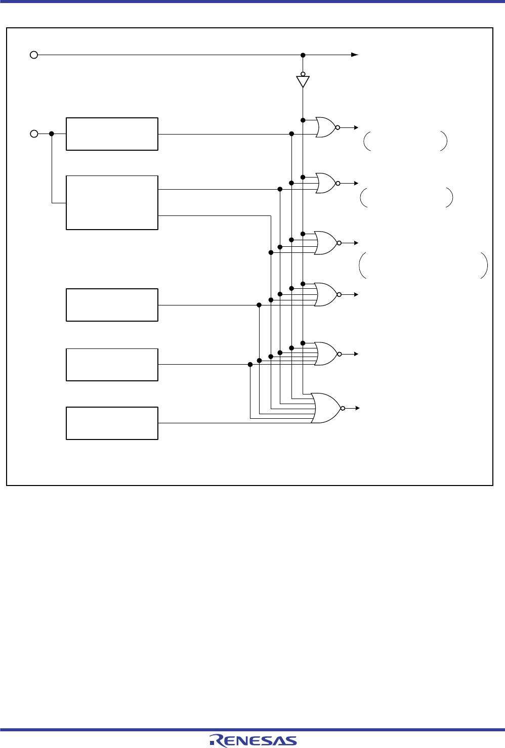
R01UH0034EJ0200 Rev.2.00 Page 169 of 1489
Dec 27, 2013
RX62T Group, RX62G Group 6. Resets
Under development Preliminary document
Specifications in this document are tentative and subject to change.
Figure 6.1 Block Diagram of Reset Circuit
Deep software standby reset
Watchdog timer reset
Pin reset
RES#
Watchdog timer
Register related to the independent
watchdog timer (IWDTCR, IWDTSR)
Deep software
standby reset
generation circuit
Register related to the watchdog timer
(RSTCSR)
Power-on reset
Voltage-monitoring reset (Vdet1)
Voltage detection circuit
Independent watchdog timer
Power-on reset circuit
Vcc Registers for voltage-monitoring (Vdet1)
Register related to the power-on reset
circuit (RSTSR.PORF)
Internal state other than above, and
pin states*
Independent watchdog timer
reset
RSTSR.LVD1F
LVDCR.LVD1E, LVD1RI
Note: * The pins are initialized by a pin reset, power-on reset, voltage monitoring reset, independent watchdog timer reset, and watchdog
timer reset. In deep software standby mode, the pins keep the same state as before a reset. For details, see section 9, Low Power
Consumption.
RSTSR.DPSRSTF,
DPSBYCR, DPSWCR, DPSIER, DPSIFR
DPSBKRn, DPSIEGR, FWEPROR,
SUBOSCCR
Registers related to low power
consumption function
Voltage-monitoring reset (Vdet2)
Registers for voltage-monitoring (Vdet2)
RSTSR.LVD2F
LVDCR.LVD2E, LVD2RI
Register related to the realtime clock
(RCR2.START)
R01UH0034EJ0200 Rev.2.00 Page 170 of 1489
Dec 27, 2013
RX62T Group, RX62G Group 6. Resets
Under development Preliminary document
Specifications in this document are tentative and subject to change.
When a reset is canceled, the reset exception handling is started. For the reset exception handling, see section 10,
Exceptions.
Table 6.3 shows the pin related to the resets.
Table 6.2 Targets to be Initialized by Each Reset Type
Targets to be Initialized Pin
Reset Power-On
Reset
Voltage-
Monitoring Reset Deep Software
Standby Reset
Independent
Watchdog
Timer Reset Watchdog
Timer ResetVdet1 Vdet2
Register related to the power-
on reset circuit
RSTSR.PORF
√——————
Registers related to the voltage
monitor function (Vdet1)
RSTSR. LVD1F,
LVDCR. LVD1E, LVD1RI
√√ —————
Registers related to the voltage
monitor function (Vdet2)
RSTSR.LVD2F,
LVDCR.LVD2E, LVD2RI
√√ √————
Registers related to the low
power-consumption function
RSTSR.DPSRSTF, DPSBYCR,
DPSWCR, DPSIER, DPSIFR,
DPSBKRn, DPSIEGR,
FWEPROR, SUBOSCCR
√√ √√———
Register related to the
independent watchdog timer
IWDTCR, IWDTSR
√√ √√√ ——
Register related to the
watchdog timer
RSTCSR
√√ √ √ √ √ √ —
Registers other than the above
and internal state
√√√√√√√
Pin state √√ √√—√√
Table 6.3 Pin Related to Reset
Pin Name I/O Function
RES# Input Reset input

R01UH0034EJ0200 Rev.2.00 Page 171 of 1489
Dec 27, 2013
RX62T Group, RX62G Group 6. Resets
Under development Preliminary document
Specifications in this document are tentative and subject to change.
6.2 Register Descriptions
Table 6.4 shows the registers related to the resets.
Each register has the bits to indicate the source of each reset generated.
Note 1. The applicable reset type depends on the register; see Figure 6.1, Block Diagram of Reset Circuit and Figure 6.2, Power-On
Reset Operation.
6.2.1 Reset Status Register (RSTSR)
For details on the RSTSR register, see section 9, Low Power Consumption.
6.2.2 Reset Control/Status Register (RSTCSR)
For details on the RSTCSR register, see section 20, Watchdog Timer (WDT).
6.2.3 IWDT Status Register (IWDTSR)
For details on the IWDTSR register, see section 21, Independent Watchdog Timer (IWDT).
6.3 Operation
6.3.1 Pin Reset
This is a reset generated by the RES# pin.
When the RES# pin is driven low, all the processing in progress is aborted and the RX62T and RX62G Group enters a
reset state.
In order to firmly reset the LSI, the RES# pin should be held low for the specified oscillation stabilization time at a
power-on. During operation, the RES# pin should be held low according to the specified reset pulse width.
For details, refer to section 33, Electrical Characteristics.
6.3.2 Power-On Reset
This is an internal reset generated by the power-on reset circuit.
If the RES# pin is in the high level state when power is supplied, a power-on reset is generated. After Vcc has exceeded
Vpor and the specified period (power-on reset time) has elapsed, the chip is released from the power-on reset state. The
power-on reset time is a period for stabilization of the external power supply and the LSI circuit.
If the RES# pin is at the high level when the power supply voltage (Vcc) falls to or below Vpor, a power-on reset is
generated. The chip is released from the power-on reset state after Vcc has risen above Vpor and the power-on reset time
has elapsed.
After a power-on reset has been generated, the PORF flag in RSTSR is set to 1. The PORF flag in RSTSR is in a read-
only register and is only initialized by a pin reset.
Figure 6.2shows the operation of a power-on reset.
Table 6.4 Registers Related to Resets
Register Name Symbol Value after Reset*1Address Access Size
Reset status register RSTSR x000 0xxxb 0008 C285h 8
Reset control/status register RSTCSR 1Fh 0008 802Bh 8
IWDT status register IWDTSR 0000h 0008 8034h 16
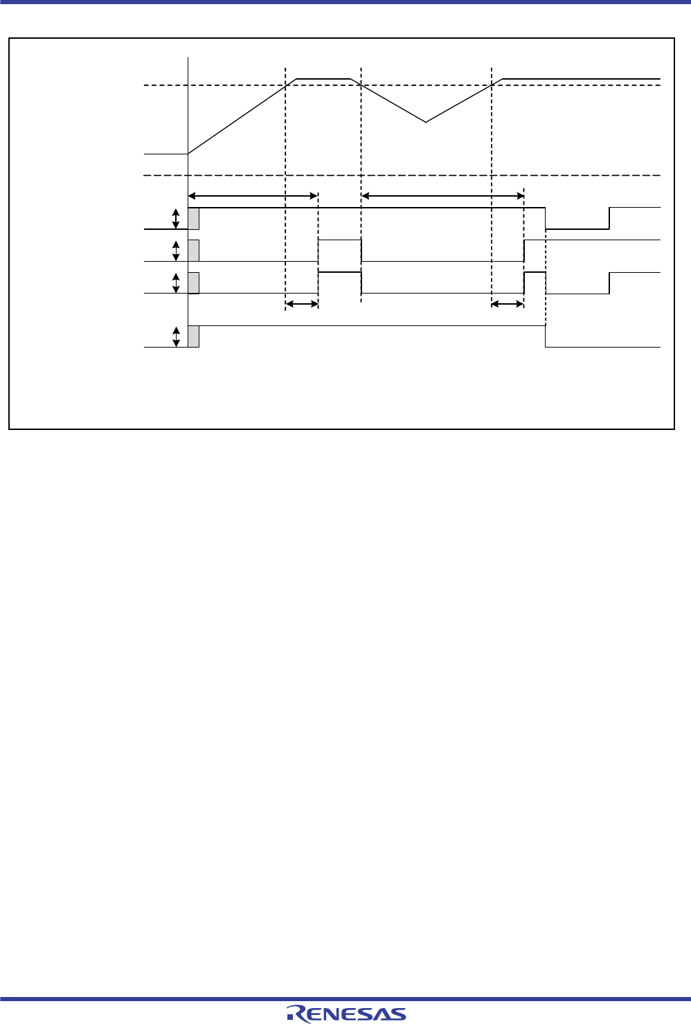
R01UH0034EJ0200 Rev.2.00 Page 172 of 1489
Dec 27, 2013
RX62T Group, RX62G Group 6. Resets
Under development Preliminary document
Specifications in this document are tentative and subject to change.
Figure 6.2 Power-On Reset Operation
Power-on reset state
Power-on reset state
Vcc
Vcc
Vcc
Vcc
External power
supply Vcc
RSTSR.PORF
Internal reset signal
RES# pin
POR signal ("L" is valid)
VPOR*1
tPOR*2tPOR*2
Reset generated
by the pin
Notes: For details on the electrical characteristics , see section 33, Electrical Characteristics.
1. Vpor shows a level of power-on reset detection level.
2. tPOR shows a time for power-on reset.

R01UH0034EJ0200 Rev.2.00 Page 173 of 1489
Dec 27, 2013
RX62T Group, RX62G Group 6. Resets
Under development Preliminary document
Specifications in this document are tentative and subject to change.
6.3.3 Voltage-Monitoring Reset
This is an internal reset generated by the voltage detection circuit.
The LVD1F flag in RSTSR is set to 1 when Vcc falls below Vdet1. If the value of the LVD1E bit is 1 (triggering of reset
or interrupt by the voltage detection circuit is enabled) and that of the LVD1RI bit is 0 (a reset is generated by low
voltage detection) in LVDCR at this time, a voltage-monitoring reset is generated by the voltage detection circuit.
In a similar way, the LVD2F flag in RSTSR is set to 1 when Vcc falls below Vdet2. If the value of the LVD2E bit is 1
(triggering of a reset or interrupt by the voltage detection circuit is enabled) and that of the LVD2RI bit is 0 (a reset is
generated by low voltage detection) in LVDCR at this time, a voltage-monitoring reset is generated by the voltage
detection circuit.
When Vcc subsequently rises above Vdet1 or Vdet2, release from the voltage-monitoring reset proceeds after a specified
stabilization time has elapsed.
For details of the voltage-monitoring reset, see section 7, Voltage Detection Circuit (LVD), and section 33, Electrical
Characteristics.
6.3.4 Deep Software Standby Reset
This is an internal reset generated when deep software standby mode is canceled by an interrupt.
When deep software standby mode is canceled, a deep software standby reset is generated, and simultaneously, clock
oscillation starts. After the time specified with the deep software standby wait time setting bits (DPSWCR.WTSTS[5:0])
has elapsed, the deep software standby reset is canceled.
For details of the deep software standby reset, see section 9, Low Power Consumption.
6.3.5 Independent Watchdog Timer Reset
This is an internal reset generated by the independent watchdog timer.
When the independent watchdog timer underflows, an independent watchdog timer reset is generated. A reset is also
generated if write operation is performed while refresh operation is not enabled. After a certain time, the independent
watchdog timer reset is canceled.
For details of the independent watchdog timer reset, see section 21, Independent Watchdog Timer (IWDT).
6.3.6 Watchdog Timer Reset
This is an internal reset generated by the watchdog timer.
When the RSTE bit in RSTCSR is set to 1, a watchdog timer reset is generated by a watchdog timer overflow. After a
certain time, the watchdog timer reset is canceled.
For details of the watchdog timer reset, see section 20, Watchdog Timer (WDT).
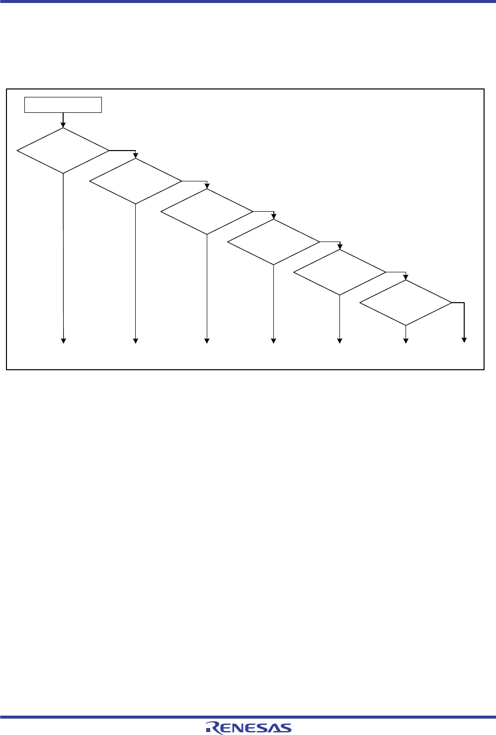
R01UH0034EJ0200 Rev.2.00 Page 174 of 1489
Dec 27, 2013
RX62T Group, RX62G Group 6. Resets
Under development Preliminary document
Specifications in this document are tentative and subject to change.
6.4 Determination of Reset Generation Source
Reading RSTCSR, IWDTSR, RSTSR, and LVDCR determines which reset was used to execute the reset exception
handling.
Figure 6.3 shows an example of the flow to identify a reset generation source.
Figure 6.3 Example of Reset Generation Source Determination Flow
6.5 Usage Notes
6.5.1 Notes on Board Design
The XTAL pin and the reset pin are crossly arranged on the RX62T and RX62G Groups. Therefore, to avoid the
reference from the clock signal, the reset signal should be guarded by GND.
NO
Reset exception
handling
RSTSR.DPSRSTF = 1
RSTSR.PORF = 1
YES
NO
Independent watchdog
timer reset Deep software standby
reset
Voltage monitoring
reset (Vdet2)
Power-on reset
YES
YES
YES
NO
Pin reset
NO
YES
Watchdog timer
reset
NO
NO
Voltage monitoring
reset (Vdet1)
YES
LVDCR.LVD2E = 1
&
LVDCR.LVD2RI = 0
RSTSR.LVD2F = 1
&
LVDCR.LVD1E = 1
&
LVDCR.LVD1RI = 0
RSTSR.LVD1F = 1
&
RSTCSR.RSTE = 1
&
RSTCSR.WOVF = 1
IWDTSR.UNDFF = 1
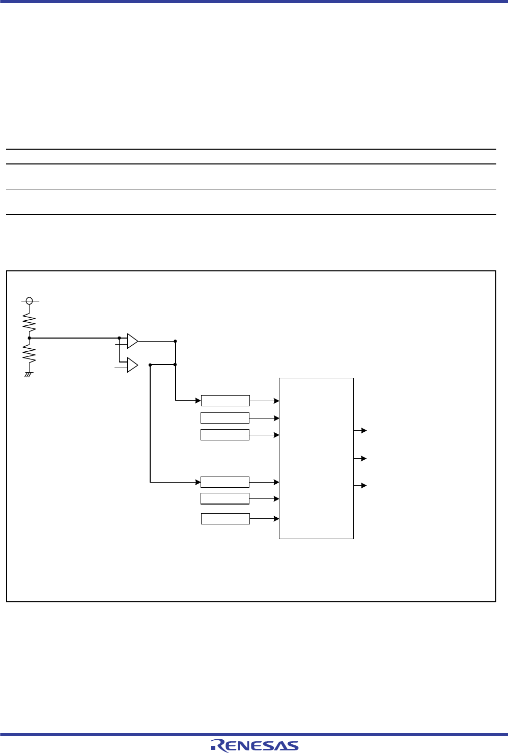
R01UH0034EJ0200 Rev.2.00 Page 175 of 1489
Dec 27, 2013
RX62T Group, RX62G Group 7. Voltage Detection Circuit (LVD)
Under development Preliminary document
Specifications in this document are tentative and subject to change.
7. Voltage Detection Circuit (LVD)
7.1 Overview
The voltage detection circuit (LVD) is used to monitor the Vcc voltage level. The LVD is capable of internally resetting
the LSI when Vcc falls to the voltage detection level. An interrupt can also be generated.
Specifications of Voltage Detection Circuit
Note: • For Vdet1 and Vdet2, see section 33, Electrical Characteristics.
Figure 7.1 shows a block diagram of the voltage detection circuit.
Figure 7.1 Block Diagram of Voltage Detection Circuit
Table 7.1 Specifications of Voltage Detection Circuit
Item Specification
Voltage detection circuit 1 (LVD1) Capable of detecting the power-supply voltage (Vcc) becoming less than or equal to Vdet1*.
Capable of generating an internal reset or interrupt when a low voltage is detected.
Voltage detection circuit 2 (LVD2) Capable of detecting the power-supply voltage (Vcc) becoming less than or equal to Vdet2*.
Capable of generating an internal reset or interrupt when a low voltage is detected.
LVD1E
LVD1RI
LVD1F
LVD2F
LVD2E
LVD2RI
Voltage monitoring reset 1 (Vdet1)
Voltage monitoring interrupt
Vcc
Reset/interrupt
control circuit
On-chip reference voltage
(for Vdet1 detection)
On-chip reference voltage
(for Vdet2 detection)
+
-
+
-
LVD1
LVD2
Voltage monitoring reset 2 (Vdet2)
[Legend]
LVD1E: LVD1 enable
LVD2E: LVD2 enable
LVD1RI: LVD1 reset/interrupt select
LVD2RI: LVD2 reset/interrupt select
LVD1F: LVD1 flag
LVD2F: LVD2 flag
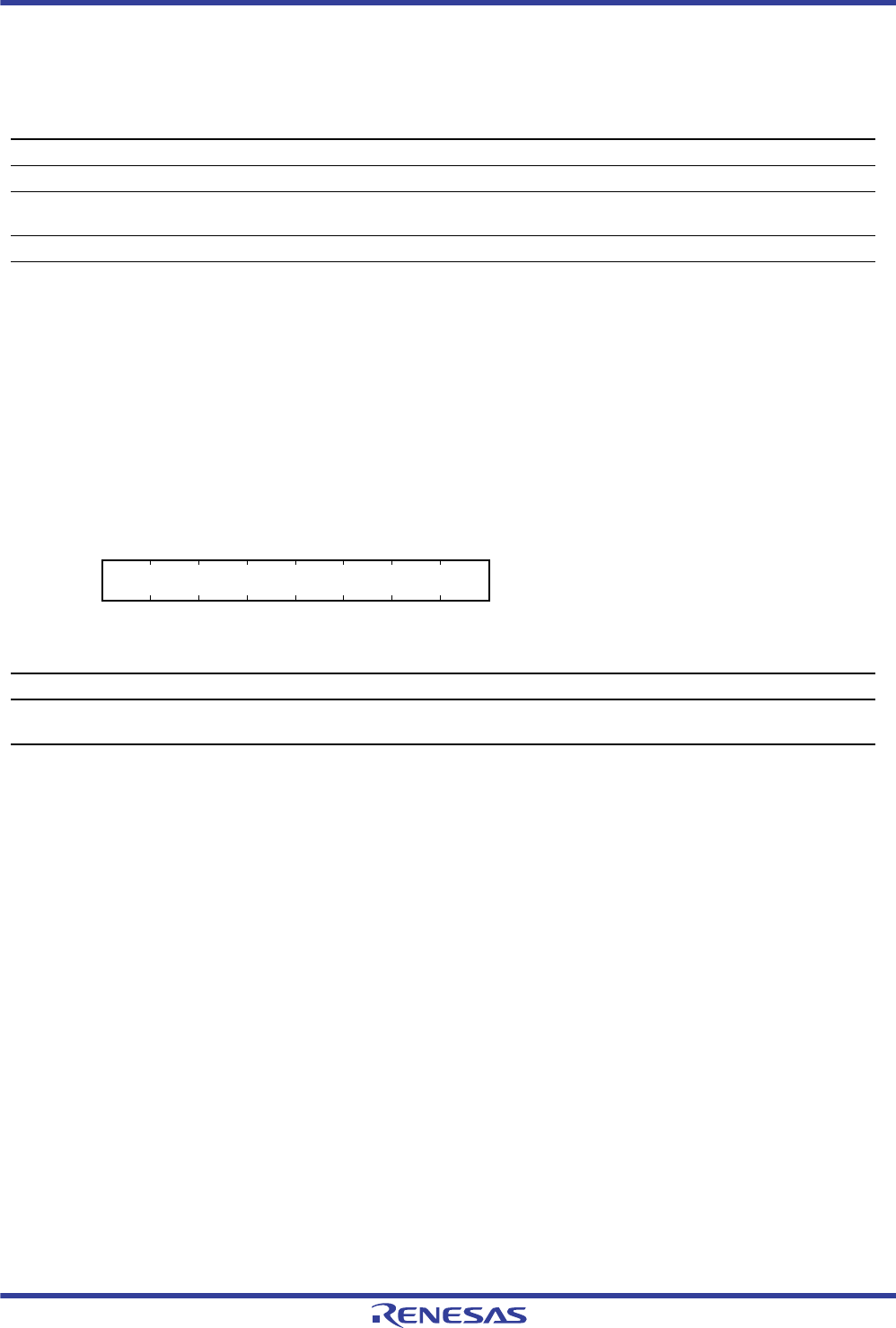
R01UH0034EJ0200 Rev.2.00 Page 176 of 1489
Dec 27, 2013
RX62T Group, RX62G Group 7. Voltage Detection Circuit (LVD)
Under development Preliminary document
Specifications in this document are tentative and subject to change.
7.2 Register Descriptions
Table 7.2is the list of voltage detection circuit registers.
7.2.1 Reset Status Register (RSTSR)
For details of RSTSR, see section 9, Low Power Consumption.
7.2.2 Key Code Register for Low-Voltage Detection Control Register (LVDKEYR)
LVDKEYR enables or disables writing to LVDCR.
After a specified key code is written to LVDKEYR, LVDCR can be written to.
KEY[7:0] Bits (LVDCR Key Code)
Writing 3Ch to LVDKEYR enables writing to LVDCR. While LVDKEYR holds a value other than 3Ch, writing to
LVDCR is ignored. After LVDCR is written to, the KEY[7:0] bits are cleared to 00h.
Table 7.2 List of Voltage Detection Circuit Registers
Register Name Symbol Value after Reset Address Access Size
Reset status register RSTSR x000 0xxxb 0008 C285h 8
Key code register for low-voltage detection control
register
LVDKEYR 00h 0008 C28Ch 8
Low-voltage detection control register LVDCR 000x 000xb 0008 C28Dh 8
Address: 0008 C28Ch
b7 b6 b5 b4 b3 b2 b1 b0
KEY[7:0]
Value after reset: 00000000
Bit Symbol Bit Name Description R/W
b7 to b0 KEY[7:0] LVDCR Key Code 3Ch: Modifying LVDCR is enabled
Others: Modifying LVDCR is disabled
R/W

R01UH0034EJ0200 Rev.2.00 Page 177 of 1489
Dec 27, 2013
RX62T Group, RX62G Group 7. Voltage Detection Circuit (LVD)
Under development Preliminary document
Specifications in this document are tentative and subject to change.
7.2.3 Low-Voltage Detection Control Register (LVDCR)
LVDCR controls the voltage detection circuit.
The LVD1E and LVD1RI bits are initialized by a pin reset or power-on reset.
The LVD2E and LVD2RI bits are initialized by a pin reset, power-on reset, or voltage monitoring reset 1 (Vdet1).
A key code must be written to LVDKEYR by KEY[7:0] bits before the LVDCR register is written to.
Table 7.3 shows the relationship between the LVDCR register settings and the states of the voltage detection circuits.
LVD1RI Bit (LVD1 Reset/Interrupt Select)
This bit selects whether an internal reset or interrupt is generated when voltage detection circuit 1 detects a low voltage.
LVD1E Bit (LVD1 Enable)
This bit enables or disables issuing of a reset or an interrupt by voltage detection circuit 1.
LVD2RI Bit (LVD2 Reset/Interrupt Select)
This bit selects whether an internal reset or interrupt is generated when voltage detection circuit 2 detects a low voltage.
LVD2E Bit (LVD2 Enable)
This bit enables or disables issuing of a reset or an interrupt by voltage detection circuit 2.
Address: 0008 C28Dh
b7 b6 b5 b4 b3 b2 b1 b0
LVD2E LVD2RI — — LVD1E LVD1RI — —
Value after reset: 000x0000
Bit Symbol Bit Name Description R/W
b0 — Reserved This bit is always read as undefined. Writing to this bit has no effect. R/W
b1 — Reserved This bit is always read as 0. The write value should be 0. R/W
b2 LVD1RI LVD1 Reset/Interrupt
Select
0: A reset is generated when a low voltage is detected
1: An interrupt is generated when a low voltage is detected
R/W
b3 LVD1E LVD1 Enable 0: LVD1 is disabled
1: LVD1 is enabled
R/W
b4 — Reserved This bit is always read as undefined. Writing to this bit has no effect. R/W
b5 — Reserved This bit is always read as 0. The write value should be 0. R/W
b6 LVD2RI LVD2 Reset/Interrupt
Select
0: A reset is generated when a low voltage is detected
1: An interrupt is generated when a low voltage is detected
R/W
b7 LVD2E LVD2 Enable 0: LVD2 is disabled
1: LVD2 is enabled
R/W

R01UH0034EJ0200 Rev.2.00 Page 178 of 1489
Dec 27, 2013
RX62T Group, RX62G Group 7. Voltage Detection Circuit (LVD)
Under development Preliminary document
Specifications in this document are tentative and subject to change.
Table 7.3 LVDCR Register Settings and Voltage Detection Circuit States
LVDCR Register Voltage Detection Circuit 2
(LVD2) Voltage Detection Circuit 1
(LVD1)LVD2E Bit LVD2RI Bit LVD1E Bit LVD1RI Bit
0 0 0 0 LVD2 disabled LVD1 disabled
0 0 1 0 LVD2 disabled LVD1 enabled (reset)
0 0 1 1 LVD2 disabled LVD1 enabled (interrupt)
1 0 0 0 LVD2 enabled (reset) LVD1 disabled
1 1 0 0 LVD2 enabled (interrupt) LVD1 disabled
1 1 1 0 LVD2 enabled (interrupt) LVD1 enabled (reset)
Other than above: Setting prohibited

R01UH0034EJ0200 Rev.2.00 Page 179 of 1489
Dec 27, 2013
RX62T Group, RX62G Group 7. Voltage Detection Circuit (LVD)
Under development Preliminary document
Specifications in this document are tentative and subject to change.
7.3 Voltage Detection Circuit
7.3.1 Voltage Monitoring Reset
Figure 7.2 andFigure 7.3 show the timing of a voltage monitoring reset by the voltage detection circuit.
The LVD2F flag in RSTSR is set to 1 when Vcc falls below Vdet2. If the value of the LVD2E bit is 1 and that of the
LVD2RI bit is 0 in LVDCR at this time, a voltage-monitoring reset is generated by the voltage detection circuit.
In a similar way, the LVD1F flag in RSTSR is set to 1 when Vcc falls below Vdet1. If the value of the LVD1E bit is 1 and
that of the LVD1RI bit is 0 in LVDCR at this time, a voltage-monitoring reset is generated by the voltage detection
circuit.
Next, after Vcc has risen above Vdet1 or Vdet2, the voltage monitoring reset is canceled. After the voltage monitoring
reset is canceled, the LSI starts reset exception handling.
Figure 7.2 Timing Diagram 1 of Voltage Monitoring Reset (Reset Selected in LVD2, LVD1 Disabled)
Vcc
LVD2E
LVD2RI
Vdet2
Vdet1
VPOR*2
Voltage monitoring reset 2
(Low)
Stabilization period (tPOR)
LVD1E
LVD2F
LVD1F
Write 0 after reading 1
LVD2 setting
LVD1RI
LVD1 setting Initial value (select reset)
Notes: 1. For the electrical characteristics, see section 33, Electrical Characteristics.
2. VPOR indicates the power-on reset detection level.
Write 0 (disable LVD1)
Write 0 after reading 1
Initial value (select reset)
Write 1 (enable LVD2)
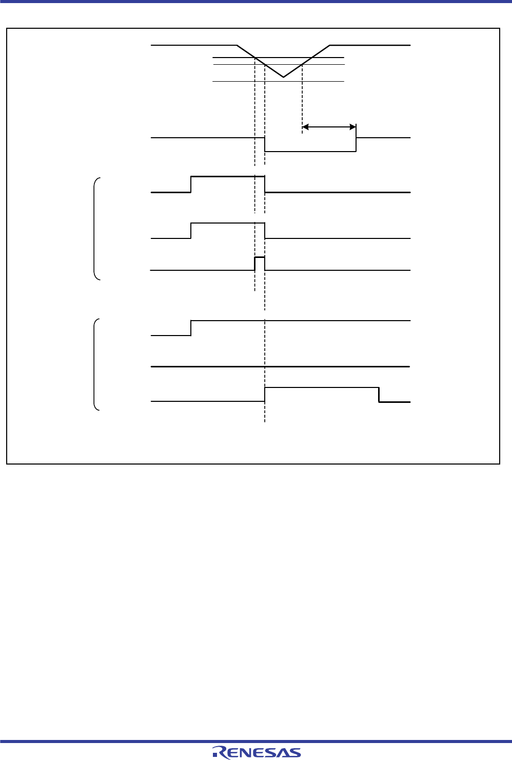
R01UH0034EJ0200 Rev.2.00 Page 180 of 1489
Dec 27, 2013
RX62T Group, RX62G Group 7. Voltage Detection Circuit (LVD)
Under development Preliminary document
Specifications in this document are tentative and subject to change.
Figure 7.3 Timing Diagram 2 of Voltage Monitoring Reset
(Interrupt Selected in LVD2, Reset Selected in LVD1)
Vcc
LVD2E
LVD2RI
Vdet2
Vdet1
VPOR*2
Voltage monitoring reset 1
(Low)
Stabilization period (tPOR)
LVD1E
LVD2F
LVD1F
LVD2 setting
LVD1RI
LVD1 setting
Initial value (select reset)
Notes: 1. For the electrical characteristics, see section 33, Electrical Characteristics.
2. VPOR indicates the power-on reset detection level.
Write 1 (enable LVD1)
Write 0 after reading 1
Write 1 (select interrupt)
Write 1 (enable LVD2)

R01UH0034EJ0200 Rev.2.00 Page 181 of 1489
Dec 27, 2013
RX62T Group, RX62G Group 7. Voltage Detection Circuit (LVD)
Under development Preliminary document
Specifications in this document are tentative and subject to change.
7.3.2 Voltage-Monitoring Interrupt
Figure 7.4 shows the timing of a voltage-monitoring interrupt by the voltage detection circuit.
The LVD1F flag in RSTSR is set to 1 when Vcc falls below Vdet1. If both the LVD1E and LVD1RI bits in LVDCR have
the value 1 at this time, a voltage-monitoring interrupt is generated by the voltage detection circuit.
In a similar way, the LVD2F flag in RSTSR is set to 1 when Vcc falls below Vdet2. If both the LVD2E and LVD2RI bits
in LVDCR have the value 1 at this time, a voltage-monitoring interrupt is generated by the voltage detection circuit.
The RSTSR.LVD1F flag can be cleared by writing 0 to the flag after reading it as 1. If the Vcc voltage level is equal to or
lower than the LVD1 detection level (Vdet1) at this point, the RSTSR.LVD1F flag cannot be cleared. After 0 has been
written to the RSTSR.LVD1F flag, reading 0 from the RSTSR.LVD1F flag will ensure that Vcc is higher than Vdet1.
Likewise, the RSTSR.LVD2F flag can be cleared by writing 0 to the flag after reading it as 1. If the Vcc voltage level is
equal to or lower than the LVD2 detection level (Vdet2) at this point, the RSTSR.LVD2F flag cannot be cleared. After 0
has been written to the RSTSR.LVD2F flag, reading 0 from the RSTSR.LVD2F flag will ensure that Vcc is higher than
Vdet2.
The voltage-monitoring interrupts are classified as non-maskable interrupts. For details of interrupt processing, see
section 11, Interrupt Controller (ICU).
Figure 7.5 shows the procedure for setting the voltage-monitoring interrupt.

R01UH0034EJ0200 Rev.2.00 Page 182 of 1489
Dec 27, 2013
RX62T Group, RX62G Group 7. Voltage Detection Circuit (LVD)
Under development Preliminary document
Specifications in this document are tentative and subject to change.
Figure 7.4 Timing of Voltage-Monitoring Interrupt (Interrupt Selected in LVD2, Reset Selected in LVD1)
Vcc
LVD2E
LVD2RI
Vdet2
Vdet1
VPOR*2
Write 1 (enable LVD2)
Write 1 (select interrupt)
LVD1E
Write 1 (enable LVD1)
LVD1RI
LVD2F
LVD1F
Voltage-monitoring
interrupt
ICU.NMISR.LVDST
Initial value (select reset)
Write 0 after reading 1*3
Stabilization period (tPOR)
LVD2
setting
LVD1
setting
Notes: 1. For the electrical characteristics, see section 33, Electrical Characteristics.
2. VPOR indicates the power-on reset detection level.
3. When the RSTSR.LVD2F flag cannot be cleared despite Vcc being at
a higher electrical potential than Vdet2, the voltage detection circuit is in the
stabilization wait state.
Clear the flag again after the specified stabilization time (tPOR) has elapsed.
Write 0 after reading 1
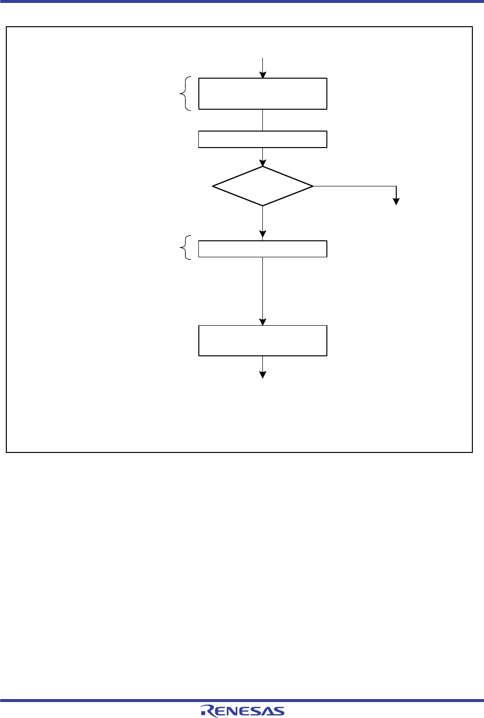
R01UH0034EJ0200 Rev.2.00 Page 183 of 1489
Dec 27, 2013
RX62T Group, RX62G Group 7. Voltage Detection Circuit (LVD)
Under development Preliminary document
Specifications in this document are tentative and subject to change.
Figure 7.5 Example of Procedure for Setting Voltage-Monitoring Interrupt
Processing for lowered Vcc
Program start
Set the voltage detection control
register.
Voltage-monitoring interrupt (NMIER)
enabled
Processing for lowered Vcc
(Vcc low)
No
Yes (high Vcc)
Note: * When RSTSR.LVD1F cannot be cleared to 0 despite Vcc being at a higher electrical potential than
Vdet1 (LVDCR.LVD1MON = 1), the voltage detection circuit is in the stabilization wait state. Clear the
bit again after the stabilization time (tPOR) has elapsed.
Write 1 to LVDCR.LVD1RI
Write 1 to LVDCR.LVD1E
RSTSR.LVD1F = 0
Write 1 to NMIER.LVDEN of ICU
Interrupt occurs when a low
voltage is detected
Clear RSTSR.LVD1F to 0
If the flag was set to 1 before the
voltage-monitoring interrupt has been
enabled, clear the flag by writing 0 to it
after reading it as 1.

R01UH0034EJ0200 Rev.2.00 Page 184 of 1489
Dec 27, 2013
RX62T Group, RX62G Group 7. Voltage Detection Circuit (LVD)
Under development Preliminary document
Specifications in this document are tentative and subject to change.
7.3.3 Cancellation of Deep Software Standby Mode by the Voltage Detection Circuit
The RSTSR.LVD1F flag is set to 1 if Vcc falls to or below Vdet1 in deep software standby mode. At this time, if the
LVDCR.LVD1E, LVDCR.LVD1RI, and DPSIER.DLVDE bits are all set to 1, the DPSIFR.DLVDF flag is set to 1 and
the voltage detection circuit requests release from deep software standby mode.
Likewise, the RSTSR.LVD2F flag is set to 1 if Vcc falls to or below Vdet2 in deep software standby mode. At this time,
if the LVDCR.LVD2E, LVDCR.LVD2RI, and DPSIER.DLVDE bits are all set to 1, the DPSIFR.DLVDF flag is set to 1
and the voltage detection circuit requests release from deep software standby mode.
For the deep software standby mode, see section 9, Low Power Consumption.
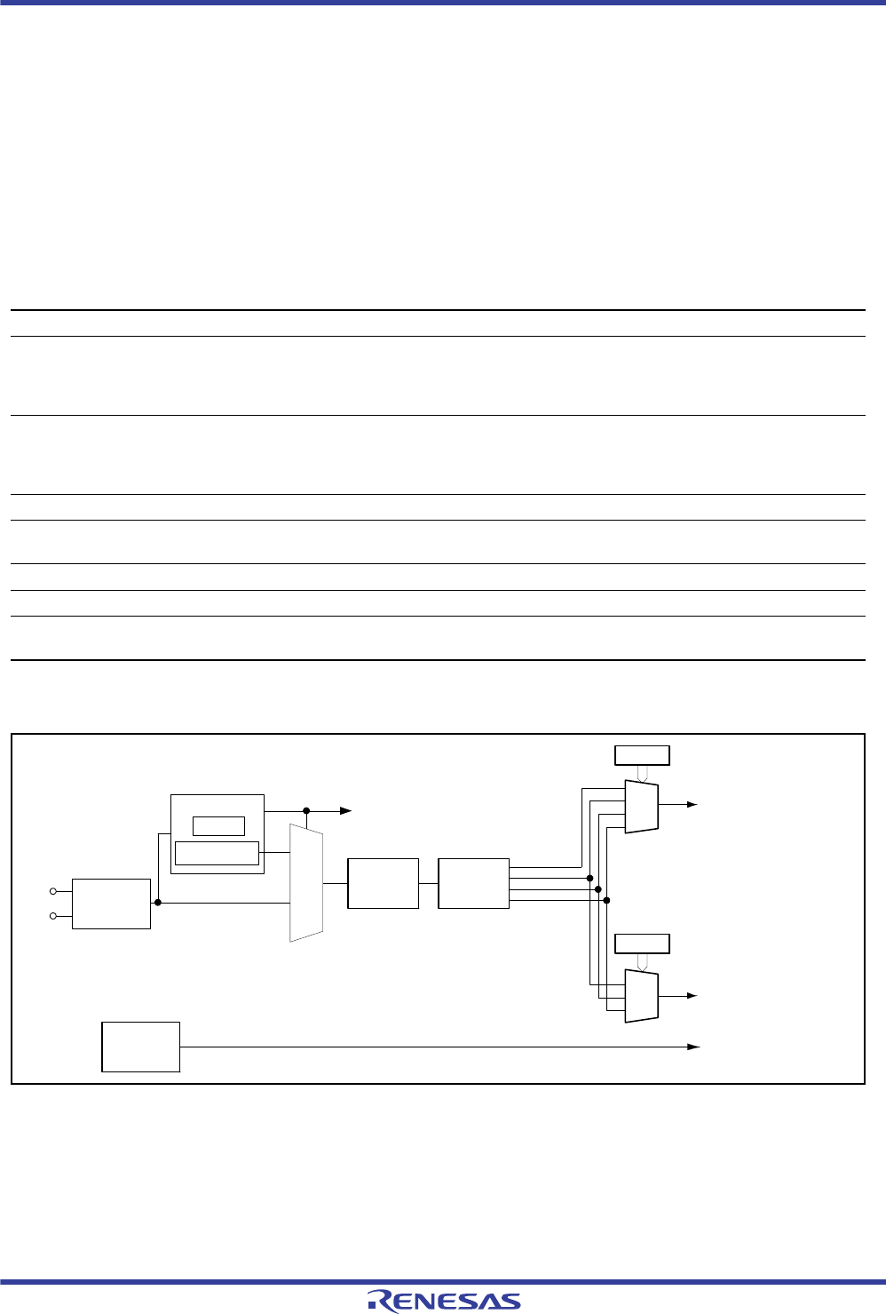
R01UH0034EJ0200 Rev.2.00 Page 185 of 1489
Dec 27, 2013
RX62T Group, RX62G Group 8. Clock Generation Circuit
8. Clock Generation Circuit
8.1 Overview
The RX62T and RX62G Groups have a clock generation circuit that generates the system clock (ICLK), peripheral
module clock (PCLK), and on-chip oscillator clock (IWDTCLK) signals.
The clock generation circuit consists of a main clock oscillator, IWDT-dedicated low-speed on-chip oscillator, oscillation
stop detection circuit, internal oscillation circuit, phase-locked loop (PLL) circuit, frequency divider, and selector.
Table 8.1 lists the specifications of the clock generation circuit. Figure 8.1shows a block diagram of the clock
generation circuit.
Note: • For details, see section 33, Electrical Characteristics.
Figure 8.1 Block Diagram of Clock Generation Circuit
Table 8.2 lists the input/output pins of the clock generation circuit.
Table 8.1 Specifications of Clock Generation Circuit
Item Specification
Use Generates the system clock (ICLK) to be supplied to the CPU, DTC, MTU3, GPT, ROM,
and RAM.
Generates the peripheral module clock (PCLK) to be supplied to peripheral modules.
Generates the on-chip oscillator clock (IWDTCLK) to be supplied to the IWDT
Operating frequency ICLK: 8 MHz to 100 MHz
PCLK: 8 to 50 MHz
IWDTCLK: 125 kHz (Typ.)
Restrictions for setting clock frequencies: ICLK PCLK
Connectable resonator or additional circuit Crystal resonator, ceramic resonator
Pins for connection to the resonator or
additional circuit
Main clock: EXTAL, XTAL
Input clock (EXTAL) frequency 8 to 12.5 MHz
Selection of ICLK or PCLK The ICLK and PCLK are independently selectable as EXTAL × 8, × 4, × 2, and × 1
Oscillation stop detection function Switches to internal oscillation upon detection of main clock oscillator stop
Sets the MTU3 and GPT pins to the high-impedance state
ICK[3:0]
EXTAL x 8
x 4
System clock (ICLK)
to CPU, DTC, MTU3, GPT, ROM, and RAM
Selector
PCK[3:0]SCKCR
SCKCR
Selector
x 2
x 1
On-chip oscillator clock (IWDTCLK)
to IWDT
IWDT-dedicated
low-speed on-chip
oscillator
PLL circuit Frequency divider
Peripheral module clock (PCLK)
to peripheral module
EXTAL
XTAL
Main clock oscillator
Oscillation stop detection
circuit OSTDI
OSTDCR
On-chip oscillation
circuit*
fMAIN
Selector
Note: * This circuit is enabled when the stop of the main clock oscillator is
detected. For details, see section 8.5, Oscillation Stop Detection Circuit.

R01UH0034EJ0200 Rev.2.00 Page 186 of 1489
Dec 27, 2013
RX62T Group, RX62G Group 8. Clock Generation Circuit
Table 8.2 Pin Configuration
Pin Name I/O Description
XTAL Output These pins are used to connect a crystal resonator. The EXTAL pin can also be used to input
an external clock. For details, see Figure 8.3.2, External Clock Input.
EXTAL Input
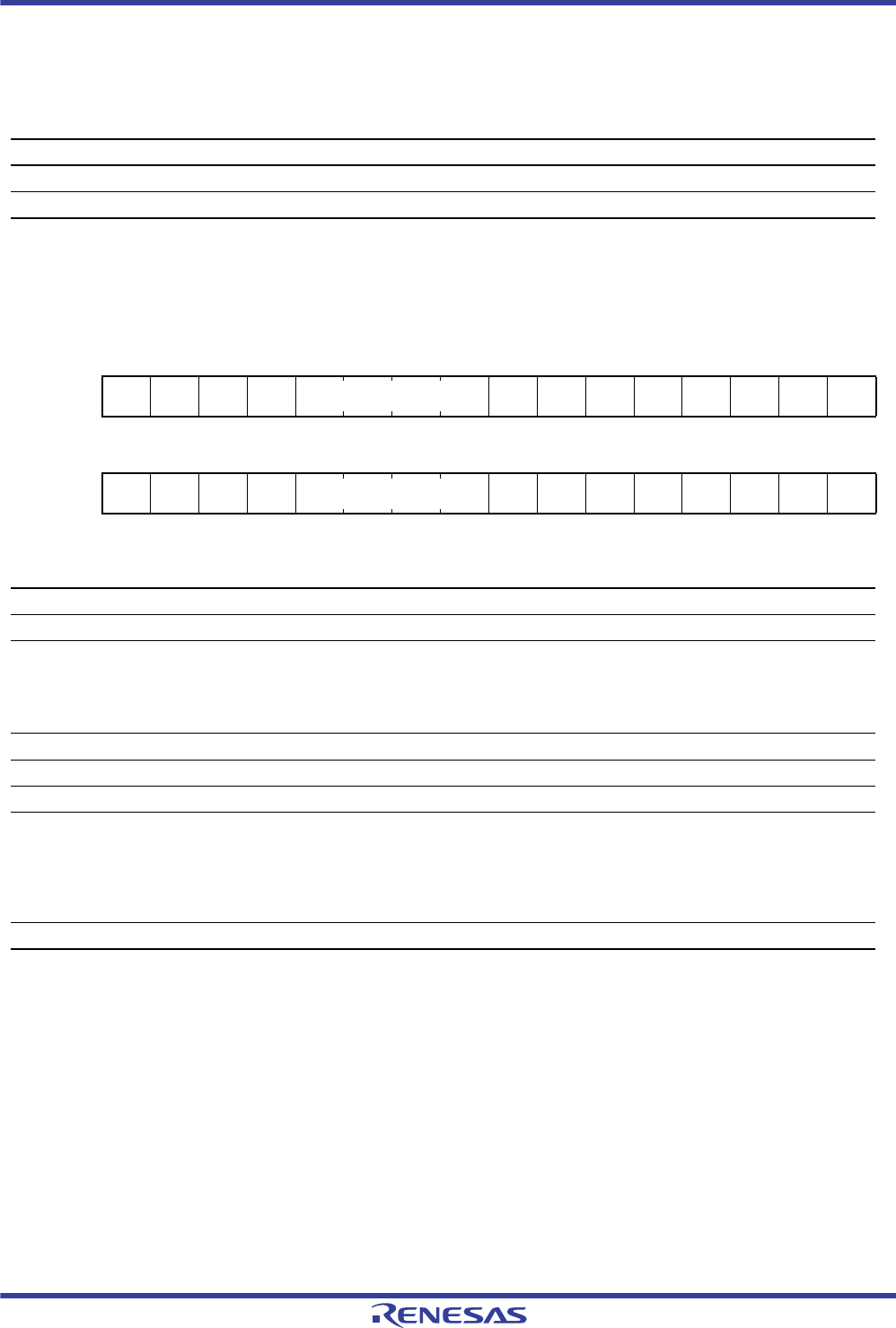
R01UH0034EJ0200 Rev.2.00 Page 187 of 1489
Dec 27, 2013
RX62T Group, RX62G Group 8. Clock Generation Circuit
8.2 Register Descriptions
Table 8.3 shows the register of the clock generation circuit.
8.2.1 System Clock Control Register (SCKCR)
Note 1. Do not set a frequency higher than the system clock (ICLK). If such a frequency is set, the clock frequency will be the same as
the ICLK.
Note 2. Do not set a frequency lower than the peripheral module clock (PCLK). If such a frequency is set, the frequency of the PCLK will
change to the system clock (ICLK) frequency.
SCKCR is used to select the frequencies of the system clock (ICLK) and peripheral module clock (PCLK).
PCK[3:0] Bits (Peripheral Module Clock Select)
These bits select the PCLK frequency.
The value of these bits indicates a multiplication factor of the input clock (EXTAL).
Table 8.3 Register of Clock Generation Circuit
Register Name Symbol Value after Reset Address Access Size
System clock control register SCKCR 0202 0200h 0008 0020h 32
Oscillation stop detection control register OSTDCR 0080h 0008 0040h 16
Address: 0008 0020h
b31 b30 b29 b28 b27 b26 b25 b24 b23 b22 b21 b20 b19 b18 b17 b16
———— ICK[3:0] ————————
Value after reset: 0000001000000010
b15 b14 b13 b12 b11 b10 b9 b8 b7 b6 b5 b4 b3 b2 b1 b0
———— PCK[3:0] ————————
Value after reset: 0000001000000000
Bit Symbol Bit Name Description R/W
b7 to b0 — Reserved These bits are always read as 0. The write value should be 0. R/W
b11 to b8 PCK[3:0]*1Peripheral Module Clock
Select
b11b8
0 0 0 1: ×4
0 0 1 0: ×2
0 0 1 1: ×1
Settings other than those listed above are prohibited.
R/W
b16 to b12 — Reserved These bits are always read as 0. The write value should be 0. R/W
b17 — Reserved This bit is always read as 1. The write value should be 1. R/W
b23 to b18 — Reserved These bits are always read as 0. The write value should be 0. R/W
b27 to b24 ICK[3:0]*2System Clock Select b27b24
0 0 0 0: ×8
0 0 0 1: ×4
0 0 1 0: ×2
0 0 1 1: ×1
Settings other than those listed above are prohibited.
R/W
b31 to b28 — Reserved These bits are always read as 0. The write value should be 0. R/W

R01UH0034EJ0200 Rev.2.00 Page 188 of 1489
Dec 27, 2013
RX62T Group, RX62G Group 8. Clock Generation Circuit
ICK[3:0] Bits (System Clock Select)
These bits select the frequency of the system clock (ICLK).
The value of these bits indicates a multiplication factor of the input clock (EXTAL).
8.2.2 Oscillation Stop Detection Control Register (OSTDCR)
OSTDCR is used to control the oscillation stop detection function.
OSTDF Flag (Oscillation Stop Detection Flag)
This flag indicates the state of the main clock oscillator.
When the OSTDF flag is 1, this indicates that the stop of the main clock oscillator is detected. The OSTDF flag is cleared
to 0 by a power-on reset or pin reset.
OSTDE Bit (Oscillation Stop Detection Function Enable)
This bit enables or disables the oscillation stop detection function.
When the OSTDE bit is 1 (oscillation stop detection function is enabled), transitions to software standby mode or deep
software standby mode are not possible. To make a transition to software standby mode or deep software standby mode,
issue a WAIT instruction after setting the OSTDE bit to 0.
KEY[7:0] Bits (OSTDCR Key Code)
These bits are used to enable or disable writing to OSTDCR.
When writing a value to the OSTDE bit, set the KEY[7:0] bits to ACh before writing. If the KEY[7:0] bits are set to a
value other than ACh, the OSTDE bit will not be changed even though OSTDCR is written to.
Address: 0008 0040h
b15 b14 b13 b12 b11 b10 b9 b8 b7 b6 b5 b4 b3 b2 b1 b0
KEY[7:0] OSTDEOSTDF——————
Value after reset: 0000000010000000
Bit Symbol Bit Name Description R/W
b5 to b0 — Reserved These bits are always read as 0. The write value should be 0. R
b6 OSTDF Oscillation Stop Detection
Flag
When OSTDE = 1:
0: The main clock oscillator is operating normally.
1: The stop of the main clock oscillator is detected.
When OSTDE = 0:
This bit is read as 0.
R
b7 OSTDE Oscillation Stop Detection
Function Enable
0: Oscillation stop detection function is disabled.
1: Oscillation stop detection function is enabled.
R/W
b15 to b8 KEY[7:0] OSTDCR Key Code ACh: Writing to OSTDCR is enabled.
Other than above: Writing to OSTDCR is disabled.
This bit is read as 0.
R/W

R01UH0034EJ0200 Rev.2.00 Page 189 of 1489
Dec 27, 2013
RX62T Group, RX62G Group 8. Clock Generation Circuit
8.3 Main Clock Oscillator
Clock pulses can be supplied by connecting a crystal resonator or by inputting an external clock.
8.3.1 Connecting a Crystal Resonator
Figure 8.2shows an example of connecting a crystal resonator.
When supplying the clock from the crystal resonator, the frequency of the resonator should be in the range of 8 to 12.5
MHz.
A damping resistor Rd should be added, if necessary. Since the resistor values vary depending on the resonator and the
oscillation drive capability, use values recommended by the resonator manufacturer.
When connecting a resonator to supply the clock, the frequency of the resonator should be in the frequency range of the
resonator for the main clock oscillator described in Table 8.1.
Figure 8.2 Example of Crystal Resonator Connection
Figure 8.3shows an equivalent circuit of the crystal resonator. Use a crystal resonator that has the characteristics shown
in Table 8.5.
Figure 8.3 Equivalent Circuit of Crystal Resonator
Table 8.4 Damping Resistance (Reference Values)
Frequency (MHz) 8 10 12.5
Rd () 200 100 0
Table 8.5 Crystal Resonator Characteristics (Reference Values)
Frequency (MHz) 8 10 12.5
RS max ()80 70 60
C0 max (pF) 7 7 7
EXTAL
XTAL
CL1
CL2
RdCL1 = CL2 = 10 to 22 pF
CL
RS
XTAL EXTAL
L
C0
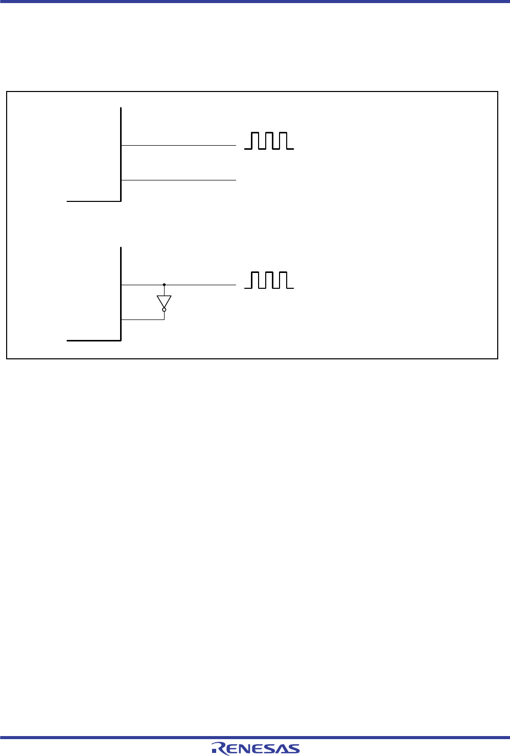
R01UH0034EJ0200 Rev.2.00 Page 190 of 1489
Dec 27, 2013
RX62T Group, RX62G Group 8. Clock Generation Circuit
8.3.2 External Clock Input
Figure 8.4 shows examples of external clock input. To leave the XTAL pin open, make the parasitic capacitance less
than 10 pF. When the counter-phase clock is input to the XTAL pin, hold the external clock in high level during standby
mode.
Figure 8.4 Examples of External Clock Input
8.4 IWDT-Dedicated Low-Speed On-Chip Oscillator
The IWDT-dedicated low-speed on-chip oscillator generates the on-chip oscillator clock (IWDTCLK) by the internal
oscillation.
8.5 Oscillation Stop Detection Circuit
The oscillation stop detection circuit is able to detect the stop of the main clock oscillator and supply the internal
oscillation clock that is output by the internal oscillation circuit, instead of the main clock.
For details, see section 8.10, Oscillation Stop Detection Function.
8.6 Internal Oscillation Circuit
The internal oscillation circuit generates the internal oscillation clock by the internal oscillation.
8.7 PLL Circuit
The PLL circuit has a function to multiply the frequency from the oscillator by a factor of 8.
8.8 Frequency Divider
The frequency divider divides the PLL clock to generate 1/2, 1/4, or 1/8 clock. After the ICK[3:0] and PCK[3:0] bits in
SCKCR are updated, the RX62T operates with the updated frequencies.
External clock input
Open
External clock input
XTAL
EXTAL
(a) Example of connection with the XTAL pin open
(b) Example of connection with counter-phase clock input to the XTAL pin
XTAL
EXTAL

R01UH0034EJ0200 Rev.2.00 Page 191 of 1489
Dec 27, 2013
RX62T Group, RX62G Group 8. Clock Generation Circuit
8.9 Internal Clock
An internal clock is generated by multiplying the external input clock (EXTAL) by 8 with the PLL circuit, and then
dividing the multiplied clock by 1, 2, 4, or 8 with the frequency divider. Other internal clocks are generated with internal
oscillation in the IWDT-dedicated low-speed on-chip oscillator.
There are the following three types of internal clock.
Operating clock of the CPU, DTC, MTU3, GPT, ROM, and RAM: System clock (ICLK)
Operating clock of peripheral modules: Peripheral module clock (PCLK)
Operating clock for the IWDT: On-chip oscillator clock (IWDTCLK)
The frequencies of these clocks are set by the combinations of bits ICK[3:0] and PCK[3:0] in SCKCR.
8.9.1 System Clock (ICLK)
The system clock (ICLK) is used as the operating clock of the CPU, DTC, MTU3, GPT, ROM, and RAM.
The ICLK frequency is specified by the ICK[3:0] bits in SCKCR.
A frequency lower than the peripheral module clock (PCLK) should not be set for the ICLK. If such a frequency is set,
though the ICLK settings are enabled, the clock frequency of the PCLK will be the same as the ICLK.
8.9.2 Peripheral Module Clock (PCLK)
The peripheral module clock (PCLK) is the operating clock for peripheral modules.
The PCLK frequency is specified by the PCK[3:0] bits in SCKCR.
A frequency higher than the system clock (ICLK) should not be set for the PCLK. If such a frequency is set, the clock
frequency will be the same as the ICLK.
8.9.3 On-Chip Oscillator Clock (IWDTCLK)
The on-chip oscillator clock (IWDTCLK) is the operating clock for the IWDT.
IWDTCLK is a clock generated by internal oscillation in the on-chip oscillator.
The IWDTCLK cycles are measured by the LOCO count function in the GPT. For details, see section 18.6, LOCO
Count Function.

R01UH0034EJ0200 Rev.2.00 Page 192 of 1489
Dec 27, 2013
RX62T Group, RX62G Group 8. Clock Generation Circuit
8.10 Oscillation Stop Detection Function
8.10.1 Detection of Oscillation Stop and Operation after the Detection
The oscillation stop detection function is used to detect termination of the main clock oscillator. After oscillation stop has
been detected, the oscillation stop detection circuit is able to supply the internal oscillation clock that is output by the
internal oscillation circuit, instead of the main clock. An oscillation stop interrupt request can be generated when
oscillation stop has been detected. Also, the MTU3 and GPT output can be forcibly set to the high-impedance state when
oscillation stop has been detected. For details on the MTU output, refer to section 16, Multi-Function Timer Pulse
Unit 3 (MTU3), section 17, Port Output Enable 3 (POE3), section 18, General PWM Timer (GPT/GPTa), and
section Appendix 1., Port States in Each Processing Mode.
The RX62T/RX62G Group detects that the main clock has stopped when the input clock is kept at 0 or 1 for a certain
period (see section 33, Electrical Characteristics due to an error in the main clock oscillator or another reason.
When oscillation stop has been detected, The RX62T/RX62G Group continues to operate on the internal oscillation
clock that is output from the internal oscillation circuit.
For the frequency of the system clock (ICLK) during operation on the internal oscillation clock, see Table 8.6.
Note: • For details on fMAIN, see section 33, Electrical Characteristics.
The operating clock is automatically switched from the main clock to the internal oscillator when stoppage of oscillation
is detected. Even if the main clock oscillator resumes operation after stoppage of oscillation has been detected, the
internal oscillator will provide the operating clock for the LSI. However, the operating clock is switched from the
internal oscillator to the main clock only during reset processing of pin resets, power-on resets, and voltage monitoring
resets. Accordingly, the operating clock for the LSI will be the main clock once oscillation of the main clock oscillator
has started.
The oscillation stop detection function is enabled immediately after the LSI has been internally initialized by all resets.
To disable this function, clear the OSTDCR.OSTDE bit to 0. In addition, when the oscillation stop is detected and the
LSI is operating on the internal oscillation clock, the OSTDCR.OSTDE bit cannot be cleared to 0.
8.10.2 Oscillation Stop Detection Interrupt
When the oscillation stop detection function is enabled, an oscillation stop detection interrupt request (OSCERI) is
generated when oscillation stop is detected. The oscillation stop detection interrupt is a non-maskable interrupt. Since
non-maskable interrupts are disabled in the initial state after the reset state is canceled, enable non-maskable interrupts
through software when using the oscillation stop detection interrupt. For details, refer to section 11, Interrupt
Controller (ICU).
The state in which the internal oscillation clock is operating due to oscillation stop detection means that an error has
occurred in the system. In this state, take only emergency measures to solve the error.
8.10.3 Note on Release from Deep Software Standby Mode
If the main clock oscillator does not operate normally due to error occurrence while the chip is in deep software standby
mode, interrupt-driven release from deep software standby mode might be impossible.
However, a pin reset will release the chip from deep software standby mode even if the main clock oscillator is not
operating. Use a pin reset if release from deep software standby mode must be ensured.
Table 8.6 System Clock (ICLK) Frequency when Internal Oscillation Circuit is Used
System Clock (ICLK) Min. Typ. Max.
ICLK frequency (x 8) 8 x fMAIN 8 x fMAIN 8 x fMAIN
ICLK frequency (x 4) 4 x fMAIN 4 x fMAIN 4 x fMAIN
ICLK frequency (x 2) 2 x fMAIN 2 x fMAIN 2 x fMAIN
ICLK frequency (x 1) fMAIN fMAIN fMAIN

R01UH0034EJ0200 Rev.2.00 Page 193 of 1489
Dec 27, 2013
RX62T Group, RX62G Group 8. Clock Generation Circuit
8.11 Usage Notes
8.11.1 Notes on Clock Generation Circuit
1. The frequencies of the system clock (ICLK) and peripheral module clock (PCLK), supplied to each module change
according to the setting of SCKCR. Select each frequency that is within the operation guaranteed range of clock
cycle time (tcyc) specified in AC characteristics of electrical characteristics. Each frequency should meet the
following:
ICLK = 8 MHz to 100 MHz
PCLK = 8 MHz to 50 MHz
2. All peripheral modules (except for the DTC, MTU3, and GPT) operate on the PCLK. Note therefore that the
operating speed of modules such as the timer and SCI varies before and after the frequency is changed.
In addition, the waiting time for canceling software standby mode varies with the PCLK frequency change. For
details, see section 9.5.3.3, Setting Oscillation Settling Time after Software Standby Mode is Canceled.
3. The relationship between the system clock (ICLK) and peripheral module clock (PCLK) is ICLK PCLK, and the
ICLK has the highest priority. For this reason, if a setting that does not meet these conditions is made, the PCLK
may have the clock frequency set by the ICK[3:0] bits in SCKCR regardless of the settings of the PCK[3:0] bits in
SCKCR.
4. After writing to the SCKCR, further writing to the same register before completion of the change in frequency is
ignored. In the case of continued writing to the SCKCR, confirm that values read from the SCKCR are actually the
most recently written values.
5. After writing to the SCKCR, transitions to software standby mode are prohibited until completion of the change in
frequency. Subsequent operation is not guaranteed if a transition to software standby mode is attempted while the
frequency is being changed. The interval between writing to the SCKCR and issuing of the WAIT instruction must
take up at least 11 cycles of the system clock. For details, see section 5, I/O Registers.
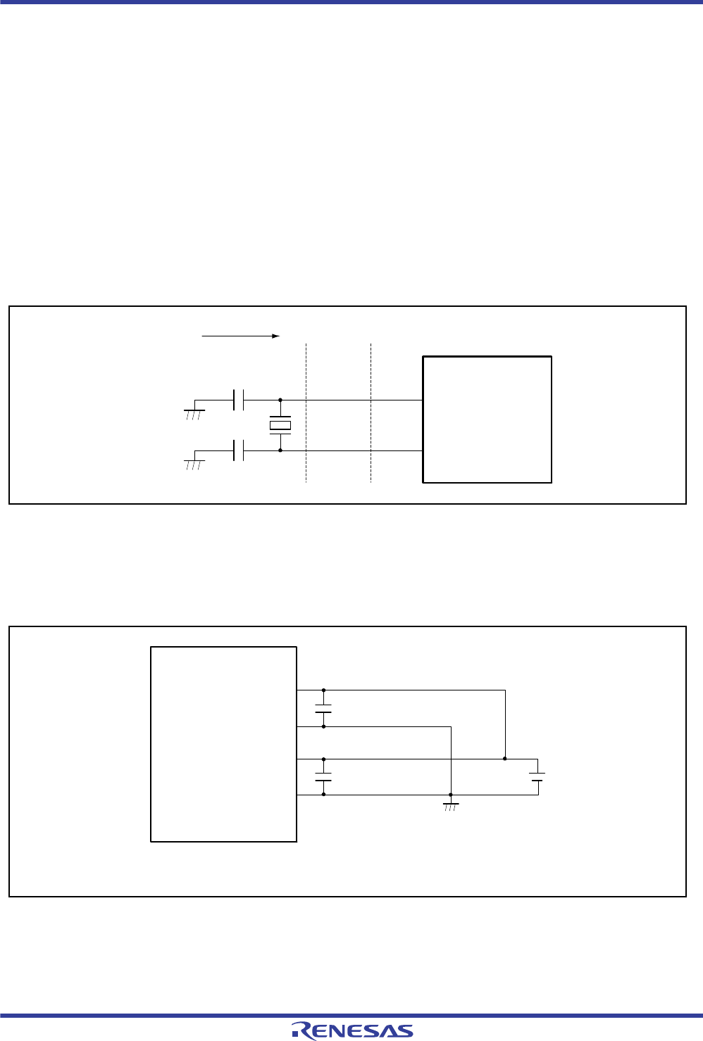
R01UH0034EJ0200 Rev.2.00 Page 194 of 1489
Dec 27, 2013
RX62T Group, RX62G Group 8. Clock Generation Circuit
8.11.2 Notes on Resonator
Since various resonator characteristics relate closely to the user's board design, adequate evaluation is required on the
user side before use, referencing the resonator connection example shown in this section. The circuit constants for the
resonator depend on the resonator to be used and the stray capacitance of the mounting circuit. Therefore, the circuit
constants should be determined in full consultation with the resonator manufacturer. The voltage to be applied between
the resonator pins must be within the absolute maximum rating.
8.11.3 Notes on Board Design
When using a crystal resonator, place the resonator and its capacitors as close to the XTAL and EXTAL pins as possible.
Other signal lines should be routed away from the oscillation circuit as shown in Figure 8.5 to prevent electromagnetic
induction from interfering with correct oscillation.
The XTAL pin and the reset pin are crossly arranged on the RX62T and RX62G Groups. Therefore, to avoid the
reference from the clock signal, the reset signal should be guarded by GND.
Figure 8.5 Notes on Board Design for Oscillation Circuit
Figure 8.6 shows a recommended external circuit for the PLL circuit. Separate pins PLLVcc and PLLVss from the other
Vcc and Vss lines at the board power supply source, and be sure to insert bypass capacitors CPB and CB close to the
pins. The pins PLLVcc and Vcc should be set to the same potential.
Figure 8.6 Recommended External Circuit for PLL Circuit
EXTAL
XTAL
CL2
CL1
RX62T
Prohibited Signal A Signal B
Note: * CB, CPB: Multilayer ceramic capacitor
CPB: 22F*
CB: 0.1F*
PLLVcc
Vcc
PLLVss
Vss

R01UH0034EJ0200 Rev.2.00 Page 195 of 1489
Dec 27, 2013
RX62T Group, RX62G Group 9. Low Power Consumption
Under development Preliminary document
Specifications in this document are tentative and subject to change.
9. Low Power Consumption
9.1 Overview
The RX62T and RX62G Groups have functions to reduce power consumption, including a multi-clock function, module
stop function, and a function for transition to low power consumption mode.
Table 9.1 shows the specifications of low power consumption function, and Table 9.2 shows the conditions to shift to
low power consumption mode, states of the CPU and peripheral modules, and mode canceling method. After the reset
state, this LSI enters the normal program execution state, but modules except the DTC do not operate.
Table 9.1 Specifications of Low Power Consumption Function
Item Specification
Multi-clock function The frequency division ratio is settable independently for the system clock (ICLK) and peripheral
module clock (PCLK)
Module stop function Functions can be stopped independently for each peripheral module.
Function for transition to low
power consumption mode
Transition to low power consumption mode is enabled to stop the CPU, peripheral modules, and
oscillator.
Four low power consumption
modes
Sleep mode
All-module clock stop mode
Software standby mode
Deep software standby mode

R01UH0034EJ0200 Rev.2.00 Page 196 of 1489
Dec 27, 2013
RX62T Group, RX62G Group 9. Low Power Consumption
Under development Preliminary document
Specifications in this document are tentative and subject to change.
Note: • "Stopped (Retained)" means that internal register values are retained and internal operations are suspended.
"Stopped (Undefined)" means that internal register values are undefined and power is not supplied to the internal circuit.
Note 1. An external interrupt or some internal interrupts (WDT, oscillation stop detection, and voltage monitoring).
Note 2. An external interrupt or some internal interrupts (voltage monitoring).
Note 3. NMI, IRQ0-A and IRQ1-A, or some internal interrupts (voltage monitor circuit). These interrupts are enabled only when the
corresponding bit in DPSIER is set to 1.
Note 4. Cancellation by the RES# pin, power-on reset, voltage monitoring reset, watchdog timer reset, or independent watchdog timer
reset is excluded. When canceled by the RES# pin, power-on reset, voltage monitoring reset, watchdog timer reset, or
independent watchdog timer reset, this LSI enters the reset state.
Note 5. When a POE interrupt source condition is satisfied while the setting to enable POE interrupts is in place, recovery from all-
module clock stop mode does not proceed but the flag to indicate satisfaction of the source condition is retained. If a different
source leads to recovery from all-module clock stop mode in this situation, a POE interrupt is generated after recovery
Note 6. If POE is operated, the high-impedance of the corresponding pin is controlled when the control condition is met.
Table 9.2 Transition and Cancellation of the Mode and the State of Operation
Transition and Cancellation
of the Mode and the State
of Operation Sleep Mode All-Module Clock Stop
Mode Software Standby
Mode Deep Software
Standby Mode
Transition method Control register +
instruction
Control register +
instruction
Control register +
instruction
Control register +
instruction
Canceling method other than
resets
Interrupt Interrupt*1 Interrupt*2 Interrupt*3
State after cancellation*4 Program execution
state (interrupt
processing)
Program execution state
(interrupt processing)
Program execution
state (interrupt
processing)
Program execution
state (reset processing)
Oscillator Operating Operating Stopped Stopped
CPU Stopped
(Retained)
Stopped
(Retained)
Stopped
(Retained)
Stopped
(Undefined)
On-chip RAM
(0000 0000h to
0000 3FFFh)
Operating
(Retained)
Stopped
(Retained)
Stopped
(Retained)
Stopped
(Undefined)
Watchdog timer (WDT) Operating Operating Stopped
(Retained)
Stopped
(Undefined)
Independent watchdog timer
(IWDT)
Operating Operating Stopped
(Retained)
Stopped
(Undefined)
Voltage detection circuit Operating Operating Operating Operating
Power-on reset circuit Operating Operating Operating Operating
Port output enable (POE) Operating possible Operating possible*5 Stopped
(Retained)
Stopped
(Undefined)
Peripheral modules Operating Stopped
(Retained)
Stopped
(Retained)
Stopped
(Undefined)
I/O pin state Operating Retained*6 Retained Retained
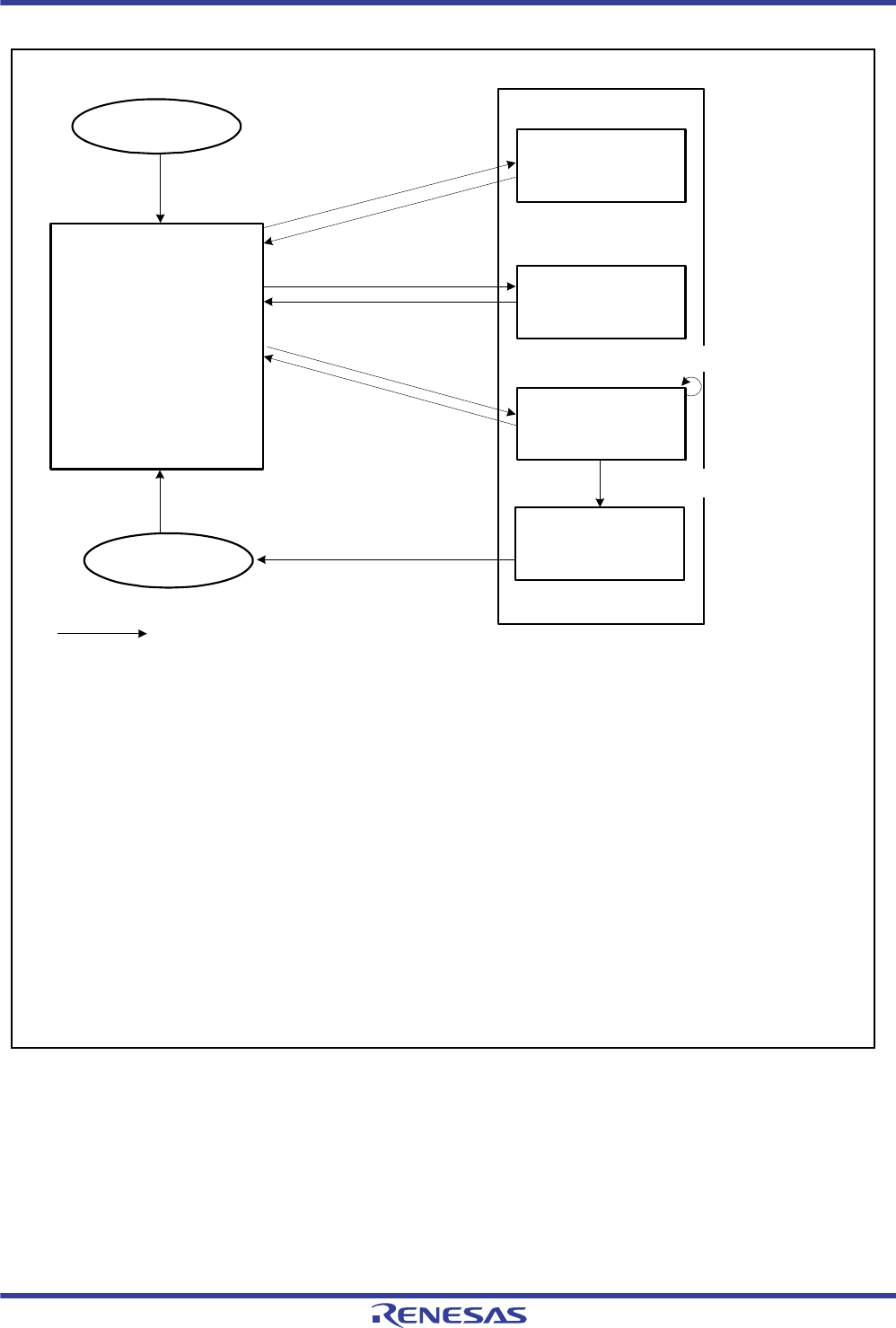
R01UH0034EJ0200 Rev.2.00 Page 197 of 1489
Dec 27, 2013
RX62T Group, RX62G Group 9. Low Power Consumption
Under development Preliminary document
Specifications in this document are tentative and subject to change.
Figure 9.1 Mode Transitions
All interrupts
: Transition after exception handling
Reset state
Program execution state
Program stopped state
All-module clock stop mode
Software standby
mode
Deep software
standby mode
Internal reset state
Sleep mode
SBYCR.SSBY = 0
MSTPCRA.ACSE = 1
MSTPCRA = FFFFFFFFh
MSTPCRB = FFFFFFFFh
Interrupt*5
Interrupt*4
WAIT instruction*1*3
(SBYCR.SSBY = 1)
Interrupt*2
WAIT instruction*1
WAIT instruction*1
(DPSBYCR.DPSBY = 0 and
no external interrupt is generated)
RES# pin = High
Notes:
SBYCR.SSBY = 0
(DPSBYCR.DPSBY = 1 and
no external interrupt is generated)*6
1. If an interrupt that becomes a canceling source is accepted while making a transition to the program stop state after
the WAIT instruction has been executed, the transition to the program stop state is canceled and the interrupt
exception handling is executed.
2. External interrupts and some internal interrupts (WDT, oscillation stop detection, and voltage monitoring).
3. Transitions to the software standby mode do not occur in the following cases.
- The WDT is in use in watchdog timer mode.
- The IWDT is in use.
- The oscillation stop detection function is enabled.
4. External interrupts and some internal interrupts (voltage monitoring).
5. External interrupts (NMI, and IRQ0-A and IRQ1-A) and some internal interrupts (voltage monitor).
However, these sources are enabled only when the corresponding bit in DPSIER is 1.
6. If a conflict between a transition to deep software standby mode and generation of software standby mode canceling
source occurs, a mode transition may be made from software standby mode to program execution state through the
interrupt exception handling. In this case, transition to deep software standby mode does not occur.
For details, see section 9.7, Usage Notes.
7. An internal reset (deep software standby reset) follows the generation of an interrupt request as in point 5 above for the
Time specified by the DPSWCR.WTSTS[5:0] bits. Release from deep software standby accompanies release from the
Internal reset state. On release from the deep software standby state, the chip enters the program-execution state and
starts reset exception processing.
When a pin reset, power-on reset, voltage monitor reset, watchdog timer reset, or independent watchdog timer reset is
generated in any state, a transition to the reset state is made.

R01UH0034EJ0200 Rev.2.00 Page 198 of 1489
Dec 27, 2013
RX62T Group, RX62G Group 9. Low Power Consumption
Under development Preliminary document
Specifications in this document are tentative and subject to change.
9.2 Register Descriptions
Table 9.3 is the list of low power consumption registers. For details on the system clock control register (SCKCR), see
section 9.2.1, Standby Control Register (SBYCR).
Table 9.3 List of Low Power Consumption Registers (1 / 2)
Register Name Symbol Value after Reset Address Access Size
Standby control register SBYCR 4F00h 0008 000Ch 16
Module stop control register A MSTPCRA 4xFF FFFFh 0008 0010h 32
Module stop control register B MSTPCRB FFFF FFFFh 0008 0014h 32
Module stop control register C MSTPCRC FFFF 0000h 0008 0018h 32
Deep standby control register DPSBYCR 31h 0008 C280h 8
Deep standby wait control register DPSWCR 0Fh 0008 C281h 8
Deep standby interrupt enable register DPSIER 00h 0008 C282h 8
Deep standby interrupt flag register DPSIFR 00h 0008 C283h 8
Deep standby interrupt edge register DPSIEGR 00h 0008 C284h 8
Reset status register RSTSR x000 0xxxb 0008 C285h 8
Deep standby backup register 0 DPSBKR0 xxh*0008 C290h 8
Deep standby backup register 1 DPSBKR1 xxh*0008 C291h 8
Deep standby backup register 2 DPSBKR2 xxh*0008 C292h 8
Deep standby backup register 3 DPSBKR3 xxh*0008 C293h 8
Deep standby backup register 4 DPSBKR4 xxh*0008 C294h 8
Deep standby backup register 5 DPSBKR5 xxh*0008 C295h 8
Deep standby backup register 6 DPSBKR6 xxh*0008 C296h 8
Deep standby backup register 7 DPSBKR7 xxh*0008 C297h 8
Deep standby backup register 8 DPSBKR8 xxh*0008 C298h 8
Deep standby backup register 9 DPSBKR9 xxh*0008 C299h 8
Deep standby backup register 10 DPSBKR10 xxh*0008 C29Ah 8
Deep standby backup register 11 DPSBKR11 xxh*0008 C29Bh 8
Deep standby backup register 12 DPSBKR12 xxh*0008 C29Ch 8
Deep standby backup register 13 DPSBKR13 xxh*0008 C29Dh 8
Deep standby backup register 14 DPSBKR14 xxh*0008 C29Eh 8
Deep standby backup register 15 DPSBKR15 xxh*0008 C29Fh 8
Deep standby backup register 16 DPSBKR16 xxh*0008 C2A0h 8
Deep standby backup register 17 DPSBKR17 xxh*0008 C2A1h 8
Deep standby backup register 18 DPSBKR18 xxh*0008 C2A2h 8
Deep standby backup register 19 DPSBKR19 xxh*0008 C2A3h 8
Deep standby backup register 20 DPSBKR20 xxh*0008 C2A4h 8
Deep standby backup register 21 DPSBKR21 xxh*0008 C2A5h 8
Deep standby backup register 22 DPSBKR22 xxh*0008 C2A6h 8
Deep standby backup register 23 DPSBKR23 xxh*0008 C2A7h 8
Deep standby backup register 24 DPSBKR24 xxh*0008 C2A8h 8
Deep standby backup register 25 DPSBKR25 xxh*0008 C2A9h 8
Deep standby backup register 26 DPSBKR26 xxh*0008 C2AAh 8
Deep standby backup register 27 DPSBKR27 xxh*0008 C2ABh 8
Deep standby backup register 28 DPSBKR28 xxh*0008 C2ACh 8
Deep standby backup register 29 DPSBKR29 xxh*0008 C2ADh 8
Deep standby backup register 30 DPSBKR30 xxh*0008 C2AEh 8

R01UH0034EJ0200 Rev.2.00 Page 199 of 1489
Dec 27, 2013
RX62T Group, RX62G Group 9. Low Power Consumption
Under development Preliminary document
Specifications in this document are tentative and subject to change.
Note: • DPSBKR0 to DPSBKR31 are not initialized and their values are undefined immediately after power-on.
9.2.1 Standby Control Register (SBYCR)
SBYCR is used to control software standby mode.
STS[4:0] Bits (Standby Timer Select)
These bits select the time for the LSI to wait until the clock is stabilized when software standby mode is canceled by an
external interrupt.
In the case of crystal oscillation, see Table 9.4 and make a selection according to the operating frequency so that the
waiting time is no less than the oscillation settling time. When an external clock is used, the PLL circuit settling time is
necessary. Select a waiting time referring to Table 9.4.
During the oscillation settling time, the standby timer is counted on the peripheral module clock (PCLK) frequency. Note
this when the multi-clock function is in use.
Deep standby backup register 31 DPSBKR31 xxh*0008 C2AFh 8
Address: 0008 000Ch
b15 b14 b13 b12 b11 b10 b9 b8 b7 b6 b5 b4 b3 b2 b1 b0
SSBY—— STS[4:0] ————————
Value after reset: 0100111100000000
Bit Symbol Bit Name Description R/W
b7 to b0 — Reserved These bits are always read as 0. The write value should always be 0. R/W
b12 to b8 STS[4:0] Standby Timer Select b12b8
0 0 1 0 1: Waiting time = 64 states
0 0 1 1 0: Waiting time = 512 states
0 0 1 1 1: Waiting time = 1024 states
0 1 0 0 0: Waiting time = 2048 states
0 1 0 0 1: Waiting time = 4096 states
0 1 0 1 0: Waiting time = 16384 states
0 1 0 1 1: Waiting time = 32768 states
0 1 1 0 0: Waiting time = 65536 states
0 1 1 0 1: Waiting time = 131072 states
0 1 1 1 0: Waiting time = 262144 states
0 1 1 1 1: Waiting time = 524288 states
Settings other than above are prohibited.
R/W
b13 — Reserved This bit is always read as 0. The write value should always be 0. R/W
b14 — Reserved This bit is always read as 1. The write value should always be 1. R/W
b15 SSBY Software Standby 0: Shifts to sleep mode or all-module clock stop mode after the WAIT
instruction is executed
1: Shifts to software standby mode after the WAIT instruction is
executed
R/W
Table 9.3 List of Low Power Consumption Registers (2 / 2)
Register Name Symbol Value after Reset Address Access Size

R01UH0034EJ0200 Rev.2.00 Page 200 of 1489
Dec 27, 2013
RX62T Group, RX62G Group 9. Low Power Consumption
Under development Preliminary document
Specifications in this document are tentative and subject to change.
SSBY Bit (Software Standby)
The SSBY bit specifies the transition destination after the WAIT instruction is executed.
When the SSBY bit is set to 0, the LSI enters either sleep mode or all-module clock stop mode after execution of the
WAIT instruction, according to the setting of the MSTPCRA and MSTPCRB registers. When the SSBY bit is set to 1,
the LSI enters software standby mode after execution of the WAIT instruction. In this case, when the DPSBY bit in
DPSBYCR is 1, the LSI enters deep software standby mode after software standby mode. For details, see Table 9.5,
Low Power Consumption Modes.
This bit is not cleared to 0 when software standby mode is canceled by an external interrupt and the LSI enters normal
mode. Write 0 to this bit to clear.
When the WDT is used in watchdog timer mode, the IWDT is used, or the oscillation stop detection function is enabled,
the setting of this bit is invalid and the LSI always enters sleep mode or all-module clock stop mode after the WAIT
instruction is executed.

R01UH0034EJ0200 Rev.2.00 Page 201 of 1489
Dec 27, 2013
RX62T Group, RX62G Group 9. Low Power Consumption
Under development Preliminary document
Specifications in this document are tentative and subject to change.
9.2.2 Module Stop Control Register A (MSTPCRA)
Address: 0008 0010h
b31 b30 b29 b28 b27 b26 b25 b24 b23 b22 b21 b20 b19 b18 b17 b16
ACSE — — MSTPA
28 ———
MSTPA
24 MSTPA
23 —————
MSTPA
17 MSTPA
16
Value after reset: 01000x1101111111
b15 b14 b13 b12 b11 b10 b9 b8 b7 b6 b5 b4 b3 b2 b1 b0
MSTPA
15 MSTPA
14 ————
MSTPA
9—MSTPA
7———————
Value after reset: 1111111111111111
x: Undefined
Bit Symbol Bit Name Description R/W
b6 to b0 — Reserved These bits are always read as 1. The write value should
always be 1.
R/W
b7 MSTPA7 General PWM Timer Module Stop Target module: GPT
0: The module stop state is canceled
1: Transition to the module stop state is made
R/W
b8 — Reserved This bit is always read as 1. The write value should always
be 1.
R/W
b9 MSTPA9 Multifunction Timer Pulse Unit 3
Module Stop
Target module: MTU3
0: The module stop state is canceled
1: Transition to the module stop state is made
R/W
b13 to b10 — Reserved These bits are always read as 1. The write value should
always be 1.
R/W
b14 MSTPA14 Compare Match Timer (Unit 1)
Module Stop
Target module: CMT unit 1 (CMT2, CMT3)
0: The module stop state is canceled
1: Transition to the module stop state is made
R/W
b15 MSTPA15 Compare Match Timer (Unit 0)
Module Stop
Target module: CMT unit 0 (CMT0, CMT1)
0: The module stop state is canceled
1: Transition to the module stop state is made
R/W
b16 MSTPA16 12-Bit A/D Converter (Unit 1)
Module Stop
Target module: 12-bit A/D converter unit 1
0: The module stop state is canceled
1: Transition to the module stop state is made
R/W
b17 MSTPA17 12-Bit A/D Converter (Unit 0)
Module Stop
Target module: 12-bit A/D converter unit 0
0: The module stop state is canceled
1: Transition to the module stop state is made
R/W
b22 to b18 — Reserved These bits are always read as 1. The write value should
always be 1.
R/W
b23 MSTPA23
*1 10-Bit A/D Converter Module Stop Target module: 10-bit AD converter
0: The module stop state is canceled
1: Transition to the module stop state is made
R/W
b24 MSTPA24 12-Bit A/D Converter Control
Section Module Stop
Target module: S12ADA control section
0: The module stop state is canceled
1: Transition to the module stop state is made
R/W
b26 to b25 — Reserved These bits are always read as 1. The write value should
always be 1.
R/W
b27 — Reserved This bit is always read as undefined. The write value should
always be 1.
R/W
b28 MSTPA28 Data Transfer Controller Module
Stop
Target module: DTC
0: The module stop state is canceled
1: Transition to the module stop state is made
R/W
b29 — Reserved This bit is always read as 0. The write value should always
be 0.
R/W

R01UH0034EJ0200 Rev.2.00 Page 202 of 1489
Dec 27, 2013
RX62T Group, RX62G Group 9. Low Power Consumption
Under development Preliminary document
Specifications in this document are tentative and subject to change.
Note 1. In the 64-pin version, this bit is reserved. It is always read as 1. The write value should be 1.
Note 2. When the SBYCR.SSBY bit is 0 and the MSTPCRA.ACSE bit is 0, shift to sleep mode after the WAIT instruction is executed.
MSTPCRA is used to control the module stop state.
ACSE Bit (All-Module Clock Stop Mode Enable)
The ACSE bit enables or disables all-module clock stop mode for reducing supply current by stopping the bus controller
and I/O ports when the CPU executes the WAIT instruction after the module stop state has been specified for all modules
controlled by MSTPCRA and MSTPCRB.
b30 — Reserved This bit is always read as 1. The write value should always
be 1.
R/W
b31 ACSE *2 All-Module Clock Stop Mode
Enable
0: All-module clock stop mode is disabled
1: All-module clock stop mode is enabled
R/W
Bit Symbol Bit Name Description R/W

R01UH0034EJ0200 Rev.2.00 Page 203 of 1489
Dec 27, 2013
RX62T Group, RX62G Group 9. Low Power Consumption
Under development Preliminary document
Specifications in this document are tentative and subject to change.
9.2.3 Module Stop Control Register B (MSTPCRB)
Note 1. In the product without the CAN function, this bit is reserved. It is always read as 1. The write value should be 1.
MSTPCRB is used to control the module stop state.
Address: 0008 0014h
b31 b30 b29 b28 b27 b26 b25 b24 b23 b22 b21 b20 b19 b18 b17 b16
MSTPB
31 MSTPB
30 MSTPB
29 —————
MSTPB
23 —MSTPB
21 ————
MSTPB
17 —
Value after reset: 1111111111111111
b15 b14 b13 b12 b11 b10 b9 b8 b7 b6 b5 b4 b3 b2 b1 b0
———————————
MSTPB
7———————
MSTPB
0
Value after reset: 1111111111111111
Bit Symbol Bit Name Description R/W
b0 MSTPB0 CAN Module Stop*1 Target module: CAN
0: The module stop state is canceled
1: Transition to the module stop state is made
R/W
b6 to b1 — Reserved These bits are always read as 1. The write value should
always be 1.
R/W
b7 MSTPB7 LIN Module Stop Target module: LIN
0: The module stop state is canceled
1: Transition to the module stop state is made
R/W
b16 to b8 — Reserved These bits are always read as 1. The write value should
always be 1.
R/W
b17 MSTPB17 Serial Peripheral Interface Module
Stop
Target module: RSPI
0: The module stop state is canceled
1: Transition to the module stop state is made
R/W
b20 to
b18
— Reserved These bits are always read as 1. The write value should
always be 1.
R/W
b21 MSTPB21 I2C Bus Interface Module Stop Target module: RIIC
0: The module stop state is canceled
1: Transition to the module stop state is made
R/W
b22 — Reserved This bit is always read as 1. The write value should always
be 1.
R/W
b23 MSTPB23 CRC Calculator Module Stop Target module: CRC
0: The module stop state is canceled
1: Transition to the module stop state is made
R/W
b28 to
b24
— Reserved These bits are always read as 1. The write value should
always be 1.
R/W
b29 MSTPB29 Serial Communication Interface 2
Module Stop
Target module: SCI2
0: The module stop state is canceled
1: Transition to the module stop state is made
R/W
b30 MSTPB30 Serial Communication Interface 1
Module Stop
Target module: SCI1
0: The module stop state is canceled
1: Transition to the module stop state is made
R/W
b31 MSTPB31 Serial Communication Interface 0
Module Stop
Target module: SCI0
0: The module stop state is canceled
1: Transition to the module stop state is made
R/W

R01UH0034EJ0200 Rev.2.00 Page 204 of 1489
Dec 27, 2013
RX62T Group, RX62G Group 9. Low Power Consumption
Under development Preliminary document
Specifications in this document are tentative and subject to change.
9.2.4 Module Stop Control Register C (MSTPCRC)
Note 1. The MSTPC0 bit should not be set to 1 during access to the on-chip RAM. The on-chip RAM should not be accessed with the
MSTPC0 bit set to 1.
MSTPCRC is used to control the module stop state.
Address: 0008 0018h
b31 b30 b29 b28 b27 b26 b25 b24 b23 b22 b21 b20 b19 b18 b17 b16
————————————————
Value after reset: 1111111111111111
b15 b14 b13 b12 b11 b10 b9 b8 b7 b6 b5 b4 b3 b2 b1 b0
———————————————
MSTPC
0
Value after reset: 0000000000000000
Bit Symbol Bit Name Description R/W
b0 MSTPC0*1RAM Module Stop Target module: RAM (0000 0000h to 0000 3FFFh)
0: The module stop state is canceled
1: Transition to the module stop state is made
R/W
b15 to b1 — Reserved These bits are always read as 0. The write value should always be 0. R/W
b31 to b16 — Reserved These bits are always read as 1. The write value should always be 1. R/W

R01UH0034EJ0200 Rev.2.00 Page 205 of 1489
Dec 27, 2013
RX62T Group, RX62G Group 9. Low Power Consumption
Under development Preliminary document
Specifications in this document are tentative and subject to change.
9.2.5 Deep Standby Control Register (DPSBYCR)
DPSBYCR is used to control deep software standby mode.
DPSBYCR is initialized by the reset signal from the RES# pin, a power-on reset, or a voltage monitoring reset, but is not
initialized by the internal reset signal that cancels deep software standby mode.
IOKEEP Bit (I/O Port Retention)
In deep software standby mode, I/O ports keep retaining the same states from software standby mode. The IOKEEP bit
specifies whether to keep retaining the I/O port states from deep software standby mode even after deep software standby
mode is canceled, or to cancel retaining the I/O port states.
DPSBY Bit (Deep Software Standby)
The DPSBY bit controls transitions to deep software standby mode.
When the WAIT instruction is executed while the SSBY and DPSBY bits in SBYCR are 1, the LSI enters deep software
standby mode through software standby mode.
This bit is not cleared to 0 when deep software standby mode is canceled by an external interrupt or an internal interrupt
(voltage monitoring). Write 0 to this bit to clear.
The setting of this bit is invalid when the WDT is used in watchdog timer mode, the IWDT is used, or the oscillation stop
detection function is enabled. In this case, even when the SSBY and DPSBY bits in SBYCR are set to 1, the LSI always
enters sleep mode or all-module clock stop mode after the WAIT instruction is executed.
Address: 0008 C280h
b7 b6 b5 b4 b3 b2 b1 b0
DPSBY IOKEE
P——————
Value after reset: 00110001
Bit Symbol Bit Name Description R/W
b0 — Reserved This bit is always read as 1. The write value should always be 1. R/W
b3 to b1 — Reserved These bits are always read as 0. The write value should always be 0. R/W
b5, b4 — Reserved These bits are always read as 1. The write value should always be 1. R/W
b6 IOKEEP I/O Port Retention 0: Deep software standby mode and I/O port retention are canceled
simultaneously
1: I/O port retention is canceled when 0 is written to the IOKEEP bit after
deep software standby mode is canceled
R/W
b7 DPSBY Deep Software
Standby
SSBY b7
0 0: Transition to sleep mode or all-module clock stop mode is made
after the WAIT instruction is executed
0 1: Transition to sleep mode or all-module clock stop mode is made
after the WAIT instruction is executed
1 0: Transition to software standby mode is made after the WAIT instruc-
tion is executed
1 1: Transition to deep software standby mode is made after the WAIT
instruction is executed
R/W

R01UH0034EJ0200 Rev.2.00 Page 206 of 1489
Dec 27, 2013
RX62T Group, RX62G Group 9. Low Power Consumption
Under development Preliminary document
Specifications in this document are tentative and subject to change.
9.2.6 Deep Standby Wait Control Register (DPSWCR)
DPSWCR is used to select the time for the LSI to wait until the clock is stabilized when deep software standby mode is
canceled by an external interrupt or an internal interrupt (voltage monitoring).
DPSWCR is initialized by the reset signal from the RES# pin, a power-on reset, or a voltage monitoring reset, but is not
initialized by the internal reset signal that cancels deep software standby mode.
WTSTS[5:0] Bits (Deep Software Standby Waiting Time)
These bits select the time for the LSI to wait until the clock is stabilized when deep software standby mode is canceled by
an external interrupt or an internal interrupt (voltage monitoring). When using deep software standby mode, set the
WTSTS[5:0] bits before a transition to deep software standby mode is made.
In the case of crystal oscillation, see Table 9.4 and make a selection according to the operating frequency so that the
waiting time is no less than the oscillation settling time. When an external clock is used, the PLL circuit settling time is
necessary. Select a waiting time referring to Table 9.4.
During the oscillation settling time, the counter is counted on the EXTAL input clock frequency.
Address: 0008 C281h
b7 b6 b5 b4 b3 b2 b1 b0
— — WTSTS[5:0]
Value after reset: 00001111
Bit Symbol Bit Name Description R/W
b5 to b0 WTSTS[5:0] Deep Software Standby
Waiting Time
b5 b0
0 0 0 1 0 1: Waiting time = 64 states
0 0 0 1 1 0: Waiting time = 512 states
0 0 0 1 1 1: Waiting time = 1024 states
0 0 1 0 0 0: Waiting time = 2048 states
0 0 1 0 0 1: Waiting time = 4096 states
0 0 1 0 1 0: Waiting time = 16384 states
0 0 1 0 1 1: Waiting time = 32768 states
0 0 1 1 0 0: Waiting time = 65536 states
0 0 1 1 0 1: Waiting time = 131072 states
0 0 1 1 1 0: Waiting time = 262144 states
0 0 1 1 1 1: Waiting time = 524288 states
R/W
b7, b6 — Reserved These bits are always read as 0. The write value should
always be 0.
R/W

R01UH0034EJ0200 Rev.2.00 Page 207 of 1489
Dec 27, 2013
RX62T Group, RX62G Group 9. Low Power Consumption
Under development Preliminary document
Specifications in this document are tentative and subject to change.
9.2.7 Deep Standby Interrupt Enable Register (DPSIER)
Note 1. After this register has been initialized by the reset signal from the RES# pin, a power-on reset, or a voltage monitoring reset, 1
can be written only once. Once 1 is written to the DNMIE bit, subsequent write accesses are disabled.
DPSIER is used to enable or disable the external interrupt pin and internal cancellation signals that cancel deep software
standby mode.
DPSIER is initialized by the reset signal from the RES# pin, a power-on reset, or a voltage monitoring reset, but is not
initialized by the internal reset signal that cancels deep software standby mode.
Note that modifying the DPSIER register setting causes a change in the internal state of control over the input buffer of
the corresponding pin. At that time, an edge might be generated internally according to the pin state, and if this happens,
it leads to setting of the DPSIFR register value to 1. Before causing a shift to deep software standby mode, set the
DPSIFR register value to 0.
Also note that the input buffer is disabled on a transition to deep software standby mode if the value of the DPSIER
register is 0. At that time, an edge might be generated internally according to the pin state, and if this happens, it leads to
setting of the DPSIFR register value to 1. In this case, however, if the DPSIEGR register value is 0, no rising edges are
detected and thus the DPSIFR register value will not be 1.
Address: 0008 C282h
b7 b6 b5 b4 b3 b2 b1 b0
DNMIE — — DLVDE — — DIRQ1
EDIRQ0
E
Value after reset: 00001110
Bit Symbol Bit Name Description R/W
b0 DIRQ0E IRQ0 Pin Enable 0: Canceling deep software standby mode by the IRQ0 pin is disabled
1: Canceling deep software standby mode by the IRQ0 pin is enabled
R/W
b1 DIRQ1E IRQ1 Pin Enable 0: Canceling deep software standby mode by the IRQ1 pin is disabled
1: Canceling deep software standby mode by the IRQ1 pin is enabled
R/W
b3, b2 — Reserved These bits are always read as 0. The write value should always be 0. R/W
b4 DLVDE LVD Deep Standby
Cancel Signal Enable
0: Canceling deep software standby mode by the voltage detection
interrupt is disabled
1: Canceling deep software standby mode by the voltage detection
interrupt is enabled
R/W
b6, b5 — Reserved These bits are always read as 0. The write value should always be 0. R/W
b7 DNMIE NMI Pin Enable 0: Canceling deep software standby mode by the NMI pin is disabled
1: Canceling deep software standby mode by the NMI pin is enabled
R/(W)*1

R01UH0034EJ0200 Rev.2.00 Page 208 of 1489
Dec 27, 2013
RX62T Group, RX62G Group 9. Low Power Consumption
Under development Preliminary document
Specifications in this document are tentative and subject to change.
9.2.8 Deep Standby Interrupt Flag Register (DPSIFR)
Note 1. Only 0 can be written to clear the flag.
DPSIFR is used to hold the request for canceling deep software standby mode.
Each flag is set to 1 when a cancel request specified by the deep standby interrupt edge register (DPSIEGR) is generated.
Since each flag is set to 1 when a cancel request is generated in any mode, a transition to deep software standby mode
should be made after DPSIFR is cleared to 0.
DPSIFR is initialized by the reset signal from the RES# pin, a power-on reset, or a voltage monitoring reset, but is not
initialized by the internal reset signal that cancels deep software standby mode.
DIRQnF Flags (IRQn Deep Standby Cancel Flag) (n = 0, 1)
These flags indicate that a cancel request by the IRQn pin has been generated.
[Setting condition]
A cancel request by the IRQn pin specified by DPSIEGR is generated
[Clearing condition]
Each bit is read as 1 and then written by 0
DLVDF Flag (LVD Deep Standby Cancel Flag)
This flag indicates that a cancel request by the voltage monitor signal has been generated.
[Setting condition]
A cancel request by the voltage monitor signal is generated
[Clearing condition]
This bit is read as 1 and then written by 0
Address: 0008 C283h
b7 b6 b5 b4 b3 b2 b1 b0
DNMIF — — DLVDF — — DIRQ1
FDIRQ0
F
Value after reset: 00000000
Bit Symbol Bit Name Description R/W
b0 DIRQ0F IRQ0 Deep Standby Cancel Flag 0: No cancel request by the IRQ0 pin is generated
1: A cancel request by the IRQ0 pin is generated
R/(W)*1
b1 DIRQ1F IRQ1 Deep Standby Cancel Flag 0: No cancel request by the IRQ1 pin is generated
1: A cancel request by the IRQ1 pin is generated
R/(W)*1
b3, b2 — Reserved These bits are always read as 0. The write value should
always be 0.
R/(W)
b4 DLVDF LVD Deep Standby Cancel Flag 0: No cancel request by the voltage monitor signal is
generated
1: A cancel request by the voltage monitor signal is
generated
R/(W)*1
b6, b5 — Reserved These bits are always read as 0. The write value should
always be 0.
R/(W)
b7 DNMIF NMI Deep Standby Cancel Flag 0: No cancel request by the NMI pin is generated
1: A cancel request by the NMI pin is generated
R/(W)*1

R01UH0034EJ0200 Rev.2.00 Page 209 of 1489
Dec 27, 2013
RX62T Group, RX62G Group 9. Low Power Consumption
Under development Preliminary document
Specifications in this document are tentative and subject to change.
DNMIF Flag (NMI Deep Standby Cancel Flag)
This flag indicates that a cancel request by the NMI pin has been generated.
[Setting condition]
A cancel request by the NMI pin specified by DPSIEGR is generated
[Clearing condition]
This bit is read as 1 and then written by 0
9.2.9 Deep Standby Interrupt Edge Register (DPSIEGR)
DPSIEGR is used to select an edge of the cancel signal for canceling deep software standby mode.
DPSIEGR is initialized by the reset signal from the RES# pin, a power-on reset, or a voltage monitoring reset, but is not
initialized by the internal reset signal that cancels deep software standby mode.
Address: 0008 C284h
b7 b6 b5 b4 b3 b2 b1 b0
DNMIE
G—————
DIRQ1
EG DIRQ0
EG
Value after reset: 00000000
Bit Symbol Bit Name Description R/W
b0 DIRQ0EG IRQ0 Edge Select 0: A cancel request is generated at a falling edge
1: A cancel request is generated at a rising edge
R/W
b1 DIRQ1EG IRQ1 Edge Select 0: A cancel request is generated at a falling edge
1: A cancel request is generated at a rising edge
R/W
b6 to b2 — Reserved These bits are always read as 0. The write value should always be 0. R/W
b7 DNMIEG NMI Edge Select 0: A cancel request is generated at a falling edge
1: A cancel request is generated at a rising edge
R/W

R01UH0034EJ0200 Rev.2.00 Page 210 of 1489
Dec 27, 2013
RX62T Group, RX62G Group 9. Low Power Consumption
Under development Preliminary document
Specifications in this document are tentative and subject to change.
9.2.10 Reset Status Register (RSTSR)
Note 1. Only 0 can be written to clear the flag.
RSTSR indicates an internal reset generation source.
PORF Flag (Power-On Reset Flag)
The PORF flag indicates that a power-on reset has been generated.
This flag is initialized by the reset signal from the RES# pin, but is not initialized by the internal reset signal that cancels
deep software standby mode.
[Setting condition]
A power-on reset is generated.
[Clearing condition]
This bit is reset by the RES# pin.
LVD1F Flag (LVD1 Detection Flag)
The LVD1F flag indicates that a Vcc voltage lower than the Vdet1 level has been detected.
This flag is initialized by the reset signal from the RES# pin or a power-on reset, but is not initialized by the internal reset
signal that cancels deep software standby mode.
[Setting condition]
Vcc voltage equal to or lower than the Vdet1 level is detected.
[Clearing conditions]
This bit is read as 1 and then written by 0 in a state where Vcc has exceeded Vdet1 and the settling time has passed,
while the LVDCR.LVD1E bit is 1.
A reset by the RES# pin is generated.
A power-on reset is generated.
Address: 0008 C285h
b7 b6 b5 b4 b3 b2 b1 b0
DPSRS
TF ————LVD2FLVD1FPORF
Value after reset: 0/1*00000/1*0/1*0/1*
Note: * The initial value depends on reset generation sources.
Bit Symbol Bit Name Description R/W
b0 PORF Power-On Reset Flag 0: A power-on reset is not generated.
1: A power-on reset is generated.
R
b1 LVD1F LVD1 Detection Flag 0: LVD1 is not detected.
1: LVD1 is detected.
R/(W)*1
b2 LVD2F LVD2 Detection Flag 0: LVD2 is not detected.
1: LVD2 is detected.
R/(W)*1
b6 to b3 — Reserved These bits are always read as 0. The write value should always be 0. R/W
b7 DPSRSTF Deep Software
Standby Reset Flag
0: A deep software standby mode canceling source is not generated by
an external interrupt or an internal interrupt (voltage monitoring).
1: A deep software standby mode canceling source is generated by an
external interrupt or an internal interrupt (voltage monitoring).
R/(W)*1

R01UH0034EJ0200 Rev.2.00 Page 211 of 1489
Dec 27, 2013
RX62T Group, RX62G Group 9. Low Power Consumption
Under development Preliminary document
Specifications in this document are tentative and subject to change.
LVD2F Flag (LVD2 Detection Flag)
The LVD2F flag indicates that a Vcc voltage lower than the Vdet2 level has been detected.
This flag is initialized by the reset signal from the RES# pin or a power-on reset, but is not initialized by the internal reset
signal that cancels deep software standby mode.
[Setting condition]
Vcc voltage equal to or lower than the Vdet2 level is detected.
[Clearing conditions]
This bit is read as 1 and then written by 0 in a state where Vcc has exceeded Vdet2 and the settling time has passed,
while the LVDCR.LVD2E bit is 1.
A reset by the RES# pin is generated.
A power-on reset is generated.
A reset by LVD1 is generated.
DPSRSTF Flag (Deep Software Standby Reset Flag)
The DPSRSTF flag indicates that deep software standby mode has been canceled by an external interrupt source
specified by DPSIER and DPSIEGR or an internal interrupt (voltage monitoring), and an internal reset has been
generated.
This flag is initialized by the reset signal from the RES# pin, a power-on reset, or a voltage monitoring reset, but is not
initialized by the internal reset signal that cancels deep software standby mode.
[Setting condition]
Deep software standby mode is canceled by an external interrupt source or an internal interrupt (voltage
monitoring).
[Clearing conditions]
This bit is read as 1 and then written by 0
A reset by the RES# pin is generated.
A power-on reset is generated.
A reset by LVD1 is generated.
A reset by LVD2 is generated.
9.2.11 Deep Standby Backup Register (DPSBKRy) (y = 0 to 31)
DPSBKRy is a 32-byte readable/writable register to store data during deep software standby mode.
The value of this register is retained even in deep software standby mode where on-chip RAM data is not retained.
DPSBKRy is not initialized and the register value is undefined immediately after power-on.
Address: 0008 C290h to 0008 C2AFh
b7 b6 b5 b4 b3 b2 b1 b0
Value after reset: xxxxxxxx
x: Undefined

R01UH0034EJ0200 Rev.2.00 Page 212 of 1489
Dec 27, 2013
RX62T Group, RX62G Group 9. Low Power Consumption
Under development Preliminary document
Specifications in this document are tentative and subject to change.
9.3 Multi-Clock Function
When the ICK[3:0] and PCK[3:0] bits in SCKCR are set, the clock frequency changes.
The CPU and bus masters operate on the operating clock specified by the ICK[3:0] bits. Peripheral modules operate on
the operating clock specified by the PCK[3:0] bits. For details, see section 8, Clock Generation Circuit.
9.4 Module Stop Function
The module stop function can be set for each on-chip peripheral module.
When the MSTPyj bit (y = A to C, j = 31 to 0) in MSTPCRA to MSTPCRC is set to 1, the specified module stops
operating and enters the module stop state, but the CPU continues to operate independently. Clearing the MSTPyj bit to 0
cancels the module stop state, allowing the module to restart operating at the end of the bus cycle.
The internal states of modules are retained in the module stop state.
After a reset is released, all modules other than the DTC and on-chip RAM are placed in the module stop state. No read/
write access can be made to the registers of the module that are in the module stop state.

R01UH0034EJ0200 Rev.2.00 Page 213 of 1489
Dec 27, 2013
RX62T Group, RX62G Group 9. Low Power Consumption
Under development Preliminary document
Specifications in this document are tentative and subject to change.
9.5 Low Power Consumption Modes
9.5.1 Sleep Mode
9.5.1.1 Transition to Sleep Mode
When the WAIT instruction is executed while the SSBY bit in SBYCR is 0, the CPU enters sleep mode.
In sleep mode, the CPU stops operating but the contents of its internal registers are retained. Other peripheral functions
do not stop.
When sleep mode is used, execute a WAIT instruction after the following settings:
1. Set the PSW.I bit to 0.*1
2. Select the CPU as the receiver of interrupts to be used for return from sleep mode.
3. Set the priority level*2 of an interrupt to be used for return from sleep mode higher than the value of the
PSW.IPL[2:0] bits*1 of the CPU
4. Set the IERm.IENj bit*2 of an interrupt to be used for return from sleep mode to 1.
5. Read the last I/O register to have been written to check that the new value has actually been reflected.
6. Execute a WAIT instruction (the PSW.I bit *1 of the CPU is automatically set to 1 due to the execution of a WAIT
instruction).
Note 1. Refer to section 2, CPU for details.
Note 2. Refer to section 11, Interrupt Controller (ICU) for details.
9.5.1.2 Canceling Sleep Mode
Sleep mode is canceled by any interrupt, the reset signal from the RES# pin, a power-on reset, a voltage monitoring reset,
a reset caused by a WDT overflow, or a reset caused by an IWDT underflow.
Canceling by an interrupt
When an interrupt occurs, sleep mode is canceled and the interrupt exception handling starts. If a maskable interrupt
has been masked by the CPU (the priority level*1 of the interrupt has been set to a value lower than that of the
IPL[3:0] bits*2 in PSW of the CPU), sleep mode is not canceled.
Canceling by the RES# pin
When the RES# pin is driven low, the LSI enters the reset state. When the RES# pin is driven high after the reset
signal is input for a predetermined time period, the CPU starts the reset exception handling.
Canceling by a WDT overflow reset
Sleep mode is canceled by an internal reset generated by a WDT overflow.
Canceling by an IWDT underflow reset
Sleep mode is canceled by an internal reset generated by an IWDT underflow.
Canceling by a voltage monitoring reset
Sleep mode is canceled by a voltage monitoring reset from the voltage detection circuit.
Canceling by a power-on reset
Sleep mode is canceled by a power-on reset.
Note 1. For details, see section 11, Interrupt Controller (ICU).
Note 2. For details, see section 2, CPU.

R01UH0034EJ0200 Rev.2.00 Page 214 of 1489
Dec 27, 2013
RX62T Group, RX62G Group 9. Low Power Consumption
Under development Preliminary document
Specifications in this document are tentative and subject to change.
9.5.2 All-Module Clock Stop Mode
9.5.2.1 Transition to All-Module Clock Stop Mode
When the following two conditions are satisfied, executing the WAIT instruction with the SSBY bit in SBYCR cleared to
0 will cause the transition to all-module clock stop mode at the end of the bus cycle.*1
The ACSE bit in MSTPCRA is set to 1.
All the modules controlled by the MSTPCRA and MSTPCRB registers are set in the module stop state (MSTPCRA
and MSTPCRB = FFFFFFFFh).
In all-module clock stop mode, all modules (other than the WDT, IWDT, voltage detection circuit, power-on reset circuit,
and POE*4), the CPU, the bus controller, and the I/O ports are stopped.
When all-module clock stop mode is in use, issue a WAIT instruction after making the following settings.
1. Clear the I bit*2 in PSW of the CPU to 0.
2. Set the interrupt destination to be used for recovery from all-module clock stop mode to the CPU.
3. Set the priority*3 of the interrupt to be used for recovery from all-module clock stop mode to a level higher than the
setting of the IPL[3:0] bits*2 in PSW.
4. Set the IENn bit*3 in IERm for the interrupt to be used for recovery from all-module clock stop mode to 1.
5. Execute a WAIT instruction (executing a WAIT instruction causes automatic setting of the I bit*2 in PSW of the
CPU to 1).
Note 1. Transitions to all-module clock stop mode are not be made in some states of DTC operations. Before setting the
MSTPA28 bit in MSTPCRA to 1, clear the DTCST bit in DTCST of the DTC to 0 so that the DTC is not initiated.
Note 2. For details, see section 2, CPU.
Note 3. For details, see section 11, Interrupt Controller (ICU).
Note 4. When a POE interrupt source condition is satisfied while the setting to enable POE interrupts is in place,
recovery from all-module clock stop mode does not proceed but the flag to indicate satisfaction of the source
condition is retained. If a different source leads to recovery from all-module clock stop mode in this situation, a
POE interrupt is generated after recovery.
9.5.2.2 Canceling All-Module Clock Stop Mode
All-module clock stop mode is canceled by an external interrupt (the NMI pin or any pin from among IRQ0 to IRQ7), the
reset signal from the RES# pin, a voltage monitoring reset, a power-on reset, or an internal interrupt (from the WDT,
voltage detection circuit, or oscillation stop detection), and normal program execution resumes once handling of the
given exception is complete. However, note that in cases where a maskable interrupt has been masked by the CPU (the
priority level*1 of the interrupt has been set to a value lower than that of the IPL[3:0] bits*2 in PSW of the CPU) or a
maskable interrupt has been set up as a trigger for transfer by the DTC, the interrupt will not trigger release from all-
module clock stop mode.
Note 1. For details, see section 11, Interrupt Controller (ICU).
Note 2. For details, see section 2, CPU.

R01UH0034EJ0200 Rev.2.00 Page 215 of 1489
Dec 27, 2013
RX62T Group, RX62G Group 9. Low Power Consumption
Under development Preliminary document
Specifications in this document are tentative and subject to change.
9.5.3 Software Standby Mode
9.5.3.1 Transition to Software Standby Mode
When the WAIT instruction is executed with the SSBY bit in SBYCR set to 1 and the DPSBY bit in DPSBYCR cleared
to 0, a transition to software standby mode is made. In this mode, the CPU, on-chip peripheral functions, and all the
oscillator functions stop. However, the contents of the CPU internal registers, on-chip RAM data, on-chip peripheral
functions, and the states of the I/O ports are retained. This mode allows significant reduction in power consumption
because the oscillator stops in this mode.
Clear the DTCST bit in DTCST of the DTC to 0 before executing the WAIT instruction.
When the WDT is used in watchdog timer mode or the IWDT is used, no transition to software standby mode is made.
Stop the WDT before executing the WAIT instruction.
When the oscillation stop detection function is enabled*1, software standby mode cannot be entered. To make a transition
to software standby mode, issue a WAIT instruction after disabling the oscillation stop detection function.
When software standby mode is in use, issue a WAIT instruction after making the following settings.
1. Clear the I bit*2 in PSW of the CPU to 0.
2. Set the interrupt destination to be used for recovery from software standby mode to the CPU.
3. Set the priority*3 of the interrupt to be used for recovery from software standby mode to a level higher than the
setting of the IPL[3:0] bits*2 in PSW of the CPU.
4. Set the IENn bit*3 in IERm for the interrupt to be used for recovery from software standby mode to 1.
5. Execute a WAIT instruction (executing a WAIT instruction causes automatic setting of the I bit*2 in PSW of the
CPU to 1).
Note 1. The oscillation stop detection function (the OSTDCR.OSTED bit) is valid after a reset is canceled.
Note 2. For details, see section 2, CPU.
Note 3. For details, see section 11, Interrupt Controller (ICU).
9.5.3.2 Canceling Software Standby Mode
Software standby mode is canceled by an external interrupt (NMI or IRQ0 to IRQ7), an internal interrupt (voltage
monitoring), the reset signal from the RES# pin, a power-on reset, or a voltage monitoring reset.
1. Canceling by an interrupt
When an interrupt request signal is input by an NMI, IRQ0 to IRQ7*1, or voltage monitoring, clock oscillation starts
thus supplying stable clocks to the entire RX62T chip. After the time specified by the STS[4:0] bits in SBYCR has
passed, software standby mode is canceled and the interrupt exception handling is started.
2. Canceling by the RES# pin
When the RES# pin is driven low, clock oscillation starts and at the same time the clocks are supplied to the entire
RX62T chip. Be sure to hold the RES# pin low until the clock oscillation settles. When the RES# pin is driven high,
the CPU begins the reset exception handling.
3. Canceling by a power-on reset
When a power-on reset is generated by a power-supply voltage drop, software standby mode is canceled.
4. Canceling by a voltage monitoring reset
When a voltage monitoring reset is generated by a power-supply voltage drop, software standby mode is canceled
and clock oscillation starts.
Note 1. For details, see section 11, Interrupt Controller (ICU).

R01UH0034EJ0200 Rev.2.00 Page 216 of 1489
Dec 27, 2013
RX62T Group, RX62G Group 9. Low Power Consumption
Under development Preliminary document
Specifications in this document are tentative and subject to change.
9.5.3.3 Setting Oscillation Settling Time after Software Standby Mode is Canceled
Set the STS[4:0] bits in SBYCR as follows:
1. When using a crystal resonator
Set the STS[4:0] bits so that the waiting time is no less than the oscillation settling time.
Table 9.4 shows operating frequencies and waiting time corresponding to each setting of the STS[4:0] bits.
2. When using an external clock
The PLL circuit settling time is necessary. Set the waiting time referring to Table 9.4.
Note 1. The PCLK is the output of the peripheral module frequency divider.
The oscillation settling time (including oscillator’s unstable oscillation time) depends on the resonator
characteristics.
The PCLK values in this table are reference values.
Table 9.4 Oscillation Settling Time Setting
STS4 STS3 STS2 STS1 STS0 Waiting Time
(States)
PCLK*1 (MHz)
Unit50 25 8
00000Reserved — — — s
1 Reserved — — —
10Reserved———
1 Reserved — — —
100Reserved — — —
1 64 1.3 2.6 8.0
1 0 512 10.25 20.5 64.0
1 1024 20.5 41.0 128.0
1 0 0 0 2048 40.95 81.9 256.0
1 4096 0.08 0.16 0.51 ms
1 0 16384 0.33 0.66 2.05
1 32768 0.655 1.31 4.10
1 0 0 65536 1.31 2.62 8.19
1 131072 2.62 5.24 16.38
1 0 262144 5.25 10.49 32.77
1 524288 10.49 20.97 65.54
1xxxxReserved — — —
: Recommended time setting when an external clock is used
: Recommended time setting when a crystal resonator is used
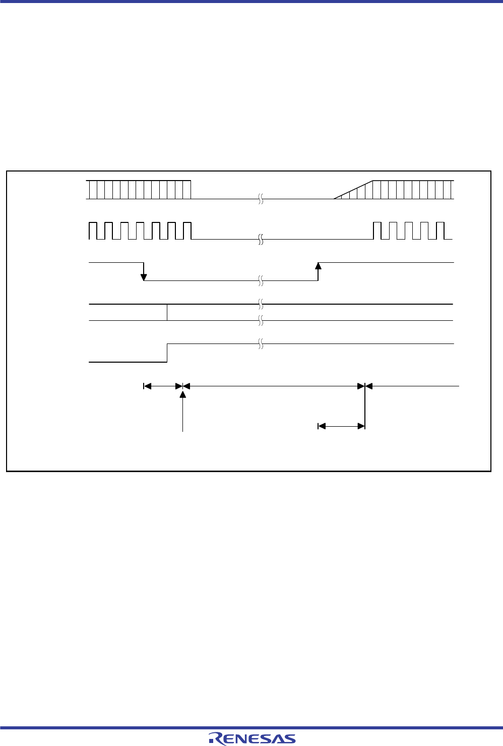
R01UH0034EJ0200 Rev.2.00 Page 217 of 1489
Dec 27, 2013
RX62T Group, RX62G Group 9. Low Power Consumption
Under development Preliminary document
Specifications in this document are tentative and subject to change.
9.5.3.4 Example of Software Standby Mode Application
Figure 9.2 shows an example where a transition to software standby mode is made at the falling edge on the IRQ pin,
and software standby mode is canceled at the rising edge on the IRQ pin.
In this example, an IRQ interrupt is accepted with the IRQMD[1:0] bits in IRQCRi of the ICU set to 01b (falling edge),
and then the IRQMD[1:0] bits are set to 10b (rising edge). After that, the SSBY bit in SBYCR are set to 1, and then the
WAIT instruction is executed. Thus a transition to software standby mode is made.
After that, software standby mode is canceled*1 at the rising edge on the IRQ pin.
Note 1. To return from software standby mode, settings of the interrupt controller (ICU) are also necessary. For details,
see section 11, Interrupt Controller (ICU).
Figure 9.2 Example of Software Standby Mode Application
Software standby mode
(power-down state)
IRQ exception handling
IRQMD[1:0] = 10
SSBY = 1
WAIT instruction Oscillation
settling time
tOSC2
IRQ exception handling
01 10
SSBY
IRQMD[1:0]
IRQ
ICLK
Oscillator

R01UH0034EJ0200 Rev.2.00 Page 218 of 1489
Dec 27, 2013
RX62T Group, RX62G Group 9. Low Power Consumption
Under development Preliminary document
Specifications in this document are tentative and subject to change.
9.5.4 Deep Software Standby Mode
9.5.4.1 Transition to Deep Software Standby Mode
When the WAIT instruction is executed with the SSBY bit in SBYCR set to 1, a transition to software standby mode*1 is
made. At this time, when the DPSBY bit in DPSBYCR is set to 1, a transition to deep software standby mode is made.
However, if a software standby mode canceling source (NMI, IRQ0 to IRQ7 interrupt requests, or some internal
interrupts of voltage monitoring) is generated concurrently when a transition to software standby mode is made, software
standby mode is canceled regardless of the DPSBY setting, and the interrupt exception handling starts after the
oscillation settling time for software standby mode specified by the STS[4:0] bits in SBYCR has passed.
When the SSBY and DPSBY bits are set to 1 and no software standby mode canceling source is generated, a transition to
deep software standby mode is made immediately after transition to software standby mode.
In deep software standby mode, the CPU, on-chip peripheral function, on-chip RAM, and all the oscillator functions
stop. Furthermore, the internal power supply to these modules stops, allowing significant reduction in power
consumption. At this time, the contents of all the registers of the CPU and on-chip peripheral functions become
undefined. All the on-chip RAM data also becomes undefined.
The voltage detection circuit and power-on reset circuit are enabled even in deep software standby mode.
The I/O port states remain unchanged from software standby mode.
Note 1. Conditions on the DTC, WDT, IWDT, and the oscillation stop detection function for transition to software standby
mode should be met before the WAIT instruction is executed.

R01UH0034EJ0200 Rev.2.00 Page 219 of 1489
Dec 27, 2013
RX62T Group, RX62G Group 9. Low Power Consumption
Under development Preliminary document
Specifications in this document are tentative and subject to change.
9.5.4.2 Canceling Deep Software Standby Mode
Deep software standby mode is canceled by an external interrupt (NMI, or IRQ0-A and IRQ1-A pins), an internal
interrupt (voltage monitoring), the reset signal from the RES# pin, a power-on reset, or a voltage monitoring reset.
1. Canceling by an external or internal interrupt
The DPSIFR holds the cancelation cause of deep software standby mode and the bits in this register are set to 1
when the corresponding cancelation requests are generated. When a bit is set to 1 and the corresponding cancelation
cause is enabled in the DPSIER register, deep software standby mode is canceled.
The DNMIF or DIRQnF flag in DPSIFR is set to 1 when an edge is generated on the NMI pin, or IRQ0-A and
IRQ1-A pins enabled by the DNMIE bit in DPSIER or the DIRQnE bit (n = 1, 0) in DPSIER. Rising edge or falling
edge is selectable with DPSIEGR for each pin.
The DLVDIF flag is set to 1 when a voltage monitoring interrupt enabled by the DLDVIE bit in DPSIER is
generated.
When a deep software standby mode canceling source is generated, clock oscillation starts and the internal power
supply begins at the same time, and then the internal reset signal is generated throughout the LSI. After the time
specified by the WTSTS[5:0] bits in DPSWCR has passed, stable clocks are supplied to the entire LSI and the
internal reset is released. At the same time, deep software standby mode is canceled and the reset exception
handling starts.
When deep software standby mode is canceled by an external or internal interrupt, the DPSRSTF flag in RSTSR is
set to 1.
2. Canceling by the RES# pin
When the RES# pin is driven low, clock oscillation starts and the internal power supply begins at the same time.
Clocks are supplied to the LSI simultaneously with the start of clock oscillation. Be sure to hold the RES# pin low
until the clock oscillation settles. When the RES# pin is driven high, the CPU begins the reset exception handling.
3. Canceling by a power-on reset
When a power-on reset is generated by a power-supply voltage drop, deep software standby mode is canceled.
4. Canceling by a voltage monitoring reset
When a voltage monitoring reset is generated by a power-supply voltage drop, deep software standby mode is
canceled.
9.5.4.3 Pin States when Deep Software Standby Mode is Canceled
In deep software standby mode, I/O ports retain the same states from software standby mode. The inside of the LSI is
initialized by an internal reset generated when deep software standby mode is canceled. Upon cancellation of deep
software standby mode, the reset exception handling starts. The following shows the states of I/O ports at this time.
Whether to initialize the I/O ports or to keep retaining the I/O port states at the time of software standby mode can be
selected by the IOKEEP bit in DPSBYCR.
When IOKEEP = 0
I/O ports are initialized by an internal reset generated when deep software standby mode is canceled.
When IOKEEP = 1
Although the inside of the LSI is initialized by an internal reset generated when deep software standby mode is canceled,
I/O ports keep retaining their states from software standby mode regardless of the LSI internal state. At this time, the I/O
port states remain unchanged from software standby mode even if settings of I/O ports or peripheral modules are made.
Then the retained I/O port states are released by clearing the IOKEEP bit to 0, and the LSI operates according to the
internal state.
The IOKEEP bit is not initialized by an internal reset generated when deep software standby mode is canceled.
R01UH0034EJ0200 Rev.2.00 Page 220 of 1489
Dec 27, 2013
RX62T Group, RX62G Group 9. Low Power Consumption
Under development Preliminary document
Specifications in this document are tentative and subject to change.
9.5.4.4 Setting Oscillation Settling Time after Deep Software Standby Mode is
Canceled
1. Set the WTSTS[5:0] bits in DPSWCR as follows:
When using a crystal resonator
2. Set the WTSTS[5:0] bits so that the waiting time is no less than the oscillation settling time.
Table 9.5 shows EXTAL input clock frequencies and waiting time corresponding to each setting of the
WTSTS[5:0] bits.
3. When using an external clock
The PLL circuit settling time is necessary. Set the waiting time referring to Table 9.5.
Note 1. The oscillation settling time (including oscillator’s unstable oscillation time) depends on the resonator characteristics.
The values of the EXTAL input clock frequency in this table are reference values.
Table 9.5 Oscillation Settling Time Setting
WTSTS
5WTSTS
4WTSTS
3WTSTS
2WTSTS
1WTSTS
0Waiting Time
(States)
EXTAL Input Clock Frequency*1 (MHz)
Unit12 10 8
000000Reserved— — — μs
1 Reserved — — —
1 0 Reserved — — —
1 Reserved — — —
1 0 0 Reserved — — —
1 64 5.3 6.4 8.0
1 0 512 42.7 51.2 64.0
1 1024 85.3 102.4 128.0
1 0 0 0 2048 170.7 204.8 256.0
1 4096 0.34 0.41 0.51 ms
1 0 16384 1.37 1.64 2.05
1 32768 2.73 3.26 4.10
1 0 0 65536 5.46 6.55 8.19
1 131072 10.92 13.11 16.38
1 0 262144 21.85 26.21 32.77
1 524288 43.69 52.43 65.54
1 × × × × Reserved — — —
1×××××Reserved— — —
: Recommended time setting when an external clock is used
: Recommended time setting when a crystal resonator is used

R01UH0034EJ0200 Rev.2.00 Page 221 of 1489
Dec 27, 2013
RX62T Group, RX62G Group 9. Low Power Consumption
Under development Preliminary document
Specifications in this document are tentative and subject to change.
9.5.4.5 Example of Deep Software Standby Mode Application
Figure 9.3 shows an example where a transition to deep software standby mode is made at the falling edge on the IRQ
pin, and deep software standby mode is canceled at the rising edge on the IRQ pin.
In this example, an IRQ interrupt is accepted with the IRQMD[1:0] bits in IRQCRi of the ICU set to 01b (falling edge),
and then the DIRQnEG bit (n = 1, 0) in DPSIEGR is set to 1 (rising edge). After that, the SSBY bit in SBYCR and the
DPSBY bit in DPSBYCR are set to 1, and then the WAIT instruction is executed. Thus a transition to deep software
standby mode is made.
After that, deep software standby mode is canceled at the rising edge on the IRQ pin.
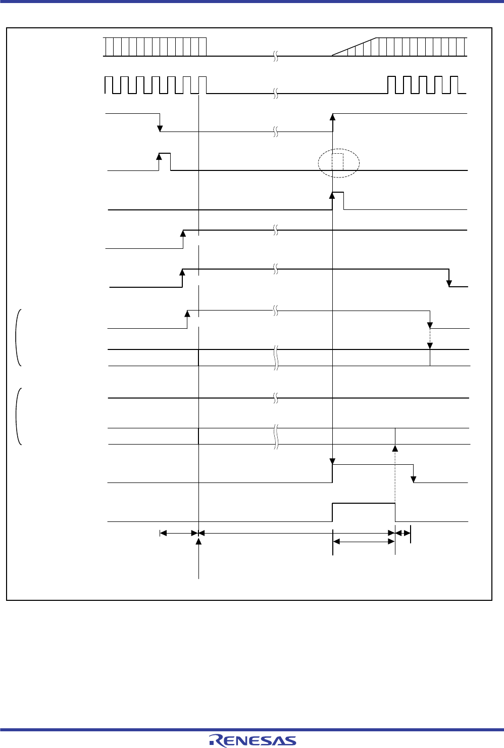
R01UH0034EJ0200 Rev.2.00 Page 222 of 1489
Dec 27, 2013
RX62T Group, RX62G Group 9. Low Power Consumption
Under development Preliminary document
Specifications in this document are tentative and subject to change.
Figure 9.3 Example of Deep Software Standby Mode Application
Disabled by an internal reset
IRQ exception handling
DIRQiEG = 1
SSBY = 1
DPSBY = 1
When IOKEEP = 0
When IOKEEP = 1
Oscillator
ICLK
IRQ
IRQ interrupt
DIRQnF set request
DIRQiEG bit
DPSBY bit Cleared
IOKEEP bit Cleared LL
I/O ports
IOKEEP bit
I/O ports
DPSRSTF flag
Internal reset
L
H
Set
Set
Set
Set
Set
Active
Active
Retained
Retained
Active
Active
Cleared
WAIT instruction
Deep software standby mode
(power-down state) Oscillation
settling time Reset exception
handling
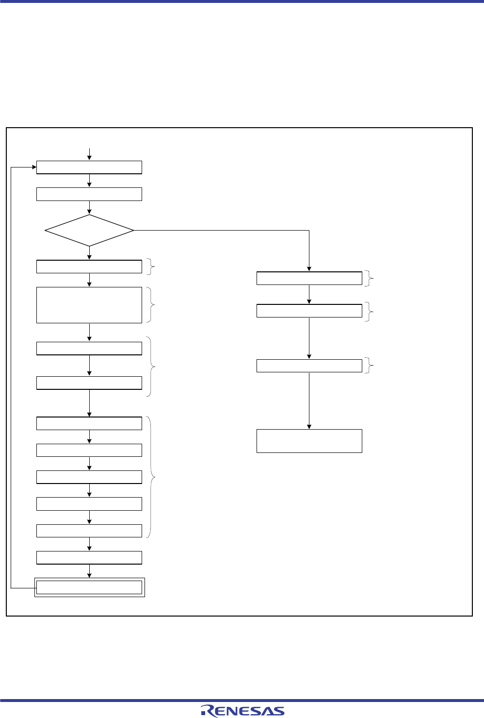
R01UH0034EJ0200 Rev.2.00 Page 223 of 1489
Dec 27, 2013
RX62T Group, RX62G Group 9. Low Power Consumption
Under development Preliminary document
Specifications in this document are tentative and subject to change.
9.5.4.6 Flowchart to Use Deep Software Standby Mode
Figure 9.4 shows an example of a flowchart to use deep software standby mode.
In this example, the DPSRSTF flag in RSTSR of the reset function is read after the reset exception handling to determine
whether a reset was generated by the RES# pin or by the cancellation of deep software standby mode.
In the case of a reset by the RES# pin, a transition to deep software standby mode is made after required register settings.
In the case of a reset by the cancellation of deep software standby mode, the IOKEEP bit in DPSBYCR is cleared to 0
after the I/O port settings.
Figure 9.4 Example of Flowchart to Use Deep Software Standby Mode
Confirm the DPSIFR clearing
Execute WAIT instruction
No
Yes
Releasing a reset generated by
the RES# pin
Set oscillation settling time
Identify deep software standby
mode canceling source -- (1)
Select deep software
standby mode Set pin states after
clearing IOKEEP to 0
A deep software standby mode canceling interrupt is generated
Set pin states during and
after cancellation of deep
software standby mode
Set deep software standby
mode canceling interrupt
Release pin states that have
been retained since transition
to deep software standby mode
Confirm the DPSIER setting
Set PORTn.DDR and PORTn.DR
RSTSR.DPSRSTF = 0
Deep software standby mode
Clear DPSIFR
Set DPSIER
Set DPSIEGR
Set DPSBYCR.IOKEEP = 1
Set the following:
• SBYCR.SSBY = 1
• DPSBYCR.DPSBY = 1
Set DPSWCR.WTSTS[5:0]
Program start
Reset exception handling
Execute a program for the
canceling source identified in (1)
Set DPSBYCR.IOKEEP = 0
Set PORTn.DDR and PORTn.DR
Read DPSIFR

R01UH0034EJ0200 Rev.2.00 Page 224 of 1489
Dec 27, 2013
RX62T Group, RX62G Group 9. Low Power Consumption
Under development Preliminary document
Specifications in this document are tentative and subject to change.
9.6 Usage Notes
9.6.1 I/O Port States
I/O port states are retained in software standby mode and deep software standby mode. Therefore, supply current is not
reduced while output signals are held high.
9.6.2 Module Stop State of the DTC
Before setting the MSTPA28 bit in MSTPCRA to 1, clear the DTCST bit in DTCST of the DTC to 0 so that initiating
transfer by the DTC is not possible.
For details, see section 14, Data Transfer Controller (DTC).
9.6.3 On-Chip Peripheral Module Interrupts
Operation of relevant interrupt is disabled in the module stop state. Therefore, if the module stop state is made with an
interrupt request pending, a CPU interrupt source or a DTC startup source cannot be cleared. For this reason, disable
interrupts before entering the module stop state.
9.6.4 Write-Access to MSTPCRA, MSTPCRB, and MSTPCRC
Write-accesses to MSTPCRA, MSTPCRB, and MSTPCRC should be made only by the CPU.
9.6.5 Input Buffer Control by DIRQnE Bit (n = 1, 0)
When the input buffers for the P10/IRQ0-A and P11/IRQ1-A pins are enabled by setting the DIRQnE bit (n = 1, 0) in
DPSIER to 1. Therefore, note that, although inputs to these pins are sent to the DIRQnF (n = 1, 0) bit in DPSIER, they
are not sent to the interrupt controller, peripheral modules, and I/O ports. Use PORTn.ICR for inputs to the interrupt
controller, peripheral modules, and I/O ports.
9.6.6 Conflict between Transition to Deep Software Standby Mode and Interrupt
If a conflict occurs between a transition to deep software standby mode and generation of a software standby mode
canceling source, the transition to deep software standby mode is not realized but the software standby mode canceling
sequence is started. After the oscillation settling time specified by the STS[4:0] bits in SBYCR for software standby
mode has passed, the interrupt exception handling is started.
Note that if a conflict occurs between a transition to deep software standby mode and a request for release from software
standby mode, an interrupt exception handling routine is required.
9.6.7 Timing of Wait Instructions
The WAIT instruction is executed before completion of the preceding register write; it may be executed before the
register modification is reflected, causing unintended operation. To avoid this, always execute the WAIT instruction after
confirming that the last write to the register has been completed.

R01UH0034EJ0200 Rev.2.00 Page 225 of 1489
Dec 27, 2013
RX62T Group, RX62G Group 10. Exceptions
Under development Preliminary document
Specifications in this document are tentative and subject to change.
10. Exceptions
10.1 Types of Exceptions
During the execution of a program by the CPU, the occurrence of certain events may necessitate suspending execution of
the main flow of the program and starting the execution of another flow. Such events are called exceptions.
The RX CPU supports the seven types of exceptions listed in Figure 10.1.
The occurrence of an exception causes the processor mode to switch to supervisor mode.
Figure 10.1 Types of Exception
Exceptions Undefined instruction exception
Privileged instruction exception
Access exception
Floating-point exceptions
Reset
Non-maskable interrupt
Interrupts
Unconditional trap

R01UH0034EJ0200 Rev.2.00 Page 226 of 1489
Dec 27, 2013
RX62T Group, RX62G Group 10. Exceptions
Under development Preliminary document
Specifications in this document are tentative and subject to change.
10.1.1 Undefined Instruction Exception
An undefined instruction exception occurs when execution of an undefined instruction (an instruction not implemented)
is detected.
10.1.2 Privileged Instruction Exception
A privileged instruction exception occurs when execution of a privileged instruction is detected while operation is in user
mode. Privileged instructions can only be executed in supervisor mode.
10.1.3 Access Exception
An access exception occurs when an error in the form of access to memory by the CPU is detected. When the error
detected by the memory protection unit is an execution memory protection error, an instruction access exception occurs.
When the error is a data memory protection error, an operand access exception occurs.
10.1.4 Floating-Point Exceptions
Floating-point exceptions are generated on the detection of any of five events specified in the IEEE754 standard, namely
overflow, underflow, inexact, division-by-zero, and invalid operation. The exception processing of floating-point
exceptions is masked when the EX, EU, EZ, EO, or EV bit in FPSW is 0.
10.1.5 Reset
A reset through input of the reset signal to the CPU causes the exception request. This has the highest priority of any
exception and is always accepted.
10.1.6 Non-Maskable Interrupt
The non-maskable interrupt is generated by input of the non-maskable interrupt signal to the CPU and is only used when
a fatal fault is considered to have occurred in the system. Never end the exception handling routine for the non-maskable
interrupt with an attempt to return to the program that was being executed at the time of interrupt generation.
10.1.7 Interrupts
Interrupts are generated by the input of interrupt signals to the CPU. A fast interrupt can be selected as the interrupt with
the highest priority. In the case of the fast interrupt, hardware pre-processing and hardware post-processing are handled
fast. The priority level of the fast interrupt is fifteen (the highest). The exception handling of interrupts is masked when
the I bit in PSW is 0.
10.1.8 Unconditional Trap
An unconditional trap is generated when the INT or BRK instruction is executed.
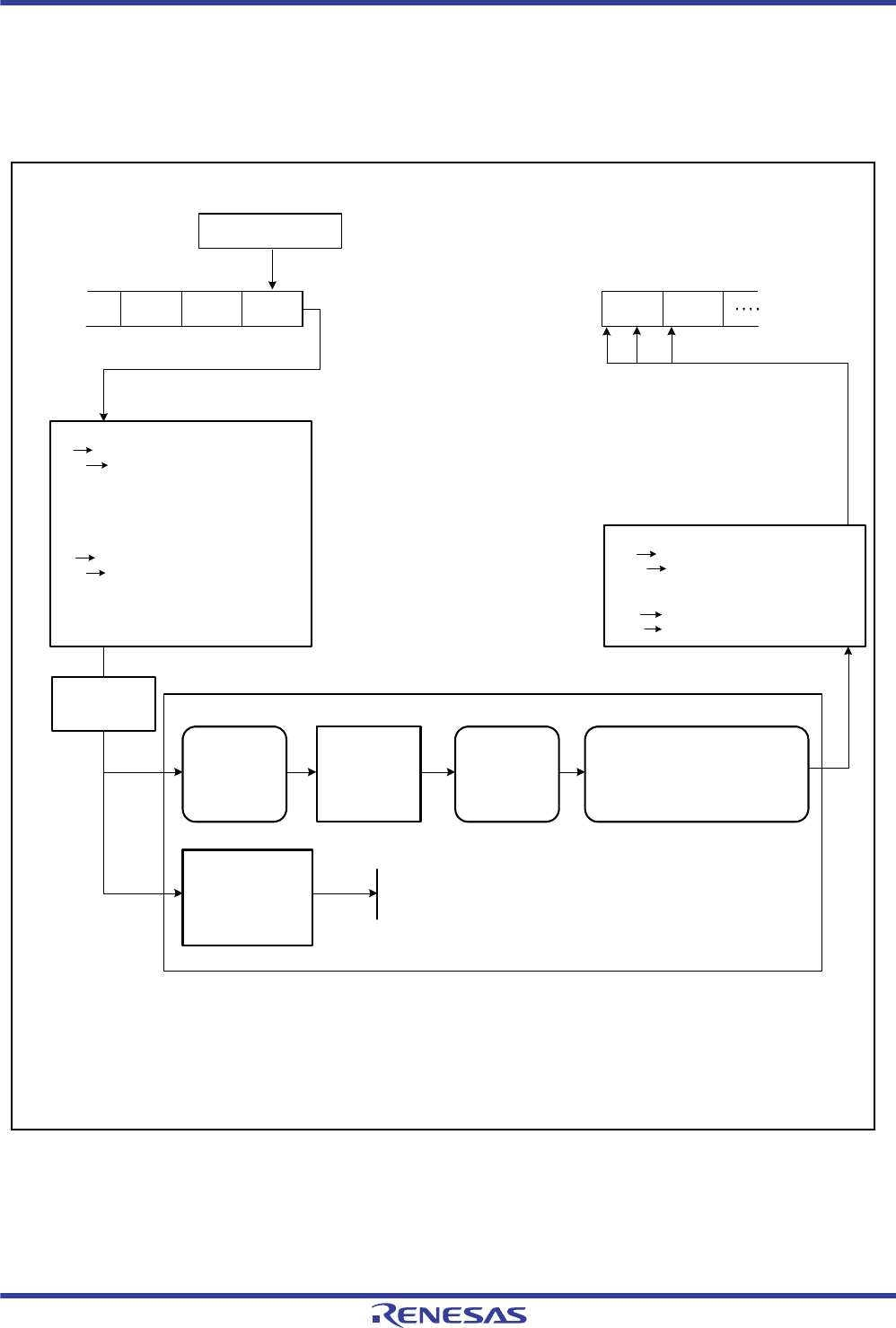
R01UH0034EJ0200 Rev.2.00 Page 227 of 1489
Dec 27, 2013
RX62T Group, RX62G Group 10. Exceptions
Under development Preliminary document
Specifications in this document are tentative and subject to change.
10.2 Exception Handling Procedure
For exception handling, part of the processing is handled automatically by hardware and part is handled by a program
(the exception handling routine) that has been written by the user. Figure 10.2 shows the handling procedure when an
exception other than a reset is accepted.
Figure 10.2 Outline of the Exception Handling Procedure
[Legend]
UND: Undefined instruction exception
PIE: Privileged instruction exception
ACE: Access exception
FPE: Floating-point exceptions
EI: Interrupts
TRAP: Unconditional trap
(For the fast interrupt)
PC BPC
PSW BPSW
U = 0
I = 0
PM = 0
(For exceptions other than the fast interrupt)
PC Saved on the stack (ISP)
PSW Saved on the stack (ISP)
U = 0
I = 0
PM = 0
(For the fast interrupt)
BPC PC
BPSW PSW
(For exceptions other than the fast interrupt)
Stack PC
Stack PSW
Transition to the user mode when the
PM bit in the PSW is 1.
Hardware pre-processing
Exception request
Instruction
AInstruction
BInstruction
CInstruction
D
Instruction
C
Restarting of the program
Processing of user-written program code
Branch to the
vector read
handling routine
Generation of
exception event
General-purpose
registers
preserved on the
stack
Handling routine Restoration of
general-purpose
registers
(For the fast interrupt)
RTFI instruction
(For exceptions other than the fast
interrupt)
RTE instruction
Non-maskable
interrupt processing End of the program or resetting of the system
Exception
handling
routine other
than the non-
maskable
interrupt
Non-
maskable
interrupt
Hardware post-
processing
• Instruction canceling type
(UND, PIE, ACE, and FPE)
• Instruction suspending type
(Reception of an EI during execution of the RMPA instruction or
a string manipulation instruction)
• Instruction completion type
(EI and TRAP)
The program is
suspended and the
exception is accepted.
Switch to the
supervisor mode

R01UH0034EJ0200 Rev.2.00 Page 228 of 1489
Dec 27, 2013
RX62T Group, RX62G Group 10. Exceptions
Under development Preliminary document
Specifications in this document are tentative and subject to change.
When an exception is accepted, hardware processing by the RX CPU is followed by vector access to acquire the address
of the branch destination. A vector address is allocated to each exception. The branch destination address of the
exception handling routine for the given exception is written to each vector address. The combination is referred to as a
vector.
Hardware pre-processing by the RX CPU handles saving of the contents of the program counter (PC) and processor
status word (PSW). In the case of the fast interrupt, the contents are saved in the backup program counter (BPC) and the
backup processor status word (BPSW), respectively. In the case of other exceptions, the contents are preserved in the
stack area.
General purpose registers and control registers other than the PC and PSW that are to be used within the exception
handling routine must be preserved on the stack by user program code at the start of the exception handling routine.
On completion of processing by exception handling routine, registers preserved under program control are restored and
the RTE instruction is executed to restore execution from the exception handling routine to the original program. For
return from the fast interrupt, the RTFI instruction is used instead. In the case of the non-maskable interrupt, however,
end the program or reset the system without returning to the original program.
Hardware post-processing by the RX CPU handles restoration of the pre-exception contents of the PC and PSW. In the
case of the fast interrupt, the contents of the BPC and BPSW are restored to the PC and PSW, respectively. In the case of
other exceptions, the contents are restored from the stack area to the PC and PSW.

R01UH0034EJ0200 Rev.2.00 Page 229 of 1489
Dec 27, 2013
RX62T Group, RX62G Group 10. Exceptions
Under development Preliminary document
Specifications in this document are tentative and subject to change.
10.3 Acceptance of Exceptions
When an exception occurs, the CPU suspends the execution of the program and processing branches to the start of the
exception handling routine
10.3.1 Timing of Acceptance and Saved PC Values
Table 10.1 lists the timing of acceptance and program counter (PC) value to be saved for each type of exception event.
10.3.2 Vector and Site for Saving the Values in the PC and PSW
The vector for each type of exception and the site for saving the values of the program counter (PC) and processor status
word (PSW) are listed in Table 10.2.
Table 10.1 Timing of Acceptance and Saved PC Value
Exception Type of Handling Timing of Acceptance Value Saved in the BPC/
on the Stack
Undefined instruction exception Instruction canceling type During instruction
execution
PC value of the instruction that
generated the exception
Privileged instruction exception Instruction canceling type During instruction
execution
PC value of the instruction that
generated the exception
Access exception Instruction canceling type During instruction
execution
PC value of the instruction that
generated the exception
Floating-point exceptions Instruction canceling type During instruction
execution
PC value of the instruction that
generated the exception
Reset Program abandonment type At each cycle None
Non-maskable
interrupt
During execution of the
RMPA, SCMPU, SMOVB,
SMOVF, SMOVU, SSTR,
SUNTIL, and SWHILE
instructions
Instruction suspending type During instruction
execution
PC value of the instruction being
executed
Other than the above Instruction completion type At the next break
between instructions
PC value of the next instruction
Interrupts During execution of the
RMPA, SCMPU, SMOVB,
SMOVF, SMOVU, SSTR,
SUNTIL, and SWHILE
instructions
Instruction suspending type During instruction
execution
PC value of the instruction being
executed
Other than the above Instruction completion type At the next break
between instructions
PC value of the next instruction
Unconditional trap Instruction completion type At the next break
between instructions
PC value of the next instruction
Table 10.2 Vector and Site for Saving the Values in the PC and PSW
Exception Vector Site for Saving the Values in the PC and PSW
Undefined instruction exception Fixed vector table Stack
Privileged instruction exception Fixed vector table Stack
Access exception Fixed vector table Stack
Floating-point exceptions Fixed vector table Stack
Reset Fixed vector table Nowhere
Non-maskable interrupt Fixed vector table Stack
Interrupts Fast interrupt FINTV BPC and BPSW
Other than the above Relocatable vector table (INTB) Stack
Unconditional trap Relocatable vector table (INTB) Stack

R01UH0034EJ0200 Rev.2.00 Page 230 of 1489
Dec 27, 2013
RX62T Group, RX62G Group 10. Exceptions
Under development Preliminary document
Specifications in this document are tentative and subject to change.
10.4 Hardware Processing for Accepting and Returning from Exceptions
This section describes the hardware processing for accepting and returning from exceptions other than a reset.
(1) Hardware pre-processing for accepting an exception
(a) Saving the values in the PSW
For the fast interrupt
PSW BPSW
For other exceptions
PSW Stack area
Note: • The values in the FPSW are not saved by hardware pre-processing. Therefore, if floating-point instructions are to
be used within an exception handling routine, the user must ensure that these values are saved on the stack.
(b) Updating of the PM, U, and I bits in the PSW
I: Cleared
U: Cleared
PM: Cleared
(c) Saving the values in the PC
For the fast interrupt
PC BPC
For other exceptions
PC Stack area
(d) Set the branch-destination address of the exception handling routine in the PC
Processing is shifted to the exception handling routine by acquiring the vector corresponding to the exception and
branching accordingly.
(2) Hardware post-processing for execution of RTE and RTFI instructions
(a) Restoring the values in the PSW
For the fast interrupt
BPSW PSW
For other exceptions
Stack area PSW
(b) Restoring the values in the PC
For the fast interrupt
BPC PC
For other exceptions
Stack area PC

R01UH0034EJ0200 Rev.2.00 Page 231 of 1489
Dec 27, 2013
RX62T Group, RX62G Group 10. Exceptions
Under development Preliminary document
Specifications in this document are tentative and subject to change.
10.5 Hardware Pre-Processing
The sequences of hardware pre-processing from reception of each exception request to execution of the associated
exception processing routine are explained below.
10.5.1 Undefined Instruction Exception
1. The value of the processor status word (PSW) is saved on the stack (ISP).
2. The processor mode select bit (PM), the stack pointer select bit (U), and the interrupt enable bit (I) in the PSW are
cleared to 0.
3. The value of the program counter (PC) is saved on the stack (ISP).
4. The address of the processing routine is fetched from the vector address, FFFFFFDCh.
5. The PC is set to the fetched address and processing branches to the start of the exception handling routine.
10.5.2 Privileged Instruction Exception
1. The value in the processor status word (PSW) is saved on the stack (ISP).
2. The processor mode select bit (PM), the stack pointer select bit (U), and the interrupt enable bit (I) in the PSW are
cleared to 0.
3. The value of the program counter (PC) is saved on the stack (ISP).
4. The address of the processing routine is fetched from the vector address, FFFFFFD0h.
5. The PC is set to the fetched address and processing branches to the start of the exception handling routine.
10.5.3 Access Exception
1. The value of the processor status word (PSW) is saved on the stack (ISP).
2. The processor mode select bit (PM), the stack pointer select bit (U), and the interrupt enable bit (I) in the PSW are
cleared to 0.
3. The value of the program counter (PC) is saved on the stack (ISP).
4. The address of the processing routine is fetched from the vector address, FFFFFFD4h.
5. The PC is set to the fetched address and processing branches to the start of the exception handling routine.
10.5.4 Floating-Point Exceptions
1. The value in the processor status word (PSW) is saved on the stack (ISP).
2. The processor mode select bit (PM), the stack pointer select bit (U), and the interrupt enable bit (I) in the PSW are
cleared to 0.
3. The value of the program counter (PC) is saved on the stack (ISP).
4. The address of the processing routine is fetched from the vector address, FFFFFFE4h.
5. The PC is set to the fetched address and processing branches to the start of the exception handling routine.
10.5.5 Reset
1. The control registers are initialized.
2. The address of the processing routine is fetched from the vector address, FFFFFFFCh.
3. The PC is set to the fetched address.

R01UH0034EJ0200 Rev.2.00 Page 232 of 1489
Dec 27, 2013
RX62T Group, RX62G Group 10. Exceptions
Under development Preliminary document
Specifications in this document are tentative and subject to change.
10.5.6 Non-Maskable Interrupt
1. The value of the processor status word (PSW) is saved on the stack (ISP).
2. The processor mode select bit (PM), the stack pointer select bit (U), and the interrupt enable bit (I) in the PSW are
cleared to 0.
3. If the interrupt was generated during the execution of an RMPA, SCMPU, SMOVB, SMOVF, SMOVU, SSTR,
SUNTIL, or SWHILE instruction, the value of the program counter (PC) for that instruction is saved on the stack
(ISP). For other instructions, the PC value of the next instruction is saved.
4. The processor interrupt priority level bits (IPL[3:0]) in the PSW are set to "Fh".
5. The address of the processing routine is fetched from the vector address, FFFFFFF8h.
6. The PC is set to the fetched address and the processing branches to the start of the exception handling routine.
10.5.7 Interrupts
1. The value of the processor status word (PSW) is saved on the stack (ISP) or, for the fast interrupt, in the backup
processor status word (BPSW).
2. The processor mode select bit (PM), the stack pointer select bit (U), and the interrupt enable bit (I) in the PSW are
cleared to 0.
3. If the interrupt was generated during the execution of an RMPA, SCMPU, SMOVB, SMOVF, SMOVU, SSTR,
SUNTIL, or SWHILE instruction, the value of the program counter (PC) for that instruction is saved. For other
instructions, the PC value of the next instruction is saved. Saving of the PC is in the backup program counter (BPC)
for fast interrupts.
4. The processor interrupt priority level bits (IPL[3:0]) in the PSW indicate the interrupt priority level of the interrupt.
5. The address of the processing routine for an interrupt source other than the fast interrupt is fetched from the
relocatable vector table. For the fast interrupt, the address is fetched from the fast interrupt vector register (FINTV).
6. The PC is set to the fetched address and processing branches to the start of the exception handling routine.
10.5.8 Unconditional Trap
1. The value in the processor status word (PSW) is saved on the stack (ISP).
2. The processor mode select bit (PM), the stack pointer select bit (U), and the interrupt enable bit (I) in the PSW are
cleared to 0.
3. The value of the program counter (PC) for the next instruction is saved on the stack (ISP).
4. For the INT instruction, the value at the vector corresponding to the INT instruction number is fetched from the
relocatable vector table.
For the BRK instruction, the value at the vector from the start address is fetched from the relocatable vector table.
5. The PC is set to the fetched address and the processing branches to the start of the exception handling routine.

R01UH0034EJ0200 Rev.2.00 Page 233 of 1489
Dec 27, 2013
RX62T Group, RX62G Group 10. Exceptions
Under development Preliminary document
Specifications in this document are tentative and subject to change.
10.6 Return from Exception Processing Routines
Executing the instructions listed in Table 10.3 at the end of the corresponding exception processing routines restores the
values of the program counter (PC) and processor status word (PSW) that were saved on the stack or in the control
registers (BPC and BPSW) immediately before the exception processing sequence.
Order of Priority for Exceptions
The order of priority for exceptions is given in Table 10.4. When multiple exceptions are generated at the same time, the
exception with the highest priority is accepted first.
Table 10.3 Return from Exception Processing Routines
Exception Instruction for Return
Undefined instruction exception RTE
Privileged instruction exception RTE
Access exception RTE
Floating-point exceptions RTE
Reset Return is impossible
Non-maskable interrupt Return is impossible
Interrupts Fast interrupt RTFI
Other than the above RTE
Unconditional trap RTE
Table 10.4 Order of Priority for Exceptions
Order of Priority Exception
High
Low
1 Reset
2 Non-maskable interrupt
3 Interrupts
4 Instruction access exception
5 Undefined instruction exception
Privileged instruction exception
6 Unconditional trap
7 Operand access exception
8 Floating-point exceptions

R01UH0034EJ0200 Rev.2.00 Page 234 of 1489
Dec 27, 2013
RX62T Group, RX62G Group 11. Interrupt Controller (ICU)
Under development Preliminary document
Specifications in this document are tentative and subject to change.
11. Interrupt Controller (ICU)
11.1 Overview
The interrupt controller (ICU) receives interrupt signals from the peripheral modules and external pins, sends interrupts
to the CPU, and activates the DTC.
Table 11.1 lists the specifications of the interrupt controller, and Figure 11.1 shows a block diagram of the interrupt
controller.
Table 11.1 Specifications of the Interrupt Controller
Item Description
Interrupts Peripheral function
interrupts
Interrupts from peripheral modules
Number of sources: 101
Interrupt detection: Edge detection/level detection
Edge detection or level detection is determined for each source of connected peripheral
modules.
External pin
interrupts
Interrupts from pins IRQ7 to IRQ0
Number of sources: 8
Interrupt detection: Low level/falling edge/rising edge/rising and falling edges
One of these detection methods can be set for each source.
Software interrupt Interrupt generated by writing to a register
One interrupt source
Interrupt priority Specified by registers.
Fast interrupt
function
Faster interrupt processing of the CPU can be set only for a single interrupt source.
DTC control The DTC can be activated by interrupt sources.
Number of DTC activating sources: 87 (78 peripheral function interrupts + 8 external pin
interrupts + 1 software interrupt)
Non-
maskable
interrupts
NMI pin interrupts Interrupt from the NMI pin
Interrupt detection: Falling edge/rising edge
Voltage monitoring
interrupt
Interrupt during power-voltage fall detection
Oscillation stop
detection interrupt
Interrupt during oscillation stop detection
Return from power-down modes Sleep mode: Return is initiated by non-maskable interrupts or any other interrupt source.
All-module clock stop mode: Return is initiated by non-maskable interrupts, IRQ7 to IRQ0
interrupts, and WDT interrupts.
Software standby mode: Return is initiated by non-maskable interrupts and IRQ7 to IRQ0
interrupts.
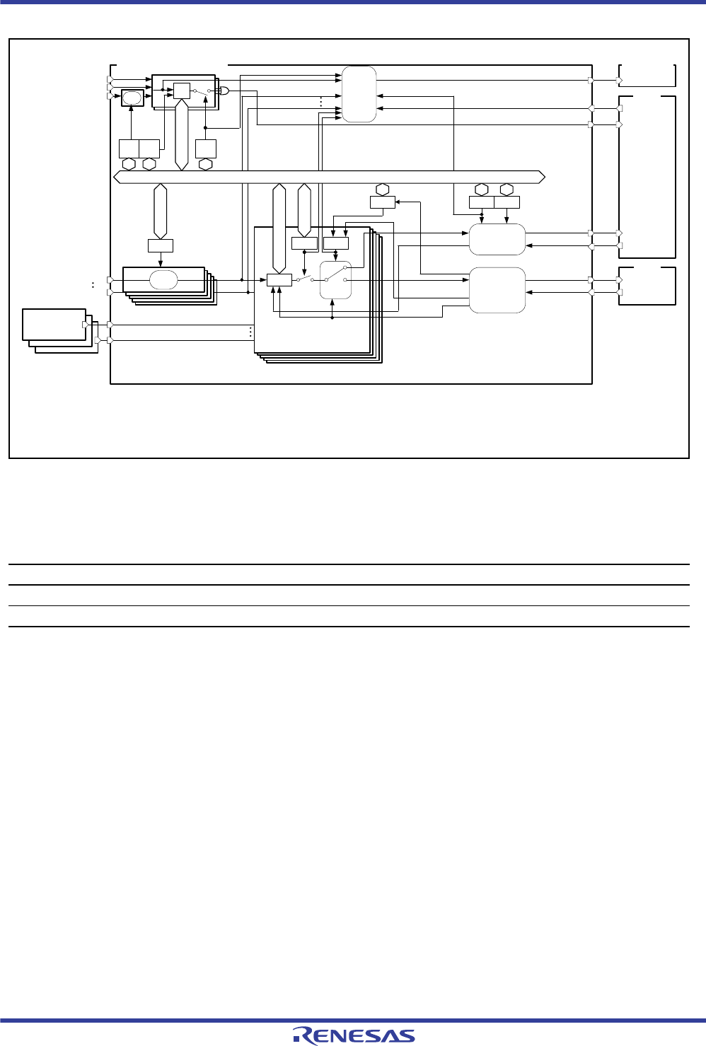
R01UH0034EJ0200 Rev.2.00 Page 235 of 1489
Dec 27, 2013
RX62T Group, RX62G Group 11. Interrupt Controller (ICU)
Under development Preliminary document
Specifications in this document are tentative and subject to change.
Figure 11.1 Block Diagram of Interrupt Controller
Table 11.2 shows the input/output pins of the interrupt controller.
Table 11.2 Pin Configuration of ICU
Pin Name I/O Description
NMI Input Non-maskable interrupt request pin
IRQ7 to IRQ0 Input External interrupt request pins
CPU priority level
judgment
DTC
activation
control
Clock
restoration
judgment
IRQ0 to IRQ7 detection
Interrupt controller
CPU
IRQ0
IRQ7
NMI pin
Peripheral
module
DTC activation
request
DTC response
Interrupt acceptance
Interrupt request
IR clear
IR clear
DTC
Interrupt source
NMI
CLR
IRQCR cntl
IR
FIRIPR
Clock generator
Clock restoration request
Interrupt status, destination switchover
[Legend]
NMIER:
NMICR:
NMICLR:
NMISR:
IRQCR:
Non-maskable interrupt enable register
NMI pin interrupt control register
Non-maskable interrupt clear register
Non-maskable interrupt status register
IRQ control register
IR:
IER:
IPR:
FIR:
DTCER:
Interrupt request register
Interrupt request enable register
Interrupt source priority register
Fast interrupt set register
DTC activation enable register
Detection
NMI
CR
IER
DTCER
Clear
Oscillation stop detection interrupt
Voltage monitoring interrupt
NMI
ER
NMI
SR
Detection
Module data bus
Nonmaskable interrupt request
Clock restoration enable level
Destination switchover
to CPU

R01UH0034EJ0200 Rev.2.00 Page 236 of 1489
Dec 27, 2013
RX62T Group, RX62G Group 11. Interrupt Controller (ICU)
Under development Preliminary document
Specifications in this document are tentative and subject to change.
11.2 Register Descriptions
Table 11.3 lists the registers of the interrupt controller.
Table 11.3 Registers of the Interrupt Controller (1 / 7)
Register Name Symbol Value after Reset Address Access Size
Interrupt source register 016 IR016 00h 0008 7010h 8
Interrupt source register 021 IR021 00h 0008 7015h 8
Interrupt source register 023 IR023 00h 0008 7017h 8
Interrupt source register 027 IR027 00h 0008 701Bh 8
Interrupt source register 028 IR028 00h 0008 701Ch 8
Interrupt source register 029 IR029 00h 0008 701Dh 8
Interrupt source register 030 IR030 00h 0008 701Eh 8
Interrupt source register 031 IR031 00h 0008 701Fh 8
Interrupt source register 044 IR044 00h 0008 702Ch 8
Interrupt source register 045 IR045 00h 0008 702Dh 8
Interrupt source register 046 IR046 00h 0008 702Eh 8
Interrupt source register 047 IR047 00h 0008 702Fh 8
Interrupt source register 056 IR056 00h 0008 7038h 8
Interrupt source register 057 IR057 00h 0008 7039h 8
Interrupt source register 058 IR058 00h 0008 703Ah 8
Interrupt source register 059 IR059 00h 0008 703Bh 8
Interrupt source register 060 IR060 00h 0008 703Ch 8
Interrupt source register 064 IR064 00h 0008 7040h 8
Interrupt source register 065 IR065 00h 0008 7041h 8
Interrupt source register 066 IR066 00h 0008 7042h 8
Interrupt source register 067 IR067 00h 0008 7043h 8
Interrupt source register 068 IR068 00h 0008 7044h 8
Interrupt source register 069 IR069 00h 0008 7045h 8
Interrupt source register 070 IR070 00h 0008 7046h 8
Interrupt source register 071 IR071 00h 0008 7047h 8
Interrupt source register 096 IR096 00h 0008 7060h 8
Interrupt source register 098 IR098 00h 0008 7062h 8
Interrupt source register 102 IR102 00h 0008 7066h 8
Interrupt source register 103 IR103 00h 0008 7067h 8
Interrupt source register 106 IR106 00h 0008 706Ah 8
Interrupt source register 114 IR114 00h 0008 7072h 8
Interrupt source register 115 IR115 00h 0008 7073h 8
Interrupt source register 116 IR116 00h 0008 7074h 8
Interrupt source register 117 IR117 00h 0008 7075h 8
Interrupt source register 118 IR118 00h 0008 7076h 8
Interrupt source register 119 IR119 00h 0008 7077h 8
Interrupt source register 120 IR120 00h 0008 7078h 8
Interrupt source register 121 IR121 00h 0008 7079h 8
Interrupt source register 122 IR122 00h 0008 707Ah 8
Interrupt source register 123 IR123 00h 0008 707Bh 8
Interrupt source register 124 IR124 00h 0008 707Ch 8
Interrupt source register 125 IR125 00h 0008 707Dh 8

R01UH0034EJ0200 Rev.2.00 Page 237 of 1489
Dec 27, 2013
RX62T Group, RX62G Group 11. Interrupt Controller (ICU)
Under development Preliminary document
Specifications in this document are tentative and subject to change.
Interrupt source register 126 IR126 00h 0008 707Eh 8
Interrupt source register 127 IR127 00h 0008 707Fh 8
Interrupt source register 128 IR128 00h 0008 7080h 8
Interrupt source register 129 IR129 00h 0008 7081h 8
Interrupt source register 130 IR130 00h 0008 7082h 8
Interrupt source register 131 IR131 00h 0008 7083h 8
Interrupt source register 132 IR132 00h 0008 7084h 8
Interrupt source register 133 IR133 00h 0008 7085h 8
Interrupt source register 134 IR134 00h 0008 7086h 8
Interrupt source register 135 IR135 00h 0008 7087h 8
Interrupt source register 136 IR136 00h 0008 7088h 8
Interrupt source register 137 IR137 00h 0008 7089h 8
Interrupt source register 138 IR138 00h 0008 708Ah 8
Interrupt source register 139 IR139 00h 0008 708Bh 8
Interrupt source register 140 IR140 00h 0008 708Ch 8
Interrupt source register 141 IR141 00h 0008 708Dh 8
Interrupt source register 142 IR142 00h 0008 708Eh 8
Interrupt source register 143 IR143 00h 0008 708Fh 8
Interrupt source register 144 IR144 00h 0008 7090h 8
Interrupt source register 145 IR145 00h 0008 7091h 8
Interrupt source register 146 IR146 00h 0008 7092h 8
Interrupt source register 149 IR149 00h 0008 7095h 8
Interrupt source register 150 IR150 00h 0008 7096h 8
Interrupt source register 151 IR151 00h 0008 7097h 8
Interrupt source register 152 IR152 00h 0008 7098h 8
Interrupt source register 153 IR153 00h 0008 7099h 8
Interrupt source register 170 IR170 00h 0008 70AAh 8
Interrupt source register 171 IR171 00h 0008 70ABh 8
Interrupt source register 172 IR172 00h 0008 70ACh 8
Interrupt source register 173 IR173 00h 0008 70ADh 8
Interrupt source register 174 IR174 00h 0008 70AEh 8
Interrupt source register 175 IR175 00h 0008 70AFh 8
Interrupt source register 176 IR176 00h 0008 70B0h 8
Interrupt source register 177 IR177 00h 0008 70B1h 8
Interrupt source register 178 IR178 00h 0008 70B2h 8
Interrupt source register 179 IR179 00h 0008 70B3h 8
Interrupt source register 180 IR180 00h 0008 70B4h 8
Interrupt source register 181 IR181 00h 0008 70B5h 8
Interrupt source register 182 IR182 00h 0008 70B6h 8
Interrupt source register 183 IR183 00h 0008 70B7h 8
Interrupt source register 184 IR184 00h 0008 70B8h 8
Interrupt source register 186 IR186 00h 0008 70BAh 8
Interrupt source register 187 IR187 00h 0008 70BBh 8
Interrupt source register 188 IR188 00h 0008 70BCh 8
Interrupt source register 189 IR189 00h 0008 70BDh 8
Table 11.3 Registers of the Interrupt Controller (2 / 7)
Register Name Symbol Value after Reset Address Access Size

R01UH0034EJ0200 Rev.2.00 Page 238 of 1489
Dec 27, 2013
RX62T Group, RX62G Group 11. Interrupt Controller (ICU)
Under development Preliminary document
Specifications in this document are tentative and subject to change.
Interrupt source register 190 IR190 00h 0008 70BEh 8
Interrupt source register 192 IR192 00h 0008 70C0h 8
Interrupt source register 193 IR193 00h 0008 70C1h 8
Interrupt source register 194 IR194 00h 0008 70C2h 8
Interrupt source register 195 IR195 00h 0008 70C3h 8
Interrupt source register 196 IR196 00h 0008 70C4h 8
Interrupt source register 214 IR214 00h 0008 70D6h 8
Interrupt source register 215 IR215 00h 0008 70D7h 8
Interrupt source register 216 IR216 00h 0008 70D8h 8
Interrupt source register 217 IR217 00h 0008 70D9h 8
Interrupt source register 218 IR218 00h 0008 70DAh 8
Interrupt source register 219 IR219 00h 0008 70DBh 8
Interrupt source register 220 IR220 00h 0008 70DCh 8
Interrupt source register 221 IR221 00h 0008 70DDh 8
Interrupt source register 222 IR222 00h 0008 70DEh 8
Interrupt source register 223 IR223 00h 0008 70DFh 8
Interrupt source register 224 IR224 00h 0008 70E0h 8
Interrupt source register 225 IR225 00h 0008 70E1h 8
Interrupt source register 246 IR246 00h 0008 70F6h 8
Interrupt source register 247 IR247 00h 0008 70F7h 8
Interrupt source register 248 IR248 00h 0008 70F8h 8
Interrupt source register 249 IR249 00h 0008 70F9h 8
Interrupt source register 254 IR254 00h 0008 70FEh 8
DTC activation enable register 027 DTCER027 00h 0008 711Bh 8
DTC activation enable register 028 DTCER028 00h 0008 711Ch 8
DTC activation enable register 029 DTCER029 00h 0008 711Dh 8
DTC activation enable register 030 DTCER030 00h 0008 711Eh 8
DTC activation enable register 031 DTCER031 00h 0008 711Fh 8
DTC activation enable register 045 DTCER045 00h 0008 712Dh 8
DTC activation enable register 046 DTCER046 00h 0008 712Eh 8
DTC activation enable register 064 DTCER064 00h 0008 7140h 8
DTC activation enable register 065 DTCER065 00h 0008 7141h 8
DTC activation enable register 066 DTCER066 00h 0008 7142h 8
DTC activation enable register 067 DTCER067 00h 0008 7143h 8
DTC activation enable register 068 DTCER068 00h 0008 7144h 8
DTC activation enable register 069 DTCER069 00h 0008 7145h 8
DTC activation enable register 070 DTCER070 00h 0008 7146h 8
DTC activation enable register 071 DTCER071 00h 0008 7147h 8
DTC activation enable register 098 DTCER098 00h 0008 7162h 8
DTC activation enable register 102 DTCER102 00h 0008 7166h 8
DTC activation enable register 103 DTCER103 00h 0008 7167h 8
DTC activation enable register 106 DTCER106 00h 0008 716Ah 8
DTC activation enable register 114 DTCER114 00h 0008 7172h 8
DTC activation enable register 115 DTCER115 00h 0008 7173h 8
DTC activation enable register 116 DTCER116 00h 0008 7174h 8
Table 11.3 Registers of the Interrupt Controller (3 / 7)
Register Name Symbol Value after Reset Address Access Size

R01UH0034EJ0200 Rev.2.00 Page 239 of 1489
Dec 27, 2013
RX62T Group, RX62G Group 11. Interrupt Controller (ICU)
Under development Preliminary document
Specifications in this document are tentative and subject to change.
DTC activation enable register 117 DTCER117 00h 0008 7175h 8
DTC activation enable register 121 DTCER121 00h 0008 7179h 8
DTC activation enable register 122 DTCER122 00h 0008 717Ah 8
DTC activation enable register 125 DTCER125 00h 0008 717Dh 8
DTC activation enable register 126 DTCER126 00h 0008 717Eh 8
DTC activation enable register 129 DTCER129 00h 0008 7181h 8
DTC activation enable register 130 DTCER130 00h 0008 7182h 8
DTC activation enable register 131 DTCER131 00h 0008 7183h 8
DTC activation enable register 132 DTCER132 00h 0008 7184h 8
DTC activation enable register 134 DTCER134 00h 0008 7186h 8
DTC activation enable register 135 DTCER135 00h 0008 7187h 8
DTC activation enable register 136 DTCER136 00h 0008 7188h 8
DTC activation enable register 137 DTCER137 00h 0008 7189h 8
DTC activation enable register 138 DTCER138 00h 0008 718Ah 8
DTC activation enable register 139 DTCER139 00h 0008 718Bh 8
DTC activation enable register 140 DTCER140 00h 0008 718Ch 8
DTC activation enable register 141 DTCER141 00h 0008 718Dh 8
DTC activation enable register 142 DTCER142 00h 0008 718Eh 8
DTC activation enable register 143 DTCER143 00h 0008 718Fh 8
DTC activation enable register 144 DTCER144 00h 0008 7190h 8
DTC activation enable register 145 DTCER145 00h 0008 7191h 8
DTC activation enable register 149 DTCER149 00h 0008 7195h 8
DTC activation enable register 150 DTCER150 00h 0008 7196h 8
DTC activation enable register 151 DTCER151 00h 0008 7197h 8
DTC activation enable register 152 DTCER152 00h 0008 7198h 8
DTC activation enable register 153 DTCER153 00h 0008 7199h 8
DTC activation enable register 174 DTCER174 00h 0008 71AEh 8
DTC activation enable register 175 DTCER175 00h 0008 71AFh 8
DTC activation enable register 176 DTCER176 00h 0008 71B0h 8
DTC activation enable register 177 DTCER177 00h 0008 71B1h 8
DTC activation enable register 178 DTCER178 00h 0008 71B2h 8
DTC activation enable register 179 DTCER179 00h 0008 71B3h 8
DTC activation enable register 180 DTCER180 00h 0008 71B4h 8
DTC activation enable register 181 DTCER181 00h 0008 71B5h 8
DTC activation enable register 182 DTCER182 00h 0008 71B6h 8
DTC activation enable register 183 DTCER183 00h 0008 71B7h 8
DTC activation enable register 184 DTCER184 00h 0008 71B8h 8
DTC activation enable register 186 DTCER186 00h 0008 71BAh 8
DTC activation enable register 187 DTCER187 00h 0008 71BBh 8
DTC activation enable register 188 DTCER188 00h 0008 71BCh 8
DTC activation enable register 189 DTCER189 00h 0008 71BDh 8
DTC activation enable register 190 DTCER190 00h 0008 71BEh 8
DTC activation enable register 192 DTCER192 00h 0008 71C0h 8
DTC activation enable register 193 DTCER193 00h 0008 71C1h 8
DTC activation enable register 194 DTCER194 00h 0008 71C2h 8
Table 11.3 Registers of the Interrupt Controller (4 / 7)
Register Name Symbol Value after Reset Address Access Size

R01UH0034EJ0200 Rev.2.00 Page 240 of 1489
Dec 27, 2013
RX62T Group, RX62G Group 11. Interrupt Controller (ICU)
Under development Preliminary document
Specifications in this document are tentative and subject to change.
DTC activation enable register 195 DTCER195 00h 0008 71C3h 8
DTC activation enable register 196 DTCER196 00h 0008 71C4h 8
DTC activation enable register 215 DTCER215 00h 0008 71D7h 8
DTC activation enable register 216 DTCER216 00h 0008 71D8h 8
DTC activation enable register 219 DTCER219 00h 0008 71DBh 8
DTC activation enable register 220 DTCER220 00h 0008 71DCh 8
DTC activation enable register 223 DTCER223 00h 0008 71DFh 8
DTC activation enable register 224 DTCER224 00h 0008 71E0h 8
DTC activation enable register 247 DTCER247 00h 0008 71F7h 8
DTC activation enable register 248 DTCER248 00h 0008 71F8h 8
DTC activation enable register 254 DTCER254 00h 0008 71FEh 8
Interrupt request enable register 02 IER02 00h 0008 7202h 8
Interrupt request enable register 03 IER03 00h 0008 7203h 8
Interrupt request enable register 05 IER05 00h 0008 7205h 8
Interrupt request enable register 07 IER07 00h 0008 7207h 8
Interrupt request enable register 08 IER08 00h 0008 7208h 8
Interrupt request enable register 0C IER0C 00h 0008 720Ch 8
Interrupt request enable register 0D IER0D 00h 0008 720Dh 8
Interrupt request enable register 0E IER0E 00h 0008 720Eh 8
Interrupt request enable register 0F IER0F 00h 0008 720Fh 8
Interrupt request enable register 10 IER10 00h 0008 7210h 8
Interrupt request enable register 11 IER11 00h 0008 7211h 8
Interrupt request enable register 12 IER12 00h 0008 7212h 8
Interrupt request enable register 13 IER13 00h 0008 7213h 8
Interrupt request enable register 15 IER15 00h 0008 7215h 8
Interrupt request enable register 16 IER16 00h 0008 7216h 8
Interrupt request enable register 17 IER17 00h 0008 7217h 8
Interrupt request enable register 18 IER18 00h 0008 7218h 8
Interrupt request enable register 1A IER1A 00h 0008 721Ah 8
Interrupt request enable register 1B IER1B 00h 0008 721Bh 8
Interrupt request enable register 1C IER1C 00h 0008 721Ch 8
Interrupt request enable register 1E IER1E 00h 0008 721Eh 8
Interrupt request enable register 1F IER1F 00h 0008 721Fh 8
Software interrupt activation register SWINTR 00h 0008 72E0h 8
Fast interrupt set register FIR 0000h 0008 72F0h 16
Interrupt source priority register 00 IPR00 00h 0008 7300h 8
Interrupt source priority register 01 IPR01 00h 0008 7301h 8
Interrupt source priority register 02 IPR02 00h 0008 7302h 8
Interrupt source priority register 03 IPR03 00h 0008 7303h 8
Interrupt source priority register 04 IPR04 00h 0008 7304h 8
Interrupt source priority register 05 IPR05 00h 0008 7305h 8
Interrupt source priority register 06 IPR06 00h 0008 7306h 8
Interrupt source priority register 07 IPR07 00h 0008 7307h 8
Interrupt source priority register 14 IPR14 00h 0008 7314h 8
Interrupt source priority register 18 IPR18 00h 0008 7318h 8
Table 11.3 Registers of the Interrupt Controller (5 / 7)
Register Name Symbol Value after Reset Address Access Size

R01UH0034EJ0200 Rev.2.00 Page 241 of 1489
Dec 27, 2013
RX62T Group, RX62G Group 11. Interrupt Controller (ICU)
Under development Preliminary document
Specifications in this document are tentative and subject to change.
Interrupt source priority register 20 IPR20 00h 0008 7320h 8
Interrupt source priority register 21 IPR21 00h 0008 7321h 8
Interrupt source priority register 22 IPR22 00h 0008 7322h 8
Interrupt source priority register 23 IPR23 00h 0008 7323h 8
Interrupt source priority register 24 IPR24 00h 0008 7324h 8
Interrupt source priority register 25 IPR25 00h 0008 7325h 8
Interrupt source priority register 26 IPR26 00h 0008 7326h 8
Interrupt source priority register 27 IPR27 00h 0008 7327h 8
Interrupt source priority register 40 IPR40 00h 0008 7340h 8
Interrupt source priority register 44 IPR44 00h 0008 7344h 8
Interrupt source priority register 48 IPR48 00h 0008 7348h 8
Interrupt source priority register 49 IPR49 00h 0008 7349h 8
Interrupt source priority register 51 IPR51 00h 0008 7351h 8
Interrupt source priority register 52 IPR52 00h 0008 7352h 8
Interrupt source priority register 53 IPR53 00h 0008 7353h 8
Interrupt source priority register 54 IPR54 00h 0008 7354h 8
Interrupt source priority register 55 IPR55 00h 0008 7355h 8
Interrupt source priority register 56 IPR56 00h 0008 7356h 8
Interrupt source priority register 57 IPR57 00h 0008 7357h 8
Interrupt source priority register 58 IPR58 00h 0008 7358h 8
Interrupt source priority register 59 IPR59 00h 0008 7359h 8
Interrupt source priority register 5A IPR5A 00h 0008 735Ah 8
Interrupt source priority register 5B IPR5B 00h 0008 735Bh 8
Interrupt source priority register 5C IPR5C 00h 0008 735Ch 8
Interrupt source priority register 5D IPR5D 00h 0008 735Dh 8
Interrupt source priority register 5E IPR5E 00h 0008 735Eh 8
Interrupt source priority register 5F IPR5F 00h 0008 735Fh 8
Interrupt source priority register 60 IPR60 00h 0008 7360h 8
Interrupt source priority register 67 IPR67 00h 0008 7367h 8
Interrupt source priority register 68 IPR68 00h 0008 7368h 8
Interrupt source priority register 69 IPR69 00h 0008 7369h 8
Interrupt source priority register 6A IPR6A 00h 0008 736Ah 8
Interrupt source priority register 6B IPR6B 00h 0008 736Bh 8
Interrupt source priority register 6C IPR6C 00h 0008 736Ch 8
Interrupt source priority register 6D IPR6D 00h 0008 736Dh 8
Interrupt source priority register 6E IPR6E 00h 0008 736Eh 8
Interrupt source priority register 6F IPR6F 00h 0008 736Fh 8
Interrupt source priority register 80 IPR80 00h 0008 7380h 8
Interrupt source priority register 81 IPR81 00h 0008 7381h 8
Interrupt source priority register 82 IPR82 00h 0008 7382h 8
Interrupt source priority register 88 IPR88 00h 0008 7388h 8
Interrupt source priority register 89 IPR89 00h 0008 7389h 8
Interrupt source priority register 8A IPR8A 00h 0008 738Ah 8
Interrupt source priority register 8B IPR8B 00h 0008 738Bh 8
Interrupt source priority register 90 IPR90 00h 0008 7390h 8
Table 11.3 Registers of the Interrupt Controller (6 / 7)
Register Name Symbol Value after Reset Address Access Size

R01UH0034EJ0200 Rev.2.00 Page 242 of 1489
Dec 27, 2013
RX62T Group, RX62G Group 11. Interrupt Controller (ICU)
Under development Preliminary document
Specifications in this document are tentative and subject to change.
IRQ control register 0 IRQCR0 00h 0008 7500h 8
IRQ control register 1 IRQCR1 00h 0008 7501h 8
IRQ control register 2 IRQCR2 00h 0008 7502h 8
IRQ control register 3 IRQCR3 00h 0008 7503h 8
IRQ control register 4 IRQCR4 00h 0008 7504h 8
IRQ control register 5 IRQCR5 00h 0008 7505h 8
IRQ control register 6 IRQCR6 00h 0008 7506h 8
IRQ control register 7 IRQCR7 00h 0008 7507h 8
Non-maskable interrupt status register NMISR 00h 0008 7580h 8
Non-maskable interrupt enable register NMIER 00h 0008 7581h 8
Non-maskable interrupt clear register NMICLR 00h 0008 7582h 8
NMI pin interrupt control register NMICR 00h 0008 7583h 8
Table 11.3 Registers of the Interrupt Controller (7 / 7)
Register Name Symbol Value after Reset Address Access Size

R01UH0034EJ0200 Rev.2.00 Page 243 of 1489
Dec 27, 2013
RX62T Group, RX62G Group 11. Interrupt Controller (ICU)
Under development Preliminary document
Specifications in this document are tentative and subject to change.
11.2.1 Interrupt Request Register i (IRi) (i = interrupt vector number)
Note 1. For edge-detected sources, only 0 can be written to this bit, which clears the flag, and writing 1 to the bit is enabled under the
condition described in section 11.7, Usage Notes. For a level detection source, neither 0 nor 1 can be written.
The IRi register indicates interrupt request status.
IRi is provided for each interrupt source, where "i" indicates the interrupt vector number.
For the correspondence between interrupt sources and interrupt vector numbers, see Table 11.4, Interrupt Vector Table.
IR Flag (Interrupt Status Flag)
This bit is the status flag of an individual interrupt request. This flag is set to 1 when the corresponding interrupt request
is generated. For the actual interrupt to be generated, interrupt output by the corresponding peripheral module should be
enabled in the case of peripheral-module interrupts.
The form of detection for an interrupt request is either edge detection or level detection. For interrupts from peripheral
modules, either edge detection or level detection is determined per interrupt source. For interrupts from IRQn pins, edge
detection or level detection is selected by the setting of the IRQMD[1:0] bits in the corresponding IRQCRn (n= 0 to 7).
Regarding detection of the various interrupt sources, see Table 11.4, Interrupt Vector Table.
(1) Edge detection
[Setting condition]
The flag is set to 1 in response to the generation of an interrupt request from the corresponding peripheral module or
IRQn pin. For interrupt generation by the various peripheral modules, refer to the sections describing the modules.
Though writing 1 to the IR flag is prohibited, it is enabled under the condition described in Table 11.7, Usage
Notes.
[Clearing conditions]
The flag is cleared to 0 when the interrupt request destination accepts the interrupt request.
The IR flag is cleared to 0 by writing 0 to it. Note that writing 0 to the IR flag is prohibited if the interrupt request
destination is the DTC.
Address: 0008 7010h to 0008 70FEh
b7 b6 b5 b4 b3 b2 b1 b0
———————IR
Value after reset: 00000000
Bit Symbol Bit Name Description R/W
b0 IR Interrupt Status Flag 0: No interrupt request is generated
1: An interrupt request is generated
R/W*1
b7 to b1 — Reserved These bits are read as 0. The write value should always be 0. R/W

R01UH0034EJ0200 Rev.2.00 Page 244 of 1489
Dec 27, 2013
RX62T Group, RX62G Group 11. Interrupt Controller (ICU)
Under development Preliminary document
Specifications in this document are tentative and subject to change.
(2) Level detection
[Setting condition]
The flag remains set to 1 while an interrupt request is being sent from the corresponding peripheral module or IRQn
pin. For interrupt generation in each peripheral module, refer to the section describing the module.
[Clearing conditions]
The flag is cleared to 0 when the source of the interrupt request is cleared. (This flag is not cleared even when the
interrupt request destination accepts the interrupt request.) For interrupt clearing in each peripheral module, refer to
the section describing the module.
When level detection has been selected for an IRQn pin, the interrupt request is withdrawn by driving the IRQn pin high.
Do not write 0 or 1 to the IR flag while level detection is selected.

R01UH0034EJ0200 Rev.2.00 Page 245 of 1489
Dec 27, 2013
RX62T Group, RX62G Group 11. Interrupt Controller (ICU)
Under development Preliminary document
Specifications in this document are tentative and subject to change.
11.2.2 Interrupt Request Enable Register m (IERm) (m = 02h to 1Fh)
Note 1. Write 0 to the bit that corresponds to the vector number for reservation. Such the bit is read as 0.
The IERm register is used to enable or disable an interrupt request to the CPU and a DTC activation request.
IENj Bits (Interrupt Request Enable) (j = 7 to 0)
When an IENj bit is 1, the corresponding interrupt request will be output to the interrupt request destination.
When an IENj bit is 0, the corresponding interrupt request will not be output to the interrupt request destination.
The setting of an IERm.IENj bit does not affect the IRi.IR flag. Even when the IERm.IENj bit is 0, the IRi.IR flag value
changes according to the conditions described in section 11.2.1, Interrupt Request Register i (IRi) (i = interrupt
vector number).
The IERm.IENj bit is set for each request source (vector number).
For the correspondence between interrupt sources and IERm.IENj bits, see Table 11.4, Interrupt Vector Table.
For the IERm.IENj bit setting procedure during interrupt request destination selection, refer to Table 11.4.3, Selecting
Interrupt Request Destinations.
Address: 0008 7202h to 0008 721Fh
b7 b6 b5 b4 b3 b2 b1 b0
IEN7 IEN6 IEN5 IEN4 IEN3 IEN2 IEN1 IEN0
Value after reset: 00000000
Bit Symbol Bit Name Description R/W
b0 IEN0 Interrupt Request Enable 0 0: Interrupt request is disabled
1: Interrupt request is enabled
R/W
b1 IEN1 Interrupt Request Enable 1 R/W
b2 IEN2 Interrupt Request Enable 2 R/W
b3 IEN3 Interrupt Request Enable 3 R/W
b4 IEN4 Interrupt Request Enable 4 R/W
b5 IEN5 Interrupt Request Enable 5 R/W
n6 IEN6 Interrupt Request Enable 6 R/W
b7 IEN7 Interrupt Request Enable 7 R/W

R01UH0034EJ0200 Rev.2.00 Page 246 of 1489
Dec 27, 2013
RX62T Group, RX62G Group 11. Interrupt Controller (ICU)
Under development Preliminary document
Specifications in this document are tentative and subject to change.
11.2.3 Interrupt Priority Register m (IPRm) (m = 00h to 90h)
The IPRm register is used to set the priority level of an interrupt source.
IPRm exists for each interrupt source group, where m is the serial number from 00h to 90h.
For the correspondence between interrupt sources and groups, see Table 11.4, Interrupt Vector Table.
IPR[3:0] Bits (Interrupt Priority Level Select)
These bits specify the priority level of the corresponding interrupt source.
Priority levels specified by the IPR[3:0] bits are used only to determine the priority of interrupt requests to be transferred
to the CPU, and do not affect transfer requests to the DTC.
The CPU accepts only interrupt requests higher than the priority level specified by the IPL[3:0] bits in PSW, and handles
accepted interrupts.
If two or more interrupt requests are generated at the same time, their priority levels are compared with the value of the
IPR[3:0] bits. If interrupt requests of the same priority level are generated at the same time, an interrupt source with a
smaller vector number takes precedence.
These bits should be written to while an interrupt request is disabled (the IERm.IENj bit = 0).
Address: 0008 7300h to 0008 7390Fh
b7 b6 b5 b4 b3 b2 b1 b0
———— IPR[3:0]
Value after reset: 00000000
Bit Symbol Bit Name Description R/W
b3 to b0 IPR[3:0] Interrupt Priority Level Select b3 b0
0 0 0 0: Level 0 (interrupt prohibited)
0 0 0 1: Level 1
0 0 1 0:Level 2
0 0 1 1:Level 3
0 1 0 0:Level 4
0 1 0 1:Level 5
0 1 1 0:Level 6
0 1 1 1:Level 7
1 0 0 0:Level 8
1 0 0 1:Level 9
1 0 1 0:Level 10
1 0 1 1:Level 11
1 1 0 0:Level 12
1 1 0 1:Level 13
1 1 1 0:Level 14
1 1 1 1: Level 15 (highest)
R/W
b7 to b4 — Reserved These bits are read as 0. The write value should always be 0. R/W

R01UH0034EJ0200 Rev.2.00 Page 247 of 1489
Dec 27, 2013
RX62T Group, RX62G Group 11. Interrupt Controller (ICU)
Under development Preliminary document
Specifications in this document are tentative and subject to change.
11.2.4 Fast Interrupt Register (FIR)
The FIR register is used to set the fast interrupt function.
The fast interrupt function based on the FIR register setting is applicable only to interrupts to the CPU. It will not affect
any transfer request to the DTC.
Before writing to this register, be sure to disable interrupt requests (IERm.IENj bit = 0).
FVCT[7:0] Bits (Fast Interrupt Vector Number)
The FVCT[7:0] bits specify the vector number of an interrupt source that uses the fast interrupt function.
FIEN Bit (Fast Interrupt Enable)
This bit enables fast interrupt.
Setting this bit to 1 makes the interrupt request of the vector number specified by the FVCT[7:0] bits a fast interrupt.
When an interrupt request of the vector number specified by the FVCT[7:0] bits is generated and the interrupt request
destination is the CPU while the FIEN bit is 1, the interrupt request is output to the CPU as a fast interrupt regardless of
the setting of the IPRm register. When using the fast interrupt for returning from the software standby mode, see Return
from Software Standby Mode, Return from Software Standby Mode.
If the setting of the IERm.IENj (m = 02h to 1Fh, j =7 to 0) bit has disabled interrupt requests from the interrupt source
with the vector number in this register, fast interrupt requests are not output to the CPU.
For settable vector numbers, see Table 11.4, Interrupt Vector Table.
Do not write any reserved vector numbers to the FVCT[7:0] bits.
For details of fast interrupt, see section 10, Exceptions, and section section 11.4.6, Fast Interrupt.
Address: 0008 72F0h
b15 b14 b13 b12 b11 b10 b9 b8 b7 b6 b5 b4 b3 b2 b1 b0
FIEN——————— FVCT[7:0]
Value after reset: 0000000000000000
Bit Symbol Bit Name Description R/W
b7 to b0 FVCT[7:0] Fast Interrupt Vector
Number
Specify the vector number of an interrupt source to be a fast
interrupt.
R/W
b14 to b8 — Reserved These bits are read as 0. The write value should always be 0. R/W
b15 FIEN Fast Interrupt Enable 0: Fast interrupt is disabled
1: Fast interrupt is enabled
R/W

R01UH0034EJ0200 Rev.2.00 Page 248 of 1489
Dec 27, 2013
RX62T Group, RX62G Group 11. Interrupt Controller (ICU)
Under development Preliminary document
Specifications in this document are tentative and subject to change.
11.2.5 Software Interrupt Activation Register (SWINTR)
Note 1. Only 1 can be written. This bit is read as 0.
The SWINTR register is used to issue a software interrupt request.
SWINT Bit (Software Interrupt Activation)
When 1 is written to the SWINT bit, the interrupt request register 27 (IR27) is set to 1.
If 1 is written to the SWINT bit when the DTC activation enable register 27 (DTCER27) is set to 0, an interrupt to the
CPU is generated.
If 1 is written to the SWINT bit when the DTC activation enable register 27 (DTCER27) is set to 1, a DTC activation
request is issued.
Address: 0008 72F0h
b7 b6 b5 b4 b3 b2 b1
——————SWINT
Value after reset: 0000000
Bit Symbol Bit Name Description R/W
b0 SWINT Software Interrupt
Activation
This bit is read as 0.
Writing 1 issues a software interrupt request.
Writing 0 to this bit has no effect.
R/W*1
b7 to b1 — Reserved These bits are read as 0. The write value should always be 0. R/W

R01UH0034EJ0200 Rev.2.00 Page 249 of 1489
Dec 27, 2013
RX62T Group, RX62G Group 11. Interrupt Controller (ICU)
Under development Preliminary document
Specifications in this document are tentative and subject to change.
11.2.6 DTC Activation Enable Register n (DTCERn) (n = interrupt vector number)
The DTCERn register is used to select an interrupt source to activate the DTC.
DTCE Bit (DTC Activation Enable)
When the DTCE bit is set to 1, the corresponding interrupt source is selected as the source for the DTC activation.
[Setting condition]
When 1 is written to the DTCE bit
[Clearing conditions]
When the specified number of transfers is completed (for the chain transfer, the number of transfers for the last chain
transfer is completed)
When 0 is written to the DTCE bit
Address: 0008 711Bh to 0008 71FEh
b7 b6 b5 b4 b3 b2 b1 b0
———————DTCE
Value after reset: 00000000
Bit Symbol Bit Name Description R/W
b0 DTCE DTC Activation Enable 0: DTC activation is disabled
1: DTC activation is enabled
R/W
b7 to b1 — Reserved These bits are read as 0. The write value should always be 0. R/W

R01UH0034EJ0200 Rev.2.00 Page 250 of 1489
Dec 27, 2013
RX62T Group, RX62G Group 11. Interrupt Controller (ICU)
Under development Preliminary document
Specifications in this document are tentative and subject to change.
11.2.7 IRQ Control Register n (IRQCRn) (n = 0 to 7)
The IRQCRn register is used to set the external interrupt IRQn pin (n = 7 to 0).
Modify the settings of this register when the interrupt request of the corresponding interrupt request enable bit is
prohibited (IENj bit in IERm is 0). After changing the value of the register, clear the IR flag in IRi and then set the
interrupt request enable bit to enable the request. However, the IR flag need not be cleared if the change was to the low
level.
IRQMD[1:0] Bits (IRQ Detection Sense Select)
These bits select the detection sensing method of external pin interrupt sources IRQ7 to IRQ0.
For the external pin interrupt detection setting, see Table 11.4.7, External Pin Interrupts.
Address: 0008 7500h to 0008 7507h
b7 b6 b5 b4 b3 b2 b1 b0
————IRQMD[1:0]——
Value after reset: 00000000
Bit Symbol Bit Name Description R/W
b1, b0 — Reserved These bits are read as 0. The write value should always be 0. R/W
b3, b2 IRQMD[1:0] IRQ Detection Sense
Select
b3 b2
0 0: Low level
0 1: Falling edge
1 0: Rising edge
1 1: Rising and falling edges
R/W
b7 to b4 — Reserved These bits are read as 0. The write value should always be 0. R/W

R01UH0034EJ0200 Rev.2.00 Page 251 of 1489
Dec 27, 2013
RX62T Group, RX62G Group 11. Interrupt Controller (ICU)
Under development Preliminary document
Specifications in this document are tentative and subject to change.
11.2.8 Non-Maskable Interrupt Status Register (NMISR)
The NMISR register monitors the status of a non-maskable interrupt source. Writing to the NMISR register is ignored.
The setting in the non-maskable interrupt enable register (NMIER) does not affect the status flags in NMISR.
Before ending from the non-maskable interrupt routine, read the NMISR register and confirm the generation status of
other non-maskable interrupts. Make sure to end from the routine after confirming that all the bits in the NMISR register
are set to 0. Make sure to end from the handler after confirming that all the bits in the NMISR register are set to 0.
NMIST Flag (NMI Status Flag)
This flag indicates the NMI pin interrupt request.
The NMIST flag is read-only, and cleared by the NMICLR.NMICLR bit.
[Setting condition]
When an edge specified by the NMICR.NMIMD bit is input to the NMI pin
[Clearing condition]
When 1 is written to the NMICLR.NMICLR bit
LVDST Flag (Voltage-Monitoring Interrupt Status Flag)
This flag indicates the request for voltage-monitoring interrupt.
[Setting condition]
When the voltage-monitoring interrupt is generated while it is enabled by the generation source
[Clearing condition]
When the interrupt is cleared by the generation source
OSTST Flag (Oscillation Stop Detection Interrupt Status Flag)
This flag indicates the request for oscillation stop detection interrupt.
The OSTST flag is read-only, and cleared by NMICLR.OSTCLR bit.
[Setting condition]
When oscillation stop detection interrupt is generated while it is enabled by the generation source
[Clearing condition]
When 1 is written to the NMICLR.OSTCLR bit
Address: 0008 7580h
b7 b6 b5 b4 b3 b2 b1 b0
—————OSTSTLVDSTNMIST
Value after reset: 00000000
Bit Symbol Bit Name Description R/W
b0 NMIST NMI Status Flag 0: NMI pin interrupt is not requested
1: NMI pin interrupt is requested
R
b1 LVDST Voltage-Monitoring Interrupt
Detection Status Flag
0: Voltage-monitoring interrupt is not requested
1: Voltage-monitoring interrupt is requested
R
b2 OSTST Oscillation Stop Detection
Interrupt Status Flag
0: Oscillation stop detection interrupt is not requested
1: Oscillation stop detection interrupt is requested
R
b7 to b3 — Reserved These bits are read as 0 and cannot be modified. R

R01UH0034EJ0200 Rev.2.00 Page 252 of 1489
Dec 27, 2013
RX62T Group, RX62G Group 11. Interrupt Controller (ICU)
Under development Preliminary document
Specifications in this document are tentative and subject to change.
11.2.9 Non-Maskable Interrupt Enable Register (NMIER)
Note 1. A 1 can be written to this bit only once, and subsequent write accesses are no longer enabled.
The NMIER register enables/disables a non-maskable interrupt source.
NMIEN Bit (NMI Pin Interrupt Enable)
This bit enables the NMI pin interrupt.
A 1 can be written to this bit only once, and subsequent write accesses are no longer enabled.
Once the NMI pin interrupt is enabled, the interrupt cannot be canceled and writing 0 to this bit is disabled.
LVDEN Bit (Voltage-Monitoring Interrupt Enable)
This bit enables the voltage-monitoring interrupt.
A 1 can be written to this bit only once, and subsequent write accesses are no longer enabled.
Once the voltage-monitoring interrupt is enabled, the interrupt cannot be canceled and writing 0 to this bit is disabled.
OSTEN Bit (Oscillation Stop Detection Interrupt Enable)
This bit enables the oscillation stop detection interrupt.
A 1 can be written to this bit only once, and subsequent write accesses are no longer enabled.
Once the oscillation stop detection interrupt is enabled, the interrupt cannot be canceled and writing 0 to this bit is
disabled.
Address: 0008 7581h
b7 b6 b5 b4 b3 b2 b1 b0
—————OSTENLVDENNMIEN
Value after reset: 00000000
Bit Symbol Bit Name Description R/W
b0 NMIEN NMI Pin Interrupt Enable 0: NMI pin interrupt is disabled
1: NMI pin interrupt is enabled
R/(W)*1
b1 LVDEN Voltage-Monitoring Interrupt
Enable
0: Voltage-monitoring interrupt is disabled
1: Voltage-monitoring interrupt is enabled
R/(W)*1
b2 OSTEN Oscillation Stop Detection
Interrupt Enable
0: Oscillation stop detection interrupt is disable
1: Oscillation stop detection interrupt is enabled
R/(W)*1
b7 to b3 — Reserved These bits are read as 0. The write value should always
be 0.
R/W

R01UH0034EJ0200 Rev.2.00 Page 253 of 1489
Dec 27, 2013
RX62T Group, RX62G Group 11. Interrupt Controller (ICU)
Under development Preliminary document
Specifications in this document are tentative and subject to change.
11.2.10 Non-Maskable Interrupt Clear Register (NMICLR)
Note 1. Only 1 can be written to this bit, to clear the NMISR.NMIST flag.
Note 2. Only 1 can be written to this bit, to clear the NMISR.OSTST flag.
The NMICLR register is used to clear the non-maskable interrupt status register (NMISR).
NMICLR Bit (NMI Clear)
Writing 1 to the NMICLR bit clears the NMISR.NMIST flag.
The NMICLR bit does not retain the "1" state. This bit is always read as 0.
OSTCLR Bit (OST Clear)
Writing 1 to the OSTCLR bit clears the NMISR.OSTST flag.
The OSTCLR bit does not retain the "1" state. This bit is always read as 0.
Address: 0008 7582h
b7 b6 b5 b4 b3 b2 b1 b0
—————
OSTCL
R—NMICL
R
Value after reset: 00000000
Bit Symbol Bit Name Description R/W
b0 NMICLR NMI Clear This bit is always read as 0.
Writing 1 to this bit clears the NMISR.NMIST flag.
Writing 0 to this bit has no effect.
R/(W)*1
b1 — Reserved This bit is read as 0. The write value should always be 0. R/W
b2 OSTCLR OST Clear This bit is always read as 0.
Writing 1 to this bit clears the NMISR.OSTST flag.
Writing 0 to this bit has no effect.
R/(W)*2
b7 to b3 — Reserved These bits are read as 0. The write value should always be 0. R/W

R01UH0034EJ0200 Rev.2.00 Page 254 of 1489
Dec 27, 2013
RX62T Group, RX62G Group 11. Interrupt Controller (ICU)
Under development Preliminary document
Specifications in this document are tentative and subject to change.
11.2.11 NMI Pin Interrupt Control Register (NMICR)
The NMICR register is used to set the NMI pin interrupt.
Change the setting of the NMICR register before the NMI pin interrupt is enabled (before 1 is written to the
NMIER.NMIEN bit).
NMIMD Bit (NMI Detection Set)
This bit specifies the detection edge of the NMI pin interrupt.
Address: 0008 7583h
b7 b6 b5 b4 b3 b2 b1 b0
————NMIMD———
Value after reset: 00000000
Bit Symbol Bit Name Description R/W
b2 to b0 — Reserved These bits are read as 0. The write value should always be 0. R/W
b3 NMIMD NMI Detection Set 0: Falling edge
1: Rising edge
R/(W)
b7 to b4 — Reserved These bits are read as 0. The write value should always be 0. R/W

R01UH0034EJ0200 Rev.2.00 Page 255 of 1489
Dec 27, 2013
RX62T Group, RX62G Group 11. Interrupt Controller (ICU)
Under development Preliminary document
Specifications in this document are tentative and subject to change.
11.3 Vector Table
There are two types of interrupts: maskable interrupts and non-maskable interrupts. Hereinafter "interrupts" is
exclusively used to indicate maskable interrupts, i.e. interrupts other than the non-maskable interrupt.
When the CPU accepts an interrupt or non-maskable interrupt, it acquires a four-byte vector address from the vector
table.
11.3.1 Interrupt Vector Table
The interrupt vector table is placed in the 1024-byte range (4 bytes x 256 sources) beginning at the address specified in
the interrupt table register (INTB) of the CPU. Write a value to the INTB register before enabling interrupts. The value
written to the INTB register should be a multiple of 4.
Table 11.4 shows the interrupt vector table. In the table, "sstb return" indicates return from the standby mode, and "Sacs
return" indicates return from all-module clock stop mode.
Table 11.4 Interrupt Vector Table (1 / 7)
Priority
Source
of
Interrupt
Request Name Vector
No.
Vector
Address
Offset Form of
Detection
Selectable
Interrupt
Request
Destination sstb
Return sacs
Return IER IPRCPU DTC
High — Reserved 0 0000h — × × × × — —
Reserved 1 0004h — × × × × — —
Reserved 2 0008h — × × × × — —
Reserved 3 000Ch — × × × × — —
Reserved 4 0010h — × × × × — —
Reserved 5 0014h — × × × × — —
Reserved 6 0018h — × × × × — —
Reserved 7 001Ch — × × × × — —
Reserved 8 0020h — × × × × — —
Reserved 9 0024h — × × × × — —
Reserved 10 0028h — × × × × — —
Reserved 11 002Ch — × × × × — —
Reserved 12 0030h — × × × × — —
Reserved 13 0034h — × × × × — —
Reserved 14 0038h — × × × × — —
Reserved 15 003Ch — × × × × — —
Bus error BUSERR 16 0040h Level √× × × IER02.IEN0 IPR00
— Reserved 17 0044h — × × × × IER02.IEN1 —
— Reserved 18 0048h — × × × × IER02.IEN2 —
Reserved 19 004Ch — × × × × IER02.IEN3 —
Reserved 20 0050h — × × × × IER02.IEN4 —
FCUIF FIFERR 21 0054h Level √× × × IER02.IEN5 IPR01
Reserved 22 0058h — × × × × IER02.IEN6 —
FRDYI 23 005Ch Edge √× × × IER02.IEN7 IPR02
— Reserved 24 0060h — × × × × IER03.IEN0 —
— Reserved 25 0064h — × × × × IER03.IEN1 —
— Reserved 26 0068h — × × × × IER03.IEN2 —
ICU SWINT 27 006Ch Edge √√× × IER03,IEN3 IPR03
Low CMT0 CMI0 28 0070h Edge √√× × IER03.IEN4 IPR04
R01UH0034EJ0200 Rev.2.00 Page 256 of 1489
Dec 27, 2013
RX62T Group, RX62G Group 11. Interrupt Controller (ICU)
Under development Preliminary document
Specifications in this document are tentative and subject to change.
High CMT1 CMI1 29 0074h Edge √√× × IER03.IEN5 IPR05
CMT2 CMI2 30 0078h Edge √√× × IER03.IEN6 IPR06
CMT3 CMI3 31 007Ch Edge √√× × IER03.IEN7 IPR07
— Reserved 32 0080h — × × × × IER04.IEN0 —
Reserved 33 0084h — × × × × IER04.IEN1 —
Reserved 34 0088h — × × × × IER04.IEN2 —
Reserved 35 008Ch — × × × × IER04.IEN3 —
Reserved 36 0090h — × × × × IER04.IEN4 —
Reserved 37 0094h — × × × × IER04.IEN5 —
Reserved 38 0098h — × × × × IER04.IEN6 —
Reserved 39 009Ch — × × × × IER04.IEN7 —
Reserved 40 00A0h — × × × × IER05.IEN0 —
Reserved 41 00A4h — × × × × IER05.IEN1 —
Reserved 42 00A8h — × × × × IER05.IEN2 —
Reserved 43 00ACh — × × × × IER05.IEN3 —
RSPI0 SPEI0 44 00B0h Level √× × × IER05.IEN4 IPR14
SPRI0 45 00B4h Edge √√× × IER05.IEN5
SPTI0 46 00B8h Edge √√× × IER05.IEN6
SPII0 47 00BCh Level √× × × IER05.IEN7
— Reserved 48 00C0h — × × × × IER06.IEN0 —
Reserved 49 00C4h — × × × × IER06.IEN1 —
Reserved 50 00C8h — × × × × IER06.IEN2 —
Reserved 51 00CCh — × × × × IER06.IEN3 —
Reserved 52 00D0h — × × × × IER06.IEN4 —
Reserved 53 00D4h — × × × × IER06.IEN5 —
Reserved 54 00D8h — × × × × IER06.IEN6 —
Reserved 55 00DCh — × × × × IER06.IEN7 —
CAN0 ERS0 56 00E0h Edge √× × × IER07.IEN0 IPR18
RXF0 57 00E4h Edge √× × × IER07.IEN1
TXF0 58 00E8h Edge √× × × IER07.IEN2
RXM0 59 00ECh Edge √× × × IER07.IEN3
TXM0 60 00F0h Edge √× × × IER07.IEN4
— Reserved 61 00F4h — × × × × IER07.IEN5 —
Reserved 62 00F8h — × × × × IER07.IEN6 —
Low Reserved 63 00FCh — × × × × IER07.IEN7 —
Table 11.4 Interrupt Vector Table (2 / 7)
Priority
Source
of
Interrupt
Request Name Vector
No.
Vector
Address
Offset Form of
Detection
Selectable
Interrupt
Request
Destination sstb
Return sacs
Return IER IPRCPU DTC
R01UH0034EJ0200 Rev.2.00 Page 257 of 1489
Dec 27, 2013
RX62T Group, RX62G Group 11. Interrupt Controller (ICU)
Under development Preliminary document
Specifications in this document are tentative and subject to change.
High External
pin
IRQ0 64 0100h Edge / Level √√√√IER08.IEN0 IPR20
IRQ1 65 0104h Edge / Level √√√√IER08.IEN1 IPR21
IRQ2 66 0108h Edge / Level √√√√IER08.IEN2 IPR22
IRQ3 67 010Ch Edge / Level √√√√IER08.IEN3 IPR23
IRQ4 68 0110h Edge / Level √√√√IER08.IEN4 IPR24
IRQ5 69 0114h Edge / Level √√√√IER08.IEN5 IPR25
IRQ6 70 0118h Edge / Level √√√√IER08.IEN6 IPR26
IRQ7 71 011Ch Edge / Level √√√√IER08.IEN7 IPR27
Reserved 72 0120h — × × × × IER09.IEN0 —
Reserved 73 0124h — × × × × IER09.IEN1 —
Reserved 74 0128h — × × × × IER09.IEN2 —
Reserved 75 012Ch — × × × × IER09.IEN3 —
Reserved 76 0130h — × × × × IER09.IEN4 —
Reserved 77 0134h — × × × × IER09.IEN5 —
Reserved 78 0138h — × × × × IER09.IEN6 —
Reserved 79 013Ch — × × × × IER09.IEN7 —
Reserved 80 0140h — × × × × IER0A.IEN0 —
Reserved 81 0144h — × × × × IER0A.IEN1 —
Reserved 82 0148h — × × × × IER0A.IEN2 —
Reserved 83 014Ch — × × × × IER0A.IEN3 —
Reserved 84 0150h — × × × × IER0A.IEN4 —
Reserved 85 0154h — × × × × IER0A.IEN5 —
Reserved 86 0158h — × × × × IER0A.IEN6 —
Reserved 87 015Ch — × × × × IER0A.IEN7 —
— Reserved 88 0160h — × × × × IER0B.IEN0 —
Reserved 89 0164h — × × × × IER0B.IEN1 —
Reserved 90 0168h — × × × × IER0B.IEN2 —
Reserved 91 016Ch — × × × × IER0B.IEN3 —
Reserved 92 0170h — × × × × IER0B.IEN4 —
Reserved 93 0174h — × × × × IER0B.IEN5 —
Reserved 94 0178h — × × × × IER0B.IEN6 —
Reserved 95 017Ch — × × × × IER0B.IEN7 —
WDT WOVI 96 0180h Edge √—— √IER0C.IEN0 IPR40
Reserved 97 0184h — × × × × IER0C.IEN1 —
AD0 ADI0 98 0188h Edge √√— — IER0C.IEN2 IPR44
— Reserved 99 018Ch — × × × × IER0C.IEN3 —
Reserved 100 0190h — × × × × IER0C.IEN4 —
Reserved 101 0194h — × × × × IER0C.IEN5 —
S12AD0 S12ADI0 102 0198h Edge √√× × IER0C.IEN6 IPR48
S12AD1 S12ADI1 103 019Ch Edge √√× × IER0C.IEN7
— Reserved 104 01A0h — × × × × IER0D.IEN0 —
Low Reserved 105 01A4h — × × × × IER0D.IEN1 —
Table 11.4 Interrupt Vector Table (3 / 7)
Priority
Source
of
Interrupt
Request Name Vector
No.
Vector
Address
Offset Form of
Detection
Selectable
Interrupt
Request
Destination sstb
Return sacs
Return IER IPRCPU DTC

R01UH0034EJ0200 Rev.2.00 Page 258 of 1489
Dec 27, 2013
RX62T Group, RX62G Group 11. Interrupt Controller (ICU)
Under development Preliminary document
Specifications in this document are tentative and subject to change.
High Comparator CMPI 106 01A8h Edge √√× × IER0D.IEN2 IPR49
— Reserved 107 01ACh — × × × × IER0D.IEN3 —
Reserved 108 01B0h — × × × × IER0D.IEN4 —
Reserved 109 01B4h — × × × × IER0D.IEN5 —
Reserved 110 01B8h — × × × × IER0D.IEN6 —
Reserved 111 01BCh — × × × × IER0D.IEN7 —
Reserved 112 01C0h — × × × × IER0E.IEN0 —
Reserved 113 01C4h — × × × × IER0E.IEN1 —
MTU0 TGIA0 114 01C8h Edge √√× × IER0E.IEN2 IPR51
TGIB0 115 01CCh Edge √√× × IER0E.IEN3
TGIC0 116 01D0h Edge √√× × IER0E.IEN4
TGID0 117 01D4h Edge √√× × IER0E.IEN5
TCIV0 118 01D8h Edge √× × × IER0E.IEN6 IPR52
TGIE0 119 01DCh Edge √× × × IER0E.IEN7
TGIF0 120 01E0h Edge √× × × IER0F.IEN0
MTU1 TGIA1 121 01E4h Edge √√× × IER0F.IEN1 IPR53
TGIB1 122 01E8h Edge √√× × IER0F.IEN2
TCIV1 123 01ECh Edge √× × × IER0F.IEN3 IPR54
TCIU1 124 01F0h Edge √× × × IER0F.IEN4
MTU2 TGIA2 125 01F4h Edge √√× × IER0F.IEN5 IPR55
TGIB2 126 01F8h Edge √√× × IER0F.IEN6
TCIV2 127 01FCh Edge √× × × IER0F.IEN7 IPR56
TCIU2 128 0200h Edge √× × × IER10.IEN0
MTU3 TGIA3 129 0204h Edge √√× × IER10.IEN1 IPR57
TGIB3 130 0208h Edge √√× × IER10.IEN2
TGIC3 131 020Ch Edge √√× × IER10.IEN3
TGID3 132 0210h Edge √√× × IER10.IEN4
TCIV3 133 0214h Edge √× × × IER10.IEN5 IPR58
MTU4 TGIA4 134 0218h Edge √√× × IER10.IEN6 IPR59
TGIB4 135 021Ch Edge √√× × IER10.IEN7
TGIC4 136 0220h Edge √√× × IER11.IEN0
TGID4 137 0224h Edge √√× × IER11.IEN1
TCIV4 138 0228h Edge √√× × IER11.IEN2 IPR5A
MTU5 TGIU5 139 022Ch Edge √√× × IER11.IEN3 IPR5B
TGIV5 140 0230h Edge √√× × IER11.IEN4
Low TGIW5 141 0234h Edge √√× × IER11.IEN5
Table 11.4 Interrupt Vector Table (4 / 7)
Priority
Source
of
Interrupt
Request Name Vector
No.
Vector
Address
Offset Form of
Detection
Selectable
Interrupt
Request
Destination sstb
Return sacs
Return IER IPRCPU DTC

R01UH0034EJ0200 Rev.2.00 Page 259 of 1489
Dec 27, 2013
RX62T Group, RX62G Group 11. Interrupt Controller (ICU)
Under development Preliminary document
Specifications in this document are tentative and subject to change.
High MTU6 TGIA6 142 0238h Edge √√× × IER11.IEN6 IPR5C
TGIB6 143 023Ch Edge √√× × IER11.IEN7
TGIC6 144 0240h Edge √√× × IER12.IEN0
TGID6 145 0244h Edge √√× × IER12.IEN1
TCIV6 146 0248h Edge √× × × IER12.IEN2 IPR5D
Reserved 147 024Ch — × × — — IER12.IEN3
Reserved 148 0250h — × × — — IER12.IEN4
MTU7 TGIA7 149 0254h Edge √√× × IER12.IEN5 IPR5E
TGIB7 150 0258h Edge √√× × IER12.IEN6
TGIC7 151 025Ch Edge √√× × IER12.IEN7 IPR5F
TGID7 152 0260h Edge √√× × IER13.IEN0
TCIV7 153 0264h Edge √√× × IER13.IEN1 IPR60
— Reserved 154 0268h — × × × × IER13.IEN2
Reserved 155 026Ch — × × × × IER13.IEN3 —
Reserved 156 0270h — × × × × IER13.IEN4 —
Reserved 157 0274h — × × × × IER13.IEN5 —
Reserved 158 0278h — × × × × IER13.IEN6 —
Reserved 159 027Ch — × × × × IER13.IEN7 —
Reserved 160 0280h — × × × × IER14.IEN0 —
Reserved 161 0284h — × × × × IER14.IEN1 —
Reserved 162 0288h — × × × × IER14.IEN2 —
Reserved 163 028Ch — × × × × IER14.IEN3 —
Reserved 164 0290h — × × × × IER14.IEN4 —
— Reserved 165 0294h — × × × × IER14.IEN5 —
Reserved 166 0298h — × × × × IER14.IEN6 —
— Reserved 167 029Ch — × × × × IER14.IEN7 —
Reserved 168 02A0h — × × × × IER15.IEN0 —
Reserved 169 02A4h — × × × × IER15.IEN1 —
POE OEl1 170 02A8h Level √× × × IER15.IEN2 IPR67
OEl2 171 02ACh Level √× × × IER15.IEN3
OEl3 172 02B0h Level √× × × IER15.IEN4
OEl4 173 02B4h Level √× × × IER15.IEN5
GPT0 GTCIA0 174 02B8h Edge √√× × IER15.IEN6 IPR68
GTCIB0 175 02BCh Edge √√× × IER15.IEN7
GTCIC0 176 02C0h Edge √√× × IER16.IEN0
GTCIE0 177 02C4h Edge √√× × IER16.IEN1 IPR69
GTCIV0 178 02C8h Edge √√× × IER16.IEN2
Low LOCO1 179 02CCh Edge √√× × IER16.IEN3
Table 11.4 Interrupt Vector Table (5 / 7)
Priority
Source
of
Interrupt
Request Name Vector
No.
Vector
Address
Offset Form of
Detection
Selectable
Interrupt
Request
Destination sstb
Return sacs
Return IER IPRCPU DTC

R01UH0034EJ0200 Rev.2.00 Page 260 of 1489
Dec 27, 2013
RX62T Group, RX62G Group 11. Interrupt Controller (ICU)
Under development Preliminary document
Specifications in this document are tentative and subject to change.
High GPT1 GTCIA1 180 02D0h Edge √√× × IER16.IEN4 IPR6A
GTCIB1 181 02D4h Edge √√× × IER16.IEN5
GTCIC1 182 02D8h Edge √√× × IER16.IEN6
GTCIE1 183 02DCh Edge √√× × IER16.IEN7 IPR6B
GTCIV1 184 02E0h Edge √√× × IER17.IEN0
Reserved 185 02E4h — × × × × IER17.IEN1 —
GPT2 GTCIA2 186 02E8h Edge √√× × IER17.IEN2 IPR6C
GTCIB2 187 02ECh Edge √√× × IER17.IEN3
GTCIC2 188 02F0h Edge √√× × IER17.IER4
GTCIE2 189 02F4h Edge √√× × IER17.IEN5 IPR6D
GTCIV2 190 02F8h Edge √√× × IER17.IEN6
Reserved 191 02FCh — × × × × IER17.IEN7 —
GPT3 GTCIA3 192 0300h Edge √√× × IER18.IEN0 IPR6E
GTCIB3 193 0304h Edge √√× × IER18.IEN1
GTCIC3 194 0308h Edge √√× × IER18.IEN2
GTCIE3 195 030Ch Edge √√× × IER18.IEN3 IPR6F
GTCIV3 196 0310h Edge √√× × IER18.IEN4
Reserved 197 0314h — × × × × IER18.IEN5
— Reserved 198 0318h — × × × × IER18.IEN6 —
Reserved 199 031Ch — × × × × IER18.IEN7 —
Reserved 200 0320h — × × × × IER19.IEN0 —
Reserved 201 0324h — × × × × IER19.IEN1 —
Reserved 202 0328h — × × × × IER19.IEN2 —
Reserved 203 032Ch — × × × × IER19.IEN3 —
Reserved 204 0330h — × × × × IER19.IEN4 —
Reserved 205 0334h — × × × × IER19.IEN5 —
Reserved 206 0338h — × × × × IER19.IEN6 —
Reserved 207 033Ch — × × × × IER19.IEN7 —
Reserved 208 0340h — × × × × IER1A.IEN0 —
Reserved 209 0344h — × × × × IER1A.IEN1 —
— Reserved 210 0348h — × × × × IER1A.IEN2 —
Reserved 211 034Ch — × × × × IER1A.IEN3 —
Reserved 212 0350h — × × × × IER1A.IEN4 —
Reserved 213 0354h — × × × × IER1A.IEN5 —
SCI0 ERI0 214 0358h Level √× × × IER1A.IEN6 IPR80
RXI0 215 035Ch Edge √√× × IER1A.IEN7
TXI0 216 0360h Edge √√× × IER1B.IEN0
TEI0 217 0364h Level √× × × IER1B.IEN1
SCI1 ERI1 218 0368h Level √× × × IER1B.IEN2 IPR81
RXI1 219 036Ch Edge √√× × IER1B.IEN3
TXI1 220 0370h Edge √√× × IER1B.IEN4
Low TEI1 221 0374h Level √× × × IER1B.IEN5
Table 11.4 Interrupt Vector Table (6 / 7)
Priority
Source
of
Interrupt
Request Name Vector
No.
Vector
Address
Offset Form of
Detection
Selectable
Interrupt
Request
Destination sstb
Return sacs
Return IER IPRCPU DTC
R01UH0034EJ0200 Rev.2.00 Page 261 of 1489
Dec 27, 2013
RX62T Group, RX62G Group 11. Interrupt Controller (ICU)
Under development Preliminary document
Specifications in this document are tentative and subject to change.
√: Selectable : Not selectable
11.3.2 Fast Interrupt Vector
The address of the entry in the interrupt vector table that corresponds to the vector number of the fast interrupt is
specified by the fast interrupt vector register (FINTV) of the CPU.
11.3.3 Non-maskable Interrupt Vector
The vector for the NMI pin interrupt is at FFFF FFF8h.
High SCI2 ERI2 222 0378h Level √× × × IER1B.IEN6 IPR82
RXI2 223 037Ch Edge √√× × IER1B.IEN7
TXI2 224 0380h Edge √√× × IER1C.IEN0
TEI2 225 0384h Level √× × × IER1C.IEN1
— Reserved 226 0388h — × × × × IER1C.IEN2 —
Reserved 227 038Ch — × × × × IER1C.IEN3 —
Reserved 228 0390h — × × × × IER1C.IEN4 —
Reserved 229 0394h — × × × × IER1C.IEN5 —
Reserved 230 0398h — × × × × IER1C.IEN6 —
Reserved 231 039Ch — × × × × IER1C.IEN7 —
Reserved 232 03A0h — × × × × IER1D.IEN0 —
Reserved 233 03A4h — × × × × IER1D.IEN1 —
Reserved 234 03A8h — × × × × IER1D.IEN2 —
Reserved 235 03ACh — × × × × IER1D.IEN3 —
Reserved 236 03B0h — × × × × IER1D.IEN4 —
Reserved 237 03B4h — × × × × IER1D.IEN5 —
Reserved 238 03B8h — × × × × IER1D.IEN6 —
Reserved 239 03BCh — × × × × IER1D.IEN7 —
Reserved 240 03C0h — × × × × IER1E.IEN0 —
Reserved 241 03C4h — × × × × IER1E.IEN1 —
Reserved 242 03C8h — × × × × IER1E.IEN2 —
Reserved 243 03CCh — × × × × IER1E.IEN3 —
Reserved 244 03D0h — × × × × IER1E.IEN4 —
Reserved 245 03D4h — × × × × IER1E.IEN5 —
RIIC0 ICEEI0 246 03D8h Level √× × × IER1E.IEN6 IPR88
ICRXI0 247 03DCh Edge √√× × IER1E.IEN7 IPR89
ICTXI0 248 03E0h Edge √√× × IER1F.IEN0 IPR8A
ICTEI0 249 03E4h Level √× × × IER1F.IEN1 IPR8B
— Reserved 250 03E8h — × × × × IER1F.IEN2 —
Reserved 251 03ECh — × × × × IER1F.IEN3 —
Reserved 252 03F0h — × × × × IER1F.IEN4 —
Reserved 253 03F4h — × × × × IER1F.IEN5 —
LIN0 LIN0 254 03F8h Edge √× × × IER1F.IEN6 IPR90
Low — Reserved 255 03FCh — × × × × IER1F.IEN7 —
Table 11.4 Interrupt Vector Table (7 / 7)
Priority
Source
of
Interrupt
Request Name Vector
No.
Vector
Address
Offset Form of
Detection
Selectable
Interrupt
Request
Destination sstb
Return sacs
Return IER IPRCPU DTC
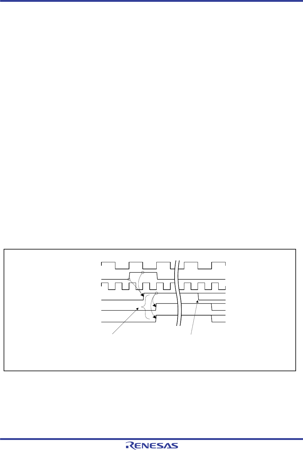
R01UH0034EJ0200 Rev.2.00 Page 262 of 1489
Dec 27, 2013
RX62T Group, RX62G Group 11. Interrupt Controller (ICU)
Under development Preliminary document
Specifications in this document are tentative and subject to change.
11.4 Interrupt Operation
The interrupt controller performs the following processing.
Detecting interrupts
Enabling and disabling interrupts
Selecting interrupt request destinations (CPU interrupt, DTC activation)
Determining priority
11.4.1 Detecting Interrupts
Interrupt requests are detected in either of two ways: the detection of edges of the interrupt signal or the detection of a
level of the interrupt signal.
Edge detection or level detection is selected for the IRQn pins (n = 7 to 0) as interrupt sources by the setting of the
IRQMD[1:0] bits in IRQCRn.
For interrupts from peripheral modules, either edge detection or level detection is determined per interrupt source.
For the correspondence between interrupt sources and methods of detection, see Table 11.4, Interrupt Vector Table.
11.4.1.1 Operation of Status Flags for Edge-Detected Interrupts
Figure 11.2 shows the operation of the IR flag in IRi in the case of edge detection of an interrupt from a peripheral
module or on an external pin.
The IR flag in IRi is set to 1 immediately after the transition of the interrupt signal due to generation of the interrupt. If
the CPU is the request destination for the interrupt, the IR flag in IRi is automatically cleared on acceptance of the
interrupt. If the DTC is the request destination for the interrupt, the timing of the IR flag clear depends on the DTC
transfer setting and number of times of transfer. For details, see Table 11.5. Therefore, the software does not have to
clear the IR flag in IRi.
Interrupt signals corresponding to interrupt vectors with numbers from 64 to 71 have different timing from the other
interrupts. When an interrupt with a vector number from 64 to 71 is used as an IRQ-pin interrupt, the internal delay from
input on the pin is extended by two cycles of PCLK.
Figure 11.2 Operation of the IRi.IR Flag in the Case of Edge Detection
System clock
Interrupt signal
IR flag in IRi
The flag becomes "0" on acceptance of a CPU
interrupt. See table 11.5 for the timing with which
the flag becomes "0" when the interrupt request is
used to activate transfer by the DTC.
Peripheral clock
CPU interrupt request
Request for DTC activation
Refer to section 11.4.3, Selecting Interrupt
Request Destinations, for settings such that only
any one interrupt request is issued at a time.

R01UH0034EJ0200 Rev.2.00 Page 263 of 1489
Dec 27, 2013
RX62T Group, RX62G Group 11. Interrupt Controller (ICU)
Under development Preliminary document
Specifications in this document are tentative and subject to change.
If the corresponding IR flag in IRi has already been set to 1 by a generated interrupt request, the generation of a further
interrupt request will be ignored.
In addition to the IRi.IR flag, all the interrupts of the GPT, MTU3, and LIN, and the CMPI interrupt of the S12ADA have
the status flags which are not automatically cleared to 0 depending on several sources. Therefore, if a further interrupt is
generated while the corresponding flag is 1, the interrupt will be ignored. To enable the acceptance of an interrupt, the
flag of the interrupt generation source should be 0. For details on the target status flag, refer to the section of each
peripheral module.
If the IR flag has been cleared to 0, it will be set again by the generation of a further interrupt request. The timing for re-
setting of the IR flag is shown in Figure 11.3.
When communication functions (SCI, RIIC, RSPI) and DTC are combined, an interrupt request is ignored and transfer
requests may be lost in some cases. For details, see section 11.7, Usage Notes.
Figure 11.3 Timing for Re-setting of the IRi.IR Flag
If a source for interrupt generation is disabled over the period where the IR flag in the corresponding IRi is set (output of
the interrupt request by the relevant peripheral module is disabled by clearing the interrupt enable bit), the IR flag is not
affected but retains its state. Figure 11.4 shows operation when the source for interrupt generation has been disabled.
Figure 11.4 Relation between the IRi.IR Flag and Disabling of the Corresponding Interrupt Source
Interrupt signal
IR flag in IRi
An interrupt request (2) is ignored while the IR flag in IRi is 1.
(1) (2) (3)
The IR flag in IRi is
cleared to 0. (1)
The IR flag in IRi is
cleared to 0. (3)
Interrupt signal
IRi.IR flag IRi.IR flag is not cleared even when the source is disabled
Source for interrupt generation
is enabled/disabled
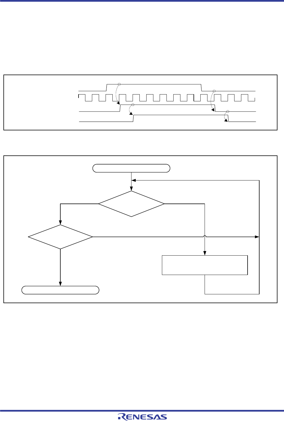
R01UH0034EJ0200 Rev.2.00 Page 264 of 1489
Dec 27, 2013
RX62T Group, RX62G Group 11. Interrupt Controller (ICU)
Under development Preliminary document
Specifications in this document are tentative and subject to change.
11.4.1.2 Operation of Status Flags for Level-Detected Interrupts
Figure 11.5 shows the operation of the interrupt status flag (IR flag) in IRi in the case of level detection of an interrupt
from a peripheral module or an external pin.
The IR flag in IRi remains set as long as the interrupt signal is asserted. To clear the IR flag in IRi, withdraw the interrupt
request at the source of the interrupt.
Confirm that the interrupt request flag in the source generating the interrupt has actually been cleared before stopping the
interrupt handler. Figure 11.6 shows the level-detected interrupt handling procedure.
Figure 11.5 Operation of the IRi.IR Flag in the Case of a Level-Detected Interrupt
Figure 11.6 Level-Detected Interrupt Handling Procedure
System clock
Interrupt signal
IR flag in IRi
CPU interrupt request
Start interrupt handling
Confirm interrupt
request source
Clear interrupt request source and
perform interrupt request source
processing
Interrupt issued
Confirm IRi.IR flag
No interrupt issued
End of interrupt handling
IRi.IR = “1”
Iri.IR = “0”

R01UH0034EJ0200 Rev.2.00 Page 265 of 1489
Dec 27, 2013
RX62T Group, RX62G Group 11. Interrupt Controller (ICU)
Under development Preliminary document
Specifications in this document are tentative and subject to change.
11.4.2 Enabling and Disabling Interrupt Sources
Enabling requests from a given interrupt source requires the following settings.
1. In the case of interrupt requests from peripheral modules, setting the interrupt enable bit for the peripheral module
to permit the output of interrupt requests from the source
2. Enabling of the interrupt by the IENj bit in IERm
When an interrupt request is generated by a source for interrupt generation for which interrupt output has been enabled,
the IR flag in the corresponding IRi register is set.
Setting the IENj bit in IERm to enable an interrupt request causes a set IR flag in the IRi register corresponding to that
interrupt request to be output to the interrupt request destination. Furthermore, if the IENj bit in IERm has been used to
disable the interrupt request, the state of the interrupt request for which the IR flag in the corresponding IRi register has
been set is held.
The IR flag in IRi is not affected by the IENj bit in IERm.
11.4.3 Selecting Interrupt Request Destinations
Possible settings for the request destination of each interrupt are fixed. That is, settings for request destination other than
those indicated in Table 11.4, Interrupt Vector Table, are not possible. Do not make an interrupt request destination
setting that is not indicated by a √ in Table 11.4.
If the DTC is selected as the request destination for an IRQ pin, be sure to set the IRQMD[1:0] bits in IRQCRn for that
interrupt to select edge detection.
The following describes how to specify the interrupt request destination.
(1) DTC Activation
Make the following settings while the IERm.IENj bit is 0.
1. Set the DTC activation enable bit (DTCERn.DTCE) in the DTC activation enabler register for the required source
to 1.
2. Set the DTC module activation bit (DTCST.DTCST) to 1.
After the above settings, set the IERm.IENj bit to 1.
For the DTC setting, see section 14.5, DTC Setting Procedure.

R01UH0034EJ0200 Rev.2.00 Page 266 of 1489
Dec 27, 2013
RX62T Group, RX62G Group 11. Interrupt Controller (ICU)
Under development Preliminary document
Specifications in this document are tentative and subject to change.
(2) CPU Interrupt Request
If the interrupt request destination is the DTC, the interrupt request is sent to the CPU. Set the IERm.IENj bit to 1 while
the DTC activation setting described above is made.
Table 11.5 covers operation when the DTC is the request destination.
Note 1. An interrupt request (DTC activation request) that is regenerated while the IR flag in IRi is still set will be ignored.
Note 2. For the chain transfer, DTC transfer is continued until the last chain transfer completes. Each of operations of CPU interrupt, IR
flag clear, and interrupt request destination after transfer for the last chain transfer, depends on the setting of DISEL bit for the
last chain transfer and the remaining specified number of transfers.
Note 3. If a re-generated interrupt request (DTC activation request) is ignored while the IRi.IR flag is set, some problems may occur to
the communication functions (SCI, RIIC, RSPI). Therefore, such communication functions should be used under the condition
where the interrupt request is not ignored or with taking the preventive measures through software. For details, see section 11.7,
Usage Notes.
The request destination for an interrupt should be changed while the IERm.IENj bit is 0.
To change the interrupt request destination or the DTC transfer information while the transfer is not completed
(DTCERn.DTCE bit is not cleared) after the settings described in (1) DTC Activation are made, use the following
procedure.
1. Clear the IENj bits in IERm for both the source to be replaced and the source that will be the new trigger for
activation to 0.
2. Check the state of transfer by the DTC. If transfer is in progress, wait for its completion.
3. Make the settings described in (1) DTC Activation.
Table 11.5 Operation at the Time of DTC Activation
Interrupt
Request
Destination
DTC.MRB
.
DISEL
Remaining
Number of
Transfer
Operations Operation per
Request IRi.IR *1*3 Interrupt Request
Destination after Transfer
DTC*2 10 DTC transfer CPU
interrupt
Cleared on interrupt
acceptance by the CPU
DTC
=0 DTC transfer CPU
interrupt
Cleared on interrupt
acceptance by the CPU
The DTCE bit in DTCR is
cleared and the CPU
becomes the destination.
00 DTC transfer Cleared on the start of DTC
data transfer after DTC transfer
information has been read
DTC
=0 DTC transfer CPU
interrupt
Cleared on interrupt
acceptance by the CPU
The DTCE bit in DTCERn is
cleared and the CPU
becomes the destination.

R01UH0034EJ0200 Rev.2.00 Page 267 of 1489
Dec 27, 2013
RX62T Group, RX62G Group 11. Interrupt Controller (ICU)
Under development Preliminary document
Specifications in this document are tentative and subject to change.
11.4.4 Determining Priority
Interrupt priority is determined for each interrupt request destination.
The priority for each interrupt request destination is determined as follows.
(1) Determining Priority when the CPU is the Request Destination of the Interrupt Signal
The source that has been specified as the fast interrupt (described below) has the highest priority. After that, an interrupt
source with a larger value of the interrupt priority level select bits (IPR[3:0]) in IPRm takes precedence. If interrupts with
the same priority level are generated by multiple sources, the source with the smallest vector number takes precedence.
(2) Determining Priority when the DTC is the Request Destination of the Interrupt Signal
The IPR[3:0] bits in IPRm have no effect. An interrupt source with a smaller vector number takes precedence.
11.4.5 Multiple Interrupts
To enable the multiple interrupts, set the PSW.I bit to 1 (interrupt enable) in the accepted interrupt handling routine.
The PSW.IPL[3:0] bits are set to the priority level of the accepted interrupt request. If the interrupt request with a priority
level higher than that set by the PSW.IPL[3:0] bits is generated, this interrupt request is accepted (and multiple interrupts
are handled).
11.4.6 Fast Interrupt
The fast interrupt is a facility for faster interrupt response by the CPU, to only one assigned interrupt source among
interrupt sources.
The fast interrupt, which has the highest interrupt priority level of 15, takes precedence over other level-15 priority
interrupt sources regardless of the value set in the IPRn.IPR[3:0] bits. However, if the value of the PSW.IPL[3:0] bits is
1111b (priority level 15), the fast interrupt is not accepted.
An interrupt source can be assigned to the fast interrupt by writing the vector number of the source to the FIR.FVCT[7:0]
bits and set the FIR.FIEN bit to 1 (fast interrupt enabled).
For details on the fast interrupt, see section 2., CPU, or section 10, Exceptions.
11.4.7 External Pin Interrupts
The procedure for using the signal on an external pin as an interrupt is given below.
1. Clear the IENj bit in IERm (IERm.IENj = 0).
2. Set and check the settings for the I/O port pin.
3. Set the method of detection for the interrupt in the IRQMD[1:0] bits of IRQCRn.
4. Clear the IR flag in the corresponding IRi register to 0 (if edge detection is in use).
5. If the interrupt is to be used for DTC activation, set the DTCE bit in DTCERn. The interrupt will be a CPU interrupt
if these settings are not made.
6. Set the IENj bit in IERm (IERm.IENj = 1).

R01UH0034EJ0200 Rev.2.00 Page 268 of 1489
Dec 27, 2013
RX62T Group, RX62G Group 11. Interrupt Controller (ICU)
Under development Preliminary document
Specifications in this document are tentative and subject to change.
11.5 Non-Maskable Interrupt Operation
The three kinds of non-maskable interrupt are produced by an interrupt signal on the NMI pin, voltage monitoring, and
detection of stoppage of oscillation. A non-maskable interrupt can only act as an interrupt for the CPU and is not capable
of activating the DTC. Non-maskable interrupts take precedence over all other interrupts, including the fast interrupt.
A non-maskable interrupt request is accepted regardless of the settings of the I bit (interrupt enable bit) and the IPL[3:0]
bits (processor interrupt priority level) in the PSW of the CPU. The presence or absence of non-maskable interrupt
requests can be confirmed by checking the value of the non-maskable interrupt status register (NMISR). Confirm that all
bits of the NMISR have returned to 0 from within the routine for the non-maskable interrupt. Non-maskable interrupts
are disabled by default.
If a system is to use non-maskable interrupts, follow the procedure below at the beginning of program processing.
Non-Maskable Interrupt Usage Procedure:
1. Set the stack pointer (SP).
2. If the NMI pin is to be used, make the detection sense setting (the NMIMD bit in the NMICR).
3. If the NMI pin is to be used, clear the NMIST flag in the NMISR by writing 1 to the NMICLR bit in NMICLR.
4. Enable the non-maskable interrupt by writing 1 to the corresponding bit in the non-maskable interrupt enable
register (NMIER).
After the NMIEN bit in NMIER is set to 1, subsequent write access to the NMIEN bit in NMIER is ignored. The non-
maskable interrupt cannot be disabled. The non-maskable interrupt is disabled only by a reset.
For the flow of non-maskable interrupt processing, see section 10, Exceptions.
Writing 1 to the NMICLR.NMICLR bit clears the NMI pin status flag (NMISR.NMIST).
Writing 1 to NMICLR.OSTCLR bit clears the oscillation stop detection interrupt status flag (NMISR.OSTST).
For clearing the voltage-monitoring interrupt status flag (NMISR.LVDST), see section 7, Voltage Detection Circuit
(LVD).
Do not issue a WAIT instruction while any bit in the NMISR is 1.

R01UH0034EJ0200 Rev.2.00 Page 269 of 1489
Dec 27, 2013
RX62T Group, RX62G Group 11. Interrupt Controller (ICU)
Under development Preliminary document
Specifications in this document are tentative and subject to change.
11.6 Return from Power-Down States
The interrupt sources that can be used to return operation from sleep mode, all-module clock stop mode, or software
standby mode are shown in Table 11.4, Interrupt Vector Table.
For details, refer to section 9, Low Power Consumption. The following describes how to use an interrupt to return
operation from each power-down mode.
11.6.1 Return from Sleep Mode
If the interrupt controller is to return operation from sleep mode in response to an interrupt or non-maskable interrupt,
make the following settings for the interrupt.
Interrupts
1. Select the CPU as the interrupt request destination.
2. Use the IENj bit in IERm to enable the given interrupt request.
3. Set an interrupt priority level higher than that set by the IPL[3:0] bits in the PSW of CPU.
Non-maskable interrupts
Use the NMIER register to enable the given interrupt request.
11.6.2 Return from All-Module Clock Stop Mode
If the interrupt controller is to return operation from all-module clock stop mode in response to an interrupt or non-
maskable interrupt, make the following settings for the interrupt.
Interrupts
1. Select the interrupt source that enables the return from the all-module clock stop mode.
2. Select the CPU as the interrupt request destination.
3. Use the IENj bit in IERm to enable the given interrupt request.
4. Set an interrupt priority level higher than that set by the IPL[3:0] bits in the PSW of CPU.
Non-maskable interrupts
Use the NMIER register to enable the given interrupt request.
11.6.3 Return from Software Standby Mode
The interrupt controller can return operation from a non-maskable interrupt or an interrupt that enables the return from
the software standby mode.
The conditions for the return are listed below.
Interrupts
1. Select the interrupt source that enables the return from the software standby mode.
2. Select the CPU as the interrupt request destination.
3. Use the IENj bit in IERm to enable the given interrupt request.
4. Set an interrupt priority level higher than that set by the IPL[3:0] bits in the PSW of CPU.
To use the interrupt source specified as a fast interrupt to return from software standby mode, the interrupt priority level
(IPRm) should be set higher than the level set by IPL in the PSW of the CPU in addition to setting the fast interrupt set
register (FIR).
Interrupt requests through the IRQ pins that do not satisfy the above conditions are not detected while the clock is
stopped in software standby mode.
Non-maskable interrupts
Use the NMIER register to enable the given interrupt request.

R01UH0034EJ0200 Rev.2.00 Page 270 of 1489
Dec 27, 2013
RX62T Group, RX62G Group 11. Interrupt Controller (ICU)
Under development Preliminary document
Specifications in this document are tentative and subject to change.
11.7 Usage Notes
11.7.1 Notes on Communication Using DTC Transfer
In the RX62T and RX62G Groups, be careful of using the communication functions using DTC transfer. When an
interrupt request is generated while the IRi.IR flag is set to 1, re-generated interrupt request is ignored. If the DTC is the
request destination for the interrupt, the timing of the IR flag clear depends on the DTC transfer setting and number of
times of transfer. Therefore, a transfer request may be lost depending on the combinations of the settings. When
communication functions (SCI, RIIC, RSPI) and DTC are combined, consider the following notes.
(1) Conditions of Transfer Request Loss during Communication using DTC Transfer
Table 11.6 shows the combinations of the DTC function which require special care.
Note 1. Communication interrupts include: transmit data empty and receive data full interrupts from SCI, RIIC, and RSPI.
Note 2. If the IRi.IR flag is cleared too late for the transfer request of the next packet to be transmitted/received, the same problem may
occur as with the case in DISEL = 1.
(2) Notes on Communication using DTC Transfer when DISEL = 1
The IR flag is automatically cleared on interrupt acceptance by the CPU after data transfer (DTC operation). A transfer
request will be lost if the next transfer request is issued before the IR flag is automatically cleared. When DISEL is set to
1, a CPU interrupt is always generated: therefore, take the preventive measures through software shown below.
Table 11.6 Combinations of the DTC Function which Require Special Care
Chain Transfer Used or
Not Used Communication Interrupts to CPU Issued or Not
Issued after Each Transfer*1 (DISEL Setting) Possibility of Problem
Generation
DTC Chain transfer not used DISEL=0
(Transfer counter value > 0)
Impossible
DISEL=0
(Transfer counter value = 0 at the last transfer)
Impossible*2
DISEL=1 Possible
Chain transfer used DISEL=0
(Transfer counter value > 0 and communication register
is accessed at the end of the chain)
Impossible
DISEL=0
(Transfer counter value = 0 at the last transfer and
communication register is accessed at the end of the
chain)
Impossible*2
DISEL=1 Possible
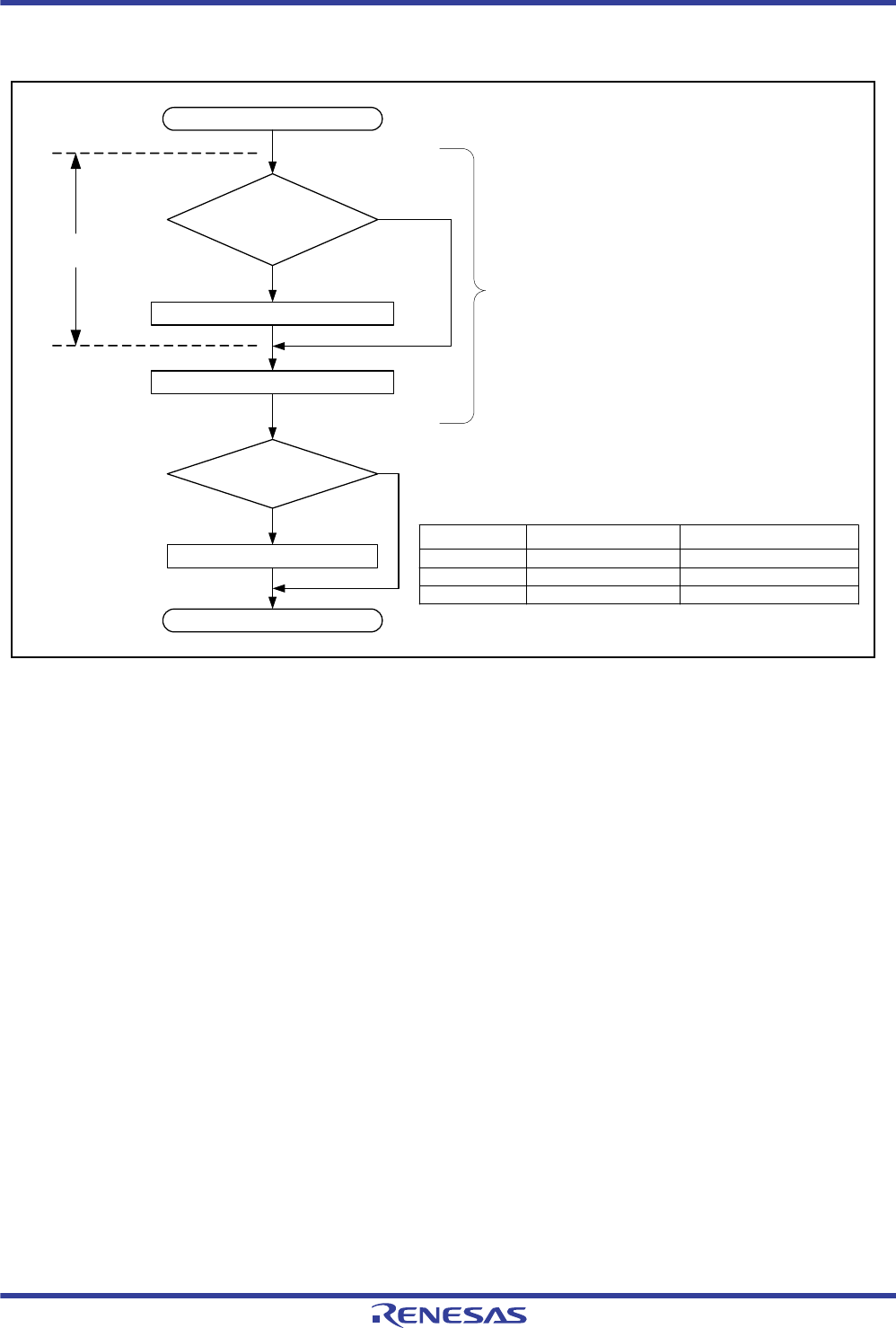
R01UH0034EJ0200 Rev.2.00 Page 271 of 1489
Dec 27, 2013
RX62T Group, RX62G Group 11. Interrupt Controller (ICU)
Under development Preliminary document
Specifications in this document are tentative and subject to change.
(3) Flowchart of Software Preventive Measures (for SCI, RIIC, RSPI)
Figure 11.7 Flowchart of Software Preventive Measures (for SCI, RIIC, RSPI)
Start interrupt handling
Determine internal
source in
communication. *1
Set IRi.IR to 1.
No
End
Yes
Set PSW.I to 1.*2
Multiple-interrupt
disabled
Transfer counter = 0?
Re-set DTC
Notes:
1. Determination of internal source in communication
Communication
Function Receive Buffer Full Flag Transmit Buffer Empty Flag
SCI SSR.RDRF=1
RIIC ICSR2.RDRF=1
RSPI SPSR.SPRF=1
SSR.TDRE=1
ICSR2.TDRE=1
SPSR.SPTEF=1
2. This step is not required when multiple-interrupt is not used.
No
Yes
Software preventive
measures
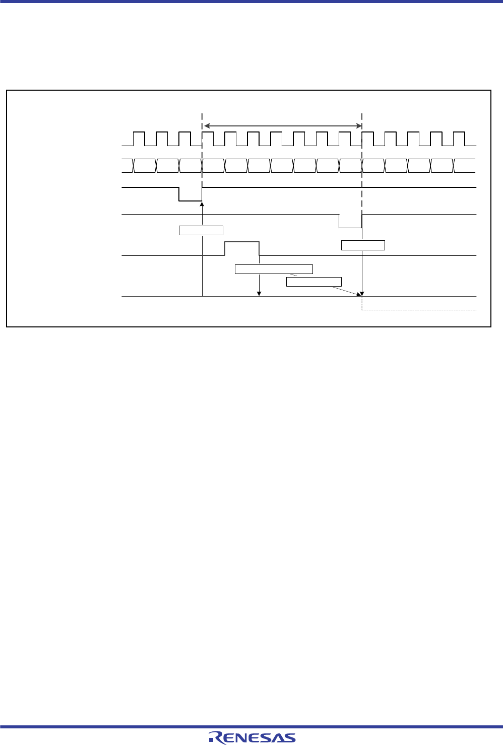
R01UH0034EJ0200 Rev.2.00 Page 272 of 1489
Dec 27, 2013
RX62T Group, RX62G Group 11. Interrupt Controller (ICU)
Under development Preliminary document
Specifications in this document are tentative and subject to change.
11.7.2 Note on Using the MUT3 Interrupt
If conditions*1, *2, or *3 apply when the status flag in the timer status register (TSR) is to be cleared to 0, and a flag setting
request is generated to set the corresponding flag to 1 before 0 has been written to the flag after 1 was read from the flag,
the corresponding flag will not be cleared and will thus retain the value 1.
Figure 11.8 State of the Status Flag in the TSR Register
Note 1. TGFm flag (input capture/output compare flag m) (m = A to F)
[Setting conditions]
• TCNT = TGRm while the TGRm register is functioning as an output compare register or compare register
• Transfer of the value in TCNT to the TGRm register in response to the input capture signal while the TGRm
register is functioning as an input capture register
[Clearing condition]
• After the TGFm flag is read while TGFm = 1, writing of 0 to the TGFm flag
Note 2. TCFj flag (overflow/underflow flag) (j = V, U)
[Setting conditions]
• Overflow of the TCNT (FFFFh → 0000h)
• Underflow of the TCNT (0000h → FFFFh)
[Clearing condition]
• After the TCFj flag is read while TCFj = 1, writing of 0 to the TCFj flag
Note 3. CMFn5 compare match/input capture flag n (n = U, V, W)
[Setting conditions]
• MTU5.TCNTn = MTU5.TGRn while the MTU5.TGRn is functioning as a compare match register
• Transfer of the value in MTU5.TCNTn to MTU5.TGRn in response to the input capture signal while the
MTU5.TGRn is functioning as an input capture register
• Transfer of the value in MTU5.TCNTn to MTU5.TGRn in response to the input capture signal while the
MTU5.TGRn is in use for measuring the pulse width of an externally input signal
[Clearing condition]
• After the CMFn5 flag is read while CMFn5 = 1, writing of 0 to the CMFn5 flag
ICLK
Request to set the given flag is generated
within this period.
TCNT
Timing of reading 1 from
the given flag in TSR
Reading of 1
Setting retained
Timing of writing 0 to
the given flag in TSR
Generation of the condition for
setting the given flag to 1
State of the given flag in TSR
Request to set the flag
Writing of 0
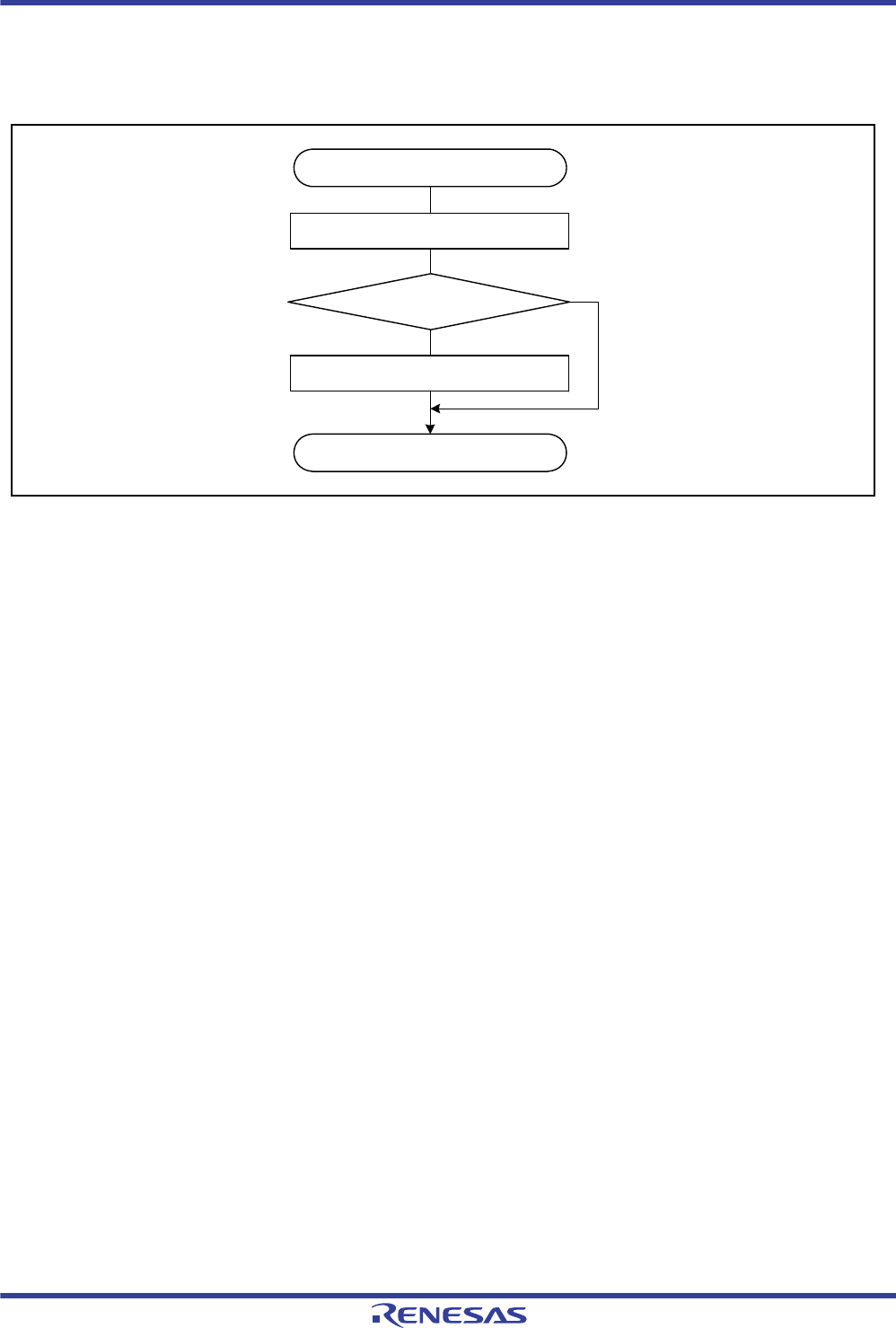
R01UH0034EJ0200 Rev.2.00 Page 273 of 1489
Dec 27, 2013
RX62T Group, RX62G Group 11. Interrupt Controller (ICU)
Under development Preliminary document
Specifications in this document are tentative and subject to change.
The interrupt request is ignored as long as the corresponding flag in the TSR register is 1. Therefore, to re-enable the
interrupt, clear the corresponding flag and then execute the procedure in the flowchart for software to avoid problems
(Figure 11.9).
Figure 11.9 Flowchart for Software to Avoid Problems
Interrupt from a given source
"1"
"0"
Confirm the state of the flag
Clear the corresponding flag in
MTU3.TSR
Set the IRi.IR bit of ICU to 1
End
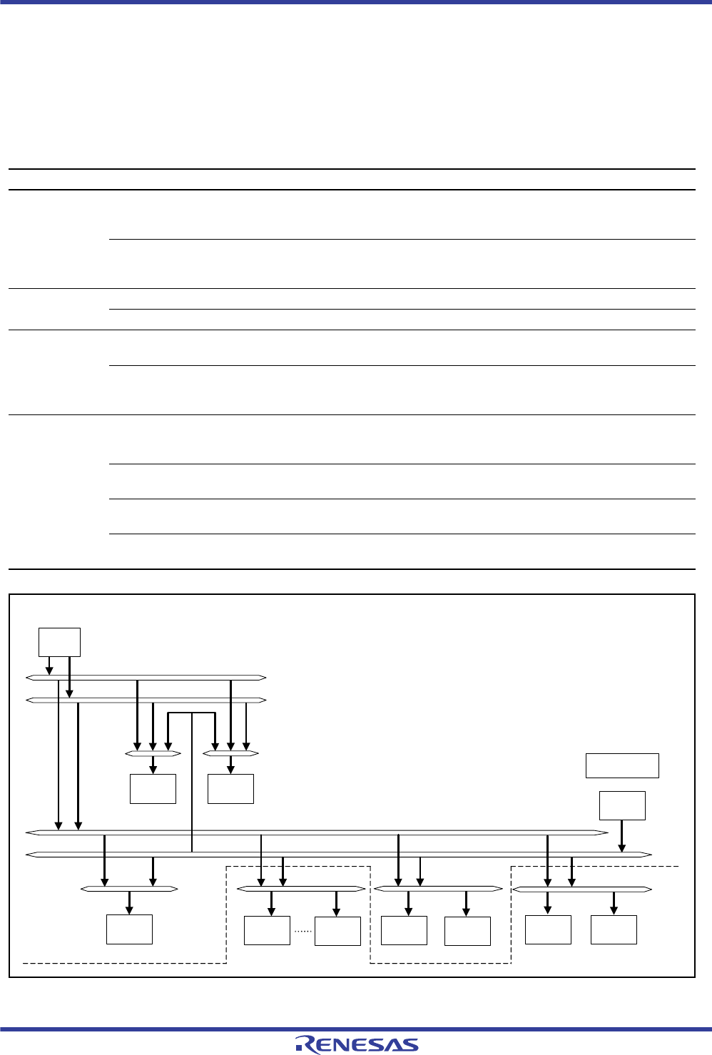
R01UH0034EJ0200 Rev.2.00 Page 274 of 1489
Dec 27, 2013
RX62T Group, RX62G Group 12. Buses
Under development Preliminary document
Specifications in this document are tentative and subject to change.
12. Buses
12.1 Overview
Figure 12.1 lists the bus specifications, Table 12.1 shows the bus configuration, and Table 12.2 shows the addresses
assigned for each bus.
Figure 12.1 Bus Configuration
Table 12.1 Bus Specifications
Bus Type Description
CPU bus Instruction bus Connected to the CPU (for instructions)
Connected to on-chip memory (on-chip RAM, on-chip ROM)
Operates in synchronization with the system clock (ICLK)
Operand bus Connected to the CPU (for operands)
Connected to on-chip memory (on-chip RAM, on-chip ROM)
Operates in synchronization with the system clock (ICLK)
Memory bus Memory bus 1 Connected to on-chip RAM
Memory bus 2 Connected to on-chip ROM
Internal main bus Internal main bus 1 Connected to the CPU
Operates in synchronization with the system clock (ICLK)
Internal main bus 2 Connected to the DTC
Connected to on-chip memory (on-chip RAM, on-chip ROM)
Operates in synchronization with the system clock (ICLK)
Internal
peripheral bus
Internal peripheral bus 1 Connected to peripheral modules(such as a bus error monitoring section and an
interrupt)
Operates in synchronization with the system clock (ICLK)
Internal peripheral bus 2 Connected to peripheral modules(such as WDT, CMT, CRC, and SCI)
Operates in synchronization with the peripheral-module clock (PCLK)
Internal peripheral bus 4 Connected to peripheral modules (MTU3 and GPT)
Operates in synchronization with the system clock (ICLK)
Internal peripheral bus 6 Connected to on-chip ROM (for programming and erasure) and data-flash memory
Operates in synchronization with the peripheral-module clock (PCLK)
Bus error monitoring
section
Internal main bus 1
Internal main bus 2
Instruction bus
Operand bus
Internal peripheral bus 1
ICLK
synchronization
Memory bus 1 Memory bus 2
Data flash
memory
Internal peripheral bus 6
PCLK
synchronization
Peripheral
module On-chip ROM
(P/E)
DTC
On-chip ROM
On-chip
RAM
CPU
Peripheral
module Peripheral
module
Internal peripheral bus 2
MTU3 GPT
Internal peripheral buses 4

R01UH0034EJ0200 Rev.2.00 Page 275 of 1489
Dec 27, 2013
RX62T Group, RX62G Group 12. Buses
Under development Preliminary document
Specifications in this document are tentative and subject to change.
Table 12.2 Addresses Assigned for Each Bus
Address Type of Bus Area
0000 0000h to 0000 3FFFh Memory bus 1 On-chip RAM
0000 4000h to 0007 FFFFh Reserved area
0008 0000h to 0008 7FFFh Internal peripheral bus 1 Peripheral I/O registers
0008 8000h to 0009 FFFFh Internal peripheral bus 2
000A 0000h to 000B FFFFh Reserved area Reserved area
000C 0000h to 000D FFFFh Internal peripheral bus 4 Peripheral I/O registers
000E 0000h to 000F FFFFh Reserved area Reserved area
0010 0000h to 0011 FFFFh Internal peripheral bus 6 Data flash memory
0012 0000h to 007F 7FFFh Reserved area
007F 8000h to 007F 9FFFh FCU RAM
007F A000h to 007F BFFFh Reserved area
007F C000h to 007F C4FFh Peripheral I/O registers
007F C500h to 007F FBFFh Reserved area
007F FC00h to 007F FFFFh Peripheral I/O registers
0080 0000h to 00DF FFFFh Reserved area
00E0 0000h to 00FF FFFFh On-chip ROM(dedicated area for writing)
0100 0000h to 7FFF FFFFh Reserved area Reserved area
8000 0000h to FFFF FFFFh Memory bus 2 On-chip ROM
(dedicated area for reading)

R01UH0034EJ0200 Rev.2.00 Page 276 of 1489
Dec 27, 2013
RX62T Group, RX62G Group 12. Buses
Under development Preliminary document
Specifications in this document are tentative and subject to change.
12.2 Description of Buses
12.2.1 CPU Buses
The CPU buses consist of the instruction and operand buses, which are connected to internal main bus 1. As the names
suggest, the instruction bus is used to fetch instructions for the CPU, while the operand bus is used for operand access.
Connection of the instruction and operand buses to on-chip RAM and on-chip ROM provides the CPU with direct access
to these areas, i.e. access is not via internal main bus 1. However, only reading is possible in direct access to on-chip
ROM by the CPU; programming and erasure are handled via an internal peripheral bus.
Bus requests for instruction fetching and operand access, that are not for the on-chip RAM or on-chip ROM, are
arbitrated through internal main bus 1. The order of priority is operand access then instruction fetching.
If instruction fetching and operand access are requested for different buses (memory bus 1, memory bus 2, and internal
main bus 1), the bus-access operations can proceed simultaneously. For example, parallel access to on-chip ROM and
on-chip RAM or to on-chip ROM is possible.
12.2.2 Memory Buses
The memory buses consist of memory bus 1 and memory bus 2. On-chip RAM is connected to memory bus 1 and on-
chip ROM is connected to memory bus 2. Requests for bus mastership from the CPU buses (instruction fetching and
operand) and internal main bus 2 are arbitrated through memory buses 1 and 2.
The order of priority is internal main bus 2 then CPU bus (operand then instruction fetching).
12.2.3 Internal Main Buses
The internal main buses consist of a bus for use by the CPU (internal main bus 1) and a bus for use by the other bus-
master modules, i.e. the DTC (internal main bus 2).
Bus requests for instruction fetching and operand access, that are not for the on-chip RAM or on-chip ROM, are
arbitrated through internal main bus 1. The order of priority is operand then instruction fetching.
If the CPU and another bus master are requesting access to different buses (on-chip memory, internal peripheral buses 1
2, 4, and 6), the respective bus-access operations can proceed simultaneously.
The order of priority is internal main bus 2 then internal main bus 1. However, when the CPU executes the XCHG
instruction, requests for bus access from masters other than the CPU are not accepted until data transfer for the XCHG
instruction is completed. Furthermore, requests for bus access from masters other than the DTC are not accepted during
reading and writing-back of transfer control information for the DTC.
Table 12.3 Order of Priority for Bus Masters
Priority Bus Master
High
Low
DTC
CPU

R01UH0034EJ0200 Rev.2.00 Page 277 of 1489
Dec 27, 2013
RX62T Group, RX62G Group 12. Buses
Under development Preliminary document
Specifications in this document are tentative and subject to change.
12.2.4 Internal Peripheral Buses
Connection of peripheral modules to the internal peripheral buses is as described in Table 12.4.
Requests for bus mastership from the CPU (internal main bus 1) and other bus masters (internal main bus 2) are
arbitrated through internal peripheral buses 1, 2, 4, and 6.
The order of priority is internal main bus 2 then internal main bus 1.
12.2.5 Parallel Operation
Parallel operation is possible when different bus-master modules are requesting access to different slave modules. For
example, if the CPU is fetching an instruction from on-chip ROM and accessing an operand from on-chip RAM, the
DTC is able to handle transfer between a peripheral bus and a peripheral bus at the same time.
An example of parallel operations is given in Figure 12.2. In this example, the CPU is able to employ the instruction and
operand buses for simultaneous access to on-chip ROM and on-chip RAM, respectively. Furthermore, the DTC
simultaneously employs internal main bus 2 for access to a peripheral bus during access to on-chip RAM and ROM by
the CPU.
Figure 12.2 Example of Parallel Operations
12.2.6 Restrictions
(1) Restrictions in relation to RMPA and string-manipulation instructions
The allocation of data to be handled by RMPA or string-manipulation instructions to I/O registers is prohibited, and
operation is not guaranteed if this restriction is not observed.
Table 12.4 Connection of Peripheral Modules to the Internal Peripheral Buses
Type of Bus Peripheral Modules
Internal peripheral bus 1 Interrupt controller
Bus error monitoring section
Internal peripheral bus 2 Peripheral modules other than those connected to internal peripheral buses 1 and 4
Data flash memory
Internal peripheral bus 4 MTU3 and GPT
Internal peripheral bus 6 On-chip ROM (P/E)/Data flash memory
CPU operand
access RAM
ROM
CPU instruction
fetching
DTC Peripheral Peripheral
On-chip ROM access
On-chip RAM access
Peripheral bus access
Peripheral bus access
ROM ROM ROM ROM ROM ROM
RAM RAM RAM RAM RAM RAM
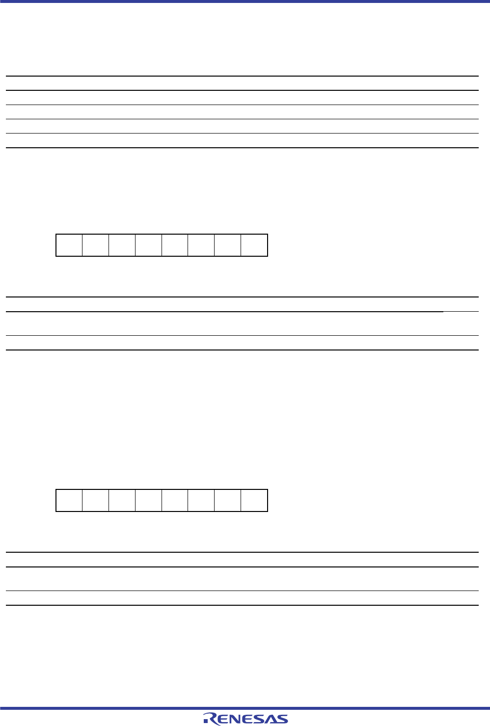
R01UH0034EJ0200 Rev.2.00 Page 278 of 1489
Dec 27, 2013
RX62T Group, RX62G Group 12. Buses
Under development Preliminary document
Specifications in this document are tentative and subject to change.
12.3 Register Descriptions
Table 12.5 lists the registers of the bus error monitoring section.
12.3.1 Bus Error Status Clear Register (BERCLR)
Note 1. Only writing 1 is effective; i.e. writing 0 has no effect.
STSCLR Bit (Status Clear)
Writing 1 to this bit clears the bus-error status registers 1and 2 (BERSR1 and BERSR2).
12.3.2 Bus Error Monitoring Enable Register (BEREN)
IGAEN Bit (Illegal Address Access Detection Enable)
This bit enables or disables detection of access to illegal addresses.
Table 12.5 Registers of the Bus Error Monitoring Section
Register Name Symbol Value after Reset Address Access Size
Bus error status clear register BERCLR 00h 0008 1300h 8
Bus error monitoring enable register BEREN 00h 0008 1304h 8
Bus error status register 1 BERSR1 00h 0008 1308h 8
Bus error status register 2 BERSR2 0000h 0008 130Ah 16
Address: 0008 1300h
b7 b6 b5 b4 b3 b2 b1 b0
———————
STSCL
R
Value after reset: 00000000
Bit Symbol Bit Name Description R/W
b0 STSCLR Status Clear 0: Invalid
1: Bus error status register cleared
R/(W)*1
b7 to b1 — Reserved These bits are always read as 0. The write value should be 0. R/W
Address: 0008 1304h
b7 b6 b5 b4 b3 b2 b1 b0
———————IGAEN
Value after reset: 00000000
Bit Symbol Bit Name Description R/W
b0 IGAEN Illegal Address Access
Detection Enable
0: Illegal address access detection is disabled.
1: Illegal address access detection is enabled.
R/W
b7 to b1 — Reserved These bits are always read as 0. The write value should be 0. R/W
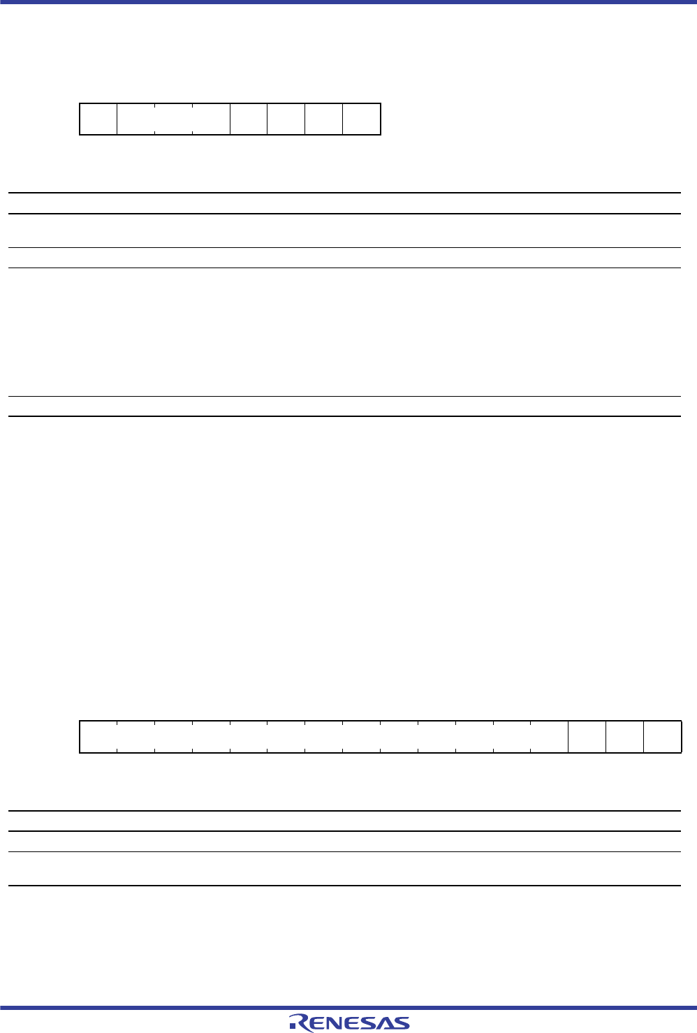
R01UH0034EJ0200 Rev.2.00 Page 279 of 1489
Dec 27, 2013
RX62T Group, RX62G Group 12. Buses
Under development Preliminary document
Specifications in this document are tentative and subject to change.
12.3.3 Bus Error Status Register 1 (BERSR1)
BERSR1 indicates the bus error generation status. It indicates whether an illegal address access was made (IA bit), or
which bus master accessed the bus (MST[2:0] bits)
IA Bit (Illegal Address Access Flag)
This bit indicates whether an illegal address access was made.
MST[2:0] Bits (Bus Master Code)
These bits indicate the bus master that accessed a bus when a bus error occurred.
12.3.4 Bus Error Status Register 2 (BERSR2)
BERSR2 indicates the upper 13 bits of an address having caused a bus error.
ADDR[12:0] Bits (Bus Error Occurrence Address)
These bits indicate the upper 13 bits of an address having caused a bus error.
Address: 0008 1308h
b7 b6 b5 b4 b3 b2 b1 b0
— MST[2:0] — — — IA
Value after reset: 00000000
Bit Symbol Bit Name Description R/W
b0 IA Illegal Address Access 0: Illegal address access not made
1: Illegal address access made
R
b3 to b1 — Reserved These bits are always read as 0. Writing to these bits has no effect. R
b6 to b4 MST[2:0] Bus Master Code b6 b4
0 0 0: CPU
0 0 1: Setting prohibited
0 1 0: Setting prohibited
0 1 1: DTC
1 0 0: Setting prohibited
1 0 1: Setting prohibited
1 1 0: Setting prohibited
1 1 1: Setting prohibited
R
b7 — Reserved This bit is always read as 0. Writing to this bit has no effect. R
Address: 0008 130Ah
b15 b14 b13 b12 b11 b10 b9 b8 b7 b6 b5 b4 b3 b2 b1 b0
ADDR[12:0] — — —
Value after reset: 0000000000000000
Bit Symbol Bit Name Description R/W
b2 to b0 — Reserved These bits are always read as 0. Writing to these bits has no effect. R
b15 to b3 ADDR[12:0] Bus Error Occurrence
Address
The upper 13 bits of an address that was accessed when a bus error
occurred (in units of 512 Kbytes).
R

R01UH0034EJ0200 Rev.2.00 Page 280 of 1489
Dec 27, 2013
RX62T Group, RX62G Group 12. Buses
Under development Preliminary document
Specifications in this document are tentative and subject to change.
12.4 Bus Error Monitoring Section
The bus-error monitoring section monitors the individual areas for bus errors. When a bus error is occurred, this section
indicates it to the bus master. Bus error has an illegal address access, which is the detection of illegal access to an area.
12.4.1 Types of Bus Error
Bus error has an illegal address access, which is the detection of illegal access to an area.
12.4.1.1 Illegal Address Access
When the illegal address access detection enable bit (IGAEN) in the bus error monitoring enable register (BEREN) is set
to 1, access of the following types leads to illegal address access errors.
Access to areas of external space for which operation has been disabled
The address ranges where access will lead to illegal address access errors are indicated in Table 12.6.
12.4.2 Operations When a Bus Error Occurs
When a bus error occurs, the error is indicated to the CPU. Operation is not guaranteed when a bus error occurs.
Bus error indication to the CPU
An interrupt is generated. The IEN register in the ICU can specify whether to generate an interrupt in the case of a
bus error.

R01UH0034EJ0200 Rev.2.00 Page 281 of 1489
Dec 27, 2013
RX62T Group, RX62G Group 12. Buses
Under development Preliminary document
Specifications in this document are tentative and subject to change.
12.4.3 Conditions Leading to Bus Errors
Table 12.6 lists the types of bus errors for each area in the respective address space.
If an illegal address access error is detected when no bus error has occurred (bus error status register n (BERSRn; n = 1
or 2) is cleared), the detected error is reflected on the BERSRn. Once a bus error occurs, no subsequent bus errors are
reflected on the register unless the register is cleared.
If bus errors are simultaneously caused by two bus masters, error information of only one bus master is reflected. Once a
bus error occurs, the status is retained until BERSRn register is cleared.
—: A bus error is not produced.
√ : A bus error is produced.
Note 1. Amounts of on-chip RAM, data-flash memory, and on-chip ROM vary with the product. For the specifications of a given device,
refer to section 30, RAM, section 31, ROM (Flash Memory for Code Storage), and section 32, Data Flash Memory (Flash
Memory for Data Storage)
Table 12.6 Types of Bus Errors
Address Type of Area
Type of Error
Illegal Address Access
0000 0000h to 0000 3FFFh On-chip RAM*1—
0000 4000h to 0007 FFFFh Reserved area
0008 0000h to 0009 0FFFh Peripheral I/O registers —
0009 1000h to 0009 3FFFh √
0009 4000h to 0009 41FFh —
0009 4200h to 0009 FFFFh √
000A 0000h to 000B FFFFh √
000C 0000h to 000C 0FFFh √
000C 1000h to 000C 27FFh —
000C 2800h to 000D FFFFh √
000E 0000h to 000F FFFFh Reserved area √
0010 0000h to 0011 FFFFh Data flash*1—
0012 0000h to 007F 7FFFh Reserved area √
007F 8000h to 007F 9FFFh FCU RAM —
007F A000h to 007F BFFFh Reserved area √
007F C000h to 007F C4FFh Peripheral I/O registers —
007F C500h to 007F FBFFh Reserved area √
007F FC00h to 007F FFFFh Peripheral I/O registers —
0080 0000h to 00DF FFFFh Reserved area —
00E0 0000h to 00FF FFFFh On-chip ROM*1 (dedicated area for writing) —
0100 0000h to 7FFF FFFFh Reserved area √
8000 0000h to FFFF FFFFh On-chip ROM* (dedicated area for reading) —

R01UH0034EJ0200 Rev.2.00 Page 282 of 1489
Dec 27, 2013
RX62T Group, RX62G Group 13. Memory-Protection Unit (MPU)
Under development Preliminary document
Specifications in this document are tentative and subject to change.
13. Memory-Protection Unit (MPU)
13.1 Overview
The RX CPU incorporates a memory-protection unit that checks the addresses of CPU access to the overall address space
(0000 0000h to FFFF FFFFh).
Access-control information can be set for up to eight regions, and permission for access to each region is in accord with
this information. The default response to the detection of access to a region where permission has not been set is the
generation of a memory-protection error.
The supported access-control information for the individual regions consists of permission to read, permission to write,
and permission to execute. This access-control information is effective when the processor mode of the CPU is user
mode. Memory protection is not applied when the CPU is in supervisor mode.
Table 13.1 lists the specifications of the memory-protection unit, and Figure 13.1 shows a block diagram of the
memory-protection unit.
Table 13.1 Specifications of Memory Protection
Specifictaions Description
Region to be covered by memory protection
and processor mode
0000 0000h to FFFF FFFFh (in user mode)
No memory protection in supervisor mode
Number of regions 8
Page size (smallest unit of protection) 16 bytes
Specifying addresses of individual regions Setting the page numbers where regions start and end
Setting to make memory protection effective
or ineffective in individual regions
A V (valid) bit in each region-n end page number register (REPAGEn) makes the
settings effective or ineffective for the corresponding region (n = 0 to 7).
Access-control information settings for
individual regions
Instruction execution: Permission to execute
Operand access: Permission to read, permission to write
Start of memory-protection operations After the memory-protection unit has been enabled, access monitoring start-ing up
with the transition to user mode.
Memory-protection error processing Generation of access exceptions
Addresses where memory-protection errors
are generated
Address in instruction execution: The PC value is preserved on the stack.
Address in operand access: The address is stored in the data memory-protection error
address register (MPDEA).
Determining the reasons for memory-
protection errors
The memory-protection error status register (MPESTS) holds indicators of the reason.
Background region setting Access-control information can be set for the background region (the whole address
space).
Processing where regions overlap The access-control information for access to an overlap between regions is the logical
OR of the attributes for the given regions, and permission is given priority.
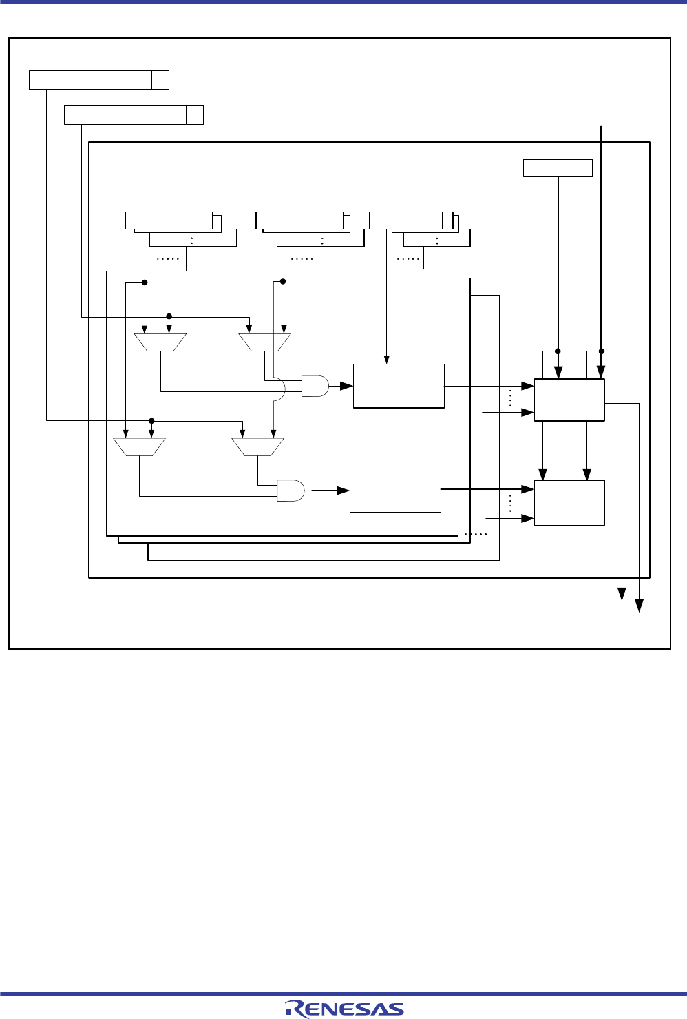
R01UH0034EJ0200 Rev.2.00 Page 283 of 1489
Dec 27, 2013
RX62T Group, RX62G Group 13. Memory-Protection Unit (MPU)
Under development Preliminary document
Specifications in this document are tentative and subject to change.
Figure 13.1 Block Diagram of the Memory-Protection Unit
A31 A4 A0
CPU instruction address
Region 0
to
Region 7
31 4 31 4
Processor mode
02
CPU operand access address
310
Region hit
Checking of access-
control information
A31 A4 A0
Region hit
Checking of access-
control information
Access control
Start page number
Background access-control register
End page number Access control V
Region 0
Region 7
Access
determination
Access
determination
Instruction memory-protection error
Data memory protection error
Start page number register End page number register

R01UH0034EJ0200 Rev.2.00 Page 284 of 1489
Dec 27, 2013
RX62T Group, RX62G Group 13. Memory-Protection Unit (MPU)
Under development Preliminary document
Specifications in this document are tentative and subject to change.
13.1.1 Types of Access Control
There are three types of access control information: permission for instruction execution, permission to read operands,
and permission to write operands. Violations of these types of access control are only detected when programs are
running in user mode. Violations are not detected when programs are running in supervisor mode.
13.1.2 Regions for Access Control
Up to eight regions for access control are definable. Settings of the range of memory for each access-control region are
made in the corresponding region-n start page number register (RSPAGEn) and region-n end page number register
(REPAGEn), where n = 0 to 7.
The minimum unit for control of access is the "page", by which the address space is divided into 16-byte units. The 28
higher-order bits ([31:4]) of the address [31:0] bits correspond to the page number.
The REPAGEn register specifies the access-control information for each area and whether the area is enabled or not.
13.1.3 Background Region
“Background region” refers to the whole address space (0000 0000h to FFFF FFFFh). Access-control information for the
background region is set in the background-region access-control register (MPBAC). In contrast to the access-control
information for the eight individual regions, protection information for the background region is effective as long as
memory protection is enabled (the MPEN bit in the MPEN register is 1).
13.1.4 Overlap between Regions
In cases of overlap between multiple regions, the access-control information becomes the logical OR of the access-
control bits for the overlapping regions (including the background region), with permission given priority.
13.1.5 Instructions and Data that Span Regions
Operations in response to the detection of memory-protection errors when instructions or data span regions for which
different access-control settings have been made are undefined. Ensure that instructions and data do not span regions for
which different access-control settings have been made.
R01UH0034EJ0200 Rev.2.00 Page 285 of 1489
Dec 27, 2013
RX62T Group, RX62G Group 13. Memory-Protection Unit (MPU)
Under development Preliminary document
Specifications in this document are tentative and subject to change.
13.2 Register Descriptions
Table 13.2 lists the registers of the interrupt controller.
Table 13.2 Registers of the Memory-Protection Unit
Register Name Symbol Value after Reset Address Access Size
Region 0 start page-number register RSPAGE0 xxxx xxx0h 0008 6400h 32
Region 0 end page-number register REPAGE0 xxxx xxx0h 0008 6404h 32
Region 1 start page-number register RSPAGE1 xxxx xxx0h 0008 6408h 32
Region 1 end page-number register REPAGE1 xxxx xxx0h 0008 640Ch 32
Region 2 start page-number register RSPAGE2 xxxx xxx0h 0008 6410h 32
Region 2 end page-number register REPAGE2 xxxx xxx0h 0008 6414h 32
Region 3 start page-number register RSPAGE3 xxxx xxx0h 0008 6418h 32
Region 3 end page-number register REPAGE3 xxxx xxx0h 0008 641Ch 32
Region 4 start page-number register RSPAGE4 xxxx xxx0h 0008 6420h 32
Region 4 end page-number register REPAGE4 xxxx xxx0h 0008 6424h 32
Region 5 start page-number register RSPAGE5 xxxx xxx0h 0008 6428h 32
Region 5 end page-number register REPAGE5 xxxx xxx0h 0008 642Ch 32
Region 6 start page-number register RSPAGE6 xxxx xxx0h 0008 6430h 32
Region 6 end page-number register REPAGE6 xxxx xxx0h 0008 6434h 32
Region 7 start page-number register RSPAGE7 xxxx xxx0h 0008 6438h 32
Region 7 end page-number register REPAGE7 xxxx xxx0h 0008 643Ch 32
Memory-protection enable register MPEN 0000 0000h 0008 6500h 32
Background access control register MPBAC 0000 0000h 0008 6504h 32
Memory-protection error status-clearing register MPECLR 0000 0000h 0008 6508h 32
Memory-protection error status register MPESTS 0000 0000h 0008 650Ch 32
Data memory-protection error address register MPDEA xxxx xxxxh 0008 6514h 32
Region search address register MPSA xxxx xxxxh 0008 6520h 32
Region search operation register MPOPS 0000h 0008 6524h 16
Region invalidation operation register MPOPI 0000h 0008 6526h 16
Instruction-hit region register MHITI 0000 0000h 0008 6528h 32
Data-hit region register MHITD 0000 0000h 0008 652Ch 32
R01UH0034EJ0200 Rev.2.00 Page 286 of 1489
Dec 27, 2013
RX62T Group, RX62G Group 13. Memory-Protection Unit (MPU)
Under development Preliminary document
Specifications in this document are tentative and subject to change.
13.2.1 Region-n Start Page Number Register (RSPAGEn) (n = 0 to 7)
RSPN[27:0] Bits (Region-Start Page Number)
These bits specify the page number where the region starts.
13.2.2 Region-n End Page Number Register (REPAGEn) (n = 0 to 7)
Addresses: RSPAGE0 0008 6400h, RSPAGE1 0008 6408h, RSPAGE2 0008 6410h, RSPAGE3 0008 6418h
RSPAGE4 0008 6420h, RSPAGE5 0008 6428h, RSPAGE6 0008 6430h, RSPAGE7 0008 6438h
b31 b30 b29 b28 b27 b26 b25 b24 b23 b22 b21 b20 b19 b18 b17 b16
RSPN[27:0]
Value after reset: xxxxxxxxxxxxxxxx
b15 b14 b13 b12 b11 b10 b9 b8 b7 b6 b5 b4 b3 b2 b1 b0
RSPN[27:0] ————
Value after reset: xxxxxxxxxxxx0000
x: Undefined
Bit Symbol Bit Name Function R/W
b3 to b0 — Reserved The read value is 0. The write value should always be 0. R/W
b31 to b4 RSPN[27:0] Region-Start Page Number Page number where the region starts, for use in region
determination
R/W
Addresses: REPAGE0 0008 6404h, REPAGE1 0008 640Ch, REPAGE2 0008 6414h, REPAGE3 0008 641Ch
REPAGE4 0008 6424h, REPAGE5 0008 642Ch, REPAGE6 0008 6434h, REPAGE7 0008 643Ch
b31 b30 b29 b28 b27 b26 b25 b24 b23 b22 b21 b20 b19 b18 b17 b16
REPN[27:0]
Value after reset: xxxxxxxxxxxxxxxx
b15 b14 b13 b12 b11 b10 b9 b8 b7 b6 b5 b4 b3 b2 b1 b0
REPN[27:0] UAC[2:0] V
Value after reset: xxxxxxxxxxxx0000
x: Undefined
Bit Symbol Bit Name Function R/W
b0 V Valid Bit 0: Region setting invalid
1: Region setting valid
R/W
b3 to b1 UAC[2:0] Access Control Bits in
User Mode
b3
0: Reading prohibited
1: Reading permitted
b2
0: Writing prohibited
1: Writing permitted
b1
0: Execution prohibited
1: Execution permitted
R/W
b31 to b4 REPN[27:0] Region-End Page Number Page number where the region ends, for use in region determination R/W

R01UH0034EJ0200 Rev.2.00 Page 287 of 1489
Dec 27, 2013
RX62T Group, RX62G Group 13. Memory-Protection Unit (MPU)
Under development Preliminary document
Specifications in this document are tentative and subject to change.
V Bit (Valid Bit)
This bit enables or disables the settings for the corresponding region.
This bit is cleared to 0 when the region invalidation operation register (MPOPI) invalidates all access-controlled areas.
UAC[2:0] Bits (Access Control Bits in User Mode)
These bits specify the access control in user mode.
REPN[27:0] Bits (Region-End Page Number)
These bits specify the page number where the region ends.
Specify a value that is greater than or equal to the page number where the corresponding region starts. The page specified
by the region-end page number is part of the target region for memory protection.

R01UH0034EJ0200 Rev.2.00 Page 288 of 1489
Dec 27, 2013
RX62T Group, RX62G Group 13. Memory-Protection Unit (MPU)
Under development Preliminary document
Specifications in this document are tentative and subject to change.
13.2.3 Memory-Protection Enable Register (MPEN)
MPEN Bit (Memory-Protection Enable)
This bit enables or disables the memory protection.
After 1 has been written to this bit, address checking for memory protection by the CPU starts on the execution of a
branch instruction (RTE and RTFI) that shifts operation to the user mode.
Address: 0008 6500h
b31 b30 b29 b28 b27 b26 b25 b24 b23 b22 b21 b20 b19 b18 b17 b16
————————————————
Value after reset: 0000000000000000
b15 b14 b13 b12 b11 b10 b9 b8 b7 b6 b5 b4 b3 b2 b1 b0
———————————————MPEN
Value after reset: 0000000000000000
Bit Symbol Bit Name Function R/W
b0 MPEN Memory-Protection Enable 1: The memory protection is enabled.
0: The memory protection is disabled.
R/W
b31 to b1 — Reserved The read value is 0. The write value should always be 0 R/W

R01UH0034EJ0200 Rev.2.00 Page 289 of 1489
Dec 27, 2013
RX62T Group, RX62G Group 13. Memory-Protection Unit (MPU)
Under development Preliminary document
Specifications in this document are tentative and subject to change.
13.2.4 Background Access Control Register (MPBAC)
UBAC[2:0] Bits (Background Access Control Bits in User Mode)
These bits specify the background access control in user mode.
Address: 0008 6504h
b31 b30 b29 b28 b27 b26 b25 b24 b23 b22 b21 b20 b19 b18 b17 b16
————————————————
Value after reset: 0000000000000000
b15 b14 b13 b12 b11 b10 b9 b8 b7 b6 b5 b4 b3 b2 b1 b0
———————————— UBAC[2:0] —
Value after reset: 0000000000000000
Bit Symbol Bit Name Function R/W
b0 — Reserved The read value is 0. The write value should always be 0. R/W
b3 to b1 UBAC[2:0] Background Access Control Bits in
User Mode
b3
0: Reading prohibited
1: Reading permitted
b2
0: Writing prohibited
1: Writing permitted
b1
0: Execution prohibited
1: Execution permitted
R/W
b31 to b4 — Reserved The read value is 0. The write value should always be 0. R/W

R01UH0034EJ0200 Rev.2.00 Page 290 of 1489
Dec 27, 2013
RX62T Group, RX62G Group 13. Memory-Protection Unit (MPU)
Under development Preliminary document
Specifications in this document are tentative and subject to change.
13.2.5 Memory-Protection Error Status-Clearing Register (MPECLR)
CLR Bit (Error Status-Clearing)
This bit clears the data read/write bit (DRW), the data memory-protection error generated bit (DA), and the instruction
memory-protection error generated bit (IA) in the memory-protection error status register (MPESTS) to 0.
Address: 0008 6508h
b31 b30 b29 b28 b27 b26 b25 b24 b23 b22 b21 b20 b19 b18 b17 b16
————————————————
Value after reset: 0000000000000000
b15 b14 b13 b12 b11 b10 b9 b8 b7 b6 b5 b4 b3 b2 b1 b0
———————————————CLR
Value after reset: 0000000000000000
Bit Symbol Bit Name Function R/W
b0 CLR Error Status-Clearing [Reading]
0: Fixed value for reading
[Writing]
0: Nothing is done.
1: The DRW, DA, and IA bits in the MPESTS are cleared to 0.
R/W
b31 to b1 — Reserved The read value is 0. The write value should always be 0. R/W

R01UH0034EJ0200 Rev.2.00 Page 291 of 1489
Dec 27, 2013
RX62T Group, RX62G Group 13. Memory-Protection Unit (MPU)
Under development Preliminary document
Specifications in this document are tentative and subject to change.
13.2.6 Memory-Protection Error Status Register (MPESTS)
IA Bit (Instruction Memory-Protection Error Generated Bit)
This bit indicates the state of memory-protection error generation by instruction execution.
Setting the error status-clearing bit (CLR) in the memory-protection error status-clearing register (MPECLR) to 1 clears
this bit to 0.
DA Bit (Data Memory-Protection Error Generated Bit)
This bit indicates the state of memory-protection error generation by operand access.
Setting the error status-clearing bit (CLR) in the memory-protection error status-clearing register (MPECLR) to 1 clears
this bit to 0.
DRW Bit (Data Read/Write Bit)
For a memory-protection error produced by operand access, this bit indicates the read/write attribute of the access
operation. This bit is only valid when the data memory-protection error generated bit (DA) is 1.
Setting the error status-clearing bit (CLR) in the memory-protection error status-clearing register (MPECLR) to 1 clears
this bit to 0.
Address: 0008 650Ch
b31 b30 b29 b28 b27 b26 b25 b24 b23 b22 b21 b20 b19 b18 b17 b16
————————————————
Value after reset: 0000000000000000
b15 b14 b13 b12 b11 b10 b9 b8 b7 b6 b5 b4 b3 b2 b1 b0
—————————————DRWDAIA
Value after reset: 0000000000000000
Bit Symbol Bit Name Function R/W
b0 IA Instruction Memory-Protection
Error Generated Bit
0: No instruction memory-protection error was generated.
1: Instruction memory-protection error was generated.
R
b1 DA Data Memory-Protection Error
Generated Bit
0: No data memory-protection error was generated.
1: Data memory-protection error was generated.
R
b2 DRW Data Read/Write Bit 0: Data were read.
1: Data were written.
R
b31 to b3 — Reserved The read value is 0. The write value should always be 0. R/W

R01UH0034EJ0200 Rev.2.00 Page 292 of 1489
Dec 27, 2013
RX62T Group, RX62G Group 13. Memory-Protection Unit (MPU)
Under development Preliminary document
Specifications in this document are tentative and subject to change.
13.2.7 Data Memory-Protection Error Address Register (MPDEA)
DEA[31:0] Bits (Data Memory-Protection Error Address)
These bits retain the address for which operand access generated a memory-protection error.
Address: 0008 6514h
b31 b30 b29 b28 b27 b26 b25 b24 b23 b22 b21 b20 b19 b18 b17 b16
DEA[31:0]
Value after reset: xxxxxxxxxxxxxxxx
b15 b14 b13 b12 b11 b10 b9 b8 b7 b6 b5 b4 b3 b2 b1 b0
DEA[31:0]
Value after reset: xxxxxxxxxxxxxxxx
x: Undefined
Bit Symbol Bit Name Function R/W
b31 to b0 DEA[31:0]
Data Memory-Protection Error Address Data memory-protection error address
R
R01UH0034EJ0200 Rev.2.00 Page 293 of 1489
Dec 27, 2013
RX62T Group, RX62G Group 13. Memory-Protection Unit (MPU)
Under development Preliminary document
Specifications in this document are tentative and subject to change.
13.2.8 Region Search Address Register (MPSA)
SA[31:0] Bits (Region Search Address)
These bits specify the address for use in comparison with region-start addresses in the region-n start page number
registers (RSPAGEn) and region-end addresses in the region-n end page number registers (REPAGEn).
13.2.9 Region Search Operation Register (MPOPS)
S Bit (Region Search Operation)
Setting this bit to 1 makes the memory-protection unit perform a region-search operation. The address specified in the
region search address register (MPSA) is compared with the address information for individual regions to search for a
hitting region.
The result of searching is stored in the data-hit region bits (HITD[7:0]) of the data-hit region register (MHITD).
Moreover, the logical OR of the respective access control bits for hitting regions is stored in the data-hit region access
control bits (UHACD[2:0]) in user mode.
Address: 0008 6520h
b31 b30 b29 b28 b27 b26 b25 b24 b23 b22 b21 b20 b19 b18 b17 b16
SA[31:0]
Value after reset: xxxxxxxxxxxxxxxx
b15 b14 b13 b12 b11 b10 b9 b8 b7 b6 b5 b4 b3 b2 b1 b0
SA[31:0]
Value after reset: xxxxxxxxxxxxxxxx
x: Undefined
Bit Symbol Bit Name Function R/W
b31 to b0 SA[31:0] Region Search Address Address for region searching R/W
Address: 0008 6524h
b15 b14 b13 b12 b11 b10 b9 b8 b7 b6 b5 b4 b3 b2 b1 b0
——————————————— S
Value after reset: 0000000000000000
Bit Symbol Bit Name Function R/W
b0 S Region Search Operation [Reading]
0: Fixed value for reading
[Writing]
0: Nothing is done.
1: A region-search operation proceeds.
R/W
b15 to b1 — Reserved The read value is 0. The write value should always be 0. R/W

R01UH0034EJ0200 Rev.2.00 Page 294 of 1489
Dec 27, 2013
RX62T Group, RX62G Group 13. Memory-Protection Unit (MPU)
Under development Preliminary document
Specifications in this document are tentative and subject to change.
13.2.10 Region Invalidation Operation Register (MPOPI)
INV Bit (Region Invalidate Start)
Setting this bit to 1 clears the valid (V) bits in all of the region-n end page number registers (REPAGEn) to 0. After a V
bit is cleared to 0, all settings other than background access-control settings are invalid.
Address: 0008 6526h
b15 b14 b13 b12 b11 b10 b9 b8 b7 b6 b5 b4 b3 b2 b1 b0
———————————————INV
Value after reset: 0000000000000000
Bit Symbol Bit Name Function R/W
b0 INV Region Invalidate Start [Reading]
0: Fixed value for reading
[Writing]
0: Nothing is done.
1: All access-controlled areas are invalidated.
R/W
b15 to b1 — Reserved The read value is 0. The write value should always be 0. R/W

R01UH0034EJ0200 Rev.2.00 Page 295 of 1489
Dec 27, 2013
RX62T Group, RX62G Group 13. Memory-Protection Unit (MPU)
Under development Preliminary document
Specifications in this document are tentative and subject to change.
13.2.11 Instruction-Hit Region Register (MHITI)
Address: 0008 6528h
b31 b30 b29 b28 b27 b26 b25 b24 b23 b22 b21 b20 b19 b18 b17 b16
———————— HITI[7:0]
Value after reset: 0000000000000000
b15 b14 b13 b12 b11 b10 b9 b8 b7 b6 b5 b4 b3 b2 b1 b0
———————————— UHACI[2:0] —
Value after reset: 0000000000000000
Bit Symbol Bit Name Function R/W
b0 — Reserved The read value is 0. The write value should always be 0. R/W
b3 to b1 UHACI[2:0] Instruction-Hit Region
Access Control Bits in
User Mode
b3
0: Reading prohibited
1: Read permitted
b2
0: Writing prohibited
1: Writing permitted
b1
0: Execution prohibited
1: Execution is permitted.
R
b15 to b4 — Reserved The read value is 0. The write value should always be 0. R/W
b23 to b16 HITI[7:0] Instruction-Hit Region When the instruction memory-protection error generated (IA) bit in the MPESTS = 1,
[b23:b16] = 0000 0000b indicates that attempted access to the background region
led to an instruction memory-protection error.
Other than above
b23
0: Instruction memory-protection error was not generated in region 7.
1: Instruction memory-protection error was generated in region 7.
b22
0: Instruction memory-protection error was not generated in region 6.
1: Instruction memory-protection error was generated in region 6.
b21
0: Instruction memory-protection error was not generated in region 5.
1: Instruction memory-protection error was generated in region 5.
b20
0: Instruction memory-protection error was not generated in region 4.
1: Instruction memory-protection error was generated in region 4.
b19
0: Instruction memory-protection error was not generated in region 3.
1: Instruction memory-protection error was generated in region 3.
b18
0: Instruction memory-protection error was not generated in region 2.
1: Instruction memory-protection error was generated in region 2.
b17
0: Instruction memory-protection error was not generated in region 1.
1: Instruction memory-protection error was generated in region 1.
b16
0: Instruction memory-protection error was not generated in region 0.
1: Instruction memory-protection error was generated in region 0.
R
b31 to b24 — Reserved The read value is 0. The write value should always be 0. R/W

R01UH0034EJ0200 Rev.2.00 Page 296 of 1489
Dec 27, 2013
RX62T Group, RX62G Group 13. Memory-Protection Unit (MPU)
Under development Preliminary document
Specifications in this document are tentative and subject to change.
UHACI[2:0] Bits (Instruction-Hit Region Access Control Bits in User Mode)
These bits hold the user-mode access control bits (REPAGEn.UAC[2:0]) for the region where the instruction memory-
protection error was generated.
If the error was generated in an overlap between regions, the value stored here is the logical OR of the user-mode access
control bits for the corresponding regions (including the background region).
HITI[7:0] Bits (Instruction-Hit Region)
These bits indicate the region where an instruction memory-protection error was generated. These bits are set to 0000
0000b in response to the generation of an instruction memory-protection error in the background region.

R01UH0034EJ0200 Rev.2.00 Page 297 of 1489
Dec 27, 2013
RX62T Group, RX62G Group 13. Memory-Protection Unit (MPU)
Under development Preliminary document
Specifications in this document are tentative and subject to change.
13.2.12 Data-Hit Region Register (MHITD)
Address: 0008 652Ch
b31 b30 b29 b28 b27 b26 b25 b24 b23 b22 b21 b20 b19 b18 b17 b16
———————— HITD[7:0]
Value after reset 0000000000000000
b15 b14 b13 b12 b11 b10 b9 b8 b7 b6 b5 b4 b3 b2 b1 b0
———————————— UHACD[2:0] —
Value after reset 0000000000000000
Bit Symbol Bit Name Function R/W
b0 — Reserved The read value is 0. The write value should always be 0. R/W
b3 to b1 UHACD[2:0] Data-Hit Region Access
Control Bits in
User Mode
b3
0: Reading prohibited
1: Reading permitted
b2
0: Writing prohibited
1: Writing permitted
b1
0: Execution prohibited
1: Execution permitted
R
b15 to b4 — Reserved The read value is 0. The write value should always be 0. R/W
b23 to b16 HITD[7:0] Data-Hit Region When the data memory-protection error generated (DA) bit = 1, [b23:b16] = 0000 0000b
indicates that attempted access to the background region led to a data memory-
protection error.
Other than above
b23
0: Neither a data memory-protection error nor a search hit was generated in region 7.
1: A data memory-protection error or search hit was generated in region 7.
b22
0: Neither a data memory-protection error nor a search hit was generated in region 6.
1: A data memory-protection error or search hit was generated in region 6.
b21
0: Neither a data memory-protection error nor a search hit was generated in region 5.
1: A data memory-protection error or search hit was generated in region 5.
b20
0: Neither a data memory-protection error nor a search hit was generated in region 4.
1: A data memory-protection error or search hit was generated in region 4.
b19
0: Neither a data memory-protection error nor a search hit was generated in region 3.
1: A data memory-protection error or search hit was generated in region 3.
b18
0: Neither a data memory-protection error nor a search hit was generated in region 2.
1: A data memory-protection error or search hit was generated in region 2.
b17
0: Neither a data memory-protection error nor a search hit was generated in region 1.
1: A data memory-protection error or search hit was generated in region 1.
b16
0: Neither a data memory-protection error nor a search hit was generated in region 0.
1: A data memory-protection error or search hit was generated in region 0.
R
b31 to b24 — Reserved The read value is 0. The write value should always be 0. R/W

R01UH0034EJ0200 Rev.2.00 Page 298 of 1489
Dec 27, 2013
RX62T Group, RX62G Group 13. Memory-Protection Unit (MPU)
Under development Preliminary document
Specifications in this document are tentative and subject to change.
UHACD[2:0] Bits (Data-Hit Region Access Control Bits in User Mode)
These bits hold the user-mode access control bits (REPAGEn.UAC[2:0]) that have been set for the region where a data
memory-protection error was generated or the region that produced a hit in region searching.
When an error is generated in an overlap between regions or a hit was generated in region searching, the value stored
here is the logical OR of the user-mode access control bits for the corresponding regions (including the background
region).
HITD[7:0] Bits (Data-Hit Region)
These bits indicate the region where a data memory-protection error was generated or the region that produced a hit in a
region search. These bits are set to 0000 0000b for a data memory-protection error generated in the background region.
Note: When access to a register of memory protection unit in user mode generates a data memory-protection error, the
value in this register is cleared to 0000 0000h.

R01UH0034EJ0200 Rev.2.00 Page 299 of 1489
Dec 27, 2013
RX62T Group, RX62G Group 13. Memory-Protection Unit (MPU)
Under development Preliminary document
Specifications in this document are tentative and subject to change.
13.3 Functions
13.3.1 Memory Protection
Memory protection means monitoring, in accord with the access-control information that has been set for the individual
access-control regions and the background region, whether or not access by programs running in user mode violates the
access-control settings. The memory-protection unit notifies the CPU of access-control violations (or memory-protection
errors) when they are detected, causing the CPU to start access-exception processing.
Memory protection is enabled by setting the memory-protection enable (MPEN) bit in the memory-protection enable
(MPEN) register to 1.
An instruction memory-protection error is generated on detection of an instruction-execution violation and a data
memory-protection error is generated on detection of an operand-access reading or writing violation. Operand access that
leads to a data memory-protection error is not actually executed.
13.3.2 Region Search
Region search means enquiry as to which of the eight specified access regions was “hit” and how the access-control
information (permission to execute, to read, and to write) is set.
When the region search operation (S) bit in the region-search operation (MPOP) register is set to 1, the address specified
in the region search address (MPSA) register is compared with the addresses for the individual regions. After a region
search is executed, the data-hit region register (MHITD) indicates the logical OR of the access-control information for
the region which was “hit” and for the other regions.
13.3.3 Protection of Registers Related to the Memory-Protection Unit
Registers related to the memory-protection unit are not accessible through means of access other than operand access by
the CPU (i.e. by instruction fetching or DMA). Attempted access to registers related to the memory-protection unit in
user mode through operand access by the CPU leads to a data memory-protection error regardless of whether or not
memory protection is in effect at the given location.
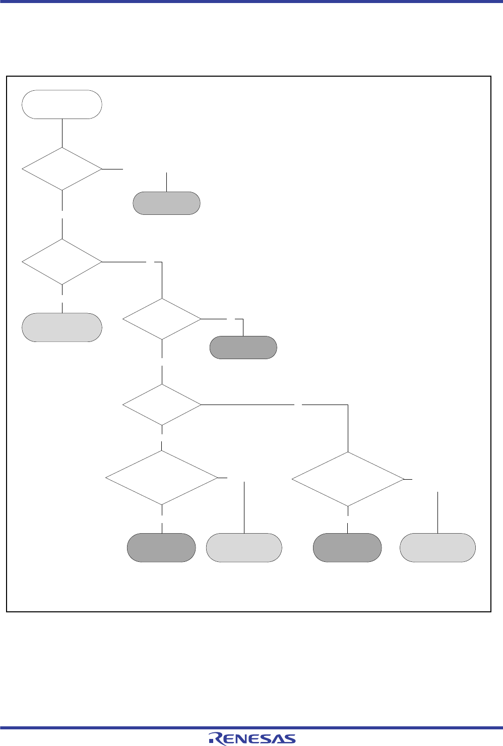
R01UH0034EJ0200 Rev.2.00 Page 300 of 1489
Dec 27, 2013
RX62T Group, RX62G Group 13. Memory-Protection Unit (MPU)
Under development Preliminary document
Specifications in this document are tentative and subject to change.
13.3.4 Flow for Determination of Access by the Memory-Protection Function
Figure 13.2 shows the flow of determination in the case of data access and Figure 13.3 shows the flow of determination
in the case of instruction access.
Figure 13.2 Flow of Determination for Data Access
Data access by the CPU
No
Yes
Access permitted
No
Permit data access Generate a data memory-
protection error Permit data access Generate a data memory-
protection error
Access permitted
Yes
Processor mode? Supervisor mode
Permit data access
User mode
Yes
No
Generate a data memory-
protection error
Note 1. Permission takes priority when the settings lead to overlapping regions overlap and are different for the given regions
(this includes the background region).
Permit data access
Is access to an
MPU-related register?
Is memory protection
enabled?
Is access to an access-
control region?
Access prohibited Access prohibited
(default)
Determination in accord with
the access-control information for
the given region*1
Determination in accord with
the access-control information for
the background region
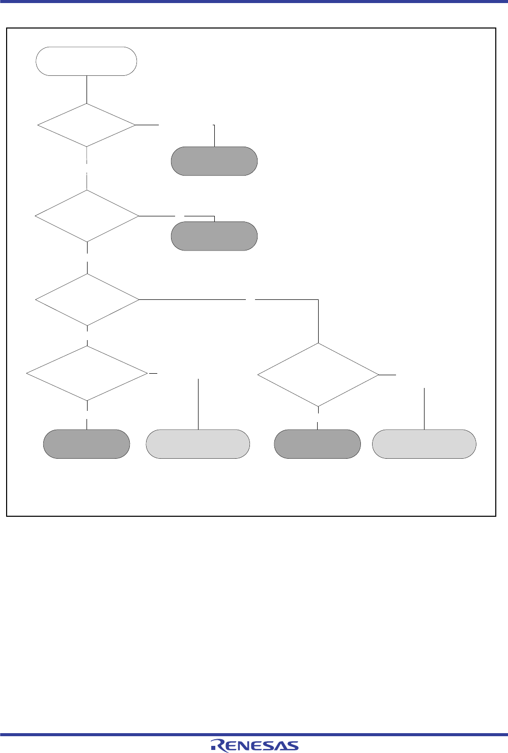
R01UH0034EJ0200 Rev.2.00 Page 301 of 1489
Dec 27, 2013
RX62T Group, RX62G Group 13. Memory-Protection Unit (MPU)
Under development Preliminary document
Specifications in this document are tentative and subject to change.
Figure 13.3 Flow of Determination for Instruction Access
Instruction access by the CPU
Yes
Access permitted
No
Permit instruction access Generate an instruction
memory-protection error Permit instruction access Generate an instruction
memory-protection error
Access prohibited
(default)
Access permitted
Yes
No
Processor mode? Supervisor mode
Permit instruction access
User mode
Permit instruction access
Note 1. Permission takes priority when the settings lead to overlapping regions overlap and are not the same for the given regions
(this includes the background region).
Is memory protection
enabled?
Is access to an access-
control region?
Determination in accord with
the access-control information
for the given region*1
Determination in accord with
The access-control information
for the background region
Access prohibited

R01UH0034EJ0200 Rev.2.00 Page 302 of 1489
Dec 27, 2013
RX62T Group, RX62G Group 13. Memory-Protection Unit (MPU)
Under development Preliminary document
Specifications in this document are tentative and subject to change.
13.4 Procedures for Using Memory Protection
13.4.1 Setting Access-Control Information
Access-control information for the various regions is set in supervisor mode.
Settings for up to eight access-control regions are made in the region-n start page number registers (RSPAGEn) and
region-n end page number registers (REPAGEn), where n = 0 to 7.
Settings for the background access-control region are made in the background access-control register (MPBAC).
13.4.2 Enabling Memory Protection
Setting the memory-protection enable (MPEN) bit in the memory-protection enable (MPEN) register to 1 while
operation is in supervisor mode enables memory protection.
13.4.3 Transition to User Mode
After updating the registers related to the memory-protection unit, be sure to read the registers for which writing was
performed and check that the settings have been made as the final step before the transition to user mode.
Either of the methods below can be used for the transition from supervisor mode to user mode.
•Set the processor mode setting (PM) bit in the copy of the processor status word (PSW) saved in the stack area to 1
(the setting for user mode) and then execute an RTE instruction.
•Set the PM bit in the backup processor status word (BPSW) to 1 and then execute an RTFI instruction.
Note: Using an MVTC or POPC instruction to write to the PSW.PM bit is invalid. Use an RTE or RTFI instruction to
update the value of the PSW.PM bit.
The memory-protection unit starts checking instruction-execution access and operand access by the CPU on the
transition to user mode.
13.4.4 Processing in Response to Memory-Protection Errors
The CPU starts access-exception processing on detection of a violation of protection set up by the access-control
information (i.e. a memory-protection error). For details on CPU operations in access-exception processing, refer to
section 10., Exceptions.
To determine whether an instruction memory-protection error or data memory-protection error has been generated, check
the values of the instruction memory-protection error generated (IA) and data memory-protection error generated (DA)
bits in the memory-protection error status (MPESTS) register from within the exception-processing routine.
After confirming the type of error, clear the memory-protection error status (MPESTS) register by writing 1 to the status
clearing (MPE) bit in the memory-protection error status clearing (MPECLR) register.

R01UH0034EJ0200 Rev.2.00 Page 303 of 1489
Dec 27, 2013
RX62T Group, RX62G Group 13. Memory-Protection Unit (MPU)
Under development Preliminary document
Specifications in this document are tentative and subject to change.
(1) When a data memory-protection error is generated
Access-exception processing by the CPU saves the address of the instruction that led to the memory-protection error on
the stack. Furthermore, the address of the operand for which access led to a memory-protection error is stored in the data
memory-protection error address register (MPDEA) and the region information for the region where the memory-
protection error was generated is stored in the data-hit region register (MHITD).
Violations of access control in access to valid regions 0 to 7
The data-hit region bits (MHITD.HITD[7:0]) with the same region number as the region where the error occurred is set
to 1. In user mode, the logical “or” of the region access-control information for the location where the error occurred is
set in the data-hit region access-control bits (MHITD.UHACD[2:0]).
Violations of access control for the background region, besides access to valid regions 0 to 7
The data-hit region bits (MHITD.HITD[7:0]) are set to 0000 0000b. In user mode, the access-control information for the
background region is set in the data-hit region access-control bits (MHITD.UHACD[2:0]).
Referring to this information can pinpoint the sources of errors.
(2) When an instruction memory-protection error is generated
Access-exception processing by the CPU saves the address of the instruction that led to the memory-protection error on
the stack. Furthermore, the region information for the region where the memory-protection error was generated is stored
in the instruction-hit region register (MHITI).
Violations of access control in access to valid regions 0 to 7
The instruction-hit region bit (MHITD.HITI[7:0]) with the same region number as the region where the error occurred is
set to 1. In user mode, the logical “or” of the region access-control information for the location where the error occurred
is set in the instruction-hit region access-control bits (MHITI.UHACI[2:0]).
Violations of access control for the background region, besides access to valid regions 0 to 7
The instruction-hit region bits (MHITI.HITI[7:0]) are set to 0000 0000b. In user mode, the access-control information
for the background region is set in the instruction-hit region access-control bits (MHITI.UHACI[2:0]).
Referring to this information can pinpoint the sources of errors.

R01UH0034EJ0200 Rev.2.00 Page 304 of 1489
Dec 27, 2013
RX62T Group, RX62G Group 14. Data Transfer Controller (DTC)
Under development Preliminary document
Specifications in this document are tentative and subject to change.
14. Data Transfer Controller (DTC)
The RX62T and RX62G Groups incorporate a data transfer controller (DTC).
The DTC is activated by an interrupt request to control data transfer.
14.1 Overview
Table 14.1 lists the specifications of the DTC, and Figure 14.1 shows a block diagram of the DTC.
Table 14.1 DTC Specifications
Item Description
Transfer mode Normal transfer mode
A single activation leads to a single data transfer.
Repeat transfer mode
A single activation leads to a single data transfer.
The transfer address is returned to the transfer start address after the number of data transfers
corresponding to "repeat size".
The maximum repeat size is 256.
Block transfer mode
A single activation leads to the transfer of a single block.
The maximum block size is 256.
Transfer channel Channel transfer corresponding to the interrupt source is possible (transferred by DTC activation
request from the ICU).
Data of multiple channels can be transferred on a single activation source (chain transfer).
Either “executed when the counter is 0” or “always executed” can be selected for chain transfer.
Transfer space In short-address mode: 16 Mbytes
(Areas from 0000 0000h to 007F FFFFh and FF80 0000h to FFFF FFFFh excepting reserved areas)
In full-address mode: 4 Gbytes
(Area from 0000 0000h to FFFF FFFFh excepting reserved areas)
Data transfer units Length of a single data: 8, 16, or 32 bits
Number of data for a single block: 1 to 255 data
CPU interrupt source An interrupt request can be generated to the CPU on a DTC activation interrupt.
An interrupt request can be generated to the CPU after a single data transfer.
An interrupt request can be generated to the CPU after data transfer of specified volume.
Read skip Transfer data read skip can be specified.
Write-back skip When "fixed" is selected for transfer source address and/or transfer destination address, write-back
skip execution is provided.
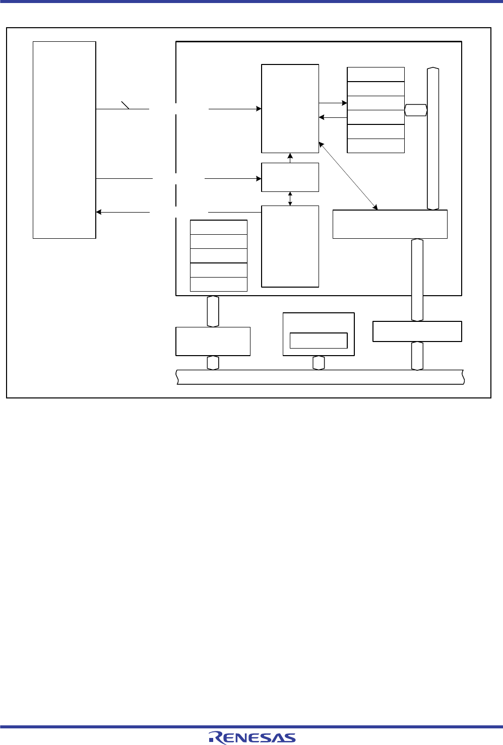
R01UH0034EJ0200 Rev.2.00 Page 305 of 1489
Dec 27, 2013
RX62T Group, RX62G Group 14. Data Transfer Controller (DTC)
Under development Preliminary document
Specifications in this document are tentative and subject to change.
Figure 14.1 Block Diagram of the DTC
DTC
On-chip SRAM
Transfer data
8
Peripheral bus
interface
DTC internal bus
Register
control
MRA
MRB
CRA
CRB
SAR
DAR
Bus interface
Startup
control
DTC
response
control
Interrupt
controller
DTCCR
DTCVBR
Vector number
DTC response
Start request
Internal main bus 2
Bus master arbitrator
DTCADMOD
DTCST
DTCSTS

R01UH0034EJ0200 Rev.2.00 Page 306 of 1489
Dec 27, 2013
RX62T Group, RX62G Group 14. Data Transfer Controller (DTC)
Under development Preliminary document
Specifications in this document are tentative and subject to change.
14.2 Register Descriptions
Table 14.2 lists the registers of the DTC.
Registers MRA, MRB, SAR, DAR, CRA, and CRB are DTC internal registers, which cannot be directly accessed from
the CPU. Values to be set in the DTC internal registers are placed in the RAM area as transfer information data. When an
activation request is generated, the DTC reads the transfer information data from the RAM area and set them in the
internal registers. After the data transfer ends, the internal register contents are written back to the RAM area as transfer
information data.
x : Undefined value
Note: • To activate the DTC, a setting of the DTCERn.DTCE bit (n = interrupt vector number) and IERm.IENj (m = 02h to 1Fh, j = 7 to 0)
bits in the interrupt controller (ICU) is required. For details, refer to section 11, Interrupt Controller (ICU).
Table 14.2 Registers of the DTC
Register Name Symbol Value after Reset Address Access Size(Bits)
DTC mode register A MRA xxh — —
DTC mode register B MRB xxh — —
DTC transfer source address register SAR xxxxxxxxh — —
DTC transfer destination address register DAR xxxxxxxxh — —
DTC transfer count register A CRA xxxxh — —
DTC transfer count register B CRB xxxxh — —
DTC control register DTCCR 08h 0008 2400h 8 bits
DTC vector base register DTCVBR 00000000h 0008 2404h 32 bits
DTC address mode register DTCADMOD 00h 0008 2408h 8 bits
DTC module start register DTCST 00h 0008 240Ch 8 bits
DTC status register DTCSTS 0000h 0008 240Eh 16 bits

R01UH0034EJ0200 Rev.2.00 Page 307 of 1489
Dec 27, 2013
RX62T Group, RX62G Group 14. Data Transfer Controller (DTC)
Under development Preliminary document
Specifications in this document are tentative and subject to change.
14.2.1 DTC Mode Register A (MRA)
MRA is used to select the operating mode of the DTC.
MRA cannot be accessed directly from the CPU.
SM[1:0] Bits (Transfer Source Address Addressing Mode)
These bits specify the SAR operation after data transfer.
SZ[1:0] Bits (DTC Data Transfer Size)
These bits specify the transfer data size.
MD[1:0] Bits (DTC Transfer Mode Select)
These bits specify the transfer mode of the DTC.
Address: (inaccessible directly from the CPU)
b7 b6 b5 b4 b3 b2 b1 b0
MD[1:0] SZ[1:0] SM[1:0] — —
Value after reset: xxxxxxxx
x: Undefined
Bit Symbol Bit Name Description R/W
b1, b0 — Reserved These bits are always read as undefined. The write value
should be 0.
—
b3, b2 SM[1:0] Transfer Source Address Addressing
Mode
b3 b2
0 0: SAR value is fixed
(Write-back to SAR is skipped)
0 1: SAR value is fixed
(Write-back to SAR is skipped)
1 0: SAR value is incremented after data transfer
(+1 when SZ[1:0] bits = 00b, +2 when SZ[1:0] bits = 01b,
+4 when SZ[1:0] bits = 10b)
1 1: SAR value is decremented after data transfer
(-1 when SZ[1:0] bits = 00b, -2 when SZ[1:0] bits = 01b,
-4 when SZ[1:0] bits = 10b)
—
b5, b4 SZ[1:0] DTC Data Transfer Size b5 b4
0 0: Byte transfer
0 1: Word transfer
1 0: Longword transfer
1 1: Setting prohibited
—
b7, b6 MD[1:0] DTC Transfer Mode Select b7 b6
0 0: Normal transfer mode
0 1: Repeat transfer mode
1 0: Block transfer mode
1 1: Setting prohibited
—

R01UH0034EJ0200 Rev.2.00 Page 308 of 1489
Dec 27, 2013
RX62T Group, RX62G Group 14. Data Transfer Controller (DTC)
Under development Preliminary document
Specifications in this document are tentative and subject to change.
14.2.2 DTC Mode Register B (MRB)
MRB is used to select the operating mode of the DTC.
MRB cannot be accessed directly from the CPU.
DM[1:0] Bits (Transfer Destination Address Addressing Mode)
These bits specify the DAR operation after data transfer.
DTS Bit (DTC Transfer Mode Select)
The DTS bit specifies the side (transfer source or destination) to be a repeat area or block area in repeat transfer mode or
block transfer mode.
DISEL Bit (DTC Interrupt Select)
The DISEL bit specifies whether to generate an interrupt request to the CPU each time DTC data transfer is performed or
when specified data transfer is completed.
CHNS Bit (DTC Chain Transfer Select)
The CHNS bit selects the chain transfer condition.
When the next transfer is chain transfer, completion of specified transfer count is not checked and the interrupt status flag
is not cleared. Moreover, an interrupt request to the CPU is not generated.
Address: (inaccessible directly from the CPU)
b7 b6 b5 b4 b3 b2 b1 b0
CHNE CHNS DISEL DTS DM[1:0] — —
Value after reset: xxxxxxxx
x: Undefined
Bit Symbol Bit Name Description R/W
b1, b0 — Reserved These bits are always read as undefined. The write value should
be 0.
—
b3, b2 DM[1:0] Transfer Destination Address
Addressing Mode
b3 b2
0 0: DAR value is address fixed
(Write-back to DAR is skipped)
0 1: DAR value is address fixed
(Write-back to DAR is skipped)
1 0: DAR value is incremented after data transfer
(+1 when SZ[1:0] bits in MRA = 00b, +2 when SZ[1:0] bits
= 01b, +4 when SZ[1:0] bits = 10b)
1 1: DAR value is decremented after data transfer
(-1 when SZ[1:0] bits in MRA = 00b, -2 when SZ[1:0] bits =
01b, -4 when SZ[1:0] bits = 10b)
—
b4 DTS DTC Transfer Mode Select 0: Destination side is repeat area or block area
1: Source side is repeat area or block area
—
b5 DISEL DTC Interrupt Select 0: An interrupt request to the CPU is generated when specified
data transfer is completed
1: An interrupt request to the CPU is generated each time DTC
data transfer is performed
—
b6 CHNS DTC Chain Transfer Select 0: Chain transfer is performed continuously
1: Chain transfer is performed only when the transfer counter is 0
—
b7 CHNE DTC Chain Transfer Enable 0: Chain transfer is disabled
1: Chain transfer is enabled
—
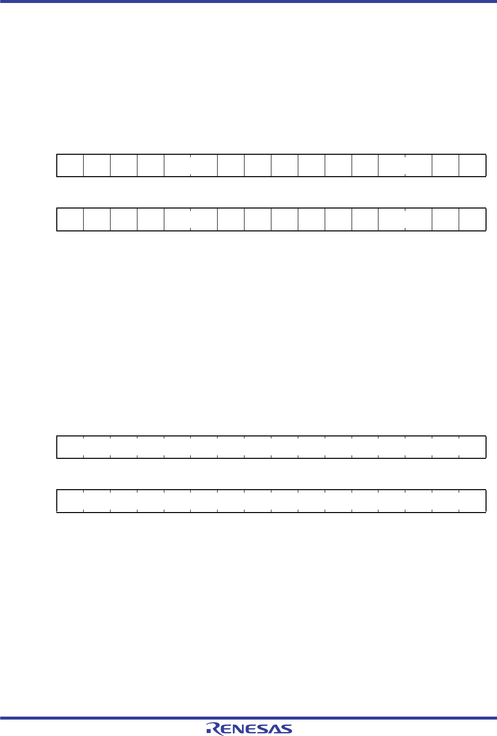
R01UH0034EJ0200 Rev.2.00 Page 309 of 1489
Dec 27, 2013
RX62T Group, RX62G Group 14. Data Transfer Controller (DTC)
Under development Preliminary document
Specifications in this document are tentative and subject to change.
CHNE Bit (DTC Chain Transfer Enable)
The CHNE bit enables or disables chain transfer.
The chain transfer condition is selected by the CHNS bit.
For details of chain transfer, see section 14.4.6, Chain Transfer.
14.2.3 DTC Transfer Source Address register (SAR)
SAR is used to set the transfer source start address.
In full-address mode, 32 bits are valid.
In short-address mode, lower 24 bits are valid and upper 8 bits (b31 to b24) are ignored. The address of this register is
extended by the value specified by b23.
SAR cannot be accessed directly from the CPU.
14.2.4 DTC Transfer Destination Address Register (DAR)
DAR is used to set the transfer destination start address.
In full-address mode, 32 bits are valid.
In short-address mode, lower 24 bits are valid and upper 8 bits (b31 to b24) are ignored. The address of this register is
extended by the value specified by b23.
DAR cannot be accessed directly from the CPU.
Address: (inaccessible directly from the CPU)
b31 b30 b29 b28 b27 b26 b25 b24 b23 b22 b21 b20 b19 b18 b17 b16
Value after reset: xxxxxxxxxxxxxxxx
b15 b14 b13 b12 b11 b10 b9 b8 b7 b6 b5 b4 b3 b2 b1 b0
Value after reset: xxxxxxxxxxxxxxxx
x: Undefined
Address: (inaccessible directly from the CPU)
b31 b30 b29 b28 b27 b26 b25 b24 b23 b22 b21 b20 b19 b18 b17 b16
Value after reset: xxxxxxxxxxxxxxxx
b15 b14 b13 b12 b11 b10 b9 b8 b7 b6 b5 b4 b3 b2 b1 b0
Value after reset: xxxxxxxxxxxxxxxx
x: Undefined

R01UH0034EJ0200 Rev.2.00 Page 310 of 1489
Dec 27, 2013
RX62T Group, RX62G Group 14. Data Transfer Controller (DTC)
Under development Preliminary document
Specifications in this document are tentative and subject to change.
14.2.5 DTC Transfer Count Register A (CRA)
Note: • Set CRAH and CRAL to the same value in repeat transfer mode and block transfer mode.
CRA is used to set the transfer count of the DTC.
The function of this register depends on transfer mode.
CRA cannot be accessed directly from the CPU.
(1) Normal transfer mode (MD[1:0] bits in MRA = 00b)
CRA functions as a 16-bit transfer counter in normal transfer mode.
The transfer count is 1, 65535, and 65536 when the set value is 0001h, FFFFh, and 0000h, respectively.
The CRA value is decremented (-1) at each data transfer.
(2) Repeat transfer mode (MD[1:0] bits in MRA = 01b)
The CRAH register retains transfer count and the CRAL register functions as an 8-bit transfer counter.
The transfer count is 1, 255, and 256 when the set value is 01h, FFh, and 00h, respectively.
The CRAL value is decremented (-1) at each data transfer. When it reaches 00h, the CRAH value is transferred to CRAL.
(3) Block transfer mode (MD[1:0] bits in MRA = 10b)
The CRAH register retains block size and the CRAL register functions as an 8-bit block size counter.
The transfer count is 1 and 255 when the set value is 01h and FFh, respectively. Setting a value of 00h is prohibited.
The CRAL value is decremented (-1) at each data transfer. When it reaches 00h, the CRAH value is transferred to CRAL.
Address: (inaccessible directly from the CPU)
Normal transfer mode
CRA
b15 b14 b13 b12 b11 b10 b9 b8 b7 b6 b5 b4 b3 b2 b1 b0
Value after reset: xxxxxxxxxxxxxxxx
Repeat transfer mode/block transfer mode
CRAH CRAL
b15 b14 b13 b12 b11 b10 b9 b8 b7 b6 b5 b4 b3 b2 b1 b0
Value after reset: xxxxxxxxxxxxxxxx
x: Undefined
Note 1. The function depends on transfer mode.
Symbol Register Name Description R/W
CRAL Transfer Counter A Lower Register Set transfer count. —
CRAH Transfer Counter A Upper Register —
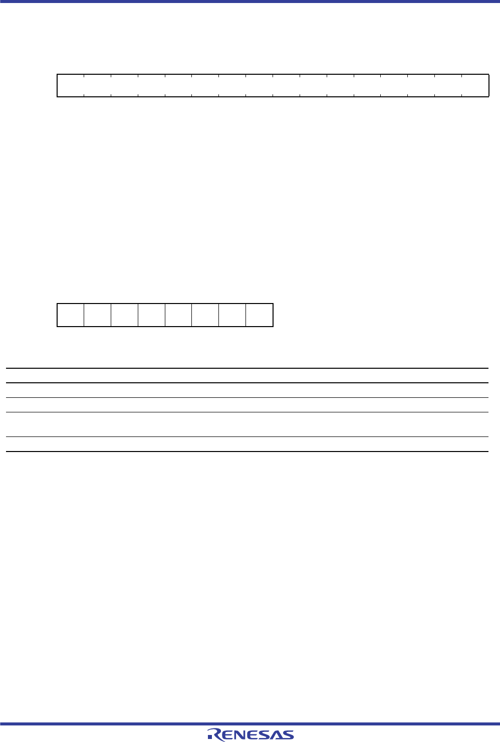
R01UH0034EJ0200 Rev.2.00 Page 311 of 1489
Dec 27, 2013
RX62T Group, RX62G Group 14. Data Transfer Controller (DTC)
Under development Preliminary document
Specifications in this document are tentative and subject to change.
14.2.6 DTC Transfer Count Register B (CRB)
CRB is used to set the block transfer count for block transfer mode.
The block transfer count is 1, 65535, and 65536 when the set value is 0001h, FFFFh, and 0000h, respectively. The CRB
value is decremented (-1) at each data transfer.
When normal transfer mode or repeat transfer mode is selected, set a value of FFFFh to the CRB.
CRB cannot be accessed directly from the CPU.
14.2.7 DTC Control Register (DTCCR)
DTCCR is used to specify the control of the DTC.
RRS Bit (DTC Transfer Data Read Skip Enable)
The DTC vector number is always compared with the vector number in the previous startup process.
When these vector numbers match and the RRS bit is set to 1, DTC data transfer is performed without reading the
transferred data. However, when the previous transfer was chain transfer, the transferred data is always read regardless of
the value of RRS bit.
Furthermore, when the transfer counter (CRA register) became 0 during the previous normal transfer and when the
transfer counter (CRB register) became 0 during the previous block transfer, the transferred data is always read
regardless of the value of RRS bit.
Address: (inaccessible directly from the CPU)
b15 b14 b13 b12 b11 b10 b9 b8 b7 b6 b5 b4 b3 b2 b1 b0
Value after reset: xxxxxxxxxxxxxxxx
x: Undefined
Address: 0008 2400h
b7 b6 b5 b4 b3 b2 b1 b0
———RRS————
Value after reset: 00001000
Bit Symbol Bit Name Description R/W
b2 to b0 — Reserved These bits are always read as 0. The write value should be 0. R/W
b3 — Reserved This bit is always read as 1. The write value should be 1. R/W
b4 RRS DTC Transfer Data Read Skip
Enable
0: Transfer data read is not skipped
1: Transfer data read is skipped when vector numbers match.
R/W
b7 to b5 — Reserved These bits are always read as 0. The write value should be 0. R/W
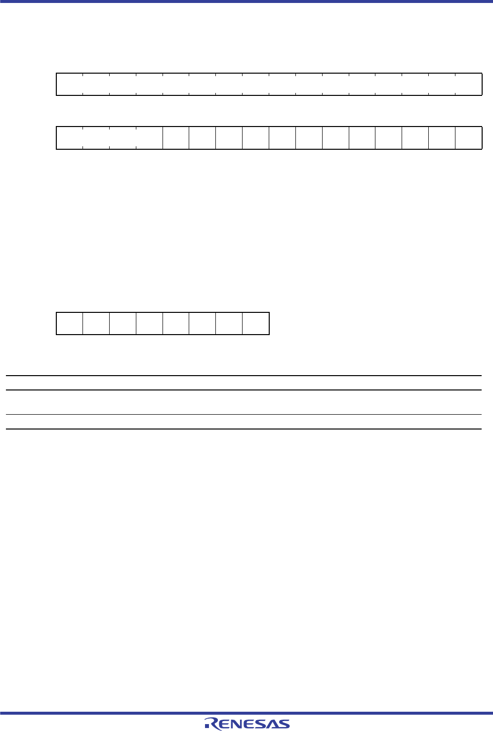
R01UH0034EJ0200 Rev.2.00 Page 312 of 1489
Dec 27, 2013
RX62T Group, RX62G Group 14. Data Transfer Controller (DTC)
Under development Preliminary document
Specifications in this document are tentative and subject to change.
14.2.8 DTC Vector Base Register (DTCVBR)
DTCVBR is used to set the base address for calculating the DTC vector table address.
The lower 12 bits (b11 to b0) are always 0 and cannot be modified.
The upper 4 bits (b31 to b28) are ignored, and the address of this register is extended by the value specified by b27.
14.2.9 DTC Address Mode Register (DTCADMOD)
DTCADMOD is used to select an address mode that specifies DTC's accessible area.
SHORT Bit (Short-Address Mode)
Full-address mode allows the DTC to access to a 4GB space (00000000h to FFFFFFFFh).
Short-address mode allows the DTC to access to a 16MB space (00000000h to 007FFFFFh and FF800000h to
FFFFFFFFh).
Address: 0008 2404h
b31 b30 b29 b28 b27 b26 b25 b24 b23 b22 b21 b20 b19 b18 b17 b16
Value after reset: 0000000000000000
b15 b14 b13 b12 b11 b10 b9 b8 b7 b6 b5 b4 b3 b2 b1 b0
000000000000
Value after reset: 0000000000000000
Address: 0008 2408h
b7 b6 b5 b4 b3 b2 b1 b0
———————SHORT
Value after reset: 00000000
Bit Symbol Bit Name Description R/W
b0 SHORT Short-Address Mode 0: Full-address mode
1: Short-address mode
R/W
b7 to b1 — Reserved These bits are always read as 0. The write value should be 0. R/W

R01UH0034EJ0200 Rev.2.00 Page 313 of 1489
Dec 27, 2013
RX62T Group, RX62G Group 14. Data Transfer Controller (DTC)
Under development Preliminary document
Specifications in this document are tentative and subject to change.
14.2.10 DTC Module Start Register (DTCST)
DTCST is used to start or stop the DTC module.
DTCST Bit (DTC Module Start)
Set the DTCST bit to 1 to enable the DTC to accept start requests. When this bit is cleared to 0, start requests are no
longer accepted.
If this bit is cleared to 0 during data transfer, the accepted start request is active until the processing is completed.
To enable transitions to the module-stop state, all-module clock stop mode, software-standby mode, or deep software-
standby mode, the DTCST bit must be set to "0".
For details on the facilities for transitions to the module-stop state, all-module clock stop mode, software-standby mode,
and deep software-standby mode, refer to section 14.8, Low-Power Consumption Function and section 9, Low
Power Consumption.
Address: 0008 240Ch
b7 b6 b5 b4 b3 b2 b1 b0
———————DTCST
Value after reset: 00000000
Bit Symbol Bit Name Description R/W
b0 DTCST DTC Module Start 0: DTC module stop
1: DTC module start
R/W
b7 to b1 — Reserved These bits are always read as 0. The write value should be 0. R/W

R01UH0034EJ0200 Rev.2.00 Page 314 of 1489
Dec 27, 2013
RX62T Group, RX62G Group 14. Data Transfer Controller (DTC)
Under development Preliminary document
Specifications in this document are tentative and subject to change.
14.2.11 DTC Status Register (DTCSTS)
The DTCSTS is used to indicate the state of DTC transfer operation.
VECN[7:0] Bits (DTC-Activating Vector Number Monitoring)
While transfer by the DTC is in progress, these bits indicate the vector number corresponding to the activating source for
the transfer.
When the DTCSTS register is read, the value read from the VECN[7:0] bits is valid if the value of the ACT flag was 1
(indicating DTC transfer in progress) and invalid if the value of the ACT flag was 0 (indicating no current DTC transfer).
See Table 14.3 for the correspondence between activating sources and vector numbers.
ACT Bit (DTC Active Flag)
This bit indicates the state of DTC transfer operation.
[Setting condition]
When the DTC is activated by a start request
[Clearing condition]
When transfer by the DTC is completed in response to a start request.
Address: 0008 240Eh
b15 b14 b13 b12 b11 b10 b9 b8 b7 b6 b5 b4 b3 b2 b1 b0
ACT——————— VECN[7:0]
Value after reset: 0000000000000000
Bit Symbol Bit Name Description R/W
b7 to b0 VECN[7:0] DTC-Activating Vector Number
Monitoring
These bits indicate the vector number for the activating source
when DTC transfer is in progress.
The value is only valid if DTC transfer is in progress (the value
of the ACT flag is 1).
R
b14 to b8 — Reserved These bits are always read as 0. The write value should be 0. R/W
b15 ACT DTC Active Flag 0: DTC transfer operation is not in progress.
1: DTC transfer operation is in progress.
R
R01UH0034EJ0200 Rev.2.00 Page 315 of 1489
Dec 27, 2013
RX62T Group, RX62G Group 14. Data Transfer Controller (DTC)
Under development Preliminary document
Specifications in this document are tentative and subject to change.
14.3 Sources of Activation
The DTC is activated by an interrupt request. Setting the DTCERn.DTCE bit (where n is the interrupt vector number of
the given interrupt) of the ICU to 1 selects the corresponding interrupt as an activation source for the DTC.
For the software activation (SWINT), see section 11, Interrupt Controller (ICU).
On completion of a single round of data transfer (or the last of the consecutive transfers in the case of a chained transfer),
follow the procedure below.
On completion of a specified round of data transfer, the DTCERn.DTCE bit is cleared to 0 and an interrupt is
requested to the CPU
On completion of other transfers, if the MRB.DISEL bit is 1, an interrupt is requested to the CPU. If the
MRB.DISEL bit is 0, the interrupt status flag (IRi.IR) of the activation source is cleared to 0.
14.3.1 Allocating Transfer Data and DTC Vector Table
The DTC reads the start address of transfer information data from the vector table for each activation source.
The vector table should be allocated so that the lower 12 bits of the base address (start address) are 0. The base address of
the DTC vector table should be set in the DTC vector base register (DTCVBR).
Transfer information data is allocated in the RAM area. The start address of transfer information data (n) of vector No. n
should be “vector table base address plus 4n”.
Transfer information data can be allocated with 3 longwords (short-address mode) or 4 longwords (full-address mode).
Use the SHORT bit in DTCADMOD to select short-address mode (SHORT bit = 1) or full-address mode (SHORT bit =
0).
Figure 14.2 shows the correspondence between the DTC vector table and transfer information data. Figure 14.3 shows
allocation of transfer information data in the RAM area. The lower address differs according to the endian mode of the
allocation area. For details, see Figure 14.16.
Figure 14.2 Correspondence between DTC Vector Table and Transfer Data
Transfer data (n)
start address
DTC Vector table
DTC vector base address
+4n
Transfer data (1)
4 bytes
Transfer data (2)
Transfer data (n)
:
:
:
Upper: DTCVBR
Lower: Vector number × 4
Transfer data (2)
start address
Transfer data (1)
start address
+4
4 bytes
:
:
:
R01UH0034EJ0200 Rev.2.00 Page 316 of 1489
Dec 27, 2013
RX62T Group, RX62G Group 14. Data Transfer Controller (DTC)
Under development Preliminary document
Specifications in this document are tentative and subject to change.
Figure 14.3 Allocation of Transfer Data in the RAM Area
Transfer data
per transfer
(4 longwords)
Transfer data for the
second transfer in
chain transfer mode
(4 longwords)
Transfer data for the
second transfer in
chain transfer mode
(3 longwords)
Start address 1(2) 0(3)
MRA SAR
MRB DAR
CRA CRB
MRA SAR
MRB DAR
CRA CRB
MRA MRB — Reserved
MRA MRB
SAR
DAR
CRA CRB
CRA CRB
SAR
DAR
3(0) 2(1)
Allocation of transfer data
in short-address mode
Chain
transfer
Transfer data
per transfer
(3 longwords)
Allocation of transfer data
in full-address mode
Start address
4 bytes
Chain
transfer
— Reserved
4 bytes
Lower address
( ): Lower address to be allocated
in the big-endian area
1(2) 0(3)3(0) 2(1)
Lower address
( ): Lower address to be allocated
in the big-endian area

R01UH0034EJ0200 Rev.2.00 Page 317 of 1489
Dec 27, 2013
RX62T Group, RX62G Group 14. Data Transfer Controller (DTC)
Under development Preliminary document
Specifications in this document are tentative and subject to change.
14.3.2 Activation Sources and Vector Address
Table 14.3shows the correspondence between DTC activation sources and vector addresses.
Table 14.3
Correspondence between Interrupt Sources, DTC Vector Addresses, and the
ICU.DTCERn
Register (1 / 2)
Actication Request
Generation Source Actication
Source Vector Number DTC Vector
Address Offset ICU.DTCERn Priority *
ICU SWINT 27 006Ch ICU.DTCER027 High
CMT0 CMI0 28 0070h ICU.DTCER028
CMT1 CMI1 29 0074h ICU.DTCER029
CMT2 CMI2 30 0078h ICU.DTCER030
CMT3 CMI3 31 007Ch ICU.DTCER031
RSPI0 SPRI0 45 00B4h ICU.DTCER045
SPTI0 46 00B8h ICU.DTCER046
External pin IRQ0 64 0100h ICU.DTCER064
IRQ1 65 0104h ICU.DTCER065
IRQ2 66 0108h ICU.DTCER066
IRQ3 67 010Ch ICU.DTCER067
IRQ4 68 0110h ICU.DTCER068
IRQ5 69 0114h ICU.DTCER069
IRQ6 70 0118h ICU.DTCER070
IRQ7 71 011Ch ICU.DTCER071
AD0 ADI0 98 0188h ICU.DTCER098
S12AD0 S12ADI0 102 0198h ICU.DTCER102
S12AD1 S12ADI1 103 019Ch ICU.DTCER103
Comparator CMPI 106 01A8h ICU.DTCER106
MTU0 TGIA0 114 01C8h ICU.DTCER114
TGIB0 115 01CCh ICU.DTCER115
TGIC0 116 01D0h ICU.DTCER116
TGID0 117 01D4h ICU.DTCER117
MTU1 TGIA1 121 01E4h ICU.DTCER121
TGIB1 122 01E8h ICU.DTCER122
MTU2 TGIA2 125 01F4h ICU.DTCER125
TGIB2 126 01F8h ICU.DTCER126
MTU3 TGIA3 129 0204h ICU.DTCER129
TGIB3 130 0208h ICU.DTCER130
TGIC3 131 020Ch ICU.DTCER131
TGID3 132 0210h ICU.DTCER132
MTU4 TGIA4 134 0218h ICU.DTCER134
TGIB4 135 021Ch ICU.DTCER135
TGIC4 136 0220h ICU.DTCER136
TGID4 137 0224h ICU.DTCER137
TCIV4 138 0228h ICU.DTCER138
MTU5 TGIU5 139 022Ch ICU.DTCER139
TGIV5 140 0230h ICU.DTCER140
TGIW5 141 0234h ICU.DTCER141 Low

R01UH0034EJ0200 Rev.2.00 Page 318 of 1489
Dec 27, 2013
RX62T Group, RX62G Group 14. Data Transfer Controller (DTC)
Under development Preliminary document
Specifications in this document are tentative and subject to change.
Note: • Once the DTC has accepted an activation request, it does not accept further activation requests until transfer for that single
request is completed, regardless of the priority order of the requests. However, if multiple activation requests are generated
while DTC transfer is in progress, the DTC accepts the request with the highest priority when the transfer ends. If multiple
activation requests are generated when the DTC module start register (DTCST) value is 0, the DTC accepts the request with the
highest priority when the DTC enters the activation-enabled state (by setting DTCST to 1).
MTU6 TGIA6 142 0238h ICU.DTCER142 High
TGIB6 143 023Ch ICU.DTCER143
TGIC6 144 0240h ICU.DTCER144
TGID6 145 0244h ICU.DTCER145
MTU7 TGIA7 149 0254h ICU.DTCER149
TGIB7 150 0258h ICU.DTCER150
TGIC7 151 025Ch ICU.DTCER151
TGID7 152 0260h ICU.DTCER152
TCIV7 153 0264h ICU.DTCER153
GPT0 GTCIA0 174 02B8h ICU.DTCER174
GTCIB0 175 02BCh ICU.DTCER175
GTCIC0 176 02C0h ICU.DTCER176
GTCIE0 177 02C4h ICU.DTCER177
GTCIV0 178 02C8h ICU.DTCER178
LOCO1 179 02CCh ICU.DTCER179
GPT1 GTCIA1 180 02D0h ICU.DTCER180
GTCIB1 181 02D4h ICU.DTCER181
GTCIC1 182 02D8h ICU.DTCER182
GTCIE1 183 02DCh ICU.DTCER183
GTCIV1 184 02E0h ICU.DTCER184
GPT2 GTCIA2 186 02E8h ICU.DTCER186
GTCIB2 187 02ECh ICU.DTCER187
GTCIC2 188 02F0h ICU.DTCER188
GTCIE2 189 02F4h ICU.DTCER189
GTCIV2 190 02F8h ICU.DTCER190
GPT3 GTCIA3 192 0300h ICU.DTCER192
GTCIB3 193 0304h ICU.DTCER193
GTCIC3 194 0308h ICU.DTCER194
GTCIE3 195 030Ch ICU.DTCER195
GTCIV3 196 0310h ICU.DTCER196
SCI0 RXI0 215 035Ch ICU.DTCER215
TXI0 216 0360h ICU.DTCER216
SCI1 RXI1 219 036Ch ICU.DTCER219
TXI1 220 0370h ICU.DTCER220
SCI2 RXI2 223 037Ch ICU.DTCER223
TXI2 224 0380h ICU.DTCER224
RIIC0 ICRXI0 247 03DCh ICU.DTCER247
ICTXI0 248 03E0h ICU.DTCER248 Low
Table 14.3
Correspondence between Interrupt Sources, DTC Vector Addresses, and the
ICU.DTCERn
Register (2 / 2)
Actication Request
Generation Source Actication
Source Vector Number DTC Vector
Address Offset ICU.DTCERn Priority *

R01UH0034EJ0200 Rev.2.00 Page 319 of 1489
Dec 27, 2013
RX62T Group, RX62G Group 14. Data Transfer Controller (DTC)
Under development Preliminary document
Specifications in this document are tentative and subject to change.
14.4 Operation
The DTC transfers data in accordance with the transfer data. Storage of the transfer data in the RAM area is required
before DTC operation.
When the DTC is activated, it reads the DTC vector corresponding to the vector number. Then the DTC reads transfer
data from the transfer data store address pointed by the DTC vector, transfers data, and then writes back the transfer data
after the data transfer. Storing transfer data in the RAM area allows data transfer of arbitrary number of channels.
There are three transfer modes: normal transfer mode, repeat transfer mode, and block transfer mode.
The DTC specifies a transfer source address in SAR and a transfer destination address in DAR. The values of these
registers are incremented, decremented, or remain unchanged independently after data transfer.
Table 14.4 lists transfer modes of the DTC.
Note 1. Set transfer source or transfer destination in the repeat area.
Note 2. Set transfer source or transfer destination in the block area.
Note 3. After data transfer of the specified count, the initial state is restored and the operation is continued (repeated).
Setting the CHNE bit in MRB to 1 allows multiple transfers (chain transfer) on a single startup source. Chain transfer is
enabled when transfer counter = 0 by setting the CHNS bit in MRB to 1.
Figure 14.4 shows the operation flowchart of the DTC.Table 14.5 shows chain transfer conditions (excluding
combinations of the second transfer and the third transfer, and combinations of subsequent transfers).
Table 14.4 Transfer Modes of the DTC
Transfer Mode Data Size Transferred on a Single
Activation Request Increment/Decrement of Memory
Address Settable Transfer
Count
Normal transfer mode One byte/word/longword Incremented/decremented by 1, 2, or 4 or
address fixed
1 to 65536
Repeat transfer mode*1 One byte/word/longword Incremented/decremented by 1, 2 or, 4 or
address fixed
1 to 256*3
Block transfer mode*2 Block size specified in CRAH
(1 to 255 bytes/words/longwords)
Incremented/decremented by 1, 2 or, 4 or
address fixed
1 to 65536

R01UH0034EJ0200 Rev.2.00 Page 320 of 1489
Dec 27, 2013
RX62T Group, RX62G Group 14. Data Transfer Controller (DTC)
Under development Preliminary document
Specifications in this document are tentative and subject to change.
Figure 14.4 Operation Flowchart of the DTC
START
Compare vector
numbers. Match?
Read DTC vector
Mismatch RRS bit = 0
Match and
RRS bit = 1
Read transfer
information data
Transfer data
Write transfer
information data
END
Transfer data
Write transfer
information data
Last data
Transferred? (transfer
counter = 1)*
NO
YES
DISEL=1
NO
YES
Clear interrupt
status flag
Update transfer
information data
start address
CHNE=1
NO
YES
CHNS=0
NO
YES
Last data
transferred? (transfer
counter = 1)*
NO
YES
Issue interrupt to
the CPU.
Transfer data
Write transfer
information data
Transfer data
Write transfer
information data
Next transfer
MD = 01b
(repeat transfer)
NO
YES
N = Interrupt vector number
Note: * Counter value before data transfer start
Clear ICU.DTCERn.
Issue interrupt to
the CPU.
Update transfer
information data Update transfer
information data Update transfer
information data Update transfer
information data

R01UH0034EJ0200 Rev.2.00 Page 321 of 1489
Dec 27, 2013
RX62T Group, RX62G Group 14. Data Transfer Controller (DTC)
Under development Preliminary document
Specifications in this document are tentative and subject to change.
Note 1. The registers to be used as transfer counters differ according to the transfer modes. Normal transfer mode: CRA, Repeat
transfer mode: CRAL, Block transfer mode: CRB
Note 2. On the last data transfer, the counter value changes from 1 to 0 in normal or block transfer mode and changes from 1 to CRAH
in repeat transfer mode. “1 → *” indicates both of these operations.
Note 3. Chain transfer can be selected for the second or subsequent transfers. The condition combination of “second transfer and CHNE
bit = 1” is omitted.
Table 14.5 Chain Transfer Conditions
First Transfer Second Transfer*3
DTC Transfer
CHNE
Bit CHNS
Bit DISEL
Bit Transfer
Counter*1*2 CHNE
Bit CHNS
Bit DISEL
Bit Transfer
Counter*1*2
0 — 0 Other than (1→0) — —— — — Ends after the first transfer
0—0(1→0) — — — — Ends after the first transfer with an
interrupt request to the CPU
0—1— ————
1 0 — — 0 — 0 Other than (1→0) Ends after the second transfer
0—0(1→0) Ends after the second transfer with
an interrupt request to the CPU
0—1—
110Other than (1→*) — — — — Ends after the first transfer
11—(1→*) 0 — 0 Other than (1→0) Ends after the second transfer
0—0(1→0) Ends after the second transfer with
an interrupt request to the CPU
0—1—
111Other than (1→*) — — — — Ends after the first transfer with an
interrupt request to the CPU

R01UH0034EJ0200 Rev.2.00 Page 322 of 1489
Dec 27, 2013
RX62T Group, RX62G Group 14. Data Transfer Controller (DTC)
Under development Preliminary document
Specifications in this document are tentative and subject to change.
14.4.1 Transfer Data Read Skip Function
Vector address read and transfer data read can be skipped by the setting of the RRS bit in DTCCR.
When a DTC activation request is generated, the current DTC vector number is always compared with the DTC vector
number in the previous startup process. When these vector numbers match and the RRS bit is set to 1, DTC data transfer
is performed without reading the vector address and transfer data. However, when the previous transfer was chain
transfer, the vector address and transfer data are always read. Furthermore, when the transfer counter (CRA register)
became 0 during the previous normal transfer and when the transfer counter (CRB register) became 0 during the previous
block transfer, transfer data is always read regardless of the value of RRS bit. Figure 14.13 shows an example of
transfer data read skip.
To update the DTC vector table and transfer data, set the RRS bit to 0, update the DTC vector table and transfer data, and
then set the RRS bit to 1. When the RRS bit is set to 0, the retained vector number is discarded and the DTC vector table
and transfer data that are updated in the following startup process are read.
14.4.2 Transfer Data Write-Back Skip Function
When the SM[1:0] bits in MRA or the DM[1:0] bits in MRB are set to "address fixed", a part of transfer data is not
written back. This function is performed independently of the setting of short-address mode or full-address mode. Table
14.6 lists transfer data write-back skip conditions and applicable registers.
The CRA and CRB registers are always written back independently of the setting of short-address mode or full-address
mode. Furthermore, in full-address mode, write-back of the MRA and MRB registers are always skipped.
Table 14.6 Transfer Data Write-Back Skip Conditions and Applicable Registers
SM[1:0] Bits in MRA DM[1:0] Bits in MRB SAR Register DAR Register
b3 b2 b3 b2
0000Skip Skip
0001
0100
0101
0 0 1 0 Skip Write-back
0011
0110
0111
1000Write-back Skip
1001
1100
1101
1 0 1 0 Write-back Write-back
1011
1110
1111
R01UH0034EJ0200 Rev.2.00 Page 323 of 1489
Dec 27, 2013
RX62T Group, RX62G Group 14. Data Transfer Controller (DTC)
Under development Preliminary document
Specifications in this document are tentative and subject to change.
14.4.3 Normal Transfer Mode
This mode allows 1-byte, 1-word, or 1-longword data transfer on a single startup source. The transfer count can be set to
1 to 65536.
Transfer source addresses and transfer destination addresses can be set to increment, decrement, or fixed independently.
This mode enables an interrupt request to the CPU to be generated at the end of specified-count transfer.
Table 14.7 lists register functions in normal transfer mode, and Figure 14.5 shows the memory map of normal transfer
mode.
Note 1. Write-back operation is skipped in address-fixed mode.
Figure 14.5 Memory Map of Normal Transfer Mode
Table 14.7 Register Functions in Normal Transfer Mode
Register Description Value Written Back by Writing Transfer Data
SAR Transfer source address Increment/decrement/fixed*1
DAR Transfer destination address Increment/decrement/fixed*1
CRA Transfer counter A CRA - 1
CRB Transfer counter B Not updated
SAR
Transfer source data area
DAR
Transfer
Transfer destination data area
Data 1
Data 2
Data 3
Data 4
Data 5
Data 6
Data 1
Data 2
Data 3
Data 4
Data 5
Data 6
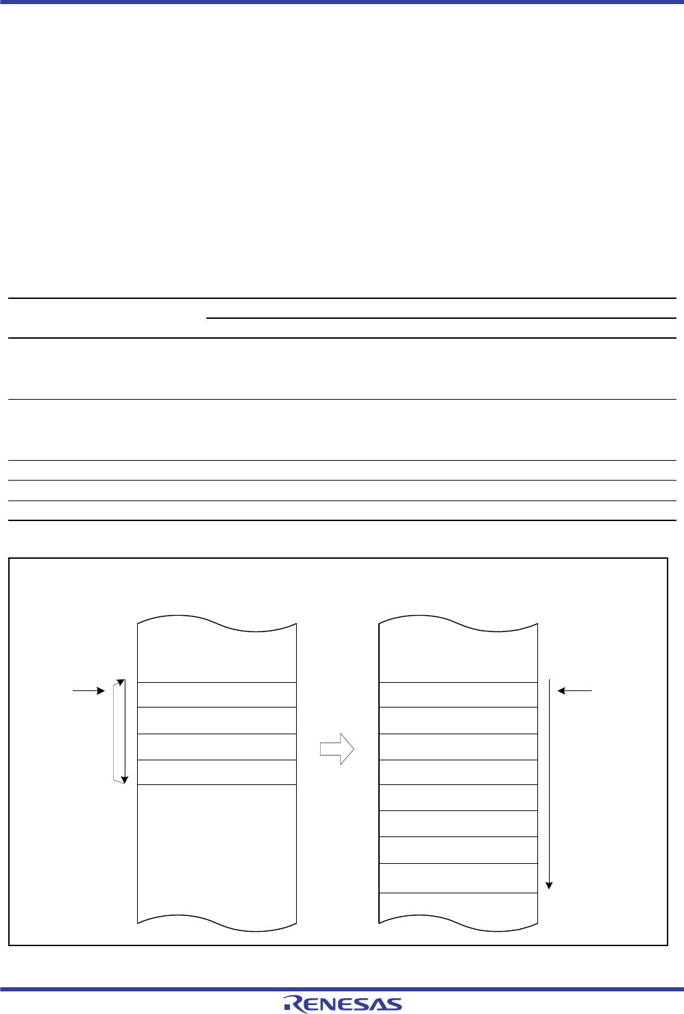
R01UH0034EJ0200 Rev.2.00 Page 324 of 1489
Dec 27, 2013
RX62T Group, RX62G Group 14. Data Transfer Controller (DTC)
Under development Preliminary document
Specifications in this document are tentative and subject to change.
14.4.4 Repeat Transfer Mode
This mode allows 1-byte, 1-word, or 1-longword data transfer on a single startup source.
Specify either transfer source or transfer destination for the repeat area by the DTS bit in MRB. The transfer count can be
set to 1 to 256. When the specified-count transfer is completed, the initial value of the address register specified in the
transfer counter and the repeat area is restored and transfer is repeated. The other address register is incremented or
decremented continuously or remains unchanged.
When the transfer counter CRAL is decreased to 00h in repeat transfer mode, the CRAL value is updated to the value set
in CRAH. Thus the transfer counter does not become 00h, which inhibits generation of interrupt request to the CPU
when the DISEL bit in MRB is set to 0 (an interrupt request to the CPU is generated when specified data transfer is
completed).
Table 14.8 lists the register functions in repeat transfer mode, and Figure 14.6 shows the memory map of repeat
transfer mode.
Note 1. Write-back is skipped in address-fixed mode.
Figure 14.6 Memory Map of Repeat Transfer Mode (Transfer Source: Repeat Area)
Table 14.8 Register Functions in Repeat Transfer Mode
Register Description
Value Written Back by Writing Transfer Data
When CRAL is not 1 When CRAL is 1
SAR Transfer source address Increment/decrement/fixed*1(When the DTS bit in MRB is 0)
Increment/decrement/fixed*1
(When the DTS bit in MRB is 1)
SAR register initial value
DAR Transfer destination
address
Increment/decrement/fixed*1(When the DTS bit in MRB is 0)
DAR register initial value
(When the DTS bit in MRB is 1)
Increment/decrement/fixed*1
CRAH Retains transfer counter CRAH CRAH
CRAL Transfer counter A CRAL - 1 CRAH
CRB Transfer counter B Not updated Not updated
SAR
Transfer source data area
(set to repeat area)
DAR
Transfer
Transfer destination data area
Data 1
Data 2
Data 3
Data 4
Data 1
Data 2
Data 3
Data 4
Data 1
Data 2
Data 3
Data 4
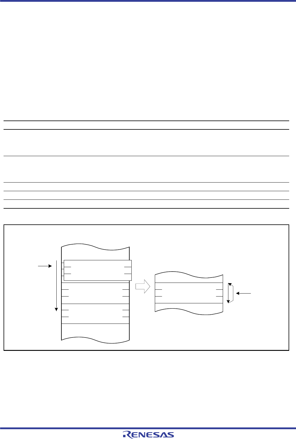
R01UH0034EJ0200 Rev.2.00 Page 325 of 1489
Dec 27, 2013
RX62T Group, RX62G Group 14. Data Transfer Controller (DTC)
Under development Preliminary document
Specifications in this document are tentative and subject to change.
14.4.5 Block Transfer Mode
This mode allows single-block data transfer on a single startup source.
Specify either transfer source or transfer destination for the block area by the DTS bit in MRB. The block size can be set
to 1 to 255 bytes (or 1 to 255 words or 1 to 255 longwords).
When transfer of the specified one block is completed, the initial values of the block size counter CRAL and the address
register (SAR when the DTS bit = 1 or DAR when the DTS bit = 0) specified in the block area are restored. The other
address register is incremented or decremented continuously or remains unchanged.
The block transfer count can be set to 1 to 65536. This mode enables an interrupt request to the CPU to be generated at
the end of specified-count block transfer.
Table 14.9 lists register functions in block transfer mode, and Figure 14.7 shows the memory map of block transfer
mode.
Note 1. Write-back is skipped in address-fixed mode.
Figure 14.7 Memory Map of Block Transfer Mode (Transfer Destination: Block Area)
Table 14.9 Register Functions in Block Transfer Mode
Register Description Value Written Back by Writing Transfer Data
SAR Transfer source address (When DTS bit in MRB is 0)
Increment/decrement/fixed*1
(When DTS bit in MRB is 1)
SAR register initial value
DAR Transfer destination address (When DTS bit in MRB is 0)
DAR register initial value
(When DTS bit in MRB is 1)
Increment/decrement/fixed*1
CRAH Retains block size CRAH
CRAL Block size counter CRAH
CRB Block transfer counter CRB - 1
Transfer source data area Transfer destination data area
(set to block area)
Block area DAR
SAR
:
:
:
Transfer
N-th block
First block
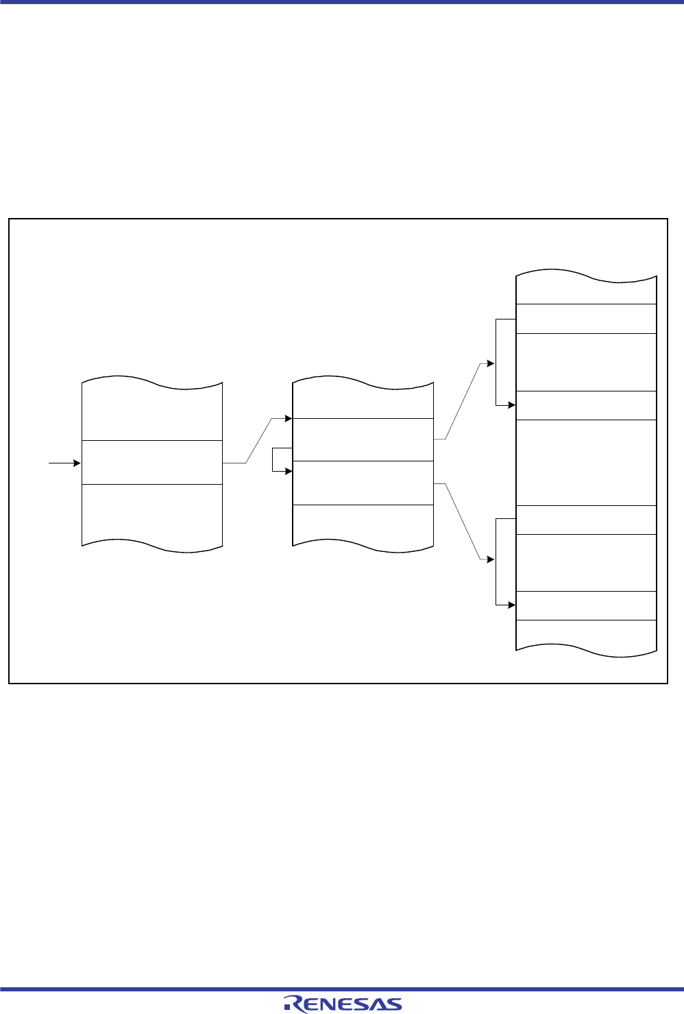
R01UH0034EJ0200 Rev.2.00 Page 326 of 1489
Dec 27, 2013
RX62T Group, RX62G Group 14. Data Transfer Controller (DTC)
Under development Preliminary document
Specifications in this document are tentative and subject to change.
14.4.6 Chain Transfer
Setting the MRB.CHNE bit to "1" enables chained transfer. In chained transfer, multiple unit transfer operations are
performed in response to a single request from an activation source.
When the MRB.CHNE bit is "1" and the MRB.CHNS bit is "0", an interrupt request is sent to the CPU on completion of
the specified number of unit transfer operations unless the MRB.DISEL bit is "1" (selecting generation of an interrupt for
the CPU after every round of data transfer), in which case an interrupt request for the CPU is not generated. Furthermore,
the interrupt status flag is not affected when an interrupt signal is being used as an activation source.
Settings for the SAR, DAR, CRA, CRB, MRA, and MRB registers can be individually made.
Figure 14.8 shows operations in chained transfer.
Figure 14.8 Chain Transfer Operation
When both the MRB.CHNE and MRB.CHNS bits are "1", chained transfer only proceeds on completion of the specified
number of rounds of data transfer (that is, when the transfer counter becomes "0"). Even if the transfer mode is repeat
transfer mode, chained transfer only proceeds on completion of the specified number of rounds of data transfer.
See Figure 14.5 for details of the conditions for chained transfer.
Transfer data
CHNE bit = 1
Transfer data allocated in
RAM area
Data area
Transfer source data (1)
Transfer data
start address
DTC Vector table
DTC vector
address
Transfer data
CHNE bit = 0
Transfer source data (1)
Transfer source data (2)
Transfer source data (2)
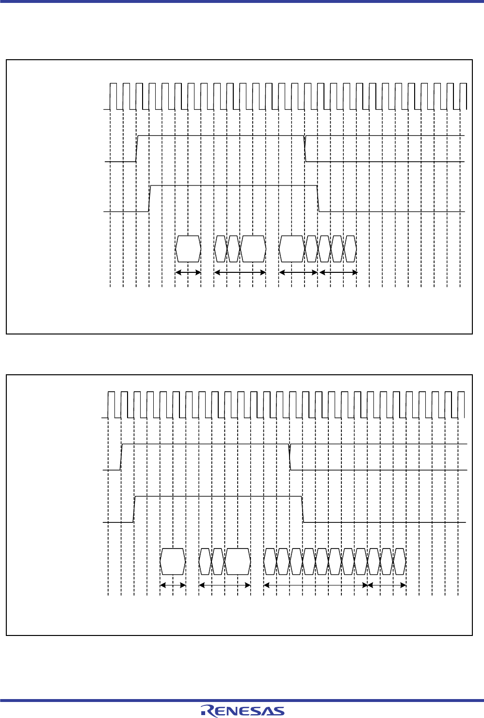
R01UH0034EJ0200 Rev.2.00 Page 327 of 1489
Dec 27, 2013
RX62T Group, RX62G Group 14. Data Transfer Controller (DTC)
Under development Preliminary document
Specifications in this document are tentative and subject to change.
14.4.7 Operation Timing
Figure 14.9 to Figure 14.12 show examples of DTC operation timing.
Figure 14.9 Example of DTC Operation Timing 1
(Short-Address Mode, Normal Transfer Mode, Repeat Transfer Mode)
Figure 14.10 Example of DTC Operation Timing 2
(Short-Address Mode, Block Transfer Mode, Block Size = 4)
System clock
DTC access
Vector read Transfer data
read
Data
transfer Transfer
data write
R W
ICU.IRi
DTC activation request
i = Interrupt vector number
System clock
DTC access
Vector read Transfer data
read
Data transfer Transfer data
write
ICU.IRi
DTC activation request
i = Interrupt vector number
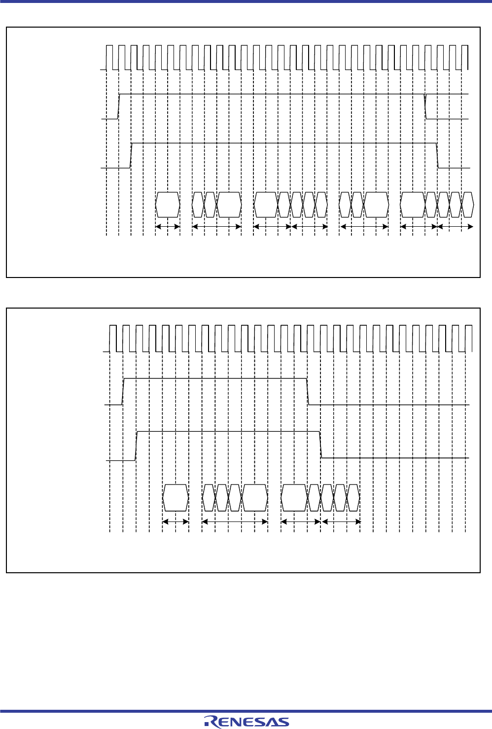
R01UH0034EJ0200 Rev.2.00 Page 328 of 1489
Dec 27, 2013
RX62T Group, RX62G Group 14. Data Transfer Controller (DTC)
Under development Preliminary document
Specifications in this document are tentative and subject to change.
Figure 14.11 Example of DTC Operation Timing 3 (Short-Address Mode, Chain Transfer)
Figure 14.12 Example of DTC Operation Timing 4
(Full-Address Mode, Normal Transfer Mode, Repeat Transfer Mode)
System clock
DTC access
Vector read Transfer data
read
Data
transfer Transfer
data write Transfer data
read Data
transfer
Transfer
data write
R W R W
ICU.IRi
DTC activation request
i = Interrupt vector number
System clock
DTC access
Vector read Transfer data
read Data
transfer Transfer
data write
R W
ICU.IRi
DTC activation request
i = Interrupt vector number
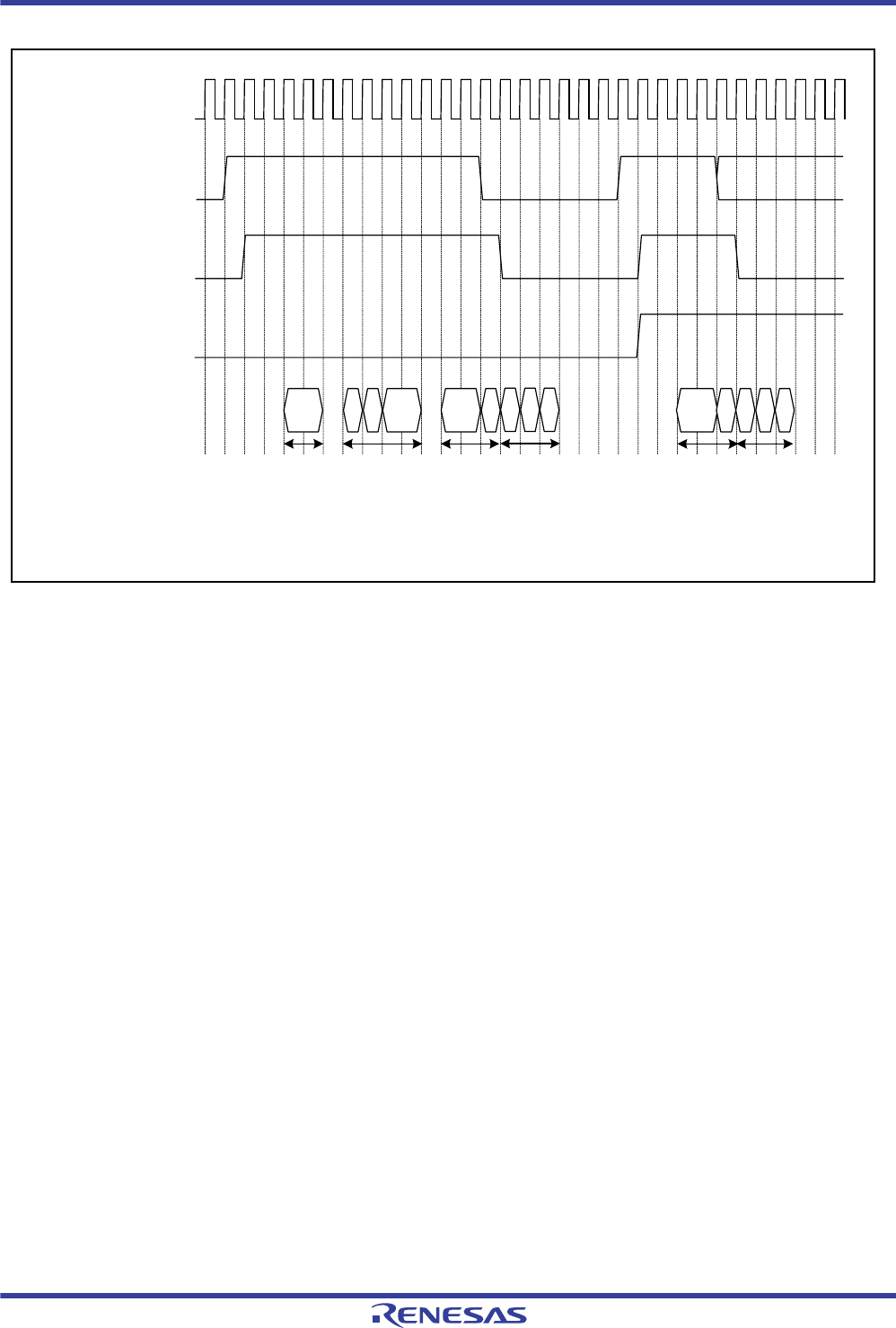
R01UH0034EJ0200 Rev.2.00 Page 329 of 1489
Dec 27, 2013
RX62T Group, RX62G Group 14. Data Transfer Controller (DTC)
Under development Preliminary document
Specifications in this document are tentative and subject to change.
Figure 14.13 Example of Transfer Data Read Skip
System clock
ICU.IRi
DTC activation request
DTC access
Vector read Transfer data
read
Data transfer Transfer
data write
Data transfer Transfer
data write
(2)
R
(1)
Note: When (1) and (2) have the same activation source (vector number) and the RRS bit is 1, transfer information read is
skipped for the request of (2).
R WR W
i = DTC vector number (interrupt vector number)
Read skip enable

R01UH0034EJ0200 Rev.2.00 Page 330 of 1489
Dec 27, 2013
RX62T Group, RX62G Group 14. Data Transfer Controller (DTC)
Under development Preliminary document
Specifications in this document are tentative and subject to change.
14.4.8 Execution Cycle of the DTC
Table 14.10 lists the execution cycle of single data transfer of the DTC.
P: Block size (set by CRAH and CRAL)
Cv: Access cycles for the vector information data storing destination
Ci: Access cycles for the transfer information data storing destination
Cr: Access cycles for the data read destination
Cw: Access cycles for the data write destination
Note 1. Transfer data skip
Note 2. Full-address mode
Note 3. Short-address mode
Note 4. When neither SAR nor DAR is set to address fixed mode
Note 5. When SAR or DAR is set to address fixed mode
Note 6. When SAR and DAR are set to address fixed mode
Note 7. These values apply when the block size is at least two. If the block size is one, the number of cycles is the same as for normal
transfer.
(The unit of vector read, transfer data read, “+1” of transfer data read, and “2” of internal operation is system clock
cycles (ICLK).)
(Cv, Ci, Cr, and Cw values depend on the access destination. For the number of cycles for the access destination, see
section 30, RAM, section 31, ROM (Flash Memory for Code Storage), and section 5, I/O Registers.
For execution timing in each transfer mode, see section 14.4.7, Operation Timing.
14.4.9 DTC Bus Mastership Release Timing
The DTC does not release the bus mastership during transfer data read and transfer data write. While transfer data is not
read or written, bus arbitration is made according to the priority determined by the bus master arbitrator.
Table 14.10 Execution Cycle of the DTC
Transfer
Mode Vector Read Transfer Data Read Transfer Data Write Data Read Data Write Internal
Operation
Normal Cv+1 0*1 4 × Ci + 1*2 3 × Ci + 1*3 0*1 3 × Ci*4 2 × Ci*5 Ci*6 Cr + 1 Cw 2 0*1
Repeat Cv+1 0*1 4 × Ci + 1*2 3 × Ci + 1*3 0*1 3 × Ci*4 2 × Ci*5 Ci*6 Cr + 1 Cw 2 0*1
Block*7Cv+1 0*1 4 × Ci + 1*2 3 × Ci + 1*3 0*1 3 × Ci*4 2 × Ci*5 Ci*6 P × Cr P × Cw 2 0*1
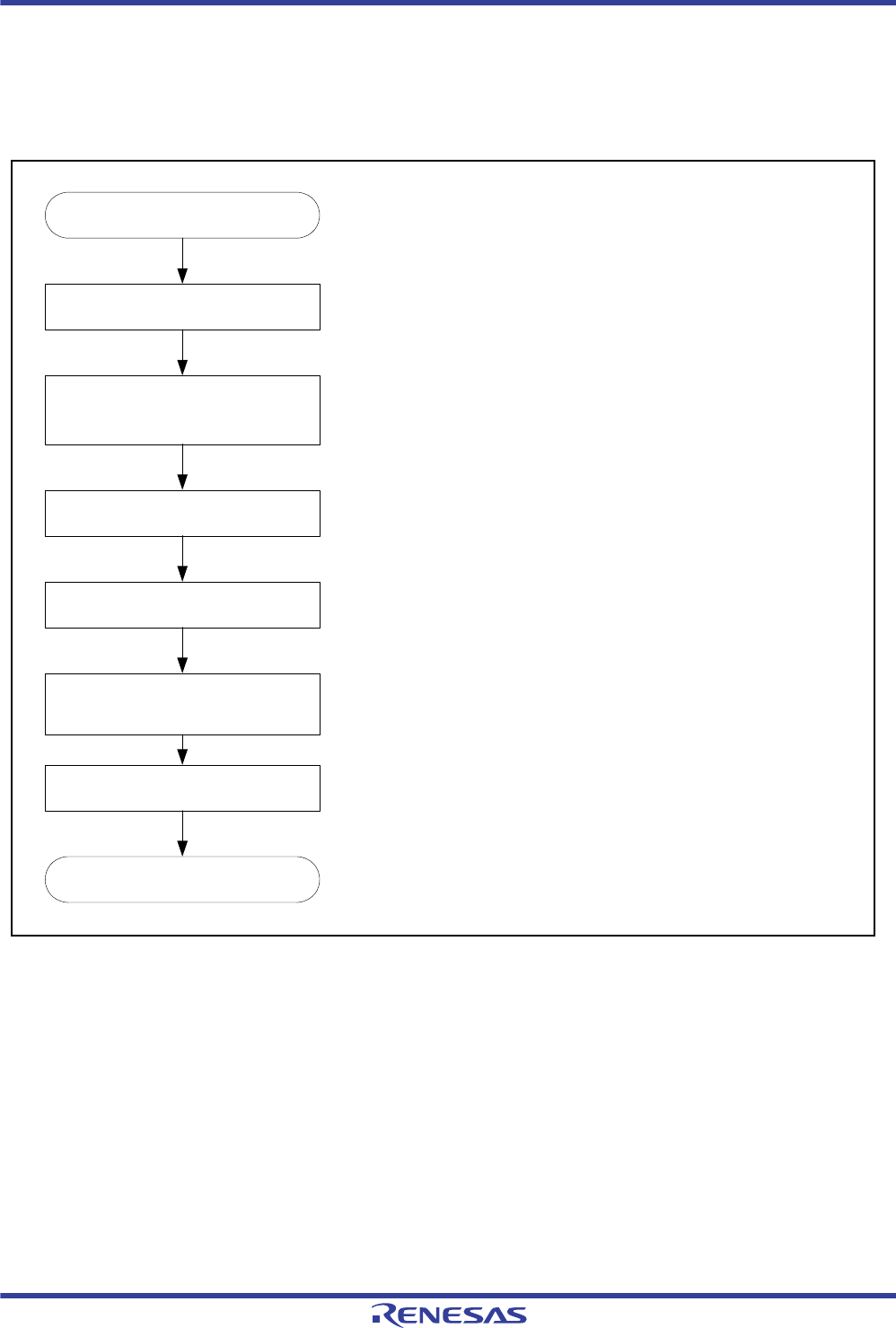
R01UH0034EJ0200 Rev.2.00 Page 331 of 1489
Dec 27, 2013
RX62T Group, RX62G Group 14. Data Transfer Controller (DTC)
Under development Preliminary document
Specifications in this document are tentative and subject to change.
14.5 DTC Setting Procedure
Before using the DTC, set the DTC vector base register (DTCVBR).
Follow the procedure shown in Figure 14.14 to set the DTC activation source.
Set the DTC module start bit (DTCST.DTCST) to 1.
Figure 14.14 Procedure to set the DTC activation source
START
Set the RRS bit in DTCCR to 0
End
Set transfer data
(MRA, MRB, SAR, DAR, CRA, and CRB)
Set transfer data start addresses in the
DTC vector table
Set the RRS bit in DTCCR to 1
Set the ICU.DTCERn.DTCE bit to 1.
Set the ICU.IERm.IENj bit to 1.
Set the interrupt source (to be a startup
source) enable bit to 1
[1]
[4]
[5]
Set the ICU.IERm.IENj bit corresponding to the activation source
interrupt to 0 and provide the following settings.
[1] Setting the RRS bit in DTCCR to 0 resets the transfer data
read skip flag. After that, transfer data read is not skipped
while the DTC is activated. When transfer data is updated, be
sure to make this setting.
[2] Allocate transfer data (MRA, MRB, SAR, DAR, CRA, and
CRB) in the RAM area. For setting transfer data, see section
14.2, Register Description. For how to allocate transfer data,
see section 14.3.1, Allocating Transfer Data and DTC Vector
Table.
[3] Set transfer data start addresses in the DTC vector table. For
how to set the DTC vector table, see section 14.3.1, Allocating
Transfer Data and DTC Vector Table.
[4] Setting the RRS bit in DTCCR to 1 can skip the second and
the subsequent transfer data read cycles for continuous DTC
activation due to the same interrupt source. The RRS bit can
always be set to 1, but this setting during DTC transfer
becomes valid from the next transfer.
[5] Set the ICU.DTCERn.DTCE and ICU.IERm.IENj bits that
correspond to the DTC activation interrupt to 1. For the
correspondence between interrupt sources and DTCERn
register, see table 14.3.
[6] Set the interrupt source enable bit to be a startup source.
When a source interrupt is generated, the DTC is activated.
For the setting of the interrupt source enable bit, refer to the
setting of the module that is to be a startup source.
Note: In addition to the setting of each source described above, set
the DTC module start bit (DTCST.DTCST) to 1 for all the DTC
sources.
[6]
[2]
[3]

R01UH0034EJ0200 Rev.2.00 Page 332 of 1489
Dec 27, 2013
RX62T Group, RX62G Group 14. Data Transfer Controller (DTC)
Under development Preliminary document
Specifications in this document are tentative and subject to change.
14.6 Examples of DTC Usage
14.6.1 Normal Transfer
As an example of DTC usage, its employment in the transfer of 128 bytes of data by an SCI is described below.
(1) Transfer Data Set
In the MRA register, make the settings to select a fixed source address (MRA.SM[1:0] = 00b), incrementation of the
destination address (MRA.DM[1:0] = 10b), transfer in normal mode (MRA.MD[1:0] = 00b), and byte-sized transfer
(MRA.SZ[1:0] = 00b). The MRB.DTS bit can be set to any value. For other bits of the MRB register, make the setting
for one interrupt to initiate one round of transfer (MRB.CHNE = "0" and MRB.DISEL = "0"). Set the SAR to the address
of the RDR for the given SCIn (n = 0 to 2), the DAR to the first address of the area in RAM where data are to be stored,
and the CRA register to 128 (0080h). The CRB register can be set to any value. Set a value of FFFFh to the CRB.
(2) DTC Vector Table
The address where the transfer-control information for use with the RXI starts is set in the vector table for the DTC.
(3) ICU Set and DTC Module Activation
Set the corresponding ICU.DTCERn.DTCE bit to "1" and the ICU.IERm.IENj bit to "1".
Set the DTCST.DTCST bit to "1".
(4) SCI Set
Enable reception-completed interrupts by setting the SCR.RIE bit in the given SCIn to "1". Also, so that further reception
does not proceed if a reception error occurs while reception by the SCI is in progress, make the CPU able to accept
reception-error interrupts.
(5) DTC Transfer
Every time the reception of one byte by the SCI is completed, an RXI interrupt is generated to activate the DTC. The
DTC transfers the received byte from the RDR of the SCI to RAM, after which the DAR register is incremented and the
CRA register is decremented.
(6) Interrupt Handling
After 128 rounds of data transfer have been completed and the value in the CRA register becomes "0", an RXI interrupt
request is generated for the CPU. Processing for completion is performed in the processing routine for this interrupt.
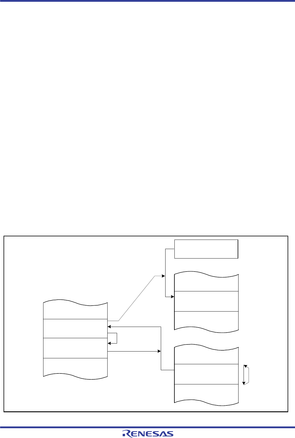
R01UH0034EJ0200 Rev.2.00 Page 333 of 1489
Dec 27, 2013
RX62T Group, RX62G Group 14. Data Transfer Controller (DTC)
Under development Preliminary document
Specifications in this document are tentative and subject to change.
14.6.2 Chain Transfer when Counter = 0
The second data transfer is performed only when the counter = 0. Repeat transfer of a transfer count of 256 or more is
enabled by the re-setting for the first data transfer.
The following shows an example of configuring a 128-kbyte input buffer, where the input buffer is set so that its lower
address starts with 0000h. Figure 14.15 shows a chain transfer when the counter = 0.
1. Set normal transfer mode for input data for the first data transfer. Set the following:
Transfer source address: Fixed, CRA = 0000h (65,536 times), CHNE bit = 1 (chain transfer enabled) in MRB,
CHNS bit = 1 (chain transfer is performed only when the transfer counter is 0) in MRB, and DISEL bit = 0 (an
interrupt request to the CPU is generated when specified data transfer is completed) in MRB.
2. Prepare the upper 8-bit address of the start address at every 65,536 times of the transfer destination address for the
first data transfer in another area (such as ROM). For example, when setting the input buffer to 200000h to
21FFFFh, prepare 21h and 20h.
3. For the second data transfer, set repeat transfer mode (source side: repeat area) for re-setting the transfer destination
address of the first data transfer. Specify the upper 8 bits of DAR in the first transfer data area for the transfer
destination. At this time, set CHNE bit = 0 (chain transfer disabled) in MRB and DISEL bit = 0 (an interrupt request
to the CPU is generated when specified data transfer is completed) in MRB. When setting the input buffer
mentioned above to 200000h to 21FFFFh, set the transfer counter to 2.
4. The first data transfer is performed by an interrupt 65,536 times. When the transfer counter of the first data transfer
becomes 0, the second data transfer starts. Set the upper 8 bits of the transfer source address of the first data transfer
to 21h. The transfer counter (lower 16 bits) of the transfer destination address of the first data transfer is 0000h.
5. In succession, the first data transfer is performed by an interrupt 65,536 times specified for the first data transfer.
When the transfer counter of the first data transfer becomes 0, the second data transfer starts. Set the upper 8 bits of
the transfer source address of the first data transfer to 20h. The transfer counter (lower 16 bits) of the transfer
destination address of the first data transfer is 0000h.
6. Steps 4 and 5 above are repeated infinitely. Since the second data transfer is in repeat transfer mode, no interrupt
request to the CPU is generated
Figure 14.15 Chain Transfer when Counter = 0
Transfer data allocated in
the on-chip memory space
Chain transfer
(counter = 0)
Input circuit
Input buffer
First data transfer
Transfer data
Second data transfer
Transfer data
Upper 8 bits of DAR

R01UH0034EJ0200 Rev.2.00 Page 334 of 1489
Dec 27, 2013
RX62T Group, RX62G Group 14. Data Transfer Controller (DTC)
Under development Preliminary document
Specifications in this document are tentative and subject to change.
14.7 Interrupt Source
When the DTC has finished data transfer of specified count or when data transfer with the DISEL bit in MRB set to 1 (an
interrupt request to the CPU is generated each time DTC data transfer is performed) has been completed, an interrupt to
the CPU is generated by the DTC activation source. Such interrupts to the CPU are controlled according to the PSW.I bit
(interrupt enable) and the PSW.IPL[3:0] bits (processor interrupt priority level) of the CPU, and the priority level of the
interrupt controller.
14.8 Low-Power Consumption Function
To place the DTC in the module-stop state, all-module clock stop mode, software-standby mode, or deep software-
standby mode, clear the DTCST.DTCST bit to 0 (DTC module stopped), and then perform the following processing.
(1) Module Stop Function
Writing 1 to the MSTPCRA.MSTPA28 bit (transition to the DTC module-stop state) enables the module-stop function of
the DTC. If DTC transfer is in progress at the time a 1 is written to the MSTPA28 bit, the transition to the module-stop
state proceeds after DTC transfer has ended. Writing 0 to the MSTPA28 bit releases the DTC from the module-stop state.
(2) All-Module Clock Stop Mode
Writing 1 to the MSTPCRA.ACSE bit (all-module clock stop mode enabled), writing 1 to all the bits in MSTPCRA and
MSTPCRB, including the MSTPA28 bit (transition to the DTC module-stop state), and executing a WAIT instruction
causes a transition to the all-module clock stop mode. If DTC transfer is in progress at the time the WAIT instruction is
executed, the DTC can enter all-module clock stop mode after completion of the current DTC transfer.
After the DTC returns from all-module clock stop mode, writing 0 to the MSTPA28 bit releases the DTC from the
module-stop state.
(3) Software Standby and Deep Software Standby Modes
Writing 1 to the SBYCR.SSBY bit (transition to software standby mode after WAIT instruction execution) and 0 to the
DPSBYCR.DPSBY bit (transition to software standby mode after WAIT instruction execution), executing a WAIT
instruction places the DTC in software standby mode.
If DTC transfer is in progress at the time the WAIT instruction is executed, the DTC enters software standby mode after
completion of the current DTC transfer.
The DTC enters deep software standby mode when the DPSBYCR.DPSBY bit is set to 1 (transition to deep software
standby mode after WAIT instruction execution) and then a WAIT instruction is executed.
(4) Notes on Low-Power Consumption Function
For the timing of WAIT instruction execution and register settings, see section 9.6.7, Timing of Wait Instructions.
To perform DTC transfer after returning from low-power consumption mode, set the DTCST.DTCST bit to 1 again.
R01UH0034EJ0200 Rev.2.00 Page 335 of 1489
Dec 27, 2013
RX62T Group, RX62G Group 14. Data Transfer Controller (DTC)
Under development Preliminary document
Specifications in this document are tentative and subject to change.
14.9 Usage Notes
14.9.1 Transfer Information Data Start Address
Be sure to set multiples of 4 for the transfer information data start addresses in the DTC vector table. Otherwise, such
addresses are accessed with their lowest 2 bits regarded as 00b.
14.9.2 Allocating Transfer Data
Allocate transfer data in the memory area according to the endian of the area as shown in Figure 14.16.
For example, when writing CRA and CRB setting data with 16 bits in big endian, write the CRA setting data to lower
address 0 and the CRB setting data to lower address 2. In little endian, write the CRB setting data to lower address 0 and
the CRA setting data to lower address 2. When writing CRA and CRB setting data with 32 bits, place the CRA setting
data at the MSB side and the CRB setting data at the LSB side regardless of endian, and then write the data to lower
address 0.
Figure 14.16 Allocation of Transfer Data
10
MRA SAR
MRB DAR
CRA CRB
32
Allocation of transfer data to
little-endian area
(Short-address mode)
4 bytes
Lower address
23
MRA SAR
MRB DAR
CRA CRB
01
Allocation of transfer data to
big-endian area
(Short-address mode)
4 bytes
Lower address
Address
4n
4(n+1)
4(n+2)
10
MRA
SAR
MRB
DAR
CRA CRB
32
Allocation of transfer data to
little-endian area
(Full-address mode)
4 bytes
Lower address
Address
4n
4(n+1)
4(n+2)
4(n+3)
23
MRA
SAR
MRB
DAR
CRA CRB
01
Allocation of transfer data to
big-endian area
(Full-address mode)
4 bytes
Lower address
Reserved (0) Reserved (0)
Address
4n
4(n+1)
4(n+2)
Address
4n
4(n+1)
4(n+2)
4(n+3)

R01UH0034EJ0200 Rev.2.00 Page 336 of 1489
Dec 27, 2013
RX62T Group, RX62G Group 14. Data Transfer Controller (DTC)
Under development Preliminary document
Specifications in this document are tentative and subject to change.
14.9.3 Setting the DTC Activation Enable Register (ICU.DTCERn) of the Interrupt
Controller
While the DTCST.DTCST bit is 0 (DTC module stop), set the interrupt destination setting register n (ISELRn) of the
ICU. For details on the ICU.DTCERn registers, refer to section 11, Interrupt Controller (ICU).
14.9.4 Selecting Communication Function Interrupt as DTC Activation Source
In the RX62T and RX62G Groups, caution should be used when the communication function (SCI, RIIC, RSPI) is used
in combination with the DTC function. For details, section 11.7, Usage Notes.

R01UH0034EJ0200 Rev.2.00 Page 337 of 1489
Dec 27, 2013
RX62T Group, RX62G Group 15. I/O Ports
Under development Preliminary document
Specifications in this document are tentative and subject to change.
15. I/O Ports
The I/O ports of the RX62T and RX62G Groups function as a programmable I/O port, an I/O pin of a peripheral module,
an input pin for an interrupt, or a bus control pin.
Each pin is also configurable as an I/O pin of a peripheral module or an input pin for an interrupt. All pins function as
input pins immediately after a reset, and pin functions are switched by register settings. The setting of each pin is
specified by the registers for the corresponding I/O port and peripheral modules.
Each port has data direction registers (DDR) that control input and output, data registers (DR) that store data for output,
port registers (PORT) for reading the pin states, and input buffer control registers (ICR) that enable or disable the input
buffer.
As the configuration of the I/O ports differs with the package, the I/O ports for the respective packages are described
separately in this section.
For the 112-pin LQFP version, see section I/O Ports [for 112-Pin LQFP], I/O Ports [for 112-Pin LQFP].
For the 100-pin LQFP versions, see section I/O Port [for 100-Pin LQFP], I/O Port [for 100-Pin LQFP].
For the 80-pin LQFP version, see section I/O Port [for 80-Pin LQFP].
For the 64-pin LQFP version, see section I/O Port [for 64-Pin LQFP].
15.1 I/O Ports [for 112-Pin LQFP]
The RX62T and RX62G Groups (112-Pin LQFP) have 14 I/O ports (ports 1 to 9 and A, B, D, E, G), which handle 61 I/O
pins.
15.1.1 Overview
Table 15.1 gives the specifications of the I/O ports and Table 15.2 lists I/O ports and pin functions.
Table 15.1 Specifications of I/O Ports (112-Pin LQFP)
Item Description
I/O pins 61
Input pins 21
Number of ports 14 (1 to 9 and A, B, D, E, and G)
Open drain outputs 2 (RIIC pin)
Large-current output 12 (MTU3 pin and GPT pin)
Schmitt trigger input pins All port inputs, CAN inputs, IRQ inputs, MTU3 inputs, POE3 inputs, RIIC inputs, SCI inputs, A/D
trigger inputs, NMI inputs, GPT inputs, and LIN inputs
Others Each pin is capable of driving a capacitive load of 30 pF in the case of a TTL load.
When configured as an output, a pin is capable of driving a Darlington transistor.
A pin is always capable of reading the status of the pins.

R01UH0034EJ0200 Rev.2.00 Page 338 of 1489
Dec 27, 2013
RX62T Group, RX62G Group 15. I/O Ports
Under development Preliminary document
Specifications in this document are tentative and subject to change.
Table 15.2 Port Functions (112-Pin LQFP) (1 / 4)
Port Description Bit
Function
CMOS
Input
Schmitt
Trigger
Input
Open
Drain
Output
Capability
Large-
Current
OutputI/O Input Output
Port 1 General I/O port pins,
MTU3 Inputs, and
interrupt inputs
0P10 MTCLKD-B/
IRQ0-A
— All input
functions
——
1P11 MTCLKC-B/
IRQ1-A
All input
functions
Port 2 General I/O port pins,
MTU3 inputs,
interrupt inputs,
A/D converter inputs,
RSPI I/O signal,
LIN I/O signal, and
CAN I/O signals
0P20 MTCLKB-B/
IRQ7/
ADTRG0#-B
— All input
functions
——
1P21 MTCLKA-B/
IRQ6/
ADTRG1#-B
All input
functions
2 P22/MISO-A LRX/CRX-B/
ADTRG#
MISO-A P22/LRX/
CRX-B/
ADTRG#
3 P23/MOSI-A LTX/
CTX-B
MOSI-A P23
4 P24/RSPCK-A RSPCK-A P24
Port 3 General I/O port pins,
MTU3 I/O signal, and
RSPI I/O signal
0 P30/
MTIOC0B-B/
SSL0-A
MTCLKD-A SSL0-A P30/
MTIOC0B-B/
MTCLKD-A
——
1 P31/
MTIOC0A-B
MTCLKC-A SSL1-A — All input
functions
2 P32/MTIOC3C MTCLKB-A SSL2-A All input
functions
3 P33/MTIOC3A MTCLKA-A SSL3-A All input
functions
Port 4 A/D converter inputs
and general input port
pins
0 P40/AN000 — P40 — —
1 P41/AN001 P41
2 P42/AN002 P42
3 P43/AN003/
CVREFL
P43
4 P44/AN100 P44
5 P45/AN101 P45
6 P46/AN102 P46
7 P47/AN103/
CVREFH
P47
Port 5 A/D converter inputs
and general input port
pins
0P50/AN6—P50——
1P51/AN7 P51
2P52/AN8 P52
3P53/AN9 P53
4P54/AN10 P54
5P55/AN11 P55
Port 6 A/D converter inputs
and general input port
pins
0P60/AN0—P60——
1P61/AN1 P61
2P62/AN2 P62
3P63/AN3 P63
4P64/AN4 P64
5P65/AN5 P65

R01UH0034EJ0200 Rev.2.00 Page 339 of 1489
Dec 27, 2013
RX62T Group, RX62G Group 15. I/O Ports
Under development Preliminary document
Specifications in this document are tentative and subject to change.
Port 7 General I/O port pins,
POE3 Inputs,
interrupt inputs,
MTU3 I/O signal, and
GPT I/O signal
0 P70 POE0#/IRQ5 — All input
functions
——
1 P71/
MTIOC3B/
GTIOC0A-A
All input
functions
√
2 P72/
MTIOC4A/
GTIOC1A-A
All input
functions
√
3 P73/
MTIOC4B/
GTIOC2A-A
All input
functions
√
4 P74/
MTIOC3D/
GTIOC0B-A
All input
functions
√
5 P75/
MTIOC4C/
GTIOC1B-A
All input
functions
√
6 P76/
MTIOC4D/
GTIOC2B-A
All input
functions
√
Port 8 General I/O port pins,
SCI I/O signal and
MTU3 inputs
0 P80 RXD2-B/
MTIC5W
— All input
functions
——
1 P81 MTIC5V TXD2-B All input
functions
2 P82/SCK2-B MTIC5U All input
functions
Port 9 General I/O port pins,
MTU3 I/O signal,
POE3 inputs, and
interrupt inputs
0 P90/MTIOC7D — All input
functions
—√
1 P91/MTIOC7C All input
functions
√
2 P92/MTIOC6D All input
functions
√
3 P93/MTIOC7B All input
functions
√
4 P94/MTIOC7A All input
functions
√
5 P95/MTIOC6B All input
functions
√
6 P96 POE4#/IRQ4 All input
functions
—
Table 15.2 Port Functions (112-Pin LQFP) (2 / 4)
Port Description Bit
Function
CMOS
Input
Schmitt
Trigger
Input
Open
Drain
Output
Capability
Large-
Current
OutputI/O Input Output

R01UH0034EJ0200 Rev.2.00 Page 340 of 1489
Dec 27, 2013
RX62T Group, RX62G Group 15. I/O Ports
Under development Preliminary document
Specifications in this document are tentative and subject to change.
Port A General I/O port pins,
MTU3 I/O signal,
RSPI I/O signal, and
A/D converter inputs
0PA0/
MTIOC6C
SSL3-B — All input
functions
——
1 PA1/MTIOC6A SSL2-B All input
functions
2 PA2/MTIOC2B SSL1-B All input
functions
3PA3/
MTIOC2A/
SSL0-B
SSL0-B PA3/
MTIOC2A
4PA4/
MTIOC1B/
RSPCK-B
ADTRG0#-A RSPCK-B PA4/
MTIOC1B/
ADTRG0#-A
5PA5/
MTIOC1A/
MISO-B
ADTRG1#-A MISO-B PA5/
MTIOC1A/
ADTRG1#-A
Port B General I/O port pins,
MTU3 I/O signal,
RSPI I/O signal,
RIIC I/O signal,
SCI I/O signal,
GPT inputs,
POE3 inputs,
interrupt inputs, and
CAN I/O signal
0PB0/
MTIOC0D/
MOSI-B
MOSI-B PB0/
MTIOC0D
——
1PB1/
MTIOC0C/
SCL
RXD0 — All input
functions
√
(SCL only)
—
2PB2/
MTIOC0B-A/
SDA
TXD0 All input
functions
√
(SDA only)
—
3PB3/
MTIOC0A-A/
SCK0
All input
functions
——
4PB4 GTETRG/
POE8#/IRQ3
All input
functions
5PB5 TXD2-A/
CTX-A/
All input
functions
6 PB6 RXD2-A/
CRX-A
All input
functions
7 PB7/SCK2-A All input
functions
Table 15.2 Port Functions (112-Pin LQFP) (3 / 4)
Port Description Bit
Function
CMOS
Input
Schmitt
Trigger
Input
Open
Drain
Output
Capability
Large-
Current
OutputI/O Input Output

R01UH0034EJ0200 Rev.2.00 Page 341 of 1489
Dec 27, 2013
RX62T Group, RX62G Group 15. I/O Ports
Under development Preliminary document
Specifications in this document are tentative and subject to change.
Port D General I/O port pins,
GPT I/O signal,
RSPI I/O signal,
SCI I/O signal, and
CAN outputs
0PD0/
GTIOC3B/
RSPCK-C
RSPCK-C PD0/
GTIOC3B
——
1PD1/
GTIOC3A/
MISO-C
MISO-C PD1/
GTIOC3A
2PD2/
GTIOC2B-B/
MOSI-C
MOSI-C PD2/
GTIOC2B-B
3PD3/
GTIOC2A-B
TXD1 — All input
functions
4PD4/
GTIOC1B-B/
SCK1
All input
functions
5PD5/
GTIOC1A-B
RXD1 — All input
functions
6PD6/
GTIOC0B-B/
SSL0-C
SSL0-C PD6/
GTIOC0B-B
7PD7/
GTIOC0A-B
SSL1-C/
CTX-C
— All input
functions
Port E General I/O port pins,
CAN inputs,
RSPI outputs,
POE3 inputs,
MTU3 inputs, and
interrupt inputs
0 PE0 CRX-C SSL2-C — All input
functions
——
1 PE1 SSL3-C All input
functions
2PE2/
POE10#-A/
NMI
All input
functions
3 PE3 MTCLKD-C/
POE11#/
IRQ2-A
All input
functions
4 PE4 MTCLKC-C/
POE10#-B/
IRQ1-B
All input
functions
5 PE5 IRQ0-B All input
functions
Port G General I/O port pins,
interrupt inputs, and
trace outputs
0 PG0 IRQ0-C TRSYNC — All input
functions
——
1PG1 IRQ1-C TRDATA
0
All input
functions
2PG2 IRQ2-B TRDATA
1
All input
functions
3PG3 TRDATA
2
All input
functions
4PG4 TRDATA
3
All input
functions
5 PG5 TRCLK All input
functions
Table 15.2 Port Functions (112-Pin LQFP) (4 / 4)
Port Description Bit
Function
CMOS
Input
Schmitt
Trigger
Input
Open
Drain
Output
Capability
Large-
Current
OutputI/O Input Output

R01UH0034EJ0200 Rev.2.00 Page 342 of 1489
Dec 27, 2013
RX62T Group, RX62G Group 15. I/O Ports
Under development Preliminary document
Specifications in this document are tentative and subject to change.
15.1.2 Register Descriptions
Table 15.3 lists registers of I/O ports, and Table 15.4 lists valid bits in each register.
Table 15.3 Registers of I/O Ports (112-Pin LQFP) (1 / 2)
Port Symbol Register Name Register Symbol Value after Reset Address Access Size
PORT1 Data direction register DDR 00h 0008 C001h 8
Data register DR 00h 0008 C021h 8
Port register PORT Undefined 0008 C041h 8
Input buffer control register ICR 00h 0008 C061h 8
PORT2 Data direction register DDR 00h 0008 C002h 8
Data register DR 00h 0008 C022h 8
Port register PORT Undefined 0008 C042h 8
Input buffer control register ICR 00h 0008 C062h 8
PORT3 Data direction register DDR 00h 0008 C003h 8
Data register DR 00h 0008 C023h 8
Port register PORT Undefined 0008 C043h 8
Input buffer control register ICR 00h 0008 C063h 8
PORT4 Port register PORT Undefined 0008 C044h 8
Input buffer control register ICR 00h 0008 C064h 8
PORT5 Port register PORT Undefined 0008 C045h 8
Input buffer control register ICR 00h 0008 C065h 8
PORT6 Port register PORT Undefined 0008 C046h 8
Input buffer control register ICR 00h 0008 C066h 8
PORT7 Data direction register DDR 00h 0008 C007h 8
Data register DR 00h 0008 C027h 8
Port register PORT Undefined 0008 C047h 8
Input buffer control register ICR 00h 0008 C067h 8
PORT8 Data direction register DDR 00h 0008 C008h 8
Data register DR 00h 0008 C028h 8
Port register PORT Undefined 0008 C048h 8
Input buffer control register ICR 00h 0008 C068h 8
PORT9 Data direction register DDR 00h 0008 C009h 8
Data register DR 00h 0008 C029h 8
Port register PORT Undefined 0008 C049h 8
Input buffer control register ICR 00h 0008 C069h 8
PORTA Data direction register DDR 00h 0008 C00Ah 8
Data register DR 00h 0008 C02Ah 8
Port register PORT Undefined 0008 C04Ah 8
Input buffer control register ICR 00h 0008 C06Ah 8
PORTB Data direction register DDR 00h 0008 C00Bh 8
Data register DR 00h 0008 C02Bh 8
Port register PORT Undefined 0008 C04Bh 8
Input buffer control register ICR 00h 0008 C06Bh 8
PORTD Data direction register DDR 00h 0008 C00Dh 8
Data register DR 00h 0008 C02Dh 8
Port register PORT Undefined 0008 C04Dh 8
Input buffer control register ICR 00h 0008 C06Dh 8

R01UH0034EJ0200 Rev.2.00 Page 343 of 1489
Dec 27, 2013
RX62T Group, RX62G Group 15. I/O Ports
Under development Preliminary document
Specifications in this document are tentative and subject to change.
PORTE Data direction register DDR 00h 0008 C00Eh 8
Data register DR 00h 0008 C02Eh 8
Port register PORT Undefined 0008 C04Eh 8
Input buffer control register ICR 00h 0008 C06Eh 8
PORTG Data direction register DDR 00h 0008 C010h 8
Data register DR 00h 0008 C030h 8
Port register PORT Undefined 0008 C050h 8
Input buffer control register ICR 00h 0008 C070h 8
IOPORT Port function register 8 PF8IRQ 00h 0008 C108h 8
Port function register 9 PF9IRQ 00h 0008 C109h 8
Port function register A PFAADC 00h 0008 C10Ah 8
Port function register C PFCMTU 00h 0008 C10Ch 8
Port function register D PFDGPT 00h 0008 C10Dh 8
Port function register F PFFSCI 00h 0008 C10Fh 8
Port function register G PFGSPI 00h 0008 C110h 8
Port function register H PFHSPI 00h 0008 C111h 8
Port function register J PFJCAN 00h 0008 C113h 8
Port function register K PFKLIN 00h 0008 C114h 8
Port function register M PFMPOE 00h 0008 C116h 8
Port function register N PFNPOE 00h 0008 C117h 8
Table 15.3 Registers of I/O Ports (112-Pin LQFP) (2 / 2)
Port Symbol Register Name Register Symbol Value after Reset Address Access Size

R01UH0034EJ0200 Rev.2.00 Page 344 of 1489
Dec 27, 2013
RX62T Group, RX62G Group 15. I/O Ports
Under development Preliminary document
Specifications in this document are tentative and subject to change.
Table 15.4 Valid Bits in Each Register (112-Pin LQFP) (1 / 2)
Register Symbol b7 b6 b5 b4 b3 b2 b1 b0
PORT1.DDRxxxxxx√√
PORT2.DDR x x x √√√√√
PORT3.DDR x x x x √√√√
PORT7.DDR x √√√√√√√
PORT8.DDRxxxxx√√√
PORT9.DDR x √√√√√√√
PORTA.DDR x x √√√√√√
PORTB.DDR √√√√√√√√
PORTD.DDR √√√√√√√√
PORTE.DDR x x √√√x√√
PORTG.DDR x x √√√√√√
PORT1.DR xxxxxx√√
PORT2.DR x x x √√√√√
PORT3.DR xxxx√√√√
PORT7.DR x √√√√√√√
PORT8.DR xxxxx√√√
PORT9.DR x √√√√√√√
PORTA.DR x x √√√√√√
PORTB.DR √√√√√√√√
PORTD.DR √√√√√√√√
PORTE.DR x x √√√x√√
PORTG.DR x x √√√√√√
PORT1.PORTxxxxxx√√
PORT2.PORT x x x √√√√√
PORT3.PORT x x x x √√√√
PORT4.PORT √√√√√√√√
PORT5.PORT x x √√√√√√√
PORT6.PORT x x √√√√√√
PORT7.PORT x √√√√√√√
PORT8.PORT x x x x √√√√
PORT9.PORT x √√√√√√√
PORTA.PORT x x √√√√√√
PORTB.PORT √√√√√√√√
PORTD.PORT √√√√√√√√√√
PORTE.PORT x x √√√√√√√
PORTG.PORT x x √√√√√√
PORT1.ICR xxxxxx√√
PORT2.ICR x x x √√√√√
PORT3.ICR x x x x √√√√
PORT4.ICR √√√√√√√√√
PORT5.ICR x x √√√√√√
PORT6.ICR x x √√√√√√
PORT7.ICR x √√√√√√√√
PORT8.ICR xxxxx√√√

R01UH0034EJ0200 Rev.2.00 Page 345 of 1489
Dec 27, 2013
RX62T Group, RX62G Group 15. I/O Ports
Under development Preliminary document
Specifications in this document are tentative and subject to change.
√: Enabled bit, x: Disabled bit (Reserved)
PORT9.ICR x √√√√√√√
PORTA.ICR x x √√√√√√
PORTB.ICR √√√√√√√√
PORTD.ICR √√√√√√√√
PORTE.ICR x x √√√√x√√
PORTG.ICR x x √√√√√√
IOPORT.PF8IRQ x x x x √√√√
IOPORT.PF9IRQ x x x x x √xx
IOPORT.PFAADC x x x x x x √√
IOPORT.PFCMTU √√xxxx√√
IOPORT.PFDGPTxxxxxxx√
IOPORT.PFFSCI x x x x x √xx
IOPORT.PFGSPI √√√√√√√x
IOPORT.PFHSPIxxxxxx√√
IOPORT.PFJCAN √√xxxxx√
IOPORT.PFKLINxxxxxxx√
IOPORT.PFMPOE x x x √√√√√
IOPORT.PFNPOE √xxxxxxx
Table 15.4 Valid Bits in Each Register (112-Pin LQFP) (2 / 2)
Register Symbol b7 b6 b5 b4 b3 b2 b1 b0
R01UH0034EJ0200 Rev.2.00 Page 346 of 1489
Dec 27, 2013
RX62T Group, RX62G Group 15. I/O Ports
Under development Preliminary document
Specifications in this document are tentative and subject to change.
15.1.2.1 Data Direction Register (DDR)
n = 1 to 3, 7 to 9, A, B, D, E, G
Each PORTn.DDR is used to select the input or output direction for individual pins of the corresponding port that have
been configured to function as general I/O pins.
Each bit of a PORTn.DDR (n = 1 to 3, 7 to 9, A, B, D, E, G) corresponds to a pin of Pn, and the settings can change from
bit to bit.
Address: PORT1.DDR 0008 C001h, PORT2.DDR 0008 C002h, PORT3.DDR 0008 C003h,PORT7.DDR 0008 C007h,
PORT8.DDR 0008 C008h, PORT9.DDR 0008 C009h, PORTA.DDR 0008 C00Ah, PORTB.DDR 0008 C00Bh,
PORTD.DDR 0008 C00Dh, PORTE.DDR 0008 C00Eh, PORTG.DDR 0008 C010h
b7 b6 b5 b4 b3 b2 b1 b0
B7 B6 B5 B4 B3 B2 B1 B0
Value after reset: 00000000
Note 1. The two lower-order bits are valid and the six higher-order bits are reserved in PORT1.DDR.
The five lower-order bits are valid and the three higher-order bits are reserved in in PORT2.DDR.
The four lower-order bits are valid and the four higher-order bits are reserved in PORT3.DDR.
The seven lower-order bits are valid and the one higher-order bit is reserved in PORT7.DDR.
The three lower-order bits are valid and the five higher-order bits are reserved in PORT8.DDR.
The seven lower-order bits are valid and the one higher-order bit is reserved in PORT9.DDR.
The six lower-order bits are valid and the two higher-order bits are reserved in PORTA.DDR.
b5 to b3, b1, and b0 are valid and b7, b6, and b2 are reserved in PORTE.DDR.
The six lower-order bits are valid and the two higher-order bits are reserved in PORTG.DDR.
Note 2. The reserved bits are read as 0. The write value should always be 0.
Bit Symbol Bit Name Description R/W
b0 B0 Pn0 I/O Select 0: An input pin
1: An output pin
R/W
b1 B1 Pn1 I/O Select R/W
b2 B2 Pn2 I/O Select R/W
b3 B3 Pn3 I/O Select R/W
b4 B4 Pn4 I/O Select R/W
b5 B5 Pn5 I/O Select R/W
b6 B6 Pn6 I/O Select R/W
b7 B7 Pn7 I/O Select R/W
R01UH0034EJ0200 Rev.2.00 Page 347 of 1489
Dec 27, 2013
RX62T Group, RX62G Group 15. I/O Ports
Under development Preliminary document
Specifications in this document are tentative and subject to change.
15.1.2.2 Data Register (DR)
n = 1 to 3, 7 to 9, A, B, D, E, G
Each PORTn.DR (n = 1 to 3, 7 to 9, A, B, D, E, G) stores the output data from the individual pins of the corresponding
port used as a general I/O port.
Address: PORT1.DR 0008 C021h, PORT2.DR 0008 C022h, PORT3.DR 0008 C023h, PORT7.DR 0008 C027h,
PORT8.DR 0008 C028h, PORT9.DR 0008 C029h, PORTA.DR 0008 C02Ah, PORTB.DR 0008 C02Bh,
PORTD.DR 0008 C02Dh, PORTE.DR 0008 C02Eh, PORTG.DR 0008 C030h
b7 b6 b5 b4 b3 b2 b1 b0
B7 B6 B5 B4 B3 B2 B1 B0
Value after reset: 00000000
Note 1. The two lower-order bits are valid and the six higher-order bits are reserved in PORT1.DR.
The five lower-order bits are valid and the three higher-order bits are reserved in in PORT2.DR.
The four lower-order bits are valid and the four higher-order bits are reserved in PORT3.DR.
The seven lower-order bits are valid and the one higher-order bit is reserved in PORT7.DR.
The three lower-order bits are valid and the five higher-order bits are reserved in PORT8.DR.
The seven lower-order bits are valid and the one higher-order bit is reserved in PORT9.DR.
The six lower-order bits are valid and the two higher-order bits are reserved in PORTA.DR.
b5 to b3, b1, and b0 are valid and b7, b6, and b2 are reserved in PORTE.DR.
The six lower-order bits are valid and the two higher-order bits are reserved in PORTG.DR.
Note 2. The reserved bits are read as 0. The write value should always be 0.
Bit Symbol Bit Name Description R/W
b0 B0 Pn0 Output Data Store Output data are stored. R/W
b1 B1 Pn1 Output Data Store R/W
b2 B2 Pn2 Output Data Store R/W
b3 B3 Pn3 Output Data Store R/W
b4 B4 Pn4 Output Data Store R/W
b5 B5 Pn5 Output Data Store R/W
b6 B6 Pn6 Output Data Store R/W
b7 B7 Pn7 Output Data Store R/W
R01UH0034EJ0200 Rev.2.00 Page 348 of 1489
Dec 27, 2013
RX62T Group, RX62G Group 15. I/O Ports
Under development Preliminary document
Specifications in this document are tentative and subject to change.
15.1.2.3 Port Register (PORT)
n = 1 to 9, A, B, D, E, G
PORT reflects individual pin states of the corresponding port.
When a PORTn.PORT (n = 1 to 9, A, B, D, E, G) is read, the corresponding pin states are read out to here.
Address: PORT1.PORT 0008 C041h, PORT2.PORT 0008 C042h, PORT3.PORT 0008 C043h, PORT4.PORT 0008 C044h,
PORT5.PORT 0008 C045h, PORT6.PORT 0008 C046h, PORT7.PORT 0008 C047h, PORT8.PORT 0008 C048h,
PORT9.PORT 0008 C049h, PORTA.PORT 0008 C04Ah, PORTB.PORT 0008 C04Bh, PORTD.PORT 0008 C04Dh,
PORTE.PORT 0008 C04Eh, PORTG.PORT 0008 C050h
b7 b6 b5 b4 b3 b2 b1 b0
B7 B6 B5 B4 B3 B2 B1 B0
Value after reset: 00000000
Note 1. The two lower-order bits are valid and the six higher-order bits are reserved in PORT1.PORT.
The five lower-order bits are valid and the three higher-order bits are reserved in in PORT2.PORT.
The four lower-order bits are valid and the four higher-order bits are reserved in PORT3.PORT.
The six lower-order bits are valid and the two higher-order bits are reserved in PORT5.PORT.
The six lower-order bits are valid and the two higher-order bits are reserved in PORT6.PORT.
The seven lower-order bits are valid and the one higher-order bit is reserved in PORT7.PORT.
The three lower-order bits are valid and the five higher-order bits are reserved in PORT8.PORT.
The seven lower-order bits are valid and the one higher-order bit is reserved in PORT9.PORT.
The six lower-order bits are valid and the two higher-order bits are reserved in PORTA.PORT.
The six lower-order bits are valid and the two higher-order bits are reserved in PORTE.PORT.
The six lower-order bits are valid and the two higher-order bits are reserved in PORTG.PORT
Note 2. The reserved bits are read as 1. Writing to these bits has no effect.
Bit Symbol Bit Name Description R/W
b0 B0 Pn0 Individual pin states of the corresponding
port are reflected.
R
b1 B1 Pn1 R
b2 B2 Pn2 R
b3 B3 Pn3 R
b4 B4 Pn4 R
b5 B5 Pn5 R
b6 B6 Pn6 R
b7 B7 Pn7 R
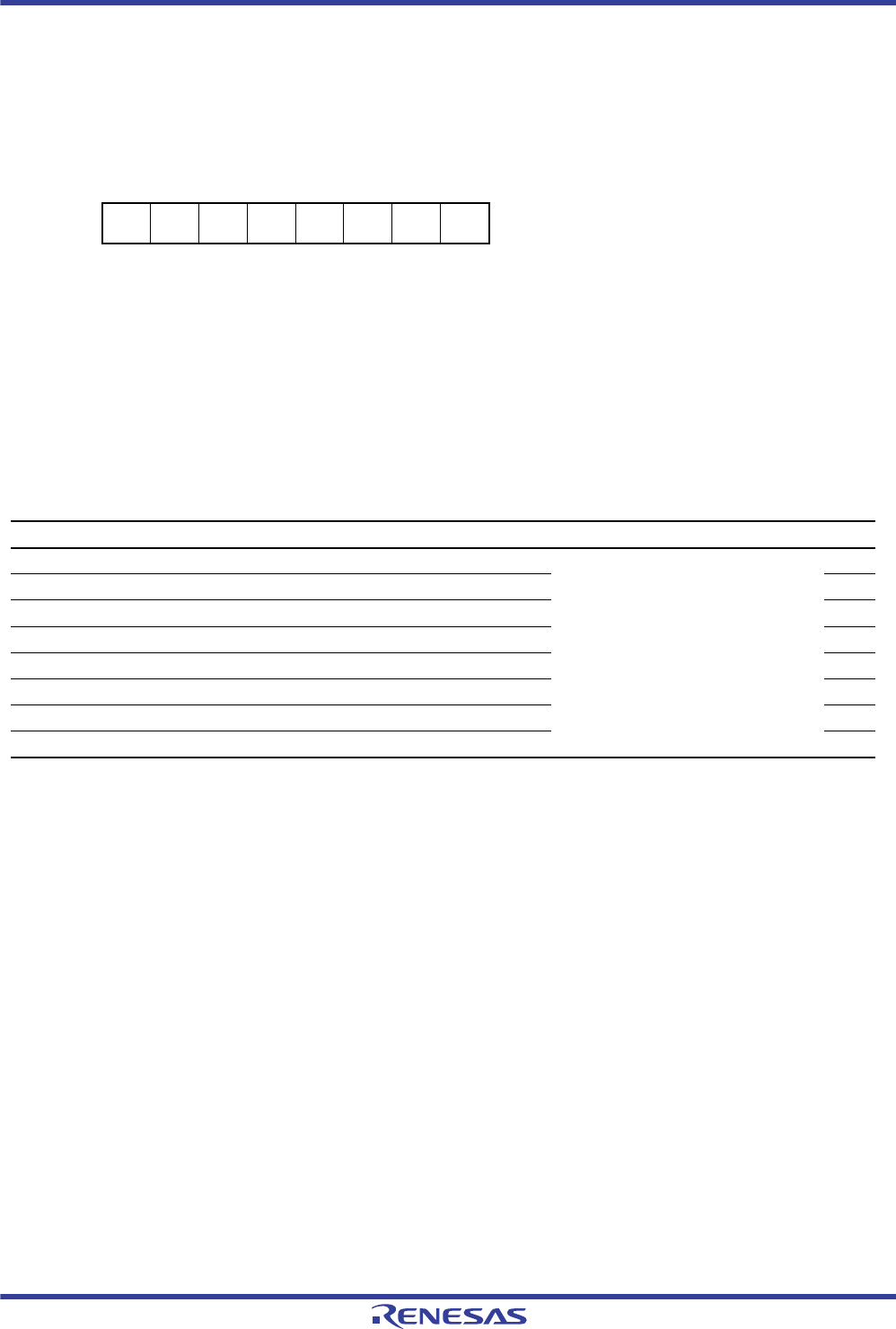
R01UH0034EJ0200 Rev.2.00 Page 349 of 1489
Dec 27, 2013
RX62T Group, RX62G Group 15. I/O Ports
Under development Preliminary document
Specifications in this document are tentative and subject to change.
15.1.2.4 Input Buffer Control Register (ICR)
n = 1 to 9, A, B, D, E, G
Note 1. For pins being used as input pins, set the corresponding bits to 1. Set the bits corresponding to pins that are not being used for
their input functions or are being used as analog input pins to 0.
Each PORTn.ICR controls the input buffers for the individual pins of the corresponding port.
Each bit of a PORTn.ICR (n=1 to 9, A, B, D, E, G) corresponds to a pin of Pn, and the settings can change from bit to bit.
When to be used as an input pin for the peripheral module, the input buffer for the corresponding pin should be enabled
beforehand by setting the PORTn.ICR bit to 1. If this register is used as an input pin for the peripheral module while the
PORTn.ICR bit is 0, the input signal to the peripheral module is fixed high.
When a Pn.PORT register is read, the pin states of the corresponding port are read out regardless of the values in
PORTn.ICR. For bits where the value in PORTn.ICR is 0, however, the value may not reflect the pin state on the
corresponding peripheral module side.
Changes in the settings of a PORTn.ICR may generate edges internally, depending on the pin state. For this reason,
change the settings of PORTn.ICR while the corresponding input pins are not in use. For example, in the case of IRQi (i
= 0 to 7) inputs, change settings of the corresponding PORTn.ICR with interrupts disabled by clearing the IR flag in IRi
(i = 64 to 71 ("i" shows an interrupt vector number of the IRQ)) of the interrupt controller (ICU) to 0, and then enable the
corresponding interrupts. If a change to a PORTn.ICR setting does generate an edge, negate the edge.
Address: PORT1.ICR 0008 C061h, PORT2.ICR 0008 C062h, PORT3.ICR 0008 C063h, PORT4.ICR 0008 C064h,
PORT5.ICR 0008 C065h, PORT6.ICR 0008 C066h, PORT7.ICR 0008 C067h, PORT8.ICR 0008 C068h,
PORT9.ICR 0008 C069h, PORTA.ICR 0008 C06Ah, PORTB.ICR 0008 C06Bh, PORTD.ICR 0008 C06Dh,
PORTE.ICR 0008 C06Eh, PORTG.ICR 0008 C070h
b7 b6 b5 b4 b3 b2 b1 b0
B7 B6 B5 B4 B3 B2 B1 B0
Value after reset: 00000000
Note 1. The two lower-order bits are valid and the six higher-order bits are reserved in PORT1.ICR.
The five lower-order bits are valid and the three higher-order bits are reserved in in PORT2.ICR.
The four lower-order bits are valid and the four higher-order bits are reserved in PORT3.ICR.
The six lower-order bits are valid and the two higher-order bits are reserved in PORT5.ICR.
The six lower-order bits are valid and the two higher-order bits are reserved in PORT6.ICR.
The seven lower-order bits are valid and the one higher-order bit is reserved in PORT7.ICR.
The three lower-order bits are valid and the five higher-order bits are reserved in PORT8.ICR.
The seven lower-order bits are valid and the one higher-order bit is reserved in PORT9.ICR.
The six lower-order bits are valid and the two higher-order bits are reserved in PORTA.ICR.
b5 to b3, b1, and b0 are valid and b7, b6, and b2 are reserved in PORTE.ICR.
The six lower-order bits are valid and the two higher-order bits are reserved in PORTG.ICR.
Note 2. The reserved bits are read as 0. The write value should always be 0.
Bit Symbol Bit Name Description R/W
b0 B0*1Pn0 Input Buffer Control 0: The input buffer for the corresponding
pin is disabled.
1: The input buffer for the corresponding
pin is enabled.
R/W
b1 B1*1Pn1 Input Buffer Control R/W
b2 B2*1Pn2 Input Buffer Control R/W
b3 B3*1Pn3 Input Buffer Control R/W
b4 B4*1Pn4 Input Buffer Control R/W
b5 B5*1Pn5 Input Buffer Control R/W
b6 B6*1Pn6 Input Buffer Control R/W
b7 B7*1Pn7 Input Buffer Control R/W

R01UH0034EJ0200 Rev.2.00 Page 350 of 1489
Dec 27, 2013
RX62T Group, RX62G Group 15. I/O Ports
Under development Preliminary document
Specifications in this document are tentative and subject to change.
15.1.2.5 Port Function Register 8 (PF8IRQ)
PF8IRQ is used to select pins for IRQ0 and IRQ1 inputs.
ITSi Bit (IRQi Pin Select) (i = 0 and 1)
Each bit selects a pin for an IRQi input.
15.1.2.6 Port Function Register 9 (PF9IRQ)
PF9IRQ is used to select pins for IRQ2 input.
ITS2 Bit (IRQ2 Pin Select)
This bit selects a pin for an IRQ2 input.
Address: 008 C108h
b7 b6 b5 b4 b3 b2 b1 b0
———— ITS1[1:0] ITS0[1:0]
Value after reset: 00000000
Bit Symbol Bit Name Description R/W
b1 to b0 ITS0[1:0] IRQ0 Pin Select b1 b0
0 0:P10 is designated as the IRQ0-A input pin.
0 1:PE5 is designated as the IRQ0-B input pin.
1 0:PG0 is designated as the IRQ0-C input pin.
1 1:Setting prohibited
R/W
b3 to b2 ITS1[1:0] IRQ1 Pin Select b3 b2
0 0:P11 is designated as the IRQ1-A input pin.
0 1:PE4 is designated as the IRQ1-B input pin.
1 0:PG1 is designated as the IRQ1-C input pin.
1 1:Setting prohibited
R/W
b7 to b4 — Reserved These bits are always read as 0. The write value should always be 0. R/W
Address: 008 C109h
b7 b6 b5 b4 b3 b2 b1 b0
—————ITS2——
Value after reset: 00000000
Bit Symbol Bit Name Description R/W
b1 to b0 — Reserved These bits are always read as 0. The write value should always be 0. R/W
b2 ITS2 IRQ2 Pin Select 0:PE3 is designated as the IRQ2-A input pin.
1:PG2 is designated as the IRQ2-B input pin.
R/W
b7 to b3 — Reserved These bits are always read as 0. The write value should always be 0. R/W

R01UH0034EJ0200 Rev.2.00 Page 351 of 1489
Dec 27, 2013
RX62T Group, RX62G Group 15. I/O Ports
Under development Preliminary document
Specifications in this document are tentative and subject to change.
15.1.2.7 Port Function Register A (PFAADC)
PFAADC is used to select the ADTRG0# and ADTRG1# pins.
ADTRGnS Bit (ADTRGn# Input Select) (n=0 and 1)
This bit selects a pin for an ADTRGn# input.
Address: 008 C10Ah
b7 b6 b5 b4 b3 b2 b1 b0
——————
ADTRG
1S ADTRG
0S
Value after reset: 00000000
Bit Symbol Bit Name Description R/W
b0 ADTRG0S ADTRG0# Input Select 0:PA4 is designated as the ADTRG0#-A input pin.
1:P20 is designated as the ADTRG0#-B input pin.
R/W
b1 ADTRG1S ADTRG1# Input Select 0:PA5 is designated as the ADTRG1#-A input pin.
1:P21 is designated as the ADTRG1#-B input pin.
R/W
b7 to b2 — Reserved These bits are always read as 0. The write value should always be 0. R/W

R01UH0034EJ0200 Rev.2.00 Page 352 of 1489
Dec 27, 2013
RX62T Group, RX62G Group 15. I/O Ports
Under development Preliminary document
Specifications in this document are tentative and subject to change.
15.1.2.8 Port Function Register C (PFCMTU)
PFCMTU is used to select pins for MTU3.
MTUSi Bit (MTU3 Pin Select) (i = 0 and 1)
Each bit selects a pin for an MTU3 input/output.
TCLKS[1:0] Bit (MTCLK Pin Select)
This bit selects a pin for a MTCLK input of the MTU3.
Address: 008 C10Ch
b7 b6 b5 b4 b3 b2 b1 b0
TCLKS[1:0]————MTUS1MTUS0
Value after reset: 00000000
Bit Symbol Bit Name Description R/W
b0 MTUS0 MTU3 Pin Select 0 0:PB3 is designated as the MTIOC0A-A pin.
1:P31 is designated as the MTIOC0A-B pin.
R/W
b1 MTUS1 MTU3 Pin Select 1 0:PB2 is designated as the MTIOC0B-A pin.
1:P30 is designated as the MTIOC0B-B pin.
R/W
b5 to b2 — Reserved These bits are always read as 0.
The write value should always be 0.
R/W
b7 to b6 TCLKS[1:0] MTCLK Pin Select b7 b6
0 0:P33 is designated as the MTCLKA-A pin.
P32 is designated as the MTCLKB-A pin.
P31 is designated as the MTCLKC-A pin.
P30 is designated as the MTCLKD-A pin.
0 1:P21 is designated as the MTCLKA-B pin.
P20 is designated as the MTCLKB-B pin.
P11 is designated as the MTCLKC-B pin.
P10 is designated as the MTCLKD-B pin.
1 0:PE4 is designated as the MTCLKC-C pin.
PE3 is designated as the MTCLKD-C pin.
(MTCLKA and MTCLKB pins cannot be selected.)
1 1:Setting prohibited
R/W
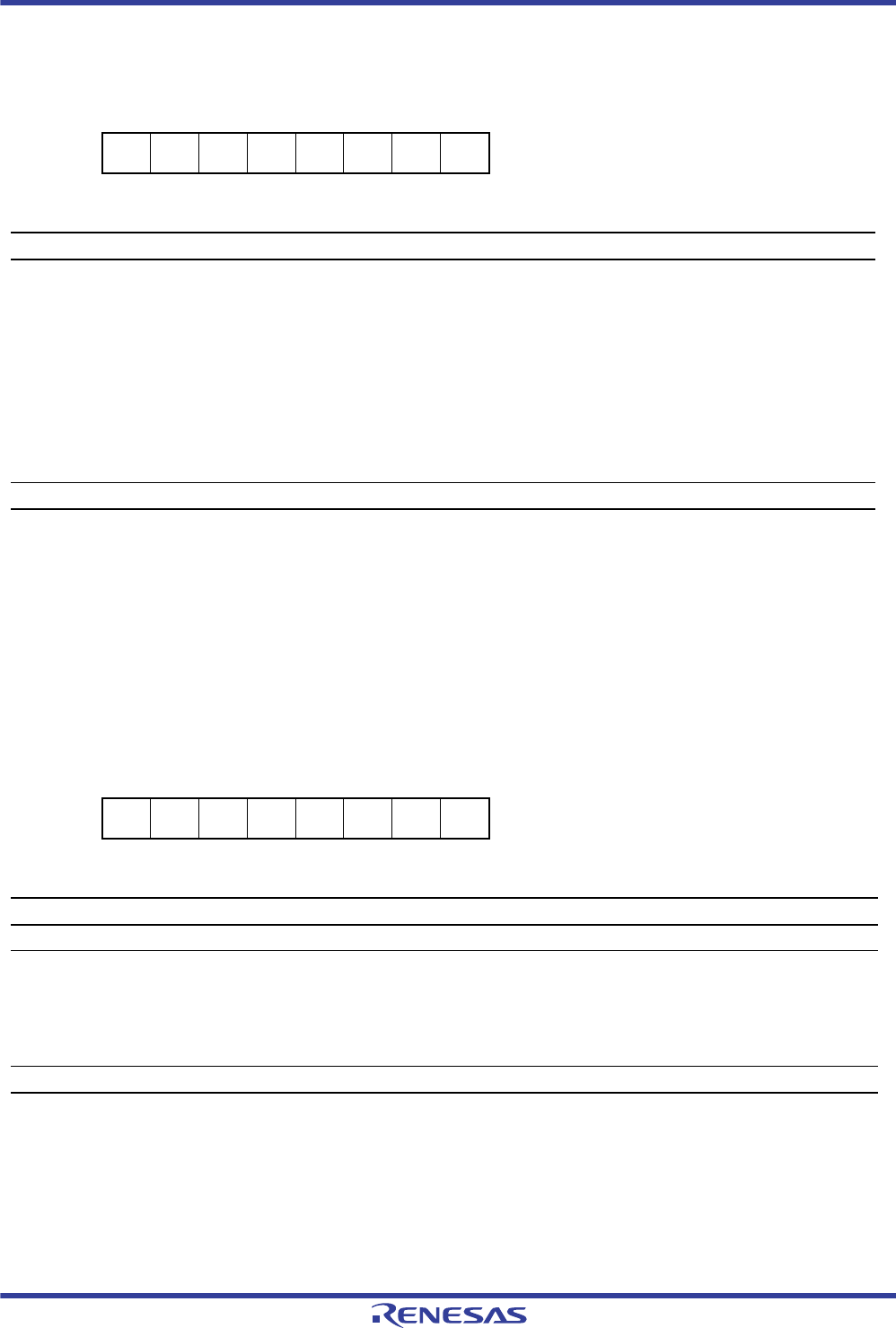
R01UH0034EJ0200 Rev.2.00 Page 353 of 1489
Dec 27, 2013
RX62T Group, RX62G Group 15. I/O Ports
Under development Preliminary document
Specifications in this document are tentative and subject to change.
15.1.2.9 Port Function Register D (PFDGPT)
PFDGPT is used to select a pin for GPT.
GPTS Bit (GPTI/O Pin Select)
Each bit selects a pin for a GPT input/output.
15.1.2.10 Port Function Register F (PFFSCI)
PFFSCI is used to select pins for SCI.
SCI2S Bit (SCI2 I/O Pin Select)
Each bit selects a pin for an SCI channel-2 input/output.
Address: 0008 C10Dh
b7 b6 b5 b4 b3 b2 b1 b0
—————GPTS
Value after reset: 00000000
Bit Symbol Bit Name Description R/W
b0 GPTS GPT Pin Select 0:P71 is designated as the GTIOC0A-A pin.
P74 is designated as the GTIOC0B-A pin.
P72 is designated as the GTIOC1A-A pin.
P75 is designated as the GTIOC1B -A pin.
P73 is designated as the GTIOC2A-A pin.
P76 is designated as the GTIOC2B-A pin.
1:PD7 is designated as the GTIOC0A-B pin.
PD6 is designated as the GTIOC0B-B pin.
PD5 is designated as the GTIOC1A-B pin.
PD4 is designated as the GTIOC1B-B pin.
PD3 is designated as the GTIOC2A-B pin.
PD2 is designated as the GTIOC2B-B pin.
R/W
b7 to b1 — Reserved These bits are always read as 0. The write value should always be 0. R/W
Address: 0008 C10Fh
b7 b6 b5 b4 b3 b2 b1 b0
———SCI2S——
Value after reset: 00000000
Bit Symbol Bit Name Description R/W
b1 to b0 — Reserved These bits are always read as 0. The write value should always be 0. R/W
b2 SCI2S SCI2 I/O Select 0:PB6 is designated as the RXD2-A pin.
PB7 is designated as the SCK2-A pin.
PB5 is designated as the TXD2-A pin.
1:P80 is designated as the RXD2-B pin.
P82 is designated as the SCK2-B pin.
P81 is designated as the TXD2-B pin.
R/W
b7 to b3 — Reserved These bits are always read as 0. The write value should always be 0. R/W

R01UH0034EJ0200 Rev.2.00 Page 354 of 1489
Dec 27, 2013
RX62T Group, RX62G Group 15. I/O Ports
Under development Preliminary document
Specifications in this document are tentative and subject to change.
15.1.2.11 Port Function Register G (PFGSPI)
PFGSPI is used to select I/O pins for RSPI.
RSPCKE Bit (RSPCK Output Enable)
This bit enables or disables the output of the RSPCK pin. Set this bit to 1 to use the RSPCK pin.
MOSIE Bit (MOSI Output Enable)
This bit enables or disables the output of the MOSI pin. Set this bit to 1 to use the MOSI pin.
MISOE Bit (MISO Output Enable)
This bit enables or disables the output of the MISO pin. Set this bit to 1 to use the MISO pin.
SSL0E Bit (SSL0 Output Enable)
This bit enables or disables the output of the SSL0 pin. Set this bit to 1 to use the SSL0 pin.
SSL1E Bit (SSL1 Output Enable)
This bit enables or disables the output of the SSL1 pin. Set this bit to 1 to use the SSL1 pin.
SSL2E Bit (SSL2 Output Enable)
This bit enables or disables the output of the SSL2 pin. Set this bit to 1 to use the SSL2 pin.
SSL3E Bit (SSL3 Output Enable)
This bit enables or disables the output of the SSL3 pin. Set this bit to 1 to use the SSL3 pin.
Address: 0008 C110h
b7 b6 b5 b4 b3 b2 b1 b0
SSL3E SSL2E SSL1E SSL0E MISOE MOSIE RSPCK
E—
Value after reset: 00000000
Bit Symbol Bit Name Description R/W
b0 — Reserved This bit is always read as 0. The write value should always be 0. R/W
b1 RSPCKE RSPCK Output Enable 0:RSPCK pin is disabled.
1:RSPCK pin is enabled.
R/W
b2 MOSIE MOSI Output Enable 0:MOSI pin is disabled.
1:MOSI pin is enabled.
R/W
b3 MISOE MISO Output Enable 0:MISO pin is disabled.
1:MISO pin is enabled.
R/W
b4 SSL0E SSL0 Output Enable 0:SSL0 pin is disabled.
1:SSL0 pin is enabled.
R/W
b5 SSL1E SSL1 Output Enable 0:SSL1 pin is disabled.
1:SSL1 pin is enabled.
R/W
b6 SSL2E SSL2 Output Enable 0:SSL2 pin is disabled.
1:SSL2 pin is enabled.
R/W
b7 SSL3E SSL3 Output Enable 0:SSL3 pin is disabled.
1:SSL3 pin is enabled.
R/W

R01UH0034EJ0200 Rev.2.00 Page 355 of 1489
Dec 27, 2013
RX62T Group, RX62G Group 15. I/O Ports
Under development Preliminary document
Specifications in this document are tentative and subject to change.
15.1.2.12 Port Function Register H (PFHSPI)
PFHSPI is used to select I/O pins for RSPI channel.
RSPIS[1:0] Bit (RSPI Pin Select)
This bit selects a pin for an RSPI input/output.
As an enable bit is provided for each RSPI input/output pin, the input/output pin is selectable while the corresponding
enable bit is 1. Otherwise, the pin cannot be selected.
Address: 0008 C111h
b7 b6 b5 b4 b3 b2 b1 b0
————RSPIS[1:0]
Value after reset: 00000000
Bit Symbol Bit Name Description R/W
b1 to b0 RSPIS[1:0] RSPI Pin Select b1 b0
0 0:P22 is designated as the MISO-A pin.
P23 is designated as the MOSI-A pin.
P24 is designated as the RSPCK-A pin.
P30 is designated as the SSL0-A pin.
P31 is designated as the SSL1-A pin.
P32 is designated as the SSL2-A pin.
P33 is designated as the SSL3-A pin.
0 1:PA5 is designated as the MISO-B pin.
PB0 is designated as the MOSI-B pin.
PA4 is designated as the RSPCK-B pin.
PA3 is designated as the SSL0-B pin.
PA2 is designated as the SSL1-B pin.
PA1 is designated as the SSL2-B pin.
PA0 is designated as the SSL3-B pin.
1 0:PD1 is designated as the MISO-C pin.
PD2 is designated as the MOSI-C pin.
PD0 is designated as the RSPCK-C pin.
PD6 is designated as the SSL0-C pin.
PD7 is designated as the SSL1-C pin.
PE0 is designated as the SSL2-C pin.
PE1 is designated as the SSL3-C pin.
1 1:Setting prohibited
R/W
b7 to b2 — Reserved These bits are always read as 0. The write value should always be 0. R/W

R01UH0034EJ0200 Rev.2.00 Page 356 of 1489
Dec 27, 2013
RX62T Group, RX62G Group 15. I/O Ports
Under development Preliminary document
Specifications in this document are tentative and subject to change.
15.1.2.13 Port Function Register J (PFJCAN)
PFJCAN is used to select I/O pins for the CAN.
CANE Bit (CAN Pin Enable)
This bit enables or disables the CAN pin. Set this bit to 1 to use the CAN pin.
CANS[1:0] Bit (CAN Pin Select)
These bits select I/O pins for the CAN.
15.1.2.14 Port Function Register K (PFKLIN)
PFKLIN is used to set I/O pins for the LIN.
LINE Bit (LIN Pin Enable)
This bit enables or disables the LIN pin. Set this bit to 1 to use the LIN pin.
Address: 0008 C113h
b7 b6 b5 b4 b3 b2 b1 b0
CANS[1:0]—————CANE
Value after reset: 00000000
Bit Symbol Bit Name Description R/W
b0 CANE CAN Pin Enable 0: The CTX and CRX pins are disabled.
1: The CTX and CRX pins are enabled.
R/W
b5 to b1 — Reserved These bits are always read as 0. The write value should always be 0. R/W
b7 to b6 CANS[1:0] CAN Pin Select b7 b6
0 0:PB5 is designated as the CTX-A pin.
PB6 is designated as the CRX-A pin.
0 1:P23 is designated as the CTX-B pin.
P22 is designated as the CRX-B pin.
1 0:PE0 is designated as the CRX-C pin.
PD7 is designated as the CTX-C pin.
1 1:Setting prohibited
R/W
Address: 0008 C114h
b7 b6 b5 b4 b3 b2 b1 b0
———————LINE
Value after reset: 00000000
Bit Symbol Bit Name Description R/W
b0 LINE LIN Pin Enable 0:LTX and LRX pins are disabled.
1:LTX and LRX pins are enabled.
R/W
b7 to b1 — Reserved These bits are always read as 0. The write value should always be 0. R/W

R01UH0034EJ0200 Rev.2.00 Page 357 of 1489
Dec 27, 2013
RX62T Group, RX62G Group 15. I/O Ports
Under development Preliminary document
Specifications in this document are tentative and subject to change.
15.1.2.15 Port Function Register M (PFMPOE)
Note 1. The first round of writing after a reset is enabled; though subsequent writing is not allowed.
PFMPOE enables or disables POEn# input pins.
To prevent the error in the system, be sure to write to this register after a reset.
The first round of writing after a reset is only enabled.
POEnE Bit (POEn# Input Enable) (n = 0, 4, 8, 10, 11)
Each bit enables or disables the corresponding POEn# input.
To use POEn#, set the corresponding POEnE bit to 1.
Address: 0008 C116h
b7 b6 b5 b4 b3 b2 b1 b0
———
POE11
EPOE10
EPOE8E POE4E POE0E
Value after reset: 00000000
Bit Symbol Bit Name Description R/W
b0 POE0E POE0# Input Enable 0:Designated as an I/O port pin
1:Designated as the POEn# input pin (n = 0, 4, 8, 10, 11)
R/W*1
b1 POE4E POE4# Input Enable R/W*1
b2 POE8E POE8# Input Enable R/W*1
b3 POE10E POE10# Input Enable R/W*1
b4 POE11E POE11# Input Enable R/W*
b7 to b5 — Reserved These bits are always read as 0. The write value should always be 0. R/W*1

R01UH0034EJ0200 Rev.2.00 Page 358 of 1489
Dec 27, 2013
RX62T Group, RX62G Group 15. I/O Ports
Under development Preliminary document
Specifications in this document are tentative and subject to change.
15.1.2.16 Port Function Register N (PFNPOE)
Note 1. The first round of writing after a reset is enabled; though subsequent writing is not allowed.
PFNPOE enables or disables POEn# input pins.
To prevent the error in the system, be sure to write to this register after a reset.
The first round of writing after a reset is only enabled.
POE10S Bit (POE10# Input Select)
This bit select input pins for the POE10#.
Address: 0008 C117h
b7 b6 b5 b4 b3 b2 b1 b0
POE10
S———————
Value after reset: 00000000
Bit Symbol Bit Name Description R/W
b6 to b0 — Reserved These bits are always read as 0. The write value should always be 0. R/W*1
b7 POE10S POE10# Input Select 0:PE2 is designated as the POE10#-A input pin.
1:PE4 B is designated as the POE10# input pin.
R/W

R01UH0034EJ0200 Rev.2.00 Page 359 of 1489
Dec 27, 2013
RX62T Group, RX62G Group 15. I/O Ports
Under development Preliminary document
Specifications in this document are tentative and subject to change.
15.1.3 Settings of Ports
When individual pins for peripheral modules are enabled, the settings for each port are modified.
An input pin for the peripheral module is specified independently by the peripheral module. To use an input pin for the
peripheral module, the corresponding bit in the input buffer control register (PORTn.ICR) should be set to 1 to enable the
input buffer, except for the port register read, NMI, and POEn# pin inputs.
The pins that function as output pins and I/O pins should be enabled for respective peripheral modules. If a conflict
occurs among the output signal enable settings for peripheral modules, that are multiplexed to the same port, the priority
will be handled according to the port-multiplexed priority.
Table 15.15 lists the port-multiplexed priority for peripheral modules.
Table 15.5 Port-Multiplexed Priority for Peripheral Modules (112-Pin LQFP)
Priority Module Name Output Pins
High
Low
1 RSPI RSPCK, MOSI, MISO, SSL0 to SSL3
2CAN CTX
3LIN LTX
4 MTU0 to MTU7 MTIOC0A, MTIOC0B, MTIOC0C, MTIOC0D, MTIOC1A, MTIOC1B, MTIOC2A, MTIOC2B,
MTIOC3A, MTIOC3B, MTIOC3C, MTIOC3D, MTIOC4A, MTIOC4B, MTIOC4C, MTIOC4D,
MTIOC6A, MTIOC6B, MTIOC6C, MTIOC6D, MTIOC7A, MTIOC7B, MTIOC7C, MTIOC7D
5 GPT0 to GPT3 GTIOC0A, GTIOC0B, GTIOC1A, GTIOC1B,
GTIOC2A, GTIOC2B, GTIOC3A, GTIOC3B
6 SCI0 to SCI2 SCK0 to SCK2, TXD0 to TXD2
7 RIIC SCL, SDA
8 IOPORT P10 to P11, P20 to P24, P30 to P33, P70 to P76, P80 to P82, P90 to P96, PA0 to PA5,
PB0 to PB7, PD0 to PD7, PE0 to PE1, PE3 to PE5, PG0 to PG5

R01UH0034EJ0200 Rev.2.00 Page 360 of 1489
Dec 27, 2013
RX62T Group, RX62G Group 15. I/O Ports
Under development Preliminary document
Specifications in this document are tentative and subject to change.
15.1.4 List of Output Enable Settings
Table 15.6 lists the output enable settings for each port.
For details on the applicable output signals, see descriptions of the registers for each peripheral module.
Setting the port function register changes the functions of peripheral-module pins with names ending in A to C.
Table 15.6 Output Enable Settings for Each Port (112-pin LQFP) (1 / 5)
Port Module Name Output Signal Name Port Function Register Settings Peripheral Module Settings
P10 PORT1 P10 PORT1.DDR.B0 = 1
P11 PORT1 P11 PORT1.DDR.B1 = 1
P20 PORT2 P20 PORT2.DDR.B0 = 1
P21 PORT2 P21 PORT2.DDR.B1 = 1
P22 RSPI MISO-A PFGSPI.MISOE = 1
PFHSPI.RSPIS[1:0] = 00
(In addition to the pin enable setting, input/
output switching function for the peripheral
module is provided.)
PORT2 P22 PORT2.DDR.B2 = 1
P23 RSPI MOSI-A PFGSPI.MOSIE = 1
PFHSPI.RSPIS[1:0] = 00
(In addition to the pin enable setting, input/
output switching function for the peripheral
module is provided.)
CAN CTX-B PFJCAN.CANE =1
PFJCAN.CANS[1:0] = 01
(The signal output state is specified by the
peripheral module settings.)
LIN LTX PFKLIN.LINE = 1 (The signal output state is specified by the
peripheral module settings.)
PORT2 P23 PORT2.DDR.B3 =1
P24 RSPI RSPCK-A PFGSPI.RSPCKE =1
PFHSPI.RSPIS[1:0] = 00
(In addition to the pin enable setting, input/
output switching function for the peripheral
module is provided.)
PORT2 P24 PORT2.DDR.B4 = 1
P30 RSPI SSL0-A PFGSPI.SSL0E = 1
PFHSPI.RSPIS[1:0] = 00
(In addition to the pin enable setting, input/
output switching function for the peripheral
module is provided.)
MTU0 MTIOC0B-B PFCMTU.MTUS1 = 1 (The signal output state is specified by the
peripheral module settings.)
PORT3 P30 PORT3.DDR.B0 = 1
P31 RSPI SSL1-A PFGSPI.SSL1E = 1
PFHSPI.RSPIS[1:0] = 00
(The signal output state is specified by the
peripheral module settings.)
MTU0 MTIOC0A-B PFCMTU.MTUS0 = 1 (The signal output state is specified by the
peripheral module settings.)
PORT3 P31 PORT3.DDR.B1 = 1
P32 RSPI SSL2-A PFGSPI.SSL2E = 1
PFHSPI.RSPIS[1:0] = 00
(The signal output state is specified by the
peripheral module settings.)
MTU3 MTIOC3C (The signal output state is specified by the
peripheral module settings.)
PORT3 P32 PORT3.DDR.B2 = 1
P33 RSPI SSL3-A PFGSPI.SSL3E = 1
PFHSPI.RSPIS[1:0] = 00
(The signal output state is specified by the
peripheral module settings.)
MTU3 MTIOC3A (The signal output state is specified by the
peripheral module settings.)
PORT3 P33 PORT3.DDR.B3 = 1
P70 PORT7 P70 PORT7.DDR.B0 = 1

R01UH0034EJ0200 Rev.2.00 Page 361 of 1489
Dec 27, 2013
RX62T Group, RX62G Group 15. I/O Ports
Under development Preliminary document
Specifications in this document are tentative and subject to change.
P71 MTU3 MTIOC3B (The signal output state is specified by the
peripheral module settings.)
GPT0 GTIOC0A-A PFDGPT.GPTS = 0 (The signal output state is specified by the
peripheral module settings.)
PORT7 P71 PORT7.DDR.B1 = 1
P72 MTU4 MTIOC4A (The signal output state is specified by the
peripheral module settings.)
GPT1 GTIOC1A-A PFDGPT.GPTS = 0 (The signal output state is specified by the
peripheral module settings.)
PORT7 P72 PORT7.DDR.B2 = 1
P73 MTU4 MTIOC4B (The signal output state is specified by the
peripheral module settings.)
GPT2 GTIOC2A-A PFDGPT.GPTS = 0 (The signal output state is specified by the
peripheral module settings.)
PORT7 P73 PORT7.DDR.B3 = 1
P74 MTU3 MTIOC3D (The signal output state is specified by the
peripheral module settings.)
GPT0 GTIOC0B-A PFDGPT.GPTS = 0 (The signal output state is specified by the
peripheral module settings.)
PORT7 P74 PORT7.DDR.B4 = 1
P75 MTU4 MTIOC4C (The signal output state is specified by the
peripheral module settings.)
GPT1 GTIOC1B-A PFDGPT.GPTS = 0 (The signal output state is specified by the
peripheral module settings.)
PORT7 P75 PORT7.DDR.B5 = 1
P76 MTU4 MTIOC4D (The signal output state is specified by the
peripheral module settings.)
GPT2 GTIOC2B-A PFDGPT.GPTS = 0 (The signal output state is specified by the
peripheral module settings.)
PORT7 P76 PORT7.DDR.B6 = 1
P80 PORT8 P80 PORT8.DDR.B0 = 1
P81 SCI2 TXD2-B PFFSCI.SCI2S = 1 SCI2.SCR.TE = 1
PORT8 P81 PORT8.DDR.B1 = 1
P82 SCI2 SCK2-B PFFSCI.SCI2S = 1 When SCI2.SCMR.SMIF = 1:
While SMR.GM = 0, SCR.CKE[1:0] = 01 or
SMR.GM = 1,
SCR.TE = 1 or SCR.RE = 1
When SCI2.SCMR.SMIF = 0:
While SMR.CM = 0, SCR.CKE[1:0] = 01 or
SMR.CM = 1,
SCR.CKE[1] = 0, SCR.TE =1 or SCR.RE=1
PORT8 P82 PORT8.DDR.B2 = 1
P90 MTU7 MTIOC7D (The signal output state is specified by the
peripheral module settings.)
I/O port P90 PORT9.DDR.B0 = 1
P91 MTU7 MTIOC7C (The signal output state is specified by the
peripheral module settings.)
PORT9 P91 PORT9.DDR.B1 = 1
P92 MTU6 MTIOC6D (The signal output state is specified by the
peripheral module settings.)
PORT9 P92 PORT9.DDR.B2 = 1
Table 15.6 Output Enable Settings for Each Port (112-pin LQFP) (2 / 5)
Port Module Name Output Signal Name Port Function Register Settings Peripheral Module Settings

R01UH0034EJ0200 Rev.2.00 Page 362 of 1489
Dec 27, 2013
RX62T Group, RX62G Group 15. I/O Ports
Under development Preliminary document
Specifications in this document are tentative and subject to change.
P93 MTU7 MTIOC7B (The signal output state is specified by the
peripheral module settings.)
PORT9 P93 PORT9.DDR.B3 = 1
P94 MTU7 MTIOC7A (The signal output state is specified by the
peripheral module settings.)
PORT9 P94 PORT9.DDR.B4 = 1
P95 MTU6 MTIOC6B The signal output state is specified by the
peripheral module settings.)
PORT9 P95 PORT9.DDR.B5 = 1
P96 PORT9 P96 PORT9.DDR.B6 = 1
PA0 RSPI SSL3-B PFGSPI.SSL3E = 1
PFHSPI.RSPIS[1:0] = 01
(The signal output state is specified by the
peripheral module settings.)
MTU6 MTIOC6C (The signal output state is specified by the
peripheral module settings.)
PORTA PA0 PORTA.DDR.B0 = 1
PA1 RSPI SSL2-B PFGSPI.SSL2E = 1
PFHSPI.RSPIS[1:0] = 01
(The signal output state is specified by the
peripheral module settings.)
MTU6 MTIOC6A (The signal output state is specified by the
peripheral module settings.)
PORTA PA1 PORTA.DDR.B1 = 1
PA2 RSPI SSL1-B PFGSPI.SSL1E = 1
PFHSPI.RSPIS[1:0] = 01
(The signal output state is specified by the
peripheral module settings.)
MTU2 MTIOC2B (The signal output state is specified by the
peripheral module settings.)
PORTA PA2 PORTA.DDR.B2 = 1
PA3 RSPI SSL0-B PFGSPI.SSL0E = 1
PFHSPI.RSPIS[1:0] = 01
(In addition to the pin enable setting, input/
output switching function for the peripheral
module is provided.)
MTU2 MTIOC2A (The signal output state is specified by the
peripheral module settings.)
PORTA PA3 PORTA.DDR.B3 = 1
PA4 RSPI RSPCK-B PFGSPI.RSPCKE = 1
PFHSPI.RSPIS[1:0] = 01
(In addition to the pin enable setting, input/
output switching function for the peripheral
module is provided.)
MTU1 MTIOC1B (The signal output state is specified by the
peripheral module settings.)
PORTA PA4 PORTA.DDR.B4 = 1
PA5 RSPI MISO-B PFGSPI.MISOE = 1
PFHSPI.RSPIS[1:0] = 01
(In addition to the pin enable setting, input/
output switching function for the peripheral
module is provided.)
MTU1 MTIOC1A (The signal output state is specified by the
peripheral module settings.)
PORTA PA5 PORTA.DDR.B5 = 1
PB0 RSPI MOSI-B PFGSPI.MOSIE = 1
PFHSPI.RSPIS[1:0] = 01
(In addition to the pin enable setting, input/
output switching function for the peripheral
module is provided.))
MTU0 MTIOC0D (The signal output state is specified by the
peripheral module settings.)
PORTB PB0 PORTB.DDR.B0 = 1
Table 15.6 Output Enable Settings for Each Port (112-pin LQFP) (3 / 5)
Port Module Name Output Signal Name Port Function Register Settings Peripheral Module Settings

R01UH0034EJ0200 Rev.2.00 Page 363 of 1489
Dec 27, 2013
RX62T Group, RX62G Group 15. I/O Ports
Under development Preliminary document
Specifications in this document are tentative and subject to change.
PB1 MTU0 MTIOC0C (The signal output state is specified by the
peripheral module settings.)
RIIC SCL RIIC.ICCR1.ICE = 1
PORTB PB1 PORTB.DDR.B1 = 1
PB2 MTU0 MTIOC0B-A PFCMTU.MTUS1 = 0 (The signal output state is specified by the
peripheral module settings.)
SCI0 TXD0 SCI0.SCR.TE = 1
RIIC SDA RIIC.ICCR1.ICE = 1
PORTB PB2 PORTB.DDR.B2 = 1
PB3 MTU0 MTIOC0A-A PFCMTU.MTUS0 = 0 (The signal output state is specified by the
peripheral module settings.)
SCI0 SCK0 When SCI0.SCMR.SMIF = 1:
While SMR.GM = 0, SCR.CKE[1:0] = 01 or
SMR.GM = 1,
SCR.TE = 1 or SCR.RE = 1
When SCI0.SCMR.SMIF = 0:
While SMR.CM = 0, SCR.CKE[1:0] = 01 or
SMR.CM = 1,
SCR.CKE[1] = 0, SCR.TE = 1 or SCR.RE = 1
PORTB PB3 PORTB.DDR.B3 = 1
PB4 PORTB PB4 PORTB.DDR.B4 = 1
PB5 CAN CTX-A PFJCAN.CANE = 1
PFJCAN.CANS[1:0] = 00
(The signal output state is specified by the
peripheral module settings.)
SCI2 TXD2-A PFFSCI.SCI2S = 0 SCI2.SCR.TE = 1
PORTB PB5 PORTB.DDR.B5 = 1
PB6 PORTB PB6 PORTB.DDR.B6 = 1
PB7 SCI2 SCK2-A PFFSCI.SCI2S = 0 When SCI2.SCMR.SMIF =1:
While SMR.GM = 0, SCR.CKE[1:0] = 01 or
SMR.GM = 1,
SCR.TE = 1 or SCR.RE = 1
When SCI2.SCMR.SMIF = 0
While SMR.CM = 0, SCR.CKE[1:0] = 01 or
SMR.CM = 1,
SCR.CKE[1] = 0, SCR.TE = 1 or SCR.RE = 1
PORTB PB7 PORTB.DDR.B7 = 1
PD0 RSPI RSPCK-C PFGSPI.RSPCKE = 1
PFHSPI.RSPIS[1:0] = 10
(In addition to the pin enable setting, input/
output switching function for the peripheral
module is provided.))
GPT3 GTIOC3B (The signal output state is specified by the
peripheral module settings.)
PORTD PD0 PORTD.DDR.B0 = 1
PD1 RSPI MISO-C PFGSPI.MISOE = 1
PFHSPI.RSPIS[1:0] = 10
(In addition to the pin enable setting, input/
output switching function for the peripheral
module is provided.))
GPT3 GTIOC3A (The signal output state is specified by the
peripheral module settings.)
PORTD PD1 PORTD.DDR.B1 = 1
PD2 RSPI MOSI-C PFGSPI.MISOE = 1
PFHSPI.RSPIS[1:0] = 10
(In addition to the pin enable setting, input/
output switching function for the peripheral
module is provided.))
GPT2 GTIOC2B-B PFDGPT.GPTS = 1 (The signal output state is specified by the
peripheral module settings.)
PORTD PD2 PORTD.DDR.B2 = 1
Table 15.6 Output Enable Settings for Each Port (112-pin LQFP) (4 / 5)
Port Module Name Output Signal Name Port Function Register Settings Peripheral Module Settings

R01UH0034EJ0200 Rev.2.00 Page 364 of 1489
Dec 27, 2013
RX62T Group, RX62G Group 15. I/O Ports
Under development Preliminary document
Specifications in this document are tentative and subject to change.
PD3 GPT2 GTIOC2A-B PFDGPT.GPTS = 1 (The signal output state is specified by the
peripheral module settings.)
SCI1 TXD1 SCI1.SCR.TE = 1
PORTD PD3 PORTD.DDR.B3 = 1
PD4 GPT1 GTIOC1B-B PFDGPT.GPTS = 1 (The signal output state is specified by the
peripheral module settings.)
SCI1 SCK1 When SCI1.SCMR.SMIF = 1:
While SMR.GM = 0, SCR.CKE[1:0] = 01 or
SMR.GM = 1,
SCR.TE = 1 or SCR.RE = 1
When SCI1.SCMR.SMIF = 0:
While SMR.CM = 0, SCR.CKE[1:0] = 01 or
SMR.CM = 1,
SCR.CKE[1] = 0, SCR.TE = 1 or SCR.RE = 1
PORTD PD4 PORTD.DDR.B4 = 1
PD5 GPT1 GTIOC1A-B PFDGPT.GPTS = 1 (The signal output state is specified by the
peripheral module settings.)
PORTD PD5 PORTD.DDR.B5 = 1
PD6 RSPI SSL0-C PFGSPI.SSL0E = 1
PFHSPI.RSPIS[1:0] = 10
(In addition to the pin enable setting, input/
output switching function for the peripheral
module is provided.)
GPT0 GTIOC0B-B PFDGPT.GPTS = 1 (The signal output state is specified by the
peripheral module settings.)
PORTD PD6 PORTD.DDR.B6 = 1
PD7 RSPI SSL1-C PFGSPI.SSL1E = 1
PFHSPI.RSPIS[1:0] = 10
(The signal output state is specified by the
peripheral module settings.)
CAN CTX-C PFJCAN.CANE = 1
PFJCAN.CANS[1:0] = 10
(The signal output state is specified by the
peripheral module settings.)
GPT0 GTIOC0A-B PFDGPT.GPTS = 1 (The signal output state is specified by the
peripheral module settings.)
PORTD PD7 PORTD.DDR.B7 = 1
PE0 RSPI SSL2-C PFGSPI.SSL2E = 1
PFHSPI.RSPIS[1:0] = 10
(The signal output state is specified by the
peripheral module settings.)
PORTE PE0 PORTE.DDR.B0 = 1
PE1 RSPI SSL3-C PFGSPI.SSL3E = 1
PFHSPI.RSPIS[1:0] = 10
(The signal output state is specified by the
peripheral module settings.)
PORTE PE1 PORTE.DDR.B1 = 1
PE3 PORTE PE3 PORTE.DDR.B3 = 1
PE4 PORTE PE4 PORTE.DDR.B4 = 1
PE5 PORTE PE5 PORTE.DDR.B5 = 1
PG0 PORTG PG0 PORTG.DDR.B0 = 1
PG1 PORTG PG1 PORTG.DDR.B1 = 1
PG2 PORTG PG2 PORTG.DDR.B2 = 1
PG3 PORTG PG3 PORTG.DDR.B3 = 1
PG4 PORTG PG4 PORTG.DDR.B4 = 1
PG5 PORTG PG5 PORTG.DDR.B5 = 1
Table 15.6 Output Enable Settings for Each Port (112-pin LQFP) (5 / 5)
Port Module Name Output Signal Name Port Function Register Settings Peripheral Module Settings

R01UH0034EJ0200 Rev.2.00 Page 365 of 1489
Dec 27, 2013
RX62T Group, RX62G Group 15. I/O Ports
Under development Preliminary document
Specifications in this document are tentative and subject to change.
15.1.5 Treatment of Unused Pins
The treatment of unused pins is listed in Table 15.7.
Note 1. Do not change the initial value of PORTn.ICR. Changing the initial value may generate shoot-through current.
Table 15.7 Treatment of Unused Pin (112-pin LQFP)
Pin Name Treatment
EMLE Connect this pin to Vss via a pull-down resistor.
MD1, MD0 (Always used as mode pins)
MDE (Always used as mode pins)
RES# Connect this pin to Vcc via a pull-up resistor.
PE2/NMI/POE10#-A Connect this pin to Vcc via a pull-up resistor.
EXTAL (Always used as a clock pin)
XTAL Leave these pins open.
WDTOVF# Leave these pins open.
Port 3, 7 to 9, A, B, D, E, G Connect these pins to Vcc via a pull-up resistor or to Vss via a pull-down resistor
These pins can be left while PORTn.ICR is in the initial state (the input buffer disabled)*1.
Port 4 Connect these pins to AVCCO via a pull-up resistor or to AVSSO via a pull-down resistor
These pins can be left while PORTn.ICR is in the initial state (the input buffer disabled)*1.
Port 5 to 6 Connect these pins to AVCC via a pull-up resistor or to AVSS via a pull-down resistor
These pins can be left while PORTn.ICR is in the initial state (the input buffer disabled)*1.
VREFH0 Connect this pin to AVCC0
VREFL0 Connect this pin to AVSS0
VREF Connect this pin to AVCC
TRST#, TMS, TCK, TDI Connect these pins to Vcc via a pull-up resistor or to Vss via a pull-down resistor
TDO Leave these pins open.

R01UH0034EJ0200 Rev.2.00 Page 366 of 1489
Dec 27, 2013
RX62T Group, RX62G Group 15. I/O Ports
Under development Preliminary document
Specifications in this document are tentative and subject to change.
15.2 I/O Port [for 100-Pin LQFP]
The RX62T and RX62G Groups (100-Pin LQFP) have 13 I/O ports (ports 1 to 9 and A, B, D, E), which handle 55 I/O
pins.
15.2.1 Overview
Table 15.8 gives the specifications of the I/O ports and Table 15.9 lists I/O ports and pin functions.
Table 15.8 Specifications of I/O Ports (100-Pin LQFP)
Item Description
I/O pins 55
Input pins 21
Number of ports 13 (1 to 9, A, B, D, E)
Open drain outputs 2 (RIIC pin)
Large-current output 12 (MTU3 pin and GPT pin)
Schmitt trigger input pins All port inputs, CAN inputs, IRQ inputs, MTU3 inputs, POE3 inputs, RIIC inputs, SCI inputs,
A/D trigger inputs, NMI inputs, GPT inputs, and LIN inputs
Others Each pin is capable of driving a capacitive load of 30 pF in the case of a TTL load.
When configured as an output, a pin is capable of driving a Darlington transistor.
A pin is always capable of reading the status of the pins.
Table 15.9 Port Functions (100-Pin LQFP) (1 / 3)
Port Description Bit
Function CMOS
Input Schmitt Trigger
Input
Open Drain
Output
Capability
Large-
Current
OutputI/O Input Output
Port 1 General I/O port
pins, MTU3 inputs,
and
interrupt inputs
0 P10 MTCLKD-B/
IRQ0-A — All input functions — —
1 P11 MTCLKC-B/
IRQ1-A All input functions
Port 2 General I/O port
pins, MTU3 inputs,
interrupt inputs,
A/D converter inputs,
RSPI I/O signal,
LIN I/O signal, and
CAN I/O signal
0 P20 MTCLKB-B/
IRQ7/
ADTRG0#-B
— All input functions — —
1 P21 MTCLKA-B/
IRQ6/
ADTRG1#-B
All input functions
2 P22/MISO-A LRX/CRX-B/
ADTRG# MISO-A P22/LRX/CRX-B/
ADTRG#
3 P23/MOSI-A LTX/CTX-B MOSI-A P23
4 P24/RSPCK-A RSPCK-A P24
Port 3 General I/O port
pins, MTU3 I/O
signal, and
RSPI I/O signal
0 P30/MTIOC0B-B/
SSL0-A MTCLKD-A SSL0-A P30/MTIOC0B-B/
MTCLKD-A ——
1 P31/MTIOC0A-B MTCLKC-A SSL1-A — All input functions
2 P32/MTIOC3C MTCLKB-A SSL2-A All input functions
3 P33/MTIOC3A MTCLKA-A SSL3-A All input functions
Port 4 A/D converter inputs
and general input
port pins
0 P40/AN000 — P40 — —
1 P41/AN001 P41
2 P42/AN002 P42
3 P43/AN003/
CVREFL P43
4 P44/AN100 P44
5 P45/AN101 P45
6 P46/AN102 P46
7 P47/AN103/
CVREFH P47

R01UH0034EJ0200 Rev.2.00 Page 367 of 1489
Dec 27, 2013
RX62T Group, RX62G Group 15. I/O Ports
Under development Preliminary document
Specifications in this document are tentative and subject to change.
Port 5 A/D converter inputs
and general input
port pins
0P50/AN6—P50——
1P51/AN7 P51
2P52/AN8 P52
3P53/AN9 P53
4P54/AN10 P54
5P55/AN11 P55
Port 6 A/D converter inputs
and general input
port pins
0P60/AN0—P60——
1P61/AN1 P61
2P62/AN2 P62
3P63/AN3 P63
4P64/AN4 P64
5P65/AN5 P65
Port 7 General I/O port
pins, POE3 inputs,
interrupt inputs,
MTU3 I/O signal, and
GPT I/O signal
0 P70 POE0#/IRQ5 — All input functions — —
1 P71/MTIOC3B/
GTIOC0A-A All input functions √
2 P72/MTIOC4A/
GTIOC1A-A All input functions √
3 P73/MTIOC4B/
GTIOC2A-A All input functions √
4 P74/MTIOC3D/
GTIOC0B-A All input functions √
5 P75/MTIOC4C/
GTIOC1B-A All input functions √
6 P76/MTIOC4D/
GTIOC2B-A All input functions √
Port 8 General I/O port
pins, SCI I/O signal,
and
MTU3 inputs
0 P80 RXD2-B/
MTIC5W — All input functions — —
1 P81 MTIC5V TXD2-B All input functions
2 P82/SCK2-B MTIC5U All input functions
Port 9 General I/O port
pins, MTU3 I/O
signal,
POE3 inputs, and
interrupt inputs
0 P90/MTIOC7D — All input functions — √
1 P91/MTIOC7C All input functions √
2 P92/MTIOC6D All input functions √
3 P93/MTIOC7B All input functions √
4 P94/MTIOC7A All input functions √
5 P95/MTIOC6B All input functions √
6 P96 POE4#/IRQ4 All input functions —
Port A General I/O port
pins, MTU3 I/O
signal, RSPI I/O
signal, and
A/D converter inputs
0 PA0/MTIOC6C SSL3-B — All input functions — —
1 PA1/MTIOC6A SSL2-B All input functions
2 PA2/MTIOC2B SSL1-B All input functions
3PA3/MTIOC2A/
SSL0-B SSL0-B PA3/MTIOC2A
4PA4/MTIOC1B/
RSPCK-B ADTRG0#-A RSPCK-B PA4/MTIOC1B/
ADTRG0#-A
5PA5/MTIOC1A/
MISO-B ADTRG1#-A MISO-B PA5/MTIOC1A/
ADTRG1#-A
Table 15.9 Port Functions (100-Pin LQFP) (2 / 3)
Port Description Bit
Function CMOS
Input Schmitt Trigger
Input
Open Drain
Output
Capability
Large-
Current
OutputI/O Input Output

R01UH0034EJ0200 Rev.2.00 Page 368 of 1489
Dec 27, 2013
RX62T Group, RX62G Group 15. I/O Ports
Under development Preliminary document
Specifications in this document are tentative and subject to change.
Port B General I/O port
pins, MTU3 I/O
signal,
RSPI I/O signal,
RIIC I/O signal,
SCI I/O signal,
GPT inputs,
POE3 inputs,
interrupt inputs,
CAN I/O signal,
and trace outputs
0PB0/MTIOC0D/
MOSI-B MOSI-B PB0/MTIOC0D — —
1PB1/MTIOC0C/
SCL RXD0 — All input functions
(SCL only) —
2PB2/MTIOC0B-A/
SDA TXD0 All input functions
(SDA only) —
3PB3/MTIOC0A-A/
SCK0 All input functions — —
4PB4 GTETRG/
POE8#/IRQ3 All input functions
5PB5 TXD2-A/
CTX-A/
TRSYNC
All input functions
6 PB6 RXD2-A/CRX-
ATRDATA0 All input functions
7 PB7/SCK2-A TRDATA1 All input functions
Port D General I/O port
pins, GPT I/O signal,
RSPI I/O signal,
SCI I/O signal,
CAN outputs,
trace outputs, and
On-chip emulator I/O
signal
0PD0/GTIOC3B/
RSPCK-C TRDATA2 RSPCK-C PD0/GTIOC3B — —
1PD1/GTIOC3A/
MISO-C TRDATA3 MISO-C PD1/GTIOC3A
2PD2/GTIOC2B-B/
MOSI-C TRCLK MOSI-C PD2/GTIOC2B-B
3 PD3/GTIOC2A-B TXD1/TDO — All input functions
4PD4/GTIOC1B-B/
SCK1 TCK — All input functions
5 PD5/GTIOC1A-B RXD1/TDI — All input functions
6PD6/GTIOC0B-B/
SSL0-C TMS SSL0-C PD6/GTIOC0B-B
7 PD7/GTIOC0A-B TRST# SSL1-C/
CTX-C — All input functions
Port E General I/O port
pins, CAN inputs,
RSPI outputs,
POE3 inputs,
MTU3 inputs, and
interrupt inputs
0 PE0 CRX-C SSL2-C — All input functions — —
1 PE1 SSL3-C All input functions
2 PE2/POE10#-
A/NMI All input functions
3 PE3 MTCLKD-C/
POE11#/
IRQ2-A
All input functions
4 PE4 MTCLKC-C/
POE10#-B/
IRQ1-B
All input functions
5 PE5 IRQ0-B All input functions
Table 15.9 Port Functions (100-Pin LQFP) (3 / 3)
Port Description Bit
Function CMOS
Input Schmitt Trigger
Input
Open Drain
Output
Capability
Large-
Current
OutputI/O Input Output

R01UH0034EJ0200 Rev.2.00 Page 369 of 1489
Dec 27, 2013
RX62T Group, RX62G Group 15. I/O Ports
Under development Preliminary document
Specifications in this document are tentative and subject to change.
15.2.2 Register Descriptions
Table 15.10 lists registers of I/O ports, and Table 15.11 lists valid bits in each register.
Table 15.10 Registers of I/O Ports (100-Pin LQFP) (1 / 2)
Port Symbol Register Name Register Symbol Value after Reset Address Access Size
PORT1 Data direction register DDR 00h 0008 C001h 8
Data register DR 00h 0008 C021h 8
Port register PORT Undefined 0008 C041h 8
Input buffer control register ICR 00h 0008 C061h 8
PORT2 Data direction register DDR 00h 0008 C002h 8
Data register DR 00h 0008 C022h 8
Port register PORT Undefined 0008 C042h 8
Input buffer control register ICR 00h 0008 C062h 8
PORT3 Data direction register DDR 00h 0008 C003h 8
Data register DR 00h 0008 C023h 8
Port register PORT Undefined 0008 C043h 8
Input buffer control register ICR 00h 0008 C063h 8
PORT4 Port register PORT Undefined 0008 C044h 8
Input buffer control register ICR 00h 0008 C064h 8
PORT5 Port register PORT Undefined 0008 C045h 8
Input buffer control register ICR 00h 0008 C065h 8
PORT6 Port register PORT Undefined 0008 C046h 8
Input buffer control register ICR 00h 0008 C066h 8
PORT7 Data direction register DDR 00h 0008 C007h 8
Data register DR 00h 0008 C027h 8
Port register PORT Undefined 0008 C047h 8
Input buffer control register ICR 00h 0008 C067h 8
PORT8 Data direction register DDR 00h 0008 C008h 8
Data register DR 00h 0008 C028h 8
Port register PORT Undefined 0008 C048h 8
Input buffer control register ICR 00h 0008 C068h 8
PORT9 Data direction register DDR 00h 0008 C009h 8
Data register DR 00h 0008 C029h 8
Port register PORT Undefined 0008 C049h 8
Input buffer control register ICR 00h 0008 C069h 8
PORTA Data direction register DDR 00h 0008 C00Ah 8
Data register DR 00h 0008 C02Ah 8
Port register PORT Undefined 0008 C04Ah 8
Input buffer control register ICR 00h 0008 C06Ah 8
PORTB Data direction register DDR 00h 0008 C00Bh 8
Data register DR 00h 0008 C02Bh 8
Port register PORT Undefined 0008 C04Bh 8
Input buffer control register ICR 00h 0008 C06Bh 8
PORTD Data direction register DDR 00h 0008 C00Dh 8
Data register DR 00h 0008 C02Dh 8
Port register PORT Undefined 0008 C04Dh 8
Input buffer control register ICR 00h 0008 C06Dh 8

R01UH0034EJ0200 Rev.2.00 Page 370 of 1489
Dec 27, 2013
RX62T Group, RX62G Group 15. I/O Ports
Under development Preliminary document
Specifications in this document are tentative and subject to change.
PORTE Data direction register DDR 00h 0008 C00Eh 8
Data register DR 00h 0008 C02Eh 8
Port register PORT Undefined 0008 C04Eh 8
Input buffer control register ICR 00h 0008 C06Eh 8
IOPORT Port function register 8 PF8IRQ 00h 0008 C108h 8
Port function register A PFAADC 00h 0008 C10Ah 8
Port function register C PFCMTU 00h 0008 C10Ch 8
Port function register D PFDGPT 00h 0008 C10Dh 8
Port function register F PFFSCI 00h 0008 C10Fh 8
Port function register G PFGSPI 00h 0008 C110h 8
Port function register H PFHSPI 00h 0008 C111h 8
Port function register J PFJCAN 00h 0008 C113h 8
Port function register K PFKLIN 00h 0008 C114h 8
Port function register M PFMPOE 00h 0008 C116h 8
Port function register N PFNPOE 00h 0008 C117h 8
Table 15.10 Registers of I/O Ports (100-Pin LQFP) (2 / 2)
Port Symbol Register Name Register Symbol Value after Reset Address Access Size

R01UH0034EJ0200 Rev.2.00 Page 371 of 1489
Dec 27, 2013
RX62T Group, RX62G Group 15. I/O Ports
Under development Preliminary document
Specifications in this document are tentative and subject to change.
Table 15.11 Valid Bits in Each Register (100-Pin LQFP) (1 / 2)
Register Symbol b7 b6 b5 b4 b3 b2 b1 b0
PORT1.DDR x×××××√√
PORT2.DDR × × × √√√√√
PORT3.DDR ××××√√√√
PORT7.DDR × √√√√√√√
PORT8.DDR ×××××√√√
PORT9.DDR × √√√√√√√√
PORTA.DDR × × √√√√√√
PORTB.DDR √√√√√√√√
PORTD.DDR √√√√√√√√
PORTE.DDR × × √√√×√√
PORT1.DR ××××××√√
PORT2.DR × × × √√√√√
PORT3.DR ××××√√√√
PORT7.DR × √√√√√√√
PORT8.DR ×××××√√√
PORT9.DR × √√√√√√√
PORTA.DR × × √√√√√√
PORTB.DR √√√√√√√√
PORTD.DR √√√√√√√√
PORTE.DR × × √√√×√√
PORT1.PORT ××××××√√
PORT2.PORT × × × √√√√√
PORT3.PORT × × × × √√√√
PORT4.PORT √√√√√√√√
PORT5.PORT × × √√√√√√
PORT6.PORT × × √√√√√√
PORT7.PORT × √√√√√√√
PORT8.PORT ×××××√√√
PORT9.PORT × √√√√√√√
PORTA.PORT × × √√√√√√
PORTB.PORT √√√√√√√√
PORTD.PORT √√√√√√√√
PORTE.PORT × × √√√√√√
PORT1.ICR ××××××√√
PORT2.ICR × × × √√√√√
PORT3.ICR × × × × √√√√
PORT4.ICR √√√√√√√√
PORT5.ICR × × √√√√√√
PORT6.ICR × × √√√√√√
PORT7.ICR × √√√√√√√
PORT8.ICR ×××××√√√
PORT9.ICR × √√√√√√√
PORTA.ICR × × √√√√√√
PORTB.ICR √√√√√√√√

R01UH0034EJ0200 Rev.2.00 Page 372 of 1489
Dec 27, 2013
RX62T Group, RX62G Group 15. I/O Ports
Under development Preliminary document
Specifications in this document are tentative and subject to change.
√: Enabled bit, x: Disabled bit (Reserved)
PORTD.ICR √√√√√√√√
PORTE.ICR × × √√√×√√
IOPORT.PF8IRQ × × × × √√√√
IOPORT.PFAADC××××××√√
IOPORT.PFCMTU √√××××√√
IOPORT.PFDGPT×××××××√
IOPORT.PFFSCI ×××××√××
IOPORT.PFGSPI √√√√√√√×
IOPORT.PFHSPI ××××××√√
IOPORT.PFJCAN √√×××××√
IOPORT.PFKLIN ×××××××√
IOPORT.PFMPOE × × × √√√√√
IOPORT.PFNPOE √×××××××
Table 15.11 Valid Bits in Each Register (100-Pin LQFP) (2 / 2)
Register Symbol b7 b6 b5 b4 b3 b2 b1 b0

R01UH0034EJ0200 Rev.2.00 Page 373 of 1489
Dec 27, 2013
RX62T Group, RX62G Group 15. I/O Ports
Under development Preliminary document
Specifications in this document are tentative and subject to change.
15.2.2.1 Data Direction Register (DDR)
n = 1 to 3, 7 to 9, A, B, D, E
Each PORTn.DDR is used to select the input or output direction for individual pins of the corresponding port that have
been configured to function as general I/O pins.
Each bit of a PORTn.DDR (n = 1 to 3, 7 to 9, A, B, D, E) corresponds to a pin of Pn, and the settings can change from bit
to bit.
Address: PORT1.DDR 0008 C001h, PORT2.DDR 0008 C002h, PORT3.DDR 0008 C003h, PORT7.DDR 0008 C007h,
PORT8.DDR 0008 C008h, PORT9.DDR 0008 C009h, PORTA.DDR 0008 C00Ah, PORTB.DDR 0008 C00Bh,
PORTD.DDR 0008 C00Dh, PORTE.DDR 0008 C00Eh
b7 b6 b5 b4 b3 b2 b1 b0
B7 B6 B5 B4 B3 B2 B1 B0
Value after reset: 00000000
Note 1. The two lower-order bits are valid and the six higher-order bits are reserved in PORT1.DDR.
The five lower-order bits are valid and the three higher-order bits are reserved in in PORT2.DDR.
The four lower-order bits are valid and the four higher-order bits are reserved in PORT3.DDR.
The seven lower-order bits are valid and the one higher-order bit is reserved in PORT7.DDR.
The three lower-order bits are valid and the five higher-order bits are reserved in PORT8.DDR.
The seven lower-order bits are valid and the one higher-order bit is reserved in PORT9.DDR.
The six lower-order bits are valid and the two higher-order bits are reserved in PORTA.DDR.
b5 to b3, b1, and b0 are valid and b7, b6, and b2 are reserved in PORTE.DDR.
Note 2. The reserved bits are read as 0. The write value should always be 0.
Bit Symbol Bit Name Description R/W
b0 B0 Pn0 I/O Select 0: An input pin
1: An output pin
R/W
b1 B1 Pn1 I/O Select R/W
b2 B2 Pn2 I/O Select R/W
b3 B3 Pn3 I/O Select R/W
b4 B4 Pn4 I/O Select R/W
b5 B5 Pn5 I/O Select R/W
b6 B6 Pn6 I/O Select R/W
b7 B7 Pn7 I/O Select R/W

R01UH0034EJ0200 Rev.2.00 Page 374 of 1489
Dec 27, 2013
RX62T Group, RX62G Group 15. I/O Ports
Under development Preliminary document
Specifications in this document are tentative and subject to change.
15.2.2.2 Data Register (DR)
n = 1 to 3, 7 to 9, A, B, D, E
Each PORTn.DR (n = 1 to 3, 7 to 9, A, B, D, E) stores the output data from the individual pins of the corresponding port
used as a general I/O port.
Address: PORT1.DR 0008 C021h, PORT2.DR 0008 C022h, PORT3.DR 0008 C023h, PORT7.DR 0008 C027h,
PORT8.DR 0008 C028h, PORT9.DR 0008 C029h, PORTA.DR 0008 C02Ah, PORTB.DR 0008 C02Bh,
PORTD.DR 0008 C02Dh, PORTE.DR 0008 C02Eh
b7 b6 b5 b4 b3 b2 b1 b0
B7 B6 B5 B4 B3 B2 B1 B0
Value after reset: 00000000
Note 1. The two lower-order bits are valid and the six higher-order bits are reserved in PORT1.DR.
The five lower-order bits are valid and the three higher-order bits are reserved in in PORT2.DR.
The four lower-order bits are valid and the four higher-order bits are reserved in PORT3.DR.
The seven lower-order bits are valid and the one higher-order bit is reserved in PORT7.DR.
The three lower-order bits are valid and the five higher-order bits are reserved in PORT8.DR.
The seven lower-order bits are valid and the one higher-order bit is reserved in PORT9.DR.
The six lower-order bits are valid and the two higher-order bits are reserved in PORTA.DR.
b5 to b3, b1, and b0 are valid and b7, b6, and b2 are reserved in PORTE.DR.
Note 2. The reserved bits are read as 0. The write value should always be 0.
Bit Symbol Bit Name Description R/W
b0 B0 Pn0 Output Data Store Output data are stored. R/W
b1 B1 Pn1 Output Data Store R/W
b2 B2 Pn2 Output Data Store R/W
b3 B3 Pn3 Output Data Store R/W
b4 B4 Pn4 Output Data Store R/W
b5 B5 Pn5 Output Data Store R/W
b6 B6 Pn6 Output Data Store R/W
b7 B7 Pn7 Output Data Store R/W
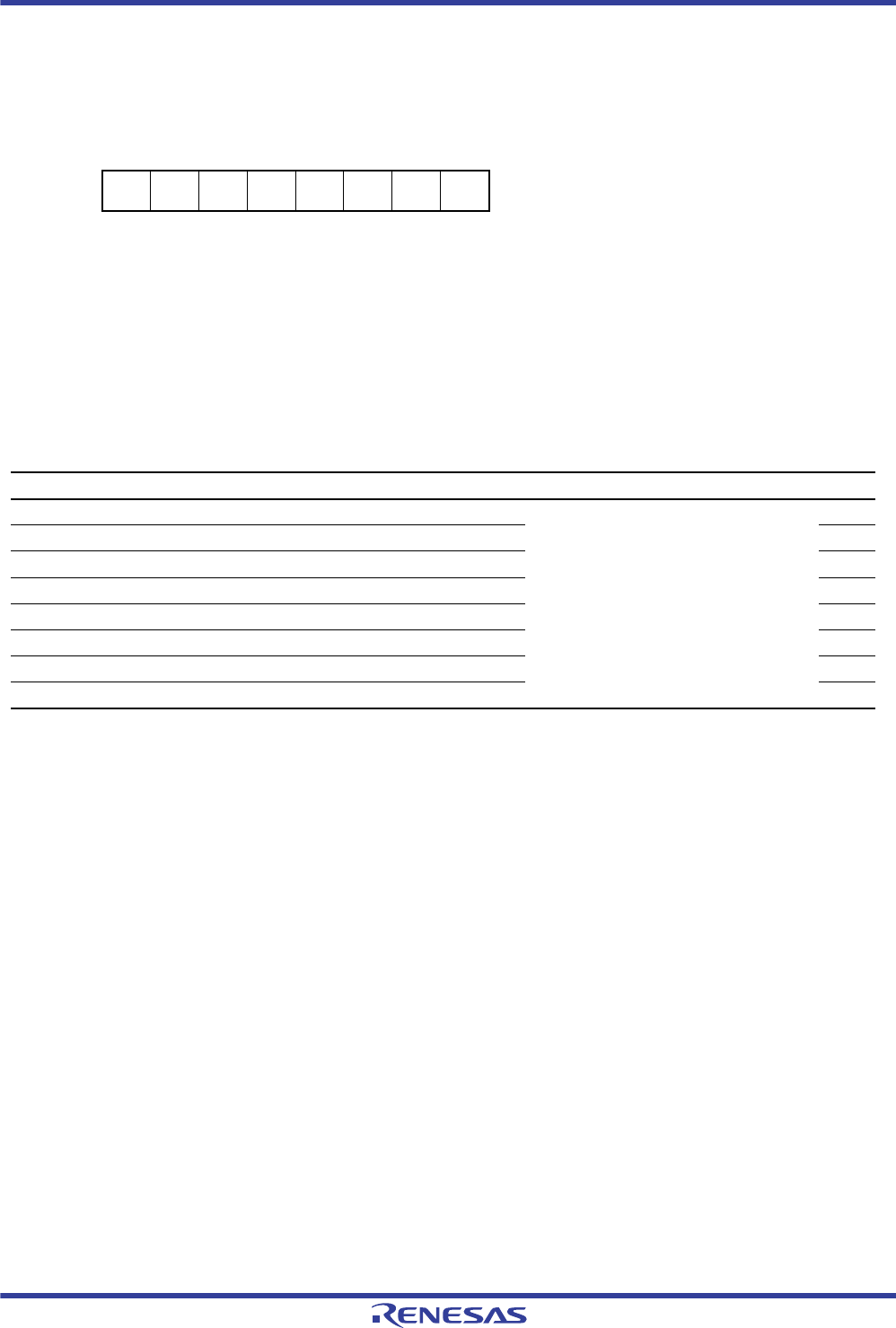
R01UH0034EJ0200 Rev.2.00 Page 375 of 1489
Dec 27, 2013
RX62T Group, RX62G Group 15. I/O Ports
Under development Preliminary document
Specifications in this document are tentative and subject to change.
15.2.2.3 Port Register (PORT)
n = 1 to 9, A, B, D, E
PORT reflects individual pin states of the corresponding port.
When a PORTn.PORT (n = 1 to 9, A, B, D, E, G) is read, the corresponding pin states are read out to here.
Address: PORT1.PORT 0008 C041h, PORT2.PORT 0008 C042h, PORT3.PORT 0008 C043h, PORT4.PORT 0008 C044h,
PORT5.PORT 0008 C045h, PORT6.PORT 0008 C046h, PORT7.PORT 0008 C047h, PORT8.PORT 0008 C048h,
PORT9.PORT 0008 C049h, PORTA.PORT 0008 C04Ah, PORTB.PORT 0008 C04Bh, PORTD.PORT 0008 C04Dh,
PORTE.PORT 0008 C04Eh
b7 b6 b5 b4 b3 b2 b1 b0
B7 B6 B5 B4 B3 B2 B1 B0
Value after reset: xxxxxxxx
Note 1. The two lower-order bits are valid and the six higher-order bits are reserved in PORT1.PORT.
The five lower-order bits are valid and the three higher-order bits are reserved in in PORT2.PORT.
The four lower-order bits are valid and the four higher-order bits are reserved in PORT3.PORT.
The six lower-order bits are valid and the two higher-order bits are reserved in PORT5.PORT.
The six lower-order bits are valid and the two higher-order bits are reserved in PORT6.PORT.
The seven lower-order bits are valid and the one higher-order bit is reserved in PORT7.PORT.
The three lower-order bits are valid and the five higher-order bits are reserved in PORT8.PORT.
The seven lower-order bits are valid and the one higher-order bit is reserved in PORT9.PORT.
The six lower-order bits are valid and the two higher-order bits are reserved in PORTA.PORT.
The six lower-order bits are valid and the two higher-order bits are reserved in PORTE.PORT.
Note 2. The reserved bits are read as 1. Writing to these bits has no effect.
Bit Symbol Bit Name Description R/W
b0 B0 Pn0 Individual pin states of the corresponding
port are reflected.
R
b1 B1 Pn1 R
b2 B2 Pn2 R
b3 B3 Pn3 R
b4 B4 Pn4 R
b5 B5 Pn5 R
b6 B6 Pn6 R
b7 B7 Pn7 R

R01UH0034EJ0200 Rev.2.00 Page 376 of 1489
Dec 27, 2013
RX62T Group, RX62G Group 15. I/O Ports
Under development Preliminary document
Specifications in this document are tentative and subject to change.
15.2.2.4 Input Buffer Control Register (ICR)
n = 1 to 9, A, B, D, E
Note 1. For pins being used as input pins, set the corresponding bits to 1. Set the bits corresponding to pins that are not being used for
their input functions or are being used as analog input pins to 0.
Each PORTn.ICR controls the input buffers for the individual pins of the corresponding port.
Each bit of a PORTn.ICR (n = 1 to 9, A, B, D, E) corresponds to a pin of Pn, and the settings can change from bit to bit.
When to be used as an input pin for the peripheral module, the input buffer for the corresponding pin should be enabled
beforehand by setting the PORTn.ICR bit to 1. If this register is used as an input pin for the peripheral module while the
PORTn.ICR bit is 0, the input signal to the peripheral module is fixed high.
When a Pn.PORT register is read, the pin states of the corresponding port are read out regardless of the values in
PORTn.ICR. For bits where the value in PORTn.ICR is 0, however, the value may not reflect the pin state on the
corresponding peripheral module side.
Changes in the settings of a PORTn.ICR may generate edges internally, depending on the pin state. For this reason,
change the settings of PORTn.ICR while the corresponding input pins are not in use. For example, in the case of IRQi (i
= 0 to 7) inputs, change settings of the corresponding PORTn.ICR with interrupts disabled by clearing the IR flag in IRi
(i = 64 to 71 ("i" shows an interrupt vector number of the IRQ)) of the interrupt controller (ICU) to 0, and then enable the
corresponding interrupts. If a change to a PORTn.ICR setting does generate an edge, negate the edge.
Address: PORT1.ICR 0008 C061h, PORT2.ICR 0008 C062h, PORT3.ICR 0008 C063h, PORT4.ICR 0008 C064h,
PORT5.ICR 0008 C065h, PORT6.ICR 0008 C066h, PORT7.ICR 0008 C067h, PORT8.ICR 0008 C068h,
PORT9.ICR 0008 C069h, PORTA.ICR 0008 C06Ah, PORTB.ICR 0008 C06Bh, PORTD.ICR 0008 C06Dh,
PORTE.ICR 0008 C06Eh
b7 b6 b5 b4 b3 b2 b1 b0
B7 B6 B5 B4 B3 B2 B1 B0
Value after reset: 00000000
Note 1. The two lower-order bits are valid and the six higher-order bits are reserved in PORT1.ICR.
The five lower-order bits are valid and the three higher-order bits are reserved in in PORT2.ICR.
The four lower-order bits are valid and the four higher-order bits are reserved in PORT3.ICR.
The six lower-order bits are valid and the two higher-order bits are reserved in PORT5.ICR.
The six lower-order bits are valid and the two higher-order bits are reserved in PORT6.ICR.
The seven lower-order bits are valid and the one higher-order bit is reserved in PORT7.ICR.
The three lower-order bits are valid and the five higher-order bits are reserved in PORT8.ICR.
The seven lower-order bits are valid and the one higher-order bit is reserved in PORT9.ICR.
The six lower-order bits are valid and the two higher-order bits are reserved in PORTA.ICR.
b5 to b3, b1, and b0 are valid and b7, b6, and b2 are reserved in PORTE.ICR.
Note 2. The reserved bits are read as 0. The write value should always be 0.
Bit Symbol Bit Name Description R/W
b0 B0*1Pn0 Input Buffer Control 0: The input buffer for the corresponding pin is
disabled.
1: The input buffer for the corresponding pin is
enabled.
R/W
b1 B1*1Pn1 Input Buffer Control R/W
b2 B2*1Pn2 Input Buffer Control R/W
b3 B3*1Pn3 Input Buffer Control R/W
b4 B4*1Pn4 Input Buffer Control R/W
b5 B5*1Pn5 Input Buffer Control R/W
b6 B6*1Pn6 Input Buffer Control R/W
b7 B7*1Pn7 Input Buffer Control R/W
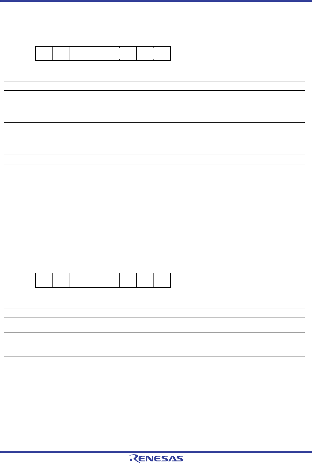
R01UH0034EJ0200 Rev.2.00 Page 377 of 1489
Dec 27, 2013
RX62T Group, RX62G Group 15. I/O Ports
Under development Preliminary document
Specifications in this document are tentative and subject to change.
15.2.2.5 Port Function Register 8 (PF8IRQ)
PF8IRQ is used to select pins for IRQ0 to IRQ1 inputs.
ITSi Bit (IRQi Pin Select) (i = 0 and 1)
Each bit selects a pin for an IRQi input.
15.2.2.6 Port Function Register A (PFAADC)
PFAADC is used to select the ADTRG0# and ADTRG1# pins.
ADTRGnS Bit (ADTRGn# Input Select) (n=0 and 1)
This bit selects a pin for an ADTRGn# input.
Address: 0008 C108h
b7 b6 b5 b4 b3 b2 b1 b0
———— ITS1[1:0] ITS0[1:0]
Value after reset: 00000000
Bit Symbol Bit Name Description R/W
b1 to b0 ITS0[1:0] IRQ0 Pin Select b1 b0
0 0:P10 is designated as the IRQ0-A input pin.
0 1:PE5 is designated as the IRQ0-B input pin.
1 0:Setting prohibited
1 1:Setting prohibited
R/W
b3 to b2 ITS1[1:0] IRQ1 Pin Select b3 b2
0 0:P11 is designated as the IRQ1-A input pin.
0 1:PE4 is designated as the IRQ1-B input pin.
1 0:Setting prohibited
1 1:Setting prohibited
R/W
b7 to b4 — Reserved These bits are always read as 0. The write value should always be 0. R/W
Address: 0008 C10Ah
b7 b6 b5 b4 b3 b2 b1 b0
——————
ADTRG
1S ADTRG
0S
Value after reset: 00000000
Bit Symbol Bit Name Description R/W
b0 ADTRG0S ADTRG0# Input Select 0:PA4 is designated as the ADTRG0#-A input pin.
1:P20 is designated as the ADTRG0#-B input pin.
R/W
b1 ADTRG1S ADTRG1# Input Select 0:PA5 is designated as the ADTRG1#-A input pin.
1:P21 is designated as the ADTRG1#-B input pin.
R/W
b7-b2 — Reserved These bits are always read as 0. The write value should always be 0. R/W

R01UH0034EJ0200 Rev.2.00 Page 378 of 1489
Dec 27, 2013
RX62T Group, RX62G Group 15. I/O Ports
Under development Preliminary document
Specifications in this document are tentative and subject to change.
15.2.2.7 Port Function Register C (PFCMTU)
PFCMTU is used to select pins for MTU3.
MTUSi Bit (MTU3 Pin Select) (i = 0 and 1)
Each bit selects a pin for an MTU3 input/output.
TCLKS[1:0] Bit (MTCLK Pin Select)
This bit selects a pin for a MTCLK input of the MTU3.
Address: 008 C10Ch
b7 b6 b5 b4 b3 b2 b1 b0
TCLKS[1:0]————MTUS1MTUS0
Value after reset: 00000000
Bit Symbol Bit Name Description R/W
b0 MTUS0 MTU3 Pin Select 0 0:PB3 is designated as the MTIOC0A-A pin.
1:P31 is designated as the MTIOC0A-B pin.
R/W
b1 MTUS1 MTU3 Pin Select 1 0:PB2 is designated as the MTIOC0B-A pin.
1:P30 is designated as the MTIOC0B-B pin.
R/W
b5 to b2 — (Reserved) These bits are always read as 0. The write value should always be 0. R/W
b7, b6 TCLKS[1:0] MTCLK Pin Select b7 b6
0 0:P33 is designated as the MTCLKA-A pin.
P32 is designated as the MTCLKB-A pin.
P31 is designated as the MTCLKC-A pin.
P30 is designated as the MTCLKD-A pin.
0 1:P21 is designated as the MTCLKA-B pin.
P20 is designated as the MTCLKB-B pin.
P11 is designated as the MTCLKC-B pin.
P10 is designated as the MTCLKD-B pin.
1 0:PE4 is designated as the MTCLKC-C pin.
PE3 is designated as the MTCLKD-C pin.
(MTCLKA and MTCLKB pins cannot be selected.)
1 1:Setting prohibited
R/W
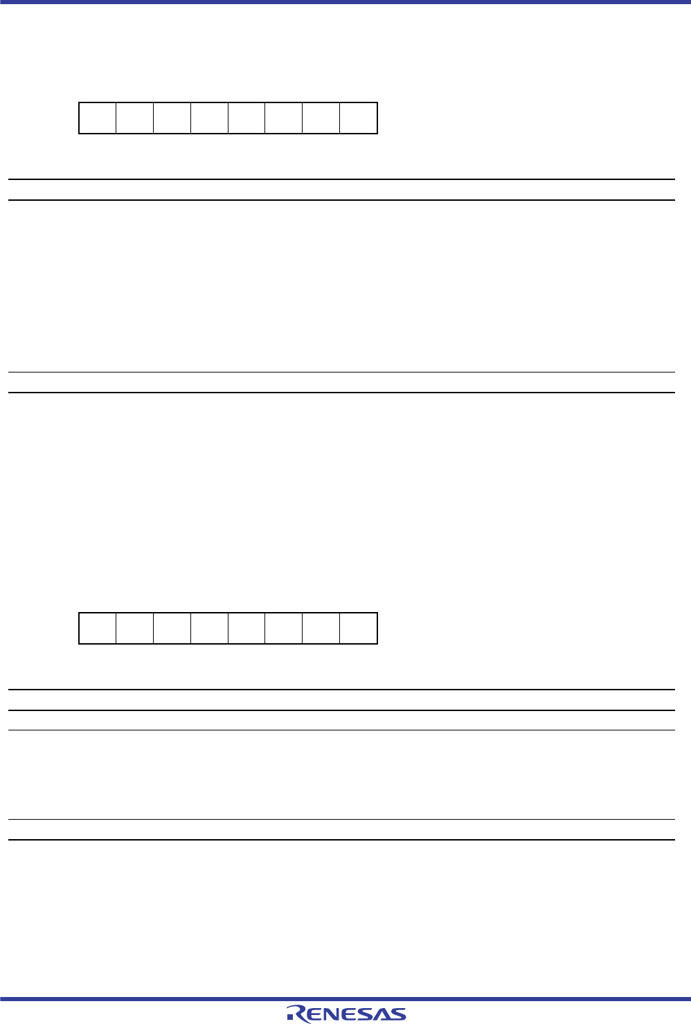
R01UH0034EJ0200 Rev.2.00 Page 379 of 1489
Dec 27, 2013
RX62T Group, RX62G Group 15. I/O Ports
Under development Preliminary document
Specifications in this document are tentative and subject to change.
15.2.2.8 Port Function Register D (PFDGPT)
PFDGPT is used to select a pin for GPT.
GPTS Bit (GPT I/O Pin Select)
Each bit selects a pin for a GPT input/output.
15.2.2.9 Port Function Register F (PFFSCI)
PFFSCI is used to select pins for SCI.
SCI2S Bit (SCI2 I/O Pin Select)
Each bit selects a pin for an SCI channel-2 input/output.
Address: 0008 C10Dh
b7 b6 b5 b4 b3 b2 b1 b0
———————GPTS
Value after reset: 00000000
Bit Symbol Bit Name Description R/W
b0 GPTS GPT Pin Select 0:P71 is designated as the GTIOC0A-A pin.
P74 is designated as the GTIOC0B-A pin.
P72 is designated as the GTIOC1A-A pin.
P75 is designated as the GTIOC1B-A pin.
P73 is designated as the GTIOC2A-A pin.
P76 is designated as the GTIOC2B-A pin.
1:PD7 is designated as the GTIOC0A-B pin.
PD6 is designated as the GTIOC0B-B pin.
PD5 is designated as the GTIOC1A-B pin.
PD4 is designated as the GTIOC1B-B pin.
PD3 is designated as the GTIOC2A-B pin.
PD2 is designated as the GTIOC2B-B pin.
R/W
b7 to b1 — Reserved These bits are always read as 0. The write value should always be 0. R/W
Address: 0008 C10Fh
b7 b6 b5 b4 b3 b2 b1 b0
—————SCI2S——
Value after reset: 00000000
Bit Symbol Bit Name Description R/W
b1 to b0 — Reserved These bits are always read as 0. The write value should always be 0. R/W
b2 SCI2S SCI2I/O Pin Select 0:PB6 is designated as the RXD2-A pin.
PB7 is designated as the SCK2-A pin.
PB5 is designated as the TXD2-A pin.
1:P80 is designated as the RXD2-B pin.
P82 is designated as the SCK2-B pin.
P81 is designated as the TXD2-B pin.
R/W
b7 to b3 — Reserved These bits are always read as 0. The write value should always be 0. R/W

R01UH0034EJ0200 Rev.2.00 Page 380 of 1489
Dec 27, 2013
RX62T Group, RX62G Group 15. I/O Ports
Under development Preliminary document
Specifications in this document are tentative and subject to change.
15.2.2.10 Port Function Register G (PFGSPI)
PFGSPI is used to select I/O pins for RSPI.
RSPCKE Bit (RSPCK Output Enable)
This bit enables or disables the output of the RSPCK pin. Set this bit to 1 to use the RSPCK pin.
MOSIE Bit (MOSI Output Enable)
This bit enables or disables the output of the MOSI pin. Set this bit to 1 to use the MOSI pin.
MISOE Bit (MISO Output Enable)
This bit enables or disables the output of the MISO pin. Set this bit to 1 to use the MISO pin.
SSL0E Bit (SSL0 Output Enable)
This bit enables or disables the output of the SSL0 pin. Set this bit to 1 to use the SSL0 pin.
SSL1E Bit (SSL1 Output Enable)
This bit enables or disables the output of the SSL1 pin. Set this bit to 1 to use the SSL1 pin.
SSL2E Bit (SSL2 Output Enable)
This bit enables or disables the output of the SSL2 pin. Set this bit to 1 to use the SSL2 pin.
SSL3E Bit (SSL3 Output Enable)
This bit enables or disables the output of the SSL3 pin. Set this bit to 1 to use the SSL3 pin.
Address: 0008 C110h
b7 b6 b5 b4 b3 b2 b1 b0
SSL3E SSL2E SSL1E SSL0E MISOE MOSIE RSPCK
E—
Value after reset: 00000000
Bit Symbol Bit Name Description R/W
b0 — Reserved This bit is always read as 0. The write value should always be 0. R/W
b1 RSPCKE RSPCK Output Enable 0:RSPCK pin is disabled.
1:RSPCK pin is enabled.
R/W
b2 MOSIE MOSI Output Enable 0:MOSI pin is disabled.
1:MOSI pin is enabled.
R/W
b3 MISOE MISO Output Enable 0:MISO pin is disabled.
1:MISO pin is enabled.
R/W
b4 SSL0E SSL0 Output Enable 0:SSL0 pin is disabled.
1:SSL0 pin is enabled.
R/W
b5 SSL1E SSL1 Output Enable 0:SSL1 pin is disabled.
1:SSL1 pin is enabled.
R/W
b6 SSL2E SSL2 Output Enable 0:SSL2 pin is disabled.
1:SSL2 pin is enabled.
R/W
b7 SSL3E SSL3 Output Enable 0:SSL3 pin is disabled.
1:SSL3 pin is enabled.
R/W

R01UH0034EJ0200 Rev.2.00 Page 381 of 1489
Dec 27, 2013
RX62T Group, RX62G Group 15. I/O Ports
Under development Preliminary document
Specifications in this document are tentative and subject to change.
15.2.2.11 Port Function Register H (PFHSPI)
PFHSPI is used to select I/O pins for RSPI channel.
RSPIS[1:0] Bit (RSPI Pin Select)
This bit selects a pin for an RSPI input/output.
As an enable bit is provided for each RSPI input/output pin, the input/output pin is selectable while the corresponding
enable bit is 1. Otherwise, the pin cannot be selected.
Address: 0008 C10Fh
b7 b6 b5 b4 b3 b2 b1 b0
——————RSPIS[1:0]
Value after reset: 00000000
Bit Symbol Bit Name Description R/W
b1 to b0 RSPIS[1:0] RSPI Pin Select b1 b0
0 0:P22 is designated as the MISO-A pin.
P23 is designated as the MOSI-A pin.
P24 is designated as the RSPCK-A pin.
P30 is designated as the SSL0-A pin.
P31 is designated as the SSL1-A pin.
P32 is designated as the SSL2-A pin.
P33 is designated as the SSL3-A pin.
0 1:PA5 is designated as the MISO-B pin.
PB0 is designated as the MOSI-B pin.
PA4 is designated as the RSPCK-B pin.
PA3 is designated as the SSL0-B pin.
PA2 is designated as the SSL1-B pin.
PA1 is designated as the SSL2-B pin.
PA0 is designated as the SSL3-B pin.
1 0:PD1 is designated as the MISO-C pin.
PD2 is designated as the MOSI-C pin.
PD0 is designated as the RSPCK-C pin.
PD6 is designated as the SSL0-C pin.
PD7 is designated as the SSL1-C pin.
PE0 is designated as the SSL2-C pin.
PE1 is designated as the SSL3-C pin.
1 1:Setting prohibited
R/W
b7 to b2 — Reserved These bits are always read as 0. The write value should always be 0. R/W

R01UH0034EJ0200 Rev.2.00 Page 382 of 1489
Dec 27, 2013
RX62T Group, RX62G Group 15. I/O Ports
Under development Preliminary document
Specifications in this document are tentative and subject to change.
15.2.2.12 Port Function Register J (PFJCAN)
PFJCAN is used to select I/O pins for the CAN.
CANE Bit (CAN Pin Enable)
This bit enables or disables the CAN pin. Set this bit to 1 to use the CAN pin.
CANS[1:0] Bit (CAN Pin Select)
These bits select I/O pins for the CAN.
15.2.2.13 Port Function Register K (PFKLIN)
PFKLIN is used to set I/O pins for the LIN.
LINE Bit ( LIN Pin Enable)
This bit enables or disables the LIN pin. Set this bit to 1 to use the LIN pin.
Address: 0008 C113h
b7 b6 b5 b4 b3 b2 b1 b0
CANS[1:0]—————CANE
Value after reset: 00000000
Bit Symbol Bit Name Description R/W
b0 CANE CAN Pin Enable 0: The CTX and CRX pins are disabled.
1: The CTX and CRX pins are enabled.
R/W
b5 to b1 — Reserved These bits are always read as 0. The write value should always be 0. R/W
b7 to b6 CANS[1:0] CAN Pin Select b7 b6
0 0:PB5 is designated as the CTX-A pin.
PB6 is designated as the CRX-A pin.
0 1:P23 is designated as the CTX-B pin.
P22 is designated as the CRX-B pin.
1 0:PE0 is designated as the CRX-C pin.
PD7 is designated as the CTX-C pin.
1 1:Setting prohibited
R/W
Address: 0008 C114h
b7 b6 b5 b4 b3 b2 b1 b0
———————LINE
Value after reset: 00000000
Bit Symbol Bit Name Description R/W
b0 LINE LIN Pin Enable 0:LTX and LRX pins are disabled.
1:LTX and LRX pins are enabled.
R/W
b7 to b1 — Reserved These bits are always read as 0. The write value should always be 0. R/W

R01UH0034EJ0200 Rev.2.00 Page 383 of 1489
Dec 27, 2013
RX62T Group, RX62G Group 15. I/O Ports
Under development Preliminary document
Specifications in this document are tentative and subject to change.
15.2.2.14 Port Function Register M (PFMPOE)
Note 1. The first round of writing after a reset is enabled; though subsequent writing is not allowed.
PFMPOE enables or disables POEn# input pins.
To prevent the error in the system, be sure to write to this register after a reset.
The first round of writing after a reset is only enabled
POEnE Bit (POEn# Input Enable) (n = 0, 4, 8, 10, 11)
Each bit enables or disables the corresponding POEn# input.
To use POEn#, set the corresponding POEnE bit to 1.
15.2.2.15 Port Function Register N (PFNPOE)
Note 1. The first round of writing after a reset is enabled; though subsequent writing is not allowed.
PFNPOE enables or disables POEn# input pins.
To prevent the error in the system, be sure to write to this register after a reset.
The first round of writing after a reset is only enabled.
POE10S Bit (POE10# Input Select)
This bit select input pins for the POE10#.
Address: 0008 C116h
b7 b6 b5 b4 b3 b2 b1 b0
———
POE11
EPOE10
EPOE8E POE4E POE0E
Value after reset: 00000000
Bit Symbol Bit Name Description R/W
b0 POE0E POE0# Input Enable 0:Designated as an I/O port pin
1:Designated as the POEn# input pin (n = 0, 4, 8, 10, 11)
R/W*1
b1 POE4E POE4# Input Enable R/W*1
b2 POE8E POE8# Input Enable R/W*1
b3 POE10E POE10# Input Enable R/W*1
b4 POE11E POE11# Input Enable R/W*1
b7 to b5 — Reserved These bits are always read as 0. The write value should always be 0. R/W
Address: 0008 C117h
b7 b6 b5 b4 b3 b2 b1 b0
POE10
S———————
Value after reset: 00000000
Bit Symbol Bit Name Description R/W
b6 to b0 — Reserved These bits are always read as 0. The write value should always be 0. R/W
b7 POE10S POE10# Input Select 0:PE2 is designated as the POE10#-A input pin.
1:PE4 B is designated as the POE10# input pin.
R/W*1

R01UH0034EJ0200 Rev.2.00 Page 384 of 1489
Dec 27, 2013
RX62T Group, RX62G Group 15. I/O Ports
Under development Preliminary document
Specifications in this document are tentative and subject to change.
15.2.3 Settings of Ports
When individual pins for peripheral modules are enabled, the settings for each port are modified.
An input pin for the peripheral module is specified independently by the peripheral module. To use an input pin for the
peripheral module, the corresponding bit in the input buffer control register (PORTn.ICR) should be set to 1 to enable the
input buffer, except for the port register read, NMI, and POEn# pin inputs.
The pins that function as output pins and I/O pins should be enabled for respective peripheral modules. If a conflict
occurs among the output signal enable settings for peripheral modules, that are multiplexed to the same port, the priority
will be handled according to the port-multiplexed priority.
Table 15.12 lists the port-multiplexed priority for peripheral modules.
Table 15.12 Port-Multiplexed Priority for Peripheral Modules (100-Pin LQFP)
Priority Module Name Output Pins
High
Low
1 RSPI RSPCK, MOSI, MISO, SSL0 to SSL3
2CAN CTX
3LIN LTX
4 MTU0 to MTU7 MTIOC0A, MTIOC0B, MTIOC0C, MTIOC0D, MTIOC1A, MTIOC1B, MTIOC2A, MTIOC2B,
MTIOC3A, MTIOC3B, MTIOC3C, MTIOC3D, MTIOC4A, MTIOC4B, MTIOC4C, MTIOC4D,
MTIOC6A, MTIOC6B, MTIOC6C, MTIOC6D, MTIOC7A, MTIOC7B, MTIOC7C, MTIOC7D
5 GPT0 to GPT3 GTIOC0A, GTIOC0B, GTIOC1A, GTIOC1B,
GTIOC2A, GTIOC2B, GTIOC3A, GTIOC3B
6 SCI0 to SCI2 SCK0 to SCK2, TXD0 to TXD2
7 RIIC SCL, SDA
8 IOPORT P10 to P11, P20 to P24, P30 to P33, P70 to P76, P80 to P82, P90 to P96, PA0 to PA5,
PB0 to PB7, PD0 to PD7, PE0 to PE1, PE3 to PE5

R01UH0034EJ0200 Rev.2.00 Page 385 of 1489
Dec 27, 2013
RX62T Group, RX62G Group 15. I/O Ports
Under development Preliminary document
Specifications in this document are tentative and subject to change.
15.2.4 List of Output Enable Settings
Table 15.13 lists the output enable settings for each port.
For details on the applicable output signals, see descriptions of the registers for each peripheral module.
Setting the port function register changes the functions of peripheral-module pins with names ending in A to C.
Table 15.13 Output Enable Settings for Each Port (100-Pin LQFP) (1 / 5)
Port Module Name Output
Signal Name Port Function Register
Settings Peripheral Module Settings
P10 PORT1 P10 PORT1.DDR.B0 = 1
P11 PORT1 P11 PORT1.DDR.B1 = 1
P20 PORT1 P20 PORT2.DDR.B0 = 1
P21 PORT1 P21 PORT2.DDR.B1 = 1
P22 RSPI MISO-A PFGSPI.MISOE = 1
PFHSPI.RSPIS[1:0] = 00
(In addition to the pin enable setting, input/output switching
function for the peripheral module is provided.)
PORT2 P22 PORT2.DDR.B2 = 1
P23 RSPI MOSI-A PFGSPI.MOSIE = 1
PFHSPI.RSPIS[1:0] = 00
(In addition to the pin enable setting, input/output switching
function for the peripheral module is provided.)
CAN CTX-B PFJCAN.CANE = 1
PFJCAN.CANS[1:0] = 01
(The signal output state is specified by the peripheral module
settings.)
LIN LTX PFKLIN.LINE = 1 (The signal output state is specified by the peripheral module
settings.)
PORT2 P23 PORT2.DDR.B3 =1
P24 RSPI RSPCK-A PFGSPI.RSPCKE =1
PFHSPI.RSPIS[1:0] = 00
(In addition to the pin enable setting, input/output switching
function for the peripheral module is provided.)
PORT2 P24 PORT2.DDR.B4 = 1
P30 RSPI SSL0-A PFGSPI.SSL0E = 1
PFHSPI.RSPIS[1:0] = 00
(In addition to the pin enable setting, input/output switching
function for the peripheral module is provided.)
MTU0 MTIOC0B-B PFCMTU.MTUS1 = 1 (The signal output state is specified by the peripheral module
settings.)
PORT3 P30 PORT3.DDR.B0 = 1
P31 RSPI SSL1-A PFGSPI.SSL1E = 1
PFHSPI.RSPIS[1:0] = 00
(The signal output state is specified by the peripheral module
settings.)
MTU0 MTIOC0A-B PFCMTU.MTUS0 = 1 (The signal output state is specified by the peripheral module
settings.)
PORT3 P31 PORT3.DDR.B1=1
P32 RSPI SSL2-A PFGSPI.SSL2E = 1
PFHSPI.RSPIS[1:0] = 00
(The signal output state is specified by the peripheral module
settings.)
MTU3 MTIOC3C (The signal output state is specified by the peripheral module
settings.)
PORT3 P32 PORT3.DDR.B2 = 1
P33 RSPI SSL3-A PFGSPI.SSL3E =1
PFHSPI.RSPIS[1:0] = 00
(The signal output state is specified by the peripheral module
settings.)
MTU3 MTIOC3A (The signal output state is specified by the peripheral module
settings.)
PORT3 P33 PORT3.DDR.B3 = 1
P70 PORT7 P70 PORT7.DDR.B0 = 1
P71 MTU3 MTIOC3B (The signal output state is specified by the peripheral module
settings.)
GPT0 GTIOC0A-A PFDGPT.GPTS = 0 (The signal output state is specified by the peripheral module
settings.)
PORT7 P71 PORT7.DDR.B1 = 1

R01UH0034EJ0200 Rev.2.00 Page 386 of 1489
Dec 27, 2013
RX62T Group, RX62G Group 15. I/O Ports
Under development Preliminary document
Specifications in this document are tentative and subject to change.
P72 MTU4 MTIOC4A (The signal output state is specified by the peripheral module
settings.)
GPT1 GTIOC1A-A PFDGPT.GPTS = 0 (The signal output state is specified by the peripheral module
settings.)
PORT7 P72 PORT7.DDR.B2 = 1
P73 MTU4 MTIOC4B (The signal output state is specified by the peripheral module
settings.)
GPT2 GTIOC2A-A PFDGPT.GPTS = 0 (The signal output state is specified by the peripheral module
settings.)
PORT7 P73 PORT7.DDR.B3 = 1
P74 MTU3 MTIOC3D (The signal output state is specified by the peripheral module
settings.)
GPT0 GTIOC0B-A PFDGPT.GPTS = 0 (The signal output state is specified by the peripheral module
settings.)
PORT7 P74 PORT7.DDR.B4 = 1
P75 MTU4 MTIOC4C (The signal output state is specified by the peripheral module
settings.)
GPT1 GTIOC1B-A PFDGPT.GPTS = 0 (The signal output state is specified by the peripheral module
settings.)
PORT7 P75 PORT7.DDR.B5 = 1
P76 MTU4 MTIOC4D (The signal output state is specified by the peripheral module
settings.)
GPT2 GTIOC2B-A PFDGPT.GPTS = 0 (The signal output state is specified by the peripheral module
settings.)
PORT7 P76 PORT7.DDR.B6 = 1
P80 PORT8 P80 PORT8.DDR.B0 = 1
P81 SCI2 TXD2-B PFFSCI.SCI2S = 1 SCI2.SCR.TE = 1
PORT8 P81 PORT8.DDR.B1 = 1
P82 SCI2 SCK2-B PFFSCI.SCI2S = 1 When SCI2.SCMR.SMIF = 1:
While SMR.GM = 0, SCR.CKE[1:0] = 01 or SMR.GM = 1,
SCR.TE = 1 or SCR.RE = 1
When SCI2.SCMR.SMIF = 0:
While SMR.CM = 0, SCR.CKE[1:0] = 01 or SMR.CM = 1,
SCR.CKE[1] = 0, SCR.TE = 1 or SCR.RE = 1
PORT8 P82 PORT8.DDR.B2 = 1
P90 MTU7 MTIOC7D (The signal output state is specified by the peripheral module
settings.)
PORT9 P90 PORT9.DDR.B0 = 1
P91 MTU7 MTIOC7C (The signal output state is specified by the peripheral module
settings.)
PORT9 P91 PORT9.DDR.B1 = 1
P92 MTU6 MTIOC6D (The signal output state is specified by the peripheral module
settings.)
PORT9 P92 PORT9.DDR.B2 = 1
P93 MTU7 MTIOC7B (The signal output state is specified by the peripheral module
settings.)
PORT9 P93 PORT9.DDR.B3 = 1
P94 MTU7 MTIOC7A (The signal output state is specified by the peripheral module
settings.)
PORT9 P94 PORT9.DDR.B4 = 1
Table 15.13 Output Enable Settings for Each Port (100-Pin LQFP) (2 / 5)
Port Module Name Output
Signal Name Port Function Register
Settings Peripheral Module Settings

R01UH0034EJ0200 Rev.2.00 Page 387 of 1489
Dec 27, 2013
RX62T Group, RX62G Group 15. I/O Ports
Under development Preliminary document
Specifications in this document are tentative and subject to change.
P95 MTU6 MTIOC6B (The signal output state is specified by the peripheral module
settings.)
PORT9 P95 PORT9.DDR.B5 = 1
P96 PORT9 P96 PORT9.DDR.B6 = 1
PA0 RSPI SSL3-B PFGSPI.SSL3E = 1
PFHSPI.RSPIS[1:0] = 01
(The signal output state is specified by the peripheral module
settings.)
MTU6 MTIOC6C (The signal output state is specified by the peripheral module
settings.)
PORTA PA0 PORTA.DDR.B0 = 1
PA1 RSPI SSL2-B PFGSPI.SSL2E = 1
PFHSPI.RSPIS[1:0] = 01
(The signal output state is specified by the peripheral module
settings.)
MTU6 MTIOC6A (The signal output state is specified by the peripheral module
settings.)
PORTA PA1 PORTA.DDR.B1 = 1
PA2 RSPI SSL1-B PFGSPI.SSL1E = 1
PFHSPI.RSPIS[1:0] = 01
(The signal output state is specified by the peripheral module
settings.)
MTU2 MTIOC2B (The signal output state is specified by the peripheral module
settings.)
PORTA PA2 PORTA.DDR.B2 = 1
PA3 RSPI SSL0-B PFGSPI.SSL0E = 1
PFHSPI.RSPIS[1:0] = 01
(In addition to the pin enable setting, input/output switching
function for the peripheral module is provided.)
MTU2 MTIOC2A (The signal output state is specified by the peripheral module
settings.)
PORTA PA3 PORTA.DDR.B3 = 1
PA4 RSPI RSPCK-B PFGSPI.RSPCKE = 1
PFHSPI.RSPIS[1:0] = 01
(In addition to the pin enable setting, input/output switching
function for the peripheral module is provided.)
MTU1 MTIOC1B (The signal output state is specified by the peripheral module
settings.)
PORTA PA4 PORTA.DDR.B4 = 1
PA5 RSPI MISO-B PFGSPI.MISOE = 1
PFHSPI.RSPIS[1:0] = 01
(In addition to the pin enable setting, input/output switching
function for the peripheral module is provided.)
MTU1 MTIOC1A (The signal output state is specified by the peripheral module
settings.)
PORTA PA5 PORTA.DDR.B5 = 1
PB0 RSPI MOSI-B PFGSPI.MOSIE = 1
PFHSPI.RSPIS[1:0] = 01
(In addition to the pin enable setting, input/output switching
function for the peripheral module is provided.)
MTU0 MTIOC0D (The signal output state is specified by the peripheral module
settings.)
PORTB PB0 PORTB.DDR.B0 = 1
PB1 MTU0 MTIOC0C (The signal output state is specified by the peripheral module
settings.)
RIIC SCL RIIC.ICCR1.ICE = 1
PORTB PB1 PORTB.DDR.B1 = 1
PB2 MTU0 MTIOC0B-A PFCMTU.MTUS1 = 0 (The signal output state is specified by the peripheral module
settings.)
SCI0 TXD0 SCI0.SCR.TE = 1
RIIC SDA RIIC.ICCR1.ICE = 1
PORTB PB2 PORTB.DDR.B2 = 1
Table 15.13 Output Enable Settings for Each Port (100-Pin LQFP) (3 / 5)
Port Module Name Output
Signal Name Port Function Register
Settings Peripheral Module Settings

R01UH0034EJ0200 Rev.2.00 Page 388 of 1489
Dec 27, 2013
RX62T Group, RX62G Group 15. I/O Ports
Under development Preliminary document
Specifications in this document are tentative and subject to change.
PB3 MTU0 MTIOC0A-A PFCMTU.MTUS0 = 0 (The signal output state is specified by the peripheral module
settings.)
SCI0 SCK0 When SCI0.SCMR.SMIF = 1:
While SMR.GM = 0, SCR.CKE[1:0] = 01 or SMR.GM = 1,
SCR.TE = 1 or SCR.RE = 1
When SCI0.SCMR.SMIF = 0:
While SMR.CM = 0, SCR.CKE[1:0] = 01 or SMR.CM = 1,
SCR.CKE[1] = 0, SCR.TE = 1 or SCR.RE = 1
PORTB PB3 PORTB.DDR.B3 = 1
PB4 PORTB PB4 PORTB.DDR.B4 = 1
PB5 CAN CTX-A PFJCAN.CANE = 1
PFJCAN.CANS[1:0] = 00
(The signal output state is specified by the peripheral module
settings.)
SCI2 TXD2-A PFFSCI.SCI2S = 0 SCI2.SCR.TE = 1
PORTB PB5 PORTB.DDR.B5 = 1
PB6 PORTB PB6 PORTB.DDR.B6 = 1
PB7 SCI2 SCK2-A PFFSCI.SCI2S = 0 When SCI2.SCMR.SMIF =1:
While SMR.GM = 0, SCR.CKE[1:0] = 01 or SMR.GM = 1,
SCR.TE = 1 or SCR.RE = 1
When SCI2.SCMR.SMIF = 0:
While SMR.CM = 0, SCR.CKE[1:0] = 01 or SMR.CM = 1,
SCR.CKE[1] = 0, SCR.TE = 1 or SCR.RE = 1
PORTB PB7 PORTB.DDR.B7 = 1
PD0 RSPI RSPCK-C PFGSPI.RSPCKE = 1
PFHSPI.RSPIS[1:0] = 10
(In addition to the pin enable setting, input/output switching
function for the peripheral module is provided.)
GPT3 GTIOC3B (The signal output state is specified by the peripheral module
settings.)
PORTD PD0 PORTD.DDR.B0 = 1
PD1 RSPI MISO-C PFGSPI.MISOE = 1
PFHSPI.RSPIS[1:0] = 10
(In addition to the pin enable setting, input/output switching
function for the peripheral module is provided.)
GPT3 GTIOC3A (The signal output state is specified by the peripheral module
settings.)
PORTD PD1 PORTD.DDR.B1 = 1
PD2 RSPI MOSI-C PFGSPI.MISOE = 1
PFHSPI.RSPIS[1:0] = 10
(In addition to the pin enable setting, input/output switching
function for the peripheral module is provided.)
GPT2 GTIOC2B-B PFDGPT.GPTS = 1 (The signal output state is specified by the peripheral module
settings.)
PORTD PD2 PORTD.DDR.B2 = 1
PD3 GPT2 GTIOC2A-B PFDGPT.GPTS = 1 (The signal output state is specified by the peripheral module
settings.)
SCI1 TXD1 SCI1.SCR.TE = 1
PORTD PD3 PORTD.DDR.B3 = 1
PD4 GPT1 GTIOC1B-B PFDGPT.GPTS = 1 (The signal output state is specified by the peripheral module
settings.)
SCI1 SCK1 When SCI1.SCMR.SMIF = 1:
While SMR.GM = 0, SCR.CKE[1:0] = 01 or SMR.GM = 1,
SCR.TE = 1 or SCR.RE = 1
When SCI1.SCMR.SMIF = 0:
While SMR.CM = 0, SCR.CKE[1:0] = 01 or SMR.CM = 1,
SCR.CKE[1] = 0, SCR.TE = 1 or SCR.RE = 1
PORTD PD4 PORTD.DDR.B4 = 1
PD5 GPT1 GTIOC1A-B PFDGPT.GPTS = 1 (The signal output state is specified by the peripheral module
settings.)
PORTD PD5 PORTD.DDR.B5 = 1
Table 15.13 Output Enable Settings for Each Port (100-Pin LQFP) (4 / 5)
Port Module Name Output
Signal Name Port Function Register
Settings Peripheral Module Settings

R01UH0034EJ0200 Rev.2.00 Page 389 of 1489
Dec 27, 2013
RX62T Group, RX62G Group 15. I/O Ports
Under development Preliminary document
Specifications in this document are tentative and subject to change.
PD6 RSPI SSL0-C PFGSPI.SSL0E = 1
PFHSPI.RSPIS[1:0] = 10
(In addition to the pin enable setting, input/output switching
function for the peripheral module is provided.)
GPT0 GTIOC0B-B PFDGPT.GPTS = 1 (The signal output state is specified by the peripheral module
settings.)
PORTD PD6 PORTD.DDR.B6 = 1
PD7 RSPI SSL1-C PFGSPI.SSL1E = 1
PFHSPI.RSPIS[1:0] = 10
(The signal output state is specified by the peripheral module
settings.)
CAN CTX-C PFJCAN.CANE = 1
PFJCAN.CANS[1:0] = 10
(The signal output state is specified by the peripheral module
settings.)
GPT0 GTIOC0A-B PFDGPT.GPTS = 1 (The signal output state is specified by the peripheral module
settings.)
PORTD PD7 PORTD.DDR.B7 = 1
PE0 RSPI SSL2-C PFGSPI.SSL2E = 1
PFHSPI.RSPIS[1:0] = 10
(The signal output state is specified by the peripheral module
settings.)
PORTE PE0 PE.DDR.B0 = 1
PE1 RSPI SSL3-C PFGSPI.SSL3E = 1
PFHSPI.RSPIS[1:0] = 10
(The signal output state is specified by the peripheral module
settings.)
PORTE PE1 PORTE.DDR.B1 = 1
PE3 PORTE PE3 PORTE.DDR.B3 = 1
PE4 PORTE PE4 PORTE.DDR.B4 = 1
PE5 PORTE PE5 PORTE.DDR.B5 = 1
Table 15.13 Output Enable Settings for Each Port (100-Pin LQFP) (5 / 5)
Port Module Name Output
Signal Name Port Function Register
Settings Peripheral Module Settings

R01UH0034EJ0200 Rev.2.00 Page 390 of 1489
Dec 27, 2013
RX62T Group, RX62G Group 15. I/O Ports
Under development Preliminary document
Specifications in this document are tentative and subject to change.
15.2.5 Treatment of Unused Pins
The treatment of unused pins is listed in Table 15.14.
Note 1. Do not change the initial value of PORTn.ICR. Changing the initial value may generate shoot-through current.
Table 15.14 Treatment of Unused Pins (100-Pin LQFP)
Pin Name Treatment
EMLE Connect this pin to Vss via a pull-down resistor.
MD1, MD0 (Always used as mode pins)
MDE (Always used as mode pins)
RES# Connect this pin to Vcc via a pull-up resistor.
PE2/NMI/POE10#-A Connect this pin to Vcc via a pull-up resistor.
EXTAL (Always used as a clock pin)
XTAL Leave these pins open.
Ports 1 to 3, 7 to 9,
A, B, D, E
Connect these pins to Vcc via a pull-up resistor or to Vss via a pull-down resistor.
These pins can be left while PORTn.ICR is in the initial state (the input buffer disabled)*1.
Ports 4 Connect these pins to AVCC0 via a pull-up resistor or to AVSS0 via a pull-down resistor.
These pins can be left while PORTn.ICR is in the initial state (the input buffer disabled)*1.
Ports 5 to 6 Connect these pins to AVCC via a pull-up resistor or to AVSS via a pull-down resistor
These pins can be left while PORTn.ICR is in the initial state (the input buffer disabled)*1.
VREFH0 Connect this pin to AVCC0
VREFL0 Connect this pin to AVSS0
VREF Connect this pin to AVCC

R01UH0034EJ0200 Rev.2.00 Page 391 of 1489
Dec 27, 2013
RX62T Group, RX62G Group 15. I/O Ports
Under development Preliminary document
Specifications in this document are tentative and subject to change.
15.3 I/O Port [for 80-Pin LQFP]
The RX62T Group (80-pin LQFP) has 11 I/O ports (ports 1 to 4, 6, 7, 9, A, B, D, E), which handle 44 I/O pins.
15.3.1 Overview
Table 15.15 gives the specifications of the I/O ports and Table 15.16 lists I/O ports and pin functions.
Table 15.15 Specifications of I/O Ports (80-pin LQFP)
Item Description
I/O pins 44
Input pins 13
Number of ports 11 (1 to 4, 6, 7, 9, A, B, D, E)
Open drain outputs 2 (RIIC pin)
Large-current output 6 (MTU3 pin and GPT pin)
Schmitt trigger input pins All port inputs, CAN inputs, IRQ inputs, MTU3 inputs, POE3 inputs, RIIC inputs, SCI inputs, A/D trigger
inputs, NMI inputs, GPT inputs, and LIN inputs
Others Each pin is capable of driving a capacitive load of 30 pF in the case of a TTL load.
When configured as an output, a pin is capable of driving a Darlington transistor.
A pin is always capable of reading the status of the pins.
Table 15.16 Port Functions (80-Pin LQFP) (1 / 3)
Port Description Bit
Function
CMOS
Input Schmitt
Trigger Input
Open
Drain
Output
Capability
Large-
Current
OutputI/O Input Output
Port 1 General I/O port
pins, MTU3 inputs,
and
interrupt inputs
0 P10 MTCLKD-B/IRQ0-A — All input
functions ——
1 P11 MTCLKC-B/IRQ1-A All input
functions
Port 2 General I/O port
pins, MTU3 inputs
interrupt inputs,
A/D converter
inputs,
RSPI I/O signal,
LIN I/O signal, and
CAN I/O signal
0 P20 MTCLKB-B/IRQ7/
ADTRG0#-B — All input
functions ——
1 P21 MTCLKA-B/IRQ6/
ADTRG1#-B All input
functions
2 P22/MISO-A LRX/CRX-B/
ADTRG# MISO-A P22/LRX/
CRX-B/
ADTRG#
3 P23/MOSI-A LTX/CTX-B MOSI-A P23
4 P24/RSPCK-A RSPCK-A P24
Port 3 General I/O port
pins, MTU3 I/O
signal,
RSPI I/O signal
0 P30/MTIOC0B-B/
SSL0-A MTCLKD-A SSL0-A
P30/MTIOC0B-
B
/MTCLKD-A ——
1 P31/MTIOC0A-B MTCLKC-A SSL1-A — All input
functions
2 P32/MTIOC3C MTCLKB-A SSL2-A All input
functions
3 P33/MTIOC3A MTCLKA-A SSL3-A All input
functions

R01UH0034EJ0200 Rev.2.00 Page 392 of 1489
Dec 27, 2013
RX62T Group, RX62G Group 15. I/O Ports
Under development Preliminary document
Specifications in this document are tentative and subject to change.
Port 4 A/D converter inputs
and general input
port pins
0 P40/AN000 — P40 — —
1 P41/AN001 P41
2 P42/AN002 P42
3 P43/AN003/
CVREFL P43
4 P44/AN100 P44
5 P45/AN101 P45
6 P46/AN102 P46
7 P47/AN103/
CVREFH P47
Port 6 A/D converter inputs
and general input
port pins
0 P60/AN0 — P60 — —
1 P61/AN1 P61
2 P62/AN2 P62
3 P63/AN3 P63
Port 7 General I/O port
pins, POE3 inputs,
interrupt inputs,
MTU3 I/O signal,
and
GPT I/O signal
0 P70 POE0#/IRQ5 — All input
functions ——
1 P71/MTIOC3B/
GTIOC0A-A All input
functions
√
2 P72/MTIOC4A/
GTIOC1A-A All input
functions
√
3 P73/MTIOC4B/
GTIOC2A-A All input
functions
√
4 P74/MTIOC3D/
GTIOC0B-A All input
functions
√
5 P75/MTIOC4C/
GTIOC1B-A All input
functions
√
6 P76/MTIOC4D/
GTIOC2B-A All input
functions
√
Port 9 General I/O port
pins, MTU3 I/O
signal,
POE3 inputs, and
interrupt inputs
1 P91/MTIOC7C — All input
functions ——
2 P92/MTIOC6D All input
functions
3 P93/MTIOC7B All input
functions
4 P94/MTIOC7A All input
functions
5 P95/MTIOC6B All input
functions
6 P96 POE4#/IRQ4 All input
functions
Port A General I/O port
pins, MTU3 I/O
signal,
RSPI I/O signal, and
A/D converter inputs
2 PA2/MTIOC2B SSL1-B — All input
functions ——
3PA3/MTIOC2A/
SSL0-B SSL0-B PA3/
MTIOC2A
4PA4/MTIOC1B/
RSPCK-B ADTRG0#-A RSPCK-B PA4/
MTIOC1B/
ADTRG0#-A
5PA5/MTIOC1A/
MISO-B ADTRG1#-A MISO-B PA5/
MTIOC1A/
ADTRG1#-A
Table 15.16 Port Functions (80-Pin LQFP) (2 / 3)
Port Description Bit
Function
CMOS
Input Schmitt
Trigger Input
Open
Drain
Output
Capability
Large-
Current
OutputI/O Input Output

R01UH0034EJ0200 Rev.2.00 Page 393 of 1489
Dec 27, 2013
RX62T Group, RX62G Group 15. I/O Ports
Under development Preliminary document
Specifications in this document are tentative and subject to change.
Port B General I/O port
pins, MTU3 I/O
signal,
RSPI I/O signal,
RIIC I/O signal,
SCI I/O signal,
GPT inputs,
POE3 inputs,
interrupt inputs, and
CAN I/O signal
0PB0/MTIOC0D/
MOSI-B MOSI-B PB0/
MTIOC0D ——
1PB1/MTIOC0C/
SCL RXD0 — All input
functions
√
(SCL only) —
2PB2/MTIOC0B-A/
SDA TXD0 All input
functions
√
(SDA only) —
3PB3/MTIOC0A-A/
SCK0 All input
functions ——
4 PB4 GTETRG/
POE8#/IRQ3 All input
functions
5PB5 TXD2-A/
CTX-A/ All input
functions
6 PB6 RXD2-A/CRX-A All input
functions
7 PB7/SCK2-A All input
functions
Port D General I/O port
pins, GPT I/O
signal,
SCI I/O signal,
CAN outputs, and
on-chip emulator I/O
signal
3 PD3/GTIOC2A-B TXD1/TDO — All input
functions ——
4PD4/GTIOC1B-B/
SCK1 TCK — All input
functions
5 PD5/GTIOC1A-B RXD1/TDI — All input
functions
6 PD6/GTIOC0B-B TMS All input
functions
7 PD7/GTIOC0A-B TRST# CTX-C — All input
functions
Port E General I/O port
pins, CAN inputs,
POE3 inputs,
MTU3 inputs, and
interrupt inputs
0 PE0 CRX-C — All input
functions ——
2 PE2/POE10#-A/
NMI All input
functions
3 PE3 MTCLKD-C/
POE11#/IRQ2-A All input
functions
4 PE4 MTCLKC-C/
POE10#-B/
IRQ1-B
All input
functions
Table 15.16 Port Functions (80-Pin LQFP) (3 / 3)
Port Description Bit
Function
CMOS
Input Schmitt
Trigger Input
Open
Drain
Output
Capability
Large-
Current
OutputI/O Input Output

R01UH0034EJ0200 Rev.2.00 Page 394 of 1489
Dec 27, 2013
RX62T Group, RX62G Group 15. I/O Ports
Under development Preliminary document
Specifications in this document are tentative and subject to change.
15.3.2 Register Descriptions
Table 15.17 lists registers of I/O ports, and Table 15.18 lists valid bits in each register
Table 15.17 Registers of I/O Ports (60-Pin LQFP) (1 / 2)
Port Symbol Register Name Register Symbol Value after Reset Address Access Size
PORT1 Data direction register DDR 00h 0008 C001h 8
Data register DR 00h 0008 C021h 8
Port register PORT Undefined 0008 C041h 8
Input buffer control register ICR 00h 0008 C061h 8
PORT2 Data direction register DDR 00h 0008 C002h 8
Data register DR 00h 0008 C022h 8
Port register PORT Undefined 0008 C042h 8
Input buffer control register ICR 00h 0008 C062h 8
PORT3 Data direction register DDR 00h 0008 C003h 8
Data register DR 00h 0008 C023h 8
Port register PORT Undefined 0008 C043h 8
Input buffer control register ICR 00h 0008 C063h 8
PORT4 Port register PORT Undefined 0008 C044h 8
Input buffer control register ICR 00h 0008 C064h 8
PORT6 Port register PORT Undefined 0008 C046h 8
Input buffer control register ICR 00h 0008 C066h 8
PORT7 Data direction register DDR 00h 0008 C007h 8
Data register DR 00h 0008 C027h 8
Port register PORT Undefined 0008 C047h 8
Input buffer control register ICR 00h 0008 C067h 8
PORT9 Data direction register DDR 00h 0008 C009h 8
Data register DR 00h 0008 C029h 8
Port register PORT Undefined 0008 C049h 8
Input buffer control register ICR 00h 0008 C069h 8
PORTA Data direction register DDR 00h 0008 C00Ah 8
Data register DR 00h 0008 C02Ah 8
Port register PORT Undefined 0008 C04Ah 8
Input buffer control register ICR 00h 0008 C06Ah 8
PORTB Data direction register DDR 00h 0008 C00Bh 8
Data register DR 00h 0008 C02Bh 8
Port register PORT Undefined 0008 C04Bh 8
Input buffer control register ICR 00h 0008 C06Bh 8
PORTD Data direction register DDR 00h 0008 C00Dh 8
Data register DR 00h 0008 C02Dh 8
Port register PORT Undefined 0008 C04Dh 8
Input buffer control register ICR 00h 0008 C06Dh 8
PORTE Data direction register DDR 00h 0008 C00Eh 8
Data register DR 00h 0008 C02Eh 8
Port register PORT Undefined 0008 C04Eh 8
Input buffer control register ICR 00h 0008 C06Eh 8

R01UH0034EJ0200 Rev.2.00 Page 395 of 1489
Dec 27, 2013
RX62T Group, RX62G Group 15. I/O Ports
Under development Preliminary document
Specifications in this document are tentative and subject to change.
IOPORT Port function register 8 PF8IRQ 00h 0008 C108h 8
Port function register A PFAADC 00h 0008 C10Ah 8
Port function register C PFCMTU 00h 0008 C10Ch 8
Port function register D PFDGPT 00h 0008 C10Dh 8
Port function register G PFGSPI 00h 0008 C110h 8
Port function register H PFHSPI 00h 0008 C111h 8
Port function register J PFJCAN 00h 0008 C113h 8
Port function register K PFKLIN 00h 0008 C114h 8
Port function register M PFMPOE 00h 0008 C116h 8
Port function register N PFNPOE 00h 0008 C117h 8
Table 15.17 Registers of I/O Ports (60-Pin LQFP) (2 / 2)
Port Symbol Register Name Register Symbol Value after Reset Address Access Size

R01UH0034EJ0200 Rev.2.00 Page 396 of 1489
Dec 27, 2013
RX62T Group, RX62G Group 15. I/O Ports
Under development Preliminary document
Specifications in this document are tentative and subject to change.
Table 15.18 Valid Bits in Each Register (80-Pin LQFP) (1 / 2)
Register Symbol b7 b6 b5 b4 b3 b2 b1 b0
PORT1.DDR ××××××√√
PORT2.DDR ×××√√√√√
PORT3.DDR ××××√√√√
PORT7.DDR × √√√√√√√
PORT9.DDR × √√√√√√×
PORTA.DDR × × √√√√××
PORTB.DDR √√√√√√√√
PORTD.DDR √√√√√×××
PORTE.DDR × × × √√××√
PORT1.DR ××××××√√
PORT2.DR ×××√√√√√
PORT3.DR ××××√√√√
PORT7.DR × √√√√√√√
PORT9.DR × √√√√√√×
PORTA.DR × × √√√√××
PORTB.DR √√√√√√√√
PORTD.DR √√√√√×××
PORTE.DR × × × √√××√
PORT1.PORT ××××××√√
PORT2.PORT × × × √√√√√
PORT3.PORT ××××√√√√
PORT4.PORT √√√√√√√√
PORT6.PORT ××××√√√√
PORT7.PORT × √√√√√√√
PORT9.PORT × √√√√√√×
PORTA.PORT × × √√√√××
PORTB.PORT √√√√√√√√
PORTD.PORT √√√√√×××
PORTE.PORT × × × √√√×√
PORT1.ICR ××××××√√
PORT2.ICR × × × √√√√√
PORT3.ICR ××××√√√√
PORT4.ICR √√√√√√√√
PORT6.ICR ××××√√√√
PORT7.ICR × √√√√√√√
PORT9.ICR × √√√√√√×
PORTA.ICR × × √√√√××
PORTB.ICR √√√√√√√√
PORTD.ICR √√√√√×××
PORTE.ICR × × × √√××√
IOPORT.PF8IRQ××××√√√√
I
OPORT.PFAADC××××××√√
IOPORT.PFCMTU √√××××√√
IOPORT.PFDGPT
×××××××√

R01UH0034EJ0200 Rev.2.00 Page 397 of 1489
Dec 27, 2013
RX62T Group, RX62G Group 15. I/O Ports
Under development Preliminary document
Specifications in this document are tentative and subject to change.
√: Enabled bit, x: Disabled bit (Reserved)
IOPORT.PFGSPI √√√√√√√×
IOPORT.PFHSPI××××××√√
IOPORT.PFJCAN √√×××××√
IOPORT.PFKLIN×××××××√
IOPORT.PFMPOE × × × √√√√√
IOPORT.PFNPOE √×××××××
Table 15.18 Valid Bits in Each Register (80-Pin LQFP) (2 / 2)
Register Symbol b7 b6 b5 b4 b3 b2 b1 b0

R01UH0034EJ0200 Rev.2.00 Page 398 of 1489
Dec 27, 2013
RX62T Group, RX62G Group 15. I/O Ports
Under development Preliminary document
Specifications in this document are tentative and subject to change.
15.3.2.1 Data Direction Register (DDR)
n = 1 to 3, 7, 9, A, B, D, E
Each PORTn.DDR is used to select the input or output direction for individual pins of the corresponding port that have
been configured to function as general I/O pins.
Each bit of a PORTn.DDR (n = 1 to 3, 7, 9, A, B, D, E) corresponds to a pin of Pn, and the settings can change from bit
to bit.
Address: PORT1.DDR 0008 C001h, PORT2.DDR 0008 C002h, PORT3.DDR 0008 C003h, PORT7.DDR 0008 C007h,
PORT9.DDR 0008 C009h, PORTA.DDR 0008 C00Ah, PORTB.DDR 0008 C00Bh, PORTD.DDR 0008 C00Dh,
PORTE.DDR 0008 C00Eh
b7 b6 b5 b4 b3 b2 b1 b0
B7 B6 B5 B4 B3 B2 B1 B0
Value after reset: 00000000
Note 1. The two lower-order bits are valid and the six higher-order bits are reserved in PORT1.DDR.
The five lower-order bits are valid and the three higher-order bits are reserved in in PORT2.DDR.
The four lower-order bits are valid and the four higher-order bits are reserved in PORT3.DDR.
The seven lower-order bits are valid and the one higher-order bit is reserved in PORT7.DDR.
b6 to b1 are valid and b7 and b0 are reserved in PORT9.DDR.
b5 to b2 are valid and b7, b6, b1, and b0 are reserved in PORTA.DDR.
The five lower-order bits are valid and the three higher-order bits are reserved in PORTD.DDR.
b4, b3, and b0 are valid and b7 to b5, b2, and b1 are reserved in PORTE.DDR.
Note 2. The reserved bits are read as 0. The write value should always be 0.
Bit Symbol Bit Name Description R/W
b0 B0 Pn0 I/O Select 0: An input pin
1: An output pin
R/W
b1 B1 Pn1 I/O Select R/W
b2 B2 Pn2 I/O Select R/W
b3 B3 Pn3 I/O Select R/W
b4 B4 Pn4 I/O Select R/W
b5 B5 Pn5 I/O Select R/W
b6 B6 Pn6 I/O Select R/W
b7 B7 Pn7 I/O Select R/W

R01UH0034EJ0200 Rev.2.00 Page 399 of 1489
Dec 27, 2013
RX62T Group, RX62G Group 15. I/O Ports
Under development Preliminary document
Specifications in this document are tentative and subject to change.
15.3.2.2 Data Register (DR)
n = 1 to 3, 7, 9, A, B, D, E
Each PORTn.DR (n = to 3, 7, 9, A, B, D, E) stores the output data from the individual pins of the corresponding port used
as a general I/O port.
Address: PORT1.DR 0008 C021h, PORT2.DR 0008 C022h, PORT3.DR 0008 C023h, PORT7.DR 0008 C027h,
PORT9.DR 0008 C029h, PORTA.DR 0008 C02Ah, PORTB.DR 0008 C02Bh, PORTD.DR 0008 C02Dh,
PORTE.DR 0008 C02Eh
b7 b6 b5 b4 b3 b2 b1 b0
B7 B6 B5 B4 B3 B2 B1 B0
Value after reset: 00000000
Note 1. The two lower-order bits are valid and the six higher-order bits are reserved in PORT1.DR.
The five lower-order bits are valid and the three higher-order bits are reserved in in PORT2.DR.
The four lower-order bits are valid and the four higher-order bits are reserved in PORT3.DR.
The seven lower-order bits are valid and the one higher-order bit is reserved in PORT7.DR.
b6 to b1 are valid and b7 and b0 are reserved in PORT9.DR.
b5 to b2 are valid and b7, b6, b1, and b0 are reserved in PORTA.DR.
The five lower-order bits are valid and the three higher-order bits are reserved in PORTD.DR.
b4, b3, and b0 are valid and b7 to b5, b2, and b1 are reserved in PORTE.DR.
The reserved bits are read as 0. The write value should always be 0.
Bit Symbol Bit Name Description R/W
b0 B0 Pn0 Output Data Store Output data are stored. R/W
b1 B1 Pn1 Output Data Store R/W
b2 B2 Pn2 Output Data Store R/W
b3 B3 Pn3 Output Data Store R/W
b4 B4 Pn4 Output Data Store R/W
b5 B5 Pn5 Output Data Store R/W
b6 B6 Pn6 Output Data Store R/W
b7 B7 Pn7 Output Data Store R/W
R01UH0034EJ0200 Rev.2.00 Page 400 of 1489
Dec 27, 2013
RX62T Group, RX62G Group 15. I/O Ports
Under development Preliminary document
Specifications in this document are tentative and subject to change.
15.3.2.3 Port Register (PORT)
n = 1 to 4, 6, 7, 9, A, B, D, E
PORT reflects individual pin states of the corresponding port.
When a PORTn.PORT (n = 1 to 4, 6, 7, 9, A, B, D, E) is read, the corresponding pin states are read out to here.
Address: PORT1.PORT 0008 C041h, PORT2.PORT 0008 C042h, PORT3.PORT 0008 C043h, PORT4.PORT 0008 C044h,
PORT6.PORT 0008 C046h, PORT7.PORT 0008 C047h, PORT9.PORT 0008 C049h, PORTA.PORT 0008 C04Ah,
PORTB.PORT 0008 C04Bh, PORTD.PORT 0008 C04Dh, PORTE.PORT 0008 C04Eh
b7 b6 b5 b4 b3 b2 b1 b0
B7 B6 B5 B4 B3 B2 B1 B0
Value after reset: xxxxxxxx
Note 1. The two lower-order bits are valid and the six higher-order bits are reserved in PORT1.PORT.
The five lower-order bits are valid and the three higher-order bits are reserved in PORT2.PORT.
The four lower-order bits are valid and the four higher-order bits are reserved in PORT3.PORT.
The four lower-order bits are valid and the four higher-order bits are reserved in PORT6.PORT.
The seven lower-order bits are valid and the one higher-order bit is reserved in PORT7.PORT.
b6 to b1 are valid and b7 and b0 are reserved in PORT9.PORT.
b5 to b2 are valid and b7, b6, b1, and b0 are reserved in PORTA.PORT.
The five lower-order bits are valid and the three higher-order bits are reserved in PORTD.PORT.
b4 to b2, and b0 are valid and b7 to b5, and b1 are reserved in PORTE.PORT.
Note 2. The reserved bits are read as 1. Writing to these bits has no effect.
Bit Symbol Bit Name Description R/W
b0 B0 Pn0 Individual pin states of the corresponding port are reflected. R
b1 B1 Pn1 R
b2 B2 Pn2 R
b3 B3 Pn3 R
b4 B4 Pn4 R
b5 B5 Pn5 R
b6 B6 Pn6 R
b7 B7 Pn7 R

R01UH0034EJ0200 Rev.2.00 Page 401 of 1489
Dec 27, 2013
RX62T Group, RX62G Group 15. I/O Ports
Under development Preliminary document
Specifications in this document are tentative and subject to change.
15.3.2.4 Input Buffer Control Register (ICR)
n = 1 to 4, 6, 7, 9, A, B, D, E
Note 1. For pins being used as input pins for peripheral modules, set the corresponding bits to 1. Set the bits corresponding to pins that
are not being used for their input functions or are being used as analog input pins to 0.
Each PORTn.ICR controls the input buffers for the individual pins of the corresponding port.
Each bit of a PORTn.ICR (1 to 4, 6, 7, 9, A, B, D, E) corresponds to a pin of PORTn, and the settings can change from bit
to bit.
When to be used as an input pin for the peripheral module, the input buffer for the corresponding pin should be enabled
beforehand by setting the PORTn.ICR bit to 1. If this register is used as an input pin for the peripheral module while the
PORTn.ICR bit is 0, the input signal to the peripheral module is fixed high.
When a PORTn.ICR register is read, the pin states of the corresponding port are read out regardless of the values in
PORTn.ICR. For bits where the value in PORTn.ICR is 0, however, the value may not reflect the pin state on the
corresponding peripheral module side.
Changes in the settings of a PORTn.ICR may generate edges internally, depending on the pin state. For this reason,
change the settings of PORTn.ICR while the corresponding input pins are not in use. For example, in the case of IRQi
( i = 0 to 7) inputs, change settings of the corresponding PORTn.ICR with interrupts disabled by clearing the IR flag in
IRi ( i = 64 to 71 ("i" shows an interrupt vector number of the IRQ)) of the interrupt controller (ICU) to 0, and then
enable the corresponding interrupts. If a change to a PORTn.ICR setting does generate an edge, negate the edge.
Address: PORT1.ICR 0008 C061h, PORT2.ICR 0008 C062h, PORT3.ICR 0008 C063h, PORT4.ICR 0008 C064h,
PORT6.ICR 0008 C066h, PORT7.ICR 0008 C067h, PORT9.ICR 0008 C069h, PORTA.ICR 0008 C06Ah,
PORTB.ICR 0008 C06Bh, PORTD.ICR 0008 C06Dh, PORTE.ICR 0008 C06Eh
b7 b6 b5 b4 b3 b2 b1 b0
B7 B6 B5 B4 B3 B2 B1 B0
Value after reset: 00000000
Note 1. The two lower-order bits are valid and the six higher-order bits are reserved in PORT1.ICR.
The five lower-order bits are valid and the three higher-order bits are reserved in in PORT2.ICR.
The four lower-order bits are valid and the four higher-order bits are reserved in PORT3.ICR.
The four lower-order bits are valid and the four higher-order bits are reserved in PORT6.ICR.
The seven lower-order bits are valid and the one higher-order bit is reserved in PORT7.ICR.
b6 to b1 are valid and b7 and b0 are reserved in PORT9.ICR.
b5 to b2 are valid and b7, b6, b1, and b0 are reserved in PORTA.ICR.
The five lower-order bits are valid and the three higher-order bits are reserved in PORTD.ICR.
b4, b3, and b0 are valid and b7 to b5, b2, and b1 are reserved in PORTE.ICR.
Note 2. The reserved bits are read as 0. The write value should always be 0.
Bit Symbol Bit Name Description R/W
b0 B0*1 Pn0 Input Buffer Control 0: The input buffer for the corresponding
pin is disabled.
1: The input buffer for the corresponding
pin is enabled.
R/W
b1 B1*1 Pn1 Input Buffer Control R/W
b2 B2*1 Pn2 Input Buffer Control R/W
b3 B3*1 Pn3 Input Buffer Control R/W
b4 B4*1 Pn4 Input Buffer Control R/W
b5 B5*1 Pn5 Input Buffer Control R/W
b6 B6*1 Pn6 Input Buffer Control R/W
b7 B7*1 Pn7 Input Buffer Control R/W
R01UH0034EJ0200 Rev.2.00 Page 402 of 1489
Dec 27, 2013
RX62T Group, RX62G Group 15. I/O Ports
Under development Preliminary document
Specifications in this document are tentative and subject to change.
15.3.2.5 Port Function Register 8 (PF8IRQ)
PF8IRQ is used to select pins for IRQ1 input.
ITS1 Bit (IRQ1 Pin Select)
This bit selects a pin for an IRQ1 input.
15.3.2.6 Port Function Register A (PFAADC)
PFAADC is used to select the ADTRG0# and ADTRG1# pins.
ADTRGnS Bit (ADTRGn# Input Select) (n=0 and 1)
This bit selects a pin for an ADTRGn# input.
Address: 0008 C108h
b7 b6 b5 b4 b3 b2 b1 b0
———— ITS1[1:0] ——
Value after reset: 00000000
Bit Symbol Bit Name Description R/W
b1 to b0 — Reserved These bits are always read as 0. The write value should always be 0. R
b3-b2 ITS1[1:0] IRQ1 P in Select b3 b2
0 0: P11 is designated as the IRQ1-A input pin.
0 1: PE4 is designated as the IRQ1-B input pin.
1 0: Reserved
1 1: Reserved
R
b7-b4 — Reserved These bits are always read as 0. The write value should always be 0. R
Address: 0008 C10Ah
b7 b6 b5 b4 b3 b2 b1 b0
——————
ADTRG
1S ADTRG
0S
Value after reset: 00000000
Bit Symbol Bit Name Description R/W
b0 ADTRG0S ADTRG0# Input Select 0:PA4 is designated as the ADTRG0#-A input pin.
1:P20 is designated as the ADTRG0#-B input pin.
R/W
b1 ADTRG1S ADTRG1# Input Select 0:PA5 is designated as the ADTRG1#-A input pin.
1:P21 is designated as the ADTRG1#-B input pin.
R/W
b7 to b2 — Reserved These bits are always read as 0. The write value should always be 0. R/W

R01UH0034EJ0200 Rev.2.00 Page 403 of 1489
Dec 27, 2013
RX62T Group, RX62G Group 15. I/O Ports
Under development Preliminary document
Specifications in this document are tentative and subject to change.
15.3.2.7 Port Function Register C (PFCMTU)
PFCMTU is used to select pins for MTU3.
MTUSi Bit (MTU3 Pin Select) (i = 0 and 1)
Each bit selects a pin for an MTU3 input/output.
TCLKS[1:0] Bit (MTCLK Pin Select)
This bit selects a pin for a MTCLK input of the MTU3.
Address: 0008 C10Ch
b7 b6 b5 b4 b3 b2 b1 b0
TCLKS[1:0]————MTUS1MTUS0
Value after reset: 00000000
Bit Symbol Bit Name Bit Name R/W
b0 MTUS0 MTU3 Pin Select 0 0:PB3 is designated as the MTIOC0A-A pin.
1:P31 is designated as the MTIOC0A-B pin.
R/W
b1 MTUS1 MTU3 Pin Select 1 0:PB2 is designated as the MTIOC0B-A pin.
1:P30 is designated as the MTIOC0B-B pin.
R/W
b5 to b2 — Reserved These bits are always read as 0. The write value should always be 0. R/W
b7 to b6 TCLKS[1:0] MTCLK Pin Select b7 b6
0 0:P33 is designated as the MTCLKA-A pin.
P32 is designated as the MTCLKB-A pin.
P31 is designated as the MTCLKC-A pin.
P30 is designated as the MTCLKD-A pin.
0 1:P21 is designated as the MTCLKA-B pin.
P20 is designated as the MTCLKB-B pin.
P11 is designated as the MTCLKC-B pin.
P10 is designated as the MTCLKD-B pin.
1 0:PE4 is designated as the MTCLKC-C pin.
PE3 is designated as the MTCLKD-C pin.
(MTCLKA and MTCLKB pins cannot be selected.)
1 1:Setting prohibited
R/W

R01UH0034EJ0200 Rev.2.00 Page 404 of 1489
Dec 27, 2013
RX62T Group, RX62G Group 15. I/O Ports
Under development Preliminary document
Specifications in this document are tentative and subject to change.
15.3.2.8 Port Function Register D (PFDGPT)
PFDGPT is used to select a pin for GPT.
GPTS Bit (GPT I/O Pin Select)
Each bit selects a pin for a GPT input/output.
Address: 0008 C10Dh
b7 b6 b5 b4 b3 b2 b1 b0
———————GPTS
Value after reset: 00000000
Bit Symbol Bit Name Description R/W
b0 GPTS GPT Pin Select 0:P71 is designated as the GTIOC0A-A pin.
P74 is designated as the GTIOC0B-A pin.
P72 is designated as the GTIOC1A-A pin.
P75 is designated as the GTIOC1B -A pin.
P73 is designated as the GTIOC2A-A pin.
P76 is designated as the GTIOC2B-A pin.
1:PD7 is designated as the GTIOC0A-B pin.
PD6 is designated as the GTIOC0B-B pin.
PD5 is designated as the GTIOC1A-B pin.
PD4 is designated as the GTIOC1B-B pin.
PD3 is designated as the GTIOC2A-B pin.
Note that the GTIOC2B-B pin is not selectable.
R/W
b7 to b1 — Reserved These bits are always read as 0. The write value should always be 0. R/W

R01UH0034EJ0200 Rev.2.00 Page 405 of 1489
Dec 27, 2013
RX62T Group, RX62G Group 15. I/O Ports
Under development Preliminary document
Specifications in this document are tentative and subject to change.
15.3.2.9 Port Function Register G (PFGSPI)
PFGSPI is used to select I/O pins for the RSPI.
RSPCKE Bit (RSPCK Output Enable)
This bit enables or disables the RSPCK pin. Set this bit to 1 to use the RSPCK pin.
MOSIE Bit (MOSI Output Enable)
This bit enables or disables the MOSI pin. Set this bit to 1 to use the MOSI pin.
MISOE Bit (MISO Output Enable)
This bit enables or disables the MISO pin. Set this bit to 1 to use the MISO pin.
SSL0E Bit (SSL0 Output Enable)
This bit enables or disables the SSL0 pin. Set this bit to 1 to use the SSL0 pin.
SSL1E Bit (SSL1 Output Enable)
This bit enables or disables the SSL1 pin. Set this bit to 1 to use the SSL1 pin.
SSL2E Bit (SSL2 Output Enable)
This bit enables or disables the SSL2 pin. Set this bit to 1 to use the SSL2 pin.
SSL3E Bit (SSL3 Output Enable)
This bit enables or disables the SSL3 pin. Set this bit to 1 to use the SSL3 pin.
Address: 0008 C110h
b7 b6 b5 b4 b3 b2 b1 b0
SSL3E SSL2E SSL1E SSL0E MISOE MOSIE RSPCK
E—
Value after reset: 00000000
Bit Symbol Bit Name Description R/W
b0 — Reserved This bit is always read as 0. The write value should always be 0. R/W
b1 RSPCKE RSPCK Output Enable 0:RSPCK pin is disabled.
1:RSPCK pin is enabled.
R/W
b2 MOSIE MOSI Output Enable 0:MOSI pin is disabled.
1:MOSI pin is enabled.
R/W
b3 MISOE MISO Output Enable 0:MISO pin is disabled.
1:MISO pin is enabled.
R/W
b4 SSL0E SSL0 Output Enable 0:SSL0 pin is disabled.
1:SSL0 pin is enabled.
R/W
b5 SSL1E SSL1 Output Enable 0:SSL1 pin is disabled.
1:SSL1 pin is enabled.
R/W
b6 SSL2E SSL2 Output Enable 0:SSL2 pin is disabled.
1:SSL2 pin is enabled.
R/W
b7 SSL3E SSL3 Output Enable 0:SSL3 pin is disabled.
1:SSL3 pin is enabled.
R/W

R01UH0034EJ0200 Rev.2.00 Page 406 of 1489
Dec 27, 2013
RX62T Group, RX62G Group 15. I/O Ports
Under development Preliminary document
Specifications in this document are tentative and subject to change.
15.3.2.10 Port Function Register H (PFHSPI)
PFHSPI is used to select I/O pins for the RSPI.
RSPIS[1:0] Bit (RSPI Pin Select)
This bit selects a pin for an RSPI input/output.
As an enable bit is provided for each RSPI input/output pin, the input/output pin is selectable while the corresponding
enable bit is 1. Otherwise, the pin cannot be selected.
Address: 0008 C111h
b7 b6 b5 b4 b3 b2 b1 b0
——————RSPIS[1:0]
Value after reset: 00000000
Bit Symbol Bit Name Description R/W
b1 to b0 RSPIS[1:0] RSPI Pin Select b1 b0
0 0:P22 is designated as the MISO-A pin.
P23 is designated as the MOSI-A pin.
P24 is designated as the RSPCK-A pin.
P30 is designated as the SSL0-A pin.
P31 is designated as the SSL1-A pin.
P32 is designated as the SSL2-A pin.
P33 is designated as the SSL3-A pin.
0 1:PA5 is designated as the MISO-B pin.
PB0 is designated as the MOSI-B pin.
PA4 is designated as the RSPCK-B pin.
PA3 is designated as the SSL0-B pin.
PA2 is designated as the SSL1-B pin.
(SSL2 and SSL3 pins cannot be selected.)
1 0:Setting prohibited
1 1:Setting prohibited
R/W
b2 to b7 — Reserved These bits are always read as 0. The write value should always be 0. R/W
R01UH0034EJ0200 Rev.2.00 Page 407 of 1489
Dec 27, 2013
RX62T Group, RX62G Group 15. I/O Ports
Under development Preliminary document
Specifications in this document are tentative and subject to change.
15.3.2.11 Port Function Register J (PFJCAN)
PFJCAN is used to select I/O pins for the CAN.
CANE Bit (CAN Pin Enable)
This bit enables or disables the CAN pin. Set this bit to 1 to use the CAN pin.
CANS[1:0] Bit (CAN Pin Select)
These bits select I/O pins for the CAN.
15.3.2.12 Port Function Register K (PFKLIN)
PFKLIN is used to select I/O pins for the LIN.
LINE Bit (LIN Pin Enable)
This bit enables or disables the LIN pin. Set this bit to 1 to use the LIN pin.
Address: 0008 C113h
b7 b6 b5 b4 b3 b2 b1 b0
CANS[1:0]—————CANE
Value after reset: 00000000
Bit Symbol Bit Name Description R/W
b0 CANE CAN Pin Enable 0:The CTX and CRX pins are disabled.
1:The CTX and CRX pins are enabled.
R/W
b5 to b1 — Reserved These bits are always read as 0. The write value should always be 0. R/W
b7 to b6 CANS[1:0] CAN Pin Select b7 b6
0 0:PB5 is designated as the CTX-A pin.
PB6 is designated as the CRX-A pin.
0 1:P23 is designated as the CTX-B pin.
P22 is designated as the CRX-B pin.
1 0:PE0 is designated as the CRX-C pin.
PD7 is designated as the CTX-C pin.
1 1:Setting prohibited
R/W
Address: 0008 C114h
b7 b6 b5 b4 b3 b2 b1 b0
———————LINE
Value after reset: 00000000
Bit Symbol Bit Name Description R/W
b0 LINE LIN Pin Enable 0:LTX and LRX pins are disabled.
1:LTX and LRX pins are enabled.
R/W
b7 to b1 — Reserved These bits are always read as 0. The write value should always be 0. R/W
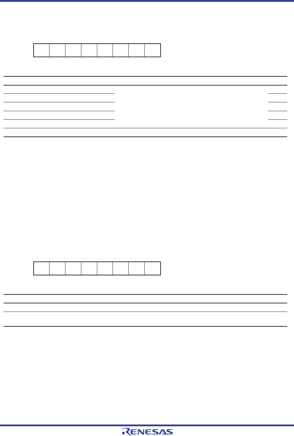
R01UH0034EJ0200 Rev.2.00 Page 408 of 1489
Dec 27, 2013
RX62T Group, RX62G Group 15. I/O Ports
Under development Preliminary document
Specifications in this document are tentative and subject to change.
15.3.2.13 Port Function Register M (PFMPOE)
Note 1. The first round of writing after a reset is enabled; though subsequent writing is not allowed.
PFMPOE enables or disables POEn# input pins.
To prevent the error in the system, be sure to write to this register after a reset.
The first round of writing after a reset is only enabled.
POEnE Bit (POEn# Input Enable) (n = 0, 4, 8, 10, 11)
Each bit enables or disables the corresponding POEn# input.
To use POEn#, set the corresponding POEnE bit to 1.
15.3.2.14 Port Function Register N (PFNPOE)
Note 1. The first round of writing after a reset is enabled; though subsequent writing is not allowed.
PFNPOE enables or disables POEn# input pins.
To prevent the error in the system, be sure to write to this register after a reset.
The first round of writing after a reset is only enabled.
POE10S Bit (POE10# Input Select)
This bit select input pins for the POE10#.
Address: 0008 C116h
b7 b6 b5 b4 b3 b2 b1 b0
———
POE11
EPOE10
EPOE8E POE4E POE0E
Value after reset: 00000000
Bit Symbol Bit Name Description R/W
b0 POE0E POE0# Input Enable 0:Designated as an I/O port pin
1:Designated as the POEn# input pin (n = 0, 4, 8, 10, 11)
R/W*1
b1 POE4E POE4# Input Enable R/W*1
b2 POE8E POE8# Input Enable R/W*1
b3 POE10E POE10# Input Enable R/W*1
b4 POE11E POE11# Input Enable R/W*1
b7 to b5
—
Reserved These bits are always read as 0. The write value should always be 0. R/W
Address: 0008 C117h
b7 b6 b5 b4 b3 b2 b1 b0
POE10
S———————
Value after reset: 00000000
Bit Symbol Bit Name Description R/W
b6-b0 — Reserved These bits are always read as 0. The write value should always be 0. R/W
b7 POE10S POE10# 0:PE2 is designated as the POE10#-A input pin.
1:PE4 is designated as the POE10#-B input pin.
R/W *1

R01UH0034EJ0200 Rev.2.00 Page 409 of 1489
Dec 27, 2013
RX62T Group, RX62G Group 15. I/O Ports
Under development Preliminary document
Specifications in this document are tentative and subject to change.
15.3.3 Settings of Ports
When individual pins for peripheral modules are enabled, the settings for each port are modified.
An input pin for the peripheral module is specified independently by the peripheral module. To use an input pin for the
peripheral module, the corresponding bit in the input buffer control register (PORTn.ICR) should be set to 1 to enable the
input buffer, except for the port register read, NMI, and POEn# pin inputs.
The pins that function as output pins and I/O pins should be enabled for respective peripheral modules. If a conflict
occurs among the output signal enable settings for peripheral modules, that are multiplexed to the same port, the priority
will be handled according to the port-multiplexed priority.
Table 15.19 lists the port-multiplexed priority for peripheral modules.
Table 15.19 Port-Multiplexed Priority for Peripheral Modules (80-Pin LQFP)
Priority Module Name Output Pins
High
Low
1 RSPI RSPCK, MOSI, MISO, SSL0 to SSL3
2CAN CTX
3LIN LTX
4 MTU0 to MTU7 MTIOC0A, MTIOC0B, MTIOC0C, MTIOC0D, MTIOC1A, MTIOC1B, MTIOC2A, MTIOC2B,
MTIOC3A, MTIOC3B, MTIOC3C, MTIOC3D, MTIOC4A, MTIOC4B, MTIOC4C, MTIOC4D,
MTIOC6B, MTIOC6D, MTIOC7A, MTIOC7B, MTIOC7C
5 GPT0 to GPT3 GTIOC0A, GTIOC0B, GTIOC1A, GTIOC1B, GTIOC2A, GTIOC2B
6 SCI0 to SCI2 SCK0 to SCK2, TXD0 to TXD2
7 RIIC SCL, SDA
8 IOPORT P10 to P11, P20 to P24, P30 to P33, P70 to P76, P91 to P96, PA2 to PA5, PB0 to PB7,
PD3 to PD7, PE0, PE3 to PE4

R01UH0034EJ0200 Rev.2.00 Page 410 of 1489
Dec 27, 2013
RX62T Group, RX62G Group 15. I/O Ports
Under development Preliminary document
Specifications in this document are tentative and subject to change.
15.3.4 List of Output Enable Settings
Table 15.20 lists the output enable settings for each port.
For details on the applicable output signals, see descriptions of the registers for each peripheral module.
Setting the port function register changes the functions of peripheral-module pins with names ending in A to C.
Table 15.20 Output Enable Settings for Each Port (80-pin LQFP) (1 / 4)
Port Module Name Output Signal
Name Port Function Register
Settings Peripheral Module Settings
P10 PORT1 P10 PORT1.DDR.B0 = 1
P11 PORT1 P11 PORT1.DDR.B1 = 1
P20 PORT2 P20 PORT2.DDR.B0 = 1
P21 PORT2 P21 PORT2.DDR.B1 = 1
P22 RSPI MISO-A PFGSPI.MISOE = 1
PFHSPI.RSPIS[1:0] = 00
(In addition to the pin enable setting, input/output switching
function for the peripheral module is provided.)
PORT2 P22 PORT2.DDR.B2 = 1
P23 RSPI MOSI-A PFGSPI.MOSIE = 1
PFHSPI.RSPIS[1:0] = 00
(In addition to the pin enable setting, input/output switching
function for the peripheral module is provided.)
CAN CTX-B PFJCAN.CANE =1
PFJCAN.CANS[1:0] = 01
(The signal output state is specified by the peripheral
module settings.)
LIN LTX PFKLIN.LINE = 1 (The signal output state is specified by the peripheral
module settings.)
PORT2 P23 PORT2.DDR.B3 =1
P24 RSPI RSPCK-A PFGSPI.RSPCKE =1
PFHSPI.RSPIS[1:0] = 00
(In addition to the pin enable setting, input/output switching
function for the peripheral module is provided.)
PORT2 P24 PORT2.DDR.B4 = 1
P30 RSPI SSL0-A PFGSPI.SSL0E = 1
PFHSPI.RSPIS[1:0] = 00
(In addition to the pin enable setting, input/output switching
function for the peripheral module is provided.)
MTU0 MTIOC0B-B PFCMTU.MTUS1 = 1 (The signal output state is specified by the peripheral
module settings.)
PORT3 P30 PORT3.DDR.B0 = 1
P31 RSPI SSL1-A PFGSPI.SSL1E = 1
PFHSPI.RSPIS[1:0] = 00
(The signal output state is specified by the peripheral
module settings.)
MTU0 MTIOC0A-B PFCMTU.MTUS0 = 1 (The signal output state is specified by the peripheral
module settings.)
PORT3 P31 PORT3.DDR.B1 = 1
P32 RSPI SSL2-A PFGSPI.SSL2E = 1
PFHSPI.RSPIS[1:0] = 00
(The signal output state is specified by the peripheral
module settings.)
MTU3 MTIOC3C (The signal output state is specified by the peripheral
module settings.)
PORT3 P32 PORT3.DDR.B2 = 1
P33 RSPI SSL3-A PFGSPI.SSL3E = 1
PFHSPI.RSPIS[1:0] = 00
(The signal output state is specified by the peripheral
module settings.)
MTU3 MTIOC3A (The signal output state is specified by the peripheral
module settings.)
PORT3 P33 PORT3.DDR.B3 = 1
P70 PORT7 P70 PORT7.DDR.B0 = 1
P71 MTU3 MTIOC3B (The signal output state is specified by the peripheral
module settings.)
GPT0 GTIOC0A-A PFDGPT.GPTS = 0 (The signal output state is specified by the peripheral
module settings.)
PORT7 P71 PORT7.DDR.B1 = 1

R01UH0034EJ0200 Rev.2.00 Page 411 of 1489
Dec 27, 2013
RX62T Group, RX62G Group 15. I/O Ports
Under development Preliminary document
Specifications in this document are tentative and subject to change.
P72 MTU4 MTIOC4A (The signal output state is specified by the peripheral
module settings.)
GPT1 GTIOC1A-A PFDGPT.GPTS = 0 (The signal output state is specified by the peripheral
module settings.)
PORT7 P72 PORT7.DDR.B2 = 1
P73 MTU4 MTIOC4B (The signal output state is specified by the peripheral
module settings.)
GPT2 GTIOC2A-A PFDGPT.GPTS = 0 (The signal output state is specified by the peripheral
module settings.)
PORT7 P73 PORT7.DDR.B3 = 1
P74 MTU3 MTIOC3D (The signal output state is specified by the peripheral
module settings.)
GPT0 GTIOC0B-A PFDGPT.GPTS = 0 (The signal output state is specified by the peripheral
module settings.)
PORT7 P74 PORT7.DDR.B4 = 1
P75 MTU4 MTIOC4C (The signal output state is specified by the peripheral
module settings.)
GPT1 GTIOC1B-A PFDGPT.GPTS = 0 (The signal output state is specified by the peripheral
module settings.)
PORT7 P75 PORT7.DDR.B5 = 1
P76 MTU4 MTIOC4D (The signal output state is specified by the peripheral
module settings.)
GPT2 GTIOC2B-A PFDGPT.GPTS = 0 (The signal output state is specified by the peripheral
module settings.)
PORT7 P76 PORT7.DDR.B6 = 1
P91 MTU7 MTIOC7C (The signal output state is specified by the peripheral
module settings.)
PORT9 P91 PORT9.DDR.B1 = 1
P92 MTU6 MTIOC6D (The signal output state is specified by the peripheral
module settings.)
PORT9 P92 PORT9.DDR.B2 = 1
P93 MTU7 MTIOC7B (The signal output state is specified by the peripheral
module settings.)
PORT9 P93 PORT9.DDR.B3 = 1
P94 MTU7 MTIOC7A (The signal output state is specified by the peripheral
module settings.)
PORT9 P94 PORT9.DDR.B4 = 1
P95 MTU6 MTIOC6B (The signal output state is specified by the peripheral
module settings.)
PORT9 P95 PORT9.DDR.B5 = 1
P96 PORT9 P96 PORT9.DDR.B6 = 1
PA2 RSPI SSL1-B PFGSPI.SSL1E = 1
PFHSPI.RSPIS[1:0] = 01
(The signal output state is specified by the peripheral
module settings.)
MTU2 MTIOC2B (The signal output state is specified by the peripheral
module settings.)
PORTA PA2 PORTA.DDR.B2 = 1
PA3 RSPI SSL0-B PFGSPI.SSL0E = 1
PFHSPI.RSPIS[1:0] = 01
(In addition to the pin enable setting, input/output switching
function for the peripheral module is provided.)
MTU2 MTIOC2A (The signal output state is specified by the peripheral
module settings.)
PORTA PA3 PORTA.DDR.B3 = 1
Table 15.20 Output Enable Settings for Each Port (80-pin LQFP) (2 / 4)
Port Module Name Output Signal
Name Port Function Register
Settings Peripheral Module Settings

R01UH0034EJ0200 Rev.2.00 Page 412 of 1489
Dec 27, 2013
RX62T Group, RX62G Group 15. I/O Ports
Under development Preliminary document
Specifications in this document are tentative and subject to change.
PA4 RSPI RSPCK-B PFGSPI.RSPCKE = 1
PFHSPI.RSPIS[1:0] = 01
(In addition to the pin enable setting, input/output switching
function for the peripheral module is provided.)
MTU1 MTIOC1B (The signal output state is specified by the peripheral
module settings.)
PORTA PA4 PORTA.DDR.B4 = 1
PA5 RSPI MISO-B PFGSPI.MISOE = 1
PFHSPI.RSPIS[1:0] = 01
(In addition to the pin enable setting, input/output switching
function for the peripheral module is provided.)
MTU1 MTIOC1A (The signal output state is specified by the peripheral
module settings.)
PORTA PA5 PORTA.DDR.B5 = 1
PB0 RSPI MOSI-B PFGSPI.MOSIE = 1
PFHSPI.RSPIS[1:0] = 01
(In addition to the pin enable setting, input/output switching
function for the peripheral module is provided.)
MTU0 MTIOC0D (The signal output state is specified by the peripheral
module settings.)
PORTB PB0 PORTB.DDR.B0 = 1
PB1 MTU0 MTIOC0C (The signal output state is specified by the peripheral
module settings.)
RIIC SCL RIIC.ICCR1.ICE = 1
PORTB PB1 PORTB.DDR.B1 = 1
PB2 MTU0 MTIOC0B-A PFCMTU.MTUS1 = 0 (The signal output state is specified by the peripheral
module settings.)
SCI0 TXD0 SCI0.SCR.TE = 1
RIIC SDA RIIC.ICCR1.ICE = 1
PORTB PB2 PORTB.DDR.B2 = 1
PB3 MTU0 MTIOC0A-A PFCMTU.MTUS0 = 0 (The signal output state is specified by the peripheral
module settings.)
SCI0 SCK0 When SCI0.SCMR.SMIF = 1:
While SMR.GM = 0, SCR.CKE[1:0] = 01 or SMR.GM = 1,
SCR.TE = 1 or SCR.RE = 1
When SCI0.SCMR.SMIF = 0:
While SMR.CM = 0, SCR.CKE[1:0] = 01 or SMR.CM = 1,
SCR.CKE[1] = 0, SCR.TE = 1 or SCR.RE = 1
PORTB PB3 PORTB.DDR.B3 = 1
PB4 PORTB PB4 PORTB.DDR.B4 = 1
PB5 CAN CTX-A PFJCAN.CANE = 1
PFJCAN.CANS[1:0] = 00
(The signal output state is specified by the peripheral
module settings.)
SCI2 TXD2-A PFFSCI.SCI2S = 0 SCI2.SCR.TE = 1
PORTB PB5 PORTB.DDR.B5 = 1
PB6 PORTB PB6 PORTB.DDR.B6 = 1
PB7 SCI2 SCK2-A PFFSCI.SCI2S = 0 When SCI2.SCMR.SMIF =1:
While SMR.GM = 0, SCR.CKE[1:0] = 01 or SMR.GM = 1,
SCR.TE = 1 or SCR.RE = 1
When SCI2.SCMR.SMIF = 0:
While SMR.CM = 0, SCR.CKE[1:0] = 01 or SMR.CM = 1,
SCR.CKE[1] = 0, SCR.TE = 1 or SCR.RE = 1
PORTB PB7 PORTB.DDR.B7 = 1
PD3 GPT2 GTIOC2A-B PFDGPT.GPTS = 1 (The signal output state is specified by the peripheral
module settings.)
SCI1 TXD1 SCI1.SCR.TE = 1
PORTD PD3 PORTD.DDR.B3 = 1
Table 15.20 Output Enable Settings for Each Port (80-pin LQFP) (3 / 4)
Port Module Name Output Signal
Name Port Function Register
Settings Peripheral Module Settings

R01UH0034EJ0200 Rev.2.00 Page 413 of 1489
Dec 27, 2013
RX62T Group, RX62G Group 15. I/O Ports
Under development Preliminary document
Specifications in this document are tentative and subject to change.
PD4 GPT1 GTIOC1B-B PFDGPT.GPTS = 1 (The signal output state is specified by the peripheral
module settings.)
SCI1 SCK1 When SCI1.SCMR.SMIF = 1:
While SMR.GM = 0, SCR.CKE[1:0] = 01 or SMR.GM = 1,
SCR.TE = 1 or SCR.RE = 1
When SCI1.SCMR.SMIF = 0:
While SMR.CM = 0, SCR.CKE[1:0] = 01 o r SMR.CM = 1,
SCR.CKE[1] = 0, SCR.TE = 1 or SCR.RE = 1
PORTD PD4 PORTD.DDR.B4 = 1
PD5 GPT1 GTIOC1A-B PFDGPT.GPTS = 1 (The signal output state is specified by the peripheral
module settings.)
PORTD PD5 PORTD.DDR.B5 = 1
PD6 GPT0 GTIOC0B-B PFDGPT.GPTS = 1 (The signal output state is specified by the peripheral
module settings.)
PORTD PD6 PORTD.DDR.B6 = 1
PD7 CAN CTX-C PFJCAN.CANE = 1
PFJCAN.CANS[1:0] = 10
(The signal output state is specified by the peripheral
module settings.)
GPT0 GTIOC0A-B PFDGPT.GPTS = 1 (The signal output state is specified by the peripheral
module settings.)
PORTD PD7 PORTD.DDR.B7 = 1
PE0 PORTE PE0 PORTE.DDR.B0 = 1
PE3 PORTE PE3 PORTE.DDR.B3 = 1
PE4 PORTE PE4 PORTE.DDR.B4 = 1
Table 15.20 Output Enable Settings for Each Port (80-pin LQFP) (4 / 4)
Port Module Name Output Signal
Name Port Function Register
Settings Peripheral Module Settings

R01UH0034EJ0200 Rev.2.00 Page 414 of 1489
Dec 27, 2013
RX62T Group, RX62G Group 15. I/O Ports
Under development Preliminary document
Specifications in this document are tentative and subject to change.
15.3.5 Treatment of Unused Pins
The treatment of unused pins is listed in Table 15.21.
Note 1. Do not change the initial value of PORTn.ICR. Changing the initial value may generate shoot-through current.
Table 15.21 Treatment of Unused Pin (80-pin LQFP)
Pin Name Treatment
EMLE Connect this pin to Vss via a pull-down resistor.
MD1, MD0 (Always used as mode pins)
MDE (Always used as mode pins)
RES# Connect this pin to Vcc via a pull-up resistor.
PE2/NMI/POE10#-A Connect this pin to Vcc via a pull-up resistor.
EXTAL (Always used as a clock pin)
XTAL Leave these pins open.
Port to 3, 7, 9, A, B, D, E Connect these pins to Vcc via a pull-up resistor or to Vss via a pull-down resistor.
These pins can be left while PORTn.ICR is in the initial state (the input buffer disabled)*1.
Port 4 Connect these pins to AVCC0 via a pull-up resistor or to AVSS0 via a pull-down resistor.
These pins can be left while PORTn.ICR is in the initial state (the input buffer disabled)*1.
Port 6 Connect these pins to AVCC via a pull-up resistor or to AVSS via a pull-down resistor
These pins can be left while PORTn.ICR is in the initial state (the input buffer disabled)*1.
VREFH0 Connect this pin to AVCC0.
VREFL0 Connect this pin to AVSS0.

R01UH0034EJ0200 Rev.2.00 Page 415 of 1489
Dec 27, 2013
RX62T Group, RX62G Group 15. I/O Ports
Under development Preliminary document
Specifications in this document are tentative and subject to change.
15.4 I/O Port [for 80-Pin LQFP (R5F562TxGDFF)]
The RX62T Group (80-pin LQFP (R5F562TxGDFF)) has 11 I/O ports (ports 1 to 4, 7 to 9, A, B, D, and E), which handle
44 I/O pins.
15.4.1 Overview
Table 15.8 gives the specifications of the I/O ports and Table 15.9 lists I/O ports and pin functions.
Table 15.22 Specifications of I/O Ports (80-Pin LQFP (R5F562TxGDFF))
Item Description
I/O pins 44
Input pins 9
Number of ports 11 (1 to 4, 7 to 9, A, B, D, E)
Open drain outputs 2 (RIIC pin)
Large-current output 12 (MTU3 pin and GPT pin)
Schmitt trigger input pins All port inputs, CAN inputs, IRQ inputs, MTU3 inputs, POE3 inputs, RIIC inputs, SCI inputs,
A/D trigger inputs, NMI inputs, GPT inputs, and LIN inputs
Others Each pin is capable of driving a capacitive load of 30 pF in the case of a TTL load.
When configured as an output, a pin is capable of driving a Darlington transistor.
A pin is always capable of reading the status of the pins.

R01UH0034EJ0200 Rev.2.00 Page 416 of 1489
Dec 27, 2013
RX62T Group, RX62G Group 15. I/O Ports
Under development Preliminary document
Specifications in this document are tentative and subject to change.
Table 15.23 Port Functions (80-Pin LQFP (R5F562TxGDFF)) (1 / 2)
Port Description Bit
Function CMOS
Input Schmitt Trigger
Input
Open Drain
Output
Capability
Large-
Current
OutputI/O Input Output
Port 1 General I/O port
pins, MTU3 inputs,
and
interrupt inputs
0 P10 MTCLKD-B/
IRQ0-A — All input functions — —
Port 2 General I/O port
pins, MTU3 inputs,
interrupt inputs,
A/D converter inputs,
RSPI I/O signal,
LIN I/O signal, and
CAN I/O signal
0 P20 MTCLKB-B/
IRQ7/
ADTRG0#-B
— All input functions — —
2 P22/MISO-A LRX/CRX-B/
ADTRG# MISO-A P22/LRX/CRX-B/
ADTRG#
3 P23/MOSI-A LTX/CTX-B MOSI-A P23
4 P24/RSPCK-A RSPCK-A P24
Port 3 General I/O port
pins, MTU3 I/O
signal, and
RSPI I/O signal
0 P30/MTIOC0B-B/
SSL0-A MTCLKD-A SSL0-A P30/MTIOC0B-B/
MTCLKD-A ——
1 P31/MTIOC0A-B MTCLKC-A SSL1-A — All input functions
2 P32/MTIOC3C MTCLKB-A SSL2-A All input functions
3 P33/MTIOC3A MTCLKA-A SSL3-A All input functions
Port 4 A/D converter inputs
and general input
port pins
0 P40/AN000 — P40 — —
1 P41/AN001 P41
2 P42/AN002 P42
3 P43/AN003/
CVREFL P43
4 P44/AN100 P44
5 P45/AN101 P45
6 P46/AN102 P46
7 P47/AN103/
CVREFH P47
Port 7 General I/O port
pins, POE3 inputs,
interrupt inputs,
MTU3 I/O signal, and
GPT I/O signal
0 P70 POE0#/IRQ5 — All input functions — —
1 P71/MTIOC3B/
GTIOC0A-A All input functions √
2 P72/MTIOC4A/
GTIOC1A-A All input functions √
3 P73/MTIOC4B/
GTIOC2A-A All input functions √
4 P74/MTIOC3D/
GTIOC0B-A All input functions √
5 P75/MTIOC4C/
GTIOC1B-A All input functions √
6 P76/MTIOC4D/
GTIOC2B-A All input functions √
Port 8 General I/O port
pins, SCI I/O signal,
and
MTU3 inputs
0 P80 RXD2-B/
MTIC5W — All input functions — —
1 P81 MTIC5V TXD2-B All input functions
2 P82/SCK2-B MTIC5U All input functions
Port 9 General I/O port
pins, MTU3 I/O
signal,
POE3 inputs, and
interrupt inputs
0 P90/MTIOC7D — All input functions — √
1 P91/MTIOC7C All input functions √
2 P92/MTIOC6D All input functions √
3 P93/MTIOC7B All input functions √
4 P94/MTIOC7A All input functions √
5 P95/MTIOC6B All input functions √
6P96 POE4#/IRQ4 All input functions —

R01UH0034EJ0200 Rev.2.00 Page 417 of 1489
Dec 27, 2013
RX62T Group, RX62G Group 15. I/O Ports
Under development Preliminary document
Specifications in this document are tentative and subject to change.
Port A General I/O port
pins, MTU3 I/O
signal, RSPI I/O
signal, and
A/D converter inputs
3PA3/MTIOC2A/
SSL0-B SSL0-B PA3/MTIOC2A — —
5PA5/MTIOC1A/
MISO-B ADTRG1#-A MISO-B PA5/MTIOC1A/
ADTRG1#-A
Port B General I/O port
pins, MTU3 I/O
signal,
RSPI I/O signal,
RIIC I/O signal,
SCI I/O signal,
GPT inputs,
POE3 inputs,
interrupt inputs,
CAN I/O signal,
and trace outputs
0PB0/MTIOC0D/
MOSI-B MOSI-B PB0/MTIOC0D — —
1PB1/MTIOC0C/
SCL RXD0 — All input functions √
(SCL only) —
2PB2/MTIOC0B-A/
SDA TXD0 All input functions √
(SDA only) —
3PB3/MTIOC0A-A/
SCK0 All input functions — —
4PB4 GTETRG/
POE8#/IRQ3 All input functions
5PB5 TXD2-A/
CTX-A/
TRSYNC
All input functions
6 PB6 RXD2-A/CRX-
ATRDATA0 All input functions
7 PB7/SCK2-A TRDATA1 All input functions
Port D General I/O port
pins, GPT I/O signal,
RSPI I/O signal,
SCI I/O signal,
CAN outputs,
trace outputs, and
On-chip emulator I/O
signal
2PD2/GTIOC2B-B/
MOSI-C TRCLK MOSI-C PD2/GTIOC2B-B — —
3 PD3/GTIOC2A-B TXD1/TDO — All input functions
4PD4/GTIOC1B-B/
SCK1 TCK — All input functions
5 PD5/GTIOC1A-B RXD1/TDI — All input functions
6PD6/GTIOC0B-B/
SSL0-C TMS SSL0-C PD6/GTIOC0B-B
7 PD7/GTIOC0A-B TRST# SSL1-C/
CTX-C — All input functions
Port E General I/O port
pins, CAN inputs,
RSPI outputs,
POE3 inputs,
MTU3 inputs, and
interrupt inputs
0 PE0 CRX-C SSL2-C — All input functions — —
1 PE1 SSL3-C All input functions
2 PE2/POE10#-
A/NMI All input functions
3 PE3 MTCLKD-C/
POE11#/
IRQ2-A
All input functions
4 PE4 MTCLKC-C/
POE10#-B/
IRQ1-B
All input functions
5 PE5 IRQ0-B All input functions
Table 15.23 Port Functions (80-Pin LQFP (R5F562TxGDFF)) (2 / 2)
Port Description Bit
Function CMOS
Input Schmitt Trigger
Input
Open Drain
Output
Capability
Large-
Current
OutputI/O Input Output

R01UH0034EJ0200 Rev.2.00 Page 418 of 1489
Dec 27, 2013
RX62T Group, RX62G Group 15. I/O Ports
Under development Preliminary document
Specifications in this document are tentative and subject to change.
15.4.2 Register Descriptions
Table 15.10 lists registers of I/O ports, and Table 15.11 lists valid bits in each register.
Table 15.24 Registers of I/O Ports (80-Pin LQFP (R5F562TxGDFF)) (1 / 2)
Port Symbol Register Name Register Symbol Value after Reset Address Access Size
PORT1 Data direction register DDR 00h 0008 C001h 8
Data register DR 00h 0008 C021h 8
Port register PORT Undefined 0008 C041h 8
Input buffer control register ICR 00h 0008 C061h 8
PORT2 Data direction register DDR 00h 0008 C002h 8
Data register DR 00h 0008 C022h 8
Port register PORT Undefined 0008 C042h 8
Input buffer control register ICR 00h 0008 C062h 8
PORT3 Data direction register DDR 00h 0008 C003h 8
Data register DR 00h 0008 C023h 8
Port register PORT Undefined 0008 C043h 8
Input buffer control register ICR 00h 0008 C063h 8
PORT4 Port register PORT Undefined 0008 C044h 8
Input buffer control register ICR 00h 0008 C064h 8
PORT7 Data direction register DDR 00h 0008 C007h 8
Data register DR 00h 0008 C027h 8
Port register PORT Undefined 0008 C047h 8
Input buffer control register ICR 00h 0008 C067h 8
PORT8 Data direction register DDR 00h 0008 C008h 8
Data register DR 00h 0008 C028h 8
Port register PORT Undefined 0008 C048h 8
Input buffer control register ICR 00h 0008 C068h 8
PORT9 Data direction register DDR 00h 0008 C009h 8
Data register DR 00h 0008 C029h 8
Port register PORT Undefined 0008 C049h 8
Input buffer control register ICR 00h 0008 C069h 8
PORTA Data direction register DDR 00h 0008 C00Ah 8
Data register DR 00h 0008 C02Ah 8
Port register PORT Undefined 0008 C04Ah 8
Input buffer control register ICR 00h 0008 C06Ah 8
PORTB Data direction register DDR 00h 0008 C00Bh 8
Data register DR 00h 0008 C02Bh 8
Port register PORT Undefined 0008 C04Bh 8
Input buffer control register ICR 00h 0008 C06Bh 8
PORTD Data direction register DDR 00h 0008 C00Dh 8
Data register DR 00h 0008 C02Dh 8
Port register PORT Undefined 0008 C04Dh 8
Input buffer control register ICR 00h 0008 C06Dh 8
PORTE Data direction register DDR 00h 0008 C00Eh 8
Data register DR 00h 0008 C02Eh 8
Port register PORT Undefined 0008 C04Eh 8
Input buffer control register ICR 00h 0008 C06Eh 8

R01UH0034EJ0200 Rev.2.00 Page 419 of 1489
Dec 27, 2013
RX62T Group, RX62G Group 15. I/O Ports
Under development Preliminary document
Specifications in this document are tentative and subject to change.
IOPORT Port function register 8 PF8IRQ 00h 0008 C108h 8
Port function register A PFAADC 00h 0008 C10Ah 8
Port function register C PFCMTU 00h 0008 C10Ch 8
Port function register D PFDGPT 00h 0008 C10Dh 8
Port function register F PFFSCI 00h 0008 C10Fh 8
Port function register G PFGSPI 00h 0008 C110h 8
Port function register H PFHSPI 00h 0008 C111h 8
Port function register J PFJCAN 00h 0008 C113h 8
Port function register K PFKLIN 00h 0008 C114h 8
Port function register M PFMPOE 00h 0008 C116h 8
Port function register N PFNPOE 00h 0008 C117h 8
Table 15.24 Registers of I/O Ports (80-Pin LQFP (R5F562TxGDFF)) (2 / 2)
Port Symbol Register Name Register Symbol Value after Reset Address Access Size

R01UH0034EJ0200 Rev.2.00 Page 420 of 1489
Dec 27, 2013
RX62T Group, RX62G Group 15. I/O Ports
Under development Preliminary document
Specifications in this document are tentative and subject to change.
Table 15.25 Valid Bits in Each Register (80-Pin LQFP (R5F562TxGDFF)) (1 / 2)
Register Symbol b7 b6 b5 b4 b3 b2 b1 b0
PORT1.DDR x××××××√
PORT2.DDR × × × √√√×√
PORT3.DDR ××××√√√√
PORT7.DDR × √√√√√√√
PORT8.DDR ×××××√√√
PORT9.DDR × √√√√√√√
PORTA.DDR × × √×√×××
PORTB.DDR √√√√√√√√
PORTD.DDR √√√√√√××
PORTE.DDR × × × √√×××
PORT1.DR ×××××××√
PORT2.DR × × × √√√×√
PORT3.DR ××××√√√√
PORT7.DR × √√√√√√√
PORT8.DR ×××××√√√
PORT9.DR × √√√√√√√
PORTA.DR × × √×√×××
PORTB.DR √√√√√√√√
PORTD.DR √√√√√√××
PORTE.DR × × × √√×××
PORT1.PORT ×××××××√
PORT2.PORT × × × √√√×√
PORT3.PORT × × × × √√√√
PORT4.PORT √√√√√√√√
PORT7.PORT × √√√√√√√
PORT8.PORT ×××××√√√
PORT9.PORT × √√√√√√√
PORTA.PORT × × √×√×××
PORTB.PORT √√√√√√√√
PORTD.PORT √√√√√√××
PORTE.PORT × × × √√√××
PORT1.ICR ×××××××√
PORT2.ICR × × × √√√×√
PORT3.ICR × × × × √√√√
PORT4.ICR √√√√√√√√
PORT7.ICR × √√√√√√√
PORT8.ICR ×××××√√√
PORT9.ICR × √√√√√√√
PORTA.ICR × × √×√×××
PORTB.ICR √√√√√√√√
PORTD.ICR √√√√√√××
PORTE.ICR × × × √√×××
IOPORT.PF8IRQ × × × × √√√√
IOPORT.PFAADC×××××××√

R01UH0034EJ0200 Rev.2.00 Page 421 of 1489
Dec 27, 2013
RX62T Group, RX62G Group 15. I/O Ports
Under development Preliminary document
Specifications in this document are tentative and subject to change.
√: Enabled bit, x: Disabled bit (Reserved)
IOPORT.PFCMTU √√××××√√
IOPORT.PFDGPT×××××××√
IOPORT.PFFSCI ×××××√××
IOPORT.PFGSPI √√√√√√√×
IOPORT.PFHSPI ××××××√√
IOPORT.PFJCAN √√×××××√
IOPORT.PFKLIN ×××××××√
IOPORT.PFMPOE × × × √√√√√
IOPORT.PFNPOE √×××××××
Table 15.25 Valid Bits in Each Register (80-Pin LQFP (R5F562TxGDFF)) (2 / 2)
Register Symbol b7 b6 b5 b4 b3 b2 b1 b0

R01UH0034EJ0200 Rev.2.00 Page 422 of 1489
Dec 27, 2013
RX62T Group, RX62G Group 15. I/O Ports
Under development Preliminary document
Specifications in this document are tentative and subject to change.
15.4.2.1 Data Direction Register (DDR)
n = 1 to 3, 7 to 9, A, B, D, E
Each PORTn.DDR is used to select the input or output direction for individual pins of the corresponding port that have
been configured to function as general I/O pins.
Each bit of a PORTn.DDR (n = 1 to 3, 7 to 9, A, B, D, E) corresponds to a pin of Pn, and the settings can change from bit
to bit.
Address: PORT1.DDR 0008 C001h, PORT2.DDR 0008 C002h, PORT3.DDR 0008 C003h, PORT7.DDR 0008 C007h,
PORT8.DDR 0008 C008h, PORT9.DDR 0008 C009h, PORTA.DDR 0008 C00Ah, PORTB.DDR 0008 C00Bh,
PORTD.DDR 0008 C00Dh, PORTE.DDR 0008 C00Eh
b7 b6 b5 b4 b3 b2 b1 b0
B7 B6 B5 B4 B3 B2 B1 B0
Value after reset: 00000000
Note 1. The one lower-order bit is valid and the seven higher-order bits are reserved in PORT1.DDR.
b4 to b2 and b0 are valid and b7 to b5 and b1 are reserved in PORT2.DDR.
The four lower-order bits are valid and the four higher-order bits are reserved in PORT3.DDR.
The seven lower-order bits are valid and the one higher-order bit is reserved in PORT7.DDR.
The three lower-order bits are valid and the five higher-order bits are reserved in PORT8.DDR.
The seven lower-order bits are valid and the one higher-order bit is reserved in PORT9.DDR.
b5 and b3 are valid and b7, b6, b4, and b2 to b0 are reserved in PORTA.DDR.
b7 to b2 are valid and b1 and b0 are reserved in PORTD.DDR.
b4 and b3 are valid and b7 to b5 and b2 to b0 are reserved in PORTE.DDR.
Note 2. Write 1 to a reserved bit.
Bit Symbol Bit Name Description R/W
b0 B0 Pn0 I/O Select 0: An input pin
1: An output pin
R/W
b1 B1 Pn1 I/O Select R/W
b2 B2 Pn2 I/O Select R/W
b3 B3 Pn3 I/O Select R/W
b4 B4 Pn4 I/O Select R/W
b5 B5 Pn5 I/O Select R/W
b6 B6 Pn6 I/O Select R/W
b7 B7 Pn7 I/O Select R/W
R01UH0034EJ0200 Rev.2.00 Page 423 of 1489
Dec 27, 2013
RX62T Group, RX62G Group 15. I/O Ports
Under development Preliminary document
Specifications in this document are tentative and subject to change.
15.4.2.2 Data Register (DR)
n = 1 to 3, 7 to 9, A, B, D, E
Each PORTn.DR (n = 1 to 3, 7 to 9, A, B, D, E) stores the output data from the individual pins of the corresponding port
used as a general I/O port.
Address: PORT1.DR 0008 C021h, PORT2.DR 0008 C022h, PORT3.DR 0008 C023h, PORT7.DR 0008 C027h,
PORT8.DR 0008 C028h, PORT9.DR 0008 C029h, PORTA.DR 0008 C02Ah, PORTB.DR 0008 C02Bh,
PORTD.DR 0008 C02Dh, PORTE.DR 0008 C02Eh
b7 b6 b5 b4 b3 b2 b1 b0
B7 B6 B5 B4 B3 B2 B1 B0
Value after reset: 00000000
Note 1. The one lower-order bit is valid and the seven higher-order bits are reserved in PORT1.DR.
b4 to b2 and b0 are valid and b7 to b5 and b1 are reserved in PORT2.DR.
The four lower-order bits are valid and the four higher-order bits are reserved in PORT3.DR.
The seven lower-order bits are valid and the one higher-order bit is reserved in PORT7.DR.
The three lower-order bits are valid and the five higher-order bits are reserved in PORT8.DR.
The seven lower-order bits are valid and the one higher-order bit is reserved in PORT9.DR.
b5 and b3 are valid and b7, b6, b4, and b2 to b0 are reserved in PORTA.DR.
b7 to b2 are valid and b1 and b0 are reserved in PORTD.DR.
b4 and b3 are valid and b7 to b5 and b2 to b0 are reserved in PORTE.DR.
Note 2. Write 1 to a reserved bit.
Bit Symbol Bit Name Description R/W
b0 B0 Pn0 Output Data Store Output data are stored. R/W
b1 B1 Pn1 Output Data Store R/W
b2 B2 Pn2 Output Data Store R/W
b3 B3 Pn3 Output Data Store R/W
b4 B4 Pn4 Output Data Store R/W
b5 B5 Pn5 Output Data Store R/W
b6 B6 Pn6 Output Data Store R/W
b7 B7 Pn7 Output Data Store R/W

R01UH0034EJ0200 Rev.2.00 Page 424 of 1489
Dec 27, 2013
RX62T Group, RX62G Group 15. I/O Ports
Under development Preliminary document
Specifications in this document are tentative and subject to change.
15.4.2.3 Port Register (PORT)
n = 1 to 4, 7 to 9, A, B, D, E
PORT reflects individual pin states of the corresponding port.
When a PORTn.PORT (n = 1 to 4, 7 to 9, A, B, D, E) is read, the corresponding pin states are read out to here.
Address: PORT1.PORT 0008 C041h, PORT2.PORT 0008 C042h, PORT3.PORT 0008 C043h, PORT4.PORT 0008 C044h,
PORT7.PORT 0008 C047h, PORT8.PORT 0008 C048h, PORT9.PORT 0008 C049h, PORTA.PORT 0008 C04Ah,
PORTB.PORT 0008 C04Bh, PORTD.PORT 0008 C04Dh, PORTE.PORT 0008 C04Eh
b7 b6 b5 b4 b3 b2 b1 b0
B7 B6 B5 B4 B3 B2 B1 B0
Value after reset: xxxxxxxx
Note 1. The one lower-order bit is valid and the seven higher-order bits are reserved in PORT1.PORT.
b4 to b2 and b0 are valid and b7 to b5 and b1 are reserved in PORT2.PORT.
The four lower-order bits are valid and the four higher-order bits are reserved in PORT3.PORT.
The seven lower-order bits are valid and the one higher-order bit is reserved in PORT7.PORT.
The three lower-order bits are valid and the five higher-order bits are reserved in PORT8.PORT.
The seven lower-order bits are valid and the one higher-order bit is reserved in PORT9.PORT.
b5 and b3 are valid and b7, b6, and b2 to b0 are reserved in PORTA.PORT.
b7 to b2 are valid and b1 and b0 are reserved in PORTD.PORT.
b4 to b2 are valid and b7 to b5, b1, and b0 are reserved in PORTE.PORT.
Note 2. The reserved bits are read as 1. Writing to these bits has no effect.
Bit Symbol Bit Name Description R/W
b0 B0 Pn0 Individual pin states of the corresponding
port are reflected.
R
b1 B1 Pn1 R
b2 B2 Pn2 R
b3 B3 Pn3 R
b4 B4 Pn4 R
b5 B5 Pn5 R
b6 B6 Pn6 R
b7 B7 Pn7 R

R01UH0034EJ0200 Rev.2.00 Page 425 of 1489
Dec 27, 2013
RX62T Group, RX62G Group 15. I/O Ports
Under development Preliminary document
Specifications in this document are tentative and subject to change.
15.4.2.4 Input Buffer Control Register (ICR)
n = 1 to 4, 7 to 9, A, B, D, E
Note 1. For pins being used as input pins for peripheral modules, set the corresponding bits to 1. Set the bits corresponding to pins that
are not being used for their input functions or are being used as analog input pins to 0.
Each PORTn.ICR controls the input buffers for the individual pins of the corresponding port.
Each bit of a PORTn.ICR (n = 1 to 4, 7 to 9, A, B, D, E) corresponds to a pin of Pn, and the settings can change from bit
to bit.
When to be used as an input pin for the peripheral module, the input buffer for the corresponding pin should be enabled
beforehand by setting the PORTn.ICR bit to 1. If this register is used as an input pin for the peripheral module while the
PORTn.ICR bit is 0, the input signal to the peripheral module is fixed high.
When a Pn.PORT register is read, the pin states of the corresponding port are read out regardless of the values in
PORTn.ICR. For bits where the value in PORTn.ICR is 0, however, the value may not reflect the pin state on the
corresponding peripheral module side.
Changes in the settings of a PORTn.ICR may generate edges internally, depending on the pin state. For this reason,
change the settings of PORTn.ICR while the corresponding input pins are not in use. For example, in the case of IRQi (i
= 0 to 7) inputs, change settings of the corresponding PORTn.ICR with interrupts disabled by clearing the IR flag in IRi
(i = 64 to 71 ("i" shows an interrupt vector number of the IRQ)) of the interrupt controller (ICU) to 0, and then enable the
corresponding interrupts. If a change to a PORTn.ICR setting does generate an edge, negate the edge.
Address: PORT1.ICR 0008 C061h, PORT2.ICR 0008 C062h, PORT3.ICR 0008 C063h, PORT4.ICR 0008 C064h,
PORT7.ICR 0008 C067h, PORT8.ICR 0008 C068h, PORT9.ICR 0008 C069h, PORTA.ICR 0008 C06Ah,
PORTB.ICR 0008 C06Bh, PORTD.ICR 0008 C06Dh, PORTE.ICR 0008 C06Eh
b7 b6 b5 b4 b3 b2 b1 b0
B7 B6 B5 B4 B3 B2 B1 B0
Value after reset: 00000000
Note 1. The one lower-order bit is valid and the seven higher-order bits are reserved in PORT1.ICR.
b4 to b2 and b0 are valid and b7 to b5 and b1 are reserved in PORT2.ICR.
The four lower-order bits are valid and the four higher-order bits are reserved in PORT3.ICR.
The seven lower-order bits are valid and the one higher-order bit is reserved in PORT7.ICR.
The three lower-order bits are valid and the five higher-order bits are reserved in PORT8.ICR.
The seven lower-order bits are valid and the one higher-order bit is reserved in PORT9.ICR.
b5 and b3 are valid and b7, b6, b4, and b2 to b0 are reserved in PORTA.ICR.
b7 to b2 are valid and b1 and b0 are reserved in PORTD.ICR.
b4 and b3 are valid and b7 to b5 and b2 to b0 are reserved in PORTE.ICR.
Note 2. The reserved bits are read as 0. The write value should always be 0.
Bit Symbol Bit Name Description R/W
b0 B0*1Pn0 Input Buffer Control 0: The input buffer for the corresponding pin is
disabled.
1: The input buffer for the corresponding pin is
enabled.
R/W
b1 B1*1Pn1 Input Buffer Control R/W
b2 B2*1Pn2 Input Buffer Control R/W
b3 B3*1Pn3 Input Buffer Control R/W
b4 B4*1Pn4 Input Buffer Control R/W
b5 B5*1Pn5 Input Buffer Control R/W
b6 B6*1Pn6 Input Buffer Control R/W
b7 B7*1Pn7 Input Buffer Control R/W

R01UH0034EJ0200 Rev.2.00 Page 426 of 1489
Dec 27, 2013
RX62T Group, RX62G Group 15. I/O Ports
Under development Preliminary document
Specifications in this document are tentative and subject to change.
15.4.2.5 Port Function Register 8 (PF8IRQ)
PF8IRQ is used to select pins for IRQ0 to IRQ1 inputs.
ITSi Bit (IRQi Pin Select) (i = 0 and 1)
Each bit selects a pin for an IRQi input.
15.4.2.6 Port Function Register A (PFAADC)
PFAADC is used to select the ADTRG0# pin.
ADTRGnS Bit (ADTRGn# Input Select) (n = 0)
This bit selects a pin for an ADTRGn# input.
Address: 0008 C108h
b7 b6 b5 b4 b3 b2 b1 b0
———— ITS1[1:0] ITS0[1:0]
Value after reset: 00000000
Bit Symbol Bit Name Description R/W
b1 to b0 ITS0[1:0] IRQ0 Pin Select b1 b0
0 0:P10 is designated as the IRQ0-A input pin.
0 1:Setting prohibited
1 0:Setting prohibited
1 1:Setting prohibited
R/W
b3 to b2 ITS1[1:0] IRQ1 Pin Select b3 b2
0 0:Setting prohibited
0 1:PE4 is designated as the IRQ1-B input pin.
1 0:Setting prohibited
1 1:Setting prohibited
R/W
b7 to b4 — Reserved These bits are always read as 0. The write value should always be 0. R/W
Address: 0008 C10Ah
b7 b6 b5 b4 b3 b2 b1 b0
———————
ADTRG
0S
Value after reset: 00000000
Bit Symbol Bit Name Description R/W
b0 ADTRG0S ADTRG0# Input Select 0:Setting prohibited
1:P20 is designated as the ADTRG0#-B input pin.
R/W
b7 to b1 — Reserved These bits are always read as 0. The write value should always be 0. R/W

R01UH0034EJ0200 Rev.2.00 Page 427 of 1489
Dec 27, 2013
RX62T Group, RX62G Group 15. I/O Ports
Under development Preliminary document
Specifications in this document are tentative and subject to change.
15.4.2.7 Port Function Register C (PFCMTU)
PFCMTU is used to select pins for MTU3.
MTUSi Bit (MTU3 Pin Select) (i = 0 and 1)
Each bit selects a pin for an MTU3 input/output.
TCLKS[1:0] Bit (MTCLK Pin Select)
This bit selects a pin for a MTCLK input of the MTU3.
Address: 008 C10Ch
b7 b6 b5 b4 b3 b2 b1 b0
TCLKS[1:0]————MTUS1MTUS0
Value after reset: 00000000
Bit Symbol Bit Name Description R/W
b0 MTUS0 MTU3 Pin Select 0 0:PB3 is designated as the MTIOC0A-A pin.
1:P31 is designated as the MTIOC0A-B pin.
R/W
b1 MTUS1 MTU3 Pin Select 1 0:PB2 is designated as the MTIOC0B-A pin.
1:P30 is designated as the MTIOC0B-B pin.
R/W
b5 to b2 — (Reserved) These bits are always read as 0. The write value should always be 0. R/W
b7, b6 TCLKS[1:0] MTCLK Pin Select b7 b6
0 0:P33 is designated as the MTCLKA-A pin.
P32 is designated as the MTCLKB-A pin.
P31 is designated as the MTCLKC-A pin.
P30 is designated as the MTCLKD-A pin.
0 1:P20 is designated as the MTCLKB-B pin.
P10 is designated as the MTCLKD-B pin.
(MTCLKA and MTCLKC pins cannot be selected.)
1 0:PE4 is designated as the MTCLKC-C pin.
PE3 is designated as the MTCLKD-C pin.
(MTCLKA and MTCLKB pins cannot be selected.)
1 1:Setting prohibited
R/W

R01UH0034EJ0200 Rev.2.00 Page 428 of 1489
Dec 27, 2013
RX62T Group, RX62G Group 15. I/O Ports
Under development Preliminary document
Specifications in this document are tentative and subject to change.
15.4.2.8 Port Function Register D (PFDGPT)
PFDGPT is used to select a pin for GPT.
GPTS Bit (GPT I/O Pin Select)
Each bit selects a pin for a GPT input/output.
15.4.2.9 Port Function Register F (PFFSCI)
PFFSCI is used to select pins for SCI.
SCI2S Bit (SCI2 I/O Pin Select)
Each bit selects a pin for an SCI channel-2 input/output.
Address: 0008 C10Dh
b7 b6 b5 b4 b3 b2 b1 b0
———————GPTS
Value after reset: 00000000
Bit Symbol Bit Name Description R/W
b0 GPTS GPT Pin Select 0:P71 is designated as the GTIOC0A-A pin.
P74 is designated as the GTIOC0B-A pin.
P72 is designated as the GTIOC1A-A pin.
P75 is designated as the GTIOC1B-A pin.
P73 is designated as the GTIOC2A-A pin.
P76 is designated as the GTIOC2B-A pin.
1:PD7 is designated as the GTIOC0A-B pin.
PD6 is designated as the GTIOC0B-B pin.
PD5 is designated as the GTIOC1A-B pin.
PD4 is designated as the GTIOC1B-B pin.
PD3 is designated as the GTIOC2A-B pin.
PD2 is designated as the GTIOC2B-B pin.
R/W
b7 to b1 — Reserved These bits are always read as 0. The write value should always be 0. R/W
Address: 0008 C10Fh
b7 b6 b5 b4 b3 b2 b1 b0
—————SCI2S——
Value after reset: 00000000
Bit Symbol Bit Name Description R/W
b1 to b0 — Reserved These bits are always read as 0. The write value should always be 0. R/W
b2 SCI2S SCI2I/O Pin Select 0:PB6 is designated as the RXD2-A pin.
PB7 is designated as the SCK2-A pin.
PB5 is designated as the TXD2-A pin.
1:P80 is designated as the RXD2-B pin.
P82 is designated as the SCK2-B pin.
P81 is designated as the TXD2-B pin.
R/W
b7 to b3 — Reserved These bits are always read as 0. The write value should always be 0. R/W

R01UH0034EJ0200 Rev.2.00 Page 429 of 1489
Dec 27, 2013
RX62T Group, RX62G Group 15. I/O Ports
Under development Preliminary document
Specifications in this document are tentative and subject to change.
15.4.2.10 Port Function Register G (PFGSPI)
PFGSPI is used to select I/O pins for RSPI.
RSPCKE Bit (RSPCK Output Enable)
This bit enables or disables the output of the RSPCK pin. Set this bit to 1 to use the RSPCK pin.
MOSIE Bit (MOSI Output Enable)
This bit enables or disables the output of the MOSI pin. Set this bit to 1 to use the MOSI pin.
MISOE Bit (MISO Output Enable)
This bit enables or disables the output of the MISO pin. Set this bit to 1 to use the MISO pin.
SSL0E Bit (SSL0 Output Enable)
This bit enables or disables the output of the SSL0 pin. Set this bit to 1 to use the SSL0 pin.
SSL1E Bit (SSL1 Output Enable)
This bit enables or disables the output of the SSL1 pin. Set this bit to 1 to use the SSL1 pin.
SSL2E Bit (SSL2 Output Enable)
This bit enables or disables the output of the SSL2 pin. Set this bit to 1 to use the SSL2 pin.
SSL3E Bit (SSL3 Output Enable)
This bit enables or disables the output of the SSL3 pin. Set this bit to 1 to use the SSL3 pin.
Address: 0008 C110h
b7 b6 b5 b4 b3 b2 b1 b0
SSL3E SSL2E SSL1E SSL0E MISOE MOSIE RSPCK
E—
Value after reset: 00000000
Bit Symbol Bit Name Description R/W
b0 — Reserved This bit is always read as 0. The write value should always be 0. R/W
b1 RSPCKE RSPCK Output Enable 0:RSPCK pin is disabled.
1:RSPCK pin is enabled.
R/W
b2 MOSIE MOSI Output Enable 0:MOSI pin is disabled.
1:MOSI pin is enabled.
R/W
b3 MISOE MISO Output Enable 0:MISO pin is disabled.
1:MISO pin is enabled.
R/W
b4 SSL0E SSL0 Output Enable 0:SSL0 pin is disabled.
1:SSL0 pin is enabled.
R/W
b5 SSL1E SSL1 Output Enable 0:SSL1 pin is disabled.
1:SSL1 pin is enabled.
R/W
b6 SSL2E SSL2 Output Enable 0:SSL2 pin is disabled.
1:SSL2 pin is enabled.
R/W
b7 SSL3E SSL3 Output Enable 0:SSL3 pin is disabled.
1:SSL3 pin is enabled.
R/W

R01UH0034EJ0200 Rev.2.00 Page 430 of 1489
Dec 27, 2013
RX62T Group, RX62G Group 15. I/O Ports
Under development Preliminary document
Specifications in this document are tentative and subject to change.
15.4.2.11 Port Function Register H (PFHSPI)
PFHSPI is used to select I/O pins for RSPI channel.
RSPIS[1:0] Bit (RSPI Pin Select)
This bit selects a pin for an RSPI input/output.
As an enable bit is provided for each RSPI input/output pin, the input/output pin is selectable while the corresponding
enable bit is 1. Otherwise, the pin cannot be selected.
Address: 0008 C10Fh
b7 b6 b5 b4 b3 b2 b1 b0
——————RSPIS[1:0]
Value after reset: 00000000
Bit Symbol Bit Name Description R/W
b1 to b0 RSPIS[1:0] RSPI Pin Select b1 b0
0 0:P22 is designated as the MISO-A pin.
P23 is designated as the MOSI-A pin.
P24 is designated as the RSPCK-A pin.
P30 is designated as the SSL0-A pin.
P31 is designated as the SSL1-A pin.
P32 is designated as the SSL2-A pin.
P33 is designated as the SSL3-A pin.
0 1:Setting prohibited
1 0:Setting prohibited
1 1:Setting prohibited
R/W
b7 to b2 — Reserved These bits are always read as 0. The write value should always be 0. R/W
R01UH0034EJ0200 Rev.2.00 Page 431 of 1489
Dec 27, 2013
RX62T Group, RX62G Group 15. I/O Ports
Under development Preliminary document
Specifications in this document are tentative and subject to change.
15.4.2.12 Port Function Register J (PFJCAN)
PFJCAN is used to select I/O pins for the CAN.
CANE Bit (CAN Pin Enable)
This bit enables or disables the CAN pin. Set this bit to 1 to use the CAN pin.
CANS[1:0] Bit (CAN Pin Select)
These bits select I/O pins for the CAN.
15.4.2.13 Port Function Register K (PFKLIN)
PFKLIN is used to set I/O pins for the LIN.
LINE Bit ( LIN Pin Enable)
This bit enables or disables the LIN pin. Set this bit to 1 to use the LIN pin.
Address: 0008 C113h
b7 b6 b5 b4 b3 b2 b1 b0
CANS[1:0]—————CANE
Value after reset: 00000000
Bit Symbol Bit Name Description R/W
b0 CANE CAN Pin Enable 0: The CTX and CRX pins are disabled.
1: The CTX and CRX pins are enabled.
R/W
b5 to b1 — Reserved These bits are always read as 0. The write value should always be 0. R/W
b7 to b6 CANS[1:0] CAN Pin Select b7 b6
0 0:PB5 is designated as the CTX-A pin.
PB6 is designated as the CRX-A pin.
0 1:P23 is designated as the CTX-B pin.
P22 is designated as the CRX-B pin.
1 0:Setting prohibited
1 1:Setting prohibited
R/W
Address: 0008 C114h
b7 b6 b5 b4 b3 b2 b1 b0
———————LINE
Value after reset: 00000000
Bit Symbol Bit Name Description R/W
b0 LINE LIN Pin Enable 0:LTX and LRX pins are disabled.
1:LTX and LRX pins are enabled.
R/W
b7 to b1 — Reserved These bits are always read as 0. The write value should always be 0. R/W
R01UH0034EJ0200 Rev.2.00 Page 432 of 1489
Dec 27, 2013
RX62T Group, RX62G Group 15. I/O Ports
Under development Preliminary document
Specifications in this document are tentative and subject to change.
15.4.2.14 Port Function Register M (PFMPOE)
Note 1. The first round of writing after a reset is enabled; though subsequent writing is not allowed.
PFMPOE enables or disables POEn# input pins.
To prevent the error in the system, be sure to write to this register after a reset.
The first round of writing after a reset is only enabled
POEnE Bit (POEn# Input Enable) (n = 0, 4, 8, 10, 11)
Each bit enables or disables the corresponding POEn# input.
To use POEn#, set the corresponding POEnE bit to 1.
15.4.2.15 Port Function Register N (PFNPOE)
Note 1. The first round of writing after a reset is enabled; though subsequent writing is not allowed.
PFNPOE enables or disables POEn# input pins.
To prevent the error in the system, be sure to write to this register after a reset.
The first round of writing after a reset is only enabled.
POE10S Bit (POE10# Input Select)
This bit select input pins for the POE10#.
Address: 0008 C116h
b7 b6 b5 b4 b3 b2 b1 b0
———
POE11
EPOE10
EPOE8E POE4E POE0E
Value after reset: 00000000
Bit Symbol Bit Name Description R/W
b0 POE0E POE0# Input Enable 0:Designated as an I/O port pin
1:Designated as the POEn# input pin (n = 0, 4, 8, 10, 11)
R/W*1
b1 POE4E POE4# Input Enable R/W*1
b2 POE8E POE8# Input Enable R/W*1
b3 POE10E POE10# Input Enable R/W*1
b4 POE11E POE11# Input Enable R/W*1
b7 to b5 — Reserved These bits are always read as 0. The write value should always be 0. R/W
Address: 0008 C117h
b7 b6 b5 b4 b3 b2 b1 b0
POE10
S———————
Value after reset: 00000000
Bit Symbol Bit Name Description R/W
b6 to b0 — Reserved These bits are always read as 0. The write value should always be 0. R/W
b7 POE10S POE10# Input Select 0:PE2 is designated as the POE10#-A input pin.
1:PE4 B is designated as the POE10# input pin.
R/W*1

R01UH0034EJ0200 Rev.2.00 Page 433 of 1489
Dec 27, 2013
RX62T Group, RX62G Group 15. I/O Ports
Under development Preliminary document
Specifications in this document are tentative and subject to change.
15.4.3 Settings of Ports
When individual pins for peripheral modules are enabled, the settings for each port are modified.
An input pin for the peripheral module is specified independently by the peripheral module. To use an input pin for the
peripheral module, the corresponding bit in the input buffer control register (PORTn.ICR) should be set to 1 to enable the
input buffer, except for the port register read, NMI, and POEn# pin inputs.
The pins that function as output pins and I/O pins should be enabled for respective peripheral modules. If a conflict
occurs among the output signal enable settings for peripheral modules, that are multiplexed to the same port, the priority
will be handled according to the port-multiplexed priority.
Table 15.12 lists the port-multiplexed priority for peripheral modules.
Table 15.26 Port-Multiplexed Priority for Peripheral Modules (80-Pin LQFP (R5F562TxGDFF))
Priority Module Name Output Pins
High
Low
1 RSPI RSPCK, MOSI, MISO, SSL0 to SSL3
2CAN CTX
3LIN LTX
4 MTU0 to MTU7 MTIOC0A, MTIOC0B, MTIOC0C, MTIOC0D, MTIOC1A, MTIOC1B, MTIOC2A, MTIOC3A,
MTIOC3B, MTIOC3C, MTIOC3D, MTIOC4A, MTIOC4B, MTIOC4C, MTIOC4D, MTIOC6B,
MTIOC6D, MTIOC7A, MTIOC7B, MTIOC7C, MTIOC7D
5 GPT0 to GPT2 GTIOC0A, GTIOC0B, GTIOC1A, GTIOC1B, GTIOC2A, GTIOC2B
6 SCI0 to SCI2 SCK0 to SCK2, TXD0 to TXD2
7 RIIC SCL, SDA
8 IOPORT P10, P20, P22 to P24, P30 to P33, P70 to P76, P80 to P82, P90 to P96, PA3, PA5
PB0 to PB7, PD2 to PD7, PE0 to PE1, PE3 to PE5

R01UH0034EJ0200 Rev.2.00 Page 434 of 1489
Dec 27, 2013
RX62T Group, RX62G Group 15. I/O Ports
Under development Preliminary document
Specifications in this document are tentative and subject to change.
15.4.4 List of Output Enable Settings
Table 15.13 lists the output enable settings for each port.
For details on the applicable output signals, see descriptions of the registers for each peripheral module.
Setting the port function register changes the functions of peripheral-module pins with names ending in A to C.
Table 15.27 Output Enable Settings for Each Port (80-Pin LQFP (R5F562TxGDFF)) (1 / 4)
Port Module Name Output
Signal Name Port Function Register
Settings Peripheral Module Settings
P10 PORT1 P10 PORT1.DDR.B0 = 1
P20 PORT1 P20 PORT2.DDR.B0 = 1
P22 RSPI MISO-A PFGSPI.MISOE = 1
PFHSPI.RSPIS[1:0] = 00
(In addition to the pin enable setting, input/output switching
function for the peripheral module is provided.)
PORT2 P22 PORT2.DDR.B2 = 1
P23 RSPI MOSI-A PFGSPI.MOSIE = 1
PFHSPI.RSPIS[1:0] = 00
(In addition to the pin enable setting, input/output switching
function for the peripheral module is provided.)
CAN CTX-B PFJCAN.CANE = 1
PFJCAN.CANS[1:0] = 01
(The signal output state is specified by the peripheral module
settings.)
LIN LTX PFKLIN.LINE = 1 (The signal output state is specified by the peripheral module
settings.)
PORT2 P23 PORT2.DDR.B3 =1
P24 RSPI RSPCK-A PFGSPI.RSPCKE =1
PFHSPI.RSPIS[1:0] = 00
(In addition to the pin enable setting, input/output switching
function for the peripheral module is provided.)
PORT2 P24 PORT2.DDR.B4 = 1
P30 RSPI SSL0-A PFGSPI.SSL0E = 1
PFHSPI.RSPIS[1:0] = 00
(In addition to the pin enable setting, input/output switching
function for the peripheral module is provided.)
MTU0 MTIOC0B-B PFCMTU.MTUS1 = 1 (The signal output state is specified by the peripheral module
settings.)
PORT3 P30 PORT3.DDR.B0 = 1
P31 RSPI SSL1-A PFGSPI.SSL1E = 1
PFHSPI.RSPIS[1:0] = 00
(The signal output state is specified by the peripheral module
settings.)
MTU0 MTIOC0A-B PFCMTU.MTUS0 = 1 (The signal output state is specified by the peripheral module
settings.)
PORT3 P31 PORT3.DDR.B1=1
P32 RSPI SSL2-A PFGSPI.SSL2E = 1
PFHSPI.RSPIS[1:0] = 00
(The signal output state is specified by the peripheral module
settings.)
MTU3 MTIOC3C (The signal output state is specified by the peripheral module
settings.)
PORT3 P32 PORT3.DDR.B2 = 1
P33 RSPI SSL3-A PFGSPI.SSL3E =1
PFHSPI.RSPIS[1:0] = 00
(The signal output state is specified by the peripheral module
settings.)
MTU3 MTIOC3A (The signal output state is specified by the peripheral module
settings.)
PORT3 P33 PORT3.DDR.B3 = 1
P70 PORT7 P70 PORT7.DDR.B0 = 1
P71 MTU3 MTIOC3B (The signal output state is specified by the peripheral module
settings.)
GPT0 GTIOC0A-A PFDGPT.GPTS = 0 (The signal output state is specified by the peripheral module
settings.)
PORT7 P71 PORT7.DDR.B1 = 1

R01UH0034EJ0200 Rev.2.00 Page 435 of 1489
Dec 27, 2013
RX62T Group, RX62G Group 15. I/O Ports
Under development Preliminary document
Specifications in this document are tentative and subject to change.
P72 MTU4 MTIOC4A (The signal output state is specified by the peripheral module
settings.)
GPT1 GTIOC1A-A PFDGPT.GPTS = 0 (The signal output state is specified by the peripheral module
settings.)
PORT7 P72 PORT7.DDR.B2 = 1
P73 MTU4 MTIOC4B (The signal output state is specified by the peripheral module
settings.)
GPT2 GTIOC2A-A PFDGPT.GPTS = 0 (The signal output state is specified by the peripheral module
settings.)
PORT7 P73 PORT7.DDR.B3 = 1
P74 MTU3 MTIOC3D (The signal output state is specified by the peripheral module
settings.)
GPT0 GTIOC0B-A PFDGPT.GPTS = 0 (The signal output state is specified by the peripheral module
settings.)
PORT7 P74 PORT7.DDR.B4 = 1
P75 MTU4 MTIOC4C (The signal output state is specified by the peripheral module
settings.)
GPT1 GTIOC1B-A PFDGPT.GPTS = 0 (The signal output state is specified by the peripheral module
settings.)
PORT7 P75 PORT7.DDR.B5 = 1
P76 MTU4 MTIOC4D (The signal output state is specified by the peripheral module
settings.)
GPT2 GTIOC2B-A PFDGPT.GPTS = 0 (The signal output state is specified by the peripheral module
settings.)
PORT7 P76 PORT7.DDR.B6 = 1
P80 PORT8 P80 PORT8.DDR.B0 = 1
P81 SCI2 TXD2-B PFFSCI.SCI2S = 1 SCI2.SCR.TE = 1
PORT8 P81 PORT8.DDR.B1 = 1
P82 SCI2 SCK2-B PFFSCI.SCI2S = 1 When SCI2.SCMR.SMIF = 1:
While SMR.GM = 0, SCR.CKE[1:0] = 01 or SMR.GM = 1,
SCR.TE = 1 or SCR.RE = 1
When SCI2.SCMR.SMIF = 0:
While SMR.CM = 0, SCR.CKE[1:0] = 01 or SMR.CM = 1,
SCR.CKE[1] = 0, SCR.TE = 1 or SCR.RE = 1
PORT8 P82 PORT8.DDR.B2 = 1
P90 MTU7 MTIOC7D (The signal output state is specified by the peripheral module
settings.)
PORT9 P90 PORT9.DDR.B0 = 1
P91 MTU7 MTIOC7C (The signal output state is specified by the peripheral module
settings.)
PORT9 P91 PORT9.DDR.B1 = 1
P92 MTU6 MTIOC6D (The signal output state is specified by the peripheral module
settings.)
PORT9 P92 PORT9.DDR.B2 = 1
P93 MTU7 MTIOC7B (The signal output state is specified by the peripheral module
settings.)
PORT9 P93 PORT9.DDR.B3 = 1
P94 MTU7 MTIOC7A (The signal output state is specified by the peripheral module
settings.)
PORT9 P94 PORT9.DDR.B4 = 1
Table 15.27 Output Enable Settings for Each Port (80-Pin LQFP (R5F562TxGDFF)) (2 / 4)
Port Module Name Output
Signal Name Port Function Register
Settings Peripheral Module Settings

R01UH0034EJ0200 Rev.2.00 Page 436 of 1489
Dec 27, 2013
RX62T Group, RX62G Group 15. I/O Ports
Under development Preliminary document
Specifications in this document are tentative and subject to change.
P95 MTU6 MTIOC6B (The signal output state is specified by the peripheral module
settings.)
PORT9 P95 PORT9.DDR.B5 = 1
P96 PORT9 P96 PORT9.DDR.B6 = 1
PA3 RSPI SSL0-B PFGSPI.SSL0E = 1
PFHSPI.RSPIS[1:0] = 01
(In addition to the pin enable setting, input/output switching
function for the peripheral module is provided.)
MTU2 MTIOC2A (The signal output state is specified by the peripheral module
settings.)
PORTA PA3 PORTA.DDR.B3 = 1
PA4 PORTA PA4 PORTA.DDR.B4 = 1
PA5 RSPI MISO-B PFGSPI.MISOE = 1
PFHSPI.RSPIS[1:0] = 01
(In addition to the pin enable setting, input/output switching
function for the peripheral module is provided.)
MTU1 MTIOC1A (The signal output state is specified by the peripheral module
settings.)
PORTA PA5 PORTA.DDR.B5 = 1
PB0 RSPI MOSI-B PFGSPI.MOSIE = 1
PFHSPI.RSPIS[1:0] = 01
(In addition to the pin enable setting, input/output switching
function for the peripheral module is provided.)
MTU0 MTIOC0D (The signal output state is specified by the peripheral module
settings.)
PORTB PB0 PORTB.DDR.B0 = 1
PB1 MTU0 MTIOC0C (The signal output state is specified by the peripheral module
settings.)
RIIC SCL RIIC.ICCR1.ICE = 1
PORTB PB1 PORTB.DDR.B1 = 1
PB2 MTU0 MTIOC0B-A PFCMTU.MTUS1 = 0 (The signal output state is specified by the peripheral module
settings.)
SCI0 TXD0 SCI0.SCR.TE = 1
RIIC SDA RIIC.ICCR1.ICE = 1
PORTB PB2 PORTB.DDR.B2 = 1
PB3 MTU0 MTIOC0A-A PFCMTU.MTUS0 = 0 (The signal output state is specified by the peripheral module
settings.)
SCI0 SCK0 When SCI0.SCMR.SMIF = 1:
While SMR.GM = 0, SCR.CKE[1:0] = 01 or SMR.GM = 1,
SCR.TE = 1 or SCR.RE = 1
When SCI0.SCMR.SMIF = 0:
While SMR.CM = 0, SCR.CKE[1:0] = 01 or SMR.CM = 1,
SCR.CKE[1] = 0, SCR.TE = 1 or SCR.RE = 1
PORTB PB3 PORTB.DDR.B3 = 1
PB4 PORTB PB4 PORTB.DDR.B4 = 1
PB5 CAN CTX-A PFJCAN.CANE = 1
PFJCAN.CANS[1:0] = 00
(The signal output state is specified by the peripheral module
settings.)
SCI2 TXD2-A PFFSCI.SCI2S = 0 SCI2.SCR.TE = 1
PORTB PB5 PORTB.DDR.B5 = 1
PB6 PORTB PB6 PORTB.DDR.B6 = 1
PB7 SCI2 SCK2-A PFFSCI.SCI2S = 0 When SCI2.SCMR.SMIF =1:
While SMR.GM = 0, SCR.CKE[1:0] = 01 or SMR.GM = 1,
SCR.TE = 1 or SCR.RE = 1
When SCI2.SCMR.SMIF = 0:
While SMR.CM = 0, SCR.CKE[1:0] = 01 or SMR.CM = 1,
SCR.CKE[1] = 0, SCR.TE = 1 or SCR.RE = 1
PORTB PB7 PORTB.DDR.B7 = 1
Table 15.27 Output Enable Settings for Each Port (80-Pin LQFP (R5F562TxGDFF)) (3 / 4)
Port Module Name Output
Signal Name Port Function Register
Settings Peripheral Module Settings

R01UH0034EJ0200 Rev.2.00 Page 437 of 1489
Dec 27, 2013
RX62T Group, RX62G Group 15. I/O Ports
Under development Preliminary document
Specifications in this document are tentative and subject to change.
PD2 RSPI MOSI-C PFGSPI.MISOE = 1
PFHSPI.RSPIS[1:0] = 10
(In addition to the pin enable setting, input/output switching
function for the peripheral module is provided.)
GPT2 GTIOC2B-B PFDGPT.GPTS = 1 (The signal output state is specified by the peripheral module
settings.)
PORTD PD2 PORTD.DDR.B2 = 1
PD3 GPT2 GTIOC2A-B PFDGPT.GPTS = 1 (The signal output state is specified by the peripheral module
settings.)
SCI1 TXD1 SCI1.SCR.TE = 1
PORTD PD3 PORTD.DDR.B3 = 1
PD4 GPT1 GTIOC1B-B PFDGPT.GPTS = 1 (The signal output state is specified by the peripheral module
settings.)
SCI1 SCK1 When SCI1.SCMR.SMIF = 1:
While SMR.GM = 0, SCR.CKE[1:0] = 01 or SMR.GM = 1,
SCR.TE = 1 or SCR.RE = 1
When SCI1.SCMR.SMIF = 0:
While SMR.CM = 0, SCR.CKE[1:0] = 01 or SMR.CM = 1,
SCR.CKE[1] = 0, SCR.TE = 1 or SCR.RE = 1
PORTD PD4 PORTD.DDR.B4 = 1
PD5 GPT1 GTIOC1A-B PFDGPT.GPTS = 1 (The signal output state is specified by the peripheral module
settings.)
PORTD PD5 PORTD.DDR.B5 = 1
PD6 RSPI SSL0-C PFGSPI.SSL0E = 1
PFHSPI.RSPIS[1:0] = 10
(In addition to the pin enable setting, input/output switching
function for the peripheral module is provided.)
GPT0 GTIOC0B-B PFDGPT.GPTS = 1 (The signal output state is specified by the peripheral module
settings.)
PORTD PD6 PORTD.DDR.B6 = 1
PD7 RSPI SSL1-C PFGSPI.SSL1E = 1
PFHSPI.RSPIS[1:0] = 10
(The signal output state is specified by the peripheral module
settings.)
CAN CTX-C PFJCAN.CANE = 1
PFJCAN.CANS[1:0] = 10
(The signal output state is specified by the peripheral module
settings.)
GPT0 GTIOC0A-B PFDGPT.GPTS = 1 (The signal output state is specified by the peripheral module
settings.)
PORTD PD7 PORTD.DDR.B7 = 1
PE3 PORTE PE3 PORTE.DDR.B3 = 1
PE4 PORTE PE4 PORTE.DDR.B4 = 1
Table 15.27 Output Enable Settings for Each Port (80-Pin LQFP (R5F562TxGDFF)) (4 / 4)
Port Module Name Output
Signal Name Port Function Register
Settings Peripheral Module Settings

R01UH0034EJ0200 Rev.2.00 Page 438 of 1489
Dec 27, 2013
RX62T Group, RX62G Group 15. I/O Ports
Under development Preliminary document
Specifications in this document are tentative and subject to change.
15.4.5 Treatment of Unused Pins
The treatment of unused pins is listed in Table 15.14.
Note 1. Do not change the initial value of PORTn.ICR. Changing the initial value may generate shoot-through current.
Table 15.28 Treatment of Unused Pins (80-Pin LQFP (R5F562TxGDFF))
Pin Name Treatment
EMLE Connect this pin to Vss via a pull-down resistor.
MD1, MD0 (Always used as mode pins)
MDE (Always used as mode pins)
RES# Connect this pin to Vcc via a pull-up resistor.
PE2/NMI/POE10#-A Connect this pin to Vcc via a pull-up resistor.
EXTAL (Always used as a clock pin)
XTAL Leave these pins open.
Ports 1 to 3, 7 to 9,
A, B, D, E
Connect these pins to Vcc via a pull-up resistor or to Vss via a pull-down resistor.
These pins can be left while PORTn.ICR is in the initial state (the input buffer disabled)*1.
Ports 4 Connect these pins to AVCC0 via a pull-up resistor or to AVSS0 via a pull-down resistor.
These pins can be left while PORTn.ICR is in the initial state (the input buffer disabled)*1.
VREFH0 Connect this pin to AVCC0
VREFL0 Connect this pin to AVSS0
VREF Connect this pin to AVCC

R01UH0034EJ0200 Rev.2.00 Page 439 of 1489
Dec 27, 2013
RX62T Group, RX62G Group 15. I/O Ports
Under development Preliminary document
Specifications in this document are tentative and subject to change.
15.5 I/O Port [for 64-Pin LQFP]
The RX62T Group (64-pin LQFP) has 10 I/O ports (ports 1 to 4, 7, 9, A, B, D, and E), which handle 37 I/O pins.
15.5.1 Overview
Table 15.29 gives the specifications of the I/O ports and Table 15.30 lists I/O ports and pin functions.
Table 15.29 Specifications of I/O Ports (64-Pin LQFP)
Item Description
I/O pins 37
Input pins 9
Number of ports 10 (1 to 4, 7, 9, A, B, D, and E)
Open drain outputs 2 (RIIC pin)
Large-current output 6 (MTU3 pin and GPT pin)
Schmitt trigger input pins All port inputs, CAN inputs, IRQ inputs, MTU3 inputs, POE3 inputs, RIIC inputs, SCI inputs, A/D trigger
inputs, NMI inputs, GPT inputs, and LIN inputs
Others Each pin is capable of driving a capacitive load of 30 pF in the case of a TTL load.
When configured as an output, a pin is capable of driving a Darlington transistor.
A pin is always capable of reading the status of the pins.

R01UH0034EJ0200 Rev.2.00 Page 440 of 1489
Dec 27, 2013
RX62T Group, RX62G Group 15. I/O Ports
Under development Preliminary document
Specifications in this document are tentative and subject to change.
Table 15.30 Port Functions (64-Pin LQFP) (1 / 2)
Port Description Bit
Function
CMOS
Input
Schmitt
Trigger
Input
Open
Drain
Output
Capability
Large-
Current
OutputI/O Input Output
Port 1 General I/O port pins,
MTU3 inputs, and
interrupt inputs
0 P10 MTCLKD-B/IRQ0-A — All input
functions ——
1 P11 MTCLKC-B/IRQ1-A All input
functions
Port 2 General I/O port pins,
RSPI I/O signal,
LIN I/O signal, and
CAN I/O signal
2 P22/MISO-A LRX/CRX-B MISO-A P22/LRX/
CRX-B ——
3 P23/MOSI-A LTX/CTX-B MOSI-A P23
4 P24/RSPCK-A RSPCK-A P24
Port 3 General I/O port pins,
MTU3 I/O signal, and
RSPI I/O
0P30/MTIOC0B-B/
SSL0-A MTCLKD-A SSL0-A P30/
MTIOC0B-B/
MTCLKD-A
——
1 P31/MTIOC0A-B MTCLKC-A SSL1-A — All input
functions
2 P32/MTIOC3C MTCLKB-A SSL2-A All input
functions
3 P33/MTIOC3A MTCLKA-A SSL3-A All input
functions
Port 4 A/D converter inputs
and general input port
pins
0 P40 P40/AN000 — P40 — —
1 P41 P41/AN001 P41
2 P42 P42/AN002 P42
3 P43 P43/AN003/
CVREFL P43
4 P44 P44/AN100 P44
5 P45 P45/AN101 P45
6 P46 P46/AN102 P46
7 P47 P47/AN103/
CVREFH P47
Port 7 General I/O port pins,
POE3 inputs,
interrupt inputs,
MTU3 I/O signal, and
GPT I/O signal
0 P70 POE0#/IRQ5 — All input
functions ——
1P71/MTIOC3B/
GTIOC0A-A All input
functions
√
2P72/MTIOC4A/
GTIOC1A-A All input
functions
√
3P73/MTIOC4B/
GTIOC2A-A All input
functions
√
4P74/MTIOC3D/
GTIOC0B-A All input
functions
√√
5P75/MTIOC4C/
GTIOC1B-A All input
functions
√
6P76/MTIOC4D/
GTIOC2B-A All input
functions
√
Port 9 General I/O port pins
and MTU3 I/O signal 1 P91/MTIOC7C — All input
functions ——
2 P92/MTIOC6D All input
functions
3 P93/MTIOC7B All input
functions
4 P94/MTIOC7A All input
functions

R01UH0034EJ0200 Rev.2.00 Page 441 of 1489
Dec 27, 2013
RX62T Group, RX62G Group 15. I/O Ports
Under development Preliminary document
Specifications in this document are tentative and subject to change.
Port A General I/O port pins,
MTU3 I/O signal,
RSPI I/O signal, and
A/D converter inputs
2 PA2/MTIOC2B SSL1-B — All input
functions ——
3 PA3/MTIOC2A/
SSL0-B SSL0-B PA3/
MTIOC2A
4 PA4/MTIOC1B/
RSPCK-B ADTRG0#-A RSPCK-B PA4/
MTIOC1B/
ADTRG0#-A
5 PA5/MTIOC1A/
MISO-B ADTRG1#-A MISO-B PA5/
MTIOC1A/
ADTRG1#-A
Port B General I/O port pins,
MTU3 I/O signal,
RSPI I/O signal, RIIC
I/O signal,
SCI I/O signal, GPT
inputs, POE3 inputs,
interrupt inputs, and
CAN I/O signal
0PB0/MTIOC0D/
MOSI-B MOSI-B PB0/
MTIOC0D ——
1PB1/MTIOC0C/
SCL RXD0 — All input
functions
√
(SCL only) —
2PB2/MTIOC0B-A/
SDA TXD0 All input
functions
√
(SDA only) —
3PB3/MTIOC0A-A/
SCK0 All input
functions ——
4 PB4 GTETRG/
POE8#/IRQ3 All input
functions
5PB5 TXD2-A/
CTX-A All input
functions
6 PB6 RXD2-A/CRX-A All input
functions
7 PB7/SCK2-A All input
functions
Port D General I/O port pins,
GPT I/O signal,
SCI I/O signal, and
on-chip emulator I/O
signal
3 PD3/GTIOC2A-B TXD1/TDO — All input
functions ——
4PD4/GTIOC1B-B/
SCK1 TCK — All input
functions
5 PD5/GTIOC1A-B RXD1/TDI — All input
functions
6 PD6/GTIOC0B-B TMS All input
functions
7 PD7/GTIOC0A-B TRST# — All input
functions
Port E General I/O port pins,
POE3 inputs,
and interrupt inputs
2 PE2/POE10#-A/
NMI All input
functions ——
Table 15.30 Port Functions (64-Pin LQFP) (2 / 2)
Port Description Bit
Function
CMOS
Input
Schmitt
Trigger
Input
Open
Drain
Output
Capability
Large-
Current
OutputI/O Input Output

R01UH0034EJ0200 Rev.2.00 Page 442 of 1489
Dec 27, 2013
RX62T Group, RX62G Group 15. I/O Ports
Under development Preliminary document
Specifications in this document are tentative and subject to change.
15.5.2 Register Descriptions
Table 15.31 lists registers of I/O ports, and Table 15.32 lists valid bits in each register
Table 15.31 Registers of I/O Ports (64-Pin LQFP)
Port Symbol Register Name Register Symbol Value after Reset Address Access Size
PORT1 Data direction register DDR 00h 0008 C001h 8
Data register DR 00h 0008 C021h 8
Port register PORT Undefined 0008 C041h 8
Input buffer control register ICR 00h 0008 C061h 8
PORT2 Data direction register DDR 00h 0008 C002h 8
Data register DR 00h 0008 C022h 8
Port register PORT Undefined 0008 C042h 8
Input buffer control register ICR 00h 0008 C062h 8
PORT3 Data direction register DDR 00h 0008 C003h 8
Data register DR 00h 0008 C023h 8
Port register PORT Undefined 0008 C043h 8
Input buffer control register ICR 00h 0008 C063h 8
PORT4 Port register PORT Undefined 0008 C044h 8
Input buffer control register ICR 00h 0008 C064h 8
PORT7 Data direction register DDR 00h 0008 C007h 8
Data register DR 00h 0008 C027h 8
Port register PORT Undefined 0008 C047h 8
Input buffer control register ICR 00h 0008 C067h 8
PORT9 Data direction register DDR 00h 0008 C009h 8
Data register DR 00h 0008 C029h 8
Port register PORT Undefined 0008 C049h 8
Input buffer control register ICR 00h 0008 C069h 8
PORTA Data direction register DDR 00h 0008 C00Ah 8
Data register DR 00h 0008 C02Ah 8
Port register PORT Undefined 0008 C04Ah 8
Input buffer control register ICR 00h 0008 C06Ah 8
PORTB Data direction register DDR 00h 0008 C00Bh 8
Data register DR 00h 0008 C02Bh 8
Port register PORT Undefined 0008 C04Bh 8
Input buffer control register ICR 00h 0008 C06Bh 8
PORTD Data direction register DDR 00h 0008 C00Dh 8
Data register DR 00h 0008 C02Dh 8
Port register PORT Undefined 0008 C04Dh 8
Input buffer control register ICR 00h 0008 C06Dh 8
PORTE Port register PORT Undefined 0008 C04Eh 8
IOPORT Port function register C PFCMTU 00h 0008 C10Ch 8
Port function register D PFDGPT 00h 0008 C10Dh 8
Port function register G PFGSPI 00h 0008 C110h 8
Port function register H PFHSPI 00h 0008 C111h 8
Port function register J PFJCAN 00h 0008 C113h 8
Port function register K PFKLIN 00h 0008 C114h 8
Port function register M PFMPOE 00h 0008 C116h 8

R01UH0034EJ0200 Rev.2.00 Page 443 of 1489
Dec 27, 2013
RX62T Group, RX62G Group 15. I/O Ports
Under development Preliminary document
Specifications in this document are tentative and subject to change.
√: Enabled bit, x: Disabled bit (Reserved)
Table 15.32 Valid Bits in Each Register 64-Pin LQFP)
Register Symbol b7 b6 b5 b4 b3 b2 b1 b0
PORT1.DDR x x x x x x √x
PORT2.DDR x x x √√√xx
PORT3.DDR x x x x √√√√
PORT7.DDR x √√√√√√√
PORT9.DDR x x x √√√√x
PORTA.DDR x x √√√√xx
PORTB.DDR √√√√√√√√
PORTD.DDR √√√√√xxx
PORT1.DR xxxxxx√√
PORT2.DR x x x √√√xx
PORT3.DR x x x x √√√√
PORT7.DR x √√√√√√√
PORT9.DR x x x √√√√x
PORTA.DR x x √√√√xx
PORTB.DR √√√√√√√√
PORTD.DR √√√√√xxx
PORT1.PORT x x x x x x √√
PORT2.PORT x x x √√√xx
PORT3.PORT x x x x √√√√
PORT4.PORT √√√√√√√√
PORT7.PORT x √√√√√√√
PORT9.PORT x x x √√√√x
PORTA.PORT x x √√√√xx
PORTB.PORT √√√√√√√√
PORTD.PORT √√√√√xxx
PORTE.PORT x x x x x √xx
PORT1.ICR x x x x x x √√
PORT2.ICR x x x √√√xx
PORT3.ICR x x x x √√√√
PORT4.ICR √√√√√√√√
PORT7.ICR x √√√√√√√
PORT9.ICR x x x √√√√x
PORTA.ICR x x √√√√xx
PORTB.ICR √√√√√√√√
PORTD.ICR √√√√√xxx
IOPORT.PFCMTU √√xxxx√√
IOPORT.PFDGPT x x x x x x x √
IOPORT.PFGSPI √√√√√√√x
IOPORT.PFHSPI x x x x x x √√
IOPORT.PFJCAN √√xxxxx√
IOPORT.PFKLIN x x x x x x x √
IOPORT.PFMPOE x x x x √√x√
R01UH0034EJ0200 Rev.2.00 Page 444 of 1489
Dec 27, 2013
RX62T Group, RX62G Group 15. I/O Ports
Under development Preliminary document
Specifications in this document are tentative and subject to change.
15.5.2.1 Data Direction Register (DDR)
n = 1 to 3, 7, 9, A, B, D, E
Each PORTn.DDR is used to select the input or output direction for individual pins of the corresponding port that have
been configured to function as general I/O pins.
Each bit of a PORTn.DDR (n=1 to 3, 7, 9, A, B, D, E) corresponds to a pin of Pn, and the settings can change from bit to
bit.
Address: PORT1.DDR 0008 C001h, PORT2.DDR 0008 C002h, PORT3.DDR 0008 C003h, PORT7.DDR 0008 C007h,
PORT9.DDR 0008 C009h, PORTA.DDR 0008 C00Ah, PORTB.DDR 0008 C00Bh, PORTD.DDR 0008 C00Dh,
PORTE.DDR 0008 C00Eh
b7 b6 b5 b4 b3 b2 b1 b0
B7 B6 B5 B4 B3 B2 B1 B0
Value after reset: 00000000
Note 1. The two lower-order bits are valid and the six higher-order bits are reserved in PORT1.DDR.
b4 to b2 are valid and b7 to b5, b1, and b0 are reserved in in PORT2.DDR.
The four lower-order bits are valid and the four higher-order bits are reserved in PORT3.DDR.
The seven lower-order bits are valid and the one higher-order bit is reserved in PORT7.DDR.
b4 to b1 are valid and b7 to b5, and b0 are reserved in PORT9.DDR.
b5 to b2 are valid and b7, b6, b1, and b0 are reserved in PORTA.DDR.
The five lower-order bits are valid and the three higher-order bits are reserved in PORTD.DDR.
Note 2. The reserved bits are read as 0. The write value should always be 0.
Bit Symbol Bit Name Description R/W
b0 B0 Pn0 I/O Select (n=1 to 3, 7, 9, A, B, D, E) 0: An input pin
1: An output pin
R/W
b1 B1 Pn1 I/O Select R/W
b2 B2 Pn2 I/O Select R/W
b3 B3 Pn3 I/O Select R/W
b4 B4 Pn4 I/O Select R/W
b5 B5 Pn5 I/O Select R/W
b6 B6 Pn6 I/O Select R/W
b7 B7 Pn7 I/O Select R/W
R01UH0034EJ0200 Rev.2.00 Page 445 of 1489
Dec 27, 2013
RX62T Group, RX62G Group 15. I/O Ports
Under development Preliminary document
Specifications in this document are tentative and subject to change.
15.5.2.2 Data Register (DR)
n = 1 to 3, 7, 9, A, B, D, E
Each PORTn.DR (n=1 to 3, 7, 9, A, B, D, E) stores the output data from the individual pins of the corresponding port
used as a general I/O port.
Address: PORT1.DR 0008 C021h, PORT2.DR 0008 C022h, PORT3.DR 0008 C023h, PORT7.DR 0008 C027h,
PORT9.DR 0008 C029h, PORTA.DR 0008 C02Ah, PORTB.DR 0008 C02Bh, PORTD.DR 0008 C02Dh,
PORTE.DR 0008 C02Eh
b7 b6 b5 b4 b3 b2 b1 b0
B7 B6 B5 B4 B3 B2 B1 B0
Value after reset: 00000000
Note 1. The two lower-order bits are valid and the six higher-order bits are reserved in PORT1.DR.
b4 to b2 are valid and b7 to b5, b1, and b0 are reserved in in PORT2.DR.
The four lower-order bits are valid and the four higher-order bits are reserved in PORT3.DR.
The seven lower-order bits are valid and the one higher-order bit is reserved in PORT7.DR.
b4 to b1 are valid and b7 to b5, and b0 are reserved in PORT9.DR.
b5 to b2 are valid and b7, b6, b1, and b0 are reserved in PORTA.DR.
The five lower-order bits are valid and the three higher-order bits are reserved in PORTD.DR.
Note 2. The reserved bits are read as 0. The write value should always be 0.
Bit Symbol Bit Name Description R/W
b0 B0 Pn0 Output Data Store Output data are stored. R/W
b1 B1 Pn1 Output Data Store R/W
b2 B2 Pn2 Output Data Store R/W
b3 B3 Pn3 Output Data Store R/W
b4 B4 Pn4 Output Data Store R/W
b5 B5 Pn5 Output Data Store R/W
b6 B6 Pn6 Output Data Store R/W
b7 B7 Pn7 Output Data Store R/W

R01UH0034EJ0200 Rev.2.00 Page 446 of 1489
Dec 27, 2013
RX62T Group, RX62G Group 15. I/O Ports
Under development Preliminary document
Specifications in this document are tentative and subject to change.
15.5.2.3 Port Register (PORT)
n = 1 to 4, 7, 9, A, B, D, E
PORT reflects individual pin states of the corresponding port.
When a PORTn.PORT (n = 1 to 4, 7, 9, A, B, D, E) is read, the corresponding pin states are read out to here.
Address: PORT1.PORT 0008 C041h, PORT2.PORT 0008 C042h, PORT3.PORT 0008 C043h, PORT4.PORT 0008 C044h,
PORT7.PORT 0008 C047h, PORT9.PORT 0008 C049h, PORTA.PORT 0008 C04Ah, PORTB.PORT 0008 C04Bh,
PORTD.PORT 0008 C04Dh, PORTE.PORT 0008 C04Eh
b7 b6 b5 b4 b3 b2 b1 b0
B7 B6 B5 B4 B3 B2 B1 B0
Value after reset: xxxxxxxx
Note 1. The two lower-order bits are valid and the six higher-order bits are reserved in PORT1.PORT.
b4 to b2 are valid and b7 to b5, b1, and b0 are reserved in in PORT2.PORT.
The four lower-order bits are valid and the four higher-order bits are reserved in PORT3.PORT.
The seven lower-order bits are valid and the one higher-order bit is reserved in PORT7.PORT.
b4 to b1 are valid and b7 to b5, and b0 are reserved in PORT9.PORT.
b5 to b2 are valid and b7, b6, b1, and b0 are reserved in PORTA.PORT.
The five lower-order bits are valid and the three higher-order bits are reserved in PORTD.PORT.
b2 is valid and b7 to b3, b1, and b0 are reserved in PORTE.PORT.
Note 2. The reserved bits are read as 1. Writing to these bits has no effect.
Bit Symbol Bit Name Description R/W
b0 B0 Pn0 (n=1 to 4, 7, 9, A, B, D, E) Individual pin states of the corresponding port are reflected. R
b1 B1 Pn1 R
b2 B2 Pn2 R
b3 B3 Pn3 R
b4 B4 Pn4 R
b5 B5 Pn5 R
b6 B6 Pn6 R
b7 B7 Pn7 R

R01UH0034EJ0200 Rev.2.00 Page 447 of 1489
Dec 27, 2013
RX62T Group, RX62G Group 15. I/O Ports
Under development Preliminary document
Specifications in this document are tentative and subject to change.
15.5.2.4 Input Buffer Control Register (ICR)
n = 1 to 4, 7, 9, A, B, D, E
Note 1. For pins being used as input pins, set the corresponding bits to 1. Set the bits corresponding to pins that are not being used for
their input functions or are being used as analog input pins to 0.
Each PORTn.ICR controls the input buffers for the individual pins of the corresponding port.
Each bit of a PORTn.ICR (n = 1 to 4, 7, 9, A, B, D) corresponds to a pin of PORTn, and the settings can change from bit
to bit.
When to be used as an input pin for the peripheral module, the input buffer for the corresponding pin should be enabled
beforehand by setting the PORTn.ICR bit to 1. If this register is used as an input pin for the peripheral module while the
PORTn.ICR bit is 0, the input signal to the peripheral module is fixed high.
When a PORTn.ICR register is read, the pin states of the corresponding port are read out regardless of the values in
PORTn.ICR. For bits where the value in PORTn.ICR is 0, however, the value may not reflect the pin state on the
corresponding peripheral module side.
Changes in the settings of a PORTn.ICR may generate edges internally, depending on the pin state. For this reason,
change the settings of PORTn.ICR while the corresponding input pins are not in use. For example, in the case of IRQi (i
= 0 to 7) inputs, change settings of the corresponding PORTn.ICR with interrupts disabled by clearing the IR flag in IRi
(i = 64 to 71 ("i" shows an interrupt vector number of the IRQ)) of the interrupt controller (ICU) to 0, and then enable the
corresponding interrupts. If a change to a PORTn.ICR setting does generate an edge, negate the edge.
Address: PORT1.ICR 0008 C061h, PORT2.ICR 0008 C062h, PORT3.ICR 0008 C063h, PORT4.ICR 0008 C064h,
PORT7.ICR 0008 C067h, PORT9.ICR 0008 C069h, PORTA.ICR 0008 C06Ah, PORTB.ICR 0008 C06Bh,
PORTD.ICR 0008 C06Dh
b7 b6 b5 b4 b3 b2 b1 b0
B7 B6 B5 B4 B3 B2 B1 B0
Value after reset: 00000000
Note 1. The two lower-order bits are valid and the six higher-order bits are reserved in PORT1.ICR.
b4 to b2 are valid and b7 to b5, b1, and b0 are reserved in in PORT2.ICR.
The four lower-order bits are valid and the four higher-order bits are reserved in PORT3.ICR.
The seven lower-order bits are valid and the one higher-order bit is reserved in PORT7.ICR.
b4 to b1 are valid and b7 to b5, and b0 are reserved in PORT9.ICR.
b5 to b2 are valid and b7, b6, b1, and b0 are reserved in PORTA.ICR.
The five lower-order bits are valid and the three higher-order bits are reserved in PORTD.ICR.
Note 2. The reserved bits are read as 0. The write value should always be 0.
Bit Symbol Bit Name Description R/W
b0 B0*1Pn0 Input Buffer Control 0: The input buffer for the corresponding pin is
disabled.
1: The input buffer for the corresponding pin is
enabled.
R/W
b1 B1*1Pn1 Input Buffer Control R/W
b2 B2*1Pn2 Input Buffer Control R/W
b3 B3*1Pn3 Input Buffer Control R/W
b4 B4*1Pn4 Input Buffer Control R/W
b5 B5*1Pn5 Input Buffer Control R/W
b6 B6*1Pn6 Input Buffer Control R/W
b7 B7*1Pn7 Input Buffer Control R/W

R01UH0034EJ0200 Rev.2.00 Page 448 of 1489
Dec 27, 2013
RX62T Group, RX62G Group 15. I/O Ports
Under development Preliminary document
Specifications in this document are tentative and subject to change.
15.5.2.5 Port Function Register C (PFCMTU)
PFCMTU is used to select pins for MTU3.
MTUSi Bit (MTU3 Pin Select) (i = 0 and 1)
Each bit selects a pin for an MTU3 input/output.
TCLKS[1:0] Bit (MTCLK Pin Select)
This bit selects a pin for a MTCLK input of the MTU3.
Address: 0008 C10Ch
b7 b6 b5 b4 b3 b2 b1 b0
TCLKS[1:0]————MTUS1MTUS0
Value after reset: 00000000
Bit Symbol Bit Name Description R/W
b0 MTUS0 MTU3 Pin Select 0 0:PB3 is designated as the MTIOC0A-A pin.
1:P31 is designated as the MTIOC0A-B pin.
R/W
b1 MTUS1 MTU3 Pin Select 1 0:PB2 is designated as the MTIOC0B-A pin.
1:P30 is designated as the MTIOC0B-B pin.
R/W
b5-b2 — Reserved These bits are always read as 0. The write value should always be 0. R/W
b7 to b6 TCLKS[1:0] MTCLK Pin Select b7 b6
0 0:P33 is designated as the MTCLKA-A pin.
P32 is designated as the MTCLKB-A pin.
P31 is designated as the MTCLKC-A pin.
P30 is designated as the MTCLKD-A pin.
0 1:P11 is designated as the MTCLKC-B pin.
P10 is designated as the MTCLKD-B pin.
(MTCLKA and MTCLKB pins cannot be selected.)
1 0:Setting prohibited
1 1:Setting prohibited
R/W

R01UH0034EJ0200 Rev.2.00 Page 449 of 1489
Dec 27, 2013
RX62T Group, RX62G Group 15. I/O Ports
Under development Preliminary document
Specifications in this document are tentative and subject to change.
15.5.2.6 Port Function Register D (PFDGPT)
PFDGPT is used to select a pin for GPT.
GPTS Bit (GPTI/O Pin Select)
Each bit selects a pin for a GPT input/output.
Address: 0008 C10Dh
b7 b6 b5 b4 b3 b2 b1 b0
———————GPTS
Value after reset: 00000000
Bit Symbol Bit Name Description R/W
b0 GPTS GPT Pin Select 0:P71 is designated as the GTIOC0A-A pin.
P74 is designated as the GTIOC0B-A pin.
P72 is designated as the GTIOC1A-A pin.
P75 is designated as the GTIOC1B -A pin.
P73 is designated as the GTIOC2A-A pin.
P76 is designated as the GTIOC2B-A pin.
1:PD7 is designated as the GTIOC0A-B pin.
PD6 is designated as the GTIOC0B-B pin.
PD5 is designated as the GTIOC1A-B pin.
PD4 is designated as the GTIOC1B-B pin.
PD3 is designated as the GTIOC2A-B pin.
Note that the GTIOC2B-B pin is not selectable.
R/W
b7 to b1 — Reserved These bits are always read as 0. The write value should always be 0. R/W

R01UH0034EJ0200 Rev.2.00 Page 450 of 1489
Dec 27, 2013
RX62T Group, RX62G Group 15. I/O Ports
Under development Preliminary document
Specifications in this document are tentative and subject to change.
15.5.2.7 Port Function Register G (PFGSPI)
PFGSPI is used to select I/O pins for RSPI.
RSPCKE Bit (RSPCK Output Enable)
This bit enables or disables the output of the RSPCK pin. Set this bit to 1 to use the RSPCK pin.
MOSIE Bit (MOSI Output Enable)
This bit enables or disables the output of the MOSI pin. Set this bit to 1 to use the MOSI pin.
MISOE Bit (MISO Output Enable)
This bit enables or disables the output of the MISO pin. Set this bit to 1 to use the MISO pin.
SSL0E Bit (SSL0 Enable)
This bit enables or disables the output of the SSL0 pin. Set this bit to 1 to use the SSL0 pin.
SSL0E Bit (SSL0 Output Enable)
This bit enables or disables the output of the SSL1 pin. Set this bit to 1 to use the SSL1 pin.
SSL1E Bit (SSL1 Output Enable)
This bit enables or disables the output of the SSL1 pin. Set this bit to 1 to use the SSL1 pin.
SSL2E Bit (SSL2 Output Enable)
This bit enables or disables the output of the SSL2 pin. Set this bit to 1 to use the SSL2 pin.
SSL3E Bit (SSL3 Output Enable)
This bit enables or disables the output of the SSL3 pin. Set this bit to 1 to use the SSL3 pin.
Address: 0008 C110h
b7 b6 b5 b4 b3 b2 b1 b0
SSL3E SSL2E SSL1E SSL0E MISOE MOSIE RSPCK
E—
Value after reset: 00000000
Bit Symbol Bit Name Description R/W
b0 — Reserved This bit is always read as 0. The write value should always be 0. R/W
b1 RSPCKE RSPCK Output Enable 0:RSPCK pin is disabled.
1:RSPCK pin is enabled.
R/W
b2 MOSIE MOSI Output Enable 0:MOSI pin is disabled.
1:MOSI pin is enabled.
R/W
b3 MISOE MISO Output Enable 0:MISO pin is disabled.
1:MISO pin is enabled.
R/W
b4 SSL0E SSL0 Output Enable 0:SSL0 pin is disabled.
1:SSL0 pin is enabled.
R/W
b5 SSL1E SSL1 Output Enable 0:SSL1 pin is disabled.
1:SSL1 pin is enabled.
R/W
b6 SSL2E SSL2 Output Enable 0:SSL2 pin is disabled.
1:SSL2 pin is enabled.
R/W
b7 SSL3E SSL3 Output Enable 0:SSL3 pin is disabled.
1:SSL3 pin is enabled.
R/W

R01UH0034EJ0200 Rev.2.00 Page 451 of 1489
Dec 27, 2013
RX62T Group, RX62G Group 15. I/O Ports
Under development Preliminary document
Specifications in this document are tentative and subject to change.
15.5.2.8 Port Function Register H (PFHSPI)
PFHSPI is used to select I/O pins for RSPI channel.
RSPIS[1:0] Bit (RSPI Pin Select)
This bit selects a pin for an RSPI input/output.
As an enable bit is provided for each RSPI input/output pin, the input/output pin is selectable while the corresponding
enable bit is 1. Otherwise, the pin cannot be selected.
Address: 0008 C111h
b7 b6 b5 b4 b3 b2 b1 b0
——————RSPIS[1:0]
Value after reset: 00000000
Bit Symbol Bit Name Description R/W
b1 to b0 RSPIS[1:0] RSPI Pin Select b1 b0
0 0:P22 is designated as the MISO-A pin.
P23 is designated as the MOSI-A pin.
P24 is designated as the RSPCK-A pin.
P30 is designated as the SSL0-A pin.
P31 is designated as the SSL1-A pin.
P32 is designated as the SSL2-A pin.
P33 is designated as the SSL3-A pin.
0 1:PA5 is designated as the MISO-B pin.
PB0 is designated as the MISO-B pin.
PA4 is designated as the RSPCK-B pin.
PA3 is designated as the SSL0-B pin.
PA2 is designated as the SSL1-B pin.
(SSL2 and SSL3 pins cannot be selected.)
1 0:Setting prohibited
1 1:Setting prohibited
R/W
b7 to b4 — Reserved These bits are always read as 0. The write value should always be 0. R/W
R01UH0034EJ0200 Rev.2.00 Page 452 of 1489
Dec 27, 2013
RX62T Group, RX62G Group 15. I/O Ports
Under development Preliminary document
Specifications in this document are tentative and subject to change.
15.5.2.9 Port Function Register J (PFJCAN)
PFJCAN is used to select I/O pins for the CAN.
CANE Bit (CAN Pin Enable)
This bit enables or disables the CAN pin. Set this bit to 1 to use the CAN pin.
CANS[1:0] Bit (CAN Pin Select)
These bits select I/O pins for the CAN.
15.5.2.10 Port Function Register K (PFKLIN)
PFKLIN is used to set I/O pins for the LIN.
LINE Bit (LIN Pin Enable)
This bit enables or disables the LIN pin. Set this bit to 1 to use the LIN pin.
Address: 0008 C113h
b7 b6 b5 b4 b3 b2 b1 b0
CANS[1:0]—————CANE
Value after reset: 00000000
Bit Symbol Bit Name Description R/W
b0 CANE CAN Pin Enable 0: The CTX and CRX pins are disabled.
1: The CTX and CRX pins are enabled.
R/W
b5 to b1 — Reserved These bits are always read as 0. The write value should always be 0. R/W
b7 to b6 CANS[1:0] CAN Pin Select b7 b6
0 0:PB5 is designated as the CTX-A pin.
PB6 is designated as the CRX-A pin.
0 1:P23 is designated as the CTX-B pin.
P22 is designated as the CRX-B pin.
1 0:Setting prohibited
1 1:Setting prohibited
R/W
Address: 0008 C114h
b7 b6 b5 b4 b3 b2 b1 b0
———————LINE
Value after reset: 00000000
Bit Symbol Bit Name Description R/W
b0 LINE LIN Pin Enable 0:LTX and LRX pins are disabled.
1:LTX and LRX pins are enabled.
R/W
b7 to b1 — Reserved These bits are always read as 0. The write value should always be 0. R/W

R01UH0034EJ0200 Rev.2.00 Page 453 of 1489
Dec 27, 2013
RX62T Group, RX62G Group 15. I/O Ports
Under development Preliminary document
Specifications in this document are tentative and subject to change.
15.5.2.11 Port Function Register M (PFMPOE)
Note 1. The first round of writing after a reset is enabled; though subsequent writing is not allowed.
PFMPOE enables or disables POEn# input pins.
To prevent the error in the system, be sure to write to this register after a reset.
The first round of writing after a reset is only enabled.
POEnE Bit (POEn# Input Enable) (n = 0, 8, 10)
Each bit enables or disables the corresponding POEn# input.
To use POEn#, set the corresponding POEnE bit to 1.
Address: 0008 C116h
b7 b6 b5 b4 b3 b2 b1 b0
————
POE10
EPOE8E — POE0E
Value after reset: 00000000
Bit Symbol Bit Name Description R/W
b0 POE0E POE0# Input Enable 0:Designated as an I/O port pin
1:Designated as the POEn# input pin
R/W*1
b1 — Reserved This bit is always read as 0. The write value should always be 0. R/W
b2 POE8E POE8# Input Enable 0:Designated as an I/O port pin
1:Designated as the POE8# input pin.
R/W*1
b3 POE10E POE10# Input Enable 0:Designated as an I/O port pin
1:Designated as the POE10# input pin.
R/W*1
b7 to b4 — Reserved These bits are always read as 0. The write value should always be 0. R/W

R01UH0034EJ0200 Rev.2.00 Page 454 of 1489
Dec 27, 2013
RX62T Group, RX62G Group 15. I/O Ports
Under development Preliminary document
Specifications in this document are tentative and subject to change.
15.5.3 Settings of Ports
When individual pins for peripheral modules are enabled, the settings for each port are modified.
An input pin for the peripheral module is specified independently by the peripheral module. To use an input pin for the
peripheral module, the corresponding bit in the input buffer control register (PORTn.ICR) should be set to 1 to enable the
input buffer, except for the port register read, NMI, and POEn# pin inputs.
The pins that function as output pins and I/O pins should be enabled for respective peripheral modules. If a conflict
occurs among the output signal enable settings for peripheral modules, that are multiplexed to the same port, the priority
will be handled according to the port-multiplexed priority.
Table 15.33 lists the port-multiplexed priority for peripheral modules.
Table 15.33 Port-Multiplexed Priority for Peripheral Modules (64-Pin LQFP)
Priority Module Name Output Pins
High
Low
1 RSPI RSPCK, MOSI, MISO, SSL0 to SSL3
2CAN CTX
3LIN LTX
4 MTU0 to MTU7 MTIOC0A, MTIOC0B, MTIOC0C, MTIOC0D, MTIOC1A, MTIOC1B, MTIOC2A, MTIOC2B,
MTIOC3A, MTIOC3B, MTIOC3C, MTIOC3D, MTIOC4A, MTIOC4B, MTIOC4C, MTIOC4D,
MTIOC6D, MTIOC7A, MTIOC7B, MTIOC7C
5 GPT0 to GPT3 GTIOC0A, GTIOC0B, GTIOC1A, GTIOC1B, GTIOC2A, GTIOC2B
6 SCI0 to SCI2 SCK0 to SCK2, TXD0 to TXD2
7 RIIC SCL, SDA
8 IOPORT P10 to P11, P22 to P24, P30 to P33, P70 to P76, P91 to P94, PA2 to PA5, PB0 to PB7,
PD3 to PD7

R01UH0034EJ0200 Rev.2.00 Page 455 of 1489
Dec 27, 2013
RX62T Group, RX62G Group 15. I/O Ports
Under development Preliminary document
Specifications in this document are tentative and subject to change.
15.5.4 List of Output Enable Settings
Table 15.34 lists the output enable settings for each port.
For details on the applicable output signals, see descriptions of the registers for each peripheral module.
Setting the port function register changes the functions of peripheral-module pins with names ending in A and B.
Table 15.34 Output Enable Settings for Each Port (64-pin LQFP) (1 / 4)
Port Module Name Output Signal Name Port Function Register Settings Peripheral Module Settings
P10 PORT1 P10 PORT1.DDR.B0 = 1
P11 PORT1 P11 PORT1.DDR.B1 = 1
P22 RSPI MISO-A PFGSPI.MISOE = 1
PFHSPI.RSPIS[1:0] = 00
(In addition to the pin enable setting, input/output
switching function for the peripheral module is
provided.)
PORT2 P22 PORT2.DDR.B2 = 1
P23 RSPI MOSI-A PFGSPI.MOSIE = 1
PFHSPI.RSPIS[1:0] = 00
(In addition to the pin enable setting, input/output
switching function for the peripheral module is
provided.)
CAN CTX-B PFJCAN.CANE =1
PFJCAN.CANS[1:0] = 01
(The signal output state is specified by the
peripheral module settings.)
LIN LTX PFKLIN.LINE = 1 (The signal output state is specified by the
peripheral module settings.)
PORT2 P23 PORT2.DDR.B3 = 1
P24 RSPI RSPCK-A PFGSPI.RSPCKE = 1
PFHSPI.RSPIS[1:0] = 00
(In addition to the pin enable setting, input/output
switching function for the peripheral module is
provided.)
PORT2 P24 PORT2.DDR.B4 = 1
P30 RSPI SSL0-A PFGSPI.SSL0E = 1
PFHSPI.RSPIS[1:0] = 00
(In addition to the pin enable setting, input/output
switching function for the peripheral module is
provided.)
MTU0 MTIOC0B-B PFCMTU.MTUS1 = 1 (The signal output state is specified by the
peripheral module settings.)
PORT3 P30 PORT3.DDR.B0 = 1
P31 RSPI SSL1-A PFGSPI.SSL1E = 1
PFHSPI.RSPIS[1:0]=00
(The signal output state is specified by the
peripheral module settings.)
MTU0 MTIOC0A-B PFCMTU.MTUS0 = 1 (The signal output state is specified by the
peripheral module settings.)
PORT3 P31 PORT3.DDR.B1 = 1
P32 RSPI SSL2-A PFGSPI.SSL2E = 1
PFHSPI.RSPIS[1:0] = 00
(The signal output state is specified by the
peripheral module settings.)
MTU3 MTIOC3C (The signal output state is specified by the
peripheral module settings.)
PORT3 P32 PORT3.DDR.B2 = 1
P33 RSPI SSL3-A PFGSPI.SSL3E =1
PFHSPI.RSPIS[1:0] = 00
(The signal output state is specified by the
peripheral module settings.)
MTU3 MTIOC3A (The signal output state is specified by the
peripheral module settings.)
PORT3 P33 PORT3.DDR.B3 = 1
P70 PORT7 P70 PORT7.DDR.B0 = 1
P71 MTU3 MTIOC3B (The signal output state is specified by the
peripheral module settings.)
GPT0 GTIOC0A-A PFDGPT.GPTS = 0 (The signal output state is specified by the
peripheral module settings.)
PORT7 P71 PORT7.DDR.B1 = 1

R01UH0034EJ0200 Rev.2.00 Page 456 of 1489
Dec 27, 2013
RX62T Group, RX62G Group 15. I/O Ports
Under development Preliminary document
Specifications in this document are tentative and subject to change.
P72 MTU4 MTIOC4A (The signal output state is specified by the
peripheral module settings.)
GPT1 GTIOC1A-A PFDGPT.GPTS = 0 (The signal output state is specified by the
peripheral module settings.)
PORT7 P72 PORT7.DDR.B2 = 1
P73 MTU4 MTIOC4B (The signal output state is specified by the
peripheral module settings.)
GPT2 GTIOC2A-A PFDGPT.GPTS=0 (The signal output state is specified by the
peripheral module settings.)
PORT7 P73 PORT7.DDR.B3 = 1
P74 MTU3 MTIOC3D (The signal output state is specified by the
peripheral module settings.)
GPT0 GTIOC0B-A PFDGPT.GPTS=0 (The signal output state is specified by the
peripheral module settings.)
PORT7 P74 PORT7.DDR.B4 = 1
P75 MTU4 MTIOC4C (The signal output state is specified by the
peripheral module settings.)
GPT1 GTIOC1B-A PFDGPT.GPTS = 0 (The signal output state is specified by the
peripheral module settings.)
PORT7 P75 PORT7.DDR.B5 = 1
P76 MTU4 MTIOC4D (The signal output state is specified by the
peripheral module settings.)
GPT2 GTIOC2B-A PFDGPT.GPTS = 0 (The signal output state is specified by the
peripheral module settings.)
PORT7 P76 PORT7.DDR.B6 = 1
P91 MTU7 MTIOC7C (The signal output state is specified by the
peripheral module settings.)
PORT9 P91 PORT9.DDR.B1 = 1
P92 MTU6 MTIOC6D (The signal output state is specified by the
peripheral module settings.)
PORT9 P92 PORT9.DDR.B2 = 1
P93 MTU7 MTIOC7B (The signal output state is specified by the
peripheral module settings.)
PORT9 P93 PORT9.DDR.B3 = 1
P94 MTU7 MTIOC7A (The signal output state is specified by the
peripheral module settings.)
PORT9 P94 PORT9.DDR.B4 = 1
PA2 RSPI SSL1-B PFGSPI.SSL1E = 1
PFHSPI.RSPIS[1:0] = 01
(The signal output state is specified by the
peripheral module settings.)
MTU2 MTIOC2B (The signal output state is specified by the
peripheral module settings.)
PORTA PA2 PORTA.DDR.B2 = 1
PA3 RSPI SSL0-B PFGSPI.SSL0E = 1
PFHSPI.RSPIS[1:0] = 01
(
In addition to the pin enable setting, input/output
switching function for the peripheral module is
provided.)
MTU2 MTIOC2A (The signal output state is specified by the
peripheral module settings.)
PORTA PA3 PORTA.DDR.B3 = 1
Table 15.34 Output Enable Settings for Each Port (64-pin LQFP) (2 / 4)
Port Module Name Output Signal Name Port Function Register Settings Peripheral Module Settings

R01UH0034EJ0200 Rev.2.00 Page 457 of 1489
Dec 27, 2013
RX62T Group, RX62G Group 15. I/O Ports
Under development Preliminary document
Specifications in this document are tentative and subject to change.
PA4 RSPI RSPCK-B PFGSPI.RSPCKE = 1
PFHSPI.RSPIS[1:0] = 01
(
In addition to the pin enable setting, input/output
switching function for the peripheral module is
provided.)
MTU1 MTIOC1B (The signal output state is specified by the
peripheral module settings.)
PORTA PA4 PORTA.DDR.B4 = 1
PA5 RSPI MISO-B PFGSPI.MISOE = 1
PFHSPI.RSPIS[1:0] = 01
(
In addition to the pin enable setting, input/output
switching function for the peripheral module is
provided.)
MTU1 MTIOC1A (The signal output state is specified by the
peripheral module settings.)
PORTA PA5 PORTA.DDR.B5 = 1
PB0 RSPI MOSI-B PFGSPI.MOSIE=1
PFHSPI.RSPIS[1:0]=01
(
In addition to the pin enable setting, input/output
switching function for the peripheral module is
provided.)
MTU0 MTIOC0D (The signal output state is specified by the
peripheral module settings.)
PORTA PB0 PORTB.DDR.B0 = 1
PB1 MTU0 MTIOC0C (The signal output state is specified by the
peripheral module settings.)
RIIC SCL RIIC.ICCR1.ICE = 1
PORTB PB1 PORTB.DDR.B1 = 1
PB2 MTU0 MTIOC0B-A PFCMTU.MTUS1 = 0 (The signal output state is specified by the
peripheral module settings.)
SCI0 TXD0 SCI0.SCR.TE = 1
RIIC SDA RIIC.ICCR1.ICE = 1
PORTB PB2 PORTB.DDR.B2 = 1
PB3 MTU0 MTIOC0A-A PFCMTU.MTUS0 = 0 (The signal output state is specified by the
peripheral module settings.)
SCI0 SCK0 When SCI0.SCMR.SMIF = 1:
While SMR.GM = 0, SCR.CKE[1:0] = 01 or
SMR.GM = 1,
SCR.TE = 1 or SCR.RE = 1
When SCI0.SCMR.SMIF = 0:
While SMR.CM = 0, SCR.CKE[1:0] = 01 or
SMR.CM = 1,
SCR.CKE[1] = 0, SCR.TE = 1 or SCR.RE = 1
PORTB PB3 PORTB.DDR.B3 = 1
PB4 PORTB PB4 PORTB.DDR.B4 = 1
PB5 CAN CTX-A PFJCAN.CANE = 1
PFJCAN.CANS[1:0] = 00
(The signal output state is specified by the
peripheral module settings.)
SCI2 TXD2-A PFFSCI.SCI2S = 0 SCI2.SCR.TE = 1
PORTB PB5 PORTB.DDR.B5 = 1
PB6 PORTB PB6 PORTB.DDR.B6 = 1
PB7 SCI2 SCK2-A PFFSCI.SCI2S = 0 When SCI2.SCMR.SMIF = 1:
While SMR.GM = 0, SCR.CKE[1:0] = 01 or
SMR.GM = 1,
SCR.TE = 1 or SCR.RE = 1
When SCI2.SCMR.SMIF = 0:
While SMR.CM = 0, SCR.CKE[1:0] = 01 or
SMR.CM = 1,
SCR.CKE[1] = 0, SCR.TE = 1 or SCR.RE = 1
PORTB PB7 PORTB.DDR.B7=1
Table 15.34 Output Enable Settings for Each Port (64-pin LQFP) (3 / 4)
Port Module Name Output Signal Name Port Function Register Settings Peripheral Module Settings

R01UH0034EJ0200 Rev.2.00 Page 458 of 1489
Dec 27, 2013
RX62T Group, RX62G Group 15. I/O Ports
Under development Preliminary document
Specifications in this document are tentative and subject to change.
PD3 GPT2 GTIOC2A-B PFDGPT.GPTS = 1 (The signal output state is specified by the
peripheral module settings.)
SCI1 TXD1 SCI1.SCR.TE = 1
PORTD PD3 PORTD.DDR.B3 = 1
PD4 GPT1 GTIOC1B-B PFDGPT.GPTS = 1 (The signal output state is specified by the
peripheral module settings.)
SCI1 SCK1 When SCI1.SCMR.SMIF = 1:
While SMR.GM = 0, SCR.CKE[1:0] = 01 or
SMR.GM = 1,
SCR.TE = 1 or SCR.RE = 1
When SCI1.SCMR.SMIF = 0:
While SMR.CM = 0, SCR.CKE[1:0] = 01 or
SMR.CM=1,
SCR.CKE[1] = 0, SCR.TE = 1 or SCR.RE = 1
PORTD PD4 PORTD.DDR.B4 = 1
PD5 GPT1 GTIOC1A-B PFDGPT.GPTS = 1 (The signal output state is specified by the
peripheral module settings.)
PORTD PD5 PORTD.DDR.B5 = 1
PD6 GPT0 GTIOC0B-B PFDGPT.GPTS = 1 (The signal output state is specified by the
peripheral module settings.)
PORTD PD6 PORTD.DDR.B6 = 1
PD7 GPT0 GTIOC0A-B PFDGPT.GPTS = 1 (The signal output state is specified by the
peripheral module settings.)
PORTD PD7 PORTD.DDR.B7 = 1
Table 15.34 Output Enable Settings for Each Port (64-pin LQFP) (4 / 4)
Port Module Name Output Signal Name Port Function Register Settings Peripheral Module Settings

R01UH0034EJ0200 Rev.2.00 Page 459 of 1489
Dec 27, 2013
RX62T Group, RX62G Group 15. I/O Ports
Under development Preliminary document
Specifications in this document are tentative and subject to change.
15.5.5 Treatment of Unused Pins
The treatment of unused pins is listed in Table 15.35.
Note 1. Do not change the initial value of PORTn.ICR. Changing the initial value may generate shoot-through current.
Table 15.35 Treatment of Unused Pin (64-pin LQFP)
Pin Name Treatment
EMLE Connect this pin to Vss via a pull-down resistor.
MD1, MD0 (Always used as mode pins)
MDE (Always used as mode pins)
RES# Connect this pin to Vcc via a pull-up resistor.
PE2/NMI/POE10#-A Connect this pin to Vcc via a pull-up resistor.
EXTAL (Always used as a clock pin)
XTAL Leave these pins open.
Port 1 to 3, 7, 9, A, B,
D, E
Connect these pins to Vcc via a pull-up resistor or to Vss via a pull-down resistor
These pins can be left while PORTn.ICR is in the initial state (the input buffer disabled)*1.
Port 4 Connect these pins to AVCC0 via a pull-up resistor or to AVSS0 via a pull-down resistor
These pins can be left while PORTn.ICR is in the initial state (the input buffer disabled)*1.
VREFH0 Connect this pin to AVCC0
VREFL0 Connect this pin to AVSS0
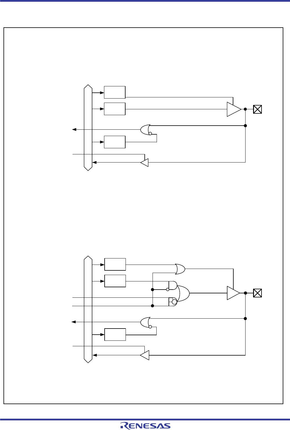
R01UH0034EJ0200 Rev.2.00 Page 460 of 1489
Dec 27, 2013
RX62T Group, RX62G Group 15. I/O Ports
Under development Preliminary document
Specifications in this document are tentative and subject to change.
15.6 I/O Port Configuration
Figure 15.1 I/O Port Configuration (1)
DDR
DR
Peripheral module
output signal
Peripheral module
output enable
Peripheral module
input signal
Reading the port
ICR
Note 1: Products in the 64-pin LQFP do not have these pins.
Note 2: Products in the 80-pin LQFP do not have these pins.
Note 3: Products in the 100-pin LQFP do not have these pins.
Note 4: Products in the 80-pin LQFP (R5F562TxGDFF) do not have these pins.
DDR
DR
ICR
Peripheral module
input signal
Reading the port
Port 2 (P22 to P24)
Port 3 (P30 to P33)
Port 7 (P71 to P76)
Port 8 (P81, P82*1, *2)
Port 9 (P90*1, *2, P91 to P94, P95*1)
Port A (PA0*4, PA1*1, *2, *4, PA2*4, PA3, PA4*4, PA5)
Port B (PB0 to PB3, PB6, PB7)
Port D (PD0, PD1*1, *2, *4, PD2*1, *2, PD3 to PD7)
Port E (PE0*1, PE3*1, PE4*1)
Port G (PG0 to PG2*1, *2, *3, *4)
Internal bus Internal bus
Port 1 (P10, P11*4)
Port 2 (P20, P21*1, *4)
Port 7 (P70)
Port 8 (P80*1, *2)
Port 9 (P96*1)
Port B (PB4)
Port E (PE5*1, *2)
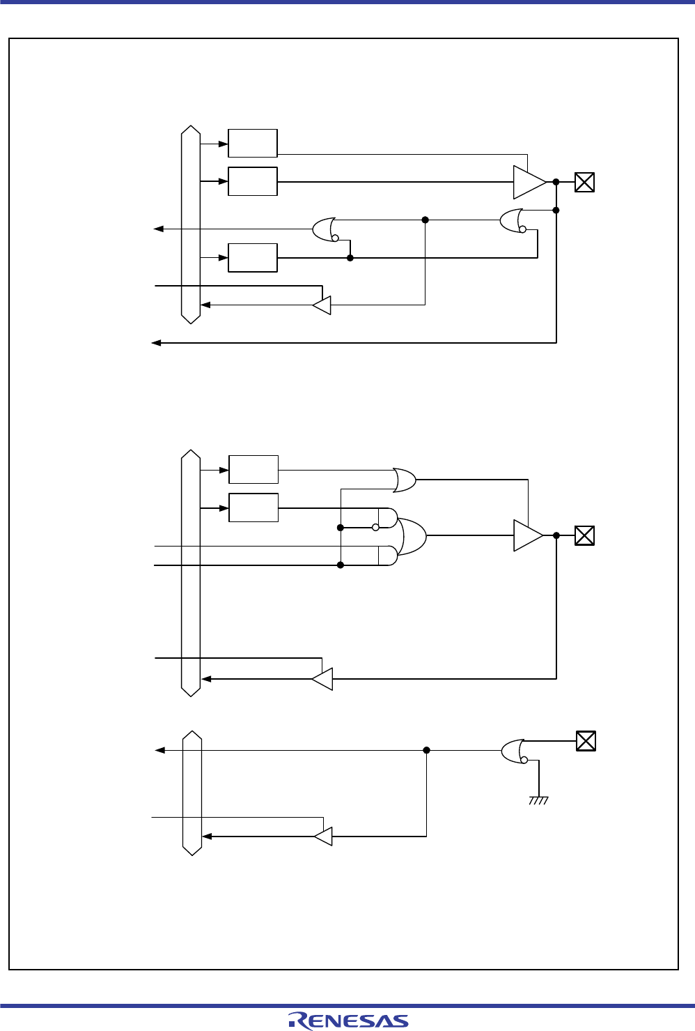
R01UH0034EJ0200 Rev.2.00 Page 461 of 1489
Dec 27, 2013
RX62T Group, RX62G Group 15. I/O Ports
Under development Preliminary document
Specifications in this document are tentative and subject to change.
Figure 15.2 I/O Port Configuration (2)
DDR
DR
Peripheral module
output signal
Peripheral module
output enable
Reading the port
Port 4 (P40 to P47)
Port 5 (P50 to P55*1, *2, *4)
Port 6 (P60 to P63*1, *4, P64, P65*1, *2, *4)
DDR
DR
ICR
Peripheral module
input signal
Reading the port
Port B (PB5)
Port E (PE1*2)
Port G (PG3 to PG5*1, *2, *3, *4)
Internal bus
Analog input
Internal bus
Note 1: Products in the 64-pin LQFP do not have these pins.
Note 2: Products in the 80-pin LQFP do not have these pins.
Note 3: Products in the 100-pin LQFP do not have these pins.
Note 4: Products in the 80-pin LQFP (R5F562TxGDFF) do not have these pins.
Note 5: When reading the port register (PORT), ensure that the corresponding bits in the ICR register are 1.
If the PORT register is read while the setting of bits in the ICR register is 0, values read from the corresponding bits
are undefined.
NMI input signal
POE input signal
Reading the port
Port E (PE2)
Internal bus
*5

R01UH0034EJ0200 Rev.2.00 Page 462 of 1489
Dec 27, 2013
RX62T Group, RX62G Group 15. I/O Ports
Under development Preliminary document
Specifications in this document are tentative and subject to change.
15.7 Usage Notes
15.7.1 Setting the Input Buffer Control Register (PORTn.ICR)
Changes to PORTn.ICR settings can lead to the generation of internal edges, depending on the setting and the pin states
at the time it is made. This may lead to operation that was not intended. Change the setting of a PORTn.ICR while the
input signal from the pins is fixed to the high level or, if a peripheral function has been assigned to a pin, while the input
function is disabled.
If a PORTn.ICR setting enables an input buffer, and several input functions have been allocated to the corresponding pin,
the pin state is reflected in the values of all of the input signals. Thus, even for input functions that are not in use,
attention must be paid to the settings of the corresponding peripheral modules.
If a pin is being used as an output pin, the output value is taken in as the pin state when the input buffer is enabled by a
PORTn.ICR setting. For pins being used as output pins, disable the input buffer by setting the corresponding bits in the
given PORTn.ICR.
15.7.2 Setting the Port Function Register
Each port function register controls an I/O port. When setting input or output functions for individual pins, select a pin
for the input or output and then enable or disable the input or output function.
If the levels for a pin before and after it has been switched to operate as an input differ from each other, an internal edge
is generated. This may lead to operation that was not intended. To avoid this, follow the procedure below when switching
a pin to input operation.
1. Disable the input in the peripheral module settings that correspond to functions of the pin to be switched.
2. Make the port function register setting to select input operation for the pin.
3. Enable the input in the peripheral module settings that correspond to functions of the pin to be switched
If the settings for a pin before and after it has been switched to operate as an output differ from each other, an internal
edge is output. This may lead to operation that was not intended. To avoid this, follow the procedure below when
switching a pin to output operation.
1. Disable the output in the peripheral module settings that correspond to functions of the pin to be switched.
2. Make the port function register setting to select output operation for the pin.
3. Enable the output in the peripheral module settings that correspond to functions of the pin to be switched.
A single pin function may correspond to a pin selection bit for changing a pin for the input or output and a pin enable bit
for enabling a pin function. In such cases, set the pin selection bit to select the pin for the input or output and then set the
enable bit to enable the pin function.

R01UH0034EJ0200 Rev.2.00 Page 463 of 1489
Dec 27, 2013
RX62T Group, RX62G Group 15. I/O Ports
Under development Preliminary document
Specifications in this document are tentative and subject to change.
15.7.3 Changing the Output Enable Settings
Pins are initially in the Hi-Z state because the output function of the port is initially disabled. If the output enable setting
is changed, the port leaves the Hi-Z state and enters the output state (high or low); however, this may lead to generation
of internal edges depending on the LSI internal state. To prevent edge generation, 0 or 1 should be previously set to the
port data register (DR) using the procedure below.
Changing the pin state from Hi-Z to high output:
1. Set 1 (set the internal state of the LSI to high) to the port data register (DR) of the pins.
2. Select the output pins by setting the port function register.
3. Enable the pins for output.
Changing the pin state from Hi-Z to low output:
1. Set 0 (set the internal state of the LSI to low) to the port data register (DR) of the pins.
2. Select the output pins by setting the port function register.
3. Enable the pins for output.
15.7.4 Reading Port Registers (PORT)
Before reading the port registers (PORT) in ports 4, 5, and 6, enable the input buffer of the corresponding pins by setting
the corresponding bits in PORTn.ICR to 1.
If the PORTn.PORT register is read with bits in the PORTn.ICR register set to 0, undefined values are read from the
corresponding bits.

R01UH0034EJ0200 Rev.2.00 Page 464 of 1489
Dec 27, 2013
RX62T Group, RX62G Group 16. Multi-Function Timer Pulse Unit 3 (MTU3)
16. Multi-Function Timer Pulse Unit 3 (MTU3)
16.1 Overview
The RX62T and RX62G Groups have on-chip multi-function timer pulse unit 3 (MTU3), which comprises eight 16-bit
timer channels.
Table 16.1 shows the specifications of the MTU and Table 16.2 shows the function list of the MTU. Figure 16.1 and
Figure 16.2 show block diagrams of the MTU.
Table 16.1 Specifications of MTU
Item Description
Pulse input/output 24 lines max.
Pulse input 3 lines
Count clock Six to eight clocks for each channel (four clocks for MTU5)
Operating frequency 8 to 100 MHz
Available operations [MTU0 to MTU4, MTU6, and MTU7]
Waveform output on compare match
Input capture function
Counter-clearing operation
Simultaneous writing to multiple timer counters (TCNT)
Simultaneous clearing on compare match or input capture
Simultaneous input and output to registers in synchronization with counter operations
Up to 12-phase PWM output in combination with synchronous operation
[MTU0, MTU3, MTU4, MTU6, and MTU7]
Buffer operation specifiable
[MTU3, MTU4, MTU6, and MTU7]
Through interlocked operation of MTU3, MTU4, MTU6, and MTU7, output of positive and
negative signals in six phases (for a total of 12 phases) in complementary-PWM and reset-
PWM operation
In complementary PWM mode, transfer of values from buffer registers to temporary registers
on peaks and troughs of the timer-counter values or writing to the buffer registers
(MTU4.TGRD and MTU7.TGRD)
Double-buffering selectable in complementary PWM mode
[MTU3 and MTU4]
Through interlocking with MTU0, a mode for driving AC synchronous motors (brushless DC
motors) by using complementary PWM output and reset PWM output is settable and allows
the selection of two types of waveform output (chopping or level)
[MTU1 and MTU2]
Independently specifiable phase-counting mode
Capable of cascade-connected operation
[MTU5]
Capable of operation as a dead-time compensation counter
Interrupt-skipping function in
complementary PWM mode
In complementary PWM mode, interrupts on crests and troughs of counter values and triggers
to start conversion by the A/D converter can be skipped
Interrupt sources 38 sources
Buffer operation Automatic transfer of register data (transfer from the buffer register to the timer register)
Trigger generation A/D converter start triggers can be generated
A/D converter start request delaying function enables A/D converter to be started with any
desired timing and to be synchronized with PWM output
Power reduction Module stop mode can be set.

R01UH0034EJ0200 Rev.2.00 Page 465 of 1489
Dec 27, 2013
RX62T Group, RX62G Group 16. Multi-Function Timer Pulse Unit 3 (MTU3)
Table 16.2 MTU Functions (1 / 3)
Item MTU0 MTU1 MTU2 MTU3 MTU4 MTU5 MTU6 MTU7
Count clock ICLK/1
ICLK/4
ICLK/16
ICLK/64
MTCLKA
MTCLKB
MTCLKC
MTCLKD
ICLK/1
ICLK/4
ICLK/16
ICLK/64
ICLK/256
MTCLKA
MTCLKB
ICLK/1
ICLK/4
ICLK/16
ICLK/64
ICLK/1024
MTCLKA
MTCLKB
MTCLKC
ICLK/1
ICLK/4
ICLK/16
ICLK/64
ICLK/256
ICLK/1024
MTCLKA
MTCLKB
ICLK/1
ICLK/4
ICLK/16
ICLK/64
ICLK/256
ICLK/1024
MTCLKA
MTCLKB
ICLK/1
ICLK/4
ICLK/16
ICLK/64
ICLK/1
ICLK/4
ICLK/16
ICLK/64
ICLK/256
ICLK/1024
ICLK/1
ICLK/4
ICLK/16
ICLK/64
ICLK/256
ICLK/1024
General registers
(TGR)
TGRA
TGRB
TGRE
TGRA
TGRB
TGRA
TGRB
TGRA
TGRB
TGRA
TGRB
TGRU
TGRV
TGRW
TGRA
TGRB
TGRA
TGRB
General registers/
buffer registers
TGRC
TGRD
TGRF
——TGRC
TGRD
TGRE
TGRC
TGRD
TGRE
TGRF
—TGRC
TGRD
TGRE
TGRC
TGRD
TGRE
TGRF
I/O pins MTIOC0A
MTIOC0B
MTIOC0C
MTIOC0D
MTIOC1A
MTIOC1B
MTIOC2A
MTIOC2B
MTIOC3A
MTIOC3B
MTIOC3C
MTIOC3D
MTIOC4A
MTIOC4B
MTIOC4C
MTIOC4D
Input pins
MTIC5U
MTIC5V
MTIC5W
MTIOC6A
MTIOC6B
MTIOC6C
MTIOC6D
MTIOC7A
MTIOC7B
MTIOC7C
MTIOC7D
Counter clear function TGR
compare
match or
input
capture
TGR
compare
match or
input
capture
TGR
compare
match or
input
capture
TGR
compare
match or
input
capture
TGR
compare
match or
input
capture
TGR
compare
match or
input
capture
TGR
compare
match or
input
capture
TGR
compare
match or
input
capture
Compar
e match
output
Low output √√√√√—√√
High
output
√√√√√—√√
Toggle
output
√√√√√—√√
Input capture function √√√√√√√√
Synchronous
operation
√√√√√—√√
PWM mode 1 √√√√√—√√
PWM mode 2 √√√—————
Complementary PWM
mode
———√√—√√
Reset-synchronized
PWM mode
———√√—√√
AC synchronous
motor drive mode
√——√√———
Phase counting mode — √√—————
Buffer operation √——√√—√√
Dead time
compensation counter
function
—————√——

R01UH0034EJ0200 Rev.2.00 Page 466 of 1489
Dec 27, 2013
RX62T Group, RX62G Group 16. Multi-Function Timer Pulse Unit 3 (MTU3)
Interrupt sources 7 sources
Compare
match or
input
capture A
Compare
match or
input
capture B
Compare
match or
input
capture
C
Compare
match or
input
capture
D
Compare
match 0E
Compare
match F
Overflow
4 sources
Compare
match or
input
capture A
Compare
match or
input
capture B
Overflow
Underflow
4 sources
Compare
match or
input
capture A
Compare
match or
input
capture B
Overflow
Underflow
5 sources
Compare
match or
input
capture A
Compare
match or
input
capture B
Compare
match or
input
capture
C
Compare
match or
input
capture
D
Overflow
5 sources
Compare
match or
input
capture A
Compare
match or
input
capture B
Compare
match or
input
capture C
Compare
match or
input
capture D
Overflow
or
underflow
(only in
comple-
mentary
PWM
mode)
3 sources
Compare
match or
input
capture
U
Compare
match or
input
capture V
Compare
match or
input
capture
W
5 sources
Compare
match or
input
capture A
Compare
match or
input
capture B
Compare
match or
input
capture
C
Compare
match or
input
capture
D
Overflow
5 sources
Compare
match or
input
capture A
Compare
match or
input
capture B
Compare
match or
input
capture C
Compare
match or
input
capture D
Overflow
or
underflow
(only in
comple-
mentary
PWM
mode)
DTC activation TGR
compare
match or
input
capture
TGR
compare
match or
input
capture
TGR
compare
match or
input
capture
TGR
compare
match or
input
capture
TGR
compare
match or
input
capture
Overflow
or
underflow
(only in
comple-
mentary
PWM
mode)
TGR
compare
match or
input
capture
TGR
compare
match or
input
capture
TGR
compare
match or
input
capture
Overflow
or
underflow
(only in
comple-
mentary
PWM
mode)
A/D converter start
trigger
TGRA
compare
match or
input
capture
TGRE
compare
match
TGRA
compare
match or
input
capture
TGRA
compare
match or
input
capture
TGRA
compare
match or
input
capture
TGRA
compare
match or
input
capture
TCNT
underflow
(trough) in
comple-
mentary
PWM mode
—TGRA
compare
match or
input
capture
TGRA
compare
match or
input
capture
TCNT
underflow
(trough) in
comple-
mentary
PWM mode
Table 16.2 MTU Functions (2 / 3)
Item MTU0 MTU1 MTU2 MTU3 MTU4 MTU5 MTU6 MTU7

R01UH0034EJ0200 Rev.2.00 Page 467 of 1489
Dec 27, 2013
RX62T Group, RX62G Group 16. Multi-Function Timer Pulse Unit 3 (MTU3)
√: Possible —: Not possible
Note 1. For details on the module stop function, see section 9, Low Power Consumption.
A/D converter start
request delaying
function
————A/D
converter
start
request
at a
match
between
TADCOR
A and
TCNT
A/D
converter
start
request
at a
match
between
TADCOR
B and
TCNT
——A/D
converter
start
request at
a match
between
TADCOR
A and
TCNT
A/D
converter
start
request at
a match
between
TADCOR
B and
TCNT
Interrupt skipping
function 1
———Skips
TGRA
compare
match
interrupts
Skips
TCIV
interrupts
—Skips
TGRA
compare
match
interrupts
Skips
TCIV
interrupts
Interrupt skipping
function 2
————Skips
interrupts
according
to the
count of
compare
matches
between
TADCOR
A and
TCNT
and
TADCOR
B and
TCNT
——Skips
interrupts
according
to the
count of
compare
matches
between
TADCOR
A and
TCNT
and
TADCOR
B and
TCNT
Module stop function MSTPCRA.MSTPA9*1
Table 16.2 MTU Functions (3 / 3)
Item MTU0 MTU1 MTU2 MTU3 MTU4 MTU5 MTU6 MTU7
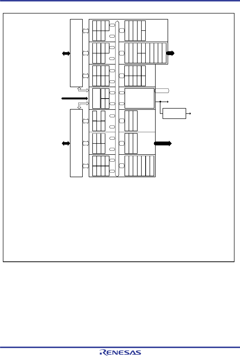
R01UH0034EJ0200 Rev.2.00 Page 468 of 1489
Dec 27, 2013
RX62T Group, RX62G Group 16. Multi-Function Timer Pulse Unit 3 (MTU3)
Figure 16.1 Block Diagram of MTU (MTU0 to MTU4)
A/D converter start signals
Input/output pins
MTU3: MTIOC3A
MTIOC3B
MTIOC3C
MTIOC3D
Interrupt request signals
MTU3 : TGIA3
TGIB3
TGIC3
TGID3
TCIV3
Clock input
Internal clock: ICLK/1
ICLK/4
ICLK/16
ICLK/64
ICLK/256
ICLK/1024
Interrupt request signals
Input/output pins
MTU0: MTIOC0A
MTIOC0B
MTIOC0C
MTIOC0D
MTU1: MTIOC1A
MTIOC1B
MTU2: MTIOC2A
MTIOC2B
Peripheral bus
[Legend]
TRG4ABN
MTU4: MTIOC4A
MTIOC4B
MTIOC4C
MTIOC4D
External clock: MTCLKA
MTCLKB
MTCLKC
MTCLKD
MTU4 : TGIA4
TGIB4
TGIC4
TGID4
TCIV4
MTU3
MTU4
CommonMTU2
TCR
MTU1MTU0
Control logic
Module data bus
Control logic for
MTU0 , MTU1 and MTU2 Control logic for
MTU3 and MTU4
TCR
TIORH
TIER
TIER2
TMDRI
TIORL
TSR
TBTM
TMDR1
TIORH TICCR
TIER TSR
TCNT
TGRA
TGRB
TGRC
TGRD TGRE
TCNT
TGRA
TGRB
TGRC TGRE
TGRD TGRF
TADCR
TADCORA
TADCORB
TADCOBRA
TADCOBRB
TCR TMDR1
TIORH TIORL
TIER TSR
TBTM
TCR TMDR1
TIORH TIORL
TIER TSR
TBTM
TOERA TMDR2A
TOCR1A TOCR2A
TOLBRA TGCRA
TCBRATCDRA
TDDRA TDERA
TCNTSA TBTERA
TWCRA TITMRA
TITCR2ATITCR1A
TITCNT2ATITCNT1A
TCNT
TGRA
TGRB
TGRC
TGRD
TGRE
TGRF
TCR TMDR1
TIORH
TIER TSR
TCNT
TGRA
TGRB
TCNT
TGRA
TGRB BUS I/F
TCSYSTR TRWERA
TSTRA TSYRA
MTU0 : TGIA0
TGIB0
TGIC0
TGID0
TGIE0
TGIF0
TCIV0
MTU1 : TGIA1
TGIB1
TCIV1
TCIU1
MTU2 : TGIA2
TGIB2
TCIV2
TCIU2
TRG4AN and
TRG4BN
skipping control logic
TCR: Timer control register
TMDR: Timer mode register 1
TMDR2A: Timer mode register 2
TIOR: Timer I/O control register
TIORH: Timer I/O control register H
TIORL: Timer I/O control register L
TIER: Timer interrupt enable register
TIER2: Timer interrupt enable register 2
TSR: Timer status register
TBTM: Timer buffer operation transfer mode register
TCNT: Timer counter
TGR: Timer general register A
TGRB: Timer general register B
TGRC: Timer general register C
TGRD: Timer general register D
TGRE: Timer general register E
TGRF: Timer general register F
TSTRA: Timer start register
TSYRA: Timer synchronous register
TCSYSTR: Timer counter synchronous start register
TRWERA: Timer read/write enable register
TOERAA: Timer output master enable register
TOCR1A: Timer output control register 1
TOCR2A: Timer output control register 2
TOLBRA: Timer output level buffer register
TGCRA: Timer gate control register
TCNTSA: Timer subcounter
TCDRA: Timer cycle data register
TCBRA: Timer cycle buffer register
TDDRA: Timer dead time data register
TDERA: Timer dead time enable register
TBTERA: Timer buffer transfer set register
TWCRA: Timer waveform control register
TICCR: Timer input capture control register
TADCR: Timer A/D converter start request control register
TADCORA: Timer A/D converter start request cycle set registerA
TADCORB: Timer A/D converter start request cycle set registerB
TADCOBRA: Timer A/D converter start request cycle set buffer register A
TADCOBRB: Timer A/D converter start request cycle set buffer register B
TITMRA: Timer interrupt skipping mode register
TITCR1A: Timer interrupt skipping set register 1
TITCR2A: Timer interrupt skipping set register 2
TITCNT1A: Timer interrupt skipping counter 1
TITCNT2A: Timer interrupt skipping counter 2
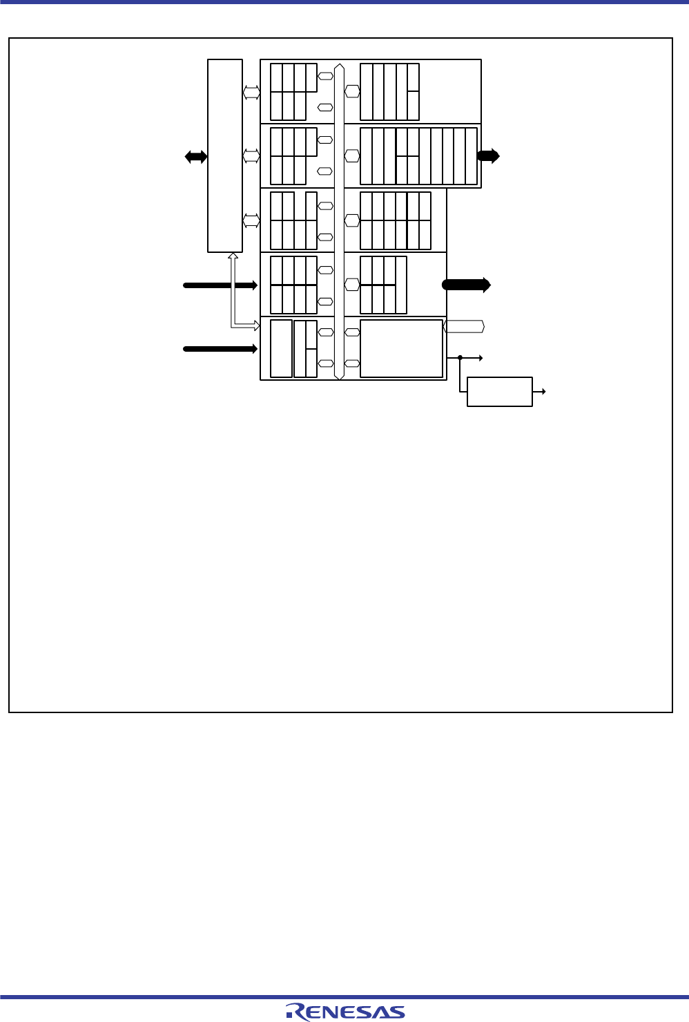
R01UH0034EJ0200 Rev.2.00 Page 469 of 1489
Dec 27, 2013
RX62T Group, RX62G Group 16. Multi-Function Timer Pulse Unit 3 (MTU3)
Figure 16.2 Block Diagram of MTU (MTU5 to MTU7)
A/D converter start signals
Input/output pins
Interrupt request signals
Clock input Peripheral bus
Interrupt request signals
Input pins
[Legend]
TRG7ABN
Common
Module data bus
Control logic
TRWERB
BUS I/F
TCNTU TGRU
TCNTV TGRV
TCNTW TGRW
TCNTCMPCLR
TOERB TMDR2B
TOCR1B TOCR2B
TOLBRB
TCDRB TCBRB
TDDRB TDERB
TCNTSB TBTERB
TWCRB TITMRB
TITCR1B TITCR2B
TITCNT1B TITCNT2B
TSYCR TCSYSTR
TCNT
TGRA
TGRB
TGRC TGRE
TGRD TGRF
TADCR
TADCORA
TADCORB
TADCOBRA
TADCOBRB
TCNT
TGRA
TGRB
TGRC
TGRD TGRE
MTU5
TSRTIER
TIORWTCRW
TIORVTCRV
TIORUTCRU
TBTM
TSRTIER
TIORLTIORH
TMDR1TCR
MTU7 MTU6
TBTM
TSRTIER
TIORLTIORH
TMDR1TCR
TSYRBTSTRB
MTU6: MTGIA6
MTGIB6
MTGIC6
MTGID6
MTCIV6
Internal clock: ICLK/4
ICLK/16
ICLK/64
ICLK/256
ICLK/1024
MTU7: MTGIA7
MTGIB7
MTGIC7
MTGID7
MTCIV7
MTU5: TGIU5
TGIV5
TGIW5
TRG7AN and
TRG7BN
skipping control logic
Control logic for
MTU6 and MTU7
MTU6: MTIOC6A
MTIOC6B
MTIOC6C
MTIOC6D
MTU7: MTIOC7A
MTIOC7B
MTIOC7C
MTIOC7D
MTU5: MTIC5U
MTIC5V
MTIC5W
TSTRB: Timer start register
TSYRB: Timer synchronous register
TSYCR: Timer synchronous clear register
TCSYSTR: Timer counter synchronous start register
TRWERB: Timer read/write enable register
TOERB: Timer output master enable register
TOCR1B: Timer output control register 1
TOCR2B: Timer output control register 2
TOLBRB: Timer output level buffer register
TCDRB: Timer cycle data register
TCBRB: Timer cycle buffer register
TDDRB: Timer dead time data register
TDERB: Timer dead time enable register
TCNTS: Timer subcounter
TBTERB: Timer buffer transfer set register
TWCRBA: Timer waveform control register
TADCR: Timer A/D converter start request control register
TADCORA: Timer A/D converter start request cycle set register A
TADCORB: Timer A/D converter start request cycle set register B
TADCOBRA: Timer A/D converter start request cycle set buffer register A
TADCOBRB: Timer A/D converter start request cycle set buffer register B
TITMRB: Timer interrupt skipping mode register
TITCR1B: Timer interrupt skipping set register 1
TITCR2B: Timer interrupt skipping set register 2
TITCNT1B: Timer interrupt skipping counter 1
TITCNT2B: Timer interrupt skipping counter 2
TCR: Timer control register
TCRU: Timer control register U
TCRV: Timer control register V
TCRW: Timer control register W
TMDR1A: Timer mode register 1
TMDR2BA: Timer mode register 2
TIORH: Timer I/O control register H
TIORL: Timer I/O control register L
TIORU: Timer I/O control register U
TIORV: Timer I/O control register V
TIORW: Timer I/O control register W
TIER: Timer interrupt enable register
TSR: Timer status register
TCNT: Timer counter
TCNTU: Timer counter U
TCNTV: Timer counter V
TCNTW: Timer counter W
TGRA: Timer general register A
TGRB: Timer general register B
TGRC: Timer general register C
TGRD: Timer general register D
TGRE: Timer general register E
TGRF: Timer general register F
TGRU: Timer general register U
TGRV: Timer general register V
TGRW: Timer general register W
TCNTCMPCLR: Timer compare match clear register

R01UH0034EJ0200 Rev.2.00 Page 470 of 1489
Dec 27, 2013
RX62T Group, RX62G Group 16. Multi-Function Timer Pulse Unit 3 (MTU3)
Table 16.3 shows the pin configuration of the MTU.
Table 16.3 Pin Configuration
Channel Pin Name I/O Function
MTU MTCLKA Input External clock A input pin (MTU1 phase counting mode A phase input)
MTCLKB Input External clock B input pin (MTU1 phase counting mode B phase input)
MTCLKC Input External clock C input pin (MTU1 phase counting mode A phase input)
MTCLKD Input External clock D input pin (MTU2 phase counting mode B phase input)
MTU0 MTIOC0A I/O MTU0 TGRA input capture input/output compare output/PWM output pin
MTIOC0B I/O MTU0 TGRB input capture input/output compare output/PWM output pin
MTIOC0C I/O MTU0 TGRC input capture input/output compare output/PWM output pin
MTIOC0D I/O MTU0 TGRD input capture input/output compare output/PWM output pin
MTU1 MTIOC1A I/O MTU1 TGRA input capture input/output compare output/PWM output pin
MTIOC1B I/O MTU1 TGRB input capture input/output compare output/PWM output pin
MTU2 MTIOC2A I/O MTU2 TGRA input capture input/output compare output/PWM output pin
MTIOC2B I/O MTU2 TGRB input capture input/output compare output/PWM output pin
MTU3 MTIOC3A I/O MTU3 TGRA input capture input/output compare output/PWM output pin
MTIOC3B I/O MTU3 TGRB input capture input/output compare output/PWM output pin
MTIOC3C I/O MTU3 TGRC input capture input/output compare output/PWM output pin
MTIOC3D I/O MTU3 TGRD input capture input/output compare output/PWM output pin
MTU4 MTIOC4A I/O MTU4 TGRA input capture input/output compare output/PWM output pin
MTIOC4B I/O MTU4 TGRB input capture input/output compare output/PWM output pin
MTIOC4C I/O MTU4 TGRC input capture input/output compare output/PWM output pin
MTIOC4D I/O MTU4 TGRD input capture input/output compare output/PWM output pin
MTU5 MTIC5U Input MTU5 TGRU input capture input/external pulse input pin
MTIC5V Input MTU5 TGRV input capture input/external pulse input pin
MTIC5W Input MTU5 TGRW input capture input/external pulse input pin
MTU6 MTIOC6A I/O MTU6 TGRA input capture input/output compare output/PWM output pin
MTIOC6B I/O MTU6 TGRB input capture input/output compare output/PWM output pin
MTIOC6C I/O MTU6 TGRC input capture input/output compare output/PWM output pin
MTIOC6D I/O MTU6 TGRD input capture input/output compare output/PWM output pin
MTU7 MTIOC7A I/O MTU7 TGRA input capture input/output compare output/PWM output pin
MTIOC7B I/O MTU7 TGRB input capture input/output compare output/PWM output pin
MTIOC7C I/O MTU7 TGRC input capture input/output compare output/PWM output pin
MTIOC7D I/O MTU7 TGRD input capture input/output compare output/PWM output pin

R01UH0034EJ0200 Rev.2.00 Page 471 of 1489
Dec 27, 2013
RX62T Group, RX62G Group 16. Multi-Function Timer Pulse Unit 3 (MTU3)
16.2 Register Descriptions
Table 16.4 lists the registers of the MTU3.
Table 16.4 Registers of MTU3 (1 / 6)
Channel Register Name Symbol Value after Reset Address Access Size
MTU0 Timer control register TCR 00h 000C 1300h 8, 16, 32
Timer mode register 1 TMDR1 00h 000C 1301h 8
Timer I/O control register H TIORH 00h 000C 1302h 8, 16
Timer I/O control register L TIORL 00h 000C 1303h 8
Timer interrupt enable register TIER 00h 000C 1304h 8, 16, 32
Timer status register TSR C0h 000C 1305h 8
Timer counter TCNT 0000h 000C 1306h 16
Timer general register A TGRA FFFFh 000C 1308h 16, 32
Timer general register B TGRB FFFFh 000C 130Ah 16
Timer general register C TGRC FFFFh 000C 130Ch 16, 32
Timer general register D TGRD FFFFh 000C 130Eh 16
Timer general register E TGRE FFFFh 000C 1320h 16, 32
Timer general register F TGRF FFFFh 000C 1322h 16
Timer interrupt enable register 2 TIER2 00h 000C 1324h 8, 16
Timer status register 2 TSR2 C0h 000C 1325h 8
Timer buffer operation transfer mode
register
TBTM 00h 000C 1326h 8
MTU1 Timer control register TCR 00h 000C 1380h 8, 16
Timer mode register 1 TMDR1 00h 000C 1381h 8
Timer I/O control register TIOR 00h 000C 1382h 8
Timer interrupt enable register TIER 00h 000C 1384h 8, 16, 32
Timer status register TSR C0h 000C 1385h 8
Timer counter TCNT 0000h 000C 1386h 16
Timer general register A TGRA FFFFh 000C 1388h 16, 32
Timer general register B TGRB FFFFh 000C 138Ah 16
Timer input capture control register TICCR 00h 000C 1390h 8
MTU2 Timer control register TCR 00h 000C 1400h 8, 16
Timer mode register 1 TMDR1 00h 000C 1401h 8
Timer I/O control register TIOR 00h 000C 1402h 8
Timer interrupt enable register TIER 00h 000C 1404h 8, 16, 32
Timer status register TSR C0h 000C 1405h 8
Timer counter TCNT 0000h 000C 1406h 16
Timer general register A TGRA FFFFh 000C 1408h 16, 32
Timer general register B TGRB FFFFh 000C 140Ah 16

R01UH0034EJ0200 Rev.2.00 Page 472 of 1489
Dec 27, 2013
RX62T Group, RX62G Group 16. Multi-Function Timer Pulse Unit 3 (MTU3)
MTU3 Timer control register TCR 00h 000C 1200h 8, 16, 32
Timer mode register 1 TMDR1 00h 000C 1202h 8, 16
Timer I/O control register H TIORH 00h 000C 1204h 8, 16, 32
Timer I/O control register L TIORL 00h 000C 1205h 8
Timer interrupt enable register TIER 00h 000C 1208h 8, 16
Timer counter TCNT 0000h 000C 1210h 16, 32
Timer general register A TGRA FFFFh 000C 1218h 16, 32
Timer general register B TGRB FFFFh 000C 121Ah 16
Timer general register C TGRC FFFFh 000C 1224h 16, 32
Timer general register D TGRD FFFFh 000C 1226h 16
Timer general register E TGRE FFFFh 000C 1272h 16
Timer status register TSR C0h 000C 122Ch 8, 16
Timer buffer operation transfer mode
register
TBTM 00h 000C 1238h 8, 16
MTU4 Timer control register TCR 00h 000C 1201h 8
Timer mode register 1 TMDR1 00h 000C 1203h 8
Timer I/O control register H TIORH 00h 000C 1206h 8, 16
Timer I/O control register L TIORL 00h 000C 1207h 8
Timer interrupt enable register TIER 00h 000C 1209h 8
Timer counter TCNT 0000h 000C 1212h 16
Timer general register A TGRA FFFFh 000C 121Ch 16, 32
Timer general register B TGRB FFFFh 000C 121Eh 16
Timer general register C TGRC FFFFh 000C 1228h 16, 32
Timer general register D TGRD FFFFh 000C 122Ah 16
Timer general register E TGRE FFFFh 000C 1274h 16
Timer general register F TGRF FFFFh 000C 1276h 16
Timer status register TSR C0h 000C 122Dh 8
Timer buffer operation transfer mode
register
TBTM 00h 000C 1239h 8
MTU4 Timer A/D converter start request
control register
TADCR 0000h 000C 1240h 16
Timer A/D converter start request cycle
set register A
TADCORA FFFFh 000C 1244h 16, 32
Timer A/D converter start request cycle
set register B
TADCORB FFFFh 000C 1246h 16
Timer A/D converter start request cycle
set buffer register A
TADCOBRA FFFFh 000C 1248h 16, 32
Timer A/D converter start request cycle
set buffer register B
TADCOBRB FFFFh 000C 124Ah 16
Table 16.4 Registers of MTU3 (2 / 6)
Channel Register Name Symbol Value after Reset Address Access Size

R01UH0034EJ0200 Rev.2.00 Page 473 of 1489
Dec 27, 2013
RX62T Group, RX62G Group 16. Multi-Function Timer Pulse Unit 3 (MTU3)
MTU5 Timer counter U TCNTU 0000h 000C 1C80h 16, 32
Timer general register U TGRU FFFFh 000C 1C82h 16
Timer control register U TCRU 00h 000C 1C84h 8
Timer I/O control register U TIORU 00h 000C 1C86h 8
Timer counter V TCNTV 0000h 000C 1C90h 16, 32
Timer general register V TGRV FFFFh 000C 1C92h 16
Timer control register V TCRV 00h 000C 1C94h 8
Timer I/O control register V TIORV 00h 000C 1C96h 8
Timer counter W TCNTW 0000h 000C 1CA0h 16, 32
Timer general register W TGRW FFFFh 000C 1CA2h 16
Timer control register W TCRW 00h 000C 1CA4h 8
Timer I/O control register W TIORW 00h 000C 1CA6h 8
Timer status register TSR 00h 000C 1CB0h 8
Timer interrupt enable register TIER 00h 000C 1CB2h 8
Timer start register TSTR 00h 000C 1CB4h 8
Timer compare match clear register TCNTCMPCLR 00h 000C 1CB6h 8
MTU6 Timer control register TCR 00h 000C 1A00h 8, 16, 32
Timer mode register 1 TMDR1 00h 000C 1A02h 8, 16
Timer I/O control register H TIORH 00h 000C 1A04h 8, 16, 32
Timer I/O control register L TIORL 00h 000C 1A05h 8
Timer interrupt enable register TIER 00h 000C 1A08h 8, 16
Timer counter TCNT 0000h 000C 1A10h 16, 32
Timer general register A TGRA FFFFh 000C 1A18h 16, 32
Timer general register B TGRB FFFFh 000C 1A1Ah 16
Timer general register C TGRC FFFFh 000C 1A24h 16, 32
Timer general register D TGRD FFFFh 000C 1A26h 16
Timer general register E TGRE FFFFh 000C 1A72h 16
Timer synchronous clear register TSYCR 00h 000C 1A50h 8
Timer status register TSR C0h 000C 1A2Ch 8, 16
Timer buffer operation transfer mode
register
TBTM 00h 000C 1A38h 8, 16
Table 16.4 Registers of MTU3 (3 / 6)
Channel Register Name Symbol Value after Reset Address Access Size

R01UH0034EJ0200 Rev.2.00 Page 474 of 1489
Dec 27, 2013
RX62T Group, RX62G Group 16. Multi-Function Timer Pulse Unit 3 (MTU3)
MTU7 Timer control register TCR 00h 000C 1A01h 8
Timer mode register 1 TMDR1 00h 000C 1A03h 8
Timer I/O control register H TIORH 00h 000C 1A06h 8, 16
Timer I/O control register L TIORL 00h 000C 1A07h 8
Timer interrupt enable register TIER 00h 000C 1A09h 8
Timer counter TCNT 0000h 000C 1A12h 16
Timer general register A TGRA FFFFh 000C 1A1Ch 16, 32
Timer general register B TGRB FFFFh 000C 1A1Eh 16
Timer general register C TGRC FFFFh 000C 1A28h 16, 32
Timer general register D TGRD FFFFh 000C 1A2Ah 16
Timer general register E TGRE FFFFh 000C 1A74h 16
Timer general register F TGRF FFFFh 000C 1A76h 16
Timer status register TSR C0h 000C 1A2Dh 8
Timer buffer operation transfer mode
register
TBTM 00h 000C 1A39h 8
Timer A/D converter start request
control register
TADCR 0000h 000C 1A40h 16
Timer A/D converter start request cycle
set register A
TADCORA FFFFh 000C 1A44h 16, 32
Timer A/D converter start request cycle
set register B
TADCORB FFFFh 000C 1A46h 16
Timer A/D converter start request cycle
set buffer register A
TADCOBRA FFFFh 000C 1A48h 16, 32
Timer A/D converter start request cycle
set buffer register B
TADCOBRB FFFFh 000C 1A4Ah 16
MTU3, MTU4
common
Timer output master enable register A TOERA C0h 000C 120Ah 8
MTU6, MTU7
common
Timer output master enable register B TOERB C0h 000C 1A0Ah 8
MTU3, MTU4
common
Timer gate control register A TGCRA 80h 000C 120Dh 8
MTU3, MTU4
common
Timer output control register 1A TOCR1A 00h 000C 120Eh 8, 16
MTU6, MTU7
common
Timer output control register 1B TOCR1B 00h 000C 1A0Eh 8, 16
MTU3, MTU4
common
Timer output control register 2A TOCR2A 00h 000C 120Fh 8
MTU6, MTU7
common
Timer output control register 2B TOCR2B 00h 000C 1A0Fh 8
MTU3, MTU4
common
Timer cycle data register A TCDRA FFFFh 000C 1214h 16, 32
MTU6, MTU7
common
Timer cycle data register B TCDRB FFFFh 000C 1A14h 16, 32
MTU3, MTU4
common
Timer dead time data register A TDDRA FFFFh 000C 1216h 16
MTU6, MTU7
common
Timer dead time data register B TDDRB FFFFh 000C 1A16h 16
MTU3, MTU4
common
Timer dead time enable register A TDERA 01h 000C 1234h 8
MTU6, MTU7
common
Timer dead time enable register B TDERB 01h 000C 1A34h 8
Table 16.4 Registers of MTU3 (4 / 6)
Channel Register Name Symbol Value after Reset Address Access Size

R01UH0034EJ0200 Rev.2.00 Page 475 of 1489
Dec 27, 2013
RX62T Group, RX62G Group 16. Multi-Function Timer Pulse Unit 3 (MTU3)
MTU3, MTU4
common
Timer subcounter A TCNTSA 0000h 000C 1220h 16, 32
MTU6, MTU7
common
Timer subcounter B TCNTSB 0000h 000C 1A20h 16, 32
MTU3, MTU4
common
Timer cycle buffer register A TCBRA FFFFh 000C 1222h 16
MTU6, MTU7
common
Timer cycle buffer register B TCBRB FFFFh 000C 1A22h 16
MTU3, MTU4
common
Timer interrupt skipping set register 1A TITCR1A 00h 000C 1230h 8, 16
MTU6, MTU7
common
Timer interrupt skipping set register 1B TITCR1B 00h 000C 1A30h 8, 16
MTU3, MTU4
common
Timer interrupt skipping set register 2A TITCR2A 00h 000C 123Bh 8
MTU6, MTU7
common
Timer interrupt skipping set register 2B TITCR2B 00h 000C 1A3Bh 8
MTU3, MTU4
common
Timer interrupt skipping counter 1A TITCNT1A 00h 000C 1231h 8
MTU6, MTU7
common
Timer interrupt skipping counter 1B TITCNT1B 00h 000C 1A31h 8
MTU3, MTU4
common
Timer interrupt skipping counter 2A TITCNT2A 00h 000C 123Ch 8
MTU6, MTU7
common
Timer interrupt skipping counter 2B TITCNT2B 00h 000C 1A3Ch 8
MTU3, MTU4
common
Timer buffer transfer set register A TBTERA 00h 000C 1232h 8
MTU6, MTU7
common
Timer buffer transfer set register B TBTERB 00h 000C 1A32h 8
MTU3, MTU4
common
Timer output level buffer register A TOLBRA 00h 000C 1236h 8
MTU6, MTU7
common
Timer output level buffer register B TOLBRB 00h 000C 1A36h 8
MTU3, MTU4
common
Timer mode register 2A TMDR2A 00h 000C 1270h 8
MTU6, MTU7
common
Timer mode register 2B TMDR2B 00h 000C 1A70h 8
MTU3, MTU4
common
Timer interrupt skipping mode register
A
TITMRA 00h 000C 123Ah 8
MTU6, MTU7
common
Timer interrupt skipping mode register
B
TITMRB 00h 000C 1A3Ah 8
MTU3, MTU4
common
Timer waveform control register A TWCRA 00h 000C 1260h 8
MTU6, MTU7
common
Timer waveform control register B TWCRB 00h 000C 1A60h 8
MTU0 to MTU4
common
Timer start register A TSTRA 00h 000C 1280h 8, 16
MTU6, MTU7
common
Timer start register B TSTRB 00h 000C 1A80h 8, 16
MTU0 to MTU4
common
Timer synchronous register A TSYRA 00h 000C 1281h 8
MTU6, MTU7
common
Timer synchronous register B TSYRB 00h 000C 1A81h 8
MTU0 to MTU7
Common
Timer counter synchronous start
register
TCSYSTR 00h 000C 1282h 8
Table 16.4 Registers of MTU3 (5 / 6)
Channel Register Name Symbol Value after Reset Address Access Size

R01UH0034EJ0200 Rev.2.00 Page 476 of 1489
Dec 27, 2013
RX62T Group, RX62G Group 16. Multi-Function Timer Pulse Unit 3 (MTU3)
MTU3, MTU4
common
Timer read/write enable register A TRWERA 01h 000C 1284h 8
MTU6, MTU7
common
Timer read/write enable register B TRWERB 01h 000C 1A84h 8
Table 16.4 Registers of MTU3 (6 / 6)
Channel Register Name Symbol Value after Reset Address Access Size

R01UH0034EJ0200 Rev.2.00 Page 477 of 1489
Dec 27, 2013
RX62T Group, RX62G Group 16. Multi-Function Timer Pulse Unit 3 (MTU3)
16.2.1 Timer Control Register (TCR)
MTU0, MTU1, MTU2, MTU3, MTU4, MTU6, MTU7
x: Don’t care
TCR controls the TCNT operation for each channel. The MTU has a total of ten TCR registers, one each for MTU 0 to
MTU4, MTU6 and MTU7 and three (TCRU, TCRV, and TCRW) for MTU 5. TCR values should be specified only while
TCNT operation is stopped.
TPSC[2:0] Bits (Time Prescaler Select)
These bits select the TCNT counter clock. The clock source can be selected independently for each channel. See Table
16.7 to Table 16.10 for details.
CKEG[1: 0] Bits (Clock Edge Select)
These bits select the input clock edge. When the input clock is counted at both edges, the input clock period is halved
(e.g. ICLK/4 at both edges = ICLK/2 at rising edge). If phase counting mode is used on MTU1 and MTU2, the setting of
these bits is ignored and the phase counting mode setting has priority. Internal clock edge selection is valid when the
input clock is ICLK/4 or slower. When ICLK/1 or the overflow/underflow in another channel is selected for the input
clock, a value can be written to these bits but counter operation compiles with the initial value.
CCLR[2:0] Bits (Counter Clear Source Select)
These bits select the TCNT counter clearing source. See Table 16.5 and Table 16.6 for details.
Address: MTU0.TCR 000C 1300h, MTU1.TCR 000C 1380h, MTU2.TCR 000C 1400h,
MTU3.TCR 000C 1200h, MTU4.TCR 000C 1201h, MTU6.TCR 000C 1A00h,
MTU7.TCR 000C 1A01h
b7 b6 b5 b4 b3 b2 b1 b0
CCLR[2:0] CKEG[1:0] TPSC[2:0]
Value after reset: 00000000
Bit Symbol Bit Name Description R/W
b2 to b0 TPSC[2:0] Time Prescaler Select See Table 16.7 to Table 16.10. R/W
b4, b3 CKEG[1:0] Clock Edge Select b4 b3
0 0: Count at rising edge
0 1: Count at falling edge
1 x: Count at both edges
R/W
b7 to b5 CCLR[2:0] Counter Clear Source Select See Table 16.5 and Table 16.6. R/W
R01UH0034EJ0200 Rev.2.00 Page 478 of 1489
Dec 27, 2013
RX62T Group, RX62G Group 16. Multi-Function Timer Pulse Unit 3 (MTU3)
MTU5
TPSC[1:0] Bits (Time Prescaler Select)
These bits select the TCNT counter clock. See Table 16.11 for details.
Note 1. Synchronous operation is selected by setting the TSYRA.SYNC or TSYRB.SYNC bit to 1.
Note 2. When TGRC or TGRD is used as a buffer register, TCNT is not cleared because the buffer register setting has priority and
compare match/input capture does not occur.
Note 1. Synchronous operation is selected by setting the TSYRA.SYNC and TSYRB.SYNC bits to 1.
Note 2. Bit 7 is reserved in MTU1 and MTU2. It is always read as 0. The write value is ignored.
Address: MTU5.TCRU 000C 1C84h, MTU5.TCRV 000C 1C94h, MTU5.TCRW 000C 1CA4h
b7 b6 b5 b4 b3 b2 b1 b0
——————TPSC[1:0]
Value after reset: 00000000
Bit Symbol Bit Name Description R/W
b1, b0 TPSC[1:0] Time Prescaler Select See Table 16.11. R/W
b7 to b2 — Reserved These bits are always read as 0. The write value should be 0. R/W
Table 16.5 CCLR[2:0] (MTU0, MTU3, MTU4, MTU6, and MTU7)
Channel
Bit 7 Bit 6 Bit 5
DescriptionCCLR2 CCLR1 CCLR0
MTU0
MTU3
MTU4
MTU6
MTU7
0 0 0 TCNT clearing disabled
0 0 1 TCNT cleared by TGRA compare match/input capture
0 1 0 TCNT cleared by TGRB compare match/input capture
0 1 1 TCNT cleared by counter clearing in another channel performing
synchronous clearing/synchronous operation*1
1 0 0 TCNT clearing disabled
1 0 1 TCNT cleared by TGRC compare match/input capture*2
1 1 0 TCNT cleared by TGRD compare match/input capture*2
1 1 1 TCNT cleared by counter clearing in another channel performing
synchronous clearing/synchronous operation*1
Table 16.6 CCLR[2:0] (MTU1 and MTU2)
Bit 7 Bit 6
Channel Reserved*2 CCLR1 CCLR0 Description
MTU1
MTU2
0 0 0 TCNT clearing disabled
0 0 1 TCNT cleared by TGRA compare match/input capture
0 1 0 TCNT cleared by TGRB compare match/input capture
0 1 1 TCNT cleared by counter clearing in another channel performing
synchronous clearing/synchronous operation*1

R01UH0034EJ0200 Rev.2.00 Page 479 of 1489
Dec 27, 2013
RX62T Group, RX62G Group 16. Multi-Function Timer Pulse Unit 3 (MTU3)
Note: • This setting is ignored when MTU1 is in phase counting mode.
Note: • This setting is ignored when MTU2 is in phase counting mode.
Table 16.7 TPSC[2:0] (MTU0)
Channel
Bit 2 Bit 1 Bit 0
DescriptionTPSC2 TPSC1 TPSC0
MTU0000Internal clock: counts on ICLK/1
001Internal clock: counts on ICLK/4
010Internal clock: counts on ICLK/16
011Internal clock: counts on ICLK/64
100External clock: counts on MTCLKA pin input
101External clock: counts on MTCLKB pin input
110External clock: counts on MTCLKC pin input
111External clock: counts on MTCLKD pin input
Table 16.8 TPSC[2:0] (MTU1)
Channel
Bit 2 Bit 1 Bit 0
DescriptionTPSC2 TPSC1 TPSC0
MTU1 0 0 0 Internal clock: counts on ICLK/1
0 0 1 Internal clock: counts on ICLK/4
0 1 0 Internal clock: counts on ICLK/16
0 1 1 Internal clock: counts on ICLK/64
1 0 0 External clock: counts on MTCLKA pin input
1 0 1 External clock: counts on MTCLKB pin input
1 1 0 Internal clock: counts on ICLK/256
1 1 1 Counts on MTU2.TCNT overflow/underflow
Table 16.9 TPSC[2:0] (MTU2)
Channel
Bit 2 Bit 1 Bit 0
DescriptionTPSC2 TPSC1 TPSC0
MTU2 0 0 0 Internal clock: counts on ICLK/1
0 0 1 Internal clock: counts on ICLK/4
0 1 0 Internal clock: counts on ICLK/16
0 1 1 Internal clock: counts on ICLK/64
1 0 0 External clock: counts on MTCLKA pin input
1 0 1 External clock: counts on MTCLKB pin input
1 1 0 External clock: counts on MTCLKC pin input
1 1 1 Internal clock: counts on ICLK/1024

R01UH0034EJ0200 Rev.2.00 Page 480 of 1489
Dec 27, 2013
RX62T Group, RX62G Group 16. Multi-Function Timer Pulse Unit 3 (MTU3)
Note 1. This setting is not allowed in MTU6 and MTU7.
Note: • Bits 7 to 2 are reserved in MTU5. These bits are always read as 0. The write value should be 0.
Table 16.10 TPSC[2:0] (MTU3, MTU4, MTU6 and MTU7)
Channel
Bit 2 Bit 1 Bit 0
DescriptionTPSC2 TPSC1 TPSC0
MTU3
MTU4
MTU6
MTU7
0 0 0 Internal clock: counts on ICLK/1
0 0 1 Internal clock: counts on ICLK/4
0 1 0 Internal clock: counts on ICLK/16
0 1 1 Internal clock: counts on ICLK/64
1 0 0 Internal clock: counts on ICLK/256
1 0 1 Internal clock: counts on ICLK/1024
1 1 0 External clock: counts on MTCLKA pin input*1
1 1 1 External clock: counts on MTCLKB pin input*1
Table 16.11 TPSC[1:0] (MTU5)
Bit 1 Bit 0
Channel TPSC1 TPSC0 Description
MTU5 0 0 Internal clock: counts on ICLK/1
0 1 Internal clock: counts on ICLK/4
1 0 Internal clock: counts on ICLK/16
1 1 Internal clock: counts on ICLK/64
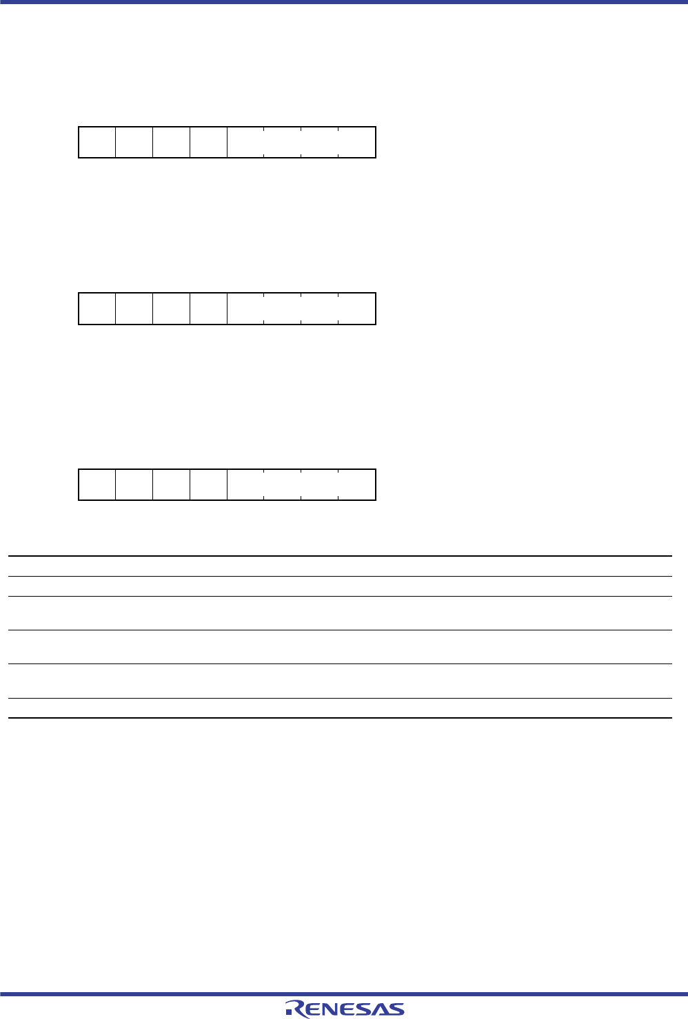
R01UH0034EJ0200 Rev.2.00 Page 481 of 1489
Dec 27, 2013
RX62T Group, RX62G Group 16. Multi-Function Timer Pulse Unit 3 (MTU3)
16.2.2 Timer Mode Register 1 (TMDR1)
MTU0.TMDR1
MTU1.TMDR1, MTU2.TMDR1
MTU3.TMDR1, MTU4.TMDR1, MTU6.TMDR1, MTU7.TMDR1
TMDR1 specifies the operating mode of each channel. The MTU3 has a total of seven TMDR1 registers, one each for
MTU0 to MTU4, MTU6, and MTU7. TMDR1 values should be specified only while TCNT operation is stopped.
Address: MTU0.TMDR1 000C 1301h
b7 b6 b5 b4 b3 b2 b1 b0
—BFEBFBBFA MD[3:0]
Value after reset: 00000000
Address: MTU1.TMDR1 000C 1381h, MTU2.TMDR1 000C 1401h
b7 b6 b5 b4 b3 b2 b1 b0
———— MD[3:0]
Value after reset: 00000000
Address: MTU3.TMDR1 000C 1202h,MTU4.TMDR1 000C 1203h,
MTU6.TMDR1 000C 1A02h,MTU7.TMDR1 000C 1A03h
b7 b6 b5 b4 b3 b2 b1 b0
——BFBBFA MD[3:0]
Value after reset: 00000000
Bit Symbol Bit Name Description R/W
b3 to b0 MD[3:0] Mode Select These bits specify the timer operating mode. See Table 16.12 for details. R/W
b4 BFA Buffer Operation A 0: TGRA and TGRC operate normally
1: TGRA and TGRC used together for buffer operation
R/W
b5 BFB Buffer Operation B 0: TGRB and TGRD operate normally
1: TGRB and TGRD used together for buffer operation
R/W
b6 BFE Buffer Operation E 0: MTU0.TGRE and MTU0.TGRF operate normally
1: MTU0.TGRE and MTU0.TGRF used together for buffer operation
R/W
b7 — Reserved This bit is always read as 0. The write value should be 0. R/W

R01UH0034EJ0200 Rev.2.00 Page 482 of 1489
Dec 27, 2013
RX62T Group, RX62G Group 16. Multi-Function Timer Pulse Unit 3 (MTU3)
x: Don't care
Note 1. PWM mode 2 cannot be set for MTU3, MTU4, MTU6, and MTU7.
Note 2. Phase counting mode cannot be set for MTU0, MTU3, MTU4, MTU6, and MTU7.
Note 3. Reset-synchronized PWM mode and complementary PWM mode can only be set for MTU3 and MTU6.
When MTU3 or MTU6 is set to reset-synchronized PWM mode or complementary PWM mode, the settings of MTU4 and MTU7
become ineffective and automatically conform to the setting of MTU3 or MTU6, respectively. MTU4 and MTU7 should be set to
the initial values (normal operation).
Reset-synchronized PWM mode and complementary PWM mode cannot be set for MTU0, MTU1, and MTU2.
BFA Bit (Buffer Operation A)
This bit specifies whether to operate TGRA in the normal way or to use TGRA and TGRC together for buffer operation.
When TGRC is used as a buffer register, TGRC input capture/output compare does not take place.
In reset synchronized PWM mode or complementary PWM mode, buffer operation in MTU3 and MTU4 (or MTU6 and
MTU7) depends on the settings in the BFA bit of MTU3.TMDR1 (MTU6.TMDR1). The BFA bit of MTU4.TMDR1
(MTU7.TMDR1) should be set to 0.
In MTU1 and MTU2, which have no TGRC, this bit is reserved. It is always read as 0. The write value should be 0.
BFB Bit (Buffer Operation B)
This bit specifies whether to operate TGRB in the normal way or to use TGRB and TGRD together for buffer operation.
When TGRD is used as a buffer register, TGRD input capture/output compare does not take place.
In reset synchronized PWM mode or complementary PWM mode, buffer operation in MTU3 and MTU4 (or MTU6 and
MTU7) depends on the settings in the BFB bit of MTU3.TMDR1 (MTU6.TMDR1). The BFB bit of MTU4.TMDR1
(MTU7.TMDR1) should be set to 0.
In MTU1 and MTU2, which have no TGRD, this bit is reserved. It is always read as 0. The write value should be 0.
BFE Bit (Buffer Operation E)
This bit specifies whether to operate MTU0.TGRE and MTU0.TGRF in the normal way or to use them together for
buffer operation.
In MTU1 to MTU4, MTU6, and MTU7, this bit is reserved. It is always read as 0. The write value should be 0.
Table 16.12 Operating Mode Setting by MD[3:0] Bits
Bit 3 Bit 2 Bit 1 Bit 0
DescriptionMD3 MD2 MD1 MD0
0000Normal operation
0001Setting prohibited
0010PWM mode 1
0011PWM mode 2
*1
0100Phase counting mode 1*2
0101Phase counting mode 2*2
0110Phase counting mode 3*2
0111Phase counting mode 4*2
1000Reset-synchronized PWM mode
*3
1001Setting prohibited
1 0 1 x Setting prohibited
1100Setting prohibited
1101Complementary PWM mode 1 (transfer at crest) *3
1110Complementary PWM mode 2 (transfer at trough)*3
1111Complementary PWM mode 3 (transfer at crest and trough)*3
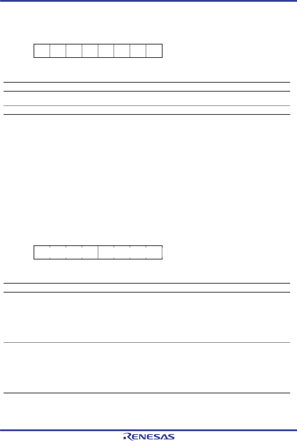
R01UH0034EJ0200 Rev.2.00 Page 483 of 1489
Dec 27, 2013
RX62T Group, RX62G Group 16. Multi-Function Timer Pulse Unit 3 (MTU3)
16.2.3 Timer Mode Registers 2 (TMDR2A and TMDR2B)
TMDR2 specifies the double buffer function in complementary PWM mode 3 (transfer at the crest and trough of the
counter value). The MTU3 has two TMDR2 registers, one each for MTU3 (TMDR2A) and MTU6 (TMDR2B).
TMDR2A and TMDR2B values should be specified only while TCNT operation is stopped.
DRS Bit (Double Buffer Select)
This bit enables or disables the double buffer function in complementary PWM mode.
16.2.4 Timer I/O Control Register (TIOR)
MTU0.TIORH, MTU1.TIOR, MTU2.TIOR, MTU3.TIORH, MTU4.TIORH, MTU6.TIORH, MTU7.TIOR
Address: TMDR2A 000C 1270h,TMDR2B 000C 1A70h
b7 b6 b5 b4 b3 b2 b1 b0
———————DRS
Value after reset: 00000000
Bit Symbol Bit Name Description R/W
b0 DRS Double Buffer Select 0: Double buffer function is disabled
1: Double buffer function is enabled
R/W
b7 to b1 — Reserved These bits are always read as 0. The write value should be 0. R/W
Address: MTU0.TIORH 000C 1302h,MTU1.TIOR 000C 1382h,MTU2.TIOR 000C 1402h,
MTU3.TIORH 000C 1204h,MTU4.TIORH 000C 1206h,MTU6.TIORH 000C 1A04h,
MTU7.TIORH 000C 1A06h
b7 b6 b5 b4 b3 b2 b1 b0
IOB[3:0] IOA[3:0]
Value after reset: 00000000
Bit Symbol Bit Name Description R/W
b3 to b0 IOA[3:0] I/O Control A See the following tables.
MTU0.TIORH: Table 16.25
MTU1.TIOR: Table 16.27
MTU2.TIOR: Table 16.28
MTU3.TIORH: Table 16.29
MTU4.TIORH: Table 16.31
MTU6.TIORH: Table 16.33
MTU7.TIORH: Table 16.35
R/W
b7 to b4 IOB[3:0] I/O Control B See the following tables.
MTU0.TIORH: Table 16.13
MTU1.TIOR: Table 16.15
MTU2.TIOR: Table 16.16
MTU3.TIORH: Table 16.17
MTU4.TIORH: Table 16.19
MTU5.TIORH: Table 16.21
MTU6.TIORH: Table 16.23
R/W
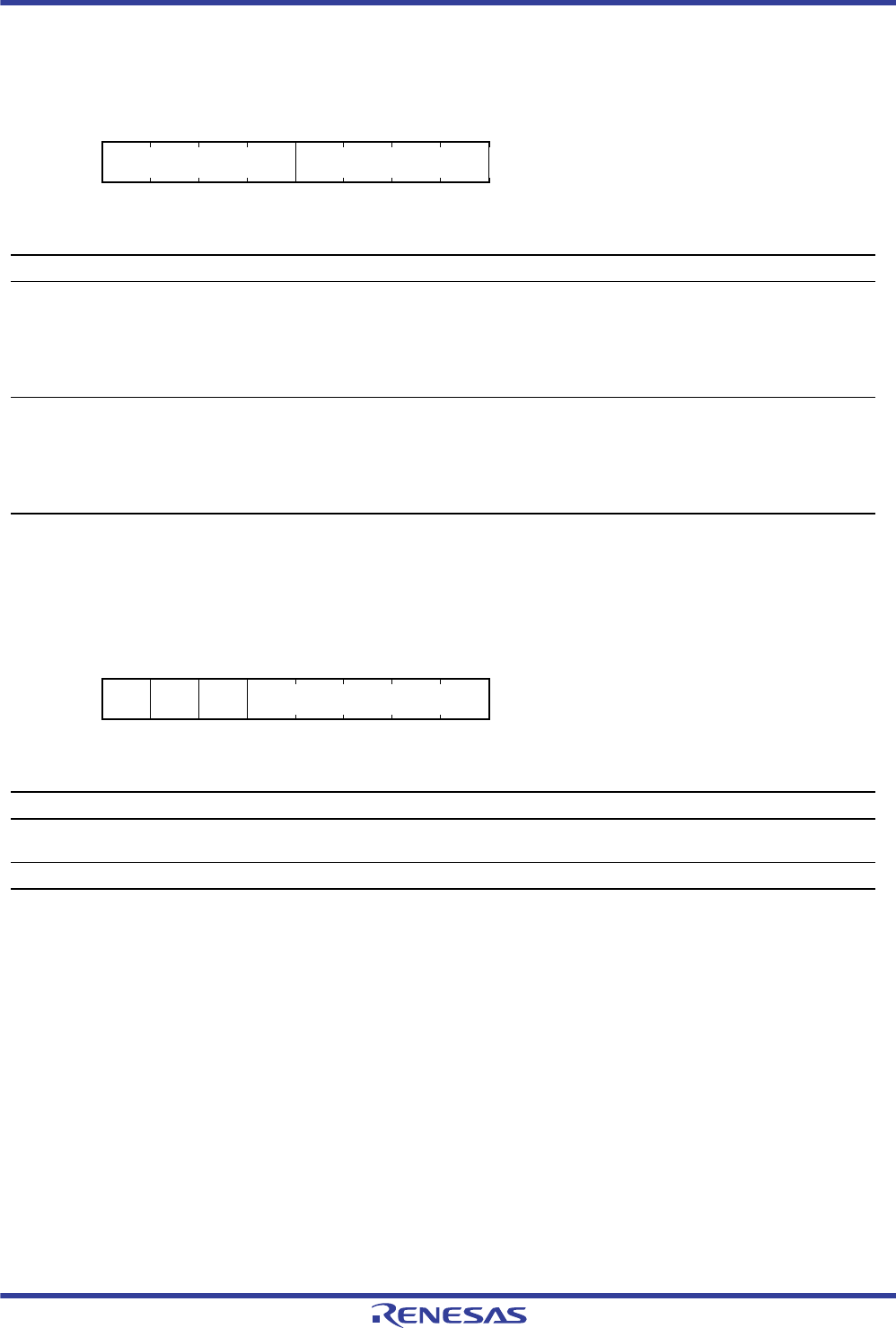
R01UH0034EJ0200 Rev.2.00 Page 484 of 1489
Dec 27, 2013
RX62T Group, RX62G Group 16. Multi-Function Timer Pulse Unit 3 (MTU3)
MTU0.TIORL, MTU3.TIORL, MTU4.TIORL, MTU6.TIORL, MTU7.TIORL
MTU5.TIORU, MTU5.TIORV, MTU5.TIORW
TIOR controls TGR. The MTU3 has a total of 15 TIOR registers, two each for MTU0, MTU3, MTU4, MTU6, and
MTU7, one each for MTU1 and MTU2, and three (MTU5.TIORU/V/W) for MTU5.
Note that TIOR is affected by the TMDR1 setting.
The initial output specified by TIOR is valid when the counter is stopped (the CST bit in TSTRA and the CST bit in
TSYRB are cleared to 0). Note also that, in PWM mode 2, the output at the point at which the counter is cleared to 0 is
specified.
When TGRC or TGRD is designated for buffer operation, this setting is invalid and the register operates as a buffer
register.
Address: MTU0.TIORL 000C 1303h, MTU3.TIORL 000C 1205h, MTU4.TIORL 000C 1207h,
MTU6.TIORL 000C 1A05h, MTU7.TIORL 000C 1A07h
b7 b6 b5 b4 b3 b2 b1 b0
IOD[3:0] IOC[3:0]
Value after reset: 00000000
Bit Symbol Bit Name Description R/W
b3 to b0 IOC[3:0] I/O Control C See the following tables.
MTU0.TIORL: Table 16.26
MTU3.TIORL: Table 16.30
MTU4.TIORL: Table 16.32
MTU6.TIORL: Table 16.34
MTU7.TIORL: Table 16.36
R/W
b7 to b4 IOD[3:0] I/O Control D See the following tables.
MTU0.TIORL: Table 16.14
MTU3.TIORL: Table 16.18
MTU4.TIORL: Table 16.20
MTU6.TIORL: Table 16.22
MTU7.TIORL: Table 16.24
R/W
Address: MTU5.TIORU 000C 1C86h, MTU5.TIORV 000C 1C96h, MTU5.TIORW 000C 1CA6h
b7 b6 b5 b4 b3 b2 b1 b0
— — — IOC[4:0]
Value after reset: 00000000
Bit Symbol Bit Name Description R/W
b4 to b0 IOC[4:0] I/O Control C See the following table.
MTU5.TIORU, MTU5.TIORV, MTU5.TIORW: Table 16.37
R/W
b7 to b5 — Reserved These bits are always read as 0. The write value should be 0. R/W

R01UH0034EJ0200 Rev.2.00 Page 485 of 1489
Dec 27, 2013
RX62T Group, RX62G Group 16. Multi-Function Timer Pulse Unit 3 (MTU3)
x: Don't care
Table 16.13 TIORH (MTU0)
Bit 7 Bit 6 Bit 5 Bit 4
MTU0.TGRB Function
Description
IOB3 IOB2 IOB1 IOB0 MTIOC0B Pin Function
0000Output compare registerOutput prohibited
0 0 0 1 Initial output is low.
Low output at compare match.
0 0 1 0 Initial output is low.
High output at compare match.
0 0 1 1 Initial output is low.
Toggle output at compare match.
0 1 0 0 Output prohibited
0 1 0 1 Initial output is high.
Low output at compare match.
0 1 1 0 Initial output is high.
High output at compare match.
0 1 1 1 Initial output is high.
Toggle output at compare match.
1000Input capture register Input capture at rising edge.
1 0 0 1 Input capture at falling edge.
1 0 1 x Input capture at both edges.
1 1 x x Capture input source is count clock in MTU1.
Input capture at MTU1.TCNT up-count/down-count.

R01UH0034EJ0200 Rev.2.00 Page 486 of 1489
Dec 27, 2013
RX62T Group, RX62G Group 16. Multi-Function Timer Pulse Unit 3 (MTU3)
x: Don't care
Note 1. When the MTU0.TMDR1.BFB is set to 1 and MTU0.TGRD is used as a buffer register, this setting is invalid and input capture/
output compare is not generated.
Table 16.14 TIORL (MTU0)
Bit 7 Bit 6 Bit 5 Bit 4
MTU0.TGRD Function
Description
IOD3 IOD2 IOD1 IOD0 MTIOC0D Pin Function
0 0 0 0 Output compare register *1Output prohibited
0 0 0 1 Initial output is low.
Low output at compare match.
0 0 1 0 Initial output is low.
High output at compare match.
0 0 1 1 Initial output is low.
Toggle output at compare match.
0 1 0 0 Output prohibited
0 1 0 1 Initial output is high.
Low output at compare match.
0 1 1 0 Initial output is high.
High output at compare match.
0 1 1 1 Initial output is high.
Toggle output at compare match.
1 0 0 0 Input capture register *1Input capture at rising edge.
1 0 0 1 Input capture at falling edge.
1 0 1 x Input capture at both edges.
1 1 x x Capture input source is count clock in MTU1.
Input capture at MTU1.TCNT up-count/down-count.

R01UH0034EJ0200 Rev.2.00 Page 487 of 1489
Dec 27, 2013
RX62T Group, RX62G Group 16. Multi-Function Timer Pulse Unit 3 (MTU3)
x: Don't care
x: Don't care
Table 16.15 TIOR (MTU1)
Bit 7 Bit 6 Bit 5 Bit 4
MTU1.TGRB Function
Description
IOB3 IOB2 IOB1 IOB0 MTIOC1B Pin Function
0 0 0 0 Output compare register Output prohibited
0 0 0 1 Initial output is low.
Low output at compare match.
0 0 1 0 Initial output is low.
High output at compare match.
0 0 1 1 Initial output is low.
Toggle output at compare match.
0 1 0 0 Output prohibited
0 1 0 1 Initial output is high.
Low output at compare match.
0 1 1 0 Initial output is high.
High output at compare match.
0 1 1 1 Initial output is high.
Toggle output at compare match.
1 0 0 0 Input capture register Input capture at rising edge.
1 0 0 1 Input capture at falling edge.
1 0 1 x Input capture at both edges.
1 1 x x Input capture at generation of MTU0.TGRC compare
match/input capture.
Table 16.16 TIOR (MTU2)
Bit 7 Bit 6 Bit 5 Bit 4
MTU2.TGRB Function
Description
IOB3 IOB2 IOB1 IOB0 MTIOC2B Pin Function
0 0 0 0 Output compare register Output prohibited
0 0 0 1 Initial output is low.
Low output at compare match.
0 0 1 0 Initial output is low.
High output at compare match.
0 0 1 1 Initial output is low.
Toggle output at compare match.
0 1 0 0 Output prohibited
0 1 0 1 Initial output is high.
Low output at compare match.
0 1 1 0 Initial output is high.
High output at compare match.
0 1 1 1 Initial output is high.
Toggle output at compare match.
1 x 0 0 Input capture register Input capture at rising edge.
1 x 0 1 Input capture at falling edge.
1 x 1 x Input capture at both edges.

R01UH0034EJ0200 Rev.2.00 Page 488 of 1489
Dec 27, 2013
RX62T Group, RX62G Group 16. Multi-Function Timer Pulse Unit 3 (MTU3)
x: Don't care
Table 16.17 TIORH (MTU3)
Bit 7 Bit 6 Bit 5 Bit 4
MTU3.TGRB Function
Description
IOB3 IOB2 IOB1 IOB0 MTIOC3B Pin Function
0 0 0 0 Output compare register Output prohibited
0 0 0 1 Initial output is low.
Low output at compare match.
0 0 1 0 Initial output is low.
High output at compare match.
0 0 1 1 Initial output is low.
Toggle output at compare match.
0 1 0 0 Output prohibited
0 1 0 1 Initial output is high.
Low output at compare match.
0 1 1 0 Initial output is high.
High output at compare match.
0 1 1 1 Initial output is high.
Toggle output at compare match.
1 x 0 0 Input capture register Input capture at rising edge.
1 x 0 1 Input capture at falling edge.
1 x 1 x Input capture at both edges.
R01UH0034EJ0200 Rev.2.00 Page 489 of 1489
Dec 27, 2013
RX62T Group, RX62G Group 16. Multi-Function Timer Pulse Unit 3 (MTU3)
x: Don't care
Note 1. When the BFB bit in MTU3.TMDR1 is set to 1 and MTU3.TGRD is used as a buffer register, this setting is invalid and input
capture/output compare is not generated.
x: Don't care
Table 16.18 TIORL (MTU3)
Bit 7 Bit 6 Bit 5 Bit 4
MTU3.TGRD Function
Description
IOD3 IOD2 IOD1 IOD0 MTIOC3D Pin Function
0 0 0 0 Output compare register *1Output prohibited
0 0 0 1 Initial output is low.
Low output at compare match.
0 0 1 0 Initial output is low.
High output at compare match.
0 0 1 1 Initial output is low.
Toggle output at compare match.
0 1 0 0 Output prohibited
0 1 0 1 Initial output is high.
Low output at compare match.
0 1 1 0 Initial output is high.
High output at compare match.
0 1 1 1 Initial output is high.
Toggle output at compare match.
1 x 0 0 Input capture register *1Input capture at rising edge.
1 x 0 1 Input capture at falling edge.
1 x 1 x Input capture at both edges.
Table 16.19 TIORH (MTU4)
Bit 7 Bit 6 Bit 5 Bit 4
MTU4.TGRB Function
Description
IOB3 IOB2 IOB1 IOB0 MTIOC4B Pin Function
0 0 0 0 Output compare register Output prohibited
0 0 0 1 Initial output is low.
Low output at compare match.
0 0 1 0 Initial output is low.
High output at compare match.
0 0 1 1 Initial output is low.
Toggle output at compare match.
0 1 0 0 Output prohibited
0 1 0 1 Initial output is high.
Low output at compare match.
0 1 1 0 Initial output is high.
High output at compare match.
0 1 1 1 Initial output is high.
Toggle output at compare match.
1 x 0 0 Input capture register Input capture at rising edge.
1 x 0 1 Input capture at falling edge.
1 x 1 x Input capture at both edges.

R01UH0034EJ0200 Rev.2.00 Page 490 of 1489
Dec 27, 2013
RX62T Group, RX62G Group 16. Multi-Function Timer Pulse Unit 3 (MTU3)
x: Don't care
Note 1. When the BFB bit in MTU4.TMDR1 is set to 1 and MTU4.TGRD is used as a buffer register, this setting is invalid and input
capture/output compare is not generated.
x: Don't care
Table 16.20 TIORL (MTU4)
Bit 7 Bit 6 Bit 5 Bit 4
MTU4.TGRD Function
Description
IOD3 IOD2 IOD1 IOD0 MTIOC4D Pin Function
0 0 0 0 Output compare register*1Output prohibited
0 0 0 1 Initial output is low.
Low output at compare match.
0 0 1 0 Initial output is low.
High output at compare match.
0 0 1 1 Initial output is low.
Toggle output at compare match.
0 1 0 0 Output prohibited
0 1 0 1 Initial output is high.
Low output at compare match.
0 1 1 0 Initial output is high.
High output at compare match.
0 1 1 1 Initial output is high.
Toggle output at compare match.
1 x 0 0 Input capture register *1Input capture at rising edge.
1 x 0 1 Input capture at falling edge.
1 x 1 x Input capture at both edges.
Table 16.21 TIORH (MTU6)
Bit 7Bit 6Bit 5Bit 4
MTU6.TGRB Function
Description
IOB3 IOB2 IOB1 IOB0 MTIOC6B Pin Function
0 0 0 0 Output compare register Output prohibited
0 0 0 1 Initial output is low.
Low output at compare match.
0 0 1 0 Initial output is low.
High output at compare match.
0 0 1 1 Initial output is low.
Toggle output at compare match.
0 1 0 0 Output prohibited
0 1 0 1 Initial output is high.
Low output at compare match.
0 1 1 0 Initial output is high.
High output at compare match.
0 1 1 1 Initial output is high.
Toggle output at compare match.
1 x 0 0 Input capture register Input capture at rising edge.
1 x 0 1 Input capture at falling edge.
1 x 1 x Input capture at both edges.

R01UH0034EJ0200 Rev.2.00 Page 491 of 1489
Dec 27, 2013
RX62T Group, RX62G Group 16. Multi-Function Timer Pulse Unit 3 (MTU3)
x: Don't care
Note 1. When the BFB bit in MTU6.TMDR1 is set to 1 and MTU6.TGRD is used as a buffer register, this setting is invalid and input
capture/output compare is not generated.
x: Don't care
Table 16.22 TIORL (MTU6)
Bit 7 Bit 6 Bit 5 Bit 4
MTU6.TGRD Function
Description
IOD3 IOD2 IOD1 IOD0 MTIOC6D Pin Function
0000 Output compare register *1Output prohibited
0001 Initial output is low.
Low output at compare match.
0010 Initial output is low.
High output at compare match.
0011 Initial output is low.
Toggle output at compare match.
0100 Output prohibited
0101 Initial output is high.
Low output at compare match.
0110 Initial output is high.
High output at compare match.
0111 Initial output is high.
Toggle output at compare match.
1x00 Input capture register *1Input capture at rising edge.
1x01 Input capture at falling edge.
1x1x Input capture at both edges.
Table 16.23 TIORH (MTU7)
Bit 7 Bit 6 Bit 5 Bit 4
MTU7.TGRB Function
Description
IOB3 IOB2 IOB1 IOB0 MTIOC7B Pin Function
0000 Output compare register Output prohibited
0001 Initial output is low.
Low output at compare match.
0010 Initial output is low.
High output at compare match.
0011 Initial output is low.
Toggle output at compare match.
0100 Output prohibited
0101 Initial output is high.
Low output at compare match.
0110 Initial output is high.
High output at compare match.
0111 Initial output is high.
Toggle output at compare match.
1x00 Input capture register Input capture at rising edge.
1x01 Input capture at falling edge.
1x1x Input capture at both edges.

R01UH0034EJ0200 Rev.2.00 Page 492 of 1489
Dec 27, 2013
RX62T Group, RX62G Group 16. Multi-Function Timer Pulse Unit 3 (MTU3)
x: Don't care
Note 1. When the BFB bit in MTU7.TMDR1 is set to 1 and MTU7.TGRD is used as a buffer register, this setting is invalid and input
capture/output compare is not generated.
Table 16.24 TIORL (MTU7)
Bit 7 Bit 6 Bit 5 Bit 4
MTU7.TGRD Function
Description
IOD3 IOD2 IOD1 IOD0 MTIOC7D Pin Function
0000 Output compare register *1Output prohibited
0001 Initial output is low.
Low output at compare match.
0010 Initial output is low.
High output at compare match.
0011 Initial output is low.
Toggle output at compare match.
0100 Output prohibited
0101 Initial output is high.
Low output at compare match.
0110 Initial output is high.
High output at compare match.
0111 Initial output is high.
Toggle output at compare match.
1x00 Input capture register*1Input capture at rising edge.
1x01 Input capture at falling edge.
1x1x Input capture at both edges.

R01UH0034EJ0200 Rev.2.00 Page 493 of 1489
Dec 27, 2013
RX62T Group, RX62G Group 16. Multi-Function Timer Pulse Unit 3 (MTU3)
x: Don't care
Table 16.25 TIORH (MTU0)
Bit 3 Bit 2 Bit 1 Bit 0
MTU0.TGRA Function
Description
IOA3 IOA2 IOA1 IOA0 MTIOC0A Pin Function
0000 Output compare
register
Output prohibited
0001 Initial output is low.
Low output at compare match.
0010 Initial output is low.
High output at compare match.
0011 Initial output is low.
Toggle output at compare match.
0100 Output prohibited
0101 Initial output is high.
Low output at compare match.
0110 Initial output is high.
High output at compare match.
0111 Initial output is high.
Toggle output at compare match.
1000 Input capture register Input capture at rising edge.
1001 Input capture at falling edge.
101x Input capture at both edges.
11xx Capture input source is count clock in MTU1
Input capture at generation of MTU1.TCNT up-count/
down-count

R01UH0034EJ0200 Rev.2.00 Page 494 of 1489
Dec 27, 2013
RX62T Group, RX62G Group 16. Multi-Function Timer Pulse Unit 3 (MTU3)
x: Don't care
Note 1. When the BFA bit in MTU0.TMDR1 is set to 1 and MTU0.TGRC is used as a buffer register, this setting is invalid and input
capture/output compare is not generated.
Table 16.26 TIORL (MTU0)
Bit 3 Bit 2 Bit 1 Bit 0
MTU0.TGRC Function
Description
IOC3 IOC2 IOC1 IOC0 MTIOC0C Pin Function
0000 Output compare register*1Output prohibited
0001 Initial output is low.
Low output at compare match.
0010 Initial output is low.
High output at compare match.
0011 Initial output is low.
Toggle output at compare match.
0100 Output prohibited
0101 Initial output is high.
Low output at compare match.
0110 Initial output is high.
High output at compare match.
0111 Initial output is high.
Toggle output at compare match.
1000 Input capture register*1Input capture at rising edge.
1001 Input capture at falling edge.
101x Input capture at both edges.
11xx Capture input source is count clock in MTU1
Input capture at generation of MTU1.TCNT up-
count/down-count

R01UH0034EJ0200 Rev.2.00 Page 495 of 1489
Dec 27, 2013
RX62T Group, RX62G Group 16. Multi-Function Timer Pulse Unit 3 (MTU3)
x: Don't care
Table 16.27 TIOR (MTU1)
Bit 3 Bit 2 Bit 1 Bit 0
MTU1.TGRA Function
Description
IOA3 IOA2 IOA1 IOA0 MTIOC1A Pin Function
0000 Output compare
register
Output prohibited
0001 Initial output is low.
Low output at compare match.
0010 Initial output is low.
High output at compare match.
0011 Initial output is low.
Toggle output at compare match.
0100 Output prohibited
0101 Initial output is high.
Low output at compare match.
0110 Initial output is high.
High output at compare match.
0111 Initial output is high.
Toggle output at compare match.
1000 Input capture register Input capture at rising edge.
1001 Input capture at falling edge.
101x Input capture at both edges.
11xx Input capture at generation of MTU0.TGRA compare
match/input capture.

R01UH0034EJ0200 Rev.2.00 Page 496 of 1489
Dec 27, 2013
RX62T Group, RX62G Group 16. Multi-Function Timer Pulse Unit 3 (MTU3)
x: Don't care
x: Don't care
Table 16.28 TIOR (MTU2)
Bit 3 Bit 2 Bit 1 Bit 0
MTU2.TGRA Function
Description
IOA3 IOA2 IOA1 IOA0 MTIOC2A Pin Function
0 0 0 0 Output compare register Output prohibited
0 0 0 1 Initial output is low.
Low output at compare match.
0 0 1 0 Initial output is low.
High output at compare match.
0 0 1 1 Initial output is low.
Toggle output at compare match.
0 1 0 0 Output prohibited
0 1 0 1 Initial output is high.
Low output at compare match.
0 1 1 0 Initial output is high.
High output at compare match.
0 1 1 1 Initial output is high.
Toggle output at compare match.
1 x 0 0 Input capture register Input capture at rising edge.
1 x 0 1 Input capture at falling edge.
1 x 1 x Input capture at both edges.
Table 16.29 TIORH (MTU3)
Bit 3 Bit 2 Bit 1 Bit 0
MTU3.TGRA Function
Description
IOA3 IOA2 IOA1 IOA0 MTIOC3A Pin Function
0 0 0 0 Output compare register Output prohibited
0 0 0 1 Initial output is low.
Low output at compare match.
0 0 1 0 Initial output is low.
High output at compare match.
0 0 1 1 Initial output is low.
Toggle output at compare match.
0 1 0 0 Output prohibited
0 1 0 1 Initial output is high.
Low output at compare match.
0 1 1 0 Initial output is high.
High output at compare match.
0 1 1 1 Initial output is high.
Toggle output at compare match.
1 x 0 0 Input capture register Input capture at rising edge.
1 x 0 1 Input capture at falling edge.
1 x 1 x Input capture at both edges.
R01UH0034EJ0200 Rev.2.00 Page 497 of 1489
Dec 27, 2013
RX62T Group, RX62G Group 16. Multi-Function Timer Pulse Unit 3 (MTU3)
x: Don't care
Note 1. When the BFA bit in MTU3.TMDR1 is set to 1 and MTU3.TGRC is used as a buffer register, this setting is invalid and input
capture/output compare is not generated.
x: Don't care
Table 16.30 TIORL (MTU3)
Bit 3 Bit 2 Bit 1 Bit 0
MTU3.TGRC Function
Description
IOC3 IOC2 IOC1 IOC0 MTIOC3C Pin Function
0 0 0 0 Output compare register *1Output prohibited
0 0 0 1 Initial output is low.
Low output at compare match.
0 0 1 0 Initial output is low.
High output at compare match.
0 0 1 1 Initial output is low.
Toggle output at compare match.
0 1 0 0 Output prohibited
0 1 0 1 Initial output is high.
Low output at compare match.
0 1 1 0 Initial output is high.
High output at compare match.
0 1 1 1 Initial output is high.
Toggle output at compare match.
1 x 0 0 Input capture register *1Input capture at rising edge.
1 x 0 1 Input capture at falling edge.
1 x 1 x Input capture at both edges.
Table 16.31 TIORH (MTU4)
Bit 3 Bit 2 Bit 1 Bit 0
MTU4.TGRA Function
Description
IOA3 IOA2 IOA1 IOA0 MTIOC4A Pin Function
0000Output compare registerOutput prohibited
0 0 0 1 Initial output is low.
Low output at compare match.
0 0 1 0 Initial output is low.
High output at compare match.
0 0 1 1 Initial output is low.
Toggle output at compare match.
0 1 0 0 Output prohibited
0 1 0 1 Initial output is high.
Low output at compare match.
0 1 1 0 Initial output is high.
High output at compare match.
0 1 1 1 Initial output is high.
Toggle output at compare match.
1 x 0 0 Input capture register Input capture at rising edge.
1 x 0 1 Input capture at falling edge.
1 x 1 x Input capture at both edges.

R01UH0034EJ0200 Rev.2.00 Page 498 of 1489
Dec 27, 2013
RX62T Group, RX62G Group 16. Multi-Function Timer Pulse Unit 3 (MTU3)
x: Don't care
Note 1. When the BFA bit in MTU4.TMDR1 is set to 1 and MTU4.TGRC is used as a buffer register, this setting is invalid and input
capture/output compare is not generated.
x: Don't care
Table 16.32 TIORL (MTU4)
Bit 3 Bit 2 Bit 1 Bit 0
MTU4.TGRC Function
Description
IOC3 IOC2 IOC1 IOC0 MTIOC4C Pin Function
0000 Output compare register *1Output prohibited
0001 Initial output is low.
Low output at compare match.
0010 Initial output is low.
High output at compare match.
0011 Initial output is low.
Toggle output at compare match.
0100 Output prohibited
0101 Initial output is high.
Low output at compare match.
0110 Initial output is high.
High output at compare match.
0111 Initial output is high.
Toggle output at compare match.
1x00 Input capture register *1Input capture at rising edge.
1x01 Input capture at falling edge.
1x1x Input capture at both edges.
Table 16.33 TIORH (MTU6)
Bit 3 Bit 2 Bit 1 Bit 0
MTU6.TGRA Function
Description
IOA3 IOA2 IOA1 IOA0 MTIOC6A Pin Function
0 0 0 0 Output compare register Output prohibited
0 0 0 1 Initial output is low.
Low output at compare match.
0 0 1 0 Initial output is low.
High output at compare match.
0 0 1 1 Initial output is low.
Toggle output at compare match.
0 1 0 0 Output prohibited
0 1 0 1 Initial output is high.
Low output at compare match.
0 1 1 0 Initial output is high.
High output at compare match.
0 1 1 1 Initial output is high.
Toggle output at compare match.
1 x 0 0 Input capture register Input capture at rising edge.
1 x 0 1 Input capture at falling edge.
1 x 1 x Input capture at both edges.
R01UH0034EJ0200 Rev.2.00 Page 499 of 1489
Dec 27, 2013
RX62T Group, RX62G Group 16. Multi-Function Timer Pulse Unit 3 (MTU3)
x: Don't care
Note 1. When the BFA bit in MTU6.TMDR1 is set to 1 and MTU6.TGRC is used as a buffer register, this setting is invalid and input
capture/output compare is not generated.
x: Don't care
Table 16.34 TIORL (MTU6)
Bit 3 Bit 2 Bit 1 Bit 0 MTU6.TGRC Function Description
IOC3 IOC2 IOC1 IOC0 MTIOC6C Pin Function
0000 Output compare register *1Output prohibited
0001 Initial output is low.
Low output at compare match.
0010 Initial output is low.
High output at compare match.
0011 Initial output is low.
Toggle output at compare match.
0100 Output prohibited
0101 Initial output is high.
Low output at compare match.
0110 Initial output is high.
High output at compare match.
0111 Initial output is high.
Toggle output at compare match.
1x00 Input capture register *1Input capture at rising edge.
1x01 Input capture at falling edge.
1x1x Input capture at both edges.
Table 16.35 TIORH (MTU7)
Bit 3 Bit 2 Bit 1 Bit 0
MTU7.TGRA Function
Description
IOA3 IOA2 IOA1 IOA0 MTIOC7A Pin Function
0 0 0 0 Output compare register Output prohibited
0 0 0 1 Initial output is low.
Low output at compare match.
0 0 1 0 Initial output is low.
High output at compare match.
0 0 1 1 Initial output is low.
Toggle output at compare match.
0 1 0 0 Output prohibited
0 1 0 1 Initial output is high.
Low output at compare match.
0 1 1 0 Initial output is high.
High output at compare match.
0 1 1 1 Initial output is high.
Toggle output at compare match.
1 x 0 0 Input capture register Input capture at rising edge.
1 x 0 1 Input capture at falling edge.
1 x 1 x Input capture at both edges.

R01UH0034EJ0200 Rev.2.00 Page 500 of 1489
Dec 27, 2013
RX62T Group, RX62G Group 16. Multi-Function Timer Pulse Unit 3 (MTU3)
x: Don't care
Note 1. When the BFA bit in MTU7.TMDR1 is set to 1 and MTU7.TGRC is used as a buffer register, this setting is invalid and input
capture/output compare is not generated.
Table 16.36 TIORL (MTU7)
Bit 3 Bit 2 Bit 1 Bit 0 MTU7.TGRC Function Description
IOC3 IOC2 IOC1 IOC0 MTIOC7C Pin Function
0000Output compare register *
1Output prohibited
0001 Initial output is low.
Low output at compare match.
0010 Initial output is low.
High output at compare match.
0011 Initial output is low.
Toggle output at compare match.
0100 Output prohibited
0101 Initial output is high.
Low output at compare match.
0110 Initial output is high.
High output at compare match.
0111 Initial output is high.
Toggle output at compare match.
1 x 0 0 Input capture register *1Input capture at rising edge.
1 x 0 1 Input capture at falling edge.
1 x 1 x Input capture at both edges.

R01UH0034EJ0200 Rev.2.00 Page 501 of 1489
Dec 27, 2013
RX62T Group, RX62G Group 16. Multi-Function Timer Pulse Unit 3 (MTU3)
x: Don't care
Table 16.37 TIORU, TIORV, and TIORW (MTU5)
Bit 4 Bit 3 Bit 2 Bit 1 Bit 0 MTU5.TGRU, MTU5.TGRV,
MTU5.TGRW Function
Description
IOC4 IOC3 IOC2 IOC1 IOC0 MTIC5U, MTIC5V, MTIC5W Pin Function
0 0 0 0 0 Compare match register Compare match
0 0 0 0 1 Setting prohibited
0 0 0 1 x Setting prohibited
0 0 1 x x Setting prohibited
0 1 x x x Setting prohibited
1 0 0 0 0 Input capture register Setting prohibited
1 0 0 0 1 Input capture at rising edge.
1 0 0 1 0 Input capture at falling edge.
1 0 0 1 1 Input capture at both edges.
1 0 1 x x Setting prohibited
1 1 0 0 0 Setting prohibited
1 1 0 0 1 Measurement of low pulse width of external input signal.
Capture at trough in complementary PWM mode.
1 1 0 1 0 Measurement of low pulse width of external input signal.
Capture at crest of complementary PWM mode.
1 1 0 1 1 Measurement of low pulse width of external input signal.
Capture at crest and trough of complementary PWM mode.
1 1 1 0 0 Setting prohibited
1 1 1 0 1 Measurement of high pulse width of external input signal.
Capture at trough in complementary PWM mode.
1 1 1 1 0 Measurement of high pulse width of external input signal.
Capture at crest of complementary PWM mode.
1 1 1 1 1 Measurement of high pulse width of external input signal.
Capture at crest and trough of complementary PWM mode.

R01UH0034EJ0200 Rev.2.00 Page 502 of 1489
Dec 27, 2013
RX62T Group, RX62G Group 16. Multi-Function Timer Pulse Unit 3 (MTU3)
16.2.5 Timer Compare Match Clear Register (TCNTCMPCLR)
TCNTCMPCLR specifies requests to clear MTU5.TCNTU, MTU5.TCNTV, and MTU5.TCNTW. The MTU has one
TCNTCMPCLR (on MTU5).
CMPCLR5n Bits (TCNT Compare Clear 5n; n = U, V, W)
These bits are used to enable or disable requests to clear MTU5.TCNTn on compare match or input capture for
MTU5.TCNTn and MTU5.TGRn.
Address: 000C 1CB6h
b7 b6 b5 b4 b3 b2 b1 b0
—————
CMPCL
R5U CMPCL
R5V CMPCL
R5W
Value after reset: 00000000
Bit Symbol Bit Name Description R/W
b0 CMPCLR5W TCNT Compare Clear 5W 0: Disables MTU5.TCNTW to be cleared to 0000h at
MTU5.TCNTW and MTU5.TGRW compare match or input
capture
1: Enables MTU5.TCNTW to be cleared to 0000h at
MTU5.TCNTW and MTU5.TGRW compare match or input
capture
R/W
b1 CMPCLR5V TCNT Compare Clear 5V 0: Disables MTU5.TCNTV to be cleared to 0000h at
MTU5.TCNTV and MTU5.TGRV compare match or input
capture
1: Enables MTU5.TCNTV to be cleared to 0000h at
MTU5.TCNTV and MTU5.TGRV compare match or input
capture
R/W
b2 CMPCLR5U TCNT Compare Clear 5U 0: Disables MTU5.TCNTU to be cleared to 0000h at
MTU5.TCNTU and MTU5.TGRU compare match or input
capture
1: Enables MTU5.TCNTU to be cleared to 0000h at
MTU5.TCNTU and MTU5.TGRU compare match or input
capture
R/W
b7 to b3 — Reserved These bits are always read as 0. The write value should be 0. R/W
R01UH0034EJ0200 Rev.2.00 Page 503 of 1489
Dec 27, 2013
RX62T Group, RX62G Group 16. Multi-Function Timer Pulse Unit 3 (MTU3)
16.2.6 Timer Interrupt Enable Register (TIER)
TIER (MTU1, MTU2)
TIER (MTU0, MTU3, MTU6)
TIER (MTU4, MTU7)
n = 4 or 7
TIER enables or disables interrupt requests in each channel. The MTU3 has a total of nine TIER registers, two for MTU0
and one each for MTU1 to MTU7.
Address: MTU1.TIER 000C 1384h, MTU2.TIER 000C 1404h
b7 b6 b5 b4 b3 b2 b1 b0
TTGE — TCIEU TCIEV — — TGIEB TGIEA
Value after reset: 00000000
Address: MTU0.TIER 000C 1304h, MTU3.TIER 000C 1208h, MTU6.TIER 000C 1A08h
b7 b6 b5 b4 b3 b2 b1 b0
TTGE — — TCIEV TGIED TGIEC TGIEB TGIEA
Value after reset: 00000000
Address: MTU4.TIER 000C 1209h, MTU7.TIER 000C 1A09h
b7 b6 b5 b4 b3 b2 b1 b0
TTGE TTGE2 — TCIEV TGIED TGIEC TGIEB TGIEA
Value after reset: 00000000
Bit Symbol Bit Name Description R/W
b0 TGIEA TGR Interrupt Enable A 0: Interrupt requests (TGIA) disabled
1: Interrupt requests (TGIA) enabled
R/W
b1 TGIEB TGR Interrupt Enable B 0: Interrupt requests (TGIB) disabled
1: Interrupt requests (TGIB) enabled
R/W
b2 TGIEC TGR Interrupt Enable C 0: Interrupt requests (TGIC) disabled
1: Interrupt requests (TGIC) enabled
R/W
b3 TGIED TGR Interrupt Enable D 0: Interrupt requests (TGID) disabled
1: Interrupt requests (TGID) enabled
R/W
b4 TCIEV Overflow Interrupt Enable 0: Interrupt requests (TCIV) disabled
1: Interrupt requests (TCIV) enabled
R/W
b5 TCIEU Underflow Interrupt Enable 0: Interrupt requests (TCIU) disabled
1: Interrupt requests (TCIU) enabled
R/W
b6 TTGE2 A/D Converter Start Request Enable 2 0: A/D converter start request generation by MTUn.TCNT
underflow (trough) disabled
1: A/D converter start request generation by MTUn.TCNT
underflow (trough) enabled
R/W
b7 TTGE A/D Converter Start Request Enable 0: A/D converter start request generation disabled
1: A/D converter start request generation enabled
R/W

R01UH0034EJ0200 Rev.2.00 Page 504 of 1489
Dec 27, 2013
RX62T Group, RX62G Group 16. Multi-Function Timer Pulse Unit 3 (MTU3)
TGIEA and TGIEB Bits (TGR Interrupt Enable A and B)
Each bit enables or disables interrupt requests (TGIn) by the TSR.TGFn flag when the TSR.TGFn flag is set to 1 (n = A
or B).
TGIEC and TGIED Bits (TGR Interrupt Enable C and D)
Each bit enables or disables interrupt requests (TGIn) in MTU0, MTU3, MTU4, MTU6, and MTU7 by the TSR.TGFn
flag when the TSR.TGFn flag is set to 1 (n = C or D).
In MTU1 and MTU2, these bits are reserved. They are always read as 0. The write value should be 0.
TCIEV Bit (Overflow Interrupt Enable)
This bit enables or disables interrupt requests (TCIV) by the TSR.TCFV flag when the TSR.TCFV flag is set to 1.
TCIEU Bit (Underflow Interrupt Enable)
This bit enables or disables interrupt requests (TCIU) in MTU1 and MTU2 by the TSR.TCFU flag when the TSR.TCFU
flag is set to 1.
In MTU0, MTU3, MTU4, MTU6, and MTU7, this bit is reserved. It is always read as 0. The write value should be 0.
TTGE2 Bit (A/D Converter Start Request Enable 2)
This bit enables or disables generation of A/D converter start requests by MTUn.TCNT underflow (trough) in
complementary PWM mode (n = 4 or 7).
In MTU0 to MTU3, and MTU6, this bit is reserved. It is always read as 0. The write value should be 0.
TTGE Bit (A/D Converter Start Request Enable)
This bit enables or disables generation of A/D converter start requests by TGRA input capture/compare match.

R01UH0034EJ0200 Rev.2.00 Page 505 of 1489
Dec 27, 2013
RX62T Group, RX62G Group 16. Multi-Function Timer Pulse Unit 3 (MTU3)
TIER2 (MTU0)
TGIEE and TGIEF Bits (TGR Interrupt Enable E and F)
Each bit enables or disables interrupt requests by compare match between MTU0.TCNT and MTU0.TGRn
(n = E or F).
TTGE2 Bit (A/D Converter Start Request Enable 2)
Each bit enables or disables interrupt requests by compare match between MTU0.TCNT and MTU0.TGRE.
Address: 000C 1324h
b7 b6 b5 b4 b3 b2 b1 b0
TTGE2—————CTGIEFTGIEE
Value after reset: 00000000
Bit Symbol Bit Name Description R/W
b0 TGIEE TGR Interrupt Enable E 0: Interrupt requests (TGIE) disabled
1: Interrupt requests (TGIE) enabled
R/W
b1 TGIEF TGR Interrupt Enable F 0: Interrupt requests (TGIF) disabled
1: Interrupt requests (TGIF) enabled
R/W
b6 to b2 — Reserved These bits are always read as 0. The write value should be 0. R/W
b7 TTGE2 A/D Converter Start Request Enable 2 0: A/D converter start request generation by compare match
between MTU0.TCNT and MTU0.TGRE disabled
1: A/D converter start request generation by compare match
between MTU0.TCNT and MTU0.TGRE enabled
R/W

R01UH0034EJ0200 Rev.2.00 Page 506 of 1489
Dec 27, 2013
RX62T Group, RX62G Group 16. Multi-Function Timer Pulse Unit 3 (MTU3)
TIER (MTU5)
TGIE5n Bits (TGR Interrupt Enable 5n)
Each bit enables or disables interrupt requests (TGIn5) by the MTU5.TSR.CMFn5 flag when the MTU5.TSR.CMFn5
flag is set to 1 (n = U, V, or W).
Address: MTU5.TIER 000C 1CB2h
b7 b6 b5 b4 b3 b2 b1 b0
—————
TGIE5
UTGIE5V TGIE5
W
Value after reset: 00000001
Bit Symbol Bit Name Description R/W
b0 TGIE5W TGR Interrupt Enable 5W 0: Interrupt requests TGIW5 disabled
1: Interrupt requests TGIW5 enabled
R/W
b1 TGIE5V TGR Interrupt Enable 5V 0: Interrupt requests TGIV5 disabled
1: Interrupt requests TGIV5 enabled
R/W
b2 TGIE5U TGR Interrupt Enable 5U 0: Interrupt requests TGIU5 disabled
1: Interrupt requests TGIU5 enabled
R/W
b7 to b3 — Reserved These bits are always read as 0. The write value should be 0. R/W

R01UH0034EJ0200 Rev.2.00 Page 507 of 1489
Dec 27, 2013
RX62T Group, RX62G Group 16. Multi-Function Timer Pulse Unit 3 (MTU3)
16.2.7 Timer Status Register (TSR)
TSR (MTU0)
TSR (MTU1, MTU2)
TSR (MTU3, MTU4, MTU6, MTU7)
Note 1. Writing 0 to this bit after reading it as 1 clears the flag and is the only allowed way.
TSR indicates the status of each channel. The MTU3 has a total of nine TSR registers, two for MTU0 and one each for
MTU1 to MTU7.
Address: 000C 1305h
b7 b6 b5 b4 b3 b2 b1 b0
— — — TCFV TGFD TGFC TGFB TGFA
Value after reset: 11000000
Address: MTU1.TSR 000C 1385h, MTU2.TSR 000C 1405h
b7 b6 b5 b4 b3 b2 b1 b0
TCFD — TCFU TCFV — — TGFB TGFA
Value after reset: 11000000
Address: MTU3.TSR 000C 122Ch, MTU4.TSR 000C 122Dh, MTU6.TSR 000C 1A2Ch,
MTU7.TSR 000C 1A2Dh
b7 b6 b5 b4 b3 b2 b1 b0
TCFD — — TCFV TGFD TGFC TGFB TGFA
Value after reset: 11000000
Bit Symbol Bit Name Description R/W
b0 TGFA Input Capture/Output
Compare Flag A
0: Neither TGRA input capture nor compare match generated
1: TGRA input capture or compare match generated
R/(W)*1
b1 TGFB Input Capture/Output
Compare Flag B
0: Neither TGRB input capture nor compare match generated
1: TGRB input capture or compare match generated
R/(W)*1
b2 TGFC Input Capture/Output
Compare Flag C
0: Neither TGRC input capture nor compare match generated
1: TGRC input capture or compare match generated
R/(W)*1
b3 TGFD Input Capture/Output
Compare Flag D
0: Neither TGRD input capture nor compare match generated
1: TGRD input capture or compare match generated
R/(W)*1
b4 TCFV Overflow Flag 0: No TCNT overflow generated
1: TCNT overflow generated
R/(W)*1
b5 TCFU Underflow flag 0: No TCNT underflow generated when MTU1 or MTU2 is in phase
counting mode
1: TCNT underflow generated when MTU1 or MTU2is in phase counting
mode
R/(W)*1
b6 — Reserved This bit is always read as 1. The write value should be 1. R/W
b7 TCFD Count Direction Flag 0: TCNT counts down
1: TCNT counts up
R

R01UH0034EJ0200 Rev.2.00 Page 508 of 1489
Dec 27, 2013
RX62T Group, RX62G Group 16. Multi-Function Timer Pulse Unit 3 (MTU3)
TGFA Flag (Input Capture/Output Compare Flag A)
Status flag that indicates the occurrence of TGRA input capture or compare match. Only 0 can be written to clear the
flag.
[Setting conditions]
When TCNT = TGRA while TGRA is functioning as output compare register
When TCNT value is transferred to TGRA by input capture signal while TGRA is functioning as input capture
register
[Clearing condition]
When 0 is written to TGFA after reading TGFA = 1
TGFB Flag (Input Capture/Output Compare Flag B)
Status flag that indicates the occurrence of TGRB input capture or compare match. Only 0 can be written to clear the
flag.
[Setting conditions]
When TCNT = TGRB while TGRB is functioning as output compare register
When TCNT value is transferred to TGRB by input capture signal while TGRB is functioning as input capture
register
[Clearing condition]
When 0 is written to TGFB after reading TGFB = 1
TGFC Flag (Input Capture/Output Compare Flag C)
Status flag that indicates the occurrence of TGRC input capture or compare match. Only 0 can be written to clear the
flag.
[Setting conditions]
When TCNT = TGRC while TGRC is functioning as output compare register
When TCNT value is transferred to TGRC by input capture signal while TGRC is functioning as input capture
register
[Clearing condition]
When 0 is written to TGFC after reading TGFC = 1
In MTU1 and MTU2, this bit is reserved. It is always read as 0. The write value should be 0.
TGFD Flag (Input Capture/Output Compare Flag D)
Status flag that indicates the occurrence of TGRD input capture or compare match. Only 0 can be written to clear the
flag.
[Setting conditions]
When TCNT = TGRD while TGRD is functioning as output compare register
When TCNT value is transferred to TGRD by input capture signal while TGRD is functioning as input capture
register
[Clearing condition]
When 0 is written to TGFD after reading TGFD = 1
In MTU1 and MTU2, this bit is reserved. It is always read as 0. The write value should be 0.

R01UH0034EJ0200 Rev.2.00 Page 509 of 1489
Dec 27, 2013
RX62T Group, RX62G Group 16. Multi-Function Timer Pulse Unit 3 (MTU3)
TCFV Flag (Overflow Flag)
Status flag that indicates that TCNT overflow has occurred. Only 0 can be written to clear the flag.
[Setting conditions]
When the TCNT value overflows (changes from FFFFh to 0000h)
In MTU4 to MTU7, when the MTU4.TCNT or MTU7.TCNT value underflows (changes from 0001h to 0000h) in
complementary PWM mode, this flag is also set.
[Clearing condition]
When 0 is written to TCFV after reading TCFV = 1
TCFU Flag (Underflow Flag)
Status flag that indicates that TCNT underflow has occurred when MTU1 or MTU2 is set to phase counting mode. Only
0 can be written to clear the flag.
[Setting condition]
When the TCNT value underflows (changes from 0000h to FFFFh)
[Clearing conditions]
When 0 is written to TCFU after reading TCFU = 1
In MTU0, MTU3, MTU4, MTU6, and MTU7, this bit is reserved. It is always read as 0. The write value should be
0.
TCFD Flag (Count Direction Flag)
Status flag that shows the direction in which TCNT counts in MTU1 to MTU4, MTU6, and MTU7.
In MTU0, this bit is reserved. It is always read as 1. The write value should be 1.

R01UH0034EJ0200 Rev.2.00 Page 510 of 1489
Dec 27, 2013
RX62T Group, RX62G Group 16. Multi-Function Timer Pulse Unit 3 (MTU3)
TSR2 (MTU0)
Note 1. Writing 0 to this bit after reading it as 1 clears the flag and is the only allowed way.
TGFE Flag (Compare Match Flag E)
Status flag that indicates the occurrence of compare match between the MTU0.TCNT and MTU0.TGRE. Only 0 can be
written to clear the flag.
[Setting condition]
When MTU0.TCNT = MTU0.TGRE while TGRE is functioning as a compare register
[Clearing condition]
When 0 is written to TGFE after reading TGFE = 1
TGFF Flag (Compare Match Flag F)
Status flag that indicates the occurrence of compare match between the MTU0.TCNT and MTU0.TGRF. Only 0 can be
written to clear the flag.
[Setting condition]
When MTU0.TCNT = MTU0.TGRF while TGRF is functioning as a compare register
[Clearing condition]
When 0 is written to TGFF after reading TGFF = 1
Address: 000C 1325h
b7 b6 b5 b4 b3 b2 b1 b0
——————TGFFTGFE
Value after reset: 11000000
Bit Symbol Bit Name Description R/W
b0 TGFE Compare Match Flag E 0: No compare match between the MTU0.TCNT and MTU0.TGRE
generated
1: Compare match between the MTU0.TCNT and MTU0.TGRE
generated
R/(W)*1
b1 TGFF Compare Match Flag F 0: No compare match between the MTU0.TCNT and MTU0.TGRF
generated
1: Compare match between the MTU0.TCNT and MTU0.TGRF
generated
R/(W)*1
b5 to b2 — Reserved These bits are always read as 0. The write value should be 0. R/W
b7, b6 — Reserved These bits are always read as 1. The write value should be 1. R/W

R01UH0034EJ0200 Rev.2.00 Page 511 of 1489
Dec 27, 2013
RX62T Group, RX62G Group 16. Multi-Function Timer Pulse Unit 3 (MTU3)
TSR (MTU5)
Note 1. Writing 0 to this bit after reading it as 1 clears the flag and is the only allowed way.
CMFn5 Flag (Compare Match/Input Capture Flag n5) (n = U, V, W)
Status flags that indicate the occurrence of MTU5.TGRn input capture or compare match. Only 0 can be written to clear
the flag.
[Setting conditions]
When MTU5.TCNTn = MTU5.TGRn while MTU5.TGRn is functioning as a compare match register
When MTU5.TCNTn value is transferred to MTU5.TGRn by input capture signal while MTU5.TGRn is
functioning as an input capture register
When MTU5.TCNTn value is transferred to MTU5.TGRn while MTU5.TGRn is functioning as a register for
measuring the pulse width of the external input signal.*1
[Clearing conditions]
When 0 is written to CMFn5 after reading CMFn5 = 1
Note 1. The transfer timing is specified by the IOC[4:0] bits in MTU5.TIORU, MTU5.TIORV, and MTU5.TIORW.
Address: 000C 1CB0h
b7 b6 b5 b4 b3 b2 b1 b0
—————CMFU5CMFV5
CMFW
5
Value after reset: 00000000
Bit Symbo Bit Name Description R/W
b0 CMFW5 Compare Match/Input
Capture Flag W5
0: Neither MTU5.TGRW input capture nor compare match generated
1: MTU5.TGRW input capture or compare match generated
R/(W)*1
b1 CMFV5 Compare Match/Input
Capture Flag V5
0: Neither MTU5.TGRV input capture nor compare match generated
1: MTU5.TGRV input capture or compare match generated
R/(W)*1
b2 CMFU5 Compare Match/Input
Capture Flag U5
0: Neither MTU5.TGRU input capture nor compare match generated
1: MTU5.TGRU input capture or compare match generated
R/(W)*1
b7 to b3 — Reserved These bits are always read as 0. The write value should be 0. R/W

R01UH0034EJ0200 Rev.2.00 Page 512 of 1489
Dec 27, 2013
RX62T Group, RX62G Group 16. Multi-Function Timer Pulse Unit 3 (MTU3)
16.2.8 Timer Buffer Operation Transfer Mode Register (TBTM)
MTU0.TBTM
MTU3.TBTM, MTU4.TBTM, MTU6.TBTM, MTU7.TBTM
TBTM specifies the timing for transferring data from the buffer register to the timer general register in PWM mode. The
MTU3 has a total of five TBTM registers, one each for MTU0, MTU3, MTU4, MTU6, and MTU7.
TTSA Bit (Timing Select A)
This bit specifies the timing for transferring data from TGRC to TGRA in each channel when they are used together for
buffer operation. When a channel is not set to PWM mode, do not set the TTSA bit in the channel to 1.
TTSB Bit (Timing Select B)
This bit specifies the timing for transferring data from TGRD to TGRB in each channel when they are used together for
buffer operation. When a channel is not set to PWM mode, do not set the TTSB bit in the channel to 1.
TTSE Bit (Timing Select E)
This bit specifies the timing for transferring data from MTU0.TGRF to MTU0.TGRE when they are used together for
buffer operation.
In MTU3, MTU4, MTU6 and MTU7, this bit is reserved. It is always read as 0 and the write value should be 0. When a
channel is not set to PWM mode, do not set the TTSE bit in the channel to 1.
Address: 000C 1326h
b7 b6 b5 b4 b3 b2 b1 b0
—————TTSETTSBTTSA
Value after reset: 00000000
Address: MTU3.TBTM 000C 1238h, MTU4.TBTM 000C 1239h
MTU6.TBTM 000C 1A38h, MTU7.TBTM 000C 1A39h
b7 b6 b5 b4 b3 b2 b1 b0
——————TTSBTTSA
Value after reset: 00000000
Bit Symbol Bit Name Description R/W
b0 TTSA Timing Select A 0: When compare match A occurs in each channel, data is transferred
from TGRC to TGRA
1: When TCNT is cleared in each channel, data is transferred from
TGRC to TGRA
R/W
b1 TTSB Timing Select B 0: When compare match B occurs in each channel, data is transferred
from TGRD to TGRB
1: When TCNT is cleared in each channel, data is transferred from
TGRD to TGRB
R/W
b2 TTSE Timing Select E 0: When compare match E occurs in MTU0, data is transferred from
MTU0.TGRF to MTU0.TGRE
1: When MTU0.TCNT is cleared in MTU0, data is transferred from
MTU0.TGRF to MTU0.TGRE
R/W
b7 to b3 — Reserved These bits are always read as 0. The write value should be 0. R/W

R01UH0034EJ0200 Rev.2.00 Page 513 of 1489
Dec 27, 2013
RX62T Group, RX62G Group 16. Multi-Function Timer Pulse Unit 3 (MTU3)
16.2.9 Timer Input Capture Control Register (TICCR)
TICCR specifies input capture conditions when MTU1.TCNT and MTU2.TCNT are cascaded. The MTU3 has one
TICCR for MTU1.
I1AE Bit (Input Capture Enable)
This bit selects or deselects the signal on the MTIOC1A pin as a condition for input capture to MTU2.TGRA.
I1BE Bit (Input Capture Enable)
This bit selects or deselects the signal on the MTIOC1B pin as a condition for input capture to MTU2.TGRB.
I2AE Bit (Input Capture Enable)
This bit selects or deselects the signal on the MTIOC2A pin as a condition for input capture to MTU1.TGRA.
I2BE Bit (Input Capture Enable)
This bit selects or deselects the signal on the MTIOC2B pin as a condition for input capture to MTU1.TGRB.
Address: 000C 1390h
b7 b6 b5 b4 b3 b2 b1 b0
————I2BEI2AEI1BEI1AE
Value after reset: 00000000
Bit Symbol Bit Name Description R/W
b0 I1AE Input Capture Enable 0: Does not include the MTIOC1A pin in the MTU2.TGRA input
capture conditions
1: Includes the MTIOC1A pin in the MTU2.TGRA input capture
conditions
R/W
b1 I1BE Input Capture Enable 0: Does not include the TMTIOC1B pin in the MTU2.TGRB
input capture conditions
1: Includes the MTIOC1B pin in the MTU2.TGRB input capture
conditions
R/W
b2 I2AE Input Capture Enable 0: Does not include the MTIOC2A pin in the MTU1.TGRA input
capture conditions
1: Includes the MTIOC2A pin in the MTU1.TGRA input capture
conditions
R/W
b3 I2BE Input Capture Enable 0: Does not include the MTIOC2B pin in the MTU1.TGRB input
capture conditions
1: Includes the MTIOC2B pin in the MTU1.TGRB input capture
conditions
R/W
b7 to b4 — Reserved These bits are always read as 0. The write value should be 0. R/W

R01UH0034EJ0200 Rev.2.00 Page 514 of 1489
Dec 27, 2013
RX62T Group, RX62G Group 16. Multi-Function Timer Pulse Unit 3 (MTU3)
16.2.10 Timer Synchronous Clear Register (TSYCR)
TSYCR specifies synchronous clear conditions for MTU6.TCNT and MTU7.TCNT. The MTU3 has one TSYCR for
MTU1.
CEnm Bits (Clear Enable nm; n = 0, 1, 2; m = A, B, C, D)
These bits enable or disable clearing in response to setting of the TGFm flag in MTUn.TSR.
16.2.11 Timer Counter (TCNT)
TCNT is a 16-bit readable/writable counter. The MTU3 has a total of ten TCNT counters, one each for MTU0 to MTU4,
MTU6, and MTU7 and three (MTU5.TCNTU, TCNTUV, and TCNTUW) for MTU5.
TCNT is initialized to 0000h by a reset.
TCNT must not be accessed in eight bits; it should always be accessed in 16 bits.
Address: 000C 1A50h
b7 b6 b5 b4 b3 b2 b1 b0
CE0A CE0B CE0C CE0D CE1A CE1B CE2A CE2B
Value after reset: 00000000
Bit Symbol Bit Name Description R/W
b0 CE2B Clear Enable 2B 0: Disables counter clearing by the TGFB flag setting in MTU2.TSR
1: Enables counter clearing by the TGFB flag setting in MTU2.TSR
R/W
b1 CE2A Clear Enable 2A 0: Disables counter clearing by the TGFA flag setting in MTU2.TSR
1: Enables counter clearing by the TGFA flag setting in MTU2.TSR
R/W
b2 CE1B Clear Enable 1B 0: Disables counter clearing by the TGFB flag setting in MTU1.TSR
1: Enables counter clearing by the TGFB flag setting in MTU1.TSR
R/W
b3 CE1A Clear Enable 1A 0: Disables counter clearing by the TGFA flag setting in MTU1.TSR
1: Enables counter clearing by the TGFA flag setting in MTU1.TSR
R/W
b4 CE0D Clear Enable 0D 0: Disables counter clearing by the TGFD flag setting in MTU0.TSR
1: Enables counter clearing by the TGFD flag setting in MTU0.TSR
R/W
b5 CE0C Clear Enable 0C 0: Disables counter clearing by the TGFC flag setting in MTU0.TSR
1: Enables counter clearing by the TGFC flag setting in MTU0.TSR
R/W
b6 CE0B Clear Enable 0B 0: Disables counter clearing by the TGFB flag setting in MTU0.TSR
1: Enables counter clearing by the TGFB flag setting in MTU0.TSR
R/W
b7 CE0A Clear Enable 0A 0: Disables counter clearing by the TGFA flag setting in MTU0.TSR
1: Enables counter clearing by the TGFA flag setting in MTU0.TSR
R/W
Address: MTU0.TCNT 000C 1306h, MTU1.TCNT 000C 1386h, MTU2.TCNT 000C 1406h, MTU3.TCNT 000C 1
0h,
MTU4.TCNT 000C 1212h, MTU5.TCNTU 000C 1C80h, MTU5.TCNTV 000C 1C90h, MTU5.TCNTW 000C 1CA0h,
MTU6.TCNT 000C 1A10h, MTU7.TCNT 000C 1A12h
b15 b14 b13 b12 b11 b10 b9 b8 b7 b6 b5 b4 b3 b2 b1 b0
Value after reset: 0000000000000000
Note 1. TCNT must not be accessed in eight bits; it should always be accessed in 16 bits.

R01UH0034EJ0200 Rev.2.00 Page 515 of 1489
Dec 27, 2013
RX62T Group, RX62G Group 16. Multi-Function Timer Pulse Unit 3 (MTU3)
16.2.12 Timer General Register (TGR)
TGR is a 16-bit readable/writable register. The MTU3 has a total of 35 TGR registers, six each for MTU0, two each for
MTU1 and MTU2, five each for MTU3 and MTU6, six each for MTU4 and MTU7, and three for MTU5.
TGRA, TGRB, TGRC, and TGRD function as either output compare or input capture registers. TGRC and TGRD for
MTU0, MTU3, MTU4, MTU6, and MTU7 can also be designated for operation as buffer registers. TGR buffer register
combinations are TGRA and TGRC, and TGRB and TGRD.
MTU0.TGRE and MTU0.TGRF function as compare registers. When the MTU0.TCNT count matches the
MTU0.TGRE value, an A/D converter start request can be issued. TGRF can also be designated for operation as a buffer
register. TGR buffer register combination is TGRE and TGRF.
MTU5.TGRU, MTU5.TGRV, and MTU5.TGRW function as compare match, input capture, or external pulse width
measurement registers.
Address: MTU0.TGRA 000C 1308h, MTU0.TGRB 000C 130Ah, MTU0.TGRC 000C 130Ch,
MTU0.TGRD 000C 130Eh, MTU0.TGRE 000C 1320h, MTU0.TGRF 000C 1322h,
MTU1.TGRA 000C 1388h, MTU1.TGRB 000C 138Ah, MTU2.TGRA 000C 1408h,
MTU2.TGRB 000C 140Ah, MTU3.TGRA 000C 1218h, MTU3.TGRB 000C 121Ah,
MTU3.TGRC 000C 1224h, MTU3.TGRD 000C 1226h, MTU3.TGRE 000C 1272h
MTU4.TGRA 000C 121Ch, MTU4.TGRB 000C 121Eh, MTU4.TGRC 000C 1228h,
MTU4.TGRD 000C 122Ah, MTU4.TGRE 000C 1274h, MTU4.TGRF 000C 1276h,
MTU5.TGRU 000C 1C82h, MTU5.TGRV 000C 1C92h, MTU5.TGRW 000C 1CA2h,
MTU6.TGRA 000C 1A18h, MTU6.TGRB 000C 1A1Ah, MTU6.TGRC 000C 1A24h,
MTU6.TGRD 000C 1A26h, MTU6.TGRE 000C 1A72h, MTU7.TGRA 000C 1A1Ch,
MTU7.TGRB 000C 1A1Eh, MTU7.TGRC 000C 1A28h, MTU7.TGRD 000C 1A2Ah,
MTU7.TGRE 000C 1A74h, MTU7.TGRF 000C 1A76h
b15 b14 b13 b12 b11 b10 b9 b8 b7 b6 b5 b4 b3 b2 b1 b0
Value after reset: 1111111111111111
Note 1. TGR must not be accessed in eight bits; it should always be accessed in 16 bits. TGR is initialized to FFFFh.

R01UH0034EJ0200 Rev.2.00 Page 516 of 1489
Dec 27, 2013
RX62T Group, RX62G Group 16. Multi-Function Timer Pulse Unit 3 (MTU3)
16.2.13 Timer Start Register (TSTR)
TSTRA (MTU0 to MTU4)
Note 1. When 1 is written to a bit in TCSYSTR, the corresponding bit in TSTRA is also set to 1 automatically.
TSTRA starts or stops TCNT operation in MTU0 to MTU4.
TSTRB starts or stops TCNT operation in MTU6 and MTU7.
TSTR starts or stops TCNT operation in MTU5.
Before setting the operating mode in TMDR1 or setting the TCNT count clock in TCR, be sure to stop the TCNT
counter.
CSTn Bits (Counter Start n; n = 0 to 4)
Each bit starts or stops TCNT in the corresponding channel.
If 0 is written to the CSTn bit during operation with the MTIOC pin designated for output, the counter stops but the
output compare signal level from the MTIOC pin is retained. If TIOR is written to while the CSTn bit is 0, the pin output
level will be changed to the specified initial output value.
Address: 000C 1280h
b7 b6 b5 b4 b3 b2 b1 b0
CST4 CST3 — — — CST2 CST1 CST0
Value after reset: 00000000
Bit Symbol Bit Name Description R/W
b0 CST0 Counter Start 0 0: MTU0.TCNT count operation is stopped
1: MTU0.TCNT performs count operation
R/W
b1 CST1 Counter Start 1 0: MTU1.TCNT count operation is stopped
1: MTU1.TCNT performs count operation
R/W
b2 CST2 Counter Start 2 0: MTU2.TCNT count operation is stopped
1: MTU2.TCNT performs count operation
R/W
b5 to b3 — Reserved These bits are always read as 0. The write value should be 0. R/W
b6 CST3 Counter Start 3 0: MTU3.TCNT count operation is stopped
1: MTU3.TCNT performs count operation
R/W
b7 CST4 Counter Start 4 0: MTU4.TCNT count operation is stopped
1: MTU4.TCNT performs count operation
R/W
R01UH0034EJ0200 Rev.2.00 Page 517 of 1489
Dec 27, 2013
RX62T Group, RX62G Group 16. Multi-Function Timer Pulse Unit 3 (MTU3)
TSTRB (MTU6, MTU7)
Note 1. When 1 is written to a bit in TCSYSTR, the corresponding bit in TSTRB is also set to 1 automatically.
CSTn Bits (Counter Start n) (n = 6 or 7)
Each bit starts or stops TCNT in the corresponding channel.
If 0 is written to the CSTn bit during operation with the MTIOC pin designated for output, the counter stops but the
output compare signal level from the MTIOC pin is retained. If TIOR is written to while the CSTn bit is 0, the pin output
level will be changed to the specified initial output value.
TSTR (MTU5)
CSTn5 Bits (Counter Start n5; n = U, V, W)
These bits cause the respective TCNT registers to stop or run.
Address: 000C 1A80h
b7 b6 b5 b4 b3 b2 b1 b0
CST7CST6——————
Value after reset: 00000000
Bit Symbol Bit Name Description R/W
b5 to b0 — Reserved These bits are always read as 0. The write value should be 0. R/W
b6 CST6 Counter Start 6 0: MTU6.TCNT count operation is stopped
1: MTU6.TCNT performs count operation
R/W
b7 CST7 Counter Start 7 0: MTU7.TCNT count operation is stopped
1: MTU7.TCNT performs count operation
R/W
Address: 000C 1CB4h
b7 b6 b5 b4 b3 b2 b1 b0
—————CSTU5CSTV5CSTW5
Value after reset: 00000000
Bit Symbol Bit Name Description R/W
b0 CSTW5 Counter Start W5 0: MTU5.TCNTW count operation is stopped
1: MTU5.TCNTW performs count operation
R/W
b1 CSTV5 Counter Start V5 0: MTU5.TCNTV count operation is stopped
1: MTU5.TCNTV performs count operation
R/W
b2 CSTU5 Counter Start U5 0: MTU5.TCNTU count operation is stopped
1: MTU5.TCNTU performs count operation
R/W
b7 to b3 — Reserved These bits are always read as 0. The write value should be 0. R/W

R01UH0034EJ0200 Rev.2.00 Page 518 of 1489
Dec 27, 2013
RX62T Group, RX62G Group 16. Multi-Function Timer Pulse Unit 3 (MTU3)
16.2.14 Timer Synchronous Register (TSYR)
TSYRA (MTU0 to MTU4)
TSYRA selects independent operation or synchronous operation of TCNT in MTU0 to MTU4.
TSYRB selects independent operation or synchronous operation of TCNT in MTU6 and MTU7.
A channel performs synchronous operation when the corresponding bit in TSYR is set to 1.
SYNCn Bits (Timer Synchronous Operation n; n = 0, 1, 2, 3, and 4)
Each bit selects whether operation is independent of or synchronized with other channels.
When synchronous operation is selected, the TCNT synchronous presetting of multiple channels and synchronous
clearing by counter clearing on another channel are possible.
To set synchronous operation, the SYNC bits for at least two channels must be set to 1. To set synchronous clearing, in
addition to the SYNC bit, the TCNT clearing source must also be set by means of bits TCR.CCLR[2:0].
Address: MTU.TSYRA 000C 1281h
b7 b6 b5 b4 b3 b2 b1 b0
SYNC4 SYNC3 — — — SYNC2 SYNC1 SYNC0
Value after reset: 00000000
Bit Symbol Bit Name Description R/W
b0 SYNC0 Timer Synchronous
Operation 0
0: MTU0.TCNT operates independently (TCNT presetting/clearing is not
related to other channels).
1: MTU0.TCNT performs synchronous operation.
(TCNT synchronous presetting/synchronous clearing is enabled.)
R/W
b1 SYNC1 Timer Synchronous
Operation 1
0: MTU1.TCNT operates independently (TCNT presetting/clearing is not
related to other channels).
1: MTU1.TCNT performs synchronous operation.
(TCNT synchronous presetting/synchronous clearing is enabled.)
R/W
b2 SYNC2 Timer Synchronous
Operation 2
0: MTU2.TCNT operates independently (TCNT presetting/clearing is not
related to other channels).
1: MTU2.TCNT performs synchronous operation.
(TCNT synchronous presetting/synchronous clearing is enabled.)
R/W
b5 to b3 — Reserved These bits are always read as 0. The write value should be 0. R/W
b6 SYNC3 Timer Synchronous
Operation 3
0: MTU3.TCNT operates independently (TCNT presetting/clearing is not
related to other channels).
1: MTU3.TCNT performs synchronous operation.
(TCNT synchronous presetting/synchronous clearing is enabled.)
R/W
b7 SYNC4 Timer Synchronous
Operation 4
0: MTU4.TCNT operates independently (TCNT presetting/clearing is not
related to other channels).
1: MTU4.TCNT performs synchronous operation.
(TCNT synchronous presetting/synchronous clearing is enabled.)
R/W

R01UH0034EJ0200 Rev.2.00 Page 519 of 1489
Dec 27, 2013
RX62T Group, RX62G Group 16. Multi-Function Timer Pulse Unit 3 (MTU3)
TSYRB (MTU6, MTU7)
SYNCn Bits (Timer Synchronous Operation n; n = 6 or 7)
Each bit selects whether operation is independent of or synchronized with other channels.
When synchronous operation is selected, the TCNT synchronous presetting of multiple channels and synchronous
clearing by counter clearing on another channel are possible.
To set synchronous operation, the SYNC bits for at least two channels must be set to 1. To set synchronous clearing, in
addition to the SYNC bit, the TCNT clearing source must also be set by means of bits TCR.CCLR[2:0].
Address: MTU.TSYRB 000C 1A81h
b7 b6 b5 b4 b3 b2 b1 b0
SYNC7SYNC6——————
Value after reset: 00000000
Bit Symbol Bit Name Description R/W
b5 to b0 — Reserved These bits are always read as 0. The write value should be 0. R/W
b6 SYNC6 Timer Synchronous
Operation 6
0: MTU6.TCNT operates independently (TCNT presetting/clearing is not
related to other channels).
1: MTU6.TCNT performs synchronous operation.
(TCNT synchronous presetting/synchronous clearing is enabled.)
R/W
b7 SYNC7 Timer Synchronous
Operation 7
0: MTU7.TCNT operates independently (TCNT presetting/clearing is not
related to other channels).
1: MTU7.TCNT performs synchronous operation.
(TCNT synchronous presetting/synchronous clearing is enabled.)
R/W

R01UH0034EJ0200 Rev.2.00 Page 520 of 1489
Dec 27, 2013
RX62T Group, RX62G Group 16. Multi-Function Timer Pulse Unit 3 (MTU3)
16.2.15 Timer Counter Synchronous Start Register (TCSYSTR)
Note 1. Only 1 can be written to clear the flag.
TCSYSTR is automatically cleared after 1 is written to.
TCSYSTR specifies synchronous start of the counters. In TCSYSTR, set the bits corresponding to the timer counters to
be started synchronously to 1 at the same time. When TCSYSTR is set, TSTRA and TSTRB for the target timer counters
are automatically set appropriately, the counters start synchronously, and TCSYSTR is automatically cleared.
SCH7 Bit (Timer Start 7)
This bit controls synchronous start of MTU7.TCNT.
[Clearing condition]
When 1 is set to the TSTRA.CST7 bit while SCH7 = 1
SCH6 Bit (Timer Start 6)
This bit controls synchronous start of MTU6.TCNT.
[Clearing condition]
When 1 is set to the TSTRA.CST6 bit while SCH6 = 1
SCH4 Bit (Timer Start 4)
This bit controls synchronous start of MTU4.TCNT.
[Clearing condition]
When 1 is set to the TSTRA.CST4 bit while SCH4 = 1
SCH3 Bit (Timer Start 3)
This bit controls synchronous start of MTU3.TCNT.
[Clearing condition]
Address: 000C 1282h
b7 b6 b5 b4 b3 b2 b1 b0
SCH0 SCH1 SCH2 SCH3 SCH4 — SCH6 SCH7
Value after reset: 00000000
Bit Symbol Bit Name Description R/W
b0 SCH7 Synchronous Start 7 0: Does not specify synchronous start for MTU7.TCNT
1: Specifies synchronous start for MTU7.TCNT
R/(W)*1
b1 SCH6 Synchronous Start 6 0: Does not specify synchronous start for MTU6.TCNT
1: Specifies synchronous start for MTU6.TCNT
R/(W)*1
b2 — Reserved This bit is always read as 0. The write value should be 0. R
b3 SCH4 Synchronous Start 4 0: Does not specify synchronous start for MTU4.TCNT
1: Specifies synchronous start for MTU4.TCNT
R/(W)*1
b4 SCH3 Synchronous Start 3 0: Does not specify synchronous start for MTU3.TCNT
1: Specifies synchronous start for MTU3.TCNT
R/(W)*1
b5 SCH2 Synchronous Start 2 0: Does not specify synchronous start for MTU2.TCNT
1: Specifies synchronous start for MTU2.TCNT
R/(W)*1
b6 SCH1 Synchronous Start 1 0: Does not specify synchronous start for MTU1.TCNT
1: Specifies synchronous start for MTU1.TCNT
R/(W)*1
b7 SCH0 Synchronous Start 0 0: Does not specify synchronous start for MTU0.TCNT
1: Specifies synchronous start for MTU0.TCNT
R/(W)*1

R01UH0034EJ0200 Rev.2.00 Page 521 of 1489
Dec 27, 2013
RX62T Group, RX62G Group 16. Multi-Function Timer Pulse Unit 3 (MTU3)
When 1 is set to the TSTRA.CST3 bit while SCH3 = 1
SCH2 Bit (Timer Start 2)
This bit controls synchronous start of MTU2.TCNT.
[Clearing condition]
When 1 is set to the TSTRA.CST2 bit while SCH2 = 1
SCH1 Bit (Timer Start 1)
This bit controls synchronous start of MTU1.TCNT.
[Clearing condition]
When 1 is set to the TSTRA.CST1 bit while SCH1 = 1
SCH0 Bit (Timer Start 0)
This bit controls synchronous start of MTU0.TCNT.
[Clearing condition]
When 1 is set to the TSTRA.CST0 bit while SCH0 = 1

R01UH0034EJ0200 Rev.2.00 Page 522 of 1489
Dec 27, 2013
RX62T Group, RX62G Group 16. Multi-Function Timer Pulse Unit 3 (MTU3)
16.2.16 Timer Read/Write Enable Registers (TRWERA and TRWERB)
TRWERA enables or disables access to the registers and counters that have write-protection capability against accidental
modification in MTU3 and MTU4.
TRWERB enables or disables access to the registers and counters that have write-protection capability against accidental
modification in MTU6 and MTU7.
RWE Bit (Read/Write Enable)
This bit enables or disables access to the registers that have write-protection capability against accidental modification.
[Clearing condition]
When 0 is written to the RWE bit after reading RWE = 1
Registers and Counters having Write-Protection Capability against Accidental Modification (TRWERA)
22 registers: MTUn.TCR, MTUn.TMDR1, MTUn.TIORH, MTUn.TIORL, MTUn.TIER, MTUn.TGRA,
MTUn.TGRB, TOERA, TOCR1A, TOCR2A, TGCRA, TCDRA, TDDRA, and MTUn.TCNT (n = 3 or 4)
Registers and Counters having Write-Protection Capability against Accidental Modification (TRWERB)
21 registers: MTUn.TCR, MTUn.TMDR1, MTUn.TIORH, MTUn.TIORL, MTUn.TIER, MTUn.TGRA,
MTUn.TGRB, TOERB, TOCR1B, TOCR2B, TCDRB, TDDRB, and MTUn.TCNT (n = 6 or 7)
Address: TRWERA 000C 1284h, TRWERB 000C 1A84h
b7 b6 b5 b4 b3 b2 b1 b0
———————RWE
Value after reset: 00000001
Bit Symbol Bit Name Description R/W
b0 RWE Read/Write Enable 0: Read/write access to the registers is disabled
1: Read/write access to the registers is enabled
R/W
b7 to b1 — Reserved These bits are always read as 0. The write value should be 0. R/W

R01UH0034EJ0200 Rev.2.00 Page 523 of 1489
Dec 27, 2013
RX62T Group, RX62G Group 16. Multi-Function Timer Pulse Unit 3 (MTU3)
16.2.17 Timer Output Master Enable Register (TOER)
TOERA
Note 1. To output a non-active level from each pin when MTU3 output is disabled, make necessary settings for non-active level output
from general I/O ports in the data direction registers (DDR) and data registers (DR) in advance. For details, refer to section 15, I/
O Ports.
TOERA enables or disables output settings for output pins MTIOC4D, MTIOC4C, MTIOC3D, MTIOC4B, MTIOC4A,
and MTIOC3B.
TOERB enables or disables output settings for output pins MTIOC7D, MTIOC7C, MTIOC6D, MTIOC7B, MTIOC7A,
and MTIOC6B.
These pins do not output correctly if the TOER bits have not been set. In MTU3, MTU4, MTU6, and MTU7, set TOER
prior to setting TIOR.
Set the MTU.TOERA register after the CST3 and CST4 bits in the MTU.TSTRA register have been cleared to 0.
Set the MTU.TOERB register after the CST0 and CST1 bits in the MTU.TSTRB register have been cleared to 0 (refer to
Figure 16.36 and Figure 16.39).
OEnm Bits (Master Enable MTIOCnm; n = 3 or 4, m = A to D)
These bits enable or disable the output setting for MTIOCnm output pin of MTU3.
Address: 000C 120Ah
b7 b6 b5 b4 b3 b2 b1 b0
— — OE4D OE4C OE3D OE4B OE4A OE3B
Value after reset: 11000000
Bit Symbol Bit Name Description R/W
b0 OE3B Master Enable MTIOC3B 0: MTU3 output is disabled *1
1: MTU3 output is enabled
R/W
b1 OE4A Master Enable MTIOC4A 0: MTU3 output is disabled *1
1: MTU3 output is enabled
R/W
b2 OE4B Master Enable MTIOC4B 0: MTU3 output is disabled *1
1: MTU3 output is enabled
R/W
b3 OE3D Master Enable MTIOC3D 0: MTU3 output is disabled *1
1: MTU3 output is enabled
R/W
b4 OE4C Master Enable MTIOC4C 0: MTU3 output is disabled *1
1: MTU3 output is enabled
R/W
b5 OE4D Master Enable MTIOC4D 0: MTU3 output is disabled *1
1: MTU3 output is enabled
R/W
b7, b6 — Reserved These bits are always read as 1. The write value should be 1. R/W

R01UH0034EJ0200 Rev.2.00 Page 524 of 1489
Dec 27, 2013
RX62T Group, RX62G Group 16. Multi-Function Timer Pulse Unit 3 (MTU3)
TOERB
Note 1. To output a non-active level from each pin when MTU3 output is disabled, make necessary settings for non-active level output
from general I/O ports in the data direction registers (DDR) and data registers (DR) in advance. For details, refer to section 15, I/
O Ports.
OEnm Bits (Master Enable MTIOCnm; n = 6 or 7, m = A to D)
These bits enable or disable the output setting for MTIOCnm output pin of MTU3.
Address: 000C 1A0Ah
b7 b6 b5 b4 b3 b2 b1 b0
— — OE7D OE7C OE6D OE7B OE7A OE6B
Value after reset: 11000000
Bit Symbol Bit Name Description R/W
b0 OE6B Master Enable MTIOC6B 0: MTU3 output is disabled*1
1: MTU3 output is enabled
R/W
b1 OE7A Master Enable MTIOC7A 0: MTU3 output is disabled*1
1: MTU3 output is enabled
R/W
b2 OE7B Master Enable MTIOC7B 0: MTU3 output is disabled*1
1: MTU3 output is enabled
R/W
b3 OE6D Master Enable MTIOC6D 0: MTU3 output is disabled*1
1: MTU3 output is enabled
R/W
b4 OE7C Master Enable MTIOC7C 0: MTU3 output is disabled*1
1: MTU3 output is enabled
R/W
b5 OE7D Master Enable MTIOC7D 0: MTU3 output is disabled*1
1: MTU3 output is enabled
R/W
b7, b6 — Reserved These bits are always read as 1. The write value should be 1. R/W

R01UH0034EJ0200 Rev.2.00 Page 525 of 1489
Dec 27, 2013
RX62T Group, RX62G Group 16. Multi-Function Timer Pulse Unit 3 (MTU3)
16.2.18 Timer Output Control Registers 1 (TOCR1A and TOCR1B)
Note 1. Setting the TOCR1j.TOCL bit to 1 prevents accidental modification when the CPU goes out of control.
Note 2. Clearing the TOCR1j.TOCS bit to 0 makes this bit setting valid.
Note 3. If dead time is not generated, the negative-phase output is always the exact inverse of the positive-phase output. In this case,
only the OLSP bit is effective.
Note 4. This bit can be set to 1 only once after a reset. After 1 is written, 0 cannot be written to the bit.
TOCR1A and TOCR1B enable or disable PWM-synchronized toggle output in complementary PWM mode and reset-
synchronized PWM mode, and control inversion of PWM output level.
OLSP Bit (Output Level Select P)
This bit selects the positive-phase output level in reset-synchronized PWM mode and complementary PWM mode.
OLSN Bit (Output Level Select N)
This bit selects the negative-phase output level in reset-synchronized PWM mode and complementary PWM mode.
TOCS Bit (TOC Select)
This bit selects either the TOCR1j or TOCR2j (j = A or B) setting to be used for the output level in complementary PWM
mode and reset-synchronized PWM mode.
TOCL Bit (TOC Register Write Protection)
This bit enables or disables write access to the TOCS, OLSN, and OLSP bits in TOCR1j (j = A or B).
PSYE Bit (PWM Synchronous Output Enable)
This bit enables or disables toggle output synchronized with the PWM cycle.
Address: TOCR1A 000C 120Eh, TOCR1B 000C 1A0Eh
b7 b6 b5 b4 b3 b2 b1 b0
— PSYE — — TOCL TOCS OLSN OLSP
Value after reset: 0000
0*1000
Bit Symbol Bit Name Description R/W
b0 OLSP Output Level Select P*1, *3 See Table 16.38. R/W
b1 OLSN Output Level Select N*1, *3 See Table 16.39. R/W
b2 TOCS TOC Select 0: TOCR1j setting is selected (j = A or B)
1: TOCR2j setting is selected
R/W
b3 TOCL TOC Register Write Protection*4 0: Write access to the TOCS, OLSN, and OLSP bits is enabled
1: Write access to the TOCS, OLSN, and OLSP bits is disabled
R/W
b5, b4 — Reserved These bits are always read as 0. The write value should be 0. R/W
b6 PSYE PWM Synchronous Output Enable 0: Toggle output is disabled
1: Toggle output is enabled
R/W
b7 — Reserved This bit is always read as 0. The write value should be 0. R/W
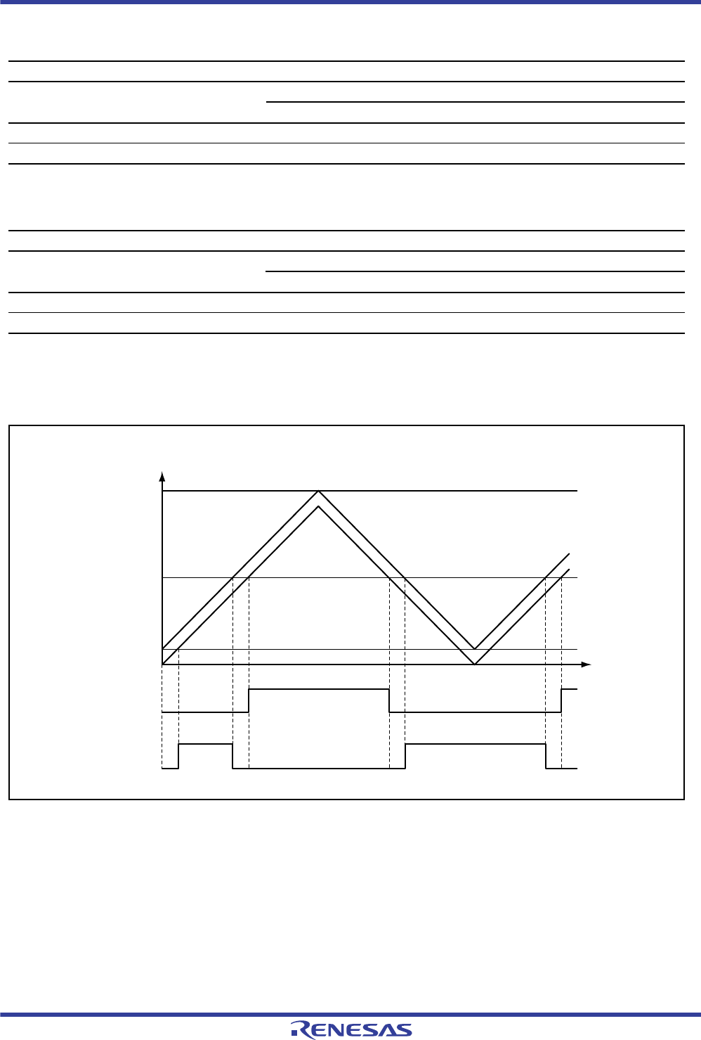
R01UH0034EJ0200 Rev.2.00 Page 526 of 1489
Dec 27, 2013
RX62T Group, RX62G Group 16. Multi-Function Timer Pulse Unit 3 (MTU3)
Note: • The initial output value of negative-phase waveform changes to an active level after the dead time has passed since counting
starts.
Figure 16.3 shows an example of output in complementary PWM mode (one phase) when OLSN = 1 and OLSP = 1.
Figure 16.3 Example of Output in Complementary PWM Mode
Table 16.38 Output Level Select Function
Bit 0 Function
OLSP Initial Output Active Level
Compare Match Output
Up-Counting Down-Counting
0 High level Low level Low level High level
1 Low level High level High level Low level
Table 16.39 Output Level Select Function
Bit 1 Function
OLSN Initial Output Active Level
Compare Match Output
Up-Counting Down-Counting
0 High level Low level High level Low level
1 Low level High level Low level High level
MTU3.TCNT and MTU4.TCNT values
MTU3.TGRA
MTU4.TGRA
TDDR
0000h Time
MTU4.TCNT
MTU3.TCNT
Positive-
phase
output
Negative-
phase
output
Active level
Compare match
output (up-count)
Initial
output
Initial
output
Compare match output
(down-count)
Compare match
output (up-count)
Compare match output
(down-count)
Active level
Active
level
R01UH0034EJ0200 Rev.2.00 Page 527 of 1489
Dec 27, 2013
RX62T Group, RX62G Group 16. Multi-Function Timer Pulse Unit 3 (MTU3)
16.2.19 Timer Output Control Registers 2 (TOCR2A and TOCR2B)
j = A or B
Note 1. Setting the TOCR1j.TOCS bit to 1 makes this bit setting valid.
Note 2. If dead time is not generated, the negative-phase output is always the exact inverse of the positive-phase output. In this case,
only the OLSiP bit is effective (i = 1, 2, 3).
TOCR2A and TOCR2B control inversion of PWM output level in complementary PWM mode and reset-synchronized
PWM mode.
m = 3 or 6
Address: TOCR2A 000C 120Fh, TOCR2B 000C 1A0Fh
b7 b6 b5 b4 b3 b2 b1 b0
BF[1:0] OLS3N OLS3P OLS2N OLS2P OLS1N OLS1P
Value after reset: 00000000
Bit Symbol Bit Name Description R/W
b0 OLS1P Output Level Select 1P*1, *2 This bit selects the output level on MTIOC3B or MTIOC6B in
reset-synchronized PWM mode and complementary PWM mode.
See Table 16.40.
R/W
b1 OLS1N Output Level Select 1N*1, *2 This bit selects the output level on MTIOC3D or MTIOC6D in
reset-synchronized PWM mode and complementary PWM mode.
See Table 16.41.
R/W
b2 OLS2P Output Level Select 2P*1, *2 This bit selects the output level on MTIOC4A or MTIOC7Ain reset-
synchronized PWM mode and complementary PWM mode.
See Table 16.42.
R/W
b3 OLS2N Output Level Select 2N*1, *2 This bit selects the output level on MTIOC4C or MTIOC7C in
reset-synchronized PWM mode and complementary PWM mode.
See Table 16.43.
R/W
b4 OLS3P Output Level Select 3P*1, *2 This bit selects the output level on MTIOC4B or MTIOC7B in
reset-synchronized PWM mode and complementary PWM mode.
See Table 16.44.
R/W
b5 OLS3N Output Level Select 3N*1, *2 This bit selects the output level on MTIOC4D or MTIOC7D in
reset-synchronized PWM mode and complementary PWM mode.
See Table 16.45.
R/W
b7, b6 BF[1:0] TOLBR Buffer Transfer Timing
Select
These bits select the timing for transferring data from TOLBRj to
TOCR2j.
See Table 16.46 for details.
R/W
Table 16.40 MTIOCmB Output Level Select Function
Bit 0 Function
OLS1P Initial Output Active Level
Compare Match Output
Up-Counting Down-Counting
0 High level Low level Low level High level
1 Low level High level High level Low level

R01UH0034EJ0200 Rev.2.00 Page 528 of 1489
Dec 27, 2013
RX62T Group, RX62G Group 16. Multi-Function Timer Pulse Unit 3 (MTU3)
m = 3 or 6
Note: • The initial output value of negative-phase waveform changes to an active level after the dead time has passed since counting
starts.
m = 4 or 7
m = 4 or 7
Note: • The initial output value of negative-phase waveform changes to an active level after the dead time has passed since counting
starts.
m = 4 or 7
Table 16.41 MTIOCmD Output Level Select Function
Bit 1 Function
OLS1N Initial Output Active Level
Compare Match Output
Up-Counting Down-Counting
0 High level Low level High level Low level
1 Low level High level Low level High level
Table 16.42 MTIOCmA Output Level Select Function
Bit 2 Function
OLS2P Initial Output Active Level
Compare Match Output
Up-Counting Down-Counting
0 High level Low level Low level High level
1 Low level High level High level Low level
Table 16.43 MTIOCmC Output Level Select Function
Bit 3 Function
OLS2N Initial Output Active Level
Compare Match Output
Up-Counting Down-Counting
0 High level Low level High level Low level
1 Low level High level Low level High level
Table 16.44 MTIOCmB Output Level Select Function
Bit 4 Function
OLS3P Initial Output Active Level
Compare Match Output
Up-Counting Down-Counting
0 High level Low level Low level High level
1 Low level High level High level Low level

R01UH0034EJ0200 Rev.2.00 Page 529 of 1489
Dec 27, 2013
RX62T Group, RX62G Group 16. Multi-Function Timer Pulse Unit 3 (MTU3)
m = 4 or 7
Note: • The initial output value of negative-phase waveform changes to an active level after the dead time has passed since counting
starts.
n = 4 or 7, m = 3 or 6, j = A or B
Table 16.45 MTIOCmD Output Level Select Function
Bit 5 Function
OLS3N Initial Output Active Level
Compare Match Output
Up-Counting Down-Counting
0 High level Low level High level Low level
1 Low level High level Low level High level
Table 16.46 Setting of TOCR2j.BF[1:0] Bits
Bit 7 Bit 6 Description
BF1 BF0 Complementary PWM Mode Reset-Synchronized PWM Mode
0 0 Does not transfer data from the buffer register (TOLBRj)
to TOCR2j.
Does not transfer data from the buffer register
(TOLBRj) to TOCR2j.
0 1 Transfers data from the buffer register (TOLBRj) to
TOCR2j at the crest of the MTUn.TCNT count.
Transfers data from the buffer register (TOLBRj)
to TOCR2j when MTUm.TCNT or MTUn.TCNT is
cleared.
1 0 Transfers data from the buffer register (TOLBRj) to
TOCR2j at the trough of the MTUn.TCNT count.
Setting prohibited
1 1 Transfers data from the buffer register (TOLBRj) to
TOCR2j at the crest and trough of the MTUn.TCNT
count.
Setting prohibited
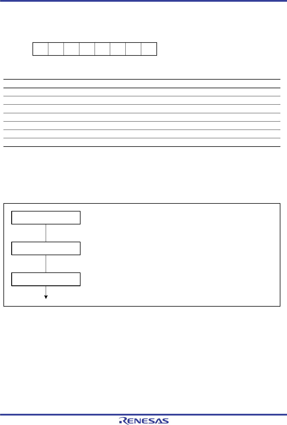
R01UH0034EJ0200 Rev.2.00 Page 530 of 1489
Dec 27, 2013
RX62T Group, RX62G Group 16. Multi-Function Timer Pulse Unit 3 (MTU3)
16.2.20 Timer Output Level Buffer Registers (TOLBRA and TOLBRB)
j = A or B
TOLBRA and TOLBRB are buffer registers for TOCR2A and TOCR2B and specify the PWM output level in
complementary PWM mode and reset-synchronized PWM mode.
Figure 16.4 shows an example of the PWM output level setting procedure in buffer operation.
Figure 16.4 Example of PWM Output Level Setting Procedure in Buffer Operation
Address: TOLBRA 000C 1236h, TOLBRB 000C 1A36h
b7 b6 b5 b4 b3 b2 b1 b0
— — OLS3N OLS3P OLS2N OLS2P OLS1N OLS1P
Value after reset: 00000000
Bit Symbol Bit Name Description R/W
b0 OLS1P Output Level Select 1P Specify the buffer value to be transferred to the OLS1P bit in TOCR2j. R/W
b1 OLS1N Output Level Select 1N Specify the buffer value to be transferred to the OLS1N bit in TOCR2j. R/W
b2 OLS2P Output Level Select 2P Specify the buffer value to be transferred to the OLS2P bit in TOCR2j. R/W
b3 OLS2N Output Level Select 2N Specify the buffer value to be transferred to the OLS2N bit in TOCR2j. R/W
b4 OLS3P Output Level Select 3P Specify the buffer value to be transferred to the OLS3P bit in TOCR2j. R/W
b5 OLS3N Output Level Select 3N Specify the buffer value to be transferred to the OLS3N bit in TOCR2j. R/W
b7, b6 — Reserved These bits are always read as 0. The write value should be 0. R/W
[1] Set bit TOCS in TOCR1j (j = A or B) to 1 to enable the TOCR2j setting.
[2] Use bits TOCR2j.BF[1:0] to select the TOLBRj buffer
transfer timing. Use bits OLS3N to OLS1N and OLS3P to OLS1P
to specify the PWM output levels.
[3] The TOLBRj initial setting must be the same value as specified in
bits OLS3N to OLS1N and OLS3P to OLS1P in TOCR2j.
Set bit TOCS
Set TOCR2j
Set TOLBRj
[1]
[2]
[3]

R01UH0034EJ0200 Rev.2.00 Page 531 of 1489
Dec 27, 2013
RX62T Group, RX62G Group 16. Multi-Function Timer Pulse Unit 3 (MTU3)
16.2.21 Timer Gate Control Register A (TGCRA)
TGCRA controls the output waveform necessary for brushless DC motor control in reset-synchronized PWM mode and
complementary PWM mode. TGCRA register settings are ineffective for anything other than complementary PWM
mode and reset-synchronized PWM mode.
UF, VF, and WF Bits (Output Phase Switch)
These bits are used to switch output of the positive- and negative-phase signals on or off.
FB Bit (External Feedback Signal Enable)
This bit selects whether the positive-/negative-phase output is switched automatically with the TGRA, TGRB, and
TGRC input capture signals in MTU0 or by writing 0 or 1 to bits 2 to 0 in TGCRA.
P Bit (Positive-Phase Output (P) Control)
This bit selects the level output or the reset-synchronized PWM/complementary PWM output for the positive-phase
output pins (MTIOC3B, MTIOC4A, and MTIOC4B pins).
N Bit (Negative-Phase Output (N) Control)
This bit selects the level output or the reset-synchronized PWM/complementary PWM output for the negative-phase
output pins (MTIOC3D, MTIOC4C, and MTIOC4D pins).
BDC Bit (Brushless DC Motor)
This bit selects whether to make the functions of TGCRA effective or ineffective.
Address: 000C 120Dh
b7 b6 b5 b4 b3 b2 b1 b0
—BDCN P FB WFVF UF
Value after reset: 10000000
Bit Symbol Bit Name Description R/W
b0 UF Output Phase Switch These bits turn on or off the positive-phase/negative-phase
output. The setting of these bits is valid only when the
TGCR.FB bit s set to 1. In this case, the setting of b0 to b2 is
used instead of the external input. See Table 16.47.
R/W
b1 VF R/W
b2 WF R/W
b3 FB External Feedback Signal Enable 0: Output is switched by external input (input sources are
TGRA, TGRB, and TGRC input capture signals in MTU0)
1: Output is switched by software (TGCRA's UF, VF, and WF
settings)
R/W
b4 P Positive-Phase Output (P) Control 0: Level output
1: Reset-synchronized PWM or complementary PWM output
R/W
b5 N Negative-Phase Output (N) Control 0: Level output
1: Reset-synchronized PWM or complementary PWM output
R/W
b6 BDC Brushless DC Motor 0: Ordinary output
1: Functions of this register are made effective
R/W
b7 — Reserved This bit is always read as 1. The write value should be 1. R/W
R01UH0034EJ0200 Rev.2.00 Page 532 of 1489
Dec 27, 2013
RX62T Group, RX62G Group 16. Multi-Function Timer Pulse Unit 3 (MTU3)
16.2.22 Timer Subcounters (TCNTSA and TCNTSB)
TCNTSA and TCNTSB are 16-bit read-only counters that are used only in complementary PWM mode.
The initial value of TCNTSA and TCNTSB after a reset is 0000h.
16.2.23 Timer Cycle Data Registers (TCDRA and TCDRB)
TCDRA and TCDRB are 16-bit readable/writable registers
registers used only in complementary PWM mode. Set half the PWM carrier cycle as the TCDRA and TCDRB values.
The initial value of TCDRA and TCDRB after a reset is FFFFh.
Table 16.47 Output Level Select Function
Bit 2 Bit 1 Bit 0 Function
WF VF UF
MTIOC3B MTIOC4A MTIOC4B MTIOC3D MTIOC4C MTIOC4D
U Phase V Phase W Phase U Phase V Phase W Phase
0 0 0 OFF OFF OFF OFF OFF OFF
0 0 1 ON OFF OFF OFF OFF ON
0 1 0 OFF ON OFF ON OFF OFF
0 1 1 OFF ON OFF OFF OFF ON
1 0 0 OFF OFF ON OFF ON OFF
1 0 1 ON OFF OFF OFF ON OFF
1 1 0 OFF OFF ON ON OFF OFF
1 1 1 OFF OFF OFF OFF OFF OFF
Address: TCNTSA 000C 1220h, TCNTSB 000C 1A20h
b15 b14 b13 b12 b11 b10 b9 b8 b7 b6 b5 b4 b3 b2 b1 b0
Value after reset: 0000000000000000
Note 1. TCNTSA and TCNTSB must not be accessed in eight bits; it should always be accessed in 16 bits.
Address: TCDRA 000C 1214h, TCDRB 000C 1A14h
b15 b14 b13 b12 b11 b10 b9 b8 b7 b6 b5 b4 b3 b2 b1 b0
Value after reset: 1111111111111111
Note 1. TCDRA and TCDRB must not be accessed in eight bits; it should always be accessed in 16 bits.
R01UH0034EJ0200 Rev.2.00 Page 533 of 1489
Dec 27, 2013
RX62T Group, RX62G Group 16. Multi-Function Timer Pulse Unit 3 (MTU3)
16.2.24 Timer Cycle Buffer Registers (TCBRA and TCBRB)
TCBRA and TCBRB are 16-bit readable/writable registers, used only in complementary PWM mode, that function as
buffer registers for TCDRA and TCDRB. The TCBRA and TCBRB values are transferred to TCDRA and TCDRB with
the transfer timing set in TMDR1. The initial value of TCBRA and TCBRB after a reset is FFFFh.
16.2.25 Timer Dead Time Data Registers (TDDRA and TDDRB)
TDDRA and TDDRB are 16-bit readable/writable registers, used only in complementary PWM mode, that specify the
MTU3.TCNT (MTU6.TCNT) and MTU4.TCNT (MTU7.TCNT) counter offset value. In complementary PWM mode,
when the MTU3.TCNT (MTU6.TCNT) and MTU4.TCNT (MTU7.TCNT) counters are cleared and then restarted, the
TDDRA (TDDRB) value is loaded into the MTU3.TCNT (MTU6.TCNT) counter and the count operation starts. The
initial value of TDDRA and TDDRB after a reset is FFFFh.
Address: TCBRA 000C 1222h, TCBRB 000C 1A22h
b15 b14 b13 b12 b11 b10 b9 b8 b7 b6 b5 b4 b3 b2 b1 b0
Value after reset: 1111111111111111
Note 1. TCBR must not be accessed in eight bits; it should always be accessed in 16 bits.
Address: TDDRA 000C 1216h, TDDRB 000C 1A16h
b15 b14 b13 b12 b11 b10 b9 b8 b7 b6 b5 b4 b3 b2 b1 b0
Value after reset: 1111111111111111
Note 1. TDDR must not be accessed in eight bits; it should always be accessed in 16 bits.

R01UH0034EJ0200 Rev.2.00 Page 534 of 1489
Dec 27, 2013
RX62T Group, RX62G Group 16. Multi-Function Timer Pulse Unit 3 (MTU3)
16.2.26 Timer Dead Time Enable Registers (TDERA and TDERB)
Note 1. TDDRA and TDDRB must be set to 1 or a larger value.
TDERA and TDERB control dead time generation in complementary PWM mode. The MTU3 has one TDER each for
MTU3 and MTU6. TDERA and TDERB should be modified only while TCNT stops.
TDER Bit (Dead Time Enable)
This bit specifies whether to generate dead time.
[Clearing condition]
When 0 is written to TDER after reading TDER = 1
16.2.27 Timer Buffer Transfer Set Registers (TBTERA and TBTERB)
Note 1. Applicable buffer registers (TBTERA):
MTU3.TGRC, MTU3.TGRD, MTU4.TGRC, MTU4.TGRD, and TCBRA
Applicable buffer registers (TBTER_B):
MTU6.TGRC, MTU6.TGRD, MTU7.TGRC, MTU7.TGRD, and TCBRB
TBTERA and TBTERB enable or disable transfer from the buffer registers used in complementary PWM mode to the
temporary registers, and specify whether to link the transfer with interrupt skipping 1 operation.
Address: MTU3.TDERA 000C 1234h, MTU6.TDERB 000C 1A34h
b7 b6 b5 b4 b3 b2 b1 b0
———————TDER
Value after reset: 00000001
Bit Symbol Bit Name Description R/W
b0 TDER Dead Time Enable 0: No dead time is generated
1: Dead time is generated *1R/(W)
b7 to b1 — Reserved These bits are always read as 0. The write value should be 0. R/W
Address: TBTERA 000C 1232h, TBTERB 000C 1A32h
b7 b6 b5 b4 b3 b2 b1 b0
—————— BTE[1:0]
Value after reset: 00000000
Bit Symbol Bit Name Description R/W
b1 to b0 BTE[1:0] Buffer Transfer Disable and
Interrupt Skipping Link Setting
These bits enable or disable transfer from the buffer registers*1
used in complementary PWM mode to the temporary registers,
and specify whether to link the transfer with interrupt skipping
function 1.
For details, see Table 16.48.
R/W
b7 to b2 — Reserved These bits are always read as 0. The write value should be 0. R/W

R01UH0034EJ0200 Rev.2.00 Page 535 of 1489
Dec 27, 2013
RX62T Group, RX62G Group 16. Multi-Function Timer Pulse Unit 3 (MTU3)
Note 1. Data is transferred according to the MD3 to MD0 bit setting in TMDR1. For details, refer to section 16.3.8, Complementary PWM
Mode .
Note 2. When interrupt skipping is disabled (the T3AEN and T4VEN (T6AEN and T7VEN) bits are cleared to 0 in the timer interrupt
skipping set register (TITCR1A (TITCR1B)) or the skipping count set bits (T3ACOR and T4VCOR (T6ACOR and T7VCOR)) in
TITCR1A (TITCR1B) are cleared to 0), be sure to disable link of buffer transfer with interrupt skipping (clear the BTE1 bit in the
timer buffer transfer set register (TBTERA (TBTERB)) to 0). If link with interrupt skipping is enabled while interrupt skipping is
disabled, buffer transfer will not be performed.
Table 16.48 Setting of TBTER.BTE[1:0] Bits
Bit 1 Bit 0
DescriptionBTE1 BTE0
0 0 Enables transfer from the buffer registers to the temporary registers*1 and does not link the
transfer with interrupt skipping function 1.
0 1 Disables transfer from the buffer registers to the temporary registers.
1 0 Links transfer from the buffer registers to the temporary registers with interrupt skipping function
1.*2
1 1 Setting prohibited

R01UH0034EJ0200 Rev.2.00 Page 536 of 1489
Dec 27, 2013
RX62T Group, RX62G Group 16. Multi-Function Timer Pulse Unit 3 (MTU3)
16.2.28 Timer Waveform Control Registers (TWCRA and TWCRB)
Note 1. This bit is only valid in register TWCRB and is a reserved bit in register TWCRA.
Note 2. Do not write 1 to this bit unless complementary PWM mode is selected.
TWCRA and TWCRB control the output waveform when synchronous counter clearing occurs in MTU3.TCNT and
MTU4.TCNT (MTU6.TCNT and MTU7.TCNT) in complementary PWM mode and specifies whether to clear the
counters at MTU3.TGRA (MTU6.TGRA) compare match.
The CCE bit and WRE bit in TWCRA and TWCRB should be modified only while TCNT stops.
WRE Bit (Waveform Retain Enable)
This bit selects the waveform output when synchronous counter clearing occurs in complementary PWM mode.
The initial output is inhibited with this function only when synchronous clearing occurs within the Tb interval at the
trough in complementary PWM mode. When synchronous clearing occurs outside this interval, the initial values
specified in TOCR1A and TOCR2A (TOCR1B and TOCR2B) are output regardless of the WRE bit setting. The initial
values specified in TOCR1A and TOCR2A (TOCR1B and TOCR2B) are also output when synchronous clearing occurs
in the Tb interval at the trough immediately after MTU3.TCNT and MTU4.TCNT (MTU6.TCNT and MTU7.TCNT)
start operation.
For the Tb interval at the trough in complementary PWM mode, see Figure 16.41.
[Setting condition]
When 1 is written to TWCR.WRE after reading TWCR.WRE = 0
Address: TWCRA 000C 1260h, TWCRB 000C 1A60h
b7 b6 b5 b4 b3 b2 b1 b0
CCE—————SCCWRE
Value after reset: 0*20000000
Bit Symbol Bit Name Description R/W
b0 WRE Waveform Retain Enable 0: Initial values specified in TOCR1A and TOCR2A (TOCR1B and
TOCR2B) are output
1: Initial output is inhibited
R/(W)
b1 SCC*1Synchronous Clearing Control (Only valid in register TWCRB)
0: Clearing of MTU6.TCNT and MTU7.TCNT in response to
synchronous clearing for MTU0, MTU1, MTU2 - MTU6, MTU7 is
enabled.
1: Clearing of MTU6.TCNT and MTU7.TCNT in response to
synchronous clearing for MTU0, MTU1, MTU2 - MTU6, MTU7 is
disabled.
R/(W)
b6 to b2 — Reserved These bits are always read as 0. The write value should be 0. R/W
b7 CCE*2Compare Match Clear Enable 0: Counters are not cleared at MTU3.TGRA (MTU6.TGRA) compare
match
1: Counters are cleared at MTU3.TGRA (MTU6.TGRA) compare
match
R/(W)

R01UH0034EJ0200 Rev.2.00 Page 537 of 1489
Dec 27, 2013
RX62T Group, RX62G Group 16. Multi-Function Timer Pulse Unit 3 (MTU3)
SCC Bit (Synchronous Clearing Control) (Only valid in register TWCRB)
The setting of this bit selects whether MTU6.TCNT and MTU7.TCNT are or are not cleared when counter-synchronous
clearing is generated for MTU0, MTU1, MTU2 - MTU6, MTU7 in complementary PWM mode.
Make the complementary PWM mode settings for MTU6 and MTU7 when this function is in use. When writing a new
value to the SCC bit while the counter is operating, do so in such a way that the values of the CCE and WRE bits are not
changed.
Synchronous clearing from the MTU3 module only becomes disabled due to the setting of the SCC bit when
synchronous clearing is generated outside the Tb interval in the trough. If synchronous clearing is generated within the
Tb interval in the trough including immediately after the value at which MTU6.TCNT and MTU7.TCNT start,
MTU6.TCNT and MTU7.TCNT are cleared.
Regarding the Tb interval in the trough in complementary PWM mode, see Figure 16.41.
[Setting condition]
Writing of 1 to the SCC bit after reading it as 0
The corresponding bit in register TWCRA is reserved and is always read as 0. When writing to TWCRA, always write 0
to this bit.
CCE Bit (Compare Match Clear Enable)
This bit specifies whether to clear counters at MTU3.TGRA (MTU6.TGRA) compare match in complementary PWM
mode.
[Setting condition]
When 1 is written to CCE after reading CCE = 0

R01UH0034EJ0200 Rev.2.00 Page 538 of 1489
Dec 27, 2013
RX62T Group, RX62G Group 16. Multi-Function Timer Pulse Unit 3 (MTU3)
16.2.29 Timer A/D Converter Start Request Control Register (TADCR)
TADCR (MTU4)
Note 1. MTU4.TADCR must not be accessed in eight bits; it should always be accessed in 16 bits.
Note 2. When interrupt skipping is disabled (the T3AEN and T4VEN bits in TITCR1A are cleared to 0 or the T3ACOR and T4VCOR bits
in TITCR1A are cleared to 0), do not link A/D converter start requests with interrupt skipping function 1 (clear the ITA3AE,
ITA4VE, ITB3AE, and ITB4VE bits in MUT3_4.TADCR to 0).
Note 3. If link with interrupt skipping is enabled while interrupt skipping is disabled, A/D converter start requests will not be issued.
Note 4. Do not set to 1 in other than complementary PWM mode.
TADCR enables or disables A/D converter start requests and specifies whether to link A/D converter start requests with
interrupt skipping function. The MTU3 has one TADCR each for MTU4 and MTU7.
Address: 000C 1240h
b15 b14 b13 b12 b11 b10 b9 b8 b7 b6 b5 b4 b3 b2 b1 b0
BF[1:0] ——————UT4AEDT4AEUT4BEDT4BEITA3AEITA4VEITB3AEITB4VE
Value after reset: 000000000
0*4 00*4 0*4 0*4 0*4 0*4
Bit Symbol Bit Name Description R/W
b0 ITB4VE*4TCIV4 Interrupt Skipping Link
Enable
0: A/D converter start request signal TRG4BN and TCI4V
interrupt skipping 1 are not linked
1: A/D converter start request signal TRG4BN and TCI4V
interrupt skipping 1 are linked
R/W
b1 ITB3AE*4TGIA3 Interrupt Skipping Link
Enable
0: A/D converter start request signal TRG4BN and TGI3A
interrupt skipping 1 are not linked
1: A/D converter start request signal TRG4BN and TGI3A
interrupt skipping 1 are linked
R/W
b2 ITA4VE*4TCIV4 Interrupt Skipping Link
Enable
0: A/D converter start request signal TRG4AN and TCI4V
interrupt skipping 1 are not linked
1: A/D converter start request signal TRG4AN and TCI4V
interrupt skipping 1 are linked
R/W
b3 ITA3AE*4TGIA3 Interrupt Skipping Link
Enable
0: A/D converter start request signal TRG4AN and TGI3A
interrupt skipping 1 are not linked
1: A/D converter start request signal TRG4AN and TGI3A
interrupt skipping 1 are linked
R/W
b4 DT4BE*4Down-Count TRG4BN Enable 0: A/D converter start requests (TRG4BN) disabled during
MTU4.TCNT down-count operation
1: A/D converter start requests (TRG4BN) enabled during
MTU4.TCNT down-count operation
R/W
b5 UT4BE Up-Count TRG4BN Enable 0: A/D converter start requests (TRG4BN) disabled during
MTU4.TCNT up-count operation
1: A/D converter start requests (TRG4BN) enabled during
MTU4.TCNT up-count operation
R/W
b6 DT4AE*4Down-Count TRG4AN Enable 0: A/D converter start requests (TRG4AN) disabled during
MTU4.TCNT down-count operation
1: A/D converter start requests (TRG4AN) enabled during
MTU4.TCNT down-count operation
R/W
b7 UT4AE Up-Count TRG4AN Enable 0: A/D converter start requests (TRG4AN) disabled during
MTU4.TCNT up-count operation
1: A/D converter up requests (TRG4AN) enabled during
MTU4.TCNT down-count operation
R/W
b13 to b8 — Reserved These bits are always read as 0. The write value should be 0. R/W
b15, b14 BF[1:0] MTU4.TADCOBRA/B Transfer
Timing Select
See Table 16.49 for details.
These bits specify the transfer timing from MTU4.TADCOBRA
and MTU4.TADCOBRB to MTU4.TADCORA and
MTU4.TADCORB.
R/W

R01UH0034EJ0200 Rev.2.00 Page 539 of 1489
Dec 27, 2013
RX62T Group, RX62G Group 16. Multi-Function Timer Pulse Unit 3 (MTU3)
Note 1. Data is transferred from the cycle set buffer register (MTU4.TADCOBRA, MTU4.TADCOBRB) to the cycle set register
(MTU4.TADCORA, MTU4.TADCORB) when the crest of the MTU4.TCNT count is reached or the MTU4.TGRD is written to in
complementary PWM mode, when a compare match occurs between MTU3.TCNT and MTU3.TGRA in reset-synchronized
PWM mode, or when a compare match occurs between MTU4.TCNT and MTU4.TGRA in PWM mode 1 or normal operation
mode.
Note 2. These settings are prohibited when complementary PWM mode is not selected.
Table 16.49 Setting of Transfer Timing by TADCR.BF[1:0] Bits (MTU4)
Bit 15 Bit 14
DescriptionBF1 BF0
0 0 Does not transfer data from the cycle set buffer register (MTU4.TADCOBRA, MTU4.TADCOBRB) to the
cycle set register (MTU4.TADCORA, MTU4.TADCORB).
0 1 Transfers data from the cycle set buffer register to the cycle set register at the crest of the MTU4.TCNT
count.*1
1 0 Transfers data from the cycle set buffer register to the cycle set register at the trough of the MTU4.TCNT
count.*2
1 1 Transfers data from the cycle set buffer register to the cycle set register at the crest and trough of the
MTU4.TCNT count.*2

R01UH0034EJ0200 Rev.2.00 Page 540 of 1489
Dec 27, 2013
RX62T Group, RX62G Group 16. Multi-Function Timer Pulse Unit 3 (MTU3)
TADCR (MTU7)
Note 1. MTU7.TADCR must not be accessed in eight bits; it should always be accessed in 16 bits.
Note 2. When interrupt skipping is disabled (the T6AEN and T7VEN bits in TITCR1B are cleared to 0 or the T6ACOR and T7VCOR bits
in TITCR1B are cleared to 0), do not link A/D converter start requests with interrupt skipping function 1 (clear the ITA6AE,
ITA7VE, ITB6AE, and ITB7VE bits in MUT3_7.TADCR to 0).
Note 3. If link with interrupt skipping is enabled while interrupt skipping is disabled, A/D converter start requests will not be issued.
Note 4. Do not set to 1 in other than complementary PWM mode.
Address: 000C 1A40h
b15 b14 b13 b12 b11 b10 b9 b8 b7 b6 b5 b4 b3 b2 b1 b0
BF[1:0] ——————UT7AEDT7AEUT7BEDT7BEITA6AEITA7VEITB6AEITB7VE
Value after reset: 000000000
0*4 00*4 0*4 0*4 0*4 0*4
Bit Symbol Bit Name Description R/W
b0 ITB7VE*4TCIV7 Interrupt Skipping Link
Enable
0: A/D converter start request signal TRG7BN and TCI7V
interrupt skipping 1 are not linked
1: A/D converter start request signal TRG7BN and TCI7V
interrupt skipping 1 are linked
R/W
b1 ITB6AE*4TGIA6 Interrupt Skipping Link
Enable
0: A/D converter start request signal TRG7BN and TGI6A
interrupt skipping 1 are not linked
1: A/D converter start request signal TRG7BN and TGI6A
interrupt skipping 1 are linked
R/W
b2 ITA7VE*4TCIV7 Interrupt Skipping Link
Enable
0: A/D converter start request signal TRG7AN and TCI7V
interrupt skipping 1 are not linked
1: A/D converter start request signal TRG7AN and TCI7V
interrupt skipping 1 are linked
R/W
b3 ITA6AE*4TGIA6 Interrupt Skipping Link
Enable
0: A/D converter start request signal TRG7AN and TGI6A
interrupt skipping 1 are not linked
1: A/D converter start request signal TRG7AN and TGI6A
interrupt skipping 1 are linked
R/W
b4 DT7BE*4Down-Count TRG7BN Enable 0: A/D converter start requests (TRG7BN) disabled during
MTU7.TCNT down-count operation
1: A/D converter start requests (TRG7BN) enabled during
MTU7.TCNT down-count operation
R/W
b5 DT7AE Up-Count TRG7BN Enable 0: A/D converter start requests (TRG7BN) disabled during
MTU7.TCNT up-count operation
1: A/D converter start requests (TRG7BN) enabled during
MTU7.TCNT up-count operation
R/W
b6 DT7AE*4Down-Count TRG7AN Enable 0: A/D converter start requests (TRG7AN) disabled during
MTU7.TCNT down-count operation
1: A/D converter start requests (TRG7AN) enabled during
MTU7.TCNT down-count operation
R/W
b7 UT7AE Up-Count TRG7AN Enable 0: A/D converter start requests (TRG7AN) disabled during
MTU7.TCNT up-count operation
1: A/D converter up requests (TRG7AN) enabled during
MTU7.TCNT down-count operation
R/W
b13 to b8 — Reserved These bits are always read as 0. The write value should be 0. R/W
b15, b14 BF[1:0] MTU7.TADCOBRA/B Transfer
Timing Select
See Table 16.50 for details.
These bits specify the transfer timing from MTU7.TADCOBRA
and MTU7.TADCOBRB to MTU7.TADCORA and
MTU7.TADCORB.
R/W

R01UH0034EJ0200 Rev.2.00 Page 541 of 1489
Dec 27, 2013
RX62T Group, RX62G Group 16. Multi-Function Timer Pulse Unit 3 (MTU3)
Note 1. Data is transferred from the cycle set buffer register (MTU7.TADCOBRA, MTU7.TADCOBRB) to the cycle set register
(MTU7.TADCORA, MTU7.TADCORB) when the crest of the MTU7.TCNT count is reached or the MTU7.TGRD is written to in
complementary PWM mode, when a compare match occurs between MTU6.TCNT and MTU6.TGRA in reset-synchronized
PWM mode, or when a compare match occurs between MTU7.TCNT and MTU7.TGRA in PWM mode 1 or normal operation
mode.
Note 2. These settings are prohibited when complementary PWM mode is not selected.
Table 16.50 Setting of Transfer Timing by TADCR.BF[1:0] Bits (MTU7)
Bit 15 Bit 14
DescriptionBF1 BF0
0 0 Does not transfer data from the cycle set buffer register (MTU7.TADCOBRA, MTU7.TADCOBRB) to the
cycle set register (MTU7.TADCORA, MTU7.TADCORB).
0 1 Transfers data from the cycle set buffer register to the cycle set register at the crest of the MTU7.TCNT
count.*1
1 0 Transfers data from the cycle set buffer register to the cycle set register at the trough of the MTU7.TCNT
count.*2
1 1 Transfers data from the cycle set buffer register to the cycle set register at the crest and trough of the
MTU7.TCNT count.*2
R01UH0034EJ0200 Rev.2.00 Page 542 of 1489
Dec 27, 2013
RX62T Group, RX62G Group 16. Multi-Function Timer Pulse Unit 3 (MTU3)
16.2.30 Timer A/D Converter Start Request Cycle Set Registers (TADCORA and
TADCORB)
TADCORA and TADCORB are 16-bit readable/writable registers that issue a corresponding A/D converter start request
when the MTUn.TCNT (n = 4 or 7) count reaches the value in TADCORA or TADCORB.
MTUn.TADCORA and TADCORB are initialized to FFFFh by a reset.
16.2.31 Timer A/D Converter Start Request Cycle Set Buffer Registers (TADCOBRA
and TADCOBRB)
TADCOBRA and TADCOBRB are 16-bit readable/writable registers whose values are transferred to TADCORA and
TADCORB, respectively, when the crest or trough of the MTUn.TCNT count is reached.
TADCOBRA and TADCOBRB are initialized to FFFFh by a reset.
Address: MTU4.TADCORA 000C 1244h, MTU4.TADCORB 000C 1246h
MTU7.TADCORA 000C 1A44h, MTU7.TADCORB 000C 1A46h
b15 b14 b13 b12 b11 b10 b9 b8 b7 b6 b5 b4 b3 b2 b1 b0
Value after reset: 1111111111111111
Note 1. MTUn.TADCORA and MTUn.TADCORB (n = 4 or 7) must not be accessed in eight bits; they should always be
accessed in 16 bits.
Note 2. When the A/D converter start request delaying function linked with skipping function 1 (for details, see section
16.3.9 (4), A/D Converter Start Request Delaying Function Linked with Interrupt Skipping Function 1) is used, the
value of this register should be 0002h to TCDRA setting - 2 in MTU4 and 0002h to TCDRB setting - 2 in MTU7.
Note 3. When interrupt skipping function 2 is used and the difference between the MTUn.TADCORA value and the
MTUn.TADCORB value is small, the skipping count may not be counted correctly and the A/D converter start
request may not be generated with the expected timing in some cases. The TADCORA and TADCORB values
should satisfy the following conditions.
(1) When skipping function 2 is specified with the skipping count set to 0
The difference between the MTUn.TADCORA and MTUn.TADCORB values should be equal to or greater
than 4.
The MTUn.TADCORA compare interval should be equal to or greater than 4 ICLK cycles (the
MTUn.TADCORA update value should be the previous value + 4 or greater, or previous value - 4 or
smaller).
The MTUn.TADCORB compare interval should be equal to or greater than 4 ICLK cycles (the
MTUn.TADCORB update value should be the previous value + 4 or greater, or previous value - 4 or
smaller).
(2) When skipping function 2 is specified with the skipping count set to 1 or greater
The difference between the MTUn.TADCORA and MTUn.TADCORB values should be equal to or greater
than 2.
The MTUn.TADCORB compare interval should be equal to or greater than 2 ICLK cycles (the
MTUn.TADCOR update value should be the previous value + 2 or greater, or previous value - 2 or smaller)
Address: MTU4.TADCORA 000C 1248h, MTU4.TADCORB 000C 124Ah
MTU7.TADCORA 000C 1A48h, MTU7.TADCORB 000C 1A4Ah
b15 b14 b13 b12 b11 b10 b9 b8 b7 b6 b5 b4 b3 b2 b1 b0
Value after reset: 1111111111111111
Note 1. TADCOBRA and TADCOBRB must not be accessed in eight bits; it should always be accessed in 16 bits.

R01UH0034EJ0200 Rev.2.00 Page 543 of 1489
Dec 27, 2013
RX62T Group, RX62G Group 16. Multi-Function Timer Pulse Unit 3 (MTU3)
16.2.32 Timer Interrupt Skipping Mode Registers (TITMRA and TITMRB)
TITMRA and TITMRB are used to select either of two skipping functions for the TITMRA and TITMRB registers.
Note 1. TITCR1A or TITCR1B enables interrupt skipping function 1.
Note 2. TITCR2A or TITCR2B enables interrupt skipping function 2.
Address: TITMRA 000C 123Ah, TITMRB 000C 1A3Ah
b7 b6 b5 b4 b3 b2 b1 b0
———————TITM
Value after reset: 00000000
Bit Symbol Bit Name Description R/W
b0 TITM Interrupt Skipping Function Select Selects one of the two types of interrupt skipping functions
shown in Table 16.51.
R/W
b7 to b1 — Reserved These bits are always read as 0. The write value should be 0. R/W
Table 16.51 Interrupt Skipping Function Selected through TITM Bit
Bit 0
DescriptionTITM
0 Selects interrupt skipping function 1 *1
1 Selects interrupt skipping function 2 *2
R01UH0034EJ0200 Rev.2.00 Page 544 of 1489
Dec 27, 2013
RX62T Group, RX62G Group 16. Multi-Function Timer Pulse Unit 3 (MTU3)
16.2.33 Timer Interrupt Skipping Set Registers 1 (TITCR1A and TITCR1B)
TITCR1A
Note 1. When 0 is specified for the interrupt skipping count, no interrupt skipping will be performed.
Before changing the interrupt skipping count, be sure to clear the TITCR1A.T3AEN and TITCR1A.T4VEN bits to 0 to clear the
skipping counter (TITCNT1A).
TITCR1A and TITCR1B enable or disable interrupt skipping and specify the interrupt skipping count. This setting is
valid only while TITMRA or TITMRB is set to 0; when TITMRA or TITMRB is set to 1, the setting in the
corresponding TITCR1 register is cleared.
TITCR1B
Note 1. When 0 is specified for the interrupt skipping count, no interrupt skipping will be performed.
Before changing the interrupt skipping count, be sure to clear the TITCR1B.T6AEN and TITCR1B.T7VEN bits to 0 to clear the
skipping counter (TITCNT1B).
Address: TITMRA 000C 123Ah, TITMRB 000C 1A3Ah
b7 b6 b5 b4 b3 b2 b1 b0
T3AEN T3ACOR[2:0] T4VEN T4VCOR[2:0]
Value after reset: 00000000
Bit Symbol Bit Name Description R/W
b2 to b0 T4VCOR[2:0] TCIV4 Interrupt Skipping Count
Setting
These bits specify the TCIV4 interrupt skipping count within
the range from 0 to 7. *1
For details, see Table 16.52.
R/W
b3 T4VEN T4VEN 0: TCIV4 interrupt skipping disabled
1: TCIV4 interrupt skipping enabled
R/W
b6 to b4 T3ACOR[2:0] TGIA3 Interrupt Skipping Count
Setting
These bits specify the TGIA3 interrupt skipping count within
the range from 0 to 7. *1
For details, see Table 16.53.
R/W
b7 T3AEN T3AEN 0: TGIA3 interrupt skipping disabled
1: TGIA3 interrupt skipping enabled
R/W
Address: 000C 1230h
b7 b6 b5 b4 b3 b2 b1 b0
T6AEN T6ACOR[2:0] T7VEN T7VCOR[2:0]
Value after reset: 00000000
Bit Symbol Bit Name Description R/W
b2 to b0 T7VCOR[2:0] TCIV7 Interrupt Skipping Count
Setting
These bits specify the TCIV7 interrupt skipping count
within the range from 0 to 7. *1
For details, see Table 16.54.
R/W
b3 T7VEN T7VEN 0: TCIV7 interrupt skipping disabled
1: TCIV7 interrupt skipping enabled
R/W
b6 to b4 T6ACOR[2:0] TGIA6 Interrupt Skipping Count
Setting
These bits specify the TGIA6 interrupt skipping count
within the range from 0 to 7. *1
For details, see Table 16.55.
R/W
b7 T6AEN T6AEN 0: TGIA6 interrupt skipping disabled
1: TGIA6 interrupt skipping enabled
R/W

R01UH0034EJ0200 Rev.2.00 Page 545 of 1489
Dec 27, 2013
RX62T Group, RX62G Group 16. Multi-Function Timer Pulse Unit 3 (MTU3)
Table 16.52 Setting of Interrupt Skipping Count by T4VCOR[2:0] Bits
Bit 2 Bit 1 Bit 0 Description
T4VCOR2 T4VCOR1 T4VCOR0
0 0 0 Does not skip TCIV4 interrupts.
0 0 1 Sets the TCIV4 interrupt skipping count to 1.
0 1 0 Sets the TCIV4 interrupt skipping count to 2.
0 1 1 Sets the TCIV4 interrupt skipping count to 3.
1 0 0 Sets the TCIV4 interrupt skipping count to 4.
1 0 1 Sets the TCIV4 interrupt skipping count to 5.
1 1 0 Sets the TCIV4 interrupt skipping count to 6.
1 1 1 Sets the TCIV4 interrupt skipping count to 7.
Table 16.53 Setting of Interrupt Skipping Count by T3ACOR[2:0] Bits
Bit 6 Bit 5 Bit 4
DescriptionT3ACOR2 T3ACOR1 T3ACOR0
0 0 0 Does not skip TGIA3 interrupts.
0 0 1 Sets the TGIA3 interrupt skipping count to 1.
0 1 0 Sets the TGIA3 interrupt skipping count to 2.
0 1 1 Sets the TGIA3 interrupt skipping count to 3.
1 0 0 Sets the TGIA3 interrupt skipping count to 4.
1 0 1 Sets the TGIA3 interrupt skipping count to 5.
1 1 0 Sets the TGIA3 interrupt skipping count to 6.
1 1 1 Sets the TGIA3 interrupt skipping count to 7.
Table 16.54 Setting of Interrupt Skipping Count by T7VCOR[2:0] Bits
Bit 2 Bit 1 Bit 0
DescriptionT7VCOR2 T7VCOR1 T7VCOR0
0 0 0 Does not skip TCIV7 interrupts.
0 0 1 Sets the TCIV7 interrupt skipping count to 1.
0 1 0 Sets the TCIV7 interrupt skipping count to 2.
0 1 1 Sets the TCIV7 interrupt skipping count to 3.
1 0 0 Sets the TCIV7 interrupt skipping count to 4.
1 0 1 Sets the TCIV7 interrupt skipping count to 5.
1 1 0 Sets the TCIV7 interrupt skipping count to 6.
1 1 1 Sets the TCIV7 interrupt skipping count to 7.

R01UH0034EJ0200 Rev.2.00 Page 546 of 1489
Dec 27, 2013
RX62T Group, RX62G Group 16. Multi-Function Timer Pulse Unit 3 (MTU3)
Table 16.55 Setting of Interrupt Skipping Count by T6ACOR[2:0] Bits
Bit 6 Bit 5 Bit 4
DescriptionT6ACOR2 T6ACOR1 T6ACOR0
000 Does not skip TGIA6 interrupts.
0 0 1 Sets the TGIA6 interrupt skipping count to 1.
0 1 0 Sets the TGIA6 interrupt skipping count to 2.
0 1 1 Sets the TGIA6 interrupt skipping count to 3.
1 0 0 Sets the TGIA6 interrupt skipping count to 4.
1 0 1 Sets the TGIA6 interrupt skipping count to 5.
1 1 0 Sets the TGIA6 interrupt skipping count to 6.
1 1 1 Sets the TGIA6 interrupt skipping count to 7.

R01UH0034EJ0200 Rev.2.00 Page 547 of 1489
Dec 27, 2013
RX62T Group, RX62G Group 16. Multi-Function Timer Pulse Unit 3 (MTU3)
16.2.34 Timer Interrupt Skipping Counters 1 (TITCNT1A and TITCNT1B)
TITCNT1A
Note 1. To clear the TITCNT1A, clear the T3AEN and T4VEN bits in TITCR1A to 0.
TITCNT1A and TITCNT1B are 8-bit readable/writable counters. TITCNTA and TITCNTB retain their values even after
stopping the count operation of MTU3.TCNT and MTU4.TCNT (MTU6.TCNT and MTU7.TCNT).
T4VCNT[2:0] Bits (TCIV4 Interrupt Counter)
While the T4VEN bit in TITCR1A is set to 1, the count in these bits is incremented every time a TCIV4 interrupt occurs.
[Clearing conditions]
When the TITM bit in TITMRA is 1
When the T4VEN bit in TITCR1A is cleared to 0
When the T4VCOR[2:0] bits in TITCR1A are cleared to 000b
When the T4VCNT[2:0] bits in TITCNT1A match the T4VCOR[2:0] bits in TITCR1A
T3ACNT[2:0] Bits (TGIA3 Interrupt Counter)
While the T3AEN bit in TITCR1A is set to 1, the count in these bits is incremented every time a TGIA3 interrupt occurs.
[Clearing conditions]
When the TITM bit in TITMRA is 1
When the T3AEN bit in TITCR1A is cleared to 0
When the T3ACOR[2:0] bits in TITCR1A are cleared to 000b
When the T3ACNT[2:0] bits in TITCNT1A match the T3ACOR[2:0] bits in TITCR1A
Address: 000C 1231h
b7 b6 b5 b4 b3 b2 b1 b0
— T3ACNT[2:0] — T4VCNT[2:0]
Value after reset: 00000000
Bit Symbol Bit Name Description R/W
b2 to b0 T4VCNT[2:0] TCIV4 Interrupt Counter While the T4VEN bit in TITCR1A is set to 1, the count in these
bits is incremented every time a TCIV4 interrupt occurs.
R
b3 — Reserved This bit is always read as 0. Writing to this bit has no effect. R
b6 to b4 T3ACNT[2:0] TGIA3 Interrupt Counter While the T3AEN bit in TITCR1A is set to 1, the count in these
bits is incremented every time a TGIA3 interrupt occurs.
R
b7 — Reserved This bit is always read as 0. Writing to this bit has no effect. R

R01UH0034EJ0200 Rev.2.00 Page 548 of 1489
Dec 27, 2013
RX62T Group, RX62G Group 16. Multi-Function Timer Pulse Unit 3 (MTU3)
TITCNT1B
Note 1. To clear the TITCNT1B, clear the T6AEN and T7VEN bits in TITCR1B to 0.
T7VCNT[2:0] Bits (TCIV7 Interrupt Counter)
While the T7VEN bit in TITCR1B is set to 1, the count in these bits is incremented every time a TCIV7 interrupt occurs.
[Clearing conditions]
When the TITM bit in TITMRB is 1
When the T7VEN bit in TITCR1B is cleared to 0
When the T7VCOR[2:0] bits in TITCR1B are cleared to 000b
When the T7VCNT[2:0] bits in TITCNT1B match the T7VCOR[2:0] bits in TITCR1B
T6ACNT[2:0] Bits (TGIA6 Interrupt Counter)
While the T6AEN bit in TITCR1B is set to 1, the count in these bits is incremented every time a TGIA6 interrupt occurs.
[Clearing conditions]
When the TITM bit in TITMRB is 1
When the T6AEN bit in TITCR1B is cleared to 0
When the T6ACOR[2:0] bits in TITCR1B are cleared to 000b
When the T6ACNT[2:0] bits in TITCNT1B match the T6ACOR[2:0] bits in TITCR1B
Address: 000C 1A31h
b7 b6 b5 b4 b3 b2 b1 b0
— T6ACNT[2:0] — T7VCNT[2:0]
Value after reset: 00000000
Bit Symbol Bit Name Description R/W
b2 to b0 T7VCNT[2:0] TCIV7 Interrupt Counter While the T7VEN bit in TITCR1B is set to 1, the count in these
bits is incremented every time a TCIV7 interrupt occurs.
R
b3 — Reserved This bit is always read as 0. Writing to this bit has no effect. R
b6 to b4 T6ACNT[2:0] TGIA6 Interrupt Counter While the T6AEN bit in TITCR1B is set to 1, the count in these
bits is incremented every time a TGIA6 interrupt occurs.
R
b7 — Reserved This bit is always read as 0. Writing to this bit has no effect. R
R01UH0034EJ0200 Rev.2.00 Page 549 of 1489
Dec 27, 2013
RX62T Group, RX62G Group 16. Multi-Function Timer Pulse Unit 3 (MTU3)
16.2.35 Timer Interrupt Skipping Set Registers 2 (TITCR2A and TITCR2B)
TITCR2A
TITCR2A and TITCR2B specify the interrupt skipping count for TRG4AN and TRG4BN (TRG7AN and TRG7BN).
This setting is valid only while TITMRA or TITMRB is set to 1.
Address: 000C 123Bh
b7 b6 b5 b4 b3 b2 b1 b0
————— TRG4COR[2:0]
Value after reset: 00000000
Bit Symbol Bit Name Description R/W
b2 to b0 TRG4COR[2:0] TRG4AN/TRG4BN Interrupt
Skipping Count Setting
These bits specify the TRG4AN/TRG4BN interrupt skipping
count within the range from 0 to 7.
For details, see Table 16.56.
R/W
b7 to b3 — Reserved These bits are always read as 0. The write value should be 0. R/W
Table 16.56 Setting of Interrupt Skipping Count by TRG4COR[2:0] Bits
Bit 2 Bit 1 Bit 0
DescriptionTRG4COR2 TRG4COR1 TRG4COR0
0 0 0 Does not skip TRG4AN and TRG4BN interrupts.
0 0 1 Sets the TRG4AN and TRG4BN interrupt skipping count to 1.
0 1 0 Sets the TRG4AN and TRG4BN interrupt skipping count to 2.
0 1 1 Sets the TRG4AN and TRG4BN interrupt skipping count to 3.
1 0 0 Sets the TRG4AN and TRG4BN interrupt skipping count to 4.
1 0 1 Sets the TRG4AN and TRG4BN interrupt skipping count to 5.
1 1 0 Sets the TRG4AN and TRG4BN interrupt skipping count to 6.
1 1 1 Sets the TRG4AN and TRG4BN interrupt skipping count to 7.

R01UH0034EJ0200 Rev.2.00 Page 550 of 1489
Dec 27, 2013
RX62T Group, RX62G Group 16. Multi-Function Timer Pulse Unit 3 (MTU3)
TITCR2B
Address: 000C 1A3Bh
b7 b6 b5 b4 b3 b2 b1 b0
————— TRG7COR[2:0]
Value after reset: 00000000
Bit Symbol Bit Name Description R/W
b2 to b0 TRG7COR[2:0] TRG7AN/TRG7BN Interrupt
Skipping Count Setting
These bits specify the TRG7AN/TRG7BN interrupt skipping
count within the range from 0 to 7.
For details, see Table 16.57.
R/W
b7 to b3 — Reserved These bits are always read as 0. The write value should be 0. R/W
Table 16.57 Setting of Interrupt Skipping Count by TRG7COR[2:0] Bits
Bit 2 Bit 1 Bit 0
DescriptionTRG7COR2 TRG7COR1 TRG7COR0
0 0 0 Does not skip TRG7AN and TRG7BN interrupts.
0 0 1 Sets the TRG7AN and TRG7BN interrupt skipping count to 1.
0 1 0 Sets the TRG7AN and TRG7BN interrupt skipping count to 2.
0 1 1 Sets the TRG7AN and TRG7BN interrupt skipping count to 3.
1 0 0 Sets the TRG7AN and TRG7BN interrupt skipping count to 4.
1 0 1 Sets the TRG7AN and TRG7BN interrupt skipping count to 5.
1 1 0 Sets the TRG7AN and TRG7BN interrupt skipping count to 6.
1 1 1 Sets the TRG7AN and TRG7BN interrupt skipping count to 7.

R01UH0034EJ0200 Rev.2.00 Page 551 of 1489
Dec 27, 2013
RX62T Group, RX62G Group 16. Multi-Function Timer Pulse Unit 3 (MTU3)
16.2.36 Timer Interrupt Skipping Counters 2 (TITCNT2A and TITCNT2B)
TITCNT2A
TITCNT2A and TITCNT2B start counting from the values set in the TRG4COR[2:0] and TRG7COR[2:0] bits and the
count decrements every time TRG4AN or TRG4BN (TITCNT2A) is generated or TRG7AN or TRG7BN (TITCNT2B)
is generated. When the count reaches 0 and is reloaded, the TRG4AN and TRG4BN interrupts or the TRG7AN and
TRG7BN interrupts become valid.
TRG4CNT[2:0] Bits (TRG4AN/TRG4BN Interrupt Counter)
These bits start counting from the value set in the TRG4COR[2:0] bits and the count decrements every time a TRG4AN
or TRG4BN interrupt is generated. When the count reaches 0 and is reloaded, the TRG4AN and TRG4BN interrupts
become valid.
[Clearing conditions]
When the TITM bit in TITMRA is 1
When the TRG4COR[2:0] bits in TITCR2A are cleared to 000b
When the count of TRG4AN and TRG4BN occurrence matches the TRG4COR[2:0] value in TITCR2A
Address: 000C 123Ch
b7 b6 b5 b4 b3 b2 b1 b0
————— TRG4CNT[2:0]
Value after reset: 00000000
Bit Symbol Bit Name Description R/W
b2 to b0 TRG4CNT[2:0] TRG4AN/TRG4BN
Interrupt Counter
These bits start counting from the value set in TRG4COR[2:0]
and the count decrements every time TRG4AN or TRG4BN is
generated. When the count reaches 0 and is reloaded, the
TRG4AN and TRG4BN interrupts become valid.
R
b7 to b3 — Reserved These bits are always read as 0. Writing to this bit has no effect. R

R01UH0034EJ0200 Rev.2.00 Page 552 of 1489
Dec 27, 2013
RX62T Group, RX62G Group 16. Multi-Function Timer Pulse Unit 3 (MTU3)
TITCNT2B
TRG7CNT[2:0] Bits (TRG7AN/TRG7BN Interrupt Counter)
These bits start counting from the value set in the TRG7COR[2:0] bits and the count decrements every time a TRG7AN
or TRG7BN interrupt is generated. When the count reaches 0 and is reloaded, the TRG7AN and TRG7BN interrupts
become valid.
[Clearing conditions]
When the TITM bit in TITMRB is 1
When the TRG7COR[2:0] bits in TITCR2B are cleared to 000b
When the count of TRG7AN and TRG7BN occurrence matches the TRG7COR[2:0] value in TITCR2B
16.2.37 Bus Master Interface
The timer counters (TCNT), general registers (TGR), timer subcounters (TCNTSA and TCNTSB), timer cycle buffer
registers (TCBRA and TCBRB), timer dead time data registers (TDDRA and TDDRB), timer cycle data registers
(TCDRA and TCDRB), timer A/D converter start request control registers (MTU4.TADCR and MTU7.TADCR), timer
A/D converter start request cycle set registers (MTU4.TADCORA, MTU4.TADCORB, MTU7.TADCORA, and
MTU7.TADCORB), and timer A/D converter start request cycle set buffer registers (MTU4.TADCOBRA,
MTU4.TADCOBRB, MTU7.TADCOBRA, and MTU7.TADCOBRB) are 16-bit registers. A 16-bit data bus to the bus
master enables 16-bit read/write access. 8-bit read/write is not allowed. Always access the registers in 16-bit units.
All registers other than the above registers are 8-bit registers. A 16-bit data bus to the CPU enables 16-bit read/write
access. These registers can also be accessed in 8-bit units.
Address: 000C 1A3Ch
b7 b6 b5 b4 b3 b2 b1 b0
————— TRG7CNT[2:0]
Value after reset: 00000000
Bit Symbol Bit Name Description R/W
b2 to b0 TRG7CNT[2:0] TRG7AN/TRG7BN
Interrupt Counter
These bits start counting from the value set in TRG7COR[2:0]
and the count decrements every time TRG7AN or TRG7BN is
generated. When the count reaches 0 and is reloaded, the
TRG7AN and TRG7BN interrupts become valid.
R
b7 to b3 — Reserved These bits are always read as 0. Writing to this bit has no effect. R
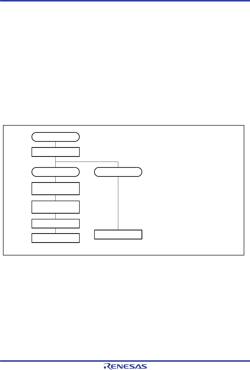
R01UH0034EJ0200 Rev.2.00 Page 553 of 1489
Dec 27, 2013
RX62T Group, RX62G Group 16. Multi-Function Timer Pulse Unit 3 (MTU3)
16.3 Operation
16.3.1 Basic Functions
Each channel has TCNT and TGR. TCNT performs up-counting, and is also capable of free-running operation, periodic
counting, and external event counting.
Each TGR can be used as an input capture register or an output compare register.
(1) Counter Operation
When one of bits CST0 to CST4 in TSTRA, bits CST6 and CST7 in TSTRB, and bits CSTU5, CSTV5, and CSTW5 in
MTU5.TSTR is set to 1, TCNT for the corresponding channel begins counting. TCNT can operate as a free-running
counter, periodic counter, for example.
(a) Example of Count Operation Setting Procedure
Figure 16.5 shows an example of the count operation setting procedure.
Figure 16.5 Example of Counter Operation Setting Procedure
[1] Select the counter clock with
bits TPSC[2:0] in TCR. At
the same time, select the
input clock edge with bits
CKEG[1:0] in TCR.
[2] For periodic counter
operation, select the TGR to
be used as the TCNT clearing
source with bits CCLR[2:0]
in TCR.
[3] Designate the TGR selected in
[2] as an output compare
register by means of TIOR.
[4] Set the periodic counter cycle
in the TGR selected in [2].
[5] Set the CST bit in TSTRA,
TSTRB, or MTU5.TSTR to 1
to start the counter operation.
<Periodic counter> <Free-running counter>
Select counter clock
Operation selection
Periodic counter
Set period
Select output compare
register
Select counter clearing
source
Start count operation
Free-running counter
Start count operation
[1]
[2]
[3]
[4]
[5] [5]
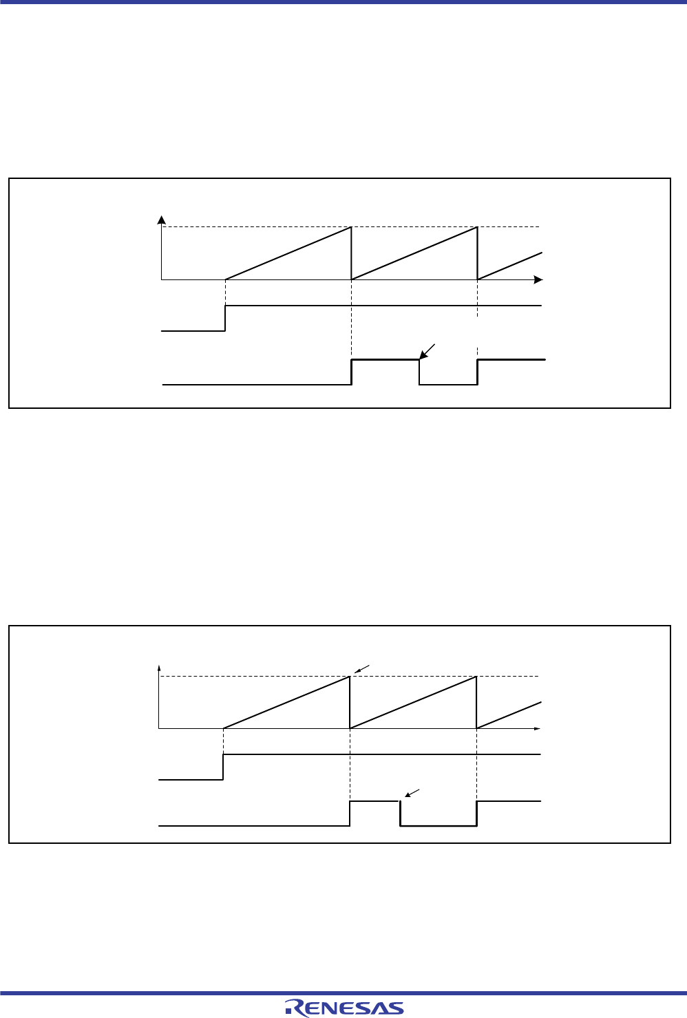
R01UH0034EJ0200 Rev.2.00 Page 554 of 1489
Dec 27, 2013
RX62T Group, RX62G Group 16. Multi-Function Timer Pulse Unit 3 (MTU3)
(b) Free-Running Count Operation and Periodic Count Operation
Immediately after a reset, the MTU’s TCNT counters are all designated as free-running counters. When the relevant bit
in TSTRA, TSTRB, or MTU5.TSTR is set to 1, the corresponding TCNT counter starts up-count operation as a free-
running counter. When TCNT overflows (from FFFFh to 0000h), the TSR.TCFV flag is set to 1. If the corresponding
TIER.TCIEV bit is 1 at this point, the MTU requests an interrupt. After an overflow, TCNT starts counting up again from
0000h.
Figure 16.6 illustrates free-running counter operation.
Figure 16.6 Free-Running Counter Operation
When compare match is selected as the TCNT clearing source, TCNT for the relevant channel performs periodic count
operation. TGR for setting the cycle is designated as an output compare register, and counter clearing by compare match
is selected by means of bits CCLR[2:0] in TCR. After the settings have been made, TCNT starts up-count operation as a
periodic counter when the corresponding bit in TSTRA, TSTRB or MTU5.TSTR is set to 1. When the count matches the
value in TGR, the TSR.TGF flag is set to 1 and TCNT is cleared to 0000h.
If the value of the corresponding TIER.TGIE bit is 1 at this point, the MTU requests an interrupt. After a compare match,
TCNT starts counting up again from 0000h.
Figure 16.7 illustrates periodic counter operation.
Figure 16.7 Periodic Counter Operation
TCNT value
FFFFh
0000h
CST bit
Time
TCIV
The flag is cleared to 0
by software
TCNT value
TGR
0000h
TSTR.CST
bit
TGF
Time
Counter cleared by TGR
compare match
Flag cleared by software

R01UH0034EJ0200 Rev.2.00 Page 555 of 1489
Dec 27, 2013
RX62T Group, RX62G Group 16. Multi-Function Timer Pulse Unit 3 (MTU3)
(2) Waveform Output by Compare Match
The MTU can output low or high or toggles output from the corresponding output pin using compare match.
(a) Example of Procedure for Setting Waveform Output by Compare Match
Figure 16.8 shows an example of the procedure for setting waveform output by compare match
Figure 16.8 Example of Procedure for Setting Waveform Output by Compare Match
[1] Select initial value low output or high output,
and compare match output value low output,
high output, or toggle output, by
means of TIOR. The set initial value is
output at the MTIOC pin until the first
compare match occurs.
[2] Set the timing for compare match
generation in TGR.
[3] Set the CST bit in TSTRi or
MTU5.TSTR to 1 to start the count
operation. (i = A or B)
<Waveform output>
Select waveform output
mode
Output selection
Set output timing
Start count operation
[1]
[2]
[3]
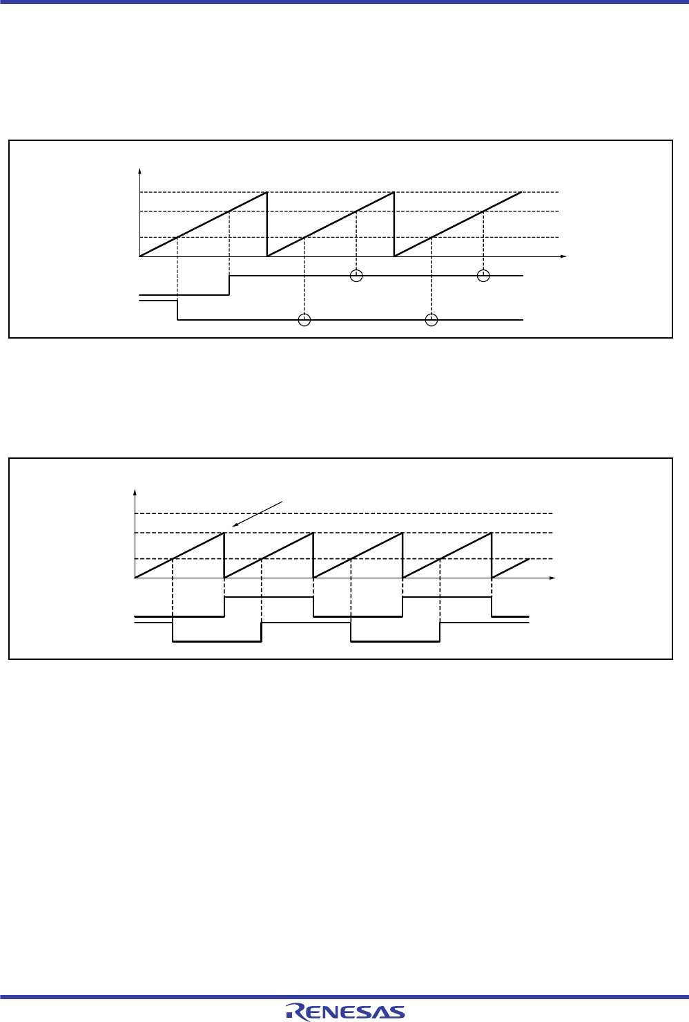
R01UH0034EJ0200 Rev.2.00 Page 556 of 1489
Dec 27, 2013
RX62T Group, RX62G Group 16. Multi-Function Timer Pulse Unit 3 (MTU3)
(b) Examples of Waveform Output Operation
Figure 16.9 shows an example of low output and high output.
In this example, TCNT has been designated as a free-running counter, and settings have been made so that high is output
by compare match A and low is output by compare match B. When the pin level is the same as the specified level, the pin
level does not change.
Figure 16.9 Example of low output and high output Operation
Figure 16.10 shows an example of toggle output.
In this example, TCNT has been designated as a periodic counter (with counter clearing on compare match B), and
settings have been made so that the output is toggled by both compare match A and compare match B.
Figure 16.10 Example of Toggle Output Operation
High output
Time
Low output
No change
No change
No change
No change
TCNT value
FFFFh
TGRA
TGRB
0000h
MTIOCA
MTIOCB
TCNT value
FFFFh
0000h
MTIOCB
MTIOCA
Time
TGRB
TGRA
Toggle output
Toggle output
Counter cleared by TGRB compare match
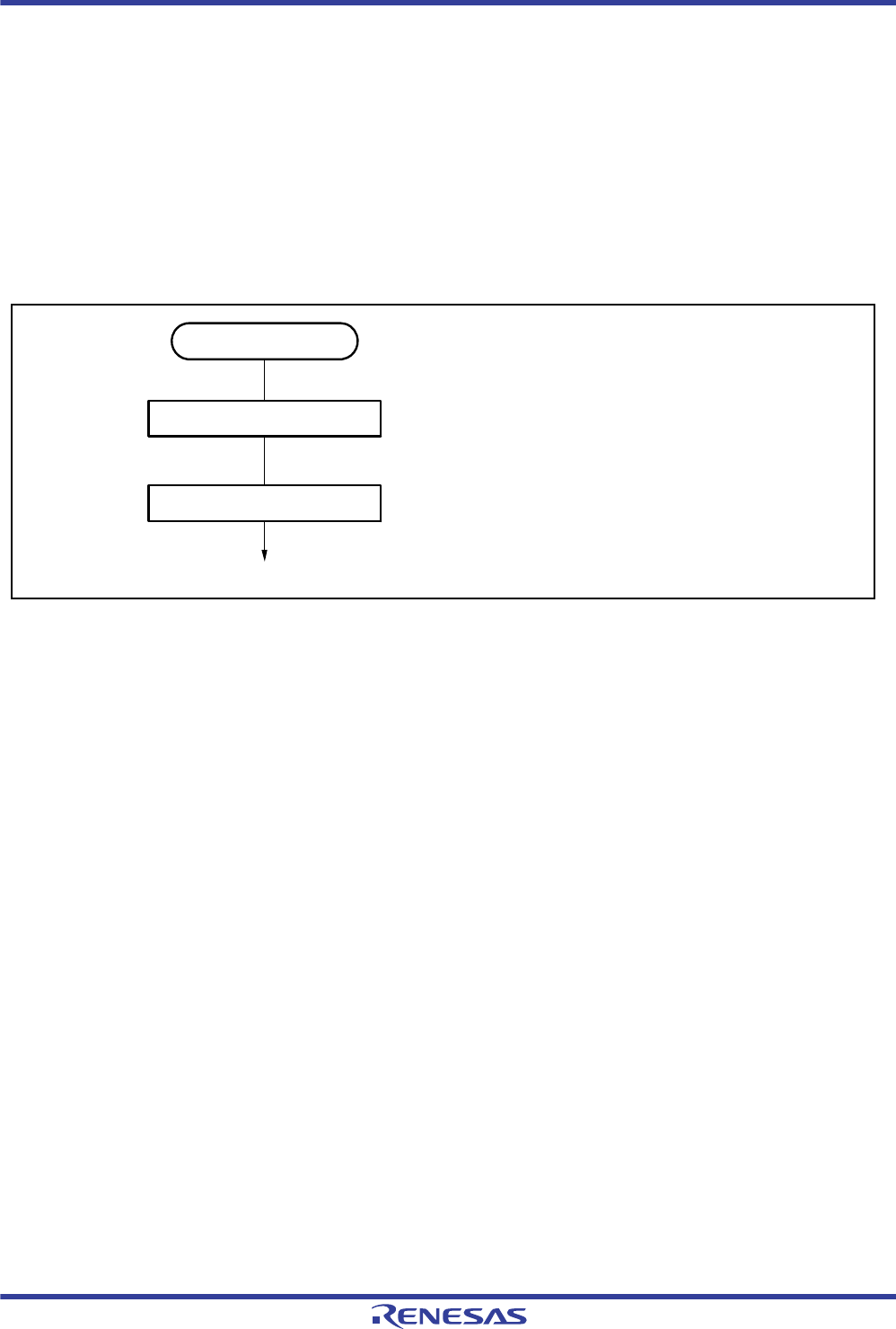
R01UH0034EJ0200 Rev.2.00 Page 557 of 1489
Dec 27, 2013
RX62T Group, RX62G Group 16. Multi-Function Timer Pulse Unit 3 (MTU3)
(3) Input Capture Function
The TCNT value can be transferred to TGR on detection of the MTIOC pin input edge.
The rising edge, falling edge, or both edges can be selected as the detection edge. For MTU0 and MTU1, another
channel's counter input clock or compare match signal can also be specified as the input capture source.
Note:When another channel's counter input clock is used as the input capture input for MTU0 and MTU1, ICLK/1
should not be selected as the counter input clock used for input capture input. Input capture will not be generated if
ICLK/1 is selected.
(a) Example of Input Capture Operation Setting Procedure
Figure 16.11 shows an example of the input capture operation setting procedure.
Figure 16.11 Example of Input Capture Operation Setting Procedure
[1]
[2]
[1] Designate TGR as an input capture
register by means of TIOR, and select
rising edge, falling edge, or both edges as
the input capture source and input signal
edge.
[2] Set the CST bit in TSTRi or
MTU5.TSTR to 1 to start the count
operation. (i = A or B)
Input selection
Select input capture input
Start count
<Input capture operation>
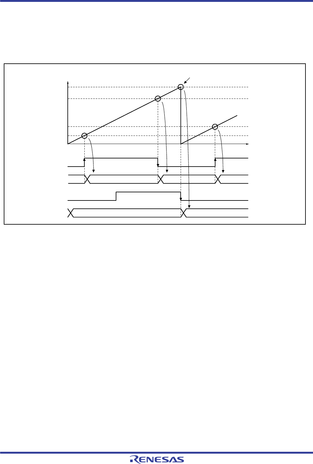
R01UH0034EJ0200 Rev.2.00 Page 558 of 1489
Dec 27, 2013
RX62T Group, RX62G Group 16. Multi-Function Timer Pulse Unit 3 (MTU3)
(b) Example of Input Capture Operation
Figure 16.12 shows an example of input capture operation.
In this example, both rising and falling edges have been selected as the MTIOCA pin input capture input edge, the falling
edge has been selected as the MTIOCB pin input capture input edge, and counter clearing by TGRB input capture has
been designated for TCNT.
Figure 16.12 Example of Input Capture Operation
TCNT value
0180h
0000h
MTIOCA
TGRA
Time
0010h
0005h
0160h
0005h 0160h 0010h
TGRB 0180h
MTIOCB
Counter cleared by MTIOCB
input (falling edge)
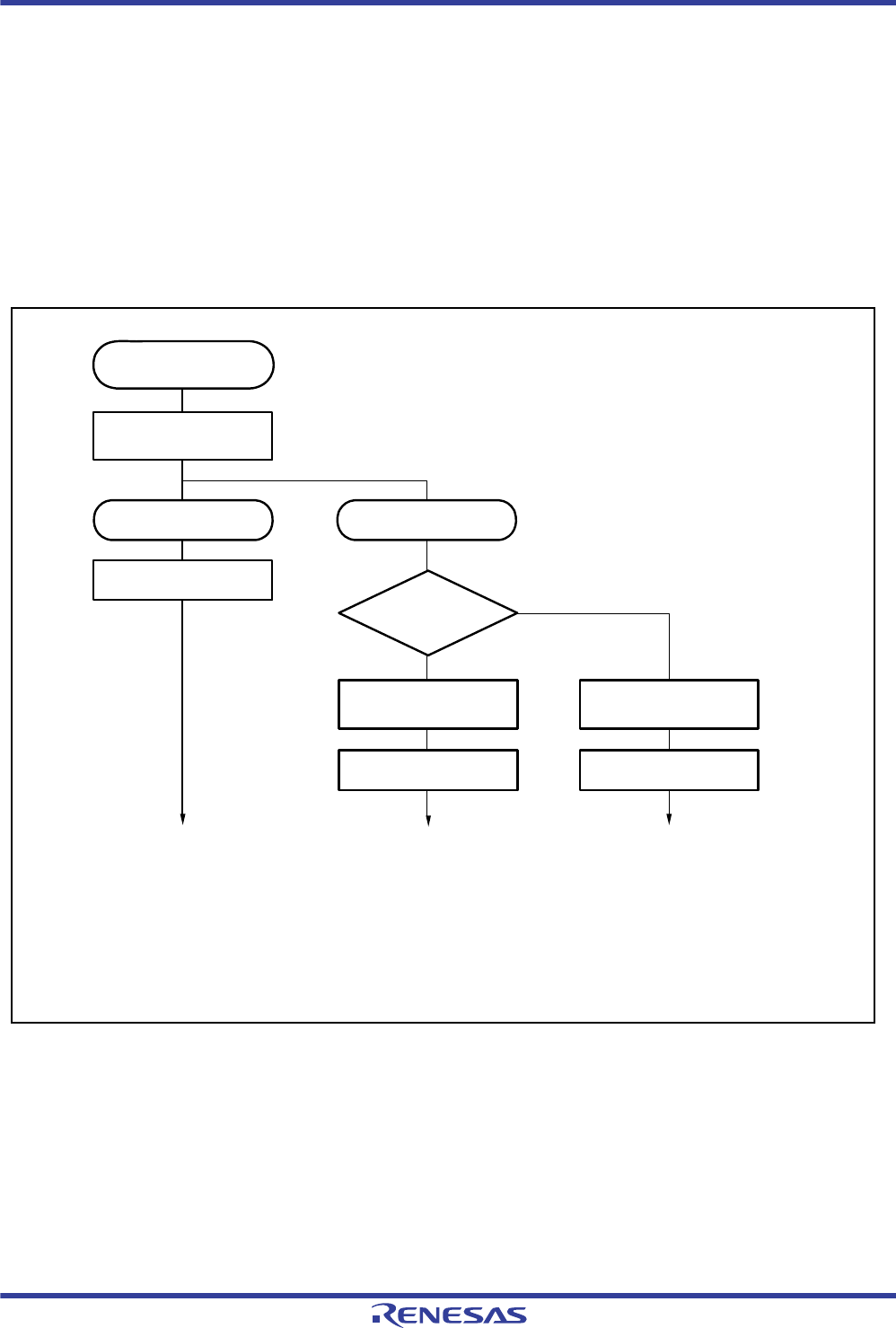
R01UH0034EJ0200 Rev.2.00 Page 559 of 1489
Dec 27, 2013
RX62T Group, RX62G Group 16. Multi-Function Timer Pulse Unit 3 (MTU3)
16.3.2 Synchronous Operation
In synchronous operation, the values in multiple TCNT counters can be modified simultaneously (synchronous
presetting). In addition, multiple TCNT counters can be cleared simultaneously (synchronous clearing) by making the
appropriate setting in TCR.
Synchronous operation increases the number of TGR registers assigned to a single time base.
MTU0 to MTU4, MTU6, and MTU7 can all be designated for synchronous operation. MTU5 cannot be used for
synchronous operation.
(1) Example of Synchronous Operation Setting Procedure
Figure 16.13 shows an example of the synchronous operation setting procedure.
Figure 16.13 Example of Synchronous Operation Setting Procedure
No
Yes
[1]
[3]
[5]
[4]
[5]
[2]
[1] Set to 1 the SYNC bits in TSYRj corresponding to the channels to be designated for synchronous operation.
(j = A or B)
[2] When the TCNT counter of any of the channels designated for synchronous operation is written to, the same
value is simultaneously written to the other TCNT counters.
[3] Use bits CCLR[2:0] in TCR to specify TCNT clearing by input capture/output compare, etc.
[4] Use bits CCLR[2:0] in TCR to designate synchronous clearing for the counter clearing source.
[5] Set to 1 the CST bits in TSTRj for the relevant channels, to start the count operation.
(j = A or B)
<Synchronous clearing>
<Counter clearing>
<Synchronous presetting>
Start count
Start count
Set synchronous
counter clearing
Select counter
clearing source
Clearing
source generation
channel?
Synchronous clearing
Synchronous presetting
Set TCNT
Set synchronous
operation
Synchronous operation
selection
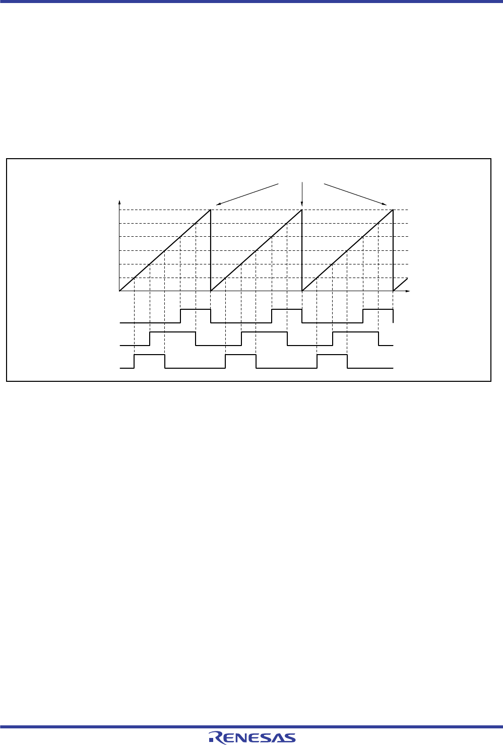
R01UH0034EJ0200 Rev.2.00 Page 560 of 1489
Dec 27, 2013
RX62T Group, RX62G Group 16. Multi-Function Timer Pulse Unit 3 (MTU3)
(2) Example of Synchronous Operation
Figure 16.14 shows an example of synchronous operation.
In this example, synchronous operation and PWM mode 1 have been designated for MTU0 to MTU2, MTU0.TGRB
compare match has been set as the counter clearing source in MTU0, and synchronous clearing has been set for the
counter clearing source in MTU1 and MTU2.
Three-phase PWM waveforms are output from pins MTIOC0A, MTIOC1A, and MTIOC2A. At this time, synchronous
presetting and synchronous clearing by MTU0.TGRB compare match are performed for the TCNT counters in cMTU1
and MTU2, and the data set in MTU0.TGRB is used as the PWM cycle.
For details of PWM modes, see section 16.3.5, PWM Modes .
Figure 16.14 Example of Synchronous Operation
TCNT value
Time
Synchronous clearing by MTU0.TGRB compare match
0000h
MTIOC0A
MTIOC1A
MTU0.TGRB
MTU2.TGRA
MTU1.TGRA
MTU2.TGRB
MTU0.TGRA
MTU1.TGRB
MTIOC2A
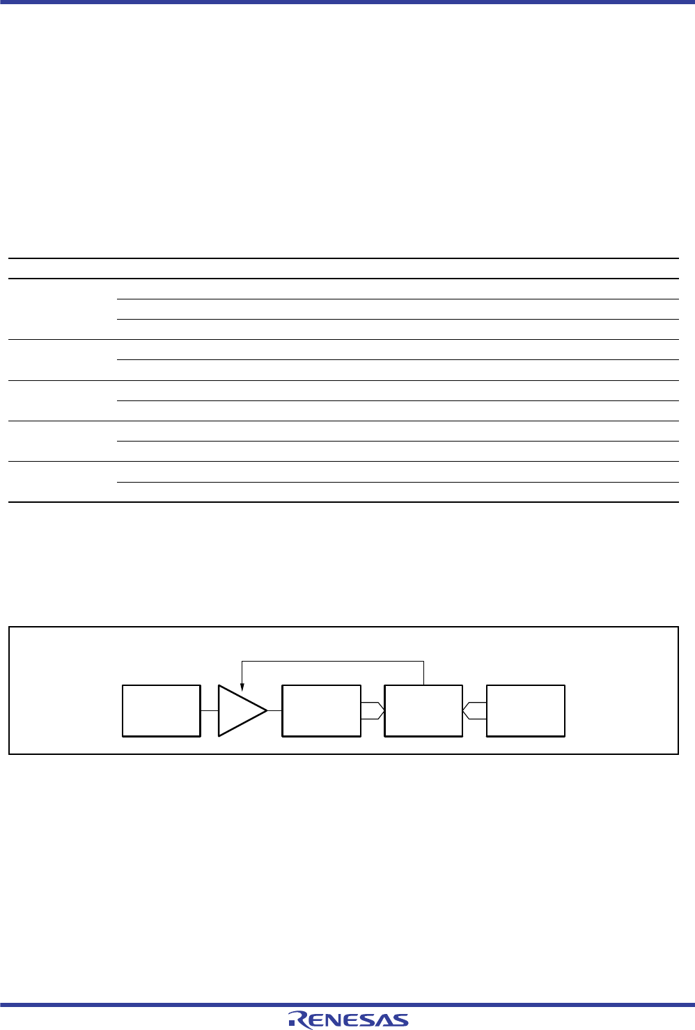
R01UH0034EJ0200 Rev.2.00 Page 561 of 1489
Dec 27, 2013
RX62T Group, RX62G Group 16. Multi-Function Timer Pulse Unit 3 (MTU3)
16.3.3 Buffer Operation
Buffer operation, provided for MTU0, MTU3, MTU4, MTU6, and MTU7, enables TGRC and TGRD to be used as
buffer registers. In MTU0, TGRF can also be used as a buffer register.
Buffer operation differs depending on whether TGR has been designated as an input capture register or as a compare
match register.
Note: • MTU0.TGRE cannot be designated as an input capture register and can only operate as a compare match
register.
shows the register combinations used in buffer operation.
When TGR is an output compare register
When a compare match occurs, the value in the buffer register for the corresponding channel is transferred to the timer
general register.
This operation is illustrated in Figure 16.15.
Figure 16.15 Compare Match Buffer Operation
Table 16.58 Register Combinations in Buffer Operation
Channel Timer General Register Buffer Register
MTU0 TGRA TGRC
TGRB TGRD
TGRE TGRF
MTU3 TGRA TGRC
TGRB TGRD
MTU4 TGRA TGRC
TGRB TGRD
MTU6 TGRA TGRC
TGRB TGRD
MTU7 TGRA TGRC
TGRB TGRD
Compare match signal
Timer general
register Comparator TCNT
Buffer
register

R01UH0034EJ0200 Rev.2.00 Page 562 of 1489
Dec 27, 2013
RX62T Group, RX62G Group 16. Multi-Function Timer Pulse Unit 3 (MTU3)
When TGR is an input capture register
When an input capture occurs, the value in TCNT is transferred to TGR and the value previously held in TGR is
transferred to the buffer register.
This operation is illustrated in Figure 16.16.
Figure 16.16 Input Capture Buffer Operation
(1) Example of Buffer Operation Setting Procedure
Figure 16.17 shows an example of the buffer operation setting procedure.
Figure 16.17 Example of Buffer Operation Setting Procedure
Input capture
signal
Buffer
register Timer general
register TCNT
[1]
[2]
[3]
[1] Designate TGR as an input capture register or
output compare register by means of TIOR.
[2] Designate TGR for buffer operation with bits BFA
and BFB in TMDR1.
[3] Set the CST bit in TSTRA or TSTRB to 1 to start
the count operation.
Buffer operation
Select TGR function
Set buffer operation
Start count
<Buffer operation>
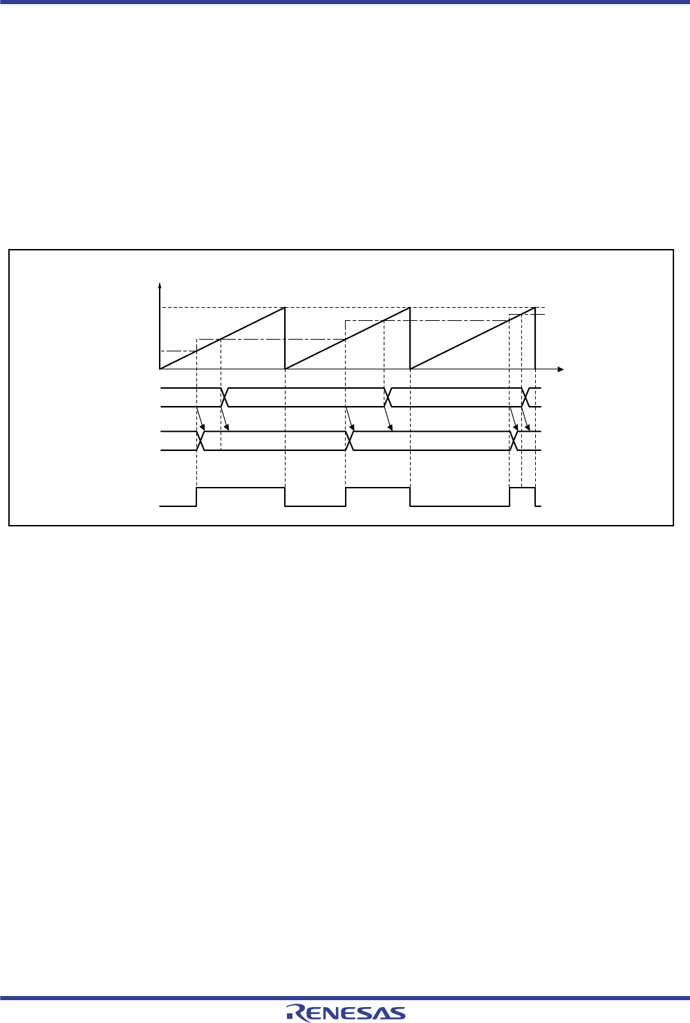
R01UH0034EJ0200 Rev.2.00 Page 563 of 1489
Dec 27, 2013
RX62T Group, RX62G Group 16. Multi-Function Timer Pulse Unit 3 (MTU3)
(2) Examples of Buffer Operation
(a) When TGR is an Output Compare Register
Figure 16.18 shows an operation example in which PWM mode 1 has been designated for MTU0, and buffer operation
has been designated for TGRA and TGRC. The settings used in this example are TCNT clearing by compare match B,
high output at compare match A, and low output at compare match B. In this example, the TTSA bit in TBTM is cleared
to 0.
As buffer operation has been set, when compare match A occurs, the output changes and the value in buffer register
TGRC is simultaneously transferred to timer general register TGRA. This operation is repeated each time compare
match A occurs.
For details of PWM modes, see section 16.3.5, PWM Modes .
Figure 16.18 Example of Buffer Operation (1)
TCNT value
Time
0200h 0520h
0200h
0450h 0520h
0450h
0450h0200h
Transfer
MTU0.TGRB
0000h
MTU0.TGRC
MTU0.TGRA
MTIOCA
MTU0.TGRA
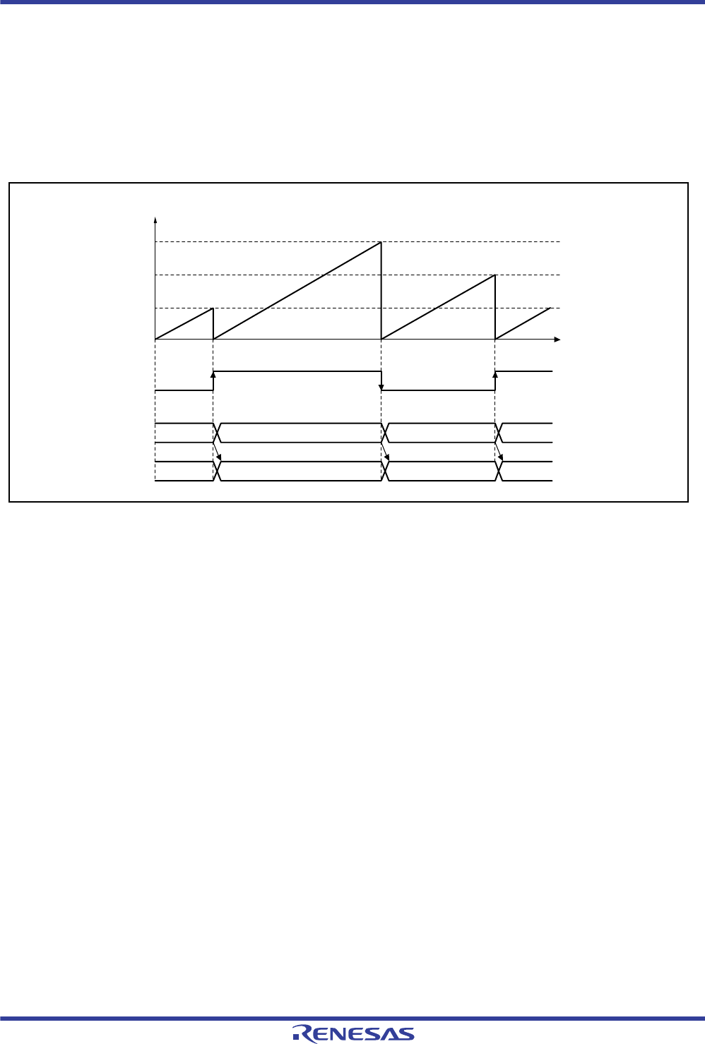
R01UH0034EJ0200 Rev.2.00 Page 564 of 1489
Dec 27, 2013
RX62T Group, RX62G Group 16. Multi-Function Timer Pulse Unit 3 (MTU3)
(b) When TGR is an Input Capture Register
Figure 16.19 shows an operation example in which TGRA has been designated as an input capture register, and buffer
operation has been designated for TGRA and TGRC.
Counter clearing by TGRA input capture has been set for TCNT, and both rising and falling edges have been selected as
the MTIOCA pin input capture input edge.
As buffer operation has been set, when the TCNT value is stored in TGRA upon occurrence of input capture A, the value
previously stored in TGRA is simultaneously transferred to TGRC.
Figure 16.19 Example of Buffer Operation (2)
TCNT value
Time
0532h
0F07h0532h
0F07h
09FBh
09FBh
0000h
TGRC
MTIOCA
TGRA
0F07h
0532h
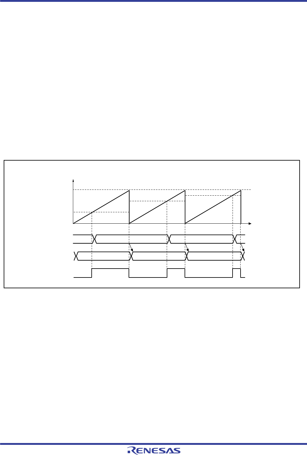
R01UH0034EJ0200 Rev.2.00 Page 565 of 1489
Dec 27, 2013
RX62T Group, RX62G Group 16. Multi-Function Timer Pulse Unit 3 (MTU3)
(3) Selecting Timing for Transfer from Buffer Registers to Timer General Registers in Buffer
Operation
The timing for transfer from buffer registers to timer general registers can be selected in PWM mode 1 or 2 for MTU0 or
in PWM mode 1 for MTU3, MTU4, MTU6, and MTU7 by setting the buffer operation transfer mode registers
(MTUn.TBTM (n = 0, 3, 4, 6, or 7)). Either compare match (value after reset) or TCNT clearing can be selected for the
transfer timing. TCNT clearing as transfer timing is one of the following cases.
When TCNT overflows (FFFFh to 0000h)
When 0000h is written to TCNT during counting
When TCNT is cleared to 0000h under the condition specified in the CCLR[2:0] bits in TCR
Note: • TBTM must be modified only while TCNT stops.
Figure 16.20 shows an operation example in which PWM mode 1 is designated for MTU0 and buffer operation is
designated for MTU0.TGRA and MTU0.TGRC. The settings used in this example are MTU0.TCNT clearing by
compare match B, high output at compare match A, and low output at compare match B. The TTSA bit in MTU0.TBTM
is set to 1.
Figure 16.20 Example of Buffer Operation When MTU0.TCNT Clearing is Selected for MTU0.TGRC-to-
MTU0.TGRA Transfer Timing
Time
0520h
0520h
0450h
0450h
0200h
0520h0450h0200h
0200H
Transfer
MTU0.TCNT value
0000h
MTU0.TGRA
MTIOCA
MTU0.TGRC
MTU0.TGRB
MTU0.TGRA

R01UH0034EJ0200 Rev.2.00 Page 566 of 1489
Dec 27, 2013
RX62T Group, RX62G Group 16. Multi-Function Timer Pulse Unit 3 (MTU3)
16.3.4 Cascaded Operation
In cascaded operation, two 16-bit counters in different channels are used together as a 32-bit counter.
This function works when overflow/underflow of MTU2.TCNT is selected as the counter clock for MTU1 through the
TPSC[2:0] bits in TCR.
Underflow occurs only when the lower 16 bits of TCNT is in phase counting mode.
Table 16.59 shows the register combinations used in cascaded operation.
Note: • When phase counting mode is set for MTU1, the counter clock setting is invalid and the counters operate
independently in phase counting mode.
For simultaneous input capture of MTU1.TCNT and MTU2.TCNT during cascaded operation, additional input capture
input pins can be specified by the input capture control register (TICCR). The edge detected as an input capture condition
is in the signal obtained by taking the logical OR of the levels being input on the original input pin and on the added input
pin. Therefore, if one signal is at the high level, edges in the other will not be detected. For details, refer to (4) Cascaded
Operation Example (c). For input capture in cascade connection, refer to section 16.6.21, Simultaneous Input
Capture in MTU1.TCNT and MTU2.TCNT in Cascade Connection.
Table 16.60 shows the TICCR setting and input capture input pins.
Table 16.59 Cascaded Combinations
Combination Upper 16 Bits Lower 16 Bits
MTU and MTU2 MTU1.TCNT MTU2.TCNT
Table 16.60 TICCR Setting and Input Capture Input Pins
Target Input Capture TICCR Setting Input Capture Input Pin
Input capture from MTU1.TCNT to
MTU1.TGRA
I2AE bit = 0 (value after reset) MTIOC1A
I2AE bit = 1 MTIOC1A, MTIOC2A
Input capture from MTU1.TCNT to
MTU1.TGRB
I2BE bit = 0 (value after reset) MTIOC1B
I2BE bit = 1 MTIOC1B, MTIOC2B
Input capture from MTU2.TCNT to
MTU2.TGRA
I1AE bit = 0 (value after reset) MTIOC2A
I1AE bit = 1 MTIOC2A, MTIOC1A
Input capture from MTU2.TCNT to
MTU2.TGRB
I1BE bit = 0 (value after reset) MTIOC2B
I1BE bit = 1 MTIOC2B, MTIOC1B
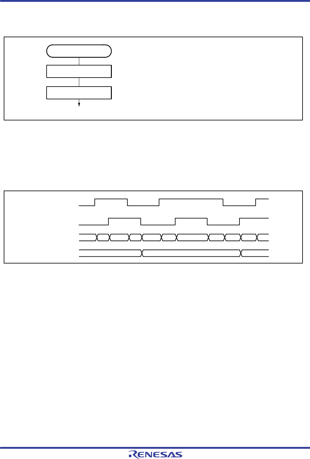
R01UH0034EJ0200 Rev.2.00 Page 567 of 1489
Dec 27, 2013
RX62T Group, RX62G Group 16. Multi-Function Timer Pulse Unit 3 (MTU3)
(1) Example of Cascaded Operation Setting Procedure
Figure 16.21 shows an example of the cascaded operation setting procedure.
Figure 16.21 Cascaded Operation Setting Procedure
(2) Cascaded Operation Example (a)
Figure 16.22 illustrates the operation when MTU2.TCNT overflow/underflow counting has been set for MTU1.TCNT
and phase counting mode has been designated for MTU2.
MTU1.TCNT is incremented by MTU2.TCNT overflow and decremented by MTU2.TCNT underflow.
Figure 16.22 Cascaded Operation Example (a)
[1]
[2]
[1] Set bits TPSC[2:0] in TCR to 111b in MTU1 to
select MTU3_2.TCNT overflow/underflow counting.
[2] Set the CST bit in TSTRA for the upper and lower
channels to 1 to start the count operation.
Cascaded operation
Set cascading
Start count
<Cascaded operation>
00010000 0000
FFFD FFFE FFFF 0000 0001 0002 0001 0000 FFFF
MTCLKC
MTU2.TCNT
MTU1.TCNT
MTCLKD
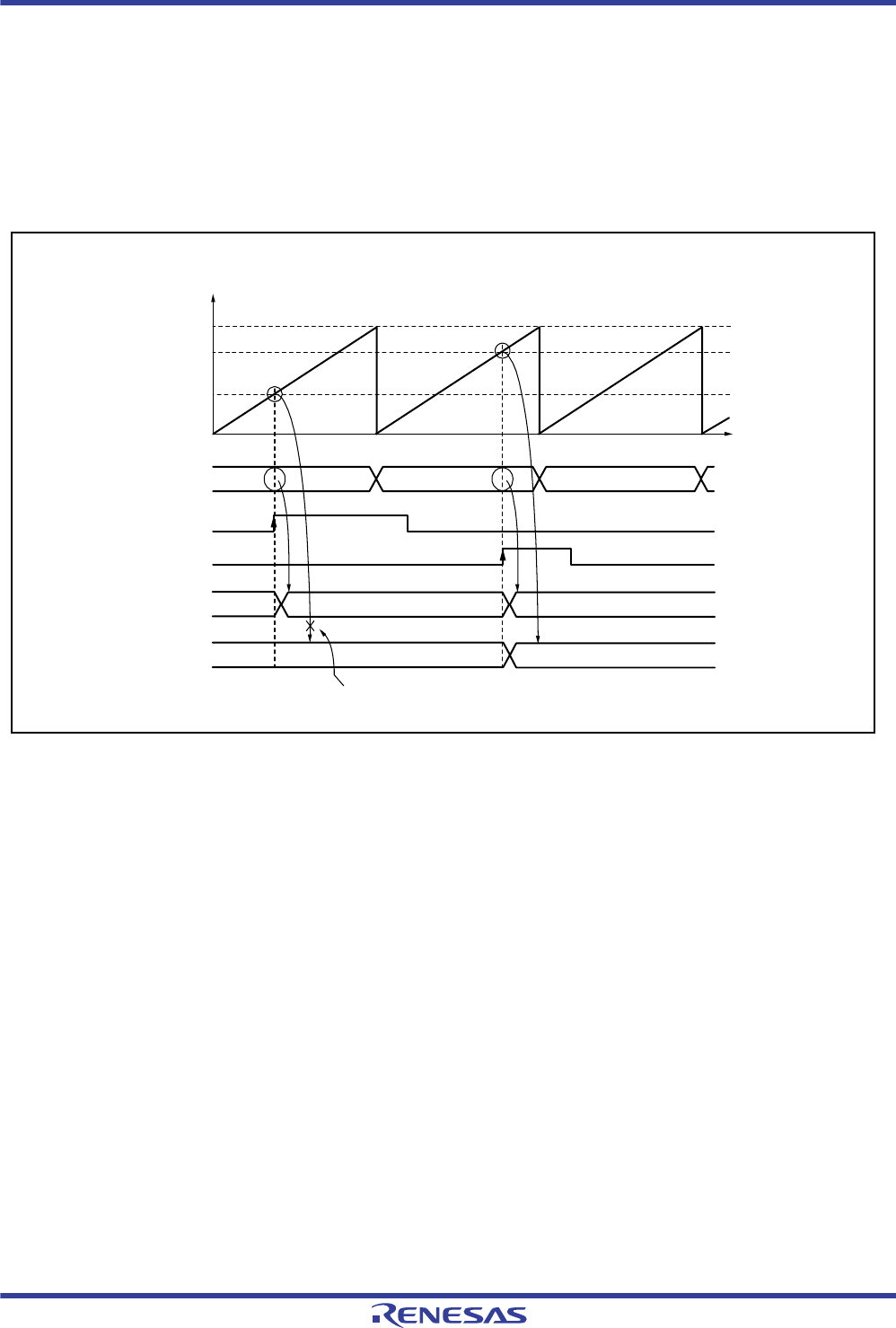
R01UH0034EJ0200 Rev.2.00 Page 568 of 1489
Dec 27, 2013
RX62T Group, RX62G Group 16. Multi-Function Timer Pulse Unit 3 (MTU3)
(3) Cascaded Operation Example (b)
Figure 16.23 illustrates the operation when MTU1.TCNT and MTU2.TCNT have been cascaded and the I2AE bit in
TICCR has been set to 1 to include the MTIOC2A pin in the MTU1.TGRA input capture conditions. In this example, the
MTU1.TIOR.IOA[3:0] bits have selected the MTIOC1A rising edge for the input capture timing while the
MTU2.TIOR.IOA[3:0] bits have selected the MTIOC2A rising edge for the input capture timing.
Under these conditions, the rising edge of both MTIOC1A and MTIOC2A is used for the MTU1.TGRA input capture
condition. For the MTU2.TGRA input capture condition, the MTIOC2A rising edge is used.
Figure 16.23 Cascaded Operation Example (b)
MTU2.TCNT value
Time
0514h0513h0512h
0513h0512h
C256h
As TICCR.I1AE = 0, data is not captured in MTU2.TGRA at
the MTIOC1A input timing.
0000h
MTU1.TGRA
MTU2.TGRA
MTIOC1A
MTIOC2A
MTU1.TCNT
C256h
FFFFh
6128h
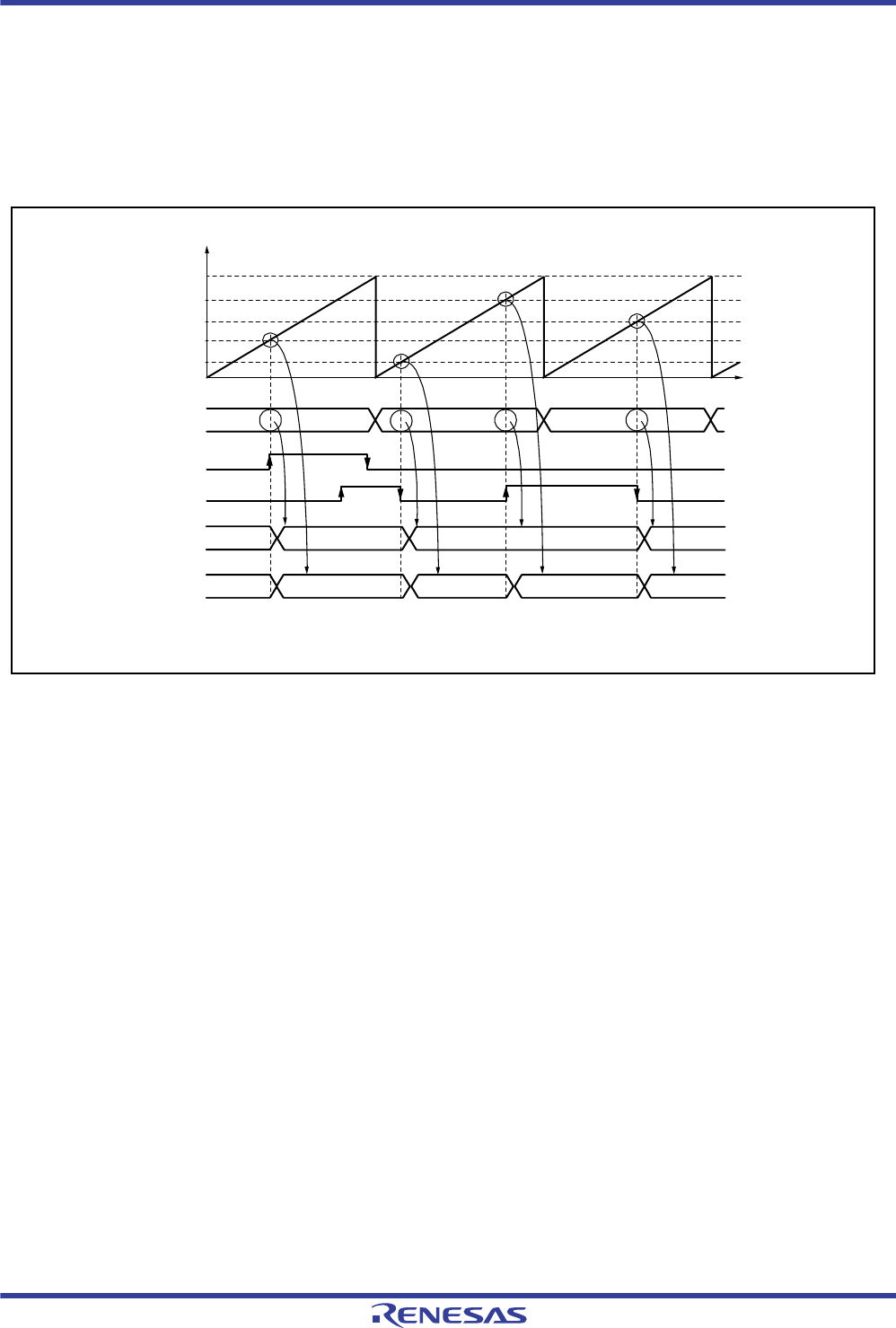
R01UH0034EJ0200 Rev.2.00 Page 569 of 1489
Dec 27, 2013
RX62T Group, RX62G Group 16. Multi-Function Timer Pulse Unit 3 (MTU3)
(4) Cascaded Operation Example (c)
Figure 16.24 illustrates the operation when MTU1.TCNT and MTU2.TCNT have been cascaded and the TICCR.I2AE
and I1AE bits have been set to 1 to include the MTIOC2A and MTIOC1A pins in the MTU1.TGRA and MTU2.TGRA
input capture conditions, respectively. In this example, the IOA[3:0] bits in both MTU1.TIOR and MTU2.TIOR have
selected both the rising and falling edges for the input capture timing. Under these conditions, the ORed result of
MTIOC1A and MTIOC2A input is used for the MTU1.TGRA and MTU2.TGRA input capture conditions.
Figure 16.24 Cascaded Operation Example (c)
MTU2.TCNT value
Time
0514h
0514h
0513h0512h
0513h0512h
C256h
6128h 2064h 9192h
0000h
MTU1.TGRA
MTU2.TGRA
MTIOC1A
MTIOC2A
MTU1.TCNT
C256h
FFFFh
6128h
2064h
9192h
*
*
Note: If one of the input pins is at the high level, the signal on the other will not act as an input
capture condition.
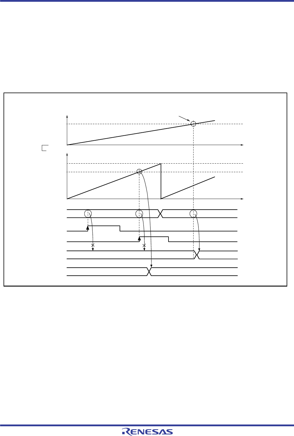
R01UH0034EJ0200 Rev.2.00 Page 570 of 1489
Dec 27, 2013
RX62T Group, RX62G Group 16. Multi-Function Timer Pulse Unit 3 (MTU3)
(5) Cascaded Operation Example (d)
Figure 16.25 illustrates the operation when MTU1.TCNT and MTU2.TCNT have been cascaded and the TICCR.I2AE
bit has been set to 1 to include the MTIOC2A pin in the MTU1.TGRA input capture conditions. In this example, the
IOA[3:0] bits in MTU1.TIOR have selected occurrence of MTU0.TGRA compare match or input capture for the input
capture timing while the IOA[3:0] bits in MTU2.TIOR have selected the MTIOC2A rising edge for the input capture
timing.
Under these conditions, as MTU1.TIOR has selected occurrence of MTU0.TGRA compare match or input capture for
the input capture timing, the MTIOC2A edge is not used for MTU1.TGRA input capture condition although the I2AE bit
in TICCR has been set to 1.
Figure 16.25 Cascaded Operation Example (d)
Time
0513h0512h
0513h
D000h
MTU0.TCNT value
Time
Compare match between MTU0.TCNT and MTU0.TGRA
MTU2.TCNT value
0000h
0000h
MTU1.TGRA
MTU2.TGRA
MTIOC1A
MTIOC2A
MTU1.TCNT
D000h
FFFFh
MTU0.TGRA

R01UH0034EJ0200 Rev.2.00 Page 571 of 1489
Dec 27, 2013
RX62T Group, RX62G Group 16. Multi-Function Timer Pulse Unit 3 (MTU3)
16.3.5 PWM Modes
PWM modes are provided to output PWM waveforms from the external pins. The output level can be selected as low,
high, or toggle output in response to a compare match of each TGR.
PWM waveforms in the range of 0% to 100% duty cycle can be output according to the TGR settings.
By designating TGR compare match as the counter clearing source, the PWM cycle can be specified in that register.
Every channel can be set to PWM mode independently. Synchronous operation is also possible.
There are two PWM modes as described below.
(a) PWM Mode 1
PWM waveforms are output from the MTIOCA and MTIOCC pins by pairing TGRA with TGRB and TGRC with
TGRD. The levels specified by the TIOR.IOA[3:0] and IOC[3:0] bits are output from the MTIOCA and MTIOCC pins at
compare matches A and C, and the level specified by the TIOR.IOB[3:0] and IOD[3:0] bits are output at compare
matches B and D. The initial output value is set in TGRA or TGRC. If the values set in paired TGRs are identical, the
output value does not change even when a compare match occurs.
In PWM mode 1, up to 12 phases of PWM waveforms can be output.

R01UH0034EJ0200 Rev.2.00 Page 572 of 1489
Dec 27, 2013
RX62T Group, RX62G Group 16. Multi-Function Timer Pulse Unit 3 (MTU3)
(b) PWM Mode 2
PWM waveform output is generated using one TGR as the cycle register and the others as duty registers. The level
specified in TIOR is output at compare matches. Upon counter clearing by a cycle register compare match, the initial
value set in TIOR is output from each pin. If the values set in the cycle and duty registers are identical, the output value
does not change even when a compare match occurs.
In PWM mode 2, up to eight phases of PWM waveforms can be output when using synchronous operation in
combination.
The correspondence between PWM output pins and registers is shown in Table 16.61.
Note 1. In PWM mode 2, PWM waveform output is not possible for the TGR register in which the PWM cycle is set.
Table 16.61 PWM Output Registers and Output Pins
Channel Register
Output Pins
PWM Mode 1 PWM Mode 2
MTU0 TGRA MTIOC0A MTIOC0A
TGRB MTIOC0B
TGRC MTIOC0C MTIOC0C
TGRD MTIOC0D
MTU1 TGRA MTIOC1A MTIOC1A
TGRB MTIOC1B
MTU2 TGRA MTIOC2A MTIOC2A
TGRB MTIOC2B
MTU3 TGRA MTIOC3A Setting prohibited
TGRB
TGRC MTIOC3C
TGRD
MTU4 TGRA MTIOC4A
TGRB
TGRC MTIOC4C
TGRD
MTU6 TGRA MTIOC6A
TGRB
TGRC MTIOC6C
TGRD
MTU7 TGRA MTIOC7A
TGRB
TGRC MTIOC7C
TGRD

R01UH0034EJ0200 Rev.2.00 Page 573 of 1489
Dec 27, 2013
RX62T Group, RX62G Group 16. Multi-Function Timer Pulse Unit 3 (MTU3)
(1) Example of PWM Mode Setting Procedure
Figure 16.26 shows an example of the PWM mode setting procedure.
Figure 16.26 Example of PWM Mode Setting Procedure
(2) Examples of PWM Mode Operation
Figure 16.27 shows an example of operation in PWM mode 1.
In this example, TGRA compare match is set as the TCNT clearing source, 0 is set as the initial output value and output
value for TGRA, and 1 is set as the output value for TGRB.
In this case, the value set in TGRA is used as the cycle, and the value set in TGRB is used as the duty ratio.
Figure 16.27 Example of PWM Mode 1 Operation
[1]
[2]
[3]
[4]
[5]
[6]
[1] Select the counter clock with bits TPSC[2:0]
in TCR. At the same time, select the input
clock edge with bits CKEG[1:0] in TCR.
[2] Use bits CCLR[2:0] in TCR to select the TGR
to be used as the TCNT clearing source.
[3] Select the PWM mode with bits MD[3:0] in TMDR.
[4] Use TIOR to designate the TGR as an output
Compare register, and select the initial value and
Output value.
[5] Set the cycle in the TGR selected in [2], and set
the duty ratio in the other TGR.
[6] Set the CST bit in TSTRA or TSTRB to 1 to start
the count operation.
PWM mode
Select counter clock
Select counter clearing
source
Set PWM mode
Select waveform output
level
Set TGR
Start count
<PWM mode>
TCNT value
Time
Counter cleared by
TGRA compare match
TGRA
0000h
MTIOCA
TGRB
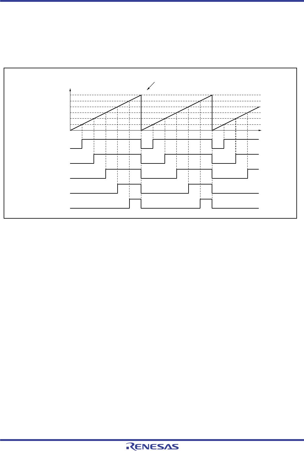
R01UH0034EJ0200 Rev.2.00 Page 574 of 1489
Dec 27, 2013
RX62T Group, RX62G Group 16. Multi-Function Timer Pulse Unit 3 (MTU3)
Figure 16.28 shows an example of operation in PWM mode 2.
In this example, synchronous operation is designated for MTU0 and MTU1, MTU1.TGRB compare match is set as the
TCNT clearing source, and 0 is set as the initial output value and 1 as the output value for the other TGR registers
(MTU0.TGRA to MTU0.TGRD and MTU1.TGRA), outputting 5-phase PWM waveforms.
In this case, the value set in MTU1.TGRB is used as the cycle, and the values set in the other TGRs are used as the duty
ratio.
Figure 16.28 Example of PWM Mode 2 Operation
Time
TCNT value Counter cleared by MTU1.TGRB
compare match
MTU1.TGRB
0000h
MTIOC0A
MTU1.TGRA
MTU0.TGRD
MTU0.TGRC
MTU0.TGRB
MTU0.TGRA
MTIOC0B
MTIOC0C
MTIOC0D
MTIOC1A
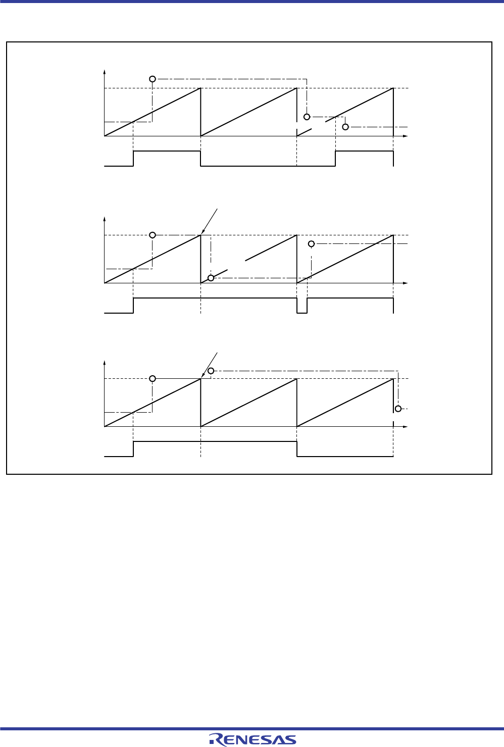
R01UH0034EJ0200 Rev.2.00 Page 575 of 1489
Dec 27, 2013
RX62T Group, RX62G Group 16. Multi-Function Timer Pulse Unit 3 (MTU3)
Figure 16.29 shows examples of PWM waveform output with 0% duty and 100% duty in PWM mode.
Figure 16.29 Examples of PWM Mode Operation (PWM Waveform Output with 0% Duty and 100% Duty)
Time
0% duty
TGRB modified
Output does not change when compare matches occur
simultaneously in cycle register and duty register
0% duty
TCNT value TGRB modified
TGRA
H'0000
MTIOCA
TGRB
TGRA
0000h
MTIOCA
TGRB
TGRA
0000h
MTIOCA
TGRB
Time
Time
100% duty
TCNT value
TGRB modified
TGRB modified
TGRB modified
TGRB modified
100% duty
TGRB modified
TCNT value
TGRB modified
Output does not change when compare matches occur
simultaneously in cycle register and duty register
TGRB modified
R01UH0034EJ0200 Rev.2.00 Page 576 of 1489
Dec 27, 2013
RX62T Group, RX62G Group 16. Multi-Function Timer Pulse Unit 3 (MTU3)
16.3.6 Phase Counting Mode
In phase counting mode, the phase difference between two external input clocks is detected and TCNT is incremented or
decremented accordingly. This mode can be set for MTU1 and MTU2.
When phase counting mode is specified, an external clock is selected as the counter input clock and TCNT operates as an
up/down-counter regardless of the setting of bits TPSC[2:0] and bits CKEG[1:0] in TCR. However, the functions of bits
CCLR[1:0] in TCR and of TIOR, TIER, and TGR are valid, and input capture/compare match and interrupt functions can
be used.
This can be used for two-phase encoder pulse input.
If an overflow occurs while TCNT is counting up, the TCFV flag in TSR is set to 1. If an underflow occurs while TCNT
is counting down, the TCFU flag is TSR is set to 1.
The TCFD flag in TSR is the count direction flag. Read the TCFD flag to check whether TCNT is counting up or down.
Table 16.62 shows the correspondence between external clock pins and channels.
(1) Example of Phase Counting Mode Setting Procedure
Figure 16.30 shows an example of the phase counting mode setting procedure.
Figure 16.30 Example of Phase Counting Mode Setting Procedure
Table 16.62 Clock Input Pins in Phase Counting Mode
Channel
External Clock Input Pins
A-Phase B-Phase
When MTU1 is set to phase counting mode MTCLKA MTCLKB
When MTU2 is set to phase counting mode MTCLKC MTCLKD
[1]
[2]
[1] Select phase counting mode with bits
MD[3:0] in TMDR1.
[2] Set the CST bit in TSTRA to 1 to start
the count operation.
Phase counting mode
Select phase counting
mode
Start count operation
<Phase counting mode>

R01UH0034EJ0200 Rev.2.00 Page 577 of 1489
Dec 27, 2013
RX62T Group, RX62G Group 16. Multi-Function Timer Pulse Unit 3 (MTU3)
(2) Examples of Phase Counting Mode Operation
In phase counting mode, TCNT is incremented or decremented according to the phase difference between two external
clocks. There are four modes according to the count conditions.
(a) Phase Counting Mode 1
Figure 16.31 shows an example of operation in phase counting mode 1, and Table 16.63 summarizes the TCNT up-/
down-count conditions.
Figure 16.31 Example of Operation in Phase Counting Mode 1
: Rising edge
: Falling edge
Table 16.63 Up-/Down-Count Conditions in Phase Counting Mode 1
MTCLKA (MTU1)
MTCLKC (MTU2) MTCLKB (MTU1)
MTCLKD (MTU2) Operation
High Up-counting
Low
Low
High
High Down-counting
Low
High
Low
Time
TCNT value
MTCLKA (MTU1)
MTCLKC (MTU2)
MTCLKB (MTU1)
MTCLKD (MTU2)
Up-counting Down-counting
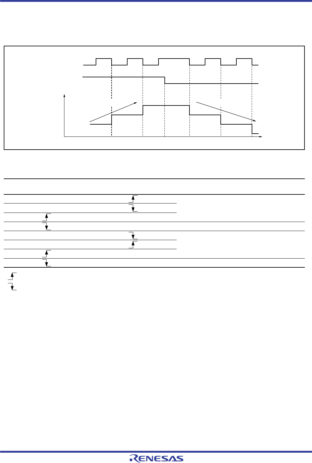
R01UH0034EJ0200 Rev.2.00 Page 578 of 1489
Dec 27, 2013
RX62T Group, RX62G Group 16. Multi-Function Timer Pulse Unit 3 (MTU3)
(b) Phase Counting Mode 2
Figure 16.32 shows an example of operation in phase counting mode 2, and Table 16.64 summarizes the TCNT up-/
down-count conditions.
Figure 16.32 Example of Operation in Phase Counting Mode 2
: Rising edge
: Falling edge
Table 16.64 Up-/Down-Count Conditions in Phase Counting Mode 2
MTCLKA (MTU1)
MTCLKC (MTU2) MTCLKB (MTU1)
MTCLKD (MTU2) Operation
High Not counted (Don't care)
Low
Low
High Up-counting
High Not counted (Don't care)
Low
High
Low Down-counting
Time
TCNT value
MTCLKA (MTU1)
MTCLKC (MTU2)
MTCLKB (MTU1)
MTCLKD (MTU2)
Down-countingUp-counting
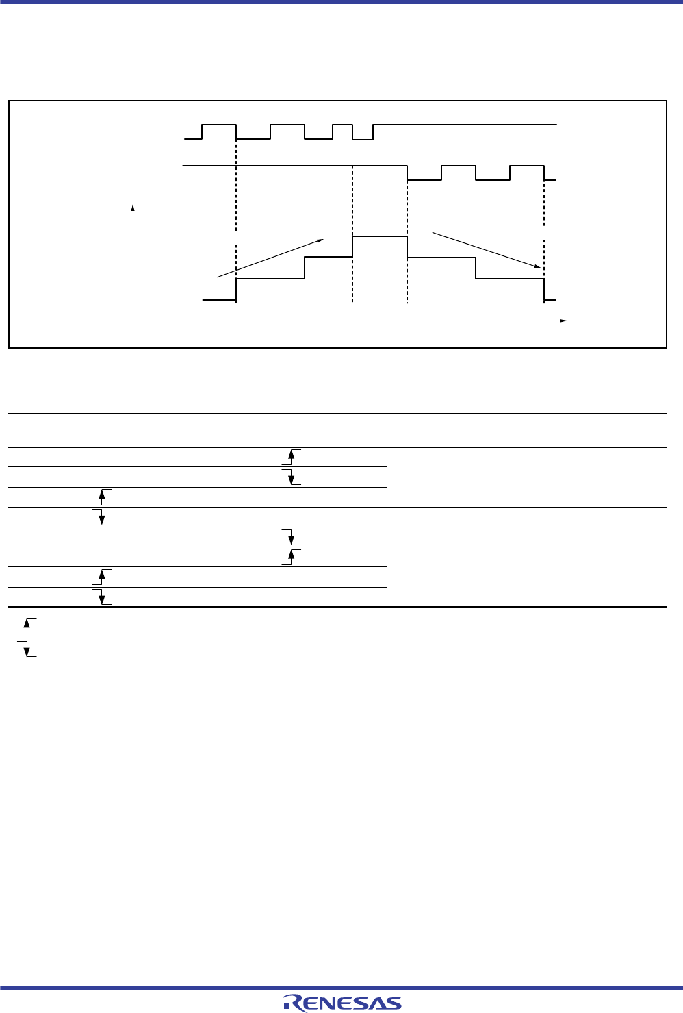
R01UH0034EJ0200 Rev.2.00 Page 579 of 1489
Dec 27, 2013
RX62T Group, RX62G Group 16. Multi-Function Timer Pulse Unit 3 (MTU3)
(c) Phase Counting Mode 3
Table 16.33 shows an example of operation in phase counting mode 3, and Table 16.65 summarizes the TCNT up-/
down-count conditions.
Figure 16.33 Example of Operation in Phase Counting Mode 3
: Rising edge
: Falling edge
Table 16.65 Up-/Down-Count Conditions in Phase Counting Mode 3
MTCLKA (MTU1)
MTCLKC (MTU2) MTCLKB (MTU1)
MTCLKD (MTU2) Operation
High Not counted (Don't care)
Low
Low
High Up-counting
High Down-counting
Low Not counted (Don't care)
High
Low
TCNT value
MTCLKA (MTU1)
MTCLKC (MTU2)
MTCLKB (MTU1)
MTCLKD (MTU2)
Time
Down-counting
Up-counting

R01UH0034EJ0200 Rev.2.00 Page 580 of 1489
Dec 27, 2013
RX62T Group, RX62G Group 16. Multi-Function Timer Pulse Unit 3 (MTU3)
(a) Phase Counting Mode 4
Table 16.34 shows an example of operation in phase counting mode 4, and Table 16.66 summarizes the TCNT up-/
down-count conditions.
Figure 16.34 Example of Operation in Phase Counting Mode 4
: Rising edge
: Falling edge
Table 16.66 Up-/Down-Count Conditions in Phase Counting Mode 4
MTCLKA (MTU1)
MTCLKC (MTU2) MTCLKB (MTU1)
MTCLKD (MTU2) Operation
High Up-counting
Low
Low Not counted (Don't care)
High
High Down-counting
Low
High Not counted (Don't care)
Low
Up-counting Down-counting
TCNT value
MTCLKA (MTU1)
MTCLKC (MTU2)
MTCLKB (MTU1)
MTCLKD (MTU2)
Time
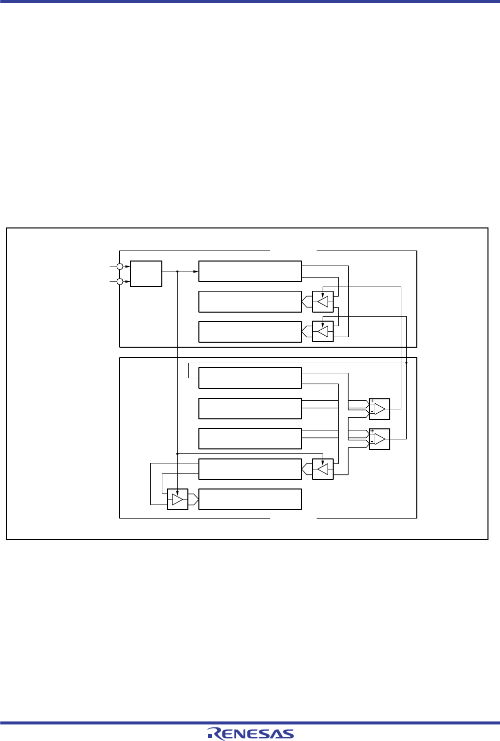
R01UH0034EJ0200 Rev.2.00 Page 581 of 1489
Dec 27, 2013
RX62T Group, RX62G Group 16. Multi-Function Timer Pulse Unit 3 (MTU3)
(3) Phase Counting Mode Application Example
Table 16.35 shows an example in which MTU1 is in phase counting mode, and MTU1 is coupled with MTU0 to input
2-phase encoder pulses of a servo motor in order to detect position or speed.
MTU1 is set to phase counting mode 1, and the encoder pulse A-phase and B-phase are input to MTCLKA and
MTCLKB.
In MTU0, MTU0.TGRC compare match is specified as the TCNT clearing source and MTU0.TGRA and MTU0.TGRC
are used for the compare match function and are set with the speed control cycle and position control cycle.
MTU0.TGRB is used for input capture, with MTU0.TGRB and MTU0.TGRD operating in buffer mode. The MTU1
counter input clock is designated as the MTU0.TGRB input capture source, and the widths of 2-phase encoder 4-
multiplication pulses are detected.
MTU1.TGRA and MTU1.TGRB for MTU1 are designated for the input capture function and MTU0.TGRA and
MTU0.TGRC compare matches in MTU0 are selected as the input capture sources to store the up/down-counter values
for the control cycles.
This procedure enables the accurate detection of position and speed.
Figure 16.35 Phase Counting Mode Application Example
MTCLKA
MTCLKB
MTU1
Edge
detection
circuit MTU1.TCNT
MTU1.TGRA
(Speed cycle capture)
MTU1.TGRB
(Position cycle capture)
MTU0.TCNT
MTU0.A
(Speed control cycle)
MTU3_0.TGRC
(Position control cycle)
MTU0
MTU3_0.TGRB
(Pulse width capture)
MTU3_0.TGRD
(Buffer operation)

R01UH0034EJ0200 Rev.2.00 Page 582 of 1489
Dec 27, 2013
RX62T Group, RX62G Group 16. Multi-Function Timer Pulse Unit 3 (MTU3)
16.3.7 Reset-Synchronized PWM Mode
In the reset-synchronized PWM mode, three phases of positive and negative PWM waveforms (six phases in total) that
share a common wave transition point can be output by combining MTU3 and MTU4, and MTU6 and MTU7.
When set for reset-synchronized PWM mode, the MTIOC3B, MTIOC3D, MTIOC4A, MTIOC4C, MTIOC4B,
MTIOC4D, MTIOC6B, MTIOC6D, MTIOC7A, MTIOC7C, MTIOC7B, and MTIOC7D pins function as PWM output
pins and timer counters 3 and 6 (MTU3.TCNT and MTU6.TCNT) functions as an up-counter.
Table 16.67 shows the PWM output pins used. Table 16.68 shows the settings of the registers.
Table 16.67 Output Pins for Reset-Synchronized PWM Mode
Channel Output Pin Description
MTU3 MTIOC3B PWM output pin 1
MTIOC3D PWM output pin 1' (negative-phase waveform of PWM output 1)
MTU4 MTIOC4A PWM output pin 2
MTIOC4C PWM output pin 2' (negative-phase waveform of PWM output 2)
MTIOC4B PWM output pin 3
MTIOC4D PWM output pin 3' (negative-phase waveform of PWM output 3)
MTU6 MTIOC6B PWM output pin 4
MTIOC6D PWM output pin 4' (negative-phase waveform of PWM output 4)
MTU7 MTIOC7A PWM output pin 5
MTIOC7C PWM output pin 5' (negative-phase waveform of PWM output 5)
MTIOC7B PWM output pin 6
MTIOC7D PWM output pin 6' (negative-phase waveform of PWM output 6)
Table 16.68 Register Settings for Reset-Synchronized PWM Mode
Register Setting
MTU3.TCNT Initial setting (0000h)
MTU4.TCNT Initial setting (0000h)
MTU3.TGRA Set the count cycle for MTU3.TCNT
MTU3.TGRB Set the transition point of the PWM waveform to be output from the MTIOC3B and MTIOC3D pins
MTU4.TGRA Set the transition point of the PWM waveform to be output from the MTIOC4A and MTIOC4C pins
MTU4.TGRB Set the transition point of the PWM waveform to be output from the MTIOC4B and MTIOC4D pins
MTU6.TCNT Initial setting (0000h)
MTU7.TCNT Initial setting (0000h)
MTU6.TGRA Set the count cycle for MTU6.TCNT
MTU6.TGRB Set the transition point of the PWM waveform to be output from the MTIOC6B and MTIOC6D pins
MTU7.TGRA Set the transition point of the PWM waveform to be output from the MTIOC7A and MTIOC7C pins
MTU7.TGRB Set the transition point of the PWM waveform to be output from the MTIOC7B and MTIOC7D pins
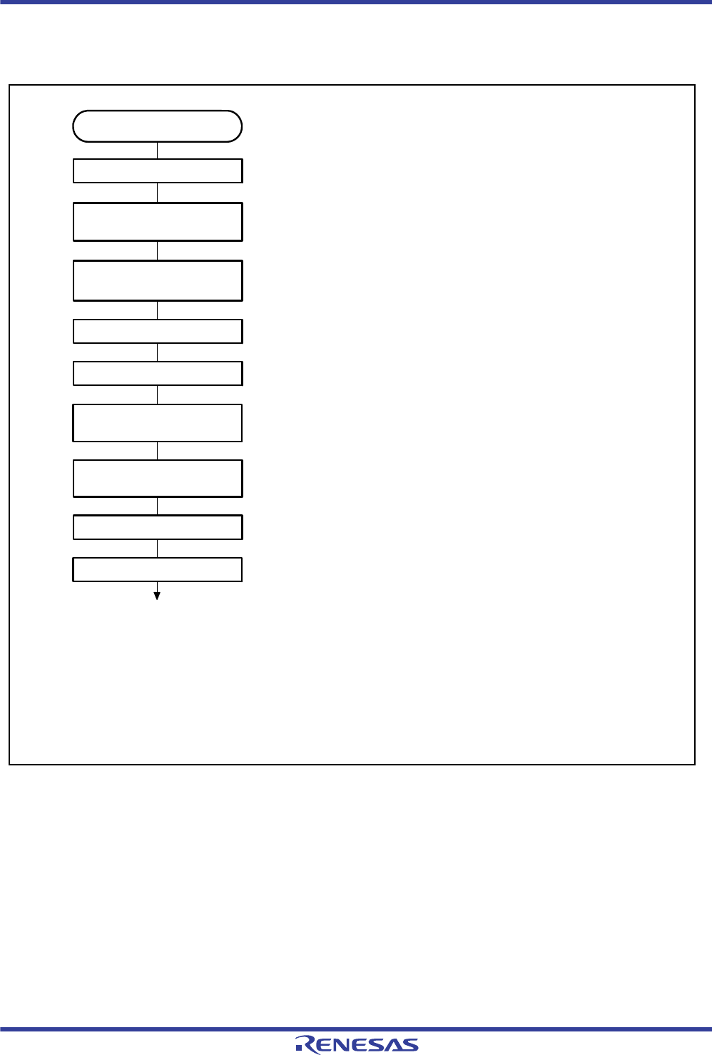
R01UH0034EJ0200 Rev.2.00 Page 583 of 1489
Dec 27, 2013
RX62T Group, RX62G Group 16. Multi-Function Timer Pulse Unit 3 (MTU3)
(1) Example of Procedure for Setting Reset-Synchronized PWM Mode
Figure 16.36 shows an example of procedure for setting the reset-synchronized PWM mode.
Figure 16.36 Procedure for Selecting Reset-Synchronized PWM Mode
[1] Clear the CST3 and CST4 bits in TSTRA to 0 to stop the TCNT
operation. Specify the reset-synchronized PWM mode while
MTU3.TCNT and MTU4.TCNT are stopped.
[2] Set bits TPSC[2:0] and CKEG[1:0] in MTU3.TCR to select
the counter clock and clock edge for MTU3. Set bits
CCLR[2:0] to select TGRA compare match as a counter clear
source.
[3] When performing brushless DC motor control,
set bit BDC in the timer gate control register
(TGCRA) and set the feedback signal input source
and output chopping or gate signal direct output.
[4] Set MTU3.TCNT and MTU4.TCNT to 0000h.
[5] MTU3.TGRA is the cycle register. Set the waveform cycle
value in MTU3.TGRA. Set the transition timing of the PWM
output waveforms in MTU3.TGRB, MTU4.TGRA, and
MTU4.TGRB. Set times within the compare match range of
MTU3.TCNT.
X MTU3.TGRA (X: Set value)
[6] Enable or disable toggle output synchronized with the PMW
cycle using bit PSYE in TOCR1A, and set the PWM output level
with bits OLSP and OLSN. When specifying the PWM output
level by using TOLBRA as a buffer for TOCR2A, see figure 16.3.
[7] Set bits MD[3:0] in MTU3.TMDR1 to 1000b to select the reset-
synchronized PWM mode. In addition, specify the buffer
operation of the MTU3.TGRA (BFA = 1) and MTU3.TGRC
(BFB = 1) when necessary. Set the MTU4.TMDR1 to the initial
value (normal operation; BFA = 0 and BFB = 0).
[8] Set the enabling/disabling of the PWM waveform output
pin in TOERA.
[9] Set the CST3 bit in the TSTRA to 1 to start the count operation.
[1]
[2]
[3]
[4]
[5]
[6]
[7]
[8]
[9]
Note: The output waveform starts to toggle at the point of
MTU3.TCNT = MTU3.TGRA = X by setting
X = MTU3.TGRA, i.e., cycle = duty ratio.
Reset-synchronized
PWM mode
Stop counting
Select counter clock and
counter clear source
Brushless DC motor
control setting
Set TCNT
Set TGR
Enable PWM cyclic output,
set PWM output level
Set reset-synchronized
PWM mode
Enable waveform output
Start count operation
<Reset-synchronized PWM mode>
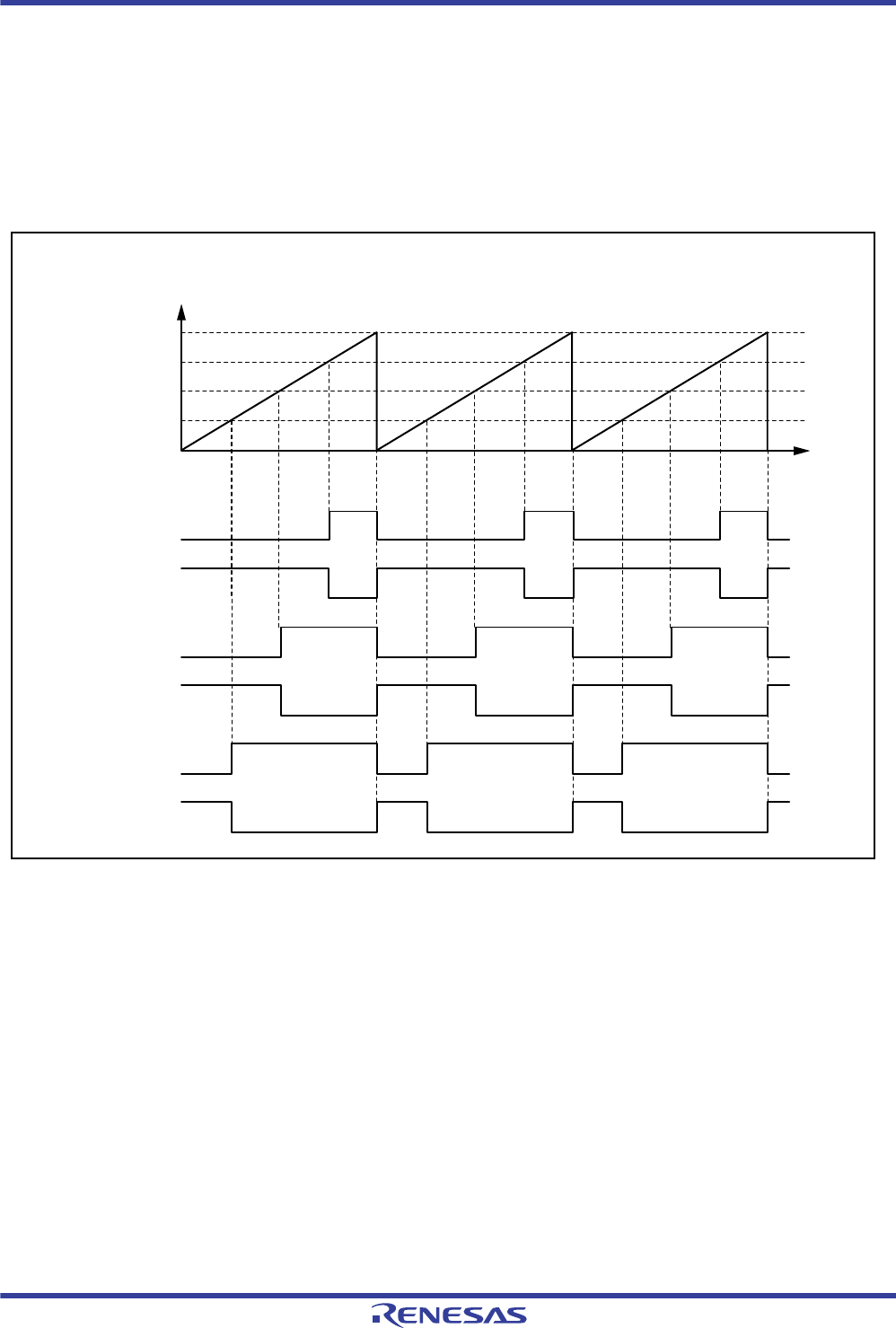
R01UH0034EJ0200 Rev.2.00 Page 584 of 1489
Dec 27, 2013
RX62T Group, RX62G Group 16. Multi-Function Timer Pulse Unit 3 (MTU3)
(2) Example of Reset-Synchronized PWM Mode Operation
Figure 16.37 shows an example of operation in the reset-synchronized PWM mode.
MTU3.TCNT and MTU4.TCNT (MTU6.TCNT and MTU7.TCNT) operate as up-counters. The counters are cleared
when a compare match occurs between MTU3.TCNT (MTU6.TCNT) and MTU3.TGRA (MTU6.TGRA), and then
begin incrementing from 0000h. The output from the PWM pins toggles every time a compare match occurs in
MTU3.TGRB (MTU6.TGRB), MTU4.TGRA (MTU7.TGRA), and MTU4.TGRB (MTU7.TGRB) and the counters are
cleared.
Figure 16.37 Example of Reset-Synchronized PWM Mode Operation
(When TOCR1A's OLSN = 1 and OLSP = 1 in MTU3 and MTU4)
MTU3_3.TCNT and
MTU3_4.TCNT values
Time
MTU3.TGRA
MTU3.TGRB
MTU4.TGRA
MTU4.TGRB
0000h
MTIOC3B
MTIOC4A
MTIOC4B
MTIOC4C
MTIOC4D
MTIOC3D

R01UH0034EJ0200 Rev.2.00 Page 585 of 1489
Dec 27, 2013
RX62T Group, RX62G Group 16. Multi-Function Timer Pulse Unit 3 (MTU3)
16.3.8 Complementary PWM Mode
In complementary PWM mode, three phases of non-overlapping positive and negative PWM waveforms (six phases in
total) can be output by combining MTU3 and MTU4, and MTU6 and MTU7. PWM waveforms without non-overlapping
interval are also available.
In complementary PWM mode, MTIOC3B, MTIOC3D, MTIOC4A, MTIOC4B, MTIOC4C, MTIOC4D, MTIOC6B,
MTIOC6D, MTIOC7A, MTIOC7B, MTIOC7C, and MTIOC7D pins function as PWM output pins, and the MTIOC3A
and MTIOC6A pins can be set for toggle output synchronized with the PWM cycle.
MTU3.TCNT, MTU4.TCNT, MTU6.TCNT, and MTU7.TCNT function as up/down-counters.
Table 16.68 shows the PWM output pins used. Table 16.70 shows the settings of the registers used.
A function to directly cut off the PWM output by using an external signal is supported as a port function.
Note 1. Avoid setting the MTIOC3C and MTIOC6C pins as timer I/O pins in complementary PWM mode.
Table 16.69 Output Pins for Complementary PWM Mode
Channel Output Pin Description
MTU3 MTIOC3A Toggle output synchronized with PWM cycle (or I/O port)
MTIOC3B PWM output pin 1
MTIOC3C I/O port*1
MTIOC3D PWM output pin 1'
(non-overlapping negative-phase waveform of PWM output 1; PWM output without non-overlapping
interval is also available)
MTU4 MTIOC4A PWM output pin 2
MTIOC4C PWM output pin 2'
(non-overlapping negative-phase waveform of PWM output 2; PWM output without non-overlapping
interval is also available)
MTIOC4B PWM output pin 3
MTIOC4D PWM output pin 3'
(non-overlapping negative-phase waveform of PWM output 3; PWM output without non-overlapping
interval is also available)
MTU6 MTIOC6A Toggle output synchronized with PWM cycle (or I/O port)
MTIOC6B PWM output pin 4
MTIOC6C I/O port*1
MTIOC6D PWM output pin 4'
(non-overlapping negative-phase waveform of PWM output 4; PWM output without non-overlapping
interval is also available)
MTU7 MTIOC7A PWM output pin 5
MTIOC7C PWM output pin 5'
(non-overlapping negative-phase waveform of PWM output 5; PWM output without non-overlapping
interval is also available)
MTIOC7B PWM output pin 6
MTIOC7D PWM output pin 6'
(non-overlapping negative-phase waveform of PWM output 6; PWM output without non-overlapping
interval is also available)

R01UH0034EJ0200 Rev.2.00 Page 586 of 1489
Dec 27, 2013
RX62T Group, RX62G Group 16. Multi-Function Timer Pulse Unit 3 (MTU3)
Note 1. Access can be enabled or disabled according to the setting in TRWERA (timer read/write enable register A).
Note 2. Access can be enabled or disabled according to the setting in TRWERB (timer read/write enable register B).
Table 16.70 Register Settings for Complementary PWM Mode
Channel Counter/ Register Description Read/Write from CPU
MTU3 TCNT Starts up-counting from the value set in the dead time
register
Maskable by TRWERA setting *1
TGRA Set MTU3.TCNT upper limit value (1/2 carrier cycle + dead
time)
Maskable by TRWERA setting *1
TGRB PWM output 1 compare register Maskable by TRWERA setting*1
TGRC MTU3.TGRA buffer register Always readable/writable
TGRD PWM output 1/MTU3.TGRB buffer register Always readable/writable
TGRE MTU3.TGRB buffer register B (when double buffer function
is used)
Always readable/writable
MTU4 TCNT Starts up-counting after being initialized to 0000h Maskable by TRWERA setting*1
TGRA PWM output 2 compare register Maskable by TRWERA setting*1
TGRB PWM output 3 compare register Maskable by TRWERA setting*1
TGRC PWM output 2/MTU4.TGRA buffer register Always readable/writable
TGRD PWM output 3/MTU4.TGRB buffer register Always readable/writable
TGRE MTU4.TGRA buffer register B (when double buffer function
is used)
Always readable/writable
TGRF MTU4.TGRB buffer register B (when double buffer function
is used)
Always readable/writable
MTU6 TCNT Starts up-counting from the value set in the dead time
register
Maskable by TRWERB setting*2
TGRA Set MTU6.TCNT upper limit value (1/2 carrier cycle + dead
time)
Maskable by TRWERB setting *2
TGRB PWM output 4 compare register Maskable by TRWERB setting*2
TGRC MTU6.TGRA buffer register Always readable/writable
TGRD PWM output 4/MTU6.TGRB buffer register Always readable/writable
TGRE MTU6.TGRB buffer register B (when double buffer function
is used)
Always readable/writable
MTU7 TCNT Starts up-counting after being initialized to 0000h Maskable by TRWERB setting*2
TGRA PWM output 5 compare register Maskable by TRWERB setting*2
TGRB PWM output 6 compare register Maskable by TRWERB setting*2
TGRC PWM output 5/MTU7.TGRA buffer register Always readable/writable
TGRD PWM output 6/MTU7.TGRB buffer register Always readable/writable
TGRE MTU7.TGRA buffer register B (when double buffer function
is used)
Always readable/writable
TGRF MTU7.TGRB buffer register B (when double buffer function
is used)
Always readable/writable

R01UH0034EJ0200 Rev.2.00 Page 587 of 1489
Dec 27, 2013
RX62T Group, RX62G Group 16. Multi-Function Timer Pulse Unit 3 (MTU3)
Note 1. Access can be enabled or disabled according to the setting in TRWERA (timer read/write enable register A).
Note 2. Access can be enabled or disabled according to the setting in TRWERB (timer read/write enable register B).
Table 16.71 Register Settings for Complementary PWM Mode
Channel Counter/ Register Description Read/Write from CPU
Timer dead time data register A
(TDDRA)
Set MTU4.TCNT and MTU3.TCNT offset value (dead
time value)
Maskable by TRWERA setting *1
Timer dead time data register B
(TDDRB)
Set MTU7.TCNT and MTU6.TCNT offset value (dead
time value)
Maskable by TRWERB setting *2
Timer cycle data register A (TCDRA) Set MTU4.TCNT upper limit value (1/2 carrier cycle) Maskable by TRWERA setting *1
Timer cycle data register B (TCDRB) Set MTU7.TCNT upper limit value (1/2 carrier cycle) Maskable by TRWERB setting *2
Timer cycle buffer register A
(TCBRA)
TCDRA buffer register Always readable/writable
Timer cycle buffer register B
(TCBRB)
TCDRB buffer register Always readable/writable
Subcounter A (TCNTSA) Subcounter A for dead time generation Read-only
Subcounter B (TCNTSB) Subcounter B for dead time generation Read-only
Temporary register 1A (TEMP1A) PWM output 1/MTU3.TGRB temporary register A Not readable/writable
Temporary register 1B (TEMP1B) PWM output 1/MTU3.TGRB temporary register B (when
double buffer function is used)
Not readable/writable
Temporary register 2A (TEMP2A) PWM output 2/MTU4.TGRA temporary register A Not readable/writable
Temporary register 2B (TEMP2B) PWM output 2/MTU4.TGRA temporary register B (when
double buffer function is used)
Not readable/writable
Temporary register 3A (TEMP3A) PWM output 3/MTU4.TGRB temporary register A Not readable/writable
Temporary register 3B (TEMP3B) PWM output 3/MTU4.TGRB temporary register B (when
double buffer function is used)
Not readable/writable
Temporary register 4A (TEMP4A) PWM output 4/MTU6.TGRB temporary register A Not readable/writable
Temporary register 4B (TEMP4B) PWM output 4/MTU6.TGRB temporary register B (when
double buffer function is used)
Not readable/writable
Temporary register 5A (TEMP5A) PWM output 5/MTU7.TGRA temporary register A Not readable/writable
Temporary register 5B (TEMP5B) PWM output 5/MTU7.TGRA temporary register B (when
double buffer function is used)
Not readable/writable
Temporary register 6A (TEMP6A) PWM output 6/MTU7.TGRB temporary register A Not readable/writable
Temporary register 6B (TEMP6B) PWM output 6/MTU7.TGRB temporary register B (when
double buffer function is used)
Not readable/writable
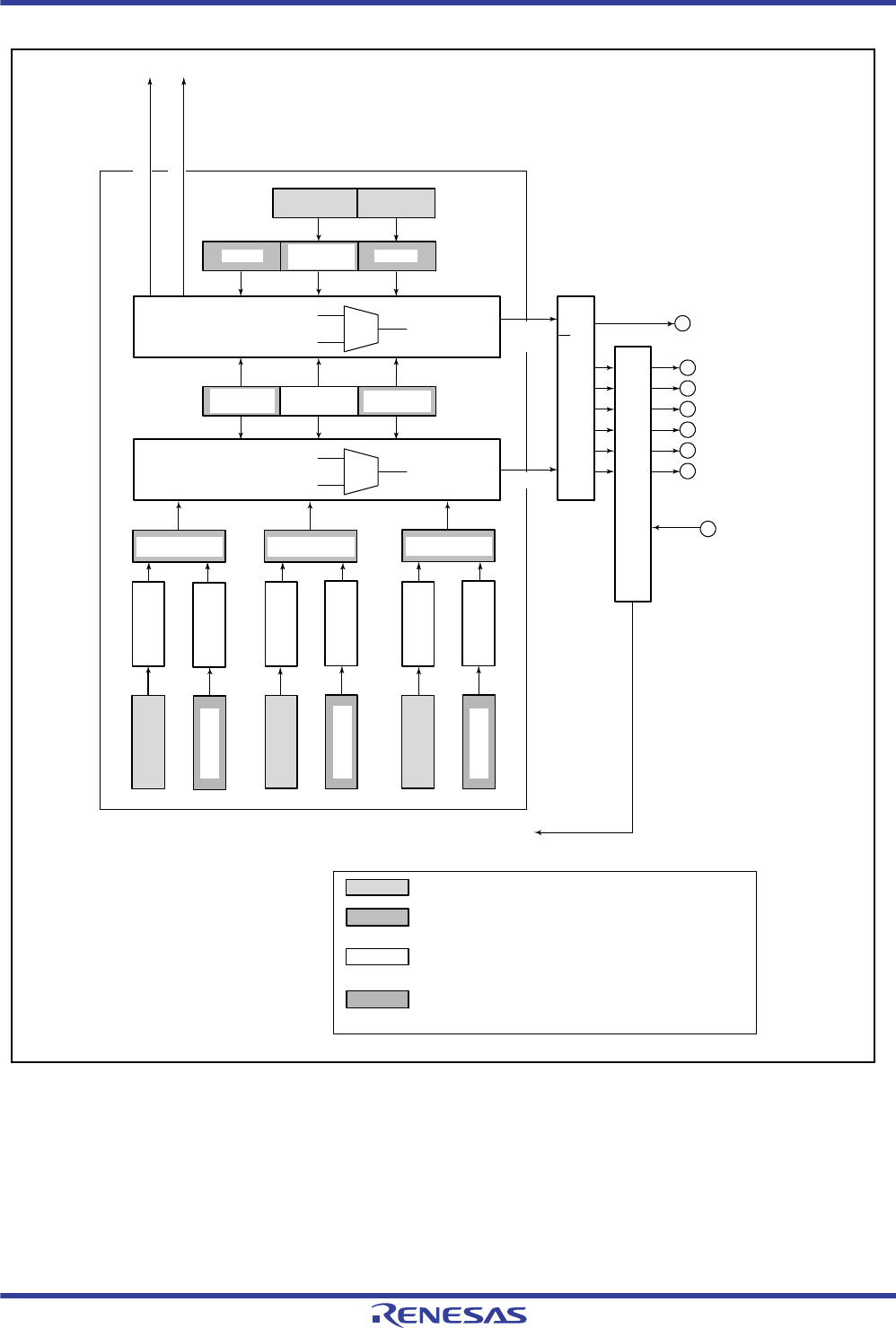
R01UH0034EJ0200 Rev.2.00 Page 588 of 1489
Dec 27, 2013
RX62T Group, RX62G Group 16. Multi-Function Timer Pulse Unit 3 (MTU3)
Figure 16.38 Block Diagram of MTU3 and MTU4 in Complementary PWM Mode
MTU3.
TGRC TCBRA
MTU4.
TGRC
MTU4.
TGRD
MTU3.
TGRD
Comparator
Comparator
Match
signal
Match
signal
Output controller
Output protection
circuit
PWM cycle output
External cutoff interrupt
Temp1A
Temp2A
Temp3A
POE0#
PWM output 1
External cutoff
input
PWM output 2
PWM output 3
PWM output 4
PWM output 5
PWM output 6
: Registers that can always be read or written from the CPU
: Registers that can be read or written from the CPU
(but for which access disabling can be set by TRWER)
: Registers that cannot be read or written from the CPU
(except for TCNTS, which can only be read)
MTU3.TGRA compare-match interrupt
MTU4.TCNT underflow interrupt
MTU3.
TCNT MTU4.
TCNT
MTU3.
TGRA
: Registers that can always be read or written from the CPU
(only when the double buffer function is used)
MTU3.
TGRB MTU4.
TGRA
MTU4.
TGRB
Temp1B
Temp3B
Temp2B
MTU3.
TGRE
MTU4.
TGRE
MTU4.
TGRF
TCNTSA
TDDRA TCDRA
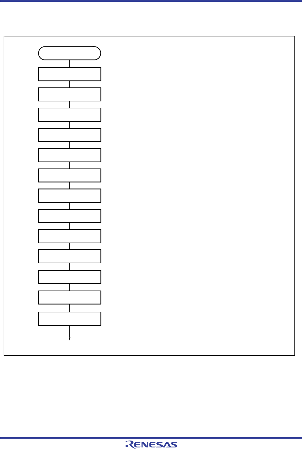
R01UH0034EJ0200 Rev.2.00 Page 589 of 1489
Dec 27, 2013
RX62T Group, RX62G Group 16. Multi-Function Timer Pulse Unit 3 (MTU3)
(1) Example of Complementary PWM Mode Setting Procedure
Figure 16.39 shows an example of the complementary PWM mode setting procedure.
Figure 16.39 Example of Complementary PWM Mode Setting Procedure
[1] Clear bits CST3 and CST4 in the timer start register (TSTRA) to 0 to
stop timer counter (TCNT) operation. Specify complementary PWM
mode while MTU3.TCNT and MTU4.TCNT are stopped.
[2] Set the same counter clock and clock edge for MTU3 and MTU4 with bits
TPSC[2:0] and bits CKEG[1:0] in the timer control register (TCR). Use bits
CCLR[2:0] to set synchronous clearing only when restarting by synchronous
clearing with another channel during complementary PWM mode operation.
[3] When performing brushless DC motor control, set bit BDC
in the timer gate control register (TGCRA) and set the feedback signal
input source and output chopping or gate signal direct output.
[4] Set the dead time in MTU3.TCNT. Set MTU4.TCNT to 0000h.
[5] Set only when restarting by synchronous clearing with another channel
during complementary PWM mode operation. In this case, synchronize
the channel generating the synchronous clear with MTU3 and MTU4 using
the timer synchronous register (TSYRA).
[6] Set the output PWM duty cycles in the duty registers (MTU3.TGRB,
MTU4.TGRA, and MTU4.TGRB) and buffer registers (MTU3.
TGRD, MTU4.TGRC, and MTU4.TGRD). Be sure to set the same
value in each pair of duty register and buffer register.
Only when using the double buffer function, set the output PWM
duty value - 1 in the buffer registers (MTU3.TGRDE, MTU4.TGRCE,
MTU4.TGRDF).
[7] This setting is necessary only when no dead time should be generated.
Make appropriate settings in the timer dead time enable register
(TDERA) so that no dead time is generated.
[8] Set the dead time in the dead time register (TDDRA), 1/2 the carrier
cycle in the Timer cycle data register (TCDRA) and Timer cycle buffer
register (TCBRA), and 1/2 the carrier cycle plus the dead time in MTU3.
TGRA and MTU3.TGRC. When no dead time generation is
selected, set 1 in TDDRA and 1/2 the carrier cycle + 1 in MTU3.TGRA
and MTU3.TGRC.
[9] Enable or disable toggle output synchronized with the PWM cycle using bit
PSYE in the timer output control register 1 (TOCR1A), and set the PWM
output level with bits OLSP and OLSN. When specifying the PWM output
level by using TOLBRA as a buffer for TOCR2A, see figure 16.3.
[10] Select complementary PWM mode in the timer mode register (MTU3.
TMDR1). In addition, specify the buffer operation of the MTU3.TGRA
(BFA = 1) and MTU3.TGRC (BFB = 1) when necessary.
Set the MTU4.TMDR1 to the initial value (normal operation; BFA = 0
and BFB = 0).
[11] Only when using the double buffer function, enable the double buffer
function in the timer mode register 2 (TMDR2A).
[12] Set enabling/disabling of PWM waveform output pin output in
the timer output master enable register (TOERA).
[13] Set bits CST3 and CST4 in TSTRA to 1 simultaneously to start
the count operation.
[1]
[2]
[3]
[4]
[5]
[6]
[7]
[8]
[9]
[11]
[10]
[12]
[13]
<Complementary PWM mode>
Start count operation
Enable waveform output
Double buffer function setting
Complementary PWM mode
setting
Enable PWM cyclic output,
set PWM output level
Dead time, carrier cycle
setting
Enable/disable dead time
generation
TGR setting
Inter-channel synchronization
setting
TCNT setting
Brushless DC motor control
setting
Counter clock, counter clear
source selection
Stop count operation
Complementary PWM mode
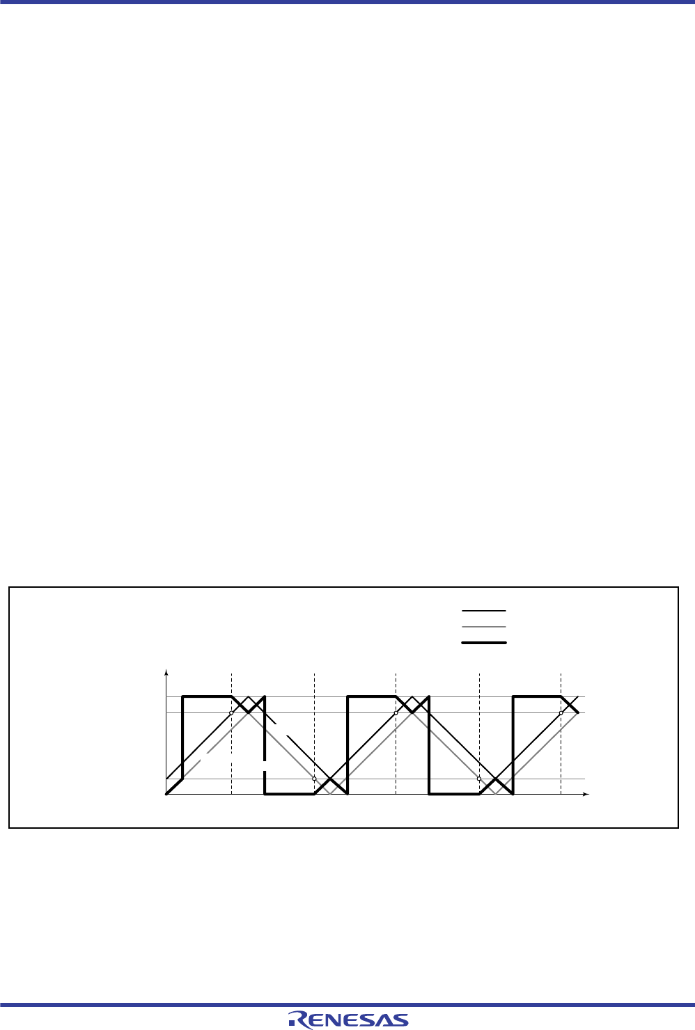
R01UH0034EJ0200 Rev.2.00 Page 590 of 1489
Dec 27, 2013
RX62T Group, RX62G Group 16. Multi-Function Timer Pulse Unit 3 (MTU3)
(2) Outline of Complementary PWM Mode Operation
In complementary PWM mode, six phases of PWM waveforms can be output. Figure 16.40 illustrates counter operation
in complementary PWM mode (MTU3 and MTU4), and Figure 16.41 shows an example of operation in
complementary PWM mode.
(a) Counter Operation
In complementary PWM mode, three counters—MTU3.TCNT, MTU4.TCNT, and TCNTSA (MTU6.TCNT,
MTU7.TCNT, and TCNTSB)—in each unit perform up-/down-count operations.
MTU3.TCNT (MTU6.TCNT) is automatically initialized to the value set in TDDRA (TDDRB) when complementary
PWM mode is selected and the CST bit in TSTRA (TSTRB) is 0. When the CST bit is set to 1, MTU3.TCNT
(MTU6.TCNT) counts up to the value set in MTU3.TGRA (MTU6.TGRA), then switches to down-counting when it
matches MTU3.TGRA (MTU6.TGRA). When the MTU4.TCNT (MTU7.TCNT) value matches 0000h, MTU3.TCNT
(MTU6.TCNT) switches to up-counting, and the operation is repeated in this way.
MTU4.TCNT (MTU7.TCNT) should be initialized to 0000h after a reset. When the CST bit is set to 1, MTU4.TCNT
(MTU7.TCNT) counts up in synchronization with MTU3.TCNT (MTU6.TCNT), and switches to down-counting when
MTU3.TCNT (MTU6.TCNT) matches MTU3.TGRA (MTU6.TGRA). On reaching 0000h, MTU4.TCNT
(MTU7.TCNT) switches to up-counting, and the operation is repeated in this way. TCNTSA (TCNTSB) is a read-only
counter. It does not need to be initialized after a reset.
In counting up by MTU3.TCNT and MTU4.TCNT (or MTU6.TCNT and MTU7.TCNT), MTU3.TCNT (or
MTU6.TCNT) starts counting up when it matches TCDRA (or TCDRB) and switches to counting down when it matches
MTU3.TGRA (or MTU6.TGRA). Furthermore, when MTU4.TCNT (or MTU7.TCNT) matches TDDRA (or TDDRB),
TCNTSA (or TCNTSB) is set to the value in MTU3.TGRA (or MTU6.TGRA) and counting is stopped.
When MTU4.TCNT (MTU7.TCNT) matches TDDRA (TDDRB) during down-counting of MTU3.TCNT and
MTU4.TCNT (MTU6.TCNT and MTU7.TCNT), TCNTSA (TCNTSB) starts up-counting, and when MTU4.TCNT
(MTU7.TCNT) matches 0000h, the operation switches to down-counting. When MTU3.TCNT (MTU6.TCNT) matches
TCDRA (TCDRB), TCNTSA (TCNTSB) is cleared to 0000h and stops counting.
TCNTSA (TCNTSB) is compared with the compare register and temporary register, in which the PWM duty is specified,
only during the count operation.
Figure 16.40 Counter Operation in Complementary PWM Mode
MTU4.TCNT TCNTSA
MTU3.TCNT
Time
Counter value
MTU3.TGRA
TCDRA
TDDRA
0000h
MTU3.TCNT
MTU4.TCNT
TCNTSA

R01UH0034EJ0200 Rev.2.00 Page 591 of 1489
Dec 27, 2013
RX62T Group, RX62G Group 16. Multi-Function Timer Pulse Unit 3 (MTU3)
(b) Register Operation
In complementary PWM mode, nine registers (compare registers, buffer registers, and temporary registers) are used for
each unit. Figure 16.41 shows an example of operation in complementary PWM mode (MTU3 and MTU4).
MTU3.TGRB, MTU4.TGRA, and MTU4.TGRB (MTU6.TGRB, MTU7.TGRA, and MTU7.TGRB) are constantly
compared with the counters to generate PWM waveforms. When these registers match the counter, the value set in bits
OLSN and OLSP in the timer output control register (TOCR1) is output.
MTU3.TGRD, MTU4.TGRC, and MTU4.TGRD (MTU6.TGRD, MTU7.TGRC, and MTU7.TGRD) are buffer registers
for these compare registers.
When the double buffer function is used, MTU3.TGRE, MTU4.TGRE, and MTU4.TGRF (MTU6.TGRE, MTU7.TGRE,
and MTU7.TGRF) are also used as buffer registers B. For details of double buffer operation, refer to section 16.3.8 (2)
(s)Double Buffer Function in Complementary PWM Mode.
Data in a compare register can be changed by writing new data to the corresponding buffer register. The buffer registers
can be read or written at any time.
The data written to a buffer register is constantly transferred to the temporary register in the Ta interval. Data is not
transferred to the temporary register in the Tb interval. Data written to a buffer register in this interval is transferred to
the temporary register at the end of the Tb interval.
The value transferred to a temporary register is transferred to the compare register when TCNTSA (TCNTSB) for
which the Tb interval ends matches MTU3.TGRA (MTU6.TGRA) while TCNTSA (TCNTSB) is counting up, or
0000h while counting down. The timing for transfer from the temporary register to the compare register can be
selected with bits MD[3:0] in the timer mode register 1 (TMDR1). Figure 16.41 shows an example in which the
trough is selected for the transfer timing.
In the Tb interval in which data is not transferred to the temporary register (Tb1 in Figure 16.41), the temporary
register has the same function as the compare register and is compared with the counter. In this interval, therefore, there
are two compare match registers for one output phase; the compare register contains the pre-change data and the
temporary register contains new data. In this interval, three counters MTU3.TCNT, MTU4.TCNT, and TCNTSA
(MTU6.TCNT, MTU7.TCNT, and TCNTSB) and two registers (compare register and temporary register) are compared,
and PWM output is controlled accordingly.
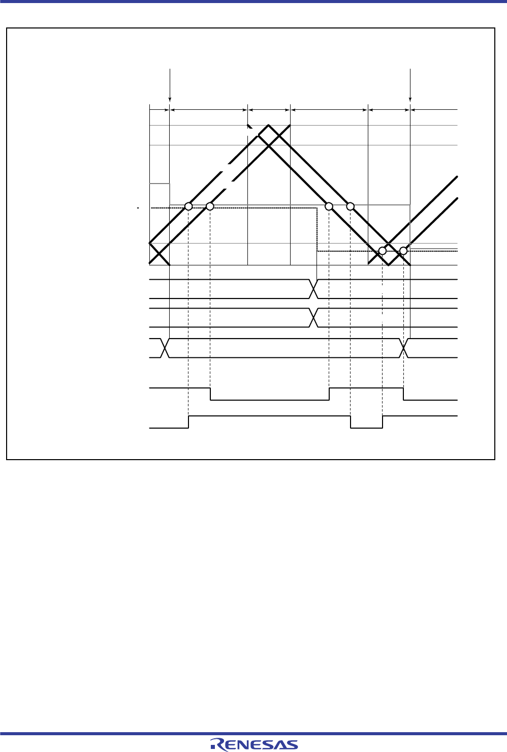
R01UH0034EJ0200 Rev.2.00 Page 592 of 1489
Dec 27, 2013
RX62T Group, RX62G Group 16. Multi-Function Timer Pulse Unit 3 (MTU3)
Figure 16.41 Example of Operation in Complementary PWM Mode (MTU3 and MTU4)
0000h
Tb2
MTU3.TCNT
MTU4.TCNT
TCNTSA
(Output waveform is active-low)
6400h 0080h
6400h
6400h 0080h
0080h
Transfer from temporary register
to compare register
Transfer from temporary register
to compare register
TaTb1 TaTa
Tb2
MTU3.TGRA
TCDRA
MTU4.TGRA
MTU4.TGRC
TDDRA
Buffer register
MTU4.TGRC
Temporary register TEMP2
Compare register
MTU4.TGRA
Output waveform
Output waveform #

R01UH0034EJ0200 Rev.2.00 Page 593 of 1489
Dec 27, 2013
RX62T Group, RX62G Group 16. Multi-Function Timer Pulse Unit 3 (MTU3)
(c) Initial Setting
In complementary PWM mode, there are six registers that require initial setting. In addition, there is a register that
specifies whether to generate dead time (it should be used only when dead time generation should be disabled).
Before setting complementary PWM mode with bits MD[3:0] in the timer mode register 1 (TMDR1), initial values
should be set in the following registers.
MTU3.TGRC (MTU6.TGRC) operates as the buffer register for MTU3.TGRA (MTU6.TGRA), and should be set with
1/2 the PWM carrier cycle + dead time Td. The timer cycle buffer register (TCBRA or TCBRB) operates as the buffer
register for the timer cycle data register (TCDRA or TCDRB), and should be set with 1/2 the PWM carrier cycle. Set
dead time Td in the timer dead time data register (TDDRA or TDDRB).
When dead time is not needed, the TDER bit in the timer dead time enable register (TDERA or TDERB) should be
cleared to 0, MTU3.TGRC and MTU3.TGRA (MTU6.TGRC and MTU6.TGRA) should be set to 1/2 the PWM carrier
cycle + 1, and TDDRA (TDDRB) should be set to 1.
Set the respective initial PWM duty values in three buffer registers A (MTU3.TGRD, MTU4.TGRC, and MTU4.TGRD
(MTU6.TGRD, MTU7.TGRC, and MTU7.TGRD)).
Set the respective (initial PWM duty – 1) values in three buffer registers B (MTU3.TGRE, MTU4.TGRE, and
MTU4.TGRF (MTU6.TGRE, MTU7.TGRE, and MTU7.TGRF)) only when the double buffer function is used.
The values set in the five buffer registers excluding TDDRA (TDDRB) are transferred to the corresponding compare
registers as soon as complementary PWM mode is set.
Set MTU4.TCNT (MTU7.TCNT) to 0000h before setting complementary PWM mode.
Note 1. The value set in MTU3.TGRC (MTU6.TGRC) should be the sum of 1/2 the PWM carrier cycle set in TCBRA (TCBRB) and dead
time Td set in TDDRA (TDDRB). When dead time generation is disabled by TDERA (TDERB), TGRC should be set to 1/2 the
PWM carrier cycle + 1.
Table 16.72 Registers and Counters Requiring Initial Setting
Register and Counter Setting
MTU3.TGRC
MTU6.TGRC
1/2 PWM carrier cycle + dead time Td
(1/2 PWM carrier cycle + 1 when dead time generation is disabled by TDERA or TDERB)
TDDRA, TDDRB Dead time Td (1 when dead time generation is disabled by TDERA or TDERB)
TCBRA, TCBRB 1/2 PWM carrier cycle
MTU3.TGRD, MTU4.TGRC,
MTU4.TGRD
MTU6.TGRD, MTU7.TGRC,
MTU7.TGRD
Initial PWM duty ratio value for each phase
MTU3.TGRE, MTU4.TGRE,
MTU4.TGRF
MTU6.TGRE, MTU7.TGRE,
MTU7.TGRF
Initial PWM duty ratio – 1 value for each phase (only when double buffer function is used)
MTU4.TCNT
MTU7.TCNT
0000h

R01UH0034EJ0200 Rev.2.00 Page 594 of 1489
Dec 27, 2013
RX62T Group, RX62G Group 16. Multi-Function Timer Pulse Unit 3 (MTU3)
(d) PWM Output Level Setting
In complementary PWM mode, the PWM pulse output level is set with bits OLSN and OLSP in timer output control
register 1 (TOCR1A or TOCR1B) or bits OLS1P to OLS3P and OLS1N to OLS3N in timer output control register 2
(TOCR2A or TOCR2B).
The output level can be set for each of the three positive phases and three negative phases of 6-phase output.
Complementary PWM mode should be cleared before setting or changing output levels.
(e) Dead Time Setting
In complementary PWM mode, PWM pulses are output with a non-overlapping relationship between the positive and
negative phases. This non-overlap time is called the dead time.
The non-overlap time is set in the timer dead time data register (TDDRA or TDDRB). The value set in TDDRA
(TDDRB) is used as the MTU3.TCNT (MTU6.TCNT) counter start value and creates a non-overlapping interval
between MTU3.TCNT (MTU6.TCNT) and MTU4.TCNT (MTU7.TCNT). Complementary PWM mode should be
cleared before changing the contents of TDDRA (TDDRB).
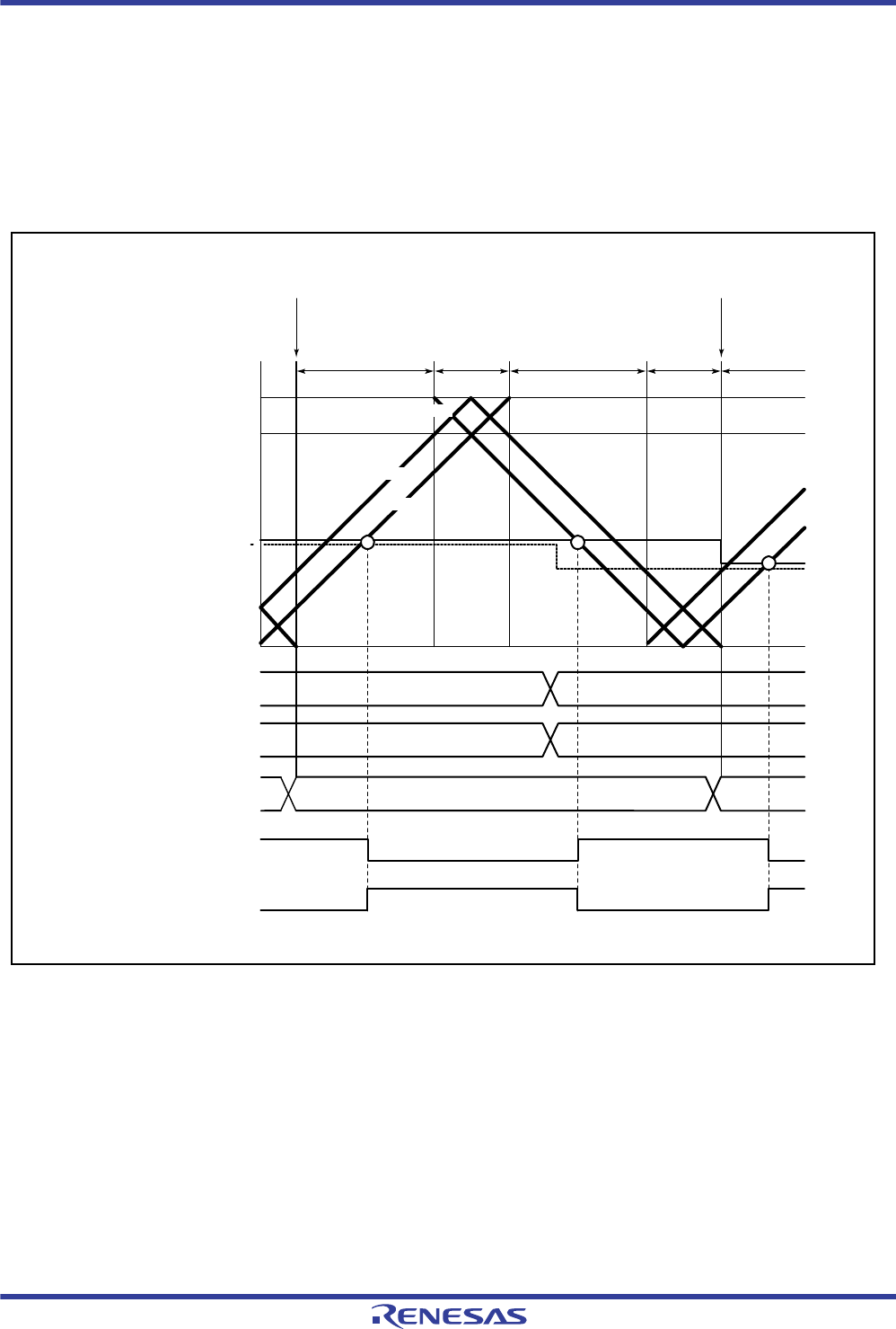
R01UH0034EJ0200 Rev.2.00 Page 595 of 1489
Dec 27, 2013
RX62T Group, RX62G Group 16. Multi-Function Timer Pulse Unit 3 (MTU3)
(f) Dead Time Suppressing
Dead time generation is suppressed by clearing the TDER bit in the timer dead time enable register (TDERA or TDERB)
to 0. TDERA (TDERB) can be cleared to 0 only when 0 is written to it after reading TDER = 1.
MTU3.TGRA and MTU4.TGRC (MTU6.TGRA and MTU7.TGRC) should be set to 1/2 PWM carrier cycle + 1 and the
timer dead time data register (TDDRA or TDDRB) should be set to 1.
By the above settings, PWM waveforms without dead time can be obtained. Figure 16.42 shows an example of
operation without dead time (MTU3 and MTU4).
Figure 16.42 Example of Operation without Dead Time (MTU3 and MTU4)
MTU3.TGRA
= TCDRA + 1
TCDRA
0000h
Buffer register
MTU4.TGRC
Temporary register TEMP2
Compare register
MTU4.TGRA
Output waveform Initial
output
Initial
output
Output waveform #
Ta
MTU3.TCNT
MTU4.TCNT
TCNTSA
(Output waveform is active-low)
Data1 Data2
Data1 Data2
Data1 Data2
Transfer from temporary register
to compare register
Ta
Tb1 Tb2 Ta
MTU4.TGRA
MTU4.TGRC
TDDRA
Transfer from temporary register
to compare register
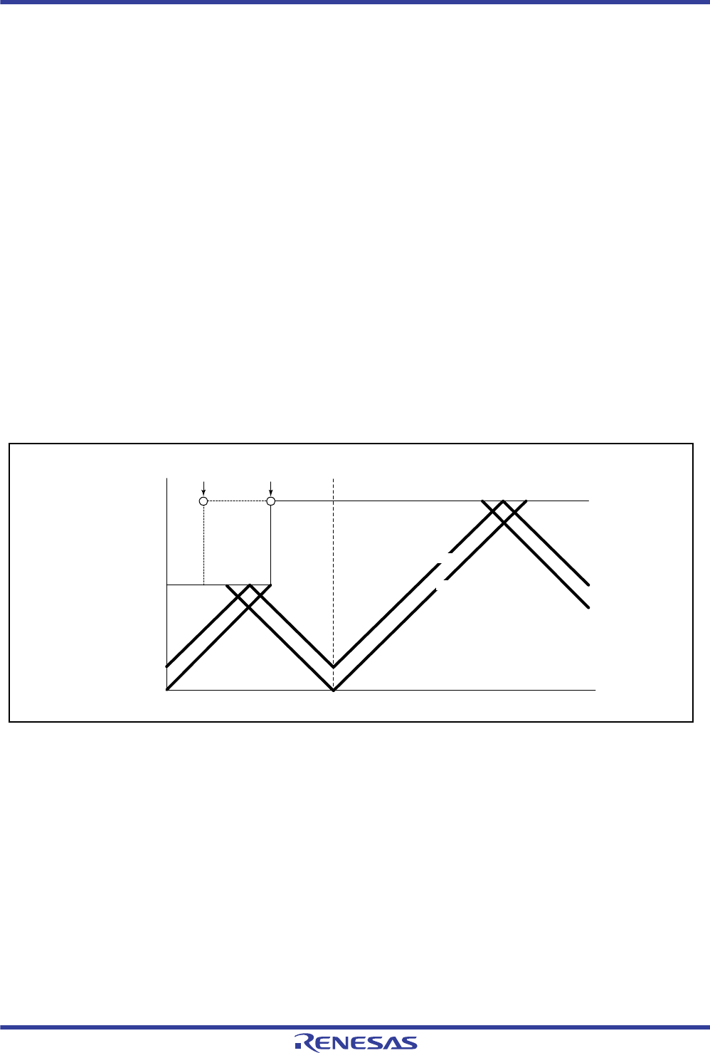
R01UH0034EJ0200 Rev.2.00 Page 596 of 1489
Dec 27, 2013
RX62T Group, RX62G Group 16. Multi-Function Timer Pulse Unit 3 (MTU3)
(g) PWM Cycle Setting
In complementary PWM mode, the PWM pulse cycle is set in two registers—MTU3.TGRA (MTU6.TGRA), in which
the MTU3.TCNT (MTU6.TCNT) upper limit value is set, and TCDRA (TCDRB), in which the MTU4.TCNT
(MTU7.TCNT) upper limit value is set. The settings should be made so as to achieve the following relationship between
these two registers:
With dead time: MTU3.TGRA (MTU6.TGRA) setting = TCDRA (TCDRB) setting + TDDRA (TDDRB) setting
Without dead time: MTU3.TGRA (MTU6.TGRA) setting = TCDRA (TCDRB) setting + 1
For the PWM output with dead time, the setting should be made so as to achieve the following relationship between these
two registers:
TCDR setting > TDDR setting × 2 + 2
The MTU3.TGRA and TCDRA (MTU6.TGRA and TCDRB) settings are made by setting values in buffer registers
MTU3.TGRC and TCBRA (MTU6.TGRC and TCBRB). The values set in MTU3.TGRC and TCBRA (MTU6.TGRC
and TCBRB) are transferred simultaneously to MTU3.TGRA and TCDRA (MTU6.TGRA and TCDRB) with the
transfer timing selected with bits MD[3:0] in the timer mode register 1 (TMDR1).
The new PWM cycle is reflected from the next cycle when data is updated at the crest, or from the current cycle when
updated in the trough. Figure 16.43 illustrates the operation when the PWM cycle is updated at the crest.
See the following section, (h)Register Data Updating, for the method of updating the data in each buffer register.
Figure 16.43 Example of PWM Cycle Updating (MTU3 and MTU4)
Counter value MTU3.TGRC
update MTU3.TGRA
update
MTU3.TGRA
MTU3.TCNT
MTU4.TCNT
Time

R01UH0034EJ0200 Rev.2.00 Page 597 of 1489
Dec 27, 2013
RX62T Group, RX62G Group 16. Multi-Function Timer Pulse Unit 3 (MTU3)
(h) Register Data Updating
In complementary PWM mode, the buffer register is used to update the data in a compare register. The update data can be
written to the buffer register at any time. There are five registers (PWM duty and carrier cycle registers) that have buffer
registers and can be updated during operation.
There is a temporary register between each of these registers and its buffer register. While subcounter TCNTSA
(TCNTSB) is not counting, if buffer register data is updated, the temporary register value also changes. Data is not
transferred from buffer registers to temporary registers while TCNTSA (TCNTSB) is counting; in this case, the value
written to a buffer register is transferred after TCNTSA (TCNTSB) halts.
The temporary register value is transferred to the compare register at the data update timing set with bits MD[3:0] in the
timer mode register 1 (TMDR1). Figure 16.44 shows an example of data updating in complementary PWM mode
(MTU3 and MTU4). This example shows the mode in which data is updated at both the counter crest and trough.
When updating buffer register data, be sure to write to MTU4.TGRD (MTU7.TGRD) at the end of the update. Data is
transferred from buffer registers to the temporary registers simultaneously for all five registers after the write to
MTU4.TGRD (MTU7.TGRD).
Even when not updating all five registers or when not updating the MTU4.TGRD (MTU7.TGRD) data, be sure to write
to MTU4.TGRD (MTU7.TGRD) after writing data to the registers to be updated. In this case, the data written to
MTU4.TGRD (MTU7.TGRD) should be the same as the data prior to the write operation.
See section 16.3.8 (2) (s)Double Buffer Function in Complementary PWM Mode, for data updating when the
double buffer function is used.

R01UH0034EJ0200 Rev.2.00 Page 598 of 1489
Dec 27, 2013
RX62T Group, RX62G Group 16. Multi-Function Timer Pulse Unit 3 (MTU3)
Figure 16.44 Example of Data Updating in Complementary PWM Mode (MTU3 and MTU4)
Temporary
register
Compare
register
Buffer register
0000h
MTU4.TGRA
MTU4.TGRC
MTU3.TGRA
Counter value
Time
data6
data6
data6
data4
data5
data5
data4
data4
data3
data3
data3
data2
data2
data2
data1
data1
data1
: Compare register
: Buffer register
Transfer from
temporary register
to compare register
Transfer from
temporary register
to compare register
Transfer from
temporary register
to compare register
Transfer from
temporary register
to compare register
Transfer from
temporary register
to compare register
Transfer from
temporary register
to compare register
Data update timing: counter crest and trough
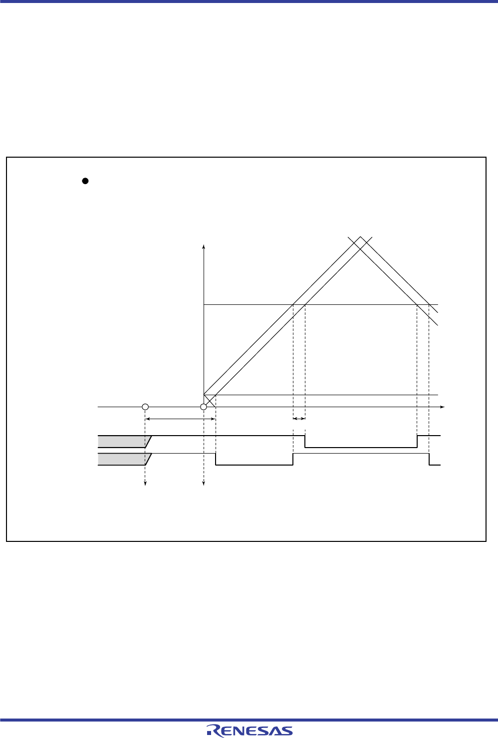
R01UH0034EJ0200 Rev.2.00 Page 599 of 1489
Dec 27, 2013
RX62T Group, RX62G Group 16. Multi-Function Timer Pulse Unit 3 (MTU3)
(i) Initial Output in Complementary PWM Mode
In complementary PWM mode, the initial output is determined by the setting of bits OLSN and OLSP in timer output
control register 1 (TOCR1A or TOCR1B) or bits OLS1N to OLS3N and OLS1P to OLS3P in timer output control
register 2 (TOCR2A or TOCR2B).
This initial output is the non-active level of the PWM pulse and continues from when complementary PWM mode is set
with the timer mode register 1 (TMDR1) until MTU4.TCNT (MTU7.TCNT) exceeds the value set in the dead time
register (TDDRA or TDDRB). Figure 16.45 shows an example of the initial output in complementary PWM mode.
An example of the waveform when the initial PWM duty ratio value is smaller than the TDDRA (TDDRB) value is
shown in Figure 16.46.
Figure 16.45 Example of Initial Output in Complementary PWM Mode (MTU3 and MTU4) (1))
Timer output control register settings
OLSN bit: 0 (initial output: high; active level: low)
OLSP bit: 0 (initial output: high; active level: low)
MTU3.TCNT, MTU3.TCNT
value
MTU4.TGRA
TDDRA
MTU3.TCNT
MTU4.TCNT
Initial output Dead time
Time
Active level
Active level
Complementary
PWM mode
(TMDR1 setting)
Positive-
phase output
Negative-
phase output
MTU3.TCNT
MTU4.TCNT
count start
(TSTR setting)
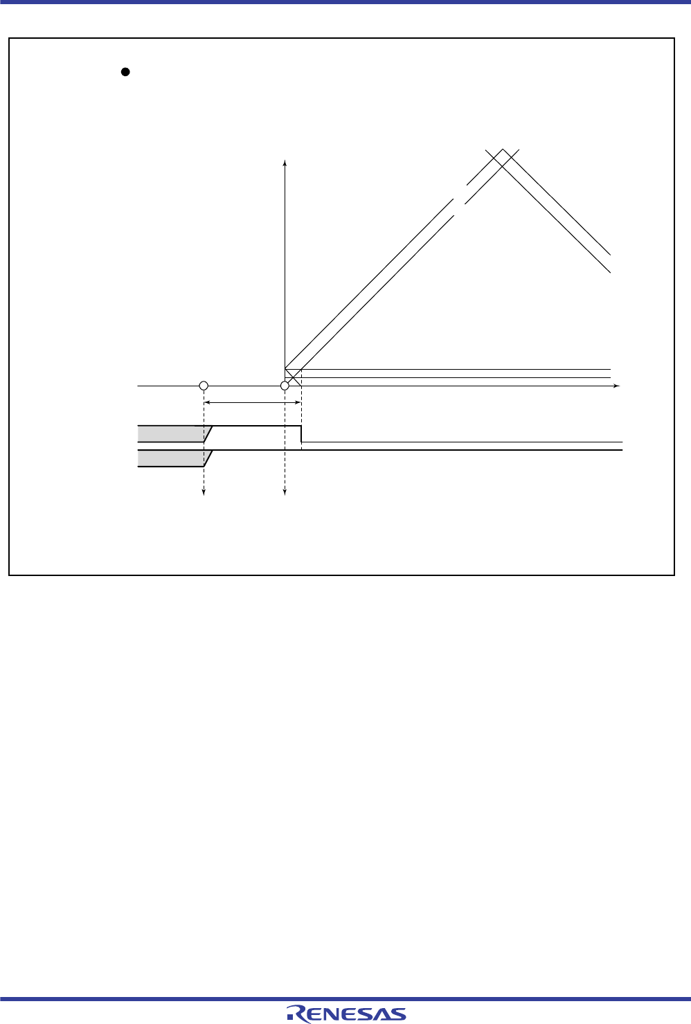
R01UH0034EJ0200 Rev.2.00 Page 600 of 1489
Dec 27, 2013
RX62T Group, RX62G Group 16. Multi-Function Timer Pulse Unit 3 (MTU3)
Figure 16.46 Example of Initial Output in Complementary PWM Mode (MTU3 and MTU4) (2)
Timer output control register settings
OLSN bit: 0 (initial output: high; active level: low)
OLSP bit: 0 (initial output: high; active level: low)
MTU3.TCNT, MTU4.TCNT value
MTU4.TGRA
TDDRA
MTU3.TCNT
MTU4.TCNT
Initial output
Time
Active level
MTU3.TCNT
MTU4.TCNT
count start
(TSTR setting)
Complementary
PWM mode
(TMDR1 setting)
Positive-
phase output
Negative-
phase output
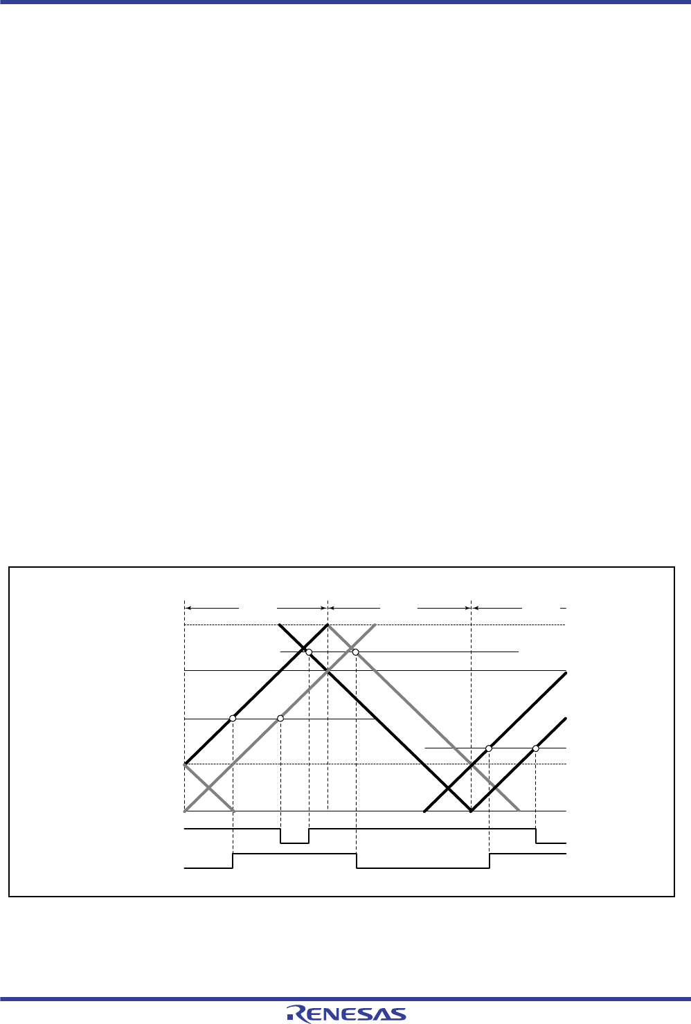
R01UH0034EJ0200 Rev.2.00 Page 601 of 1489
Dec 27, 2013
RX62T Group, RX62G Group 16. Multi-Function Timer Pulse Unit 3 (MTU3)
(j) Method for Generating PWM Output in Complementary PWM Mode
In complementary PWM mode, three phases of PWM waveforms are output with a non-overlap time between the
positive and negative phases. This non-overlap time is called the dead time.
A PWM waveform is generated by output of the level selected in the timer output control register in the event of a
compare match between a counter and a compare register. While TCNTSA (TCNTSB) is counting, the compare register
and temporary register values are simultaneously compared to create consecutive PWM pulses from 0 to 100%. The
relative timing of turn-on and turn-off compare match occurrence may vary, but the compare match that turns off each
phase takes precedence to secure the dead time and ensure that the positive-phase and negative-phase turn-on times do
not overlap. Figure 16.47 to Figure 16.49 show examples of waveform generation in complementary PWM mode.
The positive-phase and negative-phase turn-off timing is generated by a compare match with the counter value indicated
in solid lines in the figure, and the turn-on timing by a compare match with the counter indicated in dotted lines, which
operates with a delay of the dead time behind the solid-line counter. In the T1 period, compare match a that turns off the
negative phase has the highest priority, and compare matches before a are ignored. In the T2 period, compare match c
that turns off the positive phase has the highest priority, and compare matches before c are ignored.
In most cases, compare matches occur in the order a → b → c → d (or c → d → a' → b') as shown in Figure 16.47.
If compare matches deviate from the a → b → c → d order, since the time for which the negative phase is off is shorter
than twice the dead time, the positive phase is not turned on. If compare matches deviate from the c → d → a' → b' order,
since the time for which the positive phase is off is shorter than twice the dead time, the negative phase is not turned on.
As shown in Figure 16.48, if compare match c follows compare match a before compare match b, compare match b is
ignored and the negative phase is turned on by compare match d. This is because turning off the positive phase has
priority due to the occurrence of compare match c (positive-phase off timing) before compare match b (positive-phase on
timing) (consequently, the waveform does not change because the positive phase goes from off to off).
Similarly, in the example in Figure 16.49, compare match a' with new data in the temporary register occurs before
compare match c, but until compare match c, which turns off the positive phase, other compare matches are ignored. As
a result, the negative phase is not turned on.
Thus, in complementary PWM mode, compare matches at turn-off timings take precedence, and turn-on timing compare
matches that occur before a turn-off timing compare match are ignored.
Figure 16.47 Example of Waveform Output in Complementary PWM Mode (MTU3 and MTU4) (1)
T1
interval
ab
c
a' b'
d
T2
interval T1
interval
MTU3.TGRA
TCDRA
TDDRA
0000h
Positive-
phase output
Negative-
phase output
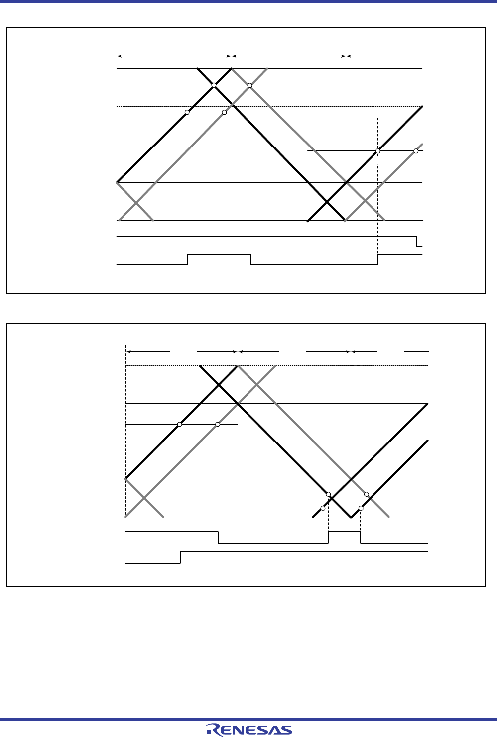
R01UH0034EJ0200 Rev.2.00 Page 602 of 1489
Dec 27, 2013
RX62T Group, RX62G Group 16. Multi-Function Timer Pulse Unit 3 (MTU3)
Figure 16.48 Example of Waveform Output in Complementary PWM Mode (MTU3 and MTU4) (2)
Figure 16.49 Example of Waveform Output in Complementary PWM Mode (MTU3 and MTU4) (3)
d
c
MTU3.TGRA
TCDRA
TDDRA
0000h
Positive-
phase output
Negative-
phase output
a
a
b
b
T1
interval T1
interval T1
interval
ab
c
a' b'
d
T1
interval T2
interval T1
interval
MTU3.TGRA
TCDRA
TDDRA
0000h
Positive-
phase output
Negative-
phase output

R01UH0034EJ0200 Rev.2.00 Page 603 of 1489
Dec 27, 2013
RX62T Group, RX62G Group 16. Multi-Function Timer Pulse Unit 3 (MTU3)
(k) 0% and 100% duty ratio Output in Complementary PWM Mode
In complementary PWM mode, 0% and 100% duty PWM waveforms can be output as required. Figure 16.50 to Figure
16.54 show output examples.
A 100% duty waveform is output when the compare register value is set to 0000h. The waveform in this case has a
positive phase with a 100% on-state. A 0% duty waveform is output when the compare register value is set to the same
value as MTU3.TGRA (MTU6.TGRA). The waveform in this case has a positive phase with a 100% off-state.
On and off compare matches occur simultaneously, but if a turn-on compare match and turn-off compare match for the
same phase occur simultaneously, both compare matches are ignored and the waveform does not change.
Figure 16.50 Example of 0% and 100% Waveform Output in Complementary PWM Mode
(MTU3 and MTU4) (1)
Figure 16.51 Example of 0% and 100% Waveform Output in Complementary PWM Mode
(MTU3 and MTU4) (2)
ab
c d
a' b'
T1
interval T2
interval T1
interval
MTU3.TGRA
TCDRA
TDDRA
0000h
Positive-
phase output
Negative-
phase output
a
c d
a b
b
T1
interval T2
interval T1
interval
MTU3.TGRA
TCDRA
TDDRA
0000h
Positive-
phase output
Negative-
phase output
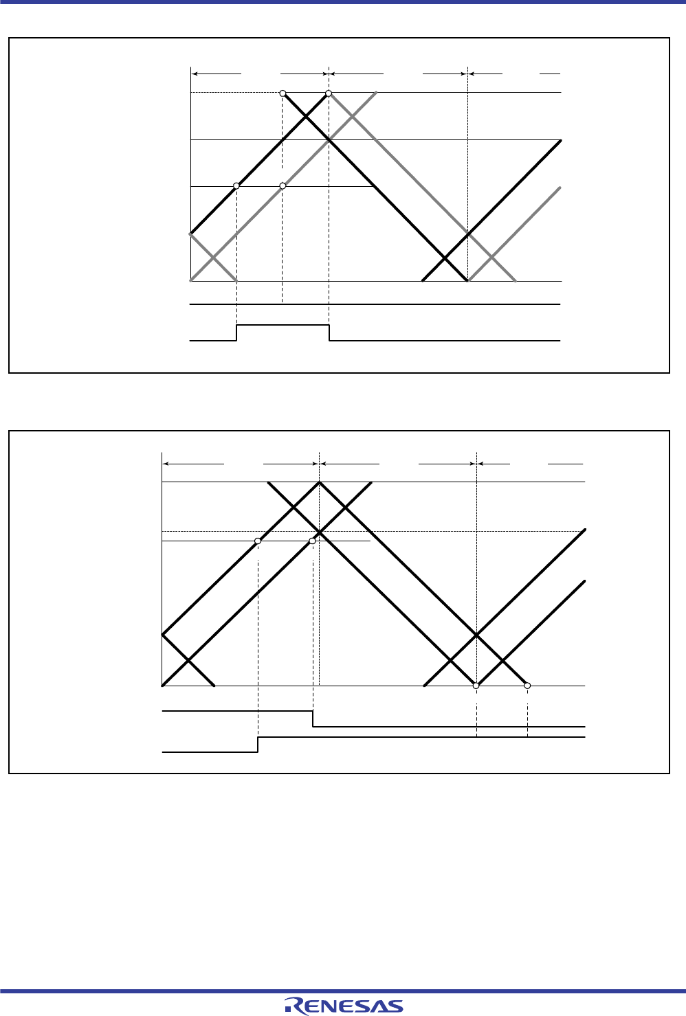
R01UH0034EJ0200 Rev.2.00 Page 604 of 1489
Dec 27, 2013
RX62T Group, RX62G Group 16. Multi-Function Timer Pulse Unit 3 (MTU3)
Figure 16.52 Example of 0% and 100% Waveform Output in Complementary PWM Mode
(MTU3 and MTU4) (3)
Figure 16.53 Example of 0% and 100% Waveform Output in Complementary PWM Mode
(MTU3 and MTU4) (4)
a b
c d
T1
interval T2
interval T1
interval
MTU3.TGRA
TCDRA
TDDRA
0000h
Positive-
phase output
Negative
phase output
ab
c b' d
T1
interval T2
interval T1
interval
MTU3.TGRA
TCDRA
TDDRA
0000h
Positive-
phase output
Negative-
phase output
a'
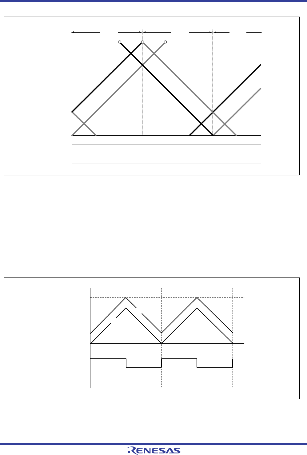
R01UH0034EJ0200 Rev.2.00 Page 605 of 1489
Dec 27, 2013
RX62T Group, RX62G Group 16. Multi-Function Timer Pulse Unit 3 (MTU3)
Figure 16.54 Example of 0% and 100% Waveform Output in Complementary PWM Mode
(MTU3 and MTU4) (5)
(l) Toggle Output Synchronized with PWM Cycle
In complementary PWM mode, toggle output in synchronization with the PWM carrier cycle can be generated by setting
the PSYE bit to 1 in the timer output control register 1 (TOCR1A or TOCR1B). An example of a toggle output waveform
is shown in Figure 16.55.
This output is toggled by a compare match between MTU3.TCNT and MTU3.TGRA (MTU6.TCNT and MTU6.TGRA)
and a compare match between MTU4.TCNT (MTU7.TCNT) and 0000h.
The MTIOC3A (MTIOC6A) pin is assigned for this toggle output. The initial output is High.
Figure 16.55 Example of Toggle Output Waveform Synchronized with PWM Output (MTU3 and MTU4)
cadb
T1
interval T2
interval T1
interval
MTU3.TGRA
TCDRA
TDDRA
0000h
Positive-
phase output
Negative-
phase output
MTU4.TCNT
MTU3.TCNT
MTU3.TGRA
0000h
Toggle output
MTIOC3A pin
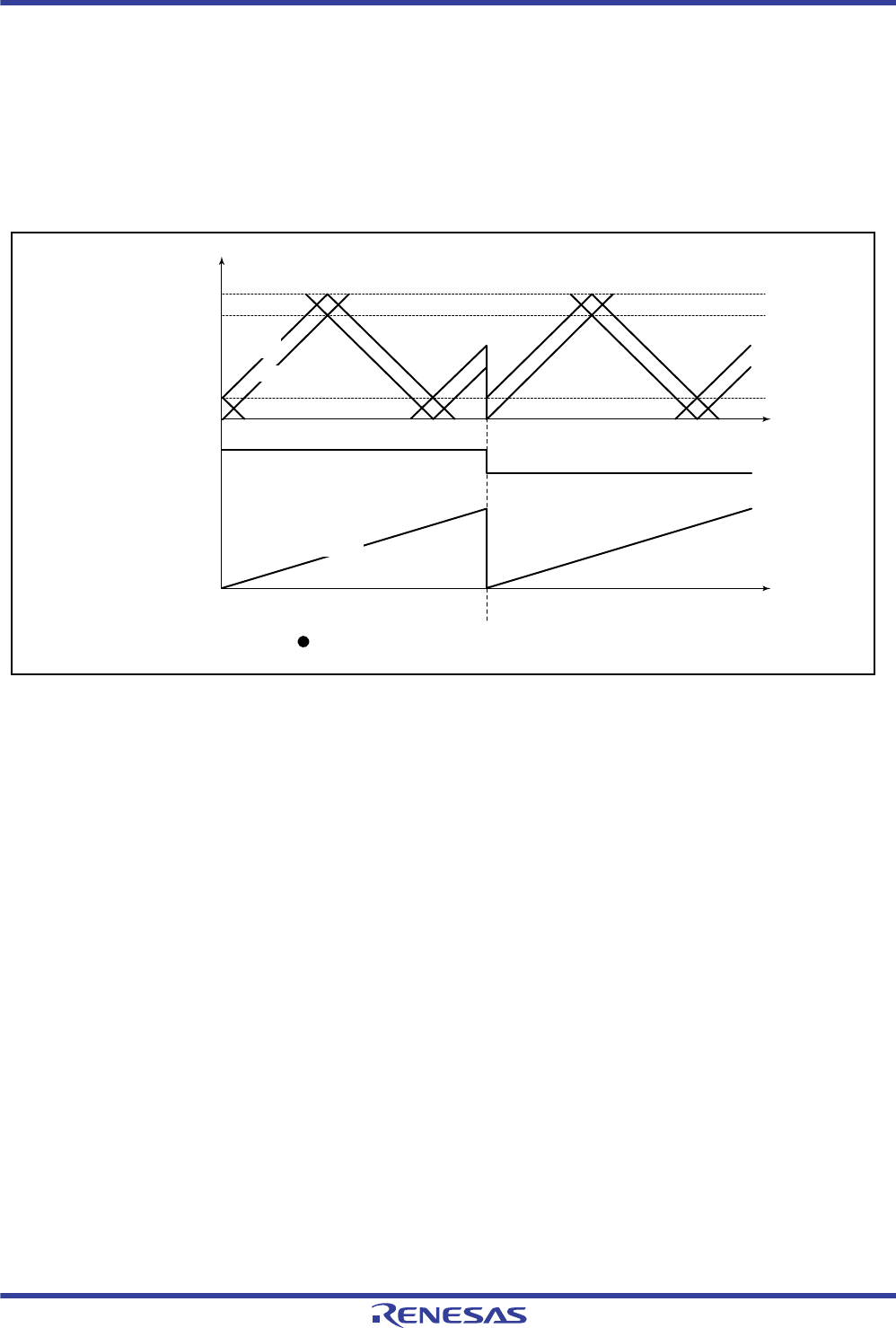
R01UH0034EJ0200 Rev.2.00 Page 606 of 1489
Dec 27, 2013
RX62T Group, RX62G Group 16. Multi-Function Timer Pulse Unit 3 (MTU3)
(m) Counter Clearing by Another Channel
In complementary PWM mode, MTU3.TCNT, MTU4.TCNT, and TCNTSA (MTU6.TCNT, MTU7.TCNT, and
TCNTSB) can be cleared by another channel when a mode for synchronization with another channel is specified through
the timer synchronous register (TSYRA or TSYRB)) and synchronous clearing is selected with bits CCLR[2:0] in the
timer control register (TCR).
Figure 16.56 illustrates an example of this operation.
Use of this function enables a counter to be cleared and restarted through an external signal.
Figure 16.56 Counter Clearing Synchronized with Another Channel (MTU3 and MTU4)
MTU1
MTU1.TCNT
MTU3.
TCNT
MTU4.TC
NT
TCNTSA
Synchronous counter clearing by MTU1 input capture A
MTU3.TGRA
TCDRA
TDDRA
0000h
input capture A
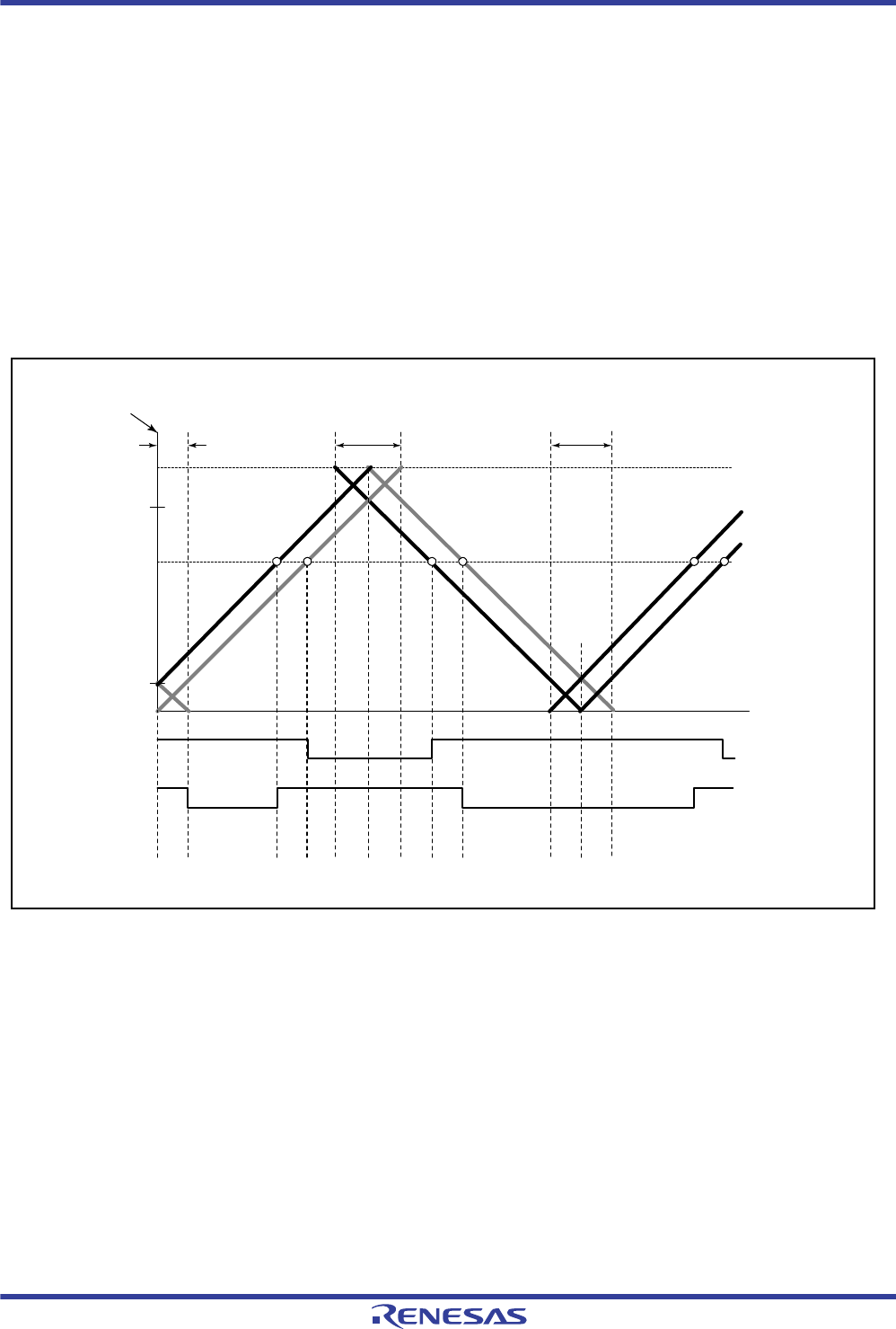
R01UH0034EJ0200 Rev.2.00 Page 607 of 1489
Dec 27, 2013
RX62T Group, RX62G Group 16. Multi-Function Timer Pulse Unit 3 (MTU3)
(n) Output Waveform Control at Synchronous Counter Clearing in Complementary PWM Mode
Setting the WRE bit in TWCRA (TWCRB) to 1 suppresses initial output when synchronous counter clearing occurs in
the Tb interval at the trough in complementary PWM mode and controls abrupt change in duty cycle at synchronous
counter clearing.
Initial output suppression through the WRE bit = 1 is applicable only when synchronous clearing occurs in the Tb
interval at the trough as indicated by (10) or (11) in Figure 16.57. When synchronous clearing occurs outside that
interval, the initial value specified by the OLS bits in TOCR1A (TOCR1B) is output. Even in the Tb interval at the
trough, if synchronous clearing occurs in the initial value output period (indicated by (1) in Figure 16.57) immediately
after the counters start operation, initial value output is not suppressed.
This function can be used in both channel combinations of MTU3 and MTU4, and MTU6 and MTU7. In MTU3 and
MTU4, synchronous clearing generated in MTU0 and MTU2 can cause counter clearing; in MTU6 and MTU7, flag
setting (compare match or input capture) in MTU0 and MTU2 can cause counter clearing.
Figure 16.57 Timing for Synchronous Counter Clearing (MTU3 and MTU4)
Tb
interval
MTU3.TCNT
MTU4.TCNT
(Output waveform is active-low)
(1) (2) (3) (4) (5) (6) (7) (8) (9) (10) (11)
Counter start Tb
interval Tb
interval
MTU3.TGRA
MTU3.TGRB
TCDRA
TDDRA
0000h
Positive
phase
Negative
phase
R01UH0034EJ0200 Rev.2.00 Page 608 of 1489
Dec 27, 2013
RX62T Group, RX62G Group 16. Multi-Function Timer Pulse Unit 3 (MTU3)
Example of Procedure for Setting Output Waveform Control at Synchronous Counter Clearing in Complementary
PWM Mode.
An example of the procedure for setting output waveform control at synchronous counter clearing in complementary
PWM mode is shown in Figure 16.58.
Figure 16.58 Example of Procedure for Setting Output Waveform Control at Synchronous Counter Clearing in
Complementary PWM Mode (MTU3 and MTU4)
Examples of Output Waveform Control at Synchronous Counter Clearing in Complementary PWM Mode
Figure 16.59 to Figure 16.62 show examples of output waveform control in which MTU3 and MTU4 operate in
complementary PWM mode and synchronous counter clearing is generated while the WRE bit in TWCRA is set to 1. In
the examples shown in Figure 16.59 to Figure 16.62, synchronous counter clearing occurs at timing (3), (6), (8), and
(11) shown in Figure 16.57, respectively.
In MTU6 and MTU7, these examples are equivalent to the cases when MTU6 and MTU7 operate in complementary
PWM mode and synchronous counter clearing is generated while the SCC bit is cleared to 0 and the WRE bit is set to 1
in TWCRB.
Stop count operation
Output waveform control at
synchronous counter clearing
Set TWCRA and
complementary PWM mode
Start count operation
Output waveform control at
synchronous counter clearing
[1]
[2]
[3]
[1] Clear bits CST3 and CST4 in the timer start
register (TSTRA) to 0 to stop timer counter
(TCNT) operation. Specify TWCRA while
MTU3.TCNT and MTU4.TCNT are
stopped.
[2] Read bit WRE in TWCRA and then write 1 to it
to suppress initial value output at counter
clearing.
[3] Set bits CST3 and CST4 in TSTRA to 1 to start
count operation.
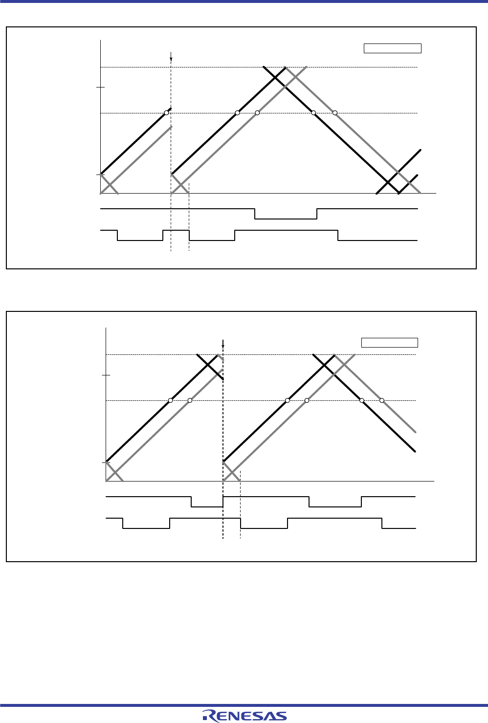
R01UH0034EJ0200 Rev.2.00 Page 609 of 1489
Dec 27, 2013
RX62T Group, RX62G Group 16. Multi-Function Timer Pulse Unit 3 (MTU3)
Figure 16.59 Example of Synchronous Clearing in Dead Time during Up-Counting
(Timing (3) in Figure 16.57; Bit WRE of TWCRA or TWCRB is 1)
Figure 16.60 Example of Synchronous Clearing in Interval Tb at Crest
(Timing (6) in Figure 16.57; Bit WRE of TWCRA or TWCRB is 1)
(Output waveform is active-low)
Synchronous clearing
MTU3.TCNT
MTU4.TCNT
WRE bit = 1
MTU3.TGRA
MTU3.TGRB
TCDRA
TDDRA
0000h
Positive
phase
Negative
phase
MTU3.TCNT
MTU4.TCNT
WRE bit = 1
MTU3.TGRA
MTU3.TGRB
TCDRA
TDDRA
0000h
(Output waveform is active-low)
Synchronous clearing
Positive
phase
Negative
phase
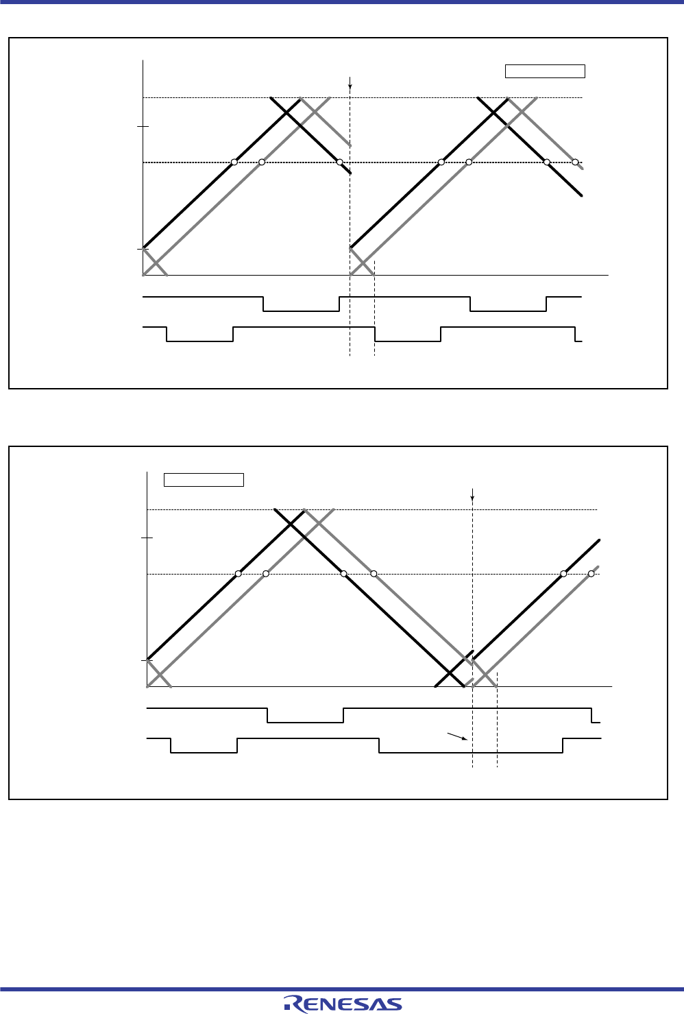
R01UH0034EJ0200 Rev.2.00 Page 610 of 1489
Dec 27, 2013
RX62T Group, RX62G Group 16. Multi-Function Timer Pulse Unit 3 (MTU3)
Figure 16.61 Example of Synchronous Clearing in Dead Time during Down-Counting
(Timing (8) in Figure 16.57; Bit WRE of TWCRA or TWCRB is 1)
Figure 16.62 Example of Synchronous Clearing in Interval Tb at Trough
(Timing (11) in Figure 16.57; Bit WRE of TWCRA or TWCRB is 1)
WRE bit = 1
MTU3.TCNT
MTU4.TCNT
MTU3.TGRA
MTU3.TGRB
TCDRA
TDDRA
0000h
(Output waveform is active-low)
Synchronous clearing
Positive
phase
Negative
phase
(Output waveform is active-low)
Synchronous clearing
Initial value output is
suppressed
MTU3.TCNT
MTU4.TCNT
WRE bit = 1
MTU3.TGRA
MTU3.TGRB
TCDRA
TDDRA
0000h
Positive
phase
Negative
phase
R01UH0034EJ0200 Rev.2.00 Page 611 of 1489
Dec 27, 2013
RX62T Group, RX62G Group 16. Multi-Function Timer Pulse Unit 3 (MTU3)
(o) Suppressing Synchronous Counter Clearing for MTU0 to MTU2, and MTU6 and MTU7
In MTU6 and MTU7, setting the SCC bit in TWCRB to 1 suppresses synchronous counter clearing caused by MTU0 to
2.
Synchronous counter clearing is suppressed only within the interval shown in Figure 16.63. When using this function,
MTU6 and MTU7 should be set to complementary PWM mode.
For details of synchronous clearing caused by MTU0 and MTU2, refer to section 16.3.10 (2)Clearing Counters of
MTU6 and MTU7 by Flag Setting Sources (Synchronous Counter Clearing for MTU6 and MTU7).
Figure 16.63 Synchronous Clearing-Suppressed Interval Specified by SCC Bit in TWCRB for MTU0 to MTU2,
and MTU6 and MTU7
Example of Procedure for Suppressing Synchronous Counter Clearing for MTU0 to MTU2, and MTU6 and MTU7
An example of the procedure for suppressing synchronous counter clearing for MTU0 to MTU2, and MTU6 and MTU7
is shown in Figure 16.64.
Tb interval
at the crest
MTU6.TGRA
MTU6.TGRB
TCDRB
TDDRB
0000h
Tb period
immediately
after counter
operation starts
Synchronous counter clearing for
MTU0 to MTU2, and MTU6 and MTU7
is suppressed
Tb interval
at the trough Tbinterval
at the crest Tb interval
at the trough
Synchronous counter clearing for
MTU0 to MTU2, and MTU6 and MTU7
is suppressed
R01UH0034EJ0200 Rev.2.00 Page 612 of 1489
Dec 27, 2013
RX62T Group, RX62G Group 16. Multi-Function Timer Pulse Unit 3 (MTU3)
Figure 16.64 Example of Procedure for Suppressing Synchronous Counter Clearing for MTU0 to MTU2, and
MTU6 and MTU7
Examples of Suppression of Synchronous Counter Clearing for MTU0 to MTU2, and MTU6 and MTU7
Figure 16.65 to Figure 16.68 show examples of operation in which channels 6 and 7 operate in complementary PWM
mode and synchronous counter clearing for MTU0 to MTU2, and MTU6 and MTU7 is suppressed by setting the SCC bit
in TWCRB in MTU6 and MTU7 to 1. In the examples shown in Figure 16.65 to Figure 16.68, synchronous counter
clearing occurs at timing (3), (6), (8), and (11) shown in Figure 16.57, respectively. In these examples, the WRE bit in
TWCRB in MTU6 and MTU7 is set to 1.
Stop count operation
(MTU0 to MTU2, and MTU6 and MTU7)
Synchronous counter clearing for
MTU0 to MTU2, and MTU6 and MTU7
suppress
Start count operation
(MTU0 to MTU2, and MTU6 and MTU7)
Output waveform control at
synchronous counter clearing and
synchronous counter clearing
suppress
[1]
[3]
• Set complementary PWM mode
(MTU6 and MTU7)
• Set compare match/input capture
operation (MTU6 and MTU7)
• Set bit WRE in TWCRB (MTU6 and MTU7)
[2]
Set bit SCC in TWCRB
(MTU6 and MTU7) [4]
[1] Clear bits CST of the timer start register (TSTRB) in MTU6 and
MTU7 to 0, and stop count operation. Clear bits CST of
TSTRA in MTU0 to MTU2 to 0, and stop count operation.
[2] Set the complementary PWM mode in MTU6 and MTU7 and
compare match/input capture operation in MTU0 to MTU2.
When bit WRE in TWCRA or TWCRB should be set, make
appropriate setting here.
[3] Set bits CST6 and CST7 in MTU6 and MTU7 to 1 to start count
operation. For synchronous counter clearing for channels 0 to
2 and channels 6 and 7, set bits CST of TSTRA in MTU0 to MTU to
1 to start count operation in any one of MTU0.TCNT
to MTU2.TCNT.
[4] Read TWCRB and then set bit SCC in TWCRB to 1 to suppress
synchronous counter clearing for MTU0 to MTU2, and MTU6 and
MTU7*. Here, do not modify the CCE and WRE bit values in
TWCRB of MTU6 and MTU7. Synchronous counter clearing for
MTU0 to MTU2, and MTU6 and MTU7 is suppressed in
the synchronous counter clearing-suppressed periods.
Note: * The TWCRB.SCC bit value can be modified during counter
operation. However, if a synchronous clearing occurs
when bit TWCRB.SCC is modified from 0 to 1, the
synchronous clearing may not be suppressed. If a
synchronous clearing occurs when bit TWCRB.SCC is
modified from 1 to 0, the synchronous clearing may be
suppressed.
R01UH0034EJ0200 Rev.2.00 Page 613 of 1489
Dec 27, 2013
RX62T Group, RX62G Group 16. Multi-Function Timer Pulse Unit 3 (MTU3)
Figure 16.65 Example of Synchronous Clearing in Dead Time during Up-Counting
(Timing (3) in Figure 16.57; Bit WRE is 1 and Bit SCC is 1 in TWCRB in MTU6 and MTU7)
Figure 16.66 Example of Synchronous Clearing in Interval Tb at Crest
(Timing (6) in Figure 16.57; Bit WRE is 1 and Bit SCC is 1 in TWCRB in MTU6 and MTU7)
MTU6.TGRA
MTU6.TGRB
TCDRB
TDDRB
0000h
Positive phase
Negative phase
(Output waveform is active-low)
Synchronous clearing for
MTU0 to MTU2, and MTU6 and MTU7
MTU6.
TCNT
MTU7.
TCNT
WRE bit = 1
SCC bit = 1
Counters are
not cleared
MTU6.TGRA
MTU6.TGRB
TCDRB
TDDRB
0000h
MTU6.
TCNT
MTU7.
TCNT
Positive phase
Negative phase
(Output waveform is active-low)
Synchronous clearing for
MTU0 to MTU2, and MTU6 and MTU7
WRE bit = 1
SCC bit = 1
Counters are
not cleared
R01UH0034EJ0200 Rev.2.00 Page 614 of 1489
Dec 27, 2013
RX62T Group, RX62G Group 16. Multi-Function Timer Pulse Unit 3 (MTU3)
Figure 16.67 Example of Synchronous Clearing in Dead Time during Down-Counting
(Timing (8) in Figure 16.57; Bit WRE is 1 and Bit SCC is 1 in TWCRB in MTU6 and MTU7)
Figure 16.68 Example of Synchronous Clearing in Interval Tb at Trough
(Timing (11) in Figure 16.57; Bit WRE is 1 and Bit SCC is 1 in TWCRB in MTU6 and MTU7)
MTU6.TGRA
MTU6.TGRB
TCDRB
TDDRB
0000h
MTU6.
TCNT
MTU7.
TCNT
Positive phase
Negative phase
(Output waveform is active-low)
Synchronous clearing for
MTU0 to MTU2, and MTU6 and MTU7
WRE bit = 1
SCC bit = 1
Counters are
not cleared
MTU6.TGRA
MTU6.TGRB
TCDRB
TDDRB
0000h
MTU6.
TCNT
MTU7.
TCNT
Initial value output
is suppressed
Positive phase
Negative phase
(Output waveform is active-low)
Synchronous clearing for
MTU0 to MTU2, and MTU6 and MTU7
WRE bit = 1
SCC bit = 1
Counters are
cleared
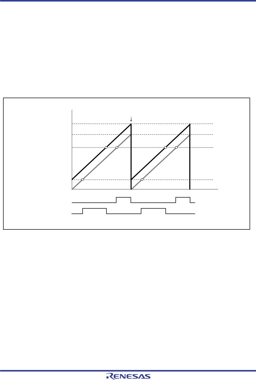
R01UH0034EJ0200 Rev.2.00 Page 615 of 1489
Dec 27, 2013
RX62T Group, RX62G Group 16. Multi-Function Timer Pulse Unit 3 (MTU3)
(p) Counter Clearing by MTU3.TGRA (MTU6.TGRA) Compare Match
In complementary PWM mode, MTU3.TCNT, MTU4.TCNT, and TCNTSA (MTU6.TCNT, MTU7.TCNT, and
TCNTSB) can be cleared by MTU3.TGRA (MTU6.TGRA) compare match when the CCE bit is set in the timer
waveform control register (TWCRA or TWCRB).
Figure 16.69 illustrates an operation example.
Note 1. Use this function only in complementary PWM mode 1 (transfer at crest).
Note 2. Do not specify synchronous clearing by another channel (do not set the SYNC0 to SYNC4 or SYNC6 to SYNC7
bits in the timer synchronous register (TSYRA or TSYRB) to 1 or the CE0A to CE0D and CE1A to CE1D bits in
the timer synchronous clear register (TSYCRA or TSYCRB) to 1).
Note 3. Do not set the PWM duty value to 0000h.
Note 4. Do not set the PSYE bit in timer output control register 1 (TOCR1A or TOCR1B) to 1.
Figure 16.69 Example of Counter Clearing Operation by MTU3.TGRA Compare Match
(Output waveform is active-high)
Counter cleared by MTU3.TGRA
compare match
MTU3.TGRA
MTU3.TGRB
TCDRA
TDDRA
0000h
Output waveform
Output waveform#
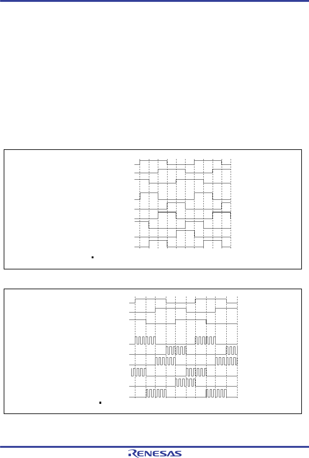
R01UH0034EJ0200 Rev.2.00 Page 616 of 1489
Dec 27, 2013
RX62T Group, RX62G Group 16. Multi-Function Timer Pulse Unit 3 (MTU3)
(q) Example of Waveform Output for Driving AC Synchronous Motor (Brushless DC Motor)
In complementary PWM mode, a brushless DC motor can easily be controlled using the timer gate control register
(TGCRA). Figure 16.70 to Figure 16.73 show examples of brushless DC motor driving waveforms created using
TGCRA.
To switch the output phases for a 3-phase brushless DC motor by means of external signals detected with a Hall element,
etc., clear the TGCRA.FB bit to 0. In this case, the external signals indicating the magnetic pole position should be input
to timer input pins MTIOC0A, MTIOC0B, and MTIOC0C in MTU0 (make appropriate settings in ICR for the I/O ports).
When an edge is detected at pin MTIOC0A, MTIOC0B, or MTIOC0C, the output on/off state is switched automatically.
When the TGCRA.FB bit is 1, the output on/off state is switched when the UF, VF, or WF bit in TGCRA is cleared to 0
or set to 1.
The driving waveforms are output from the 6-phase output pins for complementary PWM mode.
With this 6-phase output, while the output is turned on, chopping output is available through complementary PWM mode
output function by setting the N bit or P bit in TGCRA to 1. When the N bit or P bit is 0, the level output is selected.
The active level of the 6-phase output (on output level) can be set with the OLSN and OLSP bits in the timer output
control register 1A (TOCR1A) regardless of the setting of the N and P bits.
Figure 16.70 Example of Output Phase Switching by External Input (1)
Figure 16.71 Example of Output Phase Switching by External Input (2)
External input MTIOC0A pin
6-phase output
MTIOC0B pin
MTIOC0C pin
MTIOC3B pin
MTIOC3D pin
MTIOC4A pin
MTIOC4C pin
MTIOC4B pin
MTIOC4D pin
When BDC = 1, N = 0, P = 0, FB = 0, and output active level = high
External input MTIOC0A pin
6-phase output
MTIOC0B pin
MTIOC0C pin
MTIOC3B pin
MTIOC4A pin
MTIOC4C pin
MTIOC4B pin
MTIOC4D pin
When BDC = 1, N = 1, P = 1, FB = 0, and output active level = high
MTIOC3D pin
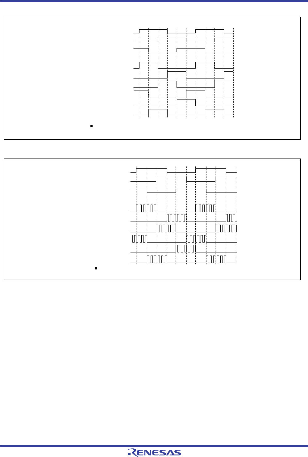
R01UH0034EJ0200 Rev.2.00 Page 617 of 1489
Dec 27, 2013
RX62T Group, RX62G Group 16. Multi-Function Timer Pulse Unit 3 (MTU3)
Figure 16.72 Example of Output Phase Switching through UF, VF, and WF Bit Settings (1)
Figure 16.73 Example of Output Phase Switching through UF, VF, and WF Bit Settings (2)
TGCRA UF bit
VF bit
WF bit
When BDC = 1, N = 0, P = 0, FB = 1, and output active level = high
6-phase output MTIOC3B pin
MTIOC3D pin
MTIOC4A pin
MTIOC4C pin
MTIOC4B pin
MTIOC4D pin
TGCRA UF bit
VF bit
WF bit
When BDC = 1, N = 1, P = 1, FB = 1, and output active level = high
6-phase output MTIOC3B pin
MTIOC4A pin
MTIOC4C pin
MTIOC4B pin
MTIOC4D pin
MTIOC3D pin

R01UH0034EJ0200 Rev.2.00 Page 618 of 1489
Dec 27, 2013
RX62T Group, RX62G Group 16. Multi-Function Timer Pulse Unit 3 (MTU3)
(r) A/D Converter Start Request Setting
In complementary PWM mode, an A/D converter start request can be issued using MTU3.TGRA (MTU6.TGRA)
compare match, MTU4.TCNT (MTU7.TCNT) underflow (trough), or compare match on a channel other than MTU3 and
MTU4 (MTU6 and MTU7).
When start requests using MTU3.TGRA (MTU6.TGRA) compare match are specified, A/D conversion can be started at
the crest of the MTU3.TCNT (MTU6.TCNT) count.
A/D converter start requests can be specified by setting the TTGE bit to 1 in the timer interrupt enable register (TIER).
To issue an A/D converter start request at an MTU4.TCNT (MTU7.TCNT) underflow (trough), set the TTGE2 bit in
MTU4.TIER (MTU7.TIER) to 1.
(s) Double Buffer Function in Complementary PWM Mode
In complementary PWM mode 3 (transfer at the crest and trough), the PWM output setting resolution can be improved
from ±2 to ±1 by setting the DRS bit in timer mode register 2 (TMDR2A or TMDR2B) to 1.
When setting buffer registers A (MTU3.TGRD, MTU4.TGRC, and MTU4.TGRD), set also buffer registers B
(MTU3.TGRE, MTU4.TGRE, and MTU4.TGRF) at the same time. Each buffer register B should be set to the buffer
register A value or (buffer register A value – 1). For details of the setting procedure, refer to section 16.3.8 (1)Example
of Complementary PWM Mode Setting Procedure
Note 1. When a buffer register B is set to the buffer register A value, symmetric PWM waveforms are output. When a
buffer register B is set to (buffer register A value – 1), asymmetric PWM waveforms are output.
Figure 16.74 shows an example of double buffer operation.
Each register data is transferred as follows.
After MTU4.TGRD (buffer A) is written to, data is transferred from MTU4.TGRD (buffer A) to Temp3A
(temporary A) and from MTU4.TGRF (buffer B) to Temp3B (temporary B).
With timing (1) in the figure, data is transferred from Temp3A (temporary A) to MTU4.TGRB (compare).
With timing (2) in the figure, data is transferred from Temp3B (temporary B) to MTU4.TGRB (compare).
In the crest interval (Tb interval at crest), the compare register and temporary register A are valid; in the trough interval
(Tb interval at trough), the compare register and temporary register B are valid.

R01UH0034EJ0200 Rev.2.00 Page 619 of 1489
Dec 27, 2013
RX62T Group, RX62G Group 16. Multi-Function Timer Pulse Unit 3 (MTU3)
Figure 16.74 Example of Double Buffer Operation
Figure 16.75 shows an example when the buffer write value is smaller than the TDDRA value, and Figure 16.76
shows an example when the write value is greater than TCDRA.
In the crest interval, the output is controlled according to the compare match with the compare register or temporary
register A; in the trough interval, the output is controlled according to the compare match with the compare register or
temporary register B.
Figure 16.75 Example of Double Buffer Operation (Buffer Write Value is Smaller than TDDRA)
MTU3.TGRA TCNTSA
MTU3.
TCNT MTU4.
TCNT
TCDRA
MTU4.TGRB
TDDRA
MTU4.TGRD
(buffer A)
Tb interval
at trough
1111h 1211h
MTU4.TGRF
(buffer B)
Temp3A
(temporary A)
Temp3B
(temporary B)
MTU4.TGRB
(compare)
(1) (1) (1)
(2) (2) (2)
Buffer A modified
1111h 1211h
1110h 1210h
1110h 1111h 1211h
MTIOC4B (output)
1211h
1110h 1210h
Buffer B modified
1210h1210h
MTIOC4D (output)
Tb interval
at crest Tb interval
at crest
Tb interval
at crest Tb interval
at trough
MTU3.TGRA TCNTSA
MTU4.
TCNT MTU4.
TCNT
TCDRA
MTU4.TGRB
TDDRA
MTU4.TGRD
(buffer A) 1111h 1011h
MTU4.TGRF
(buffer B)
Temp3A
(temporary A)
Temp3B
(temporary B)
MTU4.TGRB
(compare)
(1) (1) (1)
(2) (2) (2)
Buffer A modified
1111h 1011h
1110h 1010h
1110h 1111h 1011h
MTIOC4B(output)
1011h
1110h 1010h
Buffer B modified
1010h1010h
MTIOC4D(output)
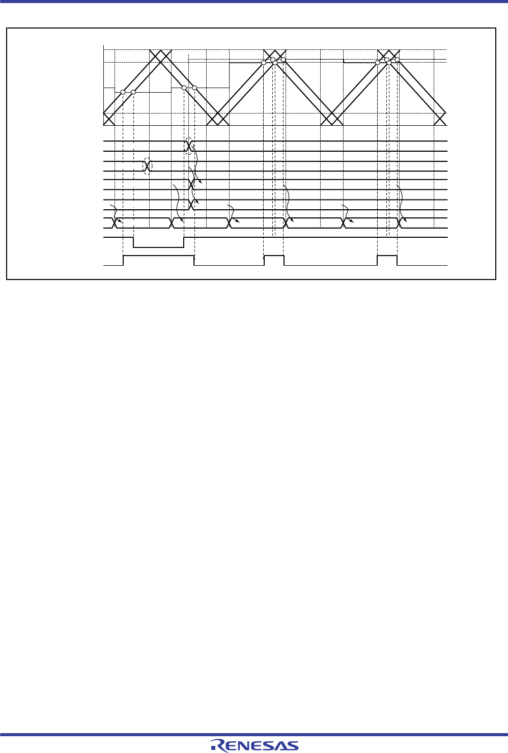
R01UH0034EJ0200 Rev.2.00 Page 620 of 1489
Dec 27, 2013
RX62T Group, RX62G Group 16. Multi-Function Timer Pulse Unit 3 (MTU3)
Figure 16.76 Example of Double Buffer Operation (Buffer Write Value is Greater than TCDRA)
MTU3.TGRA TCNTSA
MTU3.
TCNT MTU4.
TCNT
TCDRA
MTU4.TGRB
TDDRA
MTU4.TGRD
(buffer A) 1111h 1211h
MTU4.TGRF
(buffer B)
Temp3A
(temporary A)
Temp3B
(temporary B)
MTU4.TGRB
(compare)
(1) (1) (1)
(2) (2) (2)
Buffer A modified
1111h 1211h
1110h 1210h
1110h 1111h 1211h
MTIOC4B (output)
1211h
1110h 1210h
Buffer B modified
1210h1210h
MTIOC4D(output)
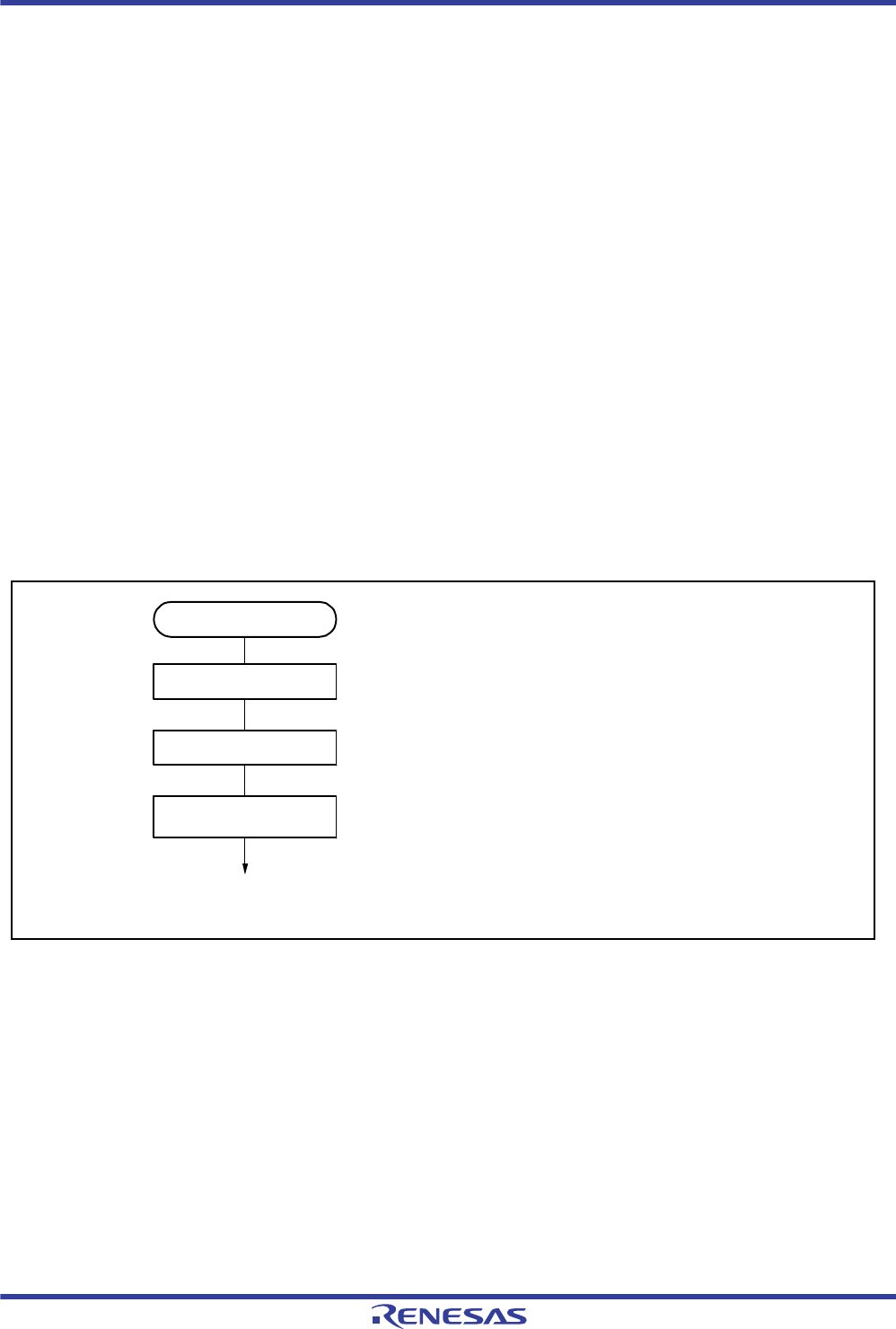
R01UH0034EJ0200 Rev.2.00 Page 621 of 1489
Dec 27, 2013
RX62T Group, RX62G Group 16. Multi-Function Timer Pulse Unit 3 (MTU3)
(3) Interrupt Skipping Function 1 in Complementary PWM Mode
Interrupts TGIA3 (TGIA6) (at the crest) and TCIV4 (TCIV7) (at the trough) in MTU3 and MTU4 (MTU6 and MTU7)
can be skipped up to seven times by making settings in the timer interrupt skipping set register 1 (TITCR1A or
TITCR1B).
Transfers from a buffer register to a temporary register or a compare register can be skipped in coordination with
interrupt skipping by making settings in the timer buffer transfer register (TBTERA or TBTERB). For the linkage with
buffer registers, refer to description (c), Buffer Transfer Control Linked with Interrupt Skipping, below.
A/D converter start requests generated by the A/D converter start request delaying function can also be skipped in
coordination with interrupt skipping by making settings in the timer A/D converter request control register
(MTU4.TADCR or MTU7.TADCR). For the linkage with the A/D converter start request delaying function, refer to
section 16.3.9, A/D Converter Start Request Delaying Function.
The timer interrupt skipping setting register 1 (TITCR1A or TITCR1B) should be set while interrupt skipping function 1
is selected by setting the TITM bit to 0 in the timer interrupt skipping mode register (TITMRA or TITMRB) and TGIA3
(TGIA6) and TCIV4 (TCIV7) interrupt requests are disabled by the settings of MTU3.TIER and MTU4.TIER
(MTU6.TIER and MTU7.TIER) under the conditions in which TGFA3 (TGFA6) and TCFV4 (TCFV7) flag settings by
compare match never occur in TITCR1A (TITCR1B). Before changing the skipping count, be sure to clear the T3AEN
(T6AEN) and T4VEN (T7VEN) bits to 0 to clear the skipping counter.
(a) Example of Interrupt Skipping Function 1 Setting Procedure
Figure 16.77 shows an example of the interrupt skipping function 1 setting procedure. Figure 16.78 shows the periods
during which interrupt skipping count can be changed.
Figure 16.77 Example of Interrupt Skipping Function 1 Setting Procedure
Clear interrupt skipping
counter
Set interrupt skipping mode
Interrupt skipping 1
Set skipping count and
enable interrupt skipping
<Interrupt skipping>
[1] Set bits T3AEN and T4VEN in the timer interrupt skipping set
register 1 (TITCR1A) to 0 to clear the skipping counter.
[2] Set bit TITM in the timer interrupt skipping mode register
(TITMRA) to 0 to select interrupt skipping function 1.
[3] Specify the interrupt skipping count within the range from 0
to 7 times in bits T3ACOR2 to T3ACOR0 and T4VCOR2 to
T4VCOR0 in TITCR1A, and enable interrupt skipping through
bits T3AEN and T4VEN.
Note: The setting of TITCR1A must be done while the TGIA3
and TCIV4 interrupt requests are disabled by the settings
of MTU3.TIER and MTU4.TIER under the conditions
in which TGFA3 and TCFV4 flag settings by compare
match never occur.
Before changing the skipping count, be sure to clear
the T3AEN and T4VEN bits to 0 to clear the skipping
counter.
[1]
[2]
[3]

R01UH0034EJ0200 Rev.2.00 Page 622 of 1489
Dec 27, 2013
RX62T Group, RX62G Group 16. Multi-Function Timer Pulse Unit 3 (MTU3)
Figure 16.78 Periods during which Interrupt Skipping Count can be Changed
(b) Example of Interrupt Skipping Function 1
Figure 16.79 shows an example of TGIA3 (TGIA6) interrupt skipping in which the interrupt skipping count is set to
three by the T3ACOR (T6ACOR) bits and the T3AEN (T6AEN) bit is set to 1 in the timer interrupt skipping set register
1 (TITCR1A or TITCR1B).
Figure 16.79 Example of Interrupt Skipping Function 1
Period during
which skipping
count can be
changed
MTU3.
TCNT
MTU4.
TCNT
Period during
which skipping
count can be
changed
Period during
which skipping
count can be
changed
Period during
which skipping
count can be
changed
Interrupt skipping period
00 01 02 03 00 01 02 03
TGIA3
interrupt flag
set signal
Skipping counter
MTU3.TGFA
flag
Interrupt skipping period
R01UH0034EJ0200 Rev.2.00 Page 623 of 1489
Dec 27, 2013
RX62T Group, RX62G Group 16. Multi-Function Timer Pulse Unit 3 (MTU3)
(c) Buffer Transfer Control Linked with Interrupt Skipping
In complementary PWM mode, whether to transfer data from a buffer register to a temporary register and whether to link
the transfer with interrupt skipping can be specified with the BTE[1:0] bits in the timer buffer transfer set register
(TBTERA or TBTERB).
Figure 16.80 shows an example of operation when buffer transfer is disabled (BTE[1:0] = 01b). While this setting is
valid, data is not transferred from the buffer register to the temporary register.
Figure 16.81 shows an example of operation when buffer transfer is linked with interrupt skipping (BTE[1:0] = 10b).
While this setting is valid, data is not transferred from the buffer register outside the buffer transfer-enabled period.
Note that the buffer transfer-enabled period depends on the T3AEN (T6AEN) and T4VEN (T7VEN) bit settings in the
timer interrupt skipping set register 1 (TITCR1A or TITCR1B). Figure 16.82 shows the relationship between the
T3AEN (T6AEN) and T4VEN (T7VEN) bit settings in TITCR1A (TITCR1B) and buffer transfer-enabled period.
Note 1. This function must always be used in combination with interrupt skipping function 1.
When interrupt skipping is disabled (the T3AEN and T4VEN (T6AEN and T7VEN) bits in the timer interrupt
skipping set register 1 (TITCR1A or TITCR1B) are cleared to 0 or the skipping count set bits (T3ACOR and
T4VCOR (T6ACOR and T7VCOR)) in TITCR1A (TITCR1B) are cleared to 0), make sure that buffer transfer is
not linked with interrupt skipping (clear the BTE1 bit in TBTERA or TBTERB to 0).
If buffer transfer is linked with interrupt skipping while interrupt skipping is disabled, buffer transfer is never
performed.
Figure 16.80 Example of Operation when Buffer Transfer is Disabled (BTE[1:0] = 01b)
MTU3.
TCNT
MTU4.
TCNT
(1)
(2)
(3)
Buffer transfer is suppressed
TBTERA.BTE1 bit
TBTERA.BTE0 bit
Temporary register
Buffer register
General register
Data1 Data2
Data2
Data2
Data*
Data*
[Legend]
(1) No data is transferred from the buffer register to the temporary register in the
buffer transfer-disabled period (bits BTE[1:0] in TBTERA are set to 01b).
(2) Data is transferred from the temporary register to the general register even in
the buffer transfer-disabled period.
(3) After buffer transfer is enabled, data is transferred from the buffer register to
the temporary register.
Note: * When buffer transfer at the crest is selected.
R01UH0034EJ0200 Rev.2.00 Page 624 of 1489
Dec 27, 2013
RX62T Group, RX62G Group 16. Multi-Function Timer Pulse Unit 3 (MTU3)
Figure 16.81 Example of Operation when Buffer Transfer is Linked with Interrupt Skipping
(BTE[1:0] = 10b)
Note: Bits MD[3:0] in MTU3.TMDR are set to 1101b. (Buffer transfer at the crest is selected.)
The skipping count is set to two.
Bit T3AEN in TITCR1A is set to 1 and bit T4VEN is set to 0.
Data1 Data2Data
Data1 Data2Data
01201
Buffer register modification timing Buffer register modification timing
MTU3.
TCNT
MTU4.T
CNT
Buffer transfer-enabled period
TITCR1A.
T3ACOR[2:0]
TITCNT1A.
T3ACNT[2:0]
Buffer register
Temporary register
TGIA3 interrupt TGIA3 interrupt
(1) Buffer register is modified within one carrier period after a TGIA3 interrupt
Data1Data
Data1Data
Data1Data
01201
Buffer register modification timing
Buffer transfer-enabled period
Buffer register
Temporary register
TGIA3 interrupt TGIA3 interrupt
(2) Buffer register is modified after one carrier period has elapsed since a TGIA3 interrupt
2
2
Compare register
MTU3.
TCNT
MTU4.T
CNT
TITCR1A.
T3ACOR[2:0]
TITCNT1A.
T3ACNT[2:0]
R01UH0034EJ0200 Rev.2.00 Page 625 of 1489
Dec 27, 2013
RX62T Group, RX62G Group 16. Multi-Function Timer Pulse Unit 3 (MTU3)
Figure 16.82 Relationship between Bits T3AEN and T4VEN in TITCR1A and Buffer Transfer-Enabled Period
Note: The skipping count is set to three.
Buffer transfer-enabled period
(T3AEN is set to 1)
Buffer transfer-enabled period
(T4VEN is set to 1)
Buffer transfer-enabled period
(T3AEN and T4VEN are set to 1)
0012 301 2 3
01 2 30123
Skipping counter
T3ACNT
Skipping counter
T4VCNT

R01UH0034EJ0200 Rev.2.00 Page 626 of 1489
Dec 27, 2013
RX62T Group, RX62G Group 16. Multi-Function Timer Pulse Unit 3 (MTU3)
(4) Complementary PWM Mode Output Protection Functions
The MTU3 provides the following protection functions for complementary PWM mode output.
(a) Register and Counter Miswrite Prevention Function
With the exception of the buffer registers, which can be modified at any time, access by the CPU can be enabled or
disabled for the mode registers, control registers, compare registers, and counters used in complementary PWM mode by
means of the RWE bit in the timer read/write enable register (TRWERA or TRWERB). The applicable registers are some
of the registers in MTU3, MTU4, MTU6, and MTU7 shown below:
43 registers in total
MTU3.TCR, MTU4.TCR, MTU3.TMDR1, MTU4.TMDR1, MTU3.TIORH,
MTU4.TIORH, MTU3.TIORL, MTU4.TIORL, MTU3.TIER, MTU4.TIER,
MTU3.TCNT, MTU4.TCNT, MTU3.TGRA, MTU4.TGRA, MTU3.TGRB, MTU4.TGRB,
TOERA, TOCR1A, TOCR2A, TGCRA, TCDRA, TDDRA
MTU6.TCR, MTU7.TCR, MTU6.TMDR1, MTU7.TMDR1, MTU6.TIORH, MTU7.TIORH,
MTU6.TIORL, MTU7.TIORL, MTU6.TIER, MTU7.TIER, MTU6.TCNT, MTU7.TCNT,
MTU6.TGRA, MTU7.TGRA, MTU6.TGRB, MTU7.TGRB,
TOERB, TOCR1B, TOCR2B, TCDRB, and TDDRB
This function can disable CPU access to the mode registers, control registers, and counters to prevent miswriting due to
CPU runaway. In the access-disabled state, the applicable registers are read as undefined and writing to these registers is
ignored.
(b) Halting of PWM Output by External Signal
The 6-phase PWM output pins can be set to the high-impedance state automatically by inputting specified external
signals.
See section 17, Port Output Enable 3 (POE3), for details.
(c) Halting of PWM Output when Oscillator is Stopped
Upon detecting that the clock input to this the RX62T has stopped, the 6-phase PWM output pins are automatically set to
the high-impedance state. Note that the pin states are not guaranteed when the clock is restarted.
See section 8.10, Oscillation Stop Detection Function.
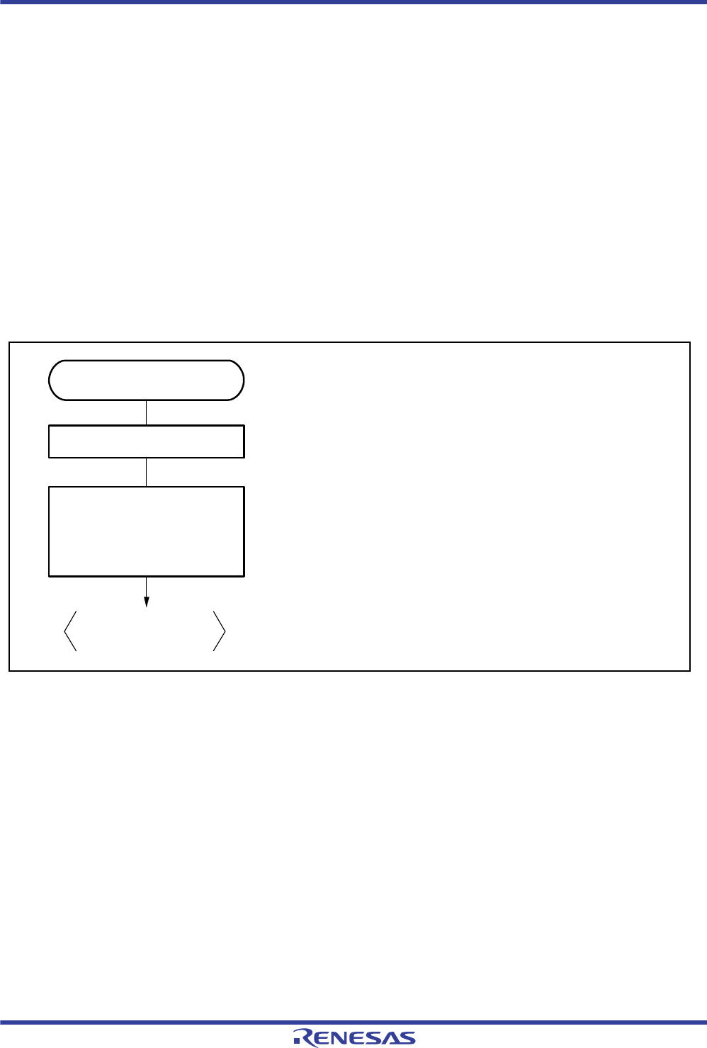
R01UH0034EJ0200 Rev.2.00 Page 627 of 1489
Dec 27, 2013
RX62T Group, RX62G Group 16. Multi-Function Timer Pulse Unit 3 (MTU3)
16.3.9 A/D Converter Start Request Delaying Function
A/D converter start requests can be issued in MTU4 or MTU7 by making settings in the timer A/D converter start request
control register (MTU4.TADCR or MTU7.TADCR), timer A/D converter start request cycle set registers
(MTU4.TADCORA and MTU4.TADCORB, or MTU7.TADCORA and MTU7.TADCORB), and timer A/D converter
start request cycle set buffer registers (MTU4.TADCOBRA and MTU4.TADCOBRB, or MTU7.TADCOBRA and
MTU7.TADCOBRB).
The A/D converter start request delaying function compares MTU4.TCNT with MTU4.TADCORA or
MTU4.TADCORB (MTU7.TCNT with MTU7.TADCORA or MTU7.TADCORB), and when their values match, the
function issues a respective A/D converter start request (TRG4AN or TRG4BN (TRG7AN or TRG7BN)).
A/D converter start requests (TRG4AN and TRG4BN (TRG7AN and TRG7BN)) can be skipped in coordination with
interrupt skipping by making settings in the ITA3AE, ITA4VE, ITB3AE, and ITB4VE bits in MTU4.TADCR (the
ITA6AE, ITA7VE, ITB6AE, and ITB7VE bits in MTU7.TADCR).
(1) Example of Procedure for Specifying A/D Converter Start Request Delaying Function
Figure 16.83 shows an example of procedure for specifying the A/D converter start request delaying function.
Figure 16.83 Example of Procedure for Specifying A/D Converter Start Request Delaying Function
[1]
[2]
[1] Set the cycle in the timer A/D converter start request cycle buffer
register (MTU4.TADCOBRA or MTU4.TADCOBRB) and timer
A/D converter start request cycle register (MTU4.TADCORA or
MTU4.TADCORB).
(When the timing of transfer from the cycle buffer register to cycle
register is set to the trough, or both trough and crest in step [2]
below, the same initial value must be specified in the cycle buffer
register and cycle register because transfer is performed
immediately after counting starts.)
[2] Use bits BF1 and BF2 in the timer A/D converter start request
control register (MTU4.TADCR) to specify the timing of transfer
from the timer A/D converter start request cycle buffer register to
A/D converter start request cycle register.
• Specify whether to link with interrupt skipping through bits
ITA3AE, ITA4VE, ITB3AE, and ITB4VE.
• Use bits UT4AE, DT4AE, UT4BE, and DT4BE to enable A/D
converter start requests (TRG4AN or TRG4BN).
Notes: 1. Perform MTU4.TADCR setting while MTU4.TCNT
is stopped.
2. Do not set MTU4.TADCR.BF1 to 1 when
complementary PWM mode is not selected.
3. Do not set ITA3AE, ITA4VE, ITB3AE, ITB4VE, DT4AE, or
DT4BE to 1 when complementary PWM mode is not
selected.
A/D converter start request
delaying function
Set A/D converter start request cycle
• Set the timing of transfer
from cycle set buffer register
• Set linkage with interrupt skipping
• Enable A/D converter start
request delaying function
A/D converter start request
delaying function
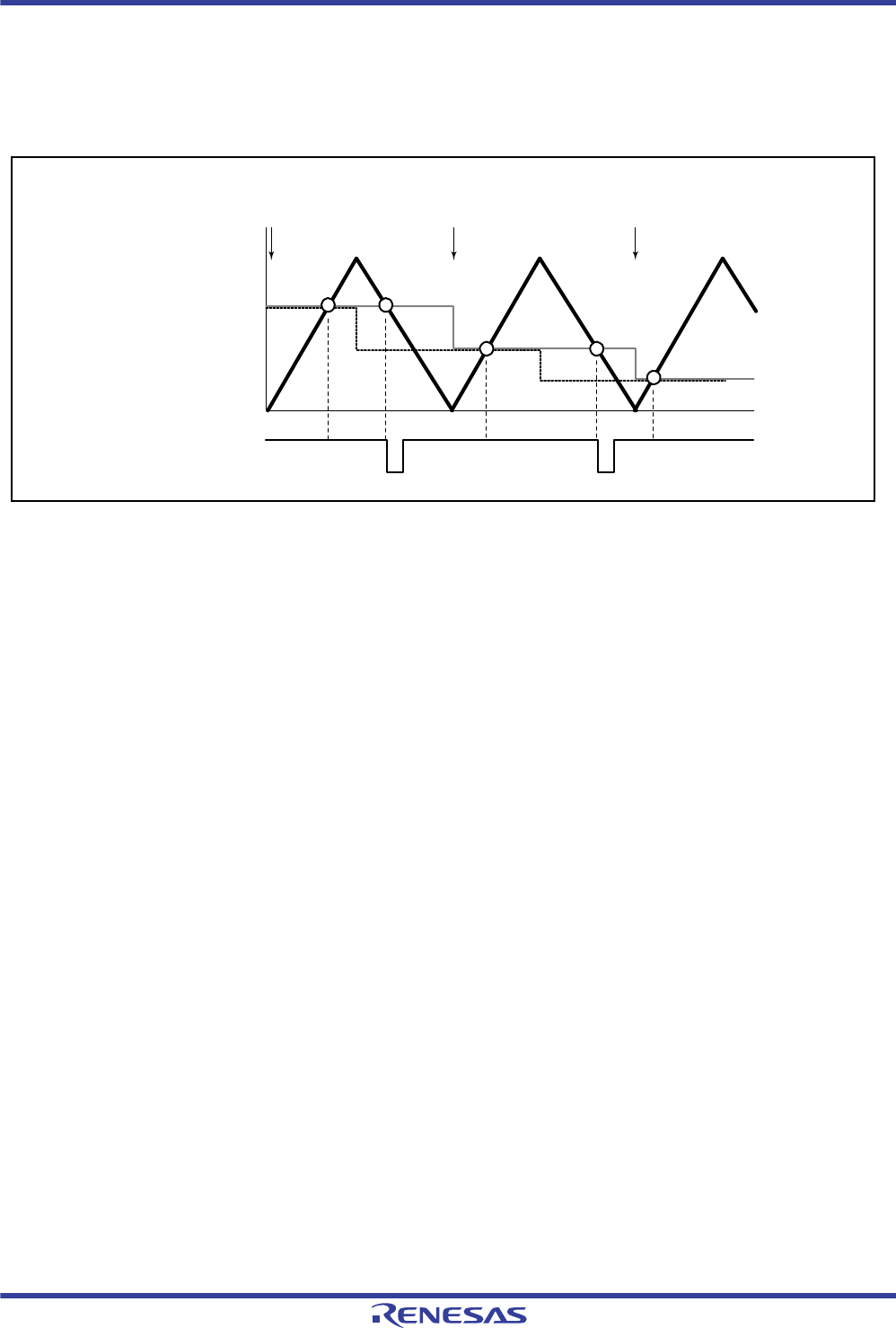
R01UH0034EJ0200 Rev.2.00 Page 628 of 1489
Dec 27, 2013
RX62T Group, RX62G Group 16. Multi-Function Timer Pulse Unit 3 (MTU3)
(2) Basic Example of A/D Converter Start Request Delaying Function Operation
Figure 16.84 shows a basic example of A/D converter start request signal (TRG4AN (TRG7AN)) operation when the
trough of MTU4.TCNT (MTU7.TCNT) is specified for the buffer transfer timing and an A/D converter start request
signal is output during MTU4.TCNT (MTU7.TCNT) down-counting.
Figure 16.84 Basic Example of A/D Converter Start Request Signal (TRG4AN) Operation
MTU4.TCNT
Transfer from cycle buffer
register to cycle register
(Complementary
PWM mode)
MTU4.TADCORA
MTU4.TADCOBRA
A/D converter start
request (TRG4AN)
Transfer from cycle buffer
register to cycle register Transfer from cycle buffer
register to cycle register
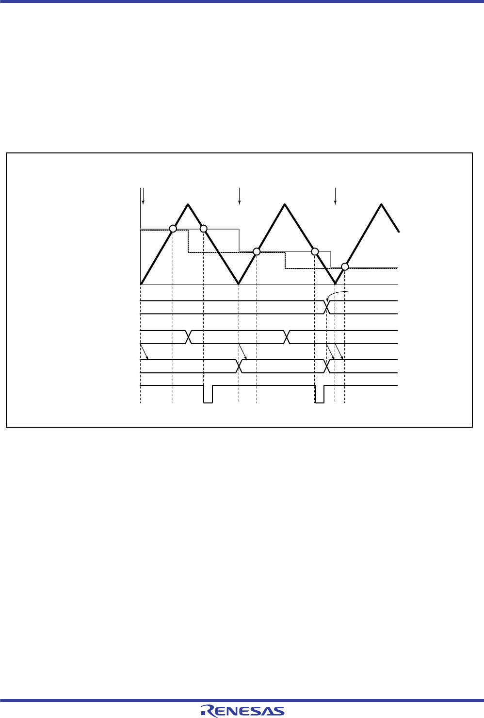
R01UH0034EJ0200 Rev.2.00 Page 629 of 1489
Dec 27, 2013
RX62T Group, RX62G Group 16. Multi-Function Timer Pulse Unit 3 (MTU3)
(3) Buffer Transfer
The data in the timer A/D converter start request cycle set registers (MTU4.TADCORA and MTU4.TADCORB, or
MTU7.TADCORA and MTU7.TADCORB) is updated by writing data to the timer A/D converter start request cycle set
buffer registers (MTU4.TADCOBRA and MTU4.TADCOBRB, or MTU7.TADCOBRA and MTU7.TADCOBRB). Data
is transferred from the buffer registers to the respective cycle set registers at the timing selected with the BF[1:0] bits in
the timer A/D converter start request control register (MTU4.TADCR or MTU7.TADCR).
In complementary PWM mode, data is also transferred from the timer A/D converter start request cycle set buffer
registers to the timer A/D converter start request cycle set registers when timer general register D (MTU4.TGRD or
MTU7.TGRD) is updated.
Figure 16.85 Example of A/D Converter Start Request Signal (TRG4AN) and Buffer Transfer Operation
MTU4.TADCORA
MTU4.TADCOBRA
MTU4.
TCNT
Transfer from cycle buffer
register to cycle register Transfer from cycle buffer
register to cycle register Transfer from cycle buffer
register to cycle register
A/D converter start request
(TRG4AN)
(Complementary PWM mode)
MTU4.TGRD modified
MTU4.TGRD
MTU4.TADCOBRA
MTU4.TADCORA
DataA DataB
Data2
Data0 Data1
Data0 Data1
Data2
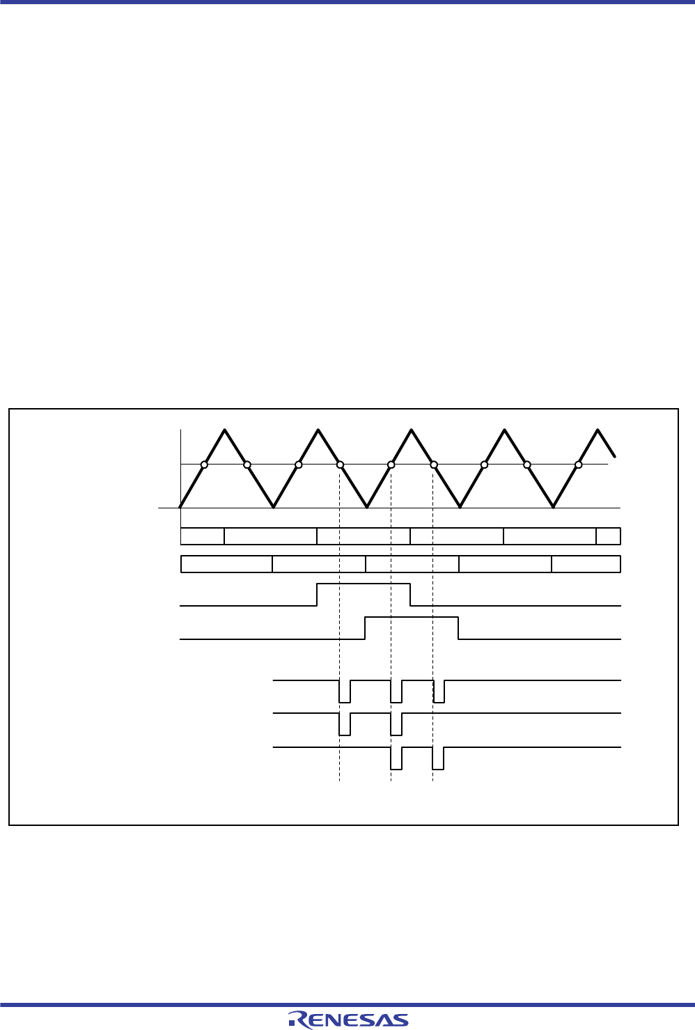
R01UH0034EJ0200 Rev.2.00 Page 630 of 1489
Dec 27, 2013
RX62T Group, RX62G Group 16. Multi-Function Timer Pulse Unit 3 (MTU3)
(4) A/D Converter Start Request Delaying Function Linked with Interrupt Skipping Function 1
A/D converter start requests (TRG4AN and TRG4BN (TRG7AN and TRG7BN)) can be issued in coordination with
interrupt skipping 1 by making settings in the ITA3AE, ITA4VE, ITB3AE, and ITB4VE (ITA6AE, ITA7VE, ITB6AE,
and ITB7VE) bits in the timer A/D converter start request control register (MTU4.TADCR or MTU7.TADCR).
Figure 16.86 shows an example of A/D converter start request signal (TRG4AN (TRG7AN)) operation when TRG4AN
(TRG7AN) output is enabled during MTU4.TCNT (MTU7.TCNT) up-counting and down-counting and A/D converter
start requests are linked with interrupt skipping 1.
Figure 16.87 shows another example of A/D converter start request signal (TRG4AN (TRG7AN)) operation when
TRG4AN (TRG7AN) output is enabled during MTU4.TCNT (MTU7.TCNT) up-counting and A/D converter start
requests are linked with interrupt skipping 1.
Note: • This function should be used in combination with interrupt skipping 1.
When interrupt skipping is disabled (the T3AEN and T4VEN (T6AEN and T7VEN) bits in the timer interrupt
skipping set register (TITCR1A (TITCR1B)) are cleared to 0 or the skipping count set bits (T3ACOR and T4VCOR
(T6ACOR and T7VCOR)) in TITCR1A (TITCR1B) are cleared to 0), make sure that A/D converter start requests
are not linked with interrupt skipping 1 (clear the ITA3AE, ITA4VE, ITB3AE, and ITB4VE (ITA6AE, ITA7VE,
ITB6AE, and ITB7VE) bits in the timer A/D converter start request control register (MTU4.TADCR
(MTU7.TADCR)) to 0).
When this function is used, MTU4.TADCORA and MTU4.TADCORB (MTU7.TADCORA and MTU7.TADCORB)
should be set with the value ranging 0002h to the value set in TCDRA minus 2 (value set in TCDRB minus 2).
Figure 16.86 Example of A/D Converter Start Request Signal (TRG4AN) Operation Linked with Interrupt
Skipping Function 1 (UT4AE and DT4AE = 1)
00 01 00 0102
00 01 00 0102
MTU4.
TCNT
MTU4.TADCORA
TGIA3 interrupt
skipping counter
TCIV4 interrupt
skipping counter
TGIA3 A/D request-
enabled period
TCIV4 A/D request-
enabled period
A/D converter start request (TRG4AN)
When linked with TGIA3 and TCIV4
interrupt skipping
When linked with TGIA3 interrupt
skipping
When linked with TCIV4 interrupt
skipping
Note: When the interrupt skipping count is set to two.
(UT4AE/DT4AE = 1)

R01UH0034EJ0200 Rev.2.00 Page 631 of 1489
Dec 27, 2013
RX62T Group, RX62G Group 16. Multi-Function Timer Pulse Unit 3 (MTU3)
Figure 16.87 Example of A/D Converter Start Request Signal (TRG4AN) Operation Linked with Interrupt
Skipping Function 1 (UT4AE = 1, DT4AE = 0)
00 01 00 0102
00 01 00 0102
MTU4.
TCNT
MTU4.TADCORA
UT4AE = 1
DT4AE = 0
TGIA3 interrupt
skipping counter
TCIV4 interrupt
skipping counter
TGIA3 A/D request-
enabled period
TCIV4 A/D request-
enabled period
A/D converter start request (TRG4AN)
When linked with TGIA3 and TCIV4
interrupt skipping
When linked with TGIA3 interrupt
skipping
When linked with TCIV4 interrupt
skipping
Note: When the interrupt skipping count is set to two.
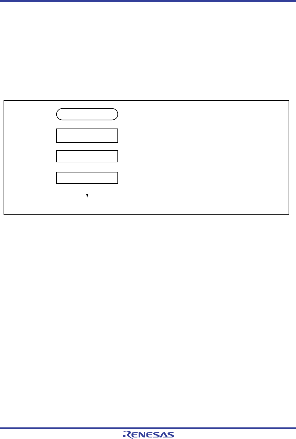
R01UH0034EJ0200 Rev.2.00 Page 632 of 1489
Dec 27, 2013
RX62T Group, RX62G Group 16. Multi-Function Timer Pulse Unit 3 (MTU3)
(5) A/D Converter Start Request Delaying Function Linked with Interrupt Skipping Function 2
By setting the TITM bit to 1 in the timer interrupt skipping mode register (TITMRA or TITMRB), the counter starts
down-counting from the value (0 to 7) set in the TRG4COR[2:0] (TRG7COR[2:0]) bits in timer interrupt skipping set
register 2 (TITCR2A (TITCR2B)) every time an A/D converter start trigger (TGR4AN or TRG4BN (TGR7AN or
TRG7BN)) is generated. When the counter value reaches 0 and is reloaded, the TRG4AN and TRG4BN (TRG7AN and
TRG7BN) interrupts become valid and an A/D converter start request signal (TRG4ABN (TRG7ABN)) is output.
This function is valid only when the A/D converter request delaying function is enabled.
(a) Example of Procedure for Setting Interrupt Skipping Function 2
Figure 16.88 shows an example of procedure for setting interrupt skipping function 2.
Figure 16.88 Example of Procedure for Setting Interrupt Skipping Function 2
Set interrupt skipping mode
Interrupt skipping 2
Set skipping count
<Interrupt skipping 2>
[1]
[1] Set the A/D converter start request delaying function.
For details, refer to section 16.3.9 (1), Example of
Procedure for Specifying A/D Converter Start
Request Delaying Function.
[2] Set bit TITM in the timer interrupt skipping mode
register (TITMRA) to 1 to select interrupt skipping
function 2.
[3] Specify the interrupt skipping count within the range
from 0 to 7 times in bits TRG4COR[2:0] in timer
interrupt skipping set register 2 (TITCR2A).
Set A/D converter start request
delaying function
[2]
[3]
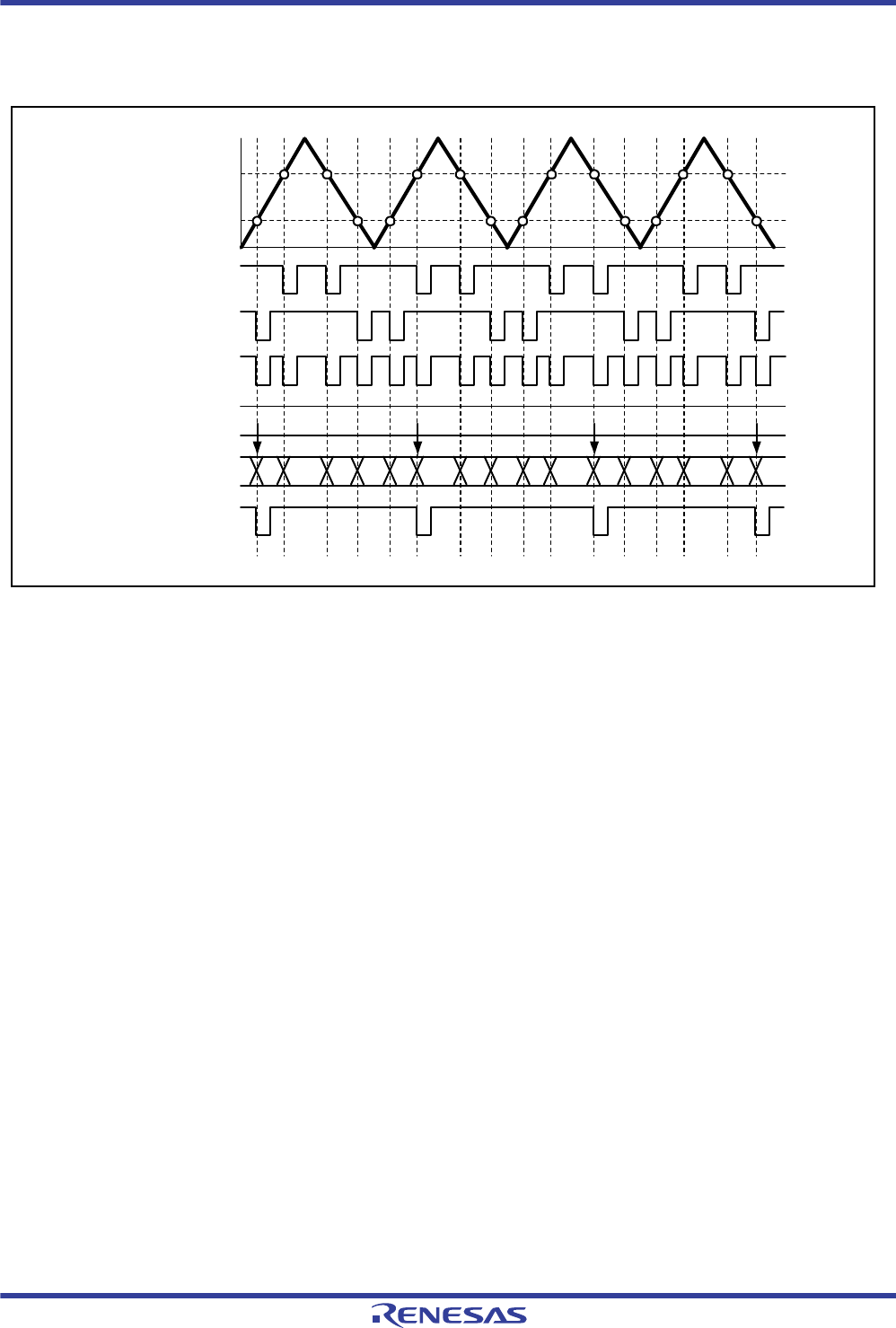
R01UH0034EJ0200 Rev.2.00 Page 633 of 1489
Dec 27, 2013
RX62T Group, RX62G Group 16. Multi-Function Timer Pulse Unit 3 (MTU3)
(b) Example of Interrupt Skipping Function 2 Operation
Figure 16.89 shows an example of interrupt skipping 2 operation.
Figure 16.89 Example of Interrupt Skipping 2 Operation (Skipping Count is Set to Four)
MTU4.TADCORA
(MTU7.TADCORA)
MTU4.TADCORB
(MTU7.TADCORB)
A/D converter start request
(Signal name: TRG4ABN
(TRG7ABN))
TRG4AN
(TRG7AN)
TRG4BN
(TRG7BN)
Signal obtained by ORing
TRG4AN (TRG7AN) and
TRG4BN (TRG7BN)
TRG4COR[2:0]
(TRG7COR[2:0])
TITCNT2A
(TITCNT2B)
100
012340123401234

R01UH0034EJ0200 Rev.2.00 Page 634 of 1489
Dec 27, 2013
RX62T Group, RX62G Group 16. Multi-Function Timer Pulse Unit 3 (MTU3)
16.3.10 Synchronous Operation of MTU0 to MTU4, and MTU6 and MTU7
(1) Synchronous Counter Start for MTU0 to MTU4, and MTU6 and MTU7
The counters in channels MTU0 to MTU4, and MTU6 and MTU7 can be started synchronously by making the
TCSYSTR settings.
(a) Example of Procedure for Setting Synchronous Counter Start for MTU0 to MTU4, and MTU6
and MTU7
Figure 16.90 shows an example of synchronous counter start setting procedure.
Figure 16.90 Example of Synchronous Counter Start Setting Procedure
(b) Examples of Synchronous Counter Start Operation
Figure 16.91 shows an example of synchronous counter start operation for MTU0 to MTU4, and MTU6 and MTU7.
Figure 16.91 Example of Synchronous Counter Start Operation
Stop count operation
Synchronous counter start
for MTU0 to MTU4, and
MTU6 and MTU7
Set the necessary operation
Synchronous timer count start
(Set TCSYSTR)
Stop timer counter
(Set TSTR) [4]
[1] Set TSTRA and TSTRB to stop the counters used for
synchronous start operation.
[2] Specify the necessary operation with appropriate registers
such as TCR, TMDR1, and TMDR2.
[3] In TCSYSTR, set the bits corresponding to the counters to be
started synchronously to 1 at the same time. When TCSYSTR
is set, TSTRA and TSTRB for the target timer counters are
automatically set appropriately, the counters start
synchronously, and TCSYSTR is automatically cleared.
[4] To stop a timer counter, set the bit in TSTRA or TSTRB that
corresponds to the counter to 0.
Notes: 1. Even if a bit in TCSYSTR corresponding to an operating
counter is cleared to 0, the counter will not stop.
2. To start counters synchronously in reset-synchronized
PWM mode or complementary PWM mode using
MTU3 and MTU4, or MTU6 and MTU7, set the bits in
TCSYSTR that correspond to MTU3, MTU4, MTU6, and MTU7
at the same time.
<Counter operation starts>
[1]
[2]
[3]
ICLK
TSTRA
TSTRB
51h
TCSYSTR 00h
42h00h
80h00h
00h
MTU1.TCNT 0000h 0001h
0001h
MTU3.TCNT 0000h
0001h
0002h
0002h
0002h
MTU7.TCNT 0000h
Automatically cleared after TCSYSTR
setting is made
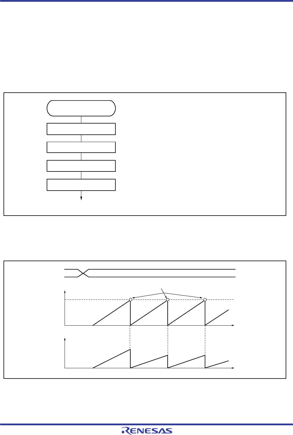
R01UH0034EJ0200 Rev.2.00 Page 635 of 1489
Dec 27, 2013
RX62T Group, RX62G Group 16. Multi-Function Timer Pulse Unit 3 (MTU3)
(2) Clearing Counters of MTU6 and MTU7 by Flag Setting Sources (Synchronous Counter
Clearing for MTU6 and MTU7)
The counters in MTU6 and MTU7 can be cleared by sources for setting the flags in MTU0.TSR to MTU2.TSR through
the TSYCR setting.
(a) Example of Procedure for Specifying Counter Clearing for MTU6 and MTU7 by Flag Setting
Sources
Figure 16.92 shows an example of procedure for specifying counter clearing for MTU6 and MTU7 by flag setting
sources.
Figure 16.92 Example of Procedure for Specifying Counter Clearing for MTU6 and MTU7
by Flag Setting Sources
(b) Examples of Counter Clearing for MTU6 and MTU7 by Flag Setting Sources
Figure 16.93 and Figure 16.94 show examples of counter clearing for MTU6 and MTU7 by flag setting sources.
Figure 16.93 Example of Counter Clearing for MTU6 and MTU7 by Flag Setting Sources (1)
Stop count operation
Clearing counters of
MTU6 and MTU7
by flag setting sources
Set TSYCR
<Counter clearing by flag setting>
[1]
Start one of MTU0 to MTU2
Start MTU6 and MTU7
[1] Set TSTRA and TSTRB to stop the counters used
for this function.
[2] Use TSYCR to specify the flag setting source to be used
for the MTU6.TCNT and MTU7.TCN clearing source.
[3] Start MTU6.TCNT or MTU7.TCNT.
[4] Start MTU0.TCNT, MTU1.TCNT, or MTU2.TCNT.
Note: The TSYCR setting is ignored while the counter is
stopped. The setting becomes valid after MTU6.TCNT
or MTU7.TCNT is started.
[2]
[3]
[4]
MTU0.TCNT
value
MTU0.
TGRA
0000h Time
Compare match between MTU0.TCNT and MTU0.TGRA
MTU0.
TCNT
MTU7.TCNT
value
0000h Time
MTU7.
TCNT
TSYCR 00h 80h
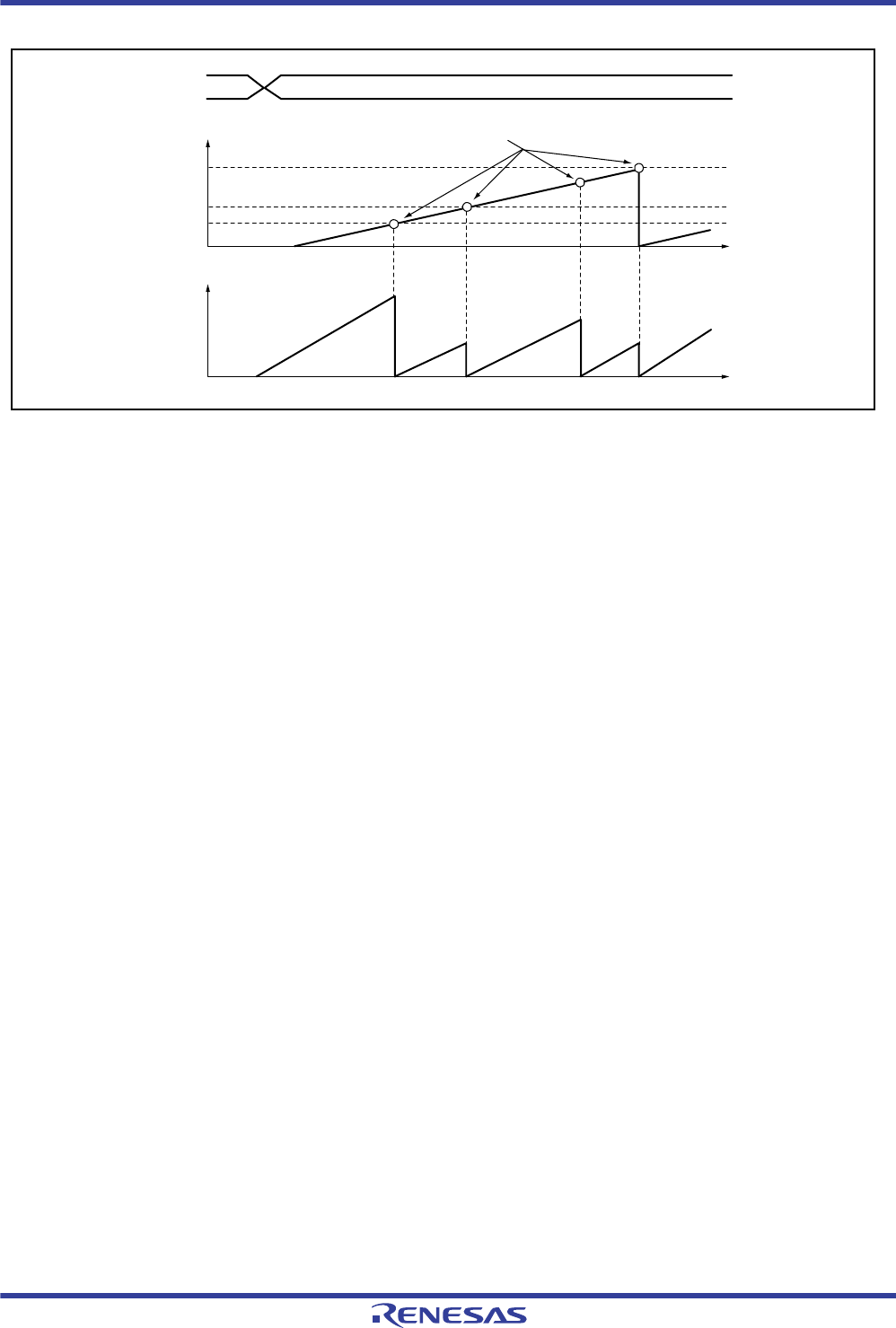
R01UH0034EJ0200 Rev.2.00 Page 636 of 1489
Dec 27, 2013
RX62T Group, RX62G Group 16. Multi-Function Timer Pulse Unit 3 (MTU3)
Figure 16.94 Example of Counter Clearing for MTU6 and MTU7 by Flag Setting Sources (2)
MTU0.TCNT
value
MTU0.TGRD
MTU0.TGRB
MTU0.TGRC
MTU0.TGRA
0000h Time
Compare match between MTU0.TCNT and TGR
MTU0.
TCNT
MTU7.TCNT
value
0000h Time
MTU7.
TCNT
TSYCR 00h F0h
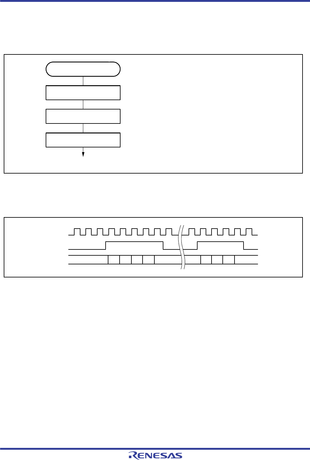
R01UH0034EJ0200 Rev.2.00 Page 637 of 1489
Dec 27, 2013
RX62T Group, RX62G Group 16. Multi-Function Timer Pulse Unit 3 (MTU3)
16.3.11 External Pulse Width Measurement
The pulse widths of up to three external input lines can be measured in MTU5.
(1) Example of External Pulse Width Measurement Setting Procedure
Figure 16.95 Example of External Pulse Width Measurement Setting Procedure
(2) Example of External Pulse Width Measurement
Figure 16.96 Example of External Pulse Width Measurement (Measuring High Pulse Width)
[1]
[2]
[3]
External pulse width
measurement
Select counter clock
Select pulse width measuring
conditions
Start count operation
<External pulse width measurement>
[1] Use bits TPSC1 and TPSC0 in MTU5.TCRU,
MTU5.TCRV, or MTU5.TCRW to select the counter
clock.
[2] In MTU5.TIORU, MTU5.TIORV, or MTU5.TIORW,
select the high level or low level for the pulse width
measuring condition.
[3] Set bit CSTU5, CSTV5, or CSTW5 in MTU5.TSTR to 1
to start count operation.
Notes: 1. Do not set bit CMPCLR5U, CMPCLR5V, or
CMPCLR5W in TCNTCMPCLR to 1.
2. Do not set bit TGIE5U, TGIE5V, or TGIE5W in
MTU5.TIER to 1.
3. The value in TCNT is not captured in TGR.
0001 0002 00030000 0004 0005 0006 0007 0008 0009
MTIC5U
MTU5.
TCNTU
ICLK

R01UH0034EJ0200 Rev.2.00 Page 638 of 1489
Dec 27, 2013
RX62T Group, RX62G Group 16. Multi-Function Timer Pulse Unit 3 (MTU3)
16.3.12 Dead Time Compensation
By measuring the delay of the output waveform and reflecting it to duty ratio, the external pulse width measurement
function can be used as the dead time compensation function while the complementary PWM is in operation.
Figure 16.97 Delay in Dead Time in Complementary PWM Operation
Tdead
Tdelay
Upper arm signal
Lower arm signal
Inverter output detection signal
Dead time delay signal
R01UH0034EJ0200 Rev.2.00 Page 639 of 1489
Dec 27, 2013
RX62T Group, RX62G Group 16. Multi-Function Timer Pulse Unit 3 (MTU3)
(1) Example of Dead Time Compensation Setting Procedure
Figure 16.98 shows an example of dead time compensation setting procedure by using three counters in MTU5.
Figure 16.98 Example of Dead Time Compensation Setting Procedure
Figure 16.99 Example of Motor Control Circuit Configuration
[3]
[4]
[5]
[1]
[2]
[1] Place MTU6 and MTU7 in complementary PWM mode. For details,
refer to section 16.3.8, Complementary PWM Mode.
[2] Specify the external pulse width measurement function for the
target TIOR in MTU5. For details, refer to section 16.3.11, External
Pulse Width Measurement.
[3] Set bits CST6 and CST7 in TSTRB and bits CSTU5, CSTV5,
and CSTW5 in MTU5.TSTR to 1 to start count operation.
[4] When the capture condition specified in TIOR is satisfied,
the MTU5.TCNT value is captured in MTU5.TGR.
[5] For U-phase dead time compensation, when an interrupt is
generated at the crest (TGIA6) or trough (TCIV7) in
complementary PWM mode, read the MTU5.TGRU value,
calculate the difference in time between MTU5.TGRU and
MTU6.TGRB, and write the corrected value to MTU6.TGRD
in the interrupt processing.
For the V phase and W phase, read the MTU5.TGRV and
MTU5.TGRW values and write the corrected values to
MTU7.TGRC and TGRD, respectively, in the same way as
for U-phase compensation.
The MTU5.TCNT value should be cleared through the
TCNTCMPCLR setting or by software.
Note: The ICR registers in the I/O port should be set up in
advance.
As an interrupt flag is set under the capture condition
specified in TIOR, do not enable interrupt requests in
MTU5.TIER.
Complementary PWM mode
External pulse width
measurement
Start count operation in
MTU6, MTU7 and MTU5
MTU5.TCNT input capture
occurs
Interrupt processing
MTU
ch6/7
ch5
Complementary
PWM output
Dead time
delay input Inverter output
monitor signals
-+
U# V#
W#
U
VW
U
V
WMotor
Level conversion
DC
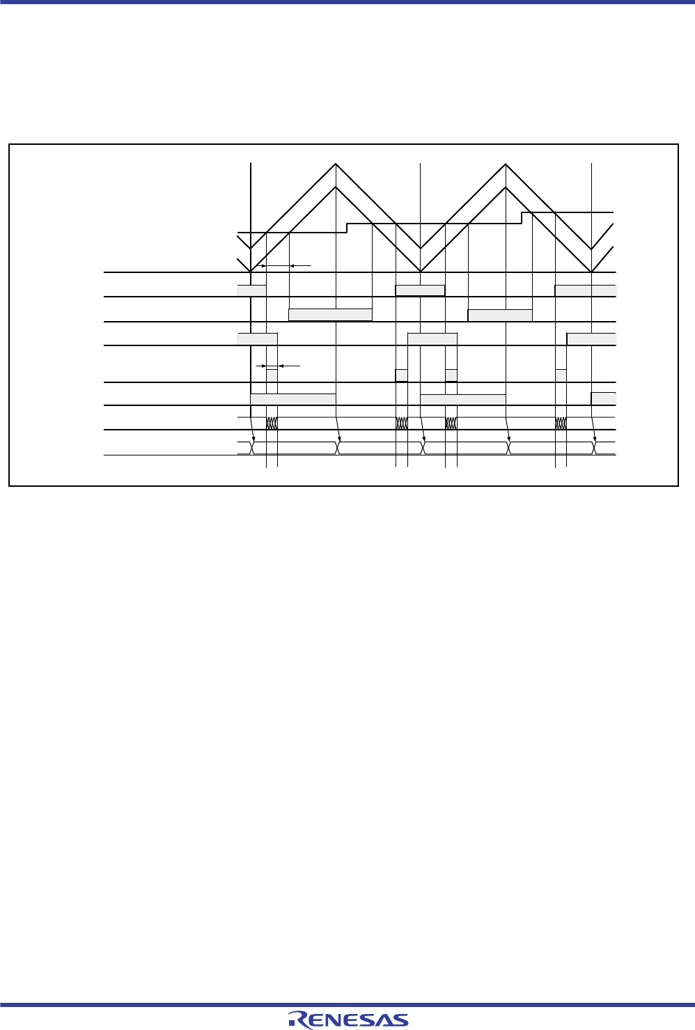
R01UH0034EJ0200 Rev.2.00 Page 640 of 1489
Dec 27, 2013
RX62T Group, RX62G Group 16. Multi-Function Timer Pulse Unit 3 (MTU3)
16.3.13 TCNT Capture at Crest and/or Trough in Complementary PWM Operation
The TCNT value is captured in TGR at either the crest or trough or at both the crest and trough during complementary
PWM operation. The timing for capturing in TGR can be selected by TIOR.
Figure 16.100 is an operating example in which TCNT is used as a free-running counter without being cleared, and the
TCNT value is captured in TGR at the specified timing (either crest or trough, or both crest and trough).
Figure 16.100 TCNT Capture at Crest and/or Trough in Complementary PWM Operation
Tdead
Tdelay
Upper arm signal
Lower arm signal
Inverter output monitor signal
Dead time delay signal
MTU7.TGRA
3DE7 3E5B
3E5B
3ED3
3ED3
3F37
3F37
3FAF
3FAF3DE7
TCNT[15:0]
TGR[15:0]
Up-count/down-count signal (udflg)

R01UH0034EJ0200 Rev.2.00 Page 641 of 1489
Dec 27, 2013
RX62T Group, RX62G Group 16. Multi-Function Timer Pulse Unit 3 (MTU3)
16.4 Interrupt Sources
16.4.1 Interrupt Sources and Priorities
There are three kinds of MTU3 interrupt source; TGR input capture/compare match, TCNT overflow, and TCNT
underflow. Each interrupt source has its own status flag and enable/disable bit, allowing the generation of interrupt
request signals to be enabled or disabled individually.
When an interrupt source is detected, the corresponding status flag in TSR is set to 1. If the corresponding enable/disable
bit in TIER is set to 1 at this time, an interrupt is requested. Setting the status flag to 1 cancels the interrupt request.
However, if a further interrupt is generated while the corresponding status flag is 1, the interrupt will be ignored. To
enable the acceptance of an interrupt, the flag of the interrupt generation source should be 0.
Relative channel priorities can be changed by the interrupt controller; however the priority within a channel is fixed. For
details, see section 11, Interrupt Controller (ICU).
Table 16.73 lists the MTU3 interrupt sources.

R01UH0034EJ0200 Rev.2.00 Page 642 of 1489
Dec 27, 2013
RX62T Group, RX62G Group 16. Multi-Function Timer Pulse Unit 3 (MTU3)
Note 1. This table shows the initial state immediately after a reset. The relative channel priorities can be changed by the interrupt
controller.
Table 16.73 MTU3 Interrupt Sources
Channel Name Interrupt Source DTC Activation Priority
MTU0 TGIA0 MTU0.TGRA input capture/compare match Possible High
Low
TGIB0 MTU0.TGRB input capture/compare match Possible
TGIC0 MTU0.TGRC input capture/compare match Possible
TGID0 MTU0.TGRD input capture/compare match Possible
TCIV0 MTU0.TCNT overflow Not possible
TGIE0 MTU0.TGRE compare match Not possible
TGIF0 MTU0.TGRF compare match Not possible
MTU1 TGIA1 MTU1.TGRA input capture/compare match Possible
TGIB1 MTU1.TGRB input capture/compare match Possible
TCIV1 MTU1.TCNT overflow Not possible
TCIU1 MTU1.TCNT underflow Not possible
MTU2 TGIA2 MTU2.TGRA input capture/compare match Possible
TGIB2 MTU2.TGRB input capture/compare match Possible
TCIV2 MTU2.TCNT overflow Not possible
TCIU2 MTU2.TCNT underflow Not possible
MTU3 TGIA3 MTU3.TGRA input capture/compare match Possible
TGIB3 MTU3.TGRB input capture/compare match Possible
TGIC3 MTU3.TGRC input capture/compare match Possible
TGID3 MTU3.TGRD input capture/compare match Possible
TCIV3 MTU3.TCNT overflow Not possible
MTU4 TGIA4 MTU4.TGRA input capture/compare match Possible
TGIB4 MTU4.TGRB input capture/compare match Possible
TGIC4 MTU4.TGRC input capture/compare match Possible
TGID4 MTU4.TGRD input capture/compare match Possible
TCIV4 MTU4.TCNT overflow/underflow (only in complementary PWM mode) Possible
MTU5 TGIU5 MTU5.TGRU input capture/compare match Possible
TGIV5 MTU5.TGRV input capture/compare match Possible
TGIW5 MTU5.TGRW input capture/compare match Possible
MTU6 TGIA6 MTU6.TGRA input capture/compare match Possible
TGIB6 MTU6.TGRB input capture/compare match Possible
TGIC6 MTU6.TGRC input capture/compare match Possible
TGID6 MTU6.TGRD input capture/compare match Possible
TCIV6 MTU6.TCNT overflow Not possible
MTU7 TGIA7 MTU7.TGRA input capture/compare match Possible
TGIB7 MTU7.TGRB input capture/compare match Possible
TGIC7 MTU7.TGRC input capture/compare match Possible
TGID7 MTU7.TGRD input capture/compare match Possible
TCIV7 MTU7.TCNT overflow/underflow (only in complementary PWM mode) Possible

R01UH0034EJ0200 Rev.2.00 Page 643 of 1489
Dec 27, 2013
RX62T Group, RX62G Group 16. Multi-Function Timer Pulse Unit 3 (MTU3)
(1) Input Capture/Compare Match Interrupt
An interrupt is requested if the TGIE bit in TIER is set to 1 when a TGR input capture/compare match occurs on a
channel and the TGE flag in TSR is set to 1. Clearing the TGE flag to 0 cancels the interrupt request. The MTU3 has 29
input capture/compare match interrupts (six for MTU0, four each for MTU3, MTU4, MTU6, and MTU7, two each for
MTU1 and MTU2, and three for MTU5). The MTU0.TGFE and MTU0.TGFF_0 flags in MTU0 are not set by the
occurrence of an input capture.
(2) Overflow Interrupt
An interrupt is requested if the TCIEV bit in TIER is set to 1 when a TCNT overflow occurs on a channel and the TCFV
flag in TSR is set to 1. Clearing the TCFV flag to 0 cancels the interrupt request. The MTU3 has seven overflow
interrupts (one for each channel).
Furthermore, when operation is in complementary PWM mode, an underflow of MTU4.TCNT and MTU7_4.TCNT
leads to setting of the TCVF flag.
(3) Underflow Interrupt
An interrupt is requested if the TCIEU bit in TIER is set to 1 when a TCNT underflow occurs on a channel and the TCFU
flag in TSR is set to 1. Clearing the TCFU flag to 0 cancels the interrupt request. The MTU3 has two underflow
interrupts (one each for MTU1 and MTU2).
16.4.2 DTC Activation
The DTC can be activated by the TGR input capture/compare match interrupt in each channel or the overflow interrupt in
MTU4 and MTU7. For details, see section 14, Data Transfer Controller (DTC).
The MTU3 provides a total of 29 input capture/compare match interrupts and overflow interrupts that can be used as
DTC activation sources: four each for MTU0, MTU3, and MTU6, two each for MTU1 and MTU2, five each for MTU4
and MTU7, and three for MTU5.
However, as similar to the interrupt handling, if a further DTC activation request is generated while the corresponding
status flag is 1, the interrupt will be ignored. To enable the acceptance of an interrupt, the flag of the interrupt generation
source should be 0.

R01UH0034EJ0200 Rev.2.00 Page 644 of 1489
Dec 27, 2013
RX62T Group, RX62G Group 16. Multi-Function Timer Pulse Unit 3 (MTU3)
16.4.3 A/D Converter Activation
The A/D converter can be activated by one of the following three methods in the MTU3. Table 16.73 shows the
relationship between interrupt sources and A/D converter start request signals.
(1) A/D Converter Activation by TGRA Input Capture/Compare Match or at MTU4.TCNT
(MTU7.TCNT) Trough in Complementary PWM Mode
The A/D converter can be activated by the occurrence of a TGRA input capture/compare match in each channel. In
addition, if complementary PWM operation is performed while the TTGE2 bit in MTU4.TIER (MTU7.TIER) is set to 1,
the A/D converter can be activated at the trough of MTU4.TCNT (MTU7.TCNT) count (MTU4.TCNT (MTU7.TCNT) =
0000h).
A/D converter start request signal TRGAnN is issued to the A/D converter under either of the following conditions (n =
MTU0 to MTU4, MTU6, or MTU7).
When a TGRA input capture/compare match occurs on a channel and the TGFA flag in TSR is set to 1 while the
TTGE bit in TIER is set to 1
When the MTU4.TCNT (MTU7.TCNT) count reaches the trough (MTU4.TCNT (MTU7.TCNT) = 0000h) during
complementary PWM operation while the TTGE2 bit in MTU4.TIER (MTU7.TIER) is set to 1
When either condition is satisfied, if A/D converter start signal TRGAnN from the MTU3 is selected as the trigger in the
A/D converter, A/D conversion will start.
(2) A/D Converter Activation by Compare Match between MTU0.TCNT and MTU0.TGRE
A/D converter start request signal TRG0N is issued to the A/D converter when a compare match occurs between
MTU0.TCNT and MTU0.TGRE in MTU0.
When the TGFE flag in MTU0.TSR2 is set to 1 by the occurrence of a compare match between MTU0.TCNT and
MTU0.TGRE in MTU0 while the TTGE2 bit in MTU0.TIER2 is set to 1, A/D converter start request TGR0N is issued to
the A/D converter. If A/D converter start signal TRG0N from the MTU3 is selected as the trigger in the A/D converter,
A/D conversion will start.
(3) A/D Converter Activation by A/D Converter Start Request Delaying Function
The A/D converter can be activated by generating A/D converter start request signal TRG4AN or TRG4BN (TRG7AN
or TRG7BN) when the MTU4.TCNT (MTU7.TCNT) count matches the MTU4.TADCORA or MTU4.TADCORB
(MTU7.TADCORA or MTU7.TADCORB) value if the UT4AE, DT4AE, UT4BE, or DT4BE (UT7AE, DT7AE,
UT7BE, or DT7BE) bit in the A/D converter start request control register (MTU4.TADCR (MTU7.TADCR)) is set to 1.
For details, refer to section 16.3.9, A/D Converter Start Request Delaying Function.
A/D conversion will start when TRG4AN (TRG7AN) is generated if A/D converter start signal TRG4AN (TRG7AN)
from the MTU3 is selected as the trigger in the A/D converter, when TRG4BN (TRG7BN) is generated if TRG4BN
(TRG7BN) from the MTU3 is selected as the trigger in the A/D converter, or when TRG4ABN (TRG7ABN) is
generated if TRG4ABN (TRG7ABN) from the MTU3 is selected as the trigger in the A/D converter.

R01UH0034EJ0200 Rev.2.00 Page 645 of 1489
Dec 27, 2013
RX62T Group, RX62G Group 16. Multi-Function Timer Pulse Unit 3 (MTU3)
Note 1. Since PWM waveforms are generated in complementary PWM mode, MTU4.TGRA (MTU7.TGRA) compare match not only with
MTU4.TCNT (MTU7.TCNT) but also with MTU3.TCNT (MTU6.TCNT) and TCNTSA (TCNTSB) is detected. Accordingly, when
compare match with MTU3.TCNT (MTU6.TCNT) and TCNTSA (TCNTSB) occurs, TRGA4N (TRGA7N) is also generated.
When MTU3 and MTU4 (MTU6 and MTU7) are made to operate in complementary PWM mode for generating an A/D converter
start request, use the A/D converter start request by compare match between MTU4.TCNT (MTU7.TCNT) and
MTU4.TADCORA/B (MTU7.TADCORA/B).
Table 16.74 Interrupt Sources and A/D Converter Start Request Signals
Target Registers Interrupt Source A/D Converter Start Request Signal
MTU0.TGRA and MTU0.TCNT Input capture/compare match TRGA0N
MTU1.TGRA and MTU1.TCNT TRGA1N
MTU2.TGRA and MTU2.TCNT TRGA2N
MTU3.TGRA and MTU3.TCNT TRGA3N
MTU4.TGRA and MTU4.TCNT*1TRGA4N
MTU4.TCNT MTU4.TCNT trough in complementary PWM
mode
MTU6.TGRA and MTU6.TCNT Input capture/compare match TRGA6N
MTU7.TGRA and MTU7.TCNT*1TRGA7N
MTU7.TCNT MTU7.TCNT trough in complementary PWM
mode
MTU0.TGRE and MTU0.TCNT Compare match TRG0AN
MTU4.TADCORA and MTU4.TCNT Compare match TRG4AN
MTU4.TADCORB and MTU4.TCNT TRG4BN
MTU7.TADCORA and MTU7.TCNT TRG7AN
MTU7.TADCORB and MTU7.TCNT TRG7BN
MTU4.TADCORA and MTU4.TCNT,
MTU4.TADCORB and MTU4.TCNT
Compare match (interrupt skipping function 2) TRG4ABN
MTU7.TADCORA and MTU7.TCNT,
MTU7.TADCORB and MTU7.TCNT
TRG7ABN
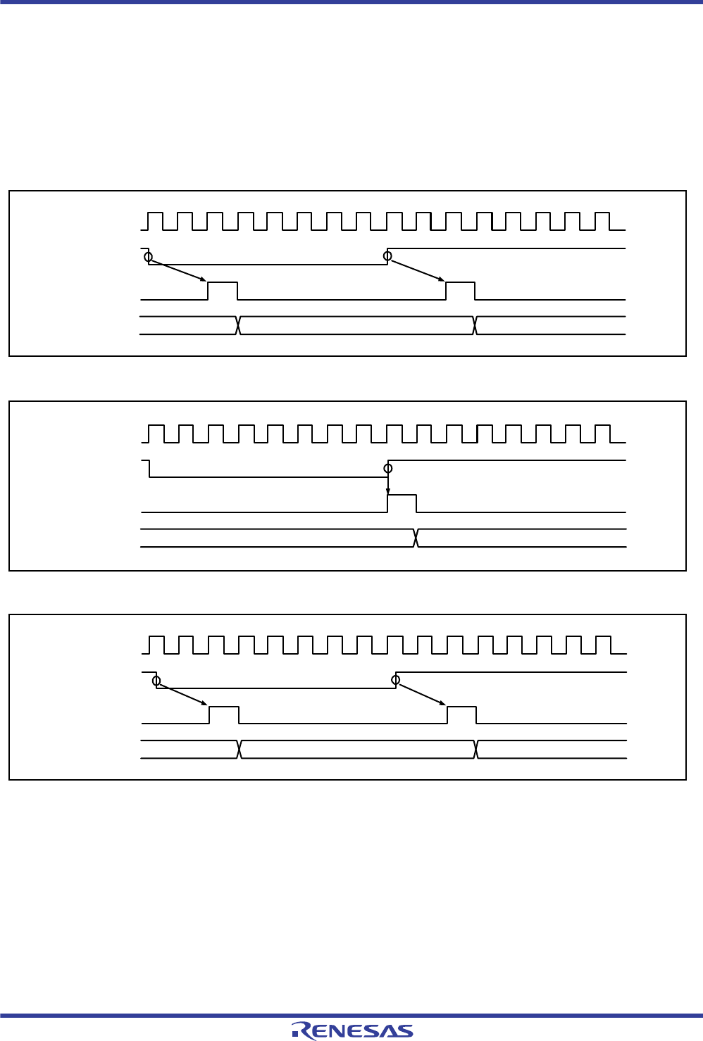
R01UH0034EJ0200 Rev.2.00 Page 646 of 1489
Dec 27, 2013
RX62T Group, RX62G Group 16. Multi-Function Timer Pulse Unit 3 (MTU3)
16.5 Operation Timing
16.5.1 Input/Output Timing
(1) TCNT Count Timing
Figure 16.101 and Figure 16.102 show the TCNT count timing in internal clock operation, Figure 16.103 shows the
TCNT count timing in external clock operation (normal mode), and Figure 16.104 shows the TCNT count timing in
external clock operation (phase counting mode).
Figure 16.101 Count Timing in Internal Clock Operation (MTU0 to MTU4, MTU6, and MTU7)
Figure 16.102 Count Timing in Internal Clock Operation (MTU5)
Figure 16.103 Count Timing in External Clock Operation (MTU0 to MTU4)
ICLK
Internal clock
TCNT
TCNT input
clock
Falling edge Rising edge
N - 1 N N + 1
ICLK
Internal clock
TCNT
Rising edge
N - 1 N
TCNT input
clock
Falling edge Rising edge
N - 1 N N + 1
ICLK
External clock
TCNT
TCNT input
clock
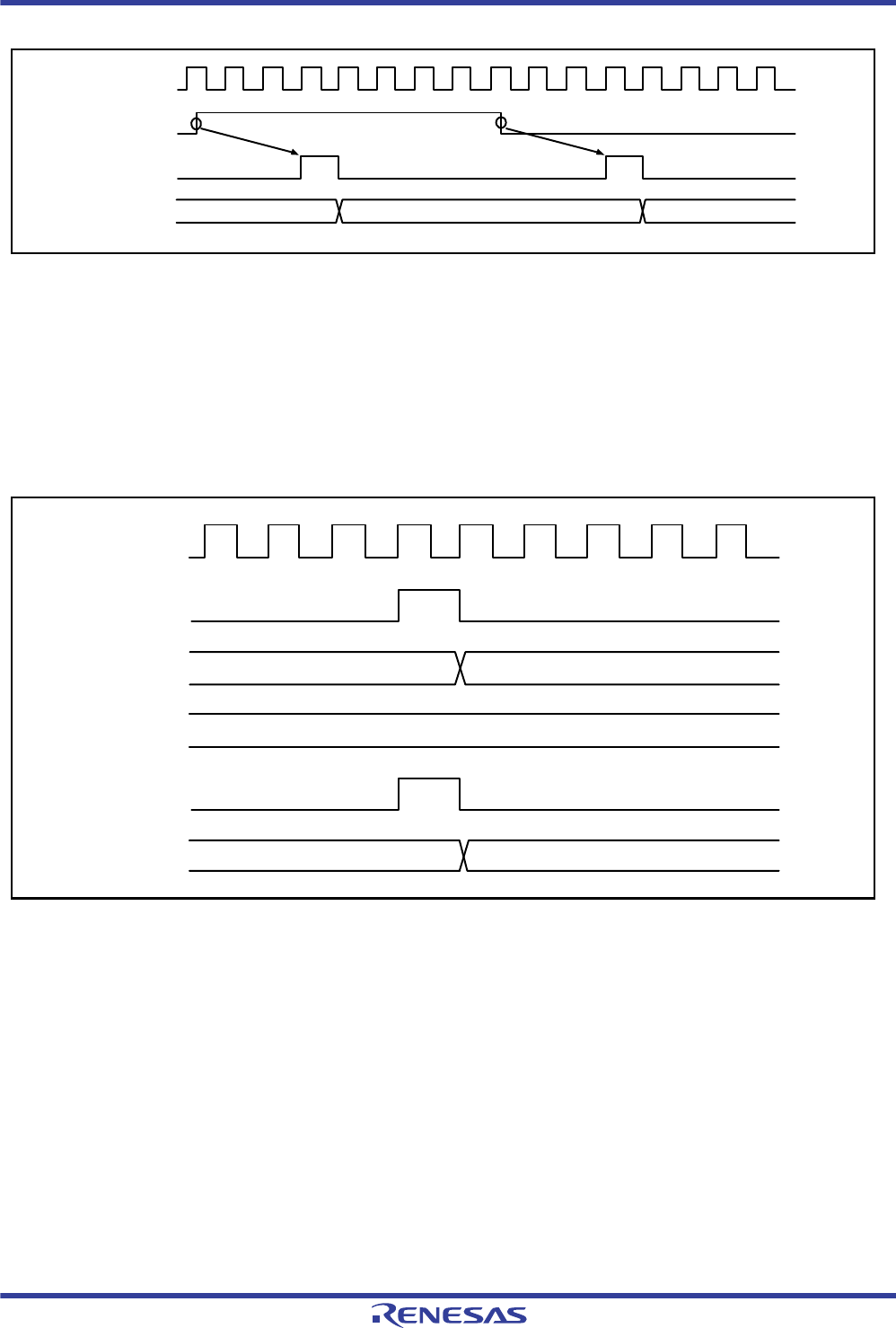
R01UH0034EJ0200 Rev.2.00 Page 647 of 1489
Dec 27, 2013
RX62T Group, RX62G Group 16. Multi-Function Timer Pulse Unit 3 (MTU3)
Figure 16.104 Count Timing in External Clock Operation (Phase Counting Mode)
(2) Output Compare Output Timing
A compare match signal is generated in the final state in which TCNT and TGR match (the point at which the count
value matched by TCNT is updated). When a compare match signal is generated, the value set in TIOR is output from
the output compare output pin (MTIOC pin). After a match between TCNT and TGR, the compare match signal is not
generated until the TCNT input clock is generated.
Figure 16.105 shows the output compare output timing (normal mode or PWM mode) and Figure 16.106 shows the
output compare output timing (complementary PWM mode or reset-synchronized PWM mode).
Figure 16.105 Output Compare Output Timing (Normal Mode or PWM Mode)
Falling edge
Rising edge
N - 1 N N - 1
ICLK
External clock
TCNT
TCNT input
clock
NN + 1
N
TCNT
TGR
Compare
match signal
MTIOC pin
ICLK
TCNT input
clock
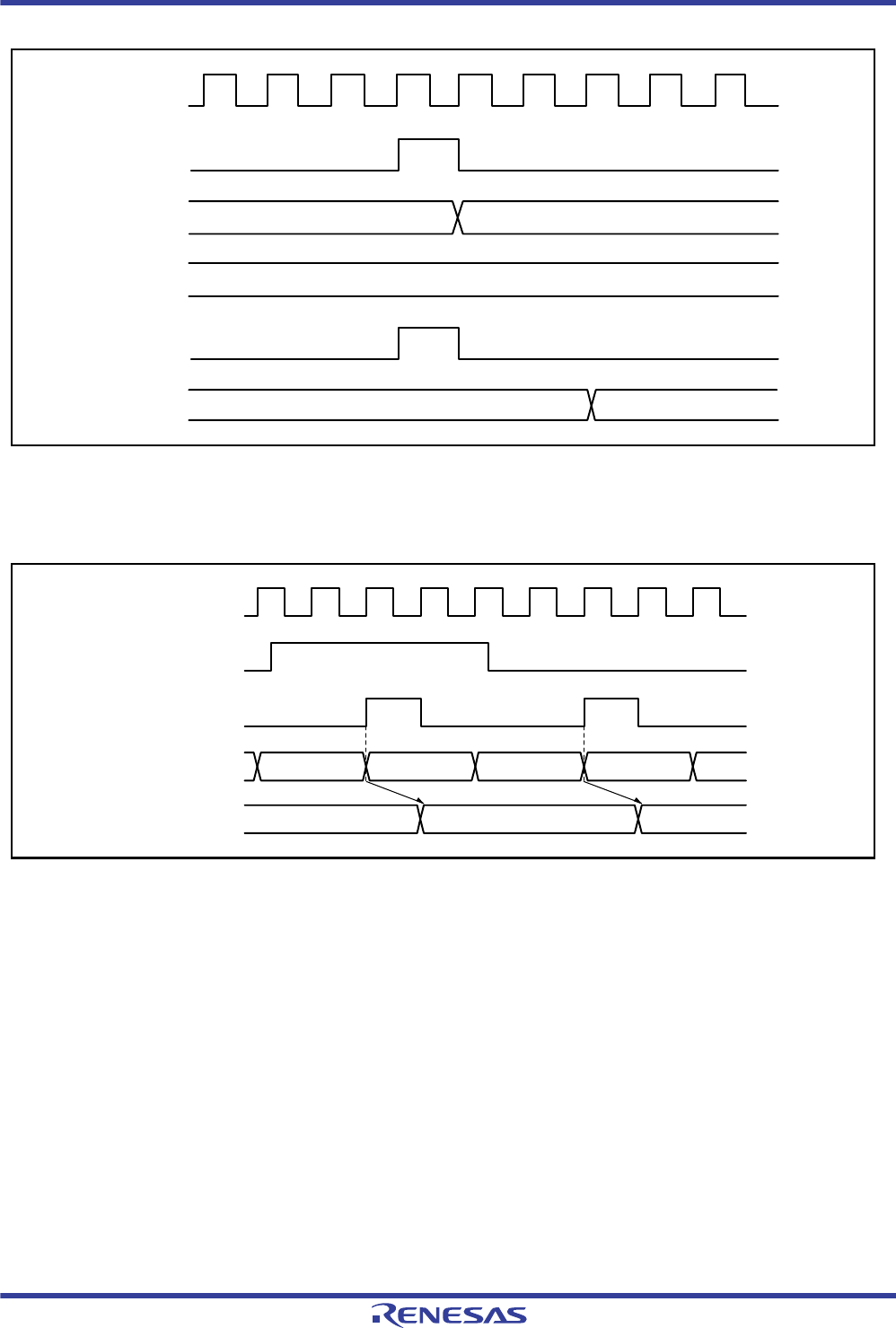
R01UH0034EJ0200 Rev.2.00 Page 648 of 1489
Dec 27, 2013
RX62T Group, RX62G Group 16. Multi-Function Timer Pulse Unit 3 (MTU3)
Figure 16.106 Output Compare Output Timing (Complementary PWM Mode or Reset-Synchronized PWM Mode)
(3) Input Capture Signal Timing
Figure 16.107 shows the input capture signal timing.
Figure 16.107 Input Capture Input Signal Timing
NN + 1
N
TCNT
TGR
Compare
match signal
MTIOC pin
TCNT input
clock
ICLK
TCNT NN + 1
N
TGR
Input capture
signal
ICLK
Input capture
input
N + 2
N + 2
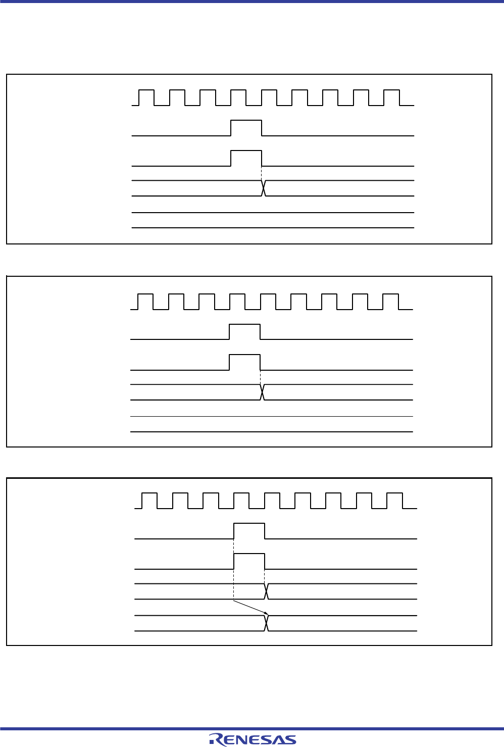
R01UH0034EJ0200 Rev.2.00 Page 649 of 1489
Dec 27, 2013
RX62T Group, RX62G Group 16. Multi-Function Timer Pulse Unit 3 (MTU3)
(4) Timing for Counter Clearing by Compare Match/Input Capture
FFigure 16.108 and Figure 16.109 show the timing when counter clearing on compare match is specified, and Figure
16.110 shows the timing when counter clearing on input capture is specified.
Figure 16.108 Counter Clear Timing (Compare Match) (MTU0 to MTU4, MTU6, and MTU7)
Figure 16.109 Counter Clear Timing (Compare Match) (MTU5)
Figure 16.110 Counter Clear Timing (Input Capture) (MTU0 to MTU7)
TCNT
Counter
clear signal
Compare
match signal
ICLK
TGR N
N 0000h
N
N - 1 0000h
TCNT
Counter
clear signal
Compare
match signal
ICLK
TGR
N 0000h
N
TCNT
Counter
clear signal
Input capture
signal
ICLK
TGR

R01UH0034EJ0200 Rev.2.00 Page 650 of 1489
Dec 27, 2013
RX62T Group, RX62G Group 16. Multi-Function Timer Pulse Unit 3 (MTU3)
(5) Buffer Operation Timing
Figure 16.111 to Figure 16.113 show the timing in buffer operation.
Figure 16.111 Buffer Operation Timing (Compare Match)
Figure 16.112 Buffer Operation Timing (Input Capture)
Figure 16.113 Buffer Operation Timing (when TCNT Cleared)
nN
N
nn + 1
TGRA,
TGRB
Compare
match signal
ICLK
TGRC,
TGRD
TCNT
N
n
n
N
NN + 1
Input capture
signal
ICLK
TCNT
TGRA,
TGRB
TGRC,
TGRD
N + 1
nN
N
n 0000h
TCNT clear
signal
ICLK
TCNT
TGRA, TGRB,
TGRE
TGRC, TGRD,
TGRF
Buffer transfer
signal
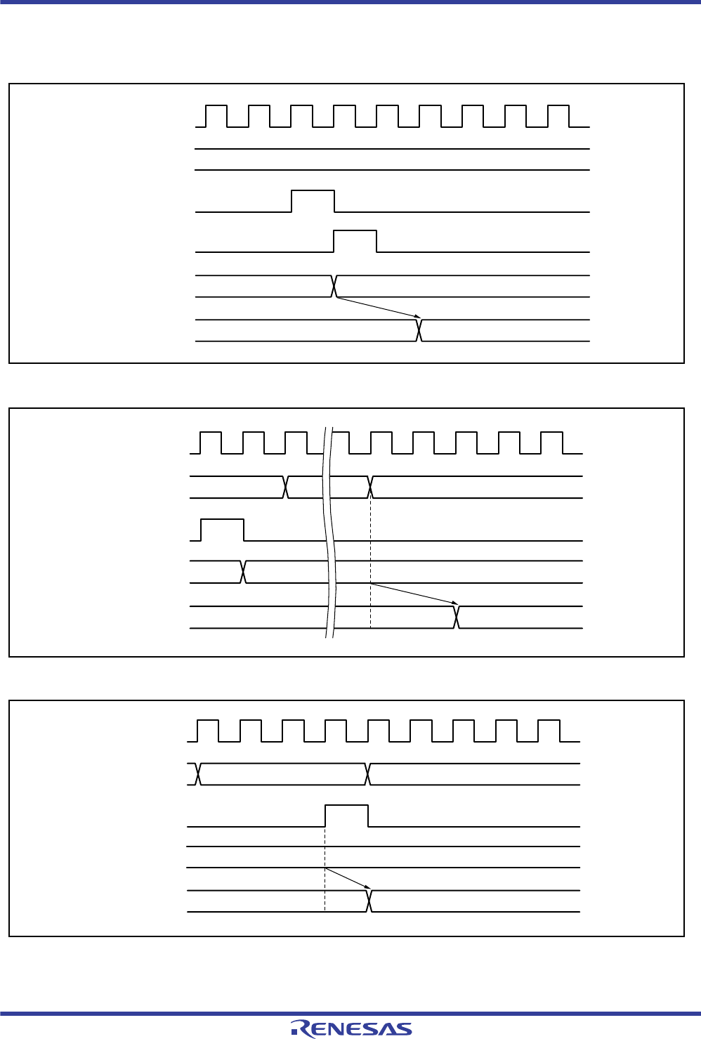
R01UH0034EJ0200 Rev.2.00 Page 651 of 1489
Dec 27, 2013
RX62T Group, RX62G Group 16. Multi-Function Timer Pulse Unit 3 (MTU3)
(6) Buffer Transfer Timing (Complementary PWM Mode)
Figure 16.114 to Figure 16.116 show the buffer transfer timing in complementary PWM mode.
Figure 16.114 Transfer Timing from Buffer Register to Temporary Register (TCNTSA Stopped)
Figure 16.115 Transfer Timing from Buffer Register to Temporary Register (TCNTSA Operating)
Figure 16.116 Transfer Timing from Temporary Register to Compare Register
nN
nN
0000h
Buffer register
MTU4.TGRD
write signal
Temporary register
transfer signal
TCNTS
Temporary register
ICLK
nN
nN
P - x P 0000h
Buffer register
MTU4.TGRD
write signal
TCNTS
Temporary
register
ICLK
N
nN
P - 1 P 0000h
Temporary
register
Buffer transfer
signal
TCNTS
Compare
register
ICLK
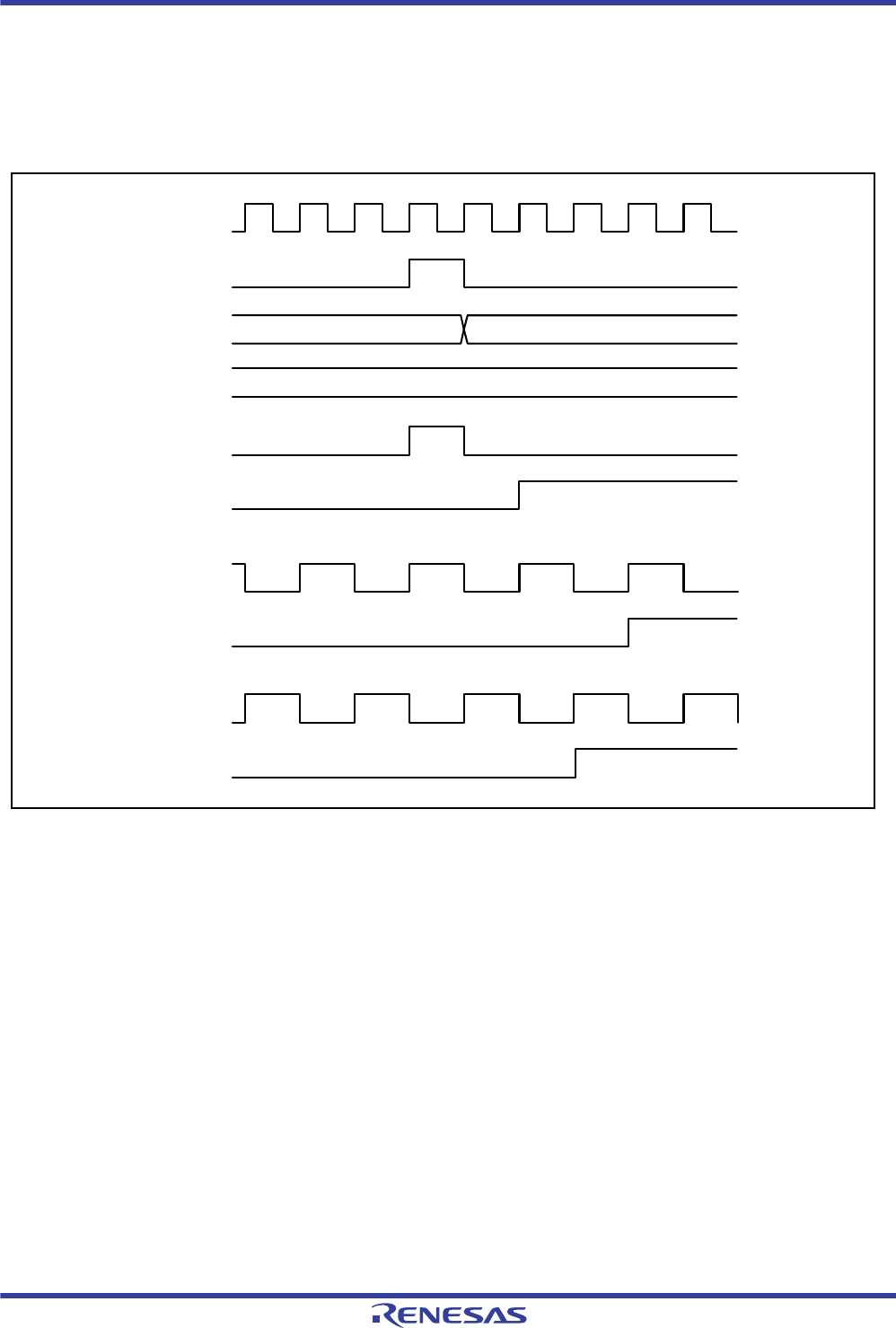
R01UH0034EJ0200 Rev.2.00 Page 652 of 1489
Dec 27, 2013
RX62T Group, RX62G Group 16. Multi-Function Timer Pulse Unit 3 (MTU3)
16.5.2 Interrupt Signal Timing
(1) Timing for TGF Flag Setting by Compare Match
Figure 16.117 and Figure 16.118 show the timing of TGF flag setting in TSR on compare match and the TGI interrupt
request signal timing.
Figure 16.117 TGI Interrupt Timing (Compare Match) (MTU0 to MTU4, MTU6, and MTU7)
TGR
TCNT
TCNT
input clock
N
NN + 1
Compare
match signal
TGF flag
Compare match generated while PCLK is high
TGI
interrupt
Compare match generated while PCLK is low
TGI
interrupt
ICLK
PCLK
PCLK
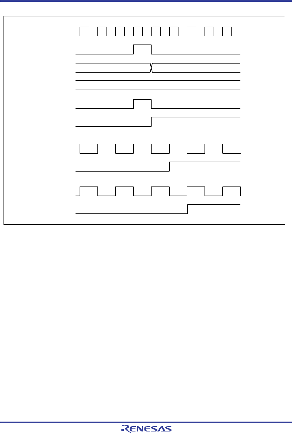
R01UH0034EJ0200 Rev.2.00 Page 653 of 1489
Dec 27, 2013
RX62T Group, RX62G Group 16. Multi-Function Timer Pulse Unit 3 (MTU3)
Figure 16.118 TGI Interrupt Timing (Compare Match) (MTU5)
TGR
TCNT
N
N - 1 N
ICLK
PCLK
PCLK
TCNT
input clock
Compare
match signal
TGF flag
Compare match generated while PCLK is high
TGI
interrupt
Compare match generated while PCLK is low
TGI
interrupt

R01UH0034EJ0200 Rev.2.00 Page 654 of 1489
Dec 27, 2013
RX62T Group, RX62G Group 16. Multi-Function Timer Pulse Unit 3 (MTU3)
(2) Timing for TGF Flag Setting by Input Capture
Figure 16.119 and Figure 16.120 show the timing of TGF flag setting in TSR on input capture and the TGI interrupt
request signal timing.
Figure 16.119 TGI Interrupt Timing (Input Capture) (MTU0 to MTU4, MTU6, and MTU7)
Input capture generated while PCLK is high
TGI
interrupt
TGI
interrupt
TGR
TCNT
Input capture
signal
N
N
TGF flag
ICLK
PCLK
Input capture generated while PCLK is low
PCLK
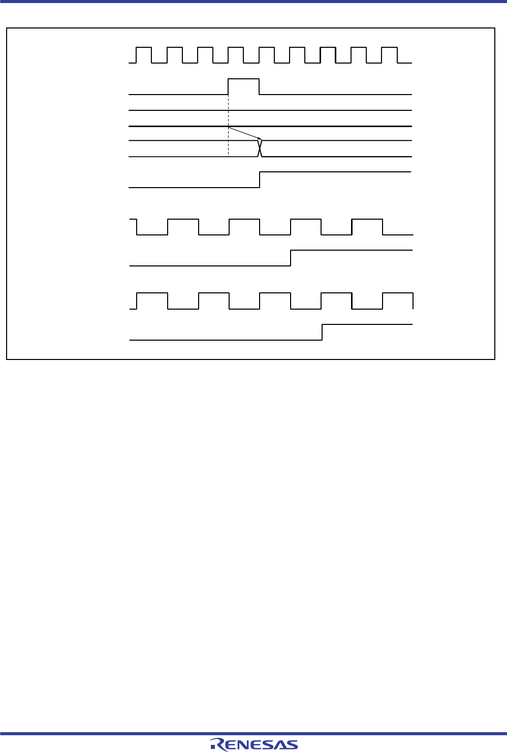
R01UH0034EJ0200 Rev.2.00 Page 655 of 1489
Dec 27, 2013
RX62T Group, RX62G Group 16. Multi-Function Timer Pulse Unit 3 (MTU3)
Figure 16.120 TGI Interrupt Timing (Input Capture) (MTU5)
N
N
Input capture generated while PCLK is high
TGI
interrupt
TGI
interrupt
TGR
TCNT
Input capture
signal
TGF flag
ICLK
PCLK
Input capture generated while PCLK is low
PCLK
Note1: Set the TGF flag while TCNT is stopped.
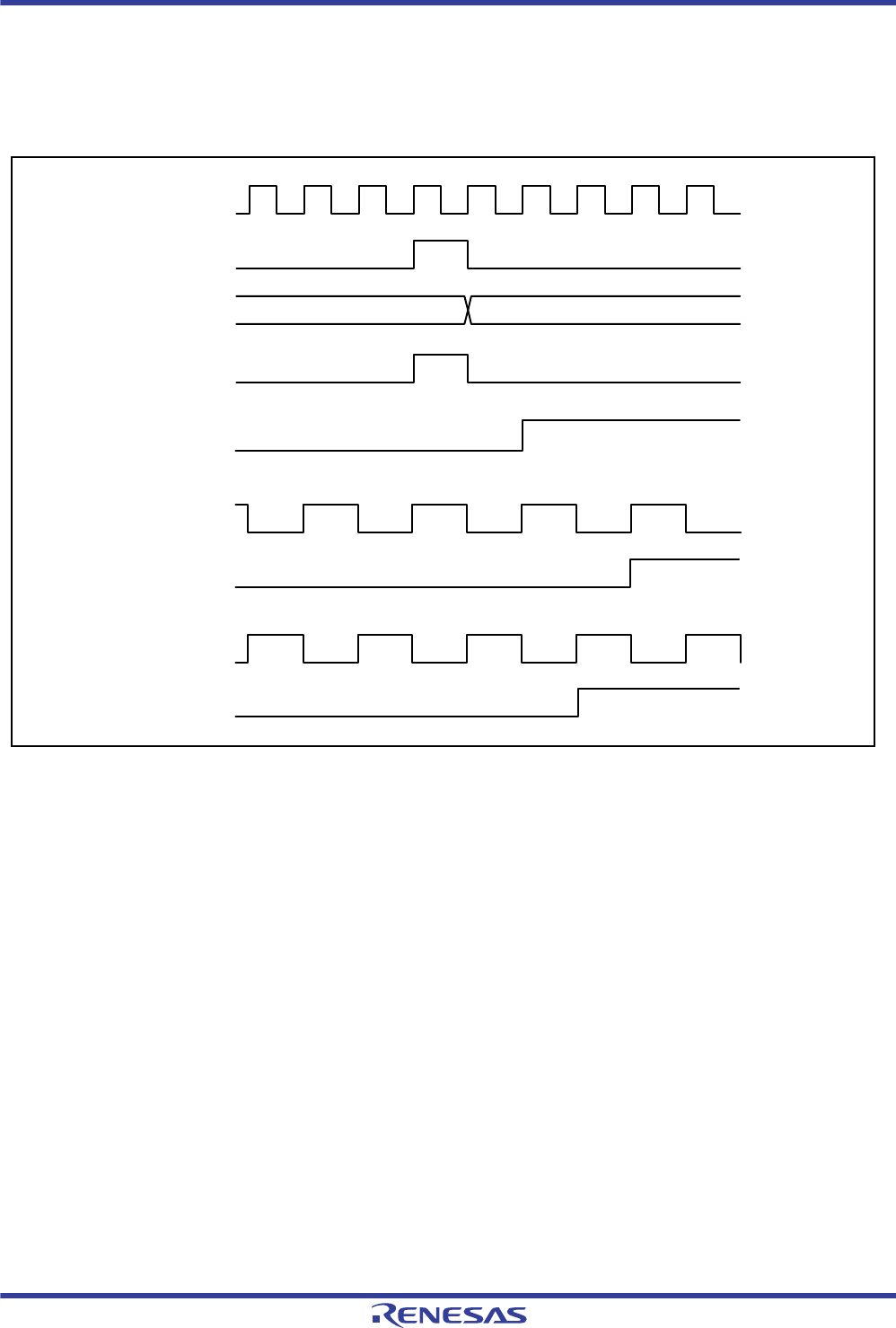
R01UH0034EJ0200 Rev.2.00 Page 656 of 1489
Dec 27, 2013
RX62T Group, RX62G Group 16. Multi-Function Timer Pulse Unit 3 (MTU3)
(3) TCFV and TCFU Interrupt Timing
Figure 16.121 shows the timing of TCFV flag setting in TSR on overflow and the TCIV interrupt request signal timing.
Figure 16.122 shows the timing of TCFU flag setting in TSR on underflow and the TCIU interrupt request signal
timing.
Figure 16.121 TCIV Interrupt Setting Timing
Input capture generated while PCLK is high
TCIV
interrupt
TCIV
interrupt
Overflow
signal
TCNT
(overflow)
TCNT
input clock
FFFFh 0000h
TCFV flag
ICLK
PCLK
Input capture generated while PCLK is low
PCLK
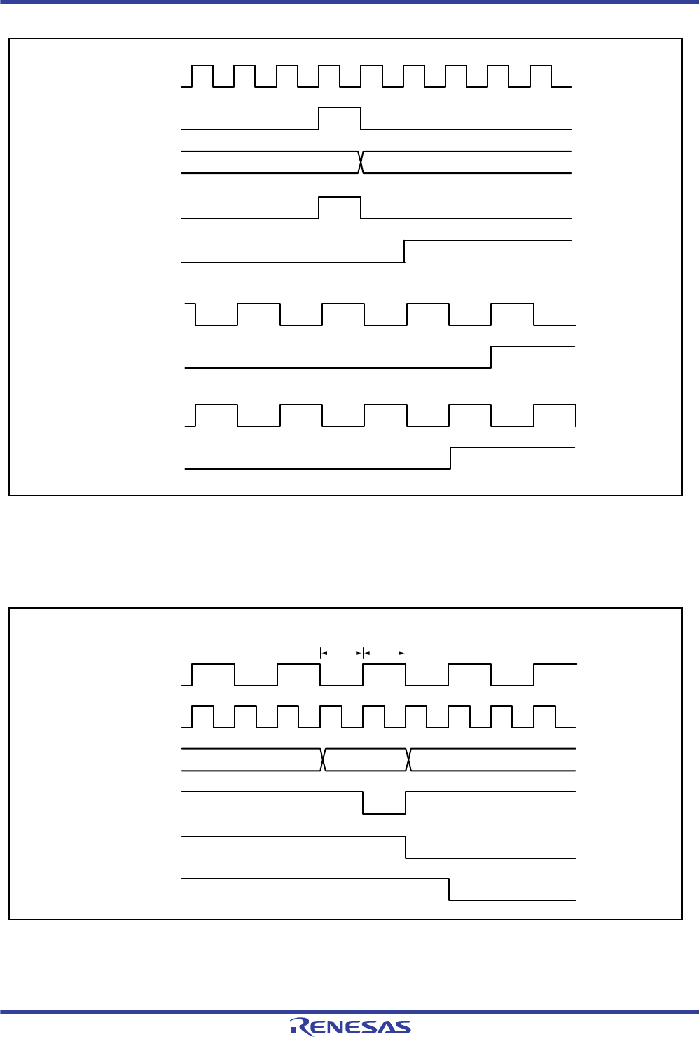
R01UH0034EJ0200 Rev.2.00 Page 657 of 1489
Dec 27, 2013
RX62T Group, RX62G Group 16. Multi-Function Timer Pulse Unit 3 (MTU3)
Figure 16.122 TCIU Interrupt Setting Timing
(4) Status Flag Clearing Timing
After the CPU reads a status flag as 1, it is cleared by writing 0 to it. Figure 16.123 shows the timing for status flag
clearing by the CPU.
Figure 16.123 Timing for Status Flag Clearing by CPU (MTU0 to MTU7)
TCIU
interrupt
TCIU
interrupt
Underflow
signal
TCNT
(underflow)
TCNT
input clock
0000h FFFFh
TCFU flag
ICLK
Input capture generated while PCLK is high
PCLK
Input capture generated while PCLK is low
PCLK
Status flag
Write signal
Address TSR address
Interrupt
request signal
TSR write cycle
T1 T2
PCLK
ICLK
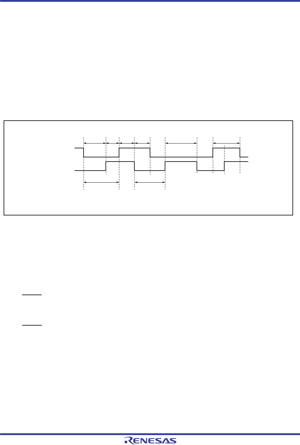
R01UH0034EJ0200 Rev.2.00 Page 658 of 1489
Dec 27, 2013
RX62T Group, RX62G Group 16. Multi-Function Timer Pulse Unit 3 (MTU3)
16.6 Usage Notes
16.6.1 Module Stop Function Setting
MTU3 operation can be disabled or enabled using the module stop control register. MTU3 operation is stopped with the
initial setting. Register access is enabled by clearing the module clock stop mode. For details, refer to section 9, Low
Power Consumption.
16.6.2 Input Clock Restrictions
The input clock pulse width must be at least 3 states for single-edge detection, and at least 5 states for both-edge
detection. The MTU3 will not operate properly at narrower pulse widths.
In phase counting mode, the phase difference and overlap between the two input clocks must be at least 3 states, and the
pulse width must be at least 5 states. Figure 16.124 shows the input clock conditions in phase counting mode.
Figure 16.124 Phase Difference, Overlap, and Pulse Width in Phase Counting Mode
16.6.3 Note on Cycle Setting
When counter clearing on compare match is set, TCNT is cleared in the final state in which it matches the TGR value
(the point at which TCNU updates the matched count value). Consequently, the actual counter frequency is given by the
following formula:
MTU0 to MTU4, MTU6, and MTU7
MTU5
f: Counter frequency
ICLK: MTU3 clock operating frequency
N: TGR setting
Pulse width
Notes: Phase difference and overlap: 3 states or more
Pulse width: 5 states or more
MTCLKA
(MTCLKC)
Overlap
Phase
differ-
ence Overlap
Phase
differ-
ence Pulse width
Pulse width Pulse width
MTCLKB
(MTCLKD)
f = ICLK
(N + 1)
f = ICLK
N
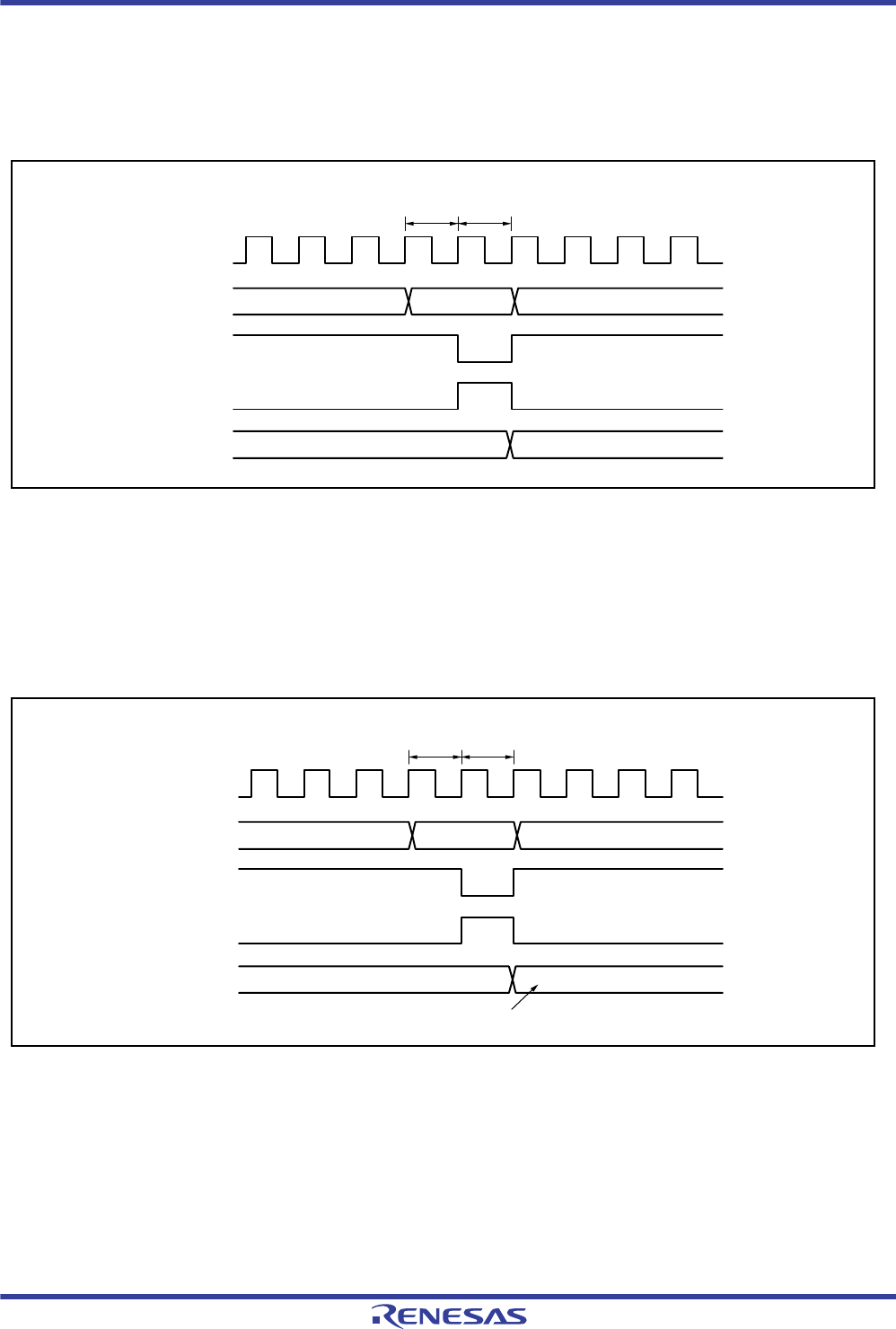
R01UH0034EJ0200 Rev.2.00 Page 659 of 1489
Dec 27, 2013
RX62T Group, RX62G Group 16. Multi-Function Timer Pulse Unit 3 (MTU3)
16.6.4 Contention between TCNT Write and Clear Operations
If the counter clear signal is generated in the T2 state of a TCNT write cycle, TCNT clearing takes precedence and TCNT
write operation is not performed.
Figure 16.125 shows the timing in this case.
Figure 16.125 Contention between TCNT Write and Clear Operations
16.6.5 Contention between TCNT Write and Increment Operations
If incrementing occurs in the T2 state of a TCNT write cycle, TCNT write operation takes precedence and TCNT is not
incremented.
Figure 16.126 shows the timing in this case.
Figure 16.126 Contention between TCNT Write and Increment Operations
Counter
clear signal
Write signal
Address TCNT address
TCNT
TCNT write cycle
T1 T2
N0000h
ICLK
TCNT
input clock
TCNT
T1 T2
N M
TCNT write data
ICLK
Write signal
Address TCNT address
TCNT write cycle
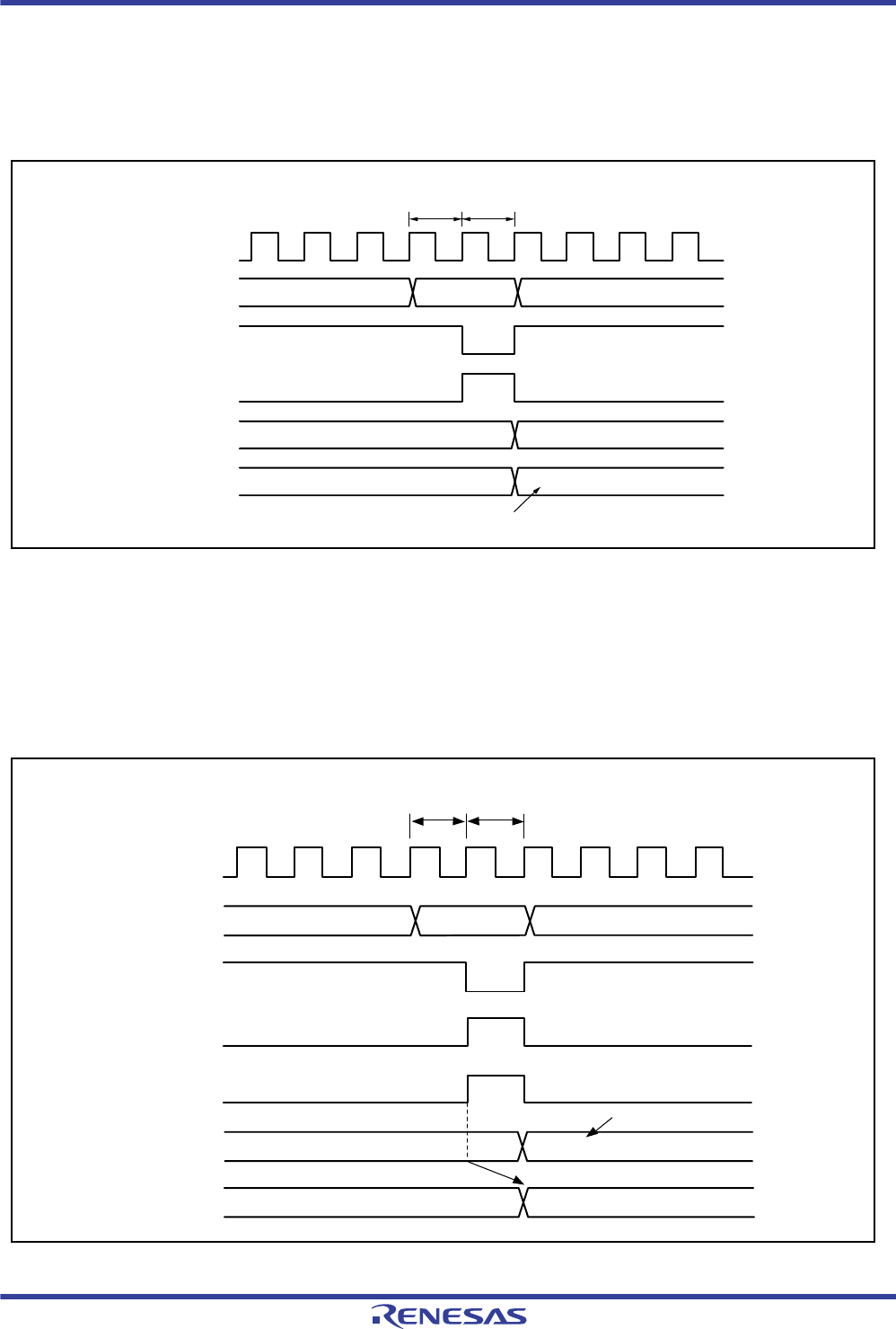
R01UH0034EJ0200 Rev.2.00 Page 660 of 1489
Dec 27, 2013
RX62T Group, RX62G Group 16. Multi-Function Timer Pulse Unit 3 (MTU3)
16.6.6 Contention between TGR Write Operation and Compare Match
If a compare match occurs in the T2 state of a TGR write cycle, TGR write operation is executed and the compare match
signal is also generated.
Figure 16.127 shows the timing in this case.
Figure 16.127 Contention between TGR Write Operation and Compare Match
16.6.7 Contention between Buffer Register Write Operation and Compare Match
If a compare match occurs in the T2 state in a TGR write cycle, the data before write operation is transferred to TGR by
the buffer operation.
Figure 16.128 shows the timing in this case.
Figure 16.128 Contention between Buffer Register Write Operation and Compare Match
Compare
match signal
Write signal
Address TGR address
TCNT
TGR write cycle
T1 T2
N M
TGR write data
TGR
NN+1
ICLK
ICLK
Address
Write signal
Compare
match signal
Compare match
buffer signal
TGR write cycle
T1 T2
Buffer register
address
N
NM
Buffer register write data
Buffer register
TGR
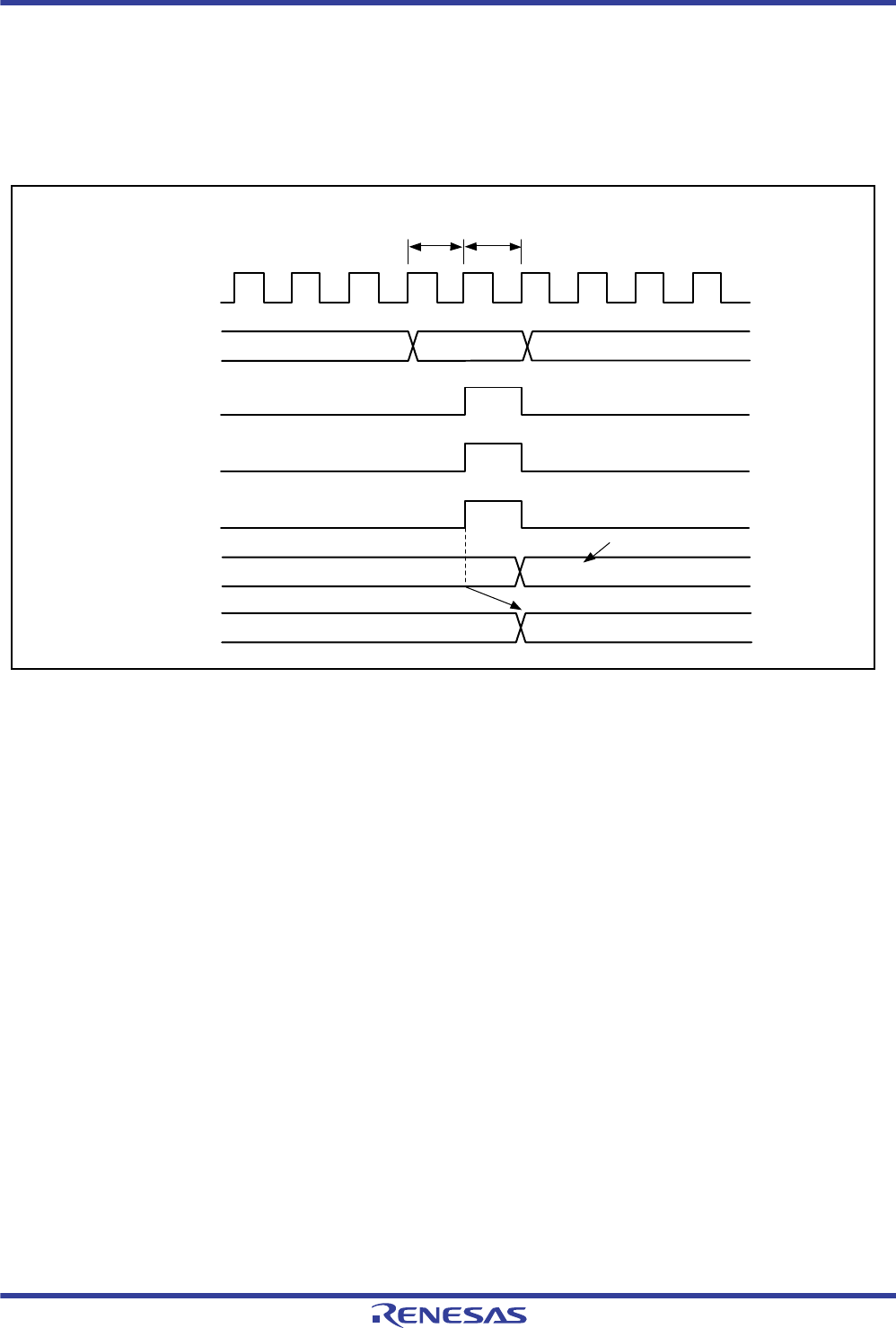
R01UH0034EJ0200 Rev.2.00 Page 661 of 1489
Dec 27, 2013
RX62T Group, RX62G Group 16. Multi-Function Timer Pulse Unit 3 (MTU3)
16.6.8 Contention between Buffer Register Write and TCNT Clear Operations
When the buffer transfer timing is set at the TCNT clear timing by the buffer transfer mode register (TBTM), if TCNT
clearing occurs in the T2 sate in a TGR write cycle, the data before write operation is transferred to TGR by the buffer
operation.
Figure 16.129 shows the timing in this case.
Figure 16.129 Contention between Buffer Register Write and TCNT Clear Operations
ICLK
TCNT clear
signal
Buffer transfer
signal
T1 T2
N
NM
TGR
Address
Write signal
TGR write cycle
Buffer register
address
Buffer register write data
Buffer register
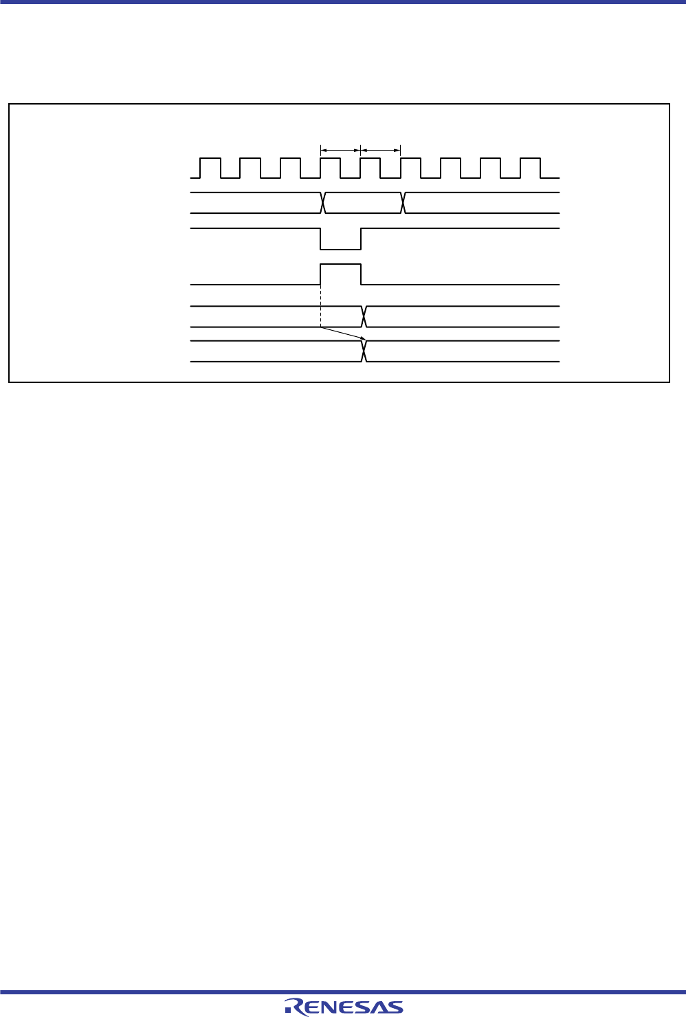
R01UH0034EJ0200 Rev.2.00 Page 662 of 1489
Dec 27, 2013
RX62T Group, RX62G Group 16. Multi-Function Timer Pulse Unit 3 (MTU3)
16.6.9 Contention between TGR Read Operation and Input Capture
If an input capture signal is generated in the T1 state in a TGR read cycle, the data before input capture transfer is read.
Figure 16.130 shows the timing in this case.
Figure 16.130 Contention between TGR Read Operation and Input Capture (MTU0 to MTU7)
Input
capture signal
Read signal
Address
TGR read cycle
T1 T2
N
TGR M
N
Internal data bus
TGR address
ICLK
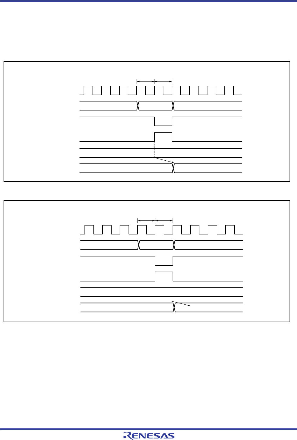
R01UH0034EJ0200 Rev.2.00 Page 663 of 1489
Dec 27, 2013
RX62T Group, RX62G Group 16. Multi-Function Timer Pulse Unit 3 (MTU3)
16.6.10 Contention between TGR Write Operation and Input Capture
If an input capture signal is generated in the T2 state in a TGR write cycle, the input capture operation takes precedence
and the TGR write operation is not performed in MTU0 to MTU4, MTU6, and MTU7. In cMTU5, the TGR write
operation is performed and the input capture signal is generated.
Figure 16.131 and Figure 16.132 show the timing in this case.
Figure 16.131 Contention between TGR Write Operation and Input Capture (MTU0 to MTU4, MTU6, and MTU7)
Figure 16.132 Contention between TGR Write Operation and Input Capture (MTU5)
Input
capture signal
Write signal
Address
TCNT
TGR write cycle
T1 T2
M
TGR
M
TGR address
ICLK
TCNT
T1 T2
N
TGR
M
TGR write data
ICLK
Input
capture signal
Write signal
Address
TGR write cycle
TGR address
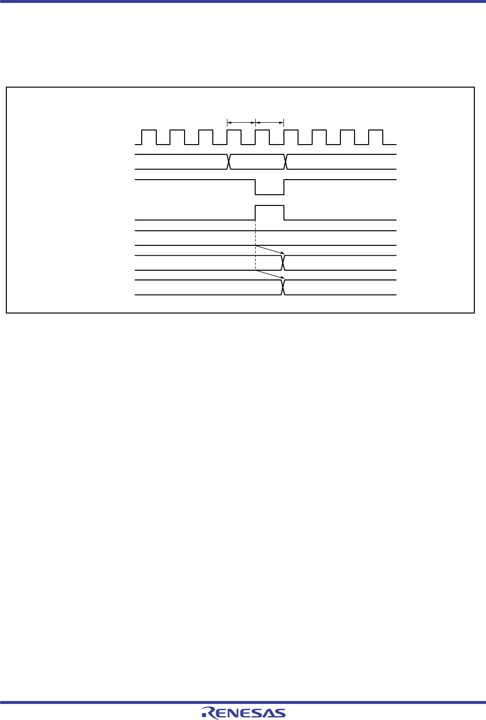
R01UH0034EJ0200 Rev.2.00 Page 664 of 1489
Dec 27, 2013
RX62T Group, RX62G Group 16. Multi-Function Timer Pulse Unit 3 (MTU3)
16.6.11 Contention between Buffer Register Write Operation and Input Capture
If an input capture signal is generated in the T2 state in a buffer register write cycle, the buffer operation takes
precedence and the buffer register write operation is not performed.
Figure 16.133 shows the timing in this case.
Figure 16.133 Contention between Buffer Register Write Operation and Input Capture
Input
capture signal
Write signal
Address
TCNT
Buffer register write cycle
T1 T2
N
TGR
N
M
M
Buffer
register
ICLK
Buffer register
address
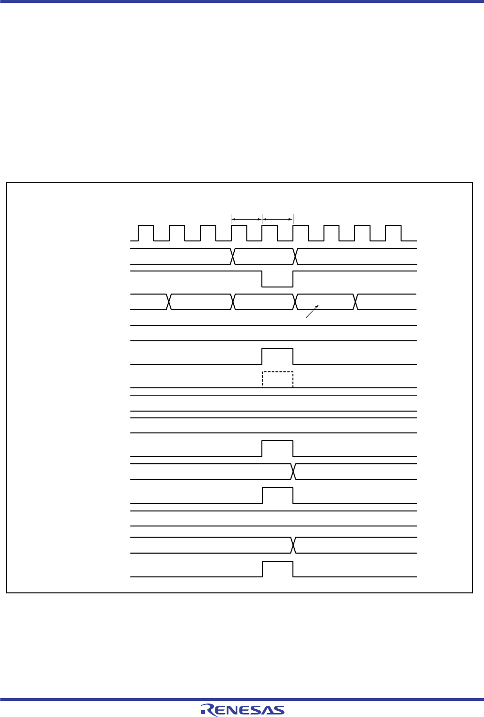
R01UH0034EJ0200 Rev.2.00 Page 665 of 1489
Dec 27, 2013
RX62T Group, RX62G Group 16. Multi-Function Timer Pulse Unit 3 (MTU3)
16.6.12 Contention between MTU2.TCNT Write Operation and Overflow/Underflow in
Cascaded Operation
With timer counters MTU1.TCNT and MTU2.TCNT in a cascade, when a contention occurs between MTU1.TCNT
counting (an MTU2.TCNT overflow/underflow) and the MTU2.TCNT write cycle, the MTU2.TCNT write operation is
performed and the MTU1.TCNT count signal is disabled. In this case, if MTU1.TGRA works as a compare match
register and there is a match between the MTU1.TGRA and MTU1.TCNT values, a compare match signal is issued.
Furthermore, when the MTU1.TCNT count clock is selected as the input capture source of MTU0, MTU0.TGRA to
MTU0.TGRD work in input capture mode. In addition, when the MTU0.TGRC compare match/input capture is selected
as the input capture source of MTU1.TGRB, MTU1.TGRB works in input capture mode.
Figure 16.134 shows the timing in this case.
When setting the TCNT clearing function in cascaded operation, be sure to synchronize MTU1 and MTU2.
Figure 16.134 Contention between MTU2.TCNT Write Operation and Overflow/Underflow in Cascaded Operation
TCNT write cycle
T1 T2
Address
Write signal
MTU2.TCNT
MTU1.TCNT
input clock
MTU1.TCNT
MTU1.TGRA
MTU1.TGRB
MTU0.TCNT
MTU0.TGRA to
MTU0.TGRD
MTU2.TGRA to
MTU2.TGRB
MTU2.TCNT
address
FFFEh FFFFh
FFFFh
NN+1
MTU2.TCNT
write data
Disabled
M
M
N
P
QP
M
ICLK
MTU2 compare
match signals A to B
MTU1 compare
match signal A
MTU1 input
capture signal B
MTU0 input
capture signals A to D
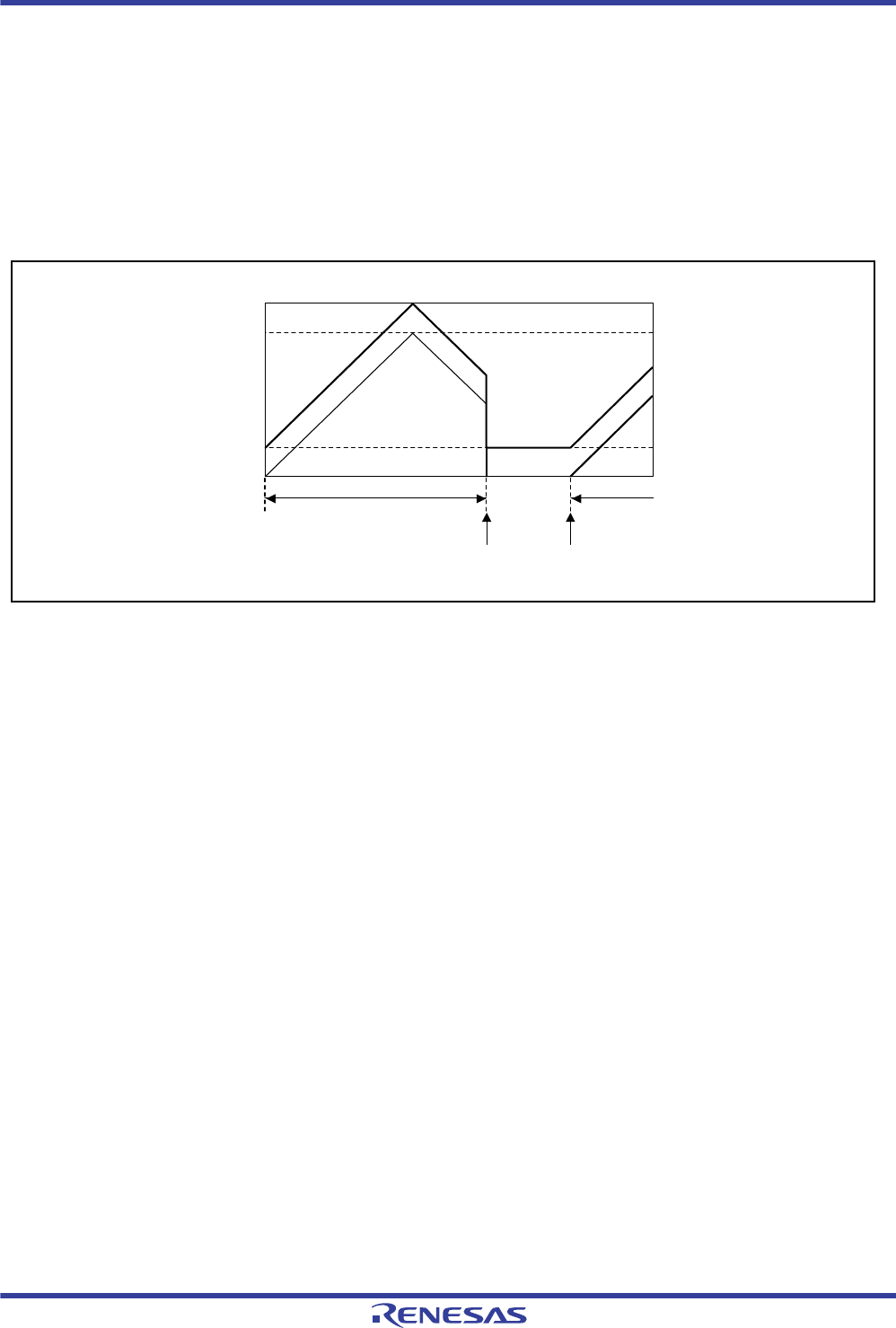
R01UH0034EJ0200 Rev.2.00 Page 666 of 1489
Dec 27, 2013
RX62T Group, RX62G Group 16. Multi-Function Timer Pulse Unit 3 (MTU3)
16.6.13 Counter Value when Stopped in Complementary PWM Mode
When counting operation in MTU3.TCNT and MTU4.TCNT (MTU6.TCNT and MTU7.TCNT) is stopped in
complementary PWM mode, the MTU3.TCNT (MTU6.TCNT) value is set to the timer dead time register (TDDRA
(TDDRB)) value and MTU4.TCNT (MTU7.TCNT)is set to 0000h.
When operation is restarted in complementary PWM mode, counting begins automatically from the initial setting state.
Figure 16.135 shows this operation.
When counting begins in another operating mode, be sure to make initial settings in MTU3.TCNT and MTU4.TCNT
(MTU6.TCNT and MTU7.TCNT).
Figure 16.135 Counter Value when Stopped in Complementary PWM Mode
16.6.14 Buffer Operation Setting in Complementary PWM Mode
When modifying the PWM cycle set register (MTU3.TGRA or MTU6.TGRA), timer cycle data register (TCDRA or
TCDRB), and duty set registers (MTU3.TGRB, MTU4.TGRA, and MTU4.TGRB (MTU6.TGRB, MTU7.TGRA, and
MTU7.TGRB)) in complementary PWM mode, be sure to use buffer operation. In addition, set the BFA and BFB bits in
MTU4.TMDR1 (MTU7.TMDR1) to 0. The MTIOC4C (MTIOC7C) pin cannot output waveforms if the BFA bit in
MTU4.TMDR1 (MTU7.TMDR1) is set to 1. Likewise, the MTIOC4D (MTIOC7D) pin cannot output waveforms if the
BFB bit in MTU4.TMDR1 (MTU7.TMDR1) is set to 1.
In complementary PWM mode, buffer operation in MTU3 and MTU4 (or MTU6 and MTU7) depends on the settings in
bits BFA and BFB of MTU3.TMDR1 (MTU6.TMDR1). When the BFA bit in MTU3.TMDR1 (MTU6.TMDR1) is set to
1, MTU3.TGRC (MTU6.TGRC) functions as a buffer register for MTU3.TGRA (MTU6.TGRA). At the same time,
MTU4.TGRC (MTU7.TGRC) functions as a buffer register for MTU4.TGRA (MTU7.TGRA), and TCBRA (TCBRB)
functions as a buffer register for TCDRA (TCDRB).
MTU3.TGRA
TCDRA
TDDRA
0000h
MTU3.TCNT
MTU4.TCNT
Complementary PWM mode
operation
Complementary PWM
mode operation
Counter
operation stop Complementary
PWM restart
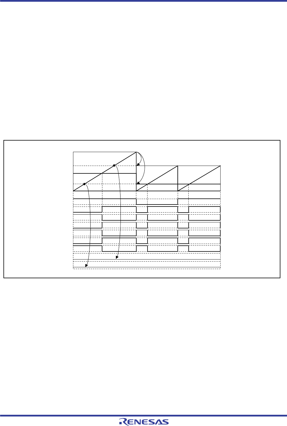
R01UH0034EJ0200 Rev.2.00 Page 667 of 1489
Dec 27, 2013
RX62T Group, RX62G Group 16. Multi-Function Timer Pulse Unit 3 (MTU3)
16.6.15 Buffer Operation and Compare Match Flags in Reset-Synchronized PWM Mode
When setting buffer operation in reset-synchronized PWM mode, set the BFA and BFB bits in MTU4.TMDR1
(MTU7.TMDR1) to 0. The MTIOC4C (MTIOC7C) pin cannot output waveforms if the BFA bit in MTU4.TMDR1
(MTU7.TMDR1) is set to 1. Likewise, the MTIOC4D (MTIOC7D) pin cannot output waveforms if the BFB bit in
MTU4.TMDR1 (MTU7.TMDR1) is set to 1.
In reset-synchronized PWM mode, buffer operation in MTU3 and MTU4 (or MTU6 and MTU7) depends on the settings
in the BFA and BFB bits of MTU3.TMDR1 (MTU6.TMDR1). For example, if the BFA bit in MTU3.TMDR1
(MTU6.TMDR1) is set to 1, MTU3.TGRC (MTU6.TGRC) functions as a buffer register for MTU3.TGRA
(MTU6.TGRA). At the same time, MTU4.TGRC (MTU7.TGRC) functions as a buffer register for MTU4.TGRA
(MTU7.TGRA).
While the MTU3.TGRC (MTU6.TGRC) and MTU3.TGRD (MTU6.TGRD) are operating as buffer registers, the TGFC
and TGFD bits in MTU3.TSR and MTU4.TSR (MTU6.TSR and MTU7.TSR) are never set.
Figure 16.136 shows an example of MTU3.TGR (MTU6.TGR), MTU4.TGR (MTU7.TGR), MTIOC3 (MTIOC6), and
MTIOC4 (MTIOC7) operation with the BFA and BFB bits in MTU3.TMDR1 (MTU6.TMDR1) set to 1 and the BFA and
BFB bits in MTU4.TMDR1 (MTU7.TMDR1) set to 0.
Figure 16.136 Buffer Operation and Compare Match Flags in Reset-Synchronized PWM Mode
MTU3.TGRA
MTU3.TGRC
MTU3.TGRB, MTU4.TGRA
MTU4.TGRB
0000h
TGFC flag
TGFD flag
MTU3.TCNT
Point a
Buffer data transferred by compare match A3
MTU3.TGRA
MTU3.TGRC
MTU3.TGRB, MTU3.TGRD
MTU4.TGRA, MTU4.TGRC
MTU4.TGRB, MTU4.TGRD
Not set
Not set
Point b
MTU3.TGRD, MTU4.TGRC
MTU4.TGRD
MTIOC3A
MTIOC3B
MTIOC3D
MTIOC4A
MTIOC4C
MTIOC4B
MTIOC4D
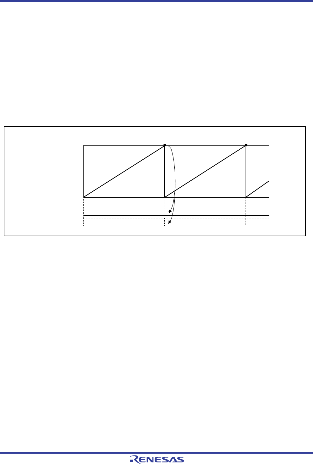
R01UH0034EJ0200 Rev.2.00 Page 668 of 1489
Dec 27, 2013
RX62T Group, RX62G Group 16. Multi-Function Timer Pulse Unit 3 (MTU3)
16.6.16 Overflow Flags in Reset-Synchronized PWM Mode
After reset-synchronized PWM mode is selected, MTU3.TCNT and MTU4.TCNT (MTU6.TCNT and MTU7.TCNT)
start counting when the CST3 (CST6) bit of TSTRA (TSTRB) is set to 1. In this state, the MTU4.TCNT (MTU7.TCNT)
count clock source and count edge are determined by the MTU3.TCR (MTU6.TCR) setting.
In reset-synchronized PWM mode, with cycle register MTU3.TGRA (MTU6.TGRA) set to FFFFh and the
MTU3.TGRA (MTU6.TGRA) compare match selected as the counter clearing source, MTU3.TCNT and MTU4.TCNT
(MTU6.TCNT and MTU7.TCNT) count up to FFFFh, then a compare match occurs with MTU3.TGRA (MTU6.TGRA),
and MTU3.TCNT and MTU4.TCNT (MTU6.TCNT and MTU7.TCNT) are both cleared. In this case, the TCFV flag in
TSR is not set.
Figure 16.137 shows an example of TCFV flag operation in reset-synchronized PWM mode with cycle register
MTU3.TGRA (MTU6.TGRA) set to FFFFh and the MTU3.TGRA (MTU6.TGRA) compare match specified for the
counter clearing source without synchronous operation setting.
Figure 16.137 Overflow Flags in Reset-Synchronized PWM Mode
MTU3.TGRA
(FFFFh)
0000h
MTU3.TSR.TCFV
MTU4.TSR.TCFV
Counter cleared by compare match 3A
Not set
Not set
MTU3.TCNT =
MTU4.TCNT
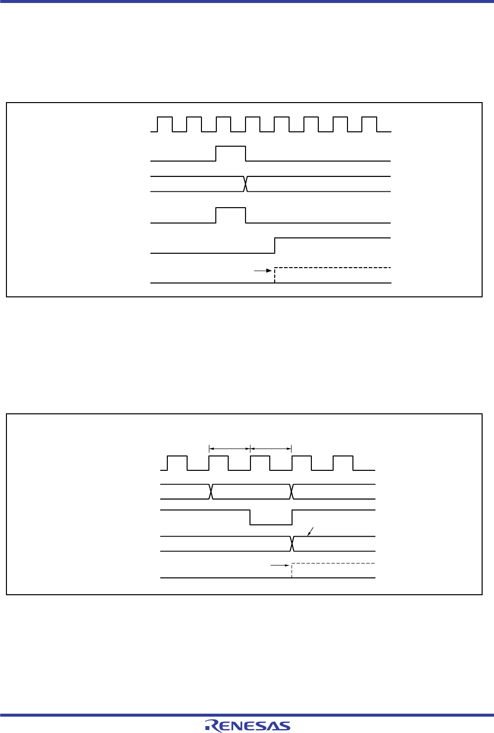
R01UH0034EJ0200 Rev.2.00 Page 669 of 1489
Dec 27, 2013
RX62T Group, RX62G Group 16. Multi-Function Timer Pulse Unit 3 (MTU3)
16.6.17 Contention between Overflow/Underflow and Counter Clearing
If an overflow/underflow and counter clearing occur simultaneously, the TCFV/FCFU flag in TSR is not set and TCNT
clearing takes precedence.
Figure 16.138 shows the operation timing when a TGR compare match is specified as the clearing source and TGR is
set to FFFFh.
Figure 16.138 Contention between Overflow and Counter Clearing
16.6.18 Contention between TCNT Write Operation and Overflow/Underflow
If TCNT counts up or down in the T2 state in a TCNT write cycle and an overflow or an underflow occurs, the TCNT
write operation takes precedence and the TCFV/TCFU flag in TSR is not set.
Figure 16.139 shows the operation timing when there is contention between TCNT write operation and overflow.
Figure 16.139 Contention between TCNT Write Operation and Overflow
FFFFh 0000h
Disabled
Counter
clear signal
TCNT input
clock
ICLK
TGF
TCFV flag
TCNT
Disabled
Write signal
Address TCNT address
TCNT
TCNT write cycle
T1 T2
H'FFFF M
TCNT write data
TCFV flag
ICLK

R01UH0034EJ0200 Rev.2.00 Page 670 of 1489
Dec 27, 2013
RX62T Group, RX62G Group 16. Multi-Function Timer Pulse Unit 3 (MTU3)
16.6.19 Note on Transition from Normal Operation or PWM Mode 1 to Reset-
Synchronized PWM Mode
When making a transition from normal operation or PWM mode 1 to reset-synchronized PWM mode in MTU3 and
MTU4 (or MTU6 and MTU7), if the counter is stopped while the output pins (MTIOC3B, MTIOC3D, MTIOC4A,
MTIOC4C, MTIOC4B, MTIOC4D, MTIOC6B, MTIOC6D, MTIOC7A, MTIOC7C, MTIOC7B, and MTIOC7D) are
held at a high level and then operation is started after a transition to reset-synchronized PWM mode, the initial pin output
will not be correct.
When making a transition from normal operation to reset-synchronized PWM mode, write 11h to MTU3.TIORH,
MTU3.TIORL, MTU4.TIORH, and MTU4.TIORL (MTU6.TIORH, MTU6.TIORL, MTU7.TIORH, and
MTU7.TIORL) to initialize the output pin state to a low level, then set the registers to the initial value (00h) before
making the mode transition.
When making a transition from PWM mode 1 to reset-synchronized PWM mode, switch to normal operation, initialize
the output pin state to a low level, and then set the registers to the initial value (00h) before making the transition to reset-
synchronized PWM mode.
16.6.20 Output Level in Complementary PWM Mode and Reset-Synchronized PWM
Mode
When MTU3 and MTU4 (or MTU6 and MTU7) are in complementary PWM mode or reset-synchronized PWM mode,
the PWM waveform output level is determined by the OLSP and OLSN bits in the timer output control register
(TOCR1A or TOCR1B). In complementary PWM mode or reset-synchronized PWM mode, TIOR should be set to 00h.
Rather than being as set in TOCR1.OLSN, the output level in the negative phase when the TDER.TDER bit is 0 (dead
time is not generated) in complementary PWM mode becomes the inverse of the normal-phase output in accord with the
setting of the TOCR1.OLSP bit.
16.6.21 Simultaneous Input Capture in MTU1.TCNT and MTU2.TCNT in Cascade
Connection
When timer counters 1 and 2 (MTU1.TCNT and MTU2.TCNT) operate as a 32-bit counter in cascade connection, the
cascaded counter value cannot be captured successfully in some cases even if input-capture input is simultaneously done
to MTIOC1A and MTIOC2A or to MTIOC1B and MTIOC2B. This is because the input timing of MTIOC1A and
MTIOC2A or to MTIOC1B and MTIOC2B may not be the same when external input-capture signals input into
MTU1.TCNT and MTU2.TCNT are taken in synchronization with the internal clock.
For example, MTU1.TCNT (the counter for upper 16 bits) does not capture the count-up value by an overflow from
MTU2.TCNT (the counter for lower 16 bits) but captures the count value before the up-counting. In this case, the values
of MTU1.TCNT = FFF1h and MTU2.TCNT = 0000h should be transferred to MTU1.TGRA and MTU2.TGRA or to
MTU1.TGRB and MTU2.TGRB, but the values of MTU1.TCNT = FFF0h and MTU2.TCNT = 0000h are erroneously
transferred.
A facility for simultaneous capture of MTU1.TCNT and MTU2.TCNT on input of the input-capture signal has been
added to the MTU. This facility can be used to ensure there is no deviation between the timing of capture for
MTU1.TCNT and MTU2.TCNT, and this makes setting up a 32-bit counter possible. For details, see section 16.2.9,
Timer Input Capture Control Register (TICCR).

R01UH0034EJ0200 Rev.2.00 Page 671 of 1489
Dec 27, 2013
RX62T Group, RX62G Group 16. Multi-Function Timer Pulse Unit 3 (MTU3)
16.6.22 Interrupt-Skipping Function 2
When interrupt-skipping function 2 is in use and the difference between the values in MTU4.TADCORA and
MTU4.TADCORB is small, correct counting of the number skipped may not be possible, in which case requests for A/D
conversion will not be generated with the expected timing. The conditions listed below thus apply to these settings.
For MTU6 and MTU7, the same conditions apply to the settings of MTU7.TADCORA and MTU7.TADCORB.
(1) When the number skipped is zero for skipping function 2
The difference between the values in MTU4.TADCORA and MTU4.TADCORB must be at least four.
The interval of comparison for MTU4.TADCORA must be at least four cycles of ICLK (the updated value of
MTU4.TADCORA is set to the previous value plus or minus at least four).
The interval of comparison for MTU4.TADCORB must be at least four cycles of ICLK (the updated value of
MTU4.TADCORB is set to the previous value plus or minus at least four).
(2) When the number skipped is one or more for skipping function 2
The difference between the values in MTU4.TADCORA and MTU4.TADCORB must be at least two.
The interval of comparison for MTU4.TADCORB must be at least two cycles of ICLK (the updated value of
MTU4.TADCORB is set to the previous value plus or minus at least two).
16.6.23 Notes when Complementary PWM Mode Output Protection Function is not
Used
The complementary PWM mode output protection function is initially enabled. If it is not used, write 00h in the
POE.POECR2 register.
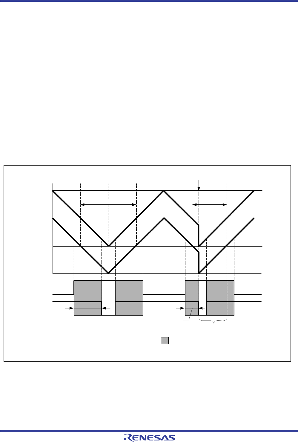
R01UH0034EJ0200 Rev.2.00 Page 672 of 1489
Dec 27, 2013
RX62T Group, RX62G Group 16. Multi-Function Timer Pulse Unit 3 (MTU3)
16.6.24 Points for Caution to Prevent Malfunctions in Synchronous Clearing for
Complementary PWM Mode
If control of the output waveform is enabled (TWCR.WRE = 1) at the time of synchronous counter clearing in
complementary PWM mode, satisfaction of either condition 1 or 2 below has the following effects.
Dead time on the PWM output pins is shortened (or disappears).
The active level is output on the PWM negative phase output pins beyond the period for active-level output.
Condition 1: In portion (10) of the initial output inhibition period in Figure 16.141, synchronous clearing occurs within
the dead-time period for PWM output.
Condition 2: In portions (10) and (11) of the initial output inhibition period in Figure 16.142, synchronous clearing
occurs when any condition from among MTU3.TGRB (MTU6.TGRB) ≤ MTU3.TGRB (MTU6.TGRB), MTU4.TGRA
(MTU7.TGRA) ≤ TDDRA (TDDRB), or MTU4.TGRB (MTU7.TGRB) ≤ TDDRA (TDDRB) is satisfied.
The following method avoids the above phenomena.
Ensure that synchronous clearing proceeds with the value of each comparison register (MTU3.TGRB (MTU6.TGRB),
MTU4.TGRA (MTU7.TGRA), and MTU4.TGRB (MTU7.TGRB) ≤ TDDRA (TDDRB)) set to at least double the value
of TDDRA (TDDRB).
Figure 16.140 Example of Synchronous Clearing (when Condition 1 Applies)
MTU3.TGRA
TGR
TDDRA
PWM output
(positive phase)
0
PWM output
(negative phase)
MTU3.
TCNT
MTU4.
TCNT
Tb interval
Tb interval
Synchronous clearing
(10) (11) (10) (11)
TDDRA
Dead time is shortened.
Initial output inhibition
Note: • PWM output is active low over the dead time.
: Dead time
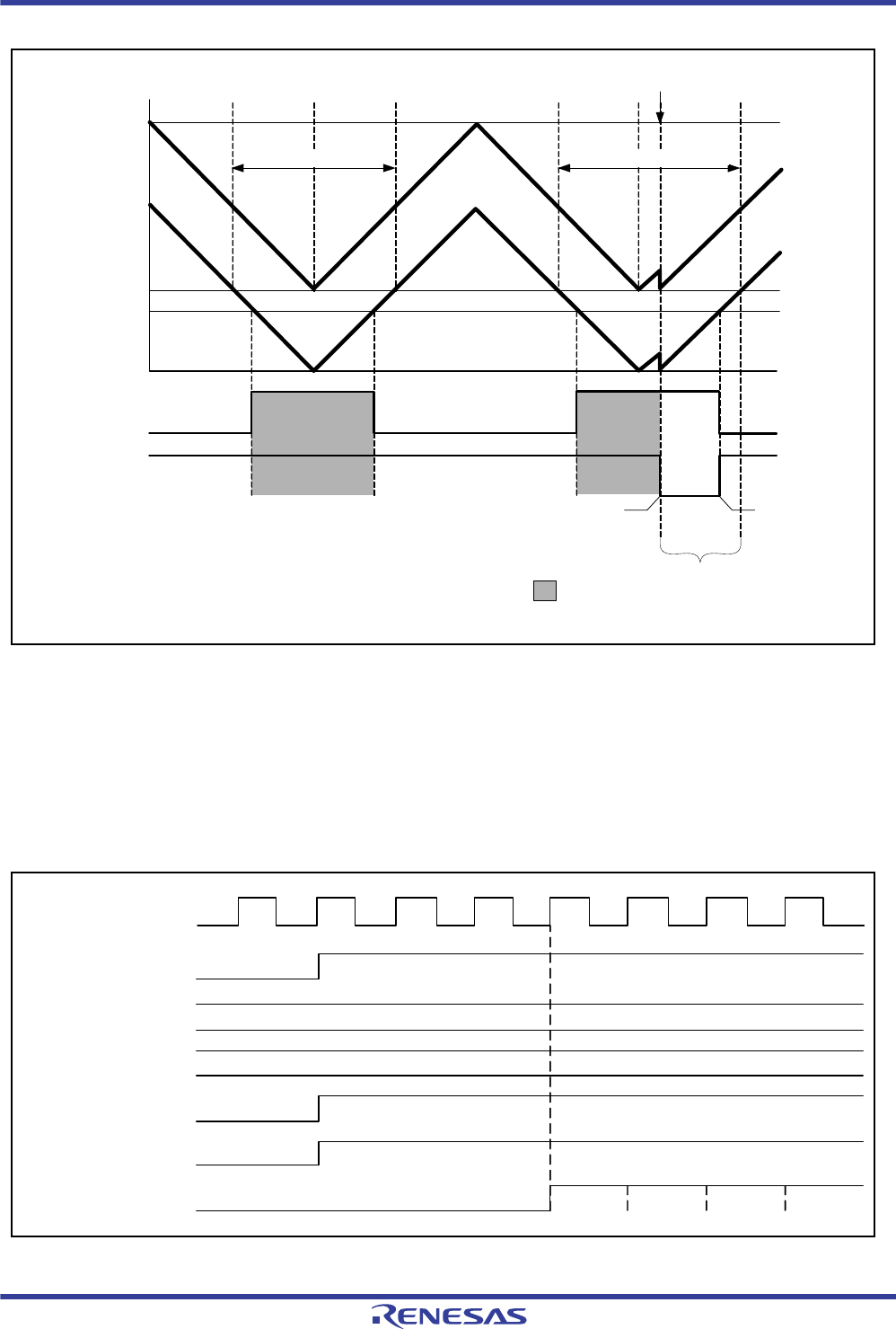
R01UH0034EJ0200 Rev.2.00 Page 673 of 1489
Dec 27, 2013
RX62T Group, RX62G Group 16. Multi-Function Timer Pulse Unit 3 (MTU3)
Figure 16.141 Example of Synchronous Clearing (when Condition 2 Applies)
16.6.25 Continuous Output of Interrupt Signal in Response to a Compare Match
When the TGR register is set to 0000h, ICLK/1 is set as the counter clock, and compare match is set as the trigger for
clearing of the counter clock, the value of the TCNT counter remains 0000h, and the interrupt signal will be output
continuously (i.e. its level will be flat) rather than output over a single cycle. Consequently, interrupts will not be
detected in response to second and subsequent compare matches.
Figure 16.143 shows the timing for continuous output of the interrupt signal in response to a compare match.
Figure 16.142 Continuous Output of Interrupt Signal in Response to a Compare Match
MTU3.TGRA
TGR
TDDRA
PWM output
(positive phase)
PWM output
(negative phase)
(10) (11) (10) (11)
Initial output inhibition
Note: • PWM output is active low.
: Dead time
Tb interval
Tb interval
Synchronous clearing
Dead time is
eliminated.
0
Although there is no period for output of the active level
over this interval, synchronous clearing leads to output of
the active level.
MTU3.
TCNT
MTU4.
TCNT
PCLK
TSTR.CST bit
TCNT
TGR
Counter clear signal
Compare-match signal
Pulse interrupt signal
0000h
0000h

R01UH0034EJ0200 Rev.2.00 Page 674 of 1489
Dec 27, 2013
RX62T Group, RX62G Group 16. Multi-Function Timer Pulse Unit 3 (MTU3)
16.7 MTU3 Output Pin Initialization
16.7.1 Operating Modes
The MTU3 has the following six operating modes. Waveforms can be output in any of these modes.
Normal mode (MTU0 to MTU4, MTU6, and MTU7)
PWM mode 1 (MTU0 to MTU4, MTU6, and MTU7)
PWM mode 2 (MTU0 to MTU2)
Phase counting modes 1 to 4 (MTU1 and MTU2)
Complementary PWM mode (MTU3, MTU4, MTU6, and MTU7)
Reset-synchronized PWM mode (MTU3, MTU4, MTU6, and MTU7)
This section describes how to initialize the MTU3 output pins in each of these modes.
16.7.2 Operation in Case of Re-Setting Due to Error during Operation
If an error occurs during MTU3 operation, MTU3 output should be cut off by the system. The output can be cut off by
making necessary settings for non-active level output in the data directions registers (DDR) and data registers (DR) in the
I/O ports in advance and disabling MTU3 output to switch them to general output ports; the specified non-active level
will be output from the pins. MTU3 output can be disabled through TIOR settings. Complementary PWM output
(MTIOC3B, MTIOC3D, MTIOC4A, MTIOC4B, MTIOC4C, MTIOC4D, MTIOC6B, MTIOC6D, MTIOC7A,
MTIOC7B, MTIOC7C, and MTIOC7D) should be specified through TOERA and TOERB settings. For PWM output
pins, output can also be cut by hardware, using port output enable 3 (POE3). The pin initialization procedures for re-
setting due to an error during operation and the procedures for restarting in a different mode after re-setting are described
below.
The MTU3 has six operating modes, as stated above. There are thus 36 mode transition combinations, but some
transitions are not available with certain channel and mode combinations. Available mode transition combinations are
shown in Table 16.75.
Normal: Normal mode
PWM1: PWM mode 1
PWM2: PWM mode 2
PCM: Phase counting modes 1 to 4
CPWM: Complementary PWM mode
RPWM: Reset-synchronized PWM mode
Table 16.75 Mode Transition Combinations
Normal PWM1 PWM2 PCM CPWM RPWM
Normal (1) (2) (3) (4) (5) (6)
PWM1 (7) (8) (9) (10) (11) (12)
PWM2 (13) (14) (15) (16) Not available Not available
PCM (17) (18) (19) (20) Not available Not available
CPWM (21) (22) Not available Not available (23) (24) (25)
RPWM (26) (27) Not available Not available (28) (29)

R01UH0034EJ0200 Rev.2.00 Page 675 of 1489
Dec 27, 2013
RX62T Group, RX62G Group 16. Multi-Function Timer Pulse Unit 3 (MTU3)
16.7.3 Overview of Initialization Procedures and Mode Transitions in Case of Error
during Operation
When making a transition to a mode (Normal, PWM1, PWM2, or PCM) in which the pin output level is selected by
the timer I/O control register (TIOR) setting, initialize the pins by means of TIOR setting.
In PWM mode 1, waveforms are not output to the MTIOCnB and MTIOCnD (n = 3, 4, 6, or 7) pins. If no other
module outputs signals through these pins, they enter high-impedance state. To output a specified level, make
necessary settings for general output ports in the data direction registers (DDR) and data registers (DR) in the I/O
ports.
In PWM mode 2, waveforms are not output to the cycle register pins. If no other module outputs signals through
these pins, they enter high-impedance state. To output a specified level, make necessary settings for general output
ports in the data direction registers (DDR) and data registers (DR) in the I/O ports.
In normal mode or PWM mode 2, if TGRC and TGRD operate as buffer registers, waveforms are not output to the
corresponding pins. If no other module outputs signals through these pins, they enter high-impedance state. To
output a specified level, make necessary settings for general output ports in the data direction registers (DDR) and
data registers (DR) in the I/O ports.
In PWM mode 1, if either TGRC or TGRD operates as a buffer register, waveforms are not output to the
corresponding pins. If no other module outputs signals through these pins, they enter high-impedance state. To
output a specified level, make necessary settings for general output ports in the data direction registers (DDR) and
data registers (DR) in the I/O ports.
When making a transition to a mode (CPWM or RPWM) in which the pin output level is selected by the timer
output control register (TOCR1A, TOCR2A, TOCR1B, or TOCR2B) setting, temporarily disable output in MTU3
and MTU4 (or MTU6 and MTU7) with the timer output master enable register (TOERA or TOERB). At this time,
if no other module outputs signals through these pins, they enter high-impedance state. To output a specified level,
make necessary settings for general output ports in the data direction registers (DDR) and data registers (DR) in the
I/O ports. Switch to normal mode, perform initialization with TIOR, restore TIOR to its initial value, then operate
the MTU3 in accordance with the mode setting procedure (TOCR1A setting, TOCR2A setting, TMDR1 setting, and
TOERA setting (TOCR1B setting, TOCR2B setting, TMDR1 setting, and TOERB setting)).
Note: • Channel number is substituted for "n" indicated in this section.
Pin initialization procedures are described below for the numbered combinations in Table 16.75. The active level is
assumed to be low.

R01UH0034EJ0200 Rev.2.00 Page 676 of 1489
Dec 27, 2013
RX62T Group, RX62G Group 16. Multi-Function Timer Pulse Unit 3 (MTU3)
(1) Operation when Error Occurs in Normal Mode and Operation is Restarted in Normal Mode
Figure 16.143 shows a case in which an error occurs in normal mode and operation is restarted in normal mode after re-
setting.
Figure 16.143 Error Occurrence in Normal Mode, Recovery in Normal Mode
(1) After a reset, the MTU3 output goes low and the ports enter high-impedance state.
(2) After a reset, the TMDR1 setting is for normal mode.
(3) For MTU3 and MTU4, enable output with TOERA before initializing the pins with TIOR.
In addition, make necessary settings in the data direction registers (DDR) and data registers (DR) in the I/O ports so
that a non-active level is output from the general ports.
(4) Initialize the pins with TIOR. (In the example, the initial output is a high level, and a low level is output on compare
match occurrence.)
(5) Start count operation by setting TSTRA.
(6) Output goes low on compare match occurrence.
(7) An error occurs.
(8) Disable the MTU3 output with TIOR to switch the pins to general output ports so that a non-active level is output
from the pins.
(9) Stop count operation by setting TSTRA.
(10) This step is not necessary when restarting in normal mode.
(11) Initialize the pins with TIOR.
(12) Restart operation by setting TSTRA.
(1)
Reset
MTU module output
Hi-Z
Hi-Z
(2)
TMDR
(normal)
(3)
TOER
(1)
(4)
TIOR
(1 init
0 out)
(5)
TSTR
(1)
(6)
Match (7)
Error
occurs
(8)
Port
output
(9)
TSTR
(0)
(10)
TMDR
(normal)
(11)
TIOR
(1 init
0 out)
(12)
TSTR
(1)
MTIOCnA
MTIOCnB
PORT output
Pxx
Pxx

R01UH0034EJ0200 Rev.2.00 Page 677 of 1489
Dec 27, 2013
RX62T Group, RX62G Group 16. Multi-Function Timer Pulse Unit 3 (MTU3)
(2) Operation when Error Occurs in Normal Mode and Operation is Restarted in PWM Mode 1
Figure 16.144 shows a case in which an error occurs in normal mode and operation is restarted in PWM mode 1 after
re-setting.
Figure 16.144 Error Occurrence in Normal Mode, Recovery in PWM Mode 1
(1) to (9) are the same as in Figure 16.143.
(10) Set PWM mode 1.
(11) Initialize the pins with TIOR. (In PWM mode 1, waveforms are not output to the MTIOCnB (MTIOCnD) pins. To
output a specified level, make necessary settings for general output ports in the data direction registers (DDR) and data
registers (DR) in the I/O ports.)
(12) Restart operation by setting TSTRA.
(1)
Reset
MTU module output
Hi-Z
Hi-Z
●Not initialized (MTIOCnB)
(2)
TMDR
(normal)
(3)
TOER
(1)
(4)
TIOR
(1 init
0 out)
(5)
TSTR
(1)
(6)
Match (7)
Error
occurs
(8)
Port
output
(9)
TSTR
(0)
(10)
TMDR
(PWM1)
(11)
TIOR
(1 init
0 out)
(12)
TSTR
(1)
MTIOCnA
MTIOCnB
PORT output
Pxx
Pxx

R01UH0034EJ0200 Rev.2.00 Page 678 of 1489
Dec 27, 2013
RX62T Group, RX62G Group 16. Multi-Function Timer Pulse Unit 3 (MTU3)
(3) Operation when Error Occurs in Normal Mode and Operation is Restarted in PWM mode 2
Figure 16.145 shows a case in which an error occurs in normal mode and operation is restarted in PWM mode 2 after
re-setting.
Figure 16.145 Error Occurrence in Normal Mode, Recovery in PWM Mode 2
(1) to (9) are the same as in Figure 16.143.
(10) Set PWM mode 2.
(11) Initialize the pins with TIOR. (In PWM mode 2, waveforms are not output to the cycle register pins. To output a
specified level, make necessary settings for general output ports in the data direction registers (DDR) and data registers
(DR) in the I/O ports.)
(12) Restart operation by setting TSTRA.
Note: • PWM mode 2 can only be selected for MTU0 to MTU2, and therefore TOERA setting is not necessary.
(1)
Reset
MTU module output
Hi-Z
Hi-Z
Not initialized (cycle register)
(2)
TMDR
(normal)
(3)
TOER
(1)
(4)
TIOR
(1 init
0 out)
(5)
TSTR
(1)
(6)
Match (7)
Error
occurs
(8)
Port
output
(9)
TSTR
(0)
(10)
TMDR
(PWM2)
(11)
TIOR
(1 init
0 out)
(12)
TSTR
(1)
MTIOCnA
MTIOCnB
PORT output
Pxx
Pxx
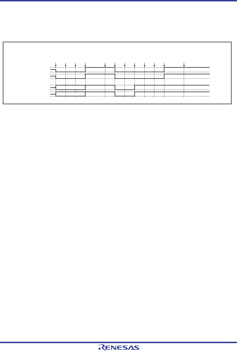
R01UH0034EJ0200 Rev.2.00 Page 679 of 1489
Dec 27, 2013
RX62T Group, RX62G Group 16. Multi-Function Timer Pulse Unit 3 (MTU3)
(4) Operation when Error Occurs in Normal Mode and Operation is Restarted in Phase Counting
Mode
Figure 16.146 shows a case in which an error occurs in normal mode and operation is restarted in phase counting mode
after re-setting.
Figure 16.146 Error Occurrence in Normal Mode, Recovery in Phase Counting Mode
(1) to (9) are the same as in Figure 16.143.
(10) Set the phase counting mode.
(11) Initialize the pins with TIOR.
(12) Restart operation by setting TSTRA.
Note: • The phase counting mode can only be selected for MTU1 and MTU2, and therefore TOER setting is not
necessary.
(1)
Reset
MTU module output
Hi-Z
Hi-Z
(2)
TMDR
(normal)
(3)
TOER
(1)
(4)
TIOR
(1 init
0 out)
(5)
TSTR
(1)
(6)
Match (7)
Error
occurs
(8)
Port
output
(9)
TSTR
(0)
(10)
TMDR
(PCM)
(11)
TIOR
(1 init
0 out)
(12)
TSTR
(1)
MTIOCnA
MTIOCnB
PORT output
Pxx
Pxx
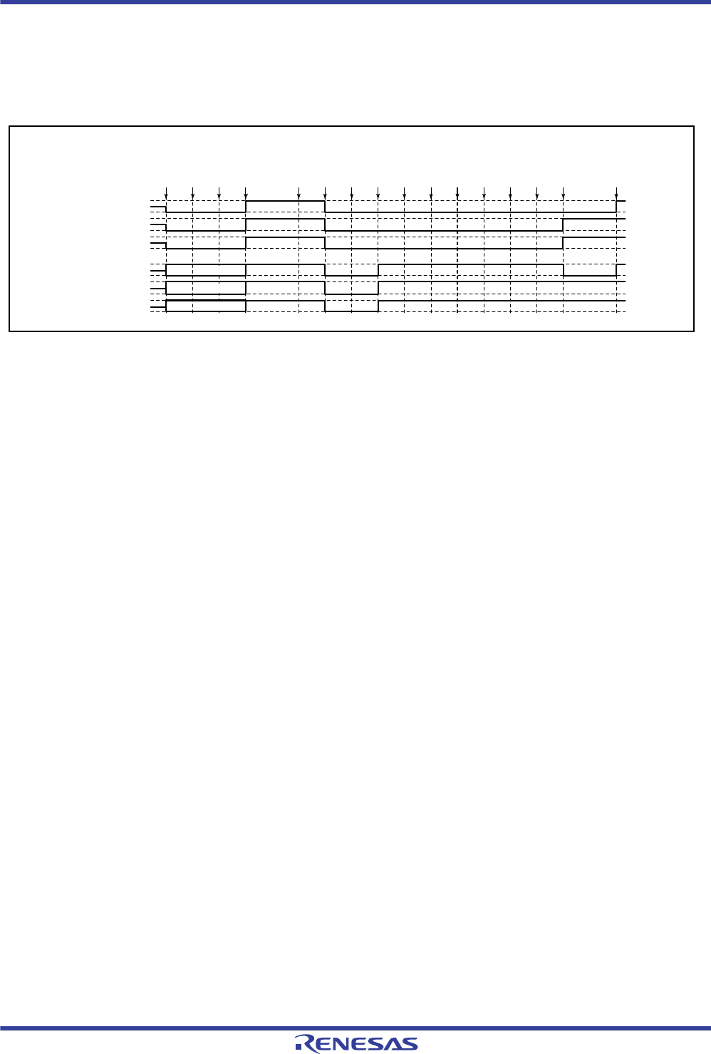
R01UH0034EJ0200 Rev.2.00 Page 680 of 1489
Dec 27, 2013
RX62T Group, RX62G Group 16. Multi-Function Timer Pulse Unit 3 (MTU3)
(5) Operation when Error Occurs in Normal Mode and Operation is Restarted in Complementary
PWM Mode
Figure 16.147 shows a case in which an error occurs in normal mode and operation is restarted in complementary PWM
mode after re-setting.
Figure 16.147 Error Occurrence in Normal Mode, Recovery in Complementary PWM Mode
(1) to (9) are the same as in Figure 16.143.
(10) Initialize the normal mode waveform generation section with TIOR.
(11) Disable operation of the normal mode waveform generation section with TIOR.
(12) Disable output in MTU3 and MTU4 with TOERA.
(13) Select the complementary PWM output level and enable or disable cyclic output with TOCR1A and TOCR2A.
(14) Set complementary PWM mode.
(15) Enable output in MTU3 and MTU4 with TOERA.
(16) Restart operation by setting TSTRA.
(1)
Reset
MTU module output
Hi-Z
Hi-Z
Hi-Z
(2)
TMDR
(normal)
(3)
TOER
(1)
(4)
TIOR
(1 init
0 out)
(5)
TSTR
(1)
(6)
Match (7)
Error
occurs
(8)
Port
output
(9)
TSTR
(0)
(10)
TIOR
(0 init
0 out)
(11)
TIOR
(disabled)
(12)
TOER
(0)
(13)
TOCR (14)
TMDR
(CPWM)
(15)
TOER
(1)
(16)
TSTR
(1)
MTIOC3A
MTIOC3B
MTIOC3D
PORT output
Pxx
Pxx
Pxx

R01UH0034EJ0200 Rev.2.00 Page 681 of 1489
Dec 27, 2013
RX62T Group, RX62G Group 16. Multi-Function Timer Pulse Unit 3 (MTU3)
(6) Operation when Error Occurs in Normal Mode and Operation is Restarted in Reset-
Synchronized PWM Mode
Figure 16.148 shows a case in which an error occurs in normal mode and operation is restarted in reset-synchronized
PWM mode after re-setting.
Figure 16.148 Error Occurrence in Normal Mode, Recovery in Reset-Synchronized PWM Mode
(1) to (12) are the same as in Figure 16.143.
(13) Select the reset-synchronized PWM output level and enable or disable cyclic output with TOCR1A and TOCR2A.
(14) Set reset-synchronized PWM mode.
(15) Enable output in MTU3 and MTU4 with TOERA.
(16) Restart operation by setting TSTRA.
(1)
Reset
MTU module output
Hi-Z
Hi-Z
Hi-Z
(2)
TMDR
(normal)
(3)
TOER
(1)
(4)
TIOR
(1 init
0 out)
(5)
TSTR
(1)
(6)
Match (7)
Error
occurs
(9)
TSTR
(0)
(10)
TIOR
(0 init
0 out)
(11)
TIOR
(disabled)
(12)
TOER
(0)
(13)
TOCR (14)
TMDR
(RPWM)
(15)
TOER
(1)
(16)
TSTR
(1)
MTIOC3A
MTIOC3B
MTIOC3D
PORT output
Pxx
Pxx
Pxx
(8)
Port
output

R01UH0034EJ0200 Rev.2.00 Page 682 of 1489
Dec 27, 2013
RX62T Group, RX62G Group 16. Multi-Function Timer Pulse Unit 3 (MTU3)
(7) Operation when Error Occurs in PWM Mode 1 and Operation is Restarted in Normal Mode
Figure 16.149 shows a case in which an error occurs in PWM mode 1 and operation is restarted in normal mode after
re-setting.
Figure 16.149 Error Occurrence in PWM Mode 1, Recovery in Normal Mode
(1) After a reset, the MTU3 output goes low and the ports enter high-impedance state.
(2) Set PWM mode 1.
(3) For MTU3 and MTU4, enable output with TOERA before initializing the pins with TIOR.
In addition, make necessary settings in the data direction registers (DDR) and data registers (DR) in the I/O ports so that
a non-active level is output from the general ports.
(4) Initialize the pins with TIOR. (In the example, the initial output is a high level, and a low level is output on compare
match occurrence. In PWM mode 1, the MTIOCnB side is not initialized.)
(5) Start count operation by setting TSTRA.
(6) Output goes low on compare match occurrence.
(7) An error occurs.
(8) Disable the MTU3 output with TIOR to switch the pins to general output ports so that a non-active level is output
from the pins.
(9) Stop count operation by setting TSTRA.
(10) Set normal mode.
(11) Initialize the pins with TIOR.
(12) Restart operation by setting TSTRA.
(1)
Reset
MTU module output
Hi-Z
Hi-Z
Not initialized (MTIOCnB)
(2)
TMDR
(PWM1)
(3)
TOER
(1)
(4)
TIOR
(1 init
0 out)
(5)
TSTR
(1)
(6)
Match (7)
Error
occurs
(8)
Port
output
(9)
TSTR
(0)
(10)
TMDR
(normal)
(11)
TIOR
(1 init
0 out)
(12)
TSTR
(1)
PORT output
Pxx
Pxx
MTIOCnA
MTIOCnB
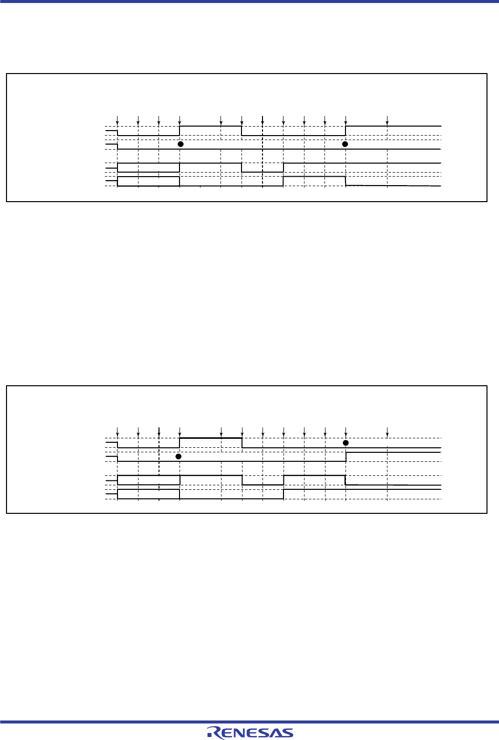
R01UH0034EJ0200 Rev.2.00 Page 683 of 1489
Dec 27, 2013
RX62T Group, RX62G Group 16. Multi-Function Timer Pulse Unit 3 (MTU3)
(8) Operation when Error Occurs in PWM Mode 1 and Operation is Restarted in PWM mode 1
Figure 16.150 shows a case in which an error occurs in PWM mode 1 and operation is restarted in PWM mode 1 after
re-setting.
Figure 16.150 Error Occurrence in PWM Mode 1, Recovery in PWM Mode 1
(1) to (9) are the same as in Figure 16.149.
(10) This step is not necessary when restarting in PWM mode 1.
(11) Initialize the pins with TIOR. (In PWM mode 1, waveforms are not output to the MTIOCnB (MTIOCnD) pins. To
output a specified level, make necessary settings for general output ports in the data direction registers (DDR) and data
registers (DR) in the I/O ports.)
(12) Restart operation by setting TSTRA.
(9) Operation when Error Occurs in PWM Mode 1 and Operation is Restarted in PWM mode 2
Figure 16.151 shows a case in which an error occurs in PWM mode 1 and operation is restarted in PWM mode 2 after
re-setting.
Figure 16.151 Error Occurrence in PWM Mode 1, Recovery in PWM Mode 2
(1) to (9) are the same as in Figure 16.149.
(10) Set PWM mode 2.
(11) Initialize the pins with TIOR. (In PWM mode 2, waveforms are not output to the cycle register pins. To output a
specified level, make necessary settings for general output ports in the data direction registers (DDR) and data registers
(DR) in the I/O ports.)
(12) Restart operation by setting TSTRA.
Note: • PWM mode 2 can only be selected for MTU0 to MTU2, and therefore TOERA setting is not necessary.
(1)
Reset
MTU module output
Hi-Z
Hi-Z
Not initialized (MTIOC*B) Not initialized (MTIOCnB)
(2)
TMDR
(PWM1)
(3)
TOER
(1)
(4)
TIOR
(1 init
0 out)
(5)
TSTR
(1)
(6)
Match (7)
Error
occurs
(8)
Port
output
(9)
TSTR
(0)
(10)
TMDR
(PWM1)
(11)
TIOR
(1 init
0 out)
(12)
TSTR
(1)
PORT output
Pxx
Pxx
MTIOCnA
MTIOCnB
(12)
TSTR
(1)
MTU module output
Hi-Z
Hi-Z
Not initialized (MTIOCnB)
Not initialized (cycle register)
(1)
Reset (2)
TMDR
(PWM1)
(3)
TOER
(1)
(4)
TIOR
(1 init
0 out)
(5)
TSTR
(1)
(6)
Match (7)
Error
occurs
(8)
Port
output
(9)
TSTR
(0)
(10)
TMDR
(PWM2)
(11)
TIOR
(1 init
0 out)
PORT output
Pxx
Pxx
MTIOCnA
MTIOCnB

R01UH0034EJ0200 Rev.2.00 Page 684 of 1489
Dec 27, 2013
RX62T Group, RX62G Group 16. Multi-Function Timer Pulse Unit 3 (MTU3)
(10) Operation when Error Occurs in PWM Mode 1 and Operation is Restarted in Phase Counting
Mode
Figure 16.152 shows a case in which an error occurs in PWM mode 1 and operation is restarted in phase counting mode
after re-setting.
Figure 16.152 Error Occurrence in PWM Mode 1, Recovery in Phase Counting Mode
(1) to (9) are the same as in Figure 16.149.
(10) Set the phase counting mode.
(11) Initialize the pins with TIOR.
(12) Restart operation by setting TSTRA.
Note: • The phase counting mode can only be selected for MTU1 and MTU2, and therefore TOERA setting is not
necessary.
(1)
Reset
MTU module output
Hi-Z
Hi-Z
Not initialized (MTIOCnB)
(2)
TMDR
(PWM1)
(3)
TOER
(1)
(4)
TIOR
(1 init
0 out)
(5)
TSTR
(1)
(6)
Match (7)
Error
occurs
(8)
Port
output
(9)
TSTR
(0)
(10)
TMDR
(PCM)
(11)
TIOR
(1 init
0 out)
(12)
TSTR
(1)
PORT output
Pxx
Pxx
MTIOCnA
MTIOCnB
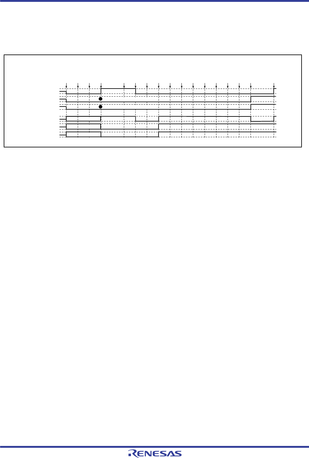
R01UH0034EJ0200 Rev.2.00 Page 685 of 1489
Dec 27, 2013
RX62T Group, RX62G Group 16. Multi-Function Timer Pulse Unit 3 (MTU3)
(11) Operation when Error Occurs in PWM Mode 1 and Operation is Restarted in Complementary
PWM Mode
Figure 16.153 shows a case in which an error occurs in PWM mode 1 and operation is restarted in complementary
PWM mode after re-setting.
Figure 16.153 Error Occurrence in PWM Mode 1, Recovery in Complementary PWM Mode
(1) to (9) are the same as in Figure 16.149.
(10) Set normal mode to initialize the normal mode waveform generation section.
(11) Initialize the PWM mode 1 waveform generation section with TIOR.
(12) Disable operation of the PWM mode 1 waveform generation section with TIOR
(13) Disable output in MTU3 and MTU4 with TOERA.
(14) Select the complementary PWM output level and enable or disable cyclic output with TOCR1A and TOCR2A.
(15) Set complementary PWM mode.
(16) Enable output in MTU3 and MTU4 with TOERA.
(17) Restart operation by setting TSTRA.
(1)
Reset
MTU module output
Hi-Z
Hi-Z
Hi-Z
Not initialized (MTIOCnB)
Not initialized (MTIOCnD)
(2)
TMDR
(PWM1)
(3)
TOER
(1)
(4)
TIOR
(1 init
0 out)
(5)
TSTR
(1)
(6)
Match (7)
Error
occurs
(8)
Port
output
(9)
TSTR
(0)
(10)
TMDR
(normal)
(11)
TIOR
(0 init
0 out)
(12)
TIOR
(disabled)
(13)
TOER
(0)
(14)
TOCR (15)
TMDR
(CPWM)
(16)
TOER
(1)
(17)
TSTR
(1)
MTIOC3A
MTIOC3B
MTIOC3D
PORT output
Pxx
Pxx
Pxx
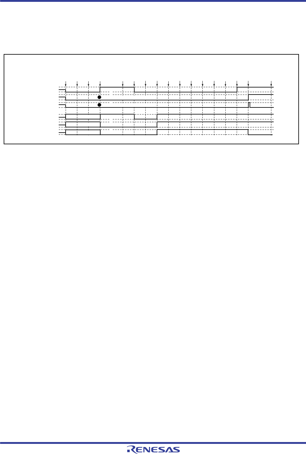
R01UH0034EJ0200 Rev.2.00 Page 686 of 1489
Dec 27, 2013
RX62T Group, RX62G Group 16. Multi-Function Timer Pulse Unit 3 (MTU3)
(12) Operation when Error Occurs in PWM Mode 1 and Operation is Restarted in Reset-
Synchronized PWM Mode
Figure 16.154 shows a case in which an error occurs in PWM mode 1 and operation is restarted in reset-synchronized
PWM mode after re-setting.
Figure 16.154 Error Occurrence in PWM Mode 1, Recovery in Reset-Synchronized PWM Mode
(1) to (13) are the same as in Figure 16.153.
(14) Select the reset-synchronized PWM output level and enable or disable cyclic output with TOCR1A and TOCR2A.
(15) Set reset-synchronized PWM mode.
(16) Enable output in MTU3 and MTU4 with TOERA.
(17) Restart operation by setting TSTRA.
(1)
Reset
MTU module output
Hi-Z
Hi-Z
Hi-Z
Not initialized (MTIOC3B)
Not initialized (MTIOC3D)
MTIOC3A
MTIOC3B
MTIOC3D
PORT output
Pxx
Pxx
Pxx
(2)
TMDR
(PWM1)
(3)
TOER
(1)
(4)
TIOR
(1 init
0 out)
(5)
TSTR
(1)
(6)
Match (7)
Error
occurs
(8)
Port
output
(9)
TSTR
(0)
(10)
TMDR
(normal)
(11)
TIOR
(0 init
0 out)
(12)
TIOR
(disabled)
(13)
TOER
(0)
(14)
TOCR (15)
TMDR
(RPWM)
(16)
TOER
(1)
(17)
TSTR
(1)

R01UH0034EJ0200 Rev.2.00 Page 687 of 1489
Dec 27, 2013
RX62T Group, RX62G Group 16. Multi-Function Timer Pulse Unit 3 (MTU3)
(13) Operation when Error Occurs in PWM Mode 2 and Operation is Restarted in Normal Mode
Figure 16.155 shows a case in which an error occurs in PWM mode 2 and operation is restarted in normal mode after
re-setting.
Figure 16.155 Error Occurrence in PWM Mode 2, Recovery in Normal Mode
(1) After a reset, the MTU3 output goes low and the ports enter high-impedance state.
(2) Set PWM mode 2.
In addition, make necessary settings in the data direction registers (DDR) and data registers (DR) in the I/O ports so
that a non-active level is output from the general ports.
(3) Initialize the pins with TIOR. (In the example, the initial output is a high level, and a low level is output on compare
match occurrence. In PWM mode 2, the cycle register pins are not initialized. In the example, MTIOCnA is the cycle
register.)
(4) Start count operation by setting TSTRA.
(5) Output goes low on compare match occurrence.
(6) An error occurs.
(7) Disable the MTU3 output with TIOR to switch the pins to general output ports so that a non-active level is output
from the pins.
(8) Stop count operation by setting TSTRA.
(9) Set normal mode.
(10) Initialize the pins with TIOR.
(11) Restart operation by setting TSTRA.
MTU module output
Hi-Z
Not initialized (cycle register)
(1)
Reset (2)
TMDR
(PWM2)
(3)
TIOR
(1 init
0 out)
(4)
TSTR
(1)
(5)
Match (6)
Error
occurs
(7)
Port
output
(8)
TSTR
(0)
(9)
TMDR
(normal)
(10)
TIOR
(1 init
0 out)
(11)
TSTR
(1)
PORT output
Pxx
Pxx
Hi-Z
MTIOCnA
MTIOCnB
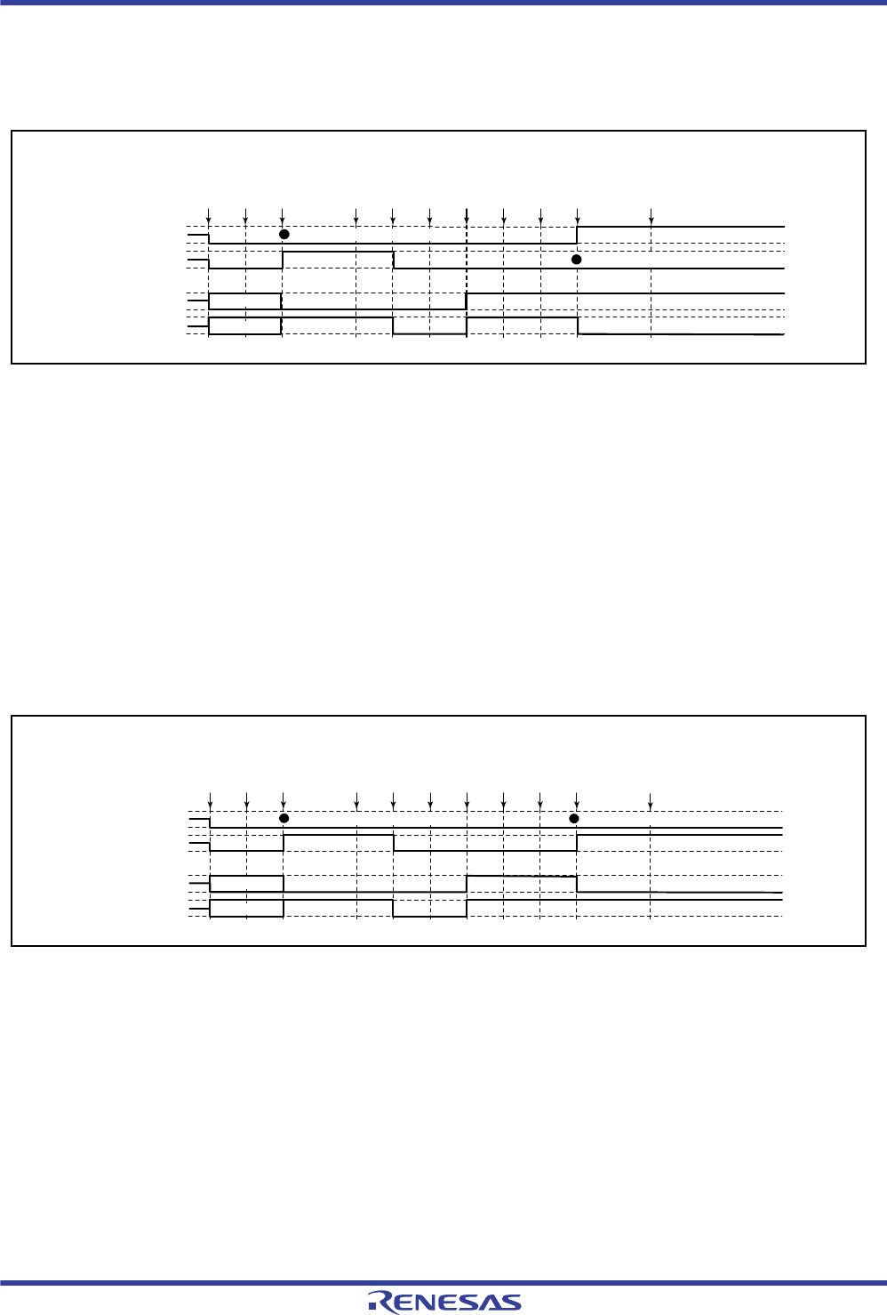
R01UH0034EJ0200 Rev.2.00 Page 688 of 1489
Dec 27, 2013
RX62T Group, RX62G Group 16. Multi-Function Timer Pulse Unit 3 (MTU3)
(14) Operation when Error Occurs in PWM Mode 2 and Operation is Restarted in PWM Mode 1
Figure 16.156 shows a case in which an error occurs in PWM mode 2 and operation is restarted in PWM mode 1 after
re-setting.
Figure 16.156 Error Occurrence in PWM Mode 2, Recovery in PWM Mode 1
(1) to (8) are the same as in Figure 16.155.
(9) Set PWM mode 1.
(10) Initialize the pins with TIOR. (In PWM mode 1, waveforms are not output to the MTIOCnB (MTIOCnD) pins.
To output a specified level, make necessary settings for general output ports in the data direction registers (DDR)
and data registers (DR) in the I/O ports.)
(11) Restart operation by setting TSTRA.
(15) Operation when Error Occurs in PWM Mode 2 and Operation is Restarted in PWM Mode 2
Figure 16.157 shows a case in which an error occurs in PWM mode 2 and operation is restarted in PWM mode 2 after
re-setting.
Figure 16.157 Error Occurrence in PWM Mode 2, Recovery in PWM Mode 2
(1) to (8) are the same as in Figure 16.155.
(9) This step is not necessary when restarting in PWM mode 2.
(10) Initialize the pins with TIOR. (In PWM mode 2, waveforms are not output to the cycle register pins. To output a
specified level, make necessary settings for general output ports in the data direction registers (DDR) and data
registers (DR) in the I/O ports.)
(11) Restart operation by setting TSTRA.
(1)
Reset
MTU module output
Hi-Z
Hi-Z
Not initialized (MTIOCnB)
Not initialized (cycle register)
(2)
TMDR
(PWM2)
(3)
TIOR
(1 init
0 out)
(4)
TSTR
(1)
(5)
Match (6)
Error
occurs
(7)
Port
output
(8)
TSTR
(0)
(9)
TMDR
(PWM1)
(10)
TIOR
(1 init
0 out)
(11)
TSTR
(1)
PORT output
Pxx
Pxx
MTIOCnA
MTIOCnB
(1)
Reset
MTU module output
Hi-Z
Not initialized (cycle register) Not initialized (cycle register)
(2)
TMDR
(PWM2)
(3)
TIOR
(1 init
0 out)
(4)
TSTR
(1)
(5)
Match (6)
Error
occurs
(7)
Port
output
(8)
TSTR
(0)
(9)
TMDR
(PWM2)
(10)
TIOR
(1 init
0 out)
(11)
TSTR
(1)
PORT output
Pxx
Pxx
Hi-Z
MTIOCnA
MTIOCnB

R01UH0034EJ0200 Rev.2.00 Page 689 of 1489
Dec 27, 2013
RX62T Group, RX62G Group 16. Multi-Function Timer Pulse Unit 3 (MTU3)
(16) Operation when Error Occurs in PWM Mode 2 and Operation is Restarted in Phase Counting
Mode
Figure 16.158 shows a case in which an error occurs in PWM mode 2 and operation is restarted in phase counting mode
after re-setting.
Figure 16.158 Error Occurrence in PWM Mode 2, Recovery in Phase Counting Mode
(1) to (8) are the same as in Figure 16.155.
(9) Set the phase counting mode.
(10) Initialize the pins with TIOR.
(11) Restart operation by setting TSTRA.
(1)
Reset
MTU module output
Not initialized (cycle register)
(2)
TMDR
(PWM2)
(3)
TIOR
(1 init
0 out)
(4)
TSTR
(1)
(5)
Match (6)
Error
occurs
(7)
Port
output
(8)
TSTR
(0)
(9)
TMDR
(PCM)
(10)
TIOR
(1 init
0 out)
(11)
TSTR
(1)
PORT output
Pxx
Pxx
Hi-Z
Hi-Z
MTIOCnA
MTIOCnB

R01UH0034EJ0200 Rev.2.00 Page 690 of 1489
Dec 27, 2013
RX62T Group, RX62G Group 16. Multi-Function Timer Pulse Unit 3 (MTU3)
(17) Operation when Error Occurs in Phase Counting Mode and Operation is Restarted in Normal
Mode
Figure 16.159 shows a case in which an error occurs in phase counting mode and operation is restarted in normal mode
after re-setting.
Figure 16.159 Error Occurrence in Phase Counting Mode, Recovery in Normal Mode
(1) After a reset, the MTU3 output goes low and the ports enter high-impedance state.
(2) Set phase counting mode.
In addition, make necessary settings in the data direction registers (DDR) and data registers (DR) in the I/O ports so
that a non-active level is output from the general ports.
(3) Initialize the pins with TIOR. (In the example, the initial output is a high level, and a low level is output on compare
match occurrence.)
(4) Start count operation by setting TSTRA.
(5) Output goes low on compare match occurrence.
(6) An error occurs.
(7) Disable the MTU3 output with TIOR to switch the pins to general output ports so that a non-active level is output
from the pins.
(8) Stop count operation by setting TSTRA.
(9) Set normal mode.
(10) Initialize the pins with TIOR.
(11) Restart operation by setting TSTRA.
(1)
Reset
Hi-Z
MTU module output
(2)
TMDR
(PCM)
(3)
TIOR
(1 init
0 out)
(4)
TSTR
(1)
(5)
Match (6)
Error
occurs
(7)
Port
output
(8)
TSTR
(0)
(9)
TMDR
(normal)
(10)
TIOR
(1 init
0 out)
(11)
TSTR
(1)
MTIOCnA
MTIOCnB
PORT output
Pxx
Pxx
Hi-Z

R01UH0034EJ0200 Rev.2.00 Page 691 of 1489
Dec 27, 2013
RX62T Group, RX62G Group 16. Multi-Function Timer Pulse Unit 3 (MTU3)
(18) Operation when Error Occurs in Phase Counting Mode and Operation is Restarted in PWM
Mode 1
Figure 16.160 shows a case in which an error occurs in phase counting mode and operation is restarted in PWM mode 1
after re-setting.
Figure 16.160 Error Occurrence in Phase Counting Mode, Recovery in PWM Mode 1
(1) to (8) are the same as in Figure 16.159.
(9) Set PWM mode 1.
(10) Initialize the pins with TIOR. (In PWM mode 1, waveforms are not output to the MTIOCnB (MTIOCnD) pins.
To output a specified level, make necessary settings for general output ports in the data direction registers (DDR)
and data registers (DR) in the I/O ports.)
(11) Restart operation by setting TSTRA.
(1)
Reset
Hi-Z
Hi-Z
Not initialized (MTIOCnB)
MTU module output
(2)
TMDR
(PCM)
(3)
TIOR
(1 init
0 out)
(4)
TSTR
(1)
(5)
Match (6)
Error
occurs
(7)
Port
output
(8)
TSTR
(0)
(9)
TMDR
(PWM1)
(10)
TIOR
(1 init
0 out)
(11)
TSTR
(1)
PORT output
Pxx
Pxx
MTIOCnA
MTIOCnB
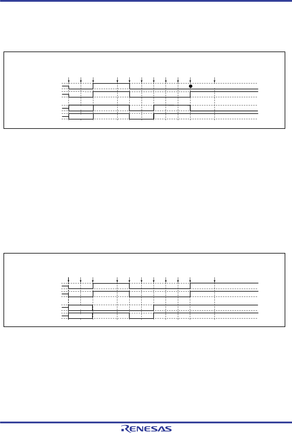
R01UH0034EJ0200 Rev.2.00 Page 692 of 1489
Dec 27, 2013
RX62T Group, RX62G Group 16. Multi-Function Timer Pulse Unit 3 (MTU3)
(19) Operation when Error Occurs in Phase Counting Mode and Operation is Restarted in PWM
Mode 2
Figure 16.161 shows a case in which an error occurs in phase counting mode and operation is restarted in PWM mode 2
after re-setting.
Figure 16.161 Error Occurrence in Phase Counting Mode, Recovery in PWM Mode 2
(1) to (8) are the same as in Figure 16.159.
(9) Set PWM mode 2.
(10) Initialize the pins with TIOR. (In PWM mode 2, waveforms are not output to the cycle register pins. To output a
specified level, make necessary settings for general output ports in the data direction registers (DDR) and data
registers (DR) in the I/O ports.)
(11) Restart operation by setting TSTRA.
(20) Operation when Error Occurs in Phase Counting Mode and Operation is Restarted in Phase
Counting Mode
Figure 16.162 shows a case in which an error occurs in phase counting mode and operation is restarted in phase
counting mode after re-setting.
Figure 16.162 Error Occurrence in Phase Counting Mode, Recovery in Phase Counting Mode
(1) to (8) are the same as in Figure 16.159.
(9) This step is not necessary when restarting in phase counting mode.
(10) Initialize the pins with TIOR.
(11) Restart operation by setting TSTRA.
(1)
Reset
Hi-Z
Hi-Z
MTU module output
(2)
TMDR
(PCM)
(3)
TIOR
(1 init
0 out)
(4)
TSTR
(1)
(5)
Match (6)
Error
occurs
(7)
Port
output
(8)
TSTR
(0)
(9)
TMDR
(PWM2)
(10)
TIOR
(1 init
0 out)
(11)
TSTR
(1)
PORT output
Pxx
Pxx
Not initialized (cycle register)
MTIOCnA
MTIOCnB
(1)
Reset
Hi-Z
MTU module output
(2)
TMDR
(PCM)
(3)
TIOR
(1 init
0 out)
(4)
TSTR
(1)
(5)
Match (6)
Error
occurs
(7)
Port
output
(8)
TSTR
(0)
(9)
TMDR
(PCM)
(10)
TIOR
(1 init
0 out)
(11)
TSTR
(1)
MTIOCnA
MTIOCnB
PORT output
Pxx
Pxx Hi-Z
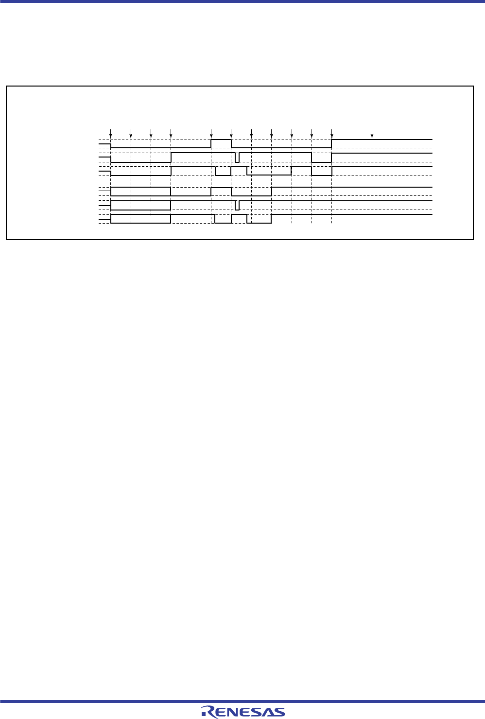
R01UH0034EJ0200 Rev.2.00 Page 693 of 1489
Dec 27, 2013
RX62T Group, RX62G Group 16. Multi-Function Timer Pulse Unit 3 (MTU3)
(21) Operation when Error Occurs in Complementary PWM Mode and Operation is Restarted in
Normal Mode
Figure 16.163 shows a case in which an error occurs in complementary PWM mode and operation is restarted in normal
mode after re-setting.
Figure 16.163 Error Occurrence in Complementary PWM Mode, Recovery in Normal Mode
(1) After a reset, the MTU3 output goes low and the ports enter high-impedance state.
(2) Select the complementary PWM output level and enable or disable cyclic output with TOCR1A and TOCR2A.
(3) Set complementary PWM mode.
In addition, make necessary settings in the data direction registers (DDR) and data registers (DR) in the I/O ports so
that a non-active level is output from the general ports.
(4) Enable output in MTU3 and MTU4 with TOERA.
(5) Start count operation by setting TSTRA.
(6) The complementary PWM waveform is output on compare match occurrence.
(7) An error occurs.
(8) Disable the MTU3 output with TIOR to switch the pins to general output ports so that a non-active level is output
from the pins.
(9) Stop count operation by setting TSTRA. (MTU3 output becomes the initial complementary PWM output value).
(10) Set normal mode (MTU3 output goes low).
(11) Initialize the pins with TIOR.
(12) Restart operation by setting TSTRA.
(1)
Reset
Hi-Z
Hi-Z
Hi-Z
MTU module output
(2)
TOCR (3)
TMDR
(CPWM)
(4)
TOER
(1)
(5)
TSTR
(1)
(6)
Match (7)
Error
occurs
(8)
Port
output
(9)
TSTR
(0)
(10)
TMDR
(normal)
(11)
TIOR
(1 init
0 out)
(12)
TSTR
(1)
MTIOC3A
MTIOC3B
MTIOC3D
PORT output
Pxx
Pxx
Pxx

R01UH0034EJ0200 Rev.2.00 Page 694 of 1489
Dec 27, 2013
RX62T Group, RX62G Group 16. Multi-Function Timer Pulse Unit 3 (MTU3)
(22) Operation when Error Occurs in Complementary PWM Mode and Operation is Restarted in
PWM Mode 1
Figure 16.164 shows a case in which an error occurs in complementary PWM mode and operation is restarted in PWM
mode 1 after re-setting.
Figure 16.164 Error Occurrence in Complementary PWM Mode, Recovery in PWM Mode 1
(1) to (9) are the same as in Figure 16.163.
(10) Set PWM mode 1 (MTU3 output goes low).
(11) Initialize the pins with TIOR. (In PWM mode 1, waveforms are not output to the MTIOCnB (MTIOCnD) pins.
To output a specified level, make necessary settings for general output ports in the data direction registers (DDR)
and data registers (DR) in the I/O ports.)
(12) Restart operation by setting TSTRA.
(1)
Reset
Not initialized (MTIOC3B)
Not initialized (MTIOC3D)
Hi-Z
Hi-Z
Hi-Z
MTU module output
(2)
TOCR (3)
TMDR
(CPWM)
(4)
TOER
(1)
(5)
TSTR
(1)
(6)
Match (7)
Error
occurs
(8)
Port
output
(9)
TSTR
(0)
(10)
TMDR
(PWM1)
(11)
TIOR
(1 init
0 out)
(12)
TSTR
(1)
MTIOC3A
MTIOC3B
MTIOC3D
PORT output
Pxx
Pxx
Pxx
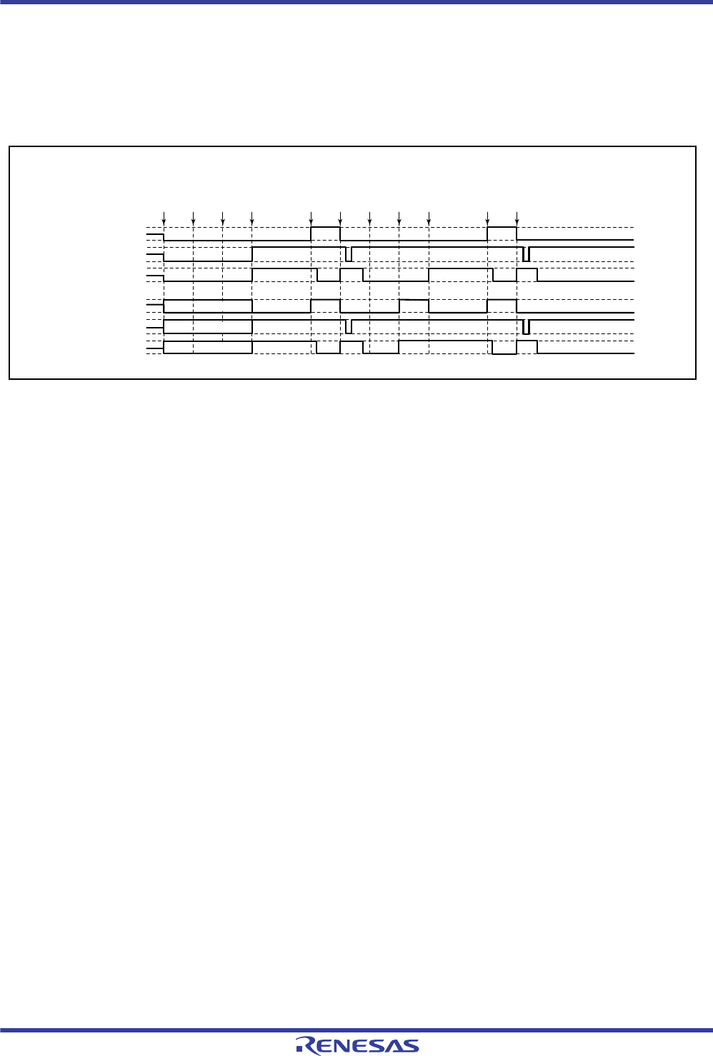
R01UH0034EJ0200 Rev.2.00 Page 695 of 1489
Dec 27, 2013
RX62T Group, RX62G Group 16. Multi-Function Timer Pulse Unit 3 (MTU3)
(23) Operation when Error Occurs in Complementary PWM Mode and Operation is Restarted in
Complementary PWM Mode
Figure 16.165 shows a case in which an error occurs in complementary PWM mode and operation is restarted in
complementary PWM mode after re-setting (when operation is restarted using the cycle and duty settings at the time of
stopping the counter).
Figure 16.165 Error Occurrence in Complementary PWM Mode, Recovery in Complementary PWM Mode (1)
(1) to (9) are the same as in Figure 16.163.
(10) Restart operation by setting TSTRA.
(11) The complementary PWM waveform is output on compare match occurrence.
(1)
Reset
Hi-Z
Hi-Z
Hi-Z
MTU module output
(2)
TOCR (3)
TMDR
(CPWM)
(4)
TOER
(1)
(5)
TSTR
(1)
(6)
Match (7)
Error
occurs
(8)
Port
output
(9)
TSTR
(0)
(10)
TSTR
(1)
(11)
Match
MTIOC3A
MTIOC3B
MTIOC3D
PORT output
Pxx
Pxx
Pxx

R01UH0034EJ0200 Rev.2.00 Page 696 of 1489
Dec 27, 2013
RX62T Group, RX62G Group 16. Multi-Function Timer Pulse Unit 3 (MTU3)
(24) Operation when Error Occurs in Complementary PWM Mode and Operation is Restarted in
Complementary PWM Mode with New Settings
Figure 16.166 shows a case in which an error occurs in complementary PWM mode and operation is restarted in
complementary PWM mode after re-setting (operation is restarted using new cycle and duty ratio settings).
Figure 16.166 Error Occurrence in Complementary PWM Mode, Recovery in Complementary PWM Mode (2)
(1) to (9) are the same as in Figure 16.163.
(10) Set normal mode and make new settings (MTU3 output goes low).
(11) Disable output in MTU3 and MTU4 with TOERA.
(12) Select the complementary PWM output level and enable or disable cyclic output with TOCR1A and TOCR2A.
(13) Set complementary PWM mode.
(14) Enable output in MTU3 and MTU4 with TOERA.
(15) Restart operation by setting TSTRA.
(1)
Reset
Hi-Z
Hi-Z
Hi-Z
MTU module output
(2)
TOCR (3)
TMDR
(CPWM)
(4)
TOER
(1)
(5)
TSTR
(1)
(6)
Match (7)
Error
occurs
(8)
Port
output
(9)
TSTR
(0)
(10)
TMDR
(normal)
(11)
TOER
(0)
(12)
TOCR (13)
TMDR
(CPWM)
(14)
TOER
(1)
(15)
TSTR
(1)
MTIOC3A
MTIOC3B
MTIOC3D
PORT output
Pxx
Pxx
Pxx
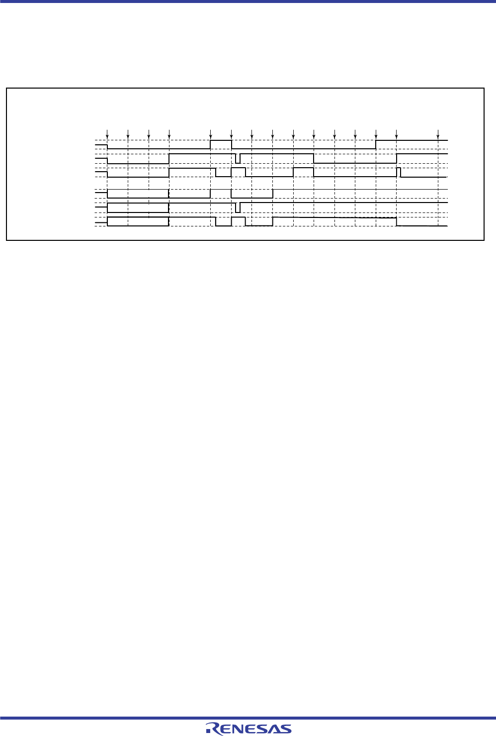
R01UH0034EJ0200 Rev.2.00 Page 697 of 1489
Dec 27, 2013
RX62T Group, RX62G Group 16. Multi-Function Timer Pulse Unit 3 (MTU3)
(25) Operation when Error Occurs in Complementary PWM Mode and Operation is Restarted in
Reset-Synchronized PWM Mode
Figure 16.167 shows a case in which an error occurs in complementary PWM mode and operation is restarted in reset-
synchronized PWM mode after re-setting.
Figure 16.167 Error Occurrence in Complementary PWM Mode, Recovery in Reset-Synchronized PWM Mode
(1) to (9) are the same as in Figure 16.163.
(10) Set normal mode (MTU3 output goes low).
(11) Disable output in MTU3 and MTU4 with TOERA.
(12) Select the reset-synchronized PWM output level and enable or disable cyclic output with TOCR1A and TOCR2A.
(13) Set reset-synchronized PWM mode.
(14) Enable output in MTU3 and MTU4 with TOERA.
(15) Restart operation by setting TSTRA.
(1)
Reset
Hi-Z
Hi-Z
Hi-Z
MTU module output
(2)
TOCR (3)
TMDR
(CPWM)
(4)
TOER
(1)
(5)
TSTR
(1)
(6)
Match (7)
Error
occurs
(8)
Port
output
(9)
TSTR
(0)
(10)
TMDR
(normal)
(11)
TOER
(0)
(12)
TOCR (13)
TMDR
(RPWM)
(14)
TOER
(1)
(15)
TSTR
(1)
MTIOC3A
MTIOC3B
MTIOC3D
PORT output
Pxx
Pxx
Pxx
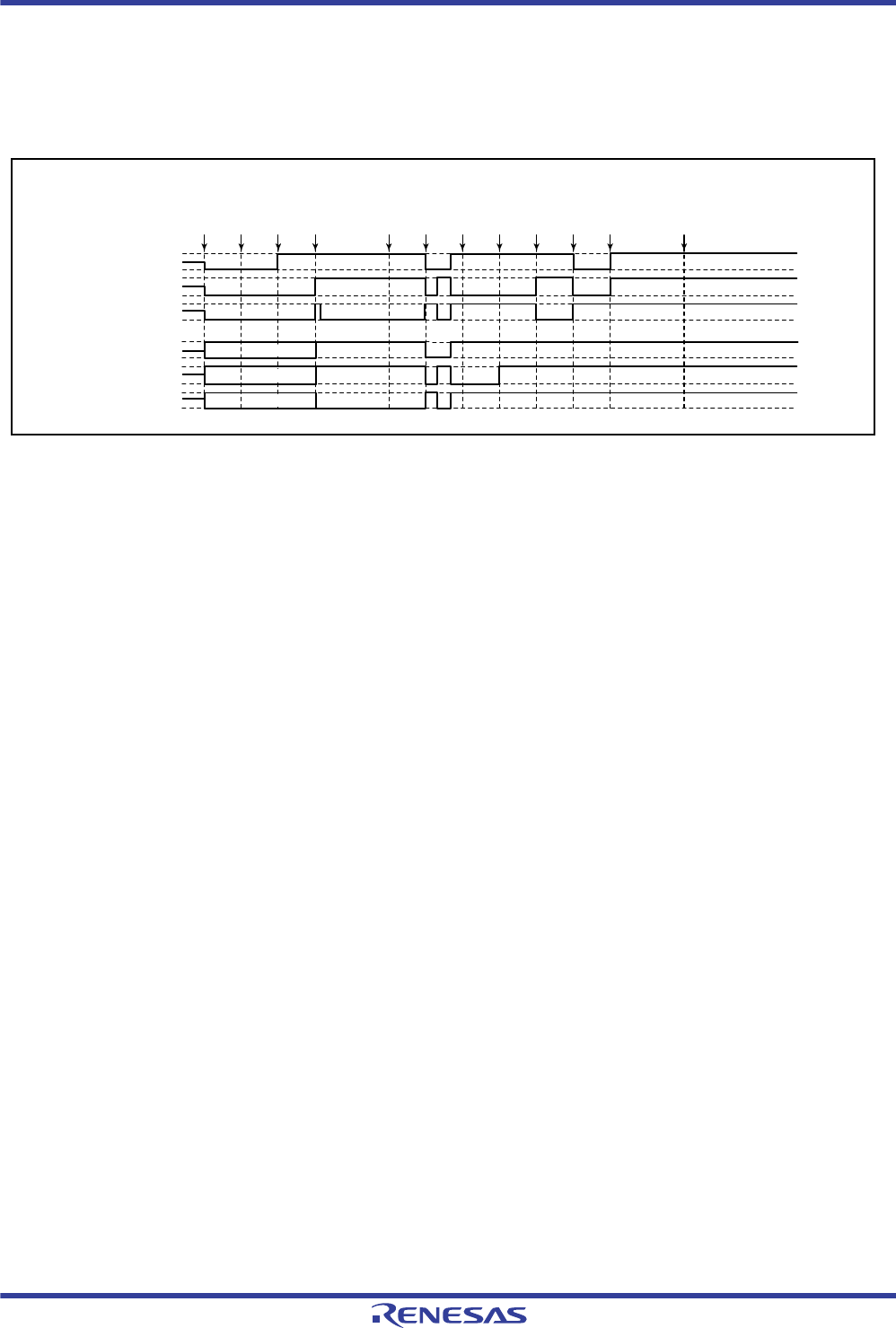
R01UH0034EJ0200 Rev.2.00 Page 698 of 1489
Dec 27, 2013
RX62T Group, RX62G Group 16. Multi-Function Timer Pulse Unit 3 (MTU3)
(26) Operation when Error Occurs in Reset-Synchronized PWM Mode and Operation is Restarted
in Normal Mode
Figure 16.168 shows a case in which an error occurs in reset-synchronized PWM mode and operation is restarted in
normal mode after re-setting.
Figure 16.168 Error Occurrence in Reset-Synchronized PWM Mode, Recovery in Normal Mode
(1) After a reset, the MTU3 output goes low and the ports enter high-impedance state.
(2) Select the reset-synchronized PWM output level and enable or disable cyclic output with TOCR1A and TOCR2A.
(3) Set reset-synchronized PWM mode.
In addition, make necessary settings in the data direction registers (DDR) and data registers (DR) in the I/O ports so
that a non-active level is output from the general ports.
(4) Enable output in MTU3 and MTU4 with TOERA.
(5) Start count operation by setting TSTRA.
(6) The reset-synchronized PWM waveform is output on compare match occurrence.
(7) An error occurs.
(8) Disable the MTU3 output with TIOR to switch the pins to general output ports so that a non-active level is output
from the pins.
(9) Stop count operation by setting TSTRA. (MTU3 output becomes the initial reset-synchronized PWM output value.)
(10) Set normal mode (positive-phase MTU3 output goes low, and negative-phase output goes high).
(11) Initialize the pins with TIOR.
(12) Restart operation by setting TSTRA.
(1)
Reset
Hi-Z
Hi-Z
Hi-Z
MTU module output
(2)
TOCR (3)
TMDR
(RPWM)
(4)
TOER
(1)
(5)
TSTR
(1)
(6)
Match (7)
Error
occurs
(8)
Port
output
(9)
TSTR
(0)
(10)
TMDR
(normal)
(11)
TIOR
(1 init
0 out)
(12)
TSTR
(1)
MTIOC3A
MTIOC3B
MTIOC3D
PORT output
Pxx
Pxx
Pxx
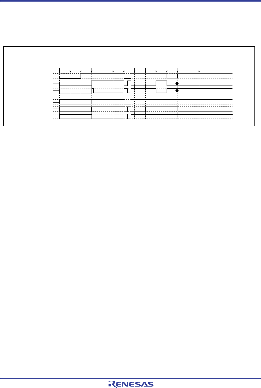
R01UH0034EJ0200 Rev.2.00 Page 699 of 1489
Dec 27, 2013
RX62T Group, RX62G Group 16. Multi-Function Timer Pulse Unit 3 (MTU3)
(27) Operation when Error Occurs in Reset-Synchronized PWM Mode and Operation is Restarted
in PWM Mode 1
Figure 16.169 shows a case in which an error occurs in reset-synchronized PWM mode and operation is restarted in
PWM mode 1 after re-setting.
Figure 16.169 Error Occurrence in Reset-Synchronized PWM Mode, Recovery in PWM Mode 1
(1) to (9) are the same as in Figure 16.168.
(10) Set PWM mode 1 (positive-phase MTU3 output goes low, and negative-phase output goes high).
(11) Initialize the pins with TIOR. (In PWM mode 1, waveforms are not output to the MTIOCnB (MTIOCnD) pins.
To output a specified level, make necessary settings for general output ports in the data direction registers (DDR)
and data registers (DR) in the I/O ports.)
(12) Restart operation by setting TSTRA.
(1)
Reset
Not initialized (MTIOC3B)
Not initialized (MTIOC3D)
Hi-Z
Hi-Z
Hi-Z
MTU module output
(2)
TOCR (3)
TMDR
(RPWM)
(4)
TOER
(1)
(5)
TSTR
(1)
(6)
Match (7)
Error
occurs
(8)
Port
output
(9)
TSTR
(0)
(10)
TMDR
(PWM1)
(11)
TIOR
(1 init
0 out)
(12)
TSTR
(1)
MTIOC3A
MTIOC3B
MTIOC3D
PORT output
Pxx
Pxx
Pxx

R01UH0034EJ0200 Rev.2.00 Page 700 of 1489
Dec 27, 2013
RX62T Group, RX62G Group 16. Multi-Function Timer Pulse Unit 3 (MTU3)
(28) Operation when Error Occurs in Reset-Synchronized PWM Mode and Operation is Restarted
in Complementary PWM Mode
Figure 16.170 shows a case in which an error occurs in reset-synchronized PWM mode and operation is restarted in
complementary PWM mode after re-setting.
Figure 16.170 Error Occurrence in Reset-Synchronized PWM Mode, Recovery in Complementary PWM Mode
(1) to (9) are the same as in Figure 16.168.
(10) Disable output in MTU3 and MTU4 with TOERA.
(11) Select the complementary PWM output level and enable or disable cyclic output with TOCR1A and TOCR2A.
(12) Set complementary PWM mode (MTU3 cyclic output pin goes low).
(13) Enable output in MTU3 and MTU4 with TOERA.
(14) Restart operation by setting TSTRA.
(1)
Reset
Hi-Z
Hi-Z
Not initialized (MTIOCnB)
MTU module output
(2)
TMDR
(PCM)
(3)
TIOR
(1 init
0 out)
(4)
TSTR
(1)
(5)
Match (6)
Error
occurs
(7)
Port
output
(8)
TSTR
(0)
(9)
TMDR
(PWM1)
(10)
TIOR
(1 init
0 out)
(11)
TSTR
(1)
PORT output
Pxx
Pxx
MTIOCnA
MTIOCnB
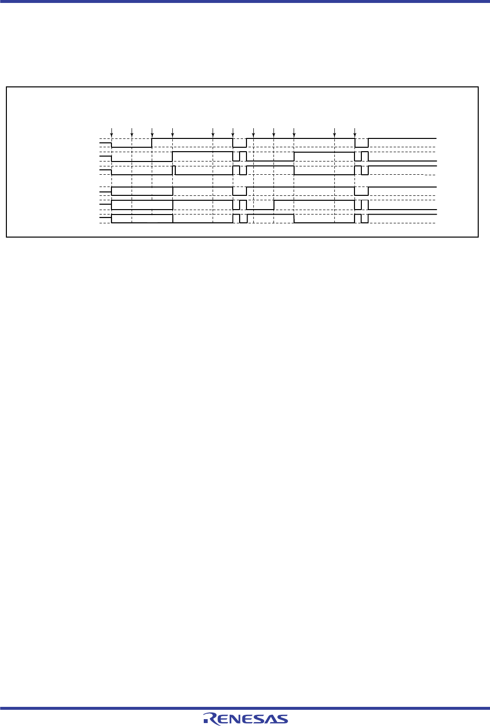
R01UH0034EJ0200 Rev.2.00 Page 701 of 1489
Dec 27, 2013
RX62T Group, RX62G Group 16. Multi-Function Timer Pulse Unit 3 (MTU3)
(29) Operation when Error Occurs in Reset-Synchronized PWM Mode and Operation is Restarted
in Reset-Synchronized PWM Mode
Figure 16.171 shows a case in which an error occurs in reset-synchronized PWM mode and operation is restarted in
reset-synchronized PWM mode after re-setting.
Figure 16.171 Error Occurrence in Reset-Synchronized PWM Mode, Recovery in Reset-Synchronized PWM
Mode
(1) to (9) are the same as in Figure 16.168.
(10) Restart operation by setting TSTRA.
(11) The reset-synchronized PWM waveform is output on compare match occurrence.
(3)
TMDR
(RPWM)
Hi-Z
Hi-Z
Hi-Z
MTU module output
(1)
Reset (2)
TOCR (4)
TOER
(1)
(5)
TSTR
(1)
(6)
Match (7)
Error
occurs
(8)
Port
output
(9)
TSTR
(0)
(10)
TSTR
(1)
(11)
Match
MTIOC3A
MTIOC3B
MTIOC3D
PORT output
Pxx
Pxx
Pxx

R01UH0034EJ0200 Rev.2.00 Page 702 of 1489
Dec 27, 2013
RX62T Group, RX62G Group 17. Port Output Enable 3 (POE3)
Under development Preliminary document
Specifications in this document are tentative and subject to change.
17. Port Output Enable 3 (POE3)
The port output enable 3 (POE3) register can be used to place complementary PWM output pins for the MTU
(MTIOC3B, MTIOC3D, MTIOC4A, MTIOC4B, MTIOC4C, MTIOC4D, MTIOC6B, MTIOC6D, MTIOC7A,
MTIOC7B, MTIOC7C, and MTIOC7D) and large-current output pins for the GPT (GTIOC0A-A, GTIOC0B-A,
GTIOC1A-A, GTIOC1B-A, GTIOC2A-A, and GTIOC2B-A) in the high-impedance state in accord with changes in the
input signals on the POE0#, POE4#, POE8#, POE10#, and POE11# pins, and to place pin functions multiplexed with
complementary PWM output pins for the MTU, pins for MTU0 (MTIOC0A, MTIOC0B, MTIOC0C, and MTIOC0D),
and pins for the GPT (GTIOC0A, GTIOC0B, GTIOC1A, GTIOC1B, GTIOC2A, GTIOC2B, GTIOC3A, and GTIOC3B)
in the high-impedance state in accord with register settings. It can also simultaneously generate interrupt requests.
Furthermore, it is capable of placing pin functions multiplexed with complementary PWM output pins for the MTU, pins
for MTU0, and pins for the GPT in the high-impedance state in response to stoppage of the clock signal from the clock
oscillator.
17.1 Overview
Table 17.1 lists the specifications of the POE3, and Figure 17.1 shows a block diagram of the POE3.
The POE3 has input level detection circuits, output level comparison circuits, and a high-impedance request/interrupt
request generating circuit as shown in Figure 17.1.
Table 17.1 POE3 Specifications
Item Description
Function Each of the POE0#, POE4#, POE8#, POE10#, and POE11# input pins can be set for falling edge, PCLK/8 16,
PCLK/16 16, or PCLK/128 16 low-level sampling.
Pins for the MTU complementary PWM output, MTU0 to MTU3 and GPT pins can be placed in high-impedance
state by POE0#, POE4#, POE8#, POE10#, and POE11# pin falling-edge or low-level sampling.
Pins for the MTU complementary PWM output, MTU0 to MTU3, and GPT pins can be placed in high-impedance
state when the oscillation-stop detection circuit in the clock pulse generator detects stopped oscillation.
Pins for the MTU complementary PWM output can be placed in high-impedance state when output levels of the
MTU complementary PWM output pins and the GPT large-current output pins are compared and simultaneous
active-level output continues for one cycle or more.
Pins for the MTU complementary PWM output, and for MTU0 to MTU3 and the GPT, can be placed in the high-
impedance state in response to comparator detection by the 12-bit A/D converter (S12ADA).
Pins for the MTU complementary PWM output, and for MTU0 to MTU3 and GPT pins can be placed in the high-
impedance state by modifying settings of the POE registers.
Interrupts can be generated by input-level sampling or output-level comparison results.
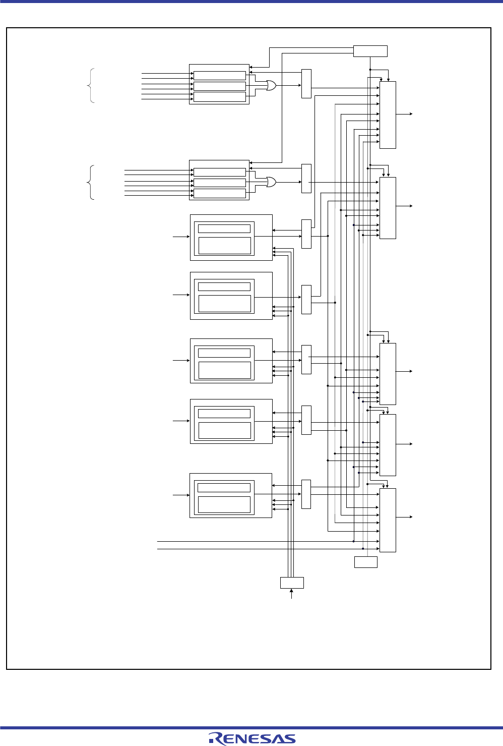
R01UH0034EJ0200 Rev.2.00 Page 703 of 1489
Dec 27, 2013
RX62T Group, RX62G Group 17. Port Output Enable 3 (POE3)
Under development Preliminary document
Specifications in this document are tentative and subject to change.
Figure 17.1 POE3 Block Diagram
Output level
comparison circuit
Output level
comparison circuit
Output level
comparison circuit
Output level
comparison circuit
Output level
comparison circuit
Output level
comparison circuit
High-impedance request signal for
MTU3 and MTU4 pins for the MTU
complementary PWM output/
GPT0 and GPT2 pins for GPT
large-current output/Interrupt signal
(OEI1)
Falling edge
detection circuit
Low level sampling circuit
Falling edge
detection circuit
Low level sampling circuit
Falling edge detection
circuit
Low level sampling circuit
Falling edge detection
circuit
Low level sampling circuit
Divider
PCLK
Pins for the MTU complementary
PWM output
(MTU3 and MTU4 pins)
or the GPT large-current output pins
(GPT0 to GPT2 pins)
High-impedance
request/interrupt request
generating circuit
High-impedance
request/interrupt request
generating circuit
High-impedance
request/interrupt request
generating circuit
High-impedance
request/interrupt request
generating circuit
POECR1 to 6
SPOER
O
C
S
R
2
O
C
S
R
1
I
C
S
R
1
I
C
S
R
2
I
C
S
R
4
I
C
S
R
3
Falling edge
detection circuit
Low level sampling circuit
High-impedance
request/interrupt request
generating circuit
I
C
S
R
5
MTIOC3B/GTIOC0A-A
MTIOC3D/GTIOC0B-A
MTIOC4A/GTIOC1A-A
MTIOC4C/GTIOC1B-A
MTIOC4B/GTIOC2A-A
MTIOC4D/GTIOC2B-A
High-impedance request signal for
MTU6 and MTU7 pins for the MTU
complementary PWM
output/Interrupt signal (OEI2)
PCLK/8
PCLK/16
PCLK/128
High-impedance request signal for
MTU0 pin/Interrupt signal (OEI3)
High-impedance request signal for
GPT0 and GPT1 pins/Interrupt
signal (OEI4)
High-impedance request signal for
GPT2 and GPT3 pins/Interrupt
signal (OEI4)
MTIOC6B
MTIOC6D
MTIOC7A
MTIOC7C
MTIOC7B
MTIOC7D
Pins for the MTU complementary
PWM output (MTU6 and MTU7 pins)
Comparator detection by the 12-bit A/D
converter
Detection of stopped oscillation
Input level detection circuit
Input level detection circuit
Input level detection circuit
Input level detection circuit
Input level detection circuit
POE0#
POE4#
POE8#
POE10#
POE11#
ICSR1
ICSR2
OCSR1
: Input level control/status register 1
: Input level control/status register 2
: Output level control/status register 1
SPOER
POECR1 to 6
: Software port output enable register
: Port output enable control register 1 to 6
ICSR4 : Input level control/status register 4
ICSR3 : Input level control/status register 3 OCSR2 : Output level control/status register 2
ICSR5 : Input level control/status register 5

R01UH0034EJ0200 Rev.2.00 Page 704 of 1489
Dec 27, 2013
RX62T Group, RX62G Group 17. Port Output Enable 3 (POE3)
Under development Preliminary document
Specifications in this document are tentative and subject to change.
Table 17.2 shows input/output pins to be used by the POE3.
Table 17.3 shows output-level comparisons with pin combinations.
Table 17.2 POE3 Input/Output Pins
Pin Name I/O Description
POE0# Input Request signal to place the MTU3 and MTU4 pins for MTU complementary PWM output in high-
impedance state, and in accord with register settings, is also capable of placing the MTU6 and MTU7
pins for MTU complementary PWM output, MTU0 pins, and GPT pins in the high-impedance state.
POE4# Input Request signal to place the MTU6 and MTU7 pins for MTU complementary PWM output in high-
impedance state, and in accord with register settings, is also capable of placing the MTU3 and MTU4
pins for MTU complementary PWM output, MTU0 pin, and GPT pins in high-impedance state.
POE8# Input Request signal to place the pins for MTU0 in high-impedance state, and in accord with register
settings, is also capable of placing the MTU3, MTU4, MTU6, and MTU7 pins for MTU
complementary PWM output, and GPT pins in high-impedance state.
POE10# Input Request signal to place the GPT0 and GPT1 pins in high-impedance state, and in accord with
register settings, is also capable of placing the MTU3, MTU4, MTU6, and MTU7 pins for MTU
complementary PWM output, MTU0 pin, and GPT2 and GPT3 pins in high-impedance state.
POE11# Input Request signal to place the pins for GPT2 and GPT3 in high-impedance state, and in accord with
register settings, is also capable of placing the MTU3, MTU4 and MTU6, MTU7 pins for MTU
complementary PWM output, MTU0 pin, and GPT0 and GPT1 pins in high-impedance state.
Table 17.3 Pin Combinations
Pin Combination I/O Description
MTIOC3B and MTIOC3D Output The MTU3 and MTU4 pins for MTU complementary PWM output are placed in high-
impedance state when both pins of a pair simultaneously output the active level (low level
when the OLSP bit in TOCR1A of MTUn is 0 with the TOCS bit in TOCR1A of MTUn
cleared to 0 or high level when the OLSP bit is 1, or low level when the OLS3N, OLS3P,
OLS2N, OLS2P, OLS1N, and OLS1P bits in TOCR2A of MTUn are 0 with the TOCS bit in
TOCR1A of MTUn set to 1 and high level when these bits are 1) for one or more cycles of
the peripheral clock (PCLK).
Pin combinations for output comparison and high-impedance control can be selected by
registers of POE3.
MTIOC4A and MTIOC4C Output
MTIOC4B and MTIOC4D Output
MTIOC6B and MTIOC6D Output The MTU6 and MTU7 pins for MTU complementary PWM output are placed in high-
impedance state when both pins of a pair simultaneously output the active level (low level
when the OLSP bit in TOCR1B of MTUn is 0 with the TOCS bit in TOCR1B of MTUn
cleared to 0 or high level when the OLSP bit is 1, or low level when the OLS3N, OLS3P,
OLS2N, OLS2P, OLS1N, and OLS1P bits in TOCR2B of MTUn are 0 with the TOCS bit in
TOCR1B of MTUn set to 1 and high level when these bits are 1) for one or more cycles of
the peripheral clock (PCLK).
Pin combinations for output comparison and high-impedance control can be selected by
registers of POE3.
MTIOC7A and MTIOC7C Output
MTIOC7B and MTIOC7D Output
GTIOC0A-A and GTIOC0B-A Output The GPT0 to GPT2 pins for the GPT large-current output are placed in high-impedance
state when both pins of a pair simultaneously output the active level (low level when the
OLSG2B, OLSG2A, OLSG1B, OLSG1A, OLSG0B, OLSG0A bits in ALR1 are 0 or high
level when those bits are 1) for one or more cycles of the peripheral clock (PCLK).
Pin combinations for output comparison and high-impedance control can be selected by
registers of POE3.
GTIOC1A-A and GTIOC1B-A Output
GTIOC2A-A and GTIOC2B-A Output

R01UH0034EJ0200 Rev.2.00 Page 705 of 1489
Dec 27, 2013
RX62T Group, RX62G Group 17. Port Output Enable 3 (POE3)
Under development Preliminary document
Specifications in this document are tentative and subject to change.
17.2 Register Descriptions
Table 17.4 is the list of POE3 registers. The POE3 registers are initialized by a reset.
Table 17.4 POE3 Register Configuration
Register Name Symbol Value after Reset Address Access Size
Input level control/status register 1 ICSR1 0000h 0008 C4C0h 8, 16
Output level control/status register 1 OCSR1 0000h 0008 C4C2h 8, 16
Input level control/status register 2 ICSR2 0000h 0008 C4C4h 8, 16
Output level control/status register 2 OCSR2 0000h 0008 C4C6h 8, 16
Input level control/status register 3 ICSR3 0000h 0008 C4C8h 8, 16
Input level control/status register 4 ICSR4 0000h 0008 C4D6h 8, 16
Input level control/status register 5 ICSR5 0000h 0008 C4D8h 8, 16
Software port output enable register SPOER 00h 0008 C4CAh 8
Port output enable control register 1 POECR1 00h 0008 C4CBh 8
Port output enable control register 2 POECR2 0707h 0008 C4CCh 16
Port output enable control register 3 POECR3 0303h 0008 C4CEh 16
Port output enable control register 4 POECR4 0402h 0008 C4D0h 16
Port output enable control register 5 POECR5 0008h 0008 C4D2h 16
Port output enable control register 6 POECR6 2010h 0008 C4D4h 16
Active level setting register 1 ALR1 0000h 0008 C4DAh 8,16

R01UH0034EJ0200 Rev.2.00 Page 706 of 1489
Dec 27, 2013
RX62T Group, RX62G Group 17. Port Output Enable 3 (POE3)
Under development Preliminary document
Specifications in this document are tentative and subject to change.
17.2.1 Input Level Control/Status Register 1 (ICSR1)
Note 1. Can be modified only once after a reset.
Note 2. Writing 0 to this bit after reading it as 1 clears the flag and is the only allowed way.
ICSR1 selects the input modes for the POE0# to POE3# pins, controls the enable/disable of interrupts, and indicates
status.
POE0M[1:0] Bits (POE0 Mode Select)
These bits select the input mode of the POE0# pin.
PIE1 Bit (Port Interrupt Enable 1)
This bit enables or disables interrupt requests when any one of the POE0F bit of the ICSR1 is set to 1.
POE0F Flag (POE0 Flag)
This flag indicates that a high-impedance request has been input to the POE0# pin.
[Clearing conditions]
By writing 0 to POE0F after reading POE0F = 1
[Setting condition]
When the input set by POE0M[1:0] occurs at the POE0# pin
Address: 0008 C4C0h
b15 b14 b13 b12 b11 b10 b9 b8 b7 b6 b5 b4 b3 b2 b1 b0
———POE0F———PIE1——————POE0M[1:0]
Value after reset: 0000000000000000
Bit Symbol Bit Name Description R/W
b1, b0 POE0M[1:0] POE0 Mode
Select
b1 b0
0 0: Accepts a request on the falling edge of POE0# input.
0 1: Accepts a request when POE0# input has been sampled 16 times at
PCLK/8 clock pulses and all are low level.
1 0: Accepts a request when POE0# input has been sampled 16 times at
PCLK/16 clock pulses and all are low level.
1 1: Accepts a request when POE0# input has been sampled 16 times at
PCLK/128 clock pulses and all are low level.
R/W*1
b7 to b2 — Reserved These bits are always read as 0. The write value should be 0. R/W
b8 PIE1 Port Interrupt
Enable 1
0: Interrupt requests disabled
1: Interrupt requests enabled
R/W
b11 to b9 — Reserved These bits are always read as 0. The write value should be 0. R/W
b12 POE0F POE0 Flag 0: Indicates that a high-impedance request has not been input to the
POE0# pin.
1: Indicates that a high-impedance request has been input to the POE0#
pin.
R/(W)*2
b13 to b15 — Reserved These bits are always read as 0. The write value should be 0. R/W

R01UH0034EJ0200 Rev.2.00 Page 707 of 1489
Dec 27, 2013
RX62T Group, RX62G Group 17. Port Output Enable 3 (POE3)
Under development Preliminary document
Specifications in this document are tentative and subject to change.
17.2.2 Output Level Control/Status Register 1 (OCSR1)
Note 1. Can be modified only once after a reset.
Note 2. Writing 0 to this bit after reading it as 1 clears the flag and is the only allowed way.
OCSR1 controls the enable/disable of output level comparison and interrupts, and indicates status.
OIE1 Bit (Output Short Interrupt Enable 1)
This bit enables or disables interrupt requests when the OSF1 bit in OCSR1 is set to 1.
OCE1 Bit (Output Short High-Impedance Enable 1)
This bit specifies whether to place the pins in high-impedance state when the OSF1 bit in OCSR1 is set to 1.
OSF1 Flag (Output Short Flag 1)
This flag indicates that any one of the three pairs of two-phase MTU3 and MTU4 pins for MTU complementary PWM
output or GPT0 to GPT2 pins for the GPT large-current output to be compared has simultaneously become an active
level.
[Clearing condition]
By writing 0 to OSF1 after reading OSF1 = 1
[Setting condition]
When any one of the three pairs of two-phase outputs has simultaneously become an active level
Address: 0008 C4C2h
b15 b14 b13 b12 b11 b10 b9 b8 b7 b6 b5 b4 b3 b2 b1 b0
OSF1—————OCE1OIE1————————
Value after reset: 0000000000000000
Bit Symbol Bit Name Description R/W
b7 to b0 — Reserved These bits are always read as 0. The write value should be 0. RW
b8 OIE1 Output Short Interrupt
Enable 1
0: Interrupt requests disabled.
1: Interrupt requests enabled.
R/W
b9 OCE1 Output Short High-
Impedance Enable 1
0: Does not place the pins in high-impedance state.
1: Places the pins in high-impedance state.
R/W*1
b14 to b10 — Reserved These bits are always read as 0. The write value should be 0. RW
b15 OSF1 Output Short Flag 1 0: Indicates that outputs have not simultaneously become an
active level.
1: Indicates that outputs have simultaneously become an active
level.
R/(W)*2

R01UH0034EJ0200 Rev.2.00 Page 708 of 1489
Dec 27, 2013
RX62T Group, RX62G Group 17. Port Output Enable 3 (POE3)
Under development Preliminary document
Specifications in this document are tentative and subject to change.
17.2.3 Active Level Setting Register 1 (ALR1)
Note 1. Can be modified only once after a reset.
ALR1 specifies the active levels of the MTU3 and GPT outputs for detection of short circuits of those outputs as
reflected in OCSR1.
OLSG0A bit (MTIOC3B/GTIOC0A-A Active Level Setting)
This bit sets the active level of the MTIOC3B and GTIOC0A-A outputs. Specifically, setting the OLSG0A bit to 0 sets
the low level and to 1 sets the high level as the active level for detection of short circuits.
OLSG0B bit (MTIOC3D/GTIOC0B-A Active Level Setting)
This bit sets the active level of the MTIOC3D and GTIOC0B-A outputs. Specifically, setting the OLSG0B bit to 0 sets
the low level and to 1 sets the high level as the active level for detection of short circuits.
OLSG1A bit (MTIOC4A/GTIOC1A-A Active Level Setting)
This bit sets the active level of the MTIOC4A and GTIOC1A-A outputs. Specifically, setting the OLSG1A bit to 0 sets
the low level and to 1 sets the high level as the active level for detection of short circuits.
OLSG1B bit (MTIOC4C/GTIOC1B-A Active Level Setting)
This bit sets the active level of the MTIOC4C and GTIOC1B-A outputs. Specifically, setting the OLSG1B bit to 0 sets
the low level and to 1 sets the high level as the active level for detection of short circuits.
OLSG2A bit (MTIOC4B/GTIOC2A-A Active Level Setting)
This bit sets the active level of the MTIOC4B and GTIOC2A-A outputs. Specifically, setting the OLSG2A bit to 0 sets
the low level and to 1 sets the high level as the active level for detection of short circuits.
Address: 0008 C4DAh
b15 b14 b13 b12 b11 b10 b9 b8 b7 b6 b5 b4 b3 b2 b1 b0
————————OLSEN—
OLSG2
BOLSG2
AOLSG1
BOLSG1
AOLSG0
BOLSG0
A
Value after reset: 0000000000000000
Bit Symbol Bit Name Description R/W
b0 OLSG0A MTIOC3B/GTIOC0A-A
active level setting
0: Active low
1: Active high
R/W*
b1 OLSG0B MTIOC3D/GTIOC0B-A
active level setting
0: Active low
1: Active high
R/W*1
b2 OLSG1A MTIOC4A/GTIOC1A-A
active level setting
0: Active low
1: Active high
R/W*1
b3 OLSG1B MTIOC4C/GTIOC1B-A
active level setting
0: Active low
1: Active high
R/W*1
b4 OLSG2A MTIOC4B/GTIOC2A-A
active level setting
0: Active low
1: Active high
R/W*1
b5 OLSG2B MTIOC4D/GTIOC2B-A
active level setting
0: Active low
1: Active high
R/W*1
b6 — Reserved This bit is always read as 0. The write value should be 0. R/W
b7 OLSEN Active level setting
enable
0: Disabled
1: Enabled
R/W*1
b15 to b8 — Reserved These bits are always read as 0. The write value should be 0. R/W

R01UH0034EJ0200 Rev.2.00 Page 709 of 1489
Dec 27, 2013
RX62T Group, RX62G Group 17. Port Output Enable 3 (POE3)
Under development Preliminary document
Specifications in this document are tentative and subject to change.
OLSG2B bit (MTIOC4D/GTIOC2B-A Active Level Setting)
This bit sets the active level of the MTIOC4D and GTIOC2B-A outputs. Specifically, setting the OLSG2B bit to 0 sets
the low level and to 1 sets the high level as the active level for detection of short circuits.
OLSEN bit (Active Level Setting)
This bit selects enabling or disabling of the active-level settings in the OLSGnm bits (n is 0 to 2, m is A or B). Clearing
the OLSEN bit to 0 disables the OLSGnm bits, in which case the active levels of the MTU3 output are as selected by the
OLSGn bits in TOCR1 and TOCR2.
Setting the OLSEN bit to 1 enables the OLSGnm bits, in which case the active levels of the MTU3 output are as selected
by the OLSGnm bits in this register.
Active levels for the GPT output can only be set when the OLSEN bit is 1. When output short-circuit detection is to be
used on the GPT outputs, set the OLSEN bit to 1 and then use the OLSGnm bits to set the active levels for the GPT
outputs.

R01UH0034EJ0200 Rev.2.00 Page 710 of 1489
Dec 27, 2013
RX62T Group, RX62G Group 17. Port Output Enable 3 (POE3)
Under development Preliminary document
Specifications in this document are tentative and subject to change.
17.2.4 Input Level Control/Status Register 2 (ICSR2)
Note 1. Can be modified only once after a reset.
Note 2. Writing 0 to this bit after reading it as 1 clears the flag and is the only allowed way.
ICSR2 selects the input modes for the POE4# pin, controls the enable/disable of interrupts, and indicates status.
POE4M[1:0] Bits (POE4 Mode Select)
These bits select the input mode of the POE4# pin.
PIE2 Bit (Port Interrupt Enable 2)
This bit enables/disables interrupt requests when the POE4F bit in ICSR2 is set to 1.
POE4F Flag (POE4 Flag)
This flag indicates that a high-impedance request has been input to the POE4# pin.
[Clearing conditions]
By writing 0 to POE4F after reading POE4F = 1
[Setting condition]
When the input set by POE4M[1:0] occurs at the POE4# pin
Address: 0008 C4C4h
b15 b14 b13 b12 b11 b10 b9 b8 b7 b6 b5 b4 b3 b2 b1 b0
———POE4F———PIE2——————POE4M[1:0]
Value after reset: 0000000000000000
Bit Symbol Bit Name Description R/W
b1, b0 POE4M[1:0] POE4 Mode
Select
b1 b0
0 0: Accepts a request on the falling edge of POE4# input.
0 1: Accepts a request when POE4# input has been sampled 16 times at
PCLK/8 clock pulses and all are low level.
1 0: Accepts a request when POE4# input has been sampled 16 times at
PCLK/16 clock pulses and all are low level.
1 1: Accepts a request when POE4# input has been sampled 16 times at
PCLK/128 clock pulses and all are low level.
R/W*1
b7 to b2 — Reserved These bits are always read as 0. The write value should be 0. R/W
b8 PIE2 Port Interrupt
Enable 2
0: Interrupt requests disabled
1: Interrupt requests enabled
R/W
b11 to b9 — Reserved These bits are always read as 0. The write value should be 0. R/W
b12 POE4F POE4 Flag 0: Indicates that a high-impedance request has not been input to the
POE4# pin.
1: Indicates that a high-impedance request has been input to the POE4#
pin.
R/(W)*2
b15 to b13 — Reserved These bits are always read as 0. The write value should be 0. R/W

R01UH0034EJ0200 Rev.2.00 Page 711 of 1489
Dec 27, 2013
RX62T Group, RX62G Group 17. Port Output Enable 3 (POE3)
Under development Preliminary document
Specifications in this document are tentative and subject to change.
17.2.5 Output Level Control/Status Register 2 (OCSR2)
Note 1. Can be modified only once after a reset.
Note 2. Writing 0 to this bit after reading it as 1 clears the flag and is the only allowed way.
OCSR2 controls the enable/disable of output level comparison and interrupts, and indicates status.
OIE2 Bit (Output Short Interrupt Enable 2)
This bit enables or disables interrupt requests when the OSF2 bit in OCSR2 is set to 1.
OCE2 Bit (Output Short High-Impedance Enable 2)
This bit specifies whether to place the pins in high-impedance state when the OSF2 bit in OCSR2 is set to 1.
OSF2 Flag (Output Short Flag 2)
This flag indicates that any one of the three pairs of two-phase MTU6 and MTU7 pins for MTU complementary PWM
output to be compared has simultaneously become an active level.
[Clearing condition]
By writing 0 to OSF2 after reading OSF2 = 1
[Setting condition]
When any one of the three pairs of two-phase outputs has simultaneously become an active level
Address: 0008 C4C6h
b15 b14 b13 b12 b11 b10 b9 b8 b7 b6 b5 b4 b3 b2 b1 b0
OSF2—————OCE2OIE2————————
Value after reset: 0000000000000000
Bit Symbol Bit Name Description R/W
b7 to b0 — Reserved These bits are always read as 0. The write value should be 0. R/W
b8 OIE2 Output Short Interrupt
Enable 2
0: Interrupt requests disabled.
1: Interrupt requests enabled.
R/W
b9 OCE2 Output Short High-
Impedance Enable 2
0: Does not place the pins in high-impedance state.
1: Places the pins in high-impedance state.
R/W*1
b14 to b10 — Reserved These bits are always read as 0. The write value should be 0. R/W
b15 OSF2 Output Short Flag 2 0: Indicates that outputs have not simultaneously become an
active level.
1: Indicates that outputs have simultaneously become an active
level.
R/(W)*2

R01UH0034EJ0200 Rev.2.00 Page 712 of 1489
Dec 27, 2013
RX62T Group, RX62G Group 17. Port Output Enable 3 (POE3)
Under development Preliminary document
Specifications in this document are tentative and subject to change.
17.2.6 Input Level Control/Status Register 3 (ICSR3)
Note 1. Can be modified only once after a reset.
Note 2. Writing 0 to this bit after reading it as 1 clears the flag and is the only allowed way.
ICSR3 selects the input mode for the POE8# pin, controls the enable/disable of interrupts, and indicates status.
POE8M[1:0] Bits (POE8 Mode Select)
These bits select the input mode of the POE8# pin.
PIE3 Bit (Port Interrupt Enable 3)
This bit enables or disables interrupt requests when the POE8F bit in ICSR3 is set to 1.
POE8E Bit (POE8 High-Impedance Enable)
This bit specifies whether to place the corresponding pin in high-impedance state when the POE8F bit is set to 1.
POE8F Flag (POE8 Flag)
This flag indicates that a high-impedance request has been input to the POE8# pin.
[Clearing condition]
By writing 0 to POE8F after reading POE8F = 1
[Setting condition]
When the input set by POE8M[1:0] occurs at the POE8# pin
Address: 0008 C4C8h
b15 b14 b13 b12 b11 b10 b9 b8 b7 b6 b5 b4 b3 b2 b1 b0
———POE8F——POE8EPIE3——————POE8M[1:0]
Value after reset: 0000000000000000
Bit Symbol Bit Name Description R/W
b1, b0 POE8M[1:0] POE8 Mode
Select
b1 b0
00: Accepts a request on the falling edge of POE8# input
01: Accepts a request when POE8# input has been sampled 16 times at
PCLK/8 clock pulses and all are low level.
10: Accepts a request when POE8# input has been sampled 16 times at
PCLK/16 clock pulses and all are low level.
11: Accepts a request when POE8# input has been sampled 16 times at
PCLK/128 clock pulses and all are low level.
R/W*1
b7 to b2 — Reserved These bits are always read as 0. The write value should be 0. R/W
b8 PIE3 Port Interrupt
Enable 3
0: Interrupt requests disabled
1: Interrupt requests enabled
R/W
b9 POE8E POE8 High-
Impedance Enable
0: Does not place the pin in high-impedance state.
1: Places the pin in high-impedance state.
R/W*1
b11, b10 — Reserved These bits are always read as 0. The write value should be 0. R/W
b12 POE8F POE8 Flag 0: Indicates that a high-impedance request has not been input to the
POE8# pin.
1: Indicates that a high-impedance request has been input to the POE8#
pin.
R/(W)*2
b15 to b13 — Reserved These bits are always read as 0. The write value should be 0. R/W

R01UH0034EJ0200 Rev.2.00 Page 713 of 1489
Dec 27, 2013
RX62T Group, RX62G Group 17. Port Output Enable 3 (POE3)
Under development Preliminary document
Specifications in this document are tentative and subject to change.
17.2.7 Input Level Control/Status Register 4 (ICSR4)
Note 1. Can be modified only once after a reset.
Note 2. Writing 0 to this bit after reading it as 1 clears the flag and is the only allowed way.
ICSR4 selects the POE10# pin input mode, controls the enable/disable of interrupts, and indicates status.
POE10M[1:0] Bits (POE10 Mode Select)
These bits select the input mode of the POE10# pin.
PIE4 Bit (Port Interrupt Enable 4)
This bit enables or disables interrupt requests when the POE10F bit is set to 1.
POE10E Bit (POE10 High-Impedance Enable)
This bit specifies whether to place the corresponding pin in high-impedance state when the POE10F bit is set to 1.
POE10F Bit (POE10 Flag)
This flag indicates that a request for the high-impedance state has been input to the POE10# pin.
[Clearing condition]
By writing 0 to POE10F after reading POE10F = 1
[Setting condition]
When the input set by POE10M[1:0] occurs at the POE10# pin
Address: 0008 C4D6h
b15 b14 b13 b12 b11 b10 b9 b8 b7 b6 b5 b4 b3 b2 b1 b0
———
POE10
F——
POE10
EPIE4——————POE10M[1:0]
Value after reset: 0000000000000000
Bit Symbol Bit Name Description R/W
b1, b0 POE10M[1:0] POE10 Mode
Select
b1 b0
00: Accepts a request on the falling edge of POE10# input
01: Accepts a request when POE10# input has been sampled 16 times at
PCLK/8 clock pulses and all are low level.
10: Accepts a request when POE10# input has been sampled 16 times at
PCLK/16 clock pulses and all are low level.
11: Accepts a request when POE10# input has been sampled 16 times at
PCLK/128 clock pulses and all are low level.
R/W*1
b7 to b2 — Reserved These bits are always read as 0. The write value should be 0. RW
b8 PIE4 Port Interrupt
Enable 4
0: Interrupt requests disabled.
1: Interrupt requests enabled.
R/W
b9 POE10E POE10 High-
Impedance Enable
0: Does not place the pin in high-impedance state.
1: Places the pin in high-impedance state.
R/W*1
b11, b10 — Reserved These bits are always read as 0. The write value should be 0. RW
b12 POE10F POE10 Flag 0: Indicates that a high-impedance request has not been input to the
POE10# pin.
1: Indicates that a high-impedance request has been input to the POE10#
pin.
R/(W)*2
b15 to b13 — Reserved These bits are always read as 0. The write value should be 0. RW

R01UH0034EJ0200 Rev.2.00 Page 714 of 1489
Dec 27, 2013
RX62T Group, RX62G Group 17. Port Output Enable 3 (POE3)
Under development Preliminary document
Specifications in this document are tentative and subject to change.
17.2.8 Input Level Control/Status Register 5 (ICSR5)
Note 1. Can be modified only once after a reset.
Note 2. Writing 0 to this bit after reading it as 1 clears the flag and is the only allowed way.
ICSR5 selects the POE11# pin input mode, controls the enable/disable of interrupts, and indicates status.
POE11M[1:0] Bits (POE11 Mode Select)
These bits select the input mode of the POE11# pin.
PIE5 Bit (Port Interrupt Enable 5)
This bit enables or disables interrupt requests when the POE11F bit is set to 1.
POE11E Bit (POE11 High-Impedance Enable)
This bit specifies whether to place the corresponding pin in high-impedance state when the POE11F bit is set to 1.
POE11F Flag (POE11 Flag)
This flag indicates that a request for the high-impedance state has been input to the POE11# pin.
[Clearing condition]
By writing 0 to POE11F after reading POE11F = 1
[Setting condition]
When the input set by POE11M[1:0] occurs at the POE11# pin
Address: 0008 C4D8h
b15 b14 b13 b12 b11 b10 b9 b8 b7 b6 b5 b4 b3 b2 b1 b0
———
POE11
F——
POE11
EPIE5——————POE11M[1:0]
Value after reset: 0000000000000000
Bit Symbol Bit Name Description
b1, b0 POE11M[1:0] POE11 Mode
Select
b1 b0
00: Accepts a request on the falling edge of POE11# input
01: Accepts a request when POE11# input has been sampled 16 times
at PCLK/8 clock pulses and all are low level.
10: Accepts a request when POE11# input has been sampled 16 times
at PCLK/16 clock pulses and all are low level.
11: Accepts a request when POE11# input has been sampled 16 times at
PCLK/128 clock pulses and all are low level.
R/W*1
b7 to b2 — Reserved These bits are always read as 0. The write value should be 0. RW
b8 PIE5 Port Interrupt
Enable 5
0: Interrupt requests disabled.
1: Interrupt requests enabled.
R/W
b9 POE11E POE11 High-
Impedance Enable
0: Does not place the pin in high-impedance state.
1: Places the pin in high-impedance state.
R/W*1
b11, b10 — Reserved These bits are always read as 0. The write value should be 0. RW
b12 POE11F POE11 Flag 0: Indicates that a high-impedance request has not been input to the
POE11# pin.
1: Indicates that a high-impedance request has been input to the POE11#
pin.
R/(W)*2
b15 to b13 — Reserved These bits are always read as 0. The write value should be 0. RW

R01UH0034EJ0200 Rev.2.00 Page 715 of 1489
Dec 27, 2013
RX62T Group, RX62G Group 17. Port Output Enable 3 (POE3)
Under development Preliminary document
Specifications in this document are tentative and subject to change.
17.2.9 Software Port Output Enable Register (SPOER)
SPOER controls high-impedance state of the pins.
MTUCH34HIZ Bit (MTU3 and MTU4 Output High-Impedance Enable)
This bit specifies whether to place the MTU complementary PWM output pins (MTIOC3B, MTIOC3D, MTIOC4A,
MTIOC4B, MTIOC4C, MTIOC4D) or the GPT large-current output pins (GTIOC0A-A, GTIOC0B-A, GTIOC1A-A,
GTIOC1B-A, GTIOC2A-A, GTIOC2B-A) in high-impedance state.
[Clearing conditions]
Reset
By writing 0 to MTUCH34HIZ after reading MTUCH34HIZ = 1
[Setting condition]
By writing 1 to MTUCH34HIZ
MTUCH67HIZ Bit (MTU6 and MTU7 Output High-Impedance Enable)
This bit specifies whether to place the MTU complementary PWM output pins (MTIOC6B, MTIOC6D, MTIOC7A,
MTIOC7B, MTIOC7C, MTIOC7D) in the high-impedance state.
[Clearing conditions]
Reset
By writing 0 to MTUCH67HIZ after reading MTUCH67HIZ = 1
[Setting condition]
By writing 1 to MTUCH67HIZ
Address: 0008 C4CAh
b7 b6 b5 b4 b3 b2 b1 b0
———
GPT23
HIZ GPT01
HIZ MTUC
H0HIZ MTUC
H67HIZ MTUC
H34HIZ
Value after reset: 00000000
Bit Symbol Bit Name Description R/W
b0 MTUCH34HIZ MTU3 and MTU4 Output High-
Impedance Enable
0: Does not place the pins in high-impedance state.
1: Places the pins in high-impedance state.
R/W
b1 MTUCH67HIZ MTU6 and MTU7 Output High-
Impedance Enable
0: Does not place the pins in high-impedance state.
1: Places the pins in high-impedance state.
R/W
b2 MTUCH0HIZ MTU0 Output High-Impedance Enable 0: Does not place the pins in high-impedance state.
1: Places the pins in high-impedance state.
R/W
b3 GPT01HIZ GPT0 and GPT1 Output High-
Impedance Enable
0: Does not place the pins in high-impedance state.
1: Places the pins in high-impedance state.
R/W
b4 GPT23HIZ GPT2 and GPT3 Output High-
Impedance Enable
These bits are always read as 0. The write value
should be 0.
RW
b7 to b5 — Reserved These bits are always read as 0. The write value
should be 0.
RW

R01UH0034EJ0200 Rev.2.00 Page 716 of 1489
Dec 27, 2013
RX62T Group, RX62G Group 17. Port Output Enable 3 (POE3)
Under development Preliminary document
Specifications in this document are tentative and subject to change.
MTUCH0HIZ Bit (MTU0 Output High-Impedance Enable)
This bit specifies whether to place the MTU0 pins in high-impedance state.
[Clearing conditions]
Reset
By writing 0 to MTUCH0HIZ after reading MTUCH0HIZ = 1
[Setting condition]
By writing 1 to MTUCH0HIZ
GPT01HIZ Bit (GPT0 and GPT1 Output High-Impedance Enable)
This bit specifies whether to place the GPT0 and GPT1 pins (GTIOC0A-B, GTIOC0B-B, GTIOC1A-B, GTIOC1B-B) in
high-impedance state.
[Clearing conditions]
Reset
By writing 0 to GPT01HIZ after reading GPT01HIZ = 1
[Setting condition]
By writing 1 to GPT01HIZ
GPT23HIZ Bit (GPT2 and GPT3 Output High-Impedance Enable)
This bit specifies whether to place the GPT2 and GPT3 pins (GTIOC2A-B, GTIOC2B-B, GTIOC3A-B, GTIOC3B-B) in
high-impedance state.
[Clearing conditions]
Reset
By writing 0 to GPT23HIZ after reading GPT23HIZ = 1
[Setting condition]
By writing 1 to GPT23HIZ

R01UH0034EJ0200 Rev.2.00 Page 717 of 1489
Dec 27, 2013
RX62T Group, RX62G Group 17. Port Output Enable 3 (POE3)
Under development Preliminary document
Specifications in this document are tentative and subject to change.
17.2.10 Port Output Enable Control Register 1 (POECR1)
Note 1. Can be modified only once after a reset.
POECR1 controls high-impedance state of the MTU0 pins.
MTU0AZE Bit (MTU CH0A High-Impedance Enable)
This bit specifies whether to place the MTIOC0A-A and MTIOC0A-B outputs for the MTU0 in high-impedance state
when any of the POE8F flag in ICSR3, MTUCH0HIZ bit in SPOER, OSTST bit in NMISR of the ICU, or, as
additionally specified in the POECR5, the POEmF (n is 1, 2, 4, or 5, m is 0, 4, 10, or 11) flag in ICSRn and CjFLAG (j is
0 to 2, 4 to 6) flag in ADCMPFR of the S12ADA, is set to 1.
MTU0BZE Bit (MTU CH0B High-Impedance Enable)
This bit specifies whether to place the MTIOC0B-A and MTIOC0B-B outputs for the MTU0 in high-impedance state
when any of the POE8F flag in ICSR3, MTUCH0HIZ bit in SPOER, OSTST bit in NMISR of the ICU, or, as
additionally specified in the POECR5, the POEmF (n is 1, 2, 4, or 5, m is 9, 4, 10, or 11)flag in ICSRn and CjFLAG(j is
0 to 2, 4 to 6) flag in ADCMPFR of the S12ADA, is set to 1.
MTU0CZE Bit (MTU CH0C High-Impedance Enable)
This bit specifies whether to place the MTIOC0C pin for the MTU0 pin in high-impedance state when any of the POE8F
flag in ICSR3, MTUCH0HIZ bit in SPOER, and OSTST bit in NMISR of the ICU, or, as additionally specified in the
POECR5, the POEmF (n is 1, 2, 4, or 5, m is 0, 4, 10, or 11) flag in ICSRn and CjFLAG (j is 0 to 2, or 4 to 6) flag in
ADCMPFR of the S12ADA, is set to 1.
MTU0DZE Bit (MTU CH0D High-Impedance Enable)
This bit specifies whether to place the MTIOC0D pin for the MTU0 pin in high-impedance state when any of the POE8F
flag in ICSR3, CH0HIZ bit in SPOER, and OSTST bit in NMISR of the ICU, or, as additionally specified in the
POECR5, the POEmF(n is 1, 2, 4, or 5, m is 0, 4, 10, or 11) flag in ICSRn and CjFLAG (j is 0 to 2, 4 to 6) flag in
ADCMPFR of the S12ADA, is set to 1.
Address: 0008 C4CBh
b7 b6 b5 b4 b3 b2 b1 b0
————
MTU0D
ZE MTU0C
ZE MTU0B
ZE MTU0A
ZE
Value after reset: 00000000
Bit Symbol Bit Name Description R/W
b0 MTU0AZE MTU CH0A High-Impedance Enable 0: Does not place the pin in high-impedance state.
1: Places the pin in high-impedance state.
R/W*1
b1 MTU0BZE MTU CH0B High-Impedance Enable 0: Does not place the pin in high-impedance state.
1: Places the pin in high-impedance state.
R/W*1
b2 MTU0CZE MTU CH0C High-Impedance Enable 0: Does not place the pin in high-impedance state.
1: Places the pin in high-impedance state.
R/W*1
b3 MTU0DZE MTU CH0D High-Impedance Enable 0: Does not place the pin in high-impedance state.
1: Places the pin in high-impedance state.
R/W*1
b7 to b4 — Reserved These bits are always read as 0. The write value
should be 0.
R/W

R01UH0034EJ0200 Rev.2.00 Page 718 of 1489
Dec 27, 2013
RX62T Group, RX62G Group 17. Port Output Enable 3 (POE3)
Under development Preliminary document
Specifications in this document are tentative and subject to change.
17.2.11 Port Output Enable Control Register 2 (POECR2)
Note 1. Can be modified only once after a reset.
POECR2 controls high-impedance state of the MTU complementary PWM output pins (MTU3, MTU4, MTU6, and
MTU7 pins) and the GPT large-current output pin (GPT0 to GPT2 pins).
MTU7BDZE Bit (MTU CH7BD High-Impedance Enable)
This bit specifies whether to place the MTIOC7B and MTIOC7D pins for the MTU7 pin when any one of the OSF2 flag
in OCSR2, POE4F flag in ICSR2, and MTUCH67HIZ bit in SPOER, OSTST bit in NMISR of the ICU or, as
additionally specified in the POECR4 register, the POEmF (n is 1, 3 to 5, m is 0, 8, 10, or 11) flag in ICSRn and CjFLAG
(j is 0 to 2, 4 to 6) flag in ADCMPFR of the S12ADA, is set to 1.
MTU7ACZE Bit (MTU CH7AC High-Impedance Enable)
This bit specifies whether to place the MTIOC7A and MTIOC7C pins for the MTU7 pin in high-impedance state when
any one of the OSF2 flag in OCSR2, POE4F flag in ICSR2, and MTUCH67HIZ bit in SPOER, OSTST bit in NMISR of
the ICU or, as additionally specified in the POECR4 register, the POEmF (n is 1, 3 to 5, m is 0, 8, 10, or 11)flag in ICSRn
and CjFLAG(j is 0 to 2, 4 to 6) flag in ADCMPFR of the S12ADA, is set to 1.
MTU6BDZE Bit (MTU CH6BD High-Impedance Enable)
This bit specifies whether to place the MTIOC6B and MTIOC6D pins for the MTU6 pin in high-impedance state when
any one of the OSF2 flag in OCSR2, POE4F flag in ICSR2, and MTUCH67HIZ bit in SPOER, OSTST bit in NMISR of
the ICU or, as additionally specified in the POECR4 register, the POEmF (n is 1, 3 to 5, m is 0, 8, 10, or 11) flag in
ICSRn and CjFLAG(j is 0 to 2, 4 to 6) flag in ADCMPFR of the S12ADA, is set to 1.
Address: 0008 C4CCh
b15 b14 b13 b12 b11 b10 b9 b8 b7 b6 b5 b4 b3 b2 b1 b0
—————
MTU3B
DZE MTU4A
CZE MTU4B
DZE —————
MTU6B
DZE MTU7A
CZE MTU7B
DZE
Value after reset: 0000011100000111
Bit Symbol Bit Name Description R/W
b0 MTU7BDZE MTU CH7BD High-Impedance
Enable
0: Does not place the pins in high-impedance state.
1: Places the pins in high-impedance state.
R/W*1
b1 MTU7ACZE MTU CH7AC High-Impedance
Enable
0: Does not place the pins in high-impedance state.
1: Places the pins in high-impedance state.
R/W*1
b2 MTU6BDZE MTU CH6BD High-Impedance
Enable
0: Does not place the pins in high-impedance state.
1: Places the pins in high-impedance state.
R/W*1
b7 to b3 — Reserved These bits are always read as 0. The write value should be 0. R/W
b8 MTU4BDZE MTU CH4BD High-Impedance
Enable
0: Does not place the pins in high-impedance state.
1: Places the pins in high-impedance state.
R/W*1
b9 MTU4ACZE MTU CH4AC High-Impedance
Enable
This bit is always read as 0. The write value should be 0. RW*1
b10 MTU3BDZE MTU CH3BD High-Impedance
Enable
0: Does not place the pins in high-impedance state.
1: Places the pins in high-impedance state.
R/W*1
b15 to b11 — Reserved These bits are always read as 0. The write value should be 0. RW

R01UH0034EJ0200 Rev.2.00 Page 719 of 1489
Dec 27, 2013
RX62T Group, RX62G Group 17. Port Output Enable 3 (POE3)
Under development Preliminary document
Specifications in this document are tentative and subject to change.
MTU4BDZE Bit (MTU CH4BD High-Impedance Enable)
This bit specifies whether to place the MTIOC4B /GTIOC2A-A output and MTIOC4D/GTIOC2B-A outputs for the
MTU4/GPT2 pin in high-impedance state when any one of the OSF1 flag in OCSR1, POE0F flag in ICSR1,
MTUCH34HIZ bit in SPOER, OSTST bit in NMISR of the ICU or, as additionally specified in the POECR4 register, the
POEmF(n is 2 to 5, m is 4, 8, 10, or 11)flag in ICSRn and CjFLAG (j is 0 to 2, 4 to 6) flag in ADCMPFR of the S12ADA,
is set to 1.
MTU4ACZE Bit (MTU CH4AC High-Impedance Enable)
This bit specifies whether to place the MTIOC4A/GTIOC1A-A output and MTIOC4C/GTIOC1B-A outputs for the
MTU4/GPT1 pin in high-impedance state when any one of the OSF1 flag in OCSR1, POE0F flag in ICSR1,
MTUCH34HIZ bit in SPOER, OSTST bit in NMISR of the ICU or, as additionally specified in the POECR4 register, the
POEmF (n is 2 to 5, m is 4, 8, 10, or 11) flag in ICSRn and CjFLAG (j is 0 to 2, 4 to 6) flag in ADCMPFR of the
S12ADA, is set to 1.
MTU3BDZE Bit (MTU CH3BD High-Impedance Enable)
This bit specifies whether to place the MTIOC3B/GTIOC0A-A output and MTIOC3D/GTIOC0B-A outputs for the
MTU3/GPT0 pin in high-impedance state when any one of the OSF1 flag in OCSR1, POE0F flag in ICSR1,
MTUCH34HIZ bit in SPOER, OSTST bit in NMISR of the ICU or, as additionally specified in the POECR4 register, the
POEmF (n is 2 to 5, m is 4, 8, 10, or 11) flag in ICSRn and CjFLAG (j is 0 to 2, 4 to 6) flag in ADCMPFR of the
S12ADA, is set to 1.

R01UH0034EJ0200 Rev.2.00 Page 720 of 1489
Dec 27, 2013
RX62T Group, RX62G Group 17. Port Output Enable 3 (POE3)
Under development Preliminary document
Specifications in this document are tentative and subject to change.
17.2.12 Port Output Enable Control Register 3 (POECR3)
Note 1. Can be modified only once after a reset.
POECR3 controls high-impedance state of the GPT pin.
GPT0ABZE Bit (GPT CH0AB High-Impedance Enable)
This bit specifies whether to place the GTIOC0A-B and GTIOC0B-B outputs for the GPT0 pin when any one of the
POE10F flag in ICSR4, GPT01HIZ bit in SPOER, OSTST bit in NMISR of the ICU or, as additionally specified in the
POECR6, the POEmF (n is 1 to 5, m is 0, 4, 8, or 11) flag in ICSRn and CjFLAG (j is 0 to 2, 4 to 6) flag in ADCMPFR
of the S12ADA, is set to 1.
GPT1ABZE Bit (GPT CH1AB High-Impedance Enable)
This bit specifies whether to place the GTIOC1A-B and GTIOC1B-B outputs for the GPT1 pin when any one of the
POE10F flag in ICSR4, GPT01HIZ bit in SPOER, OSTST bit in NMISR of the ICU, as additionally specified in the
POECR6, the POEmF (n is 1 to 4, m is 0, 4, 8, or 10) flag in ICSRn and CjFLAG (j is 0 to 2, 4 to 6) flag in ADCMPFR
of the S12ADA, is set to 1.
GPT2ABZE Bit (GPT CH2AB High-Impedance Enable)
This bit specifies whether to place the GTIOC2A-B and GTIOC2B-B outputs for the GPT2 pin when any one of the
POE11F flag in ICSR5, GPT23HIZ bit in SPOER, OSTST bit in NMISR of the ICU, as additionally specified in the
POECR6, the POEmF (n is 0 to 2, m is 4 to 6)flag in ICSRn and CjFLAG (j is 0 to 2, 4 to 6) flag in ADCMPFR of the
S12ADA, is set to 1.
GPT3ABZE Bit (GPT CH3AB High-Impedance Enable)
This bit specifies whether to place the GTIOC3A and GTIOC3B outputs for the GPT3 pin when any one of the POE11F
flag in ICSR5, GPT23HIZ bit in SPOER, OSTST bit in NMISR of the ICU, as additionally specified in the POECR6, the
POEmF (n is 1 to 4, m is 0, 4, 8, or 10)flag in ICSRn and CjFLAG (j is 0 to 2, 4 to 6) flag in ADCMPFR of the S12ADA,
is set to 1.
Address: 0008 C4CEh
b15 b14 b13 b12 b11 b10 b9 b8 b7 b6 b5 b4 b3 b2 b1 b0
——————
GPT3A
BZE GPT2A
BZE ——————
GPT1A
BZE GPT0A
BZE
Value after reset: 0000001100000011
Bit Symbol Bit Name Description R/W
b0 GPT0ABZE GPT CH0AB High-Impedance
Enable
0: Does not place the pins in high-impedance state.
1: Places the pins in high-impedance state.
R/W*1
b1 GPT1ABZE GPT CH1AB High-Impedance
Enable
0: Does not place the pins in high-impedance state.
1: Places the pins in high-impedance state.
R/W*1
b7 to b2 — Reserved These bits are always read as 0. The write value should be 0. R/W
b8 GPT2ABZE GPT CH2AB High-Impedance
Enable
0: Does not place the pins in high-impedance state.
1: Places the pins in high-impedance state.
R/W*1
b9 GPT3ABZE GPT CH3AB High-Impedance
Enable
0: Does not place the pins in high-impedance state.
1: Places the pins in high-impedance state.
R/W*1
b10 to b15 — Reserved These bits are always read as 0. The write value should be 0 RW

R01UH0034EJ0200 Rev.2.00 Page 721 of 1489
Dec 27, 2013
RX62T Group, RX62G Group 17. Port Output Enable 3 (POE3)
Under development Preliminary document
Specifications in this document are tentative and subject to change.
17.2.13 Port Output Enable Control Register 4 (POECR4)
Note 1. Can be modified only once after a reset.
The POECR4 is used to extend the control conditions of the high-impedance state for the MTU3, MTU4, MTU6, and
MTU7 pins for the MTU complementary PWM output and the GPT0 to GPT2 pins for the GPT large-current output.
CMADDMT34ZE Bit (MTU CH34 High-Impedance CFLAG Add)
Adds the CjFLAG (j is 0 to 2, and 4 to 6) flag in the ADCMPFR of the S12ADA to the high-impedance control
conditions for the MTU3, MTU4, and GPT0 to GPT2 pins (MTIOC3B/MTIOC3D/GTIOC0A-A/GTIOC0B-A/
MTIOC4A/MTIOC4C/GTIOC1A-A/GTIOC1B-A/MTIOC4B/MTIOC4D/GTIOC2A-A/GTIOC2B-A). However, when
this flag is placed in the high-impedance, the OEIn (n is 1 to 4) interrupt will not occur.
Address: 0008 C4D0h
b15 b14 b13 b12 b11 b10 b9 b8 b7 b6 b5 b4 b3 b2 b1 b0
——
IC5AD
DMT67 IC4AD
DMT67 IC3AD
DMT67 —IC1AD
DMT67 CMAD
DMT67 ——
IC5AD
DMT34 IC4AD
DMT34 IC3AD
DMT34 IC2AD
DMT34 —CMAD
DMT34
Value after reset: 0000010000000010
Bit Symbol Bit Name Description R/W
b0 CMADDMT34ZE MTU CH34 High-Impedance
CFLAG Add
0: Does not add the pins to the high-impedance control
conditions.
1: Adds the pins to high-impedance control conditions.
R/W*1
b1 — Reserved This bit is always read as 1. The write value should be 1. RW
b2 IC2ADDMT34ZE MTU CH34 High-Impedance
POE4F Add
0: Does not add the pins to high-impedance control conditions.
1: Adds the pins to high-impedance control conditions.
R/W*1
b3 IC3ADDMT34ZE MTU CH34 High-Impedance
POE8F Add
0: Does not add the pins to high-impedance control conditions.
1: Adds the pins to high-impedance control conditions.
b4 IC4ADDMT34ZE MTU CH34 High-Impedance
POE10F Add
0: Does not add the pins to the high-impedance control
conditions.
1: Adds the pins to high-impedance control conditions.
R/W*1
b5 IC5ADDMT34ZE MTU CH34 High-Impedance
POE11F Add
0: Does not add the pins the high-impedance control conditions.
1: Adds the pins to high-impedance conditions.
R/W*1
b6, b7 — Reserved These bits are always read as 0. The write value should be 0 R/W
b8 CMADDMT67ZE MTU CH67 High-Impedance
CFLAG Add
0: Does not add the pins to the high-impedance control
conditions.
1: Adds the pins to high-impedance control conditions.
R/W*1
b9 IC1ADDMT67ZE MTU CH67 High-Impedance
POE0F Add
0: Does not add the pins to the high-impedance control
conditions.
1: Adds the pins to high-impedance control conditions.
R/W*1
b10 — Reserved This bit is always read as 1. The write value should be 1. R/W
b11 IC3ADDMT67ZE MTU CH67 High-Impedance
POE8F Add
0: Does not add the pins to the high-impedance control
conditions.
1: Adds the pins to high-impedance control conditions.
R/W*1
b12 IC4ADDMT67ZE MTU CH67 High-Impedance
POE10F Add
0: Does not add the pins to the high-impedance control
conditions.
1: Adds the pins to high-impedance control conditions.
R/W*1
b13 IC5ADDMT67ZE MTU CH67 High-Impedance
POE11F Add
0: Does not add the pins to the high-impedance control
conditions.
1: Adds the pins to high-impedance control conditions.
R/W*1
b14, b15 — Reserved These bits are always read as 0. The write value should be 0 R/W

R01UH0034EJ0200 Rev.2.00 Page 722 of 1489
Dec 27, 2013
RX62T Group, RX62G Group 17. Port Output Enable 3 (POE3)
Under development Preliminary document
Specifications in this document are tentative and subject to change.
IC2ADDMT34ZE Bit (MTU CH34 High-Impedance POE4F Add)
Adds the POE4F flag in ICSR2 to the high-impedance control conditions for the MTU3, MTU4, and GPT0 to GPT2 pins
(MTIOC3B/MTIOC3D/GTIOC0A-A/GTIOC0B-A/MTIOC4A/MTIOC4C/GTIOC1A-A/GTIOC1B-A/MTIOC4B/
MTIOC4D/GTIOC2A-A/GTIOC2B-A).
IC3ADDMT34ZE Bit (MTU CH34 High-Impedance POE8F Add)
Adds the POE8F flag in ICSR3 to the high-impedance control conditions for the MTU3, MTU4, and GPT0 to GPT2 pins
(MTIOC3B/MTIOC3D/GTIOC0A-A/GTIOC0B-A/MTIOC4A/MTIOC4C/GTIOC1A-A/GTIOC1B-A/MTIOC4B/
MTIOC4D/GTIOC2A-A/GTIOC2B-A).
IC4ADDMT34ZE Bit (MTU CH34 High-Impedance POE10F Add)
Adds the POE10F flag in ICSR4 to the high-impedance control conditions for the MTU3, MTU4, and GPT0 to GPT2
pins (MTIOC3B/MTIOC3D/GTIOC0A-A/GTIOC0B-A/MTIOC4A/MTIOC4C/GTIOC1A-A/GTIOC1B-A/
MTIOC4B/MTIOC4D/GTIOC2A-A/GTIOC2B-A).
IC5ADDMT34ZE Bit (MTU CH34 High-Impedance POE11F Add)
Adds the POE11F flag in ICSR5 to the high-impedance control conditions for the MTU3, MTU4, and GPT0 to GPT2
pins (MTIOC3B/MTIOC3D/GTIOC0A-A/GTIOC0B-A/MTIOC4A/MTIOC4C/GTIOC1A-A/GTIOC1B-A/
MTIOC4B/MTIOC4D/GTIOC2A-A/GTIOC2B-A).
CMADDMT67ZE Bit (MTU CH67 High-Impedance CFLAG Add)
The CjFLAG (j is 0 to 2, and 4 to 6) flag in the ADCMPFR of the S12ADA is added to the high-impedance control
conditions for the MTU6, and MTU7 pins (MTIOC6B/MTIOC6D/MTIOC7A/MTIOC7C/MTIOC7B/MTIOC7D).
However, when those flags are placed in the high-impedance, the OEIn (n is 1 to 4) interrupt will not occur.
IC1ADDMT67ZE Bit (MTU CH67 High-Impedance POE0F Add)
Adds the POE0F flag in ICSR1 to the high-impedance control conditions for the MTU6 and MTU7 pins (MTIOC6B/
MTIOC6D/MTIOC7A/MTIOC7C/MTIOC7B/MTIOC7D).
IC3ADDMT67ZE Bit (MTU CH67 High-Impedance POE8F Add)
Adds the POE8F flag in ICSR3 to the high-impedance control conditions for the MTU6 and MTU7 pins (MTIOC6B/
MTIOC6D/MTIOC7A/MTIOC7C/MTIOC7B/MTIOC7D).
IC4ADDMT67ZE Bit (MTU CH67 High-Impedance POE10F Add)
Adds the POE10F flag in ICSR4 to the high-impedance control conditions for the MTU6 and MTU7 pins (MTIOC6B/
MTIOC6D/MTIOC7A/MTIOC7C/MTIOC7B/MTIOC7D).
IC5ADDMT67ZE Bit (MTU CH67 High-Impedance POE11F Add)
Adds the POE11F flag in ICSR5 to the high-impedance control conditions for the MTU6 and MTU7 pins (MTIOC6B/
MTIOC6D/MTIOC7A/MTIOC7C/MTIOC7B/MTIOC7D).

R01UH0034EJ0200 Rev.2.00 Page 723 of 1489
Dec 27, 2013
RX62T Group, RX62G Group 17. Port Output Enable 3 (POE3)
Under development Preliminary document
Specifications in this document are tentative and subject to change.
17.2.14 Port Output Enable Control Register 5 (POECR5)
Note 1. Can be modified only once after a reset.
The POECR5 is used to extend the control conditions of the high-impedance for the MTU0 pin.
CMADDMT0ZE Bit (MTU CH0 High-Impedance CFLAG Add)
The CjFLAG (j is 0 to 2, and 4 to 6) flag in the ADCMPFR of the S12ADA is added to the high-impedance control
conditions for the MTU0 pins (MTIOC0A, MTIOC0B, MTIOC0C, MTIOC0D). However, when this flag is placed in the
high-impedance, the OEIn (n is 1 to 4) interrupt will not occur.
IC1ADDMT0ZE Bit (MTU CH0 High-Impedance POE0F Add)
Adds the POE0F flag in ICSR1 to the high-impedance control conditions for the MTU0 pins (MTIOC0A, MTIOC0B,
MTIOC0C, MTIOC0D).
IC2ADDMT0ZE Bit (MTU CH0 High-Impedance POE4F Add)
Adds the POE4F flag in ICSR2 to the high-impedance control conditions for the MTU0 pins (MTIOC0A, MTIOC0B,
MTIOC0C, MTIOC0D).
IC4ADDMT0ZE Bit (MTU CH0 High-Impedance POE10F Add)
Adds the POE10F flag in ICSR4 to the high-impedance control conditions for the MTU0 pins (MTIOC0A, MTIOC0B,
MTIOC0C, MTIOC0D).
IC5ADDMT0ZE Bit (MTU CH0 High-Impedance POE11F Add)
Adds the POE11F flag in ICSR5 to the high-impedance control conditions for the MTU0 pins (MTIOC0A, MTIOC0B,
MTIOC0C, MTIOC0D).
Address: 0008 C4D2h
b15 b14 b13 b12 b11 b10 b9 b8 b7 b6 b5 b4 b3 b2 b1 b0
——————————
IC5AD
DMT0Z IC4AD
DMT0Z —IC2AD
DMT0Z IC1AD
DMT0Z CMAD
DMT0Z
Value after reset: 0000000000001000
Bit Symbol Bit Name Description R/W
b0 CMADDMT0Z MTU CH0 High-Impedance
CFLAG Add
0: Does not add the pins to the high-impedance control
conditions.
1: Adds the pins to high-impedance control conditions.
R/W*1
b1 IC1ADDMT0Z MTU CH0 High-Impedance
POE0F Add
0: Does not add the pins to the high-impedance control
conditions.
1: Adds the pins to high-impedance control conditions.
R/W*1
b2 IC2ADDMT0Z MTU CH0 High-Impedance
POE4F Add
0: Does not add the pins to the high-impedance control
conditions.
1: Adds the pins to high-impedance control conditions.
R/W*1
b3 — Reserved This bit is always read as 1. The write value should be 1. R/W
b4 IC4ADDMT0Z MTU CH0 High-Impedance
POE10F Add
0: Does not add the pins to the high-impedance control
conditions.
1: Adds the pins to high-impedance control conditions.
R/W*1
b5 IC5ADDMT0ZE MTU CH0 High-Impedance
POE11F Add
0: Does not add the pins to the high-impedance control
conditions.
1: Adds the pins to high-impedance control conditions.
R/W*1
b6 to b15 — Reserved These bits are always read as 0. The write value should be 0 R/W

R01UH0034EJ0200 Rev.2.00 Page 724 of 1489
Dec 27, 2013
RX62T Group, RX62G Group 17. Port Output Enable 3 (POE3)
Under development Preliminary document
Specifications in this document are tentative and subject to change.
17.2.15 Port Output Enable Control Register 6 (POECR6)
Note 1. Can be modified only once after a reset.
The POECR6 is used to extend the control conditions of the high-impedance for the GPT0 to GPT3 pins.
CMADDGPT01ZE Bit (GPT CH01 High-Impedance CFLAG Add)
Adds the CjFLAG (j is 0 to 2, and 4 to 6) flag in the ADCMPFR of the S12ADA to the high-impedance control
conditions for the GPT0 and GPT1 pins (GTIOC0A-B, GTIOC0B-B, GTIOC1A-B, GTIOC1B-B). However, when this
flag is placed in the high-impedance, the OEIn (n is 1 to 4) interrupt will not occur.
IC1ADDGPT01ZE Bit (GPT CH01 High-Impedance POE0F Add)
Adds the POE0F flag in ICSR1 to the high-impedance control conditions for the GPT0 and GPT1 pins (GTIOC0A-B,
GTIOC0B-B, GTIOC1A-B, GTIOC1B-B).
IC2ADDGPT01ZE Bit (GPT CH01 High-Impedance POE4F Add)
Adds the POE4F flag in ICSR2 to the high-impedance control conditions for the GPT0 and GPT1 pins (GTIOC0A-B,
GTIOC0B-B, GTIOC1A-B, GTIOC1B-B).
Address: 0008 C4D4h
b15 b14 b13 b12 b11 b10 b9 b8 b7 b6 b5 b4 b3 b2 b1 b0
———
IC4AD
DGPT2 IC3AD
DGPT2 IC2AD
DGPT2 IC1AD
DGPT2 CMAD
DGPT2 ——
IC5AD
DGPT0 —IC3AD
DGPT0 IC2AD
DGPT0 IC1AD
DGPT0 CMAD
DGPT0
Value after reset: 0010000000010000
Bit Symbol Bit Name Description R/W
b0 CMADDGPT0 GPT CH01 High-
Impedance CFLAG Add
0: Does not add the pins to the high-impedance control conditions.
1: Adds the pins to high-impedance control conditions.
R/W*1
b1 IC1ADDGPT0 GPT CH01 High-
Impedance POE0F Add
0: Does not add the pins to the high-impedance control conditions.
1: Adds the pins to high-impedance control conditions.
R/W*1
b2 IC2ADDGPT0 GPT CH01 High-
Impedance POE4F Add
0: Does not add the pins to the high-impedance control conditions.
1: Adds the pins to high-impedance control conditions.
R/W*1
b3 IC3ADDGPT0 GPT CH01 High-
Impedance POE8F Add
0: Does not add the pins to the high-impedance control conditions.
1: Adds the pins to high-impedance control conditions.
R/W*1
b4 — Reserved This bit is always read as 1. The write value should be 1. R/W
b5 IC5ADDGPT0 GPT CH01 High-
Impedance POE11F Add
0: Does not add the pins to the high-impedance control conditions.
1: Adds the pins to high-impedance control conditions.
R/W*1
b7, b6 — Reserved These bits are always read as 0. The write value should be 0 R/W
b8 CMADDGPT23ZE GPT CH23 High-
Impedance CFLAG Add
0: Does not add the pins to the high-impedance control conditions.
1: Adds the pins to high-impedance control conditions.
R/W*1
b9 IC1ADDGPT23ZE GPT CH23 High-
Impedance POE0F Add
0: Does not add the pins to the high-impedance control conditions.
1: Adds the pins to high-impedance control conditions.
R/W*1
b10 IC2ADDGPT23ZE GPT CH23 High-
Impedance POE4F Add
0: Does not add the pins to the high-impedance control conditions.
1: Adds the pins to high-impedance control conditions.
R/W*1
b11 IC3ADDGPT23ZE GPT CH23 High-
Impedance POE8F Add
0: Does not add the pins to the high-impedance control conditions.
1: Adds the pins to high-impedance control conditions.
R/W*1
b12 IC4ADDGPT23ZE GPT CH23 High-
Impedance POE10F Add
0: Does not add the pins to the high-impedance control conditions.
1: Adds the pins to high-impedance control conditions.
R/W*1
b13 — Reserved This bit is always read as 1. The write value should be 1. R/W
b14, b15 — Reserved These bits are always read as 0. The write value should be 0. R/W

R01UH0034EJ0200 Rev.2.00 Page 725 of 1489
Dec 27, 2013
RX62T Group, RX62G Group 17. Port Output Enable 3 (POE3)
Under development Preliminary document
Specifications in this document are tentative and subject to change.
IC3ADDGPT01ZE Bit (GPT CH01 High-Impedance POE8F Add)
Adds the POE8F flag in ICSR3 to the high-impedance control conditions for the GPT0 and GPT1 pins (GTIOC0A-B,
GTIOC0B-B, GTIOC1A-B, GTIOC1B-B).
IC5ADDGPT01ZE Bit (GPT CH01 High-Impedance POE11F Add)
Adds the POE11F flag in ICSR5 to the high-impedance control conditions for the GPT0 and GPT1 pins (GTIOC0A-B,
GTIOC0B-B, GTIOC1A-B, GTIOC1B-B).
CMADDGPT23ZE Bit (GPT CH23 High-Impedance CFLAG Add)
The CjFLAG (j is 0 to 2, and 4 to 6) flag in the ADCMPFR of the S12ADA is added to the high-impedance control
conditions for the GPT2 and GPT3 pins (GTIOC2A-B, GTIOC2B-B, GTIOC3A-B, GTIOC3B-B). However, when those
flags are placed in the high-impedance, the OEIn (n is 1 to 4) interrupt will not occur.
IC1ADDGPT23ZE Bit (GPT CH23 High -Impedance POE0F Add)
Adds the POE0F flag in ICSR1 to the high-impedance control conditions for the GPT2 and GPT3 pins (GTIOC2A-B,
GTIOC2B-B, GTIOC3A-B, GTIOC3B-B).
IC2ADDGPT23ZE Bit (GPT CH23 High -Impedance POE4F Add)
Adds the POE4F flag in ICSR2 to the high-impedance control conditions for the GPT2 and GPT3 pins (GTIOC2A-B,
GTIOC2B-B, GTIOC3A-B, GTIOC3B-B).
IC3ADDGPT23ZE Bit (GPT CH23 High -Impedance POE8F Add)
Adds the POE8F flag in ICSR3 to the high-impedance control conditions for the GPT2 and GPT3 pins (GTIOC2A-B,
GTIOC2B-B, GTIOC3A-B, GTIOC3B-B).
IC4ADDGPT23ZE Bit (GPT CH23 High -Impedance POE10F Add)
Adds the POE10F flag in ICSR4 to the high-impedance control conditions for the GPT2 and GPT3 pins (GTIOC2A-B,
GTIOC2B-B, GTIOC3A-B, GTIOC3B-B).

R01UH0034EJ0200 Rev.2.00 Page 726 of 1489
Dec 27, 2013
RX62T Group, RX62G Group 17. Port Output Enable 3 (POE3)
Under development Preliminary document
Specifications in this document are tentative and subject to change.
17.3 Operation
Table 17.5 shows the target pins for high-impedance control and conditions to place the pins in high-impedance state.
Table 17.5 Target Pins and Conditions for High-Impedance Control (1 / 4)
Pins Conditions Detailed Conditions
MTU3B/MTU3D pins
(MTIOC3B and MTIOC3D)
POE0# input level detection
MTIOC3B and MTIOC3D output level comparison
SPOER setting
Detection of stopped oscillation
Additional conditions of the POECR4
12-bit A/D converter comparator detection
POE4#, POE8#, POE10#, POE11# input level detection
MTU3BDZE・
( (POE0F)
+ (OSF1•OCE1)
+ (MTUCH34HIZ)
+ (ICU.NMISR.OSTST)
+ (CMADDMT34ZE・
S12AD.ADCMPSEL.POE・
(S12AD.ADCMPFR.CnFLAG) )
+ (IC2ADDMT34ZE•POE4F)
+ (IC3ADDMT34ZE•POE8E•POE8F)
+ (IC4ADDMT34ZE•POE10E•POE10F)
+ (IC5ADDMT34ZE•POE11E•POE11F) )
(n = 0 to 2, 4 to 6)
MTU4A/MTU4C pins
(MTIOC4A and MTIOC4C)
POE0# input level detection
MTIOC4A and MTIOC4C output level comparison
SPOER setting
Detection of stopped oscillation
Additional conditions of the POECR4
12-bit A/D converter comparator detection
POE4#, POE8#, POE10#, POE11# input level detection
MTU4ACZE・
( (POE0F)
+ (OSF1•OCE1)
+ (MTUCH34HIZ)
+ (ICU.NMISR.OSTST)
+ (CMADDMT34ZE・
S12AD.ADCMPSEL.POE・
(S12AD.ADCMPFR.CnFLAG) )
+ (IC2ADDMT34ZE•POE4F)
+ (IC3ADDMT34ZE•POE8E•POE8F)
+ (IC4ADDMT34ZE•POE10E•POE10F)
+ (IC5ADDMT34ZE•POE11E•POE11F) )
(n = 0 to 2, 4 to 6)
MTU4B/MTU4D pins
(MTIOC4B and MTIOC4D)
POE0# input level detection
MTIOC4B and MTIOC4D output level comparison
SPOER setting
Detection of stopped oscillation
Additional conditions of the POECR4
12-bit A/D converter comparator detection
POE4#, POE8#, POE10#, POE11# input level detection
MTU4BDZE・
( (POE0F)
+ (OSF1•OCE1)
+ (MTUCH34HIZ)
+ (ICU.NMISR.OSTST)
+ (CMADDMT34ZE・
S12AD.ADCMPSEL.POE・
(S12AD.ADCMPFR.CnFLAG) )
+ (IC2ADDMT34ZE•POE4F)
+ (IC3ADDMT34ZE•POE8E•POE8F)
+ (IC4ADDMT34ZE•POE10E•POE10F)
+ (IC5ADDMT34ZE•POE11E•POE11F) )
(n = 0 to 2, 4 to 6)
MTU6B/MTU6D pins
(MTIOC6B and MTIOC6D)
POE4# input level detection
MTIOC6B and MTIOC6D output level comparison
SPOER setting
Detection of stopped oscillation
Additional conditions of the POECR4
12-bit A/D converter comparator detection
POE4#, POE8#, POE10#, POE11# input level detection
MTU6BDZE・
(POE4F
+ (OSF2•OCE2)
+ (MTUCH67HIZ)
+ (ICU.NMISR.OSTST)
+ (CMADDMT67ZE・
S12AD.ADCMPSEL.POE・
(S12AD.ADCMPFR.CnFLAG) )
+ (IC1ADDMT67ZE•POE0F)
+ (IC3ADDMT67ZE•POE8E•POE8F)
+ (IC4ADDMT67ZE•POE10E•POE10F)
+ (IC5ADDMT67ZE•POE11E•POE11F) )
(n = 0 to 2, 4 to 6)

R01UH0034EJ0200 Rev.2.00 Page 727 of 1489
Dec 27, 2013
RX62T Group, RX62G Group 17. Port Output Enable 3 (POE3)
Under development Preliminary document
Specifications in this document are tentative and subject to change.
MTU7A/MTU7C pins
(MTIOC7A and MTIOC7C)
POE4# input level detection
MTIOC7A and MTIOC7C output level comparison
SPOER setting
Detection of stopped oscillation
Additional conditions of the POECR4
12-bit A/D converter comparator detection
POE4#, POE8#, POE10#, POE11# input level detection
MTU7ACZE・
( (POE4F)
+ (OSF2•OCE2)
+ (MTUCH67HIZ)
+ (ICU.NMISR.OSTST)
+ (CMADDMT67ZE・
S12AD.ADCMPSEL.POE・
(S12AD.ADCMPFR.CnFLAG) )
+ (IC1ADDMT67ZE•POE0F)
+ (IC3ADDMT67ZE•POE8E•POE8F)
+ (IC4ADDMT67ZE•POE10E•POE10F)
+ (IC5ADDMT67ZE•POE11E•POE11F) )
(n = 0 to 2, 4 to 6)
MTU7B/MTU7D pins
(MTIOC7B and MTIOC7D)
POE4# input level detection
MTIOC7B and MTIOC7D output level comparison
SPOER setting
Detection of stopped oscillation
Additional conditions of the POECR4
12-bit A/D converter comparator detection
POE4#, POE8#, POE10#, POE11# input level detection
MTU7BDZE・
( (POE4F
+ (OSF2•OCE2)
+ (MTUCH67HIZ)
+ (ICU.NMISR.OSTST)
+ (CMADDMT67ZE・
S12AD.ADCMPSEL.POE・
(S12AD.ADCMPFR.CnFLAG) )
+ (IC1ADDMT67ZE•POE0F)
+ (IC3ADDMT67ZE•POE8E•POE8F)
+ (IC4ADDMT67ZE•POE10E•POE10F)
+ (IC5ADDMT67ZE•POE11E•POE11F) )
(n = 0 to 2, 4 to 6)
GPT0 pins
(GTIOC0A-A and
GTIOC0B-A)
POE0# input level detection
GTIOC0A-A and GTIOC0B-A output level comparison
SPOER setting
Detection of stopped oscillation
Additional conditions of the POECR4
12-bit A/D converter comparator detection
POE4#, POE8#, POE10#, POE11# input level detection
MTU3BDZE・
( (POE0F)
+ (OSF1•OCE1)
+ (MTUCH34HIZ)
+ (ICU.NMISR.OSTST)
+ (CMADDMT34ZE・
S12AD.ADCMPSEL.POE・
(S12AD.ADCMPFR.CnFLAG) )
+ (IC2ADDMT34ZE•POE4F)
+ (IC3ADDMT34ZE•POE8E•POE8F)
+ (IC4ADDMT34ZE•POE10E•POE10F)
+ (IC5ADDMT34ZE•POE11E•POE11F) )
(n = 0 to 2, 4 to 6)
GPT1 pins
(GTIOC1A-A and
GTIOC1B-A)
POE0# input level detection
GTIOC1A-A and GTIOC1B-A output level comparison
SPOER setting
Detection of stopped oscillation
Additional conditions of the POECR4
12-bit A/D converter comparator detection
POE4#, POE8#, POE10#, POE11# input level detection
MTU4ACZE・
( (POE0F)
+ (OSF1•OCE1)
+ (MTUCH34HIZ)
+ (ICU.NMISR.OSTST)
+ (CMADDMT34ZE・
S12AD.ADCMPSEL.POE・
(S12AD.ADCMPFR.CnFLAG) )
+ (IC2ADDMT34ZE•POE4F)
+ (IC3ADDMT34ZE•POE8E•POE8F)
+ (IC4ADDMT34ZE•POE10E•POE10F)
+ (IC5ADDMT34ZE•POE11E•POE11F) )
(n = 0 to 2, 4 to 6)
Table 17.5 Target Pins and Conditions for High-Impedance Control (2 / 4)
Pins Conditions Detailed Conditions

R01UH0034EJ0200 Rev.2.00 Page 728 of 1489
Dec 27, 2013
RX62T Group, RX62G Group 17. Port Output Enable 3 (POE3)
Under development Preliminary document
Specifications in this document are tentative and subject to change.
GPT2 pins
(GTIOC2A-A and
GTIOC2B-A)
POE0# input level detection
GTIOC2A-A and GTIOC2B-A output level comparison
SPOER setting
Detection of stopped oscillation
Additional conditions of the POECR4
12-bit A/D converter comparator detection
POE4#, POE8#, POE10#, POE11# input level detection
MTU4BDZE・
( (POE0F)
+ (OSF1•OCE1)
+ (MTUCH34HIZ)
+ (ICU.NMISR.OSTST)
+ (CMADDMT34ZE・
S12AD.ADCMPSEL.POE・
(S12AD.ADCMPFR.CnFLAG) )
+ (IC2ADDMT34ZE•POE4F)
+ (IC3ADDMT34ZE•POE8E•POE8F)
+ (IC4ADDMT34ZE•POE10E•POE10F)
+ (IC5ADDMT34ZE•POE11E•POE11F) )
(n = 0 to 2, 4 to 6)
MTU0A pins
(MTIOC0A-A and
MTIOC0A-B)
POE8# input level detection
SPOER setting
Detection of stopped oscillation
Additional conditions of the POECR5
12-bit A/D converter comparator detection
POE0#, POE4#, POE10#, POE11# input level detection
MTU0AZE・
( (POE8F•POE8E)
+ (MTUCH0HIZ)
+ (ICU.NMISR.OSTST)
+ (CMADDMT0ZE・
S12AD.ADCMPSEL.POE・+
(S12AD.ADCMPFR.CnFLAG) )
+ (IC1ADDMT0ZE•POE0F)
+ (IC2ADDMT0ZE•POE4F)
+ (IC4ADDMT0ZE•POE10E•POE10F)
+ (IC5ADDMT0ZE•POE11E•POE11) )
(n = 0 to 2, 4 to 6)
MTU0B pins
(MTIOC0B-A and
MTIOC0B-B)
POE8# input level detection
SPOER setting
Detection of stopped oscillation
Additional conditions of the POECR5
12-bit A/D converter comparator detection
POE0#, POE4#, POE10#, POE11# input level detection
MTU0BZE・
( (POE8F•POE8E)
+ (MTUCH0HIZ)
+ (ICU.NMISR.OSTST)
+ (CMADDMT0ZE・
S12AD.ADCMPSEL.POE・
(S12AD.ADCMPFR.CnFLAG) )
+ (IC1ADDMT0ZE•POE0F)
+ (IC2ADDMT0ZE•POE4F)
+ (IC4ADDMT0ZE•POE10E•POE10F)
+ (IC5ADDMT0ZE•POE11E•POE11F) )
(n = 0 to 2, 4 to 6)
MTU0C pins
(MTIOC0C)
POE8# input level detection
SPOER setting
Detection of stopped oscillation
Additional conditions of the POECR5
12-bit A/D converter comparator detection
POE0#, POE4#, POE10#, POE11# input level detection
MTU0CZE・
( (POE8F•POE8E)
+ (MTUCH0HIZ)
+ (ICU.NMISR.OSTST)
+ (CMADDMT0ZE・
S12AD.ADCMPSEL.POE・
(S12AD.ADCMPFR.CnFLAG) )
+ (IC1ADDMT0ZE•POE0F)
+ (IC2ADDMT0ZE•POE4F)
+ (IC4ADDMT0ZE•POE10E•POE10F)
+ (IC5ADDMT0ZE•POE11E•POE11F) )
(n = 0 to 2, 4 to 6)
MTU0D pins
(MTIOC0D)
POE8# input level detection
SPOER setting
Detection of stopped oscillation
Additional conditions of the POECR5
12-bit A/D converter comparator detection
POE0#, POE4#, POE10#, POE11# input level detection
MTU0DZE・
( (POE8F•POE8E)
+ (MTUCH0HIZ)
+ (ICU.NMISR.OSTST)
+ (CMADDMT0ZE・
S12AD.ADCMPSEL.POE・
(S12AD.ADCMPFR.CnFLAG) )
+ (IC1ADDMT0ZE•POE0F)
+ (IC2ADDMT0ZE•POE4F)
+ (IC4ADDMT0ZE•POE10E•POE10F) )
+ (IC5ADDMT0ZE•POE11E•POE11F) )
(n = 0 to 2, 4 to 6)
Table 17.5 Target Pins and Conditions for High-Impedance Control (3 / 4)
Pins Conditions Detailed Conditions

R01UH0034EJ0200 Rev.2.00 Page 729 of 1489
Dec 27, 2013
RX62T Group, RX62G Group 17. Port Output Enable 3 (POE3)
Under development Preliminary document
Specifications in this document are tentative and subject to change.
GPT0 pins
(GTIOC0A-B and
GTIOC0B-B)
POE10# input level detection
SPOER setting
Detection of stopped oscillation
Additional conditions of the POECR6
12-bit A/D converter comparator detection
POE0#, POE4#, POE8#, POE11# input level detection
GPT0ABZE?
( (POE10F•POE10E)
+ (GPT01HIZ)
+ (ICU.NMISR.OSTST)
+ (CMADDGPT01ZE・
S12AD.ADCMPSEL.POE・
(S12AD.ADCMPFR.CnFLAG) )
+ (IC1ADDGPT01ZE•POE0F)
+ (IC2ADDGPT01ZE•POE4F)
+ (IC3ADDGPT01ZE•POE8E•POE8F)
+ (IC5ADDGPT01ZE•POE11E•POE11F) )
(n = 0 to 2, 4 to 6)
GPT1pins
(GTIOC1A-B and
GTIOC1B-B)
POE10# input level detection
SPOER setting
Detection of stopped oscillation
Additional conditions of the POECR6
12-bit A/D converter comparator detection
POE0#, POE4#, POE8#, POE11# input level detection
GPT1ABZE?
( (POE10F•POE10E)
+ (GPT01HIZ)
+ (ICU.NMISR.OSTST)
+ (CMADDGPT01ZE・
S12AD.ADCMPSEL.POE・
(S12AD.ADCMPFR.CnFLAG) )
+ (IC1ADDGPT01ZE•POE0F)
+ (IC2ADDGPT01ZE•POE4F)
+ (IC3ADDGPT01ZE•POE8E•POE8F)
+ (IC5ADDGPT01ZE•POE11E•POE11F) )
(n = 0 to 2, 4 to 6)
GPT2 pins
(GTIOC2A-B and
GTIOC2B-B)
POE11# input level detection
SPOER setting
Detection of stopped oscillation
Additional conditions of the POECR6
12-bit A/D converter comparator detection
POE0#, POE4#, POE8#, POE10# input level detection
GPT2ABZE・
( (POE11F•POE11E)
+ (GPT23HIZ)
+ (ICU.NMISR.OSTST)
+ (CMADDGPT23ZE・
S12AD.ADCMPSEL.POE・
(S12AD.ADCMPFR.CnFLAG) )
+ (IC1ADDGPT23ZE•POE0F)
+ (IC2ADDGPT23ZE•POE4F)
+ (IC3ADDGPT23ZE•POE8E•POE8F)
+ (IC4DDGPT23ZE•POE10E•POE10F) )
(n = 0 to 2, 4 to 6)
GPT3 pins
(GTIOC3A and GTIOC3B)
POE11# input level detection
SPOER setting
Detection of stopped oscillation
Additional conditions of the POECR6
12-bit A/D converter comparator detection
POE0#, POE4#, POE8#, POE10# input level detection
GPT3ABZE?
( (POE11F•POE11E)
+ (GPT23HIZ)
+ (ICU.NMISR.OSTST)
+ (CMADDGPT23ZE・
S12AD.ADCMPSEL.POE・
(S12AD.ADCMPFR.CnFLAG) )
+ (IC1ADDGPT23ZE•POE0F)
+ (IC2ADDGPT23ZE•POE4F)
+ (IC3ADDGPT23ZE•POE8E•POE8F)
+ (IC4ADDGPT23ZE•POE10E•POE10F) )
(n = 0 to 2, 4 to 6)
Table 17.5 Target Pins and Conditions for High-Impedance Control (4 / 4)
Pins Conditions Detailed Conditions
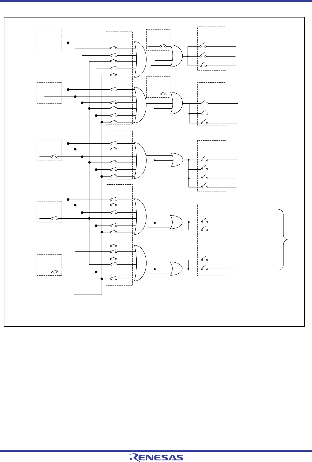
R01UH0034EJ0200 Rev.2.00 Page 730 of 1489
Dec 27, 2013
RX62T Group, RX62G Group 17. Port Output Enable 3 (POE3)
Under development Preliminary document
Specifications in this document are tentative and subject to change.
Figure 17.2 Target Pins and Conditions for High-Impedance Control
POE0F
POE0#
POE4#
MTU3BDZE
GPT
OCE1
OSF1
POECR2
MTU4ACZE
MTU4BDZE
OCSR1
CMADDMT34HIZ
ICS5ADDMT34HIZ
ICS2ADDMT34HIZ
ICS3ADDMT34HIZ
ICS4ADDMT34HIZ
ICSR1
POE4F
ICSR2
MTU6BDZE
POECR2
MTU7ACZE
MTU7BDZE
OCE2
CMADDMT67HIZ
ICS5ADDMT67HIZ
ICS1ADDMT67HIZ
ICS3ADDMT67HIZ
ICS4ADDMT67HIZ
POE8#
POECR5
CMADDMT0HIZ
ICS5ADDMT5HIZ
ICS2ADDMT0HIZ
ICS4ADDMT0HIZ
ICS1ADDMT0HIZ
MTU0BZE
POECR1
MTU0AZE
MTU0DZE
MTU0AZE
POE8E
POE8F
ICSR3
POE10# POE10E
POE10F
ICSR4 POECR3
GPT0ABZE
GPT1ABZE
GPT2ABZE
GPT3ABZE
POECR6
CMADDGPT01HIZ
ICS5ADDGPT01HIZ
ICS2ADDGPT01HIZ
ICS3ADDGPT01HIZ
ICS1ADDGPT01HIZ
POE11# POE11E
POE11F
ICSR5
CMADDGPT23HIZ
ICS4ADDGPT23HIZ
ICS2ADDGPT23HIZ
ICS3ADDGPT23HIZ
ICS1ADDGPT23HIZ
POECR4
High-impedance requests for the
GTIOC0A-B/GTIOC0B-B pins
High-impedance requests for the
GTIOC1A-B/MIOC1B-B pins
High-impedance requests for the
GTIOC2A-B/GTIOC2B-B pins
High-impedance requests for
the GTIOC3A/TIOC3B pins
12-bit A/D converter comparator detection
(S12AD.ADCMPFR.CnFLAG)
n = 0 to 2, 4 to 6
Detection of stopped
oscillation
(ICU.NMISR.OSTST)
High-impedance requests for the MIOC3B/
MIOC3D/GTIOC0A-A/GTIOC0B-A pins
High-impedance requests for the MIOC4A/
MIOC4C/GTIOC1A-A/GTIOC1B-A pins
High-impedance requests for the MIOC4B/
MIOC4D/GTIOC2A-A/GTIOC2B-A pins
High-impedance requests for the MIOC6B/
MIOC6D pins
High-impedance requests for the MIOC7A/
MIOC7C pins
High-impedance requests for the MIOC7B/
MIOC7D pins
High-impedance requests for the MIOC0A-A/
MIOC0A-B pins
High-impedance requests for the MIOC0B-A/
MIOC0B-B pins
High-impedance requests for the MIOC0C pins
High-impedance requests for the MIOC0D pins
OCSR2
OSF2
SPOER.MTUCH34HIZ
SPOER.MTUCH0HIZ
SPOER.MTUCH67HIZ
SPOER.GPT01HIZ
SPOER.GPT23HIZ
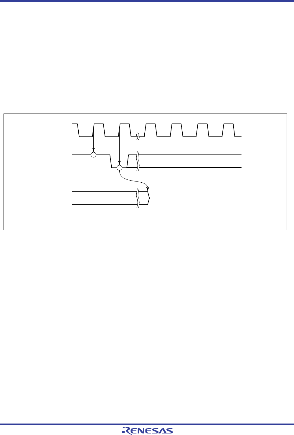
R01UH0034EJ0200 Rev.2.00 Page 731 of 1489
Dec 27, 2013
RX62T Group, RX62G Group 17. Port Output Enable 3 (POE3)
Under development Preliminary document
Specifications in this document are tentative and subject to change.
17.3.1 Input Level Detection Operation
If the input conditions set by ICSR1 to ICSR5 occur on the POE0#, POE4#, POE8#, POE10#, and POE11# pins, the
MTU3, MTU4 and MTU6 and MTU7 pins for the MTU complementary PWM output, and MTU0 pins, and GPT pins
are placed in high-impedance state. Note however, that these pins are still placed in the high-impedance state even when
the GPT and MTU3 functions are not selected for the pins.
(1) Falling Edge Detection
When a change from a high to low level is input to the POE0#, POE4#, POE8#, POE10#, and POE11# pins, the pins for
the MTU complementary PWM output, and MTU0 pins, and pin functions multiplexed with the GPT pins are placed in
high-impedance state. Figure 17.3 shows a sample timing after the level changes in input to the POE0#, POE4#,
POE8#, POE10#, and POE11# pins until the respective pins enter high-impedance state.
Figure 17.3 Falling Edge Detection
PCLK
POE# input
MTIOC3B
PCLK rising edge
Falling edge detection
High-impedance state*
Note: * The other pins also enter the high-impedance state in the similar timing.
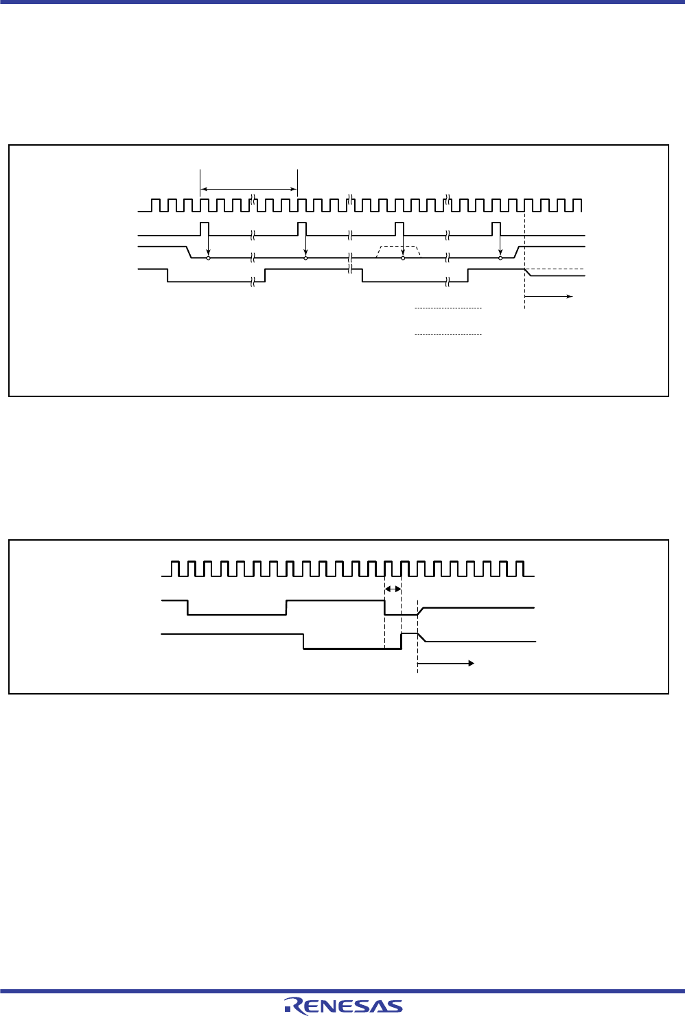
R01UH0034EJ0200 Rev.2.00 Page 732 of 1489
Dec 27, 2013
RX62T Group, RX62G Group 17. Port Output Enable 3 (POE3)
Under development Preliminary document
Specifications in this document are tentative and subject to change.
(2) Low-Level Detection
Figure 17.4 shows the low-level detection operation. Sixteen continuous low levels are sampled with the sampling clock
selected by ICSR1 to ICSR5. If even one high level is detected during this interval, the low level is not accepted.
The timing when pins for the MTU complementary PWM output, and MTU0 pins and GPT pins enter the high-
impedance state after the sampling clock is input is the same in both falling-edge detection and in low-level detection.
Figure 17.4 Low-Level Detection Operation
17.3.2 Output-Level Compare Operation
Figure 17.5 shows an example of the output-level compare operation for the combination of MTIOC3B and MTIOC3D.
The operation is the same for the other pin combinations.
Figure 17.5 Output-Level Compare Operation
PCLK
Sampling clock
POE# input
MTIOC3B
When high level is
sampled at least once
When low level is
sampled at all points [1]
High-impedance state*
Flag set (POE# received)
Flag not set
[1]
[2]
[2]
[3] [16]
[13]
Note: * Other pins pins also go to the high-impedance state at the same timing.
8/16/128 clock cycles
MTIOC3B
MTIOC3D High impedance state
Low level overlapping detected
PCLK

R01UH0034EJ0200 Rev.2.00 Page 733 of 1489
Dec 27, 2013
RX62T Group, RX62G Group 17. Port Output Enable 3 (POE3)
Under development Preliminary document
Specifications in this document are tentative and subject to change.
17.3.3 High-Impedance Control Using Registers
The high-impedance state of the MTU pins (MTU0, MTU3, MTU4, MTU6, and MTU7) and the GPT pins can be
directly controlled by using the software port output enable register (SPOER).
For instance, setting the CH34HIZ bit in SPOER to 1 places the MTU3 and MTU4 pins specified by port output enable
control register 2 (POECR2) in the high-impedance state.
The high-impedance state of other pins can also be controlled by setting the appropriate bits in SPOER.
17.3.4 High-Impedance Control through Detection of Stopped Oscillation
When the oscillation-stop detection circuit in the clock pulse generator detects stopped oscillation, the MTU3, MTU4,
MTU6, and MTU7 pins if specified in the port output enable control register 2 (POECR2), the MTU0 pins if specified in
the port output enable control register 1 (POECR1), and the GPT pin if specified by the port enable register 3(POECR3),
can be placed in the high-impedance state.
17.3.5 High-impedance Control through Detection of the Comparator
The MTU complementary PWM output pins, MTU0 pin, and the GPT pins can be placed in the high-impedance state in
response to detection by the comparator within the 12-bit A/D converter.
For instance, adding the CjFLAG (j is 0 to 2, and 4 to 6) flags in the ACMPFR of the S12ADA to the control conditions
for the high-impedance state of the MTU3 and MTU4 pins by setting the CMADDMT34ZE bit in the POECR4 register
after specifying the MTU3 and MTU4 pins in port output enable control register 2 (POECR2) leads to the pins being
placed in the high-impedance state on comparator detection.
The high-impedance state of other pins can also be controlled by setting the appropriate bits in the POECR1 to POECR6.
17.3.6 Additional Functions for Controlling High-Impedance States
Settings in port enable registers 4 to 6 (POECR4 to POECR6) can add further high-impedance control conditions for the
MTU complementary PWM output, MTU0, and GPT pins.
For instance, the settings listed below can be added as high-impedance control conditions for the MTU3 and MTU4 pins.
Setting the CMADDMT34ZE bit in POECR4 to 1 adds comparator detection
Setting the IC2ADDMT34ZE bit in POECR4 to 1 adds detection of the input level on the POE4# pin
Setting the IC3ADDMT34ZE bit in POECR4 to 1 and adds the input level detection by the POE8#
Setting the IC4ADDMT34ZE bit in POECR4 to 1 and adds the input level detection by the POE10#
Setting the IC5ADDMT34ZE bit in POECR4 to 1 and adds the input level detection by the POE11#
The high-impedance state of other pins can also be controlled by setting the appropriate bits in the POECR4 to POECR6.

R01UH0034EJ0200 Rev.2.00 Page 734 of 1489
Dec 27, 2013
RX62T Group, RX62G Group 17. Port Output Enable 3 (POE3)
Under development Preliminary document
Specifications in this document are tentative and subject to change.
17.3.7 Release from High-Impedance State
MTU pins which have entered high-impedance state due to input-level detection can be released from the state either by
returning them to their initial state with a reset, or by clearing all of the POE0#, POE4#, POE8#, POE10#, and POE11#
flags in ICSR1 to ICSR5. However, note that when low-level sampling is selected with the POE0M[1:0], POE4M[1:0],
POE8M[1:0], POE10M[1:0], and POE11M[1:0] bits in ICSR1 to ICSR5, just writing 0 to a flag is ignored (the flag is not
cleared); flags can be cleared by writing 0 to it only after a high level is input to the POE0#, POE4#, POE8#, POE10#,
and POE11# pins and is sampled.
MTU pins which have entered high-impedance state due to output-level detection can be released from the state either by
returning them to their initial state with a reset, or by clearing the OCSR1.OSF1 or OCSR2.OSF2 flag. When the
OCSR1.OSF1 or OCSR2.OSF2 flag is set to 0, the inactive level is output by setting the MTU, GRT and ALR1 registers.
MTU pins which have entered high-impedance state due to comparator detection can be released from the state either by
returning them to their initial state with a reset, or by clearing a S12AD.ADCMPFR.CnFLAG (n = 0 to 2, 4 to 6) flag. A
comparator detection flag (S12AD.ADCMPFR.CnFLAG; n = 0 to 2, 4 to 6) becoming 0 indicates that the analog input
signal that triggered comparator detection has returned to a normal voltage, so read this bit and confirm that its value is 0
before proceeding with AD conversion and so on. Take care on this point because the comparator detection flag
(S12AD.ADCMPFR.CnFLAG) is not re-set to 1 if this bit is cleared without confirmation that the analog input signal
has returned to a normal voltage and the analog input signal actually remains below the low-side threshold voltage or
above the high-side threshold voltage.
17.4 Interrupts
The POE3 issues a request to generate an interrupt when the specified condition is satisfied during input level detection
or output level comparison. Table 17.6 shows the interrupt sources and their conditions.
17.5 Usage Notes
When the POE3 is used, do not make a transition to software standby mode or deep software standby mode. In these
modes, the POE3 stops and thus the high-impedance state of pins cannot be controlled.
Table 17.6 Interrupt Sources and Conditions
Name Interrupt Source Interrupt Flag Condition
OEI1 Output enable interrupt 1 POE0F and OSF1 PIE1•POE0F + OIE1•OSF1
OEI2 Output enable interrupt 2 POE4F and OSF2 PIE2•POE4F + OIE2•OSF2
OEI3 Output enable interrupt 3 POE8F PIE3•POE8F
OEI4 Output enable interrupt 4 POE10F and POE11F PIE4•POE10F + PIE5•POE11F

R01UH0034EJ0200 Rev.2.00 Page 735 of 1489
Dec 27, 2013
RX62T Group, RX62G Group 18. General PWM Timer (GPT/GPTa)
18. General PWM Timer (GPT/GPTa)
The RX62T and RX62G Groups have a general PWM timer (GPT/GPTa) consisting of a four-channel 16-bit timer. The
GPT operates at a maximum of 100 MHz.
18.1 Overview
Table 18.1 lists the specifications for the GPT, and Table 18.2 shows the functions of the GPT. Figure 18.1 shows a
block diagram of the GPT.
Table 18.1 Specifications of GPT
Item Description
Function 16 bits × 4 channels
Up-count or down-count operation (saw waves) or up/down-count operation (triangle
waves) for each counter.
Clock sources independently selectable for each channel
Two input/output pins per channel
Two output compare/input capture registers per channel
For the two output compare/input capture registers of each channel, four registers are
provided as buffer registers and are capable of operating as comparison registers when
buffering is not in use.
In output compare operation, buffer switching can be at crests or troughs, enabling the
generation of laterally asymmetric PWM waveforms.
Registers for setting up frame cycles in each channel (with capability for generating
interrupts at overflow or underflow)
Synchronizable operation of the several counters
Modes of synchronized operation (synchronized, or displaced by desired times for phase
shifting)
Generation of dead times in PWM operation
Through combination of three counters, generation of three-phase PWM waveforms
incorporating dead times
Starting, clearing, and stopping counters in response to external or internal triggers
Internal trigger sources: output of the comparator detection, software, and compare match
The frequency-divided system clock (ICLK) can be used as a counter clock for measuring
timing of the edges of signals produced by frequency-dividing the IWDT-dedicated low-
speed on-chip oscillator clock signal (to detect abnormal oscillation).
PWM delay generation can control the timing with which signals on the two PWM output
pins for each channel rise and fall to an accuracy of up to 1/32 times the period of the
system clock (ICLK) (only for the RX62G Group).
R01UH0034EJ0200 Rev.2.00 Page 736 of 1489
Dec 27, 2013
RX62T Group, RX62G Group 18. General PWM Timer (GPT/GPTa)
Table 18.2 Functions of GPT (1 / 2)
Item GPT0 GPT1 GPT2 GPT3
Count clock ICLK
ICLK/2
ICLK/4
ICLK/8
ICLK
ICLK/2
ICLK/4
ICLK/8
ICLK
ICLK/2
ICLK/4
ICLK/8
ICLK
ICLK/2
ICLK/4
ICLK/8
Output compare/input
capture registers (GTCCR)
GTCCRA
GTCCRB
GTCCRA
GTCCRB
GTCCRA
GTCCRB
GTCCRA
GTCCRB
Compare/buffer registers GTCCRC
GTCCRD
GTCCRE
GTCCRF
GTCCRC
GTCCRD
GTCCRE
GTCCRF
GTCCRC
GTCCRD
GTCCRE
GTCCRF
GTCCRC
GTCCRD
GTCCRE
GTCCRF
Cycle setting register GTPR GTPR GTPR GTPR
Cycle setting buffer registers GTPBR
GTPDBR
GTPBR
GTPDBR
GTPBR
GTPDBR
GTPBR
GTPDBR
I/O pins GTIOC0A
GTIOC0B
GTIOC1A
GTIOC1B
GTIOC2A
GTIOC2B
GTIOC3A
GTIOC3B
External trigger input pin GTETRG
Counter clear sources GTPR compare match, input capture, comparator detection, GTETRG pin input, GTIOC3A/GTIOC3B
pin input, and GTIOC3A/GTIOC3B internal output (output compare)
Compare
match output
Low output √√√√
High output √√√√
Toggle
output
√√√√
Input capture function √√√√
Synchronized operation √√√√
Phase shift start √√√√
Automatic addition of dead
time
√√√√
PWM mode √√√√
Buffer operation √√√√
One-shot operation √√√√
DTC activation All the interrupt sources
A/D converter start trigger Compare match of
GTADTRA or
GTADTRB
Compare match of
GTADTRA or
GTADTRB
Compare match of
GTADTRA or
GTADTRB
Compare match of
GTADTRA or
GTADTRB
Interrupt sources Five sources
GTCCRA compare
match/input capture
(GTCIA0)
GTCCRB compare
match/input capture
(GTCIB0)
GTCCRC compare
match/GTCCRD
compare match/dead
time error (GTCIC0)
GTCCRE compare
match/GTCCRF
compare match
(GTCIE0)
GTCNT overflow
(GTPR compare
match)/GTCNT
undervlow (GTCIV0)
Five sources
GTCCRA compare
match/input capture
(GTCIA1)
GTCCRB compare
match/input capture
(GTCIB1)
GTCCRC compare
match/GTCCRD
compare match/dead
time error (GTCIC1)
GTCCRE compare
match/GTCCRF
compare match
(GTCIE1)
GTCNT overflow
(GTPR compare
match)/GTCNT
undervlow (GTCIV1)
Five sources
GTCCRA compare
match/input capture
(GTCIA2)
GTCCRB compare
match/input capture
(GTCIB2)
GTCCRC compare
match/GTCCRD
compare match/dead
time error (GTCIC2)
GTCCRE compare
match/GTCCRF
compare match
(GTCIE2)
GTCNT overflow
(GTPR compare
match)/GTCNT
undervlow (GTCIV2)
Five sources
GTCCRA compare
match/input capture
(GTCIA3)
GTCCRB compare
match/input capture
(GTCIB3)
GTCCRC compare
match/GTCCRD
compare match/dead
time error (GTCIC3)
GTCCRE compare
match/GTCCRF
compare match
(GTCIE3)
GTCNT overflow
(GTPR compare
match)/GTCNT
undervlow (GTCIV3)
Common interrupt source External trigger/LOCO count function interrupt (LOCOI)

R01UH0034EJ0200 Rev.2.00 Page 737 of 1489
Dec 27, 2013
RX62T Group, RX62G Group 18. General PWM Timer (GPT/GPTa)
√: Possible
—: Not possible
Interrupt skipping function Skips GTCNT overflows
(GTPR compare
match)/
GTCNT underflow
(GTCIV0) interrupts
(with interlocking
function for other
interrupts or A/D
conversion requests).
Skips GTCNT overflows
(GTPR compare
match)/
GTCNT underflow
(GTCIV1) interrupts
(with interlocking
function for other
interrupts or A/D
conversion requests).
Skips GTCNT overflows
(GTPR compare
match)/
GTCNT underflow
(GTCIV2) interrupts
(with interlocking
function for other
interrupts or A/D
conversion requests).
Skips GTCNT overflows
(GTPR compare
match)/
GTCNT underflow
(GTCIV3) interrupts
(with interlocking
function for other
interrupts or A/D
conversion requests).
Table 18.2 Functions of GPT (2 / 2)
Item GPT0 GPT1 GPT2 GPT3
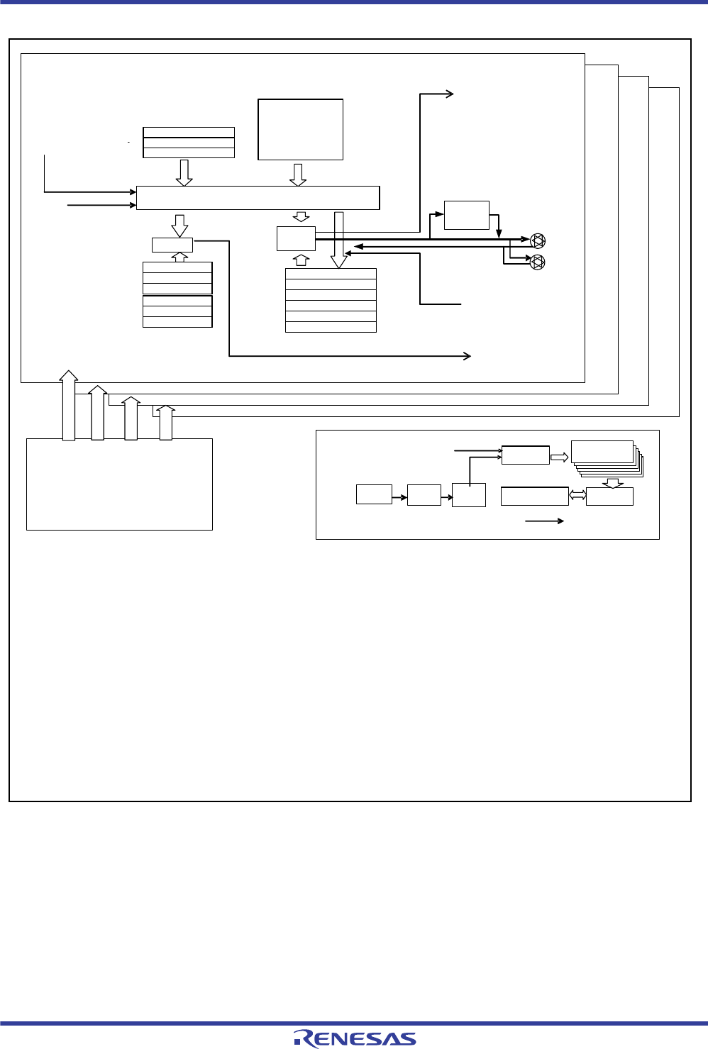
R01UH0034EJ0200 Rev.2.00 Page 738 of 1489
Dec 27, 2013
RX62T Group, RX62G Group 18. General PWM Timer (GPT/GPTa)
Figure 18.1 Block Diagram of GPT
GPT3GPT3
GPT2 GPT2
GPT1 GPT1
GPT0GPT0
Counter (GTCNT)
GTCCRA
GTCCRB
GTCCRD
GTCCRE
GTCCRF
GTCCRC
Comparator GTIOCA
GTIOCB
Output compare/input
capture registers
Output compare
Input capture
GTPR
GTPBR
GTPDBR
Cycle setting/
Cycle setting buffer registers
GTADTRA
GTADTDBRA
GTADTBRA
GTADTRA
GTADTDBRA
GTADTBRA
GTADTRB
GTADTDBRB
GTADTBRB
GTADTRB
GTADTDBRB
GTADTBRB
Comparator
A/D converter trigger input
Control registers
GTONCR
GTDTCR
GTDVU
GTDVD
GTDBU
GTDBD
GTSOS
GTSOTR
A/D converter
start request
Comparator detection
Interrupt request signals
TCFA
TCFB
TCFC
TCFD
DTEF
TCFE
TCFF
TCFPU
TCFPO
ETINF
ETIPF
I/O pins
External
trigger
GTETRG
Low-speed OCO counter
Low-speed
OCO Average
LCNTA
Permissible deviation
LCNTDU, LCNTDL
LOCO counter
LCNT
Counted results
LCNT00 to LCNT15
Clock source
ICLK
ICLK/2
ICLK/4
ICLK/8
Frequency
divider Edge
detection
Interrupt request signal LOCOI
Common registers GTSTR
GTHSCR
GTHCCR
GTHSSR
GTHPSR
GTWP
GTSYNC
GTETINT
GTBDR
GTIOR
GTINTAD
GTCR
GTBER
GTUDC
GTITC
GTST
Clock source
ICLK
ICLK/2
ICLK/4
ICLK/8
A/D converter start request timing/
A/D converter start request timing
buffer registers
[Legend]
GTSTR: General PWM timer software start register
GTHSCR: General PWM timer hardware source start control register
GTHCCR: General PWM timer hardware source clear control register
GTHSSR: General PWM timer hardware start source select register
GTHPSR: General PWM timer hardware stop/clear source select register
GTWP: General PWM timer write-protection register
GTSYNC: General PWM timer sync register
GTETINT: General PWM timer external trigger input interrupt register
GTBDR: General PWM timer buffer operation disable register
GTSWP: General PWM timer start write protection register
LCCR: LOCO count control register
LCST: LOCO count status register
LCNT: LOCO count value register
LCNTA: LOCO count result average register
LCNT00: LOCO count result register 0
LCNT01: LOCO count result register 1
LCNT02: LOCO count result register 2
LCNT03: LOCO count result register 3
LCNT04: LOCO count result register 4
LCNT05: LOCO count result register 5
LCNT06: LOCO count result register 6
LCNT07: LOCO count result register 7
LCNT08: LOCO count result register 8
LCNT09: LOCO count result register 9
LCNT10: LOCO count result register 10
LCNT11: LOCO count result register 11
LCNT12: LOCO count result register 12
LCNT13: LOCO count result register 13
LCNT14: LOCO count result register 14
LCNT15: LOCO count result register 15
LCNTDU: LOCO count upper permissible deviation register
LCNTDL: LOCO count lower permissible deviation register
GTIOR: General PWM timer I/O control register
GTINTAD: General PWM timer interrupt output setting register
GTCR: General PWM timer control register
GTBER: General PWM timer buffer enable register
GTUDC: General PWM timer count direction register
GTITC: General PWM timer interrupt and A/D converter start request skipping setting register
GTST: General PWM timer status register
GTCNT: General PWM timer counter value
GTCCRA: General PWM timer compare capture register A
GTCCRB: General PWM timer compare capture register B
GTCCRC: General PWM timer compare capture register C
GTCCRD: General PWM timer compare capture register D
GTCCRE: General PWM timer compare capture register E
GTCCRF: General PWM timer compare capture register F
GTPR: General PWM timer cycle setting register
GTPBR: General PWM timer cycle setting buffer register
GTPDBR: General PWM timer cycle setting double-buffer register
GTADTRA: A/D converter start request timing register A
GTADTBRA: A/D converter start request timing buffer register A
GTADTDBRA: A/D converter start request timing double-buffer register A
GTADTRB: A/D converter start request timing register B
GTADTBRB: A/D converter start request timing buffer register B
GTADTDBRB: A/D converter start request timing double-buffer register B
GTONCR: General PWM timer output negate control register
GTDTCR: General PWM timer dead time control register
GTDVU: General PWM timer dead time value register
GTDVD: General PWM timer dead time value register
GTDBU: General PWM timer dead time buffer register
GTDBD: General PWM timer dead time buffer register
GTSOS: General PWM timer output protection function status register
GTSOTR: General PWM timer output protection function temporary release register
PWM delay
generation
circuit
GTSWP

R01UH0034EJ0200 Rev.2.00 Page 739 of 1489
Dec 27, 2013
RX62T Group, RX62G Group 18. General PWM Timer (GPT/GPTa)
Table 18.3 lists the I/O pins used in the GPT.
Table 18.3 I/O Pins of GPT
Channel Pin Name I/O Function
GPT GTETRG Input External trigger input pin
GPT0 GTIOC0A I/O GTCCRA input capture input/output compare output/PWM output pin
GTIOC0B I/O GTCCRB input capture input/output compare output/PWM output pin
GPT1 GTIOC1A I/O GTCCRA input capture input/output compare output/PWM output pin
GTIOC1B I/O GTCCRB input capture input/output compare output/PWM output pin
GPT2 GTIOC2A I/O GTCCRA input capture input/output compare output/PWM output pin
GTIOC2B I/O GTCCRB input capture input/output compare output/PWM output pin
GPT3 GTIOC3A I/O GTCCRA input capture input/output compare output/PWM output pin
GTIOC3B I/O GTCCRB input capture input/output compare output/PWM output pin

R01UH0034EJ0200 Rev.2.00 Page 740 of 1489
Dec 27, 2013
RX62T Group, RX62G Group 18. General PWM Timer (GPT/GPTa)
18.2 Register Descriptions
Table 18.4 lists the registers of the GPT.
Table 18.4 Registers of GPT (1 / 5)
Channel Register Name Symbol Value after
Reset Address Access
Size
GPT General PWM timer software start register GTSTR 0000h 000C 2000h 8, 16, 32
General PWM timer hardware source start control register GTHSCR 0000h 000C 2004h 8, 16, 32
General PWM timer hardware source clear control register GTHCCR 0000h 000C 2006h 8, 16, 32
General PWM timer hardware start source select register GTHSSR 0000h 000C 2008h 8, 16, 32
General PWM timer hardware stop/clear source select register GTHPSR 0000h 000C 200Ah 8, 16, 32
General PWM timer write-protection register GTWP 0000h 000C 200Ch 8, 16, 32
General PWM timer sync register GTSYNC 0000h 000C 200Eh 8, 16, 32
General PWM timer external trigger input interrupt register GTETINT 0000h 000C 2010h 8, 16, 32
General PWM timer buffer operation disable register GTBDR 0000h 000C 2014h 8, 16, 32
General PWM timer start write protection register GTSWP 0000h 000C 2018h 16, 32
LOCO count control register LCCR 0000h 000C 2080h 8, 16, 32
LOCO count status register LCST 0000h 000C 2082h 8, 16, 32
LOCO count value register LCNT 0000h 000C 2084h 8, 16, 32
LOCO count result average register LCNTA 0000h 000C 2086h 8, 16, 32
LOCO count result register 0 LCNT00 0000h 000C 2088h 8, 16, 32
LOCO count result register 1 LCNT01 0000h 000C 208Ah 8, 16, 32
LOCO count result register 2 LCNT02 0000h 000C 208Ch 8, 16, 32
LOCO count result register 3 LCNT03 0000h 000C 208Eh 8, 16, 32
LOCO count result register 4 LCNT04 0000h 000C 2090h 8, 16, 32
LOCO count result register 5 LCNT05 0000h 000C 2092h 8, 16, 32
LOCO count result register 6 LCNT06 0000h 000C 2094h 8, 16, 32
LOCO count result register 7 LCNT07 0000h 000C 2096h 8, 16, 32
LOCO count result register 8 LCNT08 0000h '000C 2098h 8, 16, 32
LOCO count result register 9 LCNT09 0000h 000C 209Ah 8, 16, 32
LOCO count result register 10 LCNT10 0000h 000C 209Ch 8, 16, 32
LOCO count result register 11 LCNT11 0000h 000C 209Eh 8, 16, 32
LOCO count result register 12 LCNT12 0000h 000C 20A0h 8, 16, 32
LOCO count result register 13 LCNT13 0000h 000C 20A2h 8, 16, 32
LOCO count result register 14 LCNT14 0000h 000C 20A4h 8, 16, 32
LOCO count result register 15 LCNT15 0000h 000C 20A6h 8, 16, 32
LOCO count upper permissible deviation register LCNTDU FFFFh 000C 20A8h 8, 16, 32
LOCO count lower permissible deviation register LCNTDL FFFFh 000C 20AAh 8, 16, 32

R01UH0034EJ0200 Rev.2.00 Page 741 of 1489
Dec 27, 2013
RX62T Group, RX62G Group 18. General PWM Timer (GPT/GPTa)
GPT0 General PWM timer I/O control register GTIOR 0000h 000C 2100h 8, 16, 32
General PWM timer interrupt output setting register GTINTAD 0000h 000C 2102h 8, 16, 32
General PWM timer control register GTCR 0000h 000C 2104h 8, 16, 32
General PWM timer buffer enable register GTBER 0000h 000C 2106h 8, 16, 32
General PWM timer count direction register GTUDC 0001h 000C 2108h 8, 16, 32
General PWM timer interrupt and A/D converter start request
skipping setting register
GTITC 0000h 000C 210Ah 8, 16, 32
General PWM timer status register GTST 8000h 000C 210Ch 8, 16, 32
General PWM timer counter GTCNT 0000h 000C 210Eh 16
General PWM timer compare capture register A GTCCRA FFFFh 000C 2110h 16, 32
General PWM timer compare capture register B GTCCRB FFFFh 000C 2112h 16, 32
General PWM timer compare capture register C GTCCRC FFFFh 000C 2114h 16, 32
General PWM timer compare capture register D GTCCRD FFFFh 000C 2116h 16, 32
General PWM timer compare capture register E GTCCRE FFFFh 000C 2118h 16, 32
General PWM timer compare capture register F GTCCRF FFFFh 000C 211Ah 16, 32
General PWM timer cycle setting register GTPR FFFFh 000C 211Ch 16, 32
General PWM timer cycle setting buffer register GTPBR FFFFh 000C 211Eh 16, 32
General PWM timer cycle setting double-buffer register GTPDBR FFFFh 000C 2120h 16, 32
A/D converter start request timing register A GTADTRA FFFFh 000C 2124h 16, 32
A/D converter start request timing buffer register A GTADTBRA FFFFh 000C 2126h 16, 32
A/D converter start request timing double-buffer register A GTADTDBRA FFFFh 000C 2128h 16, 32
A/D converter start request timing register B GTADTRB FFFFh 000C 212Ch 16, 32
A/D converter start request timing buffer register B GTADTBRB FFFFh 000C 212Eh 16, 32
A/D converter start request timing double-buffer register B GTADTDBRB FFFFh 000C 2130h 16, 32
General PWM timer output negate control register GTONCR 0100h 000C 2134h 16, 32
General PWM timer dead time control register GTDTCR 0000h 000C 2136h 16, 32
General PWM timer dead time value register U GTDVU FFFFh 000C 2138h 16, 32
General PWM timer dead time value register D GTDVD FFFFh 000C 213Ah 16, 32
General PWM timer dead time buffer register U GTDBU FFFFh 000C 213Ch 16, 32
General PWM timer dead time buffer register D GTDBD FFFFh 000C 213Eh 16, 32
General PWM timer output protection function status register GTSOS 0x00h 000C 2140h 16, 32
General PWM timer output protection function temporary
release register GTSOTR 0000h 000C 2142h 16, 32
Table 18.4 Registers of GPT (2 / 5)
Channel Register Name Symbol Value after
Reset Address Access
Size

R01UH0034EJ0200 Rev.2.00 Page 742 of 1489
Dec 27, 2013
RX62T Group, RX62G Group 18. General PWM Timer (GPT/GPTa)
GPT1 General PWM timer I/O control register GTIOR 0000h 000C 2180h 8, 16, 32
General PWM timer interrupt output setting register GTINTAD 0000h 000C 2182h 8, 16, 32
General PWM timer control register GTCR 0000h 000C 2184h 8, 16, 32
General PWM timer buffer enable register GTBER 0000h 000C 2186h 8, 16, 32
General PWM timer count direction register GTUDC 0001h 000C 2188h 8, 16, 32
General PWM timer interrupt and A/D converter start request
skipping setting register
GTITC 0000h 000C 218Ah 8, 16, 32
General PWM timer status register GTST 8000h 000C 218Ch 8, 16, 32
General PWM timer counter GTCNT 0000h 000C 218Eh 16
General PWM timer compare capture register A GTCCRA FFFFh 000C 2190h 16, 32
General PWM timer compare capture register B GTCCRB FFFFh 000C 2192h 16, 32
General PWM timer compare capture register C GTCCRC FFFFh 000C 2194h 16, 32
General PWM timer compare capture register D GTCCRD FFFFh 000C 2196h 16, 32
General PWM timer compare capture register E GTCCRE FFFFh 000C 2198h 16, 32
General PWM timer compare capture register F GTCCRF FFFFh 000C 219Ah 16, 32
General PWM timer cycle setting register GTPR FFFFh 000C 219Ch 16, 32
General PWM timer cycle setting buffer register GTPBR FFFFh 000C 219Eh 16, 32
General PWM timer cycle setting double-buffer register GTPDBR FFFFh 000C 21A0h 16, 32
A/D converter start request timing register A GTADTRA FFFFh 000C 21A4h 16, 32
A/D converter start request timing buffer register A GTADTBRA FFFFh 000C 21A6h 16, 32
A/D converter start request timing double-buffer register A GTADTDBRA FFFFh 000C 21A8h 16, 32
A/D converter start request timing register B GTADTRB FFFFh 000C 21ACh 16, 32
A/D converter start request timing buffer register B GTADTBRB FFFFh 000C 21AEh 16, 32
A/D converter start request timing double-buffer register B GTADTDBRB FFFFh 000C 21B0h 16, 32
General PWM timer output negate control register GTONCR 0100h 000C 21B4h 16, 32
General PWM timer dead time control register GTDTCR 0000h 000C 21B6h 16, 32
General PWM timer dead time value register U GTDVU FFFFh 000C 21B8h 16, 32
General PWM timer dead time value register D GTDVD FFFFh 000C 21BAh 16, 32
General PWM timer dead time buffer register U GTDBU FFFFh 000C 21BCh 16, 32
General PWM timer dead time buffer register D GTDBD FFFFh 000C 21BEh 16, 32
General PWM timer output protection function status register GTSOS 0x00h 000C 21C0h 16, 32
General PWM timer output protection function temporary
release register GTSOTR 0000h 000C 21C2h 16, 32
Table 18.4 Registers of GPT (3 / 5)
Channel Register Name Symbol Value after
Reset Address Access
Size

R01UH0034EJ0200 Rev.2.00 Page 743 of 1489
Dec 27, 2013
RX62T Group, RX62G Group 18. General PWM Timer (GPT/GPTa)
GPT2 General PWM timer I/O control register GTIOR 0000h 000C 2200h 8, 16, 32
General PWM timer interrupt output setting register GTINTAD 0000h 000C 2202h 8, 16, 32
General PWM timer control register GTCR 0000h 000C 2204h 8, 16, 32
General PWM timer buffer enable register GTBER 0000h 000C 2206h 8, 16, 32
General PWM timer count direction register GTUDC 0001h 000C 2208h 8, 16, 32
General PWM timer interrupt and A/D converter start request
skipping setting register
GTITC 0000h 000C 220Ah 8, 16, 32
General PWM timer status register GTST 8000h 000C 220Ch 8, 16, 32
General PWM timer counter GTCNT 0000h 000C 220Eh 16
General PWM timer compare capture register A GTCCRA FFFFh 000C 2210h 16, 32
General PWM timer compare capture register B GTCCRB FFFFh 000C 2212h 16, 32
General PWM timer compare capture register C GTCCRC FFFFh 000C 2214h 16, 32
General PWM timer compare capture register D GTCCRD FFFFh 000C 2216h 16, 32
General PWM timer compare capture register E GTCCRE FFFFh 000C 2218h 16, 32
General PWM timer compare capture register F GTCCRF FFFFh 000C 221Ah 16, 32
General PWM timer cycle setting register GTPR FFFFh 000C 221Ch 16, 32
General PWM timer cycle setting buffer register GTPBR FFFFh 000C 221Eh 16, 32
General PWM timer cycle setting double-buffer register GTPDBR FFFFh 000C 2220h 16, 32
A/D converter start request timing register A GTADTRA FFFFh 000C 2224h 16, 32
A/D converter start request timing buffer register A GTADTBRA FFFFh 000C 2226h 16, 32
A/D converter start request timing double-buffer register A GTADTDBRA FFFFh 000C 2228h 16, 32
A/D converter start request timing register B GTADTRB FFFFh 000C 222Ch 16, 32
A/D converter start request timing buffer register B GTADTBRB FFFFh 000C 222Eh 16, 32
A/D converter start request timing double-buffer register B GTADTDBRB FFFFh 000C 2230h 16, 32
General PWM timer output negate control register GTONCR 0100h 000C 2234h 16, 32
General PWM timer dead time control register GTDTCR 0000h 000C 2236h 16, 32
General PWM timer dead time value register U GTDVU FFFFh 000C 2238h 16, 32
General PWM timer dead time value register D GTDVD FFFFh 000C 223Ah 16, 32
General PWM timer dead time buffer register U GTDBU FFFFh 000C 223Ch 16, 32
General PWM timer dead time buffer register D GTDBD FFFFh 000C 223Eh 16, 32
General PWM timer output protection function status register GTSOS 0x00h 000C 2240h 16, 32
General PWM timer output protection function temporary
release register GTSOTR 0000h 000C 2242h 16, 32
Table 18.4 Registers of GPT (4 / 5)
Channel Register Name Symbol Value after
Reset Address Access
Size

R01UH0034EJ0200 Rev.2.00 Page 744 of 1489
Dec 27, 2013
RX62T Group, RX62G Group 18. General PWM Timer (GPT/GPTa)
GPT3 General PWM timer I/O control register GTIOR 0000h 000C 2280h 8, 16, 32
General PWM timer interrupt output setting register GTINTAD 0000h 000C 2282h 8, 16, 32
General PWM timer control register GTCR 0000h 000C 2284h 8, 16, 32
General PWM timer buffer enable register GTBER 0000h 000C 2286h 8, 16, 32
General PWM timer count direction register GTUDC 0001h 000C 2288h 8, 16, 32
General PWM timer interrupt and A/D converter start request
skipping setting register
GTITC 0000h 000C 228Ah 8, 16, 32
General PWM timer status register GTST 8000h 000C 228Ch 8, 16, 32
General PWM timer counter GTCNT 0000h 000C 228Eh 16
General PWM timer compare capture register A GTCCRA FFFFh 000C 2290h 16, 32
General PWM timer compare capture register B GTCCRB FFFFh 000C 2292h 16, 32
General PWM timer compare capture register C GTCCRC FFFFh 000C 2294h 16, 32
General PWM timer compare capture register D GTCCRD FFFFh 000C 2296h 16, 32
General PWM timer compare capture register E GTCCRE FFFFh 000C 2298h 16, 32
General PWM timer compare capture register F GTCCRF FFFFh 000C 229Ah 16, 32
General PWM timer cycle setting register GTPR FFFFh 000C 229Ch 16, 32
General PWM timer cycle setting buffer register GTPBR FFFFh 000C 229Eh 16, 32
General PWM timer cycle setting double-buffer register GTPDBR FFFFh 000C 22A0h 16, 32
A/D converter start request timing register A GTADTRA FFFFh 000C 22A4h 16, 32
A/D converter start request timing buffer register A GTADTBRA FFFFh 000C 22A6h 16, 32
A/D converter start request timing double-buffer register A GTADTDBRA FFFFh 000C 22A8h 16, 32
A/D converter start request timing register B GTADTRB FFFFh 000C 22ACh 16, 32
A/D converter start request timing buffer register B GTADTBRB FFFFh 000C 22AEh 16, 32
A/D converter start request timing double-buffer register B GTADTDBRB FFFFh 000C 22B0h 16, 32
General PWM timer output negate control register GTONCR 0100h 000C 22B4h 16, 32
General PWM timer dead time control register GTDTCR 0000h 000C 22B6h 16, 32
General PWM timer dead time value register U GTDVU FFFFh 000C 22B8h 16, 32
General PWM timer dead time value register D GTDVD FFFFh 000C 22BAh 16, 32
General PWM timer dead time buffer register U GTDBU FFFFh 000C 22BCh 16, 32
General PWM timer dead time buffer register D GTDBD FFFFh 000C 22BEh 16, 32
General PWM timer output protection function status register GTSOS 0x00h 000C 22C0h 16, 32
General PWM timer output protection function temporary
release register GTSOTR 0000h 000C 22C2h 16, 32
Table 18.4 Registers of GPT (5 / 5)
Channel Register Name Symbol Value after
Reset Address Access
Size

R01UH0034EJ0200 Rev.2.00 Page 745 of 1489
Dec 27, 2013
RX62T Group, RX62G Group 18. General PWM Timer (GPT/GPTa)
18.2.1 General PWM Timer Software Start Register (GTSTR)
GTSTR starts or stops the GPTn.GTCNT counting operation (n = 0 to 3).
CSTn Bit (GPTn.GTCNT Count Start) (n = 0 to 3)
This bit starts or stops GPTn.GTCNT operation.
The counter operation can also be started or stopped by GTHSCR. When count operation is started by a hardware source,
this bit is automatically set to 1, and when count operation is stopped by a hardware source, this bit is automatically
cleared to 0.
Address: 000C 2000h
b15 b14 b13 b12 b11 b10 b9 b8 b7 b6 b5 b4 b3 b2 b1 b0
————————————CST3CST2CST1CST0
Value after reset: 0000000000000000
Bit Symbol Bit Name Description R/W
b0 CST0 GPT0.GTCNT Count Start 0: Count operation is stopped
1: Count operation is performed
R/W
b1 CST1 GPT1.GTCNT Count Start R/W
b2 CST2 GPT2.GTCNT Count Start R/W
b3 CST3 GPT3.GTCNT Count Start R/W
b15 to b4 — Reserved These bits are read as 0. The write value should be 0. R/W
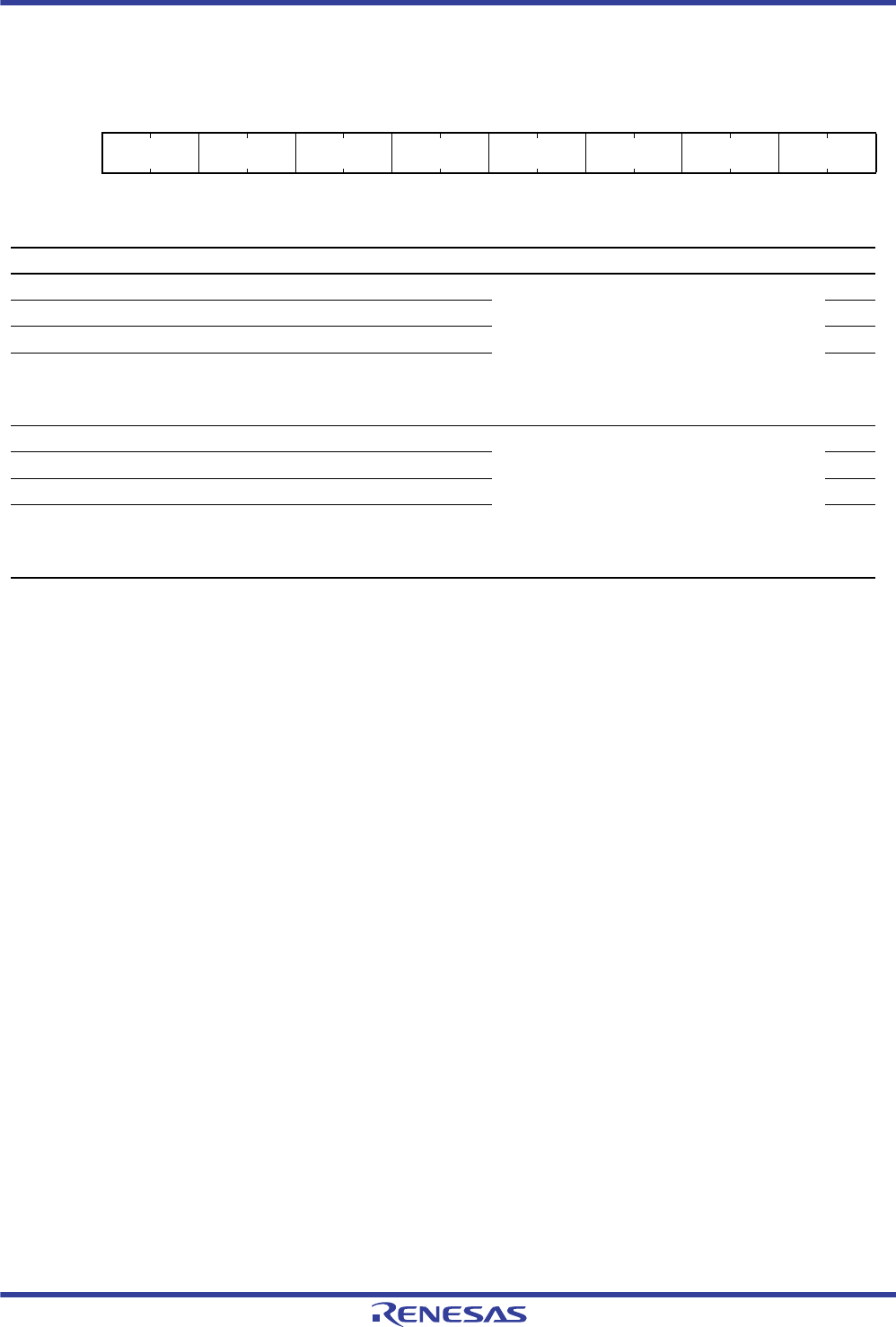
R01UH0034EJ0200 Rev.2.00 Page 746 of 1489
Dec 27, 2013
RX62T Group, RX62G Group 18. General PWM Timer (GPT/GPTa)
18.2.2 General PWM Timer Hardware Source Start Control Register (GTHSCR)
GTHSCR starts or stops the GPTn.GTCNT counting operation by a hardware source (n = 0 to 3).
When starting and stopping of GPTn.GTCNT by a hardware source occur simultaneously, counter start is given priority.
CSHWn[1:0] Bits (GPTn.GTCNT Hardware Source Count Start) (n = 0 to 3)
GPTn.GTCNT counting is started by a hardware source.
When the count operation is started by a hardware source, the corresponding bit in GTSTR automatically becomes 1.
The hardware source can be selected by GTHSSR.
CPHWn[1:0] Bits (GPTn.GTCNT Hardware Source Count Stop) (n = 0 to 3)
GPTn.GTCNT counting is stopped by a hardware source.
When the count operation is stopped by a hardware source, the corresponding bit in GTSTR automatically becomes 0.
The hardware source can be selected by GTHPSR.
Address: 000C 2004h
b15 b14 b13 b12 b11 b10 b9 b8 b7 b6 b5 b4 b3 b2 b1 b0
CPHW3[1:0] CPHW2[1:0] CPHW1[1:0] CPHW0[1:0] CSHW3[1:0] CSHW2[1:0] CSHW1[1:0] CSHW0[1:0]
Value after reset: 0000000000000000
Bit Symbol Bit Name Description R/W
b1, b0 CSHW0[1:0] GPT0.GTCNT Hardware Source Count Start 0 0: Count operation is not started by a hardware
source.
0 1: Count operation is started at the rising edge
of a hardware source.
1 0: Count operation is started at the falling edge
of a hardware source.
1 1: Count operation is started at both rising and
falling edges of a hardware source.
R/W
b3, b2 CSHW1[1:0] GPT1.GTCNT Hardware Source Count Start R/W
b5, b4 CSHW2[1:0] GPT2.GTCNT Hardware Source Count Start R/W
b7, b6 CSHW3[1:0] GPT3.GTCNT Hardware Source Count Start R/W
b9, b8 CPHW0[1:0] GPT0.GTCNT Hardware Source Count Stop 0 0: Count operation is not stopped by a hard-
ware source.
0 1: Count operation is stopped at the rising edge
of a hardware source.
1 0: Count operation is stopped at the falling edge
of a hardware source.
1 1: Count operation is stopped at both rising and
falling edges of a hardware source.
R/W
b11, b10 CPHW1[1:0] GPT1.GTCNT Hardware Source Count Stop R/W
b13, b12 CPHW2[1:0] GPT2.GTCNT Hardware Source Count Stop R/W
b15, b14 CPHW3[1:0] GPT3.GTCNT Hardware Source Count Stop R/W
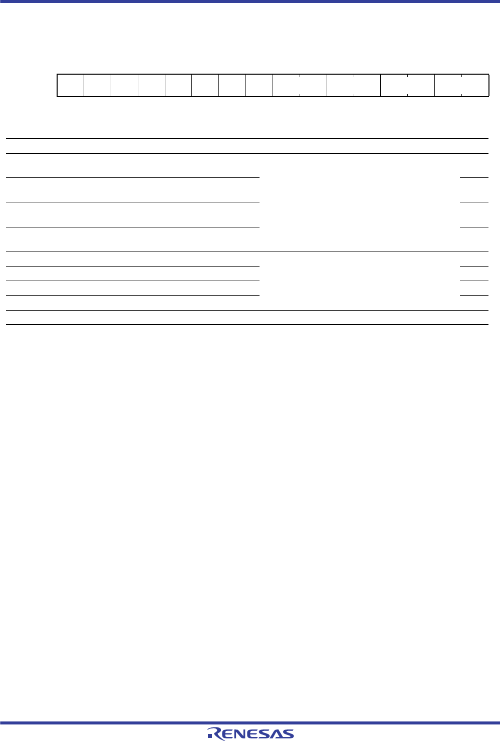
R01UH0034EJ0200 Rev.2.00 Page 747 of 1489
Dec 27, 2013
RX62T Group, RX62G Group 18. General PWM Timer (GPT/GPTa)
18.2.3 General PWM Timer Hardware Source Clear Control Register (GTHCCR)
GTHCCR sets clearing of GPTn.GTCNT by a hardware source (n = 0 to 3).
Once the clearing of GPTn.GTCNT counter by a hardware source is set, counter clearing by the hardware source is
executed whether the GPTn.GTCNT count operation is performed (GTSTR.CSTn = 1; n = 0 to 3) or stopped
(GTSTR.CSTn = 0, n = 0 to 3).
CCHWn[1:0] Bits (GPTn.GTCNT Hardware Source Count Clear) (n = 0 to 3)
GPTn.GTCNT is cleared by a hardware source.
The hardware source can be selected by GTHPSR.
When CCHWn[1:0] is 01b, 10b, or 11b, the hardware source can be accepted repeatedly.
CCSWn Bit (GPTn.GTCNT Counter Clear) (n = 0 to 3)
When 1 is written to this bit, the GPTn.GTCNT counter is cleared. This bit automatically returns to 0 after the writing of
1. This bit is always read as 0.
Address: 000C 2006h
b15 b14 b13 b12 b11 b10 b9 b8 b7 b6 b5 b4 b3 b2 b1 b0
————
CCSW
3CCSW
2CCSW
1CCSW
0CCHW3[1:0] CCHW2[1:0] CCHW1[1:0] CCHW0[1:0]
Value after reset: 0000000000000000
Bit Symbol Bit Name Description R/W
b1, b0 CCHW0[1:0] GPT0.GTCNT Hardware Source
Counter Clear
0 0: Counter is not cleared by a hardware source.
0 1: Counter is cleared at the rising edge of a hard-
ware source.
1 0: Counter is cleared at the falling edge of a hard-
ware source.
1 1: Counter is cleared at both rising and falling edges
of a hardware source.
R/W
b3, b2 CCHW1[1:0] GPT1.GTCNT Hardware Source
Counter Clear
R/W
b5, b4 CCHW2[1:0] GPT2.GTCNT Hardware Source
Counter Clear
R/W
b7, b6 CCHW3[1:0] GPT3.GTCNT Hardware Source
Counter Clear
R/W
b8 CCSW0 GPT0.GTCNT Counter Clear When 1 is written to this bit, the counter is cleared.
This bit automatically returns to 0 after the writing of 1.
These bits are read as 0.
R/W
b9 CCSW1 GPT1.GTCNT Counter Clear R/W
b10 CCSW2 GPT2.GTCNT Counter Clear R/W
b11 CCSW3 GPT3.GTCNT Counter Clear R/W
b15 to b12 — Reserved These bits are read as 0. The write value should be 0. R/W

R01UH0034EJ0200 Rev.2.00 Page 748 of 1489
Dec 27, 2013
RX62T Group, RX62G Group 18. General PWM Timer (GPT/GPTa)
18.2.4 General PWM Timer Hardware Start Source Select Register (GTHSSR)
Address: 000C 2008h
b15 b14 b13 b12 b11 b10 b9 b8 b7 b6 b5 b4 b3 b2 b1 b0
CSHSL3[3:0] CSHSL2[3:0] CSHSL1[3:0] CSHSL0[3:0]
Value after reset: 0000000000000000
Bit Symbol Bit Name Description R/W
b3 to b0 CSHSL0[3:0] GPT0.GTCNT Hardware Counter Start
Source Select
b3 b0
0 0 0 0: AN000 comparator detection
0 0 0 1: AN001 comparator detection
0 0 1 0: AN002 comparator detection
0 0 1 1: Setting prohibited
0 1 0 0: AN100 comparator detection
0 1 0 1: AN101 comparator detection
0 1 1 0: AN102 comparator detection
0 1 1 1: Setting prohibited
1 0 0 0: GTIOC3A pin input
1 0 0 1: GTIOC3B pin input
1 0 1 0: GTIOC3A internal output(output compare)
1 0 1 1: GTIOC3B internal output(output compare)
1 1 0 0: GTETRG pin input
Settings other than above are prohibited.
R/W
b7 to b4 CSHSL1[3:0] GPT1.GTCNT Hardware Counter Start
Source Select
b7 b4
0 0 0 0: AN000 comparator detection
0 0 0 1: AN001 comparator detection
0 0 1 0: AN002 comparator detection
0 0 1 1: Setting prohibited
0 1 0 0: AN100 comparator detection
0 1 0 1: AN101 comparator detection
0 1 1 0: AN102 comparator detection
0 1 1 1: Setting prohibited
1 0 0 0: GTIOC3A pin input
1 0 0 1: GTIOC3B pin input
1 0 1 0: GTIOC3A internal output(output compare)
1 0 1 1: GTIOC3B internal output(output compare)
1 1 0 0: GTETRG pin input
Settings other than above are prohibited.
R/W
b11 to b8 CSHSL2[3:0] GPT2.GTCNT Hardware Counter Start
Source Select
b11 b8
0 0 0 0: AN000 comparator detection
0 0 0 1: AN001 comparator detection
0 0 1 0: AN002 comparator detection
0 0 1 1: Setting prohibited
0 1 0 0: AN100 comparator detection
0 1 0 1: AN101 comparator detection
0 1 1 0: AN102 comparator detection
0 1 1 1: Setting prohibited
1 0 0 0: GTIOC3A pin input
1 0 0 1: GTIOC3B pin input
1 0 1 0: GTIOC3A internal output(output compare)
1 0 1 1: GTIOC3B internal output(output compare)
1 1 0 0: GTETRG pin input
Settings other than above are prohibited.
R/W

R01UH0034EJ0200 Rev.2.00 Page 749 of 1489
Dec 27, 2013
RX62T Group, RX62G Group 18. General PWM Timer (GPT/GPTa)
GTHSSR sets the hardware source to start GPTn.GTCNT (n = 0 to 3).
To change the source, clear the GTHSCR.CSHWn[1:0] bits to 0 before changing the source.
CSHSLn[3:0] Bits (GPTn.GTCNT Hardware Counter Start Source Select) (n = 0 to 3)
These bits select the hardware source to start GPTn.GTCNT.
Select 1000b as a hardware source with GPT3.GTIOR.GTIOA[5] = 0 and GPT3.GTONCR.OAE = 0. Select 1001b as a
hardware source with GPT3.GTIOR.GTIOB[5] = 0 and GPT3.GTONCR.OBE¬ = 0.
b15 to b12 CSHSL3[3:0] GPT3.GTCNT Hardware Counter Start
Source Select
b15 b12
0 0 0 0: AN000 comparator detection
0 0 0 1: AN001 comparator detection
0 0 1 0: AN002 comparator detection
0 0 1 1: Setting prohibited
0 1 0 0: AN100 comparator detection
0 1 0 1: AN101 comparator detection
0 1 1 0: AN102 comparator detection
0 1 1 1: Setting prohibited
1 0 0 0: GTIOC3A pin input
1 0 0 1: GTIOC3B pin input
1 0 1 0: Setting prohibited
1 0 1 1: Setting prohibited
1 1 0 0: GTETRG pin input
Settings other than above are prohibited.
R/W
Bit Symbol Bit Name Description R/W

R01UH0034EJ0200 Rev.2.00 Page 750 of 1489
Dec 27, 2013
RX62T Group, RX62G Group 18. General PWM Timer (GPT/GPTa)
18.2.5 General PWM Timer Hardware Stop/Clear Source Select Register (GTHPSR)
Address: 000C 200Ah
b15 b14 b13 b12 b11 b10 b9 b8 b7 b6 b5 b4 b3 b2 b1 b0
CSHPL3[3:0] CSHPL2[3:0] CSHPL1[3:0] CSHPL0[3:0]
Value after reset: 0000000000000000
Bit Symbol Bit Name Description R/W
b3 to b0 CSHPL0[3:0] GPT0.GTCNT Hardware Counter Stop/
Clear Source Select
b3 b0
0 0 0 0: AN000 comparator detection
0 0 0 1: AN001 comparator detection
0 0 1 0: AN002 comparator detection
0 0 1 1: Setting prohibited
0 1 0 0: AN100 comparator detection
0 1 0 1: AN101 comparator detection
0 1 1 0: AN102 comparator detection
0 1 1 1: Setting prohibited
1 0 0 0: GTIOC3A pin input
1 0 0 1: GTIOC3B pin input
1 0 1 0: GTIOC3A internal output (output compare)
1 0 1 1: GTIOC3B internal output (output compare)
1 1 0 0: GTETRG pin input
Settings other than above are prohibited.
R/W
b7 to b4 CSHPL1[3:0] GPT1.GTCNT Hardware Counter Stop/
Clear Source Select
b7 b4
0 0 0 0: AN000 comparator detection
0 0 0 1: AN001 comparator detection
0 0 1 0: AN002 comparator detection
0 0 1 1: Setting prohibited
0 1 0 0: AN100 comparator detection
0 1 0 1: AN101 comparator detection
0 1 1 0: AN102 comparator detection
0 1 1 1: Setting prohibited
1 0 0 0: GTIOC3A pin input
1 0 0 1: GTIOC3B pin input
1 0 1 0: GTIOC3A internal output (output compare)
1 0 1 1: GTIOC3B internal output (output compare)
1 1 0 0: GTETRG pin input
Settings other than above are prohibited.
R/W
b11 to b8 CSHPL2[3:0] GPT2.GTCNT Hardware Counter Stop/
Clear Source Select
b11 b8
0 0 0 0: AN000 comparator detection
0 0 0 1: AN001 comparator detection
0 0 1 0: AN002 comparator detection
0 0 1 1: Setting prohibited
0 1 0 0: AN100 comparator detection
0 1 0 1: AN101 comparator detection
0 1 1 0: AN102 comparator detection
0 1 1 1: Setting prohibited
1 0 0 0: GTIOC3A pin input
1 0 0 1: GTIOC3B pin input
1 0 1 0: GTIOC3A internal output (output compare)
1 0 1 1: GTIOC3B internal output (output compare)
1 1 0 0: GTETRG pin input
Settings other than above are prohibited.
R/W
R01UH0034EJ0200 Rev.2.00 Page 751 of 1489
Dec 27, 2013
RX62T Group, RX62G Group 18. General PWM Timer (GPT/GPTa)
GTHPSR sets the hardware source to stop or clear GPTn.GTCNT (n = 0 to 3).
To change the source, clear the GTHSCR.CPHWn[1:0] bits and GTHCCR.CCHWn[1:0] bits to 0 before changing the
source.
CSHPLn[3:0] Bits (GPTn.GTCNT Hardware Counter Stop/Clear Source Select) (n = 0 to 3)
These bits select the hardware source to stop or clear GPTn.GTCNT.
18.2.6 General PWM Timer Write-Protection Register (GTWP)
GTWP enables or disables writing to registers to prevent accidental modification.
For registers that are write enabled or disabled depending on the setting of the GPWP register, refer to section 18.7.1,
Write-Protection for Registers .
WPn Bit (GPTn Register Write Enable) (n = 0 to 3)
This bit enables or disables writing to GPTn registers.
b15 to b12 CSHPL3[3:0] GPT3.GTCNT Hardware Counter Stop/
Clear Source Select
b15 b12
0 0 0 0: AN000 comparator detection
0 0 0 1: AN001 comparator detection
0 0 1 0: AN002 comparator detection
0 0 1 1: Setting prohibited
0 1 0 0: AN100 comparator detection
0 1 0 1: AN101 comparator detection
0 1 1 0: AN102 comparator detection
0 1 1 1: Setting prohibited
1 0 0 0: GTIOC3A pin input
1 0 0 1: GTIOC3B pin input
1 0 1 0: Setting prohibited
1 0 1 1: Setting prohibited
1 1 0 0: GTETRG pin input
Settings other than above are prohibited.
R/W
Address: 000C 200Ch
b15 b14 b13 b12 b11 b10 b9 b8 b7 b6 b5 b4 b3 b2 b1 b0
————————————WP3WP2WP1WP0
Value after reset: 0000000000000000
Bit Symbol Bit Name Description R/W
b0 WP0 GPT0 Register Write Enable 0: Write to the register is enabled
1: Write to the register is disabled
R/W
b1 WP1 GPT1 Register Write Enable R/W
b2 WP2 GPT2 Register Write Enable R/W
b3 WP3 GPT3 Register Write Enable R/W
b15 to b4 — Reserved These bits are read as 0. The write value should be 0. R/W
Bit Symbol Bit Name Description R/W

R01UH0034EJ0200 Rev.2.00 Page 752 of 1489
Dec 27, 2013
RX62T Group, RX62G Group 18. General PWM Timer (GPT/GPTa)
18.2.7 General PWM Timer Sync Register (GTSYNC)
GTSYNC sets the clearing source of the GPTn.GTCNT counter for synchronized clearing/synchronized operation. This
register can be modified when count operation of GPTn.GTCNT is stopped (n = 0 to 3).
SYNCn[1:0] Bits (GPTn.GTCNT Counter Synchronized-Clear Source Select) (n = 0 to 3)
These bits select which channel's counter clearing source is used to clear GPTn.GTCNT. When setting the SYNCn[1:0]
bits, first set the GPTn.GTCR.CCLR[1:0] bits to 11b (cleared by counter clearing in another channel performing
synchronized clearing/synchronized operation).
Address: 000C 200Eh
b15 b14 b13 b12 b11 b10 b9 b8 b7 b6 b5 b4 b3 b2 b1 b0
— — SYNC3[1:0] — — SYNC2[1:0] — — SYNC1[1:0] — — SYNC0[1:0]
Value after reset: 0000000000000000
Bit Symbol Bit Name Description R/W
b1, b0 SYNC0[1:0] GPT0.GTCNT
Counter
Synchronized-Clear
Source Select
b1 b0
0 0: GPT0.GTCNT is cleared by a GPT0 clearing source
(synchronized clear is not performed).
0 1: GPT0.GTCNT is synchronously cleared by a GPT1 clearing source.
1 0: GPT0.GTCNT is synchronously cleared by a GPT2 clearing source.
1 1: GPT0.GTCNT is synchronously cleared by a GPT3 clearing source.
R/W
b3, b2 — Reserved These bits are read as 0. The write value should be 0. R/W
b5, b4 SYNC1[1:0] GPT1.GTCNT
Counter
Synchronized-Clear
Source Select
b5 b4
0 0: GPT1.GTCNT is synchronously cleared by a GPT0 clearing source.
0 1: GPT1.GTCNT is cleared by a GPT1 clearing source
(synchronized clear is not performed).
1 0: GPT1.GTCNT is synchronously cleared by a GPT2 clearing source.
1 1: GPT1.GTCNT is synchronously cleared by a GPT3 clearing source.
R/W
b7, b6 — Reserved These bits are read as 0. The write value should be 0. R/W
b9, b8 SYNC2[1:0] GPT2.GTCNT
Counter
Synchronized-Clear
Source Select
b9 b8
0 0: GPT2.GTCNT is synchronously cleared by a GPT0 clearing source.
0 1: GPT2.GTCNT is synchronously cleared by a GPT1 clearing source.
1 0: GPT2.GTCNT is cleared by a GPT2 clearing source
(synchronized clear is not performed).
1 1: GPT2.GTCNT is synchronously cleared by a GPT3 clearing source.
R/W
b11, b10 — Reserved These bits are read as 0. The write value should be 0. R/W
b13, b12 SYNC3[1:0] GPT3.GTCNT
Counter
Synchronized-Clear
Source Select
b13 b12
0 0: GPT3.GTCNT is synchronously cleared by a GPT0 clearing source.
0 1: GPT3.GTCNT is synchronously cleared by a GPT1 clearing source.
1 0: GPT3.GTCNT is synchronously cleared by a GPT2 clearing source.
1 1: GPT3.GTCNT is cleared by a GPT3 clearing source
(synchronized clear is not performed)
R/W
b15, b14 — Reserved These bits are read as 0. The write value should be 0. R/W

R01UH0034EJ0200 Rev.2.00 Page 753 of 1489
Dec 27, 2013
RX62T Group, RX62G Group 18. General PWM Timer (GPT/GPTa)
18.2.8 General PWM Timer External Trigger Input Interrupt Register (GTETINT)
Note 1. Only 0 can be written to clear the flag. When clearing the ETIPF or ETINF flag, be sure to write 0 only to the target flag or flags
for clearing and to write 1 to the other flags.
GTETINT enables or disables interrupts by the external trigger input pin (GTETRG). The interrupt request is generated
as a LOCOI interrupt request.
ETIPEN Bit (External Trigger Rising Input Interrupt Request Enable)
This bit enables or disables an interrupt request generated at the rising edge of an external trigger input.
ETINEN Bit (External Trigger Falling Input Interrupt Request Enable)
This bit enables or disables an interrupt request generated at the falling edge of an external trigger input.
ETIPF Flag (External Trigger Rising Input Interrupt Request Flag)
This bit is a flag for an interrupt request generated at the rising edge of an external trigger input.
[Setting condition]
An external trigger input rising edge has been detected.
[Clearing condition]
0 is written to this bit.
ETINF Flag (External Trigger Falling Input Interrupt Request Flag)
This bit is a flag for an interrupt request generated at the falling edge of an external trigger input.
[Setting condition]
An external trigger input falling edge has been detected.
[Clearing condition]
0 is written to this bit.
Address: 000C 2010h
b15 b14 b13 b12 b11 b10 b9 b8 b7 b6 b5 b4 b3 b2 b1 b0
——————ETINFETIPF——————
ETINE
NETIPE
N
Value after reset: 0000000000000000
Bit Symbol Bit Name Description R/W
b0 ETIPEN External Trigger Rising Input
Interrupt Request Enable
0: Interrupt request is disabled
1: Interrupt request is enabled
R/W
b1 ETINEN External Trigger Falling Input
Interrupt Request Enable
0: Interrupt request is disabled
1: Interrupt request is enabled
R/W
b7 to b2 — Reserved These bits are read as 0. The write value should be 0. R/W
b8 ETIPF External Trigger Rising Input
Interrupt Request Flag
0: No interrupt request is generated
1: An interrupt request is generated
R/(W)*1
b9 ETINF External Trigger Falling Input
Interrupt Request Flag
0: No interrupt request is generated
1: An interrupt request is generated
R/(W)*1
b15 to b10 — Reserved These bits are read as 0. The write value should be 0. R/W
R01UH0034EJ0200 Rev.2.00 Page 754 of 1489
Dec 27, 2013
RX62T Group, RX62G Group 18. General PWM Timer (GPT/GPTa)
18.2.9 General PWM Timer Buffer Operation Disable Register (GTBDR)
GTBDR collectively enables or disables buffer operation of each channel. Even though a bit in GTBDR is set to 0 (buffer
operation is enabled), buffer operation is not performed unless buffer operation is enabled by GTBER.
BDn[0] Bit (GPTn.GTCCR Buffer Operation Disable) (n = 0 to 3)
This bit disables buffer operation using GTCCRA, GTCCRC, and GTCCRD of GPTn together and buffer operation
using GTCCRB, GTCCRE, and GTCCRF of GPTn together. When the GTIOCnA pin or GTIOCnB pin is used for input
capture (GPTn.GTIOR.GTIOA[5] = 1 or GPTn.GTIOR.GTIOB[5] = 1), this bit must be set to 0.
BDn[1] Bit (GPTn.GTPR Buffer Operation Disable) (n = 0 to 3)
This bit disables buffer operation using GTPR, GTPBR, and GTPDBR of GPTn together.
BDn[2] Bit (GPTn.GTADTR Counter Buffer Operation Disable) (n = 0 to 3)
This bit disables buffer operation using GTADTRA, GTADTBRA, and GTADTDBRA of GPTn together and buffer
operation using GTADTRB, GTADTBRB, and GTADTDBRB of GPTn together.
BDn[3] Bit (GPTn.GTDV Counter Buffer Operation Disable) (n = 0 to 3)
This bit disables buffer operation using GTDVU and GTDBU of GPTn together and buffer operation using GTDVD and
GTDBD of GPTn together.
Address: 000C 2014h
b15 b14 b13 b12 b11 b10 b9 b8 b7 b6 b5 b4 b3 b2 b1 b0
BD3[3] BD3[2] BD3[1] BD3[0] BD2[3] BD2[2] BD2[1] BD2[0] BD1[3] BD1[2] BD1[1] BD1[0] BD0[3] BD0[2] BD0[1] BD0[0]
Value after reset: 0000000000000000
Bit Symbol Bit Name Description R/W
b0 BD0[0] GPT0.GTCCR Buffer Operation Disable 0: Buffer operation is enabled
1: Buffer operation is disabled
R/W
b1 BD0[1] GPT0.GTPR Buffer Operation Disable R/W
b2 BD0[2] GPT0.GTADTRR Buffer Operation Disable R/W
b3 BD0[3] GPT0.GTDV Buffer Operation Disable R/W
b4 BD1[0] GPT1.GTCCR Buffer Operation Disable R/W
b5 BD1[1] GPT1.GTPR Buffer Operation Disable R/W
b6 BD1[2] GPT1.GTADTRR Buffer Operation Disable R/W
b7 BD1[3] GPT1.GTDV Buffer Operation Disable R/W
b8 BD2[0] GPT2.GTCCR Buffer Operation Disable R/W
b9 BD2[1] GPT2.GTPR Buffer Operation Disable R/W
b10 BD2[2] GPT2.GTADTRR Buffer Operation Disable R/W
b11 BD2[3] GPT2.GTDV Buffer Operation Disable R/W
b12 BD3[0] GPT3.GTCCR Buffer Operation Disable R/W
b13 BD3[1] GPT3.GTPR Buffer Operation Disable R/W
b14 BD3[2] GPT3.GTADTRR Buffer Operation Disable R/W
b15 BD3[3] GPT3.GTDV Buffer Operation Disable R/W

R01UH0034EJ0200 Rev.2.00 Page 755 of 1489
Dec 27, 2013
RX62T Group, RX62G Group 18. General PWM Timer (GPT/GPTa)
18.2.10 General PWM Timer Start Write Protection Register (GTSWP)
This register is used to prevent accidental modifications to the GTSTR register by enabling and disabling access.
SWPn Bits (GTSTR.CSTn Bit Write Protection) (n = 0 to 3)
These bits enable or disable write access to the GTSTR.CSTn bits.
If the current setting of a CSTn bit prohibits writing, attempts at writing to the GTSTR.CSTn bit are ignored.
However, if starting and stopping of the counter by the signal from a hardware source are selected in the GTHSCR
register, even if the current setting of the GTSTR.CSTn bit is prohibiting write access, the state of the counter (operating
or stopped) due to the signal will be set in the GTSTR.CSTn bit.
Address: 000C 2018h
b15 b14 b13 b12 b11 b10 b9 b8 b7 b6 b5 b4 b3 b2 b1 b0
————————————SWP3SWP2SWP1SWP0
Value after reset: 0000000000000000
Bit Symbol Bit Name Description R/W
b0 SWP0 GTSTR.CST0 Bit Write Protection 0: Write access to the register is enabled
1: Write access to the register is disabled
R/W
b1 SWP1 GTSTR.CST1 Bit Write Protection R/W
b2 SWP2 GTSTR.CST2 Bit Write Protection R/W
b3 SWP3 GTSTR.CST3 Bit Write Protection R/W
b15 to b4 —Reserved These bits are always read as 0. The write value should be 0. R/W

R01UH0034EJ0200 Rev.2.00 Page 756 of 1489
Dec 27, 2013
RX62T Group, RX62G Group 18. General PWM Timer (GPT/GPTa)
18.2.11 LOCO Count Control Register (LCCR)
LCCR sets the count function of the IWDT-dedicated low-speed on-chip oscillator (LOCO). When using the count
function of the LOCO, also operate the independent watchdog timer (IWDT).
LCNTE Bit (LOCO Count Function Enable)
This bit starts or stops operation of the LOCO count function.
Address: 000C 2080h
b15 b14 b13 b12 b11 b10 b9 b8 b7 b6 b5 b4 b3 b2 b1 b0
LPSC[1:0] TPSC[1:0] LCNTA
TLCTO[2:0] — LCINT
OLCINT
DLCINT
C— LCNTS LCNTC
RLCNTE
Value after reset: 0000000000000000
Bit Symbol Bit Name Description R/W
b0 LCNTE LOCO Count Function
Enable
0: LOCO count function is stopped
1: LOCO count function is operating
R/W
b1 LCNTCR LOCO Count Value Clear When 1 is written to this bit, the LCNT register is cleared. This bit
automatically returns to 0 after the writing of 1. This bit is read as 0.
R/W
b2 LCNTS LOCO Count Value Setting When 1 is written to this bit, the LCNT00 value is set to LCNT01 to
LCNT15 registers. This bit automatically returns to 0 after the
writing of 1. This bit is read as 0.
R/W
b3 — Reserved This bit is read as 0. The write value should be 0. R/W
b4 LCINTC Frequency-Divided LOCO
Clock Rise Interrupt Enable
0: Interrupt request is disabled
1: Interrupt request is enabled
R/W
b5 LCINTD LOCO Count Value Deviation
Exceedance Interrupt Enable
0: Interrupt request is disabled
1: Interrupt request is enabled
R/W
b6 LCINTO LCNT Overflow Interrupt
Enable
0: Interrupt request is disabled
1: Interrupt request is enabled
R/W
b7 — Reserved This bit is read as 0. The write value should be 0. R/W
b10 to b8 LCTO[2:0] Frequency-Divided LOCO
Clock Rise Interrupt Skipping
Count Setting
b10 b8
0 0 0: Skipping is not performed
0 0 1: Setting prohibited
0 1 0: Setting prohibited
0 1 1: Setting prohibited
1 0 0: Skipping count of 7 (counted once every 8 times)
1 0 1: Skipping count of 15 (counted once every 16 times)
1 1 0: Skipping count of 127 (counted once every 128 times)
1 1 1: Skipping count of 255 (counted once every 256 times)
R/W
b11 LCNTAT LOCO Count Result Skipping
Setting
0: Skipping is not performed
1: Skipping is performed
R/W
b13, b12 TPSC[1:0] LOCO Count Clock Select b13 b12
0 0: ICLK (system clock)
0 1: ICLK/2 (system clock/2)
1 0: ICLK/4 (system clock/4)
1 1: ICLK/8 (system clock/8)
R/W
b15, b14 LPSC[1:0] Frequency-Divided LOCO
Clock Select
b15 b14
0 0: 1
0 1: 1/16
1 0: 1/128
1 1: 1/256
R/W

R01UH0034EJ0200 Rev.2.00 Page 757 of 1489
Dec 27, 2013
RX62T Group, RX62G Group 18. General PWM Timer (GPT/GPTa)
LCNTCR Bit (LOCO Count Value Clear)
This bit clears the LCNT register.
When 1 is written to this bit, the count value is cleared. This bit automatically returns to 0 after the writing of 1. This bit
is read as 0.
LCNTS Bit (LOCO Count Value Setting)
This bit is used to set the LCNT00 register value to the LCNT01 to LCNT15 registers. When 1 is written to this bit, the
LCNT00 value is set to LCNT01 to LCNT15. This bit automatically returns to 0 after the writing of 1. This bit is read as
0.
LCINTC Bit (Frequency-Divided LOCO Clock Rise Interrupt Enable)
This bit enables or disables an interrupt request generated by the rising edge of the frequency-divided LOCO clock. The
interrupt request is generated as a LOCOI interrupt request.
LCINTD Bit (LOCO Count Value Deviation Exceedance Interrupt Enable)
This bit enables or disables an interrupt request generated by the deviation exceedance of the LOCO count value. The
interrupt request is generated as a LOCOI interrupt request.
LCINTO Bit (LCNT Overflow Interrupt Enable)
This bit enables or disables an interrupt request generated by an overflow of the LCNT counter. The interrupt request is
generated as a LOCOI interrupt request.
LCTO[2:0] Bits (Frequency-Divided LOCO Clock Rise Interrupt Skipping Count Setting)
These bits set the skipping count for the frequency-divided LOCO clock rise interrupt.
LCNTAT Bit (LOCO Count Result Skipping Setting)
This bit specifies whether to skip the transfers of the LOCO count results to LCNTn (n = 00 to 15) as many times as the
count specified with LCTO[2:0] bits.
TPSC[1:0] Bits (LOCO Count Clock Select)
These bits select the clock for counting frequency-divided LOCO clock (LCNT operation clock).
LPSC[1:0] Bits (Frequency-Divided LOCO Clock Select)
These bits select the frequency division ratio of the frequency-divided LOCO clock.
The following relationship should be satisfied between the division ratio of the frequency-divided LOCO clock selected
by the LCCR.LPSC[1:0] bits and the IWDTCLK clock division ratio selected by the CKS[3:0] bits of the IWDTCR
register in the independent watchdog timer (IWDT):
Clock division ratio selected by the LCCR.LPSC.LPSC[1:0] bits ≤ Clock division ratio selected by the
IWDTCR.CKS[3:0] bits
Note that the LOCO count does not operate normally if the division ratio of the frequency-divided LOCO clock selected
by the LCCR.LPSC[1:0] bits is smaller than the IWDTCLK clock division ratio selected by the IWDTCR.CKS[3:0] bits.

R01UH0034EJ0200 Rev.2.00 Page 758 of 1489
Dec 27, 2013
RX62T Group, RX62G Group 18. General PWM Timer (GPT/GPTa)
18.2.12 LOCO Count Status Register (LCST)
Note 1. Only 0 can be written to clear the flag. When clearing the LISC, LISD, or LISO flag, be sure to write 0 only to the target flag or
flags for clearing and to write 1 to the other flags.
LCST indicates the count status of the frequency-divided LOCO clock.
LISC Flag (Frequency-Divided LOCO Clock Rise Interrupt Request Flag)
This bit is a flag for an interrupt request generated at the rising edge of the frequency-divided LOCO clock. The next
interrupt due to the frequency-divided LOCO clock rising edge will not occur until this flag is cleared.
[Setting condition]
The frequency-divided LOCO clock has a rising edge with LCINTC in LCCR set to 1.
[Clearing condition]
0 is written to this bit.
LISD Flag (LOCO Count Value Deviation Exceedance Interrupt Request Flag)
This bit is a flag for an interrupt request generated by LOCO count value deviation exceedance. The next interrupt due to
the LOCO count value deviation exceedance will not occur until this flag is cleared.
[Setting condition]
The LOCO count value deviation exceedance has occurred with LCCR.LCINTD set to 1.
[Clearing condition]
0 is written to this bit.
LISO Flag (LCNT Overflow Interrupt Flag)
This bit is a flag for an interrupt request generated by the LCNT counter overflow. The next interrupt due to the LCNT
counter overflow will not occur until this flag is cleared.
[Setting condition]
An overflow of the LCNT counter has occurred with LCCR.LCINTO set to 1.
[Clearing condition]
0 is written to this bit.
Address: 000C 2082h
b15 b14 b13 b12 b11 b10 b9 b8 b7 b6 b5 b4 b3 b2 b1 b0
—————————————LISOLISDLISC
Value after reset: 0000000000000000
Bit Symbol Bit Name Description R/W
b0 LISC Frequency-Divided LOCO Clock Rise
Interrupt Request Flag
0: No interrupt request is generated.
1: An interrupt request is generated.
R/(W)*1
b1 LISD LOCO Count Value Deviation
Exceedance Interrupt Request Flag
0: No interrupt request is generated.
1: An interrupt request is generated.
R/(W)*1
b2 LISO LCNT Overflow Interrupt Request Flag 0: No interrupt request is generated.
1: An interrupt request is generated.
R/(W)*1
b15 to b3 — Reserved These bits are read as 0. The write value should be 0. R/W
R01UH0034EJ0200 Rev.2.00 Page 759 of 1489
Dec 27, 2013
RX62T Group, RX62G Group 18. General PWM Timer (GPT/GPTa)
18.2.13 LOCO Count Value Register (LCNT)
The LCNT counter counts the frequency-divided LOCO clock. The LCNT counter can only be read from.
18.2.14 LOCO Count Result Average Register (LCNTA)
LCNTA indicates the average of the frequency-divided LOCO clock counting results (LCNT00 to LCNT15). LCNTA
can only be read from.
18.2.15 LOCO Count Result Register n (LCNTn) (n = 00 to 15)
LCNTn indicates the result of counting the frequency-divided LOCO clock. This register can be modified only when
counting is stopped (LCCR.LCNTE bit = 0).
The count value in LCNT00 is the latest result.
Address: 000C 2084h
b15 b14 b13 b12 b11 b10 b9 b8 b7 b6 b5 b4 b3 b2 b1 b0
Value after reset: 0000000000000000
Address: 000C 2086h
b15 b14 b13 b12 b11 b10 b9 b8 b7 b6 b5 b4 b3 b2 b1 b0
Value after reset: 0000000000000000
Address: LCNT00 000C 2088h, LCNT01 000C 208Ah, LCNT02 000C 208Ch, LCNT03 000C 208Eh,
LCNT04 000C 2090h, LCNT05 000C 2092h, LCNT06 000C 2094h, LCNT07 000C 2096h,
LCNT08 000C 2098h, LCNT09 000C 209Ah, LCNT10 000C 209Ch, LCNT11 000C 209Eh,
LCNT12 000C 20A0h, LCNT13 000C 20A2h, LCNT14 000C 20A4h, LCNT15 000C 20A6h
b15 b14 b13 b12 b11 b10 b9 b8 b7 b6 b5 b4 b3 b2 b1 b0
Value after reset: 0000000000000000

R01UH0034EJ0200 Rev.2.00 Page 760 of 1489
Dec 27, 2013
RX62T Group, RX62G Group 18. General PWM Timer (GPT/GPTa)
18.2.16 LOCO Count Upper/Lower Permissible Deviation Register (LCNTDU, LCNTDL)
LCNTDU and LCNTDL set the permissible deviation for the value obtained by counting the frequency-divided LOCO
clock cycles.
The LOCO count value deviation exceedance interrupt is generated when the LCNT00 value exceeds the upper limit
(LCNTA + LCNTDU) of the deviation or falls below the lower limit (LCNTA LCNTDL) of the deviation.
Address: LCNTDU 000C 20A8h
b15 b14 b13 b12 b11 b10 b9 b8 b7 b6 b5 b4 b3 b2 b1 b0
Value after reset: 1111111111111111
Address: LCNTDL 000C 20AAh
b15 b14 b13 b12 b11 b10 b9 b8 b7 b6 b5 b4 b3 b2 b1 b0
Value after reset: 1111111111111111

R01UH0034EJ0200 Rev.2.00 Page 761 of 1489
Dec 27, 2013
RX62T Group, RX62G Group 18. General PWM Timer (GPT/GPTa)
18.2.17 General PWM Timer I/O Control Register (GTIOR)
GPTn.GTIOR sets the functions of the GTIOCnA and GTIOCnB pins (n = 0 to 3). Each channel has one GTIOCnA pin
and one GTIOCnB pin.
GTIOA[5:0] Bits (GTIOCnA Pin Function Select)
These bits select the GTIOCnA pin function. For details, see Table 18.5.
OADFLT Bit (Output Value at GTIOCnA Pin Count Stop)
This bit sets whether the GTIOCnA pin outputs high or low when counting is stopped.
OAHLD Bit (Output Retain at GTIOCnA Pin Count Start/Stop)
This bit specifies whether the GTIOCnA pin output level is retained or the level depends on the register setting when
counting is started or stopped.
[When the OAHLD bit is set to 0]
The value specified by bit 4 in GTIOR is output when counting starts.
The value specified by the OADFLT bit is output when counting stops.
If the OADFLT bit is modified while counting is stopped, it is immediately reflected in the output.
[When the OAHLD bit is set to 1]
The output is retained when counting starts or stops.
GTIOB[5:0] Bits (GTIOCnB Pin Function Select)
These bits select the GTIOCnB pin function. For details, see Table 18.5.
Address: GPT0.GTIOR 000C 2100h, GPT1.GTIOR 000C 2180h, GPT2.GTIOR 000C 2200h, GPT3.GTIOR 000C 2280h
b15 b14 b13 b12 b11 b10 b9 b8 b7 b6 b5 b4 b3 b2 b1 b0
OBHLD OBDFL
TGTIOB[5: 0] OAHLD OADFL
TGTIOA[5: 0]
Value after reset: 0000000000000000
Bit Symbol Bit Name Description R/W
b5 to b0 GTIOA[5: 0] GTIOCnA Pin Function Select See Table 18.5. R/W
b6 OADFLT Output Value at GTIOCnA Pin Count Stop 0: The GTIOCnA pin outputs low when counting is
stopped.
1: The GTIOCnA pin outputs high when counting is
stopped.
R/W
b7 OAHLD Output Retain at GTIOCnA Pin Count Start/
Stop
0: The GTIOCnA pin output level at start/stop of
counting depends on the register setting.
1: The GTIOCnA pin output level is retained at start/
stop of counting.
R/W
b13 to b8 GTIOB[5: 0] GTIOCnB Pin Function Select See Table 18.5. R/W
b14 OBDFLT Output Value at GTIOCnB Pin Count Stop 0: The GTIOCnB pin outputs low when counting is
stopped.
1: The GTIOCnB pin outputs high when counting is
stopped.
R/W
b15 OBHLD Output Retain at GTIOCnB Pin Count Start/
Stop
0: The GTIOCnB pin output level at start/stop of
counting depends on the register setting.
1: The GTIOCnB pin output level is retained at start/
stop of counting.
R/W
R01UH0034EJ0200 Rev.2.00 Page 762 of 1489
Dec 27, 2013
RX62T Group, RX62G Group 18. General PWM Timer (GPT/GPTa)
OBDFLT Bit (Output Value at GTIOCnB Pin Count Stop)
This bit sets whether the GTIOCnB pin outputs high or low when counting is stopped.
OBHLD Bit (Output Retain at GTIOCnB Pin Count Start/Stop)
This bit specifies whether the GTIOCnB pin output level is retained or the level depends on the register setting when
counting is started or stopped.
[When the OBHLD bit is set to 0]
The value specified by bit 4 in GTIOR is output when counting starts.
The value specified by the OBDFLT bit is output when counting stops.
If the OBDFLT bit is modified while counting is stopped, it is immediately reflected in the output.
[When the OBHLD bit is set to 1]
The output is retained when counting starts or stops.
Table 18.5 Settings of GTIOA[5:0] Bits (GTIOB[5:0] Bits) (1 / 2)
GTIOA/GTIOB[5:0] Bits Function
b5 b4 b3 b2 b1 b0 b5 b4 b3, b2 b1, b0
0 0 0 0 0 0 Compare match Initial output is
Low.
Output retained at
cycle end
Output retained at GPTn.GTCCRA/
GTCCRB compare match
0 0 0 0 0 1 Low output at GPTn.GTCCRA/
GTCCRB compare match
0 0 0 0 1 0 High output at GPTn.GTCCRA/
GTCCRB compare match
0 0 0 0 1 1 Toggle output at GPTn.GTCCRA/
GTCCRB compare match
0 0 0 1 0 0 Low output at
cycle end
Output retained at GPTn.GTCCRA/
GTCCRB compare match
0 0 0 1 0 1 Low output at GPTn.GTCCRA/
GTCCRB compare match
0 0 0 1 1 0 High output at GPTn.GTCCRA/
GTCCRB compare match
0 0 0 1 1 1 Toggle output at GPTn.GTCCRA/
GTCCRB compare match
0 0 1 0 0 0 High output at
cycle end
Output retained at GPTn.GTCCRA/
GTCCRB compare match
0 0 1 0 0 1 Low output at GPTn.GTCCRA/
GTCCRB compare match
0 0 1 0 1 0 High output at GPTn.GTCCRA/
GTCCRB compare match
0 0 1 0 1 1 Toggle output at GPTn.GTCCRA/
GTCCRB compare match
0 0 1 1 0 0 Toggle output at
cycle end
Output retained at GPTn.GTCCRA/
GTCCRB compare match
0 0 1 1 0 1 Low output at GPTn.GTCCRA/
GTCCRB compare match
0 0 1 1 1 0 High output at GPTn.GTCCRA/
GTCCRB compare match
0 0 1 1 1 1 Toggle output at GPTn.GTCCRA/
GTCCRB compare match
R01UH0034EJ0200 Rev.2.00 Page 763 of 1489
Dec 27, 2013
RX62T Group, RX62G Group 18. General PWM Timer (GPT/GPTa)
x
: Don't care
Note 1. The cycle end is an overflow (GTCNT = GTPR in up-count operation) or underflow (GTCNT = 0 in down-count operation) for saw
waves, and the trough (GTCNT = 0) for triangle waves.
Note 2. When the timing of a cycle end and the timing of a GTCCRA/GTCCRB compare match are the same in a compare-match
operation, the b3-b2 setting is given priority in saw-wave PWM mode, and the b1-b0 setting is given priority in any other mode.
Note 3. Even though a compare match is set in GTIOR, output will not be made to the pins. GTONCR needs to be set separately.
0 1 0 0 0 0 Compare match Initial output is
High.
Output retained at
cycle end
Output retained at GPTn.GTCCRA/
GTCCRB compare match
0 1 0 0 0 1 Low output at GPTn.GTCCRA/
GTCCRB compare match
0 1 0 0 1 0 High output at GPTn.GTCCRA/
GTCCRB compare match
0 1 0 0 1 1 Toggle output at GPTn.GTCCRA/
GTCCRB compare match
0 1 0 1 0 0 Low output at
cycle end
Output retained at GTPn.GTCCRA/
GTCCRB compare match
0 1 0 1 0 1 Low output at GTPn.GTCCRA/
GTCCRB compare match
0 1 0 1 1 0 High output at GPTn.GTCCRA/
GTCCRB compare match
0 1 0 1 1 1 Toggle output at GPTn.GTCCRA/
GTCCRB compare match
0 1 1 0 0 0 High output at
cycle end
Output retained at GTPn.GTCCRA/
GTCCRB compare match
0 1 1 0 0 1 Low output at GPTn.GTCCRA/
GTCCRB compare match
0 1 1 0 1 0 High output at GPTn.GTCCRA/
GTCCRB compare match
0 1 1 0 1 1 Toggle output at GPTn.GTCCRA/
GTCCRB compare match
0 1 1 1 0 0 Toggle output at
cycle end
Output retained at GTPn.GTCCRA/
GTCCRB compare match
0 1 1 1 0 1 Low output at GPTn.GTCCRA/
GTCCRB compare match
0 1 1 1 1 0 High output at GPTn.GTCCRA/
GTCCRB compare match
0 1 1 1 1 1 Toggle output at GPTn.GTCCRA/
GTCCRB compare match
1 x x x 0 0 Input capture Don′t care Input capture at rising edge
1 x x x 0 1 Input capture at falling edge
1 x x x 1 0 Input capture at both edges
1x x x 11
Table 18.5 Settings of GTIOA[5:0] Bits (GTIOB[5:0] Bits) (2 / 2)
GTIOA/GTIOB[5:0] Bits Function
b5 b4 b3 b2 b1 b0 b5 b4 b3, b2 b1, b0

R01UH0034EJ0200 Rev.2.00 Page 764 of 1489
Dec 27, 2013
RX62T Group, RX62G Group 18. General PWM Timer (GPT/GPTa)
18.2.18 General PWM Timer Interrupt Output Setting Register (GTINTAD)
GTINTAD enables or disables interrupt requests and A/D converter start requests.
GTINTA Bit (GTCCRA Compare Match/Input Capture Interrupt Enable)
This bit enables or disables interrupt requests by GTCCRA compare match/input capture (GTCIA).
GTINTB Bit (GTCCRB Compare Match/Input Capture Interrupt Enable)
This bit enables or disables interrupt requests by GTCCRB compare match/input capture (GTCIB).
Address: GPT0.GTINTAD 000C 2102h, GPT1.GTINTAD 000C 2182h, GPT2.GTINTAD 000C 2202h, GPT3.GTINTAD 000C 2282h
b15 b14 b13 b12 b11 b10 b9 b8 b7 b6 b5 b4 b3 b2 b1 b0
ADTRB
DEN ADTRB
UEN ADTRA
DEN ADTRA
UEN EINT — — — GTINTPR[1:0] GTINT
FGTINT
EGTINT
DGTINT
CGTINT
BGTINT
A
Value after reset: 0000000000000000
Bit Symbol Bit Name Description R/W
b0 GTINTA GTCCRA Compare Match/Input Capture
Interrupt Enable
0: Interrupt request is disabled.
1: Interrupt request is enabled.
R/W
b1 GTINTB GTCCRB Compare Match/Input Capture
Interrupt Enable
0: Interrupt request is disabled.
1: Interrupt request is enabled.
R/W
b2 GTINTC GTCCRC Compare Match Interrupt Enable 0: Interrupt request is disabled.
1: Interrupt request is enabled.
R/W
b3 GTINTD GTCCRD Compare Match Interrupt Enable 0: Interrupt request is disabled.
1: Interrupt request is enabled.
R/W
b4 GTINTE GTCCRE Compare Match Interrupt Enable 0: Interrupt request is disabled.
1: Interrupt request is enabled.
R/W
b5 GTINTF GTCCRF Compare Match Interrupt Enable 0: Interrupt request is disabled.
1: Interrupt request is enabled.
R/W
b7, b6 GTINTPR[1:0] GTPR Compare Match Interrupt Enable b7 b6
0 0: Interrupt request is disabled.
0 1: In saw-wave mode, interrupt requests are
enabled at overflows. In triangle-wave mode,
interrupt requests are enabled at crests.
1 0: In saw-wave mode, interrupt requests are
enabled at underflows. In triangle-wave
mode, interrupt requests are enabled at
troughs.
1 1: In saw-wave mode, interrupt requests are
enabled at both overflows and underflows. In
triangle-wave mode, interrupt requests are
enabled at both crests and troughs.
R/W
b10 to b8 — Reserved These bits are read as 0.
The write value should be 0.
R/W
b11 EINT Dead Time Error Interrupt Enable 0: Interrupt request is disabled.
1: Interrupt request is enabled.
R/W
b12 ADTRAUEN GTADTRA Compare Match (Up-Counting)
A/D Converter Start Request Enable
0: A/D converter start request is disabled.
1: A/D converter start request is enabled.
R/W
b13 ADTRADEN GTADTRA Compare Match(Down-Counting)
A/D Converter Start Request Enable
0: A/D converter start request is disabled.
1: A/D converter start request is enabled.
R/W
b14 ADTRBUEN GTADTRB Compare Match (Up-Counting)
A/D Converter Start Request Enable
0: A/D converter start request is disabled.
1: A/D converter start request is enabled.
R/W
b15 ADTRBDEN GTADTRB Compare Match(Down-Counting)
A/D Converter Start Request Enable
0: A/D converter start request is disabled.
1: A/D converter start request is enabled.
R/W

R01UH0034EJ0200 Rev.2.00 Page 765 of 1489
Dec 27, 2013
RX62T Group, RX62G Group 18. General PWM Timer (GPT/GPTa)
GTINTC Bit (GTCCRC Compare Match Interrupt Enable)
This bit enables or disables interrupt requests by GTCCRC compare match (GTCIC).
GTINTD Bit (GTCCRD Compare Match Interrupt Enable)
This bit enables or disables interrupt requests by GTCCRD compare match (GTCID). The interrupt request is generated
as a GTCIC interrupt.
GTINTE Bit (GTCCRE Compare Match Interrupt Enable)
This bit enables or disables interrupt requests by GTCCRE compare match (GTCIE).
GTINTF Bit (GTCCRF Compare Match Interrupt Enable)
This bit enables or disables interrupt requests by GTCCRF compare match (GTCIF). The interrupt request is generated
as a GTCIE interrupt.
GTINTPR[1:0] Bits (GTPR Compare Match Interrupt Request Setting)
These bits enable or disable interrupt requests by a GTPR compare match (GTCNT counter overflow) and those by a
GTCNT counter underflow (GTCIV).
EINT Bit (Dead Time Error Interrupt Enable)
This bit enables or disables interrupt requests by a dead time error (GTCIC). The interrupt request is generated as a
GTCIC interrupt.
ADTRAUEN Bit (GTADTRA Compare Match (Up-Count Operation) A/D Converter Start Request Enable)
This bit enables or disables A/D converter start requests generated by GTADTRA compare matches during GTCNT up-
count operation.
ADTRADEN Bit (GTADTRA Compare Match (Down-Count Operation) A/D Converter Start Request
Enable)
This bit enables or disables A/D converter start requests generated by GTADTRA compare matches during GTCNT
down-count operation.
ADTRBUEN Bit (GTADTRB Compare Match (Up-Count Operation) A/D Converter Start Request Enable)
This bit enables or disables A/D converter start requests generated by GTADTRB compare matches during GTCNT up-
count operation.
ADTRBDEN Bit (GTADTRB Compare Match (Down-Count Operation) A/D Converter Start Request
Enable)
This bit enables or disables A/D converter start requests generated by GTADTRB compare matches during GTCNT
down-count operation.

R01UH0034EJ0200 Rev.2.00 Page 766 of 1489
Dec 27, 2013
RX62T Group, RX62G Group 18. General PWM Timer (GPT/GPTa)
18.2.19 General PWM Timer Control Register (GTCR)
GTCR controls GTCNT.
GTCR should be set while GTCNT operation is stopped.
MD[2:0] Bits (Mode Select)
These bits select the GPT operating mode.
TPCS[1:0] Bits (Timer Prescaler Select)
These bits select the clock for GTCNT. A clock source can be selected independently for each channel.
Address: GPT0.GTCR 000C 2104h, GPT1.GTCR 000C 2184h, GPT2.GTCR 000C 2204h, GPT3.GTCR 000C 2284h
b15 b14 b13 b12 b11 b10 b9 b8 b7 b6 b5 b4 b3 b2 b1 b0
——CCLR[1:0]——TPCS[1:0] ————— MD[2:0]
Value after reset: 0000000000000000
Bit Symbol Bit Name Description R/W
b2 to b0 MD[2:0] Mode Select b2 b0
0 0 0: Saw-wave PWM mode (single buffer or double buffer possible)
0 0 1: Saw-wave one-shot pulse mode (fixed buffer operation)
0 1 0: Setting prohibited
0 1 1: Setting prohibited
1 0 0: Triangle-wave PWM mode 1 (16-bit transfer at crest) (single
buffer or double buffer possible)
1 0 1: Triangle-wave PWM mode 2 (16-bit transfer at crest and
trough) (single buffer or double buffer possible)
1 1 0: Triangle-wave PWM mode 3 (32-bit transfer at trough) fixed
buffer operation)
1 1 1: Setting prohibited
R/W
b7 to b3 — Reserved These bits are read as 0. The write value should be 0. R/W
b9, b8 TPCS[1:0] Timer Prescaler Select b9 b8
0 0: ICLK (system clock)
0 1: ICLK/2 (system clock/2)
1 0: ICLK/4 (system clock/4)
1 1: ICLK/8 (system clock/8)
R/W
b11, b10 — Reserved These bits are read as 0. The write value should be 0. R/W
b13, b12 CCLR[1:0] Counter Clear Source Select b13 b12
0 0: None of the following clearing sources is specified.
0 1: Cleared by GTCCRA input capture
1 0: Cleared by GTCCRB input capture
1 1: Cleared by counter clearing in another channel performing
synchronized clearing/synchronized operation
R/W
b15, b14 — Reserved These bits are read as 0. The write value should be 0. R/W

R01UH0034EJ0200 Rev.2.00 Page 767 of 1489
Dec 27, 2013
RX62T Group, RX62G Group 18. General PWM Timer (GPT/GPTa)
CCLR[1:0] Bits (Counter Clear)
These bits select the clearing source for GTCNT.
In saw-wave mode, when synchronized clearing is selected, synchronized clearing is handled equally to clearing by the
counter's overflow or underflow and the pin output and buffer transfer are performed. However, the overflow flag and
underflow flag are not set.
In triangle-wave mode, when synchronized clearing is selected, only counter clearing is performed. Though the counter
value becomes 0, it is not handled as a trough.
Once 01b, 10b, or 11b is selected as a counter clear source, counter clearing by the source is executed whether the
GPTn.GTCNT count operation is performed (GTSTR.CSTn = 1; n = 0 to 3) or stopped (GTSTR.CSTn = 0, n = 0 to 3).

R01UH0034EJ0200 Rev.2.00 Page 768 of 1489
Dec 27, 2013
RX62T Group, RX62G Group 18. General PWM Timer (GPT/GPTa)
18.2.20 General PWM Timer Buffer Enable Register (GTBER)
Address: GPT0.GTBER 000C 2106h, GPT1.GTBER 000C 2186h, GPT2.GTBER 000C 2206h, GPT3.GTBER 000C 2286h
b15 b14 b13 b12 b11 b10 b9 b8 b7 b6 b5 b4 b3 b2 b1 b0
— ADTDB ADTTB[1:0] — ADTDA ADTTA[1:0] — CCRS
WT PR[1:0] CCRB[1:0] CCRA[1:0]
Value after reset: 0000000000000000
Bit Symbol Bit Name Description R/W
b1, b0 CCRA[1:0] GTCCRA Buffer Operation b1 b0
0 0: Buffer operation is not performed
0 1: Single buffer operation (GTCCRA GTCCRC)
1 x: Double buffer operation (GTCCRA GTCCRC GTC-
CRD)
R/W
b3, b2 CCRB[1:0] GTCCRB Buffer Operation b3 b2
0 0: Buffer operation is not performed
0 1: Single buffer operation (GTCCRB GTCCRE)
1 x: Double buffer operation (GTCCRB GTCCRE GTC-
CRF)
R/W
b5, b4 PR[1:0] GTPR Buffer Operation b5 b4
0 0: Buffer operation is not performed
0 1: Single buffer operation (GTPBR GTPR)
1 x: Double buffer operation (GTPDBR GTPBR GTPR)
R/W
b6 CCRSWT GTCCRA and GTCCRB Forcible
Buffer Operation
Writing 1 to this bit forcibly performs buffer transfer of GTCCRA
and GTCCRB. This bit automatically returns to 0 after the writing
of 1. This bit is read as 0.
R/W
b7 — Reserved This bit is read as 0. The write value should be 0. R/W
b9, b8 ADTTA[1:0] GTADTRA Buffer Transfer
Timing Select
Triangle waves
b9 b8
0 0: No transfer
0 1: Transfer at crest
1 0: Transfer at trough
1 1: Transfer at both crest and trough
Saw waves
b9 b8
0 0: No transfer
Values other than 0 0: Transfer at underflow (during down-
counting) or overflow (during up-counting) is performed.
R/W
b10 ADTDA GTADTRA Double Buffer
Operation
0: Single buffer operation
(GTADTBRA GTADTRA)
1: Double buffer operation
(GTADTDBRA GTADTBRA GTADTDRA)
R/W
b11 — Reserved This bit is read as 0. The write value should be 0. R/W
b13, b12 ADTTB[1:0] GTADTRB Buffer Transfer
Timing Select
Triangle waves
b13 b12
0 0: No transfer
0 1: Transfer at crest
1 0: Transfer at trough
1 1: Transfer at both crest and trough
Saw waves
b13 b12
0 0: No transfer
Values other than 0 0: Transfer at an underflow (in down-counting)
or overflow (in up-counting) is performed.
R/W
b14 ADTDB GTADTRB Double Buffer
Operation
0: Single buffer operation
(GTADTBRB GTADTRB)
1: Double buffer operation
(GTADTDBRB GTADTBRB GTADTDRB)
R/W
b15 — Reserved This bit is read as 0. The write value should be 0. R/W

R01UH0034EJ0200 Rev.2.00 Page 769 of 1489
Dec 27, 2013
RX62T Group, RX62G Group 18. General PWM Timer (GPT/GPTa)
GTBER makes settings for buffer operation.
GTBER should be set while GTCNT operation is stopped.
CCRA[1:0] Bits (GTCCRA Buffer Operation)
These bits set buffer operation with GTCCRA, GTCCRC, and GTCCRD combined. When buffer operation is restricted
by the operating mode set in GTCR, the GTCR setting is given priority.*
CCRB[1:0] Bits (GTCCRB Buffer Operation)
These bits set buffer operation with GTCCRB, GTCCRE, and GTCCRF combined. When buffer operation is restricted
by the operating mode set in GTCR, the GTCR setting is given priority.*
PR[1:0] Bits (GTPR Buffer Operation)
These bits set buffer operation with GTPR, GTPBR, and GTPDBR combined.
CCRSWT Bit (GTCCRA and GTCCRB Forcible Buffer Operation)
Writing 1 to the CCRSWT bit forcibly performs buffer transfer of GTCCRA and GTCCRB. This bit automatically
returns to 0 after the writing of 1. This bit is read as 0.
This bit is valid only when counting is stopped with compare match operation specified.
ADTTA[1:0] Bits (GTADTRA Buffer Transfer Timing Select)
These bits set the transfer timing for buffer operation of GTADTRA, GTADTBRA, and GTADTDBRA.
ADTDA Bit (GTADTRA Double Buffer Operation)
These bits set buffer operation with GTADTRA, GTADTBRA, and GTADTDBRA combined.
ADTTB[1:0] Bits (GTADTRB Buffer Transfer Timing Select)
These bits set the transfer timing for buffer operation of GTADTRB, GTADTBRB, and GTADTDBRB.
ADTDB Bit (GTADTRB Double Buffer Operation)
These bits set buffer operation with GTADTRB, GTADTBRB, and GTADTDBRB combined.
Note: • The buffer operation mode is fixed in saw-wave one-shot pulse mode or triangle-wave PWM mode 3 (32-bit
transfer at trough).

R01UH0034EJ0200 Rev.2.00 Page 770 of 1489
Dec 27, 2013
RX62T Group, RX62G Group 18. General PWM Timer (GPT/GPTa)
18.2.21 General PWM Timer Count Direction Register (GTUDC)
GTUDC sets the direction in which GTCNT counts (up-counting or down-counting).
In saw-wave mode
When the UD value is set to 0 during up-counting, the count direction is changed at an overflow (GTCNT = GTPR).
When the UD value is set to 1 during up-counting, the count direction is changed at an underflow (GTCNT = 0).
If the UD value is changed from 1 to 0 with the UDF bit being 0 and while counting is stopped, the counter starts up-
count operation and the count direction is changed at an overflow (GTCNT = GTPR).
If the UD value is changed from 0 to 1 with the UDF bit being 0 and while counting is stopped, the counter starts down-
count operation and the count direction is changed at an underflow (GTCNT = 0).
When the UDF bit is set to 1 while counting is stopped, the UD bit value at that time is reflected in the count direction
when counting starts.
In triangle-wave mode
Even if the UD value is changed during counting, the change will not be reflected in the count direction.
If the UD value is modified while the UDF bit is 0 and counting is stopped, the change will not be reflected in the count
direction when counting starts. If the UDF bit is set to 1 while counting is stopped, the UD bit value at that time is
reflected in the count direction when counting starts.
UD Bit (Count Direction Setting)
This bit sets the count direction (up-counting or down-counting) for GTCNT.
UDF Bit (Forcible Count Direction Setting)
This bit forcibly sets the count direction when GTCNT starts operation as the UD value.
Only 0 should be written to this bit during counter operation.
When 1 has been written to this bit while counting is stopped, this bit should be returned to 0 before counting starts.
Address: GPT0.GTUDC 000C 2108h, GPT1.GTUDC 000C 2188h, GPT2.GTUDC 000C 2208h, GPT3.GTUDC 000C 2288h
b15 b14 b13 b12 b11 b10 b9 b8 b7 b6 b5 b4 b3 b2 b1 b0
——————————————UDFUD
Value after reset: 0000000000000001
Bit Symbol Bit Name Description R/W
b0 UD Count Direction Setting 0: GTCNT counts down.
1: GTCNT counts up.
R/W
b1 UDF Forcible Count Direction Setting 0: Not forcibly set
1: Forcibly set
R/W
b15 to b2 — Reserved These bits are read as 0. The write value should be 0. R/W

R01UH0034EJ0200 Rev.2.00 Page 771 of 1489
Dec 27, 2013
RX62T Group, RX62G Group 18. General PWM Timer (GPT/GPTa)
18.2.22 General PWM Timer Interrupt and A/D Converter Start Request Skipping
Setting Register (GTITC)
GTITC sets the skipping function for GTCNT counter overflows (GTPR compare match) or underflow interrupts
(GTCIV) and also sets whether to link the other interrupts and A/D converter start requests with the GTCIV interrupt
skipping function. Note that dead time error interrupts cannot be linked with the GTCIV interrupt skipping function.
When the interrupt skipping function is set, the change in the corresponding status flag is also skipped
Address: GPT0.GTITC 000C 210Ah, GPT1.GTITC 000C 218Ah, GPT2.GTITC 000C 220Ah, GPT3.GTITC 000C 228Ah
b15 b14 b13 b12 b11 b10 b9 b8 b7 b6 b5 b4 b3 b2 b1 b0
— ADTBL — ADTAL — IVTT[2:0] IVTC[1:0] ITLF ITLE ITLD ITLC ITLB ITLA
Value after reset: 0000000000000000
Bit Symbol Bit Name Description R/W
b0 ITLA GTCCRA Compare Match/
Input Capture Interrupt Link
0: Not linked with GTCIV interrupt skipping function.
1: Linked with GTCIV interrupt skipping function. R/W
b1 ITLB GTCCRB Compare Match/
Input Capture Interrupt Link
0: Not linked with GTCIV interrupt skipping function.
1: Linked with GTCIV interrupt skipping function. R/W
b2 ITLC GTCCRC Compare Match
Interrupt Link
0: Not linked with GTCIV interrupt skipping function.
1: Linked with GTCIV interrupt skipping function. R/W
b3 ITLD GTCCRD Compare Match
Interrupt Link
0: Not linked with GTCIV interrupt skipping function.
1: Linked with GTCIV interrupt skipping function. R/W
b4 ITLE GTCCRE Compare Match
Interrupt Link
0: Not linked with GTCIV interrupt skipping function.
1: Linked with GTCIV interrupt skipping function. R/W
b5 ITLF GTCCRF Compare Match
Interrupt Link
0: Not linked with GTCIV interrupt skipping function.
1: Linked with GTCIV interrupt skipping function. R/W
b7, b6 IVTC[1:0] GTCIV Interrupt Skipping
Function Select
b7 b6
0 0: Skipping is not performed
0 1: Both overflow and underflow for saw waves and crest for
triangle waves are counted and skipped
1 0: Both overflow and underflow for saw waves and trough for
triangle waves are counted and skipped
1 1: Both overflow and underflow for saw waves and both crest and
trough for triangle waves are counted and skipped
R/W
b10 to b8 IVTT[2:0] GTCIV Interrupt Skipping
Count Select
b10 b8
0 0 0: Skipping is not performed
0 0 1: Skipping count of 1
0 1 0: Skipping count of 2
0 1 1: Skipping count of 3
1 0 0: Skipping count of 4
1 0 1: Skipping count of 5
1 1 0: Skipping count of 6
1 1 1: Skipping count of 7
R/W
b11 — Reserved This bit is read as 0. The write value should be 0. R/W
b12 ADTAL GTADTRA A/D Converter Start
Request Link
0: Not linked with GTCIV interrupt skipping function.
1: Linked with GTCIV interrupt skipping function. R/W
b13 — Reserved This bit is read as 0. The write value should be 0. R/W
b14 ADTBL GTADTRB A/D Converter Start
Request Link
0: Not linked with GTCIV interrupt skipping function.
1: Linked with GTCIV interrupt skipping function. R/W
b15 — Reserved This bit is read as 0. The write value should be 0. R/W

R01UH0034EJ0200 Rev.2.00 Page 772 of 1489
Dec 27, 2013
RX62T Group, RX62G Group 18. General PWM Timer (GPT/GPTa)
ITLA Bit (GTCCRA Compare Match/Input Capture Interrupt Link)
This bit specifies whether to link the GTCCRA compare match/input capture interrupt (GTCIA) with the GTCIV
interrupt skipping function.
ITLB Bit (GTCCRB Compare Match/Input Capture Interrupt Link)
This bit specifies whether to link the GTCCRB compare match/input capture interrupt (GTCIB) with the GTCIV
interrupt skipping function.
ITLC Bit (GTCCRC Compare Match Interrupt Link)
This bit specifies whether to link the GTCCRC compare match interrupt (GTCIC) with the GTCIV interrupt skipping
function.
ITLD Bit (GTCCRD Compare Match Interrupt Link)
This bit specifies whether to link the GTCCRD compare match interrupt (GTCID) with the GTCIV interrupt skipping
function.
ITLE Bit (GTCCRE Compare Match Interrupt Link)
This bit specifies whether to link the GTCCRE compare match interrupt (GTCIE) with the GTCIV interrupt skipping
function.
ITLF Bit (GTCCRF Compare Match Interrupt Link)
This bit specifies whether to link the GTCCRF compare match interrupt (GTCIF) with the GTCIV interrupt skipping
function.
IVTC[1:0] Bits (GTCIV Interrupt Skipping Function Select)
These bits set the skipping function for the GTPR compare match (GTCNT overflow)/GTCNT underflow interrupt
(GTCIV).
IVTT[2:0] Bits (GTCIV Interrupt Skipping Count Select)
These bits select the skipping count for the GTPR compare match (GTCNT overflow)/GTCNT underflow interrupt
(GTCIV).
When modifying the IVTT[2:0] bits, first set the IVTC[1:0] bits to 00b.
ADTAL Bit (GTADTRA A/D Converter Start Request Link)
This bit specifies whether to link the GTADTRA A/D converter start request with GTCIVn interrupt skipping function.
ADTBL Bit (GTADTRB A/D Converter Start Request Link)
This bit specifies whether to link the GTADTRB A/D converter start request with GTCIVn interrupt skipping function.

R01UH0034EJ0200 Rev.2.00 Page 773 of 1489
Dec 27, 2013
RX62T Group, RX62G Group 18. General PWM Timer (GPT/GPTa)
18.2.23 General PWM Timer Status Register (GTST)
Note 1. Only 0 can be written to clear the flag. When clearing the TCFA, TCFB, TCFC, TCFD, TCFE, TCFF, TCFPO, or TCFPU flag, be
sure to write 0 only to the target flag or flags for clearing and to write 1 to the other flags.
GTST indicates the status of the GPT.
TCFA Flag (Input Capture/Compare Match Flag A)
This status flag indicates generation of a GTCCRA input capture/compare match.
[Setting conditions]
GTCNT matches GTCCRA when GTCCRA functions as a compare match register.
The GTCNT value is transferred to GTCCRA by an input capture signal when GTCCRA functions as an input
capture register.
[Clearing conditions]
0 is written to the TCFA flag.
Address: GPT0.GTST 000C 210Ch, GPT1.GTST 000C 218Ch, GPT2.GTST 000C 220Ch, GPT3.GTST 000C 228Ch
b15 b14 b13 b12 b11 b10 b9 b8 b7 b6 b5 b4 b3 b2 b1 b0
TUCF — — — DTEF ITCNT[2:0] TCFPU TCFPO TCFF TCFE TCFD TCFC TCFB TCFA
Value after reset: 1000000000000000
Bit Symbol Bit Name Description R/W
b0 TCFA Input Capture/Compare
Match Flag A
0: No GTCCRA input capture/compare match has occurred.
1: A GTCCRA input capture/compare match has occurred.
R/(W)*1
b1 TCFB Input Capture/Compare
Match Flag B
0: No GTCCRB input capture/compare match has occurred.
1: A GTCCRB input capture/compare match has occurred.
R/(W)*1
b2 TCFC Compare Match Flag C 0: No GTCCRC compare match has occurred.
1: A GTCCRC compare match has occurred.
R/(W)*1
b3 TCFD Compare Match Flag D 0: No GTCCRD compare match has occurred.
1: A GTCCRD compare match has occurred.
R/(W)*1
b4 TCFE Compare Match Flag E 0: No GTCCRE compare match has occurred.
1: A GTCCRE compare match has occurred.
R/(W)*1
b5 TCFF Compare Match Flag F 0: No GTCCRF compare match has occurred.
1: A GTCCRF compare match has occurred.
R/(W)*1
b6 TCFPO Overflow Flag 0: No overflow or crest has occurred.
1: An overflow or crest has occurred.
R/(W)*1
b7 TCFPO Underflow Flag 0: No underflow or trough has occurred.
1: An underflow or trough has occurred.
R/(W)*1
b10 to b8 ITCNT[2:0] GTCIV Interrupt
Skipping Count Counter
Counter for counting the number of times a timer interrupt has been
skipped.
R
b11 DTEF Dead Time Error Flag 0: No dead time error has occurred.
1: A dead time error has occurred.
R
b14 to b12 — Reserved These bits are read as 0. The write value should be 0. R/W
b15 TUCF Count Direction Flag 0: The GPTn.GTCNT counter counts downward.
1: The GPTn.GTCNT counter counts upward.
R

R01UH0034EJ0200 Rev.2.00 Page 774 of 1489
Dec 27, 2013
RX62T Group, RX62G Group 18. General PWM Timer (GPT/GPTa)
TCFB Flag (Input Capture/Compare Match Flag B)
This status flag indicates generation of a GTCCRB input capture/compare match.
[Setting conditions]
GTCNT matches GTCCRB when GTCCRB functions as a compare match register
The GTCNT value is transferred to GTCCRB by an input capture signal if GTCCRB is functioning as an input
capture register
[Clearing conditions]
0 is written to the TCFB flag.
TCFC Flag (Compare Match Flag C)
This status flag indicates generation of a GTCCRC compare match.
Comparison is not performed when GTCCRC is used for buffer operation.
[Setting condition]
GTCNT matches GTCCRC.
[Clearing conditions]
0 is written to the TCFC flag.
[Conditions for not performing comparison]
GTCR.MD[2:0] = 001b (saw-wave one-shot pulse mode)
GTCR.MD[2:0] = 110b (triangle-wave PWM mode 3)
GTBER.CCRA[1:0] = 01b, 10b, or 11b (GTCCRC is used for buffer operation)
TCFD Flag (Compare Match Flag D)
This status flag indicates generation of a GTCCRD compare match.
Comparison is not performed when GTCCRD is used for buffer operation.
[Setting condition]
GTCNT matches GTCCRD.
[Clearing conditions]
0 is written to the TCFD flag.
[Conditions for not performing comparison]
GTCR.MD[2:0] = 001b (saw-wave one-shot pulse mode)
GTCR.MD[2:0] = 110b (triangle-wave PWM mode 3)
GTBER.CCRA[1:0] = 10b or 11b (GTCCRD is used for buffer operation)

R01UH0034EJ0200 Rev.2.00 Page 775 of 1489
Dec 27, 2013
RX62T Group, RX62G Group 18. General PWM Timer (GPT/GPTa)
TCFE Flag (Compare Match Flag E)
This status flag indicates generation of a GTCCRE compare match.
Comparison is not performed when GTCCRE is used for buffer operation.
[Setting condition]
GTCNT matches GTCCRE.
[Clearing conditions]
0 is written to the TCFE flag.
[Conditions for not performing comparison]
GTCR.MD[2:0] = 001b (saw-wave one-shot pulse mode)
GTCR.MD[2:0] = 110b (triangle-wave PWM mode 3)
GTBER.CCRB[1:0] = 01b, 10b, or 11b (GTCCRE is used for buffer operation)
TCFF Flag (Compare Match Flag F)
This status flag indicates generation of a GTCCRF compare match.
Comparison is not performed when GTCCRF is used for buffer operation.
[Setting condition]
GTCNT matches GTCCRF.
[Clearing conditions]
0 is written to the TCFF flag.
[Conditions for not performing comparison]
GTCR.MD[2:0] = 001b (saw-wave one-shot pulse mode)
GTCR.MD[2:0] = 110b (triangle-wave PWM mode 3)
GTBER.CCRB[1:0] = 10b or 11b (GTCCRF is used for buffer operation)
TCFPO Flag (Overflow Flag)
This flag indicates generation of an overflow or crest.
[Setting conditions]
For saw waves, when an overflow has occurred (GTCNT matches GTPR during up-count operation).
For triangle waves, when a crest has occurred (GTCNT matches GTPR).
[Clearing conditions]
0 is written to the TCFPO flag.
TCFPU Flag (Underflow Flag)
This flag indicates generation of an underflow or trough.
[Setting conditions]
For saw waves, when an underflow has occurred (GTCNT reaches 0 during down-count operation).
For triangle waves, when a trough has occurred (GTCNT reaches 0).
[Clearing conditions]
0 is written to the TCFPU flag.

R01UH0034EJ0200 Rev.2.00 Page 776 of 1489
Dec 27, 2013
RX62T Group, RX62G Group 18. General PWM Timer (GPT/GPTa)
ITCNT[2:0] Bits (GTCIV Interrupt Skipping Count Counter)
When the GTCIV interrupt skipping function is used (the GTITC.IVTC[1:0] bits are set to a value other than 00b), the
counter is incremented by 1 every time the GTCIV interrupt source is generated.
[Clearing conditions]
The GTCIV interrupt skipping function is not used (GTITC.IVTT[2:0] is 000b when GTITC.IVTC[1:0] is 00b).
The GTCIV interrupt skipping count matches the specified count (ITCNT[2:0] matches the skipping count specified
by GTITC.IVTT[2:0]).
DTEF Flag (Dead Time Error Flag)
This flag indicates that the timer output toggle point after the automatic addition of dead time has exceeded the timer
cycle.
This flag returns to 0 when the timer output toggle point after the automatic addition of dead time is back within the
cycle. This flag can only be read from. (Writing 0 to clear the flag is not allowed.)
When an interrupt by the DTEF flag is enabled (GTINTAD.EINT = 1), a GTCIC interrupt is generated every time the
DTEF flag changes from 0 to 1.
[Setting condition]
The timer output toggle point after the automatic addition of dead time has exceeded the timer cycle.
[Clearing condition]
The timer output toggle point after the automatic addition of dead time is within the timer cycle.
TUCF Flag (Count Direction Flag)
This flag indicates the count direction of GTCNT.
18.2.24 General PWM Timer Counter (GTCNT)
GTCNT is a 16-bit readable/writable counter. There is a total of four GTCNT counters, one counter for each channel.
GTCNT can be written to only when counting is stopped; GTCNT cannot be written to during counting operation.
GTCNT should always be accessed in 16-bits. Access in 8-bit units is prohibited.
Address: GPT0.GTCNT 000C 210Eh, GPT1.GTCNT 000C 218Eh, GPT2.GTCNT 000C 220Eh, GPT3.GTCNT 000C 228Eh
b15 b14 b13 b12 b11 b10 b9 b8 b7 b6 b5 b4 b3 b2 b1 b0
Value after reset: 0000000000000000

R01UH0034EJ0200 Rev.2.00 Page 777 of 1489
Dec 27, 2013
RX62T Group, RX62G Group 18. General PWM Timer (GPT/GPTa)
18.2.25 General PWM Timer Compare Capture Register m (GTCCRm) (m = A to F)
GTCCRm registers are 16-bit readable/writable registers. There is a total of 24 GTCCRm registers, six registers for each
channel.
GTCCRA and GTCCRB are registers used for both output compare and input capture.
GTCCRC and GTCCRE are compare match registers that can also function as buffer registers for GTCCRA and
GTCCRB.
GTCCRD and GTCCRF are compare match registers that can also function as buffer registers for GTCCRC and
GTCCRE (double-buffer registers for GTCCRA and GTCCRB).
18.2.26 General PWM Timer Cycle Setting Register (GTPR)
GTPR is a 16-bit readable/writable register that sets the maximum count value of GTCNT. There is a total of four GTPR
registers, one register for each channel.
For saw waves, the value of (GTPR 1) is the cycle. For triangle waves, the value of (GTPR value 2) is the cycle.
18.2.27 General PWM Timer Cycle Setting Buffer Register (GTPBR)
GTPBR is a 16-bit readable/writable register that functions as a buffer register for GTPR. There is a total of four GTPPR
registers, one register for each channel.
Address: GPT0.GTCCRA 000C 2110h, GPT1.GTCCRA 000C 2190h, GPT2.GTCCRA 000C 2210h, GPT3.GTCCRA 000C 2290h,
GPT0.GTCCRB 000C 2112h, GPT1.GTCCRB 000C 2192h, GPT2.GTCCRB 000C 2212h, GPT3.GTCCRB 000C 2292h,
GPT0.GTCCRC 000C 2114h, GPT1.GTCCRC 000C 2194h, GPT2.GTCCRC 000C 2214h, GPT3.GTCCRC 000C 2294h,
GPT0.GTCCRD 000C 2116h, GPT1.GTCCRD 000C 2196h, GPT2.GTCCRD 000C 2216h, GPT3.GTCCRD 000C 2296h,
GPT0.GTCCRE 000C 2118h, GPT1.GTCCRE 000C 2198h, GPT2.GTCCRE 000C 2218h, GPT3.GTCCRE 000C 2298h,
GPT0.GTCCRF 000C 211Ah, GPT1.GTCCRF 000C 219Ah, GPT2.GTCCRF 000C 221Ah, GPT3.GTCCRF 000C 229Ah
b15 b14 b13 b12 b11 b10 b9 b8 b7 b6 b5 b4 b3 b2 b1 b0
Value after reset: 1111111111111111
Address: GPT0.GTPR 000C 211Ch, GPT1.GTPR 000C 219Ch, GPT2.GTPR 000C 221Ch, GPT3.GTPR 000C 229Ch
b15 b14 b13 b12 b11 b10 b9 b8 b7 b6 b5 b4 b3 b2 b1 b0
Value after reset: 1111111111111111
Address: GPT0.GTPBR 000C 211Eh, GPT1.GTPBR 000C 219Eh, GPT2.GTPBR 000C 221Eh, GPT3.GTPBR 000C 229Eh
b15 b14 b13 b12 b11 b10 b9 b8 b7 b6 b5 b4 b3 b2 b1 b0
Value after reset: 1111111111111111

R01UH0034EJ0200 Rev.2.00 Page 778 of 1489
Dec 27, 2013
RX62T Group, RX62G Group 18. General PWM Timer (GPT/GPTa)
18.2.28 General PWM Timer Cycle Setting Double-Buffer Register (GTPDBR)
GTPDBR is a 16-bit readable/writable register that functions as a buffer register for GTPBR (double-buffer register for
GTPR). There is a total of four GTPDBR registers, one register for each channel.
18.2.29 A/D Converter Start Request Timing Register m (GTADTRm) (m = A, B)
GTADTRm registers are 16-bit readable/writable registers that set the timing of A/D converter start request generation.
When the GTADTRm value matches the GTCNT counter value, an A/D converter start request is generated. There is a
total of eight GTPPRm registers, two register for each channel.
GTADTRm should always be accessed in 16-bit units. Access in 8-bit units is prohibited.
18.2.30 A/D Converter Start Request Timing Buffer Register m (GTADTBRm)
(m = A, B)
GTADTBRm registers are 16-bit readable/writable registers that function as buffer registers for GTADTRm. There is a
total of eight GTPPBRm registers, two register for each channel.
GTADTBRm should always be accessed in 16-bit units. Access in 8-bit units is prohibited.
Address: GPT0.GTPDBR 000C 2120h, GPT1.GTPDBR 000C 21A0h, GPT2.GTPDBR 000C 2220h, GPT3.GTPDBR 000C 22A0h
b15 b14 b13 b12 b11 b10 b9 b8 b7 b6 b5 b4 b3 b2 b1 b0
Value after reset: 1111111111111111
Address: GPT0.GTADTRA 000C 2124h, GPT1.GTADTRA 000C 21A4h, GPT2.GTADTRA 000C 2224h,
GPT3.GTADTRA 000C 22A4h, GPT0.GTADTRB 000C 212Ch, GPT1.GTADTRB 000C 21Ach,
GPT2.GTADTRB 000C 222Ch, GPT3.GTADTRB 000C 22ACh
b15 b14 b13 b12 b11 b10 b9 b8 b7 b6 b5 b4 b3 b2 b1 b0
Value after reset: 1111111111111111
Address: GPT0.GTADTBRA 000C 2126h, GPT1.GTADTBRA 000C 21A6h, GPT2.GTADTBRA 000C 2226h,
GPT3.GTADTBRA 000C 22A6h, GPT0.GTADTBRB 000C 212Eh, GPT1.GTADTBRB 000C 21AEh,
GPT2.GTADTBRB 000C 222Eh, GPT3.GTADTBRB 000C 22AEh
b15 b14 b13 b12 b11 b10 b9 b8 b7 b6 b5 b4 b3 b2 b1 b0
Value after reset: 1111111111111111
R01UH0034EJ0200 Rev.2.00 Page 779 of 1489
Dec 27, 2013
RX62T Group, RX62G Group 18. General PWM Timer (GPT/GPTa)
18.2.31 A/D Converter Start Request Timing Double-Buffer Register m (GTADTDBRm)
(m = A, B)
GTADTDBRm registers are 16-bit readable/writable registers that function as buffer registers for GTADTBRm (double-
buffer registers for GTADTR). There is a total of eight GTPPDBRm registers, two register for each channel.
GTADTDBRm should always be accessed in 16-bit units. Access in 8-bit units is prohibited.
18.2.32 General PWM Timer Output Negate Control Register (GTONCR)
Address: GPT0.GTADTDBRA 000C 2128h, GPT1.GTADTDBRA 000C 21A8h, GPT2.GTADTDBRA 000C 2228h,
GPT3.GTADTDBRA 000C 22A8h, GPT0.GTADTDBRB 000C 2130h, GPT1.GTADTDBRB 000C 21B0h,
GPT2.GTADTDBRB 000C 2230h, GPT3.GTADTDBRB 000C 22B0h
b15 b14 b13 b12 b11 b10 b9 b8 b7 b6 b5 b4 b3 b2 b1 b0
Value after reset: 1111111111111111
Address: GPT0.GTONCR 000C 2134h, GPT1.GTONCR 000C 21B4h, GPT2.GTONCR 000C 2234h, GPT3.GTONCR 000C 22B4h
b15 b14 b13 b12 b11 b10 b9 b8 b7 b6 b5 b4 b3 b2 b1 b0
OBE OAE — SWN — — — NFV NFS[3:0] NVB NVA NEB NEA
Value after reset: 0000000100000000
Bit Symbol Bit Name Description R/W
b0 NEA GTIOCnA Pin Negate Control Enable 0: Negate is disabled
1: Negate is enabled
R/W
b1 NEB GTIOCnB Pin Negate Control Enable 0: Negate is disabled
1: Negate is enabled
R/W
b2 NVA GTIOCnA Pin Negate Value Setting 0: GTIOCnA pin is set to 0 when negate control is performed.
1: GTIOCnA pin is set to 1 when negate control is performed.
R/W
b3 NVB GTIOCnB Pin Negate Value Setting 0: GTIOCnB pin is set to 0 when negate control is performed.
1: GTIOCnB pin is set to 1 when negate control is performed.
R/W
b7 to b4 NFS[3:0] GTIOC Output Negate Source Select b7 b4
0 0 0 0: AN000 comparator detection
0 0 0 1: AN001 comparator detection
0 0 1 0: AN002 comparator detection
0 0 1 1: Setting prohibited
0 1 0 0: AN100 comparator detection
0 1 0 1: AN101 comparator detection
0 1 1 0: AN102 comparator detection
0 1 1 1: GTETRG pin input
1 x x x: Software control (control through SWN bit)
R/W
b8 NFV Negate Source Polarity Select 0: Negate control is provided when the negate source has
become 0.
1: Negate control is provided when the negate source has
become 1.
R/W
b11 to b9 — Reserved These bits are read as 0. The write value should be 0. R/W
b12 SWN Software Negate Control When NFV bit is 0:
0: Negate control is provided.
1: Negate control is not provided.
When NFV bit is 1:
0: Negate control is not provided.
1: Negate control is provided.
R/W
b13 — Reserved This bit is read as 0. The write value should be 0. R/W

R01UH0034EJ0200 Rev.2.00 Page 780 of 1489
Dec 27, 2013
RX62T Group, RX62G Group 18. General PWM Timer (GPT/GPTa)
Note 1. Note: n=0 to 3
GTONCR controls negate of the GTIOCnA pin output and GTIOCnB pin output.
NEA Bit (GTIOCnA Pin Negate Control Enable)
This bit enables negate control of the GTIOCnA pin output.
NEB Bit (GTIOCnB Pin Negate Control Enable)
This bit enables negate control of the GTIOCnB pin output.
NVA Bit (GTIOCnA Pin Negate Value Setting)
This bit sets the output value of the GTIOCnA pin at negate control.
NVB Bit (GTIOCnB Pin Negate Value Setting)
This bit sets the output value of the GTIOCnB pin at negate control.
NFS[3:0] Bits (GTIOC Output Negate Source Select)
These bits select the negate source for the GTIOCnA pin output and GTIOCnB pin output.
NFV Bit (Negate Source Polarity Select)
This bit selects the negate source polarity for the GTIOCnA pin output and GTIOCnB pin output.
SWN Bit (Software Negate Control)
This bit specifies whether to provide negate control for the GTIOCnA pin output and GTIOCnB pin output.
This bit setting is valid when software control is selected as the negate source (NFS[3] bit is set to 1).
OAE Bit (GTIOCnA Pin Output Enable)
This bit selects whether to output the GTIOCnA pin output. This bit setting is valid only when compare match has been
set (bit 5 in GTIOR is 0).
OBE Bit (GTIOCnB Pin Output Enable)
This bit selects whether to output the GTIOCnB pin output. This bit setting is valid only when compare match has been
set (bit 13 in GTIOR is 0).
b14 OAE GTIOCnA Pin Output Enable 0: No pin output
1: Pin output
R/W
b15 OBE GTIOCnB Pin Output Enable 0: No pin output
1: Pin output
R/W
Bit Symbol Bit Name Description R/W

R01UH0034EJ0200 Rev.2.00 Page 781 of 1489
Dec 27, 2013
RX62T Group, RX62G Group 18. General PWM Timer (GPT/GPTa)
18.2.33 General PWM Timer Dead Time Control Register (GTDTCR)
GTDTCR enables automatic setting of a compare match value for negative-phase waveform with dead time.
TDE Bit (Negative-Phase Waveform Setting)
This bit sets whether to use GTDVU and GTDVD. When GTDVU and GTDVD are used, the compare match value for a
negative-phase waveform with dead time that was obtained by the compare match value of a positive-phase waveform
(GTCCRA) and the dead time value (GTDVU and GTDVD) is automatically set in GTCCRB.
The TDE bit setting is ignored in saw-wave PWM mode, and automatic setting does not take place.
The automatically set GTCCRB value has the following upper and lower limit values. If the obtained GTCCRB value is
not within the upper or lower limit, the following limit value is set in GTCCRB and the GPTn.GTST.DTEF flag is set to
1.
Triangle waves
Upper limit value: GTPR 1
Lower limit value: 1 in up-counting, 0 in down-counting
Saw-wave one-shot pulse mode
Upper limit value: GTPR
Lower limit value: 0
TDBUE Bit (GTDVU Buffer Operation Enable)
This bit enables buffer operation with GTDVU and GTDBU combined.
The buffer transfer timing is the trough for triangle waves, and an overflow or underflow for saw waves.
Address: GPT0.GTDTCR 000C 2136h, GPT1.GTDTCR 000C 21B6h, GPT2.GTDTCR 000C 2236h, GPT3.GTDTCR 000C 22B6h
b15 b14 b13 b12 b11 b10 b9 b8 b7 b6 b5 b4 b3 b2 b1 b0
———————TDFER——TDBDETDBUE———TDE
Value after reset: 0000000000000000
Bit Symbol Bit Name Description R/W
b0 TDE Negative-Phase Waveform Setting 0: GTCCRB is set without using GTDVU and GTDVD.
1: GTDVU and GTDVD are used to set the compare match
value for negative-phase waveform with dead time
automatically in GTCCRB.
R/W
b3 to b1 — Reserved These bits are read as 0. The write value should be 0. R/W
b4 TDBUE GTDVU Buffer Operation Enable 0: GTDVU buffer operation is disabled
1: GTDVU buffer operation is enabled
R/W
b5 TDBDE GTDVD Buffer Operation Enable 0: GTDVD buffer operation is disabled
1: GTDVD buffer operation is enabled
R/W
b7, b6 — Reserved These bits are read as 0. The write value should be 0. R/W
b8 TDFER GTDVD Setting 0: GTDVU and GTDVD are set separately.
1: The value written to GTDVU is automatically set to GTDVD.
R/W
b15 to b9 — Reserved These bits are read as 0. The write value should be 0. R/W

R01UH0034EJ0200 Rev.2.00 Page 782 of 1489
Dec 27, 2013
RX62T Group, RX62G Group 18. General PWM Timer (GPT/GPTa)
TDBDE Bit (GTDVD Buffer Operation Enable)
This bit enables buffer operation with GTDVD and GTDBD combined.
The buffer transfer timing is the trough for triangle waves, and an overflow or underflow for saw waves.
When this bit and the TDFER bit are set to 1 simultaneously, the TDFER bit setting is given priority.
TDFER Bit (GTDVD Setting)
This bits sets whether or not the value written to GTDVU is also set to GTDVD automatically.
18.2.34 General PWM Timer Dead Time Value Register m (GTDVm) (m = U, D)
GTDVm is a 16-bit readable/writable register that sets the dead time for generating PWM waveforms with dead time.
There is a total of eight GTDVm registers, two registers for each channel: GTDVU used for up-counting and GTDVD
used for down-counting.
Setting a dead time value that exceeds the cycle is prohibited. The set value can be confirmed by reading from GTCCRB.
When GTDVm is used, writing to GTCCRB is prohibited.
When this register is set to 0, waveforms without dead time are output.
GTDVm should always be accessed in 16-bit units. Access in 8-bit units is prohibited.
18.2.35 General PWM Timer Dead Time Buffer Register m (GTDBm) (m = U, D)
GTDBm is a 16-bit readable/writable register that functions as a buffer register for GTDVm.
There is a total of eight GTDBm registers, two registers for each channel: GTDBU used for up-counting and GTDBD
used for down-counting.
Address: GPT0.GTDVU 000C 2138h, GPT1.GTDVU 000C 21B8h, GPT2.GTDVU 000C 2238h, GPT3.GTDVU 000C 22B8h,
GPT0.GTDVD 000C 213Ah, GPT1.GTDVD 000C 21Bah, GPT2.GTDVD 000C 223Ah, GPT3.GTDVD 000C 22BAh
b15 b14 b13 b12 b11 b10 b9 b8 b7 b6 b5 b4 b3 b2 b1 b0
Value after reset: 1111111111111111
Address: GPT0.GTDBU 000C 213Ch, GPT1.GTDBU 000C 21BCh, GPT2.GTDBU 000C 223Ch, GPT3.GTDBU 000C 22BCh,
GPT0.GTDBD 000C 213Eh, GPT1.GTDBD 000C 21Beh, GPT2.GTDBD 000C 223Eh, GPT3.GTDBD 000C 22BEh
b15 b14 b13 b12 b11 b10 b9 b8 b7 b6 b5 b4 b3 b2 b1 b0
Value after reset: 1111111111111111

R01UH0034EJ0200 Rev.2.00 Page 783 of 1489
Dec 27, 2013
RX62T Group, RX62G Group 18. General PWM Timer (GPT/GPTa)
18.2.36 General PWM Timer Output Protection Function Status Register (GTSOS)
GTSOS is a status register that indicates the status of the output protection function. The output protection function is
enabled only when the dead time is automatically set (GTDTCR.TDE bit = 1) in triangle-wave mode.
SOS Bit (Output Protection Function Status)
This bit indicates the status of the output protection function in triangle-wave PWM mode. For details of the output
protection function, see Output Protection Function for GTIOC Pin Output, Output Protection Function for GTIOC Pin
OutputFunction for GTIOC Pin Output.
Address: GPT0.GTSOS 000C 2140h, GPT1.GTSOS 000C 21C0h, GPT2.GTSOS 000C 2240h, GPT3.GTSOS 000C 22C0h
b15 b14 b13 b12 b11 b10 b9 b8 b7 b6 b5 b4 b3 b2 b1 b0
—————————————— SOS[1:0]
Value after reset: 000000xx00000000
x: Undefined
Bit Symbol Bit Name Description R/W
b1, b0 SOS[1:0] Output Protection Function Status b1 b0
0 0: Normal operation
0 1: Protected state (GTCCRA = 0 is set during transfer at
trough or crest)
1 0: Protected state (GTCCRA ≥ GTPR is set during transfer
at trough)
1 1: Protected state (GTCCRA ≥ GTPR is set during transfer
at crest)
R
b7 to b2 — Reserved These bits are read as 0 and cannot be modified. R
B9, b8 — Reserved The read value is undefined. These bits cannot be modified. R
b15 to b10 — Reserved These bits are read as 0 and cannot be modified. R

R01UH0034EJ0200 Rev.2.00 Page 784 of 1489
Dec 27, 2013
RX62T Group, RX62G Group 18. General PWM Timer (GPT/GPTa)
18.2.37 General PWM Timer Output Protection Function Temporary Release Register
(GTSOTR)
GTSOTR temporarily releases the protected state of GTIOCnB pin output when output protection has been set.
The protected state can be released only for the case of GTSOS.SOS[1:0] bits = 10b (protected state in which GTCCRA
GTPR has occurred during transfer at trough). The protected state cannot be released for any other case.
SOTR Bit (Output Protection Function Temporary Release)
This bit sets whether to temporarily release the protected state of the GTIOCnB pin output in an output protected state.
After the SOTR bit has been set to 1, the output protection function is canceled from the first trough. After the SOTR bit
has been set to 0, output protection is resumed from the first trough.
Address: GPT0.GTSOS 000C 2140h, GPT1.GTSOS 000C 21C0h, GPT2.GTSOS 000C 2240h, GPT3.GTSOS 000C 22C0h
b15 b14 b13 b12 b11 b10 b9 b8 b7 b6 b5 b4 b3 b2 b1 b0
———————————————SOTR
Value after reset: 0000000000000000
Bit Symbol Bit Name Description R/W
b0 SOTR Output Protection Function
Temporary Release
0: Protected state is not released
1: Protected state is released
R/W
b15 to b1 — Reserved These bits are read as 0. The write value should be 0. R/W

R01UH0034EJ0200 Rev.2.00 Page 785 of 1489
Dec 27, 2013
RX62T Group, RX62G Group 18. General PWM Timer (GPT/GPTa)
18.2.38 PWM Output Delay Control Register (GTDLYCR)
GTDLYCR controls the PWM delay generation circuit, which applies delays to the PWM outputs.
DLLEN Bit (DLL Operation Enable)
This bit selects whether the on-chip DLL in the PWM delay generation circuit is activated or not.
DLYRST Bit (PWM Delay Generation Circuit Reset)
This bit resets the internal state of the PWM delay generation circuit.
DLYEN Bit (PWM Delay Generation Circuit Enable)
This bit selects whether delays are applied to PWM output signals from the GTIOCnA and GTIOCnB pins (n = 0 to 3) by
the PWM delay generation circuit or whether the circuit is bypassed.
A signal delayed in the PWM delay generation circuit will be output three cycles of ICLK later than if it bypassed the
PWM delay generation circuit.
Address: GPT0.GTDLYCR000C2300h, GPT1.GTDLYCR000C2302h, GPT2.GTDLYCR000C2304h, GPT3.GTDLYCR000C2306h
b15 b14 b13 b12 b11 b10 b9 b8 b7 b6 b5 b4 b3 b2 b1 b0
—————————————DLYEN
DLYRS
TDLLEN
Value after reset: 0000000000000000
Bit Symbol Bit Name Description R/W
b0 DLLEN DLL Operation Enable 0: DLL operation is disabled
1: DLL operation is enabled
R/W
b1 DLYRST PWM Delay Generation Circuit
Reset
0: Normal operation
1: Reset
b2 DLYEN PWM Delay Generation Circuit
Enable
0: Delay generation circuit operation is disabled (bypassed).
1: Delay generation circuit operation is enabled.
b15 to b3 — Reserved These bits are always read as 0. The write value should be 0. R/W

R01UH0034EJ0200 Rev.2.00 Page 786 of 1489
Dec 27, 2013
RX62T Group, RX62G Group 18. General PWM Timer (GPT/GPTa)
18.2.39 GTIOCA Rising Output Delay Register (GTDLYRA)
Register GTDLYRA is used to set a delay to be applied to rising edges of output signals on the GTIOCA pin. On the
timing for the transfer of settings, see section section 18.3.10, Timing for Transfer of GTDLYRA, GTLDYRB,
GTDLYFA, and GTDLYFB Register Settings.
Address: GPT0.GTDLYRA 000C 2318h, GPT1.GTDLYRA 000C 231Ch, GPT2.GTDLYRA 000C 2320h,GPT3.GTDLYRA 000C 2324h
b15 b14 b13 b12 b11 b10 b9 b8 b7 b6 b5 b4 b3 b2 b1 b0
——————————— DLY[4:0]
Value after reset: 0000000000000000
Bit Symbol Bit Name Description R/W
b4 to b0 DLY[4:0] GTIOCA Output Rising Edge Delay
Setting
b4 b0
0 0 0 0 0: No delay on rising edges
0 0 0 0 1: Delay of 1/32 times the ICLK period is applied.
0 0 0 1 0: Delay of 2/32 times the ICLK period is applied.
0 0 0 1 1: Delay of 3/ 32 times the ICLK period is applied.
0 0 1 0 0: Delay of 4/ 32 times the ICLK period is applied.
0 0 1 0 1: Delay of 5/ 32 times the ICLK period is applied.
0 0 1 1 0: Delay of 6/ 32 times the ICLK period is applied.
0 0 1 1 1: Delay of 7/ 32 times the ICLK period is applied.
0 1 0 0 0: Delay of 8/ 32 times the ICLK period is applied.
0 1 0 0 1: Delay of 9/ 32 times the ICLK period is applied.
0 1 0 1 0: Delay of 10/ 32 times the ICLK period is applied.
0 1 0 1 1: Delay of 11/ 32 times the ICLK period is applied.
0 1 1 0 0: Delay of 12/ 32 times the ICLK period is applied.
0 1 1 0 1: Delay of 13/ 32 times the ICLK period is applied.
0 1 1 1 0: Delay of 14/ 32 times the ICLK period is applied.
0 1 1 1 1: Delay of 15/ 32 times the ICLK period is applied.
1 0 0 0 0: Delay of 16/ 32 times the ICLK period is applied.
1 0 0 0 1: Delay of 17/ 32 times the ICLK period is applied.
1 0 0 1 0: Delay of 18/ 32 times the ICLK period is applied.
1 0 0 1 1: Delay of 19/ 32 times the ICLK period is applied.
1 0 1 0 0: Delay of 20/ 32 times the ICLK period is applied.
1 0 1 0 1: Delay of 21/ 32 times the ICLK period is applied.
1 0 1 1 0: Delay of 22/ 32 times the ICLK period is applied.
1 0 1 1 1: Delay of 23/ 32 times the ICLK period is applied.
1 1 0 0 0: Delay of 24/ 32 times the ICLK period is applied.
1 1 0 0 1: Delay of 25/ 32 times the ICLK period is applied.
1 1 0 1 0: Delay of 26/ 32 times the ICLK period is applied.
1 1 0 1 1: Delay of 27/ 32 times the ICLK period is applied.
1 1 1 0 0: Delay of 28/ 32 times the ICLK period is applied.
1 1 1 0 1: Delay of 29/ 32 times the ICLK period is applied.
1 1 1 1 0: Delay of 30/ 32 times the ICLK period is applied.
1 1 1 1 1: Delay of 31/ 32 times the ICLK period is applied.
R/W
b15 to b5 — Reserved These bits are always read as 0. The write value should be 0. R/W

R01UH0034EJ0200 Rev.2.00 Page 787 of 1489
Dec 27, 2013
RX62T Group, RX62G Group 18. General PWM Timer (GPT/GPTa)
18.2.40 GTIOCA Falling Output Delay Register (GTDLYFA)
Register GTDLYFA is used to set a delay to be applied to falling edges of output signals on the GTIOCA pin. On the
timing for the transfer of settings, see section section 18.3.10, Timing for Transfer of GTDLYRA, GTLDYRB,
GTDLYFA, and GTDLYFB Register Settings.
Address: GPT0.GTDLYFA 000C 2328h, GPT1.GTDLYFA 000C 232Ch, GPT2.GTDLYFA 000C 2330h, GPT3.GTDLYFA 000C 2334h
b15 b14 b13 b12 b11 b10 b9 b8 b7 b6 b5 b4 b3 b2 b1 b0
——————————— DLY[4:0]
Value after reset: 0000000000000000
Bit Symbol Bit Name Description R/W
b0 DLY[4:0] GTIOCA Output Falling Edge Delay
Setting
b4 b0
0 0 0 0 0: No delay on falling edges
0 0 0 0 1: Delay of 1/32 times the ICLK period is applied.
0 0 0 1 0: Delay of 2/32 times the ICLK period is applied.
0 0 0 1 1: Delay of 3/ 32 times the ICLK period is applied.
0 0 1 0 0: Delay of 4/ 32 times the ICLK period is applied.
0 0 1 0 1: Delay of 5/ 32 times the ICLK period is applied.
0 0 1 1 0: Delay of 6/ 32 times the ICLK period is applied.
0 0 1 1 1: Delay of 7/ 32 times the ICLK period is applied.
0 1 0 0 0: Delay of 8/ 32 times the ICLK period is applied.
0 1 0 0 1: Delay of 9/ 32 times the ICLK period is applied.
0 1 0 1 0: Delay of 10/ 32 times the ICLK period is applied.
0 1 0 1 1: Delay of 11/ 32 times the ICLK period is applied.
0 1 1 0 0: Delay of 12/ 32 times the ICLK period is applied.
0 1 1 0 1: Delay of 13/ 32 times the ICLK period is applied.
0 1 1 1 0: Delay of 14/ 32 times the ICLK period is applied.
0 1 1 1 1: Delay of 15/ 32 times the ICLK period is applied.
1 0 0 0 0: Delay of 16/ 32 times the ICLK period is applied.
1 0 0 0 1: Delay of 17/ 32 times the ICLK period is applied.
1 0 0 1 0: Delay of 18/ 32 times the ICLK period is applied.
1 0 0 1 1: Delay of 19/ 32 times the ICLK period is applied.
1 0 1 0 0: Delay of 20/ 32 times the ICLK period is applied.
1 0 1 0 1: Delay of 21/ 32 times the ICLK period is applied.
1 0 1 1 0: Delay of 22/ 32 times the ICLK period is applied.
1 0 1 1 1: Delay of 23/ 32 times the ICLK period is applied.
1 1 0 0 0: Delay of 24/ 32 times the ICLK period is applied.
1 1 0 0 1: Delay of 25/ 32 times the ICLK period is applied.
1 1 0 1 0: Delay of 26/ 32 times the ICLK period is applied.
1 1 0 1 1: Delay of 27/ 32 times the ICLK period is applied.
1 1 1 0 0: Delay of 28/ 32 times the ICLK period is applied.
1 1 1 0 1: Delay of 29/ 32 times the ICLK period is applied.
1 1 1 1 0: Delay of 30/ 32 times the ICLK period is applied.
1 1 1 1 1: Delay of 31/ 32 times the ICLK period is applied.
R/W
b15 to b5 — Reserved These bits are always read as 0. The write value should be 0. R/W

R01UH0034EJ0200 Rev.2.00 Page 788 of 1489
Dec 27, 2013
RX62T Group, RX62G Group 18. General PWM Timer (GPT/GPTa)
18.2.41 GTIOCB Rising Output Delay Register (GTDLYRB)
Register GTDLYRB is used to set a delay to be applied to rising edges of output signals on the GTIOCB pin. On the
timing for the transfer of settings, see section section 18.3.10, Timing for Transfer of GTDLYRA, GTLDYRB,
GTDLYFA, and GTDLYFB Register Settings.
Address: GPT0.GTDLYRB 000C 231Ah, GPT1.GTDLYRB 000C 231Eh, GPT2.GTDLYRB 000C 2322h, GPT3.GTDLYRB 000C 2326h
b15 b14 b13 b12 b11 b10 b9 b8 b7 b6 b5 b4 b3 b2 b1 b0
——————————— DLY[4:0]
Value after reset: 0000000000000000
Bit Symbol Bit Name Description R/W
b0 DLY[4:0] GTIOCB Output Rising Edge Delay
Setting
b4 b0
0 0 0 0 0: No delay on rising edges
0 0 0 0 1: Delay of 1/32 times the ICLK period is applied.
0 0 0 1 0: Delay of 2/32 times the ICLK period is applied.
0 0 0 1 1: Delay of 3/ 32 times the ICLK period is applied.
0 0 1 0 0: Delay of 4/ 32 times the ICLK period is applied.
0 0 1 0 1: Delay of 5/ 32 times the ICLK period is applied.
0 0 1 1 0: Delay of 6/ 32 times the ICLK period is applied.
0 0 1 1 1: Delay of 7/ 32 times the ICLK period is applied.
0 1 0 0 0: Delay of 8/ 32 times the ICLK period is applied.
0 1 0 0 1: Delay of 9/ 32 times the ICLK period is applied.
0 1 0 1 0: Delay of 10/ 32 times the ICLK period is applied.
0 1 0 1 1: Delay of 11/ 32 times the ICLK period is applied.
0 1 1 0 0: Delay of 12/ 32 times the ICLK period is applied.
0 1 1 0 1: Delay of 13/ 32 times the ICLK period is applied.
0 1 1 1 0: Delay of 14/ 32 times the ICLK period is applied.
0 1 1 1 1: Delay of 15/ 32 times the ICLK period is applied.
1 0 0 0 0: Delay of 16/ 32 times the ICLK period is applied.
1 0 0 0 1: Delay of 17/ 32 times the ICLK period is applied.
1 0 0 1 0: Delay of 18/ 32 times the ICLK period is applied.
1 0 0 1 1: Delay of 19/ 32 times the ICLK period is applied.
1 0 1 0 0: Delay of 20/ 32 times the ICLK period is applied.
1 0 1 0 1: Delay of 21/ 32 times the ICLK period is applied.
1 0 1 1 0: Delay of 22/ 32 times the ICLK period is applied.
1 0 1 1 1: Delay of 23/ 32 times the ICLK period is applied.
1 1 0 0 0: Delay of 24/ 32 times the ICLK period is applied.
1 1 0 0 1: Delay of 25/ 32 times the ICLK period is applied.
1 1 0 1 0: Delay of 26/ 32 times the ICLK period is applied.
1 1 0 1 1: Delay of 27/ 32 times the ICLK period is applied.
1 1 1 0 0: Delay of 28/ 32 times the ICLK period is applied.
1 1 1 0 1: Delay of 29/ 32 times the ICLK period is applied.
1 1 1 1 0: Delay of 30/ 32 times the ICLK period is applied.
1 1 1 1 1: Delay of 31/ 32 times the ICLK period is applied.
R/W
b15 to b5 — Reserved These bits are always read as 0. The write value should be 0. R/W

R01UH0034EJ0200 Rev.2.00 Page 789 of 1489
Dec 27, 2013
RX62T Group, RX62G Group 18. General PWM Timer (GPT/GPTa)
18.2.42 GTIOCB Falling Output Delay Register (GTDLYFB)
Register GTDLYFB is used to set a delay to be applied to falling edges of output signals on the GTIOCB pin. On the
timing for the transfer of settings, see section section 18.3.10, Timing for Transfer of GTDLYRA, GTLDYRB,
GTDLYFA, and GTDLYFB Register Settings.
Address: GPTTDLYCR000C2306h
b15 b14 b13 b12 b11 b10 b9 b8 b7 b6 b5 b4 b3 b2 b1 b0
——————————— DLY[4:0]
Value after reset: 0000000000000000
Bit Symbol Bit Name Description R/W
b0 DLY[4:0] GTIOCB Output Falling Edge Delay
Setting
b4 b0
0 0 0 0 0: No delay on falling edges
0 0 0 0 1: Delay of 1/32 times the ICLK period is applied.
0 0 0 1 0: Delay of 2/32 times the ICLK period is applied.
0 0 0 1 1: Delay of 3/ 32 times the ICLK period is applied.
0 0 1 0 0: Delay of 4/ 32 times the ICLK period is applied.
0 0 1 0 1: Delay of 5/ 32 times the ICLK period is applied.
0 0 1 1 0: Delay of 6/ 32 times the ICLK period is applied.
0 0 1 1 1: Delay of 7/ 32 times the ICLK period is applied.
0 1 0 0 0: Delay of 8/ 32 times the ICLK period is applied.
0 1 0 0 1: Delay of 9/ 32 times the ICLK period is applied.
0 1 0 1 0: Delay of 10/ 32 times the ICLK period is applied.
0 1 0 1 1: Delay of 11/ 32 times the ICLK period is applied.
0 1 1 0 0: Delay of 12/ 32 times the ICLK period is applied.
0 1 1 0 1: Delay of 13/ 32 times the ICLK period is applied.
0 1 1 1 0: Delay of 14/ 32 times the ICLK period is applied.
0 1 1 1 1: Delay of 15/ 32 times the ICLK period is applied.
1 0 0 0 0: Delay of 16/ 32 times the ICLK period is applied.
1 0 0 0 1: Delay of 17/ 32 times the ICLK period is applied.
1 0 0 1 0: Delay of 18/ 32 times the ICLK period is applied.
1 0 0 1 1: Delay of 19/ 32 times the ICLK period is applied.
1 0 1 0 0: Delay of 20/ 32 times the ICLK period is applied.
1 0 1 0 1: Delay of 21/ 32 times the ICLK period is applied.
1 0 1 1 0: Delay of 22/ 32 times the ICLK period is applied.
1 0 1 1 1: Delay of 23/ 32 times the ICLK period is applied.
1 1 0 0 0: Delay of 24/ 32 times the ICLK period is applied.
1 1 0 0 1: Delay of 25/ 32 times the ICLK period is applied.
1 1 0 1 0: Delay of 26/ 32 times the ICLK period is applied.
1 1 0 1 1: Delay of 27/ 32 times the ICLK period is applied.
1 1 1 0 0: Delay of 28/ 32 times the ICLK period is applied.
1 1 1 0 1: Delay of 29/ 32 times the ICLK period is applied.
1 1 1 1 0: Delay of 30/ 32 times the ICLK period is applied.
1 1 1 1 1: Delay of 31/ 32 times the ICLK period is applied.
R/W
b15 to b5 — Reserved These bits are always read as 0. The write value should be 0. R/W
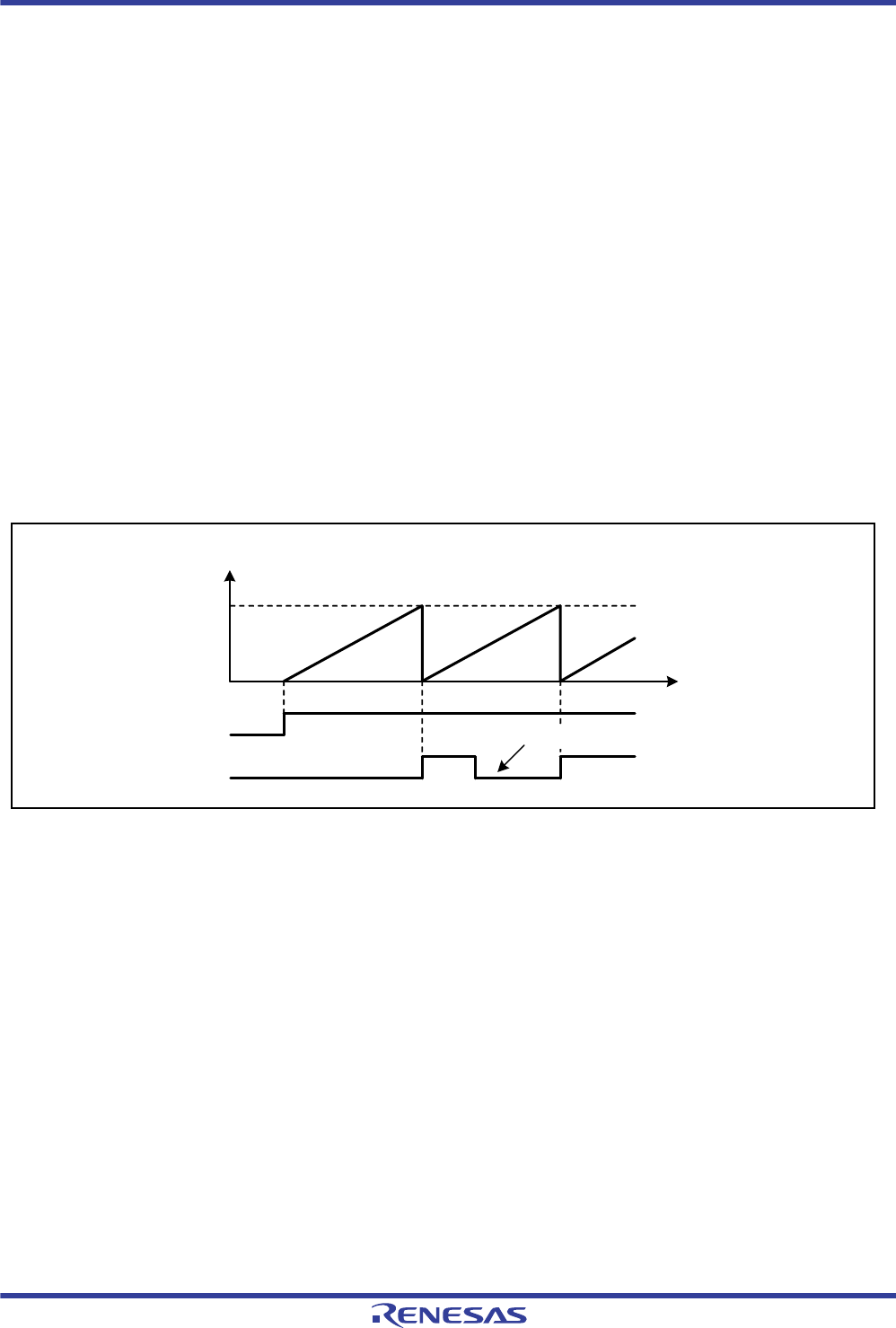
R01UH0034EJ0200 Rev.2.00 Page 790 of 1489
Dec 27, 2013
RX62T Group, RX62G Group 18. General PWM Timer (GPT/GPTa)
18.3 Operation
18.3.1 Basic Operation
Each channel has a 16-bit timer which performs up-counting, down-counting, and up-/down-counting.
The cycle is controlled by compare register GTPR.
When the counter value matches the value in GTCCRA or GTCCRB, the output from the corresponding pin GTIOCnA
or GTIOCnB can be changed (n = 0 to 3). GTCCRA or GTCCRB can be used as an input capture register with the
GTIOCnA or GTIOCnB pin as the input.
GTCCRC and GTCCRD can function as buffer registers of GTCCRA, and GTCCRE and GTCCRF can function as
buffer registers of GTCCRB.
18.3.1.1 Counter Operation
(1) Periodic Count Operation (in Up-Count Operation)
The counter in each channel starts up-count operation when the corresponding CST bit in GTSTR is set to 1. When the
GTCNT value matches the GTPR value (overflow), the GTST.TCFPO flag is set to 1. If the GTINTAD.GTINTPR[0] bit
is 1 at this time, a GTCIV interrupt is requested. After GTCNT overflows, up-count operation is resumed from 0000h.
Figure 18.2 shows an example of periodic count operation in up-count operation.
Figure 18.2 Example of Periodic Count Operation (in Up-Count Operation)
Time
GPT0.GTCNT value
0000h
GPT0.GTPR
GTSTR.CST0 bit
GPT0.TCFPO flag
Flag is cleared by software
R01UH0034EJ0200 Rev.2.00 Page 791 of 1489
Dec 27, 2013
RX62T Group, RX62G Group 18. General PWM Timer (GPT/GPTa)
Figure 18.3 shows an example for setting periodic count operation in up-count operation.
Figure 18.3 Example for Setting Periodic Count Operation (in Up-Count Operation)
Select the count clock with GTCR.TPCS[1:0].
Select count clock
Set the cycle in GTPR.
Set cycle
Set the initial value in the GTCNT register.
(In figure 18.2, 0000h is set.)
Set initial value for counter
Select the count direction with the GTUDC register. (In figure 18.2, after
0003h is set in GTUDC, 0001h is set in GTUDC (up-counting).)
Set count direction
Set the operating mode with GTCR.MD[2:0].
(In figure 18.2, 000b (saw-wave PWM mode) is set.)
Set operating mode
Set GTSTR.CST to 1 to start count operation. (In figure 18.2, 1 is set in
GTSTR.CST0.)
Start count operation
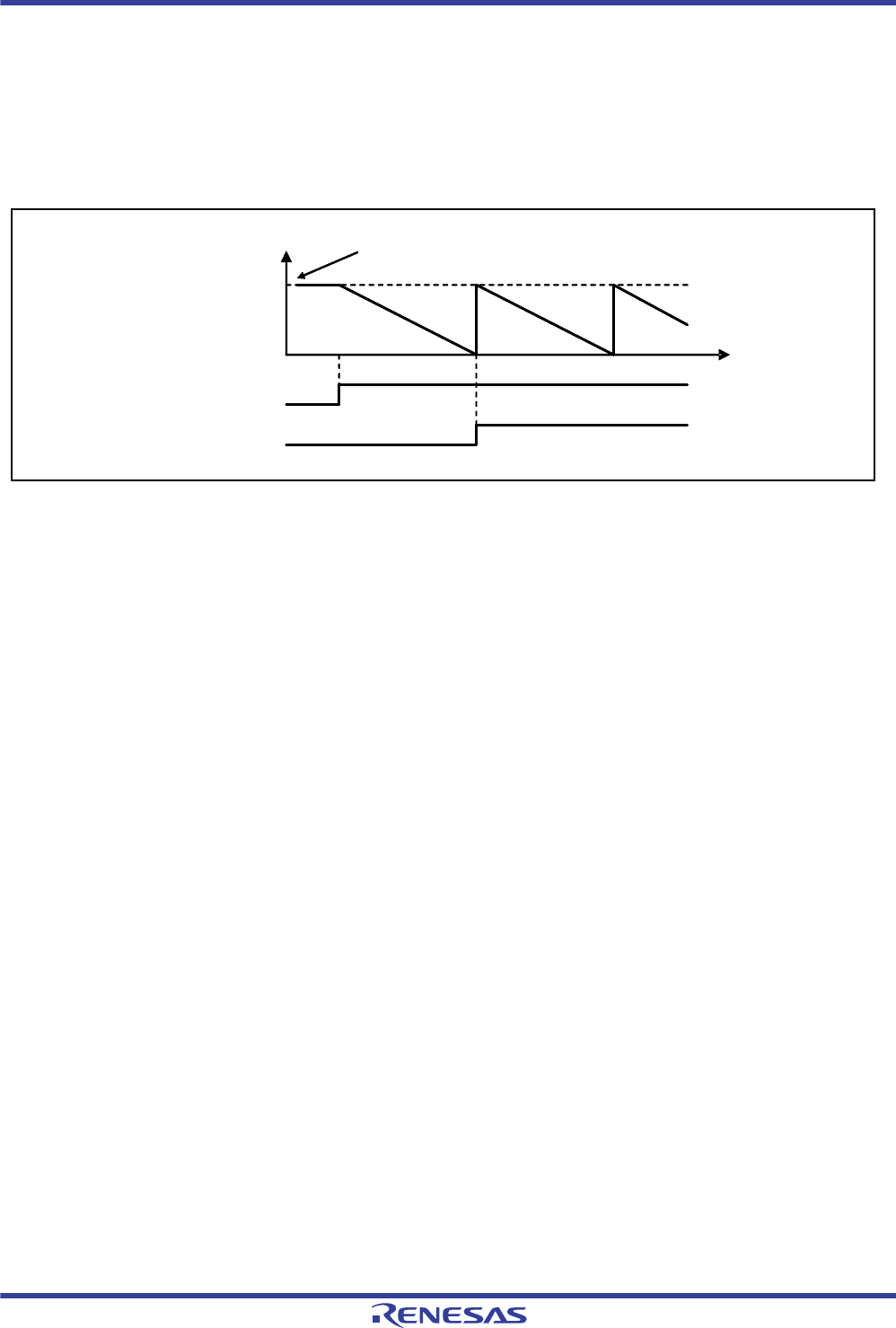
R01UH0034EJ0200 Rev.2.00 Page 792 of 1489
Dec 27, 2013
RX62T Group, RX62G Group 18. General PWM Timer (GPT/GPTa)
(2) Periodic Count Operation (in Down-Count Operation)
The counter in each channel can perform down-count operation by setting GTUDC.
When GTCNT reaches 0 (underflow), the GTST.TCFPU flag is set to 1. If the GTINTAD.GTINTPR[1] bit is 1 at this
time, a GTCIV interrupt is requested. After the GTCNT counter underflows, down-count operation is resumed from the
GTPR value.
Figure 18.4 shows an example of periodic count operation in down-count operation.
Figure 18.4 Example of Periodic Count Operation (in Down-Count Operation)
Time
GPT0.GTCNT value
0000h
GPT0.GTPR
GTSTR.CST bit
GPT0.GTST.TCFPU flag
GTCNT is written by software.
R01UH0034EJ0200 Rev.2.00 Page 793 of 1489
Dec 27, 2013
RX62T Group, RX62G Group 18. General PWM Timer (GPT/GPTa)
Figure 18.5 shows an example for setting periodic count operation in down-count operation.
Figure 18.5 Example for Setting Periodic Count Operation (in Down-Count Operation)
Select the count clock with GTCR.TPCS[1:0].
Select count clock
Set the cycle in GTPR.
Set cycle
Set the initial value in the GTCNT register.
(In figure 18.4, the GTPR value is set.)
Set initial value to counter
Select the count direction with the GTUDC register. (In figure 18.4, after
0002h is set in GTUDC, 0000h is set in GTUDC (down-counting).)
Set count direction
Set the operating mode with GTCR.MD[2:0]. (In figure 18.4, 000b (saw-
wave PWM mode) is set.)
Set operating mode
Set GTSTR.CST to 1 to start count operation. (In figure 18.4, 1 is set in
GTSTR.CST0.)
Start count operation

R01UH0034EJ0200 Rev.2.00 Page 794 of 1489
Dec 27, 2013
RX62T Group, RX62G Group 18. General PWM Timer (GPT/GPTa)
18.3.1.2 Waveform Output by Compare Match
When the GPTn.GTCNT counter value matches GTPn.GTCCRA or GTPn.GTCCRB, the GPT can output low or high or
toggles output from the corresponding GTIOCnA or GTIOCnB output pin (n = channel number).
In addition, the GTIOCnA or GTIOCnB pin output can be low, high, or toggled at the "cycle end" which is determined
by GPTn.GTPR.
The cycle end is:
For saw waves in up-count operation: When GPTn.GTPR = GPTn.GTCNT (overflow)
For saw waves in down-count operation: When GPTn.GTPR = 0 (underflow)
For triangle waves: When GPTn.GTPR = 0 (trough)
(1) Low Output and High Output
Figure 18.6 shows an example of low output and high output operation by a compare match of GTCCRA and
GTCCRB.
In this example, up-count operation is performed in GPT0, and settings have been made so that high is output from the
GTIOC0A pin by a GPT0.GTCCRA compare match, and low is output from the GTIOC0B pin by a GPT0n.GTCCRB
compare match. The pin level does not change when the specified level and pin level match.
Figure 18.6 Example of Low Output and High Output Operation
Time
GPT0.GTCNT value
0000h
GPT0.GTPR
GTIOC0A output
GTIOC0B output
GPT0.GTCCRA
GPT0.GTCCRB
[Setting examples]
No change No change
No changeNo change
GPT0.GTIOR.GTIOA[5:0]: Initial output of 0, 1 output at compare match, output retained at cycle end
GPT0.GTIOR.GTIOB[5:0]: Initial output of 1, 0 output at compare match, output retained at cycle end
R01UH0034EJ0200 Rev.2.00 Page 795 of 1489
Dec 27, 2013
RX62T Group, RX62G Group 18. General PWM Timer (GPT/GPTa)
Figure 18.7 shows an example for setting low output and high output operation
Figure 18.7 Example for Setting Low Output and High Output Operation
Select the count clock with GTCR.TPCS[1:0].
Select count clock
Set the cycle in GTPR.
Set cycle
Set the initial value in the GTCNT register.
Set initial value to counter
Select the count direction (up or down) with the GTUDC register. (In figure
18.6, after 0003h is set in GTUDC, 0001h is set in GTUDC (up-counting).)
Set count direction
Set the operating mode with GTCR.MD[2:0]. (In figure 18.6, 000b (saw-
wave PWM mode) is set.)
Set operating mode
Set GTSTR.CST to 1 to start count operation.
(In figure 18.6, 1 is set in GTSTR.CST0.)
Start count operation
Set the GTIOC pin function with GTIOA[5:0] and GTIOB[5:0] in GTIOR.
(In figure 18.6, GTIOA[5:0] = 000010b, GTIOB[5:0] = 010001b.)
Set GTIOC pin function
Set to enable the GTIOC pin output with OAE and OBE in GTONCR.
Enable GTIOC pin output
Set compare match values in the GTCCRA and GTCCRB registers.
Set compare match value
*1
*1
Note 1: Switch the procedure of "Enable GTIOC pin output" and "Set compare match value"
when the PWM delay generation circuit is in use.
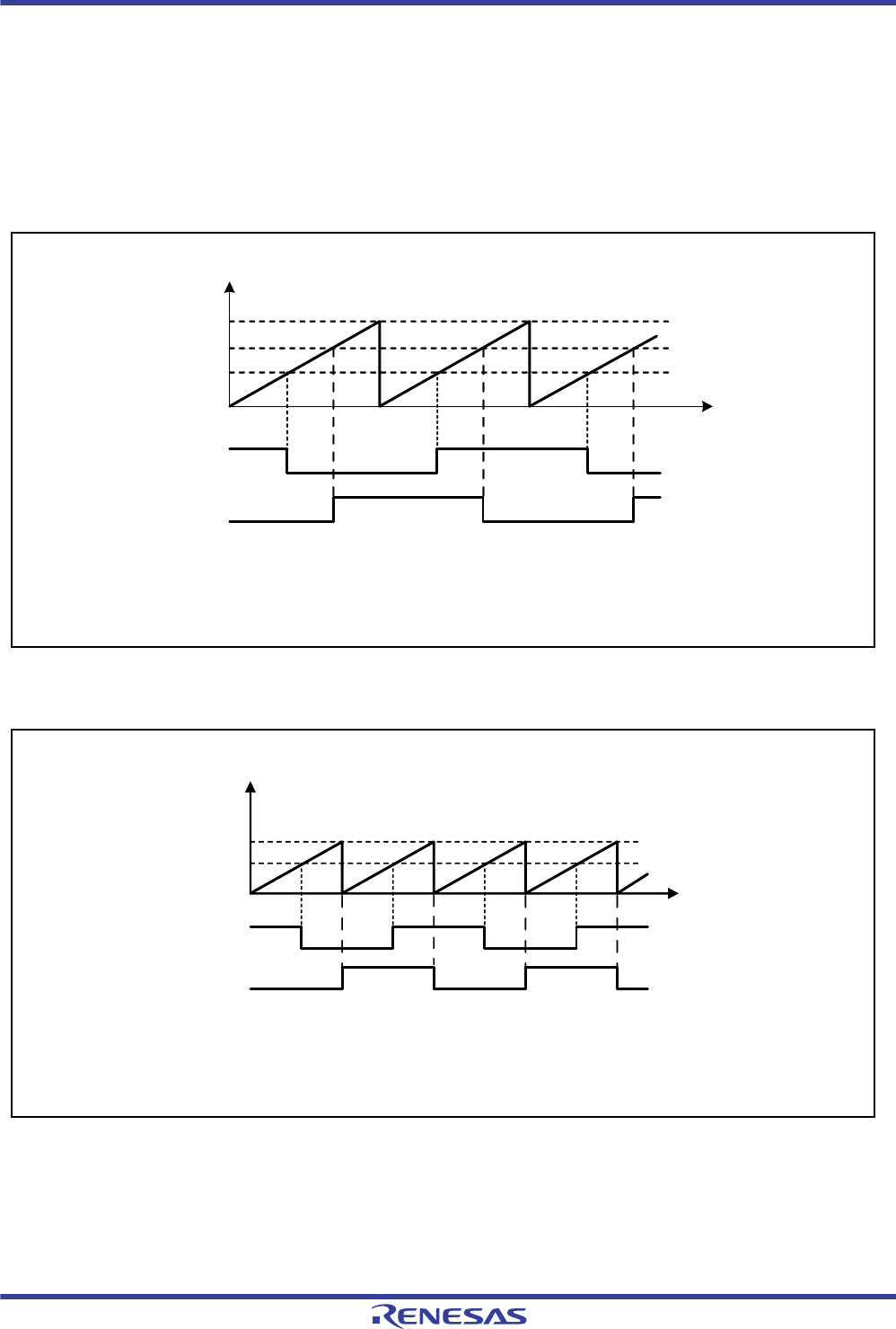
R01UH0034EJ0200 Rev.2.00 Page 796 of 1489
Dec 27, 2013
RX62T Group, RX62G Group 18. General PWM Timer (GPT/GPTa)
(2) Toggled Output
Figure 18.9 and Figure 18.10 show examples of toggled output operation by compare matches of GTCCRA and
GTCCRB. In Figure 18.8, up-count operation is performed in GPT0, and settings have been made so that the GTIOC0A
pin output by a GPT0.GTCCRA compare match and GTIOC0B pin output by a GPT0n.GTCCRB compare match are
toggled.
In Figure 18.9, up-count operation is performed in GPT0, and settings have been made so that the GTIOC0A output is
toggled by a compare match of GPT0.GTCCRA and the GTIOC0B output is toggled at the cycle end.
Figure 18.8 Example of Toggled Output Operation (1)
Figure 18.9 Example of Toggled Output Operation (2)
Time
GPT0.GTCNT value
0000h
GPT0.GTPR0
GTIOC0B output
GTIOC0A output
GPT0.GTCCRB
GPT0.GTCCRA
[Setting examples]
GPT0.GTIOR.GTIOA[5:0]: Initial output of 1, toggle output at compare match, output retained at cycle end
GPT0.GTIOR.GTIOB[5:0]: Initial output of 0, toggle output at compare match, output retained at cycle end
Time
GPT0.GTCNT value
0000h
GTIOC0B output
GTIOC0A output
GPT0.GTPR
GPT0.GTCCRA
[Setting examples]
GPT0.GTIOR.GTIOA[5:0]: Initial output of 1, toggle output at compare match, output retained at cycle end
GPT0.GTIOR.GTIOB[5:0]: Initial output of 0, output retained at compare match, toggle output at cycle end
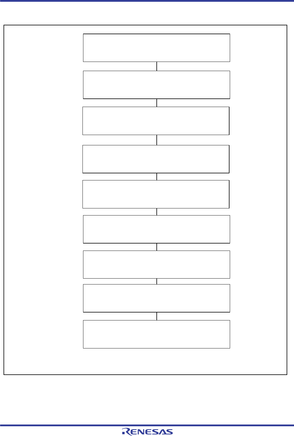
R01UH0034EJ0200 Rev.2.00 Page 797 of 1489
Dec 27, 2013
RX62T Group, RX62G Group 18. General PWM Timer (GPT/GPTa)
Figure 18.10 shows an example for setting toggled output operation
Figure 18.10 Example for Setting Toggled Output Operation
Select the count clock with GTCR.TPCS[1:0].
Select count clock
Set the cycle in GTPR.
Set cycle
Set the initial value in the GTCNT register.
Set initial value to counter
Select the count direction (up or down) with the GTUDC register. (In
figures 18.8 and 18.9, after 0003h is set in GTUDC, 0001h is set in
GTUDC (up-counting).)
Set count direction
Set the operating mode with GTCR.MD[2:0].
(In figures 18.8 and 18.9, 000b (saw-wave PWM mode) is set.)
Set operating mode
Set GTSTR.CST to 1 to start count operation.
(In figures 18.8 and 18.9, 1 is set in GTSTR.CST0.)
Start count operation
Set the GTIOC pin function with GTIOA[5:0] and GTIOB[5:0] in GTIOR.
(In figure 18.8, GTIOA[5:0] = 010011b, GTIOB[5:0] = 000011b and
in figure 18.9, GTIOA[5:0] = 010011b, GTIOB[5:0] = 001100b.)
Set GTIOC pin function
Set to enable the GTIOC pin output with OAE and OBE in GTONCR.
Enable GTIOC pin output
Set compare match values in the GTCCRA and GTCCRB registers.
Set compare match value *1
*1
Note 1: Switch the procedure of "Enable GTIOC pin output" and "Set compare match value"
when the PWM delay generation circuit is in use.
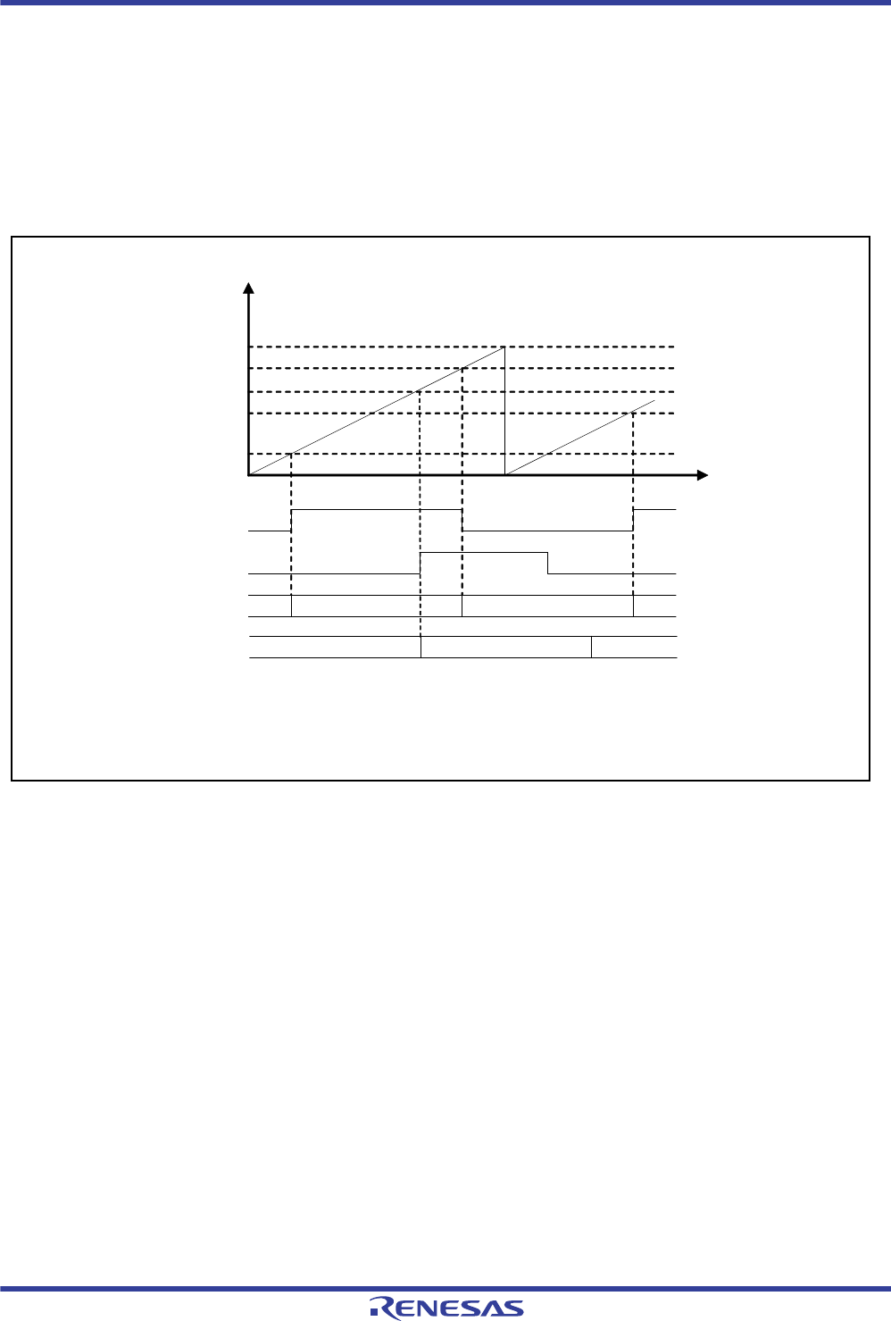
R01UH0034EJ0200 Rev.2.00 Page 798 of 1489
Dec 27, 2013
RX62T Group, RX62G Group 18. General PWM Timer (GPT/GPTa)
18.3.1.3 Input Capture Function
The GPTn.GTCNT counter value can be transferred to either GPTn.GTCCRA or GPTn.GTCCRB on detection of the
input edge of the GTIOCnA input pin or GTIOCnB input pin, respectively (n: channel number). The rising edge, falling
edge, or both edges can be selected as the detection edge.
Figure 18.11 shows an example of the input capture function. In this example, up-count operation is performed on
GPT0, and settings have been made so that an input capture is performed at both edges of the GTIOC0A input pin and at
the rising edge of the GTIOC0B input pin.
Figure 18.11 Example of Input Capture Operation
Time
GPT0.GTCNT value
1100h E400h 9682h
C154h
0000h
GTIOC0A input
GPT0.GTPR
1100h
E400h
9682h
GPT0.GTCCRA
GTIOC0B input
GPT0.GTCCRB
C154h
[Setting examples]
GPT0.GTIOR.GTIOA[5:0]: Input capture at both edges
GPT0.GTIOR.GTIOB[5:0]: Input capture at the rising edge

R01UH0034EJ0200 Rev.2.00 Page 799 of 1489
Dec 27, 2013
RX62T Group, RX62G Group 18. General PWM Timer (GPT/GPTa)
Figure 18.12 shows an example for setting input capture operation.
Figure 18.12 Example for Setting Input Capture Operation
Select the count clock with GTCR.TPCS[1:0].
Select count clock
Set the cycle in GTPR.
Set cycle
Set the initial value in the GTCNT register.
Set initial value to counter
Select the count direction (up or down) with the GTUDC register. (In figure
18.11, after 0003h is set in GTUDC, 0001h is set in GTUDC (up-
counting).)
Set count direction
Set the operating mode with GTCR.MD[2:0].
(In figure 18.11, 000b (saw-wave PWM mode) is set.)
Set operating mode
Set GTSTR.CST to 1 to start count operation.
(In figure 18.11, 1 is set to GTSTR.CST0.)
Start count operation
Set the GTIOC pin function with GTIOA[5:0] and GTIOB[5:0] in GTIOR.
(In figure 18.11, GTIOA[5:0] = 1xxx1xb, GTIOB[5:0] = 1xxx00b.)
Set GTIOC pin function
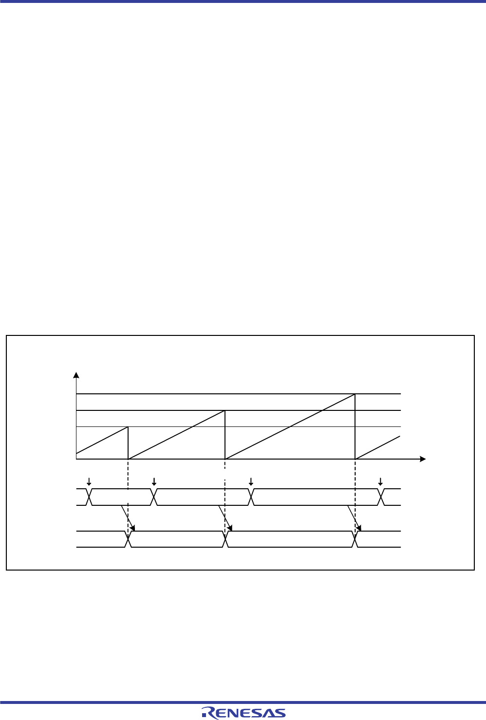
R01UH0034EJ0200 Rev.2.00 Page 800 of 1489
Dec 27, 2013
RX62T Group, RX62G Group 18. General PWM Timer (GPT/GPTa)
18.3.2 Buffer Operation
The following buffer operation can be set with GTBER.
Buffer operation with GTCCRA, GTCCRC, and GTCCRD used together
Buffer operation with GTCCRB, GTCCRE, and GTCCRF used together
Buffer operation with GTPR, GTPBR, and GTPDBR used together
Buffer operation with GTADTRA, GTADTBRA, and GTADTDBRA used together
Buffer operation with GTADTRB, GTADTBRB, and GTADTDBRB used together
The following buffer operation can be set with GTDTCR.
Buffer operation with GTDVU and GTDBU used together
Buffer operation with GTDVU and GTDBD used together
18.3.2.1 GTPR Register Buffer Operation
GTPBR can function as a buffer register for GTPR, and GTPCBR can function as a buffer register for GTPBR (double-
buffer register for GTPR).
The buffer transfer is performed at an overflow (during up-count operation) or an underflow (during down-count
operation) in saw-wave mode, and at a trough in triangle-wave mode.
To set GTPR to function as double buffer, set GTBER.PR[1:0] to 10b or 11b. For single buffer operation, set 01b. Not to
function as buffer, set 00b.
Figure 18.13 to Figure 18.15 show examples of GTPR buffer operation and Figure 18.16 shows an example for
setting GTPR buffer operation.
Figure 18.13 Example of GTPR Buffer Operation (Saw Waves in Up-Count Operation)
GTCNT value
GTPR
cccc
bbbb
0000h
aaaa
Register write
Buffer transfer
at overflow
GTPBR
Time
Register write
Register writeRegister write
Buffer transfer
at overflow Buffer transfer
at overflow
aaaa bbbb cccc
ccccbbbb
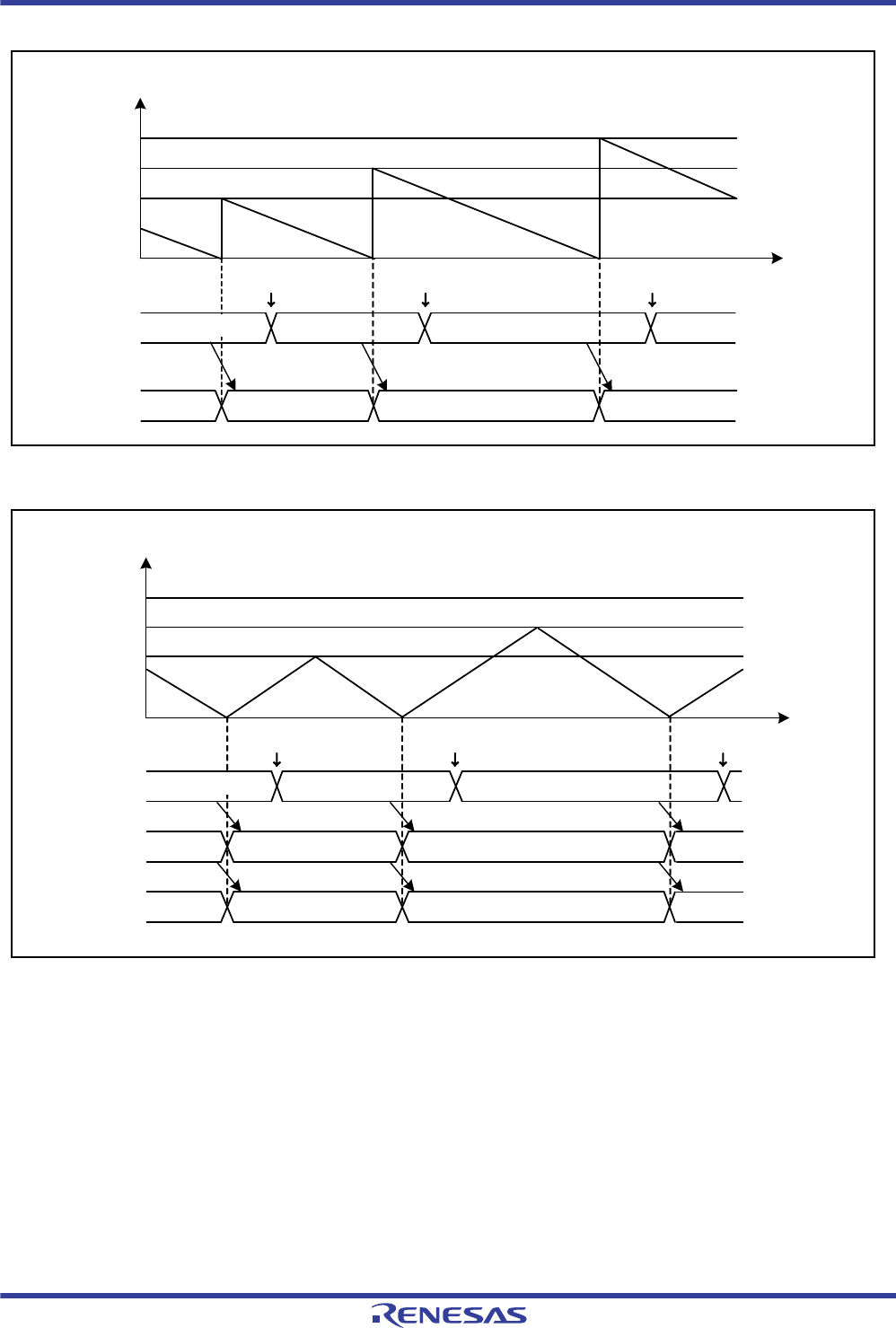
R01UH0034EJ0200 Rev.2.00 Page 801 of 1489
Dec 27, 2013
RX62T Group, RX62G Group 18. General PWM Timer (GPT/GPTa)
Figure 18.14 Example of GTPR Buffer Operation (Saw Waves in Down-Count Operation)
Figure 18.15 Example of GTPR Double Buffer Operation (Triangle Waves)
aaaa
bbbb
cccc
GTCNT value
0000h
Register write
GTPR
GTPBR bbbb
bbbbaaaa
cccc
cccc
Buffer transfer
at underflow Buffer transfer
at underflow Buffer transfer
at underflow
Time
Register write Register write
GTCNT value
0000h
aaaa
bbbb
cccc
GTPR
Register write
Time
GTPBR
GTPDBR
Register write Register write
Buffer transfer at trough
Buffer transfer at trough
Buffer transfer at trough
Buffer transfer at trough
Buffer transfer at trough
Buffer transfer at trough
aaaa
bbbb cccc
ccccbbbb
aaaa
bbbb cccc
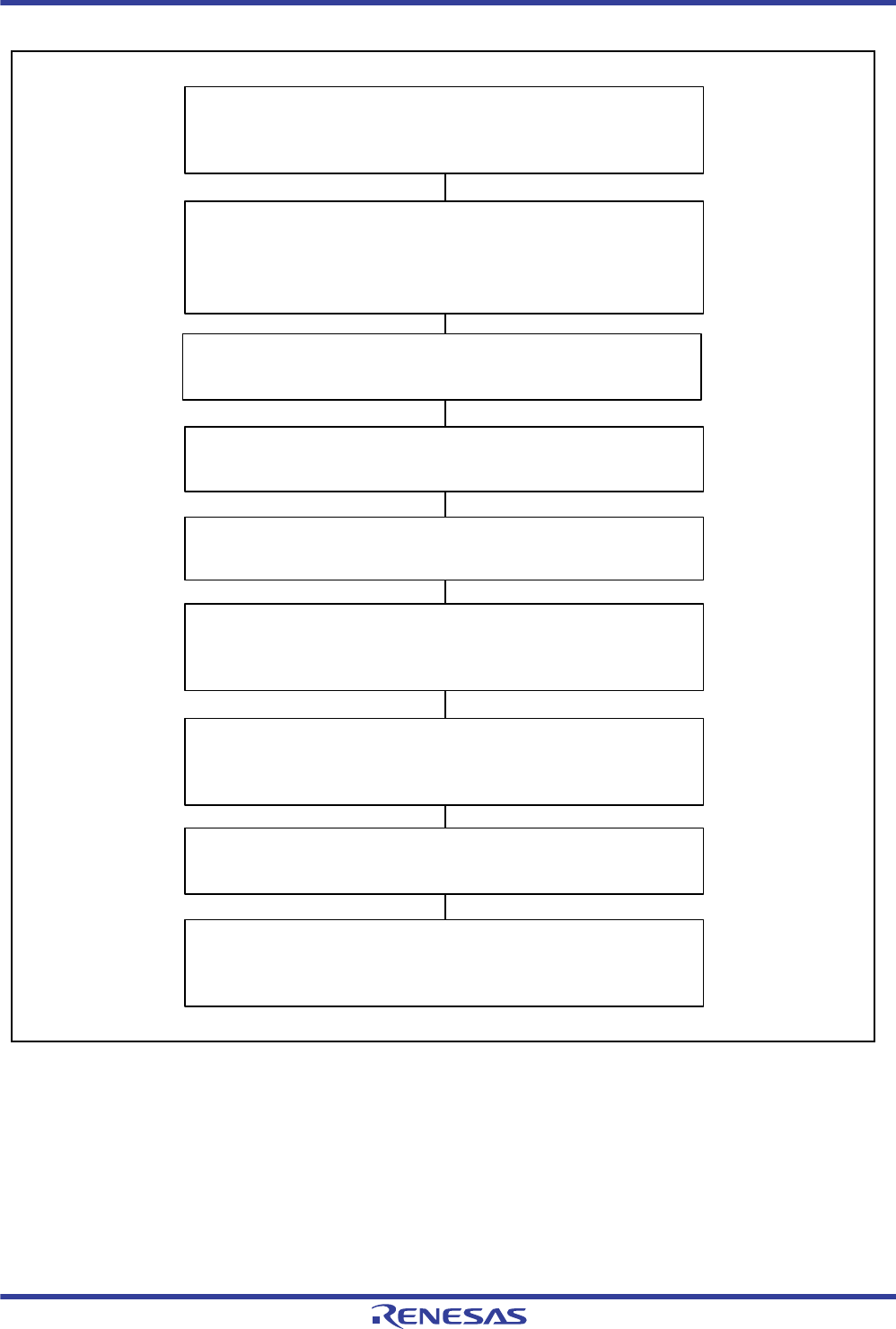
R01UH0034EJ0200 Rev.2.00 Page 802 of 1489
Dec 27, 2013
RX62T Group, RX62G Group 18. General PWM Timer (GPT/GPTa)
Figure 18.16 Example for Setting GTPR Buffer Operation
Select the count clock with GTCR.TPCS[1:0].
Select count clock
Set the cycle in GTPR.
Set cycle
Set the initial value in the GTCNT register.
Set initial value to counter
Select the count direction (up or down) with the GTUDC register. (In figure
18.13, after 0003h is set in GTUDC, 0001h is set in GTUDC (up-counting).
In figure 18.14, after 0002h is set in GTUDC, 0000h is set in GTUDC (up-
counting).)
Set count direction
Set the operating mode with GTCR.MD[2:0]. (In figures 18.13 and 18.4,
000b (saw-wave PWM mode) is set, and in figure 18.15, 100b (triangle-
wave PWM mode 1) is set.)
Set operating mode
Set GTSTR.CST to 1 to start count operation.
Start count operation
For buffer operation, set a value in one cycle after the current cycle in
GTPBR. For double buffer operation, also set a value in two cycles after
the current cycle in GTPDBR.
Set buffer value
Set buffer operation with GTBER.PR[1:0]. (In figures 18.13 and 18.14,
PR[1:0] = 01b. In figure 18.15, PR[1:0] = 1xb.)
Set buffer operation
For buffer operation, set a value in one cycle after the current cycle in
GTPBR. For double buffer operation, also set a value in two cycles after
the current cycle in GTPDBR.
Set buffer value for each cycle
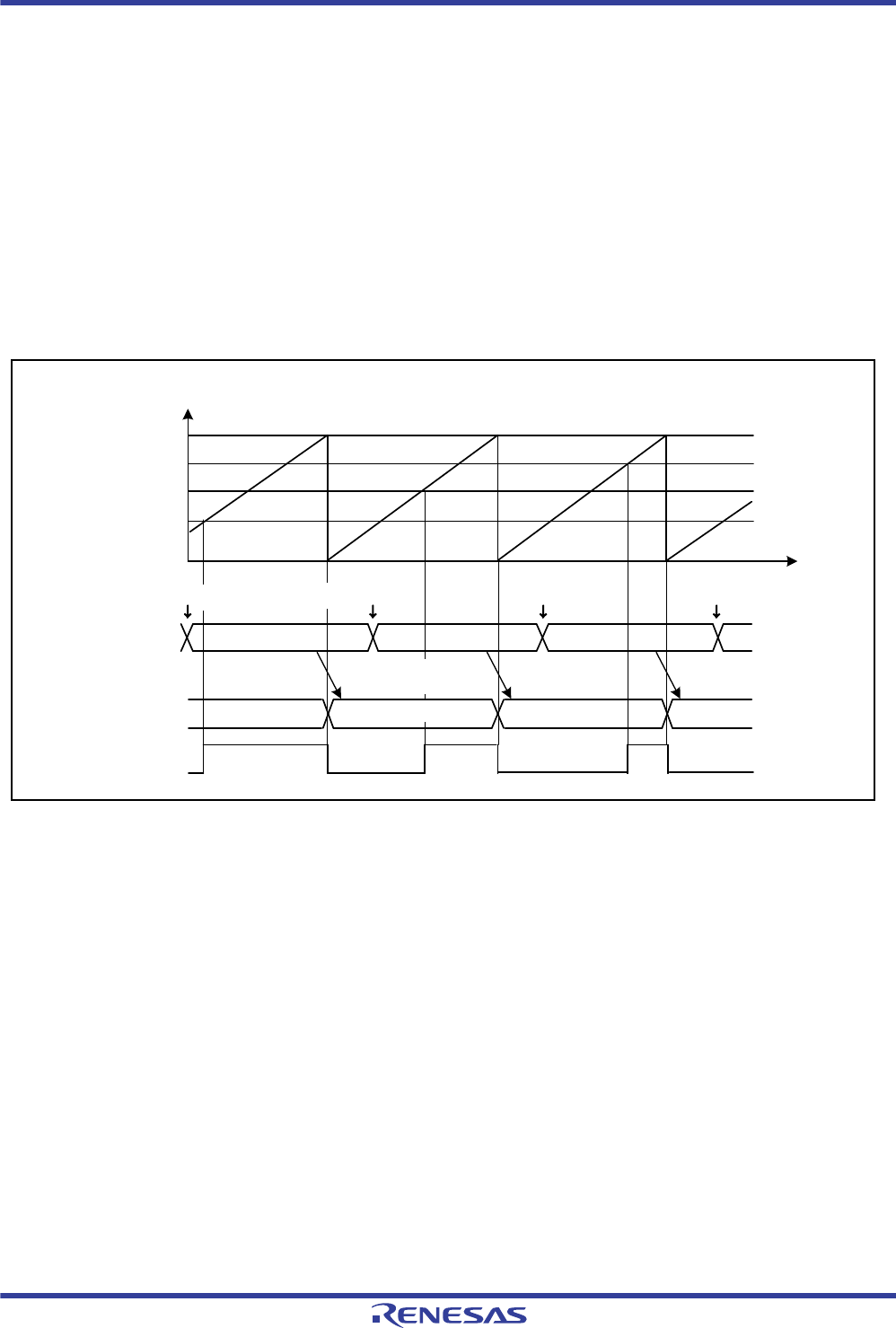
R01UH0034EJ0200 Rev.2.00 Page 803 of 1489
Dec 27, 2013
RX62T Group, RX62G Group 18. General PWM Timer (GPT/GPTa)
18.3.2.2 Buffer Operation for GTCCRA and GTCCRB
GTCCRC can function as the GTCCRA buffer register and GTCCRD can function as the GTCCRC buffer register
(double-buffer register for GTCCRA). Similarly, GTCCRE can function as the GTCCRB buffer register and GTCCRF
can function as the GTCCRE buffer register (double-buffer register for GTCCRB).
To set GTCCRA or GTCCRB to function as a double buffer, set GTBER.CCRA[1:0] or GTBER.CCRB[1:0] to 10b or
11b. For single buffer operation, set 01b. Not to function as buffer, set 00b.
(1) When GTCCRA or GTCCRB Functions as Output Compare Register
Buffer transfer is performed at an overflow (during up-count operation) or an underflow (during down-count operation)
in saw-wave mode, and at a trough in triangle-wave mode.
Figure 18.17 to Figure 18.19 show examples of GTCCRA and GTCCRB buffer operation and Figure 18.20 shows an
example for setting GTCCRA and GTCCRB buffer operation.
Figure 18.17 Example of GTCCRA and GTCCRB Buffer Operation (Output Compare, Saw Waves in Up-Count
Operation, High Output at GTCCRA Compare Match, Low Output at Cycle End)
GPT0.GCNT value
aaaa
bbbb
cccc
GPT0.GTPR
0000h
GTIOC0A output
GPT0.GTCCRA
GPT0.GTCCRC
aaaa
bbbb cccc
ccccbbbb
Register write Register write Register write
Buffer transfer
at overflow Buffer transfer
at overflow Buffer transfer
at overflow
Time
Register write
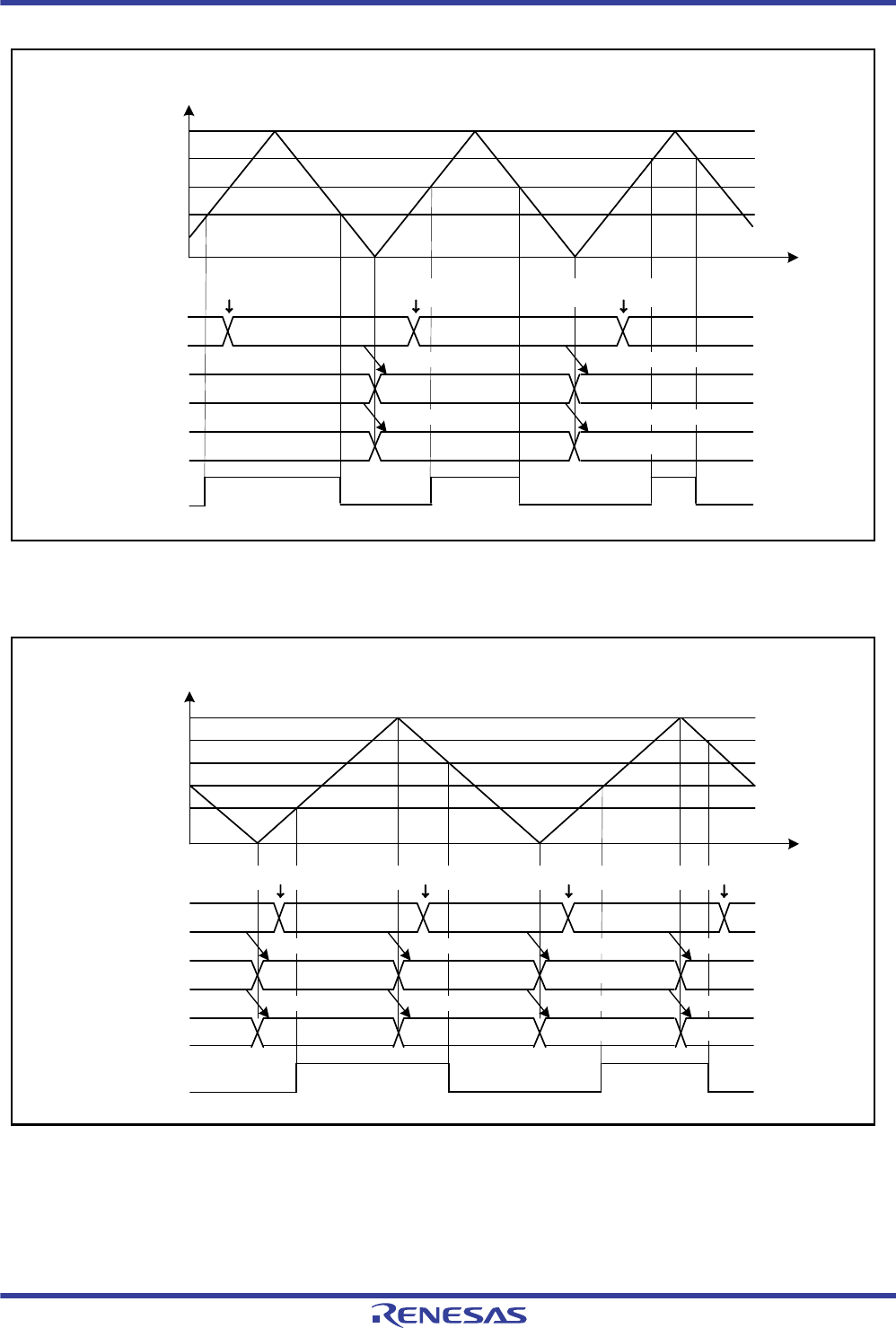
R01UH0034EJ0200 Rev.2.00 Page 804 of 1489
Dec 27, 2013
RX62T Group, RX62G Group 18. General PWM Timer (GPT/GPTa)
Figure 18.18 Example of GTCCRA and GTCCRB Double Buffer Operation (Output Compare, Triangle Waves,
Buffer Operation at Trough, Toggle Output at GTCCRA Compare Match, Output Retained at Cycle
End)
Figure 18.19 Example of GTCCRA and GTCCRB Double Buffer Operation (Output Compare, Triangle Waves,
Buffer Operation at Both Troughs and Crests, Toggle Output at GTCCRB Compare Match, Output
Retained at Cycle End)
GPT0.GTCNT value
aaaa
bbbb
cccc
GPT0.GTPR
0000h Time
Register write
Buffer transfer at
trough
GPT0.GTCCRD
GPT0.GTCCRC
GPT0.GTCCRA
GTIOC0A output
Register write Register write
Buffer transfer at
trough
Buffer transfer at
trough
Buffer transfer at
trough
cccc
ccccbbbb
bbbbaaaa cccc
Buffer transfer at
trough
aaaa
bbbb
cccc
GPT0.GTPR
0000h
GPT0.GTCNT value
dddd
GPT0.GTCCRF
GPT0.GTCCRE
GPT0.GTCCRB
GTIOC0B output
Register write Register write Register write Register write
Time
Buffer transfer at
trough
Buffer transfer at
crest
Buffer transfer at
crest
Buffer transfer at
trough
Buffer transfer at
trough
Buffer transfer at
crest
Buffer transfer at
crest
cccc
cccc
cccc bbbb
bbbb
bbbbaaaa
aaaa
dddd
dddd
dddd
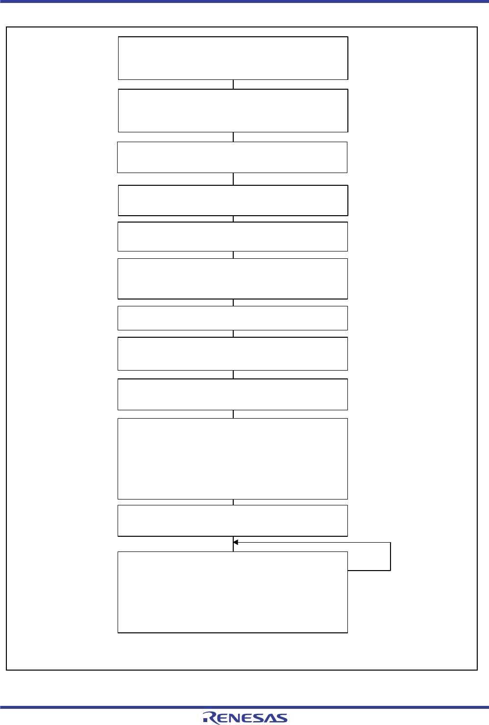
R01UH0034EJ0200 Rev.2.00 Page 805 of 1489
Dec 27, 2013
RX62T Group, RX62G Group 18. General PWM Timer (GPT/GPTa)
Figure 18.20 Example for Setting GTCCRA and GTCCRB Buffer Operation (for Output Compare)
Select the count clock with GTCR.TPCS[1:0].
Select count clock
Set the cycle in GTPR.
Set cycle
Set the initial value in the GTCNT register.
Set initial value to counter
Select the count direction (up or down) with the GTUDC register. (In figure
18.17, after 0003h is set in GTUDC, 0001h is set in GTUDC (up-
counting).)
Set count direction
Set the operating mode with GTCR.MD[2:0]. (In figure 18.17, 000b (saw-
wave PWM mode) is set, in figure 18.18, 100b (triangle-wave PWM mode
1) is set, and in figure 18.19, 101b (triangle-wave PWM mode 2) is set.)
Set operating mode
Set GTSTR.CST to 1 to start count operation. (In figures 18.17, 18.18, and
18.19, 1 is set in GTSTR.CST0.)
Start count operation
For buffer operation, set the GTIOCA pin and GTIOCB pin changing points in
one cycle after the current cycle (in saw-wave mode or triangle-wave mode
with buffer transfer at trough or crest) or half cycle after the current cycle (in
triangle-wave mode with buffer transfer at both trough and crest) in GTCCRC
and GTCCRE, respectively.
For double buffer operation, also set the GTIOCA pin and GTIOCB pin
changing points in two cycles after the current cycle (in saw-wave mode or
triangle-wave mode with buffer transfer at trough or crest) or one cycle after
the current cycle (in triangle-wave mode with buffer transfer at both trough and
crest) in GTCCRD and GTCCRF, respectively.
Set buffer value
Set the GTIOCA pin changing point in GTCCRA and GTIOCB pin
changing point in the GTCCRB.
Set compare match value
Set to enable GTIOC pin output with OAE and OBE in GTONCR.
Enable GTIOC pin output
Set the GTIOC pin function with GTIOA[5:0] and GTIOB[5:0] in GTIOR.
(In figure 18.17, GTIOA[5:0] = 000110b, in figure 18.18, GTIOA[5:0] =
000011b, and in figure 18.19, GTIOB[5:0] = 000011b.)
Set GTIOC pin function
For buffer operation, set the GTIOCA pin and GTIOCB pin changing points in
one cycle after the current cycle (in saw-wave mode or triangle-wave mode
with buffer transfer at trough or crest) or half cycle after the current cycle (in
triangle-wave mode with buffer transfer at both trough and crest) in GTCCRC
and GTCCRE, respectively.
For double buffer operation, also set the GTIOCA pin and GTIOCB pin
changing points in two cycles after the current cycle (in saw-wave mode or
triangle-wave mode with buffer transfer at trough or crest) or one cycle after
the current cycle (in triangle-wave mode with buffer transfer at both trough and
crest) in GTCCRD and GTCCRF, respectively.
Set buffer value for each cycle
Set buffer operation with CCRA and CCRB in GTONCR. (In figure 18.17, CCRA
= 01b, in figure 18.18, CCRA = 1xb, and in figure 18.19, CCRB = 1xb.)
Set buffer operation
*1
*1
Note 1: Switch the procedure of "Enable GTIOC pin output" and "Set compare match value"
when the PWM delay generation circuit is in use.
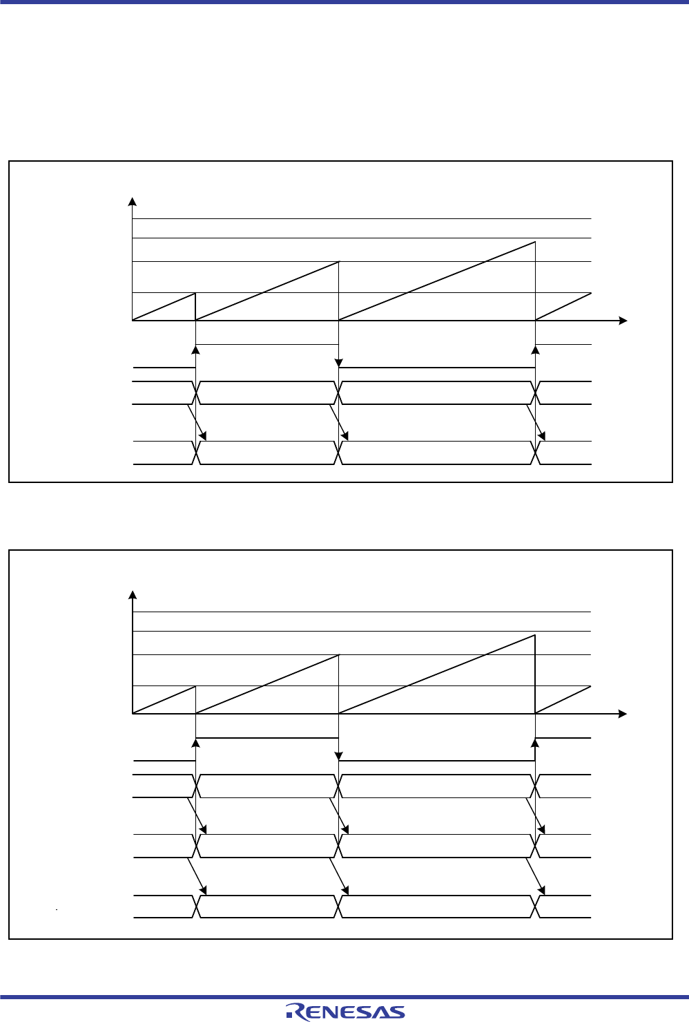
R01UH0034EJ0200 Rev.2.00 Page 806 of 1489
Dec 27, 2013
RX62T Group, RX62G Group 18. General PWM Timer (GPT/GPTa)
(2) When GTCCRA or GTCCRB Functions as Input Capture Register
Buffer transfer is performed at a point when an input capture is generated. When an input capture is generated, the
GTCNT counter value is transferred to GTCCRA and GTCCRB and the stored GTCCRA and GTCCRB register values
are transferred to buffer registers.
Figure 18.21 and Figure 18.22 show examples of GTCCRA and GTCCRB buffer operation and Figure 18.23 shows
an example for setting GTCCRB buffer operation.
Figure 18.21 Example of GTCCRA and GTCCRB Buffer Operation (Input Capture at Both Edges of GTIOC0A
Input, Saw Waves in Up-Count Operation, GTCNT Counter Cleared at GTCCRA Input Capture)
Figure 18.22 Example of GTCCRA and GTCCRB Double Buffer Operation (Input Capture at Both Edges of
GTIOC0B Input, Saw Waves in Up-Count Operation, GTCNT Counter Cleared at GTCCRB Input
Capture)
Time
aaaa
bbbb
cccc
GPT0.GTPR
0000h
GPT0.GTCNT value
GPT0.GTCCRC
GPT0.GTCCRA
GTIOC0A input
aaaa
aaaa
bbbb
bbbb
cccc
Buffer transfer at input
capture Buffer transfer at input
capture Buffer transfer at input
capture
GPT0.GTCNT value
aaaa
bbbb
cccc
GPT0.GTPR
0000h
aaaa bbbb cccc
Buffer transfer at input
capture
Time
GPT0.GTCCRF
GPT0.GTCCRE
GTIOC0B input
GPT0.GTCCRB
aaaa
aaaa
Buffer transfer at input
capture
Buffer transfer at input
capture
Buffer transfer at input
capture
Buffer transfer at input
capture
Buffer transfer at input
capture
bbbb
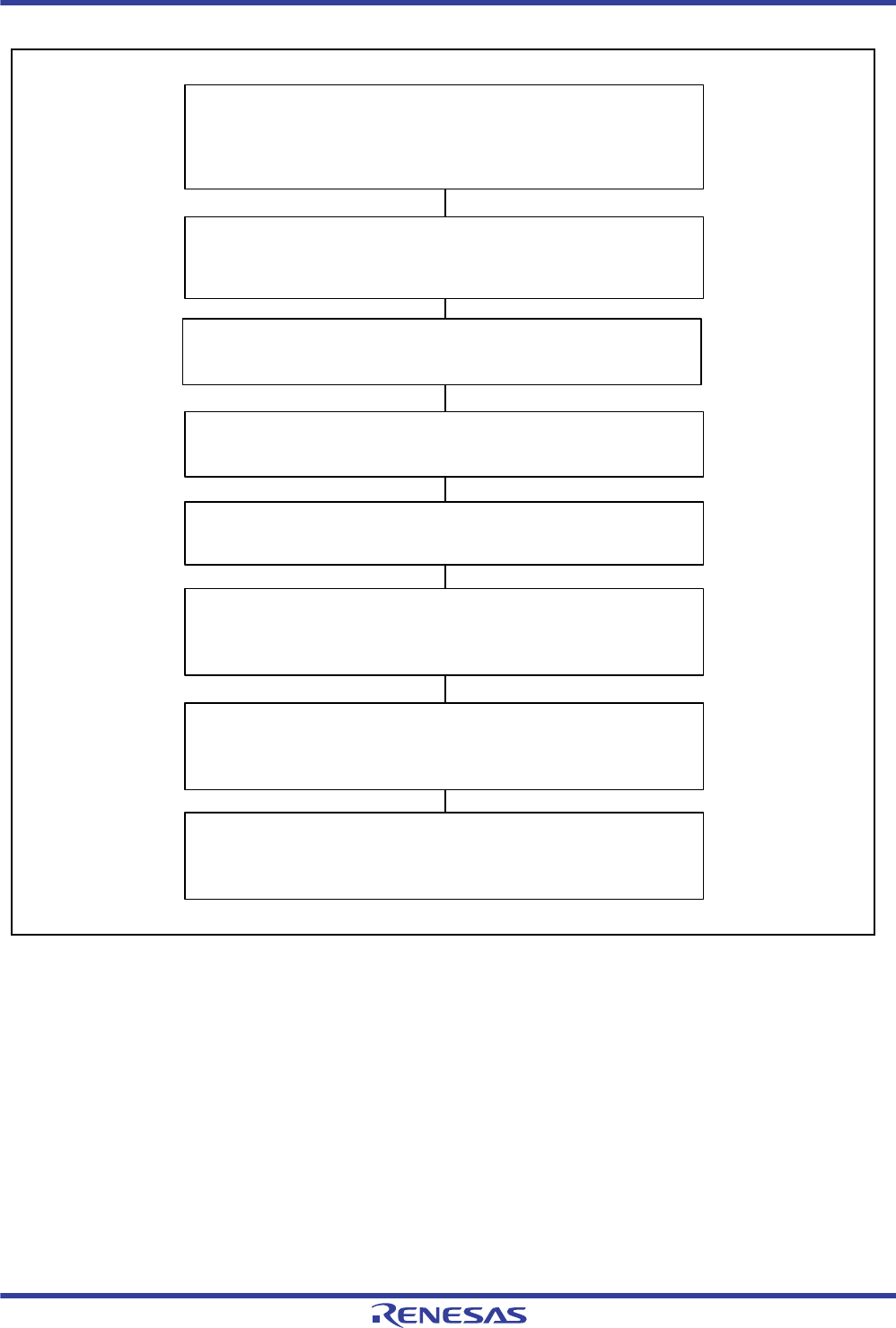
R01UH0034EJ0200 Rev.2.00 Page 807 of 1489
Dec 27, 2013
RX62T Group, RX62G Group 18. General PWM Timer (GPT/GPTa)
Figure 18.23 Example for Setting GTCCRA and GTCCRB Buffer Operation (for Input Capture)
Select the count clock with GTCR.TPCS[1:0].
Select count clock
Set the cycle in GTPR.
Set cycle
Set the initial value in the GTCNT register.
Set initial value to counter
Select the count direction (up or down) with the GTUDC register. (In figure
18.21, after 0003h is set in GTUDC, 0001h is set in GTUDC (up-
counting).)
Set count direction
Set the operating mode with GTCR.MD[2:0] and counter clear source with
CCLR[1:0]. (In figure 18.21, MD[2:0] = 000b (saw-wave PWM mode) and
CCLR[1:0] = 01b, and in figure 18.22, MD[2:0] = 000b (saw-wave PWM
mode) and CCLR[1:0] = 10b.)
Set operating mode
Set GTSTR.CST to 1 to start count operation.
(In figure 18.21, and in figure 18.22, 1 is set in GTSTR.CST0.)
Start count operation
Set buffer operation with CCRA and CCRB in GTBER.
(In figure 18.21, CCRA = 01b, and in figure 18.22, CCRB = 1xb.)
Set buffer operation
Set the GTIOC pin function with GTIOA[5:0] and GTIOB[5:0] in GTIOR.
(In figure 18.21, GTIOA[5:0] = 1xxx1xb, and in figure 18.22, GTIOB[5:0] =
1xxx1xb.)
Set GTIOC pin function
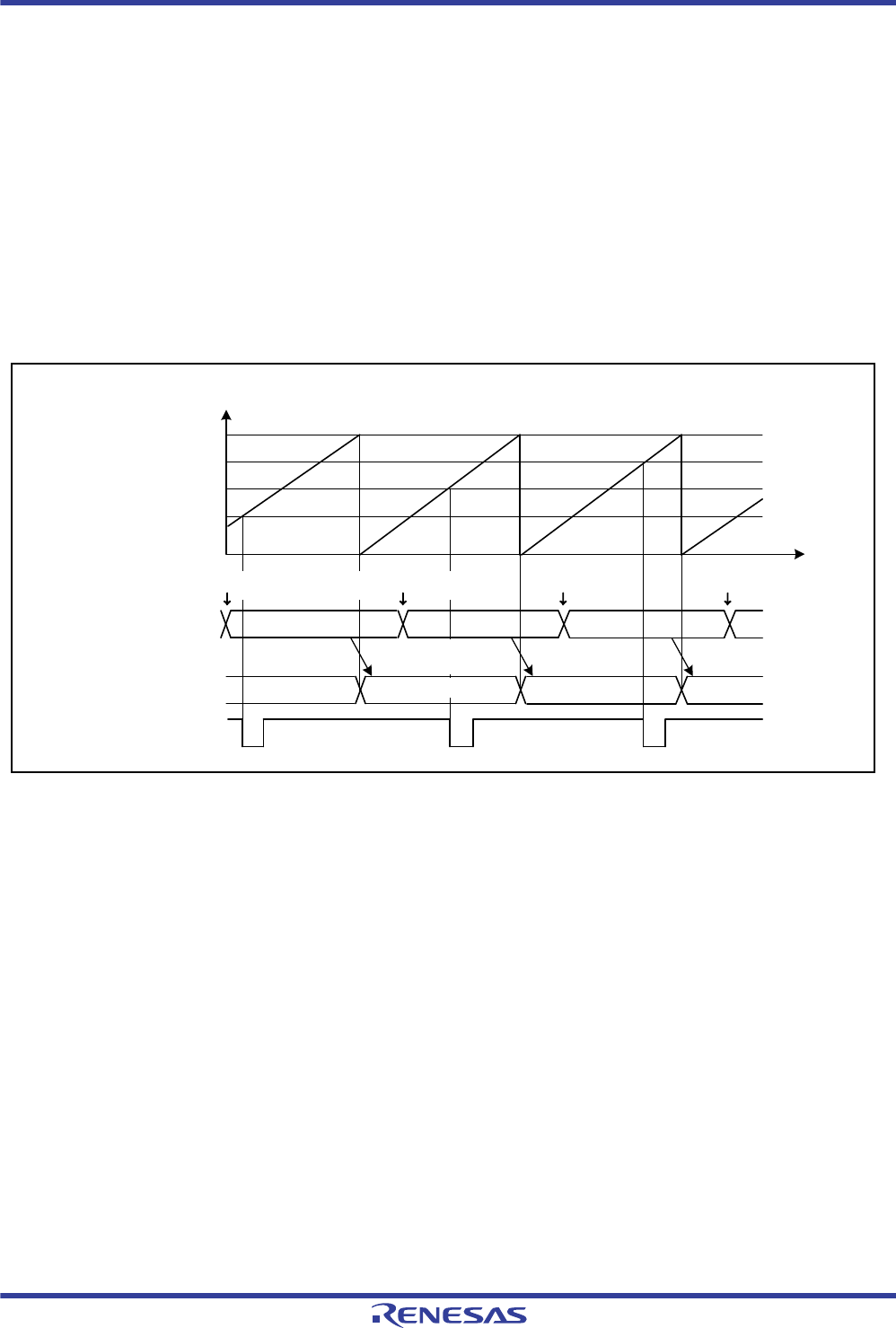
R01UH0034EJ0200 Rev.2.00 Page 808 of 1489
Dec 27, 2013
RX62T Group, RX62G Group 18. General PWM Timer (GPT/GPTa)
18.3.2.3 Buffer Operation for GTADTRA and GTADTRB
GTADTBRA can function as the GTADTRA buffer register and GTADTDBRA can function as the GTADTBRA buffer
register (double-buffer register for GTADTRA). Similarly, GTADTBRB can function as the GTADTRB buffer register
and GTADTDBRB can function as the GTADTBRB buffer register (double-buffer register for GTADTRB).
To set GTADTRA or GTADTRB to function as a double buffer, set GTBER.ADTDA or GTBER.ADTDB to 1. For
single buffer operation, set 0. Not to function as buffer, set GTBER.ADTTA[1:0] or GTBER.ADTTB[1:0] to 00b.
The buffer transfer timing can be set with the GTBER.ADTTA[1:0] bits. For saw waves, overflows (during up-count
operation) or underflows (during down-count operation) can be selected. For triangle waves, crests are selected when
GTBER.ADTTA[1:0] = 01b, troughs are selected when GTBER.ADTTA[1:0] = 10b, and both crests and troughs are
selected when GTBER.ADTTA[1:0] = 00b.
Figure 18.24 to Figure 18.26 show examples of GTADTRA and GTADTRB buffer operation and Figure 18.27 shows
an example for setting GTDTRA and GTADTRB buffer operation.
Figure 18.24 Example of GTADTRA and GTADTRB Buffer Operation (Saw Waves in Up-Count Operation, A/D
Converter Start Request Generated by Up-Counting)
GTCNT value
aaaa
bbbb
cccc
GTPR
0000h
GTADTBRA
GTADTRA
GTADTRA
(A/D conversion request)
Register write Register write Register write Register write
Time
bbbb
aaaa
cccc
bbbb cccc
Buffer transfer
at overflow Buffer transfer
at overflow Buffer transfer
at overflow

R01UH0034EJ0200 Rev.2.00 Page 809 of 1489
Dec 27, 2013
RX62T Group, RX62G Group 18. General PWM Timer (GPT/GPTa)
Figure 18.25 Example of GTADTRA and GTADTRB Double Buffer Operation (Triangle Waves, Buffer Transfer
at Troughs, A/D Converter Start Request Generated by Down-Counting)
Figure 18.26 Example of GTADTRA and GTADTRB Double Buffer Operation (Triangle Waves, Buffer Transfer
at Both Troughs and Crests, A/D Converter Start Request Generated by Both Up- and Down-
Counting)
GTCNT value
aaaa
bbbb
cccc
GTPR
0000h
GTADTDBRA
GTADTBRA
GTADTRA
GTADTRA (A/D
conversion request)
cccc
bbbb
aaaa
cccc
ccccbbbb
Register write Register write Register write
Time
Buffer transfer at
trough
Buffer transfer at
trough
Buffer transfer at
trough
Buffer transfer at
trough
Time
aaaa
bbbb
cccc
GTPR
0000h
GTCNT value
dddd
GTADTDBRB
GTADTBRB
GTADTRB
GTADTRB (A/D
conversion request)
Register write Register write Register write Register write
cccc
aaaa
bbbb dddd
dddd
dddd
bbbb
bbbb
cccc
ccccaaaa
Buffer transfer at
trough
Buffer transfer at
trough
Buffer transfer at
crest
Buffer transfer at
crest
Buffer transfer at
trough
Buffer transfer at
trough
Buffer transfer at
crest
Buffer transfer at
crest
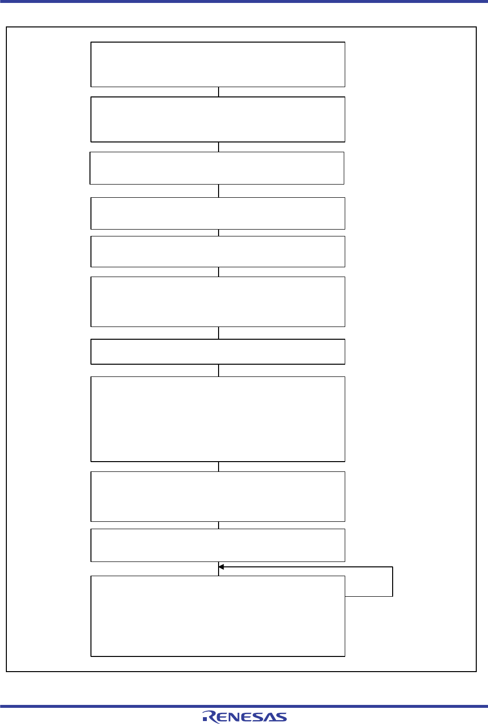
R01UH0034EJ0200 Rev.2.00 Page 810 of 1489
Dec 27, 2013
RX62T Group, RX62G Group 18. General PWM Timer (GPT/GPTa)
Figure 18.27 Example for Setting GTADTRA and GTADTRB Buffer Operation
Select the count clock with GTCR.TPCS[1:0].
Select count clock
Set the cycle in GTPR.
Set cycle
Set the initial value in the GTCNT register.
Set initial value to counter
Select the count direction (up or down) with the GTUDC register. (In figure
18.24, after 0003h is set in GTUDC, 0001h is set in GTUDC (up-
counting).)
Set count direction
Set the operating mode with GTCR.MD[2:0]. (In figure 18.24, 000b (saw-
wave PWM mode) is set, in figures 18.25 and 18.26, 100b, 101b, or 110b
(triangle-wave PWM mode) is set.)
Set operating mode
Set GTSTR.CST to 1 to start count operation.
Start count operation
For buffer operation, set the A/D converter start request point in one cycle after
the current cycle (in saw-wave mode or triangle-wave mode with buffer transfer
at trough or crest) or half cycle after the current cycle (in triangle-wave mode
with buffer transfer at both trough and crest) in GTADTBRA and GTADTBRB.
For double buffer operation, also set the A/D converter start request point in
two cycles after the current cycle (in saw-wave mode or triangle-wave mode
with buffer transfer at trough or crest) or one cycle after the current cycle (in
triangle-wave mode with buffer transfer at both trough and crest) in
GTADTBRA and GTADTBRB.
Set buffer value
Set the A/D converter start request point in GTADTRA and GTADTRB.
Set compare match value
Set buffer operation with ADTTA[1:0], ADTTB[1:0], ADTDA, and ADTDB
in GTBER. (In figure 18.24, ADTTA[1:0] = 10b or 11b and ADTDA = 0, in
figure 18.25, ADTTA[1:0] = 10b and ADTDA = 1, and in figure 18.26,
ADTTA[1:0] = 11b and ADTDA = 1.)
Set buffer operation
Set to enable A/D converter start requests with ADTRAUEN, ADTRADEN,
ADTRBUEN, and ADTRBDEN in GTINTAD. (In figure 18.24, ADTRAUEN
= 1, in figure 18.25, ADTRADEN = 1, and in figure 18.26, ADTRBUEN = 1
and ADTRBDEN = 1.)
Enable A/D converter start request
For buffer operation, set the A/D converter start request point in one cycle after
the current cycle (in saw-wave mode or triangle-wave mode with buffer transfer
at trough or crest) or half cycle after the current cycle (in triangle-wave mode
with buffer transfer at both trough and crest) in GTADTBRA and GTADTBRB.
For double buffer operation, also set the A/D converter start request point in
two cycles after the current cycle (in saw-wave mode or triangle-wave mode
with buffer transfer at trough or crest) or one cycle after the current cycle (in
triangle-wave mode with buffer transfer at both trough and crest) in
GTADTBRA and GTADTBRB.
Set buffer value for each cycle
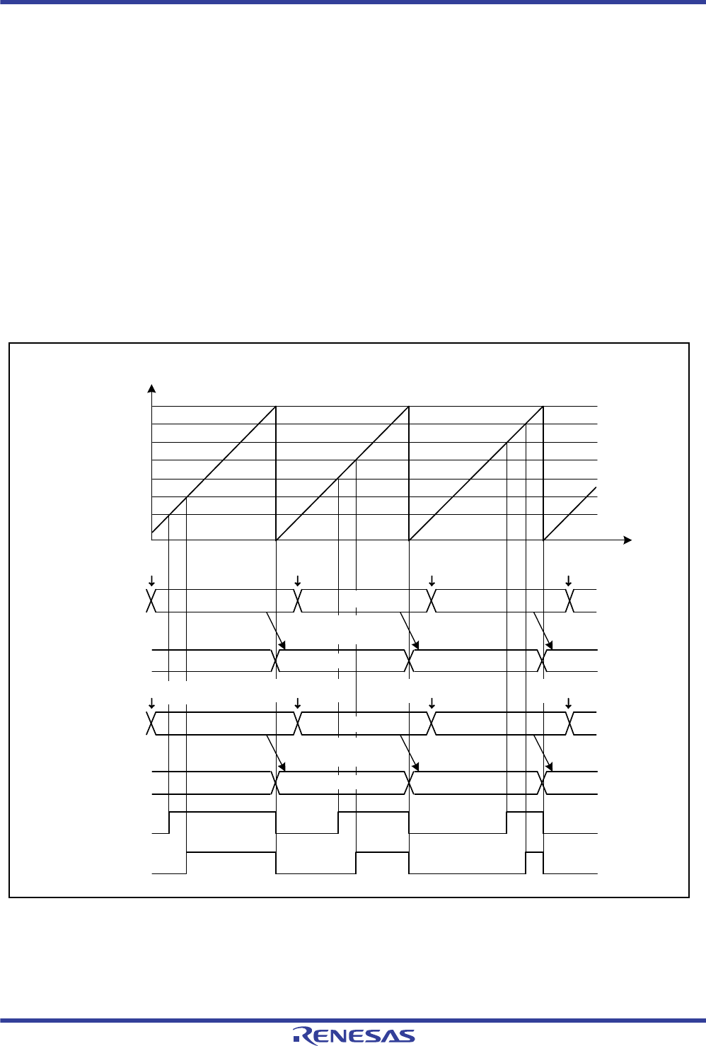
R01UH0034EJ0200 Rev.2.00 Page 811 of 1489
Dec 27, 2013
RX62T Group, RX62G Group 18. General PWM Timer (GPT/GPTa)
18.3.3 PWM Output Operating Mode
The GPT can output PWM waveforms to the GTIOCnA pin or GTIOCnB pin by a compare match between the
GPTn.CTCNT counter and GPTn.GTCCRA or GPTn.GTCCRB (n: channel number). An operating mode can be set
independently for each channel, and synchronized operation on channels is also possible.
By setting GTDTCR, GTDVU, and GTDVD, the compare match value for a negative-phase waveform with dead time
can automatically be set to GTCCRB.
(1) Saw-Wave PWM Mode (GTCR.MD = 000b)
In saw-wave PWM mode, GPTn.GTCNT performs saw-wave (half-wave) operation by setting the cycle in GTPR and a
PWM waveform is output to the GTIOCnA or GTIOCnB pin when a GPTn.GTCCRA or GPTn.GTCCRB compare
match occurs (n: channel number). The pin output value can be selected from low output, high output, or toggle output
separately for a compare match and for the cycle end according to the GTIOR setting
Figure 18.28 shows an example of saw-wave PWM mode operation, and Figure 18.29 shows an example for setting
saw-wave PWM mode.
Figure 18.28 Example of Saw-Wave PWM Mode Operation (Up-Count Operation, Buffer Operation, High Output
at GTCCRA/GTCCRB Compare Match, Low Output at Cycle End)
aaaa
bbbb
eeee
Buffer transfer
at overflow
Register write
GPT0.GTCNT value
dddd
aaaa
bbbb
cccc
GPT0.GTPR
0000h
dddd
GPT0.GTCCRE
GTIOC0A output
Time
eeee
ffff
GPT0.GTCCRB
GTIOC0B output
GPT0.GTCCRA
GPT0.GTCCRC
Register write Register write Register write
Buffer transfer
at overflow Buffer transfer
at overflow
Buffer transfer
at overflow Buffer transfer
at overflow Buffer transfer
at overflow
Register write Register write Register writeRegister write
cccc
cccc
dddd
ffff
ffff
eeee
R01UH0034EJ0200 Rev.2.00 Page 812 of 1489
Dec 27, 2013
RX62T Group, RX62G Group 18. General PWM Timer (GPT/GPTa)
Figure 18.29 Example for Setting Saw-Wave PWM Mode
Select the count clock with GTCR.TPCS[1:0].
Select count clock
Set the cycle in GTPR.
Set cycle
Set the initial value in the GTCNT register.
Set initial value to counter
Select the count direction (up or down) with the GTUDC register. (In figure
18.28, after 0003h is set in GTUDC, 0001h is set in GTUDC (up-
counting).)
Set count direction
Set the operating mode with GTCR.MD[2:0]. (In figure 18.28, 000b (saw-
wave PWM mode) is set.)
Set operating mode
Set GTSTR.CST to 1 to start count operation. (In figure 18.28, 1 is set in
GTSTR.CST0.)
Start count operation
For buffer operation, set the GTIOCA pin and GTIOCB pin changing points in
one cycle after the current cycle in GTCCRC and GTCCRE, respectively.
For double buffer operation, also set the GTIOCA pin and GTIOCB pin
changing points in two cycles after the current cycle in GTCCRD and
GTCCRF, respectively.
Set buffer value
Set the GTIOCA pin changing point in GTADTRA and GTIOCB pin
changing point in GTADTRB.
Set compare match value
Set buffer operation with CCRA and CCRB in GTBER. (In figure 18.28,
CCRA = 01b and CCRB = 01b.)
Set buffer operation
For buffer operation, set the GTIOCA pin and GTIOCB pin changing points in
one cycle after the current cycle in GTCCRC and GTCCRE, respectively.
For double buffer operation, also set the GTIOCA pin and GTIOCB pin
changing points in two cycles after the current cycle in GTCCRD and
GTCCRF, respectively.
Set buffer value for each cycle
Set the GTIOC pin function with GTIOA[5:0] and GTIOB[5:0] in GTIOR. (In
figure 18.28, GTIOA[5:0] = 000110b and GTIOB[5:0] = 000110b.)
Set GTIOC pin function
Set to enable the GTIOC pin output with OAE and OBE in GTONCR.
Enable GTIOC pin output
*1
*1
Note 1: Switch the procedure of "Enable GTIOC pin output" and "Set compare match value"
when the PWM delay generation circuit is in use.

R01UH0034EJ0200 Rev.2.00 Page 813 of 1489
Dec 27, 2013
RX62T Group, RX62G Group 18. General PWM Timer (GPT/GPTa)
(2) Saw-Wave One-Shot Pulse Mode
The saw-wave one-shot pulse mode is a mode in which the cycle is set in GPTn.GTPR, the GPTn.GTCNT counter
performs saw-wave (half-wave) operation and a PWM waveform is output to the GTIOCnA or GTIOCnB pin at a
compare match of GPTn.GTCCRA or GPTn.GTCCRB with buffer operation fixed (n: channel number).
Buffer operation in saw-wave one-shot pulse mode is different from the usual buffer operation. Buffer transfer is
performed from GTCCRC to GTCCRA, from GTCCRE to GTCCRB, from GTCCRD to temporary register A, and from
GTCCRF to temporary register B at the cycle end, and from temporary register A to GTCCRA at a GTCCRA compare
match and from temporary register B to GTCCRB at a GTCCRB compare match. The pin output value can be selected
from low output, high output, or toggle output separately for a compare match and the cycle end according to the GTIOR
setting.
By setting GTDTCR, GTCVU, and GTDVD, a compare match value for a negative-phase waveform with dead time can
automatically be set to GTCCRB.
Figure 18.30 shows an example of saw-wave one-shot pulse mode operation, and Figure 18.31 shows an example for
setting saw-wave one-shot pulse mode.
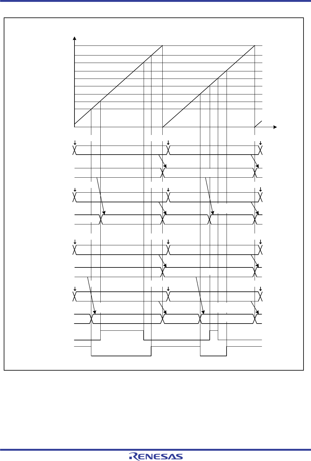
R01UH0034EJ0200 Rev.2.00 Page 814 of 1489
Dec 27, 2013
RX62T Group, RX62G Group 18. General PWM Timer (GPT/GPTa)
Figure 18.30 Example of Saw-Wave One-Shot Pulse Mode Operation (Up-Count Operation, Low Output from
GTIOC0A and High Output from GTIOC0B at Count Start, Toggle Output at GTCCRA/GTCCRB
Compare Match, Output Retained at Cycle End)
aaaa
bbbb
cccc
Buffer transfer
at overflow
Register write
GPT0.GTCNT value
dddd
aaaa
bbbb
cccc
GPT0.GTPR
0000h
dddd
Time
eeee
ffff
gggg
hhhh
GPT0.GTCCRE
GTIOC0A output
GPT0.GTCCRB
GTIOC0B output
GPT0.GTCCRA
GPT0.GTCCRC
Temporary register A
GPT0.GTCCRD
Temporary register B
GPT0.GTCCRF
Register write Register write
Register write Register write Register write
Register write Register write Register write
Register write Register write Register write
Buffer transfer
at overflow
Buffer transfer at
compare match Buffer transfer at
compare match Buffer transfer
at overflow
Buffer transfer
at overflow
Buffer transfer
at overflow
Buffer transfer at
compare match Buffer transfer at
compare match Buffer transfer
at overflow
cccc
eeee
ffff
gggg
hhhh
eeee
dddd
gggg eeee
ffff
hhhh ffff
Buffer transfer
at overflow
R01UH0034EJ0200 Rev.2.00 Page 815 of 1489
Dec 27, 2013
RX62T Group, RX62G Group 18. General PWM Timer (GPT/GPTa)
Figure 18.31 Example for Setting Saw-Wave One-Shot Pulse Mode
Select the count clock with GTCR.TPCS[1:0].
Select count clock
Set the cycle in GTPR.
Set cycle
Set the initial value in the GTCNT register.
Set initial value to counter
Select the count direction (up or down) with the GTUDC register. (In figure
18.30, after 0003h is set in GTUDC, 0001h is set in GTUDC (up-
counting).)
Set count direction
Set the operating mode with GTCR.MD[2:0]. (In figure 18.30, 001b (saw-
wave one-shot pulse mode) is set.)
Set operating mode
Set GTSTR.CST to 1 to start count operation. (In figure 18.30, 1 is set in
GTSTR.CST0.)
Start count operation
Set the GTIOCA pin changing point in one cycle after the current cycle in
GTCCRC and GTCCRD and the GTIOCB pin changing point in GTCCRE and
GTCCRF.
Set buffer value
Set GTBER.CCRSWT to 1 to transfer buffer register data forcibly.
Set forcible buffer transfer
Set the GTIOCA pin changing point immediately after the count start in
GTCCRC and GTCCRD and the GTIOCB pin changing point in GTCCRE and
GTCCRF.
Set buffer value
Set the GTIOCA pin changing point in one cycle after the current cycle in
GTCCRC and GTCCRD and the GTIOCB pin changing point in GTCCRE and
GTCCRF.
Set buffer value for each cycle
Set the GTIOC pin function with GTIOA[5:0] and GTIOB[5:0] in GTIOR. (In
figure 18.30, GTIOA[5:0] = 000011b and GTIOB[5:0] = 010011b.)
Set GTIOC pin function
Set to enable the GTIOC pin output with OAE and OBE in GTONCR.
Enable GTIOC pin output
*1
*1
Note 1: Switch the procedure of "Enable GTIOC pin output" and "Set compare match value"
when the PWM delay generation circuit is in use.
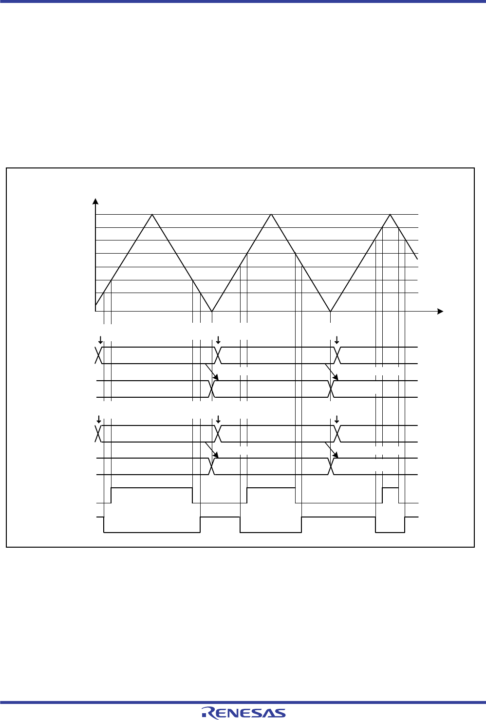
R01UH0034EJ0200 Rev.2.00 Page 816 of 1489
Dec 27, 2013
RX62T Group, RX62G Group 18. General PWM Timer (GPT/GPTa)
(3) Triangle-Wave PWM Mode 1 (16-Bit Transfer at Trough)
The triangle-wave PWM mode 1 is a mode in which the cycle is set in GPTn.GTPR, the GPTn.GTCNT counter performs
triangle-wave (full-wave) operation, and a PWM waveform is output to the GTIOCnA or GTIOCnB pin when a
GPTn.GTCCRA or GPTn.GTCCRB compare match occurs (n: channel number). Buffer transfer is performed at the
trough. The pin output value can be selected from low output, high output, or toggle output separately for a compare
match and for the cycle end according to the GTIOR setting.
By setting GTDTCR, GTCVU, and GTDVD, a compare match value for a negative-phase waveform with dead time can
automatically be set to GTCCRB.
Figure 18.32 shows an example of triangle-wave PWM mode 1 operation, and Figure 18.33 shows an example for
setting triangle-wave PWM mode 1.
Figure 18.32 Example of Triangle-Wave PWM Mode 1 Operation (Buffer Operation, Low Output from GTIOC0A
and High Output from GTIOC0B at Count Start, Toggle Output at GTCCRA/GTCCRB Compare
Match, Output Retained at Cycle End)
aaaa
bbbb
cccc
Register write
GPT0.GTCNT value
Buffer transfer at
trough
dddd
aaaa
bbbb
cccc
GPT0.GTPR
0000h
dddd
GTIOC0A output
Time
eeee
ffff
Register write Register write
Register write Register write Register write
dddd
cccc
Buffer transfer at
trough
Buffer transfer at
trough
Buffer transfer at
trough
eeee
eeee
ffff
ffff
GPT0.GTCCRA
GPT0.GTCCRC
GPT0.GTCCRE
GPT0.GTCCRB
GTIOC0B output
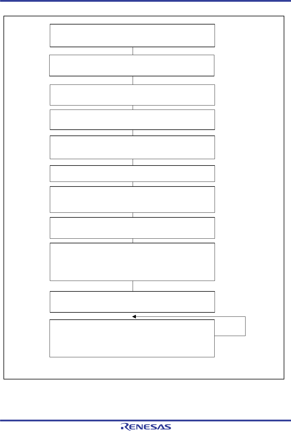
R01UH0034EJ0200 Rev.2.00 Page 817 of 1489
Dec 27, 2013
RX62T Group, RX62G Group 18. General PWM Timer (GPT/GPTa)
Figure 18.33 Example for Setting Triangle-Wave PWM Mode 1
Select the count clock with GTCR.TPCS[1:0].
Select count clock
Set the cycle in GTPR.
Set cycle
Set the initial value in the GTCNT register.
Set initial value to counter
Set the operating mode with GTCR.MD[2:0].
(In figure 18.32, 100b (triangle-wave PWM mode 1) is set.)
Set operating mode
Set GTSTR.CST to 1 to start count operation. (In figure 18.32, 1 is set in
GTSTR.CST0.)
Start count operation
For buffer operation, set the GTIOCA pin and GTIOCB pin changing points in
one cycle after the current cycle in GTCCRC and GTCCRE, respectively.
For double buffer operation, also set the GTIOCA pin and GTIOCB pin
changing points in two cycles after the current cycle in GTCCRD and
GTCCRF, respectively.
Set buffer value
Set the GTIOCA pin and GTIOCB pin changing points in GTCCRA and
GTCCRB, respectively.
Set compare match value
Set buffer operation with CCRA and CCRB in GTBER. (In figure 18.32, CCRA
= 01b and CCRB = 01b.)
Set buffer operation
For buffer operation, set the GTIOCA pin and GTIOCB pin changing points in
one cycle after the current cycle in GTCCRC and GTCCRE, respectively.
For double buffer operation, also set the GTIOCA pin and GTIOCB pin
changing points in two cycles after the current cycle in GTCCRD and
GTCCRF, respectively.
Set buffer value for each cycle
Set the GTIOC pin function with GTIOA[5:0] and GTIOB[5:0] in GTIOR. (In
figure 18.32, GTIOA[5:0] = 000011b and GTIOB[5:0] = 010011b.)
Set GTIOC pin function
Set to enable the GTIOC pin output with OAE and OBE in GTONCR.
Enable GTIOC pin output
*1
*1
Note 1: Switch the procedure of "Enable GTIOC pin output" and "Set compare match value"
when the PWM delay generation circuit is in use.
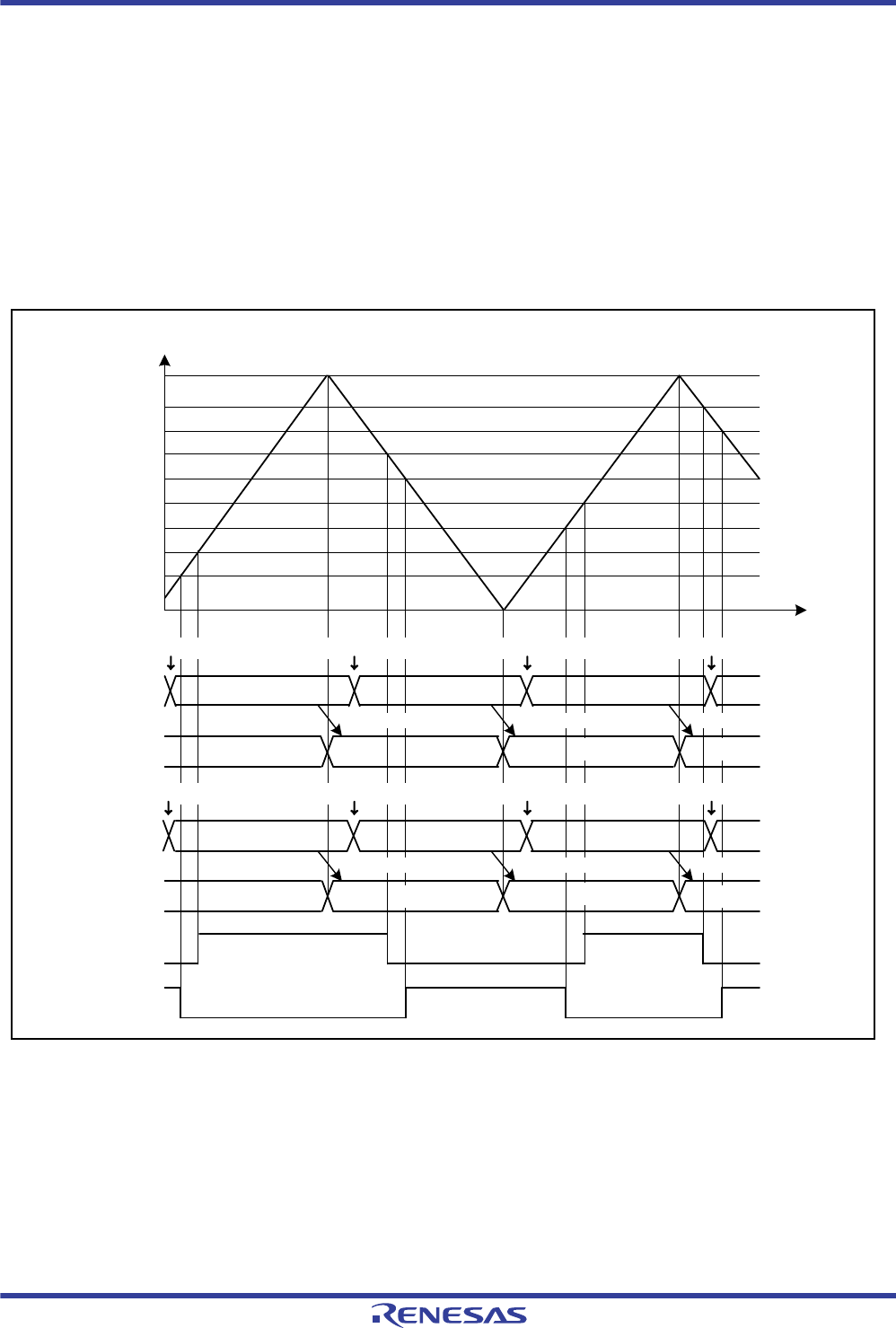
R01UH0034EJ0200 Rev.2.00 Page 818 of 1489
Dec 27, 2013
RX62T Group, RX62G Group 18. General PWM Timer (GPT/GPTa)
(4) Triangle-Wave PWM Mode 2 (16-Bit Transfer at Crest and Trough)
Similarly to triangle-wave PWM mode 1, in triangle-wave PWM mode 2 the cycle is set in GPTn.GTPR, the
GPTn.GTCNT counter performs triangle-wave (full-wave) operation, and a PWM waveform is output to the GTIOCnA
or GTIOCnB pin when a GPTn.GTCCRA or GPTn.GTCCRB compare match occurs (n: channel number). The buffer
transfer is performed at both crests and troughs. The pin output value can be selected from low output, high output, or
toggle output separately for a compare match and for the cycle end according to the GTIOR setting.
By setting GTDTCR, GTCVU, and GTDVD, a compare match value for a negative-phase waveform with dead time can
automatically be set to GTCCRB.
Figure 18.34 shows an example of triangle-wave PWM mode 2 operation, and Figure 18.35 shows an example for
setting triangle-wave PWM mode 2.
Figure 18.34 Example of Triangle-Wave PWM Mode 2 Operation (Buffer Operation, Low Output from GTIOC0A
and High Output from GTIOC0B at Count Start, Toggle Output at GTCCRA/GTCCRB Compare
Match, Output Retained at Cycle End)
aaaa
bbbb
cccc
Register write
GPT0.GTCNT value
Buffer transfer at
trough Buffer transfer at
crest
dddd
aaaa
bbbb
cccc
GPT0.GTPR
0000h
dddd
Time
GPT0.GTCCRE
GTIOC0A output
GPT0.GTCCRB
GTIOC0B output
GPT0.GTCCRA
GPT0.GTCCRC
eeee
ffff
gggg
hhhh
Register write Register write Register write
Register write Register write Register write Register write
Buffer transfer at
crest
Buffer transfer at
trough Buffer transfer at
crest
Buffer transfer at
crest
eeee
ffff
gggg
hhhh
hhhhffff
dddd
eeee cccc gggg
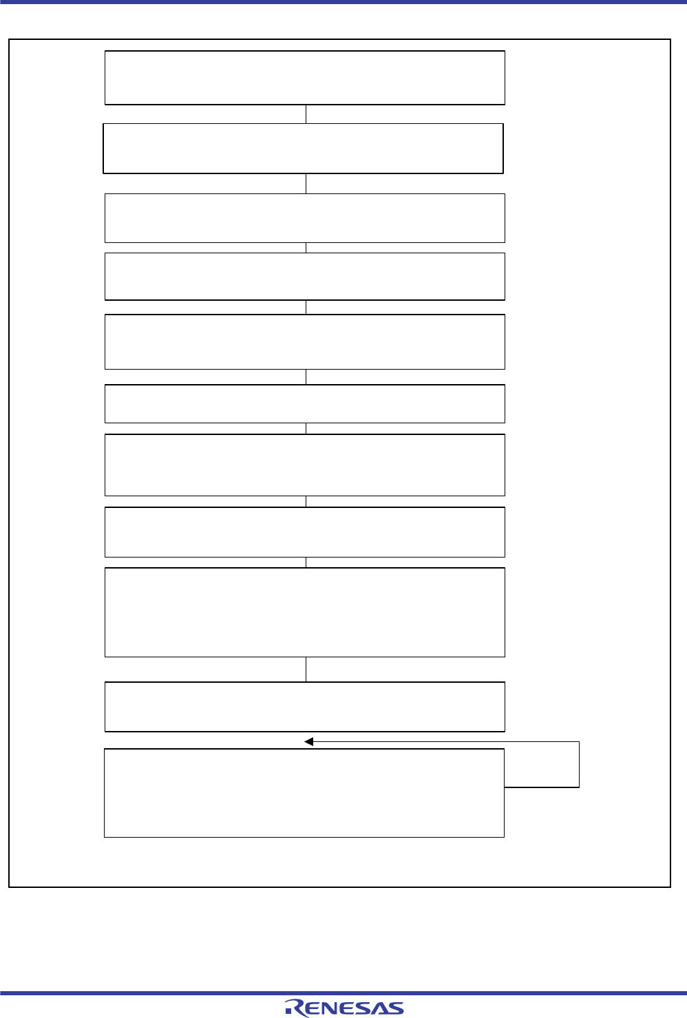
R01UH0034EJ0200 Rev.2.00 Page 819 of 1489
Dec 27, 2013
RX62T Group, RX62G Group 18. General PWM Timer (GPT/GPTa)
Figure 18.35 Example for Setting Triangle-Wave PWM Mode 2
Select the count clock with GTCR.TPCS[1:0].
Select count clock
Set the cycle in GTPR.
Set cycle
Set the initial value in the GTCNT register.
Set initial value to counter
Set the operating mode with GTCR.MD[2:0].
(In figure 18.34, 101b (triangle-wave PWM mode 2) is set.)
Set operating mode
Set GTSTR.CST to 1 to start the count operation. (In figure 18.34, 1 is set
in GTSTR.CST0.)
Start count operation
For buffer operation, set the GTIOCA pin and GTIOCB pin changing points in
half cycle after the current cycle in GTCCRC and GTCCRE, respectively.
For double buffer operation, also set the GTIOCA pin and GTIOCB pin
changing points in one cycle after the current cycle in GTCCRD and GTCCRF,
respectively.
Set buffer value
Set the GTIOCA pin and GTIOCB pin changing points in GTCCRA and
GTCCRB, respectively.
Set compare match value
Set buffer operation with CCRA and CCRB in GTBER. (In figure 18.34, CCRA
= 01b and CCRB = 01b.)
Set buffer operation
For buffer operation, set the GTIOCA pin and GTIOCB pin changing points in
half cycle after the current cycle in GTCCRC and GTCCRE, respectively.
For double buffer operation, also set the GTIOCA pin and GTIOCB pin
changing points in one cycle after the current cycle in GTCCRD and GTCCRF,
respectively.
Set buffer value for each half cycle
Set the GTIOC pin function with GTIOA[5:0] and GTIOB[5:0] in GTIOR. (In
figure 18.34, GTIOA[5:0] = 000011b and GTIOB[5:0] = 010011b.)
Set GTIOC pin function
Set to enable the GTIOC pin output with OAE and OBE in GTONCR.
Enable GTIOC pin output
*1
*1
Note 1: Switch the procedure of "Enable GTIOC pin output" and "Set compare match value"
when the PWM delay generation circuit is in use.

R01UH0034EJ0200 Rev.2.00 Page 820 of 1489
Dec 27, 2013
RX62T Group, RX62G Group 18. General PWM Timer (GPT/GPTa)
(5) Triangle-Wave PWM Mode 3 (32-Bit Transfer at Trough)
The triangle-wave PWM mode 3 is a mode in which the cycle is set in GPTn.GTPR, the GPTn.GTCNT counter performs
triangle-wave (full-wave) operation and a PWM waveform is output to the GTIOCnA or GTIOCnB pin at a compare
match of GPTn.GTCCRA or GPTn.GTCCRB with buffer operation fixed (n: channel number). Buffer operation in
triangle-wave PWM mode 3 is different from the usual buffer operation. Buffer transfer is performed from GTCCRC to
GTCCRA, from GTCCRE to GTCCRB, from GTCCRD to temporary register A, and from GTCCRF to temporary
register B at the trough, and from temporary register A to GTCCRA and from temporary register B to GTCCRB at the
crest. The pin output value can be selected from low output, high output, or toggle output separately for a compare match
and for the cycle end according to the GTIOR setting.
By setting GTDTCR, GTCVU, and GTDVD, a compare match value for a negative-phase waveform with dead time can
automatically be set to GTCCRB.
Figure 18.36 shows an example of triangle-wave PWM mode 3 operation, and Figure 18.37 shows an example for
setting triangle-wave PWM mode 3.
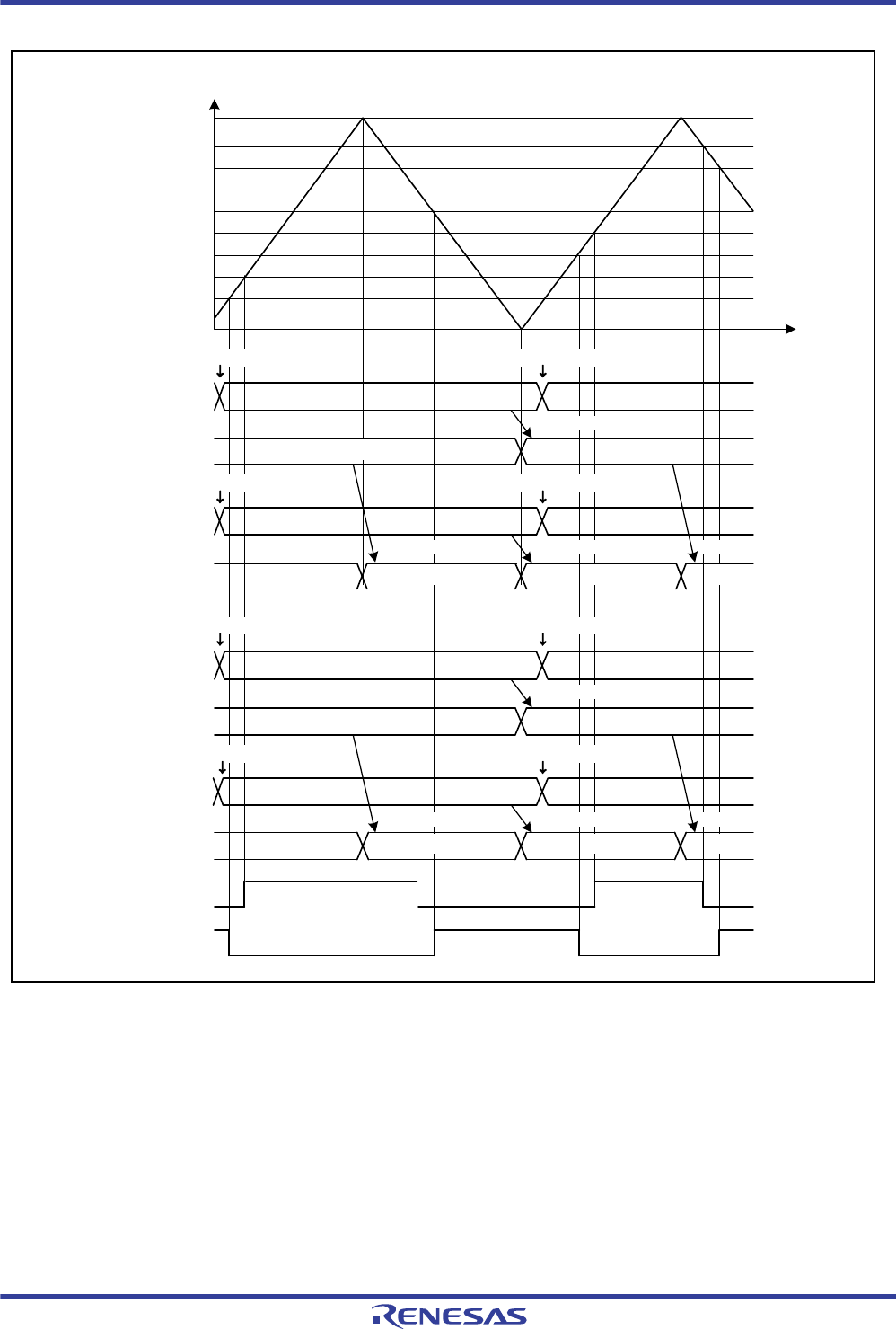
R01UH0034EJ0200 Rev.2.00 Page 821 of 1489
Dec 27, 2013
RX62T Group, RX62G Group 18. General PWM Timer (GPT/GPTa)
Figure 18.36 Example of Triangle-Wave PWM Mode 3 Operation (Low Output from GTIOC0A and High Output
from GTIOC0B at Count Start, Toggle Output at GTCCRA/GTCCRB Compare Match,
Output Retained at Cycle End)
GPT0.GTCCRF
GTIOC0A output
GPT0.GTCCRB
GTIOC0B output
GPT0.GTCCRA
GPT0.GTCCRC
aaaa
bbbb
cccc
GPT0.GTPR
0000h
dddd
eeee
ffff
gggg
hhhh
GPT0.GTCNT value
Register write
Buffer transfer at
crest Buffer transfer at
trough
Time
GPT0.GTCCRE
Temporary register B
Temporary register A
GPT0.GTCCRD
Register write
Register write Register write
Register write Register write
Register write Register write
Buffer transfer at
crest
Buffer transfer at
crest Buffer transfer at
trough Buffer transfer at
crest
Buffer transfer at
trough
Buffer transfer at
trough
aaaa
bbbb
cccc
dddd
eeee
ffff
gggg
hhhh
hhhh
dddd
ffff hhhh
gggg
eeee cccc gggg
R01UH0034EJ0200 Rev.2.00 Page 822 of 1489
Dec 27, 2013
RX62T Group, RX62G Group 18. General PWM Timer (GPT/GPTa)
Figure 18.37 Example for Setting Triangle-Wave PWM Mode 3
Select the count clock with GTCR.TPCS[1:0].
Select count clock
Set the cycle in GTPR.
Set cycle
Set the initial value in the GTCNT register.
Set initial value to counter
Set the operating mode with GTCR.MD[2:0].
(In figure 18.36, 110b (triangle-wave PWM mode 3) is set.)
Set operating mode
Set GTSTR.CST to 1 to start count operation. (In figure 18.36, 1 is set in
GTSTR.CST0.)
Start count operation
Set the GTIOCA pin changing point in one cycle after the current cycle in
GTCCRC and GTCCRD and the GTIOCB pin changing point in GTCCRE and
GTCCRF.
Set buffer value
Set GTBER.CCRSWT to 1 to transfer buffer register data forcibly.
Set forcible buffer transfer
Set the GTIOCA pin changing point immediately after the count start in
GTCCRC and GTCCRD and the GTIOCB pin changing point in GTCCRE and
GTCCRF.
Set buffer value
Set the GTIOCA pin changing point in one cycle after the current cycle in
GTCCRC and GTCCRD and the GTIOCB pin changing point in GTCCRE and
GTCCRF.
Set buffer value for each cycle
Set the GTIOC pin function with GTIOA[5:0] and GTIOB[5:0] in GTIOR. (In
figure 18.36, GTIOA[5:0] = 000011b and GTIOB[5:0] = 010011b.)
Set GTIOC pin function
Set to enable the GTIOC pin output with OAE and OBE in GTONCR.
Enable GTIOC pin output
*1
*1
Note 1: Switch the procedure of "Enable GTIOC pin output" and "Set compare match value"
when the PWM delay generation circuit is in use.
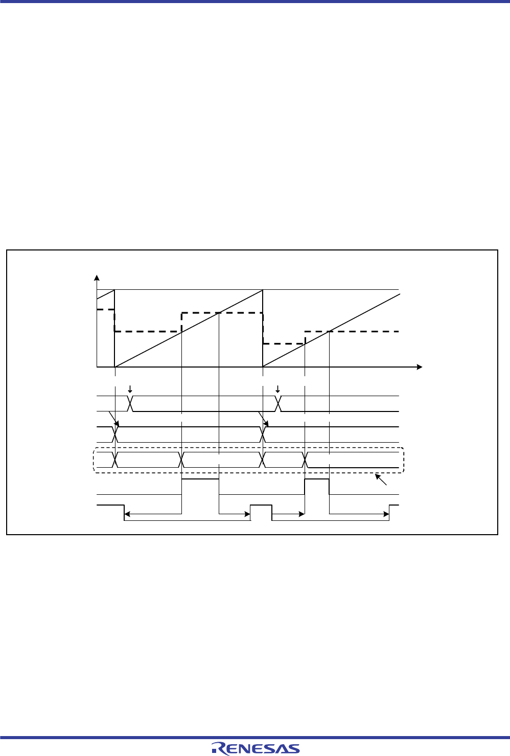
R01UH0034EJ0200 Rev.2.00 Page 823 of 1489
Dec 27, 2013
RX62T Group, RX62G Group 18. General PWM Timer (GPT/GPTa)
18.3.4 Automatic Dead Time Setting Function
By setting GTDTCR, a compare match value for a negative waveform with dead time obtained by a compare match
value for a positive waveform (GTCCRA value) and specified dead time values (GTDVU and GTDVD values) can
automatically be set to GTCCRB.
The automatic dead time setting function can be used in saw-wave one-shot pulse mode and all the triangle PWM modes.
Dead time can be separately set for the first half and second half of a waveform. Dead time for the changing point in the
first half of a negative waveform is set in GTDVU and that in the second half is set in GTDVD. The same dead time can
also be set for the first and second halves.
GTDBU can be used as a buffer register of GTDVU, and GTDBD can be used as a buffer register of GTDVD. Buffer
transfer is performed at the cycle end (at a GTCNT overflow (during up-count operation) or an underflow (during down-
count operation) for saw waves and at the trough for triangle waves).
Writing to GTCCRB is prohibited when the automatic dead time setting function is used. Dead time setting beyond the
cycle is also prohibited. Values for automatic dead time setting can be read from GTCCRB.
Figure 18.38 to Figure 18.40 show examples of automatic dead time setting function operation. Figure 18.41 and
17.42 show the setting examples.
Figure 18.38 Example of Automatic Dead Time Setting Function Operation (Saw-Wave One-Shot Pulse Mode,
GTDVU and GTDVD Set to Buffer Operation, Active Level: High)
Register write
Buffer transfer at overflowBuffer transfer at overflow
Register write
Time
GTDVU and GTDVD values are
automatically set as dead time.
GTDVU GTDVD GTDVU GTDVD
GTCCRA-GTDVU GTCCRA+GTDVD GTCCRA
-GTDVU GTCCRA+GTDVD
GTIOC0B output
GTIOC0A output
GPT0.GTCCRB
(Automatic setting)
GPT0.GTDVU/D
GPT0.GTDBU/D
GPT0.GTCCRA
0000h
GPT0.GTPR
GPT0.GTCNT value
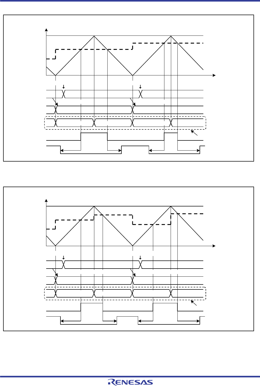
R01UH0034EJ0200 Rev.2.00 Page 824 of 1489
Dec 27, 2013
RX62T Group, RX62G Group 18. General PWM Timer (GPT/GPTa)
Figure 18.39 Example of Automatic Compare-Match Value Setting Function with Dead Time (Triangle-Wave
PWM Mode 1, GTDVU and GTDVD Set to Buffer Operation, Active Level: High)
Figure 18.40 Example of Automatic Compare-Match Value Setting Function with Dead Time (Triangle-Wave
PWM Mode 2 or 3, GTDVU and GTDVD Set to Buffer Operation, Active Level: High)
GTIOC0B output
GTIOC0A output
GPT0.GTCCRB
(Automatic setting)
GPT0.GTDVU/D
GPT0.GTDBU/D
GPT0.GTCCRA
0000h
GPT0.GTPR
GPT0.GTCNT value
Register write
Buffer transfer at troughBuffer transfer at trough
Register write
Time
GTDVU and GTDVD values are
automatically set as dead time.
GTDVU GTDVD
GTCCRA-GTDVU GTCCRA-GTDVD
GTDVD GTDVU
GTCCRA-GTDVU GTCCRA
-GTDVD
GTIOC0B output
GTIOC0A output
GPT0.GTCCRB
(Automatic setting)
GPT0.GTDVU/D
GPT0.GTDBU/D
GPT0.GTCCRA
0000h
GPT0.GTPR
GPT0.GTCNT value
Buffer transfer at overflowBuffer transfer at overflow
Register writeRegister write
GTCCRA-GTDVU GTCCRA-GTDVD GTCCRA-GTDVU GTCCRA
-GTDVD
GTDVU and GTDVD values are
automatically set as dead time.
GTDVU GTDVDGTDVD GTDVU
Time
R01UH0034EJ0200 Rev.2.00 Page 825 of 1489
Dec 27, 2013
RX62T Group, RX62G Group 18. General PWM Timer (GPT/GPTa)
Figure 18.41 Example for Setting Automatic Dead Time Setting Function (Saw-Wave One-Shot Pulse Mode,
Triangle-Wave PWM Mode 3)
Select count clock
Select the count clock with GTCR.TPCS[1:0].
Set cycle
Set the cycle in GTPR.
Set GTIOC pin function
Set the GTIOC pin function with GTIOA[5:0] and GTIOB[5:0] in GTIOR.
(In figures 18.38 and 18.40, GTIOA[5:0] = 000011b and GTIOA[5:0] = 010011b.)
Enable GTIOC pin output
Set to enable the GTIOC pin output with OAE and OBE in GTONCR.
Set buffer value for compare match
Set the GTIOCA pin changing point immediately after the count start in GTCCRC and
GTCCRD.
Set count direction
Select the count direction (up or down) with the GTUDC register.
(In figure 18.38, after 0003h is set in GTUDC, 0001h is set in GTUDC (up-counting).)
Set operating mode
Set the operating mode with GTCR.MD[2:0].
(In figure 18.38, 001b (saw-wave one-shot pulse mode) is set. In figure 18.40, 110b
(triangle-wave PWM mode 3) is set.)
Set initial value for counter
Set the initial value in the GTCNT register.
Set dead time value
Set the first half dead time value in GTDVU and the second half dead time in GTDVD.
When GTDVU is set with GTDTCR.TDDEU set to 1, the same value is also set to GTDVD;
the same dead time value can be set for the first and second halves.
Set buffer operation for dead time setting
Set buffer operation with TDBUE and TDBDE in GTDTCR.
Set automatic dead time setting function
Set GTDTCR.TDE to 1 to enable the automatic dead time setting function.
Set buffer value for compare match
Set the GTIOCA pin changing point in one cycle after the current cycle in GTCCRC and
GTCCRD.
Set forcible buffer transfer for compare match
Set GTBER.CCRSWT to 1 to transfer buffer register data forcibly to GTCCRA.
Set buffer value for each cycle
Set the GTIOCA pin changing point in one cycle after the current cycle in GTCCRC and
GTCCRD.
When the dead time register is used as a buffer register, set the first half dead time in one
cycle after the current cycle in GTDBU and the second half dead time in GTDBD.
Start count operation
Set GTSTR.CST to 1 to start count operation.
(In figures 18.38 and 18.40, 1 is set in GTSTR.CST0.)
Set buffer value for dead time
For buffer operation, set the first half dead time in one cycle after the current cycle in
GTDBU and the second half dead time in GTDBD.
*1
*1
Note 1: Switch the procedure of "Enable GTIOC pin output" and "Set compare match value"
when the PWM delay generation circuit is in use.
R01UH0034EJ0200 Rev.2.00 Page 826 of 1489
Dec 27, 2013
RX62T Group, RX62G Group 18. General PWM Timer (GPT/GPTa)
Figure 18.42 Example for Setting Automatic Dead Time Setting Function (Triangle-Wave PWM Mode 1 or 2)
Set cycle
Set the cycle in GTPR.
Set initial value for counter
Set the initial value in the GTCNT register.
Enable GTIOC pin output
Set to enable the GTIOC pin output with OAE and OBE in GTONCR.
Set buffer operation for compare match
Set buffer operation with CCRA in GTBER.
Set compare match value
Set the GTIOCA pin changing point in GTCCRA.
Set buffer value for compare match
For buffer operation, set the GTIOCA pin changing point in one cycle after the current
cycle (in triangle-wave PWM mode 1) or half cycle after the current cycle (in triangle-
wave PWM mode 2) in GTCCRC. For double buffer operation, also set the GTIOCA pin
changing point in two cycles after the current cycle (in triangle-wave PWM mode 1) or
one cycle after the current cycle (in triangle-wave PWM mode 2) in GTCCRD.
Set automatic dead time setting function
Set GTDTCR.TDE to 1 to enable the automatic dead time setting function.
Set buffer value for each cycle
When the compare match register is used for buffer operation, set the GTIOCA pin changing
point in one cycle after the current cycle (in triangle-wave PWM mode 1) or half cycle after the
current cycle (in triangle-wave PWM mode 2) in GTCCRC. When the compare match register
is used for double buffer operation, also set the GTIOCA pin changing point in two cycles
after the current cycle (in triangle-wave PWM mode 1) or one cycle after the current cycle (in
triangle-wave PWM mode 2) in GTCCRD. When the dead time register is used for buffer
operation, set the first half dead time in one cycle after the current cycle in GTDBU and the
second half dead time in GTDBD.
Select count clock
Select the count clock with GTCR.TPCS[1:0].
Set operating mode
Set the operating mode with GTCR.MD[2:0].
(In figure 18.39, 100b (triangle-wave PWM mode 1) is set. In figure 18.40, 101b
(triangle PWM mode 2) is set.)
Set GTIOC pin function
Set the GTIOC pin function with GTIOA[5:0] and GTIOB[5:0] in GTIOR.
(In figures 18.39 and 18.40, GTIOA[5:0] = 000011b and GTIOB[5:0] = 010011b.)
Set buffer operation for dead time setting
Set buffer operation with TDBUE and TDBDE in GTDTCR.
Set dead time value
Set the first half dead time value in GTDVU and the second half dead time in GTDVD.
When GTDVU is set with GTDTCR.TDDEU set to 1, the same value is also set to
GTDVD; the same dead time value can be set for the first and second halves.
Set buffer value for dead time
For buffer operation, set the first half dead time in one cycle after the current cycle
in GTDBU and the second half dead time in GTDBD.
Start count operation
Set GTSTR.CST to 1 to start count operation.
(In figures 18.39 and 18.40, 1 is set in GTSTR.CST0.)
*1
*1
Note 1: Switch the procedure of "Enable GTIOC pin output" and "Set compare match value"
when the PWM delay generation circuit is in use.
R01UH0034EJ0200 Rev.2.00 Page 827 of 1489
Dec 27, 2013
RX62T Group, RX62G Group 18. General PWM Timer (GPT/GPTa)
18.3.5 Count Direction Changing Function
The count direction of the GTCNT counter can be changed by modifying the UD bit in GTUDC.
In saw-wave mode, if the UD bit in GTUDC is modified during count operation, the count direction is changed at an
overflow (when modified during up-count operation) or an underflow (when modified during down-count operation). If
the UD bit is modified while count operation is stopped and the UDF bit is 0, the UD bit modification is not reflected at
the start of counting and the count direction is changed at an overflow or an underflow. If the UDF bit is set to 1 while
count operation is stopped, the UD bit value at that time is reflected at the start of counting.
In triangle-wave mode, the count direction is not changed even though the UD bit in GTUDC is modified during count
operation. Similarly, even though the UD bit is modified while count operation is stopped and UDF bit is 0, the UD bit
value is not reflected to the count operation. If the UDF bit is set to 1 while count operation is stopped, the UD bit value
at that time is reflected at the start of counting.
If the count direction is changed during saw-wave count operation, the GTPR value after the start of up-counting is
reflected to the count cycle during up-count operation and the GTPR value before the start of down-counting is reflected
during down-count operation.
Figure 18.43 shows an example of count direction changing function operation.
Figure 18.43 Example of Count Direction Changing Function Operation (during Buffer Operation)
bbbb
aaaa
Time
0000h
aaaa bbbb
bbbb aaaa
Register write
Register write
Register write
aaaa bbbb
Register write
Register write
bbbb
Up-counting Down-counting Up-counting
Up-counting Down-counting Up-counting
Register write
Register write
GTPR
Buffer transfer at
overflow Buffer transfer at
overflow Buffer transfer at
underflow Buffer transfer at
underflow Buffer transfer at
overflow
GTPBR
GTST.TUCF flag
(Count direction flag)
GTUDC.UD bit
(Count direction setting)
GTCNT value
R01UH0034EJ0200 Rev.2.00 Page 828 of 1489
Dec 27, 2013
RX62T Group, RX62G Group 18. General PWM Timer (GPT/GPTa)
18.3.6 Hardware Start/Stop and Clear Operation
The GTCNT counter can be started, stopped, or cleared by a hardware source in the RX62T/RX62G Group. There are
four hardware sources: GTETRG pin input, comparator detection, GTIOC3A/GTIOC3B pin input, and GTIOC3A/
GTIOC3B internal output (output compare).
The counter can also be cleared by the GTCCRA or GTCCRB input capture.
18.3.6.1 Hardware Start Operation
The GTCNT counter can be started by a hardware source. Select a hardware source to start counting using
GTHSSR.CSHSL, set the changing edge for the hardware source with GTHSCR.CSHW, and then enable to start
counting.
Figure 18.44 shows an example of count start operation by a hardware source. Figure 18.45 shows the setting example.
Figure 18.44 Example of Count Start Operation by Hardware Source
(Started at AN000 Comparator Detection)
Time
GTCNT value
0000h
GTPR
AN000 comparator
detection signal
Count started at the
comparator detection

R01UH0034EJ0200 Rev.2.00 Page 829 of 1489
Dec 27, 2013
RX62T Group, RX62G Group 18. General PWM Timer (GPT/GPTa)
Figure 18.45 Example for Setting Count Start Operation by Hardware Source
Set count direction
Select the count direction (up or down) with the GTUDC register.
(In figure 18 .44, after 0003h is set in GTUDC, 0001h is set in GTUDC (up-
counting).)
Set operating mode
Set the operating mode with GTCR.MD[2:0].
(In figure 18.44, 000b (saw-wave PWM mode) is set.)
Set hardware count start
Select a hardware source for starting count operation with GTHSSR.CSHSL
and set an edge for the hardware source with GTHSCR.CSHW to enable count
start and wait for count start by the hardware source. (In figure 18.44,
GTHSSR.CSHSLn = 0000b and GTHSCR.CSHWn = 11b (n = 0, 1, 2, 3).)
Set cycle
Set the cycle in GTPR.
Select count clock
Select the count clock with GTCR.TPCS[1:0].
Set initial value for counter
Set the initial value in the GTCNT register.
(In figure 18.44, 0000h is set.)
Set hardware source operation
Set operation of the hardware source selected with GTHSSR.CSHSL and start
counting.
(In figure 18.44, AN000 comparator operation is set.)
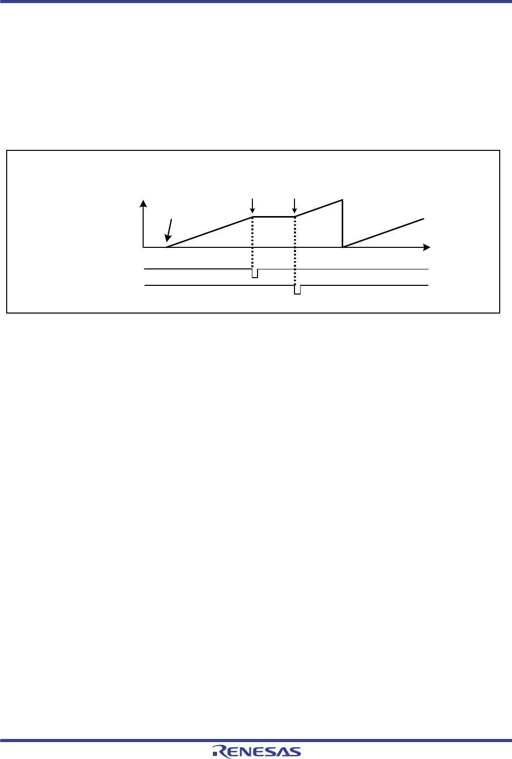
R01UH0034EJ0200 Rev.2.00 Page 830 of 1489
Dec 27, 2013
RX62T Group, RX62G Group 18. General PWM Timer (GPT/GPTa)
18.3.6.2 Hardware Stop Operation
The GTCNT counter can be stopped by a hardware source. Select a hardware source to stop counting using
GTHPSR.CSHPL, set the changing edge for the hardware source with GTHSCR.CPHW, and then enable to stop
counting.
Figure 18.46 shows an example of count stop operation by a hardware source. Figure 18.47 shows the setting example.
In this example, the count operation is stopped at both edges of the GTIOC3A internal output (output compare) and is
restarted at both edges of the GTIOC3B internal output (output compare).
Figure 18.46 Example of Count Stop Operation by Hardware Source (Started by Software, Stopped at GTIOC3A
Internal Output (Output Compare), Restarted at GTIOC3B Internal Output
(Output Compare))
Time
0000h
GTPR
GTCNT valud
Software start
GTIOC3A internal output
(output compare)
GTIOC3B internal output
(output compare)
Count stopped at
GTIOC3A internal
output (output compare)
Count started at
GTIOC3B internal
output (output compare)

R01UH0034EJ0200 Rev.2.00 Page 831 of 1489
Dec 27, 2013
RX62T Group, RX62G Group 18. General PWM Timer (GPT/GPTa)
Figure 18.47 Example for Setting Count Stop Operation by Hardware Source
Set count direction
Select the count direction (up or down) with the GTUDC register.
(In figure 18.46, after 0003h is set in GTUDC, 0001h is set in GTUDC (up-
counting).)
Set operating mode
Set the operating mode with GTCR.MD[2:0].
(In figure 18.46, 000b (saw-wave PWM mode) is set.)
Set hardware count start
Select a hardware source for starting count operation with GTHSSR.CSHSL
and set an edge for the hardware source with GTHSCR.CSHW to enable count
start and wait for count start by the hardware source.
(In figure 18.46, GTHSSR.CSHSLn = 1010b and GTHSCR.CSHWn = 11b (n =
0 to 2).)
Set cycle
Set the cycle in GTPR.
Select count clock
Select the count clock with GTCR.TPCS[1:0].
Set initial value for counter
Set the initial value in the GTCNT register.
(In figure 18.46, 0000h is set.)
Set hardware source operation
Set operation of the hardware source selected with GTHSSR.CSHSL or
GTHPSR.CSHPL and start or stop counting.
(In figure 18.46, GPT3.GTCCRA compare match, GPT3.GTCCRB compare
match, and GPT3.GTIOR bit are set, and then set GTSTR.CST to 1 to start
counting.)
Set hardware count stop
Select a hardware source for stopping count operation with GTHPSR.CSHPL
and set an edge for the hardware source with GTHSCR.CPHW to enable count
stop and wait for count stop by the hardware source.
(In figure 18.46, GTHSSR.CSHPLn = 1011b and GTHSCR.CPHWn = 11b (n =
0 to 2).)
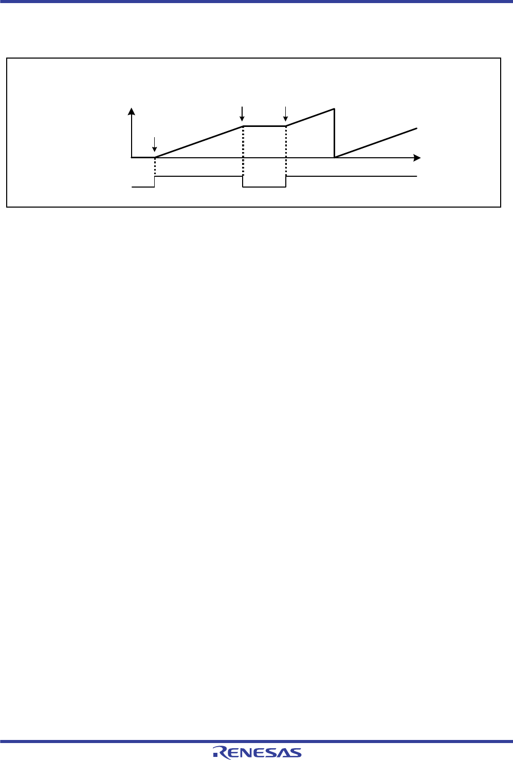
R01UH0034EJ0200 Rev.2.00 Page 832 of 1489
Dec 27, 2013
RX62T Group, RX62G Group 18. General PWM Timer (GPT/GPTa)
Figure 18.48 shows an example of count start/stop operation by a hardware source. Figure 18.49 shows the setting
example. In this example, the counter operates during the high-level periods of the external trigger input GTETRG.
Figure 18.48 Example of Count Start/Stop Operation by Hardware Source (Started at Rising Edge of GTETRG
Pin Input, Stopped at Falling Edge of GTETRG Pin Input)
Time
0000h
GTETRG pin input
GTCNT
value GTPR
Count stopped at
the falling edge of
GTETRG
Count started at
the rising edge
of GTETRG
Count started
at the rising
edge of
GTETRG
R01UH0034EJ0200 Rev.2.00 Page 833 of 1489
Dec 27, 2013
RX62T Group, RX62G Group 18. General PWM Timer (GPT/GPTa)
Figure 18.49 Example for Setting Count Start/Stop Operation by Hardware Source
Set count direction
Select the count direction (up or down) with the GTUDC register.
(In figure 18.48, after 0003h is set in GTUDC, 0001h is set in GTUDC (up-
counting).)
Set operating mode
Set the operating mode with GTCR.MD[2:0].
(In figure 18.48, 000b (saw-wave PWM mode) is set.)
Set hardware count start
Select a hardware source for starting count operation with GTHSSR.CSHSL
and set an edge for the hardware source with GTHSCR.CSHW to enable count
start and wait for count start by the hardware source.
(In figure 18.48, GTHSSR.CSHSLn = 1100b and GTHSCR.CSHWn = 01b (n =
0 to 3).)
Set cycle
Set the cycle in GTPR.
Select count clock
Select the count clock with GTCR.TPCS[1:0].
Set initial value for counter
Set the initial value in the GTCNT register.
(In figure 18.48, 0000h is set.)
Set hardware source operation
Set operation of the hardware source selected with GTHSSR.CSHSL or
GTHPSR.CSHPL and start or stop counting.
(In figure 18.48, the GTETRG pin operation is set.)
Set hardware count stop
Select a hardware source for stopping count operation with GTHPSR.CSHPL
and set an edge for the hardware source with GTHSCR.CPHW to enable count
stop and wait for count stop by the hardware source.
(In figure 18.48, GTHSSR.CSHPLn = 1100b and GTHSCR.CPHWn = 10b (n =
0 to 3).)

R01UH0034EJ0200 Rev.2.00 Page 834 of 1489
Dec 27, 2013
RX62T Group, RX62G Group 18. General PWM Timer (GPT/GPTa)
18.3.6.3 Hardware Clear Operation
The GTCNT counter can be cleared by a hardware source. Select a hardware source to clear the counter using
GTHPSR.CSHPL, set the changing edge for the hardware source with GTHCCR.CCHW, and then enable to clear the
counter.
The counter can also be cleared by a GTCCRA or GTCCRB input capture by setting GTCR.CCLR[1:0].
Note that the GTCIV interrupt (overflow/underflow interrupt) is not generated when the counter is cleared by a hardware
source or by software.
Figure 18.50 and Figure 18.51 show examples of counter clearing operation by a hardware source. Figure 18.52
shows the setting example. In this example, the counter is started at both edges of the GTIOC3A pin, and the counter is
stopped/cleared at both edges of the GTOC3B pin input.
Figure 18.50 Examples of Count Clearing Operation by Hardware Source (Saw-Wave Up-Counting, Started at
GTIOC3A Pin Input, Stopped/Cleared at GTIOC3B Pin Input)
Figure 18.51 Examples of Count Clearing Operation by Hardware Source (Saw-Wave Down-Counting, Started
at GTIOC3A Pin Input, Stopped/Cleared at GTIOC3B Pin Input)
Count started at
GTIOC3A pin input
Count stopped/cleared at
GTIOC3B pin input
Count started at
GTIOC3A pin input
Cleared by software (by
writing 1 to
GTHCCR.CCSW.)
Time
GTIOC3A pin input
GTCNT value
0000h
GTIOC3B pin input
GTIOC3A pin input
Count started at
GTIOC3A pin input Count stopped/cleared at
GTIOC3B pin input Count started at
GTIOC3A pin input
Cleared by software (by
writing 1 to GTHCCR.CCSW)
GTCNT value
0000h
GTPR
Time
GTIOC3B pin input
R01UH0034EJ0200 Rev.2.00 Page 835 of 1489
Dec 27, 2013
RX62T Group, RX62G Group 18. General PWM Timer (GPT/GPTa)
Figure 18.52 Example for Setting Count Clearing Operation by Hardware Source
Set count direction
Select the count direction (up or down) with the GTUDC register.
(In figure 18.50, after 0003h is set in GTUDC, 0001h is set in GTUDC (up-
counting). In figure 18.50, after 0002h is set in GTUDC, 0000h is set in GTUDC
(down-counting).)
Set operating mode
Set the operating mode with GTCR.MD[2:0].
(In figures 18.50 and 18.51, 000b (saw-wave PWM mode) is set.)
Set hardware count start
Select a hardware source for starting count operation with GTHSSR.CSHSL.
Set an edge for the hardware source with GTHSCR.CSHW to enable count
start and wait for count start by the hardware source.
(In figure 18.50, GTHSSR.CSHSLn = 1000b and GTHSCR.CSHWn = 11b (n =
0 to 2).)
Set cycle
Set the cycle in GTPR.
Select count clock
Select the count clock with GTCR.TPCS[1:0].
Set initial value for counter
Set the initial value in the GTCNT register.
(In figure 18.50, 0000h is set. In figure 18.51, the GTPR value is set.)
Set hardware source operation
Set operation of the hardware source selected with GTHSSR.CSHSL or
GTHPSR.CSHPL and start, stop, or clear counting.
(In figure 18.50, the GTIOC3A pin input operation and GTIOC3B pin input
operation are set.)
Set hardware count stop/clear
Select a hardware source for stopping/clearing count operation with
GTHPSR.CSHPL.
Set an edge for the hardware source with GTHSCR.CPHW to enable count
stop and wait for count stop by the hardware source.
Similarly, set an edge for the hardware source with GTHCCR.CCHW to enable
count clear and wait for count clear by the hardware source.
(In figure 18.50, GTHPSR.CSHPLn = 1001b, GTHSCR.CPHWn = 11b, and
GTHCCR.CCHWn = 11b (n = 0 to 2).)
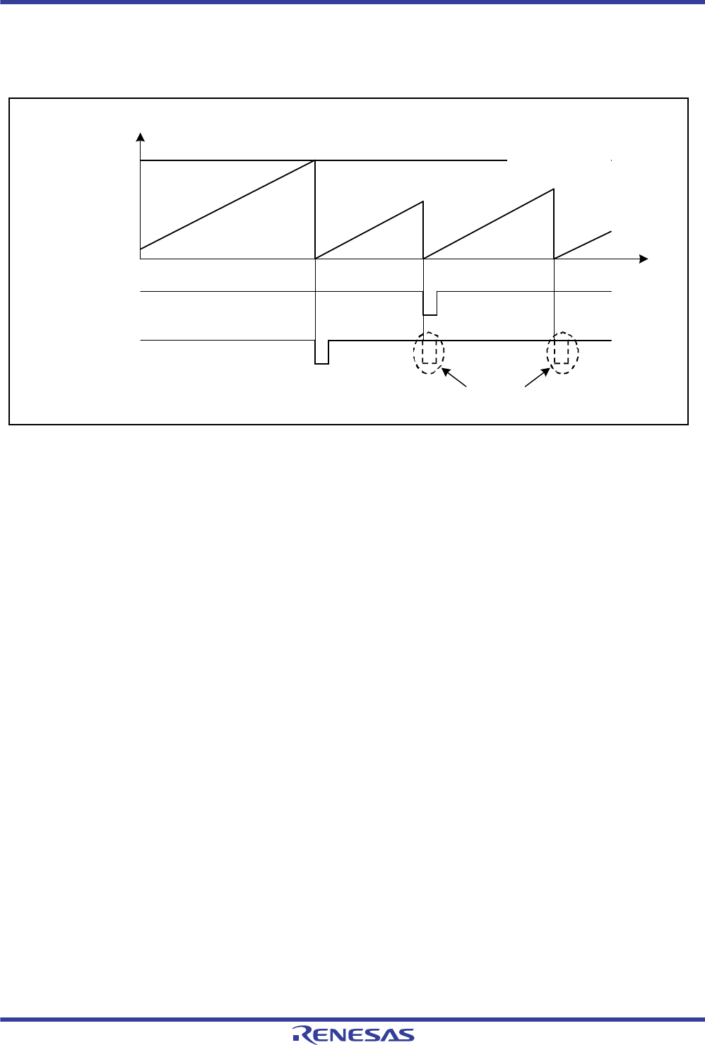
R01UH0034EJ0200 Rev.2.00 Page 836 of 1489
Dec 27, 2013
RX62T Group, RX62G Group 18. General PWM Timer (GPT/GPTa)
The GTCIV interrupt (overflow/underflow interrupt) is not generated when the counter is cleared by a hardware source
or by software.
Figure 18.53 shows the relationship between the counter clearing by a hardware source and the GTCIV interrupt.
Figure 18.53 Relationship between Counter Clearing by Hardware Source and GTCIV Interrupt
Hardware source counter
clear signal
GTCIV interrupt request
GTCNT value
0000h
GTPR
GTCIV interrupt not generated
Time
Counter cleared
at overflow
Counter cleared by
hardware source
Cleared by software (by
writing 1 to
GTHCCR.CCSW)
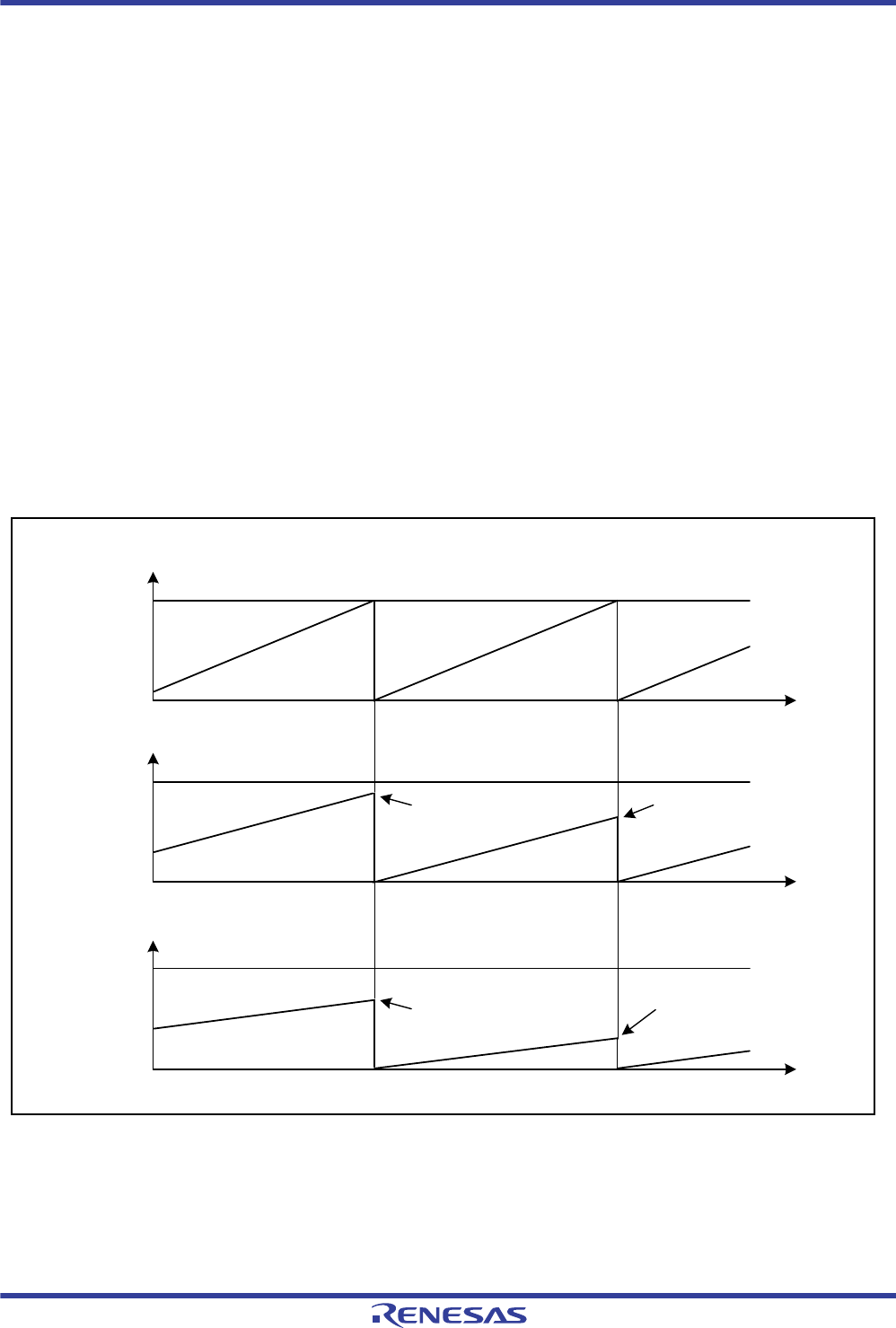
R01UH0034EJ0200 Rev.2.00 Page 837 of 1489
Dec 27, 2013
RX62T Group, RX62G Group 18. General PWM Timer (GPT/GPTa)
18.3.7 Synchronized Operation
Synchronized operation on channels (synchronized clear operation, synchronized start operation) can be performed.
18.3.7.1 Synchronized Clear Operation
Synchronized clearing on channels can be controlled. Select which channels to be synchronously cleared by setting
GTCR.CCLR[1:0] of the pertinent channels to 11b and which channel clearing source to be used for synchronized
clearing by setting GTSYNC.SYNCn[1:0] (n = 0 to 3).
Figure 18.54 shows an example of synchronized clear operation, and Figure 18.56 shows the setting example. In this
example, GPT1.GTCNT and GPT2.GTCNT are synchronously cleared by the GPT0.GTCNT clearing source
(overflow).
Synchronized clearing of channels by a clear source does not cause synchronized clearing of another channel by the same
clear source. (Synchronized clearing is not transmitted.)
Figure 18.55 shows an operation example in which two channels are synchronously cleared by the clear source of one
of the channels and another channel is synchronously cleared by the clear source of the other one of the two channels.
Figure 18.56 shows the setting example. In this example, GPT1.GTCNT is synchronously cleared by GPT0.GTCNT
clearing source (overflow), and GPT2.GTCNT is synchronously cleared by GPT1.GTCNT clearing source (overflow).
Although GPT1.GTCNT is synchronously cleared by the GPT0.GTCNT clearing source (overflow), GPT2.GTCNT is
not synchronously cleared when GPT1.GTCNT is cleared by the GPT0.GTCNT clearing source.
Figure 18.54 Example of Synchronized Clear Operation (GPT1.GTCNT and GPT2.GTCNT are Synchronously
Cleared by GPT0.GTCNT Clearing Source)
Counter cleared at
GPT0.GTCNT overflow
Counter cleared at
GPT0.GTCNT overflow Counter cleared at
GPT0.GTCNT overflow
Counter cleared at
GPT0.GTCNT overflow
Counter cleared
at overflow
Counter cleared
at overflow
Time
Time
GPT0.GTPR
GPT1.GTPR
GPT2.GTPR
GPT2.GTCNT value
GPT1.GTCNT value
GPT0.GTCNT value
Time
0000h
0000h
0000h
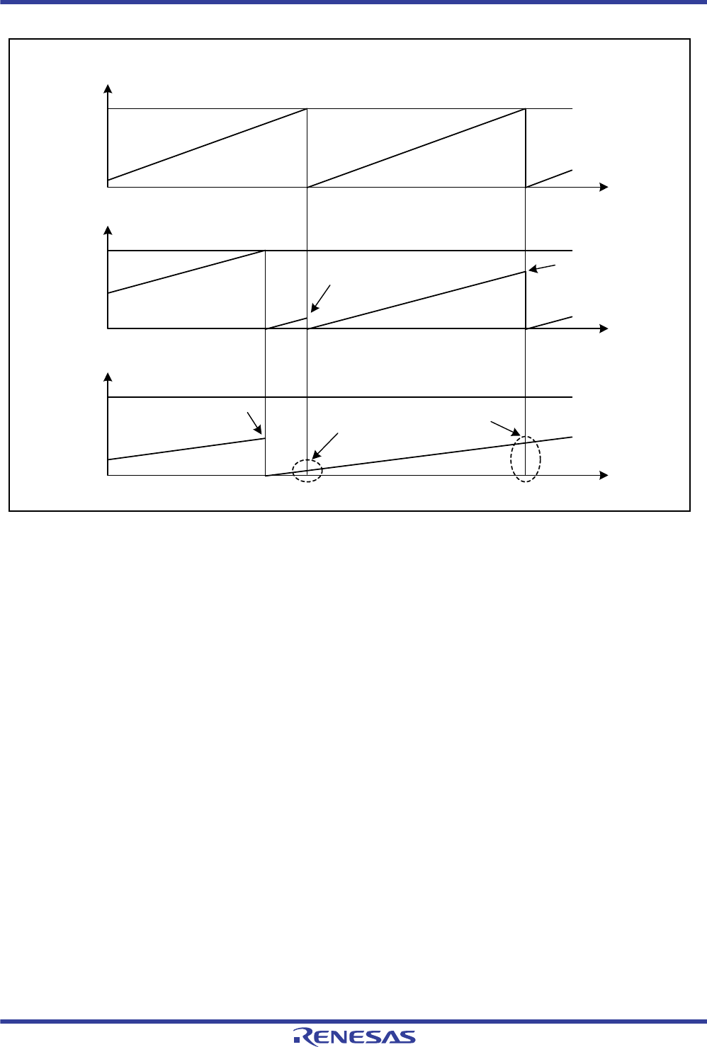
R01UH0034EJ0200 Rev.2.00 Page 838 of 1489
Dec 27, 2013
RX62T Group, RX62G Group 18. General PWM Timer (GPT/GPTa)
Figure 18.55 Example of Synchronized Clear Operation (GPT1.GTCNT is Synchronously Cleared by
GPT0.GTCNT Clearing Source and GPT2.GTCNT is Synchronously Cleared by GPT1.GTCNT
Clearing Source)
Counter cleared at
GPT0.GTCNT overflow
Counter cleared
at overflow
Counter cleared
at overflow
Counter cleared at
GPT0.GTCNT overflow
Time
Time
Time
Synchronized clearing is not
generated by a synchronously-
cleared channel (synchronized
clearing is not transmitted).
Counter cleared at
GPT1.GTCNT overflow
GPT0.GTPR
GPT1.GTPR
GPT2.GTPR
GPT1.GTCNT value
0000h
GPT2.GTCNT value
0000h
0000h
GPT0.GTCNT value
Counter cleared
at overflow
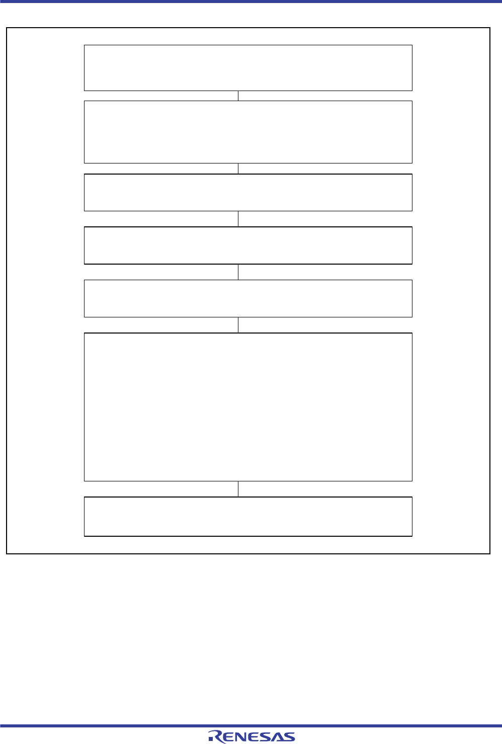
R01UH0034EJ0200 Rev.2.00 Page 839 of 1489
Dec 27, 2013
RX62T Group, RX62G Group 18. General PWM Timer (GPT/GPTa)
Figure 18.56 Example for Setting Synchronized Clear Operation
Set count direction
Select the count direction (up or down) with the GTUDC register of the
corresponding channel.
(In figures 18.54 and 18.55, after 0003h is set in GTUDC, 0001h is set in
GTUDC (up-counting).
Set operating mode
Set the operating mode with GTCR.MD[2:0].
(In figures 18.54 and 18.55, 000b (saw-wave PWM mode) is set.)
Set cycle
Set the cycle in GTPR of the corresponding channel.
Select count clock
Select the count clock with GTCR.TPCS[1:0] of the corresponding channel.
Set synchronized clear
Select a source for clearing the counter with GTCR.CCLR[1:0] of the
corresponding channel. Set 11b in GTCR.CCLR[1:0] of the channel to be
synchronously cleared. Set which channel clearing source to be used for
synchronized clearing with GTSYNC.SYNCn[1:0] (n = 0 to 3).
(In figure 18.54, GPT0.GTCR.CCLR[1:0] = 00b, GPT1.GTCR.CCLR[1:0] = 11b,
GPT2.GTCR.CCLR[1:0] = 11b, GTSYNC.SYNC1[1:0] = 00b, and
GTSYNC.SYNC2[1:0] = 00b.)
(In figure 18.55, GPT0.GTCR.CCLR[1:0] = 00b, GPT1.GTCR.CCLR[1:0] = 11b,
GPT2.GTCR.CCLR[1:0] = 11b, GTSYNC.SYNC1[1:0] = 00b, and
GTSYNC.SYNC2[1:0] = 01b.)
Start count operation
Set GTSTR.CST to 1 to start counting.
Set initial value for counter
Set the initial value in the GTCNT register of the corresponding channel.
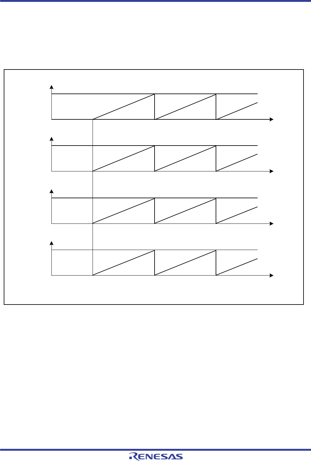
R01UH0034EJ0200 Rev.2.00 Page 840 of 1489
Dec 27, 2013
RX62T Group, RX62G Group 18. General PWM Timer (GPT/GPTa)
18.3.7.2 Synchronized Start Operation
(1) Simultaneous Start by Software
Count operation can be started simultaneously on channels by simultaneously setting the GTSTR.CST bits which
correspond to the channels to be started simultaneously to 1. (n = 0 to 3)
Figure 18.57 shows an example of simultaneous start by software.
Figure 18.57 Example of Simultaneous Start by Software (with Same Count Cycle (GTPR Value))
GPT0.GTPR
GPT1.GTPR
GPT2.GTPR
GPT1.GTCNT value
0000h
GPT3.GTPR
GPT0.GTCNT value
GPT2.GTCNT value
GPT3.GTCNT value
0000h
0000h
0000h Time
Time
Time
Time
Write 000Fh in GTSTR (count operation
started in all the channels)
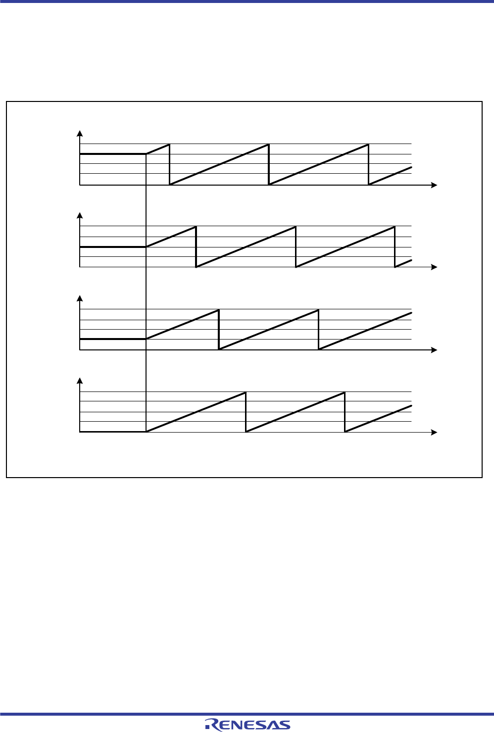
R01UH0034EJ0200 Rev.2.00 Page 841 of 1489
Dec 27, 2013
RX62T Group, RX62G Group 18. General PWM Timer (GPT/GPTa)
(2) Phase Start by Software
Count start with a phase difference is possible by setting the initial value in GCNT before counting starts and then
simultaneously setting the CST bits in GTSTR which correspond to the channels to be started simultaneously to 1. (n = 0
to 3)
Figure 18.58 shows an example of phase start operation by software.
Figure 18.58 Example of Software Phase Start (with Same Count Cycle (GTPR Value))
GPT0.GTPR
GPT1.GTPR
GPT2.GTPR
GPT2.GTCNT value
GPT1.GTCNT value
GPT0.GTCNT value
0000h
0000h
0000h
0000h
GPT3.GTPR
aaaa
bbbb
cccc
aaaa
bbbb
cccc
aaaa
bbbb
cccc
aaaa
bbbb
cccc
GPT3.GTCNT value
Set the initial value.
Set the initial value.
Set initial the value.
Set initial the value.
Write 000Fh in GTSTR. (Start count
operation in all the channels.)
Time
Time
Time
Time
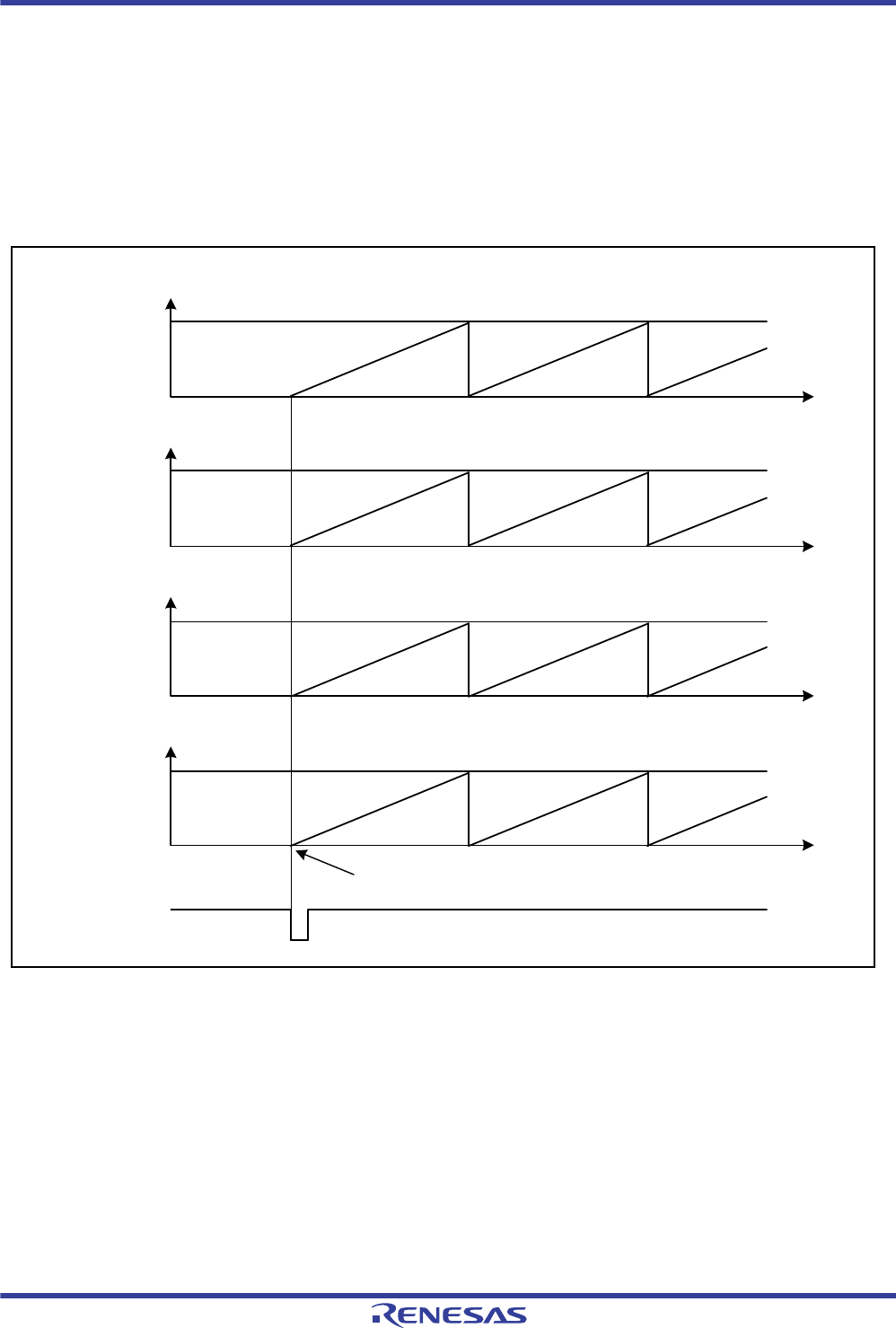
R01UH0034EJ0200 Rev.2.00 Page 842 of 1489
Dec 27, 2013
RX62T Group, RX62G Group 18. General PWM Timer (GPT/GPTa)
(3) Simultaneous Start by Hardware Source
Count operation can be started simultaneously on channels by a hardware source in the RX62T/RX62G Group. There are
four hardware sources: GTETRG pin input, comparator detection, GTIOC3A/GTIOC3B pin input, and GTIOC3A/
GTIOC3B internal output (output compare).
Figure 18.59 shows an example of simultaneous start operation by a hardware source and Figure 18.60 shows the
setting example. In this example, count operation is started in all the channels by the AN000 comparator detection.
Figure 18.59 Example of Simultaneous Start Operation by Hardware Source (with Same Count Cycle (GTPR
Value))
Time
GPT0.GTPR
GPT1.GTPR
GPT2.GTPR
GPT2.GTCNT value
GPT1.GTCNT value
GPT0.GTCNT value
0000h
Time
Time
Time
GPT3.GTCNT value
0000h
0000h
0000h
GPT3.GTPR
AN000 comparator
detection signal
Count operation started in all the channels
by AN000 comparator detection signal.
R01UH0034EJ0200 Rev.2.00 Page 843 of 1489
Dec 27, 2013
RX62T Group, RX62G Group 18. General PWM Timer (GPT/GPTa)
Figure 18.60 Example for Setting Simultaneous Start by Hardware Source
Set operating mode
Set the operating mode with GTCR.MD[2:0] of the corresponding channel.
(In figure 18.59, 000b (saw-wave PWM mode) is set.)
Set count direction
Select the count direction (up or down) with the GTUDC register of the
corresponding channel.
(In figure 18.59 of the corresponding channel, after 0003h is set in GTUDC, 0001h
is set in GTUDC (up-counting).)
Select count clock
Select the count clock with GTCR.TPCS[1:0] of the corresponding channel.
Set cycle
Set the cycle in GTPR of the corresponding channel.
Set initial value for counter
Set the initial value in the GTCNT register of the corresponding channel.
Set hardware count start
Select a hardware source for starting count operation with GTHSSR.CSHSL and
set an edge for the hardware source with GTHSCR.CSHW to enable count start
and wait for count start by the hardware source.
(In figure 18.59, GTHSSR.CSHSL0 = 0000b, GTHSSR.CSHSL1 = 0000b,
GTHSSR.CSHSL2 = 0000b, GTHSSR.CSHSL3 = 0000b, GTHSCR.CSHW0 = 11b,
GTHSCR.CSHW1 = 11b, GTHSCR.CSHW2 = 11b, and GTHSCR.CSHW3 = 11b.)
Set hardware source operation
Set operation of the hardware source selected with GTHSSR.CSHSL and start
counting.
(In figure 18.59, AN000 comparator operation is set.)
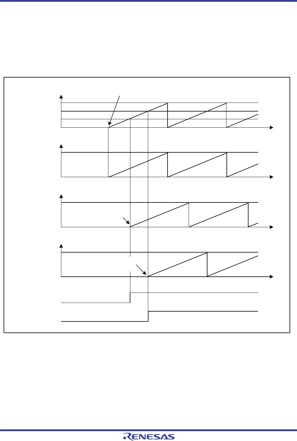
R01UH0034EJ0200 Rev.2.00 Page 844 of 1489
Dec 27, 2013
RX62T Group, RX62G Group 18. General PWM Timer (GPT/GPTa)
(4) Phase Start by Hardware Source
Count start with a phase difference is possible by a hardware source in the RX62T/RX62G Group.
There are four hardware sources: GTETRG pin input, comparator detection, GTIOC3A/GTIOC3B pin input, and
GTIOC3A/GTIOC3B internal output (output compare).
Figure 18.61 shows an example of phase start operation by a hardware source and Figure 18.62 shows the setting
example. In this example, GPT3.GTCNT and GPT0.GTCNT simultaneously start counting and GPT1.GTCNT and
GPT2.GTCNT start counting by the GTIOC3A and GTIOC3B internal outputs (output compare).
Figure 18.61 Example of Phase Start Operation by Hardware Source (with Same Count Cycle (GTPR Value))
Time
GPT3.GTCCRA
0000h
GPT0.GTPR
GPT3.GTCNT value
GPT0.GTCNT value
GPT1.GTCNT value
GPT2.GTCNT value
GPT1.GTPR
GPT2.GTPR
GPT3.GTPR
GPT3.GTCCRB
0000h
0000h
0000h
Count operation started at
the rising edge of GTIOC3A
internal output (output
compare)
Write 0009h in GTSTR.
(GPT0.GTCNT and GPT3.GTCNT start counting.)
Time
Time
Time
Count operation started at the
rising edge of GTIOC3B internal
output (output compare)
GTIOC3A internal output
(output compare)
GTIOC3B internal output
(output compare)

R01UH0034EJ0200 Rev.2.00 Page 845 of 1489
Dec 27, 2013
RX62T Group, RX62G Group 18. General PWM Timer (GPT/GPTa)
Figure 18.62 Example for Setting Phase Start by Hardware Source
Set count direction
Select the count direction (up or down) with the GTUDC register of the
corresponding channel.
(In figure 18.61 of the corresponding channel, after 0003h is set in GTUDC,
0001h is set in GTUDC (up-counting).)
Set operating mode
Set the operating mode with GTCR.MD[2:0] of the corresponding channel.
(In figure 18.61, 000b (saw-wave PWM mode) is set.)
Set cycle
Set the cycle in the GTPR register of the corresponding channel.
Select count clock
Select the count clock with GTCR.TPCS[1:0] of the corresponding channel.
Set hardware count start
Select a hardware source for starting count operation with GTHSSR.CSHSL
aNd set an edge for the hardware source with GTHSCR.CSHW to enable count
start and wait for count start by the hardware source.
(In figure 18.61, GTHSSR.CSHSL1 = 1010b, GTHSSR.CSHSL2 = 1011b,
GTHSCR.CSHW0 = 00b, GTHSCR.CSHW1 = 01b, GTHSCR.CSHW2 = 01b,
and GTHSCR.CSHW3 = 00b.)
Set hardware source operation
Set operation of the hardware source selected with GTHSSR.CSHSL and start
counting.
(In figure 18.61, GPT3 operation is set.)
Set GTIOA[5:0] and GTIOB[5:0] bits in GPT3.GTIOR so that the initial output
is low, output is retained at the cycle end, and high is output at
GPT3.GTCCRA/GTCCRB compare match. (GTIOA[5:0] = 000010b and
GTIOB[5:0] = 000010b)
Set the compare match value in GPT3.GTCCRA and GPT3.GTCCRB.
Set GTSTR.CST to 1 to start counting. (GTSTR = 0009h)
Set initial value for counter
Set the initial value in the GTCNT register of the corresponding channel.
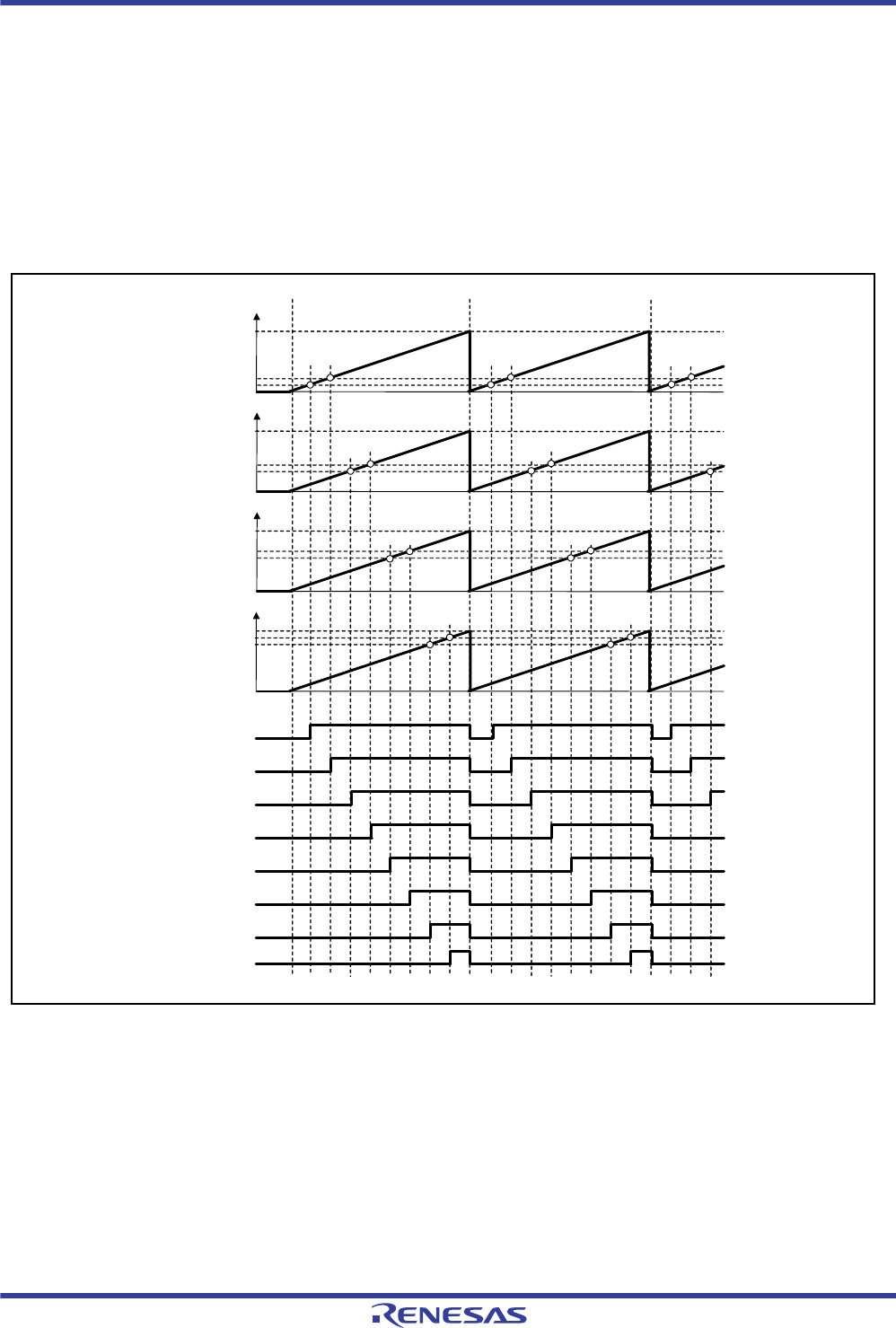
R01UH0034EJ0200 Rev.2.00 Page 846 of 1489
Dec 27, 2013
RX62T Group, RX62G Group 18. General PWM Timer (GPT/GPTa)
18.3.8 PWM Output Operation Examples
(1) Synchronized PWM Output
The GPT can output eight phases of linked PWM waveforms for a maximum of four channels by synchronizing
operation of the channels.
Figure 18.63 shows an example in which all the channels perform synchronized operation in saw-wave PWM mode and
eight phases of PWM waveforms are output. The GTIOCnA is set so that it will output low as the initial value, high at a
GTCCRA compare match, and low at the cycle end. The GTIOCnB is set so that it will output low as the initial value,
high at a GTCCRB compare match, and low at the cycle end.
Figure 18.63 Example of Synchronized PWM Output
GPT0.GTPR
GPT0.GTCCRB
GPT0.GTCNT
GPT0.GTCCRA
GPT1.GTPR
GPT1.GTCNT
GPT2.GTPR
GPT2.GTCNT
GPT3.GTPR
GPT3.GTCNT
GPT1.GTCCRB
GPT1.GTCCRA
GPT2.GTCCRB
GPT2.GTCCRA
GPT3.GTCCRB
GPT3.GTCCRA
GTIOC0A output pin
GTIOC0B output pin
GTIOC1A output pin
GTIOC1B output pin
GTIOC2A output pin
GTIOC2B output pin
GTIOC3A output pin
GTIOC3B output pin
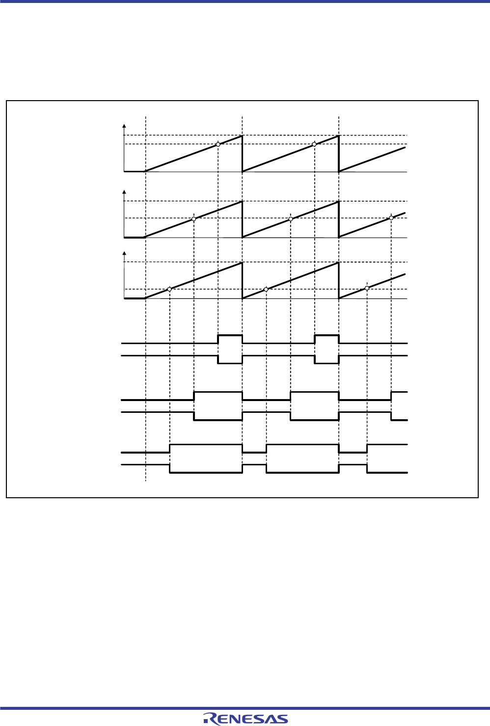
R01UH0034EJ0200 Rev.2.00 Page 847 of 1489
Dec 27, 2013
RX62T Group, RX62G Group 18. General PWM Timer (GPT/GPTa)
(2) Three-Phase Saw-Wave Complementary PWM Output
Figure 18.64 shows an example in which three channels perform synchronized operation in saw-wave PWM mode and
three-phase complementary PWM waveforms are output. The GTIOCnA is set so that it will output low as the initial
value, high at a GTCCRA compare match, and low at the cycle end. The GTIOCnB is set so that it will output high as the
initial value, low at a GTCCRB compare match, and high at the cycle end.
Figure 18.64 Example of Three-Phase Saw-Wave Complementary PWM Output
GPT0.GTPR
GPT0.GTCCRA
=GPT0.GTCCRB
GPT0.GTCNT
GPT1.GTPR
GPT1.GTCNT
GPT2.GTPR
GPT2.GTCNT
GTIOC0A output pin
GTIOC0B output pin
GTIOC1A output pin
GTIOC1B output pin
GTIOC2B output pin
GTIOC2A output pin
GPT1.GTCCRA
=GPT1.GTCCRB
GPT2.GTCCRA
=GPT2.GTCCRB
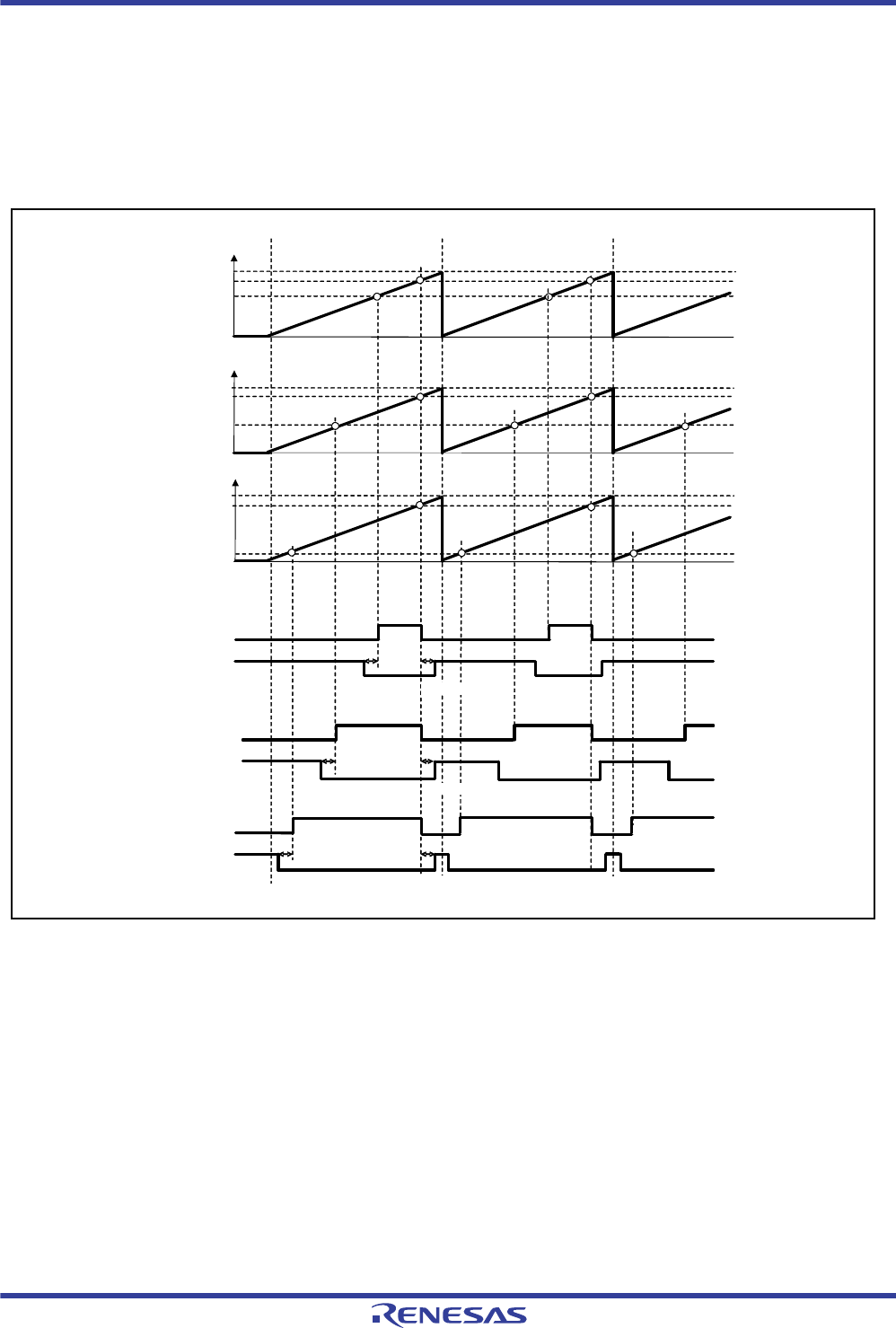
R01UH0034EJ0200 Rev.2.00 Page 848 of 1489
Dec 27, 2013
RX62T Group, RX62G Group 18. General PWM Timer (GPT/GPTa)
(3) Three-Phase Saw-Wave Complementary PWM Output with Automatic Dead Time Setting
Figure 18.65 shows an example in which three channels perform synchronized operation in saw-wave one-shot pulse
mode with automatic dead time setting and three-phase complementary PWM waveforms are output. The GTIOCnA is
set so that it will output low as the initial value, toggle the output at a GTCCRA compare match, and retain the output at
the cycle end. The GTIOCnB is set so that it will output high as the initial value, toggle the output at a GTCCRB
compare match, and retain the output at the cycle end.
Figure 18.65 Example of Three-Phase Saw-Wave Complementary PWM Output with Automatic Dead Time
Setting
GPT0.GTPR
GPT0.GTCNT
GPT1.GTPR
GPT1.GTCNT
GPT2.GTPR
GPT2.GTCNT
GTIOC0A output pin
GTIOC0B output pin
GTIOC1A output pin
GTIOC1B output pin
GTIOC2B output pin
GTIOC2A output pin
GPT0.GTCCRD
GPT1.GTCCRD
GPT2.GTCCRD
GPT0.GTDVU GPT0.GTDVD
GPT1.GTDVU GPT1.GTDVD
GPT2.GTDVU GPT2.GTDVD
GPT0.GTCCRC
GPT1.GTCCRC
GPT2.GTCCRC
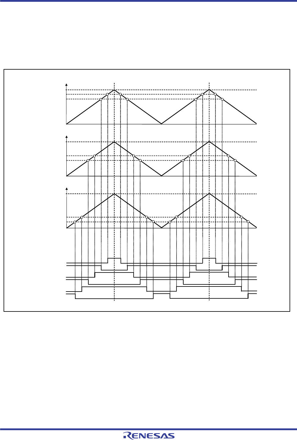
R01UH0034EJ0200 Rev.2.00 Page 849 of 1489
Dec 27, 2013
RX62T Group, RX62G Group 18. General PWM Timer (GPT/GPTa)
(4) Three-Phase Triangle-Wave Complementary PWM Output
Figure 18.66 shows an example in which three channels perform synchronized operation in triangle-wave PWM mode
1 and three-phase complementary PWM waveforms are output. The GTIOCnA is set so that it will output low as the
initial value, toggle the output at a GTCCRA compare match, and retain the output at the cycle end. The GTIOCnB is set
so that it will output high as the initial value, toggle the output at a GTCCRB compare match, and retain the output at the
cycle end.
Figure 18.66 Example of Three-Phase Triangle-Wave Complementary PWM Output
GPT2.GTPR
GPT2.GTCCRA
GPT2.GTCCRB
GPT1.GTPR
GPT1.GTCCRA
GPT1.GTCCRB
GPT0.GTPR
GPT0.GTCCRA
GPT0.GTCCRB
GPT2.GTCNT
GPT1.GTCNT
GPT0.GTCNT
GTIOC0A output pin
GTIOC0B output pin
GTIOC1A output pin
GTIOC1B output pin
GTIOC2A output pin
GTIOC2B output pin
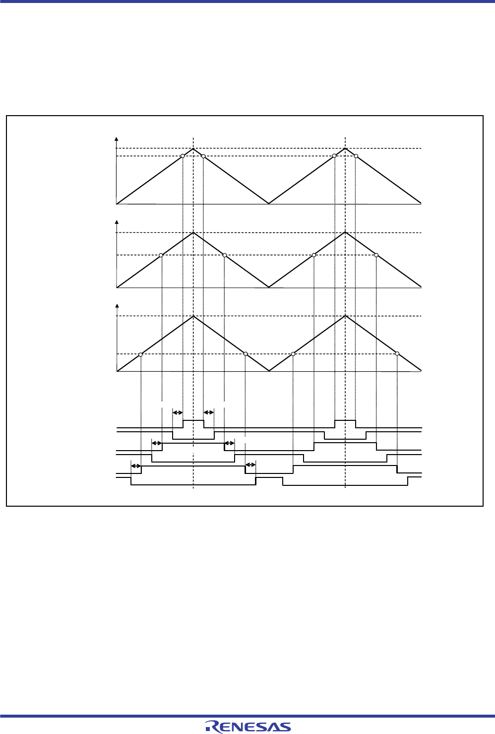
R01UH0034EJ0200 Rev.2.00 Page 850 of 1489
Dec 27, 2013
RX62T Group, RX62G Group 18. General PWM Timer (GPT/GPTa)
(5) Three-Phase Triangle-Wave Complementary PWM Output with Automatic Dead Time Setting
Figure 18.67 shows an example in which three channels perform synchronized operation in triangle-wave PWM mode
1 with automatic dead time setting and three-phase complementary PWM waveforms are output. The GTIOCnA is set so
that it will output low as the initial value, toggle the output at a GTCCRA compare match, and retain the output at the
cycle end. The GTIOCnB is set so that it will output high as the initial value, toggle the output at a GTCCRB compare
match, and retain the output at the cycle end.
Figure 18.67 Example of Three-Phase Triangle-Wave Complementary PWM Output with Automatic Dead Time
Setting
GPT2.GTPR
GPT2.GTCCRA
GPT1.GTPR
GPT1.GTCCRA
GPT0.GTPR
GPT0.GTCCRA
GPT2.GTCNT
GPT1.GTCNT
GPT0.GTCNT
GPT0.GTDVU GPT0.GTDVD
GPT1.GTDVU
GPT1.GTDVD
GPT2.GTDVU
GPT2.GTDVD
GTIOC0A output pin
GTIOC0B output pin
GTIOC1A output pin
GTIOC1B output pin
GTIOC2A output pin
GTIOC2B output pin
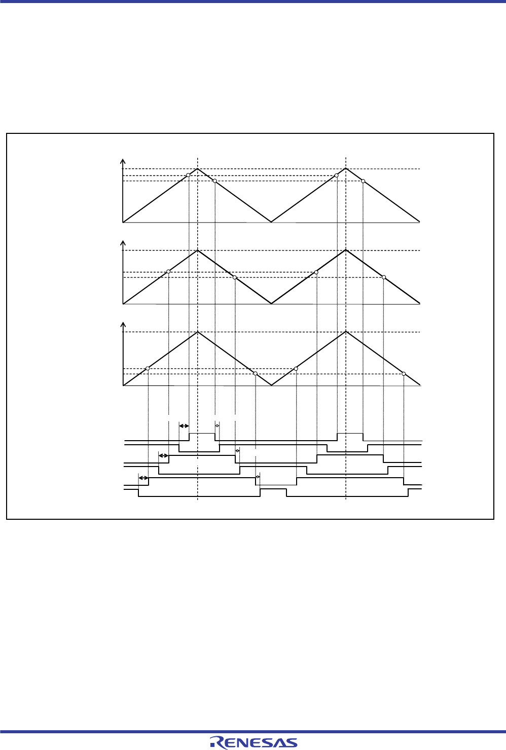
R01UH0034EJ0200 Rev.2.00 Page 851 of 1489
Dec 27, 2013
RX62T Group, RX62G Group 18. General PWM Timer (GPT/GPTa)
(6) Three-Phase Asymmetric Triangle-Wave Complementary PWM Output with Automatic Dead
Time Setting
Figure 18.68 shows an example in which three channels perform synchronized operation in triangle-wave PWM mode
3 with automatic dead time setting and three-phase complementary PWM waveforms are output. The GTIOCnA is set so
that it will output low as the initial value, toggle the output at a GTCCRA compare match, and retain the output at the
cycle end. The GTIOCnB is set so that it will output high as the initial value, toggle the output at a GTCCRB compare
match, and retain the output at the cycle end.
Figure 18.68 Example of Three-Phase Asymmetric Triangle-Wave Complementary PWM Output with Automatic
Dead Time Setting
GTIOC0A output pin
GTIOC0B output pin
GTIOC1A output pin
GTIOC1B output pin
GTIOC2A output pin
GTIOC2B output pin
GPT0.GTDVU GPT0.GTDVD
GPT1.GTDVU
GPT1.GTDVD
GPT2.GTDVU
GPT2.GTDVD
GPT0.GTPR
GPT0.GTCCRC
GPT0.GTCNT
GPT0.GTCCRD
GPT1.GTPR
GPT1.GTCCRC
GPT1.GTCNT
GPT1.GTCCRD
GPT2.GTPR
GPT2.GTCCRC
GPT2.GTCNT
GPT2GTCCRD
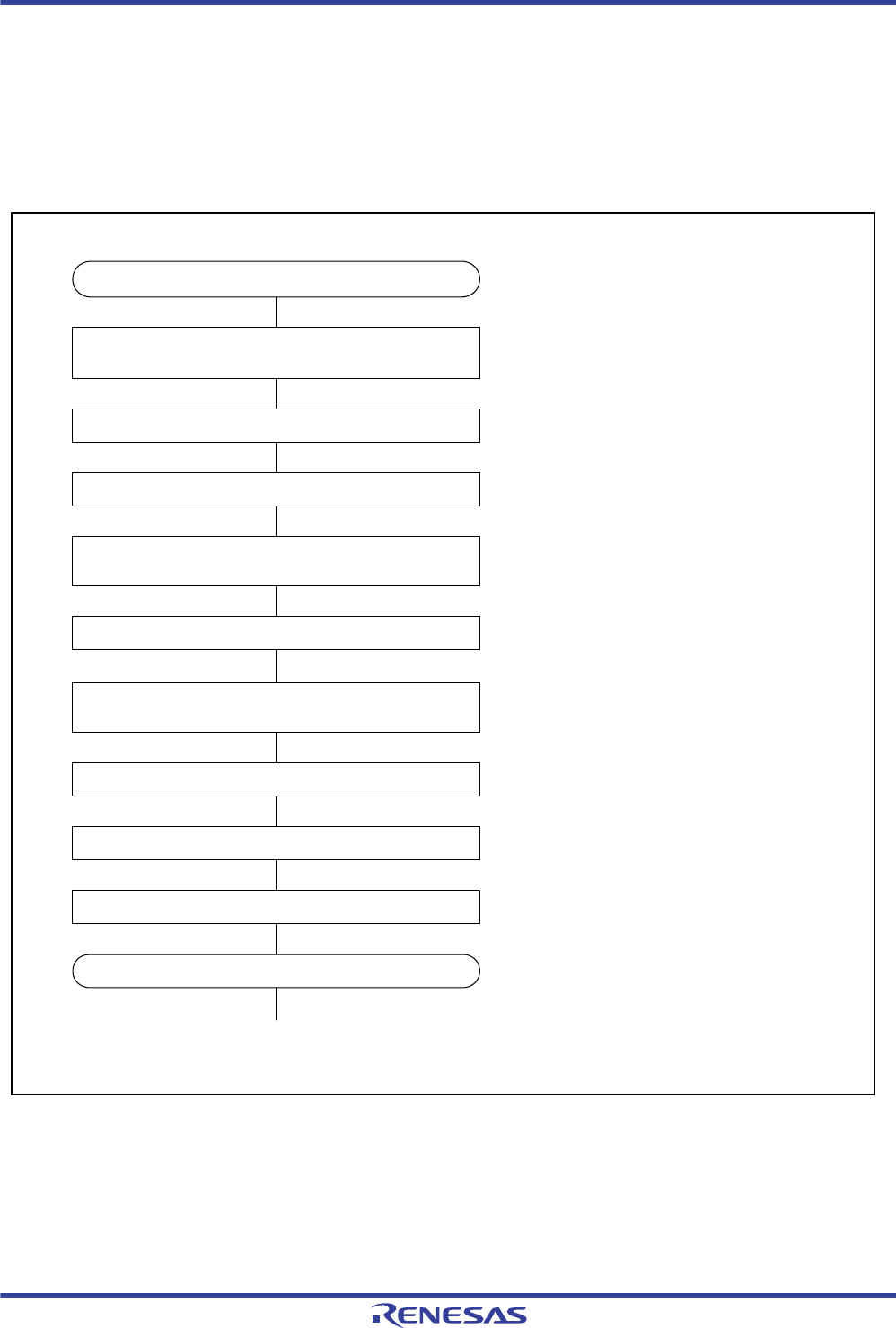
R01UH0034EJ0200 Rev.2.00 Page 852 of 1489
Dec 27, 2013
RX62T Group, RX62G Group 18. General PWM Timer (GPT/GPTa)
18.3.9 Adjustments to the Timing of Rising and Falling Edges in PWM Waveforms
The timing of rising and falling edges in PWM waveforms which are output from the GTIOCnA and GTIOCnB pins
(where n = channel number) can be delayed to an accuracy of 1/32 of the system clock (ICLK) period. At this time, make
sure that the system clock is running at a frequency no lower than 80 MHz.
If the timing of rising or falling edges in PWM waveforms output from the GTIOCnA and GTIOCnB pins is to be
adjusted, make initial settings for the PWM generation circuit in accord with the procedure shown in Figure 18.69.
Figure 18.69 Initialization Flowchart Example of PWM Delay Generation Circuit
Set the SCKCR.ICK[3:0] bits so that the system clock
(ICLK) runs at a frequency no lower than 80 MHz.
Initial setting
GPTn.GTDLYCR.DLLEN = 1
Wait for 20µs.
Set the SCKCR.ICK[3:0] bits again so that the
frequency multiplier for ICLK is no greater than 1/2.
Wait for 4µs.
Set the SCKCR.ICK[3:0] bits so that the system clock
(ICLK) runs at a frequency no lower than 80 MHz.
GPTn.GTDLYCR.DLYRST = 1
End of initial settings
Enable the DLL.
Reset the PWM delay generation circuit.
Enable the PWM delay generation circuit.
n = 0 to 3
GPTn.GTDLYCR.DLYRST = 0
GPTn.GTDLYCR.DLYEN = 1

R01UH0034EJ0200 Rev.2.00 Page 853 of 1489
Dec 27, 2013
RX62T Group, RX62G Group 18. General PWM Timer (GPT/GPTa)
In the PWM delay generation circuit, delay can be applied to rising and falling edges of the PWM output to an accuracy
of 1/32 of the period of the system clock (ICLK). This is described in section section 18.3.3, PWM Output Operating
Mode. Delays corresponding to the settings are reflected in the PWM output with the timing described in section
section 18.3.10, Timing for Transfer of GTDLYRA, GTLDYRB, GTDLYFA, and GTDLYFB Register Settings.
Table 18.6 shows the correspondence between the GTDLYRA, GTLDYRB, GTDLYFA, and GTDLYFB registers and
the PWM outputs.
When the PWM delay generation circuit is in use, the timing with which a PWM output signal rises and falls can be
controlled to an accuracy of 1/32 of the period of the system clock (ICLK). When this facility is not in use, the period of
the PWM output waveform is controlled to an accuracy of one period of the input clock for the timer counter (which is
ICLK). With the PWM delay generation circuit, the output can be controlled to an accuracy 32 times better. Furthermore,
the delay settings also control the periods at high and low level for the PWM waveform to the given accuracy.
Each of the four PWM channels includes a PWM delay generation circuit, and the circuits can be individually enabled or
disabled.
18.3.10 Timing for Transfer of GTDLYRA, GTLDYRB, GTDLYFA, and GTDLYFB
Register Settings
Settings for the GTDLYRA, GTLDYRB, GTDLYFA, and GTDLYFB registers are initially transferred to temporary
registers, and then reflected in the amounts of delay on the GTIOCnA and GTIOCnB (n = 0 to 3) outputs. Transfer of the
settings takes place on overflows (in up-counting) or underflows (in down-counting) for saw waves, and in the troughs of
triangle waves.
Figure 18.70 and Figure 18.71 show examples of the operation of the GTDLYRA and GTDLYFA registers.
Table 18.6 Correspondence between PWM Output Pins and Delay Setting Registers
PWM Output Pin Rising-Edge Delay Setting Register Falling-Edge Delay Setting Register
GTIOC0A GPT0.GTDLYRA GPT0.GTDLYFA
GTIOC0B GPT0.GTDLYRB GPT0.GTDLYFB
GTIOC1A GPT1.GTDLYRA GPT1.GTDLYFA
GTIOC1B GPT1.GTDLYRB GPT1.GTDLYFB
GTIOC2A GPT2.GTDLYRA GPT2.GTDLYFA
GTIOC2B GPT2.GTDLYRB GPT2.GTDLYFB
GTIOC3A GPT3.GTDLYRA GPT3.GTDLYFA
GTIOC3B GPT3.GTDLYRB GPT3.GTDLYFB
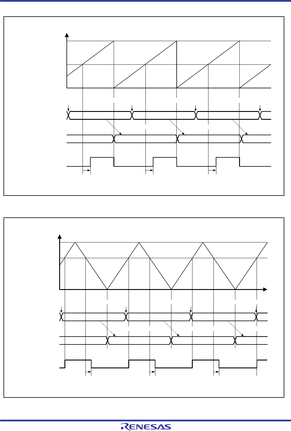
R01UH0034EJ0200 Rev.2.00 Page 854 of 1489
Dec 27, 2013
RX62T Group, RX62G Group 18. General PWM Timer (GPT/GPTa)
Figure 18.70 Example of GTLDYRA Register Operation (in PWM Saw-Wave Generation)
Figure 18.71 Example of GTLDYFA Register Operation (in PWM Triangle-Wave Generation)
GPT0.GTDLYRA.DLY b
0000h
GPT0.GTPR
GPT0.GTCNT value
cd
b ca
yyyy
Register writing Register writing Register writing Register writing
Transfer on the overflow Transfer on the overflow Transfer on the
overflow
bca
Temporary register
GTIOC0A output
Amount of delay on the rising edge
GPT0.GTDLYFA.DLY b
0000h
GPT0.GTPR
GPT0.GTCNT value
cd
b ca
yyyy
bca
Temporary register
GTIOC0A output
Amount of delay on the falling edge
Time
Register writing Register writing Register writing Register writing
Transfer in the trough Transfer in the trough Transfer in the trough
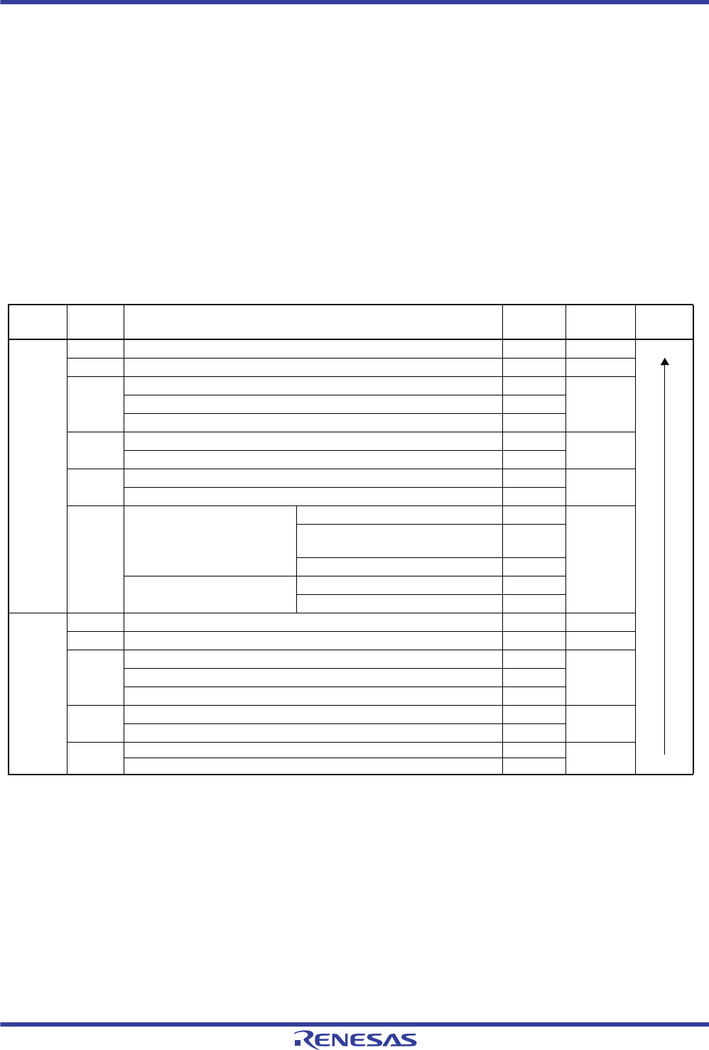
R01UH0034EJ0200 Rev.2.00 Page 855 of 1489
Dec 27, 2013
RX62T Group, RX62G Group 18. General PWM Timer (GPT/GPTa)
18.4 Interrupt Sources
18.4.1 Interrupt Sources and Priorities
There are four kinds of GPT interrupt sources; GTCCR input capture/compare match, GTCNT counter overflow (GTPR
compare match)/underflow, dead time error, and LOCO count function interrupt. Each interrupt source has its own status
flag and enable/disable bit, allowing the generation of interrupt request signals to be enabled or disabled individually
When an interrupt source is generated, the corresponding status flag in GTST is set to 1. If the corresponding enable/
disable bit in GTINTAD is set to 1 at this time, an interrupt is requested.
However, if a further interrupt is generated while the corresponding status flag is 1, the interrupt will be ignored. To
enable the acceptance of an interrupt, the flag of the interrupt generation source should be 0.
Relative channel priorities can be changed by the interrupt controller; however the priority within a channel is fixed. For
details, see section 11, Interrupt Controller (ICU). Table 18.7 lists the GPT interrupt sources.
Table 18.7 GPT Interrupt Sources (1 / 2)
Channel Name Interrupt Source Interrupt
Flag DTC
Activation Priority
0 GTCIA0 GPT0.GTCCRA input capture/compare match TCFA Possible High
Low
GTCIB0 GPT0.GTCCRB input capture/compare match TCFB Possible
GTCIC0 GPT0.GTCCRC compare match TCFC Possible
GPT0.GTCCRD compare match TCFD
Dead time error DTEF
GTCIE0 GPT0.GTCCRE compare match TCFE Possible
GPT0.GTCCRF compare match TCFF
GTCIV0 GPT0.GTCNT overflow (GPT0.GTPR compare match) TCFPO Possible
GPT0.GTCNT underflow TCFPU
LOCOI LOCO count function interrupt LCNT overflow LISO Possible
LOCO count value deviation
exceedance
LISD
Frequency-divided LOCO clock rise LISC
External trigger input External trigger falling input ETINF
External trigger rising input ETIPF
1 GTCIA1 GPT1.GTCCRA input capture/compare match TCFA Possible
GTCIB1 GPT1.GTCCRB input capture/compare match TCFB Possible
GTCIC1 GPT1.GTCCRC compare match TCFC Possible
GPT1.GTCCRD compare match TCFD
Dead time error DTEF
GTCIE1 GPT1.GTCCRE compare match TCFE Possible
GPT1.GTCCRF compare match TCFF
GTCIV1 GPT1.GTCNT overflow (GPT1.GTPR compare match) TCFPO Possible
GPT1.GTCNT underflow TCFPU
R01UH0034EJ0200 Rev.2.00 Page 856 of 1489
Dec 27, 2013
RX62T Group, RX62G Group 18. General PWM Timer (GPT/GPTa)
Note: • This table shows the initial state immediately after a reset. The relative channel priorities can be changed by the interrupt
controller.
2 GTCIA2 GPT2.GTCCRA input capture/compare match TCFA Possible High
Low
GTCIB2 GPT2.GTCCRB input capture/compare match TCFB Possible
GTCIC2 GPT2.GTCCRC compare match TCFC Possible
GPT2.GTCCRD compare match TCFD
Dead time error DTEF
GTCIE2 GPT2.GTCCRE compare match TCFE Possible
GPT2.GTCCRF compare match TCFF
GTCIV2 GPT2.GTCNT overflow (GPT2.GTPR compare match) TCFPO Possible
GPT2.GTCNT underflow TCFPU
3 GTCIA3 GPT3.GTCCRA input capture/compare match TCFA Possible
GTCIB3 GPT3.GTCCRB input capture/compare match TCFB Possible
GTCIC3 GPT3.GTCCRC compare match TCFC Possible
GPT3.GTCCRD compare match TCFD
Dead time error DTEF
GTCIE3 GPT3.GTCCRE compare match TCFE Possible
GPT3.GTCCRF compare match TCFF
GTCIV3 GPT3.GTCNT overflow (GPT3.GTPR compare match) TCFPO Possible
GPT3.GTCNT underflow TCFPU
Table 18.7 GPT Interrupt Sources (2 / 2)
Channel Name Interrupt Source Interrupt
Flag DTC
Activation Priority

R01UH0034EJ0200 Rev.2.00 Page 857 of 1489
Dec 27, 2013
RX62T Group, RX62G Group 18. General PWM Timer (GPT/GPTa)
(1) Input Capture/Compare Match Interrupt
If the corresponding interrupt enable bit in GTINTAD is 1 when a GTCCR input capture/compare match in each channel
occurs, an interrupt is requested.
(2) Overflow/Underflow (Periodic) Interrupt
A periodic interrupt whose generation interval is determined by GTPR of each channel can be generated.
For saw-waves, the GTST.TCFPO flag is set to 1 when the GTCNT counter value matches GTPR (overflow) in up-count
operation, the GTST.TCFPU flag is set to 1 when GTCNT reaches 0 (underflow) in down-count operation, and a GTCIV
interrupt request is generated if the bits that correspond to GTINTPR.GTINTPR[1:0] are set to 01b, 10b, or 11b.
For triangle waves, GTST.TCFPO flag is set to 1 when the GTCNT counter value matches GTPR (crest) in up-count
operation, the GTST.TCFPU flag is set to 1 when GTCNT reaches 0 (trough) in down-count operation, and a GTCIV
interrupt request is generated if bits that correspond to GTINTPR.GTINTPR[1:0] are set to 01b, 10b, or 11b.
(3) LOCO Count Function Interrupt
When the frequency-divided LOCO clock rising is detected, LOCO count value exceeds the specified deviation, or an
overflow occurs in the LCNT counter, the corresponding status flag in LCST is set to 1. If the corresponding interrupt
enable bit in LCCR is 1 at this time, a LOCOI interrupt request is generated.
Similarly, when the GTETRG external trigger input rising or falling is detected, the corresponding status flag in
GTETINT is set to 1. If the corresponding interrupt enable bit in GTETINT is 1 at this time, a LOCOI interrupt request is
generated.

R01UH0034EJ0200 Rev.2.00 Page 858 of 1489
Dec 27, 2013
RX62T Group, RX62G Group 18. General PWM Timer (GPT/GPTa)
(4) Dead Time Error Interrupt
When automatic dead time setting has been made, the GTST.DTEF flag becomes 1 when the timer output toggle point
with dead time added exceeds the timer cycle. If GTINTAD.EINT is 1 at this time, a LOCOI interrupt request is
generated.
(5) Points for Caution when Interrupt Sources Are in Use at the Same Time
For the GTCICn, GTCIEn, GTCIVn, LOCOI (n=0, 1, 2, 3) interrupts, which have multiple interrupt sources, if the value
of the interrupt request (IR) flag in ICUA is becoming 1 due to a request from a given interrupt source (for example, the
TCFC flag in GTCICn) when another interrupt source (for example, the TCFD flag in GTCICn) generates an interrupt,
the request from the other interrupt source (in this case, the TCFD flag in GTCICn) is ignored.
Accordingly, if the multiple interrupt sources of such an interrupt are to be used at the same time, confirm the values of
all flags corresponding to the interrupt sources that are in use from within the interrupt handling routine, and ensure
appropriate processing for all source flags that are currently set.
Table 18.8 Interrupt Signals, Interrupt Enable Bits, and Status Flags
Interrupt Signal Interrupt Enable Bit Status Flag
GTCIV GTINTAD[7:6](GTINTPR[1:0]) GTST[7] (TCFPU)
GTST[6] (TCFPO)
GTCIE GTINTAD[5] (GTINTF) GTST[5] (TCFF)
GTINTAD[4] (GTINTE) GTST[4] (TCFE)
GTCIC GTINTAD[11](EINT) GTST[11] (DTEF)
GTINTAD[3] (GTINTD) GTST[3] (TCFD)
GTINTAD[2] (GTINTC) GTST[2] (TCFC)
GTCIB GTINTAD[1] (GTINTB) GTST[1] (TCFB)
GTCIA GTINTAD[0] (GTINTA) GTST[0] (TCFA)
LOCOI LCCR[6] (LCINTO) LCST[2] (LISO)
LCCR[5] (LCINTD) LCST[1] (LISD)
LCCR[4] (LCINTC) LCST[0] (LISC)
GTETINT[1] (ETINEN) GTETINT[9] (ETINF)
GTETINT[0] (ETIPEN) GTETINT[8] (ETIPF)
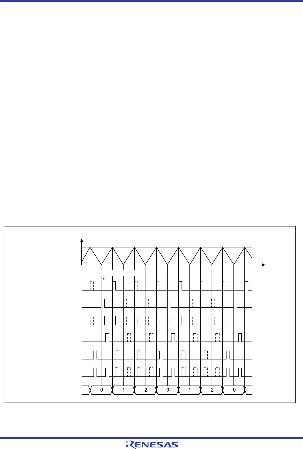
R01UH0034EJ0200 Rev.2.00 Page 859 of 1489
Dec 27, 2013
RX62T Group, RX62G Group 18. General PWM Timer (GPT/GPTa)
18.4.2 DTC Activation
The DTC can be activated by the interrupt in each channel. For details, see section 11, Interrupt Controller (ICU), and
section 14, Data Transfer Controller (DTC).
However, as similar to the interrupt handling, if a further DTC activation request is generated while the corresponding
status flag is 1, the interrupt will be ignored. To enable the acceptance of an interrupt, the flag of the interrupt generation
source should be 0.
18.4.3 Interrupt and A/D Conversion Request Skipping Function
By setting the GTITC register, the GTCNT counter overflows (GTPR compare matches)/underflow interrupts (GTCIV)
can be skipped. Other interrupts and A/D converter start request signals can be skipped in coordination with the GTCIV
skipping function. However, the dead time error interrupts cannot be linked with the GTCIV skipping function. If an
interrupt is skipped, the change in the corresponding status flag is also skipped and the skipping function operates while
the status flag is set.
When both troughs and crests are counted and skipped in triangle-wave mode, if the number of times of skipping is odd,
GTCIV interrupt requests cannot be generated at troughs only or at crests only depending on the skipping counter start
timing. Therefore, in order to count both troughs and crests and generate the GTCIV interrupts at troughs only or crests
only in triangle-wave mode, the number of times of skipping should be even.
Similarly, in saw-wave mode, when both overflows and underflows are counted and skipped with the count direction
changed, GTCIV interrupt requests cannot be generated at overflows only or at underflows only. Therefore, in order to
count both overflows and underflows with the count direction changed and generate the GTCIV interrupts at overflows
only or underflows only in saw wave mode, the skipping state should be carefully checked before using.
When changing the skipping count, be sure to release the skipping count setting (GTITC.IVTC[1:0] = 00b).
Figure 18.72 to Figure 18.77 show examples of skipping function operation.
Figure 18.72 Example of Interrupt Skipping Function Operation (Triangle Waves, Counting and Skipping
Crests, Skipping Count: 2)
GTCIV interrupt request at crest
GTCIV interrupt request at trough
GTICIV interrupt request at
both crest and trough
Interrupt request generated
during up-count operation
Interrupt request generated
during down-count operation
Interrupt request generated during both
up-count and down-count operation
GTST.ITCNT[2:0]
(skipping counter)
0000h
GTPR
GTCNT value
Time
Skipped interrupt requests
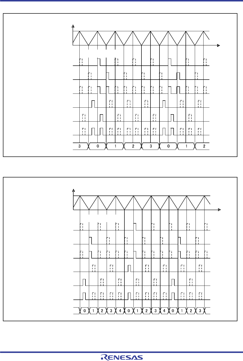
R01UH0034EJ0200 Rev.2.00 Page 860 of 1489
Dec 27, 2013
RX62T Group, RX62G Group 18. General PWM Timer (GPT/GPTa)
Figure 18.73 Example of Interrupt Skipping Function Operation (Triangle Waves, Counting and Skipping
Troughs, Skipping Count: 3)
Figure 18.74 Example of Interrupt Skipping Function Operation (Triangle Waves, Counting and Skipping Both
Troughs and Crests, Skipping Count: 4)
GTCNT value
GTPR
0000h
Skipped interrupt requests
Time
GTCIV interrupt request at crest
GTCIV interrupt request at trough
GTICIV interrupt request at
both crest and trough
Interrupt request generated
during up-count operation
Interrupt request generated
during down-count operation
Interrupt request generated during both
up-count and down-count operation
GTST.ITCNT[2:0]
(skipping counter)
Skipped interrupt requests
GTCNT value
GTPR
0000h Time
GTCIV interrupt request at crest
GTCIV interrupt request at trough
GTICIV interrupt request at
both crest and trough
Interrupt request generated
during up-count operation
Interrupt request generated
during down-count operation
Interrupt request generated during both
up-count and down-count operation
GTST.ITCNT[2:0]
(skipping counter)
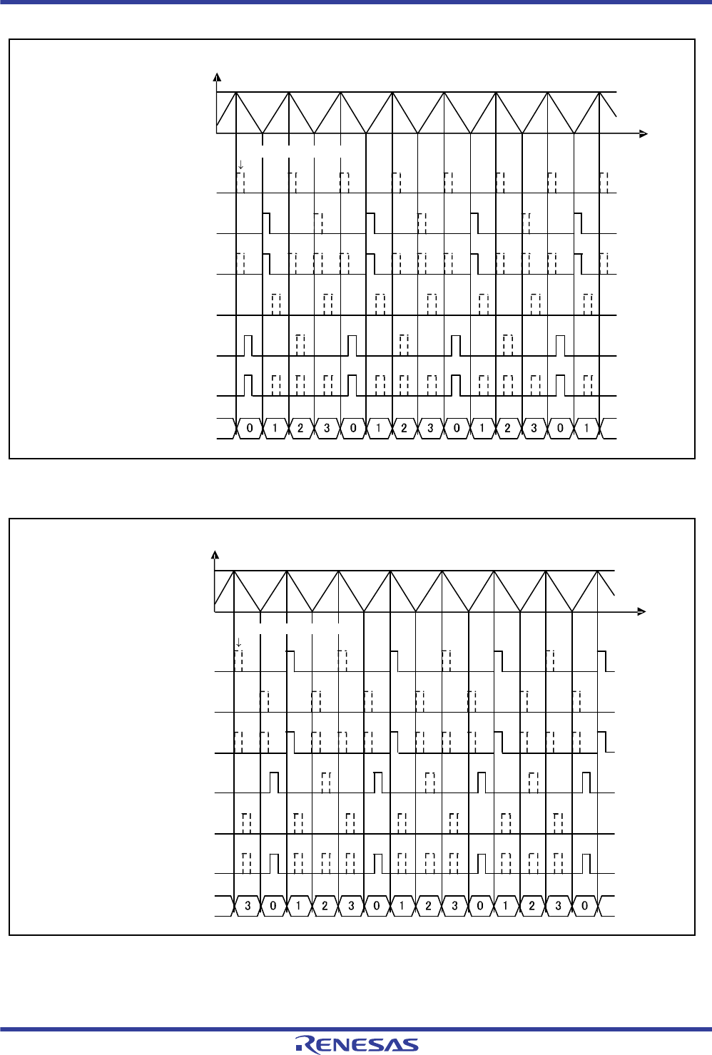
R01UH0034EJ0200 Rev.2.00 Page 861 of 1489
Dec 27, 2013
RX62T Group, RX62G Group 18. General PWM Timer (GPT/GPTa)
Figure 18.75 Example of Interrupt Skipping Function Operation (Triangle Waves, Counting and Skipping Both
Troughs and Crests, Skipping Count: 3, Skipping Started at Up-Counting)
Figure 18.76 Example of Interrupt Skipping Function Operation (Triangle Waves, Counting and Skipping Both
Troughs and Crests, Skipping Count: 3, Skipping Started at Down-Counting)
GTCNT value
GTPR
0000h
Skipped interrupt requests
Time
GTCIV interrupt request at crest
GTCIV interrupt request at trough
GTICIV interrupt request at
both crest and trough
Interrupt request generated
during up-count operation
Interrupt request generated
during down-count operation
Interrupt request generated during both
up-count and down-count operation
GTST.ITCNT[2:0]
(skipping counter)
0000h
GTPR
GTCNT value
Skipped interrupt requests
Time
GTCIV interrupt request at crest
GTCIV interrupt request at trough
GTICIV interrupt request at
both crest and trough
Interrupt request generated
during up-count operation
Interrupt request generated
during down-count operation
Interrupt request generated during both
up-count and down-count operation
GTST.ITCNT[2:0]
(skipping counter)

R01UH0034EJ0200 Rev.2.00 Page 862 of 1489
Dec 27, 2013
RX62T Group, RX62G Group 18. General PWM Timer (GPT/GPTa)
Figure 18.77 Example of Interrupt Skipping Function Operation (Saw Waves, Operation with Count Direction
Changed, Counting and Skipping Both Overflows and Underflows, Skipping Count: 4)
Interrupt request generated
at overflow
Interrupt request generated
at underflow
Interrupt request generated at both
overflow and underflow
Interrupt request generated
during count operation
GTST.ITCNT[2:0]
(skipping counter)
0000h
GTPR
GTCNT value
Skipped interrupt requests
Time
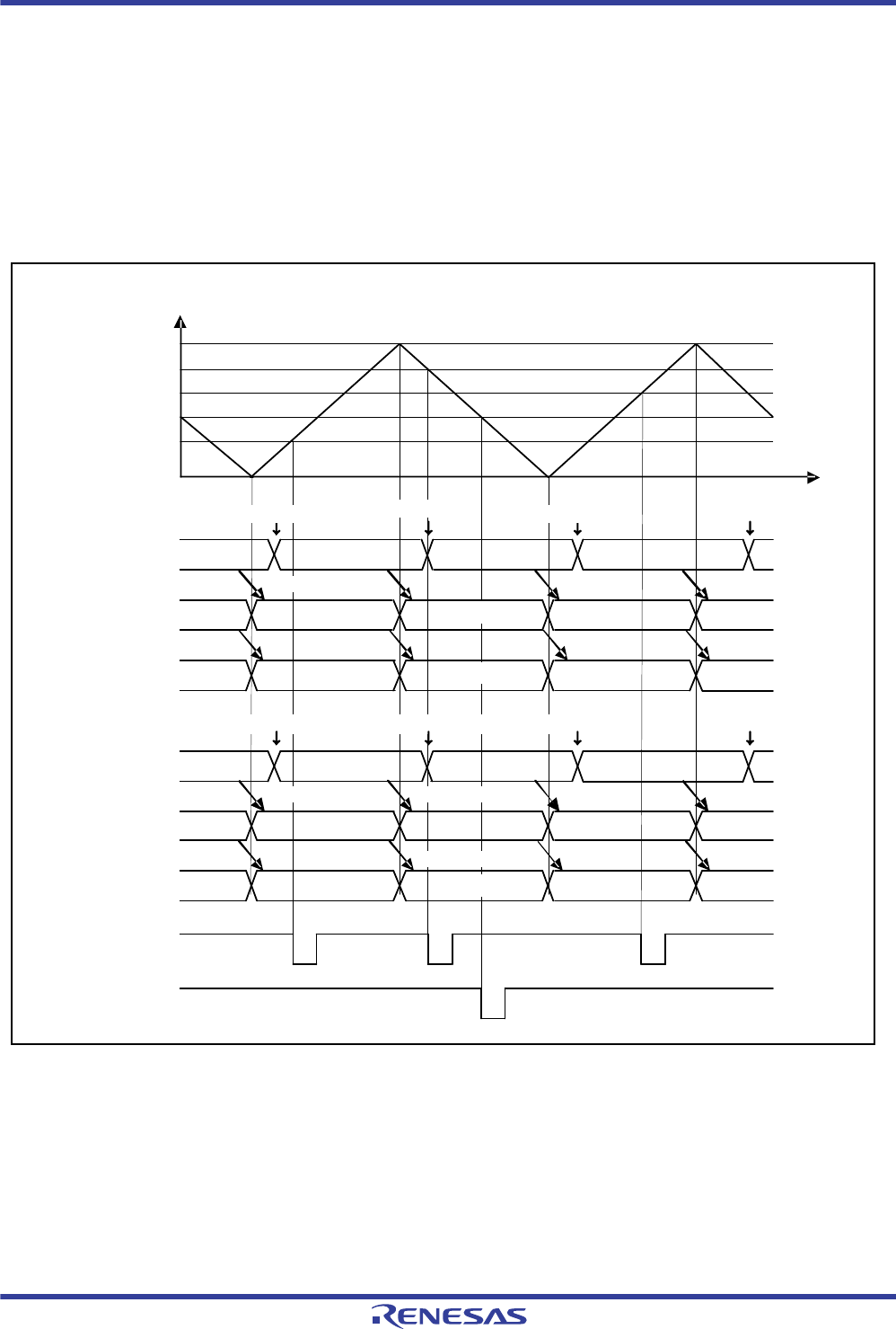
R01UH0034EJ0200 Rev.2.00 Page 863 of 1489
Dec 27, 2013
RX62T Group, RX62G Group 18. General PWM Timer (GPT/GPTa)
18.5 A/D Converter Start Request
An A/D converter start request can be issued at a compare match between the GTCNT counter and GTADTRA or
GTADTRB, and up-counting only, down-counting only, or both up-counting and down-counting can be specified.
GTADTRA and GTADTRB each has two buffer registers. Buffer operation with GTADTRA used together with
GTADTBRA and GTADTDBRA, and buffer operation with GTADTRB used together with GTADTBRB and
GTADTDBRB can be performed.
Figure 18.78 shows an example of A/D converter start request operation, and Figure 18.79 shows an example for
setting A/D converter start request operation.
Figure 18.78 Example of A/D Converter Start Request Timing Operation (Triangle Waves, Double Buffer
Operation, Buffer Transfer at Both Troughs and Crests, A/D Converter Start Requested by
GTADTRA0 at Both Up-Counting and Down-Counting, A/D Converter Start Requested by
GTADTRB0 at Down-Counting,)
Time
Register write Register write
Register write Register write
GTCNT value
GTPR
dddd
cccc
bbbb
aaaa
0000h
GTADTDBRA
GTADTBRA
GTADTRB
GTADTDBRB
GTADTBRB
GTADTRA
GTADTRB
(AD conversion request)
GTADTRA
(AD conversion request)
dddd
dddd
dddd
aaaa
aaaa cccc
cccc
cccc
bbbb
bbbb
bbbb
Register write Register write Register write
Buffer transfer
at trough
Buffer transfer
at trough
Buffer transfer
at trough
Buffer transfer
at trough
Buffer transfer
at crest
Buffer transfer
at crest Buffer transfer
at crest
Buffer transfer
at crest
Buffer transfer
at trough
Buffer transfer
at trough
Buffer transfer
at trough
Buffer transfer
at trough
Buffer transfer
at crest
Buffer transfer
at crest
Buffer transfer
at crest
Buffer transfer
at crest
Register write
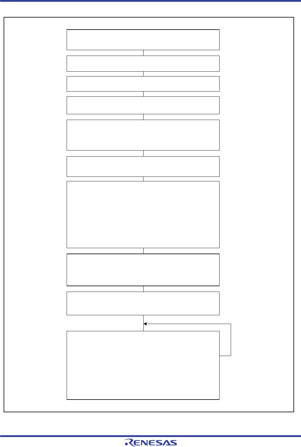
R01UH0034EJ0200 Rev.2.00 Page 864 of 1489
Dec 27, 2013
RX62T Group, RX62G Group 18. General PWM Timer (GPT/GPTa)
Figure 18.79 Example for Setting A/D Converter Start Request Timing Operation
Set operating mode
Set the operating mode with GTCR.MD[2:0].
(In figure 18.75, 100b or 101b (triangle-wave PWM mode) is set.)
Select count clock
Select the count clock with GTCR.TPCS[1:0].
Set cycle
Set the cycle in GTPR.
Enable A/D converter start request
Set to enable an A/D converter start request with ADTRAUEN,
ADTRADEN, ADTRBUEN, and ADTRBDEN in GTINTAD.
(In figure 18.75, ADTRAUEN = 1, ADTRADEN = 1, ADTRBUEN = 0,
and ADTRBDEN = 1.)
Start count operation
Set GTSTR.CST to 1 to start count operation.
(In figure 18.75, 1 is set in GTSTR.CST0.)
Set initial value for counter
Set the initial value in the GTCNT register.
Set buffer operation
Set buffer operation with ADTTA[1:0], ADTTB[1:0], ADTDA, and ADTDB
in GTBER.
(In figure 18.55, ADTTA[1:0] = 11b, ADTTB[1:0] = 11b, ADTDA = 1, and
ADTDB = 1.)
Set buffer value
For buffer operation, set the A/D converter start request points in one
cycle after the current cycle (in saw-wave mode or triangle-wave mode
with buffer transfer at trough or crest) or half cycle after the current cycle
(in triangle-wave mode with buffer transfer at both trough and crest) in
GTADTBRA and GTADTBRB.
For double buffer operation, also set the A/D converter start request
points in two cycles after the current cycle (in saw-wave mode or
triangle-wave mode with buffer transfer at trough or crest) or one cycle
after the current cycle (in triangle-wave mode with buffer transfer at both
trough and crest) in GTADTBRA and GTADTBRB.
Set compare match value
Set the A/D converter start request points in GTADTRA and GTADTRB.
Set buffer value for each cycle
For buffer operation, set the A/D converter start request points in one
cycle after the current cycle (in saw-wave mode or triangle-wave mode
with buffer transfer at trough or crest) or half cycle after the current cycle
(in triangle-wave mode with buffer transfer at both trough and crest) in
GTADTBRA and GTADTBRB.
For double buffer operation, set the A/D converter start request points in
two cycles after the current cycle (in saw-wave mode or triangle-wave
mode with buffer transfer at trough or crest) or one cycle after the
current cycle (in triangle-wave mode with buffer transfer at both trough
and crest) in GTADTBRA and GTADTBRB.
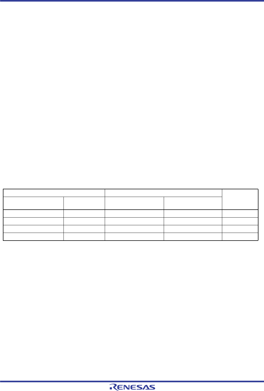
R01UH0034EJ0200 Rev.2.00 Page 865 of 1489
Dec 27, 2013
RX62T Group, RX62G Group 18. General PWM Timer (GPT/GPTa)
18.6 LOCO Count Function
The GPT can measure the cycle of the frequency-divided LOCO clock used for the independent watchdog timer (IWDT)
in the RX62T/RX62G Group. By this function, the main clock oscillation frequency errors can be detected.
The target LOCO clock to be measured (frequency-divided LOCO clock) can be selected from the LOCO clock/1,
LOCO clock/16, LOCO clock/128, and LOCO clock/256, and the count clock for measuring the frequency-divided
LOCO clock can be selected from ICLK/1, ICLK/2, ICLK/4, and ICLK/8.
The LCNT counter counts the frequency-divided LOCO clock cycle with the count clock, and the recent 16 count results
are stored in LCNT0 to LCNT15 (the latest count result in LCNT00). The average value of the recent 16 count results is
automatically computed and stored in LCNTA.
The frequency-divided LOCO clock rise interrupt requests can be generated when the rising edge of the frequency-
divided LOCO clock is detected. The frequency-divided LOCO clock rise interrupt requests can be skipped, and the
count results can also be skipped. When the count result (LCNT00 value) exceeds the upper limit or lower limit value,
the LOCO deviation exceedance interrupt request can be generated. The upper and lower limits can be set in LCNTDU
and LCNTDL, respectively, and the upper limit value is obtained by (LCNTA value + LCNTDU value) and the lower
limit value is obtained by (LCNTA value – LCNTDL value). When the frequency-divided LOCO clock frequency is too
low and the LCNT counter overflows, the LCNT overflow interrupt request can be generated. Since all of these
interrupts are output as LOCOI interrupts, the interrupt source should be determined by reading the status flags after the
interrupt generation.
When using the LOCO count function, the independent watchdog timer (IWDT) should be activated.
Table 18.9 shows a frequency setting example for the LOCO count function.
Figure 18.80 shows an example of LOCO count function operation, and Figure 18.81 shows the setting flow example.
Table 18.9 Frequency Setting Example for LOCO Count Function
Frequency-Divided LOCO Clock Count Clock
Desired Count
Result ValueLCCR.LPSC[1:0] Setting Frequency LCCR.TPSC[1:0] Setting Frequency
(When ICLK = 100 MHz)
00 (not divided) 125 KHz 00 (not divided) 100 MHz 320h
01 (divided by 16) 7.81 KHz 00 (not divided) 100 MHz 3200h
10 (divided by 128) 976 Hz 10 (divided by 4) 25 MHz 6400h
11 (divided by 256) 488 Hz 11 (divided by 8) 12.5 MHz 6400h
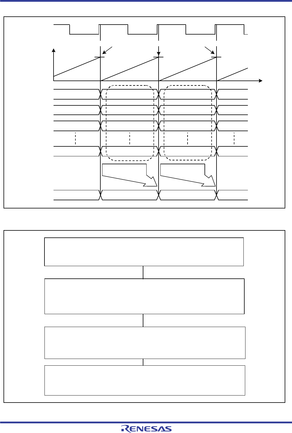
R01UH0034EJ0200 Rev.2.00 Page 866 of 1489
Dec 27, 2013
RX62T Group, RX62G Group 18. General PWM Timer (GPT/GPTa)
Figure 18.80 Example of LOCO Count Function Operation
Figure 18.81 Example for Setting LOCO Count Function Operation
Frequency-divided
LOCO clock
LCNT value
0000h
aaaa bbbb
The rising edge of frequency-divided LOCO clock is detected
and the counter is cleared.
Average value of
results in LCNT00 to
LCNT15
Average
value
Time
cccc
Average
value Average
value Average
value
LCNT00
LCNT01
LCNT02
LCNT15
LCNTA
aaaa bbbb cccc
aaaa bbbb
aaaa
Average value of
results in LCNT00 to
LCNT15
Select count clock
Select the frequency-divided LOCO clock with LPSC[1:0] in LCCR. Select
the count clock with TPSC[1:0] in LCCR.
Set IWDT
Activate the IWDT. (Refer to section 20, Independent Watchdog Timer (IWDT).)
When the value other than 00b is set in LCCR.LPSC[1:0], set
IWDT.ISDTCR.CKS[3:0] to the value other than 00xx.
Initialize count result registers
Set the initial values in the LCNT00 to LCNT15 registers.
When LCCR.LCNTS is set to 1, the LCNT00 value is also set in LCNT01 to
LCNT15.
Start count operation
Set LCCR.LCNTE to 1, and count operation will start on detecting the frequency-
divided LOCO clock rising.
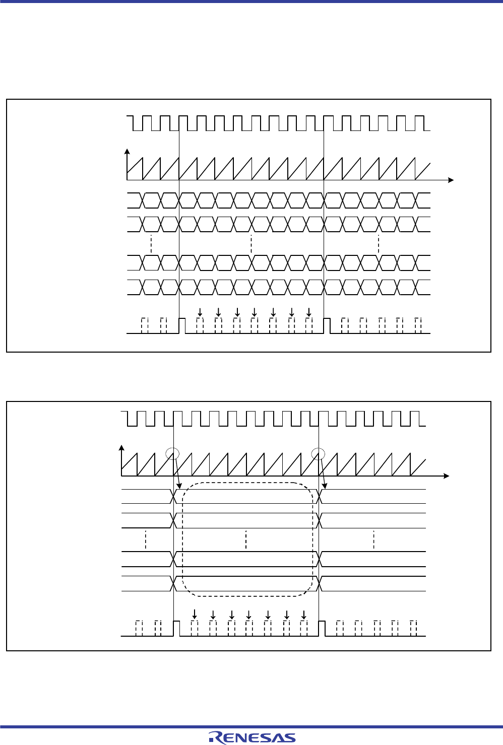
R01UH0034EJ0200 Rev.2.00 Page 867 of 1489
Dec 27, 2013
RX62T Group, RX62G Group 18. General PWM Timer (GPT/GPTa)
The frequency-divided LOCO clock rise interrupt requests can be skipped, and the count results can also be skipped. The
skipping count can be selected from 7, 15, 127, and 255 times with LCCR.LCTO[2:0]. Whether to skip the count results
is set with LCCR.LCNTAT.
Figure 18.82 shows an example in which the count result is not skipped, and Figure 18.83 shows an example in which
the count result is also skipped.
Figure 18.82 Example of LOCO Count Skipping Function Operation (Skipping Count: 7, Count Result not
Skipped)
Figure 18.83 Example of LOCO Count Skipping Function Operation (Skipping Count: 7, Count Result Skipped)
LCNT00
Frequency-divided LOCO
clock rise interrupt
request
0000h
LCNT value
Time
Skipped interrupt requests
LCNT01
LCNT15
LCNTA
Frequency-divided
LOCO clock
0000h
LCNT value
Frequency-divided
LOCO clock
LCNT00
LCNT01
LCNT15
LCNTA
Frequency-divided LOCO
clock rise interrupt
request
Skipped interrupt requests
Count result is also skipped
Time

R01UH0034EJ0200 Rev.2.00 Page 868 of 1489
Dec 27, 2013
RX62T Group, RX62G Group 18. General PWM Timer (GPT/GPTa)
18.7 Protection Function
18.7.1 Write-Protection for Registers
In order to prevent registers from being accidentally modified, registers can be write-protected in channel units by setting
GTWP.WPn (n = 0 to 3).
The write-protection can be set for the following registers:
GPTn.GTIOR, GPTn.GTINTAD, GPTn.GTCR, GPTn.GTBER, GPTn.GTUDC, GPTn.GTITC, GPTn.GTST,
GPTn.GTCNT, GPTn.GTCCRA, GPTn.GTCCRB, GPTn.GTCCRC, GPTn.GTCCRD, GPTn.GTCCRE,
GPTn.GTCCRF, GPTn.GTPR, GPTn.GTPBR, GPTn.GTPDBR, GPTn.GTADTRA, GPTn.GTADTBRA,
GPTn.GTADTDBRA, GPTn.GTADTRB, GPTn.GTADTBRB, GPTn.GTADTDBRB, GPTn.GTONCR,
GPTn.GTDTCR, GPTn.GTDVU, GPTn.GTDVD, GPTn.GTDBU, GPTn.GTDBD, GPTn.GTSOS, GPTn.GTSOS,
GPTn.GTSOTR
18.7.2 Disabling of Buffer Operation
If the timing of buffer register write is too late for the buffer transfer timing, buffer operation can be suspended with the
GTBDR setting. Specifically, buffer transfer can be temporarily disabled, even though a buffer transfer condition is
generated during buffer register write, by setting the corresponding GTBDR bit to 1 (buffer operation disabled) before
buffer register write and clearing the bit to 0 (buffer operation enabled) after completion of writing to all the buffer
registers.
Figure 18.84 shows an example of operation for disabling buffer operation
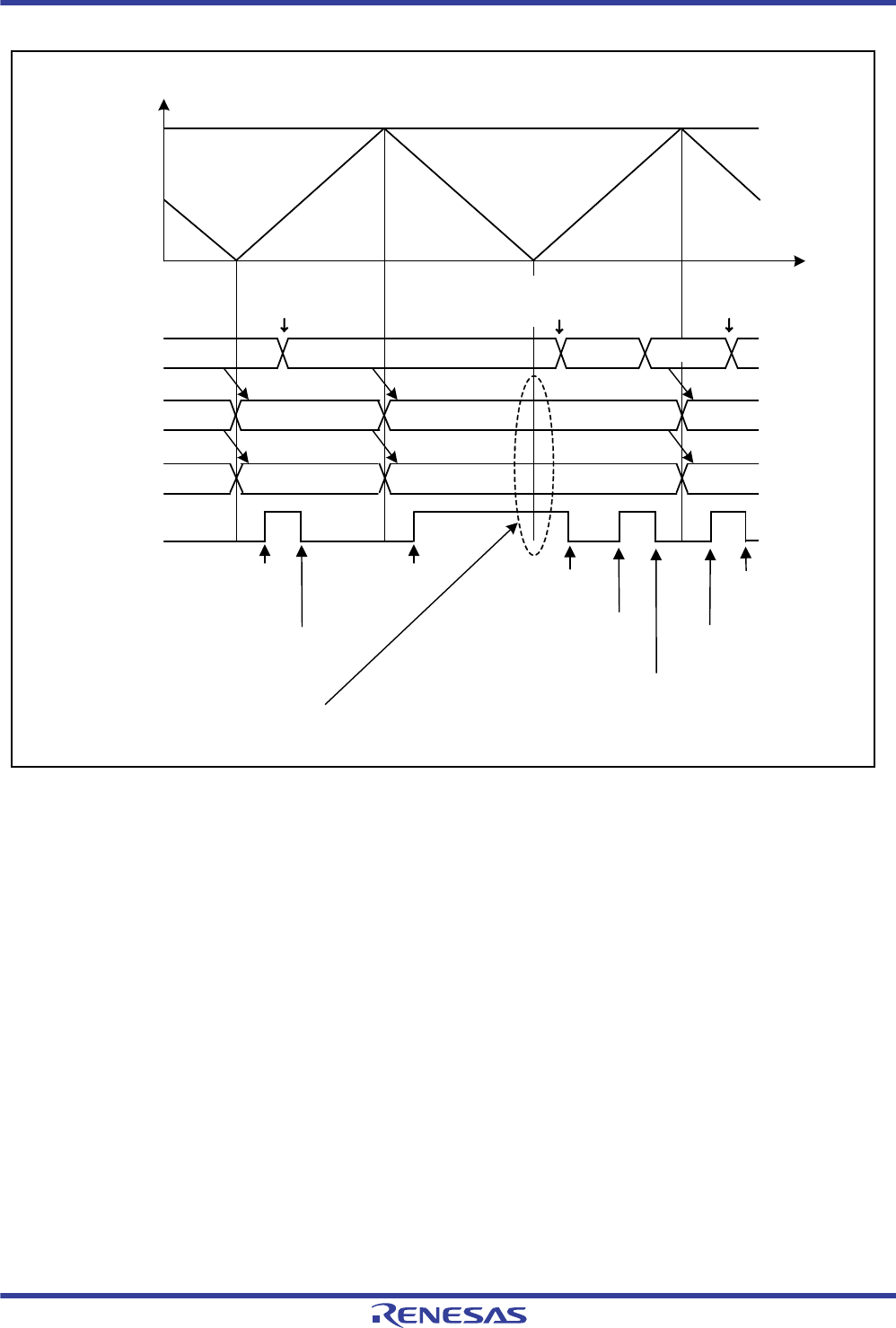
R01UH0034EJ0200 Rev.2.00 Page 869 of 1489
Dec 27, 2013
RX62T Group, RX62G Group 18. General PWM Timer (GPT/GPTa)
Figure 18.84 Example of Operation for Disabling Buffer Operation (Triangle Waves, Double Buffer Operation,
Buffer Transfer at Both Troughs and Crests)
Register write timing is too
late for buffer transfer timing
GPT0.GTCCRF
0000h
GPT0.GTPR
GPT0.GTCCRE
GPT0.GTCCRB
GPBDR.BD[0] bit
GPT0.GTCNT value
bbbb cccc eeeedddd
bbbb ccccaaaa
bbbbaaaa
eeee
cccc
Buffer transfer at
trough
Buffer transfer at
trough
Buffer transfer
at crest
Buffer transfer at
crest
Buffer transfer
at crest
Buffer transfer at
crest
Register write Register write
Set to 1 before
GPT0.GTCCRF
is written
Set to 1 before
GPT0.GTCCRF
is written
Cleared to 0 after
GPT0.GTCCRF
is written
Cleared to 0 after
GPT0.GTCCRF
is written
Cleared to 0 after
GPT0.GTCCRF
is written
Cleared to 0 after
GPT0.GTCCRF
is written
Set to 1 before
GPT0.GTCCRF
is written
Set to 1 before
GPT0.GTCCRF
is written
Buffer transfer not
performed when
GTBDR.BD0[0] = 1.
Time
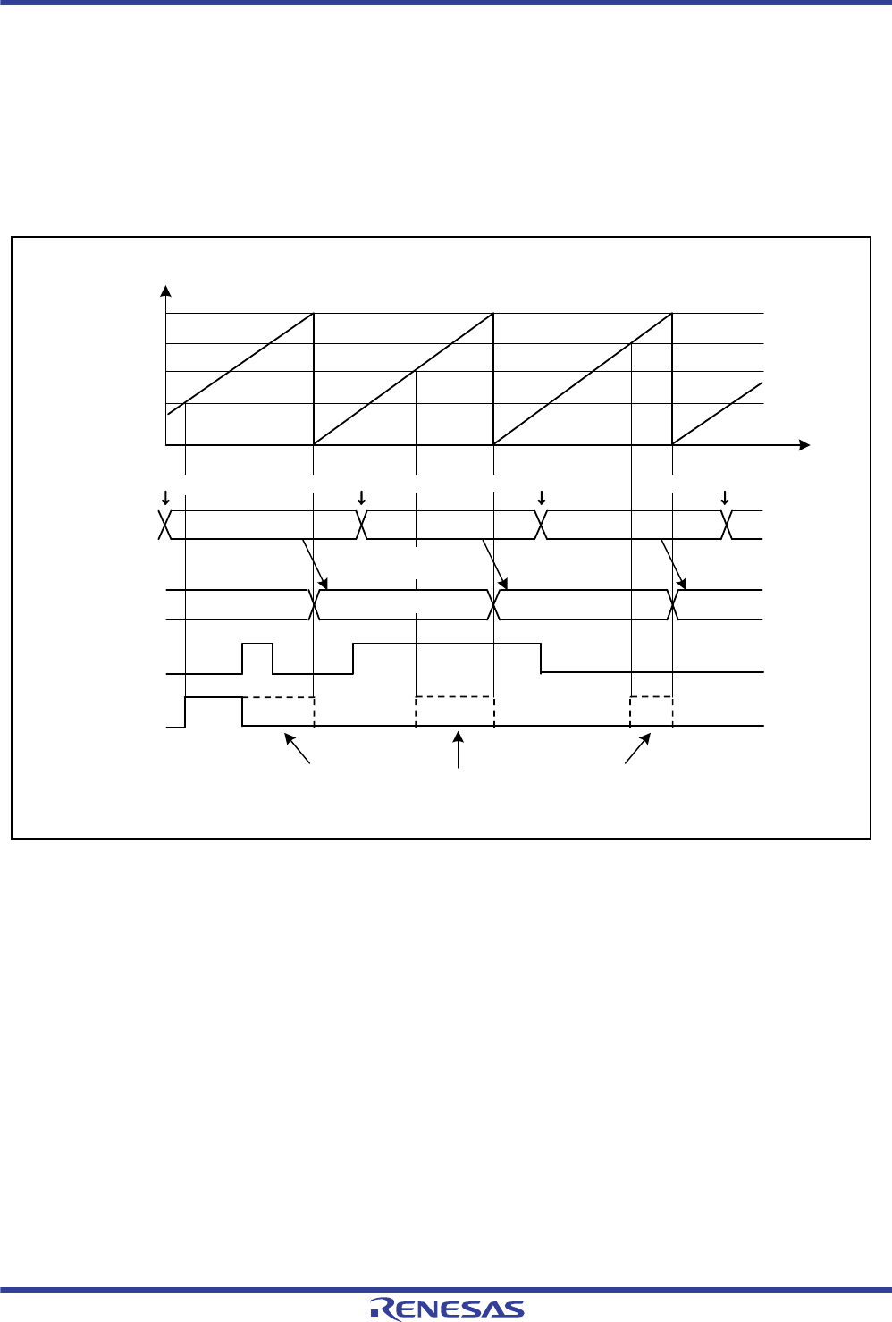
R01UH0034EJ0200 Rev.2.00 Page 870 of 1489
Dec 27, 2013
RX62T Group, RX62G Group 18. General PWM Timer (GPT/GPTa)
18.7.3 GTIOC Pin Output Negate Control
For protection from system failure, the negate control (deactivating the output level) is provided for GTIOC pin output
with the GTONCR setting. There are three negate control sources: the comparator detection, GTETRG pin input, and
writing to GTONCR.SWN.
Figure 18.85 shows an example of the GTIOC pin output negate control operation.
Note that once the negate control is performed, the negate control will not be released in the same cycle if the negate
condition is no longer satisfied. The negate control is released in the next cycle.
Figure 18.85 Example of GTIOC Pin Output Negate Control Operation (Saw-Wave Up-Counting, Buffer
Operation, Active Level: 1, High Output at GTCCRA Compare Match, Low Output at Cycle End)
GPT0.GTCCRC
0000h
GPT0.GTPR
GPT0.GTCNT value
Register write
aaaa
bbbb
cccc
Buffer transfer
at overflow
Register write Register write Register write
Buffer transfer
at overflow Buffer transfer
at overflow
ccccbbbbaaaa
ccccbbbb
Time
GPT0.GTCCRA
GTIOC pin output negated when the negate
control source is generated (deactivating the
output level).
Negate control
source
GTIOC0A output
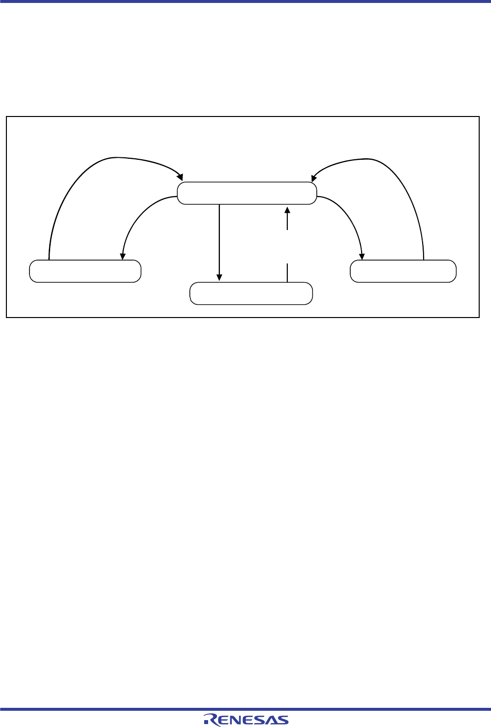
R01UH0034EJ0200 Rev.2.00 Page 871 of 1489
Dec 27, 2013
RX62T Group, RX62G Group 18. General PWM Timer (GPT/GPTa)
18.7.4 Output Protection Function for GTIOC Pin Output
In preparation for incorrect GTCCRA settings (settings outside the range of 0 < GTCCRA < GTPR), the output
protection function for the GTIOC pin output (disabling function) is activated when the automatic dead time setting
(GTDTCR.TDE = 1) is made in triangle-wave mode.
The status of the output protection function can be read from GTSOS.SOS[1:0].
Figure 18.86 shows the output protection function state transition.
Figure 18.86 Output Protection Function
(1) Output Protection Function When GTCCRA is Set to 0 during Buffer Transfer
Figure 18.87 and Figure 18.88 show examples of output protection function operation when GTCCRA is set to 0
during buffer transfer at troughs, and Figure 18.89 and Figure 18.90 show examples when GTCCRA is set to 0 during
buffer transfer at crests.
0 < GTCCRA < GTPR
or counting is stopped or
GTDTCR.TDE = 0
GTCCRA = 0
during buffer
transfer
0 < GTCCRA < GTPR
or counting is stopped
or GTDTCR.TDE = 0
0 < GTCCRA < GTPR
or counting is stopped
or GTDTCR.TDE = 0
Normal state (Output protection
function not activated)
(GTSOS.SOS[1:0] = 00b)
GTCCRA
GTPR during
buffer transfer
at trough
GTCCRA
GTPR during
buffer transfer
at crest
Output protected state
(GTSOS.SOS[1:0] = 01b)
Output protected state
(GTSOS.SOS[1:0] = 10b)
Output protected state
(GTSOS.SOS[1:0] = 11b)
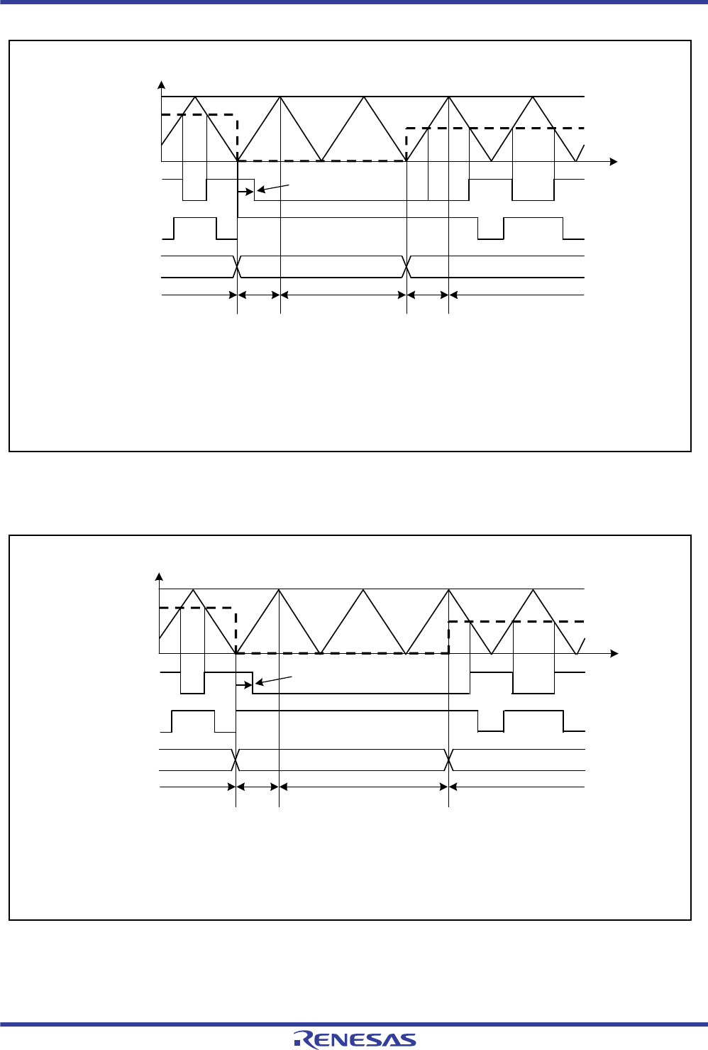
R01UH0034EJ0200 Rev.2.00 Page 872 of 1489
Dec 27, 2013
RX62T Group, RX62G Group 18. General PWM Timer (GPT/GPTa)
Figure 18.87 Example of Output Protection Function Operation When GTCCRA is Set to 0 during Buffer
Transfer at Troughs (Restored to 0<GTCCRA<GTPR during Buffer Transfer at Troughs, Active
Level: Low)
Figure 18.88 Example of Output Protection Function Operation When GTCCRA is Set to 0 during Buffer
Transfer at Troughs (Restored to 0<GTCCRA<GTPR during Buffer Transfer at Crests, Active
Level: Low)
(1) Normal operation period:
(2) Transition period:
(3) Output holding period:
(4) Recovery period:
(5) Normal operation period:
0000h
GPT0.GTPR
GPT0.GTCNT value
GPT0.GTCCRA
GTIOC0A pin output
(active low)
GTIOC0B pin output
(active low)
GTSOS.SOS[1:0]
bits
(1) Normal operation (2)
Transition (3) Output holding (4)
Recovery (5) Normal operation
Correction to
secure dead time
0100 00
Time
Toggle output due to a compare match is performed normally.
When GTCCRA = 0 is detected at the trough, the output protection status changes to
GTSOS.SOS[1:0] = 01b, and toggle output is continued up to the next crest.
The output is held while GTCCRA = 0.
When 0 < GTCCRA < GTPR is detected at the trough, the output protection status changes to
GTSOS.SOS[1:0] = 00b, and holding output is maintained up to the next crest.
Toggle output due to a compare match is performed normally.
0000h
GPT0.GTPR
GPT0.GTCNT value
GPT0.GTCCRA
GTIOC0A pin output
(active low)
GTIOC0B pin output
(active low)
GTSOS.SOS[1:0]
bits
(1) Normal operation (2)
Transition (3) Output holding (4) Normal operation
Correction to secure dead time
0100 00
Time
(1) Normal operation period:
(2) Transition period:
(3) Output holding period:
(4) Normal operation period:
Toggle output due to a compare match is performed normally.
When GTCCRA = 0 is detected at the trough, the output protection status changes to
GTSOS.SOS[1:0] = 01b, and toggle output is continued up to the next crest.
The output is held while GTCCRA = 0.
When 0 < GTCCRA < GTPR is detected at the crest, the output protection status changes to
GTSOS.SOS[1:0] = 00b, and toggle output due to a compare match is performed normally.
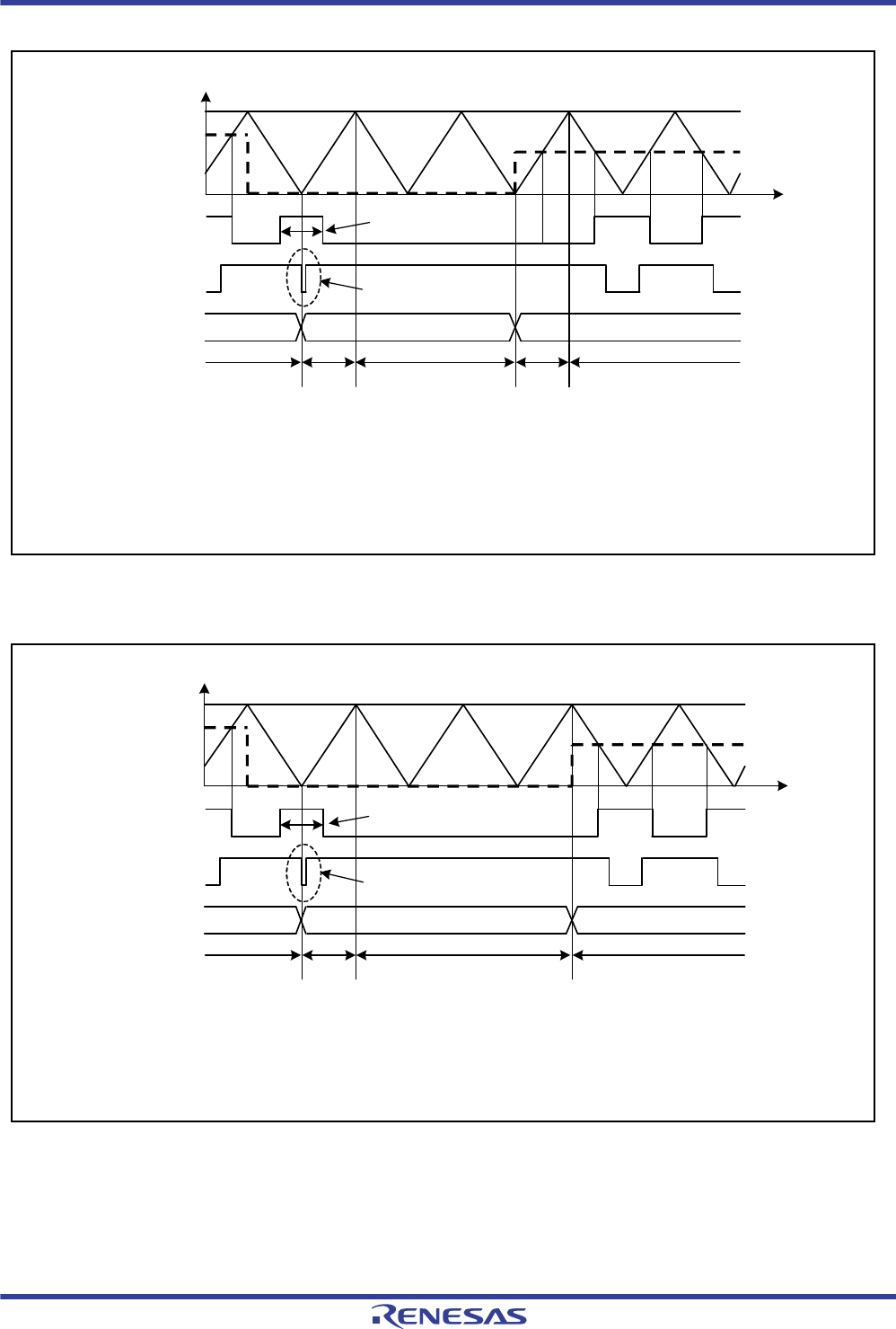
R01UH0034EJ0200 Rev.2.00 Page 873 of 1489
Dec 27, 2013
RX62T Group, RX62G Group 18. General PWM Timer (GPT/GPTa)
Figure 18.89 Example of Output Protection Function Operation When GTCCRA is Set to 0 during Buffer
Transfer at Crests (Restored to 0<GTCCRA<GTPR during Buffer Transfer at Troughs, Active
Level: Low)
Figure 18.90 Example of Output Protection Function Operation When GTCCRA is Set to 0 during Buffer
Transfer at Crests (Restored to 0<GTCCRA<GTPR during Buffer Transfer at Crests, Active Level:
Low)
(1) Normal operation period:
(2) Transition period:
(3) Output holding period:
(4) Recovery period:
(5) Normal operation period:
0000h
GPT0.GTPR
GPT0.GTCNT value
GPT0.GTCCRA
GTIOC0A pin output
(active low)
GTIOC0B pin output
(active low)
GTSOS.SOS[1:0]
bits
(1) Normal operation (2)
Transition (3) Output holding (4)
Recovery (5) Normal operation
0100 00
Time
A pulse of one count-
clock cycle is generated
Correction to secure
dead time
Toggle output due to a compare match is performed normally.
When GTCCRA = 0 is detected at the trough, the output protection status changes to
GTSOS.SOS[1:0] = 01b, and toggle output is continued up to the next crest.
The output is held while GTCCRA = 0.
When 0 < GTCCRA < GTPR is detected at the trough, the output protection status changes to
GTSOS.SOS[1:0] = 00b, and holding output is maintained up to the next crest.
Toggle output due to a compare match is performed normally.
(1) Normal operation period:
(2) Transition period:
(3) Output holding period:
(4) Recovery period:
0000h
GPT0.GTPR
GPT0.GTCNT value
GPT0.GTCCRA
GTIOC0A pin output
(active low)
GTIOC0B pin output
(active low)
GTSOS.SOS[1:0]
bits
(1) Normal operation (2)
Transition (3) Output holding (4) Normal operation
Correction to
secure dead line
0100 00
Time
A pulse of one count-
clock cycle is generated
Toggle output due to a compare match is performed normally.
When GTCCRA = 0 is detected at the trough, the output protection status changes to
GTSOS.SOS[1:0] = 01b, and toggle output is continued up to the next crest.
The output is held while GTCCRA = 0.
When 0 < GTCCRA < GTPR is detected at the crest, the output protection status changes to
GTSOS.SOS[1:0] = 00b, and toggle output due to a compare match is performed normally.
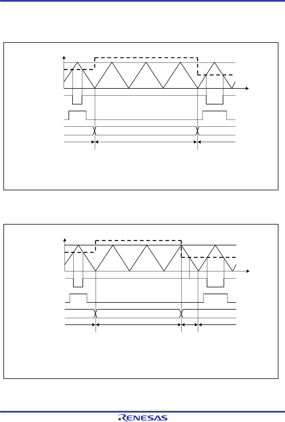
R01UH0034EJ0200 Rev.2.00 Page 874 of 1489
Dec 27, 2013
RX62T Group, RX62G Group 18. General PWM Timer (GPT/GPTa)
(2) Output Protection Function When GTCCRA GTPR is Set during Buffer Transfer at Troughs
Figure 18.91 and Figure 18.92 show examples of output protection function operation when GTCCRA GTPR is set
during buffer transfer at troughs.
Figure 18.91 Example of Output Protection Function Operation When GTCCRA GTPR is set during Buffer
Transfer at Troughs (Restored to 0<GTCCRA<GTPR during Buffer Transfer at Troughs,
Active Level: Low)
Figure 18.92 Example of Output Protection Function Operation When GTCCRA GTPR is Set during Buffer
Transfer at Troughs (Restored to 0<GTCCRA<GTPR during Buffer Transfer at Crests, Active
Level: Low)
(1) Normal operation period:
(2) Output holding period:
(3) Normal operation period:
0000h
GPT0.GTPR
GPT0.GTCNT value
GPT0.GTCCRA
GTIOC0A pin output
(active low)
GTIOC0B pin output
(active low)
GTSOS.SOS[1:0]
bits
(1) Normal operation (2) Output holding (3) Normal operation
1000 00
Time
Toggle output due to a compare match is performed normally.
When GTCCRA GTPR is detected at the trough, the output protection status changes to
GTSOS[1:0] = 10b, and the output is held while GTCCRA GTPR.
When 0 < GTCCRA < GTPR is detected at the trough, the output protection status changes to
GTSOS[1:0] = 00b, ant toggle output due to a compare match is performed normally.
(1) Normal operation period:
(2) Output holding period:
(3) Recovery period:
(4) Normal operation period:
0000h
GPT0.GTPR
GPT0.GTCNT value
GPT0.GTCCRA
GTIOC0A pin output
(active low)
GTIOC0B pin output
(active low)
GTSOS.SOS[1:0]
bits
(1) Normal operation (2) Output holding (3)
Recovery (4) Normal operation
1000 00
Time
Toggle output due to a compare match is performed normally.
When GTCCRA GTPR is detected at the trough, the output protection status changes to
GTSOS[1:0] = 10b, and the output is held while GTCCRA GTPR.
When 0 < GTCCRA < GTPR is detected at the crest, the output protection status changes to
GTSOS.SOS[1:0] = 00b, and holding output is maintained up to the next trough.
Toggle output due to a compare match is performed normally.

R01UH0034EJ0200 Rev.2.00 Page 875 of 1489
Dec 27, 2013
RX62T Group, RX62G Group 18. General PWM Timer (GPT/GPTa)
(3) Output Protection Function When GTCCRA GTPR is Set during Buffer Transfer at Crests
Figure 18.93 and Figure 18.94 show examples of output protection function operation when GTCCRA GTPR is set
during buffer transfer at crests.
Figure 18.93 Example of Output Protection Function Operation When GTCCRA GTPR is Set during Buffer
Transfer at Crests (Restored to 0<GTCCRA<GTPR during Buffer Transfer at Crests, Active Level:
Low)
Figure 18.94 Example of Output Protection Function Operation When GTCCRA GTPR is Set during Buffer
Transfer at Crests (Restored to 0<GTCCRA<GTPR during Buffer Transfer at Troughs, Active
Level: Low)
0000h
GPT0.GTPR
GPT0.GTCNT value
GPT0.GTCCRA
GTIOC0A pin output
(active low)
GTIOC0B pin output
(active low)
GTSOS.SOS[1:0]
bits
(1) Normal operation (2) Output holding (3) Normal operation
1100 00
(1) Normal operation period:
(2) Output holding period:
(3) Normal operation period:
Time
Toggle output due to a compare match is performed normally.
When GTCCRA GTPR is detected at the crest, the output protection status changes to
GTSOS[1:0] = 11b, and the output is held while GTCCRA GTPR.
When 0 < GTCCRA < GTPR is detected at the crest, the output protection status changes to
GTSOS.SOS[1:0] = 00b, and toggle output due to a compare match is performed normally.
GPT0.GTPR
GPT0.GTCNT value
GPT0.GTCCRA
GTIOC0A pin output
(active low)
GTIOC0B pin output
(active low)
GTSOS.SOS[1:0]
bits
(1) Normal operation (2) Output holding (3)
Recovery (4) Normal operation
1100 00
Time
(1) Normal operation period:
(2) Output holding period:
(3) Recovery period:
(4) Normal operation period:
0000h
Toggle output due to a compare match is performed normally.
When GTCCRA GTPR Is detected at the crest, the output protection status changes to
GTSOS[1:0] = 11b, and the output is held while GTCCRA GTPR.
When 0 < GTCCRA < GTPR is detected at the trough, the output protection status changes to
GTSOS.SOS[1:0] = 00b, and holding output is maintained up to the next crest.
Toggle output due to a compare match is performed normally.

R01UH0034EJ0200 Rev.2.00 Page 876 of 1489
Dec 27, 2013
RX62T Group, RX62G Group 18. General PWM Timer (GPT/GPTa)
(4) Restricted Specification of Output Protection Function
The GTCCRA value must be set within the range of (0 < GTCCRA < GTPR) at count start.
If an incorrect value is set in GTCCRA during count operation, (a setting outside the range of 0 < GTCCRA < GTPR),
the output protection function deactivates the level of one of the positive and negative outputs. However, the function
does not operate correctly if counting starts with an incorrect value set in GTCCRA.
18.7.5 High-Impedance Control of GTIOC Pin Output by POE Function
For protection from system failure, the high-impedance state of the GTIOC pin output can be controlled by the port
output enable (POE) function.
For details, see section 17, Port Output Enable 3 (POE3).

R01UH0034EJ0200 Rev.2.00 Page 877 of 1489
Dec 27, 2013
RX62T Group, RX62G Group 18. General PWM Timer (GPT/GPTa)
18.8 Initialization Method of Output Pins
18.8.1 Pin Settings after Reset
The GPT registers are initialized at a reset. Start counting after setting GTIOR and the OAE and OBE bits in GTONCR
and outputting the GPT function to external pins.
Figure 18.95 Example of Pin Settings after Reset
18.8.2 Pin Initialization Due to Error during Operation
If an error occurs during GPT operation, the following four types of pin processing can be performed before pin
initialization.
(1) Set OAHLD and OBHLD bits in GTIOR to 1 and retain the outputs at count stop.
(2) Set OAHLD and OBHLD bits in GTIOR to 0, specify arbitrary output values at OADFLT and OBDFLT in GTIOR,
and output the arbitrary values at count stop.
(3) Similar to the MTU3, previously set the pin to output an arbitrary value as a general output port by setting the DDR
and DR registers of the I/O port. Set the OAE and OBE bits in GTONCR to 0 when an error occurs to allow the
arbitrary values to be output from the pin set as a general output port.
(4) Drive the output to a high impedance state using the POE function of the port output enable 3 (POE3).
When automatic dead time setting has been made, clear the GTDTCR.TDE bit to 0 once after counting is stopped.
When counting is stopped, only the values of registers that are changed by a GPT external source will change. If counting
is resumed, operation will carry on from where it was stopped.
If counting was stopped, registers should be initialized before counting is started.
PD6/GTIOC0B-B output
PD7/GTIOC0A-B output
GPT0.GTCCRB
0000h
GPT0.GTPR
GPT0.GTCNT value
GPT0.GTCCRA
GPT initialization settings Count operation
Reset is released.
Reset
Count operation starts.
GTONCR.OAE and
GTONCR.OBE are set.
[Setting examples]
GTIOR.GTIOA[5:0]: Initial output of low, output retained at cycle end, toggle output at compare match
GTIOR.GTIOB[5:0]: Initial output of high, output retained at cycle end, toggle output at compare match
Hi-Z
Hi-Z
Time

R01UH0034EJ0200 Rev.2.00 Page 878 of 1489
Dec 27, 2013
RX62T Group, RX62G Group 18. General PWM Timer (GPT/GPTa)
18.9 Usage Notes
18.9.1 Module Stop Function Setting
Operation of the GPT can be disabled or enabled by the module stop control register. The initial setting is for operation of
the GPT to be halted. Register access is enabled by clearing module stop state. For details, see section 9, Low Power
Consumption.
18.9.2 Settings of GTCCRn during Compare Match Operation (n = A, B, C, D, E, F)
(1) When automatic dead time setting has been made in triangle-wave PWM mode
GTCCRA should be set within the range of GTDVU < GTCCRA, GTDVD < GTCCRA, and GTCCRA < GTPR.
When the setting of GTCCRA = 0 or GTCCRA GTPR is made during count operation, the output protection function
is activated.
Be sure to set 0 < GTCCRA < GTPR at count start. Otherwise, the output protection function is not be activated
correctly. For details, refer to section 18.7.4, Output Protection Function for GTIOC Pin Output .
(2) When automatic dead time setting has not been made in triangle-wave PWM mode
GTCCRA should be set within the range of 0 < GTCCRA < GTPR. If GTCCRA = 0 or GTCCRA GTPR is set, a
compare match occurs within the cycle only when GTCCRA = 0 or GTCCRA = GTPR is satisfied. In the case of
GTCCRA > GTPR, no compare match occurs.
Similarly, GTCCRB should be set within the range of 0 < GTCCRB < GTPR. If GTCCRB = 0 or GTCCRA GTPR is
set, a compare match occurs within the cycle only when GTCCRB = 0 or GTCCRB = GTPR is satisfied. In the case of
GTCCRB > GTPR, no compare match occurs.
(3) When automatic dead time setting has been made in saw-wave one-shot pulse mode
GTCCRC and GTCCRD should be set to satisfy the following restrictions. If the restrictions are not satisfied, correct
output waveforms with secured dead time may not be obtained.
In up-count operation: GTCCRC < GTCCRD, GTCCRC > GTDVU, GTCCRD < GTPR - GTDVD
In down-count operation: GTCCRC > GTCCRD, GTCCRC < GTPR – GTDVU, GTCCRD > GTDVD

R01UH0034EJ0200 Rev.2.00 Page 879 of 1489
Dec 27, 2013
RX62T Group, RX62G Group 18. General PWM Timer (GPT/GPTa)
(4) When automatic dead time setting has not been made in saw-wave one-shot pulse mode
GTCCRC and GTCCRD should be set to satisfy the following restrictions. If the restrictions are not satisfied, two
compare matches do not occur and pulse output cannot be performed.
In up-count operation: 0 < GTCCRC < GTCCRD < GTPR
In down-count operation: GTPR > GTCCRC > GTCCRD > 0
Similarly, GTCCRE and GTCCRF should be set to satisfy the following restrictions. If the restrictions are not satisfied,
two compare matches do not occur and pulse output cannot be performed.
In up-count operation: 0 < GTCCRE < GTCCRF < GTPR
In down-count operation: GTPR > GTCCRE > GTCCRF > 0
(5) In saw-wave PWM mode
GTCCRA should be set with the range of 0 < GTCCRA < GTPR. If GTCCRA = 0 or GTCCRA = GTPR is set, a
compare match occurs within the cycle only when GTCCRA = 0 or GTCCRA = GTPR is satisfied. If GTCCRA > GTPR
is set, no compare match occurs.
Similarly, GTCCRB should be set with the range of 0 < GTCCRB < GTPR. If GTCCRB = 0 or GTCCRB = GTPR is set,
a compare match occurs within the cycle only when GTCCRB = 0 or GTCCRB = GTPR is satisfied. If GTCCRB >
GTPR is set, no compare match occurs.
18.9.3 Stopping the Timer in the Safe Way
When the timer stopping by the GTSTR writing and the GPT compare match interrupt conflict, an interrupt may be
generated after the GTSTR writing.
Therefore, stop the timer in the following order. Then, a compare match interrupt is not generated after the timer has been
stopped, and the timer can be stopped in the safe way.
(1) Disable the interrupt request by the interrupt request enable registers (IER15 to IER18) of the ICU.
(2) Disable the interrupt request by the interrupt output setting register (GTINTAD) of the GPT.
(3) Clear the CSTn bit in GTSTR to 0.
18.9.4 Low-Power Consumption Setting when the LOCO Count Function is in Use
In the case when the GPT operation is stopped during the LOCO count operation by the module stop control register or
standby control register and then restarted, first clear the LCCR.LCNTE bit to 0 to stop the LOCO count before the GPT
operation is stopped. Then, set the LCCR.LCNTE bit to 1 to restart the LOCO count after the GPT operation is restarted.
For details on the module stop control register and the standby control register, see section 9., Low Power
Consumption.
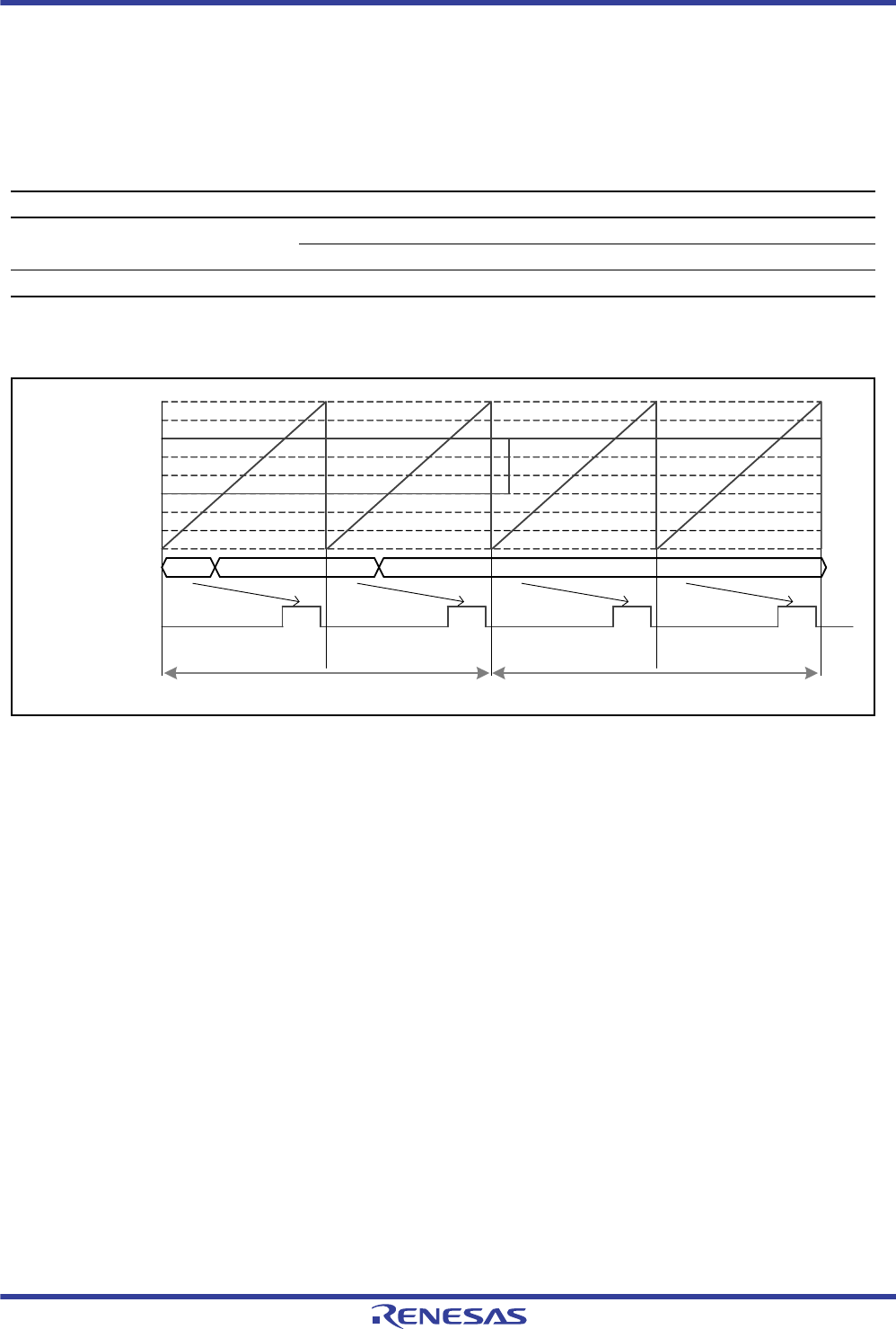
R01UH0034EJ0200 Rev.2.00 Page 880 of 1489
Dec 27, 2013
RX62T Group, RX62G Group 18. General PWM Timer (GPT/GPTa)
18.9.5 Notes on Delay Time Settings for PWM Delay Generation Circuit
When the PWM delay generation circuit generates delays for a PWM output waveform and the waveform is being
toggled in response to compare-matches, do not change the settings for delay time while the compare-match value is
within the ranges listed in the following table. This restriction applies to the GTDLYFA, GTDLYRA, GTDLFB, and
GTDLYRB registers.
An example of how the restrictions apply to the timing of setting GTDLYFA in sawtooth waveform one-shot pulse mode
(counting up) is shown as figure 18.94. Do not change the value set in GTDLYFA while GTCCRD ≥ GTPR - 2.
Figure 18.96 Restriction on the Timing of GTDLYFA Register Settings
Changing the values in the GTDLYFA, GTDLYRA, GTDLYFB, and GTDLYRB registers during periods where changes
to settings are not allowed may lead to faulty output waveforms, i.e., shifts in the timing of output waveform transitions
from the expected values.
Mode Direction of Counting Compare-Match Value
Sawtooth waveform Up GTPR - 2 or above
Down 2 or below
Triangle waveform Down 2 or below
BTPR
Set GTPR - 5 to the
GTCCRO register
Set GTPR - 2 to the
GTCCRO register
GTDLYFA register
GTDOGnA pin
Change of GTDLYFA setting allowed Change of GTDLYFA setting not allowed
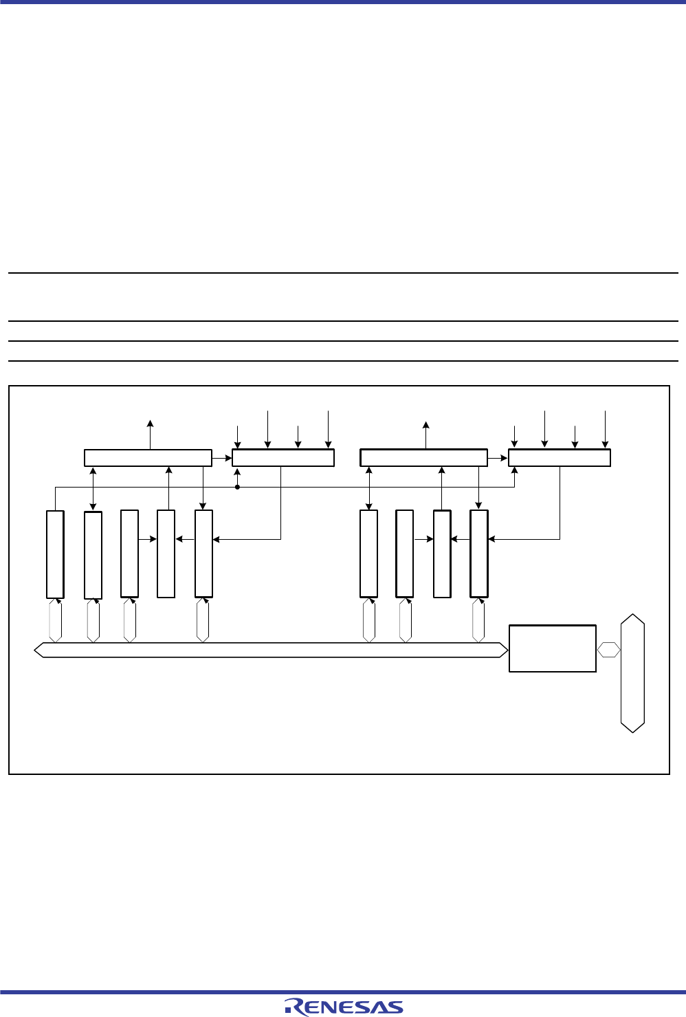
R01UH0034EJ0200 Rev.2.00 Page 881 of 1489
Dec 27, 2013
RX62T Group, RX62G Group 19. Compare Match Timer (CMT)
Under development Preliminary document
Specifications in this document are tentative and subject to change.
19. Compare Match Timer (CMT)
The RX62T and RX62G Groups have two on-chip compare match timer (CMT) units (unit 0 and unit 1) each consisting
of a two-channel 16-bit timer (i.e., a total of four channels). The CMT has a 16-bit counter, and can generate interrupts at
set intervals.
19.1 Overview
Table 19.1 lists the specifications for the CMT.
Figure 19.1 shows a block diagram of the CMT (unit 0). A two-channel CMT constitutes a unit. Unit 0 and unit 1 are the
same in terms of specifications.
Figure 19.1 Block Diagram of CMT (Unit 0)
Table 19.1 Specifications of CMT
Item Description
Count clock Four internal clocks
One clock from PCLK/8, PCLK/32, PCLK/128, and PCLK/512 can be selected individually for
each channel.
Interrupt A compare match interrupt can be requested individually for each channel.
Low power consumption facilities Each unit can be placed in a module stop state.
Control unit Clock selection
Module bus
CMI0 PCLK/32 PCLK/512
PCLK/128
PCLK/8
Control unit Clock selection
CMI1 PCLK/32 PCLK/512
PCLK/128
PCLK/8
Bus interface
Comparator
Comparator
Internal bus
CMSTR0: Compare match timer start register 0
CMCR: Compare match timer control register
CMCOR: Compare match constant register
CMCNT: Compare match timer counter
CMI: Compare match interrupt
[Legend]
CMSTR0
CMCR
CMCOR
CMCNT
CMCR
CMCOR
CMCNT

R01UH0034EJ0200 Rev.2.00 Page 882 of 1489
Dec 27, 2013
RX62T Group, RX62G Group 19. Compare Match Timer (CMT)
Under development Preliminary document
Specifications in this document are tentative and subject to change.
19.2 Register Descriptions
Table 19.2 lists the registers of the CMT.
Table 19.2 List of CMT Registers
Unit Channel Register Name Symbol Value after
Reset Address Access
Size
Unit 0 CMT Compare match timer start register 0 CMSTR0 0000h 0008 8000h 16
CMT0 Compare match timer control register CMCR 00x0h 0008 8002h 16
Compare match timer counter CMCNT 0000h 0008 8004h 16
Compare match timer constant register CMCOR FFFFh 0008 8006h 16
CMT1 Compare match timer control register CMCR 00x0h 0008 8008h 16
Compare match timer counter CMCNT 0000h 0008 800Ah 16
Compare match timer constant register CMCOR FFFFh 0008 800Ch 16
Unit 1 CMT Compare match timer start register 1 CMSTR1 0000h 0008 8010h 16
CMT2 Compare match timer control register CMCR 00x0h 0008 8012h 16
Compare match timer counter CMCNT 0000h 0008 8014h 16
Compare match timer constant register CMCOR FFFFh 0008 8016h 16
CMT3 Compare match timer control register CMCR 00x0h 0008 8018h 16
Compare match timer counter CMCNT 0000h 0008 801Ah 16
Compare match timer constant register CMCOR FFFFh 0008 801Ch 16

R01UH0034EJ0200 Rev.2.00 Page 883 of 1489
Dec 27, 2013
RX62T Group, RX62G Group 19. Compare Match Timer (CMT)
Under development Preliminary document
Specifications in this document are tentative and subject to change.
19.2.1 Compare Match Timer Start Register 0 (CMSTR0)
CMSTR0 selects whether the CMT0.CMCNT or CMT1.CMCNT counter operates or is stopped.
STR0 Bit (Count Start 0)
The STR0 bit specifies whether CMT0.CMCNT operates or is stopped.
STR1 Bit (Count Start 1)
The STR1 bit specifies whether CMT1.CMCNT operates or is stopped.
Address: 0008 8000h
b15 b14 b13 b12 b11 b10 b9 b8 b7 b6 b5 b4 b3 b2 b1 b0
——————————————STR1STR0
Value after reset: 0000000000000000
Bit Symbol Bit Name Description R/W
b0 STR0 Count Start 0 0: CMT0.CMCNT count is stopped
1: CMT0.CMCNT count is started
R/W
b1 STR1 Count Start 1 0: CMT1.CMCNT count is stopped
1: CMT1.CMCNT count is started
R/W
b15 to b2 — Reserved These bits are always read as 0. The write value should always be 0. R/W

R01UH0034EJ0200 Rev.2.00 Page 884 of 1489
Dec 27, 2013
RX62T Group, RX62G Group 19. Compare Match Timer (CMT)
Under development Preliminary document
Specifications in this document are tentative and subject to change.
19.2.2 Compare Match Timer Start Register 1 (CMSTR1)
CMSTR1 selects whether the CMT2.CMCNT or CMT3.CMCNT counter operates or is stopped.
STR2 Bit (Count Start 2)
The STR2 bit specifies whether CMT2.CMCNT operates or is stopped.
STR3 Bit (Count Start 3)
The STR3 bit specifies whether CMT3.CMCNT operates or is stopped.
Address: 0008 8010h
b15 b14 b13 b12 b11 b10 b9 b8 b7 b6 b5 b4 b3 b2 b1 b0
——————————————STR3STR2
Value after reset: 0000000000000000
Bit Symbol Bit Name Description R/W
b0 STR2 Count Start 2 0: CMT2.CMCNT count is stopped
1: CMT2.CMCNT count is started
R/W
b1 STR3 Count Start 3 0: CMT3.CMCNT count is stopped
1: CMT3.CMCNT count is started
R/W
b15 to b2 — Reserved These bits are always read as 0. The write value should always be 0. R/W

R01UH0034EJ0200 Rev.2.00 Page 885 of 1489
Dec 27, 2013
RX62T Group, RX62G Group 19. Compare Match Timer (CMT)
Under development Preliminary document
Specifications in this document are tentative and subject to change.
19.2.3 Compare Match Timer Control Register (CMCR)
CMCR sets the clock used for counting up.
If data write to the CMCR register conflicts with the generation of a compare-match, data write to the CMCR register is
ignored. For details, see section 19.5.4, Notes on Data Write to the Compare-Match Timer Control Register
(CMCR).
CKS[1:0] Bits (Clock Select)
These bits select the count clock to be input to CMCNT from four internal clocks obtained by dividing the peripheral
clock (PCLK).
When the STRn (n = 0 to 3) bit in CMSTRm (m = 0 or 1) is set to 1, CMCNT starts counting up on the count clock
selected with bits CKS[1:0].
CMIE Bit (Compare Match Interrupt Enable)
The CMIE bit enables or disables compare match interrupt (CMIn) (n = 0 to 3) generation when CMCNT and CMCOR
values match.
Address: CMT0.CMCR 0008 8002h, CMT1.CMCR 0008 8008h,
CMT2.CMCR 0008 8012h, CMT3.CMCR 0008 8018h
b15 b14 b13 b12 b11 b10 b9 b8 b7 b6 b5 b4 b3 b2 b1 b0
—————————CMIE——— CKS[1:0]
Value after reset: 00000000x0000000
x: Undefined
Bit Symbol Bit Name Description R/W
b1, b0 CKS[1:0] Clock Select b1 b0
0 0: PCLK/8
0 1: PCLK/32
1 0: PCLK/128
1 1: PCLK/512
R/W
b5 to b2 — Reserved These bits are always read as 0.
The write value should always be 0.
R/W
b6 CMIE Compare Match Interrupt Enable 0: Compare match interrupt (CMIn) disabled
1: Compare match interrupt (CMIn) enabled
R/W
b7 — Reserved This bit is always read as undefined.
The write value should always be 1.
R/W
b15 to b8 — Reserved These bits are always read as 0.
The write value should always be 0.
R/W
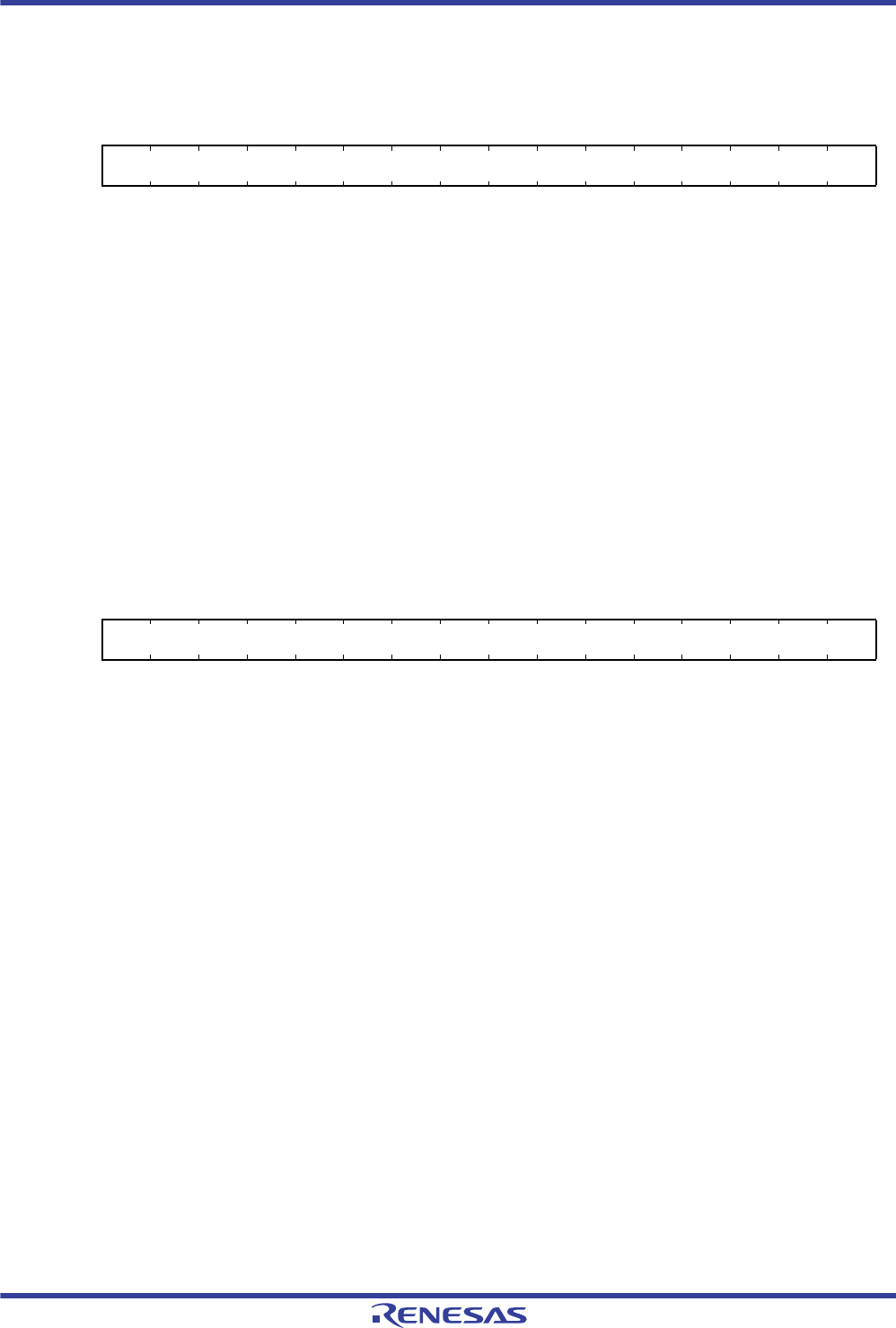
R01UH0034EJ0200 Rev.2.00 Page 886 of 1489
Dec 27, 2013
RX62T Group, RX62G Group 19. Compare Match Timer (CMT)
Under development Preliminary document
Specifications in this document are tentative and subject to change.
19.2.4 Compare Match Timer Counter (CMCNT)
CMCNT is a readable/writable up-counter to generate interrupt requests.
When a count clock is selected by bits CKS[1:0] in CMCR and the STRn (n = 0 to 3) bit in CMSTRm (m = 0 or 1) is set
to 1, CMCNT starts counting up using the selected count clock.
When the value in CMCNT and the value in CMCOR match, CMCNT is cleared to 0000h. At the same time, a compare
match interrupt (CMIn) (n = 0 to 3) is generated.
Do not set the CMCNT counter and the CMCOR register to the same value while the CMCNT counter counting
operation is halted. For details, see section 19.5.5, Notes on the Compare-Match Timer Counter (CMCNT) and
the Compare-Match Constant Register (CMCOR).
19.2.5 Compare Match Timer Constant Register (CMCOR)
CMCOR sets the interval up to a compare match with CMCNT.
Do not set the CMCNT counter and the CMCOR register to the same value while the CMCNT counter counting
operation is halted. For details, see section 19.5.5, Notes on the Compare-Match Timer Counter (CMCNT) and
the Compare-Match Constant Register (CMCOR).
Address: CMT0.CMCNT 0008 8004h, CMT1.CMCNT 0008 800Ah,
CMT2.CMCNT 0008 8014h, CMT3.CMCNT 0008 801Ah
b15 b14 b13 b12 b11 b10 b9 b8 b7 b6 b5 b4 b3 b2 b1 b0
Value after reset: 0000000000000000
Address: CMT0.CMCOR 0008 8006h, CMT1.CMCOR 0008 800Ch,
CMT2.CMCOR 0008 8016h, CMT3.CMCOR 0008 801Ch
b15 b14 b13 b12 b11 b10 b9 b8 b7 b6 b5 b4 b3 b2 b1 b0
Value after reset: 1111111111111111
R01UH0034EJ0200 Rev.2.00 Page 887 of 1489
Dec 27, 2013
RX62T Group, RX62G Group 19. Compare Match Timer (CMT)
Under development Preliminary document
Specifications in this document are tentative and subject to change.
19.3 Operation
19.3.1 Periodic Count Operation
When a count clock is selected by bits CKS[1:0] in CMCR and the STRn (n = 0 to 3) bit in CMSTRm (m = 0 or 1) is set
to 1, CMCNT starts counting up using the selected count clock.
When the value in CMCNT and the value in CMCOR match, CMCNT is cleared to 0000h. At the same time, a compare
match interrupt (CMIn) (n = 0 to 3) is generated. CMCNT then starts counting up again from 0000h. Figure 19.2 shows
the operation of the CMCNT counter.
Figure 19.2 CMCNT Counter Operation
19.3.2 CMCNT Count Timing
One of four internal clocks (PCLK/8, PCLK/32, PCLK/128, and PCLK/512) obtained by dividing the peripheral clock
(PCLK) can be selected as a count clock with the CKS[1:0] bits in CMCSR. Figure 19.3 shows the timing of CMCNT.
Figure 19.3 CMCNT Count Timing
Time
Counter cleared by compare match with CMCOR
CMCNT value
CMCOR
0000h
PCLK
Count clock
CMCNT NN+1N-1
R01UH0034EJ0200 Rev.2.00 Page 888 of 1489
Dec 27, 2013
RX62T Group, RX62G Group 19. Compare Match Timer (CMT)
Under development Preliminary document
Specifications in this document are tentative and subject to change.
19.4 Interrupts
19.4.1 Interrupt Sources
The CMT has channels and each of them to which a different vector address is allocated has a compare match interrupt
(CMIn) (n = 0 to 3). When a compare match interrupt occurs, the corresponding interrupt request is output.
When the interrupt is used to activate a CPU interrupt, the priority of channels can be changed by the interrupt controller
settings. For details, see section 11., Interrupt Controller (ICU).
19.4.2 Timing of Compare Match Interrupt Generation
When CMCNT and CMCOR match, a compare match interrupt (CMIn) (n = 0 to 3) is generated.
A compare match signal is generated at the last state in which the values match (the timing when the CMCNT counter
updates the matched count value). That is, after a match between CMCOR and CMCNT, the compare match signal is not
generated until the next count clock.
Figure 19.4 shows the timing of the interrupt for a compare-match.
Figure 19.4 Timing of Generation of Compare Match Signal
Table 19.3 CMT Interrupt Sources
Name Interrupt Sources Interrupt Status
Flag DTC Activation
CMI0 Compare match between CMT0.CMCNT and CMT0.CMCOR IR028.IR Possible
CMI1 Compare match between CMT1.CMCNT and CMT1.CMCOR IR029.IR Possible
CMI2 Compare match between CMT2.CMCNT and CMT2.CMCOR IR030.IR Possible
CMI3 Compare match between CMT3.CMCNT and CMT3.CMCOR IR031.IR Possible
PCLK
Count clock
CMCNT
CMCOR
Interrupt signal
N
N
0000h
Compare match signal
R01UH0034EJ0200 Rev.2.00 Page 889 of 1489
Dec 27, 2013
RX62T Group, RX62G Group 19. Compare Match Timer (CMT)
Under development Preliminary document
Specifications in this document are tentative and subject to change.
19.5 Usage Notes
19.5.1 Setting the Module Stop Function
The CMT can be enabled or disabled using the module stop control register. The CMT is disabled by default. The
registers can be accessed by canceling the module stop state. For details, see section 9., Low Power Consumption.
19.5.2 Conflict between Write and Compare-Match Processes of Compare Match
Timer Counter (CMCNT)
When the compare match signal is generated while writing to CMCNT, clearing CMCNT has priority over writing to it.
In this case, CMCNT is not written to. Figure 19.5 shows the timing to clear the CMCNT counter.
Figure 19.5 Conflict between Write and Compare Match Processes of CMCNT
19.5.3 Conflict between Write and Count-Up Processes of Compare Match Timer
Counter (CMCNT)
Even when the count-up occurs while writing to CMCNT, the writing has priority over the count-up. In this case, the
count-up is not performed. Figure 19.6 shows the timing to write the CMCNT counter.
Figure 19.6 Conflict between Write and Count-Up Processes of CMCNT
0000h
N
Write to CMCNT
CMCNT
Compare match signal
Internal write signal
PCLK
CMCNT write data
Write to CMCNT
PCLK
Internal write signal
Count clock
CMCNT M
N

R01UH0034EJ0200 Rev.2.00 Page 890 of 1489
Dec 27, 2013
RX62T Group, RX62G Group 19. Compare Match Timer (CMT)
Under development Preliminary document
Specifications in this document are tentative and subject to change.
19.5.4 Notes on Data Write to the Compare-Match Timer Control Register (CMCR)
If data write to the CMCR register conflicts with the generation of a compare-match, data write to the CMCR register is
ignored. Therefore, write data to the CMCR register, then read the data from the CMCR register to confirm that the data
is written correctly. If the data is not written correctly, write data to the CMCR register again.
Since undefined data is read from bit 7 in the CMCR register, comparison with the written data requires special care.
19.5.5 Notes on the Compare-Match Timer Counter (CMCNT) and the Compare-Match
Constant Register (CMCOR)
Do not set the CMCNT counter and the CMCOR register to the same value while the CMCNT counter is halted.
Otherwise, a compare-match occurs even while the counter is halted. At this time, if the compare-match interrupt enable
bit (CMCR.CMIE) is set to 1 (enabled), a compare-match interrupt is generated.
Note that the CMCNT counter is automatically cleared to 0000h when a compare-match with the CMCOR register value
occurs regardless of whether a compare-match interrupt is disabled or enabled.

R01UH0034EJ0200 Rev.2.00 Page 891 of 1489
Dec 27, 2013
RX62T Group, RX62G Group 20. Watchdog Timer (WDT)
Under development Preliminary document
Specifications in this document are tentative and subject to change.
20. Watchdog Timer (WDT)
The watchdog timer (WDT) is an 8-bit timer that outputs an overflow signal (WDTOVF#) if a system crash prevents the
CPU from writing to the timer counter, thus allowing it to overflow. At the same time, the WDT can internally reset the
LSI.
When this watchdog function is not needed, the WDT can be used as an interval timer. In interval timer operation, an
interval timer interrupt is generated each time the counter overflows.
20.1 Overview
Table 20.1 lists the specifications of the WDT.
Figure 20.1 shows a block diagram of the WDT.
Table 20.1 Specifications of WDT
Item Specifications
Count clocks PCLK/4, PCLK/64, PCLK/128, PCLK/512, PCLK/2048, PCLK/8192, PCLK/32768, and
PCLK/131072
Number of channels 8 bits x 1 channel
Count clear Write to TCNT
Operating modes Switchable between watchdog timer mode and interval timer mode
Watchdog timer mode Outputs a WDTOVF# signal when the counter overflows.
Selectable whether or not to internally reset the LSI at the same time.
Interval timer mode Generates an interval timer interrupt (WOVI) when the counter overflows.
R01UH0034EJ0200 Rev.2.00 Page 892 of 1489
Dec 27, 2013
RX62T Group, RX62G Group 20. Watchdog Timer (WDT)
Under development Preliminary document
Specifications in this document are tentative and subject to change.
Figure 20.1 Block Diagram of WDT
Table 20.2 shows the input/output pin used for the WDT.
Table 20.2 Pin Configuration
Pin Name I/O Description
WDTOVF# Output Outputs a counter overflow signal in watchdog timer mode.
Peripheral bus
WOVI
(Interrupt request signal)
Internal reset signal*
WDTOVF#
(Overflow signal)
[Legend]
Note: * An internal reset signal can be generated depending on the register setting.
Clock
selection
Interrupt
control
Reset control
RSTCSR TCNT TCSR
Overflow
Clock
Internal
main bus
Internal clocks
PCLK/512
PCLK/128
PCLK/64
PCLK/4
PCLK/2048
PCLK/131072
PCLK/32768
PCLK/8192
Peripheral bus
interface
WINB WINA
TCSR: Timer control/status register
TCNT: Timer counter
RSTCSR: Reset control/status register
WINA: Write window A register
WINB: Write window B register
R01UH0034EJ0200 Rev.2.00 Page 893 of 1489
Dec 27, 2013
RX62T Group, RX62G Group 20. Watchdog Timer (WDT)
Under development Preliminary document
Specifications in this document are tentative and subject to change.
20.2 Register Descriptions
Table 20.3 lists the registers of the WDT.
Note 1. Read-only register
Note 2. Write-only register
20.2.1 Timer Counter (TCNT)
TCNT is an 8-bit up-counter for the internal clock.
TCNT is initialized to 00h when the TME bit in TCSR is set to 0.
To read this counter, use 8-bit access.
To write to this counter, write data in WINA by 16-bit access.
For details, see section 20.5.1, Notes on Register Access.
Table 20.3 WDT Registers
Register Name Symbol Value after Reset Address Access Size
Timer control/status register TCSR x8h 0008 8028h*18
Timer counter TCNT 00h 0008 8029h*18
Reset control/status register RSTCSR 1Fh 0008 802Bh*18
Write window A register WINA — 0008 8028h*216
Write window B register WINB — 0008 802Ah*216
Address: 0008 8029h
b7 b6 b5 b4 b3 b2 b1 b0
Value after reset: 00000000

R01UH0034EJ0200 Rev.2.00 Page 894 of 1489
Dec 27, 2013
RX62T Group, RX62G Group 20. Watchdog Timer (WDT)
Under development Preliminary document
Specifications in this document are tentative and subject to change.
20.2.2 Timer Control/Status Register (TCSR)
TCSR selects the clock source to be input to TCNT, and the timer mode.
To read this register, use 8-bit access.
To write to this register, write data to WINA by 16-bit access.
For details, see section 20.5.1, Notes on Register Access.
CKS[2:0] Bits (Clock Select)
These bits select the clock source to be input to TCNT.
TME Bit (Timer Enable)
Selects whether TCNT starts or stops counting. When this bit is set to 1, TCNT starts counting. When this bit is cleared
to 0, TCNT stops counting and is initialized to 00h.
TMS Bit (Timer Select)
Selects whether the WDT is used as a watchdog timer or interval timer.
Address: 0008 8028h
b7 b6 b5 b4 b3 b2 b1 b0
— TMS TME — — CKS[2:0]
Value after reset: x0011000
x: Undefined
Bit Symbol Bit Name Description R/W
b2 to b0 CKS[2:0] Clock Select b2 b0
0 0 0: PCLK/4 (cycle: 20.4 s)
0 0 1: PCLK/64 (cycle: 326.4 s)
0 1 0: PCLK/128 (cycle: 652.8 s)
0 1 1: PCLK/512 (cycle: 2.6 ms)
1 0 0: PCLK/2048 (cycle: 10.4 ms)
1 0 1: PCLK/8192 (cycle: 41.8 ms)
1 1 0: PCLK/32768 (cycle: 167.1 ms)
1 1 1: PCLK/131072 (cycle: 668.5 ms)
Note: The overflow cycle for PCLK = 50 MHz is indicated in
parentheses.
R/W
b4, b3 — Reserved These bits are always read as 1. The write value should always be 1. R/W
b5 TME Timer Enable 0: TCNT stops counting and is initialized to 00h.
1: TCNT starts counting.
R/W
b6 TMS Timer Mode Select 0: Interval timer mode
When TCNT overflows, an interval timer interrupt (WOVI) is requested.
1: Watchdog timer mode
When TCNT overflows, WDTOVF# is output.
R/W
b7 — Reserved If read, an undefined value will be read. The write value should always
be 1.
R/W

R01UH0034EJ0200 Rev.2.00 Page 895 of 1489
Dec 27, 2013
RX62T Group, RX62G Group 20. Watchdog Timer (WDT)
Under development Preliminary document
Specifications in this document are tentative and subject to change.
20.2.3 Reset Control/Status Register (RSTCSR)
Note : * Only 0 can be written to this bit, to clear the flag.
RSTCSR controls the generation of the internal reset signal when TCNT overflows, and selects the type of internal reset
signal.
RSTCSR is initialized to 1Fh by a reset signal from the RES# pin or a deep software standby reset, but not by the WDT
internal reset signal caused by a WDToverflow.
To read this register, use 8-bit access.
To write to this register, write data in WINB by 16-bit access.
For details, see section 20.5.1, Notes on Register Access.
RSTE Bit (Reset Enable)
Selects whether or not this LSI is internally reset when TCNT overflows in watchdog timer mode.
WOVF Flag (Watchdog Timer Overflow)
Indicates that TCNT overflows in watchdog timer mode. This bit cannot be set to 1 in interval timer mode.
[Setting condition]
When TCNT overflows (changed form FFh to 00h) in watchdog timer mode
[Clearing condition]
Reading RSTCSR when WOVF = 1, and then writing 0 to WOVF
Address: 0008 802Bh
b7 b6 b5 b4 b3 b2 b1 b0
WOVFRSTE——————
Value after reset: 00011111
Bit Symbol Bit Name Description R/W
b4 to b0 — Reserved These bits are always read as 1. The write value should always be 1. R/W
b5 — Reserved This bit is always read as 0. The write value should always be 0. R/W
b6 RSTE Reset Enable 0: The LSI is not reset internally when TCNT overflows in watchdog timer
mode. (TCNT and TCSR of the WDT are reset.)
1: The LSI is internally reset when TCNT overflows in watchdog timer
mode.
R/W
b7 WOVF Watchdog Timer
Overflow Flag
0: TCNT has not overflowed in watchdog timer mode.
1: TCNT has overflowed in watchdog timer mode.
R/(W)*

R01UH0034EJ0200 Rev.2.00 Page 896 of 1489
Dec 27, 2013
RX62T Group, RX62G Group 20. Watchdog Timer (WDT)
Under development Preliminary document
Specifications in this document are tentative and subject to change.
20.2.4 Write Window A Register (WINA)
WINA is a write-only register for writing to TCNT and TCSR.
The writing method varies between TCNT and TCSR. For details, see section 20.5.1, Notes on Register Access.
To write to this register, use 16-bit access.
20.2.5 Write Window B Register (WINB)
WINB is a write-only register for writing to RSTCSR.
The writing method varies between writing 0 to the WOVF flag in RSTCSR and writing the RSTE bit in RSTCSR. For
details, see section 20.5.1, Notes on Register Access. To write to this register, use 16-bit access.
Address: 0008 8028h
b15 b14 b13 b12 b11 b10 b9 b8 b7 b6 b5 b4 b3 b2 b1 b0
Value after reset: ————————————————
Address: 0008 802Ah
b15 b14 b13 b12 b11 b10 b9 b8 b7 b6 b5 b4 b3 b2 b1 b0
Value after reset: ————————————————
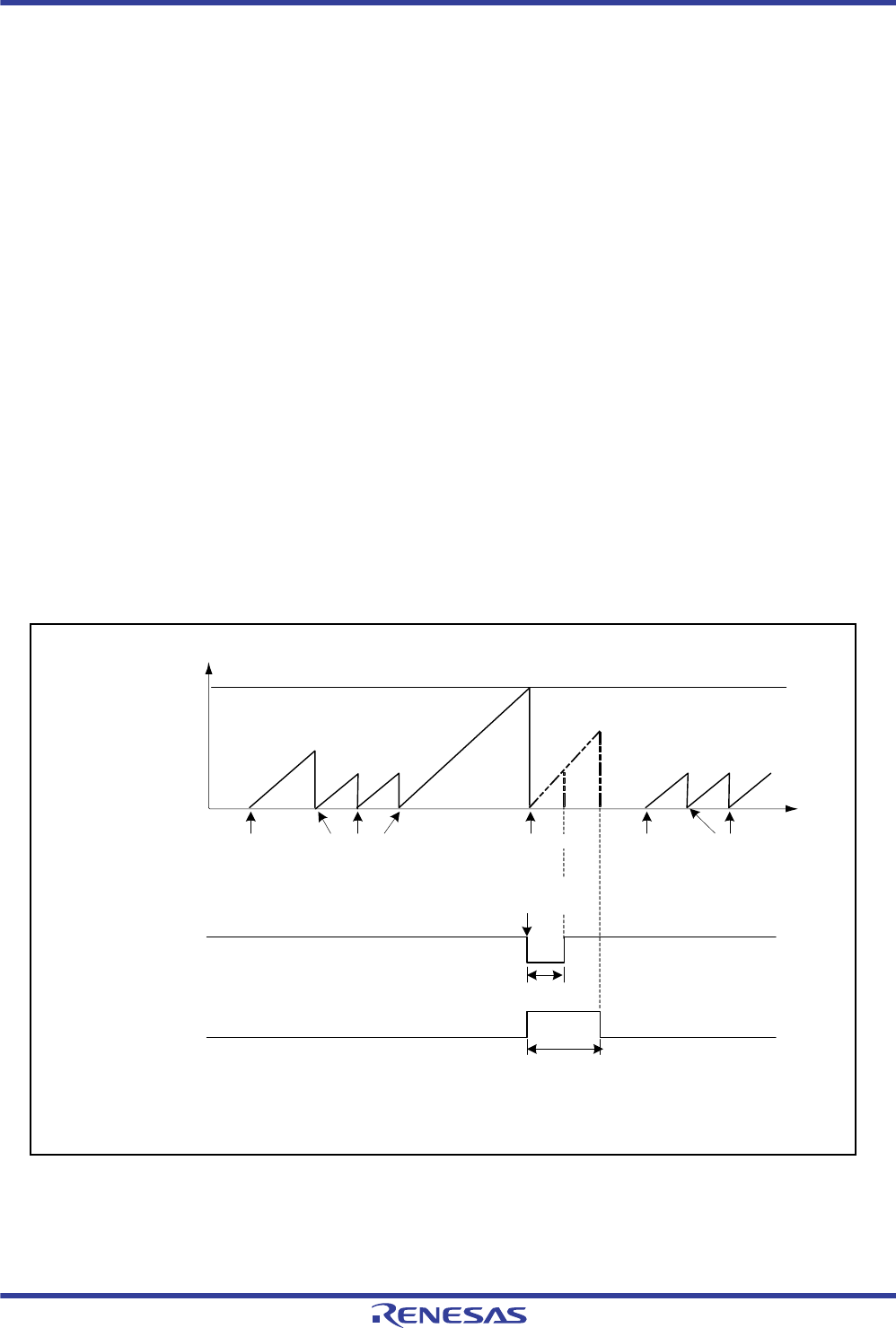
R01UH0034EJ0200 Rev.2.00 Page 897 of 1489
Dec 27, 2013
RX62T Group, RX62G Group 20. Watchdog Timer (WDT)
Under development Preliminary document
Specifications in this document are tentative and subject to change.
20.3 Operation
20.3.1 Watchdog Timer Mode
To use the WDT in watchdog timer mode, set the TCSR.TMS bit to 1 (watchdog timer mode) and the TCSR.TME bit to
1 (TCNT starts counting).
During watchdog timer operation, if TCNT overflows without being rewritten because of a system crash or another error,
the WDTOVF# signal is output. This ensures that TCNT does not overflow while the system is operating normally.
Software must prevent TCNT overflows by rewriting the TCNT value (normally 00h is written) before overflow occurs.
This WDTOVF# signal can be used to reset the LSI internally in watchdog timer mode.
If TCNT counter overflows in the watchdog timer mode, the RSTCSR.WOVF bit is set to 1. In addition, if TCNT
counter overflows while the RSTCSR.RSTE bit is set to 1, a signal that resets the LSI internally is generated as the same
time as the WDTOVF# signal is output. If a reset caused by a signal input to the RES# pin occurs at the same time as a
reset caused by a WDT overflow, the RES# pin reset has priority and the WOVF flag in RSTCSR is cleared to 0.
The WDTOVF# signal is output for 257 cycles of PCLK when RSTE = 1, and for 256 cycles of PCLK when RSTE = 0.
The internal reset signal is output for 1027 cycles of PCLK.
When RSTE = 1, an internal reset signal is generated. Since the system clock control register (SCKCR) is initialized, the
multiplication ratio of PCLK becomes the initial value.
When RSTE = 0, an internal reset signal is not generated. Neither SCKCR nor the multiplication ratio of PCLK is
changed.
When TCNT overflows in watchdog timer mode, the WOVF flag is set to 1. If TCNT overflows when the RSTE bit is set
to 1, an internal reset signal is generated for the entire RX62T.
Figure 20.2 Operation in Watchdog Timer Mode
TCNT value
00h Time
FFh
TMS = 1
TME = 1 Write 00h to
TCNT
WDTOVF# signal
Internal reset signal
Notes: 1. An internal reset signal is generated if TCNT overflows when the RSTE bit in RSTCSR is set to 1.
2. The WDTOVF# signal is output for 256 cycles when RSTE bit in RSTCSR is set to 0.
Overflow
TMS = 1
TME = 1 Write 00h to
TCNT
257 cycles
1027 cycles
*1
*2
Generating WDTOVF#
and internal reset
WOVF = 1
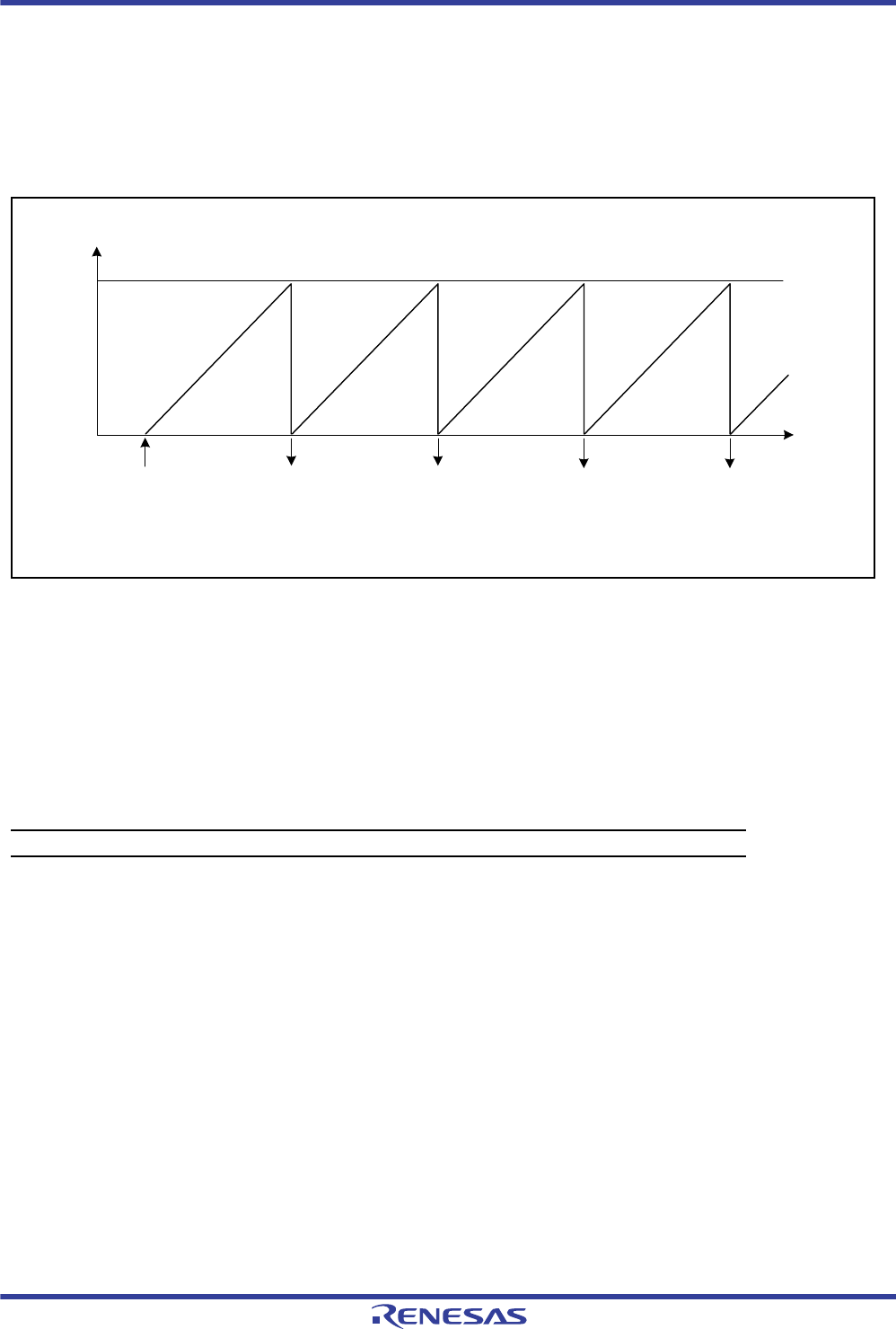
R01UH0034EJ0200 Rev.2.00 Page 898 of 1489
Dec 27, 2013
RX62T Group, RX62G Group 20. Watchdog Timer (WDT)
Under development Preliminary document
Specifications in this document are tentative and subject to change.
20.3.2 Interval Timer Mode
To use the WDT as an interval timer, set the TCSR.TMS bit to 0 (interval timer mode) and the TCSR.TME bit to 1
(TCNT starts counting).
When the WDT is used as an interval timer, an interval timer interrupt (WOVI) is generated each time TCNT overflows.
Therefore, an interrupt can be generated at intervals.
Figure 20.3 Operation in Interval Timer Mode
20.4 Interrupt Source
During interval timer mode operation, a TCNT overflow generates an interval timer interrupt (WOVI). For details, see
section 11., Interrupt Controller (ICU).
Table 20.4 WDT Interrupt Source
Name Interrupt Source Interrupt Status Flag DTC Activation
WOVI TCNT overflow IR096.IR Not possible
TCNT value
00h Time
FFh
TMS = 0
TME = 1 WOVI
Overflow Overflow Overflow Overflow
WOVI: An interval timer interrupt request is generated.
WOVI WOVI WOVI

R01UH0034EJ0200 Rev.2.00 Page 899 of 1489
Dec 27, 2013
RX62T Group, RX62G Group 20. Watchdog Timer (WDT)
Under development Preliminary document
Specifications in this document are tentative and subject to change.
20.5 Usage Notes
20.5.1 Notes on Register Access
The watchdog timer's TCNT, TCSR, and RSTCSR differ from other registers in being more difficult to write to.
(1) Writing to TCNT Counter, TCSR Register, and RSTCSR Register
When writing to TCNT and TCSR, be sure to use a word transfer instruction to the write window A register (WINA)
(00088028h). For writing, TCNT and TCSR are assigned to the same address. Accordingly, perform data transfer as
shown in Figure 20.4.
To write to TCNT, set 5Ah in the upper byte and data in the lower byte, and perform data transfer to TCNT.
To write to TCSR, set A5h in the upper byte and data in the lower byte, and perform data transfer to TCSR.
When writing to RSTCSR, use a word transfer instruction to the write window B register (WINB) (0008802Ah).
The method of writing 0 to the WOVF flag in RSTCSR differs from that of writing to the RSTE bit in RSTCSR. Perform
data transfer as shown in Figure 20.4.
To write 0 to the WOVF flag, set A5h in the upper byte and 00h in the lower byte and write data in 16 bits, as shown in
Figure 20.4. This writing has no effect on the RSTE bit.
To write to the RSTE bit, set 5Ah in the upper byte and the RSTCSR register write data in the lower byte and write data
in 16 bits, as shown in Figure 20.4. This writing has no effect on the WOVF flag.
Figure 20.4 Writing to TCNT, TCSR, and RSTCSR
<Writing to TCNT>
Data to be written to TCNT5Ah
15 8 7 0
Address: 0008 8028h (WINA)
< Writing to TCSR >
Data to be written to TCSRA5h
15 8 7 0
Address: 0008 8028h (WINA)
<Writing to RSTE bit in RSTCSR>
Data to be written to RSTCSR5Ah
15 8 7 0
Address: 0008 802Ah (WINB)
<Writing 0 to WOVF flag in RSTCSR>
A5h 00h
15 8 7 0
Address: 0008 802Ah (WINB)
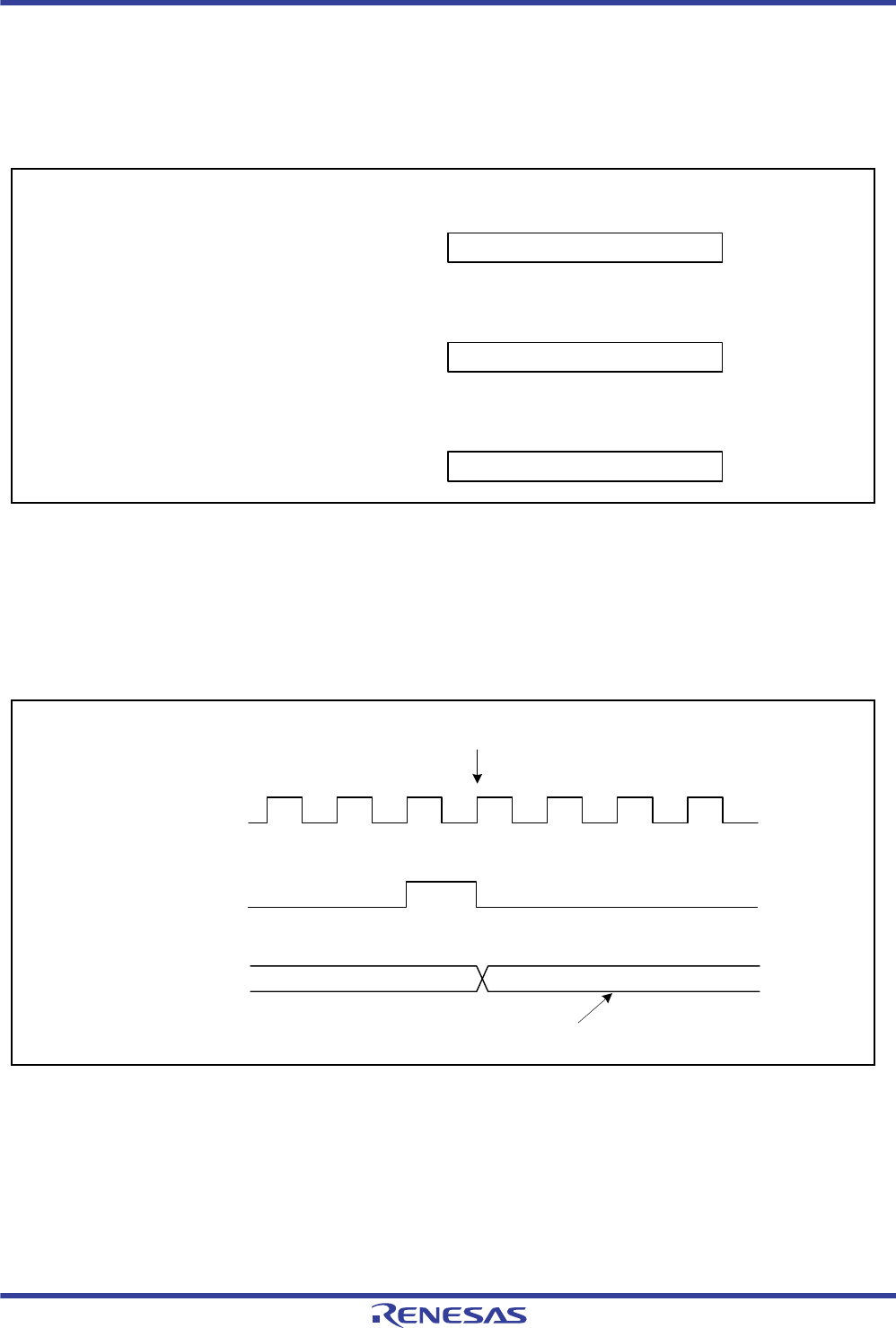
R01UH0034EJ0200 Rev.2.00 Page 900 of 1489
Dec 27, 2013
RX62T Group, RX62G Group 20. Watchdog Timer (WDT)
Under development Preliminary document
Specifications in this document are tentative and subject to change.
(2) Reading from TCNT Counter, TCSR Register, and RSTCSR Register
These counter and registers can be read from in the same way as other registers.
TCSR is assigned to address 00088028h, TCNT to address 00088029h, and RSTCSR to address 0008802Ah. For
reading, use 8-bit access.
Figure 20.5 Reading from TCNT, TCSR, and RSTCSR
20.5.2 Conflict between Timer Counter (TCNT) Write and Increment
If a TCNT clock pulse is generated during a TCNT write cycle, the write takes priority and the timer counter is not
incremented. Figure 20.6 shows this operation.
Figure 20.6 Conflict between TCNT Write and Increment
20.5.3 Changing Values of Bits CKS[2:0]
If bits CKS[2:0] bits in TCSR are written to while the WDT is operating, errors could occur in the incrementation. The
watchdog timer must be stopped (by clearing the TME bit in TCSR to 0) before the values of CKS[2:0] bits in TCSR are
changed.
<Reading from TCSR>
Address: 0008 8028h (TCSR)
70
Data read from TCSR
Address: 0008 8029h (TCNT)
<Reading from TCNT>
70
Data read from TCNT
<Reading from RSTCSR>
Address: 0008 802Bh (RSTCSR)
70
Data read from RSTCSR
TCNT input clock
TCNT NM
Data written to TCNT counter
PCLK
Writing to TCNT counter by CPU
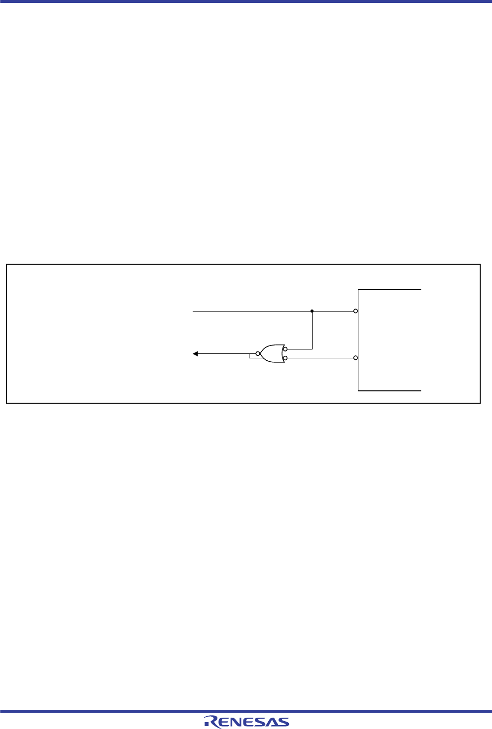
R01UH0034EJ0200 Rev.2.00 Page 901 of 1489
Dec 27, 2013
RX62T Group, RX62G Group 20. Watchdog Timer (WDT)
Under development Preliminary document
Specifications in this document are tentative and subject to change.
20.5.4 Switching between Watchdog Timer Mode and Interval Timer Mode
If the timer mode is switched from watchdog timer mode to interval timer mode while the watchdog timer is operating,
errors could occur in the operation. The watchdog timer must be stopped (by clearing the TME bit in TCSR to 0) before
switching the timer mode.
20.5.5 Internal Reset in Watchdog Timer Mode
The RX62T is not reset internally if TCNT overflows while the RSTE bit in RSTCSR is cleared to 0 during watchdog
time mode operation, but TCNT and the TCSR of the watchdog timer are reset.
TCNT, TCSR, and RSTCSR cannot be written to while the WDTOVF# signal is low. Also note that a read of the WOVF
flag in RSTCSR is not recognized during this period. To clear the WOVF flag, therefore, read RSTCSR after the
WDTOVF# signal goes high, then write 0 to the WOVF flag.
20.5.6 System Reset by WDTOVF# Signal
If the WDTOVF# signal is input to the RES# pin, the RX62T will not be initialized correctly. Make sure that the
WDTOVF# signal is not input logically to the RES# pin. To reset the entire system by means of the WDTOVF# signal,
use a circuit like that shown in Figure 20.7.
Figure 20.7 Circuit for System Reset by WDTOVF# Signal (Example)
20.5.7 Transition to Watchdog Timer Mode or Software Standby Mode
When the WDT operates in watchdog timer mode, a transition to software standby mode is not made even when the
WAIT instruction is executed when the software standby bit (SSBY in SBYCR) in the standby control register is set to 1.
Instead, a transition to sleep mode or all-module clock-stop mode is made.
To transit to software standby mode, the WAIT instruction must be executed after halting the watchdog timer (clearing
the TME bit in TCSR to 0).
When the WDT operates in interval timer mode, a transition to software standby mode is made through execution of the
WAIT instruction when the SSBY bit is set to 1. For details, see section 9., Low Power Consumption.
Reset input #
Reset signal # for entire system
RX62T
RES#
WDTOVF#
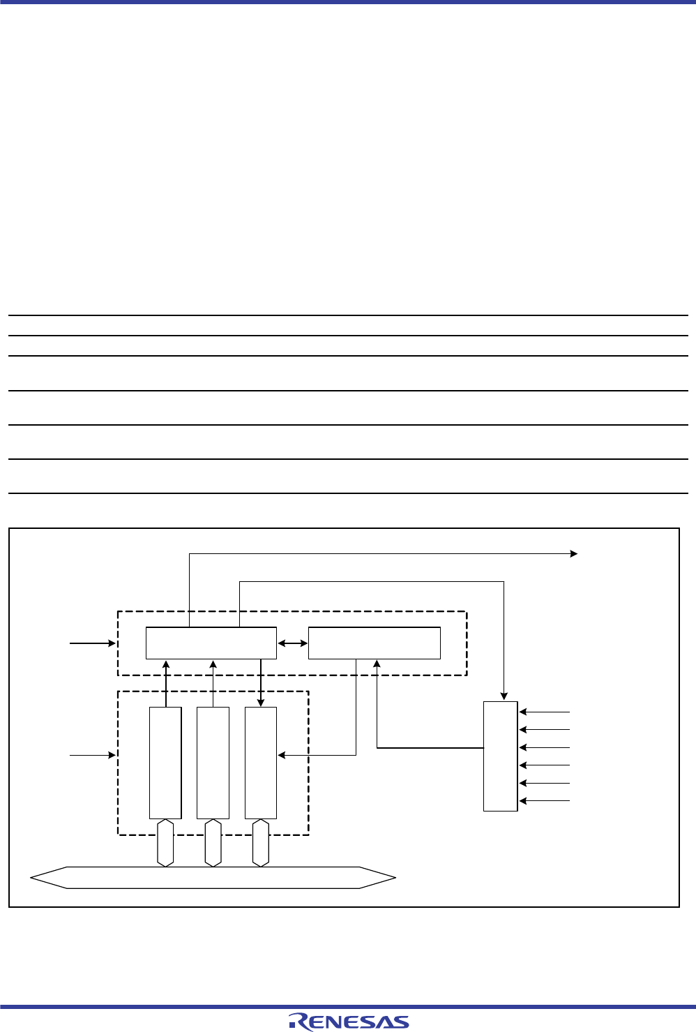
R01UH0034EJ0200 Rev.2.00 Page 902 of 1489
Dec 27, 2013
RX62T Group, RX62G Group 21. Independent Watchdog Timer (IWDT)
Under development Preliminary document
Specifications in this document are tentative and subject to change.
21. Independent Watchdog Timer (IWDT)
The independent watchdog timer (IWDT) is a watchdog timer for use independently of the conventional watchdog timer,
which is for detecting programs entering runaway execution and system crashes.
The IWDT incorporates a 14-bit down-counter and resets the system if counting leads to an underflow of the value in the
counter. The IWDT also has a refresh facility.
Note: • The value in the IWDT must be refreshed before the counter underflows. For details, see section 21.3.3, Control
of Refreshing
21.1 Overview
The specifications of the IWDT are given in Table 21.1. Figure 21.1 is a block diagram of the IWDT.
Figure 21.1 Block Diagram of the IWDT
Table 21.1 Specifications of the IWDT
Item Specifications
Clock for counting IWDTCLK, IWDTCLK/16, IWDTCLK/32, IWDTCLK/64, IWDTCLK/128, IWDTCLK/256
Counter operation Counting down by a 14-bit down-counter
Conditions for starting the
counter
Counting can be started by refreshing the down-counter (write FFh after 00h has been written to the
IWDTRR register).
Conditions for stopping the
counter
Pin reset (the down-counter and other registers return to their initial values)
Generation of an underflow
Reset-output sources of the
IWDT
Underflow of the down-counter
Reading the value of the
IWDT counter
The value reached in counting by the down-counter can be read out from a register (the IWDTSR).
Internal bus
IWDT control circuit 14-bit down counter
PCLK
IWDTCLK
I
W
D
T
R
R
I
W
D
T
C
R
I
W
D
T
S
R
[Legend]
IWDTRR: IWDT refresh register
IWDTCR: IWDT control register
IWDTSR: IWDT status register
IWDT reset output
Count clock
IWDTCLK/16
IWDTCLK/64
IWDTCLK/32
IWDTCLK/128
IWDTCLK/256
IWDTCLK
Clock
selec-
tion
R01UH0034EJ0200 Rev.2.00 Page 903 of 1489
Dec 27, 2013
RX62T Group, RX62G Group 21. Independent Watchdog Timer (IWDT)
Under development Preliminary document
Specifications in this document are tentative and subject to change.
21.2 Register Descriptions
Table 21.2 lists the registers of the IWDT.
21.2.1 IWDT Refresh Register (IWDTRR)
IWDTRR refreshes the down-counter of the IWDT.
The down-counter of the IWDT is refreshed by writing 00h and then writing FFh to the IWDTRR (refreshing). After the
counter has been refreshed, it starts counting down from the value selected by the TOPS[1:0] bits in the IWDT control
register (IWDTCR).
In addition, when the first time the counter is refreshed after the release from the reset state, it starts counting down from
the value selected by the TOPS[1:0] bits in IWDTCR.
Writing a value other than FFh after 00h invalidates the writing of 00h. To enable refreshing of the counter, 00h must be
written to this register again, and this must be followed by writing of FFh.
Although reading the register after the writing of 00h will produce the value 00h, reading the register after writing any
value other than 00h will always produce the value FFh.
Table 21.2 IWDT Registers
Register Name Symbol Value after Reset Address Access Size
IWDT refresh register IWDTRR FFh 0008 8030h 8
IWDT control register IWDTCR 3303h 0008 8032h 16
IWDT status register IWDTSR 0000h 0008 8034h 16
Address: 0008 8030h
b7 b6 b5 b4 b3 b2 b1 b0
Value after reset: 11111111
R01UH0034EJ0200 Rev.2.00 Page 904 of 1489
Dec 27, 2013
RX62T Group, RX62G Group 21. Independent Watchdog Timer (IWDT)
Under development Preliminary document
Specifications in this document are tentative and subject to change.
21.2.2 IWDT Control Register (IWDTCR)
IWDTCR specifies the time-out period for the underflow of the down-counter, and count clock.
Writing to the IWDTCR is only possible once during the period between release from the reset state and the first time the
counter is refreshed. Writing to the IWDTCR is not possible after a refresh operation; furthermore, writing to the
IWDTCR two or more times is not possible. This is because writing to the IWDTCR has been locked.
The writing to IWDTCR is unlocked by the reset source of the IWDT. With other reset sources, writing to the IWDTCR
is not unlocked. For details, see section 6., Resets.
TOPS[1:0] Bits (Time-out Period Selection)
The TOPS[1:0] bits select the time-out period (period until the down-counter underflows) among 1024, 4096, 8192, or
16384 cycles, with taking the count clock specified by the CKS[3:0] bits as one cycle.
The combination of the settings of the CKS[3:0] and TOPS[1:0] bits determines the time (in cycles of the IWDTCLK)
for the counter to underflow after being refreshed.
The relations between the settings of the CKS[3:0] and TOPS[1:0] bits, and the number of cycles of the IWDTCLK are
shown in Table 21.3.
Address: 0008 8032h
b15 b14 b13 b12 b11 b10 b9 b8 b7 b6 b5 b4 b3 b2 b1 b0
———————— CKS[3:0] ——TOPS[1:0]
Value after reset: 0011001100000011
Bit Symbol Bit Name Description R/W
b1, b0 TOPS[1:0] Time-out Period Selection b1 b0
0 0: 1024 cycles (03FFh)
0 1: 4096 cycles (0FFFh)
1 0: 8192 cycles (1FFFh)
1 1: 16384 cycles (3FFFh)
R/W
b3, b2 — Reserved These bits are read as 0. The write value should be 0. R/W
b7 to b4 CKS[3:0] Clock Selection b7 b4
0 0 : IWDTCLK
0 1 0 0: IWDTCLK/16
0 1 0 1: IWDTCLK/32
0 1 1 0: IWDTCLK/64
0 1 1 1: IWDTCLK/128
1 : IWDTCLK/256
R/W
b9, b8 — Reserved These bits are read as 1. The write value should be 1. R/W
b11, b10 — Reserved These bits are read as 0. The write value should be 0. R/W
b13, b12 — Reserved These bits are read as 1. The write value should be 1. R/W
b15, b14 — Reserved These bits are read as 0. The write value should be 0. R/W
R01UH0034EJ0200 Rev.2.00 Page 905 of 1489
Dec 27, 2013
RX62T Group, RX62G Group 21. Independent Watchdog Timer (IWDT)
Under development Preliminary document
Specifications in this document are tentative and subject to change.
CKS[3:0] Bits (Clock Selection)
These bits select the count clock for down counting among IWDTCLK, IWDTCLK/16, IWDTCLK/32, IWDTCLK/64,
IWDTCLK/128, or IWDTCLK/256. In combination with the setting of the TOPS[1:0] bits, a counting period between
1024 and 4194304 cycles of the IWDTCLK signal is selected for the IWDT.
Table 21.3 Settings and Time-out Periods
CKS[3:0] TOPS[1:0] Count Clock Time-out Period
(Number of Cycles) Cycles of the IWDTCLK
Signal
0 0 — — 0 0 IWDTCLK 1024 1024
0 1 4096 4096
1 0 8192 8192
1 1 16384 16384
01000 0 IWDTCLK/16 1024 16384
0 1 4096 65536
1 0 8192 131072
1 1 16384 262144
01010 0 IWDTCLK/32 1024 32768
0 1 4096 131072
1 0 8192 262144
1 1 16384 524288
01100 0 IWDTCLK/64 1024 65536
0 1 4096 262144
1 0 8192 524288
1 1 16384 1048576
01110 0 IWDTCLK/128 1024 131072
0 1 4096 524288
1 0 8192 1048576
1 1 16384 2097152
1 — — — 0 0 IWDTCLK/256 1024 262144
0 1 4096 1048576
1 0 8192 2097152
1 1 16384 4194304

R01UH0034EJ0200 Rev.2.00 Page 906 of 1489
Dec 27, 2013
RX62T Group, RX62G Group 21. Independent Watchdog Timer (IWDT)
Under development Preliminary document
Specifications in this document are tentative and subject to change.
21.2.3 IWDT Status Register (IWDTSR)
IWDTSR checks the counter value of the down-counter, and the generation state of the underflow.
IWDTSR is initialized by the reset source of the IWDT. With other reset sources, IWDTSR is not initialized. For details,
see section 6., Resets.
CNTVAL[13:0] Bits (Down-Counter)
These bits can be read to confirm the value of the down-counter.
UNDFF Flag (Underflow Flag)
This bit can be read to confirm the state of the down-counter in terms of whether or not an underflow has occurred.
The value "1" indicates that the down-counter has underflowed. The value "0" indicates that the down-counter has not
underflowed.
Clear the UNDFF bit by writing "0" to it. Writing "1" has no effect.
Address: 0008 8034h
b15 b14 b13 b12 b11 b10 b9 b8 b7 b6 b5 b4 b3 b2 b1 b0
— UNDFF CNTVAL [13:0]
Value after reset: 0011001100000011
Bits Symbol Name Function R/W
b13 to b0 CNTVAL [13:0] Down-Counter Value counted by the down-counter R
b14 UNDFF Underflow Flag 1: Underflow
0: No underflow
R/W
b15 — Reserved This bit is always read as 0. The write value should be 0. R/W
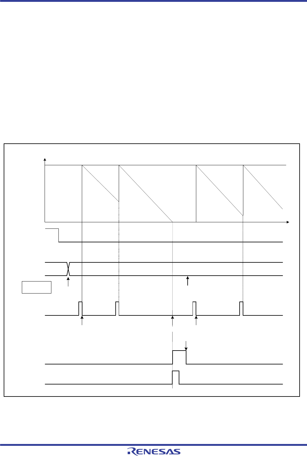
R01UH0034EJ0200 Rev.2.00 Page 907 of 1489
Dec 27, 2013
RX62T Group, RX62G Group 21. Independent Watchdog Timer (IWDT)
Under development Preliminary document
Specifications in this document are tentative and subject to change.
21.3 Description of Operation
21.3.1 Count Operation of the Down-Counter
Settings for the count clock and the time-out period are made in the IWDTCR after release from the reset state.
Refreshing the down-counter then starts it counting down from the value selected by the setting of the
IWDTCR.TOPS[1:0] bits.
After that, as long as the program continues in normal operation, the value in the counter is re-set when the counter is
refreshed, and counting down continues. The IWDT does not output the reset signal as long as this continues. However,
if the down-counter underflows because refreshing the down-counter is not possible due to the program having entered
crashed execution, the IWDT outputs the reset signal.
After assertion of the reset signal, the down-counter is initialized (all bits cleared to "0") and kept in that state. After the
system has been re-booted, counting down is again started by refreshing the counter.
An example of operation under the below conditions is shown in Figure 21.2.
Figure 21.2 Example of Down-Counter Operation
Value in the down-counter
100%
0%
25%
50%
75%
IWDTCR
register (1) (2) (2)
Writing to the
register is valid.
Reset input to the
IWDT
Refreshing the
counter
Counting starts
Underflow flag
Reset output from
the IWDT
The status is cleared
(1) Initial value
(2) Set value
Counting starts
Underflow
Writing to the
register is valid.
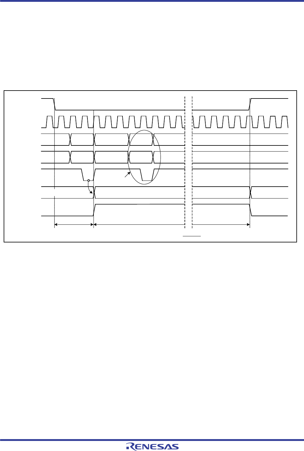
R01UH0034EJ0200 Rev.2.00 Page 908 of 1489
Dec 27, 2013
RX62T Group, RX62G Group 21. Independent Watchdog Timer (IWDT)
Under development Preliminary document
Specifications in this document are tentative and subject to change.
21.3.2 Control over Writing to the IWDT Control Register (IWDTCR)
Writing to the IWDTCR is only possible for once after the reset state is canceled.
Writing to the IWDTCR makes the value of the internal register-lock signal of the IWDT become "1", locking the
IWDTCR against subsequent attempts at writing.
The writing to IWDTCR is unlocked by the reset source of the IWDT. With other reset sources, writing to the IWDTCR
is not unlocked. For details, see section 6., Resets.
Figure 21.3 is a chart of the waveforms in response to writing to the IWDTCR.
Figure 21.3 Control Waveforms in Response to Writing to the IWDTCR
Reset input to the
IWDT
PCLK
Address bus
Write-data bus
Write enable signal
IWDTCR
register
Register lock
signal (internal)
xxh 02h xxh 02h
xxxxh 3131h xxxxh 2013h
3131h3303h (initial value)
Writing disabled
Period where writing is
possible
Period where the IWDTCR is locked (period where
writing is disabled
3131h
xxh
xxxxh
3303h (initial value)
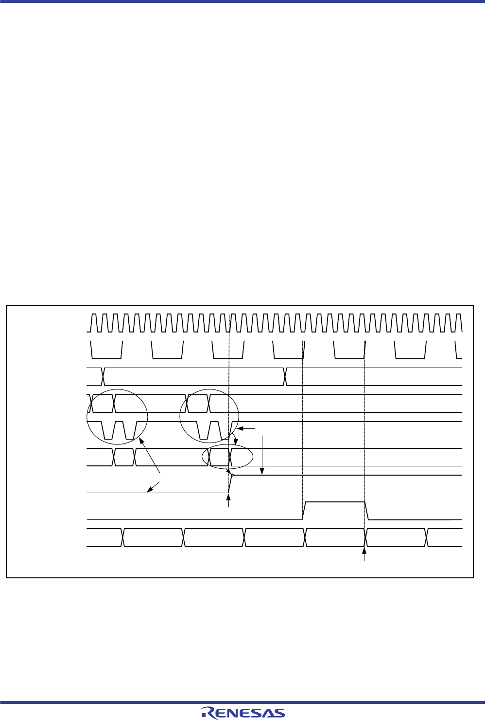
R01UH0034EJ0200 Rev.2.00 Page 909 of 1489
Dec 27, 2013
RX62T Group, RX62G Group 21. Independent Watchdog Timer (IWDT)
Under development Preliminary document
Specifications in this document are tentative and subject to change.
21.3.3 Control of Refreshing
The IWDT starts operation (start of the down-counter) or the down-counter is refreshed by writing the values 00h and
then FFh to the IWDT refresh register (IWDTRR). Write operations other than these (in order) are invalid. After invalid
writing, correct refreshing is performed by writing 00h and then FFh to the IWDT refresh register (IWDTRR).
Though writing 00h 00h is invalid, if FFh is written after that, writing 00h FFh will be valid. Thus, writing
00h00hFFh is valid. Moreover, if the first writing value is not 00h, writing will be valid if the operation contains the set
of writing 00h FFh.
Sample sequences of writing that are invalid for refreshing the counter
23h (a value other than 00h) FFh
00h 54h (a value other than FFh)
00h AAh (a value other than FFh) FFh
After writing of FFh to the IWDTRR register, refreshing the down-counter requires up to four cycles of the signal for
counting (the IWDTCR.CKS[3:0] bits determine how many cycles of the signal from the IWDTCLK make up one cycle
for counting). Therefore, writing FFh to the IWDTRR should be completed four cycles before the counter underflows.
The value of the counter is checked by the counter bits (IWDTSR.CNTVAL[13:0]).
Figure 21.4 shows refresh-operation waveforms for the count clock of the IWDTCLK.
Figure 21.4 Refresh Operation Waveform (IWDTCR.CKS[3:0] = 0000b, IWDTCR.TOPS[1:0] = 11b)
IWDTCLK clock
PCLK
Address bus
Write-data bus
Write enable signal
IWDTRR register
Refresh request
signal
xxh xxh00h
FFh
00h
00h 54h
00h FFh 00h
FFh
Invalid
Refresh signal (after
synchronization with
the LOCO)
3FFFh(n)h
Counter value
Valid
Refresh
FFh
Request for refresh
(n+2)h 3FFEh(n+1)h (n-1)h (n-2)h

R01UH0034EJ0200 Rev.2.00 Page 910 of 1489
Dec 27, 2013
RX62T Group, RX62G Group 21. Independent Watchdog Timer (IWDT)
Under development Preliminary document
Specifications in this document are tentative and subject to change.
21.3.4 Status Flags
Reset requests from the refresh-error flag (IWDTSR.REFEF) and underflow flag (IWDTSR.UNDFF) are retained after
output of the reset signal from the IWDT.
Thus, after release from the reset state, read the IWDTSR.REFEF and UNDFF bits to check for these reset requests.
For both flags, writing "0" clears the bit and writing "1" has no effect.
Leaving the status flags set does not affect operation. If the flags are not cleared, at the time of the next reset from the
IWDT, the earlier reset request is cleared and the new reset request is written.
21.4 Usage Notes
21.4.1 Limitation on Transitions to Low-Power-Consumption Modes
Writing to the IWDTCR or refresh operations brings the IWDT into use. When the IWDT is in use, even executing a
WAIT instruction while the SSBY bit in the SBYCR is set to 1 will not cause a transition to software standby mode;
instead, the transition will be to sleep mode or all-module-clock-stop mode. Furthermore, the reset source for the IWDT
triggers release from the given mode, while the other reset sources do not. For details, see section 6., Resets.

R01UH0034EJ0200 Rev.2.00 Page 911 of 1489
Dec 27, 2013
RX62T Group, RX62G Group 22. Serial Communications Interface (SCIb)
22. Serial Communications Interface (SCIb)
The RX62T and RX62G Groups have three independent serial communications interface (SCI) units.
The SCI can handle both asynchronous and clock synchronous serial communications.
Asynchronous serial data communications can be carried out with standard asynchronous communications chips such as
a Universal Asynchronous Receiver/Transmitter (UART) or Asynchronous Communications Interface Adapter (ACIA).
The SCI also supports the smart card (IC card) interface (SMCI) conforming to ISO/IEC 7816-3 (standards for
Identification Cards) as an extended asynchronous communications mode.
22.1 Overview
Table 22.1 lists the specifications of the SCI.
Figure 22.1 shows a block diagram of the SCI0 to SCI2.
Table 22.1 Specifications of SCI
Item Specifications
Serial communications mode Asynchronous
Clock synchronous
Smart card interface
Transfer speed Bit rate specifiable with on-chip baud rate generator.
Full-duplex communications Transmitter: Enables continuous transmission by double-buffering.
Receiver: Enables continuous reception by double-buffering.
Input/output pins See Table 22.2.
Data transfer Selectable from LSB-first or MSB-first transfer
Interrupt sources Transmit-end, transmit-data-empty, receive-data-full, and receive error
Power consumption reduction function Module stop state can be set for each unit.
Asynchronous mode Data length 7 or 8 bits
Transmission stop bit 1 or 2 bits
Parity Even, odd, or none
Receive error detection Parity, overrun, and framing errors
Break detection Break can be detected by reading RXDn (n = 0 to 2) pin level directly in case of
a framing error
Clock source Selectable from internal or external clock
Multi-processor
communications function
Serial communication among multiple processors
Noise cancellation Capable of canceling noise on the RXDn (n = 0 to 2) pin.
Detection of a low level or falling edge on the RxD pin for start bit detection selectable
Clock synchronous
mode
Data length 8 bits
Receive error detection Overrun errors
Smart card interface
mode
Error processing An error signal can be automatically transmitted on detection of a parity error
during reception
Data can be automatically re-transmitted on receiving an error signal during
transmission
Data type Both direct convention and inverse convention are supported.
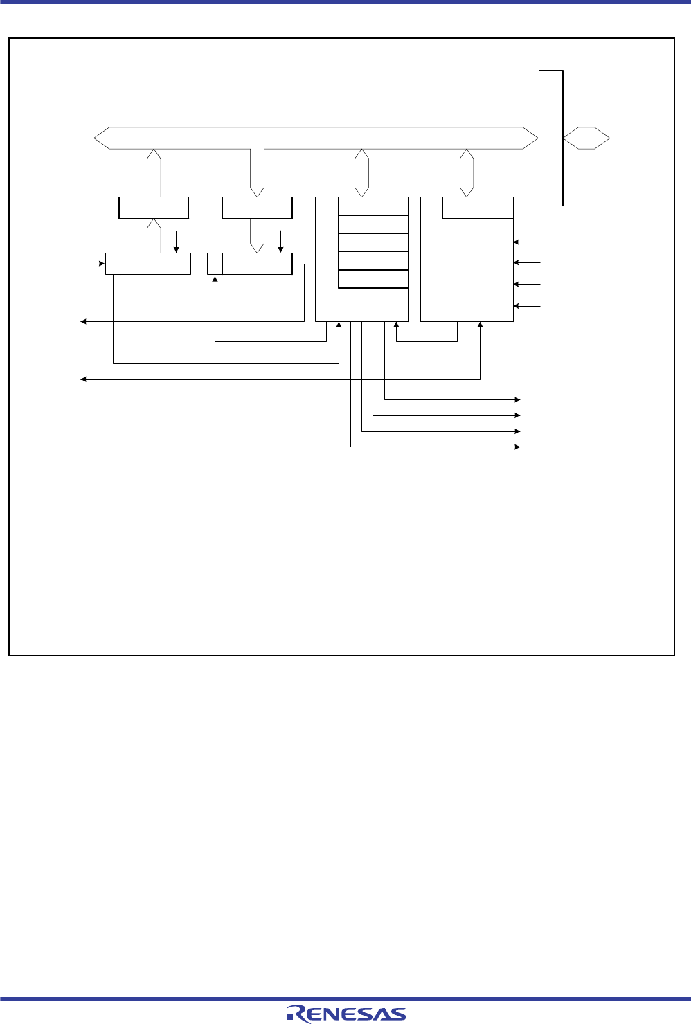
R01UH0034EJ0200 Rev.2.00 Page 912 of 1489
Dec 27, 2013
RX62T Group, RX62G Group 22. Serial Communications Interface (SCIb)
Figure 22.1 Block Diagram of SCI0 to SCI2
RXDn
TXDn
SCKn External clock
PCLK
TEI
TXI
RXI
ERI
SCMR
SSR
SCR
SEMR
Transmission
and reception
control
BRRRDR
TSRRSR
Parity error occurrence
[Legend]
TDR
Module data bus
Baud rate
generator PCLK/4
PCLK/16
PCLK/64
Clock
Parity check
RSR: Receive shift register
RDR: Receive data register
TSR: Transmit shift register
TDR: Transmit data register
SMR: Serial mode register
SCR: Serial control register
SSR: Serial status register
SCMR: Smart card mode register
BRR: Bit rate register
SEMR: Serial extended mode register
NF: Noise cancellation circuit
(available in the asynchronious mode)
Bus interface
Internal data bus
SMR

R01UH0034EJ0200 Rev.2.00 Page 913 of 1489
Dec 27, 2013
RX62T Group, RX62G Group 22. Serial Communications Interface (SCIb)
Table 22.2 lists the pin configuration of the SCI/SMCI.
Table 22.2 Pin Configuration of SCI
Channel Pin Name I/O Function
SCI0/SMCI0 SCK0 I/O SCI0/SMCI0 clock input/output
RXD0 Input SCI0/SMCI0 receive data input
TXD0 Output SCI0/SMCI0 transmit data output
SCI1/SMCI1 SCK1 I/O SCI1/SMCI1 clock input/output
RXD1 Input SCI1/SMCI1 receive data input
TXD1 Output SCI1/SMCI1 transmit data output
SCI2/SMCI2 SCK2 I/O SCI2/SMCI2 clock input/output
RXD2 Input SCI2/SMCI2 receive data input
TXD2 Output SCI2/SMCI2 transmit data output

R01UH0034EJ0200 Rev.2.00 Page 914 of 1489
Dec 27, 2013
RX62T Group, RX62G Group 22. Serial Communications Interface (SCIb)
22.2 Serial Communications Interface Mode
22.2.1 Register Descriptions
Table 22.3 lists the registers of the SCI.
Table 22.3 Registers of SCI
Channel Register Name Symbol Value after Reset Address Access Size
SCI0 Serial mode register SMR 00h 0008 8240h 8
Bit rate register BRR FFh 0008 8241h 8
Serial control register SCR 00h 0008 8242h 8
Transmit data register TDR FFh 0008 8243h 8
Serial status register SSR 84h 0008 8244h 8
Receive data register RDR 00h 0008 8245h 8
Smart card mode register SCMR F2h 0008 8246h 8
Serial extended mode register SEMR 00h 0008 8247h 8
SCI1 Serial mode register SMR 00h 0008 8248h 8
Bit rate register BRR FFh 0008 8249h 8
Serial control register SCR 00h 0008 824Ah 8
Transmit data register TDR FFh 0008 824Bh 8
Serial status register SSR 84h 0008 824Ch 8
Receive data register RDR 00h 0008 824Dh 8
Smart card mode register SCMR F2h 0008 824Eh 8
Serial extended mode register SEMR 00h 0008 824Fh 8
SCI2 Serial mode register SMR 00h 0008 8250h 8
Bit rate register BRR FFh 0008 8251h 8
Serial control register SCR 00h 0008 8252h 8
Transmit data register TDR FFh 0008 8253h 8
Serial status register SSR 84h 0008 8254h 8
Receive data register RDR 00h 0008 8255h 8
Smart card mode register SCMR F2h 0008 8256h 8
Serial extended mode register SEMR 00h 0008 8257h 8
R01UH0034EJ0200 Rev.2.00 Page 915 of 1489
Dec 27, 2013
RX62T Group, RX62G Group 22. Serial Communications Interface (SCIb)
22.2.1.1 Receive Shift Register (RSR)
RSR is a shift register which is used to receive serial data input from the RXDn pin and converts it into parallel data.
When one frame of data has been received, it is transferred to RDR automatically.
RSR cannot be directly accessed by the CPU.
22.2.1.2 Receive Data Register (RDR)
RDR is an 8-bit register that stores receive data.
When the SCI has received one frame of serial data, it transfers the received serial data from RSR to RDR where it is
stored. This allows RSR to receive the next data.
Since RSR and RDR function as a double buffer in this way, continuous receive operations can be performed.
Read RDR only once after a receive data full interrupt (RXI) has occurred. Note that if next one frame of data is received
before reading receive data from RDR, an overrun error occurs.
RDR cannot be written to by the CPU.
22.2.1.3 Transmit Data Register (TDR)
TDR is an 8-bit register that stores transmit data.
When the SCI detects that TSR is empty, it transfers the transmit data written in TDR to TSR and starts transmission.
The double-buffered structures of TDR and TSR enable continuous serial transmission. If the next transmit data has
already been written to TDR when one frame of data is transmitted, the SCI transfers the written data to TSR to continue
transmission.
The CPU is able to read from or write to TDR at any time. Only write data for transmission to TDR once after each
instance of the transmit data empty interrupt (TXI).
22.2.1.4 Transmit Shift Register (TSR)
TSR is a shift register that transmits serial data.
To perform serial data transmission, the SCI first automatically transfers transmit data from TDR to TSR, and then sends
the data to the TXDn pin.
TSR cannot be directly accessed by the CPU.
Address: SCI0.RDR 0008 8245h, SCI1.RDR 0008 824Dh, SCI2.RDR 0008 8255h
b7 b6 b5 b4 b3 b2 b1 b0
Value after reset: 00000000
Address: SCI0.TDR 0008 8243h, SCI1.TDR 0008 824Bh, SCI2.TDR 0008 8253h
b7 b6 b5 b4 b3 b2 b1 b0
Value after reset: 11111111

R01UH0034EJ0200 Rev.2.00 Page 916 of 1489
Dec 27, 2013
RX62T Group, RX62G Group 22. Serial Communications Interface (SCIb)
22.2.1.5 Serial Mode Register (SMR)
Note 1. n is the decimal notation of the value of n in BRR (see section 22.2.1.9, Bit Rate Register (BRR).
Note 2. In clock synchronous mode, this bit setting is invalid and a fixed data length of 8 bits is used.
Note 3. LSB-first is fixed and the MSB (bit 7) in TDR is not transmitted in transmission.
Note 4. Writable only when TE in SCR = 0 and RE in SCR = 0 (both serial transmission and reception are disabled).
SMR is used to set the SCI's serial transfer format and select the clock source for the on-chip baud rate generator.
CKS[1:0] Bits (Clock Select)
These bits select the clock source for the on-chip baud rate generator.
For the relation between the settings of these bits and the baud rate, see section 22.2.1.9, Bit Rate Register (BRR).
MP Bit (Multi-Processor Mode)
Disables/enables the multi-processor communications function. The settings of the PE bit and PM bit are invalid in
multi-processor mode.
STOP Bit (Stop Bit Length)
Selects the stop bit length in transmission.
In reception, only the first stop bit is checked regardless of this bit setting. If the second stop bit is 0, it is treated as the
start bit of the next transmit frame.
Address: SCI0.SMR 0008 8240h, SCI1.SMR 0008 8248h, SCI2.SMR 0008 8250h
b7 b6 b5 b4 b3 b2 b1 b0
CM CHR PE PM STOP MP CKS[1:0]
Value after reset: 00000000
Bit Symbol Bit Name Function R/W
b1, b0 CKS[1:0] Clock Select b1 b0
00: PCLK clock (n = 0)*1
01: PCLK/4 clock (n = 1)*1
10: PCLK/16 clock (n = 2)*1
11: PCLK/64 clock (n = 3)*1
R/W*4
b2 MP Multi-Processor Mode (Valid only in asynchronous mode)
0: Multi-processor communications function is disabled
1: Multi-processor communications function is enabled
R/W*4
b3 STOP Stop Bit Length (Valid only in asynchronous mode)
0: 1 stop bit
1: 2 stop bits
R/W*4
b4 PM Parity Mode (Valid only when the PE bit is 1 in asynchronous mode)
0: Selects even parity
1: Selects odd parity
R/W*4
b5 PE Parity Enable (Valid only in asynchronous mode)
When transmitting
0: Parity bit addition is not performed
1: The parity bit is added
When receiving
0: Parity bit checking is not performed
1: The parity bit is checked
R/W*4
b6 CHR Character Length (Valid only in asynchronous mode)
0: Selects 8 bits as the data length*2
1: Selects 7 bits as the data length*3
R/W*4
b7 CM Communications Mode 0: Asynchronous mode
1: Clock synchronous mode
R/W*4

R01UH0034EJ0200 Rev.2.00 Page 917 of 1489
Dec 27, 2013
RX62T Group, RX62G Group 22. Serial Communications Interface (SCIb)
PM Bit (Parity Mode)
Selects the parity mode (even or odd) for transmission and reception.
The setting of the PM bit is invalid in multi-processor mode.
PE Bit (Parity Enable)
When this bit is set to 1, the parity bit is added to transmit data, and the parity bit is checked in reception.
Irrespective of the setting of the PE bit, the parity bit is not added or checked in multi-processor format.
CHR Bit (Character Length)
Selects the data length for transmission and reception.
In clock synchronous mode, a fixed data length of 8 bits is used.
CM Bit (Communications Mode)
Selects asynchronous or clock synchronous mode.

R01UH0034EJ0200 Rev.2.00 Page 918 of 1489
Dec 27, 2013
RX62T Group, RX62G Group 22. Serial Communications Interface (SCIb)
22.2.1.6 Serial Control Register (SCR)
Note 1. Writable only when TE = 0 and RE = 0.
Note 2. While the SMR.CM bit is 1, 1 can be written only when TE = 0 and RE = 0. After setting TE or RE to 1, only 0 can be written in
TE and RE.
While the SMR.CM bit is 0, bits are writable by any timing.
SCR is a register that enables or disables the SCI transfer operations and selects the transfer clock source.
CKE[1:0] Bits (Clock Enable)
These bits select the clock source and SCKn pin function.
Address: SC 0.SCR 0008 8242h, SCI1.SCR 0008 824Ah, SCI2.SCR 0008 8252h
b7 b6 b5 b4 b3 b2 b1 b0
TIE RIE TE RE MPIE TEIE CKE[1:0]
Value after reset: 00000000
Bit Symbol Bit Name Function R/W
b1, b0 CKE[1:0] Clock Enable For SCI0 to SCI2
Asynchronous mode
b1 b0
0 0: On-chip baud rate generator
The SCKn pin functions as I/O port.
0 1: On-chip baud rate generator
The clock with the same frequency as the bit rate is output from the
SCKn pin.
1 0: External clock
Input a clock signal with a frequency 16 times the bite rate from the
SCKn pin. Input a clock signal with a frequency eight times the bit
rate when the SEMR.ABCS bit is 1.
1 1: External clock
Input a clock signal with a frequency 16 times the bite rate from the
SCKn pin. Input a clock signal with a frequency eight times the bit
rate when the SEMR.ABCS bit is 1.
Clock synchronous mode
b1 b0
0 0: Internal clock
The SCKn pin functions as the clock output pin.
0 1: Internal clock
The SCKn pin functions as the clock output pin.
1 0: External clock
The SCKn pin functions as the clock input pin.
1 1: External clock
The SCKn pin functions as the clock input pin.
R/W*1
b2 TEIE Transmit End Interrupt Enable 0: A TEI interrupt request is disabled
1: A TEI interrupt request is enabled
R/W
b3 MPIE Multi-Processor Interrupt Enable (Valid in asynchronous mode when SMR.MP = 1)
0: Normal reception
1: The multi-processor reception
R/W
b4 RE Receive Enable 0: Serial reception is disabled
1: Serial reception is enabled
R/W*2
b5 TE Transmit Enable 0: Serial transmission is disabled
1: Serial transmission is enabled
R/W*2
b6 RIE Receive Interrupt Enable 0: RXI and ERI interrupt requests are disabled
1: RXI and ERI interrupt requests are enabled
R/W
b7 TIE Transmit Interrupt Enable 0: A TXI interrupt request is disabled
1: A TXI interrupt request is enabled
R/W

R01UH0034EJ0200 Rev.2.00 Page 919 of 1489
Dec 27, 2013
RX62T Group, RX62G Group 22. Serial Communications Interface (SCIb)
TEIE Bit (Transmit End Interrupt Enable)
Enables or disables a TEI interrupt request.
A TEI interrupt request is disabled by clearing the TEIE bit to 0.
MPIE Bit (Multi-Processor Interrupt Enable)
When the MPIE bit is set to 1, the receive data (SSR.MPB bit is 0) is not transferred from the RSR to the RDR, a receive
error is not detected, and setting the flags ORER and FER to 1 is disabled.
When the receive data includes the MPB bit is set to 1, the SSR.MPB bit is set to 1, the MPIE bit is automatically cleared
to 0 and normal operation is resumed. The RXI and ERI interrupt requests are enabled (if the RIE bit in SCR is set to 1),
and setting the flags ORER and FER to 1 is enabled. For details, see section 22.2.3, Multi-Processor
Communications Function.
MPIE should be set to 0 if multi-processor communications function is not to be used.
RE Bit (Receive Enable)
Enables or disables serial reception.
When this bit is set to 1, serial reception is started by detecting the start bit in asynchronous mode or the synchronous
clock input in clock synchronous mode. Note that SMR should be set prior to setting the RE bit to 1 in order to designate
the reception format.
Even if reception is halted by clearing the RE bit to 0, the ORER, FER, and PER flags in SSR are not affected and the
previous value is retained.
TE Bit (Transmit Enable)
Enables or disables serial transmission.
When this bit is set to 1, serial transmission is started by writing transmit data to TDR. Note that SMR should be set prior
to setting the TE bit to 1 in order to designate the transmission format.
RIE Bit (Receive Interrupt Enable)
Enables or disables RXI and ERI interrupt requests.
An RXI interrupt request is disabled by clearing the RIE bit to 0.
An ERI interrupt request can be cancelled by reading 1 from the ORER, FER, or PER flag in SSR and then clearing the
flag to 0, or clearing the RIE bit to 0.
TIE Bit (Transmit Interrupt Enable)
Enables or disables notification of a TXI interrupt request.
Notification of a TXI interrupt request is disabled by clearing the TIE bit to 0.

R01UH0034EJ0200 Rev.2.00 Page 920 of 1489
Dec 27, 2013
RX62T Group, RX62G Group 22. Serial Communications Interface (SCIb)
22.2.1.7 Serial Status Register (SSR)
Note 1. Only 0 can be written to this bit after reading it as 1, to clear the flag.
Note 2. Write 1 when writing is necessary.
SSR is a register containing status flags of the SCI and the transmission/reception multi-processor bit.
MPBT Bit (Multi-Processor Bit Transfer)
Sets the value of the multi-processor bit for adding to the transmission frame.
MPB Bit (Multi-Processor)
Holds the value of the multi-processor bit in the reception frame. This bit does not change when the RE bit in SCR is 0.
TEND Flag (Transmission End Flag)
Indicates completion of transmission.
[Setting conditions]
Clearing of the SCR.TE bit to 0 (disabling serial transmission operations)
The TDR is not updated at the time of transmission of the tail-end bit of a character being transmitted
[Clearing condition]
Writing of further data for transmission to the TDR
When the TEND flag was cleared by writing the data for transmission to the TDR, follow the procedure below to dummy
read the SSR register.
(1) Write transmit data in the TDR register.
(2) Read the SSR register value in a general-purpose register.
(3) Use the read value to execute some calculations.
Address: SCI0.SSR 0008 8244h, SCI1.SSR 0008 824Ch, SCI2.SSR 0008 8254h
b7 b6 b5 b4 b3 b2 b1 b0
TDRE RDRF ORER FER PER TEND MPB MPBT
Value after reset: 10000100
Bit Symbol Bit Name Function R/W
b0 MPBT Multi-Processor Bit Transfer Sets the multi-processor bit for adding to the transmission frame R/W
b1 MPB Multi-Processor Value of the multi-processor bit in the reception frame R
b2 TEND Transmit End Flag 0: A character is being transmitted.
1: Character transfer has been completed.
R
b3 PER Parity Error Flag 0: No parity error occurred
1: A parity error has occurred
R/(W)*1
b4 FER Framing Error Flag 0: No framing error occurred
1: A framing error has occurred
R/(W)*1
b5 ORER Overrun Error Flag 0: No overrun error occurred
1: An overrun error has occurred
R/(W)*1
b6 RDRF Receive Data Full Flag 0: When data is transferred from RDR
1: When data has been received normally, and transferred from
RSR to RDR
R/(W)*2
b7 TDRE Transmit Data Empty Flag 0: When data is transferred to TDR
1: When data is transferred from TDR to TSR
R/(W)*2

R01UH0034EJ0200 Rev.2.00 Page 921 of 1489
Dec 27, 2013
RX62T Group, RX62G Group 22. Serial Communications Interface (SCIb)
PER Bit (Parity Error Flag)
Indicates that a parity error has occurred during reception in asynchronous mode and the reception ends abnormally.
[Setting condition]
When a parity error is detected during reception
Although receive data when the parity error occurs is transferred to RDR, no RXI interrupt request occurs. Note that
when the PER flag is being set to 1, the subsequent serial reception cannot be transferred to RDR.
[Clearing condition]
When a 0 is written to PER after reading PER = 1 (after writing a 0 to it, read the PER bit to check that it has
actually been cleared to 0.)
Even when the RE bit in SCR is cleared to 0 (which indicates that serial reception is disabled), the PER flag is not
affected and retains its previous value.
FER Bit (Framing Error Flag)
Indicates that a framing error has occurred during reception in asynchronous mode and the reception ends abnormally.
[Setting condition]
When the stop bit is 0
In 2-stop-bit mode, only the first stop bit is checked whether it is 1 but the second stop bit is not checked. Note that
although receive data when the framing error occurs is transferred to RDR, no RXI interrupt request occurs. In
addition, when the FER flag is being set to 1, the subsequent serial reception cannot be transferred to RDR.
[Clearing condition]
When a 0 is written to FER after reading FER = 1 (After writing a 0 to it, read the FER bit to check that it has
actually been cleared to 0.)
Even when the RE bit in SCR is cleared to 0, the FER flag is not affected and retains its previous value.
ORER Bit (Overrun Error Flag)
Indicates that an overrun error has occurred during reception and the reception ends abnormally.
[Setting condition]
When the next data is received before receive data is read from RDR
In RDR, receive data prior to an overrun error occurrence is retained, but data received after the overrun error
occurrence is lost. When the ORER flag is set to 1, subsequent serial reception cannot be performed. Note that, in
clock synchronous mode, serial transmission also cannot continue.
[Clearing condition]
When a 0 is written to ORER after reading ORER = 1 (After writing a 0 to it, read the ORER bit to check that it has
actually been cleared to 0.)
Even when the RE bit in SCR is cleared to 0, the ORER flag is not affected and retains its previous value.
RDRF Bit (Receive Data Full Flag)
Indicates whether RDR has received data.
[Setting condition]
When data has been received normally, and transferred from RSR to RDR
[Clearing condition]
When data is transferred from RDR

R01UH0034EJ0200 Rev.2.00 Page 922 of 1489
Dec 27, 2013
RX62T Group, RX62G Group 22. Serial Communications Interface (SCIb)
TDRE Bit (Transmit Data Empty Flag)
Indicates whether TDR has data to be transmitted.
[Setting condition]
When data is transferred from TDR to TSR
[Clearing condition]
When data is transferred to TDR
22.2.1.8 Smart Card Mode Register (SCMR)
Note 1. Writable only when TE in SCR = 0 and RE in SCR = 0 (both serial transmission and reception are disabled).
Note 2. S is the value of S in BRR (see section 22.2.1.9, Bit Rate Register (BRR).
SCMR selects smart card interface mode and its format.
SMIF Bit (Smart Card Interface Mode Select)
When this bit is set to 1, smart card interface mode is selected.
When this bit is set to 0, asynchronous or clock synchronous mode is selected.
SINV Bit (Smart Card Data Invert)
Inverts the transmit/receive data logic level. This bit does not affect the logic level of the parity bit. To invert the parity
bit, invert the PM bit in SMR.
Address: SCI0.SSR 0008 8244h, SCI1.SSR 0008 824Ch, SCI2.SSR 0008 8254h
b7 b6 b5 b4 b3 b2 b1 b0
BCP2 — — — SDIR SINV —SMIF
Value after reset: 11110010
Bit Symbol Bit Name Function R/W
b0 SMIF Smart Card Interface Mode Select 0: Serial communications interface mode
1: Smart card interface mode
R/W*1
b1 — Reserved This bit is always read as 1. The write value should always be 1. R/W
b2 SINV Smart Card Data Invert 0: TDR contents are transmitted as they are. Receive data is
stored as it is in RDR.
1: TDR contents are inverted before being transmitted. Receive
data is stored in inverted form in RDR.
R/W*1
b3 SDIR Bit Order Select 0: Transfer with LSB-first
1: Transfer with MSB-first
R/W*1
b6 to b4 — Reserved These bits are always read as 1. The write value should always
be 1.
R/W
b7 BCP2 Base Clock Pulse 2 Selects the number of base clock cycles in combination with the
BCP1 and BCP0 bits in SMR.
Setting values in BCP2 bit in SCMR and BCP1 and BCP0 bits in
SMR
BCP2 BCP1 BCP0
0 0 0: 93 clock cycles (S = 93)*2
0 0 1: 128 clock cycles (S = 128)*2
0 1 0: 186 clock cycles (S = 186)*2
0 1 1: 512 clock cycles (S = 512)*2
1 0 0: 32 clock cycles (S = 32)*2 (Initial Value)
1 0 1: 64 clock cycles (S = 64)*2
1 1 0: 372 clock cycles (S = 372)*2
1 1 1: 256 clock cycles (S = 256)*2
R/W*1

R01UH0034EJ0200 Rev.2.00 Page 923 of 1489
Dec 27, 2013
RX62T Group, RX62G Group 22. Serial Communications Interface (SCIb)
SDIR Bit (Bit Order Select)
Selects the serial/parallel conversion format.
BCP2 Bit (Base Clock Pulse 2)
Selects the number of base clock cycles in a 1-bit data transfer time in smart card interface mode. Set this bit in
combination with the BCP1 and BCP0 bits in SMR.
22.2.1.9 Bit Rate Register (BRR)
BRR is an 8-bit register that adjusts the bit rate.
As the SCI performs baud rate generator control independently for each channel, different bit rates can be set for each
channel. Table 22.4 shows the relationships between the N setting in BRR and bit rate B for normal asynchronous mode
and clock synchronous mode, and smart card interface mode.
The initial value of BRR is FFh.
BRR can be read from by the CPU at all times, but it can be written to only when the TE and RE bits in SCR are 0.
Table 22.5 shows sample N settings in BRR in normal asynchronous mode. Table 22.6 shows the maximum bit rate
settable for each operating frequency. Table 22.8 and Table 22.10 show sample N settings in BRR in clock
synchronous mode and smart card interface mode, respectively. In smart card interface mode, the number of base clock
cycles S in a 1-bit data transfer time can be selected. For details, see section 22.3.3.2, Receive Data Sampling
Timing and Reception Margin. Table 22.7 and Table 22.9 show the maximum bit rates with external clock input.
When the asynchronous mode base clock select bit (ABCS) in the serial extended mode register (SEMR) is set to 1 in
asynchronous mode, the bit rate is two times that of shown in Table 22.5.
Address: SC 0.BRR 0008 8241h, SCI1.BRR 0008 8249h, SCI2.BRR 0008 8251h
b7 b6 b5 b4 b3 b2 b1 b0
Value after reset: 11111111
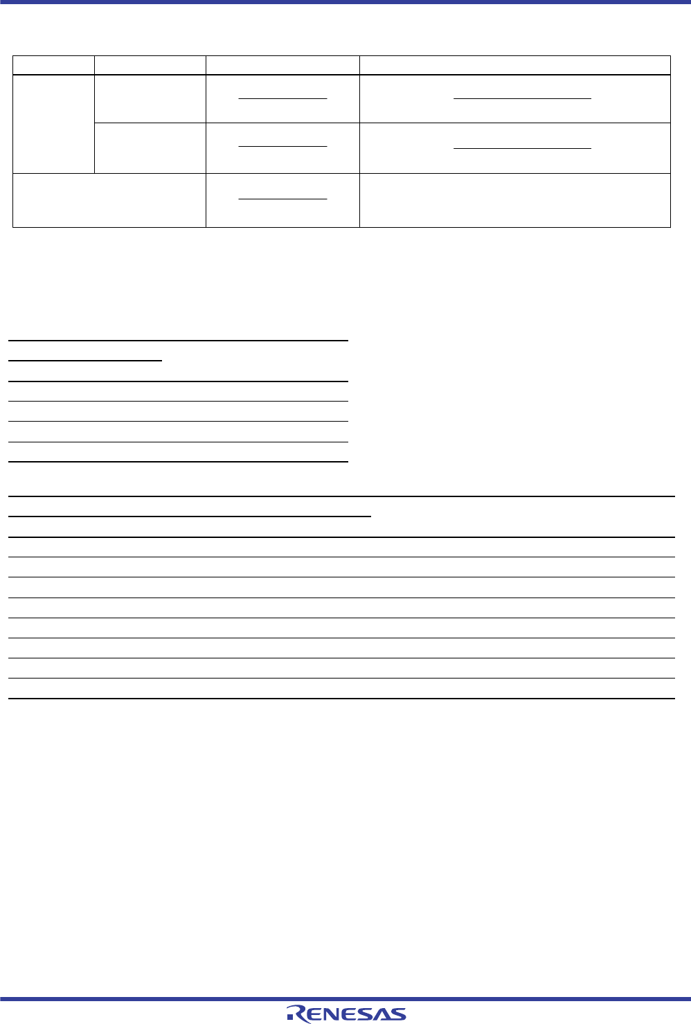
R01UH0034EJ0200 Rev.2.00 Page 924 of 1489
Dec 27, 2013
RX62T Group, RX62G Group 22. Serial Communications Interface (SCIb)
Table 22.4 Relationships between N Setting in BRR and Bit Rate B
B: Bit rate (bps)
N: BRR setting for baud rate generator (0 N 255)
PCLK: Operating frequency (MHz)
n and S: Determined by the SMR setting shown in the following table.
SMR Setting
Clock Source nCKS[1:0] Bits
0 0 PCLK clock 0
0 1 PCLK/4 clock 1
1 0 PCLK/16 clock 2
1 1 PCLK/64 clock 3
SCMR Setting SMR Setting
Base Clock SBCP2 Bit BCP[1:0] Bits
0 0 0 93 clock cycles 93
0 0 1 128 clock cycles 128
0 1 0 186 clock cycles 186
0 1 1 512 clock cycles 512
1 0 0 32 clock cycles 32
1 0 1 64 clock cycles 64
1 1 0 372 clock cycles 372
1 1 1 256 clock cycles 256
Mode
Asynchronous
Clock synchronous
N =
ABCS Bit in SEMR
-1 Error (%) = { -1 } 100
BRR Setting Error
0
1
64 22n-1 B
PCLK 106
N = -1
32 22n-1 B
PCLK 106
N = -1
8 22n-1 B
PCLK 106
PCLK 106
B 64 22n-1 (N+1)
Error (%) = { -1 } 100
PCLK 106
B 32 22n-1 (N+1)
R01UH0034EJ0200 Rev.2.00 Page 925 of 1489
Dec 27, 2013
RX62T Group, RX62G Group 22. Serial Communications Interface (SCIb)
Note: • Notes:This is an example when the ABCS bit in SEMR is 0.
When the ABCS bit is set to 1, the bit rate is two times.
Table 22.5 Examples of BRR Settings for Various Bit Rates (Asynchronous Mode) (1)
Bit Rate
(bps)
Operating Frequency PCLK (MHz)
8 9.8304 10 12
n N Error (%) n N Error (%) n N Error (%) n N Error (%)
110 2 141 0.03 2 174 -0.26 2 177 -0.25 2 212 0.03
150 2 103 0.16 2 127 0.00 2 129 0.16 2 155 0.16
300 1 207 0.16 1 255 0.00 2 64 0.16 2 77 0.16
600 1 103 0.16 1 127 0.00 1 129 0.16 1 155 0.16
1200 0 207 0.16 0 255 0.00 1 64 0.16 1 77 0.16
2400 0 103 0.16 0 127 0.00 0 129 0.16 0 155 0.16
4800 0 51 0.16 0 63 0.00 0 64 0.16 0 77 0.16
9600 0 25 0.16 0 31 0.00 0 32 -1.36 0 38 0.16
19200 0 12 0.16 0 15 0.00 0 15 1.73 0 19 -2.34
31250 0 7 0.00 0 9 -1.70 0 9 0.00 0 11 0.00
38400 — — — 0 7 0.00 0 7 1.73 0 9 -2.34
Bit Rate
(bps)
Operating Frequency PCLK (MHz)
12.288 14 16
n N Error (%) n N Error (%) n N Error (%)
110 2 217 0.08 2 248 -0.17 3 70 0.03
150 2 159 0.00 2 181 0.16 2 207 0.16
300 2 79 0.00 2 90 0.16 2 103 0.16
600 1 159 0.00 1 181 0.16 1 207 0.16
1200 1 79 0.00 1 90 0.16 1 103 0.16
2400 0 159 0.00 0 181 0.16 0 207 0.16
4800 0 79 0.00 0 90 0.16 0 103 0.16
9600 0 39 0.00 0 45 -0.93 0 51 0.16
19200 0 19 0.00 0 22 -0.93 0 25 0.16
31250 0 11 2.40 0 13 0.00 0 15 0.00
38400 0 9 0.00 — —— — 0 12 0.16
R01UH0034EJ0200 Rev.2.00 Page 926 of 1489
Dec 27, 2013
RX62T Group, RX62G Group 22. Serial Communications Interface (SCIb)
Note: • This is an example when the ABCS bit in SEMR is 0.
When the ABCS bit is set to 1, the bit rate is two times.
Table 22.5 Examples of BRR Settings for Various Bit Rates (Asynchronous Mode) (2)
Bit Rate
(bps)
Operating Frequency PCLK (MHz)
17.2032 18 19.6608 20
n N Error (%) n N Error (%) n N Error (%) n N Error (%)
110 3 75 0.48 3 79 -0.12 3 86 0.31 3 88 -0.25
150 2 223 0.00 2 233 0.16 2 255 0.00 3 64 0.16
300 2 111 0.00 2 116 0.16 2 127 0.00 2 129 0.16
600 1 223 0.00 1 233 0.16 1 255 0.00 2 64 0.16
1200 1 111 0.00 1 116 0.16 1 127 0.00 1 129 0.16
2400 0 223 0.00 0 233 0.16 0 255 0.00 1 64 0.16
4800 0 111 0.00 0 116 0.16 0 127 0.00 0 129 0.16
9600 0 55 0.00 0 58 -0.69 0 63 0.00 0 64 0.16
19200 0 27 0.00 0 28 1.02 0 31 0.00 0 32 -1.36
31250 0 16 1.20 0 17 0.00 0 19 -1.70 0 19 0.00
38400 0 13 0.00 0 14 -2.34 0 15 0.00 0 15 1.73
Bit Rate
(bps)
Operating Frequency PCLK (MHz)
25 30 33 50
n N Error (%) n N Error (%) n N Error (%) n N Error (%)
110 3 110 -0.02 3 132 0.13 3 145 0.33 3 221 -0.02
150 3 80 0.47 3 97 -0.35 3 106 0.39 3 162 -0.15
300 2 162 -0.15 2 194 0.16 2 214 -0.07 3 80 0.47
600 2 80 0.47 2 97 -0.35 2 106 0.39 2 162 -0.15
1200 1 162 -0.15 1 194 0.16 1 214 -0.07 2 80 0.47
2400 1 80 0.47 1 97 -0.35 1 106 0.39 1 162 -0.15
4800 0 162 -0.15 0 194 0.16 0 214 -0.07 1 80 0.47
9600 0 80 0.47 0 97 -0.35 0 106 0.39 1 40 -0.77
19200 0 40 -0.76 0 48 -0.35 0 53 -0.54 0 80 0.47
31250 0 24 0.00 0 29 0 0 32 0 0 49 0.00
38400 0 19 1.73 0 23 1.73 0 26 -0.54 0 40 -0.77

R01UH0034EJ0200 Rev.2.00 Page 927 of 1489
Dec 27, 2013
RX62T Group, RX62G Group 22. Serial Communications Interface (SCIb)
Note: • When the ABCS bit in SEMR is set to 1, the bit rate is two times.
Note: • This is an example when the ABCS bit in SEMR is 0.
Note: • This is an example when the ABCS bit in SEMR is 1.
Table 22.6 Maximum Bit Rate for Each Operating Frequency (Asynchronous Mode)
PCLK (MHz) Maximum Bit Rate
(bps) n N PCLK (MHz) Maximum Bit Rate
(bps) n N
8 250000 0 0 18 562500 0 0
9.8304 307200 0 0 19.6608 614400 0 0
10 312500 0 0 20 625000 0 0
12 375000 0 0 25 781250 0 0
12.288 384000 0 0 30 937500 0 0
14 437500 0 0 33 1031250 0 0
16 500000 0 0 50 1562500 0 0
17.2032 537600 0 0
Table 22.7 Maximum Bit Rate with External Clock Input (Asynchronous Mode) (1)
PCLK (MHz) External Input Clock
(MHz) Maximum Bit Rate
(bps) PCLK (MHz) External Input Clock
(MHz) Maximum Bit Rate
(bps)
8 2.0000 125000 18 4.5000 281250
9.8304 2.4576 153600 19.6608 4.9152 307200
10 2.5000 156250 20 5.0000 312500
12 3.0000 187500 25 6.2500 390625
12.288 3.0720 192000 30 7.5000 468750
14 3.5000 218750 33 8.2500 515625
16 4.0000 250000 50 12.500 781250
17.2032 4.3008 268800
Table 22.7 Maximum Bit Rate with External Clock Input (Asynchronous Mode) (2)
PCLK (MHz) External Input Clock
(MHz) Maximum Bit Rate
(bps) PCLK (MHz) External Input Clock
(MHz) Maximum Bit Rate
(bps)
8 2.0000 250000 18 4.5000 562500
9.8304 2.4576 307200 19.6608 4.9152 614400
10 2.5000 312500 20 5.0000 625000
12 3.0000 375000 25 6.2500 781250
12.288 3.0720 384000 30 7.5000 937500
14 3.5000 437500 33 8.2500 1031250
16 4.0000 500000 50 12.500 1562500
17.2032 4.3008 537600
R01UH0034EJ0200 Rev.2.00 Page 928 of 1489
Dec 27, 2013
RX62T Group, RX62G Group 22. Serial Communications Interface (SCIb)
Space: Setting prohibited.
—: Can be set, but the actual bit rate doesn't match the bit rate value in the table.
Note 1. Continuous transmission or reception is not possible.
Table 22.8 BRR Settings for Various Bit Rates (Clock Synchronous Mode)
Bit Rate
(bps)
Operating Frequency PCLK (MHz)
8 10162025303350
nNnNnNnNnNnNnNnN
110
250 3 124 — — 3 249
500 2 249 — — 3 124 — — 3 233
1k 2 124 — — 2 249 — — 3 97 3 116 3 128 3 194
2.5k 1 199 1 249 2 99 2 124 2 155 2 187 2 205 3 77
5k 1 99 1 124 1 199 1 249 2 77 2 93 2 102 2 155
10k 0 199 0 249 1 99 1 124 1 155 1 187 1 205 2 77
25k 0 79 0 99 0 159 0 199 0 249 1 74 1 82 1 124
50k 0 39 0 49 0 79 0 99 0 124 0 149 0 164 1 61
100k 0 19 0 24 0 39 0 49 0 62 0 74 0 82 0 124
250k 0 7 0 9 0 15 0 19 0 24 0 29 0 32 0 49
500k 03040709——014——024
1M 0 1 0 3 0 4 ————————
2.5M 0 0*101——02——04
5M 0 0*1————————
Table 22.9 Maximum Bit Rate with External Clock Input (Clock Synchronous Mode)
PCLK (MHz) External Input Clock
(MHz) Maximum Bit Rate
(bps) PCLK (MHz) External Input Clock
(MHz) Maximum Bit Rate
(bps)
8 1.3333 1333333.3 20 3.3333 3333333.3
10 1.6667 1666666.7 25 4.1667 4166666.7
12 2.0000 2000000.0 30 5.0000 5000000.0
14 2.3333 2333333.3 33 5.5000 5500000.0
16 2.6667 2666666.7 50 8.3333 8333333.3
18 3.0000 3000000.0
R01UH0034EJ0200 Rev.2.00 Page 929 of 1489
Dec 27, 2013
RX62T Group, RX62G Group 22. Serial Communications Interface (SCIb)
Table 22.10 BRR Settings for Various Bit Rates (Smart Card Interface Mode, n = 0, S = 372)
Bit Rate
(bps)
Operating Frequency PCLK (MHz)
7.1424 10.00 10.7136 13.00
n N Error (%) n N Error (%) n N Error (%) n N Error (%)
9600 0 0 0.00 0 1 30 0 1 25 0 1 8.99
Bit Rate
(bps)
Operating Frequency PCLK (MHz)
14.2848 16.00 18.00 20.00
n N Error (%) n N Error (%) n N Error (%) n N Error (%)
9600 0 1 0.00 0 1 12.01 0 2 15.99 0 2 6.66
Bit Rate
(bps)
Operating Frequency PCLK (MHz)
25.00 30.00 33.00 50.00
n N Error (%) n N Error (%) n N Error (%) n N Error (%)
9600 0 3 12.49 0 3 5.01 0 4 7.59 0 6 0.01
Table 22.11 Maximum Bit Rate for Each Operating Frequency (Smart Card Interface Mode, S = 372)
PCLK (MHz) Maximum Bit Rate
(bps) n N PCLK (MHz) Maximum Bit Rate
(bps) n N
10.00 13441 0 0 20.00 26882 0 0
10.7136 14400 0 0 25.00 33602 0 0
13.00 17473 0 0 30.00 40323 0 0
16.00 21505 0 0 33.00 44355 0 0
18.00 24194 0 0 50.00 67205 0 0

R01UH0034EJ0200 Rev.2.00 Page 930 of 1489
Dec 27, 2013
RX62T Group, RX62G Group 22. Serial Communications Interface (SCIb)
22.2.1.10 Serial Extended Mode Register (SEMR)
Note 1. Writable only when TE in SCR = 0 and RE in SCR = 0 (both serial transmission and reception are disabled).
Settings in the SEMR select the number of clock cycles for 1 bit period and whether to enable or disable cancellation of
noise on the RXDn pin in asynchronous mode.
ABCS Bit (Asynchronous Mode Base Clock Select)
Selects the number of base clock pulses for 1-bit period.
NFEN Bit (Noise Cancelling Function Select)
Selects whether to enable or disable noise cancellation. When the setting is “enabled”, noise cancellation is applied to
signals on the reception pin (RXDn input). See section 22.4, Noise Cancellation.
RXDESEL bit (Asynchronous Start Bit Edge Detection Select)
Selects the detection method of the start bit for reception in asynchronous mode. When a break occurs, data receiving
operation depends on the settings of this bit. Set this bit to 1 when reception should be stopped while a break occurs or
when reception should be started without retaining the RXDn pin input at High level for the period of one data frame or
longer after completion of the break.
Set this bit to 0 in modes other than asynchronous mode.
Address: SCI0.SEMR 0008 8247h, SCI1.SEMR 0008 824Fh, SCI2.SEMR 0008 8257h
b7 b6 b5 b4 b3 b2 b1 b0
RXDES
EL — NFEN ABCS — — — —
Value after reset: 00000000
Bit Symbol Bit Name Function R/W
b3 to b0 — Reserved These bits are always read as 0. The write value should always be 0. R/W
b4 ABCS Asynchronous Mode
Base Clock Select
(Valid only in asynchronous mode)
0: Selects 16 base clock cycles for 1-bit period
1: Selects 8 base clock cycles for 1-bit period
R/W*1
b5 NFEN Noise Cancelling
Function Select
(Valid only in asynchronous mode)
0: Disables noise cancellation for the RXDn pin
1: Enables noise cancellation for the RXDn pin
R/W*1
b6 — Reserved These bits are always read as 0. The write value should always be 0. R/W
b7 RXDESE
L
Asynchronous Start Bit
Edge Detection Select
(Valid only in asynchronous mode).
0: Detects the beginning of start bit at Low level of RXDn pin input.
1: Detects the beginning of start bit at falling edge of RXDn pin input.
R/W*1
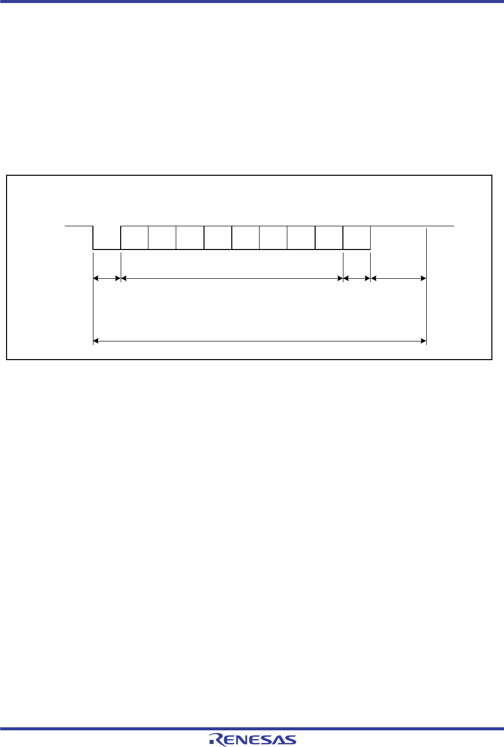
R01UH0034EJ0200 Rev.2.00 Page 931 of 1489
Dec 27, 2013
RX62T Group, RX62G Group 22. Serial Communications Interface (SCIb)
22.2.2 Operation in Asynchronous Mode
Figure 22.2 shows the general format for asynchronous serial communications.
One frame consists of a start bit (Low), transmit/receive data, a parity bit, and stop bits (High).
In asynchronous serial communications, the communications line is usually held in the mark state (High).
The SCI monitors the communications line, and upon detection of the space state (Low) while the SEMR.RXDESEL bit
is 0 or a falling edge to the space state (Low) while the SEMR.RXDESEL bit is 1, it recognizes a start bit and starts serial
communications.
Inside the SCI, the transmitter and receiver are independent units, enabling full-duplex communications. Both the
transmitter and the receiver also have a double-buffered structure, so that data can be read or written during transmission
or reception, enabling continuous data transmission and reception.
Figure 22.2 Format in Asynchronous Serial Communications
(Example with 8-Bit Data, Parity, Two Stop Bits)
0
Transmit/receive data
D0 0/1 1
1 1
Idle state
(mark state)
LSB MSB
D1 D2 D3 D4 D5 D6 D7 1
Parity bit
1 or 0 bit
Stop bit
1 or 2 bits7 or 8 bits
One unit of transfer data (character or frame)
Start bit
1 bit
Serial data

R01UH0034EJ0200 Rev.2.00 Page 932 of 1489
Dec 27, 2013
RX62T Group, RX62G Group 22. Serial Communications Interface (SCIb)
22.2.2.1 Serial Data Transfer Format
Table 22.12 shows the serial data transfer formats that can be used in asynchronous mode.
Any of 12 transfer formats can be selected according to the SMR setting. For details of multi-processor function, see
section 22.2.3, Multi-Processor Communications Function.
Table 22.12 Serial Transfer Formats (Asynchronous Mode)
S: Start bit
STOP: Stop bit
P: Parity bit
MPB: Multi-processor bit
1
S
S
S
S
1
0
0
1
1
0
1
1
1
1
1
0
1
0
1
SPSTOP STOP
7-bit data
7-bit data
7-bit data
8-bit data
8-bit data STOP STOP
STOP
STOP STOP
MPB
STOPMPB
MPB
MPB
—
—
—
—
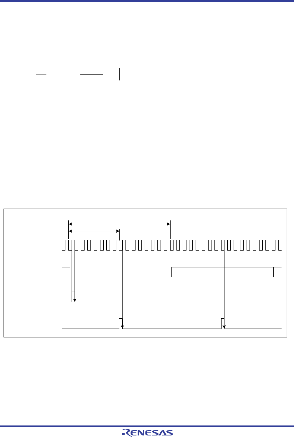
R01UH0034EJ0200 Rev.2.00 Page 933 of 1489
Dec 27, 2013
RX62T Group, RX62G Group 22. Serial Communications Interface (SCIb)
22.2.2.2 Receive Data Sampling Timing and Reception Margin in Asynchronous Mode
In asynchronous mode, the SCI operates on a base clock with a frequency of 16 times*1 the bit rate.
In reception, the SCI samples the falling edge of the start bit using the base clock, and performs internal synchronization.
Since receive data is sampled at the rising edge of the 8th pulse* of the base clock, data is latched at the middle of each
bit, as shown in Figure 22.3. Thus the reception margin in asynchronous mode is determined by formula (1) below.
M: Reception margin
N: Ratio of bit rate to clock (N = 16 when ABCS in SEMR = 0, N = 8 when ABCS in SEMR = 1)
D: Duty cycle of clock (D = 0.5 to 1.0)
L: Frame length (L = 9 to 12)
F: Absolute value of clock frequency deviation
Assuming values of F = 0 and D = 0.5 in formula (1), the reception margin is determined by the formula below.
M = {0.5 - 1/(2 x 16)} × 100 (%) = 46.875%
However, this is only the computed value, and a margin of 20% to 30% should be allowed in system design.
Note 1. This is an example when the ABCS bit in SEMR is 0. When the ABCS bit is 1, a frequency of 8 times the bit rate
is used as a base clock and receive data is sampled at the rising edge of the 4th pulse of the base clock.
Figure 22.3 Receive Data Sampling Timing in Asynchronous Mode
M = (0.5 - ) - (L - 0.5) F - (1+F)
1
2N
D – 0.5
N 100 [%] Formula (1)
...
Receive data (RXDn)
Internal base clock
D0 D1
Synchronization
sampling timing
Data sampling
timing
Start bit
8 clock pulses
16 clock pulses
0157701570
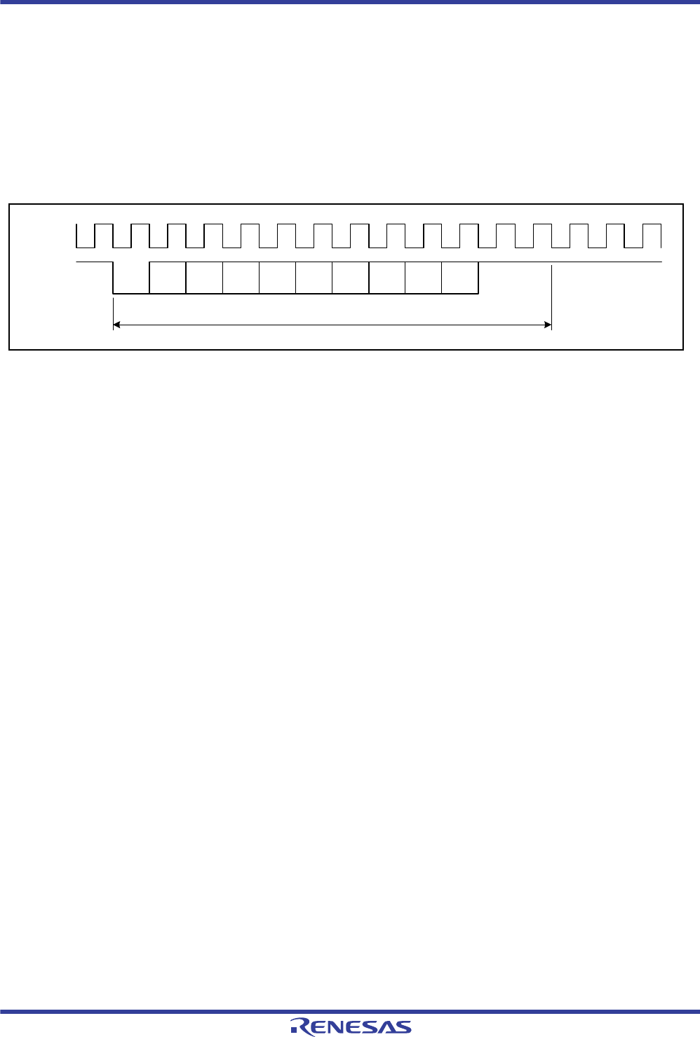
R01UH0034EJ0200 Rev.2.00 Page 934 of 1489
Dec 27, 2013
RX62T Group, RX62G Group 22. Serial Communications Interface (SCIb)
22.2.2.3 Clock
Either an internal clock generated by the on-chip baud rate generator or an external clock input to the SCKn pin can be
selected as the SCI's transfer clock, according to the setting of the CA bit in SMR and the CKE[1:0] bits in SCR.
When an external clock is input to the SCKn pin, the clock frequency should be 16 times the bit rate (when ABCS in
SEMR = 0) and 8 times the bit rate (when ABCS in SEMR = 1).
When the SCI is operated on an internal clock, the clock can be output from the SCKn pin. The frequency of the clock
output in this case is equal to the bit rate, and the phase is such that the rising edge of the clock is in the middle of the
transmit data, as shown in Figure 22.4.
Figure 22.4 Phase Relationship between Output Clock and Transmit Data (Asynchronous Mode)
TXDn
SCKn
0
1 frame
D0 1 1D1 D2 D3 D4 D5 D6 D7 0/1
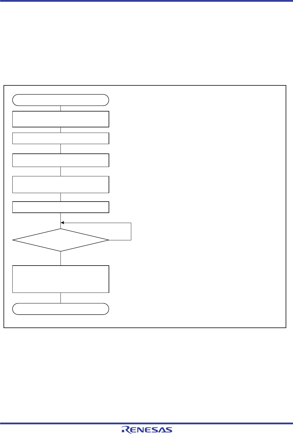
R01UH0034EJ0200 Rev.2.00 Page 935 of 1489
Dec 27, 2013
RX62T Group, RX62G Group 22. Serial Communications Interface (SCIb)
22.2.2.4 SCI Initialization (Asynchronous Mode)
Before transmitting and receiving data, start by writing the initial value "00h" to the SCR and then continue through the
procedure for SCI given in the sample flowchart (Figure 22.5). Whenever the operating mode or transfer format is
changed, the SCR must be initialized before the change is made.
When the external clock is used in asynchronous mode, ensure that the clock signal is supplied even during initialization.
Note that clearing the SCR.RE bit to 0 initializes neither the ORER, FER, and PER flags in SSR nor RDR.
Moreover, note that switching the value of the SCR.TE bit from 1 to 0 or 0 to 1 while the SCR.TIE bit is 1 leads to the
generation of a TXI interrupt request.
Figure 22.5 Sample SCI Initialization Flowchart (Asynchronous Mode)
Wait
Start initialization
[ 1 ]
No
Yes
Clear bits TIE, RIE, TE, RE, and
TEIE in SCR to 0
1-bit interval elapsed
[ 1 ] Set the Bj bit in ICR of PORTn for the
corresponding pin to 1 (input buffer of the
corresponding pin is enabled) when receiving
data or using an external clock.
[ 2 ] Set the clock selection in SCR.
When the clock output is selected in
asynchronous mode, the clock is output
immediately after SCR settings are made.
[ 3 ] Set the data transfer format in SMR and
SCMR*1.
[ 4 ] Write a value corresponding to the bit rate to
BRR. This step is not necessary if an external
clock is used.
[ 5 ] Wait at least one bit interval, then set the TE
bit or RE bit in SCR to 1. Also set the TIE,
RIE, and TEIE bits in SCR*2.
Setting the TE and RE bits enables the TXDn
and RXDn pins to be used.
Set Bj bit in ICR of PORTn to 1
Set bits CKE[1:0] in SCR [ 2 ]
[ 3 ]
[ 4 ]
[ 5 ]
Set data transfer format in
SMR and SCMR
Set a value in BRR
Set TE or RE bit in SCR to 1, and set
TIE, RIE, and TEIE bits in SCR
Initialization completion
Note 1: Set the initial value in SCMR.
Note 2: When the TXI interrupt is activating the
DMAC or DTC and the TIE and TEIE bits
are both set to 1, a TEI interrupt will be
generated as a CPU interrupt while
transfer by the DMAC or DTC is in progress.
Set the TEIE bit to 1 on completion of all
transfer by the DMAC or DTC.
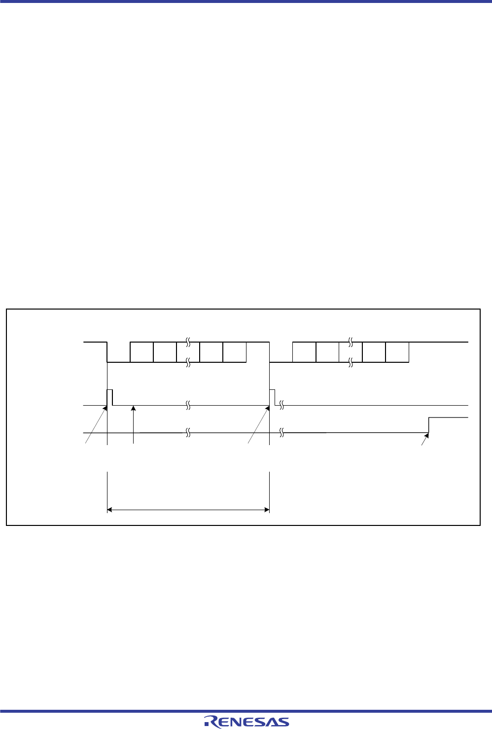
R01UH0034EJ0200 Rev.2.00 Page 936 of 1489
Dec 27, 2013
RX62T Group, RX62G Group 22. Serial Communications Interface (SCIb)
22.2.2.5 Serial Data Transmission (Asynchronous Mode)
Figure 22.6 shows an example of the operation for serial transmission in asynchronous mode.
In serial transmission, the SCI operates as described below.
1. The SCI transfers data from TDR to TSR when data is written to TDR in the TXI interrupt processing routine. The
TXI interrupt request at the beginning of transmission is generated when the TE bit in SCR is set to 1 after the TIE
bit in SCR is set to 1 or when these two bits are set to 1 simultaneously by a single instruction.
2. After transferring data from TDR to TSR, the SCI starts transmission. If the TIE bit in SCR is 1 at this time, a TXI
interrupt request is generated. Continuous transmission is enabled by writing the next transmit data to TDR in the
TXI interrupt processing routine before transmission of the current transmit data is completed.
3. Data is sent from the TXDn pin in the following order: start bit, transmit data, parity bit or multi-processor bit (may
be omitted depending on the format), and stop bit.
4. The SCI checks for updating of (writing to) TDR at the time of stop bit output.
5. When TDR is updated, the next transmit data is transferred from TDR to TSR, the stop bit is sent, and then serial
transmission of the next frame is started.
6. If TDR is not updated, the TEND flag in SSR is set to 1, the stop bit is sent, and then the mark state is entered in
which high is output. If the TEIE flag in SCR is 1 at this time, the TEND flag in SSR is set to 1 and a TEI interrupt
request is generated.
Figure 22.7 shows a sample flowchart for serial transmission in asynchronous mode.
Figure 22.6 Example of Operation for Serial Transmission in Asynchronous Mode
(Example with 8-Bit Data, Parity, One Stop Bit)
TXI interrupt signal
0
1 frame
D0 D1 D7 0/1 1 0 D0 D1 D7 0/1 1
1 1
Data Data Parity
bit Stop
bit
Start
bit
Parity
bit Stop
bit
Start
bit
Idle state
(mark state)
TEI interrupt
request
generated
TXI interrupt
request
generated
Data written to TDR in TXI
interrupt processing
routine
TXI interrupt
request
generated
SSR.TEND flag
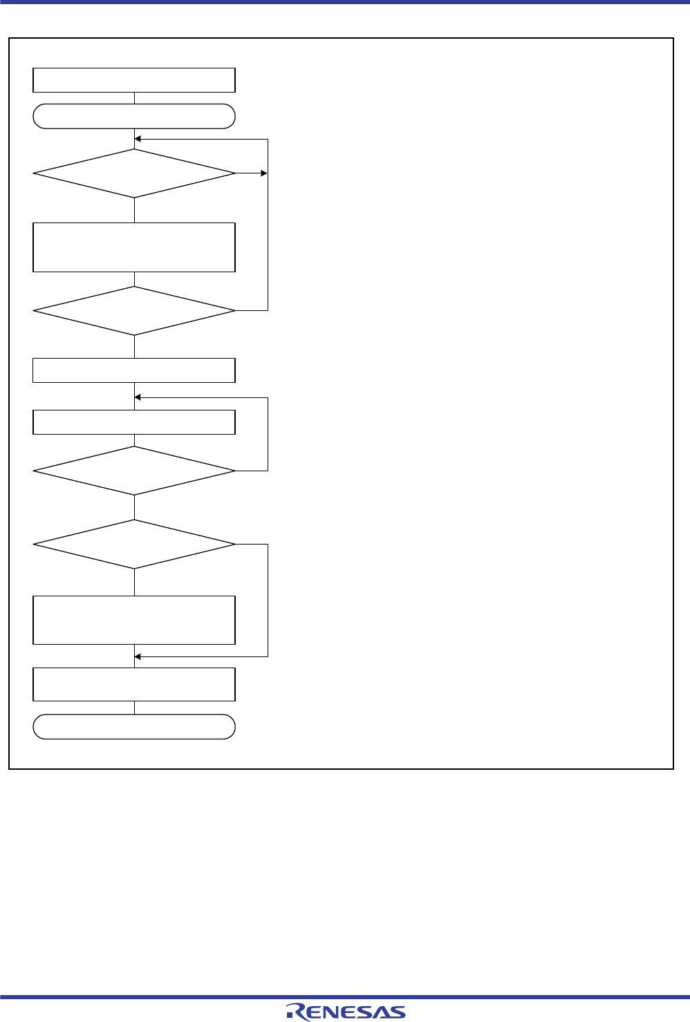
R01UH0034EJ0200 Rev.2.00 Page 937 of 1489
Dec 27, 2013
RX62T Group, RX62G Group 22. Serial Communications Interface (SCIb)
Figure 22.7 Example of Serial Transmission Flowchart in Asynchronous Mode
Initialization
Start data transmission
[ 1 ] [ 1 ] SCIn initialization:
The TXDn pin is automatically designated as the transmit
data output pin. After the TE bit in SCR is set to 1, the pin is
driven high for a frame.
[ 2 ] Transmit data write to TDR by a TXI interrupt request:
When transmit data is transferred from TDR to TSR, a transmit
data empty interrupt (TXI) request is generated. Write transmit
data to TDR once in the TXI interrupt processing routine.
[ 3 ] Serial transmission continuation procedure:
To continue serial transmission, write transmit data to
TDR once using a TXI interrupt request.
Transmit data can also be written to TDR by activating the
DTC.
[ 4 ] Break output at the end of serial transmission:
To output a break in serial transmission, set the Bj bit
in DDR of PORTn for the port corresponding to the TXDn pin
to 1 (output port), clear the Bj bit in DR of PORTn to 0
(low level output), and then clear the TE bit in SCR to 0.
[ 2 ]
No
Yes
Write transmit data to TDR
No
Yes
No
Yes
Read TEND flag in SSR
No
Yes
Clear Bj bit in DR of PORTn to 0 and
set Bj bit in DDR of PORTn to 1
Clear bits TIE, TE, and TEIE
in SCR to 0
TXI interrupt
All data transmitted?
SSR.TEND = 1
Break output [ 4 ]
[ 3 ]
Clear TIE bit in SCR to 0
End
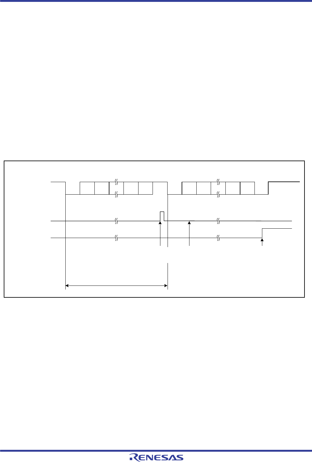
R01UH0034EJ0200 Rev.2.00 Page 938 of 1489
Dec 27, 2013
RX62T Group, RX62G Group 22. Serial Communications Interface (SCIb)
22.2.2.6 Serial Data Reception (Asynchronous Mode)
Figure 22.8 shows an example of the operation for serial data reception in asynchronous mode.
In serial data reception, the SCI operates as described below.
1.When the SCI monitors the communications line and detects a start bit, it performs internal synchronization, stores
receive data in RSR, and checks the parity bit and stop bit.
2.If an overrun error occurs, the ORER flag in SSR is set to 1. If the RIE bit in SCR is 1 at this time, an ERI interrupt
request is generated. Receive data is not transferred to RDR.
3.If a parity error is detected, the PER bit in SSR is set to 1 and receive data is transferred to RDR. If the RIE bit in SCR
is 1 at this time, an ERI interrupt request is generated.
4.If a framing error (when the stop bit is 0) is detected, the FER bit in SSR is set to 1 and receive data is transferred to
RDR. If the RIE bit in SCR is 1 at this time, an ERI interrupt request is generated.
5.When reception finishes successfully, receive data is transferred to RDR. If the RIE bit in SCR is 1 at this time, an RXI
interrupt request is generated. Continuous reception is enabled by reading the receive data transferred to RDR in this RXI
interrupt processing routine before reception of the next receive data is completed.
Figure 22.8 Example of SCI Operation for Serial Reception in Asynchronous Mode
(Example with 8-Bit Data, Parity, One Stop Bit)
Table 22.13 shows the states of the SSR status flags and receive data handling when a receive error is detected.
If a receive error is detected, an ERI interrupt request is generated but an RXI interrupt request is not generated. Data
reception cannot be resumed while the receive error flag is 1. Accordingly, clear the ORER, FER, and PER bits to 0
before resuming reception. Moreover, be sure to read the RDR during overrun error processing.
Figure 22.9 shows samples of flowcharts for serial data reception.
RXI interrupt signal
SSR.FER flag
0
1 frame
D0 D1 D7 0/1 1 0 D0 D1 D7 0/1 0
1 1
Data Data Parity
bit Stop
bit
Start
bit
Parity
bit Stop
bit
Start
bit
Idle state
(mark state)
ERI interrupt request
generated by framing
error
RDR data read in RXI
interrupt processing
routine
RXI interrupt
request
generated
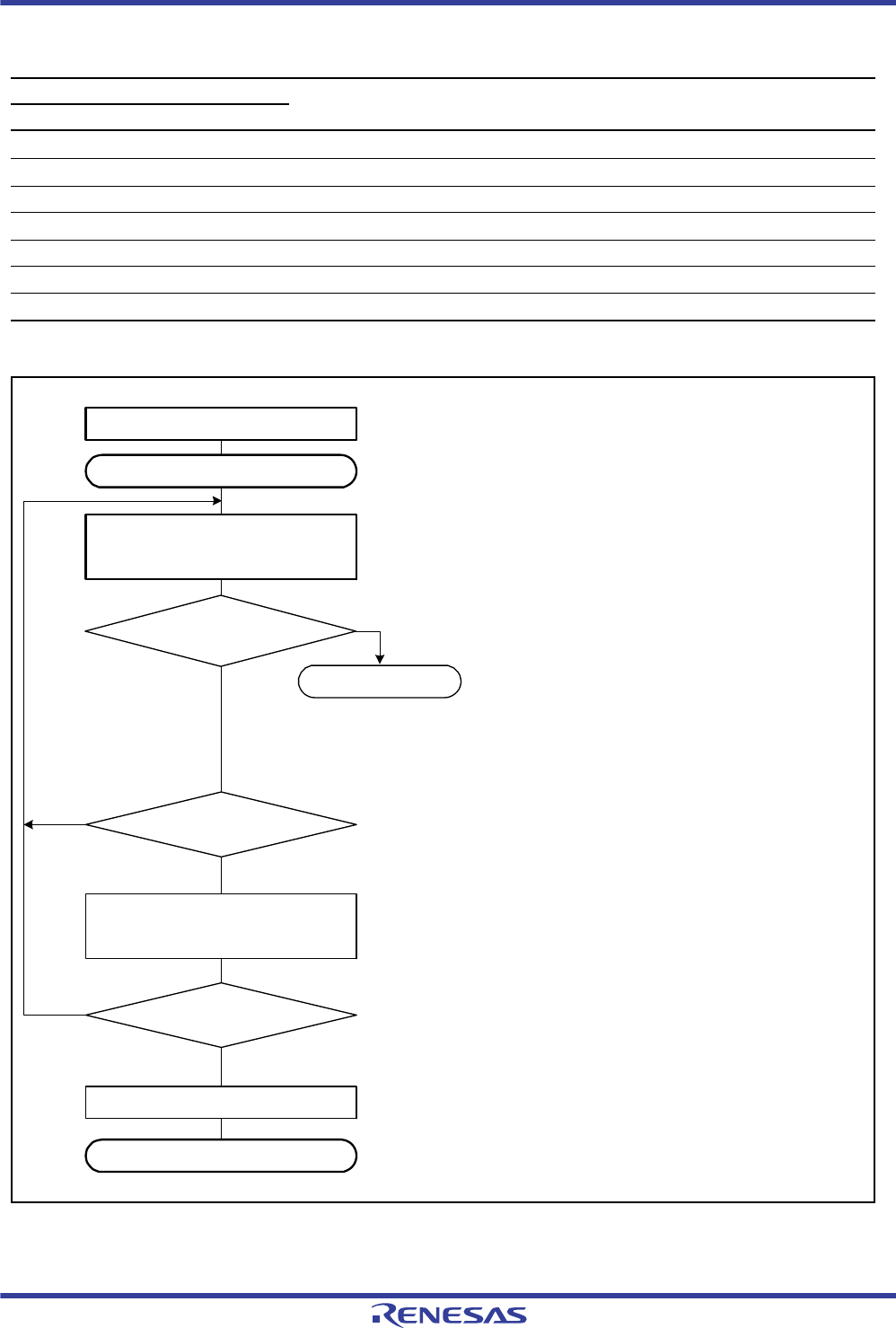
R01UH0034EJ0200 Rev.2.00 Page 939 of 1489
Dec 27, 2013
RX62T Group, RX62G Group 22. Serial Communications Interface (SCIb)
Figure 22.9 Example of Serial Reception Flowchart (1) (Asynchronous Mode)
Table 22.13 SSR Status Flags and Receive Data Handling
SSR Status Flag
Receive Data Receive Error TypeORER FER PER
100Lost Overrun error
010Transferred to RDR Framing error
0 0 1 Transferred to RDR Parity error
110Lost Overrun error + framing error
1 0 1 Lost Overrun error + parity error
0 1 1 Transferred to RDR Framing error + parity error
111Lost Overrun error + framing error + parity error
Yes
No
Initialization
Start data reception
No
Yes
Clear bits RIE and RE in SCR to 0
Read ORER, PER, and FER flags in
SSR
Error processing
(Continued to next page)
Read receive data in RDR
No
Yes
RXI interrupt
All data received?
[ 1 ] SCIn initialization:
The RXDn pin is automatically designated as the
receive data input pin.
[ 2 ] [ 3 ] Receive error processing and break detection:
If a receive error occurs, an ERI interrupt is
generated. An error is identified by reading the
ORER, PER, and FER flags in SSR. After
performing the appropriate error processing, be
sure to clear the ORER, PER, and FER flags to 0.
Reception cannot be resumed if any of these flags
is set to 1. In the case of a framing error, a break
can be detected by reading the value of the input
port corresponding to the RXDn pin.
[ 4 ] Read the receive data in RDR once in the RXI
interrupt processing routine.
[ 5 ] Serial reception continuation procedure:
To continue serial reception, before the stop bit of
the current frame is received, read data from RDR
in the RXI interrupt processing routine. The RDR
data can also be read by activating the DTC.
[ 1 ]
[ 2 ]
[ 3 ]
[ 4 ]
[ 5 ]
ORER or PER or FER = 1
End
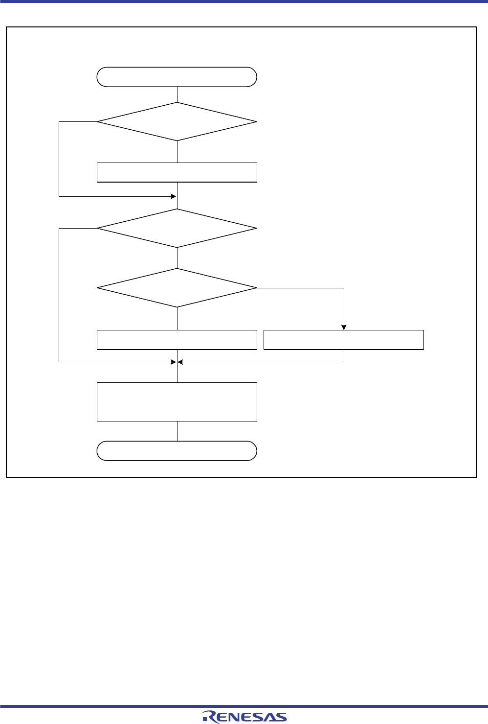
R01UH0034EJ0200 Rev.2.00 Page 940 of 1489
Dec 27, 2013
RX62T Group, RX62G Group 22. Serial Communications Interface (SCIb)
Figure 22.10 Example of Serial Reception Flowchart (2) (Asynchronous Mode)
[ 3 ]
Error processing
Yes
No
Clear ORER, FER, and PER flags
in SSR to 0
No
Yes
No
Yes
Framing error processing
Overrun error processing*
ORER in SSR = 1
FER in SSR = 1
Break?
Clear RE bit in SCR to 0
Note: * Read the RDR register.
End
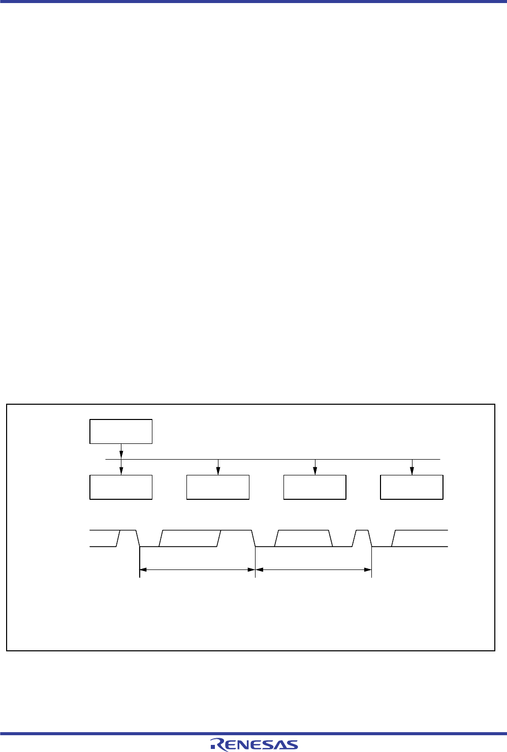
R01UH0034EJ0200 Rev.2.00 Page 941 of 1489
Dec 27, 2013
RX62T Group, RX62G Group 22. Serial Communications Interface (SCIb)
22.2.3 Multi-Processor Communications Function
Using the multi-processor communication functions enables to transmit and receive data by sharing a communication
line between multiple processors by using asynchronous serial communication in which the multi-processor bit is added.
In multi-processor communication, a unique ID code is allocated to each receiving station. Serial communication cycles
consist of an ID transmission cycle to specify the receiving station and a data transmission cycle to transmit data to the
specified receiving station. The multi-processor bit is used to distinguish between the ID transmission cycle and the data
transmission cycle. When the multi-processor bit is set to 1, it indicates the ID transmission cycle and when the multi-
processor bit is set to 0, it indicates the data transmission cycle. Figure 22.11 shows an example of communication
between processors by using a multi-processor format. First, a transmitting station transmits communication data in
which the multi-processor bit set to 1 is added to the ID code of the receiving station. Next, the transmitting station
transmits the communication data in which the multi-processor bit set to 0 is added to the transmission data. Upon
receiving the communication data in which the multi-processor bit is set to 1, the receiving station compares the received
ID with the ID of the receiving station itself and if the two match, receives the communication data that is subsequently
transmitted. If the received ID does not match with the ID of the receiving station, the receiving station skips the
communication data until again receiving the communication data in which the multi-processor bit is set to 1.
For supporting this function, the SCI provides the MPIE bit in SCR. When the MPIE bit is set to 1, transfer of reception
data from the RSR to the RDR, detection of a reception error, and setting the respective status flags ORER and FER in
SSR are disabled until reception of data in which the multi-processor bit is set to 1. Upon receiving a reception character
in which the multi-processor bit is set to 1, the MPB bit in SSR is set to 1 and the MPIE bit in SCR is automatically
cleared, thus returning to a normal reception operation. During this time, an RXI interrupt is generated if the RIE bit in
SCR is set.
As the transmitting in the multi-processor mode, in the ID transmission cycle and the data transmission cycle, the data
should be transmitted with the SSR.MPBT bit to 1 and 0, respectively.
When the multi-processor format is specified, specification of the parity bit is disabled. Apart from this, there is no
difference from the operation in the normal asynchronous mode. A clock which is used for the multi-processor
communication is also the same as the clock used in the normal asynchronous mode.
Figure 22.11 An Example of Communication using the Multi-Processor Format
(Example of Transmission of Data AAh to Receiving Station A)
Transmitting
station
Receiving
station A
(ID = 01)
Receiving
station B Receiving
station C Receiving
station D
Communication line
Serial data
ID transmission cycle =
specification of a receiving station Data transmission cycle = data
transmission to the receiving
station specified by ID
(MPB = 0)
01h AAh
[Legend]
MPB: Multi-processor bit
(ID = 02) (ID = 03) (ID = 04)
(MPB = 1)
(MPB = 1)
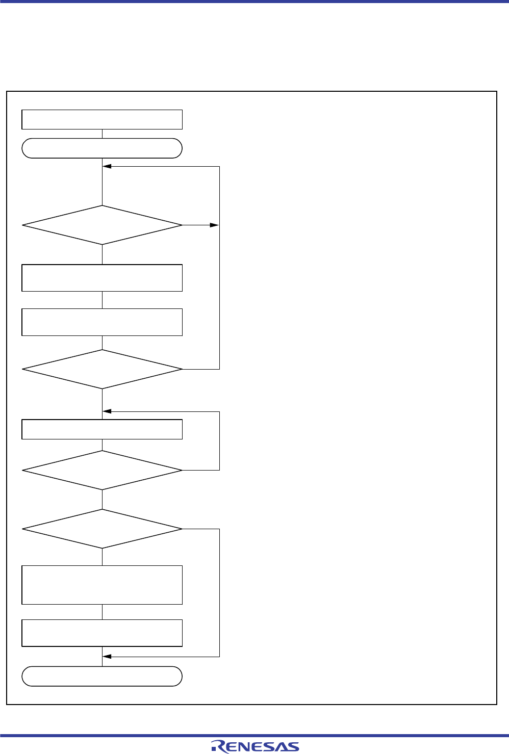
R01UH0034EJ0200 Rev.2.00 Page 942 of 1489
Dec 27, 2013
RX62T Group, RX62G Group 22. Serial Communications Interface (SCIb)
22.2.3.1 Multi-Processor Serial Data Transmission
Figure 22.12 is a sample flowchart of multi-processor data transmission. In the ID transmission cycle, the ID should be
transmitted with the MPBT bit in SSR set to 1. In the data transmission cycle, the data should be transmitted with the
MPBT bit set to 0. The other operations are the same as the operations in asynchronous mode.
Figure 22.12 Example of Multi-Processor Serial Transmission Flowchart
No
Yes
Initialization
Start data transmission
Set MPBT bit in SSR
No
Yes
No
Yes
Read TEND flag in SSR
No
Yes
Clear Bj bit in DR of PORTn to 0 and
set Bj bit in DDR of PORTn to 1
Clear bits TE, TIE, and TEIE in SCR
to 0
TXI interrupt
All data write
TEI interrupt
Break output
Write transmit data to TDR
[3]
[1]
[4]
[1] SCI initialization:
The TXDn pin is automatically designated as the
transmit data output pin. After the TE bit in SCR is set
to 1, the pin is driven high for a frame, and transmission
is
enabled.
[2] TXI interrupt request:
When transmit data is transferred from TDR to TSR, a
transmit data empty interrupt (TXI) request is generated.
Set the MPBT bit in SSR to 0 or 1, and write transmit data
to TDR once in the TXI interrupt processing routine.
[3] Serial transmission continuation procedure:
To continue serial transmission, write transmit data to
TDR once using a TXI interrupt request.
Transmit data can also be written to TDR by activating
the DTC.
[4] Break output at the end of serial transmission:
To output a break in serial transmission, set the Bj bit in
DDR of PORTn for the port corresponding to the TXDn
pin to 1 (output port), clear the Bj bit in DR of PORTn to 0
(low level output), and then clear the TE bit in SCR to 0.
[2]
End

R01UH0034EJ0200 Rev.2.00 Page 943 of 1489
Dec 27, 2013
RX62T Group, RX62G Group 22. Serial Communications Interface (SCIb)
22.2.3.2 Multi-Processor Serial Data Reception
Figure 22.14 and Figure 22.15 are sample flowcharts of multi-processor data reception. When the MPIE bit in SCR is
set to 1, transmitting the receive data to RDR from RSR is skipped until reception of the communication data in which
the multi-processor bit is set to 1. When the communication data in which the multi-processor bit is set to 1 is received,
the received data is transferred to RDR. During this time, the RXI interrupt request is generated. The other operations are
the same as the operations in asynchronous mode.
Figure 22.13 is the example of operation for reception.
Figure 22.13 Example of SCI Reception (8-Bit Data/Multi-Processor Bit/One Stop Bit)
MPIE
0D0 D1 D7 1 1 0 D0 D1 D7 0 1
11
MPB
Data (Data1)
MPB
RXI interrupt request
(multi-processor
interrupt) generated
ID1
0D0 D1 D7 1 1 0 D0 D1 D7 0 1
11
ID2 Data2ID1
Stop bit
Idle state
(mark state)
Data (ID1)
Start bitStop bitStart bit
RDR value
MPIE = 0
MPIE
RXI interrupt signal
RDR value
MPIE = 0
MPIE bit set to 1 again
when the received ID
does not match the ID
of the receiving station
itself
RXI interrupt request
not generated. RDR
retains the state.
(a) When the received ID does not match the ID of the receiving station itself
(b) When the received ID matches the ID of the receiving station itself
RDR data read in RXI
interrupt processing
routine
MPB
Data (Data2)
MPB Stop bit
Idle state
(mark state)
Data (ID2)
Start bitStop bitStart bit
RXI interrupt request
(multi-processor
interrupt) generated
Since the received ID matches
the ID of the receiving station
itself, reception continued and
data received in RXI interrupt
processing routine
MPIE bit set to 1 again
RDR data read in RXI
interrupt processing
routine
RXI interrupt signal
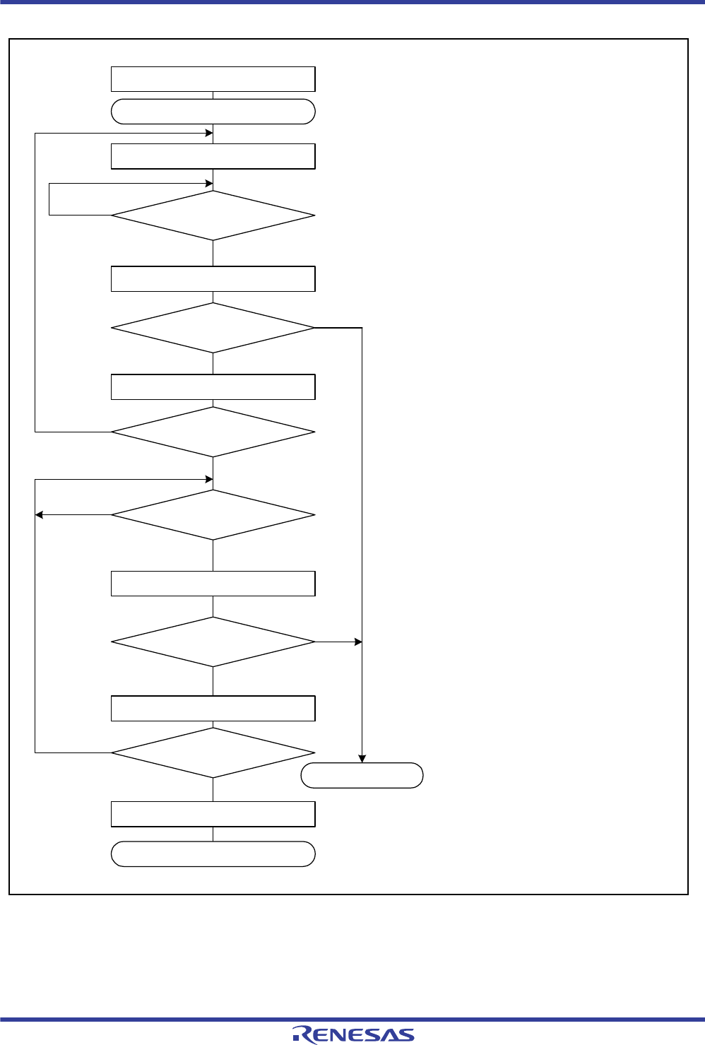
R01UH0034EJ0200 Rev.2.00 Page 944 of 1489
Dec 27, 2013
RX62T Group, RX62G Group 22. Serial Communications Interface (SCIb)
Figure 22.14 Example of Multi-Processor Serial Reception Flowchart (1)
Yes
No
Initialization
Start data reception
No
Yes
Clear bits RIE and RE in SCR to 0
Error
processing
(Continued to next page)
No
Yes
RXI interrupt
FER V ORER = 1
All data received?
Set MPIE bit in SCR to 1
Read ORER and FER flags in SSR
Read receive data in RDR
No
Yes
ID of receiving station itself?
Read ORER and FER flags in SSR
Yes
No
FER V ORER = 1
RXI interrupt
No
Yes
Read receive data in RDR
[1]
[2]
[3]
[4]
[5]
[1] SCI initialization:
The RXDn pin is automatically designated as the receive
data input pin.
[2] ID reception cycle:
The MPIE bit in SCR is set to 1 , and wait for ID reception.
[3] SCIn status confirmation and reception and comparison of ID:
Read data in RDR at the first RXI interrupt, and compare it
with the ID of the receiving station itself. If the ID does not
match the ID of the receiving station itself, set the MPIE bit
to 1 again, and wait for another RXI interrupt.
[4] Data reception at an RXI interrupt:
Read data in RDR once in the RXI interrupt routine.
[5] Receive error processing and break detection:
If a receive error occurs, an error is identified by reading the
ORER and FER flags in SSR. After performing the
appropriate error processing, be sure to clear the ORER and
FER flags to 0. Reception cannot be resumed if any of these
flags is set to 1. In the case of a framing error, a break can
be detected by reading the value of the input port
corresponding to the RXD pin.
End
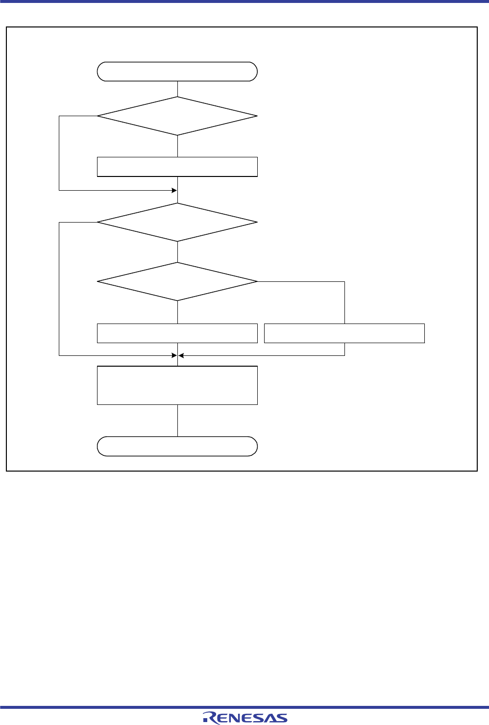
R01UH0034EJ0200 Rev.2.00 Page 945 of 1489
Dec 27, 2013
RX62T Group, RX62G Group 22. Serial Communications Interface (SCIb)
Figure 22.15 Example of Multi-Processor Serial Reception Flowchart (2)
Error processing
Yes
No
Clear ORER, PER, and FER flags
in SSR to 0
No
Yes
No
Yes
Frame error processing
Overrun error processing*
ORER in SSR = 1
FER in SSR = 1
Break?
Clear RE bit in SCR to 0
Note: * Read the RDR register.
End
[5]
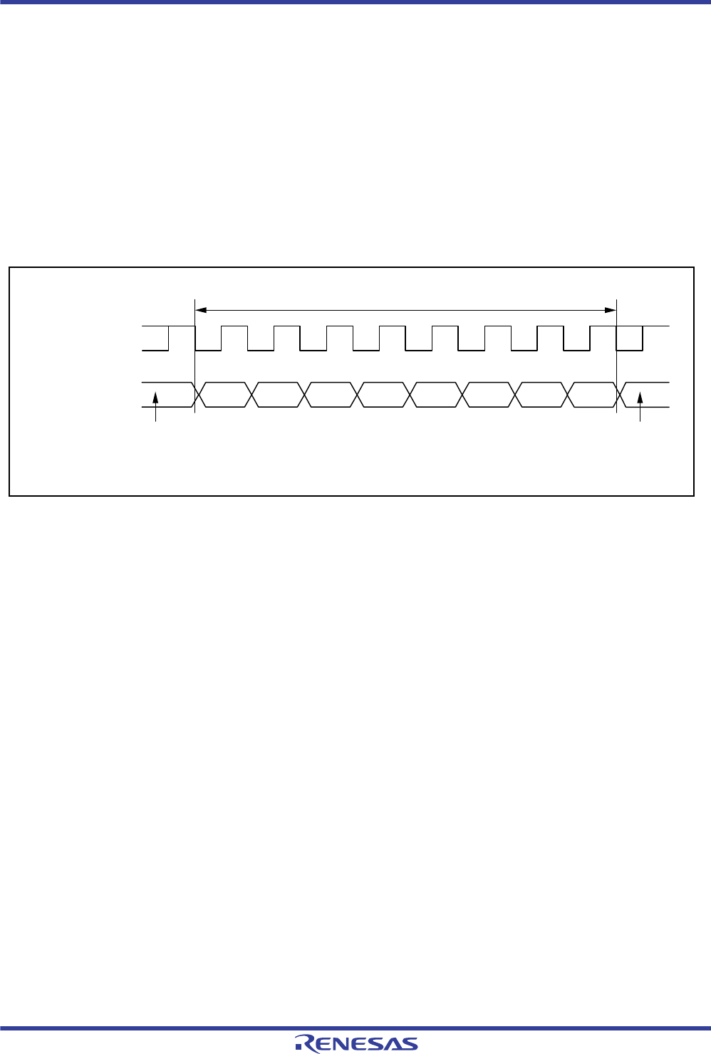
R01UH0034EJ0200 Rev.2.00 Page 946 of 1489
Dec 27, 2013
RX62T Group, RX62G Group 22. Serial Communications Interface (SCIb)
22.2.4 Operation in Clock Synchronous Mode
Figure 22.16 shows the data format for clock synchronous serial data communications.
In clock synchronous mode, data is transmitted or received in synchronization with clock pulses. One character in
transfer data consists of 8-bit data. In clock synchronous mode, no parity bit can be added.
In data transmission, the SCI outputs data from one falling edge of the synchronization clock to the next. In data
reception, the SCI receives data in synchronization with the rising edge of the synchronization clock. After 8-bit data is
output, the transmission line holds the MSB output state.
Inside the SCI, the transmitter and receiver are independent units, enabling full-duplex communications by use of a
common clock. Both the transmitter and the receiver also have a double-buffered structure, so that the next transmit data
can be written during transmission or the previous receive data can be read during reception, enabling continuous data
transfer.
Figure 22.16 Data Format in Clock Synchronous Serial Communications (LSB-First)
22.2.4.1 Clock
Either an internal clock generated by the on-chip baud rate generator or an external synchronization clock input at the
SCKn pin can be selected, according to the setting of the CKE[1:0] bits in SCR.
When the SCI is operated on an internal clock, the synchronization clock is output from the SCKn pin. Eight
synchronization clock pulses are output in the transfer of one character, and when no transfer is performed the clock is
held high. However, the synchronization clock is continuously output only during data reception until an overrun error
occurs or the RE bit in SCR is cleared to 0.
Don't care
One unit of transfer data (character or frame)
Serial data
Synchronization
clock
LSB MSB
Note: Holds a high level except during continuous transfer
Bit 0 Bit 1 Bit 2 Bit 3 Bit 4 Bit 5 Bit 6
Don't care
Bit 7
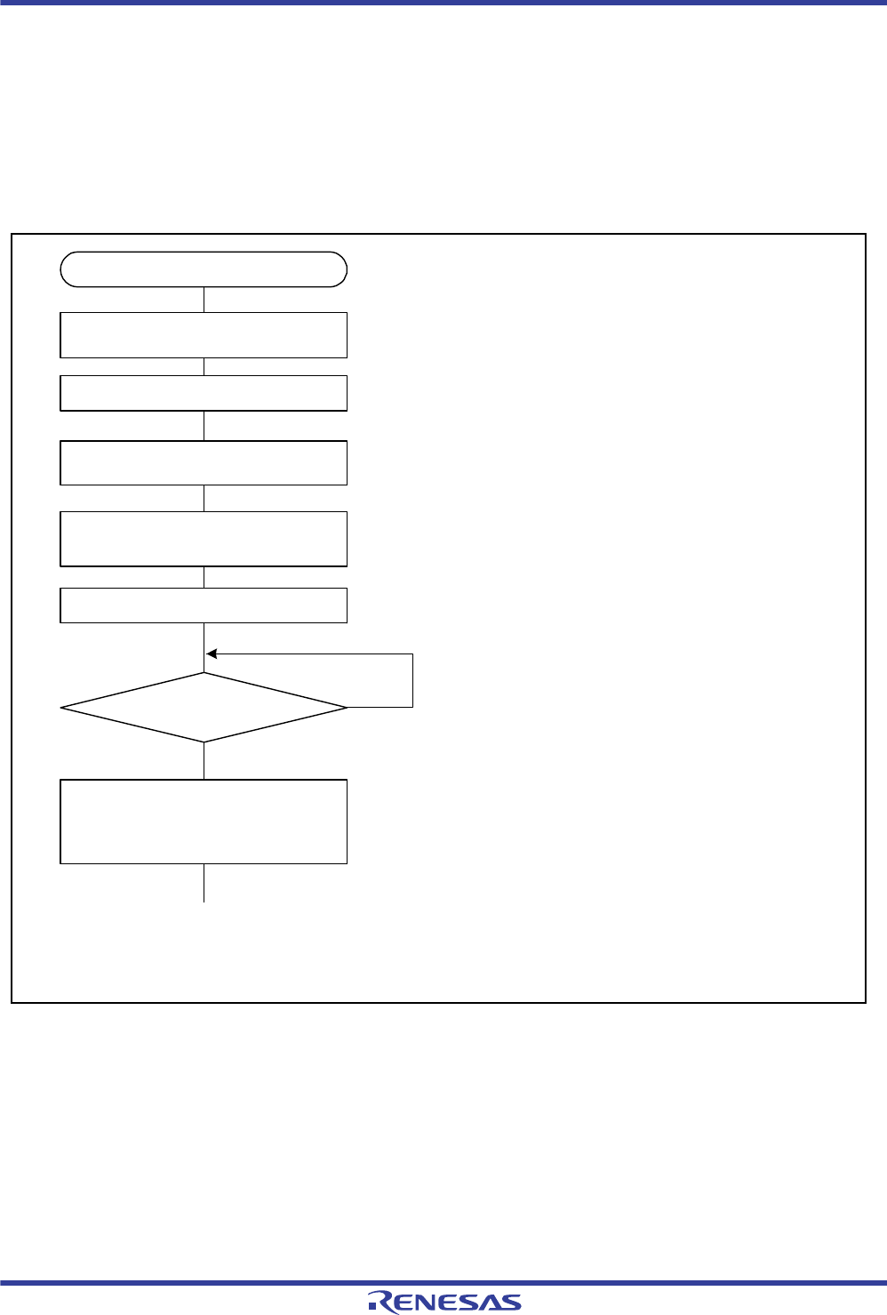
R01UH0034EJ0200 Rev.2.00 Page 947 of 1489
Dec 27, 2013
RX62T Group, RX62G Group 22. Serial Communications Interface (SCIb)
22.2.4.2 SCI Initialization (Clock Synchronous Mode)
Before transmitting and receiving data, start by writing the initial value "00h" to the SCR and then continue through the
procedure for SCI given in the sample flowchart (Figure 22.17). Whenever the operating mode or transfer format is
changed, the SCR must be initialized before the change is made.
Note that clearing the SCR.RE bit to 0 initializes neither the ORER, FER, and PER flags in SSR nor RDR.
Moreover, note that switching the value of the SCR.TE bit from 1 to 0 or 0 to 1 while the SCR.TIE bit is 1 leads to the
generation of a TXI interrupt request.
Figure 22.17 Example of SCI Initialization Flowchart (Clock Synchronous Mode)
Wait
<Transfer start>
Note: In simultaneous transmit and receive operations, the TE and RE bits in SCR should both be cleared
to 0 or set to 1 simultaneously.
Start initialization
Set data transfer format in SMR and
SCMR
No
Yes
Set a value in BRR
Clear bits TIE, RIE, TE, RE, and TEIE
in SCR to 0
Set Bj bit in ICR of PORTn to 1
Set TE or RE bit in SCR to 1, and set
TIE, RIE, and TEIE bits in SCR
1-bit interval elapsed?
Set bits CKE[1:0] in SCR
[ 1 ]
[ 2 ]
[ 3 ]
[ 4 ]
[ 1 ] When receiving data or using an external clock
[ 2 ] Set the data transfer format in SMR and
SCMR*1.
[ 3 ] Write a value corresponding to the bit rate to
BRR. This step is not necessary if an external
clock is used.
[ 4 ] Wait at least one bit interval, then set the TE bit
or RE bit in SCR to 1. Also set the TIE, RIE,
and TEIE bits in SCR*2. Setting the TE and RE
bits enables the TXDn and RXDn pins to be
used.
Note 1: Set the initial value in SCMR.
Note 2: When the TXI interrupt is activating the
DMAC or DTC and the TIE and TEIE bits
are both set to 1, a TEI interrupt will be
generated as a CPU interrupt while
transfer by the DMAC or DTC is in progress.
Set the TEIE bit to 1 on completion of all
transfer by the DMAC or DTC.
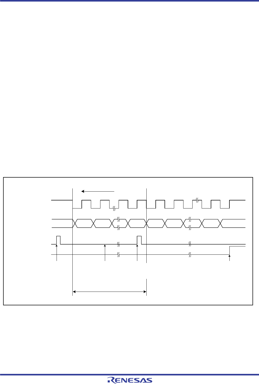
R01UH0034EJ0200 Rev.2.00 Page 948 of 1489
Dec 27, 2013
RX62T Group, RX62G Group 22. Serial Communications Interface (SCIb)
22.2.4.3 Serial Data Transmission (Clock Synchronous Mode)
Figure 22.18 shows an example of the operation for serial transmission in clock synchronous mode.
In serial data transmission, the SCI operates as described below.
1. The SCI transfers data from TDR to TSR when data is written to TDR in the TXI interrupt processing routine. The
TXI interrupt request at the beginning of transmission is generated when the TE bit in SCR is set to 1 after the TIE
bit in SCR is set to 1 or when these two bits are set to 1 simultaneously by a single instruction.
2. After transferring data from TDR to TSR, the SCI starts transmission. When the TIE bit is set to 1 at this time, a TXI
interrupt request is generated. Continuous transmission is enabled by writing the next transmit data to TDR in this
TXI interrupt processing routine before transmission of the current transmit data has finished.
3. 8-bit data is sent from the TXDn pin in synchronization with the output clock when clock output mode has been
specified and in synchronization with the input clock when use of an external clock has been specified.
4. The SCI checks for updating of (writing to) the TDR at the time of the last bit output.
5. When TDR is updated, the next transmit data is transferred from TDR to TSR, and serial transmission of the next
frame is started.
6. If TDR is not updated, set the SSR flag in TEND to 1 and the TXDn pin retains the output state of the last bit. If the
TEIE bit in SCR is 1 at this time, a TEI interrupt request is generated. The SCKn pin is held high.
Figure 22.19 shows a sample flowchart of serial data transmission.
Transmission will not start while a receive error flag (ORER, FER, or PER in SSR) is set to 1. Be sure to clear the receive
error flags to 0 before starting transmission. Note that clearing the RE bit in SCR to 0 does not clear the receive error
flags.
Figure 22.18 Example of Operation for Serial Transmission in Clock Synchronous Mode
Transfer direction
Bit 0
Synchronization
clock
1 frame
TXI interrupt signal
SSR.TEND flag
Serial data
TXI interrupt
request
generated
Data written to TDR in
TXI interrupt processing
routine
TEI interrupt
request
generated
Bit 1 Bit 7 Bit 0 Bit 1 Bit 7Bit 6
TXI interrupt
request
generated
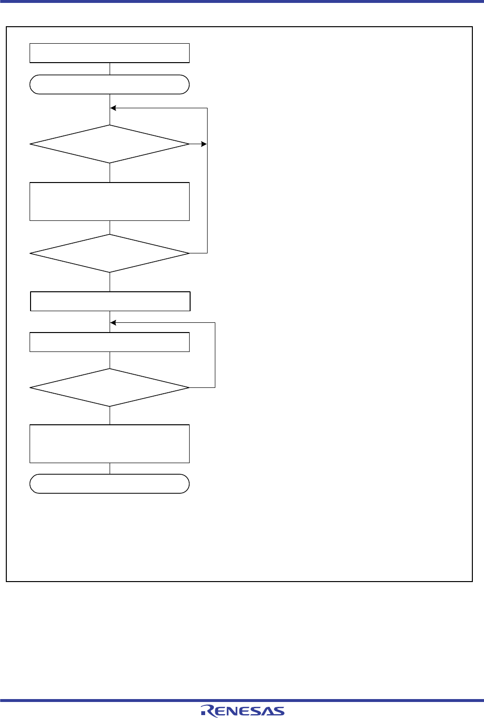
R01UH0034EJ0200 Rev.2.00 Page 949 of 1489
Dec 27, 2013
RX62T Group, RX62G Group 22. Serial Communications Interface (SCIb)
Figure 22.19 Example of Serial Transmission Flowchart (Clock Synchronous Mode)
No
Yes
Initialization
Start transmission
Write transmit data to TDR
No
Yes
No
Yes
Clear bits TIE, TE, and TEIE
in SCR to 0
TXI interrupt
All data transmitted
SSR.TEND = 1
[ 1 ]
[ 2 ]
[ 3 ]
[ 1 ] SCIn initialization:
The TXDn pin is automatically designated as
the transmit data output pin.
[ 2 ] Transmit data write to TDR by a TXI interrupt
request:
When transmit data is transferred from TDR to
TSR, a transmit data empty interrupt (TXI)
request is generated.
Transmit data is written to TDR once upon
accepting a transmit data empty interrupt (TXI)
request.
[ 3 ] Serial transmission continuation procedure:
To continue serial transmission, write transmit
data to TDR upon accepting a transmit data
empty interrupt (TXI) . Transmit data can also
be written to TDR by initiating the DTC when a
TXI interrupt request is accepted.
Read TEND flag in SSR
Clear the TIE bit in SCR to 0
End
Note: When the external clock is selected (when bit SCR.CKE[1] = 1), the SSR.TEND flag becomes 1 on
the rising edge of the SCK signal for the final bit.
Take care because quickly clearing the SCR.TE bit to 0 can leave the receiving device with insufficient
hold time for the received data.
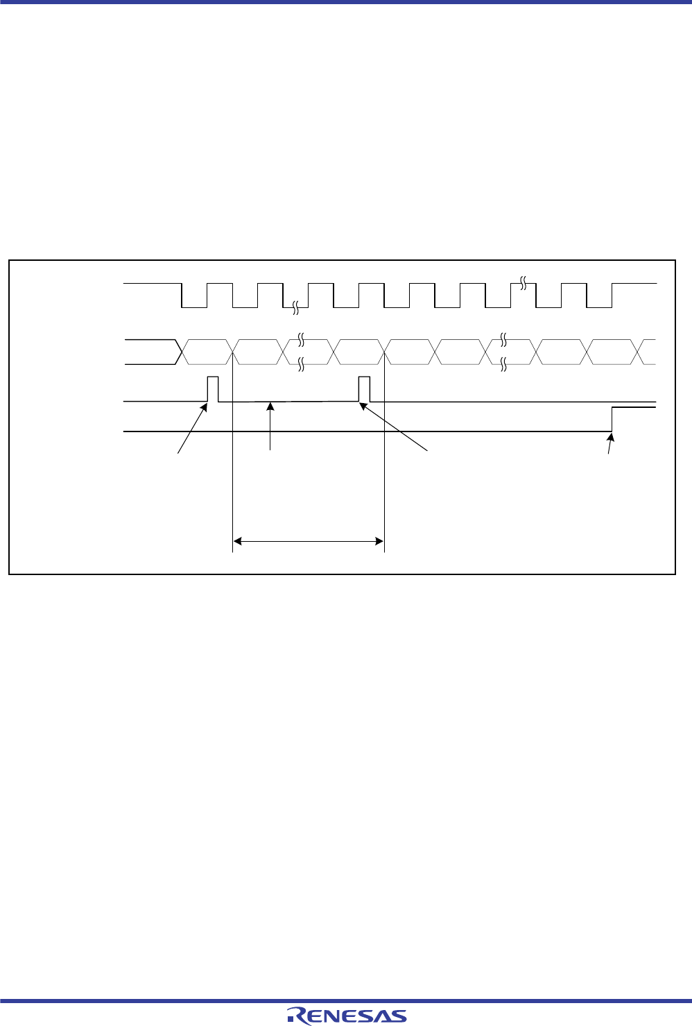
R01UH0034EJ0200 Rev.2.00 Page 950 of 1489
Dec 27, 2013
RX62T Group, RX62G Group 22. Serial Communications Interface (SCIb)
22.2.4.4 Serial Data Reception (Clock Synchronous Mode)
Figure 22.20 shows an example of SCI operation for serial reception in clock synchronous mode.
In serial data reception, the SCI operates as described below.
1. The SCI performs internal initialization and starts receiving data in synchronization with a synchronization clock
input or output, and stores the receive data in RSR.
2. If an overrun error occurs, the ORER bit in SSR is set to 1. If the RIE bit in SCR is 1 at this time, an ERI interrupt
request is generated. Receive data is not transferred to RDR.
3. When reception finishes successfully, receive data is transferred to RDR. If the RIE bit in SCR is 1 at this time, an
RXI interrupt request is generated. Continuous reception is enabled by reading the receive data transferred to RDR
in this RXI interrupt processing routine before reception of the next receive data is completed.
Figure 22.20 Example of Operation for Serial Reception in Clock Synchronous Mode
Data transfer cannot be resumed while a receive error flag is 1. Accordingly, clear the ORER, FER, and PER flags in
SSR to 0 before resuming reception. Moreover, be sure to read the RDR during overrun error processing.
Figure 22.21 shows a sample flowchart for serial data reception.
1 frame
RXI interrupt signal
SSR.ORER flag
Serial data
Reception clock
Bit 7 Bit 0 Bit 7 Bit 0 Bit 1 Bit 7Bit 6
RDR data read in RXI
interrupt processing
routine
RXI interrupt request
generated RXI interrupt request
generated ERI interrupt request
generated by overrun error
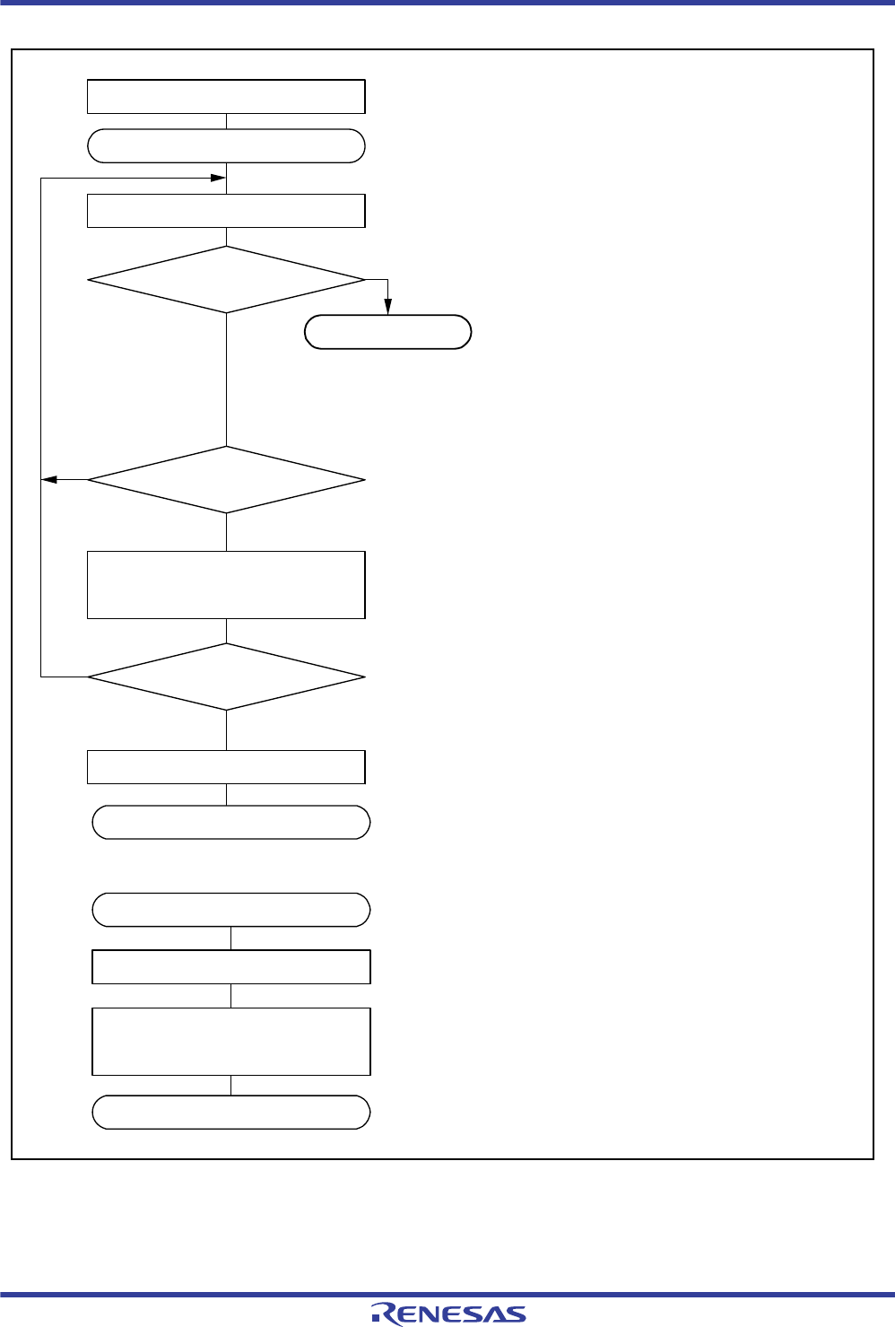
R01UH0034EJ0200 Rev.2.00 Page 951 of 1489
Dec 27, 2013
RX62T Group, RX62G Group 22. Serial Communications Interface (SCIb)
Figure 22.21 Example of Serial Reception Flowchart (Clock Synchronous Mode)
Yes
No
Initialization
Start data reception
No
Yes
Clear bits RIE and RE in SCR to 0
Error processing
(Continued below)
Read receive data in RDR
No
Yes
ORER in SSR = 1
RXI interrupt
All data received
Read ORER flag in SSR
Error processing
Clear ORER flag in SSR to 0
Overrun error processing*
[ 1 ]
[ 2 ]
[ 1 ] SCIn initialization:
Set the port to be used as the RxDn pin to an
input port.
[ 2 ] [ 3 ] Receive error processing:
If a receive error occurs, read the ORER flag in
SSR, perform the relevant error processing, and
then clear the ORER flag to 0. Data reception
cannot be resumed while the ORER flag is 1.
[ 4 ] Read the receive data in RDR once in the
receive data full interrupt (RXI) request
processing routine.
[ 5 ] Serial reception continuation procedure:
To continue serial reception, before the MSB
(bit 7) of the current frame is received, finish
reading the receive data in RDR. The RDR data
can also be read by activating the DTC by an
RXI interrupt request.
[ 3 ]
[ 4 ]
[ 5 ]
[ 3 ]
Note: * Read the RDR register.
End
End

R01UH0034EJ0200 Rev.2.00 Page 952 of 1489
Dec 27, 2013
RX62T Group, RX62G Group 22. Serial Communications Interface (SCIb)
22.2.5 Simultaneous Serial Data Transmission and Reception (Clock Synchronous
Mode)
Figure 22.22 shows a sample flowchart for simultaneous serial transmit and receive operations in clock synchronous
mode.
After initializing the SCI, the following procedure should be used for simultaneous serial data transmit and receive
operations.
To switch from transmit mode to simultaneous transmit and receive mode, check that the SCI has finished transmission
by reading that the TEND flag in SSR is 1, and then initialize the SCR register. Then set the TIE, RIE, TE, RE, and TEIE
bits in SCR to 1 simultaneously by a single instruction.
To switch from receive mode to simultaneous transmit and receive mode, check that the SCI has finished reception, and
then clear the RIE and RE bits to 0. Then check that the receive error flags (ORER, FER, and PER in SSR) are 0, and
then set the TIE, RIE, TE, RE, and TEIE bits in SCR to 1 simultaneously by a single instruction.
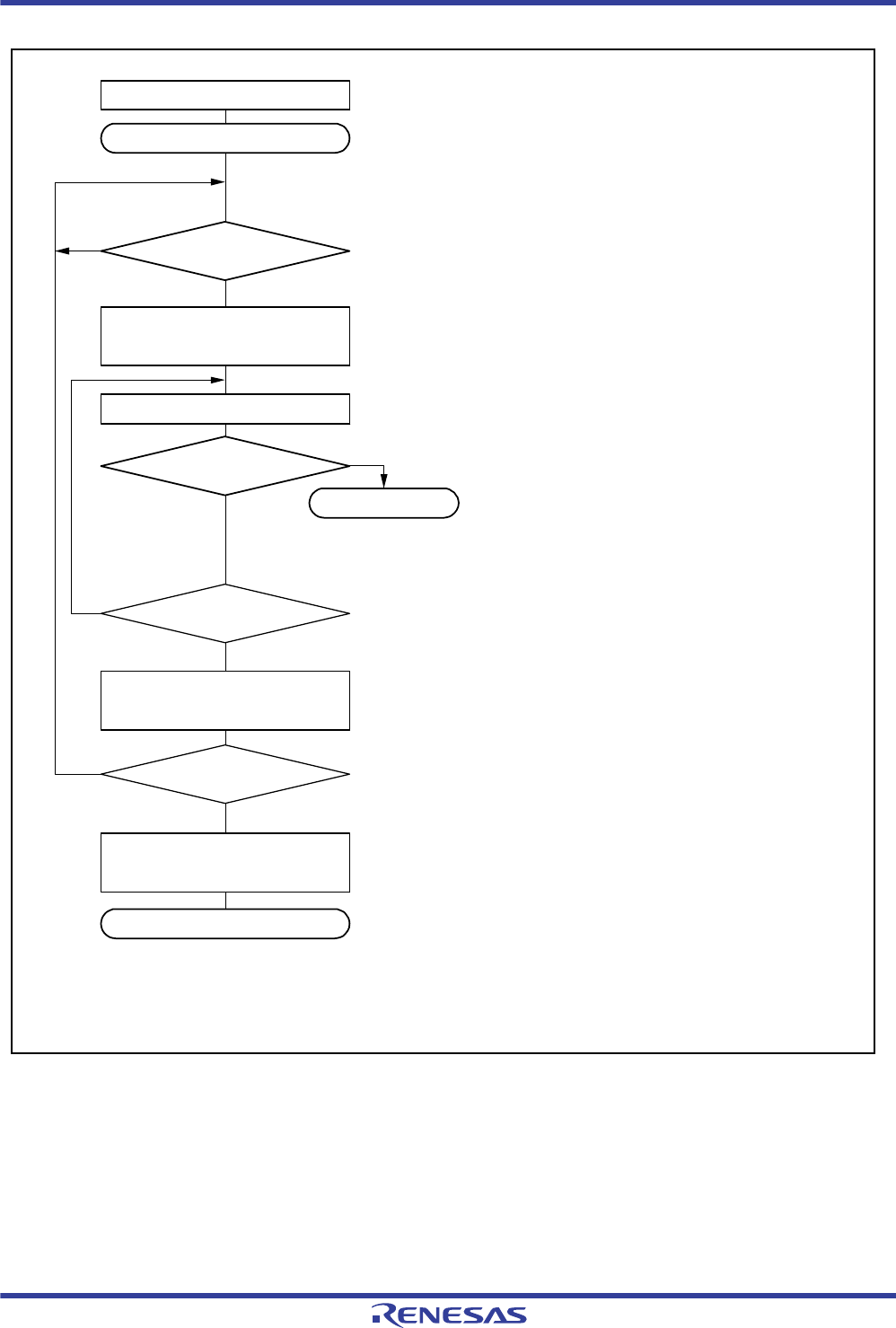
R01UH0034EJ0200 Rev.2.00 Page 953 of 1489
Dec 27, 2013
RX62T Group, RX62G Group 22. Serial Communications Interface (SCIb)
Figure 22.22 Example of Simultaneous Serial Transmission and Reception Flowchart
(Clock Synchronous Mode)
Yes
No
Initialization
Start data transmission/reception
Error processing
Read receive data in RDR
No
Yes
ORER in SSR = 1
All data received?
No
Yes
TXI interrupt
Write transmit data to TDR
No
Yes
RXI interrupt
Read ORER flag in SSR
Clear TIE, RIE, TE, RE, and TEIE
bits in SCR to 0
Note: When switching from transmit or receive operation to
simultaneous transmit and receive operations, first clear the TIE,
RIE, TE, RE, and TEIE bits in SCR to 0, and then set these bits
to 1 simultaneously.
[ 1 ]
[ 2 ]
[ 3 ]
[ 1 ] SCIn initialization:
The TXDn pin is designated as the transmit data
output pin, and the RXDn pin is designated as the
receive data input pin, enabling simultaneous
transmit and receive operations.
[ 2 ] Transmit data write:
Write transmit data to TDR once in the TXI
interrupt request processing routine.
[ 3 ] Receive error processing:
If a receive error occurs, read the ORER flag in
SSR, perform the relevant error processing, and
then clear the ORER flag to 0. Data reception
cannot be resumed while the ORER flag is 1.
[ 4 ] Receive data read:
Read the receive data in RDR once in the RXI
interrupt request processing routine.
[ 5 ] Serial transmission/reception continuation
procedure:
To continue serial transmission and reception,
before the MSB (bit 7) of the current frame is
received, finish reading the receive data in RDR by
the RXI interrupt. Also, before the MSB (bit 7) of
the current frame is transmitted, write data to TDR
by the TXI interrupt.
Transmit data can also be written to TDR by
activating the DTC by a transmit data empty
interrupt (TXI) request. Similarly, the RDR data can
also be read by activating the DTC by a receive
data full interrupt (RXI) request.
[ 4 ]
[ 5 ]
End

R01UH0034EJ0200 Rev.2.00 Page 954 of 1489
Dec 27, 2013
RX62T Group, RX62G Group 22. Serial Communications Interface (SCIb)
22.3 Smart Card Interface Mode
As an extended function of the SCI, it is capable of operating in compliance with ISO/IEC 7816-3 (Identification Cards)
as an interface with smart cards (IC cards).
The SCI runs in smart-card interface mode when the setting of the SCMR.SMIF bit is "1".
22.3.1 Register Descriptions
Table 22.14 lists the registers of the SMCI. Some registers (TDR, RDR, and SCMR) have same functions in serial
communications interface mode and smart card interface mode. Therefore, for the descriptions on the TDR, RDR, and
SCMR registers, see section 22.2.1, Register Descriptions.
Table 22.14 Registers of SMCI
Channel Register Name Symbol Value after Reset Address Access Size
SMCI0 Serial mode register SMR 00h 0008 8240h 8
Bit rate register BRR FFh 0008 8241h 8
Serial control register SCR 00h 0008 8242h 8
Transmit data register TDR FFh 0008 8243h 8
Serial status register SSR 84h 0008 8244h 8
Receive data register RDR 00h 0008 8245h 8
Smart card mode register SCMR F2h 0008 8246h 8
Serial extended mode register SEMR 00h 0008 8247h 8
SMCI1 Serial mode register SMR 00h 0008 8248h 8
Bit rate register BRR FFh 0008 8249h 8
Serial control register SCR 00h 0008 824Ah 8
Transmit data register TDR FFh 0008 824Bh 8
Serial status register SSR 84h 0008 824Ch 8
Receive data register RDR 00h 0008 824Dh 8
Smart card mode register SCMR F2h 0008 824Eh 8
Serial extended mode register SEMR 00h 0008 824Fh 8
SMCI2 Serial mode register SMR 00h 0008 8250h 8
Bit rate register BRR FFh 0008 8251h 8
Serial control register SCR 00h 0008 8252h 8
Transmit data register TDR FFh 0008 8253h 8
Serial status register SSR 84h 0008 8254h 8
Receive data register RDR 00h 0008 8255h 8
Smart card mode register SCMR F2h 0008 8256h 8
Serial extended mode register SEMR 00h 0008 8257h 8

R01UH0034EJ0200 Rev.2.00 Page 955 of 1489
Dec 27, 2013
RX62T Group, RX62G Group 22. Serial Communications Interface (SCIb)
22.3.1.1 Serial Mode Register (SMR)
Note 1. n is the decimal notation of the value of n in BRR (see section 22.3.1.4, Bit Rate Register (BRR).
Note 2. S is the value of S in BRR (see section 22.3.1.4, Bit Rate Register (BRR).
Note 3. Writable only when TE in SCR = 0 and RE in SCR = 0 (both serial transmission and reception are disabled).
SMR is used to set the SCI's serial transfer format and select the clock source for the on-chip baud rate generator.
CKS[1:0] Bits (Clock Select)
These bits select the clock source for the on-chip baud rate generator.
For the relationship between the settings of these bits and the baud rate, see section 22.3.1.4, Bit Rate Register
(BRR).
BCP[1:0] Bits (Base Clock Pulse)
These bits select the number of base clock cycles in a 1-bit data transfer time in smart card interface mode.
Set these bits in combination with the BCP2 bit in SCMR.
For details, see section 22.3.3.2, Receive Data Sampling Timing and Reception Margin.
Address: SMCI0.SMR 0008 8240h, SMCI1.SMR 0008 8248h, SMCI2.SMR 0008 8250h
b7 b6 b5 b4 b3 b2 b1 b0
GM BLK PE PM BCP[1:0] CKS[1:0]
Value after reset: 00000000
Bit Symbol Bit Name Function R/W
b1, b0 CKS[1:0] Clock Select b1 b0
00: PCLK clock (n = 0)*1
01: PCLK/4 clock (n = 1)*1
10: PCLK/16 clock (n = 2)*1
11: PCLK/64 clock (n = 3)*1
R/W*3
b3, b2 BCP[1:0] Base Clock Pulse Selects the number of base clock cycles in combination with the
BCP2 bit in SCMR.
Setting values in BCP2 bit in SCMR and BCP[1:0] bits in SMR:
BCP2 b3 b2
0 0 0: 93 clock cycles (S = 93)*2
0 0 1: 128 clock cycles (S = 128)*2
0 1 0: 186 clock cycles (S = 186)*2
0 1 1: 512 clock cycles (S = 512)*2
1 0 0: 32 clock cycles (S = 32)*2 (Initial value)
1 0 1: 64 clock cycles (S = 64)*2
1 1 0: 372 clock cycles (S = 372)*2
1 1 1: 256 clock cycles (S = 256)*2
R/W*3
b4 PM Parity Mode (Valid only when the PE bit is 1 in asynchronous mode)
0: Selects even parity
1: Selects odd parity
R/W*3
b5 PE Parity Enable (Valid only in asynchronous mode)
When this bit is set to 1, the parity bit is added to transmit data
before transmission, and the parity bit is checked in reception.
Set this bit to 1 in smart card interface mode.
R/W*3
b6 BLK Block Transfer Mode 0: Normal mode operation
1: Block transfer mode operation
R/W*3
b7 GM GSM Mode 0: Normal mode operation
1: GSM mode operation
R/W*3

R01UH0034EJ0200 Rev.2.00 Page 956 of 1489
Dec 27, 2013
RX62T Group, RX62G Group 22. Serial Communications Interface (SCIb)
PM Bit (Parity Mode)
Selects the parity mode for transmission and reception (even or odd).
For details on the usage of this bit in smart card interface mode, see section 22.3.3, Data Format (Except in Block
Transfer Mode).
PE Bit (Parity Enable)
Set the PE bit to 1.
The parity bit is added to transmit data before transmission, and the parity bit is checked in reception.
BLK Bit (Block Transfer Mode)
Setting this bit to 1 allows block transfer mode operation.
For details, see section 22.3.3.1, Block Transfer Mode.
GM Bit (GSM Mode)
Setting this bit to 1 allows GSM mode operation.
In GSM mode, the SSR.TEND flag set timing is put forward to 11.0 etu (elementary time unit = 1-bit transfer time) from
the start and the clock output control function is appended. For details, see section 22.3.3.4, Serial Data
Transmission (Except in Block Transfer Mode) and section 22.3.3.6, Clock Output Control.

R01UH0034EJ0200 Rev.2.00 Page 957 of 1489
Dec 27, 2013
RX62T Group, RX62G Group 22. Serial Communications Interface (SCIb)
22.3.1.2 Serial Control Register (SCR)
Note 1. Writable only when TE = 0 and RE = 0.
Note 2. While the SMR.CM bit is 1, 1 can be written only when TE = 0 and RE = 0. After setting TE or RE to 1, only 0 can be written in
TE and RE.
SCR is a register that enables/disables the SCI transfer operations and the interrupt requests and selects the transfer clock
source. For details on interrupt sources, see section 22.5, Interrupt Sources.
CKE[1:0] Bits (Clock Enable)
These bits control the clock output from the SCKn pin.
In GSM mode, clock output can be dynamically switched. For details, see section 22.3.3.6, Clock Output Control.
TEIE Bit (Transmit End Interrupt Enable)
This bit should be 0 in smart card interface mode.
MPIE Bit (Multi-Processor Interrupt Enable)
This bit should be 0 in smart card interface mode.
Address: SMCI0.SCR 0008 8242h, SMCI1.SCR 0008 824Ah, SMCI2.SCR 0008 8252h
b7 b6 b5 b4 b3 b2 b1 b0
TIE RIE TE RE MPIE TEIE CKE[1:0]
Value after reset: 00000000
Bit Symbol Bit Name Function R/W
b1, b0 CKE[1:0] Clock Enable When GM in SMR = 0
b1 b0
0 0: Output disabled (SCKn pin functions as I/O port.)
0 1: Clock output
1 0: (Setting prohibited)
1 1: (Setting prohibited)
When GM in SMR = 1
0 0: Output fixed low
0 1: Clock output
1 0: Output fixed high
1 1: Clock output
R/W*1
b2 TEIE Transmit End Interrupt Enable This bit should be 0 in smart card interface mode. R/W
b3 MPIE Multi-Processor Interrupt Enable This bit should be 0 in smart card interface mode. R/W
b4 RE Receive Enable 0: Serial reception is disabled
1: Serial reception is enabled
R/W*2
b5 TE Transmit Enable 0: Serial transmission is disabled
1: Serial transmission is enabled
R/W*2
b6 RIE Receive Interrupt Enable 0: RXI and ERI interrupt requests are disabled
1: RXI and ERI interrupt requests are enabled
R/W
b7 TIE Transmit Interrupt Enable 0: A TXI interrupt request is disabled
1: A TXI interrupt request is enabled
R/W

R01UH0034EJ0200 Rev.2.00 Page 958 of 1489
Dec 27, 2013
RX62T Group, RX62G Group 22. Serial Communications Interface (SCIb)
RE Bit (Receive Enable)
Enables or disables serial reception.
When this bit is set to 1, serial reception is started by detecting the start bit. Note that SMR should be set prior to setting
the RE bit to 1 in order to designate the reception format.
Even if reception is halted by clearing the RE bit to 0, the ORER, FER, and PER flags in SSR are not affected and the
previous value is retained.
TE Bit (Transmit Enable)
Enables or disables serial transmission.
When this bit is set to 1, serial transmission is started by writing transmit data to TDR. Note that SMR should be set prior
to setting the TE bit to 1 in order to designate the transmission format.
RIE Bit (Receive Interrupt Enable)
Enables or disables RXI and ERI interrupt requests.
An RXI interrupt request is disabled by clearing the RIE bit to 0.
An ERI interrupt request can be cancelled by reading 1 from the ORER, FER, or PER flag in SSR and then clearing the
flag to 0, or clearing the RIE bit to 0.
TIE Bit (Transmit Interrupt Enable)
Enables or disables notification of a TXI interrupt request.
Notification of a TXI interrupt request is disabled by clearing the TIE bit to 0.

R01UH0034EJ0200 Rev.2.00 Page 959 of 1489
Dec 27, 2013
RX62T Group, RX62G Group 22. Serial Communications Interface (SCIb)
22.3.1.3 Serial Status Register (SSR)
Note 1. Only 0 can be written to this bit after reading it as 1, to clear the flag.
Note 2. Write 1 when writing is necessary.
SSR is a register containing status flags of the SCI.
MPBT Bit (Multi-Processor Bit Transfer)
This bit should be set to 0 in smart card interface mode.
MPB Bit (Multi-Processor)
This bit is not used in smart card interface mode. It should be set to 0.
TEND Flag (Transmission End Flag)
With no error signal from the receiving side, this bit is set to 1 when further data for transfer is ready to be transferred to
the TDR register.
[Setting conditions]
When SCR.TE bit = 0 (disabling serial transmission operations)
When a specified period has elapsed after the latest transmission of one byte, the ERS flag is 0, and the TDR register
is not updated
The set timing is determined by register settings as listed below.
When SMR.GM = 0 and SMR.BLK = 0, 12.5 etu after the start of transmission
When SMR.GM = 0 and SMR.BLK = 1, 11.5 etu after the start of transmission
When SMR.GM = 1 and SMR.BLK = 0, 11.0 etu after the start of transmission
When SMR.GM = 1 and SMR.BLK = 1, 11.0 etu after the start of transmission
[Clearing condition]
Writing further data for transmission to the TDR register
Address: SMCI0.SSR 0008 8244h, SMCI1.SSR 0008 824Ch, SMCI2.SSR 0008 8254h
b7 b6 b5 b4 b3 b2 b1 b0
TDRE RDRF ORER ERS PER TEND MPB MPBT
Value after reset: 10000100
Bit Symbol Bit Name Function R/W
b0 MPBT Multi-Processor Bit Transfer This bit should be set to 0 in smart card interface mode. R/W
b1 MPB Multi-Processor This bit is not used in smart card interface mode. It should be set to 0. R
b2 TEND Transmit End Flag 0: A character is being transmitted.
1: Character transfer has been completed.
R
b3 PER Parity Error Flag 0: No parity error occurred
1: A parity error has occurred
R/(W)*1
b4 ERS Error Signal Status Flag 0: Low error signal not responded
1: Low error signal responded
R/(W)* 1
b5 ORER Overrun Error Flag 0: No overrun error occurred
1: An overrun error has occurred
R/(W)* 1
b6 RDRF Receive Data Full Flag 0: When data is transferred from RDR
1: When data has been received normally, and transferred from RSR
to RDR
R/(W) *2
b7 TDRE Transmit Data Empty Flag 0: When data is transferred to TDR
1: When data is transferred from TDR to TSR
R/(W) *2

R01UH0034EJ0200 Rev.2.00 Page 960 of 1489
Dec 27, 2013
RX62T Group, RX62G Group 22. Serial Communications Interface (SCIb)
PER Flag (Parity Error Flag)
Indicates that a parity error has occurred during reception in asynchronous mode and the reception ends abnormally.
[Setting condition]
When a parity error is detected during reception
Although receive data when the parity error occurs is transferred to RDR, no RXI interrupt request occurs. Note that
when the PER flag is being set to 1, the subsequent serial reception cannot be transferred to RDR.
[Clearing condition]
When a 0 is written to PER after reading PER = 1 (After writing a 0 to it, read the PER bit to check that it has actually
been cleared to 0.)
Even when the RE bit in SCR is cleared to 0 (which indicates that serial reception is disabled), the PER flag is not
affected and retains its previous value.
ERS Flag (Error Signal Status Flag)
[Setting condition]
When a low error signal is sampled
[Clearing condition]
When a 0 is written to ERS after reading ERS = 1
ORER Flag (Overrun Error Flag)
Indicates that an overrun error has occurred during reception and the reception ends abnormally.
[Setting condition]
When the next data is received before receive data is read from RDR
In RDR, the receive data prior to an overrun error occurrence is retained, but data received following the overrun
error occurrence is lost. When the ORER flag is set to 1, subsequent serial reception cannot be performed.
[Clearing condition]
When a 0 is written to ORER after reading ORER = 1 (After writing a 0 to it, read the ORER bit to check that it has
actually been cleared to 0.)
Even when the RE bit in SCR is cleared to 0, the ORER flag is not affected and retains its previous value.
RDRF Bit (Receive Data Full Flag)
Indicates whether RDR has received data.
[Setting condition]
When data has been received normally, and transferred from RSR to RDR
[Clearing condition]
When data is transferred from RDR
TDRE Bit (Transmit Data Empty Flag)
Indicates whether TDR has data to be transmitted.
[Setting condition]
When data is transferred from TDR to TSR
[Clearing condition]
When data is transferred to TDR
R01UH0034EJ0200 Rev.2.00 Page 961 of 1489
Dec 27, 2013
RX62T Group, RX62G Group 22. Serial Communications Interface (SCIb)
22.3.1.4 Bit Rate Register (BRR)
BRR is an 8-bit register that adjusts the bit rate.
As the SCI performs baud rate generator control independently for each channel, different bit rates can be set for each
channel.
The initial value of BRR is FFh.
BRR can be read from by the CPU at all times, but it can be written to only when the TE and RE bits in SCR are 0.
Table 21.15 shows the relationships between the N setting in BRR and bit rate B for smart card interface mode.
Table 28.15 shows sample N settings in BRR in smart card interface mode.
In smart card interface mode, the number of base clock cycles S in a 1-bit data transfer time can be selected. For details,
see section 22.3.3.2, Receive Data Sampling Timing and Reception Margin.
Table 22.15 Relationships between N Setting in BRR and Bit Rate B
B: Bit rate (bps)
N: BRR setting for baud rate generator (0 N 255)
PCLK: Operating frequency (MHz)
n and S: Determined by the SMR setting shown in the following table.
Address: SMCI0.BRR 0008 8241h, SMCI1.BRR 0008 8249h, SMCI2.BRR 0008 8251h
b7 b6 b5 b4 b3 b2 b1 b0
Value after reset: 11111111
Mode
Smart card interface
BRR Setting Error
N = -1
S 22n+1 B
PCLK 106
Error (%) = { -1 } 100
PCLK 106
B S 22n+1 (N+1)
R01UH0034EJ0200 Rev.2.00 Page 962 of 1489
Dec 27, 2013
RX62T Group, RX62G Group 22. Serial Communications Interface (SCIb)
Table 22.16 BRR Settings for Various Bit Rates (Smart Card Interface Mode, n = 0, S = 372)
Bit Rate
(bps)
Operating Frequency PCLK (MHz)
7.1424 10.00 10.7136 13.00
n N Error (%) n N Error (%) n N Error (%) n N Error (%)
9600 0 0 0.00 0 1 0.00 0 1 25 0 1 8.99
Bit Rate
(bps)
Operating Frequency PCLK (MHz)
14.2848 16.00 18.00 20.00
n N Error (%) n N Error (%) n N Error (%) n N Error (%)
9600 0 0 0.00 0 1 12.04 0 2 15.99 0 2 6.66
Bit Rate
(bps)
Operating Frequency PCLK (MHz)
25.00 30.00 33.00 50.00
n N Error (%) n N Error (%) n N Error (%) n N Error (%)
9600 0 3 12.49 0 3 5.01 0 4 7.59 0 6 0.01
Table 22.17 Maximum Bit Rate for Each Operating Frequency (Smart Card Interface Mode, S = 372)
PCLK (MHz) Maximum Bit Rate
(bps) n N PCLK (MHz) Maximum Bit Rate
(bps) n N
10.00 13441 0 0 20.00 26882 0 0
10.7136 14400 0 0 25.00 33602 0 0
13.00 17473 0 0 30.00 40323 0 0
16.00 21505 0 0 33.00 44355 0 0
18.00 24194 0 0 50.00 67205 0 0

R01UH0034EJ0200 Rev.2.00 Page 963 of 1489
Dec 27, 2013
RX62T Group, RX62G Group 22. Serial Communications Interface (SCIb)
22.3.2 Operation in Smart Card Interface Mode
The SCI supports the smart card (IC card) interface conforming to the ISO/IEC 7816-3 (Identification Card) standard, as
an extended function of the SCI.
Smart card interface mode can be selected using the appropriate register.
22.3.2.1 Sample Connection
Figure 22.23 shows a sample connection between a smart card (IC card) and this LSI.
As in the figure, since this LSI communicates with an IC card using a single transmission line, interconnect the TXDn
and RXDn pins and pull up the data transmission line to Vcc using a resistor.
Setting the TE and RE bits in SCR to 1 with an IC card disconnected enables closed transmission/reception allowing self
diagnosis.
To supply an IC card with the clock pulses generated by the SCI, input the SCKn pin output to the CLK pin of an IC card.
The output port of the RX62T can be used to output a reset signal.
Figure 22.23 Sample Connection with a Smart Card (IC Card)
TXDn
RXDn
RX62T
Vcc
I/O
Main unit of the device to
be connected
IC card
Data line
CLK
RST
SCKn
Port
Clock line
Reset line
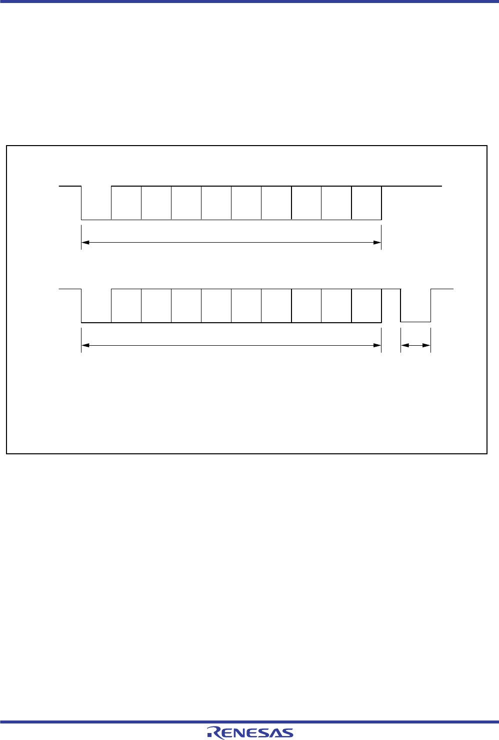
R01UH0034EJ0200 Rev.2.00 Page 964 of 1489
Dec 27, 2013
RX62T Group, RX62G Group 22. Serial Communications Interface (SCIb)
22.3.3 Data Format (Except in Block Transfer Mode)
Figure 22.24 shows the data transfer formats in smart card interface mode.
One frame consists of 8-bit data and a parity bit in asynchronous mode.
During transmission, at least 2 etu (elementary time unit: time required for transferring one bit) is secured as a guard time
from the end of the parity bit until the start of the next frame.
If a parity error is detected during reception, a low-level error signal is output for 1 etu after 10.5 etu has passed from the
start bit.
If an error signal is sampled during transmission, the same data is automatically re-transmitted after at least 2 etu.
Figure 22.24 Data Formats in Smart Card Interface Mode
Ds D0 D1 D2 D3 D4 D5 D6 D7 Dp
In normal transmission/reception
Output from the transmitting station
Ds D0 D1 D2 D3 D4 D5 D6 D7 Dp
When a parity error is generated
Output from the transmitting station
DE
Output from the
receiving station
[Legend]
Ds: Start bit
D0 to D7: Data bits
Dp: Parity bit
DE: Error signal
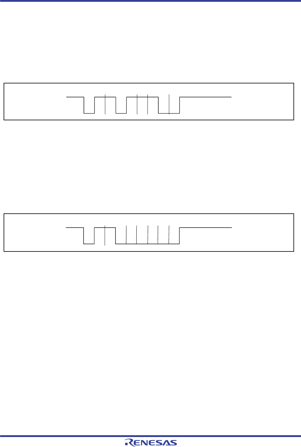
R01UH0034EJ0200 Rev.2.00 Page 965 of 1489
Dec 27, 2013
RX62T Group, RX62G Group 22. Serial Communications Interface (SCIb)
For communications with IC cards of the direct convention type and inverse convention type, follow the procedure
below.
(1) Direct Convention Type
For the direct convention type, logic levels 1 and 0 correspond to states Z and A, respectively, and data is transferred with
LSB-first as the start character, as shown in Figure 22.25. Therefore, data in the start character in the figure is 3Bh.
When using the direct convention type, write 0 to both the SDIR and SINV bits in SCMR. Write 0 to the PM bit in SMR
in order to use even parity, which is prescribed by the smart card standard.
Figure 22.25 Direct Convention (SDIR in SCMR = 0, SINV in SCMR =0, PM in SMR = 0)
(2) Inverse Convention Type
For the inverse convention type, logic levels 1 and 0 correspond to states A and Z, respectively and data is transferred
with MSB-first as the start character, as shown in Figure 22.26. Therefore, data in the start character in the figure is 3Fh.
When using the inverse convention type, write 1 to both the SDIR and SINV bits in SCMR. The parity bit is logic level 0
to produce even parity, which is prescribed by the smart card standard, and corresponds to state Z. Since the SNIV bit of
the RX62T only inverts data bits D7 to D0, write 1 to the PM bit in SMR to invert the parity bit for both transmission and
reception.
Figure 22.26 Inverse Convention (SDIR in SCMR = 1, SINV in SCMR =1, PM in SMR = 1)
Ds
AZZAZZ ZZAA
(Z) (Z) state
D0 D1 D2 D3 D4 D5 D6 D7 Dp
Ds
AZZAAA ZAAA
D7 D6 D5 D4 D3 D2 D1 D0 Dp
(Z) (Z) state

R01UH0034EJ0200 Rev.2.00 Page 966 of 1489
Dec 27, 2013
RX62T Group, RX62G Group 22. Serial Communications Interface (SCIb)
22.3.3.1 Block Transfer Mode
Block transfer mode is different from normal smart card interface mode in the following respects.
Even if a parity error is detected during reception, no error signal is output. Since the PER bit in SSR is set by error
detection, clear the PER bit before receiving the parity bit of the next frame.
During transmission, at least 1 etu is secured as a guard time from the end of the parity bit until the start of the next
frame.
Since the same data is not re-transmitted during transmission, the TEND flag in SSR is set 11.5 etu after
transmission start.
In block transfer mode, the ERS flag in SSR indicates the error signal status as in normal smart card interface mode,
but the flag is always read as 0 because no error signal is transferred.
22.3.3.2 Receive Data Sampling Timing and Reception Margin
Only the internal clock generated by the on-chip baud rate generator can be used as a transfer clock in smart card
interface mode.
In this mode, the SCI can operate on a base clock with a frequency of 32, 64, 372, 256, 93, 128, 186, or 512 times the bit
rate according to the settings of the BCP2 bit in SCMR and the BCP[1:0] bits in SMR (the frequency is always 16 times
the bit rate in normal asynchronous mode).
For data reception, the falling edge of the start bit is sampled with the base clock to perform internal synchronization. For
data reception, the falling edge of the start bit is sampled with the base clock to perform internal synchronization.
Receive data is sampled on the 16th, 32nd, 186th, 128th, 46th, 64th, 93rd, and 256th rising edges of the base clock so that
it can be latched at the middle of each bit as shown in Figure 22.27. The reception margin here is determined by the
following formula.
M: Reception margin (%)
N: Ratio of bit rate to clock (N = 32, 64, 372, 256)
D: Duty cycle of clock (D = 0 to 1.0)
L: Frame length (L = 10)
F Absolute value of clock frequency deviation
Assuming values of F = 0, D = 0.5, and N = 372 in the above formula, the reception margin is determined by the formula
below.
M = {0.5 - 1/(2 x 372)} × 100 (%) = 49.866%
M = (0.5 - ) - (L - 0.5) F - (1+F)
1
2N
D - 0.5
Nx 100 [%]
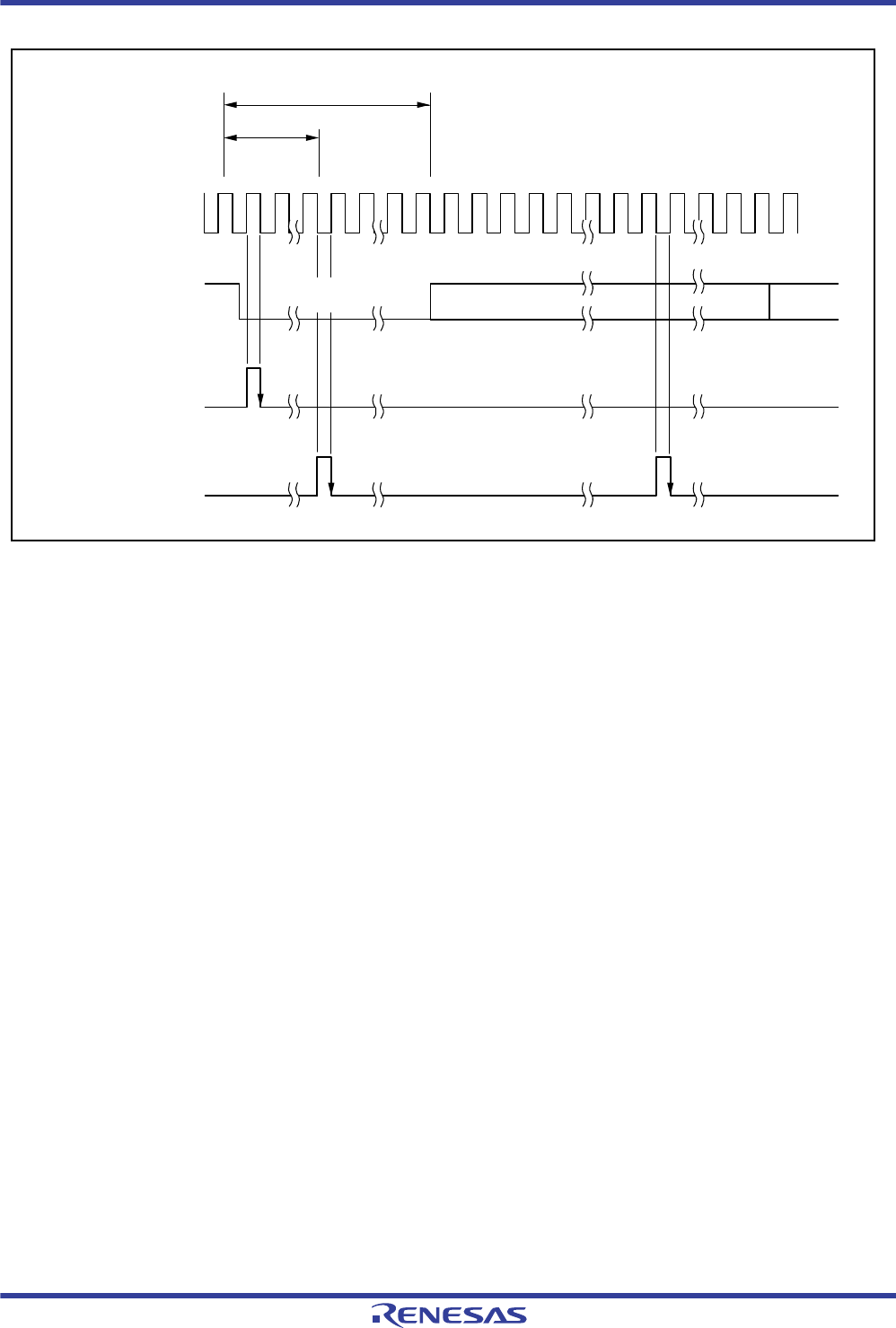
R01UH0034EJ0200 Rev.2.00 Page 967 of 1489
Dec 27, 2013
RX62T Group, RX62G Group 22. Serial Communications Interface (SCIb)
Figure 22.27 Receive Data Sampling Timing in Smart Card Interface Mode
(When Clock Frequency is 372 Times the Bit Rate)
Internal base clock
372 clock cycles
186 clock cycles
D0 D1
185 371 0371185 00
Receive data (RXDn)
Synchronization
sampling timing
Data sampling
timing
Start bit

R01UH0034EJ0200 Rev.2.00 Page 968 of 1489
Dec 27, 2013
RX62T Group, RX62G Group 22. Serial Communications Interface (SCIb)
22.3.3.3 Initialization of the Smart Card Interface
Before transmitting and receiving data, initialize the SCI using the following procedure. Initialization is also necessary
before switching from transmission to reception and vice versa.
1. Write the initial value "00h" to the SCR.
2. Set the Bj bit in ICR of PORTn (n = 1 to 9 and A to G, j = 0 to 7) of the corresponding pin to 1.
3. Set the error flags ORER, ERS, and PER in SSR to 0.
4. Set bits GM, BLK, OE, BCP[1:0], and CKS[1:0] in SMR and the BCP2 bit in SCMR appropriately. Also set the PE
bit in SMR to 1.
5. Set bits SDIR, SINV, and SMIF in SCMR appropriately. Also set the Bj bit in DDR of PORTn corresponding to the
TXDn pin to 0. Then the TXDn and RXDn pins are changed from port pins to SCI pins and placed in the high
impedance state.
6. Set the value corresponding to the bit rate in BRR.
7. Set the CKE[1:0] bits in SCR appropriately, and set bits TIE, RIE, TE, RE, and TEIE in SCR to 0 at the same time.
When the CKE0 bit is set to 1, the SCKn pin is allowed to output clock pulses.
8. Wait for at least a 1-bit interval, and then set the TIE, RIE, TE, and RE bits in SCR to 1. Setting the TE and RE bits
to 1 simultaneously is prohibited except for self diagnosis.
To change reception mode to transmission mode, first check that reception has completed, and then initialize the SCI. At
the end of initialization, set TE = 1 and RE = 0. Reception completion can be verified by reading the RXI request, ORER,
or PER flag in SSR.
To change transmission mode to reception mode, first check that transmission has completed, and then initialize the SCI.
At the end of initialization, set TE = 0 and RE = 1. Transmission completion can be verified by reading the TEND flag in
SSR.

R01UH0034EJ0200 Rev.2.00 Page 969 of 1489
Dec 27, 2013
RX62T Group, RX62G Group 22. Serial Communications Interface (SCIb)
22.3.3.4 Serial Data Transmission (Except in Block Transfer Mode)
Serial data transmission in smart card interface mode (except in block transfer mode) is different from that in normal
serial communications interface mode in that an error signal is sampled and data can be re-transmitted. Figure 22.28
shows the data re-transfer operation during transmission.
1. When an error signal from the receiving end is sampled after one-frame data has been transmitted, the ERS flag in
SSR is set to 1. If the RIE bit in SCR is 1 at this time, an ERI interrupt request is generated. Clear the ERS flag to 0
before the next parity bit is sampled.
2. For a frame in which an error signal is received, the TEND flag in SSR is not set. Data is re-transferred from TDR to
TSR allowing automatic data retransmission.
3. If no error signal is returned from the receiving end, the ERS flag is not set to 1.
4. In this case, the SCI judges that transmission of one-frame data (including retransfer) has been completed, and the
TEND flag is set. If the TIE bit in SCR is 1 at this time, a TXI interrupt request is generated. Writing transmit data
to TDR starts transmission of the next data.
Figure 22.30 shows a sample flowchart of serial transmission. All the processing steps are automatically performed
using a TXI interrupt request to activate the DTC.
When the TEND flag in SSR is set to 1 in transmission, if the TIE bit in SCR is 1, a TXI interrupt request is generated.
The DTC is activated by a TXI interrupt request if the TXI interrupt request is specified as a source of DTC activation
beforehand, allowing transfer of transmit data. The TEND flag is automatically cleared to 0 when the DTC transfers the
data.
If an error occurs, the SCI automatically re-transmits the same data. During this retransmission, the TEND flag is kept to
0 and the DTC is not activated. Therefore, the SCI and DTC automatically transmit the specified number of bytes,
including retransmission in the case of error occurrence. However, since the ERS flag is not automatically cleared; set
the RIE bit to 1 beforehand to enable an ERI interrupt request to be generated at error occurrence, and clear the ERS flag
to 0.
When transmitting/receiving data using the DTC, be sure to make settings to enable the DTC before making SCI settings.
For DTC settings, see section 14, Data Transfer Controller (DTC).
Figure 22.28 Data Retransfer Operation in SMCI Transmission Mode
Note that the SSR.TEND flag is set in different timings depending on the GM bit setting in SMR. Figure 22.29 shows
the TEND flag generation timing.
Retransfer framen-th transfer frame (n + 1)-th transfer
frame
[1]
[2] [4]
[3]
(DE)
SSR.FER flag/
SSR.ERS flag
Ds D0 D1 D2 D6 D7 DpD3 D4 D5 DE D6 D7 DpD5
TXI interrupt signal
Note: * For the corresponding interrupt vector number, see section 11, Interrupt Controller (ICU).
Ds D0 D1 D2 D3 D4 Ds D0 D1 D2 D3 D4
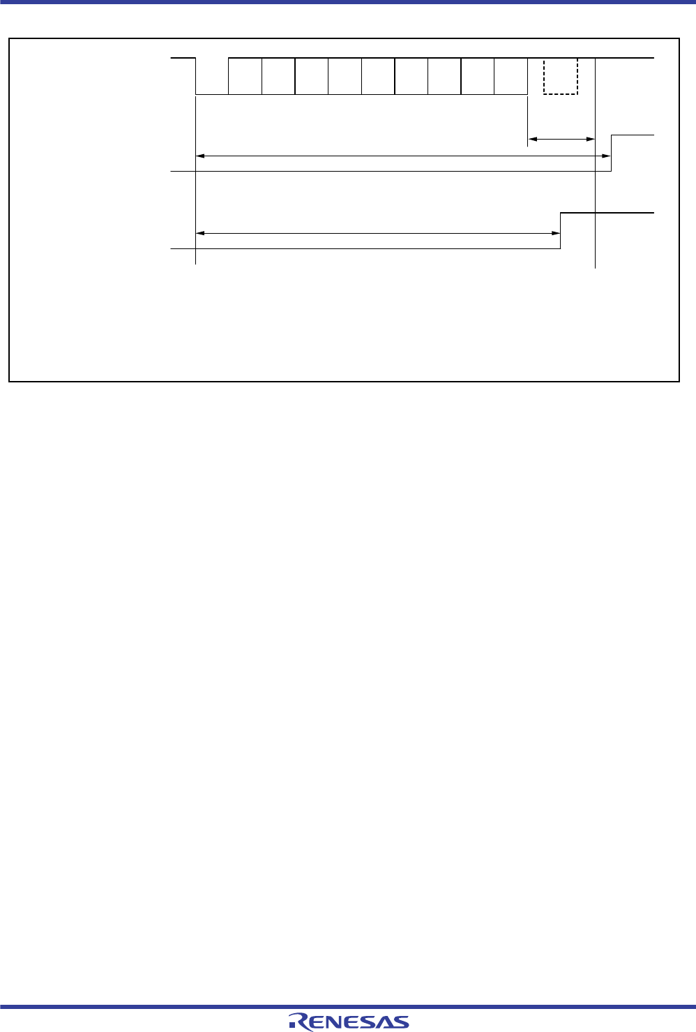
R01UH0034EJ0200 Rev.2.00 Page 970 of 1489
Dec 27, 2013
RX62T Group, RX62G Group 22. Serial Communications Interface (SCIb)
Figure 22.29 SSR.TEND Flag Generation Timing during Transmission
Ds D0 D1 D2 D3 D4 D5 D6 D7 Dp
I/O data
12.5 etu (11.5 etu in block transfer mode)
SSR.TEND flag
(TXI interrupt)
11.0 etu
DE
Guard
time
When GM bit in SMR = 0
[Legend]
Ds: Start bit
D0 to D7: Data bits
Dp: Parity bit
DE: Error signal
When GM bit in SMR = 1
Note: For the corresponding interrupt vector number, see section 11, Interrupt Controller (ICU).
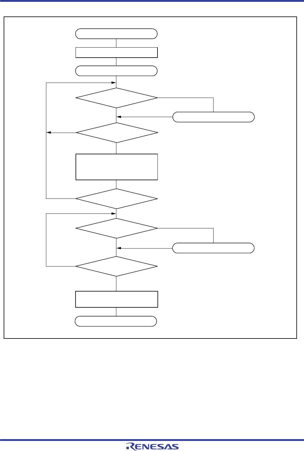
R01UH0034EJ0200 Rev.2.00 Page 971 of 1489
Dec 27, 2013
RX62T Group, RX62G Group 22. Serial Communications Interface (SCIb)
Figure 22.30 Sample Serial Transmission Flowchart
Initialization
No
Write data to TDR
Yes
Clear bits TIE, RIE, and TE
in SCR to 0
Start data transmission
Start
No
No
No
Yes
Yes
Yes
Yes
No
End
TXI interrupt
Error processing
Error processing
SSR.ERS = 0?
All data transmitted?
TXI interrupt
SSR.ERS = 0?
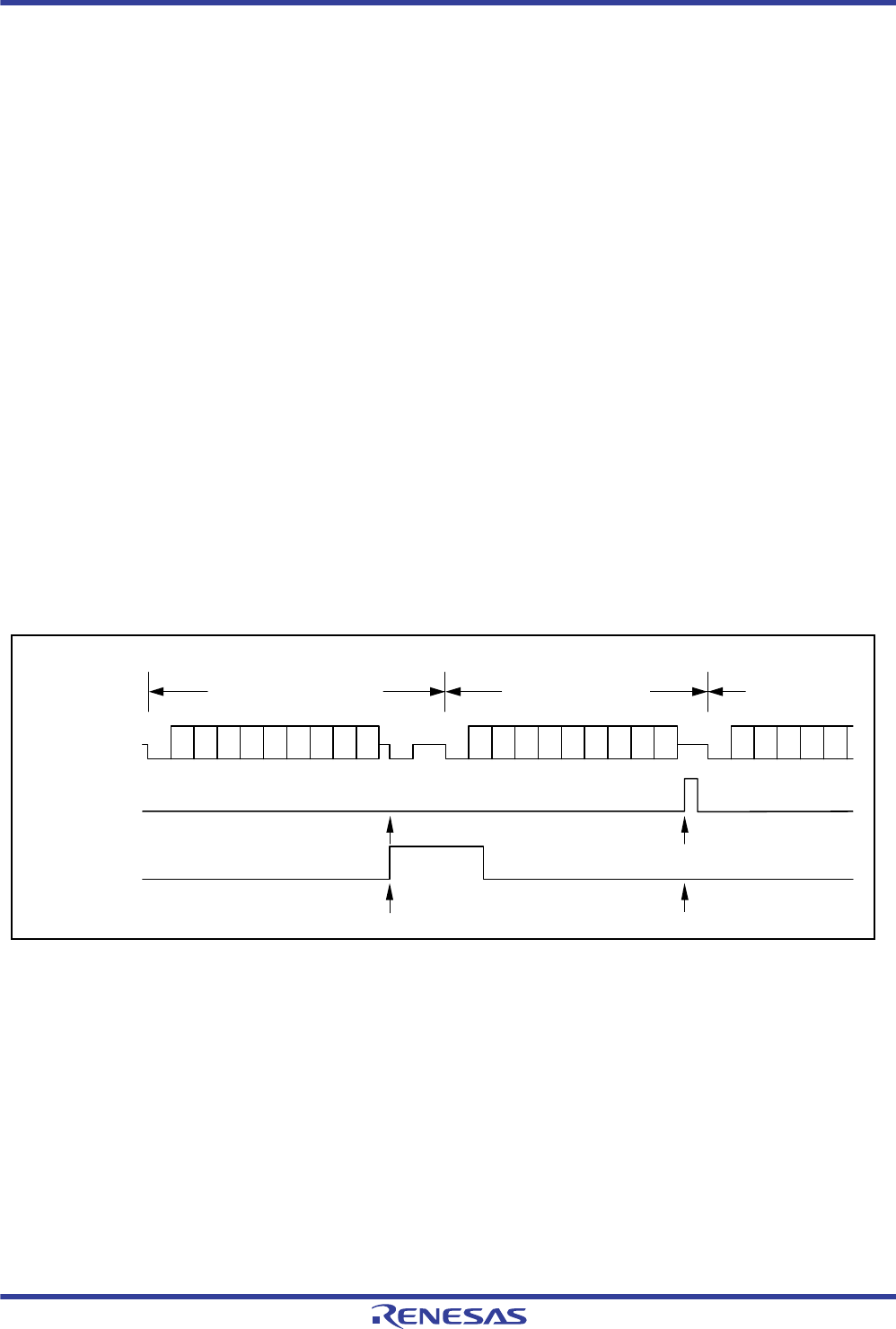
R01UH0034EJ0200 Rev.2.00 Page 972 of 1489
Dec 27, 2013
RX62T Group, RX62G Group 22. Serial Communications Interface (SCIb)
22.3.3.5 Serial Data Reception (Except in Block Transfer Mode)
Serial data reception in smart card interface mode is similar to that in serial communications interface mode. Figure
22.31 shows the data retransfer operation in reception mode.
1. If a parity error is detected in receive data, the PER flag in SSR is set to 1. When the RIE bit in SCR is 1 at this time,
an ERI interrupt request is generated. Clear the PER flag to 0 before the next parity bit is sampled.
2. For a frame in which a parity error is detected, no RXI interrupt is generated.
3. When no parity error is detected, the PER flag in SSR is not set to 1.
4. In this case, data is determined to have been received successfully. When the RIE bit in SCR is 1, an RXI interrupt
request is generated.
Figure 22.32 shows a sample flowchart for serial data reception. All the processing steps are automatically performed
using an RXI interrupt request to activate the DTC.
In reception, setting the RIE bit to 1 allows an RXI interrupt request to be generated. The DTC is activated by an RXI
interrupt request if the RXI interrupt request is specified as a source of DTC activation beforehand, allowing transfer of
receive data.
If an error occurs during reception and either the ORER or PER flag in SSR is set to 1, a receive error interrupt (ERI)
request is generated. Clear the error flag. If an error occurs, the DTC is not activated and receive data is skipped.
Therefore, the number of bytes of receive data specified in the DTC is transferred.
Even if a parity error occurs and the PER flag is set to 1 during reception, receive data is transferred to RDR, thus
allowing the data to be read.
Note: • For operations in block transfer mode, see section 22.2.2, Operation in Asynchronous Mode.
Figure 22.31 Data Retransfer Operation in SMCI Reception Mode
(n + 1)-th transfer
frame
Retransfer framen-th transfer frame
Ds D0 D1 D2 D6 D7 DpD3 D4 D5 DE Ds D0 D1 D2 D6 D7 DpD3 D4 D5 Ds D0 D1 D2 D3 D4
[1]
[2] [4]
[3]
RXI interrupt
signal
SSR.PER flag
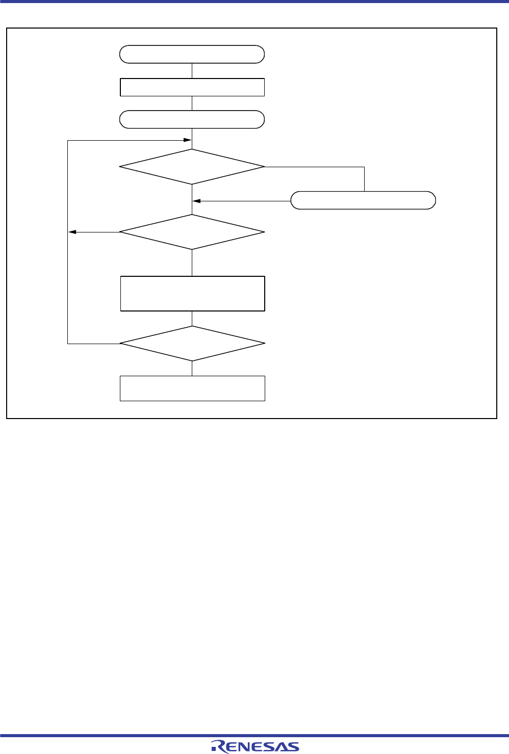
R01UH0034EJ0200 Rev.2.00 Page 973 of 1489
Dec 27, 2013
RX62T Group, RX62G Group 22. Serial Communications Interface (SCIb)
Figure 22.32 Sample Serial Reception Flowchart
Initialization
Read data from RDR
Clear bits RIE and RE
in SCR to 0
Start data reception
Start
Error processing
No
No
No
Yes
Yes
SSR.ORER = 0 and
SSR.PER = 0?
RXI interrupt
All data received?
Yes
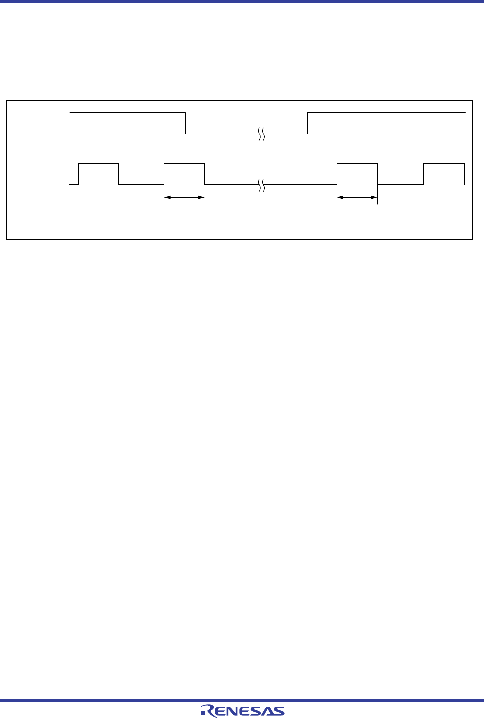
R01UH0034EJ0200 Rev.2.00 Page 974 of 1489
Dec 27, 2013
RX62T Group, RX62G Group 22. Serial Communications Interface (SCIb)
22.3.3.6 Clock Output Control
Clock output can be stopped using the CKE[1:0] bits in SCR when the GM bit in SMR is 1. Specifically, the minimum
width of a clock pulse can be specified.
Figure 22.33 shows an example of clock output stop timing when the CKE0 bit is controlled with GM = 1 and
CKE1 = 0.
Figure 22.33 Clock Output Stop Timing
At power-on and transitions to/from software standby mode, use the following procedure to secure the appropriate clock
duty cycle.
(1) At Power-On
To secure the appropriate clock duty cycle simultaneously with power-on, use the following procedure.
1. Initially, port input is enabled in the high-impedance state. To fix the potential level, use a pull-up or pull-down
resistor.
2. Fix the SCKn pin to the specified output using the CKE1 bit in SCR.
3. Set SMR and SCMR to enable smart card interface mode. Set the CKE0 bit in SCR to 1 to start clock output.
(2) At Mode Switching
(a) At transition from smart card interface mode to software standby mode
1. Set the data register (DR of PORTi) and data direction register (DDR of PORTi) corresponding to the SCKn pin to
the values for the output fixed state in software standby mode.
2. Write 0 to the TE and RE bits in SCR to stop transmission/reception.
Simultaneously, set the CKE1 bit in SCR to the value for the output fixed state in software standby mode.
3. Write 0 to the CKE0 bit in SCR to stop the clock.
4. Wait for one cycle of the serial clock. In the mean time, the clock output stops with the low level retained after
outputting the specified high width.
5. Make a transition to software standby mode.
Given pulse width
SCR.CKE0 bit
SCKn
Given pulse width
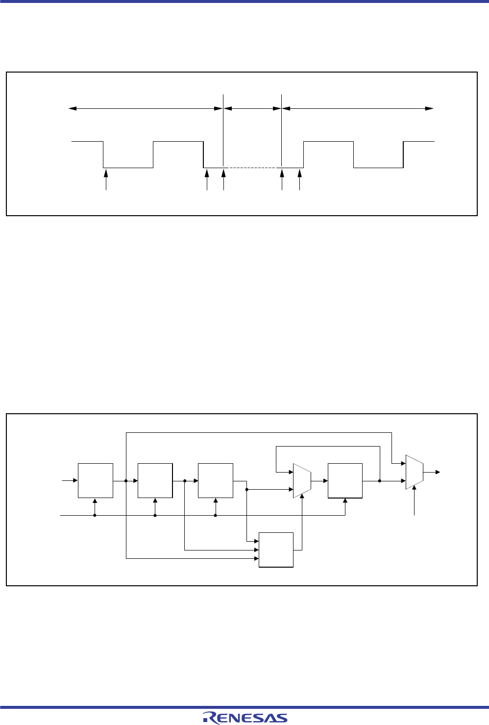
R01UH0034EJ0200 Rev.2.00 Page 975 of 1489
Dec 27, 2013
RX62T Group, RX62G Group 22. Serial Communications Interface (SCIb)
(b) At transition from software standby mode to smart card interface mode
1. Cancel software standby mode.
2. Set the SCR.CKE0 bit to 1. The clock output with the specified clock frequency is then restarted.
Figure 22.34 Clock Stop and Restart Procedure
22.4 Noise Cancellation
Figure 22.35 shows the structure of the noise cancellation circuit. This is used to eliminate noise on the RXD signal in
asynchronous mode.When noise cancellation is enabled, the signal received on the RXD pin passes through this circuit
before being handled within the SCI. The noise-cancelling function is made up of a three-stage latch circuit and a match
detector.
When SEMR.ABCS = 0, the level received on RXD is passed through the three-stage latch circuit at 16 times the
peripheral clock frequency, and if the levels in the three latches match, it is conveyed to the next stage. If the levels do
not match, the level remains the same as the last time they did match.
That is, the noise-cancelling function recognizes the received signal if it has remained at the same level for at least three
clock cycles but judges that it is noise, and thus rejects it, if it has not.
Figure 22.35 Configuration of the Noise-Cancelling Function
[2][1] [3] [4] [5] [6] [7]
Software
standby
Normal operation Normal operation
SCKn
RXD
The circuit for detect the matching
Base clock for
asynchronous
mode SEMR.NFEN
RXD out
DQ
C
DQ
C
DQ
C
DQ
C

R01UH0034EJ0200 Rev.2.00 Page 976 of 1489
Dec 27, 2013
RX62T Group, RX62G Group 22. Serial Communications Interface (SCIb)
22.5 Interrupt Sources
22.5.1 Interrupts in Serial Communications Interface Mode
Table 22.18 lists interrupt sources in normal serial communications interface mode. A different interrupt vector is
assigned to each interrupt source, and individual interrupt sources can be enabled or disabled with the enable bits in SCR.
Transfer of data from the transmit data register (TDR) to TSR while the TIE bit in SCR is 1 leads to the generation of a
TXI interrupt request. Moreover, setting the TIE bit in SCR to 1 and then setting the TE bit to 1, or setting the TIE and
TE bits in SCR to 1 simultaneously using one instruction, leads to the generation of a TXI interrupt request. A TXI
interrupt request can activate the DTC for data transfer.
Setting of received data in RDR while the RIE bit in SCR is 1 leads to the generation of an RXI interrupt request. An RXI
interrupt can activate the DTC for data transfer.
Setting the ORER, FER, or PER flag in SSR to 1 while the RIE bit in SCR is 1 leads to generation of an ERI interrupt
request. Here, an RXI interrupt request is not generated.
If the TDR has not been updated by the time of transmission of the tail-end bit of data being transmitted, the TEND flag
in SSR is set to 1 and, if the value of the TEIE bit in SCR is 1, a TEI interrupt request is generated. Writing of data to the
TDR during TXI interrupt processing leads to clearing of the TEND flag in SSR and clearing of the TEI interrupt at its
source. When clearing the TEND flag in SSR by writing transmit data to TDR, read the TEND flag in SSR to confirm
that it is 0.
The TXI interrupt request is generated by setting the TIE bit in SCR to 1 and then setting the TE bit to 1 or by setting the
TIE and TE bits in SCR to 1 simultaneously using one instruction. The TXI interrupt is not generated if the TE bit is set
while the TIE bit is 0 or the TIE bit is set to 1 after the TE bit is set to 1. Therefore, to disable the TXI interrupt, perform
the transmit end interrupt processing, and then start data transfer again, for example, in the final data transmission, the
TXI interrupt should be enabled/disabled using the corresponding ICU.IERm.IENj bit.
Table 22.18 SCI Interrupt Sources
Name Interrupt Source Interrupt Flag DTC Activation Priority
ERI Receive error ORER, FER, or PER Not possible High
Low
RXI Receive data full — Possible
TXI Transmit data empty — Possible
TEI Transmit end TEND Not possible

R01UH0034EJ0200 Rev.2.00 Page 977 of 1489
Dec 27, 2013
RX62T Group, RX62G Group 22. Serial Communications Interface (SCIb)
22.5.2 Interrupts in Smart Card Interface Mode
Table 22.19 lists interrupt sources in smart card interface mode. A transmit end interrupt (TEI) request cannot be used in
this mode.
Data transmission/reception using the DTC is also possible in smart card interface mode, similar to in the normal SCI
mode. In transmission, when the TEND flag in SSR is set to 1, a TXI interrupt request is generated. This TXI interrupt
request activates the DTC allowing transfer of transmit data if the TXI request is specified beforehand as a source of
DTC activation. The TEND flag is automatically cleared to 0 when the DTC transfers the data.
If an error occurs, the SCI automatically re-transmits the same data. During the retransmission, the TEND flag is kept to
0 and the DTC is not activated. Therefore, the SCI and DTC automatically transmit the specified number of bytes,
including retransmission in the case of error occurrence. However, the ERS flag in SSR is not automatically cleared to 0
at error occurrence. Therefore, the ERS flag must be cleared by previously setting the RIE bit in SCR to 1 to enable an
ERI interrupt request to be generated at error occurrence.
When transmitting/receiving data using the DTC, be sure to make settings to enable the DTC before making SCI settings.
For DTC settings, see section 14, Data Transfer Controller (DTC).
In reception, an RXI interrupt request is generated when receive data is set to RDR. This RXI interrupt request activates
the DTC allowing transfer of receive data if the RXI request is specified beforehand as a source of DTC activation. If an
error occurs, the error flag is set. Therefore, the DTC is not activated and an ERI interrupt request is issued to the CPU
instead; the error flag must be cleared.
Table 22.19 SCI Interrupt Sources
Name Interrupt Source Interrupt Flag DTC Activation Priority
ERI Receive error or error signal detection ORER, PER, or ERS Not possible High
Low
RXI Receive data full — Possible
TXI Transmit data empty TEND Possible

R01UH0034EJ0200 Rev.2.00 Page 978 of 1489
Dec 27, 2013
RX62T Group, RX62G Group 22. Serial Communications Interface (SCIb)
22.6 Usage Notes
22.6.1 Setting the Module Stop Function
Operation of the SCI can be disabled or enabled using the module stop control register B (MSTPCRB). The initial setting
is for operation of the SCI to be halted. Register access is enabled by clearing the module stop state. For details, see
section 9, Low Power Consumption.
22.6.2 Break Detection and Processing
When a framing error is detected, a break can be detected by reading the RXDn pin value directly. In a break, the input
from the RXDn pin becomes all 0s, and so the FER flag in SSR is set to 1 (framing error), and the PER flag in SSR may
also be set to 1 (parity error). The SCI continues the receive operation even after a break is received. Therefore, note that
even if the FER flag is cleared to 0 (no framing error), it will be set to 1 again.
22.6.3 Mark State and Break Detection
When the TE bit in SCR is 0 (serial transmission disabled), the TXDn pin is used as an I/O port whose direction (input or
output) and level are determined by the Bj bit in DR of PORTi and Bj bit in DDR of PORTi. This can be used to set the
TXDn pin to mark state or send a break during serial data transmission. To maintain the communications line in mark
state (the state of 1) until the TE bit is set to 1 (to enable serial transmission), set both Bj bit in DR of PORTi and Bj bit in
DDR of PORTi to 1. Since the TE bit is cleared to 0 at this time, the TXDn pin becomes an I/O port, and 1 is output from
the TXDn pin. To send a break during serial data transmission, first set Bj bit in DDR of PORTi = 1 and Bj bit in DR of
PORTi = 0, and then clear the TE bit to 0. When the TE bit is cleared to 0, the transmitter is initialized regardless of the
current transmission state, the TXDn pin becomes an I/O port, and a 0 is output from the TXDn pin.
22.6.4 Receive Error Flags and Transmit Operations (Clock Synchronous Mode Only)
Transmission cannot be started when a receive error flag (ORER, FER, or RER) in SSR is set to 1, even if data is written
to TDR. Be sure to clear the receive error flags to 0 before starting transmission. Note also that the receive error flags
cannot be cleared to 0 even if the RE bit in SCR is cleared to 0 (serial reception disabled).
22.6.5 Writing Data to TDR
Data can always be written to TDR. However, if new data is written to TDR when transmit data is remaining in TDR, the
previous data in TDR is lost because it has not been transferred to TSR yet. Be sure to write transmit data to TDR in the
TXI interrupt request processing routine.
22.6.6 Restrictions on Clock Synchronous Transmission
When the external clock source is used as a synchronization clock, update TDR by the DTC and wait for at least five
clock cycles of PCLK before allowing the transmit clock to be input. If the transmit clock is input within four clock
cycles after TDR is updated, the SCI may malfunction.
22.6.7 Restrictions on Using DTC
When using the DTC to read RDR, be sure to set the receive end interrupt (RXI) as the activation source of the relevant
SCI.

R01UH0034EJ0200 Rev.2.00 Page 979 of 1489
Dec 27, 2013
RX62T Group, RX62G Group 22. Serial Communications Interface (SCIb)
22.6.8 SCI Operations during Low Power Consumption State
(1) Transmission
Before specifying the module stop state or making a transition to software standby mode, stop the transmit operations
(TIE = TE = TEIE = 0 in SCR). TSR, TDR, and SSR are reset. Setting the TE bit to 0 modifies the TSR register and the
SSR.TEND flag to 0. The states of the output pins in the module stop state or in software standby mode depend on the
port settings, and the output pins are held high after cancellation. If the transition is made during data transmission,
transmission will be suspended.
To transmit data in the same transmission mode after cancellation of the low power consumption state, set the TE bit to 1,
read SSR, and write data to TDR sequentially to start data transmission. To transmit data with a different transmission
mode, initialize the SCI first.
Figure 22.36 shows a sample flowchart for transition to software standby mode during transmission. Figure 22.37 and
21.38 show the port pin states during transition to software standby mode.
Before specifying the module stop state or making a transition to software standby mode from the transmission mode
using DTC transfer, stop the transmit operations. To start transmission after cancellation using the DTC, set the TE bit to
1. The TXI interrupt flag is set to 1 and transmission starts using the DTC.
(2) Reception
Before specifying the module stop state or making a transition to software standby mode, stop the receive operations (RE
in SCR = 0). If transition is made during data reception, the data being received will be invalid.
To receive data in the same reception mode after cancellation of the low power consumption state, set the RE bit to 1, and
then start reception. To receive data in a different reception mode, initialize the SCI first.
Figure 22.39 shows a sample flowchart for mode transition during reception.
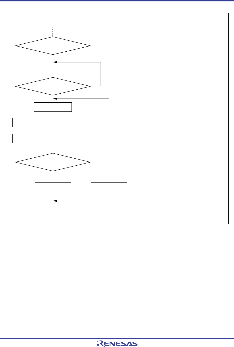
R01UH0034EJ0200 Rev.2.00 Page 980 of 1489
Dec 27, 2013
RX62T Group, RX62G Group 22. Serial Communications Interface (SCIb)
Figure 22.36 Example of Flowchart for Transition to Software Standby Mode during Transmission
<Start data transmission>
Initialization SCR.TE = 1
SCR.TE bit = 0
Make transition to software standby mode
Cancel software standby mode
No
No
No
Yes
Yes
Yes
All data transmitted?
SSR.TEND = 1
Change operating mode?
<Data transmission>
[ 1 ]
[ 2 ]
[ 3 ]
[ 1 ] Data being transmitted is lost halfway. Data can be
normally transmitted from the CPU by setting the TE
bit in SCR to 1, reading SSR, and writing data to
TDR after canceling software standby mode.
However, if the DTC has been activated, the data
remaining in the DTC will be transmitted when both
the TE and TIE bits in SCR are set to 1.
[ 2 ] Clear the TIE and TEIE bits in SCR to 0 when they
are 1.
[ 3 ] Setting for the module stop state is included.
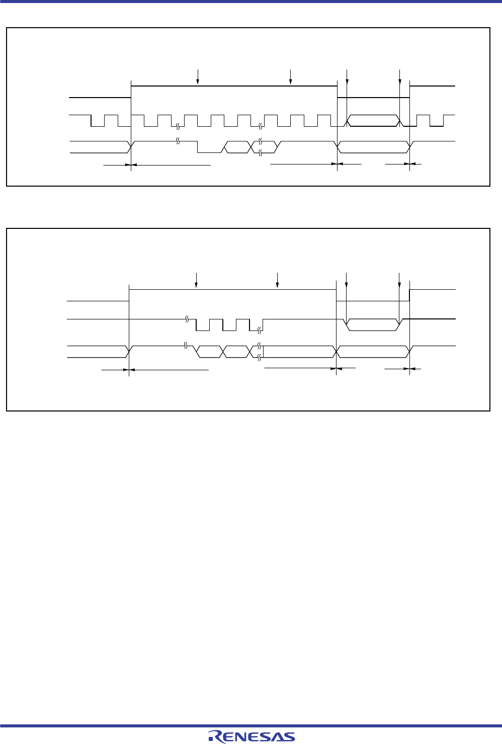
R01UH0034EJ0200 Rev.2.00 Page 981 of 1489
Dec 27, 2013
RX62T Group, RX62G Group 22. Serial Communications Interface (SCIb)
Figure 22.37 Port Pin States during Transition to Software Standby Mode
(Internal Clock, Asynchronous Transmission)
Figure 22.38 Port Pin States during Transition to Software Standby Mode
(Internal Clock, Clock Synchronous Transmission)
Port input/output High outputPort input/output High output Stop
Transmission start Transmission end
Port input/output
SCI TXDn output Port
Port
Transition to
software standby
mode Software standby mode
canceled
SCKn output pin
SCR.TE bit
TXDn output pin
SCI TXDn output
Port input/output High output*Port input/output Marking output
Transmission start Transmission end
Port input/output
SCI TXDn output
Port
Port
Transition to
software standby
mode
SCKn output pin
SCR.TE bit
TXDn output pin
Software standby
mode canceled
SCI TXDn output
Last TxD bit retained
Note: * Initialized in software standby mode
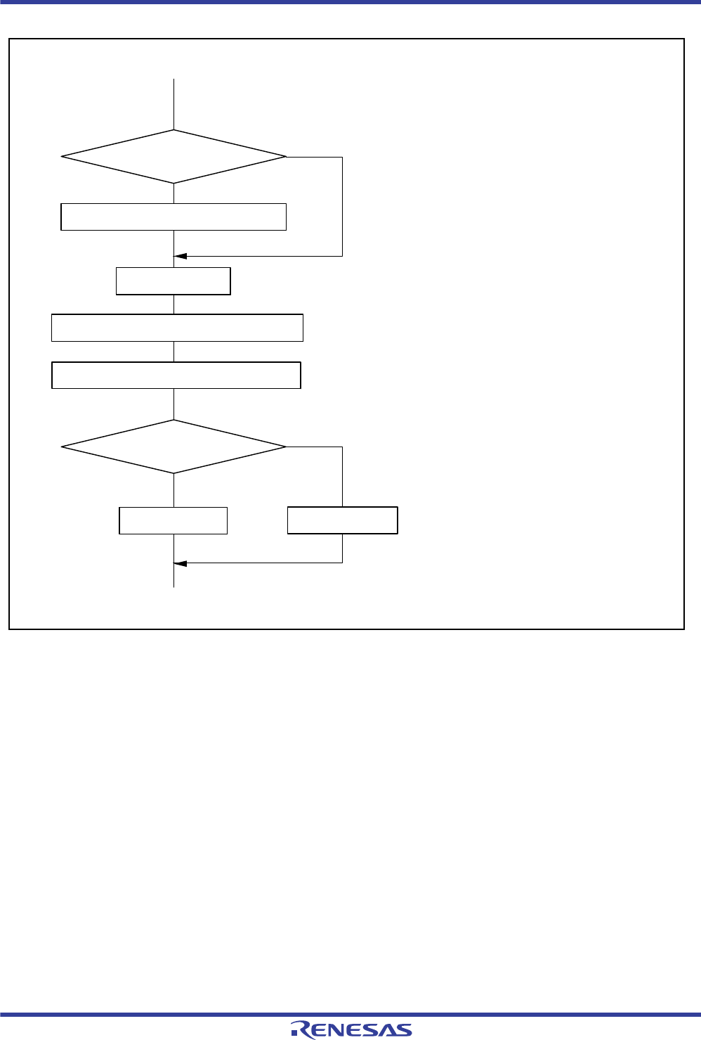
R01UH0034EJ0200 Rev.2.00 Page 982 of 1489
Dec 27, 2013
RX62T Group, RX62G Group 22. Serial Communications Interface (SCIb)
Figure 22.39 Example of Flowchart for Transition to Software Standby Mode during Reception
22.6.9 External Clock Input in Clock Synchronous Mode
In clock synchronous mode, the external clock SCKn must be input as follows:
High-pulse period, low-pulse period = 2 PCLK or more, period = 6 PCLK or more
<Start data reception>
Initialization SCR.RE = 1
SCR.RE = 0
Read receive data in RDR
Make transition to software standby mode
Cancel software standby mode
No
No
Yes
Yes
RXI interrupt
Change operating mode?
<Data reception>
[ 1 ]
[ 2 ]
[ 1 ] Data being received is invalid.
[ 2 ] Setting for the module stop state is included.
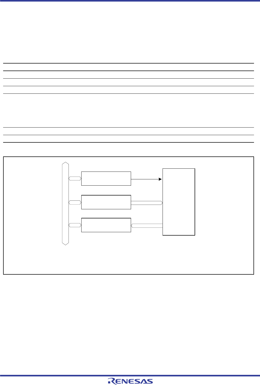
R01UH0034EJ0200 Rev.2.00 Page 983 of 1489
Dec 27, 2013
RX62T Group, RX62G Group 23. CRC Calculator (CRC)
Under development Preliminary document
Specifications in this document are tentative and subject to change.
23. CRC Calculator (CRC)
The CRC (Cyclic Redundancy Check) calculator generates CRC codes of data blocks.
23.1 Overview
Table 23.1 lists the specifications of the CRC calculator, and Figure 23.1 shows a block diagram of the CRC calculator.
Note 1. The circuit does not have functionality to divide data for calculation into a data-block size. Write data in 8-bit units.
Figure 23.1 Block Diagram of CRC Calculator
Table 23.1 Specifications of CRC
Item Description
Data for CRC calculation*1CRC code generated for any desired data in 8n-bit units (where n is a whole number)
Data block size 8 bits
CRC processor unit Operation executed on eight bits in parallel
CRC generating polynomial One of three generating polynomials selectable
8-bit CRC
X8 + X2 + X + 1
16-bit CRC
X16 + X15 + X2 + 1
X16 + X12 + X5 + 1
CRC calculation switching CRC code generation for LSB-first or MSB-first communication selectable
Power-down function Module stop state can be set
CRCCR
CRCDIR
CRCDOR
CRC code
generation
circuit
Control signal
CRCCR : CRC control register
CRCDIR : CRC data input register
CRCDOR : CRC data output register
Internal bus
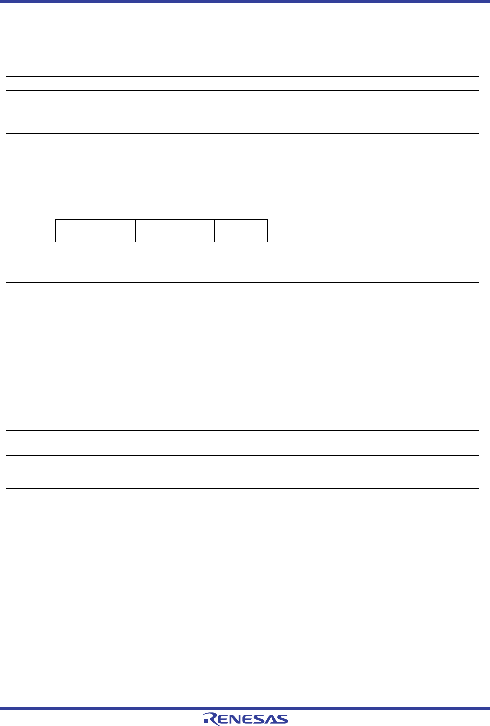
R01UH0034EJ0200 Rev.2.00 Page 984 of 1489
Dec 27, 2013
RX62T Group, RX62G Group 23. CRC Calculator (CRC)
Under development Preliminary document
Specifications in this document are tentative and subject to change.
23.2 Register Descriptions
Table 23.2 lists the registers of the CRC calculator.
23.2.1 CRC Control Register (CRCCR)
Note 1. The CRC data output register (CRCDOR) is always 0000h.
CRCCR initializes the CRC calculator, switches the operation mode, and selects the generating polynomial.
GPS[1:0] Bits (CRC Generating Polynomial Switching)
These bits select the CRC code generating polynomial.
LMS Bit (CRC Calculation Switching)
Selects LSB-first or MSB-first communication for the CRC code generation.
DORCLR Bit (CRCDOR Register Clear)
Write 1 to this bit so that the CRCDOR register is cleared to 0000h.
This bit is always read as 0.
Table 23.2 Registers of CRC Calculator
Register Name Symbol Value after Reset Address Access Size
CRC control register CRCCR 00h 0008 8280h 8
CRC data input register CRCDIR 00h 0008 8281h 8
CRC data output register CRCDOR 0000h 0008 8282h 16
Address: 0008 8280h
b7 b6 b5 b4 b3 b2 b1 b0
DORCL
R————LMSGPS[1:0]
Value after reset: 00000000
Bit Symbol Bit Name Description R/W
b1, b0 GPS[1:0] CRC Generating Polynomial
Switching
b1 b0
0 0: No calculation is executed.*1
0 1: X8 + X2 + X + 1
1 0: X16 + X15 + X2 + 1
1 1: X16 + X12 + X5 + 1
R/W
b2 LMS CRC Calculation Switching 0: Performs CRC operation for LSB-first communication. The
lower-order byte (bits 7 to 0) is the first to be transmitted
when the contents of the CRCDOR (CRC code) are divided
into bytes.
1: Performs CRC operation for MSB-first communication. The
higher-order byte (bits 15 to 8) is first to be transmitted
when the contents of the CRCDOR (CRC code) are divided
into bytes.
R/W
b6 to b3 Reserved These bits are always read as 0. The write value should
always be 0.
R/W
b7 DORCLR CRCDOR Register Clear 0: No effect on the operation
1: Clear the CRCDOR register
This bit is always read as 0.
R/W
R01UH0034EJ0200 Rev.2.00 Page 985 of 1489
Dec 27, 2013
RX62T Group, RX62G Group 23. CRC Calculator (CRC)
Under development Preliminary document
Specifications in this document are tentative and subject to change.
23.2.2 CRC Data Input Register (CRCDIR)
CRCDIR is an 8-bit readable/writable register, to which the bytes to be CRC-operated are written.
23.2.3 CRC Data Output Register (CRCDOR)
CRCDOR is a 16-bit readable/writable register that contains the result of CRC calculation.
In general, the value will be 0 if there is no CRC error when the calculated CRC code matches the CRC code that
continues on, for verification, from the transferred data.
When eight-bit CRC codes (from the polynomial X8 + X2 + X + 1) are in use, the valid CRC code is obtained from the
lower-order byte (b7 to b0). The higher-order byte (b15 to b8) is not updated.
Address: 0008 8281h
b7 b6 b5 b4 b3 b2 b1 b0
Value after reset: 00000000
Address: 0008 8282h
b15 b14 b13 b12 b11 b10 b9 b8 b7 b6 b5 b4 b3 b2 b1 b0
Value after reset: 0000000000000000
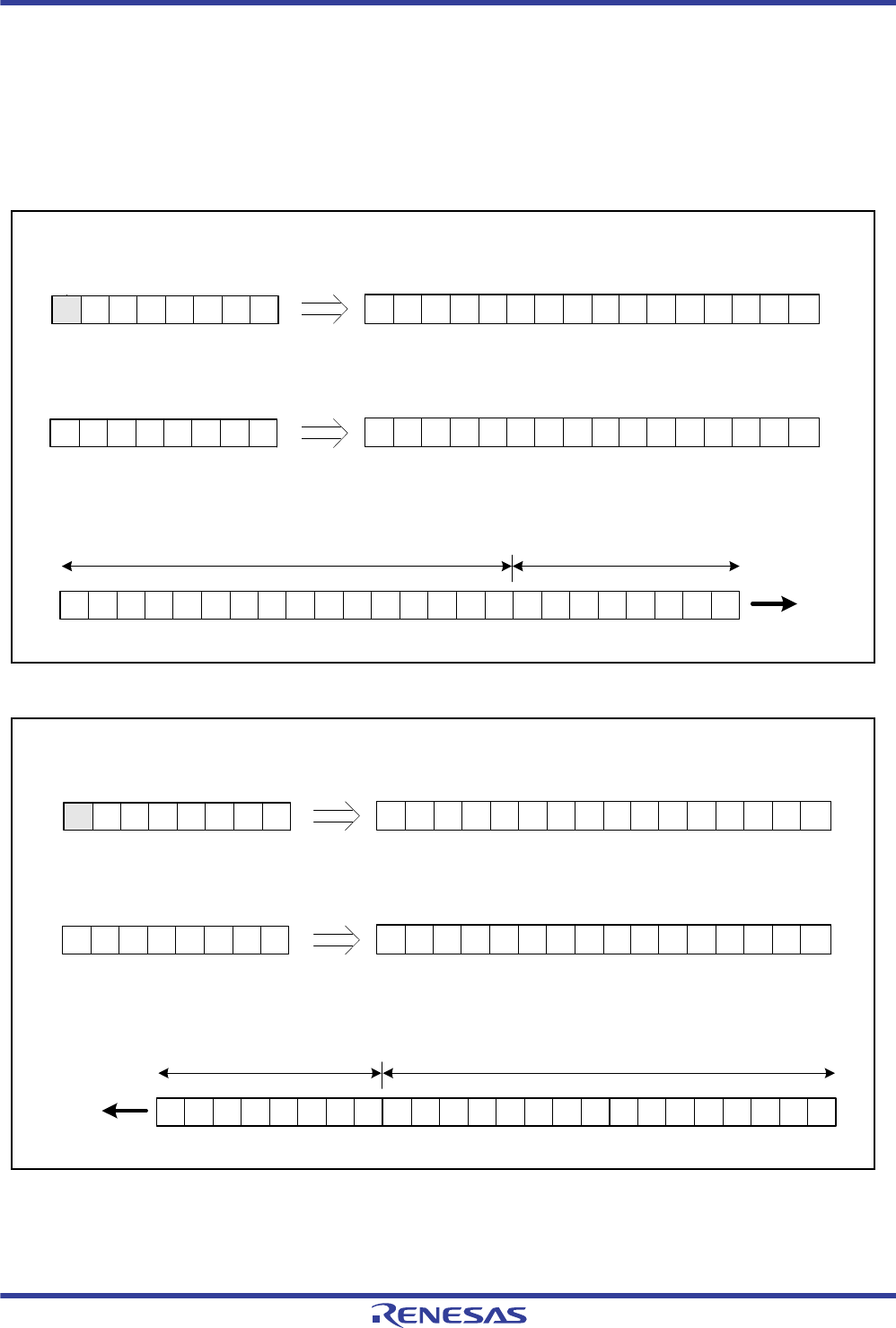
R01UH0034EJ0200 Rev.2.00 Page 986 of 1489
Dec 27, 2013
RX62T Group, RX62G Group 23. CRC Calculator (CRC)
Under development Preliminary document
Specifications in this document are tentative and subject to change.
23.3 Operation
The CRC calculator is capable of generating LSB- or MSB-first CRC codes for transfer.
Examples of usage for CCR code-generation from the data F0h with the CRCCR.GPS[1:0] bits set to 11b to select 16-bit
CCR codes (from the polynomial X16 + X12 + X5 + 1) are given below.
When eight-bit CRC codes (from the polynomial X8 + X2 + X + 1) are in use, the valid CRC code is obtained from the
lower-order byte (b7 to b0).
Figure 23.2 LSB-First Data Transmission
Figure 23.3 MSB-First Data Transmission
CRCDORCRCCR
Clear CRCDOR
1
7
00000
0
70
15 0
11 000000 00
CRCDIR
CRC code generation
111100 00
CRC code
Output
Data
7
7
7FFF08
00
111101 11100011 1111110000
2. Write F0h to CRCDIR
3. Read CRCDOR
CRC code = F78Fh
4. Serial transmission (LSB first)
1. Write 83h to CRCCR
000000 00
CRCDOR
15 0
111101 1110 001 1 11
78
78
70
CRCDORCRCCR
Clear CRCDOR
1
7
00001
0
70
15 0
11 000000 00
CRCDIR
CRC code generation
111100 00
CRC code
Output
Data
77
0FF1FE
00
111100 00111011 1100011111
2. Write F0h to CRCDIR
3. Read CRCDOR
CRC code = EF1Fh
4. Serial transmission (MSB first)
1. Write 87h to CRCCR
000000 00
CRCDOR
15 0
111011 11000111 11
78
78
70

R01UH0034EJ0200 Rev.2.00 Page 987 of 1489
Dec 27, 2013
RX62T Group, RX62G Group 23. CRC Calculator (CRC)
Under development Preliminary document
Specifications in this document are tentative and subject to change.
Figure 23.4 LSB-First Data Reception
CRCCR CRCDOR
Clear CRCDOR
100000 11000000 00 000000 00
CRCDIR
111100 00111101 1
1100011 1
1
100011 11000000 0011110111
111101 1
1
Input
Data
7FFF08
70
111101 11 100011 1111110000
70
70
70
70
70
70
70
70
CRC code
CRC code generation
1. Serial reception (LSB first)
2. Write 83h to CRCCR
3. Write F0h to CRCDIR
4. Write 8Fh to CRCDIR
5. Write F7h to CRCDIR
6. Read CRCDOR
CRC code = 0000h no error
CRCDIR
CRCDIR
7070
000000 00 000000 00
CRC code generation
CRC code generation
815
15
15
15
8
8
8
CRCDOR
CRCDOR
CRCDOR
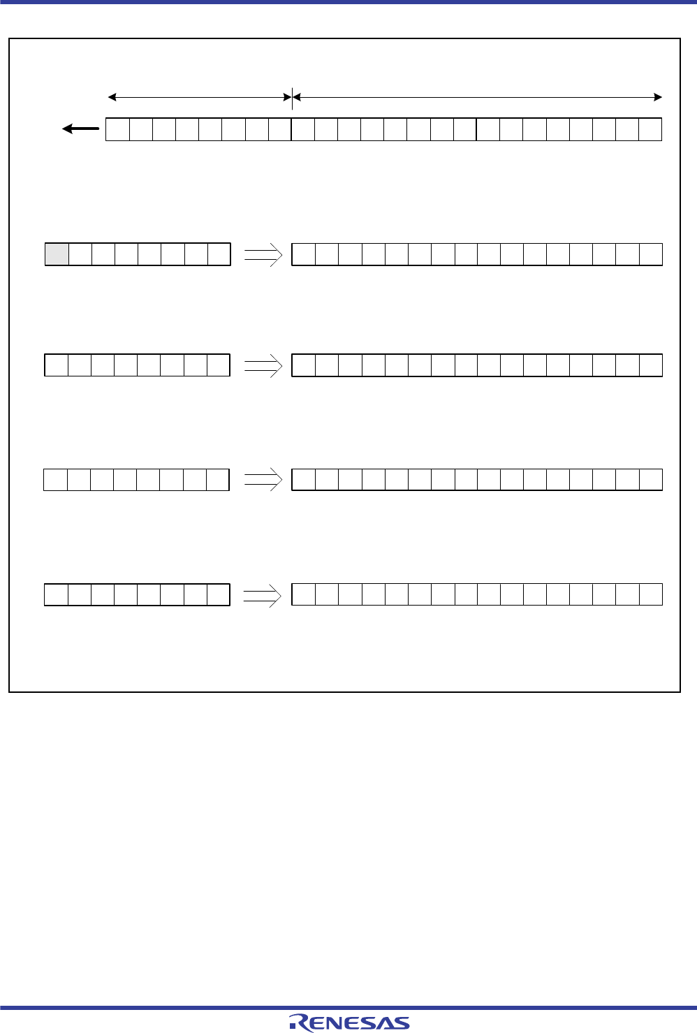
R01UH0034EJ0200 Rev.2.00 Page 988 of 1489
Dec 27, 2013
RX62T Group, RX62G Group 23. CRC Calculator (CRC)
Under development Preliminary document
Specifications in this document are tentative and subject to change.
Figure 23.5 MSB-First Data Reception
Input
0FF1FE
111100 00 111011 1100011111
CRC code
1. Serial reception (MSB first)
6. Read CRCDOR
CRC code = 000h no error
Data
70
70
70
CRCCR CRCDOR
Clear CRCDOR
100001 11000000 00 000000 00
CRCDIR
111100 00111011 1
1000111 1
1
111011 11000111 1100000000
000111 1
1
70
70
70
70
70
70
70
70
CRC code generation
2. Write 87h to CRCCR
3. Write F0h to CRCDIR
4. Write EFh to CRCDIR
5. Write 1Fh to CRCDIR
CRCDIR
CRCDIR
000000 00 000000 00
CRC code generation
CRC code generation
815
15
15
15
8
8
8
CRCDOR
CRCDOR
CRCDOR
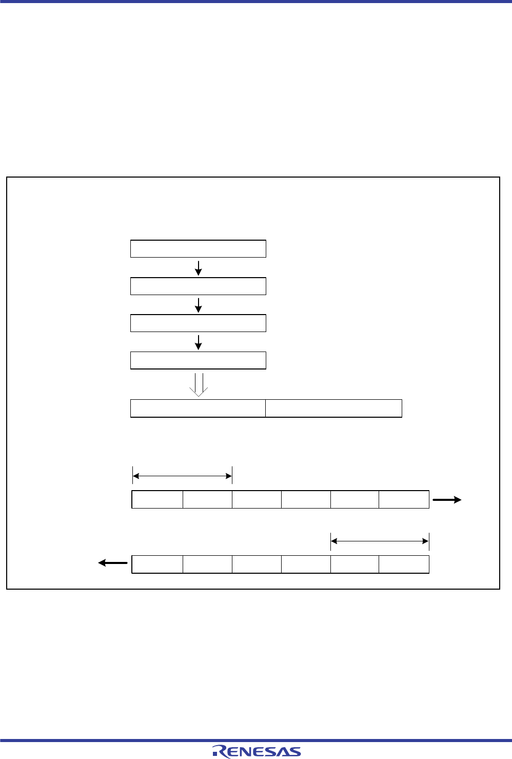
R01UH0034EJ0200 Rev.2.00 Page 989 of 1489
Dec 27, 2013
RX62T Group, RX62G Group 23. CRC Calculator (CRC)
Under development Preliminary document
Specifications in this document are tentative and subject to change.
23.4 Usage Notes
23.4.1 Module Stop Function Setting
Operation of the CRC calculator can be disabled or enabled using the module stop control register B (MSTPCRB). The
initial setting is for operation of the CRC calculator to be halted. Register access is enabled by clearing the module stop
state. For details, see section 9, Low Power Consumption.
23.5 Note on Transmission
Note that the sequence of transmission for the CRC code differs according to whether transmission is LSB-first or MSB-
first.
Figure 23.6 LSB-First and MSB-First Data Transmission
CRCDIR
CRCDOR
1. CRC code
CRC code generation
After specifying the method for generation calculation, write data to CRCDIR in order of (1), (2), (3), and (4).
Output
15
770 0
0
0
70
000777 7
(1)
CRC code (H)
CRC code
Output
770000007777
2. Transmission data
CRC code (L)
(H) (L) (4) (3) (2) (1)
(i) When transmission is LSB-first
(ii) When transmission is MSB-first
(1) (2) (3) (4) (H) (L)
CRC code
CRCDIR
70
(2)
CRCDIR
70
(3)
CRCDIR
70
(4)
78

R01UH0034EJ0200 Rev.2.00 Page 990 of 1489
Dec 27, 2013
RX62T Group, RX62G Group 24. I2C Bus Interface (RIIC)
24. I2C Bus Interface (RIIC)
The RX62T and RX62G Groups have one I2C bus interface (RIIC module).
The RIIC module conforms with and provides a subset of the NXP I2C bus (inter-IC bus) interface functions.
24.1 Overview
Table 24.1 lists the specifications of the RIIC, Figure 24.1 shows a block diagram of the RIIC, and Figure 24.2 shows
an example of I/O pin connections to external circuits (I2C bus configuration example). Table 24.2 shows the input/
output pins of the RIIC.
Table 24.1 RIIC Specifications
Item Specifications
Communications format I2C bus format or SMBus format
Master mode or slave mode selectable
Automatic securing of the various set-up times, hold times, and bus-free times for the transfer rate
Transfer rate Up to 400k bps
SCL clock For master operation, the duty cycle of the SCL clock is selectable in the range from 4% to 96%.
Issuing and detecting
conditions
Start, restart, and stop conditions are automatically generated.
Start conditions (including restart conditions) and stop conditions are detectable.
Slave address Up to three slave-address settings can be made.
Seven- and ten-bit address formats are supported (along with the use of both at once).
General call addresses, device ID addresses, and SMBus host addresses are detectable.
Acknowledgement For transmission, the acknowledge bit is automatically loaded.
Transfer of the next data for transmission can be automatically suspended on detection of a not-
acknowledge bit.
For reception, the acknowledge bit is automatically transmitted.
If a wait between the eighth and ninth clock cycles has been selected, software control of the value in
the acknowledge field in response to the received value is possible (i.e. the return of ACK or NACK is
selectable).
Wait function In reception, the following periods of waiting can be obtained by holding the clock signal (SCL) at the
low level:
waiting between the eighth and ninth clock cycles (timing of the received data full interrupt can be
selected for this); and
waiting between the ninth clock cycle and the first clock cycle of the next transfer (WAIT function)
SDA output delay function Timing of the output of transmitted data, including the not-acknowledge bit, can be delayed.
Arbitration For multi-master operation
Operation to synchronize the SCL (clock) signal in cases of conflict with the SCL signal from another
master is possible.
When issuing the start condition would create conflict on the bus, loss of arbitration is detected by
testing for non-matching between the internal signal for the SDA line and the level on the SDA line.
In master operation, loss of arbitration is detected by testing for non-matching between the signal on
the SDA line and the internal signal for the SDA line.
Loss of arbitration due to detection of the start condition while the bus is busy is detectable (to prevent
the issuing of double start conditions).
Loss of arbitration in transfer of a not-acknowledge bit due to the internal signal for the SDA line and
the level on the SDA line not matching is detectable.
Loss of arbitration due to non-matching of internal and line levels for data is detectable in slave
transmission.
Timeout function The internal time-out function is capable of detecting long-interval stoppages of the SCL (clock signal).
Noise removal The interface incorporates digital noise filters for both the SCL and SDA signals, and the width for
noise cancellation by the filters is adjustable.
Interrupt sources Four sources:
Error in transfer or occurrence of events (detection of AL, NACK, time-out, a start condition including a
restart condition, or a stop condition)
Receive-data-full (including matching with a slave address)
Transmit-data-empty (including matching with a slave address)
Transmission complete
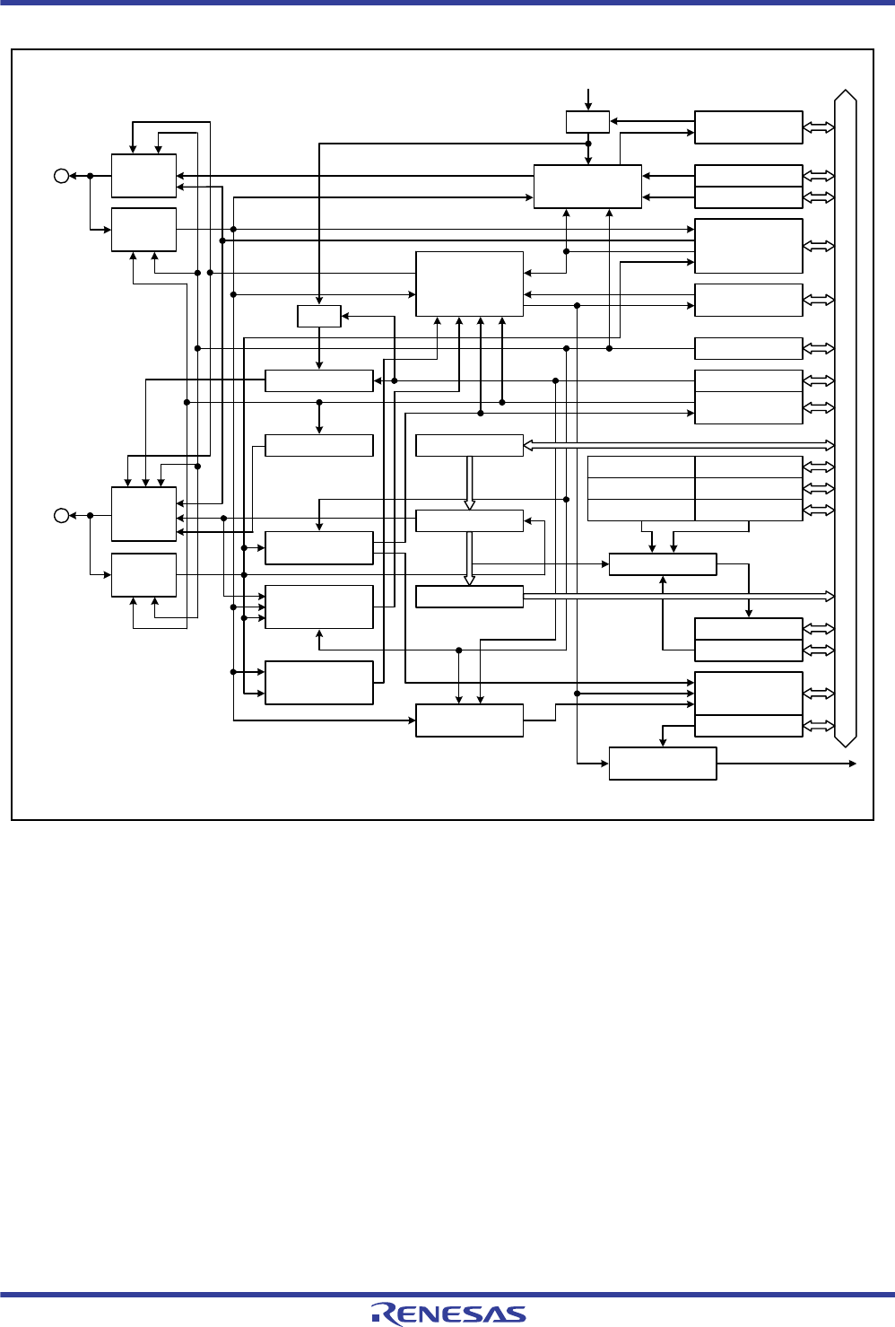
R01UH0034EJ0200 Rev.2.00 Page 991 of 1489
Dec 27, 2013
RX62T Group, RX62G Group 24. I2C Bus Interface (RIIC)
Figure 24.1 Block Diagram of RIIC
ICCR1
Output
control
Noise
canceler
Bus state decision
circuit
Arbitration decision
circuit
Output
control
Noise
canceler
ICDRS
ICDRT
ICDRR
Address comparator
ICCR2
ICMR1
ICMR2
ICMR3
ICFER
ICSR1
ICSR2
ICSER
ICIER
ICBRH
ICBRL
Timeout circuit
Interrupt generator
Transmission/rece
ption control circuit
Transfer clock
generator
ACK output circuit
SCL
SDA
NACK decision/ACK
reception circuit
Internal data bus
BC[2:0]
CKS[2:0]
CLO
SDAI
BBSY, MST, TRS
SDA output delay control
ST, RS, SP
IICRST
SDDL[2:0]
PCLK
ACKBR
WAIT, RDRFS
NF[1:0]
ACKBT
NFE
SARL0
SARL1
SARL2
SARU0
SARU1
SARU2
NACKF
(TXI, TEI, RXI, STI, SPI, NAKI, ALI, TMOI)
Interrupt request
NF[1:0]
NFE
FMPE
FMPE
MALE, NALE, SALE
TMOE TMOS, TMOH, TMOL
SCLE
NACKE
SCLI
SCL0, SDA0
PS DLCS
TMOF
PS
IIC (PCLK/1 to PCLK/128)
IIC, IIC/2
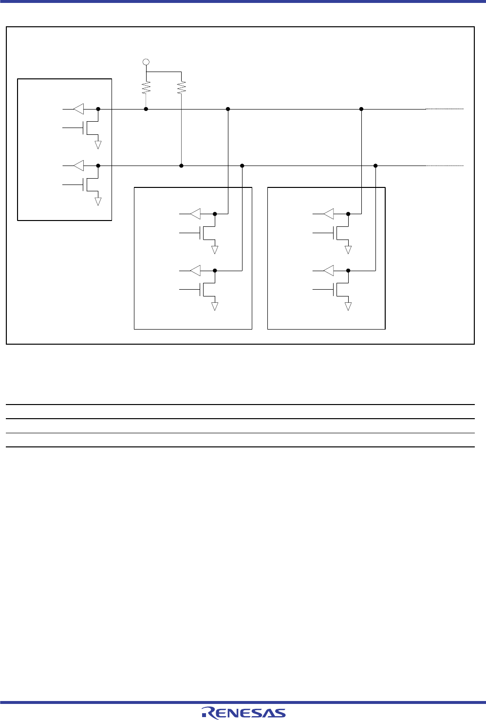
R01UH0034EJ0200 Rev.2.00 Page 992 of 1489
Dec 27, 2013
RX62T Group, RX62G Group 24. I2C Bus Interface (RIIC)
Figure 24.2 Connections to the External Circuit by the I/O Pins (I2C Bus Configuration Example)
Table 24.2 Pin Configuration
Pin Name I/O Function
SCL I/O Serial clock I/O pin
SDA I/O Serial data I/O pin
Power supply for pull-
up (VCC to 5 V)
SCL
SDA
(Master)
(Slave 1)
SCL
SDA
(Slave 2)
SCL
SDA
SCL
SDA
SCLin
SDAin
SCLout#
SDAout#
SCLin
SDAin
SCLout#
SDAout#
SCLin
SDAin
SCLout#
SDAout#

R01UH0034EJ0200 Rev.2.00 Page 993 of 1489
Dec 27, 2013
RX62T Group, RX62G Group 24. I2C Bus Interface (RIIC)
24.2 Register Descriptions
Table 24.3 lists the registers of the RIIC.
Table 24.3 Registers of the RIIC
Channel Register Name Symbol Value after Reset Address Access Size
RIIC0 I2C bus control register 1 ICCR1 1Fh 0008 8300h 8
I2C bus control register 2 ICCR2 00h 0008 8301h 8
I2C bus mode register 1 ICMR1 08h 0008 8302h 8
I2C bus mode register 2 ICMR2 06h 0008 8303h 8
I2C bus mode register 3 ICMR3 00h 0008 8304h 8
I2C bus function enable register ICFER 72h 0008 8305h 8
I2C bus status enable register ICSER 09h 0008 8306h 8
I2C bus interrupt enable register ICIER 00h 0008 8307h 8
I2C bus status register 1 ICSR1 00h 0008 8308h 8
I2C bus status register 2 ICSR2 00h 0008 8309h 8
Slave address register L0 SARL0 00h 0008 830Ah 8
Timeout internal counter L TMOCNTL 0000h 0008 830Ah 16
Slave address register U0 SARU0 00h 0008 830Bh 8
Timeout internal counter TMOCNTU 0000h 0008 830Bh 16
Slave address register L1 SARL1 00h 0008 830Ch 8
Slave address register U1 SARU1 00h 0008 830Dh 8
Slave address register L2 SARL2 00h 0008 830Eh 8
Slave address register U2 SARU2 00h 0008 830Fh 8
I2C bus bit rate low-level register ICBRL FFh 0008 8310h 8
I2C bus bit rate high-level register ICBRH FFh 0008 8311h 8
I2C bus transmit data register ICDRT FFh 0008 8312h 8
I2C bus receive data register ICDRR 00h 0008 8313h 8
I2C bus shift register ICDRS — — 8

R01UH0034EJ0200 Rev.2.00 Page 994 of 1489
Dec 27, 2013
RX62T Group, RX62G Group 24. I2C Bus Interface (RIIC)
24.2.1 I2C Bus Control Register 1 (ICCR1)
Note 1. Do not write to these bits during communication. Changing a value during communication may cause a transmission or reception
failure or an AL error.
Note 2. To change the SDAO and SCLO bits, set the SOWP bit to 0 at the same timing to set the SDAO and SCLO bits to 0.
ICCR1 enables or disables the RIIC, resets the internal state of the RIIC, outputs an extra SCL clock cycle, and
manipulates and monitors the SCL pin and SDA pin.
SDAO Bit (SDA Output Control/Monitor) and SCLO Bit (SDA Output Control/Monitor)
These bits are used to directly control the SDAn and SCLn signals output from the RIIC.
When writing to these bits, also write 0 to the SOWP bit.
The result of setting these bits is input to the RIIC via the input buffer. When slave mode is selected, a start condition
may be detected and the bus may be released depending on the bit settings.
Do not rewrite these bits during a start condition, stop condition, repeated start condition, or during transmission or
reception. Operation after rewriting under the above conditions is not guaranteed.
When reading these bits, the state of signals output from the RIIC can be read.
Address: 0008 8300h
b7 b6 b5 b4 b3 b2 b1 b0
ICE IICRST CLO SOWP SCLO SDAO SCLI SDAI
Value after reset: 00011111
Bit Symbol Bit Name Description R/W
b0 SDAI SDA Line Bus Input Monitor 0: The SDA line is at a low level
1: The SDA line is at a high level
R
b1 SCLI SCL Line Bus Input Monitor 0: The SDA line is at a low level
1: The SDA line is at a high level
R
b2 SDAO SDA Output Control/Monitor Read:
0: The RIIC has driven the SDA pin low.
1: The RIIC has released the SDA pin.
Write:
0: The RIIC drives the SDA pin low.
1: The RIIC releases the SDA pin.
R/W
*1, *2
b3 SCLO SCL Output Control/Monitor Read:
0: SCL pin is at a low level
1: SCL pin is in a high-impedance state
Write:
0: The RIIC drives the SCL pin low.
1: The RIIC releases the SCL pin.
R/W
*1, *2
b4 SOWP SCLO/SDAO Write Protect*20: Allows the SCLO and SDAO bits to be rewritten.
1: Protects the SCLO and SDAO bits.
(This bit is always read as 1.)
R/W
*2
b5 CLO Extra SCL Clock Cycle Output 0: Does not output an extra SCL clock cycle (default)
1: Outputs an extra SCL clock cycle
(The CLO bit is cleared automatically after one clock cycle is output.)
R/W
b6 IICRST I2C Bus Interface Internal Reset 0: Clears the RIIC reset or internal reset
1: Initiates the RIIC reset or internal reset
(Clears the bit counter and the SCL/SDA output latch)
R/W
b7 ICE I2C Bus Interface Enable 0: Disables the RIIC (the SCL pin and SDA pin function as ports)
1: Enables the RIIC transfer function
(the SCL pin and SDA pin drive the bus)
R/W

R01UH0034EJ0200 Rev.2.00 Page 995 of 1489
Dec 27, 2013
RX62T Group, RX62G Group 24. I2C Bus Interface (RIIC)
SOWP Bit (SCLO/SDAO Write Protect)
This bit controls the modification of the SCLO and SDAO bits.
CLO Bit (Extra SCL Clock Cycle Output)
This bit is used to output an extra SCL clock cycle for debugging or error processing.
Normally, set the bit to 0. Setting the bit to 1 in a normal communication state causes a communication error.
For details on this function, see section 24.11.2, Extra SCL Clock Cycle Output Function.
IICRST Bit (I2C Bus Interface Internal Reset)
This bit is used to reset the internal states of the RIIC.
Setting this bit to 1 initiates an RIIC reset or internal reset.
Whether an RIIC reset or internal reset is initiated is determined according to the combination with the ICE bit. Table
24.4 lists the resets of the RIIC.
The RIIC reset resets all registers including the BBSY flag in ICCR2 and internal states of the RIIC, and the internal
reset resets the bit counter (BC[2:0] bits in ICMR1), the I2C bus shift register (ICDRS), and the I2C bus status registers
(ICSR1 and ICSR2) as well as the internal states of the RIIC. For the reset conditions for each register, see section
24.14, Reset States.
An internal reset initiated with the IICRST bit set to 1 during operation (with the ICE bit set to 1) resets the internal states
of the RIIC without initializing the port settings and the control and setting registers of the RIIC when the bus or RIIC
hangs up due to a communication error.
If the RIIC hangs up in a low level output state, resetting the internal states cancels the low level output state and releases
the bus with the SCL pin and SDA pin at a high impedance.
Note: • If an internal reset is initiated using the IICRST bit for a bus hang-up occurred during communication with the
master device in slave mode, the states may become different between the slave device and the master device
(due to the difference in the bit counter information). For this reason, do not initiate an internal reset in slave
mode, but initiate restoration processing from the master device. If an internal reset is necessary because the
RIIC hangs up with the SCL line in a low level output state in slave mode, initiate an internal reset and then issue
a restart condition from the master device or resume communication from the start condition issuance after
issuing a stop condition. If communication is restarted by initiating a reset solely in the slave device without
issuing a start condition or restart condition from the master device, synchronization will be lost because the
master and slave devices operate asynchronously.

R01UH0034EJ0200 Rev.2.00 Page 996 of 1489
Dec 27, 2013
RX62T Group, RX62G Group 24. I2C Bus Interface (RIIC)
ICE Bit (I2C Bus Interface Enable)
This bit is used to enable or disable the transfer operation of the RIIC.
When this bit is set to 0 to disable the RIIC, the SCL pin and SDA pin function as ports. An RIIC reset is initiated by
setting the IICRST bit to 1 with the ICE bit set to 0, and an internal reset is initiated by setting the IICRST bit to 1 with
the ICE bit set to 1.
To prevent unexpected communications, set the RIIC registers with the ICE bit set to 0 (to disable the RIIC), and set the
ICE bit to 1 (to enable the transfer operation) after finishing all register settings.
Note 1. In addition to the I2C bus pin functions, other functions are also multiplexed onto the pins of the RX62T and
RX62G Groups. To use the pins as I2C bus pins (SCL pin and SDA pin), disable the other multiplexed functions.
Since both of the SCL pin and SDA pin of the I2C bus pins are I/O pins, set the corresponding PORTn.DDR
register to 0 (input) and set the PORTn.ICR register to 1 (input buffer enabled).
Table 24.4 RIIC Resets
IICRST ICE State Specifications
1 0 RIIC reset Resets all registers and internal states of the RIIC.
1 Internal reset Reset the BC[2:0] bits in ICMR1, and the ICSR1, ICSR2, ICDRS registers and the
internal states of the RIIC.

R01UH0034EJ0200 Rev.2.00 Page 997 of 1489
Dec 27, 2013
RX62T Group, RX62G Group 24. I2C Bus Interface (RIIC)
24.2.2 I2C Bus Control Register 2 (ICCR2)
Note 1. When the MTWP bit in ICMR1 is set to 1, the MST and TRS bits can be written to.
ICCR2 has a flag function that indicates whether or not the I2C bus is occupied and whether the RIIC is in transmit/
receive or master/slave mode as well as a function to issue a start or stop condition.
ST Bit (Start Condition Issuance Request)
This bit is used to request transition to master mode and issuance of a start condition.
When this bit is set to 1 to request to issue a start condition, a start condition is issued when the BBSY flag is set to 0 (bus
free).
For details on the start condition issuance, see section 24.10, Start Condition/Restart Condition/Stop Condition
Issuing Function.
[Setting condition]
When 1 is written to the ST bit
[Clearing conditions]
When 0 is written to the ST bit
When a start condition has been issued
When the AL (arbitration lost) flag in ICSR2 is set to 1
When 1 is written to the IICRST bit in ICCR1 to apply an RIIC reset or an internal reset
Note: • Set the ST bit to 1 (start condition issuance request) when the BBSY flag is set to 0 (bus free).
Note that arbitration may be lost if the ST bit is set to 1 (start condition issuance request) when the BBSY flag is
set to 1 (bus busy).
Address: 0008 8301h
b7 b6 b5 b4 b3 b2 b1 b0
BBSY MST TRS — SP RS ST —
Value after reset: 00000000
Bit Symbol Bit Name Description R/W
b0 — Reserved This bit is always read as 0. The write value should always be 0. R/W
b1 ST Start Condition Issuance Request 0: Does not request to issue a start condition
1: Requests to issue a start condition
R/W
b2 RS Restart Condition Issuance Request 0: Does not request to issue a restart condition
1: Requests to issue a restart condition
R/W
b3 SP Stop Condition Issuance Request 0: Does not request to issue a stop condition
1: Requests to issue a stop condition
R/W
b4 — Reserved This bit is always read as 0. The write value should always be 0. R/W
b5 TRS Transmit/Receive Mode 0: Receive mode
1: Transmit mode
R/W*1
b6 MST Master/Slave Mode 0: Slave mode
1: Transmit mode
R/W*1
b7 BBSY Bus Busy Detection Flag 0: The I2C bus is released (bus free state)
1: The I2C bus is occupied (bus busy state or in the bus free state)
R

R01UH0034EJ0200 Rev.2.00 Page 998 of 1489
Dec 27, 2013
RX62T Group, RX62G Group 24. I2C Bus Interface (RIIC)
RS Bit (Restart Condition Issuance Request)
This bit is used to request that a restart condition be issued in master mode.
When this bit is set to 1 to request to issue a restart condition, a restart condition is issued when the BBSY flag is set to 1
(bus busy) and the MST bit is set to 1 (master mode).
For details on the restart condition issuance, see section 24.10, Start Condition/Restart Condition/Stop Condition
Issuing Function.
[Setting condition]
When 1 is written to the RS bit with the BBSY flag in ICCR2 set to 1
[Clearing conditions]
When 0 is written to the RS bit
When a restart condition has been issued or a start condition is detected
When the AL (arbitration lost) flag in ICSR2 is set to 1
When 1 is written to the IICRST bit in ICCR1 to apply an RIIC reset or an internal reset
Note 1. This bit cannot be written to while the BBSY flag is 0 (bus free state).
Note 2. Do not set the RS bit to 1 while issuing a stop condition.
Note 3. If the RS bit is set to 1 (restart condition issuance request) in mode other than master mode, the restart condition
is not issued in this mode but the restart condition issuance request bit remains set. If the operating mode
changes to master mode with the bit not being cleared, the restart condition may be issued: this may hinder
communications or cause an unexpected action.
SP Bit (Stop Condition Issuance Request)
This bit is used to request that a stop condition be issued in master mode.
When this bit is set to 1 to request to issue a stop condition, a stop condition is issued when the BBSY flag is set to 1 (bus
busy) and the MST bit is set to 1 (master mode).
For details on the stop condition issuance, see section 24.10, Start Condition/Restart Condition/Stop Condition
Issuing Function.
[Setting condition]
When 1 is written to the SP bit with both the BBSY flag and the MST bit in ICCR2 set to 1
[Clearing conditions]
When 0 is written to the SP bit after reading SP = 1
When a stop condition has been issued or a stop condition is detected
When the AL (arbitration lost) flag in ICSR2 is set to 1
When a start condition and a restart condition are detected
When 1 is written to the IICRST bit in ICCR1 to apply an RIIC reset or an internal reset
Note 1. Writing to the SP bit is not possible while the setting of the BBSY flag is 0 (bus free).
Note 2. Do not set the SP bit to 1 while a restart condition is being issued.

R01UH0034EJ0200 Rev.2.00 Page 999 of 1489
Dec 27, 2013
RX62T Group, RX62G Group 24. I2C Bus Interface (RIIC)
TRS Bit (Transmit/Receive Mode)
This bit indicates transmit or receive mode.
The RIIC is in receive mode when the TRS bit is set to 0 and is in transmit mode when the bit is set to 1. Combination of
this bit and the MST bit indicates the operating mode of the RIIC.
The value of the TRS bit is automatically changed to the value for transmission mode or reception mode by detection or
issuing of a start condition, setting or clearing of the R/W# bit, etc. Although writing to the TRS bit is possible when the
MTWP bit in ICMR1 is set to 1, writing to this bit is not necessary during normal usage.
[Setting conditions]
When a start condition is issued normally according to the start condition issuance request (when a start condition is
detected with the ST bit set to 1)
When the R/W# bit added to the slave address is set to 0 in master mode
When the address received in slave mode matches the address enabled in ICSER, with the R/W# bit set to 1
When 1 is written to the TRS bit with the MTWP bit in ICMR1 set to 1
[Clearing conditions]
When a stop condition is detected
The AL (arbitration lost) flag in ICSR2 being set to 1
In master mode, reception of a slave address to which an R/W# bit with the value 1 is appended
In slave mode, a match between the received address and the address enabled in ICSER when the value of the
received R/W# bit is 0 (including cases where the received address is the general call address)
In slave mode, a restart condition is detected (a start condition is detected with ICCR2.BBSY = 1 and ICCR2.MST
= 0)
When 0 is written to the TRS bit with the MTWP bit in ICMR1 set to 1
When 1 is written to the IICRST bit in ICCR1 to apply an RIIC reset or an internal reset
MST Bit (Master/Salve Mode)
This bit indicates master or slave mode.
The RIIC is in slave mode when the MST bit is set to 0 and is in master mode when the bit is set to 1. Combination of this
bit and the TRS bit indicates the operating mode of the RIIC.
The value of the MST bit is automatically changed to the value for master mode or slave mode by detection or issuing of
a start condition, etc. Although writing to the MST bit is possible when the MTWP bit in ICMR1 is set to 1, writing to
this bit is not necessary during normal usage.
[Setting conditions]
When a start condition is issued normally according to the start condition issuance request (when a start condition is
detected with the ST bit set to 1)
When 1 is written to the MST bit with the MTWP bit in ICMR1 set to 1
[Clearing conditions]
When a stop condition is detected
When the AL (arbitration lost) flag in ICSR2 is set to 1
When 0 is written to the MST bit with the MTWP bit in ICMR1 set to 1
When 1 is written to the IICRST bit in ICCR1 to apply an RIIC reset or an internal reset

R01UH0034EJ0200 Rev.2.00 Page 1000 of 1489
Dec 27, 2013
RX62T Group, RX62G Group 24. I2C Bus Interface (RIIC)
BBSY Flag (Bus Busy Detection)
The BBSY flag indicates whether the I2C bus is occupied (bus busy) or released (bus free).
This bit is set to 1 when the SDA line changes from high to low under the condition of SCL = high, assuming that a start
condition has been issued.
When the SDA line changes from low to high under the condition of SCL = high, this bit is cleared to 0 after the bus free
time (specified in ICBRL) start condition is not detected, assuming that a stop condition has been issued.
[Setting condition]
When a start condition is detected
[Clearing conditions]
When the bus free time (specified in ICBRL) start condition is not detected after detecting a stop condition
When 1 is written to the IICRST bit in ICCR1 with the ICE bit in ICCR1 set to 0 (RIIC reset)

R01UH0034EJ0200 Rev.2.00 Page 1001 of 1489
Dec 27, 2013
RX62T Group, RX62G Group 24. I2C Bus Interface (RIIC)
24.2.3 I2C Bus Mode Register 1 (ICMR1)
Note 1. Set the BCWP bit to 0 to rewrite the BC[2:0] bits. The BC[2:0] bits must be rewritten by using the MOV instruction.
ICMR1 specifies the internal reference clock source within the RIIC, indicates the number of bits to be transferred, and
protects the MST and TRS bits in ICCR2 from being written.
BC[2:0] Bits (Bit Counter)
These bits function as a counter that indicates the number of bits remaining to be transferred at the detection of a rising
edge on the SCL line. Although these bits are writable and readable, it is not necessary to access these bits under normal
conditions.
To write to these bits, specify the number of bits to be transferred plus one (data is transferred with an additional
acknowledge bit) between transferred frames when the SCL line is at a low level.
The values of the BC[2:0] bits return to 000b at the end of a data transfer including the acknowledge bit or when a start
condition including a restart condition is detected.
BCWP Bit (BC Write Protect)
This bit enables a value to be written in the BC[2:0] bits.
CKS[2:0] Bits (Internal Reference Clock Selection)
These bits select a reference clock source (IIC) inside the RIIC.
MTWP Bit (MST/TRS Write Protect)
This bit controls the modification of the MST and TRS bits in ICCR2.
Address: 0008 8302h
b7 b6 b5 b4 b3 b2 b1 b0
MTWP CKS[2:0] BCWP BC[2:0]
Value after reset: 00001000
Bit Symbol Bit Name Description R/W
b2 to b0 BC[2:0]] Bit Counter*1 b2 b1 b0
0 0 0: 9 bits
0 0 1: 2 bits
0 1 0: 3 bits
0 1 1: 4 bits
1 0 0: 5 bits
1 0 1: 6 bits
1 1 0: 7 bits
1 1 1: 8 bits
R/W*1
b3 BCWP BC Write Protect*10: Enables a value to be written in the BC[2:0] bits
(This bit is always read as 1.)
R/W*1
b6 to b4 CKS[2:0] Internal Reference Clock Selection b6 b5 b4
0 0 0: PCLK/1 clock
0 0 1: PCLK/2 clock
0 1 0: PCLK/4 clock
0 1 1: PCLK/8 clock
1 0 0: PCLK/16 clock
1 0 1: PCLK/32 clock
1 1 0: PCLK/64 clock
1 1 1: PCLK/128 clock
R/W
b7 MTWP MST/TRS Write Protect 0: Disables writing to the MST and TRS bits in ICCR2
1: Enables writing to the MST and TRS bits in ICCR2
R/W

R01UH0034EJ0200 Rev.2.00 Page 1002 of 1489
Dec 27, 2013
RX62T Group, RX62G Group 24. I2C Bus Interface (RIIC)
24.2.4 I2C Bus Mode Register 2 (ICMR2)
Note 1. The selection DLCS = 1 (IIC/2) is only effective when the SCL signal is at the low level. Setting DLCS = 1 while SCL is high is
ineffective, and the internal reference clock (IIC) will be selected.
ICMR2 has a timeout function and an SDA output delay function.
TMOS Bit (Timeout Detection Time Selection)
This bit is used to select long mode or short mode for the timeout detection time when the timeout function is enabled
(TMOE bit = 1 in ICFER). When this bit is set to 0, long mode is selected. When this bit is set to 1, short mode is
selected. In long mode, the timeout detection internal counter functions as a 16 bit-counter. In short mode, the counter
functions as a 14 bit-counter. While the SCL line is in the state that enables this counter as specified by bits TMOH and
TMOL, the counter counts up in synchronization with the internal reference clock (IIC) as a count source.
For details on the timeout function, see section 24.11.1, Timeout Function.
Address: 0008 8303h
b7 b6 b5 b4 b3 b2 b1 b0
DLCS SDDL[2:0] TMWE TMOH TMOL TMOS
Value after reset: 00000110
Bit Symbol Bit Name Description R/W
b0 TMOS Timeout Detection Time Selection 0: Long mode is selected
1: Short mode is selected
R/W
b1 TMOL Timeout L Count Control 0: Count is disabled while the SCL line is at a low level
1: Count is enabled while the SCL line is at a low level
R/W
b2 TMOH Timeout H Count Control 0: Count is disabled while the SCL line is at a high level
1: Count is enabled while the SCL line is at a high level
R/W
b3 TMWE Timeout internal counter write
enable bit
0: Writing to internal counter of timeout detection function is
disabled.
1: Writing to internal counter of timeout detection function is
enabled.
R/W
b6 to b4 SDDL[2:0] SDA Output Delay Counter When ICMR2.DLCS = 0 (IIC)
b6 b4
0 0 0: No output delay
0 0 1: 1 IIC cycle
0 1 0: 2 IIC cycles
0 1 1: 3 IIC cycles
1 0 0: 4 IIC cycles
1 0 1: 5 IIC cycles
1 1 0: 6 IIC cycles
1 1 1: 7 IIC cycles
When ICMR2.DLCS = 1 (IIC/2)
b6 b4
0 0 0: No output delay
0 0 1: 1 or 2 IIC cycles
0 1 0: 3 or 4 IIC cycles
0 1 1: 5 or 6 IIC cycles
1 0 0: 7 or 8 IIC cycles
1 0 1: 9 or 10 IIC cycles
1 1 0: 11 or 12 IIC cycles
1 1 1: 13 or 14 IIC cycles
R/W
b7 DLCS SDA Output Delay Clock Source
Selection
0: The internal reference clock (IIC) is selected as the clock
source of the SDA output delay counter
1: The internal reference clock divided by 2 (IIC/2) is selected
as the clock source of the SDA output delay counter*1
R/W

R01UH0034EJ0200 Rev.2.00 Page 1003 of 1489
Dec 27, 2013
RX62T Group, RX62G Group 24. I2C Bus Interface (RIIC)
TMOL Bit (Timeout L Count Control)
This bit is used to enable or disable the internal counter of the timeout function to count up while the SCL line is held low
when the timeout function is enabled (TMOE bit = 1 in ICFER).
TMOH Bit (Timeout H Count Control)
This bit is used to enable or disable the internal counter of the timeout function to count up while the SCL line is held
high when the timeout function is enabled (TMOE bit = 1 in ICFER).
TMWE Bit (Timeout internal counter write enable bit)
This bit is used to enable or disable writing to Timeout internal counter (TMOCNT_L/U).
When this bit is set to “1”, the address of timeout internal counter (TMOCNT_L/U) is allocated to the address of SARL0/
SARU0.
SDDL[2:0] Bits (SDA Output Delay Setup Counter)
The SDA output can be delayed by the SDDL[2:0] setting. This counter works with the clock source selected by the
DLCS bit. The setting of this function can be used for all types of SDA output, including the transmission of the acknowledge
bit.
For details on this function, see section 24.5, Facility for Delaying SDA Output.
Note 1. Set the SDA output delay time to meet the I2C bus standard (within the data enable time/acknowledge enable
time*2) or the SMBus standard (within the data hold time: 300 ns or more, and SCL-clock low-level period the
data setup time: 250 ns). Note that, if a value outside the standard is set, communication with communication
devices may malfunction or it may seemingly become a start condition or stop condition depending on the bus
state.
Note 2. Data enable time/acknowledge enable time
3,450 ns (up to 100 kbps: standard mode [Sm])
900 ns (up to 400 kbps: fast mode [fm])
DLCS bit (SDA Output Delay Clock Source Selection)
This bit is used to select the internal reference clock (IIC) or the internal reference clock divided by 2 (IIC/2) as the
clock source of the SDA output delay time.
The selection DLCS = 1 (IIC/2) is only effective when the SCL signal is at the low level.
Setting DLCS = 1 while SCL is high is ineffective, and the internal reference clock (IIC) will be selected.

R01UH0034EJ0200 Rev.2.00 Page 1004 of 1489
Dec 27, 2013
RX62T Group, RX62G Group 24. I2C Bus Interface (RIIC)
24.2.5 I2C Bus Mode Register 3 (ICMR3)
Note 1. If it is attempted to write 1 to both ACKWP and ACKBT bits, the ACKBT bit cannot be set to 1.
Note 2. The WAIT and RDRFS bits are valid only in receive mode (invalid in transmit mode).
ICMR3 has functions to send/receive acknowledge and to select the RDRF set timing in RIIC receive operation, WAIT
operation, and the SCL pin and SDA pin input level of the RIIC.
NF[1:0] Bits (Noise Filter Stage Selection)
These bits are used to select the number of stages of the digital noise filter.
Note 1. Set the noise range to be filtered out by the noise filter within a range less than the SCL line high-level
period or low-level period. If the noise range is set to a value of (SCL clock width: high-level period or low-
level period, whichever is shorter) [1.5 internal reference clock sync (IIC) cycles + analog noise filter:
120 ns (reference value)] or more, the SCL clock is regarded as noise by the noise filter function of the
RIIC, which may prevent the RIIC from operating normally.
Address: 0008 8304h
b7 b6 b5 b4 b3 b2 b1 b0
SMBS WAIT RDRFS ACKW
PACKBT ACKBR NF[1:0]
Value after reset: 00000000
Bit Symbol Bit Name Description R/W
b1, b0 NF[1:0] Noise Filter Stage
Selection
b1 b0
0 0: Noise of up to 1-IIC range is filtered out (single-stage filter)
0 1: Noise of up to 2- IIC range is filtered out (2-stage filter)
1 0: Noise of up to 3- IIC range is filtered out (3-stage filter)
1 1: Noise of up to 4- IIC range is filtered out (4-stage filter)
R/W
b2 ACKBR Receive Acknowledge 0: A 0 is received as the acknowledge bit (ACK reception)
1: A 1 is received as the acknowledge bit (NACK reception)
R
b3 ACKBT Transmit Acknowledge 0: A 0 is sent as the acknowledge bit (ACK transmission)
1: A 1 is sent as the acknowledge bit (NACK transmission)
R/W
*1
b4 ACKWP ACKBT Write Protect 0: Modification of the ACKBT bit is disabled
1: Modification of the ACKBT bit is enabled*1 W*1
b5 RDRFS RDRF Flag Set Timing
Selection
0: The RDRF flag is set at the rising edge of the ninth SCL clock cycle
(The SCL line is not held low at the falling edge of the eighth clock cycle.)
1: The RDRF flag is set at the rising edge of the eighth SCL clock cycle
(The SCL line is held low at the falling edge of the eighth clock cycle.)
Low-hold is released by writing a value to the ACKBT bit
R/W
*2
b6 WAIT WAIT 0: No WAIT
(The period between ninth clock cycle and first clock cycle is not held low.)
1: WAIT
(The period between ninth clock cycle and first clock cycle is held low.)
Low-hold is released by reading ICDRR
R/W
*2
b7 SMBS SMBus/I2C Bus
Selection
0: The I2C bus is selected
1: The SMBus is selected
R/W

R01UH0034EJ0200 Rev.2.00 Page 1005 of 1489
Dec 27, 2013
RX62T Group, RX62G Group 24. I2C Bus Interface (RIIC)
ACKBR Bit (Receive Acknowledge)
This bit is used to store the acknowledge bit information received from the receive device in transmit mode.
[Setting condition]
When a 1 is received as the acknowledge bit with the TRS bit in ICCR2 set to 1
[Clearing conditions]
When a 0 is received as the acknowledge bit with the TRS bit in ICCR2 set to 1
When 1 is written to the IICRST bit in ICCR1 while the ICE bit in ICCR1 is 0 (RIIC reset)
ACKBT Bit (Transmit Acknowledge)
This bit is used to set the bit to be sent at the acknowledge timing in receive mode.
[Setting condition]
When 1 is written to this bit with the ACKWP bit set to 1
[Clearing conditions]
When 0 is written to this bit with the ACKWP bit set to 1
When stop condition issuance is detected (when a stop condition is detected with the SP bit in ICCR2 set to 1)
When 1 is written to the IICRST bit in ICCR1 while the ICE bit in ICCR1 is 0 (RIIC reset)
Note: • The ACKBT bit must be modified while the ACKWP bit is 1. If the ACKBT bit is modified with the ACKWP bit
cleared to 0, writing to the ACKBT bit is disabled.
ACKWP Bit (ACKBT Write Protect)
This bit is used to control the modification of the ACKBT bit.
RDRFS Bit (RDRF Flag Set Timing Selection)
This bit is used to select the RDRF flag set timing in receive mode and also to select whether to hold the SCL line low at
the falling edge of the eighth SCL clock cycle.
When the RDRFS bit is 0, the SCL line is not held low at the falling edge of the eighth SCL clock cycle, and the RDRF
flag is set to 1 at the rising edge of the ninth SCL clock cycle.
When the RDRFS bit is 1, the RDRF flag is set to 1 at the rising edge of the eighth SCL clock cycle and the SCL line is
held low at the falling edge of the eighth SCL clock cycle. The low-hold of the SCL line is released by writing a value to
the ACKBT bit.
After data is received with this setting, the SCL line is automatically held low before the acknowledge bit is sent. This
enables processing to send ACK (ACKBT = 0) or NACK (ACKBT = 1) according to receive data.
WAIT Bit (WAIT)
This bit is used to control whether to hold the period between the ninth SCL clock cycle and the first SCL clock cycle
low until the receive data buffer (ICDRR) is completely read each time single-byte data is received in receive mode.
When the WAIT bit is 0, the receive operation is continued without holding the period between the ninth and the first
SCL clock cycle low. When both the RDRFS and WAIT bits are 0, continuous receive operation is enabled with the
double buffer.
When the WAIT bit is 1, the SCL line is held low from the falling edge of the ninth clock cycle until the ICDRR value is
read each time single-byte data is received. This enables receive operation in byte units.
Note: When the value of the WAIT bit is to be read, be sure to read the ICDRR beforehand.
SMBS Bit (SMBus/I2C Bus Selection)
Setting this bit to 1 selects the SMBus and enables the HOAE bit in ICSER.

R01UH0034EJ0200 Rev.2.00 Page 1006 of 1489
Dec 27, 2013
RX62T Group, RX62G Group 24. I2C Bus Interface (RIIC)
24.2.6 I2C Bus Function Enable Register (ICFER)
ICFER enables or disables the timeout function, the arbitration lost detection function, and the receive operation
suspension function during NACK reception, and selects the use of a digital noise filter circuit and SCL synchronous
circuit.
TMOE Bit (Timeout Function Enable)
This bit is used to enable or disable the timeout function.
For details on the timeout function, see section 24.11.1, Timeout Function.
MALE Bit (Master Arbitration Lost Detection Enable)
This bit is used to specify whether to use the arbitration lost detection function in master mode. Normally, set this
bit to 1.
NALE Bit (NACK Transmission Arbitration Lost Detection Enable)
This bit is used to specify whether to cause arbitration to be lost when ACK is detected during transmission of NACK in
receive mode (such as when slaves with the same address exist on the bus or when two or more masters select the same
slave device simultaneously with different number of receive bytes).
Address: 0008 8305h
b7 b6 b5 b4 b3 b2 b1 b0
— SCLE NFE NACKE SALE NALE MALE TMOE
Value after reset: 01110010
Bit Symbol Bit Name Description R/W
b0 TMOE Timeout Function Enable 0: The timeout function is disabled
1: The timeout function is enabled
R/W
b1 MALE Master Arbitration Lost
Detection Enable
0: Master arbitration lost detection is disabled
(Disables the arbitration lost detection function and does not clear
the MST and TRS bits in ICCR2 automatically when arbitration is
lost.)
1: Master arbitration lost detection is enabled
(Enables the arbitration lost detection function and clears the MST
and TRS bits in ICCR2 automatically when arbitration is lost.)
R/W
b2 NALE NACK Transmission Arbitration
Lost Detection Enable
0: NACK transmission arbitration lost detection is disabled
1: NACK transmission arbitration lost detection is enabled
R/W
b3 SALE Slave Arbitration Lost Detection
Enable
0: Slave arbitration lost detection is disabled
1: Slave arbitration lost detection is enabled
R/W
b4 NACKE NACK Reception Transfer
Suspension Enable
0: Transfer operation is not suspended during NACK reception (transfer
suspension disabled)
1: Transfer operation is suspended during NACK reception (transfer
suspension enabled)
R/W
b5 NFE Digital Noise Filter Circuit
Enable
0: No digital noise filter circuit is used
1: A digital noise filter circuit is used
R/W
b6 SCLE SCL Synchronous Circuit
Enable
0: No SCL synchronous circuit is used
1: An SCL synchronous circuit is used
R/W
b7 — Reserved This bit is always read as 0. The write value should always be 0. R/W

R01UH0034EJ0200 Rev.2.00 Page 1007 of 1489
Dec 27, 2013
RX62T Group, RX62G Group 24. I2C Bus Interface (RIIC)
SALE Bit (Slave Arbitration Lost Detection Enable)
This bit is used to specify whether to cause arbitration to be lost when a value different from the value being transmitted
is detected on the bus in slave transmit mode (such as when slaves with the same address exist on the bus or when a
mismatch with the transmit data occurs due to noise).
NACKE Bit (NACK Reception Transfer Suspension Enable)
This bit is used to specify whether to continue or discontinue the transfer operation when NACK is received from the
slave device in transmit mode. Normally, set this bit to 1.
When NACK is received with the NACKE bit set to 1, the next transfer operation is suspended.
When the NACKE bit is 0, the next transfer operation is continued regardless of the received acknowledge content.
For details on the NACK reception transfer suspension function, see section 24.8.2, NACK Reception Transfer
Suspension Function.
NFE Bit (Digital Noise Filter Circuit Enable)
This bit is used to specify whether to use a digital noise filter circuit.
SCLE Bit (SCL Synchronous Circuit Enable)
This bit is used to specify whether to synchronize the SCL clock with the SCL input clock. Normally, set this bit to 1.
When the SCLE bit is cleared to 0 (SCL synchronous circuit not used), the RIIC does not synchronize the SCL clock
with the SCL input clock (by detecting the SCL line level) for the SCL clock output operation in master mode, and the
RIIC outputs the SCL clock with the transfer rate set in ICBRH and ICBRL regardless of the SCL line state. For this
reason, if the bus load of the I2C bus line is much larger than the specification value or if the SCL clock output overlaps
in multiple masters, the short-cycle SCL clock that does not meet the specification may be output. When no SCL
synchronous circuit is used, it also affects the issuance of a start condition, restart condition, and stop condition, and the
continuous output of extra SCL clock cycles.
This bit must not be cleared to 0 except for checking the output of the transfer rate that was set during debugging.
FMPE Bit (Fast-mode Plus Enable)
This bit is used to specify whether to use a slope control circuit for Fast-mode Plus[fm+].
When this bit is set to 1, a slope control circuit conforming to the Fast-mode Plus[fm+] slope control standard (tof) of the
I2C bus is selected. When this bit is cleared to 0, a slope control circuit conforming to the Standard-mode[Sm] and Fast-
mode[fm] slope control standard (tof) of the I2C bus is selected.
Set this bit to 1 when using the transmission rate within a range up to 1 Mbps (Fast-mode Plus[fm+]) of the I2C bus
standard. Clear this bit to 0 when using the transmission rate at other rates (up to 100 kbps[Sm], up to 400 kbps[fm]) or
for SMBus (10 to 100 kbps).

R01UH0034EJ0200 Rev.2.00 Page 1008 of 1489
Dec 27, 2013
RX62T Group, RX62G Group 24. I2C Bus Interface (RIIC)
24.2.7 I2C Bus Status Enable Register (ICSER)
ICSER enables or disables comparison of slave addresses, general call address detection, device-ID command detection,
and host address detection.
SARyE Bit (Slave Address Register y Enable) (y = 0 to 2)
This bit is used to enable or disable the received slave address and the slave address set in SARLy and SARUy.
When this bit is set to 1, the slave address set in SARLy and SARUy is enabled and is compared with the received slave
address.
When this bit is cleared to 0, the slave address set in SARLy and SARUy is disabled and is ignored even if it matches the
received slave address.
GCAE Bit (General Call Address Enable)
This bit is used to specify whether to ignore the general call address (0000 000b + 0 [W]: All 0) when it is received.
When this bit is set to 1, if the received slave address matches the general call address, the RIIC recognizes the received
slave address as the general call address independently of the slave addresses set in SARLy and SARUy (y = 0 to 2) and
performs data receive operation.
When this bit is cleared to 0, the received slave address is ignored even if it matches the general call address.
Address: 0008 8306h
b7 b6 b5 b4 b3 b2 b1 b0
HOAE — DIDE — GCAE SAR2E SAR1E SAR0E
Value after reset: 00001001
Bit Symbol Bit Name Description R/W
b0 SAR0E Slave Address Register 0 Enable 0: Slave address in SARL0 and SARU0 is disabled
1: Slave address in SARL0 and SARU0 is enabled
R/W
b1 SAR1E Slave Address Register 1 Enable 0: Slave address in SARL1 and SARU1 is disabled
1: Slave address in SARL1 and SARU1 is enabled
R/W
b2 SAR2E Slave Address Register 2 Enable 0: Slave address in SARL2 and SARU2 is disabled
1: Slave address in SARL2 and SARU2 is enabled
R/W
b3 GCAE General Call Address Enable 0: General call address detection is disabled
1: General call address detection is enabled
R/W
b4 — Reserved This bit is always read as 0. The write value should always
be 0.
R/W
b5 DIDE Device-ID Address Detection Enable 0: Device-ID address detection is disabled
1: Device-ID address detection is enabled
R/W
b6 — Reserved This bit is always read as 0. The write value should always
be 0.
R/W
b7 HOAE Host Address Enable 0: Host address detection is disabled
1: Host address detection is enabled
R/W

R01UH0034EJ0200 Rev.2.00 Page 1009 of 1489
Dec 27, 2013
RX62T Group, RX62G Group 24. I2C Bus Interface (RIIC)
DIDE Bit (Device-ID Address Detection Enable)
This bit is used to specify whether to recognize and execute the Device-ID address when a device ID (1111 100b) is
received in the first frame after a start condition or restart condition is detected.
When this bit is set to 1, if the received first frame matches the device ID, the RIIC recognizes that the Device-ID address
has been received. When the following R/W# bit is 0 [W], the RIIC recognizes the second and the following frames as
slave addresses and continues the receive operation.
When this bit is cleared to 0, the RIIC ignores the received first frame even if it matches the device ID address and
recognizes the first frame as a normal slave address.
For details on the device-ID address detection, see section 24.7.3, Device-ID Address Detection.
HOAE Bit (Host Address Enable)
This bit is used to specify whether to ignore received host address (0001 000b) when the SMBS bit in ICMR3 is 1.
When this bit is set to 1 while the SMBS bit in ICMR3 is 1, if the received slave address matches the host address, the
RIIC recognizes the received slave address as the host address independently of the slave addresses set in SARLy and
SARUy (y = 0 to 2) and performs the receive operation.
When the SMBS bit in ICMR3 or the HOAE bit is cleared to 0, the received slave address is ignored even if it matches
the host address.

R01UH0034EJ0200 Rev.2.00 Page 1010 of 1489
Dec 27, 2013
RX62T Group, RX62G Group 24. I2C Bus Interface (RIIC)
24.2.8 I2C Bus Interrupt Enable Register (ICIER)
ICIER enables or disables various interrupt sources.
TMOIE Bit (Timeout Interrupt Enable)
This bit is used to enable or disable timeout interrupt requests (TMOI) when the TMOF flag in ICSR2 is set to 1. A
TMOI interrupt request is canceled by clearing the TMOF flag or the TMOIE bit to 0.
ALIE Bit (Arbitration Lost Interrupt Enable)
This bit is used to enable or disable arbitration lost interrupt requests (ALI) when the AL flag in ICSR2 is set to 1. An
ALI interrupt request is canceled by clearing the AL flag or the ALIE bit to 0.
STIE Bit (Start Condition Detection Interrupt Enable)
This bit is used to enable or disable start condition detection interrupt requests (STI) when the START flag in ICSR2 is
set to 1. An STI interrupt request is canceled by clearing the START flag or the STIE bit to 0.
SPIE Bit (Stop Condition Detection Interrupt Enable)
This bit is used to enable or disable stop condition detection interrupt requests (SPI) when the STOP flag in ICSR2 is set
to 1. An SPI interrupt request is canceled by clearing the STOP flag or the SPIE bit to 0.
NAKIE Bit (NACK Reception Interrupt Enable)
This bit is used to enable or disable NACK reception interrupt requests (NAKI) when the NACKF flag in ICSR2 is set to
1. An NAKI interrupt request is canceled by clearing the NACKF flag or the NAKIE bit to 0.
Address: 0008 8307h
b7 b6 b5 b4 b3 b2 b1 b0
TIE TEIE RIE NAKIE SPIE STIE ALIE TMOIE
Value after reset: 00000000
Bit Symbol Bit Name Description R/W
b0 TMOIE Timeout Interrupt Enable 0: Timeout interrupt request (TMOI) is disabled
1: Timeout interrupt request (TMOI) is enabled
R/W
b1 ALIE Arbitration Lost Interrupt Enable 0: Arbitration lost interrupt request (ALI) is disabled
1: Arbitration lost interrupt request (ALI) is enabled
R/W
b2 STIE Start Condition Detection Interrupt Enable 0: Start condition detection interrupt request (STI) is disabled
1: Start condition detection interrupt request (STI) is enabled
R/W
b3 SPIE Stop Condition Detection Interrupt Enable 0: Stop condition detection interrupt request (SPI) is disabled
1: Stop condition detection interrupt request (SPI) is enabled
R/W
b4 NAKIE NACK Reception Interrupt Enable 0: NACK reception interrupt request (NAKI) is disabled
1: NACK reception interrupt request (NAKI) is enabled
R/W
b5 RIE Receive Data Full Interrupt Enable 0: Receive data full interrupt request (ICRXI) is disabled
1: Receive data full interrupt request (ICRXI) is enabled
R/W
b6 TEIE Transmit End Interrupt Enable 0: Transmit end interrupt request (ICTEI) is disabled
1: Transmit end interrupt request (ICTEI) is enabled
R/W
b7 TIE Transmit Data Empty Interrupt Enable 0: Transmit data empty interrupt request (ICTXI) is disabled
1: Transmit data empty interrupt request (ICTXI) is enabled
R/W

R01UH0034EJ0200 Rev.2.00 Page 1011 of 1489
Dec 27, 2013
RX62T Group, RX62G Group 24. I2C Bus Interface (RIIC)
RIE Bit (Receive Data Full Interrupt Enable)
This bit is used to enable or disable receive data full interrupt requests (ICRXI) when the RDRF flag in ICSR2 is set to 1.
TEIE Bit (Transmit End Interrupt Enable)
This bit is used to enable or disable transmit end interrupts (ICTEI) when the TEND flag in ICSR2 is set to 1. An ICTEI
interrupt request is canceled by clearing the TEND flag or the TEIE bit to 0.
TIE Bit (Transmit Data Empty Interrupt Enable)
This bit is used to enable or disable transmit data empty interrupts (ICTXI) when the TDRE flag in ICSR2 is set to 1.

R01UH0034EJ0200 Rev.2.00 Page 1012 of 1489
Dec 27, 2013
RX62T Group, RX62G Group 24. I2C Bus Interface (RIIC)
24.2.9 I2C Bus Status Register 1 (ICSR1)
Note 1. Only 0 can be written to clear the flag.
Address: 0008 8308h
b7 b6 b5 b4 b3 b2 b1 b0
HOA — DID — GCA AAS2 AAS1 AAS0
Value after reset: 00000000
Bit Symbol Bit Name Description R/W
b0 AAS0 Slave Address 0 Detection Flag 0: Slave address 0 is not detected
1: Slave address 0 is detected
This bit is set to 1 when the received slave address matches the
SVA[6:0] value in SARL0 while the FS bit in SARU0 is 0 (7-bit
address format selected).
This bit is set to 1 when the received slave address matches a
value of (1111 0b + SVA [1:0] in SARU0) and the following address
matches the SARL0 value while the FS bit in SARU0 is 1 (10-bit
address format selected).
(This bit is set at the rising edge of the ninth SCL clock cycle in the
SARL0 match determination frame.)
R/(W)
*1
b1 AAS1 Slave Address 1 Detection Flag 0: Slave address 1 is not detected
1: Slave address 1 is detected
This bit is set to 1 when the received slave address matches the
SVA[6:0] value in SARL1 while the FS bit in SARU1 is 0 (7-bit
address format selected).
This bit is set to 1 when the received slave address matches a
value of (1111 0b + SVA [1:0] in SARU1) and the following address
matches the SARL1 value while the FS bit in SARU1 is 1 (10-bit
address format selected).
(This bit is set at the rising edge of the ninth SCL clock cycle in the
SARL1 match determination frame.)
R/(W)
*1
b2 AAS2 Slave Address 2 Detection Flag 0: Slave address 2 is not detected
1: Slave address 2 is detected
This bit is set to 1 when the received slave address matches the
SVA[6:0] value in SARL2 while the FS bit in SARU2 is 0 (7-bit
address format selected).
This bit is set to 1 when the received slave address matches a
value of (1111 0b + SVA [1:0] in SARU2) and the following address
matches the SARL2 value while the FS bit in SARU2 is 1 (10-bit
address format selected).
(This bit is set at the rising edge of the ninth SCL clock cycle in the
SARL2 match determination frame.)
R/(W)
*1
b3 GCA General Call Address Detection
Flag
0: General call address is not detected
1: General call address is detected
This bit is set to 1 when the received slave address matches the
general call address (all 0).
R/(W)
*1
b4 — Reserved This bit is always read as 0. The write value should always be 0. R/W
b5 DID Device-ID Command Detection
Flag
0: Device-ID command is not detected
1: Device-ID command is detected
This bit is set to 1 when the first frame received immediately after a
start condition is detected matches a value of (device ID (1111
100b) + 0 [W]).
R/(W)
*1
b6 — Reserved This bit is always read as 0. The write value should always be 0. R/W
b7 HOA Host Address Detection Flag 0: Host address is not detected
1: Host address is detected
This bit is set to 1 when the received slave address matches the
host address (0001 000b).
R/(W)
*1

R01UH0034EJ0200 Rev.2.00 Page 1013 of 1489
Dec 27, 2013
RX62T Group, RX62G Group 24. I2C Bus Interface (RIIC)
ICSR1 indicates various address detection statuses.
AASy Flag (Slave Address y Detection) (y = 0 to 2)
[Setting conditions]
<For 7-bit address format: SARUy.FS = 0>
When the received slave address matches the SVA[6:0] value in SARLy with the SARyE bit in ICSER set to 1
(slave address m detection enabled)
This flag is set to 1 at the rising edge of the ninth SCL clock cycle in the frame.
<For 10-bit address format: SARUy.FS = 1>
When the received slave address matches a value of (1111 0b + SVA [1:0] in SARUy) and the following address
matches the SARLy value with the SARyE bit in ICSER set to 1 (slave address m detection enabled)
This flag is set to 1 at the rising edge of the ninth SCL clock cycle in the frame.
[Clearing conditions]
When 0 is written to the AASy bit after reading AASy = 1
When a stop condition is detected
When 1 is written to the IICRST bit in ICCR1 to apply an RIIC reset or an internal reset
<For 7-bit address format: SARUy.FS = 0>
When the received slave address does not match the SVA[6:0] value in SARLy with the SARyE bit in ICSER set to
1 (slave address m detection enabled)
This flag is cleared to 0 at the rising edge of the ninth SCL clock cycle in the frame.
<For 10-bit address format: SARUy.FS = 1>
When the received slave address does not match a value of (1111 0b + SVA [1:0] in SARUy) with the SARyE bit in
ICSER set to 1 (slave address m detection enabled)
This flag is cleared to 0 at the rising edge of the ninth SCL clock cycle in the frame.
When the received slave address matches a value of (1111 0b + SVA [1:0] in SARUy) and the following address
does not match the SARLy value with the SARyE bit in ICSER set to 1 (slave address m detection enabled)
This flag is cleared to 0 at the rising edge of the ninth SCL clock cycle in the frame.
GCA Flag (General Call Address Detection)
[Setting condition]
When the received slave address matches the general call address (0000 000b + 0 [W]) with the GCAE bit in ICSER
set to 1 (general call address detection enabled)
This flag is set to 1 at the rising edge of the ninth SCL clock cycle in the frame.
[Clearing conditions]
When 0 is written to the GCA bit after reading GCA = 1
When a stop condition is detected
When the received slave address does not match the general call address (0000 000b + 0 [W]) with the GCAE bit in
ICSER set to 1 (general call address detection enabled)
This flag is cleared to 0 at the rising edge of the ninth SCL clock cycle in the frame.
When 1 is written to the IICRST bit in ICCR1 to apply an RIIC reset or an internal reset

R01UH0034EJ0200 Rev.2.00 Page 1014 of 1489
Dec 27, 2013
RX62T Group, RX62G Group 24. I2C Bus Interface (RIIC)
DID Flag (Device-ID Address Detection)
[Setting condition]
When the first frame received immediately after a start condition or restart condition is detected matches a value of
(device ID (1111 100b) + 0 [W]) with the DIDE bit in ICSER set to 1 (Device-ID address detection enabled)
This flag is set to 1 at the rising edge of the ninth SCL clock cycle in the frame.
[Clearing conditions]
When 0 is written to the DID bit after reading DID = 1
When a stop condition is detected
When the first frame received immediately after a start condition or restart condition is detected does not match a
value of (device ID (1111 100b)) with the DIDE bit in ICSER set to 1 (Device-ID address detection enabled)
This flag is cleared to 0 at the rising edge of the ninth SCL clock cycle in the frame.
When the first frame received immediately after a start condition or restart condition is detected matches a value of
(device ID (1111 100b) + 0 [W]) and the second frame does not match any of slave addresses 0 to 2 with the DIDE
bit in ICSER set to 1 (Device-ID address detection enabled)
This flag is cleared to 0 at the rising edge of the ninth SCL clock cycle in the frame.
When 1 is written to the IICRST bit in ICCR1 to apply an RIIC reset or an internal reset
HOA Flag (Host Address Detection)
[Setting condition]
When the received slave address matches the host address (0001 000b) with the HOAE bit in ICSER set to 1 (host
address detection enabled)
This flag is set to 1 at the rising edge of the ninth SCL clock cycle in the frame.
[Clearing conditions]
When 0 is written to the HOA bit after reading HOA = 1
When a stop condition is detected
When 0 is written to the SMBS bit in ICMR3 or the HOAE bit in ICSER
When the received slave address does not match the host address (0001 000b) with the HOAE bit in ICSER set to 1
(host address detection enabled)
This flag is cleared to 0 at the rising edge of the ninth SCL clock cycle in the frame.
When 1 is written to the IICRST bit in ICCR1 to apply an RIIC reset or an internal reset

R01UH0034EJ0200 Rev.2.00 Page 1015 of 1489
Dec 27, 2013
RX62T Group, RX62G Group 24. I2C Bus Interface (RIIC)
24.2.10 I2C Bus Status Register 2 (ICSR2)
Note 1. Only 0 can be written to clear the flag.
ICSR2 indicates various interrupt request flags and statuses.
TMOF Flag (Timeout Detection)
This flag is set to 1 when the RIIC recognizes timeout after the SCL line state remains unchanged for a certain period.
[Setting condition]
When the SCL line state remains unchanged for the period specified by bits TMOH, TMOL, and TMOS in ICMR2
with the TMOE bit in ICFER set to 1 (timeout detection enabled) in master mode or in the slave specification state.
[Clearing conditions]
When 0 is written to the TMOF bit after reading TMOF = 1
When 1 is written to the IICRST bit in ICCR1 to apply an RIIC reset or an internal reset
Address: 0008 8309h
b7 b6 b5 b4 b3 b2 b1 b0
TDRE TEND RDRF NACKF STOP START AL TMOF
Value after reset: 00000000
Bit Symbol Bit Name Description R/W
b0 TMOF Timeout Detection Flag 0: Timeout is not detected
1: Timeout is detected
R/(W)
*1
b1 AL Arbitration Lost Flag 0: Arbitration is not lost
1: Arbitration is lost
R/(W)
*1
b2 START Start Condition Detection Flag 0: Start condition is not detected
1: Start condition is detected
R/(W)
*1
b3 STOP Stop Condition Detection Flag 0: Stop condition is not detected
1: Stop condition is detected
R/(W)
*1
b4 NACKF NACK Detection Flag 0: NACK is not detected
1: NACK is detected
R/(W)
*1
b5 RDRF Receive Data Full Flag 0: ICDRR contains no receive data
1: ICDRR contains receive data
R/(W)
*1
b6 TEND Transmit End Flag 0: Data is being transmitted
1: Data has been transmitted
R/(W)
*1
b7 TDRE Transmit Data Empty Flag 0: ICDRT contains transmit data
1: ICDRT contains no transmit data
R

R01UH0034EJ0200 Rev.2.00 Page 1016 of 1489
Dec 27, 2013
RX62T Group, RX62G Group 24. I2C Bus Interface (RIIC)
AL Flag (Arbitration Lost Flag)
This flag shows that bus mastership has been lost (loss in arbitration) due to a bus conflict or some other reason when a
start condition is issued or an address and data are transmitted. The RIIC monitors the level on the SDA line during
transmission and, if the level on the line does not match the value of the bit being output, sets the value of the AL bit to 1
to indicate that the bus is occupied by another device.
The RIIC can also set the flag to indicate the detection of loss of arbitration during NACK transmission in master mode
or during data transmission in slave mode.
[Setting conditions]
<When master arbitration lost detection is enabled: ICFER.MALE = 1>
When the internal SDA output state does not match the SDA line level at the rising edge of SCL clock except for the
ACK period during data (including slave address) transmission in master transmit mode (when the SDA line is
driven low while the internal SDA output is 1 (the SDA pin is in the high-impedance state))
When a start condition is detected while the ST bit in ICCR2 is 1 (start condition issuance request) or the internal
SDA output state does not match the SDA line level
When the ST bit in ICCR2 is set to 1 (start condition issuance request) with the BBSY flag in ICCR2 set to 1.
<When NACK arbitration lost detection is enabled: ICFER.MALE = 1>
When the internal SDA output state does not match the SDA line level at the rising edge of SCL clock in the ACK
period during NACK transmission in receive mode
<When slave arbitration lost detection is enabled>
When the internal SDA output state does not match the SDA line level at the rising edge of SCL clock except for the
ACK period during data transmission in slave transmit mode
[Clearing conditions]
When 0 is written to the AL bit after reading AL = 1
When 1 is written to the IICRST bit in ICCR1 to apply an RIIC reset or an internal reset
* : Don’t care
START Flag (Start Condition Detection)
[Setting condition]
When a start condition (or a restart condition) is detected
[Clearing conditions]
When 0 is written to the START bit after reading START = 1
When a stop condition is detected
When 1 is written to the IICRST bit in ICCR1 to apply an RIIC reset or an internal reset
Table 24.5 Relationship between Arbitration Lost Generation Sources and Arbitration Lost Enable Functions
ICFER ICSR2
Error Arbitration Lost Generation SourceMALE NALE SALE AL
1 * * 1 Start condition
issuance error
When internal SDA output state does not match SDA line level when a
start condition is detected while the ST bit in ICCR2 is 1
When ST in ICCR2 is set to 1 with BBSY in ICCR2 set to 1
1 Transmit data
mismatch
When transmit data (including slave address) does not match the bus
state in master transmit mode
* 1 * 1 NACK
transmission
mismatch
When ACK is detected during transmission of NACK in master receive
mode or slave receive mode
* * 1 1 Transmit data
mismatch
When transmit data does not match the bus state in slave transmit mode

R01UH0034EJ0200 Rev.2.00 Page 1017 of 1489
Dec 27, 2013
RX62T Group, RX62G Group 24. I2C Bus Interface (RIIC)
STOP Flag (Stop Condition Detection)
[Setting condition]
When a stop condition is detected
[Clearing conditions]
When 0 is written to the STOP bit after reading STOP = 1
When 1 is written to the IICRST bit in ICCR1 to apply an RIIC reset or an internal reset
NACKF Flag (NACK Detection)
[Setting condition]
When acknowledge is not received (NACK is received) from the receive device in transmit mode with the NACKE
bit in ICFER set to 1 (transfer suspension enabled)
[Clearing conditions]
When 0 is written to the NACKF bit after reading NACKF = 1
When 1 is written to the IICRST bit in ICCR1 to apply an RIIC reset or an internal reset
Note: • When the NACKF flag is set to 1, the RIIC suspends data transmission/reception. Writing to ICDRT in transmit
mode or reading from ICDRR in receive mode with the NACKF flag set to 1 does not enable data transmit/receive
operation. To restart data transmission/reception, clear the NACKF flag to 0.
RDRF Flag (Receive Data Full)
[Setting conditions]
When receive data has been transferred from ICDRS to ICDRR
This flag is set to 1 at the rising edge of the eighth or ninth SCL clock cycle (selected by the RDRFS bit in ICMR3)
When the received slave address matches after a start condition (or a restart condition) is detected with the TRS bit
in ICCR2 cleared to 0
[Clearing conditions]
When 0 is written to the RDRF bit after reading RDRF = 1
When data is read from ICDRR
When 1 is written to the IICRST bit in ICCR1 to apply an RIIC reset or an internal reset
TEND Flag (Transmit End)
[Setting condition]
At the rising edge of the ninth SCL clock cycle while the TDRE flag is 1
[Clearing conditions]
When 0 is written to the TEND bit after reading TEND = 1
When data is written to ICDRT
When a stop condition is detected
When 1 is written to the IICRST bit in ICCR1 to apply an RIIC reset or an internal reset

R01UH0034EJ0200 Rev.2.00 Page 1018 of 1489
Dec 27, 2013
RX62T Group, RX62G Group 24. I2C Bus Interface (RIIC)
TDRE Flag (Transmit Data Empty)
[Setting conditions]
When data has been transferred from ICDRT to ICDRS and ICDRT becomes empty
When the TRS bit in ICCR2 is set to 1
a. When the MST bit in ICCR2 is set to 1 after a start condition (or a restart condition) is detected
b. When the RIIC enters transmit mode from receive mode
c. When 1 is written to while the ICMR1.MTWP bit is 1
When the received slave address matches while the TRS bit is 1
[Clearing conditions]
When data is written to ICDRT
When the TRS bit in ICCR2 is cleared to 0
a. When a stop condition is detected
b. When the RIIC enters receive mode from transmit mode
c. When 0 is written to while the ICMR1.MTWP bit is 1
When 1 is written to the IICRST bit in ICCR1 to apply an RIIC reset or an internal reset
Note: • When the NACKF flag is set to 1 while the NACKE bit in ICFER is 1, the RIIC suspends data transmission/
reception. Here, if the TDRE flag is 0 (next transmit data has been written), data is transferred to the ICDRS
register and the ICDRT register becomes empty at the rising edge of the ninth clock cycle, but the TDRE flag is
not set to 1.

R01UH0034EJ0200 Rev.2.00 Page 1019 of 1489
Dec 27, 2013
RX62T Group, RX62G Group 24. I2C Bus Interface (RIIC)
24.2.11 Slave Address Register Ly (SARLy) (y = 0 to 2)
SARLy sets slave address y (7-bit address or lower eight bits of 10-bit address).
SVA0 Bit (10-Bit Address LSB)
When the 10-bit address format is selected (SARUy.FS = 1), this bit functions as the LSB of a 10-bit address and forms
the lower eight bits of a 10-bit address in combination with the SVA[6:0] bits.
When the SARyE bit in ICSER is set to 1 (SARLy and SARUy enabled) and the SARUy.FS bit is 1, this bit is valid.
While the SARUy.FS bit or SARyE bit is 0, the setting of this bit is ignored.
SVA[6:0] Bits (7-Bit Address/10-Bit Address Lower Bits)
When the 7-bit address format is selected (SARUy.FS = 0), these bits function as a 7-bit address. When the 10-bit
address format is selected (SARUy.FS = 1), these bits function as the lower eight bits of a 10-bit address in combination
with the SVA0 bit.
While the SARyE bit in ICSER is 0, the setting of these bits is ignored.
Address: SARL0 0008 830Ah
SARL1 0008 830Ch
SARL2 0008 830Eh
b7 b6 b5 b4 b3 b2 b1 b0
SVA[6:0] SVA0
Value after reset: 00000000
Bit Symbol Bit Name Description R/W
b0 SVA0 10-Bit Address LSB The least significant bit (LSB) of a 10-bit slave address is set
When the FS bit in SARUy is 0 (7-bit address format), this bit is invalid
When the FS bit in SARUy is 1 (10-bit address format), this bit is the LSB
of the lower 8-bit address (combined with the SVA[6:0] bits) of a 10-bit
slave address
R/W
b7 to b1 SVA[6:0] 7-Bit Address/10-Bit
Address Lower Bits
A slave address is set
When the FS bit in SARUy is 0 (7-bit address format), these bits form a
7-bit slave address
When the FS bit in SARUy is 1 (10-bit address format), these bits form
the lower 8-bit address (combined with the SVA0 bit) of a 10-bit slave
address
R/W

R01UH0034EJ0200 Rev.2.00 Page 1020 of 1489
Dec 27, 2013
RX62T Group, RX62G Group 24. I2C Bus Interface (RIIC)
24.2.12 Slave Address Register Uy (SARUy) (y = 0 to 2)
SARUy selects 7-bit address format or 10-bit address format and sets the upper bits of a 10-bit slave address.
FS Bit (7-Bit/10-Bit Address Format Selection)
This bit is used to select 7-bit address or 10-bit address for slave address y (in SARLy and SARUy).
When the SARyE bit in ICSER is set to 1 (SARLy and SARUy enabled) and the SARUy.FS bit is 0, the 7-bit address
format is selected for slave address y, the SVA[6:0] setting in SARLy is valid, and the settings of the SVA[1:0] bits and
the SVA0 bit in SARLy are ignored.
When the SARyE bit in ICSER is set to 1 (SARLy and SARUy enabled) and the SARUy.FS bit is 1, the 10-bit address
format is selected for slave address m and the settings of the SVA[1:0] bits and SARLy are valid.
While the SARyE bit in ICSER is 0 (SARLy and SARUy disabled), the setting of the SARUy.FS bit is invalid.
SVA[1:0] Bits (10-Bit Address Upper Bits)
When the 10-bit address format is selected (FS = 1), these bits function as the upper two bits of a 10-bit address.
When the SARyE bit in ICSER is set to 1 (SARLy and SARUy enabled) and the SARUy.FS bit is 1, these bits are valid.
While the SARUy.FS bit or SARyE bit is 0, the setting of these bits is ignored.
Address: SARL0 0008 830Ah
SARL1 0008 830Ch
SARL2 0008 830Eh
b7 b6 b5 b4 b3 b2 b1 b0
————— SVA[1:0] FS
Value after reset: 00000000
Bit Symbol Bit Name Description R/W
b0 FS 7-Bit/10-Bit Address Format
Selection
0: The 7-bit address format is selected
1: The 10-bit address format is selected
R/W
b2, b1 SVA[1:0] 10-Bit Address Upper Bits A slave address is set
When the SARUy.FS bit is 0 (7-bit address format), these bits are
invalid
When the SARUy.FS bit is 1 (10-bit address format), these bits form
the upper two bits of a 10-bit slave address
R/W
b7 to b3 ―Reserved These bits are always read as 0. The write value should always be 0. R/W

R01UH0034EJ0200 Rev.2.00 Page 1021 of 1489
Dec 27, 2013
RX62T Group, RX62G Group 24. I2C Bus Interface (RIIC)
24.2.13 I2C Bus Bit Rate Low-Level Register (ICBRL)
ICBRL is a 5-bit register to set the low-level period of SCL clock. It also works to generate the data setup time for
automatic SCL low-hold operation (see section 24.8, Function to Automatically Hold SCL Clock Low; when the
RIIC is used only in slave mode, this register needs to be set to a value longer than the data setup time*1.
ICBRL counts the low-level period with the internal reference clock source (IIC) specified by the CKS[2:0] bits in
ICMR1.
Note 1. Data setup time (tSU: DAT)
250 ns (up to 100 kbps: standard mode [Sm])
100 ns (up to 400 kbps: fast mode [fm])
Address: ICBRL 0008 8310h
b7 b6 b5 b4 b3 b2 b1 b0
— — — BRL[4:0]
Value after reset: 11111111
Bit Symbol Bit Name Description R/W
b4 to b0 BRL[4:0] Bit Rate Low-Level Period Low-level period of SCL clock R/W
b7 to b5 — Reserved These bits are always read as 1. The write value should always be 1. R/W

R01UH0034EJ0200 Rev.2.00 Page 1022 of 1489
Dec 27, 2013
RX62T Group, RX62G Group 24. I2C Bus Interface (RIIC)
24.2.14 I2C Bus Bit Rate High-Level Register (ICBRH)
ICBRH is a 5-bit register to set the high-level period of SCL clock. ICBRH is valid in master mode. If the RIIC is used
only in slave mode, this register need not to set the high-level period.
ICBRH counts the high-level period with the internal reference clock source (IIC) specified by the CKS[2:0] bits in
ICMR1.
The I2C transfer rate and the SCL clock duty are calculated using the following expression.
Transfer rate = 1 / {[(ICBRH + 1) + (ICBRL + 1)] / IIC*1 + SCL line rising time [tr] + SCL line falling time [tf]}
Duty cycle = {SCL line rising time [tr]*2 + (ICBRH + 1) / IIC} / {SCL line falling time [tf]*2 + (ICBRL+1) / IIC}
Note 1. IIC = PCLK × 106 × Division ratio
Note 2. 2.The SCL line rising time [tr] and SCL line falling time [tf] depend on the total bus line capacitance [Cb] and the
pull-up resistor [Rp]. For details, see the I2C bus standard from NXP Semiconductors.
Address: 0008 8311h
b7 b6 b5 b4 b3 b2 b1 b0
——— BRH[4:0]
Value after reset: 11111111
Bit Symbol Bit Name Description R/W
b4 to b0 BRH[4:0] Bit Rate High-Level Period High-level period of SCL clock R/W
b7 to b5 — Reserved These bits are always read as 1. The write value should always be 1. R/W
R01UH0034EJ0200 Rev.2.00 Page 1023 of 1489
Dec 27, 2013
RX62T Group, RX62G Group 24. I2C Bus Interface (RIIC)
Table 24.6 shows examples of ICBRH/ICBRL settings.
Note: • ICBRH/ICBRL settings in these tables are calculated using the following values:
SCL line rising time (tr): 100 kbps or less, [Sm]: 1000 ns, 400 kbps or less, [Fm]: 300 ns
SCL line falling time (tf): 400 kbps or less, [Sm/Fm]: 300 ns
For the specified values of SCL line rising time (tr) and SCL line falling time (tf), see the I2C bus standard from NXP
Semiconductors.
Table 24.6 Examples of ICBRH/ICBRL Settings for Transfer Rate
Transfer
Rate
(kbps)
Operating Frequency PCLK (MHz)
8 10 12.5
CKS
[2:0] ICBRH ICBRL CKS
[2:0] ICBRH ICBRL CKS
[2:0] ICBRH ICBRL
10 100b 22 (F6h) 25 (F9h) 101b 13 (EDh) 15 (EFh) 101b 16 (F0h) 20 (F4h)
50 010b 16 (F0h) 19 (F3h) 010b 21 (F5h) 24 (F8h) 011b 12 (ECh) 15 (EFh)
100 001b 15 (EFh) 18 (F2h) 001b 19 (F3h) 23 (F7h) 001b 24 (F8h) 29 (FDh)
400 000b 4 (E4h) 10 (EAh) 000b 5 (E5h) 12 (ECh) 000b 7 (E7h) 16 (F0h)
Transfer
Rate
(kbps)
Operating Frequency PCLK (MHz)
16 20 25
CKS
[2:0] ICBRH ICBRL CKS
[2:0] ICBRH ICBRL CKS
[2:0] ICBRH ICBRL
10 101b 22 (F6h) 25 (F9h) 110b 13 (EDh) 15 (EFh) 110b 16 (F0h) 20 (F4h)
50 011b 16 (F0h) 19 (F3h) 011b 21 (F5h) 24 (F8h) 100b 12 (ECh) 15 (EFh)
100 010b 15 (EFh) 18 (F2h) 010b 19 (F3h) 23 (F7h) 010b 24 (F8h) 29 (FDh)
400 000b 9 (E9h) 20 (F4h) 000b 11 (EBh) 25 (F9h) 001b 7 (E7h) 16 (F0h)
Transfer
Rate
(kbps)
Operating Frequency PCLK (MHz)
30 33 50
CKS
[2:0] ICBRH ICBRL
CKS
[2:0] ICBRH ICBRL
CKS
[2:0] ICBRH ICBRL
10 110b 20 (F4h) 24 (F8h) 110b 22 (F6h) 26 (FAh) 111b 16 (F0h) 20 (F4h)
50 100b 15 (EFh) 18 (F2h) 100b 17 (F1h) 20 (F4h) 100b 26 (FAh) 31 (FFh)
100 010b 2 (E2h) 3 (E3h) 011b 16 (F0h) 19 (F3h) 011b 24 (F8h) 29 (FDh)
400 001b 8 (E8h) 19 (F3h) 001b 9 (E9h) 21 (F5h) 010b 7 (E7h) 16 (F0h)
R01UH0034EJ0200 Rev.2.00 Page 1024 of 1489
Dec 27, 2013
RX62T Group, RX62G Group 24. I2C Bus Interface (RIIC)
24.2.15 I2C Bus Transmit Data Register (ICDRT)
ICDRT is an 8-bit readable/writable register that stores transmit data. When ICDRT detects a space in the I2C bus shift
register (ICDRS), it transfers the transmit data that has been written to ICDRT to ICDRS and starts transmitting data in
transmit mode.
The double-buffer structure of ICDRT and ICDRS allows continuous transmit operation if the next transmit data has
been written to ICDRT while the ICDRS data is being transmitted.
ICDRT can always be read and written. Write transmit data to ICDRT once when a transmit data empty interrupt (ICTXI)
request is generated.
24.2.16 I2C Bus Receive Data Register (ICDRR)
ICDRR is an 8-bit read-only register that stores receive data. When one byte of data has been received, the received data
is transferred from the I2C bus shift register (ICDRS) to ICDRR to enable the next data to be received.
The double-buffer structure of ICDRS and ICDRR allows continuous receive operation if the received data has been read
from ICDRR while ICDRS is receiving data.
ICDRR cannot be written. Read data from ICDRR once when a receive data full interrupt (ICRXI) request is generated.
If ICDRR receives the next receive data before the current data is read from ICDRR (while the RDRF flag in ICSR2 is
1), the RIIC automatically holds the SCL clock low one cycle before the RDRF flag is set to 1 next.
24.2.17 I2C Bus Shift Register (ICDRS)
ICDRS is an 8-bit shift register to transmit and receive data.
During transmission, transmit data is transferred from ICDRT to ICDRS and is sent from the SDA pin. During reception,
data is transferred from ICDRS to ICDRR after one byte of data has been received.
ICDRS cannot be accessed directly.
Address: 0008 8312h
b7 b6 b5 b4 b3 b2 b1 b0
Value after reset: 11111111
Address: 0008 8313h
b7 b6 b5 b4 b3 b2 b1 b0
Value after reset: 00000000
b7 b6 b5 b4 b3 b2 b1 b0
Value after reset: ————————

R01UH0034EJ0200 Rev.2.00 Page 1025 of 1489
Dec 27, 2013
RX62T Group, RX62G Group 24. I2C Bus Interface (RIIC)
24.2.18 Timeout internal counter (TMOCNT)
TMOCNTL register
Note 1. The value in the internal timeout counter is not readable. If reading is attempted, the value read is FFh.
TMOCNTU register
Note 1. With TMOS = 1 (short mode), b7 to b4 are reserved. They are writable but writing does not affect their values.
Note 2. The value in the internal timeout counter is not readable. If reading is attempted, the value read is FFh.
Timeout internal counter (TMOCNTL/TMOCNTU) is initialized (00h) after a reset, while ICCR1.IICRST=1 or
ICFER.TMOE = 1 and PCLK/1 is selected with ICMR1.CKS[2:0] = 000b setting, and when counter clear conditions
specified by TMOH/TMOL of ICMR2 (SCL rising edge/falling edge detection) are satisfied.
The TMOCNTL and TMOCNTU registers are also accessible in combination as a 16-bit register through 16-bit access.
Address: TMOCNTL 0008 830Ah*1, RIIC1.TMOCNTU 0008 830Bh*1
TMOS = 0 (Long mode)
TMOCNTU TMOCNTL
b7 b6 b5 b4 b3 b2 b1 b0 b7 b6 b5 b4 b3 b2 b1 b0
Value after reset: 0000000000000000
TMOS = 1 (Short mode)
TMOCNTU TMOCNTL
b7 b6 b5 b4 b3 b2 b1 b0 b7 b6 b5 b4 b3 b2 b1 b0
————
Value after reset: 0000000000000000
Note 1. Same address with ones of the slave address registers, SARL0,SARU0. Care should be taken.
Bit Symbol Bit Name Description R/W
b7 to b0 TMOCNTL Timeout Internal Counter Timeout internal counter lower-order bits W*1
Bit Symbol Bit Name Description R/W
b7 to b0 TMOCNTU Timeout Internal Counter Timeout internal counter higher-order bits*1W*2
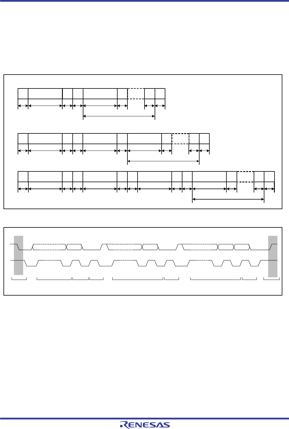
R01UH0034EJ0200 Rev.2.00 Page 1026 of 1489
Dec 27, 2013
RX62T Group, RX62G Group 24. I2C Bus Interface (RIIC)
24.3 Operation
24.3.1 Communication Data Format
The I2C bus format consists of 8-bit data and 1-bit acknowledge. The frame following a start condition or restart
condition is an address frame used to specify a slave device with which the master device communicates. The specified
slave is valid until a new slave is specified or a stop condition is issued.
Figure 24.3 shows the I2C bus format, and Figure 24.4 shows the I2C bus timing.
Figure 24.3 I2C Bus Format
Figure 24.4 I2C Bus Timing (SLA = 7 Bits)
S: Start condition. The master device drives the SDA line low from high level while the SCL line is at a high level.
SLA: Slave address, by which the master device selects a slave device.
R/W#: Indicates the direction of data transfer: from the slave device to the master device when R/W is 1, or from the master
device to the slave device when R/W is 0.
A: Acknowledge. The receive device drives the SDA line low. (In master transmit mode, the slave device returns
acknowledge. In master receive mode, the master device returns acknowledge.)
Sr: Restart condition. The master device drives the SDA line low from the high level after the setup time has elapsed with
the SCL line at the high level.
DATA: Transmitted or received data
P: Stop condition. The master device drives the SDA line high from low level while the SCL line is at a high level.
[7-bit address format]
SR/W# A A A/A# P
S
SLA (7 bits)
W# A A A/A# PSLA (8 bits)11110b+SLA(2 bits)
DATA (8 bits)
A
SW# A A A/A# PSLA (8 bits)11110b+SLA(2 bits) ASr 11110b+SLA(2 bits) R
DATA (8 bits)
1711 1 118
ADATA (8 bits)
1711 1 118
1118
18
1711 181 17 1
[10-bit address format]
n (n = 1 or more)
n (n = 1 or more)
n (n = 1 or more)
n: Number of transfer frames
SSLA R/W# A Data A Data A P
SDA
1 to 7 8 9 1 to 7 8 9 1 to 7 8 9
SCL
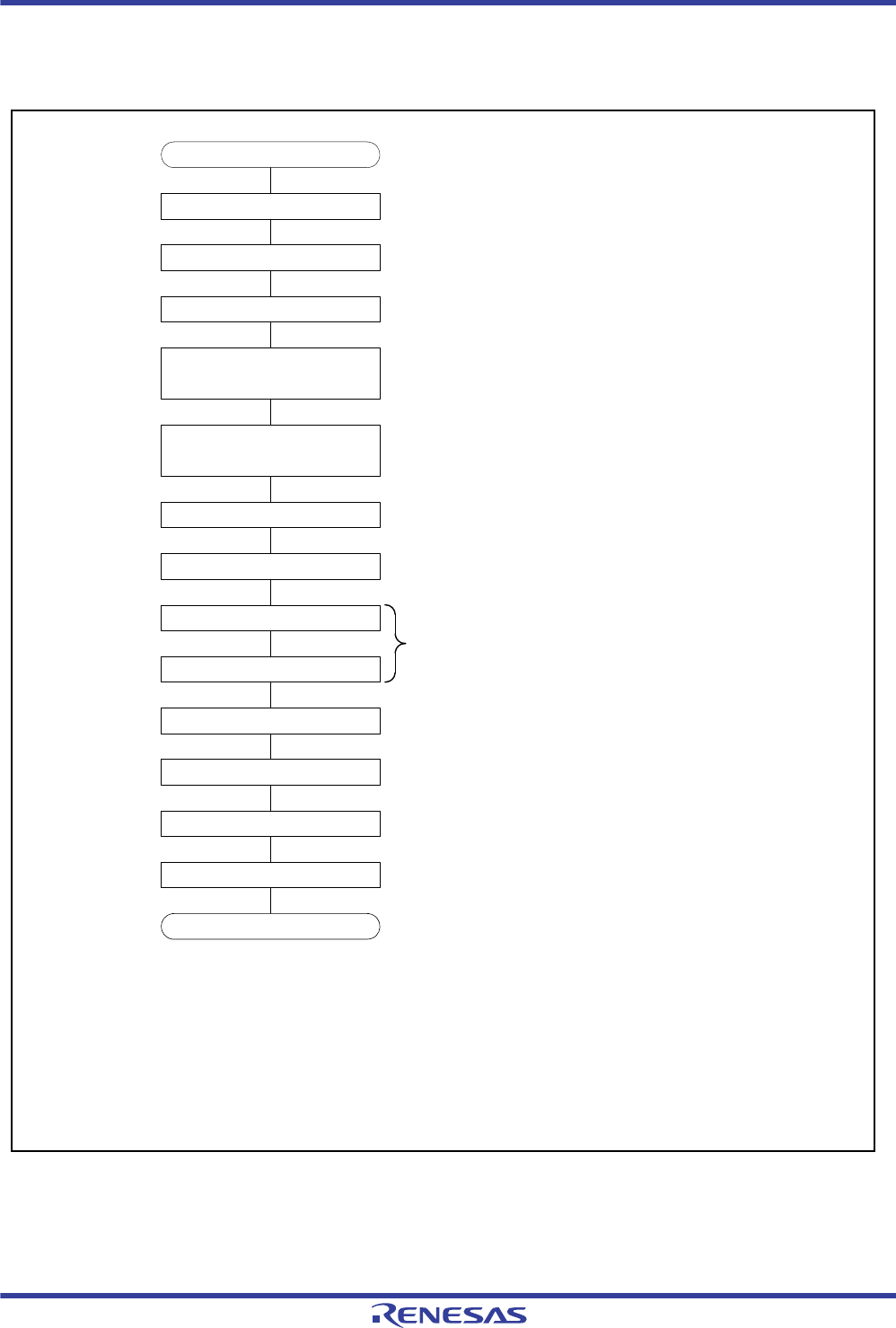
R01UH0034EJ0200 Rev.2.00 Page 1027 of 1489
Dec 27, 2013
RX62T Group, RX62G Group 24. I2C Bus Interface (RIIC)
24.3.2 Initial Settings
Before starting data transmission and reception, initialize the RIIC according to the procedure in Figure 24.5.
Figure 24.5 Example of RIIC Initialization Flow
Set transfer bit rate *1
*2
Initial settings
Set CKS[2:0] in ICMR1 and
ICBRL/ICBRH
Set ICMR2 and ICMR3
Set ICFER
ICCR1.ICE = 0
ICCR1.IICRST = 1
ICCR1.IICRST = 0
RIIC internal reset
Cancel RIIC internal reset
RIIC function disabled
Set SARLn and SARUn.
Set ICSER Set slave address format and slave address
RIIC transfer operation enabled
Set interrupt enable
y = 0 to 2
Set ICIER
ICCR1.IC E = 1
End
Note 1. When the RIIC is used only in slave mode, set the ICBRL register to
a value longer than the data setup time.
Note 2. Set these registers as necessary.
Note 3. These steps need to be included if the timeout function is to be used.
They are not required if the timeout function is not to be used.
Note 4. This is the flow for eight-bit access. If you are using 16-bit access,
set 0000h at the address given under Allocation of Registers for 16-bit Access.
ICMR2.TMWE = 1
ICFER.TMOE = 1
*2
*2
*2
Writing to the timeout internal counter is enabled *3
The timeout function is enabled *3
TMOCNTL = 00h
TMOCNTU = 00h
*2,*4Initialization of the internal timeout counter*3

R01UH0034EJ0200 Rev.2.00 Page 1028 of 1489
Dec 27, 2013
RX62T Group, RX62G Group 24. I2C Bus Interface (RIIC)
24.3.3 Master Transmitter Operation
In master transmitter operation, the RIIC outputs the SCL (clock) and transmitted data signals as the master device, and
the slave device returns acknowledgements. Figure 24.6 shows an example of usage of master transmission and Figure
24.7 to Figure 24.9 show the timing of operations in master transmission.
The following describes the procedure and operations for master transmission.
1. Set the IICRST bit in ICCR1 to 1 (internal reset) and then clear the IICRST bit to 0 (canceling reset) with the ICE
bit in ICCR1 cleared to 0 (disabling the interface). This initializes the internal state and the various flags of ICSR1.
After that, set registers SARLy, SARUy, ICSER, ICMR1, ICBRH, and ICBRL (y = 0 to 2), and set the other
registers as necessary (for initial settings of the RIIC, see Figure 24.5). When the necessary register settings have
been completed, set the ICE bit to 1 (to enable transfer). This step is not necessary if initialization of the RIIC has
already been completed.
2. Read the BBSY flag in ICCR2 to check that the bus is open, and then set the ST bit in ICCR2 to 1 (start condition
issuance request). Upon receiving the request, the RIIC issues a start condition. At the same time, the BBSY flag
and the START flag in ICSR2 are automatically set to 1 and the ST bit is automatically cleared to 0. At this time, if
the start condition is detected and the internal levels for the SDA output state and the levels on the SDA line have
matched while the ST bit is 1, the RIIC recognizes that issuing of the start condition as requested by the ST bit has
been successfully completed, and the MST and TRS bits in ICCR2 are automatically set to 1, placing the RIIC in
master transmitter mode. The TDRE flag in ICSR2 is also automatically set to 1 in response to setting of the TRS bit
to 1.
3. Check that the TDRE flag in ICSR2 is 1, and then write the value for transmission (the slave address and the R/W#
bit) to ICDRT. Once the data for transmission are written to ICDRT, the TDRE flag is automatically cleared to 0,
the data are transferred from ICDRT to ICDRS, and the TDRE flag is again set to 1. After the byte containing the
slave address and R/W# bit has been transmitted, the value of the TRS bit is automatically updated to select master
transmitter or master receiver mode in accord with the value of the transmitted R/W# bit. If the value of the R/W#
bit was 0, the RIIC continues in master transmitter mode.
Since the ICSR2.NACKF flag being 1 at this time indicates that no slave device recognized the address or there was
an error in communications, write 1 to the ICCR2.SP bit to issue a stop condition.
For data transmission with an address in the 10-bit format, start by writing 1111 0b, the two higher-order bits of the
slave address, and W to ICDRT as the first address transmission. Then, as the second address transmission, write the
eight lower-order bits of the slave address to ICDRT.
4. After confirming that the TDRE flag in ICSR2 is 1, write the data for transmission to the ICDRT register. The RIIC
automatically holds the SCL line low until the data for transmission are ready or a stop condition is issued.
5. After all bytes of data for transmission have been written to the ICDRT register, wait until the value of the TEND
flag in ICSR2 returns to 1, and then set the SP bit in ICCR2 to 1 (stop condition issuance request). Upon receiving a
stop condition issuance request, the RIIC issues the stop condition.
6. Upon detecting the stop condition, the RIIC automatically clears the MST and TRS bits in ICCR2 to 00b and enters
slave receiver mode. Furthermore, it automatically clears the TDRE and TEND flags to 0, and sets the STOP flag in
ICSR2 to 1.
7. After checking that the ICSR2.STOP flag is 1, clear the ICSR2.NACKF and STOP flags to 0 for the next transfer
operation.
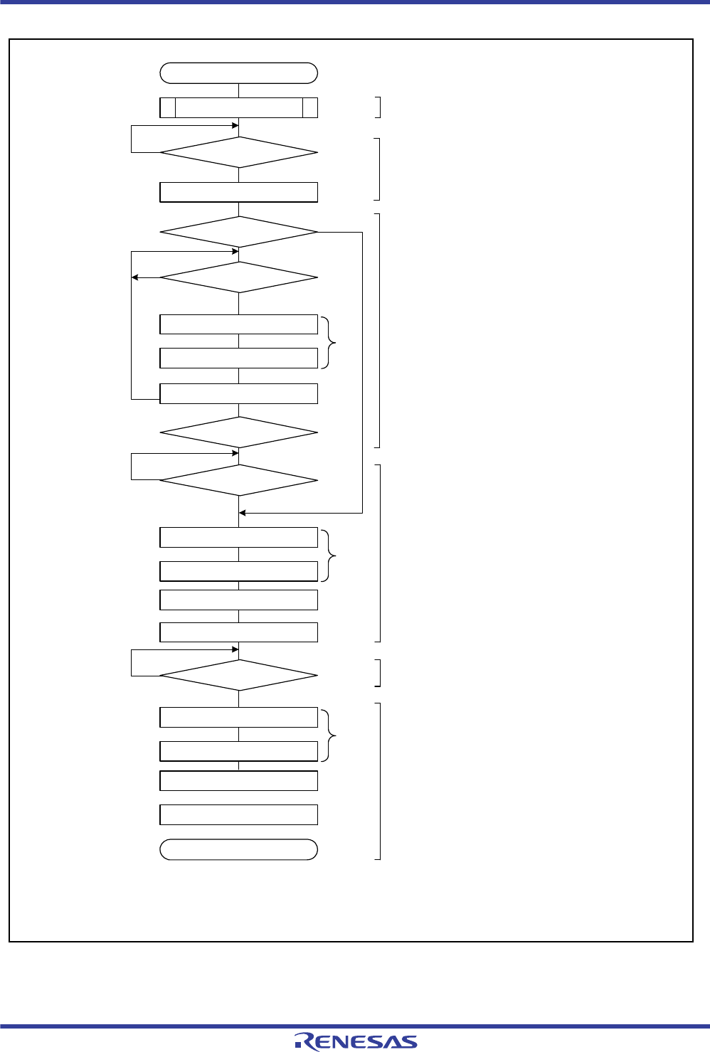
R01UH0034EJ0200 Rev.2.00 Page 1029 of 1489
Dec 27, 2013
RX62T Group, RX62G Group 24. I2C Bus Interface (RIIC)
Figure 24.6 Example of Master Transmission Flowchart
Yes
ICCR2.BBSY = 0?
ICSR2.STOP = 0
Master transmission
ICCR2.SP = 1
ICSR2.NACKF = 0
End of master transmission
ICCR2.ST = 1
Yes
No
ICSR2.TDRE = 1?
Write data to ICDRT
Initial settings
Yes
Yes
All data transmitted?
ICSR2.TEND = 1?
Yes
ICSR2.STOP = 1?
ICSR2.STOP = 0
No
No
No
No
No
[1] Initial settings
[2] Check I2C bus occupation and issue a
start condition.
[6] Check stop condition issuance
[7] Processing for the next transfer operation
Yes
[5] Check end of last data
transmission and issue a stop
condition.
[3] Transmit slave address and W (first byte).
[4] Check ACK and set transmit data.
ICSR2.NACKF = 0?
TMOCNTL = 00h
Note 1. Timeout internal counter clearing.
Those procedures need to be added only when using timeout function. Not needed when not using timeout function.
Note 2. These steps need to be included if the timeout function is to be used.
They are not required if the timeout function is not to be used.
TMOCNTU = 00h
*2,*4
TMOCNTL = 00h
TMOCNTU = 00h
*2,*4
TMOCNTL = 00h
TMOCNTU = 00h
*2,*4
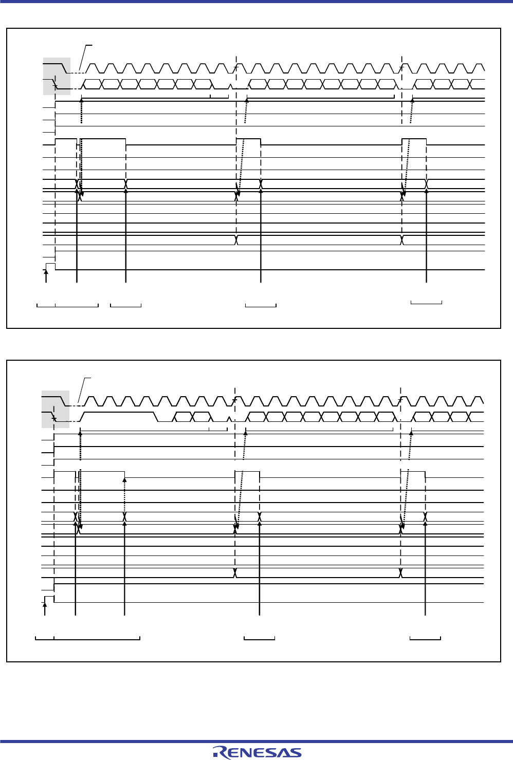
R01UH0034EJ0200 Rev.2.00 Page 1030 of 1489
Dec 27, 2013
RX62T Group, RX62G Group 24. I2C Bus Interface (RIIC)
Figure 24.7 Master Transmit Operation Timing (1) (7-Bit Address Format)
Figure 24.8 Master Transmit Operation Timing (2) (10-Bit Address Format)
Write ICDRT
(7-bit address
+ W)
Write ICDRT
(DATA1) Write ICDRT
(DATA2)
7-bit address + W
Transmit data (DATA1) Transmit data (DATA2)Transmit data (7-bit address + W)
TDRE
MST
TRS
BBSY
TEND
S 9
Write ICDRT
(DATA3)
8
b0
SCL
SDA
ST
START
ICDRT
ICDRS 7-bit address + W
DATA 1
DATA 1
DATA 2 DATA 3
DATA 2
Write 1
to ST
1
b7
7-bit slave address W
2
b6
3
b5
4
b4
5
b3
6
b2
7
b1
2
b6
4
b4
5
b3
6
b2
7
b1
3
b5
8
b0
1
b7
2
b6
4
b4
3
b5
DATA 1 DATA 2
1
b7
RDRF
ICDRR
9
ACKBT
ACKBR
"0" (ACK)
"X" (ACK/NACK)
[3] [4] [4]
[2] [4]
"0" (ACK)
ACK
ACK
"0" (ACK)
XXXX (Initial value/last data for reception)
Automatic low-hold (to prevent wrong transmission)
Transmit data (upper 10 bits + W)
"0" (ACK)
Write ICDRT
(11110b + 2
bits + W)
Write ICDRT
(lower 8 bits) Write ICDRT
(DATA 1) Write ICDRT
(DATA2)
Write 1
to ST
RDRF
ICDRR
TDRE
MST
TRS
BBSY
TEND
S 9
SCL
SDA
ST
START
ICDRT
ICDRS Upper 10 bits + W
Lower 10 bits
Lower 10 bits
DATA 1 DATA 2
DATA 1
Upper 10-bit addresses (11110b + 2 bits) WLower 10-bit addresses
1
b7
2
b6
4
b4
5
b3
6
b2
7
b1
3
b5
8
b0
1
b7
2
b6
4
b4
3
b5
DATA 1
2
b6
3
b5
4
b4
5
b3
6
b2
8
b0
7
b1
1
b7
9
ACKBT
ACKBR
[3] [4] [4][2]
"X" (ACK/NACK)
Transmit data (lower 10 bits)
ACK
Transmit data (DATA1)
ACK
Automatic low-hold (to prevent wrong transmission)
10-bit address + W
"0" (ACK) "0" (ACK)
XXXX (Initial value/last data for reception)
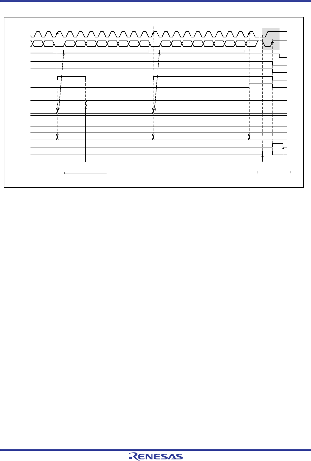
R01UH0034EJ0200 Rev.2.00 Page 1031 of 1489
Dec 27, 2013
RX62T Group, RX62G Group 24. I2C Bus Interface (RIIC)
Figure 24.9 Master Transmit Operation Timing (3)
DATA n-1
DATA n
DATA n
2
b6
4
b4
5
b3
6
b2
7
b1
3
b5
8
b0
1
b7
2
b6
4
b4
5
b3
6
b2
7
b1
3
b5
8
b0
8
b0
1
b7
7
b1
9
DATA n-1
DATA n-1 DATA nDATA n-2
99
XXXX (Initial value/final receive data)
[5]
Write
SP = 1
[4]
Write 0 to
STOP
[7]
P
Write ICDRT
(Final transmit data [DATA n])
"0" (ACK)"0" (ACK)
"0" (ACK)
DATA n-2
TDRE
MST
TRS
BBSY
TEND
SCL
SDA
STOP
ICDRT
ICDRS
SP
RDRF
ICDRR
ACKBT
ACKBR
A/NAACK
"X" (ACK/NACK)
Transmit data (DATA n-1) Transmit data (DATA n)
ACK

R01UH0034EJ0200 Rev.2.00 Page 1032 of 1489
Dec 27, 2013
RX62T Group, RX62G Group 24. I2C Bus Interface (RIIC)
24.3.4 Master Receiver Operation
In master receiver operation, the RIIC as a master device outputs the SCL (clock) signal, receives data from the slave
device, and returns acknowledgements. Since the RIIC must start by sending a slave address to the corresponding slave
device, this part of the procedure is performed in master transmitter mode, but the subsequent steps are in master receiver
mode.
Figure 24.11 shows an example of usage of master reception and Figure 24.12 and Figure 24.14 show the timing of
operations in master reception.
The following describes the procedure and operations for master reception.
1. Set the IICRST bit in ICCR1 to 1 (internal reset) and then clear the IICRST bit to 0 (canceling reset) with the ICE
bit in ICCR1 cleared to 0 (disabling the interface). This initializes the internal state and the various flags of ICSR1.
After that, set registers SARLy, SARUy, ICSER, ICMR1, ICBRH, and ICBRL (y = 0 to 2), and set the other
registers as necessary (for initial settings of the RIIC, see Figure 24.5). When the necessary register settings have
been completed, set the ICE bit to 1 (to enable transfer). This step is not necessary if initialization of the RIIC has
already been completed.
2. Read the BBSY flag in ICCR2 to check that the bus is open, and then set the ST bit in ICCR2 to 1 (start condition
issuance request). Upon receiving the request, the RIIC issues a start condition. When the RIIC detects the start
condition, the BBSY flag and the START flag in ICSR2 are automatically set to 1 and the ST bit is automatically
cleared to 0. At this time, if the start condition is detected and the levels for the SDA output and the levels on the
SDA line have matched while the ST bit is 1, the RIIC recognizes that issuing of the start condition as requested by
the ST bit has been successfully completed, and the MST and TRS bits in ICCR2 are automatically set to 1, placing
the RIIC in master transmitter mode. The TDRE flag in ICSR2 is also automatically set to 1 in response to setting of
the TRS bit to 1.
3. Check that the TDRE flag in ICSR2 is 1, and then write the value for transmission (the first byte indicates the slave
address and value of the R/W# bit) to ICDRT. Once the data for transmission are written to ICDRT, the TDRE flag
is automatically cleared to 0, the data are transferred from ICDRT to ICDRS, and the TDRE flag is again set to 1.
Once the byte containing the slave address and R/W# bit has been transmitted, the value of the ICCR2.TRS bit is
automatically updated to select master transmitter or master receiver mode in accord with the value of the
transmitted R/W# bit. If the value of the R/W# bit was 1, the TRS bit is cleared to 0 on the rising edge of the ninth
cycle of SCL (the clock signal), placing the RIIC in master receiver mode. At this time, the TDRE flag is
automatically cleared to 0 and the ICSR2.RDRF flag is automatically set to 1.
Since the ICSR2.NACKF flag being 1 at this time indicates that no slave device recognized the address or there was
an error in communications, write 1 to the ICCR2.SP bit to issue a stop condition.
For master reception from a device with a 10-bit address, start by using master transmission to issue the 10-bit
address, and then issue a restart condition. After that, transmitting 1111 0b, the two higher-order bits of the slave
address, and the R bit places the RIIC in master receiver mode.
4. Dummy read ICDRR after confirming that the RDRF flag in ICSR2 is 1; this makes the RIIC start output of the
SCL (clock) signal and start data reception.
5. After one byte of data has been received, the RDRF flag in ICSR2 is set to 1 on the rising edge of the eighth or ninth
cycle of SCL clock (the clock signal) as selected by the RDRFS bit in ICMR3. Reading out ICDRR at this time will
produce the received data, and the RDRF flag is automatically cleared to 0 at the same time. Furthermore, the value
of the acknowledgement field received during the ninth cycle of SCL clock is returned as the value set in the
ACKBT bit of ICMR3. Furthermore, if the next byte to be received is the next to last byte, set the ICMR3.WAIT bit
to 1 (for wait insertion) before reading the ICDRR (containing the second byte from last). As well as enabling
NACK output even in the case of delays in processing to set the ICMR3.ACKBT bit to 1 (NACK) in step (6), due to
other interrupts etc., this fixes the SCLn line to the low level on the rising edge of the ninth clock cycle in reception
of the last byte, so the state is such that issuing a stop condition is possible.
6. When the ICMR3.RDRFS bit is 0 and the slave device must be notified that it is to end transfer for data reception
after transfer of the next (final) byte, set the ACKBT bit in ICMR3 to 1 (NACK).

R01UH0034EJ0200 Rev.2.00 Page 1033 of 1489
Dec 27, 2013
RX62T Group, RX62G Group 24. I2C Bus Interface (RIIC)
7. After reading out the byte before last from the ICDRR register, if the value of the ICSR2.RDRF flag is confirmed to
be 1, write 1 to the SP bit in ICCR2 (stop condition issuance request) and then read the last byte from ICDRR. When
ICDRR is read, the RIIC is released from the wait state and issues the stop condition after low-level output in the
ninth clock cycle is completed or the SCL line is released from the low-hold state.
8. Upon detecting the stop condition, the RIIC automatically clears the MST and TRS bits in ICCR2 to "00b" and
enters slave receiver mode. Furthermore, detection of the stop condition leads to setting of the STOP flag in ICSR2
to 1.
9. After checking that the ICSR2.STOP flag is 1, clear the ICSR2.NACKF and STOP flags to 0 for the next transfer
operation.
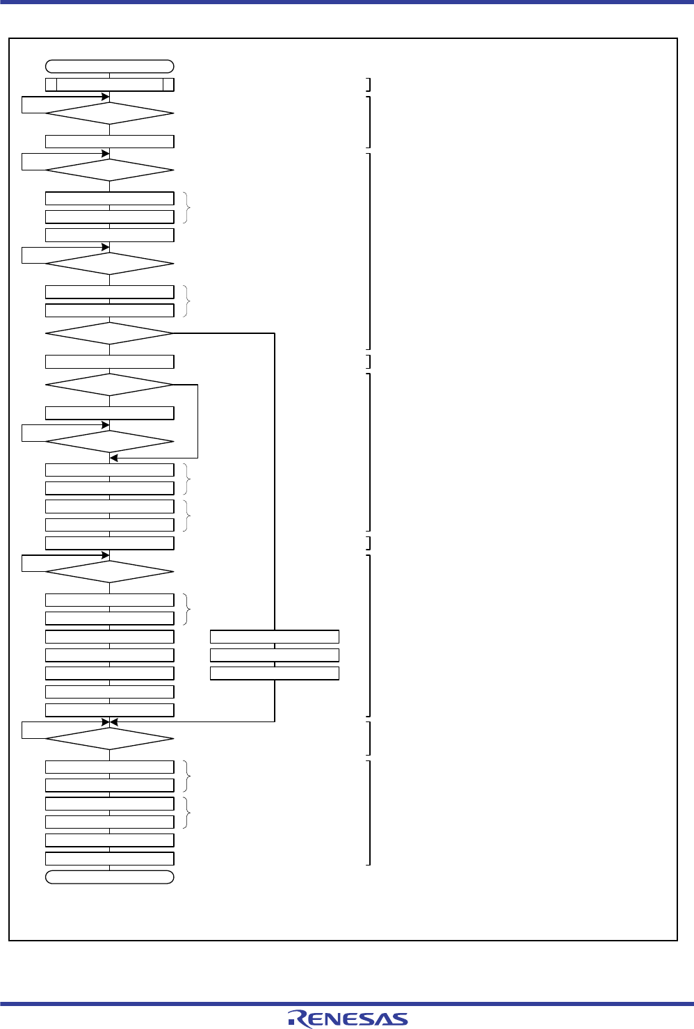
R01UH0034EJ0200 Rev.2.00 Page 1034 of 1489
Dec 27, 2013
RX62T Group, RX62G Group 24. I2C Bus Interface (RIIC)
Figure 24.10 Example of Master Reception Flowchart (7-bit Address Format, 1 or 2 Bytes)
Master reception
Initial settings
ICCR2.BBSY=0?
ICCR2.ST=1
ICSR2.TDRE=1?
Write data to ICDRT
ICSR2.RDRF=1?
ICSR2.NACKF=0?
ICMR3.WAIT=1
Next data = Final byte?
Perform dummy read of ICDRR
ICSR2.RDRF=1?
ICMR3.ACKBT=1
Read ICDRR
ICSR2.RDRF=1?
No
Yes
No
Yes
No
Yes
No
Yes
Yes
No
No
Yes
No
ICSR2.STOP=0
Yes
ICSR2.SP=1
Read ICDRR
ICMR3.WAIT=0
ICSR2.STOP=0
ICSR2.SP=1
Perform dummy read of ICDRR
ICSR2.STOP=1?
No
Yes
ICSR2.NACKF=0
ICSR2.STOP=0
End of master reception
(1) Initial settings
(2) Check I2C bus occupation and issue a start condition
(3) Transmit slave address and R, and check ACK
(4) Set WAIT
(5) Set NACK (perform dummy read if received data is 2 bytes)
(6) Read receive data (perform dummy read if received data is 1 byte)
(7) Read final data, release SCL by setting ACKBT, and
issue a stop condition
(8) Check stop condition issuance
(9) Processing for the next transfer operation
TMOCNTL=00h
TMOCNTU=00h
TMOCNTL=00h
TMOCNTU=00h
TMOCNTL=00h
TMOCNTU=00h
ICMR3.RDRFS=1
TMOCNTL=00h
TMOCNTU=00h
TMOCNTL=00h
TMOCNTU=00h
ICMR3.ACKBT=1
ICMR3.ACKBT=0
ICMR3.RDRFS=0
(*1, *2)
(*1, *2)
(*1, *2)
(*1, *2)
(*1, *2)
(*3)
(*3)
Note 1. These steps need to be included if the timeout function is to be used.
Note 2. Word access as a 16-bit register is also possible.
Note 3. Simultaneous writing is possible.
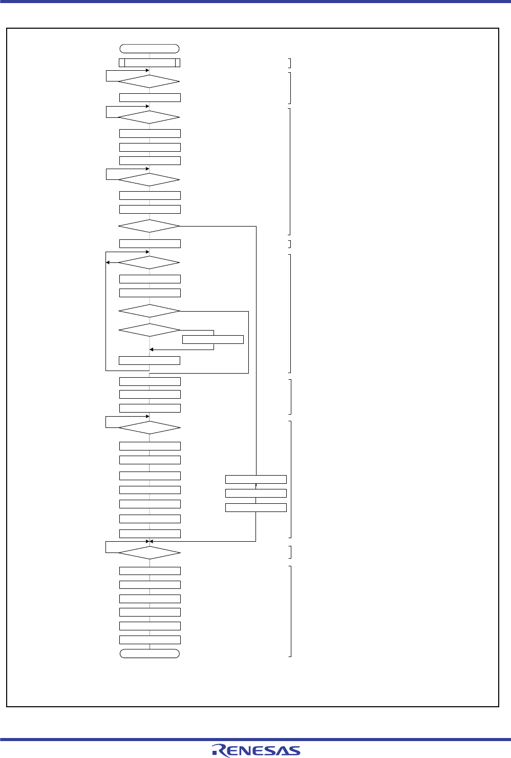
R01UH0034EJ0200 Rev.2.00 Page 1035 of 1489
Dec 27, 2013
RX62T Group, RX62G Group 24. I2C Bus Interface (RIIC)
Figure 24.11 Example of Master Reception Flowchart (7-bit Address Format, 3 Bytes or More)
ICSR2.STOP = 0
ICCR2.SP = 1
Perform dummy read of ICDRR
(3) Transmit slave address and R,
and check ACK
No
Yes
(2) Check I2C bus occupation
and issue a start condition
Yes
Yes
Yes
Master reception
ICCR2.ST = 1
Initial settings
ICCR2.BBSY = 0?
No
Yes
Write data to ICDRT
Yes
No
ICSR2.NACKF = 0?
Yes
Perform dummy read of ICDRR
ICSR2.RDRF = 1?
Yes
Next data = Final byte-1?
No
Read ICDRR
ICMR3.WAIT = 1
ICMR3.RDRFS = 1
Read ICDRR
No
No
ICSR2.STOP = 0
ICCR2.SP = 1
Read ICDRR
ICMR3.WAIT = 0
ICSR2.STOP=1?
No
End of master reception
ICSR2.NACKF = 0
ICSR2.STOP = 0
Yes
(1) Initial settings
(4) Perform dummy read.
(5) Read received data and prepare for
receiving final data.
(6) Change the timing with which RDRF is
set, set non-acknowledgment, and read
the last byte but one.
(7) Read final data and issue a stop condition.
(8) Check stop condition issuance
(9) Processing for the next transfer operation
No
ICSR2.TDRE=1?
ICSR2.RDRF = 1?
ICSR2.RDRF = 1?
Next data = Final byte-2?
No
TMOCNTU = 00h
Note 1. These steps need to be included if the timeout function is to be used.
They are not required if the timeout function is not to be used .
Note 2: This is the flow for eight-bit access. If you are using 16-bit access, set 0000h at the address given under
Allocation of Registers for 16-bit Access.
Note 3. Simultaneous writing is possible.
ICMR3.ACKBT = 1
ICMR3.RDRFS = 0
ICMR3.ACKBT = 0
ICMR3.ACKBT = 1
TMOCNTL = 00h
TMOCNTU = 00h
TMOCNTL = 00h
TMOCNTU = 00h
TMOCNTL = 00h
TMOCNTU = 00h
TMOCNTL = 00h
TMOCNTU = 00h
TMOCNTL = 00h
*1, *2
*1, *2
*3
*3
*1, *2
*1, *2
*1, *2
*1, *2
*1, *2
*1, *2
*1, *2
*1, *2
*1, *2
*1, *2
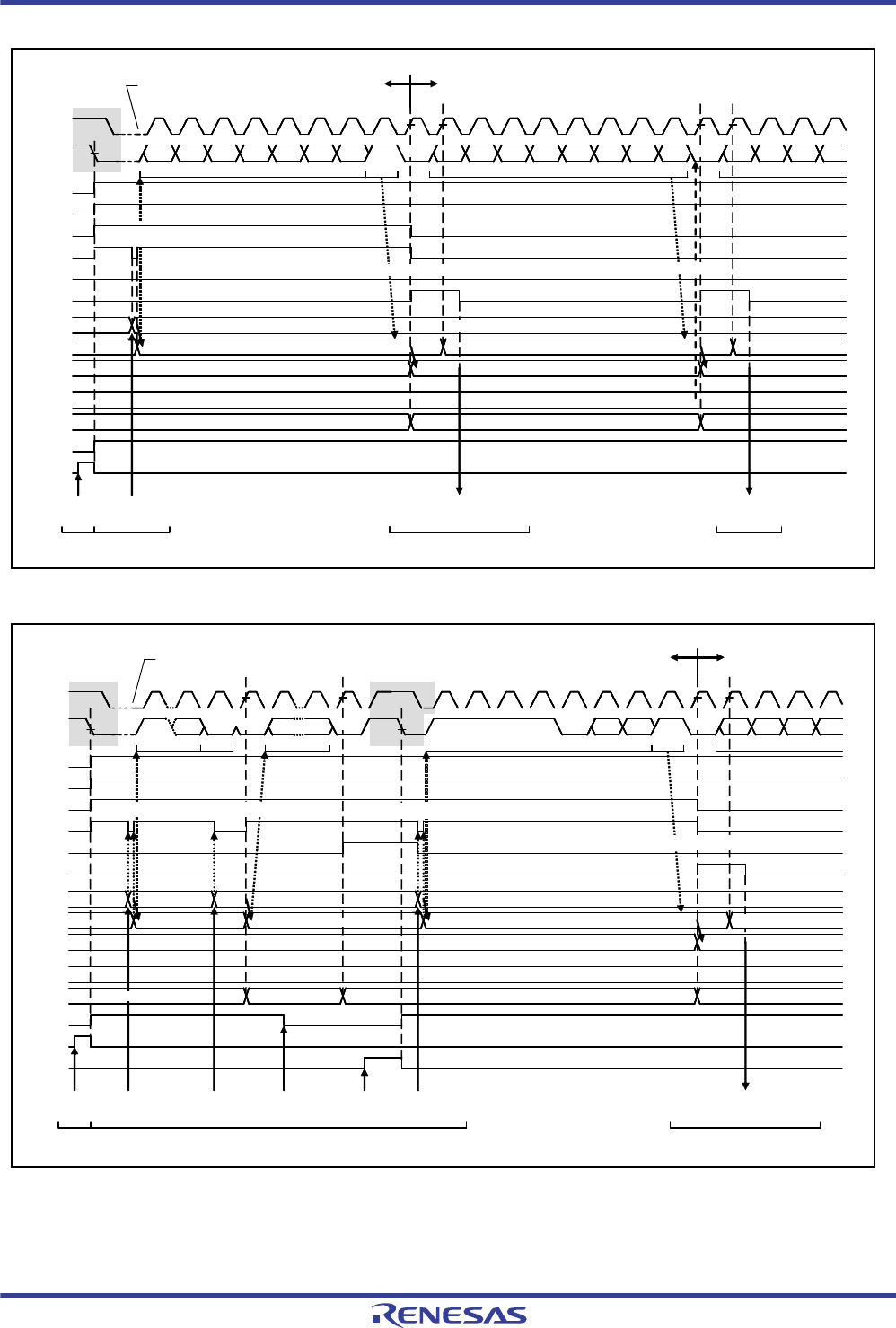
R01UH0034EJ0200 Rev.2.00 Page 1036 of 1489
Dec 27, 2013
RX62T Group, RX62G Group 24. I2C Bus Interface (RIIC)
Figure 24.12 Master Receive Operation Timing (1) (7-Bit Address Format, when RDRFS=0)
Figure 24.13 Master Receive Operation Timing (2) (10-Bit Address Format, when RDRFS=0)
Read ICDRR
(Dummy read)
Read ICDRR
(DATA 1)
Read ICDRT
(7-bit address + R)
Write 1
to ST
"X" (ACK/NACK)
"0" (ACK)
XXXX (Initial value/last data for reception) 7-bit address + R
7-bit address + R
Transmit data (7-bit address + R)
7-bit slave address
Automatic low hold
(error transmission protected)
TDRE
MST
TRS
BBSY
TEND
S 9
SCL
SDA
ST
START
ICDRT
ICDRS XXXX (Initial value/last data for reception) DATA 2
1
b7
R
2
b6
3
b5
4
b4
5
b3
6
b2
7
b1
2
b6
4
b4
5
b3
6
b2
7
b1
3
b5
8
b0
1
b7
2
b6
4
b4
3
b5
DATA 1 DATA 2
1
b7
RDRF
ICDRR DATA 1
98
b0
Master transmit mode Master receive mode
ACKBT
ACKBR
[3] [4] [5][2]
"0" (ACK) "0" (ACK)
ACK
Receive data (7-bit address + R)
7-bit address + R
ACK
Receive data (DATA 1)
Write 1
to ST
Write data to ICDRT
(11110b + 2 bits + R)
"0" (ACK)
XXXX (Initial value/last data for reception) Upper 10 bits + R
Upper 10 bits + R
Upper 10 bits + R
Master transmit mode Master receive mode
Automatic low hold (error transmission protected)
Read ICDRR
(Dummy read)
Upper 10 bits+W
TDRE
MST
TRS
BBSY
TEND
S
SCL
SDA
ST
START
ICDRT
ICDRS
W
7
b1
1
b7
2
b6
4
b4
3
b5
DATA 1
RDRF
ICDRR
Upper 10-bit addresses (11110b + 2 bits) R
98
b0
2
b6
3
b5
4
b4
5
b3
1
b7
6
b2
Sr1 to 8
b7 b0
998
b0
1 to 7
b7 b1
Lower 10 bitsUpper 10 bits
RS
ACKBT
ACKBR
[3] [4][2]
Upper 10 bits+W
Lower 10 bits
"0" (ACK) "0" (ACK)"0" (ACK)
Write 1
to RS
Clear
START to 0
Write data to
ICDRT
(lower 8 bits)
Write data to ICDRT
(11110b + 2 bits + W)
Transmit data (lower 10 bits)Transmit data (upper 10 bits + W) Transmit data (upper 10 bits + R)
Transmit data (upper 10 bits + R)
ACKACKACK
"X" (ACK/NACK)
Lower 10 bits XXXX (Initial value/last data
for reception)
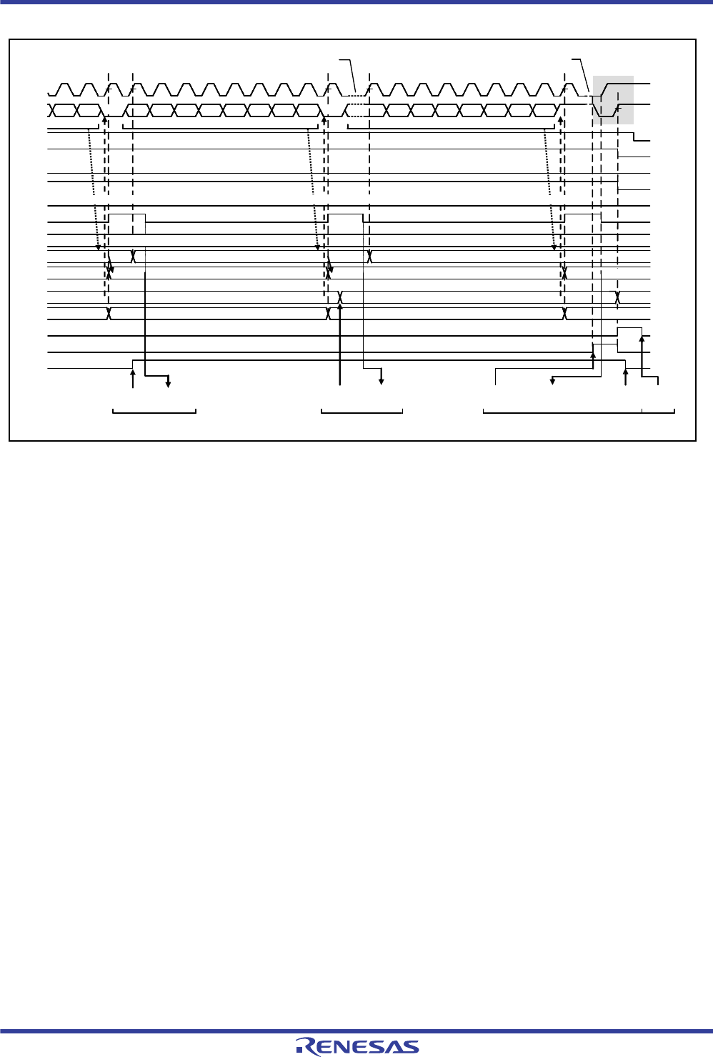
R01UH0034EJ0200 Rev.2.00 Page 1037 of 1489
Dec 27, 2013
RX62T Group, RX62G Group 24. I2C Bus Interface (RIIC)
Figure 24.14 Master Receive Operation Timing (3) (when RDRFS=0)
Clear STOP
to 0
DATA n-1
Automatic low hold (error transmission protected)
Read ICDRR
(last data for reception [DATA n])
"0" (ACK)
9
TDRE
MST
TRS
BBSY
TEND
SCL
SDA
STOP
ICDRT
ICDRS DATA n
2
b6
4
b4
5
b3
6
b2
7
b1
3
b5
8
b0
1
b7
2
b6
4
b4
5
b3
6
b2
7
b1
3
b5
8
b0
8
b0
1
b7
7
b1
DATA n-2
SP
DATA n
DATA n-2
RDRF
ICDRR DATA n-3
WAIT
9
NACK
ACKBT
ACKBR
[6] [7][5]
9 P
[9]
DATA n-1
DATA n-1
DATA n-2
"0" (ACK)"0" (ACK)
"0" (ACK) "1" (NACK)
Clear WAIT
to 0
Write 1
to SP
Write 1
to WAIT Write 1
to ACKBT
Read ICDRR
(DATA n-1)
Read ICDRR
(DATA n-2)
"0"
ACK ACK
Receive data (DATA n-1) Receive data (DATA n)
XXXX (last data for transmission [7-bit addresses + R/Upper 10 bits + R])
Receive data (DATA n-2)
DATA n
"1" (ACK)
Automatic low hold (WAIT)

R01UH0034EJ0200 Rev.2.00 Page 1038 of 1489
Dec 27, 2013
RX62T Group, RX62G Group 24. I2C Bus Interface (RIIC)
24.3.5 Slave Transmitter Operation
In slave transmitter operation, the master device outputs the SCL (clock) signal, the RIIC transmits data as a slave
device, and the master device returns acknowledgements.
Figure 24.15 shows an example of usage of slave transmission and Figure 24.16 and Figure 24.17 show the timing of
operations in slave transmission.
The following describes the procedure and operations for slave transmission.
1. Follow the procedure in Figure 24.5 to make initial settings for the RIIC. This step is not necessary if initialization
of the RIIC has already been completed. After initial settings, the RIIC will stay in the standby state until it receives
a slave address that it matches.
2. After receiving a matching slave address, the RIIC sets one of the corresponding bits ICSR1.HOA, GCA, and AASy
(y = 0 to 2) to 1 on the rising edge of the ninth cycle of SCL clock (the clock signal) and outputs the value set in the
ICMR3.ACKBT bit to the acknowledge bit on the ninth cycle of SCL clock. If the value of the R/W# bit that was
also received at this time is 1, the RIIC automatically places itself in slave transmitter mode by setting both the TRS
bit and the TDRE flag in ICSR2 to 1.
3. After the ICSR2.TEND flag is confirmed to be 1, write the data for transmission to the ICDRT register. At this time,
if the RIIC receives no acknowledge from the master device (receives an NACK signal) while the ICFER.NACKE
bit is 1, the RIIC suspends transfer of the next data.
4. Wait unit the ICSR2.TEND flag is set to 1 while the ICSR2.TDRE flag is 1, after the ICSR2.NACKF flag is set to
1or the last byte for transmission is written to the ICDRT register. When the ICSR2.NACKF flag or the TEND flag
is 1, the RIIC drives the SCL line low on the ninth falling edge of SCL clock.
5. When the ICSR2.NACKF flag or the ICSR2.TEND flag is 1, dummy read ICDRR to complete the processing. This
releases the SCL line.
6. Upon detecting the stop condition, the RIIC automatically clears bits ICSR1.HOA, GCA, and AASy (y = 0 to 2),
flags ICSR2.TDRE and TEND, and the ICCR2.TRS bit to 0, and enters slave receiver mode.
7. After checking that the ICSR2.STOP flag is 1, clear the ICSR2.NACKF and STOP flags to 0 for the next transfer
operation.
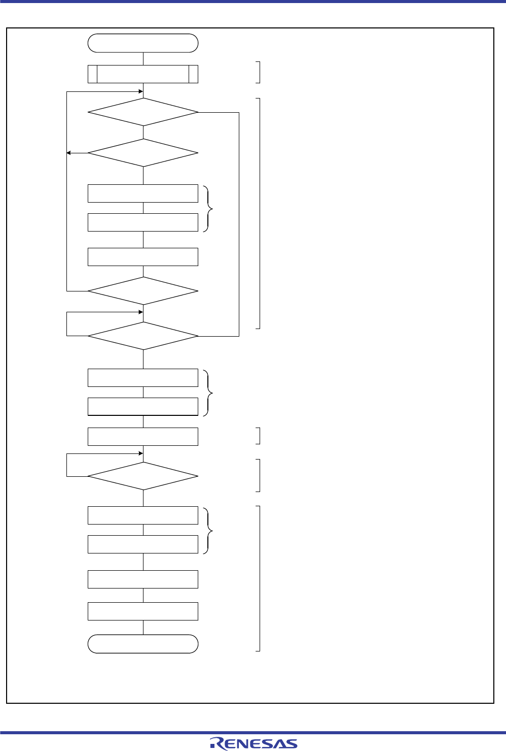
R01UH0034EJ0200 Rev.2.00 Page 1039 of 1489
Dec 27, 2013
RX62T Group, RX62G Group 24. I2C Bus Interface (RIIC)
Figure 24.15 Example of Slave Transmission Flowchart
Read ICDRR
Slave transmission
ICSR2.NACKF = 0
End of slave transmission
Yes
No
ICSR2.NACKF = 0?
ICSR2.TDRE = 1?
Write data to ICDRT
Yes
Yes
All data transmitted?
Yes
ICSR2.STOP = 0
No
No
No
No
[1] Initial settings
[2], [3] Check ACK and set transmit data
(Checking of ACK not necessary immediately after
address is received)
[5] Check stop condition detection
Yes
[4] Dummy read to release the SCL
[6] Processing for the next transfer operation.
Initial settings
ICSR2.TEND = 1?
ICSR2.STOP = 1?
Note1: These steps need to be included if the timeout function is to be used.
They are not required if the timeout function is not to be used.
Note2: This is the flow for eight-bit access. If you are using 16-bit access, set 0000h at the address given under
Allocation of Registers for 16-bit Access.
TMOCNTL = 00h
TMOCNTU = 00h
*2,*4
TMOCNTL = 00h
TMOCNTU = 00h
*2,*4
TMOCNTL = 00h
TMOCNTU = 00h
*2,*4
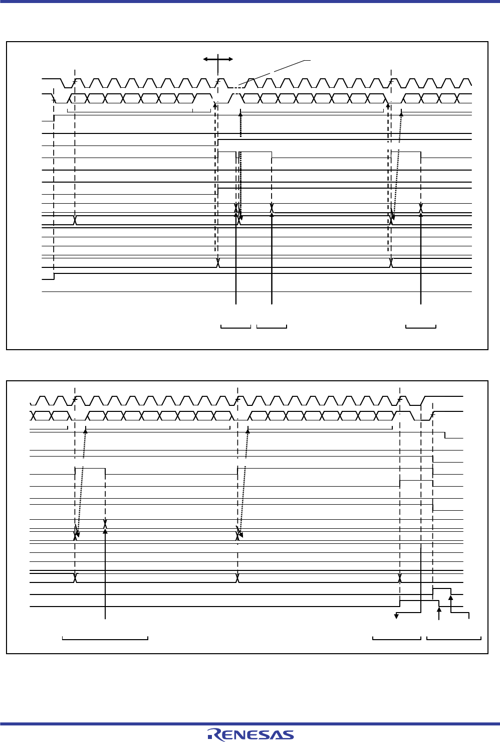
R01UH0034EJ0200 Rev.2.00 Page 1040 of 1489
Dec 27, 2013
RX62T Group, RX62G Group 24. I2C Bus Interface (RIIC)
Figure 24.16 Slave Transmit Operation Timing (1) (7-Bit Address Format)
Figure 24.17 Slave Transmit Operation Timing (2)
Automatic low hold (error transmission protected)
"0" (ACK)
Write data to
ICDRT
(DATA1)
TDRE
MST
TRS
BBSY
TEND
S 9
SCL
SDA
NACKF
START
ICDRT
ICDRS
DATA 2 DATA 3
DATA 2
7-bit slave address R
2
b6
3
b5
4
b4
5
b3
6
b2
7
b1
2
b6
4
b4
5
b3
6
b2
7
b1
3
b5
8
b0
1
b7
2
b6
4
b4
3
b5
DATA 1 DATA 2
RDRF
ICDRR
ACKBT
ACKBR
[3] [3]
1
b7
98
b0
DATA 1
DATA 1
[3]
1
b7
Slave receive mode Slave transmit mode
AASy
Transmit data (DATA 1)
XXXX (Initial value/last data for reception)
7-bit address + R
XXXX (Initial value/last data for reception)
"0" (ACK)
"X" (ACK/NACK) "0" (ACK)
Write data to
ICDRT
(DATA2)
Write data to
ICDRT
(DATA3)
ACKACK
Transmit data (DATA 2)
"0" (ACK)
TDRE
MST
TRS
BBSY
TEND
SCL
SDA
STOP
ICDRT
ICDRS
DATA n
DATA n
2
b6
4
b4
5
b3
6
b2
7
b1
3
b5
8
b0
1
b7
2
b6
4
b4
5
b3
6
b2
7
b1
3
b5
8
b0
8
b0
1
b7
7
b1
DATA n-1
DATA n-1 DATA nDATA n-2
RDRF
ICDRR
99
ACKBT
ACKBR
[5][4]
NACKF
9 P
[7]
AASy
DATA n-2 DATA n-1
"0" (ACK)
"0" (ACK) "1" (NACK)
Dummy read ICDRR
(SCLn line is released)
Write data to ICDRT
(Last data for transmission [DATA n])
Write 0 to
STOP
Write 0 to
NACKF
ACK ACK NACK
XXXX (Initial value/last data for reception)
Transmit data (DATA n-1) Transmit data (DATA n)

R01UH0034EJ0200 Rev.2.00 Page 1041 of 1489
Dec 27, 2013
RX62T Group, RX62G Group 24. I2C Bus Interface (RIIC)
24.3.6 Slave Receiver Operation
In slave receiver operation, the master device outputs the SCL clock and data, and the RIIC returns acknowledgements as
a slave device.
Figure 24.18 shows an example of usage of slave reception and Figure 24.20 and Figure 24.20 show the timing of
operations in slave reception.
The following describes the procedure and operations for slave reception.
1. Follow the procedure in Figure 24.5 to make initial settings for the RIIC. This step is not necessary if initialization
of the RIIC has already been completed. After initial settings, the RIIC will stay in the standby state until it receives
a slave address that it matches.
2. After receiving a matching slave address, the RIIC sets one of the corresponding bits ICSR1.HOA, GCA, and AASy
(y = 0 to 2) to 1 on the rising edge of the ninth cycle of SCL clock (the clock signal) and outputs the value set in the
ICMR3.ACKBT bit to the acknowledge bit on the ninth cycle of SCL clock. If the value of the R/W# bit that was
also received at this time is 1, the RIIC continues to place itself in slave receiver mode and sets the RDRF flag in
ICSR2 to 1.
3. After the ICSR2.STOP flag is confirmed to be 0 and the ICSR2.RDRF flag to be 1, dummy read ICDRR (the
dummy value consists of the slave address and R/W# bit when the 7-bit address format is selected, or the lower
eight bits when the 10-bit address format is selected).
4. When ICDRR is read, the RIIC automatically clears the ICSR2.RDRF flag to 0. If reading of ICDRR is delayed and
a next byte is received while the RDRF flag is still set to 1, the RIIC holds the SCL line low from one SCL cycle
before the timing with which RDRF should be set. In this case, reading ICDRR releases the SCL line from being
held at the low level.
When the ICSR2.STOP flag is 1 and the ICSR2.RDRF flag is also 1, read ICDRR until all the data is completely
received.
5. Upon detecting the stop condition, the RIIC automatically clears bits ICSR1.HOA, GCA, and AASy (y = 0 to 2) to
0.
6. After checking that the ICSR2.STOP flag is 1, clear the ICSR2. STOP flag to 0 for the next transfer operation.
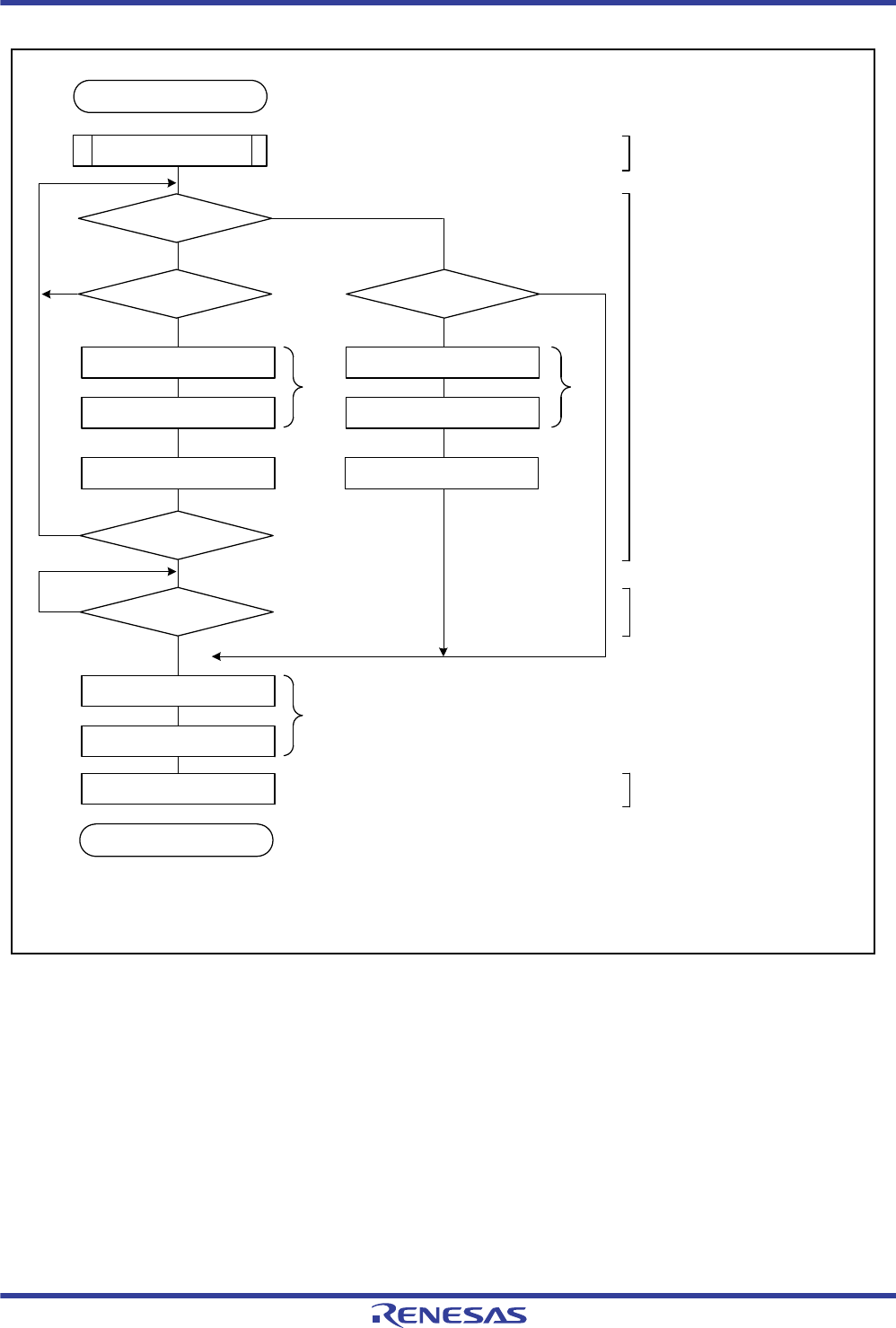
R01UH0034EJ0200 Rev.2.00 Page 1042 of 1489
Dec 27, 2013
RX62T Group, RX62G Group 24. I2C Bus Interface (RIIC)
Figure 24.18 Example of Slave Reception Flowchart
Slave reception
Initial settings
[2], [3], [4] Read receive data
(Dummy read first)
No
Yes
No
ICSR2.STOP = 0?
Yes
ICSR2.RDRF = 1?
Yes
Read ICDRR
All data received?
No
End of slave reception
ICSR2.STOP = 0
Yes
ICSR2.RDRF = 1?
ICSR2.STOP = 1?
No
Yes
Read ICDRR (last data)
[1] Initial settings
[6] Processing for the next transfer
[5] Check stop condition detection
Yes
No
Note1: These steps need to be included if the timeout function is to be used.
They are not required if the timeout function is not to be used.
Note2: This is the flow for eight-bit access. If you are using 16-bit access, set
0000h at the address given under Allocation of Registers for 16-bit Access.
TMOCNTU = 00h
TMOCNTL = 00h
*1,*2
TMOCNTU = 00h
TMOCNTL = 00h
*1,*2
TMOCNTU = 00h
TMOCNTL = 00h
*1,*2
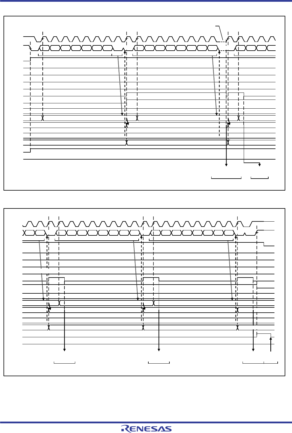
R01UH0034EJ0200 Rev.2.00 Page 1043 of 1489
Dec 27, 2013
RX62T Group, RX62G Group 24. I2C Bus Interface (RIIC)
Figure 24.19 Slave Receive Operation Timing (1) (7-Bit Address Format, when RDRFS=0)
Figure 24.20 Slave Receive Operation Timing (2) (when RDRFS=0)
7-bit address + W
Read ICDRR
(Dummy read
[7-bit address + W])
Automatic low hold
(error transmission protected)
7-bit slave address
"X" (ACK/NACK)
XXXX (Initial value/last data for reception)
"0" (ACK)
9
TDRE
MST
TRS
BBSY
TEND
S
SCL
SDA
NACKF
START
ICDRT
ICDRS DATA 2
W
2
b6
3
b5
4
b4
5
b3
6
b2
7
b1
2
b6
4
b4
5
b3
6
b2
7
b1
3
b5
8
b0
1
b7
2
b6
4
b4
3
b5
DATA 1 DATA 2
RDRF
ICDRR
ACKBT
ACKBR
[3]
1
b7
DATA 1
[3][4]
8
b0
9 1
b7
DATA 1
AASy
Receive data (7-bit address + W) Receive data (DATA 1)
XXXX (Initial value/last data for transmission)
7-bit address + W
"0" (ACK)
"0" (ACK)
Read ICDRR
(DATA 1)
ACKACK
XXXX (Initial value/last data for transmission)
"0"(ACK)
Read ICDRR
(DATA n-2)
TDRE
MST
TRS
BBSY
TEND
SCL
SDA
STOP
ICDRT
ICDRS DATA n
2
b6
4
b4
5
b3
6
b2
7
b1
3
b5
8
b0
1
b7
2
b6
4
b4
5
b3
6
b2
7
b1
3
b5
8
b0
8
b0
1
b7
7
b1
DATA n-1 DATA nDATA n-2
RDRF
ICDRR
99
ACKBT
ACKBR
[3] [4]
NACKF
AASy
9 P
[3] [4] [3] [4] [6]
Receive data (DATA n)Receive data (DATA n-1)
DATA n-2 DATA n-1
DATA n-1DATA n-3 DATA n-2
"0" (ACK)
"0" (ACK)
Read ICDRR
(DATA n-1) Read ICDRR
(DATA n) Write 0 to
STOP
Receive data (DATA n-2)
ACK ACK ACK
"0" (ACK)
DATA n
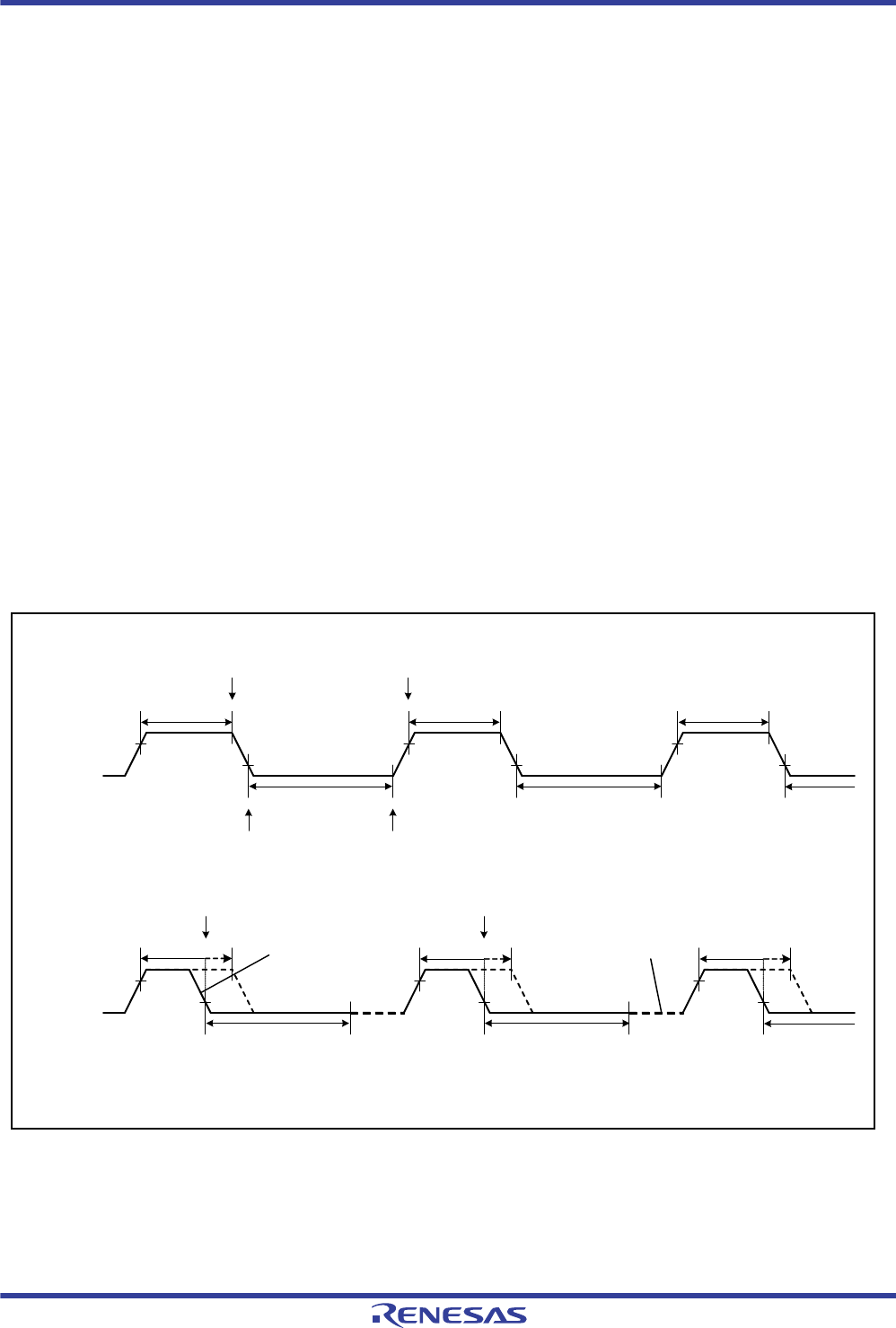
R01UH0034EJ0200 Rev.2.00 Page 1044 of 1489
Dec 27, 2013
RX62T Group, RX62G Group 24. I2C Bus Interface (RIIC)
24.4 SCL Synchronization Circuit
In generation of the SCL (clock) signal, the RIIC starts counting out the value for width at high level specified in ICBRH
when it detects a rising edge on the SCL line and drives the SCL line low once counting of the width at high level is
complete. When the RIIC detects the falling edge of the SCL line, it starts counting out the width at low level period
specified in ICBRL, and then stops driving the SCL line (releases the line) once counting of the width at low level is
complete. The SCL (clock) signal is thus generated.
If multiple master devices are connected to the I2C bus, a collision of SCL signals may arise due to contention with
another master device. In such cases, the master devices have to synchronize their SCL signals. Since this
synchronization of SCL signals must be bit by bit, the RIIC is equipped with a facility (the SCL synchronization circuit)
to obtain bit-by-bit synchronization of the SCL clock signals by monitoring the SCL line while in master mode.
When the RIIC has detected a rising edge on the SCL line and thus started counting out the width at high level specified
in ICBRH, and the level on the SCL line falls because an SCL signal is being generated by another master device, the
RIIC stops counting when it detects the falling edge, drives the level on the SCL line low, and starts counting out the
width at low level specified in ICBRL. When the RIIC finishes counting out the width at low level, it stops driving the
SCL line to the low level (i.e. releases the line). At this time, if the width at low level of the SCL clock signal from the
other master device is longer than the width at low level set in the RIIC, the width at low level of the SCL signal will be
extended. Once the width at low level for the other master device has ended, the SCL signal rises because the SCL line
has been released. When the RIIC finishes outputting the low-level period of the SCL clock of, the SCL line is released
and the SCL clock rises. That is, in cases of contention of SCL signals from more than one master, the width at high level
of the SCL signal is synchronized with that of the clock having the narrower width, and the width at low level of the SCL
signal is synchronized with that of the clock having the broader width. However, such synchronization of the SCL signal
is only enabled when the SCLE bit in ICFER is set to 1.
Figure 24.21 Generation and Synchronization of the SCL Signal from the RIIC
ICBRH
ICBRL
SCL
ICBRL
ICBRH ICBRH
ICBRL
SCL
[SCL clock generation]
Compare match
(Counter clear, low-drive start)
ICBRH
ICBRL
Counter clearCounter clear
ICBRH
ICBRH
ICBRL
[Legend]
ICBRH: I2C bus bit rate high-level register (SCL clock high-level period counter)
ICBRL: I2C bus bit rate low-level register (SCL clock low-level period counter)
[SCL synchronization]
Rising of SCL detected
(High-level period count start)
Compare match generated
(Counter clear, SCL line released)
Falling of SCL detected
(Low-level period count start)
Low-level output of
other master device Low-level output of
other master device
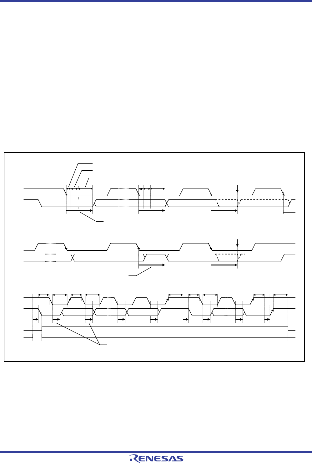
R01UH0034EJ0200 Rev.2.00 Page 1045 of 1489
Dec 27, 2013
RX62T Group, RX62G Group 24. I2C Bus Interface (RIIC)
24.5 Facility for Delaying SDA Output
The RIIC module incorporates a facility for delaying output on the SDA line. The delay can be applied to all output
(issuing of the start, restart, and stop conditions, data, and the ACK and NACK signals) on the SDA line.
With the SDA output delay facility, SDA output is delayed from detection of a falling edge of the SCL signal to ensure
that the SDA signal is output within the interval over which the SCL (clock) signal is at the low level. Doing this leads to
usage with the aim of preventing erroneous operation of communications devices, with the aim of satisfying the 300-ns
(min.) data-hold time requirement of the SMBus specification.
The output delay facility is enabled by setting the SDDL[2:0] bits in IMCR2 to any value other than 000b, and disabled
by setting the same bits to 000b.
While the SDA output delay facility is enabled (i.e. while the SDDL[2:0] bits in IMCR2 are set to any value other than
000b), the DLCS bit in IMCR2 selects the clock source for counting by the SDA output delay counter as the internal base
clock (IIC) for the RIIC module or as a clock signal derived by dividing the frequency of the internal base clock by two
(IIC/2). The counter counts the number of cycles set in the SDDL[2:0] bits in IMCR2. After counting of the set number
of cycles of delay is completed, the RIIC module places the required output (start, restart, or stop condition, data, or an
ACK or NACK signal) on the SDA line.
Figure 24.22 SDA Output Delay Facility
SDA output delay
b6 to b0
1 to 9
SDA output delay
b7 to b1
1 to 7 SDA output release timing
Mater mode
Receive mode
SCL
SDA
ST RS SP1 2 to 8 9
ICBRH ICBRL ICBRH ICBRL
ICBRH
ACK/NACKb7
ST
BBSY
Note: * The output delay facility is set by the DLCS, and SDDL[2:0] bits when a start (ST),
restart (RS), or stop (SP) condition is issued.
SCL
SDA
8
b7 to b1
SCL
SDA
89
b0
S 9
P
Transmit mode
SDA output delay
ACK/NACK
b0
SDA output release timing
*
ACK/NACK
ICBRL ICBRH ICBRLICBRL
*
Analog noise filter delay time + PCLK sampling error (1 PCLK (max))
Digital noise filter delay time (NFE, NF[1:0] settings = 0.5 PCLK (min), 1 IIC to 4 IIC (max))
SDA output delay time (DLCS,SDDL[2:0] settings = 0 (min) to 14 IIC (max))
*
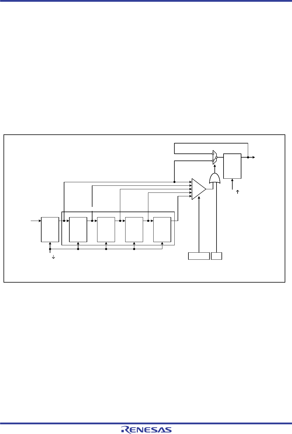
R01UH0034EJ0200 Rev.2.00 Page 1046 of 1489
Dec 27, 2013
RX62T Group, RX62G Group 24. I2C Bus Interface (RIIC)
24.6 Digital Noise-Filter Circuits
The states of the SCL and SDA pins are conveyed to the internal circuitry through analog noise-filter and digital noise-
filter circuits. Figure 24.23 is a block diagram of the digital noise-filter circuit.
The on-chip digital noise-filter circuit of the RIIC consists of four flip-flop circuit stages connected in series and a match-
detection circuit.
The number of effective stages in the digital noise filter is selected by the NF[1:0] bits in ICMR3. The selected number
of effective stages determines the noise-filtering capability as a period from one to four IIC cycles.
The input signal to the SCL pin (or SDA pin) is sampled on falling edges of the PCLK signal. When the input signal level
matches the output level of the number of effective flip-flop circuit stages as selected by the NF[1:0] bits in ICMR3, the
signal level is conveyed to the subsequent stage. If the signal levels do not match, the previous value is retained.
If the ratio between the frequency of the internal operating clock (PCLK) and the transfer rate is small (e.g. data transfer
at 400 kbps with PCLK = 4 MHz), the characteristics of the digital noise filter may lead to the elimination of needed
signals as noise. In such cases, it is possible to disable the digital noise-filter circuit (by clearing the NFE bit in ICFER)
and use only the analog noise-filter circuit.
Figure 24.23 Block Diagram of Digital Noise Filter Circuit
Mismatch
Match
DQ
CLK
DQ
CLK
DQ
CLK
DQ
CLK
NFE
SCL/SDA
input signal
IICNF[1:0]
Compa-
rator
DQ
CLK
DQ
CLK
Four-stage digital noise filter
SCL/SDA
internal signal
PCLK
[Legend]
NFE: Digital noise filter circuit enable bit
NF[1:0]: Digital noise filter stage selection bits
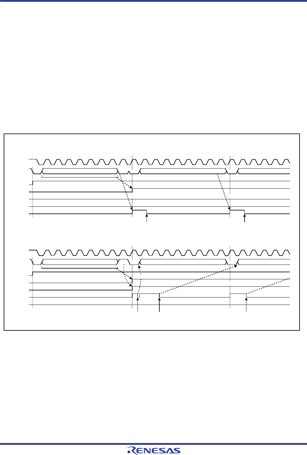
R01UH0034EJ0200 Rev.2.00 Page 1047 of 1489
Dec 27, 2013
RX62T Group, RX62G Group 24. I2C Bus Interface (RIIC)
24.7 Address Match Detection
The RIIC can set three unique slave addresses in addition to the general call address and host address, and also can set 7-
bit or 10-bit slave addresses.
24.7.1 Slave-Address Match Detection
The RIIC can set three unique slave addresses, and has a slave address detection function for each unique slave address.
When the SARyE bit (y = 0 to 2) in ICSER is set to 1, the slave addresses set in SARUy and SARLy (y = 0 to 2) can be
detected.
When the RIIC detects a match of the set slave address, the corresponding AASy flag (y = 0 to 2) in ICSR1 is set to 1 at
the rising edge of the ninth SCL clock cycle, and the RDRF flag in ICSR2 or the TDRE flag in ICSR2 is set to 1 by the
following R/W# bit. This causes a receive data full interrupt (ICRXI) or transmit data empty interrupt (ICTXI) to be
generated. The AASy flag is used to identify which slave address has been specified.
Figure 24.24 to Figure 24.26 show the AASy (y = 0 to 2) flag set timing in three cases.
Figure 24.24 AASy Flag Set Timing with 7-Bit Address Format Selected
TDRE
AASy
S1234567
7-bit slave address
8
W
1
8
R
9
ACK
TRS
9
ACK
BBSY
TDRE
AASy
TRS
BBSY
RDRF
RDRF
234567
Data (DATA1)
8 9
ACK
S 1 234567
12345
234567 8 9
ACK
1
Read ICDRR
(Dummy read [7-bit address])
Address match
[7-bit address format: Slave reception]
SCL
SDA
SCL
SDA
12345
[7-bit address format: Slave transmission]
7-bit slave address
Data (DATA2)
Data (DATA1) Data (DATA2)
Receive data (7-bit address) Receive data (DATA1)
Read ICDRR
(DATA1)
Write data to ICDRT
(DATA3)
Write data to ICDRT
(DATA1)
Write data to ICDRT
(DATA2)
Transmit data (DATA2)Transmit data (DATA1)
Address match
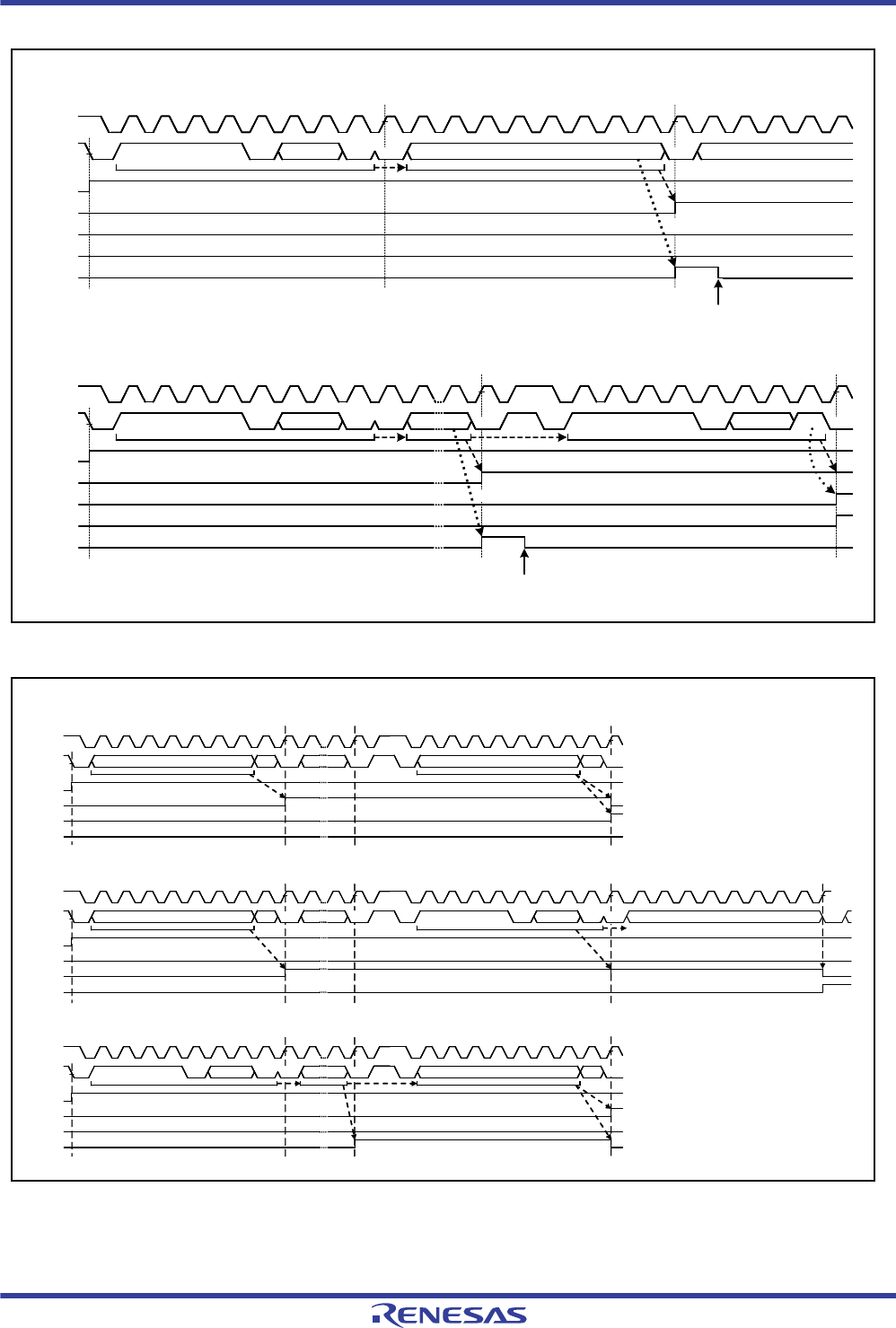
R01UH0034EJ0200 Rev.2.00 Page 1048 of 1489
Dec 27, 2013
RX62T Group, RX62G Group 24. I2C Bus Interface (RIIC)
Figure 24.25 AASy Flag Set Timing with 10-Bit Address Format Selected
Figure 24.26 AASy Flag Set/Clear Timing with 7-Bit/10-Bit Address Formats Mixed
Read ICDRR
(Dummy read [lower addresses])
Address match
TDRE
AASy
S1
1
8
W
1
8
R
9
ACK
TRS
9
ACK
BBSY
TDRE
AASy
TRS
BBSY
RDRF
RDRF
234567 8 9
ACK
S
12345
Data
Address match
234567
1110
1
1
8
W
9
ACK
234567
1110
1
1
234567
1110
9
ACK
Sr1 to 8
[10-bit address format: Slave reception]
[10-bit address format: Slave transmission]
SCL
SDA
SCL
SDA
10-bit slave address (lower 8 bits)
Upper 2 bits
Read ICDRR
(Dummy read [lower addresses])
Receive data (lower addresses)
Upper 2 bits Lower 8 bits Upper 2 bits
Receive data (lower addresses)
ACK
Upper 2 bits
[In the case of SAR0L: 7-bit address, SAR1L: 7-bit address, SAR2: 10-bit address]
[In the case of SAR0L: 7-bit address, SAR1L: 7-bit address, SAR2: 10-bit address]
Address match
AAS1
AAS2
AAS0
BBSY
1 W11 10 Lower 8 bits R/W
Address
match
AAS1
AAS2
AAS0
BBSY
Address match
SCL
SDA
SCL
SDA W
DATA 11110R/W
AAS1
AAS2
AAS0
BBSY
S
7-bit slave address (SAR0L)
[In the case of SAR0L: 7-bit address, SAR1L: 7-bit address, SAR2: 10-bit address]
Address
mismatch
Address
match
SCL
SDA DATA
R/W 7-bit slave address (SAR1L) R/W
Address match
Address
mismatch
S9Sr23456711 8 98 34567 981 2
to
S9Sr23456711 8 98 34567 981 2
to
S9Sr23456711 8 98 34567 981 2
to
7-bit slave address (SAR1L)
Upper 2 bits 7-bit slave address (SAR0L)
ACK ACK
ACK ACK
ACK
ACK
ACK ACK ACK
10-bit slave address (Lower 8 bits)
234567198

R01UH0034EJ0200 Rev.2.00 Page 1049 of 1489
Dec 27, 2013
RX62T Group, RX62G Group 24. I2C Bus Interface (RIIC)
24.7.2 Detection of the General Call Address
The RIIC has a facility for detecting the general call address (0000 000b + 0 [W]). This is enabled by setting the GCAE
bit in ICSER to 1.
If the address received after a start or restart condition is issued is 0000 000b + 1[R] (start byte), the RIIC recognizes this
as the address of a slave device with an "all-zero" address but not as the general call address.
When the RIIC detects the general call address, both the GCA flag in ICSR1 and the RDRF flag in ICSR2 are set to 1 on
the rising edge of the ninth cycle of SCL clock. This leads to the generation of a receive data full interrupt (ICRXI). The
value of the GCA flag can be confirmed to recognize that the general call address has been transmitted.
Operation after detection of the general call address is the same as normal slave receive operation.
Figure 24.27 Timing of GCA Flag Setting during Reception of General Call Address
AAS2
AAS0
S234567
000000
1
AAS1
9
ACK
BBSY
RDRF
234567 8 9
ACK
1
General call address match (0000 000b + W)
[General call address reception]
1
0
GCA
SCL
SDA
8
W
2345
Read ICDRR
(Dummy read [7-bit address]) Read ICDRR
(DATA1)
Data (DATA1) Data (DATA2)
Receive data (7-bit address) Receive data (DATA1)

R01UH0034EJ0200 Rev.2.00 Page 1050 of 1489
Dec 27, 2013
RX62T Group, RX62G Group 24. I2C Bus Interface (RIIC)
24.7.3 Device-ID Address Detection
The RIIC module has a facility for detecting device-ID addresses conformant with the I2C bus standard (Rev. 03).
When the RIIC receives 1111 100b as the first byte after a start condition or restart condition was issued with the DIDE
bit in ICSER set to 1, the RIIC recognizes the address as a device ID, sets the DID flag in ICSR1 to 1 on the rising edge
of the ninth SCL clock cycle when the following R/W# bit is 0, and then compares the second and subsequent bytes with
its own slave address. If the address matches the value in the slave address register, the RIIC sets the corresponding
AASy flag (y = 0 to 2) in ICSR1 to 1.
After that, when the first byte received after a start condition or restart condition is issued matches the device ID address
(1111 100b) again and the following R/W# bit is 1, the RIIC does not compare the second and subsequent bytes and sets
the ICSR2.TDRE flag to 1.
In the device-ID address detection function, the RIIC clears the DID flag to 0 if a match with the RIIC's own slave
address is not obtained or a match with the device ID address is not obtained after a match with the RIIC's own slave
address and the detection of a restart condition. If the first byte after detection of a start or restart condition matches the
device ID address (1111 100b) and the R/W# bit is 0, the RIIC sets the DID flag to 1 and compares the second and
subsequent bytes with the RIIC's slave address. If the R/W# bit is 1, the DID flag holds the previous value and the RIIC
does not compare the second and subsequent bytes. Therefore, the reception of a device-ID address can be checked by
reading the DID flag after confirming that TDRE = 1.
Furthermore, prepare the device-ID fields (three bytes: 12 bits indicating the manufacturer + 9 bits identifying the part +
3 bits indicating the revision) that must be sent to the host after reception of a continuous device-ID field as normal data
for transmission. For details of the information that must be included in device-ID fields, contact NXP Semiconductors.
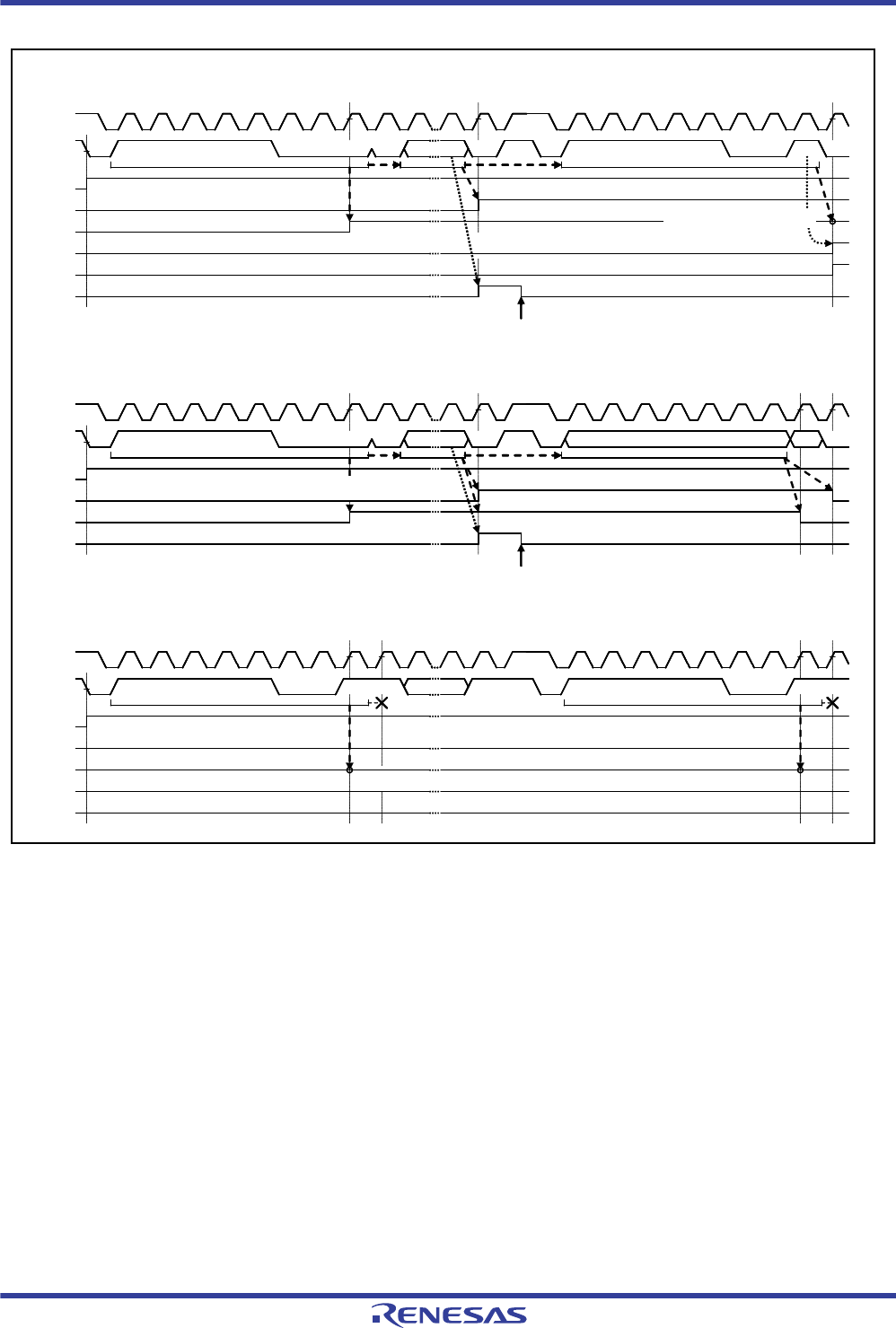
R01UH0034EJ0200 Rev.2.00 Page 1051 of 1489
Dec 27, 2013
RX62T Group, RX62G Group 24. I2C Bus Interface (RIIC)
Figure 24.28 AASy/DID Flag Set/Clear Timing during Reception of Device-ID
[When address before the Device-ID + R does not match the slave address]
[When address received after a restart condition is detected does not match the Device-ID]
Device-ID match (1111 100b + W)
S9Sr23456711 to 8 9834567981 2
[Device-ID reception]
The previous value is retained.
Address match
Receive data (7-bit address/lower 10 bits)
RACK
TDRE
AASy
TRS
BBSY
RDRF
ACK Address 1
DID
Address match
AASy
BBSY
ACK Address
DID
R/W
Address mismatch
Device-ID mismatch
RDRF
SCL
SDA
SCL
SDA
W
W
001 1 1 1
001 1 1 1
001 1 1 1
7-bit slave address (other station)
AASy
BBSY
DID
TDRE
SCL
SDA 0
01 1 1 1 RNACK NACK 1 001 1 1 1 RNACK
Comparing the second and the following
bytes is stopped.
RDRF
ACK ACK
ACK1
1
1
Read ICDRR
(Dummy read [7-bit address/lower 10 bits])
S9Sr23456711 to 8 9834567981 2
Receive data (7-bit address/lower 10 bits)
Device-ID match (1111 100b + W)
Read ICDRR
(Dummy read [7-bit address/lower 10 bits])
S9Sr23456711 to 8 9834567981 2
Device-ID match (1111 100b + R) Device-ID match (1111 100b + R)
Device-ID match (1111 100b + R)
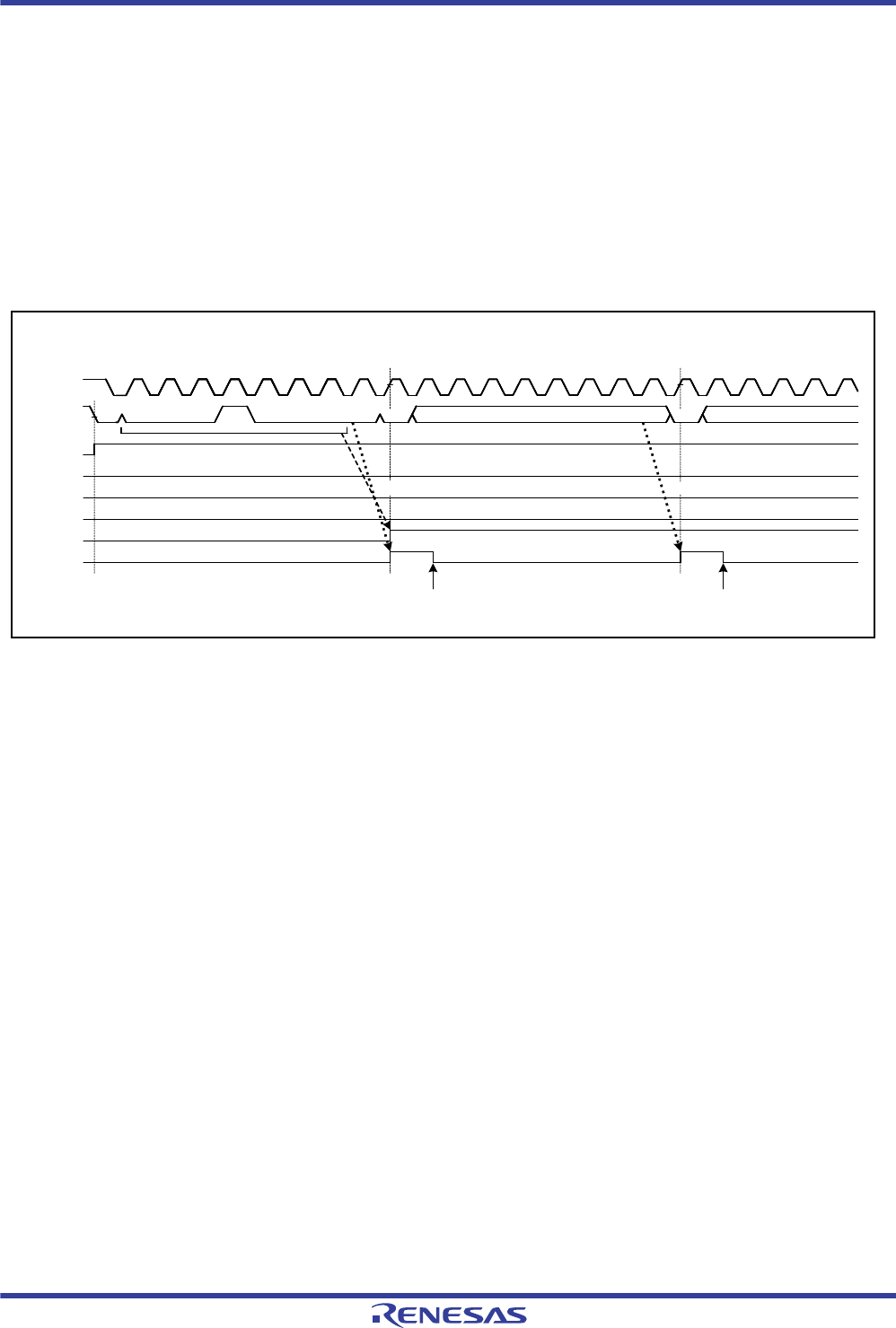
R01UH0034EJ0200 Rev.2.00 Page 1052 of 1489
Dec 27, 2013
RX62T Group, RX62G Group 24. I2C Bus Interface (RIIC)
24.7.4 Host Address Detection
The RIIC has a function to detect the host address while the SMBus is operating. When the HOAE bit in ICSER is set to
1 while the SMBS bit in ICMR3 is 1, the RIIC can detect the host address (0001 000b) in slave receive mode (MST and
TRS bits = 00b in ICCR2).
When the RIIC detects the host address, the HOA flag in ICSR1 is set to 1 at the rising edge of the ninth SCL clock
cycle, and at the same time, the TDRE flag in ICSR2 is set to 1 when the R/W# bit is 0 (Wr bit). This causes a transmit
data empty interrupt (ICTXI) to be generated. The HOA flag is used to recognize that the host address was sent from the
smart battery or other devices.
If the bit following the host address (0001 000b) is an Rd bit (R/W# bit = 1), the RIIC can also detect the host address.
After the host address is detected, the RIIC operates in the same manner as normal slave operation.
Figure 24.29 HOA Flag Set Timing during Reception of Host Address
Read ICDRR
(Dummy read [7-bit address])
AAS2
AAS0
S1
AAS1
9
ACK
BBSY
RDRF
234567 8 9
ACK
1
[Host address reception]
1
0
HOA
234567
001000
SCL
SDA
8
W
2345
Data (DATA1) Data (DATA2)
Read ICDRR
(DATA1)
Receive data (7-bit address) Receive data (DATA1)
Host address match (0001 000b)
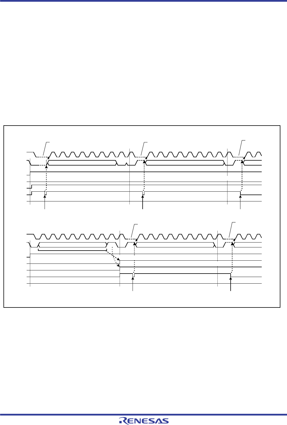
R01UH0034EJ0200 Rev.2.00 Page 1053 of 1489
Dec 27, 2013
RX62T Group, RX62G Group 24. I2C Bus Interface (RIIC)
24.8 Function to Automatically Hold SCL Clock Low
24.8.1 Function to Prevent Wrong Transmission of Transmit Data
If the shift register (ICDRS) is empty when data have not been written to the transmit data register (ICDRT) with the
RIIC in transmission mode (TRS bit = 1 in ICCR2), the SCL signal is automatically held at the low level over the
intervals shown below. This low-hold period is extended until data for transmission have been written, which prevents
the unintended transmission of erroneous data.
<Master transmitter mode>
Low-level interval after a start condition or restart condition is issued
Low-level interval of one clock cycle between the ninth clock cycle of one transfer and the first clock cycle of the
next
<Slave transmitter mode>
Low-level interval between the ninth clock cycle of one transfer and the first clock cycle of the next
Figure 24.30 Automatic Low-Hold Operation in Transmit Mode
8
R
9
ACK
TDRE
AASy
TRS
BBSY
RDRF
S 1 234567 234567 8 9
ACK
23
[Master transmit mode]
[Slave transmit mode]
TDRE
AASy
TRS
BBSY
RDRF
S234567 234567 8 9
ACK
8
W
9
ACK
2
SCL
SDA
SCL
SDA
111
11
Data (DATA1)
7-bit slave address
Data (DATA1)
7-bit slave address
Write data to ICDRT
(DATA1) Write data to ICDRT
(DATA2)
Write data to ICDRT
(DATA2)
Write data to ICDRT
(DATA1)
Write data to ICDRT
(7-bit address + W)
Transmit data (7-bit address + W) Transmit data (DATA1) Transmit data (DATA2)
Transmit data (DATA1) Transmit data (DATA2)
Address match
Automatic low-hold (to prevent wrong transmission)
Automatic low-hold
(to prevent wrong
transmission)
Automatic low-hold
(to prevent wrong
transmission)
Automatic low-hold (to prevent wrong transmission)Automatic low-hold (to prevent wrong transmission)
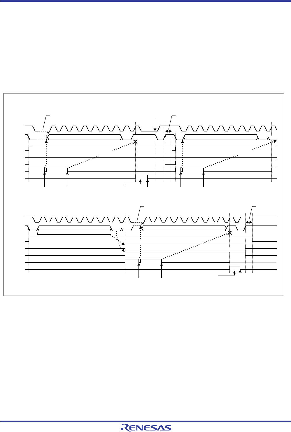
R01UH0034EJ0200 Rev.2.00 Page 1054 of 1489
Dec 27, 2013
RX62T Group, RX62G Group 24. I2C Bus Interface (RIIC)
24.8.2 NACK Reception Transfer Suspension Function
The RIIC has a function to suspend transfer operation when NACK is received in transmit mode (TRS bit = 1 in ICCR2).
This function is enabled when the NACKE bit in ICFER is set to 1 (transfer suspension enabled). If the next transmit data
has already been written (TDRE flag = 0 in ICSR2) when NACK is received, next data transmission at the falling edge of
the ninth SCL clock cycle is automatically suspended. This prevents the SDA line output level from being held low when
the MSB of the next transmit data is 0.
If the transfer operation is suspended by this function (NACKF flag = 1 in ICSR2), transmit operation and receive
operation are discontinued. To restore transmit/receive operation, be sure to clear the NACKF flag to 0. In master
transmit mode, clear the NACKF flag to 0, issue a restart or stop condition, and then issue a start condition again.
Figure 24.31 Suspension of Data Transfer when NACK is Received (NACKE = 1)
ACK
NACK
ACK
Transfer suspended
Transmit data (DATA2)
Write data to ICDRT
(7-bit address + W)
TDRE
AASy
TRS
BBSY
NACKF
S 1 234567 234567 8 9
[Master transmit mode]
[Slave transmit mode]
TDRE
AASy
TRS
BBSY
NACKF
S234567 8
W
9 S 234567 8
W
9
8
W
9 P
P
SCL
SDA
SCL
SDA
Dummy read ICDRR
1
1
1
Automatic low-hold (to prevent wrong transmission) Bus free time (ICBRL)
7-bit slave address 7-bit slave address
Write data to ICDRT
(DATA1) Write data to ICDRT
(7-bit address + W) Write data to ICDRT
(DATA1)
Clear NACKF
Clear NACKF
Write data to ICDRT
(DATA1) Write data to ICDRT
(DATA2)
Automatic low-hold (to prevent wrong transmission) Bus free time
(ICBRL)
7-bit slave address Data (DATA1)
Transmit data
(7-bit address + W) Transmit data (DATA1) Transmit data
(7-bit address + W) Transmit data (DATA1)
Transfer suspended
Transmit data (DATA1)
Address match
Write 1 to SP
Write 1 to SP

R01UH0034EJ0200 Rev.2.00 Page 1055 of 1489
Dec 27, 2013
RX62T Group, RX62G Group 24. I2C Bus Interface (RIIC)
24.8.3 Function to Prevent Failure to Receive Data
If response processing is delayed when receive data (ICDRR) read is delayed for a period of one transfer frame or more
with receive data full (RDRF flag = 1 in ICSR2) in receive mode (TRS = 0 in ICCR2), the RIIC holds the SCL line low
automatically immediately before the next data is received to prevent failure to receive data.
This function to prevent failure to receive data using the automatic low-hold function is also enabled even if the read
processing of the final receive data is delayed and, in the meantime, the RIIC's own slave address is designated after a
stop condition is issued. This function does not disturb other communication because the RIIC does not hold the SCL
line low when a mismatch with its own slave address occurs after a stop condition is issued.
Sections in which the SCL line is held low can be selected with a combination of the WAIT and RDRFS bits in ICMR3.
(1) One-Byte Receive Operation and Automatic Low-Hold Function Using the WAIT Bit
When the WAIT bit in ICMR3 is set to 1, the RIIC performs one-byte receive operation using the WAIT bit function.
Furthermore, when the ICMR3.RDRFS bit is 0, the RIIC automatically sends the ACKBT bit value in ICMR3 for the
acknowledge bit in the period from the falling edge of the eighth SCL clock cycle to the falling edge of the ninth SCL
clock cycle, and automatically holds the SCL line low at the falling edge of the ninth SCL clock cycle using the WAIT bit
function. This low-hold is released by reading data from ICDRR, which enables bytewise receive operation.
The WAIT bit function is enabled for receive frames after a match with the RIIC's own slave address (including the
general call address and host address) is obtained in master receive mode or slave receive mode.
(2) One-Byte Receive Operation (ACK/NACK Transmission Control) and Automatic Low-Hold
Function Using the RDRFS Bit
When the RDRFS bit in ICMR3 is set to 1, the RIIC performs one-byte receive operation using the RDRFS bit function.
When the RDRFS bit is set to 1, the RDRF flag (receive data full) in ICSR2 is set to 1 at the rising edge of the eighth
SCL clock cycle, and the SCL line is automatically held low at the falling edge of the eighth SCL clock cycle. This low-
hold is released by writing a value to the ACKBT bit in ICMR3, but cannot be released by reading data from ICDRR,
which enables receive operation by the ACK/NACK transmission control according to the data received in byte units.
The RDRFS bit function is enabled for receive frames after a match with the RIIC’s own slave address (including the
general call address and host address) is obtained in master receive mode or slave receive mode.
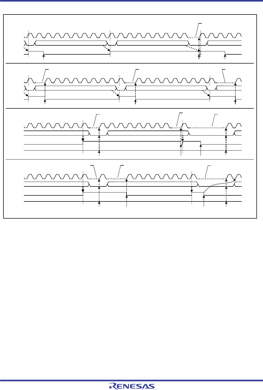
R01UH0034EJ0200 Rev.2.00 Page 1056 of 1489
Dec 27, 2013
RX62T Group, RX62G Group 24. I2C Bus Interface (RIIC)
Figure 24.32 Automatic Low-Hold Operation in Receive Mode (Using RDRFS and WAIT Bits)
RDRF
Read ICDRR
RDRF
SCL
SDA
SCL
SDA
ACK
Data
Automatic low-hold (WAIT)
Automatic low-hold (WAIT)
ACK
Data Data
[RDRFS = 0, WAIT = 0]
Read ICDRR
Read ICDRR Read ICDRR
[RDRFS = 0, WAIT = 1] Automatic low-hold
(WAIT)
Data Data
ACK Data
Read ICDRR
Read ICDRR
Automatic low-hold
(to prevent failure to
receive data)
Automatic low-hold
(RDRFS)
Automatic low-hold (RDRFS)
[RDRFS = 1, WAIT = 0]
[RDRFS = 1, WAIT = 1]
Write 0 to ACKBT Read ICDRR Read ICDRR Write 0 to ACKBT
ACK
Data ACK Data ACK
Automatic low-hold
(RDRFS)
Automatic low-hold (WAIT)
Automatic low-hold
(RDRFS)
Write 0 to ACKBT Read ICDRR Read ICDRR Write 0 to ACKBT
234567 81234234567 819991
234567 81234567 819991
234567 8 91234567 819
234567 8 919 234567 81
Automatic low-hold
(to prevent failure to receive data)
ACK
ACK ACK ACK
RDRF
SCL
SDA
ACKBT
SCL
RDRF
SDA
ACKBT
Data

R01UH0034EJ0200 Rev.2.00 Page 1057 of 1489
Dec 27, 2013
RX62T Group, RX62G Group 24. I2C Bus Interface (RIIC)
24.9 Arbitration-Lost Detection Functions
In addition to the normal arbitration-lost detection function defined by the I2C bus standard, the RIIC has functions to
prevent double-issue of a start condition, to detect arbitration during transmission of NACK, and to detect arbitration in
slave transmit mode.
24.9.1 Master Arbitration Lost Detection (MALE Bit)
The RIIC drives the SDA line low to issue a start condition. However, if the SDA line has already been driven low by
another master device issuing a start condition, the RIIC regards its own issuing of a start condition as an error and
considers this a loss in arbitration, so priority is given to transfer by the other master device. Similarly, if a request to
issue a start condition is made by setting the ST bit in ICCR2 to 1 while the bus is busy (BBSY flag = 1 in ICCR2), the
RIIC regards this as a double-issuing-of-start-condition error and considers itself to have lost in arbitration, thus
preventing a failure of transfer due to issuing of a start condition while transfer is in progress.
When a start condition is issued successfully, if the data for transmission including the address bits (i.e. the internal SDA
output level) and the level on the SDA line do not match (the 1 output as the internal SDA output; i.e. the SDA pin is in
the high-impedance state) and the low level is detected on the SDA line, the RIIC loses in arbitration.
After a loss in arbitration of mastership, the RIIC immediately enters slave receiver mode. If a slave address (including
the general call address) matches its own address at this time, the RIIC continues in slave operation.
A loss in arbitration of mastership is detected when the following conditions are met while the MALE bit in ICFER is 1
(master arbitration lost detection enabled).
[Master arbitration lost conditions]
Non-matching of the internal level for output on SDA and the level on the SDA line after a start condition was
issued by setting the ST bit in ICCR2 to 1 while the BBSY flag in ICCR2 was cleared to 0 (erroneous issuing of a
start condition)
Setting of the ST bit in ICCR2 to 1 (start condition double-issue error) while the BBSY flag is set to 1
When the transmit data excluding acknowledge (internal SDA output level) does not match the level on the SDA
line in master transmit mode (MST and TRS bits = 11b in ICCR2)
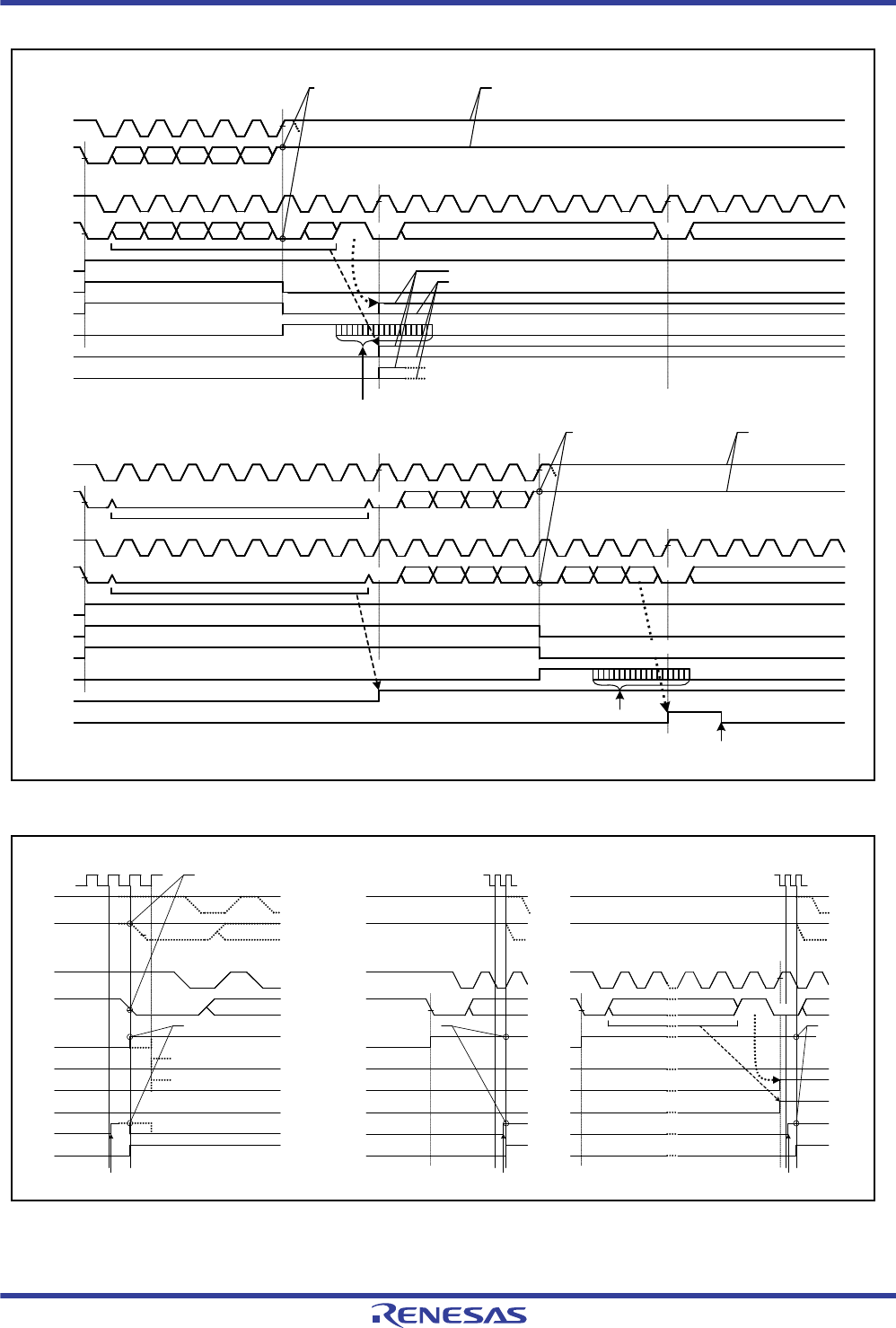
R01UH0034EJ0200 Rev.2.00 Page 1058 of 1489
Dec 27, 2013
RX62T Group, RX62G Group 24. I2C Bus Interface (RIIC)
Figure 24.33 Examples of Master Arbitration Lost Detection (MALE = 1)
Figure 24.34 Arbitration Lost when a Start Condition is Issued (MALE = 1)
[When slave addresses conflict]
S
12345
Data
S 1 9
6
1
1
2 3 41 6
0
75
2 31
8
R
9234567
Data
8
4 5
[When data transmission conflicts after general call address is sent]
S 1
12345
Data
234
SS 2 3 41 5
0
6789
5
1
9
9
234567
000000
1
0
234567
000000
1
0
8
W
Address match
Address mismatch
8
W
Read ICDRR
General call address match (0000 000b + W)
Transmit data mismatch
(Arbitration lost) Release SCLn/SDA
TRS
AL
MST
BBSY
GCA
RDRF
SCL
SDA
SCL
SDA
TRS
AL
MST
BBSY
AASy
TDRE
SCL
SDA
SCL
SDA
Transmit data mismatch
(Arbitration lost) Release SCL/SDA
ACKACK
ACK
Write 0 to AL
Write 0 to AL
ACK ACK
Receive data
S
PCLK
S 1 S 8
R
9 12 12671
ACK
7-bit/10-bit slave address
ST = 1, BBSY = 1
Bus free (BBSY = 0) start condition issuance (ST = 1) error Bus busy (BBSY =1) start condition issuance (ST = 1) error
ST = 1,
BBSY = 1
TRS
AL
MST
BBSY
AASy
ST
SCL
SDA
SCL
SDA
Write 1 to ST Write 1 to ST Write 1 to ST
SDA mismatch PCLK PCLK
TRS
AL
MST
BBSY
AASy
ST
SCL
SDA
SCL
SDA
TRS
AL
MST
BBSY
AASy
ST
SCL
SDA
SCL
SDA
ST = 1, BBSY = 1
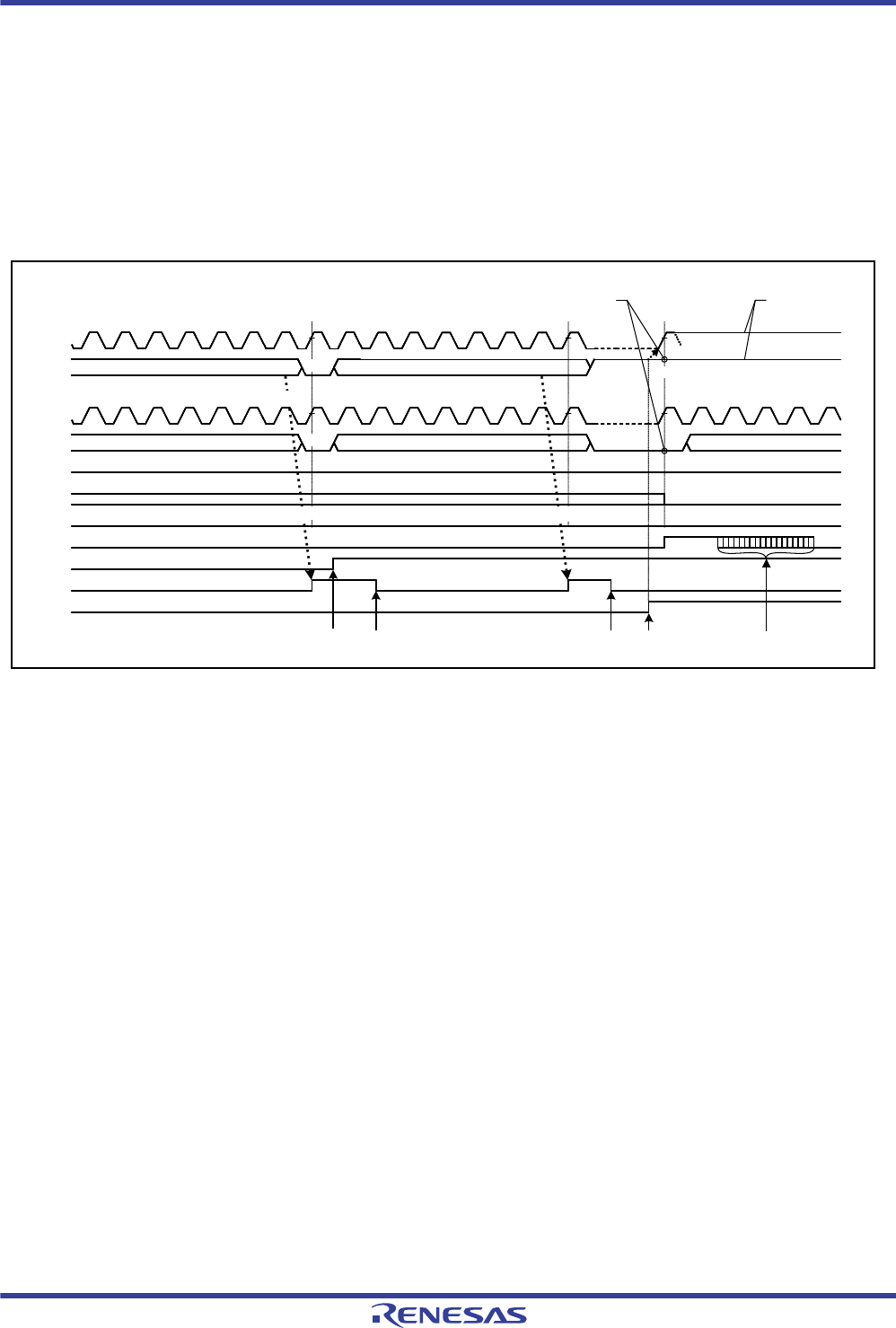
R01UH0034EJ0200 Rev.2.00 Page 1059 of 1489
Dec 27, 2013
RX62T Group, RX62G Group 24. I2C Bus Interface (RIIC)
24.9.2 Function to Detect Loss of Arbitration during NACK Transmission (NALE Bit)
The RIIC has a function to cause arbitration to be lost if the internal SDA output level does not match the level on the
SDA line (the 1 output as the internal SDA output; i.e. the SDA pin is in the high-impedance state) and the low level is
detected on the SDA line during transmission of NACK in receive mode. Arbitration is lost due to a conflict of NACK
transmission and ACK transmission when two or more master devices receive data from the same slave device
simultaneously in a multi-master system. Such conflict occurs when multiple master devices send/receive the same
information through a single slave device. Figure 24.35 shows an example of arbitration lost detection during
transmission of NACK.
Figure 24.35 Example of Arbitration Lost Detection during Transmission of NACK (NALE = 1)
The following explains arbitration lost detection using an example where two master devices (master A and master B)
and a single slave device are connected through the bus. In this example, master A receives two bytes of data from the
slave device, and master B receives four bytes of data from the slave device.
If master A and master B access the slave device simultaneously, because the slave address is identical, arbitration is not
lost in both master A and master B during access to the slave device. Therefore, both master A and master B recognize
that they have obtained the bus mastership and operate as such. Here, master A sends NACK when it has received two
final bytes of data from the slave device. Meanwhile, master B sends ACK because it has not received necessary four
bytes of data. At this time, the NACK transmission from master A and the ACK transmission from master B conflict. In
general, if a conflict like this occurs, master A cannot detect ACK transmitted by master B and issues a stop condition.
Therefore, the issuance of the stop condition conflicts with the SCL clock output of master B, which disturbs
communication.
When the RIIC receives ACK during transmission of NACK, it detects a defeat in conflict with other master devices and
causes arbitration to be lost.
If arbitration is lost during transmission of NACK, the RIIC immediately cancels the slave match condition and enters
slave receive mode. This prevents a stop condition from being issued, preventing a communication failure on the bus.
Similarly, in the ARP command processing of SMBus, the function to detect loss of arbitration during transmission of
NACK is also available for eliminating the extra clock cycle processing (such as FFh transmission processing) necessary
if no response is received in the Get UDID (general) processing after the Assign address command.
The RIIC detects arbitration lost during transmission of NACK when the following condition is met with the NALE bit
8234567
Data
823456
Data
8234567
Data
234567
Data
9
9 1
1 1
9
92345
Data
Read ICDRR Write 1 to ACKBT Write 0 to AL
NACK transmission mismatch
(Arbitration lost) Release SCL/SDA
TRS
AL
MST
BBSY
RDRFS
SCL
SDA
SCL
SDA
RDRF
ACKBT
[Conflict during transmission of NACK (ACK received)]
ACK NACK
ACK ACK
Write 1 to RDRFS Read ICDRR
78
Receive data Receive data
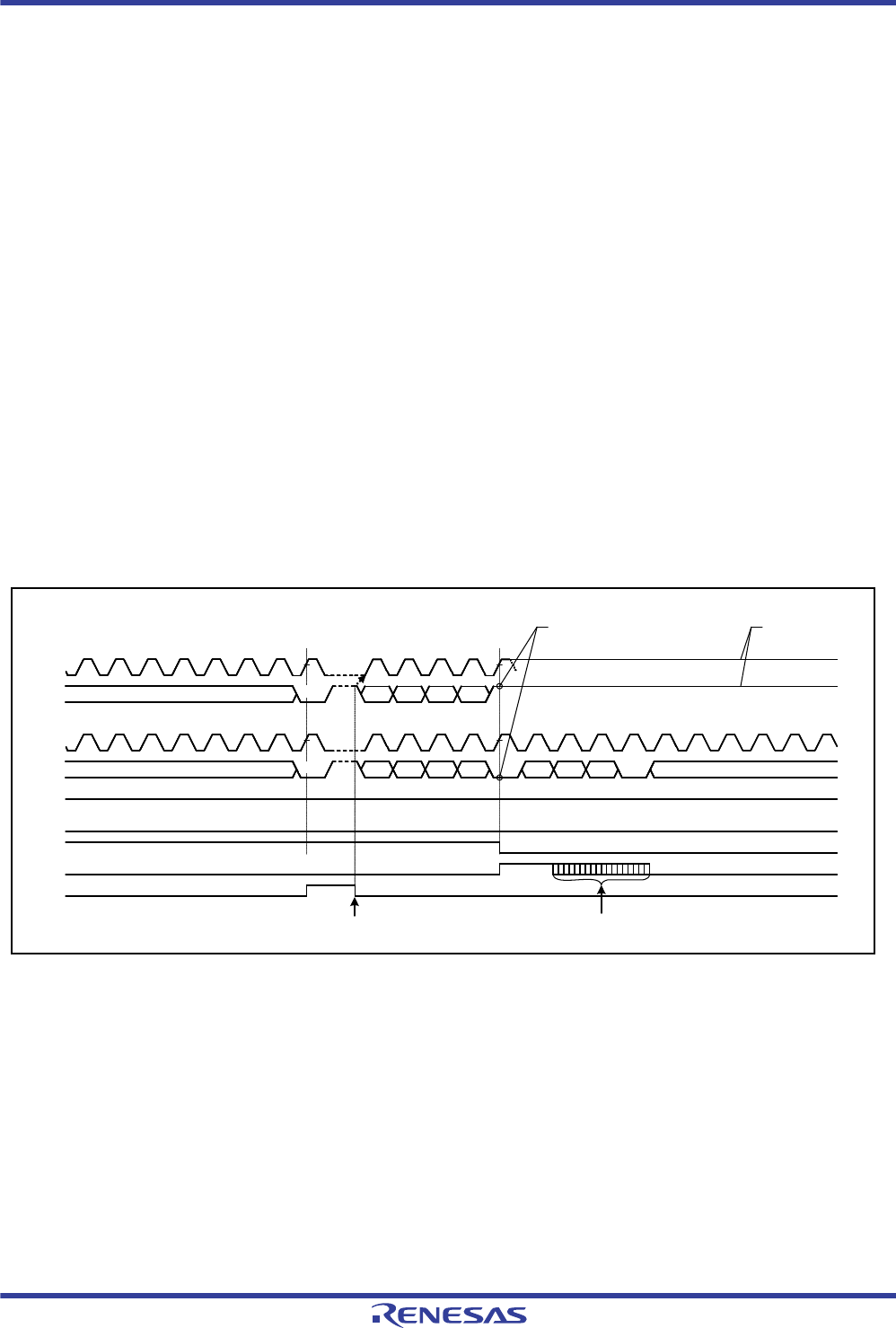
R01UH0034EJ0200 Rev.2.00 Page 1060 of 1489
Dec 27, 2013
RX62T Group, RX62G Group 24. I2C Bus Interface (RIIC)
in ICFER set to 1 (arbitration lost detection during NACK transmission enabled).
[Condition for arbitration lost during NACK transmission]
When the internal SDA output level does not match the SDA line (ACK is received) during transmission of NACK
(ACKBT bit = 1 in ICMR3)
24.9.3 Slave Arbitration Lost Detection (SALE Bit)
The RIIC has a function to cause arbitration to be lost if the data for transmission (i.e. the internal SDA output level) and
the level on the SDA line do not match (the 1 output as the internal SDA output; i.e. the SDA pin is in the high-
impedance state) and the low level is detected on the SDA line in slave transmitter mode. This arbitration lost detection
function is mainly used when transmitting a UDID (Unique Device Identifier) over an SMBus.
When it loses slave arbitration, the RIIC is immediately released from the slave-matched state and enters slave receiver
mode. This function can detect conflicts of data during transmission of UDIDs over an SMBus and eliminates
subsequent redundant processing (processing for the transmission of FFh).
The RIIC detects slave arbitration lost when the following condition is met with the SALE bit in ICFER set to 1 (slave
arbitration lost detection enabled).
[Condition for slave arbitration lost]
When transmit data excluding acknowledge (internal SDA output level) does not match the SDA line in slave
transmit mode (MST and TRS bits = 01b in ICCR2)
Figure 24.36 Example of Slave Arbitration Lost Detection (SALE = 1)
8234567
Data
8234567
Data
9
9
1
Transmit data mismatch
(Arbitration lost) Release SCL/SDA
2 3 4
2 3 4 5
0
6 7 8 9
5
1
1
1
123456
Data
3456
[Conflict during data transmission]
ACK
ACK
ACK
Write data to ICDRT Write 0 to AL
TRS
AL
MST
BBSY
TDRE
SCL
SDA
SCL
SDA
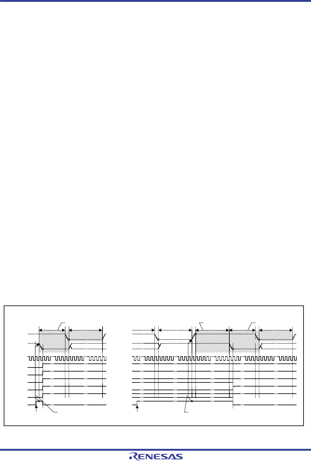
R01UH0034EJ0200 Rev.2.00 Page 1061 of 1489
Dec 27, 2013
RX62T Group, RX62G Group 24. I2C Bus Interface (RIIC)
24.10 Start Condition/Restart Condition/Stop Condition Issuing Function
24.10.1 Issuing a Start Condition
The RIIC issues a start condition when the ST bit in ICCR2 is set to 1.
When the ST bit is set to 1, a start condition issuance request is made and the RIIC issues a start condition when the
BBSY flag in ICCR2 is 0 (bus free). When a start condition is issued normally, the RIIC automatically shifts to the
master transmit mode.
A start condition is issued in the following sequence.
[Start condition issuance]
Drive the SDA line low (high level to low level).
Ensure the time set in ICBRH and the start condition hold time.
Drive the SCL line low (high level to low level).
Detect low level of the SCL line and ensure the low-level period of SCL set in ICBRL.
24.10.2 Issuing a Restart Condition
The RIIC issues a restart condition when the RS bit in ICCR2 is set to 1.
When the RS bit is set to 1, a restart condition issuance request is made and the RIIC issues a restart condition when the
BBSY flag in ICCR2 is 1 (bus busy) and the MST bit in ICCR2 is 1 (master mode).
A restart condition is issued in the following sequence.
[Restart condition issuance]
Release the SDA line.
Ensure the low-level period of SCL line set in ICBRL.
Release the SCL line (low level to high level).
Detect a high level of the SCL line and ensure the time set in ICBRL and the restart condition setup time.
Drive the SDA line low (high level to low level).
Ensure the time set in ICBRH and the restart condition hold time.
Drive the SCL line low (high level to low level).
Detect a low level of the SCL line and ensure the low-level period of SCL line set in ICBRL.
Figure 24.37 Start Condition/Restart Condition Issue Timing (ST and RS Bits)
[Start condition issuing operation] [Restart condition issuing operation]
Write 1 to ST
ICBRH ICBRL
Write 1 to RS
ICBRH ICBRLICBRLICBRLICBRH
ACK/NACK
S9
Sr
Hold time Hold time
Setup time
Accept restart condition issuanceAccept start condition issuance
Issue start
condition
SCL
SDA
TRS
START
MST
BBSY
IIC
TDRE
ST
TRS
RS
MST
BBSY
IIC
SCL
SDA
TDRE
START
Issue restart
condition
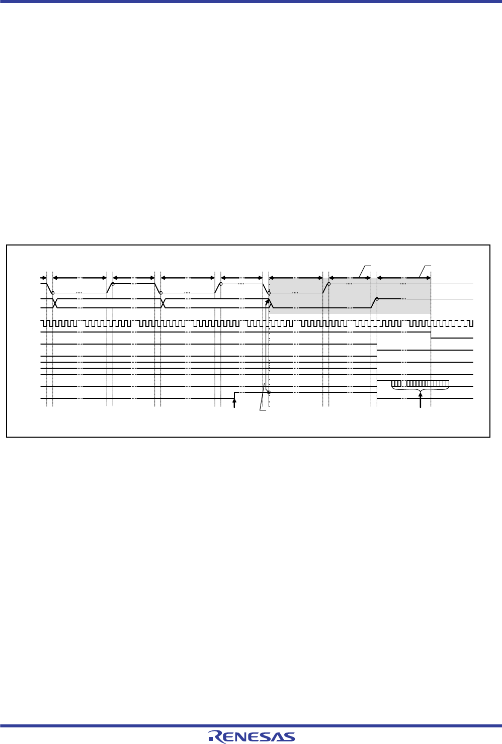
R01UH0034EJ0200 Rev.2.00 Page 1062 of 1489
Dec 27, 2013
RX62T Group, RX62G Group 24. I2C Bus Interface (RIIC)
24.10.3 Issuing a Stop Condition
The RIIC issues a stop condition when the SP bit in ICCR2 is set to 1.
When the SP bit is set to 1, a stop condition issuance request is made and the RIIC issues a stop condition when the
BBSY flag in ICCR2 is 1 (bus busy) and the MST bit in ICCR2 is 1 (master mode).
A stop condition is issued in the following sequence.
[Stop condition issuance]
Drive the SDA line low (high level to low level).
Ensure the low-level period of SCL line set in ICBRL.
Release the SCL line (low level to high level).
Detect a high level of the SCL line and ensure the time set in ICBRH and the stop condition setup time.
Release the SDA line (low level to high level).
Ensure the time set in ICBRL and the bus free time.
Clear the BBSY flag to 0 (to release the bus mastership).
Figure 24.38 Stop Condition Issue Timing (SP Bit)
TRS
STOP
MST
BBSY
IIC
SCL
SDA
Write 1 to SP
ICBRH ICBRL
TDRE
ICBRLICBRH
ACK/NACK
ICBRLICBRH
89 P
SP
ICBRL
b0
Accept stop
condition issuance Write 0 to STOP
Bus free time
Setup time
Issue stop
condition

R01UH0034EJ0200 Rev.2.00 Page 1063 of 1489
Dec 27, 2013
RX62T Group, RX62G Group 24. I2C Bus Interface (RIIC)
24.11 Bus Hanging
If the clock signals from the master and slave devices go out of synchronization due to noise or other factors, the I2C bus
might hang with a fixed level on the SCL line and/or SDA line.
As measures against the bus hanging, the RIIC has a timeout function to detect hanging by monitoring the SCL line, a
function for the output of an extra SCL clock cycle to release the bus from a hung state due to clock signals being out of
synchronization, and the RIIC/internal reset function.
By checking the SCLO, SDAO, SCLI, and SDAI bits in ICCR1, it is possible to see whether the RIIC or its partner in
communications is placing the low level on the SCL or SDA lines.
24.11.1 Timeout Function
The RIIC has the timeout function to detect an abnormality that the SCL line is held for a certain period of time. The
RIIC can detect an abnormal bus state by monitoring that the SCL line is held low or high for a predetermined time.
The timeout function monitors the SCL line state and counts the low-level period or high-level period using the internal
counter. The timeout function resets the internal counter each time the SCL line changes (rising or falling), but continues
to count unless the SCL line changes. If the internal counter overflows due to no SCL line change, the RIIC can detect
the timeout and report the bus abnormality.
This timeout function is enabled when the TMOE bit in ICFER is 1. It detects an abnormal bus state that the SCn line is
held low or high during the following period.
• The bus is busy (ICCR2.BBSY flag = 1) in master mode (ICCR2.MST bit = 1).
• The RIIC's own slave address matches (ICSR1 is not 00h) and the bus is busy (ICCR2.BBSY flag = 1) in slave mode
(ICCR2.MST bit = 0).
• The bus is free (ICCR2.BBSY flag = 0) while issuing of a start condition is requested (ICCR2.ST = 1).
The internal counter of the timeout function works using the internal reference clock (IIC) set by the CKS[2:0] bits in
ICMR1 as a count source. It functions as a 16-bit counter when long mode is selected (TMOS bit = 0 in ICMR2) or a 14-
bit counter when short mode is selected (TMOS bit = 1).
The SCL line level (low/high or both levels) during which this counter is activated can be selected by the setting of the
TMOH and TMOL bits in ICMR2. If both TMOL and TMOH bits are cleared to 0, the internal counter does not work.

R01UH0034EJ0200 Rev.2.00 Page 1064 of 1489
Dec 27, 2013
RX62T Group, RX62G Group 24. I2C Bus Interface (RIIC)
Figure 24.39 Timeout Function (TMOE, TMOS, TMOH, and TMOL Bits)
TMOH
TMOE
BBSY
IIC?
SCL
SDA
TMOL
Clear internal counter
Data
2
8 9
A/NA
S
P 1 8
R/W
72 9
ACK
7-bit slave address
1
7
TMOS = 0 TMOS = 1
Start internal counter Start counter
Clear counter
Start counter
Clear counter Clear counter Clear counter
Start counter Start counter Start counter
16-bit counter
overflows
14-bit counter
overflows
Write 1 to TMOL Write 0 to TMOEWrite 0 to TMOL
Write 1 to TMOH
Clear counter Start counter
[Example of operation when TMOH = 1 and TMOL = 1]
BBSY
SCL
SDA
TMOF
TMOE
Clear counter Clear counter
ST
When a stat condition
is issued In the slave-address
matched state
[Timeout function]
Bus free time
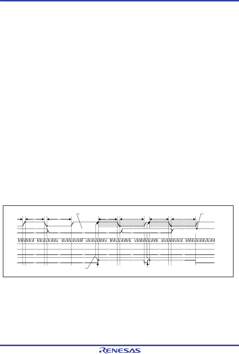
R01UH0034EJ0200 Rev.2.00 Page 1065 of 1489
Dec 27, 2013
RX62T Group, RX62G Group 24. I2C Bus Interface (RIIC)
24.11.2 Extra SCL Clock Cycle Output Function
In master mode, the RIIC module has a facility for the output of extra SCL (clock) cycles to release the SDA line of the
slave device from being held at the low level due to the master being out of synchronization with the slave device.
This function is mainly used in master mode to release the SDA line of the slave device from the state of being fixed to
the low level by including extra cycles of SCL output from the RIIC with single cycles of the SCL (clock) signal as the
unit in the case of a bus error where the RIIC cannot issue a stop condition because the slave device is holding the SDA
line at the low level. Do not use this facility in normal situations. Using it when communications are proceeding correctly
will lead to malfunctions.
When the CLO bit in ICCR1 is set to 1 in master mode, a single cycle of the SCL clock at the frequency corresponding to
the transfer rate settings (settings of the CKS[2:0] bits in ICMR1, and of the ICBRH and ICBRL registers) is output as an
extra clock cycle. After output of this single cycle of the SCL clock, the CLO bit is automatically cleared to 0. Therefore,
further extra clock cycles can be output consecutively by the software program writing 1 to the CLO bit after having read
CLO = 0.
When the RIIC module is in master mode and the slave device is holding the SDA line at the low level because
synchronization with the slave device has been lost due to the effects of noise etc., the output of a stop condition is not
possible. The facility for output of an extra cycle of the SCL (clock) signal can be used to output extra cycles of SCL one
by one to make the slave device release the SDA line from being held at the low level, thus recovering the bus from an
unusable state. Release of the SDA line by the slave device can be monitored by reading the SDAI bit in ICCR1. After
confirming release of the SDA line by the slave device, complete communications by reissuing the stop condition.
Use this facility with the MALE bit (master arbitration lost detection disabled) in ICFER cleared to 0. If the MALE bit is
set to 1 (master arbitration lost detection enabled), arbitration is lost when the value of the SDAO bit in ICCR1does not
match the state of the SDA line, so take care on this point.
[Output conditions for using the CLO bit in ICCR1]
When the bus is free (BBSY flag in ICCR2 = 0) or in master mode (MST bit = 1 and BBSY flag = 1 in ICCR2)
When the communication device does not hold the SCL line low
Figure 24.40 shows the operation timing of the extra SCL clock cycle output function.
Figure 24.40 Extra SCL Clock Cycle Output Function (CLO Bit)
Write 1 to CLO
Accept CLO output Write 1 to CLO
Data "1"
MSB or next data
ICBRH ICBRLICBRH
ACK or data "0"
ICBRLICBRLICBRH
9
Extra clock cycle
output Extra clock cycle
output
TRS
MST
BBSY
IIC
SCL
SDA
CLO
SDAn line is held low due to irregular bits Release SDAn line

R01UH0034EJ0200 Rev.2.00 Page 1066 of 1489
Dec 27, 2013
RX62T Group, RX62G Group 24. I2C Bus Interface (RIIC)
24.11.3 RIIC Reset and Internal Reset
The RIIC module incorporates a function for resetting itself. There are two types of reset. One is referred to as an RIIC
reset; this initializes all registers including the BBSY flag in ICCR2. The other is referred to as an internal reset; this
releases the RIIC from the slave-address matched state and initializes the internal counter while retaining other settings.
After issuing a reset, be sure to clear the IICRST bit in ICCR1 to 0.
Both types of reset are effective for release from bus-hung states since both restore the output state of the SCL and SDA
pins to the high impedance state.
Issuing a reset during slave operation may lead to a loss of synchronization between the master device clock and the
slave device clock, so avoided this where possible. Note that monitoring of the bus state, such as for the presence of a
start condition, is not possible during an RIIC reset (ICE and IICRST bits = 01b in ICCR1).
For a detailed description of the RIIC and internal resets, see section 24.14, Reset States.

R01UH0034EJ0200 Rev.2.00 Page 1067 of 1489
Dec 27, 2013
RX62T Group, RX62G Group 24. I2C Bus Interface (RIIC)
24.12 SMBus Operation
The RIIC is available for data communication conforming to the SMBus standard (Version 2.0). To perform SMBus
communication, set the SMBS bit in ICMR3 to 1 to select input level conforming to the SMBus for the SCL pin/SDA pin
function. To use the transfer rate within a range of 10 kbps to 100 kbps of the SMBus standard, set the CKS[2:0] bits in
ICMR1, ICBRH, and ICBRL. In addition, determine the values of the DLCS bit in ICMR2 and the SDDL[2:0] bits in
ICMR2 to meet the data hold time specification of 300 ns or more. When the RIIC is used only as a slave device, the
transfer rate setting is not necessary, whereas the ICBRL needs to be set to a value longer than the data setup time (250
ns).
For the SMBus device default address (1100 001b), use one of the slave address registers L0 to L2 (SARL0, SARL1, and
SARL2), and set the corresponding FS bit (7-bit/10-bit address format select) in SARUy (y = 0 to 2) to 0 (7-bit address
format).
When transmitting the UDID (Unique Device Identifier), set the SALE bit in ICFER to 1 to enable the slave arbitration
lost detection function.
24.12.1 SMBus Timeout Measurement
(1) Measuring timeout of slave device
The following period (timeout interval: TLOW: SEXT) must be measured for slave devices in SMBus communication.
From start condition to stop condition
To measure timeout for slave devices, measure the period from start condition detection to stop condition detection with
the on-chip timer using a start condition detection interrupt (STI) and stop condition detection interrupt (SPI) of the
RIIC. The measured timeout period must be within the total clock low-level period [slave device] TLOW: SEXT: 25 ms
(max.) of the SMBus standard.
If the time measured with the on-chip timer exceeds the clock low-level detection timeout TTIMEOUT: 25 ms (min.) of the
SMBus standard, the slave device must release the bus by writing 1 to the IICRST bit in ICCR1 to issue an internal reset
of the RIIC. When an internal reset is issued, the RIIC stops driving the bus for the SCL pin and SDA pin and make the
SCL/SDA pin outputs high impedance, which releases the bus.
(2) Measuring timeout of master device
The following periods (timeout interval: TLOW: MEXT) must be measured for master devices in SMBus communication.
From start condition to acknowledge bit
Between acknowledge bits
From acknowledge bit to stop condition
To measure timeout for master devices, measure these periods with the on-chip timer using a start condition detection
interrupt (STI), stop condition detection interrupt (SPI), and transmit end interrupt (ICTEI) or receive data full interrupt
(ICRXI) of the RIIC. The measured timeout period must be within the total clock low-level extended period [master
device] TLOW: MEXT: 10 ms (max.) of the SMBus standard, and the total of all TLOW: MEXT from start condition to stop
condition must be within TLOW: SEXT: 25 ms (max.).
For the ACK receive timing (rising edge of the ninth SMBCLK clock cycle), monitor the TEND flag in ICSR2 in master
transmit mode (master transmitter) and the RDRF flag in ICSR2 in master receive mode (master receiver). For this
reason, perform bytewise transmit operation in master transmit mode, and hold the RDRFS bit in ICMR3 0 until the byte
just before reception of the final byte in master receive mode. While the RDRFS bit is 0, the RDRF flag is set to 1 at the
rising edge of the ninth SMBCLK clock cycle.
If the period measured with the on-chip timer exceeds the total clock low-level extended period [master device] TLOW:
MEXT: 10 ms (max.) of the SMBus standard or the total of measured periods exceeds the clock low-level detection
timeout TTIMEOUT: 25 ms (min.) of the SMBus standard, the master device must stop the transaction by issuing a stop
condition. In master transmit mode, immediately stop the transmit operation (writing data to ICDRT).
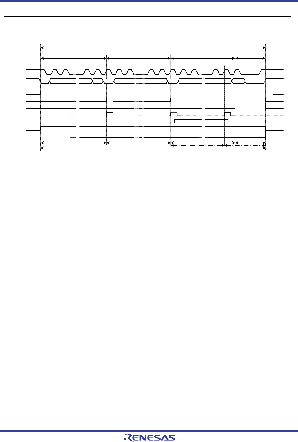
R01UH0034EJ0200 Rev.2.00 Page 1068 of 1489
Dec 27, 2013
RX62T Group, RX62G Group 24. I2C Bus Interface (RIIC)
Figure 24.41 SMBus Timeout Measurement
24.12.2 Packet Error Code (PEC)
The RX62T and RX62G Groups incorporate a CRC operation circuit. The CRC operation circuit enables transmission of
a packet error code (PEC) or checking the received data of the SMBus in data communication of the RIIC. For the CRC
generating polynomials of the CRC operation circuit, see section 23, CRC Calculator (CRC).
The PEC data in master transmit mode (master transmitter) can be generated by writing all transmit data to the CRC data
input register (CRCDIR) in the CRC operation circuit.
The REC data in master receive mode (master receiver) can be checked by writing all receive data to CRCDIR in the
CRC operation circuit and comparing the obtained value in the CRC data output register (CRCDOR) with the received
PEC data.
To send ACK or NACK according to the match or mismatch result when the final byte is received as a result of the PEC
code check, set the RDRFS bit in ICMR3 to 1 before the rising edge of the eighth SMBCLK clock cycle during reception
of the final byte, and hold the SCL line low at the falling edge of the eighth clock cycle.
24.12.3 SMBus Host Notification Protocol/Notify ARP Master
In communications over an SMBus, a slave device can temporarily act as a master device to notify the SMBus host (or
ARP master) of (or request the SMBus host for) its own slave address or to request its own slave address from the
SMBus host.
For a product of the the RX62T or RX62G Group to operate as an SMBus host (or ARP master), the host address (0001
000b) sent from the slave device must be detected as a slave address, so the RIIC has a function for detecting the host
address. To detect the host address as a slave address, set the SMBS bit in ICMR3 and the HOAE bit in ICSER to 1.
Operation after the host address has been detected is the same as normal slave operation.
S 1 1 P998
R/W
7
7-bit slave address
297
Data
2872 8 72 87
Data
281
Start Stop
Clk ACK
Measured with the on-chip timer
TLOW:SEXT
Clk ACK
TLOW:MEXT TLOW:MEXT Clk ACK TLOW:MEXT
TEND
TDRE
BBSY
RDRF
SCL
SDA
START
STOP
RDRFS
TLOW:MEXT
TLOW:SEXT: Total clock low-level extended period (slave device)
TLOW:MEXT: Total clock low-level extended period (master device)
SMBus standard
ACK ACK A/NA

R01UH0034EJ0200 Rev.2.00 Page 1069 of 1489
Dec 27, 2013
RX62T Group, RX62G Group 24. I2C Bus Interface (RIIC)
24.13 Interrupt Sources
The RIIC issues four types of interrupt sources: transfer error or event generation (arbitration lost, NACK detection,
timeout detection, start condition detection, and stop condition detection), receive data full, transmit data empty, and
transmit end.
Table 24.7 shows details of the several interrupt sources. The receive data full and transmit data empty are both capable
of launching data transfer by the DTC.
Clear or mask the various interrupt sources during interrupt handling.
Notes on interrupt processing:
1. There is a latency (delay) between the execution of a write instruction for a peripheral module by the CPU and
actual writing to the module. Thus, when an interrupt flag has been cleared or masked, read the relevant flag again to
check whether clearing or masking has been completed, and then return from interrupt processing. Returning from
interrupt processing without checking that writing to the module has been completed creates a possibility of repeated
processing of the same interrupt.
2. Since ICTXI is an edge-detected interrupted, it does not require clearing. Furthermore, the TDRE flag in ICSR2
(a condition for ICTXI) is automatically cleared to 0 when data for transmission are written to ICDRT or a stop condition
is detected (STOP flag = 1 in ICSR2).
3. Since ICRXI is an edge-detected interrupted, it does not require clearing. Furthermore, the RDRF flag in ICSR2
(a condition for ICRXI) is automatically cleared to 0 when data are read out from ICDRR.
4. When using the ICTEI interrupt, clear the TEND flag in ICSR2 in the ICTEI interrupt processing. Note that the
TEND flag in ICSR2 is automatically cleared to 0 when data for transmission are written to ICDRT or a stop condition
is detected (STOP flag = 1 in ICSR2).
Table 24.7 Interrupt Sources
Abbreviation Interrupt Source Interrupt Flag DTC Launching Priority Interrupt Condition
ICEEI0 Transfer Error/
Event Generation
AL Not possible High
Low
(AL=1) • (ALIE=1)
NACKF (NACKF=1) • (NAKIE=1)
TMOF (TMOF=1) • (TMOIE=1)
START (START=1) • (STIE=1)
STOP (STOP=1) • (SPIE=1)
ICRXI0 Receive Data Full — Possible (RDRF=1)
•
(RIE=1)
ICTXI0 Transmit Data Empty — Possible (TDRE=1)
•
(TIE=1)
ICTEI0 Transmit End TEND Not possible (TEND=1)
•
(TEIE=1)
R01UH0034EJ0200 Rev.2.00 Page 1070 of 1489
Dec 27, 2013
RX62T Group, RX62G Group 24. I2C Bus Interface (RIIC)
24.14 Reset States
The RIIC has chip reset, RIIC reset, and internal reset functions. Table 24.8 shows the scope of each reset and reset
conditions.
Table 24.8 Reset Conditions
Chip Reset
RIIC Reset
(ICE = 0, IICRST = 1)
Internal Reset
(ICE = 1, IICRST = 1)
Start Condition/
Restart Condition
Detection
Stop Condition
Detection
ICCR1 ICE,
IICRST
At a reset Retained Retained Operation (retained) Operation (retained)
SCLO,
SDAO
At a reset At a reset
Others Retained
ICCR2 BBSY At a reset At a reset Operation Operation Operation
ST At a reset At a reset Operation (retained)
Others At a reset
ICMR1 BC[2:0] At a reset At a reset At a reset At a reset Operation (retained)
Others Retained Operation (retained)
ICMR2 At a reset At a reset Retained Operation (retained) Operation (retained)
ICMR3 At a reset At a reset Retained Operation (retained) Operation (retained)
ICFER At a reset At a reset Retained Operation (retained) Operation (retained)
ICSER At a reset At a reset Retained Operation (retained) Operation (retained)
ICIER At a reset At a reset Retained Operation (retained) Operation (retained)
ICSR1 At a reset At a reset At a reset Operation (retained) At a reset
ICSR2 TDRE,
TEND
At a reset At a reset At a reset Operation (retained) At a reset
START Operation
STOP Operation (retained) Operation
Others Operation (retained)
SARL0 to SARL2
SARU0 to SARU2
At a reset At a reset Retained Operation (retained) Operation (retained)
ICBRH, ICBRL At a reset At a reset Retained Operation (retained) Operation (retained)
ICDRT At a reset At a reset Retained Operation (retained) Operation (retained)
ICDRR At a reset At a reset Retained Operation (retained) Operation (retained)
ICDRS At a reset At a reset At a reset Operation (retained) Operation (retained)
Timeout function At a reset At a reset Operation Operation Operation
Bus free time
measurement
At a reset At a reset Operation Operation Operation

R01UH0034EJ0200 Rev.2.00 Page 1071 of 1489
Dec 27, 2013
RX62T Group, RX62G Group 24. I2C Bus Interface (RIIC)
24.15 Usage Notes
24.15.1 Setting Module Stop Function
Module stop state can be entered or canceled using module stop control register B (MSTPCRB). The initial setting is for
operation of the RIIC to be halted. RIIC register access is enabled by clearing module stop state.
For details of module stop control register B, see section 9, Low Power Consumption.
24.15.2 Setting Input Buffer Control Register
Input to peripheral modules can be enabled or disabled using the input buffer control register (PORTn.ICR). The initial
setting is for input to the RIIC to be disabled.
As the SCL and SDA lines on the I2C bus are bidirectional, the SCL and SDA pins of the RIIC are input/output pins.
Make appropriate settings in the input buffer control bits in the PORTn.ICR corresponding to the SCL and SDA pins of
the RIIC to enable input to the RIIC. If the required input is disabled, the RIIC cannot detect start conditions (including
restart conditions) or stop conditions, or count the SCL clock cycles.
For details of the input buffer control register, see section 15, I/O Ports.

R01UH0034EJ0200 Rev.2.00 Page 1072 of 1489
Dec 27, 2013
RX62T Group, RX62G Group 25. CAN Module
25. CAN Module
25.1 Overview
The RX62T and RX62G Groups implement one channel of the CAN (Controller Area Network) module that complies
with the ISO11898-1 Specifications. The CAN module transmits and receives both formats of messages, namely the
standard identifier (11 bits) (identifier is hereafter referred to as ID) and extended ID (29 bits).
Table 25.1 lists the specifications of the CAN module, and Figure 25.1 shows a block diagram of the CAN module.
Connect the CAN bus transceiver externally.
Note: • The CAN module is an optional function. For details, see Table 1.3.
Table 25.1 Specifications of CAN Module
Item Description
Protocol ISO11898-1 compliant (standard and extended frames)
Bit rate Programmable bit rate up to 1 Mbps (fCAN 8 MHz)
fCAN: CAN clock source
Message box 32 mailboxes: Two selectable mailbox modes
Normal mailbox mode: 32 mailboxes can be configured for either transmission or reception.
FIFO mailbox mode: 24 mailboxes can be configured for either transmission or reception.
Of the other mailboxes, four FIFO stages can be configured for
transmission and four FIFO stages for reception.
Reception Data frame and remote frame can be received.
Selectable receiving ID format (only standard ID, only extended ID, or both IDs)
Programmable one-shot reception function
Selectable from overwrite mode (message overwritten) and overrun mode (message discarded)
The reception complete interrupt can be individually enabled or disabled for each mailbox.
Acceptance filter Eight acceptance masks (one mask for every four mailboxes)
The mask can be individually enabled or disabled for each mailbox.
Transmission Data frame and remote frame can be transmitted.
Selectable transmitting ID format (only standard ID, only extended ID, or both IDs)
Programmable one-shot transmission function
Selectable from ID priority mode and mailbox number priority mode
Transmission request can be aborted (the completion of abort can be confirmed with a flag)
The transmission complete interrupt can be individually enabled or disabled for each mailbox.
Mode transition for bus-off
recovery
Mode transition for the recovery from the bus-off state can be selected:
ISO11898-1 Specifications compliant
Automatic entry to CAN halt mode at bus-off entry
Automatic entry to CAN halt mode at bus-off end
Entry to CAN halt mode by a program
Transition into error-active state by a program
Error status monitoring CAN bus errors (stuff error, form error, ACK error, CRC error, bit error, and ACK delimiter error)
can be monitored.
Transition to error states can be detected (error-warning, error-passive, bus-off entry, and bus-off
recovery).
The error counters can be read.
Time stamp function Time stamp function using a 16-bit counter
The reference clock can be selected from 1-, 2-, 4- and 8-bit time periods.
Interrupt function Five types of interrupt sources (reception complete, transmission complete, receive FIFO, transmit
FIFO, and error interrupts)
CAN sleep mode Current consumption can be reduced by stopping the CAN clock.
Software support unit Three software support units:
Acceptance filter support
Mailbox search support (receive mailbox search, transmit mailbox search, and message lost
search)
Channel search support
CAN clock source Peripheral module clock (PCLK)
Test mode Three test modes available for user evaluation
Listen-only mode
Self-test mode 0 (external loopback)
Self-test mode 1 (internal loopback)
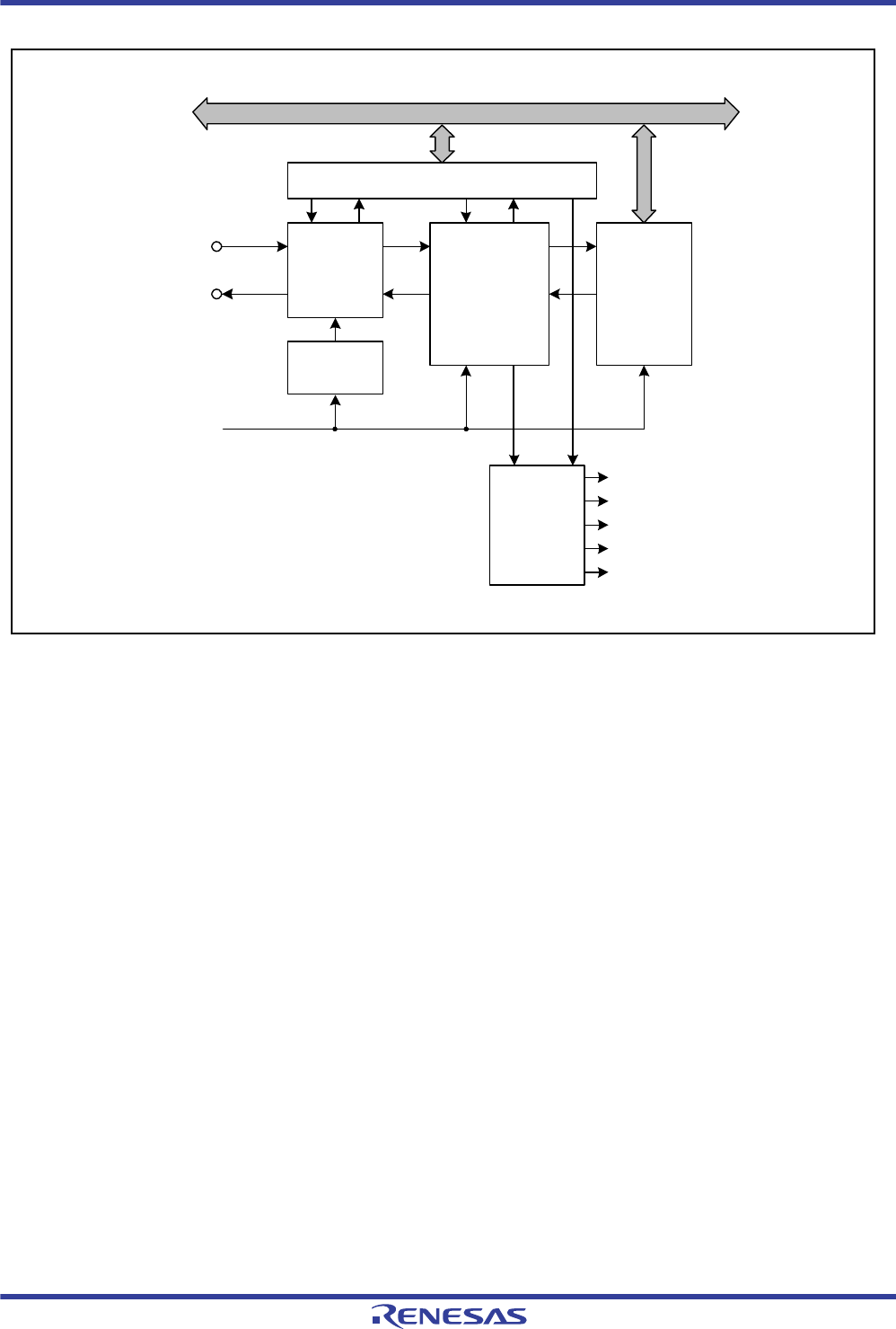
R01UH0034EJ0200 Rev.2.00 Page 1073 of 1489
Dec 27, 2013
RX62T Group, RX62G Group 25. CAN Module
Figure 25.1 Block Diagram of CAN Module
CRX and CTX
CAN input and output pins
Protocol controller
Handles CAN protocol processing such as bus arbitration, bit timing at transmission and reception, stuffing, and
error handling, etc.
Message box
Consists of 32 mailboxes which can be configured as either transmit or receive mailboxes. Each mailbox has an
individual ID, data length code, a data field (8 bytes), and a time stamp.
Acceptance filter
Performs filtering of received messages. MKR0 to MKR7 are used for the filtering process.
Timer
Used for the time stamp function. The timer value when a message is stored into the mailbox is written as the time
stamp value.
Interrupt generator
Generates the following five types of interrupts:
CAN0 reception complete interrupt
CAN0 transmission complete interrupt
CAN0 receive FIFO interrupt
CAN0 transmit FIFO interrupt
CAN0 error interrupt
CRX
CTX
Peripheral module clock
(PCLK)
[Legend]
BRP : Bit in the BCR register
fCANCLK : CAN Communication clock
fCAN : CAN system clock
fCANCLK
fCAN
Baud rate
prescaler
(BRP)
Protocol
controller
CAN-related register
Internal peripheral bus
Message box
Interrupt
generator
Acceptance
filter
ID priority
transmission
controller
Timer
CAN0 reception complete interrupt
CAN0 transmission complete interrupt
CAN0 receive FIFO interrupt
CAN0 transmit FIFO interrupt
CAN0 error interrupt

R01UH0034EJ0200 Rev.2.00 Page 1074 of 1489
Dec 27, 2013
RX62T Group, RX62G Group 25. CAN Module
Table 25.2 shows the CAN module pins.
The CAN functions should be selected for the pins multiplexed with other signals. For details, see section 15, I/O
Ports.
Table 25.2 Pin Configuration
Module Symbol Pin Name I/O Function
CAN0 CRX Input Pin for receiving data
CTX Output Pin for transmitting data

R01UH0034EJ0200 Rev.2.00 Page 1075 of 1489
Dec 27, 2013
RX62T Group, RX62G Group 25. CAN Module
25.2 Register Descriptions
Table 25.3 lists the registers of the CAN module.
Table 25.3 Registers of CAN Module
Module
Symbol Register Name Symbol Value after
Reset Address Access Size
CAN0 Control register CTLR 0500h 0009 0840h 8, 16
Bit configuration register BCR 0000 0000h 0009 0844h 8, 16, 32
Bit configuration register 0 MKR0 Undefined 0009 0400h 8, 16, 32
Bit configuration register 1 MKR1 Undefined 0009 0404h 8, 16, 32
Bit configuration register 2 MKR2 Undefined 0009 0408h 8, 16, 32
Bit configuration register 3 MKR3 Undefined 0009 040Ch 8, 16, 32
Bit configuration register 4 MKR4 Undefined 0009 0410h 8, 16, 32
Bit configuration register 5 MKR5 Undefined 0009 0414h 8, 16, 32
Bit configuration register 6 MKR6 Undefined 0009 0418h 8, 16, 32
Bit configuration register 7 MKR7 Undefined 0009 041Ch 8, 16, 32
FIFO received ID compare register 0 FIDCR0 Undefined 0009 0420h 8, 16, 32
FIFO received ID compare register 1 FIDCR1 Undefined 0009 0424h 8, 16, 32
Mask invalid register MKIVLR Undefined 0009 0428h 8, 16, 32
Mailbox registers 0 to 31 MB0 to MB31 Undefined 0009 0200h to
0009 03FFh
8, 16, 32
Mailbox interrupt enable register MIER Undefined 0009 042Ch 8, 16, 32
Message control registers 0 to 31 MCTL0 to
MCTL31
00h 0009 0820h to
0009 083Fh
8
Receive FIFO control register RFCR 80h 0009 0848h 8
Receive FIFO pointer control register RFPCR Undefined 0009 0849h 8
Transmit FIFO control register TFCR 80h 0009 084Ah 8
Transmit FIFO pointer control register TFPCR Undefined 0009 084Bh 8
Status register STR 0500h 0009 0842h 8, 16
Mailbox search mode register MSMR 00h 0009 0853h 8
Mailbox search status register MSSR 80h 0009 0852h 8
Channel search support register CSSR Undefined 0009 0851h 8
Acceptance filter support register AFSR Undefined 0009 0856h 8, 16
Error interrupt enable register EIER 00h 0009 084Ch 8
Error interrupt factor judge register EIFR 00h 0009 084Dh 8
Receive error count register RECR 00h 0009 084Eh 8
Transmit error count register TECR 00h 0009 084Fh 8
Error code store register ECSR 00h 0009 0850h 8
Time stamp register TSR 0000h 0009 0854h 8, 16
Test control register TCR 00h 0009 0858h 8

R01UH0034EJ0200 Rev.2.00 Page 1076 of 1489
Dec 27, 2013
RX62T Group, RX62G Group 25. CAN Module
25.2.1 Control Register (CTLR)
Note 1. Write to the BOM[1:0], TSPS[1:0], TPM, MLM, IDFM[1:0], and MBM bits in CAN reset mode.
Note 2. Set the RBOC bit to 1 in the bus-off state.
Note 3. This bit is automatically set back to 0 after being set to 1. It should be read as 0.
Note 4. Set the TSRC bit to 1 in CAN operation mode.
Note 5. When the CANM[1:0] and SLPM bits are changed, check STR to ensure that the mode has been switched. Do not change the
CANM[1:0] bits or SLPM bit until the mode has been switched.
Note 6. Write to the SLPM bit in CAN reset mode or CAN halt mode. To change the value of the SLPM bit to 0 or 1, use an arithmetic/
logic instruction to clear or set the bit.
Address: 0009 0840h
0009 0840h 0009 0841h
b15 b14 b13 b12 b11 b10 b9 b8 b7 b6 b5 b4 b3 b2 b1 b0
— — RBOC BOM[1:0] SLPM CANM[1:0] TSPS[1:0] TSRC TPM MLM IDFM[1:0] MBM
Value after reset: 0000010100000000
Bit Symbol Bit Name Description R/W
b0 MBM CAN Mailbox Mode
Select*1 0: Normal mailbox mode
1: FIFO mailbox mode R/W
b2, b1 IDFM[1:0] ID Format Mode Select*1 b2 b1
0 0: Standard ID mode
All mailboxes (including FIFO mailboxes) handle only standard
Ids.
0 1: Extended ID mode
All mailboxes (including FIFO mailboxes) handle only extended
IDs.
1 0: Mixed ID mode
All mailboxes (including FIFO mailboxes) handle both standard
IDs and extended IDs. Standard IDs or extended IDs are speci-
fied by using the IDE bit in the corresponding mailbox in normal
mailbox mode. In FIFO mailbox mode, the IDE bit in the corre-
sponding mailbox is used for mailboxes [0] to [23], the IDE bits in
FIDCR0 and FIDCR1 are used for the receive FIFO, and the IDE
bit in mailbox [24] is used for the transmit FIFO.
1 1: Do not use this combination
R/W
b3 MLM Message Lost Mode
Select*2 0: Overwrite mode
1: Overrun mode R/W
b4 TPM Transmission Priority
Mode Select*2 0: ID priority transmit mode
1: Mailbox number priority transmit mode R/W
b5 TSRC Time Stamp Counter
Reset Command*4 0: Nothing occurred
1: Reset*3 R/W
b7, b6 TSPS[1:0] Time Stamp Prescaler
Select*1
b7 b6
0 0: Every bit time
0 1: Every 2-bit time
1 0: Every 4-bit time
1 1: Every 8-bit time
R/W
b9, b8 CANM[1:0] CAN Operating Mode
Select*5
b9 b8
0 0: CAN operation mode
0 1: CAN reset mode
1 0: CAN halt mode
1 1: CAN reset mode (forcible transition)
R/W
b10 SLPM CAN Sleep Mode*5*6 0: Other than CAN sleep mode
1: CAN sleep mode R/W
b12, b11 BOM[1:0] Bus-Off Recovery Mode*1 b12 b11
0 0: Normal mode (ISO11898-1 compliant)
0 1: Entry to CAN halt mode automatically at bus-off entry
1 0: Entry to CAN halt mode automatically at bus-off end
1 1: Entry to CAN halt mode (during bus-off recovery period) by a pro-
gram request
R/W
b13 RBOC Forcible Return From
Bus-Off*2 0: Nothing occurred
1: Forcible return from bus-off*3 R/W
b15, b14 — Reserved These bits are always read as 0. The write value should always be 0. R/W

R01UH0034EJ0200 Rev.2.00 Page 1077 of 1489
Dec 27, 2013
RX62T Group, RX62G Group 25. CAN Module
MBM Bit (CAN Mailbox Mode Select)
When the MBM bit is 0 (normal mailbox mode), mailboxes [0] to [31] are configured as transmit or receive mailboxes.
When the MBM bit is 1 (FIFO mailbox mode), mailboxes [0] to [23] are configured as transmit or receive mailboxes.
Mailboxes [24] to [27] are configured as a transmit FIFO and mailboxes [28] to [31] as a receive FIFO.
Transmit data is written into mailbox [24] (mailbox [24] is a window mailbox for the transmit FIFO). Receive data is
read from mailbox [28] (mailbox [28] is a window mailbox for the receive FIFO).
Table 25.4 lists the mailbox configuration.
IDFM[1:0] Bits (ID Format Mode Select)
The IDFM[1:0] bits specify the ID format.
MLM Bit (Message Lost Mode Select)
The MLM bit specifies the operation when a new message is captured in the unread mailbox. Overwrite mode or overrun
mode can be selected. All mailboxes (including the receive FIFO) are set to either overwrite mode or overrun mode.
When the MLM bit is 0, all mailboxes are set to overwrite mode and the new message is overwriting the old message.
When the MLM bit is 1, all mailboxes are set to overrun mode and the new message is discarded.
TPM Bit (Transmission Priority Mode Select)
The TPM bit specifies the priority of modes when transmitting messages. ID priority transmit mode or mailbox number
transmit mode can be selected. All mailboxes are set for either ID priority transmission or mailbox number priority
transmission.
When the TPM bit is 0, ID priority transmit mode is selected and transmission priority complies with the CAN bus
arbitration rule, as defined in the ISO11898-1 Specifications. In ID priority transmit mode, mailboxes [0] to [31] (in
normal mailbox mode), and mailboxes [0] to [23] (in FIFO mailbox mode), and the transmit FIFO are compared for the
IDs of mailboxes configured for transmission. If two or more mailbox IDs are the same, the mailbox with the smaller
number has higher priority.
Only the next message to be transmitted from the transmit FIFO is included in the transmission arbitration. If a transmit
FIFO message is being transmitted, the next pending message within the transmit FIFO is included in the transmission
arbitration.
When the TPM bit is 1, mailbox number transmit mode is selected and the transmit mailbox with the smallest mailbox
number has the highest priority. In FIFO mailbox mode, the transmit FIFO has lower priority than normal mailboxes
(mailboxes [0] to [23]).
TSRC Bit (Time Stamp Counter Reset Command)
The TSRC bit is used to reset the time stamp counter. When the TSRC bit is set to 1, TSR is set to 0000h. Then this bit is
automatically set to 0.
TSPS[1:0] Bits (Time Stamp Prescaler Select)
The TSPS bits select the prescaler for the time stamp. The reference clock for the time stamp can be selected to be either
1-, 2-, 4- or 8-bit time periods.
CANM[1:0] Bits (CAN Operating Mode Select)
The CANM[1:0] bits select one of the following modes for the CAN module: CAN operation mode, CAN reset mode, or
CAN halt mode. CAN sleep mode is set by the SLPM bit. For details, refer to section 25.3, Operating Mode.
When the CAN module enters CAN halt mode according to the setting of the BOM[1:0] bits, the CANM[1:0] bits are
automatically set to 10.

R01UH0034EJ0200 Rev.2.00 Page 1078 of 1489
Dec 27, 2013
RX62T Group, RX62G Group 25. CAN Module
SLPM Bit (CAN Sleep Mode)
When the SLPM bit is set to 1, the CAN module enters CAN sleep mode. When the SLPM bit is set to 0, the CAN
module exits CAN sleep mode. For details, refer to section 25.3, Operating Mode.
BOM[1:0] Bits (Bus-Off Recovery Mode)
The BOM[1:0] bits are used to select bus-off recovery mode for the CAN module.
When the BOM[1:0] bits are 00b, the recovery from bus-off is compliant with the ISO11898-1 Specifications, i.e. the
CAN module re-enters CAN communication (error-active state) after detecting 11 consecutive recessive bits 128 times.
A bus-off recovery interrupt request is generated when recovering from bus-off.
When the BOM[1:0] bits are 01b, the CAN module enters CAN halt mode as soon as it reaches the bus-off state and the
CANM[1:0] bits are set to 10b (CAN halt mode). No bus-off recovery interrupt request is generated when recovering
from bus-off, and TECR and RECR are set to 00h.
When the BOM[1:0] bits are 10b, the CANM[1:0] bits are set to 10b as soon as the CAN module reaches the bus-off
state. The CAN module enters CAN halt mode after the recovery from the bus-off state, i.e. after detecting 11
consecutive recessive bits 128 times. A bus-off recovery interrupt request is generated when recovering from bus-off,
and TECR and RECR are set to 00h.
When the BOM[1:0] bits are 11b, the CAN module enters CAN halt mode by setting the CANM[1:0] bits to 10b while
the CAN module is still in the bus-off state. No bus-off recovery interrupt request is generated when recovering from
bus-off and TECR and RECR are set to 00h. However, if the CAN module recovers from bus-off after detecting 11
consecutive recessive bits 128 times before the CANM[1:0] bits are set to 10b, a bus-off recovery interrupt request is
generated.
If the CPU requests an entry to CAN reset mode at the same time as the CAN module attempts to enter CAN halt mode
(at bus-off entry when the BOM[1:0] bits are 01b, or at bus-off end when the BOM[1:0] bits are 10b), then the CPU
request to enter CAN reset mode has higher priority.
RBOC Bit (Forcible Return From Bus-Off)
When the RBOC bit is set to 1 (force return from bus-off) in the bus-off state, the CAN module forcibly returns from the
bus-off state. Then this bit is automatically set to 0. The error state changes from bus-off to error-active. When the RBOC
bit is set to 1, RECR and TECR are set to 00h and the BOST bit in STR is set to 0 (the CAN module is not in bus-off
state). The other registers remain unchanged even when the RBOC bit is set to 1. No bus-off recovery interrupt request is
generated by this recovery from the bus-off state. Use the RBOC bit only when the BOM[1:0] bits are 00b (normal
mode).

R01UH0034EJ0200 Rev.2.00 Page 1079 of 1489
Dec 27, 2013
RX62T Group, RX62G Group 25. CAN Module
Note: • Points 1 to 5 below should be considered when the CTLR.MBM bit is set to 1.
1. Transmit FIFO is controlled by TFCR. MCTLj (j = 0 to 31) of mailboxes [24] to [27] is disabled.
MCTL24 to MCTL27 cannot be used by the transmit FIFO.
2. Receive FIFO is controlled by RFCR. MCTLj (j = 0 to 31) of mailboxes [28] to [31] is disabled.
MCTL28 to MCTL31 cannot be used by the receive FIFO.
3. Refer to MIER about the FIFO interrupts.
4. The corresponding bits in MKIVLR for mailboxes [24] to [31] are disabled. Set 0 to these bits.
5. Transmit/receive FIFOs can be used for both data frames and remote frames.
Table 25.4 Mailbox Configuration
Mailbox MBM Bit = 0
(Normal Mailbox Mode) MBM Bit = 1
(FIFO Mailbox Mode)
Mailboxes [0] to [23] Normal mailbox Normal mailbox
Mailboxes [24] to [27] Transmit FIFO
Mailboxes [28] to [31] Receive FIFO

R01UH0034EJ0200 Rev.2.00 Page 1080 of 1489
Dec 27, 2013
RX62T Group, RX62G Group 25. CAN Module
25.2.2 Bit Configuration Register (BCR)
Tq: Time Quantum
Address: 0009 0844h
0009 0844h 0009 0845h
b31 b30 b29 b28 b27 b26 b25 b24 b23 b22 b21 b20 b19 b18 b17 b16
TSEG[3:0] — — BRP[9:0]
Value after reset: 0000010100000000
0009 0846h 0009 0847h
b15 b14 b13 b12 b11 b10 b9 b8 b7 b6 b5 b4 b3 b2 b1 b0
—— SJW[1:0] — TSEG2[2:0] ————————
Value after reset: 0000010100000000
Bit Symbol Bit Name Description R/W
b7 to b0 — Reserved These bits are always read as 0. The write value should always be 0. R/W
b10 to b8 TSEG2[2:0] Time Segment 2 Control b10 b9 b8
0 0 0: Setting prohibited
0 0 1: 2 Tq
0 1 0: 3 Tq
0 1 1: 4 Tq
1 0 0: 5 Tq
1 0 1: 6 Tq
1 1 0: 7 Tq
1 1 1: 8 Tq
R/W
b11 — Reserved This bit is always read as 0.The write value should always be 0. R/W
b13, b12 SJW[1:0] Resynchronization Jump
Width Control
b13 b12
0 0: 1Tq
0 1: 2Tq
1 0: 3Tq
1 1: 4Tq
R/W
b15, b14 — Reserved These bits are always read as 0. The write value should always be 0. R/W
b25 to
b16
BRP[9:0] Prescaler Division Ratio
Select
These bits set the frequency of the CAN communication clock
(fCANCLK).
R/W
b27, b26 — Reserved These bits are always read as 0. The write value should always be 0. R/W
b31 to 28 TSEG[3:0] Time Segment 1 Control b31 b28
0 0 0 0: Setting prohibited
0 0 0 1: Setting prohibited
0 0 1 0: Setting prohibited
0 0 1 1: 4 Tq
0 1 0 0: 5 Tq
0 1 0 1: 6 Tq
0 1 1 0: 7 Tq
0 1 1 1: 8 Tq
1 0 0 0: 9 Tq
1 0 0 1: 10 Tq
1 0 1 0: 11 Tq
1 0 1 1: 12 Tq
1 1 0 0: 13 Tq
1 1 0 1: 14 Tq
1 1 1 0: 15 Tq
1 1 1 1: 16 Tq
R/W

R01UH0034EJ0200 Rev.2.00 Page 1081 of 1489
Dec 27, 2013
RX62T Group, RX62G Group 25. CAN Module
BCR specifies the segment length with a Tq value.
For bit timing setting, refer to section 25.4, CAN Communication Speed Setting.
Set BCR before entering CAN halt mode or CAN operation mode from CAN reset mode. After the setting is made once,
this register can be written to in CAN reset mode or CAN halt mode.
BCR consists of 24 bits. A 32-bit read/write access should be performed carefully not to rewrite bits b0 to b7.
TSEG2[2:0] Bits (Time Segment 2 Control)
The TSEG2[2:0] bits are used to specify the length of the phase buffer segment 2 (PHASE_SEG2) with a Tq value. A
value from 2 to 8 Tq can be set. Set a value smaller than that of the TSEG1[3:0] bits.
SJW[1:0] Bits (Resynchronization Jump Width Control)
The SJW[1:0] bits are used to specify the resynchronization jump width with a Tq value. A value from 1 to 4 Tq can be
set. Set a value smaller than or equal to that of the TSEG2[2:0] bits.
BRP[9:0] Bits (Prescaler Division Ratio Select)
The BRP[9:0] bits are used to set the frequency of the CAN communication clock (fCANCLK). The fCANCLK cycle is
1 Tq. If the setting is P (0 to 1023), the baud rate prescaler divides fCAN by P + 1.
TSEG1[3:0] Bits (Time Segment 1 Control)
The TSEG1[3:0] bits are used to specify the total length of the propagation time segment (PROP_SEG) and phase buffer
segment 1 (PHASE_SEG1) with a time quantum (Tq) value.
A value from 4 to 16 Tq can be set.

R01UH0034EJ0200 Rev.2.00 Page 1082 of 1489
Dec 27, 2013
RX62T Group, RX62G Group 25. CAN Module
25.2.3 Mask Register i (MKRi) (i = 0 to 7)
For the mask function in FIFO mailbox mode, refer to section 25.6, Acceptance Filtering and Masking Functions.
Write to MKR0 to MKR7 in CAN reset mode or CAN halt mode.
EID Bit (Extended ID)
The EID[17:0] bits are the filter mask bits for the CAN extended ID bits.
These bits are used to receive extended ID messages.
When the EID[17:0] bit is set to 0, the received ID is not compared with the mailbox ID for the corresponding EID[17:0]
bit.
When the EID[17:0] bit is set to 1, the received ID is compared with the mailbox ID for the corresponding EID[17:0] bit.
SID Bit (Standard ID)
The SID[10:0] bits are the filter mask bits corresponding to the CAN standard ID bits.
These bits are used to receive both standard ID and extended ID messages.
When the SID[10:0] bit is set to 0, the received ID is not compared with the mailbox ID for the corresponding SID[10:0]
bit.
When the SID[10:0] bit is set to 1, the received ID is compared with the mailbox ID for the corresponding SID[10:0] bit.
Address: 0009 0400h to 0009 041Ch
0009 0400h
+(I×4h) 0009 0401h
+(I×4h)
b31 b30 b29 b28 b27 b26 b25 b24 b23 b22 b21 b20 b19 b18 b17 b16
— — — SID[10:0] EID[17:0]
Value after reset: xxxxxxxxxxxxxxxx
0009 0402h
+(I×4h) 0009 0403h
+(I×4h)
b15 b14 b13 b12 b11 b10 b9 b8 b7 b6 b5 b4 b3 b2 b1 b0
EID[17:0]
Value after reset: xxxxxxxxxxxxxxxx
[Legend] x: Undefined
Bit Symbol Bit Name Description R/W
b17 to b0 EID[17:0] Extended ID 0: Corresponding EID[17:0] bit is not compared
1: Corresponding EID[17:0] bit is compared
R/W
b28 to b18 SID[10:0] Standard ID 0: Corresponding SID[10:0] bit is not compared
1: Corresponding SID[10:0] bit is compared
R/W
b31 to b29 — Reserved The read value is undefined. The write value should always be 0. R/W

R01UH0034EJ0200 Rev.2.00 Page 1083 of 1489
Dec 27, 2013
RX62T Group, RX62G Group 25. CAN Module
25.2.4 FIFO Received ID Compare Registers 0 and 1 (FIDCR0 and FIDCR1)
Note 1. When the IDFM[1:0] bits in CTLR are not 10b, the IDE bit should be written with 0 and read as 0.
FIDCR0 and FIDCR1 are enabled when the MBM bit in CTLR is set to 1 (FIFO mailbox mode). Bits EID[17:0],
SID[10:0], RTR, and IDE bits in MB28 to MB31 are disabled.
For the usage of FIDCR0 and FIDCR1, refer to section 25.6, Acceptance Filtering and Masking Functions.
Write to FIDCR0 and FIDCR1 in CAN reset mode or CAN halt mode.
EID Bit (Extended ID)
The EID[17:0] bits set the extended ID of data frames and remote frames.
The EID[17:0] bits are used to receive extended ID messages.
SID Bit (Standard ID)
The SID[10:0] bits set the standard ID of data frames and remote frames.
The SID[10:0] bits are used to receive both standard ID and extended ID messages.
RTR Bit (Remote Transmission Request)
The RTR bit sets the specified frame format of data frames or remote frames.
When both RTR bits in FIDCR0 and FIDCR1 are set to 0, only data frames can be received.
When both RTR bits in FIDCR0 and FIDCR1 are set to 1, only remote frames can be received.
When the RTR bits in FIDCR0 and FIDCR1 are set to 0 or 1 individually, both data frames and remote frames can
be received.
Address: FIDCR1 0009 0420h,
FIDCR1 0009 0424h
0009 0400h,
0009 0424h 0009 0421h,
0009 0425h
b31 b30 b29 b28 b27 b26 b25 b24 b23 b22 b21 b20 b19 b18 b17 b16
IDE RTR — SID[10:0] EID[17:0]
Value after reset: xxxxxxxxxxxxxxxx
0009 0422h,
0009 0426h 0009 0423h,
0009 0427h
b15 b14 b13 b12 b11 b10 b9 b8 b7 b6 b5 b4 b3 b2 b1 b0
EID[17:0]
Value after reset: xxxxxxxxxxxxxxxx
[Legend] x: Undefined
Bit Symbol Bit Name Description R/W
b17 to b0 EID[17:0] Extended ID 0: Corresponding EID[17:0] bit is 0
1: Corresponding EID[17:0] bit is 1
R/W
b28 to
b18
SID[10:0] Standard ID 0: Corresponding SID[10:0] bit is 0
1: Corresponding SID[10:0] bit is 1
R/W
b29 — Reserved The read value is undefined. The write value should always be 0. R/W
b30 RTR Remote Transmission
Request
0: Data frame
1: Remote frame
R/W
b31 IDE ID Extension*0: Standard ID
1: Extended ID
R/W

R01UH0034EJ0200 Rev.2.00 Page 1084 of 1489
Dec 27, 2013
RX62T Group, RX62G Group 25. CAN Module
IDE Bit (ID Extension)
The IDE bit sets the ID format to standard ID or extended ID. The IDE bit is enabled when the IDFM[1:0] bits in CTLR
is 10b (mixed ID mode).
When both IDE bits in FIDCR0 and FIDCR1 are set to 0, only standard ID frames can be received.
When both IDE bits in FIDCR0 and FIDCR1 are set to 1, only extended ID frames can be received.·
When the IDE bits in FIDCR0 and FIDCR1 are set to 0 or 1 individually, both standard ID and extended ID frames
can be received.

R01UH0034EJ0200 Rev.2.00 Page 1085 of 1489
Dec 27, 2013
RX62T Group, RX62G Group 25. CAN Module
25.2.5 Mask Invalid Register (MKIVLR)
Each bit in MKIVLR corresponds to a mailbox.
The correspondence between the bits and mailboxes is shown below.
Bit 0 in MKIVLR corresponds to mailbox 0 and bit 31 corresponds to mailbox 31.*
When a bit is set to 1, the relevant acceptance mask register becomes invalid for the corresponding mailbox. When a
mask invalid bit is set to 1, a message is received by the corresponding mailbox only if the receive message ID matches
the mailbox ID exactly.
Write to MKIVLR in CAN reset mode or CAN halt mode.
Note 1. Set bits 31 to 24 to 0 in FIFO mailbox mode.
Address: 0009 0428h
0009 0428h 0009 0429h
b31 b30 b29 b28 b27 b26 b25 b24 b23 b22 b21 b20 b19 b18 b17 b16
Value after reset: xxxxxxxxxxxxxxxx
0009 0430h 0009 0431h
b15 b14 b13 b12 b11 b10 b9 b8 b7 b6 b5 b4 b3 b2 b1 b0
Value after reset: xxxxxxxxxxxxxxxx
[Legend] x: Undefined
Bit Symbol Bit Name Description R/W
b31 to b0 — — 0: Mask valid
1: Mask invalid
R/W

R01UH0034EJ0200 Rev.2.00 Page 1086 of 1489
Dec 27, 2013
RX62T Group, RX62G Group 25. CAN Module
25.2.6 Mailbox Register j (MBj) (j = 0 to 31)
Table 25.5 lists the CAN mailbox memory mapping, and Table 25.6 lists the CAN data frame configuration.
The value after reset of the CAN mailbox is undefined.
Write to MBj only when the related MCTLj (j = 0 to 31) is 00h and the corresponding mailbox is not processing an abort
request.
See Table 25.3 for detailed register addresses.
Table 25.5 Mailbox Memory Mapping
Address Register Symbol Message Content
CAN0 CAN0 Memory Mapping
0009 0200h + 16 x j + 0 MB.ID IDE, RTR, SID10 to SID6
0009 0200h + 16 x j + 1 SID5to SID0, EID17, EID16
0009 0200h + 16 x j + 2 EID15 to EID8
0009 0200h + 16 x j + 3 EID7 to EID0
0009 0200h + 16 x j + 4 MB.DLC —
0009 0200h + 16 x j + 5 Data length code (DLC[3:0])
0009 0200h + 16 x j + 6 MB.DATA0 to MB.DATA7 Data byte 0
0009 0200h + 16 x j + 7
:
0009 0200h + 16 x j + 13
Data byte 1
:
Data byte 7
0009 0200h + 16 x j + 14 MB.TS Time stamp upper byte
0009 0200h + 16 x j + 15 Time stamp lower byte
Table 25.6 CAN Data Frame Configuration
SID10 to SID6 SID5 to SID0 EID17 to EID16 EID15 to EID8 EID7 to EID0 DLC3 to DLC1 DATA0 DATA1 DATA7

R01UH0034EJ0200 Rev.2.00 Page 1087 of 1489
Dec 27, 2013
RX62T Group, RX62G Group 25. CAN Module
The previous value of each mailbox is retained unless a new message is received.
(a) MB.ID
Note 1. If the mailbox has received a standard ID message, the EID[17:0] bits in the mailbox are undefined.
Note 2. The IDE bit is enabled when the IDFM[1:0] bits in CTLR are 10b (mixed ID mode). When the IDFM[1:0] bits in CTLR are not 10b,
it should be written with 0 and read as 0.
EID[17:0] Bit (Extended ID)
The EID[17:0] bits set the extended ID of data frames and remote frames.
The EID[17:0] bits are used to transmit or receive extended ID messages.
SID[10:0] Bit (Standard ID)
The SID[10:0] bits set the standard ID of data frames and remote frames.
The SID[10:0] bits are used to transmit or receive both standard ID and extended ID messages.
RTR Bit (Remote Frame Request)
The RTR bit sets the frame format of data frames or remote frames.
Receive mailbox receives only frames with the format specified by the RTR bit.·
Transmit mailbox transmits according to the frame format specified by the RTR bit.
Receive FIFO mailbox receives the data frame, remote frame, or both frames specified by the RTR bit in FIDCR0
and FIDCR1.
Transmit FIFO mailbox transmits the data frame or remote frame specified by the RTR bit in the relevant transmit
message.
Address: 0009 0200h to 0009 03FFh
0009 0200h
+(j×10h) 0009 0201h
+(j×10h)
b31 b30 b29 b28 b27 b26 b25 b24 b23 b22 b21 b20 b19 b18 b17 b16
IDE RTR — SID[10:0] EID[17:0]
Value after reset: xxxxxxxxxxxxxxxx
0009 0202h
+(j×10h) 0009 0203h
+(j×10h)
b15 b14 b13 b12 b11 b10 b9 b8 b7 b6 b5 b4 b3 b2 b1 b0
EID[17:0]
Value after reset: xxxxxxxxxxxxxxxx
[Legend] x: Undefined
Bit Symbol Bit Name Description R/W
b17 to b0 EID[17:0] Extended ID*1 0: Corresponding EID[17:0] bit is 0
1: Corresponding EID[17:0] bit is 1
R/W
b28 to
b18
SID[10:0] Standard ID 0: Corresponding SID[10:0] bit is 0
1: Corresponding SID[10:0] bit is 1
R/W
b29 — Reserved The read value is undefined. The write value should always be 0. R/W
b30 RTR Remote Frame Request 0: Data frame
1: Remote frame
R/W
b31 IDE ID Extension*2 0: Standard ID
1: Extended ID
R/W

R01UH0034EJ0200 Rev.2.00 Page 1088 of 1489
Dec 27, 2013
RX62T Group, RX62G Group 25. CAN Module
IDE Bit (ID Extension)
The IDE bit sets the ID format of standard IDs or extended IDs. The IDE bit is enabled when the IDFM[1:0] bits in
CTLR is 10b (mixed ID mode).
Receive mailbox receives only the ID format specified by the IDE bit.
Transmit mailbox transmits with the ID format specified by the IDE bit.
Receive FIFO mailbox receives messages with the standard ID, extended ID, or both IDs specified by the IDE bit in
FIDCR0 and FIDCR1.
Transmit FIFO mailbox transmits messages with the standard ID or extended ID specified by the IDE bit in the
relevant transmit message.
(b) MB.DLC
Note 1. If the mailbox has received a message whose data length set by the DLC[3:0] bits is less than 8 bytes, the values of DATA larger
than the data length set by the DLC[3:0] bits in the mailbox are undefined.
DLC[3:0] Bits (Data Length Code)
The DLC[3:0] bits are used to set the number of data bytes to be transmitted in a data frame. When data is requested
using a remote frame, the number of data bytes to be requested is set.
When a data frame is received, the number of received data bytes is stored. When a remote frame is received, the number
of requested data bytes is stored.
Address: 0009 0205h to 0009 03F5h
0009 0205h
+(j×10h) 0009 0206h
+(j×10h)
b15 b14 b13 b12 b11 b10 b9 b8 b7 b6 b5 b4 b3 b2 b1 b0
———————————— DLC[3:0]
Value after reset: xxxxxxxxxxxxxxxx
[Legend] x: Undefined
Bit Symbol Bit Name Description R/W
b3 to b0 DLC[3:0] Data Length Code*1b3 b0
0 0 0 0: Data length = 0 byte
0 0 0 1: Data length = 1 byte
0 0 1 0: Data length = 2 bytes
0 0 1 1: Data length = 3 bytes
0 1 0 0: Data length = 4 bytes
0 1 0 1: Data length = 5 bytes
0 1 1 0: Data length = 6 bytes
0 1 1 1: Data length = 7 bytes
1 x x x: Data length = 8 bytes
Note:x represents any value.
R/W
b15 to b4 — Reserved The read value is undefined. The write value should always be 0. R/W
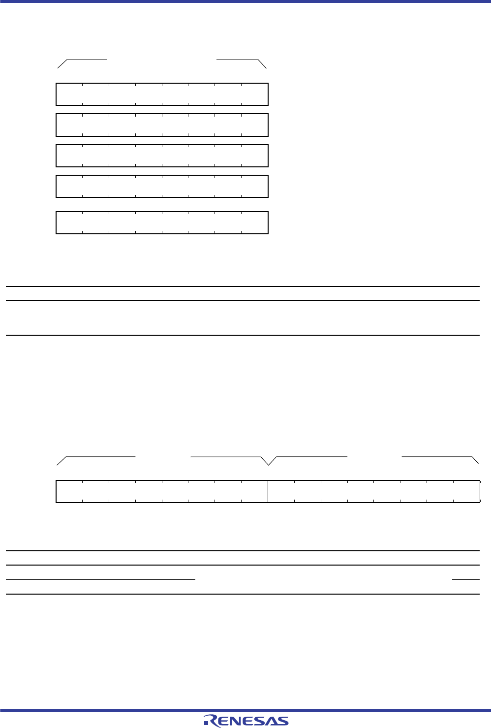
R01UH0034EJ0200 Rev.2.00 Page 1089 of 1489
Dec 27, 2013
RX62T Group, RX62G Group 25. CAN Module
(c) MB.DATA0 to MB.DATA7
Note 1. If the mailbox has received a message with n bytes less than 8 bytes, the values of DATA0 to DATA7 in the mailbox are
undefined.
Note 2. If the mailbox has received a remote frame, the previous values of DATA0 to DATA7 in the mailbox are retained.
(d) MB.TS
Address: 0009 0206h to 0009 03FDh
0009 0206h + (j×10h) to
0009 020Dh + (j×10h)
b7 b6 b5 b4 b3 b2 b1 b0
DATA0
DATA1
DATA2
DATA3
:
DATA7
Value after reset: xxxxxxxx
[Legend] x: Undefined
Bit Symbol Bit Name Description R/W
b7 to b0 DATA0 to
DATA7
Data Bytes 0 to 7*1*2DATA0 to DATA7 store the transmitted or received CAN message data.
Transmission or reception starts from DATA0. The bit order on the CAN
bus is MSB first, and transmission or reception starts from bit 7.
R/W
Address: 0009 020Eh to 0009 03FFh
0009 020Eh
+(j×10h) 0009 020Fh
+(j×10h)
b15 b14 b13 b12 b11 b10 b9 b8 b7 b6 b5 b4 b3 b2 b1 b0
TSH[7:0] TSL[7:0]
Value after reset: xxxxxxxxxxxxxxxx
[Legend] x: Undefined
Bit Symbol Bit Name Description R/W
b7 to b0 TSL[7:0]] Time Stamp Lower Byte Bits TSH[7:0] and TSL[7:0] store the counter value of the time stamp
when received messages are stored in the mailbox.
R/W
b15 to b8 TSH[7:0] Time Stamp Higher Byte R/W

R01UH0034EJ0200 Rev.2.00 Page 1090 of 1489
Dec 27, 2013
RX62T Group, RX62G Group 25. CAN Module
25.2.7 Mailbox Interrupt Enable Register (MIER)
Normal mailbox mode
Address: 0009 042Ch
0009 042Ch 0009 042Dh
b31 b30 b29 b28 b27 b26 b25 b24 b23 b22 b21 b20 b19 b18 b17 b16
————————————————
Value after reset: xxxxxxxxxxxxxxxx
0009 042Eh 0009 042Fh
b15 b14 b13 b12 b11 b10 b9 b8 b7 b6 b5 b4 b3 b2 b1 b0
————————————————
Value after reset: xxxxxxxxxxxxxxxx
[Legend] x: Undefined
Bit Symbol Bit Name Description R/W
b31 to b0 — Interrupt Enable 0: Interrupt disabled
1: Interrupt enabled
Bit 31 corresponds to mailbox 31, and bit 0 corresponds to mailbox 0.
R/W

R01UH0034EJ0200 Rev.2.00 Page 1091 of 1489
Dec 27, 2013
RX62T Group, RX62G Group 25. CAN Module
FIFO mailbox mode
Note 1. No interrupt request is generated when the receive FIFO becomes buffer warning from full. “Buffer warning” indicates a state in
which the third message is stored in the receive FIFO.
MIER can individually enable interrupts for each mailbox.
In normal mailbox mode (all bits) and in FIFO mailbox mode (bits 23 to 0 in MIER), each bit corresponds to the mailbox
with the related number. These bits enable or disable transmission/reception complete interrupts for the corresponding
mailboxes.
Bit 0 in MIER corresponds to mailbox 0.
Bit 31 in MIER corresponds to mailbox 31.
In FIFO mailbox mode, bits 29, 28, 25, and 24 of MIER specify whether transmit/receive FIFO interrupts are enabled/
disabled and the timing when interrupt requests are generated.
Write to MIER only when the related MCTLj (j = 0 to 31) is 00h and the corresponding mailbox is not processing a
transmission or reception abort request. In FIFO mailbox mode, change the bits in MIER for the related FIFO only when
the TFE bit in TFCR is 0 and the TFEST bit in TFCR is 1, and the RFE bit in RFCR is 0 and the RFEST bit in RFCR is 1.
Address: 0009 042Ch
0009 042Ch 0009 042Dh
b31 b30 b29 b28 b27 b26 b25 b24 b23 b22 b21 b20 b19 b18 b17 b16
————————————————
Value after reset: xxxxxxxxxxxxxxxx
0009 042Eh 0009 042Fh
b15 b14 b13 b12 b11 b10 b9 b8 b7 b6 b5 b4 b3 b2 b1 b0
————————————————
Value after reset: xxxxxxxxxxxxxxxx
[Legend] x: Undefined
Bit Symbol Bit Name Description R/W
b23 to b0 — Interrupt Enable 0: Interrupt disabled
1: Interrupt enabled
Bit 23 corresponds to mailbox 23, and bit 0 corresponds to mailbox 0.
R/W
b24 — Transmit FIFO Interrupt
Enable
0: Interrupt disabled
1: Interrupt enabled
R/W
b25 — Transmit FIFO Interrupt
Generation Timing
Control
0: Every time transmission is completed
1: When the transmit FIFO becomes empty due to completion of
transmission
R/W
b27, b26 — Reserved The read value is undefined. The write value should always be 0. R/W
b28 — Receive FIFO Interrupt
Enable
0: Interrupt disabled
1: Interrupt enabled
R/W
b29 — Receive FIFO Interrupt
Generation Timing
Control*1
0: Every time reception is completed
1: When the receive FIFO becomes buffer warning by completion of
reception
R/W
b31, b30 — Reserved The read value is undefined. The write value should always be 0. R/W
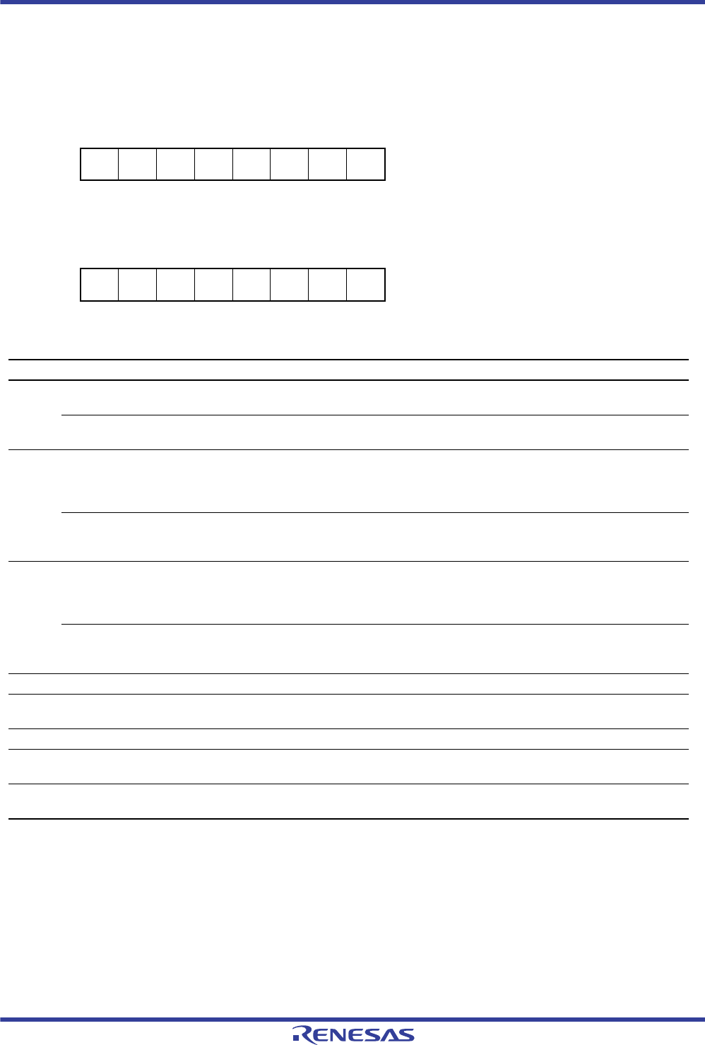
R01UH0034EJ0200 Rev.2.00 Page 1092 of 1489
Dec 27, 2013
RX62T Group, RX62G Group 25. CAN Module
25.2.8 Message Control Register j (MCTLj) (j = 0 to 31)
Note 1. Write 0 only. Writing 1 has no effect.
Note 2. When writing 0 to bits NEWDATA, SENTDATA, MSGLOST, TRMABT, RECREQ, and TRMREQ by a program, do not use the
logic operation instruction (AND.B). Write 0 to only the specified bit and write 1 to the other bits before using the transfer (MOV)
instruction. Writing 1 to this bit has no effect.
Note 3. To enter one-shot receive mode, write 1 to the ONESHOT bit at the same time as setting the RECREQ bit to 1.
To exit one-shot receive mode, write 0 to the ONESHOT bit after writing 0 to the RECREQ bit and confirming that it has been set
to 0.
To enter one-shot transmit mode, write 1 to the ONESHOT bit at the same time as setting the TRMREQ bit to 1.
To exit one-shot transmit mode, write 0 to the ONESHOT bit after the message has been transmitted or aborted.
Note 4. Do not set both the RECREQ and TRMREQ bits to 1.
Note 5. When setting the RECREQ bit to 0, set bits MSGLOST, NEWDATA, and RECREQ to 0 simultaneously.
Address: 0009 0820h to 0009 083Fh
MCTL.TX
Transmit mode (when the TRMREQ bit is 1 and the RECREQ bit is 0)
b7 b6 b5 b4 b3 b2 b1 b0
TRMRE
QRECRE
Q—ONESH
OT —TRMAB
TTRMAC
TIVE SENTD
ATA
Value after reset: 00000000
MCTL.RX
Receive mode (when the TRMREQ bit is 0 and the RECREQ bit is 1)
b7 b6 b5 b4 b3 b2 b1 b0
TRMRE
QRECRE
Q—ONESH
OT —MSGL
OST INVALD
ATA NEWD
ATA
Value after reset: 00000000
Bit Symbol Bit Name Description R/W
b0 SENTDATA Transmission Complete
Flag*1*2 0: Transmission is not completed
1: Transmission is completed
R/W
(W)
NEWDATA Reception Complete
Flag*1*2 0: No data has been received or 0 is written to the NEWDATA bit
1: A new message is being stored or has been stored to the mailbox
R/W
(W)
b1 TRMACTIVE Transmission-in-Progress
Status Flag
(Transmit mailbox setting enabled)
0: Transmission is pending or transmission is not requested
1: From acceptance of transmission request to completion of
transmission, or error/arbitration lost
R
INVALDATA Reception-in-Progress
Status Flag
(Receive mailbox setting enabled)
0: Message valid
1: Message being updated
R
b2 TRMABT Transmission Abort
Complete Flag
*1*2
(Transmit mailbox setting enabled)
0: Transmission has started, transmission abort failed because
transmission is completed, or transmission abort is not requested
1: Transmission abort is completed
R/W
(W)
MSGLOST Message Lost Flag*1*2 (Receive mailbox setting enabled)
0: Message is not overwritten or overrun
1: Message is overwritten or overrun
R/W
(W)
b3 — Reserved This bit is always read as 0. The write value should always be 0. R/W
b4 ONESHOT One-Shot Enable*3 0: One-shot reception or one-shot transmission disabled
1: One-shot reception or one-shot transmission enabled
R/W
b5 — Reserved This bit is always read as 0. The write value should always be 0. R/W
b6 RECREQ Receive Mailbox
Request*2*3*4*5 0: Not configured for reception
1: Configured for reception
R/W
b7 TRMREQ Transmit Mailbox
Request*2*4 0: Not configured for transmission
1: Configured for transmission
R/W

R01UH0034EJ0200 Rev.2.00 Page 1093 of 1489
Dec 27, 2013
RX62T Group, RX62G Group 25. CAN Module
Write to the MCTLj in CAN operation mode or CAN halt mode.
Do not use MCTL24 to MCTL31 in FIFO mailbox mode.
SENTDATA Flag (Transmission Complete Flag)
The SENTDATA flag is set to 1 when data transmission from the corresponding mailbox is completed. The SENTDATA
flag is set to 0 by writing 0 by a program.
To set the SENTDATA flag to 0, first set the TRMREQ bit to 0. Bits SENTDATA and TRMREQ cannot be set to 0
simultaneously. To transmit a new message from the corresponding mailbox, set the SENTDATA flag to 0.
NEWTDATA Flag (Reception Complete Flag)
The NEWDATA flag is set to 1 when a new message is being stored or has been stored to the mailbox. The timing for
setting this bit to 1 is simultaneous with the INVALDATA bit. The NEWDATA flag is set to 0 by writing 0 by a program.
The NEWDATA flag cannot be set to 0 by writing 0 by a program while the related INVALDATA bit is 1.
TRMACTIVE Bit (Transmission-in-Progress Status Flag)
The TRMACTIVE bit is set to 1 when the corresponding mailbox of the CAN module begins transmitting a message.
The TRMACTIVE is set to 0 when the CAN module has lost CAN bus arbitration, a CAN bus error occurs, or data
transmission is completed.
INVALDATA Bit (Reception-in-Progress Status Flag)
After the completion of a message reception, the INVALDATA bit is set to 1 while the received message is being updated
into the corresponding mailbox. The INVALDATA bit is set to 0 immediately after the message has been stored. If the
mailbox is read while the INVALDATA bit is 1, the data is undefined.
TRMABT Flag (Transmission Abort Complete Flag)
The TRMABT flag is set to 1 in the following cases:
Following a transmission abort request, when the transmission abort is completed before starting transmission.·
Following a transmission abort request, when the CAN module detects CAN bus arbitration lost or a CAN bus error.
In one-shot transmission mode (RECREQ bit = 0, TRMREQ bit = 1, and ONESHOT bit = 1), when the CAN
module detects CAN bus arbitration lost or a CAN bus error.
The TRMABT flag is not set to 1 when data transmission is completed. In this case, the SENTDATA flag is set to 1. The
TRMABT flag is set to 0 by writing 0 by a program.
MSGLOST Flag (Message Lost Flag)
The MSGLOST flag is set to 1 when the mailbox is overwritten or overrun by a new received message while the
NEWDATA flag is 1. The MSGLOST flag is set to 1 at the end of the 6th bit of EOF. The MSGLOST flag is set to 0 by
writing 0 by a program.
In both overwrite and overrun modes, the MSGLOST flag cannot be set to 0 by writing 0 by a program during five
peripheral module clock (PCLK) cycles following the sixth bit of EOF.

R01UH0034EJ0200 Rev.2.00 Page 1094 of 1489
Dec 27, 2013
RX62T Group, RX62G Group 25. CAN Module
ONESHOT Bit (One-Shot Enable)
The ONESHOT bit can be used in the following two ways, receive mode and transmit mode.
One-shot receive mode
When the ONESHOT bit is set to 1 in receive mode (RECREQ bit = 1 and TRMREQ bit = 0), the mailbox receives
a message only one time. (The mailbox does not behave as a receive mailbox after having received a message one
time.) The behavior of bits NEWDATA and INVALDATA is the same as in normal receive mode. In one-shot
receive mode, the MSGLOST flag is not set to 1.To set the ONESHOT bit to 0, first write 0 to the RECREQ bit and
ensure that it has been set to 0.
One-shot transmit mode
When the ONESHOT bit is set to 1 in transmit mode (RECREQ bit = 0 and TRMREQ bit = 1), the CAN module
transmits a message only one time. (The CAN module does not transmit the message again if a CAN bus error or
CAN bus arbitration lost occurs.) When transmission is completed, the SENTDATA flag is set to 1. If transmission
is not completed due to a CAN bus error or CAN bus arbitration lost, the TRMABT flag is set to 1. Set the
ONESHOT bit to 0 after the SENTDATA or TRMABT bit is set to 1.
RECREQ Bit (Receive Mailbox Request)
The RECREQ bit selects receive modes shown in Table 25.11.
When the RECREQ bit is set to 1, the corresponding mailbox is configured for reception of a data frame or a remote
frame.
When the RECREQ bit is set to 0, the corresponding mailbox is not configured for reception of a data frame or a remote
frame.
Due to hardware protection, the RECREQ bit cannot be set to 0 by writing 0 by a program during the following period.
Hardware protection is started
From the acceptance filter processing (the beginning of CRC field)
Hardware protection is released
For the mailbox that is specified to receive the incoming message, after the received data is stored into the mailbox
or a CAN bus error occurs (i.e. maximum period of hardware protection is from the beginning of CRC field to the
end of the 7th bit of EOF)
For the other mailboxes, after the acceptance filter processing
If no mailbox is specified to receive the message, after the acceptance filter processing
When setting the RECREQ bit to 1, do not set the TRMREQ bit to 1. To change the configuration of a mailbox
from transmission to reception, first abort the transmission and then set bits SENTDATA and TRMABT to 0
before changing to reception.
When setting the RECREQ bit to 1, do not set the TRMREQ bit to 1. To change the configuration of a mailbox from
transmission to reception, first abort the transmission and then set bits SENTDATA and TRMABT to 0 before changing
to reception.

R01UH0034EJ0200 Rev.2.00 Page 1095 of 1489
Dec 27, 2013
RX62T Group, RX62G Group 25. CAN Module
TRMREQ Bit (Transmit Mailbox Request)
The TRMREQ bit selects transmit modes shown in Table 25.11.
When the TRMREQ bit is set to 1, the corresponding mailbox is configured for transmission of a data frame or a remote
frame.
When the TRMREQ bit is set to 0, the corresponding mailbox is not configured for transmission of a data frame or a
remote frame.
If the TRMREQ bit is changed from 1 to 0 to cancel the corresponding transmission request, either the TRMABT or
SENTDATA flag is set to 1 with a maximum delay of one frame. This is used to confirm whether the transmission abort
request has been completed or not. When setting the TRMREQ bit to 1, do not set the RECREQ bit to 1. To change the
configuration of a mailbox from reception to transmission, first abort the reception and then set bits NEWDATA and
MSGLOST to 0 before changing to transmission.

R01UH0034EJ0200 Rev.2.00 Page 1096 of 1489
Dec 27, 2013
RX62T Group, RX62G Group 25. CAN Module
25.2.9 Receive FIFO Control Register (RFCR)
Write to RFCR in CAN operation mode or CAN halt mode.
RFE Bit (Receive FIFO Enable)
When the RFE bit is set to 1, the receive FIFO is enabled.
When the RFE bit is set to 0, the receive FIFO is disabled for reception and becomes empty (RFEST bit = 1). Write 0 to
the RFE bit simultaneously with setting the RFMLF bit.
Do not set this bit to 1 in normal mailbox mode (MBM bit in CTLR = 0). Due to hardware protection, the RFE bit is not
set to 0 by writing 0 by a program during the following period.
Hardware protection is started
From the acceptance filter processing (the beginning of CRC field)
Hardware protection is released
If the receive FIFO is specified to receive the incoming message, after the received data is stored into the receive
FIFO or a CAN bus error occurs (i.e. maximum period of hardware protection is from the beginning of CRC field
to the end of 7th bit of EOF)
If the receive FIFO is not specified to receive the message, after the acceptance filter processing
RFUST[2:0] Bits (Receive FIFO Unread Message Number Status)
The RFUST[2:0] bits indicate the number of unread messages in the receive FIFO.
The value of the RFUST[2:0] bits is initialized to 000 when the RFE bit is set to 0.
Address: 0009 0848h
b7 b6 b5 b4 b3 b2 b1 b0
RFEST RFWST RFFST RFMLF RFUST[2:0] RFE
Value after reset: 00000000
Bit Symbol Bit Name Description R/W
b0 RFE Receive FIFO Enable 0: Receive FIFO disabled
1: Receive FIFO enabled
R/W
b3 to b1 RFUST[2:0] Receive FIFO Unread
Message Number Status
b3 b1
0 0 0: No unread message
0 0 1: 1 unread message
0 1 0: 2 unread messages
0 1 1: 3 unread messages
1 0 0: 4 unread messages
1 0 1: Reserved
1 1 0: Reserved
1 1 1: Reserved
R
b4 RFMLF Receive FIFO Message
Lost Flag
0: No receive FIFO message lost has occurred
1: Receive FIFO message lost has occurred
R/W
b5 RFFST Receive FIFO Full Status
Flag
0: Receive FIFO is not full
1: Receive FIFO is full (4 unread messages)
R
b6 RFWST Receive FIFO Buffer
Warning Status Flag
0: Receive FIFO is not buffer warning
1: Receive FIFO is buffer warning (3 unread messages)
R
b7 RFEST Receive FIFO Empty
Status Flag
0: Unread message in receive FIFO
1: No unread message in receive FIFO
R

R01UH0034EJ0200 Rev.2.00 Page 1097 of 1489
Dec 27, 2013
RX62T Group, RX62G Group 25. CAN Module
RFMLF Flag (Receive FIFO Message Lost Flag)
The RFMLF bit is set to 1 (receive FIFO message lost has occurred) when the receive FIFO receives a new message and
the receive FIFO is full. The timing for setting this bit to 1 is at the end of the 6th bit of EOF.
The RFMLF bit is set to 0 by writing 0 by a program (writing 1 has no effect). In both overwrite and overrun modes, the
RFMLF bit cannot be set to 0 (receive FIFO message lost has not occurred) by writing 0 by a program due to hardware
protection during five peripheral module clock (PCLK) cycles following the sixth bit of EOF, if the receive FIFO is full
and determined to receive a message.
RFFST Flag (Receive FIFO Full Status Flag)
The RFFST bit is set to 1 (receive FIFO is full) when the number of unread messages in the receive FIFO is 4. The
RFFST bit is 0 (receive FIFO is not full) when the number of unread messages in the receive FIFO is less than 4. The
RFFST bit is set to 0 when the RFE bit is 0.
RFWST Flag (Receive FIFO Buffer Warning Status Flag)
The RFWST bit is set to 1 (receive FIFO is buffer warning) when the number of unread messages in the receive FIFO is
3. The RFWST bit is 0 (receive FIFO is not buffer warning) when the number of unread messages in the receive FIFO is
less than 3 or equal to 4. The RFWST bit is set to 0 when the RFE bit is 0.
RFEST Flag (Receive FIFO Empty Status Flag)
The RFEST bit is set to 1 (no unread message in receive FIFO) when the number of unread messages in the receive FIFO
is 0. The RFEST bit is set to 1 when the RFE bit is set to 0. The RFEST bit is set to 0 (unread message in receive FIFO)
when the number of unread messages in the receive FIFO is one or more.

R01UH0034EJ0200 Rev.2.00 Page 1098 of 1489
Dec 27, 2013
RX62T Group, RX62G Group 25. CAN Module
Table 25.2 shows the receive FIFO mailbox operation.
Figure 25.2 Receive FIFO Mailbox Operation (Bits 29 and 28 in MIER = 01 or 11)
CAN bus
Internal bus
RFCR.RFEST flag
RFCR.RFWST flag
RFCR.RFFST bit
CAN0 receive FIFO interrupt
Bits 29 and 28 in MIER = 01
RFPCR
Receive FIFO mailbox
CAN0 receive FIFO interrupt
Bits 29 and 28 in MIER = 11
Frame 1
Frame 1 Frame 2 Frame 3 Frame 4
Frame 1 Frame 2 Frame 3 Frame 4
Frame 2
Frame 3
Frame 4
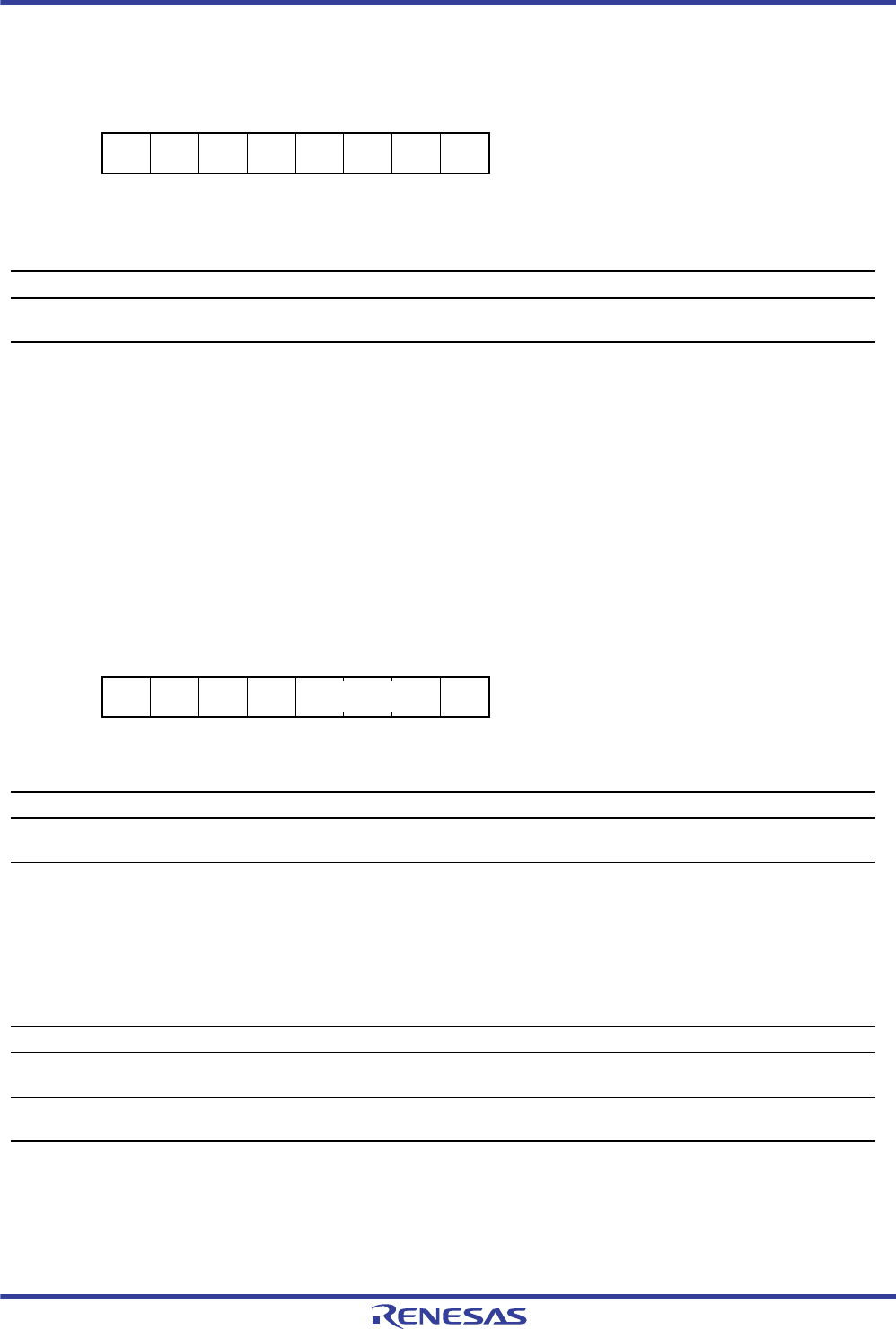
R01UH0034EJ0200 Rev.2.00 Page 1099 of 1489
Dec 27, 2013
RX62T Group, RX62G Group 25. CAN Module
25.2.10 Receive FIFO Pointer Control Register (RFPCR)
When the receive FIFO is not empty, write FFh to RFPCR by a program to increment the CPU-side pointer for the
receive FIFO to the next mailbox location.
Do not write to RFPCR when the RFE bit in RFCR is 0 (receive FIFO disabled).
Both the CAN-side pointer and the CPU-side pointer are incremented when a new message is received and the RFFST
bit in RFCR is 1 (receive FIFO is full) in overwrite mode. When the RFMLF bit in RFCR is 1 in this condition, the CPU-
side pointer cannot be incremented by writing to RFPCR by a program.
25.2.11 FIFO Control Register (TFCR)
Write to TFCR in CAN operation mode or CAN halt mode.
Address: 0009 0849h
b7 b6 b5 b4 b3 b2 b1 b0
————————
Value after reset: xxxxxxxx
[Legend] x: Undefined
Bit Symbol Bit Name Description R/W
b7 to b0 — — The CPU-side pointer for the receive FIFO is incremented by writing
FFh to RFPCR.
W
Address: 0009 084Ah
b7 b6 b5 b4 b3 b2 b1 b0
TFEST TFFST — — TFUST[2:0] TFE
Value after reset: 10000000
Bit Symbol Bit Name Description R/W
b0 TFE Transmit FIFO Enable 0: Transmit FIFO disabled
1: Transmit FIFO enabled
R/W
b3 to b1 TFUST[2:0] Transmit FIFO Unsent
Message Number Status
b3 b1
000: No unsent message
001: 1 unsent message
010: 2 unsent messages
011: 3 unsent messages
100: 4 unsent messages
101: Reserved
110: Reserved
111: Reserved
R
b5, b4 — Reserved These bits are always read as 0. The write value should always be 0. R/W
b6 TFFST Transmit FIFO Full Status 0: Transmit FIFO is not full
1: Transmit FIFO is full (4 unsent messages)
R
b7 TFEST Transmit FIFO Full Status 0: Unsent message in transmit FIFO
1: No unsent message in transmit FIFO
R

R01UH0034EJ0200 Rev.2.00 Page 1100 of 1489
Dec 27, 2013
RX62T Group, RX62G Group 25. CAN Module
TFE Bit (Transmit FIFO Enable)
When the TFE bit is set to 1, the transmit FIFO is enabled.
When the TFE bit is set to 0, the transmit FIFO becomes empty (TFEST bit = 1) and then unsent messages from the
transmit FIFO are lost as described below:
Immediately if a message from the transmit FIFO is not scheduled for the next transmission or during transmission
Following the completion of transmission, a CAN bus error, CAN bus arbitration lost, or entry to CAN halt mode if
a message from the transmit FIFO is scheduled for the next transmission or already during transmission
Before setting the TFE bit to 1 again, ensure that the TFEST bit has been set to 1. After setting the TFE bit to 1, write
transmit data into MB24.
Do not set the TFE bit to 1 in normal mailbox mode (MBM bit in CTLR = 0).
TFUST[2:0] Bits (Transmit FIFO Unsent Message Number Status)
The TFUST[2:0] bits indicate the number of unsent messages in the transmit FIFO.
The TFUST[2:0] bits are set to 000 when transmission from the transmit FIFO has been aborted.
TFFST Bit (Transmit FIFO Full Status)
The TFFST bit is set to 1 (transmit FIFO is full) when the number of unsent messages in the transmit FIFO is 4. The
TFFST bit is set to 0 (transmit FIFO is not full) when the number of unsent messages in the transmit FIFO is less than 4.
The TFFST bit is set to 0 when transmission from the transmit FIFO has been aborted.
TFEST Bit (Transmit FIFO Empty Status)
The TFEST bit is set to 1 (no message in transmit FIFO) when the number of unsent messages in the transmit FIFO is 0.
The TFEST bit is set to 1 when transmission from the transmit FIFO has been aborted. The TFEST bit is set to 0
(message in transmit FIFO) when the number of unsent messages in the transmit FIFO is not 0.
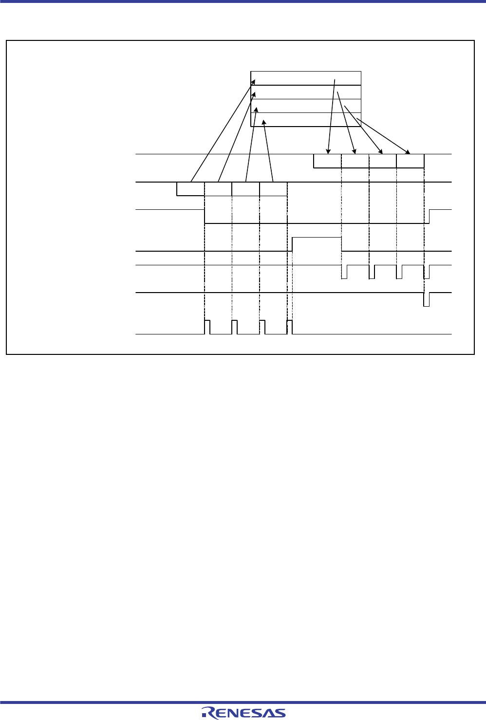
R01UH0034EJ0200 Rev.2.00 Page 1101 of 1489
Dec 27, 2013
RX62T Group, RX62G Group 25. CAN Module
Table 25.3 shows the transmit FIFO mailbox operation.
Figure 25.3 Transmit FIFO Mailbox Operation (Bits 25 and 24 in MIER = 01b or 11b)
CAN bus
Internal bus
RFCR.RFEST flag
RFCR.RFFST bit
RFPCR
Transmit FIFO mailbox
Frame 1
Frame 2
Frame 3
Frame 4
Frame 1 Frame 2 Frame 3 Frame 4
Frame 1 Frame 2 Frame 3 Frame 4
CAN0 transmit FIFO interrupt
Bits 25 and 24 in MIER = 11b
CAN0 transmit FIFO interrupt
Bits 25 and 24 in MIER = 01b

R01UH0034EJ0200 Rev.2.00 Page 1102 of 1489
Dec 27, 2013
RX62T Group, RX62G Group 25. CAN Module
25.2.12 Transmit FIFO Pointer Control Register (TFPCR)
When the transmit FIFO is not full, write FFh to TFPCR by a program to increment the CPU-side pointer for the transmit
FIFO to the next mailbox location.
Do not write to TFPCR when the TFE bit in TFCR is 0 (transmit FIFO disabled).
Address: 0009 084Bh
b7 b6 b5 b4 b3 b2 b1 b0
————————
Value after reset: xxxxxxxx
[Legend] x: Undefined
Bit Symbol Bit Name Description R/W
b7 to b0 — — The CPU-side pointer for the transmit FIFO is incremented by writing
FFh to TFPCR.
W

R01UH0034EJ0200 Rev.2.00 Page 1103 of 1489
Dec 27, 2013
RX62T Group, RX62G Group 25. CAN Module
25.2.13 Status Register (STR)
Address: 0009 0842h
0009 0842h 0009 0843h
b15 b14 b13 b12 b11 b10 b9 b8 b7 b6 b5 b4 b3 b2 b1 b0
— RECST TRMST BOST EPST SLPST HLTST RSTST EST TABST FMLST NMLST TFST RFST SDST NDST
Value after reset: xxxxxxxxxxxxxxxx
[Legend] x: Undefined
Bit Symbol Bit Name Description R/W
b0 NDST NEWDATA Status Flag 0: No mailbox with NEWDATA bit = 1
1: Mailbox(es) with NEWDATA bit = 1
R
b1 SDST SENTDATA Status Flag 0: No mailbox with SENTDATA bit = 1
1: Mailbox(es) with SENTDATA bit = 1
R
b2 RFST Receive FIFO Status Flag 0: No message in receive FIFO (empty)
1: Message in receive FIFO
R
b3 TFST Transmit FIFO Status
Flag
0: Transmit FIFO is full
1: Transmit FIFO is not full
R
b4 NMLST Normal Mailbox Message
Lost Status Flag
0: No mailbox with MSGLOST bit = 1
1: Mailbox(es) with MSGLOST bit = 1
R
b5 FMLST FIFO Mailbox Message
Lost Status Flag
0: RFMLF bit = 0
1: RFMLF bit = 1
R
b6 TABST Transmission Abort
Status Flag
0: No mailbox with TRMABT bit = 1
1: Mailbox(es) with TRMABT bit = 1
R
b7 EST Error Status Flag 0: No error occurred
1: Error occurred
R
b8 RSTST CAN Reset Status Flag 0: Not in CAN reset mode
1: In CAN reset mode
R
b9 HLTST CAN Halt Status Flag 0: Not in CAN halt mode
1: In CAN halt mode
R
b10 SLPST CAN Sleep Status Flag 0: Not in CAN sleep mode
1: In CAN sleep mode
R
b11 EPST Error-Passive Status Flag 0: Not in error-passive state
1: In error-passive state
R
b12 BOST Bus-Off Status Flag 0: Not in bus-off state
1: In bus-off state
R
b13 TRMST Transmit Status Flag
(transmitter)
0: Bus idle or reception in progress
1: Transmission in progress or in bus-off state
R
b14 RECST Receive Status Flag
(receiver)
0: Bus idle or transmission in progress
1: Reception in progress
R
b15 — Reserved The read value is undefined. The write value should always be 0. R

R01UH0034EJ0200 Rev.2.00 Page 1104 of 1489
Dec 27, 2013
RX62T Group, RX62G Group 25. CAN Module
NDST Flag (NEWDATA Status Flag)
The NDST flag is set to 1 when at least one NEWDATA flag in MCTLj (j = 0 to 31) is 1 regardless of the value of MIER.
The NDST flag is set to 0 when all NEWDATA flags are 0.
SDST Flag (SENTDATA Status Flag)
The SDST flag is set to 1 when at least one SENTDATA flag in MCTLj (j = 0 to 31) is 1 regardless of the value of MIER.
The SDST flag is set to 0 when all SENTDATA flags in MCTLj are 0.
RFST Flag (Receive FIFO Status Flag)
The RFST flag is set to 1 when the receive FIFO is not empty. The RFST flag is set to 0 when the receive FIFO is empty
or normal mailbox mode is selected.
TFST Flag (Transmit FIFO Status Flag)
The TFST flag is set to 1 when the transmit FIFO is not full. The TFST flag is set to 0 when the transmit FIFO is full or
normal mailbox mode is selected.
NMLST Flag (Normal Mailbox Message Lost Status Flag)
The NMLST flag is set to 1 when at least one MSGLOST flag inMCTLj (j = 0 to 31) is 1 regardless of the value of
MIER. The NMLST flag is set to 0 when all MSGLOST flags in MCTLj are 0.
FMLST Flag (FIFO Mailbox Message Lost Status Flag)
The FMLST flag is set to 1 when the RFMLF flag in RFCR is 1 regardless of the value of MIER. The FMLST flag is set
to 0 when the RFMLF flag in RFCR is 0.
TABST Flag (Transmission Abort Status Flag)
The TABST flag is set to 1 when at least one TRMABT flag in MCTLj (j = 0 to 31) is 1 regardless of the value of
MIER.The TABST flag is set to 0 when all TRMABT flags in MCTLj are 0.
EST Flag (Error Status Flag)
The EST flag is set to 1 when at least one error is detected by EIFR regardless of the value of EIER. The EST flag is set
to 0 when no error is detected by EIFR.
RSTST Flag (CAN Reset Status Flag)
The RSTST flag is set to 1 when the CAN module is in CAN reset mode. The RSTST flag is 0 when the CAN module is
not in CAN reset mode or not in the state from CAN reset mode to CAN sleep mode. Even when the state is changed
from CAN reset mode to CAN sleep mode, the RSTST flag remains 1.
HLTST Flag (CAN Halt Status Flag)
The HLTST flag is set to 1 when the CAN module is in CAN halt mode. The HLTST flag is 0 when the CAN module is
not in CAN halt mode or not in the state from CAN halt mode to CAN sleep mode. Even when the state is changed from
CAN halt mode to CAN sleep mode, the HLTST flag remains 1.

R01UH0034EJ0200 Rev.2.00 Page 1105 of 1489
Dec 27, 2013
RX62T Group, RX62G Group 25. CAN Module
SLPST Flag (CAN Sleep Status Flag)
The SLPST flag is set to 1 when the CAN module is in CAN sleep mode. The SLPST flag is set to 0 when the CAN
module is not in CAN sleep mode.
EPST Flag (Error-Passive Status Flag)
The EPST flag is set to 1 when the value of TECR or RECR exceeds 127 and the CAN module is in the error-passive
state (128 ≤ TEC < 256 or 128 ≤ REC < 256). The EPST flag is set to 0 when the CAN module is not in the error-passive
state.
BOST Flag (Bus-Off Status Flag)
The BOST flag is set to 1 when the value of TECR exceeds 255 and the CAN module is in the bus-off state (TEC ≥ 256).
The BOST flag is set to 0 when the CAN module is not in the bus-off state.
TRMST Flag (Transmit Status Flag) (transmitter)
The TRMST flag is set to 1 when the CAN module performs as a transmitter node or is in the bus-off state. The TRMST
flag is set to 0 when the CAN module performs as a receiver node or is in the bus-idle state.
RECST Flag (Receive Status Flag) (receiver)
The RECST flag is set to 1 when the CAN module performs as a receiver node. The RECST flag is set to 0 when the
CAN module performs as a transmitter node or is in the bus-idle state.

R01UH0034EJ0200 Rev.2.00 Page 1106 of 1489
Dec 27, 2013
RX62T Group, RX62G Group 25. CAN Module
25.2.14 Mailbox Search Mode Register (MSMR)
Write to MSMR in CAN operation mode or CAN halt mode.
MBSM[1:0] Bits (Mailbox Search Mode Select)
The MBSM[1:0] bits select the search mode for the mailbox search function.
When the MBSM[1:0] bits are 00b, receive mailbox search mode is selected. In this mode, the search targets are the
NEWDATA flag in MCTLj (j = 0 to 31) for the normal mailbox and the RFEST flag in RFCR.
When the MBSM[1:0] bits are 01b, transmit mailbox search mode is selected. In this mode, the search target is the
SENTDATA flag in MCTLj.
When the MBSM[1:0] bits are 10b, message lost search mode is selected. In this mode, the search targets are the
MSGLOST flag in MCTLj for the normal mailbox and the RFMLF flag in RFCR.
When the MBSM[1:0] bits are 11b, channel search mode is selected. In this mode, the search target is CSSR. Refer to
section 25.2.16, Channel Search Support Register (CSSR).
Address: 0009 0853h
b7 b6 b5 b4 b3 b2 b1 b0
——————MBSM[1:0]
Value after reset: 00000000
Bit Symbol Bit Name Description R/W
b1 to b0 MBSM[1:0] Mailbox Search Mode
Select
00: Receive mailbox search mode
01: Transmit mailbox search mode
10: Message lost search mode
11: Channel search mode
R/W
b7 to b2 — Reserved These bits are always read as 0. The write value should always be 0. R/W

R01UH0034EJ0200 Rev.2.00 Page 1107 of 1489
Dec 27, 2013
RX62T Group, RX62G Group 25. CAN Module
25.2.15 Mailbox Search Status Register (MSSR)
MBNST[4:0] Bits (Search Result Mailbox Number Status)
The MBNST[4:0] bits output the smallest mailbox number that is searched in each mode of MSMR. In receive mailbox
search mode, transmit mailbox search mode, and message lost search mode, the value of the mailbox i.e., the search
result to be output, is updated as described below:
When the NEWDATA, SENTDATA or MSGLOST flag in MCTj (j = 0 to 31) for the output mailbox is set to 0
When the NEWDATA, SENTDATA or MSGLOST flag in MCTj (j = 0 to 31) for a higher-priority mailbox is set to
1
If the MBSM[1:0] bits in MSMR are set to 00b (receive mailbox search mode) or 10b (message lost search mode), the
receive FIFO (mailbox [28]) is output when the receive FIFO is not empty and there are no unread received messages or
no lost messages in any of the normal mailboxes (mailboxes [0] to [23]). If the MBSM[1:0] bits in MSMR are set to 01b
(transmit mailbox search mode), the transmit FIFO (mailbox [24]) is not output. Table 25.7 lists the behavior of the
MBNST[4:0] bits in FIFO mailbox mode.
In channel search mode, the MBNST[4:0] bits output the corresponding channel number. After MSSR is read by a
program, the next target channel number is output.
SEST Bit (Search Result Status)
The SEST bit is set to 1 (no search result) when no corresponding mailbox is found after searching all mailboxes. For
example, in transmit mailbox search mode, the SEST bit is set to 1 when no SENTDATA flag in MCTj for mailboxes is
1. The SEST bit is set to 0 when at least one SENTDATA bit is 1. When the SEST bit is 1, the value of the MBNST[4:0]
bits is undefined.
Address: 0009 0852h
b7 b6 b5 b4 b3 b2 b1 b0
SEST — — MBNST[4:0]
Value after reset: 10000000
Bit Symbol Bit Name Description R/W
b4 to b0 MBNST[4:0] Search Result Mailbox
Number Status
These bits output the smallest mailbox number that is searched in each
mode of MSMR.
R
b6, b5 — Reserved These bits are always read as 0. The write value should always be 0. R/W
b7 SEST Search Result Status 0: Search result found
1: No search result
R

R01UH0034EJ0200 Rev.2.00 Page 1108 of 1489
Dec 27, 2013
RX62T Group, RX62G Group 25. CAN Module
Table 25.7 Behavior of MBNST[4:0] Bits in FIFO Mailbox Mode
MSMR.MBSM
[1:0] Bits
Mailbox [24]
(Transmit FIFO)
Mailbox [28]
(Receive FIFO)
00 Mailbox [24] is not
output.
Mailbox [28] is output when no MCTLj.NEWDATA flag for the normal mailboxes is set to 1
(new message is being stored or has been stored to the mailbox) and the receive FIFO is
not empty.(j = 0 to 23)
01 Mailbox [28] is not output.
10 Mailbox [28] is output when no MCTLj.MSGLOST flag for the normal mailboxes is set to 1
(message is overwritten or overrun) and the RFCR.RFMLF flag is set to 1 (receive FIFO
message lost has occurred) in the receive FIFO.(j = 0 to 23)
11 Mailbox [28] is not output.
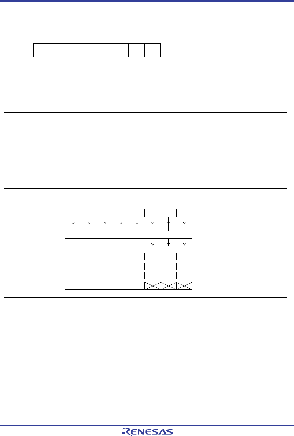
R01UH0034EJ0200 Rev.2.00 Page 1109 of 1489
Dec 27, 2013
RX62T Group, RX62G Group 25. CAN Module
25.2.16 Channel Search Support Register (CSSR)
The bits in CSSR, which are set to 1, are encoded by an 8/3 encoder (the LSB position has the higher priority) and output
to the MBNST[4:0] bits in MSSR.
MSSR outputs the updated value whenever MSSR is read by a program.
Write to CSSR only when the MBSM[1:0] bits in MSMR are 11 (channel search mode). Do not write to CSSR in CAN
reset mode.
Figure 25.4 shows the write and read of CSSR and MSSR.
Figure 25.4 Write and Read of CSSR and MSSR
The value of CSSR is also updated whenever MSSR is read. When read, the value prior to conversion by the 8/3 encoder
can be read.
Address: 0009 0851h
b7 b6 b5 b4 b3 b2 b1 b0
————————
Value after reset: xxxxxxxx
x: Undefined
Bit Symbol Bit Name Description R/W
b7 to b0 — — When the value for the channel search is input, the channel number is
output to MSSR.
R/W
CSSR
Address
CAN0
0009 0851h
CAN0
0009 0852h
MSSR
(1st read)
8/3 encoder
b7 b6 b3 b0
0 1 0 0 1 0 0 1
b7 b0b2
0 0 0 0 0 0 1 1
0 0 0 0 0 0 0 0
0 0 0 0 0 1 1 0
(Search result: Channel no. 0 read)
1 0 0 0 0
(2nd read)
(3rd read)
(4th read)
(Search result: Channel no. 3 read)
(Search result: Channel no. 6 read)
(Search result: No corresponding
channel no.)

R01UH0034EJ0200 Rev.2.00 Page 1110 of 1489
Dec 27, 2013
RX62T Group, RX62G Group 25. CAN Module
25.2.17 Acceptance Filter Support Register (AFSR)
The acceptance filter support unit (ASU) can be used for data table (8 bits × 256) search. In the data table, all standard
IDs created by the user are set to be valid/invalid in bit units. When AFSR is written with data in 16-bit units including
the SID[10:0] bit in MBj (j = 0 to 31), in which a received standard ID is stored, a decoded row (byte offset) position and
column (bit) position for data table search can be read. The ASU can be used for standard (11-bit) IDs only.
The ASU is enabled in the following cases:
When the ID to receive cannot be masked by the acceptance filter
(Example) IDs to receive: 078h, 087h, and 111h
When there are too many IDs to receive and software filtering time is expected to be shortened
It should be noted that AFSR cannot be set in CAN reset mode.
Table 25.5 shows the write and read of AFSR.
Figure 25.5 Write and Read of AFSR
Address: 0009 0856h
0009 0856h 0009 0857h
b15 b14 b13 b12 b11 b10 b9 b8 b7 b6 b5 b4 b3 b2 b1 b0
————————————————
Value after reset: xxxxxxxxxxxxxxxx
x: Undefined
Bit Symbol Bit Name Description R/W
b15 to b0 — — After the standard ID of a received message is written, the value
converted for data table search can be read.
R/W
b15
When writing*
Address
CAN0
0009 0856h
CAN0
0009 0856h
When reading
Note: * Write the same value as the 16-bit unit data including the SID[10:0] bit in MBj (j = 0 to 31).
b15 b8
SID
10 SID
9SID
8SID
7SID
6
3/8 decoder
SID
5SID
4SID
3SID
2SID
1
b7 b0
SID
0
b8
SID
10 SID
9SID
8
b7 b0
SID
5SID
4SID
3
SID
7SID
6
Row (byte offset) position in data tableColumn (bit) position in data table

R01UH0034EJ0200 Rev.2.00 Page 1111 of 1489
Dec 27, 2013
RX62T Group, RX62G Group 25. CAN Module
25.2.18 Error Interrupt Enable Register (EIER)
EIER is used to enable or disable the error interrupt individually for each error interrupt source in EIFR.
Write to EIER in CAN reset mode.
BEIE Bit (Bus Error Interrupt Enable)
When the BEIE bit is 0, no error interrupt request is generated even if the BEIF flag in EIFR is set to 1. When the BEIE
bit is 1, an error interrupt request is generated if the BEIF flag in EIFR is set to 1.
EWIE Bit (Error-Warning Interrupt Enable)
When the EWIE bit is 0, no error interrupt request is generated even if the EWIF flag in EIFR is set to 1. When the EWIE
bit is 1, an error interrupt request is generated if the EWIF flag in EIFR is set to 1.
EPIE Bit (Error-Passive Interrupt Enable)
When the EPIE bit is 0, no error interrupt request is generated even if the EPIF flag in EIFR is set to 1. When the EPIE
bit is 1, an error interrupt request is generated if the EPIF flag in EIFR is set to 1.
BOEIE Bit (Bus-Off Entry Interrupt Enable)
When the BOEIE bit is 0, no error interrupt request is generated even if the BOEIF flag in EIFR is set to 1. When the
BOEIE bit is 1, an error interrupt request is generated if the BOEIF flag in EIFR is set to 1.
Address: 0009 084Ch
b7 b6 b5 b4 b3 b2 b1 b0
BLIE OLIE ORIE BORIE BOEIE EPIE EWIE BEIE
Value after reset: 10000000
Bit Symbol Bit Name Description R/W
b0 BEIE Bus Error Interrupt
Enable
0: Bus error interrupt disabled
1: Bus error interrupt enabled
R/W
b1 EWIE Error-Warning Interrupt
Enable
0: Error-warning interrupt disabled
1: Error-warning interrupt enabled
R/W
b2 EPIE Error-Passive Interrupt
Enable
0: Error-passive interrupt disabled
1: Error-passive interrupt enabled
R/W
b3 BOEIE Bus-Off Entry Interrupt
Enable
0: Bus-off entry interrupt disabled
1: Bus-off entry interrupt enabled
R/W
b4 BORIE Bus-Off Recovery
Interrupt Enable
0: Bus-off recovery interrupt disabled
1: Bus-off recovery interrupt enabled
R/W
b5 ORIE Overrun Interrupt Enable 0: Receive overrun interrupt disabled
1: Receive overrun interrupt enabled
R/W
b6 OLIE Overload Frame Transmit
Interrupt Enable
0: Overload frame transmit interrupt disabled
1: Overload frame transmit interrupt enabled
R/W
b7 BLIE Bus Lock Interrupt Enable 0: Bus lock interrupt disabled
1: Bus lock interrupt enabled
R/W

R01UH0034EJ0200 Rev.2.00 Page 1112 of 1489
Dec 27, 2013
RX62T Group, RX62G Group 25. CAN Module
BORIE Bit (Bus-Off Recovery Interrupt Enable)
When the BORIE bit is 0, an error interrupt request is not generated even if the BORIF flag in EIFR is set to 1. When the
BORIE bit is set to 1, an error interrupt request is generated if the BORIF flag in EIFR t is set to 1.
ORIE Bit (Overrun Interrupt Enable)
When the ORIE bit is 0, an error interrupt request is not generated even if the ORIF flag in EIFR is set to 1. When the
ORIE bit is 1, an error interrupt request is generated if the ORIF flag in EIFR is set to 1.
OLIE Bit (Overload Frame Transmit Interrupt Enable)
When the OLIE bit is 0, no error interrupt request is generated even if the OLIF flag in EIFR is set to 1. When the OLIE
bit is 1, an error interrupt request is generated if the OLIF flag in EIFR is set to 1.
BLIE Bit (Bus Lock Interrupt Enable)
When the BLIE bit is 0, no error interrupt request is generated even if the BLIF flag in EIFR is set to 1. When the BLIE
bit is 1, an error interrupt request is generated if the BLIF flag in EIFR is set to 1.

R01UH0034EJ0200 Rev.2.00 Page 1113 of 1489
Dec 27, 2013
RX62T Group, RX62G Group 25. CAN Module
25.2.19 Error Interrupt Factor Judge Register (EIFR)
If an event corresponding to each flag occurs, the corresponding flag in EIFR is set to 1 regardless of the setting of EIER.
To set each flag to 0, write 0 by a program. If the set timing occurs simultaneously with the clear timing by the program,
the flag becomes 1.
When a single flag is set to 0 by a program, do not use the logic operation instruction (AND.B) – use the transfer
instruction (MOV) to ensure that only the specified flag is set to 0 and the other flags are set to 1. Writing 1 has no effect
to these bit values.
BEIF Flag (Bus Error Detect Flag)
The BEIF flag is set to 1 when a bus error is detected.
EWIF Flag (Error-Warning Detect Flag)
The EWIF flag is set to 1 when the value of the receive error counter (REC) or transmit error counter (TEC) exceeds 95.
The EWIF flag is set to 1 only when the REC or TEC initially exceeds 95. Thus, if 0 is written to the EWIF flag by a
program while the REC or TEC remains greater than 95, the EWIF flag is not set to 1 until the REC or TEC goes below
95 and then exceeds 95 again.
Address: 0009 084Dh
b7 b6 b5 b4 b3 b2 b1 b0
BLIF OLIF ORIF BORIF BOEIF EPIF EWIF BEIF
Value after reset: 00000000
Bit Symbol Bit Name Description R/W
b0 BEIF Bus Error Detect Flag 0: No bus error detected
1: Bus error detected
R/W
b1 EWIF Error-Warning Detect
Flag
0: No error-warning detected
1: Error-warning detected
R/W
b2 EPIF Error-Passive Detect Flag 0: No error-passive detected
1: Error-passive detected
R/W
b3 BOEIF Bus-Off Entry Detect Flag 0: No bus-off entry detected
1: Bus-off entry detected
R/W
b4 BORIF Bus-Off Recovery Detect
Flag
0: No bus-off recovery detected
1: Bus-off recovery detected
R/W
b5 ORIF Receive Overrun Detect
Flag
0: No receive overrun detected
1: Receive overrun detected
R/W
b6 OLIF Overload Frame
Transmission Detect Flag
0: No overload frame transmission detected
1: Overload frame transmission detected
R/W
b7 BLIF Bus Lock Detect Flag 0: No bus lock detected
1: Bus lock detected
R/W

R01UH0034EJ0200 Rev.2.00 Page 1114 of 1489
Dec 27, 2013
RX62T Group, RX62G Group 25. CAN Module
EPIF Flag (Error-Passive Detect Flag)
The EPIF flag is set to 1 when the CAN error state becomes error-passive (the REC (receive error counter) or TEC
(transmit error counter) value exceeds 127).
The EPIF flag is set to 1 only when the REC or TEC initially exceeds 127. Thus, if 0 is written by a program while the
REC or TEC remains greater than 127, the EPIF flag is not set to 1 until the REC or TEC goes below 127 and then
exceeds 127 again.
BOEIF Flag (Bus-Off Entry Detect Flag)
The BOEIF bit is set to 1 when the CAN error state becomes bus-off (the TEC (transmit error counter) value exceeds
255). The BOEIF bit is also set to 1 when the BOM[1:0] bits in CTLR are 01 (entry to CAN halt mode automatically at
bus-off entry) and the CAN module becomes the bus-off state.
BORIF Flag (Bus-Off Recovery Detect Flag)
The BORIF bit is set to 1 when the CAN module recovers from the bus-off state normally by detecting 11 consecutive
bits 128 times in the following conditions:
When the BOM[1:0] bits in CTLR are 00b
When the BOM[1:0] bits in CTLR are 10b
When the BOM[1:0] bits in CTLR are 11b
However, the BORIF bit is not set to 1 if the CAN module recovers from the bus-off state in the following conditions:
When the CANM[1:0] bits in CTLR are set to 01b or 11b (CAN reset mode)
When the RBOC bit in CTLR is set to 1 (forcible return from bus-off)
When the BOM[1:0] bits in CTLR are set to 01b
When the BOM[1:0] bits in CTLR are set to 11b and the CANM[1:0] bits in CTLR are set to 10b (CAN halt mode)
before normal recovery occurs
ORIF Flag (Receive Overrun Detect Flag)
The ORIF bit is set to 1 when a receive overrun occurs. This bit is not to set to 1 in overwrite mode.
In overwrite mode, a reception complete interrupt request is generated if an overwrite condition occurs and the ORIF bit
is not set to 1.
In normal mailbox mode, if an overrun occurs in any of mailboxes [0] to [31] in overrun mode, this bit is set to 1. In
FIFO mailbox mode, if an overrun occurs in any of mailboxes [0] to [23] or the receive FIFO in overrun mode, this bit is
set to 1.
OLIF Flag (Overload Frame Transmission Detect Flag)
The OLIF bit is set to 1 if the transmitting condition of an overload frame is detected when the CAN module performs
transmission or reception.

R01UH0034EJ0200 Rev.2.00 Page 1115 of 1489
Dec 27, 2013
RX62T Group, RX62G Group 25. CAN Module
BLIF Flag (Bus Lock Detect Flag)
The BLIF flag is set to 1 if 32 consecutive dominant bits are detected on the CAN bus while the CAN module is in CAN
operation mode.
After the BLIF flag is set to 1, a bus lock can be detected again under either of the following conditions:
After this flag is set to 0 from 1, recessive bits are detected (the bus lock is cleared).
After this flag is set to 0 from 1, the CAN module enters CAN reset mode and then enters CAN operation mode
again (internal reset).
Table 25.8 lists the behavior of flags BOEIF and BORIF according to the CTLR.BOM[1:0] bit setting.
25.2.20 CAN0 Receive Error Count Register (RECR)
RECR indicates the value of the receive error counter.
Refer to the CAN Specifications (ISO11898-1) about the increment/decrement conditions of the receive error counter.
The value of RECR in the bus-off state is undefined.
Table 25.8 Behavior of BOEIF and BORIF Flags according to CTLR.BOM[1:0] Bit Setting
CTLR.BOM[1:0]
Bits BOEIF Flag BORIF Flag
00 Set to 1 on entry to the bus-off state. Set to 1 on exit from the bus-off state.
01 Do not set to 1.
10 Set to 1 on exit from the bus-off state.
11 Set to 1 if normal bus-off recovery occurs before the CTLR.CANM[1:0]
bits are set to 10 (CAN halt mode).
Address: 0009 084Eh
b7 b6 b5 b4 b3 b2 b1 b0
————————
Value after reset: 00000000
Bit Symbol Bit Name Description R/W
b7 to b0 — Receive Error Count
Function
RECR increments or decrements the counter value according to the
error status of the CAN module during reception.
R
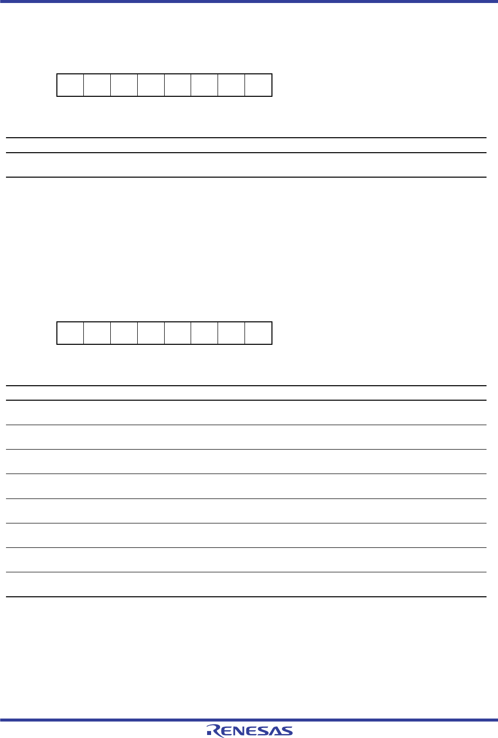
R01UH0034EJ0200 Rev.2.00 Page 1116 of 1489
Dec 27, 2013
RX62T Group, RX62G Group 25. CAN Module
25.2.21 Transmit Error Count Register (TECR)
TECR indicates the value of the transmit error counter.
Refer to the CAN Specifications (ISO11898-1) about the increment/decrement conditions of the transmit error counter.
The value of TECR in the bus-off state is undefined.
25.2.22 Error Code Store Register (ECSR)
Note 1. Write to the EDPM bit in CAN reset mode or CAN halt mode.
Note 2. If more than one error condition is detected simultaneously, all related bits are set to 1.
Note 3. Writing 1 has no effect to these bit values.
Note 4. To write 0 to flags SEF, FEF, AEF, CEF, BE1F, BE0F, and ADEF, do not use the logic operation instruction (AND.B). Use the
transfer (MOV) instruction to ensure that only the specified flag is set to 0 and the other flags are set to 1.
Address: 0009 084Fh
b7 b6 b5 b4 b3 b2 b1 b0
————————
Value after reset: 00000000
Bit Symbol Bit Name Description R/W
b7 to b0 — Transmit Error Count
Function
TECR increments or decrements the counter value according to the
error status of the CAN module during transmission.
R
Address: 0009 0850h
b7 b6 b5 b4 b3 b2 b1 b0
EDPM ADEF BE0F BE1F CEF AEF FEF SEF
Value after reset: 00000000
Bit Symbol Bit Name Description R/W
b0 SEF Stuff Error Flag*3*4 0: No stuff error detected
1: Stuff error detected
R/W
b1 FEF Form Error Flag*3*4 0: No form error detected
1: Form error detected
R/W
b2 AEF ACK Error Flag*3*4 0: No ACK error detected
1: ACK error detected
R/W
b3 CEF CRC Error Flag*3*4 0: No CRC error detected
1: CRC error detected
R/W
b4 BE1F Bit Error (recessive)
Flag*3*4 0: No bit error (recessive) detected
1: Bit error (recessive) detected
R/W
b5 BE0F Bit Error (dominant)
Flag*3*4 0: No bit error (dominant) detected
1: Bit error (dominant) detected
R/W
b6 ADEF ACK Delimiter Error
Flag*3*4 0: No ACK delimiter error detected
1: ACK delimiter error detected
R/W
b7 EDPM Error Display Mode
Select*1*2 0: Output of first detected error code
1: Output of accumulated error code
R/W

R01UH0034EJ0200 Rev.2.00 Page 1117 of 1489
Dec 27, 2013
RX62T Group, RX62G Group 25. CAN Module
ECSR can be used to monitor whether an error has occurred on the CAN bus.
Refer to the CAN Specifications (ISO11898-1) to check the generation conditions of each error.
To set each bit except for the EDPM flag to 0, write 0 by a program. If the timing at which each flag is set to 1 and the
timing at which 0 is written by a program are the same, the relevant flag is set to 1.
SEF Flag (Stuff Error Flag)
The SEF bit is set to 1 when a stuff error is detected.
FEF Flag (Form Error Flag)
The FEF bit is set to 1 when a form error is detected.
AEF Flag (ACK Error Flag)
The AEF bit is set to 1 when an ACK error is detected.
CEF Flag (CRC Error Flag)
The CEF bit is set to 1 when a CRC error is detected.
BE1F Flag (Bit Error (recessive) Flag)
The BE1F bit is set to 1 when a recessive bit error is detected.
BE0F Flag (Bit Error (dominant) Flag)
The BE0F bit is set to 1 when a dominant bit error is detected.
ADEF Flag (ACK Delimiter Error Flag)
The ADEF bit is set to 1 when a form error is detected with the ACK delimiter during transmission.
EDPM Bit (Error Display Mode Select)
The EDPM bit selects the output mode of ECSR. When the EDPM bit is set to 0, ECSR outputs the first error code.
When the EDPM bit is set to 1, ECSR outputs the accumulated error code.

R01UH0034EJ0200 Rev.2.00 Page 1118 of 1489
Dec 27, 2013
RX62T Group, RX62G Group 25. CAN Module
25.2.23 Time Stamp Register (TSR)
Note 1. Read TSR in 16-bit units.
When TSR is read, the value of the time stamp counter (16-bit free-running counter) at that moment is read.
The value of the time stamp counter reference clock is a multiple of 1 bit time, as configured by the TSPS[1:0] bits in
CTLR.
The time stamp counter stops in CAN sleep mode and CAN halt mode, and is initialized in CAN reset mode.
The time stamp counter value is stored to bits TSL[7:0] and TSH[7:0] in MBj when a received message is stored in a
receive mailbox.
Address: 0009 0854h
0009 0854h 0009 0855h
b15 b14 b13 b12 b11 b10 b9 b8 b7 b6 b5 b4 b3 b2 b1 b0
————————————————
Value after reset: 0000000000000000
Bit Symbol Bit Name Description R/W
b15 to b0 — Time Stamp Register Free-running counter value for the time stamp function R

R01UH0034EJ0200 Rev.2.00 Page 1119 of 1489
Dec 27, 2013
RX62T Group, RX62G Group 25. CAN Module
25.2.24 Test Control Register (TCR)
TCR controls the CAN test mode. Write to TCR in CAN halt mode only.
(1) Listen-Only Mode
The CAN Specifications (ISO11898-1) recommend an optional bus monitoring mode. In listen-only mode, valid data
frames and valid remote frames can be received. However, only recessive bits can be sent on the CAN bus, and the ACK
bit, overload flag, and active error flag cannot be sent.
Listen-only mode can be used for baud rate detection.
Do not request transmission from any mailboxes in listen-only mode.
Figure 25.6 shows the connection when listen-only mode is selected.
Figure 25.6 Connection when Listen-Only Mode is Selected
Address: 0009 0858h
b7 b6 b5 b4 b3 b2 b1 b0
—————TSTM[1:0]TSTE
Value after reset: 00000000
Bit Symbol Bit Name Description R/W
b0 TSTE CAN Test Mode Enable 0: CAN test mode disabled
1: CAN test mode enabled
R/W
b2, b1 TSTM[1:0] CAN Test Mode Select b2 b1
0 0: Other than CAN test mode
0 1: Listen-only mode
1 0: Self-test mode 0 (external loopback)
1 1: Self-test mode 1 (internal loopback)
R/W
b7 to b3 — Reserved These bits are always read as 0. The write value should always be 0. R/W
CTX
(internal) CRX
(internal)
CTX CRX
Recessive level
R01UH0034EJ0200 Rev.2.00 Page 1120 of 1489
Dec 27, 2013
RX62T Group, RX62G Group 25. CAN Module
(2) Self-Test Mode 0 (External Loopback))
Self-test mode 0 is for testing the CAN transceiver (self-diagnostic function under a self-loaded condition). Connect the
CTX and CRX pins to the CAN transceiver when this mode is to be used.
As a node, this module is capable of transmitting its own ACK bits in self-test mode 0, making self-diagnostic tests to
check for normal CAN operation possible even when no other node is connected to the network.
Figure 25.7 shows the connection when self-test mode 0 is selected.
Figure 25.7 Connection when Self-Test Mode 0 is Selected
(3) Self-Test Mode 1 (Internal Loopback)
Self-test mode 1 is provided for self-test functions.
In self-test mode 1, the protocol controller treats its transmitted messages as received messages and stores them into the
receive mailbox. To be independent from external stimulation, the protocol controller generates the ACK bit.
In self-test mode 1, the protocol controller performs an internal feedback from the internal CTX pin to the internal CRX
pin. The input value of the external CRX pin is ignored. The external CTX pin outputs only recessive bits. The CTX and
CRX pins do not need to be connected to the CAN bus or any external device.
Figure 25.8 shows the connection when self-test mode 1 is selected.
Figure 25.8 Connection when Self-Test Mode 1 is Selected
CTX
(internal) CRX
(internal)
CTX CRX
CAN tranceiver
ACK
CTX
(internal) CRX
(internal)
ACK
CTX CRX
Recessive level
R01UH0034EJ0200 Rev.2.00 Page 1121 of 1489
Dec 27, 2013
RX62T Group, RX62G Group 25. CAN Module
25.3 Operating Mode
The CAN module has the following four operating modes.
CAN reset mode
CAN halt mode
CAN operation mode
CAN sleep mode
Figure 25.9 shows the transition between CAN operating modes.
Figure 25.9 Transition between CAN Operating Modes
CPU reset
CANM, SLPM, BOM, RBOC: Bits in CTLR
Notes: 1. The transition timing from the bus-off state to CAN halt mode depends on the setting of the CTLR.BOM[1:0] bits.
— When the CTLR.BOM[1:0] bits are 01b, the state transition timing is immediately after entering the bus-off state.
— When the CTLR.BOM[1:0] bits are 10b, the state transition timing is at the end of the bus-off state.
— When the CTLR.BOM[1:0] bits are 11b, the state transition timing is at the setting of the CTLR.CANM[1:0] bits to 10b
(CAN halt mode).
2. Write 0 to only the CTLR.SLPM bit to exit CAN sleep mode. Only when the CAN module enters CAN sleep mode from CAN
halt mode, the transition from CAN sleep mode to CAN halt mode is enabled
3. A transition to CAN halt mode does not take place while the CAN bus is locked at the dominant level. In this case, place the
CAN module in CAN reset mode.
SLPM = 1
SLPM = 1
CANM[1:0] = 00b
CANM[1:0] = 01b or 11b
when SLPM = 0
CANM[1:0]
= 01b, 11b
CANM[1:0] =10b
when SLPM = 0 When the BOM[1:0] bits = 00b or 11b
(no halt request) and 11 consecutive
recessive bits are detected 128 times
or the RBOC bit = 1
CANM[1:0]
=01, 11
CANM[1:0]
=10b
TEC>255
CANM[1:0] = 10b*1
CANM[1:0]
=00b
CANM[1:0]
= 01b, 11b
CANM[1:0]
=10b*3
CAN sleep mode*2 CAN reset mode CAN operaion mode
CAN operation mode
(bus-off state)
CAN halt mode

R01UH0034EJ0200 Rev.2.00 Page 1122 of 1489
Dec 27, 2013
RX62T Group, RX62G Group 25. CAN Module
25.3.1 CAN Reset Mode
CAN reset mode is provided for CAN communication configuration.
When the CTLR.CANM[1:0] bits are set to 01 or 11, the CAN module enters CAN reset mode. Then, the STR.RSTST
bit is set to 1. Do not change the CTLR.CANM[1:0] bits until the RSTST bit is set to 1. Set BCR before exiting CAN
reset mode to any other modes.
The following registers are initialized to their reset values after entering CAN reset mode, and their initial values are
retained during CAN reset mode:
MCTLj (j = 0 to 31)
STR (except for the SLPST and TFST bits)
EIFR
RECR
TECR
TSR
MSSR
MSMR
RFCR
TFCR
TCR
ECSR (except for the EDPM bit)
The following registers retain their previous values even after entering CAN reset mode.
CTLR
STR (only the SLPST and TFST bits)
MIER
EIER
BCR
CSSR
ECSR (only the EDPM bit)
MBj (j = 0 to 31)
MKRi (i = 0 to 7)
FIDCR0 and FIDCR1
MKIVLR
AFSR
RFPCR
TFPCR

R01UH0034EJ0200 Rev.2.00 Page 1123 of 1489
Dec 27, 2013
RX62T Group, RX62G Group 25. CAN Module
25.3.2 CAN Halt Mode
CAN halt mode is used for mailbox configuration and test mode setting.
When the CTLR.CANM[1:0] bits are set to 10, CAN halt mode is selected. Then the STR.HLTST flag is set to 1. Do not
change the CTLR.CANM[1:0] bits until the HLTST flag is set to 1.
See Table 25.9 for the state transition conditions when transmitting or receiving.
All registers except for flags RSTST, HLTST, and SLPST in STR remain unchanged when the CAN enters CAN halt
mode.
Do not change CTLR (except for bits CANM[1:0] and SLPM), and EIER in CAN halt mode. BCR can be changed in
CAN halt mode only when listen-only mode is selected for automatic baud rate detection.
Note 1. If several messages are requested to be transmitted, mode transition occurs after the completion of the first message
transmission. In a case that the CAN reset mode is being requested during suspend transmission, mode transition occurs when
the bus is idle, the next transmission ends, or the CAN module becomes a receiver.
Note 2. If the CAN bus is locked at the dominant level, the program can detect this state by monitoring the EIFR.BLIF flag. A transition to
CAN halt mode does not take place while the CAN bus is locked at the dominant level. In this case, place the CAN module in
CAN reset mode.
Note 3. If a CAN bus error occurs during reception after CAN halt mode is requested, the CAN module transits to CAN halt mode
immediately. However, if the CAN bus is locked at the dominant level, a transition to CAN halt mode does not take place.
Note 4. If a CAN bus error or arbitration-lost occurs during transmission after CAN reset mode or CAN halt mode is requested, the CAN
module transits to the requested CAN mode. However, if the CAN bus is locked at the dominant level, a transition to CAN halt
mode does not take place.
Table 25.9 Operation in CAN Reset Mode and CAN Halt Mode
Mode Receiver Transmitter Bus-Off
CAN reset mode
(forcible transition)
CANM[1:0] = 11b
CAN module enters CAN reset
mode without waiting for the end
of message reception.
CAN module enters CAN reset
mode without waiting for the end
of message transmission.
CAN module enters CAN reset mode
without waiting for the end of bus-off
recovery.
CAN reset mode
CANM[1:0] = 01b
CAN module enters CAN reset
mode without waiting for the end
of message reception.
CAN module enters CAN reset
mode after waiting for the end of
message transmission.*1, *4
CAN module enters CAN reset mode
without waiting for the end of bus-off
recovery.
CAN halt mode CAN module enters CAN halt
mode after waiting for the end of
message reception.*2, *3
CAN module enters CAN halt
mode after waiting for the end of
message transmission.*1, *2, *4
[When the CTLR.BOM[1:0] bits are 00]
A halt request from a program will be
accepted only after bus-off recovery.
[When the CTLR.BOM[1:0] bits are 01]
CAN module automatically enters CAN
halt mode without waiting for the end of
bus-off recovery (regardless of a halt
request from a program).
[When the CTLR.BOM[1:0] bits are 10]
CAN module automatically enters CAN
halt mode after waiting for the end of bus-
off recovery (regardless of a halt request
from a program).
[When the CTLR.BOM[1:0] bits are 11]
CAN module enters CAN halt mode
(without waiting for the end of bus-off
recovery) if a halt is requested by a
program during bus-off.
R01UH0034EJ0200 Rev.2.00 Page 1124 of 1489
Dec 27, 2013
RX62T Group, RX62G Group 25. CAN Module
25.3.3 CAN Sleep Mode
CAN sleep mode is used for reducing current consumption by stopping the clock supply to the CAN module. After an
MCU pin reset or software reset, the CAN module starts from CAN sleep mode.
When the SLPM bit in CTLR is set to 1, the CAN module enters CAN sleep mode. Then, the SLPST flag in STR is set to
1. Do not change the value of the SLPM bit in CTLR until the SLPST flag in STR is set to 1. The other registers remain
unchanged when the CAN module enters CAN sleep mode.
Write to the SLPM bit in CTLR in CAN reset mode and CAN halt mode. Do not change any registers (except for the
SLPM bit in CTLR) during CAN sleep mode. Read operation is still allowed.
When the SLPM bit in CTLR is set to 0, the CAN module is released from CAN sleep mode. When the CAN module
exits CAN sleep mode, the other registers remain unchanged.
25.3.4 CAN Operation Mode (Excluding Bus-Off State)
CAN operation mode is used for CAN communication.
When the CANM[1:0] bits in CTLR are set to 00, the CAN module enters CAN operation mode.
Then flags RSTST and HLTST in STR are set to 0. Do not change the value of the CANM[1:0] bits in CTLR until flags
RSTST and HLTST in STR are set to 0.
If 11 consecutive recessive bits are detected after entering CAN operation mode, the CAN module is in the following
states:
The CAN module becomes an active node on the network, thus enabling transmission and reception of CAN
messages.
Error monitoring of the CAN bus, such as receive and transmit error counters, is performed.
During CAN operation mode, the CAN module may be in one of the following three sub-modes, depending on the status
of the CAN bus.
Idle mode: Transmission or reception is not being performed.
Receive mode: A CAN message sent by another node is being received.
Transmit mode:A CAN message is being transmitted. The CAN module may receive its own message
simultaneously when self-test mode 0 (TSTM bits in TCR = 10) or self-test mode 1 (TSTM bits in TCR = 11) is
selected.
Figure 25.10 shows the sub-modes of CAN operation mode.
Figure 25.10 Sub-Modes of CAN Operation Mode
Transmission
starts
Lost in arbitration
Transmission
completed Reception
completed
SOF
detected
Transmit mode
STR.TRMST=1
STR.RECST=0
Idle mode
STR.TRMST=0
STR.RECST=0
Receive mode
STR.TRMST=0
STR.RECST=1

R01UH0034EJ0200 Rev.2.00 Page 1125 of 1489
Dec 27, 2013
RX62T Group, RX62G Group 25. CAN Module
25.3.5 CAN Operation Mode (Bus-Off State)
The CAN module enters the bus-off state according to the increment/decrement rules for the transmit/error counters in
the CAN Specifications.
The following cases apply when the CAN module is recovering from the bus-off state. When the CAN module is in the
bus-off state, the values of the CAN-related registers, except for STR, EIFR, RECR, TECR and TSR, remain unchanged.
(1) When bits BOM[1:0] in CTLR are 00 (normal mode)
The CAN module enters the error-active state immediately after it has completed the recovery from the bus-off state and
CAN communication is enabled instantly. The BORIF flag in EIFR is set to 1 (bus-off recovery detected) at this time.
(2) When bit RBOC in CTLR is set to 1 (forcible return from bus-off)
The CAN module enters the error-active state immediately when it is in the bus-off state and the RBOC bit in CTLR is
set to 1. CAN communication is enabled again after 11 consecutive recessive bits are detected. The BORIF flag in EIFR
is not set to 1 at this time.
(3) When bits BOM[1:0] in CTLR are 01 (automatic transition to CAN halt mode at bus-off entry)
The CAN module enters CAN halt mode immediately when it reaches the bus-off state. The BORIF flag in EIFR is not
set to 1 at this time.
(4) When bits BOM[1:0] in CTLR are 10 (automatic transition to CAN halt mode at bus-off end)
The CAN module enters CAN halt mode when it has completed the recovery from bus-off. The BORIF flag in EIFR is
set to 1 at this time.
(5) When bits BOM[1:0] in CTLR are 11 (transition to CAN halt mode by a program) and bits
CANM[1:0] in CTLR are set to 10 (CAN halt mode) during bus-off state
The CAN module enters CAN halt mode immediately when it is in the bus-off state and the CANM[1:0] bits in CTLR
are set to 10 (CAN halt mode). The BORIF flag in EIFR is not set to 1 at this time.
If the CANM[1:0] bits in CTLR are not set to 10 during bus-off, the same behavior as (1) applies.
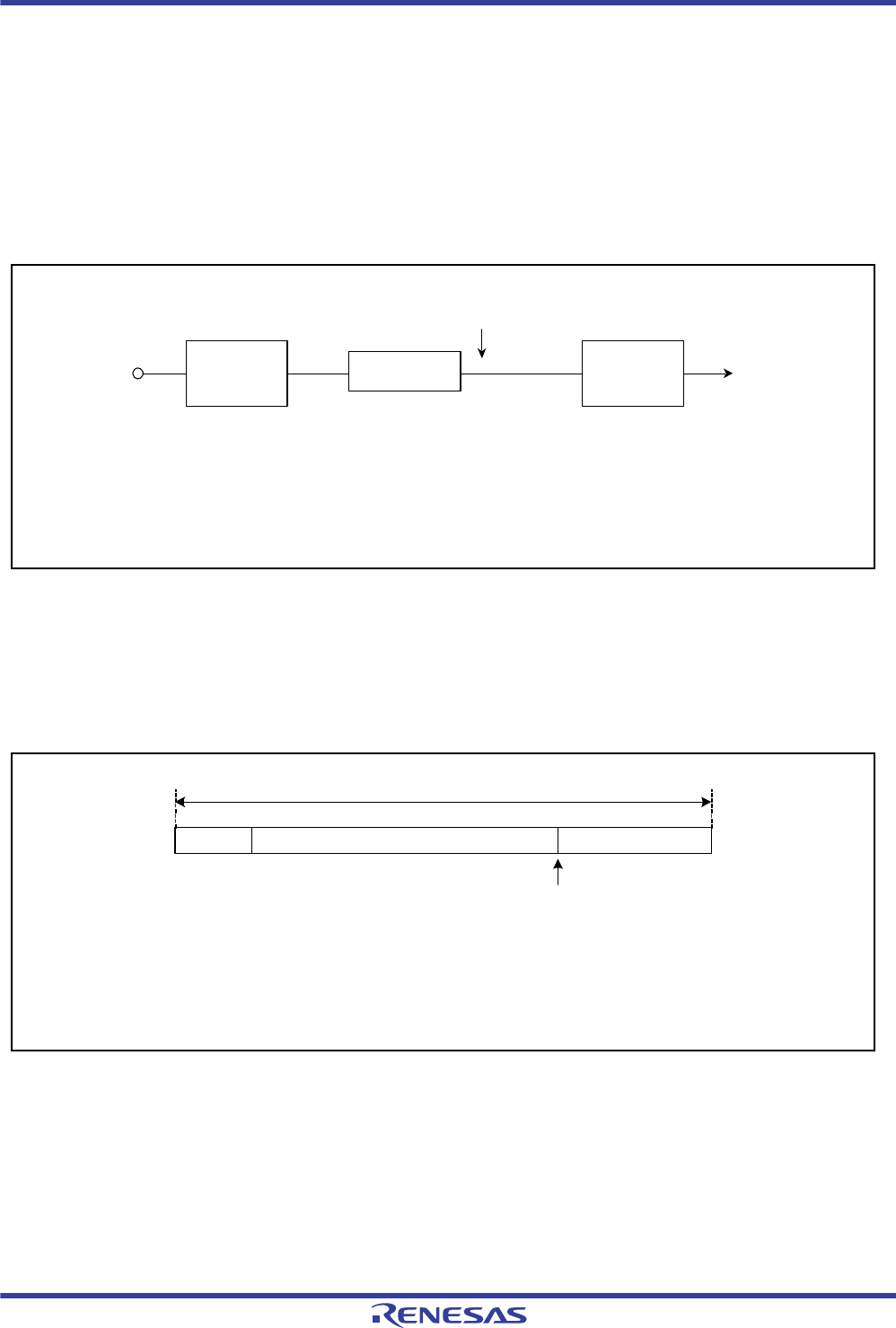
R01UH0034EJ0200 Rev.2.00 Page 1126 of 1489
Dec 27, 2013
RX62T Group, RX62G Group 25. CAN Module
25.4 CAN Communication Speed Setting
The following description explains about CAN communication speed setting.
25.4.1 CAN Clock Setting
This LSI has a CAN clock selector.
The CAN clock can be set by the BRP[9:0] bits in BCR.
Figure 25.11 shows a block diagram of the CAN clock generator.
Figure 25.11 Block Diagram of CAN Clock Generator
25.4.2 Bit Timing Setting
The bit time consists of the following three segments.
Figure 25.12 shows the bit timing.
Figure 25.12 Bit Timing
P=0 to 1023
fCAN fCANCLK
EXTAL Baud rate
prescaler
1/(P+1)
Peripheral module clock
(PCLK)
[Legend]
fCAN: CAN system clock
P: Value selected by BRP[9:0] bits in BCR (P = 0 to 1023)
fCANCLK: CAN communication clock (fCANCLK = fCAN/(P + 1))
Frequency
divider
PLL
frequency
synthesizer
Sample point
Bit time
The range of each segment: Bit time = 8 Tq to 25 Tq
SS = 1 Tq
TSEG1 = 4 Tq to 16 Tq
TSEG2 = 2 Tq to 8 Tq
SJW = 1 Tq to 4 Tq
Setting of TSEG1 and TSEG2: TSEG1 > TSEG2 SJW
SS TSEG1 TSEG2

R01UH0034EJ0200 Rev.2.00 Page 1127 of 1489
Dec 27, 2013
RX62T Group, RX62G Group 25. CAN Module
25.4.3 Bit Rate
The bit rate depends on the division value of fCAN (CAN system clock), the division value of the baud rate prescaler,
and the number of Tq of one bit time.
Note 1. Division value of baud rate prescaler = P + 1 (P: 0 to 1023)
Setting of the BRP[9:0] bits in BCR
Table 25.10 lists bit rate examples.
Bit rate [bps] = fCAN = fCANCLK
Baud rate prescaler division value*1 x number of Tq of one bit time Number of Tq of one bit time
Table 25.10 Bit Rate Examples
fCAN 50 MHz 48 MHz 40 MHz 32 MHz
Bit Rate Number of Tq P + 1 Number of Tq P + 1 Number of Tq P + 1 Number of Tq P + 1
1 Mbps 10 Tq
25 Tq
5
2
8 Tq
12 Tq
16 Tq
6
4
3
10 Tq
20 Tq
4
2
8 Tq
16 Tq
4
2
500 kbps 10 Tq
25 Tq
10
4
8 Tq
12 Tq
16 Tq
12
8
6
10 Tq
20 Tq
8
4
8 Tq
16 Tq
8
4
250 kbps 10 Tq
25 Tq
20
8
8 Tq
12 Tq
16 Tq
24
16
12
10 Tq
20 Tq
16
8
8 Tq
16 Tq
16
8
125 kbps 10 Tq
25 Tq
40
16
8 Tq
12 Tq
16 Tq
48
32
24
10 Tq
20 Tq
32
16
8 Tq
16 Tq
32
16
83.3 kbps 10 Tq
25 Tq
60
24
8 Tq
12 Tq
16 Tq
72
48
36
8 Tq
10 Tq
16 Tq
20 Tq
60
48
30
24
8 Tq
16 Tq
48
24
33.3 kbps 10 Tq
25 Tq
150
60
8 Tq
12 Tq
16 Tq
180
120
90
8 Tq
10 Tq
20 Tq
150
120
60
8 Tq
10 Tq
16 Tq
20 Tq
120
96
60
48
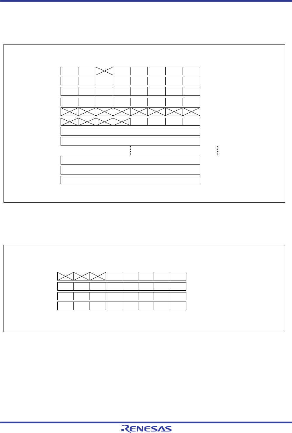
R01UH0034EJ0200 Rev.2.00 Page 1128 of 1489
Dec 27, 2013
RX62T Group, RX62G Group 25. CAN Module
25.5 Mailbox and Mask Register Structure
Figure 25.13 shows the structure of MBj.
There are 32 mailboxes with the same structure.
Figure 25.13 Structure of MBj (j = 0 to 31)
Figure 25.14 shows the structure of MKRi.
There are eight mask registers with the same structure.
Figure 25.14 Structure of MKRi (i = 0 to 7)
Address
MBj
CAN0
0009 0200h
+16j+0
b7 b0
EID7 EID6 EID5 EID4 EID3 EID2 EID1 EID0
EID15 EID14 EID13 EID12 EID11 EID10 EID9 EID8
SID5 SID4 SID3 SID2 SID1 SID0 EID17 EID16
IDE RTR SID10 SID9 SID8 SID7 SID6
DLC3 DLC2 DLC1 DLC0
DATA0
DATA1
DATA7
TSH
TSL
0009 0200h
+16j+1
0009 0200h
+16j+2
0009 0200h
+16j+3
0009 0200h
+16j+4
0009 0200h
+16j+5
0009 0200h
+16j+6
0009 0200h
+16j+7
0009 0200h
+16j+13
0009 0200h
+16j+14
0009 0200h
+16j+15
b7 b0
EID7 EID6 EID5 EID4 EID3 EID2 EID1 EID0
EID15 EID14 EID13 EID12 EID11 EID10 EID9 EID8
SID5 SID4 SID3 SID2 SID1 SID0 EID17 EID16
SID10 SID9 SID8 SID7 SID6
Address
CAN0
MKRi (i = 0 to 7)
0009 0400h
+4i+0
0009 0400h
+4i+1
0009 0400h
+4i+2
0009 0400h
+4i+3
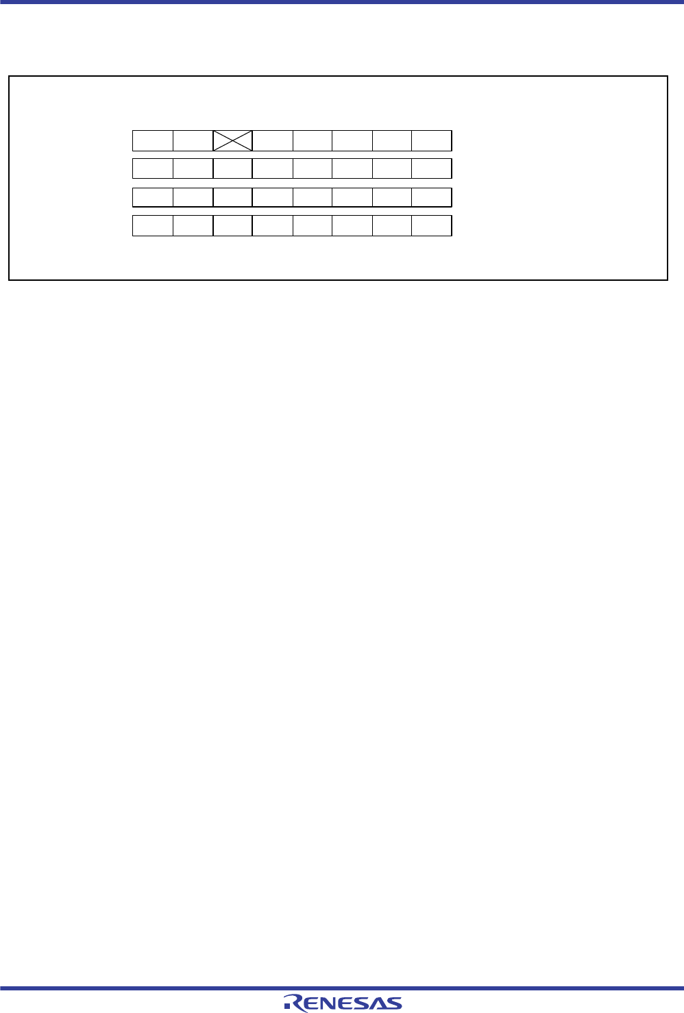
R01UH0034EJ0200 Rev.2.00 Page 1129 of 1489
Dec 27, 2013
RX62T Group, RX62G Group 25. CAN Module
Figure 25.15 shows the structure of FIDCR0 and FIDCR1.
There are two FIFO received ID compare registers with the same structure.
Figure 25.15 Structure of FIDCRn (n = 0, 1)
25.6 Acceptance Filtering and Masking Functions
The acceptance filtering function and masking function allows the user to receive messages with a specified range of
multiple IDs for mailboxes.
Registers MKR0 to MKR7 can perform masking of the standard ID and the extended ID of 29 bits.
MKR0 corresponds to mailboxes [0] to [3]
MKR1 corresponds to mailboxes [4] to [7]
MKR2 corresponds to mailboxes [8] to [11]
MKR3 corresponds to mailboxes [12] to [15]
MKR4 corresponds to mailboxes [16] to [19]
MKR5 corresponds to mailboxes [20] to [23]
MKR6 corresponds to mailboxes [24] to [27] in normal mailbox mode and the receive FIFO mailboxes [28] to [31]
in FIFO mailbox mode.
MKR7 corresponds to mailboxes [28] to [31] in normal mailbox mode and the receive FIFO mailboxes [28] to [31]
in FIFO mailbox mode.
MKIVLR disables acceptance filtering individually for each mailbox.
The IDE bit in MBj is valid when the IDFM[1:0] bits in CTLR are 10 (mixed ID mode).
The RTR bit in MBj selects a data frame or a remote frame.
In FIFO mailbox mode, normal mailboxes (mailboxes [0] to [23]) use the single corresponding register among MKR0 to
MKR5 for acceptance filtering. Receive FIFO mailboxes (mailboxes [28] to [31]) use two registers MKR6 and MKR7
for acceptance filtering.
Also, the receive FIFO uses two registers FIDCR0 and FIDCR1 for ID comparison. Bits EID, SID, RTR, and IDE in
MB28 to MB31 for the receive FIFO are disabled. As acceptance filtering depends on the result of two logic AND
operations, two ranges of IDs can be received into the receive FIFO.
MKIVLR is disabled for the receive FIFO.
Address
CAN0
FIDCRn (n = 0, 1)
b7 b0
EID7 EID6 EID5 EID4 EID3 EID2 EID1 EID0
EID15 EID14 EID13 EID12 EID11 EID10 EID9 EID8
SID5 SID4 SID3 SID2 SID1 SID0 EID17 EID16
IDE RTR SID10 SID9 SID8 SID7 SID6 0009 0420h
+4n+0
0009 0420h
+4n+1
0009 0420h
+4n+2
0009 0420h
+4n+3
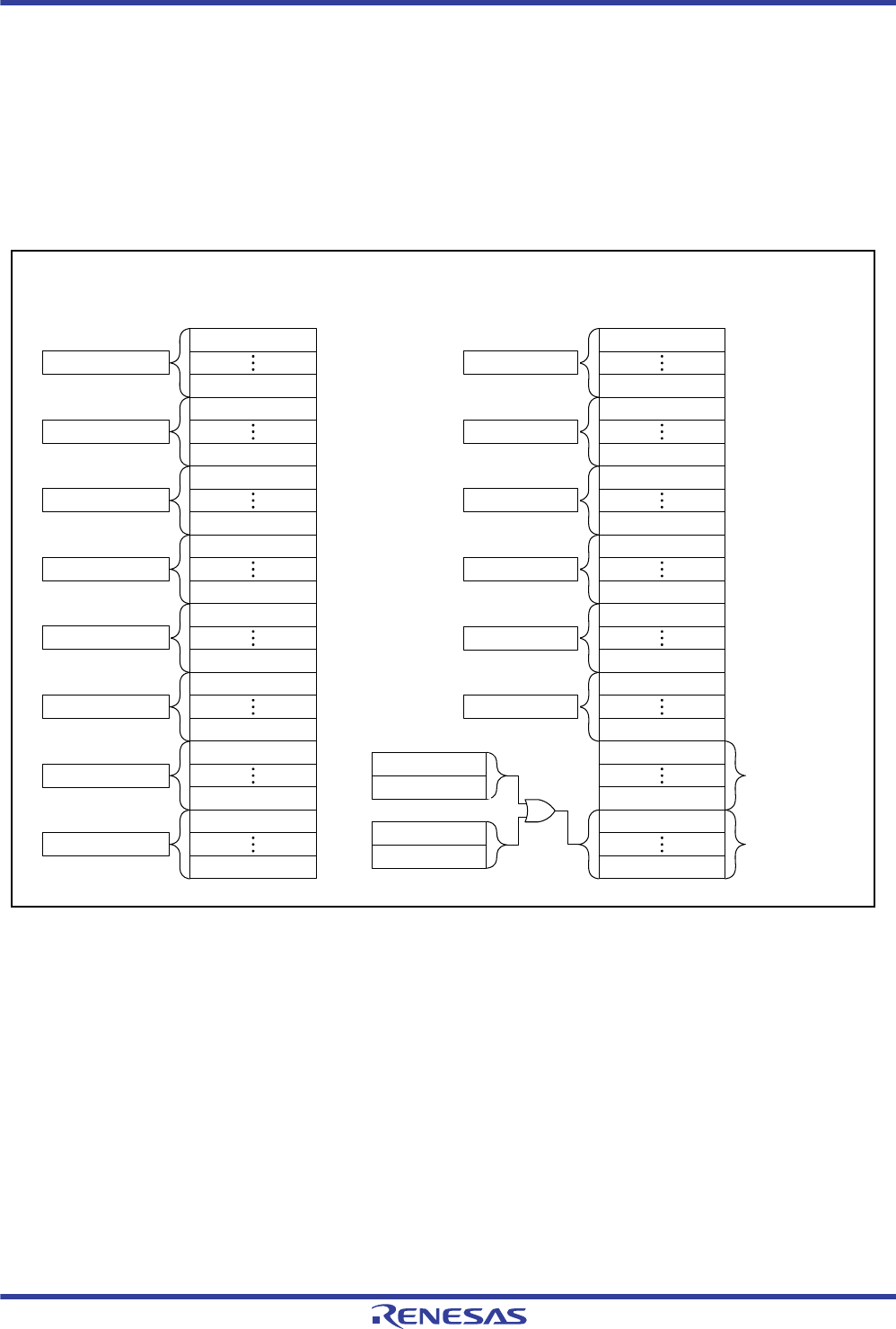
R01UH0034EJ0200 Rev.2.00 Page 1130 of 1489
Dec 27, 2013
RX62T Group, RX62G Group 25. CAN Module
If both the standard ID and extended ID are set in the IDE bits in FIDCR0 and FIDCR1 individually, both ID formats are
received.
If both the data frame and remote frame are set in the RTR bits in FIDCR0 and FIDCR1 individually, both data and
remote frames are received.
When combination with two ranges of IDs is not necessary, set the same mask value and the same ID into both the FIFO
ID and mask register.
Figure 25.16 shows the correspondence between mask registers and mailboxes. Figure 25.17 shows acceptance
filtering.
Figure 25.16 Correspondence between Mask Registers and Mailboxes
Normal mailbox mode FIFO mailbox mode
Mailbox [0]
Mailbox [3]
MKR0 register
Mailbox [4]
Mailbox [7]
MKR1 register
Mailbox [8]
Mailbox [11]
MKR2 register
Mailbox [12]
Mailbox [15]
MKR3 register
Mailbox [16]
Mailbox [19]
MKR4 register
Mailbox [20]
Mailbox [23]
MKR5 register
Mailbox [24]
Mailbox [27]
MKR6 register
Mailbox [28]
Mailbox [31]
MKR7 register
Mailbox [0]
Mailbox [3]
MKR0 register
Mailbox [4]
Mailbox [7]
MKR1 register
Mailbox [8]
Mailbox [11]
MKR2 register
Mailbox [12]
Mailbox [15]
MKR3 register
Mailbox [16]
Mailbox [19]
MKR4 register
Mailbox [20]
Mailbox [23]
MKR5 register
Mailbox [24]
Mailbox [27]
Mailbox [28]
Mailbox [31]
Transmit FIFO
Receive FIFO
MKR6 register
FIDCR0 register
MKR7 register
FIDCR1 register
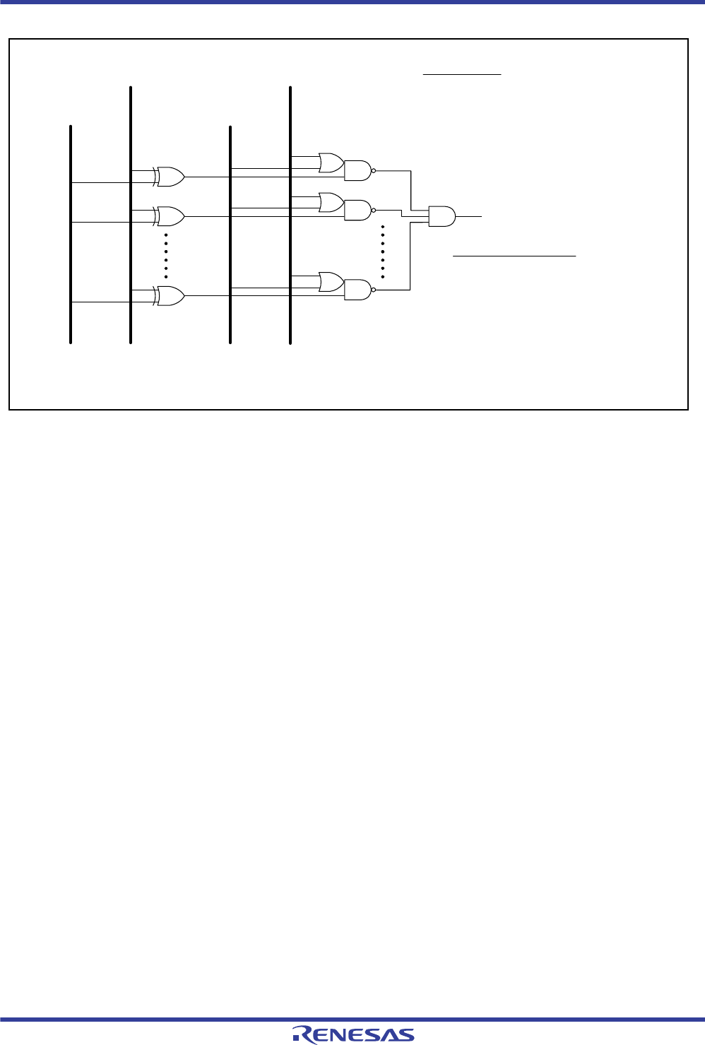
R01UH0034EJ0200 Rev.2.00 Page 1131 of 1489
Dec 27, 2013
RX62T Group, RX62G Group 25. CAN Module
Figure 25.17 Acceptance Filtering
ID value of received
message
Acceptance judge signal
ID setting of MBj
(j = 0 to 31)*1 Setting of MKIVLR*2
Setting of MKRi
(i = 0 to 7)
Mask bit values
0: IDs not compared
1: IDs compared
Acceptance judge signal
0: Receiving message is ignored
(not stored in any mailbox)
1: Receiving message is stored in a mailbox
which matches the ID
Notes: 1. The settings of FIDCR0 and FIDCR1 are used in FIFO mailbox mode.
2. Invalid in FIFO mailboxes.

R01UH0034EJ0200 Rev.2.00 Page 1132 of 1489
Dec 27, 2013
RX62T Group, RX62G Group 25. CAN Module
25.7 Reception and Transmission
Table 25.11 shows how to make the CAN communication mode settings.
j = 0 to 31
When a mailbox is configured as a receive mailbox or a one-shot receive mailbox, note the following:
1. Before a mailbox is configured as a receive mailbox or a one-shot receive mailbox, set MCTLj to 00h.
2. A received message is stored into the first mailbox that matches the condition according to the result of receive
mode setting and acceptance filtering. Upon deciding the mailbox to store the received message, the mailbox with
the smaller number has higher priority.
3. In CAN operation mode, when the CAN module transmits a message whose ID matches with the ID/mask set of a
mailbox configured to receive messages, the CAN module never receives the transmitted data. In self-test mode,
however, the CAN module will receive its transmitted data. In this case, the CAN module returns ACK.
When configuring a mailbox as a transmit mailbox or a one-shot transmit mailbox, note the following:
1. Before a mailbox is configured as a transmit mailbox or a one-shot transmit mailbox, ensure that MCTLj is 00h and
that there is no pending abort process.
Table 25.11 Setting of CAN Receive Mode and CAN Transmit Mode
MCTLj.
TRMREQ MCTLj.
RECREQ MCTLj.
ONESHOT Communication Mode of Mailbox
000Mailbox disabled or transmission being aborted.
001Can be configured only when transmission or reception from a mailbox programmed in
one-shot mode is aborted.
010Configured as a receive mailbox for a data frame or a remote frame.
011Configured as a one-shot receive mailbox for a data frame or a remote frame.
100Configured as a transmit mailbox for a data frame or a remote frame.
101Configured as a one-shot transmit mailbox for a data frame or a remote frame.
110Do not set.
111Do not set.
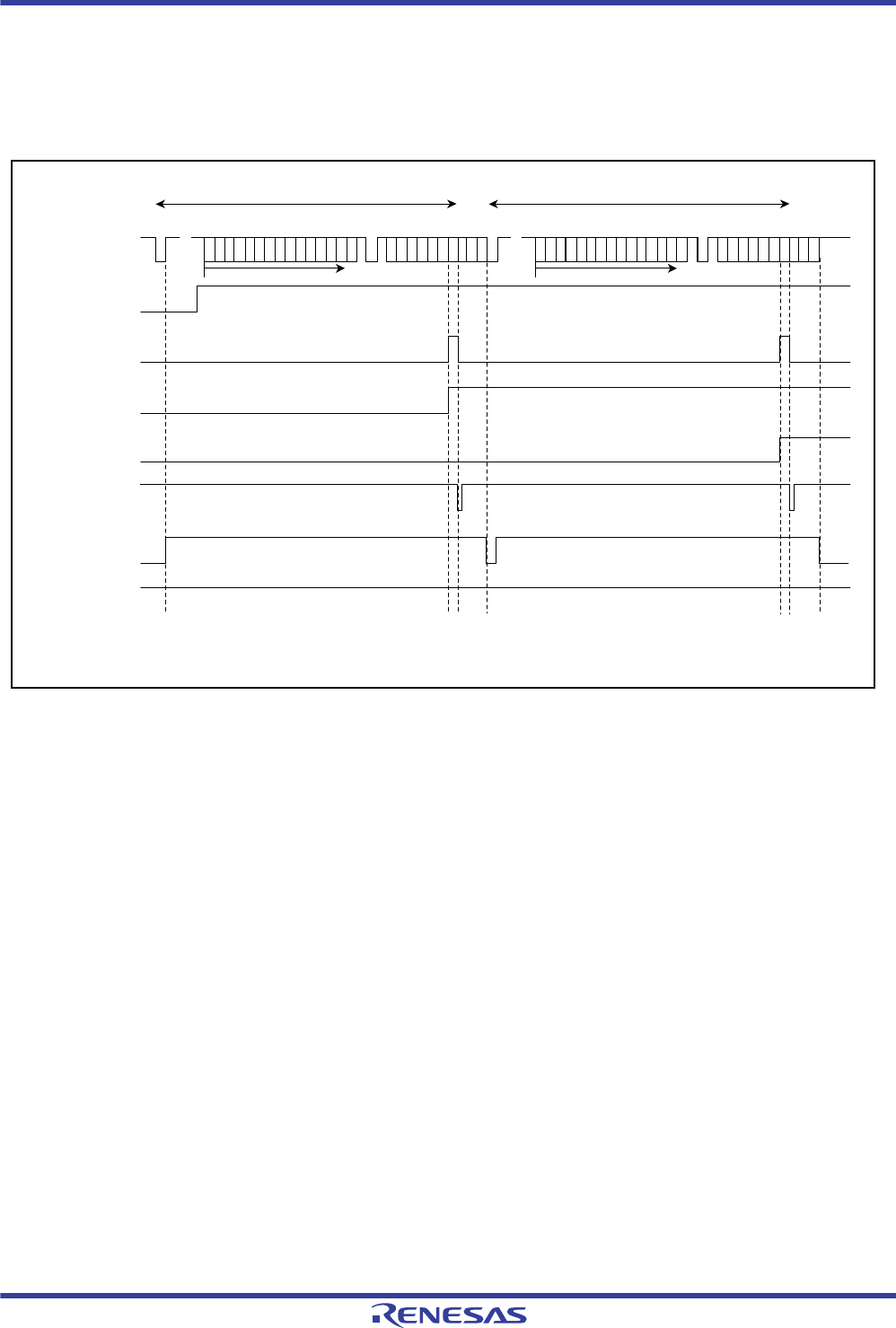
R01UH0034EJ0200 Rev.2.00 Page 1133 of 1489
Dec 27, 2013
RX62T Group, RX62G Group 25. CAN Module
25.7.1 Reception
Figure 25.18 shows an operation example of data frame reception in overwrite mode.
This example shows the operation of overwriting the first message when the CAN module receives two consecutive
CAN messages which match the receiving conditions of MCTLj (j = 0 to 31).
Figure 25.18 Operation Example of Data Frame Reception in Overwrite Mode
1. When an SOF is detected on the CAN bus, the RECST bit in STR is set to 1 (reception in progress) immediately if
the CAN module has no message ready to start transmission.
2. The acceptance filter processing starts at the beginning of the CRC field to select the receive mailbox.
3. After a message has been received, the NEWDATA bit in MCTLj for the receive mailbox is set to 1 (new message
is being stored or has been stored to the mailbox). The INVALDATA bit in MCTLj is set to 1 (message is being
updated) at the same time, and then the INVALDATA bit in MCTLj is set to 0 (message valid) again after the
complete message is transferred to the mailbox.
4. When the interrupt enable bit in MIER for the receive mailbox is 1 (interrupt enabled), the CAN reception complete
interrupt request is generated. This interrupt (CAN reception complete interrupt) is generated when the
INVALDATA bit in MCTLj is set to 0.
5. After reading the message from the mailbox, the NEWDATA flag in MCTLj needs to be set to 0 by a program.
6. In overwrite mode, if the next CAN message has been received into a mailbox whose NEWDATA flag in MCTLj is
still set to 1, the MSGLOST flag in MCTLj is set to 1 (message has been overwritten). The new received message is
transferred to the mailbox. The CAN reception complete interrupt request is generated the same as in 4.
CAN bus
MCTLj.
RECREQ
MCTLj.
INVALDATA
MCTLj.
NEWDATA
MCTLj.
MSGLOST
STR.
RECST
[Legend]: j = 0 to 31
CAN0 error
interrupt
CRC ACK EOF IFS SOF CRC ACK EOF IFSSOF
Receive message in mailbox j
Acceptance filtering Acceptance filtering
CAN0 reception
complete
interrupt
Receive message in mailbox j
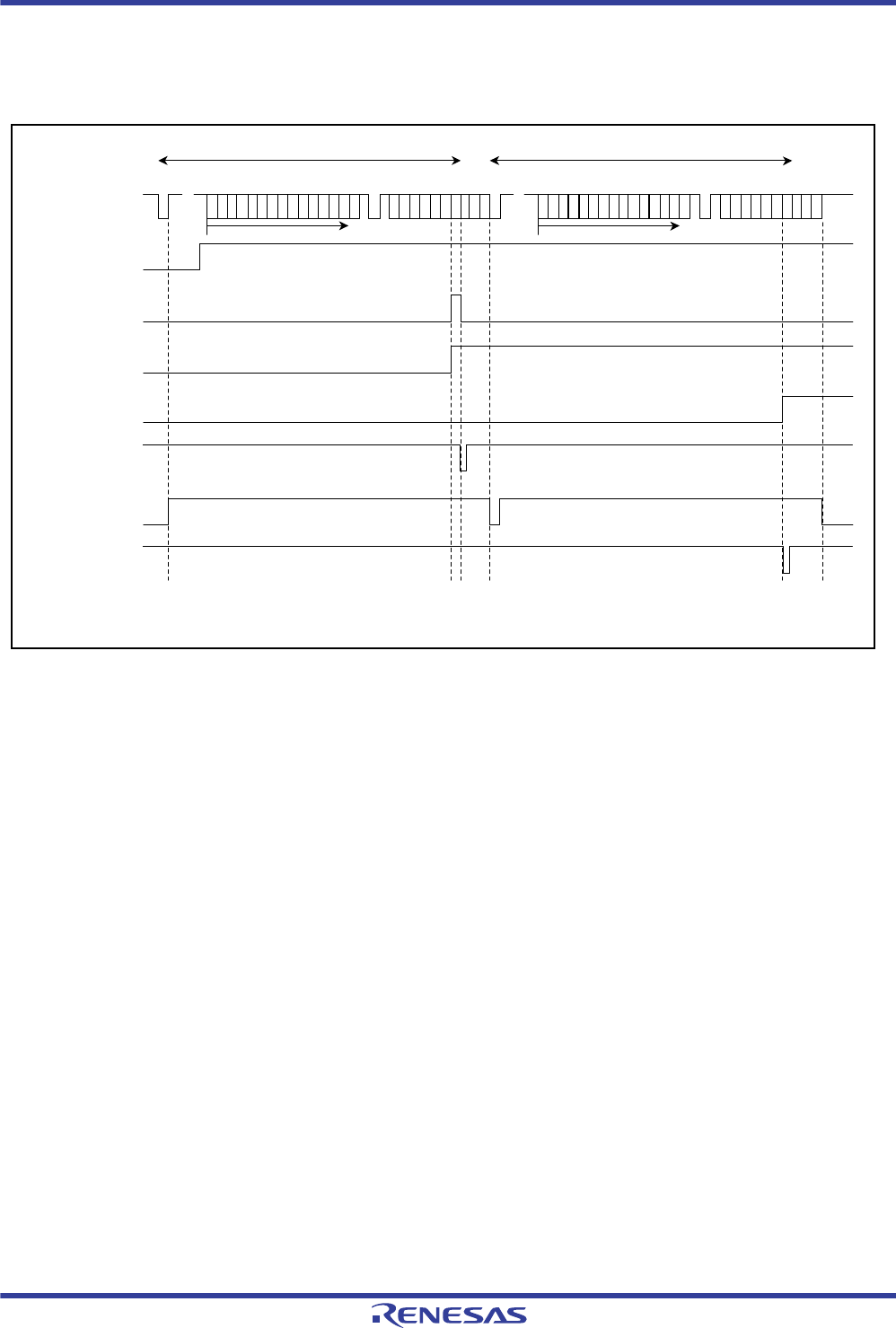
R01UH0034EJ0200 Rev.2.00 Page 1134 of 1489
Dec 27, 2013
RX62T Group, RX62G Group 25. CAN Module
Figure 25.19 shows the operation example of data frame reception in overrun mode.
This example shows the operation of overrunning the second message when the CAN module receives two consecutive
CAN messages which match the receiving conditions of MCTLj (j = 0 to 31).
Figure 25.19 Operation Example of Data Frame Reception in Overrun Mode
1. to 5. are the same as in overwrite mode.
6. In overrun mode, if the next CAN message has been received before the NEWDATA flag in MCTLj is set to 0, the
MSGLOST flag in MCTLj is set to 1 (message has been overrun). The new received message is discarded and a
CAN error interrupt request is generated if the corresponding interrupt enable bit in EIER is set to 1 (interrupt
enabled).
[Legend]: j = 0 to 31
CRC ACK EOF IFS SOF CRC ACK EOF IFSSOF
Receive message in mailbox j Receive message in mailbox j
Acceptance filtering Acceptance filtering
CAN bus
MCTLj.
RECREQ
MCTLj.
INVALDATA
MCTLj.
NEWDATA
MCTLj.
MSGLOST
STR.
RECST
CAN0 error
interrupt
AN reception
complete
interrupt
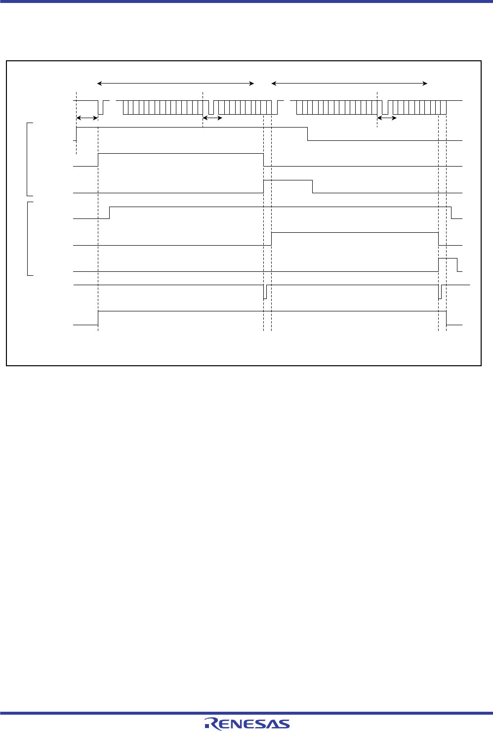
R01UH0034EJ0200 Rev.2.00 Page 1135 of 1489
Dec 27, 2013
RX62T Group, RX62G Group 25. CAN Module
25.7.2 Transmission
Figure 25.20 shows an operation example of data frame transmission.
Figure 25.20 Operation Example of Data Frame Transmission
1. When a TRMREQ bit in MCTLj (j = 0 to 31) is set to 1 (transmit mailbox) in the bus-idle state, the mailbox scan
processing starts to decide the highest-priority mailbox for transmission. Once the transmit mailbox is decided, the
TRMACTIVE bit in MCTLj is set to 1 (from acceptance of transmission request to completion of transmission, or
error/arbitration lost), the TRMST flag in STR is set to 1 (transmission in progress), and the CAN module starts
transmission.*
2. If other TRMREQ bits in MCTLj are set, the transmission scan processing starts with the CRC delimiter for the next
transmission.
3. If transmission is completed without losing arbitration, the SENTDATA flag in MCTLj is set to 1 (transmission
completed) and the TRMACTIVE bit in MCTLj is set to 0 (transmission is pending or transmission is not
requested). If the interrupt enable bit in MIER is 1 (interrupt enabled), the CAN transmission complete interrupt
request is generated.
4. When requesting the next transmission from the same mailbox, set SENDTDATA flag and TRMREQ bit in MCTLj
to 0, then set the TRMREQ bit to 1 after checking that SENDTDATA flag and TRMREQ bit in MCTLj have been
set to 0.
Note 1. If arbitration is lost after the CAN module starts transmission, the TRMACTIVE bit in MCTLj is set to 0. The
transmission scan processing is performed again to search for the highest-priority transmit mailbox from the
beginning of the CRC delimiter. If an error occurs either during transmission or following the arbitration lost, the
transmission scan processing is performed again to search for the highest-priority transmit mailbox from the
start of the error delimiter.
CRC IFS SOF CRC EOF IFSSOF CRC
delimiter CRC
delimiter
EOF
MCTLj.
TRMACTIVE
MCTLj.
SENTDATA
MCTLk.
TRMREQ
MCTLk.
TRMACTIVE
MCTLk.
SENTDATA
[Legend]: j, k = 0 to 31, j k
Transmission message in mailbox j
STC.
TRMST
CAN0
transmission
complete
interrupt
CAN bus
MCTLj.
TRMREQ
Next transmission scan
Transmission message in mailbox k
Next transmission scan Next transmission scan
Mailbox j
Mailbox k

R01UH0034EJ0200 Rev.2.00 Page 1136 of 1489
Dec 27, 2013
RX62T Group, RX62G Group 25. CAN Module
25.8 CAN Interrupt
The CAN module provides the following CAN interrupts for each channel. Table 25.12 lists CAN interrupts.
CAN0 reception complete interrupt (mailboxes 0 to 31) [RXM0]
CAN0 transmission complete interrupt (mailboxes 0 to 31) [TXM0]
CAN0 receive FIFO interrupt [RXF0]
CAN0 transmit FIFO interrupt [TXF0]
CAN0 error interrupt [ERS0]
There are eight types of interrupt sources for the CAN0 error interrupts. These sources can be determined by checking
EIFR.
- Bus error
- Error-warning
- Error-passive
- Bus-off entry
- Bus-off recovery
- Receive overrun
- Overload frame transmission
- Bus lock
Table 25.12 CAN Interrupts
Module Interrupt
Symbol Interrupt Source Source Flag
CAN0 ERS0 Bus lock detected EIFR.BLIF
Overload frame transmission detected EIFR.OLIF
Overrun detected EIFR.ORIF
Bus-off recovery detected EIFR.BORIF
Bus-off entry detected EIFR.BOEIF
Error-passive detected EIFR.EPIF
Error-warning detected EIFR.EWIF
Bus error detected EIFR.BEIF
RXF0 Receive FIFO message received (MIER[29] = 0) —
Receive FIFO warning (MIER[29] = 1)
TXF0 Transmit FIFO message transmission completed (MIER[25] = 0) —
FIFO last message transmission completed (MIER[25] = 1)
RXM0 Mailbox 0 to 31 message received MCTL0.NEWDATA to
MCTL31.NEWDATA
TXM0 Mailbox 0 to 31 message transmission completed MCTL0.SENTDATA to
MCTL31.SENTDATA

R01UH0034EJ0200 Rev.2.00 Page 1137 of 1489
Dec 27, 2013
RX62T Group, RX62G Group 26. Serial Peripheral Interface (RSPI)
Under development Preliminary document
Specifications in this document are tentative and subject to change.
26. Serial Peripheral Interface (RSPI)
26.1 Overview
The RX62T and RX62G Groups include one independent channel of Serial Peripheral Interface (RSPI).
The RSPI channels are capable of full-duplex high-speed serial communications with multiple processors and peripheral
devices.
Table 26.1 shows the specifications of the RSPI, and Figure 26.1 shows a block diagram of the RSPI.
Table 26.1 Specifications of RSPI
Item Description
Number of channels One channel
RSPI transfer functions Use of MOSI (master out/slave in), MISO (master in/slave out), SSL (slave select), and
RSPCK (RSPI clock) signals allows serial communications through SPI operation (four-wire
method) or clock synchronous operation (three-wire method).
Transmit-only operation is available.
Capable of serial communications in master/slave mode
Switching of the polarity of the serial transfer clock
Switching of the phase of the serial transfer clock
Data format MSB-first/LSB-first selectable
Transfer bit length is selectable as 8, 9, 10, 11, 12, 13, 14, 15, 16, 20, 24, or 32 bits.
128-bit transmit/receive buffers
Up to four frames can be transferred in one round of transmission/reception (each frame
consisting of up to 32 bits).
Buffer configuration Double buffer configuration for the transmit/receive buffers
Error detection Mode fault error detection
Overrun error detection
Parity error detection
SSL control function Four SSL signals (SSLn0 to SSLn3) for each channel
In single-master mode, SSL0 to SSL3 signals are output.
In multi-master mode:
SSL0 signal for input, and SSL1 to SSL3 signals for either output or high-impedance.
In slave mode:
SSL0 signal for input, and SSL1 to SSL3 signals for high-impedance.
Controllable delay from SSL output assertion to RSPCK operation (RSPCK delay)
Range: 1 to 8 RSPCK cycles (set in RSPCK-cycle units)
Controllable delay from RSPCK stoppage to SSL output negation (SSL negation delay)
Range: 1 to 8 RSPCK cycles (set in RSPCK-cycle units)
Controllable wait for next-access SSL output assertion (next-access delay)
Range: 1 to 8 RSPCK cycles (set in RSPCK-cycle units)
Function for changing SSL polarity
Control in master transfer A transfer of up to eight commands can be executed sequentially in looped execution.
For each command, the following can be set:
SSL signal value, bit rate, RSPCK polarity/phase, transfer data length, LSB/MSB-first, burst,
RSPCK delay, SSL negation delay, and next-access delay
A transfer can be initiated by writing to the transmit buffer.
MOSI signal value specifiable in SSL negation
Interrupt sources Maskable interrupt sources
RSPI receive interrupt (receive buffer full)
RSPI transmit interrupt (transmit buffer empty)
RSPI error interrupt (mode fault, overrun, parity error)
RSPI idle interrupt (RSPI idle)
Others Function for disabling (initializing) the RSPI
Loopback mode
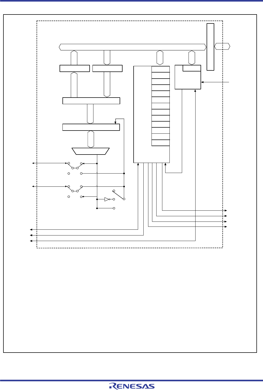
R01UH0034EJ0200 Rev.2.00 Page 1138 of 1489
Dec 27, 2013
RX62T Group, RX62G Group 26. Serial Peripheral Interface (RSPI)
Under development Preliminary document
Specifications in this document are tentative and subject to change.
Figure 26.1 Block Diagram of RSPI
Module data bus
Transmission/
reception
controller
Clock
SPRX SPCR
SSLP
SPPCR
SPSR
SPDR
SPSCR
SPSSR
SPDCR
SPCKD
SSLND
SPND
SPCMD
Shift register
Selector
SPTX
Peripheral bus
SPTI0
SPRI0
SPEI0
SSL0
SSL1 to SSL3
RSPCK
SPBR
Bus interface
PCLK
Parity circuit
SPCR2
SPII0
MOSI
MISO
Master
Slave
Normal
Master
Normal
Loopback
Loopback 2
Slave
Loopback
Loopback 2
Loopback
Normal
Loopback 2
SPCR: RSPI control register
SPCR2: RSPI control register 2
SSLP: RSPI slave select polarity register
SPPCR: RSPI pin control register
SPSR: RSPI status register
SPDR: RSPI data register
SPSCR: RSPI sequence control register
SPSSR: RSPI sequence status register
SPDCR: RSPI data control register
SPCKD: RSPI clock delay register
SSLND: RSPI slave select negate delay register
SPND: RSPI next-access delay register
SPCMD: RSPI command registers 0 to 7 (eight registers)
SPBR: RSPI bit rate register
SPTX: RSPI transmit buffer
SPRX: RSPI receive buffer
SPTI0: RSPI transmit interrupt
SPRI0: RSPI receive interrupt
SPII0: SPI idle interrupt
SPEI0: RSPI error interrupt
[Legend]
Baud rate
generator

R01UH0034EJ0200 Rev.2.00 Page 1139 of 1489
Dec 27, 2013
RX62T Group, RX62G Group 26. Serial Peripheral Interface (RSPI)
Under development Preliminary document
Specifications in this document are tentative and subject to change.
Table 26.2 shows the input and output pins used in the RSPI.
The RSPI automatically switches the input/output direction of the SSL0 pin. SSL0 is set as an output when the RSPI is a
single master and as an input when the RSPI is a multi-master or a slave. Pins RSPCK, MOSI, and MISO are
automatically set as inputs or outputs according to the setting of master or slave and the level input on the SSL0 pin (see
section 26.3.2, Controlling RSPI Pins ).
Table 26.2 RSPI Pin Configuration
Module Symbol Pin Name I/O Function
RSPI0 RSPCK I/O Clock input/output pin
MOSI I/O Master transmit data input/output pin
MISO I/O Slave transmit data input/output pin
SSL0 I/O Slave selection input/output pin
SSL1 Output Slave selection output pin
SSL2 Output Slave selection output pin
SSL3 Output Slave selection output pin

R01UH0034EJ0200 Rev.2.00 Page 1140 of 1489
Dec 27, 2013
RX62T Group, RX62G Group 26. Serial Peripheral Interface (RSPI)
Under development Preliminary document
Specifications in this document are tentative and subject to change.
26.2 Register Descriptions
Table 26.3 shows a list of the RSPI registers. These registers enable the RSPI to perform the following controls:
specifying master/slave modes, specifying a transfer format, and controlling the transmitter and receiver.
x: Undefined
Table 26.3 Registers of RSPI
Module Symbol Register Name Symbol Value after Reset Address Access Size
RSPI0 RSPI control register SPCR 00h 0008 8380h 8
RSPI slave select polarity register SSLP 00h 0008 8381h 8
RSPI pin control register SPPCR 00h 0008 8382h 8
RSPI status register SPSR 20h 0008 8383h 8
RSPI data register SPDR 00000000h 0008 8384h 16, 32
RSPI sequence control register SPSCR 00h 0008 8388h 8
RSPI sequence status register SPSSR 00h 0008 8389h 8
RSPI bit rate register SPBR FFh 0008 838Ah 8
RSPI data control register SPDCR 00h 0008 838Bh 8
RSPI clock delay register SPCKD 00h 0008 838Ch 8
RSPI slave select negation delay register SSLND 00h 0008 838Dh 8
RSPI next-access delay register SPND 00h 0008 838Eh 8
RSPI control register 2 SPCR2 00h 0008 838Fh 8
RSPI command register 0 SPCMD0 070Dh 0008 8390h 16
RSPI command register 1 SPCMD1 070Dh 0008 8392h 16
RSPI command register 2 SPCMD2 070Dh 0008 8394h 16
RSPI command register 3 SPCMD3 070Dh 0008 8396h 16
RSPI command register 4 SPCMD4 070Dh 0008 8398h 16
RSPI command register 5 SPCMD5 070Dh 0008 839Ah 16
RSPI command register 6 SPCMD6 070Dh 0008 839Ch 16
RSPI command register 7 SPCMD7 070Dh 0008 839Eh 16

R01UH0034EJ0200 Rev.2.00 Page 1141 of 1489
Dec 27, 2013
RX62T Group, RX62G Group 26. Serial Peripheral Interface (RSPI)
Under development Preliminary document
Specifications in this document are tentative and subject to change.
26.2.1 RSPI Control Register (SPCR)
SPCR sets the operating mode of the RSPI. If the SPCR.MSTR, SPCR.MODFEN, and SPCR.TXMD bits are changed
while the RSPI function is enabled (SPCR.SPE = 1), subsequent operations cannot be guaranteed.
SPMS Bit (RSPI Mode Select)
The SPMS bit selects SPI operation (four-wire method) or clock synchronous operation (three-wire method).
The SSL0 to SSL3 pins are not used in clock synchronous operation. The three pins RSPCK, MOSI, and MISO handle
communications. If clock-synchronous operation is to proceed in master mode (SPCR.MSTR = 1), the CPHA bit in the
RSPI command register (SPCMD) can be set to either 0 or 1. Set the SPCMD.CPHA bit to 1 if clock-synchronous
operation is to proceed in slave mode (SPCR.MSTR = 0). Operation is not guaranteed if the SPCMD.CPHA bit is set to
0 when clock-synchronous operation is to proceed in slave mode (SPCR.MSTR = 0).
TXMD Bit (Communications Operating Mode Select)
The TXMD bit selects full-duplex synchronous serial communications or transmit operations only.
When performing communications with the TXMD bit set to 1, the RSPI performs only transmit operations and not
receive operations (see section 26.3.6, Communications Operating Mode).
When the TXMD bit is set to 1, receive buffer full interrupt requests cannot be used.
MODFEN Bit (Mode Fault Error Detection Enable)
The MODFEN bit enables or disables the detection of mode fault error (see section 26.3.8, Error Detection). In
addition, the RSPI determines the input/output direction of the SSL0 to SSL3 pins based on combinations of the
MODFEN and MSTR bits (see section 26.3.2, Controlling RSPI Pins ).
Address: 0008 8380h
b7 b6 b5 b4 b3 b2 b1 b0
SPRIE SPE SPTIE SPEIE MSTR MODF
EN TXMD SPMS
Value after reset: 00000000
Bit Symbol Bit Name Description R/W
b0 SPMS RSPI Mode Select 0: SPI operation (four-wire method)
1: Clock synchronous operation (three-wire method)
R/W
b1 TXMD Communications Operating Mode
Select
0: Full-duplex synchronous serial communications
1: Serial communications consisting of only transmit operations
R/W
b2 MODFEN Mode Fault Error Detection Enable 0: Disables the detection of mode fault error
1: Enables the detection of mode fault error
R/W
b3 MSTR RSPI Master/Slave Mode Select 0: Slave mode
1: Master mode
R/W
b4 SPEIE RSPI Error Interrupt Enable 0: Disables the generation of RSPI error interrupt requests
1: Enables the generation of RSPI error interrupt requests
R/W
b5 SPTIE RSPI Transmit Interrupt Enable 0: Disables the generation of RSPI transmit interrupt requests
1: Enables the generation of RSPI transmit interrupt requests
R/W
b6 SPE RSPI Function Enable 0: Disables the RSPI function
1: Enables the RSPI function
R/W
b7 SPRIE RSPI Receive Interrupt Enable 0: Disables the generation of RSPI receive interrupt requests
1: Enables the generation of RSPI receive interrupt requests
R/W

R01UH0034EJ0200 Rev.2.00 Page 1142 of 1489
Dec 27, 2013
RX62T Group, RX62G Group 26. Serial Peripheral Interface (RSPI)
Under development Preliminary document
Specifications in this document are tentative and subject to change.
MSTR Bit (RSPI Master/Slave Mode Select)
The MSTR bit selects master/slave mode of the RSPI. According to MSTR bit settings, the RSPI determines the
direction of pins RSPCK, MOSI, MISO.
SPEIE Bit (RSPI Receive Interrupt Enable)
The SPEIE bit enables or disables the generation of RSPI error interrupt requests when the RSPI detects a mode fault
error and sets the SPSR.MODF bit to 1, or when the RSPI detects an overrun error and sets the SPSR.OVRF flag to 1
(see section 26.3.8, Error Detection).
SPTIE Bit (RSPI Transmit Interrupt Enable)
The SPTIE bit enables or disables the generation of RSPI transmit interrupt requests when the RSPI detects transmit
buffer empty.
At the beginning of transmission, the transmit interrupt requests are generated by setting the SPE bit to 1 at the same time
or after the SPTIE bit has been set to 1.
Therefore, note that even while the RSPI function is disabled (SPE bit is 0), setting the SPTIE bit to 1 will generate an
RSPI transmit interrupt request.
SPE Bit (RSPI Function Enable)
The SPE bit enables or disables the RSPI function. When the SPSR.MODF flag is 1, the SPE bit cannot be set to 1. For
details, refer to section 26.3.8, Error Detection.
Setting the SPE bit to 0 disables the RSPI function, and initializes a part of the module function. For details, refer to
section 26.3.9, Initializing RSPI.
SPRIE Bit (RSPI Error Interrupt Enable)
If the RSPI has detected a receive buffer write after completion of a serial transfer, the SPRIE bit enables or disables the
generation of an RSPI receive interrupt request.

R01UH0034EJ0200 Rev.2.00 Page 1143 of 1489
Dec 27, 2013
RX62T Group, RX62G Group 26. Serial Peripheral Interface (RSPI)
Under development Preliminary document
Specifications in this document are tentative and subject to change.
26.2.2 RSPI Slave Select Polarity Register (SSLP)
SSLP sets the polarity of the SSL0 to SSL3 signals of the RSPI.
If the contents of SSLP are changed by the CPU while the RSPI function is enabled (SPCR.SPE = 1), subsequent
operations are not guaranteed.
SSLiP Bit (SSL Signal Polarity Setting) (i = 0 to 3)
These bits set the polarity of the SSLi signals. The setting of SSLiP indicates the active polarity of the SSLi signal.
Address: 0008 8381h
b7 b6 b5 b4 b3 b2 b1 b0
————SSL3PSSL2PSSL1PSSL0P
Value after reset: 00000000
Bit Symbol Bit Name Description R/W
b0 SSL0P SSL0 Signal Polarity Setting 0: SSL0 signal is 0-active
1: SSL0 signal is 1-active
R/W
b1 SSL1P SSL1 Signal Polarity Setting 0: SSL1 signal is 0-active
1: SSL1 signal is 1-active
R/W
b2 SSL2P SSL2 Signal Polarity Setting 0: SSL2 signal is 0-active
1: SSL2 signal is 1-active
R/W
b3 SSL3P SSL3 Signal Polarity Setting 0: SSL3 signal is 0-active
1: SSL3 signal is 1-active
R/W
b7 to b4 — Reserved These bits are always read as 0. The write value should always be 0. R/W

R01UH0034EJ0200 Rev.2.00 Page 1144 of 1489
Dec 27, 2013
RX62T Group, RX62G Group 26. Serial Peripheral Interface (RSPI)
Under development Preliminary document
Specifications in this document are tentative and subject to change.
26.2.3 RSPI Pin Control Register (SPPCR)
SPPCR sets the modes of the RSPI pins. If the contents of SPPCR are changed by the CPU while the RSPI function is
enabled (SPCR.SPE = 1), subsequent operations are not guaranteed.
SPLP Bit (RSPI Loopback)
The SPLP bit selects the mode of the RSPI pins.
When the SPLP bit is set to 1, the RSPI shuts off the path between the MISO pin and the shift register if the SPCR.MSTR
bit is 1, and between the MOSI pin and the shift register if the SPCR.MSTR bit is 0, and connects (reverses) the input
path and output path for the shift register (loopback mode). For details, see section 26.3.13, Loopback Mode.
SPLP2 Bit (RSPI Loopback 2)
The SPLP2 bit selects the mode of the RSPI pins.
When the SPLP2 bit is set to 1, the RSPI shuts off the path between the MISO pin and the shift register if the
SPCR.MSTR bit is 1, and between the MOSI pin and the shift register if the SPCR.MSTR bit is 0, and connects the input
path and output path for the shift register (loopback mode 2). For details, see section 26.3.13, Loopback Mode.
MOIFV Bit (MOSI Idle Fixed Value)
If the MOIFE bit is 1 in master mode, the MOIFV bit determines the MOSI pin output value during the SSL negation
period (including the SSL retention period during a burst transfer).
MOIFE Bit (MOSI Idle Value Fixing Enable)
The MOIFE bit fixes the MOSI output value when the RSPI in master mode is in an SSL negation period (including the
SSL retention period during a burst transfer). When the MOIFE bit is 0, the RSPI outputs the last data from the previous
serial transfer during the SSL negation period. When the MOIFE bit is 1, the RSPI outputs the fixed value set in the
MOIFV bit to the MOSI bit.
Address: 0008 8382h
b7 b6 b5 b4 b3 b2 b1 b0
— — MOIFE MOIFV — — SPLP2 SPLP
Value after reset: 00000000
Bit Symbol Bit Name Description R/W
b0 SPLP RSPI Loopback 0: Normal mode
1: Loopback mode (reversed transmit data = receive data)
R/W
b1 SPLP2 RSPI Loopback 2 0: Normal mode
1: Loopback mode (transmit data = receive data)
R/W
b3, b2 — Reserved These bits are always read as 0. The write value should always be 0. R/W
b4 MOIFV MOSI Idle Fixed Value 0: MOSI Idle fixed value equals 0
1: MOSI Idle fixed value equals 1
R/W
b5 MOIFE MOSI Idle Value Fixing Enable 0: MOSI output value equals final data from previous transfer
1: MOSI output value equals the value set in the MOIFV bit
R/W
b7, b6 — Reserved These bits are always read as 0. The write value should always be 0. R/W

R01UH0034EJ0200 Rev.2.00 Page 1145 of 1489
Dec 27, 2013
RX62T Group, RX62G Group 26. Serial Peripheral Interface (RSPI)
Under development Preliminary document
Specifications in this document are tentative and subject to change.
26.2.4 RSPI Status Register (SPSR)
Note 1. Only 0 can be written to clear the flag after reading 1.
Note 2. The write value should always be 1.
SPSR indicates the operating status of the RSPI. SPSR can always be read by the CPU. Writing to SPSR can only be
performed by the CPU under certain conditions.
OVRF Flag (Overrun Error Flag)
The OVRF flag indicates the occurrence of an overrun error.
[Setting condition]
If a serial transfer ends while the SPCR.TXMD bit is 0 and the receive buffer holds data that has not yet been read
out
[Clearing condition]
The CPU reads SPSR when the OVRF flag is 1, and then writes the value 0 to the OVRF flag.
Address: 0008 8383h
b7 b6 b5 b4 b3 b2 b1 b0
SPRF — SPTEF — PERF MODF IDLNF OVRF
Value after reset: 00100000
Bit Symbol Bit Name Description R/W
b0 OVRF Overrun Error Flag 0: No overrun error occurs
1: An overrun error occurs
R/(W)*1
b1 IDLNF RSPI Idle Flag 0: RSPI is in the idle state
1: RSPI is in the transfer state
R
b2 MODF Mode Fault Error Flag 0: No mode fault error occurs
1: A mode fault error occurs
R/(W)*1
b3 PERF Parity Error Flag 0: No parity error occurs
1: A parity error occurs
R/(W)*1
b4 — Reserved This bit is always read as 0. The write value should always be 0. R/W
b5 SPTEF Transmit Buffer Empty Flag 0: When data is transferred to SPDR (Transmit buffer is full)
1: When data is transferred from SPDR to shift register
(Transmit buffer is empty)
R/(W)*2
b6 — Reserved This bit is always read as 0. The write value should always be 0. R/W
b7 SPRF Receive Buffer Full Flag 0: When data is transferred from SPDR
(SPDR has no valid received data)
1: When data has been received normally and transferred from shift
register to SPDR (SPDR has valid received data)
R/(W)*2

R01UH0034EJ0200 Rev.2.00 Page 1146 of 1489
Dec 27, 2013
RX62T Group, RX62G Group 26. Serial Peripheral Interface (RSPI)
Under development Preliminary document
Specifications in this document are tentative and subject to change.
IDLNF Flag (RSPI Idle Flag)
The IDLNF flag indicates the transfer status of the RSPI.
[Setting condition]
<Master mode>
Even one condition among the following clearing conditions for master mode is not satisfied
<Slave mode>
The SPCR.SPE bit is 1 (RSPI function is enabled)
[Clearing conditions]
<Master mode>
The SPCR.SPE bit is 0 (RSPI is initialized)
The transmit buffer (SPTX) is empty (data for the next transfer is not set)
The SPSSR.SPCP[2:0] bits are 000 (beginning of sequence control)
The RSPI internal sequencer has entered the idle state (status in which operations up to the next-access delay have
finished)
The flag is cleared to 0 when the above first clearing condition is satisfied or all of the second to fourth clearing
conditions are satisfied.
<Slave mode>
The SPCR.SPE bit is 0 (RSPI is initialized)
MODF Flag (Mode Fault Error Flag)
Indicates the occurrence of a mode fault error.
[Setting condition]
<Multi-master mode>
When the input level of the SSL pin changes to the active level while the SPCR.MSTR bit is 1 (master mode) and
the SPCR.MODFEN bit is 1 (mode fault error detection is enabled), the RSPI detects a mode fault error
<Slave mode>
When the SSL pin is negated before the RSPCK cycle necessary for data transfer ends while the SPCR.MSTR bit is
0 (slave mode) and the SPCR.MODFEN bit is 1 (mode fault error detection is enabled), the RSPI detects a mode
fault error
The active level of the SSL signal is determined by the SSLP.SSLiP bit (SSL signal polarity setting bit).(i = 0 to 3)
[Clearing condition]
The CPU reads SPSR when the MODF flag is 1, and then writes the value 0 to the MODF flag

R01UH0034EJ0200 Rev.2.00 Page 1147 of 1489
Dec 27, 2013
RX62T Group, RX62G Group 26. Serial Peripheral Interface (RSPI)
Under development Preliminary document
Specifications in this document are tentative and subject to change.
PERF Flag (Parity Error Flag)
Indicates the occurrence of a parity error.
[Setting condition]
When a serial transfer ends while the SPCR.TXMD bit is 0 and the SPCR2.SPPE bit is 1, the RSPI detects a parity
error
[Clearing condition]
The CPU reads SPSR when the PERF flag is 1, and then writes the value 0 to the PERF flag
SPTEF Flag (Transmit Buffer Empty Flag)
Indicates whether the transmit buffer is empty.
[Setting condition]
When data is transferred from SPDR to shift register
[Clearing condition]
When data is transferred to SPDR
SPRF Flag (Receive Buffer Full Flag)
Indicates whether the receive buffer is full.
[Setting condition]
When data has been received normally and transferred from shift register to SPDR
[Clearing condition]
When data is transferred from SPDR

R01UH0034EJ0200 Rev.2.00 Page 1148 of 1489
Dec 27, 2013
RX62T Group, RX62G Group 26. Serial Peripheral Interface (RSPI)
Under development Preliminary document
Specifications in this document are tentative and subject to change.
26.2.5 RSPI Data Register (SPDR)
SPDR which can always be read from or written to by the CPU is a buffer that holds data for transmission and reception
by the RSPI.
The transmit buffer (SPTX) and receive buffer (SPRX) are independent and are mapped to SPDR.
Reading from or writing to SPDR should be performed in word or longword units according to the SPDCR.SPLW bit
setting. When the SPLW bit is 0, SPDR is a 64-bit buffer that consists of up to four 16-bit frames. When the SPLW bit is
1, SPDR is a 128-bit buffer that consists of up to four 32-bit frames.
The frame length used by SPDR is determined by the number of frames specification bits (SPDCR.SPFC[1:0]), and the
bit length to be used is determined by the RSPI data length specification bits (SPCMD.SPB[3:0]).
If the transmit buffer (SPTX) is empty (data for the next transfer is not set) when data is written to SPDR, the RSPI
allows writing of the data to the transmit buffer of SPDR. If the transmit buffer holds data that has not yet been
transmitted, the RSPI does not allow updating of the transmit buffer of SPDR.
If the SPDCR.SPRDTD bit is 0 when data is read from SPDR, the RSPI allows reading of the receive buffer. If the
SPDCR.SPRDTD bit is 1, the RSPI allows reading of the transmit buffer.
When reading from the transmit buffer, the value written to the buffer immediately before the read operation is read. If
the transmit buffer holds data that has not yet been transmitted, the data read out will be 0.
In the normal operation method, data is read from the receive buffer when the SPRDTD bit is 0 and a receive buffer full
interrupt occurs. When the receive buffer holds data that has not yet been read out or the SPSR.OVRF flag is 1, the RSPI
does not update the receive buffer of SPDR at the end of a serial transfer.
To read from or write to the SPDR register in words or longwords, access the following addresses. Otherwise, the data is
not guaranteed.
Longwords: RSPI.SPDR 0008 8384h
Words: RSPI.SPDR 0008 8384h
Address: 0008 8384h
b31 b30 b29 b28 b27 b26 b25 b24 b23 b22 b21 b20 b19 b18 b17 b16
H[15:0]
Value after reset: 0000000000000000
b15 b14 b13 b12 b11 b10 b9 b8 b7 b6 b5 b4 b3 b2 b1 b0
L[15:0]
Value after reset: 0000000000000000
R01UH0034EJ0200 Rev.2.00 Page 1149 of 1489
Dec 27, 2013
RX62T Group, RX62G Group 26. Serial Peripheral Interface (RSPI)
Under development Preliminary document
Specifications in this document are tentative and subject to change.
26.2.6 RSPI Sequence Control Register (SPSCR)
SPSCR sets the sequence control method when the RSPI operates in master mode. When changing the
SPSCR.SPSLN[2:0] bits while both the SPCR.MSTR and SPCR.SPE bits are 1, the bits should be changed while the
SPSR.IDLNF flag is 0.
SPSLN[2:0] Bits (RSPI Sequence Length Specification)
The SPSLN[2:0] bits specify a sequence length when the RSPI in master mode performs sequential operations. The RSPI
in master mode changes RSPI command registers 0 to 7 (SPCMD0 to SPCMD7) to be referenced and the order in which
they are referenced according to the sequence length that is set in the SPSLN[2:0] bits.
The RSPI in slave mode always references SPCMD0.
26.2.7 RSPI Sequence Status Register (SPSSR)
Address: 0008 8388h
b7 b6 b5 b4 b3 b2 b1 b0
————— SPSLN[2:0]
Value after reset: 00000000
Bit Symbol Bit Name Description R/W
b2 to b0 SPSLN[2:0] RSPI Sequence
Length Specification
b2 b1 b0 Sequence Length Referenced SPCMD0 to SPCMD7 (No.)
0 0 0: 1 0 0
0 0 1: 2 0 1 0
0 1 0: 3 0 1 2 0
0 1 1: 4 0 1 2 3 0
1 0 0: 5 0 1 2 3 4 0
1 0 1: 6 0 1 2 3 4 5 0
1 1 0: 7 0 1 2 3 4 5 6 0
1 1 1: 8 0 1 2 3 4 5 6 7 0
SPCMD0 to SPCMD7 to be referenced and the order in which they are
referenced are changed according to the sequence length that is set in these
bits. The relationship among the setting of these bits, sequence length, and
SPCMD0 to SPCMD7 referenced by the RSPI is shown below. However, the
RSPI in slave mode always references SPCMD0.
R/W
b7 to b3 — Reserved These bits are always read as 0. The write value should always be 0. R/W
Address: 0008 8389h
b7 b6 b5 b4 b3 b2 b1 b0
— SPECM[2:0] — SPCP[2:0]
Value after reset: 00000000
Bit Symbol Bit Name Description R/W
b2 to b0 SPCP[2:0] RSPI Command Pointer b2 b1 b0
0 0 0: SPCMD0
0 0 1: SPCMD1
0 1 0: SPCMD2
0 1 1: SPCMD3
1 0 0: SPCMD4
1 0 1: SPCMD5
1 1 0: SPCMD6
1 1 1: SPCMD7
R
R01UH0034EJ0200 Rev.2.00 Page 1150 of 1489
Dec 27, 2013
RX62T Group, RX62G Group 26. Serial Peripheral Interface (RSPI)
Under development Preliminary document
Specifications in this document are tentative and subject to change.
SPSSR indicates the sequence control status when the RSPI operates in master mode.
Any writing to SPSSR by the CPU is ignored.
SPCP[2:0] Bits (RSPI Command Pointer)
The SPCP[2:0] bits indicate SPCMD0 to SPCMD7 that is currently pointed to by the pointer during sequence control by
the RSPI.
For the RSPI's sequence control, see section 26.3.10.1, Master Mode Operation.
SPECM[2:0] Bits (RSPI Error Command)
The SPECM[2:0] bits indicate SPCMD0 to SPCMD7 that is specified by the SPCP[2:0] bits when an error is detected
during sequence control by the PERF. The RSPI updates the SPECM[2:0] bits only when an error is detected. If the
OVRF, MODF, and PERF bits in SPSR are all 0 and there is no error, the values of the SPECM[2:0] bits have no
meaning.
For the RSPI's error detection function, see section 26.3.8, Error Detection. For the RSPI's sequence control, see
section 26.3.10.1, Master Mode Operation.
26.2.8 RSPI Bit Rate Register (SPBR)
SPBR which can be read from or written to by the CPU sets the bit rate in master mode. If the contents of SPBR are
changed by the CPU while both the SPCR.MSTR and SPE bits are 1 with the RSPI function in master mode enabled,
subsequent operations cannot be guaranteed.
When the RSPI is used in slave mode, the bit rate depends on the bit rate of the input clock (bit rate satisfying the
electrical characteristics should be used) regardless of the settings of SPBR and the SPCMDm.BRDV[1:0] bits (bit rate
division setting bits).
The bit rate is determined by combinations of the SPBR setting and the BRDV[1:0] bit setting in SPCMD0 to SPCMD7.
The equation for calculating the bit rate is given below. In the equation, n denotes an SPBR setting (0, 1, 2, …, 255), and
N denotes a BRDV[1:0] bit setting (0, 1, 2, 3).
b3 — Reserved This bit is always read as 0. Writing to this bit has no effect. R/W
b6 to b4 SPECM[2:0] RSPI Error Command b6 b5 b4
0 0 0: SPCMD0
0 0 1: SPCMD1
0 1 0: SPCMD2
0 1 1: SPCMD3
1 0 0: SPCMD4
1 0 1: SPCMD5
1 1 0: SPCMD6
1 1 1: SPCMD7
R
b7 — Reserved This bit is always read as 0. Writing to this bit has no effect. R/W
Address: 0008 838Ah
b7 b6 b5 b4 b3 b2 b1 b0
SPR7 SPR6 SPR5 SPR4 SPR3 SPR2 SPR1 SPR0
Value after reset: 11111111
Bit Symbol Bit Name Description R/W

R01UH0034EJ0200 Rev.2.00 Page 1151 of 1489
Dec 27, 2013
RX62T Group, RX62G Group 26. Serial Peripheral Interface (RSPI)
Under development Preliminary document
Specifications in this document are tentative and subject to change.
Table 26.4 shows examples of the relationship between the SPBR register and BRDV[1:0] bit settings.
Note 1. Can be set in this LSI but bit rates satisfying the electrical characteristics should be used.
Table 26.4 Relationship between SPBR and BRDV[1:0] Bit Settings
SPBR (n) BRDV[1:0]
Bits (N) Division Ratio
Bit Rate
PCLK = 32 MHz PCLK = 36 MHz PCLK = 40 MHz PCLK = 50 MHz
0 0 2 16.0 Mbps*118.0 Mbps*120.0 Mbps*125.0 Mbps*1
1 0 4 8.00 Mbps 9.00 Mbps 10.0 Mbps 12.5 Mbps
2 0 6 5.33 Mbps 6.00 Mbps 6.67 Mbps 8.33 Mbps
3 0 8 4.00 Mbps 4.50 Mbps 5.00 Mbps 6.25 Mbps
4 0 10 3.20 Mbps 3.60 Mbps 4.00 Mbps 5.00 Mbps
5 0 12 2.67 Mbps 3.00 Mbps 3.33 Mbps 4.16 Mbps
5 1 24 1.33 Mbps 1.50 Mbps 1.67 Mbps 2.08 Mbps
5 2 48 667 kbps 750 kbps 833 kbps 1.04 Mbps
5 3 96 333 kbps 375 kbps 417 kbps 521 kbps
255 3 4096 7.81 kbps 8.80 kbps 9.78 kbps 12.2 kbps
Bit rate = f (PCLK)
2 × (n+1) 2N
R01UH0034EJ0200 Rev.2.00 Page 1152 of 1489
Dec 27, 2013
RX62T Group, RX62G Group 26. Serial Peripheral Interface (RSPI)
Under development Preliminary document
Specifications in this document are tentative and subject to change.
26.2.9 RSPI Data Control Register (SPDCR)
SPDCR is a register used to set the number of frames that can be stored in SPDR, control the SSL pin output and reading
from SPDR, and select the width (longword or word) for access to SPDR.
Up to four frames can be transmitted or received in one round of transmission or reception activation. The amount of data
in each transfer is controlled by the combination of the RSPI data length specification bits (SPB[3:0]) in the RSPI
command register (SPCMDm, m = 0 to 7), the RSPI sequence length specification bits (SPSLN[2:0]) in the RSPI
sequence control register (SPSCR), and the number of frames specification bits (SPFC[1:0]) in the RSPI data control
register (SPDCR).
When changing the SPDCR.SPFC[1:0] bits while the SPCR.SPE bit is 1 with the RSPI function enabled, the bits should
be changed while the SPSR.IDLNF flag is 0.
Page 1072.
SPFC[1:0] Bits (Number of Frames Specification)
The SPFC[1:0] bits specify the number of frames that can be stored in SPDR. Up to four frames can be transmitted or
received in one round of transmission or reception, and the amount of data is determined by the combination of the RSPI
data length specification bits (SPB[3:0]) in the RSPI command register (SPCMDm), the RSPI sequence length
specification bits (SPSLN[2:0]) in the RSPI sequence control register (SPSCR), and the number of frames specification
bits (SPFC[1:0]) in the RSPI data control register (SPDCR). Also, the SPFC[1:0] bits specify the number of received
data at which the RSPI receive buffer full interrupt is requested. Table 26.5 and Figure 26.2 show the frame
Address: 0008 838Bh
b7 b6 b5 b4 b3 b2 b1 b0
— — SPLW SPRDT
DSLSEL[1:0] SPFC[1:0]
Value after reset: 00000000
Bit Symbol Bit Name Description R/W
b1, b0 SPFC[1:0] Number of Frames
Specification
These bits specify the number of frames that can be stored in SPDR.
Table 26.5 and Figure 26.2 show the frame configurations that can be
stored in SPDR and examples of combinations of settings for
transmission and reception. If combinations of settings other than those
shown in the examples are made, subsequent operations cannot be
guaranteed.
R/W
b3, b2 SLSEL[1:0] SSl Pin Output Selection R/W
b4 SPRDTD RSPI Receive/Transmit
Data Selection
0: SPDR values are read from the receive buffer
1: SPDR values are read from the transmit buffer
(but only if the transmit buffer is empty)
R/W
b5 SPLW RSPI Longword Access/
Word Access Specification
0: SPDR is accessed in words
1: SPDR is accessed in longwords
R/W
b7, b6 — Reserved These bits are always read as 0. The write value should always be 0. R/W
Operation is not guaranteed if SLSEL[1:0] = 11 is set.
SLSEL SLSEL SLSEL SLSEL
[1:0] = 00 [1:0] = 01 [1:0] = 10 [1:0] = 11
SSL3 Output I/O I/O Setting
prohibited
SSL2 Output I/O I/O
SSL1 Output I/O Output
SSL0 Output Output Output

R01UH0034EJ0200 Rev.2.00 Page 1153 of 1489
Dec 27, 2013
RX62T Group, RX62G Group 26. Serial Peripheral Interface (RSPI)
Under development Preliminary document
Specifications in this document are tentative and subject to change.
configurations that can be stored in SPDR and examples of combinations of settings for transmission and reception. If
combinations of settings other than those shown in the examples are made, subsequent operations are not guaranteed.
SLSEL[1:0] Bits (SSl Pin Output Selection)
The SLSEL[1:0] bits control the SSL pin output in master mode.
SPRDTD Bit (RSPI Receive/Transmit Data Selection)
The SPRDTD bit selects whether the RSPI data register (SPDR) reads values from the receive buffer or from the transmit
buffer.
If reading is from the transmit buffer, the value written to SPDR immediately beforehand is read.
SPLW Bit (RSPI Longword Access/Word Access Specification)
The SPLW bit specifies the access width for SPDR. Access to SPDR is in words when the SPLW bit is 0 and in
longwords when the SPLW bit is 1.
Also, when the SPLW bit is 0, set the SPCMD.SPB[3:0] bits (RSPI data length specification bits) to 8 to 16 bits. When
20, 24, or 32 bits is specified, operation is not guaranteed.
N, M, O, P, Q, R, S, T: Data length that can be specified by the SPB[3:0] bits
Table 26.5 Data Length Settable by SPB[3:0] Bits
Setting SPB[3:0] SPSLN[2:0] SPFC[1:0]
Number of
Frames for
Transfer
Number of Frames at which Receive
Buffer Full Interrupt Occurs or Transmit
Buffer Holding Data is Recognized
1-1 N 000 00 1 1
1-2 N 000 01 2 2
1-3 N 000 10 3 3
1-4 N 000 11 4 4
2-1 N, M 001 01 2 2
2-2 N, M 001 11 4 4
3 N, M, O 010 10 3 3
4 N, M, O, P 011 11 4 4
5 N, M, O, P, Q 100 00 5 1
6 N, M, O, P, Q, R 101 00 6 1
7 N, M, O, P, Q, R, S 110 00 7 1
8 N, M, O, P, Q, R, S, T 111 00 8 1
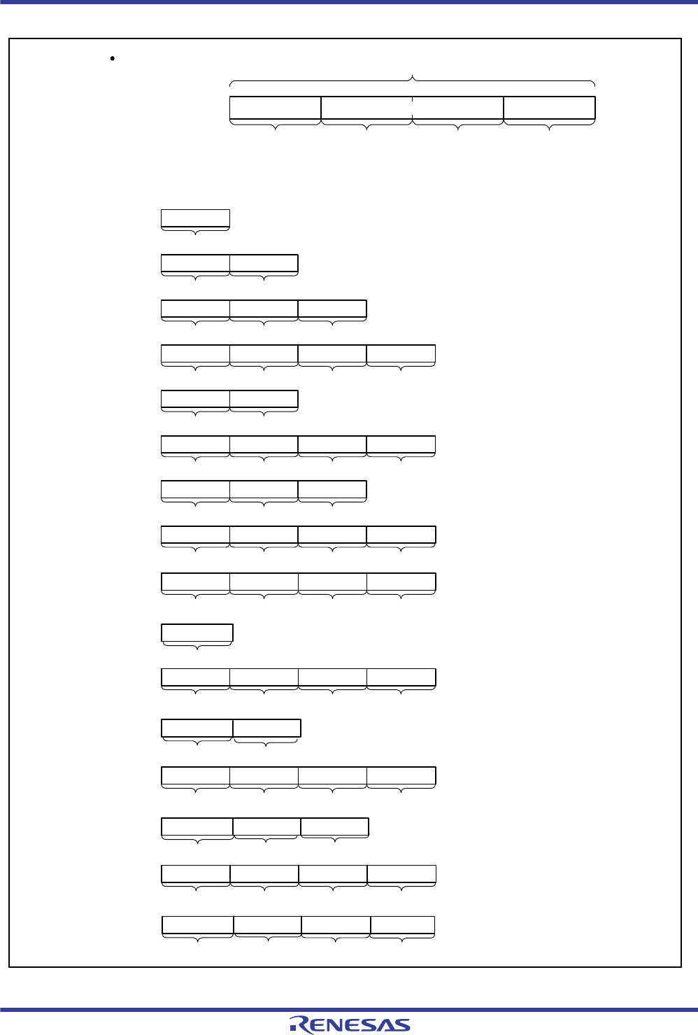
R01UH0034EJ0200 Rev.2.00 Page 1154 of 1489
Dec 27, 2013
RX62T Group, RX62G Group 26. Serial Peripheral Interface (RSPI)
Under development Preliminary document
Specifications in this document are tentative and subject to change.
Figure 26.2 Frame Configurations and Examples of Combinations of Transmission and Reception Settings
1 frame
Frame configuration
32 bits
Only 1 frame
Transmit/receive buffer
O bit
Setting 1-1
1 frame
32 bits
1 frame
32 bits
1 frame
32 bits
128 bits
Examples of combination of settings for transmission and reception
With one activation, data can be transmitted or received as shown below when settings 1-1 to
8 in table 25.5 are made.
Setting 1-2
Setting 1-3
Setting 1-4
Setting 2-1
Setting 2-2
Setting 3
Setting 4
N bit M bit
N bit M bit N bit M bit
N bit M bit
O bit
N bit M bit P bit
1st frame 2nd frame
1st frame 2nd frame 3rd frame
1st frame 2nd frame 3rd frame 4th frame
1st frame 2nd frame
1st frame 2nd frame 3rd frame 4th frame
1st frame 2nd frame 3rd frame
1st frame 2nd frame 3rd frame 4th frame
N bit
N bit N bit
N bit N bit N bit
N bit N bit N bit N bit
Setting 5 O bit
N bit M bit P bit
1st frame 2nd frame 3rd frame 4th frame
Q bit
5th frame
Setting 6 O bit
N bit M bit P bit
1st frame 2nd frame 3rd frame 4th frame
Q bit
5th frame
R bit
6th frame
Setting 7 O bit
N bit M bit P bit
1st frame 2nd frame 3rd frame 4th frame
Q bit
5th frame
R bit
6th frame
S bit
7th frame
Setting 8 O bit
N bit M bit P bit
1st frame 2nd frame 3rd frame 4th frame
Q bit
5th frame
R bit
6th frame
S bit
7th frame
T bit
8th frame

R01UH0034EJ0200 Rev.2.00 Page 1155 of 1489
Dec 27, 2013
RX62T Group, RX62G Group 26. Serial Peripheral Interface (RSPI)
Under development Preliminary document
Specifications in this document are tentative and subject to change.
26.2.10 RSPI Clock Delay Register (SPCKD)
SPCKD sets a period from the beginning of SSL signal assertion to RSPCK oscillation (RSPCK delay) when the
SPCMD.SCKDEN bit is 1. If the contents of SPCKD are changed while both the SPCR.MSTR and SPCR.SPE bits are 1
with the RSPI function in master mode enabled, subsequent operations cannot be guaranteed.
When using the RSPI in slave mode, set the SCKDL[2:0] bits to 000.
SCKDL[2:0] Bits (RSPCK Delay Setting)
The SCKDL[2:0] bits set an RSPCK delay value when the SPCMD.SCKDEN bit is 1.
When using the RSPI in slave mode, set the SCKDL[2:0] bits to 000.
Address: 0008 838Ch
b7 b6 b5 b4 b3 b2 b1 b0
————— SCKDL[2:0]
Value after reset: 00000000
Bit Symbol Bit Name Description R/W
b2 to b0 SCKDL[2:0] RSPCK Delay Setting b2 b1 b0
0 0 0: 1 RSPCK
0 0 1: 2 RSPCK
0 1 0: 3 RSPCK
0 1 1: 4 RSPCK
1 0 0: 5 RSPCK
1 0 1: 6 RSPCK
1 1 0: 7 RSPCK
1 1 1: 8 RSPCK
R/W
b7 to b3 — Reserved These bits are always read as 0. The write value should always be 0. R/W

R01UH0034EJ0200 Rev.2.00 Page 1156 of 1489
Dec 27, 2013
RX62T Group, RX62G Group 26. Serial Peripheral Interface (RSPI)
Under development Preliminary document
Specifications in this document are tentative and subject to change.
26.2.11 RSPI Slave Select Negation Delay Register (SSLND)
SSLND sets a period (SSL negation delay) from the transmission of a final RSPCK edge to the negation of the SSL
signal during a serial transfer by the RSPI in master mode. If the contents of SSLND are changed while both the
SPCR.MSTR and SPCR.SPE bits are 1 with the RSPI function in master mode enabled, subsequent operations cannot be
guaranteed.
When using the RSPI in slave mode, set the SLNDL[2:0] bits to 000.
SLNDL[2:0] Bits (SSL Negation Delay Setting)
The SLNDL[2:0] bits set an SSL negation delay value when the RSPI is in master mode.
When using the RSPI in slave mode, set the SLNDL[2:0] bits to 000.
Address: 0008 838Dh
b7 b6 b5 b4 b3 b2 b1 b0
————— SLNDL[2:0]
Value after reset: 00000000
Bit Symbol Bit Name Description R/W
b2 to b0 SLNDL[2:0] SSL Negation Delay Setting b2 b1 b0
0 0 0: 1 RSPCK
0 0 1: 2 RSPCK
0 1 0: 3 RSPCK
0 1 1: 4 RSPCK
1 0 0: 5 RSPCK
1 0 1: 6 RSPCK
1 1 0: 7 RSPCK
1 1 1: 8 RSPCK
R/W
b7 to b3 — Reserved These bits are always read as 0. The write value should always be 0. R/W

R01UH0034EJ0200 Rev.2.00 Page 1157 of 1489
Dec 27, 2013
RX62T Group, RX62G Group 26. Serial Peripheral Interface (RSPI)
Under development Preliminary document
Specifications in this document are tentative and subject to change.
26.2.12 RSPI Next-Access Delay Register (SPND)
SPND sets a non-active period (next-access delay) after termination of a serial transfer when the SPCMD.SPNDEN bit is
1. If the contents of SPND are changed while both the SPCR.MSTR and SPCR.SPE bits are 1 with the RSPI function in
master mode enabled, subsequent operations cannot be guaranteed.
When using the RSPI in slave mode, set the SPNDL[2:0] bits to 000.
SPNDL[2:0] Bits (RSPI Next-Access Delay Setting)
The SPNDL[2:0] bits set a next-access delay when the SPCMD.SPNDEN bit is 1.
When using the RSPI in slave mode, set the SPNDL[2:0] bits to 000.
Address: 0008 838Eh
b7 b6 b5 b4 b3 b2 b1 b0
————— SPNDL[2:0]
Value after reset: 00000000
Bit Symbol Bit Name Description R/W
b2 to b0 SPNDL[2:0] RSPI Next-Access Delay Setting b2 b1 b0
0 0 0: 1 RSPCK + 2 PCLK
0 0 1: 2 RSPCK + 2 PCLK
0 1 0: 3 RSPCK + 2 PCLK
0 1 1: 4 RSPCK + 2 PCLK
1 0 0: 5 RSPCK + 2 PCLK
1 0 1: 6 RSPCK + 2 PCLK
1 1 0: 7 RSPCK + 2 PCLK
1 1 1: 8 RSPCK + 2 PCLK
R/W
b7 to b3 — Reserved These bits are always read as 0. The write value should
always be 0.
R/W

R01UH0034EJ0200 Rev.2.00 Page 1158 of 1489
Dec 27, 2013
RX62T Group, RX62G Group 26. Serial Peripheral Interface (RSPI)
Under development Preliminary document
Specifications in this document are tentative and subject to change.
26.2.13 RSPI Control Register 2 (SPCR2)
SPCR2 sets the operating mode of the RSPI. If the SPPE bit or SPOE bit in SPCR2 is changed while the SPCR.SPE bit
is 1 with the RSPI function enabled, subsequent operations cannot be guaranteed.
SPPE Bit (Parity Enable)
The SPPE bit enables or disables the parity function.
The parity bit is added to transmit data and parity checking is performed for receive data when the communications
operating mode select bit (TXMD) in the RSPI control register (SPCR) is 0 and the SPPE bit in SPCR is 1.
The parity bit is added to transmit data but parity checking is not performed for receive data when the SPCR.TXMD bit
is 1 and the SPPE bit in SPCR is 1.
SPOE Bit (Parity Mode)
When even parity is set, parity bit addition is performed so that the total number of 1-bits in the transmit/receive
character plus the parity bit is even. Similarly, when odd parity is set, parity bit addition is performed so that the total
number of 1-bits in the transmit/receive character plus the parity bit is odd.
The SPOE bit is valid only when the SPPE bit is 1.
SPIIE Bit (RSPI Idle Interrupt Enable)
The SPIIE bit enables or disables the generation of RSPI idle interrupt requests when the RSPI being in the idle state is
detected and the IDLNF flag in the RSPI status register (SPSR) is cleared to 0.
PTE Bit (Parity Self-Testing)
The PTE bit enables the self-diagnosis function of the parity circuit in order to check whether the parity function is
operating correctly.
Address: 0008 838Fh
b7 b6 b5 b4 b3 b2 b1 b0
————PTESPIIESPOESPPE
Value after reset: 00000000
Bit Symbol Bit Name Description R/W
b0 SPPE Parity Enable 0: Does not add the parity bit to transmit data and does not
check the parity bit of receive data
1: Adds the parity bit to transmit data and checks the parity bit
of receive data (when SPCR.TXMD = 0)
Adds the parity bit to transmit data but does not check the
parity bit of receive data (when SPCR.TXMD = 1)
R/W
b1 SPOE Parity Mode 0: Selects even parity for use in transmission and reception
1: Selects odd parity for use in transmission and reception
R/W
b2 SPIIE RSPI Idle Interrupt Enable 0: Disables the generation of idle interrupt requests
1: Enables the generation of idle interrupt requests
R/W
b3 PTE Parity Self-Testing 0: Disables the self-diagnosis function of the parity circuit
1: Enables the self-diagnosis function of the parity circuit
R/W
b7 to b4 — Reserved These bits are always read as 0. The write value should always
be 0.
R/W

R01UH0034EJ0200 Rev.2.00 Page 1159 of 1489
Dec 27, 2013
RX62T Group, RX62G Group 26. Serial Peripheral Interface (RSPI)
Under development Preliminary document
Specifications in this document are tentative and subject to change.
26.2.14 RSPI Command Register m (SPCMDm, m = 0 to 7)
SPCMDm is used to set a transfer format for the RSPI in master mode. Some of the bits in SPCMD0 are used to set a
transfer mode for the RSPI in slave mode. The RSPI in master mode sequentially references SPCMDm according to the
settings in the SPSLN[2:0] bits in the RSPI sequence control register (SPSCR), and executes the serial transfer that is set
in the referenced SPCMDm.
Address: SPCMD0 0008 8390h, SPCMD1 0008 8392h, SPCMD2 0008 8394h, SPCMD3 0008 8396h,
SPCMD4 0008 8398h, SPCMD5 0008 839Ah, SPCMD6 0008 839Ch, SPCMD7 0008 839Eh
b15 b14 b13 b12 b11 b10 b9 b8 b7 b6 b5 b4 b3 b2 b1 b0
SCKDE
NSLNDE
NSPNDE
NLSBF SPB[3:0] SSLKP SSLA[2:0] BRDV[1:0] CPOL CPHA
Value after reset: 0000011100001101
Bit Symbol Bit Name Description R/W
b0 CPHA RSPCK Phase
Setting
0: Data sampling on odd edge, data variation on even edge
1: Data variation on odd edge, data sampling on even edge
R/W
b1 CPOL RSPCK Polarity
Setting
0: RSPCK = 0 when idle
1: RSPCK = 1 when idle
R/W
b3, b2 BRDV[1:0] Bit Rate Division
Setting
b3 b2
0 0: These bits select the base bit rate
0 1: These bits select the base bit rate divided by 2
1 0: These bits select the base bit rate divided by 4
1 1: These bits select the base bit rate divided by 8
R/W
b6 to b4 SSLA[2:0] SSL Signal
Assertion Setting
b6 b5 b4
0 0 0: SSL0
0 0 1: SSL1
0 1 0: SSL2
0 1 1: SSL3
1 x x: — (Setting prohibited)
x: Don’t care
R/W
b7 SSLKP SSL Signal Level
Keeping
0:Negates all SSL signals upon completion of transfer
1:Keeps the SSL signal level from the end of transfer until the beginning of the
next access.
R/W
b11 to b8 SPB[3:0] RSPI Data Length
Setting
b11 b10 b9 b8
0100 to 0111: 8 bits
1 0 0 0: 9 bits
1 0 0 1: 10 bits
1 0 1 0: 11 bits
1 0 1 1: 12 bits
1 1 0 0: 13 bits
1 1 0 1: 14 bits
1 1 1 0: 15 bits
1 1 1 1: 16 bits
0 0 0 0: 20 bits
0 0 0 1: 24 bits
0010, 0011: 32 bits
R/W
b12 LSBF RSPI LSB First 0: MSB first
1: LSB first
R/W
b13 SPNDEN RSPI Next-Access
Delay Setting Enable
0:A next-access delay of 1 RSPCK + 2 PCLK
1:A next-access delay is equal to the setting of the RSPI next-access delay
register (SPND)
R/W
b14 SLNDEN SSL Negation Delay
Setting Enable
0:An SSL negation delay of 1 RSPCK
1:An SSL negation delay is equal to the setting of the RSPI slave select
negation delay register (SSLND)
R/W
b15 SCKDEN RSPCK Delay
Setting Enable
0:An RSPCK delay of 1 RSPCK
1:An RSPCK delay is equal to the setting of the RSPI clock delay register
(SPCKD)
R/W

R01UH0034EJ0200 Rev.2.00 Page 1160 of 1489
Dec 27, 2013
RX62T Group, RX62G Group 26. Serial Peripheral Interface (RSPI)
Under development Preliminary document
Specifications in this document are tentative and subject to change.
SPCMDm should be set while the transmit buffer is empty (data for the next transfer is not set) and before setting of the
data that is to be transmitted when that SPCMDm is referenced.
SPCMDm that is referenced by the RSPI in master mode can be checked by means of the SPCP[2:0] bits in the RSPI
sequence status register (SPSSR). If the contents of SPCMDm are changed with the RSPI function in slave mode
enabled, subsequent operations cannot be guaranteed.
CPHA Bit (RSPCK Phase Setting)
The CPHA bit sets an RSPCK phase of the RSPI in master mode or slave mode. Data communications between RSPI
modules require the same RSPCK phase setting between the modules.
CPOL Bit (RSPCK Polarity Setting)
The CPOL bit sets an RSPCK polarity of the RSPI in master mode or slave mode. Data communications between RSPI
modules require the same RSPCK polarity setting between the modules.
BRDV[1:0] Bits (Bit Rate Division Setting)
The BRDV[1:0] bits are used to determine the bit rate. A bit rate is determined by combinations of the settings in the
BRDV[1:0] bits and SPBR (see section 26.2.8, RSPI Bit Rate Register (SPBR)). The settings in SPBR determine
the base bit rate. The settings in the BRDV[1:0] bits are used to select a bit rate which is obtained by dividing the base bit
rate by 1, 2, 4, or 8. In SPCMDm, different BRDV[1:0] bit settings can be specified. This permits the execution of serial
transfers at a different bit rate for each command.
SSLA[2:0] Bits (SSL Signal Assertion Setting)
The SSLA[2:0] bits control the SSL signal assertion when the RSPI performs serial transfers in master mode. Setting the
SSLA[2:0] bits controls the assertion for the SSLi (i = 0 o 3) signals. When an SSL signal is asserted, its polarity is
determined by the set value in the corresponding SSLP. When the SSLA[2:0] bits are set to 000 in multi-master mode,
serial transfers are performed with all the SSLi signals in the negated state (as the SSL0 pin acts as input).
When using the RSPI in slave mode, set the SSLA[2:0] bits to 000.
SSLKP Bit (SSL Signal Level Keeping)
When the RSPI in master mode performs a serial transfer, the SSLKP bit specifies whether the SSL signal level for the
current command is to be kept or negated between the SSL negation timing associated with the current command and the
SSL assertion timing associated with the next command.
When using the RSPI in slave mode, the SSLKP bit should be set to 0.
SPB[3:0] Bits (RSPI Data Length Setting)
The SPB[3:0] bits set a transfer data length for the RSPI in master mode or slave mode.
LSBF Bit (RSPI LSB First)
The LSBF bit sets the data format of the RSPI in master mode or slave mode to MSB first or LSB first.
SPNDEN Bit (RSPI Next-Access Delay Setting Enable)
The SPNDEN bit sets the period from the time the RSPI in master mode terminates a serial transfer and sets the SSL
signal inactive until the RSPI enables the SSL signal assertion for the next access (next-access delay). If the SPNDEN bit
is 0, the RSPI sets the next-access delay to 1 RSPCK + 2 PCLK. If the SPNDEN bit is 1, the RSPI inserts a next-access
delay in compliance with the SPND setting.
When using the RSPI in slave mode, the SPNDEN bit should be set to 0.

R01UH0034EJ0200 Rev.2.00 Page 1161 of 1489
Dec 27, 2013
RX62T Group, RX62G Group 26. Serial Peripheral Interface (RSPI)
Under development Preliminary document
Specifications in this document are tentative and subject to change.
SLNDEN Bit (SSL Negation Delay Setting Enable)
The SLNDEN bit sets the period (SSL negation delay) from the time the master mode RSPI stops RSPCK oscillation
until the RSPI sets the SSL signal inactive. If the SLNDEN bit is 0, the RSPI sets the SSL negation delay to 1 RSPCK. If
the SLNDEN bit is 1, the RSPI negates the SSL signal at an SSL negation delay in compliance with the SSLND setting.
When using the RSPI in slave mode, the SLNDEN bit should be set to 0.
SCKDEN Bit (RSPCK Delay Setting Enable)
The SCKDEN bit sets the period from the point when the RSPI in master mode activates the SSL signal until the RSPCK
starts oscillation (RSPI clock delay). If the SCKDEN bit is 0, the RSPI sets the RSPCK delay to 1 RSPCK. If the
SCKDEN bit is 1, the RSPI starts the oscillation of RSPCK at an RSPCK delay in compliance with the SPCKD setting.
When using the RSPI in slave mode, the SCKDEN bit should be set to 0.

R01UH0034EJ0200 Rev.2.00 Page 1162 of 1489
Dec 27, 2013
RX62T Group, RX62G Group 26. Serial Peripheral Interface (RSPI)
Under development Preliminary document
Specifications in this document are tentative and subject to change.
26.3 Operation
In this section, the serial transfer period means a period from the beginning of driving valid data to the fetching of the
final valid data.
26.3.1 Overview of RSPI Operations
The RSPI is capable of synchronous serial transfers in slave mode (SPI operation), single-master mode (SPI operation),
multi-master mode (SPI operation), slave mode (clock synchronous operation), and master mode (clock synchronous
operation). A particular mode of the RSPI can be selected by using the MSTR, MODFEN, and SPMS bits in SPCR.
Table 26.6 gives the relationship between RSPI modes and SPCR settings, and a description of each mode.
Table 26.6 Relationship between RSPI Modes and SPCR and Description of Each Mode
Mode Slave
(SPI Operation) Single-Master
(SPI Operation) Multi-Master
(SPI Operation)
Slave (Clock
Synchronous
Operation)
Master (Clock
Synchronous
Operation)
MSTR bit setting 0 1 1 0 1
MODFEN bit setting 0 or 1 0 1 0 0
SPMS bit setting 0 0 0 1 1
RSPCK signal Input Output Output/Hi-Z Input Output
MOSI signal Input Output Output/Hi-Z Input Output
MISO signal Output/Hi-Z Input Input Output Input
SSL0 signal Input Output Input Hi-Z Hi-Z
SSL1 to SSL3 signals Hi-Z Output/Hi-Z Output/Hi-Z Hi-Z Hi-Z
SSL polarity modification
function
Supported Supported Supported — —
Transfer rate Up to PCLK/8 Up to PCLK/2 Up to PCLK/2 Up to PCLK/8 Up to PCLK/2
Clock source RSPCK input On-chip baud
rate generator
On-chip baud
rate generator
RSPCK input On-chip baud rate
generator
Clock polarity Two Two Two Two Two
Clock phase Two Two Two One (CPHA = 1) Two
First transfer bit MSB/LSB MSB/LSB MSB/LSB MSB/LSB MSB/LSB
Transfer data length 8 to 32 bits 8 to 32 bits 8 to 32 bits 8 to 32 bits 8 to 32 bits
Burst transfer Possible
(CPHA = 1)
Possible
(CPHA = 0, 1)
Possible
(CPHA = 0, 1)
——
RSPCK delay control Not supported Supported Supported Not supported Supported
SSL negation delay control Not supported Supported Supported Not supported Supported
Next-access delay control Not supported Supported Supported Not supported Supported
Transfer activation method SSL input active
or RSPCK
oscillation
Transmit buffer is
written to at
generation of a
transmit buffer
empty interrupt
request
Transmit buffer
is written to at
generation of a
transmit buffer
empty interrupt
request
RSPCK oscillation Transmit buffer is
written to at
generation of a
transmit buffer empty
interrupt request
Sequence control Not supported Supported Supported Not supported Supported
Transmit buffer empty
detection
Supported Supported Supported Supported Supported
Receive buffer full detection Supported*1Supported*1Supported*1Supported*1Supported*1
Overrun error detection Supported*1Supported*1Supported*1Supported*1Supported*1
Parity error detection Supported*1*2Supported*1*2Supported*1*2Supported*1*2Supported*1*2
Mode fault error detection Supported
(MODFEN = 1)
Not supported Supported Not supported Not supported

R01UH0034EJ0200 Rev.2.00 Page 1163 of 1489
Dec 27, 2013
RX62T Group, RX62G Group 26. Serial Peripheral Interface (RSPI)
Under development Preliminary document
Specifications in this document are tentative and subject to change.
Note 1. When the SPCR.TXMD bit is 1, receiver buffer full detection, overrun error detection, and parity error detection are not
performed.
Note 2. When the SPCR2.SPPE bit is 0, parity error detection is not performed.

R01UH0034EJ0200 Rev.2.00 Page 1164 of 1489
Dec 27, 2013
RX62T Group, RX62G Group 26. Serial Peripheral Interface (RSPI)
Under development Preliminary document
Specifications in this document are tentative and subject to change.
26.3.2 Controlling RSPI Pins
According to the MSTR, MODFEN, and SPMS bits in SPCR, the RSPI can automatically switch pin directions and
output modes. Table 26.7 shows the relationship between pin states and bit settings.
Note 1. RSPI settings are not indicated in the multiplex pins for which the RSPI function is not selected.
Note 2. When SSL0 is at the active level, the pin state is Hi-Z.
Note 3. When SSL0 is at the non-active level or the SPE bit in SPCR is cleared (= 0), the pin state is Hi-Z.
Note 4. In clock synchronous operation, SSL0 to SSL3 are available for use as I/O port pins.
Table 26.7 Relationship between Pin States and Bit Settings
Mode Pin Pin State*1
Single-master mode (SPI operation)
(MSTR = 1, MODFEN = 0, SPMS = 0)
RSPCK Output
SSL0 to SSL3 Output
MOSI Output
MISO Input
Multi-master mode (SPI operation)
(MSTR = 1, MODFEN = 1, SPMS = 0)
RSPCK*2 Output/Hi-Z
SSL0 Input
SSL1 to SSL3*2 Output/Hi-Z
MOSI*2 Output/Hi-Z
MISO Input
Slave mode (SPI operation)
(MSTR = 0, SPMS = 0)
RSPCK Input
SSL0 Input
SSL1 to SSL3 Hi-Z
MOSI Input
MISO*3 Output/Hi-Z
Master mode
(Clock synchronous operation)
(MSTR = 1, MODFEN = 0, SPMS = 1)
RSPCK Output
SSL0 to SSL3*4 Hi-Z
MOSI Output
MISO Input
Slave mode
(Clock synchronous operation)
(MSTR = 0, SPMS = 1)
RSPCK Input
SSL0 to SSL3*4 Hi-Z
MOSI Input
MISO Output
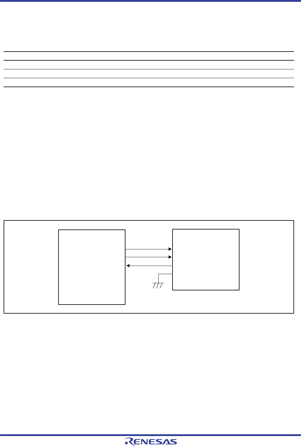
R01UH0034EJ0200 Rev.2.00 Page 1165 of 1489
Dec 27, 2013
RX62T Group, RX62G Group 26. Serial Peripheral Interface (RSPI)
Under development Preliminary document
Specifications in this document are tentative and subject to change.
The RSPI in single-master mode (SPI operation) or multi-master mode (SPI operation) determines MOSI signal values
during the SSL negation period (including the SSL retention period during a burst transfer) according to MOIFE and
MOIFV bit settings in SPPCR, as shown in Table 26.8.
26.3.3 RSPI System Configuration Examples
26.3.3.1 Single Master/Single Slave (with This LSI Acting as Master)
Figure 26.3 shows a single-master/single-slave RSPI system configuration example when this LSI is used as a master.
In the single-master/single-slave configuration, the SSL0 to SSL3 output of this LSI (master) are not used. The SSL input
of the RSPI slave is fixed to the low level, and the RSPI slave is always maintained in a select state.*1
This LSI (master) always drives the RSPCK and MOSI. The RSPI slave always drives the MISO.
Note 1. In the transfer format corresponding to the case where the SPCMDm.CPHA bit (m = 0 to 7) is 0, there are slave
devices for which the SSL signal cannot be fixed to the active level. In situations where the SSL signal cannot be
fixed, the SSL output of this LSI should be connected to the SSL input of the slave device.
Figure 26.3 Single-Master/Single-Slave Configuration Example (This LSI = Master)
Table 26.8 MOSI Signal Value Determination during SSL Negation Period
SPPCR.MOIFE Bit SPPCR.MOIFV Bit MOSI Signal Value during SSL Negation Period
0 0, 1 Final data from previous transfer
10Always 0
11Always 1
This LSI (master) RSPI slave
RSPCK
MOSI
MISO
SSL0
SSL1
SSL2
SSL3
RSPCK
MOSI
MISO
SSL
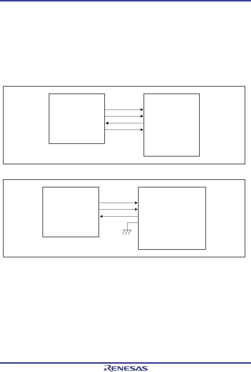
R01UH0034EJ0200 Rev.2.00 Page 1166 of 1489
Dec 27, 2013
RX62T Group, RX62G Group 26. Serial Peripheral Interface (RSPI)
Under development Preliminary document
Specifications in this document are tentative and subject to change.
26.3.3.2 Single Master/Single Slave (with This LSI Acting as Slave)
Figure 26.4 shows a single-maFster/single-slave RSPI system configuration example when this LSI is used as a slave.
When this LSI is to operate as a slave, the SSL0 pin is used as SSL input. The RSPI master always drives the RSPCK and
MOSI. This LSI (slave) always drives the MISO.*1
In the single-slave configuration in which the SPCMD0.CPHA bit is set to 1, the SSL0 input of this LSI (slave) is fixed
to the 0 level, this LSI (slave) is always maintained in a selected state, and in this manner it is possible to execute serial
transfer (Figure 26.5).
Note 1. When SSL0 is at the active level, the pin state is Hi-Z.
Figure 26.4 Single-Master/Single-Slave Configuration Example (This LSI = Slave)
Figure 26.5 Single-Master/Single-Slave Configuration Example (This LSI = Slave, SPCMD0.CPHA = 1)
RSPCK
MOSI
MISO
SSL0
SSL1
SSL2
SSL3
RSPCK
MOSI
MISO
SSL
RSPI master This LSI (slave)
RSPCK
MOSI
MISO
SSL0
SSL1
SSL2
SSL3
RSPCK
MOSI
MISO
SSL
RSPI master This LSI (slave, CPHA = 1)
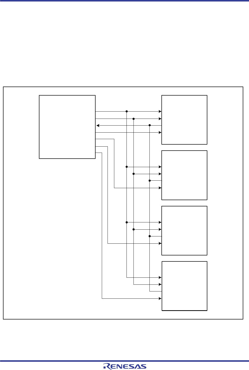
R01UH0034EJ0200 Rev.2.00 Page 1167 of 1489
Dec 27, 2013
RX62T Group, RX62G Group 26. Serial Peripheral Interface (RSPI)
Under development Preliminary document
Specifications in this document are tentative and subject to change.
26.3.3.3 Single Master/Multi-Slave (with This LSI Acting as Master)
Figure 26.6 shows a single-master/multi-slave RSPI system configuration example when this LSI is used as a master. In
the example of Figure 26.6, the RSPI system is comprised of this LSI (master) and four slaves (RSPI slave 0 to RSPI
slave 3).
The RSPCK and MOSI outputs of this LSI (master) are connected to the RSPCK and MOSI inputs of RSPI slave 0 to
RSPI slave 3. The MISO outputs of RSPI slave 0 to RSPI slave 3 are all connected to the MISO input of this LSI
(master). SSL0 to SSL3 outputs of this LSI (master) are connected to the SSL inputs of RSPI slave 0 to RSPI slave 3,
respectively.
This LSI (master) always drives RSPCK, MOSI, and SSL0 to SSL3. Of the RSPI slave 0 to RSPI slave 3, the slave that
receives low-level input into the SSL input drives MISO.
Figure 26.6 Single-Master/Multi-Slave Configuration Example (This LSI = Master)
RSPCK
MOSI
MISO
SSL0
SSL1
SSL2
SSL3
RSPCK
MOSI
MISO
RSPCK
MOSI
MISO
RSPCK
MOSI
MISO
RSPCK
MOSI
MISO
This LSI (master) RSPI slave 0
RSPI slave 1
RSPI slave 2
RSPI slave 3
SSL
SSL
SSL
SSL
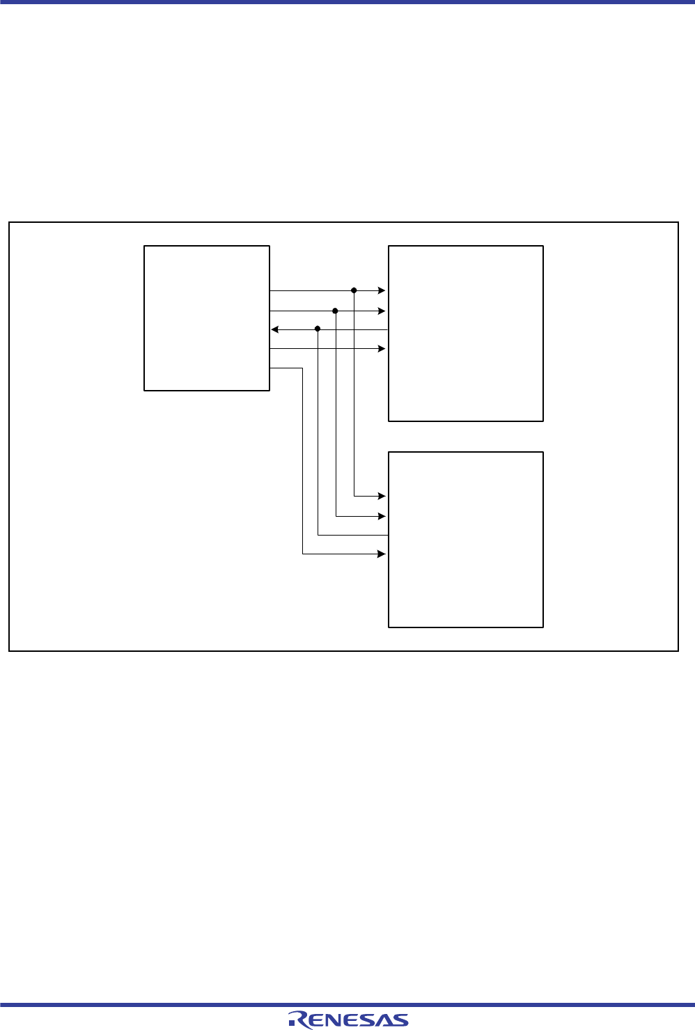
R01UH0034EJ0200 Rev.2.00 Page 1168 of 1489
Dec 27, 2013
RX62T Group, RX62G Group 26. Serial Peripheral Interface (RSPI)
Under development Preliminary document
Specifications in this document are tentative and subject to change.
26.3.3.4 Single Master/Multi-Slave (with This LSI Acting as Slave)
Figure 26.7 shows a single-master/multi-slave RSPI system configuration example when this LSI is used as a slave. In
the example of Figure 26.7, the RSPI system is comprised of an RSPI master and two LSIs (slave X and slave Y).
The RSPCK and MOSI outputs of the RSPI master are connected to the RSPCK and MOSI inputs of the LSIs (slave X
and slave Y). The MISO outputs of the LSIs (slave X and slave Y) are all connected to the MISO input of the RSPI
master. SSLX and SSLY outputs of the RSPI master are connected to the SSL0 inputs of the LSIs (slave X and slave Y),
respectively.
The RSPI master always drives RSPCK, MOSI, SSLX, and SSLY. Of the LSIs (slave X and slave Y), the slave that
receives low-level input into the SSL0 input drives MISO.
Figure 26.7 Single-Master/Multi-Slave Configuration Example (This LSI = Slave)
RSPCK
MOSI
MISO
SSL0
SSL1
SSL2
SSL3
RSPCK
MOSI
MISO
SSL0
SSL1
SSL2
SSL3
RSPCK
MOSI
MISO
SSLX
RSPI master This LSI (slave X)
SSLY
This LSI (slave Y)

R01UH0034EJ0200 Rev.2.00 Page 1169 of 1489
Dec 27, 2013
RX62T Group, RX62G Group 26. Serial Peripheral Interface (RSPI)
Under development Preliminary document
Specifications in this document are tentative and subject to change.
26.3.3.5 Multi-Master/Multi-Slave (with This LSI Acting as Master)
Figure 26.8 shows a multi-master/multi-slave RSPI system configuration example when this LSI is used as a master. In
the example of Figure 26.8, the RSPI system is comprised of two LSIs (master X and master Y) and two RSPI slaves
(RSPI slave 1 and RSPI slave 2).
The RSPCK and MOSI outputs of the LSIs (master X and master Y) are connected to the RSPCK and MOSI inputs of
RSPI slaves 1 and 2. The MISO outputs of RSPI slaves 1 and 2 are connected to the MISO inputs of the LSIs (master X
and master Y). Any generic port Y output from this LSI (master X) is connected to the SSL0 input of this LSI (master Y).
Any generic port X output of this LSI (master Y) is connected to the SSL0 input of this LSI (master X). The SSL1 and
SSL2 outputs of the LSIs (master X and master Y) are connected to the SSL inputs of the RSPI slaves 1 and 2. In this
configuration example, because the system can be comprised solely of SSL0 input, and SSL1 and SSL2 outputs for slave
connections, the SSL3 output of this LSI is not required.
This LSI drives RSPCK, MOSI, SSL1, and SSL2 when the SSL0 input level is 1. When the SSL0 input level is 0, this
LSI detects a mode fault error, sets RSPCK, MOSI, SSL1, and SSL2 to Hi-Z, and releases the RSPI bus right to the other
master. Of the RSPI slaves 1 and 2, the slave that receives low-level input into the SSL input drives MISO.
Figure 26.8 Multi-Master/Multi-Slave Configuration Example (This LSI = Master)
RSPCK
MOSI
MISO
SSL0
SSL1
SSL2
SSL3
Port Y
RSPCK
MOSI
MISO
SSL0
SSL1
SSL2
SSL3
RSPCK
MOSI
MISO
RSPCK
MOSI
MISO
RSPI slave 1
This LSI (master X) This LSI (master Y)
Port X
RSPI slave 2
SSL
SSL

R01UH0034EJ0200 Rev.2.00 Page 1170 of 1489
Dec 27, 2013
RX62T Group, RX62G Group 26. Serial Peripheral Interface (RSPI)
Under development Preliminary document
Specifications in this document are tentative and subject to change.
26.3.3.6 Master (Clock Synchronous Operation)/Slave (Clock Synchronous Operation)
(with This LSI Acting as Master)
Figure 26.9 shows a master (clock synchronous operation)/slave (clock synchronous operation) RSPI system
configuration example when this LSI is used as a master. In the master (clock synchronous operation)/slave (clock
synchronous operation) configuration, SSL0 to SSL3 of this LSI (master) are not used.
This LSI (master) always drives the RSPCK and MOSI. The RSPI slave always drives the MISO.
Figure 26.9 Master (Clock Synchronous Operation)/Slave (Clock Synchronous Operation) Configuration
Example (This LSI = Master)
RSPCK
MOSI
MISO
SSL0
SSL1
SSL2
SSL3
RSPCK
MOSI
MISO
This LSI (master) RSPI slave
SSL
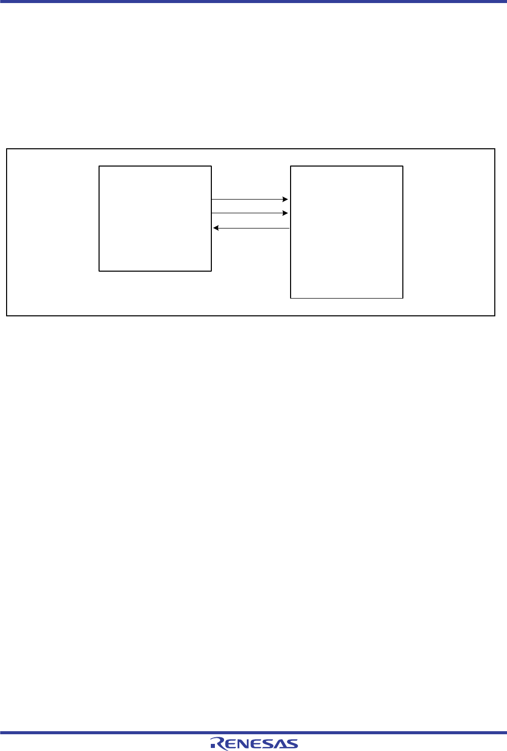
R01UH0034EJ0200 Rev.2.00 Page 1171 of 1489
Dec 27, 2013
RX62T Group, RX62G Group 26. Serial Peripheral Interface (RSPI)
Under development Preliminary document
Specifications in this document are tentative and subject to change.
26.3.3.7 Master (Clock Synchronous Operation)/Slave (Clock Synchronous Operation)
(with This LSI Acting as Slave)
Figure 26.10 shows a master (clock synchronous operation)/slave (clock synchronous operation) RSPI system
configuration example when this LSI is used as a slave. When this LSI is to operate as a slave (clock synchronous
operation), this LSI (slave) always drives the MISO and the RSPI master always drives the RSPCK and MOSI. In
addition, SSL0 to SSL3 of this LSI (slave) are not used.
Only in the single-slave configuration in which the SPCMD0.CPHA bit is set to 1, this LSI (slave) can execute serial
transfer.
Figure 26.10 Master (Clock Synchronous Operation)/Slave (Clock Synchronous Operation) Configuration
Example (This LSI = Slave, SPCMD0.CPHA = 1)
RSPCK
MOSI
MISO
SSL0
SSL1
SSL2
SSL3
RSPCK
MOSI
MISO
SSL
RSPI master This LSI (slave)
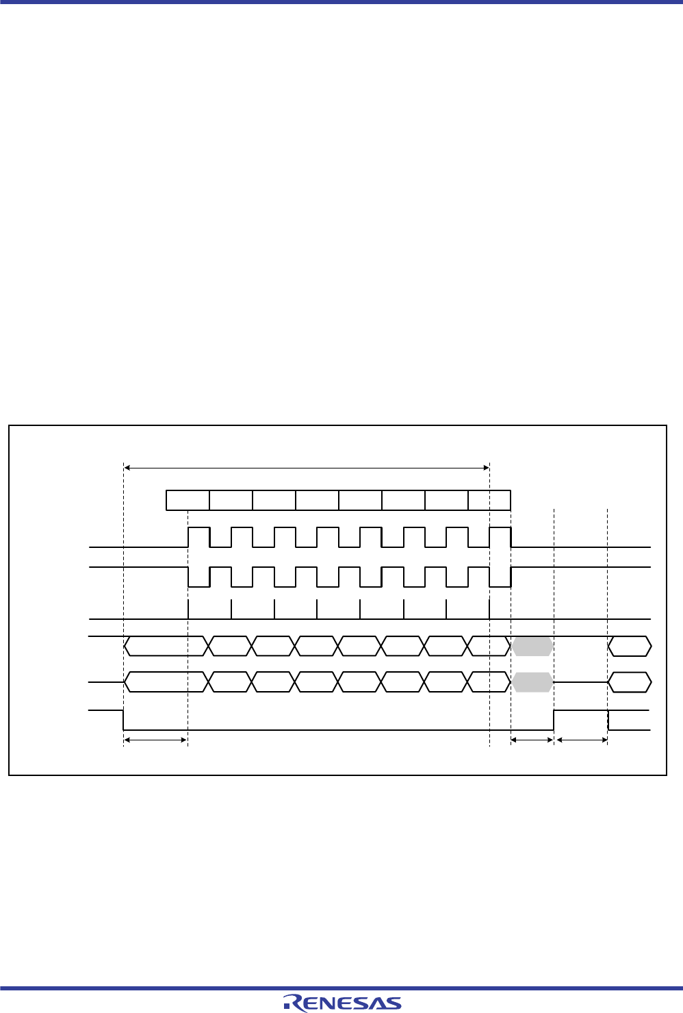
R01UH0034EJ0200 Rev.2.00 Page 1172 of 1489
Dec 27, 2013
RX62T Group, RX62G Group 26. Serial Peripheral Interface (RSPI)
Under development Preliminary document
Specifications in this document are tentative and subject to change.
26.3.4 Transfer Format
26.3.4.1 CPHA = 0
Figure 26.11 shows a sample transfer format for the serial transfer of 8-bit data when the SPCMDm.CPHA bit is 0. Note
that clock synchronous operation (the SPCR.SPMS bit is 1) is not guaranteed when the RSPI operates in slave mode
(SPCR.MSTR = 0) and the CPHA bit is 0. In Figure 26.11, RSPCK (CPOL = 0) indicates the RSPCK signal waveform
when the CPOL bit in SPCMDm is 0; RSPCK (CPOL = 1) indicates the RSPCK signal waveform when the CPOL bit is
1. The sampling timing represents the timing at which the RSPI fetches serial transfer data into the shift register. The
input/output directions of the signals depend on the RSPI settings. For details, see section 26.3.2, Controlling RSPI
Pins .
When the CPHA bit is 0, the driving of valid data to the MOSI and MISO signals commences at an SSL signal assertion
timing. The first RSPCK signal change timing that occurs after the SSL signal assertion becomes the first transfer data
fetch timing. After this timing, data is sampled at every 1 RSPCK cycle. The change timing for MOSI and MISO signals
is always 1/2 RSPCK cycles after the transfer data fetch timing. The SPCMDm.CPOL bit setting does not affect the
RSPCK signal operation timing; it only affects the signal polarity.
t1 denotes a period from an SSL signal assertion to RSPCK oscillation (RSPCK delay). t2 denotes a period from the
termination of RSPCK oscillation to an SSL signal negation (SSL negation delay). t3 denotes a period in which SSL
signal assertion is suppressed for the next transfer after the end of serial transfer (next-access delay). t1, t2, and t3 are
controlled by a master device running on the RSPI system. For a description of t1, t2, and t3 when the RSPI of this LSI is
in master mode, see section 26.3.10.1, Master Mode Operation.
Figure 26.11 RSPI Transfer Format (CPHA = 0)
Serial transfer period
12345678
RSPCK
cycle
Start End
RSPCK
(CPOL=0)
Sampling
timing
MOSI
MISO
SSL
t1 t2 t3
RSPCK
(CPOL=1)
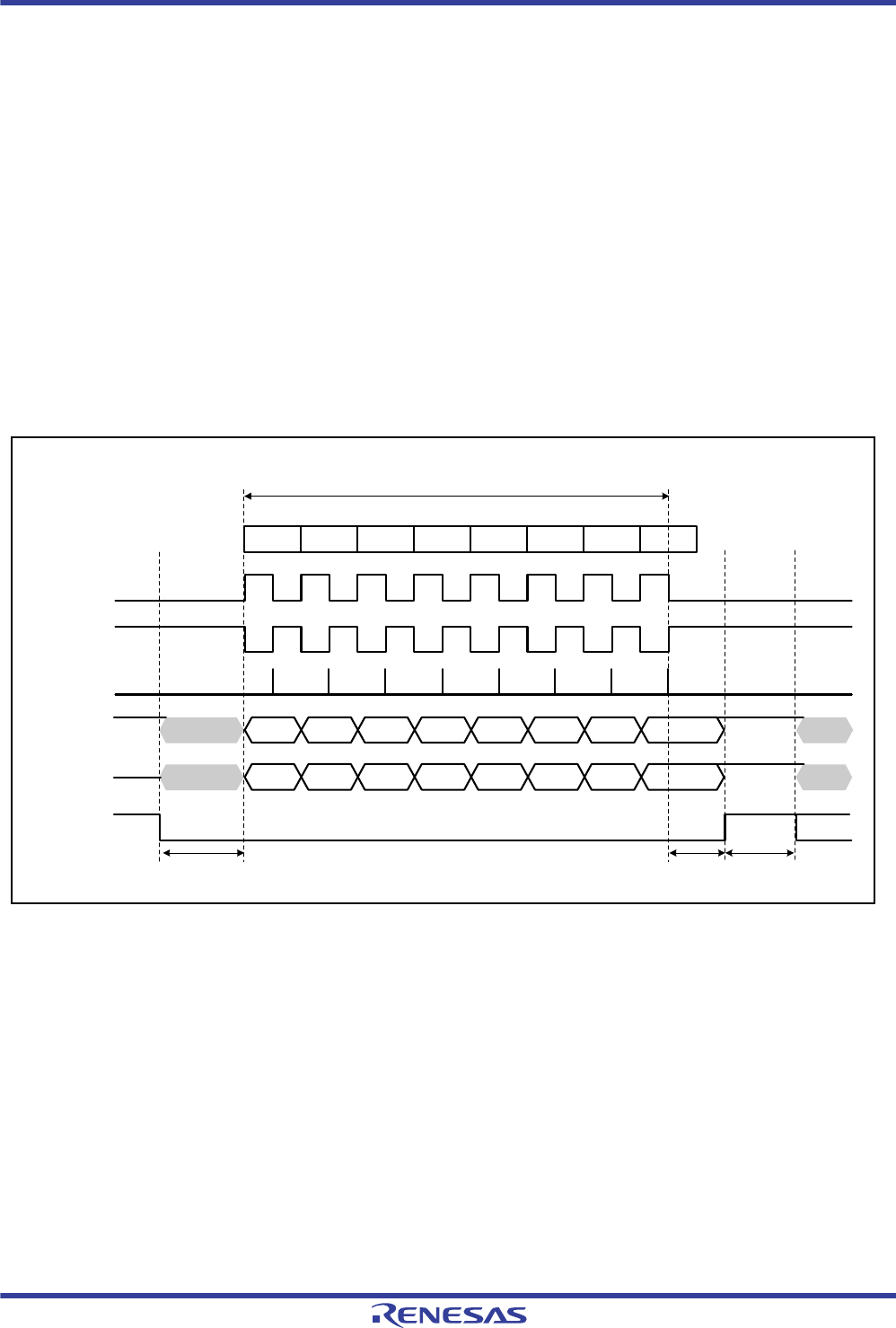
R01UH0034EJ0200 Rev.2.00 Page 1173 of 1489
Dec 27, 2013
RX62T Group, RX62G Group 26. Serial Peripheral Interface (RSPI)
Under development Preliminary document
Specifications in this document are tentative and subject to change.
26.3.4.2 CPHA = 1 (m = 0 to 7)
Figure 26.12 shows a sample transfer format for the serial transfer of 8-bit data when the SPCMDm.CPHA bit is 1.
However, when the SPCR.SPMS bit is 1, the SSL signals are not used, and only the three signals RSPCK, MOSI, and
MISO handle communications. In Figure 26.12, RSPCK (CPOL = 0) indicates the RSPCK signal waveform when the
CPOL bit in SPCMDm is 0; RSPCK (CPOL = 1) indicates the RSPCK signal waveform when the CPOL bit is 1. The
sampling timing represents the timing at which the RSPI fetches serial transfer data into the shift register. The input/
output directions of the signals depend on the RSPI mode (master or slave). For details, see section 26.3.2, Controlling
RSPI Pins .
When the CPHA bit is 1, the driving of invalid data to the MISO signal commences at an SSL signal assertion timing.
The output of valid data to the MOSI and MISO signals commences at the first RSPCK signal change timing that occurs
after the SSL signal assertion. After this timing, data is updated at every 1 RSPCK cycle. The transfer data fetch timing is
always 1/2 RSPCK cycles after the data update timing. The SPCMDm.CPOL bit setting does not affect the RSPCK
signal operation timing; it only affects the signal polarity.
t1, t2, and t3 are the same as those in the case of SPCMDm.CPHA = 0. For a description of t1, t2, and t3 when the RSPI
of this LSI is in master mode, see section 26.3.10.1, Master Mode Operation.
Figure 26.12 RSPI Transfer Format (CPHA = 1)
Serial transfer period
12345678
RSPCK
cycle
Start End
RSPCK
(CPOL=0)
Sampling
timing
MOSI
MISO
SSL
t1 t2 t3
RSPCK
(CPOL=1)
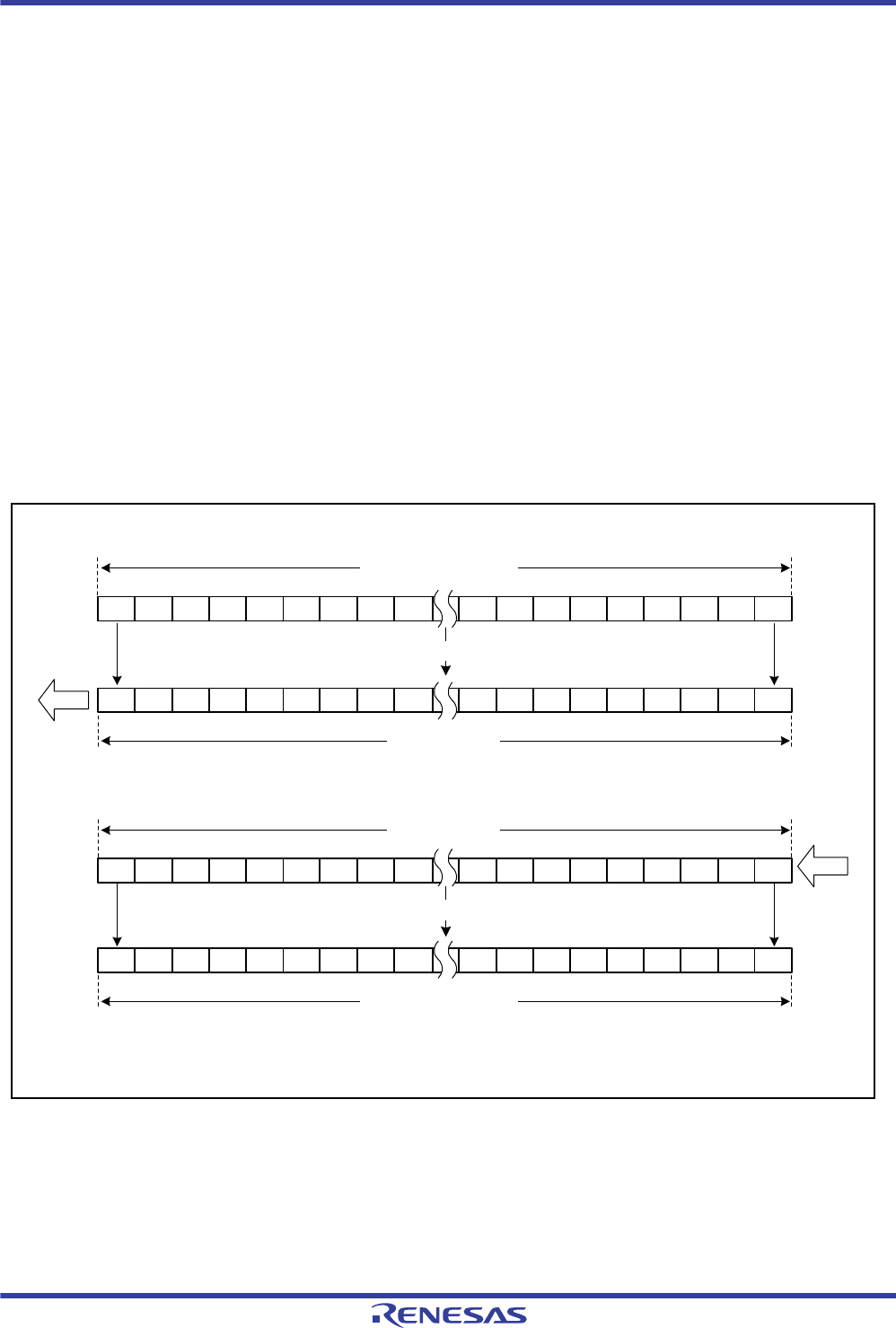
R01UH0034EJ0200 Rev.2.00 Page 1174 of 1489
Dec 27, 2013
RX62T Group, RX62G Group 26. Serial Peripheral Interface (RSPI)
Under development Preliminary document
Specifications in this document are tentative and subject to change.
26.3.5 Data Format
The RSPI's data format depends on the settings in SPCMDm register (m = 0 to 7) and the SPCR2.SPPE bit. Irrespective
of MSB/LSB first, the RSPI treats the range from the SPDR.LSB bit to the assigned data length as transfer data.
26.3.5.1 MSB First Transfer (32-Bit Data)
(1) Parity Function is Disabled (SPCR2.SPPE = 0)
Figure 26.13 shows the operation of SPDR and the shift register when the RSPI performs a 32-bit data length MSB-first
data transfer with the parity function disabled.
Data T31 to T00 is written to the transmit buffer of SPDR. If the transmit buffer holds data and the shift register is empty,
the RSPI copies the data in the transmit buffer of SPDR to the shift register, and fully populates the shift register. When
serial transfer starts, the RSPI outputs data from the MSB (bit 31) of the shift register, and shifts in the data from the LSB
(bit 0) of the shift register. When the RSPCK cycles required for the serial transfer of 32 bits have passed, data R31 to
R00 is stored in the shift register. In this state, when performing full-duplex synchronous serial communications
(SPCR.TXMD = 0), the RSPI copies the data from the shift register to the receive buffer of SPDR, and empties the shift
register.
If another serial transfer is started before data is written to the transmit buffer of SPDR, received data R31 to R00 is
shifted out from the shift register.
Figure 26.13 MSB First Transfer (1) (32-Bit Data, Parity Function Disabled)
Bit 31
Transfer start
Transfer end
Note: Output = MOSI (master)/MISO (slave), input = MISO (master)/MOSI (slave)
Bit 0
T31 T30 T29 T28 T27 T26 T25 T24 T23 T06 T05 T04 T03 T02 T01 T00
T31 T30 T29 T28 T27 T26 T25 T24 T23 T06 T05 T04 T03 T02 T01 T00
R31 R30 R29 R28 R27 R26 R25 R24 R23 R06 R05 R04 R03 R02 R01 R00
R31 R30 R29 R28 R27 R26 R25 R24 R23 R06 R05
T08 T07
T08 T07
R08 R07
R08 R07 R04 R03 R02 R01 R00
SPDR (transmit buffer)
Shift register
Copy
Shift register
Input
Output
Copy (SPCR.TXMD = 0)
Bit 0
Bit 0
Bit 0
SPDR (receive buffer)
Bit 31
Bit 31
Bit 31
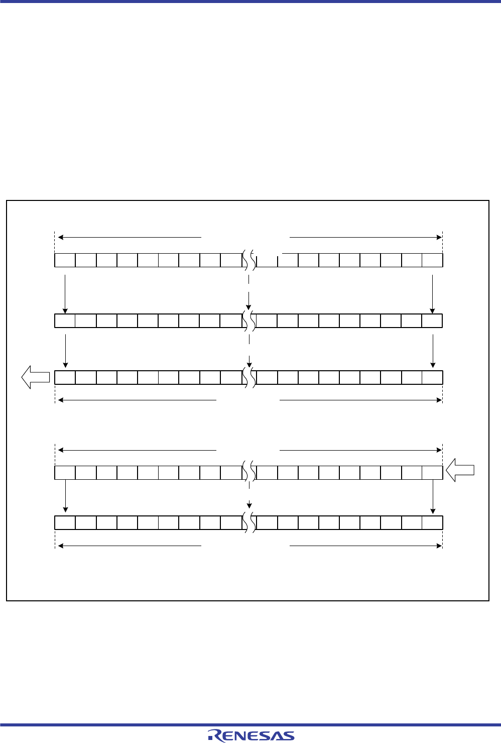
R01UH0034EJ0200 Rev.2.00 Page 1175 of 1489
Dec 27, 2013
RX62T Group, RX62G Group 26. Serial Peripheral Interface (RSPI)
Under development Preliminary document
Specifications in this document are tentative and subject to change.
(2) Parity Function is Enabled (SPCR2.SPPE = 1)
Figure 26.14 shows the operation of SPDR and the shift register when the RSPI performs a 32-bit data length MSB-first
data transfer with the parity function enabled.
Data T31 to T00 is written to the transmit buffer of SPDR. If the transmit buffer holds data and the shift register is empty,
the RSPI converts T00 of the data stored in the transmit buffer of SPDR into the parity bit (P). Then, the RSPI copies the
data with the added parity bit (P) to the shift register, and fully populates the shift register. When serial transfer starts, the
RSPI outputs data from the MSB (bit 31) of the shift register, and shifts in the data from the LSB (bit 0) of the shift
register. When the RSPCK cycles required for the serial transfer of 32 bits have passed, data R31 to P is stored in the
shift register. In this state, when performing full-duplex synchronous serial communications (SPCR.TXMD = 0), the
RSPI copies the data from the shift register to the receive buffer of SPDR, and empties the shift register.
If another serial transfer is started before data is written to the transmit buffer of SPDR, received data R31 to P is shifted
out from the shift register.
Figure 26.14 MSB First Transfer (2) (32-Bit Data, Parity Function Enabled)
Bit 31
Transfer start
Transfer end
Note: Output = MOSI (master)/MISO (slave), input = MISO (master)/MOSI (slave)
Bit 0
T31 T30 T29 T28 T27 T26 T25 T24 T23 T06 T05 T04 T03 T02 T01 T00
T31 T30 T29 T28 T27 T26 T25 T24 T23 T06 T05 T04 T03 T02 T01 P
R31 R30 R29 R28 R27 R26 R25 R24 R23 R06 R05 R04 R03 R02 R01 P
R31 R30 R29 R28 R27 R26 R25 R24 R23 R06 R05
T08 T07
T08 T07
R08 R07
R08 R07 R04 R03 R02 R01 P
SPDR (transmit buffer)
Shift register
Copy
Shift register
Input
Output
Copy (SPCR.TXMD = 0)
Bit 0
Bit 0
Bit 0
SPDR (receive buffer)
Bit 31
Bit 31
Bit 31
T31 T30 T29 T28 T27 T26 T25 T24 T23 T06 T05 T04 T03 T02 T01 PT08 T07
Copy
Parity bit addition (T31 to T01 + parity bit (P))
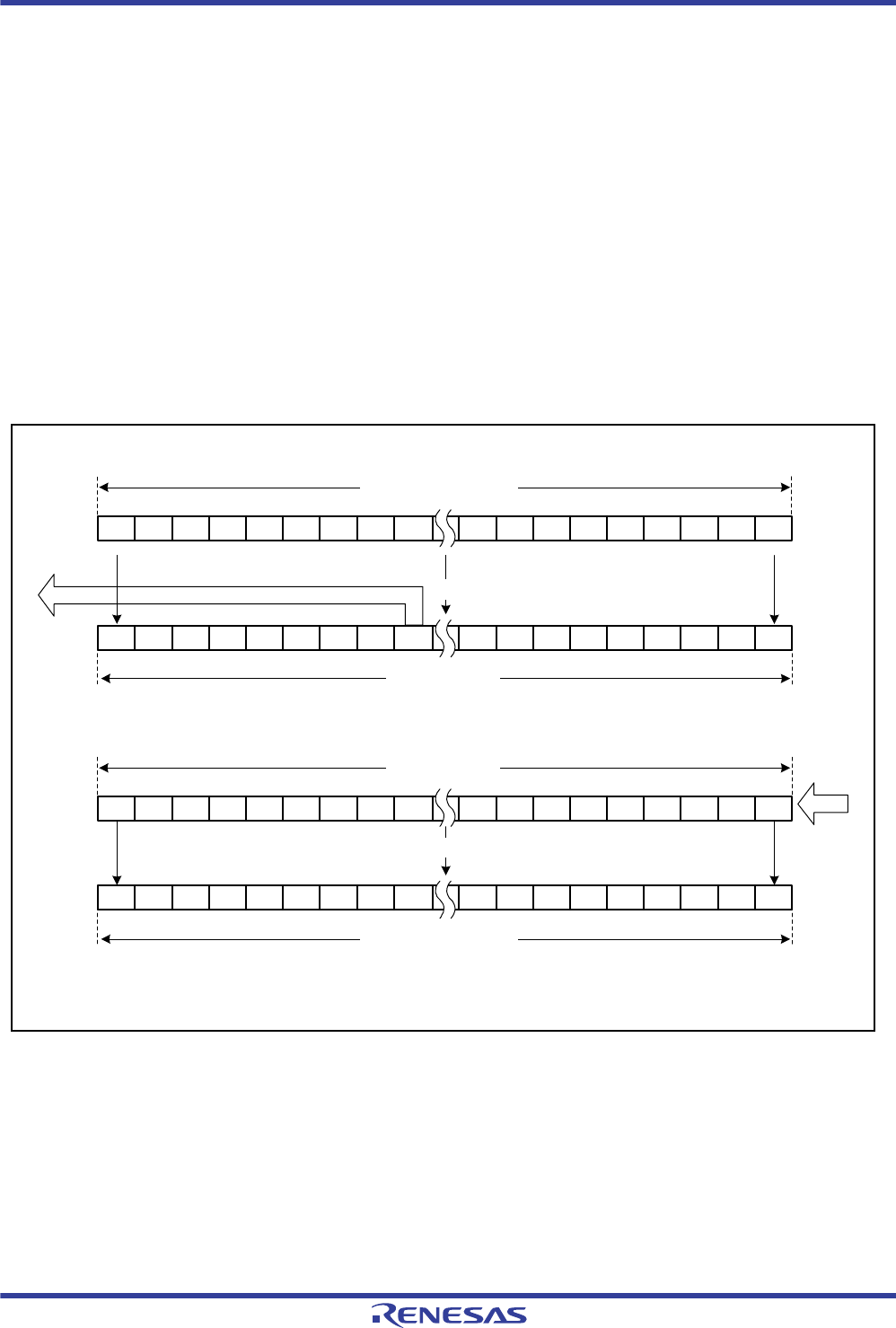
R01UH0034EJ0200 Rev.2.00 Page 1176 of 1489
Dec 27, 2013
RX62T Group, RX62G Group 26. Serial Peripheral Interface (RSPI)
Under development Preliminary document
Specifications in this document are tentative and subject to change.
26.3.5.2 MSB First Transfer (24-Bit Data)
(1) Parity Function is Disabled (SPCR2.SPPE = 0)
Figure 26.15 shows the operation of SPDR and the shift register when the RSPI performs a 24-bit data length MSB-first
data transfer (as a data transfer example of lengths other than 32 bits) with the parity function disabled.
Data T31 to T00 is written to the transmit buffer of SPDR. If the transmit buffer holds data and the shift register is empty,
the RSPI copies the data stored in the transmit buffer of SPDR to the shift register, and fully populates the shift register.
When serial transfer starts, the RSPI outputs data from bit 23 of the shift register, and shifts in the data from the LSB (bit
0) of the shift register. When the RSPCK cycles required for the serial transfer of 24 bits have passed, received data R23
to R00 is stored in bits 23 to 0 of the shift register. After completion of the serial transfer, data that existed before the
transfer is retained in bits 31 to 24 of the shift register. In this state, when performing full-duplex synchronous serial
communications (SPCR.TXMD = 0), the RSPI copies the data from the shift register to the receive buffer of SPDR, and
empties the shift register.
If another serial transfer is started before data is written to the transmit buffer of SPDR, received data R23 to R00 is
shifted out from the shift register.
Figure 26.15 MSB First Transfer (1) (24-Bit Data, Parity Function Disabled)
Output
Transfer start
Transfer end
T31 T30 T29 T28 T27 T26 T25 T24 T23 T06 T05 T04 T03 T02 T01 T00
T31 T30 T29 T28 T27 T26 T25 T24 T23
T31 T30 T29 T28 T27 T26 T25 T24 R23
T31 T30 T29 T28 T27 T26 T25 T24 R23
T06T05T04T03T02T01T00
R06 R05 R04 R03 R02 R01 R00
R06 R05
T08 T07
T08 T07
R08 R07
R08 R07 R04 R03 R02 R01 R00
Shift register
Copy
Shift register
Input
Copy (SPCR.TXMD = 0)
Bit 0
SPDR (receive buffer)
Bit 31 Bit 24 Bit 23
Bit 0Bit 31 Bit 24 Bit 23
Bit 0Bit 31 Bit 23
SPDR (transmit buffer)
Bit 0Bit 31 Bit 23
Note: Output = MOSI (master)/MISO (slave), input = MISO (master)/MOSI (slave)
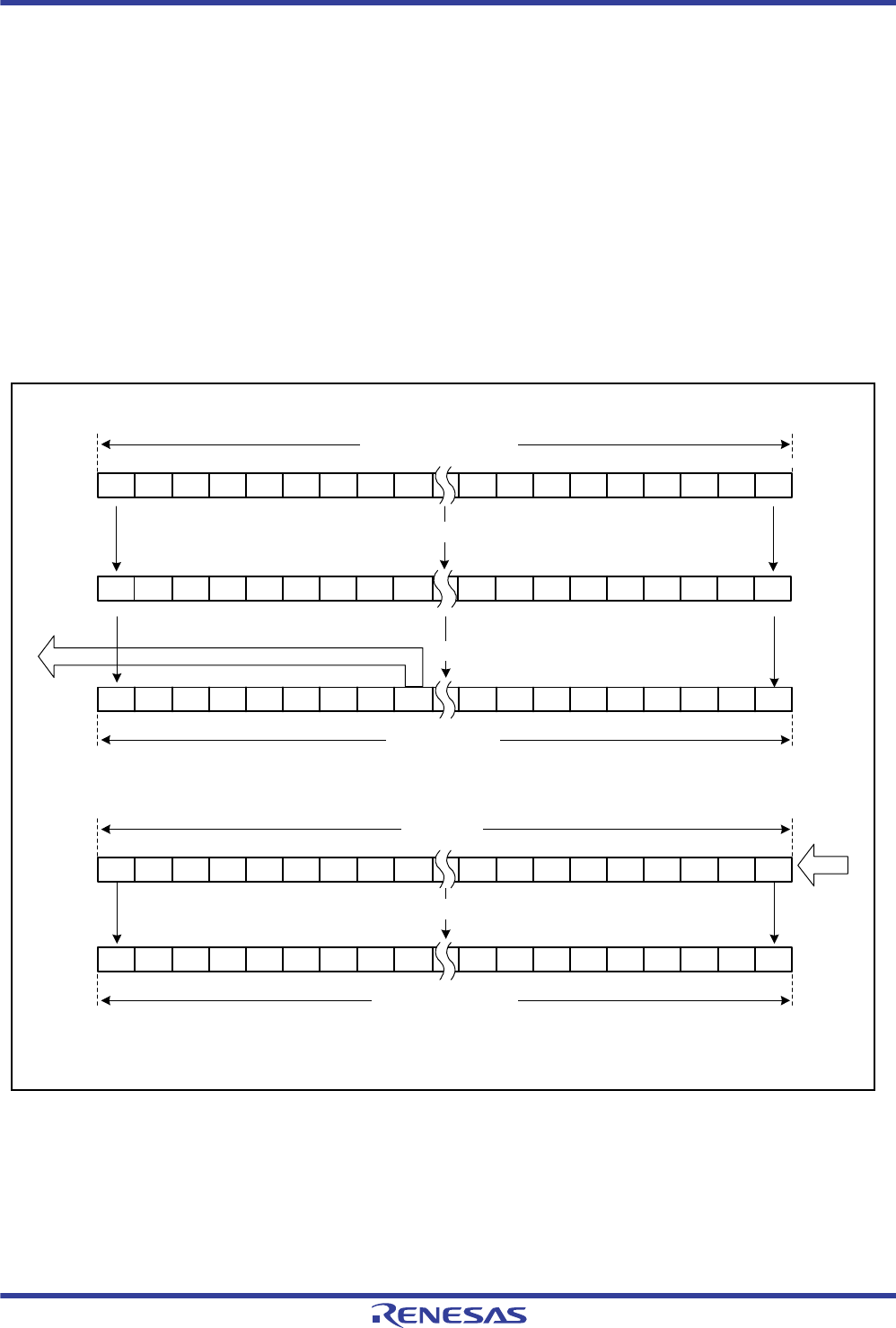
R01UH0034EJ0200 Rev.2.00 Page 1177 of 1489
Dec 27, 2013
RX62T Group, RX62G Group 26. Serial Peripheral Interface (RSPI)
Under development Preliminary document
Specifications in this document are tentative and subject to change.
(2) Parity Function is Enabled (SPCR2.SPPE = 1)
Figure 26.16 shows the operation of SPDR and the shift register when the RSPI performs a 24-bit data length MSB-first
data transfer (as a data transfer example of lengths other than 32 bits) with the parity function enabled.
Data T31 to T00 is written to the transmit buffer of SPDR. If the transmit buffer holds data and the shift register is empty,
the RSPI converts T00 of the data stored in the transmit buffer of SPDR into the parity bit (P). Then, the RSPI copies the
data with the added parity bit (P) to the shift register, and fully populates the shift register. When serial transfer starts, the
RSPI outputs data from bit 23 of the shift register, and shifts in the data from the LSB (bit 0) of the shift register. When
the RSPCK cycles required for the serial transfer of 24 bits have passed, received data R23 to P is stored in bits 23 to 0 of
the shift register. After completion of the serial transfer, data that existed before the transfer is retained in bits 31 to 24 of
the shift register. In this state, when performing full-duplex synchronous serial communications (SPCR.TXMD = 0), the
RSPI copies the data from the shift register to the receive buffer of SPDR, and empties the shift register.
If another serial transfer is started before data is written to the transmit buffer of SPDR, received data R23 to P is shifted
out from the shift register.
Figure 26.16 MSB First Transfer (2) (24-Bit Data, Parity Function Enabled)
Output
Transfer start
Transfer end
T31 T30 T29 T28 T27 T26 T25 T24 T23 T06 T05 T04 T03 T02 T01 T00
T31 T30 T29 T28 T27 T26 T25 T24 T23
T31 T30 T29 T28 T27 T26 T25 T24 R23
T31 T30 T29 T28 T27 T26 T25 T24 R23
T06T05T04T03T02T01 P
R06 R05 R04 R03 R02 R01 P
R06 R05
T08 T07
T08 T07
R08 R07
R08 R07 R04 R03 R02 R01 P
Shift register
Copy
Shift register
Input
Copy (SPCR.TXMD = 0)
Bit 0
SPDR (receive buffer)
Bit 31 Bit 24 Bit 23
Bit 0Bit 31 Bit 24 Bit 23
Bit 0Bit 31 Bit 23
SPDR (transmit buffer)
Bit 0Bit 31 Bit 23
Note: Output = MOSI (master)/MISO (slave), input = MISO (master)/MOSI (slave)
T31 T30 T29 T28 T27 T26 T25 T24 T23 T06 T05 T04 T03 T02 T01 PT08 T07
Parity bit addition (T23 to T01 + parity bit (P))
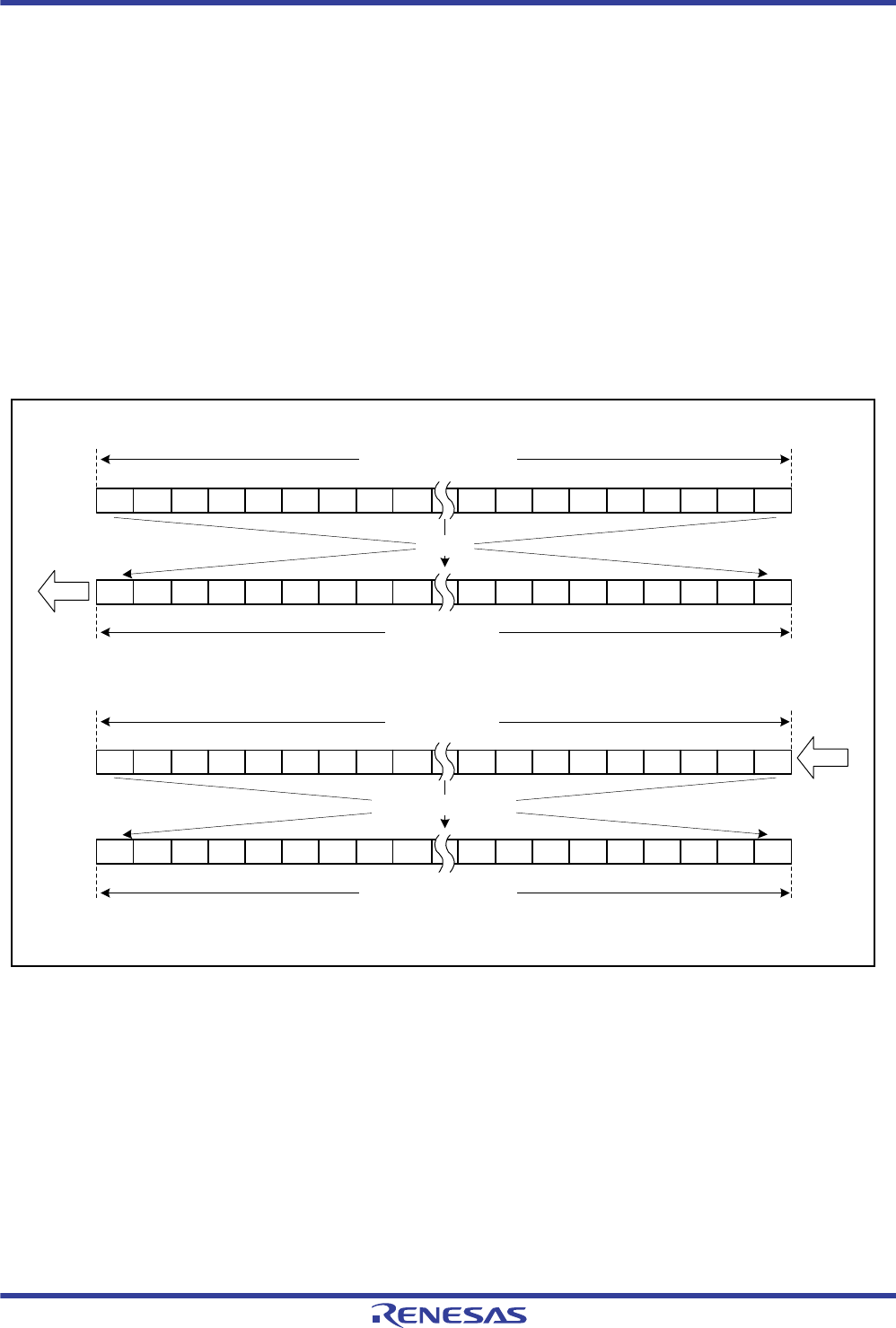
R01UH0034EJ0200 Rev.2.00 Page 1178 of 1489
Dec 27, 2013
RX62T Group, RX62G Group 26. Serial Peripheral Interface (RSPI)
Under development Preliminary document
Specifications in this document are tentative and subject to change.
26.3.5.3 LSB First Transfer (32-Bit Data)
(1) Parity Function is Disabled (SPCR2.SPPE = 0)
Figure 26.17 shows the operation of SPDR and the shift register when the RSPI performs a 32-bit data length LSB-first
data transfer with the parity function disabled.
Data T31 to T00 is written to the transmit buffer of SPDR. If the transmit buffer holds data and the shift register is empty,
the RSPI reverses the order of the bits of the data in the transmit buffer of SPDR, copies it to the shift register, and fully
populates the shift register. When serial transfer starts, the RSPI outputs data from the MSB (bit 31) of the shift register,
and shifts in the data from the LSB (bit 0) of the shift register. When the RSPCK cycles required for the serial transfer of
32 bits have passed, data R00 to R31 is stored in the shift register. In this state, when performing full-duplex synchronous
serial communications (SPCR.TXMD = 0), the RSPI copies the data, in which the order of the bits is reversed, from the
shift register to the receive buffer of SPDR, and empties the shift register.
If another serial transfer is started before data is written to the transmit buffer of SPDR, received data R00 to R31 is
shifted out from the shift register.
Figure 26.17 LSB First Transfer (1) (32-Bit Data, Parity Function Disabled)
Transfer start
Transfer end
T31 T30 T29 T28 T27 T26 T25 T24 T23 T06 T05 T04 T03 T02 T01 T00
T00 T01 T02 T03 T04 T05 T06 T07 T08 T25 T26 T27 T28 T29 T30 T31
R00 R01 R02 R03 R04 R05 R06 R07 R08 R25 R26 R27 R28 R29 R30 R31
R31 R30 R29 R28 R27 R26 R25 R24 R23 R06 R05
R23 R24
R08 R07 R04 R03 R02 R01 R00
T08 T07
T23 T24
Shift register
Shift register
Input
Output
Copy
Copy (SPCR.TXMD = 0)
Bit 0
SPDR (receive buffer)
Bit 31
Note: Output = MOSI (master)/MISO (slave), input = MISO (master)/MOSI (slave)
SPDR (transmit buffer)
Bit 0Bit 31
Bit 0Bit 31
Bit 0Bit 31

R01UH0034EJ0200 Rev.2.00 Page 1179 of 1489
Dec 27, 2013
RX62T Group, RX62G Group 26. Serial Peripheral Interface (RSPI)
Under development Preliminary document
Specifications in this document are tentative and subject to change.
(2) Parity Function is Enabled (SPCR2.SPPE = 1)
Figure 26.18 shows the operation of SPDR and the shift register when the RSPI performs a 32-bit data length LSB-first
data transfer with the parity function enabled.
Data T31 to T00 is written to the transmit buffer of SPDR. The RSPI converts T31 of the data stored in the transmit
buffer of SPDR into the parity bit (P). If the transmit buffer holds data and the shift register is empty, the RSPI reverses
the order of the bits of the data with the added parity bit (P), copies it to the shift register, and fully populates the shift
register. When serial transfer starts, the RSPI outputs data from the MSB (bit 31) of the shift register, and shifts in the
data from the LSB (bit 0) of the shift register. When the RSPCK cycles required for the serial transfer of 32 bits have
passed, data R00 to P is stored in the shift register. In this state, when performing full-duplex synchronous serial
communications (SPCR.TXMD = 0), the RSPI copies the data, in which the order of the bits is reversed, from the shift
register to the receive buffer of SPDR, and empties the shift register.
If another serial transfer is started before data is written to the transmit buffer of SPDR, received data R00 to P is shifted
out from the shift register.
Figure 26.18 LSB First Transfer (2) (32-Bit Data, Parity Function Enabled)
Transfer start
Transfer end
T31 T30 T29 T28 T27 T26 T25 T24 T23 T06 T05 T04 T03 T02 T01 T00
T00 T01 T02 T03 T04 T05 T06 T07 T08 T25 T26 T27 T28 T29 T30 P
R00 R01 R02 R03 R04 R05 R06 R07 R08 R25 R26 R27 R28 R29 R30 P
P R30 R29 R28 R27 R26 R25 R24 R23 R06 R05
R23 R24
R08 R07 R04 R03 R02 R01 R00
T08 T07
T23 T24
Shift register
Shift register
Input
Output
Copy
Copy (SPCR.TXMD = 0)
Bit 0
SPDR (receive buffer)
Bit 31
Note: Output = MOSI (master)/MISO (slave), input = MISO (master)/MOSI (slave)
SPDR (transmit buffer)
Bit 0Bit 31
Bit 0Bit 31
Bit 0Bit 31
P T30 T29 T28 T27 T26 T25 T24 T23 T06 T05 T04 T03 T02 T01 T00
T08 T07
Bit 0Bit 31
Parity bit addition (parity bit (P) + T30 to T00)
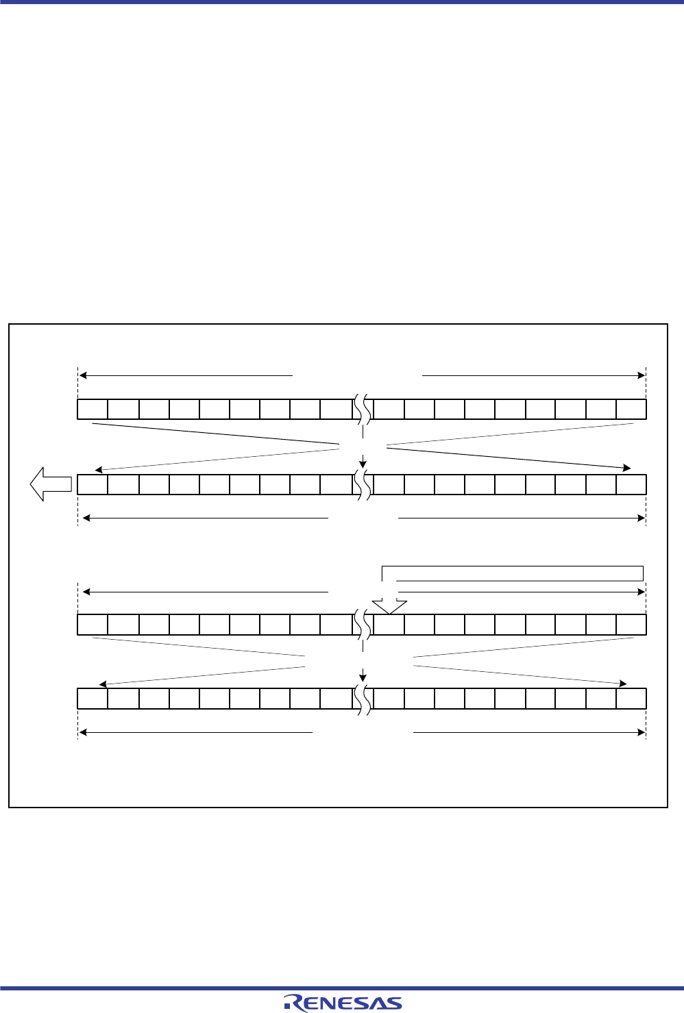
R01UH0034EJ0200 Rev.2.00 Page 1180 of 1489
Dec 27, 2013
RX62T Group, RX62G Group 26. Serial Peripheral Interface (RSPI)
Under development Preliminary document
Specifications in this document are tentative and subject to change.
26.3.5.4 LSB First Transfer (24-Bit Data)
(1) Parity Function is Disabled (SPCR2.SPPE = 0)
Figure 26.19 shows the operation of SPDR and the shift register when the RSPI performs a 24-bit data length LSB-first
data transfer (as a data transfer example of lengths other than 32 bits) with the parity function disabled.
Data T31 to T00 is written to the transmit buffer of SPDR. If the transmit buffer holds data and the shift register is empty,
the RSPI reverses the order of the bits of the data in the transmit buffer of SPDR, copies it to the shift register, and fully
populates the shift register. When serial transfer starts, the RSPI outputs data from the MSB (bit 31) of the shift register,
and shifts in the data from bit 8 of the shift register. When the RSPCK cycles required for the serial transfer of 24 bits
have passed, received data R00 to R23 is stored in bits 31 to 8 of the shift register. After completion of the serial transfer,
data that existed before the transfer is retained in bits 7 to 0 of the shift register. In this state, when performing full-duplex
synchronous serial communications (SPCR.TXMD = 0), the RSPI copies the data, in which the order of the bits is
reversed, from the shift register to the receive buffer of SPDR, and empties the shift register.
If another serial transfer is started before data is written to the transmit buffer of SPDR, received data R00 to R23 is
shifted out from the shift register.
Figure 26.19 LSB First Transfer (1) (24-Bit Data, Parity Function Disabled)
R00 R01 R02 R03 R04 R05 R06 R07 R08 T25 T26 T27 T28 T29 T30 T31
T31T30T29T28T27T26T25T24R23 R06R05
R23 T24
R08 R07 R04 R03 R02 R01 R00
Input
Transfer start
Transfer end
Bit 31 Bit 0
T31 T30 T29 T28 T27 T26 T25 T24 T23 T06 T05 T04 T03 T02 T01 T00
T00 T01 T02 T03 T04 T05 T06 T07 T08 T25 T26 T27 T28 T29 T30 T31
T08 T07
T23 T24
SPDR (receive buffer)
SPDR (transmit buffer)
Shift register
Shift register
Output
Copy
Copy (SPCR.TXMD = 0)
Bit 31 Bit 0
Bit 31 Bit 0
Bit 31 Bit 0
Note: Output = MOSI (master)/MISO (slave), input = MISO (master)/MOSI (slave)

R01UH0034EJ0200 Rev.2.00 Page 1181 of 1489
Dec 27, 2013
RX62T Group, RX62G Group 26. Serial Peripheral Interface (RSPI)
Under development Preliminary document
Specifications in this document are tentative and subject to change.
(2) Parity Function is Enabled (SPCR2.SPPE = 1)
Figure 26.20 shows the operation of SPDR and the shift register when the RSPI performs a 24-bit data length LSB-first
data transfer (as a data transfer example of lengths other than 32 bits) with the parity function enabled.
Data T31 to T00 is written to the transmit buffer of SPDR. The RSPI converts T23 of the data stored in the transmit
buffer of SPDR into the parity bit (P). If the transmit buffer holds data and the shift register is empty, the RSPI reverses
the order of the bits of the data with the added parity bit (P), copies it to the shift register, and fully populates the shift
register. When serial transfer starts, the RSPI outputs data from the MSB (bit 31) of the shift register, and shifts in the
data from bit 8 of the shift register. When the RSPCK cycles required for the serial transfer of 24 bits have passed,
received data R00 to P is stored in bits 31 to 8 of the shift register. After completion of the serial transfer, data that existed
before the transfer is retained in bits 7 to 0 of the shift register. In this state, when performing full-duplex synchronous
serial communications (SPCR.TXMD = 0), the RSPI copies the data, in which the order of the bits is reversed, from the
shift register to the receive buffer of SPDR, and empties the shift register.
If another serial transfer is started before data is written to the transmit buffer of SPDR, received data R00 to P is shifted
out from the shift register.
Figure 26.20 LSB First Transfer (2) (24-Bit Data, Parity Function Enabled)
R00 R01 R02 R03 R04 R05 R06 R07 R08 T25 T26 T27 T28 T29 T30 T31
T31T30T29T28T27T26T25T24 P R06R05
PT24
R08R07 R04R03R02R01R00
Input
Transfer start
Transfer end
Bit 31 Bit 0
T31 T30 T29 T28 T27 T26 T25 T24 T23 T06 T05 T04 T03 T02 T01 T00
T00 T01 T02 T03 T04 T05 T06 T07 T08 T25 T26 T27 T28 T29 T30 T31
T08 T07
PT24
SPDR (receive buffer)
SPDR (transmit buffer)
Shift register
Shift register
Output
Copy
Copy (SPCR.TXMD = 0)
Bit 31 Bit 0
Bit 31 Bit 0
Bit 31 Bit 0
Note: Output = MOSI (master)/MISO (slave), input = MISO (master)/MOSI (slave)
T31 T30 T29 T28 T27 T26 T25 T24 P T06 T05 T04 T03 T02 T01 T00
T08 T07
Bit 31 Bit 0
Parity bit addition (parity bit (P) + T22 to T00)
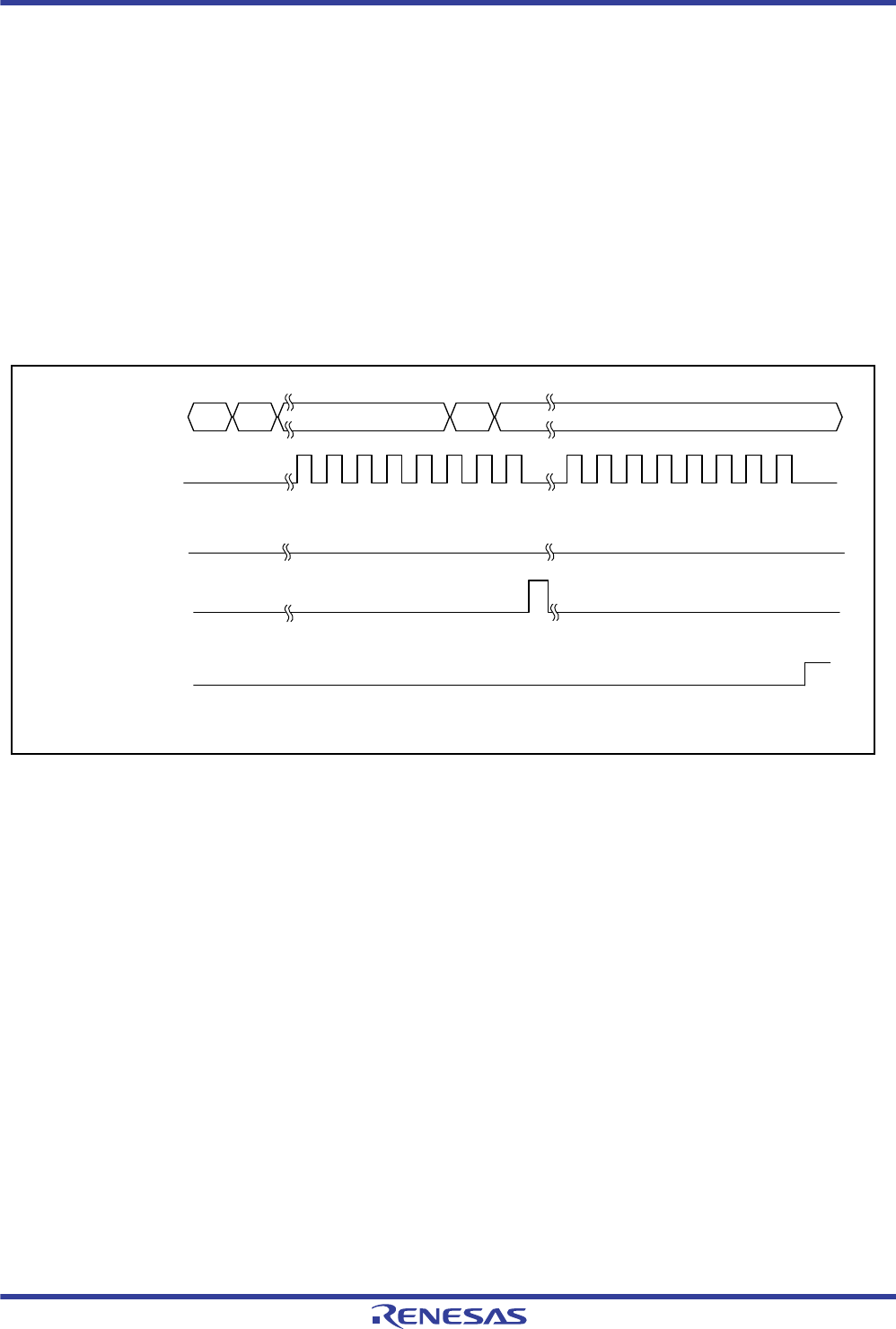
R01UH0034EJ0200 Rev.2.00 Page 1182 of 1489
Dec 27, 2013
RX62T Group, RX62G Group 26. Serial Peripheral Interface (RSPI)
Under development Preliminary document
Specifications in this document are tentative and subject to change.
26.3.6 Communications Operating Mode
Full-duplex synchronous serial communications or transmit operations only can be selected by the communications
operating mode select bit (TXMD) in the RSPI control register (SPCR). The SPDR access shown in Figure 26.21 and
Figure 26.22 indicates the condition of access to the RSPI data register (SPDR), where I denotes an idle cycle and W a
write cycle.
26.3.6.1 Full-Duplex Synchronous Serial Communications (SPCR.TXMD = 0)
Figure 26.21 shows an example of operation when the communications operating mode select bit (TXMD) in the RSPI
control register (SPCR) is set to 0. In the example of Figure 26.21, the RSPI performs an 8-bit serial transfer in which
the SPDCR.SPFC[1:0] bits are 00, the SPCMDm.CPHA bit is 1, and the SPCMDm.CPOL bit is 0. The numbers given
under the RSPCK waveform represent the number of RSPCK cycles (i.e., the number of transferred bits).(m = 0 to 7)
Figure 26.21 Operation Example of SPCR.TXMD = 0
The operation of the flags at timings shown in steps (1) and (2) in the figure is described below.
1. When a serial transfer ends with the receive buffer of SPDR empty, the RSPI generates a receive buffer full
interrupt request (SPRI) and copies the received data in the shift register to the receive buffer.
2. When a serial transfer ends with the receive buffer of SPDR holding data that was received in the previous serial
transfer, the RSPI sets the OVRF flag in SPSR to 1 and discards the received data in the shift register.
When performing full-duplex synchronous serial communications (SPCR.TXMD = 0), the RSPI transmits transmit data
and receives received data. Therefore, the OVRF flag in SPSR is set to 1 at the timings of (1) and (2).
SPDR access
SPSR.OVRF
SPRI0
RSPCKn
87654321 87654321
(SPCMDm.CPHA = 1,
SPCMDm.CPOL = 0)
(1)
(2)
(TXMD = 0)
TXMD
IW I IW
(m = 0 to 7)
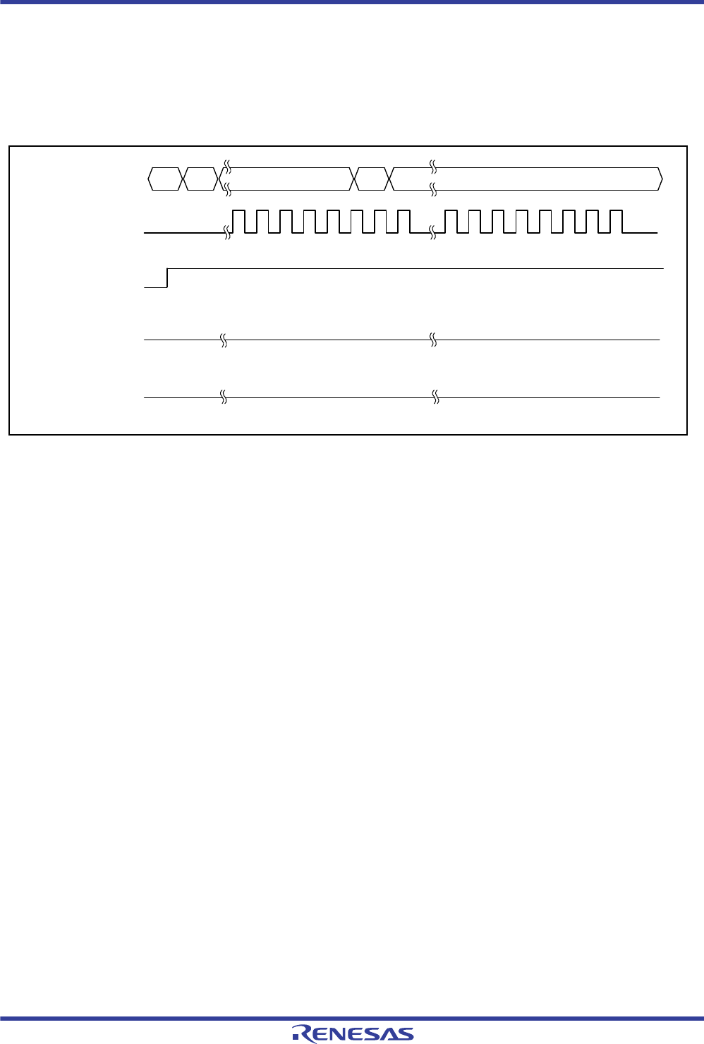
R01UH0034EJ0200 Rev.2.00 Page 1183 of 1489
Dec 27, 2013
RX62T Group, RX62G Group 26. Serial Peripheral Interface (RSPI)
Under development Preliminary document
Specifications in this document are tentative and subject to change.
26.3.6.2 Transmit Operations Only (SPCR.TXMD = 1)
Figure 26.22 shows an example of operation when the communications operating mode select bit (TXMD) in the RSPI
control register (SPCR) is set to 1. In the example of Figure 26.22, the RSPI performs an 8-bit serial transfer in which
the SPDCR.SPFC[1:0] bits are 00, the SPCMDm.CPHA bit is 1, and the SPCMDm.CPOL bit is 0. The numbers given
under the RSPCK waveform represent the number of RSPCK cycles (i.e., the number of transferred bits).(m = 0 to 7)
Figure 26.22 Operation Example of SPCR.TXMD = 1
The operation of the flags at timings shown in steps (1) to (3) in the figure is described below.
1. Make sure there is no data left in the receive buffer and the SPSR.OVRF flag is 0 before entering the mode of
transmit operations only (SPCR.TXMD = 1).
2. When a serial transfer ends with the receive buffer of SPDR empty, if the mode of transmit operations only is
selected (SPCR.TXMD = 1), the RSPI does not copy the data in the shift register to the receive buffer.
3. Since the receive buffer of SPDR does not hold data that was received in the previous serial transfer, even when a
serial transfer ends, the SPSR.OVRF flag retains the value of 0, and the data in the shift register is not copied to the
receive buffer.
When performing transmit operations only (SPCR.TXMD = 1), the RSPI transmits transmit data but does not receive
received data. Therefore, the SPSR.OVRF flag remains cleared to 0 at the timings of (1) to (3).
SPDR access
SPSR.OVRF
SPRI
RSPCKn
87654321 87654321
(SPCMDm.CPHA = 1,
SPCMDm.CPOL = 0)
(1)
(2)
(TXMD = 1)
TXMD
(3)
IW I IW
(m = 0 to 7)
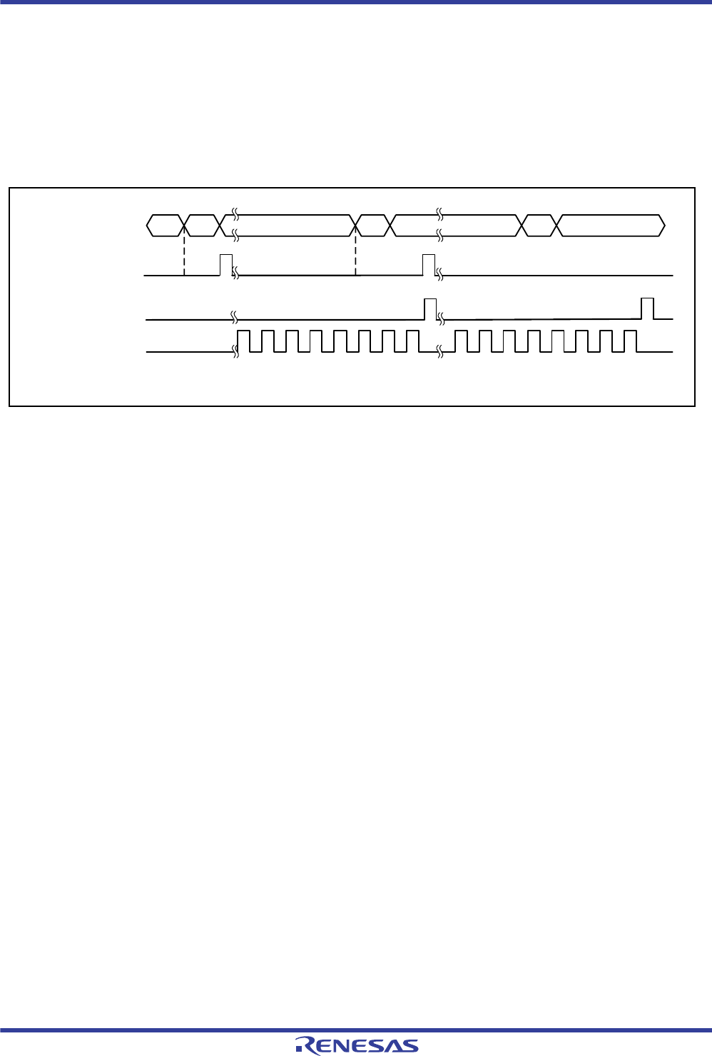
R01UH0034EJ0200 Rev.2.00 Page 1184 of 1489
Dec 27, 2013
RX62T Group, RX62G Group 26. Serial Peripheral Interface (RSPI)
Under development Preliminary document
Specifications in this document are tentative and subject to change.
26.3.7 Transmit Buffer Empty/Receive Buffer Full Interrupts
Figure 26.23 shows an example of operation of the RSPI transmit buffer empty interrupt (SPTI) and the RSPI receive
buffer full interrupt (SPRI). The SPDR access shown in Figure 26.23 indicates the condition of access to the RSPI data
register (SPDR), where I denotes an idle cycle, W a write cycle, and R a read cycle. In the example of Figure 26.23, the
RSPI performs an 8-bit serial transfer in which the SPCR.TXMD bit is 0, the SPDCR.SPFC[1:0] bits are 00, the
SPCMDm.CPHA bit is 1, and the SPCMDm.CPOL bit is 0. The numbers given under the RSPCK waveform represent
the number of RSPCK cycles (i.e., the number of transferred bits).(m = 0 to 7)
Figure 26.23 Operation Example of SPTI and SPRI Interrupts
The operation of the interrupts at timings shown in steps (1) to (5) in the figure is described below.
1. When transmit data is written to SPDR when the transmit buffer of SPDR is empty (data for the next transfer is not
set), the RSPI writes data to the transmit buffer.
2. If the shift register is empty, the RSPI copies the data in the transmit buffer to the shift register and generates a
transmit buffer empty interrupt request (SPTI). How a serial transfer is started depends on the mode of the RSPI.
For details, see section 26.3.10, SPI Operation, and section 26.3.11, Clock Synchronous Operation.
3. When transmit data is written to SPDR by the transmit buffer empty interrupt routine, the data is transferred to the
transmit buffer. Because the data being transferred serially is stored in the shift register, the RSPI does not copy the
data in the transmit buffer to the shift register.
4. When the serial transfer ends with the receive buffer of SPDR being empty, the RSPI copies the receive data in the
shift register to the receive buffer and generates a receive buffer full interrupt request (SPRI). Because the shift
register becomes empty upon completion of serial transfer, when the transmit buffer had been full before the serial
transfer ended, the RSPI copies the data in the transmit buffer to the shift register. Even when received data is not
copied from the shift register to the receive buffer in an overrun error status, upon completion of the serial transfer,
the RSPI determines that the shift register is empty, thus data transfer from the transmit buffer to the shift register is
enabled.
5. When SPDR is read by the receive buffer full interrupt routine, the RSPI sends the data in the receive buffer to the
bus inside the chip.
SPDR access
SPTI0
SPRI0
87654321 87654321
IW I I IWR
RSPCK
(SPCMDm.CPHA = 1,
SPCMDm.CPOL = 0)
(1) (2) (3) (4) (5)
(m = 0 to 7)

R01UH0034EJ0200 Rev.2.00 Page 1185 of 1489
Dec 27, 2013
RX62T Group, RX62G Group 26. Serial Peripheral Interface (RSPI)
Under development Preliminary document
Specifications in this document are tentative and subject to change.
If SPDR is written to when the transmit buffer holds data that has not yet been transmitted, the RSPI does not update the
data in the transmit buffer. When writing to SPDR, make sure to use a transmit buffer empty interrupt request. To use an
RSPI transmit interrupt, set the SPTIE bit in SPCR to 1.
If the RSPI is disabled (the SPE bit in SPCR being 0), set the SPTIE bit in SPCR to 0.
When serial transfer ends with the receive buffer being full, the RSPI does not copy data from the shift register to the
receive buffer, and detects an overrun error (see section 26.3.8, Error Detection). To prevent a receive data overrun
error, read the received data using a receive buffer full interrupt request before the next serial transfer ends. To use an
RSPI receive interrupt, set the SPRIE bit in SPCR to 1.
The status of the transmit/receive buffer can be checked by either using a transmit/receive interrupt or by reading the
corresponding IRi.IR flag of the ICU.
26.3.8 Error Detection
In the normal RSPI serial transfer, the data written to the transmit buffer of SPDR is serially transmitted, and the serially
received data can be read from the receive buffer of SPDR. If access is made to SPDR, depending on the status of the
transmit/receive buffer or the status of the RSPI at the beginning or end of serial transfer, in some cases non-normal
transfers can be executed.
If a non-normal transfer operation occurs, the RSPI detects the event as an overrun error, parity error, or mode fault error.
Table 26.9 shows the relationship between non-normal transfer operations and the RSPI's error detection function.
On operation A shown in Table 26.9, the RSPI does not detect an error. To prevent data omission during the writing to
SPDR, write operations to SPDR should be executed using a transmit interrupt request.
The RSPI does not detect an error on operation B. In a serial transfer that was started before the shift register was
updated, the RSPI sends the data that was received in the previous serial transfer, and does not treat the operation
indicated in B as an error. Note that the received data from the previous serial transfer is retained in the receive buffer of
SPDR, thus it can be correctly read (if SPDR is not read before the end of the serial transfer, an overrun error may occur).
Similarly, the RSPI does not detect an error on operation C. To prevent extraneous data from being read, SPDR read
Table 26.9 Relationship between Non-Normal Transfer Operations and RSPI Error Detection Function
Occurrence Condition RSPI Operation Error Detection
A SPDR is written when the transmit buffer is full. The contents of the transmit buffer are kept.
Missing write data.
None
B Serial transfer is started in slave mode when transmit
data is still not loaded on the shift register.
Data received in previous serial transfer is serially
transmitted.
None
C SPDR is read when the receive buffer is empty. Previously received serial data is output. None
D Serial transfer terminates when the receive buffer is
full.
The contents of the receive buffer are kept.
Missing serial receive data.
Overrun error
E An incorrect parity bit is received when performing
full-duplex synchronous serial communications with
the parity function enabled.
The parity error flag is asserted. Parity error
F The SSL0 input signal is asserted when the serial
transfer is idle in multi-master mode.
Driving of the RSPCK, MOSI, SSL1 to SSL3
output signals is stopped.
RSPI function is disabled.
Mode fault error
G The SSL0 input signal is asserted during serial
transfer in multi-master mode.
Serial transfer is suspended.
Missing transmit/receive data.
Driving of the RSPCK, MOSI, SSL1 to SSL3
output signals is stopped.
RSPI function is disabled.
Mode fault error
H The SSL0 input signal is negated during serial
transfer in slave mode.
Serial transfer is suspended.
Missing transmit/receive data.
Driving of the MISO output signal is stopped.
RSPI function is disabled.
Mode fault error

R01UH0034EJ0200 Rev.2.00 Page 1186 of 1489
Dec 27, 2013
RX62T Group, RX62G Group 26. Serial Peripheral Interface (RSPI)
Under development Preliminary document
Specifications in this document are tentative and subject to change.
operation should be executed using a receive interrupt request.
An overrun error shown in D is described in section 26.3.8.1, Overrun Error. A parity error shown in E is described in
section 26.3.8.2, Parity Error. A mode fault error shown in F to H is described in section 26.3.8.3, Mode Fault
Error.
For the transmit and receive interrupts, refer to section 26.3.7, Transmit Buffer Empty/Receive Buffer Full
Interrupts.
26.3.8.1 Overrun Error
If a serial transfer ends when the receive buffer of SPDR is full, the RSPI detects an overrun error, and sets the OVRF
flag in SPSR to 1. When the SPSR.OVRF flag is 1, the RSPI does not copy data from the shift register to the receive
buffer so that the data prior to the occurrence of the error is retained in the receive buffer. To set the OVRF flag in SPSR
to 0, write 0 to the SPSR.OVRF flag after the CPU has read SPSR with the SPSR.OVRF flag set to 1.
Figure 26.24 shows an example of operation of the SPSR.OVRF flag. The SPSR and SPDR accesses shown in Figure
26.24 indicates the condition of accesses to SPSR and SPDR, respectively, where I denotes an idle cycle, W a write
cycle, and R a read cycle. In the example of Figure 26.24, the RSPI performs an 8-bit serial transfer in which the
SPCMDm.CPHA bit is 1 and the SPCMDm.CPOL bit is 0. The numbers given under the RSPCK waveform represent
the number of RSPCK cycles (i.e., the number of transferred bits).(m = 0 to 7)
Figure 26.24 Operation Example of OVRF Flag
The operation of the flags at the timing shown in steps (1) to (4) in the figure is described below.
1. If a serial transfer terminates with the receive buffer full, the RSPI detects an overrun error, and sets the
SPSR.OVRF flag to 1. The RSPI does not copy the data in the shift register to the receive buffer. Even if the
SPCR2.SPPE bit is 1, parity errors are not detected. In master mode, the RSPI copies the pointer value to SPCMDm
to the SPSSR.SPECM[2:0] bits.(m = 0 to 7)
2. When SPDR is read, the RSPI outputs the data in the receive buffer to an internal bus. The receive buffer becoming
empty does not clear the SPSR.OVRF flag.
3. If the serial transfer ends with the SPSR.OVRF flag being 1 (an overrun error), the RSPI does not copy the data in
the shift register to the receive buffer. Even if the SPCR2.SPPE bit is 1, parity errors are not detected. When in
master mode, the RSPI does not update the SPSSR.SPECM[2:0] bits. When in an overrun error state and the RSPI
does not copy the received data from the shift register to the receive buffer, upon termination of the serial transfer,
the RSPI determines that the shift register is empty; in this manner, data transfer from the transmit buffer to the shift
register is enabled.
4. If the CPU writes the value 0 to the SPSR.OVRF flag after reading SPSR when the SPSR.OVRF flag is 1, the RSPI
clears the SPSR.OVRF flag.
The occurrence of an overrun can be checked either by reading SPSR or by using an RSPI error interrupt and reading
SPSR. When using an RSPI error interrupt, set the SPEIE bit in the RSPI control register (SPCR) to 1. When executing a
SPSR.OVRF
RSPCKn
87654321 87654321
I
I
IR
IWR
(SPCMDm.CPHA = 1,
SPCMDm.CPOL = 0)
SPDR access
SPSR access
(CPU)
(1) (2) (3) (4)
(m = 0 to 7)
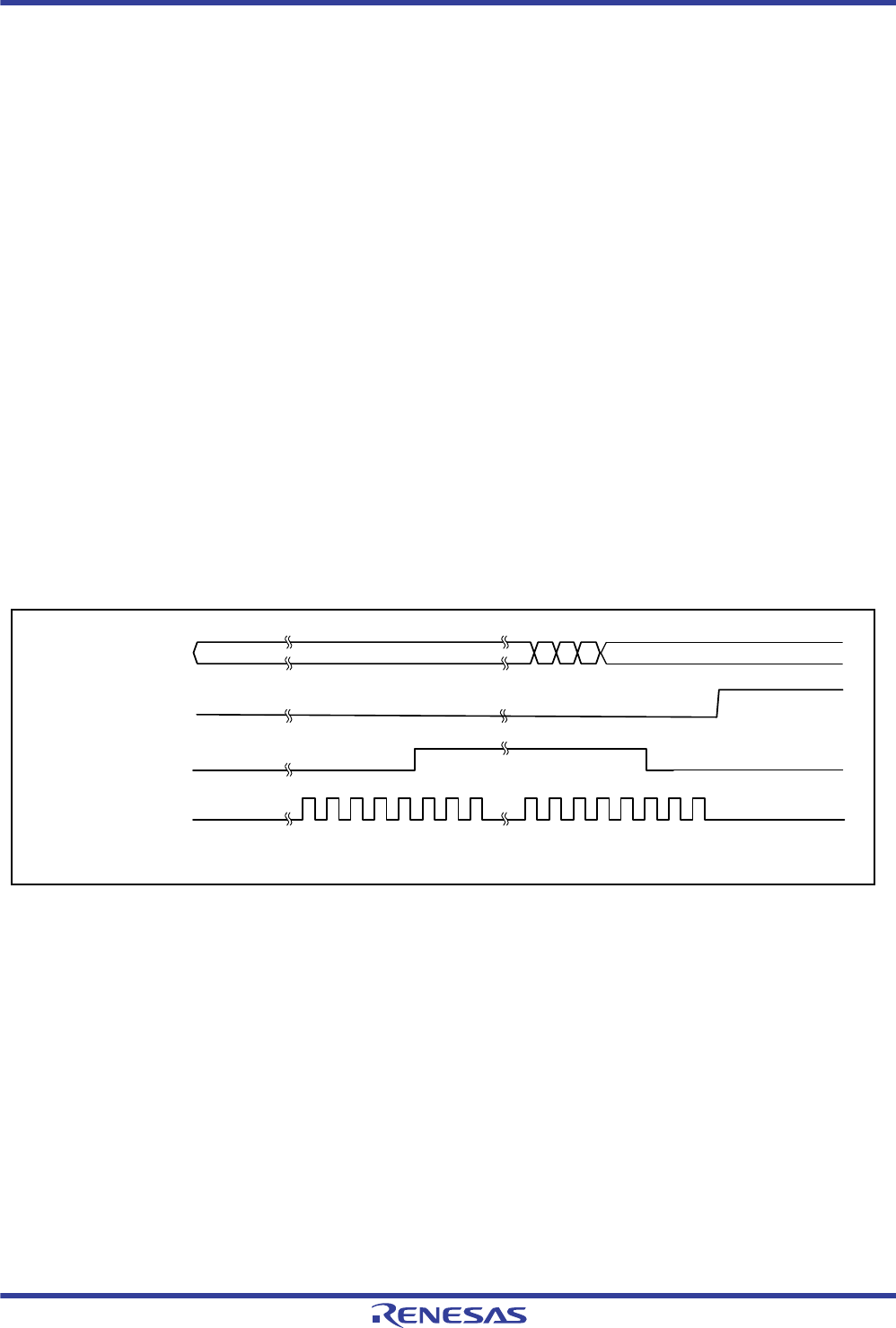
R01UH0034EJ0200 Rev.2.00 Page 1187 of 1489
Dec 27, 2013
RX62T Group, RX62G Group 26. Serial Peripheral Interface (RSPI)
Under development Preliminary document
Specifications in this document are tentative and subject to change.
serial transfer without using an RSPI error interrupt, measures should be taken to ensure the early detection of overrun
errors, such as reading SPSR immediately after SPDR is read. When the RSPI is used in master mode, the pointer value
to SPCMD at the occurrence of the error can be checked by reading the SPSSR.SPECM[2:0] bits.
If an overrun error occurs and the SPSR.OVRF flag is set to 1, normal reception operations cannot be performed until the
SPSR.OVRF flag is cleared. The SPSR.OVRF flag is cleared to 0 under the following condition:
[Clearing condition]
The CPU reads SPSR when the SPSR.OVRF flag is 1, and then writes the value 0 to the SPSR.OVRF flag.
26.3.8.2 Parity Error
If full-duplex synchronous serial communications is performed with the TXMD bit in the RSPI control register (SPCR)
cleared to 0 and the SPPE bit in RSPI control register 2 (SPCR2) set to 1, when serial transfer ends, the RSPI checks
whether there are parity errors. Upon detecting a parity error in the received data, the RSPI sets the PERF flag in the
RSPI status register (SPSR) to 1. Since the RSPI does not copy the data in the shift register to the receive buffer when the
OVRF flag is set to 1, parity error detection is not performed for the received data. To set the PERF bit in SPSR to 0,
write 0 to the SPSR.PERF flag after the CPU has read SPSR with the SPSR.PERF flag set to 1.
Figure 26.25 shows an example of operation of the OVRF and PERF bits in SPSR. The SPSR access shown in Figure
26.25 indicates the condition of access to SPSR, where I denotes an idle cycle, W a write cycle, and R a read cycle. In
the example of Figure 26.25, full-duplex synchronous serial communications is performed while the TXMD bit in the
RSPI control register (SPCR) is 0 and the SPPE bit in RSPI control register 2 (SPCR2) is 1. The RSPI performs an 8-bit
serial transfer in which the SPCMDm.CPHA bit is 1 and the SPCMDm.CPOL bit is 0. The numbers given under the
RSPCK waveform represent the number of RSPCK cycles (i.e., the number of transferred bits).(m = 0 to 7)
Figure 26.25 Operation Example of SPSR.PERF Flag
The operation of the flags at the timing shown in steps (1) to (3) in the figure is described below.
1. If a serial transfer terminates with the RSPI not detecting an overrun error, the RSPI copies the data in the shift
register to the receive buffer. The RSPI judges the received data at this timing, and sets the SPSR.PERF flag to 1 if
a parity error is detected. In master mode, the RSPI copies the pointer value to SPCMDm to the
SPSSR.SPECM[2:0] bits.(m = 0 to 7)
2. If the CPU writes the value 0 to the SPSR.PERF flag after reading SPSR when the SPSR.PERF bit is 1, the RSPI
clears the SPSR.OVRF flag.
3. When the RSPI detects an overrun error and serial transfer is terminated, the data in the shift register is not copied to
the receive buffer. The RSPI does not perform parity error detection at this timing.
The occurrence of a parity error can be checked either by reading SPSR or by using an RSPI error interrupt and reading
SPSR. When using an RSPI error interrupt, set the SPEIE bit in the RSPI control register (SPCR) to 1. When executing a
serial transfer without using an RSPI error interrupt, measures should be taken to ensure the early detection of parity
SPSR.OVRF
PERF
RSPCKn
(SPCMDm.CPHA = 1,
SPCMDm.CPOL = 0) 87654321 87654321
IIWR
SPSR access
(CPU)
(1) (2) (3)
I
(m = 0 to 7)

R01UH0034EJ0200 Rev.2.00 Page 1188 of 1489
Dec 27, 2013
RX62T Group, RX62G Group 26. Serial Peripheral Interface (RSPI)
Under development Preliminary document
Specifications in this document are tentative and subject to change.
errors, such as reading SPSR immediately after SPDR is read. When the RSPI is used in master mode, the pointer value
to SPCMDm at the occurrence of the error can be checked by reading the SPSSR.SPECM[2:0] bits.
The SPSR.PERF flag is cleared to 0 under the following condition:
[Clearing condition]
The CPU reads SPSR when the SPSR.PERF flag is 1, and then writes the value 0 to the SPSR.PERF flag.
26.3.8.3 Mode Fault Error
The RSPI operates in multi-master mode when the SPCR.MSTR bit is 1, the SPCR.SPMS bit is 0, and the
SPCR.MODFEN bit is 1. If the active level is input with respect to the SSL0 input signal of the RSPI in multi-master
mode, the RSPI detects a mode fault error irrespective of the status of the serial transfer, and sets the MODF bit in the
RSPI status register (SPSR) to 1. Upon detecting the mode fault error, the RSPI copies the value of the pointer to
SPCMDm to the SPSSR.SPECM[2:0] bits. The active level of the SSL0 signal is determined by the SSL0P bit in the
RSPI slave select polarity register (SSLP).(m = 0 to 7)
When the SPCR.MSTR bit is 0, the RSPI operates in slave mode. The RSPI detects a mode fault error if the
SPCR.MODFEN bit in the RSPI in slave mode is 1, and the SPCR.SPMS bit is 0, and if the SSL0 input signal is negated
during the serial transfer period (from the time the driving of valid data is started to the time the final valid data is
fetched).
Upon detecting a mode fault error, the RSPI stops driving of the output signals and clears the SPE bit in SPCR to 0 (see
section 26.3.9, Initializing RSPI). In the case of multi-master configuration, detection of a mode fault error is used to
stop driving of the output signals and the RSPI function, which allows the master right to be released.
The occurrence of a mode fault error can be checked either by reading SPSR or by using an RSPI error interrupt and
reading SPSR. When using an RSPI error interrupt, set the SPEIE bit in the RSPI control register (SPCR) to 1. To detect
a mode fault error without using an RSPI error interrupt, it is necessary to poll SPSR. When using the RSPI in master
mode, the pointer value to SPCMDm at the occurrence of the error can be checked by reading the SPSSR.SPECM[2:0]
bits.
When the SPSR.MODF flag is 1, the RSPI ignores the writing of the value 1 to the SPCR.SPE bit by the CPU. To enable
the RSPI function after the detection of a mode fault error, the SPSR.MODF flag must be set to 0.
The SPSR.MODF flag is cleared to 0 under the following condition:
[Clearing condition]
The CPU reads SPSR when the SPSR.MODF flag is 1, and then writes the value 0 to the SPSR.MODF flag.

R01UH0034EJ0200 Rev.2.00 Page 1189 of 1489
Dec 27, 2013
RX62T Group, RX62G Group 26. Serial Peripheral Interface (RSPI)
Under development Preliminary document
Specifications in this document are tentative and subject to change.
26.3.9 Initializing RSPI
If the CPU writes the value 0 to the SPE bit in the RSPI control register (SPCR) or the RSPI clears the SPCR.SPE bit to
0 because of the detection of a mode fault error, the RSPI disables the RSPI function, and initializes some of the module
functions. When a system reset is generated, the RSPI initializes all of the module functions. The following describes
initialization by the clearing of the SPCR.SPE bit and initialization by a system reset.
26.3.9.1 Initialization by Clearing the SPE Bit
When the SPE bit in SPCR is cleared, the RSPI performs the following initialization:
Suspending any serial transfer that is being executed
Stopping the driving of output signals (Hi-Z) in slave mode
Initializing the internal state of the RSPI
Initializing the transmit buffer of the RSPI
Initialization by the clearing of the SPCR.SPE bit does not initialize the control bits of the RSPI. For this reason, the
RSPI can be started in the same transfer mode as prior to the initialization if the CPU resets the value 1 to the SPCR.SPE
bit.
The OVRF and MODF flags in SPSR are not initialized, nor is the value of the RSPI sequence status register (SPSSR)
initialized. For this reason, even after the RSPI is initialized, data from the receive buffer can be read in order to check
the status of error occurrence during an RSPI transfer.
The transmit buffer is initialized to an empty state. Therefore, if the SPTIE bit in SPCR is set to 1 after RSPI
initialization, an RSPI transmit interrupt is generated. When the RSPI is initialized by the CPU, in order to disable any
RSPI transmit interrupt, the value 0 should be written to the SPCR.SPTIE bit simultaneously with the writing of the
value 0 to the SPCR.SPE bit. To disable any RSPI transmit interrupt after a mode fault error is detected, use an error
handling routine to write the value 0 to the SPCR.SPTIE bit.
26.3.9.2 System Reset
The initialization by a system reset completely initializes the RSPI through the initialization of all bits for controlling the
RSPI, initialization of the status bits, and initialization of data registers, in addition to the requirements described in
section 26.3.9.1, Initialization by Clearing the SPE Bit.

R01UH0034EJ0200 Rev.2.00 Page 1190 of 1489
Dec 27, 2013
RX62T Group, RX62G Group 26. Serial Peripheral Interface (RSPI)
Under development Preliminary document
Specifications in this document are tentative and subject to change.
26.3.10 SPI Operation
26.3.10.1 Master Mode Operation
The only difference between single-master mode operation and multi-master mode operation lies in mode fault error
detection (see section 26.3.8, Error Detection). When operating in single-master mode, the RSPI does not detect mode
fault errors whereas the RSPI running in multi-master mode does detect mode fault errors. This section explains
operations that are common to single-master mode and multi-master mode.
(1) Starting a Serial Transfer
The RSPI updates the data in the transmit buffer when data is written to the RSPI data register (SPDR) with the RSPI
transmit buffer being empty (data for the next transfer is not set). If the shift register is empty due to the writing to SPDR,
the RSPI copies the data in the transmit buffer to the shift register and starts a serial transfer. Upon copying transmit data
to the shift register, the RSPI changes the status of the shift register to "full", and upon termination of serial transfer, it
changes the status of the shift register to "empty". The status of the shift register cannot be referenced from the CPU.
For details on the RSPI transfer format, see section 26.3.4, Transfer Format. The polarity of the SSL output pins
depends on the settings in the RSPI slave select polarity register (SSLP).
(2) Terminating a Serial Transfer
Irrespective of the CPHA bit in the RSPI command register (SPCMD), the RSPI terminates the serial transfer after
transmitting an RSPCK edge corresponding to the final sampling timing. If free space is available in the receive buffer,
upon termination of serial transfer, the RSPI copies data from the shift register to the receive buffer of the RSPI data
register (SPDR).
It should be noted that the final sampling timing varies depending on the bit length of transfer data. In master mode, the
RSPI data length depends on the SPCMD.SPB[3:0] bit setting. The polarity of the SSL output pin depends on the
settings in the RSPI slave select polarity register (SSLP).
For details on the RSPI transfer format, see section 26.3.4, Transfer Format. (m = 0 to 7)
(3) Sequence Control
The transfer format that is employed in master mode is determined by SPSCR, SPCMDm, SPBR, SPCKD, SSLND, and
SPND.
SPSCR is a register used to determine the sequence configuration for serial transfers that are executed by the RSPI in
master mode. The following items are set in RSPI command registers SPCMDm: SSL pin output signal value, MSB/LSB
first, data length, some of the bit rate settings, RSPCK polarity/phase, whether SPCKD is to be referenced, whether
SSLND is to be referenced, and whether SPND is to be referenced. SPBR holds some of the bit rate settings; SPCKD, an
RSPI clock delay value; SSLND, an SSL negation delay; and SPND, a next-access delay value.
According to the sequence length that is assigned to SPSCR, the RSPI makes up a sequence comprised of a part or all of
SPCMDm. The RSPI contains a pointer to the SPCMDm that makes up the sequence. The CPU can check the value of
this pointer by reading the SPSSR.SPCP[2:0] bits. When the SPCR.SPE bit is set to 1 and the RSPI function is enabled,
the RSPI loads the pointer to the commands in SPCMD0, and incorporates the SPCMD0 settings into the transfer format
at the beginning of serial transfer.
The RSPI increments the pointer each time the next-access delay period for a data transfer ends. Upon completion of the
serial transfer that corresponds to the final command comprising the sequence, the RSPI sets the pointer in SPCMD0,
and in this manner the sequence is executed repeatedly.(m = 0 to 7)
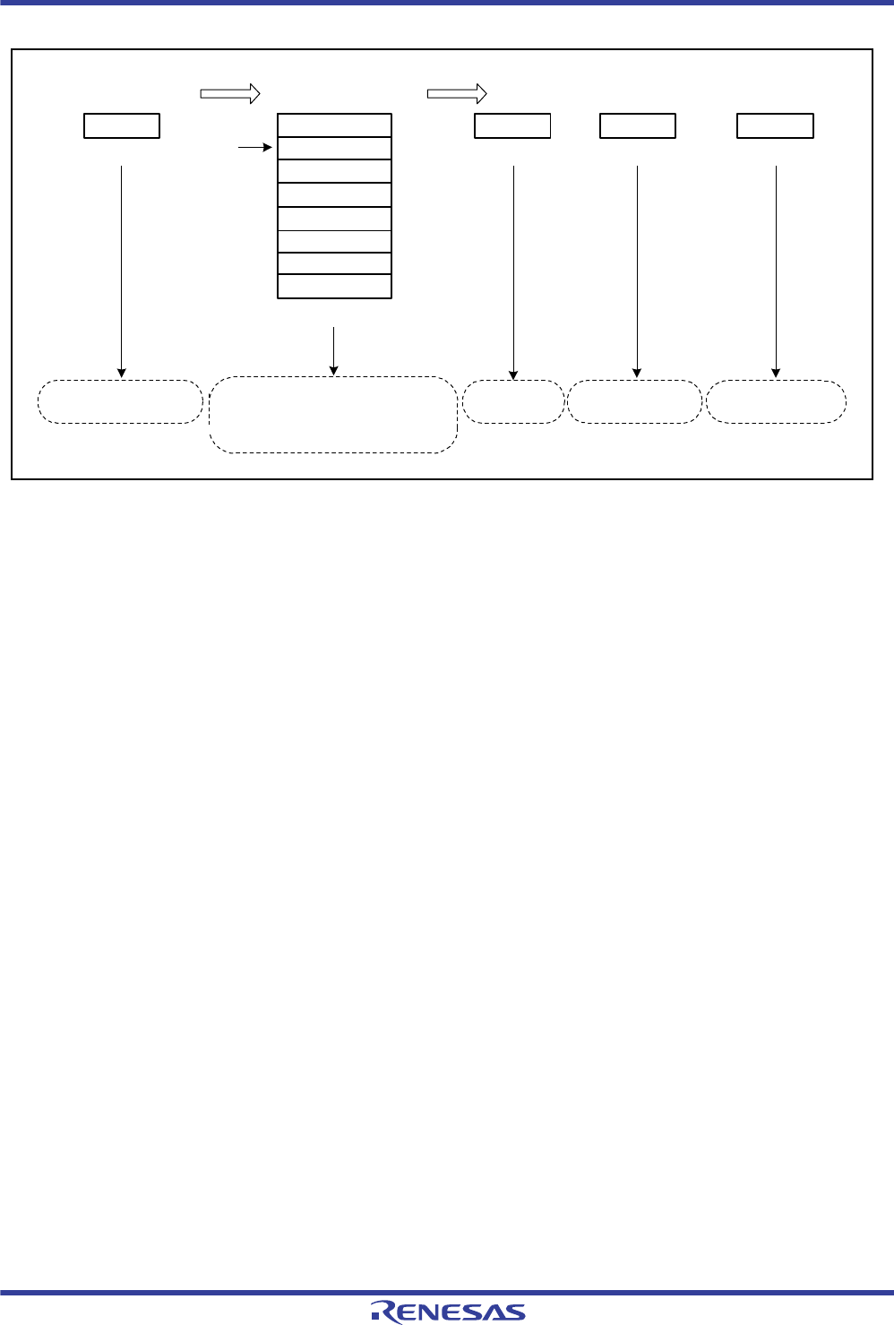
R01UH0034EJ0200 Rev.2.00 Page 1191 of 1489
Dec 27, 2013
RX62T Group, RX62G Group 26. Serial Peripheral Interface (RSPI)
Under development Preliminary document
Specifications in this document are tentative and subject to change.
Figure 26.26 Determination Procedure of Serial Transfer Mode in Master Mode (SPI Operation)
(4) Burst Transfer
If the SSLKP bit in the RSPI command register (SPCMD) (m = 0 to 7)that the RSPI references during the current serial
transfer is 1, the RSPI keeps the SSL signal level during the serial transfer until the beginning of the SSL signal assertion
for the next serial transfer. If the SSL signal level for the next serial transfer is the same as the SSL signal level for the
current serial transfer, the RSPI can execute continuous serial transfers while keeping the SSL signal assertion status
(burst transfer).
Figure 26.27 shows an example of an SSL signal operation for the case where a burst transfer is implemented using
SPCMD0 and SPCMD1 settings. The text below explains the RSPI operations (1) to (7) as shown in Figure 26.27. It
should be noted that the polarity of the SSL output signal depends on the settings in the RSPI slave select polarity
register (SSLP).
Based on SPCMD0, the RSPI asserts the SSL signal and inserts RSPCK delays.
The RSPI executes serial transfers according to SPCMD0.
The RSPI inserts SSL negation delays.
Because the SSLKP bit in SPCMD0 is 1, the RSPI keeps the SSL signal value on SPCMD0. This period is sustained, at
the shortest, for a period equal to the next-access delay of SPCMD0. If the shift register is empty after the passage of a
minimum period, this period is sustained until the transmit data is stored in the shift register for the next transfer.
Based on SPCMD1, the RSPI asserts the SSLn signal and inserts RSPCK delays.
The RSPI executes serial transfers according to SPCMD1.
Because the SSLKP bit in SPCMD1 is 0, the RSPI negates the SSL signal. In addition, a next-access delay is inserted
according to SPCMD1.
Sequence
determined
Pointer
SPCP[2:0]
Determine transfer
format Refer to SCKD, SSLND, and SPND (if necessary)
SPCMD0
SPCMD1
SPCMD2
SPCMD3
SPSCR
Sequence is formed in
SPCMD0 to SPCMD2
SCKD SSLND SPND
02h 01h
E720h
00h 02h
SCKD, SSLND, and SPND must be
referenced. MSB first, 8 bits,
SSL2 assert, base division
ratio = 1 CPOL = 0, CPHA = 0
RSPCK delay
= 2 RSPCK SSL negation delay
= 1 RSPCK Next-access delay = 3
RSPCK + 2 PCLK
SPCMD4
SPCMD5
SPCMD6
SPCMD7
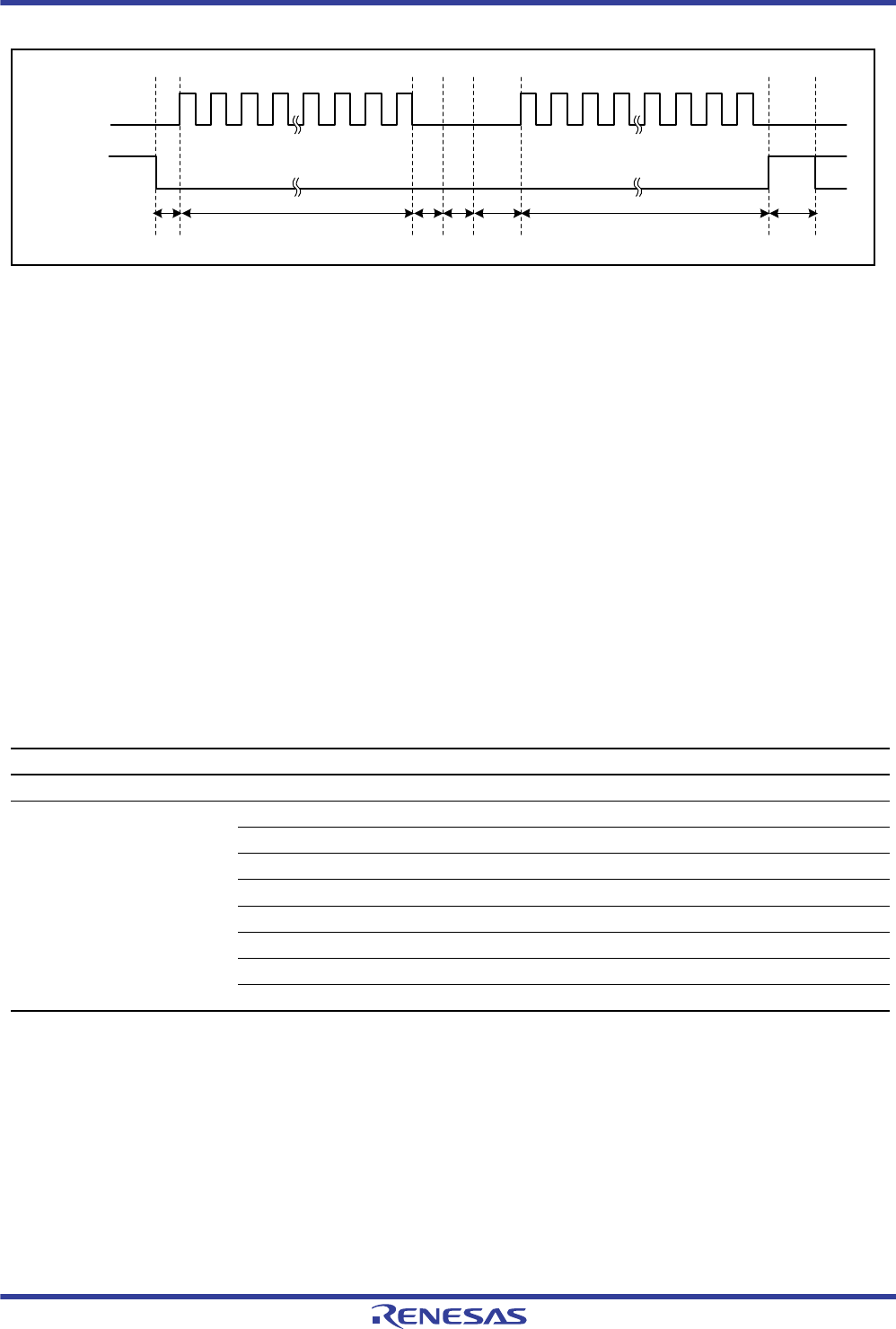
R01UH0034EJ0200 Rev.2.00 Page 1192 of 1489
Dec 27, 2013
RX62T Group, RX62G Group 26. Serial Peripheral Interface (RSPI)
Under development Preliminary document
Specifications in this document are tentative and subject to change.
Figure 26.27 Example of Burst Transfer Operation using SPCMDm.SSLKP Bit (m = 0 to 7)
If the SSL signal output settings in the SPCMDm in which 1 is assigned to the SSLKP bit are different from the SSL
signal output settings in the SPCMDm to be used in the next transfer, the RSPI switches the SSL signal status to SSL
signal assertion ((5) in Figure 26.27) corresponding to the command for the next transfer. Note that if such an SSL
signal switching occurs, the slaves that drive the MISO signal compete, and collision of signal levels may occur.
The RSPI in master mode references the SSL signal operation within the module for the case where the SSLKP bit is not
used. Even when the SPCMDm.CPHA bit is 0, the RSPI can accurately start serial transfers by asserting the SSL signal
for the next transfer. For this reason, burst transfers in master mode can be executed irrespective of SPCMDm.CPHA bit
settings (see section 26.3.10.2, Slave Mode Operation).
(5) RSPCK Delay (t1)
The RSPCK delay value of the RSPI in master mode depends on the SPCMDm.SCKDEN bit (m = 0 to 7) setting and the
SPCKD setting. The RSPI determines the SPCMDm to be referenced during serial transfer by pointer control, and
determines an RSPCK delay value during serial transfer by using the SCKDEN bit in the selected SPCMDm and
SPCKD, as shown in Table 26.10. For a definition of RSPCK delay, see section 26.3.4, Transfer Format.
(m = 0 to 7)
Table 26.10 Relationship among SPCMDm.SCKDEN Bit, SPCKD, and RSPCK Delay Value
SPCMDm.SCKDEN Bit SPCKD.SCKDL[2:0] Bit RSPCK Delay Value
0 000 to 111 1 RSPCK
1 000 1 RSPCK
001 2 RSPCK
010 3 RSPCK
011 4 RSPCK
100 5 RSPCK
101 6 RSPCK
110 7 RSPCK
111 8 RSPCK
RSPCK
SSL
(CPHA = 1,
CPOL = 0)
(1) (2) (3) (4) (5) (6) (7)

R01UH0034EJ0200 Rev.2.00 Page 1193 of 1489
Dec 27, 2013
RX62T Group, RX62G Group 26. Serial Peripheral Interface (RSPI)
Under development Preliminary document
Specifications in this document are tentative and subject to change.
(6) SSL Negation Delay (t2)
The SSL negation delay value of the RSPI in master mode depends on the SPCMDm.SLNDEN bit (m = 0 to 7) setting
and the SSLND setting. The RSPI determines the SPCMDm to be referenced during serial transfer by pointer control,
and determines an SSL negation delay value during serial transfer by using the SLNDEN bit in the selected SPCMDm
and SSLND, as shown in Table 26.11. For a definition of SSL negation delay, see section 26.3.4, Transfer Format.
(m = 0 to 7)
(7) Next-Access Delay (t3)
The next-access delay value of the RSPI in master mode depends on the SPCMDm.SPNDEN bit (m = 0 to 7) setting and
the SPND setting. The RSPI determines the SPCMDm to be referenced during serial transfer by pointer control, and
determines a next-access delay value during serial transfer by using the SPNDEN bit in the selected SPCMDm and
SPND, as shown in Table 26.12. For a definition of next-access delay, see section 26.3.4, Transfer Format.
Table 26.12 Relationship among SPCMDm.SPNDEN Bit, SPND, and Next-Access Delay Value
(m = 0 to 7)
(8) Initialization Flowchart
Figure 26.28 is a flowchart illustrating an example of initialization in SPI operation when the RSPI is used in master
mode. For a description of how to set up the interrupt controller, DTC, and input/output ports, see the descriptions given
in the individual blocks.
Table 26.11 Relationship among SPCMDm.SCKDEN Bit, SSLND, and SSL Negation Delay Value
SPCMDm.SLNDEN Bit SSLND.SLNDL[2:0] Bit SSL Negation Delay Value
0 000 to 111 1 RSPCK
1 000 1 RSPCK
001 2 RSPCK
010 3 RSPCK
011 4 RSPCK
100 5 RSPCK
101 6 RSPCK
110 7 RSPCK
111 8 RSPCK
Table 26.12 Relationship among SPCMDm.SPNDEN Bit, SPND, and Next-Access Delay Value
SPCMDm.SPNDEN Bit SPND.SPNDL[2:0] Bit Next-Access Delay Value
0 000 to 111 1 RSPCK + 2 PCLK
1 000 1 RSPCK + 2 PCLK
001 2 RSPCK + 2 PCLK
010 3 RSPCK + 2 PCLK
011 4 RSPCK + 2 PCLK
100 5 RSPCK + 2 PCLK
101 6 RSPCK + 2 PCLK
110 7 RSPCK + 2 PCLK
111 8 RSPCK + 2 PCLK
R01UH0034EJ0200 Rev.2.00 Page 1194 of 1489
Dec 27, 2013
RX62T Group, RX62G Group 26. Serial Peripheral Interface (RSPI)
Under development Preliminary document
Specifications in this document are tentative and subject to change.
Figure 26.28 Example of Initialization Flowchart in Master Mode (SPI Operation)
Set RSPI pin control
register (SPPCR)
Set RSPI bit rate
register (SPBR)
Set RSPI data control
register (SPDCR)
Set RSPI clock delay register
(SPCKD)
Set RSPI slave select negation
delay register (SSLND)
Set RSPI next-access delay
register (SPND)
Set RSPI command registers 0 to 7
(SPCMD0 to SPCMD7)
Set input/output ports
Set RSPI control
register (SPCR)
Set interrupt controller
Set DTC
Start of initialization in
master mode
• Sets output mode (CMOS or open-drain).
• Sets MOSI signal value when transfer is in idle state.
• Sets next-access delay value.
(when using an interrupt)
• Sets transfer bit rate.
• Sets number of frames to be used.
• Sets RSPCK delay value.
End of initialization in
master mode
• Sets SSL signal level.
• Sets RSPCK delay enable.
• Sets SSL negation delay enable.
• Sets next-access delay enable.
• Sets MSB or LSB first.
• Sets data length.
• Sets transfer bit rate.
• Sets clock phase.
• Sets clock polarity.
• Sets SSL negation delay value.
(when using the DTC)
• Sets master mode.
• Sets interrupt mask.
• Sets RSPI mode.
Set RSPI control register 2 (SPCR2) • Sets parity function.
• Sets interrupt mask.
Read RSPI control register (SPCR)
R01UH0034EJ0200 Rev.2.00 Page 1195 of 1489
Dec 27, 2013
RX62T Group, RX62G Group 26. Serial Peripheral Interface (RSPI)
Under development Preliminary document
Specifications in this document are tentative and subject to change.
(9) Transfer Operation Flowchart
Figure 26.29 is a flowchart illustrating a transfer in SPI operation when the RSPI is used in master mode.
Figure 26.29 Transfer Operation Flowchart in Master Mode (SPI Operation)
Copy transmit data from
transmit buffer to shift register
Copy received data from shift
register to receive buffer
RSPCK cycle count
Receive buffer
status
Continue serial
transfer
Overrun error/parity
error status
Transmit buffer
status
Start serial transfer
Empty
Empty
No
Yes
Error occurred
Full
Full
No error
Error occurred
No error
Shorter than data length
Equal to data length
Update command pointer
Error handling
End of initialization
in master mode
End of transfer
Copy command pointer to
SPSSR.SPECM[2:0] bits
Note:
Transmission
and reception/transmission
only
SPCR.TXMD = 1
Overrun error/parity
error status
SPCR.TXMD = 0
When the SSL0 input signal is asserted in multi-master mode, the RSPI detects a
mode fault error irrespective of the hardware status. When an error is detected,
the RSPI copies the command pointer to the SPSSR.SPECM[2:0] bits.

R01UH0034EJ0200 Rev.2.00 Page 1196 of 1489
Dec 27, 2013
RX62T Group, RX62G Group 26. Serial Peripheral Interface (RSPI)
Under development Preliminary document
Specifications in this document are tentative and subject to change.
26.3.10.2 Slave Mode Operation
(1) Starting a Serial Transfer
If the SPCMD0.CPHA bit is 0, when detecting an SSL0 input signal assertion, the RSPI needs to start driving valid data
to the MISO output signal. For this reason, when the CPHA bit is 0, the assertion of the SSL0 input signal triggers the
start of a serial transfer.
If the SPCMD0.CPHA bit is 1, when detecting the first RSPCK edge in an SSL0 signal asserted condition, the RSPI
needs to start driving valid data to the MSO output signal. For this reason, when the CPHA bit is 1, the first RSPCK edge
in an SSL0 signal asserted condition triggers the start of a serial transfer.
When detecting the start of a serial transfer in a condition in which the shift register is empty, the RSPI changes the status
of the shift register to "full", so that data cannot be copied from the transmit buffer to the shift register when serial
transfer is in progress. If the shift register was full before the serial transfer started, the RSPI leaves the status of the shift
register unchanged, in the full state.
Irrespective of SPCMD0.CPHA bit setting, the timing at which the RSPI starts driving of the MISO output signal is the
SSL0 signal assertion timing. The data which is output by the RSPI is either valid or invalid, depending on the
SPCMD0.CPHA bit setting.
For details on the RSPI transfer format, see section 26.3.4, Transfer Format. The polarity of the SSL0 input signal
depends on the setting of the SSL0P bit in the RSPI slave select polarity register (SSLP).
(2) Terminating a Serial Transfer
Irrespective of the SPCMD0.CPHA bit, the RSPI terminates the serial transfer after detecting an RSPCK edge
corresponding to the final sampling timing. When free space is available in the receive buffer, upon termination of serial
transfer the RSPI copies received data from the shift register to the receive buffer of the RSPI data register (SPDR).
Upon termination of a serial transfer the RSPI changes the status of the shift register to "empty". A mode fault error
occurs if the RSPI detects an SSL0 input signal negation from the beginning of serial transfer to the end of serial transfer
(see section 26.3.8, Error Detection).
The final sampling timing changes depending on the bit length of transfer data. In slave mode, the RSPI data length
depends on the SPCMD0.SPB[3:0] bit setting. The polarity of the SSL0 input signal depends on the SSLP.SSL0P bit
setting.
For details on the RSPI transfer format, see section 26.3.4, Transfer Format.
(3) Notes on Single-Slave Operations
If the SPCMD0.CPHA bit is 0, the RSPI starts serial transfers when it detects the assertion edge for an SSL0 input signal.
In the type of configuration shown in Figure 26.5 as an example, if the RSPI is used in single-slave mode, the SSL0
signal is always fixed at the active state. Therefore, when the SPCMD0.CPHA bit is set to 0, the RSPI cannot correctly
start a serial transfer. To correctly execute transmit/receive operations by the RSPI in a configuration in which the SSL0
input signal is fixed at the active state, the SPCMD0.CPHA bit should be set to 1. If there is a need for setting the
SPCMD0.CPHA bit to 0, the SSL0 input signal should not be fixed.
(4) Burst Transfer
If the SPCMD0.CPHA bit is 1, continuous serial transfer (burst transfer) can be executed while retaining the assertion
state for the SSL0 input signal. If the SPCMD0.CPHA bit is 1, the period from the first RSPCK edge to the sampling
timing for the reception of the final bit in an SSL0 signal active state corresponds to a serial transfer period. Even when
the SSL0 input signal remains at the active level, the RSPI can accommodate burst transfers because it can detect the
start of an access.
If the SPCMD0.CPHA bit is 0, second and subsequent serial transfers during burst transfer cannot be executed correctly.
R01UH0034EJ0200 Rev.2.00 Page 1197 of 1489
Dec 27, 2013
RX62T Group, RX62G Group 26. Serial Peripheral Interface (RSPI)
Under development Preliminary document
Specifications in this document are tentative and subject to change.
(5) Initialization Flowchart
Figure 26.30 is a flowchart illustrating an example of initialization in SPI operation when the RSPI is used in slave
mode. For a description of how to set up the interrupt controller, DTC, and input/output ports, see the descriptions given
in the individual blocks.
Figure 26.30 Example of Initialization Flowchart in Slave Mode (SPI Operation)
(6) Transfer Operation Flowchart (CPHA = 0)
Figure 26.31 is a flowchart illustrating a transfer in SPI operation when the RSPI is used in slave mode with the
SPCMD0.CPHA bit set to 0.
• Sets number of frames to be used.
Set RSPI slave select polarity
register (SSLP)
Set RSPI data control
register (SPDCR)
Set DTC
Set input/output ports
Set RSPI control register
(SPCR)
Set RSPI command register 0
(SPCMD0)
Set interrupt controller
Start of initialization in
slave mode
End of initialization in
slave mode
• Sets polarity of SSL0 input signal
(when using an interrupt)
(when using the DTC)
• Sets MSB or LSB first.
• Sets data length.
• Sets clock phase.
• Sets clock polarity.
• Sets slave mode.
• Sets mode fault error detection.
• Sets interrupt mask.
• Sets RSPI mode.
• Sets parity function.
• Sets interrupt mask.
Set RSPI control register 2
(SPCR2)
Read RSPI control register
(SPCR)
R01UH0034EJ0200 Rev.2.00 Page 1198 of 1489
Dec 27, 2013
RX62T Group, RX62G Group 26. Serial Peripheral Interface (RSPI)
Under development Preliminary document
Specifications in this document are tentative and subject to change.
Figure 26.31 Transfer Operation Flowchart in Slave Mode (SPCMD0.CPHA = 0) (SPI Operation)
Copy received data from the
shift register to the receive
buffer
Detect mode fault
error
RSPCK cycle count
Receive buffer
status
SSL0 input level
Overrun error/
parity error status
SSL0 input level
SSL0 input level
MISO Hi-Z
Negate
Negate
Negate
Empty
Error occurred
Full
Assert
Assert
Assert
No error
No error
Shorter than data length
Equal to data length
Start serial transfer
End of initialization
in slave mode
Error handling
Continue serial
transfer
End of transfer
Overrun error/
parity error status
Error
occurred
Error handling
No
Yes
Transmission and
reception/transmission
only
SPCR.TXMD = 1
SPCR.TXMD = 0
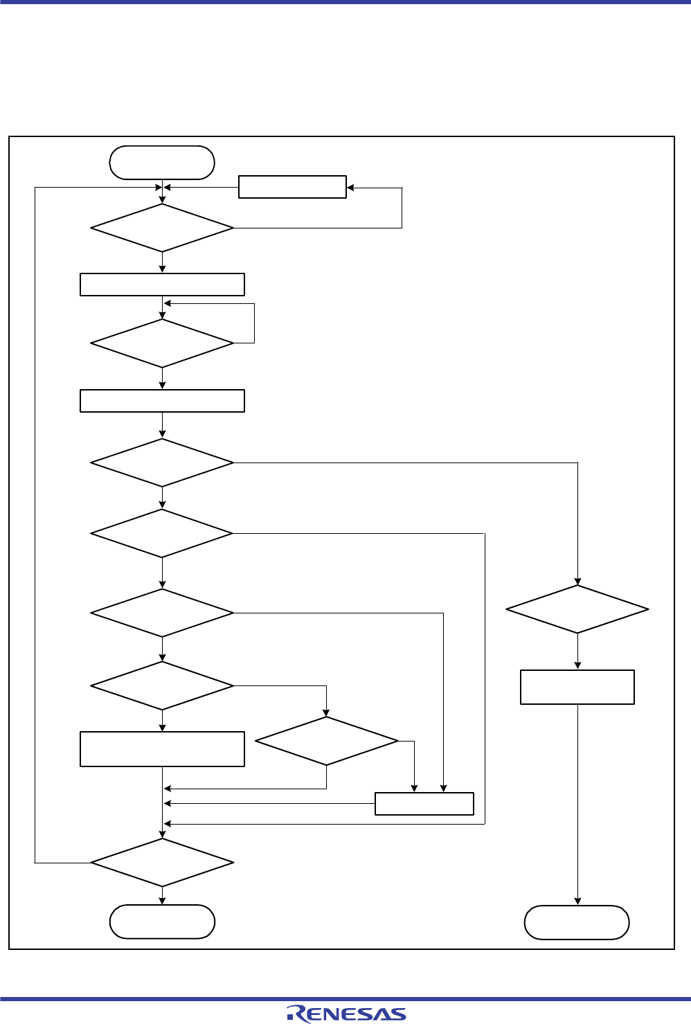
R01UH0034EJ0200 Rev.2.00 Page 1199 of 1489
Dec 27, 2013
RX62T Group, RX62G Group 26. Serial Peripheral Interface (RSPI)
Under development Preliminary document
Specifications in this document are tentative and subject to change.
(7) Transfer Operation Flowchart (CPHA = 1)
Figure 26.32 is a flowchart illustrating a transfer in SPI operation when the RSPI is used in slave mode with both the
SPCMD0.CPHA bit and SPCR.MODFEN bit set to 1. The subsequent operations are not guaranteed when the serial
transfer is started with the MODFEN bit set to 0 and the SSL0 input level is negated with a number of RSPCK cycles
shorter than the data length.
Figure 26.32 Transfer Operation Flowchart in Slave Mode (SPCMD0.CPHA = 1) (SPI Operation)
End of transfer
No
Yes
Error handling
Error
occurred
Copy received data from the
shift register to the receive buffer
Detect mode
fault error
RSPCK cycle count
RSPCK input level
Receive buffer
status
Overrun error/parity
error status
SSL0 input level
Negate
Empty
Error occurred
No error
Full
No change
Changed
No error
Shorter than data length
Equal to data length
Start serial transfer
MISO output
SSL0 input level
MISO Hi-Z
Negate
Assert
End of initialization
in slave mode
Overrun error/parity
error status
Error handling
Continue data
transfer
Transmission and
reception/transmission
only
SPCR.TXMD = 1
SPCR.TXMD = 0

R01UH0034EJ0200 Rev.2.00 Page 1200 of 1489
Dec 27, 2013
RX62T Group, RX62G Group 26. Serial Peripheral Interface (RSPI)
Under development Preliminary document
Specifications in this document are tentative and subject to change.
26.3.11 Clock Synchronous Operation
Setting the SPMS bit in the RSPI control register (SPCR) to 1 selects clock synchronous operation of the RSPI. In clock
synchronous operation, the SSL pin is not used, and the three pins of RSPCK, MOSI, and MISO handle communications.
The SSL pin is available as I/O port pins.
Although clock synchronous operation does not require use of the SSL pin, operation of the module is the same as in SPI
operation. That is, in both master and slave operations, communications can be performed with the same flow as in SPI
operation. However, mode fault errors are not detected because the SSL pin is not used.
Furthermore, operation is not guaranteed if clock synchronous operation proceeds when the SPCMD.CPHA bit (m = 0 to
7) is set to 0 in slave mode (SPCR.MSTR = 0).
26.3.11.1 Master Mode Operation
(1) Starting a Serial Transfer
The RSPI updates the data in the transmit buffer when data is written to the RSPI data register (SPDR) with the RSPI
transmit buffer being empty (data for the next transfer is not set). If the shift register is empty due to the writing of 0
either after the writing to SPDR, the RSPI copies the data in the transmit buffer to the shift register and starts a serial
transfer. Upon copying transmit data to the shift register, the RSPI changes the status of the shift register to "full", and
upon termination of serial transfer, it changes the status of the shift register to "empty". The status of the shift register
cannot be referenced from the CPU.
For details on the RSPI transfer format, see section 26.3.4, Transfer Format.
(2) Terminating a Serial Transfer
The RSPI terminates the serial transfer after transmitting an RSPCK edge corresponding to the sampling timing. If free
space is available in the receive buffer, upon termination of serial transfer, the RSPI copies data from the shift register to
the receive buffer of the RSPI data register (SPDR).
It should be noted that the final sampling timing varies depending on the bit length of transfer data. In master mode, the
RSPI data length depends on the SPCMDm.SPB[3:0] bit (m = 0 to 7) setting.
For details on the RSPI transfer format, see section 26.3.4, Transfer Format.
(3) Sequence Control
The transfer format employed in master mode is determined by SPSCR, SPCMDm, SPBR, SPCKD, SSLND, and SPND.
Although the SSL signals are not output in clock synchronous operation, these settings are valid.
SPSCR is a register used to determine the sequence configuration for serial transfers that are executed by the RSPI in
master mode. The following items are set in RSPI command registers SPCMDm: SSL output signal value, MSB/LSB
first, data length, some of the bit rate settings, RSPCK polarity/phase, whether SPCKD is to be referenced, whether
SSLND is to be referenced, and whether SPND is to be referenced. SPBR holds some of the bit rate settings; SPCKD, an
RSPI clock delay value; SSLND, an SSL negation delay; and SPND, a next-access delay value.
According to the sequence length that is assigned to SPSCR, the RSPI makes up a sequence comprised of a part or all of
SPCMDm. The RSPI contains a pointer to the SPCMD that makes up the sequence. The CPU can check the value of this
pointer by reading the SPSSR.SPCP[2:0] bits. When the SPCR.SPE bit is set to 1 and the RSPI function is enabled, the
RSPI loads the pointer to the commands in SPCMD0, and incorporates the SPCMD0 settings into the transfer format at
the beginning of serial transfer. The RSPI increments the pointer each time the next-access delay period for a data
transfer ends. Upon completion of the serial transfer that corresponds to the final command comprising the sequence, the
RSPI sets the pointer in SPCMD0, and in this manner the sequence is executed repeatedly.

R01UH0034EJ0200 Rev.2.00 Page 1201 of 1489
Dec 27, 2013
RX62T Group, RX62G Group 26. Serial Peripheral Interface (RSPI)
Under development Preliminary document
Specifications in this document are tentative and subject to change.
Figure 26.33 Determination Procedure of Serial Transfer Mode in Master Mode
(Clock Synchronous Operation)
Sequence
determined
Pointer
SPCP[2:0]
Determine transfer
format Refer to SCKD, SSLND, and SPND (if necessary)
SPCMD0
SPCMD1
SPCMD2
SPCMD3
SPSCR SCKD SSLND SPND
02h 01h
E720h
00h 02h
Sequence is formed in
SPCMD0 to SPCMD2
SCKD, SSLND, and SPND must be
referenced. MSB first, 8 bits,
SSL2 assert, base division
ratio = 1, CPOL = 0, CPHA = 0
RSPCK delay
= 2 RSPCK SSL negation delay
= 1 RSPCK Next-access delay = 3
RSPCK + 2 PCLK
SPCMD7
SPCMD6
SPCMD5
SPCMD4

R01UH0034EJ0200 Rev.2.00 Page 1202 of 1489
Dec 27, 2013
RX62T Group, RX62G Group 26. Serial Peripheral Interface (RSPI)
Under development Preliminary document
Specifications in this document are tentative and subject to change.
(4) Initialization Flowchart
Figure 26.34 is a flowchart illustrating an example of initialization in clock synchronous operation when the RSPI is
used in master mode. For a description of how to set up the interrupt controller, DTC, and input/output ports, see the
descriptions given in the individual blocks.
Figure 26.34 Example of Initialization Flowchart in Master Mode (Clock Synchronous Operation)
Set RSPI pin control
register (SPPCR)
Set RSPI bit rate
register (SPBR)
Set RSPI data control register
(SPDCR)
Set RSPI clock delay register
(SPCKD)
Set RSPI slave select negation
delay register (SSLND)
Set RSPI slave select negate
delay
register (SSLND)
Set RSPI command registers 0 to
7 (SPCMD0 to SPCMD7)
Set input/output ports
Set RSPI control
register (SPCR)
Set interrupt controller
Set DTC
Start of initialization in
master mode
• Sets output mode (CMOS or open-drain).
• Sets MOSI signal value when transfer is in idle state.
• Sets SSL negation delay value.
• Sets next-access delay value.
(when using an interrupt)
(when using the DTC)
• Sets transfer bit rate.
• Sets number of frames to be used.
• Sets RSPCK delay value.
End of initialization in
master mode
• Sets SSL signal level.
• Sets RSPCK delay enable.
• Sets SSL negation delay enable.
• Sets next-access delay enable.
• Sets MSB or LSB first.
• Sets data length.
• Sets transfer bit rate.
• Sets clock phase.
• Sets clock polarity.
• Sets master mode.
• Sets interrupt mask.
• Sets RSPI mode.
Set RSPI control register 2
(SPCR2)
• Sets parity function.
• Sets interrupt mask.
Read RSPI control register
(SPCR)
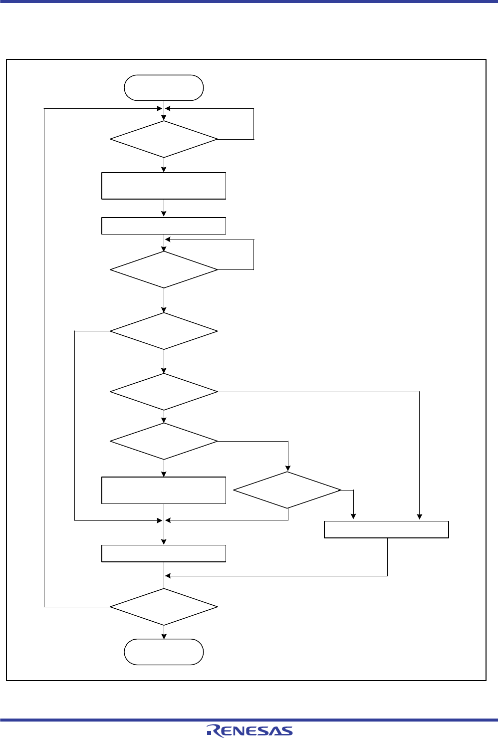
R01UH0034EJ0200 Rev.2.00 Page 1203 of 1489
Dec 27, 2013
RX62T Group, RX62G Group 26. Serial Peripheral Interface (RSPI)
Under development Preliminary document
Specifications in this document are tentative and subject to change.
(5) Transfer Operation Flowchart
Figure 26.35 is a flowchart illustrating a transfer in clock synchronous operation when the RSPI is used in master mode.
Figure 26.35 Transfer Operation Flowchart in Master Mode (Clock Synchronous Operation)
Copy transmit data from
transmit buffer to shift register
Copy received data from shift
register to receive buffer
RSPCK cycle count
Receive buffer status
Continue
serial transfer
Overrun error/
parity error status
Overrun error/
parity error status
Transmit buffer
status
Start serial transfer
Empty
Empty
No
Yes
Error occurred
Full
Full
No error
Error occurred
No error
Shorter than data length
Equal to data length
Update command pointer
Error handling
End of initialization
in master mode
End of transfer
Transmission and
reception/transmission
only
SPCR.TXMD = 1
SPCR.TXMD = 0

R01UH0034EJ0200 Rev.2.00 Page 1204 of 1489
Dec 27, 2013
RX62T Group, RX62G Group 26. Serial Peripheral Interface (RSPI)
Under development Preliminary document
Specifications in this document are tentative and subject to change.
26.3.11.2 Slave Mode Operation
(1) Starting a Serial Transfer
When the SPCR.SPMS bit is 1, the first RSPCK edge triggers the start of a serial transfer in the RSPI.
When detecting the start of a serial transfer in a condition in which the shift register is empty, the RSPI changes the status
of the shift register to "full", so that data cannot be copied from the transmit buffer to the shift register when serial
transfer is in progress. If the shift register was full before the serial transfer started, the RSPI keeps the status of the shift
register unchanged, in the full state.
When the SPCR.SPMS bit is 1, the RSPI always drives the MISO output signal.
For details on the RSPI transfer format, see section 26.3.4, Transfer Format. It should be noted that the SSL0 input
signal is not used in clock synchronous operation.
(2) Terminating a Serial Transfer
The RSPI terminates the serial transfer after detecting an RSPCK edge corresponding to the final sampling timing. When
free space is available in the receive buffer, upon termination of serial transfer the RSPI copies received data from the
shift register to the receive buffer of the RSPI data register (SPDR). Upon termination of a serial transfer the RSPI
changes the status of the shift register to "empty". The final sampling timing changes depending on the bit length of
transfer data. In slave mode, the RSPI data length depends on the SPCMD0.SPB[3:0] bit setting.
For details on the RSPI transfer format, see section 26.3.4, Transfer Format.
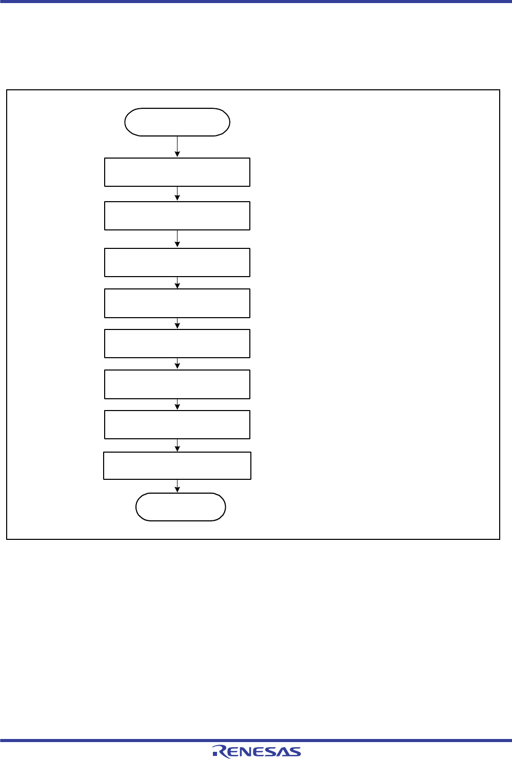
R01UH0034EJ0200 Rev.2.00 Page 1205 of 1489
Dec 27, 2013
RX62T Group, RX62G Group 26. Serial Peripheral Interface (RSPI)
Under development Preliminary document
Specifications in this document are tentative and subject to change.
(3) Initialization Flowchart
Figure 26.36 is a flowchart illustrating an example of initialization in clock synchronous operation when the RSPI is
used in slave mode. For a description of how to set up the interrupt controller, DTC, and input/output ports, see the
descriptions given in the individual blocks.
Figure 26.36 Example of Initialization Flowchart in Slave Mode (Clock Synchronous Operation)
Set RSPI data control
register (SPDCR)
Set RSPI command register 0
(SPCMD0)
Set input/output ports
Set RSPI control register
(SPCR)
Set interrupt controller
Set DTC
Start of initialization in
slave mode
End of initialization
in slave mode
• Sets number of frames to be used.
(when using an interrupt)
(when using the DTC)
• Sets MSB or LSB first.
• Sets data length.
• Sets clock phase.
• Sets clock polarity.
• Sets slave mode.
• Sets interrupt mask.
• Sets RSPI mode.
Set RSPI control register 2
(SPCR2) • Sets parity function.
• Sets interrupt mask.
Read RSPI control register
(SPCR)

R01UH0034EJ0200 Rev.2.00 Page 1206 of 1489
Dec 27, 2013
RX62T Group, RX62G Group 26. Serial Peripheral Interface (RSPI)
Under development Preliminary document
Specifications in this document are tentative and subject to change.
(4) Transfer Operation Flowcharts
Figure 26.37 is a flowchart illustrating a transfer when the RSPI is in clock synchronous operation.
Figure 26.37 Transfer Operation Flowchart in Slave Mode
(SPCMDm.CPHA = 1) (Clock Synchronous Operation)
Copy received data from the
shift register to the receive buffer
RSPCK cycle count
Receive buffer
status
Continue data
transfer
No
Yes
Overrun error/
parity error status
RSPCK input level
Empty
Error occurred
Full
No error
No change
No error
Changed
Error occurred
Shorter than data length
Equal to data length
Start serial transfer
MISO output
End of initialization
in slave mode
End of transfer
Overrun error/
parity error status
Error handling
Transmission and
reception/transmission
only
SPCR.TXMD = 1
SPCR.TXMD = 0
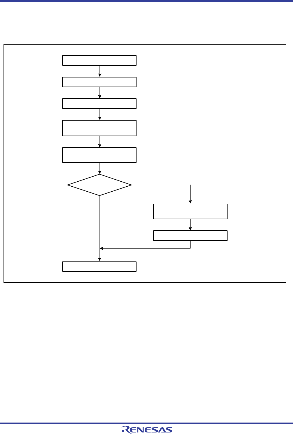
R01UH0034EJ0200 Rev.2.00 Page 1207 of 1489
Dec 27, 2013
RX62T Group, RX62G Group 26. Serial Peripheral Interface (RSPI)
Under development Preliminary document
Specifications in this document are tentative and subject to change.
26.3.12 Error Handling
Figure 26.38 to Figure 26.40 show error handling for the RSPI. The following error handling is used to return from the
error state after an error has occurred in master mode or slave mode.
Figure 26.38 Error Handling (Overrun Error)
Transmit buffer status
Overrun error occurred.
User handling
Holds data that has not been transmitted
Clear the OVRF flag in SPSR.
Read the receive data prior to the
occurrence of the overrun error.
Check that the PERF and OVRF
flags in SPSR are 0.
Clear the SPCR.SPE bit to
initialize
the internal sequencer.
Set the SPCR.SPE bit to 1.
End of overrun error handing
Empty

R01UH0034EJ0200 Rev.2.00 Page 1208 of 1489
Dec 27, 2013
RX62T Group, RX62G Group 26. Serial Peripheral Interface (RSPI)
Under development Preliminary document
Specifications in this document are tentative and subject to change.
Figure 26.39 Error Handling (Parity Error)
Figure 26.40 Error Handling (Mode Fault Error)
Transmit buffer status
Parity error occurred.
User handling
Holds data that has not been transmitted
Clear the SPSR.PERF flag.
Check that the PERF and OVRF
flags in SPSR are 0.
Clear the SPCR.SPE bit to
initialize the internal sequencer.
Set the SPCR.SPE bit to 1.
End of parity error handling
Empty
Mode fault error occurred.
User handling
Clear the SPSR.MODF bit to 0.
End of mode fault error handing
Set the SPCR.SPE bit to 1.
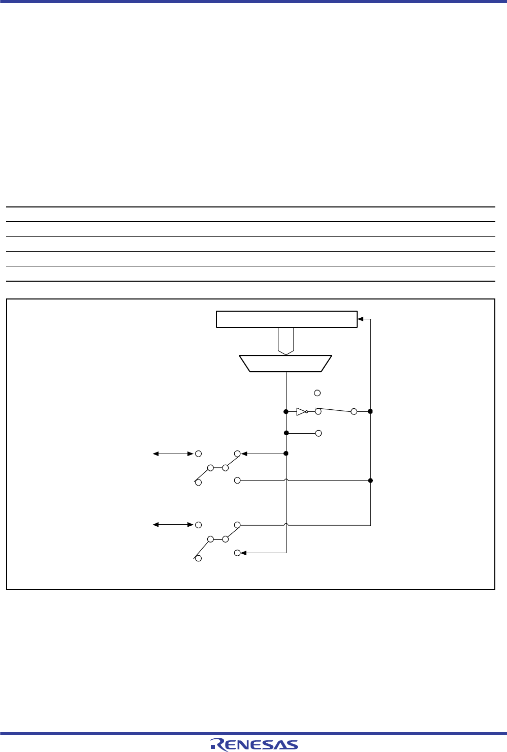
R01UH0034EJ0200 Rev.2.00 Page 1209 of 1489
Dec 27, 2013
RX62T Group, RX62G Group 26. Serial Peripheral Interface (RSPI)
Under development Preliminary document
Specifications in this document are tentative and subject to change.
26.3.13 Loopback Mode
When the CPU writes 1 to the SPPCR.SPLP2 bit or SPPCR.SPLP bit in loopback mode, the RSPI shuts off the path
between the MISO pin and the shift register if the SPCR.MSTR bit is 1, and between the MOSI pin and the shift register
if the SPCR.MSTR bit is 0, and connects the input path and output path of the shift register. The RSPI does not shut off
the path between the MOSI pin and the shift register if the SPCR.MSTR bit is 1, and between the MISO pin and the shift
register if the SPCR.MSTR bit is 0.
When a serial transfer is executed in loopback mode, the transmit data for the RSPI becomes the received data for the
RSPI.
Table 26.13 shows the relationship among the SPLP2 and SPLP bits in SPPCR and the received data. Figure 26.41
shows the configuration of the shift register input/output paths for the case where the RSPI in master mode is set in
loopback mode (SPPCR.SPLP2 = 0, SPPCR.SPLP = 1).
Figure 26.41 Configuration of Shift Register Input/Output Paths in Loopback Mode (Master Mode)
Table 26.13 SPPCR.SPLP2 and SPLP Bit Settings and Received Data
SPPCR.SPLP2 Bit SPPCR.SPLP Bit Received Data
0 0 Input data from the MOSIn pin or MISOn pin (n = A, B)
0 1 Reversed transmit data
1 0 Transmit data
1 1 Transmit data
MOSI
MISO
Shift register
Selector
Master
Slave
Normal
MasterNormal
Loopback
Loopback 2
Slave
Loopback
Loopback 2
Loopback
Normal
Loopback 2
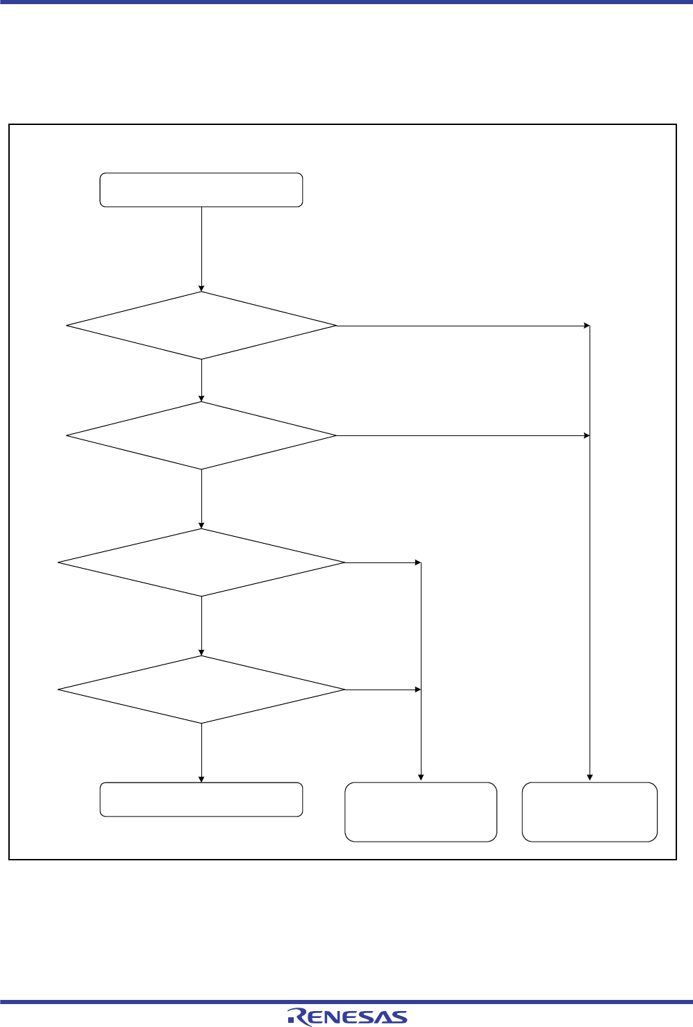
R01UH0034EJ0200 Rev.2.00 Page 1210 of 1489
Dec 27, 2013
RX62T Group, RX62G Group 26. Serial Peripheral Interface (RSPI)
Under development Preliminary document
Specifications in this document are tentative and subject to change.
26.3.14 Self-Diagnosis of Parity Bit Function
The parity circuit consists of a parity bit adding unit used for transmit data and an error detecting unit used for received
data. In order to detect defects in the parity bit adding unit and error detecting unit of the parity circuit, self-diagnosis is
executed for the parity circuit following the flowchart shown in Figure 26.42.
Figure 26.42 Flowchart for Self-Diagnosis of Parity Circuit
Start of self-diagnosis of parity circuit
Add correct parity bit to
transmit data and transfer it
Add incorrect parity bit to
transmit data and transfer it
Loopback operation with
the parity bit at normal operation added
Check the data that is stored in
the transmit data register
Normal end
No defect in parity circuit Erroneous end
Defect found in
parity bit adding unit
No defect in error detecting unit
Erroneous end
Defect found in error
detecting unit
Select full-duplex synchronous serial communications (SPCR.TXMD = 0).
Enable the parity circuit self-diagnosis function (SPCR2.PTE = 1).
Enable the parity function (SPCR2.SPPE = 1).
Select loopback operation (SPPCR.SPLP2 = 1).
Parity error occurred
No parity error
No parity error
Parity error occurred
Disable the parity circuit self-diagnosis function (SPCR2.PTE = 0).
Parity error occurred
No parity error
Correct parity bit is added
Incorrect parity bit is added

R01UH0034EJ0200 Rev.2.00 Page 1211 of 1489
Dec 27, 2013
RX62T Group, RX62G Group 26. Serial Peripheral Interface (RSPI)
Under development Preliminary document
Specifications in this document are tentative and subject to change.
26.3.15 Interrupt Sources
The RSPI has interrupt sources of receive buffer full, transmit buffer empty, mode fault, and RSPI idle. In addition, the
DTC can be activated by the receive buffer full or transmit buffer empty interrupt to perform data transfer.
Table 26.14 shows the RSPI interrupt sources. When any of the interrupt conditions in Table 26.14 is met, an interrupt
is generated. Clear the interrupt sources by data transfer.
When using the DTC to perform data transmission/reception, the DTC must be set up first to be in a status in which
transfer is enabled before making the RSPI settings. For the method for setting the DTC, refer to section 14, Data
Transfer Controller (DTC).
26.4 Usage Note
26.4.1 Transmit Operation when Parity Function is Enabled in Master Mode
To perform transmit operation with the parity bit added when the parity function is enabled in master mode, the
following settings of each command register should be set to the same value.
Transfer bit length setting of each command register
MSB-first/LSB-first setting of each command register
Table 26.14 Interrupt Sources of RSPI
Interrupt Source Abbreviation Interrupt Condition DTC Activation
Receive buffer full SPRI0 (sprie = 1) (Receive buffer full) O
Transmit buffer empty SPTI0 (sptie = 1) (Transmit buffer empty) O
Mode fault
Overrun
Parity error
SPEI0 (speie = 1) {(modf = 1) | (ovrf = 1) | (perf = 1)} —
RSPI idle SPII0 (spiie = 1) (idlnf = 0) —

R01UH0034EJ0200 Rev.2.00 Page 1212 of 1489
Dec 27, 2013
RX62T Group, RX62G Group 27. LIN Module (LIN)
Under development Preliminary document
Specifications in this document are tentative and subject to change.
27. LIN Module (LIN)
27.1 Overview
The LIN module is a hardware LIN communication controller that is compliant with LIN Specification Package
Revisions 1.3, 2.0, and 2.1, and it transmits and receives frames, and judges errors automatically. The LIN module
incorporates a 1-channel master controller.
Table 27.1 lists the specifications for the LIN module, and Figure 27.1 shows a block diagram of the LIN module.
Note 1. The interbyte space (header) has the same value as the response space since both spaces are set in the same register.
Note 2. Wake-up reception indicates the input signal Low time counting.
Table 27.1 Specifications of LIN Module
Item Specifications
Protocol LIN Specification Package Revisions 1.3, 2.0, and 2.1
Number of channels 1 channel (LIN master)
Variable frame configuration Transmit break width: 13 to 28 Tbits
Transmit break delimiter width: 1 to 4 Tbits
Interbyte space (header): 0 to 7 Tbits (space between Sync field and ID field)*1
Response space: 0 to 7 Tbits*1
Interbyte space: 0 to 3 Tbits (space between data bytes in response space)
Wake-up: 1 to 16 Tbits
Check sum Automatic calculation in both transmission and reception
Either classic check sum or enhanced check sum is selectable
(changeable at each frame)
Data bytes in response field Variable from 0 to 8 bytes
Frame transmission mode Mode in which a header and response are transmitted by a single transmit start request
Mode in which a header and response are transmitted by respective transmit start requests
(frame separate mode)
Wake-up transmission/reception Available in LIN wake-up mode
Wake-up transmission (1 to 16 Tbits)
Wake-up reception
Input signal Low time counting
Status Frame/wake-up transmit completion
Header transmit completion
Frame/wake-up receive completion*2
Data 1 receive completion
Error detection
Operating mode
(LIN reset mode, LIN wake-up mode, LIN operation mode, or LIN self-test mode)
Error status Bit error
Check sum error
Frame timeout error
Physical bus error
Framing error
Baud rate Selectable LIN-specified value generated by the baud rate generator
Test mode Self-test mode for user evaluation
Interrupt function Frame/wake-up transmit completion
Frame/wake-up receive completion*2
Error detection
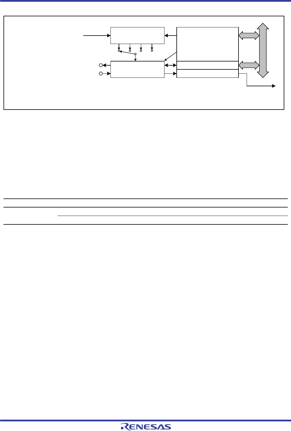
R01UH0034EJ0200 Rev.2.00 Page 1213 of 1489
Dec 27, 2013
RX62T Group, RX62G Group 27. LIN Module (LIN)
Under development Preliminary document
Specifications in this document are tentative and subject to change.
Figure 27.1 Block Diagram of LIN Module
LTX and LRX: I/O pins of the LIN module
Baud rate generator: Generates a communication clock for the LIN module
LIN common registers: Common registers for the LIN module
Interrupt control circuit: Controls the interrupt request (LIN interrupt) generated by the LIN module
Table 27.2 lists the I/O pins used in the LIN module.
Table 27.2 I/O Pins of LIN Module
Module Symbol Pin Name I/O Description
LIN0 LRX Input Input pin for the LIN communication function
LTX Output Output pin for the LIN communication function
LIN protocol controller
LIN interrupt
LTX
LRX
Baud rate generator
LIN common registers
Data bus
LIN exclusive use registers
Interrupt control circuit
LIN communication clock source*
fbfa fd
fc
LCKS
Note: * For the LIN communication clock source, refer to section 8, Clock Generation Circuit.

R01UH0034EJ0200 Rev.2.00 Page 1214 of 1489
Dec 27, 2013
RX62T Group, RX62G Group 27. LIN Module (LIN)
Under development Preliminary document
Specifications in this document are tentative and subject to change.
27.2 Register Descriptions
Table 27.3 shows the registers of the LIN module.
Table 27.3 Registers of LIN Module
Module
Symbol Register Name Symbol Value after Reset Address Access Size
LIN0 LIN wake-up baud rate select register LWBR 00h 0009 4001h 8
LIN baud rate prescaler 0 register LBRP0 00h 0009 4002h 8, 16
LIN baud rate prescaler 1 register LBRP1 00h 0009 4003h 8, 16
LIN self-test control register LSTC 00h 0009 4004h 8
Mode register L0MD 00h 0009 4008h 8, 16, 32
Break field setting register L0BRK 00h 0009 4009h 8, 16, 32
Space setting register L0SPC 00h 0009 400Ah 8, 16, 32
Wake-up setting register L0WUP 00h 0009 400Bh 8, 16, 32
Interrupt enable register L0IE 00h 0009 400Ch 8, 16
Error detection enable register L0EDE 00h 0009 400Dh 8, 16
Control register L0C 00h 0009 400Eh 8
Transmission control register L0TC 00h 0009 4010h 8, 16, 32
Mode status register L0MST 00h 0009 4011h 8, 16, 32
Status register L0ST 00h 0009 4012h 8, 16, 32
Error status register L0EST 00h 0009 4013h 8, 16, 32
Response field set register L0RFC 00h 0009 4014h 8, 16
Buffer register L0IDB Undefined 0009 4015h 8, 16
Check sum buffer register L0CBR Undefined 0009 4016h 8
Data 1 buffer register L0DB1 Undefined 0009 4018h 8, 16, 32
Data 2 buffer register L0DB2 Undefined 0009 4019h 8, 16, 32
Data 3 buffer register L0DB3 Undefined 0009 401Ah 8, 16, 32
Data 4 buffer register L0DB4 Undefined 0009 401Bh 8, 16, 32
Data 5 buffer register L0DB5 Undefined 0009 401Ch 8, 16, 32
Data 6 buffer register L0DB6 Undefined 0009 401Dh 8, 16, 32
Data 7 buffer register L0DB7 Undefined 0009 401Eh 8, 16, 32
Data 8 buffer register L0DB8 Undefined 0009 401Fh 8, 16, 32
R01UH0034EJ0200 Rev.2.00 Page 1215 of 1489
Dec 27, 2013
RX62T Group, RX62G Group 27. LIN Module (LIN)
Under development Preliminary document
Specifications in this document are tentative and subject to change.
27.2.1 LIN Wake-Up Baud Rate Select Register (LWBR)
LWBR register should be set in LIN reset mode.
LWBR0 Bit (Wake-up Baud Rate Select)
When LIN Specification Package Revision 1.3 is used, set the LWBR.LWBR0 bit to 0. This allows the input signal Low
time to be measured for 2.5 or more Tbits of fLIN. When LIN Specification Package Revisions 2.0 and 2.1 are used, set
the LWBR.LWBR0 bit to 1. This allows the input signal Low time to be measured for 130 s or more.
27.2.2 LIN Baud Rate Prescaler 0 Register (LBRP0)
LBRP0 register should be set in LIN reset mode.
27.2.3 LIN Baud Rate Prescaler 1 Register (LBRP1)
LBRP1 register should be set in LIN reset mode.
Address: 0009 4001h
b7 b6 b5 b4 b3 b2 b1 b0
———————LWBR0
Value after reset: 00000000
Bit Symbol Bit Name Description R/W
b0 LWBR0 Wake-up Baud Rate Select 0: When LIN1.3 is used
1: When LIN2.0 and 2.1 are used
R/W
b7 to b1 — Reserved These bits are read as 0. The write value should be 0. R/W
Address: 0009 4002h
b7 b6 b5 b4 b3 b2 b1 b0
Value after reset: 00000000
Bit Description Setting Range R/W
b7 to b0 The peripheral clock is divided by (N + 1) by the baud rate prescaler. (N = setting of 0 to 255) 00h to FFh R/W
Address: 0009 4003h
b7 b6 b5 b4 b3 b2 b1 b0
Value after reset: 00000000
Bit Description Setting Range R/W
b7 to b0 The peripheral clock is divided by (M + 1) by the baud rate prescaler. (M = setting of 0 to 255) 00h to FFh R/W

R01UH0034EJ0200 Rev.2.00 Page 1216 of 1489
Dec 27, 2013
RX62T Group, RX62G Group 27. LIN Module (LIN)
Under development Preliminary document
Specifications in this document are tentative and subject to change.
27.2.4 LIN Self-Test Control Register (LSTC)
LSTC register should be set in LIN reset mode.
LSTC register is used to unlock protection of LIN self-test mode.
When A7h, 58h, and 01h are consecutively written to this register, the LIN module enters LIN self-test mode.
If consecutive writing is successful and the LIN module has entered LIN self-test mode, the LSTM bit is set to 1. Do not
perform another writing while consecutive writing is in progress.
For details of transition to LIN self-test mode, refer to section 27.12.1, Entry into LIN Self-Test Mode.
LSTM Bit (Self-Test Mode)
This bit is set to 1 when the LIN module enters LIN self-test mode.
For details of how to exit LIN self-test mode, refer to section 27.12.1, Entry into LIN Self-Test Mode.
Other than consecutively writing A7h, 58h, and 01h to this register, writing 1 does not change the value of this bit.
Address: 0009 4004h
b7 b6 b5 b4 b3 b2 b1 b0
LSTM
Value after reset: 00000000
Bit Symbol Bit Name Description R/W
b7 to b1 When A7h, 58h, and 01h are consecutively written, the LIN module enters LIN self-test mode. R/W
b0 LSTM Self-Test Mode 0: Non-LIN self-test mode
1: LIN self-test mode
R/W

R01UH0034EJ0200 Rev.2.00 Page 1217 of 1489
Dec 27, 2013
RX62T Group, RX62G Group 27. LIN Module (LIN)
Under development Preliminary document
Specifications in this document are tentative and subject to change.
27.2.5 Mode Register (L0MD)
L0MD register should be set in LIN reset mode.
LCKS[1:0] Bits (LIN System Clock Select)
These bits select the clock to be input to the protocol controller.
When these bits are set to 00b, fa (clock generated by baud rate prescaler 0) is input to the protocol controller.
When these bits are to 01b, fb (clock generated by baud rate prescaler 0 is divided by 2) is input to the protocol
controller.
When these bits are to 10b, fc (clock generated by baud rate prescaler 0 is divided by 8) is input to the protocol controller.
When these bits are to 11b, fd (clock generated by baud rate prescaler 1 is divided by 2) is input to the protocol controller.
Address: 0009 4008h
b7 b6 b5 b4 b3 b2 b1 b0
————LCKS[1:0] ——
Value after reset: 00000000
Bit Symbol Bit Name Description R/W
b1, b0 — Reserved These bits are read as 0. The write value should be 0. R/W
b3, b2 LCKS[1:0] LIN System Clock Select b3 b2
0 0 : fa (clock generated by baud rate prescaler 0)
0 1 : fb (clock generated by baud rate prescaler 0 is divided by 2)
1 0 : fc (clock generated by baud rate prescaler 0 is divided by 8)
1 1 : fd (clock generated by baud rate prescaler 1 is divided by 2)
R/W
b7 to b4 — Reserved These bits are read as 0. The write value should be 0. R/W

R01UH0034EJ0200 Rev.2.00 Page 1218 of 1489
Dec 27, 2013
RX62T Group, RX62G Group 27. LIN Module (LIN)
Under development Preliminary document
Specifications in this document are tentative and subject to change.
27.2.6 Break Field Setting Register (L0BRK)
L0BRK register should be set in LIN reset mode.
The length of one frame may exceed the frame timeout period depending on the combination of settings. Make sure to set
appropriate values.
BLT[3:0] Bits (Transmit Break (Low) Width Setting)
These bits set the (Low) time pulse width for a break in the transmit frame header.
A value from 13 Tbits to 28 Tbits can be set.
BDT[1:0] Bits (Transmit Break Delimiter (High) Width Setting)
These bits set the (High) time pulse width for a break delimiter in the transmit frame header.
A value from 1 Tbit to 4 Tbits can be set.
Address: 0009 4009h
b7 b6 b5 b4 b3 b2 b1 b0
— — BDT[1:0] BLT[3:0]
Value after reset: 00000000
Bit Symbol Bit Name Description R/W
b3 to b0 BLT[3:0] Transmit Break (Low) Width Setting b3 b0
0 0 0 0: 13 Tbits
0 0 0 1: 14 Tbits
0 0 1 0: 15 Tbits
:
1 1 1 0: 27 Tbits
1 1 1 1: 28 Tbits
R/W
b5, b4 BDT[1:0] Transmit Break Delimiter (High) Width
Setting
b5 b4
0 0 : 1 Tbit
0 1 : 2 Tbits
1 0 : 3 Tbits
1 1 : 4 Tbits
R/W
b7, b6 — Reserved These bits are read as 0. The write value should be 0. R/W

R01UH0034EJ0200 Rev.2.00 Page 1219 of 1489
Dec 27, 2013
RX62T Group, RX62G Group 27. LIN Module (LIN)
Under development Preliminary document
Specifications in this document are tentative and subject to change.
27.2.7 Space Setting Register (L0SPC)
L0SPC register should be set in LIN reset mode.
This register is enabled only for transmission (header and response). In response reception, this register is disabled.
The length of one frame may exceed the frame timeout period depending on the combination of settings. Make sure to set
appropriate values.
IBSH[2:0] Bits (Interbyte Space (Header)/Response Space Setting)
These bits set the width of the interbyte space (header) and response space required for the transmit frame header.
A value from 0 Tbit to 7 Tbits can be set.
The values of the interbyte space (header) and response space are the same.
IBS[1:0] Bits (Interbyte Space Setting)
These bits set the width of the interbyte space required for the transmit frame response.
A value from 0 Tbit to 3 Tbits can be set.
Address: 0009 400Ah
b7 b6 b5 b4 b3 b2 b1 b0
— — IBS[1:0] — IBSH[2:0]
Value after reset: 00000000
Bit Symbol Bit Name Description R/W
b2 to b0 IBSH[2:0] Interbyte Space (Header)/
Response Space Setting
b2 b0
0 0 0 : 0 Tbit
0 0 1 : 1 Tbit
0 1 0 : 2 Tbits
0 1 1 : 3 Tbits
1 0 0 : 4 Tbits
1 0 1 : 5 Tbits
1 1 0 : 6 Tbits
1 1 1 : 7 Tbits
R/W
b3 — Reserved This bit is read as 0. The write value should be 0. R/W
b5, b4 IBS[1:0] Interbyte Space Setting b5 b4
0 0 : 0 Tbit
0 1 : 1 Tbit
1 1 : 2 Tbits
1 1 : 3 Tbits
R/W
b7, b6 — Reserved These bits are read as 0. The write value should be 0. R/W

R01UH0034EJ0200 Rev.2.00 Page 1220 of 1489
Dec 27, 2013
RX62T Group, RX62G Group 27. LIN Module (LIN)
Under development Preliminary document
Specifications in this document are tentative and subject to change.
27.2.8 Wake-Up Setting Register (L0WUP)
L0WUP register should be set in LIN reset mode.
WUTL[3:0] Bits (Wake-up Transmission Low Width Setting)
These bits set the Low time pulse width of wake-up transmission.
A value from 1 Tbit to 16 Tbits can be set.
Address: 0009 400Bh
b7 b6 b5 b4 b3 b2 b1 b0
WUTL[3:0] — — — —
Value after reset: 00000000
Bit Symbol Bit Name Description R/W
b3 to b0 — Reserved These bits are read as 0. The write value should be 0. R/W
b7 to b4 WUTL[3:0] Wake-up Transmission Low Width Setting b7 b4
0 0 0 0 : 1 Tbit
0 0 0 1 : 2 Tbits
0 0 1 0 : 3 Tbits
0 0 1 1 : 4 Tbits
:
1 1 0 0 : 13 Tbits
1 1 0 1 : 14 Tbits
1 1 1 0 : 15 Tbits
1 1 1 1 : 16 Tbits
R/W

R01UH0034EJ0200 Rev.2.00 Page 1221 of 1489
Dec 27, 2013
RX62T Group, RX62G Group 27. LIN Module (LIN)
Under development Preliminary document
Specifications in this document are tentative and subject to change.
27.2.9 Interrupt Enable Register (L0IE)
L0IE register should be set in LIN reset mode.
FTCIE Bit (Frame/Wake-up Transmit Completion Interrupt Enable)
This bit enables or disables an interrupt when a frame or wake-up frame transmission is completed.
When this bit is set to 0, a LIN interrupt is not generated when the L0ST.FTC flag becomes 1.
When this bit is set to 1, a LIN interrupt is generated when the L0ST.FTC flag becomes 1.
FRCIE Bit (Frame/Wake-up Receive Completion Interrupt Enable)
This bit enables or disables an interrupt when a frame or wake-up frame reception is completed.
When this bit is set to 0, a LIN interrupt is not generated when the L0ST.FRC flag becomes 1.
When this bit is set to 1, a LIN interrupt is generated when the L0ST.FRC flag becomes 1.
ERRIE Bit (Error Detection Interrupt Enable)
This bit enables or disables an interrupt when an error is detected.
When this bit is set to 0, a LIN interrupt is not generated when the L0ST.ERR flag becomes 1.
When this bit is set to 1, a LIN interrupt is generated when the L0ST.ERR flag becomes 1.
The sources to generate the LIN interrupt are the following interrupts: bit error, physical bus error, frame timeout error,
framing error, and check sum error.
The detection of a bit error, physical bus error, frame timeout error, and framing error can be enabled or disabled by
L0EDE.
Address: 0009 400Ch
b7 b6 b5 b4 b3 b2 b1 b0
—————ERRIEFRCIEFTCIE
Value after reset: 00000000
Bit Symbol Bit Name Description R/W
b0 FTCIE Frame/Wake-up Transmit
Completion Interrupt Enable
0: Frame/wake-up transmit completion interrupt is disabled
1: Frame/wake-up transmit completion interrupt is enabled
R/W
b1 FRCIE Frame/Wake-up Receive
Completion Interrupt Enable
0: Frame/wake-up receive completion interrupt is disabled
1: Frame/wake-up receive completion interrupt is enabled
R/W
b2 ERRIE Error Detection Interrupt Enable 0: Error detection interrupt is disabled
1: Error detection interrupt is enabled
R/W
b7 to b3 — Reserved These bits are read as 0. The write value should be 0. R/W

R01UH0034EJ0200 Rev.2.00 Page 1222 of 1489
Dec 27, 2013
RX62T Group, RX62G Group 27. LIN Module (LIN)
Under development Preliminary document
Specifications in this document are tentative and subject to change.
27.2.10 Error Detection Enable Register (L0EDE)
L0EDE register should be set in LIN reset mode.
BERE Bit (Bit Error Detection Enable)
This bit enables or disables bit error detection.
When this bit is set to 0, no bit error is detected.
When this bit is set to 1, a bit error is detected.
The detection result when this bit is 1 is reflected in the L0EST.BER flag.
For details on a bit error, refer to section 27.10, Error Status.
PBERE Bit (Physical Bus Error Detection Enable)
This bit enables or disables physical bus error detection.
When this bit is set to 0, no physical bus error is detected.
When this bit is set to 1, a physical bus error is detected.
The detection result when this bit is 1 is reflected in the L0EST.PBER flag.
For details on a physical bus error, refer to section 27.10, Error Status.
FTERE Bit (Frame Timeout Error Detection Enable)
This bit enables or disables frame timeout error detection.
When this bit is set to 0, no frame timeout error is detected.
When this bit is set to 1, a frame timeout error is detected.
The detection result when this bit is 1 is reflected in the L0EST.FTER flag.
For details on a frame timeout error, refer to section 27.10, Error Status.
FERE Bit (Framing Error Detection Enable)
This bit enables or disables framing error detection.
When this bit is set to 0, no framing error is detected.
When this bit is set to 1, a framing error is detected.
The detection result when this bit is 1 is reflected in the L0EST.FER flag.
For details on a framing error, refer to section 27.10, Error Status.
Address: 0009 400Dh
b7 b6 b5 b4 b3 b2 b1 b0
————FEREFTEREPBEREBERE
Value after reset: 00000000
Bit Symbol Bit Name Description R/W
b0 BERE Bit Error Detection Enable 0: Bit error detection is disabled
1: Bit error detection is enabled
R/W
b1 PBERE Physical Bus Error Detection Enable 0: Physical bus error detection is disabled
1: Physical bus error detection is enabled
R/W
b2 FTERE Frame Timeout Error Detection Enable 0: Frame timeout error detection is disabled
1: Frame timeout error detection is enabled
R/W
b3 FERE Framing Error Detection Enable 0: Framing error detection is disabled
1: Framing error detection is enabled
R/W
b7 to b4 — Reserved These bits are read as 0. The write value should be 0. R/W

R01UH0034EJ0200 Rev.2.00 Page 1223 of 1489
Dec 27, 2013
RX62T Group, RX62G Group 27. LIN Module (LIN)
Under development Preliminary document
Specifications in this document are tentative and subject to change.
27.2.11 Control Register (L0C)
When the LIN module exits LIN reset mode, this register should be set to 01h to enter LIN wake-up mode and 03h to
enter LIN operation mode.
In LIN self-test mode, this register should be set to 03h after the LIN module enters LIN self-test mode.
OM0 Bit (LIN Reset)
This bit selects whether the LIN module enters or exits LIN reset mode.
When this bit is set to 0, the LIN module enters LIN reset mode.
When this bit is set to 1, the LIN module exits LIN reset mode.
OM1 Bit (LIN Mode Select)
This bit selects the LIN operating mode (LIN wake-up mode or LIN operation mode) when the LIN module exits LIN
reset mode.
When this bit is set to 0, the LIN module enters LIN wake-up mode.
When this bit is set to 1, the LIN module enters LIN operation mode.
This register is enabled only when the L0MST.OMM0 bit is set to 1.
This bit cannot be written to while the L0TC.FTS bit is 1.
Address: 0009 400Eh
b7 b6 b5 b4 b3 b2 b1 b0
——————OM1OM0
Value after reset: 00000000
Bit Symbol Bit Name Description R/W
b0 OM0 LIN Reset 0: LIN reset mode
1: Non-LIN reset mode
R/W
b1 OM1 LIN Mode Select 0: LIN wake-up mode
1: LIN operation mode
R/W
b7 to b2 — Reserved These bits are read as 0. The write value should be 0. R/W

R01UH0034EJ0200 Rev.2.00 Page 1224 of 1489
Dec 27, 2013
RX62T Group, RX62G Group 27. LIN Module (LIN)
Under development Preliminary document
Specifications in this document are tentative and subject to change.
27.2.12 Transmission Control Register (L0TC)
FTS Bit (Frame Transmission/Wake-up Transmission and Reception Start)
Set this bit to 1 when a frame/wake-up transmission starts.
Set this bit to 1 to perform a wake-up reception (input signal Low time counting).
This bit is set to 1 during communication. It becomes 0 when there is no communication or when the LIN module enters
LIN reset mode.
This bit can be set to 1 only. It cannot be set to 0. This bit automatically becomes 0 when the transmission is completed.
RTS Bit (Response Transmission Start)
Set this bit to 1 when a response transmission starts.
This bit is set to 1 during communication. It becomes 0 when there is no communication or when the LIN module enters
LIN reset mode.
This bit can be set to 1 only. It cannot be set to 0. This bit automatically becomes 0 when the transmission is completed.
When setting the RTS bit to 1, use an MOV instruction to write 02h to the register.
Set this bit when the L0RFC.FSM bit is 1 (frame separate mode) and the FTS bit is 1 (frame transmission/wake-up
transmission and reception started).
Address: 0009 4010h
b7 b6 b5 b4 b3 b2 b1 b0
——————RTSFTS
Value after reset: 00000000
Bit Symbol Bit Name Description R/W
b0 FTS Frame Transmission/Wake-up
Transmission and Reception Start
0: Frame transmission/wake-up transmission and reception is
stopped
1: Frame transmission/wake-up transmission and reception is
started
R/W
b1 RTS Response Transmission Start 0: Response transmission in frame separate mode is stopped
1: Response transmission in frame separate mode is started
R/W
b7 to b2 — Reserved These bits are read as 0. The write value should be 0. R/W

R01UH0034EJ0200 Rev.2.00 Page 1225 of 1489
Dec 27, 2013
RX62T Group, RX62G Group 27. LIN Module (LIN)
Under development Preliminary document
Specifications in this document are tentative and subject to change.
27.2.13 Mode Status Register (L0MST)
OMM0 Bit (LIN0 Reset Status Monitor)
OMM1 Bit (LIN0 Mode Status Monitor)
These bits are used to check the current operating mode.
Address: 0009 4011h
b7 b6 b5 b4 b3 b2 b1 b0
——————OMM1OMM0
Value after reset: 00000000
Bit Symbol Bit Name Description R/W
b0 OMM0 LIN0 Reset Status Monitor 0: LIN0 reset mode
1: Non-LIN0 reset mode
R
b1 OMM1 LIN0 Mode Status Monitor 0: LIN0 wake-up mode
1: LIN0 operation mode
R
b7 to b2 — Reserved These bits are read as 0. The write value should be 0. R/W

R01UH0034EJ0200 Rev.2.00 Page 1226 of 1489
Dec 27, 2013
RX62T Group, RX62G Group 27. LIN Module (LIN)
Under development Preliminary document
Specifications in this document are tentative and subject to change.
27.2.14 Status Register (L0ST)
L0ST register automatically becomes 00h when the LIN module enters LIN reset mode or when the next communication
starts.
This register retains 00h during LIN reset mode.
L0ST cannot be written to while the L0TC.FTS flag is 1 (frame transmission/wake-up transmission and reception
started).
FTC Flag (Frame/Wake-up Transmit Completion Flag)
Only 0 can be written to this bit. When 1 is written to this bit, the value before the write is retained.
This bit becomes 1 when a frame or wake-up transmission is completed. An interrupt is generated if the L0IE.FTCIE bit
is set to 1 (interrupt enabled) at this time. To set this bit to 0 before the next communication starts, write 0 to this bit in
LIN operation mode.
FRC Flag (Frame/Wake-up Receive Completion Flag)
Only 0 can be written to this bit. When 1 is written to this bit, the value before the write is retained.
This bit becomes 1 when a frame or wake-up reception is completed. An interrupt is generated if the L0IE.FRCIE bit is
set to 1 (interrupt enabled) at this time. To set this bit to 0 before the next communication starts, write 0 to this bit in LIN
operation mode.
ERR Flag (Error Detection Flag)
This bit becomes 1 when an error is detected. An interrupt is generated if the L0IE.ERRIE bit is set to 1 (interrupt
enabled) at this time. To set this bit to 0 before the next communication starts, write 0 to the L0EST.CSER, FER, FTER,
PBER, and BER flags in LIN operation mode. This will make the ERR flag become 0.
D1RC Flag (Data 1 Receive Completion Flag)
Only 0 can be written to this bit. When 1 is written to this bit, the value before the write is retained.
This bit becomes 1 when a data 1 reception is completed, but no interrupt is generated. To set this bit to 0 before the next
communication starts, write 0 to this bit in LIN operation mode.
Address: 0009 4012h
b7 b6 b5 b4 b3 b2 b1 b0
HTRC D1RC — — ERR — FRC FTC
Value after reset: 00000000
Bit Symbol Bit Name Description R/W
b0 FTC Frame/Wake-up Transmit
Completion Flag
0: Transmission is uncompleted
1: Frame or wake-up transmission has been completed
R/W
b1 FRC Frame/Wake-up Receive
Completion Flag
0: Reception is uncompleted
1: Frame or wake-up reception has been completed
R/W
b2 — Reserved This bit is read as 0. The write value should be 0. R/W
b3 ERR Error Detection Flag 0: Error is not detected
1: Error has been detected
R
b5, b4 — Reserved These bits are read as 0. The write value should be 0. R/W
b6 D1RC Data 1 Receive Completion Flag 0: Reception is uncompleted
1: Data 1 reception has been completed
R/W
b7 HTRC Header Transmit Completion Flag 0: Transmission is uncompleted
1: Header transmission has been completed
R/W

R01UH0034EJ0200 Rev.2.00 Page 1227 of 1489
Dec 27, 2013
RX62T Group, RX62G Group 27. LIN Module (LIN)
Under development Preliminary document
Specifications in this document are tentative and subject to change.
HTRC Flag (Header Transmit Completion Flag)
Only 0 can be written to this bit. When 1 is written to this bit, the value before the write is retained.
This bit becomes 1 when a header reception is completed, but no interrupt is generated. To set this bit to 0 before the next
communication starts, write 0 to this bit in LIN operation mode.
27.2.15 Error Status Register (L0EST)
L0EST register automatically becomes 00h when the LIN module enters LIN reset mode or when the next
communication starts.
This register retains 00h during LIN reset mode.
L0EST cannot be written to while the L0TC.FTS flag is 1 (frame transmission/wake-up transmission and reception
started).
BER Flag (Bit Error Flag)
Only 0 can be written to this bit. When 1 is written to this bit, the value before the write is retained.
This bit becomes 1 when a bit error is detected. To set this bit to 0 before the next communication starts, write 0 to this bit
in LIN operation mode.
PBER Flag (Physical Bus Error Flag)
Only 0 can be written to this bit. When 1 is written to this bit, the value before the write is retained.
This bit becomes 1 when a physical bus error is detected. To set this bit to 0 before the next communication starts, write
0 to this bit in LIN operation mode.
Address: 0009 4013h
b7 b6 b5 b4 b3 b2 b1 b0
— — CSER — FER FTER PBER BER
Value after reset: 00000000
Bit Symbol Bit Name Description R/W
b0 BER Bit Error Flag 0: Bit error is not detected
1: Bit error has been detected
R/W
b1 PBER Physical Bus Error Flag 0: Physical bus error is not detected
1: Physical bus error has been detected
R/W
b2 FTER Frame Timeout Error Flag 0: Frame timeout error is not detected
1: Frame timeout error has been detected
R/W
b3 FER Framing Error Flag 0: Framing error is not detected
1: Framing error has been detected
R/W
b4 — Reserved This bit is read as 0. The write value should be 0. R/W
b5 CSER Check Sum Error Flag 0: Check sum error is not detected
1: Check sum error has been detected
R/W
b7, b6 — Reserved These bits are read as 0. The write value should be 0. R/W

R01UH0034EJ0200 Rev.2.00 Page 1228 of 1489
Dec 27, 2013
RX62T Group, RX62G Group 27. LIN Module (LIN)
Under development Preliminary document
Specifications in this document are tentative and subject to change.
FTER Flag (Frame Timeout Error Flag)
Only 0 can be written to this bit. When 1 is written to this bit, the value before the write is retained.
This bit becomes 1 when a frame timeout error is detected. To set this bit to 0 before the next communication starts, write
0 to this bit in LIN operation mode.
FER Flag (Framing Error Flag)
Only 0 can be written to this bit. When 1 is written to this bit, the value before the write is retained.
This bit becomes 1 when a framing error is detected. To set this bit to 0 before the next communication starts, write 0 to
this bit in LIN operation mode.
CSER Flag (Check Sum Error Flag)
Only 0 can be written to this bit. When 1 is written to this bit, the value before the write is retained.
This bit becomes 1 when a check sum error is detected. To set this bit to 0 before the next communication starts, write 0
to this bit in LIN operation mode.

R01UH0034EJ0200 Rev.2.00 Page 1229 of 1489
Dec 27, 2013
RX62T Group, RX62G Group 27. LIN Module (LIN)
Under development Preliminary document
Specifications in this document are tentative and subject to change.
27.2.16 Response Field Set Register (L0RFC)
L0RFC register should be set when the L0TC.FTS bit is 0 (frame transmission/wake-up transmission and reception
stopped).
RFDL[3:0] Bits (Response Field Data Length Setting)
These bits set the data length of the response field.
The data length can be set from 0 to 8 bytes, and the check sum size is not included in the data length.
RFT Bit (Response Field Transmit/Receive Direction Setting)
When this bit is set to 0, a response is received by the response field. In LIN wake-up mode, a wake-up is received (input
signal Low time counting).
When this bit is set to 1, a response is transmitted by the response field. In LIN wake-up mode, a wake-up is transmitted.
CSM Bit (Check Sum Select)
This bit sets the check sum mode.
When this bit is set to 0, classic check sum is selected.
When this bit is set to 1, enhanced check sum is selected.
If a frame timeout error is used (L0EDE.FTERE bit is 1), the frame timeout period differs according to the CSM bit
setting. For details, refer to section 27.10, Error Status.
FSM Bit (Frame Separate Mode Select)
When this bit is set to 0, frame separate mode is not selected.
When this bit is set to 1, frame separate mode is selected.
In response reception (RFT bit is 0), the FSM bit setting has no effect on operation.
When making a transition to LIN self-test mode, set this bit to 0 before transition.
For details on frame separate mode, refer to section 27.7.1.1, Frame Separate Mode.
Address: 0009 4014h
b7 b6 b5 b4 b3 b2 b1 b0
— FSM CSM RFT RFDL[3:0]
Value after reset: 00000000
Bit Symbol Bit Name Description R/W
b3 to b0 RFDL[3:0] Response Field Data Length Setting b3 b0
0 0 0 0 : 0 byte + check sum
0 0 0 1 : 1 byte + check sum
0 0 1 0 : 2 bytes + check sum
:
0 1 1 1 : 7 bytes + check sum
1 0 0 0 : 8 bytes + check sum
Settings other than above are prohibited.
R/W
b4 RFT Response Field Transmit/Receive
Direction Setting
0: Reception
1: Transmission
R/W
b5 CSM Check Sum Select 0: Classic check sum
1: Enhanced check sum
R/W
b6 FSM Frame Separate Mode Select 0: Non-frame separate mode
1: Frame separate mode
R/W
b7 — Reserved This bit is read as 0. The write value should be 0. R/W

R01UH0034EJ0200 Rev.2.00 Page 1230 of 1489
Dec 27, 2013
RX62T Group, RX62G Group 27. LIN Module (LIN)
Under development Preliminary document
Specifications in this document are tentative and subject to change.
27.2.17 ID Buffer Register (L0IDB)
L0IDB register should be set when the L0TC.FTS bit is 0 (frame transmission/wake-up transmission and reception
stopped).
In LIN self-test mode, the settings are as follows.
When the L0RFC.RFT bit = 1 (transmission)
The inverted value of the transmitted value can be read. The value to be transmitted can be written before
communication.
When the L0RFC.RFT bit = 0 (reception)
The inverted value of the received value can be read. The value to be received can be written before communication.
ID Bit (ID Setting)
These bits set a 6-bit ID to be transmitted by the ID field in a LIN frame.
IDP Bit (Parity Setting)
These bits set the parity bits (P0 and P1) to be transmitted by the ID field in a LIN frame.
Since the parity is not automatically calculated, set the calculated value. Even if an erroneous calculation result is set, the
set value will be transmitted.
Address: 0009 4015
b7 b6 b5 b4 b3 b2 b1 b0
IDP ID
Value after reset: 00000000
Bit Symbol Bit Name Description R/W
b5 to b0 ID ID Setting Set a 6-bit ID value to be transmitted by the ID field. R/W
b7, b6 IDP Parity Setting Set the parity bits (P) to be transmitted by the ID field. R/W

R01UH0034EJ0200 Rev.2.00 Page 1231 of 1489
Dec 27, 2013
RX62T Group, RX62G Group 27. LIN Module (LIN)
Under development Preliminary document
Specifications in this document are tentative and subject to change.
27.2.18 Check Sum Buffer Register (L0CBR)
L0CBR register should be set when the L0TC.FTS bit is 0 (frame transmission/wake-up transmission and reception
stopped).
In LIN operation mode, the settings are as follows.
When the L0RFC.RFT bit = 1 (transmission)
The transmitted value can be read. Writing is disabled.
When the L0RFC.RFT bit = 0 (reception)
The received value can be read. Writing is disabled.
In LIN self-test mode, the settings are as follows.
When the L0RFC.RFT bit = 1 (transmission)
The inverted value of the transmitted value can be read. Writing is disabled.
When the L0RFC.RFT bit = 0 (reception)
The inverted value of the received value can be read. The value to be received can be written before communication.
Address: 0009 4016h
b7 b6 b5 b4 b3 b2 b1 b0
Value after reset: 00000000
Bit Description R/W
b7 to b0 Store the check sum data to be transmitted and received. R/W

R01UH0034EJ0200 Rev.2.00 Page 1232 of 1489
Dec 27, 2013
RX62T Group, RX62G Group 27. LIN Module (LIN)
Under development Preliminary document
Specifications in this document are tentative and subject to change.
27.2.19 Data n Buffer Register (L0DBn) (n = 1 to 8)
L0DBn register should be set in the following states.
In response transmission:
L0RFC.RFT bit = 1 (transmission)
L0RFC.FSM bit = 0 (non-frame separate mode)
L0TC.FTS bit = 0 (frame transmission/wake-up transmission and reception stopped)
or
L0RFC.RFT bit = 1 (transmission)
L0RFC.FSM bit = 1 (frame separate mode)
L0TC.RTS bit = 0 (response transmission stopped)
In response reception:
The received data is overwritten. When an error is detected, data up to the point where the reception was aborted is
stored.
In LIN self-test mode, the settings are as follows.
When the L0RFC.RFT bit = 1 (transmission)
The inverted value of the transmitted value can be read. The value to be transmitted can be written before
communication.
When the L0RFC.RFT bit = 0 (reception)
The inverted value of the received value can be read. The value to be received can be written before communication.
Address: L0DB1 0009 4018h, L0DB2 0009 4019h, L0DB3 0009 401Ah, L0DB4 0009 401Bh,
L0DB5 0009 401Ch, L0DB6 0009 401Dh, L0DB7 0009 401Eh, L0DB8 0009 401Fh
b7 b6 b5 b4 b3 b2 b1 b0
Value after reset: 00000000
Bit Description Setting Range R/W
b7 to b0 Set the data to be transmitted or read the received data. 00h to FFh R/W
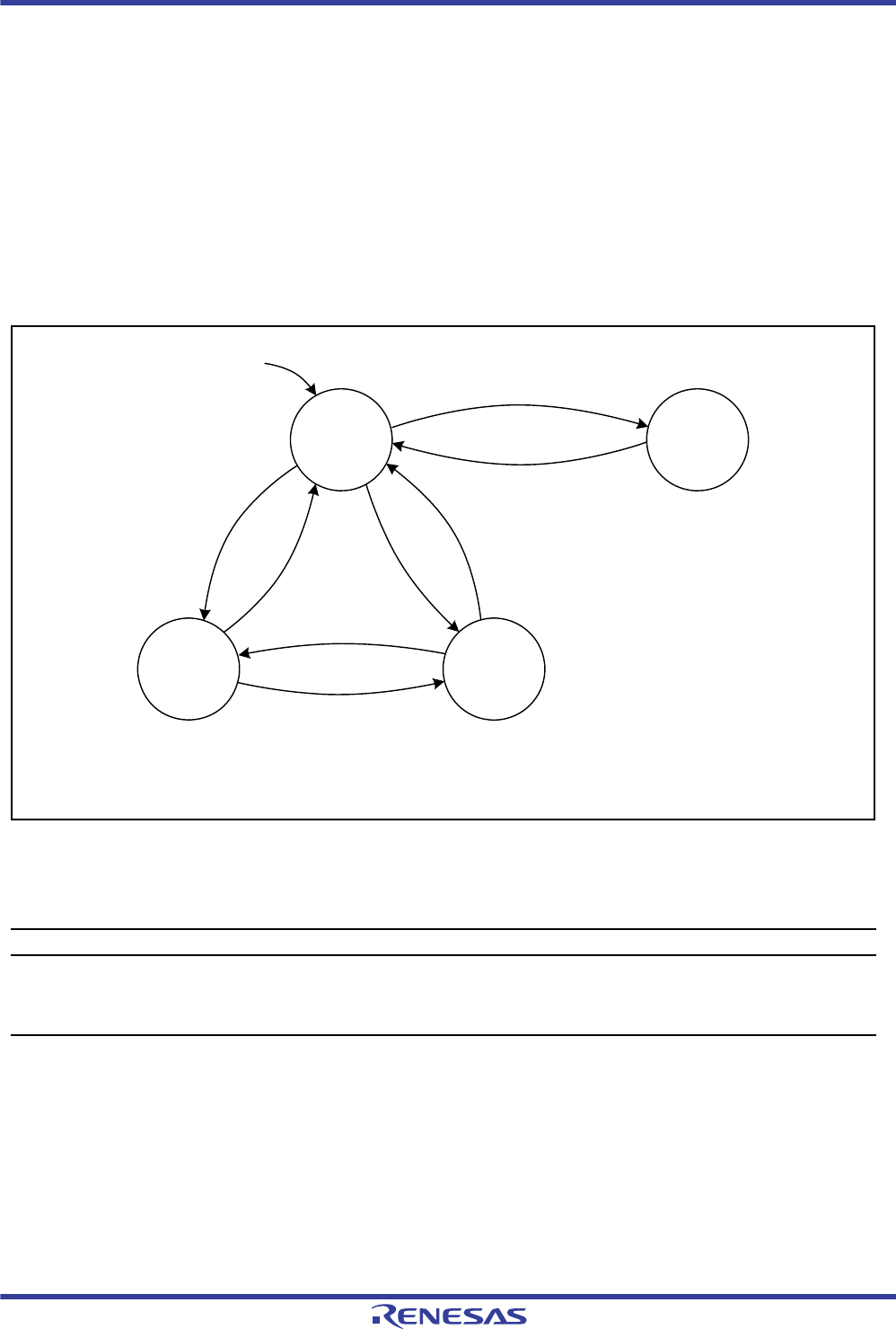
R01UH0034EJ0200 Rev.2.00 Page 1233 of 1489
Dec 27, 2013
RX62T Group, RX62G Group 27. LIN Module (LIN)
Under development Preliminary document
Specifications in this document are tentative and subject to change.
27.3 Operating Mode
The LIN module has the following four operating modes:
LIN reset mode
LIN operation mode
LIN wake-up mode
LIN self-test mode
In LIN reset mode, the power consumption can be reduced since the clock is not provided to the LIN module.
Figure 27.2 shows the transition processes between LIN operating modes, and Table 27.4 lists functions available in
each operating mode.
Figure 27.2 Operating Mode Transition
The transition to LIN reset mode, LIN operation mode, and LIN wake-up mode can be checked by reading the
L0MST.OMM1, OMM0 bits.
For details on LIN self-test mode, refer to section 27.12, LIN Self-Test Mode.
Table 27.4 Available Functions in Each Operating Mode
LIN Operation Mode LIN Wake-up Mode LIN Self-Test Mode
Header transmission
Response transmission
Response reception
Error detection
Wake-up transmission
Wake-up reception
Error detection
Self-test
L0C.OM1, OM0 = 00b
L0C.OM1, OM0 = 10b
CPU reset
LIN reset
mode
LIN operation
mode
LIN wake-up
mode
L0C.OM1, OM0 = 01b
L0C.OM1, OM0 = 11b
L0C.OM1, OM0 = 01b
L0C.OM1, OM0 = 11b
LIN self-test
mode
*
Note: * For details, refer to section 27.12, LIN Self-Test Mode.
*

R01UH0034EJ0200 Rev.2.00 Page 1234 of 1489
Dec 27, 2013
RX62T Group, RX62G Group 27. LIN Module (LIN)
Under development Preliminary document
Specifications in this document are tentative and subject to change.
27.3.1 LIN Reset Mode
LIN reset mode is activated by setting the L0C.OM1, OM0 bits to 00b or 10b (LIN reset mode), and the transition to LIN
reset mode can be checked when the L0C.OM1, OM0 bits become 00b or 10b (LIN reset mode). In this mode, all LIN
communication functions are stopped as well as fLIN.
The LIN module can enter LIN operation mode, LIN wake-up mode, or LIN self-test mode from LIN reset mode.
The following registers are initialized to their reset values after the LIN module enters LIN reset mode. The registers
retain their initial values during LIN reset mode.
L0TC
L0ST
L0EST
The following registers retain their previous values even after the LIN module enters LIN reset mode.
LWBR
LBRP0
LBRP1
LSTC (LSTC.LSTM bit only)
L0MD
L0BRK
L0SPC
L0WUP
L0IE
L0EDE
L0RFC
L0IDB
L0DBn (n = 1 to 8)
27.3.2 LIN Operation Mode
LIN operation mode is activated by setting the L0C.OM1, OM0 bits to 11b, and the L0MST.OMM1, OMM0 bits become
11b.Set the transmit data after the L0MST bits have been set to 11b.
27.3.3 LIN Wake-up Mode
LIN wake-up mode is activated by setting the L0C.OM1, OM0 bits to 01b, and the L0MST.OMM1, OMM0 bits become
01b.
27.3.4 LIN Self-Test Mode
LIN self-test mode is activated by writing to the LSTC register, and the transition to LIN self-test mode can be checked
when the LSTC.LSTM bit is set to 1.
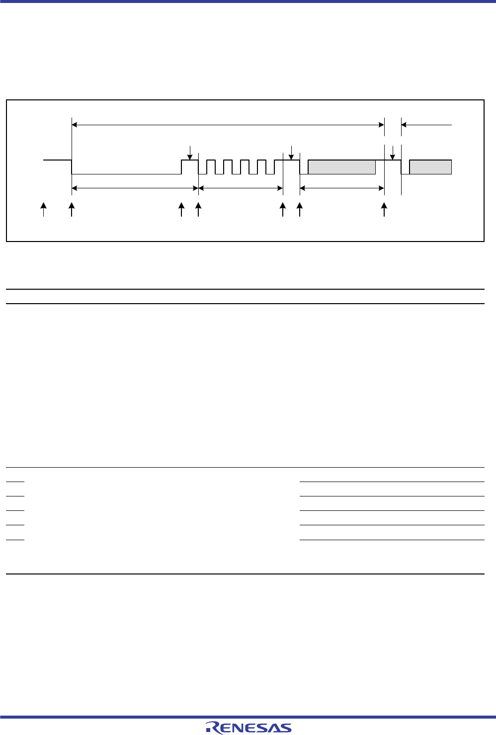
R01UH0034EJ0200 Rev.2.00 Page 1235 of 1489
Dec 27, 2013
RX62T Group, RX62G Group 27. LIN Module (LIN)
Under development Preliminary document
Specifications in this document are tentative and subject to change.
27.4 Operational Overview
27.4.1 Header Transmission
Figure 27.3 shows the LIN module operation in header transmission, and Table 27.5 lists the processing in header
transmission.
Figure 27.3 Operation in Header Transmission
Table 27.5 Processing in Header Transmission
Software Processing LIN Module Processing
(1) Set the baud rate (see section 27.5, Baud Rate Generator).
Set the L0IE.FTCIE bit to 1 (frame/wake-up transmit completion interrupt
enabled), set the L0IE.FRCIE bit to 1 (frame/wake-up receive completion
interrupt enabled), and set the L0IE.ERRIE bit to 1 (error detection interrupt
enabled).
Change the LIN module operating mode by the L0C.OM1, OM0 bits.
Set the break width (13 to 28 Tbits) by the L0BRK.BLT[3:0] bits and set the
break delimiter width (1 to 4 Tbits) by the L0BRK.BDT[1:0] bits.
Set the interbyte space (header)/response space width (0 to 7 Tbits) by the
L0SPC.IBSH[2:0] bits and set the interbyte space width (0 to 3 Tbits) by the
L0SPC.IBS[1:0] bits.
Set the ID value and parity value to L0IDB.
Set the data length by the L0RFC.RFDL[3:0] bits, set the response transmit/
receive direction by the L0RFC.RFT bit, and set the check sum mode by the
L0RFC.CSM bit.
Set the transmit data.
Wait for frame/wake-up transmission start by
software (idle).
(2) Set the L0TC.FTS bit to 1 (frame transmission/wake-up transmission and
reception started).
Transmit the break Low.
(3) Transmit the break delimiter.
(4) Transmit the Sync field (55h).
(5) Transmit the interbyte space (header).
(6) Transmit the ID field.
(7) Set the header transmit completion flag or error
flag.
Transmit the response space.
Header
ID + parityBreak
Break field Sync field
Break delimiter Interbyte space (header)
ID field
Response space
Response
Data 1
(1) (2) (3) (4) (5) (6) (7)
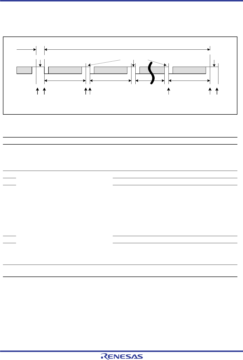
R01UH0034EJ0200 Rev.2.00 Page 1236 of 1489
Dec 27, 2013
RX62T Group, RX62G Group 27. LIN Module (LIN)
Under development Preliminary document
Specifications in this document are tentative and subject to change.
27.4.2 Response Transmission
Figure 27.4 shows the LIN module operation in response transmission, and Table 27.6 lists the processing in response
transmission.
Figure 27.4 Operation in Response Transmission
Table 27.6 Processing in Response Transmission
Software Processing LIN Module Processing
(1) (In frame separate mode)
Set the L0TC.RTS bit to 1 (response transmission
started).
(In non-frame separate mode)
Wait for generation of an interrupt request.
(In frame separate mode)
Transmit the response space while waiting for response transmission
to be started.
(In non-frame separate mode)
Go to (2) if the response space transmission has been completed.
(2) Wait for generation of an interrupt request. Transmit Data 1.
(3) Transmit the interbyte space.
(4) Transmit Data 2.
Transmit the interbyte space.
Transmit Data 3.
Transmit the interbyte space.
(Repeat this processing for the data length specified by the
L0RFC.RFDL[3:0] bits. Abort it when the L0EST.BER flag becomes 1
(bit error detected). If an error occurs, check sum transmission in (5) is
not executed.)
:
:
(5) Transmit the check sum.
(6) Set the frame/wake-up transmit completion flag or error flag.
Set the L0TC.FTS bit to 0 (frame transmission/wake-up transmission
and reception stopped) and set the L0TC.RTS bit to 0 (response
transmission stopped).
(7) Processing after communication:
Check the L0ST register and clear flags to 0.
Idle
Interrupt
Header
ID +
parity
Response space
Response
Data 1
Data field
Data 2
Data field
Interbyte space
Check sum
Check sum
Interframe space
(1) (2) (3)(4) (5) (6) (7)
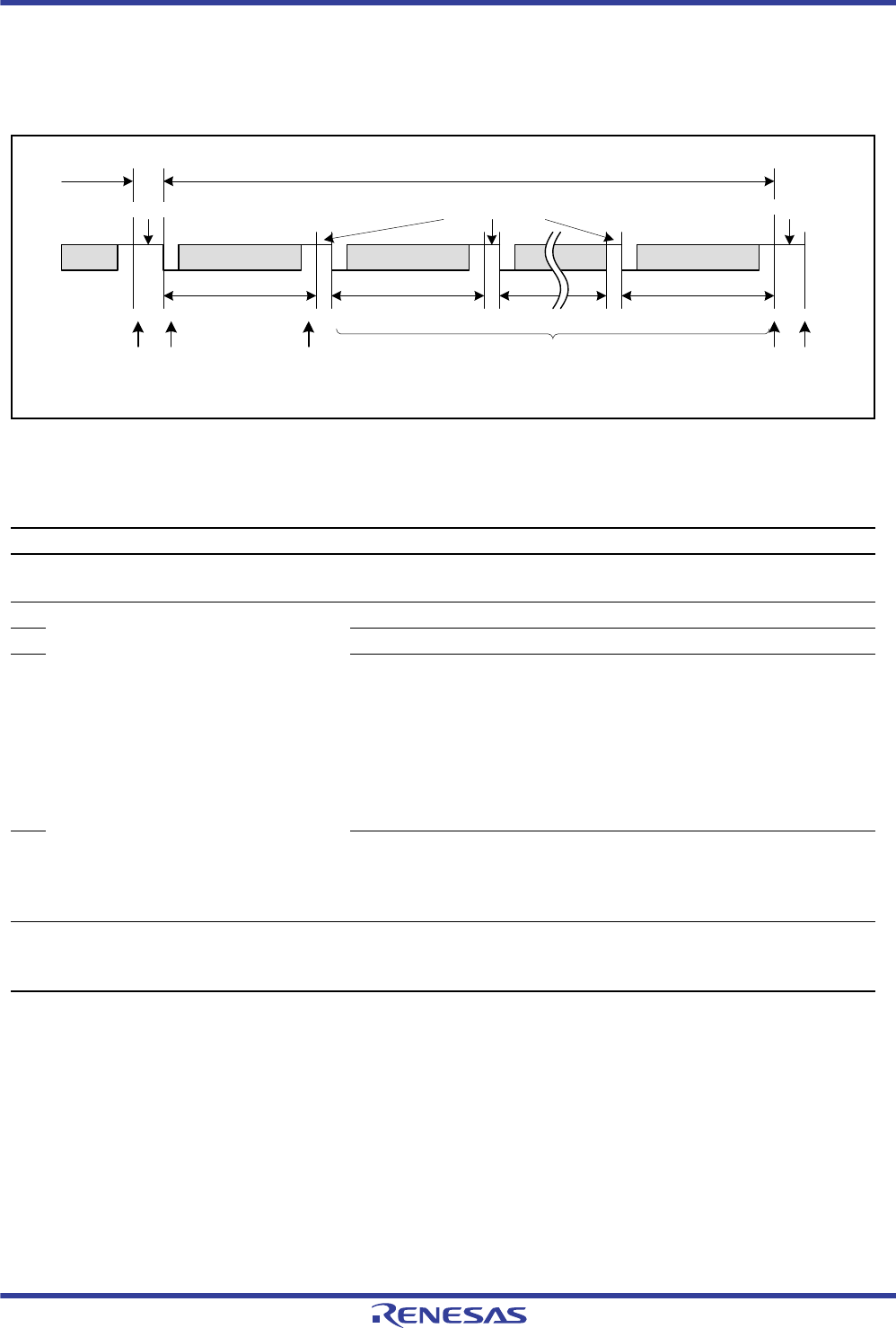
R01UH0034EJ0200 Rev.2.00 Page 1237 of 1489
Dec 27, 2013
RX62T Group, RX62G Group 27. LIN Module (LIN)
Under development Preliminary document
Specifications in this document are tentative and subject to change.
27.4.3 Response Reception
Figure 27.5 shows the LIN module operation in response reception, and Table 27.7 lists the processing in response
reception.
Figure 27.5 Operation in Response Reception
Table 27.7 Processing in Response Reception
Software Processing LIN Module Processing
(1) Wait for generation of an interrupt request
(without processing).
Wait for detection of a start bit.
(2) Wait for generation of an interrupt request. Receive Data 1 due to a start bit detected.
(3) Set the Data 1 receive completion flag.
(4) Receive Data 2 due to a start bit detected.
Receive Data 3 due to a start bit detected.
(Repeat this processing for the data length specified by the L0RFC.RFDL[3:0]
bits. Abort it when any bit in the L0EST register becomes 1 (error is detected). If
an error occurs, check sum judgement in (5) is not executed.)
:
:
Receive check sum due to a start bit detected.
(5) ·Judge the check sum.
·Set the frame/wake-up receive completion flag or error flag.
·Set the L0TC.FTS bit to 0 (frame transmission/wake-up transmission and
reception stopped).
(6) Processing after communication:
Read the received data.
Check the L0ST register and clear flags to 0.
Idle
Interrupt
Header
ID +
parity
Response space
Response
Data 1
Data field
Data 2
Data field
Interbyte space
Check sum
Check sum
Interframe space
(1) (2) (4) (5) (6)(3)

R01UH0034EJ0200 Rev.2.00 Page 1238 of 1489
Dec 27, 2013
RX62T Group, RX62G Group 27. LIN Module (LIN)
Under development Preliminary document
Specifications in this document are tentative and subject to change.
27.5 Baud Rate Generator
The LIN system clock (fLIN) is generated by the LIN communication clock source divided by the baud rate generator.
This fLIN, divided by 16, is used as the bit rate. The reciprocal of the bit rate is called bit time, expressed as "Tbit".
The LBRP0 register should be set so that fa is 307200 Hz (19200 × 16). Therefore, fa = 19200 × 16, fb = 9600 × 16, and
fc = 2400 × 16. Then they are divided by 16 in the bit timing generator, which results in 19200 bps, 9600 bps, and 2400
bps, respectively. The baud rate of 10417 bps is generated by the LBRP1 setting.
Figure 27.6 Block Diagram of Baud Rate Generation
Table 27.8 and Table 27.9 list the baud rates (19200, 9600, 2400, and 10417 bps) for each peripheral clock frequency,
and their error.
—: Corresponding baud rate cannot be generated
Table 27.8 Baud Rate Generation Examples (19200 bps, 9600 bps, and 2400 bps)
LIN
Communicati
on Clock
Source
Baud Rate
Generator 0
(Divided by N 1)
Baud Rate to be Generated
Errorfa Selection fb Selection fc Selection
50 MHz 162 19290.12 (19200 bps) 9645.06 (9600 bps) 2411.27 (2400 bps) +0.47%
40 MHz 130 19230.77 (19200 bps) 9615.38 (9600 bps) 2403.85 (2400 bps) 0.16
25 MHz 81 19290.12 (19200 bps) 9645.06 (9600 bps) 2411.27 (2400 bps) 0.47
24 MHz 78 19230.77 (19200 bps) 9615.38 (9600 bps) 2403.85 (2400 bps) 0.16
20 MHz 65 19230.77 (19200 bps) 9615.38 (9600 bps) 2403.85 (2400 bps) 0.16
16 MHz 52 19230.77 (19200 bps) 9615.38 (9600 bps) 2403.85 (2400 bps) 0.16
12 MHz 39 19230.77 (19200 bps) 9615.38 (9600 bps) 2403.85 (2400 bps) 0.16
10 MHz 65 9615.38 (9600 bps) — — — — 0.16
8 MHz 26 19230.77 (19200 bps) 9615.38 (9600 bps) 2403.85 (2400 bps) 0.16
6 MHz 39 9615.38 (9600 bps) — — — — 0.16
156 2403.85 (2400 bps) 0.16
5 MHz 130 2403.85 (2400 bps) — — — — 0.16
4 MHz 13 19230.77 (19200 bps) 9615.38 (9600 bps) 2403.85 (2400 bps) 0.16
2 MHz 13 9615.38 (9600 bps) — — — — 0.16
52 2403.85 (2400 bps) 0.16
LIN baud rate
prescaler 0
(LBRP0)
LIN baud rate
prescaler 1
(LBRP1)
1/2
1/8
1/2
Fa = 16 x 19.2 kHz -> 19.2 kbps
*2
*3
Fb = 16 x 9.6 kHz -> 9.6 kbps
Fc = 16 x 2.4 kHz -> 2.4 kbps
Fd = 16 x 10.417 kHz -> 10.417 kbps
LIN communication clock
source*1
Notes: 1. For the LIN communication clock source, refer to section 8, Clock Generation Circuit.
2. Set n + 1 division (n = 0 to 255) by LBRP0.
3. Set m + 1 division (m = 0 to 255) by LBRP1.

R01UH0034EJ0200 Rev.2.00 Page 1239 of 1489
Dec 27, 2013
RX62T Group, RX62G Group 27. LIN Module (LIN)
Under development Preliminary document
Specifications in this document are tentative and subject to change.
Table 27.9 Baud Rate Generation Examples (10417 bps)
LIN Communication Clock
Block Baud Rate Generator 1
(Divided by M 1) Baud Rate to be Generated
fd Selection Error
40 MHz 120 10416.67 0.003
25 MHz 75 10416.67 0.003
24 MHz 72 10416.67 0.003
20 MHz 60 10416.67 0.003
16 MHz 48 10416.67 0.003
12 MHz 36 10416.67 0.003
10 MHz 30 10416.67 0.003
8 MHz 24 10416.67 0.003
6 MHz 18 10416.67 0.003
5 MHz 15 10416.67 0.003
4 MHz 12 10416.67 0.003
2 MHz 6 10416.67 0.003
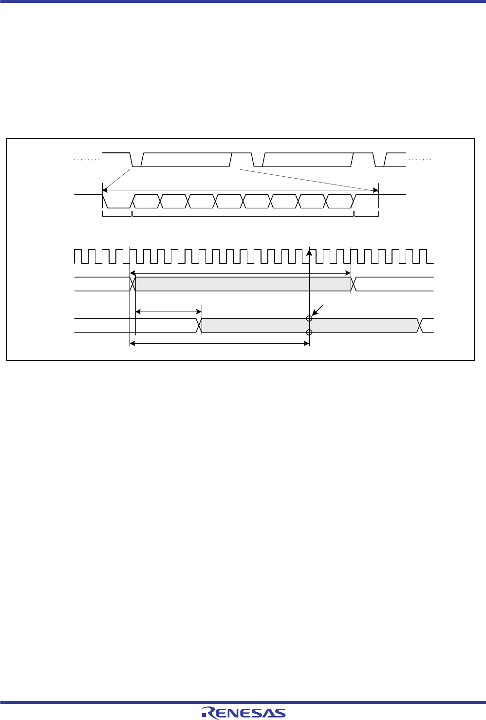
R01UH0034EJ0200 Rev.2.00 Page 1240 of 1489
Dec 27, 2013
RX62T Group, RX62G Group 27. LIN Module (LIN)
Under development Preliminary document
Specifications in this document are tentative and subject to change.
27.6 Data Transmission and Reception
27.6.1 Data Transmission
The LIN module transmits one bit data per Tbit.
The transmitted data returns to the input pin for data reception via the LIN transceiver. Then the received data is
compared to the transmitted data and the result is stored in the L0EST.BER flag (see section 27.10, Error Status). The
timing to sample the received data is at the 13th clock (position of 81.25%) when 1 Tbit is generated by 16 fLIN.
Figure 27.7 shows the data transmission timing.
Figure 27.7 Data Transmission Timing
8 bits of dataST
SPST
LTX SP 8 bits of dataST SP
D0 D1 D2 D3 D4 D5 D6 D7
Byte field
fLIN
LTX DnDn-1 Dn+1
1 Tbit = 16 fLIN
Physical layer delay Sampling point for
bit error detection
Dn-1 Dn
13/16 Tbit
LRX
8 bits of data
Start bit Stop bit

R01UH0034EJ0200 Rev.2.00 Page 1241 of 1489
Dec 27, 2013
RX62T Group, RX62G Group 27. LIN Module (LIN)
Under development Preliminary document
Specifications in this document are tentative and subject to change.
27.6.2 Data Reception
The LIN module receives data using a synchronized LRX signal (internal signal) generated by synchronizing the input
signal from the LRX pin with fLIN.
The byte field of this synchronized LRX signal is synchronized with fLIN at the falling edge of the start bit. The start bit
is recognized if the synchronized LRX signal still remains low when being re-sampled 0.5 Tbits after the falling edge
was detected. If the LRX signal remains low after exiting reset mode or if it is held high on re-sampling, no start bit is
found.
Once the start bit is detected, data bits are sampled every 1 Tbit.
Figure 27.8 shows the data reception timing.
Figure 27.8 Data Reception Timing
LRX SPST D0 D1 D2 D3 D4 D5 D6 D7
Byte field
LRX (detail) Start bit D0 D1
fLIN
Synchronized LRX
(internal signal)
Falling
edge is
detected
Low-level is confirmed
after 0.5 Tbit Bit 0 is read out
after 1 Tbit
D0 D1
0.5 Tbit
Start bit
1 Tbit (= 16 fLIN)
Read out for each
1 Tbit from here
1 Tbit (= 16 fLIN)
8 bits of dataStart bit Stop bit
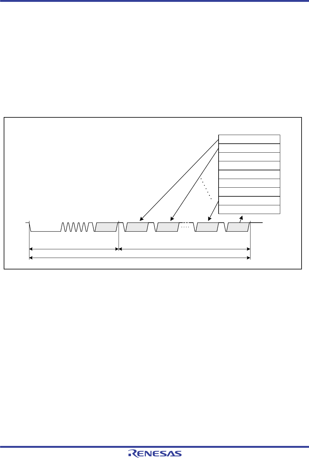
R01UH0034EJ0200 Rev.2.00 Page 1242 of 1489
Dec 27, 2013
RX62T Group, RX62G Group 27. LIN Module (LIN)
Under development Preliminary document
Specifications in this document are tentative and subject to change.
27.7 Buffer Processing of Data to be Transmitted and Received Data
The buffer processing in consecutive data transmission and reception by the LIN module is described below.
27.7.1 Transmission of LIN Frame
In 8-byte transmission, the contents stored in registers L0DB1 to L0DB8 are transmitted to Data 1 to Data 8 areas of the
LIN frame in order. In 4-byte transmission, the contents stored in registers L0DB1 to L0DB4 are transmitted to Data 1 to
Data 4 areas of the LIN frame, and the contents stored in registers L0DB5 to L0DB8 are not transmitted. The transmitted
check sum data is stored in the L0CBR register.
Figure 27.8 shows LIN transmission processing and buffers.
Figure 27.9 LIN Transmission Processing and Buffers
27.7.1.1 Frame Separate Mode
Frame separate mode is selected by setting the L0RFC.FSM bit to 1.
In frame separate mode, a header and response can be transmitted according to separate transmit start requests.
When the header transmission has been completed, the L0ST.HTRC flag becomes 1 (header transmission completed).
L0DB1 register
L0DB2 register
L0DB3 register
L0DB4 register
L0DB5 register
L0DB6 register
L0DB7 register
L0DB8 register
Data 1 Checksum
Header Response
Frame
Buffer
Data 2 Data 8
L0CBR register
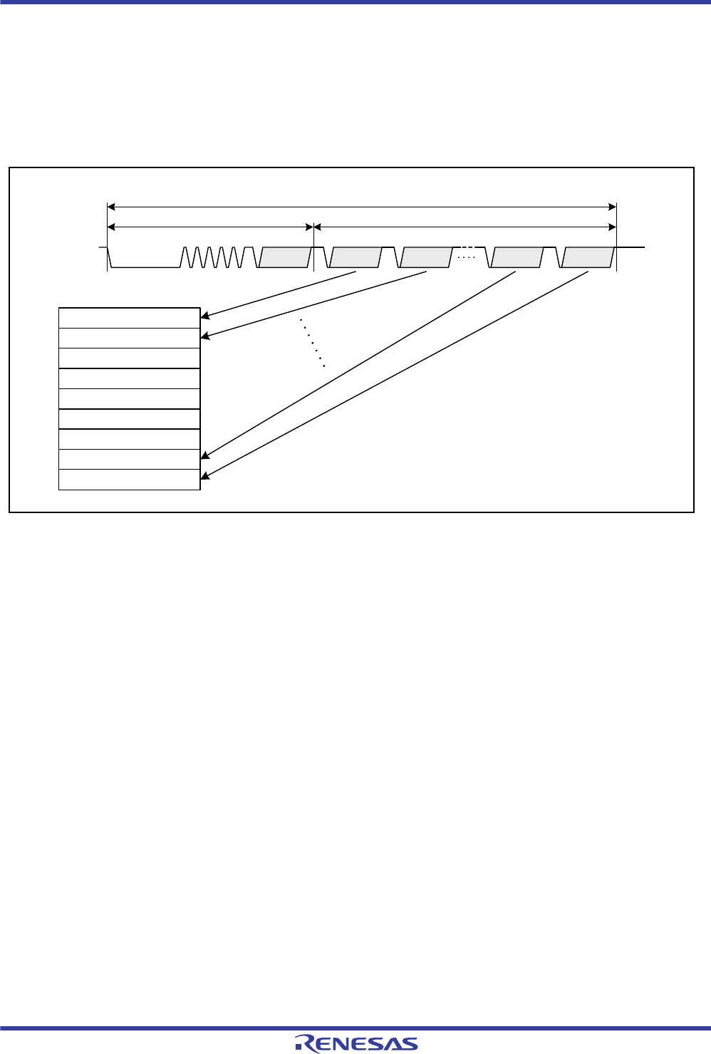
R01UH0034EJ0200 Rev.2.00 Page 1243 of 1489
Dec 27, 2013
RX62T Group, RX62G Group 27. LIN Module (LIN)
Under development Preliminary document
Specifications in this document are tentative and subject to change.
27.7.2 Reception of LIN Frame
In 8-byte reception, the contents of Data 1 to Data 8 areas of the LIN frame are stored in registers L0DB1 to L0DB8 in
order upon every completion of stop bit reception. In 4-byte reception, the contents of Data 1 to Data 4 areas of the LIN
frame are stored in registers L0DB1 to L0DB4, and no data is stored in registers L0DB5 to L0DB8. The received check
sum data is stored in the L0CBR register.
Figure 27.9 shows LIN reception processing and buffers.
Figure 27.10 LIN Reception Processing and Buffers
27.7.2.1 Data 1 Reception
When the first byte of data reception is completed, the L0ST.D1RC flag becomes 1 (data 1 reception completed).
Data 1 Data 2 Data 8 Checksum
Header Response
Frame
L0DB1 register
L0DB2 register
L0DB3 register
L0DB4 register
L0DB5 register
L0DB6 register
L0DB7 register
L0DB8 register
Buffer
L0CBR register
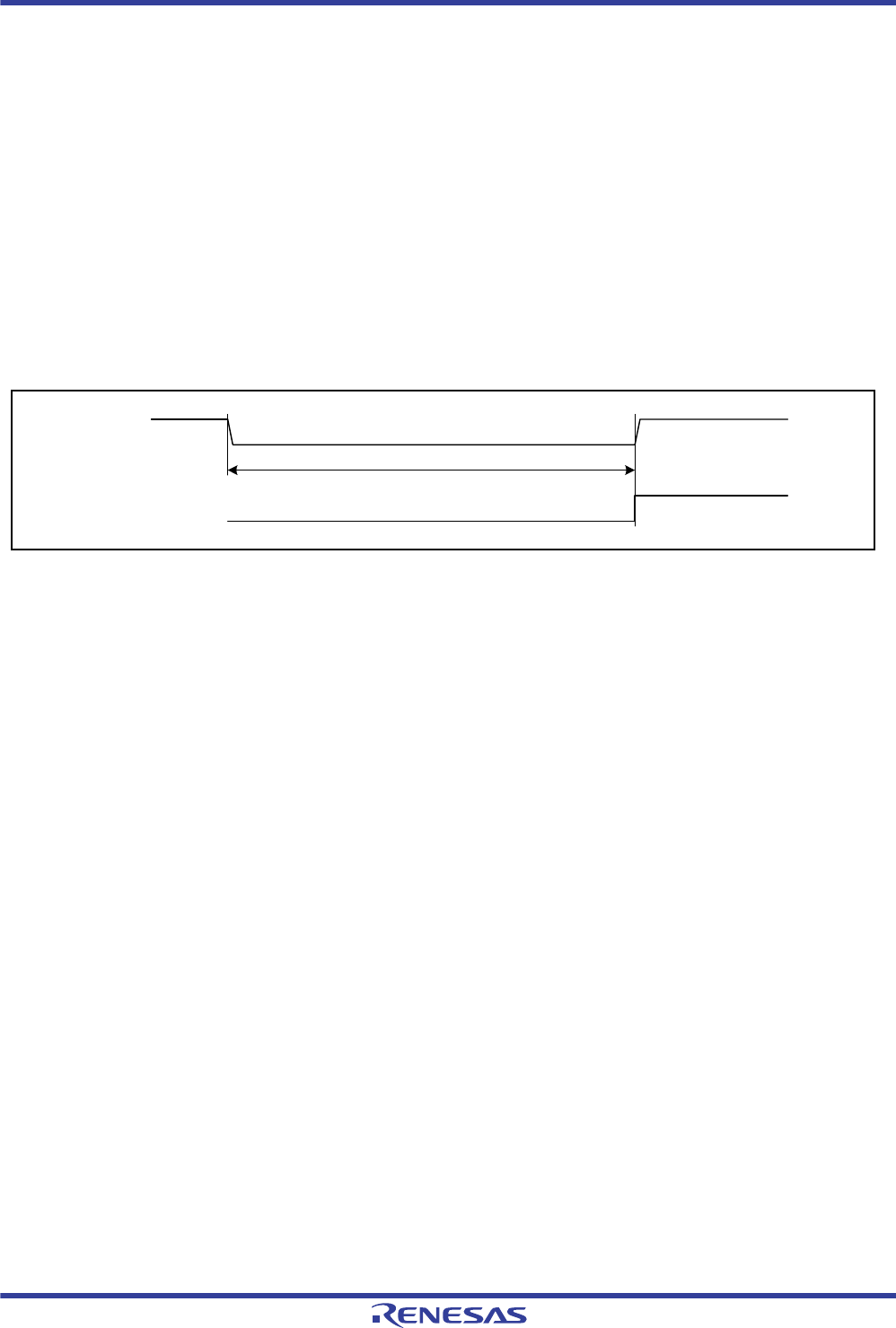
R01UH0034EJ0200 Rev.2.00 Page 1244 of 1489
Dec 27, 2013
RX62T Group, RX62G Group 27. LIN Module (LIN)
Under development Preliminary document
Specifications in this document are tentative and subject to change.
27.8 Wake-up Transmission and Reception
Wake-up transmission and reception are available in LIN wake-up mode.
27.8.1 Operation in Wake-up Transmission
In LIN wake-up mode, if the L0RFC.RFT bit is set to 1 (transmission) and the L0TC.FTS bit is set to 1 (frame
transmission/wake-up transmission and reception started), the wake-up signal is output at the output pin. Low time of the
wake-up signal is set by the L0WUP.WUTL[3:0] bits.
When Low of wake-up is output without any bit error detected, the L0ST.FTC flag becomes 1 (frame or wake-up
transmission completed). If the L0IE.FTCIE bit is set to 1 (frame/wake-up transmit completion interrupt enabled) at this
time, an interrupt request is generated.
When a bit error is detected, the wake-up transmission is aborted and the L0EST.BER flag becomes 1 (bit error
detected).
Figure 27.11 shows the wake-up transmission timing.
Figure 27.11 Wake-up Transmission Timing
27.8.2 Operation in Wake-up Reception
The LIN module uses the input signal Low time counting function for detecting a wake-up.
The input signal Low time counting function is used to measure the Low time of the input signal at the LRX pin by
counting at the same sampling timing as that of data reception. The Low time to be measured varies depending on the
setting of the LWBR.LWBR0 bit. When LIN Specification Package Revision 1.3 is used, set the LWBR.LWBR0 bit to 0.
This allows the input signal Low time to be measured for 2.5 or more Tbits of fLIN. When LIN Specification Package
Revisions 2.0 and 2.1 are used, set the LWBR.LWBR0 bit to 1. This allows the input signal Low time to be measured for
130 s or more.
To use this function, set the L0RFC.RFT bit to 0 (reception) and the L0TC.FTS bit to 1 (frame transmission/wake-up
transmission and reception started) in LIN wake-up mode.
When the Low time to be measured is reached, the L0ST.FRC flag becomes 1 (frame or wake-up reception completed).
If the L0IE.FRCIE bit is set to 1 (frame/wake-up receive completion interrupt enabled) at this time, an interrupt request
is generated.
Low time setting (1 to 16 Tbit)
LRX
L0ST.FTC flag
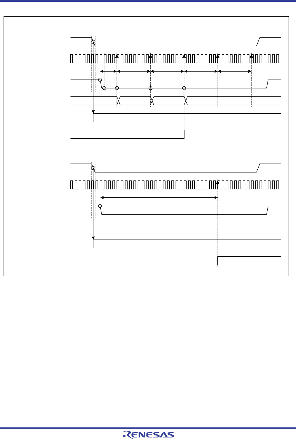
R01UH0034EJ0200 Rev.2.00 Page 1245 of 1489
Dec 27, 2013
RX62T Group, RX62G Group 27. LIN Module (LIN)
Under development Preliminary document
Specifications in this document are tentative and subject to change.
Figure 27.12 Input Signal Low Time Counting Function
During wake-up transmission, the input signal Low time counting function is not workable.
27.8.3 Wake-up Collision
When the master and slave transmit wake-up signals simultaneously, a signal collision occurs on the LIN bus. However,
no collision of wake-up signals is detected in the LIN module.
Counter value
LRX
fLIN
Synchronized LRX
(internal signal)
0.5 Tbit 1 Tbit 1 Tbit 1 Tbit 1 Tbit
0 1 2 0
IRn.IR flag of LIN Low
detection interrupt
L0ST.FRC flag
When LWBR.LWBR0 bit is 0 (LIN Specification Package Revision 1.3 used)
LRX
fLIN
Synchronized LRX
(internal signal)
130 s or more
IR bit of LIN Low
detection interrupt
L0ST.FRC flag
When LWBR.LWBR0 bit is 1 (LIN Specification Package Revisions 2.0 and 2.1 used)

R01UH0034EJ0200 Rev.2.00 Page 1246 of 1489
Dec 27, 2013
RX62T Group, RX62G Group 27. LIN Module (LIN)
Under development Preliminary document
Specifications in this document are tentative and subject to change.
27.9 Operating Status
The LIN module detects seven types of operating status.
The three states that can generate an interrupt request are: frame/wake-up transmit completion, frame/wake-up receive
completion, and error detection.
Table 27.10 lists the operating status types.
Note 1. By writing 0 to flags L0EST.CSER, FER, FTER, PBER, and BER in LIN operation mode, the L0ST.ERR flag becomes 0.
Note 2. This status is not detected when the L0RFC.RFDL[3:0] bits are set to 0000b (0 byte + check sum).
Table 27.10 Operating Status Types
Operating
Status Status Setting Condition Status Clearing Conditions Status Detectable
Operating Modes Corresponding
Bit
LIN mode When the LIN module has actually
entered LIN operation mode after the
L0C.OM1 bit was set to select LIN
operation mode
When the LIN module has actually
entered LIN wake-up mode after
the L0C.OM1 bit was set to select
LIN wake-up mode
LIN operation mode
LIN wake-up mode
L0MST.OMM1
bit
Reset When the LIN module has actually
exited LIN reset mode after the
L0C.OM0 bit was set to select non-LIN
reset mode
When the LIN module has actually
entered LIN reset mode after the
L0C.OM1 bit was set to select LIN
reset mode
All modes L0MST.OMM0
bit
Frame/
wake-up
transmit
completion
When a response field or wake-up
signal transmission has been
successfully completed
When the next communication
starts
Clearing by software
On transition to LIN reset mode
LIN operation mode
LIN wake-up mode
L0ST.FTC flag
Frame/
wake-up
receive
completion
When a response field or wake-up
signal reception has been successfully
completed
When the next communication
starts
Clearing by software
On transition to LIN reset mode
LIN operation mode
LIN wake-up mode
L0ST.FRC flag
Error
detection
When any of flags L0EST.CSER, FER,
FTER, PBER, and BER becomes 1
(error detected)
When the next communication
starts
Clearing by software*1
On transition to LIN reset mode
LIN operation mode
LIN wake-up mode
L0ST.ERR flag
Data 1
receive
completion
When the reception of the first one byte
of a response frame has been
completed with the L0RFC.RFT bit set
to 0 (reception)*2
When the next communication
starts
Clearing by software
On transition to LIN reset mode
LIN operation mode L0ST.D1RC flag
Header
transmit
completion
When a header field transmission has
been successfully completed
When the next communication
starts
Clearing by software
On transition to LIN reset mode
LIN operation mode L0ST.HTRC flag

R01UH0034EJ0200 Rev.2.00 Page 1247 of 1489
Dec 27, 2013
RX62T Group, RX62G Group 27. LIN Module (LIN)
Under development Preliminary document
Specifications in this document are tentative and subject to change.
27.10 Error Status
27.10.1 Error Status Types
The LIN module detects five types of error status. These error states can be checked by the bits in the LEST register.
Table 27.11 lists the error status types.
Note 1. When a bit error is detected, the processing is aborted after the stop bit is transmitted. If it is detected in a non-data space, such
as an interbyte space, the transmission processing is aborted after a check in that space is completed. If a bit error is detected
during wake-up transmission, the wake-up transmission is aborted immediately after the error bit is transmitted.
Note 2. The timeout period depends on the response field data length (L0RFC.RFDL[3:0] bits) and the selected check sum
(L0RFC.CSM bit), and can be calculated as follows:
When classic check sum is selected (L0RFC.CSM bit = 0)
Timeout period = 49 + (data bytes + 1) 14 [Tbit]
When enhanced check sum is selected (L0RFC.CSM bit = 1)
Timeout period = 48 + (data bytes + 1) 14 [Tbit]
The above timeout period will exceed the value of TFRAME_MAX shown in LIN Specification Package Revision 1.3 when
classic check sum is selected, and the value of TFRAME_MAX shown in LIN Specification Package Revisions 2.0 and 2.1 when
enhanced check sum is selected.
Table 27.11 Error Status Types
Error Status Error Detecting Condition
(Clearing to 0 by Software) Error Detectable
Operating Modes Communication
Processing
Detection
Enabled/
Disabled Corresponding
Bit
Bit error When the transmitted data does not
match with that on the LIN bus
monitored by the pin for reception*1
LIN operation mode
LIN wake-up mode
Abort Selectable
L0EST.
BER flag
Physical bus
error
If the LIN bus detects high when the
break field is transmitted
If the LIN bus detects low when the
break delimiter is transmitted
If the LIN bus detects high when the
wake-up is transmitted
LIN operation mode
LIN wake-up mode
Abort Selectable
L0EST.
PBER
flag
Frame
timeout error
When frame transmission/reception is
not completed within a specified period
of time*2
LIN operation mode Abort Selectable
L0EST.
FTER flag
Framing error When the stop bit of each data byte is
Low in response frame reception
processing
LIN operation mode Abort Selectable
L0EST.
FER flag
Check sum
error
When the check sum judgement of
response frame reception processing
results in an error
LIN operation mode — Non-
selectable
L0EST.
CSER
flag
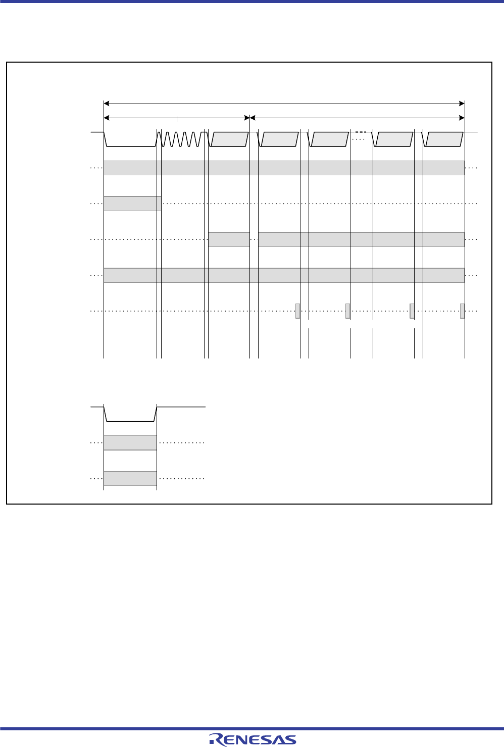
R01UH0034EJ0200 Rev.2.00 Page 1248 of 1489
Dec 27, 2013
RX62T Group, RX62G Group 27. LIN Module (LIN)
Under development Preliminary document
Specifications in this document are tentative and subject to change.
27.10.2 Target Areas for LIN Error Detection
Figure 27.13 shows the areas which the LIN module monitors for error detection.
Figure 27.13 LIN Error Detection Target Areas
<Wake-up transmission>
Wake-up
Bit error
Physical bus
error
Data 1 Data 2 Data 8 Checksum
Header Response
Frame
Break field Sync field ID field
Bit error
Physical bus
error
Check sum error
Frame timeout
error
Framing error
In transmission only
In break field and
break delimiter
transmission only
In enhanced
check sum
selected and
in reception
only
In reception only
Stop bit in reception only
<Frame transmission/reception>

R01UH0034EJ0200 Rev.2.00 Page 1249 of 1489
Dec 27, 2013
RX62T Group, RX62G Group 27. LIN Module (LIN)
Under development Preliminary document
Specifications in this document are tentative and subject to change.
27.11 Interrupts
The interrupt request generated by the LIN module is the LIN interrupt.
There are three interrupt sources: frame/wake-up transmit completion, frame/wake-up receive completion, and error
detection.
Interrupt requests by the three interrupt sources of frame/wake-up transmit completion, frame/wake-up receive
completion, and error detection are aggregated by logical OR as a single interrupt request "LIN interrupt".
The respective interrupt request is output when the corresponding flag in the L0ST register becomes 1 while the
corresponding bit in the L0IE register is set to 1 (interrupt enabled). However, while the corresponding bit in the LOST
register is 1, the interrupt request is ignored. Therefore, set the corresponding flag to 0 to enable the interrupt.
Figure 27.14 shows a block diagram of the LIN interrupt.
Figure 27.14 Block Diagram of LIN Interrupt
Frame timeout error
Frame transmit completion
Wake-up transmit completion
Bit error
Checksum error
Physical bus error
Framing error
Frame receive completion
Wake-up receive completion*
L0ST.FTC
L0ST.FRC
Error detection flagL0ST.ERR
Error detection interrupt enable
Error detection interrupt
LIN interrupt
request
Frame/wake-up transmit completion flag
Frame/wake-up receive
completion flag*
Frame/wake-up transmit
completion interrupt
Frame/wake-up receive
completion interrupt*
Frame/wake-up transmit completion
interrupt enable
Frame/wake-up receive completion
interrupt enable*
Note: * Wake-up reception indicates the input signal Low time counting.
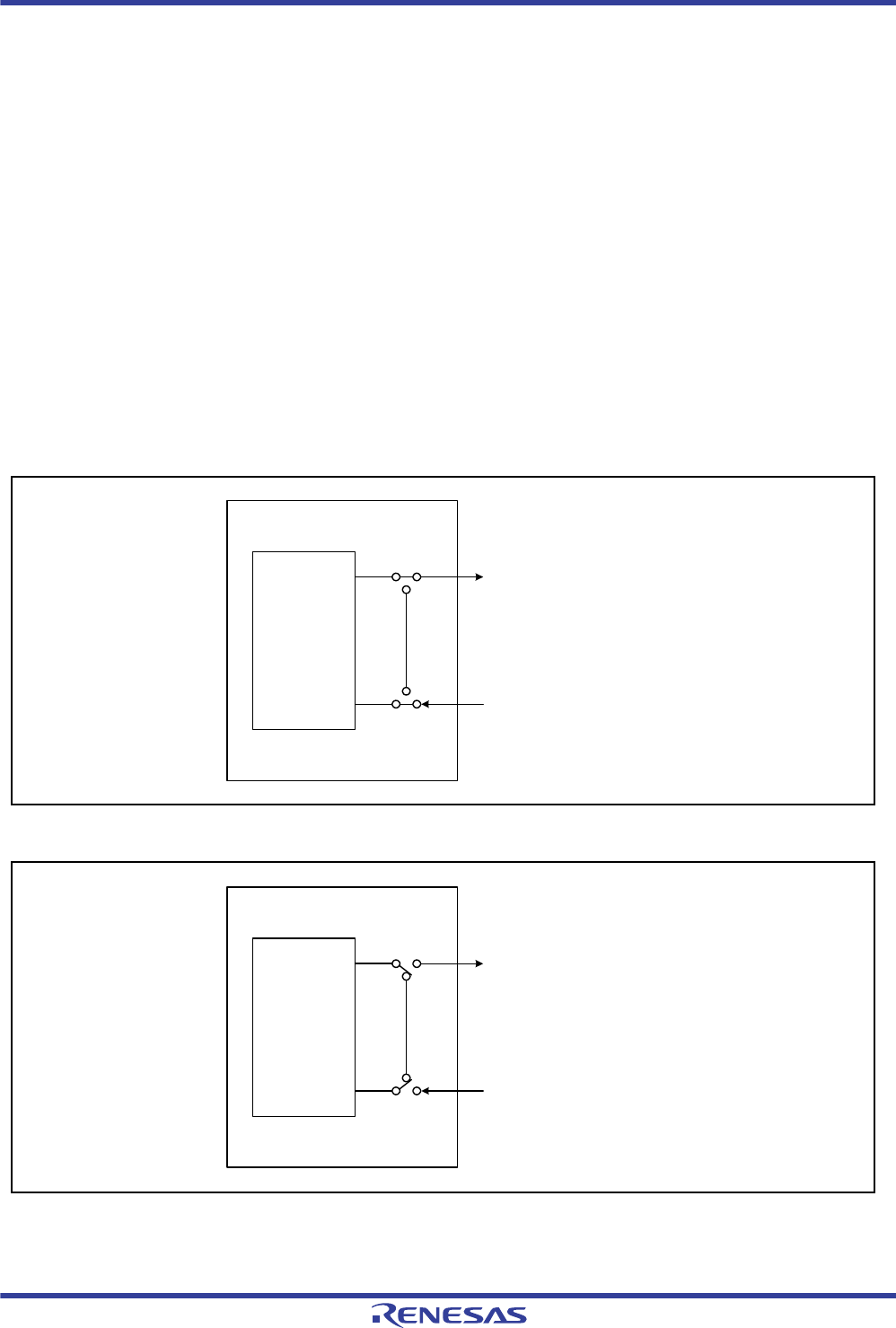
R01UH0034EJ0200 Rev.2.00 Page 1250 of 1489
Dec 27, 2013
RX62T Group, RX62G Group 27. LIN Module (LIN)
Under development Preliminary document
Specifications in this document are tentative and subject to change.
27.12 LIN Self-Test Mode
The LIN module has LIN self-test mode. Once the LIN module enters LIN self-test mode, it is disconnected from the
LIN bus, and the internal LTX is looped back to the internal LRX (loop back).
LIN self-test mode operates in the following states.
In LIN self-test mode
Wake-up is not supported
Frame separate mode is not supported
The baud rate generator is set to the fastest settings (LBRP0 = 00h, LBRP1 = 00h, and L0MD.LCKS[1:0]bits = 00b)
Do not enter LIN wake-up mode.
Before entering LIN self-test mode, set the L0RFC.FSM bit to 0 (non-frame separate mode).
The baud rate setting is automatic in LIN self-test mode. When entering LIN reset mode from LIN self-test mode, the
automatic setting is set back to the setting prior to LIN self-test mode.
Other settings are retained and remain valid when entering LIN self-test mode, and when entering LIN reset mode from
LIN self-test mode.
Registers L0ST and L0EST remain functional, but the L0EST.FER, PBER, and BER flags cannot detect any errors at the
loop back, and do not become 1.
Figure 27.15 LIN Operation Mode Connection
Figure 27.16 LIN Self-Test Mode Connection
LTX
(internal)
LIN controller
LRX
(internal)
LTX pin
LRX pin
I/O from/to LIN transceiver
LTX
(internal)
LIN controller
LRX
(internal)
LTX pin
LRX pin
I/O from/to LIN transceiver

R01UH0034EJ0200 Rev.2.00 Page 1251 of 1489
Dec 27, 2013
RX62T Group, RX62G Group 27. LIN Module (LIN)
Under development Preliminary document
Specifications in this document are tentative and subject to change.
27.12.1 Entry into LIN Self-Test Mode
To enter LIN self-test mode, a particular key sequence must be used. In this key sequence, the user has to do three
consecutive writes to the LIN self-test control register as follows.
Enter LIN reset mode.
First write: LSTC register = 1010 0111 (A7h)
Second write: LSTC register = 0101 1000 (58h)
Third write: LSTC register = 0000 0001 (01h)
If the first key is written twice, then the sequence is broken and must be restarted.
If this sequence is broken by a write access to any other LIN register, then it must be restarted.
LIN self-test mode does not support frame separate mode. Two tests can be carried out.
LIN self-test mode (transmission): Header transmission and response transmission
LIN self-test mode (reception): Header transmission and response reception
27.12.2 Transmission in LIN Self-Test Mode
The following steps are to be performed to execute the LIN self-test.
Write 11b to the L0C.OM1, OM0 bits, and then confirm the L0MST.OMM1, OMM0 bits are set to 11b.
Set the L0RFC.RFT bit to 1 (transmission).
Set the frame configuration to be transmitted.
Set the L0TC.FTS bit to 1 (frame transmission/wake-up transmission and reception started).
LIN self-test mode (transmission) is executed. Interrupt generation and update of status and error status are
appropriately executed. Check sum is automatically calculated by the LIN module.
If transmission is completed, the inverted value of the frame data after looped back is stored in registers L0IDB,
L0CBR, and L0DBn (stored as an inverted value to compare the transmitted value and looped back value) (n = 1 to
8).
If transmission is not completed due to an error, the corresponding error flag is set.
27.12.3 Reception in LIN Self-Test Mode
The following steps are to be performed to execute the LIN self-test.
Enter LIN self-test mode.
Set the L0RFC.RFT bit to 0 (reception).
Set the frame configuration to be received. Since check sum is not automatically calculated, store the calculated
value. A check sum error can be tested by setting an erroneous calculation result in the check sum.
Set the L0TC.FTS bit to 1 (frame transmission/wake-up transmission and reception started).
LIN self-test mode (reception) is executed. Interrupt generation and update of status and error status are
appropriately executed.
If reception is completed, the inverted value of the frame data after looped back is stored in registers L0IDB,
L0CBR, and L0DBn (stored as an inverted value to compare the set value and received value after looped back).(n
= 1 to 8)
If reception is not completed due to an error, the corresponding error flag is set.

R01UH0034EJ0200 Rev.2.00 Page 1252 of 1489
Dec 27, 2013
RX62T Group, RX62G Group 27. LIN Module (LIN)
Under development Preliminary document
Specifications in this document are tentative and subject to change.
27.12.4 Exit from LIN Self-Test Mode
To exit LIN self-test mode, perform the following step.
Enter LIN reset mode.
(When the L0MST.OMM1, OMM0 bits are not 11b, write 11b to the L0C.OM1, OM0 bits, and then confirm the
L0MST.OMM1, OMM0 bits are set to 11b before entering LIN reset mode.)

R01UH0034EJ0200 Rev.2.00 Page 1253 of 1489
Dec 27, 2013
RX62T Group, RX62G Group 28. 12-Bit A/D Converter (S12ADA)
28. 12-Bit A/D Converter (S12ADA)
28.1 Overview
The RX62T and RX62G Groups have two units of 12-bit successive approximation A/D converter. Up to 4-channel
analog inputs can be selected in each unit.
The A/D converter has two types of operating mode: single mode in which analog input of one channel is converted only
once and scan mode in which analog inputs of up to four channels are sequentially converted.
Table 28.1 lists the specifications of the A/D converter and Table 28.2 shows the functions of the A/D converter.
Figure 28.1 shows a block diagram of the A/D converter.
Table 28.1 Specifications of A/D Converter
Item Specifications
Number of units Two units (S12AD0 and S12AD1)
Input channels Eight channels (four channels x two units)
A/D conversion method Successive approximation method
Resolution 12 bits
Conversion time 1.0 s per 1 channel (when operating with A/D conversion clock ADCLK = 50 MHz and
AVCC = 4.0 to 5.5V)
2.0 s per 1 channel (when operating with A/D conversion clock ADCLK = 25 MHz and
AVCC = 3.0 to 3.6V)
A/D conversion clock Four types: PCLK, PCLK/2, PCLK/4, PCLK/8
Data registers Ten data registers
The A/D conversion result is held in a 12-bit A/D data register.
For AN000 and AN100 inputs, two A/D data registers are provided, which are switched according to the
trigger type.
Operating modes Single mode: Analog inputs of one channel are converted only once.
Scan mode
Single-cycle scan mode: Analog inputs of up to four channels are converted only once.
Continuous scan mode: Analog inputs of up to four channels are converted repeatedly.
2-channel scan mode:Channels in each unit are divided into two groups and the conversion startup
source can be separately selected for each group.
Conditions of A/D
conversion start
Software trigger
Conversion start trigger by the multifunction timer pulse unit 3 (MTU3) or general PWM timer (GPT).
External trigger
A/D conversion can be externally triggered from the ADTRG0# pin in S12AD0 and from the ADTRG1# pin
in S12AD1.
Function Sample-and-hold function (three channels per unit)
A dedicated sample-and-hold circuit is provided for each of channels 0 to 2 (AN000 to AN002) of S12AD0
and channels 0 to 2 (AN100 to AN102) of S12AD1, which enables simultaneous sampling in multiple
channels (up to three channels) in each unit.
Self-diagnostic functions for A/D converter
Input signal amplification function provided through programmable gain amplifier (three channels
per unit)
Window comparator function (three channels per unit)
Interrupt source Interrupt request (S12ADI) can be generated on completion of A/D conversion in each unit.
A S12ADI interrupt can activate the data transfer controller (DTC).
Interrupt request (CMPI) can be generated when a specified comparison condition is detected
(can also be used for a POE source).
Power-down function Module stop state can be specified in each unit.

R01UH0034EJ0200 Rev.2.00 Page 1254 of 1489
Dec 27, 2013
RX62T Group, RX62G Group 28. 12-Bit A/D Converter (S12ADA)
Table 28.2 Functions of A/D Converter
Item Unit 0 (S12AD0) Unit 1 (S12AD1)
Analog input channel AN000 to AN003 AN100 to AN103
A/D conversion
start conditions
Software Software trigger Enabled Enabled
External trigger Trigger pin ADTRG0# ADTRG1#
Trigger from
MTU3
Compare match/input capture in MTU0.TGRA TRGA0N TRGA0N
Compare match/input capture in MTU1.TGRA TRGA1N TRGA1N
Compare match/input capture in MTU2.TGRA TRGA2N TRGA2N
Compare match/input capture in MTU3.TGRA TRGA3N TRGA3N
Compare match/input capture in MTU4.TGRA, or
MTU4.TCNT underflow (trough) in complementary
PWM mode
TRGA4N TRGA4N
Compare match/input capture in MTU6.TGRA TRGA6N TRGA6N
Compare match/input capture in MTU7.TGRA, or
MTU7.TCNT underflow (trough) in complementary
PWM mode
TRGA7N TRGA7N
Compare match in MTU0.TGRE TRG0N TRG0N
Compare match between MTU4.TADCORA and
MTU4.TCNT
TRG4AN TRG4AN
Compare match between MTU4.TADCORB and
MTU4.TCNT
TRG4BN TRG4BN
Compare match between MTU4.TADCORA and
MTU4.TCNT, or compare match between
MTU4.TADCORB and MTU4.TCNT
TRG4AN or
TRG4BN
TRG4AN or
TRG4BN
Compare match between MTU4.TADCORA and
MTU4.TCNT and compare match between
MTU4.TADCORB and MTU4.TCNT
(when interrupt skipping function 2 is used)
TRG4ABN TRG4ABN
Compare match between MTU7.TADCORA and
MTU7.TCNT
TRG7AN TRG7AN
Compare match between MTU7.TADCORB and
MTU7.TCNT
TRG7BN TRG7BN
Compare match between MTU7.TADCORA and
MTU7.TCNT, or compare match between
MTU7.TADCORB and MTU7.TCNT
TRG7AN or
TRG7BN
TRG7AN or
TRG7BN
Compare match between MTU7.TADCORA and
MTU7.TCNT and compare match between
MTU7.TADCORB and MTU7.TCNT
(when interrupt skipping function 2 is used)
TRG7ABN TRG7ABN

R01UH0034EJ0200 Rev.2.00 Page 1255 of 1489
Dec 27, 2013
RX62T Group, RX62G Group 28. 12-Bit A/D Converter (S12ADA)
Note 1. For details, see section 9, Low Power Consumption.
A/D conversion
start conditions
Trigger from GPT Compare match in GPT0.GTADTRA GTADTRA0N GTADTRA0N
Compare match in GPT0.GTADTRB GTADTRB0N GTADTRB0N
Compare match in GPT1.GTADTRA GTADTRA1N GTADTRA1N
Compare match in GPT1.GTADTRB GTADTRB1N GTADTRB1N
Compare match in GPT2.GTADTRA GTADTRA2N GTADTRA2N
Compare match in GPT2.GTADTRB GTADTRB2N GTADTRB2N
Compare match in GPT3.GTADTRA GTADTRA3N GTADTRA3N
Compare match in GPT3.GTADTRB GTADTRB3N GTADTRB3N
Compare match in GPT0.GTADTRA, or compare
match in GPT0.GTADTRB
GTADTRA0N or
GTADTRB0N
GTADTRA0N or
GTADTRB0N
Compare match in GPT1.GTADTRA, or compare
match in GPT1.GTADTRB
GTADTRA1N or
GTADTRB1N
GTADTRA1N or
GTADTRB1N
Compare match in GPT2.GTADTRA, or compare
match in GPT2.GTADTRB
GTADTRA2N or
GTADTRB2N
GTADTRA2N or
GTADTRB2N
Compare match in GPT3.GTADTRA, or compare
match in GPT3.GTADTRB
GTADTRA3N or
GTADTRB3N
GTADTRA3N or
GTADTRB3N
Independent
sample-and-hold
function
dedicated for
channel
Target channel AN000 to AN002 AN100 to AN102
Programmable
gain amplifier
Target channel AN000 to AN002 AN100 to AN102
Gain setting 2.0, 2.5, 3.077, 3.636, 4.0, 4.444,
5.0, 5.714, 6.667, 10.0, 13.333
(11 steps in total)
Window
comparator
Target channel AN000 to AN002 AN100 to AN102
Reference
voltage setting
Specified through external pin CVREFL: AN003, CVREFH: AN103
Internal generation 1/8AVCC0, 2/8AVCC0, 3/8AVCC0, 4/
8AVCC0, 5/8AVCC0, 6/8AVCC0, 7/
8AVCC0
Noise canceling function Comparator detection results are
sampled 16 times with PCLK, PCLK/2,
PCLK/4, PCLK/8, PCLK/ 16, or PCLK/
128
Interrupt S12ADI0 and
CMPI
S12ADI1 and
CMPI
Module stop function setting*MSTPCRA.
MSTPA17 bit
MSTPCRA.
MSTPA16 bit
Table 28.2 Functions of A/D Converter
Item Unit 0 (S12AD0) Unit 1 (S12AD1)
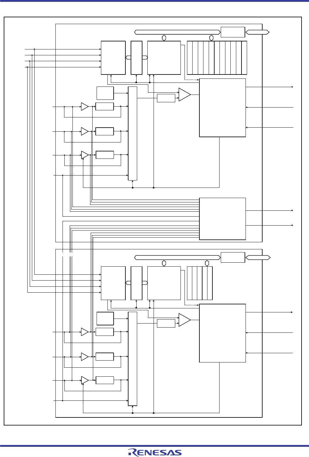
R01UH0034EJ0200 Rev.2.00 Page 1256 of 1489
Dec 27, 2013
RX62T Group, RX62G Group 28. 12-Bit A/D Converter (S12ADA)
Figure 28.1 Block Diagram of A/D Converter
Successive
approximation register
+
–
Analog multiplexer
ADCSR
Bus interface
Power
generator
for self
diagnostic
AVCC0
AVSS0
VREFH0
VREFL0
12-bit D/A
Sample-and-
hold circuit
Control circuit
(including decoder)
Interrupt signal
(A/D conversion
end)
Internal trigger
(MTU3 or GPT)
Comparator
S12AD0
AN000
AN003
ADRD
ADDR0A/B
ADDR1/2/3
External trigger
(ADTRG0#)
Sample-and-
hold circuit
Programmable
gain amplifier
AN001 Sample-and-
hold circuit
Programmable
gain amplifier
AN002 Sample-and-
hold circuit
Programmable
gain amplifier
Comparator
(including reference generator)
Interrupt signal
(comparator
detection)
POE control
signal generation
Successive
approximation register
+
–
Analog multiplexer
ADCSR
ADCER
ADANS
ADPG
ADSTRGR
Bus interface
Power
generator
for self
diagnostic
12-bit D/A
Sample-and-
hold circuit
Control circuit
(including decoder)
Interrupt signal
(A/D conversion
end)
Internal trigger
(MTU3 or GPT)
Comparator
AN100
AN103
ADRD
ADDR0A/B
ADDR1/2/3
External trigger
(ADTRG1#)
Sample-and-
hold circuit
Programmable
gain amplifier
AN101 Sample-and-
hold circuit
Programmable
gain amplifier
AN102 Sample-and-
hold circuit
Programmable
gain amplifier
ADCER
ADANS
ADPG
ADSTRGR
ADCMPMD0
ADCMPMD1
ADCMPNR0
ADCMPNR1
ADCMPFR
ADCMPSEL
S12ADA1

R01UH0034EJ0200 Rev.2.00 Page 1257 of 1489
Dec 27, 2013
RX62T Group, RX62G Group 28. 12-Bit A/D Converter (S12ADA)
Table 28.3 indicates the input pins of the 12-bit A/D converter.
The 12-bit A/D converter has two units; unit 0 (S12AD0) and unit 1 (S12AD1) can be operated separately. The input
channels for S12AD0 and S12AD1 can be operated separately in two groups. Programmable gain amplifiers (PGA) and
comparators are provided for AN000 to AN002 and AN100 to AN102.
Note: • Each pin is connected to either of two units. Each unit has its own control registers, so be sure to set up the necessary registers
in both units.
If the internal PGA is in use, ensure that the analog input voltage is within the range given in Table 33.17, Characteristics of the
Programmable Gain Amplifier, of section 33.4, A/D Conversion Characteristics.
Table 28.3 Input Pins of A/D Converter
Unit Pin Name I/O Function Internal
PGA Internal
Comparator
Unit 0
(S12AD0)
AN000 Input Analog input pin 0 Provided Provided
AN001 Input Analog input pin 1 Provided Provided
AN002 Input Analog input pin 2 Provided Provided
AN003/CVREFL Input Analog input pin 3/comparator low reference voltage pin
(works as the comparator low reference voltage pin when
the comparator operation is enabled and reference voltage
application through the external pin is selected)
——
ADTRG0# Input External trigger input pin for starting A/D conversion — —
Unit 1
(S12AD1)
AN100 Input Analog input pin 4 Provided Provided
AN101 Input Analog input pin 5 Provided Provided
AN102 Input Analog input pin 6 Provided Provided
AN103/CVREFH Input Analog input pin 7/comparator high reference voltage pin
(works as the comparator high reference voltage pin when
the comparator operation is enabled and reference voltage
application through the external pin is selected)
——
ADTRG1# Input External trigger input pin for starting A/D conversion — —
Common AVCC0 Input Analog block power supply pin — —
AVSS0 Input Analog block ground pin — —
VREFH0 Input Analog reference power supply pin for A/D converter — —
VREFL0 Input Analog reference ground pin for A/D converter — —

R01UH0034EJ0200 Rev.2.00 Page 1258 of 1489
Dec 27, 2013
RX62T Group, RX62G Group 28. 12-Bit A/D Converter (S12ADA)
28.2 Register Descriptions
Table 28.4 lists the registers of the A/D converter.
Table 28.4 Registers of 12-Bit A/D Converter
Unit Module
Symbol Register Name Register
Symbol Value after
Reset Address Access
Size
0 S12AD0 A/D control register ADCSR 00h 0008 9000h 8
A/D channel select register ADANS 0000h 0008 9004h 16
A/D programmable gain amplifier register ADPG 0000h 0008 900Ah 16
A/D control extended register ADCER 0000h 0008 900Eh 16
A/D start trigger select register ADSTRGR 0000h 0008 9010h 16
A/D data register Diag ADRD 0000h 0008 901Eh 16
A/D data register 0A ADDR0A 0000h 0008 9020h 16
A/D data register 1 ADDR1 0000h 0008 9022h 16
A/D data register 2 ADDR2 0000h 0008 9024h 16
A/D data register 3 ADDR3 0000h 0008 9026h 16
A/D data register 0B ADDR0B 0000h 0008 9030h 16
A/D sampling state register ADSSTR 14h 0008 9060h 8
1 S12AD1 A/D control register ADCSR 00h 0008 9080h 8
A/D channel select register ADANS 0000h 0008 9084h 16
A/D programmable gain amplifier register ADPG 0000h 0008 908Ah 16
A/D control extended register ADCER 0000h 0008 908Eh 16
A/D start trigger select register ADSTRGR 0000h 0008 9090h 16
A/D data register Diag ADRD 0000h 0008 909Eh 16
A/D data register 0A ADDR0A 0000h 0008 90A0h 16
A/D data register 1 ADDR1 0000h 0008 90A2h 16
A/D data register 2 ADDR2 0000h 0008 90A4h 16
A/D data register 3 ADDR3 0000h 0008 90A6h 16
A/D data register 0B ADDR0B 0000h 0008 90B0h 16
A/D sampling state register ADSSTR 14h 0008 90E0h 8
Common S12AD Comparator operating mode select register 0 ADCMPMD0 0000h 0008 9012h 16
Comparator operating mode select register 1 ADCMPMD1 0000h 0008 9014h 16
Comparator filter mode register 0 ADCMPNR0 0000h 0008 9016h 16
Comparator filter mode register 1 ADCMPNR1 0000h 0008 9018h 16
Comparator detection flag register ADCMPFR 00h 0008 901Ah 8
Comparator interrupt select register ADCMPSEL 0000h 0008 901Ch 16

R01UH0034EJ0200 Rev.2.00 Page 1259 of 1489
Dec 27, 2013
RX62T Group, RX62G Group 28. 12-Bit A/D Converter (S12ADA)
28.2.1 A/D Data Registers n (ADDRn) (n = 0A, 0B, and 1 to 3) and A/D Data register
Diag (ADRD)
ADDRn is a 16-bit read-only register that stores the A/D conversion results. Two data registers (double data registers)
are provided each for AN000 and AN100 to store conversion results for two triggers separately when the conversion
startup source is set to "TRGnAN or TRGnBN (n = 4 or 7) in the MTU3" or "GTADTRAnN or GTADTRBnN (n = 0 to
3) in the GPT". Table 28.5 shows the correspondence between analog input channels and ADDRn registers.
A/D data register Diag (ADRD) is a 16-bit read-only register that stores the A/D converted results for self diagnostic.
ADDRn and ADRD use different formats under the following conditions.
Setting of A/D data register format select bit (right-alignment or left-alignment)
Setting of A/D data register bit precision bits (12 bits, 10 bits, or 8 bits)
(1) ADDRn (n = 0A, 0B, and 1 to 3)
The ADCER.ADRFMT bit can be used to specify either right- or left-alignment. The ADCER.ADPRC[1:0] bit settings
can be used to specify the bit precision for data storage. ADDRn.AD11 to AD0 bits indicate the 12-bit A/D-converted
value. The other bits are reserved. The reserved bits are always read as 0 and the write value should always be 0.
When right-alignment with 12-bit precision is selected
When right-alignment with 10-bit precision is selected
Address: S12AD0.ADDR0A 0008 9020h, S12AD0.ADDR1 0008 9022h, S12AD0.ADDR2 0008 9024h,
S12AD0.ADDR3 0008 9026h, S12AD0.ADDR0B 0008 9030h
S12AD1.ADDR0A 0008 90A0h, S12AD1.ADDR1 0008 90A2h, S12AD1.ADDR2 0008 90A4h,
S12AD1.ADDR3 0008 90A6h, S12AD1.ADDR0B 0008 90B0h
b15 b14 b13 b12 b11 b10 b9 b8 b7 b6 b5 b4 b3 b2 b1 b0
————AD11AD10AD9AD8AD7AD6AD5AD4AD3AD2AD1AD0
Value after reset: 0000000000000000
Bit Symbol Bit Name Description R/W
b11 to b0 AD11 to
AD0
A/D Converted Value 11
to 0
12-bit A/D-converted value R
b15 to
b12
— Reserved These bits are always read as 0. Writing 0 to these bits has no effect. R
Address: S12AD0.ADDR0A 0008 9020h, S12AD0.ADDR1 0008 9022h, S12AD0.ADDR2 0008 9024h,
S12AD0.ADDR3 0008 9026h, S12AD0.ADDR0B 0008 9030h
S12AD1.ADDR0A 0008 90A0h, S12AD1.ADDR1 0008 90A2h, S12AD1.ADDR2 0008 90A4h,
S12AD1.ADDR3 0008 90A6h, S12AD1.ADDR0B 0008 90B0h
b15 b14 b13 b12 b11 b10 b9 b8 b7 b6 b5 b4 b3 b2 b1 b0
——————AD11AD10AD9AD8AD7AD6AD5AD4AD3AD2
Value after reset: 0000000000000000
Bit Symbol Bit Name Description R/W
b9 to b0 AD11 to
AD2
A/D Converted Value 11
to 2
Upper ten bits of 12-bit A/D-converted value R
b15 to
b10
— Reserved These bits are always read as 0. Writing 0 to these bits has no effect. R
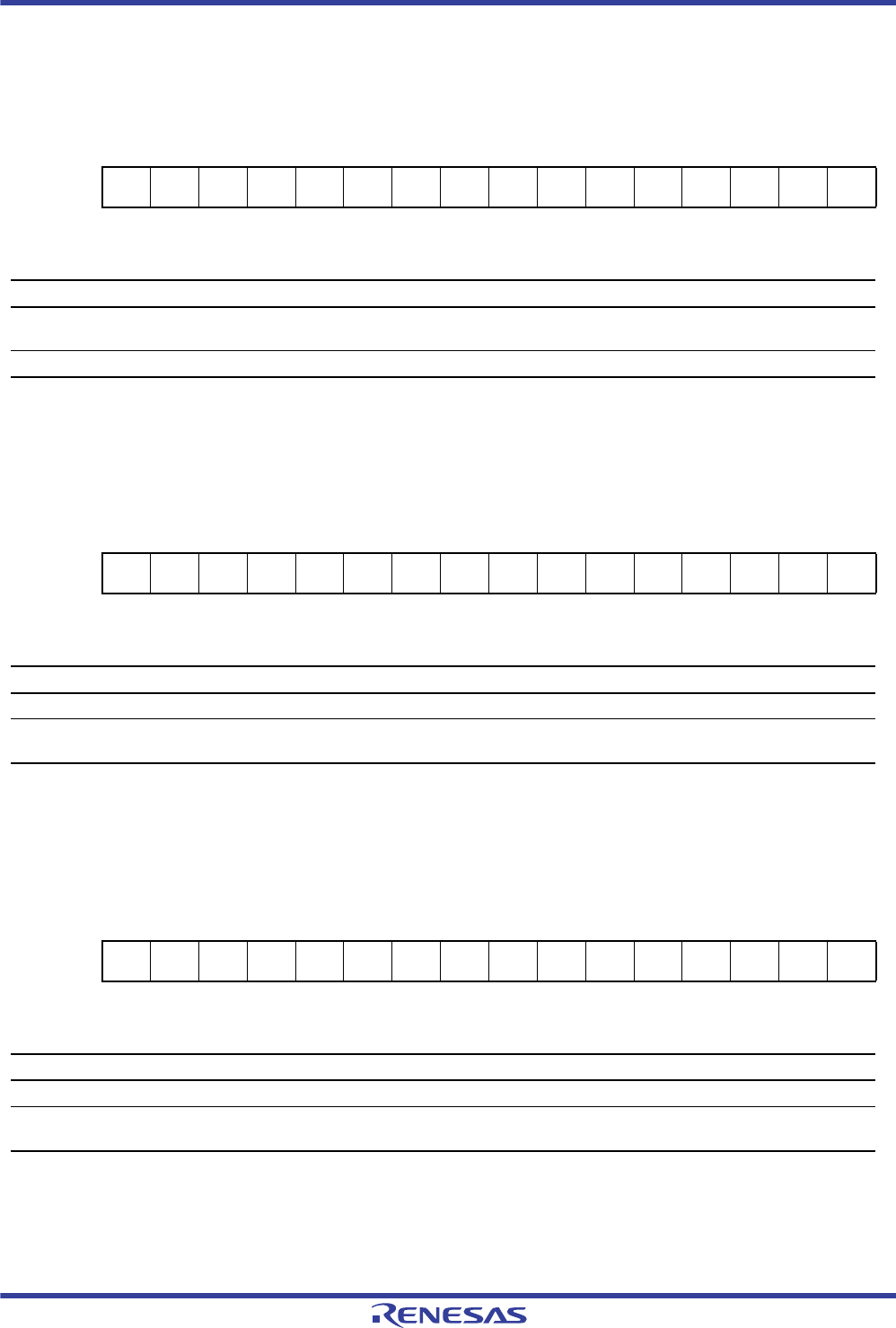
R01UH0034EJ0200 Rev.2.00 Page 1260 of 1489
Dec 27, 2013
RX62T Group, RX62G Group 28. 12-Bit A/D Converter (S12ADA)
When right-alignment with 8-bit precision is selected
When left-alignment with 12-bit precision is selected
When left-alignment with 10-bit precision is selected
Address: S12AD0.ADDRA0 0008 9020h, S12AD0.ADDRB 0008 9022h, S12AD0.ADDRC 0008 9024h,
S12AD0.ADDRD 0008 9026h, S12AD0.ADDRA1 0008 9030h
S12AD1.ADDRA0 0008 90A0h, S12AD1.ADDRB 0008 90A2h, S12AD1.ADDRC 0008 90A4h,
S12AD1.ADDRD 0008 90A6h, S12AD1.ADDRA1 0008 90B0h
b15 b14 b13 b12 b11 b10 b9 b8 b7 b6 b5 b4 b3 b2 b1 b0
————————AD11AD10AD9AD8AD7AD6AD5AD4
Value after reset: 0000000000000000
Bit Symbol Bit Name Description R/W
b7 to b0 AD11 to
AD4
A/D Converted Value 11
to 4
Upper eight bits of 12-bit A/D-converted value R
b15 to b8 — Reserved These bits are always read as 0. Writing 0 to these bits has no effect. R
Address: S12AD0.ADDR0A 0008 9020h, S12AD0.ADDR1 0008 9022h, S12AD0.ADDR2 0008 9024h,
S12AD0.ADDR3 0008 9026h, S12AD0.ADDR0B 0008 9030h
S12AD1.ADDR0A 0008 90A0h, S12AD1.ADDR1 0008 90A2h, S12AD1.ADDR2 0008 90A4h,
S12AD1.ADDR3 0008 90A6h, S12AD1.ADDR0B 0008 90B0h
b15 b14 b13 b12 b11 b10 b9 b8 b7 b6 b5 b4 b3 b2 b1 b0
AD11AD10AD9AD8AD7AD6AD5AD4AD3AD2AD1AD0————
Value after reset: 0000000000000000
Bit Symbol Bit Name Description R/W
b3 to b0 — Reserved These bits are always read as 0. Writing 0 to these bits has no effect. R
b15 to b4 AD11 to
AD0
A/D Converted Value 11
to 0
12-bit A/D-converted value R
Address: S12AD0.ADDR0A 0008 9020h, S12AD0.ADDR1 0008 9022h, S12AD0.ADDR2 0008 9024h,
S12AD0.ADDR3 0008 9026h, S12AD0.ADDR0B 0008 9030h
S12AD1.ADDR0A 0008 90A0h, S12ADS12AD1.ADDR1 0008 90A2h, S12AD1.ADDR2 0008 90A4h,
S12AD1.ADDR3 0008 90A6h, S12AD1.ADDR0B 0008 90B0h
b15 b14 b13 b12 b11 b10 b9 b8 b7 b6 b5 b4 b3 b2 b1 b0
AD11AD10AD9AD8AD7AD6AD5AD4AD3AD2——————
Value after reset: 0000000000000000
Bit Symbol Bit Name Description R/W
b5 to b0 — Reserved These bits are always read as 0. Writing 0 to these bits has no effect. R
b15 to b6 AD11 to
AD2
A/D Converted Value 11
to 2
Upper ten bits of 12-bit A/D-converted value R

R01UH0034EJ0200 Rev.2.00 Page 1261 of 1489
Dec 27, 2013
RX62T Group, RX62G Group 28. 12-Bit A/D Converter (S12ADA)
When left-alignment with 8-bit precision is selected
Address: S12AD0.ADDR0A 0008 9020h, S12AD0.ADDR1 0008 9022h, S12AD0.ADDR2 0008 9024h,
S12AD0.ADDR3 0008 9026h, S12AD0.ADDR0B 0008 9030h
S12AD1.ADDR0A 0008 90A0h, S12AD1.ADDR1 0008 90A2h, S12AD1.ADDR2 0008 90A4h,
S12AD1.ADDR3 0008 90A6h, S12AD1.ADDR0B 0008 90B0h
b15 b14 b13 b12 b11 b10 b9 b8 b7 b6 b5 b4 b3 b2 b1 b0
AD11AD10AD9AD8AD7AD6AD5AD4————————
Value after reset: 0000000000000000
Bit Symbol Bit Name Description R/W
b7 to b0 — Reserved These bits are always read as 0. Writing 0 to these bits has no effect. R
b15 to b8 AD11 to AD4 A/D Converted Value 11 to 4 Upper eight bits of 12-bit A/D-converted value R
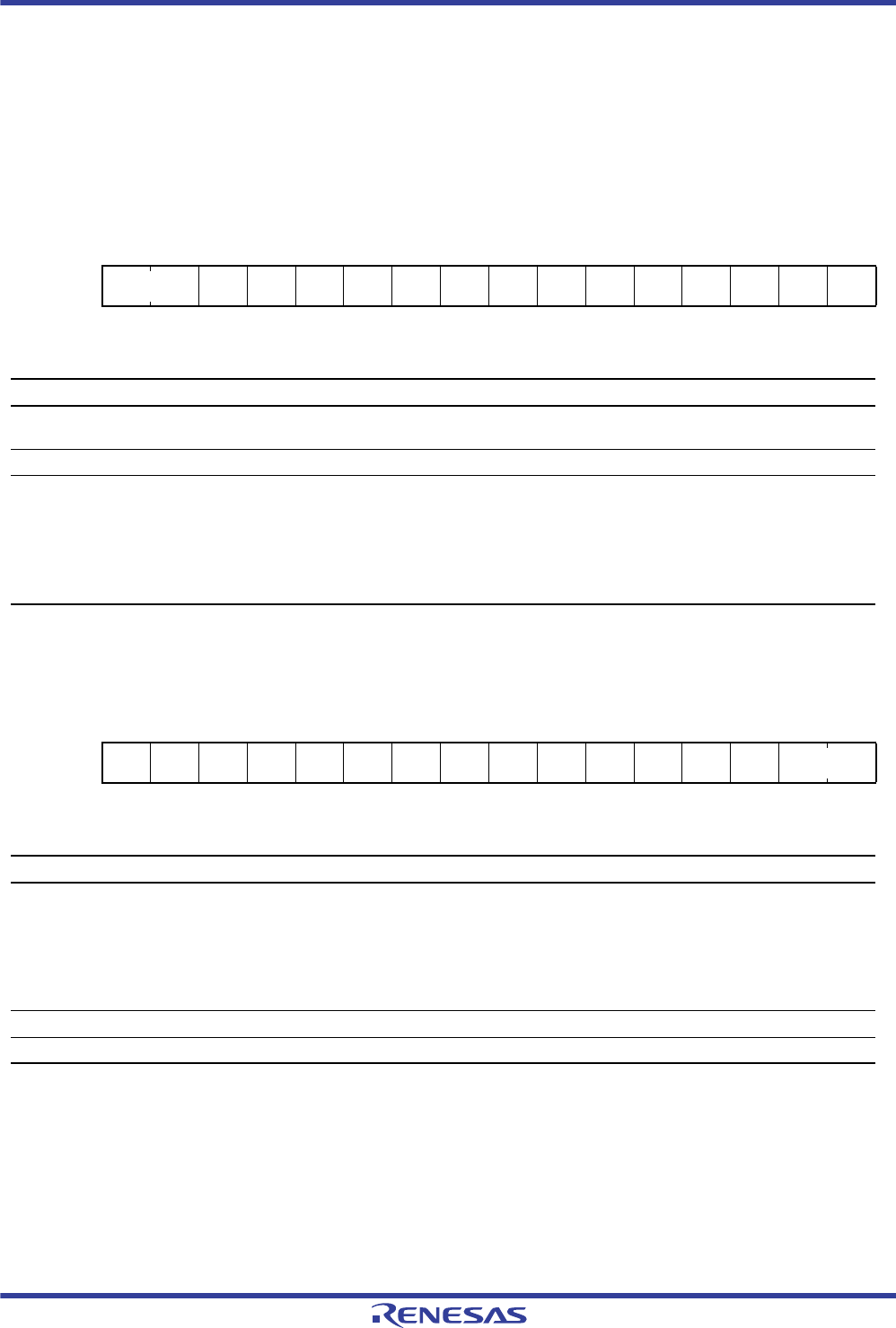
R01UH0034EJ0200 Rev.2.00 Page 1262 of 1489
Dec 27, 2013
RX62T Group, RX62G Group 28. 12-Bit A/D Converter (S12ADA)
(2) ADRD
The ADCER.ADRFMT bit can be used to specify either right- or left-alignment. The AD11 to AD0 bits indicate a 12-bit
A/D-converted value. Self diagnostic status (ADRD.DIAGST[1:0]) bits are also included. The other bits are reserved.
The reserved bits are always read as 0 and writing 0 to these bits has no effect.
When right-alignment is selected
When left-alignment is selected
Address: S12AD0.ADRD 0008 901Eh, S12AD1.ADRA 0008 909Eh
b15 b14 b13 b12 b11 b10 b9 b8 b7 b6 b5 b4 b3 b2 b1 b0
DISGST[1:0] — — AD11 AD10 AD9 AD8 AD7 AD6 AD5 AD4 AD3 AD2 AD1 AD0
Value after reset: 0000000000000000
Bit Symbol Bit Name Description R/W
b11 to b0 AD11 to
AD0
A/D Converted Value 11
to 0
12-bit A/D-converted value R
b13, b12 — Reserved These bits are always read as 0. Writing 0 to these bits has no effect. R
b15, b14 DIAGST
[1:0]
Self Diagnostic Status b15 b14
0 0:No self diagnostic has ever been performed since power-on.
0 1:Self diagnostic has been performed at a voltage of VREFH0 0.
1 0:Self diagnostic has been performed at a voltage of VREFH0 1/2.
1 1:Self diagnostic has been performed at a voltage of VREFH0 1.
Note: • For details on self diagnostic, see section 28.2.4, A/D Control
Extended Register (ADCER).
R
Address: S12AD0.ADRD 0008 901Eh, S12AD1.ADRD 0008 909Eh
b15 b14 b13 b12 b11 b10 b9 b8 b7 b6 b5 b4 b3 b2 b1 b0
AD11 AD10 AD9 AD8 AD7 AD6 AD5 AD4 AD3 AD2 AD1 AD0 — — DISGST[1:0]
Value after reset: 0000000000000000
Bit Symbol Bit Name Description R/W
b1, b0 DIAGST
[1:0]
Self Diagnostic Status b1 b0
0 0:No self diagnostic has ever been performed since power-on.
0 1:
Self diagnostic has been performed at a voltage of VREFH0
0.
1 0:
Self diagnostic has been performed at a voltage of VREFH0
1/2.
1 1:
Self diagnostic has been performed at a voltage of VREFH0
1.
Note: • For details on self diagnostic, section 28.2.4, A/D Control
Extended Register (ADCER).
R
b3, b2 — Reserved These bits are always read as 0. Writing 0 to these bits has no effect. R
b15 to b4 AD11 to AD0
A/D Converted Value 11 to 0
12-bit A/D-converted value R

R01UH0034EJ0200 Rev.2.00 Page 1263 of 1489
Dec 27, 2013
RX62T Group, RX62G Group 28. 12-Bit A/D Converter (S12ADA)
Note 1. When the A/D conversion startup source is neither "TRGnAN or TRGnBN (n = 4 or 7) in the MTU3" nor "GTADTRAnN or
GTADTRBnN (n = 0 to 3) in the GPT" (ADSTRGR.ADSTRSn[4:0] bit are not 01011b, 01111b, or 11001b to 11100b), the conversion
result is stored in ADDR0A.
Note 2. When the A/D conversion startup source is "TRGnAN or TRGnBN (n = 4 or 7) in the MTU3" (ADSTRGR.ADSTRSn[4:0] bits are set to
01011b or 01111b), the result of conversion started by TRGnAN is stored in ADDR0A and that started by TRGnBN is stored in
ADDR0B.
Note 3. When the A/D conversion startup source is "GTADTRAnN or GTADTRBnN (n = 0 to 3) in the GPT" (ADSTRGR.ADSTRSn[4:0] bits
are set to 11001b to 11100b), the result of conversion started by GTADTRAnN is stored in ADDR0A and that started by GTADTRBnN
is stored in ADDR0B.
Table 28.5 Analog Input Channels and Corresponding ADDRn Registers
Analog Input Channel ADDRn Register
AN000 S12AD0.ADDR0A and S12AD0.ADDR0B *
AN001 S12AD0.ADDR1
AN002 S12AD0.ADDR2
AN003 S12AD0.ADDR3
AN100 S12AD1.ADDR0A and S12AD1.ADDR0B *
AN101 S12AD1.ADDR1
AN102 S12AD1.ADDR2
AN103 S12AD1.ADDR3

R01UH0034EJ0200 Rev.2.00 Page 1264 of 1489
Dec 27, 2013
RX62T Group, RX62G Group 28. 12-Bit A/D Converter (S12ADA)
28.2.2 A/D Control Register (ADCSR)
Note: Starting an A/D conversion using an external trigger
If 1 is written to both the TRGE and EXTRG bits when a high-level signal is input to the external trigger pin (ADTRGn#), and then if the
ADTRGn# signal is driven low, the falling edge of ADTRGn# is detected and the A/D conversion process started.
In this case, the pulse width of the low-level input must be at least 1.5 PCLK clock cycles. (n = 0 or 1)
ADCSR selects the clock and performs the settings for A/D conversion start/stop, A/D conversion mode, and A/D
conversion trigger. The ADCS[1:0] and CKS[1:0] bits should be set while the ADST bit is 0.
CKS[1:0] Bits (Clock Select)
These bits set the frequency of the A/D conversion clock (ADCLK) and thus select the A/D conversion time.
Set the frequency of ADCLK above 4 MHz. When AVCC0 is in the range from 3.0 V to 3.6 V, set the frequency of
ADCLK below 25 MHz.
For details, see section 28.3.3, Analog Input Sampling and A/D Conversion Time.
Address: S12AD0.ADCSR 0008 9000h, S12AD1.ADCSR 0008 9080h
b7 b6 b5 b4 b3 b2 b1 b0
ADST ADCS[1:0] ADIE CKS[1:0] TRGE EXTRG
Value after reset: 00000000
Bit Symbol Bit Name Description R/W
b0 EXTRG Trigger Select 0: A/D conversion is started by a timer source selected by the A/D start
trigger select register (ADSTRGR).
1: A/D conversion is started by an external trigger (ADTRGn#).
(n = 0 or 1)
R/W
b1 TRGE Trigger Enable 0: Disables A/D conversion to be started by an external trigger
(ADTRGn#) or a trigger from MTU3 or GPT.
1: Enables A/D conversion to be started by an external trigger
(ADTRGn#) or a trigger from MTU3 or GPT.
(n = 0 or 1)
R/W
b3, b2 CKS[1:0] Clock Select b3 b2
0 0: PCLK/8
0 1: PCLK/4
1 0: PCLK/2
1 1: PCLK
R/W
b4 ADIE A/D Conversion End
Interrupt Enable
0: Disables S12ADI interrupt generation upon A/D conversion
completion.
1: Enables S12ADI interrupt generation upon A/D conversion
completion.
R/W
b6, b5 ADCS[1:0] A/D Conversion Mode
Select
b6 b5
0 0:Single mode
0 1:Single-cycle scan mode
1 0:Continuous scan mode
1 1:2-channel scan mode
R/W
b7 ADST A/D Start 0: Stops an A/D conversion process.
1: Starts an A/D conversion process.
R/W

R01UH0034EJ0200 Rev.2.00 Page 1265 of 1489
Dec 27, 2013
RX62T Group, RX62G Group 28. 12-Bit A/D Converter (S12ADA)
ADIE Bit (A/D Conversion End Interrupt Enable)
The ADIE bit enables or disables the A/D conversion end interrupt (S12ADI).
When A/D conversion of the specified channels is completed while the ADIE bit is set to 1, an A/D conversion end
interrupt (S12ADI) is generated.
ADCS[1:0] Bits (A/D Conversion Mode Select)
The ADCS bits select the A/D conversion mode.
In single mode, A/D conversion of the analog input from the single channel specified by the ADANS.CH[1:0] bits is
performed only once.
In single-cycle scan mode, A/D conversion of the analog inputs from up to four channels specified by the
ADANS.CH[1:0] bits is performed in the ascending order of channel numbers only once, and when A/D conversion of
all selected channels is completed, A/D conversion stops.
In continuous scan mode, while the ADCSR.ADST bit is 1, A/D conversion of the analog inputs from up to four
channels specified by the ADANS.CH[1:0] bits is performed in the ascending order of channel numbers, and when A/D
conversion of all selected channels is completed, A/D conversion returns to the first channel and repeats A/D conversion.
A/D conversion stops when the ADCSR.ADST bit is cleared to 0.
In 2-channel scan mode, four channels of analog inputs are separated into two groups and the start trigger can be
separately selected for each group. A/D conversion of the analog inputs from up to three channels specified by the
ADANS.CH[1:0] bits is performed in the ascending order of channel numbers only once, and when A/D conversion of
all selected channels is completed, A/D conversion stops.
ADST Bit (A/D Start)
This bit starts or stops an A/D conversion process. Before the ADST bit is set to 1, set the A/D conversion clock and
operating mode.
[Setting conditions]
When 1 is written by software
When the TRGE bit is set to 1, the EXTRG bit is cleared to 0, and the MTU3 or GPT trigger selected by the
ADSTRGR.ADSTRSn[4:0] bits is detected
When the TRGE and EXTRG bits are set to 1, the ADSTRGR.ADSTRSn[4:0] bits are set to 00000b, and an
external trigger is detected
[Clearing conditions]
When 0 is written by software
When A/D conversion is completed in single mode
When A/D conversion of all selected channels is completed in single-cycle scan mode
When A/D conversion of all selected channels in each group is completed in 2-channel scan mode

R01UH0034EJ0200 Rev.2.00 Page 1266 of 1489
Dec 27, 2013
RX62T Group, RX62G Group 28. 12-Bit A/D Converter (S12ADA)
28.2.3 A/D Channel Select Register (ADANS)
(1) S12AD0.ADANS
Address: 0008 9004h
b15 b14 b13 b12 b11 b10 b9 b8 b7 b6 b5 b4 b3 b2 b1 b0
— — CH[1:0] — PG002
SEL PG001
SEL PG000
SEL —————
PG002
EN PG001
EN PG000
EN
Value after reset: 0000000000000000
Bit Symbol Bit Name Description R/W
b0 PG000EN AN000 Programmable
Gain Amplifier Enable
0: Programmable gain amplifier disabled
1: Programmable gain amplifier enabled
R/W
b1 PG001EN AN001 Programmable
Gain Amplifier Enable
0: Programmable gain amplifier disabled
1: Programmable gain amplifier enabled
R/W
b2 PG002EN AN002 Programmable
Gain Amplifier Enable
0: Programmable gain amplifier disabled
1: Programmable gain amplifier enabled
R/W
b7 to b3 — Reserved These bits are always read as 0. The write value should always be 0. R/W
b8 PG000SEL AN000 Programmable
Gain Amplifier Select
0: Programmable gain amplifier not used (bypassed)
1: Programmable gain amplifier used
R/W
b9 PG001SEL AN001 Programmable
Gain Amplifier Select
0: Programmable gain amplifier not used (bypassed)
1: Programmable gain amplifier used
R/W
b10 PG002SEL AN002 Programmable
Gain Amplifier Select
0: Programmable gain amplifier not used (bypassed)
1: Programmable gain amplifier used
R/W
b11 — Reserved This bit is always read as 0. The write value should always be 0. R/W
b13, b12 CH[1:0] Channel Set These bits select the analog input channels to be A/D-converted in
S12AD0. For details, see Table 28.6
R/W
b15, b14 — Reserved These bits are always read as 0. The write value should always be 0. R/W

R01UH0034EJ0200 Rev.2.00 Page 1267 of 1489
Dec 27, 2013
RX62T Group, RX62G Group 28. 12-Bit A/D Converter (S12ADA)
(2) S12AD1.ADANS
ADANS is a register that selects the channels that are subject to A/D conversion and specifies whether to enable and use
the programmable gain amplifiers for AN000 to AN002 and AN100 and AN102.
Note that ADANS should be specified only while the ADCSR.ADST bit is 0.
PGnEN Bit (ANn Programmable Gain Amplifier Enable) (n = 000 to 002 and 100 to 102)
The PGnEN bit enables or disables the programmable gain amplifier.
PGnSEL Bit (ANn Programmable Gain Amplifier Select) (n = 000 to 002 and 100 to 102)
The PGnSEL bit specifies whether to use the programmable gain amplifier.
CH[1:0] Bits (Channel Set)
The CH[1:0] bits specify the channels subject to A/D conversion. This setting depends on the ADCSR.ADCS[1:0] bit
setting. For details, refer to Table 28.6.
Address: 0008 9084h
b15 b14 b13 b12 b11 b10 b9 b8 b7 b6 b5 b4 b3 b2 b1 b0
— — CH[1:0] — PG102
SEL PG101
SEL PG100
SEL —————
PG102
EN PG101
EN PG100
EN
Value after reset: 0000000000000000
Bit Symbol Bit Name Description R/W
b0 PG100EN AN100 Programmable
Gain Amplifier Enable
0: Programmable gain amplifier disabled
1: Programmable gain amplifier enabled
R/W
b1 PG101EN AN101 Programmable
Gain Amplifier Enable
0: Programmable gain amplifier disabled
1: Programmable gain amplifier enabled
R/W
b2 PG102EN AN102 Programmable
Gain Amplifier Enable
0: Programmable gain amplifier disabled
1: Programmable gain amplifier enabled
R/W
b7 to b3 — Reserved These bits are always read as 0. The write value should always be 0. R/W
b8 PG100SEL AN100 Programmable
Gain Amplifier Select
0: Programmable gain amplifier not used (bypassed)
1: Programmable gain amplifier used
R/W
b9 PG101SEL AN101 Programmable
Gain Amplifier Select
0: Programmable gain amplifier not used (bypassed)
1: Programmable gain amplifier used
R/W
b10 PG102SEL AN102 Programmable
Gain Amplifier Select
0: Programmable gain amplifier not used (bypassed)
1: Programmable gain amplifier used
R/W
b11 — Reserved This bit is always read as 0. The write value should always be 0. R/W
b13, b12 CH[1:0] Channel Set These bits select the analog input channels to be A/D-converted in
S12AD0. For details, see Table 28.6
R/W
b15, b14 — Reserved These bits are always read as 0. The write value should always be 0. R/W

R01UH0034EJ0200 Rev.2.00 Page 1268 of 1489
Dec 27, 2013
RX62T Group, RX62G Group 28. 12-Bit A/D Converter (S12ADA)
Table 28.6 Conversion Channel Settings
ADANS.CH[1:0]
Analog Input Channel
Single Mode Single-Cycle Scan Mode/Continuous Scan Mode
b1 b0 S12AD0 S12AD1 S12AD0 S12AD1
0 0 AN000 AN100 AN000 AN100
0 1 AN001 AN101 AN000, AN001 AN100, AN101
1 0 AN002 AN102 AN000 to AN002 AN100 to AN102
1 1 AN003 AN103 AN000 to AN003 AN100 to AN103
ADANS.CH[1:0]
Analog Input Channel
2-Channel Scan Mode (Started by Timer Trigger or External Trigger)
b1 b0 S12AD0 S12AD1
0 0 Group 0: AN000
Group 1: AN001 to AN003
Group 0: AN100
Group 1: AN101 to AN103
0 1 Group 0: AN000, AN001
Group 1: AN002, AN003
Group 0: AN100, AN101
Group 1: AN102, AN103
1 0 Group 0: AN000 to AN002
Group 1: AN003
Group 0: AN100 to AN102
Group 1: AN103
1 1 Setting prohibited (same operation as 00b) Setting prohibited (same operation as 00b)
ADANS.CH[1:0]
Analog Input Channel
2-Channel Scan Mode (Started by Software)
b1 b0 S12AD0 S12AD1
0 0 AN000 AN100
0 1 AN000, AN001 AN100, AN101
1 0 AN000 to AN002 AN100 to AN102
1 1 AN000 to AN003 AN100 to AN103

R01UH0034EJ0200 Rev.2.00 Page 1269 of 1489
Dec 27, 2013
RX62T Group, RX62G Group 28. 12-Bit A/D Converter (S12ADA)
28.2.4 A/D Control Extended Register (ADCER)
ADCER sets the A/D data register format, self diagnostic mode, and automatic clearing of registers, and selects the
sample-and-hold circuit dedicated for the channel and interrupt generation. The ADCER value should be changed only
while the ADCSR.ADST bit is 0.
SHBYP Bit (Dedicated Sample-and-Hold Circuit Select)
The SHBYP bit selects whether to use the sample-and-hold circuit dedicated for the channel.
When a programmable gain amplifier is in use, set the SHBYP bit to 0 (selecting use of the sample-and-hold circuit).
Address: S12AD0.ADCER 0008 900Eh, S12AD1.ADCER 0008 908Eh
b15 b14 b13 b12 b11 b10 b9 b8 b7 b6 b5 b4 b3 b2 b1 b0
ADRFM
T— ADIEW ADIE2 DIAGM DIAGL
DDIAGVAL[1:0] — — ACE — — ADPRC[1:0] SHBYP
Value after reset: 0000000000000000
Bit Symbol Bit Name Description R/W
b0 SHBYP Dedicated Sample-and-
Hold Circuit Select
0: Sample-and-hold circuit used
1: Sample-and-hold circuit not used
R/W
b2, b1 ADPRC[1:0] A/D Data Register Bit
Precision Set
0 0: Stored in A/D data register with 12-bit precision
0 1: Stored in A/D data register with 10-bit precision
1 0: Stored in A/D data register with 8-bit precision
1 1: Setting prohibited (Stored with 12-bit precision)
R/W
b4, b3 — Reserved These bits are always read as 0. The write value should always be 0. R/W
b5 ACE Automatic Clearing
Enable
0: Disables automatic clearing of ADDRn and ADRD after they have
been read.
1: Enables automatic clearing of ADDRn and ADRD after they have
been read.
R/W
b7, b6 — Reserved These bits are always read as 0. The write value should always be 0. R/W
b9, b8 DIAGVAL[1:0] Self Diagnostic Voltage
Select
b9 b8
0 0: Setting prohibited
0 1: Self diagnostic at a voltage of VREFH0 0
1 0: Self diagnostic at a voltage of VREFH0 1/2
1 1: Self diagnostic at a voltage of VREFH0 1
R/W
b10 DIAGLD Self Diagnostic Mode
Select
0: Self diagnostic voltages are automatically rotated
1: Self diagnostic voltage is fixed to the DIAGVAL[1:0] bit setting
R/W
b11 DIAGM Self Diagnostic Enable 0: Self diagnostic of the A/D converter is not performed
1: Self diagnostic of the A/D converter is performed
R/W
b12 ADIE2 2-Channel Scan Interrupt
Select
0: S12ADI interrupt is generated every time a conversion process
started by either of group 0 and 1 triggers is completed
1: S12ADI interrupt is generated when the conversion processes
started by group 0 and 1 triggers are both completed
R/W
b13 ADIEW Double Trigger Interrupt
Select
0: S12ADI interrupt is generated every time a conversion process
started by either of the double triggers is completed
1: S12ADI interrupt is generate when the conversion processes started
by the double triggers are both completed
R/W
b14 — Reserved This bit is always read as 0. The write value should always be 0. R/W
b15 ADRFMT A/D Data Register
Format Select
0: Right-alignment is selected for the A/D data register format.
1: Left-alignment is selected for the A/D data register format.
R/W

R01UH0034EJ0200 Rev.2.00 Page 1270 of 1489
Dec 27, 2013
RX62T Group, RX62G Group 28. 12-Bit A/D Converter (S12ADA)
ADPRC Bit (A/D Data Register Bit Precision Set)
The ADPRC bit selects the precision for storing A/D conversion results in the A/D data register from 8 bits, 10 bits, and
12 bits.
ACE Bit (Automatic Clearing Enable)
The ACE bit enables or disables automatic clearing of ADDRn or ADRD after it has been read by the CPU or DTC. This
function enables update failures of ADDRn and ADRD to be detected.
DIAGVAL[1:0] Bits (Self Diagnostic Voltage Select)
For details of these bits, refer to the description of the DIAGLD bit. When the DIAGVAL[1:0] bits are set to 00b (setting
prohibited) which is the initial value, do not start self diagnostic with the DIAGLD bit to set to 1.
DIAGLD Bit (Self Diagnostic Mode Select)
The DIAGLD bit selects whether to rotate among three voltages or use a fixed voltage for conversion in self diagnostic.
When the DIAGLD bit is cleared to 0, three voltages are converted in turn, in the order of VREFH0 × 0 → VREFH0 × 1/
2 → VREFH0 × 1. After a power-on reset, self diagnostic starts with VREFH0 × 0. Even when scan conversion is
completed, the self-diagnostic voltage is not reset to VREFH0 × 0; when scan conversion is performed again, voltage
rotation starts from where conversion is completed in the previous diagnostic.
When the DIAGLD bit is set to 1, the conversion voltage is fixed at that specified in the DIAGVAL[1:0] bits (automatic
rotation is not done). When the DIAGLD bit is cleared to 0 again, rotation starts from the voltage fixed before (load
function).
DIAGM Bit (Self Diagnostic Enable)
The self diagnostic function is used to detect faults in the A/D converter. One of three internally-generated voltages,
VREFH0 × 0, VREFH0 × 1/2, and VREFH0 × 1, is converted.
After A/D conversion ends, the A/D-converted value and information on the converted voltage are stored in A/D data
register Diag (ADRD). Then, whether the conversion result is within the normal range (normal) or not (error) can be
found out from the values read from ADRD by software. Self diagnostic is performed before the smallest-numbered
channel is converted in the scan conversion process.
In each execution of self diagnostic, one of the three voltages is converted, and the three voltages are automatically
rotated each time self diagnostic is executed. The execution time required for self diagnostic is equal to the A/D
conversion time for one channel.
ADIE2 Bit (2-Channel Scan Interrupt Select)
The ADIE2 bit selects the timing for generating an S12ADI interrupt in 2-channel scan mode. The ADIE2 bit setting is
valid only when A/D conversion is started by a trigger (ADCSR.TRGE = 1) in 2-channel scan mode.
ADIEW Bit (Double Trigger Interrupt Select)
The ADIEW bit selects the timing for generating an S12ADI interrupt when double triggers are selected. The ADIEW bit
setting is valid only when A/D conversion is started by a trigger (ADCSR.TRGE = 1) and the trigger source is set to
"TRG4AN or TRG4BN", "TRG7AN or TRG7BN", "GTADTRA0N or GTADTRB0N", "GTADTRA1N or
GTADTRB1N", "GTADTRA2N or GTADTRB2N", or "GTADTRA3N or GTADTRB3N".
ADRFMT Bit (A/D Data Register Format Select)
The ADRFMT bit specifies left-alignment or right-alignment for the data to be stored in the A/D data register.
For details on the format of the A/D data registers, see section 28.2.1, A/D Data Registers n (ADDRn) (n = 0A, 0B,
and 1 to 3) and A/D Data register Diag (ADRD).

R01UH0034EJ0200 Rev.2.00 Page 1271 of 1489
Dec 27, 2013
RX62T Group, RX62G Group 28. 12-Bit A/D Converter (S12ADA)
28.2.5 A/D Start Trigger Select Register (ADSTRGR)
ADSTRGR selects the A/D conversion startup trigger.
The ADSTRGR value should be changed only while the ADCSR.ADST bit is 0.
Software trigger (ADCSR.ADST bit) is always enabled regardless of the values set in the ADCSR.TRGE,
ADCSR.EXTRG, and ADSTRGR register.
When using an external input as the A/D conversion startup trigger (ADTRGn#), set the ADCSR.TRGE bit to 1 and
the ADCSR.EXTRG bit to 1. (n = 0 or 1)
When using the MTU3 or GPT as the A/D conversion startup source, set the ADCSR.TRGE bit to 1 and the
ADCSR.EXTRG bit to 0.
Address: 12ADA0.ADSTRGR 0008 9010h, S12AD1.ADSTRGR 0008 9090h
b15 b14 b13 b12 b11 b10 b9 b8 b7 b6 b5 b4 b3 b2 b1 b0
— — — ADSTRS1[4:0] — — — ADSTRS0[4:0]
Value after reset: 0000000000000000
Bit Symbol Bit Name Description R/W
b4 to b0 ADSTRS0[4:0] A/D Start Trigger
Group 0 Select
The combination of bits 4 to 0 selects the source of requests to start A/D
conversion from among various on-chip peripheral I/O sources and
input on the trigger input pin. Specify the starting source for conversion
in single mode, single-cycle scan mode, continuous scan mode or the
starting source for group 0 when conversion is in two-channel scan
mode. See Table 28.7 for the correspondence between the settings and
starting sources.
R/W
b7, b5 — Reserved These bits are always read as 0. The write value should always be 0. R/W
b12 to b8 ADSTRS1[4:0] A/D Start Trigger
Group 1 Select
These bits are only used in two-channel scan mode. The combination of
bits 4 to 0 selects the source of requests to start A/D conversion from
among various on-chip peripheral I/O sources and input on the trigger
input pin. Specify the starting source for group 1 when conversion is in
two-channel scan mode. See Table 28.7 for the correspondence
between the settings and starting sources.
In two-channel scan mode, specify different sources for requests to start
conversion by group 0 and group 1 such that requests to start
conversion by both groups are not generated at the same time.
R/W
b15 to b13 — Reserved These bits are always read as 0. The write value should always be 0. R/W

R01UH0034EJ0200 Rev.2.00 Page 1272 of 1489
Dec 27, 2013
RX62T Group, RX62G Group 28. 12-Bit A/D Converter (S12ADA)
Table 28.7 List of A/D Conversion Startup Sources
Module
A/D
Conversion
Startup
Sources Startup Condition
ADSTRSn
[4]
ADSTRSn
[3]
ADSTRSn
[2]
ADSTRSn
[1]
ADSTRSn
[0]
Software ADST ADCSR.ADST bit is set — — — — —
External
pin
ADTRGn# Trigger input pin 0 0 0 0 0
MTU3 TRGA0N Compare match/input capture in MTU0.TGRA 0 0 0 0 1
TRGA1N Compare match/input capture in MTU1.TGRA 0 0 0 1 0
TRGA2N Compare match/input capture in MTU2.TGRA 0 0 0 1 1
TRGA3N Compare match/input capture in MTU3.TGRA 0 0 1 0 0
TRGA4N Compare match/input capture in MTU4.TGRA,
or MTU4.TCNT underflow in complementary
PWM mode (trough)
0 0 1 0 1
TRGA6N Compare match/input capture in MTU6.TGRA 0 0 1 1 0
TRGA7N Compare match/input capture in MTU7.TGRA,
or MTU7.TCNT underflow in complementary
PWM mode (trough)
0 0 1 1 1
TRG0N Compare match in MTU0.TGRE 0 1 0 0 0
TRG4AN Compare match between MTU4.TADCORA
and MTU4.TCNT
0 1 0 0 1
TRG4BN Compare match between MTU4.TADCORB
and MTU4.TCNT
0 1 0 1 0
TRG4AN or
TRG4BN
Compare match between MTU4.TADCORA
and MTU4.TCNT or compare match between
MTU4.TADCORB and MTU4.TCNT
0 1 0 1 1
TRG4ABN Compare match between MTU4.TADCORA
and MTU4.TCNT and compare match between
MTU4.TADCORB and MTU4.TCNT
(when interrupt skipping function 2 is used)
0 1 1 0 0
TRG7AN Compare match between MTU7.TADCORA
and MTU7.TCNT
0 1 1 0 1
TRG7BN Compare match between MTU7.TADCORB
and MTU7.TCNT
0 1 1 1 0
TRG7AN or
TRG7BN
Compare match between MTU7.TADCORA
and MTU7.TCNT or compare match between
MTU7.TADCORB and MTU7.TCNT
0 1 1 1 1
TRG7ABN Compare match between MTU7.TADCORA
and MTU7.TCNT and compare match between
MTU7.TADCORB and MTU7.TCNT
(when interrupt skipping function 2 is used)
1 0 0 0 0

R01UH0034EJ0200 Rev.2.00 Page 1273 of 1489
Dec 27, 2013
RX62T Group, RX62G Group 28. 12-Bit A/D Converter (S12ADA)
Note: • When ADTRGn# is used as the A/D conversion trigger, the PORTn.DDR.Bj bit and PORTn.ICR.Bj bit corresponding to the pin
should be set to 0 (input port) and 1 (the input buffer of the corresponding pin enabled), respectively. For details, refer to section
15, I/O Ports.
GPT GTADTRA0N Compare match in GPT0.GTADTRA 1 0 0 0 1
GTADTRB0N Compare match in GPT0.GTADTRB 1 0 0 1 0
GTADTRA1N Compare match in GPT1.GTADTRA 1 0 0 1 1
GTADTRB1N Compare match in GPT1.GTADTRB 1 0 1 0 0
GTADTRA2N Compare match in GPT2.GTADTRA 1 0 1 0 1
GTADTRB2N Compare match in GPT2.GTADTRB 1 0 1 1 0
GTADTRA3N Compare match in GPT3.GTADTRA 1 0 1 1 1
GTADTRB3N Compare match in GPT3.GTADTRB 1 1 0 0 0
GTADTRA0N
or
GTADTRB0N
Compare match in GPT0.GTADTRA or
compare match in GPT0.GTADTRB
1 1 0 0 1
GTADTRA1N
or
GTADTRB1N
Compare match in GPT1.GTADTRA or
compare match in GPT1.GTADTRB
1 1 0 1 0
GTADTRA2N
or
GTADTRB2N
Compare match in GPT2.GTADTRA or
compare match in GPT2.GTADTRB
1 1 0 1 1
GTADTRA3N
or
GTADTRB3N
Compare match in GPT3.GTADTRA or
compare match in GPT3.GTADTRB
1 1 1 0 0
Table 28.7 List of A/D Conversion Startup Sources
Module
A/D
Conversion
Startup
Sources Startup Condition
ADSTRSn
[4]
ADSTRSn
[3]
ADSTRSn
[2]
ADSTRSn
[1]
ADSTRSn
[0]

R01UH0034EJ0200 Rev.2.00 Page 1274 of 1489
Dec 27, 2013
RX62T Group, RX62G Group 28. 12-Bit A/D Converter (S12ADA)
28.2.6 A/D Programmable Gain Amplifier Register (ADPG)
(1) S12AD0.ADPG
Address: 0008 900Ah
b15 b14 b13 b12 b11 b10 b9 b8 b7 b6 b5 b4 b3 b2 b1 b0
———— PG002GAIN[3:0] PG001GAIN[3:0] PG000GAIN[3:0]
Value after reset: 0000000000000000
Bit Symbol Bit Name Description R/W
b3 to b0 PG000GAI
N[3:0]
Gain Select for AN000
Programmable Gain
Amplifier
b3 b0
0 0 0 0: 2.0
0 0 0 1: 2.5
0 0 1 0: Setting prohibited
0 0 1 1: Setting prohibited
0 1 0 0: 3.077
0 1 0 1: Setting prohibited
0 1 1 0: 3.636
0 1 1 1: 4.0
1 0 0 0: 4.444
1 0 0 1: 5.0
1 0 1 0: 5.714
1 0 1 1: 6.667
1 1 0 0: Setting prohibited
1 1 0 1: 10.0
1 1 1 0: 13.333
1 1 1 1: Setting prohibited
R/W
b7 to b4 PG001GAI
N[3:0]
Gain Select for AN001
Programmable Gain
Amplifier
b7 b4
0 0 0 0: 2.0
0 0 0 1: 2.5
0 0 1 0: Setting prohibited
0 0 1 1: Setting prohibited
0 1 0 0: 3.077
0 1 0 1: Setting prohibited
0 1 1 0: 3.636
0 1 1 1: 4.0
1 0 0 0: 4.444
1 0 0 1: 5.0
1 0 1 0: 5.714
1 0 1 1: 6.667
1 1 0 0: Setting prohibited
1 1 0 1: 10.0
1 1 1 0: 13.333
1 1 1 1: Setting prohibited
R/W
b11 to b8 PG002GAI
N[3:0]
Gain Select for AN002
Programmable Gain
Amplifier
b11 b8
0 0 0 0: 2.0
0 0 0 1: 2.5
0 0 1 0: Setting prohibited
0 0 1 1: Setting prohibited
0 1 0 0: 3.077
0 1 0 1: Setting prohibited
0 1 1 0: 3.636
0 1 1 1: 4.0
1 0 0 0: 4.444
1 0 0 1: 5.0
1 0 1 0: 5.714
1 0 1 1: 6.667
1 1 0 0: Setting prohibited
1 1 0 1: 10.0
1 1 1 0: 13.333
1 1 1 1: Setting prohibited
R/W
b15 to
b12
— Reserved These bits are always read as 0. The write value should always be 0. R/W

R01UH0034EJ0200 Rev.2.00 Page 1275 of 1489
Dec 27, 2013
RX62T Group, RX62G Group 28. 12-Bit A/D Converter (S12ADA)
(2) S12AD1.ADPG
Address: 0008 908Ah
b15 b14 b13 b12 b11 b10 b9 b8 b7 b6 b5 b4 b3 b2 b1 b0
———— PG102GAIN[3:0] PG101GAIN[3:0] PG100GAIN[3:0]
Value after reset: 0000000000000000
Bit Symbol Bit Name Description R/W
b3 to b0 PG100GAI
N[3:0]
Gain Select for AN100
Programmable Gain
Amplifier
b3 b0
0 0 0 0: 2.0
0 0 0 1: 2.5
0 0 1 0: Setting prohibited
0 0 1 1: Setting prohibited
0 1 0 0: 3.077
0 1 0 1: Setting prohibited
0 1 1 0: 3.636
0 1 1 1: 4.0
1 0 0 0: 4.444
1 0 0 1: 5.0
1 0 1 0: 5.714
1 0 1 1: 6.667
1 1 0 0: Setting prohibited
1 1 0 1: 10.0
1 1 1 0: 13.333
1 1 1 1: Setting prohibited
R/W
b7 to b4 PG101GAI
N[3:0]
Gain Select for AN101
Programmable Gain
Amplifier
b7 b4
0 0 0 0: 2.0
0 0 0 1: 2.5
0 0 1 0: Setting prohibited
0 0 1 1: Setting prohibited
0 1 0 0: 3.077
0 1 0 1: Setting prohibited
0 1 1 0: 3.636
0 1 1 1: 4.0
1 0 0 0: 4.444
1 0 0 1: 5.0
1 0 1 0: 5.714
1 0 1 1: 6.667
1 1 0 0: Setting prohibited
1 1 0 1: 10.0
1 1 1 0: 13.333
1 1 1 1: Setting prohibited
R/W
b11 to b8 PG102GAI
N[3:0]
Gain Select for AN102
Programmable Gain
Amplifier
b11 b8
0 0 0 0: 2.0
0 0 0 1: 2.5
0 0 1 0: Setting prohibited
0 0 1 1: Setting prohibited
0 1 0 0: 3.077
0 1 0 1: Setting prohibited
0 1 1 0: 3.636
0 1 1 1: 4.0
1 0 0 0: 4.444
1 0 0 1: 5.0
1 0 1 0: 5.714
1 0 1 1: 6.667
1 1 0 0: Setting prohibited
1 1 0 1: 10.0
1 1 1 0: 13.333
1 1 1 1: Setting prohibited
R/W
b15 to
b12
— Reserved These bits are always read as 0. The write value should always be 0. R/W

R01UH0034EJ0200 Rev.2.00 Page 1276 of 1489
Dec 27, 2013
RX62T Group, RX62G Group 28. 12-Bit A/D Converter (S12ADA)
ADPG specifies the gains for the programmable gain amplifiers provided for AN000 to AN002 and AN100 to AN102.
The ADPG value should be changed only while the ADCSR.ADST bit is 0.
PGnGAIN[3:0] Bits (Gain Select for ANn Programmable Gain Amplifier) (n = 000 to 002 or 100 to 102)
The PGnGAIN bits specify the gain for the programmable gain amplifier.

R01UH0034EJ0200 Rev.2.00 Page 1277 of 1489
Dec 27, 2013
RX62T Group, RX62G Group 28. 12-Bit A/D Converter (S12ADA)
28.2.7 Comparator Operating Mode Select Register 0 (ADCMPMD0)
ADCMPMD0 specifies whether to use the comparators.
Address: 0008 9012h
b15 b14 b13 b12 b11 b10 b9 b8 b7 b6 b5 b4 b3 b2 b1 b0
— — CEN102[1:0] CEN101[1:0] CEN100[1:0] — — CEN002[1:0] CEN001[1:0] CEN000[1:0]
Value after reset: 0000000000000000
Bit Symbol Bit Name Description R/W
b1, b0 CEN000[1:0] AN000 Comparator
Select
b1 b0
0 0:Comparator is not used
0 1:Used as a low-level comparator, which detects a voltage lower than
the low reference voltage
1 0:Used as a high-level comparator, which detects a voltage higher
than the high reference voltage
1 1:Used as a window comparator, which detects a voltage outside the
range from the low reference voltage to the high reference voltage
R/W
b3, b2 CEN001[1:0] AN001 Comparator
Select
b3 b2
0 0:Comparator is not used
0 1:Used as a low-level comparator, which detects a voltage lower than
the low reference voltage
1 0:Used as a high-level comparator, which detects a voltage higher
than the high reference voltage
1 1:Used as a window comparator, which detects a voltage outside the
range from the low reference voltage to the high reference voltage
R/W
b5, b4 CEN002[1:0] AN002 Comparator
Select
b5 b4
0 0:Comparator is not used
0 1:Used as a low-level comparator, which detects a voltage lower than
the low reference voltage
1 0:Used as a high-level comparator, which detects a voltage higher
than the high reference voltage
1 1:Used as a window comparator, which detects a voltage outside the
range from the low reference voltage to the high reference voltage
R/W
b7, b6 — Reserved These bits are always read as 0. The write value should always be 0. R/W
b9, b8 CEN100[1:0] AN100 Comparator
Select
b9 b8
0 0:Comparator is not used
0 1:Used as a low-level comparator, which detects a voltage lower than
the low reference voltage
1 0:Used as a high-level comparator, which detects a voltage higher
than the high reference voltage
1 1:Used as a window comparator, which detects a voltage outside the
range from the low reference voltage to the high reference voltage
R/W
b11, b10 CEN101[1:0] AN101 Comparator
Select
b11 b10
0 0:Comparator is not used
0 1:Used as a low-level comparator, which detects a voltage lower than
the low reference voltage
1 0:Used as a high-level comparator, which detects a voltage higher
than the high reference voltage
1 1:Used as a window comparator, which detects a voltage outside the
range from the low reference voltage to the high reference voltage
R/W
b13, b12 CEN102[1:0] AN102 Comparator
Select
b13 b12
0 0:Comparator is not used
0 1:Used as a low-level comparator, which detects a voltage lower than
the low reference voltage
1 0:Used as a high-level comparator, which detects a voltage higher
than the high reference voltage
1 1:Used as a window comparator, which detects a voltage outside the
range from the low reference voltage to the high reference voltage
R/W
b15, b14 — Reserved These bits are always read as 0. The write value should always be 0. R/W

R01UH0034EJ0200 Rev.2.00 Page 1278 of 1489
Dec 27, 2013
RX62T Group, RX62G Group 28. 12-Bit A/D Converter (S12ADA)
CENn[1:0] Bits (ANn Comparator Select) (n = 000 to 002 or 100 to 102)
The CENn[1:0] bits specify whether to use each comparator and select the operating mode for the comparator.

R01UH0034EJ0200 Rev.2.00 Page 1279 of 1489
Dec 27, 2013
RX62T Group, RX62G Group 28. 12-Bit A/D Converter (S12ADA)
28.2.8 Comparator Operating Mode Select Register 1 (ADCMPMD1)
Address: 0008 9014h
b15 b14 b13 b12 b11 b10 b9 b8 b7 b6 b5 b4 b3 b2 b1 b0
—VSELL
1VSELH
1CSEL1 — VSELL
0VSELH
0CSEL0 — REFH[2:0] — REFL[2:0]
Value after reset: 0000000000000000
Bit Symbol Bit Name Description R/W
b2 to b0 REFL[2:0] Internal Voltage Select for
Comparator Low
Reference Voltage
b2 b1 b0
0 0 0: Invalid
0 0 1: AVCC0 1/8
0 1 0: AVCC0 2/8
0 1 1: AVCC0 3/8
1 0 0: AVCC0 4/8
1 0 1: AVCC0 5/8
1 1 0: AVCC0 6/8
1 1 1: AVCC0 7/8
R/W
b3 — Reserved This bit is always read as 0. The write value should always be 0. R/W
b6 to b4 REFH[2:0] Internal Voltage Select for
Comparator High
Reference Voltage
b6 b5 b3
0 0 0: Invalid
0 0 1: AVCC0 1/8
0 1 0: AVCC0 2/8
0 1 1: AVCC0 3/8
1 0 0: AVCC0 4/8
1 0 1: AVCC0 5/8
1 1 0: AVCC0 6/8
1 1 1: AVCC0 7/8
R/W
b7 — Reserved This bit is always read as 0. The write value should always be 0. R/W
b8 CSEL0 AN000 to AN002
Comparator Input Select
0:Signal before amplified by the programmable gain amplifier is input to
the comparator
1:Signal after amplified by the programmable gain amplifier is input to
the comparator
R/W
b9 VSELH0 AN000 to AN002
Comparator High
Reference Voltage Select
0: High reference voltage is input from the AN103 pin
1: Internal voltage selected through the REFH[2:0] bits are input as the
high reference voltage
R/W
b10 VSELL0 AN000 to AN002
Comparator Low
Reference Voltage Select
0: Low reference voltage is input from the AN003 pin
1: Internal voltage selected through the REFL[2:0] bits are input as the
low reference voltage
R/W
b11 — Reserved This bit is always read as 0. The write value should always be 0. R/W
b12 CSEL1 AN100 to AN102
Comparator Input Select
0:Signal before amplified by the programmable gain amplifier is input to
the comparator
1:Signal after amplified by the programmable gain amplifier is input to
the comparator
R/W
b13 VSELH1 AN100 to AN102
Comparator High
Reference Voltage Select
0: High reference voltage is input from the AN103 pin
1: Internal voltage selected through the REFH[2:0] bits are input as the
high reference voltage
R/W
b14 VSELL1 AN100 to AN102
Comparator Low
Reference Voltage Select
0: Low reference voltage is input from the AN003 pin
1: Internal voltage selected through the REFL[2:0] bits are input as the
low reference voltage
R/W
b15 — Reserved This bit is always read as 0. The write value should always be 0. R/W

R01UH0034EJ0200 Rev.2.00 Page 1280 of 1489
Dec 27, 2013
RX62T Group, RX62G Group 28. 12-Bit A/D Converter (S12ADA)
ADCMPMD1 specifies comparator input and reference voltages.
REFL[2:0] Bits (Internal Voltage Select for Comparator Low Reference Voltage)
These bits select the value of the voltage when an internal voltage is used as the low reference voltage for the comparator.
The range of available voltage settings differs with the conditions of usage, so consult the range of voltage for REFL
given in Table 33.18, Comparator Characteristics, and make the setting accordingly.
REFH[2:0] Bits (Internal Voltage Select for Comparator High Reference Voltage)
These bits select the value of the voltage when an internal voltage is used as the low reference voltage for the comparator.
The range of available voltage settings differs with the conditions of usage, so consult the range of voltage for REFL
given in Table 33.18, Comparator Characteristics, and make the setting accordingly.
CSEL0 Bit (AN000 to AN002 Comparator Input Select)
The CSEL0 bit specifies the input to the comparators for AN000 to AN002.
VSELH0 Bit (AN000 to AN002 Comparator High Reference Voltage Select)
The VSELH0 bit selects the source of the high reference voltage for the AN000 to AN002 comparators.
VSELL0 Bit (AN000 to AN002 Comparator Low Reference Voltage Select)
The VSELL0 bit selects the source of the low reference voltage for the AN000 to AN002 comparators.
CSEL1 Bit (AN100 to AN102 Comparator Input Select)
The CSEL1 bit specifies the input to the comparators for AN100 to AN102.
VSELH1 Bit (AN100 to AN102 Comparator High Reference Voltage Select)
The VSELH1 bit selects the source of the high reference voltage for the AN100 to AN102 comparators
VSELL1 Bit (AN100 to AN102 Comparator Low Reference Voltage Select)
The VSELL1 bit selects the source of the low reference voltage for the AN100 to AN1022 comparators.

R01UH0034EJ0200 Rev.2.00 Page 1281 of 1489
Dec 27, 2013
RX62T Group, RX62G Group 28. 12-Bit A/D Converter (S12ADA)
28.2.9 Comparator Filter Mode Register 0 (ADCMPNR0)
ADCMPNR0 specifies the noise filter operation for the AN000 to AN002 comparators.
CnNR[3:0] Bits (ANn Comparator Noise Cancellation Filter Mode Select) (n = 000 to 002)
The CnNR[3:0] bits specify the noise filter operation for the ANn comparator. The comparator detection results are
sampled as specified in these bits, and when the specified voltage condition is detected at all sampled points, the
ADCMPFR.CnFLAG is set. At this time, a comparator interrupt (CMPI) request and a port output enable 3 (POE3)
startup request can be issued according to the ADCMPSEL setting.
Address: 0008 9016h
b15 b14 b13 b12 b11 b10 b9 b8 b7 b6 b5 b4 b3 b2 b1 b0
———— C002NR[3:0] C001NR[3:0] C000NR[3:0]
Value after reset: 0000000000000000
Bit Symbol Bit Name Description R/W
b3 to b0 C000NR[3:0] AN000 Comparator
Noise Cancellation Filter
Mode Select
b3 b0
0 0 0 0: Comparator detection results are not sampled
1 0 0 0: Comparator detection results are sampled 16 times with PCLK
1 0 0 1:
Comparator detection results are sampled 16 times with PCLK/2
1 0 1 0:
Comparator detection results are sampled 16 times with PCLK/4
1 0 1 1:
Comparator detection results are sampled 16 times with PCLK/8
1 1 0 0:
Comparator detection results are sampled 16 times with PCLK/16
1 1 0 1:
Comparator detection results are sampled 16 times with PCLK/128
Others: Setting prohibited
R/W
b7 to b4 C001NR[3:0] AN001 Comparator
Noise Cancellation Filter
Mode Select
b7 b4
0 0 0 0: Comparator detection results are not sampled
1 0 0 0: Comparator detection results are sampled 16 times with PCLK
1 0 0 1:
Comparator detection results are sampled 16 times with PCLK/2
1 0 1 0:
Comparator detection results are sampled 16 times with PCLK/4
1 0 1 1:
Comparator detection results are sampled 16 times with PCLK/8
1 1 0 0:
Comparator detection results are sampled 16 times with PCLK/16
1 1 0 1:
Comparator detection results are sampled 16 times with PCLK/128
Others: Setting prohibited
R/W
b11 to b8 C002NR[3:0] AN002 Comparator
Noise Cancellation Filter
Mode Select
b11 b8
0 0 0 0: Comparator detection results are not sampled
1 0 0 0: Comparator detection results are sampled 16 times with PCLK
1 0 0 1:
Comparator detection results are sampled 16 times with PCLK/2
1 0 1 0:
Comparator detection results are sampled 16 times with PCLK/4
1 0 1 1:
Comparator detection results are sampled 16 times with PCLK/8
1 1 0 0:
Comparator detection results are sampled 16 times with PCLK/16
1 1 0 1:
Comparator detection results are sampled 16 times with PCLK/128
Others: Setting prohibited
R/W
b15 to
b12
— Reserved These bits are always read as 0. The write value should always be 0. R/W

R01UH0034EJ0200 Rev.2.00 Page 1282 of 1489
Dec 27, 2013
RX62T Group, RX62G Group 28. 12-Bit A/D Converter (S12ADA)
28.2.10 Comparator Filter Mode Register 1 (ADCMPNR1)
ADCMPNR1 specifies the noise filter operation for the AN100 to AN102 comparators.
CnNR[3:0] Bits (ANn Comparator Noise Cancellation Filter Mode Select) (n = 100 to 102)
The CnNR[3:0] bits specify the noise filter operation for the ANn comparator. The comparator detection results are
sampled as specified in these bits, and when the specified voltage condition is detected at all sampled points, the
ADCMPFR.CnFLAG is set. At this time, a comparator interrupt (CMPI) request and a port output enable 3 (POE3)
startup request can be issued according to the ADCMPSEL setting.
Address: 0008 9016h
b15 b14 b13 b12 b11 b10 b9 b8 b7 b6 b5 b4 b3 b2 b1 b0
———— C102NR[3:0] C101NR[3:0] C100NR[3:0]
Value after reset: 0000000000000000
Bit Symbol Bit Name Description R/W
b3 to b0 C100NR[3:0] AN100 Comparator
Noise Cancellation Filter
Mode Select
b3 b0
0 0 0 0: Comparator detection results are not sampled
1 0 0 0: Comparator detection results are sampled 16 times with PCLK
1 0 0 1:
Comparator detection results are sampled 16 times with PCLK/2
1 0 1 0:
Comparator detection results are sampled 16 times with PCLK/4
1 0 1 1:
Comparator detection results are sampled 16 times with PCLK/8
1 1 0 0:
Comparator detection results are sampled 16 times with PCLK/16
1 1 0 1:
Comparator detection results are sampled 16 times with PCLK/128
Others: Setting prohibited
R/W
b7 to b4 C101NR[3:0] AN101 Comparator
Noise Cancellation Filter
Mode Select
b7 b4
0 0 0 0: Comparator detection results are not sampled
1 0 0 0: Comparator detection results are sampled 16 times with PCLK
1 0 0 1:
Comparator detection results are sampled 16 times with PCLK/2
1 0 1 0:
Comparator detection results are sampled 16 times with PCLK/4
1 0 1 1:
Comparator detection results are sampled 16 times with PCLK/8
1 1 0 0:
Comparator detection results are sampled 16 times with PCLK/16
1 1 0 1:
Comparator detection results are sampled 16 times with PCLK/128
Others: Setting prohibited
R/W
b11 to b8 C102NR[3:0] AN102 Comparator
Noise Cancellation Filter
Mode Select
b11 b8
0 0 0 0: Comparator detection results are not sampled
1 0 0 0: Comparator detection results are sampled 16 times with PCLK
1 0 0 1:
Comparator detection results are sampled 16 times with PCLK/2
1 0 1 0:
Comparator detection results are sampled 16 times with PCLK/4
1 0 1 1:
Comparator detection results are sampled 16 times with PCLK/8
1 1 0 0:
Comparator detection results are sampled 16 times with PCLK/16
1 1 0 1:
Comparator detection results are sampled 16 times with PCLK/128
Others: Setting prohibited
R/W
b15 to
b12
— Reserved These bits are always read as 0. The write value should always be 0. R/W

R01UH0034EJ0200 Rev.2.00 Page 1283 of 1489
Dec 27, 2013
RX62T Group, RX62G Group 28. 12-Bit A/D Converter (S12ADA)
28.2.11 Comparator Detection Flag Register (ADCMPFR)
Note 1. Only 0 can be written to clear the flag.
ADCMPFR is a flag register that indicates whether each comparator has detected the specified voltage condition.
CnFLAG Bit (ANn Comparator Detection Flag) (n = 000 to 002 or 100 to 102)
The CnFLAG flag indicates whether each comparator has detected the specified voltage condition.
[Setting Condition]
When the comparator detection results are sampled 16 times with the clock selected by the
ADCMPNRn.CmNR[3:0] (n = 0 or 1, m = 000 to 002 or 100 to 102) bits and the specified condition is detected at
all sampled points
[Clearing Condition]
When 0 is written to the bit by software
Address: 0008 901Ah
b7 b6 b5 b4 b3 b2 b1 b0
——
C102FL
AG C101FL
AG C100FL
AG C002FL
AG C001FL
AG C000FL
AG
Value after reset: 00000000
Bit Symbol Bit Name Description R/W
b0 C000FLAG AN000 Comparator
Detection Flag
0: Specified condition is not detected in the comparator
1: Specified condition is detected in the comparator
R/(W)*
b1 C001FLAG AN001 Comparator
Detection Flag
0: Specified condition is not detected in the comparator
1: Specified condition is detected in the comparator
R/(W)*
b2 C002FLAG AN002 Comparator
Detection Flag
0: Specified condition is not detected in the comparator
1: Specified condition is detected in the comparator
R/(W)*
b3 C100FLAG AN100 Comparator
Detection Flag
0: Specified condition is not detected in the comparator
1: Specified condition is detected in the comparator
R/(W)*
b4 C101FLAG AN101 Comparator
Detection Flag
0: Specified condition is not detected in the comparator
1: Specified condition is detected in the comparator
R/(W)*
b5 C102FLAG AN102 Comparator
Detection Flag
0: Specified condition is not detected in the comparator
1: Specified condition is detected in the comparator
R/(W)*
b7, b6 — Reserved These bits are always read as 0. The write value should always be 0. R/W

R01UH0034EJ0200 Rev.2.00 Page 1284 of 1489
Dec 27, 2013
RX62T Group, RX62G Group 28. 12-Bit A/D Converter (S12ADA)
28.2.12 Comparator Interrupt Select Register (ADCMPSEL)
ADCMPSEL specifies whether to use specified condition detection in the comparator as an interrupt or POE request.
SELn Bit (ANn Comparator Detection Select) (n = 000 to 002 or 100 to 102)
The SELn bit specifies whether to use specified condition detection in each comparator as an interrupt or POE request.
IE Bit (Interrupt Enable)
The IE bit enables or disables comparator detection interrupt (CMPI) generation. A CMPI interrupt is generated by
ORing the comparator detection states selected by the SELn bits.
POE Bit (POE Request Set)
The POE bit enables or disables POE request generation by specified condition detection in the comparator. A POE
request is generated by ORing the comparator detection states selected by the SELn bits.
Address: 0008 901Ch
b15 b14 b13 b12 b11 b10 b9 b8 b7 b6 b5 b4 b3 b2 b1 b0
——————
POER
QIE — — SEL102 SEL101 SEL100 SEL002 SEL001 SEL000
Value after reset: 0000000000000000
Bit Symbol Bit Name Description R/W
b0 SEL000 AN000 Comparator
Detection Select
0: Detection in the comparator is not used as an interrupt or a POE
request
1: Detection in the comparator is used as an interrupt or a POE request
R/W
b1 SEL001 AN001 Comparator
Detection Select
0: Detection in the comparator is not used as an interrupt or a POE
request
1: Detection in the comparator is used as an interrupt or a POE request
R/W
b2 SEL002 AN002 Comparator
Detection Select
0: Detection in the comparator is not used as an interrupt or a POE
request
1: Detection in the comparator is used as an interrupt or a POE request
R/W
b3 SEL100 AN100 Comparator
Detection Select
0: Detection in the comparator is not used as an interrupt or a POE
request
1: Detection in the comparator is used as an interrupt or a POE request
R/W
b4 SEL101 AN101 Comparator
Detection Select
0: Detection in the comparator is not used as an interrupt or a POE
request
1: Detection in the comparator is used as an interrupt or a POE request
R/W
b5 SEL102 AN102 Comparator
Detection Select
0: Detection in the comparator is not used as an interrupt or a POE
request
1: Detection in the comparator is used as an interrupt or a POE request
R/W
b7, b6 — Reserved These bits are always read as 0. The write value should always be 0. R/W
b8 IE Interrupt Enable 0: CMPI interrupt by specified condition detection in the comparator is
disabled
1: CMPI interrupt by specified condition detection in the comparator is
enabled
R/W
b9 POERQ POE Request Set 0: POE request by specified condition detection in the comparator is
disabled
1: POE request by specified condition detection in the comparator is
enabled
R/W
b15 to
b10
— Reserved These bits are always read as 0. The write value should always be 0. R/W

R01UH0034EJ0200 Rev.2.00 Page 1285 of 1489
Dec 27, 2013
RX62T Group, RX62G Group 28. 12-Bit A/D Converter (S12ADA)
28.2.13 A/D Sampling State Register (ADSSTR)
ADSSTR is an 8-bit readable/writable register that is used to set the sampling time for analog inputs.
Sampling time is adjustable when the signal source impedance of analog input is high and the sampling time is
insufficient or the speed of A/D conversion clock (ADCLK) is low.
Set the value of 0Dh or larger.
Ensure to rewrite this register while the A/D conversion is stopped (the ADST bit in ADCSR = 0) in order to prevent
incorrect operation.
For details, see section 28.3.3, Analog Input Sampling and A/D Conversion Time.
Address: S12AD0.ADSSTR 0008 9060h, S12AD1.ADSSTR 0008 90E0h
b7 b6 b5 b4 b3 b2 b1 b0
Value after reset: 00010100
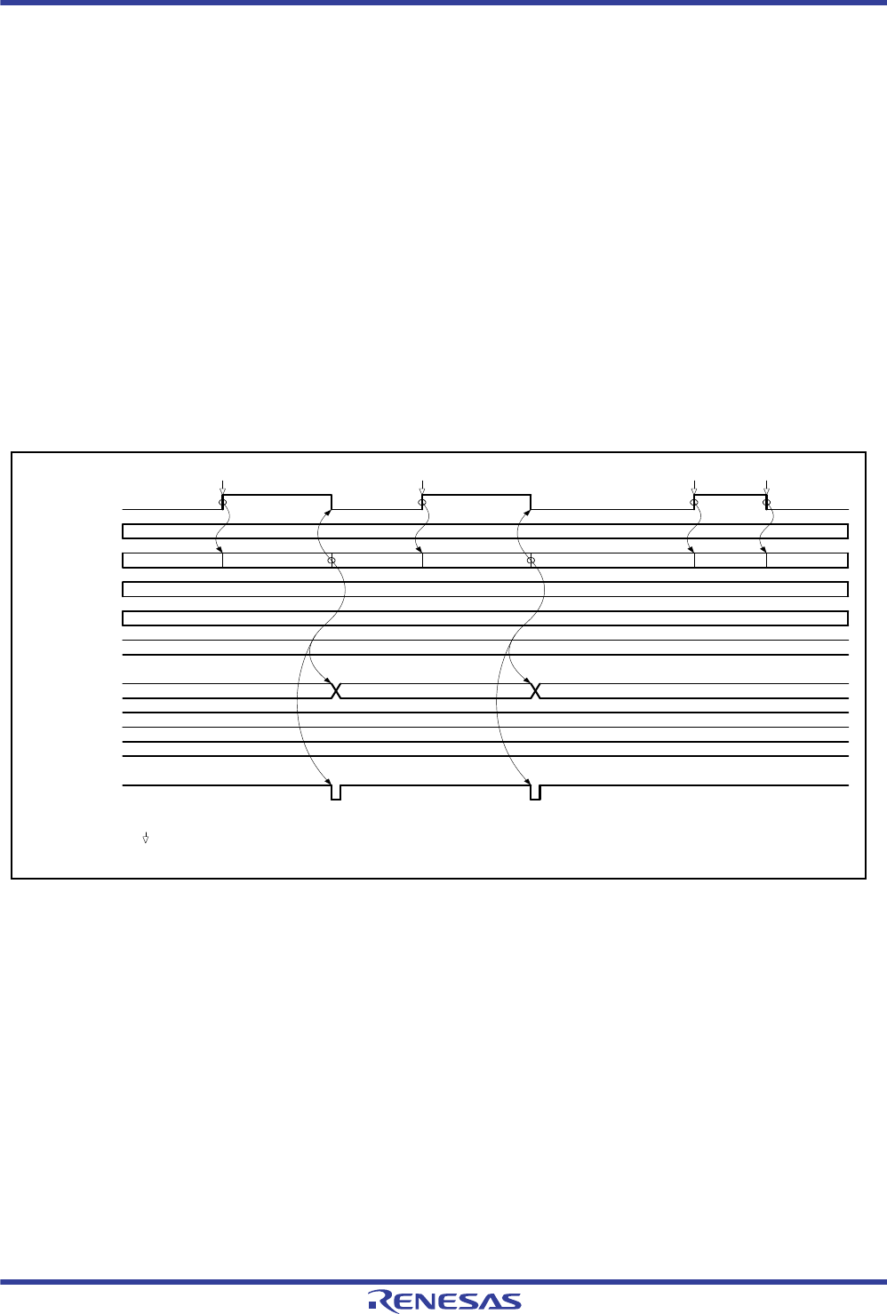
R01UH0034EJ0200 Rev.2.00 Page 1286 of 1489
Dec 27, 2013
RX62T Group, RX62G Group 28. 12-Bit A/D Converter (S12ADA)
28.3 Operation
28.3.1 Single Mode
In single mode, A/D conversion is to be performed for only once on the analog input of the specified single channel as
below.
(1) A/D conversion for the selected channel is started when the ADST bit in ADCSR is set to 1 (A/D conversion start)
by software, MTU3, GPT, or an external trigger input.
(2) When A/D conversion is completed, the A/D conversion result is stored in the A/D data register n (ADDRn)
corresponding to the channel.0A,
(3) When A/D conversion is completed, if the ADCSR.ADIE bit is set to 1 (S12ADI interrupt enable by completing A/
D conversion), an S12ADI interrupt request is generated.
(4) The ADCSR.ADST bit remains at 1 (A/D conversion start) during A/D conversion, and is automatically cleared to
0 when A/D conversion ends. Then the A/D converter enters a wait state.
(5) If the ADCSR.ADST bit is cleared to 0 during A/D conversion (A/D conversion stop), A/D conversion stops and
the A/D converter enters a wait state.
Figure 28.2 shows an example of operation when AN001 is selected as an analog input.
Figure 28.2 Example of A/D Converter Operation (Single Mode)
ADCSR.ADST A/D conversion
started
Waiting for conversion
Waiting for
conversion
Waiting for
conversion
Waiting for
conversion
ADDR0A
ADDR1
ADDR2
ADDR3
S12ADI
A/D conversion 1
Set*1
(1)
(2)
(3)
Stored
Interrupt generated
(4)
A/D conversion result 1
Set
A/D conversion 2
Waiting for
conversion
Interrupt generated
Set
Waiting for
conversion A/D
conversion 3*2
Cleared
(5) Waiting for
conversion
A/D conversion result 2
Notes: 1. indicates instruction execution by software.
2. Data being converted is ignored.
AN000
AN001
AN002
AN003

R01UH0034EJ0200 Rev.2.00 Page 1287 of 1489
Dec 27, 2013
RX62T Group, RX62G Group 28. 12-Bit A/D Converter (S12ADA)
28.3.2 Scan Conversion
A scan conversion is performed in three operating modes: single-cycle scan mode, continuous scan mode, and 2-channel
scan mode.
In single-cycle scan mode, one or more specified channels are scanned once and conversion stops. In continuous scan
mode, one or more specified channels are scanned repeatedly until the ADCSR.ADST bit is modified from 1 to 0 by
software. In 2-channel scan mode, four analog input channels are separated into groups 0 and 1, and a separate startup
trigger can be specified for each group. Conversion in each group is the same as that in single-cycle scan mode (one or
more channels are scanned once and conversion stops).
28.3.2.1 Single-Cycle Scan Mode
In single-cycle scan mode, A/D conversion is to be performed only once on the analog input of the specified single
channel as below.
(1) When the ADCSR.ADST bit is set to 1 (A/D conversion start) by software, MTU3, GPT, or an external trigger
input, A/D conversion is performed for ANn channels in the order selected by the CH[1:0] bits in ADANS.
(2) When A/D conversion for a channel is completed, the A/D conversion result is stored in the A/D data register n
(ADDRn) corresponding to the channel.(n = 0A, 0B, 1 to 3)
(3) When A/D conversion of all selected channels is completed, if the ADCSR.ADIE bit is set to 1 (S12ADI interrupt
enable by completing A/D conversion), an S12ADI interrupt request is generated.
(4) The ADST bit remains at 1 (A/D conversion start) during A/D conversion, and is automatically cleared to 0 when
A/D conversion of all selected channels ends. Then the A/D converter enters a wait state.
Note that sampling operation depends on the ADCER.SHBYP bit setting. Figure 28.3 shows an example of operation
when ADCER.SHBYP = 0, and Figure 28.4 shows an example when ADCER.SHBYP = 1.
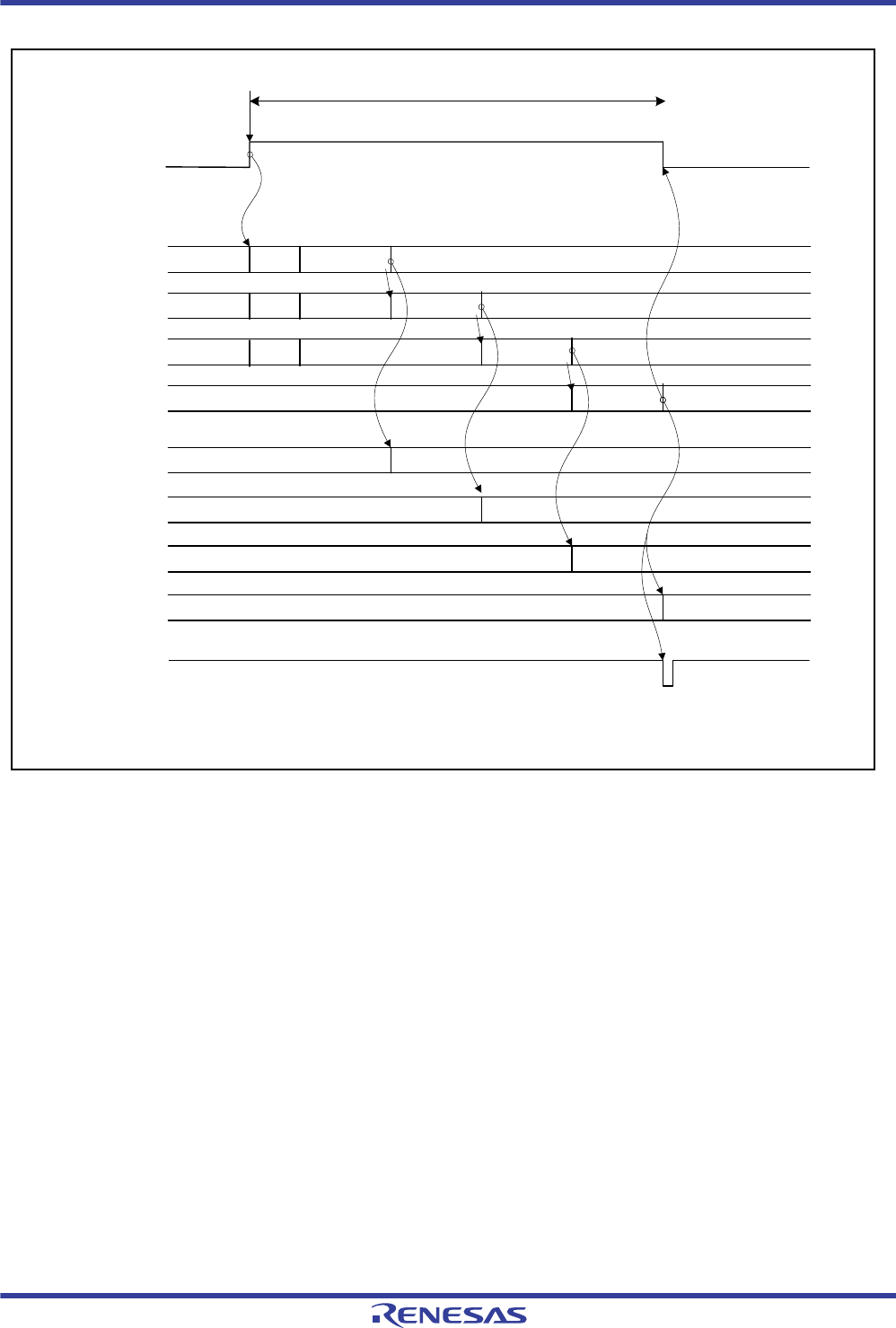
R01UH0034EJ0200 Rev.2.00 Page 1288 of 1489
Dec 27, 2013
RX62T Group, RX62G Group 28. 12-Bit A/D Converter (S12ADA)
Figure 28.3 Example of Operation in Single-Cycle Scan Mode (ADCER.SHBYP = 0:
Sample-and-Hold Circuit Dedicated for Channel is Used)
ADCSR.ADST
S12ADI
A/D conversion
started
AN000
AN002
AN003
ADDR0A
ADDR1
ADDR2
ADDR3
A/D conversion is performed only once
Set*
A/D
conversion 0
Sample
A/D conversion result 0
AN001 Sample
Sample
Waiting for
conversion
Waiting for
conversion
Waiting for
conversion
Waiting for conversion
A/D
conversion 1
A/D
conversion 2
A/D
conversion 3
Simultaneous sampling
Simultaneous sampling
Simultaneous sampling
Hold
Hold
Waiting for conversion
Waiting for conversion
Waiting for conversion
Waiting for conversion
A/D conversion result 1
A/D conversion result 2
A/D conversion result 3
Interrupt generated
Note: indicates instruction execution by software.
(1) (4)
(2)
(2)
(2)
(2)
(3)
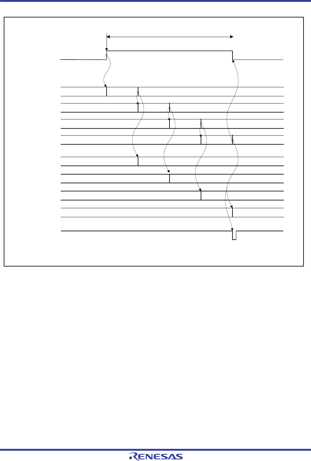
R01UH0034EJ0200 Rev.2.00 Page 1289 of 1489
Dec 27, 2013
RX62T Group, RX62G Group 28. 12-Bit A/D Converter (S12ADA)
Figure 28.4 Example of Operation in Single-Cycle Scan Mode
(ADCER.SHBYP = 1: Sample-and-Hold Circuit Dedicated for Channel is Not Used)
ADCSR.ADST
S12ADI
A/D conversion
started
AN000
AN002
AN003
ADDR0A
ADDR1
ADDR2
ADDR3
A/D conversion is performed only once
Set*
A/D
conversion 0
A/D conversion result 0
AN001
Waiting for
conversion
Waiting for conversion
Waiting for conversion
Waiting for conversion
A/D
conversion 1
A/D
conversion 2
A/D
conversion 3
Waiting for conversion
Waiting for conversion
Waiting for conversion
Waiting for conversion
A/D conversion result 1
A/D conversion result 2
A/D conversion result 3
Interrupt generated
Note: indicates instruction execution by software.
(1) (4)
(2)
(2)
(2)
(2)
(3)
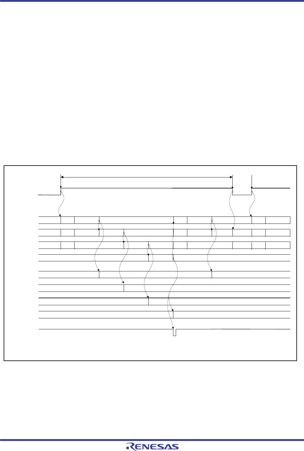
R01UH0034EJ0200 Rev.2.00 Page 1290 of 1489
Dec 27, 2013
RX62T Group, RX62G Group 28. 12-Bit A/D Converter (S12ADA)
28.3.2.2 Continuous Scan Mode
In continuous scan mode, A/D conversion is to be performed repeatedly on the analog inputs of the specified channels as
below.
(1) When the ADCSR.ADST bit is set to 1 (A/D conversion start) by software, MTU3, GPT, or an external trigger
input, A/D conversion is performed for ANn channels in the order selected by the CH[1:0] bits in ADANS.
(2) When A/D conversion for a channel is completed, the A/D conversion result is stored in the corresponding A/D data
register n (ADDRn).(n = 0A, 0B, 1 to 3)
(3) When A/D conversion of all selected channels is completed, if the ADCSR.ADIE bit is set to 1 (S12ADI interrupt
enable by completing A/D conversion), an S12ADI interrupt request is generated. A/D converter starts A/D
conversion for ANn channels in the order selected by the CH[1:0] bits in ADANS.
(4) The ADST bit is not cleared automatically, and steps (2) and (3) are repeated as long as the ADST bit remains set to
1 (A/D conversion start). When the ADST bit is cleared to 0 (A/D conversion stop), A/D conversion stops and the
A/D converter enters a wait state.
(5) If the ADST bit is later set to 1 (A/D conversion start), A/D conversion starts again for ANn channels in the order
selected by the CH[1:0] bits in ADANS.
Note that sampling operation depends on the ADCER.SHBYP bit setting. Figure 28.5 shows an example of operation
when ADCER.SHBYP = 0, and Figure 28.6 shows an example when ADCER.SHBYP = 1.
Figure 28.5 Example of Operation in Continuous Scan Mode (ADCER.SHBYP = 0:
Sample-and-Hold Circuit Dedicated for Channel is Used)
ADCSR.ADST
S12ADI
A/D conversion
started
AN000
AN002
AN003
ADDR0A
ADDR1
ADDR2
ADDR3
A/D conversion is performed repeatedly
Set*
A/D
conversion 0
Sample
A/D conversion result 0
AN001 Sample
Sample
Waiting for
conversion
Waiting for
conversion
Waiting for
conversion
Waiting for conversion
A/D
conversion 1
A/D
conversion 2
A/D
conversion 3
Simultaneous sampling
Simultaneous sampling
Simultaneous sampling
Hold
Hold
Waiting for conversion
Waiting for conversion
Waiting for
conversion
Waiting for conversion
A/D conversion result 1
A/D conversion result 2
A/D conversion result 3
Interrupt generated
Notes: 1. indicates instruction execution by software.
2. Converted data is ignored.
A/D
conversion 4
Sample
Sample
Sample
A/D
conversion 5
Simultaneous sampling
Simultaneous sampling
Simultaneous sampling
Hold
Hold
Cleared Set
A/D
conversion 6
Sample
Sample
Sample
Simultaneous sampling
Simultaneous sampling
Simultaneous sampling
Hold
Hold
Waiting for
conversion
Waiting for
conversion
Waiting for
conversion
*2
A/D conversion result 4
(1) (5)
(4)
(2)
(2)
(2)
(2)
(3)
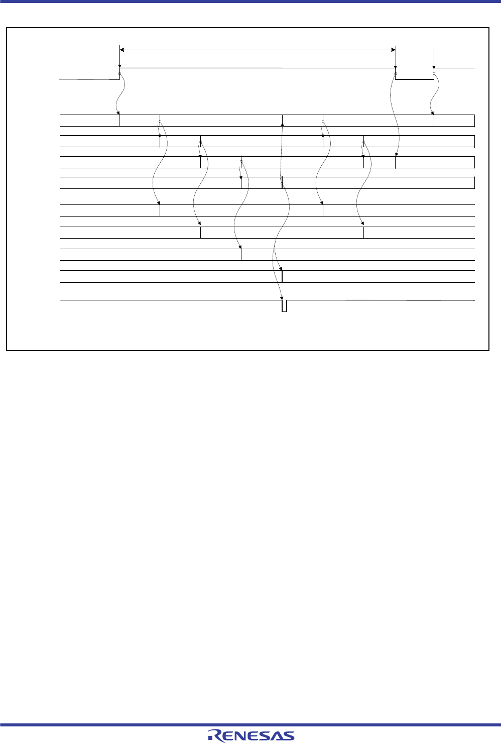
R01UH0034EJ0200 Rev.2.00 Page 1291 of 1489
Dec 27, 2013
RX62T Group, RX62G Group 28. 12-Bit A/D Converter (S12ADA)
Figure 28.6 Example of Operation in Continuous Scan Mode
(ADCER.SHBYP = 1: Sample-and-Hold Circuit Dedicated for Channel is Not Used)
ADCSR.ADST
S12ADI
A/D conversion
started
AN000
AN002
AN003
ADDR0A
ADDR1
ADDR2
ADDR3
A/D conversion is performed repeatedly
Set*
A/D
conversion 0
A/D conversion result 0
AN001
Waiting for conversion
Waiting for conversion
Waiting for conversion
Waiting for conversion
A/D
conversion 1
A/D
conversion 2
A/D
conversion 3
Waiting for conversion
Waiting for conversion
Waiting for
conversion
Waiting for conversion
A/D conversion result 1
A/D conversion result 2
A/D conversion result 3
Interrupt generated
A/D
conversion 4
A/D
conversion 5
Cleared Set
A/D
conversion 7
Waiting for conversion
Waiting for conversion
Waiting for conversion
*2
A/D conversion result 4
A/D
conversion 6
A/D conversion result 5
(1) (5)
(4)
(2)
(2)
(2)
(2)
(3)
Notes: 1. indicates instruction execution by software.
2. Converted data is ignored.
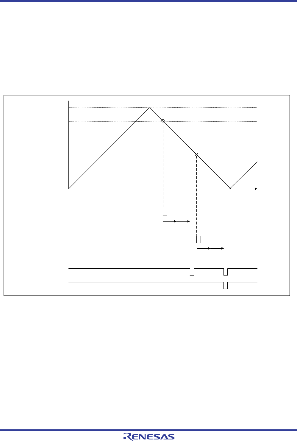
R01UH0034EJ0200 Rev.2.00 Page 1292 of 1489
Dec 27, 2013
RX62T Group, RX62G Group 28. 12-Bit A/D Converter (S12ADA)
28.3.2.3 2-Channel Scan Mode
In 2-channel scan mode, four analog input channels are separated into groups 0 and 1, and a separate startup trigger can
be selected for each group. The timing for generating a conversion end interrupt in 2-channel scan mode can be set to the
end of group 0 or 1 or the end of both groups.
When using a trigger to start conversion, select different trigger sources for groups 0 and 1 through the ADSTRGR
settings. Note that if a startup request for group 1 is generated during conversion of group 0, the startup request for group
1 is ignored.
Figure 28.7 shows an example of operation when TRG4AN in MTU4 is selected for the A/D conversion startup request
for group 0, TRG4BN in MTU4 is selected for group 1, and the ADANS.CH[1:0] bits are set to 01b.
Figure 28.7 Example of Operation in 2-Channel Scan Mode
Time0000h
MTU4.TADCORB
MTU4.TADCORA
MTU4.TGRA
MTU4.TCNT
Group 0 A/D converter
startup request
Group 1 A/D converter
startup request
AN000
conversion AN001
conversion
AN002
conversion AN003
conversion
S12ADI interrupt
When ADCER.ADIE2 = 0
When ADCER.ADIE2 = 1

R01UH0034EJ0200 Rev.2.00 Page 1293 of 1489
Dec 27, 2013
RX62T Group, RX62G Group 28. 12-Bit A/D Converter (S12ADA)
28.3.3 Analog Input Sampling and A/D Conversion Time
A/D converter activation can be selected from software activation, activation by triggers from MTU3 and GPT, and
activation by ADTRGn# (external trigger). After the start-of-A/D-conversion delay time (tD) has passed, the A/D
converter samples the analog input, performs self diagnostic, and then begins the A/D conversion process.
The A/D conversion time (tSCAN) includes the start-of-A/D-conversion delay time (tD), dedicated sample-and-hold
circuit sampling time (tSPLSH), self diagnostic time (tDIAG), A/D conversion processing time (tCONV), and end-of-A/
D-conversion delay time (tED).
The A/D conversion processing time (tCONV) is the sum of the input sampling time (tSPL) and successive conversion
time (tSAM).
The input sampling time (tSPL) is the time for charging the input capacitance of the A/D converter's sample-and-hold
circuit. If the impedance of the analog input signal source is high and the sampling time is insufficient or the A/D
conversion clock (ADCLK) is running at low speed, the sampling time can be adjusted by using the ADSSTR.
The successive conversion time (tSAM) is fixed at 30 states of ADCLK.
Table 28.8 shows ADSSTR setting examples and Table 28.8 shows the A/D conversion time.
The A/D conversion time (tSCAN) in single-cycle scan mode for which the number of selected channels is n can be
determined as follows.
(1) For AN000 to AN002 and AN100 to AN102
Neither dedicated sample-and-hold circuit nor self diagnostic function is used
tSCAN = tD + (tCONV n) + tED
Dedicated sample-and-hold circuit is not used and self diagnostic function is used
tSCAN = tD + tDIAG + (tCONV n) + tED
Dedicated sample-and-hold circuit is used and self diagnostic function is not used
tSCAN = tD + tSPLSH + (tCONV n) + tED
Both dedicated sample-and-hold circuit and self diagnostic function are used
tSCAN = tD + tSPLSH + tDIAG + (tCONV n) + tED
(2) For AN003 and AN103
Self diagnostic function is not used
tSCAN = tD + (tCONV n) + tED
Self diagnostic function is used
tSCAN = tD + tDIAG + (tCONV n) + tED
The conversion time for the first cycle in single mode or continuous scan mode is the same as that for single-cycle scan
mode.
The conversion time for the second and subsequent cycles in continuous scan mode is tSCAN in single-cycle scan mode
minus tD.

R01UH0034EJ0200 Rev.2.00 Page 1294 of 1489
Dec 27, 2013
RX62T Group, RX62G Group 28. 12-Bit A/D Converter (S12ADA)
Note 1. Note: * Set the sampling time ≥ 0.4 μs. Sampling time is obtained by the following equation.
PCLK: Module clock, ADCLK: A/D conversion clock
Note 1. For the timing of external trigger input, see section 33.3.3, Timing of On-Chip Peripheral Modules.
Note 2. This is the maximum time from software writing or trigger input to the start of A/D conversion.
Note 3. This is the time from the end of A/D conversion to generation of an A/D conversion end interrupt.
Table 28.8 Examples of ADSSTR Setting
Example of Setting Setting Range Sampling Time*
Standard (initial value) 14h 0.4 μs (When PCLK = ADCLK = 50 MHz)
Analog input signal impedance is high and the sampling
time may be insufficient
15h to FFh Example: FFh
5.1 μs (When PCLK = ADCLK = 50 MHz)
Input sampling time should be less than the initial value
when ADCLK is below 50 MHz
0Dh to 13h Example: 10h
0.4 μs (When PCLK = ADCLK = 40 MHz)
Table 28.9 A/D Conversion Time
Item Symbol ADTRGn#
(External Trigger) MTU3 and
GPT Trigger Software
Activation Unit
Start-of-A/D-conversion delay time*2 tD 4PCLK +
3ADCLK*1
3PCLK +
3ADCLK
2PCLK +
3ADCLK
Cycle
Processing time
required for the
independent sample-
and-hold circuit
dedicated for channel
Sampling time tSPLSH tSH 20ADCLK
Sampling-to-A/D
conversion wait time
tW 10ADCLK
Self diagnostic
conversion
processing time
Sampling time tDIAG tSPL ADSSTR setting (initial value is 20) ADCLK
Successive conversion
time
tSAM 30ADCLK
A/D conversion
processing time
Sampling time tCONV tSPL ADSSTR setting (initial value is 20) ADCLK
Successive conversion
time
tSAM 30ADCLK
End-of-A/D-conversion delay time*3 tED 1PCLK + 5ADCLK
Sampling time (s) = ADSSTR register setting
ADCLK (MHz)

R01UH0034EJ0200 Rev.2.00 Page 1295 of 1489
Dec 27, 2013
RX62T Group, RX62G Group 28. 12-Bit A/D Converter (S12ADA)
28.3.4 Usage Example of ADDRn Register Automatic Clearing Function
( n = 0A, 0B, 1 to 3 )
Setting the ADCER.ACE bit to 1 automatically clears the A/D data registers n (ADDRn and ADRD) to 0000h when the
ADDRn and ADRD registers are read by the CPU or DTC.
This function is used to detect update failures of the ADDRn and ADRD registers.
Examples in which the function to automatically clear the ADDRn registers are enabled and disabled are shown below.
In a case where the ACE bit in ADCER is 0 (automatic clearing is disabled), if the A/D conversion result (0222h) is not
written to the ADDRn registers for some reason, the old data (0111h) will become the ADDRn value. Furthermore, if this
ADDRn value is written to a general register using an A/D conversion end interrupt, the old data (0111h) will be saved in
the general register. When checking data that has not been updated, it is necessary to frequently save the old data in the
RAM or a general register.
In a case where the ACE bit in ADCER is 1 (automatic clearing is enabled), when ADDRn = 0111h is read by the CPU
or DTC, ADDRn is automatically cleared to 0000h. After that, if the A/D conversion result of 0222h cannot be
transferred to ADDRn for some reason, the cleared data (0000h) remains as the ADDRn value. If this ADDRn value is
written to a general register using an A/D scan conversion end interrupt at this point, 0000h will be saved in the general
register. Occurrence of an ADDRn update failure can be determined by simply checking whether the read data value is
0000h.
If automatic clearing of the ADDRn registers is selected, when data is read from the ADDRn registers, the converted data
will be cleared.
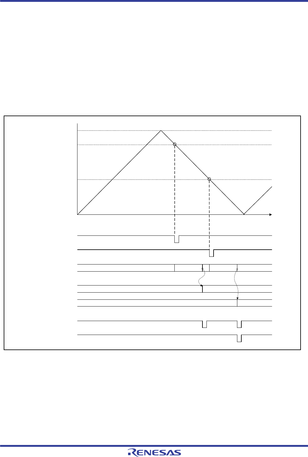
R01UH0034EJ0200 Rev.2.00 Page 1296 of 1489
Dec 27, 2013
RX62T Group, RX62G Group 28. 12-Bit A/D Converter (S12ADA)
28.3.5 Operation of Double Data Registers (Only for ADDR0)
When analog input AN000 or AN100 is selected and the startup source is set through the ADSTRGR.ADSTRSn[4:0]
bits to "TRGnAN or TRGnBN in MTU3 (n = 4 or 7)" (ADSTRGR.ADSTRSn[4:0] bits = 01011b or 01111b) or
"GTADTRAnN or GTADTRBnN in GPT (n = 0 to 3)" (ADSTRGR.ADSTRSn[4:0] bits = 11001b to 11100b), the
AN000 or AN100 conversion results are stored in separate registers according to the startup trigger. When conversion is
started by TRGnAN in MTU3 or GTADTRAnN in GPT, the AN000 or AN100 conversion result is stored in ADDR0A.
When conversion is started by TRGnBN in MTU3 or GTADTRBnN in GPT, the AN000 or AN100 conversion result is
stored in ADDR0B. The timing for generating a conversion end interrupt can be set to the end of conversion started by
the later one of the two triggers or the end of conversion started by each trigger through the ADCER.ADIEW setting.
Figure 28.8 shows an example of operation when AN000 is selected, TRG4AN or TRG4BN in MTU3 is selected as the
trigger, and conversion is started in single mode.
Figure 28.8 Example of Double Data Register Operation
Time0000h
MTU4.TADCORB
MTU4.TADCORA
MTU4.TGRA
MTU4.TCNT
TRG4AN
TRG4BN
S12ADI interrupt
When ADCER.ADIEW = 0
When ADCER.ADIEW = 1
AN000
ADDR0A
ADDR0B
A/D
conversion 0 A/D
conversion 1
Waiting for conversion Waiting for
conversion
A/D conversion
result 0
A/D conversion
result 1

R01UH0034EJ0200 Rev.2.00 Page 1297 of 1489
Dec 27, 2013
RX62T Group, RX62G Group 28. 12-Bit A/D Converter (S12ADA)
28.3.6 Programmable Gain Amplifier
A programmable gain amplifier is provided for each of the AN000 to AN002 and AN100 to AN102 pins.
The gain can be selected through the ADPG.PGnGAIN[3:0] bits (n = 000 to 002 or 100 to 102), and the operational
amplifier to be used can be selected through the ADANS.PGnEN and ADANS.PGnSEL bits.
The ADCER.SHBYP bit must be 0 (the sample and hold circuit is in use) if the programmable gain amplifier is to be
used.
28.3.7 Comparator
A comparator is provided for each of the AN000 to AN002 and AN100 to AN102 pins. The comparator operation can be
selected from three modes: low-level comparator operation which detects that the analog input voltage is lower than the
low reference voltage, high-level comparator operation which detects that the analog input voltage is higher than the high
reference voltage, and window comparator operation which detects that the analog input voltage is outside the range
from the low reference voltage to the high reference voltage. The analog input before or after programmable gain
amplification can be selected as the voltage for comparison. The reference voltages can be selected from the input from
the pins (low reference: AN003/CVREFL; high reference: AN103/CVREFH) and internally-generated voltage (1/8 ×
AVCC0 to 7/8 × AVCC0). A noise cancellation circuit is provided for the comparator detection results; detection results
are sampled 16 times with 1/PCLK to 128/PCLK and only when the specified voltage level is detected at all sampled
points, the detection flag is set and an interrupt (CMPI) or a POE request (request for placing the complementary PWM
output pins in the MTU3 and GPT output pins in high-impedance state) can be generated.
The comparator settings should be made in the following order.
1. Select the voltage before or after programmable gain amplification as the voltage for comparison through the
ADCMPMD1.CSELn bits (n = 0 or 1).
2. Select the pin inputs or internally-generated voltages as the reference voltages through the ADCMPMD1.VSELLn
bits (n = 0 or 1) and ADCMPMD1.VSELHn bits (n = 0 or 1). When the internally-generated voltages are selected,
specify the high reference voltage through the ADCMPMD1.REFL[2:0] bits and the low reference voltage through
the ADCMPMD1.REFH[2:0] bits.
3. Set up the noise cancellation circuit for each comparator through the ADCMPNRn.CmNR[3:0] bits (n = 0 or 1, m =
000 to 002 or 100 to 102).
4. Select whether to generate an interrupt request (CMPI) or a POE request on detection of the specified condition in
each comparator through the ADCMPSEL.SELm bits (m = 000 to 002 or 100 to 102). To generate an interrupt
request (CMPI) or a POE request, enable interrupt requests (CMPI) through the ADCMPSEL.IE bit or enable POE
requests through the ADCMPSEL.POE bit.
5. Select the comparator to be used and the comparator operating mode through the ADCMPMD0.CENm[1:0] bits.
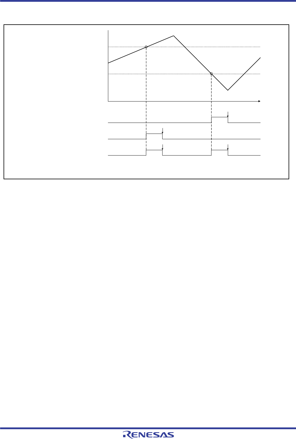
R01UH0034EJ0200 Rev.2.00 Page 1298 of 1489
Dec 27, 2013
RX62T Group, RX62G Group 28. 12-Bit A/D Converter (S12ADA)
Figure 28.9 shows an example of comparator operation.
Figure 28.9 Example of Comparator Operation (Reference Voltages are Input from Pins)
TimeAVSS0
CVREFL
CVREFH
AN000
AVCC0
ADCMPFR.C000FLAG
ADCMPMD0.CEN000[1:0] = 01b
ADCMPMD0.CEN000[1:0] = 10b
ADCMPMD0.CEN000[1:0] = 11b
Cleared*
Cleared*
Cleared* Cleared*
Note:indicates instruction execution by software.
Low-level comparator:
High-level comparator:
Window comparator:

R01UH0034EJ0200 Rev.2.00 Page 1299 of 1489
Dec 27, 2013
RX62T Group, RX62G Group 28. 12-Bit A/D Converter (S12ADA)
28.3.8 Starting A/D Conversion with External Trigger
The A/D converter can be activated by the input of an external trigger. To start up the A/D converter by an external
trigger, the pin function should be set up using PFAADC. After setting the A/D start trigger select register (ADSTRGR)
to 00h and applying a high-level signal to the ADTRGn# pin, both the ADCSR.TRGE and ADCSR.EXTRG bits should
be set to 1. Figure 28.10 shows a timing diagram of the external trigger input.
For details on pin function settings, see section 15, I/O Ports.
Figure 28.10 External Trigger Input Timing
28.3.9 Starting A/D Conversion with Trigger from Peripheral Modules
A/D conversion can be activated by a timer trigger of the MTU3 or GPT. To start up A/D conversion by a timer trigger,
the ADCSR.TRGE bit should be set to 1, the ADCSR.EXTRG bit should be cleared to 0, and the relevant source should
be selected by ADSTRGR.ADSTRS[4:0] bits.
28.4 Interrupt Sources and DTC Transfer Request
28.4.1 Interrupt Request on Completion of Each A/D Conversion
The A/D converter can send an A/D conversion end interrupt request (S12ADI) to the CPU.
By setting the ADCSR.ADIE bit to 1, an S12ADI interrupt is enabled; by clearing the ADIE bit to 0, an S12ADI
interrupt is disabled.
If the A/D converter is used with double data registers in 2-channel scan mode, an S12ADI interrupt request is generated
every time conversion is completed, regardless of the settings of the 2-channel scan interrupt select bit (ADIE2) and the
double trigger interrupt select bit (ADIEW) of the A/D control extended register (ADCER).
In addition, the DTC can be started up when an S12ADI interrupt is generated. Using an S12ADI interrupt to allow the
DTC to read the converted data enables continuous conversion without burden on software.
For details on DTC settings, see section 14, Data Transfer Controller (DTC).
28.4.2 Interrupt Request on Detection of Comparator
The comparator can send a converter detection interrupt request (CMPI) to the CPU.
After setting any of bits SEL000 to 002, or 100 to 102 in ADCMPSEL to 1, setting the ADCMPSEL.IE bit to 1 or 0
enables or disables the CMPI interrupt, respectively. However, while a comparator detection flag in the comparator
detection flag register (ADCMPFR) is 1, an interrupt request is ignored. Therefore, set the corresponding flag to 0 to
enable the interrupt.
ADTRGn# signal sampling timing
ADTRGn#
PCLK
ADCSR.ADST bit
4 states
Internal trigger signal

R01UH0034EJ0200 Rev.2.00 Page 1300 of 1489
Dec 27, 2013
RX62T Group, RX62G Group 28. 12-Bit A/D Converter (S12ADA)
28.5 Usage Notes
28.5.1 Module Stop Function Setting
Operation of the A/D converter can be disabled or enabled using the module stop control register. The initial setting is for
operation of the A/D converter to be halted. A/D converter registers can be accessed after the module stop state is
canceled. For details, see section 9, Low Power Consumption.
28.5.2 Notes on Restarting A/D Conversion
Stopping analog input to the A/D converter by clearing the ADCSR.ADST bit to 0 requires two cycles of the ADCLK.
Starting analog input to the A/D converter by setting the ADCSR.ADST bit to 1 requires three cycles of the ADCLK.
Before restarting A/D conversion, be sure to perform self diagnostic.
28.5.3 Point for Caution Regarding Countermeasures for Noise
To disable A/D conversion when an external trigger or timer has been selected as the condition for starting A/D
conversion, set the ADCSR.TRGE bit to 0 to select the software trigger as the trigger to start A/D conversion, and then
set the ADCSR.ADST bit to 0 (to stop A/D conversion).
28.5.4 Notes on Entering Low Power Consumption States
For the transition to the module stop state or software standby mode, make sure to stop the A/D conversion. To do so, set
the ADST bit in ADCSR to 0, and allow time for disabling of the analog input to the A/D converter.
Follow the procedure given below to ensure that this time is secured.
(1) Set the ADCSR.TRGE bit to 0 (software trigger).
(2) Clear the ADCSR.ADST bit to 0.
(3) Set the ADCR.CKS[1:0] bits to 11b (PCLK).
(4) After confirming that the A/D converter has been disabled (at least 6 PCLK cycles are required to stop the
conversion), place the LSI in the module stop state or software standby mode.
After the module stop state, software standby mode, or deep software standby mode is entered, part of the A/D converter
is in operation waiting state. To place the A/D converter in standby state completely, set the MSTPCRA.MSTPA24 bit to
1. In this case, after the module stop state, software standby mode, or deep software standby mode is canceled, clear the
STPCRA.MSTPA24 bit to 0 and then wait for 10 ms before starting A/D conversion.
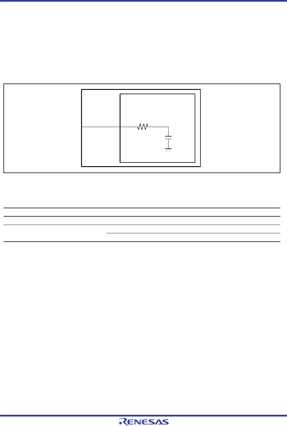
R01UH0034EJ0200 Rev.2.00 Page 1301 of 1489
Dec 27, 2013
RX62T Group, RX62G Group 28. 12-Bit A/D Converter (S12ADA)
28.5.5 Permissible Impedance of Signal Sources
To realize high-speed conversion 1.0 s, the A/D conversion accuracy is guaranteed only when the impedance of the
signal sources for analog input signals of the the RX62T/RX62G Group circuit is less than or equal to 3.0 kΩ. If a large
external capacitance is provided in the case of conversion in single mode, the input load becomes only the actual internal
input resistance (10 kΩ), so the impedance of the signal source becomes insufficient. However, since the circuit has
become a low-pass filter, the rapid and large fluctuations in the analog signal produced by differentiation (for example,
greater than 5 mV/μs) become impossible to track (Figure 28.11). Include a low-impedance buffer amplifier if high-rate
analog signals are to be converted or conversion is to be in scan mode.
Figure 28.11 Equivalent Circuit for the Internal Circuit of Analog Input Pins
28.5.6 Factors Affecting Absolute Accuracy
Including a capacitor introduces ground coupling. A noisy ground can have a bad effect on absolute accuracy, so be sure
to connect the AVSS0 pins and so on to an electrically stable ground.
Furthermore, a mounted filter circuit can interfere with digital-signal lines on the board, so take care to ensure that the
design does not set up an antenna.
Table 28.10 Specifications of Analog Pins
Item Min. Max. Unit
Permissible signal-source impedance — 3.0 kΩ
Values in the equivalent circuits for the internal
circuits of pins
Rs — 10.0 kΩ
Cs — 8.0 pF
RX62T/RX62G A/D converter equivalent circuit
Cs
Rs

R01UH0034EJ0200 Rev.2.00 Page 1302 of 1489
Dec 27, 2013
RX62T Group, RX62G Group 28. 12-Bit A/D Converter (S12ADA)
28.5.7 Ranges of Settings for Analog Power Supply and Other Pins
Using this LSI circuit with voltages beyond the ranges given below can have a bad effect on LSI reliability.
Range for the setting of analog input voltages
Keep voltages applied to analog input pins (ANn pins) within the range defined by VREFL0 ≤ VAN ≤ VREFH0.
Power-Supply Pins (AVCC0 – AVSS0, AVCC – AVSS, and VCC – VSS)
For the various power-supply pins (AVCC0 – AVSS0, AVCC – AVSS, and VCC – VSS), ensure that VCC ≤
AVCC0 = AVCC and AVSS0 = AVSS = VSS hold. If the 12-bit A/D converter is not in use, ensure that VCC =
AVCC0 = AVCC and AVSS0 = AVSS = VSS.
Range for the settings of VREFH0 and VREFL0
Ensure that the voltages on the VREFH0 and VREFL0 pins satisfy VREFH0 ≤ AVCC0 and VREFL0 = AVSS0.
When the A/D converters are not in use, ensure that VREFH0 = AVCC0 and VREFL0 = AVSS0.
28.5.8 Point for Caution Regarding Board Design
As far as possible, separate the analog circuits from the digital circuits in board design. Furthermore, do not allow the
wiring runs for a signal of a digital circuit and a signal of an analog circuit to cross or be in each other's vicinity.
Inductive coupling causes noise to be generated on the analog signals and has a bad effect on the results of analog
conversion. Separate the signal lines for analog input pins (AN000 to AN003 and AN100 to AN103), the analog
reference power supply pins (VREFH0 and VREFL0), and the analog power-supply voltage (AVCC0) away from digital
circuitry by the analog ground (AVSS0). Furthermore, connect the analog ground (AVSS0) to the stabilized ground
(VSS) on the board at a single point. Also, connect the 0.1-μF capacitors shown in Figure 28.12 to form the shortest
possible closed loops between the respective pairs of power-supply lines.

R01UH0034EJ0200 Rev.2.00 Page 1303 of 1489
Dec 27, 2013
RX62T Group, RX62G Group 28. 12-Bit A/D Converter (S12ADA)
28.5.9 Point for Caution Regarding Countermeasures for Noise
To prevent destruction of the circuits for the analog input pins by abnormal voltages such as excessively large surges,
connect capacitors as shown in Figure 28.12 between AVCC0 and AVSS0, and between VREFH0 and VREFL0; also
connect suitable protective circuits to the analog input pins (AN000 to AN003 and AN100 to AN103).
Figure 28.12 Example of a Protective Circuit for Analog Inputs
28.5.10 Usage Note when Double Data Registers are Used in 2-Channel Scan Mode
If the A/D converter is used with double data registers in 2-channel scan mode, an S12ADI interrupt request is generated
every time conversion is completed, regardless of the settings of the 2-channel scan interrupt select bit (ADIE2) and the
double trigger interrupt select bit (ADIEW) of the A/D control extended register (ADCER).
*1
Rin*2
AVCC0
VREFH0
AN000 to AN003 and
AN100 to AN103
AVSS0
Notes: The value is for reference.
*2 Rin: Input impedance
10 F0.01 F
*1*1
VREFL0
0.1 F
0.1 F

R01UH0034EJ0200 Rev.2.00 Page 1304 of 1489
Dec 27, 2013
RX62T Group, RX62G Group 29. 10-Bit A/D Converter (ADA)
Under development Preliminary document
Specifications in this document are tentative and subject to change.
29. 10-Bit A/D Converter (ADA)
29.1 Overview
The RX62T and RX62G Groups include a single successive-approximation-type 10-bit A/D converter. The converter is
capable of handling up to 12 analog input channels.
The A/D converter has two kinds of operating modes, that are single mode which converts the analog input of the
specified single channel for only once and scan mode which continuously converts the analog inputs of the specified
channels up to 12.
Table 29.1 lists the specifications of the A/D converter and the Table 29.2 indicates its functions. Figure 29.1 shows a
block diagram of the A/D converter.
Table 29.1 Specifications of A/D Converter
Item Specifications
Number of units One unit
Input channels 12 channels
A/D conversion method Successive approximation method
Resolution 10 bits
Conversion time 1.0 s per 1 channel (when operating A/D conversion clock ADCLK = 50 MHz, AVCC = 4.0 to 5.5 V)
2.0 s per 1 channel (when operating A/D conversion clock ADCLK = 25 MHz, AVCC = 3.0 to 3.6 V)
A/D conversion clock 4 types: PCLK, PCLK/2, PCLK/4, PCLK/8
Operating modes Single mode: A/D conversion is to be performed for only once on the analog input of the specified single
channel.
Scan mode
Continuous scan mode: A/D conversion is to be performed sequentially on the analog inputs of the
specified channels up to 12.
One-cycle scan mode: A/D conversion is to be performed for one cycle on the analog inputs of the
specified channels up to 12.
Conditions of A/D
conversion start
Software trigger
Conversion start trigger by the multi-function timer pulse unit (MTU3) or general PWM timer (GPT).
External trigger
A/D conversion can be triggered from the ADTRG# pin.
Function Sample-and-hold function
Number of sampling state is adjustable.
Self-diagnostic functions
Interrupt source A/D conversion end interrupt (ADI0) request can be generated.
An ADI interrupt can activate data transfer controller (DTC).
Power-down function Module stop state can be set.

R01UH0034EJ0200 Rev.2.00 Page 1305 of 1489
Dec 27, 2013
RX62T Group, RX62G Group 29. 10-Bit A/D Converter (ADA)
Under development Preliminary document
Specifications in this document are tentative and subject to change.
Note 1. See section 9, Low Power Consumption, for details.
Table 29.2 List of A/D Converter Function
Item Function
Analog channels AN0 to AN11
A/D conversion-start
conditions
software Software trigger Possible
External
trigger
Trigger input pin ADTRG#
Trigger from
MTU3
Compare-match with or input-capture to MTU0.TGRA TRGA0N
Compare-match with or input-capture to MTU1.TGRA TRGA1N
Compare-match with or input-capture to MTU2.TGRA TRGA2N
Compare-match with or input-capture to MTU3.TGRA TRGA3N
Compare-match with or input-capture to MTU4.TGRA, or
underflow of the TCNT bit in MTU4 in complementary PWM mode
TRGA4N
Compare-match with or input-capture to MTU6.TGRA TRGA6N
Compare-match with or input-capture to MTU7.TGRA, or
underflow of the MTU7.TCNT in complementary PWM mode
TRGA7N
Compare match with MTU0.TGRE TRG0N
Compare match between MTU4.TADCORA and MTU4. TCNT TRG4AN
Compare-match between MTU4.TADCORB and MTU4.TCNT TRG4BN
Compare-match between MTU4.TADCORA or MTU4.TADCORB and
MTU4.TCNT
TRG4AN
or TRG4BN
Compare-match between MTU4.TADCORA or MTU4.TADCORB and
MTU4.TCNT (when interrupt skipping function 2 is in use)
TRG4ABN
Compare-match between MTU7.TADCORA and MTU7.TCNT TRG7AN
Compare-match between MTU7.TADCORB and MTU7.TCNT TRG7BN
Compare-match between MTU7.TADCORA or MTU7.TADCORB and
MTU7.TCNT
TRG7AN
or TRG7BN
Compare-match between MTU7.TADCORA or MTU7.TADCORB and
MTU7.TCNT (when interrupt skipping function 2 is in use)
TRG7ABN
Trigger from
GPT
Compare-match with GPT0.GTADTRA GTADTRA0
Compare-match with GPT0.GTADTRB GTADTRB0
Compare-match with GPT1.GTADTRA GTADTRA1
Compare-match with GPT1.GTADTRB GTADTRB1
Compare-match with GPT2. GTADTRA GTADTRA2
Compare-match with GPT2.GTADTRB GTADTRB2
Compare-match with GPT3.GTADTRA GTADTRA3
Compare-match with GPT3.GTADTRB GTADTRB3
A/D conversion-start
conditions
Trigger from
GPT
Compare-match with GPT0.GTADTRA or with GPT0.GTADTRB GTADTRA0
or GTADTRB0
Compare-match with GPT1.GTADTRA or with GPT1.GTADTRB GTADTRA1
or GTADTRB1
Compare-match with GPT2.GTADTRA or with GPT2.GTADTRB GTADTRA2
or GTADTRB2
Compare-match with GPT3.GTADTRA or with GPT3.GTADTRB GTADTRA3
or GTADTRB3
Interrupt ADI interrupt
Setting of the module-stop function*1MSTPCRA.
MSTPA23 bit
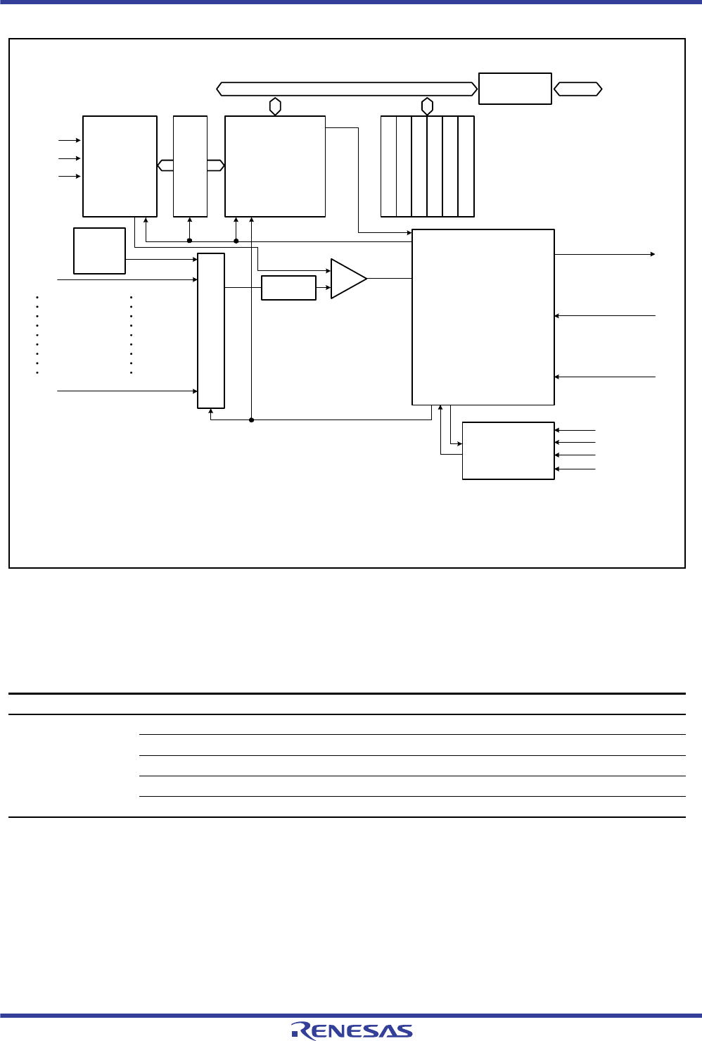
R01UH0034EJ0200 Rev.2.00 Page 1306 of 1489
Dec 27, 2013
RX62T Group, RX62G Group 29. 10-Bit A/D Converter (ADA)
Under development Preliminary document
Specifications in this document are tentative and subject to change.
Figure 29.1 The Block Diagram of the A/D Converter
Input pins for use with the A/D converter are listed inTable 29.3.
Table 29.3 Input Pin for A/D Converter
Module Symbol Pin Input Function
AD0 AN0 to AN11 Input Analog input pins
ADTRG# Input External trigger input pin for starting A/D conversion
AVCC Input Power pin for the analog section
AVSS Input Ground pin for the analog section
VREF Input Reference-voltage pin for the A/D converter
Successive
approximation
register
+
-
Analog Multiplexer
ADCSR
ADCR
ADSSTR
ADDIAGR
ADDPR
Bus interface
Power
generation
for self-
diagnostic
AVCC
AVSS
VREF
10-bit
D/A
Sample-and-
hold circuit
Control circuit
(includes the decode)
Interrupt signal
(AD conversion end)
AD conversion trigger
(MTU3, GPT)
Comparator
AN0
AN11 External trigger
(ADTRG#)
ADDRA to ADDRL
ADSTRGR
[Legend]
ADDRA to ADDRL: A/D data register A to A/D data register L
ADCSR: A/D control/Status register
ADCR: A/D control register
ADDPR: ADDRn format select register
ADSSTR: A/D sampling state register
ADSTRGR: A/D start trigger select register
ADDIAGR: A/D self-diagnostic register
Internal data
bus
Module data bus
Clock selection
PCLK
PCLK/4
PCLK/8
PCLK/2
ADCLK

R01UH0034EJ0200 Rev.2.00 Page 1307 of 1489
Dec 27, 2013
RX62T Group, RX62G Group 29. 10-Bit A/D Converter (ADA)
Under development Preliminary document
Specifications in this document are tentative and subject to change.
29.2 Register Descriptions
Table 29.4 lists the registers of the A/D converter.
Table 29.4 Registers of A/D Converter
Module
Symbol Register Name Register
Symbol Value after
Reset Address Access
Size
AD0 A/D data register A ADDRA 0000h 0008 8040h 16
A/D data register B ADDRB 0000h 0008 8042h 16
A/D data register C ADDRC 0000h 0008 8044h 16
A/D data register D ADDRD 0000h 0008 8046h 16
A/D data register E ADDRE 0000h 0008 8048h 16
A/D data register F ADDRF 0000h 0008 804Ah 16
A/D data register G ADDRG 0000h 0008 804Ch 16
A/D data register H ADDRH 0000h 0008 804Eh 16
A/D data register I ADDRI 0000h 0008 8060h 16
A/D data register J ADDRJ 0000h 0008 8062h 16
A/D data register K ADDRK 0000h 0008 8064h 16
A/D data register L ADDRL 0000h 0008 8066h 16
A/D control/status register ADCSR x0h 0008 8050h 8
A/D control register ADCR 00h 0008 8051h 8
A/D sampling state register ADSSTR 19h 0008 805Bh 8
A/D self-diagnostic register ADDIAGR 00h 0008 805Dh 8
A/D start trigger select register ADSTRGR 00h 0008 8070h 8
ADDRn format select register ADDPR 00h 0008 8072h 8
R01UH0034EJ0200 Rev.2.00 Page 1308 of 1489
Dec 27, 2013
RX62T Group, RX62G Group 29. 10-Bit A/D Converter (ADA)
Under development Preliminary document
Specifications in this document are tentative and subject to change.
29.2.1 A/D Data Register n (ADDRn) (n = A to L)
Address: ADDRA 0008 8040h, ADDRB 0008 8042h, ADDRC 0008 8044h, ADDRD 0008 8046h
ADDRE 0008 8048h, ADDRF 0008 804Ah, ADDRG 0008 804Ch, ADDRH 0008 804Eh
ADDRI 0008 8060h, ADDRJ 0008 8062h, ADDRK 0008 8064h, ADDRL 0008 8066Eh
ADDPR.DPSEL bit = 1, DDPPRC.DPSEL bit = 0 (The value has 10-bit accuracy and is padded at the MSB end)
b15 b14 b13 b12 b11 b10 b9 b8 b7 b6 b5 b4 b3 b2 b1 b0
AD9AD8AD7AD6AD5AD4AD3AD2AD1AD0——————
Value after reset: 0000000000000000
Bit Symbol Bit Function R/W
b5 to b0 —Reserved These bits are always read as 0. Writing to those bits has no
effect.
R
b15 to b6 AD9 to AD0 Converted value[9:0] 10-bit result of A/D conversion R
ADDPR.DPSEL bit = 1, ADDPR.DPPRC bit = 1 (The value has 8-bit accuracy and is padded at the MSB end)
b15 b14 b13 b12 b11 b10 b9 b8 b7 b6 b5 b4 b3 b2 b1 b0
AD9AD8AD7AD6AD5AD4AD3AD2————————
Value after reset: 0000000000000000
Bit Symbol Bit Function R/W
b7 to b0 —Reserved These bits are always read as 0. Writing to those bits has no
effect.
R
b15 to b8 AD9 to AD2 Converted value [9:2] Higher-order 8 bits of the 10-bit result of A/D conversion R
ADDPR.DPSEL bit = 0, ADDPR.DPPRC bit = 1 (The value has 10-bit accuracy and is padded at the LSB end)
b15 b14 b13 b12 b11 b10 b9 b8 b7 b6 b5 b4 b3 b2 b1 b0
——————AD9AD8AD7AD6AD5AD4AD3AD2AD1AD0
Value after reset: 0000000000000000
Bit Symbol Bit Function R/W
b9 to b0 AD9 to AD0 Converted value[9:0] 10-bit result of A/D conversion R
b15 to b10 —Reserved These bits are always read as 0. Writing to those bits has no effect. R
ADDPR.DPSEL bit = 0, ADDPR.DPPRC bit = 1 (The value has 10-bit accuracy and is padded at the LSB end)
b15 b14 b13 b12 b11 b10 b9 b8 b7 b6 b5 b4 b3 b2 b1 b0
————————AD9AD8AD7AD6AD5AD4AD3AD2
Value after reset: 0000000000000000
Bit Symbol Bit Function R/W
b7 to b0 AD9 to AD2 Converted value[9:2] Higher-order 8 bits of the 10-bit result of A/D conversion R
b15 to b8 —— Reserved These bits are always read as 0. Writing to those bits has no effect. R

R01UH0034EJ0200 Rev.2.00 Page 1309 of 1489
Dec 27, 2013
RX62T Group, RX62G Group 29. 10-Bit A/D Converter (ADA)
Under development Preliminary document
Specifications in this document are tentative and subject to change.
The ADDRn registers are 16-bit read-only registers which store the results of A/D conversion on the respective channels.
Table 29.5 lists the analog input channels and corresponding ADDRn registers.
10-bit data can be relocated by setting the DPSEL bit in ADDPR.
Also, the precision (in bits) of the stored data can be set by the DPPRC bit in ADDPR.
Table 29.5 Analog Input Channels and Corresponding ADDRn Registers
Analog Input Channel ADDRn Register
AN0 ADDRA
AN1 ADDRB
AN2 ADDRC
AN3 ADDRD
AN4 ADDRE
AN5 ADDRF
AN6 ADDRG
AN7 ADDRH
AN8 ADDRI
AN9 ADDRJ
AN10 ADDRK
AN11 ADDRL

R01UH0034EJ0200 Rev.2.00 Page 1310 of 1489
Dec 27, 2013
RX62T Group, RX62G Group 29. 10-Bit A/D Converter (ADA)
Under development Preliminary document
Specifications in this document are tentative and subject to change.
29.2.2 A/D Control/Status Register (ADCSR)
Note 1. The PORTn.DDR.Bi bit for the analog input should be set to 0 (input port) and the PORTn.ICR.Bi bit should be set to 0 (disabling
the input buffer and fixing the input signal to the high level). For details, see section 15, I/O Ports. (n = 6, 5, i = 5 to 0)
ADCSR controls the A/D conversion operations.
Set the CH[3:0] and ADIE bits while the ADST bit is 0.
CH[3:0] Bits (Channel Select)
These bits select analog input channels that allow A/D conversion.
Single mode (ADCR.MODE[1:0] bits = 00b)
Select the single analog input channel that allows A/D.
Scan mode (ADCR.MODE[1:0] bits = 10b or 11b)
Select analog input channels up to 12 that allow A/D conversion.
ADST Bit (A/D Start)
The ADST bit starts/stops A/D conversion.
Before setting the ADST bit to 1, complete the setting for A/D conversion clock and the operation mode.
[Setting conditions]
When 1 is written by software
Detection of the trigger selected by the ADSTRGR.ADSTRS [4:0] bits
[Clearing conditions]
When 0 is written by software
The A/D conversion is completed in single mode
The A/D conversion is completed on every selected channel in one-cycle scan mode.
Address: 0008 8050h
b7 b6 b5 b4 b3 b2 b1 b0
— ADIE ADST — CH[3:0]
Value after reset: 00000000
x: Undefined
Bit Symbol Bit Name Description R/W
b3 to b0 CH[3:0] Channel
Select*1Single mode
(ADCR.MODE[1:0] = 00b)
Scan mode
(ADCR.MODE[1:0] = 10b or 11b)
R/W
b3 b0
0 0 0 0: AN0
0 0 0 1: AN1
0 0 1 0: AN2
0 0 1 1: AN3
::
1 0 1 1: AN11
Settings other than above are prohibited.
b3 b0
0 0 0 0: AN0
0 0 0 1: AN0 and AN1
0 0 1 0: AN0 to AN2
0 0 1 1: AN0 to AN3
::
1 0 1 1: AN0 to AN11
Settings other than above are prohibited.
b4 — Reserved This bit is always read as 0. The write value should always be 0. R/W
b5 ADST A/D Start 0: Stops A/D conversion
1: Starts A/D conversion
R/W
b6 ADIE A/D Interrupt
Enable
0: ADI interrupt is disabled by completing A/D conversion
1: ADI interrupt is enabled by completing A/D conversion
R/W
b7 — Reserved The read value is undefined. The write value should always be 0. R/W

R01UH0034EJ0200 Rev.2.00 Page 1311 of 1489
Dec 27, 2013
RX62T Group, RX62G Group 29. 10-Bit A/D Converter (ADA)
Under development Preliminary document
Specifications in this document are tentative and subject to change.
ADIE Bit (A/D Interrupt Enable)
The ADIE bit enables/disables the A/D conversion end interrupt (ADI).

R01UH0034EJ0200 Rev.2.00 Page 1312 of 1489
Dec 27, 2013
RX62T Group, RX62G Group 29. 10-Bit A/D Converter (ADA)
Under development Preliminary document
Specifications in this document are tentative and subject to change.
29.2.3 A/D Control Register (ADCR)
ADCR enables setting for an A/D conversion, an operating mode, and A/D conversion clock mode.
Set ADCR while the ADST bit in ADCSR is 0.
MODE[1:0] Bits (Operating Mode Select)
These bits select the A/D conversion operation mode.
CKS[1:0] Bits (Clock Select)
These bits set the frequency of the A/D conversion clock (ADCLK) and thus select the A/D conversion time.
Set the frequency of ADCLK above 4 MHz. When AVCC is in the range from 3.0 V to 3.6 V, set the frequency of
ADCLK below 25 MHz.
For details, see section 29.3.3, Input Sampling and A/D Conversion Time.
Address: 0008 8051h
b7 b6 b5 b4 b3 b2 b1 b0
———— CKS[1:0] MODE[1:0]
Value after reset: 00000000
Bit Symbol Bit Name Description R/W
b1, b0 MODE[1:0] Operation Mode Select b1 b0
0 0: Single mode
0 1: Setting prohibited
1 0: Continuous scan mode
1 1: One-cycle scan mode
R/W
b3, b2 CKS[1:0] Clock Select b3 b2
0 0: PCLK/8
0 1: PCLK/4
1 0: PCLK/2
1 1: PCLK
R/W
b7 to b4 — Reserved These bits are always read as 0. The write value should always be 0. R/W

R01UH0034EJ0200 Rev.2.00 Page 1313 of 1489
Dec 27, 2013
RX62T Group, RX62G Group 29. 10-Bit A/D Converter (ADA)
Under development Preliminary document
Specifications in this document are tentative and subject to change.
29.2.4 A/D start trigger select register (ADSTRGR)
Address: 0008 8070h
b7 b6 b5 b4 b3 b2 b1 b0
— — — ADSTRS[4:0]
Value after reset: 00000000
Bit Symbol Bit Name Description R/W
b4 to b0 ADSTRS[4:0] A/D start trigger
select
Bits 0 to 4 select a peripheral module as the source for activation of the A/D
converter. See Table 29.6 for the correspondence between settings and
activation sources.
R/W
b7 to b5 — Reserved These bits are always read as 0. The write value should always be 0. R/W

R01UH0034EJ0200 Rev.2.00 Page 1314 of 1489
Dec 27, 2013
RX62T Group, RX62G Group 29. 10-Bit A/D Converter (ADA)
Under development Preliminary document
Specifications in this document are tentative and subject to change.
Table 29.6 A/D Activation Source Selection (1 / 2)
Activation
source Source Start condition ADSTRS
[4] ADSTRS
[3] ADSTRS
[2] ADSTRS
[1] ADSTRS
[0]
Software ADST Set the ADST bit in ADCSR — — — — —
External pin ADTRG#*1External trigger 0 0 0 0 0
MTU3 TRGA0N Compare-match with or input-capture to
MTU0.TGRA
00 00 1
TRGA1N Compare-match with or input-capture to
MTU1.TGRA
00 01 0
TRGA2N Compare-match with or input-capture to
MTU2.TGRA
00 01 1
TRGA3N Compare-match with or input-capture to
MTU3.TGRA
00 10 0
TRGA4N Compare-match with or input-capture to
MTU4.TGRA, or underflow of the TCNT bits
in MTU4 in complementary PWM mode
00 10 1
TRGA6N Compare-match with or input-capture to
MTU6.TGRA
00 11 0
TRGA7N Compare-match with or input-capture to
MTU7.TGRA, or underflow of the TCNT bits
in MTU7 in complementary PWM mode
00 11 1
TRG0N Compare-match with MTU0.TGRE 0 1 0 0 0
TRG4AN Compare-match with MTU4.TADCORA and
MTU4.TCNT
01 00 1
TRG4BN Compare-match between MTU4.TADCORB
and MTU4.TCNT
01 01 0
TRG4AN
or
TRG4BN
Compare-match between MTU4.TADCORA
or MTU4.TADCORB and MTU4.TCNT
01 01 1
TRG4ABN Compare-match between MTU4.TADCORA
or MTU4.TADCORB and MTU4.TCNT
(when interrupt skipping function 2 is in use)
01 10 0
TRG7AN Compare-match between MTU7.TADCORA
and MTU7.TCNT
01 10 1
TRG7BN Compare-match between MTU7.TADCORB
and MTU7.TCNT
01 11 0
TRG7AN
or
TRG7BN
Compare-match between MTU7.TADCORA
or
MTU7.TADCORB and MTU7.TCNT
01 11 1
TRG7ABN Compare-match between MTU7.TADCORA
or
MTU7.TADCORB and MTU7.TCNT
(when interrupt skipping function 2 is in use)
10 00 0
GPT GTADTRA0 Compare-match with GPT0.GTADTRA 1 0 0 0 1
GTADTRB0 Compare-match with GPT0.GTADTRB 1 0 0 1 0
GTADTRA1 Compare-match with GPT1.GTADTRA 1 0 0 1 1
GTADTRB1 Compare-match with GPT1.GTADTRB 1 0 1 0 0
GTADTRA2 Compare-match with GPT2.GTADTRA 1 0 1 0 1
GTADTRB2 Compare-match with GPT2.GTADTRB 1 0 1 1 0
GTADTRA3 Compare-match with GPT3.GTADTRA 1 0 1 1 1
GTADTRB3 Compare-match with GPT3.GTADTRB 1 1 0 0 0
GTADTRA0
or
GTADTRB0
Compare-match with GPT0.GTADTRA or
with GPT0.GTADTRB
11 00 1

R01UH0034EJ0200 Rev.2.00 Page 1315 of 1489
Dec 27, 2013
RX62T Group, RX62G Group 29. 10-Bit A/D Converter (ADA)
Under development Preliminary document
Specifications in this document are tentative and subject to change.
Note 1. When an ADTRG# signal is selected as a trigger to start A/D conversion, set the PORTn.DDR.Bi bit to 0 (selecting input
operation) and the PORTn.ICR.Bi bit to 1 (enabling the input buffer for the given pin). For details, see section 15, I/O Ports.
GPT GTADTRA1
or
GTADTRB1
Compare-match with GPT1.GTADTRA or
with GPT1.GTADTRB
11 01 0
GTADTRA2
or
GTADTRB2
Compare-match with GPT2.GTADTRA or
with GPT2.GTADTRB
11 01 1
GTADTRA3
or
GTADTRB3
Compare-match with GPT3.GTADTRA or
GPT3.GTADTRB
11 10 0
Table 29.6 A/D Activation Source Selection (2 / 2)
Activation
source Source Start condition ADSTRS
[4] ADSTRS
[3] ADSTRS
[2] ADSTRS
[1] ADSTRS
[0]

R01UH0034EJ0200 Rev.2.00 Page 1316 of 1489
Dec 27, 2013
RX62T Group, RX62G Group 29. 10-Bit A/D Converter (ADA)
Under development Preliminary document
Specifications in this document are tentative and subject to change.
29.2.5 ADDRn Format Select Register (ADDPR) (n = A to L)
ADDPR selects the placement of data in the A/D data registers.
DPPRC Bit (Accuracy Specification)
This bit selects storage of the results of A/D conversion in the data registers with 8- or 10-bit accuracy.
DPSEL Bit (ADDRn Format Select)
The DPSEL bit selects whether data in the A/D data register n (ADDRn) is padded at the LSB or MSB end.
Address: 0008 8072h
b7 b6 b5 b4 b3 b2 b1 b0
DPSEL——————DPPRC
Value after reset: 00000000
Bit Symbol Bit Name Description R/W
b0 DPPRC Accuracy Specification 0: Values stored in the A/D registers have 10-bit accuracy.
1: Values stored in the A/D registers have 8-bit accuracy.
R/W
b6 to b1 — Reserved These bits are always read as 0. The write value should
always be 0.
R/W
b7 DPSEL ADDRn Format Select 0: A/D data is padded at the LSB end.
1: A/D data is padded at the MSB end.
R/W

R01UH0034EJ0200 Rev.2.00 Page 1317 of 1489
Dec 27, 2013
RX62T Group, RX62G Group 29. 10-Bit A/D Converter (ADA)
Under development Preliminary document
Specifications in this document are tentative and subject to change.
29.2.6 A/D Self-Diagnostic Register (ADDIAGR)
ADDIAGR specifies the self-diagnostic function and the voltage for use with the function.
Specify ADDIAGR while the ADCSR.ADST bit is 0.
DIAG[1:0] Bits (Self-Diagnostic)
The self-diagnostic function is used to detect faults in the A/D converter. The setting selects whether the function is or is
not in use, and if it is, whether the internally generated voltage is to be derived as Vref x 0, Vref x 1/2, or Vref x 1.
To perform the self-diagnostic, select the voltage value by the ADDIAGR.DIAG[1:0] bits and start the A/D conversion
in the procedure below.
Single mode (the ADCR.MODE[1:0] bits = 00)
Analog input AN0 is only enabled (the ADCSR.CH[3:0] bits = 0000)*
A/D conversion is started by software. (the ADCR.TRGS[2:0] bits = 000)
After A/D conversion ends, the conversion result is stored in the A/D data register A (ADDRA). Then, whether the
conversion result is within the normal range (normal) or not (error) can be found out from the values read from ADDRA
by software. The execution time required for self-diagnostic is the same as that for A/D conversion of one channel.
Note: • Set AN0 as the input channel to perform self-diagnosis of A/D converter. Since selection of the data register to
store the result of conversion is required, the AN0 pin itself is disabled.
Address: 0008 805Dh
b7 b6 b5 b4 b3 b2 b1 b0
—————— DIAG[1:0]
Value after reset: 00000000
Bit Symbol Bit Name Description R/W
b1, b0 DIAG[1:0] Self-Diagnostic b1 b0
0 0: Self-diagnostic function is off.
0 1: A/D conversion of Vref x 0 voltage value is enabled.
1 0: A/D conversion of Vref x 1/2 voltage value is enabled.
1 1: A/D conversion of Vref x 1 voltage value is enabled.
R/W
b7 to b2 — Reserved These bits are always read as 0. The write value should always be 0. R/W

R01UH0034EJ0200 Rev.2.00 Page 1318 of 1489
Dec 27, 2013
RX62T Group, RX62G Group 29. 10-Bit A/D Converter (ADA)
Under development Preliminary document
Specifications in this document are tentative and subject to change.
29.2.7 A/D Sampling State Register (ADSSTR)
ADSSTR is an 8-bit readable/writable register that is used to set the sampling time for analog inputs.
Sampling time is adjustable when the signal source impedance of analog input is high and the sampling time is
insufficient or the speed of A/D conversion clock (ADCLK) is low.
Set the value of 02h or larger.
Ensure to rewrite this register while the A/D conversion is stopped (the ADST bit in ADCSR = 0) in order to prevent
incorrect operation.
For details, see section 29.3.3, Input Sampling and A/D Conversion Time.
Address: 0008 805Bh
b7 b6 b5 b4 b3 b2 b1 b0
Value after reset: 00000000
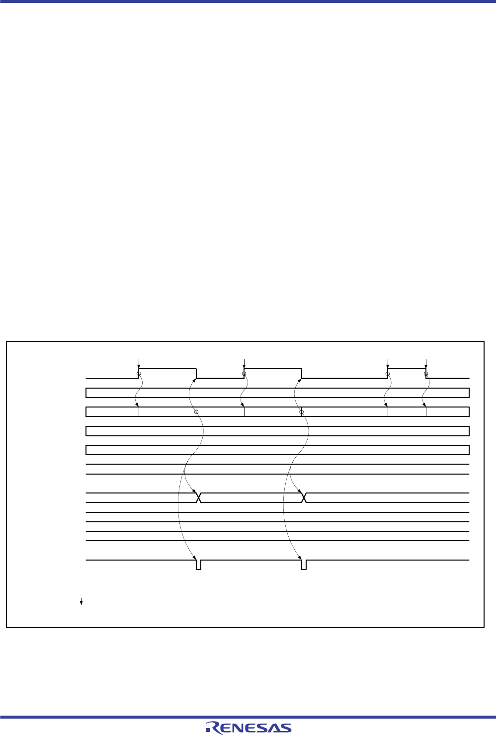
R01UH0034EJ0200 Rev.2.00 Page 1319 of 1489
Dec 27, 2013
RX62T Group, RX62G Group 29. 10-Bit A/D Converter (ADA)
Under development Preliminary document
Specifications in this document are tentative and subject to change.
29.3 Operation
The A/D converter has two operating modes: single mode and scan mode.
In single mode, A/D conversion is to be performed for only once on the analog input of the specified single channel.
In scan mode, A/D conversion is to be performed sequentially on the analog inputs of the specified channels up to 12.
Two types of scan mode are provided, that is, continuous san mode where A/D conversion is repeatedly performed and
one-cycle scan mode where A/D conversion is performed for the specified channels for one cycle.
29.3.1 Single Mode
In single mode, A/D conversion is to be performed for only once on the analog input of the specified single channel as
below.
1. A/D conversion for the selected channel is started when the ADST bit in ADCSR is set to 1 (A/D conversion start)
by software, MTU3, GPT, or an external trigger input.
2. When A/D conversion is completed, the A/D conversion result is stored into the corresponding A/D data register
(ADDRn) of the channel.
3. When A/D conversion is completed, if the ADIE bit in ADCSR is set to 1 (A/D interrupt enable by completing A/D
conversion), an ADI interrupt request is generated.
4. The ADST bit in the ADCSR remains at 1 during A/D conversion, and is automatically cleared to 0 when A/D
conversion ends. Then the A/D converter enters a wait state.
5. If the ADST bit in the ADCSR is cleared to 0 during A/D conversion (A/D conversion stop), A/D conversion stops
and the A/D converter enters a wait state.
Figure 29.2 shows an example of operation when AN1 is selected as an analog input.
Figure 29.2 Example of A/D Converter Operation (Single Mode)
ADCSR.ADST A/D conversion start
Channel 0 (AN0) Standby for conversion
Channel 1 (AN1)
Channel 2 (AN2)
Channel 3 (AN3)
ADDRA
ADDRB
ADDRC
ADDRD
ADI0
A/D conversion 1
Set*1
(1)
(2)
(3)
Store
Interrupt generation
(4)
A/D conversion result 1
Set
A/D conversion 2
Interrupt generation
Set
A/D conversion 3*2
Clear
(5)
A/D conversion result 2
Notes:
1. indicates an instruction execution by software.
2. Data during conversion is ignored.
Standby for conversion
Standby for conversion
Standby for conversion Standby for conversion Standby for conversion
Standby for conversion
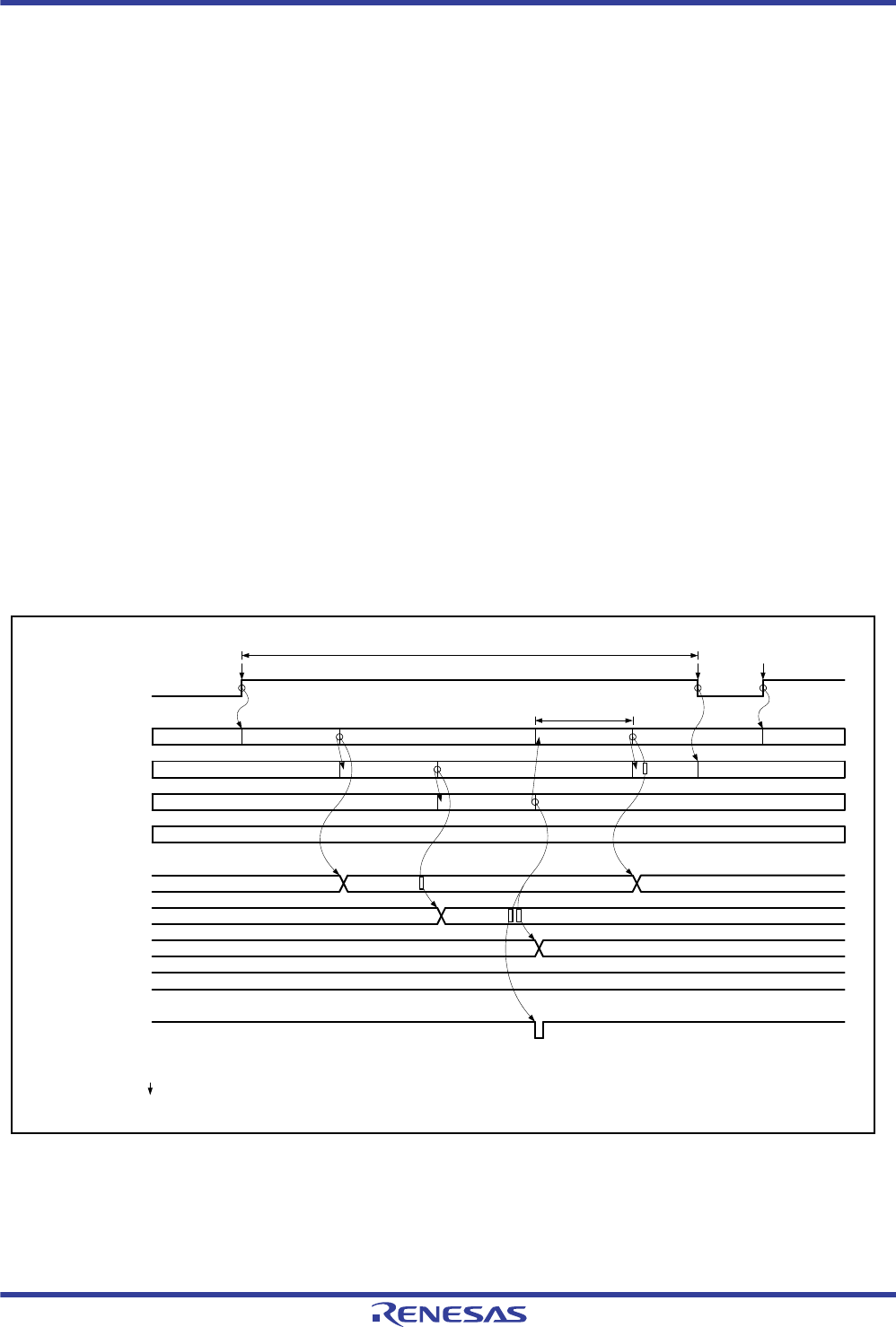
R01UH0034EJ0200 Rev.2.00 Page 1320 of 1489
Dec 27, 2013
RX62T Group, RX62G Group 29. 10-Bit A/D Converter (ADA)
Under development Preliminary document
Specifications in this document are tentative and subject to change.
29.3.2 Scan Mode
In scan mode, A/D conversion is to be performed sequentially on the analog inputs of the specified channels up to 12.
Two types of scan mode are provided, that is, continuous scan mode where A/D conversion is repeatedly performed and
one-cycle scan mode where A/D conversion is performed for the specified channels for one cycle.
29.3.2.1 Continuous Scan Mode
In continuous scan mode, A/D conversion is to be performed sequentially on the analog inputs of the specified channels
as below.
1. When the ADST bit in ADCSR is set to 1 (A/D conversion start) by software, MTU3, GPT, or an external trigger
input, A/D conversion starts on the first channel in the specified channel group.
2. When A/D conversion for each channel is completed, the A/D conversion result is stored into the corresponding A/
D data registers n (ADDRn) (n = A to L).
3. When A/D conversion of all selected channels is completed, if the ADIE bit in ADCSR is set to 1 (A/D interrupt
enable by completing A/D conversion), an ADI interrupt request is generated. A/D converter starts A/D conversion
from the first channel.
4. The ADST bit in the ADCSR is not cleared automatically, and steps 2 to 3 are repeated as long as the ADST bit
remains set to 1 (A/D conversion start). When the ADST bit is cleared to 0 (A/D conversion stop), A/D conversion
stops and the A/D converter enters a wait state.
5. If the ADST bit in the ADCSR is later set to 1 (A/D conversion start), A/D conversion starts again from the first
channel in the group.
Figure 29.3 shows an example of A/D conversion when three channels (AN0 to AN2) are selected for analog input.
Figure 29.3 Example of A/D Converter Operation (Continuous Scan Mode)
ADCSR.ADST A/D conversion start
Channel 0 (AN0) Standby for conversion
Channel 1 (AN1) Standby for conversion
Channel 2 (AN2) Standby for conversion
Channel 3 (AN3) Standby for conversion
ADDRA
ADDRB
ADDRC
ADDRD
ADI0
A/D conversion 1
(1)
(2) Store
A/D conversion 2
Standby for conversion
Interrupt generation
Standby for conversion
Clear
(4)
Standby for conversion
Notes:
1. indicates an instruction execution by software.
2. Data during conversion is ignored.
A/D conversion 3
A/D conversion 4
A/D conversion result 1
Standby for
conversion
Standby for conversion
A/D conversion result 2
A/D conversion result 3
A/D conversion result 4
A/D conversion time
Execute A/D conversion repeatedly
(2)
(2)
(3)
Set
(5)
A/D conversion 6
Set*1
A/D conversion 5*2
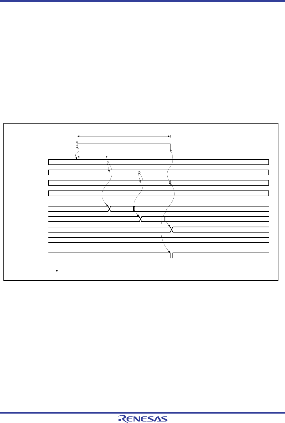
R01UH0034EJ0200 Rev.2.00 Page 1321 of 1489
Dec 27, 2013
RX62T Group, RX62G Group 29. 10-Bit A/D Converter (ADA)
Under development Preliminary document
Specifications in this document are tentative and subject to change.
29.3.2.2 One-Cycle Scan Mode
In one-cycle scan mode, A/D conversion is to be performed for one cycle on the analog inputs of the specified channels
as below.
1.When the ADST bit in ADCSR is set to 1 (A/D conversion start) by software, MTU3, GPT, or an external trigger input,
A/D conversion starts on the first channel in the specified channel group.
2.When A/D conversion for each channel is completed, the A/D conversion result is stored into the corresponding A/D
data registers (ADDRn) (n = A to L).
3.When A/D conversion of all selected channels is completed, if the ADIE bit in ADCSR is set to 1 (A/D interrupt enable
by completing A/D conversion), an ADI interrupt request is generated.
4.The ADST bit in ADCSR remains at 1 (A/D conversion start) during A/D conversion, and is automatically cleared to 0
when A/D conversion of all selected channels end. The A/D converter enters a wait state.
Figure 29.4 shows an example of A/D conversion when three channels (AN0 to AN2) are selected for analog input.
Figure 29.4 Example of A/D Converter Operation (One-Cycle Scan Mode)
Set*
ADCSR.ADST A/D conversion start
Channel 0 (AN0) Standby for conversion
Channel 1 (AN1) Standby for conversion
Channel 2 (AN2) Standby for conversion
Channel 3 (AN3) Standby for conversion
ADDRA
ADDRB
ADDRC
ADDRD
ADI0
A/D conversion 1
(1)
(2) Store
A/D conversion 2
Interrupt generation
Standby for conversion
Note: * indicates an instruction execution by software.
A/D conversion 3
A/D conversion result 1
Standby for conversion
A/D conversion result 2
A/D conversion result 3
A/D conversion time
Execute A/D conversion for once
(2)
(2)
(3)
(4)
Standby for conversion
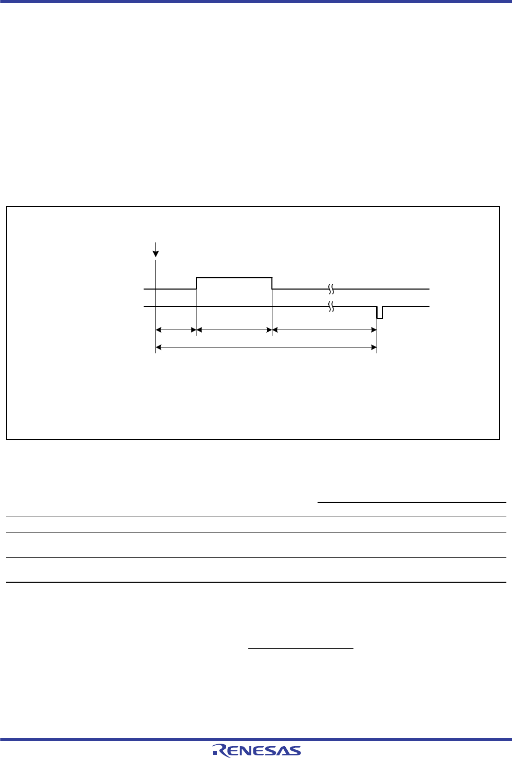
R01UH0034EJ0200 Rev.2.00 Page 1322 of 1489
Dec 27, 2013
RX62T Group, RX62G Group 29. 10-Bit A/D Converter (ADA)
Under development Preliminary document
Specifications in this document are tentative and subject to change.
29.3.3 Input Sampling and A/D Conversion Time
The A/D converter samples the analog input when the A/D conversion start delay time (tD) passes after the conditions of
A/D conversion start are generated by software, MTU3, GPT, or an external trigger, then starts A/D conversion.
Figure 29.5 shows the A/D conversion timing.
The A/D conversion time (tCONV) directly after the generation of the A/D conversion start condition includes the A/D
conversion start delay time (tD), the input sampling time (tSPL), and the successive conversion time (tSAM). The
subsequent A/D conversion time (tCONV) includes tSPL and tSAM.
The input sampling time (tSPL) is the time charging of the input capacitance of the A/D converter's sample-and-hold
circuit takes. If the impedance of the signal source is high and the sampling time is insufficient or the A/D conversion
clock (ADCLK) is running at low speed, the sampling time can be adjusted by using the ADSSTR.
The successive conversion time (tSAM) is fixed at 25 cycles of ADCLK.
Table 29.6 lists the sample of ADSSTR settings and Table 29.7 lists the A/D conversion time.
Figure 29.5 A/D Conversion Timing
Note 1. Set the sampling time 0.5 s. Sampling time is shown as the formula below.
Table 29.7 Example of ADSSTR Settings
Example of Setting Setting Range Sampling Time*1
Standard (initial value) 19h 0.5 s (When PCLK = ADCLK = 50 MHz)
Analog input signal impedance is high and the sampling
time may be insufficient
1Ah to FFh Example: FFh
5.1 s (When PCLK = ADCLK = 50 MHz)
Input sampling time is less than the initial value when
ADCLK is below 50 MHz
02h to 18h Example: 14h
0.5 s (When PCLK = ADCLK = 40 MHz)
[Legend]
tD tSPL
tCONV
Sampling signal
ADI0
tD:
tSPL:
tSAM: Successive conversion time
A/D conversion start delay time
Input sampling time
Generation of A/D
conversion start condition
tSAM
tCONV: A/D conversion time
Sampling time (µs) =ADCLK (MHz)
Setting value of ADSSTR

R01UH0034EJ0200 Rev.2.00 Page 1323 of 1489
Dec 27, 2013
RX62T Group, RX62G Group 29. 10-Bit A/D Converter (ADA)
Under development Preliminary document
Specifications in this document are tentative and subject to change.
Table 29.8 A/D Conversion Time
The examples of the calculation of A/D conversion times are listed below.
When PCLK = ADCLK = 50 MHz, ADSSTR = 19h, and the conversion is the second round in scan mode,
A/D conversion time (tCONV) = ADSSTR/ADCLK + 25/ADCLK
= 25/50 MHz + 25/50 MHz
= 0.5 μs + 0.5 μs
= 1.0 μs
When PCLK = ADCLK = 40 MHz, ADSSTR = 14h, and conversion is the first (min.) round in scan mode,
A/D conversion time (tCONV) = 3/PCLK + ADSSTR/ADCLK + 25/ADCLK
= 3/40 MHz + 20/40 MHz + 25/40 MHz
= 0.075 μs + 0.5 μs + 0.625 μs
= 1.2 μs
Item Symbol Formula
min max
tD
tSPL
tSAM
tCONV
tCONV
PCLK (MHz)
4
+
ADCLK (MHz)
1
PCLK (MHz)
3
ADCLK (MHz)
25
ADCLK (MHz)
Setting value of ADSSTR
A/D conversion start delay time (1)
Input sampling time (2)
Successive conversion time (3)
A/D conversion time*1
A/D conversion time*2
Notes: 1. A/D conversion time in single mode and scan mode (first round)
2. A/D conversion time in scan mode (after the second round)
(1) + (2) + (3)
(2) + (3)
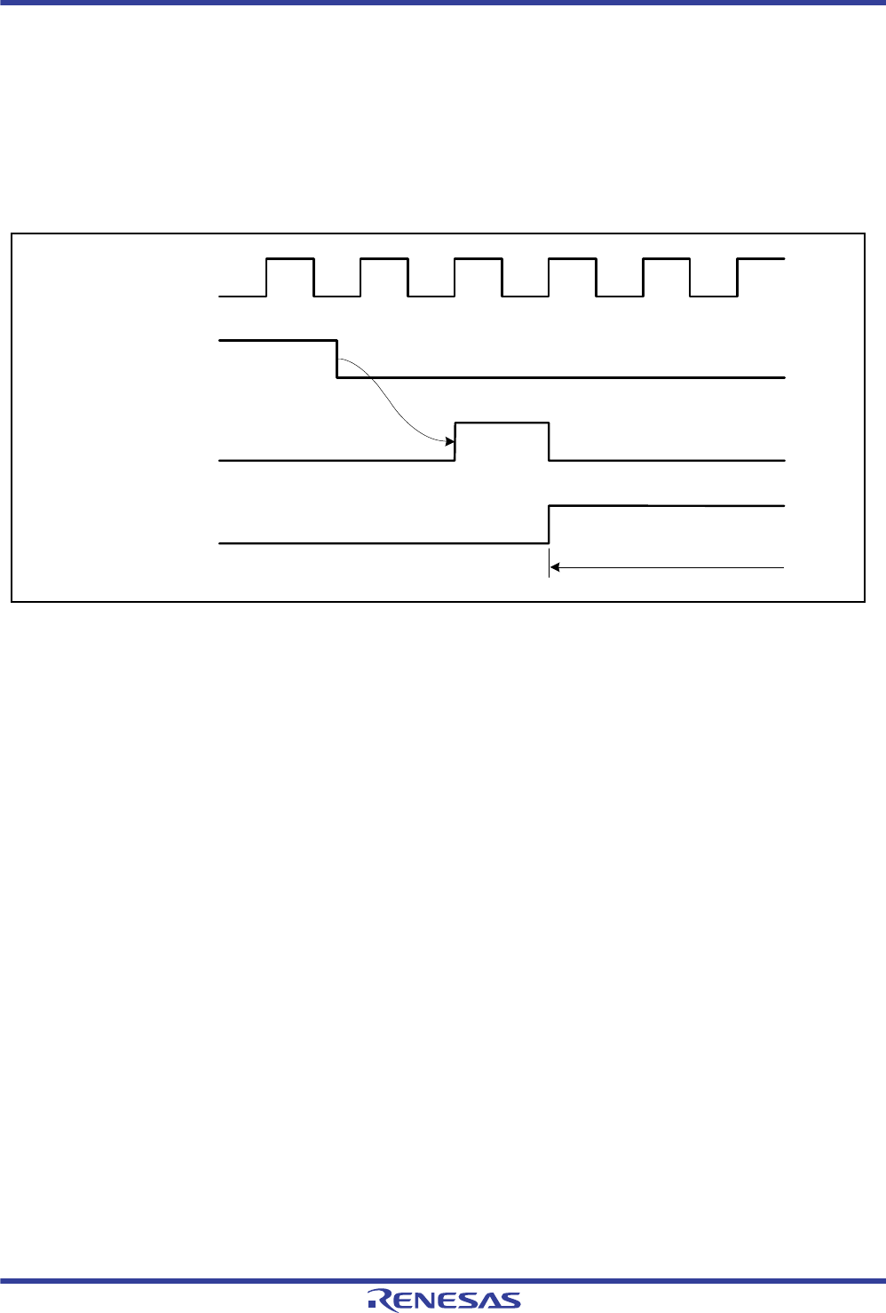
R01UH0034EJ0200 Rev.2.00 Page 1324 of 1489
Dec 27, 2013
RX62T Group, RX62G Group 29. 10-Bit A/D Converter (ADA)
Under development Preliminary document
Specifications in this document are tentative and subject to change.
29.3.4 A/D Converter Activation by External Triggers
External trigger signals (ADTRG#) are capable of starting A/D conversion.
When the setting of the ADSTRGR.ADSTRS[4:0] bits is 00000b (specifying ADTRG# as a trigger), a falling edge on
the ADTRG# pin leads to setting of the ADST (A/D conversion start) bit in ADCSR to 1 and thus starts A/D conversion.
Figure 29.6 shows the timing.
Take note that if the external trigger input is already at the low-level, selecting the external trigger may generate a falling
edge in the internal signal and thus start A/D conversion.
Figure 29.6 Timing of Activation by an External Trigger
29.3.5 Activation by the MTU3 and GPT Modules
A/D conversion can be started by requests for A/D conversion from the MTU3 and GPT as interval timers.
For the MTU3 or GPT to start the A/D converter, the ADSTRGR.ADSTRS[4:0] (A/D conversion start trigger) bits must
be set accordingly. Once this is done, the ADCSR.ADST (A/D conversion start) bit is set to 1 in response to a request for
A/D conversion from an interval timer of the MTU3 or GPT module, and A/D conversion starts. Timing between setting
of the ADST bit to 1 and the start of A/D conversion is the same as when software is used to set the ADST bit.
PCLK
ADTRG#
Internal trigger
signal
ADCSR.ADST A/D conversion

R01UH0034EJ0200 Rev.2.00 Page 1325 of 1489
Dec 27, 2013
RX62T Group, RX62G Group 29. 10-Bit A/D Converter (ADA)
Under development Preliminary document
Specifications in this document are tentative and subject to change.
29.4 Interrupt Source
The A/D converter generates an A/D conversion end interrupt (ADI0) at the end of A/D conversion while the ADIE bit in
ADCSR is set to 1 (after ADI interrupt is enabled by completing A/D conversion).
The data transfer controller (DTC) can be activated by an ADI interrupt. Using an ADI interrupt to allow the DTC to read
the converted data enables continuous conversion without burden on the CPU.
29.5 A/D Conversion Accuracy Definitions
The RX62T/RX62G Group's A/D conversion accuracy definitions are given below.
Resolution
The number of A/D converter digital output codes
Quantization error
The deviation inherent in the A/D converter, given by 1/2 LSB (Figure 29.7)
Offset error
The deviation of the analog input voltage value from the ideal A/D conversion characteristic when the digital output
changes from the minimum voltage value 0000000000b (000h) to 0000000001b (001h) (Figure 29.8)
Full-scale error
The deviation of the analog input voltage value from the ideal A/D conversion characteristic when the digital output
changes from 1111111110b (3FEh) to 1111111111b (3FFh) (Figure 29.8)
Nonlinearity error
The error with respect to the ideal A/D conversion characteristic between the zero voltage and the full-scale voltage.
Does not include the offset error, full-scale error, or quantization error (Figure 29.8).
Absolute accuracy
The deviation between the digital value and the analog input value. Includes the offset error, full-scale error,
quantization error, and nonlinearity error.
Table 29.9 A/D Converter Interrupt Source
Name Interrupt Source Interrupt Status Flag DTC Activation
ADI0 A/D conversion end ICU.IR98.IR Possible
R01UH0034EJ0200 Rev.2.00 Page 1326 of 1489
Dec 27, 2013
RX62T Group, RX62G Group 29. 10-Bit A/D Converter (ADA)
Under development Preliminary document
Specifications in this document are tentative and subject to change.
Figure 29.7 A/D Conversion Accuracy Definitions (1)
Figure 29.8 A/D Conversion Accuracy Definitions (2)
111
110
101
100
011
010
001
000 FS
Quantization
error
Digital output
1
1024 2
1024 1022
1024 1023
1024
Analog input voltage
Ideal A/D conversion
characteristic
FS
Offset error
Nonlinearity
error
Digital output Full-scale error
Ideal A/D
conversion
characteristic
Actual A/D conversion
characteristic Analog input voltage

R01UH0034EJ0200 Rev.2.00 Page 1327 of 1489
Dec 27, 2013
RX62T Group, RX62G Group 29. 10-Bit A/D Converter (ADA)
Under development Preliminary document
Specifications in this document are tentative and subject to change.
29.6 Usage Notes
29.6.1 Module Stop Function Setting
Operation of the A/D converter can be disabled or enabled using the module stop control register. The initial setting is for
operation of the A/D converter to be halted. Register access is enabled by clearing the module stop state. For details, see
section 9, Low Power Consumption.
29.6.2 Notes on Disabling A/D Conversion
To disable A/D conversion when an external trigger or timer has been selected as the condition for starting A/D
conversion, set the ADST bit in ADCSR to 0 (to stop A/D conversion).
29.6.3 Notes on Restarting A/D Conversion
Stopping analog input to the A/D converter by clearing the ADST bit in ADCSR to 0, requires one cycle of the ADCLK.
If A/D conversion is to be restarted right after the ADST bit in ADCSR was set to 0, set the ADST bit in ADCSR to 1
after one cycle of the ADCLK has elapsed.
29.6.4 Notes on Entering Power-Down States
When the RX62T/RX62G Group enters the module stop state or software standby mode with A/D conversion enabled,
the analog power supply current is the same as it is during A/D conversion. If the analog power supply current needs to
be reduced in the module stop state or software standby mode, disable A/D conversion. To do so, set the ADST bit in
ADCSR to 0, and allow time for disabling of the analog input to the A/D converter.
Follow the procedure given below to ensure that this time is secured.
(1) Clear the ADCSR.ADST bit to 0.
(2) Set the ADCR.CKS[1:0] bits to 11b (PCLK).
(3) After confirming that the A/D converter has been disabled, place the LSI in the module stop state or software
standby mode.
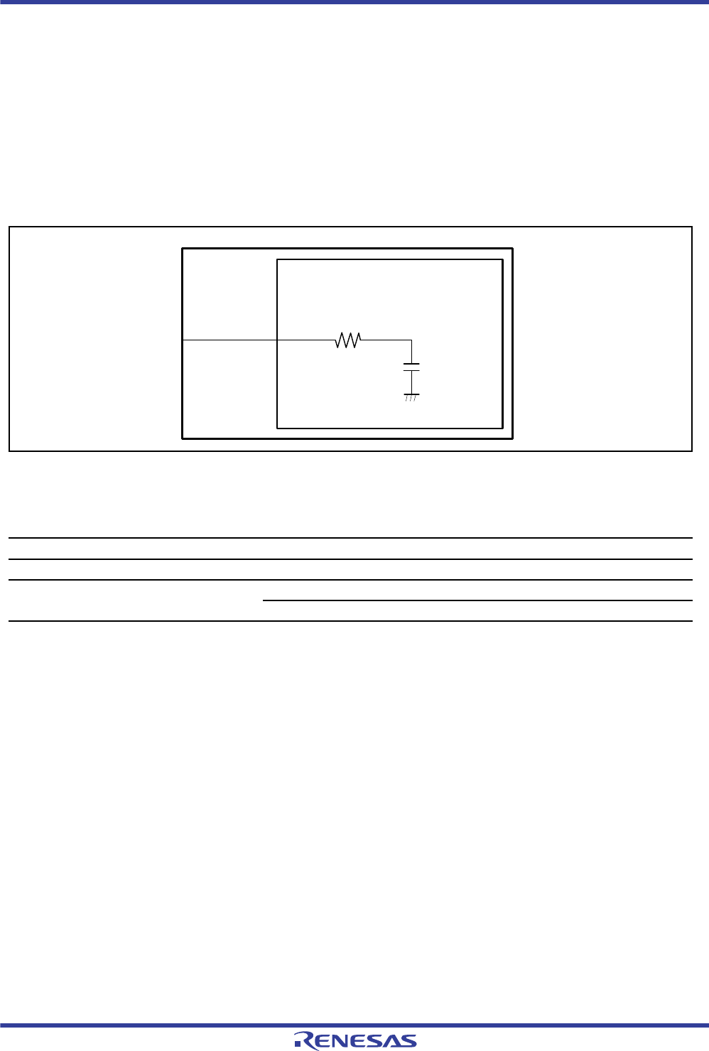
R01UH0034EJ0200 Rev.2.00 Page 1328 of 1489
Dec 27, 2013
RX62T Group, RX62G Group 29. 10-Bit A/D Converter (ADA)
Under development Preliminary document
Specifications in this document are tentative and subject to change.
29.6.5 Permissible Impedance of Signal Sources
To realize high-speed conversion 1.0 s, the A/D conversion accuracy is guaranteed only when the impedance of the
signal sources for analog input signals of the the RX62T/RX62G Group circuit is less than or equal to 1.0 kΩ. If a large
external capacitance is provided in the case of conversion in single mode, the input load becomes only the actual internal
input resistance (8 kΩ), so the impedance of the signal source becomes insufficient. However, since the circuit has
become a low-pass filter, the rapid and large fluctuations in the analog signal produced by differentiation (for example,
greater than 5 mV/μs) become impossible to track (Figure 29.9). Include a low-impedance buffer amplifier if high-rate
analog signals are to be converted or conversion is to be in scan mode.
Figure 29.9 Equivalent Circuit for the Internal Circuit of Analog Input Pins
29.6.6 Factors Affecting Absolute Accuracy
Including a capacitor introduces ground coupling. A noisy ground can have a bad effect on absolute accuracy, so be sure
to connect the AVSS pins and so on to an electrically stable ground.
Furthermore, a mounted filter circuit can interfere with digital-signal lines on the board, so take care to ensure that the
design does not set up an antenna.
Table 29.10 Specifications of Analog Pins
Item Min. Max. Unit
Permissible signal-source impedance — 1.0 kΩ
Values in the equivalent circuits for the internal
circuits of pins
Rs — 8.0 kΩ
Cs — 7.0 pF
RX62T/RX62G Equivalent circuit for the A/D converter
Cs
Rs
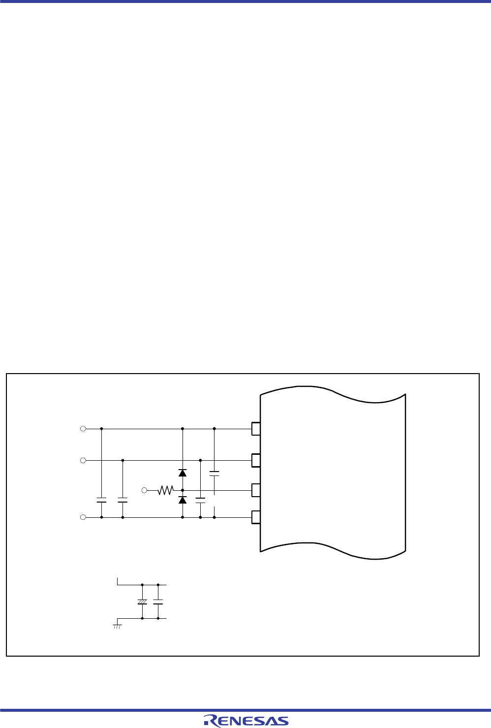
R01UH0034EJ0200 Rev.2.00 Page 1329 of 1489
Dec 27, 2013
RX62T Group, RX62G Group 29. 10-Bit A/D Converter (ADA)
Under development Preliminary document
Specifications in this document are tentative and subject to change.
29.6.7 Ranges of Settings for Analog Power Supply and Other Pins
Using this LSI circuit with voltages beyond the ranges given below can have a bad effect on LSI reliability.
Range for the setting of analog input voltages
Keep voltages applied to analog input pins (ANn pins) within the range defined by AVSS ≤ VAN ≤ VREF.
Power-Supply Pins (AVCC0 – AVSS0, AVCC – AVSS, and VCC – VSS)
For the various power-supply pins (AVCC0 – AVSS0, AVCC – AVSS, and VCC – VSS), ensure that VCC ≤
AVCC0 = AVCC and AVSS0 = AVSS = VSS hold. If the 10-bit A/D converter is not in use, ensure that VCC =
AVCC0 = AVCC and AVSS0 = AVSS = VSS.
Range for the setting of VREF
Keep the reference voltage on the VREF pin within the range defined by VREF ≤ AVCC. If the A/D converters are
not in use, ensure that VREF = AVCC
29.6.8 Point for Caution Regarding Board Design
As far as possible, separate the analog circuits from the digital circuits in board design. Furthermore, do not allow the
wiring runs for a signal of a digital circuit and a signal of an analog circuit to cross or be in each other's vicinity.
Inductive coupling causes noise to be generated on the analog signals and has a bad effect on the results of analog
conversion. Keep the signal lines for analog input pins (AN0 to AN11), the analog reference power supply pin (VREF),
the analog power-supply voltage (AVCC), and analog ground (AVSS) away from digital circuitry. Furthermore, connect
the analog ground (AVSS) to the stabilized ground (VSS) on the board at a single point.
29.6.9 Point for Caution Regarding Countermeasures for Noise
To prevent destruction of the circuits for the analog input pins by abnormal voltages such as excessively large surges,
connect capacitors as shown in Figure 29.10 between AVCC and AVSS, and between VREF and AVSS; also connect
suitable protective circuits to the analog input pins (AN0 to AN11).
Figure 29.10 Example of a Protective Circuit for Analog Inputs
*1.
Rin*2
AVCC
VREF
AN0 to AN11
AVSS
Notes: The value is for reference.
*2. Rin: Input impedance
10 F0.01 F
*1 *1
0.1 F
0.1 F

R01UH0034EJ0200 Rev.2.00 Page 1330 of 1489
Dec 27, 2013
RX62T Group, RX62G Group 30. RAM
Under development Preliminary document
Specifications in this document are tentative and subject to change.
30. RAM
The RX62T and RX62G Groups have a high-speed static RAM.
30.1 Overview
Table 30.1 lists the specifications of the RAM.
Note 1. The RAM capacity varies with the product.
Note 2. Selectable by the RAME bit in SYSCR1. For details on SYSCR1, see section 3.2.4, System Control Register 1 (SYSCR1).
30.2 Operation
30.2.1 Power-Down Function
Power consumption can be reduced by setting the module stop control register C (MSTPCRC) to stop supply of the clock
signal to the on-chip RAM.
If the MSTPC0 bit in MSTPCRC is set to 1, supply of the clock signal to RAM is stopped.
The module is placed in the module stop state by stopping supply of the clock signals. The initial value after a reset is for
the RAM to be operational.
RAM is not accessible if it is in the module stop state. A transition to the module stop state should not be made while
access to RAM is in progress.
For details on the MSTPCRC registers, see section 9, Low Power Consumption.
Table 30.1 Specifications of the RAM
Item Description
RAM capacity 16 Kbytes, 8 Kbytes*1
RAM address 0000 0000h to 0000 3FFFh (16 Kbytes)
0000 0000h to 0000 1FFFh (8 Kbytes)
Access Single-cycle access is possible for both reading and writing.
Enabling or disabling of on-chip RAM is selectable.*2
Power-down function The module stop function is independently selectable
Product Name RAM Capacity RAM Address
R5F562TAxxxx 16 Kbytes 0000 0000h to 0000 3FFFh
R5F562T7xxxx 8 Kbytes 0000 0000h to 0000 1FFFh
R5F562T6xxxx

R01UH0034EJ0200 Rev.2.00 Page 1331 of 1489
Dec 27, 2013
RX62T Group, RX62G Group 31. ROM (Flash Memory for Code Storage)
31. ROM (Flash Memory for Code Storage)
The RX62T and RX62G Groups have two flash-memory modules: a maximum 256-Kbyte ROM (max.) for storing code
and a 32-Kbyte (max.) data flash block for storing data.
This section covers the flash memory for code storage. For the data flash, see section 32, Data Flash Memory (Flash
Memory for Data Storage).
31.1 Overview
Table 31.1 lists the specifications of the ROM, and Figure 31.1 show a block diagram of the ROM, data-flash memory
(data flash), and related modules.
Note 1. Each product has different ROM sizes.
Table 31.1 Specifications of the ROM
Item Specifications
Memory capacity User area: 256 Kbytes, 128 Kbytes, or 64 Kbytes*1
High-speed reading A read operation takes one cycle of ICLK
Programming/erasing method The chip incorporates a dedicated sequencer (FCU) for programming of the ROM.
Programming and erasing the ROM are handled by issuing commands to the
FCU.
The ROM in the erased state can be read as FFFF FFFFh in 32-bit access.
BGO (background operation) The CPU is able to execute program code from areas other than the ROM or data
flash while the ROM is being programmed or erased.
Execution of program code from the ROM is possible while the data flash memory
is being programmed or erased.
Suspension and resumption The CPU is able to execute program code from the ROM during suspension of
programming or erasure.
Programming and erasure of the ROM can be restarted (resumed) after
suspension.
Units of programming and erasure Unit of programming for the user area: 256 bytes
Units of erasure for the user area: 4 Kbytes (8 blocks),
16 Kbytes (when the ROM size is 256 Kbytes: 14 blocks, when the ROM size is
128 Kbytes: 6 blocks, and when the ROM size is 64 Kbytes: 2 blocks)
On-board programming (two types) Programming in boot mode
The asynchronous serial interface (SCI1) is used.
The transfer rate is adjusted automatically.
Programming by a routine for ROM programming within the user program
This allows ROM programming without resetting the system.
Off-board programming A PROM programmer can be used to program the user area.
Protection Software-controlled
protection
The FENTRYR.FENTRY0, FWEPROR.FLWE[1:0], and lock bits can be used to
prevent unintentional programming.
Error protection Prevention of further programming or erasure after the detection of abnormal
operations during programming or erasure
Times for programming and erasure, durability
(number of times reprogramming is possible)
See section 33, Electrical Characteristics.
Product Code ROM Size
ROM Addresses
Reading Programming or Erasure
R5F562TAxxxx 256 Kbytes FFFC 0000h to FFFF FFFFh 00FC 0000h to 00FF FFFFh
R5F562T7xxxx 128 Kbytes FFFE 0000h to FFFF FFFFh 00FE 0000h to 00FF FFFFh
R5F562T6xxxx 64 Kbytes FFFF 0000h to FFFF FFFFh 00FF 0000h to 00FF FFFFh
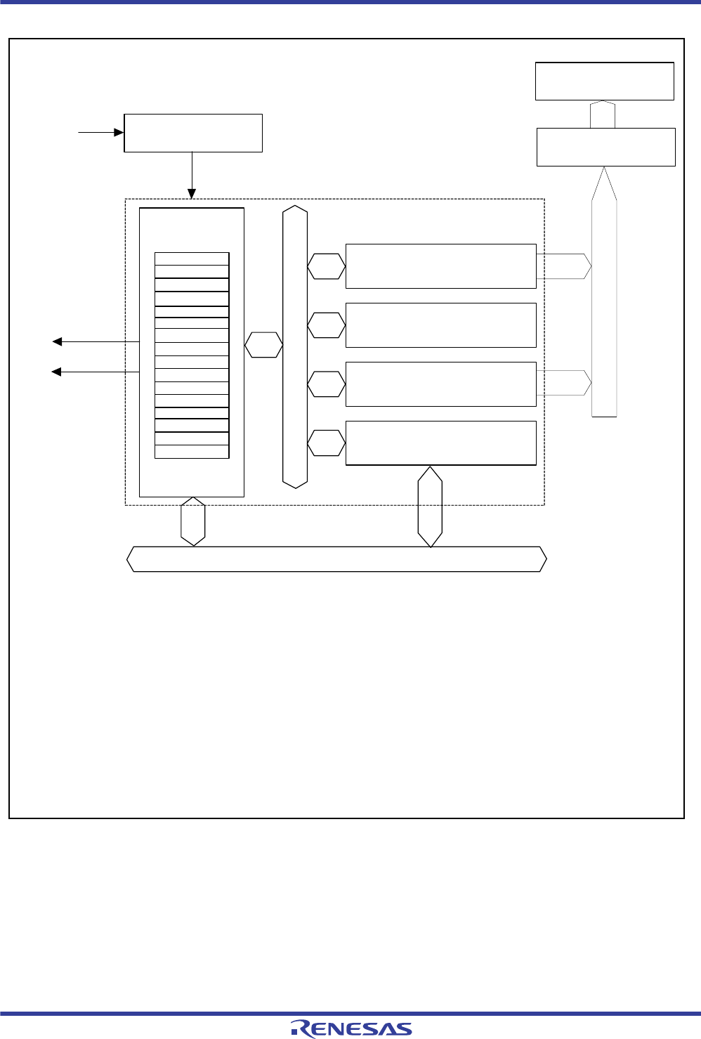
R01UH0034EJ0200 Rev.2.00 Page 1332 of 1489
Dec 27, 2013
RX62T Group, RX62G Group 31. ROM (Flash Memory for Code Storage)
Figure 31.1 Block Diagram of ROM
Mode decoder
Mode pins
FCU
FIFERR
[Legend]
FMODR
FASTAT
FAEINT
DFLRE
DFLWE
FCPSR
DFLBCCNT
DFLBCSTAT
PCKAR
FMODR: Flash mode register
FASTAT: Flash access status register
FAEINT: Flash access error interrupt enable register
DFLRE: Data flash read enable register
DFLWE: Data flash programming/erasure enable register
FCURAME: FCU RAM enable register
FSTATR0: Flash status register 0
FSTATR1: Flash status register 1
FENTRYR: Flash P/E mode entry register
FRESETR: Flash reset register
FCMDR: FCU command register
FRDYIE: Flash ready interrupt enable register
FCPSR: FCU processing switching register
DFLBCCNT: Data flash blank check control register
DFLBCSTAT: Data flash blank check status register
PCKAR: Peripheral clock notification register
FIFERR: Flash interface error interrupt
FRDYI: Flash ready interrupt
Peripheral bus
FCURAME
FSTATR0
FSTATR1
FENTRYR
FRESETR
FCMDR
FRDYIE
FRDYI
CPU
Memory interface
FCU RAM
ROM area
User area: Up to 256 Kbytes
FCU firmware store area: 8 Kbytes
Data flash area
Data area: 32 Kbytes (max.)

R01UH0034EJ0200 Rev.2.00 Page 1333 of 1489
Dec 27, 2013
RX62T Group, RX62G Group 31. ROM (Flash Memory for Code Storage)
Input and output pins associated with the ROM are listed in Table 31.2.
31.2 Register Descriptions
Table 31.3 lists the registers related to ROM. Although some registers have bits related to data flash, this section deals
only with the bits related to ROM. For details on the bits related to the data flash, see section 32.2, Register
Descriptions in section 32, Data Flash Memory (Flash Memory for Data Storage).
The registers related to the ROM are initialized by a reset.
Table 31.2 Input and Output Pins Associated with the ROM
Pin Name I/O Description
PD5/RxD1 Input Used in boot mode to receive data via SCI1 (for host communications)
PD3/TxD1 Output Used in boot mode to transmit data from SCI1 (for host communications)
MD1/MD0 Input Set the operating mode for the RX62T/RX62G Group
Table 31.3 Registers Related to ROM
Register Name Symbol Value after Reset Address Access Size
Flash mode register FMODR 00h 007F C402h 8
Flash access status register FASTAT 00h 007F C410h 8
Flash access error interrupt enable register FAEINT 9Bh 007F C411h 8
Flash ready interrupt enable register FRDYIE 00h 007F C412h 8
FCU RAM enable register FCURAME 0000h 007F C454h 16
Flash status register 0 FSTATR0 80h 007F FFB0h 8
Flash status register 1 FSTATR1 0xh 007F FFB1h 8
Flash P/E mode entry register FENTRYR 0000h 007F FFB2h 16
Flash protection register FPROTR 0000h 007F FFB4h 16
Flash reset register FRESETR 0000h 007F FFB6h 16
FCU command register FCMDR FFFFh 007F FFBAh 16
FCU processing switching register FCPSR 0000h 007F FFC8h 16
Flash P/E status register FPESTAT 0000h 007F FFCCh 16
Peripheral clock notification register PCKAR 0000h 007F FFE8h 16
Flash write erase protection register FWEPROR 02h 0008 C289h 8

R01UH0034EJ0200 Rev.2.00 Page 1334 of 1489
Dec 27, 2013
RX62T Group, RX62G Group 31. ROM (Flash Memory for Code Storage)
31.2.1 Flash Mode Register (FMODR)
FMODR is a register to specify the method for the reading of lock bits.
When on-chip ROM is disabled, the data read from FMODR is 00h and writing is disabled.
FMODR is initialized by a reset.
FRDMD Bit (FCU Read Mode Select)
This bit is used to specify the method for the reading of lock bits.
If the blank checking command for the data flash is to be used, this bit has to be set for the register read mode (see
section 32, Data Flash Memory (Flash Memory for Data Storage)).
Address: 007F C402h
b7 b6 b5 b4 b3 b2 b1 b0
———
FRDM
D————
Value after reset: 00000000
Bit Symbol Bit Name Description R/W
b3 to b0 — Reserved These bits are always read as 0. The write value should always be 0. R/W
b4 FRDMD FCU Read Mode Select 0: Memory Area Read Method
Memory area read mode is set to read a lock bit of ROM in ROM lock
bit read mode.
1: Register Read Method
Register read mode is set to read a lock bit of ROM using the lock bit
read 2 command.
R/W
b7 to b5 — Reserved These bits are always read as 0. The write value should always be 0. R/W

R01UH0034EJ0200 Rev.2.00 Page 1335 of 1489
Dec 27, 2013
RX62T Group, RX62G Group 31. ROM (Flash Memory for Code Storage)
31.2.2 Flash Access Status Register (FASTAT)
Note 1. Only 0 can be written after reading 1 to clear the flag.
FASTAT is a register to check if the access to the ROM/data flash is allowed.
When on-chip ROM is disabled, the data read from FASTAT is 00h and writing is disabled. When one of the bits in
FASTAT is set to 1, the FCU is placed in the command-locked state (see section 31.8.2, Error Protection). To clear the
command-locked state, a status register clearing command must be issued to the FCU after setting FASTAT to 10h.
FASTAT is initialized by a reset.
CMDLK Bit (FCU Command Lock)
This bit indicates that the FCU is in the command-locked state (see section 31.8.2, Error Protection).
[Setting condition]
After the FCU detects an error and enters the command-locked state
[Clearing condition]
After the FCU processes a status register clearing command under conditions where FASTAT is set to 10h
Address: 007F C410h
b7 b6 b5 b4 b3 b2 b1 b0
ROMA
E— — CMDLK DFLAE — DFLRP
EDFLWP
E
Value after reset: 00000000
Bit Symbol Bit Name Description R/W
b0 DFLWPE Data Flash Programming/Erasure
Protection Violation
See section 32, Data Flash Memory (Flash Memory for Data
Storage).
R/(W)*1
b1 DFLRPE Data Flash Read Protection Violation See section 32, Data Flash Memory (Flash Memory for Data
Storage).
R/(W)*1
b2 — Reserved This bit is always read as 0. The write value should always
be 0.
R/W
b3 DFLAE Data Flash Access Violation See section 32, Data Flash Memory (Flash Memory for Data
Storage).
R/(W)*1
b4 CMDLK FCU Command Lock 0: FCU is not in the command-locked state
1: FCU is in the command-locked state
R
b6, b5 — Reserved These bits are always read as 0. The write value should
always be 0.
R/W
b7 ROMAE ROM Access Violation 0: No ROM access error
1: ROM access error
R/(W)*1

R01UH0034EJ0200 Rev.2.00 Page 1336 of 1489
Dec 27, 2013
RX62T Group, RX62G Group 31. ROM (Flash Memory for Code Storage)
ROMAE Bit (ROM Access Violation)
This bit indicates whether a ROM access violation occurred.
When the ROMAE bit is set to 1, the ILGLERR bit in FSTATR0 is set to 1, placing the FCU in the command-locked
state.
[Setting conditions]
A read command is issued for ROM programming/erasure addresses 00FC 0000h to 00FF FFFFh when the FCU is
in ROM P/E normal mode and the FENTRYR.FENTRY0 bit is set to 1.
A command is issued for ROM programming/erasure addresses 00FC 0000h to 00FF FFFFh when the FENTRY0
bit is set to 0.
A read command is issued for ROM read addresses FFFC 0000h to FFFF FFFFh when FENTRYR is set to other
than 0000h.
[Clearing condition]
When 0 is written after reading 1

R01UH0034EJ0200 Rev.2.00 Page 1337 of 1489
Dec 27, 2013
RX62T Group, RX62G Group 31. ROM (Flash Memory for Code Storage)
31.2.3 Flash Access Error Interrupt Enable Register (FAEINT)
FAEINT is a register to enable and disable the flash interface error interrupt (FIFERR).
When on-chip ROM is disabled, the data read from FAEINT is 00h and writing is disabled.
FAEINT is initialized by a reset.
CMDLKIE Bit (FCU Command Lock Interrupt Enable)
This bit is used to enable or disable FIFERR interrupt requests when an FCU command lock occurs and the CMDLK bit
in FASTAT is set to 1.
ROMAEIE Bit (ROM Access Violation Interrupt Enable)
This bit is used to enable or disable FIFERR interrupt requests when a ROM access violation occurs and the ROMAE bit
in FASTAT is set to 1.
Address: 007F C411h
b7 b6 b5 b4 b3 b2 b1 b0
ROMA
EIE ——
CMDLK
IE DFLAEI
E—DFLRP
EIE DFLWP
EIE
Value after reset: 10011011
Bit Symbol Bit Name Description R/W
b0 DFLWPEIE Data Flash Programming/Erasure
Protection Violation Interrupt Enable
See section 32, Data Flash Memory (Flash Memory for Data
Storage).
R/W
b1 DFLRPEIE Data Flash Read Protection Violation
Interrupt Enable
See section 32, Data Flash Memory (Flash Memory for Data
Storage).
R/W
b2 — Reserved This bit is always read as 0. The write value should always be
0.
R/W
b3 DFLAEIE Data Flash Access Violation Interrupt
Enable
See section 32, Data Flash Memory (Flash Memory for Data
Storage).
R/W
b4 CMDLKIE FCU Command Lock Interrupt Enable 0: FIFERR interrupt requests disabled when the CMDLK bit in
FASTAT is set to 1
1: FIFERR interrupt requests enabled when the CMDLK bit in
FASTAT is set to 1
R/W
b6, b5 — Reserved These bits are always read as 0. The write value should
always be 0.
R/W
b7 ROMAEIE ROM Access Violation Interrupt Enable 0: FIFERR interrupt requests disabled when the ROMAE bit
in FASTAT is set to 1
1: FIFERR interrupt requests enabled when the ROMAE bit in
FASTAT is set to 1
R/W

R01UH0034EJ0200 Rev.2.00 Page 1338 of 1489
Dec 27, 2013
RX62T Group, RX62G Group 31. ROM (Flash Memory for Code Storage)
31.2.4 FCU RAM Enable Register (FCURAME)
Note 1. Write data is not retained.
FCURAME is a register to enable and disable an access to the FCU RAM area.
Only specific values written to the upper byte in word access are valid. Data written to the upper byte is not retained.
When on-chip ROM is disabled, the data read from FCURAME is 00h and writing is disabled.
FCURAME is initialized by a reset.
FCRME Bit (FCU RAM Enable)
This bit is used to enable and disable an access to the FCU RAM.
Data written to the FCRME bit is valid only when it is written in word access and the KEY[7:0] bits are C4h. When
programming data to the FCU RAM, set FENTRYR to 0000h and stop the FCU.
KEY[7:0] Bits (Key Code)
These bits are used to enable or disable rewriting of the FCRME bit.
Data written to the KEY[7:0] bits is not retained.
Address: 007F C454h
b15 b14 b13 b12 b11 b10 b9 b8 b7 b6 b5 b4 b3 b2 b1 b0
KEY[7:0] ———————FCRME
Value after reset: 0000000000000000
Bit Symbol Bit Name Description R/W
b0 FCRME FCU RAM Enable 0: Access to the FCU RAM disabled
1: Access to the FCU RAM enabled
R/W
b7 to b1 — Reserved These bits are always read as 0. The write value should always be 0. R/W
b15 to b8 KEY[7:0] Key Code This bit is used to enable or disable rewriting of the FCRME bit. R/(W)*1

R01UH0034EJ0200 Rev.2.00 Page 1339 of 1489
Dec 27, 2013
RX62T Group, RX62G Group 31. ROM (Flash Memory for Code Storage)
31.2.5 Flash Status Register 0 (FSTATR0)
FSTATR0 is a register to check the FCU status.
When on-chip ROM is disabled, the data read from FSTATR0 is 00h.
FSTATR0 is initialized by a reset, or when the FRESET bit in FRESETR is set to 1.
PRGSPD Bit (Programming Suspend Status)
This bit is used to indicate that the FCU enters the programming suspend processing state or programming suspended
state (see section 31.7, Suspending Operation).
[Setting condition]
The FCU has initiated a write suspend command.
[Clearing condition]
The FCU has accepted a resume command.
ERSSPD Bit (Erasure Suspend Status)
This bit is used to indicate that the FCU enters the erasure suspend processing state or erasure suspended state (see
section 31.7, Suspending Operation).
[Setting condition]
The FCU has initiated an erasure suspend command.
[Clearing condition]
The FCU has accepted a resume command.
Address: 007F FFB0h
b7 b6 b5 b4 b3 b2 b1 b0
FRDY ILGLER
RERSER
RPRGER
RSUSRD
Y—ERSSP
DPRGSP
D
Value after reset: 10000000
Bit Symbol Bit Name Description R/W
b0 PRGSPD Programming Suspend Status 0: Other than the status described below
1: During programming suspend processing or programming
suspended
R
b1 ERSSPD Erasure Suspend Status 0: Other than the status described below
1: When erasure suspend processing or erasure suspended
R
b2 — Reserved This bit is always read as 0. Writing to this bit has no effect. R
b3 SUSRDY Suspend Ready 0: P/E suspend commands cannot be received
1: P/E suspend commands can be received
R
b4 PRGERR Programming Error 0: Programming terminates normally
1: An error occurs during programming
R
b5 ERSERR Erasure Error 0: Erasure terminates normally
1: An error occurs during erasure
R
b6 ILGLERR Illegal Command Error 0: FCU detects no illegal command or ROM/data flash access
1: FCU detects an illegal command or ROM/data flash access
R
b7 FRDY Flash Ready 0: During programming/erasure,
During suspending programming/erasure,
During the lock bit read 2 command processing,
During the peripheral clock notification command processing
During the blank check processing of data flash
(See section 32, Data Flash Memory (Flash Memory for Data
Storage)).
1: Processing described above is not performed
R

R01UH0034EJ0200 Rev.2.00 Page 1340 of 1489
Dec 27, 2013
RX62T Group, RX62G Group 31. ROM (Flash Memory for Code Storage)
SUSRDY Bit (Suspend Ready Status)
This bit is used to indicate whether the FCU can receive a P/E suspend command.
[Setting condition]
After starting programming/erasure process, the FCU enters a state in which P/E suspend commands can be
received.
[Clearing conditions]
The FCU has accepted a P/E suspend command.
During programming/erasure process, the FCU enters the command-locked state.
PRGERR Bit (Programming Error)
This bit is used to indicate the result of the ROM/data flash programming process by the FCU.
When the PRGERR bit is set to 1, the FCU is placed in the command-locked state (see section 31.8.2, Error
Protection).
[Setting condition]
An error occurs during programming.
A programming command is issued to areas protected by a lock bit.
[Clearing condition]
After the FCU processes a status register clearing command
ERSERR Bit (Erasure Error)
This bit is used to indicate the result of the ROM/data flash erasure process by the FCU.
When the ERSERR bit is set to 1, the FCU is placed in the command-locked state (see section 31.8.2, Error
Protection).
[Setting condition]
An error occurs during erasure.
A block erase command is issued to areas protected by a lock bit.
[Clearing condition]
After the FCU processes a status register clearing command
ILGLERR Bit (Illegal Command Error)
This bit is used to indicate that the FCU detects any illegal command or ROM/data flash access.
When the ILGLERR bit is set to 1, the FCU is placed in the command-locked state (see section 31.8.2, Error
Protection).
[Setting conditions]
The FCU detects an illegal command.
The FCU detects an illegal ROM/data flash access
(one of the ROMAE, DFLAE, DFLRPE, and DFLWPE bits in FASTAT is 1).
The setting of FENTRYR is invalid.
[Clearing condition]
After the FCU processes a status register clearing command under conditions where FASTAT is set to 10h
FRDY Bit (Flash Ready)
This bit is used to check the processing status of the FCU.

R01UH0034EJ0200 Rev.2.00 Page 1341 of 1489
Dec 27, 2013
RX62T Group, RX62G Group 31. ROM (Flash Memory for Code Storage)
31.2.6 Flash Status Register 1 (FSTATR1)
FSTATR1 is a register to check the FCU status.
When on-chip ROM is disabled, the data read from FSTATR1 is 00h.
FSTATR1 is initialized by a reset, or when the FRESET bit in FRESETR is set to 1.
FLOCKST Bit (Lock Bit Status)
This bit is to reflect the read data of a lock bit when using the lock bit read 2 command.
When the FRDY bit in FSTATR0 is set to 1 after a lock bit read 2 command is issued, valid data is stored in the
FLOCKST bit. The value of the FLOCKST bit is retained until the completion of the next lock bit read 2 command.
FCUERR Bit (FCU Error)
This bit is used to indicate that an error occurs in the FCU internal processing.
When the FCUERR bit is set to 1, set the FRESET bit in FRESETR to 1 to initialize the FCU. Additionally, recopy the
FCU firmware from the FCU firmware area to the FCU RAM area.
Address: 007F FFB1h
b7 b6 b5 b4 b3 b2 b1 b0
FCUER
R——
FLOCK
ST ————
Value after reset: 000000xx
x: Undefined
Bit Symbol Bit Name Description R/W
b1, b0 — Reserved The read value is undefined. Writing to these bits has no effect. R
b3, b2 — Reserved These bits are always read as 0. Writing to these bits has no effect. R
b4 FLOCKST Lock Bit Status 0: Protected
1: Not protected
R
b6, b5 — Reserved These bits are always read as 0. Writing to these bits has no effect. R
b7 FCUERR FCU Error 0: No error occurs in the FCU processing
1: An error occurs in the FCU processing
R

R01UH0034EJ0200 Rev.2.00 Page 1342 of 1489
Dec 27, 2013
RX62T Group, RX62G Group 31. ROM (Flash Memory for Code Storage)
31.2.7 Flash Ready Interrupt Enable Register (FRDYIE)
FRDYIE is a register to enable and disable the flash ready interrupt (FRDYI) output.
When on-chip ROM is disabled, the data read from FRDYIE is 00h and writing is disabled.
FRDYIE is initialized by a reset.
FRDYIE Bit (Flash Ready Interrupt Enable)
This bit is to enable/disable a FRDYI interrupt request when programming/erasure is completed.
If the FRDYIE bit is set to 1, a flash ready interrupt request (FRDYI) is generated when execution of the FCU command
has completed (FSTATR0.FRDY bit changes from 0 to 1).
Address: 007F C412h
b7 b6 b5 b4 b3 b2 b1 b0
———————
FRDYI
E
Value after reset: 00000000
Bit Symbol Bit Name Description R/W
b0 FRDYIE Flash Ready Interrupt Enable 0: FRDYI interrupt requests disabled
1: FRDYI interrupt requests enabled
R/W
b7 to b1 — Reserved These bits are always read as 0. The write value should always be 0. R/W

R01UH0034EJ0200 Rev.2.00 Page 1343 of 1489
Dec 27, 2013
RX62T Group, RX62G Group 31. ROM (Flash Memory for Code Storage)
31.2.8 Flash P/E Mode Entry Register (FENTRYR)
Note 1. Write data is not retained.
FENTRYR is a register to place the ROM/data flash in P/E mode.
To place the ROM/data flash in P/E mode so that the FCU can accept commands, either the FENTRYD or FENTRY0 bit
must be set to 1. Note that if both bits are set to 1, the ILGLERR bit in FSTATR0 is set and the FCU enters the command-
locked state.
After writing to FENTRYR to initiate a transition to ROM-reading mode, read the register and confirm that it actually
holds the new setting before proceeding to read the ROM.
Only specific values written to the upper byte in word access are valid. Any other writing causes the register to be
initialized. Data written to the upper byte is not retained.
When on-chip ROM is disabled, the data read from FENTRYR is 0000h and writing is disabled.
FENTRYR is initialized by a reset, or when the FRESET bit in FRESETR is set to 1.
FENTRY0 Bit (ROM P/E Mode Entry 0)
This bit is used to place the ROM in P/E mode.
[Writing-enable conditions (when all of the following conditions are met)]
On-chip ROM is enabled.
The FRDY bit in FSTATR0 is set to 1.
AAh is written to the FEKEY[7:0] bits in word access.
[Setting condition]
When the writing-enable conditions are met, FENTRYR is set to 0000h, and 1 is written to the FENTRY0 bit
[Clearing conditions]
Data is written in byte access.
Data is written in word access when the FEKEY[7:0] bits are other than AAh.
When the writing-enable conditions are met, 0 is written to the FENTRY0 bit.
When the writing-enable conditions are met and FENTRYR is other than 0000h, data is written to FENTRYR.
FEKEY[7:0] Bits (Key Code)
These bits enable or disable rewriting of the FENTRYD and FENTRY0 bits.
Data written to the FEKEY[7:0] bits is not retained.
Address: 007F FFB2h
b15 b14 b13 b12 b11 b10 b9 b8 b7 b6 b5 b4 b3 b2 b1 b0
FEKEY[7:0] FENTR
YD ——————
FENTR
Y0
Value after reset: 0000000000000000
Bit Symbol Bit Name Description R/W
b0 FENTRY0 ROM P/E Mode Entry 0 0: ROM is in ROM reading mode
1: ROM is in ROM P/E mode.
R/W
b6 to b1 — Reserved These bits are always read as 0. The write value should always be 0. R/W
b7 FENTRYD E2 Data Flash P/E Mode
Entry
See section 32, Data Flash Memory (Flash Memory for Data Storage). R/W
b15 to b8 FEKEY[7:0] Key Code These bits enable or disable rewriting of the FENTRYD and FENTRY0
bits.
R/(W)
*1

R01UH0034EJ0200 Rev.2.00 Page 1344 of 1489
Dec 27, 2013
RX62T Group, RX62G Group 31. ROM (Flash Memory for Code Storage)
31.2.9 Flash Protection Register (FPROTR)
Note 1. Write data is not retained.
FPROTR is a register used to enable/disable the programming/erasure protection function with a lock bit.
Only specific values written to the upper byte in word access are valid. Any other writing causes the register to be
initialized. Data written to the upper byte is not retained.
When on-chip ROM is disabled, the data read from FPROTR is 0000h and writing is disabled.
FPROTR is initialized by a reset, or when the FRESET bit in FRESETR is set to 1.
FPROTCN Bit (Lock Bit Protection Cancel)
This bit is used to enable/disable the programming/erasure protection with a lock bit.
[Setting condition]
The FPKEY[7:0] bits are set to 55h, and the FPROTCN bit is set to 1 in word access when the value of FENTRYR
is other than 0000h.
[Clearing conditions]
Data is written in byte access.
Data is written in word access when the FPKEY[7:0] bits are other than 55h.
The FPKEY[7:0] bits are set to 55h, and the FPROTCN bit is set to 0 in word access.
The value of FENTRYR is 0000h.
FPKEY[7:0] Bits (Key Code)
These bits are used to enable or disable rewriting of the FPROTCN bit.
Data written to the FPKEY[7:0] bits is not retained.
Address: 007F FFB4h
b15 b14 b13 b12 b11 b10 b9 b8 b7 b6 b5 b4 b3 b2 b1 b0
FPKEY[7:0] ———————
FPROT
CN
Value after reset: 0000000000000000
Bit Symbol Bit Name Description R/W
b0 FPROTCN Lock Bit Protection Cancel 0: Protection with a lock bit enabled
1: Protection with a lock bit disabled
R/W
b7 to b1 — Reserved These bits are always read as 0. The write value should always be 0. R/W
b15 to b8 FPKEY[7:0] Key Code These bits are used to enable or disable rewriting of the FPROTCN
bit.
R/(W)
*1

R01UH0034EJ0200 Rev.2.00 Page 1345 of 1489
Dec 27, 2013
RX62T Group, RX62G Group 31. ROM (Flash Memory for Code Storage)
31.2.10 Flash Reset Register (FRESETR)
Note 1. Write data is not retained.
FRESETR is a register to initialize the FCU.
Only specific values written to the upper byte in word access are valid. Data written to the upper byte is not retained.
When on-chip ROM is disabled, the data read from FRESETR is 0000h and writing is disabled.
FRESETR is initialized by a reset.
FRESET Bit (Flash Reset)
When the FRESET bit is set to 1, programming/erasure operations for the ROM/data flash are forcibly terminated, and
the FCU is initialized.
High voltage is applied to the memory of the ROM/data flash during programming/erasure. To ensure time required for
dropping the voltage applied to the memory, keep the FRESET bit set to 1 for tRESW2 (see section 33, Electrical
Characteristics) when initializing the FCU. While the FRESET bit is kept 1, prohibit the ROM/data flash from being
read. Additionally, when the FRESET bit is set to 1, the FCU commands cannot be used because FENTRYR is
initialized.
Writing of the FRESET bit is enabled only in word access and when the FRKEY[7:0] bits are CCh.
FRKEY[7:0] Bits (Key Code)
These bits are used to enable or disable rewriting of the FRESET bit.
Data written to the FRKEY[7:0] bits is not retained.
Address: 007F FFB6h
b15 b14 b13 b12 b11 b10 b9 b8 b7 b6 b5 b4 b3 b2 b1 b0
FRKEY[7:0] ———————
FRESE
T
Value after reset: 0000000000000000
Bit Symbol Bit Name Description R/W
b0 FRESET Flash Reset 0: FCU is not reset
1: FCU is reset
R/W
b7 to b1 — Reserved These bits are always read as 0. The write value should always be 0. R/W
b15 to b8 FRKEY[7:0] Key Code These bits are used to enable or disable rewriting of the FRESET bit. R/(W)
*1
R01UH0034EJ0200 Rev.2.00 Page 1346 of 1489
Dec 27, 2013
RX62T Group, RX62G Group 31. ROM (Flash Memory for Code Storage)
31.2.11 FCU Command Register (FCMDR)
FCMDR is a register to store commands received by the FCU.
When on-chip ROM is disabled, the data read from FCMDR is 0000h and writing is disabled.
FCMDR is initialized by a reset, or when the FRESET bit in FRESETR is set to 1.
Table 31.4 lists the states of FCMDR after receiving each command. For details on the blank check processing, see
section 32.6, Programming and Erasing the Data Flash Memory in section 32, Data Flash Memory (Flash
Memory for Data Storage).
Address: 007F FFBAh
b15 b14 b13 b12 b11 b10 b9 b8 b7 b6 b5 b4 b3 b2 b1 b0
CMDR[7:0] PCMDR[7:0]
Value after reset: 1111111111111111
Bit Symbol Bit Name Description R/W
b7 to b0 PCMDR[7:0] Precommand Store the command immediately before the last command received by
the FCU.
R
b15 to b8 CMDR[7:0] Command Store the last command received by the FCU. R
Table 31.4 States of FCMDR after Receiving Each Command
Command CMDR PCMDR
P/E Normal mode transition FFh Previous command
Status read mode transition 70h Previous command
Lock bit read mode transition (lock bit read 1) 71h Previous command
Peripheral clock notification command E9h Previous command
Programming E8h Previous command
Block erase D0h 20h
P/E suspend B0h Previous command
P/E resume D0h Previous command
Status register clearing 50h Previous command
Lock bit read 2/blank check D0h 71h
Lock bit programming D0h 77h

R01UH0034EJ0200 Rev.2.00 Page 1347 of 1489
Dec 27, 2013
RX62T Group, RX62G Group 31. ROM (Flash Memory for Code Storage)
31.2.12 FCU Processing Switching Register (FCPSR)
FCPSR is a register to select the method of suspending the FCU erasure processing.
When on-chip ROM is disabled, the data read from FCPSR is 0000h and writing is disabled.
FCPSR is initialized by a reset, or when the FRESET bit in FRESETR is set to 1.
ESUSPMD Bit (Erasure Suspend Mode)
This bit is to select the erasure suspend mode for when a P/E suspend command is issued while the FCU executes the
erasure processing for the ROM/data flash (see section 31.7, Suspending Operation).
Address: 007F FFC8h
b15 b14 b13 b12 b11 b10 b9 b8 b7 b6 b5 b4 b3 b2 b1 b0
———————————————
ESUSP
MD
Value after reset: 0000000000000000
Bit Symbol Bit Name Description R/W
b0 ESUSPMD Erasure Suspend Mode 0: Suspension priority mode
1: Erasure priority mode
R/W
b15 to b1 — Reserved These bits are always read as 0. The write value should always be 0. R/W

R01UH0034EJ0200 Rev.2.00 Page 1348 of 1489
Dec 27, 2013
RX62T Group, RX62G Group 31. ROM (Flash Memory for Code Storage)
31.2.13 Flash P/E Status Register (FPESTAT)
FPESTAT is a register to indicate the result of the programming/erasure processing for the ROM/data flash.
When on-chip ROM is disabled, the data read from FPESTAT is 0000h and writing is disabled.
FPESTAT is initialized by a reset, or when the FRESET bit in FRESETR is set to 1.
PEERRST[7:0] Bits (P/E Error Status)
These bits are used to indicate the reason of an error that occurs during the programming/erasure processing for the
ROM/data flash.
The value of the PEERRST[7:0] bits is valid only when the ERSERR bit or PRGERR bit in FSTATR0 is 1. The value of
the reason of the past error is retained in the PEERRST[7:0] bits when the ERSERR bit and PRGERR bit is 0.
Address: 007F FFCCh
b15 b14 b13 b12 b11 b10 b9 b8 b7 b6 b5 b4 b3 b2 b1 b0
———————— PEERRST[7:0]
Value after reset: 0000000000000000
Bit Symbol Bit Name Description R/W
b7 to b0 PEERRST[7:0] P/E Error Status 00h: No programming error
01h: Programming error against areas protected by a lock bit
02h: Programming error due to sources other than the lock bit protection
11h: Erasure error against areas protected by a lock bit
12h: Erasure error due to sources other than the lock bit protection
(Values other than above are reserved)
R
b15 to b8 — Reserved These bits are always read as 0 and cannot be modified. R

R01UH0034EJ0200 Rev.2.00 Page 1349 of 1489
Dec 27, 2013
RX62T Group, RX62G Group 31. ROM (Flash Memory for Code Storage)
31.2.14 Peripheral Clock Notification Register (PCKAR)
PCKAR is a register to notify the sequencer of the frequency setting data of the peripheral clock (PCLK) at the
programming/erasure for the ROM/data flash. This setting is used to control programming and erasure times.
When on-chip ROM is disabled, the data read from PCKAR is 0000h and writing is disabled.
PCKAR is initialized by a reset, or when the FRESET bit in FRESETR is set to 1.
PCKA[7:0] Bits (Peripheral Clock Notification)
These bits are used to set the peripheral clock (PCLK) at the programming/erasure for the ROM/data flash.
Set the PCKA[7:0] bits to the PCLK frequency and issue a peripheral clock notification command before programming/
erasure. Do not change the frequency during the programming/erasure processing for the ROM/data flash.
Calculate the setting value as follows:
Convert an operating frequency represented in MHz units to binary and write it to the PCKA[7:0] bits.
For example, when the operating frequency of the peripheral clock is 35.9 MHz, the setting value is calculated as
follows:
Round up 35.9
Convert 36 to binary and set the upper bits and lower bits of the PCKA[7:0] bits to 00h and 24h (0010 0100b).
Note 1. When the PCKA[7:0] bits are set to values outside the range from 8 to 50 MHz, do not issue a programming
command to the ROM/data flash.
Note 2. When the PCKA[7:0] bits are set to a frequency that is different from the actual frequency, the data of the ROM/
data flash may crash.
Note 3. Please note that programming time depends on the frequency to some extent even if the PCKA[7:0] bits are
used.
Address: 007F FFE8h
b15 b14 b13 b12 b11 b10 b9 b8 b7 b6 b5 b4 b3 b2 b1 b0
———————— PCKA[7:0]
Value after reset: 0000000000000000
Bit Symbol Bit Name Description R/W
b7 to b0 PCKA[7:0] Peripheral Clock
Notification
These bits are used to set the flashIF clock (FCLK) at the
programming/erasure for the ROM/E2 data flash.
R/W
b15 to b8 — Reserved These bits are always read as 0. The write value should always be 0. R/W

R01UH0034EJ0200 Rev.2.00 Page 1350 of 1489
Dec 27, 2013
RX62T Group, RX62G Group 31. ROM (Flash Memory for Code Storage)
31.2.15 Flash Write Erase Protection Register (FWEPROR)
FWEPROR is a readable/writable register to protect the execution of the flash write/erase with software.
FWEPROR is initialized in software standby mode or deep software standby.
FLWE[1:0] Bits (Flash Write Erase)
These bits protect the execution of the flash write/erase with software.
Address: 0008 C289h
b7 b6 b5 b4 b3 b2 b1 b0
——————FLWE[1:0]
Value after reset: 00000010
Bit Symbol Bit Name Description R/W
b1, b0 FLWE[1:0] Flash Programming/
Erasure
b1 b0
0 0: Flash programming/erasure disabled.
0 1: Flash programming/erasure enabled.
1 0: Flash programming/erasure disabled. (initial value)
1 1: Flash programming/erasure disabled.
R/W
b7 to b2 — Reserved These bits are always read as 0. The write value should always be 0. R/W
R01UH0034EJ0200 Rev.2.00 Page 1351 of 1489
Dec 27, 2013
RX62T Group, RX62G Group 31. ROM (Flash Memory for Code Storage)
31.3 Configuration of Memory Areas for the ROM
The ROM of products in the RX62T and RX62G Groups is configured of a maximum 256-Kbyte user area. The address
range occupied by this area is shown in Figure 31.2.
Note that for the user area, the address range for reading differs from the address range for programming and erasure.
Figure 31.2 Memory Area Configuration of ROM
31.4 Block Configuration
The configuration of erasure blocks for the user area is shown in Figure 31.3. As units of erasure, the user area is
divided into 8 blocks of 4 Kbytes each and 14 blocks of 16 Kbytes each. For programming, the user area consists of the
256-byte units starting from 00h as the lower-order byte of the address.
Figure 31.3 Configuration of Erasure Blocks for the User Area
Address FFFC 0000h
Address FFFF FFFFh
User area
(256 Kbytes)
<For reading>
Address 00FC 0000h
Address 00FF FFFFh
<For programming/erasure>
User area
(128 Kbytes) User area
(64 Kbytes)
R5F562TAxxxx R5F562T7xxxx R5F562T6xxxx
Address FFFE 0000h
Address FFFF 0000h
Address 00FE 0000h
Address 00FF 0000h
Address FFFC 0000h
Address FFFF FFFFh
User area
EB21 to EB14
Erasure block
R5F562TAxxxx R5F562T7xxxx R5F562T6xxxx
Address FFFE 0000h
Address FFFF 0000h
Address FFFF 8000h
User area
User area
16 Kbytes
×14 blocks
4 Kbytes
×8 blocks
16 Kbytes
×6 blocks 16 Kbytes
×2 blocks
4 Kbytes
×8 blocks
4 Kbytes
×8 blocks
EB13 to EB10
EB07 to EB00
EB09 to EB08
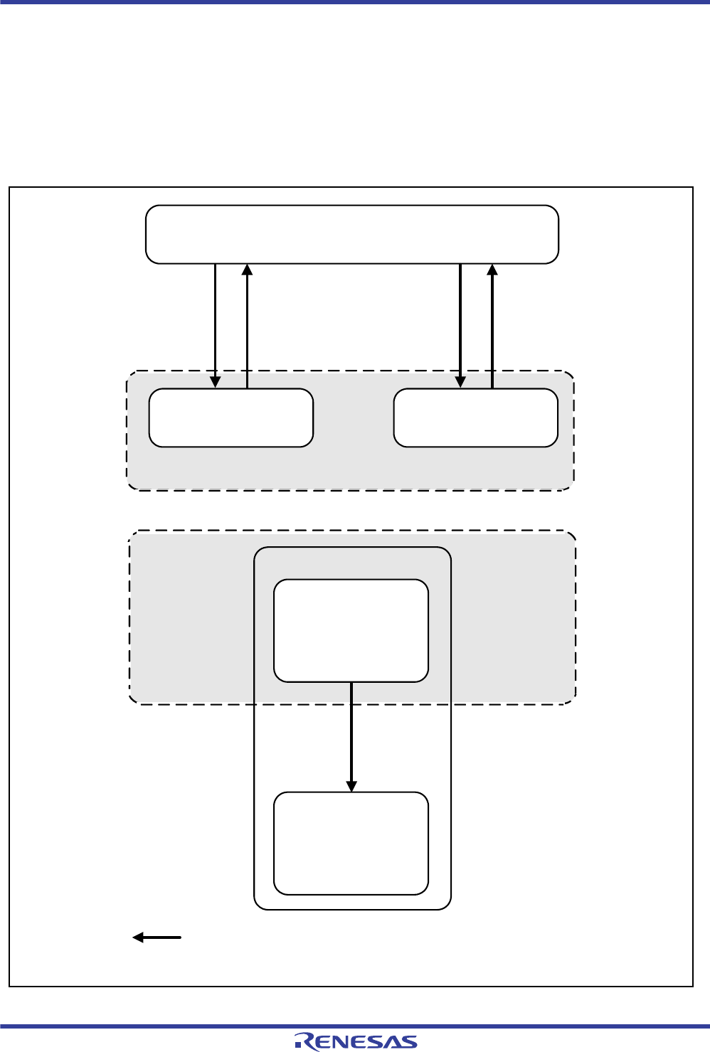
R01UH0034EJ0200 Rev.2.00 Page 1352 of 1489
Dec 27, 2013
RX62T Group, RX62G Group 31. ROM (Flash Memory for Code Storage)
31.5 Operating Modes Associated with the ROM
Figure 31.4 is a diagram of the operating-mode transitions for the RX62T and RX62G Groups.
On release from the reset state, transitions are in accord with the levels on the MD0 and MD1 pins, as shown in Figure
31.4.
For more information on the connections between the settings of the levels on the MD0 and MD1 pins and the operating
mode for the RX62T and RX62G Groups, refer to section 3, Operating Modes.
Figure 31.4 Transitions between Operating Modes in Terms of the ROM
Reset state
RES# = 0
Boot mode Single-chip mode
RES# = 0RES# = 0
RES# = 1
MD1 = 0
MD0 = 1
RES# = 1
MD1 = 1
MD0 = 1
On-board programming
Single-chip mode
Mode can shift
Note: * Initial value after a reset
ROME = 0
On-chip ROM: Enabled*
ROME = 1
On-chip ROM: Disabled
ROME = 0
On-board programming

R01UH0034EJ0200 Rev.2.00 Page 1353 of 1489
Dec 27, 2013
RX62T Group, RX62G Group 31. ROM (Flash Memory for Code Storage)
Reading, programming, and erasing of the ROM in an on-board device can proceed if the device is in boot or single-chip
mode (with on-chip ROM enabled), or in on-chip-ROM-enabled expansion mode.
Which areas are programmable and erasable, the area from which booting up proceeds after a reset, etc., differs with the
mode. The differences between modes are indicated in Table 31.5.
Note 1. The entire ROM may be erased at the time of booting up. Specified blocks can subsequently be erased. For details, refer to
section 31.9.2, ID Code Protection.
Note 2. Not available to users.
In boot mode, a host is able to program or read out the user area or data area via an SCI.
In boot mode, on-chip RAM is employed for the embedded program for use in boot mode. For this reason,
preserving the contents of on-chip RAM is not possible in this case.
Table 31.5 Differences between Modes
Item Boot Mode Single-Chip Mode (with On-chip ROM Enabled)
Environment for programming and erasure On-board programming On-board programming
Programmable and erasable area User area User area
Division into erasure blocks Possible*1 Possible
Target area for booting after a reset Area containing the embedded
program*2 User area
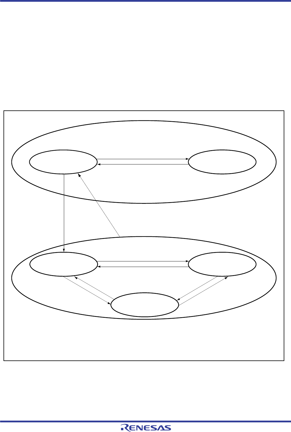
R01UH0034EJ0200 Rev.2.00 Page 1354 of 1489
Dec 27, 2013
RX62T Group, RX62G Group 31. ROM (Flash Memory for Code Storage)
31.6 Programming and Erasing the ROM
The ROM is programmed and erased by issuing commands to a dedicated sequencer (FCU) for programming and
erasure. The FCU has five modes. For programming and erasure, the mode is changed and then commands for
programming and erasure are issued.
The mode transitions required to program or erase the ROM and the system of commands are described below. The
descriptions apply in common to boot and single-chip mode (with on-chip ROM enabled).
31.6.1 FCU Modes
The FCU has five modes or sets of modes. Transitions between modes are caused by modifying FENTRYR or issuing
FCU commands. Figure 31.5 is a diagram of the FCU mode transitions.
Figure 31.5 Mode Transitions of the FCU (Associated with the ROM)
ROM P/E mode
ROM status read
mode
(B)
(A)
ROM P/E normal
mode
ROM lock bit read
mode
(C)
(B)
(A)
(C)
Data flash P/E mode
ROM/data flash
read mode
FENTRYR = 0080h
FENTRYR = 0000h
ROM read mode
FENTRYR = 0000h
(A): Execute a normal mode transition command.
(B): Execute a command that is neither a normal mode transition command nor a lock bit read mode transition command.
(C): Execute a lock bit read mode transition command.
FENTRYR = 0001h
[Legend]

R01UH0034EJ0200 Rev.2.00 Page 1355 of 1489
Dec 27, 2013
RX62T Group, RX62G Group 31. ROM (Flash Memory for Code Storage)
31.6.1.1 ROM Read Modes
The ROM read modes are for high-speed reading of the ROM. Access to an address for reading can be accomplished in
one cycle of ICLK.
ROM/data-flash read mode and data-flash P/E mode are the two kinds of ROM reading mode.
(1) ROM/Data Flash Read Mode
This mode is for reading the ROM and data-flash memory. The FCU does not accept commands.
The FCU enters this mode when the FENTRY0 bit in FENTRYR is set to 0, and the FENTRYD bit in FENTRYR is set
to 0.
(2) Data Flash P/E Modes
These modes are for programming and erasure of the data-flash memory. High-speed reading of the ROM is also
possible. Although the FCU accepts FCU commands related to the data-flash memory in this mode, it does not accept
FCU commands related to the ROM. The FCU enters these modes when the FENTRY0 bit in FENTRYR is set to 0, or
the FENTRYD bit in FENTRYR is set to 1.
For details on the data flash P/E modes, see section 32.6.1, FCU Modes, in section 32, Data Flash Memory (Flash
Memory for Data Storage).
31.6.1.2 ROM P/E Modes
The ROM P/E modes are for programming and erasure of the ROM. High-speed reading of the ROM is not possible in
these modes. Read access to an address within the range for reading causes a ROM-access violation, and the FCU enters
the command-locked state (see section 31.8.2, Error Protection).
ROM P/E normal mode, ROM status read mode, and ROM lock-bit read mode are the three ROM P/E modes.
(1) ROM P/E Normal Mode
The transition to ROM P/E normal mode is the first transition in the process of programming or erasing the ROM. The
FCU enters this mode when the FENTRYD bit in FENTRYR is set to 0, and the FENTRY0 bit in FENTRYR is set to 1
in ROM read mode, or when the normal mode transition command is received in ROM P/E modes. Table 31.8 lists the
acceptable commands in this mode.
Read access to an address within the range for programming and erasure while the FENTRY0 bit in FENTRYR is set to
1 causes a ROM-access violation, and the FCU enters the command-locked state (see section 31.8.2, Error
Protection).
(2) ROM Status Read Mode
The ROM status read mode is for reading information on the state of the ROM. The FCU enters this mode when a
command other than the normal mode transition and lock bit read mode transition command is received in ROM P/E
modes.
ROM status read mode encompasses the states where the FRDY bit in FSTATR0 is 0 and the command-locked state after
an error has occurred. Table 31.8 lists the acceptable commands in this mode.
Read access to an address within the range for programming and erasure while the FENTRY0 bit in FENTRYR is 1 will
actually read out the value of FSTATR0.
(3) ROM Lock-Bit Read Mode
The ROM lock-bit read mode is for reading the values of the lock bits of the ROM. The FCU enters this mode when a
lock-bit read mode transition command is received in ROM P/E modes. Table 31.8 lists the acceptable commands in this
mode.
In read access to an address within the range for programming and erasure while the FENTRY0 bit in FENTRYR is 1, all
bits of the value read out have the value of the lock bit of the erasure block that includes the accessed address.

R01UH0034EJ0200 Rev.2.00 Page 1356 of 1489
Dec 27, 2013
RX62T Group, RX62G Group 31. ROM (Flash Memory for Code Storage)
31.6.2 FCU Commands
FCU commands consist of commands for mode transitions of the FCU and commands for programming and erasure.
Table 31.6 lists the FCU commands for use with the ROM.
The lock bit read 2 command is also used as the blank-checking command for the data-flash memory. That is, when a
lock bit read 2 command is issued for the data flash, blank checking is executed for the data-flash memory (see section
32, Data Flash Memory (Flash Memory for Data Storage)).
Commands for the FCU are issued by write access to addresses within the range for programming and erasure. Table
31.7 shows the formats of the FCU commands. Write access as listed in Table 31.7 and in accord with certain
conditions causes the FCU to execute processing for the corresponding command. For details on the conditions for the
acceptance of the individual FCU commands, see section 31.6.3, Connections between FCU Modes and
Commands. For how to use the FCU commands, see section 31.6.4, FCU Command Usage.
Table 31.6 FCU Commands for Use with the ROM
Command Description
P/E normal mode transition Changes the mode to normal mode (see section 31.6.3, Connections between FCU
Modes and Commands)
Status read mode transition Changes the mode to status read mode (see section 31.6.3, Connections between
FCU Modes and Commands)
Lock bit read mode transition
(lock bit read 1)
Changes the mode to lock bit read mode (see section 31.6.3, Connections between
FCU Modes and Commands)
Peripheral clock notification Sets the frequency of the peripheral clock
Programming ROM programming (in 256-byte units)
Block erasure ROM erasure (in block units, with the lock bit being erased simultaneously)
P/E suspension Suspends programming/erasure
P/E resumption Resumes programming/erasure
Status register clearing Clears the ILGLERR, ERSERR and PRGERR bits in FSTATR0 and releases the FCU
from the command locked state
Lock bit read 2/blank checking Reads the lock bit of a specified erasure block (the value of the lock bit is reflected in
the FLOCKST bit of FSTATR1)/blank checking of the data-flash memory
Lock bit programming Programs the lock bit of a specified erasure block
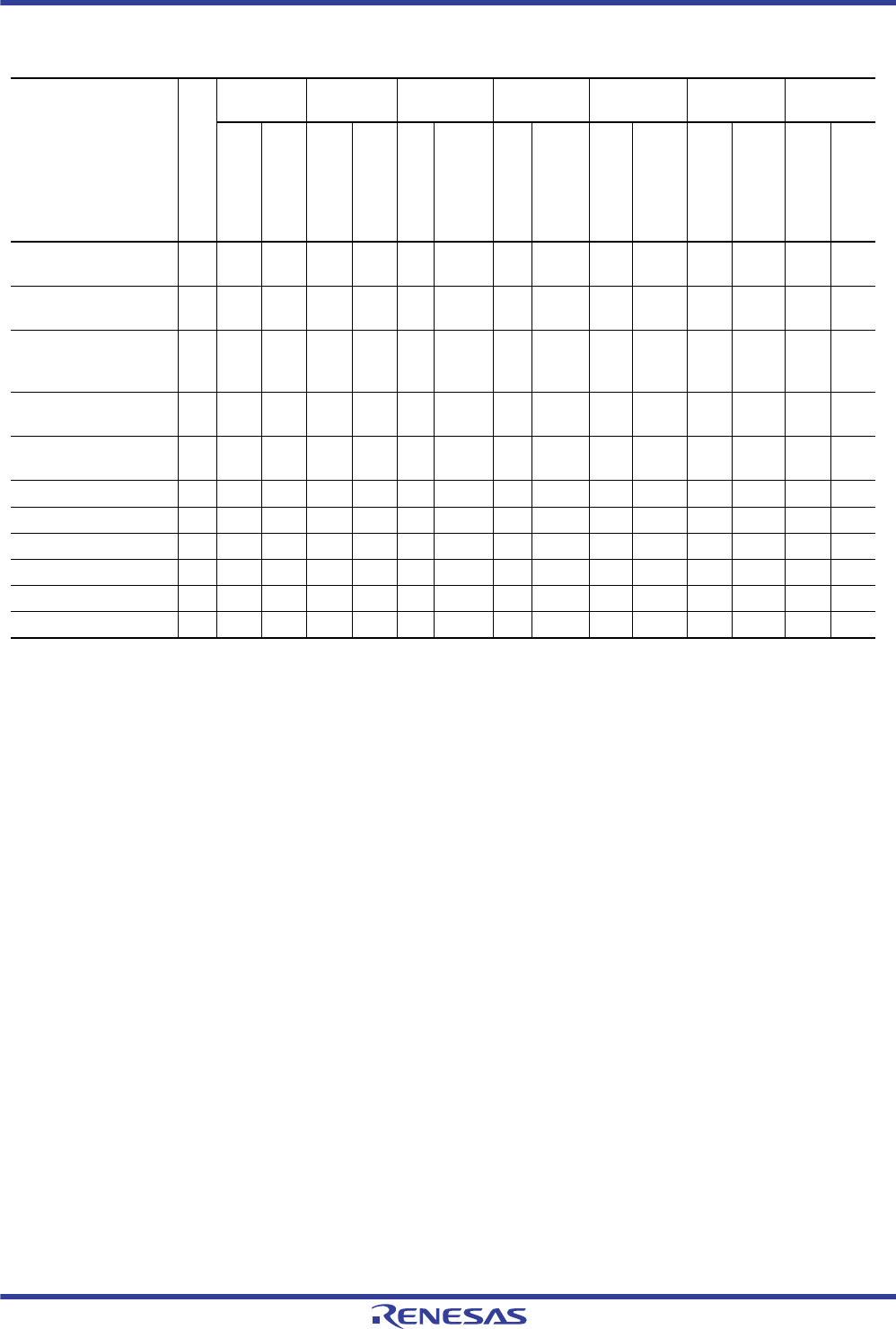
R01UH0034EJ0200 Rev.2.00 Page 1357 of 1489
Dec 27, 2013
RX62T Group, RX62G Group 31. ROM (Flash Memory for Code Storage)
Address column RA:ROM programming/erasure address
When the FENTRY0 bit in FENTRYR is 1: An address from 00FC 0000h to 00FF FFFFh
WA:ROM programming-destination address
Start address for programming of 256 bytes of data
BA:ROM erasure block address
An address within the target erasure block
(specified as an address in the range for programming and erasure)
Data column WDn:nth word of data for programming (n = 1 to 128)
Table 31.7 FCU Command Formats
Command
Number of bus cycles
First Cycle Second
ycle Third Cycle 4th to 5th
Cycles 6th Cycle 7th to 130th
Cycles 131st
Cycle
Address
Data
Address
Data
Address
Data
Address
Data
Address
Data
Address
Data
Address
Data
P/E normal mode
transition
1 RA FFh — — — — — — — — — — — —
Status read mode
transition
1 RA 70h — — — — — — — — — — — —
Lock bit read mode
transition
(lock bit read 1)
1 RA 71h — — — — — — — — — — — —
Peripheral clock
notification
6 RA E9h RA 03h RA 0F0Fh RA 0F0Fh RA D0h — — — —
Programming 131 RA E8h RA 80h W
A
WDn RA WDn RA WDn RA WDn RA D0h
Block erasure 2 RA 20h BA D0h — — — — — — — — — —
P/E suspension 1 RA B0h — — — — — — — — — — — —
P/E resumption 1 RA D0h — — — — — — — — — — — —
Status register clearing 1 RA 50h — — — — — — — — — — — —
Lock bit read 2 2 RA 71h BA D0h — — — — — — — — — —
Lock bit programming 2 RA 77h BA D0h — — — — — — — — — —

R01UH0034EJ0200 Rev.2.00 Page 1358 of 1489
Dec 27, 2013
RX62T Group, RX62G Group 31. ROM (Flash Memory for Code Storage)
31.6.3 Connections between FCU Modes and Commands
The sets of FCU commands that can be accepted in each of the FCU modes are fixed. Furthermore, which commands are
acceptable in a given FCU mode also depends on the state of the FCU.
Issuing of an FCU command must follow checking of the FCU’s state after transitions of the FCU mode.
Commands that are acceptable in the various FCU modes and states are listed in Table 31.8. Issuing a command that is
not currently acceptable leads to the FCU being placed in the command-locked state (see section 31.8.2, Error
Protection).
Issuing of an FCU command must follow checking of the values of the FRDY, ILGLERR, ERSERR, and PRGERR bits
in FSTATR0 and of the FCUERR bit in FSTATR1 after transitions of the FCU mode. Furthermore, the CMDLK bit in
FASTAT can be checked to see if an error has occurred. The value of the CMDLK bit in FASTAT is the logical OR of the
ILGLERR, ERSERR, and PRGERR bits in FSTATR0 and the FCUERR bit in FSTATR1.
A: Acceptable
*: Only programming is acceptable for blocks other than the block where erasure was suspended
X: Not acceptable
Table 31.8 Acceptable Commands and the State and Mode (ROM P/E Mode) of the FCU
Command
P/E Normal Mode Status Read Mode Lock-Bit Read Mode
Programming suspended
Erasure suspended
Other state
Programming or erasure
Processing to suspend
programming or erasure
Lock bit read 2 processing
Programming suspended
Erasure suspended
Command-locked state
Other state
Programming suspended
Erasure suspended
Other state
FSTATR0.FRDY bit 1 1 1 0 0 0 1 1 0/1 1 1 1 1
FSTATR0.SUSRDY bit 000 1000000000
FSTATR0.ERSSPD bit 0 1 0 0 0/1 0 0 1 0 0 0 1 0
FSTATR0.PRGSPD bit 1 0 0 0 0/1 0 1 0 0 0 1 0 0
FASTAT.CMDLK bit 000 0000010000
P/E Normal mode transition A A A X X X A A X A A A A
Status read transition A A A X X X A A X A A A A
Lock-bit read transition
(lock bit read 1)
AAA XXXAAXAAAA
Peripheral clock setting X X A X X X X X X A X X A
Programming X * A X X X X * X A X * A
Block erasure X X A X X X X X X A X X A
P/E suspension X X X A X X X X X X X X X
P/E resumption AAX XXXAAXXAAX
Status register clearing A A A X X X A A A A A A A
Lock bit read 2 A A A X X X A A X A A A A
Lock bit programming X * A X X X X * X A X * A
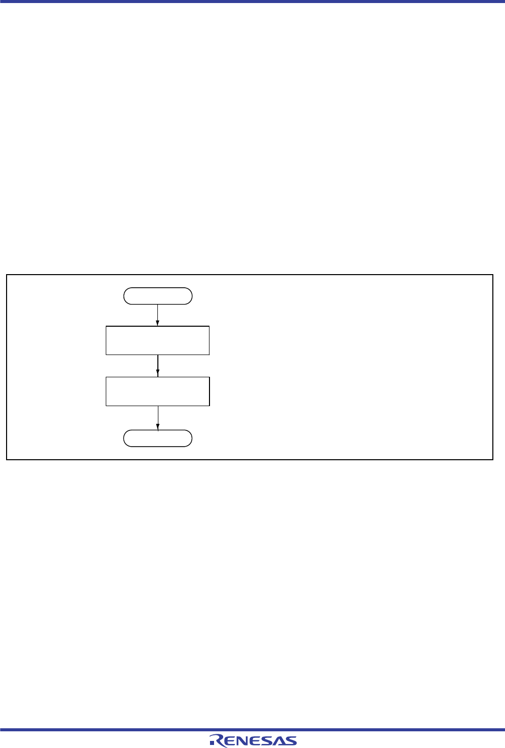
R01UH0034EJ0200 Rev.2.00 Page 1359 of 1489
Dec 27, 2013
RX62T Group, RX62G Group 31. ROM (Flash Memory for Code Storage)
31.6.4 FCU Command Usage
The set of FCU commands consists of commands for FCU mode transitions, actually programming or erasing the ROM,
error processing, and suspension and resumption. The following passages describe the various commands. For a
description of the modes and states where the respective commands are acceptable, see section 31.6.3, Connections
between FCU Modes and Commands.
31.6.4.1 Mode Transitions
This subsection covers the commands for mode transitions. For an illustration of the various transitions between modes,
see Figure 31.5.
(1) Switching to ROM P/E Mode
A transition to ROM P/E mode is required before executing an FCU command for the ROM becomes possible.
Setting the FENTRY0 bit in FENTRYR to 1 causes a transition to ROM P/E mode for programming and erasure of the
corresponding address range.
Before actually proceeding to program or erase the ROM, enable programming and erasure by writing 01h as a byte to
FWEPROR (see section 31.2.15, Flash Write Erase Protection Register (FWEPROR)).
Figure 31.6 Procedure for Transition to ROM P/E Mode
(2) Switching to ROM Read Mode
High-speed reading of the ROM requires clearing of the FENTRY0 bit in FENTRYR, which places the FCU in ROM
read mode.
Writing of 02h to FWEPROR is also required to disable programming and erasure (see section 31.2.15, Flash Write
Erase Protection Register (FWEPROR)).
Before switching the FCU from P/E mode to read mode, ensure that all processing of FCU commands has been
completed and that the FCU has not detected an error.
Write to FENTRYR Set ROM P/E mode
When setting the FENTRY0 bit to 1: Write AA01h
End
Start
Write 01h to FWEPROR
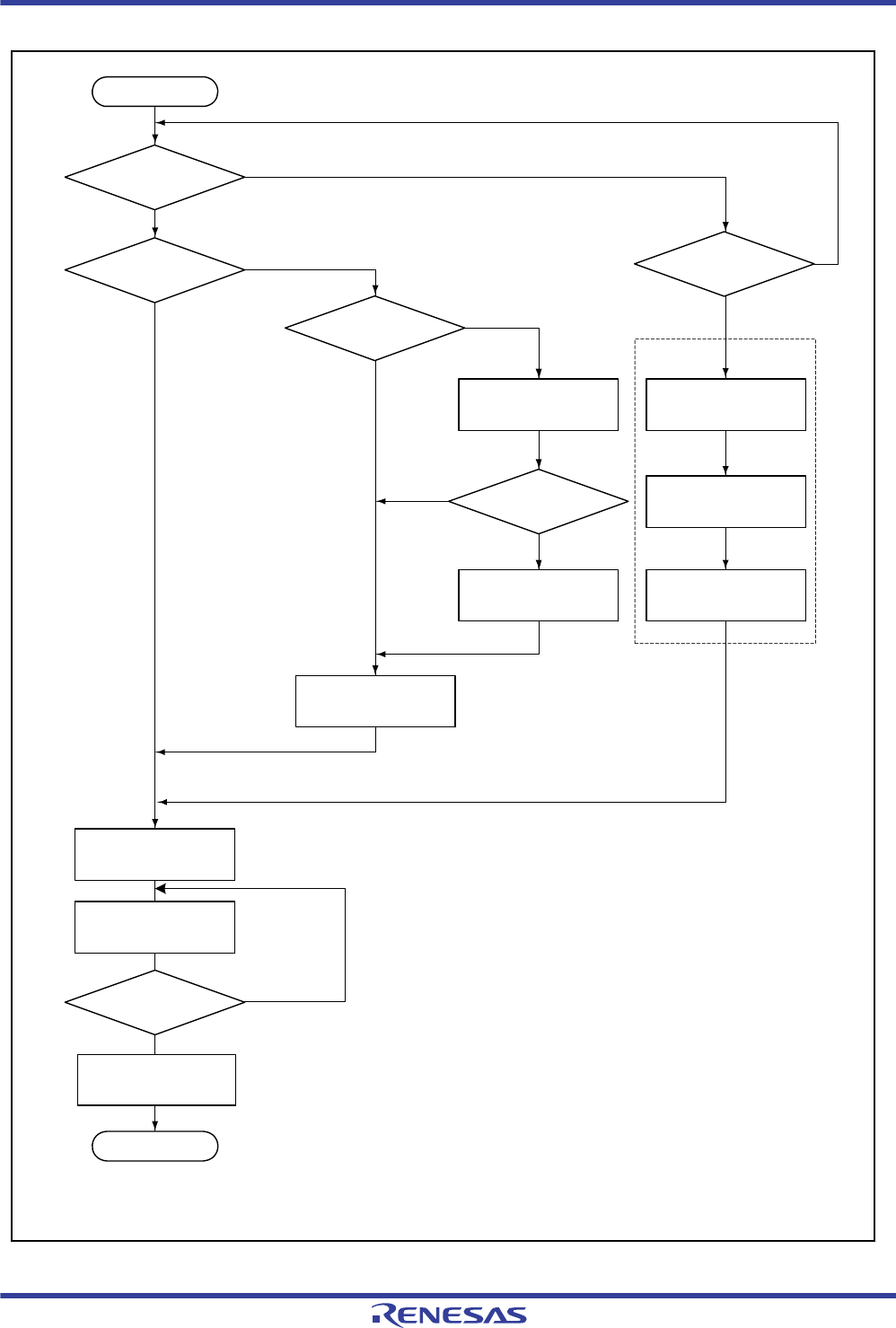
R01UH0034EJ0200 Rev.2.00 Page 1360 of 1489
Dec 27, 2013
RX62T Group, RX62G Group 31. ROM (Flash Memory for Code Storage)
Figure 31.7 Procedure for Transition to ROM Read Mode
ILGLERR, ERSERR, or PRGERR = 1
"0"
"1"
Error check
FRDY bit check
ILGLERR bit
check
Read FASTAT
Write 10h to FASTAT
FRESETR.FRESET = 1
writing
FRESETR.FRESET = 0
writing
Wait
(tRESW2)*
Issue a status register
clearing command
Write AA00h to
FENTRYR
Timeout
(tE16K×1.1)*
10h
Yes
No
Yes
No
FCU
initialization
ILGLERR = 0
ERSERR = 0
PRGERR = 0
End
Start
Note: * tE16K: Erasure time for a 16-Kbyte erasure block (see section 33, Electrical Characteristics)
tRESW2: Reset pulse width during programming/erasure (see section 33, Electrical Characteristics)
"0"
"1"
Write 02h to FWEPROR
Read FENTRYR
0000h No
Yes
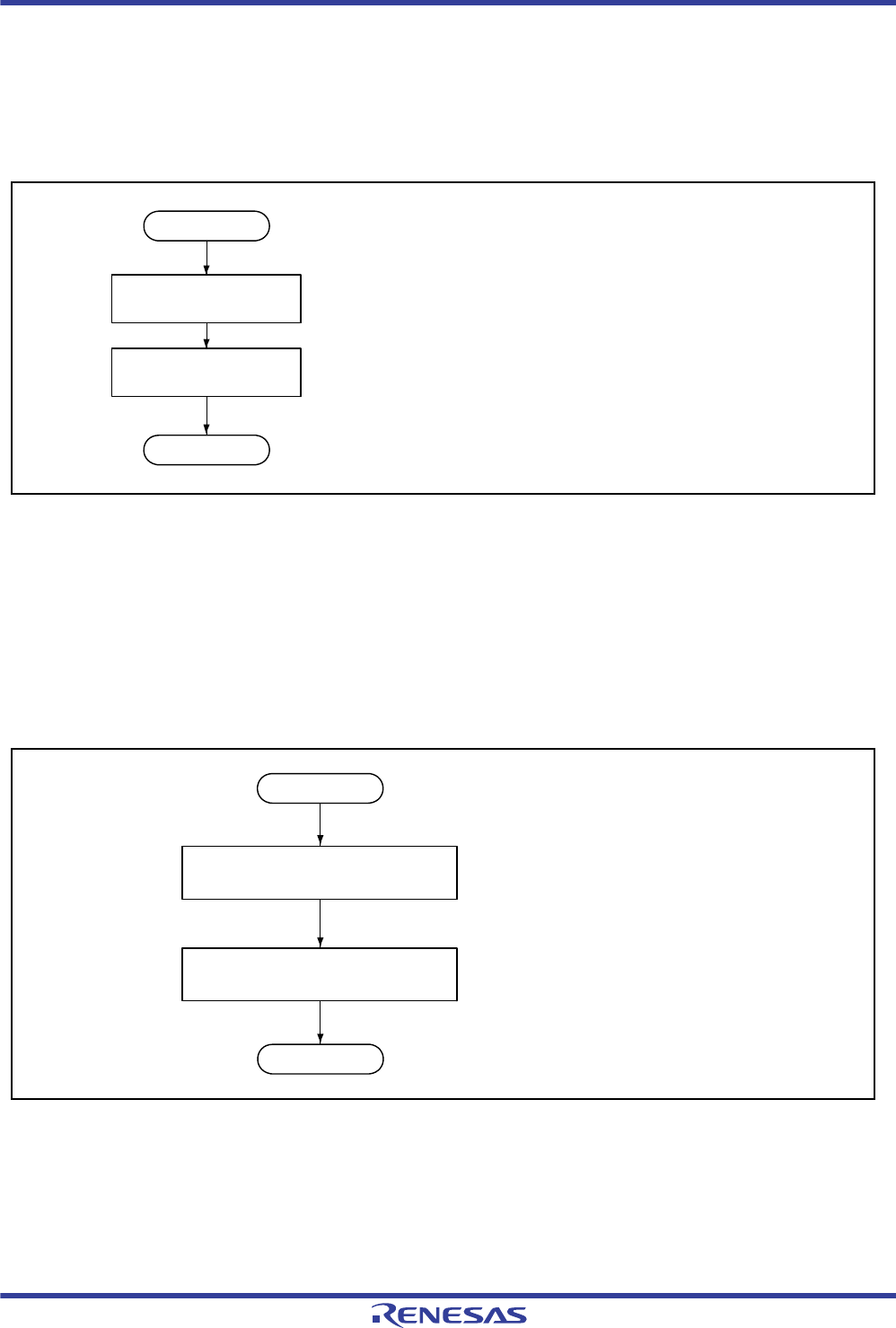
R01UH0034EJ0200 Rev.2.00 Page 1361 of 1489
Dec 27, 2013
RX62T Group, RX62G Group 31. ROM (Flash Memory for Code Storage)
(3) Switching to ROM P/E Normal Mode
Two methods are available for the transition to ROM P/E normal mode: setting the FENTRYR register while the FCU is
in ROM read mode (see section 31.6.1, FCU Modes), or issuing the normal mode transition command while the FCU
is in ROM P/E mode (see Figure 31.8). The normal mode transition command is issued by writing FFh as a byte to an
address in the range for programming and erasure of the ROM.
Figure 31.8 Procedure for Transition to ROM P/E Normal Mode
(4) Switching to ROM Status Read Mode
Issuing an FCU command other than a normal mode transition or lock bit read mode transition command places the FCU
in ROM status read mode. The same transition can be obtained by issuing the status read mode transition command.
Figure 31.9 shows the procedure for checking the register FSTATR0 as an example. In the example, the status read
mode transition command is issued to place the FCU in ROM status read mode, and the value of FSTATR0 is obtained
by read access to the area for programming and erasure and then checked.
Figure 31.9 Procedure for Transition to ROM Status Read Mode and the Status Checking
Issue a normal mode
transition command
FSTATR0 check When the ILGLERR bit is 1, the normal mode transition command is not
accepted by the FCU.
Start
End
Read from the address for ROM
programming and erasure in bytes
Write 70h to the address for ROM
programming and erasure in bytes Transition to ROM status read mode
Read the value of FSTATR0
Start
End
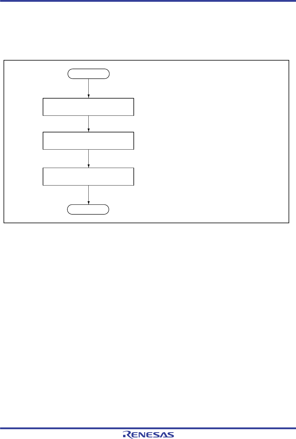
R01UH0034EJ0200 Rev.2.00 Page 1362 of 1489
Dec 27, 2013
RX62T Group, RX62G Group 31. ROM (Flash Memory for Code Storage)
(5) Switching to ROM Lock-Bit Read Mode
Clearing the FRDMD bit in FMODR (memory area method) issues a lock bit read mode transition (lock bit read 1)
command. After the transition to ROM lock bit read mode, lock bit value are obtained by read access to the area for
ROM programming and erasure. All bits of a value thus read out have the value of the lock bit of the erasure block that
contains the accessed address (Figure 31.10).
Figure 31.10 Procedure for Transition to ROM Lock-Bit Read Mode and the Lock-Bit Read Method
31.6.4.2 Programming and Erasure Procedures
The following passages describe the flow of procedures for programming or erasing the ROM. For details on the
acceptance of commands by the FCU, see section 31.6.3, Connections between FCU Modes and Commands.
Figure 31.11 is a simple flowchart of the procedure for executing FCU commands.
Transition to ROM lock bit read mode
Check the transition to ROM lock bit read mode
Read the value of the lock bit
Use the address for ROM programming and erasure
(Do not use the address for reading.)
Start
End
Write 71h to the address for ROM
programming and erasure in bytes
Check the FSTATR0.ILGLERR bit
Read from the arbitrary address in the
erasure block in bytes
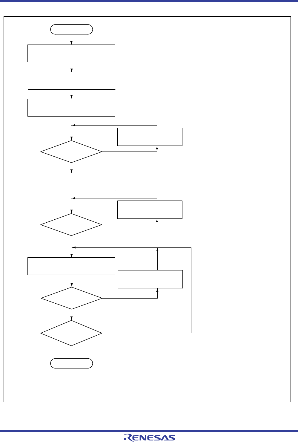
R01UH0034EJ0200 Rev.2.00 Page 1363 of 1489
Dec 27, 2013
RX62T Group, RX62G Group 31. ROM (Flash Memory for Code Storage)
Figure 31.11 Simple Flowchart of the Procedure for Programming and Erasure
ROM P/E mode transition
Determine the error source,
and issue a status register
clearing command
Error check
Issue a peripheral clock
notification command
Error
No error
Firmware transfer to the FCU RAM
Start
End
Error check Error
No error
Determine the error source,
and issue a status register
clearing command
Issue an FCU command*1
Error check Error
No error
Determine the error source,
and issue a status register
clearing command
Check the
execution result of
the FCU
command*2
NG
OK
Transferred only one time after reset is cleared.
For details, see section 31.6.4.2 (1), Transferring Firmware to the FCU
RAM.
Set FWEPROR and FENTRYR
Issued only one time after a peripheral clock is set.
For details, see section 31.6.4.2 (4), Using the Peripheral Clock Notification
Command.
See table 31.9, Error Protection Types and
section 31.6.4.3, Error Processing.
Notes: 1. Selected among the programming, block erase, lock bit programming, and lock bit read 2 commands.
2. To check the result of programming/erasure processing, enter ROM read mode and read data from the
ROM (see section 31.6.4.1 (2), Switching to ROM Read Mode.)
Jump to the on-chip RAM
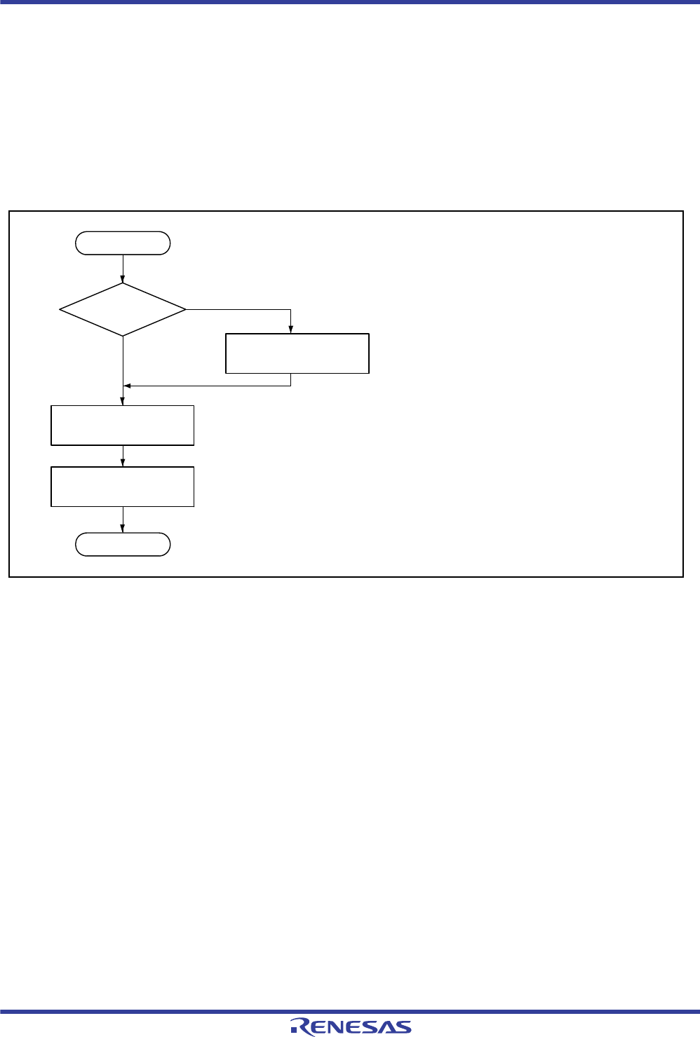
R01UH0034EJ0200 Rev.2.00 Page 1364 of 1489
Dec 27, 2013
RX62T Group, RX62G Group 31. ROM (Flash Memory for Code Storage)
(1) Transferring Firmware to the FCU RAM
FCU commands can only be used if the FCU RAM holds the firmware for the FCU. The FCU RAM does not hold the
FCU firmware immediately after the chip has been booted up, so the firmware must be copied from the FCU firmware
area to the FCU RAM. Furthermore, when the FCUERR bit in FSTATR1 is set to 1, the FCU must be reset and the
firmware recopied because the firmware stored in the FCU RAM may have been corrupted.
Figure 31.12 shows the flow of the procedure for transferring firmware to the FCU RAM. Before writing data to the
FCU RAM, set FENTRYR to 0000h and stop the FCU.
Figure 31.12 Procedure for Firmware Transfer to FCU RAM
(2) Jumping to Locations in On-chip RAM
Since fetching instructions from the ROM is not possible while the ROM is being programmed or erased, code has to be
executed from an area other than the ROM. Copy the required program code to on-chip RAM and then make execution
jump to the address where the code starts in on-chip RAM.
(3) Transition to ROM P/E Mode
The FCU is placed in ROM P/E mode by the settings of the FENTRY0 bit in FENTRYR and of FWEPROR. Details are
given in section 31.6.4.1 (1) Switching to ROM P/E Mode.
Other than 0000h
0000h
FENTRYR
check
Write C401h to
FCURAME
Copy to FCU RAM
Clear the FENTRY0 bit See section 31.6.4.1 (2), Switching to ROM Read Mode.
Enable access to the FCU RAM.
Copy the FCU firmware to the FCU RAM
Transfer source: FEFF E000h to FEFF FFFFh (FCU firmware area)
Transfer destination: 007F 8000h to 007F 9FFFh (FCU RAM area)
Start
End

R01UH0034EJ0200 Rev.2.00 Page 1365 of 1489
Dec 27, 2013
RX62T Group, RX62G Group 31. ROM (Flash Memory for Code Storage)
(4) Using the Peripheral Clock Notification Command
The peripheral clock is used in programming and erasing the ROM, so the frequency of this clock has to be set in the
PCKAR. Frequencies in the range from 8 to 50 MHz are selectable.Make sure to set a frequency within this range.
If a frequency within this range has not been set, the FCU will detect the error and enter the command-blocked state (see
section 31.8.2, Error Protection).
The peripheral clock notification command is used after the PCKAR setting has been made. In the first and second cycles
for the peripheral clock notification command, respectively, the values E9h and 03h are written to the address range for
programming and erasure of the ROM. Word-unit writing is used in the third to fifth cycles of the command.
Accordingly, make sure that the addresses used are aligned with four-byte boundaries. After 0F0Fh has been written
three times (as a word) to the address range for programming and erasure of the ROM, the process of the FCU setting the
frequency of the peripheral clock starts once the value D0h has been written as a byte in the sixth cycle. The FRDY bit in
FSTATR0 can be used to check whether or not the settings have been completed.
Addresses that can be used in the first to sixth cycles differ according to the setting of the FENTRY0 bit in FENTRYR.
Ensure that the addresses suit the setting of the bit. If issuing of the command is attempted with an erroneous
combination of the setting of the bit and specified addresses, the FCU will detect the error and enter the command-
blocked state (see section 31.8.2, Error Protection).
Furthermore, if the setting for the peripheral clock in use will not be changed from this setting after release from the reset
state, this setting is also valid for the next FCU command.
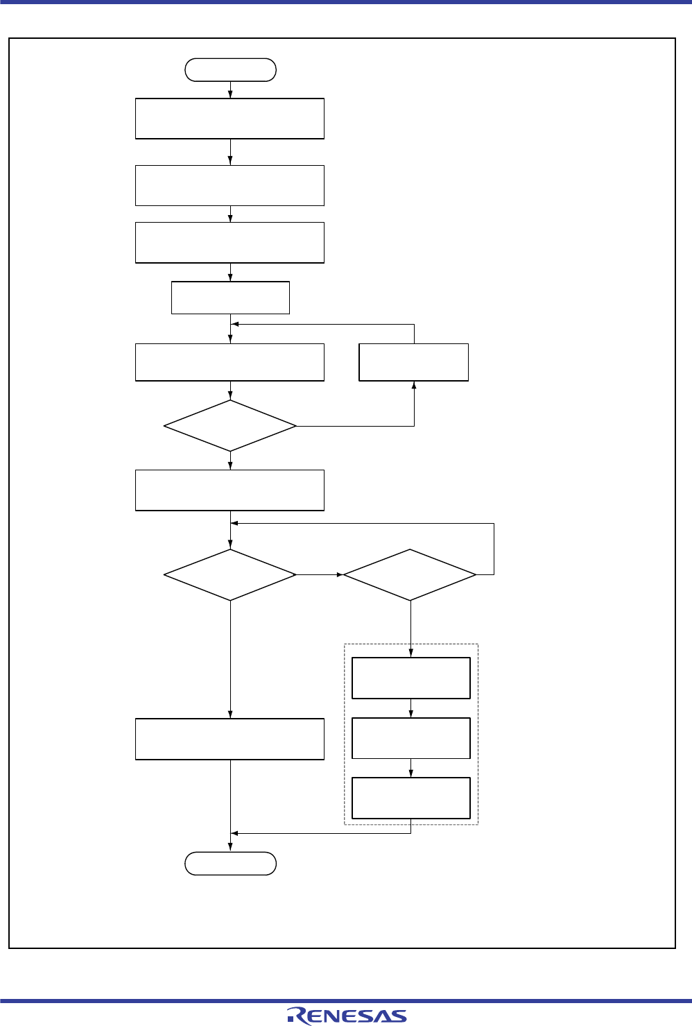
R01UH0034EJ0200 Rev.2.00 Page 1366 of 1489
Dec 27, 2013
RX62T Group, RX62G Group 31. ROM (Flash Memory for Code Storage)
Figure 31.13 Using the Peripheral Clock Notification Command
Write E9h to ROM programming/
erasure address in byte access
Write 03h to ROM programming/
erasure address in byte access
n = 1
n = n + 1
Write 0F0Fh data to ROM
programming/erasure address in
word access
N = 3 ?
Write D0h to ROM programming/
erasure address in byte access
FRDY bit check Timeout
tPCKA
FCU initialization
FRESETR.FRESET = 1
writing
ILGLERR bit check Wait
(tRESW2)
FRESETR.FRESET = 0
writing
[Legend]
tPCKA: When PCLK runs at 50 MHz, 60 µs; when PCLK runs at 25 MHz, 120 µs
tRESW2: Reset pulse width during programming/erasure (see section 33, Electrical Characteristics)
No
Yes
No
Yes
"0"
"1"
Set PCKAR to
frequency of peripheral clock (PCLK)
Start
End

R01UH0034EJ0200 Rev.2.00 Page 1367 of 1489
Dec 27, 2013
RX62T Group, RX62G Group 31. ROM (Flash Memory for Code Storage)
(5) Programming
The programming command is used to write data to the ROM.
In the first and second cycles for the peripheral clock notification command, respectively, the values E8h and 80h are
written to the address range for programming and erasure of the ROM. In the third cycle, write the actual data to be
programmed, as a word unit, to the target address for programming. For this first address, always use an address that is
on a 256-byte boundary. In the fourth to the 130th cycles, write the data for programming in 127 word-unit rounds to the
address range for programming and erasure of the ROM. Once the value D0h has been written as a byte to the address
range for programming and erasure of the ROM in the 131st cycle, the FCU begins the actual process of programming
the ROM. The FRDY bit in FSTATR0 can be used to check whether or not the programming has been completed.
Addresses that can be used in the first to 131st cycles differ according to the setting of the FENTRY0 bit in FENTRYR.
Ensure that the addresses suit the setting of the bit. If issuing of the command is attempted with an erroneous
combination of the setting of the bit and specified addresses, the FCU will detect the error and enter the command-
blocked state (see section 31.8.2, Error Protection).
In cases where the target range in the third to 130th cycles includes addresses that do not require programming, use
FFFFh as the data for programming to those addresses. To execute a programming with lock bit protection disabled,
proceed with programming after setting the FPROTCN bit in FPROTR.

R01UH0034EJ0200 Rev.2.00 Page 1368 of 1489
Dec 27, 2013
RX62T Group, RX62G Group 31. ROM (Flash Memory for Code Storage)
Figure 31.14 Procedure for ROM Programming
Write E8h to ROM programming/
erasure address in byte access
Write 80h to ROM programming/
erasure address in byte access
Write programming data to start
address of programming destination in
word access
n = 1
n = n + 1
Write programming data to ROM
programming/erasure address in
word access
n = 127 ?
Write D0h to ROM programming/
erasure address in byte access
FRDY bit check Timeout
(tP256 1.1)*
FCU initialization
FRESETR.FRESET = 1
writing
ILGLERR bit and PRGERR bit check Wait
(tRESW2)*
FRESETR.FRESET = 0
writing
Note: * tP256: Programming time for 256-byte data (see section 33, Electrical Characteristics)
tRESW2: Reset pulse width during programming/erasure (see section 33, Electrical Characteristics)
No
Yes
No
Yes
"0"
"1"
Start
End
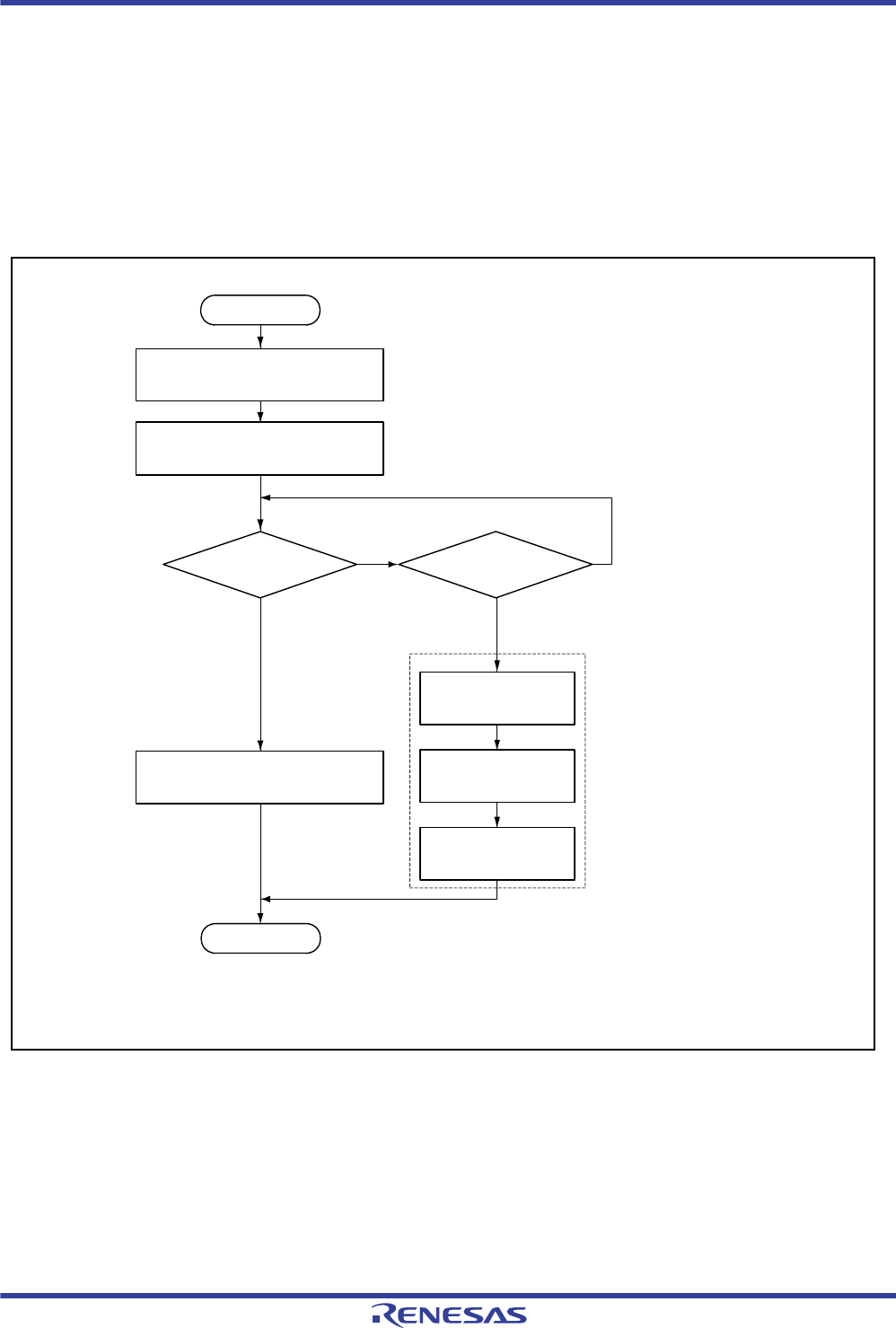
R01UH0034EJ0200 Rev.2.00 Page 1369 of 1489
Dec 27, 2013
RX62T Group, RX62G Group 31. ROM (Flash Memory for Code Storage)
(6) Erasure
To erase data from the ROM, use the block erase command.
Write 20h to the ROM programming/erasure address in byte access in the first cycle of the block erase command. When
D0h is written to an arbitrary address in an erasure target block in byte access in the second cycle, the FCU start the
erasure processing for the ROM. Whether erasure is completed can be checked with the FRDY bit in FSTATR0. The
ROM in the erased state can be read by the CPU as FFFF FFFFh in 32-bit access.
To execute an erasure with lock bit protection disabled, set the FPROTCN bit in FPROTR before erasure.
Figure 31.15 Procedure for ROM Erasure
Write 20h to ROM programming/
erasure address in byte access
Write D0h to arbitrary address in
erasure block in byte access
FRDY bit check
FCU initialization
FRESETR.FRESET = 1
writing
ILGLERR bit and ERSERR bit check Wait
(tRESW2) *1
FRESETR.FRESET = 0
writing
Note 1. tE16K: Erasure time for a 16-Kbyte erasure block (see section 33, Electrical Characteristics)
tRESW2: Reset pulse width during programming/erasure (see section 33, Electrical Characteristics)
No
Yes
"0"
"1"
Use the ROM programming/erasure address
(Do not use a read address)
Start
End
Time out
(tE16K 1.1) *1
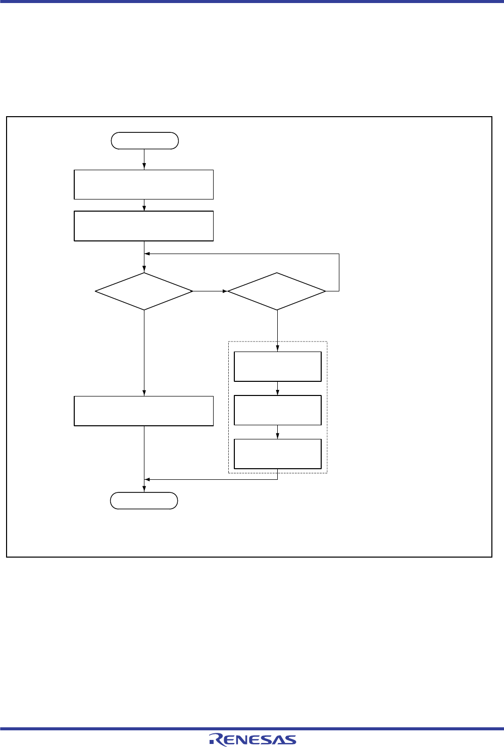
R01UH0034EJ0200 Rev.2.00 Page 1370 of 1489
Dec 27, 2013
RX62T Group, RX62G Group 31. ROM (Flash Memory for Code Storage)
(7) Writing to/Erasing Lock Bit
Each erasure block in the user area includes a lock bit. To write to a lock bit, use the lock bit programming command. In
the first cycle of the lock bit programming command, 77h is programmed to the ROM programming/erasure address in
byte access. When D0h is programmed to an arbitrary address in an erasure block whose lock bit is to be programmed in
the second cycle in byte access, the FCU start the programming processing of the lock bit. Whether programming is
completed can be checked with the FRDY bit in FSTATR0.
Figure 31.16 Procedure for Writing to the Lock Bit
To erase a lock bit, use the block erase command.
When the FPROTCN bit in FPROTR is 0, erasure blocks whose lock bit is set to 0 cannot be erased. When erasing a lock
bit, issue a block erase command with the FPROTCN bit set to 1. Using the block erase command erases all data in the
erasure block. It is impossible to erase only a lock bit.
Write 77h to ROM programming/
erasure address in byte access
Write D0h to arbitrary address in
erasure block in byte access
FRDY bit check Timeout
(tP256 1.1) *1
FCU initialization
FRESETR.FRESET = 1
writing
ILGLERR bit and PRGERR bit
check Wait
(tRESW2) *1
FRESETR.FRESET = 0
writing
Note 1. tP256: Programming time for 256-byte data (see section 33, Electrical Characteristics)
tRESW2: Reset pulse width during programming/erasure (see section 33, Electrical Characteristics)
No
Yes
"0"
"1"
Use the ROM programming/erasure address
(Do not use a read address)
Start
End
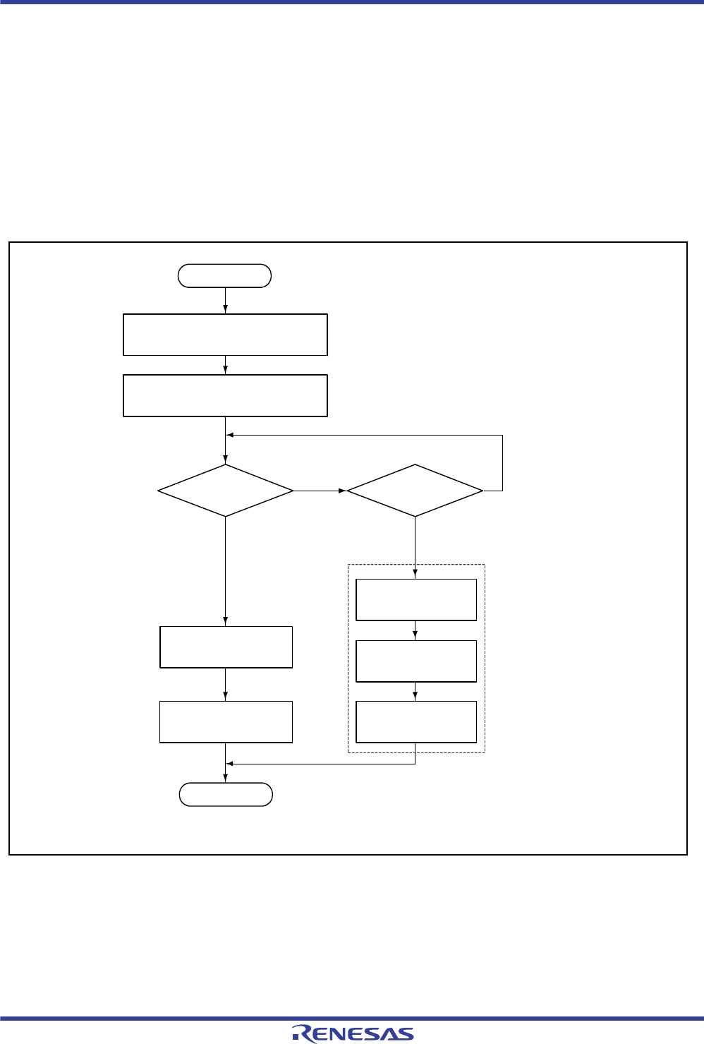
R01UH0034EJ0200 Rev.2.00 Page 1371 of 1489
Dec 27, 2013
RX62T Group, RX62G Group 31. ROM (Flash Memory for Code Storage)
(8) Reading Lock Bits
Lock bits can be read out by either reading from a memory area or reading from a register.
The lock bit read 2 command is issued in the case of the register-reading method (i.e. when the FRDMD bit in FMODR
is 1). This command is issued to an address within the block for which the lock bit is to be read out; the address range is
that for programming and erasing the ROM. In the first and second cycles of the lock bit read 2 command, the values 71h
and D0h are written as bytes; once these values have been written, the value of the lock bit for the specified erasure block
is copied to the FLOCKST bit in FSTATR1.
In the case of the memory area reading method (i.e. when the FRDMD bit in FMODR is 0), the FCU is placed in lock-bit
reading mode, and the lock bit is obtained by reading from an address within the address range for programming and
erasure of the ROM. Details are given in section 31.6.4.1 (5) Switching to ROM Lock-Bit Read Mode.
Figure 31.17 Procedure for Reading Lock Bit in Register Read Mode
FRDY bit check
Write D0h to arbitrary address in
erasure block in byte access
FRESETR.FRESET = 1
writing
Wait
(tRESW2)*
FRESETR.FRESET = 0
writing
FCU initialization
No
Yes
Timeout
(10?s)
"0"
"1"
Note: * tRESW2: Reset pulse width during programming/erasure (see section 33, Electrical Characteristics)
ILGLERR bit check
FLOCKST bit check
Write 71h to ROM programming/
erasure address in byte access
Issue a lock bit read 2 command
Use the ROM programming/erasure address
(Do not use a read address)
Start
End
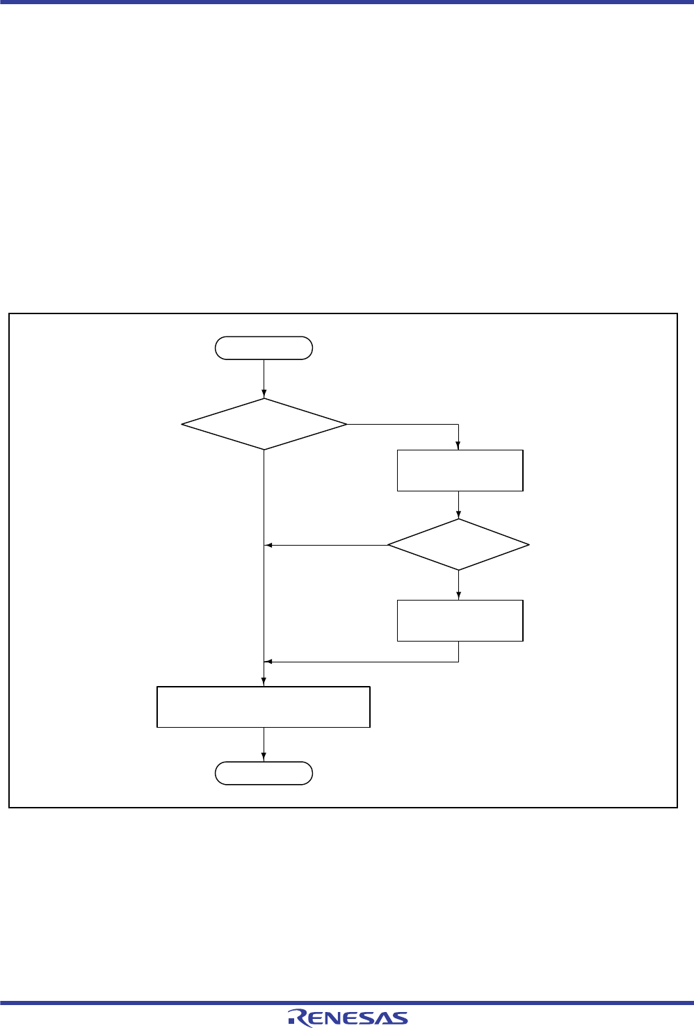
R01UH0034EJ0200 Rev.2.00 Page 1372 of 1489
Dec 27, 2013
RX62T Group, RX62G Group 31. ROM (Flash Memory for Code Storage)
31.6.4.3 Error Processing
The following passages describe the flow of error processing. For details on errors, see section 31.8, Protection.
(1) Checking Flash Status Register 0 (FSTATR0)
To check FSTATR0, read FSTATR0 directly or read the ROM programming/erasure address in ROM status read mode.
For the reading in ROM status read mode, see section 31.6.4.1 (4) Switching to ROM Status Read Mode.
(2) Clearing Flash Status Register 0 (FSTATR0)
To clear the ILGLERR, ERSERR and PRGERR bits in FSTATR0, use the status register clearing command.
When one of the ILGLERR, ERSERR and PRGERR bits in FSTATR0 is 1, the FCU is placed in the command-locked
state and receives no FCU commands other than the status register clearing command. If the ILGLERR is 1, also check
the values of the ROMAE, DFLAE, DFLRPE, and DFLWPE bits in FASTAT. Even if issuing a status register clearing
command without clearing these bits, the ILGLERR bit is not cleared.
Figure 31.18 Procedure for Clearing FSTATR0
ILGLERR bit check
Read FASTAT
Write 10h to FASTAT
No
Yes
Write 50h to ROM programming/
erasure address in byte access
10h
"0"
"1"
Start
End

R01UH0034EJ0200 Rev.2.00 Page 1373 of 1489
Dec 27, 2013
RX62T Group, RX62G Group 31. ROM (Flash Memory for Code Storage)
(3) Initializing the FPU
When a timeout leads to the FRDY bit in FSTATR0 not being set to 1 after an FCU command has been issued,
FRESETR must be used to initialize the FCU. This is also necessary when the FCUERR bit in FSTATR1 has been set. In
either case, maintain the FRESET bit in FRESETR at logical one over a period of at least tRESW2 (see section 33,
Electrical Characteristics). Disable reading from the ROM and data-flash memory over this period. In addition, while
the FRESET bit is 1, FCU commands are disabled because the FENTRYR register is initialized. Restart the processing
from the start, as shown in Figure 31.11.
31.6.4.4 Suspension and Resumption
(1) Suspending Programming or Erasure
To suspend programming/erasure for the ROM, use the P/E suspend command.
When issuing a P/E suspend command, check that the ILGLERR, ERSERR, and PRGERR bits in FSTATR0 and the
FCUERR bit in FSTATR1 are 0, and the execution of programming/erasure is normally performed. To confirm that the
suspend command can be received, also check that the SUSRDY bit in FSTATR0 is 1. After issuing a P/E suspend
command, read FSTATR0 and FSTATR1 to confirm that no error occurs.
If an error occurs during programming/erasure, at least one of the ILGLERR, PRGERR, ERSERR, and FCUERR bits is
set to 1. When programming/erasure processing has finished during the interval from when it is checked that the
SUSRDY bit is 1 to when a P/E suspend command is received, the ILGLERR bit is set to 1 because the issued P/E
suspend command is detected as an illegal command.
When programming/erasure processing has finished simultaneously with the reception of a P/E suspend command, no
error occurs and the suspended state is not entered (the FRDY bit in FSTATR0 is 1 and the ERSSPD and PRGSPD bits in
FSTATR0 are 0). When a P/E suspend command is received and then the programming/erasure suspend processing
finishes normally, the FCU enters the suspended state, the FRDY bit is set to 1, and the ERSSPD or PRGSPD bit is set to
1. After issuing a P/E suspend command, check that the ERSSPD or PRGSPD bit is 1 and the FCU enters the suspended
state, and then decide the subsequent flow. When issuing a P/E resume command in the subsequent flow although the
FCU does not enter the suspended state, an illegal command error occurs and the FCU is placed in the command-locked
state (see section 31.8.2, Error Protection).
If the erasure suspended state is entered, programming to blocks other than an erasure target can be performed.
Additionally, the programming and erasure suspended states can change to ROM read mode by clearing FENTRYR.
For details on FCU operations at the reception of a P/E suspend command, see section 31.7, Suspending Operation.
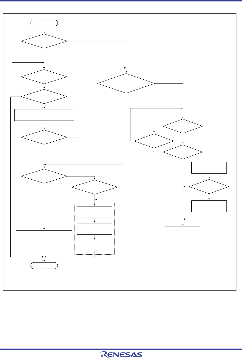
R01UH0034EJ0200 Rev.2.00 Page 1374 of 1489
Dec 27, 2013
RX62T Group, RX62G Group 31. ROM (Flash Memory for Code Storage)
Figure 31.19 Procedure for Programming/Erasure Suspension
Note: * tSEED: Suspend delay time
tRESW2: Reset pulse width during programming/erasure (see section 33, Electrical Characteristics)
tE16K: Erasure time for a 16-Kbyte erasure block (see section 33, Electrical Characteristics)
Error bit check
FRDY bit check
Error bit check
FRDY bit check
Write B0h to ROM programming/
erasure address in byte access
ERSSPD bit and PRGSPD bit
check
Timeout
(tSEED × 1.1)*
FCU initialization
FRESETR.FRESET = 1
writing
Wait
(tRESW2)*
FRESETR.FRESET = 0
writing
No
Yes
FCUERR bit check
Timeout
(tE16K×1.1)*
FRDY bit check
ILGLERR bit check
10h
Issue a status register
clearing command
Read FASTAT
Write 10h to FASTAT
No
Yes
ILGLERR, ERSERR,
PRGERR, FCUERR = 1
FCUERR = 0
ILGLERR = 0
ERSERR = 0
PRGERR = 0
FCUERR = 0
ILGLERR = 0
ERSERR = 0
PRGERR = 0
FCUERR = 0
ILGLERR, ERSERR,
PRGERR, FCUERR = 1
FCUERR = 1
Start
End
"1"
"0"
"1"
"0" SUSRDY bit check
"1"
"0"
"1"
"0"
"1"
"0"

R01UH0034EJ0200 Rev.2.00 Page 1375 of 1489
Dec 27, 2013
RX62T Group, RX62G Group 31. ROM (Flash Memory for Code Storage)
(2) Resuming Programming or Erasure
To resume a suspended programming/erasure processing, use the P/E resume command. When the settings of FENTRYR
are changed during suspension, reset FENTRYR to the value immediately before a P/E suspend command is issued, and
then issue a P/E resume command.
Figure 31.20 Procedure for Resuming Programming or Erasure
FRDY bit check
Write D0h to ROM programming/
erasure address in byte access
FRESETR.FRESET = 1
writing
Wait
(tRESW2)*
FRESETR.FRESET = 0
writing
FCU initialization
No
Yes
ILGLERR bit, ERSERR bit and
PRGERR bit check
Timeout
(tE16K 1.1)*
"0"
"1"
Note: * tE16K: Erasure time for a 16-Kbyte erasure block (see section 33, Electrical Characteristics)
tRESW2: Reset pulse width during programming/erasure (see section 33, Electrical Characteristics)
Start
End
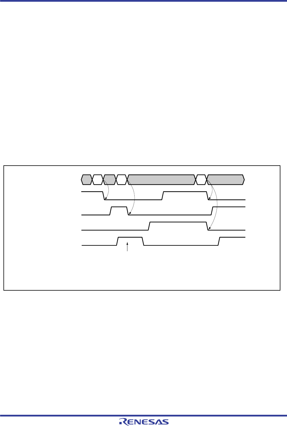
R01UH0034EJ0200 Rev.2.00 Page 1376 of 1489
Dec 27, 2013
RX62T Group, RX62G Group 31. ROM (Flash Memory for Code Storage)
31.7 Suspending Operation
The ROM cannot be read out during programming/erasure. The ROM can be read out by suspending the ROM
programming/erasure with the P/E suspend command. The P/E suspend command includes one programming mode and
two erasure modes (suspension priority mode and erasure priority mode). The P/E resume command that resumes
suspended programming/erasure processing is also provided.
31.7.1 Suspension during Programming
When issuing a P/E suspend command during the ROM programming/erasure, the FCU suspends programming
processing. Figure 31.21 shows the suspend operation of programming.
When receiving a programming-related command, the FCU clears the FRDY bit in FSTATR0 to 0 to start programming.
If the FCU enters the state in which the P/E suspend command can be received after starting programming, the SUSRDY
bit in FSTATR0 is set to 1. When a P/E suspend command is issued, the FCU receives the command and clears the
SUSRDY bit to 0. If the FCU receives a P/E suspend command while a programming pulse is being applied, the FCU
continues applying the pulse. After specified pulse application time, the FCU finishes pulse application, and starts the
programming suspend processing and sets the PRGSPD bit in FSTATR0 to 1. When the suspend processing finishes, the
FCU sets the FRDY bit to 1 to enter the programming suspended state. If receiving a P/E resume command in the
programming suspended state, the FCU clears the FRDY and PRGSPD bits to 0 and resumes programming.
Figure 31.21 Suspension during Programming
Pulse application
continues
[Legend]
P: Programming-related command (interleave programming, lock bit programming, P/E resume)
S: P/E suspend command
R: P/E resume command
Programming
pulse
PRGSPD bit
SUSRDY bit
FRDY bit
FCU command PS R
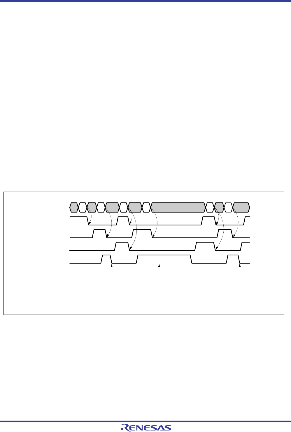
R01UH0034EJ0200 Rev.2.00 Page 1377 of 1489
Dec 27, 2013
RX62T Group, RX62G Group 31. ROM (Flash Memory for Code Storage)
31.7.2 Suspension during Erasure (Suspension Priority Mode)
Figure 31.22 shows the suspend operation of erasure when the erasure suspend mode is set to the suspension priority
mode (ESUSPMD bit in FCPSR is 0).
When receiving an erasure-related command, the FCU clears the FSTATR0.FRDY bit to 0 to start erasure. If the FCU
enters the state in which the P/E suspend command can be received after starting erasure, the FSTATR0.SUSRDY bit is
set to 1. When a P/E suspend command is issued, the FCU receives the command and clears the SUSRDY bit to 0. When
receiving a suspend command during erasure, the FCU starts the suspend processing and sets the ERSSPD bit in
FSTATR0 to 1 even if it is applying an erasure pulse. When the suspend processing finishes, the FCU sets the FRDY bit
to 1 to enter the erasure suspended state. If receiving a P/E resume command in the erasure suspended state, the FCU
clears the FRDY and ERSSPD bits to 0 and resumes erasure. Operations of the FRDY, SUSRDY, and ERSSPD bits at the
suspension and resume of erasure are the same, regardless of the erasure suspend mode.
The setting of the erasure suspend mode affects the control method of erasure pulses. In suspension priority mode, when
receiving a P/E suspend command while erasure pulse A that has never been suspended in the past is being applied, the
FCU suspends the application of erasure pulse A and enters the erasure suspended state. When receiving a P/E suspend
command while reapplying erasure pulse A after erasure is resumed by a P/E resume command, the FCU continues
applying erasure pulse A. After specified pulse application time, the FCU finishes erasure pulse application and enters
the erasure suspended state. When the FCU receives a P/E resume command next and erasure pulse B starts to be newly
applied, and then the FCU receives a P/E suspend command again, the application of erasure pulse B is suspended. In
suspension priority mode, delay due to suspend can be minimized because the application of an erasure pulse is
suspended one time per pulse and priority is given to the suspension processing.
Figure 31.22 Suspension during Erasure (Suspension Priority Mode)
Pulse A application
continues
[Legend]
E: Erasure-related command (block erase, P/E resume)
S: P/E suspend command
R: P/E resume command
Pulse A application
discontinues Pulse B application
discontinues
FCU command
FRDY bit
SUSRDY bit
ERSSPD bit
ES R S RS
Erasure pulse
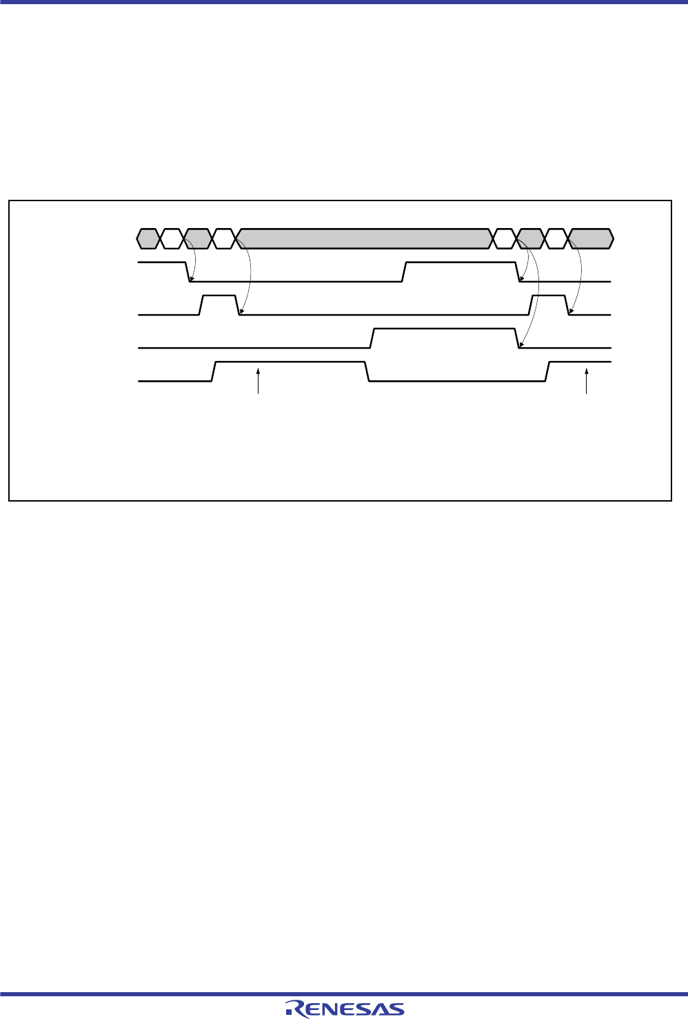
R01UH0034EJ0200 Rev.2.00 Page 1378 of 1489
Dec 27, 2013
RX62T Group, RX62G Group 31. ROM (Flash Memory for Code Storage)
31.7.3 Suspension during Erasure (Erasure Priority Mode)
Figure 31.23 shows the suspend operation of erasure when the erasure suspend mode is set to the erasure priority mode
(ESUSPMD bit in FCPSR is 1). The control method of erasure pulses in erasure priority mode is the same as that of
programming pulses for the programming suspend processing.
If the FCU receives a P/E suspend command while an erasure pulse is being applied, the FCU definitely continues
applying the pulse. In this mode, required time for the whole erasure processing can be reduced as compared with the
suspension priority mode because the reapplication of erasure pulses does not occur when a P/E resume command
issued.
Figure 31.23 Suspension during Erasure (Erasure Priority Mode)
Pulse A application
continues
[Legend]
E: Erasure-related command (block erase, P/E resume)
S: P/E suspend command
R: P/E resume command
Pulse B application
continues
FCU command ES RS
FRDY bit
SUSRDY bit
ERSSPD bit
Erasure pulse

R01UH0034EJ0200 Rev.2.00 Page 1379 of 1489
Dec 27, 2013
RX62T Group, RX62G Group 31. ROM (Flash Memory for Code Storage)
31.8 Protection
Protection against programming/erasure for the ROM includes software protection and error protection.
31.8.1 Software Protection
With the software protection, the ROM programming/erasure is prohibited by the settings of the control register or user
area lock bit. When the software protection is violated and a ROM programming/erasure-related command is issued, the
FCU detects an error and enters the command-locked state.
(1) Protection through FWEPROR
If the FLWE[1:0] bits in FWEPROR are not set to 01b, programming cannot be performed in any of the modes.
(2) Protection through FENTRYR
When the FENTRY0 bit in FENTRYR is 0, ROM read mode is selected. Because the FCU command cannot be received
in ROM read mode, ROM programming/erasure is prohibited. When an FCU command is issued in ROM read mode, the
FCU detects an illegal command error and is placed in the command-locked state (see section 31.8.2, Error
Protection).
(3) Protection through Lock Bit
Each erasure block in the user area includes a lock bit. When the FPROTCN bit in FPROTR is 0, erasure blocks whose
lock bit is set to 0 are prohibited from being programmed/erased. To program or erase erasure blocks whose lock bit is set
to 0, set the FPROTCN bit to 1. When the lock bit protection is violated and a ROM programming/erasure-related
command is issued, the FCU detects a programming/erasure error and enters the command-locked state (see section
31.8.2, Error Protection).
31.8.2 Error Protection
With the error protection, FCU command issuance errors, prohibited access occurrences, and FCU malfunctions are
detected, and an FCU command is prohibited from being received (command-locked state). When the FCU enters the
command-locked state (FASTAT.CMDLK bit is 1), one or several of the status bits (FSTATR0.ILGLERR, ERSERR, and
PRGERR bits, FSTATR1.FCUERR bit, and FASTAT.ROMAE bit) are set to 1 and programming and erasure of the ROM
are prohibited. To clear the command-locked state, a status register clearing command must be issued with FASTAT set
to 10h.
While the CMDLKIE bit in FAEINT is set to 1, if the FCU is placed in the command-locked state (CMDLK bit in
FASTAT is set to 1), a flash interface error (FIFERR) interrupt occurs. While the ROMAEIE bit in FAEINT is set to 1, if
the ROMAE bit in FASTAT is set to 1, an FIFERR interrupt occurs.
Table 31.9 lists the relationship between the contents of the ROM-related error protection and status bit values
(ILGLERR, ERSERR, PRGERR bits in FSTATR0, FCUERR bit in FSTATR1, ROMAE bit in FASTAT) at error
detection. If a command other than the suspend command is issued during programming/erasure and the FCU enters the
command-locked state, it continues the programming/erasure. In this state, it is impossible to issue a P/E suspend
command and suspend programming/erasure. When a command is issued in the command-locked state, the ILGLERR
bit is set to 1.
R01UH0034EJ0200 Rev.2.00 Page 1380 of 1489
Dec 27, 2013
RX62T Group, RX62G Group 31. ROM (Flash Memory for Code Storage)
Table 31.9 Error Protection Types (Types Dedicated to ROM and Types Common to ROM and Data Flash)
Type Description
ILGLERR
ERSERR
PRGERR
FCUERR
ROMAE
CMDLK
FENTRYR setting
error
More than one bit is set to 1 among the FENTRYD and FENTRY0 bits in
FENTRYR
100001
The FENTRYR setting at suspension disagrees with that at resume 1 0 0 0 0 1
Illegal command error Undefined code is specified in the first cycle of an FCU command 1 0 0 0 0 1
Other than D0h is specified in the last cycle of a multi-cycle FCU
command
100001
A command other than the suspend command is issued during
programming/erasure
100001
A suspend command is issued during processing other than
programming/erasure
100001
A suspend command is issued in the suspended state 1 0 0 0 0 1
A resume command is issued in other than the suspended state 1 0 0 0 0 1
A programming/erasure-related (programming/lock bit programming/
block erase) command is issued in the programming suspended state
100001
A block erase command is issued in the erasure suspended state 1 0 0 0 0 1
A programming or lock bit programming command is issued to an erasure
suspend target area in the erasure suspended state
100001
Other than 80h is specified in the second cycle of the programming
command
100001
A command is issued in the command-locked state 1 0/1 0/1 0/1 0/1 1
Erasure error An error occurs during erasure 0 1 0 0 0 1
When the FPROTCN bit in FPROTR is 0, a block erase command is
issued to a erasure block whose lock bit is set to 0
010001
Programming error An error occurs during programming 0 0 1 0 0 1
When the FPROTCN bit in FPROTR is 0, a programming or lock bit
programming command is issued to a erasure block whose lock bit is set
to 0
001001
FCU error An error occurs during FCU internal processing 0 0 0 1 0 1
ROM access violation When the FENTRY0 bit in FENTRYR is 1 and the FCU is in P/E normal
mode, a read command is issued for programming or erasure addresses
100011
When the FENTRY0 bit in FENTRYR is 0, a command is issued for
programming or erasure addresses
100011
A read command is issued for read addresses when FENTRYR is set to
other than 0000h
100011
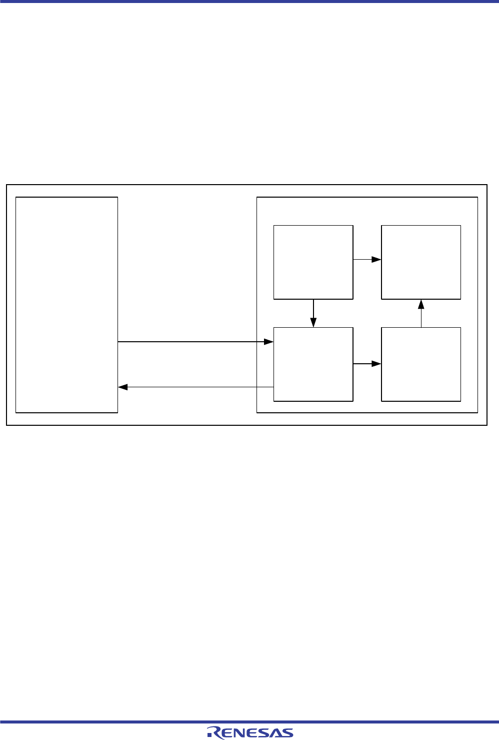
R01UH0034EJ0200 Rev.2.00 Page 1381 of 1489
Dec 27, 2013
RX62T Group, RX62G Group 31. ROM (Flash Memory for Code Storage)
31.9 Boot Mode
31.9.1 System Configuration
In boot mode, the host sends control commands and data for programming, and the user area and data area are
programmed or erased accordingly. An on-chip SCI handles transfer between the host and RX62T in asynchronous
mode. Tools for the transmission of control commands and the data for programming must be prepared in the host.
When the RX62T is activated in boot mode, the program on the area that holds the embedded program is executed. This
program automatically adjusts the bit rate of the SCI and controls programming/erasure in response to control commands
received from the host.
Figure 31.24 shows the system configuration for operations in boot mode.
Figure 31.24 System Configuration for Operations in Boot Mode
31.9.2 ID Code Protection
This function is used to prohibit reading/programming/erasure from the host.
Using the control code and ID code written in the ROM, ID code protection is enabled or disabled and ID code protection
is judged. When ID code protection is enabled, the code sent from the host is compared with the control code and ID
code in the ROM to determine whether they match, and reading/programming/erasure will be enabled only when the two
match.
The control code and ID code in the ROM consists of four 32-bit words. Figure 31.25 shows the configuration of the
control code and ID code. The ID code should be set in 32-bit units.
Host
Tools for boot
programming,
and
data for programming
RX62T
On-chip SCI
PD5/RxD1
PD3/TxD1
Control command
Analysis/
execution
software
(on-chip)
ROM
On-chip RAM
Status
Control command and
data for programming

R01UH0034EJ0200 Rev.2.00 Page 1382 of 1489
Dec 27, 2013
RX62T Group, RX62G Group 31. ROM (Flash Memory for Code Storage)
Figure 31.25 Configuration of Control Code and ID Code in ROM
(1) Control Code
The control code determines whether ID code protection is or is not enabled and the method of authentication to use with
the host. Table 31.10 shows how the control code determines the method of authentication
(2) ID Code
The ID code can be set to any desired value. However, if the control code is 52h and the ID code is 50h, 72h, 6Fh, 74h,
65h, 63h, 74h, FFh, ..., FFh (from the ID code 1 field), there is no determination of matching and the ID code is always
considered to be non-matching. Accordingly, reading, programming, and erasure from the host are prohibited.
Table 31.10 Specifications for ID Code Protection
Control Code ID Code State of Protection Operations at the Time of SCI Connection
45h As desired Protection enabled
(authentication method 1)
Matching ID code: ID code protection is lifted, and this is
followed by a transition to the state of waiting for a host
command.
Non-matching ID code: Up to two more transitions to the ID
code protection waiting state; complete erasure if a non-
matching ID code is received for a third time.
52h Sequences other than
50h, 72h, 6Fh, 74h, 65h,
63h, 74h, FFh, ..., FFh
Protection enabled
(authentication method 2)
Matching ID code: ID code protection is lifted, and this is
followed by a transition to the state of waiting for a host
command.
Non-matching ID code: Further transition to the ID code
protection waiting state
50h, 72h, 6Fh, 74h, 65h,
63h, 74h, FFh, ..., FFh
Protection enabled
(authentication method 3)
Always judged to be a non-matching ID code.
Other than the
above
— Protection disabled Erasure of all blocks
Control code ID code 1 ID code 2 ID code 3
ID code 4 ID code 5 ID code 6 ID code 7
ID code 8 ID code 9 ID code 10 ID code 11
ID code 12 ID code 13 ID code 14 ID code 15
FFFF FFA0h
FFFF FFA4h
FFFF FFA8h
FFFF FFACh
31 24 23 16 15 8 7 0
R01UH0034EJ0200 Rev.2.00 Page 1383 of 1489
Dec 27, 2013
RX62T Group, RX62G Group 31. ROM (Flash Memory for Code Storage)
(3) Example of Assembler Directives for Setting an ID Code
The following assembler directives set up a control code of 45h and an ID code of 01h, 02h, 03h, 04h, 05h, 06h, 07h,
08h, 0Ah, 0Bh, 0Ch, 0Dh, 0Eh, 0Fh (from the ID code 1 field).
.SECTION ID_CODE,CODE
.ORG 0FFFFFFA0h
.LWORD 45010203h
.LWORD 04050607h
.LWORD 08090A0Bh
.LWORD 0C0D0E0Fh
31.9.3 State Transitions in Boot Mode
Figure 31.26 is a diagram of the state transitions in boot mode.
Figure 31.26 State Transitions in Boot Mode
Activated in boot mode
(Reset in boot mode)
User area and Data area are
completely erased
55h
Inquiry command
Response to command
(2)
Host command (read or check)
Specify the
erasure block
(4)
Data for
programming
Programming/erasure state
transition command
Programming
select command
End of
programming
(1)
ID code
protected?
Protection enabled
ID
OK
Failed/Retry
Failed/The number for
retrying is overflowed
(5)
Wait for inquiry/
selection host command
Wait for the ID code Check the ID code
Execute inquiry/
selection host command
Bit rate adjustment
Wait for
programming/erasure host
command
Execute host command
(read or check)
Wait for data for
programming Wait for the specification
of erasure block
User area and Data area are
completely erased
End of erasure
Erasure select command
00h,......,00h
(Bit rate adjustment)
(3)
Protection disabled
Response to command

R01UH0034EJ0200 Rev.2.00 Page 1384 of 1489
Dec 27, 2013
RX62T Group, RX62G Group 31. ROM (Flash Memory for Code Storage)
(1) Matching the Bit Rates
When the RX62T is activated in boot mode, the bit rate of the SCI is automatically adjusted to match that of the host. On
completion of this adjustment, the RX62T transmits the value 00h to the host. On subsequent correct reception of the
value 55h sent from the host, the RX62T enters the state of waiting for a host command for inquiry or selection. For
details on matching of the bit rates, see section 31.9.4, Automatic Adjustment of the Bit Rate.
(2) Waiting for a Host Command for Inquiry or Selection
This state is for inquiries on area size, area configuration, the addresses where areas start, the state of support etc., and for
selection of the device, clock mode, and bit rate. The RX62T receives a programming/erasure state transition command
issued by the host and then enters the state to determine whether ID code protection is enabled or disabled. For the
inquiry/selection host commands, see section 31.9.5, Inquiry/Selection Host Command Wait State.
(3) Judging ID Code Protection
This state is for determining whether ID code protection is enabled or disabled. The control code and ID code written in
the ROM are used to determine whether ID code protection is enabled or disabled. When enabled, the state of waiting for
the ID code is entered. When disabled, the user area and data area are all completely erased, and the state of waiting for
programming and erasure commands from the host is entered. For details on the control code and ID code, see section
31.9.2, ID Code Protection.
(4) Waiting for an ID Code
This state is for waiting for the control code and ID code to be sent from the host. The control code and ID code sent by
the host are compared with the code stored in the ROM, and the state of waiting for programming and erasure commands
from the host is entered if the two match. If they do not match, the next transition is back to the state of waiting for an ID
code. However, if the ID codes fail to match three times in a row and also the state of protection is authentication method
1, the ROM is completely erased, and the state of waiting for an ID code is entered again. A reset is required to release
the system from this state due to non-matching ID codes. For details on the control code and ID code, see section
31.9.2, ID Code Protection.
(5) Waiting for a Host Command for Programming or Erasure
In this state, programming and erasure proceed in accordance with commands from the host. In response to the reception
of a command, the RX62T enters the state of waiting for the data to use in programming, waiting for specification of the
erasure block to be erased, or executing the processing of commands for reading, fetching and so on.
When the RX62T receives a programming selection command, it enters the state of waiting for the data to use in
programming. After the host has issued the programming selection command, the process continues with the address
where programming is to start and then the data for programming. Setting of FFFF FFFFh as the address where
programming is to start indicates the completion of programming, and the next transition is from the state of waiting for
the data to use in programming to the state of waiting for programming and erasure commands.
When the RX62T receives a programming selection command, it enters the state of waiting for specification of the
erasure block to be erased. After the host has issued the programming selection command, the process continues with the
number of the erasure block to be erased. Setting of FFh as the number of the erasure block indicates the completion of
erasure, and the next transition is from the state of waiting for specification of the erasure block to the state of waiting for
programming and erasure commands. Since the user area and data area are all completely erased during the interval
between booting up in boot mode and transition to the state of waiting for programming and erasure commands, explicit
execution of erasure is not necessary unless newly programmed data are to be erased without a further reset.
Other than the programming and erasure commands, commands from the host for execution in this state include those for
sum checking of the user area, blank checking (to confirm erasure), reading from memory, and acquiring state
information.
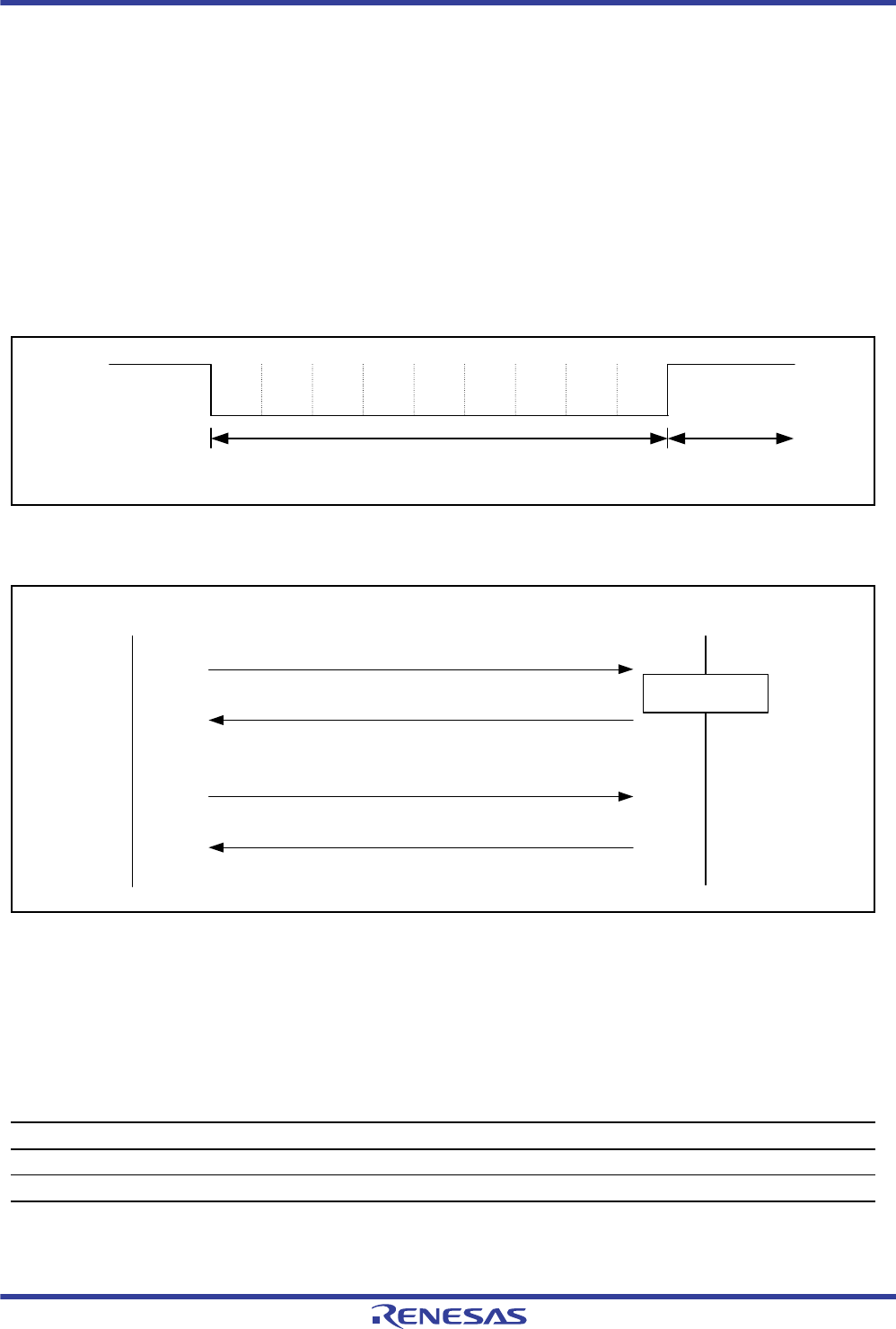
R01UH0034EJ0200 Rev.2.00 Page 1385 of 1489
Dec 27, 2013
RX62T Group, RX62G Group 31. ROM (Flash Memory for Code Storage)
31.9.4 Automatic Adjustment of the Bit Rate
When the RX62T is booted up in boot mode, asynchronous transfer by the SCI is used to measure the periods at low
level of consecutive bytes with value 00h that are sent from the host. While the period at low level is being measured, set
the host’s SCI parameters to eight-bit data, one stop bit, no parity, and a transfer rate of 9,600 bps or 19,200 bps. The
RX62T calculates the host's SCI bit rate from the measured periods at low level, adjusts its own bit rate accordingly, and
then sends a 00h byte to the host. If reception of the value 00h by the host is normal, the host responds by sending the
value 55h to the RX62T. If normal reception of 00h by the host is not possible, the RX62T is re-booted in boot mode, and
then repeats the process of automatically adjusting the bit rate. If reception of the value 55h by the RX62T is normal, it
responds by sending E6h to the host, and if normal reception of 55h by the RX62T is not possible, it responds by sending
FFh to the host.
Figure 31.27 Transfer Format Used by the SCI in Automatic Adjustment of the Bit Rate
Figure 31.28 Sequence of Transfer between the Host and RX62T
Since the bit rate of the RX62T's SCI module depends on the frequency of the peripheral clock, adjustment to match the
bit rate of the host will not be possible under some conditions. Accordingly, ensure that SCI transfer is under the
conditions given in Table 31.11.
Table 31.11 Conditions for Automatic Bit-Rate Adjustment to be Possible
Bit Rate of the SCI in the Host Range of Frequency for the EXTAL Signal
9,600 bps 8 to 14 MHz
19,200 bps 8 to 14 MHz
Start
bit D0 D1 D2 D3 D4 D5 D6 D7 Stop
bit
Measurement of low-level period for nine bits
(data is 00h)
High-level period for at
least one bit
Host RX62T
Measures 9-bit
period
00h (up to 30 times)
00h (on completion of automatic adjustment)
55h
E6h (for normal reception of 55h) or FFh (error)
R01UH0034EJ0200 Rev.2.00 Page 1386 of 1489
Dec 27, 2013
RX62T Group, RX62G Group 31. ROM (Flash Memory for Code Storage)
31.9.5 Inquiry/Selection Host Command Wait State
Table 31.12 shows the host commands available in the inquiry/selection host command wait state. The embedded
program status inquiry command can also be used in the programming/erasure host command wait state. The other
commands can only be used in the inquiry/selection host command wait state.
If the host has sent an undefined command, the RX62T/RX62G returns a response indicating a command error in the
format shown below. The command field holds the first byte of the undefined command sent from the host.
In the inquiry/selection host command wait state, send selection commands from the host in the order of device selection,
clock mode selection, and new bit rate selection to set up the RX62T/RX62G according to the responses to inquiry
commands.
that the supported device inquiry and clock mode inquiry commands are the only inquiry commands that can be sent
before the clock mode selection command; other inquiry commands must not be issued before the clock mode selection
command. If commands are issued in an incorrect order, the RX62T/RX62G returns a response indicating a command
error. Figure 31.29 shows an example of the procedure to use inquiry/selection host commands.
Table 31.12 Inquiry/Selection Host Commands
Host Command Name Function
Supported device inquiry Inquires regarding the device codes and the product codes for the embedded programs
Device selection Selects a device code
Clock mode inquiry Inquires regarding the clock mode
Clock mode selection Notifies the selected clock mode
Multiplication ratio inquiry Inquires regarding the number of clock types, the number of multiplication/division ratios,
and the multiplication /division ratios
Operating frequency inquiry Inquires regarding the number of clock types and the maximum and minimum operating
frequencies
User area information inquiry Inquires regarding the number of user areas and the start and end addresses
Erasure block information inquiry Inquires regarding the number of blocks and the start and end addresses
Programming size inquiry Inquires regarding the size of programming data
New bit rate selection Modifies the bit rate of SCI communications between the host and RX62T/RX62G
Programming/erasure state transition Enters the state for determining ID code protection
Embedded program status inquiry Inquires regarding the processing state
Error response 80h Command

R01UH0034EJ0200 Rev.2.00 Page 1387 of 1489
Dec 27, 2013
RX62T Group, RX62G Group 31. ROM (Flash Memory for Code Storage)
Figure 31.29 Example of Procedure to Use Inquiry/Selection Host Commands for User Area
Each host command is described in detail below. The "command" in the description indicates a command sent from the
host to the RX62T/RX62G and the "response" indicates a response sent from the RX62T/RX62G to the host. The
"checksum" is byte-size data calculated so that the sum of all bytes to be sent by the RX62T/RX62G becomes 00h.
Start
Supported device inquiry
User area information inquiry
Erasure block information inquiry
Programming size inquiry
Device selection
Clock mode inquiry
Clock mode selection
Multiplication ratio inquiry
Operating frequency inquiry
New bit rate selection
Inquiry regarding area programming
information
Programming/erasure state transition
End
R01UH0034EJ0200 Rev.2.00 Page 1388 of 1489
Dec 27, 2013
RX62T Group, RX62G Group 31. ROM (Flash Memory for Code Storage)
(1) Supported Device Inquiry
In response to a supported device inquiry command sent from the host, the RX62T/RX62G returns the information
concerning the devices supported by the embedded program for boot mode. If the supported device inquiry command
comes after the host has selected a device, the RX62T/RX62G only returns the information concerning the selected
device.
Size (1 byte): Total number of bytes in the device count, character count, device code, and product code fields}
Device count (1 byte): Number of device types supported by the embedded program for boot mode
Character count (1 byte): Number of characters included in the device code and product code fields
Device code (4 bytes): ASCII code for the product name of the chip
Product code (n bytes): ASCII code for the supported device
SUM (1 byte): Checksum (in response)
(2) Device Selection
In response to a device selection command sent from the host, the RX62T/RX62G checks if the selected device is
supported. When the selected device is supported, the RX62T/RX62G specifies this device as the device for use and
returns a response (06h). If the selected device is not supported or the sent command is illegal, the RX62T/RX62G
returns an error response (90h).
Even when 01h has been returned as the number of supported devices in response to a supported device inquiry
command, issue a device selection command to specify the device code that has been returned as the result of the inquiry.
Size (1 byte): Number of characters in the device code field (fixed at four)
Device code (4 bytes): ASCII code for the product name of the chip (one of the device codes returned in response to the
supported device inquiry command)
SUM (1 byte): Checksum
Error (1 byte): Error code
11h: Checksum error (illegal command)
21h: Incorrect device code error
Command 20h
Response 30h Size Device count
Character
count
Device code Product code
Character
count
Device code Product code
:: :
Character
count
Device code Product code
SUM
Command 10h Size Device code SUM
Response 06h
Error response 90h Error

R01UH0034EJ0200 Rev.2.00 Page 1389 of 1489
Dec 27, 2013
RX62T Group, RX62G Group 31. ROM (Flash Memory for Code Storage)
(3) Clock Mode Inquiry
In response to a clock mode inquiry command sent from the host, the RX62T/RX62G returns the supported clock modes.
If the clock mode inquiry command comes after the host has selected a clock mode, the RX62T/RX62G only returns the
information concerning the selected clock mode.
Size (1 byte): Total number of bytes in the mode count and mode fields
Mode (1 byte): Supported clock mode (for example, 01h indicates clock mode 1)
SUM (1 byte): Checksum
(4) Clock Mode Selection
In response to a clock mode selection command sent from the host, the RX62T/RX62G checks if the selected clock mode
is supported. When the selected mode is supported, the RX62T/RX62G specifies this clock mode for use and returns a
response (06h). If the selected mode is not supported or the sent command is illegal, the RX62T/RX62G returns an error
response (91h).
Be sure to issue a clock mode selection command only after issuing a device selection command. Even when 00h or 01h
has been returned as the number of supported clock modes in response to a clock mode inquiry command, issue a clock
mode selection command to specify the clock mode that has been returned as the result of the inquiry.
Size (1 byte): Number of characters in the mode field (fixed at 1)
Mode (1 byte): Clock mode (same mode as the response to the clock mode inquiry command)
SUM (1 byte): Checksum
Error (1 byte): Error code
11h: Checksum error (illegal command)
21h: Incorrect clock mode error
Command 21h
Response 31h Size
Mode Mode . . . Mode
SUM
Command 11h Size Mode SUM
Response 06h
Error response 91h Error

R01UH0034EJ0200 Rev.2.00 Page 1390 of 1489
Dec 27, 2013
RX62T Group, RX62G Group 31. ROM (Flash Memory for Code Storage)
(5) Multiplication Ratio Inquiry
In response to a multiplication ratio inquiry command sent from the host, the RX62T/RX62G returns the clock types, the
number of multiplication/division ratios, and the multiplication division ratios supported.
Size (1 byte): Total number of bytes in the clock type count, multiplication ratio type, and multiplication ratio
fields
Clock type count (1 byte): Number of clock types (for example, 02h indicates two clock types; that is, a system clock
and a peripheral clock)
Multiplication ratio count (1 byte): Number of supported multiplication/division ratios (for example, 04h indicates that four
multiplication ratios are supported for the system clock (x1, x2, x4, and x8))
Multiplication ratio (1 byte): A positive value indicates a multiplication ratio (for example, 04h = 4 = multiplication by 4)
A negative value indicates a division ratio (for example, FEh = -2 = division by 2)
SUM (1 byte): Checksum
Command 22h
Response 32h Size Clock type
count
Multiplication
ratio count
Multiplication
ratio
Multiplication
ratio
. . . Multiplication
ratio
Multiplication
ratio count
Multiplication
ratio
Multiplication
ratio
. . . Multiplication
ratio
: : : . . . :
Multiplication
ratio count
Multiplication
ratio
Multiplication
ratio
. . . Multiplication
ratio
SUM
R01UH0034EJ0200 Rev.2.00 Page 1391 of 1489
Dec 27, 2013
RX62T Group, RX62G Group 31. ROM (Flash Memory for Code Storage)
(6) Operating Clock Frequency Inquiry
In response to an operating clock frequency inquiry command sent from the host, the RX62T/RX62G returns the
minimum and maximum frequencies for each clock.
Size (1 byte): Total number of bytes in the clock type count, minimum frequency, and maximum frequency
fields
Clock type count (1 byte): Number of clock types (for example, 02h indicates two clock types; that is, a system clock and a
peripheral clock)
Minimum frequency (2 bytes): Minimum value of the operating frequency (for example, 07D0h indicates 20.00 MHz).
This value should be calculated by multiplying the frequency value (MHz) to two decimal places
by 100.
Maximum frequency (2 bytes): Maximum value of the operating frequency represented in the same format as the minimum
frequency
SUM (1 byte): Checksum
(7) User Area Information Inquiry
In response to a user area information inquiry command sent from the host, the RX62T/RX62G returns the number of
user area areas and their addresses.
Size (1 byte): Total number of bytes in the area count, area start address, and area end address fields
Area count (1 byte): Number of user area areas (consecutive areas are counted as one area)
Area start address (4 bytes): Start address of a user area
Area end address (4 bytes): End address of a user area
SUM (1 byte): Checksum
Command 23h
Response 33h Size Clock type
count
Minimum frequency Maximum frequency
Minimum frequency Maximum frequency
::
Minimum frequency Maximum frequency
SUM
Command 25h
Response 35h Size Area count
Area start address
Area end address
Area start address
Area end address
:
Area start address
Area end address
SUM
R01UH0034EJ0200 Rev.2.00 Page 1392 of 1489
Dec 27, 2013
RX62T Group, RX62G Group 31. ROM (Flash Memory for Code Storage)
(8) Erasure Block Information Inquiry
In response to an erasure block information inquiry command sent from the host, the RX62T/RX62G returns the number
of erasure blocks in the user area and their addresses.
Size (2 byte): Total number of bytes in the block count, block start address, and block end address fields
Block count (1 byte): Number of erasure blocks in the user area
Block start address (4 bytes): Start address of an erasure block
Block end address (4 bytes): End address of an erasure block
SUM (1 byte): Checksum
(9) Programming Size Inquiry
In response to a programming size inquiry command sent from the host, the RX62T/RX62G returns the programming
size.
Size (1 byte): Number of characters included in the programming size field (fixed at two)
Programming size (2 bytes): Programming unit (bytes)
SUM (1 byte): Checksum
Command 26h
Response 36h Size Block count
Block start address
Block end address
Block start address
Block end address
:
Block start address
Block end address
SUM
Command 27h
Response 37h Size Programming size SUM
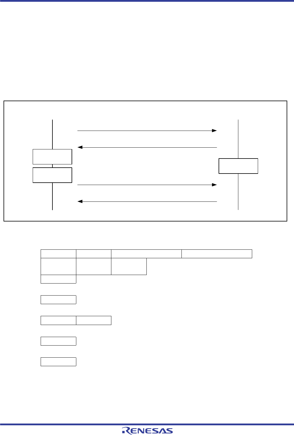
R01UH0034EJ0200 Rev.2.00 Page 1393 of 1489
Dec 27, 2013
RX62T Group, RX62G Group 31. ROM (Flash Memory for Code Storage)
(10) New Bit Rate Selection
In response to a new bit rate selection command sent from the host, the RX62T/RX62G checks if the on-chip SCI can be
set to the selected new bit rate. When the SCI can be set to the new bit rate, the RX62T/RX62G returns a response (06h)
and sets the SCI to the new bit rate. If the SCI cannot be set to the new bit rate or the sent command is illegal, the RX62T/
RX62G returns an error response (BFh). Upon reception of response 06h, the host waits for a one-bit period in the
previous bit rate with which the new bit rate selection command has been sent, and then sets the host's bit rate to the new
one. After that, the host sends confirmation data (06h) in the new bit rate, and the RX62T/RX62G returns a response
(06h) to the confirmation data.
Be sure to issue a new bit rate selection command only after a clock mode selection command.
Figure 31.30 New Bit Rate Selection Sequence
Size (1 byte): Total number of bytes in the bit rate, input frequency, clock type count, and multiplication ratio fields
Bit rate (2 bytes): New bit rate (for example, 00C0h indicates 19200 bps)
1/100 of the new bit rate value should be specified.
Input frequency (2 bytes): Clock frequency input to the RX62T (for example, 04E2h indicates 12.50 MHz)
This value should be calculated by multiplying the input frequency value to two decimal places
by100.
Command 3Fh Size Bit rate Input frequency
Clock type
count
Multiplication
ratio 1
Multiplication
ratio 2
SUM
Response 06h
Error response BFh Error
Confirmation 06h
Response 06h
Host RX62T/RX62G
New bit rate selection command
Response (06h)
Confirmation (06h)
Response (06h)
Wait for
one-bit period
Set new
bit rate
Set new
bit rate

R01UH0034EJ0200 Rev.2.00 Page 1394 of 1489
Dec 27, 2013
RX62T Group, RX62G Group 31. ROM (Flash Memory for Code Storage)
Clock type count (1 byte): Number of clock types (for example, 02h indicates two clock types; that is, a system clock and
a peripheral clock)
Multiplication ratio 1 (1 byte): Multiplication/division ratio of the input frequency to obtain the system clock (ICLK)
A positive value indicates a multiplication ratio (for example, 04h = 4 = multiplication by 4)
A negative value indicates a division ratio (for example, FEh = -2 = division by 2)
Multiplication ratio 2 (1 byte): Multiplication/division ratio of the input frequency to obtain the peripheral clock (PCLK)
This value is represented in the same format as multiplication ratio 1
SUM (1 byte): Checksum
Error: Error code
11h: Checksum error
24h: Bit rate selection error
25h: Input frequency error
26h: Multiplication ratio error
27h: Operating frequency error
Bit rate selection error
A bit rate selection error occurs when the bit rate selected through a new bit rate selection command cannot be set
for the SCI of the RX62T within an error of 4%. The bit rate error can be obtained by the following equation from
the bit rate (B) selected through a new bit rate selection command, the input frequency (fEX), multiplication ratio 2
(MPφ), the bit rate register (BRR) setting (N) in the SCI, and the CKS[1:0] bit value (n) in the serial mode register
(SMR).
Input frequency error
An input frequency error occurs when the input frequency specified through a new bit rate selection command is
outside the range from the minimum to maximum input frequencies for the clock mode selected through a clock
mode selection command.
Multiplication ratio error
A multiplication ratio error occurs when the multiplication ratio specified through a new bit rate selection command
does not match the clock mode selected through a clock mode selection command. To check the selectable
multiplication ratios, issue a multiplication ratio inquiry command.
Operating frequency error
An operating frequency error occurs when the RX62T/RX62G cannot operate at the operating frequencies selected
through a new bit rate selection command. RX62T/RX62G calculates the operating frequencies from the input
frequency and multiplication ratios specified through a new bit rate selection command and checks if each
calculated frequency is within the range from the minimum to maximum frequencies for the respective clock. To
check the minimum and maximum operating frequencies for each clock, issue an operating clock frequency inquiry
command.
2
64
10
Mf
6
PEX -1
B(N+1)
Error (%)
2n-1 100

R01UH0034EJ0200 Rev.2.00 Page 1395 of 1489
Dec 27, 2013
RX62T Group, RX62G Group 31. ROM (Flash Memory for Code Storage)
(11) Programming/Erasure State Transition
In response to a programming/erasure state transition command sent from the host, the RX62T/RX62G determines
whether ID code protection is enabled or disabled using the control code and ID code written in the ROM. When ID code
protection is enabled, the RX62T/RX62G returns a response (16h) and waits for the ID code. When ID code protection is
disabled, the RX62T/RX62G erases the entire area of each of the user area and data area. After completing erasure, the
RX62T/RX62G returns a response (16h) and waits for a programming/erasure host command. If the RX62T/RX62G has
failed to complete erasure due to an error, it returns an error response (sends C0h and 51h in that order).
Do not issue a programming/erasure state transition command before device selection, clock mode selection, and new bit
rate selection commands.
ACK (1 byte): ACK code
26h: ID code protection is disabled
16h: ID code protection is enabled
Command 40h
Response ACK
Error response C0h 51h
R01UH0034EJ0200 Rev.2.00 Page 1396 of 1489
Dec 27, 2013
RX62T Group, RX62G Group 31. ROM (Flash Memory for Code Storage)
(12) Embedded Program Status Inquiry
In response to an embedded program status inquiry command sent from the host, the RX62T/RX62G returns its current
status. The embedded program status inquiry command can be issued in both the inquiry/selection host command wait
state and programming/erasure host command wait state.
Size (1 byte): Total number of bytes in the status and error fields (fixed at two)
Status (1 byte): Current status in the RX62T/RX62G (see Table 31.13)
Error (1 byte): Error status in the RX62T/RX62G (see Table 31.14)
Command 4Fh
Response 5Fh Size Status Error
Table 31.13 Status Code
Code Description
11h Waiting for device selection
12h Waiting for clock mode selection
13h Waiting for bit rate selection
1Fh Waiting for transition to programming/erasure host command wait state (bit rate has been selected)
31h Erasing the user area
3Fh Waiting for a programming/erasure host command
4Fh Waiting for reception of programming data
5Fh Waiting for erasure block selection
Table 31.14 Error Code
Code Description
00h No error
11h Checksum error
21h Incorrect device code error
22h Incorrect clock mode error
24h Bit rate selection error
25h Input frequency error
26h Multiplication ratio error
27h Operating frequency error
29h Block number error
2Ah Address error
2Bh Data size error
51h Erasure error
52h Incomplete erasure error
53h Programming error
54h Selection error
80h Command error
FFh Bit rate adjustment verification error
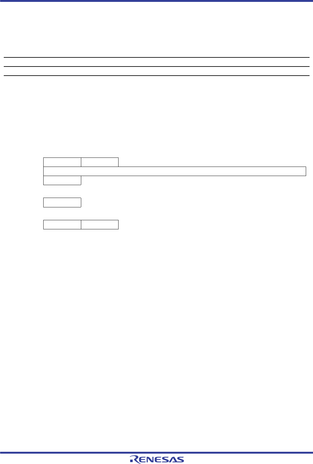
R01UH0034EJ0200 Rev.2.00 Page 1397 of 1489
Dec 27, 2013
RX62T Group, RX62G Group 31. ROM (Flash Memory for Code Storage)
31.9.6 ID Code Wait State
Table 31.15 shows the host command available in the ID code wait state.
If the host has sent an undefined command, the RX62T returns a response indicating a command error. For the format of
this response, see ssection 31.9.5, Inquiry/Selection Host Command Wait State.
(1) ID Code Check
In response to an ID code check command sent from the host, the RX62T compares the code sent from the host with the
control code and ID code in the ROM and returns the result.
Size (1 byte): Number of bytes in the ID code field (fixed at 16)
ID code (16 bytes): Control code (1 byte) + ID code (15 bytes)
SUM (1 byte): Checksum
ACK (1 byte): ACK code
26h: Returns the response for a programming/erasure state transition command
Error (1 byte): Error code
11h: Checksum error
61h: ID code mismatch
63h: ID code mismatch (erasure error)
An error has occurred during erasure triggered by an ID code mismatch.
Table 31.15 ID Code Check Host Command
Host Command Name Function
ID code check Performs the ID code check
Command 60h Size
Control code + ID code
SUM
Response ACK
Error response E0h Error

R01UH0034EJ0200 Rev.2.00 Page 1398 of 1489
Dec 27, 2013
RX62T Group, RX62G Group 31. ROM (Flash Memory for Code Storage)
31.9.7 Programming/Erasure Host Command Wait State
Table 31.16 shows the host commands available in the programming/erasure host command wait state.
If the host has sent an undefined command, the RX62T returns a response indicating a command error. For the format of
this response, see section 31.9.5, Inquiry/Selection Host Command Wait State.
To program the ROM, issue a programming selection command (user area programming selection) and then a 256-byte
programming command from the host. Upon reception of a programming selection command, the RX62T enters the
programming data wait state (see section 31.9.3, State Transitions in Boot Mode). In response to a 256-byte
programming command sent from the host in this state, the RX62T starts programming the ROM. When the host sends a
256-byte programming command specifying FFFF FFFFh as the programming start address, the RX62T detects it as the
end of programming and enters the programming/erasure host command wait state.
To erase the ROM, issue an erasure selection command and then a block erasure command from the host. Upon reception
of an erasure selection command, the RX62T enters the erasure block selection wait state (see section 31.9.3, State
Transitions in Boot Mode). In response to a block erasure command sent from the host in this state, the RX62T erases
the specified block in the ROM. When the host sends a block erasure command specifying FFh as the block number, the
RX62T detects it as the end of erasure and enters the programming/erasure host command wait state.
Table 31.16 Programming/Erasure Host Commands
Host Command Name Function
User area programming selection Selects the program for user area programming
256-byte programming Programs 256 bytes of data
Erasure selection Selects the erasure program
Block erasure Erases block data
Memory read Reads data from memory
User area checksum Performs checksum verification for the user area
User area blank check Checks whether the user area is blank
Read lock bit status Reads from the lock bit
Lock bit program Writes to the lock bit
Lock bit enable Enables the lock bit protection
Lock bit disable Disables the lock bit protection
Embedded program status inquiry Inquires regarding the state of the RX62T
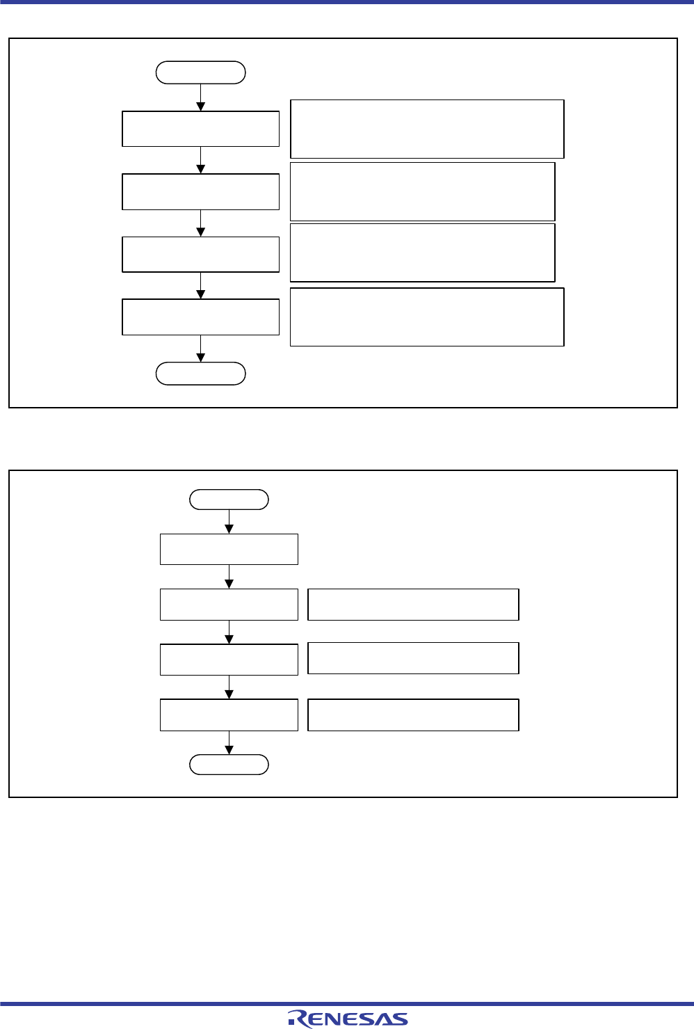
R01UH0034EJ0200 Rev.2.00 Page 1399 of 1489
Dec 27, 2013
RX62T Group, RX62G Group 31. ROM (Flash Memory for Code Storage)
Figure 31.31 Procedure for ROM Programming in Boot Mode
Figure 31.32 Procedure for ROM Erasure in Boot Mode
Each host command is described in detail below. The "command" in the description indicates a command sent from the
host to the RX62T and the "response" indicates a response sent from the RX62T to the host. The "checksum" is byte-size
data calculated so that the sum of all bytes to be sent by the RX62T becomes 00h.
Start
Programming selection
256-byte programming
256-byte programming
256-byte programming
End
User area programming selection
Address and data specification
Address and data specification
Address FFFF FFFFh specification
Start
Erasure selection
Block erasure
Block erasure
Block erasure
End
Block specification
Block specification
Block number FFh specification
R01UH0034EJ0200 Rev.2.00 Page 1400 of 1489
Dec 27, 2013
RX62T Group, RX62G Group 31. ROM (Flash Memory for Code Storage)
(1) User Area Programming Selection
In response to a user area programming selection command sent from the host, the RX62T selects the program for user
area programming and waits for programming data.
(2) 256-Byte Programming
In response to a 256-byte programming command sent from the host, the RX62T programs the ROM. After completing
ROM programming successfully, the RX62T returns a response (06h). If an error has occurred during ROM
programming, the RX62T returns an error response (D0h).
Programming address (4 bytes): Target address of programming
To program the ROM, a 256-byte boundary address should be specified.
To terminate programming, FFFF FFFFh should be specified.
Data (256 bytes): Programming data
FFh should be specified for the bytes that do not need to be programmed.
When terminating programming, no data needs to be sent
(only the programming address and SUM should be sent in that order).
SUM (1 byte): Checksum
Error (1 byte): Error code
11h: Checksum error
2Ah: Address error (the specified address is not in the target area)
53h: Programming cannot be done due to a programming error
(3) Erasure Selection
In response to an erasure selection command sent from the host, the RX62T selects the erasure program and waits for
erasure block specification.
Command 43h
Response 06h
Command 50h Programming address
Data Data . . . Data
SUM
Response 06h
Error response D0h Error
Command 48h
Response 06h
R01UH0034EJ0200 Rev.2.00 Page 1401 of 1489
Dec 27, 2013
RX62T Group, RX62G Group 31. ROM (Flash Memory for Code Storage)
(4) Block Erasure
In response to a block erasure command sent from the host, the RX62T erases the ROM. After completing ROM erasure
successfully, the RX62T returns a response (06h). If an error has occurred during ROM erasure, the RX62T returns an
error response (D8h).
Size (1 byte): Number of bytes in the block specification field (fixed at 1)
Block (1 byte): Block number whose data is to be erased
To terminate erasure, FFh should be specified.
SUM (1 byte): Checksum
Error (1 byte): Error code
11h: Checksum error
29h: Block number error (an incorrect block number is specified)
51h: Erasure cannot be done due to an erasure error
(5) Memory Read
In response to a memory read command sent from the host, the RX62T reads data from the ROM. After completing
ROM reading successfully, the RX62T returns the data stored in the address specified by the memory read command. If
the RX62T has failed to read the ROM, the RX62T returns an error response (D2h).
Size (1 byte): Total number of bytes in the area, read start address, and reading size fields
Area (1 byte): Target area to be read
01h: User area
Read start address (4 bytes): Start address of the area to be read
Reading size (4 bytes): Size of data to be read (bytes)
SUM (1 byte): Checksum
Data (1 byte): Data read from the ROM
Error (1 byte): Error code
11h: Checksum error
2Ah: Address error
The value specified for area selection is neither 00h nor 01h.
The specified read start address is outside the selected area.
2Bh: Data size error
00h is specified for the reading size.
Command 58h Size Block SUM
Response 06h
Error response D8h Error
Command 52h Size Area Read start address
Reading size SUM
Response 52h Reading size
Data Data . . . Data
SUM
Error response D2h Error

R01UH0034EJ0200 Rev.2.00 Page 1402 of 1489
Dec 27, 2013
RX62T Group, RX62G Group 31. ROM (Flash Memory for Code Storage)
The reading size is larger than the area.
The end address calculated from the read start address and the reading size is
outside the selected area.
(6) User Area Checksum
In response to a user area checksum command sent from the host, the RX62T sums the user area data in byte units and
returns the result (checksum).
Size (1 byte): Number of bytes in the area checksum field (fixed at 4)
Area checksum (4 bytes): Checksum of the user area data
The user area also stores the key code for debugging function authentication. Note that the
checksum includes this key code value.
SUM (1 byte): Checksum (for the response data)
(7) User Area Blank Check
In response to a user area blank check command sent from the host, the RX62T checks whether the user area is
completely erased. When the use area is completely erased, the RX62T returns a response (06h). If the user area has an
unerased area, the RX62T returns an error response (sends CDh and 52h in that order).
Command 4Bh
Response 5Bh Size Area checksum SUM
Command 4Dh
Response 06h
Error response CDh 52h

R01UH0034EJ0200 Rev.2.00 Page 1403 of 1489
Dec 27, 2013
RX62T Group, RX62G Group 31. ROM (Flash Memory for Code Storage)
(8) Read Lock Bit Status
In response to a read lock bit status command sent from the host, the RX62T reads data from the lock bit. After
completing the lock bit reading successfully, the RX62T returns the data stored in the address specified by the read lock
bit status command. If the RX62T has failed to read the lock bit, the RX62T returns an error response (F1h).
Size (1 byte): Total number of bytes in the area, third highest order address, second highest order
address, and highest order
address fields (fixed at 4 in the RX62T)
Area (1 byte): Target area to be read
01h: User area
Third highest order address (1 byte): Third highest order address at the specified block's end address (8 to 15 bits)
Second highest order address (1 byte): Second highest order address at the specified block's end address (16 to 23 bits)
Highest order address (1 byte): Highest order address at the specified block's end address (24 to 31 bits)
SUM (1 byte): Checksum
Status (1 byte): Bit 6 locked at "0"
Bit 6 unlocked at "1"
Error (1 byte): Error code
11h: Checksum error
2Ah: Address error (the specified address is not in the target area)
Command 71h Size Area Third highest
order address
Second highest
order address
Highest order
address
SUM
Response Status
Error response F1h Error

R01UH0034EJ0200 Rev.2.00 Page 1404 of 1489
Dec 27, 2013
RX62T Group, RX62G Group 31. ROM (Flash Memory for Code Storage)
(9) Lock Bit Program
In response to a lock bit program command sent from the host, the RX62T writes to a lock bit and locks the specified
block. After completing the lock bit blocking successfully, the RX62T returns a response (06h). If the RX62T has failed
to lock, the RX62T returns an error response (F7h).
Size (1 byte): Total number of bytes in the area, third highest order address, second highest order
address, and highest order
address fields (fixed at 4 in the RX62T)
Area (1 byte): Target area to be locked
01h: User area
Third highest order address (1 byte): Third highest order address at the specified block's end address (8 to 15 bits)
Second highest order address (1 byte): Second highest order address at the specified block's end address (16 to 23 bits)
Highest order address (1 byte): Highest order address at the specified block's end address (24 to 31 bits)
SUM (1 byte): Checksum
Error (1 byte): Error code
11h: Checksum error
2Ah: Address error (the specified address is not in the target area)
53h: Locking cannot be done due to a programming error
(10) Lock Bit Enable
In response to a lock bit enable command sent from the host, the RX62T enables a lock bit.
(11) Lock Bit Disable
In response to a lock bit disable command sent from the host, the RX62T disables a lock bit.
(12) Embedded Program Status Inquiry
For details, refer to section 31.9.5, Inquiry/Selection Host Command Wait State.
Command 77h Size Area Third highest
order address
Second highest
order address
Highest order
address
SUM
Response 06h
Error response F7h Error
Command 7Ah
Response 06h
Command 75h
Response 06h

R01UH0034EJ0200 Rev.2.00 Page 1405 of 1489
Dec 27, 2013
RX62T Group, RX62G Group 31. ROM (Flash Memory for Code Storage)
31.10 ID Code Protection on Connection of the On-Chip Debugger
This function is used to prohibit connection with the on-chip debugger. When connecting an on-chip debugger, the
control code and ID code that have been written to the ROM are used to determine whether ID code protection on
connection of the on-chip debugger is enabled or disabled and to judge ID code protection on connection of the on-chip
debugger. When the ID code protection is enabled, the code sent from the on-chip debugger is compared with the control
code and ID code in the ROM to determine whether they match. If they match, connection with the on-chip debugger is
allowed. If they do not match, the on-chip debugger cannot be connected. However, if the control code is 52h and the ID
code is 50h, 72h, 6Fh, 74h, 65h, 63h, 74h, FFh, ..., FFh (from the ID code 1 field), there is no determination of matching
and the ID code is always considered to be non-matching. Furthermore, if all bytes of the control code and ID code have
the value FFh, there is no determination of matching, the ID code is always considered to match, and connection of the
on-chip debugger is allowed. See Figure 31.25 for the configuration of ID codes in flash memory.
Table 31.17 Specifications for ID Code Protection on Connection of the On-Chip Debugger
Table 31.17 Specifications for ID Code Protection on Connection of the On-Chip Debugger
Control Code ID Code State of Protection Operations at the Time of Connection with the On-Chip
Debugger
FFh FFh, …, FFh
(all bytes FFh)
Protection disabled The control code and ID code are not judged, the ID code always
matches, and connection to the on-chip debugger is permitted.
52h 50h, 72h, 6Fh,
74h, 65h, 63h,
74h, FFh, ..., FFh
Protection enabled The control code and ID code are not judged, the ID code is
always non-matching, and connection to the on-chip debugger is
prohibited.
Other than the above Other than the
above
Protection enabled Matching ID code: Authentication of the on-chip debugger is
ended and connection with the on-chip debugger is permitted.
Non-matching ID code: Further transition to the ID code protection
waiting state

R01UH0034EJ0200 Rev.2.00 Page 1406 of 1489
Dec 27, 2013
RX62T Group, RX62G Group 31. ROM (Flash Memory for Code Storage)
31.11 ROM Code Protection
ROM code protection is a facility for prohibiting a PROM programmer from reading from or writing to flash memory.
The ROM code in flash memory is a 32-bit code. Figure 31.33 shows the configuration of ROM codes. Set ROM codes
as 32-bit units.
For release from ROM code protection, erase block EB00 (erasure block 00) in boot mode or by user programming.
Figure 31.33 Configuration of a ROM Code
Table 31.18 Specifications for ROM Code Protection
ROM Code State of Protection Operations at the Time of Connection with the PROM Programmer
0000 0000h Protection enabled
(ROM code protection 1)
Access (both reading and writing) to the user area is prohibited.
0000 0001h Protection enabled
(ROM code protection 2)
Reading from the user area is prohibited.
Other than the
above
Protection disabled Access (both reading and writing) to the user area is permitted.
FFFF FF9Ch
31 0
ROM code

R01UH0034EJ0200 Rev.2.00 Page 1407 of 1489
Dec 27, 2013
RX62T Group, RX62G Group 31. ROM (Flash Memory for Code Storage)
31.12 Usage Notes
(1) Areas where Programming or Erasure is Suspended
Data in areas where programming or erasure is suspended are undefined. To avoid malfunctions due to the reading of
undefined data, prevent the reading of data and execution of code from areas where programming or erasure is currently
suspended.
(2) Suspending Programming or Erasure
If you use the programming/erasure suspension command to suspend the processing of programming or erasure, be sure
to use the resumption command so that the processing is completed. Within 20 μs (PCLK = 50 MHz) after the resume
command has been issued, do not issue the programming/erasing suspension command again.
(3) Prohibition of Reprogramming
Two or more programming operations cannot be performed for the same address range. If an address range that has
already been programmed is to be programmed again, be sure to erase the area in advance of the programming.
(4) Reset during Programming or Erasure
When applying a reset on the RES# pin during programming or erasure, only release the chip from the reset state after at
least 100 μs have elapsed while the operating voltage is within the range specified in the electrical characteristics.
When using the FRESETR.FRESET bit to reset the FCU during programming or erasure, make sure that the reset state is
maintained over tRESW2 (see section 33, Electrical Characteristics). Do not allow programming or erasure of the
ROM while the FCU is being reset.
WDT and IWDT resets during programming or erasure can be used without securing the above intervals.
(5) Prohibition of Non-maskable Interrupts during Programming or Erasure
The generation of a non-maskable interrupt (interrupt on the NMI pin, oscillation-stoppage detected interrupt, or a
voltage-monitoring 1 interrupt, or voltage-monitoring 2 interrupt) during programming or erasure leads to fetching of the
corresponding vector from the ROM, but the data read out are undefined. Therefore, make sure that non-maskable
interrupts are not generated during programming or erasure (this prohibition only applies to the ROM).
(6) Interrupt Vector Assignment During Programming or Erasure
The generation of interrupts during programming or erasure may lead to the fetching of vectors from the ROM. To
prevent access to the ROM area due to the generation of interrupts, set the interrupt table register (INTB) of the CPU so
that the destination for the fetching of interrupt vector is an area outside the ROM.
(7) Abnormal Termination of Programming and Erasure
When programming or erasure is not completed normally due to a fluctuation of the operating voltage above the allowed
range, a reset, a reset of the FCU by using the FRESETR.FRESET bit, entry to the command-locked state due to the
detection of an error, or any of the prohibited items listed under point (8) below, the value of the lock bit becomes zero
(corresponding to the protected state). In such cases, issue a block-erasure command to erase the lock bit while the
FPROTR.FPROTCN bit is 1. After that, repeat the programming that was not completed normally.

R01UH0034EJ0200 Rev.2.00 Page 1408 of 1489
Dec 27, 2013
RX62T Group, RX62G Group 31. ROM (Flash Memory for Code Storage)
(8) Actions Prohibited during Programming and Erasure
To prevent damage to the flash memory during programming or erasure, observe the prohibitions described below.
In an RX62T product, the voltage from the power supply being beyond the allowed range of operating voltage
A change to the value of the FWEPROR.FLWE[1:0] bits
A change to the operating mode due to the setting of the SYSCR0.ROME bit
A change to the PCLK multiplication ratio due to the setting in the SCKCR register
Setting the PCKAR register for a frequency other than that of PCLK
A transition to all-module clock stop mode, software standby mode, or deep software standby mode.

R01UH0034EJ0200 Rev.2.00 Page 1409 of 1489
Dec 27, 2013
RX62T Group, RX62G Group 32. Data Flash Memory (Flash Memory for Data Storage)
Under development Preliminary document
Specifications in this document are tentative and subject to change.
32. Data Flash Memory (Flash Memory for Data Storage)
The RX62T and RX62G Groups have a maximum 256-Kbyte (max.) flash memory for storing program code (ROM) and
an 32-Kbyte (max.) flash memory for storing data (data flash).
This section covers the flash memory for data storage. For the ROM, see section 31, ROM (Flash Memory for Code
Storage).
32.1 Overview
Table 32.1 lists the specifications of the data flash memory, and Figure 32.1 is a block diagram of the ROM, data flash
memory, and related modules.
Note 1. Each product has different data flash sizes.
Table 32.1 Specifications of Data Flash Memory
Item Specifications
Memory capacity Data area: 32 Kbytes, or 8 Kbytes*1
Reading via the peripheral bus A read operation takes three cycles of PCLK in words or bytes
Programming/erasing method The chip incorporates a dedicated sequencer (FCU) for programming of the data
flash.
Programming and erasing the data flash are handled by issuing commands to the
FCU.
BGO (background operation) The CPU is able to execute program code from areas other than the ROM/data
flash while the ROM is being programmed or erased.
Execution of program code from the ROM is possible while the data flash memory
is being programmed or erased.
Suspension and resumption The CPU is able to read the data flash area by suspending the
programming/erasing operation to the data flash (suspended).
Programming and erasure of the ROM can be restarted (resumed) after
suspension.
Units of programming and erasure Unit of programming for the data area: 8 or 128 bytes
Unit of erasure for the data area: 2 Kbytes
(32-Kbyte data flash: 16 blocks
8-Kbyte data flash: 4 blocks)
Blank checking function The blank checking command can be executed to check the erasure state of data
flash.
The size of the area to be blank-checked is 8 bytes or 2 Kbytes.
On-board programming (two types) Programming in boot mode
The asynchronous serial interface (SCI1) is used.
The transfer rate is adjusted automatically.
Programming by a routine for ROM programming within the user program
This allows ROM programming without resetting the system.
Protection Software-controlled protection The FENTRYR.FENTRYD bit, FWEPROR.FLWE[1:0] bits, and DFLREk and
DFLWEk registers, can be used to prevent unintentional programming. (k = 0, 1)
Error protection Prevention of further programming or erasure after the detection of abnormal
operations during programming or erasure
Times for programming and erasure, durability
(number of times reprogramming is possible)
See section 33, Electrical Characteristics.
Product Code Data Flash Size Data Flash Addresses
R5F562TAxxxx 32 Kbytes 0010 0000h to 0010 7FFFh
R5F562T7xxxx 8 Kbytes 0010 0000h to 0010 1FFFh
R5F562T6xxxx
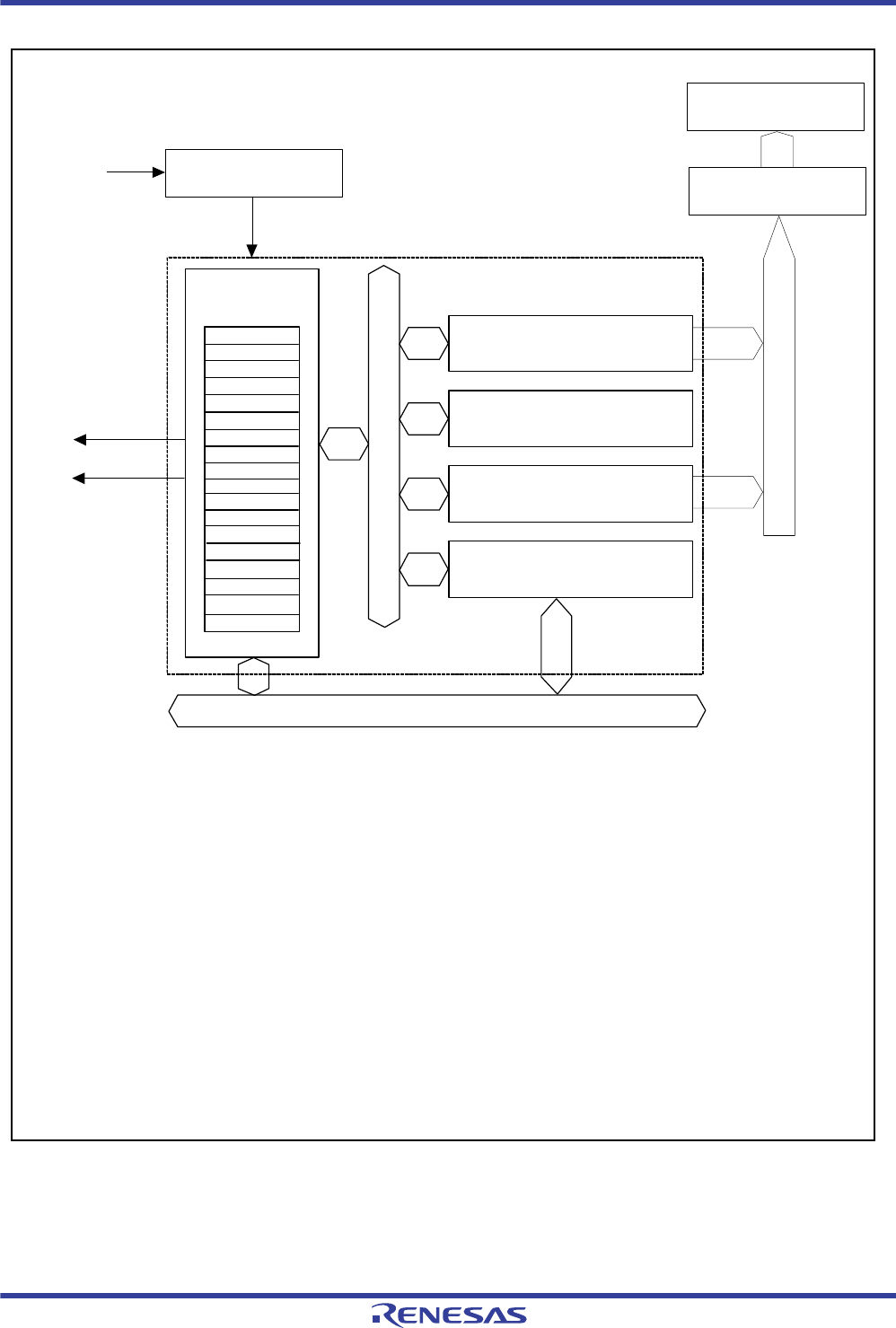
R01UH0034EJ0200 Rev.2.00 Page 1410 of 1489
Dec 27, 2013
RX62T Group, RX62G Group 32. Data Flash Memory (Flash Memory for Data Storage)
Under development Preliminary document
Specifications in this document are tentative and subject to change.
Figure 32.1 Block Diagram of Data Flash Memory
Mode decoder
Mode pins
FCU
FIFERR
[Legend]
FMODR
FASTAT
FAEINT
DFLRE0
DFLRE1
DFLWE0
DFLWE1
FCPSR
DFLBCCNT
DFLBCSTAT
PCKAR
FMODR: Flash mode register
FASTAT: Flash access status register
FAEINT: Flash access error interrupt enable register
DFLRE0: Data flash read enable register 0
DFLRE1: Data flash read enable register 1
DFLWE0: Data flash Programming/erasure enable register 0
DFLWE1: Data flash Programming/erasure enable register 1
FCURAME: FCU RAM enable register
FSTATR0: Flash status register 0
FSTATR1: Flash status register 1
FENTRYR: Flash P/E mode entry register
FRESETR: Flash reset register
FCMDR: FCU command register
FRDYIE: Flash ready interrupt enable register
FCPSR: FCU process switch register
DFLBCCNT: Data flash blank check control register
DFLBCSTAT: Data flash blank check status register
PCKAR: Peripheral clock notification register
FIFERR: Flash interface error interrupt
FRDYI: Flash ready interrupt
Peripheral bus
FCURAME
FSTATR0
FSTATR1
FENTRYR
FRESETR
FCMDR
FRDYIE
FRDYI
CPU
Memory interface
FCU RAM
ROM area unit
User area: Up to 256 Kbytes
Area to store FCU firmware: 8 Kbytes
Data flash area unit
Data area: 32 Kbytes (max.)

R01UH0034EJ0200 Rev.2.00 Page 1411 of 1489
Dec 27, 2013
RX62T Group, RX62G Group 32. Data Flash Memory (Flash Memory for Data Storage)
Under development Preliminary document
Specifications in this document are tentative and subject to change.
Input and output pins associated with the data flash are listed in Table 32.2.
32.2 Register Descriptions
Table 32.3 lists the registers related to the data flash memory. Some registers also have bits related to the ROM, but this
section deals only with the bits that are relevant to the data flash. For registers containing bits with common functions for
the ROM and data flash (FRDYIE, FCURAME, FSTATR0, FSTATR1, FRESETR, FCMDR, FCPSR, PCKAR, and
FWEPROR) and details on the functions of bits dedicated to the ROM, see section 31.2, Register Descriptions in
section of ROM (Flash Memory for Code Storage).
The registers related to the data flash are initialized by a reset.
Table 32.2 Input and Output Pins Associated with the Data Flash
Pin Name I/O Description
PD5/RxD1 Input Used in boot mode to receive data via SCI (for host communications)
PD3/TxD1 Output Used in boot mode to transmit data from SCI (for host communications)
MD1, MD0 Input Set the operating mode for the RX62T/RX62G Group
Table 32.3 Registers Related to the Data Flash
Register Name Symbol Value after Reset Address Access Size
Flash mode register FMODR 00h 007F C402h 8
Flash access status register FASTAT 00h 007F C410h 8
Flash access error interrupt enable register FAEINT 9Bh 007F C411h 8
Flash ready interrupt enable register FRDYIE 00h 007F C412h 8
Data flash read enable register 0 DFLRE0 0000h 007F C440h 16
Data flash read enable register 1 DFLRE1 0000h 007F C442h 16
Data flash programming/erasure enable register 0 DFLWE0 0000h 007F C450h 16
Data flash programming/erasure enable register 1 DFLWE1 0000h 007F C452h 16
FCU RAM enable register FCURAME 0000h 007F C454h 16
Flash status register 0 FSTATR0 80h 007F FFB0h 8
Flash status register 1 FSTATR1 00h 007F FFB1h 8
Flash P/E mode entry register FENTRYR 0000h 007F FFB2h 16
Flash reset register FRESETR 0000h 007F FFB6h 16
FCU command register FCMDR FFFFh 007F FFBAh 16
FCU processing switching register FCPSR 0000h 007F FFC8h 16
Data flash blank check control register DFLBCCNT 0000h 007F FFCAh 16
Data flash blank check status register DFLBCSTAT 0000h 007F FFCEh 16
Peripheral clock notification register PCKAR 0000h 007F FFE8h 16
Flash write erase protection register FWEPROR 02h 0008 C289h 8

R01UH0034EJ0200 Rev.2.00 Page 1412 of 1489
Dec 27, 2013
RX62T Group, RX62G Group 32. Data Flash Memory (Flash Memory for Data Storage)
Under development Preliminary document
Specifications in this document are tentative and subject to change.
32.2.1 Flash Mode Register (FMODR)
FMODR is used to specify the method for the reading of lock bits. Set the FRDMD bit to 1 if blank checking is to be
used.
In modes in which the on-chip ROM is disabled, the value read from FMODR is 00h and writing is disabled.
FMODR is initialized by a reset.
FRDMD Bit (FCU Read Mode Select)
Processing for a transition of the lock bit reading mode is used in processing for blank checking of the data flash.
The FRDMD bit is used to select the method of reading when lock bit values for the ROM are read out (see section 31,
ROM (Flash Memory for Code Storage)).
Address: 007F C402h
b7 b6 b5 b4 b3 b2 b1 b0
———
FRDM
D————
Value after reset: 00000000
Bit Symbol Bit Name Description R/W
b3 to b0 — Reserved These bits are always read as 0. The write value should always be 0. R/W
b4 FRDMD FCU Read Mode Select 0:Memory Area Reading Method
The method of lock bit reading is set. Since there are no lock bits for
the data flash, undefined data are read from the data flash area after
the FCU has been placed in lock bit read mode.
1:Register Reading Method
This is the setting when the blank checking command is to be used.
R/W
b7 to b5 — Reserved These bits are always read as 0.The write value should always be 0. R/W

R01UH0034EJ0200 Rev.2.00 Page 1413 of 1489
Dec 27, 2013
RX62T Group, RX62G Group 32. Data Flash Memory (Flash Memory for Data Storage)
Under development Preliminary document
Specifications in this document are tentative and subject to change.
32.2.2 Flash Access Status Register (FASTAT)
Note 1. Only 0 can be written after reading 1 to clear the flag.
FASTAT is a register to check if the access to the ROM/data flash is allowed.
When on-chip ROM is disabled, the data read from FASTAT is 00h and writing is disabled. When one of the bits in
FASTAT is set to 1, the FCU is placed in the command-locked state (see section 32.7.2, Error Protection). To clear the
command-locked state, a status register clearing command must be issued to the FCU after setting FASTAT to 10h.
FASTAT is initialized by a reset.
DFLWPE Bit (Data Flash Programming/Erasure Protection Violation)
This bit is used to indicate whether or not the programming/erasure protection set by DFLWEk (k = 0, 1) is violated.
[Setting condition]
A programming/erasure command is issued for a data flash area for which programming or erasure is disabled by
DFLWEk (k = 0, 1).
[Clearing condition]
When 0 is written after reading 1
DFLRPE Bit (Data Flash Read Protection Violation)
This bit is used to indicate whether or not the reading protection set by DFLREk (k = 0, 1) is violated.
[Setting condition]
A read command is issued for a data flash area for which reading is disabled by DFLREk (k = 0, 1).
[Clearing condition]
When 0 is written after reading 1
Address: 007F C410h
b7 b6 b5 b4 b3 b2 b1 b0
ROMA
E— — CMDLK DFLAE — DFLRP
EDFLWP
E
Value after reset: 00000000
Bit Symbol Bit Name Description R/W
b0 DFLWPE Data Flash
Programming/Erasure
Protection Violation
0: No data flash programming/erasure command is not issued which
conflicts with the DFLWEk settings
1: A data flash programming/erasure command is issued which
conflicts with the DFLWEk settings
(k = 0, 1)
R/(W)*1
b1 DFLRPE Data Flash
Read Protection Violation
0: There is no such data flash read that conflicts with the DFLREk
settings
1: There is such a data flash read that conflicts with the DFLREk
settings
(k = 0, 1)
R/(W)*1
b2 — Reserved This bit is always read as 0. The write value should always be 0. R/W
b3 DFLAE Data Flash Access Violation 0: No data flash access violation
1: Data flash access violation
R/(W)*1
b4 CMDLK FCU Command Lock 0: FCU is not in the command-locked state
1: FCU is in the command-locked state
R
b6, b5 — Reserved These bits are always read as 0. The write value should always be 0. R/W
b7 ROMAE ROM Access Violation See section 31, ROM (Flash Memory for Code Storage). R/(W)*1

R01UH0034EJ0200 Rev.2.00 Page 1414 of 1489
Dec 27, 2013
RX62T Group, RX62G Group 32. Data Flash Memory (Flash Memory for Data Storage)
Under development Preliminary document
Specifications in this document are tentative and subject to change.
DFLAE Bit (Data Flash Read Protection Violation)
This bit indicates whether a data flash access violation occurred.
When the DFLAE bit is set to 1, the ILGLERR bit in FSTATR0 is set to 1, placing the FCU in the command-locked state.
For FSTATR0, see section 32.2.5, Data Flash Read Enable Register 1 (DFLRE1).
[Setting conditions]
A read command is issued for a data flash area in data flash P/E normal mode and when the FENTRYD bit in
FENTRYR is set to 1.
A write command is issued for a data flash area when the FENTRYD bit is set to 0.
A command is issued for a data flash area when the FENTRY0 bit in FENTRYR is set to 1.
[Clearing condition]
When 0 is written after reading 1
CMDLK Bit (FCU Command-Locked)
This command indicates that the FCU is in the command-locked state (see section 32.7.2, Error Protection).
[Setting condition]
After the FCU detects an error and enters the command-locked state
[Clearing condition]
After the FCU has processed a status register clearing command

R01UH0034EJ0200 Rev.2.00 Page 1415 of 1489
Dec 27, 2013
RX62T Group, RX62G Group 32. Data Flash Memory (Flash Memory for Data Storage)
Under development Preliminary document
Specifications in this document are tentative and subject to change.
32.2.3 Flash Access Error Interrupt Enable Register (FAEINT)
FAEINT is a register to enable and disable a flash interface error interrupt (FIFERR).
When on-chip ROM is disabled, the data read from FAEINT is 00h and writing is disabled.
FAEINT is initialized by a reset.
DFLWPEIE Bit (Data Flash Programming/Erasure Protection Violation Interrupt Enable)
This bit is used to enable or disable FIFERR interrupt requests when a data flash programming/erasure protection
violation occurs and the DFLWPE bit in FASTAT is set to 1.
DFLRPEIE Bit (Data Flash Read Protection Violation Interrupt Enable)
This bit is used to enable or disable FIFERR interrupt requests when a data flash read protection violation occurs and the
DFLRPE bit in FASTAT is set to 1.
DFLAEIE Bit (Data Flash Read Protection Violation Interrupt Enable)
This bit is used to enable or disable FIFERR interrupt requests when a data flash access violation occurs and the DFLAE
bit in FASTAT is set to 1.
CMDLKIE Bit (FCU Command Lock Interrupt Enable)
This bit is used to enable or disable FIFERR interrupt requests when a FCU command-locked state occurs and the
CMDLK bit in FASTAT is set to 1.
Address: 007F C411h
b7 b6 b5 b4 b3 b2 b1 b0
ROMA
EIE ——
CMDLK
IE DFLAEI
E—DFLRP
EIE DFLWP
EIE
Value after reset: 10011011
Bit Symbol Bit Name Description R/W
b0 DFLWPEIE Data Flash Programming/Erasure
Protection Violation Interrupt Enable
0: FIFERR interrupt requests disabled when the DFLWPE bit
in FASTAT is set to 1
1: FIFERR interrupt requests enabled when the DFLWPE bit
in FASTAT is set to 1
R/W
b1 DFLRPEIE Data Flash Read Protection Violation
Interrupt Enable
0: FIFERR interrupt requests disabled when the DFLRPE bit
in FASTAT is set to 1
1: FIFERR interrupt requests enabled when the DFLRPE bit
in FASTAT is set to 1
R/W
b2 — Reserved This bit is always read as 0. The write value should always
be 0.
R/W
b3 DFLAEIE Data Flash Read Access Violation
Interrupt Enable
0: FIFERR interrupt requests disabled when the DFLAE bit in
FASTAT is set to 1
1: FIFERR interrupt requests enabled when the DFLAE bit in
FASTAT is set to 1
R/W
b4 CMDLKIE FCU Command Lock Interrupt Enable 0: FIFERR interrupt requests disabled when the CMDLK bit
in FASTAT is set to 1
1: FIFERR interrupt requests enabled when the CMDLK bit in
FASTAT is set to 1
R/W
b6, b5 — Reserved These bits are always read as 0. The write value should
always be 0.
R/W
b7 ROMAEIE ROM Access Violation Interrupt Enable See section 31, ROM (Flash Memory for Code Storage). R/W

R01UH0034EJ0200 Rev.2.00 Page 1416 of 1489
Dec 27, 2013
RX62T Group, RX62G Group 32. Data Flash Memory (Flash Memory for Data Storage)
Under development Preliminary document
Specifications in this document are tentative and subject to change.
32.2.4 Data Flash Read Enable Register 0 (DFLRE0)
Note 1. Bits 7 to 4 are reserved in R5F562T7xxxx or R5F562T6xxxx. These bits are always read as 0. The write value should always be
0.
Note 2. Write data is not retained.
DFLRE0 is a register to enable or disable the DB00 to DB07 blocks of the data area (see Figure 32.3) to be read.
Only specific values written to the upper byte in word access are valid. Data written to the upper byte is not retained.
When on-chip ROM is disabled, the data read from DFLRE0 is 0000h and writing is disabled.
DFLRE0 is initialized by a reset.
DBREi Bit (DBi Block Read Enable) (i = 07 to 00)
This bit is used to enable or disable the DB00 to DB07 blocks of the data area to be read.
The DBREi bit is used to control reading of the DBi blocks.
Writing to the DBREi is enabled only in word access when the KEY[7:0] bits are 2Dh.
KEY[7:0] Bits (Key Code)
These bits are used to enable or disable rewriting of the DBREi bit.
Data written to the KEY[7:0] bits is not retained.
Address: 007F C440h
b15 b14 b13 b12 b11 b10 b9 b8 b7 b6 b5 b4 b3 b2 b1 b0
KEY[7:0] DBRE0
7DBRE0
6DBRE0
5DBRE0
4DBRE0
3DBRE0
2DBRE0
1DBRE0
0
Value after reset: 0000000000000000
Bit Symbol Bit Name Description R/W
b0 DBRE00 DB00 Block Read Enable 0: Read disabled
1: Read enabled
R/W
b1 DBRE01 DB01 Block Read Enable R/W
b2 DBRE02 DB02 Block Read Enable R/W
b3 DBRE03 DB03 Block Read Enable R/W
b4 DBRE04*1 DB04 Block Read Enable R/W
b5 DBRE05*1 DB05 Block Read Enable R/W
b6 DBRE06*1 DB06 Block Read Enable R/W
b7 DBRE07*1 DB07 Block Read Enable R/W
b15 to b8 KEY[7:0] Key Code Enable or disable rewriting of the DBREi bit (i = 07 to 00). R/(W)*2

R01UH0034EJ0200 Rev.2.00 Page 1417 of 1489
Dec 27, 2013
RX62T Group, RX62G Group 32. Data Flash Memory (Flash Memory for Data Storage)
Under development Preliminary document
Specifications in this document are tentative and subject to change.
32.2.5 Data Flash Read Enable Register 1 (DFLRE1)
Note 1. Bits 7 to 0 are reserved in R5F562T7xxxx or R5F562T6xxxx. These bits are always read as 0. The write value should always be
0.
Note 2. Write data is not retained.
DFLRE1 is a register to enable or disable the DB15 to DB08 blocks of the data area (see Figure 32.3) to be read.
Only specific values written to the upper byte in word access are valid. Data written to the upper byte is not retained.
When on-chip ROM is disabled, the data read from DFLRE1 is 0000h and writing is disabled.
DFLRE1 is initialized by a reset.
DBREi Bit (DBi Block Read Enable) (i = 15 to 08)
This bit is used to enable or disable the DB15 to DB08 blocks of the data area to be read.
The DBREi bit is used to control reading of the DBi blocks.
Writing to the DBREi is enabled only in word access when the KEY[7:0] bits are D2h.
KEY[7:0] Bits (Key Code)
These bits are used to enable or disable rewriting of the DBREi bit.
Data written to the KEY[7:0] bits is not retained.
Address: 007F C442h
b15 b14 b13 b12 b11 b10 b9 b8 b7 b6 b5 b4 b3 b2 b1 b0
KEY[7:0] DBRE1
5DBRE1
4DBRE1
3DBRE1
2DBRE1
1DBRE1
0DBRE0
9DBRE0
8
Value after reset: 0000000000000000
Bit Symbol Bit Name Description R/W
b0 DBRE08*1 DB8 Block Read Enable 0: Read disabled
1: Read enabled
R/W
b1 DBRE09*1 DB9 Block Read Enable R/W
b2 DBRE10*1 DB10 Block Read Enable R/W
b3 DBRE11*1 DB11 Block Read Enable R/W
b4 DBRE12*1 DB12 Block Read Enable R/W
b5 DBRE13*1 DB13 Block Read Enable R/W
b6 DBRE14*1 DB14 Block Read Enable R/W
b7 DBRE15*1 DB15 Block Read Enable R/W
b15 to b8 KEY[7:0] Key Code Enable or disable rewriting of the DBREi bit (i = 15 to 8). R/(W)
*2

R01UH0034EJ0200 Rev.2.00 Page 1418 of 1489
Dec 27, 2013
RX62T Group, RX62G Group 32. Data Flash Memory (Flash Memory for Data Storage)
Under development Preliminary document
Specifications in this document are tentative and subject to change.
32.2.6 Data Flash Programming/Erasure Enable Register 0 (DFLWE0)
Note 1. Bits 7 to 4 are reserved in R5F562T7xxxx or R5F562T6xxxx. These bits are always read as 0. The write value should always be
0.
Note 2. Write data is not retained.
DFLWE0 is a register to enable or disable the DB00 to DB07 blocks of the data area (see Figure 32.3) to be
programmed or erased.
Only specific values written to the upper byte in word access are valid. Data written to the upper byte is not retained.
When on-chip ROM is disabled, the data read from DFLWE0 is 0000h and writing is disabled.
DFLWE0 is initialized by a reset.
DBWEi Bit (DBi Block Programming/Erasure Enable) (i = 07 to 00)
This bit is used to enable or disable the DB07 to DB00 blocks of the data area to be programmed or erased.
The DBWEi bit is used to control programming/erasure of the DBi blocks.
Programming of the DBWEi bit is enabled only in word access when the KEY[7:0] bits are 1Eh.
KEY[7:0] Bits (Key Code)
These bits are used to enable or disable rewriting of the DBWEi bit.
Data written to the KEY[7:0] bits is not retained.
Address: 007F C450h
b15 b14 b13 b12 b11 b10 b9 b8 b7 b6 b5 b4 b3 b2 b1 b0
KEY[7:0] DBWE0
7DBWE0
6DBWE0
5DBWE0
4DBWE0
3DBWE0
2DBWE0
1DBWE0
0
Value after reset: 0000000000000000
Bit Symbol Bit Name Description R/W
b0 DBWE00 DB00 Block Programming/Erasure Enable 0: Programming/erasure disabled
1: Programming/erasure enabled
R/W
b1 DBWE01 DB01 Block Programming/Erasure Enable R/W
b2 DBWE02 DB02 Block Programming/Erasure Enable R/W
b3 DBWE03 DB03 Block Programming/Erasure Enable R/W
b4 DBWE04*1 DB04 Block Programming/Erasure Enable R/W
b5 DBWE05*1 DB05 Block Programming/Erasure Enable R/W
b6 DBWE06*1 DB06 Block Programming/Erasure Enable R/W
b7 DBWE07*1 DB07 Block Programming/Erasure Enable R/W
b15 to b8 KEY[7:0] Key Code Enable or disable rewriting of the DBWEi bit (i = 07 to
00).
R/(W)
*2

R01UH0034EJ0200 Rev.2.00 Page 1419 of 1489
Dec 27, 2013
RX62T Group, RX62G Group 32. Data Flash Memory (Flash Memory for Data Storage)
Under development Preliminary document
Specifications in this document are tentative and subject to change.
32.2.7 Data Flash Programming/Erasure Enable Register 1 (DFLWE1)
Note 1. Bits 7 to 0 are reserved in R5F562T7xxxx or R5F562T6xxxx. These bits are always read as 0. The write value should always be
0.
Note 2. Write data is not retained.
DFLWE1 is a register to enable or disable the DB15 to DB08 blocks of the data area (see Figure 32.3) to be
programmed or erased.
Only specific values written to the upper byte in word access are valid. Data written to the upper byte is not retained.
When on-chip ROM is disabled, the data read from DFLWE1 is 0000h and writing is disabled.
DFLWE1 is initialized by a reset.
DBWEi Bit (DBi Block Programming/Erasure Enable) (i = 15 to 08)
This bit is used to enable or disable the DB15 to DB08 blocks of the data area to be programmed or erased.
The DBWEi bit is used to control programming/erasure of the DBi blocks.
Programming of the DBWEi bit is enabled only in word access when the KEY[7:0] bits are E1h.
KEY[7:0] Bits (Key Code)
These bits are used to enable or disable rewriting of the DBWEi bit.
Data written to the KEY[7:0] bits is not retained.
Address: 007F C452h
b15 b14 b13 b12 b11 b10 b9 b8 b7 b6 b5 b4 b3 b2 b1 b0
KEY[7:0] DBWE1
5DBWE1
4DBWE1
3DBWE1
2DBWE1
1DBWE1
0DBWE0
9DBWE0
8
Value after reset: 0000000000000000
Bit Symbol Bit Name Description R/W
b0 DBWE08*1 DB08 Block Programming/Erasure Enable 0: Programming/erasure disabled
1: Programming/erasure enabled
R/W
b1 DBWE09*1 DB09 Block Programming/Erasure Enable R/W
b2 DBWE10*1 DB10 Block Programming/Erasure Enable R/W
b3 DBWE11*1 DB11 Block Programming/Erasure Enable R/W
b4 DBWE12*1 DB12 Block Programming/Erasure Enable R/W
b5 DBWE13*1 DB13 Block Programming/Erasure Enable R/W
b6 DBWE14*1 DB14 Block Programming/Erasure Enable R/W
b7 DBWE15*1 DB15 Block Programming/Erasure Enable R/W
b15 to b8 KEY[7:0] Key Code Enable or disable rewriting of the DBWEi bit (i = 15 to 8). R/(W)
*2

R01UH0034EJ0200 Rev.2.00 Page 1420 of 1489
Dec 27, 2013
RX62T Group, RX62G Group 32. Data Flash Memory (Flash Memory for Data Storage)
Under development Preliminary document
Specifications in this document are tentative and subject to change.
32.2.8 Flash P/E Mode Entry Register (FENTRYR)
Note 1. Write data is not retained.
FENTRYR is a register to place the ROM/data flash in P/E mode.
To place ROM/data flash in P/E mode and accept commands from the FCU, either the FENTRYD or FENTRY0 bit must
be set to 1. If more than one bit is set to 1, the ILGLERR bit is set in FSTATR0 and the FCU enters the command-locked
state.
Only specific values written to the upper byte in word access are valid. Any other writing causes the register to be
initialized. Data written to the upper byte is not retained.
When on-chip ROM is disabled, the data read from FENTRYR is 0000h and writing is disabled.
FENTRYR is initialized by a reset, or when the FRESET bit in FRESETR is set to 1.
For FSTATR0, see section 31.2.5, Flash Status Register 0 (FSTATR0).
For FRESETR, see section 31.2.10, Flash Reset Register (FRESETR).
FENTRYD Bit (Data Flash P/E Mode Entry)
The FENTRYD bit is used to place the data flash in P/E mode.
[Writing-enable conditions (when all of the following conditions are met)]
On-chip ROM is enabled.
The FRDY bit in FSTATR0 is set to 1
AAh is written to the FEKEY[7:0] bits in word access.
[Setting condition]
When the writing-enable conditions are met, FENTRYR is set to 0000h, and 1 is written to the FENTRYD bit
[Clearing conditions]
Data is written in byte access.
Data is written in word access when the FEKEY[7:0] bits are other than AAh.
When the writing-enable conditions are met, 0 is written to the FENTRYD bit.
When the writing-enable conditions are met and FENTRYR is other than 0000h, data is written to FENTRYR.
FEKEY[7:0] Bits (Key Code)
These bits enable or disable rewriting of the FENTRYD and FENTRY0 bits.
Data written to the FEKEY[7:0] bits is not retained.
Address: 007F FFB2h
b15 b14 b13 b12 b11 b10 b9 b8 b7 b6 b5 b4 b3 b2 b1 b0
FEKEY[7:0] FENTR
YD ——————
FENTR
Y0
Value after reset: 0000000000000000
Bit Symbol Bit Name Description R/W
b0 FENTRY0 ROM P/E Mode Entry 0 See section 31, ROM (Flash Memory for Code Storage). R/W
b6 to b1 — Reserved These bits are always read as 0. The write value should always be
0.
R/W
b7 FENTRYD Data Flash P/E Mode Entry 0: Data flash is in read mode
1: Data flash is in P/E mode
R/W
b15 to b8 FEKEY[7:0] Key Code Enable or disable rewriting of the FENTRYD and FENTRY0 bits. R/(W)*1

R01UH0034EJ0200 Rev.2.00 Page 1421 of 1489
Dec 27, 2013
RX62T Group, RX62G Group 32. Data Flash Memory (Flash Memory for Data Storage)
Under development Preliminary document
Specifications in this document are tentative and subject to change.
32.2.9 Data Flash Blank Check Control Register (DFLBCCNT)
DFLBCCNT is a register for specifying the address and size of the area to be checked by a blank check command.
When on-chip ROM is disabled, the data read from DFLBCCNT is 0000h and writing is disabled.
DFLBCCNT is initialized by a reset, or when the FRESET bit in FRESETR is set to 1.
For FRESETR, see section 31.2.10, Flash Reset Register (FRESETR).
BCSIZE Bit (Blank Check Size Setting)
The BCSIZE bit is used to set the size of the area to be checked by a blank check command.
BCADR[7:0] Bits (Blank Check Address Setting)
When the size of the area to be checked by a blank check command is 8 bytes (the BCSIZE bit is set to 0), this bit is used
to set the address of the area to be checked.
When the BCSIZE bit is set to 0, the setting of DFLBCCNT (the setting of the BCADR[7:0] bits shifted three bits in the
MSB direction) added with the erased block start address specified when issuing a blank check command is the start
address of the area to be checked.
Address: 007F FFCAh
b15 b14 b13 b12 b11 b10 b9 b8 b7 b6 b5 b4 b3 b2 b1 b0
————— BCADR[7:0] ——
BCSIZ
E
Value after reset: 0000000000000000
Bit Symbol Bit Name Description R/W
b0 BCSIZE Blank Check Size Setting 0: The size of the area to be blank-checked is 8 bytes.
1: The size of the area to be blank-checked is 2 Kbytes.
R/W
b2, b1 — Reserved These bits are always read as 0. The write value should always
be 0.
R/W
b10 to b3 BCADR[7:0] Blank Check Address Setting Set the address of the area to be checked R/W
b15 to b11 — Reserved These bits are always read as 0. The write value should always
be 0.
R/W

R01UH0034EJ0200 Rev.2.00 Page 1422 of 1489
Dec 27, 2013
RX62T Group, RX62G Group 32. Data Flash Memory (Flash Memory for Data Storage)
Under development Preliminary document
Specifications in this document are tentative and subject to change.
32.2.10 Data Flash Blank Check Status Register (DFLBCSTAT)
DFLBCSTAT is a register which stores the results of a blank check command.
When on-chip ROM is disabled, the data read from DFLBCSTAT is 0000h and writing is disabled.
DFLBCSTAT is initialized by a reset, or when the FRESET bit in FRESETR is set to 1.
For FRESETR, see section 31.2.10, Flash Reset Register (FRESETR).
BCST Bit (Blank Check Status)
This bit is used to indicate the results of blank checking.
Address: 007F FFCEh
b15 b14 b13 b12 b11 b10 b9 b8 b7 b6 b5 b4 b3 b2 b1 b0
———————————————BCST
Value after reset: 0000000000000000
Bit Symbol Bit Name Description R/W
b0 BCST Blank Check Status 0: The area to be blank-checked is erased (blank)
1: 0 or 1 is written in the area to be blank-checked
R
b15 to b1 — Reserved These bits are always read as 0. The write value should always be 0. R/W

R01UH0034EJ0200 Rev.2.00 Page 1423 of 1489
Dec 27, 2013
RX62T Group, RX62G Group 32. Data Flash Memory (Flash Memory for Data Storage)
Under development Preliminary document
Specifications in this document are tentative and subject to change.
32.3 Configuration of Memory Area for the Data Flash Memory
The data flash memory of products in the RX62T and RX62G Groups is configured as an 8-Kbyte data area. The address
range occupied by this area is shown in Figure 32.2.
Note that for the data area, the address range for reading is the same as the address range for programming and erasure.
Figure 32.2 Configuration of the Data Area
32.4 Block Configuration
Figure 32.3 shows how the erasure blocks of the data area are configured. The data area is divided into four 2-Kbyte
blocks, and erasure proceeds in these block units. Programming proceeds in 8- or 128-byte units. For programming in 8-
byte units, each unit starts at an address where the value of the three lower-order bits is 0. For programming in 128-byte
units, each unit starts at an address where the value of the lower-order bits is 00h or 80h.
Figure 32.3 Division of the Data Area into Blocks
Address 0010 0000h
Address 0010 7FFFh
Data area
(32 Kbytes)
R5F562TAxxxx
R5F562T7xxxx
R5F562T6xxxx
Address 0010 1FFFh
Data area
(8 Kbytes)
Address 0010 0000h
Address 0010 7FFFh
2 Kbytes ×
16 blocks
Address 0010 1FFFh
2 Kbytes × 4
blocks DB00 to DB03
DB04 to DB15
R5F562TAxxxx
R5F562T7xxxx
R5F562T6xxxx
Data area Blocks

R01UH0034EJ0200 Rev.2.00 Page 1424 of 1489
Dec 27, 2013
RX62T Group, RX62G Group 32. Data Flash Memory (Flash Memory for Data Storage)
Under development Preliminary document
Specifications in this document are tentative and subject to change.
32.5 Operating Modes Associated with the Data Flash
For the transitions between operating modes, see section 31.5, Operating Modes Associated with the ROM.
Reading, programming, and erasing of the data flash memory in an on-board device can proceed if the device is in boot
mode or single-chip mode (with on-chip ROM enabled).
The differences between modes are indicated in Table 32.4.
Note 1. All flash memory areas may be erased at the time of booting up. Specified blocks can subsequently be erased. For details, refer
to section 31.9.2, ID Code Protection in Boot Mode.
Note 2. Not available to users.
In boot mode, a host is able to program or read out the data area via an SCI.
In boot mode, on-chip RAM is employed for the embedded program for use in boot mode. For this reason,
preserving the contents of on-chip RAM is not possible in this case.
Table 32.4 Differences between Modes
Item Boot Mode Single-Chip Mode (with On-chip ROM Enabled)
Environment for programming and
erasure
On-board programming On-board programming
Programmable and erasable area Data area Data area
Division into erasure blocks Possible*1 Possible
Target area for booting after a reset Area containing the embedded program*2 User area
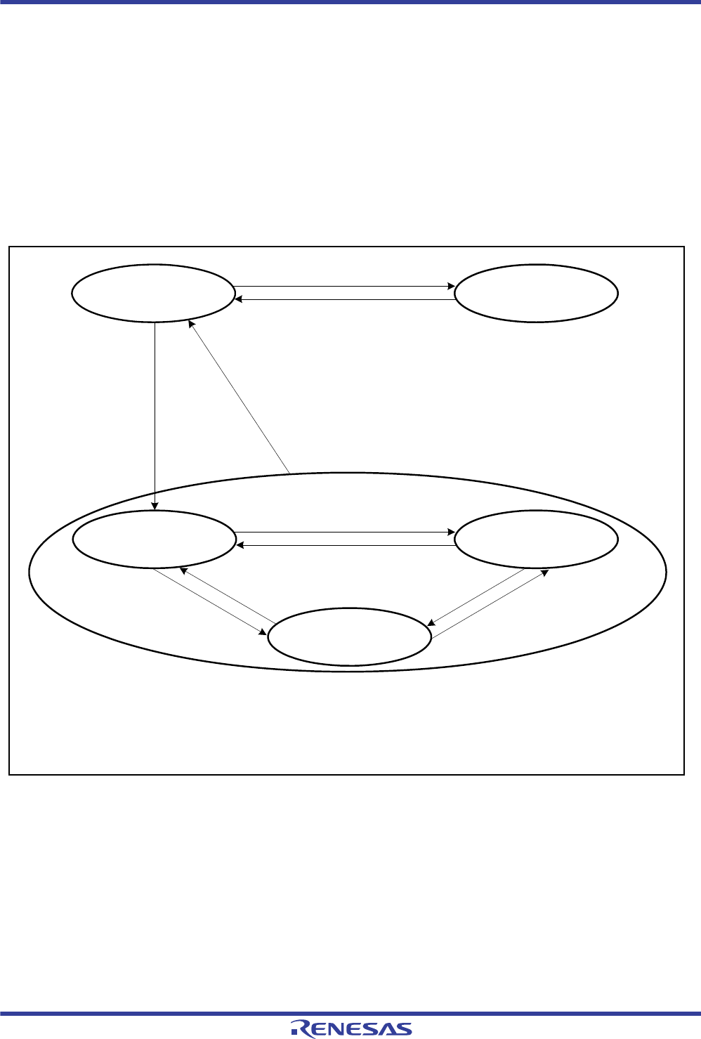
R01UH0034EJ0200 Rev.2.00 Page 1425 of 1489
Dec 27, 2013
RX62T Group, RX62G Group 32. Data Flash Memory (Flash Memory for Data Storage)
Under development Preliminary document
Specifications in this document are tentative and subject to change.
32.6 Programming and Erasing the Data Flash Memory
The data flash memory is programmed and erased by issuing commands to a dedicated sequencer (FCU) for
programming and erasure. The FCU has five modes. For programming and erasure, the mode is changed and then
commands for programming and erasure are issued.
The mode transitions required to program or erase the data flash and the system of commands are described below. The
descriptions apply in common to boot mode and single-chip mode (with on-chip ROM enabled).
32.6.1 FCU Modes
The FCU has five modes or sets of modes. Transitions between modes are caused by writing to the FENTRYR register or
issuing FCU commands. Figure 32.4 is a diagram of the FCU mode transitions.
Figure 32.4 Mode Transitions of the FCU (Associated with the Data Flash)
Data flash P/E mode
Data flash status read
mode
(B)
(A)
Data flash P/E
normal mode
Data flash lock bit read
mode
(C)
(B)
(A)
(C)
ROM P/E modeROM/data flash read mode
FENTRYR = 0001h
FENTRYR = 0000h
FENTRYR = 0000h
FENTRYR = 0080h
(A): Execute a normal mode transition command.
(B): Execute a command that is neither a normal mode transition command nor a lock bit read mode transition
command.
(C): Execute a lock bit read mode transition command.
[Legend]

R01UH0034EJ0200 Rev.2.00 Page 1426 of 1489
Dec 27, 2013
RX62T Group, RX62G Group 32. Data Flash Memory (Flash Memory for Data Storage)
Under development Preliminary document
Specifications in this document are tentative and subject to change.
32.6.1.1 ROM P/E Modes
The ROM P/E modes are for programming and erasure of the ROM.
For details on the ROM P/E modes, see section 31.6.1.2, ROM P/E Modes.
32.6.1.2 ROM/Data Flash Read Mode
This mode is for reading the ROM or data flash memory. The FCU does not accept commands.
The FCU enters this mode when both the FENTRYD bit and FENTRY0 bit in FENTRYR are set to 0.
32.6.1.3 Data Flash P/E Modes
These modes are for programming and erasure of the data flash memory. Reading out the data flash is not possible.
Data flash P/E normal mode, data flash status read mode, and data flash lock-bit read mode are the three data flash P/E
modes.
(1) Data Flash P/E Normal Mode
The transition to data flash P/E normal mode is the first transition in the process of programming or erasing the data
flash. The FCU enters this mode when the FENTRYD bit in FENTRYR is set to 1 and the FENTRY0 bit in FENTRYR is
set to 0 in ROM/data flash read mode, or when the normal mode transition command is received in data flash P/E modes.
Table 32.7 lists the acceptable commands in this mode.
Read access to an address within the data flash area causes a data-flash-access violation, and the FCU enters the
command-locked state. High-speed reading of the ROM is possible.
(2) Data Flash Status Read Mode
The data flash status read mode is for reading information on the state of the data flash.
The FCU enters this mode when a command other than the normal mode transition and lock bit read mode transition
command is received in data flash P/E modes. Data flash status read mode encompasses the states where the FRDY bit in
FSTATR0 is 0 and the command-locked state after an error has occurred. Table 32.7 lists the acceptable commands in
this mode.
Read access to an address within the data flash area will actually read out the value of the FSTATR0 register. High-speed
reading of the ROM is possible.
(3) Data Flash Lock-Bit Read Mode
The data flash lock-bit read mode is for reading the values of the lock bits of the data flash. However, this is not possible
because the data flash does not have lock bits.
The FCU enters this mode when a lock-bit read mode transition command is received in data flash P/E modes. Table
32.7 lists the acceptable commands in this mode.
Since the data flash does not have lock bits, data read out in read access to addresses within the data flash area are
undefined. However, the access does not lead to a data-flash-access violation. High-speed reading of the ROM is
possible.

R01UH0034EJ0200 Rev.2.00 Page 1427 of 1489
Dec 27, 2013
RX62T Group, RX62G Group 32. Data Flash Memory (Flash Memory for Data Storage)
Under development Preliminary document
Specifications in this document are tentative and subject to change.
32.6.2 FCU Commands
FCU commands consist of commands for mode transitions of the FCU and of commands for programming and erasure.
Table 32.5 lists the FCU commands for use with the data flash.
Commands other than the blank-checking command are also for use with the ROM.
The blank-checking command for the data flash memory is also used as the lock bit read 2 command for the ROM. That
is, when the same command is issued for the ROM, a lock bit of the ROM is read out.
Commands for the FCU are issued by write access to addresses within the data flash area.
Table 32.6 shows the formats of the programming commands and the blank checking command. For the formats of FCU
commands other than programming and blank checking commands, see section 31.6.2, FCU Commands in section
31, ROM (Flash Memory for Code Storage)).
Write access as listed in Table 32.6 and in accord with certain conditions causes the FCU to execute processing for the
corresponding command. For details on the conditions for acceptance of the individual FCU commands, see section
32.6.3, Connections between FCU Modes and Commands. For how to use the FCU commands, see section
32.6.4, FCU Command Usage.
Table 32.5 FCU Commands for Use with Data Flash Memory
Command Description
P/E Normal mode transition Changes the mode to normal mode (see section 32.6.3, Connections between FCU
Modes and Commands)
Status read mode transition Changes the mode to status read mode (seesection 32.6.3, Connections between
FCU Modes and Commands)
Lock bit read mode transition
(lock bit read 1)
Changes the mode to lock bit read mode (see section 32.6.3, Connections between
FCU Modes and Commands)
Peripheral clock notification Sets the frequency of the peripheral clock
Programming Data flash programming (in 8-byte or 128-byte units)
Block erasure Data flash erasure (in block units, with the lock bit being erased simultaneously)
P/E suspension Suspends programming/erasure
P/E resumption Resumes programming/erasure
Status register clearing Clears the ILGLERR, ERSERR and PRGERR bits in FSTATR0 and releases the FCU
from the command-locked state
Lock bit read 2/blank checking Checks whether the specified block of data flash memory has been erased (is blank)

R01UH0034EJ0200 Rev.2.00 Page 1428 of 1489
Dec 27, 2013
RX62T Group, RX62G Group 32. Data Flash Memory (Flash Memory for Data Storage)
Under development Preliminary document
Specifications in this document are tentative and subject to change.
Address column EA: Address within the data flash area. Any address in the range from 0010 0000h to 0010 1FFFh.
WA: Start address in 8-byte or 128-byte.
BA: Address in an erasure block of the data flash. Any address within the target erasure block.
Data columns WDn: nth word of data for programming (n = 1 to N)
Table 32.6 FCU Command Formats
Command
Number of bus cycles
First
Cycle Second
Cycle Third
Cycle 4th to (N+2)th
Cycles (N+3)th
Cycles
Address
Data
Address
Data
Address
Data
Address
Data
Address
Data
Programming
(8-byte programming;
n = 4)
7 EA E8h EA 04h WA WDn EA WDn EA D0h
Programming
(128-byte
programming; n = 64)
67 EA E8h EA 40h WA WDn EA WDn EA D0h
Blank checking 2 EA 71h BA D0h — — — — — —
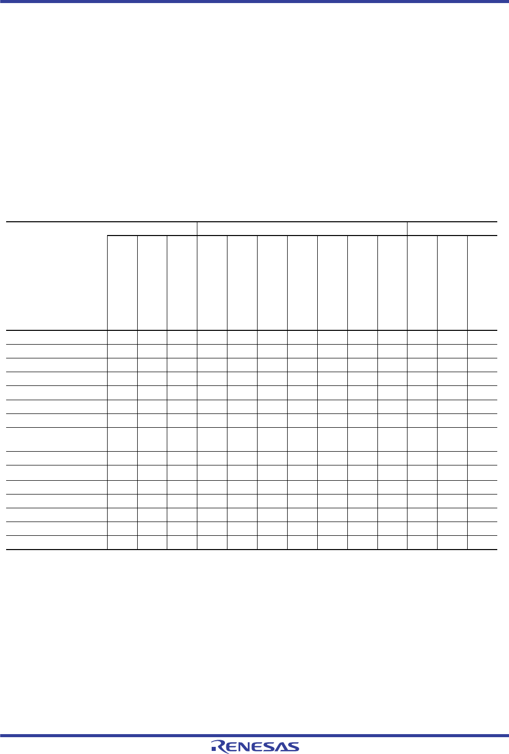
R01UH0034EJ0200 Rev.2.00 Page 1429 of 1489
Dec 27, 2013
RX62T Group, RX62G Group 32. Data Flash Memory (Flash Memory for Data Storage)
Under development Preliminary document
Specifications in this document are tentative and subject to change.
32.6.3 Connections between FCU Modes and Commands
The sets of FCU commands that can be accepted in each of the FCU modes are fixed. Furthermore, which commands are
acceptable in a given FCU mode varies according to the state of the FCU.
Issuing of an FCU command must follow checking of the FCU's state after transitions of the FCU mode.
Commands that are acceptable in the various FCU modes and states are listed in Table 32.7. Issuing a command that is
not currently acceptable leads to the FCU being placed in the command-locked state (see section 32.7.2, Error
Protection).
Issuing of an FCU command must follow checking of the values of the FRDY, ILGLERR, ERSERR, and PRGERR bits
in FSTATR0 and of the FCUERR bit in FSTATR1 after transitions of the FCU mode. Furthermore, the CMDLK bit in
FASTAT can be checked to see if an error has occurred. The value of the CMDLK bit in FASTAT is the logical OR of the
ILGLERR, ERSERR, and PRGERR bits in FSTATR0 and the FCUERR bit in FSTATR1.
A: Acceptable
*: Only programming is acceptable for blocks other than the block where erasure was suspended
X: Not acceptable
Table 32.7 Acceptable Commands and the State and Mode (Data Flash P/E Mode) of the FCU
Command P/E Normal Mode Status read mode Lock-bit read mode
Programming suspended
Erasure suspended
Other state
Programming or erasure
Processing to suspend
programming or erasure
Blank checking
Programming suspended
Erasure suspended
Command-locked state
Other state
Programming suspended
Erasure suspended
Other state
FSTATR0.FRDY bit 111000110/11111
FSTATR0.SUSRDY bit 0001000000000
FSTATR0.ERSSPD bit 01000/100100010
FSTATR0.PRGSPD bit 10000/101000100
FASTAT.CMDLK bit 0000000010000
P/E Normal mode transition A A A X X X A A X A A A A
Status read transition A A A X X X A A X A A A A
Lock-bit read transition
(lock bit read 1)
AAAXXXAAXAAAA
Peripheral clock setting XXAXXXXXXAXXA
Programming X *AXXXX*XAX*A
Block erasure XXAXXXXXXAXXA
P/E suspension XXXAXXXXXXXXX
P/E resumption AAXXXXAAXXAAX
Status register clearing AAAXXXAAAAAAA
Blank checking AAAXXXAAXAAAA

R01UH0034EJ0200 Rev.2.00 Page 1430 of 1489
Dec 27, 2013
RX62T Group, RX62G Group 32. Data Flash Memory (Flash Memory for Data Storage)
Under development Preliminary document
Specifications in this document are tentative and subject to change.
32.6.4 FCU Command Usage
This section shows how to program and erase the data flash memory by using programming and block erasure
commands, respectively, and how to check the state of erasure of the data flash by using the blank check command. For
the method for transferring the firmware to the FCU RAM and the ways to use other FCU commands, see section
31.6.4, FCU Command Usage in section 31, ROM (Flash Memory for Code Storage).
(1) Using the Peripheral Clock Notification Command
This command handles notification of the frequency of the peripheral clock. For details, see section 31.6.4, FCU
Command Usage in section 31, ROM (Flash Memory for Code Storage). Set the FENTRYD bit in FENTRYR to 1
and make settings to indicate an address within the data flash area.
(2) Programming
To program the data flash, use one of the programming commands.
Use byte access to write E8h to an address within the data flash area in the first cycle of the programming command, and
the number of words (N)*1 to be programmed in the second cycle. Access the peripheral bus in words from the third
cycle to cycle N + 2 of the command. In the third cycle, write the first word of data for programming to the address
where the target area for programming starts. This address must be on an 8-byte boundary for 8-byte programming or on
a 128-byte boundary address for 128-byte programming. After writing words to addresses in the data flash area N times,
write byte D0h to an address within the data flash area in cycle N + 3; the FCU will then start actual programming of the
data flash. Read the FRDY bit in FSTATR0 to confirm the completion of data flash programming.
If the area accessed in the third cycle to cycle N + 2 includes addresses that do not require programming, write FFFFh as
the programming data for those addresses. To ignore the programming and erasure protection provided by the DFLWEk
(k = 0, 1) setting, set the program/erase enable bit for the target block to 1 before programming starts.
Figure 32.5 shows the procedure for data flash programming.
Note 1. N = 04h for 8-byte programming or N = 40h for 128-byte programming.
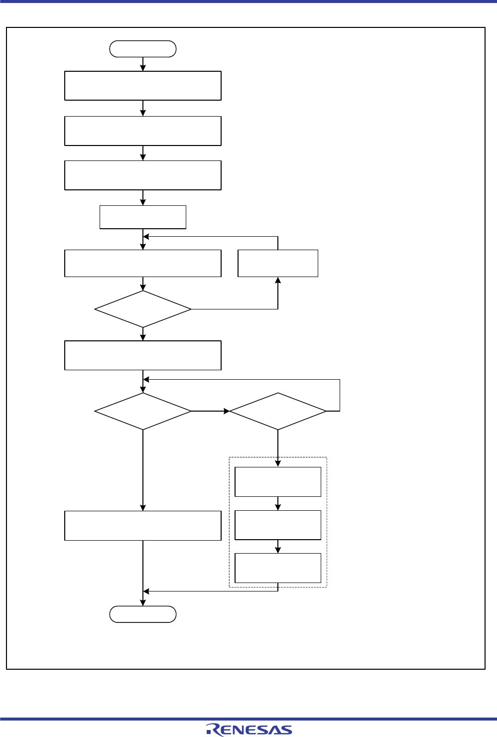
R01UH0034EJ0200 Rev.2.00 Page 1431 of 1489
Dec 27, 2013
RX62T Group, RX62G Group 32. Data Flash Memory (Flash Memory for Data Storage)
Under development Preliminary document
Specifications in this document are tentative and subject to change.
Figure 32.5 Procedure for Data Flash Programming
Write byte E8h to a data flash area address
Write the number of programming
words (N) to a data flash area address
through byte access
Write a programming data word to the
start address of the programming area
n = 1
Write a programming data word
to a data flash area
n = N - 1
Write byte D0h to a data flash area address
Timeout
(tDP128 1.1)*
FCU initialization
Check the ILGLERR and PRGERR bits
Note: * tDP128: Time required for programming 128-byte data (see section 33, Electrical Characteristics)
tRESW2: Reset pulse width during programming/erasure (see section 33, Electrical Characteristics)
No
Yes
No
Yes
0
1
Start
End
8-byte programming: N = 04h
128-byte programming: N = 40h
FRDY bit check
FRESETR.FRESET = 1
writing
FRESETR.FRESET = 0
writing
Wait
(tRESW2)*
n = n + 1

R01UH0034EJ0200 Rev.2.00 Page 1432 of 1489
Dec 27, 2013
RX62T Group, RX62G Group 32. Data Flash Memory (Flash Memory for Data Storage)
Under development Preliminary document
Specifications in this document are tentative and subject to change.
(3) Erasure
To erase the data flash, use the block erasure command. The data flash is erased in the same way as the ROM (see
section 31, ROM (Flash Memory for Code Storage)).
Note that the data flash has a programming and erasure protection function that is controlled by DFLWEk (k = 0, 1).
Erasure can only be performed with protection provided by the DFLWEk (k = 0, 1) setting disabled, so set the
programming/erasure enable bit for the target erasure block to 1 before issuing the erasure command.
(4) Blank Checking
Since using the CPU to read erased areas of the data flash produces undefined values, the blank checking command
should be used to check whether the data flash has actually been erased. To make the blank checking command available
for use, start by setting the FRDMD bit in FMODR to 1 to enable the command, and then specify the size and start
address of the target area in DFLBCCNT. If the BCSIZE bit of DFLBCCNT is set to 1, checking will be performed for
the entire erasure block (2 Kbytes) specified in the second cycle of the command. If the BCSIZE bit is set to 0, checking
will be performed on the 8-byte range starting from the address obtained by adding the start address of the erased area as
specified in the second cycle of the command and the value held by DFLBCCNT. In the first cycle of the command
sequence, the value 71h is written as a byte unit to an address in the data flash. In the second cycle, when the value D0h
is written to an address within the target area, the FCU starts blank checking of the data flash. Test the FRDY bit in the
FSTATR0 register to check whether or not the check is complete. On completion of blank checking, check the BCST bit
of DFLBCSTAT to see whether the target area has been erased or is filled with 0s and/or 1s via.
Figure 32.6 shows the procedure for blank checking of the data flash.
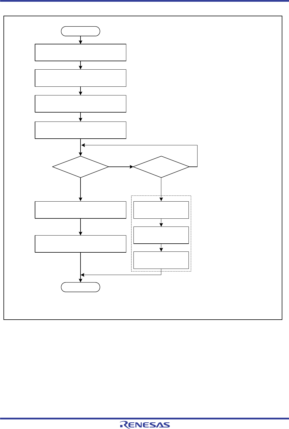
R01UH0034EJ0200 Rev.2.00 Page 1433 of 1489
Dec 27, 2013
RX62T Group, RX62G Group 32. Data Flash Memory (Flash Memory for Data Storage)
Under development Preliminary document
Specifications in this document are tentative and subject to change.
Figure 32.6 Procedure for Blank Checking of the Data Flash
Write 1 to the FRDMD bit in FMODR
Set DFLBCCNT
Write D0h to any addresses in the erasure
block in byte units
Timeout
(tDBC2K x 1.1)*
FCU initialization
Check the ILGLERR bit
Note: * tDBC2K: Time required for blank check of 2-Kbyte data (see section 33, Electrical Characteristics)
tRESW2: Reset pulse width during programming/erasure (see section 33, Electrical Characteristics)
No
Yes
0
1
Start
End
BCSIZE 0: 8 bytes, 1: 2 Kbytes
BCADR The address of a target area when BCSIZE = 0
Write 71h to the addresses in data flash
area in byte units
Check DFLBCSTAT
FRDY bit check
FRESETR.FRESET = 1
writing
FRESETR.FRESET = 0
writing
Wait
(tRESW2)*

R01UH0034EJ0200 Rev.2.00 Page 1434 of 1489
Dec 27, 2013
RX62T Group, RX62G Group 32. Data Flash Memory (Flash Memory for Data Storage)
Under development Preliminary document
Specifications in this document are tentative and subject to change.
32.7 Protection
There are two types of data flash programming/erasure protection: software protection and error protection.
32.7.1 Software Protection
In the software protection function, control register settings are used to disable data flash programming and erasure. If an
attempt is made to issue a programming or erasure command for the data flash and the command violates current
software protection, the FCU detects the error and enters the command-locked state.
(1) Protection through FWEPROR
If the FLWE[1:0] bits in FWEPROR are not set to 01b, programming cannot be performed in any mode.
(2) Protection through FENTRYR
When the FENTRYD bit in FENTRYR is 0, the ROM/data flash read mode is selected. Since the FCU does not accept
commands in ROM/data flash read mode, data flash programming and erasure are disabled. If an attempt is made to issue
an FCU command for the data flash in ROM/data flash read mode, the FCU detects an illegal command error and enters
the command-locked state (see section 32.7.2, Error Protection).
(3) Protection through DFLWEk
When the DBWEi (i = 15 to 00) bit in DFLWEk (k = 0, 1) is 0, programming and erasure of block DBi in the data area is
disabled. If an attempt is made to program or erase block DBi while the DBWEi bit is 0, the FCU detects a
programming/erasure protection error and enters the command-locked state (see section 32.7.2, Error Protection).
(4) Protection through DFLREk
When the DBREi (i = 15 to 00) bit in DFLREk (k = 0, 1) is 0, reading of block DBi in the data area is disabled. If an
attempt is made to read block DBi while the DBREi bit is 0, the FCU detects a read protection error and enters the
command-locked state (see section 32.7.2, Error Protection).

R01UH0034EJ0200 Rev.2.00 Page 1435 of 1489
Dec 27, 2013
RX62T Group, RX62G Group 32. Data Flash Memory (Flash Memory for Data Storage)
Under development Preliminary document
Specifications in this document are tentative and subject to change.
32.7.2 Error Protection
Error protection is the detection of errors in the issuing of FCU commands and of prohibited access, and response in the
form of notification of the FCU malfunction and prohibition of the reception of further commands by the FCU (the FCU
enters the command-locked state). When the FCU enters the command-locked state (FASTAT.CMDLK bit is 1), one or
several of the status bits (FSTATR0.ILGLERR, ERSERR, and PRGERR bits, FSTATR1.FCUERR bit, and
FASTAT.DFLAE, DFLRPE, and DFLWPE bits) are set to 1 and programming and erasure of the data-flash are
prohibited by placing the FCU in the command-locked state. To release the FCU from the command-locked state, a status
register clearing command must be issued with FASTAT set to 10h.
While the CMDLKIE bit in FAEINT is 1, a flash interface error (FIFERR) interrupt will be generated if the FCU enters
the command-locked state (the CMDLK bit in FASTAT becomes 1). While a data flash-related interrupt enable bit
(DFLAEIE, DFLRPEIE, or DFLWPEIE) in FAEINT is 1, an FIFERR interrupt will also be generated if the
corresponding status bit (DFLAE, DFLRPE, or DFLWPE) in FASTAT becomes 1.
Table 32.8 shows the error protection types for the data flash and the values of the status bits (the ILGLERR, ERSERR,
and PRGERR bits in FSTATR0 and the DFLAE, DFLRPE, and DFLWPE bits in FASTAT) after the detection of each
type of error. For the error protection types used in common by the ROM and data flash (FENTRYR setting error, most
illegal command errors, erasing errors, programming errors, and FCU errors, see section 31.8.2, Error Protection in
section 31, ROM (Flash Memory for Code Storage).
If the FCU enters the command-locked state due to a command other than a suspension command issued during
programming or erasure processing, the FCU continues programming or erasing the data flash. In this state, the P/E
suspension command cannot suspend programming or erasure. If a command is issued in the command-locked state, the
ILGLERR bit becomes 1.
Table 32.8 Error Protection Types (for Data Flash Only)
Error Description
ILGLERR
ERSERR
PRGERR
DFLAE
DFLRPE
DFLWPE
CMDLK
Illegal command
error
The value specified in the second cycle of a programming command
was neither 04h nor 40h.
1000001
A lock bit programming command was issued for an area in the data
flash while the FENTRYD bit of FENTRYR register was set to 1.
1000001
Data flash
access error
A read access command was issued for the data flash area while
FENTRYD = 1 in FENTRYR in data flash P/E normal mode.
1001001
A write access command was issued for the data flash area while
FENTRYD = 0.
1001001
An access command was issued for the data flash area while the
FENTRY0 bit in FENTRYR was 1.
1001001
Data flash
read protect
error
A read access command was issued for the data flash area while it
was protected against reading by the DFLREk (k = 0, 1) setting.
1000101
Data flash
programming
protect error
A program/block erase command was issued for the data flash area
while it was protected against programming or erasure by the
DFLWEk (k = 0, 1) setting.
1000011

R01UH0034EJ0200 Rev.2.00 Page 1436 of 1489
Dec 27, 2013
RX62T Group, RX62G Group 32. Data Flash Memory (Flash Memory for Data Storage)
Under development Preliminary document
Specifications in this document are tentative and subject to change.
32.8 Boot Mode
To program or erase the data area in boot mode, send control commands and programming data from the host. For the
system configuration and settings in boot mode, see section 31.9, Boot Mode. This section describes only the
commands dedicated for the data flash.
32.8.1 Inquiry/Selection Host Commands
Table 32.9 shows the inquiry/selection host commands dedicated to the data flash. The data area inquiry and data area
information inquiry commands are used in the step of "Inquiry regarding area programming information" in the
flowchart shown in Figure 31.29 (Example of Procedure to Use Inquiry/Selection Host Commands for User Area/User
Boot Area) in section 31.9.5, Inquiry/Selection Host Command Wait State.
Each host command is described in detail below. The "command" in the description indicates a command sent from the
host to the RX62T and the "response" indicates a response sent from the RX62T to the host. The "checksum" is byte-size
data calculated so that the sum of all bytes to be sent by the RX62T becomes 00h.
(1) Data Area Inquiry
In response to a data area inquiry command sent from the host, the RX62T returns the information concerning the
availability of data areas.
Size (1 byte): Number of characters in the area availability field (fixed at 1)
Area availability (1 byte): Availability of data areas (fixed at 21h)
21h: Data area is available
SUM (1 byte): Checksum
Table 32.9 Inquiry/Selection Host Commands (only for Data Flash)
Host Command Name Function
Data area inquiry Inquires regarding the availability of data area
Data area information inquiry Inquires regarding the number of data areas and the start and end addresses
Command 2Ah
Response 3Ah Size Area availability SUM
R01UH0034EJ0200 Rev.2.00 Page 1437 of 1489
Dec 27, 2013
RX62T Group, RX62G Group 32. Data Flash Memory (Flash Memory for Data Storage)
Under development Preliminary document
Specifications in this document are tentative and subject to change.
(2) Data Area Information Inquiry
In response to a data area information inquiry command sent from the host, the RX62T returns the number of data area
areas and their addresses.
Size (1 byte): Total number of bytes in the area count, area start address, and area end address fields
Area count (1 byte): Number of data area areas (consecutive areas are counted as one area)
Area start address (4 bytes): Start address of a data area
Area end address (4 bytes): End address of a data area
SUM (1 byte): Checksum
The information concerning the block configuration in the data area is included in the response to the erasure block
information inquiry command (see section 31.9.5, Inquiry/Selection Host Command Wait State).
Command 2Bh
Response 3Bh Size Area count
Area start address
Area end address
Area start address
Area end address
:
Area start address
Area end address
SUM
R01UH0034EJ0200 Rev.2.00 Page 1438 of 1489
Dec 27, 2013
RX62T Group, RX62G Group 32. Data Flash Memory (Flash Memory for Data Storage)
Under development Preliminary document
Specifications in this document are tentative and subject to change.
32.8.2 Programming/Erasing Host Commands
Table 32.10 shows the programming/erasing host commands dedicated to the data flash. Data flash-dedicated host
commands are provided only for checksum and blank check of the data flash; the programming, erasing, and reading
commands are used in common for the ROM and data flash.
To program the data area, issue from the host a user area programming selection command and then a 256-byte
programming command specifying a data area address as the programming address. To erase the data area, issue an
erasure selection command and then a block erasure command specifying an erasure block in the data area. The
information concerning the erasure block in the data area is included in the response to the erasure block information
inquiry command. To read data from the data area, select the user area through a memory read command specifying a
data area address as the read address.
For the user area programming selection, 256-byte programming, erasure selection, block erasure, and memory read
commands, refer to section 31.9.7, Programming/Erasure Host Command Wait State. For the erasure block
information inquiry command, refer to section 31.9.5, Inquiry/Selection Host Command Wait State.
Each host command is described in detail below. The "command" in the description indicates a command sent from the
host to the RX62T and the "response" indicates a response sent from the RX62T to the host. The "checksum" is byte-size
data calculated so that the sum of all bytes to be sent by the RX62T becomes 00h.
(1) Data Area Checksum
In response to a data area checksum command sent from the host, the RX62T sums the data area data in byte units and
returns the result (checksum).
Size (1 byte): Number of bytes in the area checksum field (fixed at 4)
Area checksum (4 bytes): Checksum of the data area data
SUM (4 bytes): Checksum (for the response data)
Table 32.10 Programming/Erasure Host Commands (only for Data Flash)
Host Command Name Function
Data area checksum Performs checksum verification for the data area
Data area blank check Checks whether the data area is blank
Command 61h
Response 71h Size Area checksum SUM

R01UH0034EJ0200 Rev.2.00 Page 1439 of 1489
Dec 27, 2013
RX62T Group, RX62G Group 32. Data Flash Memory (Flash Memory for Data Storage)
Under development Preliminary document
Specifications in this document are tentative and subject to change.
(2) Data Area Blank Check
In response to a data area blank check command sent from the host, the RX62T checks whether the data area is
completely erased. When the data area is completely erased, the RX62T returns a response (06h). If the data area has an
unerased area, the RX62T returns an error response (sends E2h and 52h in that order).
32.9 Usage Notes
(1) Protection of Data Area Immediately after a Reset
As the initial values of DFLREk and DFLWEk (k = 0, 1) are 0000h, programming, erasure, and reading of the data area
are disabled immediately after a reset. To read data from the data area, set DFLREk appropriately before accessing the
data area. To program or erase the data area, set DFLWEk appropriately before issuing an FCU command for
programming or erasure. If an attempt is made to read, program, or erase the data area without setting the registers, the
FCU detects the error and enters the command-locked state.
(2) Other Points to Note
The other points to note are the same as for the ROM. See section 31.12, Usage Notes. However, data-flash memory
also has a blank-checking facility. Accordingly, for “programming and erasure”, please read “programming, erasure, and
blank checking”.
Command 62h
Response 06h
Error response E2h 52h
R01UH0034EJ0200 Rev.2.00 Page 1440 of 1489
Dec 27, 2013
RX62T Group, RX62G Group 33. Electrical Characteristics
Under development Preliminary document
Specifications in this document are tentative and subject to change.
33. Electrical Characteristics
33.1 Absolute Maximum Ratings
Caution: Permanent damage to the LSI may result if absolute maximum ratings are exceeded.
Note 1. Do not leave the AVCC0, VREFH0, VREFL0, AVSS0, AVCC, VREF, and AVSS pins open circuit even if the A/D converter is not
to be used.
· When the 12-bit converter is not in use:
Connect the AVCC0 pin to AVCC (or VCC for a 64-pin product), the VREFH0 pin to VREF (or AVCC or VCC for an 80- or
64-pin product, respectively), and the AVSS0 and VREFL0 pins to VSS.
· When the 10-bit converter is not in use:
Connect the AVCC pin to AVCC0, the VREF pin to VREFH0, and the AVSS pin to AVSS0.
· When neither the 10- nor the 12-bit converter is in use:
Connect the AVCC0, VREFH0, AVCC, and VREF pins to VCC, and the AVSS0, VREFL0, and AVSS pins to VSS.
Table 33.1 Absolute Maximum Ratings
Item Symbol Value Unit
Power supply voltage VCC
PLLVCC
-0.3 to +6.5 V
Input voltage (except for ports 4 to 6) VIN -0.3 to VCC+0.3 V
Input voltage (port 4) VIN -0.3 to AVCC0+0.3 V
Input voltage (ports 5 and 6) VIN -0.3 to AVCC+0.3 V
Analog power supply voltage AVCC0, AVCC*1 -0.3 to +6.5 V
Reference power supply voltage VREFH0*1 -0.3 to AVCC0+0.3 V
VREF*1 -0.3 to AVCC+0.3
Analog input voltage (port 4) VAN -0.3 to AVCC0+0.3 V
Analog input voltage (ports 5 and 6) VAN -0.3 to AVCC+0.3 V
Operating temperature D version Topr -40 to +85 C
G version Topr -40 to +105 C
Storage temperature Tstg -55 to +125 C

R01UH0034EJ0200 Rev.2.00 Page 1441 of 1489
Dec 27, 2013
RX62T Group, RX62G Group 33. Electrical Characteristics
Under development Preliminary document
Specifications in this document are tentative and subject to change.
33.2 DC Characteristics
Table 33.2 DC Characteristics (1) (1 / 3)
Note: Items for which test conditions are not specifically stated in the table below have the same values under conditions 1 to 3.
Condition 1: VCC = PLLVCC = 2.7 to 3.6 V, VSS = PLLVSS = AVSS0 = AVSS = VREFL0 = 0 V
AVCC0 = AVCC = 3.0 to 3.6 V, VREFH0 = 3.0 V to AVCC0, VREF = 3.0 V to AVCC
Condition 2: VCC = PLLVCC = 2.7 to 3.6 V, VSS = PLLVSS = AVSS0 = AVSS = VREFL0 = 0V
AVCC0 = AVCC = 4.0 to 5.5 V, VREFH0 = 4.0 V to AVCC0, VREF = 4.0 V to AVCC
Condition 3: VCC = PLLVCC = 4.0 to 5.5 V, VSS = PLLVSS = AVSS0 = AVSS = VREFL0 = 0V
AVCC0 = AVCC = 4.0 to 5.5 V, VREFH0 = 4.0 V to AVCC0, VREF = 4.0 V to AVCC
Ta = Topr. Ta is the same under conditions 1 to 3.
Item Symbol Min. Typ. Max. Unit Test Conditions
Schmitt trigger
input voltage
CAN input pin
IRQ input pin
MTU3 input pin
POE3 input pin
SCI input pin
A/D trigger input pin
NMI input pin
GPT input pin
LIN input pin
RES#
VIH VCC0.8 - VCC+0.3 V
VIL -0.3 - VCC0.2
VTVCC
0.06
--
RIIC input pin
(IICBus)
VIH VCC0.7 - VCC+0.3
VIL -0.3 - VCC0.3
VTVCC
0.05
--
Port 4*1
(also usable as an
analog port)
VIH AVCC0
0.8
- AVCC0 +0.3
VIL - 0.3 - AVCC0 0.2
VTAVCC0
0.06
--
Ports 5 and 6*1
(also usable as analog
ports)
VIH AVCC
0.8
-AVCC
+0.3
VIL -0.3 - AVCC
0.2
VTAVCC
0.06
--
Ports 1 to 3*1
Ports 7 to B*1
Ports D, E, and G*1
VIH VCC0.8 - VCC+0.3
VIL -0.3 - VCC0.2
VTVCC
0.06
--
Input high voltage
(except Schmitt
trigger input pin)
MD pin, EMLE VIH VCC0.9 - VCC+0.3 V
EXTAL
RSPI input pin
VCC0.8 VCC+0.3
RIIC input pin
(SMBus)
2.1 VCC+0.3 Conditions 1 and 2
Input low voltage
(except Schmitt
trigger input pin)
MD pin, EMLE VIL -0.3 - VCC0.1 V
EXTAL
RSPI input pin
-0.3 - VCC0.2
RIIC input pin
(SMBus)
-0.3 - 0.8 Conditions 1 and 2

R01UH0034EJ0200 Rev.2.00 Page 1442 of 1489
Dec 27, 2013
RX62T Group, RX62G Group 33. Electrical Characteristics
Under development Preliminary document
Specifications in this document are tentative and subject to change.
Output high
voltage
All output pins
(except for P71 to P76
and P90 to P95)
VOH VCC-0.5 - - V IOH = -1 mA
P71 to P76 VCC-0.5 - - IOH = -1mA
64-pin LQFP
Condition 3
VCC-1.0 - - IOH = -5mA
64-pin LQFP
Other than condition 3
P90 to P95 VCC-0.5 - - IOH = -1mA
80-pin LQFP or
64-pin LQFP
VCC-1.0 - - IOH = -5 mA
112-pin LQFP or
100-pin LQFP
Output low
voltage
All output pins
(except for P71 to P76,
P90 to P95, and RIIC)
VOL --0.5 VI
OL = 1.0 mA
P71 to P76 - - 0.5 IOL = 1.0 mA
64-pin LQFP
Other than condition 3
--1.1 I
OL = 15 mA
Conditions 1 and 2
--1.4 I
OL = 15 mA
Other than 64-pin
LQFP
Condition 3
P90 to P95 - - 0.5 IOL = 1.0 mA
80-pin LQFP or
64-pin LQFP
--1.1 I
OL = 15 mA
112-pin LQFP or
100-pin LQFP
Conditions 1 and 2
--1.4 I
OL = 1 mA
112-pin LQFP or
100-pin LQFP
Condition 3
RIIC pin - - 0.4 IOL = 3 mA
--0.6 I
OL = 6 mA
Input leakage
current
RES#, MD pin, EMLE Iin--1.0 AV
in = 0 V,
Vin = VCC
Three-state
leakage current
(off state)
Ports 1 to A, PB0, PB3
to PB7, D, E, G
ITSI--1.0 AV
in = 0 V,
Vin = VCC
Ports PB1 and PB2 - - 5.0
Table 33.2 DC Characteristics (1) (2 / 3)
Note: Items for which test conditions are not specifically stated in the table below have the same values under conditions 1 to 3.
Condition 1: VCC = PLLVCC = 2.7 to 3.6 V, VSS = PLLVSS = AVSS0 = AVSS = VREFL0 = 0 V
AVCC0 = AVCC = 3.0 to 3.6 V, VREFH0 = 3.0 V to AVCC0, VREF = 3.0 V to AVCC
Condition 2: VCC = PLLVCC = 2.7 to 3.6 V, VSS = PLLVSS = AVSS0 = AVSS = VREFL0 = 0V
AVCC0 = AVCC = 4.0 to 5.5 V, VREFH0 = 4.0 V to AVCC0, VREF = 4.0 V to AVCC
Condition 3: VCC = PLLVCC = 4.0 to 5.5 V, VSS = PLLVSS = AVSS0 = AVSS = VREFL0 = 0V
AVCC0 = AVCC = 4.0 to 5.5 V, VREFH0 = 4.0 V to AVCC0, VREF = 4.0 V to AVCC
Ta = Topr. Ta is the same under conditions 1 to 3.
Item Symbol Min. Typ. Max. Unit Test Conditions

R01UH0034EJ0200 Rev.2.00 Page 1443 of 1489
Dec 27, 2013
RX62T Group, RX62G Group 33. Electrical Characteristics
Under development Preliminary document
Specifications in this document are tentative and subject to change.
Note 1. This includes the multiplexed input pins, except in cases where port pins PB1 and PB2 are used as RIIC input pins or port pins
P22 to P24, P30, PA3 to PA5, PB0, PD0 to PD2, or PD6 are used as RSPI input pins.
Input capacitance All input pins
(except for ports PB1
and PB2)
Cin - - 15 pF Vin = 0 V,
f = 1 MHz,
Ta = 25C
Ports PB1 and PB2 - - 30
Table 33.2 DC Characteristics (1) (3 / 3)
Note: Items for which test conditions are not specifically stated in the table below have the same values under conditions 1 to 3.
Condition 1: VCC = PLLVCC = 2.7 to 3.6 V, VSS = PLLVSS = AVSS0 = AVSS = VREFL0 = 0 V
AVCC0 = AVCC = 3.0 to 3.6 V, VREFH0 = 3.0 V to AVCC0, VREF = 3.0 V to AVCC
Condition 2: VCC = PLLVCC = 2.7 to 3.6 V, VSS = PLLVSS = AVSS0 = AVSS = VREFL0 = 0V
AVCC0 = AVCC = 4.0 to 5.5 V, VREFH0 = 4.0 V to AVCC0, VREF = 4.0 V to AVCC
Condition 3: VCC = PLLVCC = 4.0 to 5.5 V, VSS = PLLVSS = AVSS0 = AVSS = VREFL0 = 0V
AVCC0 = AVCC = 4.0 to 5.5 V, VREFH0 = 4.0 V to AVCC0, VREF = 4.0 V to AVCC
Ta = Topr. Ta is the same under conditions 1 to 3.
Item Symbol Min. Typ. Max. Unit Test Conditions
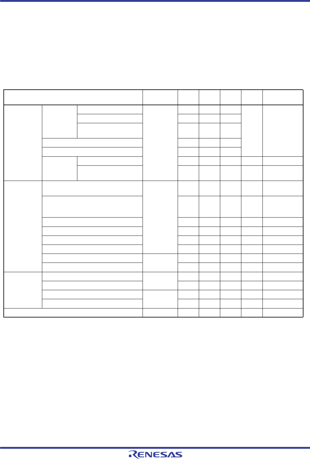
R01UH0034EJ0200 Rev.2.00 Page 1444 of 1489
Dec 27, 2013
RX62T Group, RX62G Group 33. Electrical Characteristics
Under development Preliminary document
Specifications in this document are tentative and subject to change.
Note 1. Supply current values are with all output pins unloaded.
Note 2. Measured with clocks supplied to the peripheral functions. This does not include the BGO operation.
Note 3. ICC depends on f (ICLK) as follows. (ICLK: PCLK = 8:4)
ICC max. = 0.54 x f + 16 (max.)
ICC max. = 0.3 x f + 5 (normal operation)
ICC max. = 0.44 x f + 16 (sleep mode)
Note 4. Measured with clocks not supplied to the peripheral functions. This does not include the BGO operation.
Note 5. Incremented if data is written to or erased from the ROM or data flash for data storage during the program execution.
Note 6. The values are for reference.
Table 33.3 DC Characteristics (2)
Note: Items for which test conditions are not specifically stated in the table below have the same values under conditions 1 to 3.
Condition 1: VCC = PLLVCC = 2.7 to 3.6 V, VSS = PLLVSS = AVSS0 = AVSS = VREFL0 = 0 V
AVCC0 = AVCC = 3.0 to 3.6 V, VREFH0 = 3.0 V to AVCC0, VREF = 3.0 V to AVCC
Condition 2: VCC = PLLVCC = 2.7 to 3.6 V, VSS = PLLVSS = AVSS0 = AVSS = VREFL0 = 0 V
AVCC0 = AVCC = 4.0 to 5.5 V, VREFH0 = 4.0 V to AVCC0, VREF = 4.0 V to AVCC
Condition 3: VCC = PLLVCC = 4.0 to 5.5 V, VSS = PLLVSS = AVSS0 = AVSS = VREFL0 = 0 V
AVCC0 = AVCC = 4.0 to 5.5 V, VREFH0 = 4.0 V to AVCC0, VREF = 4.0 V to AVCC
Ta = Topr. Ta is the same under conditions 1 to 3.
Item Symbol Min. Typ. Max. Unit Test
Conditions
Supply
current*1 In operation Max.*2 ICC*3 --70mAICLK =
100 MHz
PCLK =
50 MHz
Normal*4 -35-
Increased by BGO
operation*5 -15-
Sleep 22 60
All-module-clock-stop mode*6 14 28
Standby
mode
Software standby mode - 0.10 3 mA
Deep software standby
mode
-2060A
Analog power
supply current
During 12-bit A/D conversion (when a
sample-and-hold circuit is in use; per unit)
AICC0 -35mA
During 12-bit A/D conversion (when a
sample-and-hold circuit is not in use; per
unit)
-35mA
Programmable gain amp (per channel) - 1 2 mA
Window comparator (1 channel) 0.5 1 mA
Window comparator (6 channels) - 1 2 mA
During 12-bit A/D conversion (per unit) - 60 90 A
During 10-bit A/D conversion (per unit) AICC -0.92mA
Waiting for 10-bit A/D conversion (all units) - 0.3 3 A
Reference
power supply
current
During 12-bit A/D conversion (per unit) AIREFH0 -1.63mA
Waiting for 12-bit A/D conversion (all units) - 1.6 3 mA
During 10-bit A/D conversion (per unit) AIREF -0.11mA
Waiting for 10-bit A/D conversion (all units) - 0.1 3 A
VCC rising gradient SVCC --20ms/V

R01UH0034EJ0200 Rev.2.00 Page 1445 of 1489
Dec 27, 2013
RX62T Group, RX62G Group 33. Electrical Characteristics
Under development Preliminary document
Specifications in this document are tentative and subject to change.
Caution: To protect the LSI's reliability, the output current values should not exceed the permissible output current.
Note 1. IOL = 15 mA (max.)/ - IOH = 5 mA (max.) for P71 to P76 and P90 to P95. Note, however, that up to 6 (112-pin or 100-pin LQFP)
or 3 (80-pin or 64-pin LQFP) pins can accept over 2.0-mA IOL / - IOH at the same time.
Note: • Please contact Renesas Electronics sales office for derating of operation under Ta = +85°C to +105°C. Derating is the
systematic reduction of load for improved reliability.
Note 1. The total power consmuption of the whole chip including output current.
Table 33.4 Permissible Output Currents
Note: Items for which test conditions are not specifically stated in the table below have the same values under conditions 1 to 3.
Condition 1: VCC = PLLVCC = 2.7 to 3.6 V, VSS = PLLVSS = AVSS0 = AVSS = VREFL0 = 0 V
AVCC0 = AVCC = 3.0 to 3.6 V, VREFH0 = 3.0 V to AVCC0, VREF = 3.0 V to AVCC
Condition 2: VCC = PLLVCC = 2.7 to 3.6 V, VSS = PLLVSS = AVSS0 = AVSS = VREFL0 = 0 V
AVCC0 = AVCC = 4.0 to 5.5 V, VREFH0 = 4.0 V to AVCC0, VREF = 4.0 V to AVCC
Condition 3: VCC = PLLVCC = 4.0 to 5.5 V, VSS = PLLVSS = AVSS0 = AVSS = VREFL0 = 0 V
AVCC0 = AVCC = 4.0 to 5.5 V, VREFH0 = 4.0 V to AVCC0, VREF = 4.0 V to AVCC
Ta = Topr. Ta is the same under conditions 1 to 3.
Item Symbol Min. Typ. Max. Unit
Permissible output low current
(average value per pin)
IOL --2.0
*1 mA
Permissible output low current
(max. value per pin)
IOL --4.0
*1 mA
Permissible output low current (total) IOL --110mA
Permissible output high current
(average value per pin)
- IOH --2.0
*1 mA
Permissible output high current
(max. value per pin)
- IOH --4.0
*1 mA
Permissible output high current (total) - IOH --35mA
Table 33.5 Permissible Power Consumption (Only for G Version)
Note: Items for which test conditions are not specifically stated in the table below have the same values under conditions 1 to 3.
Condition 1: VCC = PLLVCC = 2.7 to 3.6 V, VSS = PLLVSS = AVSS0 = AVSS = VREFL0 = 0 V
AVCC0 = AVCC = 3.0 to 3.6 V, VREFH0 = 3.0 V to AVCC0, VREF = 3.0 V to AVCC
Condition 2: VCC = PLLVCC = 2.7 to 3.6 V, VSS = PLLVSS = AVSS0 = AVSS = VREFL0 = 0 V
AVCC0 = AVCC = 4.0 to 5.5 V, VREFH0 = 4.0 V to AVCC0, VREF = 4.0 V to AVCC
Condition 3: VCC = PLLVCC = 4.0 to 5.5 V, VSS = PLLVSS = AVSS0 = AVSS = VREFL0 = 0 V
AVCC0 = AVCC = 4.0 to 5.5 V, VREFH0 = 4.0 V to AVCC0, VREF = 4.0 V to AVCC
Ta = Topr. Ta is the same under conditions 1 to 3.
Item Symbol Typ. Max. Unit Test Conditions
Total permissible power consumption*1Pd — 325 mW 85°C < Ta ≤ 105°C
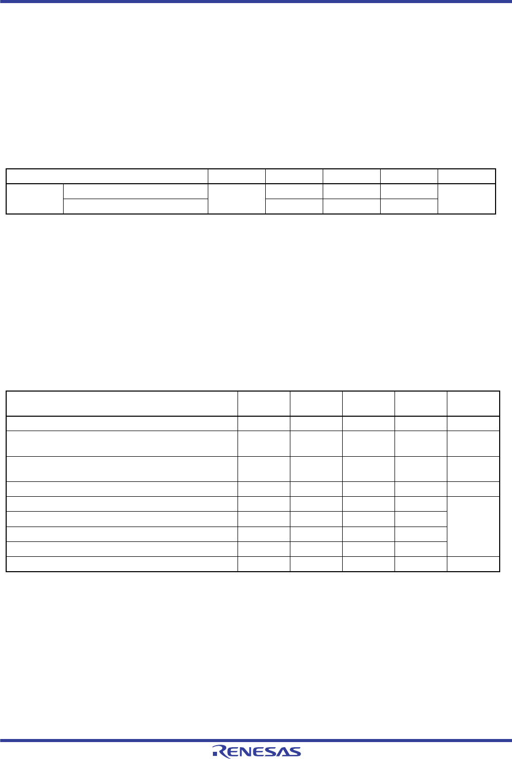
R01UH0034EJ0200 Rev.2.00 Page 1446 of 1489
Dec 27, 2013
RX62T Group, RX62G Group 33. Electrical Characteristics
Under development Preliminary document
Specifications in this document are tentative and subject to change.
33.3 AC Characteristics
33.3.1 Clock Timing
Table 33.6 Operation Frequency Value
Note:Items for which test conditions are not specifically stated in the table below have the same values under conditions 1 to 3.
Condition 1: VCC = PLLVCC = 2.7 to 3.6 V, VSS = PLLVSS = AVSS0 = AVSS = VREFL0 = 0 V
AVCC0 = AVCC = 3.0 to 3.6 V, VREFH0 = 3.0 V to AVCC0, VREF = 3.0 V to AVCC
Condition 2: VCC = PLLVCC = 2.7 to 3.6 V, VSS = PLLVSS = AVSS0 = AVSS = VREFL0 = 0 V
AVCC0 = AVCC = 4.0 to 5.5 V, VREFH0 = 4.0 V to AVCC0, VREF = 4.0 V to AVCC
Condition 3: VCC = PLLVCC = 4.0 to 5.5 V, VSS = PLLVSS = AVSS0 = AVSS = VREFL0 = 0 V
AVCC0 = AVCC = 4.0 to 5.5 V, VREFH0 = 4.0 V to AVCC0, VREF = 4.0 V to AVCC
Ta = Topr. Ta is the same under conditions 1 to 3.
Item Symbol Min. Typ. Max. Unit
Operating
frequency
System clock (ICLK) f 8 - 100 MHz
Peripheral module clock (PCLK) 8 - 50
Table 33.7 Clock Timing
Note:Items for which test conditions are not specifically stated in the table below have the same values under conditions 1 to 3.
Condition 1: VCC = PLLVCC = 2.7 to 3.6 V, VSS = PLLVSS = AVSS0 = AVSS = VREFL0 = 0 V
AVCC0 = AVCC = 3.0 to 3.6 V, VREFH0 = 3.0 V to AVCC0, VREF = 3.0 V to AVCC
Condition 2: VCC = PLLVCC = 2.7 to 3.6 V, VSS = PLLVSS = AVSS0 = AVSS = VREFL0 = 0 V
AVCC0 = AVCC = 4.0 to 5.5 V, VREFH0 = 4.0 V to AVCC0, VREF = 4.0 V to AVCC
Condition 3: VCC = PLLVCC = 4.0 to 5.5 V, VSS = PLLVSS = AVSS0 = AVSS = VREFL0 = 0 V
AVCC0 = AVCC = 4.0 to 5.5 V, VREFH0 = 4.0 V to AVCC0, VREF = 4.0 V to AVCC
Ta = Topr. Ta is the same under conditions 1 to 3.
Item Symbol Min. Max. Unit Test
Conditions
Oscillation settling time after reset (crystal) tOSC1 10 - ms Figure 33.1
Oscillation settling time after leaving software standby mode
(crystal)
tOSC2 10 - ms Figure 33.2
Oscillation settling time after leaving deep software standby
mode (crystal)
tOSC3 10 - ms Figure 33.3
EXTAL external clock output delay settling time tDEXT 1 - ms Figure 33.1
EXTAL external clock input low pulse width tEXL 35 - ns Figure 33.4
EXTAL external clock input high pulse width tEXH 35 - ns
EXTAL external clock rising time tEXr -5ns
EXTAL external clock falling time tEXf -5ns
On-chip oscillator (IWDTCLK) oscillation frequency fIWDTCLK 62.5 187.5 kHz
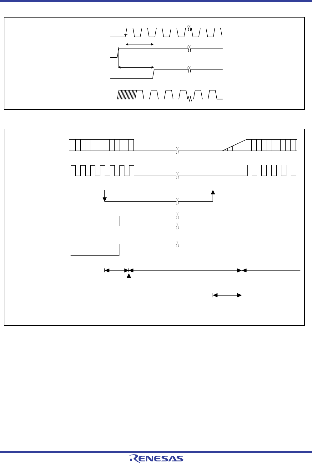
R01UH0034EJ0200 Rev.2.00 Page 1447 of 1489
Dec 27, 2013
RX62T Group, RX62G Group 33. Electrical Characteristics
Under development Preliminary document
Specifications in this document are tentative and subject to change.
Figure 33.1 Oscillation Settling Timing
Figure 33.2 Oscillation Settling Timing after Software Standby Mode
tOSC1
tDEXT
VCC
EXTAL
RES#
ICLK
Software standby mode
(power-down mode)
IRQ exception handling
IRQMD[1:0] = 10b
SSBY = 1
WAIT instruction Oscillation
settling time
tOSC2
IRQ exception
handling
01 10
SSBY
IRQCRn.IRQMD[1:0]
IRQ
ICLK
Oscillator
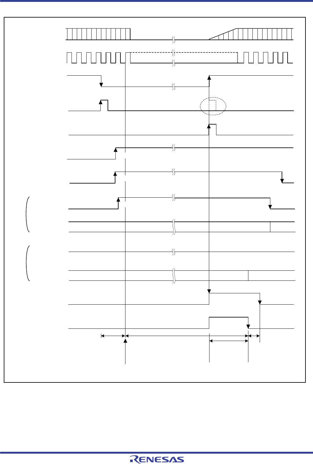
R01UH0034EJ0200 Rev.2.00 Page 1448 of 1489
Dec 27, 2013
RX62T Group, RX62G Group 33. Electrical Characteristics
Under development Preliminary document
Specifications in this document are tentative and subject to change.
Figure 33.3 Oscillation Settling Timing after Deep Software Standby Mode
Invalid by the
internal reset
IRQ exception handling
DIRQnEG = 1
SSBY = 1
Deep software
standby mode
(power-down mode)
Reset exception
handling
Oscillation
settling time
tOSC3
WAIT instruction
When IOKEEP=L
Operating
When IOKEEP=H
Oscillator
ICLK
IRQ
IRQ interrupt
DIRQnF set request Set
DIRQnEG bit Set
DPSBY bit Set
IOKEEP bit Cleared
Set
L
I/O port Operating Retained
IOKEEP bit
I/O port Operating Retained Operating
DPSRSTF flag
Internal reset
L
H
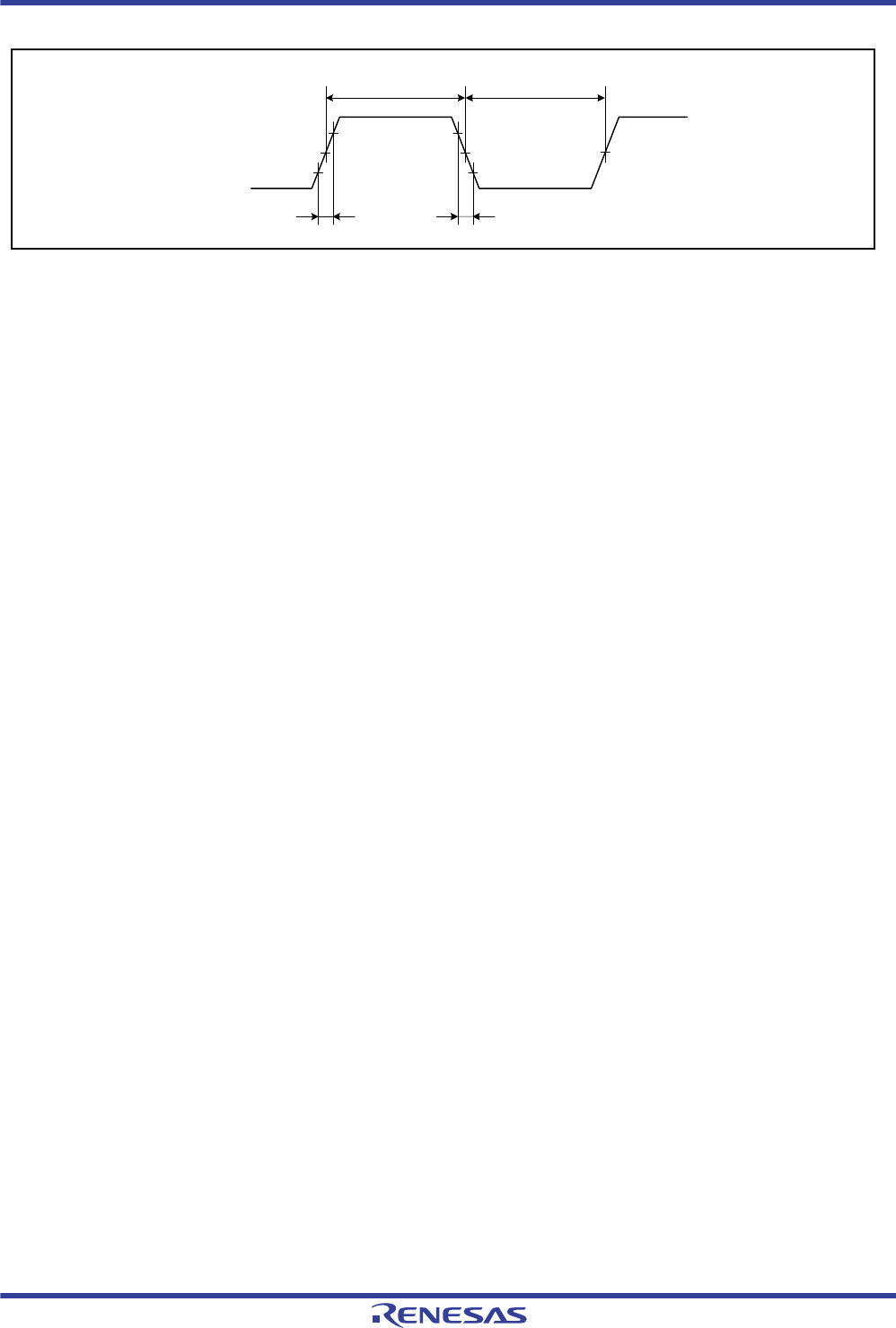
R01UH0034EJ0200 Rev.2.00 Page 1449 of 1489
Dec 27, 2013
RX62T Group, RX62G Group 33. Electrical Characteristics
Under development Preliminary document
Specifications in this document are tentative and subject to change.
Figure 33.4 EXTAL External Input Clock Timing
tEXf
VCC×0.5
EXTAL
tEXH tEXL
tEXr
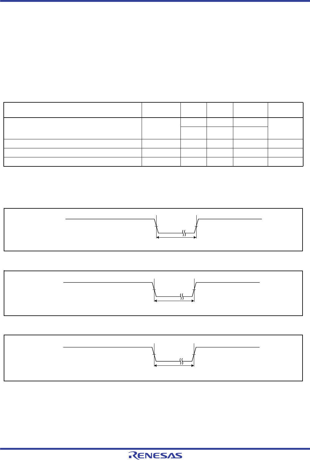
R01UH0034EJ0200 Rev.2.00 Page 1450 of 1489
Dec 27, 2013
RX62T Group, RX62G Group 33. Electrical Characteristics
Under development Preliminary document
Specifications in this document are tentative and subject to change.
33.3.2 Control Signal Timing
Note 1. For a reset by the signal on the RES# pin during programming or erasure of the ROM or data-flash memory or during blank
checking of the data-flash memory, see section 31.12, Usage Notes in section 31, ROM (Flash Memory for Code Storage).
Note 2. Both the time and the number of cycles should satisfy the specifications.
Note 3. This is to specify the FCU reset.
Note 4. ICLK cycles.
Figure 33.5 Reset Input Timing
Figure 33.6 NMI Interrupt Input Timing
Figure 33.7 IRQ Interrupt Input Timing
Table 33.8 Control Signal Timing
Note:Items for which test conditions are not specifically stated in the table below have the same values under conditions 1 to 3.
Condition 1: VCC = PLLVCC = 2.7 to 3.6 V, VSS = PLLVSS = AVSS0 = AVSS = VREFL0 = 0 V
AVCC0 = AVCC = 3.0 to 3.6 V, VREFH0 = 3.0 V to AVCC0, VREF = 3.0 V to AVCC
Condition 2: VCC = PLLVCC = 2.7 to 3.6 V, VSS = PLLVSS = AVSS0 = AVSS = VREFL0 = 0 V
AVCC0 = AVCC = 4.0 to 5.5 V, VREFH0 = 4.0 V to AVCC0, VREF = 4.0 V to AVCC
Condition 3: VCC = PLLVCC = 4.0 to 5.5 V, VSS = PLLVSS = AVSS0 = AVSS = VREFL0 = 0 V
AVCC0 = AVCC = 4.0 to 5.5 V, VREFH0 = 4.0 V to AVCC0, VREF = 4.0 V to AVCC
Ta = Topr. Ta is the same under conditions 1 to 3.
Item Symbol Min. Max. Unit Test
Conditions
RES# pulse width
(except for programming or erasure of the ROM or data-flash
memory or blank checking of the data-flash memory*1)
tRESW*220 - tIcyc*4Figure 33.5
1.5 - s
Internal reset time*3tRESW2 35 - s
NMI pulse width tNMIW 200 - ns Figure 33.6
IRQ pulse width tIRQW 200 - ns Figure 33.7
RES#
tRESW
NMI
tNMIW
IRQ
tIRQW
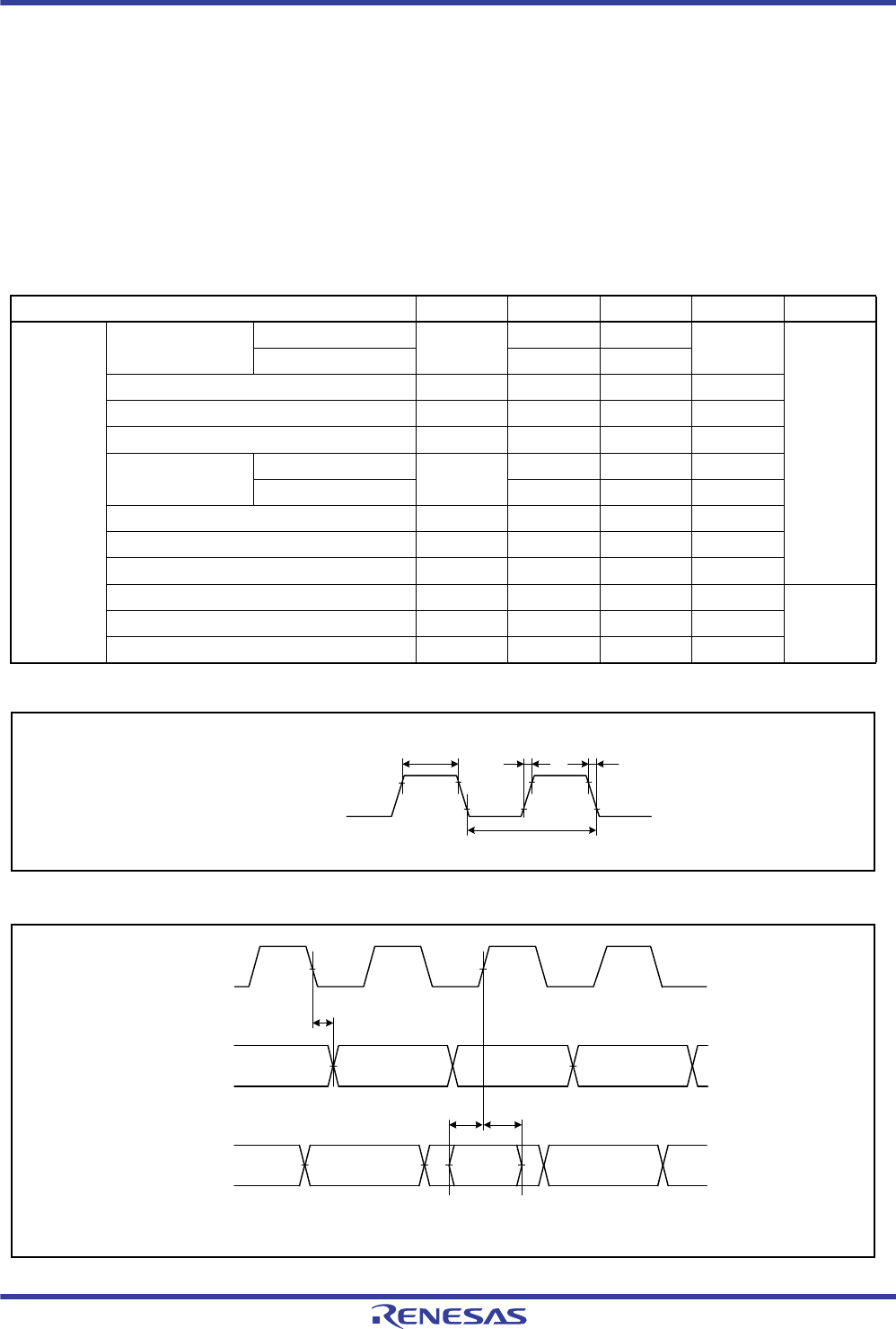
R01UH0034EJ0200 Rev.2.00 Page 1451 of 1489
Dec 27, 2013
RX62T Group, RX62G Group 33. Electrical Characteristics
Under development Preliminary document
Specifications in this document are tentative and subject to change.
33.3.3 Timing of On-Chip Peripheral Modules
Note: • tPcyc: PCLK cycle
Figure 33.8 SCK Clock Input Timing
Figure 33.9 SCI Input/Output Timing: Clock Synchronous Mode
Table 33.9 Timing of On-Chip Peripheral Modules (1)
Note:Items for which test conditions are not specifically stated in the table below have the same values under conditions 1 to 3.
Condition 1: VCC = PLLVCC = 2.7 to 3.6 V, VSS = PLLVSS = AVSS0 = AVSS = VREFL0 = 0 V
AVCC0 = AVCC = 3.0 to 3.6 V, VREFH0 = 3.0 V to AVCC0, VREF = 3.0 V to AVCC
Condition 2: VCC = PLLVCC = 2.7 to 3.6 V, VSS = PLLVSS = AVSS0 = AVSS = VREFL0 = 0 V
AVCC0 = AVCC = 4.0 to 5.5 V, VREFH0 = 4.0 V to AVCC0, VREF = 4.0 V to AVCC
Condition 3: VCC = PLLVCC = 4.0 to 5.5 V, VSS = PLLVSS = AVSS0 = AVSS = VREFL0 = 0 V
AVCC0 = AVCC = 4.0 to 5.5 V, VREFH0 = 4.0 V to AVCC0, VREF = 4.0 V to AVCC
Ta = Topr. Ta is the same under conditions 1 to 3.
Item Symbol Min. Typ. Max. Unit
SCI Input clock cycle Asynchronous tScyc 4tPcyc - ns Figure 33.8
Clock synchronous 6tPcyc -
Input clock pulse width tSCKW 0.4tPcyc 0.6tScyc ns
Input clock rise time tSCKr -20ns
Input clock fall time tSCKf -20ns
Output clock cycle Asynchronous tScyc 16tPcyc -ns
Clock synchronous 6tPcyc -ns
Output clock pulse width tSCKW 0.4tScyc 0.6tScyc ns
Output clock rise time tSCKr -20ns
Output clock fall time tSCKf -20ns
Transmit data delay time (clock synchronous) tTXD - 40 ns Figure 33.9
Receive data setup time (clock synchronous) tRXS 40 - ns
Receive data hold time (clock synchronous) tRXH 40 - ns
tSCKW tSCKr tSCKf
tScyc
SCKn
(n = 0 to 2)
tTXD
tRXS tRXH
TxDn
RxDn
SCKn
n = 0 to 2
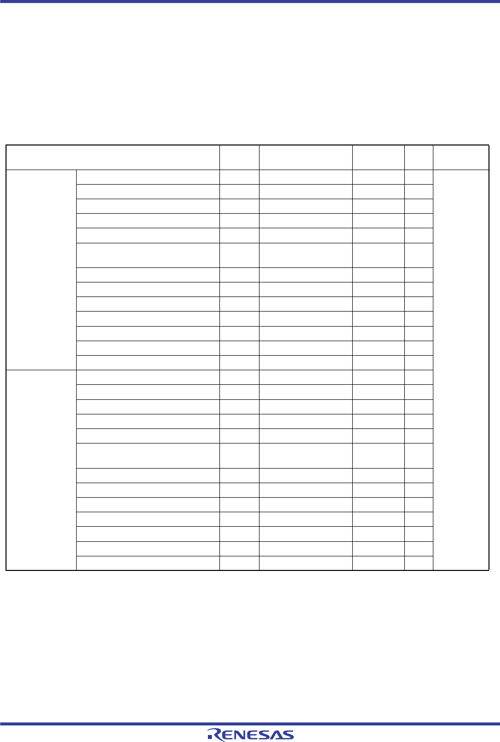
R01UH0034EJ0200 Rev.2.00 Page 1452 of 1489
Dec 27, 2013
RX62T Group, RX62G Group 33. Electrical Characteristics
Under development Preliminary document
Specifications in this document are tentative and subject to change.
Note: • tIICcyc: Cycles of internal base clock (IICφ) for the RIIC module
Note 1. The value in parentheses is used when ICMR3.NF[1:0] are set to 11b while a digital filter is enabled with ICFER.NFE = 1.
Note 2. Cb indicates the total capacity of the bus line.
Table 33.10 Timing of On-Chip Peripheral Modules (2)
Note:Items for which test conditions are not specifically stated in the table below have the same values under conditions 1 to 3.
Condition 1: VCC = PLLVCC = 2.7 to 3.6 V, VSS = PLLVSS = AVSS0 = AVSS = VREFL0 = 0 V
AVCC0 = AVCC = 3.0 to 3.6 V, VREFH0 = 3.0 V to AVCC0, VREF = 3.0 V to AVCC
Condition 2: VCC = PLLVCC = 2.7 to 3.6 V, VSS = PLLVSS = AVSS0 = AVSS = VREFL0 = 0 V
AVCC0 = AVCC = 4.0 to 5.5 V, VREFH0 = 4.0 V to AVCC0, VREF = 4.0 V to AVCC
Condition 3: VCC = PLLVCC = 4.0 to 5.5 V, VSS = PLLVSS = AVSS0 = AVSS = VREFL0 = 0 V
AVCC0 = AVCC = 4.0 to 5.5 V, VREFH0 = 4.0 V to AVCC0, VREF = 4.0 V to AVCC
Ta = Topr. Ta is the same under conditions 1 to 3.
Item Symbol Min.*1 *2Max. Unit Test
Conditions
RIIC
(standard mode)
SCL input cycle time tSCL 6(12) tllCcyc + 1300 - ns Figure 33.10
SCL input high pulse width tSCLH 3(6) tllCcyc + 300 - ns
SCL input low pulse width tSCLL 3(6) tllCcyc + 1000 - ns
SCL, SDA input rising time tSr - 1000 ns
SCL, SDA input falling time tSf - 300 ns
SCL, SDA input spike pulse removal
time
tSP 01(4) tllCcyc ns
SDA input bus free time tBUF 3(6) tllCcyc + 300 - ns
Start condition input hold time tSTAH tllCcyc + 300 - ns
Re-start condition input setup time tSTAS 1000 - ns
Stop condition input setup time tSTOS 1000 - ns
Data input setup time tSDAS tllCcyc + 50 - ns
Data input hold time tSDAH 0-ns
SCL, SDA capacitive load Cb- 400 pF
RIIC
(fast mode)
SCL input cycle time tSCL 6(12) tllCcyc + 600 - ns
SCL input high pulse width tSCLH 3(6) tllCcyc + 300 - ns
SCL input low pulse width tSCLL 3(6) tllCcyc + 300 - ns
SCL, SDA input rising time tSr 20 + 0.1Cb300 ns
SCL, SDA input falling time tSf 20 + 0.1Cb300 ns
SCL, SDA input spike pulse removal
time
tSP 01(4) tllCcyc ns
SDA input bus free time tBUF 3(6) tllCcyc + 300 - ns
Start condition input hold time tSTAH tllCcyc + 300 - ns
Re-start condition input setup time tSTAS 300 - ns
Stop condition input setup time tSTOS 300 - ns
Data input setup time tSDAS tllCcyc + 50 - ns
Data input hold time tSDAH 0-ns
SCL, SDA capacitive load Cb- 400 pF
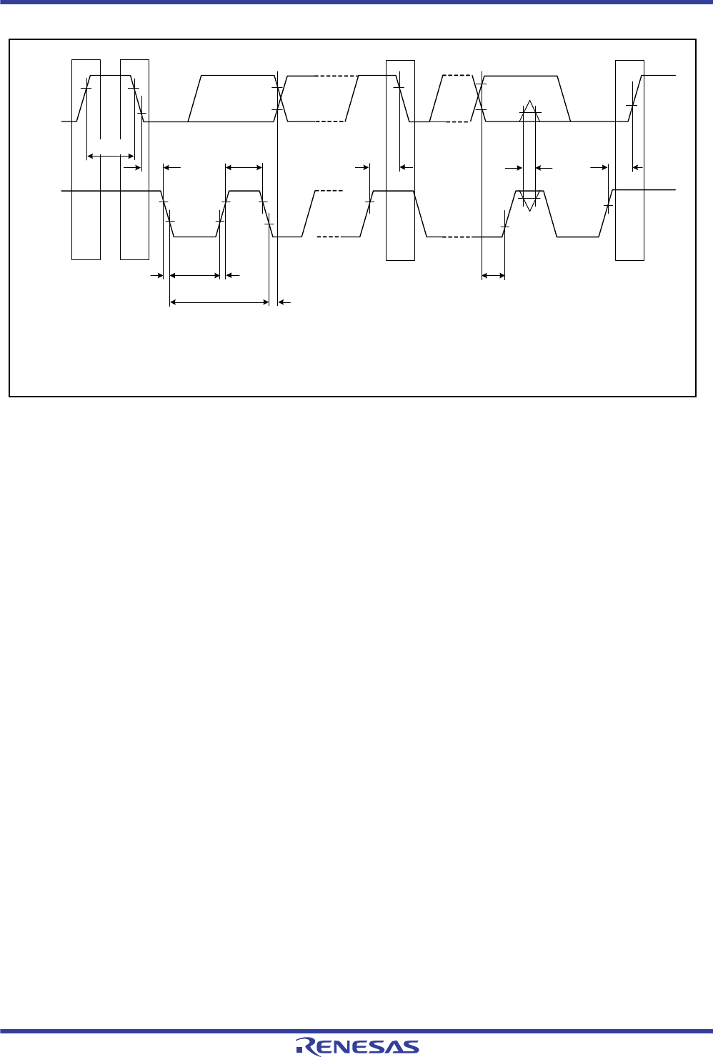
R01UH0034EJ0200 Rev.2.00 Page 1453 of 1489
Dec 27, 2013
RX62T Group, RX62G Group 33. Electrical Characteristics
Under development Preliminary document
Specifications in this document are tentative and subject to change.
Figure 33.10 I2C Bus Interface Input/Output Timing
SDA
SCL
VIH
VIL
tSTAH
tSCLH
tSCLL
P *1S *1
tSf tSr
tSCL tSDAH
tSDAS
tSTAS tSP tSTOS
P *1
tBUF
Note 1: S, P, and Sr indicate the following conditions.
S: Start condition
P: Stop condition
Sr: Restart condition
Test conditions
VIH = VCC × 0.7, VIL = VCC × 0.3
VOL = 0.6 V, IOL = 6 mA (ICFER.FMPE = 0)
VOL = 0.4 V, IOL = 15 mA (ICFER.FMPE = 1)
Sr *1
R01UH0034EJ0200 Rev.2.00 Page 1454 of 1489
Dec 27, 2013
RX62T Group, RX62G Group 33. Electrical Characteristics
Under development Preliminary document
Specifications in this document are tentative and subject to change.
Note: • Note 1: tPcyc: PCLK cycle
Table 33.11 Timing of On-Chip Peripheral Modules (3)
Note:Items for which test conditions are not specifically stated in the table below have the same values under conditions 1 to 3.
Condition 1: VCC = PLLVCC = 2.7 to 3.6 V, VSS = PLLVSS = AVSS0 = AVSS = VREFL0 = 0 V
AVCC0 = AVCC = 3.0 to 3.6 V, VREFH0 = 3.0 V to AVCC0, VREF = 3.0 V to AVCC
Condition 2: VCC = PLLVCC = 2.7 to 3.6 V, VSS = PLLVSS = AVSS0 = AVSS = VREFL0 = 0 V
AVCC0 = AVCC = 4.0 to 5.5 V, VREFH0 = 4.0 V to AVCC0, VREF = 4.0 V to AVCC
Condition 3: VCC = PLLVCC = 4.0 to 5.5 V, VSS = PLLVSS = AVSS0 = AVSS = VREFL0 = 0 V
AVCC0 = AVCC = 4.0 to 5.5 V, VREFH0 = 4.0 V to AVCC0, VREF = 4.0 V to AVCC
Ta = Topr. Ta is the same under conditions 1 to 3.
Item Symbol Min. Max. Unit Test
Conditions
RSPI RSPCK clock cycle Master tSPcyc 4 4096 tPcyc Figure 33.11
Slave 8 4096
RSPCK clock high pulse width Master tSPCKWH (tSpcyc - tSPCKR -
tSPCKF) / 2-3
-ns
Slave (tSpcyc - tSPCKR -
tSPCKF) / 2
-
RSPCK clock low pulse width Master tSPCKWL (tSpcyc - tSPCKR -
tSPCKF) / 2-3
-ns
Slave (tSpcyc - tSPCKR -
tSPCKF) / 2
-
RSPCK clock rise/fall time Output tSPCKR
tSPCKF
-5ns
Input - 1 s
Data input setup time Master tSU 25 - ns Figure 33.12 to
Figure 33.15
Slave 0 -
Data input hold time Master tH0-ns
Slave 20+2tPcyc -
SSL setup time Master tLEAD 18t
SPcyc
Slave 4 - tPcyc
SSL hold time Master tLAG 18t
SPcyc
Slave 4 - tPcyc
Data output delay time Master tOD -20ns
Slave - 3tPcyc
+40
Data output hold time Master tOH 0-ns
Slave 0 -
Successive transmission delay time Master tTD tSPcyc+2tPcyc 8tSPcyc
+2tPcyc
ns
Slave 4tPcyc -
MOSI, MISO rise/fall time Output tDR
tDF
- 15 ns Figure 33.12 to
Figure 33.15
Input - 1 s
SSL rise/fall time Output tSSLR
tSSLF
-15ns
Input - 1 s
Slave access time tSA -4t
Pcyc Figure 33.12 to
Figure 33.15
Slave output release time tREL -3t
Pcyc
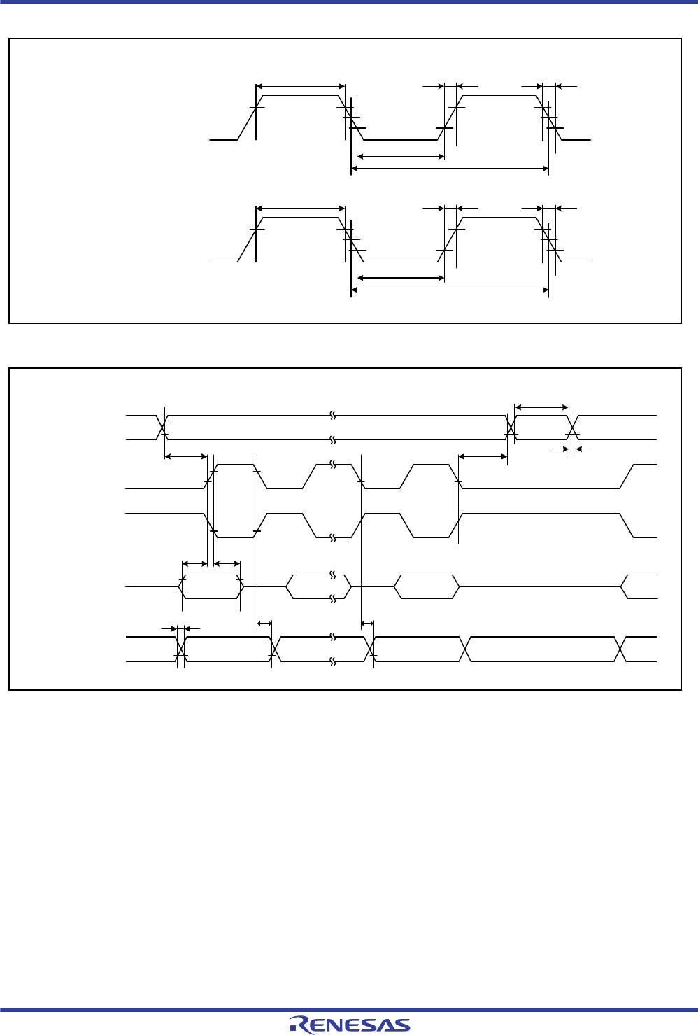
R01UH0034EJ0200 Rev.2.00 Page 1455 of 1489
Dec 27, 2013
RX62T Group, RX62G Group 33. Electrical Characteristics
Under development Preliminary document
Specifications in this document are tentative and subject to change.
Figure 33.11 RSPI Clock Timing
Figure 33.12 RSPI Timing (Master, CPHA = 0)
RSPCK
Master select output
RSPCK
Slave select output
tSPCKWH
VOH VOH
VOL VOL
VOH VOH
tSPCKWL
tSPCKr tSPCKf
VOL
tSPcyc
tSPCKWH
VIH VIH
VIL VIL
VIH VIH
tSPCKWL
tSPCKr tSPCKf
VIL
tSPcyc
SSL0 to SSL3
output
RSPCK
CPOL=0
output
RSPCK
CPOL=1
output
MISO
input
MOSI
output
tDr, tDf
tSU tH
tLEAD
tTD
tLAG
tSSLr, tSSLf
tOH tOD
MSB IN DATA LSB IN MSB IN
MSB OUT DATA LSB OUT IDLE MSB OUT
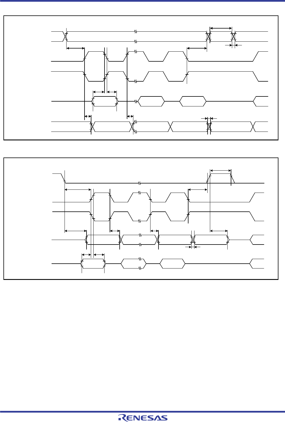
R01UH0034EJ0200 Rev.2.00 Page 1456 of 1489
Dec 27, 2013
RX62T Group, RX62G Group 33. Electrical Characteristics
Under development Preliminary document
Specifications in this document are tentative and subject to change.
Figure 33.13 RSPI Timing (Master, CPHA = 1)
Figure 33.14 RSPI Timing (Slave, CPHA = 0)
SSL0 to SSL3
output
RSPCK
CPOL=0
output
RSPCK
CPOL=1
output
MISO
input
MOSI
output
tDr, tDf
tSU tH
tLEAD
tTD
tLAG
tSSLr, tSSLf
tOH
MSB IN DATA LSB IN MSB IN
MSB OUT DATA LSB OUT IDLE MSB OUT
tOD
SSL0
input
RSPCK
CPOL=0
input
RSPCK
CPOL=1
input
MOSI
input
MISO
output
tDr, tDf
tSU tH
tLEAD
tTD
tLAG
tSA
MSB IN DATA LSB IN MSB IN
MSB OUT DATA LSB OUT MSB IN MSB OUT
tOH tOD tREL
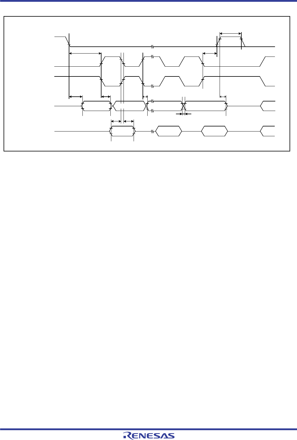
R01UH0034EJ0200 Rev.2.00 Page 1457 of 1489
Dec 27, 2013
RX62T Group, RX62G Group 33. Electrical Characteristics
Under development Preliminary document
Specifications in this document are tentative and subject to change.
Figure 33.15 RSPI Timing (Slave, CPHA = 1)
SSL0
input
RSPCK
CPOL=0
input
RSPCK
CPOL=1
input
MISO
output
MOSI
input
tDr, tDf
tSA tOH
tLEAD
tTD
tLAG
tH
LSB OUT
(Last data) DATA MSB OUT
MSB IN DATA LSB IN MSB IN
LSB OUT
tSU
tOD tREL
MSB OUT
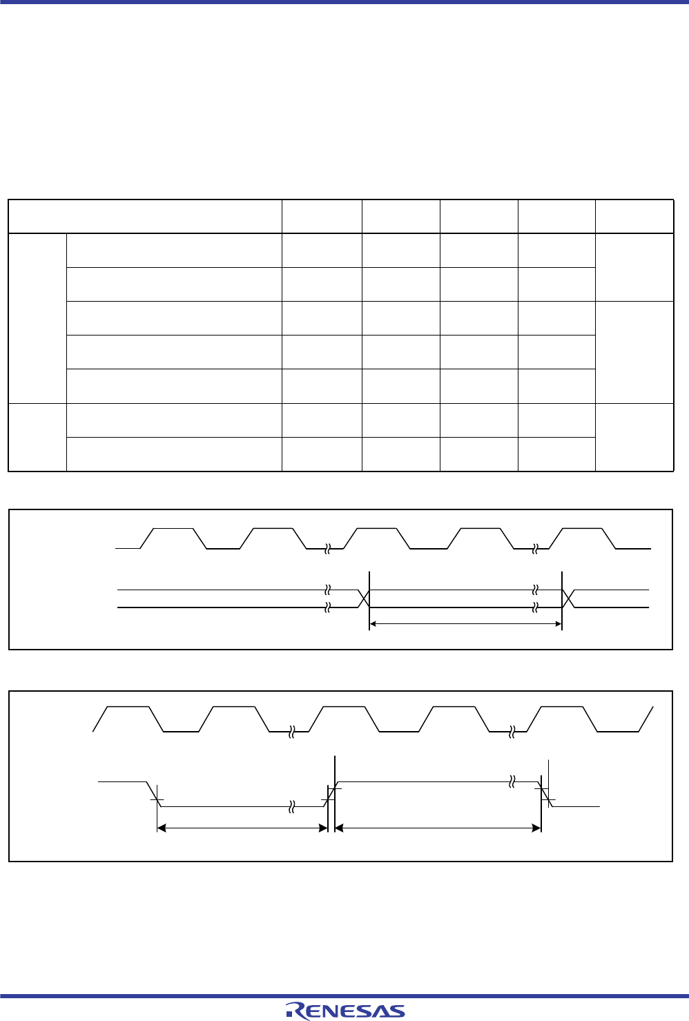
R01UH0034EJ0200 Rev.2.00 Page 1458 of 1489
Dec 27, 2013
RX62T Group, RX62G Group 33. Electrical Characteristics
Under development Preliminary document
Specifications in this document are tentative and subject to change.
Note: • tIcyc: ICLK cycle
Figure 33.16 MTU3 Input/Output Timing
Figure 33.17 MTU3 Clock Input Timing
Table 33.12 Timing of On-Chip Peripheral Modules (4)
Note:Items for which test conditions are not specifically stated in the table below have the same values under conditions 1 to 3.
Condition 1: VCC = PLLVCC = 2.7 to 3.6 V, VSS = PLLVSS = AVSS0 = AVSS = VREFL0 = 0 V
AVCC0 = AVCC = 3.0 to 3.6 V, VREFH0 = 3.0 V to AVCC0, VREF = 3.0 V to AVCC
Condition 2: VCC = PLLVCC = 2.7 to 3.6 V, VSS = PLLVSS = AVSS0 = AVSS = VREFL0 = 0 V
AVCC0 = AVCC = 4.0 to 5.5 V, VREFH0 = 4.0 V to AVCC0, VREF = 4.0 V to AVCC
Condition 3: VCC = PLLVCC = 4.0 to 5.5 V, VSS = PLLVSS = AVSS0 = AVSS = VREFL0 = 0 V
AVCC0 = AVCC = 4.0 to 5.5 V, VREFH0 = 4.0 V to AVCC0, VREF = 4.0 V to AVCC
Ta = Topr. Ta is the same under conditions 1 to 3.
Item Symbol Min. Max. Unit Test
Conditions
MTU3 Input capture input pulse width
(single-edge setting)
tTICW 3.0 - tIcyc Figure 33.16
Input capture input pulse width
(both-edge setting)
tTICW 5.0 - tIcyc
Timer clock pulse width
(single-edge setting)
tTCKWH/L 3.0 - tIcyc Figure 33.17
Timer clock pulse width
(both-edge setting)
tTCKWH/L 5.0 - tIcyc
Timer clock pulse width
(phase coefficient mode)
tTCKWH/L 5.0 - tIcyc
GPT Input capture input pulse width
(single-edge setting)
tGTICW 3.0 - tIcyc Figure 33.18
Input capture input pulse width
(both-edge setting)
tGTICW 5.0 - tIcyc
Input capture
input
ICLK
tTICW
MTCLKA to
MTCLKD
ICLK
tTCKWL tTCKWH
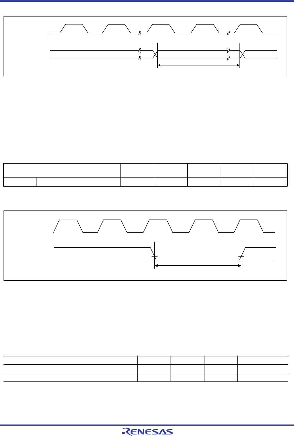
R01UH0034EJ0200 Rev.2.00 Page 1459 of 1489
Dec 27, 2013
RX62T Group, RX62G Group 33. Electrical Characteristics
Under development Preliminary document
Specifications in this document are tentative and subject to change.
Figure 33.18 GPT Input/Output Timing
Note: • tPcyc: PCLK cycle
Figure 33.19 POE3# Clock Timing
33.3.4 Timing of PWM Delay Generation Circuit
Note 1. This value is correct when the difference between each code and the next is a resolution of one bit (1 LSB).
Table 33.13 Timing of On-Chip Peripheral Modules (5)
Note:Items for which test conditions are not specifically stated in the table below have the same values under conditions 1 to 3.
Condition 1: VCC = PLLVCC = 2.7 to 3.6 V, VSS = PLLVSS = AVSS0 = AVSS = VREFL0 = 0 V
AVCC0 = AVCC = 3.0 to 3.6 V, VREFH0 = 3.0 V to AVCC0, VREF = 3.0 V to AVCC
Condition 2: VCC = PLLVCC = 2.7 to 3.6 V, VSS = PLLVSS = AVSS0 = AVSS = VREFL0 = 0 V
AVCC0 = AVCC = 4.0 to 5.5 V, VREFH0 = 4.0 V to AVCC0, VREF = 4.0 V to AVCC
Condition 3: VCC = PLLVCC = 4.0 to 5.5 V, VSS = PLLVSS = AVSS0 = AVSS = VREFL0 = 0 V
AVCC0 = AVCC = 4.0 to 5.5 V, VREFH0 = 4.0 V to AVCC0, VREF = 4.0 V to AVCC
Ta = Topr. Ta is the same under conditions 1 to 3.
Item Symbol Min. Max. Unit Test
Conditions
POE3 POE# input pulse width tPOEW 1.5 - tPcyc Figure 33.19
Table 33.14 Timing of the PWM Delay Generation Circuit
Note: Items for which test conditions are not specifically stated in the table below have the same values under conditions 1 to 3.
Condition 1: VCC = PLLVCC = 4.0 to 5.5 V, VSS = PLLVSS = AVSS = VREL0 = 0 V
AVCC = AVCC = 4.0 to 5.5 V, VREFH0 = 4.0 V to AVCC0, VREF = 4.0 V to AVCC
Ta = Topr.
Item Symbol Typ. Max. Unit Test Conditions
Resolution — 312.5 — ps ICLK = 100 MHz
DNL*1—2.0 — LSB
Input capture
input
ICLK
tGTICW
POEn# input
PCLK
tPOEW

R01UH0034EJ0200 Rev.2.00 Page 1460 of 1489
Dec 27, 2013
RX62T Group, RX62G Group 33. Electrical Characteristics
Under development Preliminary document
Specifications in this document are tentative and subject to change.
33.4 A/D Conversion Characteristics
Note 1. The conversion time includes the sampling time and the comparison time. As the test conditions, the number of sampling states
is indicated.
Table 33.15 10-Bit A/D Conversion Characteristics
Note:Items for which test conditions are not specifically stated in the table below have the same values under conditions 1 to 3.
Condition 1: VCC = PLLVCC = 2.7 to 3.6 V, VSS = PLLVSS = AVSS0 = AVSS = VREFL0 = 0 V
AVCC0 = AVCC = 3.0 to 3.6 V, VREFH0 = 3.0 V to AVCC0, VREF = 3.0 V to AVCC
Ta = Topr
Item Min. Typ. Max. Unit Test Conditions
Resolution 10 10 10 Bit
Conversion time*1
(AD clock = 25-MHz operation)
2.0 - - s Sampling 25 states
Analog input capacitance - - 4 pF
Integral nonlinearity error - - 3.0 LSB
Offset error - - 3.0 LSB
Full-scale error - - 3.0 LSB
Quantization error - 0.5 - LSB
Absolute accuracy - - 4.0 LSB
Permissible signal source impedance - - 1.0 k
Condition 2: VCC = PLLVCC = 2.7 to 3.6 V, VSS = PLLVSS = AVSS0 = AVSS = VREFL0 = 0 V
AVCC0 = AVCC = 4.0 to 5.5 V, VREFH0 = 4.0 V to AVCC0, VREF = 4.0 V to AVCC
Condition 3: VCC = PLLVCC = 4.0 to 5.5 V, VSS = PLLVSS = AVSS0 = AVSS = VREFL0 = 0 V
AVCC0 = AVCC = 4.0 to 5.5 V, VREFH0 = 4.0 V to AVCC0, VREF = 4.0 V to AVCC
Ta = Topr. Ta is the same under conditions 2 and 3.
Item Min. Typ. Max. Unit Test Conditions
Resolution 10 10 10 Bit
Conversion time*1
(AD clock = 50-MHz operation)
1.0 - - s Sampling 25 states
Analog input capacitance - - 4 pF
Integral nonlinearity error - - 3.0 LSB
Offset error - - 3.0 LSB
Full-scale error - - 3.0 LSB
Quantization error - 0.5 - LSB
Absolute accuracy - - 4.0 LSB
Permissible signal source impedance - - 1.0 k
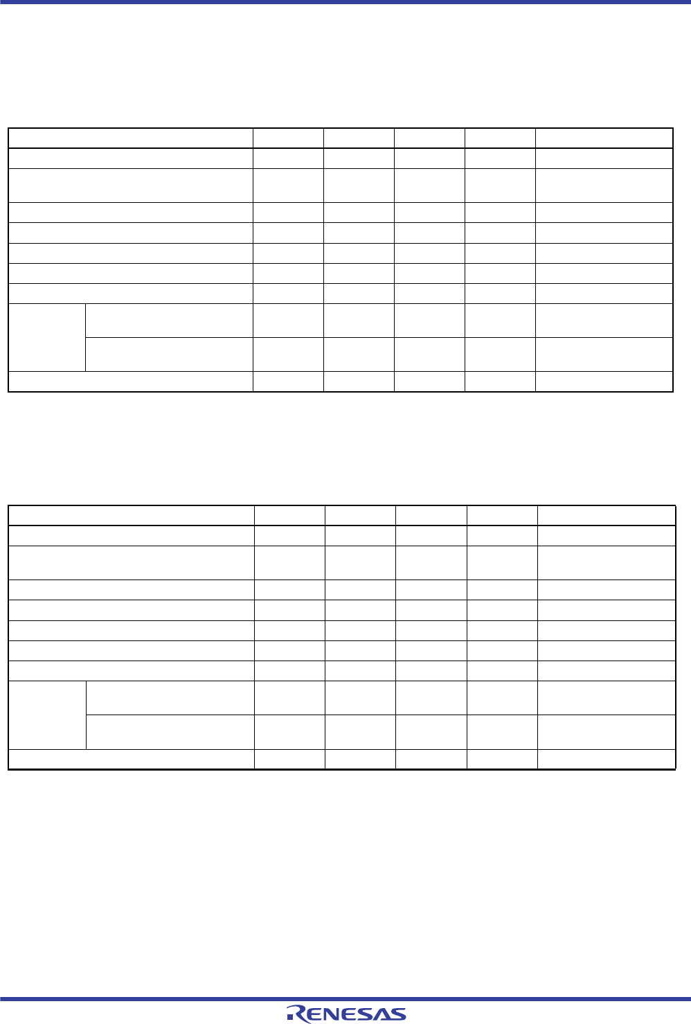
R01UH0034EJ0200 Rev.2.00 Page 1461 of 1489
Dec 27, 2013
RX62T Group, RX62G Group 33. Electrical Characteristics
Under development Preliminary document
Specifications in this document are tentative and subject to change.
Note 1. The conversion time includes the sampling time and the comparison time. As the test conditions, the number of sampling states
is indicated.
Table 33.16 12-Bit A/D Conversion Characteristics
Note:Items for which test conditions are not specifically stated in the table below have the same values under conditions 1 to 3.
Condition 1: VCC = PLLVCC = 2.7 to 3.6 V, VSS = PLLVSS = AVSS0 = AVSS = VREFL0 = 0 V
AVCC0 = AVCC = 3.0 to 3.6 V, VREFH0 = 3.0 V to AVCC0, VREF = 3.0 V to AVCC
Ta = Topr, ICLK = 8 to 100 MHz, PCLK = 8 to 50 MHz
Item Min. Typ. Max. Unit Test Conditions
Resolution 12 12 12 Bit
Conversion time*1
(AD clock = 25-MHz operation)
2.0 - - s Sampling 20 states
Analog input capacitance - - 6 pF
Integral nonlinearity error - - 4.0 LSB
Offset error - - 7.5 LSB
Full-scale error - - 7.5 LSB
Quantization error - 0.5 - LSB
Absolute
accuracy
When a sample-and-hold circuit
is in use
--8.0 LSB AVin = 0.25 to AVREFH -
0.25
When a sample-and-hold circuit
is not in use
--8.0 LSB AVin = AVREFL to AVREFH
Permissible signal source impedance - - 3.0 k
Condition 2: VCC = PLLVCC = 2.7 to 3.6 V, VSS = PLLVSS = AVSS0 = AVSS = VREFL0 = 0 V
AVCC0 = AVCC = 4.0 to 5.5 V, VREFH0 = 4.0 V to AVCC0, VREF = 4.0 V to AVCC
Condition 3: VCC = PLLVCC = 4.0 to 5.5 V, VSS = PLLVSS = AVSS0 = AVSS = VREFL0 = 0 V
AVCC0 = AVCC = 4.0 to 5.5 V, VREFH0 = 4.0 V to AVCC0, VREF = 4.0 V to AVCC
Ta = Topr. Ta is the same under conditions 2 and 3. ICLK = 8 to 100 MHz, PCLK = 8 to 50 MHz.
Item Min. Typ. Max. Unit Test Conditions
Resolution 12 12 12 Bit
Conversion time*1
(AD clock = 25-MHz operation)
1.0 - - s Sampling 20 states
Analog input capacitance - - 6 pF
Integral nonlinearity error - - 4.0 LSB
Offset error - - 7.5 LSB
Full-scale error - - 7.5 LSB
Quantization error - 0.5 - LSB
Absolute
accuracy
When a sample-and-hold circuit
is in use
--8.0 LSB AVin = 0.25 to AVREFH -
0.25
When a sample-and-hold circuit
is not in use
--8.0 LSB AVin = AVREFL to AVREFH
Permissible signal source impedance - - 3.0 k
R01UH0034EJ0200 Rev.2.00 Page 1462 of 1489
Dec 27, 2013
RX62T Group, RX62G Group 33. Electrical Characteristics
Under development Preliminary document
Specifications in this document are tentative and subject to change.
Table 33.17 Characteristics of the Programmable Gain Amplifier
Note:Items for which test conditions are not specifically stated in the table below have the same values under conditions 1 to 3.
Condition 1: VCC = PLLVCC = 2.7 to 3.6 V, VSS = PLLVSS = AVSS0 = AVSS = VREFL0 = 0 V
AVCC0 = AVCC = 3.0 to 3.6 V, VREFH0 = 3.0 V to AVCC0, VREF = 3.0 V to AVCC
Condition 2: VCC = PLLVCC = 2.7 to 3.6 V, VSS = PLLVSS = AVSS0 = AVSS = VREFL0 = 0 V
AVCC0 = AVCC = 4.0 to 5.5 V, VREFH0 = 4.0 V to AVCC0, VREF = 4.0 V to AVCC
Condition 3: VCC = PLLVCC = 4.0 to 5.5 V, VSS = PLLVSS = AVSS0 = AVSS = VREFL0 = 0 V
AVCC0 = AVCC = 4.0 to 5.5V, VREFH0 = 4.0 V to AVCC0, VREF = 4.0 V to AVCC
Ta = Topr. Ta is the same under conditions 1 to 3.
Item Symbol Min. Typ. Max. Unit Test
Conditions
Analog input capacitance Cin - - 6 pF
Input offset voltage Voff - - 8 mV
Input voltage
range (Vin)
Gain 2.000 Vin 0.050 x AVcc - 0.450 x AVcc V
Gain 2.500 0.047 x AVcc - 0.360 x AVcc
Gain 3.077 0.045 x AVcc - 0.292 x AVcc
Gain 3.636 0.042 x AVcc - 0.247 x AVcc
Gain 4.000 0.040 x AVcc - 0.212 x AVcc
Gain 4.444 0.036 x AVcc - 0.191 x AVcc
Gain 5.000 0.033 x AVcc - 0.170 x AVcc
Gain 5.714 0.031 x AVcc - 0.148 x AVcc
Gain 6.667 0.029 x AVcc - 0.127 x AVcc
Gain 10.000 0.025 x AVcc - 0.08 x AVcc
Gain 13.333 0.023 x AVcc - 0.06 x AVcc
Slew rate SR 10 - - V/s
Gain error Gain 2.000 - - - 1 %
Gain 2.500 - - 1
Gain 3.077 - - 1
Gain 3.636 - - 1.5
Gain 4.000 - - 1.5
Gain 4.444 - - 2
Gain 5.000 - - 2
Gain 5.714 - - 2
Gain 6.667 - - 3
Gain 10.000 - - 4
Gain 13.333 - - 4
R01UH0034EJ0200 Rev.2.00 Page 1463 of 1489
Dec 27, 2013
RX62T Group, RX62G Group 33. Electrical Characteristics
Under development Preliminary document
Specifications in this document are tentative and subject to change.
Table 33.18 Comparator Characteristics
Note:Items for which test conditions are not specifically stated in the table below have the same values under conditions 1 to 3.
Condition 1: VCC = PLLVCC = 2.7 to 3.6 V, VSS = PLLVSS = AVSS0 = AVSS = VREFL0 = 0 V
AVCC0 = AVCC = 3.0 to 3.6 V, VREFH0 = 3.0 V to AVCC0, VREF = 3.0 V to AVCC
Condition 2: VCC = PLLVCC = 2.7 to 3.6 V, VSS = PLLVSS = AVSS0 = AVSS = VREFL0 = 0 V
AVCC0 = AVCC = 4.0 to 5.5 V, VREFH0 = 4.0 V to AVCC0, VREF = 4.0 V to AVCC
Condition 3: VCC = PLLVCC = 4.0 to 5.5 V, VSS = PLLVSS = AVSS0 = AVSS = VREFL0 = 0 V
AVCC0 = AVCC = 4.0 to 5.5 V, VREFH0 = 4.0 V to AVCC0, VREF = 4.0 V to AVCC
Ta = Topr. Ta is the same under conditions 1 to 3.
Item Symbol Min. Typ. Max. Unit Test
Conditions
Analog input capacitance Cin - - 6 pF
REFH pin offset voltage Voff - - 5 mV
REFL pin offset voltage - - 5 mV
REFH input voltage range Vin 1.7 - AVcc – 0.3 V
REFL input voltage range 0.3 - AVcc – 1.7 V
REFH reply time tCR - - 1 s
REFL reply time tCF - - 1 s
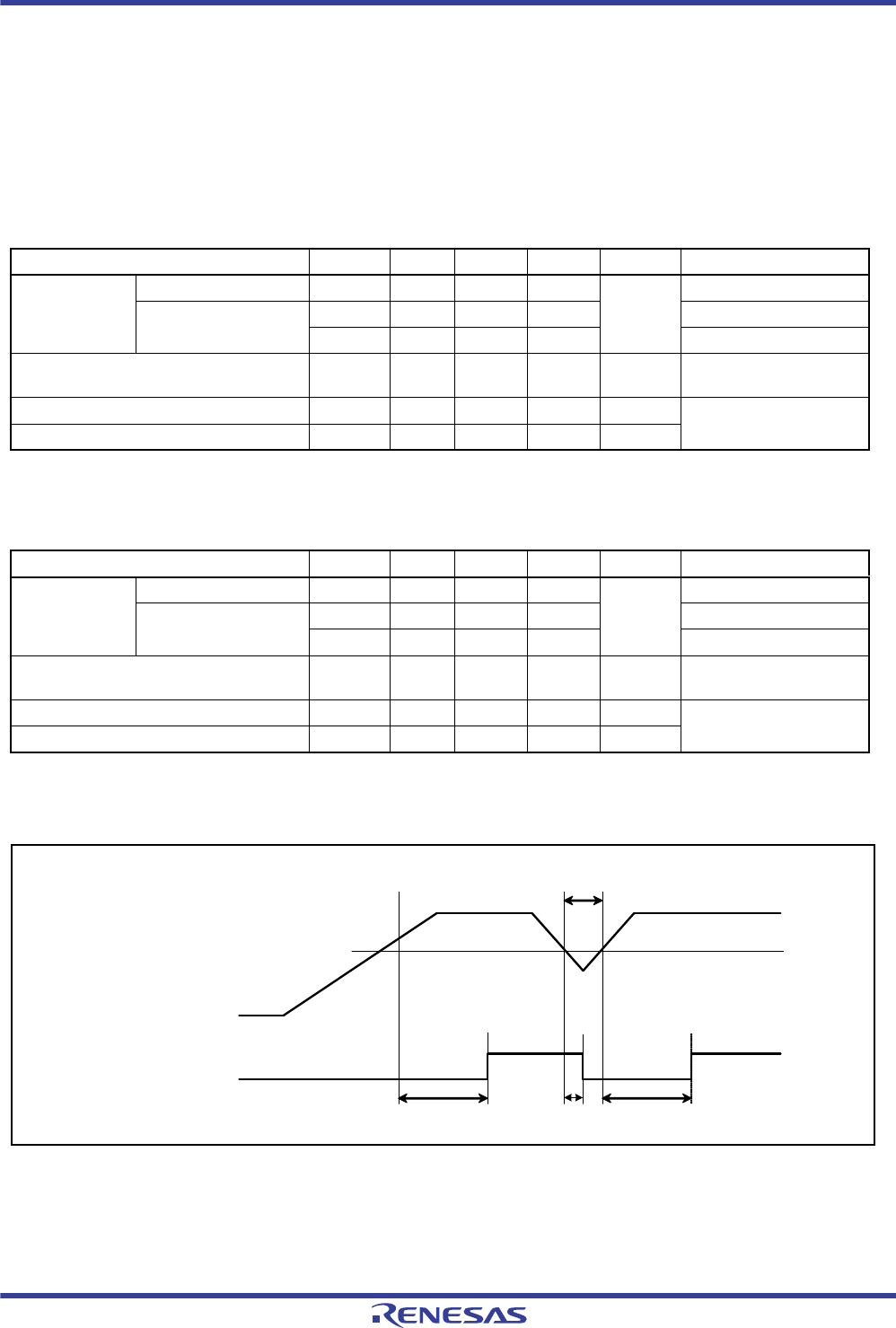
R01UH0034EJ0200 Rev.2.00 Page 1464 of 1489
Dec 27, 2013
RX62T Group, RX62G Group 33. Electrical Characteristics
Under development Preliminary document
Specifications in this document are tentative and subject to change.
33.5 Power-on Reset Circuit, Voltage Detection Circuit Characteristics
Note 1. The power-off time indicates the time when VCC is below the minimum value of voltage detection levels VPOR, Vdet1, and Vdet2
for the POR/ LVD.
Figure 33.20 Power-on Reset Timing
Table 33.19 Power-on Reset Circuit, Voltage Detection Circuit Characteristics
Note:Items for which test conditions are not specifically stated in the table below have the same values under conditions 1 to 3.
Condition 1: VCC = PLLVCC = 2.7 to 3.6 V, VSS = PLLVSS = AVSS0 = AVSS = VREFL0 = 0 V
AVCC0 = AVCC = 3.0 to 3.6 V, VREFH0 = 3.0 V to AVCC0, VREF = 3.0 V to AVCC
Condition 2: VCC = PLLVCC = 2.7 to 3.6 V, VSS = PLLVSS = AVSS0 = AVSS = VREFL0 = 0 V
AVCC0 = AVCC = 4.0 to 5.5 V, VREFH0 = 4.0 V to AVCC0, VREF = 4.0 V to AVCC
Ta = Topr. Ta is the same under conditions 1 and 2.
Item Symbol Min. Typ. Max. Unit Test Conditions
Voltage detection
level
Power-on reset (POR) VPOR 2.48 2.60 2.72 V Figure 33.20
Voltage detection circuit
(LVD)
Vdet1 2.68 2.80 2.92 Figure 33.21
Vdet2 2.98 3.10 3.22 Figure 33.22
Internal reset time tPOR 20 35 50 ms Figure 33.21 and
Figure 33.22
Min. VCC down time*1 tVOFF 200 - - us Figure 33.20 to
Figure 33.22
Reply delay time tdet - - 200 us
Condition 3: VCC = PLLVCC = 4.0 to 5.5 V, VSS = PLLVSS = AVSS0 = AVSS = VREFL0 = 0 V
AVCC0 = AVCC = 4.0 to 5.5 V, VREFH0 = 4.0 V to AVCC0, VREF = 4.0 V to AVCC
Ta = Topr
Item Symbol Min. Typ. Max. Unit Test Conditions
Voltage detection
level
Power-on reset (POR) VPOR 3.70 3.90 4.10 V Figure 33.20
Voltage detection circuit
(LVD)
Vdet1 3.95 4.15 4.35 Figure 33.21
Vdet2 4.40 4.60 4.80 Figure 33.22
Internal reset time tPOR 20 35 50 ms Figure 33.21 and
Figure 33.22
Min. VCC down time*1 tVOFF 200 - - us Figure 33.20 to
Figure 33.22
Reply delay time tdet - - 200 us
Internal reset signal
(low valid)
VCC
tVOFF
VPOR
tPOR
tPOR tdet
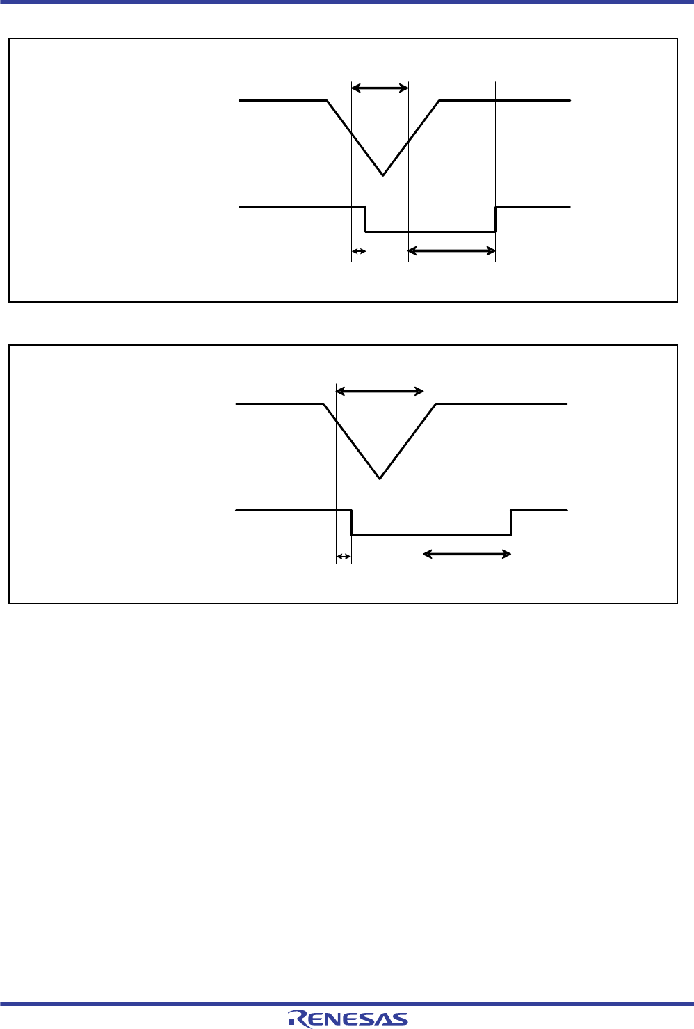
R01UH0034EJ0200 Rev.2.00 Page 1465 of 1489
Dec 27, 2013
RX62T Group, RX62G Group 33. Electrical Characteristics
Under development Preliminary document
Specifications in this document are tentative and subject to change.
Figure 33.21 Voltage Detection Circuit Timing (Vdet1)
Figure 33.22 Voltage Detection Circuit Timing (Vdet2)
VCC Vdet1
tVOFF
tPOR
tdet
Internal reset signal
(low valid)
VCC Vdet2
tVOFF
tPOR
tdet
Internal reset signal
(low valid)

R01UH0034EJ0200 Rev.2.00 Page 1466 of 1489
Dec 27, 2013
RX62T Group, RX62G Group 33. Electrical Characteristics
Under development Preliminary document
Specifications in this document are tentative and subject to change.
33.6 Oscillation Stop Detection Timing
Figure 33.23 Oscillation Stop Detection Timing
Table 33.20 Oscillation Stop Detection Circuit Characteristics
Note:Items for which test conditions are not specifically stated in the table below have the same values under conditions 1 to 3.
Condition 1: VCC = PLLVCC = 2.7 to 3.6 V, VSS = PLLVSS = AVSS0 = AVSS = VREFL0 = 0 V
AVCC0 = AVCC = 3.0 to 3.6 V, VREFH0 = 3.0 V to AVCC0, VREF = 3.0 V to AVCC
Condition 2: VCC = PLLVCC = 2.7 to 3.6 V, VSS = PLLVSS = AVSS0 = AVSS = VREFL0 = 0 V
AVCC0 = AVCC = 4.0 to 5.5 V, VREFH0 = 4.0 V to AVCC0, VREF = 4.0 V to AVCC
Condition 3: VCC = PLLVCC = 4.0 to 5.5 V, VSS = PLLVSS = AVSS0 = AVSS = VREFL0 = 0 V
AVCC0 = AVCC = 4.0 to 5.5 V, VREFH0 = 4.0 V to AVCC0, VREF = 4.0 V to AVCC
Ta = Topr. Ta is the same under conditions 1 to 3.
Item Symbol Min. Typ. Max. Unit Test
Conditions
Detection time tdr - - 1.0 ms Figure 33.23
Internal oscillation frequency when
oscillation stop is detected
fMAIN 0.5 - 7.0 MHz
ICLK
Main clock oscillator
Internal oscillation
Normal operation Abnormal operation
OSTDF*
Note : * This indicates the OSTDF flag in the oscillation detection control register (OSTDCR).
tdr
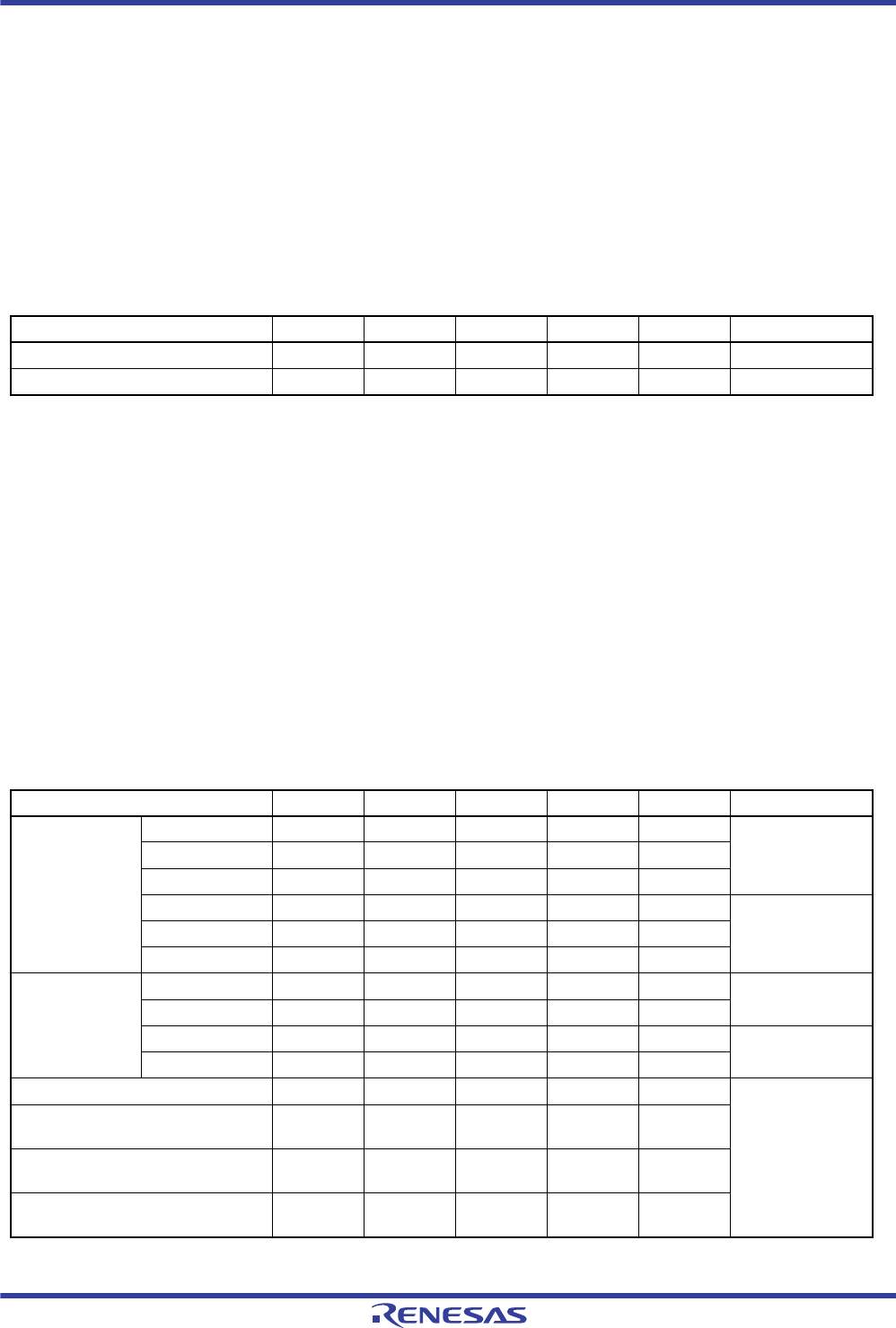
R01UH0034EJ0200 Rev.2.00 Page 1467 of 1489
Dec 27, 2013
RX62T Group, RX62G Group 33. Electrical Characteristics
Under development Preliminary document
Specifications in this document are tentative and subject to change.
33.7 ROM (Flash Memory for Code Storage) Characteristics
Note 1. Definition of rewrite/erase cycle:
The rewrite/erase cycle is the number of erasing for each block. When the rewrite/erase cycle is n times (n = 1000), erasing can
be performed n times for each block. For instance, when 256-byte writing is performed 16 times for different addresses in 4-
Kbyte block and then the entire block is erased, the rewrite/erase cycle is counted as one. However, writing to the same address
for several times as one erasing is not enabled (overwriting is prohibited).
Note 2. The value is obtained from the reliability test.
Table 33.21 ROM (Flash Memory for Code Storage) Characteristics (1)
Note:Items for which test conditions are not specifically stated in the table below have the same values under conditions 1 to 3.
Condition 1: VCC = PLLVCC = 2.7 to 3.6 V, VSS = PLLVSS = AVSS0 = AVSS = VREFL0 = 0 V
AVCC0 = AVCC = 3.0 to 3.6 V, VREFH0 = 3.0 V to AVCC0, VREF = 3.0 V to AVCC
Condition 2: VCC = PLLVCC = 2.7 to 3.6 V, VSS = PLLVSS = AVSS0 = AVSS = VREFL0 = 0 V
AVCC0 = AVCC = 4.0 to 5.5 V, VREFH0 = 4.0 V to AVCC0, VREF = 4.0 V to AVCC
Condition 3: VCC = PLLVCC = 4.0 to 5.5 V, VSS = PLLVSS = AVSS0 = AVSS = VREFL0 = 0 V
AVCC0 = AVCC = 4.0 to 5.5 V, VREFH0 = 4.0 V to AVCC0, VREF = 4.0 V to AVCC
Temperature range for the programming/erasure operation:
Ta = Topr. Ta is the same under conditions 1 to 3.
Item Symbol Min. Typ. Max. Unit Test Conditions
Rewrite/erase cycle*1 NPEC 1000 — — Times
Data hold time tDRP 30*2 — — Year Ta = +85C°
Table 33.22 ROM (Flash Memory for Code Storage) Characteristics (2)
Note:Items for which test conditions are not specifically stated in the table below have the same values under conditions 1 to 3.
Condition 1: VCC = PLLVCC = 2.7 to 3.6 V, VSS = PLLVSS = AVSS0 = AVSS = VREFL0 = 0 V
AVCC0 = AVCC = 3.0 to 3.6 V, VREFH0 = 3.0 V to AVCC0, VREF = 3.0 V to AVCC
Condition 2: VCC = PLLVCC = 2.7 to 3.6 V, VSS = PLLVSS = AVSS0 = AVSS = VREFL0 = 0 V
AVCC0 = AVCC = 4.0 to 5.5 V, VREFH0 = 4.0 V to AVCC0, VREF = 4.0 V to AVCC
Condition 3: VCC = PLLVCC = 4.0 to 5.5 V, VSS = PLLVSS = AVSS0 = AVSS = VREFL0 = 0 V
AVCC0 = AVCC = 4.0 to 5.5 V, VREFH0 = 4.0 V to AVCC0, VREF = 4.0 V to AVCC
Temperature range for the programming/erasure operation:
Ta = Topr. Ta is the same under conditions 1 to 3.
Item Symbol Min. Typ. Max. Unit Test Conditions
Programming time 256 bytes tP256 — 2 12 ms PCLK = 50 MHz
NPEC 100
4 Kbytes tP4K —2350ms
16 Kbytes tP16K — 90 200 ms
256 byte tP256 — 2.4 14.4 ms PCLK = 50 MHz
NPEC > 100
4 Kbytes tP4K — 27.6 60 ms
16 Kbytes tP16K — 108 240 ms
Erasure time 4 Kbytes tE4K —2560msPCLK = 50 MHz
NPEC 100
16 Kbytes tE16K — 100 240 ms
4 Kbytes tE4K —3072msPCLK = 50 MHz
NPEC > 100
16 Kbytes tE16K — 120 288 ms
Suspend delay time during writing tSPD — — 120 s Figure 33.24
PCLK = 50 MHz
First suspend delay time during
erasing (in suspend priority mode)
tSESD1 — — 120 s
Second suspend delay time during
erasing (in suspend priority mode)
tSESD2 ——1.7ms
Suspend delay time during erasing
(in erasure priority mode)
tSEED ——1.7ms
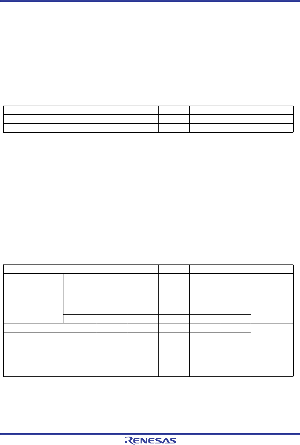
R01UH0034EJ0200 Rev.2.00 Page 1468 of 1489
Dec 27, 2013
RX62T Group, RX62G Group 33. Electrical Characteristics
Under development Preliminary document
Specifications in this document are tentative and subject to change.
33.8 Data Flash (Flash Memory for Data Storage) Characteristics
Note 1. Definition of rewrite/erase cycle:
The rewrite/erase cycle is the number of erasing for each block. When the rewrite/erase cycle is n times (n = 30000), erasing can
be performed n times for each block. For instance, when 128-byte writing is performed 16 times for different addresses in 2-
Kbyte block and then the entire block is erased, the rewrite/erase cycle is counted as one. However, writing to the same address
for several times as one erasing is not enabled (overwriting is prohibited).
Note 2. The value is obtained from the reliability test.
Table 33.23 Data Flash (Flash Memory for Data Storage) Characteristics (1)
Note:Items for which test conditions are not specifically stated in the table below have the same values under conditions 1 to 3.
Condition 1: VCC = PLLVCC = 2.7 to 3.6 V, VSS = PLLVSS = AVSS0 = AVSS = VREFL0 = 0 V
AVCC0 = AVCC = 3.0 to 3.6 V, VREFH0 = 3.0 V to AVCC0, VREF = 3.0 V to AVCC
Condition 2: VCC = PLLVCC = 2.7 to 3.6 V, VSS = PLLVSS = AVSS0 = AVSS = VREFL0 = 0 V
AVCC0 = AVCC = 4.0 to 5.5 V, VREFH0 = 4.0 V to AVCC0, VREF = 4.0 V to AVCC
Condition 3: VCC = PLLVCC = 4.0 to 5.5 V, VSS = PLLVSS = AVSS0 = AVSS = VREFL0 = 0 V
AVCC0 = AVCC = 4.0 to 5.5 V, VREFH0 = 4.0 V to AVCC0, VREF = 4.0 V to AVCC
Temperature range for the programming/erasure operation:
Ta = Topr. Ta is the same under conditions 1 to 3.
Item Symbol Min. Typ. Max. Unit Test Conditions
Rewrite/erase cycle*1 NDPEC 30000 — — Times
Data hold time tDDRP 30*2 — — Year Ta = +85C°
Table 33.24 Data Flash (Flash Memory for Data Storage) Characteristics (2)
Note:Items for which test conditions are not specifically stated in the table below have the same values under conditions 1 to 3.
Condition 1: VCC = PLLVCC = 2.7 to 3.6 V, VSS = PLLVSS = AVSS0 = AVSS = VREFL0 = 0 V
AVCC0 = AVCC = 3.0 to 3.6 V, VREFH0 = 3.0 V to AVCC0, VREF = 3.0 V to AVCC
Condition 2: VCC = PLLVCC = 2.7 to 3.6 V, VSS = PLLVSS = AVSS0 = AVSS = VREFL0 = 0 V
AVCC0 = AVCC = 4.0 to 5.5 V, VREFH0 = 4.0 V to AVCC0, VREF = 4.0 V to AVCC
Condition 3: VCC = PLLVCC = 4.0 to 5.5 V, VSS = PLLVSS = AVSS0 = AVSS = VREFL0 = 0 V
AVCC0 = AVCC = 4.0 to 5.5 V, VREFH0 = 4.0 V to AVCC0, VREF = 4.0 V to AVCC
Temperature range for the programming/erasure operation:
Ta = Topr. Ta is the same under conditions 1 to 3.
Item Symbol Min. Typ. Max. Unit Test Conditions
Programming time 8 bytes tDP8 —0.42 msPCLK =
50 MHz
128 bytes tDP128 —1 5 ms
Erasure time 2 Kbytes tDE2K — 70 250 ms PCLK =
50 MHz
Blank check time 8 bytes tDBC8 ——30sPCLK =
50 MHz
2 Kbytes tDBC2K — — 0.7 ms
Suspend delay time during writing tDSPD — — 120 s Figure 33.24
PCLK =
50 MHz
First suspend delay time during erasing
(in suspend priority mode)
tDSESD1 — — 120 s
Second suspend delay time during
erasing (in suspend priority mode)
tDSESD2 — — 1.7 ms
Suspend delay time during erasing
(in erasure priority mode)
tDSEED — — 1.7 ms
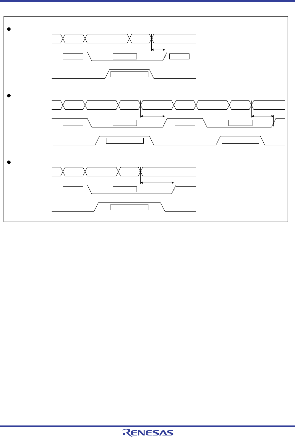
R01UH0034EJ0200 Rev.2.00 Page 1469 of 1489
Dec 27, 2013
RX62T Group, RX62G Group 33. Electrical Characteristics
Under development Preliminary document
Specifications in this document are tentative and subject to change.
Figure 33.24 Flash Memory Write/Erase Suspend Timing
FCU command
FSTATR0.FRDY
Write pulse
Write suspend
FCU command
FSTATR0.FRDY
Erasure pulse
Erasure suspend in suspend priority mode
FCU command
FSTATR0.FRDY
Erasure pulse
Erasure suspend in erasure priority mode
Program Suspend
Ready Not Ready Ready
Programming
tSPD
Erase Suspend
Ready Not Ready Ready
tSEED
Erasing
Erase Suspend Resume Suspend
Ready Not Ready Ready Not Ready
tSESD1 tSESD2
Erasing Erasing

R01UH0034EJ0200 Rev.2.00 Page 1470 of 1489
Dec 27, 2013
RX62T Group, RX62G Group Appendix 1. Port States in Each Processing Mode
Appendix 1.Port States in Each Processing Mode
Note: • The configuration of the I/O ports differs with the package. For the I/O ports for the respective packages, see section 14, I/O
Ports.
H: High-level
L: Low-level
Keep-O: Output pins retain their previous values, and input pins become high-impedance.
*1. Input to pins in use as IRQ pins and set up as triggers for release from software standby mode is possible.
*2. Input to pins in use as IRQ pins and set up as triggers for release from deep software standby mode is
possible.
Keep: Pin states are retained during periods on software standby.
Hi-Z: High-impedance
IOKEEP = 1*: I/O pins retain their states until the IOKEEP bit in DPSBYCR is cleared to 0.
Table 1.1 Port States in Each Processing State
Port Name
Pin Name Reset Software Standby Mode
Deep Software Standby
Mode
IOKEEP = 1/0
After Deep Software Standby Mode is Canceled
(Return of Start-up Mode)
IOKEEP = 1*IOKEEP = 0
Port 1 Hi-Z Keep-O *1 Keep-O *2Keep Hi-Z
P20, P21 Hi-Z Keep-O *1 Keep Keep Hi-Z
P22 to P24 Hi-Z Keep-O Keep Keep Hi-Z
Port 3 Hi-Z Keep-O Keep Keep Hi-Z
Port 4 Hi-Z Keep-O Keep Keep Hi-Z
Port 5 Hi-Z Keep-O Keep Keep Hi-Z
Port 6 Hi-Z Keep-O Keep Keep Hi-Z
P70 Hi-Z Keep-O *1 Keep Keep Hi-Z
P71 to P76 Hi-Z Hi-Z Keep Keep Hi-Z
Port 8 Hi-Z Keep-O Keep Keep Hi-Z
P90 to P95 Hi-Z Hi-Z Keep Keep Hi-Z
P96 Hi-Z Keep-O *1 Keep Keep Hi-Z
Port A Hi-Z Keep-O Keep Keep Hi-Z
PB0 to PB3 Hi-Z Keep-O Keep Keep Hi-Z
PB4 Hi-Z Keep-O *1 Keep Keep Hi-Z
PB5 to PB7 Hi-Z Keep-O Keep Keep Hi-Z
Port D Hi-Z Keep-O Keep Keep Hi-Z
PE0, PE1 Hi-Z Keep-O Keep Keep Hi-Z
PE2 Hi-Z [When NMI is specified
as a canceling source]
NMI
[Other than the above]
Keep-O
[When NMI is specified
as a canceling source]
NMI
[Other than the above]
Keep
[When NMI is specified
as a canceling source]
NMI
[Other than the above]
Keep
[When NMI is specified
as a canceling source
NMI
[Other than the above]
Hi-Z
PE3 to PE5 Hi-Z Keep-O *1 Keep Keep Hi-Z
PG0 to PG2 Hi-Z Keep-O *1 Keep Keep Hi-Z
PG3 to PG5 Hi-Z Keep-O Keep Keep Hi-Z
WDTOVF# WDTOVF
output
HH H
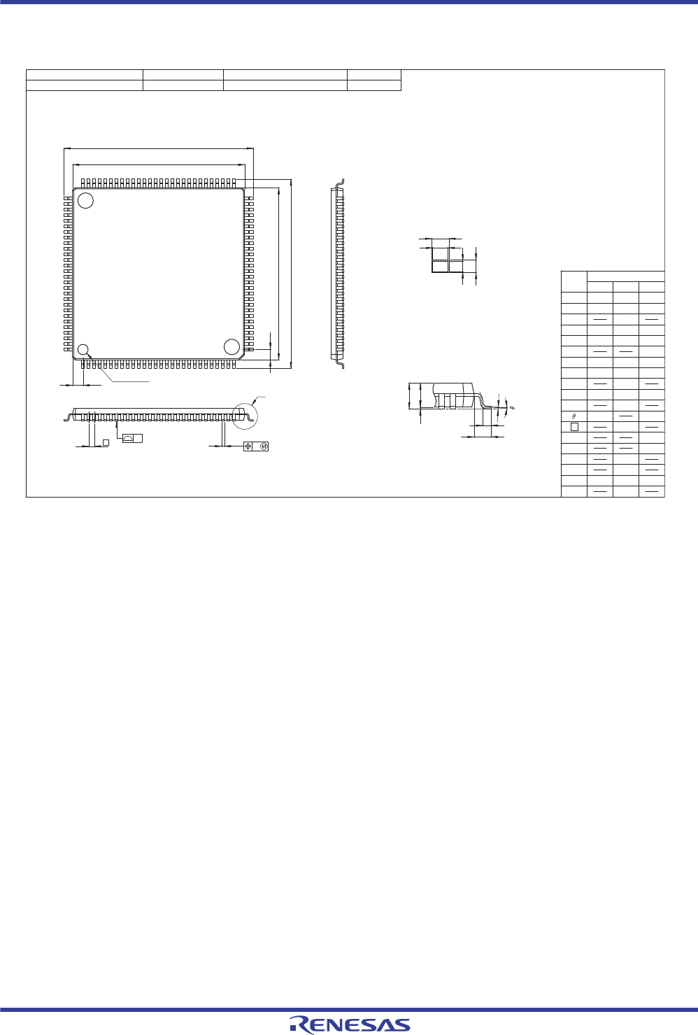
R01UH0034EJ0200 Rev.2.00 Page 1471 of 1489
Dec 27, 2013
RX62T Group, RX62G Group Appendix 2. Package Dimensions
Appendix 2.Package Dimensions
Figure A 112-Pin LQFP (PLQP0112JA-A) Package Dimensions
x
*2
*1
*3
F
112
85
84 57
56
29
281
Index mark
y
E
Z
D
Z
E
H
D
D
H
E
b
p
Detail F
L
c
L
1
A
2
A
A
1
INCLUDE TRIM OFFSET.
DIMENSION "*3" DOES NOT
NOTE)
DO NOT INCLUDE MOLD FLASH.
DIMENSIONS "*1" AND "*2"1.
2.
L1
ZE
ZD
c1
b1
bp
A1
HE
HD
y0.10
e0.65
c
0° 8°
x
L0.35 0.5 0.65
0.05 0.1 0.15
A1.7
21.8 22.0 22.2
21.8 22.0 22.2
A21.4
E19.9 20.0 20.1
D19.9 20.0 20.1
Reference
Symbol
Dimension in Millimeters
Min Nom Max
0.27 0.32 0.37
0.09 0.145 0.20
0.13
1.225
1.225
0.30
0.125
1.0
P-LQFP112-20x20-0.65 1.2g
MASS[Typ.]
FP-112E / FP-112EVPLQP0112JA-A
RENESAS CodeJEITA Package Code Previous Code
Terminal cross section
c
b
p
c
1
b
1
e
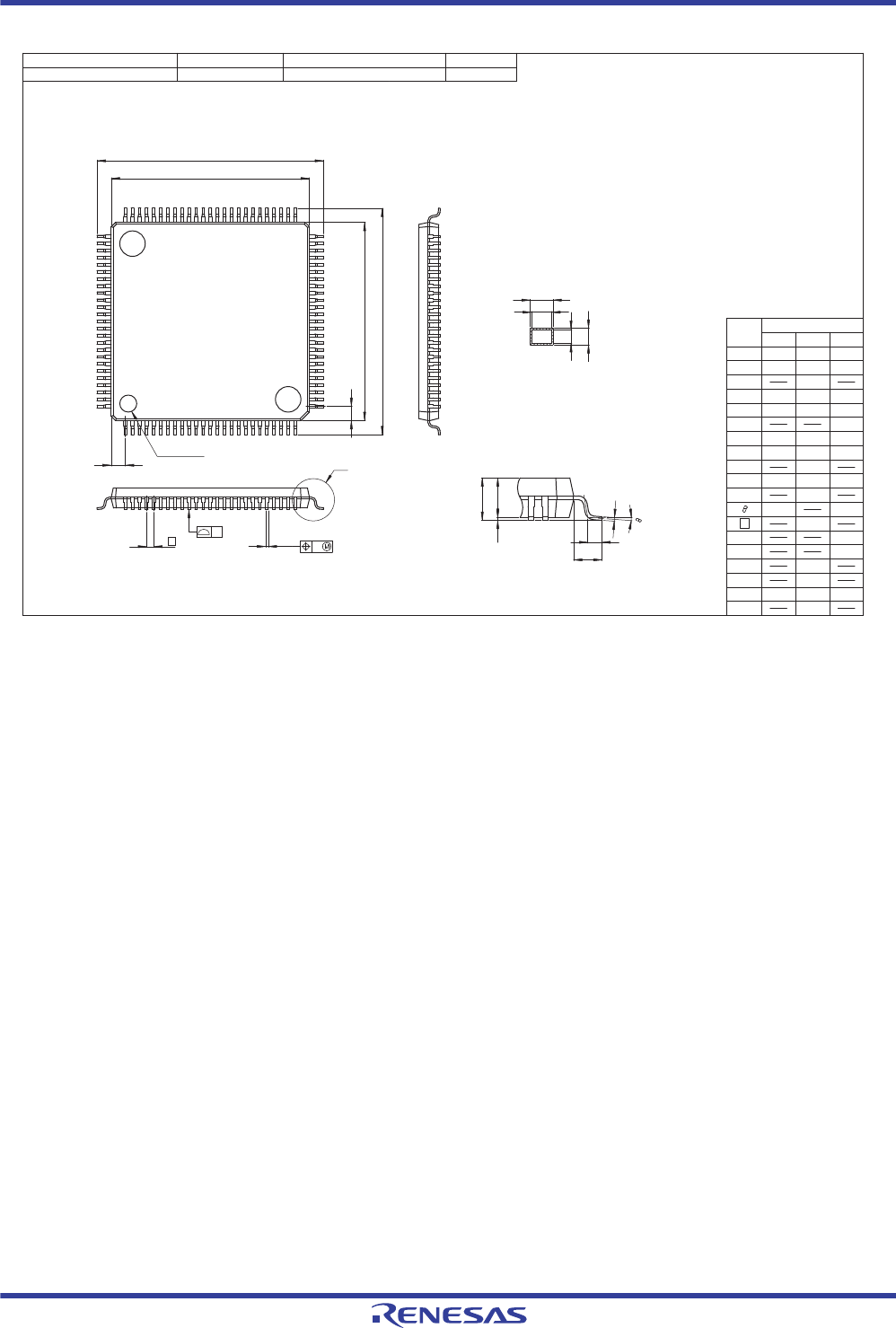
R01UH0034EJ0200 Rev.2.00 Page 1472 of 1489
Dec 27, 2013
RX62T Group, RX62G Group Appendix 2. Package Dimensions
Figure B 100-Pin LQFP (PLQP0100KB-A) Package Dimensions
Terminal cross section
b
1
c
1
b
p
c
2.
1. DIMENSIONS "*1" AND "*2"
DO NOT INCLUDE MOLD FLASH.
NOTE)
DIMENSION "*3" DOES NOT
INCLUDE TRIM OFFSET.
y
Index mark
x
125
26
50
51
75
76
100
F
*1
*3
*2
Z
E
Z
D
E
D
H
D
H
E
b
p
Detail F
L
1
A
2
A
1
L
A
c
L1
ZE
ZD
c1
b1
bp
A1
HE
HD
y0.08
e0.5
c
0° 8°
x
L0.35 0.5 0.65
0.05 0.1 0.15
A1.7
15.8 16.0 16.2
15.8 16.0 16.2
A21.4
E13.9 14.0 14.1
D13.9 14.0 14.1
Reference
Symbol
Dimension in Millimeters
Min Nom Max
0.15 0.20 0.25
0.09 0.145 0.20
0.08
1.0
1.0
0.18
0.125
1.0
Previous CodeJEITA Package Code RENESAS Code
PLQP0100KB-A 100P6Q-A / FP-100U / FP-100UV
MASS[Typ.]
0.6gP-LQFP100-14x14-0.50
e
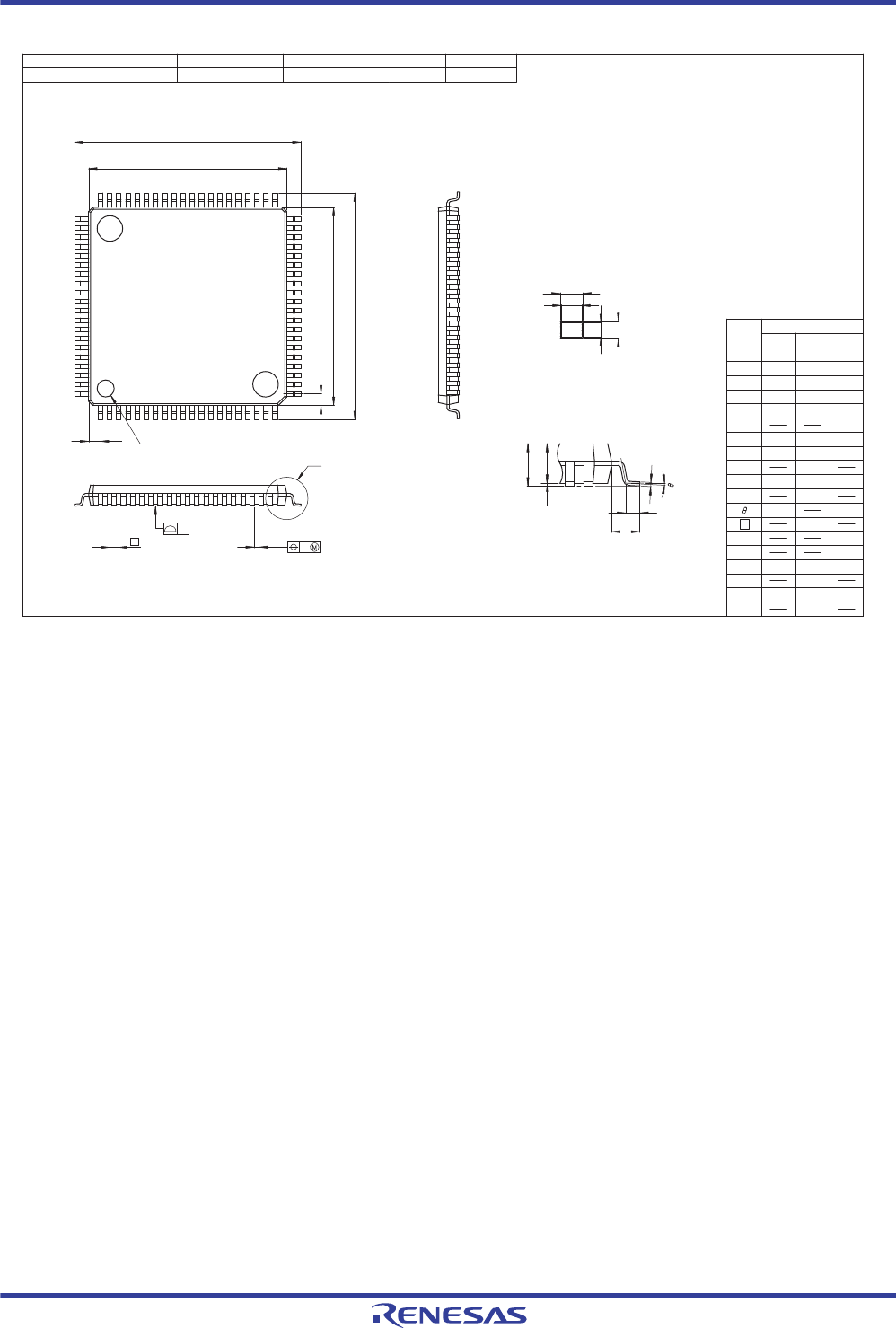
R01UH0034EJ0200 Rev.2.00 Page 1473 of 1489
Dec 27, 2013
RX62T Group, RX62G Group Appendix 2. Package Dimensions
Figure C 80-Pin LQFP (PLQP0080JA-A) Package Dimensions
y
*2
*1
*3
F
80
61
60 41
40
21
201
x
Index mark
E
D
H
D
H
E
Z
D
Z
E
b
p
Detail F
L
c
A
2
L
1
A
A
1
INCLUDE TRIM OFFSET.
DIMENSION "*3" DOES NOT
NOTE)
DO NOT INCLUDE MOLD FLASH.
DIMENSIONS "*1" AND "*2"1.
2.
Previous CodeJEITA Package Code RENESAS Code
PLQP0080JA-A FP-80W / FP-80WV
MASS[Typ.]
0.6gP-LQFP80-14x14-0.65
1.0
0.125
0.30
0.825
0.825
0.13
0.20
0.145
0.09
0.370.320.27
MaxNomMin
Dimension in Millimeters
Symbol
Reference
14.114.013.9
D
14.114.013.9
E
1.4
A2
16.216.015.8 16.216.015.8
1.7
A
0.15
0.1
0.05
0.65
0.5
0.35
L
x
8°0°
c
0.65
e
0.10
y
HD
HE
A1
bp
b1
c1
ZD
ZE
L1
Terminal cross section
c
bp
c1
b1
e
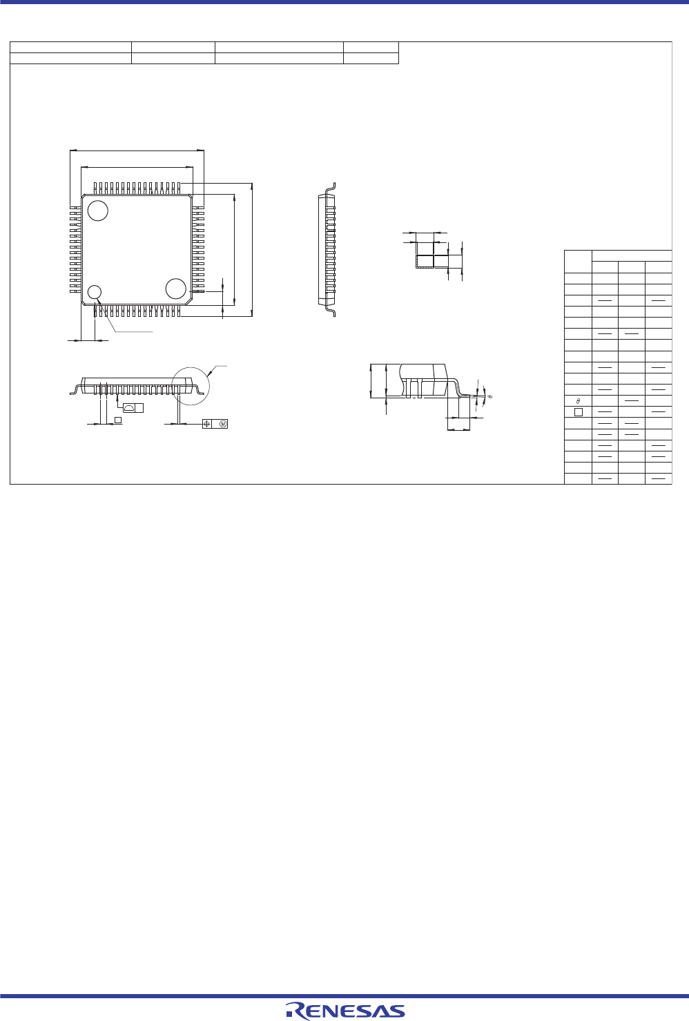
R01UH0034EJ0200 Rev.2.00 Page 1474 of 1489
Dec 27, 2013
RX62T Group, RX62G Group Appendix 2. Package Dimensions
Figure D 64-Pin LQFP (PLQP0064KB-A) Package Dimensions
Terminal cross section
b
1
c
1
b
p
c
2.
1. DIMENSIONS "*1" AND "*2"
DO NOT INCLUDE MOLD FLASH.
NOTE)
DIMENSION "*3" DOES NOT
INCLUDE TRIM OFFSET.
Index mark
*3
17
32
64
49
116
3348
F
*1
*2
x
y
b
p
H
E
E
H
D
D
Z
D
Z
E
Detail F
A
c
A
2
A
1
L
1
L
P-LQFP64-10x10-0.50 0.3g
MASS[Typ.]
64P6Q-A / FP-64K / FP-64KVPLQP0064KB-A
RENESAS CodeJEITA Package Code Previous Code
1.0
0.125
0.18
1.25
1.25
0.08
0.20
0.145
0.09
0.250.200.15
MaxNomMin
Dimension in Millimeters
Symbol
Reference
10.110.0
9.9
D
10.110.0
9.9
E
1.4
A
2
12.212.011.8 12.212.011.8
1.7
A
0.15
0.1
0.05
0.65
0.5
0.35
L
x
8°0°
c
0.5
e
0.08
y
H
D
H
E
A
1
b
p
b
1
c
1
Z
D
Z
E
L
1
e
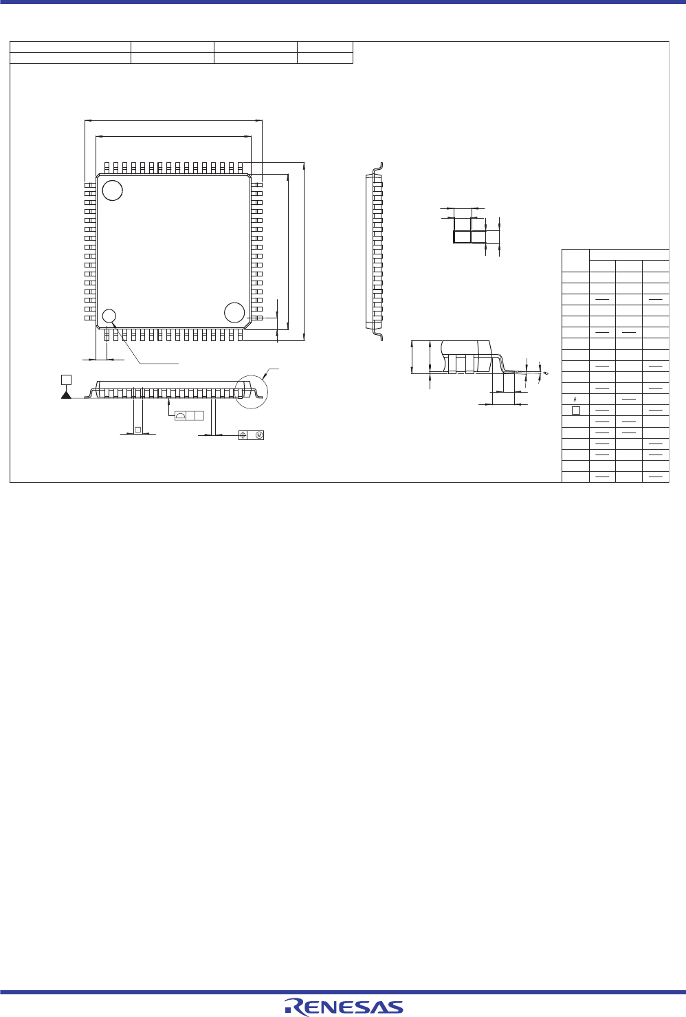
R01UH0034EJ0200 Rev.2.00 Page 1475 of 1489
Dec 27, 2013
RX62T Group, RX62G Group Appendix 2. Package Dimensions
Figure E 64-Pin LQFP (PLQP0064GA-A) Package Dimensions
Terminal cross section
b1
c1
bp
c
2.
1. DIMENSIONS "*1" AND "*2"
DO NOT INCLUDE MOLD FLASH.
NOTE)
DIMENSION "*3" DOES NOT
INCLUDE TRIM OFFSET.
*3
116
17
32
33
48
49
64
F
*1
*2
x
Index mark
D
H
D
E
H
E
eb
p
Z
D
Z
E
Detail F
c
A
A
2
A
1
L
L
1
Previous CodeJEITA Package Code RENESAS Code
PLQP0064GA-A 64P6U-A/ ⎯
MASS[Typ.]
0.7gP-LQFP64-14x14-0.80
1.0
0.125
0.35
1.0
1.0
0.20
0.20
0.145
0.09
0.420.370.32
MaxNomMin
Dimension in Millimeters
Symbol
Reference
14.114.013.9
D
14.114.013.9
E
1.4
A2
16.216.015.8 16.216.015.8 1.7
A
0.20.1
0
0.70.50.3
L
x
8°0°
c
0.8
e
0.10
y
HD
HE
A1
bp
b1
c1
ZD
ZE
L1
yS
S

R01UH0034EJ0200 Rev.2.00 Page 1476 of 1489
Dec 27, 2013
RX62T Group, RX62G Group REVISION HISTORY
REVISION HISTORY RX62T Group, RX62G Group User’s Manual: Hardware
Rev. Date Description
Page Summary
0.50 Oct 05, 2010 — First edition issued
1.00 Oct 22, 2010 1. Overview
35 to 41 Table 1.1 Outline of Specifications: Description changed and deleted
5. I/O Registers
113 to 145 Table 5.1 List of I/O Registers (Address Order): Description changed and added
13. Data Transfer Controller (DTC)
301 13.2.1 DTC Mode Register A (MRA): Description changed
310 Figure 13.3 Allocation of Transfer Data in the RAM Area, changed
14. I/O Ports
427 14.5.4 Reading Port Registers (PORT), added
15. Multi-Function Timer Pulse Unit 3 (MTU3)
433 Figure 15.1 Block Diagram of MTU3 (Channels 0 to 4), changed
461 Table 15.21 TIORH (MTU3_6) to table 15.27 TIOR (MTU3_1), changed
26. LIN Module (LIN)
1227 Figure 26.13 LIN Error Detection Target Areas, changed
27. 12-Bit A/D Converter (S12ADA)
1232 Table 27.1 Specifications of A/D Converter: Description changed
1242 27.2.2 A/D Control Register (ADCSR): Description added
1265 27.2.13 A/D Sampling State Register (ADSSTR): Description changed
1273 27.3.3 Analog Input Sampling and A/D Conversion Time: Description changed
1274 Table 27.9 A/D Conversion Time, changed
1279 27.3.8 Starting A/D Conversion with External Trigger: Description changed
28. 10-Bit A/D Converter (ADA)
1285 Table 28.1 Specifications of A/D Converter: Description changed
1294 28.2.3 A/D Control Register (ADCR): Description changed
1299 28.2.7 A/D Sampling State Register (ADSSTR): Description changed
30. ROM (Flash Memory for Code Storage)
1321, 1322 30.2.2 Flash Access Status Register (FASTAT): Description changed
1345 Table 30.7 FCU Command Formats: Description changed
32. Electrical Characteristics
1438 to 1465 All the description added
1.10 Apr 20, 2011 All Register symbol description, changed
All Name of the on-chip oscillator clock, changed
All One Page Summary, added
1. Overview
42 Table 1.3 List of Products: Operating voltage, changed
5. I/O Registers
105 Opening description, (1) I/O register addresses (address order): Description changed
108 to 131 Table 5.1 List of I/O Registers (Address Order): Register symbol, changed
132 to 162 Table 5.2 List of I/O Registers (Bit Order), changed
REVISION HISTORY

R01UH0034EJ0200 Rev.2.00 Page 1477 of 1489
Dec 27, 2013
RX62T Group, RX62G Group REVISION HISTORY
1.10 Apr 20, 2011 8. Clock Generation Circuit
180 Table 8.1 Specifications of Clock Generation Circuit, changed
186 8.9.3 On-Chip Oscillator Clock (IWDTCLK): Description changed
9. Low Power Consumption
192 Figure 9.1 Mode Transitions: Note 7, changed
213 9.5.4.1 Transition to Deep Software Standby Mode: Note changed
11. Interrupt Controller (ICU)
246 11.2.8 Non-Maskable Interrupt Status Register (NMISR): Description changed
250 Table 11.4 Interrupt Vector Table, changed
257 11.4.1.1 Operation of Status Flags for Edge-Detected Interrupts: Description changed
257 Figure 11.2 Operation of the IRi.IR Flag in the Case of Edge Detection, changed
259 Figure 11.5 Operation of the IRi.IR Flag in the Case of a Level-Detected Interrupt, changed
12. Buses
270 12.2.6 Restrictions on RMPA and String-Manipulation Instructions, added
13. Data Transfer Controller (DTC)
297 13.4.6 Chain Transfer: Description changed
14. I/O Ports
All Port register symbol, changed
325 14.1.2.11 Port Function Register G (PFGSPI): Bit name, changed
328 14.1.2.15 Port Function Register M (PFMPOE): Bit name, changed
351 14.2.2.10 Port Function Register G (PFGSPI): Bit name, changed
354 14.2.2.14 Port Function Register M (PFMPOE): Bit name, changed
376 14.3.2.9 Port Function Register G (PFGSPI): Bit name, changed
379 14.3.2.13 Port Function Register M (PFMPOE): Bit name, changed
397 14.4.2.7 Port Function Register G (PFGSPI): Bit name, changed
400 14.4.2.11 Port Function Register M (PFMPOE): Bit name, changed
15. Multi-Function Timer Pulse Unit 3 (MTU3)
All Register symbol description of MTU3, changed
418 to 421 15.2.8 Timer Buffer Operation Transfer Mode Register (TBTM): Bit description, changed
481 15.2.28 Timer Waveform Control Registers (TWCRA and TWCRB): Bit description, changed
518 Figure 15.26 Example of PWM Mode Setting Procedure, changed
572 Figure 15.83 Example of Procedure for Specifying A/D Converter Start Request Delaying
Function: Figure title, changed
16. Port Output Enable 3 (POE3)
All Register symbol description of MTU3, changed
17. General PWM Timer (GPT)
688 17.2.2 General PWM Timer Hardware Source Clear Control Register (GTHSCR): Bit name,
changed
689 17.2.3 General PWM Timer Hardware Source Clear Control Register (GTHCCR): Descrip-
tion added
690 7.2.4 General PWM Timer Hardware Start Source Select Register (GTHSSR): Description
added
707 17.2.18 General PWM Timer Control Register (GTCR): Address changed and description
added
19. Watchdog Timer (WDT)
831 19.5.1 (1) Writing to TCNT Counter, TCSR Register, and RSTCSR Register, changed
832 19.5.2 (1) Reading from TCNT Counter, TCSR Register, and RSTCSR Register, changed
Rev. Date Description
Page Summary

R01UH0034EJ0200 Rev.2.00 Page 1478 of 1489
Dec 27, 2013
RX62T Group, RX62G Group REVISION HISTORY
1.10 Apr 20, 2011 20. Independent Watchdog Timer (IWDT)
All The symbol of the on-chip oscillator clock is changed from OCOCLK to IWDTCLK.
21. Serial Communications Interface (SCIb)
All The register symbol in smart card interface is changed to "SMCI".
All The section configuration is separated according to the mode.
843 Table 21.1 Specifications of SCI: Note added
845 Table 21.2 Pin Configuration of SCI/SMCI: Title and contents, changed
867 Figure 21.5 Sample SCI Initialization Flowchart (Asynchronous Mode), changed
868 Figure 21.6 Example of Operation for Serial Transmission in Asynchronous Mode (Example
with 8-Bit Data, Parity, One Stop Bit), changed
870 Figure 21.8 Example of SCI Operation for Serial Reception in Asynchronous Mode
(Example with 8-Bit Data, Parity, One Stop Bit), changed
875 Figure 21.13 Example of SCI Reception (8-Bit Data/Multi-Processor Bit/One Stop Bit),
changed
879 Figure 21.17 Example of SCI Initialization Flowchart (Clock Synchronous Mode): Note added
880 Figure 21.18 Example of Operation for Serial Transmission in Clock Synchronous Mode,
changed
881 Figure 21.19 Example of Serial Transmission Flowchart (Clock Synchronous Mode): Note
added
882 Figure 21.20 Example of Operation for Serial Reception in Clock Synchronous Mode,
changed
886 21.3 Smart Card Interface Mode, Separated and added
901 Figure 21.28 Data Retransfer Operation in SMCI Transmission Mode, changed
904 Figure 21.31 Data Retransfer Operation in SMCI Reception Mode, changed
907 21.4 Noise Cancellation: Description changed
23. I2C Bus Interface (RIIC)
924 Figure 23.2 Connections to the External Circuit by the I/O Pins (I2C Bus Configuration Exam-
ple), changed
951 23.2.11 Slave Address Register Ly (SARLy): Bit name, changed
952 23.2.12 Slave Address Register Uy (SARUy): Bit name, changed
954 23.2.14 I2C Bus Bit Rate High-Level Register (ICBRH): Description on the duty ratio,
changed
963 23.3.4 Master Receiver Operation, changed
965 Figure23.10 Example of Master Reception Flowchart (7-Bit Address Format), changed
967 Figure23.13 Master Receive Operation Timing (3) (when RDRFS=0), changed
996 23.11.2 Extra SCL Clock Cycle Output Function: Description changed
1002 23.15.2 Setting Input Buffer Control Register: Description changed
24. CAN Module (CAN)
All Register symbol description of CAN registers, changed
1006 Table 24.3 Registers of CAN Module, changed
1013 24.2.3 Mask Register I (MKRi): Bit name, changed
1017 Table 24.5 Mailbox Memory Mapping, changed
1027 24.2.9 Receive FIFO Control Register (RFCR): Bit name, changed
1051 24.2.24 (2) Self-Test Mode 0 (External Loopback): Description changed
1063 24.7 Reception and Transmission: Description changed
25. Serial Peripheral Interface (RSPI)
1079 25.2.5 RSPI Data Register (SPDR): Bit name, changed
1080 25.2.6 RSPI Sequence Control Register (SPSCR): Description changed
Rev. Date Description
Page Summary

R01UH0034EJ0200 Rev.2.00 Page 1479 of 1489
Dec 27, 2013
RX62T Group, RX62G Group REVISION HISTORY
1.10 Apr 20, 2011 1116 Table 25.9 Relationship between Non-Normal Transfer Operations and RSPI Error Detection
Function, changed
1136 Figure 25.36 Example of Initialization Flowchart in Slave Mode (Clock Synchronous Opera-
tion), changed
26. LIN Module (LIN)
All Register symbol description of LIN registers, changed
1165 26.3.2 LIN Operation Mode: Description changed
27. 12-Bit A/D Converter (S12ADA)
All Register symbol description of S12ADA registers, changed
1188 Table 27.3 Input Pins of A/D Converter: Note changed
1203 27.2.5 A/D Start Trigger Select Register (ADSTRGR): Bit description, changed
1216 27.2.12 Comparator Interrupt Select Register (ADCMPSEL): Symbol of b9, changed
1232 27.5.1 Module Stop Function Setting to 27.5.9 Point for Caution Regarding Countermea-
sures for Noise: Description order, changed
1233 27.5.5 Permissible Impedance of Signal Sources: Description changed
1233 Table 27.10 Specifications of Analog Pins, changed
1233 27.5.6 Realizing High-Speed Conversion, deleted
1234 27.5.8 Point for Caution Regarding Board Design: Description added
28. 10-Bit A/D Converter (ADA)
1238 Table 28.3 Input Pin for A/D Converter: Symbol changed
1239 Table 28.4 Registers of A/D Converter: Symbol changed
28.2.2 A/D Control/Status Register (ADCSR): Description
1261 28.6.10 Realizing High-Speed Conversion, deleted
30. ROM (Flash Memory for Code Storage)
1278 Table 30.4 States of FCMDR after Receiving Each Command, changed
1312 Table 30.9 Error Protection Types (Types Dedicated to ROM and Types Common to ROM
and Data Flash), changed
1339 30.12 (4) Reset during Programming or Erasure: Description added
31. Data Flash Memory (Flash Memory for Data Storage)
1352 31.2.9 Data Flash Blank Check Control Register (DFLBCCNT): Bit table, changed
1362 Table 31.5 FCU Commands for Use with Data Flash Memory, changed
32. Electrical Characteristics
1375 Table 32.3 DC Characteristics (2): Note 3, changed
1381 Table 32.7 Control Signal Timing, changed
1383 Table 32.9 Timing of On-Chip Peripheral Modules (2), changed
1389 Figure 32.17 MTU3 Clock Input Timing, changed
1391 Table 32.13 10-Bit A/D Conversion Characteristics, changed
1392 Table 32.14 12-Bit A/D Conversion Characteristics, changed
1.20 Oct 04, 2011 8. Clock Generation Circuit
184 8.3.1 Connecting a Crystal Resonator, changed
184 Figure 8.3 Equivalent Circuit of Crystal Resonator, changed
9. Low Power Consumption
219 9.6.6 Conflict between Transition to Deep Software Standby Mode and Interrupt, changed
11. Interrupt Controller (ICU)
229 Table 11.1 Specifications of the Interrupt Controller, changed
230 Figure 11.1 Block Diagram of Interrupt Controller, signal name changed
245 11.2.7 IRQ Control Register n (IRQCRn), description changed
Rev. Date Description
Page Summary

R01UH0034EJ0200 Rev.2.00 Page 1480 of 1489
Dec 27, 2013
RX62T Group, RX62G Group REVISION HISTORY
1.20 Oct 04, 2011 246 11.2.8 Non-Maskable Interrupt Status Register (NMISR), description changed
247 11.2.9 Non-Maskable Interrupt Enable Register (NMIER), description changed
263 11.5 Non-Maskable Interrupt Operation, description changed
13. Data Transfer Controller (DTC)
301 Table 13.10 Execution Cycle of the DTC, changed, note7 added
14. I/O Ports
331 to 335 Table 14.6 Output Enable Settings for Each Port (112-pin LQFP), RSPI in PB0 setting
changed
356 to 360 Table 14.13 Output Enable Settings for Each Port (100-Pin LQFP), RSPI in PB0 setting
changed
375 14.3.2.8 Port Function Register D (PFDGPT), changed
381 to 384 Table 14.20 Output Enable Settings for Each Port (80-pin LQFP), RSPI in PB0 setting
changed
396 14.4.2.6 Port Function Register D (PFDGPT), changed
402 to 405 Table 14.27 Output Enable Settings for Each Port (64-pin LQFP), RSPI in PB0 setting
changed
407, 408 14.5 I/O Port Configuration, added
15. Multi-Function Timer Pulse Unit 3 (MTU3)
465, 466 15.2.14 Timer Synchronous Register (TSYR), symbols of TSYRA and TSYRB changed
617 15.6.20 Output Level in Complementary PWM Mode and Reset-Synchronized PWM Mode,
description added
617 15.6.21 Simultaneous Input Capture in MTU1.TCNT and MTU2.TCNT in Cascade Connec-
tion, description added
17. General PWM Timer (GPT)
685 to 688 Table 17.4 Registers of GPT, value after reset and initial value for GTSOS changed
731 Figure 17.5 Example for Setting Periodic Count Operation (in Down-Count Operation),
changed
781 Figure17.60 Example for Setting Simultaneous Start by Hardware Source, changed
784 Figure 17.63 Example of Synchronized PWM Output, changed
785 Figure17.64 Example of Three-Phase Saw-Wave Complementary PWM Output, changed
786 Figure17.65 Example of Three-Phase Saw-Wave Complementary PWM Output with Auto-
matic Dead Time Setting, changed
787 Figure17.66 Example of Three-Phase Triangle-Wave Complementary PWM Output,
changed
788 Figure17.67 Example of Three-Phase Triangle-Wave Complementary PWM Output with
Automatic Dead Time Setting, changed
789 Figure17.68 Example of Three-Phase Asymmetric Triangle-Wave Complementary PWM
Output with Automatic Dead Time Setting, changed
793 17.4.1 Interrupt Sources and Priorities, (5) Points for Caution when Interrupt Sources Are in
Use at the Same Time, added
795 Figure 17.71 Example of Interrupt Skipping Function Operation (Triangle Waves, Counting
and Skipping Both Troughs and Crests, Skipping Count: 4), changed
796 Figure 17.73 Example of Interrupt Skipping Function Operation (Triangle Waves, Counting
and Skipping Both Troughs and Crests, Skipping Count: 3, Skipping Started at Down-Count-
ing), changed
21. Serial Communications Interface (SCIb)
852 21.2.1.6 Serial Control Register (SCR), CKE[1:0] bit description changed
869 Figure 21.5 Sample SCI Initialization Flowchart (Asynchronous Mode), note added
881 Figure 21.17 Example of SCI Initialization Flowchart (Clock Synchronous Mode), note added
Rev. Date Description
Page Summary

R01UH0034EJ0200 Rev.2.00 Page 1481 of 1489
Dec 27, 2013
RX62T Group, RX62G Group REVISION HISTORY
1.20 Oct 04, 2011 23. I2C Bus Interface (RIIC)
936, 937 23.2.4 I2C Bus Mode Register 2 (ICMR2), note added, bit description changed
968 Figure 23.11 Master Receive Operation Timing (1) (7-Bit Address Format, when RDRFS =
0), changed
968 Figure 23.12 Master Receive Operation Timing (2) (10-Bit Address Format, when RDRFS =
0)
969 Figure 23.13 Master Receive Operation Timing (3) (when RDRFS = 0), changed
980 Figure 23.25 AASy Flag Set/Clear Timing with 7-Bit/10-Bit Address Formats Mixed, changed
24. CAN Module
1068 Table 24.12 CAN Interrupts, changed
25. Serial Peripheral Interface (RSPI)
1070 Figure 25.1 Block Diagram of RSPI, changed
1100 Figure 25.7 Single-Master/Multi-Slave Configuration Example (This LSI = Slave), changed
1108 Figure 25.15 MSB First Transfer (1) (24-Bit Data, Parity Function Disabled), changed
27. 12-Bit A/D Converter (S12ADA)
1201 27.2.4 A/D Control Extended Register (ADCER), bit description added
1229 27.3.6 Programmable Gain Amplifier, description added
1234 27.5.7 Ranges of Settings for Analog Power Supply and Other Pins, changed
28. 10-Bit A/D Converter (ADA)
1261 28.6.7 Ranges of Settings for Analog Power Supply and Other Pins, changed
30. ROM (Flash Memory for Code Storage)
1326 30.9.5 (10) New Bit Rate Selection, Bit rate selection error, calculation formula changed
1339 30.12 (4) Reset during Programming or Erasure, changed
32. Electrical Characteristics
1371 Table 32.1 Absolute Maximum Ratings, note changed
1382 Table 32.8 Timing of On-Chip Peripheral Modules (1), input clock cycle changed
1.30 Mar 07. 2012 — Features, Package lineup, added
1. Overview
37
Table
1.1 Outline of Specifications (1/5) Description of
CPU, added
41
Table
1.1 Outline of Specifications (5/5), 64-pin packaged, added
42
Table
1.2 Functions of RX62T Group Products, 64-pin package, added
43 to 44
Table
1.3 List of Products, 64-pin package part number, changed
44
Figure
1.1 How to Read the Product Part No., 64-pin package part number, changed
45 Figure1.2 Block Diagram, changed
49
Figure
1.6 Pin Assignment of the 64-Pin LQFP,
Figure PLQP0064GA-A, added
2. CPU
65 2.1 Features, description, added
84 2.6.1 Fixed Vector Table, text, added
84
Figure
2.8 Fixed Vector Table, changed
5.
I/O
Register
109 to 110
Table
5.1 List of I/O Registers (Address Order), MPU, added
118 Table 5.1 List of I/O Registers (Address Order) TMOCNTL, TMOCNTU register, added
128 Table 5.1 List of I/O Registers (Address Order), GTSWP register, added
134 to 136
Table
5.2 List of I/O Registers (Bit Order), MPU, added
145
Table
5.2 List of I/O Registers (Bit Order), TMOCNTL, TMOCNTU register, added
158
Table
5.2 List of I/O Registers (Bit Order), GTSWP register, added
Rev. Date Description
Page Summary

R01UH0034EJ0200 Rev.2.00 Page 1482 of 1489
Dec 27, 2013
RX62T Group, RX62G Group REVISION HISTORY
1.30 Mar 07. 2012 9. Low Power Consumption
205 9.2.7 Deep Standby Interrupt Enable Register (DPSIER), description, changed
211 9.5.1.1 Transition to Sleep Mode, description, changed
10. Exceptions
223
Figure
10.1 Types of Exception, changed
224 10.1.3 Access Exception, added
227
Table
10.1 Timing of Acceptance and Saved PC Value, Access exception, a line added
227
Table
10.2 Vector and Site for Saving the Values in the PC and PSW, a line added
229 10.5.3 Access Exception, added
231
Table
10.3 Return from Exception Processing Routines, a line added
231
Table
10.4 Order of Priority for Exceptions, Table title, changed
231
Table
10.4 Order of Priority for Exceptions, a line added
278 to 299 13. Memory Protection Unit (MPU), added
15. I/O Ports
432 Figure 15.1 I/O Port Configuration (1), changed
433 Figure 15.2 I/O Port Configuration (2), changed
16. Multi-Function Timer Pulse Unit 3 (MTU3)
436 to 671 Channel changed to MTU throughout this section
492
16.2.15
Timer Counter Synchronous Start Register (TCSYSTR), note1, changed
495
16.2.17
Timer Output Master Enable Register (TOER), description, added
497 16.2.18 Timer Output Control Registers 1 (TOCR1A and TOCR1B), note, changed
499 16.2.19 Timer Output Control Registers 2 (TOCR2A and TOCR2B), note, changed
508 16.2.28 Timer Waveform Control Registers (TWCRA and TWCRB), note, added
510 to 512 16.2.29 Timer A/D Converter Start Request Control Register (TADCR), note, added
538 16.3.4 Cascaded Operation, description, added
541
Figure
16.24 Cascaded Operation Example (c), note, added
544 16.3.5 PWM Modes (b) PWM Mode 2, text, changed
561 Figure 16.39 Example of Complementary PWM Mode Setting Procedure, changed
573 16.3.8 Complementary PWM Mode
(j)
Method for Generating PWM Output in Complemen-
tary PWM Mode, text, changed
575 16.3.8 Complementary PWM Mode
(k) 0% and 100% duty ratio Output in Complementary
PWM Mode
, text, changed
625
Figure
16.118
TGI Interrupt Timing (Compare Match) (MTU 5), note, added
17 Port Output Enable 3 (POE3),
672 to 704 Power-on reset changed to reset in notes and text
18. General PWM Timer (GPT)
710
Table
18.4 Registers of GPT (1 / 4)
, GTSWP register, added
725 18.2.10 General PWM timer start write protection register (GTSWP), added
736 18.2.19 General PWM Timer Control Register (GTCR), bit, description, changed
22. Serial Communications Interface (SCIb)
872
Table
22.1 Specifications of SCI, note, deleted
23. CRC Calculator (CRC)
946 23.2.3 CRC Data Output Register (CRCDOR), description, changed
24.I2C Bus Interface (RIIC)
986 24.2.18 Timeout internal counter (TMOCNT), added
988 Figure 24.5 Example of RIIC Initialization Flow, changed
Rev. Date Description
Page Summary

R01UH0034EJ0200 Rev.2.00 Page 1483 of 1489
Dec 27, 2013
RX62T Group, RX62G Group REVISION HISTORY
1.30 Mar 07. 2012 990 Figure 24.6 Example of Master Transmission Flowchart, changed
995 Figure 24.10 Example of Master Reception Flowchart (7-Bit Address Format), changed
999 Figure 24.14 Example of Slave Transmission Flowchart, changed
1002 Figure 24.17 Example of Slave Reception Flowchart, changed
27. LIN Module (LIN)
1184 27.2.12 Transmission Control Register (L0TC), RTS bit description, changed
31. ROM (Flash Memory for Code Storage)
— All in this section, mat → area, changed
1291 Table 31.1 Specifications of the ROM, On-board programming (two types), changed
1367 31.12 (2) Suspending Programming or Erasure, changed
1367 31.12 (4) Reset during Programming or Erasure, changed
1367 31.12 (5) Prohibition of Non-maskable Interrupts during Programming or Erasure, changed
1366 31.12 (7) Abnormal Termination of Programming and Erasure, changed
1368
31.12 (8)
Actions Prohibited during Programming and Erasure, changed
32. Data Flash Memory (Flash Memory for Data Storage)
— All in this section, mat → area, changed
1369 Table 32.1 Specifications of Data Flash Memory, On-board programming (two types),
changed
1399 32.9 (2) Other Points to Note, changed
33. Electrical Characteristics
1410
Table
33.7 Control Signal Timing, notes 1 and 3, changed
1411
Table
33.8 Timing of On-Chip Peripheral Modules (1), minimum values of input/output clock
cycles, changed
Appendix 2.Package Dimensions
1435
Figure
E
64-Pin
LQFP (PLQP0064GA-A), added
2.00 Dec 27. 2013 35 Features, changed
1. Overview
37 to 41 Table 1.1 Outline of Specifications, changed; Note 1, added
42, 43 Table 1.2 Functions of RX62T Group and RX62G Group Products, changed
44, 45 Table 1.3 List of Products, changed; Note 1, added
46 Figure 1.1 How to Read the Product Part No., changed
59 to 61 Figure 1.6 Pin Assignment of the 80-Pin LQFP (Two-Motor Control Supported Version),
added
62 to 64 Table 1.7 List of Pins and Pin Functions (80-Pin LQFP: R5F562TxGDFF), added
2. CPU
82 2.4 Data Types, changed
—2.4.1 Integer to 2.4.4 Strings, deleted
—Figure 2.2 Integer, Figure 2.3 Floating-Point, Figure 2.4 Bit, Figure 2.5 String, deleted
5. I/O Registers
113 to 137 Table 5.1 List of I/O Registers (Address Order), changed
138 to 167 Table 5.2 List of I/O Registers (Bit Order), changed
8. Clock Generation Circuit
185 Table 8.1 Specifications of Clock Generation Circuit, changed
188 8.2.2 Oscillation Stop Detection Control Register (OSTDCR), OSTDF flag (Oscillation Stop
Detection Flag), changed
189 8.3 Main Clock Oscillator, changed
189 8.3.1 Connecting a Crystal Resonator, changed
Rev. Date Description
Page Summary

R01UH0034EJ0200 Rev.2.00 Page 1484 of 1489
Dec 27, 2013
RX62T Group, RX62G Group REVISION HISTORY
2.00 Dec 27. 2013 9. Low Power Consumption
196
Table
9.2 Transition and Cancellation of the Mode and the State of Operation, changed
213 9.5.1.1 Transition to Sleep Mode, changed
214 9.5.2.1 Transition to All-Module Clock Stop Mode, changed; Note 4, added
11. Interrupt Controller (ICU)
267 11.4.5 Multiple Interrupts, added
267 11.4.6 Fast Interrupt, changed
272 11.7.2 Note on Using the MUT3 Interrupt, added
272 Figure 11.8 State of the Status Flag in the TSR Register, added
273 Figure 11.9 Flowchart for Software to Avoid Problems, added
15. I/O Ports
391 15.3 I/O Port [for 80-Pin LQFP], changed
415 to 438 15.4 I/O Port [for 80-Pin LQFP (R5F562TxGDFF)], added
439 15.5 I/O Port [for 64-Pin LQFP], changed
460 Figure 15.1 I/O Port Configuration (1), changed
461 Figure 15.2 I/O Port Configuration (2), changed
16. Multi-Function Timer Pulse Unit 3 (MTU3)
469 Figure 16.2 Block Diagram of MTU (MTU5 to MTU7), changed
502 16.2.15 Timer Counter Synchronous Start Register (TCSYSTR), changed
596 16.3.8 Complementary PWM Mode, (2) Outline of Complementary PWM Mode Operation,
(g) PWM Cycle Setting, changed
654 Figure 16.119 TGI Interrupt Timing (Input Capture) (MTU0 to MTU4, MTU6, and MTU7),
changed
658 16.6.2 Input Clock Restrictions, changed
658 Figure 16.124 Phase Difference, Overlap, and Pulse Width in Phase Counting Mode,
changed
662 16.6.9 Contention between TGR Read Operation and Input Capture, changed
662 Figure 16.130 Contention between TGR Read Operation and Input Capture (MTU0 to
MTU7), title changed
663 Figure 16.131 Contention between TGR Read Operation and Input Capture (MTU5), deleted
671 16.6.23 Notes when Complementary PWM Mode Output Protection Function is not Used,
added
672 16.6.24 Points for Caution to Prevent Malfunctions in Synchronous Clearing for Complemen-
tary PWM Mode, added
672 Figure 16.140 Example of Synchronous Clearing (when Condition 1 Applies), added
673 Figure 16.141 Example of Synchronous Clearing (when Condition 2 Applies), added
673 16.6.25 Continuous Output of Interrupt Signal in Response to a Compare Match, added
673 Figure 16.142 Continuous Output of Interrupt Signal in Response to a Compare Match,
added
18. General PWM Timer (GPT/GPTa?
735 Table 18.1 Specifications of GPT, changed
751 18.2.6 General PWM Timer Write-Protection Register (GTWP), changed
753 18.2.8 General PWM Timer External Trigger Input Interrupt Register (GTETINT): Note 1,
changed
756 18.2.11 LOCO Count Control Register (LCCR), description of the LPSC[1:0] bits (Frequency-
Divided LOCO Clock Select), changed
758 18.2.12 LOCO Count Status Register (LCST): Note 1, changed
Rev. Date Description
Page Summary

R01UH0034EJ0200 Rev.2.00 Page 1485 of 1489
Dec 27, 2013
RX62T Group, RX62G Group REVISION HISTORY
2.00 Dec 27. 2013 771 to 772 18.2.22 General PWM Timer Interrupt and A/D Converter Start Request Skipping Setting
Register (GTITC), changed
773 18.2.23 General PWM Timer Status Register (GTST): Note 1, changed
777 18.2.26 General PWM Timer Cycle Setting Register (GTPR), description changed
795 Figure 18.7 Example for Setting Low Output and High Output Operation, changed
797 Figure 18.10 Example for Setting Toggled Output Operation, changed
805 Figure 18.20 Example for Setting GTCCRA and GTCCRB Buffer Operation (for Output Com-
pare), changed
812 Figure 18.29 Example for Setting Saw-Wave PWM Mode, changed
815 Figure 18.31 Example for Setting Saw-Wave One-Shot Pulse Mode, changed
817 Figure 18.33 Example for Setting Triangle-Wave PWM Mode 1, changed
819 Figure 18.35 Example for Setting Triangle-Wave PWM Mode 2, changed
822 Figure 18.37 Example for Setting Triangle-Wave PWM Mode 3, changed
824 Figure 18.39 Example of Automatic Compare-Match Value Setting Function with Dead Time
(Triangle-Wave PWM Mode 1, GTDVU and GTDVD Set to Buffer Operation, Active Level:
High), changed
824 Figure 18.40 Example of Automatic Compare-Match Value Setting Function with Dead Time
(Triangle-Wave PWM Mode 2 or 3, GTDVU and GTDVD Set to Buffer Operation, Active
Level: High), changed
825 Figure 18.41 Example for Setting Automatic Dead Time Setting Function (Saw-Wave One-
Shot Pulse Mode, Triangle-Wave PWM Mode 3), changed
875 Figure 18.93 Example of Output Protection Function Operation When GTCCRA ≥ GTPR is
Set during Buffer Transfer at Crests (Restored to 0<GTCCRA<GTPR during Buffer Transfer
at Troughs, Active Level: Low), changed
878 18.9.2 Settings of GTCCRn during Compare Match Operation (n = A, B, C, D, E, F), (3)
When automatic dead time setting has been made in saw-wave one-shot pulse mode,
changed
880 18.9.5 Notes on Delay Time Settings for PWM Delay Generation Circuit, added
880 Figure 18.96 Restriction on the Timing of GTDLYFA Register Settings, added
22. Serial Communications Interface (SCIb)
911 Table 22.1 Specifications of SCI, changed
920 22.2.1.7 Serial Status Register (SSR), TEND flag (Transmit End Flag), changed
930 22.2.1.10 Serial Extended Mode Register (SEMR), changed
931 22.2.2 Operation in Asynchronous Mode, changed
936 Figure 22.6 Example of Operation for Serial Transmission in Asynchronous Mode (Example
with 8-Bit Data, Parity, One Stop Bit), changed
24. I2C Bus Interface (RIIC)
994 24.2.1 I2C Bus Control Register 1 (ICCR1), changed
1025 24.2.18 Timeout internal counter (TMOCNT), changed
1027 Figure 24.5 Example of RIIC Initialization Flow, changed
1029 Figure 24.6 Example of Master Transmission Flowchart, changed
1034 Figure 24.10 Example of Master Reception Flowchart (7-bit Address Format, 1 or 2 Bytes),
added
1035 Figure 24.11 Example of Master Reception Flowchart (7-bit Address Format, 3 Bytes or
More), changed
1037 Figure 24.14 Master Receive Operation Timing (3) (when RDRFS=0), changed
1039 Figure 24.15 Example of Slave Transmission Flowchart, changed
1042 Figure 24.18 Example of Slave Reception Flowchart, changed
1061 Figure 24.37 Start Condition/Restart Condition Issue Timing (ST and RS Bits), changed
1063 24.11.1 Timeout Function, changed
Rev. Date Description
Page Summary

R01UH0034EJ0200 Rev.2.00 Page 1486 of 1489
Dec 27, 2013
RX62T Group, RX62G Group REVISION HISTORY
2.00 Dec 27. 2013 25. CAN Module
1113 25.2.19 Error Interrupt Factor Judge Register (EIFR), BLIF flag (Bus Lock Detect Flag),
changed
1121 Figure 25.9 Transition between CAN Operating Modes, changed
1123 Table 25.9 Operation in CAN Reset Mode and CAN Halt Mode, changed
28. 12-Bit A/D Converter (S12ADA)
1234 28.2.11 Comparator Detection Flag Register (ADCMPFR), changed
1299 28.4.1 Interrupt Request on Completion of Each A/D Conversion, changed
1303 28.5.10 Usage Note when Double Data Registers are Used in 2-Channel Scan Mode, added
31. ROM (Flash Memory for Code Storage)
1343 31.2.8 Flash P/E Mode Entry Register (FENTRYR), changed
1360 Figure 31.7 Procedure for Transition to ROM Read Mode, changed
1393 to 1395 31.9.5 Inquiry/Selection Host Command Wait State, (10) New Bit Rate Selection, changed;
(11) Programming/Erasure State Transition, changed
32. Data Flash Memory (Flash Memory for Data Storage)
1409 Table 32.1 Specifications of Data Flash Memory, changed
33. Electrical Characteristics
— Conditions in the table, change to Ta = Topr from Ta = -40 to +105°C.
1440 Table 33.1 Absolute Maximum Ratings, changed
1444 Table 33.3 DC Characteristics (2): Note 3, changed
1445 Table 33.5 Permissible Power Consumption, added
1459 33.3.4 Timing of PWM Delay Generation Circuit, added
1459 Table 33.14 Timing of the PWM Delay Generation Circuit, added
1462 Table 33.17 Characteristics of the Programmable Gain Amplifier, changed
1467 Table 33.21 ROM (Flash Memory for Code Storage) Characteristics (1), changed
1467
Table
33.22 ROM (Flash Memory for Code Storage) Characteristics (2), added
1468
Table
33.23 Data Flash (Flash Memory for Data Storage) Characteristics (1), changed
1468
Table
33.24 Data Flash (Flash Memory for Data Storage) Characteristics (2), added
Rev. Date Description
Page Summary

RX62T Group User’s Manual: Hardware
Publication Date: Rev.0.50 Oct 05, 2010
Rev.2.00 Dec 27, 2013
Published by: Renesas Electronics Corporation
Colophon

http://www.renesas.com
Refer to "http://www.renesas.com/" for the latest and detailed information.
Renesas Electronics America Inc.
2880 Scott Boulevard Santa Clara, CA 95050-2554, U.S.A.
Tel: +1-408-588-6000, Fax: +1-408-588-6130
Renesas Electronics Canada Limited
1101 Nicholson Road, Newmarket, Ontario L3Y 9C3, Canada
Tel: +1-905-898-5441, Fax: +1-905-898-3220
Renesas Electronics Europe Limited
Dukes Meadow, Millboard Road, Bourne End, Buckinghamshire, SL8 5FH, U.K
Tel: +44-1628-651-700, Fax: +44-1628-651-804
Renesas Electronics Europe GmbH
Arcadiastrasse 10, 40472 Düsseldorf, Germany
Tel: +49-211-65030, Fax: +49-211-6503-1327
Renesas Electronics (China) Co., Ltd.
7th Floor, Quantum Plaza, No.27 ZhiChunLu Haidian District, Beijing 100083, P.R.China
Tel: +86-10-8235-1155, Fax: +86-10-8235-7679
Renesas Electronics (Shanghai) Co., Ltd.
Unit 301, Tower A, Central Towers, 555 LanGao Rd., Putuo District, Shanghai, China
Tel: +86-21-2226-0888, Fax: +86-21-2226-0999
Renesas Electronics Hong Kong Limited
Unit 1601-1613, 16/F., Tower 2, Grand Century Place, 193 Prince Edward Road West, Mongkok, Kowloon, Hong Kong
Tel: +852-2886-9318, Fax: +852 2886-9022/9044
Renesas Electronics Taiwan Co., Ltd.
13F, No. 363, Fu Shing North Road, Taipei, Taiwan
Tel: +886-2-8175-9600, Fax: +886 2-8175-9670
Renesas Electronics Singapore Pte. Ltd.
80 Bendemeer Road, Unit #06-02 Hyflux Innovation Centre Singapore 339949
Tel: +65-6213-0200, Fax: +65-6213-0300
Renesas Electronics Malaysia Sdn.Bhd.
Unit 906, Block B, Menara Amcorp, Amcorp Trade Centre, No. 18, Jln Persiaran Barat, 46050 Petaling Jaya, Selangor Darul Ehsan, Malaysia
Tel: +60-3-7955-9390, Fax: +60-3-7955-9510
Renesas Electronics Korea Co., Ltd.
12F., 234 Teheran-ro, Gangnam-Gu, Seoul, 135-080, Korea
Tel: +82-2-558-3737, Fax: +82-2-558-5141
SALES OFFICES
© 2013 Renesas Electronics Corporation. All rights reserved.
Colophon 2.0

RX62T Group, RX62G Group
R01UH0034EJ0200
Back cover
