SAME70 XPLD User Guide SAM E70 Xplained
User Manual: Pdf
Open the PDF directly: View PDF ![]() .
.
Page Count: 58
- Preface
- Table of Contents
- 1. Introduction
- 2. Getting Started
- 3. Xplained Pro
- 4. Hardware User Guide
- 4.1. Microcontroller
- 4.2. Power Distribution
- 4.3. Connectors
- 4.4. Peripherals
- 4.5. Zero Ohm Resistors
- 4.6. Embedded Debugger Implementation
- 5. Board Schematics
- 6. Board Layout
- 7. Evaluation Board/kit Important Notice
SMART ARM-based Microcontrollers
SAME70-XPLD
USER GUIDE
Preface
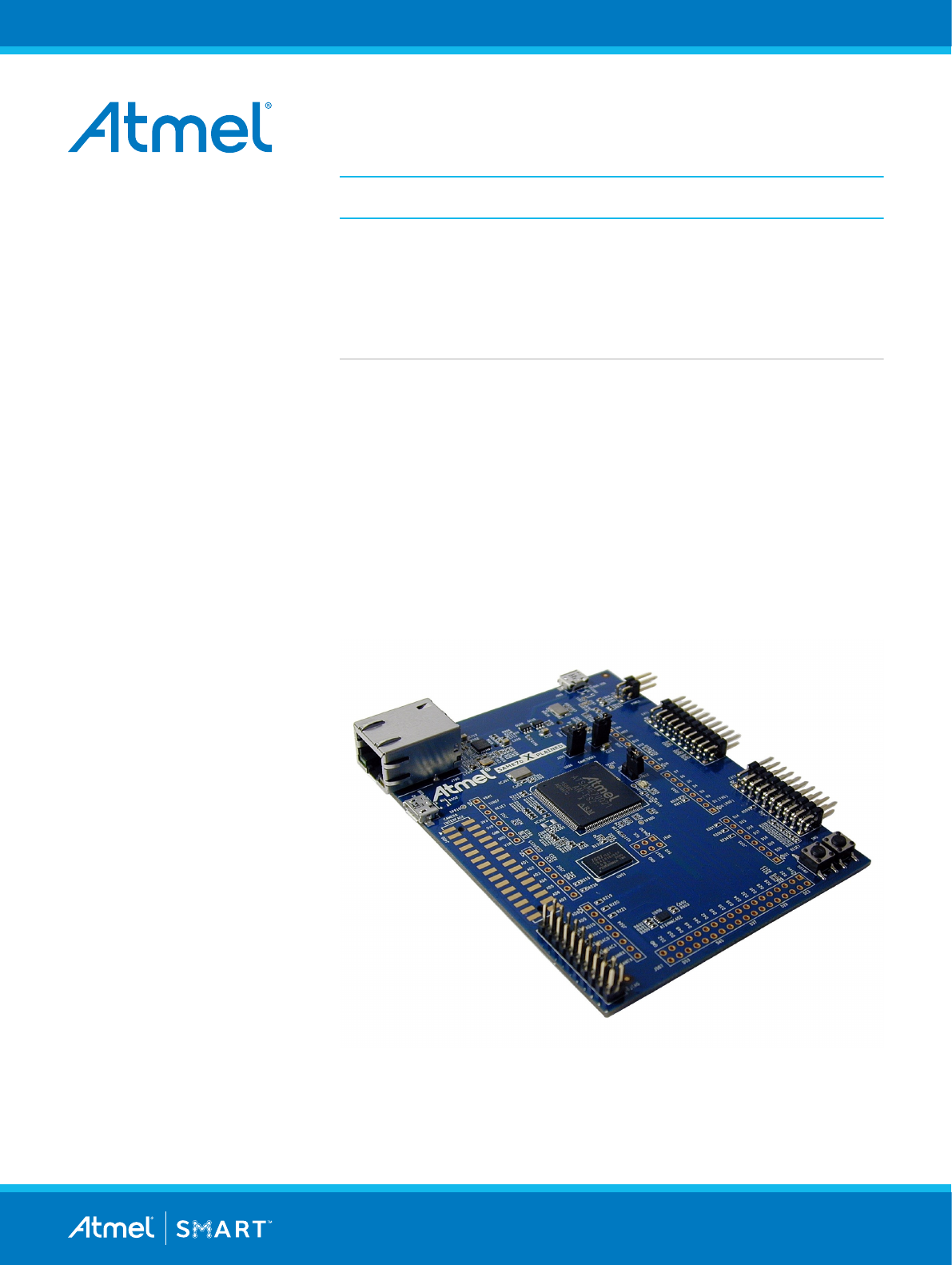
The Atmel® SAM E70 Xplained evaluation kit is a hardware platform to
evaluate the Atmel ATSAME70Q21 microcontroller.
Supported by the Atmel Studio integrated development platform, the kit
provides easy access to the features of the ATSAME70Q21 and explains
how to integrate the device in a custom design.
The Xplained Pro MCU series evaluation kits include an on-board
Embedded Debugger, and no external tools are necessary to program or
debug the ATSAME70Q21.
The Xplained Pro extension series evaluation kits offers additional
peripherals to extend the features of the board and ease the development of
custom designs.
Atmel-44050A-SAME70-XPLD_User Guide-12/2015

Table of Contents
Preface............................................................................................................................ 1
1. Introduction................................................................................................................3
1.1. Kit Contents..................................................................................................................................3
1.2. Related Items............................................................................................................................... 3
1.3. Kit Overview................................................................................................................................. 3
2. Getting Started...........................................................................................................6
2.1. Xplained Pro Quick Start.............................................................................................................. 6
2.2. Design documentation and relevant links.....................................................................................6
3. Xplained Pro.............................................................................................................. 7
3.1. Embedded Debugger................................................................................................................... 7
3.2. Hardware Identification System....................................................................................................7
3.3. Power Sources............................................................................................................................. 8
3.4. Xplained Pro Standard Extension Header....................................................................................8
3.5. Xplained Pro Power Header.........................................................................................................9
4. Hardware User Guide.............................................................................................. 11
4.1. Microcontroller............................................................................................................................ 11
4.2. Power Distribution.......................................................................................................................11
4.3. Connectors................................................................................................................................. 12
4.4. Peripherals................................................................................................................................. 30
4.5. Zero Ohm Resistors................................................................................................................... 38
4.6. Embedded Debugger Implementation........................................................................................41
5. Board Schematics....................................................................................................44
6. Board Layout........................................................................................................... 51
7. Evaluation Board/kit Important Notice..................................................................... 57
Atmel SAME70-XPLD [USER GUIDE]
Atmel-44050A-SAME70-XPLD_User Guide-12/2015
2
1. Introduction
This user guide introduces the Atmel SAME70-XPLD evaluation kit and describes the development and
debugging capabilities for applications running on a SAM E70 ARM-based embedded microcontroller.
1.1. Kit Contents
•Boards
–One SAME70-XPLD board
•Cables
–One Micro-AB type USB cable
1.2. Related Items
•Atmel SAM E70 Series Datasheet
1.3. Kit Overview
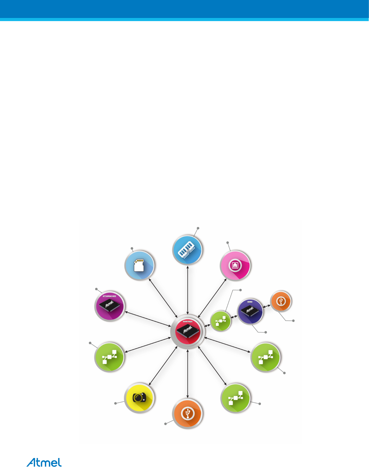
1.3.1. Evaluation Kit Architecture
Figure 1-1 Evaluation Kit Architecture
SDRAM
16Mb SDRAM
ETHERNET
Ethernet 10/100 Interface
SDCARD
4-bit SDCARD
Reader Interface
USB DEBUG
USB Micro A/B Connector
ATMEL EDBG
Atmel Embedded Debugguer
JTAG
20-Pin JTAG Connector
ARDUINO CONNECTORS
8-Expansion Headers
Arduino R3 compatible PIO Signals
(Not Populated)
XPRO CONNECTORS
3-Expansions Headers
Compatible with Atmel XPRO Extensions
TARGET USB
USB Micro A/B Connector
CAMERA MODULE
Camera Interface Connector
for CAMx-EB Camera Module series
(Not Populated)
TRACE
20-pin debug connector
For Trace
(Not Populated)
EEPROM
I²C - 2k-bit serial EEprom
And Unique 128-bit serial number
AT24MAC402
Atmel SAME70-XPLD [USER GUIDE]
Atmel-44050A-SAME70-XPLD_User Guide-12/2015
3
1.3.2. Evaluation Kit Specifications
Table 1-1 Evaluation Kit Specifications
Characteristic Specifications
Temperature Operating 0°C to +70°C
Storage -40°C to +85°C
Relative Humidity 0 to 90% (non-condensing)
RoHS status Compliant
Ordering code ATSAME70-XPLD
1.3.3. Board Features
Table 1-2 Board Specifications
Characteristics Specifications
PCB characteristics 83.5 × 105 × 16mm (4 layers)
Processor ATSAME70Q21 (144-lead LQFP package) ARM Cortex-M7 Processor.
Processor clock sources 12 MHz crystal oscillator
32.768 kHz crystal oscillator (not populated)
EEPROM One AT24MAC402 EEPROM
SDRAM One IS42S16100E 16 Mb SDRAM
SD/MMC One 4-bit SD card connector
USB One Micro-AB USB device
One Micro-AB USB for EDBG debug interface
Camera interface Camera Extension Header for connection with ISI Modules (not populated)
Ethernet One Ethernet PHY (RMII 10/100)
Debug port One JTAG interface connector
One ETM Trace interface connector (not populated)
Expansion connectors Three Atmel XPRO Extension Headers
Arduino R3 compatible set of headers (not populated)
GPIO,TWI, SPI, USART, UART and Audio interfaces are accessible via these
headers
Board supply voltage 5V from USB target, from USB Debug or from Arduino shield
On-board power regulation is performed by a 3.3V LDO
User interface Reset and free user pushbutton
One green user LED
1.3.4. Board Overview
The Atmel SAME70-XPLD is a hardware platform to evaluate the Atmel ATSAME70Q21.
Atmel SAME70-XPLD [USER GUIDE]
Atmel-44050A-SAME70-XPLD_User Guide-12/2015
4
It offers a set of features that enables the ATSAME70Q21 user to get started with the SAM V71, SAM
V70, SAM E70 and SAM S70 peripherals right away and to get an understanding of how to integrate the
device in their own design.
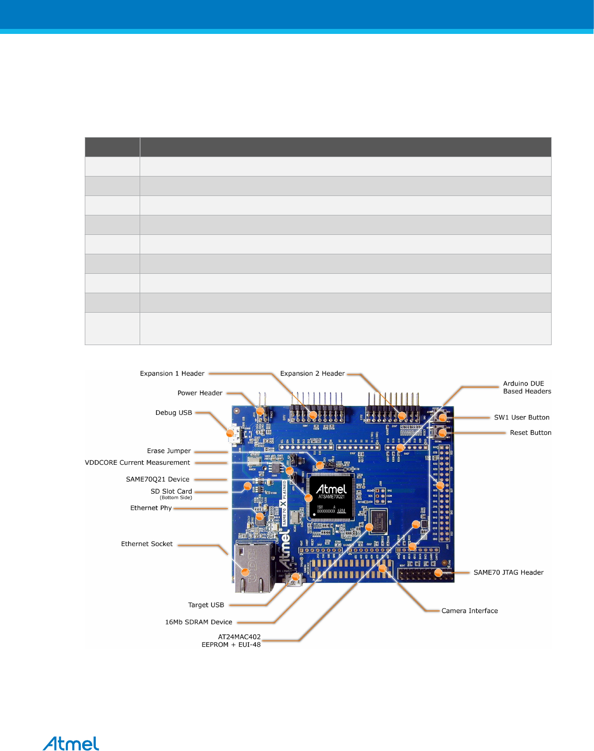
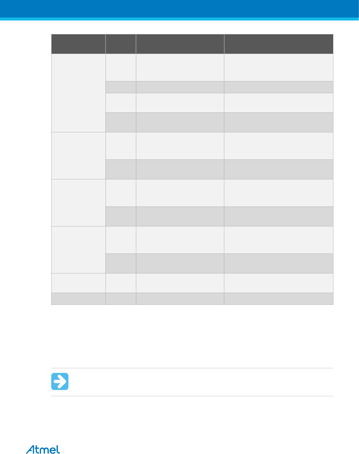
The SAME70-XPLD board is equipped with the interface connectors described in Table 1-3.
Table 1-3 SAME70-XPLD Board Interface Connectors
Header Interfaces to
J302 USB A device. Supports USB device using a Micro-AB connector
J400 Camera Interface Connector (not populated)
J401-J402 Atmel XPRO expansion connectors
J403 Connector for Trace (not populated) (Footprint available on bottom side)
J406 JTAG, 20-pin connector
J500–J507 Expansion connectors with Arduino R3 compatible PIO signals (not populated)
J600 SD/MMC connector (available on bottom side)
J700 Ethernet ETH1
J900 Debug USB interface. Supports USB device using a Micro-AB connector. Interface used for
target debug
Figure 1-2 SAME70-XPLD Board Overview
Atmel SAME70-XPLD [USER GUIDE]
Atmel-44050A-SAME70-XPLD_User Guide-12/2015
5

2. Getting Started
2.1. Xplained Pro Quick Start
Three steps to start exploring the Atmel Xplained Pro platform:
1. Download Atmel Studio.
2. Launch Atmel Studio.
3. Connect a USB cable (Standard-A to Micro-B or Micro-AB) between the PC and the DEBUG USB
port of the board.
When the Atmel SAME70-XPLD is connected to your computer for the first time, the operating system will
perform a driver software installation. The driver file supports both 32- and 64-bit versions of Microsoft®
Windows® XP, Windows Vista®, Windows 7, and Windows 8.
Once the board is powered, Atmel Studio will auto detect which kind of MCU and extension board(s) are
connected. Atmel Studio will present links to relevant information like datasheets and kit documentation.
The kit landing page in Atmel Studio also has the option to launch Atmel Software Framework (ASF)
example applications for the kit. The SAM E70 device is programmed and debugged by the on-board
Embedded Debugger and therefore no external programmer or debugger tool is needed.
2.2. Design documentation and relevant links
The following list contains links to the most relevant documents and software for SAME70-XPLD:
•Xplained Pro products - Atmel Xplained Pro is a series of small-sized and easy-to-use evaluation
kits for Atmel microcontrollers and other Atmel products. It consists of a series of low-cost MCU
boards for evaluation and demonstration of features and capabilities of different MCU families.
•Atmel Studio - Free Atmel IDE for development of C/C++ and assembler code for Atmel
microcontrollers.
•Atmel sample store - Atmel sample store where you can order samples of devices.
•EDBG User Guide - User guide containing more information about the on-board Embedded
Debugger.
•IAR Embedded Workbench® for ARM® - This is a commercial C/C++ compiler that is available for
ARM®. There is a 30 day evaluation version as well as a code size limited kick-start version
available from their website. The code size limit is 16KB for devices with M0, M0+, and M1 cores
and 32KB for devices with other cores.
•Atmel Data Visualizer - Atmel Data Visualizer is a program used for processing and visualizing
data. Data Visualizer can receive data from various sources such as the Embedded Debugger Data
Gateway Interface found on Xplained Pro boards and COM ports.
•Design Documentation - Package containing schematics, BOM, assembly drawings, 3D plots,
layer plots etc.
•Hardware Users Guide in PDF format - PDF version of this User Guide.
Atmel SAME70-XPLD [USER GUIDE]
Atmel-44050A-SAME70-XPLD_User Guide-12/2015
6
3. Xplained Pro
Xplained Pro is an evaluation platform that provides the full Atmel microcontroller experience. The
platform consists of a series of Microcontroller (MCU) boards and extension boards, which are integrated
with Atmel Studio, have Atmel Software Framework (ASF) drivers and demo code, support data
streaming, and more. Xplained Pro MCU boards support a wide range of Xplained Pro extension boards,
which are connected through a set of standardized headers and connectors. Each extension board has
an identification (ID) chip to uniquely identify which boards are connected to an Xplained Pro MCU board.
This information is used to present relevant user guides, application notes, datasheets, and example
code through Atmel Studio.
3.1. Embedded Debugger
The SAME70-XPLD contains the Atmel Embedded Debugger (EDBG) for on-board debugging. The
EDBG is a composite USB device of three interfaces: a debugger, Virtual COM Port, and a Data Gateway
Interface (DGI).
Together with Atmel Studio, the EDBG can program and debug the ATSAME70Q21. On the SAME70-
XPLD, the SWD interface is connected between the EDBG and the ATSAME70Q21.
The Virtual COM Port is connected to a UART on the ATSAME70Q21 and provides an easy way to
communicate with the target application through terminal software. It offers variable baud rate, parity, and
stop bit settings. Note that the settings on the ATSAME70Q21 must match the settings applied in the
terminal software.
Note: If not set automatically, data terminal ready (DTR) must be set in the terminal software.
The DGI consists of several physical interfaces for communication with the host computer.
Communication over the interfaces are bidirectional. It can be used to send events and values from the
ATSAME70Q21 or as a generic printf-style data channel. Traffic over the interfaces can be timestamped
on the EDBG for more accurate tracing of events. Note that timestamping imposes an overhead that
reduces maximal throughput. Atmel Data Visualizer is used to send and receive data through DGI.
For further documentation on the EDBG, see the EDBG User Guide.
3.2. Hardware Identification System
All Xplained Pro compatible extension boards have an Atmel ATSHA204 CryptoAuthentication™ chip
mounted. This chip contains information that identifies the extension with its name and some extra data.
When an Xplained Pro extension is connected to an Xplained Pro MCU board the information is read and
sent to Atmel Studio. The Atmel Kits extension, installed with Atmel Studio, will give relevant information,
code examples, and links to relevant documents. The table below shows the data fields stored in the ID
chip with example content.
Table 3-1 Xplained Pro ID Chip Content
Data field Data type Example content
Manufacturer ASCII string Atmel'\0'
Product Name ASCII string Segment LCD1 Xplained Pro'\0'
Product Revision ASCII string 02'\0'
Product Serial Number ASCII string 1774020200000010’\0’
Atmel SAME70-XPLD [USER GUIDE]
Atmel-44050A-SAME70-XPLD_User Guide-12/2015
7
Data field Data type Example content
Minimum Voltage [mV] uint16_t 3000
Maximum Voltage [mV] uint16_t 3600
Maximum Current [mA] uint16_t 30
3.3. Power Sources
The SAME70-XPLD kit can be powered by several power sources listed in the table below.
Warning: The 3.3V power domain is locally generated and must never be supplied from
external sources or this would damage the on-board regulators.
Table 3-2 SAME70-XPLD Power Sources
Power input Voltage requirements Connector marking
Embedded debugger USB 4.4V to 5.25V (USB spec.) DEBUG USB
Target USB 4.4V to 5.25V (USB spec.) TARGET USB
Arduino connector 5.0V typically J501 (pin 5)
In case of USB power sources, the board automatically detects and switches to the available one. If the
two are present (which is no problem whatsoever) the following priority applies:
1. Target USB (J302 connector)
2. Embedded Debugger USB (J900 connector)
Info: USB sources supposedly provide a maximum current of 500mA. Calculate the power
budget of your system, there is a possiblity this could be not enough if your SAME70-XPLD also
connects to power demanding extension boards.
The optional 5Vcc power source from the Arduino connector J501 is connected in parallel to the USB
power switching system, hence the following warning:
Warning: do not power the board form the Arduino shield (J501) when either of the two USB
sources are connected. Doing so could damage the board and potentially also damage the USB
port of your PC.
3.4. Xplained Pro Standard Extension Header
All Xplained Pro kits have one or more dual row, 20-pin, 100mil extension header. Xplained Pro MCU
boards have male headers, while Xplained Pro extensions have their female counterparts. Note that all
pins are not always connected. All connected pins follow the defined pin-out description in the table
below.
Atmel SAME70-XPLD [USER GUIDE]
Atmel-44050A-SAME70-XPLD_User Guide-12/2015
8
The extension headers can be used to connect a variety of Xplained Pro extensions to Xplained Pro MCU
boards or to access the pins of the target MCU on Xplained Pro MCU boards directly.
Table 3-3 Xplained Pro Standard Extension Header
Pin number Name Description
1 ID Communication line to the ID chip on an extension board
2 GND Ground
3 ADC(+) Analog to digital converter, alternatively positive part of differential
ADC
4 ADC(-) Analog to digital converter, alternatively negative part of differential
ADC
5 GPIO1 General purpose I/O
6 GPIO2 General purpose I/O
7 PWM(+) Pulse width modulation, alternatively positive part of differential
PWM
8 PWM(-) Pulse width modulation, alternatively negative part of differential
PWM
9 IRQ/GPIO Interrupt request line and/or general purpose I/O
10 SPI_SS_B/
GPIO
Slave select for SPI and/or general purpose I/O
11 I2C_SDA Data line for I2C interface. Always implemented, bus type.
12 I2C_SCL Clock line for I2C interface. Always implemented, bus type.
13 UART_RX Receiver line of target device UART
14 UART_TX Transmitter line of target device UART
15 SPI_SS_A Slave select for SPI. Should preferably be unique.
16 SPI_MOSI Master out slave in line of serial peripheral interface. Always
implemented, bus type.
17 SPI_MISO Master in slave out line of serial peripheral interface. Always
implemented, bus type.
18 SPI_SCK Clock for serial peripheral interface. Always implemented, bus type.
19 GND Ground
20 VCC Power for extension board
3.5. Xplained Pro Power Header
The power header can only be used as supply for external peripherals or extension boards. Care must be
taken not to exceed the total current limitation of the on-board regulator when using the 3.3V pin.
Atmel SAME70-XPLD [USER GUIDE]
Atmel-44050A-SAME70-XPLD_User Guide-12/2015
9
Table 3-4 Xplained Pro Power Header
Pin number Pin name Description
1 n/a not connected
2 GND Ground
3 VCC_5V0 Output: unregulated 5V (output, derived from one of the input
sources)
4 VCC_3V3 Output: regulated 3.3V (output, used as main power supply for the
kit)
Atmel SAME70-XPLD [USER GUIDE]
Atmel-44050A-SAME70-XPLD_User Guide-12/2015
10
4. Hardware User Guide
4.1. Microcontroller
The SAME70-XPLD board is built around the ATSAME70Q21 in a 144-lead LQFP package. It is a low-
power ARM Cortex-M7 application microcontroller achieving high-performance computing device and
embedding a wide range of communication peripherals. It features a combination of user interface
functionalities and high data rate IOs, camera interface, 10/100 Ethernet ports, high-speed USB and SD
Card.
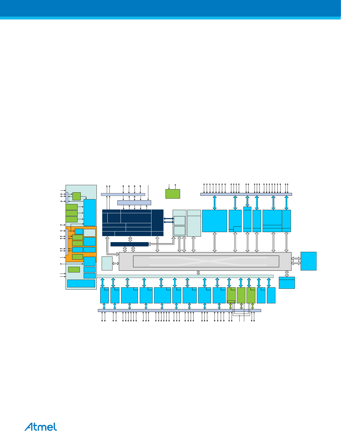
The ARM Cortex-M7 processor supports SDRAM memory through an EBI interface. An internal 150 MHz
multi-layer AHB bus architecture associated with 24 XDMA channels, 384 Kbytes of SRAM and 2048
Kbytes of Flash sustains the high bandwidth required by the microcontroller and the high-speed
peripherals.
Figure 4-1 SAM E70 Block Diagram
12-layer Bus Matrix
fMAX 150 MHz
XDMA
PCK0..2
XIN32
XOUT32
ERASE
VDDCORE
VDDIO
VDDOUT
Voltage
Regulator
TST
WKUP0..13
VDDIO
XIN
XOUT
VDDPLL
RTCOUT0
RTCOUT1
S M MMMS
S S S
S
MM
M
M
M
S
System Controller
SM
In-Circuit Emulator
MPU
Cortex-M7 Processor
fMAX 300 MHz
NVIC
FPU
TPIU
ETM
16 Kbytes ICache + ECC16 Kbytes DCache + ECC
TCM
Interface
AXIM
AHBP AHBS
AXI Bridge
TCK/SWCLK
TDI
TDO/TRACESWO
JTAGSEL
Serial Wire Debug/JTAG Boundary Scan
TRACECLK
TRACED0..3
TMS/SWDIO
NRST
PIOA/B/C/D/E
24-channel
XDMA
ROM
Boot
Program
Multi-port
SRAM
Flash
2048 Kbytes
1024 Kbytes
512 Kbytes
Flash
Unique ID
ITCM
DTCM USBHS
Transceiver
External Bus Interface
Static Memory Controller (SMC)
SDRAM Controller (SDRAMC)
NAND Flash Logic
QSPI
XIP DMA
ISI GMAC
MII/RMII
5 x
UART
3 x
TWIHS
3 x
USART
2 x
PWM
2 x
12-bit
AFE ACC 12-bit
DAC
PIO SSC HSMCI 2 x
SPI
4 x
TC
XDMA
DMA
Peripheral Bridge
URXD0..4
UTXD0..4
VREFN
CANRX0..1
CANTX0..1
RXD0..2
SCK0..2
RTS 0..2
TXD0..2
CTS 0..2
DSR0..2, DTR0 ..2
RI0..2, DCD0..2
ICM/SHA
PIODCCLK
PIODCEN1..2
PIODC0..7
TF
TK
TD
RD
RK
RF
MCDA0 ..3
MCCDA
MCCK
SPIx_NPCS 0..3
SPIx_MIS O
SPIx_MOSI
SPIx_SPC K
PWMCx_P WMH0..3
PWMCx_P WML0..3
PWMCx_P WMFI0..2
PWMCx_P WMEXTRG0..1
AFEx_ADTRG
AFEx_AD0..11
DAC0..1
DATRG
TWD0..2
TWCK0..2
2 x
MCAN
GTXCK, GRXCK, GREFCK
GCRS , G COL, GCRS DV
GMDC, G MDIO
GTS UCOMP
GRX0..3, GTX0 ..3
GRXER, GRXDV
GTXER, GTXDV
ISI_D[11 :0]
ISI_P CK, ISI_MCK
ISI_HS YNC, IS I_VSYNC
HSDP
HSDM
QMISO/QIO1
QMOS I/QIO0
QS CK, QCS
QIO2..3
A[23:0], D[15:0 ]
A21/NANDALE
A22/NANDCLE
NANDOE, NANDWE
A0/NLB, NUB
NWAIT, NCS 0..3, NRD, NWE
A16/S DBA0, A17/S DBA1
RAS, CAS , DQM0..1, S DCK, S DCKE, S DA10
DMA DMA
Temp Sensor
TIOB0..11
TCLK0..11
TIOA0..11
XDMA
XDMA
XDMAXDMAXDMAXDMAXDMA
XDMAXDMA
XDMA
FIFO
XDMA
TRNG
AES
DMA
VREFP
Backup RAM
1 Kbyte
TCM SRAM
System RAM
0–256 Kbytes
128–384 Kbytes
0–256 Kbytes
PMC
4/8/12 MHz
RC Oscillator
RSTC
SM
POR
SUPC
RTTRTC
WDT
UPLL
PLLA
3-20 MHz
Crystal
Oscillator
32 kHz
Crystal
Oscillator
32 kHz
RC Oscillator
Immediate Clear
256-bit SRAM
(GPBR)
Backup
RSWDT
4.2. Power Distribution
The SAME70-XPLD has two power sources as described in the figure Power Supply Block Diagram.
The kit can be powered from the EDBG USB or from the target USB. The kit automatically selects a
source to draw power. Priority is given to TARGET USB power input.
Atmel SAME70-XPLD [USER GUIDE]
Atmel-44050A-SAME70-XPLD_User Guide-12/2015
11
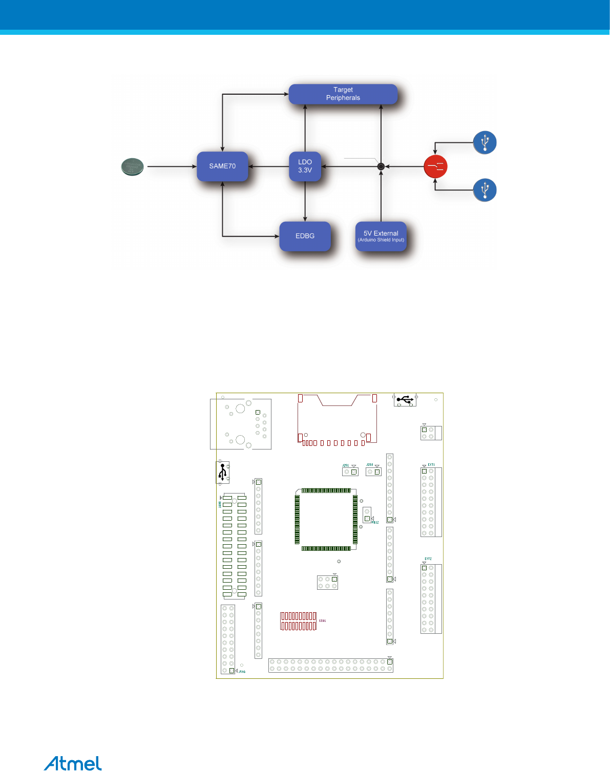
Figure 4-2 Power Supply Block Diagram
Coin Cell
TARGET USB
EDBG USB
VCC_5V0
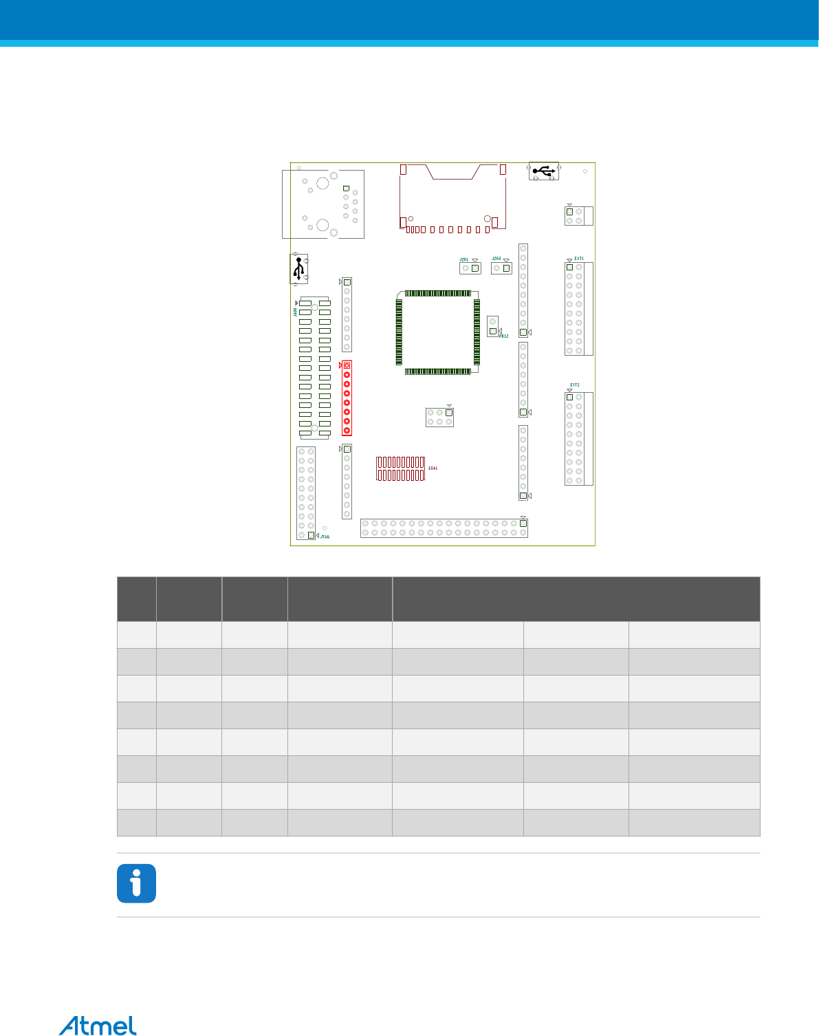
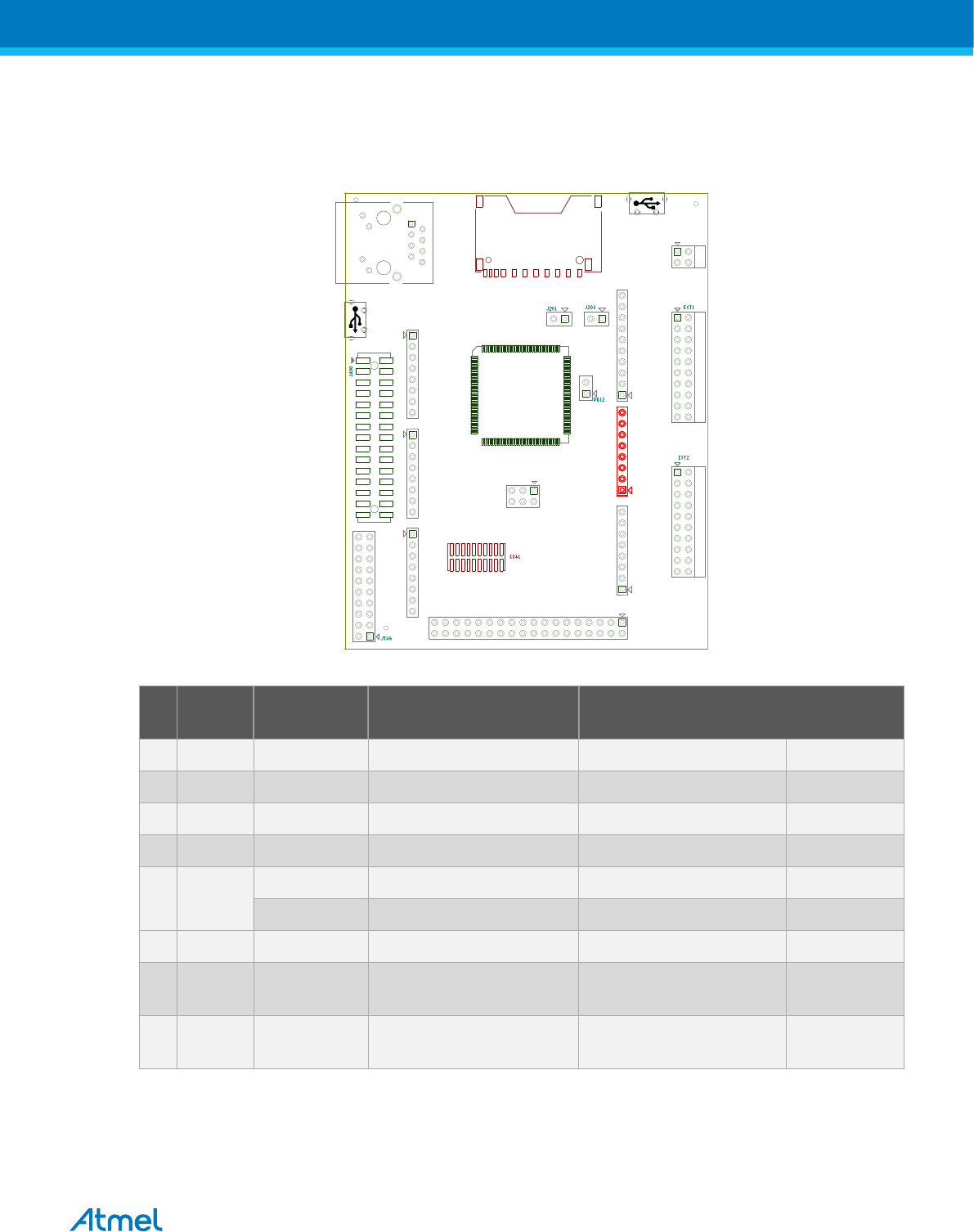
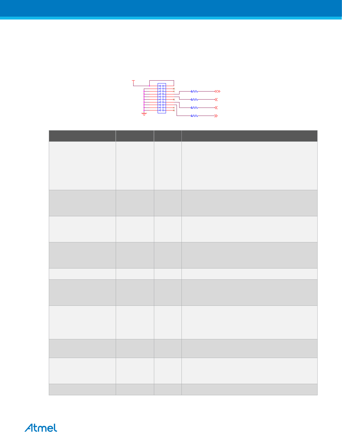
4.3. Connectors
These sections describe the implementation of all connectors and headers on SAME70-XPLD and their
connection to the ATSAME70Q21. The tables of connections in these sections also describe which
signals are shared between the headers and on-board functionality. The figure below shows all available
connectors and jumpers on the SAME70-XPLD.
Figure 4-3 SAME70-XPLD Connector Overview
J406 - SAME70 De bu g (SWD)
CAMERA
INTERFACE
J600 - SDCARD Socket
(Bottom Side )
J900
DEBUG USB
Co resight 20 - SWD + ETM
(Bottom Side )
J506 - SPI
J504 - An alog High J502 - Analog Low J501 - Powe r
J500 - Digital Hig hJ503 - Digital LowJ505 - Co mmunicat ion
J402 - Exte nsion Heade r 2 J401 - Exte nsion Heade r 1 J101 - Powe r He ader
VDDCORE VCC_MCU_3V3
J200 - ERASE
J700 - Ethern et RJ45
J507 - Digital Extra
J302
Ta rget USB
OPTIONOPTIONOPTION
OPTION OPTION OPTION
OPTION
OPTION
OPTION
Atmel SAME70-XPLD [USER GUIDE]
Atmel-44050A-SAME70-XPLD_User Guide-12/2015
12
4.3.1. Extension Headers
The Xplained Pro headers EXT1 and EXT2 on SAME70-XPLD give access to the I/O of the
microcontroller in order to expand the system, e.g. by connecting extensions boards. The headers have a
pitch of 2.54mm.
Table 4-1 EXT1 Header
EXT1 Pin SAM E70
Pin
Function Shared Functionality
1 [ID ] -- ID_EXT1 Signal connected to Embedded Debugger
2 [GND] -- -- Ground Connection with Extension Board
3 [ADC(+)] PC31 AFE1_AD6 J502 Header & J504 Header (Arduino Shield)
4 [ADC(-)] PA19 AFE0_AD8 J502 Header (Arduino Shield)
5 [GPIO1] PB3 GPIO/RTS0 Camera Connector, EXT2 Header, J504 Header &
J507 Header (Arduino Shield)
6 [GPIO2] PB2 GPIO/CTS0 EXT2 Header, J504 Header & J507 Header
(Arduino Shield)
7 [PWM(+)] PA0 PWMC0_H0 --
8 [PWM(-)] PC30 TIOB5 J502 Header (Arduino Shield)
9 [IRQ/GPIO] PD28 WKUP5 Camera Connector, Embedded Debugger, J503
Header & J505 Header (Arduino Shield)
10 [SPI_SS_B/GPIO] PC17 GPIO --
11 [I2C_SDA] PA3 TWD0 Camera Connector, EXT2 Header, J500 Header
(Arduino Shield), AT24MAC402, Embedded
Debugger
12 [I2C_SCL] PA4 TWCK0 Camera Connector, EXT2 Header, J500 Header
(Arduino Shield), AT24MAC402, Embedded
Debugger
13 [UART_RX] PB0 RXD0 EXT2 Header, J505 Header & J507 Header
(Arduino Shield)
14 [UART_TX] PB1 TXD0 EXT2 Header, J505 Header & J507 Header
(Arduino Shield)
15 [SPI_SS_A] PD25 SPI0_NPCS1 Camera Connector, J500 Header (Arduino Shield)
16 [SPI_MOSI] PD21 SPI0_MOSI EXT2 Header, Camera Connector, J500 Header &
J506 Header (Arduino Shield), Embedded
Debugger
17 [SPI_MISO] PD20 SPI0_MISO EXT2 Header, J500 Header & J506 Header
(Arduino Shield), Embedded Debugger
18 [SPI_SCK} PD22 SPI0_SPCK EXT2 Header, Camera Connector, J500 Header &
J506 Header (Arduino Shield), Embedded
Debugger
Atmel SAME70-XPLD [USER GUIDE]
Atmel-44050A-SAME70-XPLD_User Guide-12/2015
13
EXT1 Pin SAM E70
Pin
Function Shared Functionality
19 [GND] -- -- Ground Connection with Extension Board
20 [VCC] -- -- Power For Extension Board (3.3V only)
Table 4-2 EXT2 Header
EXT2 Pin SAM E70
Pin
Function Shared Functionality
1 [ID ] -- ID_EXT2 Signal connected to Embedded
Debugger
2 [GND] -- -- Ground Connection with Extension
Board
3 [ADC(+)] PD30 AFE0_AD0 Camera Connector, J502 Header &
J503 Header (Arduino Shield)
4 [ADC(-)] PC13 AFE1_AD1 J502 Header (Arduino Shield)
5 [GPIO1] PA6 GPIO Camera Connector, J503 Header
(Arduino Shield)
6 [GPIO2] PD11 GPIO Camera Connector, J500 Header &
J503 Header (Arduino Shield)
7 [PWM(+)] PC19 PWMC0_H2 Camera Connector, J503 Header
(Arduino Shield)
8 [PWM(-)] PD26 PWMC0_L2 J502 Header (Arduino Shield)
9 [IRQ/GPIO] PA2 WKUP2 J503 Header (Arduino Shield),
Embedded Debugger
10 [SPI_SS_B/
GPIO]
PA24 GPIO Camera Connector, J507 Header
(Arduino Shield)
11 [I2C_SDA] PA3 TWD0 Camera Connector, EXT1 Header,
J500 Header (Arduino Shield),
AT24MAC402, Embedded Debugger
12 [I2C_SCL] PA4 TWCK0 Camera Connector, EXT1 Header,
J500 Header (Arduino Shield),
AT24MAC402, Embedded Debugger
13 [UART_RX] PA21 RXD1 J507 Header (Arduino Shield),
Embedded Debugger
14 [UART_TX] PB4 TXD1 J507 Header (Arduino Shield),
Embedded Debugger
Atmel SAME70-XPLD [USER GUIDE]
Atmel-44050A-SAME70-XPLD_User Guide-12/2015
14
EXT2 Pin SAM E70
Pin
Function Shared Functionality
15 [SPI_SS_A] PB3 USART_SPI_NSS_MASTER_0 EXT1 Header, Camera Connector,
J504 Header & J507 Header (Arduino
Shield)
PD31 USART_SPI_NSS_MASTER_0 Camera Connector
PB2 USART_SPI_NSS_SLAVE EXT1 Header, J504 Header & J507
Header (Arduino Shield)
PD27 SPI0_NPCS3 Camera Connector, J503 Header &
J505 Header (Arduino Shield)
16 [SPI_MOSI] PD21 SPI0_MOSI EXT1 Header, Camera Connector,
J500 Header & J506 Header (Arduino
Shield), Embedded Debugger
PB1 USART_SPI_MOSI EXT1 Header, J505 Header & J507
Header (Arduino Shield)
17 [SPI_MISO] PD20 SPI0_MISO EXT1 Header, J500 Header & J506
Header (Arduino Shield), Embedded
Debugger
PB0 USART_SPI_MOSI EXT1 Header, J505 Header & J507
Header (Arduino Shield)
18 [SPI_SCK} PD22 SPI0_SPCK EXT1 Header, Camera Connector,
J500 Header & J506 Header (Arduino
Shield), Embedded Debugger
PB13 USART_SPI_SPCK J504 Header & J507 Header (Arduino
Shield)
19 [GND] -- -- Ground Connection with Extension
Board
20 [VCC] -- -- Power For Extension Board (3.3V only)
4.3.2. Arduino Connectors
Five 8-pin, one 10-pin, one 2×3-pin and one 2×18-pin headers footprints (J500 to J507) are implemented
on the board to enable the addition of "Arduino shields" extension cards. These accessory boards are
various and widely available on the market, often custom developed. Due to the PIO multiplexing of the
ATSAME70Q21, various peripheral signals may be connected to each pin. These connectors are
mechanically (location and footprint) compatible with the Arduino R3 shields.
Important: As the SAM E70 signals have a voltage level of 3.3V, 5V level shields cannot
properly function with SAME70-XPLD.
In addition to its standard IO functionality, the SAM E70 microcontroller can provide alternate functions to
external IO lines available on the J500 to J507 headers.
These alternate functions are:
Atmel SAME70-XPLD [USER GUIDE]
Atmel-44050A-SAME70-XPLD_User Guide-12/2015
15
•UARTs: UART1, UART2, UART3, UART4
•USARTs: USART0, USART1, USART2
•SPI: SPI0
•I²C: TWI0, TWI2
•Timer capture and compare: TIOA[0, 2,11], TIOB[5, 7, 8,11], TCLK[1, 2, 5, 8,11]
•Clock out: PCK0, PCK1, PCK2
•PWMs: PWMC0_PWMEXTRG[0,1], PWMC0_PWMH[0:3], PWMC_PWML[0, 2, 3],
PWMC1_PWMEXTRG[0,1], PWMC1_PWMFI[0:2], PWMC1_PWMH[0, 2], PWMC1_PWML[0:3]
•DIGITAL AUDIO: TD, TK, TF, RD, RK, RF, GTSUCOMP
•CAN: CANRX0, CANTX0, CANRX1, CANTX1
•Analog: ADVREF, AFE0_AD[0, 6, 8], AFE1_AD[1, 3, 5, 6], DAC[0,1]
•GPIO: MISC
•RESET
Refer to the SAM E70 Series datasheet for further details on the PIO multiplexing and alternate function
selection.
Caution: Like the Arduino Due, SAME70-XPLD runs at 3.3V and the maximum voltage that
the I/O pins can tolerate is 3.3V, connecting higher voltages e.g. 5V to those I/O pin could
damage the board.
Important: not all pins of the shield connectors are necessarily connected to an I/O of the
ATSAME70Q21. Each shield should be checked for compatibility against the SAME70-XPLD
schematics before it is purchased and connected.
4.3.2.1. J500 Header
J500 is a 10-pin header with 2.54mm pitch. It is not populated by default and can be used to connect to
Arduino Shields. It includes PWM, Timer Counter and I2C interface signals and analog reference.
Atmel SAME70-XPLD [USER GUIDE]
Atmel-44050A-SAME70-XPLD_User Guide-12/2015
16
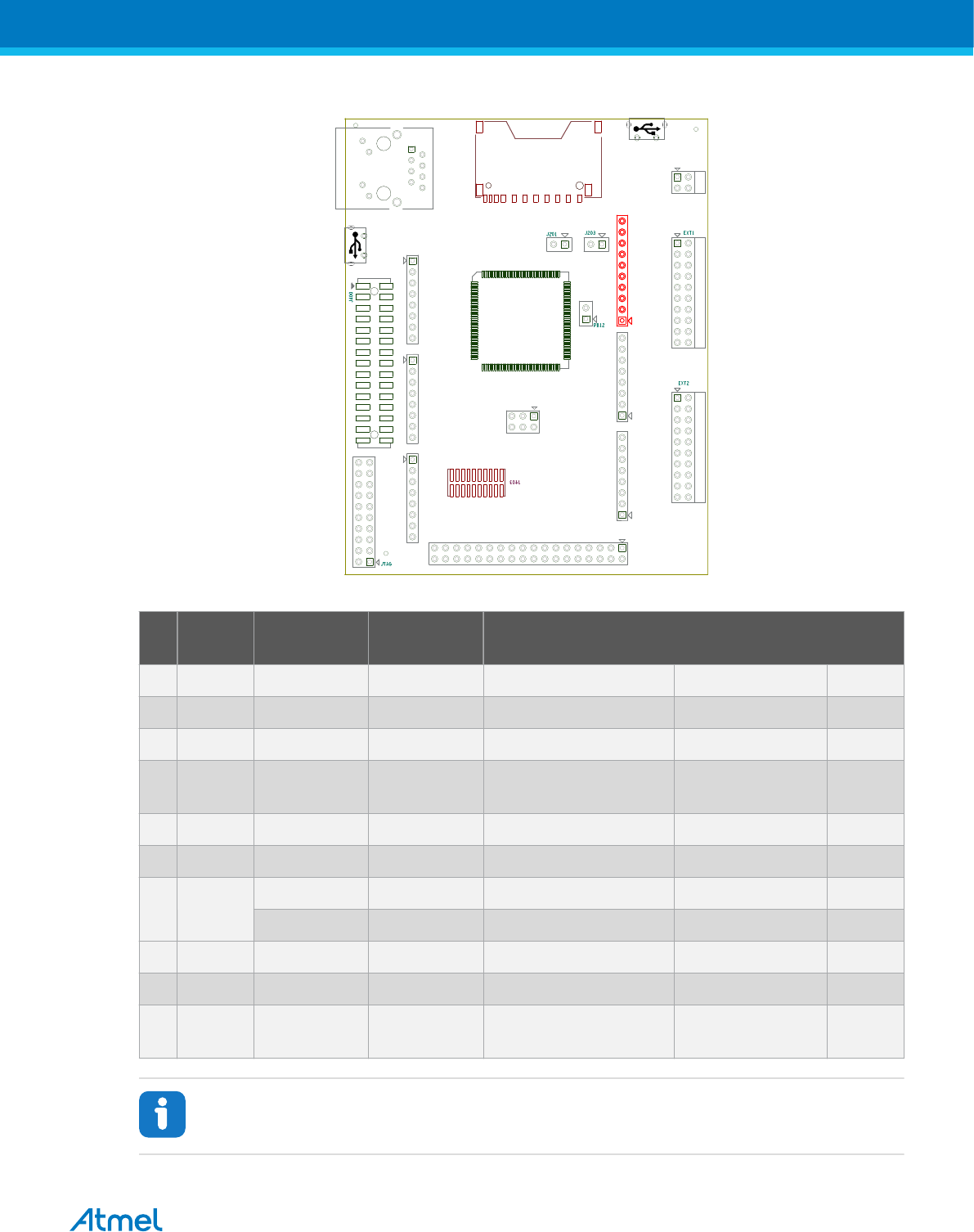
Figure 4-4 J500 Header
J406 - SAME70 De bu g (SWD)
J600 - SDCARD Socket
(Bottom Side )
J900
DEBUG USB
Co resight 20 - SWD + ETM
(Bottom Side )
VDDCORE VCC_MCU_3V3
J200 - ERASE
J700 - Ethern et RJ45
J302
Ta rget USB
CAMERA
INTERFACE
J501 - Powe r
OPTION
J502 - An alog Low
OPTION
J504 - An alog High
OPTION
J506 - SPI
OPTION
OPTION
J500 - Digital Hig h
OPTION
J503 - Digital Low
OPTION
J505 - Co mmunicat ion
OPTION
J507 - Digital Extra
OPTION
J402 - Exte nsion Heade r 2 J401 - Exte nsion Heade r 1 J101 - Powe r He ader
Table 4-3 J500 Header IOs
Pin PCB
Marking
PIO Primary
Function
Alternate Function
10 SCL PA4 TWCK0 TCLK0 UTXD1 WKUP3
9 SDA PA3 TWD0 PCK2 -- --
8 AREF ADVREF -- -- -- --
7 GND -- System
ground
-- -- --
6 D13 PD22 SPI0_SPCK TIOB11 PWMC0_PWMH2 --
5 D12 PD20 SPI0_MISO GSTUCOMP PWMC0_PWMH0 --
4 D11 PD21 SPI0_MOSI TIOA11 PWMC0_PWMH1 --
PD11 GTSUCOMP PWMC0_PWMH0 -- --
3 D10 PD25 SPI0_NPCS1 URXD2 PWMC0PWML1 --
2 D9 PC9 TIOB7 -- -- --
1 D8 PA17 PWMC0_PW
MH3
AFE0_AD6 PCK1 --
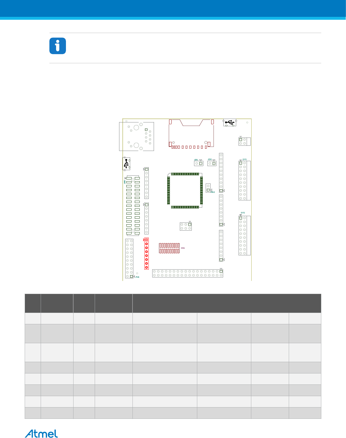
Info: By default, pin 4 is connected to PD21 PIO through a 0R serial resistor. Alternately, it can
be connected to PD11. To do so R210 must be removed and R212 must be mounted.
Atmel SAME70-XPLD [USER GUIDE]
Atmel-44050A-SAME70-XPLD_User Guide-12/2015
17
4.3.2.2. J501 Header
J501 is a 8-pin header with 2.54mm pitch. It is not populated by default and can be used to connect to
Arduino Shields. It allows power distribution (3.3V and 5V) to any Arduino Shield connected on the
SAME70-XPLD board.
Figure 4-5 J501 Header
J406 - SAME70 De bu g (SWD)
J600 - SDCARD Socket
(Bottom Side )
J900
DEBUG USB
Co resight 20 - SWD + ETM
(Bottom Side )
VDDCORE VCC_MCU_3V3
J200 - ERASE
J700 - Ethern et RJ45
J302
Ta rget USB
CAMERA
INTERFACE
J501 - Powe r
OPTION
J502 - An alog Low
OPTION
J504 - An alog High
OPTION
J506 - SPI
OPTION
OPTION
J500 - Digital Hig h
OPTION
J503 - Digital Low
OPTION
J505 - Co mmunicat ion
OPTION
J507 - Digital Extra
OPTION
J402 - Exte nsion Heade r 2 J401 - Exte nsion Heade r 1 J101 - Powe r He ader
Table 4-4 J501 Header IOs
Pin PCB Marking Function
1 VBAT Not used on SAME70-XPLD board. Connected to testpoint TP910
2 IOREF ADVREF. Reference voltage for the analog inputs of the SAM E70
microcontroller. Actually connected to 3.3V.
3 RESET System reset
4 3V3 Main 3.3V supply - generated by the on-board regulator.
5 5V0 Main 5.0V supply (ouput or input). In case that pin is used as power supply
source, do check the recommendations given in Power Sources on page 8
section.
6 GND System ground
7 GND System ground
8 VIN Not connected by default. Optional 5Vcc supply for any Arduino Shield.
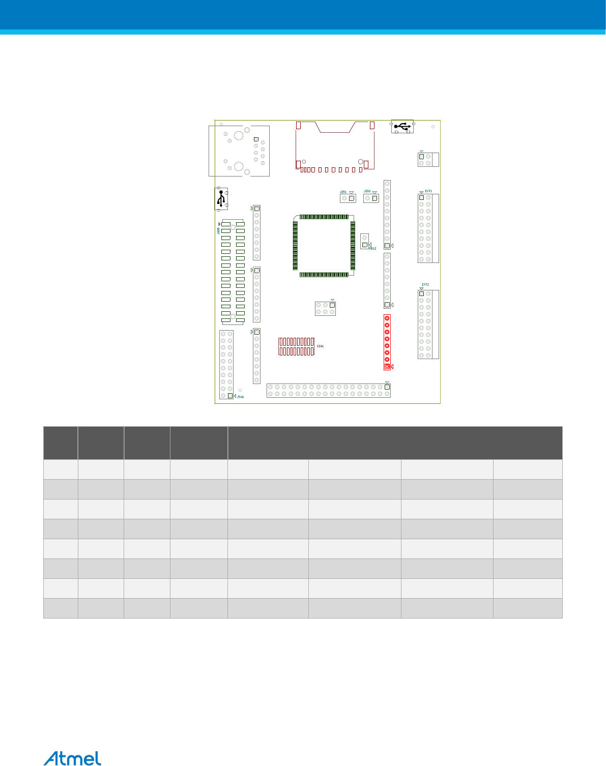
Info: Pin 8 is connected to the SAME70-XPLD board through an 0R serial resistor. It is
necessary to mount 0R resistor R623 to enable the functionality.
Atmel SAME70-XPLD [USER GUIDE]
Atmel-44050A-SAME70-XPLD_User Guide-12/2015
18
4.3.2.3. J502 Header
J502 is a 8-pin header with 2.54mm pitch. It is not populated by default and can be used to connect to
Arduino Shields. It includes ADC inputs and a part of the Digital Audio Interface (TD).
Figure 4-6 J502 Header
J406 - SAME70 De bu g (SWD)
J600 - SDCARD Socket
(Bottom Side )
J900
DEBUG USB
Co resight 20 - SWD + ETM
(Bottom Side )
VDDCORE VCC_MCU_3V3
J200 - ERASE
J700 - Ethern et RJ45
J302
Ta rget USB
CAMERA
INTERFACE
J501 - Powe r
OPTION
J502 - An alog Low
OPTION
J504 - An alog High
OPTION
J506 - SPI
OPTION
OPTION
J500 - Digital Hig h
OPTION
J503 - Digital Low
OPTION
J505 - Co mmunicat ion
OPTION
J507 - Digital Extra
OPTION
J402 - Exte nsion Heade r 2 J401 - Exte nsion Heade r 1 J101 - Powe r He ader
Table 4-5 J502 Header IOs
Pin PCB
Marking
PIO Primary
Function
Alternate Function
1 AD0 PD26 TD UTXD2 UTXD1 PWMC0_PWML2
2 AD1 PC31 AFE1_AD6 TCLK5 -- --
3 AD2 PD30 AFE0_AD0 UTXD3 -- --
4 AD3 PA19 AFE0_AD8 PWMC0_PWML0 WKUP9 --
5 AD4 PC13 AFE1_AD1 PWMC0_PWMH3 -- --
6 AD5 PC30 AFE1_AD5 TIOB5 SPI1_NPCS3 --
7 AD6 PA17 AFE0_AD6 PWMC0_PWMH3 PCK1 --
8 AD7 PC12 AFE1_AD3 TIOB8 CANRX1 --
Info: Pins 6, 7, 8 are connected to SAM E70 PIOs through 0R serial resistors. It is necessary
to mount them to enable the PIO functionality, respectively R214, R216, R236.
Atmel SAME70-XPLD [USER GUIDE]
Atmel-44050A-SAME70-XPLD_User Guide-12/2015
19
4.3.2.4. J503 Header
J503 is a 8-pin header with 2.54mm pitch. It is not populated by default and can be used to connect to
Arduino Shields. It includes PWM, Timer Counter, SPI Chip Select and UART3.
Figure 4-7 J503 Header
J406 - SAME70 De bu g (SWD)
J600 - SDCARD Socket
(Bottom Side )
J900
DEBUG USB
Co resight 20 - SWD + ETM
(Bottom Side )
VDDCORE VCC_MCU_3V3
J200 - ERASE
J700 - Ethern et RJ45
J302
Ta rget USB
CAMERA
INTERFACE
J501 - Powe r
OPTION
J502 - An alog Low
OPTION
J504 - An alog High
OPTION
J506 - SPI
OPTION
OPTION
J500 - Digital Hig h
OPTION
J503 - Digital Low
OPTION
J505 - Co mmunicat ion
OPTION
J507 - Digital Extra
OPTION
J402 - Exte nsion Heade r 2 J401 - Exte nsion Heade r 1 J101 - Powe r He ader
Table 4-6 J503 Header IOs
Pin PCB
Marking
PIO Primary Function Alternate Function
8 D7 PA2 PWMC0_PWMH1 WKUP2 --
7 D6 PC19 PWMC0_PWMH2 -- --
6 D5 PD11 PWMC0_PWMH0 -- --
5 D4 PD27 SPI0_NPCS3 PWMC0_PWML3 TWD2
4 D3 PA6 PCK0 UTXD1 --
PD10 PWMC0_PWML0 TD --
3 D2 PA5 PWMC1_PWML3 URXD1 WKUP4
2 D1
(TXD)
PD30 UTXD3 AFE0_AD0 --
4 D0
(RXD)
PD28 URXD3 TWCK2 CANRX1
Atmel SAME70-XPLD [USER GUIDE]
Atmel-44050A-SAME70-XPLD_User Guide-12/2015
20
Info: By default, pin 4 is connected to SAM E70 PA6 PIO through a 0R serial resistor.
Alternately, it can be connected to PD10. To do so, R217 must be removed and R218 must be
mounted.
4.3.2.5. J504 Header
J504 is a 8-pin header with 2.54mm pitch. It is not populated by default and can be used to connect to
Arduino Shields. It includes ADC inputs, DAC outputs, CAN interface and Digital Audio Receive interface
(RF, RD, RK).
Figure 4-8 J504 Header
J406 - SAME70 De bu g (SWD)
J600 - SDCARD Socket
(Bottom Side )
J900
DEBUG USB
Co resight 20 - SWD + ETM
(Bottom Side )
VDDCORE VCC_MCU_3V3
J200 - ERASE
J700 - Ethern et RJ45
J302
Ta rget USB
CAMERA
INTERFACE
J501 - Powe r
OPTION
J502 - An alog Low
OPTION
J504 - An alog High
OPTION
J506 - SPI
OPTION
OPTION
J500 - Digital Hig h
OPTION
J503 - Digital Low
OPTION
J505 - Co mmunicat ion
OPTION
J507 - Digital Extra
OPTION
J402 - Exte nsion Heade r 2 J401 - Exte nsion Heade r 1 J101 - Powe r He ader
Table 4-7 J504 Header IO
Pin PCB
Marking
PIO Primary
Function
Alternate Function
1 AD8 PD24 RF TCLK11 PWMC0_PWML0 -- --
2 AD9 PA10 RD PWMC0_PWMEXTRG
0
-- -- --
3 AD10 PA22 RK PWMC0_PWMEXTRG
1
-- -- --
4 AD11 PC31 AFE1_AD6 TCLK5 -- -- --
5 DAC0 PB13 DAC0 PWMC0_PWML2 PCK0 -- --
6 DAC1 PD0 DAC1 PWMC1_PWML0 SPI1_NPCS1 -- --
7 CANRX PB3 CANRX0 RTS0 PCK2 AFE0_AD2 WKUP12
8 CANTX PB2 CANTX0 AFE0_AD5 SPI0_NPCS0 CTS0 --
Atmel SAME70-XPLD [USER GUIDE]
Atmel-44050A-SAME70-XPLD_User Guide-12/2015
21
4.3.2.6. J505 Header
J505 is a 8-pin header with 2.54mm pitch. It is not populated by default and can be used to connect to
Arduino Shields. It includes UART0, UART2, UART4 and TWI interfaces.
Figure 4-9 J505 Header
J406 - SAME70 De bu g (SWD)
J600 - SDCARD Socket
(Bottom Side )
J900
DEBUG USB
Co resight 20 - SWD + ETM
(Bottom Side )
VDDCORE VCC_MCU_3V3
J200 - ERASE
J700 - Ethern et RJ45
J302
Ta rget USB
CAMERA
INTERFACE
J501 - Powe r
OPTION
J502 - An alog Low
OPTION
J504 - An alog High
OPTION
J506 - SPI
OPTION
OPTION
J500 - Digital Hig h
OPTION
J503 - Digital Low
OPTION
J505 - Co mmunicat ion
OPTION
J507 - Digital Extra
OPTION
J402 - Exte nsion Heade r 2 J401 - Exte nsion Heade r 1 J101 - Powe r He ader
Table 4-8 J505 Header IOs
Pin PCB
Marking
PIO Primary
Function
Alternate Function
8 D14 PB1 TXD0 TK GTSUCOMP PWMC0_PWMH1 AFE1_AD0
7 D15 PB0 RXD0 TF PWMC0_PWMH0 AFE0_AD10 --
6 D16 PD16 TXD2 -- -- -- --
5 D17 PD15 RXD2 -- -- -- --
4 D18 PD19 UTXD4 CTS2 -- -- --
3 D19 PD18 URXD4 RTS2 -- -- --
2 D20 PD27 TWD2 SPI0_NPCS3 PWMC0_PWML3 -- --
1 D21 PD28 TWCK2 CANRX1 URXD3 WKUP5 --
4.3.2.7. J506 Header
J506 is a 2x3-pin header with 2.54mm pitch. It is not populated by default and can be used to connect to
Arduino Shields. It includes the SPI interface.
Atmel SAME70-XPLD [USER GUIDE]
Atmel-44050A-SAME70-XPLD_User Guide-12/2015
22
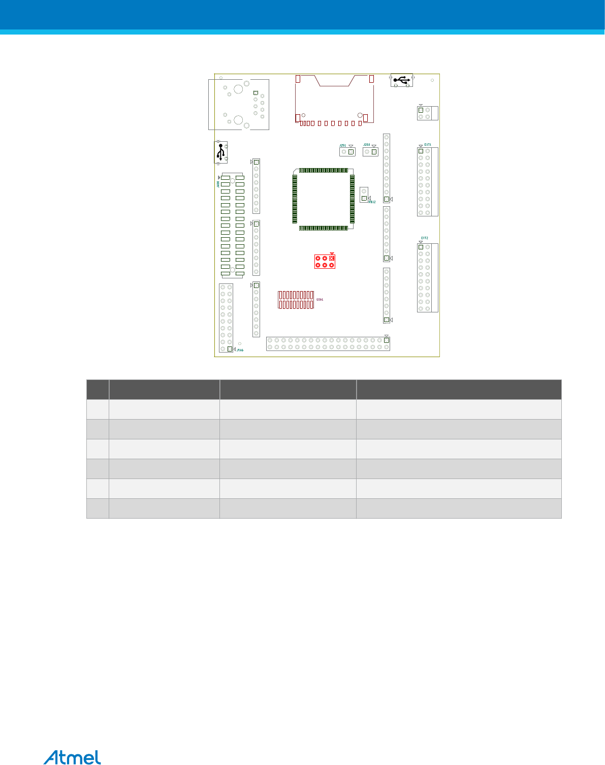
Figure 4-10 J506 Header
J406 - SAME70 De bu g (SWD)
J600 - SDCARD Socket
(Bottom Side )
J900
DEBUG USB
Co resight 20 - SWD + ETM
(Bottom Side )
VDDCORE VCC_MCU_3V3
J200 - ERASE
J700 - Ethern et RJ45
J302
Ta rget USB
CAMERA
INTERFACE
J501 - Powe r
OPTION
J502 - An alog Low
OPTION
J504 - An alog High
OPTION
J506 - SPI
OPTION
OPTION
J500 - Digital Hig h
OPTION
J503 - Digital Low
OPTION
J505 - Co mmunicat ion
OPTION
J507 - Digital Extra
OPTION
J402 - Exte nsion Heade r 2 J401 - Exte nsion Heade r 1 J101 - Powe r He ader
Table 4-9 J506 Header IOs
Pin PCB Marking PIO Primary Function
1 MISO PD20 SPI0_MISO
2 5V0 -- Power supply
3 SPCK PD22 SPI0_SPCK
4 MOSI PD21 SPI0_MOSI
5 RST NRST System reset
6 GND -- System ground
4.3.2.8. J507 Header
J507 is a 2x18-pin header with 2.54mm pitch. It is not populated by default and can be used to connect to
Arduino Shields. It includes PWM, Timer Counters, Audio Transmit interface, CAN interface, USART1 and
USART2 interfaces and four UART interfaces.
Atmel SAME70-XPLD [USER GUIDE]
Atmel-44050A-SAME70-XPLD_User Guide-12/2015
23
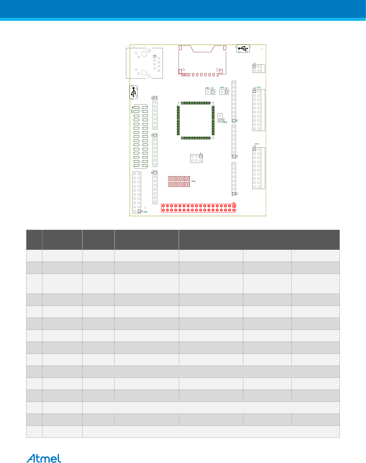
Figure 4-11 J507 Header
J406 - SAME70 De bu g (SWD)
J600 - SDCARD Socket
(Bottom Side )
J900
DEBUG USB
Co resight 20 - SWD + ETM
(Bottom Side )
VDDCORE VCC_MCU_3V3
J200 - ERASE
J700 - Ethern et RJ45
J302
Ta rget USB
CAMERA
INTERFACE
J501 - Powe r
OPTION
J502 - An alog Low
OPTION
J504 - An alog High
OPTION
J506 - SPI
OPTION
OPTION
J500 - Digital Hig h
OPTION
J503 - Digital Low
OPTION
J505 - Co mmunicat ion
OPTION
J507 - Digital Extra
OPTION
J402 - Exte nsion Heade r 2 J401 - Exte nsion Heade r 1 J101 - Powe r He ader
Table 4-10 J507 Header IOs
Pin PCB
Marking
PIO Primary Function Alternate Function
1 5V0 -- Power supply -- -- --
2 5V0 -- Power supply -- -- --
3 D22 PA18 PCK2 PWMC1_PWMEXTR
G1
-- --
4 D23 PB1 TK PWMC0_PWMH1 AFE1_AD0 GTSUCOMP
5 D24 PB0 TF PWMC0_PWMH0 AFE0_AD10 RXD0
6 D25 PD17 SCK2 -- -- --
7 D26 PD19 CTS2 UTXD4 -- --
8 D27 PD18 RTS2 URXD4 -- --
9 D28 PA5 PWMC1_PWML3 URXD1 WKUP4 --
10 D29 Not Connected
11 D30 PA29 TCLK2 -- -- --
12 D31 PA1 WKUP1 PWMC0_PWML0 TIOB0 --
13 D32 Not Connected
14 D33 PA26 PWMC1_PWMFI1 TIOA2 -- --
15 D34 Not Connected
Atmel SAME70-XPLD [USER GUIDE]
Atmel-44050A-SAME70-XPLD_User Guide-12/2015
24
Pin PCB
Marking
PIO Primary Function Alternate Function
16 D35 PA12 PWMC1_PWMH0 PWMC0_PWMH1 -- --
17 D36 PA13 PWMC1_PWML1 PWMC0_PWMH2 -- --
18 D37 Not Connected
19 D38 PB13 SCK0 PWMC0_PWML2 DAC0 PCK0
20 D39 PB2 CTS0 SPI0_NPCS0 CANTX0 AFE0_AD5
21 D40 PB3 RTS0 PCK2 CANRX0 AFE0_AD2
22 D41 PA31 PWMC1_PWMH2 PCK2 SPI0_NPCS1 --
23 D42 Not Connected
24 D43 PA23 PWMC0_PWMH0 PWMC1_PWML2 SCK1 --
25 D44 PA25 CTS1 PWMC0_PWMH2 -- --
26 D45 PA24 RTS1 PWMC0_PWMH1 -- --
27 D46 PA21 RXD1 PWMC1_PWMFI0 AFE0_AD1 PCK1
28 D47 PB4 TXD1 PWMC0_PWMH2 TWD1 --
29 D48 PA30 PWMC1_PWMEXTR
G0
PWMC0_PWML2 WKUP11 --
30 D49 PA28 PWMC1_PWMFI2 TCLK1 -- --
31 D50 PA18 PWMC1_PWMEXTR
G1
PCK2 -- --
32 D51 Not Connected
33 D52 PC12 CANRX1 AFE1_AD3 TIOB8 --
34 D53 PC14 CANTX1 TCLK8 -- --
35 GND -- System ground -- -- --
36 GND -- System ground -- -- --
4.3.3. Camera Connector
A 2×15-pin, 100mil pin-header camera connector is implemented to give access to the SAM E70 parallel
Image Sensor Interface (ISI).
Atmel SAME70-XPLD [USER GUIDE]
Atmel-44050A-SAME70-XPLD_User Guide-12/2015
25
Figure 4-12 Camera Connector
J406 - SAME70 De bu g (SWD)
J600 - SDCARD Socket
(Bottom Side )
J900
DEBUG USB
Co resight 20 - SWD + ETM
(Bottom Side )
VDDCORE VCC_MCU_3V3
J200 - ERASE
J700 - Ethern et RJ45
J302
Ta rget USB
CAMERA
INTERFACE
J501 - Powe r
OPTION
J502 - An alog Low
OPTION
J504 - An alog High
OPTION
J506 - SPI
OPTION
OPTION
J500 - Digital Hig h
OPTION
J503 - Digital Low
OPTION
J505 - Co mmunicat ion
OPTION
J507 - Digital Extra
OPTION
J402 - Exte nsion Heade r 2 J401 - Exte nsion Heade r 1 J101 - Powe r He ader
Table 4-11 J400 - Camera Connector
Pin Number SAM E70 Pin Function Shared Functionality
1 - 3 -- VCC_3V3 --
2 - 4 -- GND --
5 PA13 ISI_RST J507 Header (Arduino Shield)
6 PC19 ISI_PWD EXT2 Header, J503 Header (Arduino Shield)
7 PA4 TWCK0 EXT1 Header, EXT2 Header, AT24MAC402, J500 Header
(Arduino Shield), Embedded Debugger
8 PA3 TWD0 EXT1 Header, EXT2 Header, J503 Header, J500 Header
(Arduino Shield), Embedded Debugger
9 -- GND --
10 PA6 PCK0 EXT2 Header, J503 Header (Arduino Shield)
11 -- GND --
12 PD25 ISI_VSYNC EXT1 Header, J500 Header (Arduino Shield)
13 -- GND --
14 PD24 ISI_HSYNC J504 Header (Arduino Shield)
15 -- GND --
16 PA24 ISI_PCK EXT2 Header, J507 Header (Arduino Shield)
17 -- GND --
Atmel SAME70-XPLD [USER GUIDE]
Atmel-44050A-SAME70-XPLD_User Guide-12/2015
26
Pin Number SAM E70 Pin Function Shared Functionality
18 PD22 ISI_D0 EXT1 Header, EXT2 Header, J500 Header & J506 Header
(Arduino Shield), Embedded Debugger
19 PD21 ISI_D1 EXT1 Header, EXT2 Header, J500 Header & J506 Header
(Arduino Shield), Embedded Debugger
20 PB3 ISI_D2 EXT1 Header, EXT2 Header, J504 Header & J507 Header
(Arduino Shield)
21 PA9 ISI_D3 Embedded Debugger
22 PA5 ISI_D4 J503 Header & J507 Header (Arduino Shield)
23 PD11 ISI_D5 EXT2 Header, J500 Header & J503 Header (Arduino Shield)
24 PD12 ISI_D6 Embedded Debugger
25 PA27 ISI_D7 SD Card
26 PD27 ISI_D8 EXT2 Header, J503 Header & J505 Header (Arduino Shield)
27 PD28 ISI_D9 EXT1 Header, J503 Header & J505 Header (Arduino Shield),
Embedded Debugger
28 PD30 ISI_D10 EXT2 Header, J502 Header & J503 Header (Arduino Shield)
29 PD31 ISI_D11 EXT2 Header
30 -- GND --
4.3.4. USB
The SAME70-XPLD board features a Micro-USB connector that implements the SAM E70 USB high
speed interface. This connector is labeled as TARGET USB on the board.
Figure 4-13 USB Interface Schematic
ATMEL
SAME70
VCC_USB
C219
10pF
5V D- D+ ID G
MICRO USB AB 5
J302
1
2
3
4
5
R233
5.62K
D302
PRTR5V0U2X
DNP
1
2
3
4
HSDP 137
HSDM 136
VBG 140
Table 4-12 USB Interface Signal Descriptions
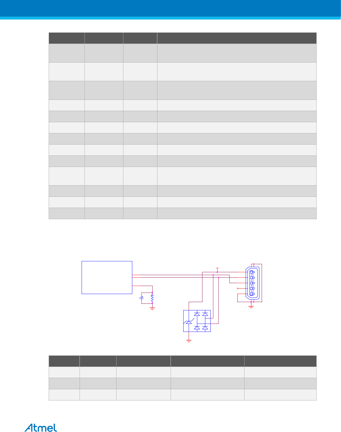
J302 Pin Mnemonic Pin on SAM E70 SAM E70 Signal Name Signal Description
1 VBUS -- -- 5V power
2 DM 136 HSDM Data minus
3 DP 137 HSDP Data plus
Atmel SAME70-XPLD [USER GUIDE]
Atmel-44050A-SAME70-XPLD_User Guide-12/2015
27
J302 Pin Mnemonic Pin on SAM E70 SAM E70 Signal Name Signal Description
4 ID -- -- On-the-go identification
5 Ground GND GND System Ground
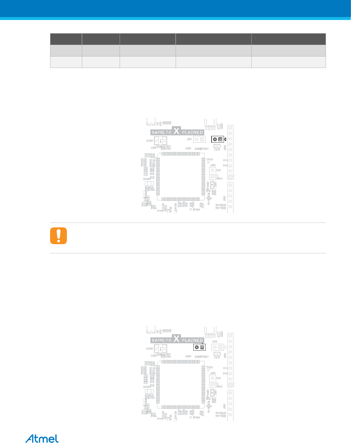
4.3.5. Current Measurement Header (VCC_MCU_P3V3 )
A 100mil pin-header marked "J203" is located at the upper edge of the SAME70-XPLD. All the power
going to the ATSAME70Q21 is routed through this header. To measure the power consumption of the
device, remove the jumper and replace it with an ammeter.
Figure 4-14 VCC_MCU_P3V3 Connector Placement J203
J203
Caution: Removing the jumper from the pin-header while the board is connected to otherwise
powered extension boards or systems may cause the ATSAME70Q21 to be powered through its
I/O pins. This could cause permanent damage to the device.
4.3.6. VDDCORE Current Measurement
A 100mil pin-header marked "J201" is located at the upper edge of the SAME70-XPLD board. It is not
mounted by default and is replaced by a shunt trace between the two pads of the connector. All power to
VDDCORE of the ATSAME70Q21 is routed through this header. To measure the power consumption of
VDDCORE, cut the shunt trace between the two points, mount a header or solder wires and connect an
ammeter.
Figure 4-15 VDDCORE Connector Placement J201
J201
Atmel SAME70-XPLD [USER GUIDE]
Atmel-44050A-SAME70-XPLD_User Guide-12/2015
28

Caution: Leaving J201 open while the main power source is present is to be avoided. This
would feed all power pins of the ATSAME70Q21 except VDDCORE, which may cause
permanent damage to the device.
4.3.7. Chip Erase Header
The chip erase header J200 is connected to the SAM E70 erase pin (PB12) and the main 3.3V. To erase
the contents of the SAM E70 flash memory, set a jumper on J200 and turn the power supply on. The
jumper can be removed soon after the power is on (flash erasing takes only 200ms). Using the chip erase
jumper is the only way to erase a chip with the security bit set.
Figure 4-16 ERASE Chip Connector Placement J200
J200
PB12
3V3
4.3.8. Trace Connector
ATSAME70Q21 supports 4-bit parallel trace. SAME70-XPLD implements a CoreSight 20 20-pin, 50-mil
connector footprint on PCB bottom side (not mounted by default).
Figure 4-17 Trace connector location on PCB
CORESIGHT20
SWD+ETM
J403
To use the trace functionality, an external debugger with trace support and CoreSight 20 pinout has to be
used. The table CoreSight 20-Pin Trace Connector shows the connections on the board.
Figure 4-18 CoreSight 20-Pin Trace Connector Schematic
SWDIO
SWCLK
TRACESWO
TRACECLK
TRACED0
TRACED1
TRACED2
TRACED3
VTREF
TRACE
VCC_3V3
PB6
PB7
PB5
PD8
TARGET_RESET
PD4
PD5
PD6
PD7
J403
CONN_HDR_10X2_19
DNP
1 2
3 4
65
8
9 10
11 12
13 14
15 16
17 18
19 20
Atmel SAME70-XPLD [USER GUIDE]
Atmel-44050A-SAME70-XPLD_User Guide-12/2015
29
Table 4-13 CoreSight 20-Pin Trace Connector
Pin Number SAM E70 Pin Function Shared With
1-[VTREF] - VCC_3V3 --
2-[SWDIO] PB6 SWDIO Embedded Debugger
3-5-9-15-17-19[GND] - System Ground --
4-[SWCLK] PB7 SWCLK Embedded Debugger
6-[TRACESWO] PB5 TRACESWO Embedded Debugger
7-[KEY] - - --
8-11-13[NC] - - --
10-[nSRST] NRST NRST Arduino Connectors and Embedded Debugger
12-[TRACECLK] PD8 TRACECLK Ethernet
14-[TRACED0] PD4 TRACED0 Ethernet
16-[TRACED1] PD5 TRACED1 Ethernet
18-[TRACED2] PD6 TRACED2 Ethernet
20-[TRACED3] PD7 TRACED3 Ethernet
4.4. Peripherals
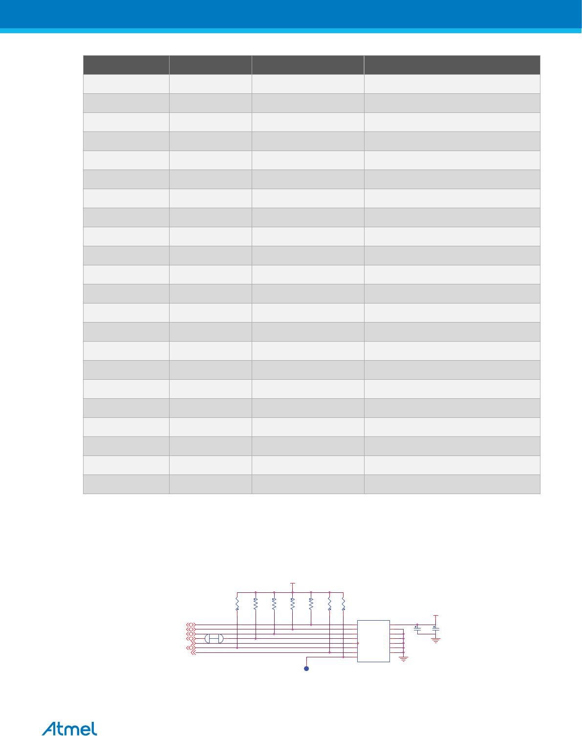
4.4.1. Clock Circuitry
The SAME70-XPLD board features three clock sources:
•Two crystals for the ATSAME70Q21 processor
•One crystal oscillator for the Ethernet MII/RMII chip
The crystals of the ATSAME70Q21 have cut-straps next to them that can be used to measure the
oscillator safety factor. This is done by cutting the strap and adding a resistor across the strap.
Information about oscillator allowance and safety factor can be found in the application note AVR4100;
information about clock calibration and compensation can be found in the application note AT03155.
Table 4-14 Main Components Associated with the Clock Systems
Quantity Description Component Assignment
1 Crystal for internal clock, 12 MHz XC301
1 Crystal for RTC clock, 32.768 kHz (Not Populated) XC300
1 Oscillator for Ethernet clock RMII, 25 MHz XC700
Table 4-15 External Crystals Connected on SAM E70
SAM E70 pin Function
32.768 kHz External Crystal Connection (Not Populated by default)
PA7 XIN32: Slow Clock Oscillator Input
Atmel SAME70-XPLD [USER GUIDE]
Atmel-44050A-SAME70-XPLD_User Guide-12/2015
30

SAM E70 pin Function
PA8 XOUT32: Slow Clock Oscillator Output
12 MHz External Crystal Connection
PB9 XIN: Main Oscillator Input
PB8 XOUT: Main Oscillator Output
Figure 4-19 SAM E70 Crystals Schematic
SAME70
XIN
XOUT
C302
12pF
C303
12pF
XC301
12MHz
3
21
4
PB8 141
PB9 142
J301
1 2
PA8
PA7
XOUT32
XIN32
PA8
J300
12
C301 18pF
DNP
36
35
XC300 32.768 kHz
DNP
C300
18pF
DNP
PA7
4.4.2. Mechanical Buttons
Two pushbutton switches are available. When a button is pressed, it drives the corresponding I/O line to
GND.
•One board reset button (SW100). When pressed and released, this pushbutton causes a power-on
reset of the whole board.
•One wakeup pushbutton that brings the processor out of Low-power mode (SW300)
Figure 4-20 Mechanical Button Schematic
VCC_3V3
EDBG_TARGET_RESET
TARGET_RESET_SENSE
TARGET_RESET
R110
39R
C104
10nF
R122
0R
TP100
SW100
1
42
3
R107
330R
R106
100K
SAME70
USER BUTTON
WKUP6
PA11
R300
39R
PA11
64
TP300
SW300
1
42
3
Important: There is no pull-up resistor connected to SW300 button. Remember to enable the
internal pull-up in the SAM E70 to use the button.
4.4.3. LEDs
There is one green LED mounted on the SAME70-XPLD. It can be activated by driving the connected I/O
line to a low level.
Figure 4-21 LED Indicators Schematic
USER LED
LED0
PC8
VCC_3V3
R303
330R
D301
Green
Atmel SAME70-XPLD [USER GUIDE]
Atmel-44050A-SAME70-XPLD_User Guide-12/2015
31
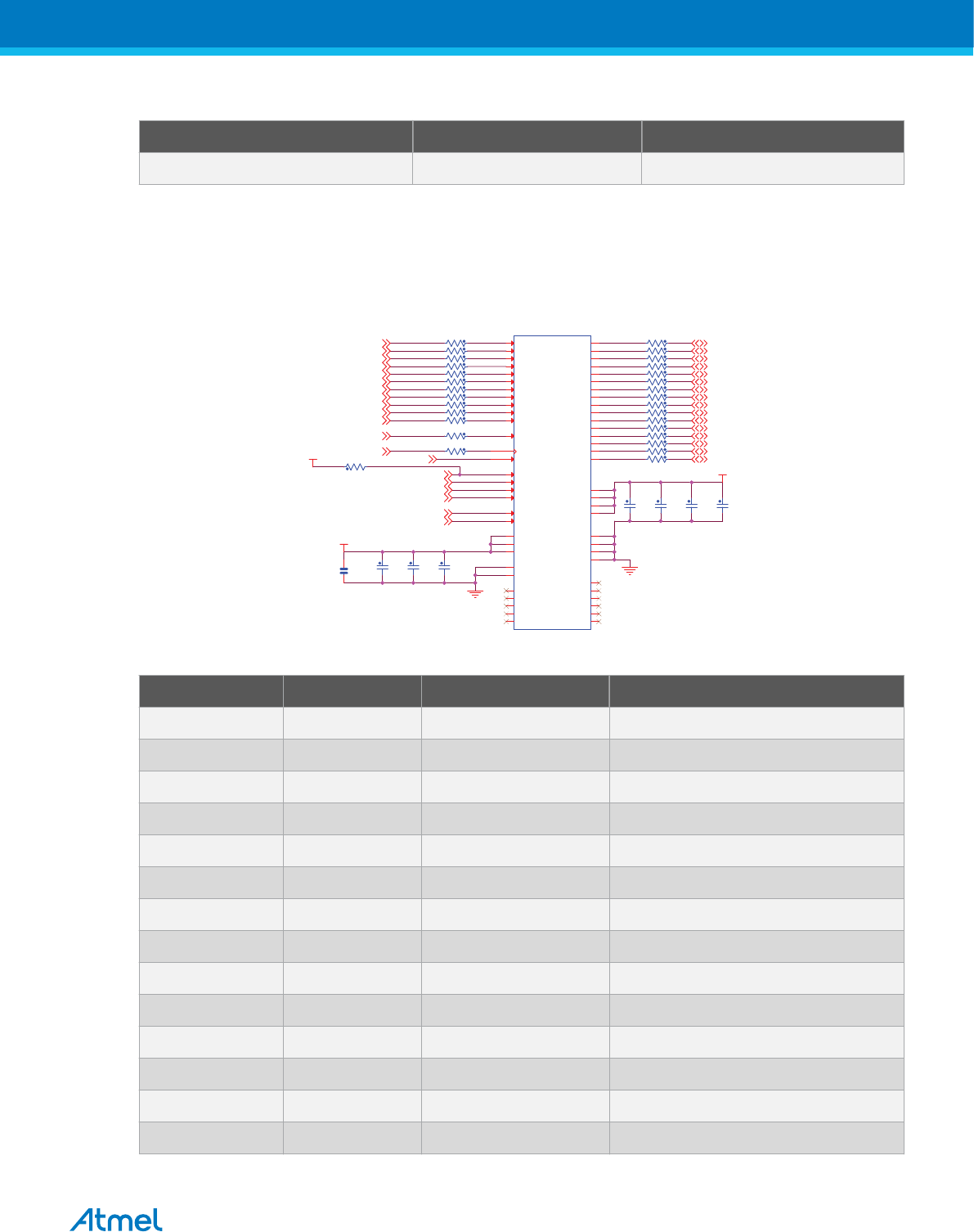
Table 4-16 LED Connection
SAM E70 Pin Function Shared With
PC8 Green LED --
4.4.4. SDRAM
The SAME70-XPLD features one IS42S16100F-5BL, 512K×16×2, 10ns, SDRAM chip. The SDRAM is
connected to chip select NCS1. SDRAM access can be configured in the SDRAM Controller in the SAM
E70. Table 4-17 SDRAM Connections on page 32 lists all I/O lines connected to the SDRAM.
Figure 4-22 SDRAM Schematic
D0
D1
D2
D3
D4
D5
D7
D6
D8
D9
D10
D11
D12
D13
D14
D15
A2
A3
A5
A4
A6
A7
A8
A9
A10
A11
SDA10
BA0
SDCK
SDCKE
SDCS
RAS
CAS
SDWE
A0/NBS0
NWR1/NBS1
VCC_3V3
VCC_3V3
VCC_3V3
PC0
PC1
PC2
PC3
PC4
PC5
PC6
PC7
PE0
PE1
PE2
PE3
PE4
PE5
PA15
PA16
PC20
PC21
PC22
PC23
PC24
PC25
PC26
PC27
PC28
PC29
PD13
PA20
PD23
PD14
PC15
PD16
PD17
PD29
PC18
PD15
R137 22R
R115 22R
R617 100K
C908
2.2uF
R128 22R
R119 22R
R132 22R
R124 22R
C922
100nF
R136 22R
R140 22R
R114 22R
R127 22R
R118 22R
C918
100nF
R125 22R
R131 22R
R123 22R
R111 22R
C921
100nF
R135 22R
R139 22R
R113 22R
R126 22R
R117 22R
C917
100nF
R130 22R
R121 22R
C920
100nF
R134 22R
R138 22R
R112 22R
R116 22R
C919
100nF
C916
100nF
U901
IS42S16100F-5BL
A0
N6
A1
P7
A2
P6
A3
R6
A4
R2
A5
P2
A6
P1
A7
N2
A8
N1
A9
M2
A10
N7
A11
M1
DQ0 A6
DQ1 B7
DQ2 C7
DQ3 D7
DQ4 D6
DQ5 E7
DQ6 F7
DQ7 G7
DQ8 G1
DQ9 F1
DQ10 E1
DQ11 D2
DQ12 D1
DQ13 C1
DQ14 B1
DQ15 A2
CLK
K2
CKE
L1
CS
L7
RAS
K6
CAS
K7
WE
J7
LDQM
J6
UDQM
J2
VDD2
R7
VDD3
H6
VDD1
A7
VSS1
A1
VSS2
R1
VSSQ4 F6
VSSQ3 E2
VSSQ2 C6
VSSQ1 B2
VDDQ4 F2
VDDQ3 E6
VDDQ2 C2
VDDQ1 B6
NC1
G2
NC2
G6
NC3
H1
NC4
H2
NC5
H7
NC7 K1
NC8 L2
NC9 L6
NC10 M6
NC11 M7
NC6 J1
R129 22R
R120 22R
R133 22R
Table 4-17 SDRAM Connections
SAM E70 Pin Function SDRAM Function Shared With
PC0 D0 Data line 0 –
PC1 D1 Data line 1 –
PC2 D2 Data line 2 –
PC3 D3 Data line 3 –
PC4 D4 Data line 4 –
PC5 D5 Data line 5 –
PC6 D6 Data line 6 –
PC7 D7 Data line 7 –
PE0 D8 Data line 8 –
PE1 D9 Data line 9 –
PE2 D10 Data line 10 –
PE3 D11 Data line 11 –
PE4 D12 Data line 12 –
PE5 D13 Data line 13 –
Atmel SAME70-XPLD [USER GUIDE]
Atmel-44050A-SAME70-XPLD_User Guide-12/2015
32
SAM E70 Pin Function SDRAM Function Shared With
PA15 D14 Data line 14 –
PA16 D15 Data line 15 –
PC20 A2 Address line 0 –
PC21 A3 Address line 1 –
PC22 A4 Address line 2 –
PC23 A5 Address line 3 –
PC24 A6 Address line 4 –
PC25 A7 Address line 5 –
PC26 A8 Address line 6 –
PC27 A9 Address line 7 –
PC28 A10 Address line 8 –
PC29 A11 Address line 9 –
PD13 SDA10 Address line 10 –
PA20 BA0 Bank select line 0 –
PD23 SDCK Clock –
PD14 SDCKE Clock Enable –
PC15 SDCS Chip Select –
PD16 RAS RAS Shield J505 Header (Arduino Shield)
PD17 CAS CAS J507 Header (Arduino Shield)
PD29 SDWE Write Enable –
PC18 A0/NBS0 LDQM –
PD15 NWR1/NBS1 UDQM J505 Header (Arduino Shield)
4.4.5. SD Card
The SAME70-XPLD has one standard SD card slot, connected to the High-speed Multimedia Card
Interface (HSMCI) of the SAM E70. Table 4-18 SD/MMC Socket J600 Signal Descriptions on page 34
lists all I/O lines connected to the SD card connector.
Figure 4-23 SD/MMC Socket J600 Schematic
SD_WP
SD_D0
SD_D1
SD_D2
SD_D3
SD_CLK
SD_DETECT
SD_CMD
VCC_3V3
VCC_3V3
PA30
PA31
PA26
PA27
PA28
PA25
PC16
R607
100K
J901
J600
SD Card SOCKET
DAT0
7
DAT1
8
DAT2
9
DAT3
1
VDD 4
VSS1 3
VSS2 6
SHELL 12
CLK
5
CMD
2
C/D
10
W/P
11
SHELL 13
SHELL 14
SHELL 15
R606
10K
R610
100K
R612
10K
R609
100K
R611
10K
TP600
C613
100nF
R608
100K
C612
10uF
Atmel SAME70-XPLD [USER GUIDE]
Atmel-44050A-SAME70-XPLD_User Guide-12/2015
33
Table 4-18 SD/MMC Socket J600 Signal Descriptions
Pin Mnemonic SAM E70 Pin Signal Description Shared WIth
1 DAT3 PA27 Data bit (MCDA3) Camera Connector
2 CMD PA28 Command line (MCCDA) J507 Header (Arduino Shield)
3 VSS -- Common ground --
4 VCC -- Supply voltage 3.3V --
5 CLK PA25 Clock / command line (MCCK) J507 Header (Arduino Shield)
6 VSS -- Common ground --
7 DAT0 PA30 Data bit (MCDA0) J507 Header (Arduino Shield)
8 DAT1 PA31 Data bit (MCDA1) J507 Header (Arduino Shield)
9 DAT2 PA26 Data bit (MCDA2) J507 Header (Arduino Shield)
10 C/D PC16 Card Detect --
11 WP -- Protect --
12 SHELL -- Connected to Ground --
13 SHELL -- Connected to Ground --
14 SHELL -- Connected to Ground --
15 SHELL -- Connected to Ground --
4.4.6. Ethernet
The ATSAME70Q21 has a built-in 10/100 Mbps Ethernet IEEE 802.3 compatible MAC with RMII
interface. The SAME70-XPLD connects the MAC to a Micrel KSZ8081RNACA RMII physical-layer
transceiver (PHY), which is connected to one RJ45 Ethernet connector.
A unique EUI-48™ address is available on every SAME70-XPLD through the on-board AT24MAC402, the
EUI-48 address can be used as a MAC address for the KSZ8081RNACA. The address is also
programmed into the on-board EDBG.
Table 4-19 KSZ8081RNACA Connections on page 35 lists all pins connected from the SAM E70 to the
Ethernet PHY.
Info: Several of the Ethernet signals are shared with the trace connector and thus there is no
Ethernet support if trace is used in an application.
Atmel SAME70-XPLD [USER GUIDE]
Atmel-44050A-SAME70-XPLD_User Guide-12/2015
34
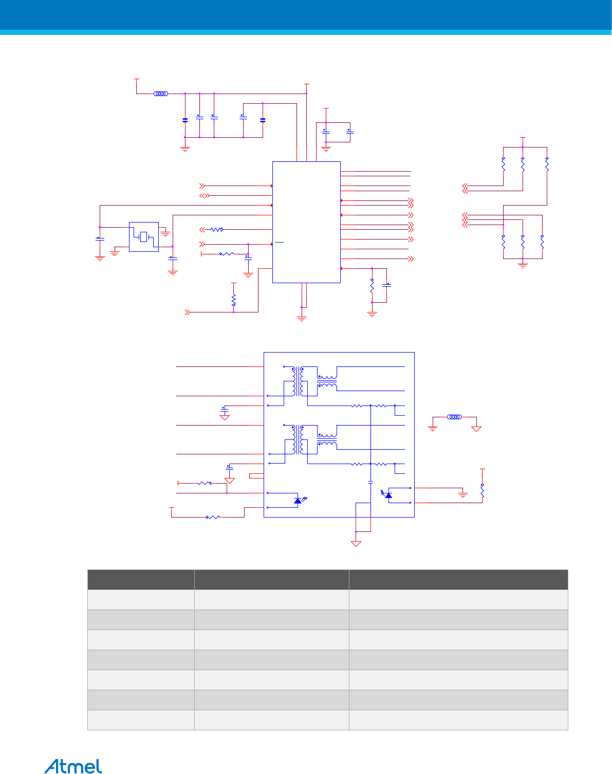
Figure 4-24 RMII Ethernet Schematic
PHY_RESET
PHY_INTERRUPT
PHY_MDC
PHY_MDIO
PHY_CRS_DV
PHY_TXEN
PHY_TXD0
PHY_TXD1
PHY_RXER
PHY_RXD0
PHY_RXD1PHY_REFCLK
PHY_MDIO
PHY_RXD1
PHY_RXD0
PHY_CRS_DV
PHY_MDC
RMII_XTALO
RMII_XTALI
VDDPLL_1.2V
VDDA_ENET
VCC_3V3
VCC_3V3
VCC_3V3
VCC_3V3
VCC_3V3
PD0
PD1
PD2
PD3
PD5
PD6
PD4
PD7
PC10
PA14
PD8
PD9
PD8
PD5
PD6
PD9
PD4
KSZ8081RNACA
U700
VDD_1V2 1
VDDA_3V3 2
RXM 3
RXP 4
TXM 5
TXP 6
XO
7
XI
8
REXT 9
MDIO
10
MDC
11
RXD1 12
RXD0 13
VDDIO 14
CRS_RV/PHYAD1/PHYAD0 15
REF_CLK
16
RXER 17
INTRP
18
TXEN 19
TXD0 20
TXD1 21
GND1
22
LED0/ANEN_SPEED 23
RST
24
GND2
25
R56
1.5K
C704
24PF
R238 39R
C708
2.2uF
R70210K
C709
24PF
C700
100nF
L700
C711
100nF
R67
10K
DNP
C702
100nF
C220
10uF
R704
6.49K
R69
10K
DNP
R70
10K
C92
100PF
DNP
C713
10uF
C710
100nF
R906
1K
R71
10K
DNP
XC700
25MHZ
1 4
32
R55
1.5K
DNP
C701
4.7uF
PHY_TXP
PHY_TXM
PHY_RXP
PHY_RXM
LED0_SPEED
Figure 4-25 Ethernet RJ45 Schematic
LED1_LINK
VCC_3V3
VCC_3V3
R703
470
C706
100nF
R701 470
L701
TD+_R1
TD-_R2
TCT_R3
RD+_R7
1000pF
Y
+
75 OHMS
1 : 1
NC_4
C7
C6_RX-
C3_RX+
C5
C4
C8
C2_TX-
C1_TX+
NC_5
L4
L3
L2
L1
1 : 1
75 OHMS
75 OHMS75 OHMS
G
S2
S1
RD-_R8
RCT_R6
+
J700
RJ45
1
2
7
3
6
8
14
13
11
9
10
4
5
12
C705
100nF
PHY_TXP
PHY_TXM
PHY_RXP
PHY_RXM
LED0_SPEED
VCC_3V3 R604 10K
Table 4-19 KSZ8081RNACA Connections
SAM E70 Pin Exthernet Function Shared With
PD0 PHY_REFCLK J504 Header (Arduino Shield)
PD1 PHY_TXEN –
PD2 PHY_TXD0 –
PD3 PHY_TXD1 –
PD4 PHY_CRS_DV Trace Connector
PD5 PHY_RXD0 Trace Connector
PD6 PHY_RXD1 Trace Connector
Atmel SAME70-XPLD [USER GUIDE]
Atmel-44050A-SAME70-XPLD_User Guide-12/2015
35
SAM E70 Pin Exthernet Function Shared With
PD7 PHY_RXER Trace Connector
PD8 PHY_MDC Trace Connector
PD9 PHY_MDIO –
PC10 PHY_RESET –
PA14 PHY_INTERRUPT –
The KSZ8081RNACA also has a set of parameters that are latched in during reset based on I/O pin
levels. These configuration options have a default mode on the kit done by external pull-up and pull-down
resistors. For detailed information about the configuration, refer to the KSZ8081RNACA datasheet.
Table 4-20 KSZ8081RNACA Configuration
Configuration Name Default Value on
Kit
Default Configuration
PHYAD 0x0h The PHYs address is 0x0h. It can be set to 0x3h if R70
and R71 are permutted.
AUTONEG Pull-Up Auto negotiation enabled and set 100Mbps speed
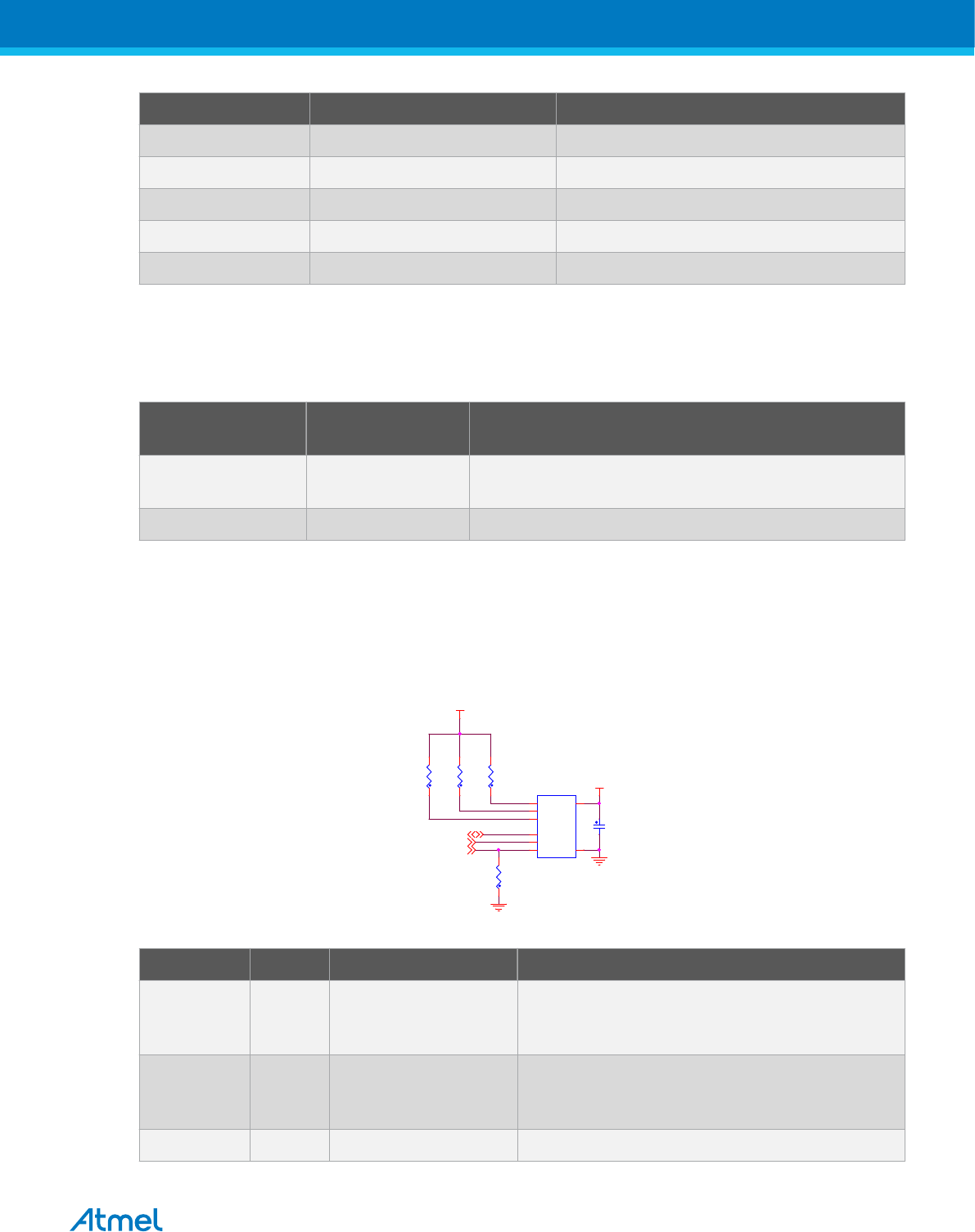
4.4.7. AT24MAC402
The SAME70-XPLD features one Atmel AT24MAC402 serial EEPROM with an EIA-48 MAC address
connected to the SAM E70 through I2C. This AT24MAC402 is configured on the I2C interface with the
address 0x37h. It contains a MAC address for use with the Ethernet interface. Table 4-21 AT24MAC402
Connections on page 36 lists all I/O lines connected to the AT24MAC402 device.
Figure 4-26 AT24MAC402 Schematic
MAC24_A0
MAC24_A1
MAC24_A2
TWD0
TWCK0
VCC_3V3
VCC_3V3
PA3
PA4
PC11
R603
10K
U600
AT24MAC402-MAHM-T
A0
1
A1
2
A2
3
GND 4
SDA
5
SCL
6
WP
7
VCC 8
R600
10K
R601
10K
R602
10K
C600
100nF
Table 4-21 AT24MAC402 Connections
SAM E70 Pin Function AT24MAC402 Function Shared With
PA3 TWD0 SDA (Serial Data Line) Camera Connector, EXT1 Header, EXT2 Header,
J500 Header (Arduino Shield), Embedded
Debugger
PA4 TWCK0 SCL (Serial Click Line) Camera Connector, EXT1 Header, EXT2 Header,
J500 Header (Arduino Shield), Embedded
Debugger
PC11 GPIO WP (Write Protect) --
Atmel SAME70-XPLD [USER GUIDE]
Atmel-44050A-SAME70-XPLD_User Guide-12/2015
36
4.4.8. Debug JTAG/ICE
A 2×10-pin JTAG header is implemented on the SAME70-XPLD board to enable software development
and debugging of the board by using various JTAG emulators. The interface signals have a voltage level
of 3.3V.
Figure 4-27 JTAG/ICE Interface Schematic
ARM JTAG
SWDIO
SWCLK
TRACESWO
VCC_3V3
PB6
PB7
PB5
TARGET_RESET
R401
0R
R402
0R
R403
0R
J406
12
34
6 5
78
910
1112
1314
1516
1718
1920
R400
0R
Table 4-22 JTAG/ICE Connector J406 Signal Descriptions
Pin Signal Type Signal Description
1 VTref /
VCC_3V3
Input This is the target reference voltage. It is used to
check if the target has power, to create the logic-
level reference for the input comparators and to
control the output logic levels to the target. It is
normally fed from Vdd of the target board and must
not have a series resistor.
2 Vsupply /
VCC_3V3
Not Used This pin is not connected in J-Link. It is reserved for
compatibility with other equipment. Connect to Vdd
or leave open in target system.
3 Not used NC This pin is not used by J-Link. If the device may
also be accessed via JTAG, this pin may be
connected to nTRST, otherwise leave open.
5 Not used NC This pin is not used by J-Link. If the device may
also be accessed via JTAG, this pin may be
connected to TDI, otherwise leave open.
7 SWDIO I/O Single bi-directional data pin.
9 SWCLK Output Clock signal to target CPU. It is recommended that
this pin is pulled to a defined state of the target
board. Typically connected to TCK of target CPU.
11 Not used NC This pin is not used by J-Link. This pin is not used
by J-Link when operating in SWD mode. If the
device may also be accessed via JTAG, this pin
may be connected to RTCK, otherwise leave open.
13 SWO Output Serial Wire Output trace port. (Optional, not
required for SWD communication.)
15 RESET I/O Target CPU reset signal. Typically connected to the
RESET pin of the target CPU, which is typically
called "nRST", "nRESET" or "RESET".
17 Not used NC This pin is not connected in J-Link.
Atmel SAME70-XPLD [USER GUIDE]
Atmel-44050A-SAME70-XPLD_User Guide-12/2015
37
Pin Signal Type Signal Description
19 Not Used
(5V-Supply)
Output This pin is used to supply power to some eval
boards. Not all JLinks supply power on this pin, only
the KS (Kickstart) versions. Typically left open on
target hardware.
4-6-8-10-12-14-16-18-20 GND -- System Ground
4.5. Zero Ohm Resistors
The SAME70-XPLD has several zero ohm resistors that can be used to disconnect I/O pins of the
ATSAME70Q21 from connectors and on-board ICs and to disconnect power signals. All Arduino pin
numbers are listed in Arduino Connectors. The table Zero Ohm Resistors lists all zero ohm resistors on
the kit. The figures Zero Ohm Resistors - Top Side and Zero Ohm Resistors - Bottom Side show where
they are located.
Info: Note that some zero ohm resistors listed in the table Zero Ohm Resistors are not
mounted by default on the kit.
Table 4-23 Zero Ohm Resistors
Designator Mounted From To Comments
R122 Yes TARGET_RESET TARGET_RESET_SENSE –
R201 Yes PB0 J401 - Pin 13 RXD0 on EXT1 Connector
R202 Yes PB1 J401 - Pin 14 TXD0 on EXT1 Connector
R203 Yes PD28 J401 - Pin 9
R204 Yes PD27 J402 - Pin 15 SPI Interface: Chip Select
R205 Yes J402 - Pin 17 PD20 SPI Interface: MISO Line
R207 Yes PB1 J505 - Pin 8 Arduino DUE Pin 17
R208 Yes PB0 J505 - Pin 7 Arduino DUE Pin 18
R209 Yes PD26 EXT2 –
R210 Yes PD21 J500 - Pin 4 SPI Interface: MOSI Line -
Arduino DUE Pin 20
R211 Yes PB1 J507 - Pin 4 –
R212 No PD11 J500 - Pin 4 Used for GTSUCOMP - Arduino
DUE Pin 20
R213 Yes PB0 J507 - Pin 5
R214 No PC30 J502 - Pin 6 Arduino DUE Pin 83
R215 Yes PD26 J502 - Pin 1 Arduino DUE Pin 78
R216 No PA17 J502 - Pin 7 Arduino DUE Pin 84
Atmel SAME70-XPLD [USER GUIDE]
Atmel-44050A-SAME70-XPLD_User Guide-12/2015
38
Designator Mounted From To Comments
R217 Yes PA6 J503 - Pin 4 Arduino DUE Pin 139
R218 No PD10 J503 - Pin 4 Arduino DUE Pin 139
R219 Yes PD24 J504 - Pin 1 Arduino DUE Pin 88
R220 Yes PA10 J504 - Pin 2 Arduino DUE Pin 89
R221 Yes PA22 J504 - Pin 3 Arduino DUE Pin 90
R222 No PA13 J400 - Pin 5 Camera Module Reset
Command
R223 No PD22 J400 - Pin 18 ISI Interface: Data Line 0
R224 No PB3 J402 - Pin 15 Chip Select for USART in SPI
Mode with Master Mode
R225 No PD31 J402 - Pin 15 Chip Select for USART in SPI
Mode with Master Mode
R226 No PB2 J402 - Pin 15 Chip Select for USART in SPI
Mode with Slave Mode
R227 No J402 - Pin 17 PB0 MISO for USART in SPI Mode
R228 No PB1 J402 - Pin 16 MOSI for USART in SPI Mode
R229 No PB13 J402 - Pin 18 SPI Clock for USART in SPI
Mode
R230 Yes PD22 J402 - Pin 18 SPI Interface: Clock Line
R234 Yes PD16 J505 - Pin 6 Arduino DUE Pin 6
R235 Yes PD21 J402 - Pin 16 SPI Interface: MOSI Line
R236 No PC12 J502 - Pin 8 Arduino DUE Pin 85
R400 Yes PB6 J406 - Pin 7 SWDIO for JTAG Interface
R401 Yes PB7 J406 - Pin 9 SWCLK for JTAG Interface
R402 Yes J406 - Pin 15 TARGET_RESET Reset From JTAG Interface
R403 Yes PB5 J406 - Pin 13 TRACESWO for JTAG Interface
R623 No VCC_5V0 VIN For 5V supply of any shield
R624 Yes SAM E70 Pin 3 VDDOUT Node LDO Output for current
measurement
Atmel SAME70-XPLD [USER GUIDE]
Atmel-44050A-SAME70-XPLD_User Guide-12/2015
39
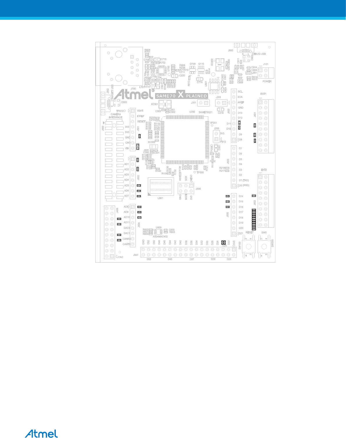
Figure 4-28 Zero Ohm Resistors Position – Top Side
R400
R401
R403
R402
R214
R215
R221
R220
R219
R236
R216
R223 R623 R222
R211
R213
R208
R234
R207
R229
R205
R204
R226
R227
R230
R224
R225
R235
R228
R209
R212R210
R202 R201 R203
Atmel SAME70-XPLD [USER GUIDE]
Atmel-44050A-SAME70-XPLD_User Guide-12/2015
40
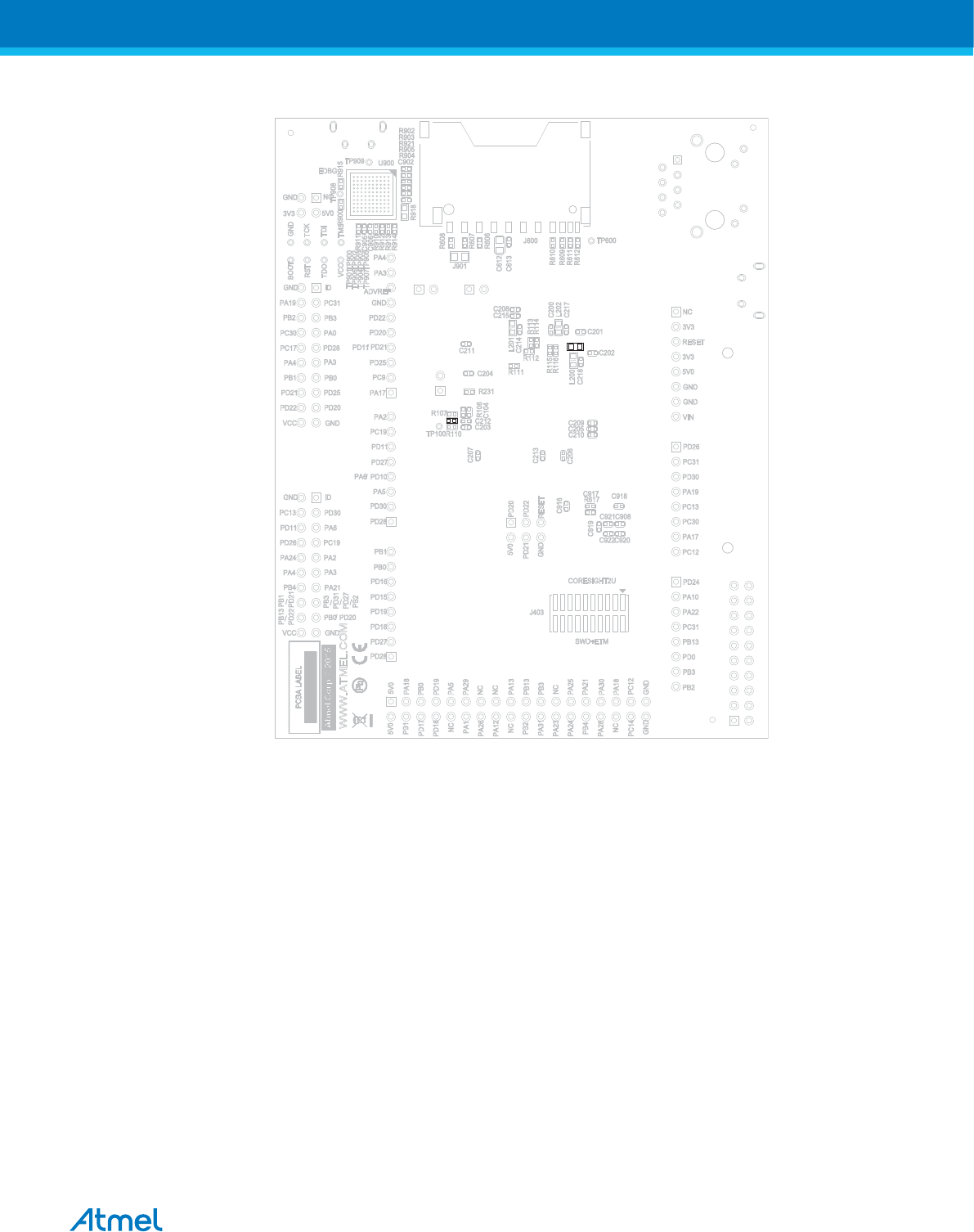
Figure 4-29 Zero Ohm Resistors Position – Bottom Side
R624
R122
4.6. Embedded Debugger Implementation
SAME70-XPLD contains an Embedded Debugger (EDBG) that can be used to program and debug the
ATSAME70Q21 using Serial Wire Debug (SWD). The EDBG also includes:
•a Virtual Com port interface over UART
•an Atmel Data Gateway Interface over SPI
•an I2C channel
•connections to four of the SAM E70 GPIOs
Atmel Studio can be used as a front end for the Embedded Debugger.
4.6.1. Serial Wire Debug
The Serial Wire Debug (SWD) uses two pins to communicate with the target. For further information on
how to use the programming and debugging capabilities of the EDBG, see Embedded Debugger on page
7.
Atmel SAME70-XPLD [USER GUIDE]
Atmel-44050A-SAME70-XPLD_User Guide-12/2015
41
Table 4-24 SWD Connections
SAM E70 Pin Function Shared Functionality
PB5 SWO Trace Data Trace Connector (J403), Embedded Debugger
PB6 SWD Data Trace Connector (J403), Embedded Debugger
PB7 SWD Clock Trace Connector (J403), Embedded Debugger
PB12 Erase Embedded Debugger
4.6.2. Virtual COM Port
The Embedded Debugger acts as a Virtual Com Port gateway by using one of the ATSAME70Q21
UARTs. For further information on how to use the Virtual COM port, see Embedded Debugger on page 7.
Table 4-25 Virtual COM Port Connections
SAM E70 Pin Function Shared Functionality
PB4 TXD1 (SAM E70 UART TX Line) EXT2 Header, J507 Header, Embedded Debugger
PA21 RXD1 (SAM E70 UART RX Line) EXT2 Header, J507 Header, Embedded Debugger
4.6.3. Atmel Data Gateway Interface
The Embedded Debugger features an Atmel Data Gateway Interface (DGI) by using either a SPI or I2C
port. The DGI can be used to send a variety of data from the ATSAME70Q21 to the host PC. For further
information on how to use the DGI interface, see Embedded Debugger on page 7.
Table 4-26 DGI Interface Connections When Using SPI
SAM E70 Pin Function Shared Functionality
PD12 SPI0_NPCS2 (Slave Select) Camera Connector, Embedded Debugger
PD20 SPI0_MISO (Master In, Slave
Out)
EXT1 Header, EXT2 Header, J500 Header, J506
Header, Embedded Debugger
PD21 SPI0_MOSI (Master Out -
Slave In)
EXT1 Header, EXT2 Header, J500 Header, J506
Header, Camera Connector, Embedded Debugger
PD22 SPI0_SPCK EXT1 Header, EXT2 Header, J500 Header, J506
Header, Camera Connector, Embedded Debugger
Table 4-27 DGI Interface Connections When Using I²C
SAM E70 Pin Function Shared Functionality
PA3 TWD0 (I²C Data Line) EXT1 Header, EXT2 Header, J500 Header, AT24MAC402,
Camera Connector, Embedded Debugger
PA4 TWCK0 (I²C Clock Line) EXT1 Header, EXT2 Header, J500 Header, Camera
Connector, Camera Connector, Embedded Debugger
Four GPIO lines are connected to the Embedded Debugger. The EDBG can monitor these lines and
timestamp pin value changes. This makes it possible to accurately timestamp events in the SAM E70
application code. For further information on how to configure and use the GPIO monitoring features, see
Embedded Debugger on page 7.
Atmel SAME70-XPLD [USER GUIDE]
Atmel-44050A-SAME70-XPLD_User Guide-12/2015
42

Table 4-28 GPIO Lines Connected to the EDBG
SAM E70 Pin Function Shared Functionality
PA9 DGI_GPIO0 Camera Connector, Embedded Debugger
PA23 DGI_GPIO1 J507 Header, Embedded Debugger
PD28 DGI_GPIO2 EXT1 Header, Camera Connector,J503 Header, J505 Header, Embedded
Debugger
PA2 DGI_GPIO3 EXT2 Header, J503 Header, Embedded Debugger
Atmel SAME70-XPLD [USER GUIDE]
Atmel-44050A-SAME70-XPLD_User Guide-12/2015
43
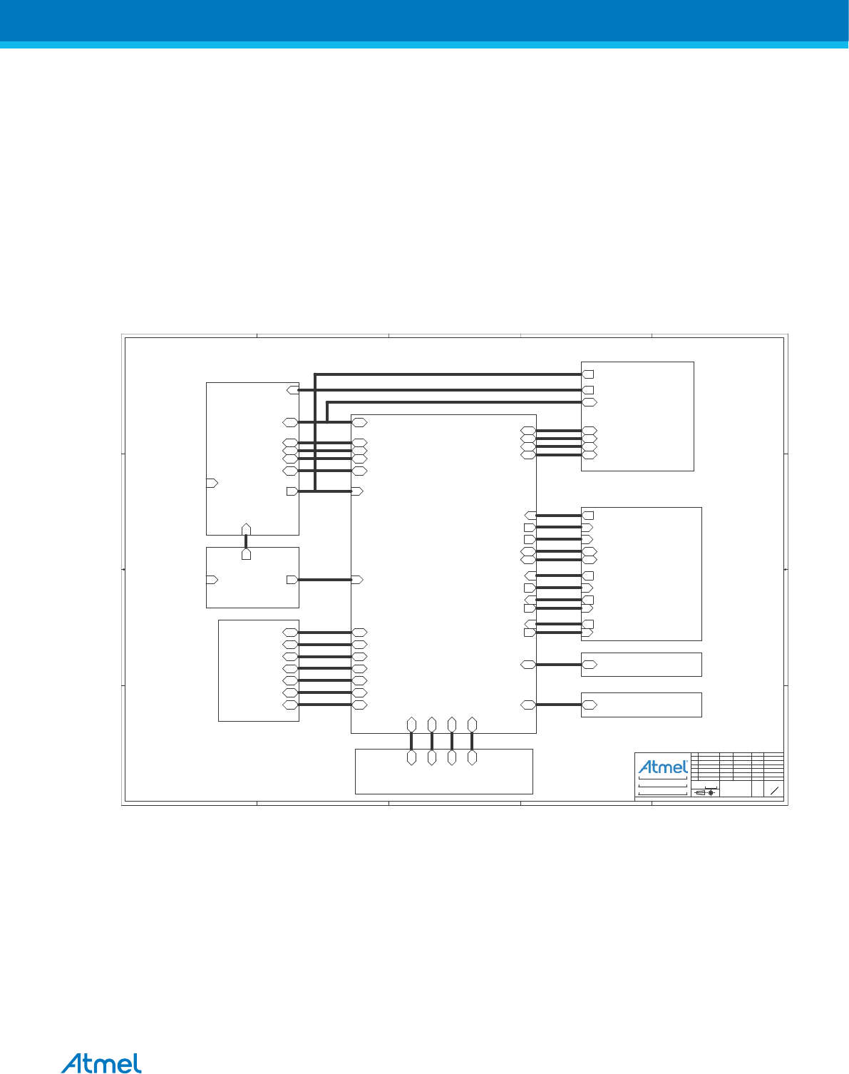
5. Board Schematics
This section contains the following schematics:
•Block Diagram
•SAM E70 Device, Crystals and USB Device interface
•Atmel XPRO Extended Connectors, Debug and Camera Interface Connectors
•Arduino R3 Extended Connectors
•Memories and Power
•Ethernet 10/100
•EDBG Interface
Figure 5-1 Block Diagram
5
5
4
4
3
3
2
2
1
1
D D
C C
B B
AA
Target MCU
SAME70
EDBG
ID_SYS ID_SYS
Connectors
Peripherals
ETHERNET
CAN
Power Supply
OPTIONAL
TARGET_RESET
DWSDWS
EDBG_DGI_SPI
EDBG_DGI_I2C
EDBG_DGI_GPIO
EDBG_CDC_UART
EDBG_DGI_SPI
EDBG_DGI_I2C
EDBG_DGI_GPIO
EDBG_CDC_UART
TRACE
CAMERA
EXT1
EXT2
TRACE
CAMERA
EXT1
EXT2
SWD
BTN0
LED0
LED1
BTN0
LED0
LED1
TARGET_USB_P
TARGET_USB_N
TARGET_USB_P
TARGET_USB_N
VBUS_DETECTVBUS_DETECT
VBUS_HOST_ENVBUS_HOST_EN
XIN32
XOUT32
XIN
XOUT
XIN32
XOUT32
XIN
XOUT
ETHERNET
CANCAN
ETHERNET
TARGET_RESET_SENSE
IOH
IOL
COM
ADCL
ADCH
DIG
SPI
IOH
IOL
COM
ADCL
ADCH
DIG
SPI
TESER_TEGRATTESER_TEGRAT_GBDE
VCC_3V3
VCC_3V3
VCC_5V0
Memory
EBIEBI
I2CI2C
SDRAM
SDCARD
SDRAM
SDCARD
REV
DATE
MODIF.
DES.
DATE
VER.
SCALE
1/1
REV. SHEET
INIT EDIT
A
A RevA
17
A
TOP
SAME70-XPLD
Embest 14-Oct-15
REV
DATE
MODIF.
DES.
DATE
VER.
SCALE
1/1
REV. SHEET
INIT EDIT
A
A RevA
17
A
TOP
SAME70-XPLD
Embest 14-Oct-15
REV
DATE
MODIF.
DES.
DATE
VER.
SCALE
1/1
REV. SHEET
INIT EDIT
A
A RevA
17
A
TOP
SAME70-XPLD
Embest 14-Oct-15
Atmel SAME70-XPLD [USER GUIDE]
Atmel-44050A-SAME70-XPLD_User Guide-12/2015
44
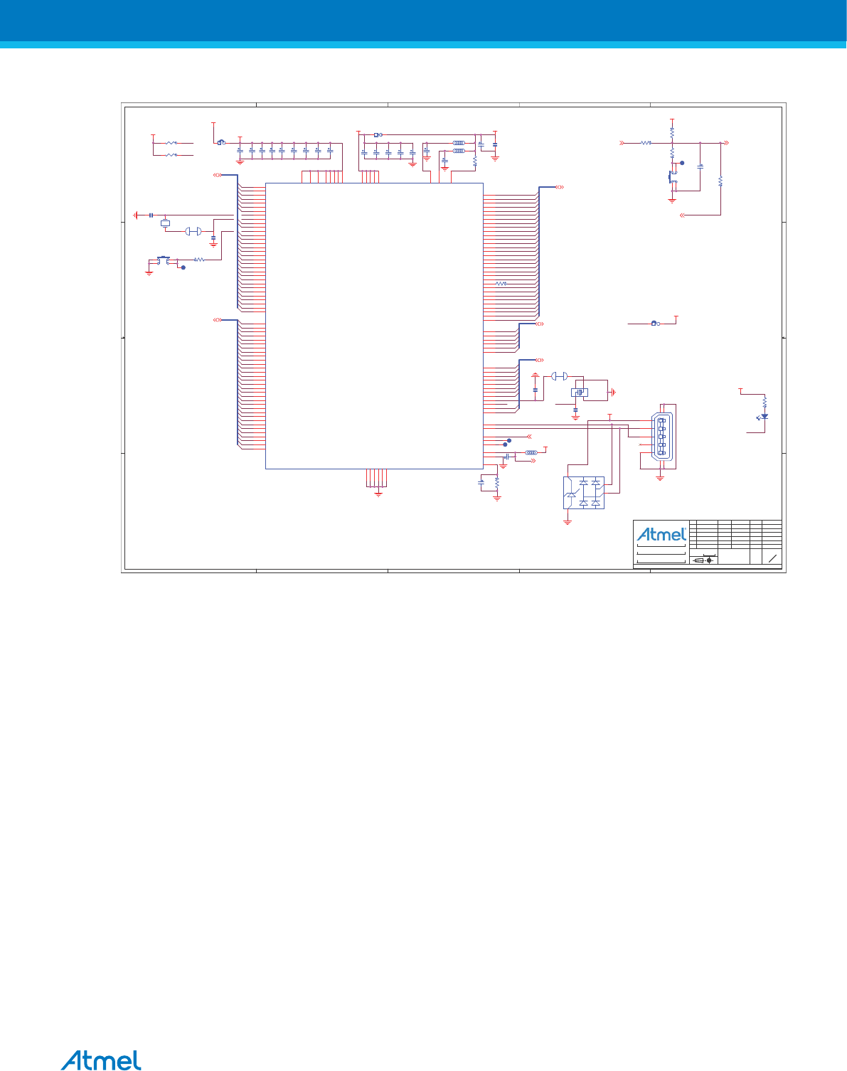
Figure 5-2 SAM E70 Device, Crystals and USB Device interface
5
5
4
4
3
3
2
2
1
1
D D
C C
B B
AA
ATMEL
Cortex-M7 Processor
SAME70 QFP144
These straps with SMD pads can be
used to place a resistor in the XOUT
signal in order to measure the oscillator
allowance. By default these straps are
closed and nothing is mounted on the pads.
These straps with SMD pads can be
used to place a resistor in the XOUT
signal in order to measure the oscillator
allowance. By default these straps are
closed and nothing is mounted on the pads. USER LEDs
USER BUTTONs
LED0
Re-power the kit to
erase SAME70 chip
SDA
SCL
For current measurements
of the target MCU,remove
jumper and connect a
measurement instrument
With jumper: Erase
Without jumper: Normal (default)
WKUP6
XOUT32
XIN32
XOUT
PC8
PC16
PA0
PA1
PA2
PA3
PA4
PA5
PA6
PA10
PA12
PA13
PA14
PA15
PA16
PA17
PA18
PA19
PA20
PA21
PA22
PA24
PA25
PA26
PA27
PA28
PA29
PA30
PA31
PC0
PA23
PC1
PC2
PC3
PC4
PC5
PC6
PC7
PC8
PC9
PC10
PC11
PC12
PC13
PC14
PC15
PC17
PC18
PC19
PC20
PC21
PC22
PC23
PC24
PC25
PC26
PC27
PC28
PC29
PC30
PC31
PD9
PD10
PD0
PD1
PD2
PD3
PD4
PD5
PD6
PD7
PD8
PD11
PD12
PD13
PD14
PD15
PD16
PD17
PD18
PD19
PD20
PD21
PD23
PD24
PD25
PD26
PD27
PD28
PD29
PD30
PD31
PE0
PE1
PE2
PE3
PE4
PE5
PB0
PB1
PB2
PB3
PB4
PB5
PB6
PB7
PB13
PD22
PA11
PB12
PA3
PA4
PA8
PA9
PA11
PB12
XIN32
PA8
XIN XIN
VCC_MCU_P3V3
VDDCORE VDDOUT
VCC_MCU_P3V3
VCC_USB
VCC_3V3
VCC_3V3
VCC_3V3
VCC_3V3
VCC_3V3
EDBG_TARGET_RESET
{7}
TARGET_RESET_SENSE
{7}
PD[0..31] {3,4,5,6,7}
TARGET_RESET {2,3,4}
TARGET_RESET {2,3,4}
ADVREF {4}
PA[0..31]
{3,4,5,6,7}
PC[0..31]
{3,4,5,6}
PE[0..5] {4,5}
PB[0..13] {3,4,7}
REV
DATE
MODIF.
DES.
DATE
VER.
SCALE
1/1
REV. SHEET
INIT EDIT
A
A RevA
27
A
SAME70
SAME70-XPLD
Embest 14-Oct-15
REV
DATE
MODIF.
DES.
DATE
VER.
SCALE
1/1
REV. SHEET
INIT EDIT
A
A RevA
27
A
SAME70
SAME70-XPLD
Embest 14-Oct-15
REV
DATE
MODIF.
DES.
DATE
VER.
SCALE
1/1
REV. SHEET
INIT EDIT
A
A RevA
27
A
SAME70
SAME70-XPLD
Embest 14-Oct-15
C302
12pF
C207
100nF
C303
12pF
C219
10pF
J300
C301 18pF
DNP
R231 4.7K
C202
100nF
5V D- D+ ID G
MICRO USB AB 5
J302
1
2
3
4
S2
5
S1
S3S4
XC301
12MHz
3
21
4
C209
100nF
R233
5.62K
R232 4.7K
L200
R206
39R
R110
39R
C210
100nF
C104
10nF
R303
330R
C201
100nF
C200
100nF
R624
0R
R122
0R
D301
Green
C211
100nF
R300
39R
XC300 32.768 kHz
DNP
TP100
U200
PD6 121
PD7 119
PD18 69
GND_1
44
PD19 67
PD8 113
PD22 60
PD30 34
PD25 52
PD24 55
VDDCORE_1 29
PD29 108
PD9 110
PD10 101
PD11 98
PD12 92
PD14 84
PD15 106
PA26
62 PA25
59 PA24
56
PA20
22 PA19
23 PA18
24
PA8
36
PC1
38
PC6
54
VDDIO_1 30
HSDP 137
JTAGSEL 104
TST 85
GND_2
95
PD4 126
VDDCORE_2 33
PD5 125
PC7
48
PC0
11
NRST 83
VDDIO_2 43
GND_3
61
VDDPLL 123
PC8
82
PC5
58 PC4
41 PC3
40 PC2
39
PA29
129 PA28
112 PA27
70
PA6
114
VDDCORE_3 50
PA3
91
PA21
32
PA22
37
PA23
46
PA9
75
PA10
66
PA11
64
PA13
42
PA14
51
PA15
49
PA16
45
PA17
25
VDDIO_3 80
ADVREFN 8
GND_4
115
PD31 2
PD23 57
PD13 88
PA5
73 PA4
77
PA12
68
VDDIN 5
VDDOUT 3
PD21 63
PD20 65
VDDCORE_4 107
PA0
102
PD27 47
PD26 53
PD28 71
PD16 78
PA1
99
PD17 74
PA7
35
VDDIO_4 96
PA2
93
PA30
116
PA31
118
PC10
90
PC11
94
PC12
17
PC13
19
PC14
97
PC15
18
PC16
100
PC17
103
PC18
111
PC19
117
PC20
120
PC21
122
PC22
124
PC23
127
PC24
130
PC25
133
PC26
13
PC27
12
PC28
76
PC29
16
PC30
15
PC31
14
PC9
86
PB4 105
PB5 109
PB6 79
PB7 89
PB8 141
PB9 142
PB12 87
PB13 144
PB0 21
PB1 20
PB2 26
PB3 31
PE0 4
PE1 6
PE2 7
PE3 10
PE4 27
PE5 28
PD0 1
PD1 132
PD2 131
PD3 128
VDDCORE_5 81
VDDUTMIC 139
VDDUTMII 134
VDDPLLUSB 143
GND_5
138
GND_6
135
HSDM 136
ADVREFP 9
VBG 140
VDDIO_5 72
C300
18pF
DNP
TP300
C215
1uF
D302
PRTR5V0U2X
DNP
1
2
3
4
C216
10uF
C212
100nF
SW300
1
4
2
3
L201
SW100
1
42
3
J200
C204
100nF
C213
100nF
L202C203
100nF
J203
J301
C205
100nF
R107 330R
TP201
C214
100nF
C206
100nF
R106
100K
TP200
J201 DNP
C208
100nF
C218
100nF
C217
100nF
Atmel SAME70-XPLD [USER GUIDE]
Atmel-44050A-SAME70-XPLD_User Guide-12/2015
45
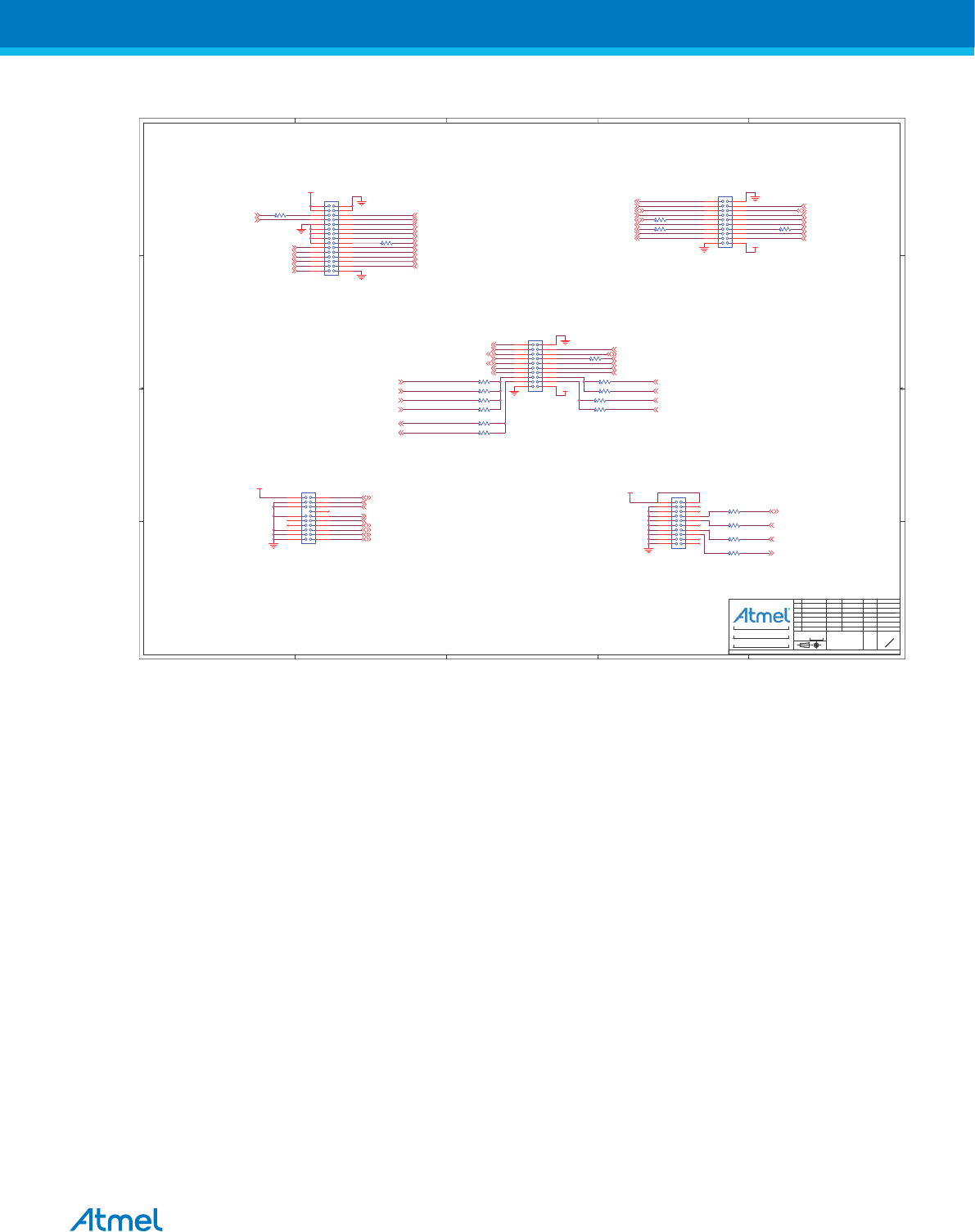
Figure 5-3 Atmel XPRO Extended Connectors, Debug and Camera Interface Connectors
5
5
4
4
3
3
2
2
1
1
D D
C C
B B
AA
RST
TWCK0
ISI_D1
ISI_D3
ISI_D5
ISI_D7
ISI_D9
ISI_D11
Camera Interface Connector
ISI_D0
ISI_D2
ISI_D4
ISI_D6
ISI_D8
ISI_D10
ISI_PCK
ISI_HSYNC
ISI_VSYNC
PCK0
TWD0
ISI_PWD
AFE1_AD6 AFE0_AD8
ID_EXT1
0STC0STR
PWMC0_H0 TIOB5
SPI0_MISO
SPI0_NPCS1 SPI0_MOSI
SPI0_SPCK
0DXT0DXR
0KCWT0DWT
OIPG5PUKW
ID_EXT2
MISO
NPCS
RXD1
TWD0
WKUP2
PWMC0_H2
GPIO
AFE0_AD0
SPI0_SPCK
SPI0_MOSI
TXD1
TWCK0
GPIO
PWMC0_L2
GPIO
AFE1_AD1
EXT1
EXT2
SWDIO
SWCLK
TRACESWO
TRACECLK
TRACED0
TRACED1
TRACED2
TRACED3
VTREF
ARM JTAG
TRACE
SWDIO
SWCLK
TRACESWO
50???? single ended for
trace signals
USART_SPI_MOSI
USART_SPI_SCK
USART_SPI_MOSI
SPI0_MISO
SPI0_NPCS3
USART_SPI_NSS_MASTER_0
USART_SPI_NSS_MASTER_1
USART_SPI_NSS_SLAVE
MOSI
SPCK
VCC_3V3
VCC_3V3
VCC_3V3
VCC_3V3
VCC_3V3
PA13
{2,4}
ID_1
{7}
PA4
{2,3,4,5,7}
PA24 {2,3,4}
PD24 {2,4}
PD25 {2,3,4}
PA6 {2,3,4}
PC19 {2,3,4}
ID_2
{7}
PC31
{2,4} PA19 {2,4,6}
PA0
{2} PC30 {2,4}
PB2 {2,3,4}
PB3
{2,3,4}
PD28
{2,3,4,7}
PD25
{2,3,4} PD21 {2,3,4,7}
PD22 {2,3,4,7}
PD20
{2,3,4,7}
PC17 {2}
PA4 {2,3,4,5,7}
PB0
{2,4} PB1 {2,3,4}
PD30
{2,3,4}
PC19
{2,3,4}
PA6
{2,3,4}
PA2
{2,4,7}
PD27
{2,3,4}
PD20
{2,3,4,7}
PA21
{2,4,7}
PC13 {2,4}
PD11 {2,3,4}
PD26 {2,4}
PD21 {2,3,4,7}
PD22 {2,3,4,7}
PA24 {2,3,4}
PA4 {2,3,4,5,7}
PB4 {2,4,7}
PB6 {2,3,7}
PB7 {2,3,7}
PB5 {2,3,7}
PD8 {2,6}
TARGET_RESET {2,3,4}
PD4 {2,6}
PD5 {2,6}
PD6 {2,6}
PD7 {2,6}
PB6 {2,3,7}
PB7 {2,3,7}
PB5 {2,3,7}
TARGET_RESET {2,3,4}
PA3 {2,3,4,5,7}
PA3
{2,3,4,5,7}
PA3
{2,3,4,5,7}
PD22 {2,3,4,7}
PB3 {2,3,4}
PA5 {2,3,4}
PD12 {2,7}
PD27 {2,3,4}
PD30 {2,3,4}
PD21
{2,3,4,7}
PA9
{2,7}
PD11
{2,3,4}
PA27
{2,5}
PD28
{2,3,4,7}
PD31
{2,3}
PB3
{2,3,4}
PD31
{2,3}
PB2
{2,3,4}
PB0
{2,3,4,7}
PB1 {2,3,4}
PB13 {2,4}
REV
DATE
MODIF.
DES.
DATE
VER.
SCALE
1/1
REV. SHEET
INIT EDIT
A
A RevA
37
A
Extension Connectors
SAME70-XPLD
Embest 14-Oct-15
REV
DATE
MODIF.
DES.
DATE
VER.
SCALE
1/1
REV. SHEET
INIT EDIT
A
A RevA
37
A
Extension Connectors
SAME70-XPLD
Embest 14-Oct-15
REV
DATE
MODIF.
DES.
DATE
VER.
SCALE
1/1
REV. SHEET
INIT EDIT
A
A RevA
37
A
Extension Connectors
SAME70-XPLD
Embest 14-Oct-15
R226 0R
DNP
R225 0R
DNP
J401
12
34
6
5
78
910
11 12
13 14
15 16
17 18
19 20
R230 0R
R403 0R
R209 0R
R227 0R
DNP
R201 0R
J406
12
34
6 5
78
910
1112
13
14
1516
1718
1920
R229 0R
DNP
R205 0R
R224 0R
DNP
R402 0R
R228 0R
DNP
R204 0R
J403
CONN_HDR_10X2_19
DNP
12
34
6
5
8
910
11 12
13 14
15 16
17 18
19 20
J400
CONN_HDR_15X2
12
34
6
5
78
910
11 12
13 14
15 16
17 18
19 20
21
23
25
27
22
24
26
28
29 30
R202 0R
R401 0R
R223 0R
R222 0R
R400 0R
J402
1 2
34
6
5
78
910
11 12
13 14
15 16
17 18
19 20
R203 0R
R235 0R
Atmel SAME70-XPLD [USER GUIDE]
Atmel-44050A-SAME70-XPLD_User Guide-12/2015
46
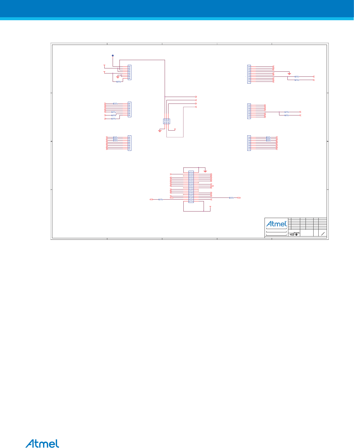
Figure 5-4 Arduino R3 Extended Conncetors
5
5
4
4
3
3
2
2
1
1
D D
C C
B B
AA
SPI0_SPCK
SPI0_MOSI
SPI0_MISO
ADCL
AD0
AD1
AD2
AD3
AD4
AD5
AD6
AD7
ADCH
AD8
AD9
AD10
AD11
DAC0
DAC1
CANRX0
CANTX0
AREF
PWMC0_PWMH3
LED TIOB7
IOH
SPI0_NPCS1
SPI0_MOSI
SPI0_MISO
SPI0_SPCK
TWD0
TWCK0
TWD2
TWCK2
TXD0
RXD0
TXD2
RXD2
UTXD4
URXD4
COM
UTXD3
URXD3
PWMC0_H1
PWMC0_H2
PWMC0_H0
PWMC1_L3
GPIO
SPI0_NPCS3
IOL
CANRX1CANTX1
1DXR1DXT
1STC1STR
RTS0
CTS0
CTS2RTS2
TF
2KCPKT
GTSUCOMP
PWMC0_L2
PWMC1_PWML3
TCLK2
PWMC1_PWML1
SCK0
PWMC1_PWMEXTRG1
PWMC1_PWMEXTRG0
PWMC1_PWMFI2
PWMC1_PWML2
PWMC1_PWMH2
PWMC1_PWMH0
PWMC1_PWMFI1
WKUP1
SCK2
VCC_3V3
VCC_5V0
VCC_5V0
VCC_5V0
TARGET_RESET {2,3}
PD22 {2,3,4,7}
PD20 {2,3,4,7}
PD21 {2,3,4,7}
PD26
{2,3}
PC31
{2,3,4}
PD30
{2,3,4}
PA19
{2,3,6}
PC13
{2,3}
PC30
{2,3}
PA17
{2,4}
PC12
{2,4}
PD24
{2,3}
PA10
{2}
PA22
{2}
PC31
{2,3,4}
PB13
{2,3,4}
PD0
{2,6}
PB2
{2,3,4} PB3
{2,3,4}
ADVREF {2}
PA17 {2,4}
PC9 {2}
PD25 {2,3}
PD20 {2,3,4,7}
PD22 {2,3,4,7}
PD21 {2,3,4,7}
PA4 {2,3,5,7}
PA3 {2,3,5,7}
PB0 {2,3,4}
PB1 {2,3,4}
PD27 {2,3,4}
PD28 {2,3,4,7}
PD15 {2,5}
PD16 {2,5}
PD18 {2,4,5}
PD19 {2,4}
PA2 {2,3,7}
PC19 {2,3}
PD11 {2,3,4}
PD27 {2,3,4}
PA5 {2,3,4} PA6 {2,3}
PD28 {2,3,4,7}
PD30 {2,3,4}
PC12 {2,4}
PC14
{2}
PB2
{2,3,4}
PB4
{2,3,7}
PA24
{2,3} PA21 {2,3,4,7}
PA25 {2,5}
PB3 {2,3,4}
PD19 {2,4}
PD18
{2,4,5}
PB1
{2,3,4} PA18 {2,4}
PB0 {2,3,4}
PD11 {2,3,4}
PD10 {2}
PA5 {2,3,4}
PA29 {2}
PA13 {2}
PB13 {2,3,4}
PA18 {2,4}
PA30 {2,5}
PA28
{2,5}
PA23
{2,7}
PA31
{2,5}
PA12
{2}
PA26
{2,5}
PA1
{2}
PD17
{2,5}
REV
DATEMODIF.
DES.
DATE
VER.
SCALE
1/1
REV. SHEET
INIT EDIT
A
A RevA
47
A
Shield Connectors
SAME70-XPLD
Embest 14-Oct-15
REV
DATEMODIF.
DES.
DATE
VER.
SCALE
1/1
REV. SHEET
INIT EDIT
A
A RevA
47
A
Shield Connectors
SAME70-XPLD
Embest 14-Oct-15
REV
DATEMODIF.
DES.
DATE
VER.
SCALE
1/1
REV. SHEET
INIT EDIT
A
A RevA
47
A
Shield Connectors
SAME70-XPLD
Embest 14-Oct-15
J502
CONN_HDR_8X1
DNP
1
2
3
4
6
5
7
8
TP910
R220 0R
R214 0R
DNP
J501
CONN_HDR_8X1
DNP
1
2
3
4
6
5
7
8
R234 0R
R236 0R
DNP
R208 0R
J504
CONN_HDR_8X1
DNP
1
2
3
4
6
5
7
8
R210 0R
R215 0R
J507
CONN_HDR_18X2
DNP
12
3
4
65
78
910
1112
13
14
1516
17
18
19
20
21
23
25
22
24
26
27
29
31
33
35
28
30
32
34
36
R212 0R
DNP
R217 0R
R213 0R
J503
CONN_HDR_8X1
DNP
1
2
3
4
6
5
7
8
J506
CONN_HDR_3X2
DNP
12
34
6 5
J500
CONN_HDR_10X1
DNP
1
2
3
4
6
5
7
8
9
10
J505
CONN_HDR_8X1
DNP
1
2
3
4
6
5
7
8
R211 0R
R221 0R
R207 0R
R623 0R
DNP
R218 0R
DNP
R216 0R
DNP
R219 0R
Atmel SAME70-XPLD [USER GUIDE]
Atmel-44050A-SAME70-XPLD_User Guide-12/2015
47
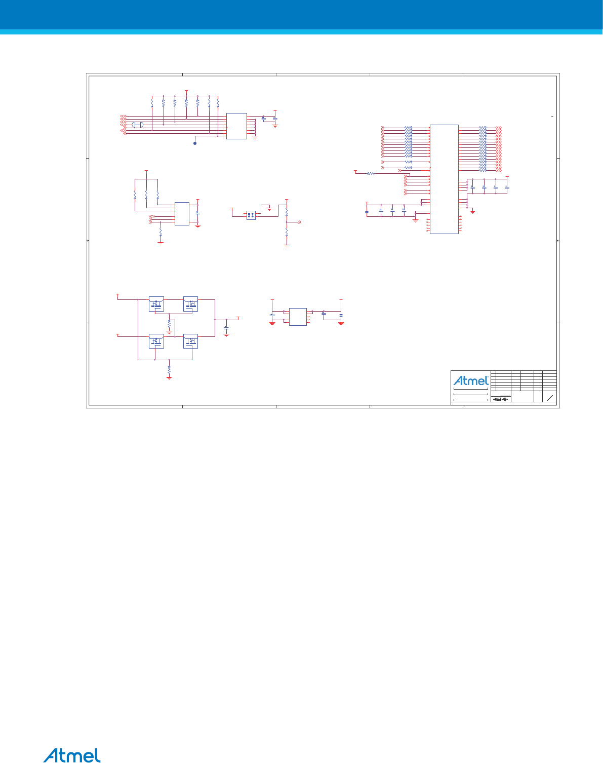
Figure 5-5 Memories and Power
5
5
4
4
3
3
2
2
1
1
D D
C C
B B
AA
MAC24_A0
MAC24_A1
MAC24_A2
TWD0
TWCK0
SD_WP
SD_D0
SD_D1
SD_D2
SD_D3
SD_CLK
SD_DETECT
SD_CMD
D0
D1
D2
D3
D4
D5
D7
D6
D8
D9
D10
D11
D12
D13
D14
D15
A2
A3
A5
A4
A6
A7
A8
A9
A10
A11
SDA10
BA0
SDCK
SDCKE
SDCS
RAS
CAS
SDWE
A0/NBS0
NWR1/NBS1
VCC_3V3
VCC_3V3
VCC_3V3
VCC_3V3
VCC_3V3
VCC_5V0
VCC_USB_EDBG
VCC_USB
VCC_5V0
VCC_5V0
VCC_3V3
VCC_3V3
VCC_3V3
VCC_3V3
PA3
{2,3,4,7}
PA4
{2,3,4,7}
PA30
{2,4}
PA31
{2,4}
PA26
{2,4}
PA27
{2,3}
PA28
{2,4} PA25
{2,4}
PC16
{2}
EDBG_ADC0 {7}
PC0 {2}
PC1 {2}
PC2 {2}
PC3 {2}
PC4 {2}
PC5 {2}
PC6 {2}
PC7 {2}
PE0 {2,4}
PE1 {2}
PE2 {2}
PE3 {2,4}
PE4 {2,4}
PE5 {2,4}
PA15 {2,4}
PA16 {2,4}
PC20
{2}
PC21
{2}
PC22
{2}
PC23
{2}
PC24
{2}
PC25
{2}
PC26
{2}
PC27
{2}
PC28
{2}
PC29
{2}
PD13
{2}
PA20
{2}
PD23
{2}
PD14
{2}
PC15
{2}
PD16
{2,4}
PD17
{2,4}
PD29
{2}
PC18
{2}
PD15
{2,4}
PC11
{2}
REV
DATEMODIF.
DES.
DATE
VER.
SCALE
1/1
REV. SHEET
INIT EDIT
A
A RevA
57
A
Memory & Power
SAME70-XPLD
Embest 14-Oct-15
REV
DATEMODIF.
DES.
DATE
VER.
SCALE
1/1
REV. SHEET
INIT EDIT
A
A RevA
57
A
Memory & Power
SAME70-XPLD
Embest 14-Oct-15
REV
DATEMODIF.
DES.
DATE
VER.
SCALE
1/1
REV. SHEET
INIT EDIT
A
A RevA
57
A
Memory & Power
SAME70-XPLD
Embest 14-Oct-15
R607
100K
R137 22R
R115 22R
R617 100K
R601
10K
U600
AT24MAC402-MAHM-T
A0
1
A1
2
A2
3
GND 4
SDA
5
SCL
6
WP
7
VCC 8
C908
2.2uF
R128 22R
R119 22R
Hearder 2x2
J101
1
3
2
4
R132 22R
R124 22R
J901
C922
100nF
J600
SD Card SOCKET
DAT0
7
DAT1
8
DAT2
9
DAT3
1
VDD 4
VSS1 3
VSS2 6
SHELL 12
CLK
5
CMD
2
C/D
10
W/P
11
SHELL 13
SHELL 14
SHELL 15
R614
100K
R606
10K
R136 22R
R140 22R
C603
2.2UF
R114 22R
R610
100K
C714
10uF
R600
10K
R127 22R
R118 22R
C602
4.7uF
C918
100nF
R125 22R
R616
47K
R131 22R
R123 22R
R111 22R
C921
100nF
R613
100K
R612
10K
R135 22R
R139 22R
R113 22R
R609
100K
R126 22R
R117 22R
R611
10K
C917
100nF
R615
47K
TP600
R130 22R
R121 22R
C920
100nF
R134 22R
C613
100nF
R608
100K
C600
100nF
R138 22R
R112 22R
R116 22R
Q109A
FDC6312P
1
G1
S1
5D1 6
R603
10K
C612
10uF
C919
100nF
Q110A
FDC6312P
1
G1
S1
5D1 6
R602
10K
Q109B
FDC6312P
3
G2
S2 2
D2
4
C601
100nF
C916
100nF
U901
IS42S16100F-5BL
A0
N6
A1
P7
A2
P6
A3
R6
A4
R2
A5
P2
A6
P1
A7
N2
A8
N1
A9
M2
A10
N7
A11
M1
DQ0 A6
DQ1 B7
DQ2 C7
DQ3 D7
DQ4 D6
DQ5 E7
DQ6 F7
DQ7 G7
DQ8 G1
DQ9 F1
DQ10 E1
DQ11 D2
DQ12 D1
DQ13 C1
DQ14 B1
DQ15 A2
CLK
K2
CKE
L1
CS
L7
RAS
K6
CAS
K7
WE
J7
LDQM
J6
UDQM
J2
VDD2
R7
VDD3
H6
VDD1
A7
VSS1
A1
VSS2
R1
VSSQ4 F6
VSSQ3 E2
VSSQ2 C6
VSSQ1 B2
VDDQ4 F2
VDDQ3 E6
VDDQ2 C2
VDDQ1 B6
NC1
G2
NC2
G6
NC3
H1
NC4
H2
NC5
H7
NC7 K1
NC8 L2
NC9 L6
NC10 M6
NC11 M7
NC6 J1
R129 22R
R120 22R
R133 22R
U601
BD33IC0WEFJ-E2
Vo 1
Vo_s 2
GND
3NC1 4
EN
5
NC2 6
NC3 7
VCC
8
FIN
9
Q110B
FDC6312P
3
G2
S2 2
D2
4
Atmel SAME70-XPLD [USER GUIDE]
Atmel-44050A-SAME70-XPLD_User Guide-12/2015
48
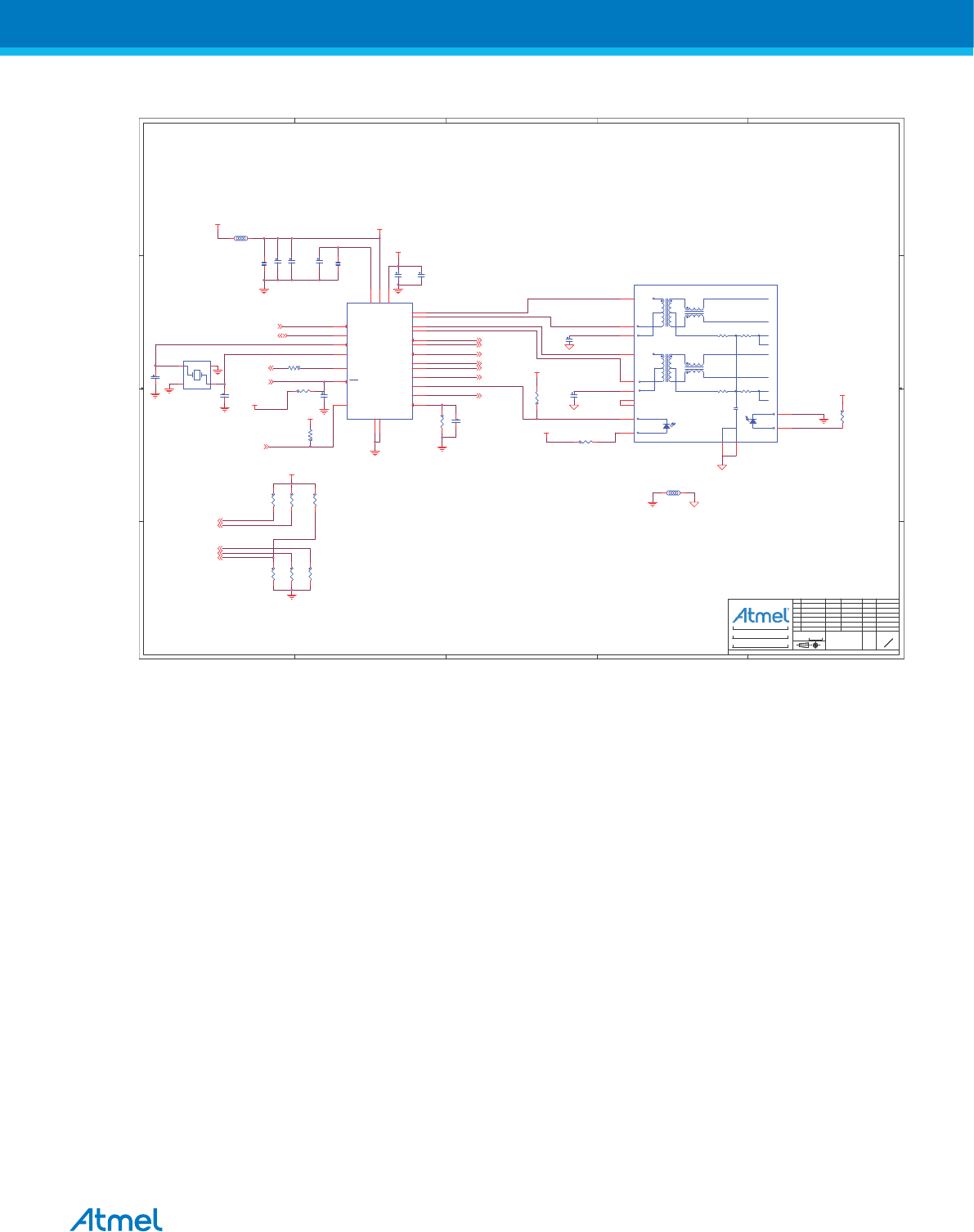
Figure 5-6 Ethernet 10/100
5
5
4
4
3
3
2
2
1
1
D D
C C
B B
AA
PHY_RESET
PHY_INTERRUPT
PHY_MDC
PHY_MDIO
PHY_CRS_DV
PHY_TXEN
PHY_TXD0
PHY_TXD1
PHY_RXER
PHY_RXD0
PHY_RXD1PHY_REFCLK
PHY_MDIO
PHY_RXD1
PHY_RXD0
PHY_CRS_DV
PHY_MDC
RMII_XTALO
RMII_XTALI
LED1_LINK
VDDPLL_1.2V
LED0_SPEED
VDDA_ENET
VCC_3V3
VCC_3V3
VCC_3V3
VCC_3V3
VCC_3V3
VCC_3V3
VCC_3V3
VCC_3V3
PD0{2,4}
PD1 {2}
PD2 {2}
PD3 {2}
PD5 {2,3,6}
PD6 {2,3,6}
PD4 {2,3,6}
PD7 {2,3}
PC10{2}
PA14{2}
PD8
{2,3,6}
PD9
{2,6}
PD8{2,3,6}
PD5{2,3,6}
PD6{2,3,6}
PD9{2,6}
PD4{2,3,6}
REV
DATEMODIF.
DES.
DATE
VER.
SCALE
1/1
REV. SHEET
INIT EDIT
A
A RevA
67
A
Ethernet
SAME70-XPLD
Embest 14-Oct-15
REV
DATEMODIF.
DES.
DATE
VER.
SCALE
1/1
REV. SHEET
INIT EDIT
A
A RevA
67
A
Ethernet
SAME70-XPLD
Embest 14-Oct-15
REV
DATEMODIF.
DES.
DATE
VER.
SCALE
1/1
REV. SHEET
INIT EDIT
A
A RevA
67
A
Ethernet
SAME70-XPLD
Embest 14-Oct-15
TD+_R1
TD-_R2
TCT_R3
RD+_R7
1000pF
Y
+
75 OHMS
1 : 1
NC_4
C7
C6_RX-
C3_RX+
C5
C4
C8
C2_TX-
C1_TX+
NC_5
L4
L3
L2
L1
1 : 1
75 OHMS
75 OHMS75 OHMS
G
S2
S1
RD-_R8
RCT_R6
+
J700
RJ45
1
2
7
3
6
8
14
13
11
9
10
4
5
12
R70
10K
R704
6.49K
C702
100nF
R70210K
R238 39R
L701
L700
R71
10K
DNP
R604
10K
C709
24PF
C706
100nF
C710
100nF
KSZ8081RNACA
U700
VDD_1V2 1
VDDA_3V3 2
RXM 3
RXP 4
TXM 5
TXP 6
XO
7
XI
8
REXT 9
MDIO
10
MDC
11
RXD1 12
RXD0 13
VDDIO 14
CRS_RV/PHYAD1/PHYAD0 15
REF_CLK
16
RXER 17
INTRP
18
TXEN 19
TXD0 20
TXD1 21
GND1
22
LED0/ANEN_SPEED 23
RST
24
GND2
25
R701 470
R69
10K
DNP
C704
24PF
R56
1.5K
C700
100nF
XC700
25MHZ
1 4
3
2
C92
100PF
DNP
R703
470
C705
100nF
R906
1K
C220
10uF
C711
100nF
C701
4.7uF
R55
1.5K
DNP
C713
10uF
R67
10K
DNP
C708
2.2uF
Atmel SAME70-XPLD [USER GUIDE]
Atmel-44050A-SAME70-XPLD_User Guide-12/2015
49
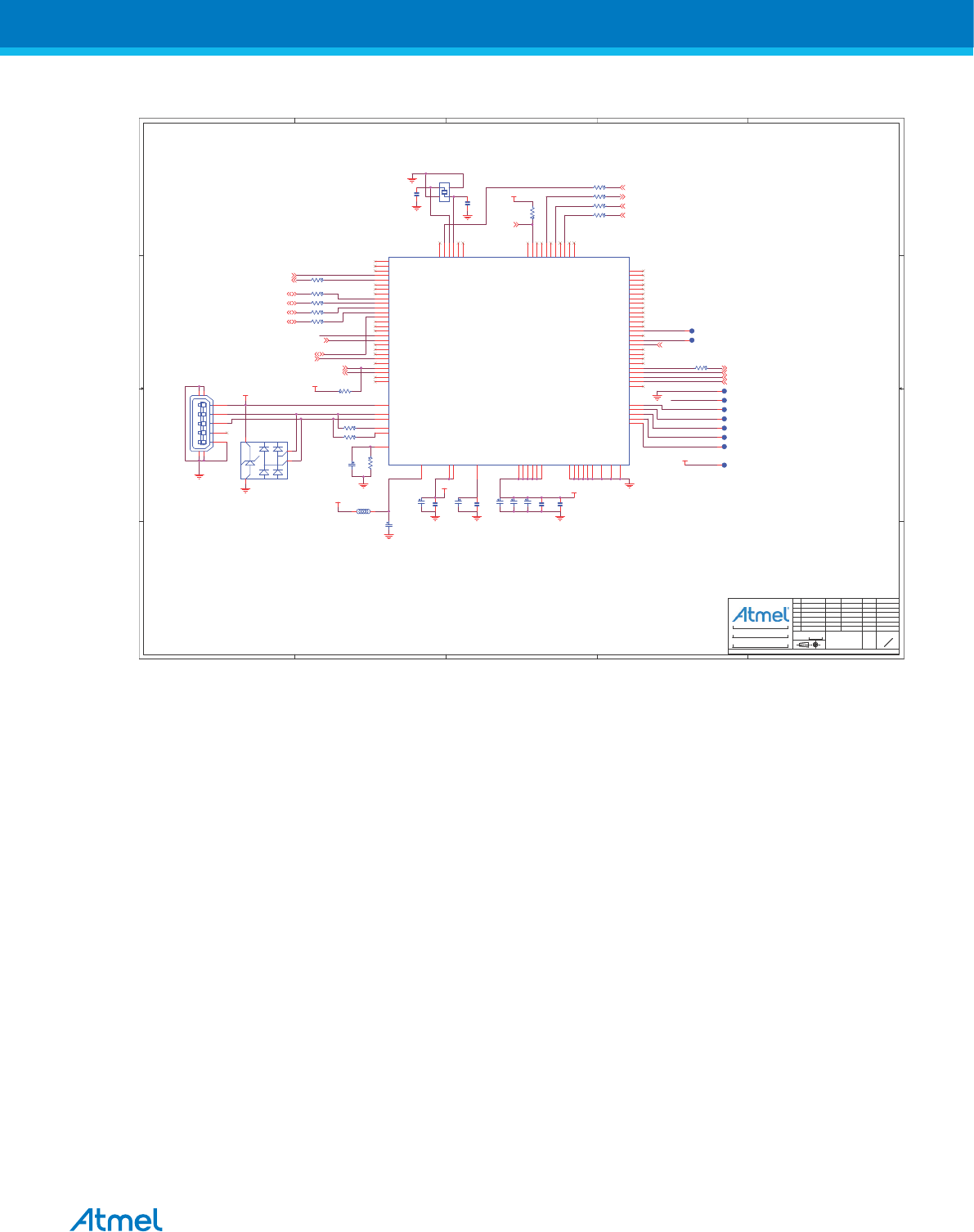
Figure 5-7 EDBG Interface
5
5
4
4
3
3
2
2
1
1
D D
C C
B B
AA
EDBG_SPI_DGI_MISO
EDBG_SPI_DGI_MOSI
EDBG_SPI_DGI_SCK
EDBG_SPI_DGI_SS
TARGET_CHIP_ERASE
TRACESWO
SWCLK
SWDIO
EDBG_CDC_UART_RX
EDBG_CDC_UART_TX
DGI_GPIO0
DGI_GPIO1
DGI_GPIO2
DGI_GPIO3
EDBG_DGI_I2C_SDA
EDBG_DGI_I2C_SCL
Connect TP900 to TP901 during
startup of the EDBG to force it
into bootloader mode
POWER_LED_CTRL
STATUS_LED_CTRL
XIN0
XOUT0
EDBG_JTAG_TCK
EDBG_JTAG_TDI
EDBG_JTAG_TDO
EDBG_RESET_N
EDBG_FORCE_BOOT
EDBG_FORCE_BOOT
EDBG_JTAG_TMS
VCC_3V3
VCC_3V3
VCC_3V3
VCC_3V3
VCC_3V3
VCC_3V3
VCC_USB_EDBG
ID_1
{3}
ID_2
{3}
EDBG_TARGET_RESET
{2}
TARGET_RESET_SENSE {2}
PD22 {2,3,4}
PD12 {2,3}
PD21 {2,3,4}
PD20 {2,3,4}
PB12 {2}
PB6 {2,3}
PB7 {2,3}
PB5 {2,3}
PB4
{2,3,4}
PA21
{2,3,4}
PA9
{2,3}
PA23
{2,4}
PD28
{2,3,4}
PA2
{2,3,4}
PA4
{2,3,4,5}
PA3
{2,3,4,5}
EDBG_ADC0
{5}
REV
DATEMODIF.
DES.
DATE
VER.
SCALE
1/1
REV. SHEET
INIT EDIT
A
A RevA
77
A
Embedded Debugger
SAME70-XPLD
Embest 14-Oct-15
REV
DATEMODIF.
DES.
DATE
VER.
SCALE
1/1
REV. SHEET
INIT EDIT
A
A RevA
77
A
Embedded Debugger
SAME70-XPLD
Embest 14-Oct-15
REV
DATEMODIF.
DES.
DATE
VER.
SCALE
1/1
REV. SHEET
INIT EDIT
A
A RevA
77
A
Embedded Debugger
SAME70-XPLD
Embest 14-Oct-15
C914
2.2uF
XC900
12MHz
3
21
4
TP908
C904
100nF
C909
2.2uF
TP907
R913 330R
R905 330R
R904 330R
R915 330R
TP901
TP905
D902
PRTR5V0U2X
DNP
1
2
3
4
R921 330R
TP903
C913
100nF
R900 330R
R912 330R
U900
AT32UC3A4256J-C1UR
PX6 F3
PX7 F4
GNDIO_1
F5
PX19/PX59 F1
PX8 E3
PX30 G5
PX25 H4
PX24 J2
VDDCORE
E10
PX29 J4
PX9 E4
PX10 D2
PX12 D1
PX15/PX32 K4
PA26/PB5
F7 PA24/PX17
J10
PA20/PX18
H9
PA8
F8
PC1 K6
VDDIO_1
F6
DMHS
A9
USB_VBUS
A10
GNDIO_2
H3
PX4 H1
PX5 G1
PC0/PX14 K5
RESET_N J9
VDDIO_2
F2
GNDIO_3
C3
PC5 A7
PC4 B7
PC3 A6
PC2 A5
PA29
B4 PA28
A1 PA27
A2
PA6/PA13
E8
PA3
F9
PA21/PX22
K10
PA22/PX20
H6
PA23/PX46
G6
PA9
D8
PA10
C10
PA11
C9
PA14/PX11
K7
PA15/PX45
J7
PA16
E7
VDDIO_3
B6
DPFS
B8
GNDIO_4
E2
PX31 H5
PX23 K1
PX13 D3
PA5
G9 PA4
E9
PA12/PA25
G7
VDDIN_1
D10
PX21 H2
PA0/PA18
G8
PX27 K2
PX26 J3
PX28 K3
PX16/PX53 D4
PA1/PA17
G10
PA7/PA19
H10
VDDIO_4
J5
PA2/PX47
E1
PA30
A4
PA31
C2
PB4 A3
PB6 D7
PB7 D6
PB8 C6
PB9 C5
PB10 D5
PB11 C1
PB0 B1
PB1 B2
PB2 B3
PB3 C4
TDI K8
TDO J8
TMS H7
PX0 G4
PX1 G2
PX2 G3
PX3 J1
VDDIO_5
B5
VDDANA
J6
GNDIO_5
C8
GNDIO_6
E6
DPHS
A8
DMFS
B9
USB_VBIAS
C7
VDDIO_6
E5
VDDIN_2
D9
GNDANA
H8
GNDCORE
F10
GNDPLL
B10
TCK K9
R918
6.81K
L901
C900
22pF
C905
2.2uF
C901
22pF
C912
100nF
C911
100nF
R91739R
TP909
R911 330R
TP906
C906
1nF
TP900
TP904
TP902
C915
2.2uF
R910 330R
C902
10pF
R91639R
5VD-D+IDG
MICRO USB AB 5
J900
1
2
3
4
S2
5
S1
S3S4
R902 1K
R914 330R
C910
100nF
R903
1K
Atmel SAME70-XPLD [USER GUIDE]
Atmel-44050A-SAME70-XPLD_User Guide-12/2015
50
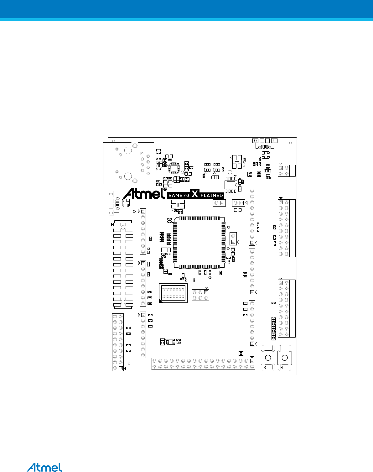
6. Board Layout
This section contains the following layouts:
•Top Component Placement with Silkscreen
•Bottom Component Placement with Silkscreen
•Top Signals Layer
•Layer 2: Ground
•Layer 3: Power Planes
•Bottom Signals Layer
Figure 6-1 Top Component Placement with Silkscreen
J400
INTERFACE
J302
JTAG
R400
R401
R403
R402
J406
CAMERA
TP910
TARGET USB
CANTX
CANRX
DAC1
DAC0
AD11
AD9
AD10
AD8
AD6
AD7
AD4
AD5
AD3
AD2
AD1
GND
VIN
5V0
GND
3V3
D302
J507
J504
R214
J502 R215 J501
RESET
VBAT
IOREF
J700
D53
D52
GND
R601
R600
R602
R221
R220
R219
R236
R216
R223
R125
R126
R128
R129
R137
R138
C300
J300
R623
XC300
R222
R133
R134
R135
R136
R703
L701
C706
L700
C701
C705
R604
R701
D48
D50
AT24MAC402
U600
U901
R140
R127
C301
R123
R117
R118
R120
C219
R233
C303
XC301
XC700
C704
C709
C702
C700
C708
C710
D45
D46
R130
R131
R56
R704
C92
U700
R702
C713
D42
D44
R603
C600
R132
C302
J301
R69
R55
R67
D38
D40 GND
MOSI SCK
RST
R206
R124
R139
R613
17R 07R
C711
C220
R238
R906
D37
D34
D36 5V0
J506
MISO
R300
TP300
U200
J201
C714
Q109
D30
D32
R121
SAME70Q21
U601
Q110
D29
D26
D28
R232
R119 TP200
J200
TP201
J203
R614
XC900
D23
D24
R211
R213
J505
R208
R234
R207
R217
R218
J503
R303 D301
PB12
3V3
D11
D10
C216
C603 C601
C602
5V0
D22 J500
AREF
SDA
R916
R917
C909
C910
C913
C915
C901
C911
C900
J900
SW100
D21
D20 R229
D19 R205
R204
R226
R227
R230
D17
D18
R224
R225
R235
R228
D15
D16
D14 R209
D1
D0
(TXD)
(RXD)
D3
D2
D5
D4
D6
D8
D7
D9
R212R210
D13
D12
GND
SCL
C912
J402 R202 R201 R203
J401
R616
R615
C904
L901
C914
DEBUG USB
D902
EXT2
EXT1
POWER
J101
SW300
2
5
34
1
3
2
4
15
RESET SW0
Atmel SAME70-XPLD [USER GUIDE]
Atmel-44050A-SAME70-XPLD_User Guide-12/2015
51
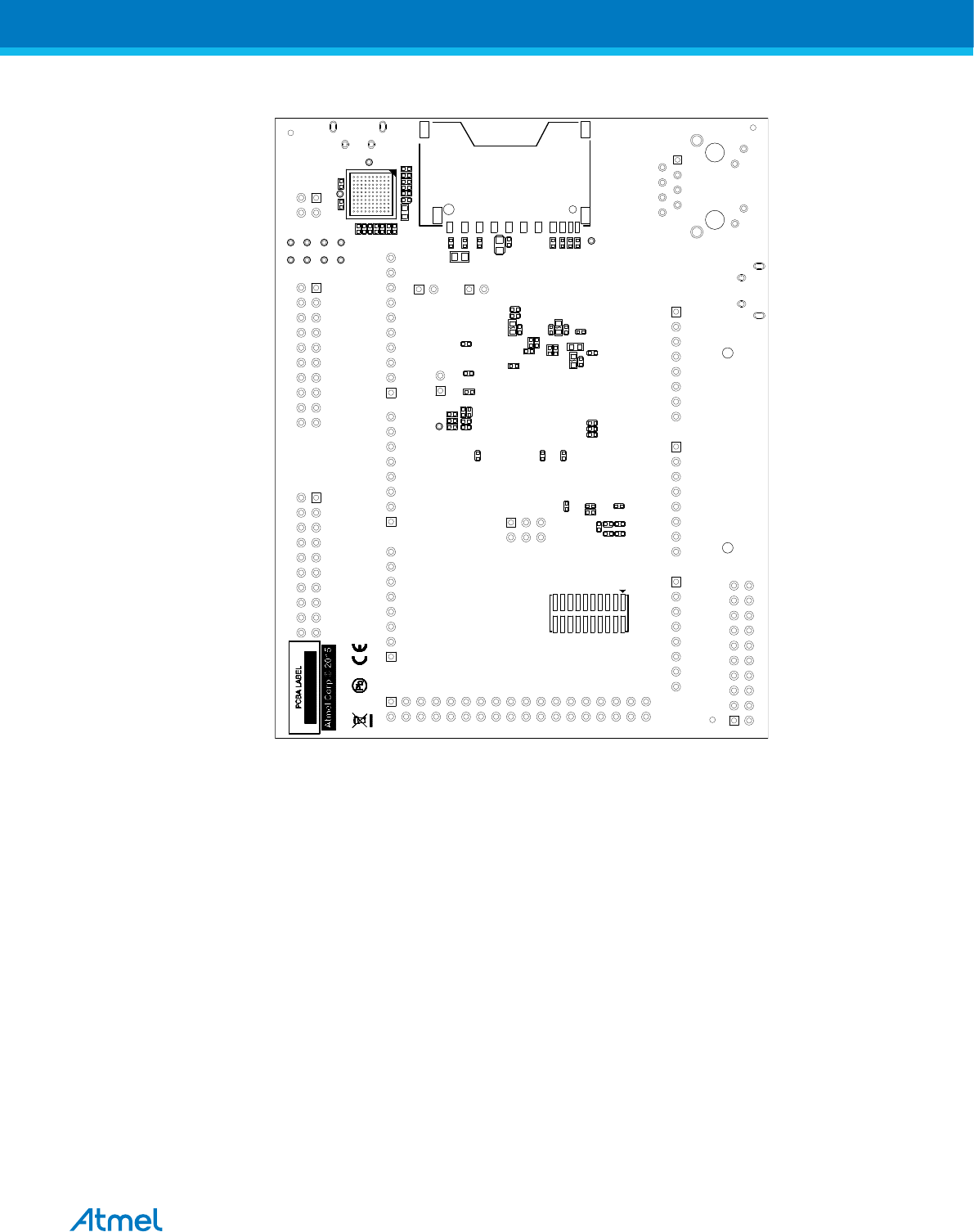
Figure 6-2 Bottom Component Placement with Silkscreen
PB2
PB3
PD0
PB13
PC31
PA10
PA22
PD24
PC12
PA17
PC30
PC13
PA19
PD30
PC31
PD26
VIN
GND
GND
5V0
3V3
RESET
3V3
NC
GND
PC14
GND
PC12
NC
PA28 PA30
PA18
CORESIGHT2U
C920C922
C921C908
C918
C202
TP600
PB4 PA21
SWD+ETM
C919
R617
C917
C210
C209
C205
C218
L200
R624
C201
R612
PA23
PA24 PA25
NC C916
C206
R115
R116
C217
C200
L202 R610
R609
R611
PB2
PA31 PB3
PB13
J403
GND
PD21 PD22
RESET C213
R111
R112
C214
R113
R114
J600
NC
PA12 NC
PA13 5V0 PD20
R231
C204
L201
C215
C208
C613
C612
PA26
PA1 PA29
NC
C207
C212
C203
R106
C104
C211
J901
R606
R607
NC
PD18 PD19
PA5
R110
R122
TP100
R107
R608
PD17
PB1 PA18
PB0
R918
R904
R905
R921
C902
R902
R903
5V0 5V0
PD28
PD27
PD18
PD19
PD15
PD16
PB0
PB1
PD30
PD28
PD10
PA5
PD11
PD27
PC19
PA17
PA2
PD25
PC9
PD21
PD22
PD20
ADVREF
GND
PA4
PA3
R912
R914
R913
U900
PD20
PB2
/
/
PA6
/
PD11
TP901
TP904
TP906
TP907
TP900
TP902
TP903
TP905
R910
R911
C905
C906
TP909
PB0
GND
/
PA21
PB3
/
PD31
PD27
/
PA2
PA3
PC19
PA6
PD30
ID
GND
PD20
PD25
PB0
PA3
PD28
PA0
PB3
ID
PC31
TDO
VCC
TDI
TMS
5V0
NC
R900
TP908
EDBG
R915
RST TCK
VCC
PD22
/
PB13
PD21
PB4
/
PB1
PA4
PA24
PD26
PD11
PC13
GND
VCC
PD21
PD22
PA4
PB1
PC17
PB2
PC30
GND
PA19
BOOT GND
3V3
GND
WWW.ATMEL.COM
Atmel SAME70-XPLD [USER GUIDE]
Atmel-44050A-SAME70-XPLD_User Guide-12/2015
52
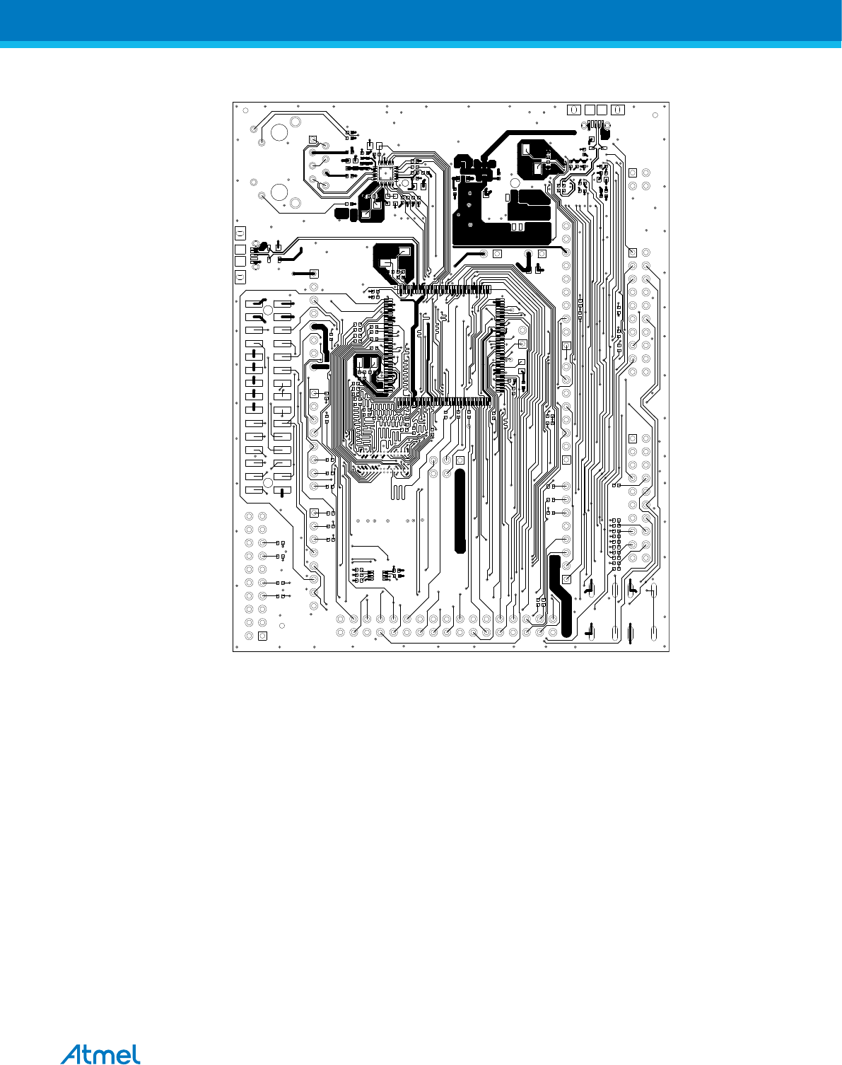
Figure 6-3 Top Signals Layer
Atmel SAME70-XPLD [USER GUIDE]
Atmel-44050A-SAME70-XPLD_User Guide-12/2015
53
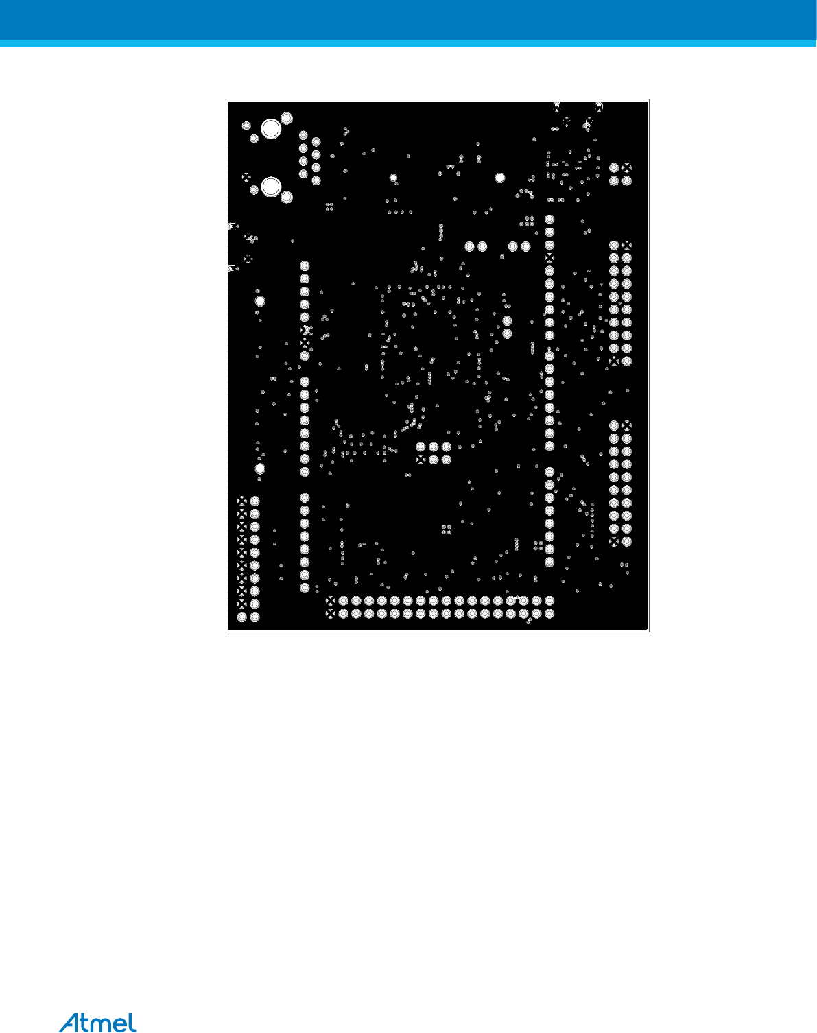
Figure 6-4 Layer 2: Ground
Atmel SAME70-XPLD [USER GUIDE]
Atmel-44050A-SAME70-XPLD_User Guide-12/2015
54
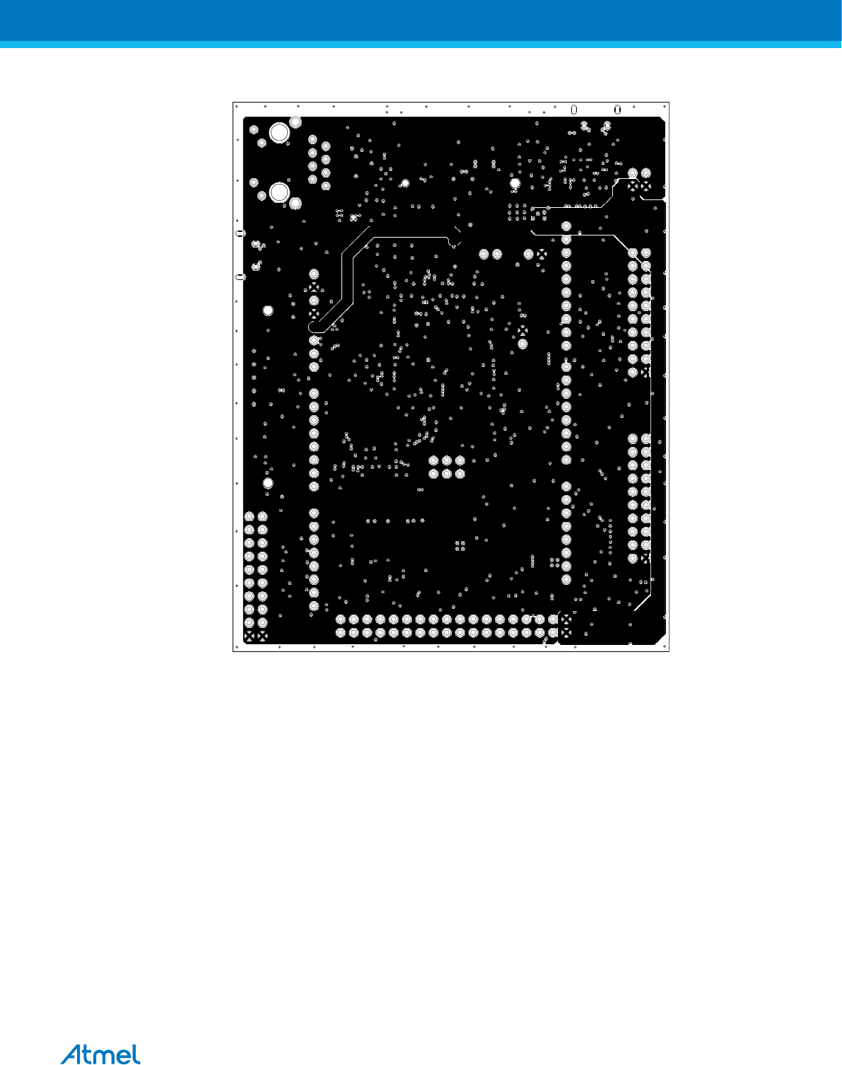
Figure 6-5 Layer 3: Power Planes
Atmel SAME70-XPLD [USER GUIDE]
Atmel-44050A-SAME70-XPLD_User Guide-12/2015
55
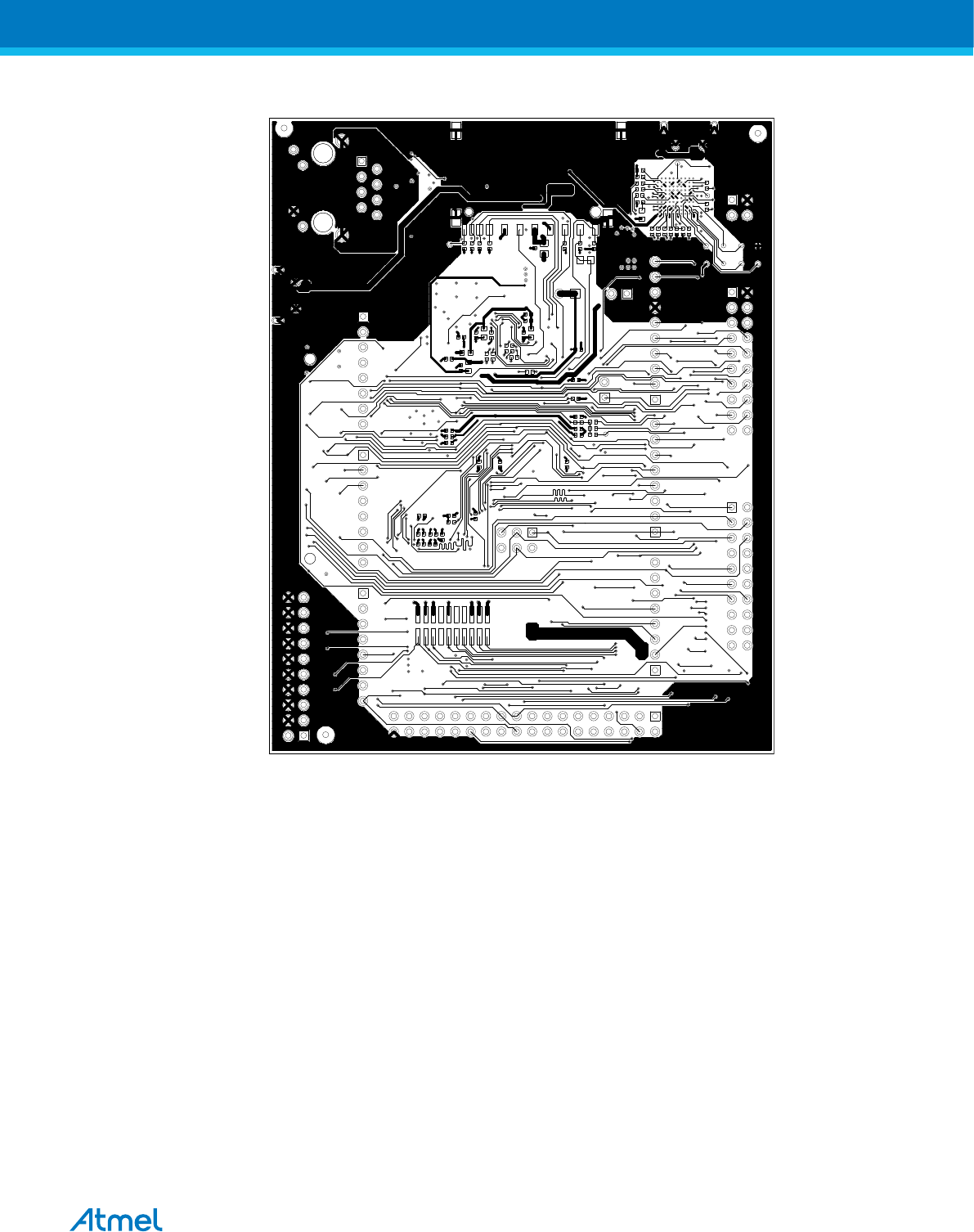
Figure 6-6 Bottom Signals Layer
Atmel SAME70-XPLD [USER GUIDE]
Atmel-44050A-SAME70-XPLD_User Guide-12/2015
56

7. Evaluation Board/kit Important Notice
This evaluation board/kit is intended for use for FURTHER ENGINEERING, DEVELOPMENT,
DEMONSTRATION, OR EVALUATION PURPOSES ONLY. It is not a finished product and may not
(yet) comply with some or any technical or legal requirements that are applicable to finished products,
including, without limitation, directives regarding electromagnetic compatibility, recycling (WEEE), FCC,
CE or UL (except as may be otherwise noted on the board/kit). Atmel supplied this board/kit "AS IS,"
without any warranties, with all faults, at the buyer's and further users' sole risk. The user assumes all
responsibility and liability for proper and safe handling of the goods. Further, the user indemnifies Atmel
from all claims arising from the handling or use of the goods. Due to the open construction of the
product, it is the user's responsibility to take any and all appropriate precautions with regard to
electrostatic discharge and any other technical or legal concerns.
EXCEPT TO THE EXTENT OF THE INDEMNITY SET FORTH ABOVE, NEITHER USER NOR ATMEL
SHALL BE LIABLE TO EACH OTHER FOR ANY INDIRECT, SPECIAL, INCIDENTAL, OR
CONSEQUENTIAL DAMAGES.
No license is granted under any patent right or other intellectual property right of Atmel covering or
relating to any machine, process, or combination in which such Atmel products or services might be or
are used.
Mailing Address: Atmel Corporation
1600 Technology Drive
San Jose, CA 95110
USA
Atmel SAME70-XPLD [USER GUIDE]
Atmel-44050A-SAME70-XPLD_User Guide-12/2015
57

Atmel Corporation 1600 Technology Drive, San Jose, CA 95110 USA T: (+1)(408) 441.0311 F: (+1)(408) 436.4200 | www.atmel.com
© 2015 Atmel Corporation. / Rev.: Atmel-44050A-SAME70-XPLD_User Guide-12/2015
Atmel®, Atmel logo and combinations thereof, Enabling Unlimited Possibilities®, and others are registered trademarks or trademarks of Atmel Corporation in U.S. and
other countries. ARM®, ARM Connected® logo, and others are the registered trademarks or trademarks of ARM Ltd. Other terms and product names may be
trademarks of others.
DISCLAIMER: The information in this document is provided in connection with Atmel products. No license, express or implied, by estoppel or otherwise, to any
intellectual property right is granted by this document or in connection with the sale of Atmel products. EXCEPT AS SET FORTH IN THE ATMEL TERMS AND
CONDITIONS OF SALES LOCATED ON THE ATMEL WEBSITE, ATMEL ASSUMES NO LIABILITY WHATSOEVER AND DISCLAIMS ANY EXPRESS, IMPLIED
OR STATUTORY WARRANTY RELATING TO ITS PRODUCTS INCLUDING, BUT NOT LIMITED TO, THE IMPLIED WARRANTY OF MERCHANTABILITY,
FITNESS FOR A PARTICULAR PURPOSE, OR NON-INFRINGEMENT. IN NO EVENT SHALL ATMEL BE LIABLE FOR ANY DIRECT, INDIRECT,
CONSEQUENTIAL, PUNITIVE, SPECIAL OR INCIDENTAL DAMAGES (INCLUDING, WITHOUT LIMITATION, DAMAGES FOR LOSS AND PROFITS, BUSINESS
INTERRUPTION, OR LOSS OF INFORMATION) ARISING OUT OF THE USE OR INABILITY TO USE THIS DOCUMENT, EVEN IF ATMEL HAS BEEN ADVISED
OF THE POSSIBILITY OF SUCH DAMAGES. Atmel makes no representations or warranties with respect to the accuracy or completeness of the contents of this
document and reserves the right to make changes to specifications and products descriptions at any time without notice. Atmel does not make any commitment to
update the information contained herein. Unless specifically provided otherwise, Atmel products are not suitable for, and shall not be used in, automotive
applications. Atmel products are not intended, authorized, or warranted for use as components in applications intended to support or sustain life.
SAFETY-CRITICAL, MILITARY, AND AUTOMOTIVE APPLICATIONS DISCLAIMER: Atmel products are not designed for and will not be used in connection with any
applications where the failure of such products would reasonably be expected to result in significant personal injury or death (“Safety-Critical Applications”) without
an Atmel officer's specific written consent. Safety-Critical Applications include, without limitation, life support devices and systems, equipment or systems for the
operation of nuclear facilities and weapons systems. Atmel products are not designed nor intended for use in military or aerospace applications or environments
unless specifically designated by Atmel as military-grade. Atmel products are not designed nor intended for use in automotive applications unless specifically
designated by Atmel as automotive-grade.
