STM32F411xC/E Advanced ARM® Based 32 Bit MCUs STM32F411x C Reference Manual
User Manual: Pdf
Open the PDF directly: View PDF ![]() .
.
Page Count: 837 [warning: Documents this large are best viewed by clicking the View PDF Link!]
- 1 Documentation conventions
- 2 Memory and bus architecture
- 3 Embedded Flash memory interface
- 3.1 Introduction
- 3.2 Main features
- 3.3 Embedded Flash memory in STM32F411xC/E
- 3.4 Read interface
- 3.5 Erase and program operations
- 3.6 Option bytes
- 3.7 One-time programmable bytes
- 3.8 Flash interface registers
- 4 CRC calculation unit
- 5 Power controller (PWR)
- 5.1 Power supplies
- 5.2 Power supply supervisor
- 5.3 Low-power modes
- 5.4 Power control registers
- 5.5 PWR register map
- 6 Reset and clock control (RCC) for STM32F411xC/E
- 6.1 Reset
- 6.2 Clocks
- 6.3 RCC registers
- 6.3.1 RCC clock control register (RCC_CR)
- 6.3.2 RCC PLL configuration register (RCC_PLLCFGR)
- 6.3.3 RCC clock configuration register (RCC_CFGR)
- 6.3.4 RCC clock interrupt register (RCC_CIR)
- 6.3.5 RCC AHB1 peripheral reset register (RCC_AHB1RSTR)
- 6.3.6 RCC AHB2 peripheral reset register (RCC_AHB2RSTR)
- 6.3.7 RCC APB1 peripheral reset register for (RCC_APB1RSTR)
- 6.3.8 RCC APB2 peripheral reset register (RCC_APB2RSTR)
- 6.3.9 RCC AHB1 peripheral clock enable register (RCC_AHB1ENR)
- 6.3.10 RCC AHB2 peripheral clock enable register (RCC_AHB2ENR)
- 6.3.11 RCC APB1 peripheral clock enable register (RCC_APB1ENR)
- 6.3.12 RCC APB2 peripheral clock enable register (RCC_APB2ENR)
- 6.3.13 RCC AHB1 peripheral clock enable in low power mode register (RCC_AHB1LPENR)
- 6.3.14 RCC AHB2 peripheral clock enable in low power mode register (RCC_AHB2LPENR)
- 6.3.15 RCC APB1 peripheral clock enable in low power mode register (RCC_APB1LPENR)
- 6.3.16 RCC APB2 peripheral clock enabled in low power mode register (RCC_APB2LPENR)
- 6.3.17 RCC Backup domain control register (RCC_BDCR)
- 6.3.18 RCC clock control & status register (RCC_CSR)
- 6.3.19 RCC spread spectrum clock generation register (RCC_SSCGR)
- 6.3.20 RCC PLLI2S configuration register (RCC_PLLI2SCFGR)
- 6.3.21 RCC Dedicated Clocks Configuration Register (RCC_DCKCFGR)
- 6.3.22 RCC register map
- 7 System configuration controller (SYSCFG)
- 7.1 I/O compensation cell
- 7.2 SYSCFG registers
- 7.2.1 SYSCFG memory remap register (SYSCFG_MEMRMP)
- 7.2.2 SYSCFG peripheral mode configuration register (SYSCFG_PMC)
- 7.2.3 SYSCFG external interrupt configuration register 1 (SYSCFG_EXTICR1)
- 7.2.4 SYSCFG external interrupt configuration register 2 (SYSCFG_EXTICR2)
- 7.2.5 SYSCFG external interrupt configuration register 3 (SYSCFG_EXTICR3)
- 7.2.6 SYSCFG external interrupt configuration register 4 (SYSCFG_EXTICR4)
- 7.2.7 Compensation cell control register (SYSCFG_CMPCR)
- 7.2.8 SYSCFG register map
- 8 General-purpose I/Os (GPIO)
- 8.1 GPIO introduction
- 8.2 GPIO main features
- 8.3 GPIO functional description
- Table 23. Port bit configuration table (continued)
- 8.3.1 General-purpose I/O (GPIO)
- 8.3.2 I/O pin multiplexer and mapping
- 8.3.3 I/O port control registers
- 8.3.4 I/O port data registers
- 8.3.5 I/O data bitwise handling
- 8.3.6 GPIO locking mechanism
- 8.3.7 I/O alternate function input/output
- 8.3.8 External interrupt/wakeup lines
- 8.3.9 Input configuration
- 8.3.10 Output configuration
- 8.3.11 Alternate function configuration
- 8.3.12 Analog configuration
- 8.3.13 Using the OSC32_IN/OSC32_OUT pins as GPIO PC14/PC15 port pins
- 8.3.14 Using the OSC_IN/OSC_OUT pins as GPIO PH0/PH1 port pins
- 8.3.15 Selection of RTC additional functions
- 8.4 GPIO registers
- 8.4.1 GPIO port mode register (GPIOx_MODER) (x = A..E and H)
- 8.4.2 GPIO port output type register (GPIOx_OTYPER) (x = A..E and H)
- 8.4.3 GPIO port output speed register (GPIOx_OSPEEDR) (x = A..E and H)
- 8.4.4 GPIO port pull-up/pull-down register (GPIOx_PUPDR) (x = A..E and H)
- 8.4.5 GPIO port input data register (GPIOx_IDR) (x = A..E and H)
- 8.4.6 GPIO port output data register (GPIOx_ODR) (x = A..E and H)
- 8.4.7 GPIO port bit set/reset register (GPIOx_BSRR) (x = A..E and H)
- 8.4.8 GPIO port configuration lock register (GPIOx_LCKR) (x = A..E and H)
- 8.4.9 GPIO alternate function low register (GPIOx_AFRL) (x = A..E and H)
- 8.4.10 GPIO alternate function high register (GPIOx_AFRH) (x = A..E and H)
- 8.4.11 GPIO register map
- 9 DMA controller (DMA)
- 9.1 DMA introduction
- 9.2 DMA main features
- 9.3 DMA functional description
- 9.3.1 General description
- 9.3.2 DMA transactions
- 9.3.3 Channel selection
- 9.3.4 Arbiter
- 9.3.5 DMA streams
- 9.3.6 Source, destination and transfer modes
- 9.3.7 Pointer incrementation
- 9.3.8 Circular mode
- 9.3.9 Double buffer mode
- 9.3.10 Programmable data width, packing/unpacking, endianess
- 9.3.11 Single and burst transfers
- 9.3.12 FIFO
- 9.3.13 DMA transfer completion
- 9.3.14 DMA transfer suspension
- 9.3.15 Flow controller
- 9.3.16 Summary of the possible DMA configurations
- 9.3.17 Stream configuration procedure
- 9.3.18 Error management
- 9.4 DMA interrupts
- 9.5 DMA registers
- 9.5.1 DMA low interrupt status register (DMA_LISR)
- 9.5.2 DMA high interrupt status register (DMA_HISR)
- 9.5.3 DMA low interrupt flag clear register (DMA_LIFCR)
- 9.5.4 DMA high interrupt flag clear register (DMA_HIFCR)
- 9.5.5 DMA stream x configuration register (DMA_SxCR) (x = 0..7)
- 9.5.6 DMA stream x number of data register (DMA_SxNDTR) (x = 0..7)
- 9.5.7 DMA stream x peripheral address register (DMA_SxPAR) (x = 0..7)
- 9.5.8 DMA stream x memory 0 address register (DMA_SxM0AR) (x = 0..7)
- 9.5.9 DMA stream x memory 1 address register (DMA_SxM1AR) (x = 0..7)
- 9.5.10 DMA stream x FIFO control register (DMA_SxFCR) (x = 0..7)
- 9.5.11 DMA register map
- 10 Interrupts and events
- 10.1 Nested vectored interrupt controller (NVIC)
- 10.2 External interrupt/event controller (EXTI)
- 10.3 EXTI registers
- 11 Analog-to-digital converter (ADC)
- 11.1 ADC introduction
- 11.2 ADC main features
- 11.3 ADC functional description
- 11.4 Data alignment
- 11.5 Channel-wise programmable sampling time
- 11.6 Conversion on external trigger and trigger polarity
- 11.7 Fast conversion mode
- 11.8 Data management
- 11.9 Temperature sensor
- 11.10 Battery charge monitoring
- 11.11 ADC interrupts
- 11.12 ADC registers
- 11.12.1 ADC status register (ADC_SR)
- 11.12.2 ADC control register 1 (ADC_CR1)
- 11.12.3 ADC control register 2 (ADC_CR2)
- 11.12.4 ADC sample time register 1 (ADC_SMPR1)
- 11.12.5 ADC sample time register 2 (ADC_SMPR2)
- 11.12.6 ADC injected channel data offset register x (ADC_JOFRx) (x=1..4)
- 11.12.7 ADC watchdog higher threshold register (ADC_HTR)
- 11.12.8 ADC watchdog lower threshold register (ADC_LTR)
- 11.12.9 ADC regular sequence register 1 (ADC_SQR1)
- 11.12.10 ADC regular sequence register 2 (ADC_SQR2)
- 11.12.11 ADC regular sequence register 3 (ADC_SQR3)
- 11.12.12 ADC injected sequence register (ADC_JSQR)
- 11.12.13 ADC injected data register x (ADC_JDRx) (x= 1..4)
- 11.12.14 ADC regular data register (ADC_DR)
- 11.12.15 ADC common control register (ADC_CCR)
- 11.12.16 ADC register map
- 12 Advanced-control timer (TIM1)
- 12.1 TIM1 introduction
- 12.2 TIM1 main features
- 12.3 TIM1 functional description
- 12.3.1 Time-base unit
- 12.3.2 Counter modes
- 12.3.3 Repetition counter
- 12.3.4 Clock selection
- 12.3.5 Capture/compare channels
- 12.3.6 Input capture mode
- 12.3.7 PWM input mode
- 12.3.8 Forced output mode
- 12.3.9 Output compare mode
- 12.3.10 PWM mode
- 12.3.11 Complementary outputs and dead-time insertion
- 12.3.12 Using the break function
- 12.3.13 Clearing the OCxREF signal on an external event
- 12.3.14 6-step PWM generation
- 12.3.15 One-pulse mode
- 12.3.16 Encoder interface mode
- 12.3.17 Timer input XOR function
- 12.3.18 Interfacing with Hall sensors
- 12.3.19 TIMx and external trigger synchronization
- 12.3.20 Timer synchronization
- 12.3.21 Debug mode
- 12.4 TIM1 registers
- 12.4.1 TIM1 control register 1 (TIMx_CR1)
- 12.4.2 TIM1 control register 2 (TIMx_CR2)
- 12.4.3 TIM1 slave mode control register (TIMx_SMCR)
- 12.4.4 TIM1 DMA/interrupt enable register (TIMx_DIER)
- 12.4.5 TIM1 status register (TIMx_SR)
- 12.4.6 TIM1 event generation register (TIMx_EGR)
- 12.4.7 TIM1 capture/compare mode register 1 (TIMx_CCMR1)
- 12.4.8 TIM1 capture/compare mode register 2 (TIMx_CCMR2)
- 12.4.9 TIM1 capture/compare enable register (TIMx_CCER)
- 12.4.10 TIM1 counter (TIMx_CNT)
- 12.4.11 TIM1 prescaler (TIMx_PSC)
- 12.4.12 TIM1 auto-reload register (TIMx_ARR)
- 12.4.13 TIM1 repetition counter register (TIMx_RCR)
- 12.4.14 TIM1 capture/compare register 1 (TIMx_CCR1)
- 12.4.15 TIM1 capture/compare register 2 (TIMx_CCR2)
- 12.4.16 TIM1 capture/compare register 3 (TIMx_CCR3)
- 12.4.17 TIM1 capture/compare register 4 (TIMx_CCR4)
- 12.4.18 TIM1 break and dead-time register (TIMx_BDTR)
- 12.4.19 TIM1 DMA control register (TIMx_DCR)
- 12.4.20 TIM1 DMA address for full transfer (TIMx_DMAR)
- 12.4.21 TIM1 register map
- 13 General-purpose timers (TIM2 to TIM5)
- 13.1 TIM2 to TIM5 introduction
- 13.2 TIM2 to TIM5 main features
- 13.3 TIM2 to TIM5 functional description
- 13.3.1 Time-base unit
- 13.3.2 Counter modes
- 13.3.3 Clock selection
- 13.3.4 Capture/compare channels
- 13.3.5 Input capture mode
- 13.3.6 PWM input mode
- 13.3.7 Forced output mode
- 13.3.8 Output compare mode
- 13.3.9 PWM mode
- 13.3.10 One-pulse mode
- 13.3.11 Clearing the OCxREF signal on an external event
- 13.3.12 Encoder interface mode
- 13.3.13 Timer input XOR function
- 13.3.14 Timers and external trigger synchronization
- 13.3.15 Timer synchronization
- 13.3.16 Debug mode
- 13.4 TIM2 to TIM5 registers
- 13.4.1 TIMx control register 1 (TIMx_CR1)
- 13.4.2 TIMx control register 2 (TIMx_CR2)
- 13.4.3 TIMx slave mode control register (TIMx_SMCR)
- 13.4.4 TIMx DMA/Interrupt enable register (TIMx_DIER)
- 13.4.5 TIMx status register (TIMx_SR)
- 13.4.6 TIMx event generation register (TIMx_EGR)
- 13.4.7 TIMx capture/compare mode register 1 (TIMx_CCMR1)
- 13.4.8 TIMx capture/compare mode register 2 (TIMx_CCMR2)
- 13.4.9 TIMx capture/compare enable register (TIMx_CCER)
- 13.4.10 TIMx counter (TIMx_CNT)
- 13.4.11 TIMx prescaler (TIMx_PSC)
- 13.4.12 TIMx auto-reload register (TIMx_ARR)
- 13.4.13 TIMx capture/compare register 1 (TIMx_CCR1)
- 13.4.14 TIMx capture/compare register 2 (TIMx_CCR2)
- 13.4.15 TIMx capture/compare register 3 (TIMx_CCR3)
- 13.4.16 TIMx capture/compare register 4 (TIMx_CCR4)
- 13.4.17 TIMx DMA control register (TIMx_DCR)
- 13.4.18 TIMx DMA address for full transfer (TIMx_DMAR)
- 13.4.19 TIM2 option register (TIM2_OR)
- 13.4.20 TIM5 option register (TIM5_OR)
- 13.4.21 TIMx register map
- 14 General-purpose timers (TIM9 to TIM11)
- 14.1 TIM9/10/11 introduction
- 14.2 TIM9/10/11 main features
- 14.3 TIM9 to TIM11 functional description
- 14.3.1 Time-base unit
- 14.3.2 Counter modes
- 14.3.3 Clock selection
- 14.3.4 Capture/compare channels
- 14.3.5 Input capture mode
- 14.3.6 PWM input mode (only for TIM9)
- 14.3.7 Forced output mode
- 14.3.8 Output compare mode
- 14.3.9 PWM mode
- 14.3.10 One-pulse mode
- 14.3.11 TIM9 external trigger synchronization
- 14.3.12 Timer synchronization (TIM9)
- 14.3.13 Debug mode
- 14.4 TIM9 registers
- 14.4.1 TIM9 control register 1 (TIMx_CR1)
- 14.4.2 TIM9 slave mode control register (TIMx_SMCR)
- 14.4.3 TIM9 Interrupt enable register (TIMx_DIER)
- 14.4.4 TIM9 status register (TIMx_SR)
- 14.4.5 TIM9 event generation register (TIMx_EGR)
- 14.4.6 TIM9 capture/compare mode register 1 (TIMx_CCMR1)
- 14.4.7 TIM9 capture/compare enable register (TIMx_CCER)
- 14.4.8 TIM9 counter (TIMx_CNT)
- 14.4.9 TIM9 prescaler (TIMx_PSC)
- 14.4.10 TIM9 auto-reload register (TIMx_ARR)
- 14.4.11 TIM9 capture/compare register 1 (TIMx_CCR1)
- 14.4.12 TIM9 capture/compare register 2 (TIMx_CCR2)
- 14.4.13 TIM9 register map
- 14.5 TIM10/11 registers
- 14.5.1 TIM10/11 control register 1 (TIMx_CR1)
- 14.5.2 TIM status register (TIMx_SR)
- 14.5.3 TIM event generation register (TIMx_EGR)
- 14.5.4 TIM10/11 capture/compare mode register 1 (TIMx_CCMR1)
- 14.5.5 TIM10/11 capture/compare enable register (TIMx_CCER)
- 14.5.6 TIM10/11 counter (TIMx_CNT)
- 14.5.7 TIM10/11 prescaler (TIMx_PSC)
- 14.5.8 TIM10/11 auto-reload register (TIMx_ARR)
- 14.5.9 TIM10/11 capture/compare register 1 (TIMx_CCR1)
- 14.5.10 TIM11 option register 1 (TIM11_OR)
- 14.5.11 TIM10/11 register map
- 15 Independent watchdog (IWDG)
- 16 Window watchdog (WWDG)
- 17 Real-time clock (RTC)
- 17.1 Introduction
- 17.2 RTC main features
- 17.3 RTC functional description
- 17.3.1 Clock and prescalers
- 17.3.2 Real-time clock and calendar
- 17.3.3 Programmable alarms
- 17.3.4 Periodic auto-wakeup
- 17.3.5 RTC initialization and configuration
- 17.3.6 Reading the calendar
- 17.3.7 Resetting the RTC
- 17.3.8 RTC synchronization
- 17.3.9 RTC reference clock detection
- 17.3.10 RTC coarse digital calibration
- 17.3.11 RTC smooth digital calibration
- 17.3.12 Timestamp function
- 17.3.13 Tamper detection
- 17.3.14 Calibration clock output
- 17.3.15 Alarm output
- 17.4 RTC and low power modes
- 17.5 RTC interrupts
- 17.6 RTC registers
- 17.6.1 RTC time register (RTC_TR)
- 17.6.2 RTC date register (RTC_DR)
- 17.6.3 RTC control register (RTC_CR)
- 17.6.4 RTC initialization and status register (RTC_ISR)
- 17.6.5 RTC prescaler register (RTC_PRER)
- 17.6.6 RTC wakeup timer register (RTC_WUTR)
- 17.6.7 RTC calibration register (RTC_CALIBR)
- 17.6.8 RTC alarm A register (RTC_ALRMAR)
- 17.6.9 RTC alarm B register (RTC_ALRMBR)
- 17.6.10 RTC write protection register (RTC_WPR)
- 17.6.11 RTC sub second register (RTC_SSR)
- 17.6.12 RTC shift control register (RTC_SHIFTR)
- 17.6.13 RTC time stamp time register (RTC_TSTR)
- 17.6.14 RTC time stamp date register (RTC_TSDR)
- 17.6.15 RTC timestamp sub second register (RTC_TSSSR)
- 17.6.16 RTC calibration register (RTC_CALR)
- 17.6.17 RTC tamper and alternate function configuration register (RTC_TAFCR)
- 17.6.18 RTC alarm A sub second register (RTC_ALRMASSR)
- 17.6.19 RTC alarm B sub second register (RTC_ALRMBSSR)
- 17.6.20 RTC backup registers (RTC_BKPxR)
- 17.6.21 RTC register map
- 18 Inter-integrated circuit (I2C) interface
- 18.1 I2C introduction
- 18.2 I2C main features
- 18.3 I2C functional description
- 18.4 I2C interrupts
- 18.5 I2C debug mode
- 18.6 I2C registers
- 18.6.1 I2C Control register 1 (I2C_CR1)
- 18.6.2 I2C Control register 2 (I2C_CR2)
- 18.6.3 I2C Own address register 1 (I2C_OAR1)
- 18.6.4 I2C Own address register 2 (I2C_OAR2)
- 18.6.5 I2C Data register (I2C_DR)
- 18.6.6 I2C Status register 1 (I2C_SR1)
- 18.6.7 I2C Status register 2 (I2C_SR2)
- 18.6.8 I2C Clock control register (I2C_CCR)
- 18.6.9 I2C TRISE register (I2C_TRISE)
- 18.6.10 I2C FLTR register (I2C_FLTR)
- 18.6.11 I2C register map
- 19 Universal synchronous asynchronous receiver transmitter (USART)
- 19.1 USART introduction
- 19.2 USART main features
- 19.3 USART functional description
- 19.3.1 USART character description
- 19.3.2 Transmitter
- 19.3.3 Receiver
- 19.3.4 Fractional baud rate generation
- Table 72. Error calculation for programmed baud rates at fPCLK = 8 MHz or fPCLK = 12 MHz, oversampling by 16 (continued)
- Table 73. Error calculation for programmed baud rates at fPCLK = 8 MHz or fPCLK =12 MHz, oversampling by 8 (continued)
- Table 74. Error calculation for programmed baud rates at fPCLK = 16 MHz or fPCLK = 24 MHz, oversampling by 16
- Table 75. Error calculation for programmed baud rates at fPCLK = 16 MHz or fPCLK = 24 MHz, oversampling by 8
- Table 76. Error calculation for programmed baud rates at fPCLK = 8 MHz or fPCLK = 16 MHz, oversampling by 16 (continued)
- Table 77. Error calculation for programmed baud rates at fPCLK = 8 MHz or fPCLK = 16 MHz, oversampling by 8 (continued)
- Table 78. Error calculation for programmed baud rates at fPCLK = 30 MHz or fPCLK = 60 MHz, oversampling by 16 (continued)
- Table 79. Error calculation for programmed baud rates at fPCLK = 30 MHz or fPCLK = 60 MHz, oversampling by 8
- Table 80. Error calculation for programmed baud rates at fPCLK = 42 MHz or fPCLK = 84 Hz, oversampling by 16
- Table 81. Error calculation for programmed baud rates at fPCLK = 42 MHz or fPCLK = 84 MHz, oversampling by 8
- 19.3.5 USART receiver tolerance to clock deviation
- 19.3.6 Multiprocessor communication
- 19.3.7 Parity control
- 19.3.8 LIN (local interconnection network) mode
- 19.3.9 USART synchronous mode
- 19.3.10 Single-wire half-duplex communication
- 19.3.11 Smartcard
- 19.3.12 IrDA SIR ENDEC block
- 19.3.13 Continuous communication using DMA
- 19.3.14 Hardware flow control
- 19.4 USART interrupts
- 19.5 USART mode configuration
- 19.6 USART registers
- 20 Serial peripheral interface (SPI)
- 20.1 SPI introduction
- 20.2 SPI and I2S main features
- 20.3 SPI functional description
- 20.3.1 General description
- 20.3.2 Configuring the SPI in slave mode
- 20.3.3 Configuring the SPI in master mode
- 20.3.4 Configuring the SPI for half-duplex communication
- 20.3.5 Data transmission and reception procedures
- 20.3.6 CRC calculation
- 20.3.7 Status flags
- 20.3.8 Disabling the SPI
- 20.3.9 SPI communication using DMA (direct memory addressing)
- 20.3.10 Error flags
- 20.3.11 SPI interrupts
- 20.4 I2S functional description
- 20.5 SPI and I2S registers
- 20.5.1 SPI control register 1 (SPI_CR1)(not used in I2S mode)
- 20.5.2 SPI control register 2 (SPI_CR2)
- 20.5.3 SPI status register (SPI_SR)
- 20.5.4 SPI data register (SPI_DR)
- 20.5.5 SPI CRC polynomial register (SPI_CRCPR)(not used in I2S mode)
- 20.5.6 SPI RX CRC register (SPI_RXCRCR)(not used in I2S mode)
- 20.5.7 SPI TX CRC register (SPI_TXCRCR)(not used in I2S mode)
- 20.5.8 SPI_I2S configuration register (SPI_I2SCFGR)
- 20.5.9 SPI_I2S prescaler register (SPI_I2SPR)
- 20.5.10 SPI register map
- 21 Secure digital input/output interface (SDIO)
- 21.1 SDIO main features
- 21.2 SDIO bus topology
- 21.3 SDIO functional description
- 21.4 Card functional description
- 21.4.1 Card identification mode
- 21.4.2 Card reset
- 21.4.3 Operating voltage range validation
- 21.4.4 Card identification process
- 21.4.5 Block write
- 21.4.6 Block read
- 21.4.7 Stream access, stream write and stream read (MultiMediaCard only)
- 21.4.8 Erase: group erase and sector erase
- 21.4.9 Wide bus selection or deselection
- 21.4.10 Protection management
- 21.4.11 Card status register
- 21.4.12 SD status register
- 21.4.13 SD I/O mode
- 21.4.14 Commands and responses
- 21.5 Response formats
- 21.6 SDIO I/O card-specific operations
- 21.7 CE-ATA specific operations
- 21.8 HW flow control
- 21.9 SDIO registers
- 21.9.1 SDIO power control register (SDIO_POWER)
- 21.9.2 SDI clock control register (SDIO_CLKCR)
- 21.9.3 SDIO argument register (SDIO_ARG)
- 21.9.4 SDIO command register (SDIO_CMD)
- 21.9.5 SDIO command response register (SDIO_RESPCMD)
- 21.9.6 SDIO response 1..4 register (SDIO_RESPx)
- 21.9.7 SDIO data timer register (SDIO_DTIMER)
- 21.9.8 SDIO data length register (SDIO_DLEN)
- 21.9.9 SDIO data control register (SDIO_DCTRL)
- 21.9.10 SDIO data counter register (SDIO_DCOUNT)
- 21.9.11 SDIO status register (SDIO_STA)
- 21.9.12 SDIO interrupt clear register (SDIO_ICR)
- 21.9.13 SDIO mask register (SDIO_MASK)
- 21.9.14 SDIO FIFO counter register (SDIO_FIFOCNT)
- 21.9.15 SDIO data FIFO register (SDIO_FIFO)
- 21.9.16 SDIO register map
- 22 USB on-the-go full-speed (OTG_FS)
- 22.1 OTG_FS introduction
- 22.2 OTG_FS main features
- 22.3 OTG_FS functional description
- 22.4 OTG dual role device (DRD)
- 22.5 USB peripheral
- 22.6 USB host
- 22.7 SOF trigger
- 22.8 Power options
- 22.9 Dynamic update of the OTG_FS_HFIR register
- 22.10 USB data FIFOs
- 22.11 Peripheral FIFO architecture
- 22.12 Host FIFO architecture
- 22.13 FIFO RAM allocation
- 22.14 USB system performance
- 22.15 OTG_FS interrupts
- 22.16 OTG_FS control and status registers
- 22.16.1 CSR memory map
- 22.16.2 OTG_FS global registers
- OTG_FS control and status register (OTG_FS_GOTGCTL)
- OTG_FS interrupt register (OTG_FS_GOTGINT)
- OTG_FS AHB configuration register (OTG_FS_GAHBCFG)
- OTG_FS USB configuration register (OTG_FS_GUSBCFG)
- OTG_FS reset register (OTG_FS_GRSTCTL)
- OTG_FS core interrupt register (OTG_FS_GINTSTS)
- OTG_FS interrupt mask register (OTG_FS_GINTMSK)
- OTG_FS Receive status debug read/OTG status read and pop registers (OTG_FS_GRXSTSR/OTG_FS_GRXSTSP)
- OTG_FS Receive FIFO size register (OTG_FS_GRXFSIZ)
- OTG_FS Host non-periodic transmit FIFO size register (OTG_FS_HNPTXFSIZ)/Endpoint 0 Transmit FIFO size (OTG_FS_DIEPTXF0)
- OTG_FS non-periodic transmit FIFO/queue status register (OTG_FS_HNPTXSTS)
- OTG_FS general core configuration register (OTG_FS_GCCFG)
- OTG_FS core ID register (OTG_FS_CID)
- OTG_FS Host periodic transmit FIFO size register (OTG_FS_HPTXFSIZ)
- OTG_FS device IN endpoint transmit FIFO size register (OTG_FS_DIEPTXFx) (x = 1..3, where x is the FIFO_number)
- 22.16.3 Host-mode registers
- OTG_FS Host configuration register (OTG_FS_HCFG)
- OTG_FS Host frame interval register (OTG_FS_HFIR)
- OTG_FS Host frame number/frame time remaining register (OTG_FS_HFNUM)
- OTG_FS_Host periodic transmit FIFO/queue status register (OTG_FS_HPTXSTS)
- OTG_FS Host all channels interrupt register (OTG_FS_HAINT)
- OTG_FS Host all channels interrupt mask register (OTG_FS_HAINTMSK)
- OTG_FS Host port control and status register (OTG_FS_HPRT)
- OTG_FS Host channel-x characteristics register (OTG_FS_HCCHARx) (x = 0..7, where x = Channel_number)
- OTG_FS Host channel-x interrupt register (OTG_FS_HCINTx) (x = 0..7, where x = Channel_number)
- OTG_FS Host channel-x interrupt mask register (OTG_FS_HCINTMSKx) (x = 0..7, where x = Channel_number)
- OTG_FS Host channel-x transfer size register (OTG_FS_HCTSIZx) (x = 0..7, where x = Channel_number)
- 22.16.4 Device-mode registers
- OTG_FS device configuration register (OTG_FS_DCFG)
- OTG_FS device control register (OTG_FS_DCTL)
- OTG_FS device status register (OTG_FS_DSTS)
- OTG_FS device IN endpoint common interrupt mask register (OTG_FS_DIEPMSK)
- OTG_FS device OUT endpoint common interrupt mask register (OTG_FS_DOEPMSK)
- OTG_FS device all endpoints interrupt register (OTG_FS_DAINT)
- OTG_FS all endpoints interrupt mask register (OTG_FS_DAINTMSK)
- OTG_FS device VBUS discharge time register (OTG_FS_DVBUSDIS)
- OTG_FS device VBUS pulsing time register (OTG_FS_DVBUSPULSE)
- OTG_FS device IN endpoint FIFO empty interrupt mask register: (OTG_FS_DIEPEMPMSK)
- OTG_FS device control IN endpoint 0 control register (OTG_FS_DIEPCTL0)
- OTG device endpoint-x control register (OTG_FS_DIEPCTLx) (x = 1..3, where x = Endpoint_number)
- OTG_FS device control OUT endpoint 0 control register (OTG_FS_DOEPCTL0)
- OTG_FS device endpoint-x control register (OTG_FS_DOEPCTLx) (x = 1..3, where x = Endpoint_number)
- OTG_FS device endpoint-x interrupt register (OTG_FS_DIEPINTx) (x = 0..3, where x = Endpoint_number)
- OTG_FS device endpoint-x interrupt register (OTG_FS_DOEPINTx) (x = 0..3, where x = Endpoint_number)
- OTG_FS device IN endpoint 0 transfer size register (OTG_FS_DIEPTSIZ0)
- OTG_FS device OUT endpoint 0 transfer size register (OTG_FS_DOEPTSIZ0)
- OTG_FS device endpoint-x transfer size register (OTG_FS_DIEPTSIZx) (x = 1..3, where x = Endpoint_number)
- OTG_FS device IN endpoint transmit FIFO status register (OTG_FS_DTXFSTSx) (x = 0..3, where x = Endpoint_number)
- OTG_FS device OUT endpoint-x transfer size register (OTG_FS_DOEPTSIZx) (x = 1..3, where x = Endpoint_number)
- 22.16.5 OTG_FS power and clock gating control register (OTG_FS_PCGCCTL)
- 22.16.6 OTG_FS register map
- 22.17 OTG_FS programming model
- 23 Debug support (DBG)
- 23.1 Overview
- 23.2 Reference ARM® documentation
- 23.3 SWJ debug port (serial wire and JTAG)
- 23.4 Pinout and debug port pins
- 23.5 STM32F411xC/E JTAG TAP connection
- 23.6 ID codes and locking mechanism
- 23.7 JTAG debug port
- 23.8 SW debug port
- 23.9 AHB-AP (AHB access port) - valid for both JTAG-DP and SW-DP
- 23.10 Core debug
- 23.11 Capability of the debugger host to connect under system reset
- 23.12 FPB (Flash patch breakpoint)
- 23.13 DWT (data watchpoint trigger)
- 23.14 ITM (instrumentation trace macrocell)
- 23.15 ETM (Embedded trace macrocell)
- 23.16 MCU debug component (DBGMCU)
- 23.17 TPIU (trace port interface unit)
- 23.17.1 Introduction
- 23.17.2 TRACE pin assignment
- 23.17.3 TPUI formatter
- 23.17.4 TPUI frame synchronization packets
- 23.17.5 Transmission of the synchronization frame packet
- 23.17.6 Synchronous mode
- 23.17.7 Asynchronous mode
- 23.17.8 TRACECLKIN connection inside the STM32F411xC/E
- 23.17.9 TPIU registers
- 23.17.10 Example of configuration
- 23.18 DBG register map
- 24 Device electronic signature
- Revision history

July 2014 DocID026448 Rev 1 1/836
RM0383
Reference manual
STM32F411xC/E advanced ARM®-based 32-bit MCUs
Introduction
This Reference manual targets application developers. It provides complete information on
how to use the memory and the peripherals of the STM32F411xC/E microcontroller.
STM32F411xC/E is part of the family of microcontrollers with different memory sizes,
packages and peripherals.
For ordering information, mechanical and electrical device characteristics refer to the
datasheets.
For information on the ARM® Cortex®-M4 with FPU core, refer to the Cortex®-M4 with FPU
Technical Reference Manual.
Related documents
Available from STMicroelectronics web site (http://www.st.com):
•STM32F411xC/E datasheet
For information on the ARM®-M4 core with FPU, refer to the STM32F3xx/F4xxx Cortex®-
M4 with FPU-M4 programming manual (PM0214).
www.st.com

Contents RM0383
2/836 DocID026448 Rev 1
Contents
1 Documentation conventions . . . . . . . . . . . . . . . . . . . . . . . . . . . . . . . . . 33
1.1 List of abbreviations for registers . . . . . . . . . . . . . . . . . . . . . . . . . . . . . . . 33
1.2 Glossary . . . . . . . . . . . . . . . . . . . . . . . . . . . . . . . . . . . . . . . . . . . . . . . . . . 34
1.3 Peripheral availability . . . . . . . . . . . . . . . . . . . . . . . . . . . . . . . . . . . . . . . . 34
2 Memory and bus architecture . . . . . . . . . . . . . . . . . . . . . . . . . . . . . . . . 35
2.1 System architecture . . . . . . . . . . . . . . . . . . . . . . . . . . . . . . . . . . . . . . . . . 35
2.1.1 I-bus . . . . . . . . . . . . . . . . . . . . . . . . . . . . . . . . . . . . . . . . . . . . . . . . . . . . 36
2.1.2 D-bus . . . . . . . . . . . . . . . . . . . . . . . . . . . . . . . . . . . . . . . . . . . . . . . . . . . 36
2.1.3 S-bus . . . . . . . . . . . . . . . . . . . . . . . . . . . . . . . . . . . . . . . . . . . . . . . . . . . 36
2.1.4 DMA memory bus . . . . . . . . . . . . . . . . . . . . . . . . . . . . . . . . . . . . . . . . . 36
2.1.5 DMA peripheral bus . . . . . . . . . . . . . . . . . . . . . . . . . . . . . . . . . . . . . . . . 36
2.1.6 BusMatrix . . . . . . . . . . . . . . . . . . . . . . . . . . . . . . . . . . . . . . . . . . . . . . . . 36
2.1.7 AHB/APB bridges (APB) . . . . . . . . . . . . . . . . . . . . . . . . . . . . . . . . . . . . 36
2.2 Memory organization . . . . . . . . . . . . . . . . . . . . . . . . . . . . . . . . . . . . . . . . 37
2.3 Memory map . . . . . . . . . . . . . . . . . . . . . . . . . . . . . . . . . . . . . . . . . . . . . . 37
2.3.1 Embedded SRAM . . . . . . . . . . . . . . . . . . . . . . . . . . . . . . . . . . . . . . . . . 38
2.3.2 Flash memory overview . . . . . . . . . . . . . . . . . . . . . . . . . . . . . . . . . . . . . 39
2.3.3 Bit banding . . . . . . . . . . . . . . . . . . . . . . . . . . . . . . . . . . . . . . . . . . . . . . . 39
2.4 Boot configuration . . . . . . . . . . . . . . . . . . . . . . . . . . . . . . . . . . . . . . . . . . 40
3 Embedded Flash memory interface . . . . . . . . . . . . . . . . . . . . . . . . . . . . 42
3.1 Introduction . . . . . . . . . . . . . . . . . . . . . . . . . . . . . . . . . . . . . . . . . . . . . . . 42
3.2 Main features . . . . . . . . . . . . . . . . . . . . . . . . . . . . . . . . . . . . . . . . . . . . . . 42
3.3 Embedded Flash memory in STM32F411xC/E . . . . . . . . . . . . . . . . . . . . 43
3.4 Read interface . . . . . . . . . . . . . . . . . . . . . . . . . . . . . . . . . . . . . . . . . . . . . 44
3.4.1 Relation between CPU clock frequency and Flash memory read time . 44
3.4.2 Adaptive real-time memory accelerator (ART Accelerator™) . . . . . . . . 45
3.5 Erase and program operations . . . . . . . . . . . . . . . . . . . . . . . . . . . . . . . . . 47
3.5.1 Unlocking the Flash control register . . . . . . . . . . . . . . . . . . . . . . . . . . . 47
3.5.2 Program/erase parallelism . . . . . . . . . . . . . . . . . . . . . . . . . . . . . . . . . . . 48
3.5.3 Erase . . . . . . . . . . . . . . . . . . . . . . . . . . . . . . . . . . . . . . . . . . . . . . . . . . . 48
3.5.4 Programming . . . . . . . . . . . . . . . . . . . . . . . . . . . . . . . . . . . . . . . . . . . . . 49

DocID026448 Rev 1 3/836
RM0383 Contents
22
3.5.5 Interrupts . . . . . . . . . . . . . . . . . . . . . . . . . . . . . . . . . . . . . . . . . . . . . . . . 50
3.6 Option bytes . . . . . . . . . . . . . . . . . . . . . . . . . . . . . . . . . . . . . . . . . . . . . . . 50
3.6.1 Description of user option bytes . . . . . . . . . . . . . . . . . . . . . . . . . . . . . . 50
3.6.2 Programming user option bytes . . . . . . . . . . . . . . . . . . . . . . . . . . . . . . . 52
3.6.3 Read protection (RDP) . . . . . . . . . . . . . . . . . . . . . . . . . . . . . . . . . . . . . 52
3.6.4 Write protections . . . . . . . . . . . . . . . . . . . . . . . . . . . . . . . . . . . . . . . . . . 55
3.6.5 Proprietary code readout protection (PCROP) . . . . . . . . . . . . . . . . . . . 56
3.7 One-time programmable bytes . . . . . . . . . . . . . . . . . . . . . . . . . . . . . . . . . 57
3.8 Flash interface registers . . . . . . . . . . . . . . . . . . . . . . . . . . . . . . . . . . . . . . 58
3.8.1 Flash access control register (FLASH_ACR) . . . . . . . . . . . . . . . . . . . . 58
3.8.2 Flash key register (FLASH_KEYR) . . . . . . . . . . . . . . . . . . . . . . . . . . . . 59
3.8.3 Flash option key register (FLASH_OPTKEYR) . . . . . . . . . . . . . . . . . . . 59
3.8.4 Flash status register (FLASH_SR) . . . . . . . . . . . . . . . . . . . . . . . . . . . . 60
3.8.5 Flash control register (FLASH_CR) . . . . . . . . . . . . . . . . . . . . . . . . . . . 61
3.8.6 Flash option control register (FLASH_OPTCR) . . . . . . . . . . . . . . . . . . . 62
3.8.7 Flash interface register map . . . . . . . . . . . . . . . . . . . . . . . . . . . . . . . . . 65
4 CRC calculation unit . . . . . . . . . . . . . . . . . . . . . . . . . . . . . . . . . . . . . . . . 66
4.1 CRC introduction . . . . . . . . . . . . . . . . . . . . . . . . . . . . . . . . . . . . . . . . . . . 66
4.2 CRC main features . . . . . . . . . . . . . . . . . . . . . . . . . . . . . . . . . . . . . . . . . . 66
4.3 CRC functional description . . . . . . . . . . . . . . . . . . . . . . . . . . . . . . . . . . . . 66
4.4 CRC registers . . . . . . . . . . . . . . . . . . . . . . . . . . . . . . . . . . . . . . . . . . . . . . 67
4.4.1 Data register (CRC_DR) . . . . . . . . . . . . . . . . . . . . . . . . . . . . . . . . . . . . 67
4.4.2 Independent data register (CRC_IDR) . . . . . . . . . . . . . . . . . . . . . . . . . 67
4.4.3 Control register (CRC_CR) . . . . . . . . . . . . . . . . . . . . . . . . . . . . . . . . . . 68
4.4.4 CRC register map . . . . . . . . . . . . . . . . . . . . . . . . . . . . . . . . . . . . . . . . . 68
5 Power controller (PWR) . . . . . . . . . . . . . . . . . . . . . . . . . . . . . . . . . . . . . 69
5.1 Power supplies . . . . . . . . . . . . . . . . . . . . . . . . . . . . . . . . . . . . . . . . . . . . . 69
5.1.1 Independent A/D converter supply and reference voltage . . . . . . . . . . . 70
5.1.2 Battery backup domain . . . . . . . . . . . . . . . . . . . . . . . . . . . . . . . . . . . . . 70
5.1.3 Voltage regulator . . . . . . . . . . . . . . . . . . . . . . . . . . . . . . . . . . . . . . . . . . 71
5.2 Power supply supervisor . . . . . . . . . . . . . . . . . . . . . . . . . . . . . . . . . . . . . 72
5.2.1 Power-on reset (POR)/power-down reset (PDR) . . . . . . . . . . . . . . . . . . 72
5.2.2 Brownout reset (BOR) . . . . . . . . . . . . . . . . . . . . . . . . . . . . . . . . . . . . . . 73
5.2.3 Programmable voltage detector (PVD) . . . . . . . . . . . . . . . . . . . . . . . . . 73

Contents RM0383
4/836 DocID026448 Rev 1
5.3 Low-power modes . . . . . . . . . . . . . . . . . . . . . . . . . . . . . . . . . . . . . . . . . . 74
5.3.1 Slowing down system clocks . . . . . . . . . . . . . . . . . . . . . . . . . . . . . . . . . 75
5.3.2 Peripheral clock gating . . . . . . . . . . . . . . . . . . . . . . . . . . . . . . . . . . . . . 75
5.3.3 Sleep mode . . . . . . . . . . . . . . . . . . . . . . . . . . . . . . . . . . . . . . . . . . . . . . 76
5.3.4 Stop mode . . . . . . . . . . . . . . . . . . . . . . . . . . . . . . . . . . . . . . . . . . . . . . . 77
5.3.5 Standby mode . . . . . . . . . . . . . . . . . . . . . . . . . . . . . . . . . . . . . . . . . . . . 79
5.3.6 Programming the RTC alternate functions to wake up the device from
the Stop and Standby modes . . . . . . . . . . . . . . . . . . . . . . . . . . . . . . . . . 80
5.4 Power control registers . . . . . . . . . . . . . . . . . . . . . . . . . . . . . . . . . . . . . . 83
5.4.1 PWR power control register (PWR_CR) . . . . . . . . . . . . . . . . . . . . . . . . 83
5.4.2 PWR power control/status register (PWR_CSR) . . . . . . . . . . . . . . . . . 85
5.5 PWR register map . . . . . . . . . . . . . . . . . . . . . . . . . . . . . . . . . . . . . . . . . . 86
6 Reset and clock control (RCC) for STM32F411xC/E . . . . . . . . . . . . . . 87
6.1 Reset . . . . . . . . . . . . . . . . . . . . . . . . . . . . . . . . . . . . . . . . . . . . . . . . . . . . 87
6.1.1 System reset . . . . . . . . . . . . . . . . . . . . . . . . . . . . . . . . . . . . . . . . . . . . . 87
6.1.2 Power reset . . . . . . . . . . . . . . . . . . . . . . . . . . . . . . . . . . . . . . . . . . . . . . 88
6.1.3 Backup domain reset . . . . . . . . . . . . . . . . . . . . . . . . . . . . . . . . . . . . . . . 89
6.2 Clocks . . . . . . . . . . . . . . . . . . . . . . . . . . . . . . . . . . . . . . . . . . . . . . . . . . . . 89
6.2.1 HSE clock . . . . . . . . . . . . . . . . . . . . . . . . . . . . . . . . . . . . . . . . . . . . . . . 91
6.2.2 HSI clock . . . . . . . . . . . . . . . . . . . . . . . . . . . . . . . . . . . . . . . . . . . . . . . . 92
6.2.3 PLL configuration . . . . . . . . . . . . . . . . . . . . . . . . . . . . . . . . . . . . . . . . . . 93
6.2.4 LSE clock . . . . . . . . . . . . . . . . . . . . . . . . . . . . . . . . . . . . . . . . . . . . . . . . 94
6.2.5 LSI clock . . . . . . . . . . . . . . . . . . . . . . . . . . . . . . . . . . . . . . . . . . . . . . . . 94
6.2.6 System clock (SYSCLK) selection . . . . . . . . . . . . . . . . . . . . . . . . . . . . . 94
6.2.7 Clock security system (CSS) . . . . . . . . . . . . . . . . . . . . . . . . . . . . . . . . . 94
6.2.8 RTC/AWU clock . . . . . . . . . . . . . . . . . . . . . . . . . . . . . . . . . . . . . . . . . . . 95
6.2.9 Watchdog clock . . . . . . . . . . . . . . . . . . . . . . . . . . . . . . . . . . . . . . . . . . . 96
6.2.10 Clock-out capability . . . . . . . . . . . . . . . . . . . . . . . . . . . . . . . . . . . . . . . . 96
6.2.11 Internal/external clock measurement using TIM5/TIM11 . . . . . . . . . . . . 96
6.3 RCC registers . . . . . . . . . . . . . . . . . . . . . . . . . . . . . . . . . . . . . . . . . . . . . . 99
6.3.1 RCC clock control register (RCC_CR) . . . . . . . . . . . . . . . . . . . . . . . . . . 99
6.3.2 RCC PLL configuration register (RCC_PLLCFGR) . . . . . . . . . . . . . . . 101
6.3.3 RCC clock configuration register (RCC_CFGR) . . . . . . . . . . . . . . . . . 103
6.3.4 RCC clock interrupt register (RCC_CIR) . . . . . . . . . . . . . . . . . . . . . . . 105
6.3.5 RCC AHB1 peripheral reset register (RCC_AHB1RSTR) . . . . . . . . . . 108
6.3.6 RCC AHB2 peripheral reset register (RCC_AHB2RSTR) . . . . . . . . . . 110

DocID026448 Rev 1 5/836
RM0383 Contents
22
6.3.7 RCC APB1 peripheral reset register for (RCC_APB1RSTR) . . . . . . . 110
6.3.8 RCC APB2 peripheral reset register (RCC_APB2RSTR) . . . . . . . . . . 112
6.3.9 RCC AHB1 peripheral clock enable register (RCC_AHB1ENR) . . . . . 114
6.3.10 RCC AHB2 peripheral clock enable register (RCC_AHB2ENR) . . . . . 115
6.3.11 RCC APB1 peripheral clock enable register (RCC_APB1ENR) . . . . . 115
6.3.12 RCC APB2 peripheral clock enable register
(RCC_APB2ENR) . . . . . . . . . . . . . . . . . . . . . . . . . . . . . . . . . . . . . . . . 118
6.3.13 RCC AHB1 peripheral clock enable in low power mode register
(RCC_AHB1LPENR) . . . . . . . . . . . . . . . . . . . . . . . . . . . . . . . . . . . . . . 120
6.3.14 RCC AHB2 peripheral clock enable in low power mode register
(RCC_AHB2LPENR) . . . . . . . . . . . . . . . . . . . . . . . . . . . . . . . . . . . . . . 121
6.3.15 RCC APB1 peripheral clock enable in low power mode register
(RCC_APB1LPENR) . . . . . . . . . . . . . . . . . . . . . . . . . . . . . . . . . . . . . . 122
6.3.16 RCC APB2 peripheral clock enabled in low power mode register
(RCC_APB2LPENR) . . . . . . . . . . . . . . . . . . . . . . . . . . . . . . . . . . . . . . 124
6.3.17 RCC Backup domain control register (RCC_BDCR) . . . . . . . . . . . . . . 126
6.3.18 RCC clock control & status register (RCC_CSR) . . . . . . . . . . . . . . . . 127
6.3.19 RCC spread spectrum clock generation register (RCC_SSCGR) . . . . 129
6.3.20 RCC PLLI2S configuration register (RCC_PLLI2SCFGR) . . . . . . . . . 130
6.3.21 RCC Dedicated Clocks Configuration Register (RCC_DCKCFGR) . . 132
6.3.22 RCC register map . . . . . . . . . . . . . . . . . . . . . . . . . . . . . . . . . . . . . . . . 133
7 System configuration controller (SYSCFG) . . . . . . . . . . . . . . . . . . . . 136
7.1 I/O compensation cell . . . . . . . . . . . . . . . . . . . . . . . . . . . . . . . . . . . . . . . 136
7.2 SYSCFG registers . . . . . . . . . . . . . . . . . . . . . . . . . . . . . . . . . . . . . . . . . 136
7.2.1 SYSCFG memory remap register (SYSCFG_MEMRMP) . . . . . . . . . . 136
7.2.2 SYSCFG peripheral mode configuration register (SYSCFG_PMC) . . 137
7.2.3 SYSCFG external interrupt configuration register 1
(SYSCFG_EXTICR1) . . . . . . . . . . . . . . . . . . . . . . . . . . . . . . . . . . . . . 137
7.2.4 SYSCFG external interrupt configuration register 2
(SYSCFG_EXTICR2) . . . . . . . . . . . . . . . . . . . . . . . . . . . . . . . . . . . . . 138
7.2.5 SYSCFG external interrupt configuration register 3
(SYSCFG_EXTICR3) . . . . . . . . . . . . . . . . . . . . . . . . . . . . . . . . . . . . . 139
7.2.6 SYSCFG external interrupt configuration register 4
(SYSCFG_EXTICR4) . . . . . . . . . . . . . . . . . . . . . . . . . . . . . . . . . . . . . 139
7.2.7 Compensation cell control register (SYSCFG_CMPCR) . . . . . . . . . . . 140
7.2.8 SYSCFG register map . . . . . . . . . . . . . . . . . . . . . . . . . . . . . . . . . . . . . 141
8 General-purpose I/Os (GPIO) . . . . . . . . . . . . . . . . . . . . . . . . . . . . . . . . 142
8.1 GPIO introduction . . . . . . . . . . . . . . . . . . . . . . . . . . . . . . . . . . . . . . . . . . 142

Contents RM0383
6/836 DocID026448 Rev 1
8.2 GPIO main features . . . . . . . . . . . . . . . . . . . . . . . . . . . . . . . . . . . . . . . . 142
8.3 GPIO functional description . . . . . . . . . . . . . . . . . . . . . . . . . . . . . . . . . . 142
8.3.1 General-purpose I/O (GPIO) . . . . . . . . . . . . . . . . . . . . . . . . . . . . . . . . 144
8.3.2 I/O pin multiplexer and mapping . . . . . . . . . . . . . . . . . . . . . . . . . . . . . 145
8.3.3 I/O port control registers . . . . . . . . . . . . . . . . . . . . . . . . . . . . . . . . . . . 147
8.3.4 I/O port data registers . . . . . . . . . . . . . . . . . . . . . . . . . . . . . . . . . . . . . 148
8.3.5 I/O data bitwise handling . . . . . . . . . . . . . . . . . . . . . . . . . . . . . . . . . . . 148
8.3.6 GPIO locking mechanism . . . . . . . . . . . . . . . . . . . . . . . . . . . . . . . . . . 148
8.3.7 I/O alternate function input/output . . . . . . . . . . . . . . . . . . . . . . . . . . . . 149
8.3.8 External interrupt/wakeup lines . . . . . . . . . . . . . . . . . . . . . . . . . . . . . . 149
8.3.9 Input configuration . . . . . . . . . . . . . . . . . . . . . . . . . . . . . . . . . . . . . . . . 149
8.3.10 Output configuration . . . . . . . . . . . . . . . . . . . . . . . . . . . . . . . . . . . . . . 150
8.3.11 Alternate function configuration . . . . . . . . . . . . . . . . . . . . . . . . . . . . . . 150
8.3.12 Analog configuration . . . . . . . . . . . . . . . . . . . . . . . . . . . . . . . . . . . . . . 151
8.3.13 Using the OSC32_IN/OSC32_OUT pins as GPIO PC14/PC15
port pins . . . . . . . . . . . . . . . . . . . . . . . . . . . . . . . . . . . . . . . . . . . . . . . . 152
8.3.14 Using the OSC_IN/OSC_OUT pins as GPIO PH0/PH1 port pins . . . . 152
8.3.15 Selection of RTC additional functions . . . . . . . . . . . . . . . . . . . . . . . . . 152
8.4 GPIO registers . . . . . . . . . . . . . . . . . . . . . . . . . . . . . . . . . . . . . . . . . . . . 153
8.4.1 GPIO port mode register (GPIOx_MODER) (x = A..E and H) . . . . . . . 153
8.4.2 GPIO port output type register (GPIOx_OTYPER)
(x = A..E and H) . . . . . . . . . . . . . . . . . . . . . . . . . . . . . . . . . . . . . . . . . . 154
8.4.3 GPIO port output speed register (GPIOx_OSPEEDR)
(x = A..E and H) . . . . . . . . . . . . . . . . . . . . . . . . . . . . . . . . . . . . . . . . . . 155
8.4.4 GPIO port pull-up/pull-down register (GPIOx_PUPDR)
(x = A..E and H) . . . . . . . . . . . . . . . . . . . . . . . . . . . . . . . . . . . . . . . . . . 156
8.4.5 GPIO port input data register (GPIOx_IDR) (x = A..E and H) . . . . . . . 156
8.4.6 GPIO port output data register (GPIOx_ODR) (x = A..E and H) . . . . . 157
8.4.7 GPIO port bit set/reset register (GPIOx_BSRR) (x = A..E and H) . . . . 157
8.4.8 GPIO port configuration lock register (GPIOx_LCKR)
(x = A..E and H) . . . . . . . . . . . . . . . . . . . . . . . . . . . . . . . . . . . . . . . . . . 157
8.4.9 GPIO alternate function low register (GPIOx_AFRL) (x = A..E and H) 159
8.4.10 GPIO alternate function high register (GPIOx_AFRH)
(x = A..E and H) . . . . . . . . . . . . . . . . . . . . . . . . . . . . . . . . . . . . . . . . . . 159
8.4.11 GPIO register map . . . . . . . . . . . . . . . . . . . . . . . . . . . . . . . . . . . . . . . . 160
9 DMA controller (DMA) . . . . . . . . . . . . . . . . . . . . . . . . . . . . . . . . . . . . . . 162
9.1 DMA introduction . . . . . . . . . . . . . . . . . . . . . . . . . . . . . . . . . . . . . . . . . . 162

DocID026448 Rev 1 7/836
RM0383 Contents
22
9.2 DMA main features . . . . . . . . . . . . . . . . . . . . . . . . . . . . . . . . . . . . . . . . . 162
9.3 DMA functional description . . . . . . . . . . . . . . . . . . . . . . . . . . . . . . . . . . . 164
9.3.1 General description . . . . . . . . . . . . . . . . . . . . . . . . . . . . . . . . . . . . . . . 164
9.3.2 DMA transactions . . . . . . . . . . . . . . . . . . . . . . . . . . . . . . . . . . . . . . . . 165
9.3.3 Channel selection . . . . . . . . . . . . . . . . . . . . . . . . . . . . . . . . . . . . . . . . 166
9.3.4 Arbiter . . . . . . . . . . . . . . . . . . . . . . . . . . . . . . . . . . . . . . . . . . . . . . . . . 167
9.3.5 DMA streams . . . . . . . . . . . . . . . . . . . . . . . . . . . . . . . . . . . . . . . . . . . . 167
9.3.6 Source, destination and transfer modes . . . . . . . . . . . . . . . . . . . . . . . 168
9.3.7 Pointer incrementation . . . . . . . . . . . . . . . . . . . . . . . . . . . . . . . . . . . . . 171
9.3.8 Circular mode . . . . . . . . . . . . . . . . . . . . . . . . . . . . . . . . . . . . . . . . . . . 171
9.3.9 Double buffer mode . . . . . . . . . . . . . . . . . . . . . . . . . . . . . . . . . . . . . . . 172
9.3.10 Programmable data width, packing/unpacking, endianess . . . . . . . . . 173
9.3.11 Single and burst transfers . . . . . . . . . . . . . . . . . . . . . . . . . . . . . . . . . . 175
9.3.12 FIFO . . . . . . . . . . . . . . . . . . . . . . . . . . . . . . . . . . . . . . . . . . . . . . . . . . . 175
9.3.13 DMA transfer completion . . . . . . . . . . . . . . . . . . . . . . . . . . . . . . . . . . . 178
9.3.14 DMA transfer suspension . . . . . . . . . . . . . . . . . . . . . . . . . . . . . . . . . . 179
9.3.15 Flow controller . . . . . . . . . . . . . . . . . . . . . . . . . . . . . . . . . . . . . . . . . . . 179
9.3.16 Summary of the possible DMA configurations . . . . . . . . . . . . . . . . . . . 180
9.3.17 Stream configuration procedure . . . . . . . . . . . . . . . . . . . . . . . . . . . . . . 181
9.3.18 Error management . . . . . . . . . . . . . . . . . . . . . . . . . . . . . . . . . . . . . . . . 182
9.4 DMA interrupts . . . . . . . . . . . . . . . . . . . . . . . . . . . . . . . . . . . . . . . . . . . . 183
9.5 DMA registers . . . . . . . . . . . . . . . . . . . . . . . . . . . . . . . . . . . . . . . . . . . . . 183
9.5.1 DMA low interrupt status register (DMA_LISR) . . . . . . . . . . . . . . . . . . 183
9.5.2 DMA high interrupt status register (DMA_HISR) . . . . . . . . . . . . . . . . . 184
9.5.3 DMA low interrupt flag clear register (DMA_LIFCR) . . . . . . . . . . . . . . 185
9.5.4 DMA high interrupt flag clear register (DMA_HIFCR) . . . . . . . . . . . . . 186
9.5.5 DMA stream x configuration register (DMA_SxCR) (x = 0..7) . . . . . . . 187
9.5.6 DMA stream x number of data register (DMA_SxNDTR) (x = 0..7) . . . 190
9.5.7 DMA stream x peripheral address register (DMA_SxPAR) (x = 0..7) . 191
9.5.8 DMA stream x memory 0 address register (DMA_SxM0AR) (x = 0..7) 191
9.5.9 DMA stream x memory 1 address register (DMA_SxM1AR) (x = 0..7) 191
9.5.10 DMA stream x FIFO control register (DMA_SxFCR) (x = 0..7) . . . . . . 192
9.5.11 DMA register map . . . . . . . . . . . . . . . . . . . . . . . . . . . . . . . . . . . . . . . . 194
10 Interrupts and events . . . . . . . . . . . . . . . . . . . . . . . . . . . . . . . . . . . . . . 198
10.1 Nested vectored interrupt controller (NVIC) . . . . . . . . . . . . . . . . . . . . . . 198
10.1.1 NVIC features . . . . . . . . . . . . . . . . . . . . . . . . . . . . . . . . . . . . . . . . . . . 198

Contents RM0383
8/836 DocID026448 Rev 1
10.1.2 SysTick calibration value register . . . . . . . . . . . . . . . . . . . . . . . . . . . . 198
10.1.3 Interrupt and exception vectors . . . . . . . . . . . . . . . . . . . . . . . . . . . . . . 198
10.2 External interrupt/event controller (EXTI) . . . . . . . . . . . . . . . . . . . . . . . . 198
10.2.1 EXTI main features . . . . . . . . . . . . . . . . . . . . . . . . . . . . . . . . . . . . . . . 201
10.2.2 EXTI block diagram . . . . . . . . . . . . . . . . . . . . . . . . . . . . . . . . . . . . . . . 202
10.2.3 Wakeup event management . . . . . . . . . . . . . . . . . . . . . . . . . . . . . . . . 202
10.2.4 Functional description . . . . . . . . . . . . . . . . . . . . . . . . . . . . . . . . . . . . . 202
10.2.5 External interrupt/event line mapping . . . . . . . . . . . . . . . . . . . . . . . . . 204
10.3 EXTI registers . . . . . . . . . . . . . . . . . . . . . . . . . . . . . . . . . . . . . . . . . . . . . 205
10.3.1 Interrupt mask register (EXTI_IMR) . . . . . . . . . . . . . . . . . . . . . . . . . . . 205
10.3.2 Event mask register (EXTI_EMR) . . . . . . . . . . . . . . . . . . . . . . . . . . . . 205
10.3.3 Rising trigger selection register (EXTI_RTSR) . . . . . . . . . . . . . . . . . . 206
10.3.4 Falling trigger selection register (EXTI_FTSR) . . . . . . . . . . . . . . . . . . 206
10.3.5 Software interrupt event register (EXTI_SWIER) . . . . . . . . . . . . . . . . 207
10.3.6 Pending register (EXTI_PR) . . . . . . . . . . . . . . . . . . . . . . . . . . . . . . . . 207
10.3.7 EXTI register map . . . . . . . . . . . . . . . . . . . . . . . . . . . . . . . . . . . . . . . . 208
11 Analog-to-digital converter (ADC) . . . . . . . . . . . . . . . . . . . . . . . . . . . . 209
11.1 ADC introduction . . . . . . . . . . . . . . . . . . . . . . . . . . . . . . . . . . . . . . . . . . 209
11.2 ADC main features . . . . . . . . . . . . . . . . . . . . . . . . . . . . . . . . . . . . . . . . . 209
11.3 ADC functional description . . . . . . . . . . . . . . . . . . . . . . . . . . . . . . . . . . . 210
11.3.1 ADC on-off control . . . . . . . . . . . . . . . . . . . . . . . . . . . . . . . . . . . . . . . . 211
11.3.2 ADC clock . . . . . . . . . . . . . . . . . . . . . . . . . . . . . . . . . . . . . . . . . . . . . . 211
11.3.3 Channel selection . . . . . . . . . . . . . . . . . . . . . . . . . . . . . . . . . . . . . . . . 211
11.3.4 Single conversion mode . . . . . . . . . . . . . . . . . . . . . . . . . . . . . . . . . . . 212
11.3.5 Continuous conversion mode . . . . . . . . . . . . . . . . . . . . . . . . . . . . . . . 212
11.3.6 Timing diagram . . . . . . . . . . . . . . . . . . . . . . . . . . . . . . . . . . . . . . . . . . 213
11.3.7 Analog watchdog . . . . . . . . . . . . . . . . . . . . . . . . . . . . . . . . . . . . . . . . . 213
11.3.8 Scan mode . . . . . . . . . . . . . . . . . . . . . . . . . . . . . . . . . . . . . . . . . . . . . . 214
11.3.9 Injected channel management . . . . . . . . . . . . . . . . . . . . . . . . . . . . . . . 214
11.3.10 Discontinuous mode . . . . . . . . . . . . . . . . . . . . . . . . . . . . . . . . . . . . . . 215
11.4 Data alignment . . . . . . . . . . . . . . . . . . . . . . . . . . . . . . . . . . . . . . . . . . . . 216
11.5 Channel-wise programmable sampling time . . . . . . . . . . . . . . . . . . . . . 217
11.6 Conversion on external trigger and trigger polarity . . . . . . . . . . . . . . . . 218
11.7 Fast conversion mode . . . . . . . . . . . . . . . . . . . . . . . . . . . . . . . . . . . . . . 219
11.8 Data management . . . . . . . . . . . . . . . . . . . . . . . . . . . . . . . . . . . . . . . . . 220

DocID026448 Rev 1 9/836
RM0383 Contents
22
11.8.1 Using the DMA . . . . . . . . . . . . . . . . . . . . . . . . . . . . . . . . . . . . . . . . . . . 220
11.8.2 Managing a sequence of conversions without using the DMA . . . . . . 220
11.8.3 Conversions without DMA and without overrun detection . . . . . . . . . . 221
11.9 Temperature sensor . . . . . . . . . . . . . . . . . . . . . . . . . . . . . . . . . . . . . . . . 221
11.10 Battery charge monitoring . . . . . . . . . . . . . . . . . . . . . . . . . . . . . . . . . . . 222
11.11 ADC interrupts . . . . . . . . . . . . . . . . . . . . . . . . . . . . . . . . . . . . . . . . . . . . 222
11.12 ADC registers . . . . . . . . . . . . . . . . . . . . . . . . . . . . . . . . . . . . . . . . . . . . . 224
11.12.1 ADC status register (ADC_SR) . . . . . . . . . . . . . . . . . . . . . . . . . . . . . . 224
11.12.2 ADC control register 1 (ADC_CR1) . . . . . . . . . . . . . . . . . . . . . . . . . . . 225
11.12.3 ADC control register 2 (ADC_CR2) . . . . . . . . . . . . . . . . . . . . . . . . . . . 227
11.12.4 ADC sample time register 1 (ADC_SMPR1) . . . . . . . . . . . . . . . . . . . . 229
11.12.5 ADC sample time register 2 (ADC_SMPR2) . . . . . . . . . . . . . . . . . . . . 229
11.12.6 ADC injected channel data offset register x (ADC_JOFRx) (x=1..4) . . 230
11.12.7 ADC watchdog higher threshold register (ADC_HTR) . . . . . . . . . . . . . 230
11.12.8 ADC watchdog lower threshold register (ADC_LTR) . . . . . . . . . . . . . . 231
11.12.9 ADC regular sequence register 1 (ADC_SQR1) . . . . . . . . . . . . . . . . . 231
11.12.10 ADC regular sequence register 2 (ADC_SQR2) . . . . . . . . . . . . . . . . . 232
11.12.11 ADC regular sequence register 3 (ADC_SQR3) . . . . . . . . . . . . . . . . . 232
11.12.12 ADC injected sequence register (ADC_JSQR) . . . . . . . . . . . . . . . . . . 233
11.12.13 ADC injected data register x (ADC_JDRx) (x= 1..4) . . . . . . . . . . . . . . 233
11.12.14 ADC regular data register (ADC_DR) . . . . . . . . . . . . . . . . . . . . . . . . . 234
11.12.15 ADC common control register (ADC_CCR) . . . . . . . . . . . . . . . . . . . . . 235
11.12.16 ADC register map . . . . . . . . . . . . . . . . . . . . . . . . . . . . . . . . . . . . . . . . 235
12 Advanced-control timer (TIM1) . . . . . . . . . . . . . . . . . . . . . . . . . . . . . . 238
12.1 TIM1 introduction . . . . . . . . . . . . . . . . . . . . . . . . . . . . . . . . . . . . . . . . . . 238
12.2 TIM1 main features . . . . . . . . . . . . . . . . . . . . . . . . . . . . . . . . . . . . . . . . 238
12.3 TIM1 functional description . . . . . . . . . . . . . . . . . . . . . . . . . . . . . . . . . . 240
12.3.1 Time-base unit . . . . . . . . . . . . . . . . . . . . . . . . . . . . . . . . . . . . . . . . . . . 240
12.3.2 Counter modes . . . . . . . . . . . . . . . . . . . . . . . . . . . . . . . . . . . . . . . . . . 241
12.3.3 Repetition counter . . . . . . . . . . . . . . . . . . . . . . . . . . . . . . . . . . . . . . . . 249
12.3.4 Clock selection . . . . . . . . . . . . . . . . . . . . . . . . . . . . . . . . . . . . . . . . . . . 251
12.3.5 Capture/compare channels . . . . . . . . . . . . . . . . . . . . . . . . . . . . . . . . . 254
12.3.6 Input capture mode . . . . . . . . . . . . . . . . . . . . . . . . . . . . . . . . . . . . . . . 255
12.3.7 PWM input mode . . . . . . . . . . . . . . . . . . . . . . . . . . . . . . . . . . . . . . . . . 256
12.3.8 Forced output mode . . . . . . . . . . . . . . . . . . . . . . . . . . . . . . . . . . . . . . . 257

Contents RM0383
10/836 DocID026448 Rev 1
12.3.9 Output compare mode . . . . . . . . . . . . . . . . . . . . . . . . . . . . . . . . . . . . . 258
12.3.10 PWM mode . . . . . . . . . . . . . . . . . . . . . . . . . . . . . . . . . . . . . . . . . . . . . 259
12.3.11 Complementary outputs and dead-time insertion . . . . . . . . . . . . . . . . 262
12.3.12 Using the break function . . . . . . . . . . . . . . . . . . . . . . . . . . . . . . . . . . . 263
12.3.13 Clearing the OCxREF signal on an external event . . . . . . . . . . . . . . . 266
12.3.14 6-step PWM generation . . . . . . . . . . . . . . . . . . . . . . . . . . . . . . . . . . . . 267
12.3.15 One-pulse mode . . . . . . . . . . . . . . . . . . . . . . . . . . . . . . . . . . . . . . . . . 268
12.3.16 Encoder interface mode . . . . . . . . . . . . . . . . . . . . . . . . . . . . . . . . . . . . 269
12.3.17 Timer input XOR function . . . . . . . . . . . . . . . . . . . . . . . . . . . . . . . . . . . 271
12.3.18 Interfacing with Hall sensors . . . . . . . . . . . . . . . . . . . . . . . . . . . . . . . . 272
12.3.19 TIMx and external trigger synchronization . . . . . . . . . . . . . . . . . . . . . . 274
12.3.20 Timer synchronization . . . . . . . . . . . . . . . . . . . . . . . . . . . . . . . . . . . . . 277
12.3.21 Debug mode . . . . . . . . . . . . . . . . . . . . . . . . . . . . . . . . . . . . . . . . . . . . 277
12.4 TIM1 registers . . . . . . . . . . . . . . . . . . . . . . . . . . . . . . . . . . . . . . . . . . . . 278
12.4.1 TIM1 control register 1 (TIMx_CR1) . . . . . . . . . . . . . . . . . . . . . . . . . . 278
12.4.2 TIM1 control register 2 (TIMx_CR2) . . . . . . . . . . . . . . . . . . . . . . . . . . 279
12.4.3 TIM1 slave mode control register (TIMx_SMCR) . . . . . . . . . . . . . . . . 282
12.4.4 TIM1 DMA/interrupt enable register (TIMx_DIER) . . . . . . . . . . . . . . . . 284
12.4.5 TIM1 status register (TIMx_SR) . . . . . . . . . . . . . . . . . . . . . . . . . . . . . . 286
12.4.6 TIM1 event generation register (TIMx_EGR) . . . . . . . . . . . . . . . . . . . . 287
12.4.7 TIM1 capture/compare mode register 1 (TIMx_CCMR1) . . . . . . . . . . . 289
12.4.8 TIM1 capture/compare mode register 2 (TIMx_CCMR2) . . . . . . . . . . . 292
12.4.9 TIM1 capture/compare enable register (TIMx_CCER) . . . . . . . . . . . . 293
12.4.10 TIM1 counter (TIMx_CNT) . . . . . . . . . . . . . . . . . . . . . . . . . . . . . . . . . . 297
12.4.11 TIM1 prescaler (TIMx_PSC) . . . . . . . . . . . . . . . . . . . . . . . . . . . . . . . . 297
12.4.12 TIM1 auto-reload register (TIMx_ARR) . . . . . . . . . . . . . . . . . . . . . . . . 297
12.4.13 TIM1 repetition counter register (TIMx_RCR) . . . . . . . . . . . . . . . . . . . 298
12.4.14 TIM1 capture/compare register 1 (TIMx_CCR1) . . . . . . . . . . . . . . . . . 298
12.4.15 TIM1 capture/compare register 2 (TIMx_CCR2) . . . . . . . . . . . . . . . . . 299
12.4.16 TIM1 capture/compare register 3 (TIMx_CCR3) . . . . . . . . . . . . . . . . . 299
12.4.17 TIM1 capture/compare register 4 (TIMx_CCR4) . . . . . . . . . . . . . . . . . 300
12.4.18 TIM1 break and dead-time register (TIMx_BDTR) . . . . . . . . . . . . . . . 300
12.4.19 TIM1 DMA control register (TIMx_DCR) . . . . . . . . . . . . . . . . . . . . . . . 302
12.4.20 TIM1 DMA address for full transfer (TIMx_DMAR) . . . . . . . . . . . . . . . 303
12.4.21 TIM1 register map . . . . . . . . . . . . . . . . . . . . . . . . . . . . . . . . . . . . . . . . 304
13 General-purpose timers (TIM2 to TIM5) . . . . . . . . . . . . . . . . . . . . . . . . 306

DocID026448 Rev 1 11/836
RM0383 Contents
22
13.1 TIM2 to TIM5 introduction . . . . . . . . . . . . . . . . . . . . . . . . . . . . . . . . . . . 306
13.2 TIM2 to TIM5 main features . . . . . . . . . . . . . . . . . . . . . . . . . . . . . . . . . . 306
13.3 TIM2 to TIM5 functional description . . . . . . . . . . . . . . . . . . . . . . . . . . . . 307
13.3.1 Time-base unit . . . . . . . . . . . . . . . . . . . . . . . . . . . . . . . . . . . . . . . . . . . 307
13.3.2 Counter modes . . . . . . . . . . . . . . . . . . . . . . . . . . . . . . . . . . . . . . . . . . 309
13.3.3 Clock selection . . . . . . . . . . . . . . . . . . . . . . . . . . . . . . . . . . . . . . . . . . . 317
13.3.4 Capture/compare channels . . . . . . . . . . . . . . . . . . . . . . . . . . . . . . . . . 320
13.3.5 Input capture mode . . . . . . . . . . . . . . . . . . . . . . . . . . . . . . . . . . . . . . . 322
13.3.6 PWM input mode . . . . . . . . . . . . . . . . . . . . . . . . . . . . . . . . . . . . . . . . . 323
13.3.7 Forced output mode . . . . . . . . . . . . . . . . . . . . . . . . . . . . . . . . . . . . . . . 324
13.3.8 Output compare mode . . . . . . . . . . . . . . . . . . . . . . . . . . . . . . . . . . . . . 324
13.3.9 PWM mode . . . . . . . . . . . . . . . . . . . . . . . . . . . . . . . . . . . . . . . . . . . . . 325
13.3.10 One-pulse mode . . . . . . . . . . . . . . . . . . . . . . . . . . . . . . . . . . . . . . . . . 328
13.3.11 Clearing the OCxREF signal on an external event . . . . . . . . . . . . . . . 329
13.3.12 Encoder interface mode . . . . . . . . . . . . . . . . . . . . . . . . . . . . . . . . . . . . 330
13.3.13 Timer input XOR function . . . . . . . . . . . . . . . . . . . . . . . . . . . . . . . . . . . 333
13.3.14 Timers and external trigger synchronization . . . . . . . . . . . . . . . . . . . . 333
13.3.15 Timer synchronization . . . . . . . . . . . . . . . . . . . . . . . . . . . . . . . . . . . . . 336
13.3.16 Debug mode . . . . . . . . . . . . . . . . . . . . . . . . . . . . . . . . . . . . . . . . . . . . 341
13.4 TIM2 to TIM5 registers . . . . . . . . . . . . . . . . . . . . . . . . . . . . . . . . . . . . . . 342
13.4.1 TIMx control register 1 (TIMx_CR1) . . . . . . . . . . . . . . . . . . . . . . . . . . 342
13.4.2 TIMx control register 2 (TIMx_CR2) . . . . . . . . . . . . . . . . . . . . . . . . . . 344
13.4.3 TIMx slave mode control register (TIMx_SMCR) . . . . . . . . . . . . . . . . . 345
13.4.4 TIMx DMA/Interrupt enable register (TIMx_DIER) . . . . . . . . . . . . . . . . 348
13.4.5 TIMx status register (TIMx_SR) . . . . . . . . . . . . . . . . . . . . . . . . . . . . . . 349
13.4.6 TIMx event generation register (TIMx_EGR) . . . . . . . . . . . . . . . . . . . . 351
13.4.7 TIMx capture/compare mode register 1 (TIMx_CCMR1) . . . . . . . . . . . 352
13.4.8 TIMx capture/compare mode register 2 (TIMx_CCMR2) . . . . . . . . . . . 355
13.4.9 TIMx capture/compare enable register (TIMx_CCER) . . . . . . . . . . . . . 356
13.4.10 TIMx counter (TIMx_CNT) . . . . . . . . . . . . . . . . . . . . . . . . . . . . . . . . . . 358
13.4.11 TIMx prescaler (TIMx_PSC) . . . . . . . . . . . . . . . . . . . . . . . . . . . . . . . . 358
13.4.12 TIMx auto-reload register (TIMx_ARR) . . . . . . . . . . . . . . . . . . . . . . . . 358
13.4.13 TIMx capture/compare register 1 (TIMx_CCR1) . . . . . . . . . . . . . . . . . 358
13.4.14 TIMx capture/compare register 2 (TIMx_CCR2) . . . . . . . . . . . . . . . . . 359
13.4.15 TIMx capture/compare register 3 (TIMx_CCR3) . . . . . . . . . . . . . . . . . 359
13.4.16 TIMx capture/compare register 4 (TIMx_CCR4) . . . . . . . . . . . . . . . . . 360
13.4.17 TIMx DMA control register (TIMx_DCR) . . . . . . . . . . . . . . . . . . . . . . . 360

Contents RM0383
12/836 DocID026448 Rev 1
13.4.18 TIMx DMA address for full transfer (TIMx_DMAR) . . . . . . . . . . . . . . . 361
13.4.19 TIM2 option register (TIM2_OR) . . . . . . . . . . . . . . . . . . . . . . . . . . . . . 363
13.4.20 TIM5 option register (TIM5_OR) . . . . . . . . . . . . . . . . . . . . . . . . . . . . . 363
13.4.21 TIMx register map . . . . . . . . . . . . . . . . . . . . . . . . . . . . . . . . . . . . . . . . 364
14 General-purpose timers (TIM9 to TIM11) . . . . . . . . . . . . . . . . . . . . . . . 366
14.1 TIM9/10/11 introduction . . . . . . . . . . . . . . . . . . . . . . . . . . . . . . . . . . . . . 366
14.2 TIM9/10/11 main features . . . . . . . . . . . . . . . . . . . . . . . . . . . . . . . . . . . . 366
14.2.1 TIM9 main features . . . . . . . . . . . . . . . . . . . . . . . . . . . . . . . . . . . . . . . 366
14.2.2 TIM10/TIM11 main features . . . . . . . . . . . . . . . . . . . . . . . . . . . . . . . . . 367
14.3 TIM9 to TIM11 functional description . . . . . . . . . . . . . . . . . . . . . . . . . . . 369
14.3.1 Time-base unit . . . . . . . . . . . . . . . . . . . . . . . . . . . . . . . . . . . . . . . . . . . 369
14.3.2 Counter modes . . . . . . . . . . . . . . . . . . . . . . . . . . . . . . . . . . . . . . . . . . 370
14.3.3 Clock selection . . . . . . . . . . . . . . . . . . . . . . . . . . . . . . . . . . . . . . . . . . . 373
14.3.4 Capture/compare channels . . . . . . . . . . . . . . . . . . . . . . . . . . . . . . . . . 375
14.3.5 Input capture mode . . . . . . . . . . . . . . . . . . . . . . . . . . . . . . . . . . . . . . . 376
14.3.6 PWM input mode (only for TIM9) . . . . . . . . . . . . . . . . . . . . . . . . . . . . . 377
14.3.7 Forced output mode . . . . . . . . . . . . . . . . . . . . . . . . . . . . . . . . . . . . . . . 378
14.3.8 Output compare mode . . . . . . . . . . . . . . . . . . . . . . . . . . . . . . . . . . . . . 379
14.3.9 PWM mode . . . . . . . . . . . . . . . . . . . . . . . . . . . . . . . . . . . . . . . . . . . . . 380
14.3.10 One-pulse mode . . . . . . . . . . . . . . . . . . . . . . . . . . . . . . . . . . . . . . . . . 381
14.3.11 TIM9 external trigger synchronization . . . . . . . . . . . . . . . . . . . . . . . . . 382
14.3.12 Timer synchronization (TIM9) . . . . . . . . . . . . . . . . . . . . . . . . . . . . . . . 385
14.3.13 Debug mode . . . . . . . . . . . . . . . . . . . . . . . . . . . . . . . . . . . . . . . . . . . . 385
14.4 TIM9 registers . . . . . . . . . . . . . . . . . . . . . . . . . . . . . . . . . . . . . . . . . . . . 385
14.4.1 TIM9 control register 1 (TIMx_CR1) . . . . . . . . . . . . . . . . . . . . . . . . . . 385
14.4.2 TIM9 slave mode control register (TIMx_SMCR) . . . . . . . . . . . . . . . . 387
14.4.3 TIM9 Interrupt enable register (TIMx_DIER) . . . . . . . . . . . . . . . . . . . . 388
14.4.4 TIM9 status register (TIMx_SR) . . . . . . . . . . . . . . . . . . . . . . . . . . . . . . 389
14.4.5 TIM9 event generation register (TIMx_EGR) . . . . . . . . . . . . . . . . . . . . 390
14.4.6 TIM9 capture/compare mode register 1 (TIMx_CCMR1) . . . . . . . . . . . 392
14.4.7 TIM9 capture/compare enable register (TIMx_CCER) . . . . . . . . . . . . 395
14.4.8 TIM9 counter (TIMx_CNT) . . . . . . . . . . . . . . . . . . . . . . . . . . . . . . . . . . 396
14.4.9 TIM9 prescaler (TIMx_PSC) . . . . . . . . . . . . . . . . . . . . . . . . . . . . . . . . 396
14.4.10 TIM9 auto-reload register (TIMx_ARR) . . . . . . . . . . . . . . . . . . . . . . . . 396
14.4.11 TIM9 capture/compare register 1 (TIMx_CCR1) . . . . . . . . . . . . . . . . . 397
14.4.12 TIM9 capture/compare register 2 (TIMx_CCR2) . . . . . . . . . . . . . . . . . 397

DocID026448 Rev 1 13/836
RM0383 Contents
22
14.4.13 TIM9 register map . . . . . . . . . . . . . . . . . . . . . . . . . . . . . . . . . . . . . . . . 397
14.5 TIM10/11 registers . . . . . . . . . . . . . . . . . . . . . . . . . . . . . . . . . . . . . . . . . 400
14.5.1 TIM10/11 control register 1 (TIMx_CR1) . . . . . . . . . . . . . . . . . . . . . . . 400
14.5.2 TIM status register (TIMx_SR) . . . . . . . . . . . . . . . . . . . . . . . . . . . . . . . 401
14.5.3 TIM event generation register (TIMx_EGR) . . . . . . . . . . . . . . . . . . . . . 401
14.5.4 TIM10/11 capture/compare mode register 1
(TIMx_CCMR1) . . . . . . . . . . . . . . . . . . . . . . . . . . . . . . . . . . . . . . . . . . 402
14.5.5 TIM10/11 capture/compare enable register
(TIMx_CCER) . . . . . . . . . . . . . . . . . . . . . . . . . . . . . . . . . . . . . . . . . . . 405
14.5.6 TIM10/11 counter (TIMx_CNT) . . . . . . . . . . . . . . . . . . . . . . . . . . . . . . 406
14.5.7 TIM10/11 prescaler (TIMx_PSC) . . . . . . . . . . . . . . . . . . . . . . . . . . . . . 406
14.5.8 TIM10/11 auto-reload register (TIMx_ARR) . . . . . . . . . . . . . . . . . . . . . 406
14.5.9 TIM10/11 capture/compare register 1 (TIMx_CCR1) . . . . . . . . . . . . . . 407
14.5.10 TIM11 option register 1 (TIM11_OR) . . . . . . . . . . . . . . . . . . . . . . . . . . 407
14.5.11 TIM10/11 register map . . . . . . . . . . . . . . . . . . . . . . . . . . . . . . . . . . . . . 407
15 Independent watchdog (IWDG) . . . . . . . . . . . . . . . . . . . . . . . . . . . . . . 410
15.1 IWDG introduction . . . . . . . . . . . . . . . . . . . . . . . . . . . . . . . . . . . . . . . . . 410
15.2 IWDG main features . . . . . . . . . . . . . . . . . . . . . . . . . . . . . . . . . . . . . . . . 410
15.3 IWDG functional description . . . . . . . . . . . . . . . . . . . . . . . . . . . . . . . . . . 410
15.3.1 Hardware watchdog . . . . . . . . . . . . . . . . . . . . . . . . . . . . . . . . . . . . . . . 410
15.3.2 Register access protection . . . . . . . . . . . . . . . . . . . . . . . . . . . . . . . . . 410
15.3.3 Debug mode . . . . . . . . . . . . . . . . . . . . . . . . . . . . . . . . . . . . . . . . . . . . 411
15.4 IWDG registers . . . . . . . . . . . . . . . . . . . . . . . . . . . . . . . . . . . . . . . . . . . . .411
15.4.1 Key register (IWDG_KR) . . . . . . . . . . . . . . . . . . . . . . . . . . . . . . . . . . . 412
15.4.2 Prescaler register (IWDG_PR) . . . . . . . . . . . . . . . . . . . . . . . . . . . . . . 413
15.4.3 Reload register (IWDG_RLR) . . . . . . . . . . . . . . . . . . . . . . . . . . . . . . . 413
15.4.4 Status register (IWDG_SR) . . . . . . . . . . . . . . . . . . . . . . . . . . . . . . . . . 413
15.4.5 IWDG register map . . . . . . . . . . . . . . . . . . . . . . . . . . . . . . . . . . . . . . . 415
16 Window watchdog (WWDG) . . . . . . . . . . . . . . . . . . . . . . . . . . . . . . . . . 416
16.1 WWDG introduction . . . . . . . . . . . . . . . . . . . . . . . . . . . . . . . . . . . . . . . . 416
16.2 WWDG main features . . . . . . . . . . . . . . . . . . . . . . . . . . . . . . . . . . . . . . 416
16.3 WWDG functional description . . . . . . . . . . . . . . . . . . . . . . . . . . . . . . . . 416
16.4 How to program the watchdog timeout . . . . . . . . . . . . . . . . . . . . . . . . . . 418
16.5 Debug mode . . . . . . . . . . . . . . . . . . . . . . . . . . . . . . . . . . . . . . . . . . . . . . 419
16.6 WWDG registers . . . . . . . . . . . . . . . . . . . . . . . . . . . . . . . . . . . . . . . . . . 420

Contents RM0383
14/836 DocID026448 Rev 1
16.6.1 Control register (WWDG_CR) . . . . . . . . . . . . . . . . . . . . . . . . . . . . . . . 420
16.6.2 Configuration register (WWDG_CFR) . . . . . . . . . . . . . . . . . . . . . . . . . 421
16.6.3 Status register (WWDG_SR) . . . . . . . . . . . . . . . . . . . . . . . . . . . . . . . . 421
16.6.4 WWDG register map . . . . . . . . . . . . . . . . . . . . . . . . . . . . . . . . . . . . . . 422
17 Real-time clock (RTC) . . . . . . . . . . . . . . . . . . . . . . . . . . . . . . . . . . . . . . 423
17.1 Introduction . . . . . . . . . . . . . . . . . . . . . . . . . . . . . . . . . . . . . . . . . . . . . . 423
17.2 RTC main features . . . . . . . . . . . . . . . . . . . . . . . . . . . . . . . . . . . . . . . . . 423
17.3 RTC functional description . . . . . . . . . . . . . . . . . . . . . . . . . . . . . . . . . . . 425
17.3.1 Clock and prescalers . . . . . . . . . . . . . . . . . . . . . . . . . . . . . . . . . . . . . . 425
17.3.2 Real-time clock and calendar . . . . . . . . . . . . . . . . . . . . . . . . . . . . . . . 425
17.3.3 Programmable alarms . . . . . . . . . . . . . . . . . . . . . . . . . . . . . . . . . . . . . 426
17.3.4 Periodic auto-wakeup . . . . . . . . . . . . . . . . . . . . . . . . . . . . . . . . . . . . . 426
17.3.5 RTC initialization and configuration . . . . . . . . . . . . . . . . . . . . . . . . . . . 427
17.3.6 Reading the calendar . . . . . . . . . . . . . . . . . . . . . . . . . . . . . . . . . . . . . . 429
17.3.7 Resetting the RTC . . . . . . . . . . . . . . . . . . . . . . . . . . . . . . . . . . . . . . . . 430
17.3.8 RTC synchronization . . . . . . . . . . . . . . . . . . . . . . . . . . . . . . . . . . . . . 430
17.3.9 RTC reference clock detection . . . . . . . . . . . . . . . . . . . . . . . . . . . . . . 431
17.3.10 RTC coarse digital calibration . . . . . . . . . . . . . . . . . . . . . . . . . . . . . . . 431
17.3.11 RTC smooth digital calibration . . . . . . . . . . . . . . . . . . . . . . . . . . . . . . 432
17.3.12 Timestamp function . . . . . . . . . . . . . . . . . . . . . . . . . . . . . . . . . . . . . . . 434
17.3.13 Tamper detection . . . . . . . . . . . . . . . . . . . . . . . . . . . . . . . . . . . . . . . . . 435
17.3.14 Calibration clock output . . . . . . . . . . . . . . . . . . . . . . . . . . . . . . . . . . . . 436
17.3.15 Alarm output . . . . . . . . . . . . . . . . . . . . . . . . . . . . . . . . . . . . . . . . . . . . 437
17.4 RTC and low power modes . . . . . . . . . . . . . . . . . . . . . . . . . . . . . . . . . . 437
17.5 RTC interrupts . . . . . . . . . . . . . . . . . . . . . . . . . . . . . . . . . . . . . . . . . . . . 437
17.6 RTC registers . . . . . . . . . . . . . . . . . . . . . . . . . . . . . . . . . . . . . . . . . . . . . 439
17.6.1 RTC time register (RTC_TR) . . . . . . . . . . . . . . . . . . . . . . . . . . . . . . . . 439
17.6.2 RTC date register (RTC_DR) . . . . . . . . . . . . . . . . . . . . . . . . . . . . . . . . 440
17.6.3 RTC control register (RTC_CR) . . . . . . . . . . . . . . . . . . . . . . . . . . . . . . 441
17.6.4 RTC initialization and status register (RTC_ISR) . . . . . . . . . . . . . . . . . 443
17.6.5 RTC prescaler register (RTC_PRER) . . . . . . . . . . . . . . . . . . . . . . . . . 445
17.6.6 RTC wakeup timer register (RTC_WUTR) . . . . . . . . . . . . . . . . . . . . . . 446
17.6.7 RTC calibration register (RTC_CALIBR) . . . . . . . . . . . . . . . . . . . . . . . 446
17.6.8 RTC alarm A register (RTC_ALRMAR) . . . . . . . . . . . . . . . . . . . . . . . . 447
17.6.9 RTC alarm B register (RTC_ALRMBR) . . . . . . . . . . . . . . . . . . . . . . . . 448

DocID026448 Rev 1 15/836
RM0383 Contents
22
17.6.10 RTC write protection register (RTC_WPR) . . . . . . . . . . . . . . . . . . . . . 449
17.6.11 RTC sub second register (RTC_SSR) . . . . . . . . . . . . . . . . . . . . . . . . . 450
17.6.12 RTC shift control register (RTC_SHIFTR) . . . . . . . . . . . . . . . . . . . . . . 451
17.6.13 RTC time stamp time register (RTC_TSTR) . . . . . . . . . . . . . . . . . . . . 451
17.6.14 RTC time stamp date register (RTC_TSDR) . . . . . . . . . . . . . . . . . . . . 452
17.6.15 RTC timestamp sub second register (RTC_TSSSR) . . . . . . . . . . . . . . 453
17.6.16 RTC calibration register (RTC_CALR) . . . . . . . . . . . . . . . . . . . . . . . . . 453
17.6.17 RTC tamper and alternate function configuration register
(RTC_TAFCR) . . . . . . . . . . . . . . . . . . . . . . . . . . . . . . . . . . . . . . . . . . . 455
17.6.18 RTC alarm A sub second register (RTC_ALRMASSR) . . . . . . . . . . . . 456
17.6.19 RTC alarm B sub second register (RTC_ALRMBSSR) . . . . . . . . . . . . 457
17.6.20 RTC backup registers (RTC_BKPxR) . . . . . . . . . . . . . . . . . . . . . . . . . 459
17.6.21 RTC register map . . . . . . . . . . . . . . . . . . . . . . . . . . . . . . . . . . . . . . . . 459
18 Inter-integrated circuit (I2C) interface . . . . . . . . . . . . . . . . . . . . . . . . . 462
18.1 I2C introduction . . . . . . . . . . . . . . . . . . . . . . . . . . . . . . . . . . . . . . . . . . . . 462
18.2 I2C main features . . . . . . . . . . . . . . . . . . . . . . . . . . . . . . . . . . . . . . . . . . 463
18.3 I2C functional description . . . . . . . . . . . . . . . . . . . . . . . . . . . . . . . . . . . . 464
18.3.1 Mode selection . . . . . . . . . . . . . . . . . . . . . . . . . . . . . . . . . . . . . . . . . . . 464
18.3.2 I2C slave mode . . . . . . . . . . . . . . . . . . . . . . . . . . . . . . . . . . . . . . . . . . 465
18.3.3 I2C master mode . . . . . . . . . . . . . . . . . . . . . . . . . . . . . . . . . . . . . . . . . 468
18.3.4 Error conditions . . . . . . . . . . . . . . . . . . . . . . . . . . . . . . . . . . . . . . . . . . 474
18.3.5 Programmable noise filter . . . . . . . . . . . . . . . . . . . . . . . . . . . . . . . . . . 475
18.3.6 SDA/SCL line control . . . . . . . . . . . . . . . . . . . . . . . . . . . . . . . . . . . . . . 476
18.3.7 SMBus . . . . . . . . . . . . . . . . . . . . . . . . . . . . . . . . . . . . . . . . . . . . . . . . . 476
18.3.8 DMA requests . . . . . . . . . . . . . . . . . . . . . . . . . . . . . . . . . . . . . . . . . . . 479
18.3.9 Packet error checking . . . . . . . . . . . . . . . . . . . . . . . . . . . . . . . . . . . . . 480
18.4 I2C interrupts . . . . . . . . . . . . . . . . . . . . . . . . . . . . . . . . . . . . . . . . . . . . . 481
18.5 I2C debug mode . . . . . . . . . . . . . . . . . . . . . . . . . . . . . . . . . . . . . . . . . . . 483
18.6 I2C registers . . . . . . . . . . . . . . . . . . . . . . . . . . . . . . . . . . . . . . . . . . . . . . 483
18.6.1 I2C Control register 1 (I2C_CR1) . . . . . . . . . . . . . . . . . . . . . . . . . . . . . 483
18.6.2 I2C Control register 2 (I2C_CR2) . . . . . . . . . . . . . . . . . . . . . . . . . . . . . 485
18.6.3 I2C Own address register 1 (I2C_OAR1) . . . . . . . . . . . . . . . . . . . . . . . 487
18.6.4 I2C Own address register 2 (I2C_OAR2) . . . . . . . . . . . . . . . . . . . . . . . 487
18.6.5 I2C Data register (I2C_DR) . . . . . . . . . . . . . . . . . . . . . . . . . . . . . . . . . 488
18.6.6 I2C Status register 1 (I2C_SR1) . . . . . . . . . . . . . . . . . . . . . . . . . . . . . . 488
18.6.7 I2C Status register 2 (I2C_SR2) . . . . . . . . . . . . . . . . . . . . . . . . . . . . . . 492

Contents RM0383
16/836 DocID026448 Rev 1
18.6.8 I2C Clock control register (I2C_CCR) . . . . . . . . . . . . . . . . . . . . . . . . . 493
18.6.9 I2C TRISE register (I2C_TRISE) . . . . . . . . . . . . . . . . . . . . . . . . . . . . . 494
18.6.10 I2C FLTR register (I2C_FLTR) . . . . . . . . . . . . . . . . . . . . . . . . . . . . . . . 495
18.6.11 I2C register map . . . . . . . . . . . . . . . . . . . . . . . . . . . . . . . . . . . . . . . . . 496
19 Universal synchronous asynchronous receiver
transmitter (USART) . . . . . . . . . . . . . . . . . . . . . . . . . . . . . . . . . . . . . . . 498
19.1 USART introduction . . . . . . . . . . . . . . . . . . . . . . . . . . . . . . . . . . . . . . . . 498
19.2 USART main features . . . . . . . . . . . . . . . . . . . . . . . . . . . . . . . . . . . . . . 499
19.3 USART functional description . . . . . . . . . . . . . . . . . . . . . . . . . . . . . . . . 500
19.3.1 USART character description . . . . . . . . . . . . . . . . . . . . . . . . . . . . . . . 502
19.3.2 Transmitter . . . . . . . . . . . . . . . . . . . . . . . . . . . . . . . . . . . . . . . . . . . . . . 503
19.3.3 Receiver . . . . . . . . . . . . . . . . . . . . . . . . . . . . . . . . . . . . . . . . . . . . . . . . 506
19.3.4 Fractional baud rate generation . . . . . . . . . . . . . . . . . . . . . . . . . . . . . . 511
19.3.5 USART receiver tolerance to clock deviation . . . . . . . . . . . . . . . . . . . . 521
19.3.6 Multiprocessor communication . . . . . . . . . . . . . . . . . . . . . . . . . . . . . . 521
19.3.7 Parity control . . . . . . . . . . . . . . . . . . . . . . . . . . . . . . . . . . . . . . . . . . . . 523
19.3.8 LIN (local interconnection network) mode . . . . . . . . . . . . . . . . . . . . . . 524
19.3.9 USART synchronous mode . . . . . . . . . . . . . . . . . . . . . . . . . . . . . . . . . 526
19.3.10 Single-wire half-duplex communication . . . . . . . . . . . . . . . . . . . . . . . . 528
19.3.11 Smartcard . . . . . . . . . . . . . . . . . . . . . . . . . . . . . . . . . . . . . . . . . . . . . . 529
19.3.12 IrDA SIR ENDEC block . . . . . . . . . . . . . . . . . . . . . . . . . . . . . . . . . . . . 531
19.3.13 Continuous communication using DMA . . . . . . . . . . . . . . . . . . . . . . . . 533
19.3.14 Hardware flow control . . . . . . . . . . . . . . . . . . . . . . . . . . . . . . . . . . . . . 535
19.4 USART interrupts . . . . . . . . . . . . . . . . . . . . . . . . . . . . . . . . . . . . . . . . . . 537
19.5 USART mode configuration . . . . . . . . . . . . . . . . . . . . . . . . . . . . . . . . . . 538
19.6 USART registers . . . . . . . . . . . . . . . . . . . . . . . . . . . . . . . . . . . . . . . . . . 538
19.6.1 Status register (USART_SR) . . . . . . . . . . . . . . . . . . . . . . . . . . . . . . . . 538
19.6.2 Data register (USART_DR) . . . . . . . . . . . . . . . . . . . . . . . . . . . . . . . . . 541
19.6.3 Baud rate register (USART_BRR) . . . . . . . . . . . . . . . . . . . . . . . . . . . . 541
19.6.4 Control register 1 (USART_CR1) . . . . . . . . . . . . . . . . . . . . . . . . . . . . . 541
19.6.5 Control register 2 (USART_CR2) . . . . . . . . . . . . . . . . . . . . . . . . . . . . . 544
19.6.6 Control register 3 (USART_CR3) . . . . . . . . . . . . . . . . . . . . . . . . . . . . . 545
19.6.7 Guard time and prescaler register (USART_GTPR) . . . . . . . . . . . . . . 547
19.6.8 USART register map . . . . . . . . . . . . . . . . . . . . . . . . . . . . . . . . . . . . . . 548
20 Serial peripheral interface (SPI) . . . . . . . . . . . . . . . . . . . . . . . . . . . . . . 549

DocID026448 Rev 1 17/836
RM0383 Contents
22
20.1 SPI introduction . . . . . . . . . . . . . . . . . . . . . . . . . . . . . . . . . . . . . . . . . . . 549
20.2 SPI and I2S main features . . . . . . . . . . . . . . . . . . . . . . . . . . . . . . . . . . . 550
20.2.1 SPI features . . . . . . . . . . . . . . . . . . . . . . . . . . . . . . . . . . . . . . . . . . . . . 550
20.2.2 I2S features . . . . . . . . . . . . . . . . . . . . . . . . . . . . . . . . . . . . . . . . . . . . . 551
20.3 SPI functional description . . . . . . . . . . . . . . . . . . . . . . . . . . . . . . . . . . . . 552
20.3.1 General description . . . . . . . . . . . . . . . . . . . . . . . . . . . . . . . . . . . . . . . 552
20.3.2 Configuring the SPI in slave mode . . . . . . . . . . . . . . . . . . . . . . . . . . . 555
20.3.3 Configuring the SPI in master mode . . . . . . . . . . . . . . . . . . . . . . . . . . 558
20.3.4 Configuring the SPI for half-duplex communication . . . . . . . . . . . . . . . 560
20.3.5 Data transmission and reception procedures . . . . . . . . . . . . . . . . . . . 560
20.3.6 CRC calculation . . . . . . . . . . . . . . . . . . . . . . . . . . . . . . . . . . . . . . . . . . 567
20.3.7 Status flags . . . . . . . . . . . . . . . . . . . . . . . . . . . . . . . . . . . . . . . . . . . . . 569
20.3.8 Disabling the SPI . . . . . . . . . . . . . . . . . . . . . . . . . . . . . . . . . . . . . . . . . 570
20.3.9 SPI communication using DMA (direct memory addressing) . . . . . . . 571
20.3.10 Error flags . . . . . . . . . . . . . . . . . . . . . . . . . . . . . . . . . . . . . . . . . . . . . . 573
20.3.11 SPI interrupts . . . . . . . . . . . . . . . . . . . . . . . . . . . . . . . . . . . . . . . . . . . . 574
20.4 I2S functional description . . . . . . . . . . . . . . . . . . . . . . . . . . . . . . . . . . . . 575
20.4.1 I2S general description . . . . . . . . . . . . . . . . . . . . . . . . . . . . . . . . . . . . 575
20.4.2 I2S full duplex . . . . . . . . . . . . . . . . . . . . . . . . . . . . . . . . . . . . . . . . . . . 576
20.4.3 Supported audio protocols . . . . . . . . . . . . . . . . . . . . . . . . . . . . . . . . . . 577
20.4.4 Clock generator . . . . . . . . . . . . . . . . . . . . . . . . . . . . . . . . . . . . . . . . . . 584
20.4.5 I2S master mode . . . . . . . . . . . . . . . . . . . . . . . . . . . . . . . . . . . . . . . . . 586
20.4.6 I2S slave mode . . . . . . . . . . . . . . . . . . . . . . . . . . . . . . . . . . . . . . . . . . 588
20.4.7 Status flags . . . . . . . . . . . . . . . . . . . . . . . . . . . . . . . . . . . . . . . . . . . . . 590
20.4.8 Error flags . . . . . . . . . . . . . . . . . . . . . . . . . . . . . . . . . . . . . . . . . . . . . . 591
20.4.9 I2S interrupts . . . . . . . . . . . . . . . . . . . . . . . . . . . . . . . . . . . . . . . . . . . . 592
20.4.10 DMA features . . . . . . . . . . . . . . . . . . . . . . . . . . . . . . . . . . . . . . . . . . . . 592
20.5 SPI and I2S registers . . . . . . . . . . . . . . . . . . . . . . . . . . . . . . . . . . . . . . . 593
20.5.1 SPI control register 1 (SPI_CR1)(not used in I2S mode) . . . . . . . . . . . 593
20.5.2 SPI control register 2 (SPI_CR2) . . . . . . . . . . . . . . . . . . . . . . . . . . . . . 595
20.5.3 SPI status register (SPI_SR) . . . . . . . . . . . . . . . . . . . . . . . . . . . . . . . . 596
20.5.4 SPI data register (SPI_DR) . . . . . . . . . . . . . . . . . . . . . . . . . . . . . . . . . 597
20.5.5 SPI CRC polynomial register (SPI_CRCPR)(not used in I2S
mode) . . . . . . . . . . . . . . . . . . . . . . . . . . . . . . . . . . . . . . . . . . . . . . . . . . 598
20.5.6 SPI RX CRC register (SPI_RXCRCR)(not used in I2S mode) . . . . . . . 598
20.5.7 SPI TX CRC register (SPI_TXCRCR)(not used in I2S mode) . . . . . . . 598
20.5.8 SPI_I2S configuration register (SPI_I2SCFGR) . . . . . . . . . . . . . . . . . . 599

Contents RM0383
18/836 DocID026448 Rev 1
20.5.9 SPI_I2S prescaler register (SPI_I2SPR) . . . . . . . . . . . . . . . . . . . . . . . 600
20.5.10 SPI register map . . . . . . . . . . . . . . . . . . . . . . . . . . . . . . . . . . . . . . . . . 602
21 Secure digital input/output interface (SDIO) . . . . . . . . . . . . . . . . . . . . 603
21.1 SDIO main features . . . . . . . . . . . . . . . . . . . . . . . . . . . . . . . . . . . . . . . . 603
21.2 SDIO bus topology . . . . . . . . . . . . . . . . . . . . . . . . . . . . . . . . . . . . . . . . . 603
21.3 SDIO functional description . . . . . . . . . . . . . . . . . . . . . . . . . . . . . . . . . . 605
21.3.1 SDIO adapter . . . . . . . . . . . . . . . . . . . . . . . . . . . . . . . . . . . . . . . . . . . . 607
21.3.2 SDIO APB2 interface . . . . . . . . . . . . . . . . . . . . . . . . . . . . . . . . . . . . . . 617
21.4 Card functional description . . . . . . . . . . . . . . . . . . . . . . . . . . . . . . . . . . . 618
21.4.1 Card identification mode . . . . . . . . . . . . . . . . . . . . . . . . . . . . . . . . . . . 618
21.4.2 Card reset . . . . . . . . . . . . . . . . . . . . . . . . . . . . . . . . . . . . . . . . . . . . . . 618
21.4.3 Operating voltage range validation . . . . . . . . . . . . . . . . . . . . . . . . . . . 618
21.4.4 Card identification process . . . . . . . . . . . . . . . . . . . . . . . . . . . . . . . . . 619
21.4.5 Block write . . . . . . . . . . . . . . . . . . . . . . . . . . . . . . . . . . . . . . . . . . . . . . 620
21.4.6 Block read . . . . . . . . . . . . . . . . . . . . . . . . . . . . . . . . . . . . . . . . . . . . . . 621
21.4.7 Stream access, stream write and stream read
(MultiMediaCard only) . . . . . . . . . . . . . . . . . . . . . . . . . . . . . . . . . . . . . 621
21.4.8 Erase: group erase and sector erase . . . . . . . . . . . . . . . . . . . . . . . . . 622
21.4.9 Wide bus selection or deselection . . . . . . . . . . . . . . . . . . . . . . . . . . . . 623
21.4.10 Protection management . . . . . . . . . . . . . . . . . . . . . . . . . . . . . . . . . . . . 623
21.4.11 Card status register . . . . . . . . . . . . . . . . . . . . . . . . . . . . . . . . . . . . . . . 626
21.4.12 SD status register . . . . . . . . . . . . . . . . . . . . . . . . . . . . . . . . . . . . . . . . 629
21.4.13 SD I/O mode . . . . . . . . . . . . . . . . . . . . . . . . . . . . . . . . . . . . . . . . . . . . 633
21.4.14 Commands and responses . . . . . . . . . . . . . . . . . . . . . . . . . . . . . . . . . 634
21.5 Response formats . . . . . . . . . . . . . . . . . . . . . . . . . . . . . . . . . . . . . . . . . 638
21.5.1 R1 (normal response command) . . . . . . . . . . . . . . . . . . . . . . . . . . . . . 638
21.5.2 R1b . . . . . . . . . . . . . . . . . . . . . . . . . . . . . . . . . . . . . . . . . . . . . . . . . . . 638
21.5.3 R2 (CID, CSD register) . . . . . . . . . . . . . . . . . . . . . . . . . . . . . . . . . . . . 638
21.5.4 R3 (OCR register) . . . . . . . . . . . . . . . . . . . . . . . . . . . . . . . . . . . . . . . . 639
21.5.5 R4 (Fast I/O) . . . . . . . . . . . . . . . . . . . . . . . . . . . . . . . . . . . . . . . . . . . . 639
21.5.6 R4b . . . . . . . . . . . . . . . . . . . . . . . . . . . . . . . . . . . . . . . . . . . . . . . . . . . 640
21.5.7 R5 (interrupt request) . . . . . . . . . . . . . . . . . . . . . . . . . . . . . . . . . . . . . . 640
21.5.8 R6 . . . . . . . . . . . . . . . . . . . . . . . . . . . . . . . . . . . . . . . . . . . . . . . . . . . . 641
21.6 SDIO I/O card-specific operations . . . . . . . . . . . . . . . . . . . . . . . . . . . . . 641
21.6.1 SDIO I/O read wait operation by SDIO_D2 signalling . . . . . . . . . . . . . 641
21.6.2 SDIO read wait operation by stopping SDIO_CK . . . . . . . . . . . . . . . . 642

DocID026448 Rev 1 19/836
RM0383 Contents
22
21.6.3 SDIO suspend/resume operation . . . . . . . . . . . . . . . . . . . . . . . . . . . . 642
21.6.4 SDIO interrupts . . . . . . . . . . . . . . . . . . . . . . . . . . . . . . . . . . . . . . . . . . 642
21.7 CE-ATA specific operations . . . . . . . . . . . . . . . . . . . . . . . . . . . . . . . . . . 642
21.7.1 Command completion signal disable . . . . . . . . . . . . . . . . . . . . . . . . . . 642
21.7.2 Command completion signal enable . . . . . . . . . . . . . . . . . . . . . . . . . . 643
21.7.3 CE-ATA interrupt . . . . . . . . . . . . . . . . . . . . . . . . . . . . . . . . . . . . . . . . . 643
21.7.4 Aborting CMD61 . . . . . . . . . . . . . . . . . . . . . . . . . . . . . . . . . . . . . . . . . 643
21.8 HW flow control . . . . . . . . . . . . . . . . . . . . . . . . . . . . . . . . . . . . . . . . . . . 643
21.9 SDIO registers . . . . . . . . . . . . . . . . . . . . . . . . . . . . . . . . . . . . . . . . . . . . 643
21.9.1 SDIO power control register (SDIO_POWER) . . . . . . . . . . . . . . . . . . . 643
21.9.2 SDI clock control register (SDIO_CLKCR) . . . . . . . . . . . . . . . . . . . . . 644
21.9.3 SDIO argument register (SDIO_ARG) . . . . . . . . . . . . . . . . . . . . . . . . . 645
21.9.4 SDIO command register (SDIO_CMD) . . . . . . . . . . . . . . . . . . . . . . . . 646
21.9.5 SDIO command response register (SDIO_RESPCMD) . . . . . . . . . . . 647
21.9.6 SDIO response 1..4 register (SDIO_RESPx) . . . . . . . . . . . . . . . . . . . 647
21.9.7 SDIO data timer register (SDIO_DTIMER) . . . . . . . . . . . . . . . . . . . . . 648
21.9.8 SDIO data length register (SDIO_DLEN) . . . . . . . . . . . . . . . . . . . . . . 648
21.9.9 SDIO data control register (SDIO_DCTRL) . . . . . . . . . . . . . . . . . . . . . 649
21.9.10 SDIO data counter register (SDIO_DCOUNT) . . . . . . . . . . . . . . . . . . . 650
21.9.11 SDIO status register (SDIO_STA) . . . . . . . . . . . . . . . . . . . . . . . . . . . . 651
21.9.12 SDIO interrupt clear register (SDIO_ICR) . . . . . . . . . . . . . . . . . . . . . . 652
21.9.13 SDIO mask register (SDIO_MASK) . . . . . . . . . . . . . . . . . . . . . . . . . . . 654
21.9.14 SDIO FIFO counter register (SDIO_FIFOCNT) . . . . . . . . . . . . . . . . . . 656
21.9.15 SDIO data FIFO register (SDIO_FIFO) . . . . . . . . . . . . . . . . . . . . . . . . 657
21.9.16 SDIO register map . . . . . . . . . . . . . . . . . . . . . . . . . . . . . . . . . . . . . . . . 657
22 USB on-the-go full-speed (OTG_FS) . . . . . . . . . . . . . . . . . . . . . . . . . . 659
22.1 OTG_FS introduction . . . . . . . . . . . . . . . . . . . . . . . . . . . . . . . . . . . . . . . 659
22.2 OTG_FS main features . . . . . . . . . . . . . . . . . . . . . . . . . . . . . . . . . . . . . 660
22.2.1 General features . . . . . . . . . . . . . . . . . . . . . . . . . . . . . . . . . . . . . . . . . 660
22.2.2 Host-mode features . . . . . . . . . . . . . . . . . . . . . . . . . . . . . . . . . . . . . . . 661
22.2.3 Peripheral-mode features . . . . . . . . . . . . . . . . . . . . . . . . . . . . . . . . . . 661
22.3 OTG_FS functional description . . . . . . . . . . . . . . . . . . . . . . . . . . . . . . . 662
22.3.1 OTG full-speed core . . . . . . . . . . . . . . . . . . . . . . . . . . . . . . . . . . . . . . 662
22.3.2 Full-speed OTG PHY . . . . . . . . . . . . . . . . . . . . . . . . . . . . . . . . . . . . . . 663
22.4 OTG dual role device (DRD) . . . . . . . . . . . . . . . . . . . . . . . . . . . . . . . . . 664

Contents RM0383
20/836 DocID026448 Rev 1
22.4.1 ID line detection . . . . . . . . . . . . . . . . . . . . . . . . . . . . . . . . . . . . . . . . . . 664
22.4.2 HNP dual role device . . . . . . . . . . . . . . . . . . . . . . . . . . . . . . . . . . . . . . 664
22.4.3 SRP dual role device . . . . . . . . . . . . . . . . . . . . . . . . . . . . . . . . . . . . . . 665
22.5 USB peripheral . . . . . . . . . . . . . . . . . . . . . . . . . . . . . . . . . . . . . . . . . . . . 665
22.5.1 SRP-capable peripheral . . . . . . . . . . . . . . . . . . . . . . . . . . . . . . . . . . . . 666
22.5.2 Peripheral states . . . . . . . . . . . . . . . . . . . . . . . . . . . . . . . . . . . . . . . . . 666
22.5.3 Peripheral endpoints . . . . . . . . . . . . . . . . . . . . . . . . . . . . . . . . . . . . . . 667
22.6 USB host . . . . . . . . . . . . . . . . . . . . . . . . . . . . . . . . . . . . . . . . . . . . . . . . 669
22.6.1 SRP-capable host . . . . . . . . . . . . . . . . . . . . . . . . . . . . . . . . . . . . . . . . 670
22.6.2 USB host states . . . . . . . . . . . . . . . . . . . . . . . . . . . . . . . . . . . . . . . . . . 670
22.6.3 Host channels . . . . . . . . . . . . . . . . . . . . . . . . . . . . . . . . . . . . . . . . . . . 672
22.6.4 Host scheduler . . . . . . . . . . . . . . . . . . . . . . . . . . . . . . . . . . . . . . . . . . . 673
22.7 SOF trigger . . . . . . . . . . . . . . . . . . . . . . . . . . . . . . . . . . . . . . . . . . . . . . . 674
22.7.1 Host SOFs . . . . . . . . . . . . . . . . . . . . . . . . . . . . . . . . . . . . . . . . . . . . . . 674
22.7.2 Peripheral SOFs . . . . . . . . . . . . . . . . . . . . . . . . . . . . . . . . . . . . . . . . . 674
22.8 Power options . . . . . . . . . . . . . . . . . . . . . . . . . . . . . . . . . . . . . . . . . . . . . 675
22.9 Dynamic update of the OTG_FS_HFIR register . . . . . . . . . . . . . . . . . . . 676
22.10 USB data FIFOs . . . . . . . . . . . . . . . . . . . . . . . . . . . . . . . . . . . . . . . . . . . 676
22.11 Peripheral FIFO architecture . . . . . . . . . . . . . . . . . . . . . . . . . . . . . . . . . 677
22.11.1 Peripheral Rx FIFO . . . . . . . . . . . . . . . . . . . . . . . . . . . . . . . . . . . . . . . 677
22.11.2 Peripheral Tx FIFOs . . . . . . . . . . . . . . . . . . . . . . . . . . . . . . . . . . . . . . 678
22.12 Host FIFO architecture . . . . . . . . . . . . . . . . . . . . . . . . . . . . . . . . . . . . . . 678
22.12.1 Host Rx FIFO . . . . . . . . . . . . . . . . . . . . . . . . . . . . . . . . . . . . . . . . . . . . 678
22.12.2 Host Tx FIFOs . . . . . . . . . . . . . . . . . . . . . . . . . . . . . . . . . . . . . . . . . . . 679
22.13 FIFO RAM allocation . . . . . . . . . . . . . . . . . . . . . . . . . . . . . . . . . . . . . . . 679
22.13.1 Device mode . . . . . . . . . . . . . . . . . . . . . . . . . . . . . . . . . . . . . . . . . . . . 679
22.13.2 Host mode . . . . . . . . . . . . . . . . . . . . . . . . . . . . . . . . . . . . . . . . . . . . . . 680
22.14 USB system performance . . . . . . . . . . . . . . . . . . . . . . . . . . . . . . . . . . . 680
22.15 OTG_FS interrupts . . . . . . . . . . . . . . . . . . . . . . . . . . . . . . . . . . . . . . . . . 681
22.16 OTG_FS control and status registers . . . . . . . . . . . . . . . . . . . . . . . . . . . 682
22.16.1 CSR memory map . . . . . . . . . . . . . . . . . . . . . . . . . . . . . . . . . . . . . . . . 683
22.16.2 OTG_FS global registers . . . . . . . . . . . . . . . . . . . . . . . . . . . . . . . . . . . 688
22.16.3 Host-mode registers . . . . . . . . . . . . . . . . . . . . . . . . . . . . . . . . . . . . . . 710
22.16.4 Device-mode registers . . . . . . . . . . . . . . . . . . . . . . . . . . . . . . . . . . . . . 721
22.16.5 OTG_FS power and clock gating control register
(OTG_FS_PCGCCTL) . . . . . . . . . . . . . . . . . . . . . . . . . . . . . . . . . . . . . 743

DocID026448 Rev 1 21/836
RM0383 Contents
22
22.16.6 OTG_FS register map . . . . . . . . . . . . . . . . . . . . . . . . . . . . . . . . . . . . . 744
22.17 OTG_FS programming model . . . . . . . . . . . . . . . . . . . . . . . . . . . . . . . . 751
22.17.1 Core initialization . . . . . . . . . . . . . . . . . . . . . . . . . . . . . . . . . . . . . . . . . 751
22.17.2 Host initialization . . . . . . . . . . . . . . . . . . . . . . . . . . . . . . . . . . . . . . . . . 752
22.17.3 Device initialization . . . . . . . . . . . . . . . . . . . . . . . . . . . . . . . . . . . . . . . 752
22.17.4 Host programming model . . . . . . . . . . . . . . . . . . . . . . . . . . . . . . . . . . 753
22.17.5 Device programming model . . . . . . . . . . . . . . . . . . . . . . . . . . . . . . . . . 770
22.17.6 Operational model . . . . . . . . . . . . . . . . . . . . . . . . . . . . . . . . . . . . . . . . 772
22.17.7 Worst case response time . . . . . . . . . . . . . . . . . . . . . . . . . . . . . . . . . . 789
22.17.8 OTG programming model . . . . . . . . . . . . . . . . . . . . . . . . . . . . . . . . . . 790
23 Debug support (DBG) . . . . . . . . . . . . . . . . . . . . . . . . . . . . . . . . . . . . . . 797
23.1 Overview . . . . . . . . . . . . . . . . . . . . . . . . . . . . . . . . . . . . . . . . . . . . . . . . 797
23.2 Reference ARM® documentation . . . . . . . . . . . . . . . . . . . . . . . . . . . . . . 798
23.3 SWJ debug port (serial wire and JTAG) . . . . . . . . . . . . . . . . . . . . . . . . . 798
23.3.1 Mechanism to select the JTAG-DP or the SW-DP . . . . . . . . . . . . . . . . 799
23.4 Pinout and debug port pins . . . . . . . . . . . . . . . . . . . . . . . . . . . . . . . . . . 799
23.4.1 SWJ debug port pins . . . . . . . . . . . . . . . . . . . . . . . . . . . . . . . . . . . . . . 800
23.4.2 Flexible SWJ-DP pin assignment . . . . . . . . . . . . . . . . . . . . . . . . . . . . 800
23.4.3 Internal pull-up and pull-down on JTAG pins . . . . . . . . . . . . . . . . . . . . 801
23.4.4 Using serial wire and releasing the unused debug pins as GPIOs . . . 802
23.5 STM32F411xC/E JTAG TAP connection . . . . . . . . . . . . . . . . . . . . . . . . 802
23.6 ID codes and locking mechanism . . . . . . . . . . . . . . . . . . . . . . . . . . . . . . 804
23.6.1 MCU device ID code . . . . . . . . . . . . . . . . . . . . . . . . . . . . . . . . . . . . . . 804
23.6.2 Boundary scan TAP . . . . . . . . . . . . . . . . . . . . . . . . . . . . . . . . . . . . . . . 804
23.6.3 Cortex®-M4 with FPU TAP . . . . . . . . . . . . . . . . . . . . . . . . . . . . . . . . . . 804
23.6.4 Cortex®-M4 with FPU JEDEC-106 ID code . . . . . . . . . . . . . . . . . . . . . 805
23.7 JTAG debug port . . . . . . . . . . . . . . . . . . . . . . . . . . . . . . . . . . . . . . . . . . 805
23.8 SW debug port . . . . . . . . . . . . . . . . . . . . . . . . . . . . . . . . . . . . . . . . . . . . 807
23.8.1 SW protocol introduction . . . . . . . . . . . . . . . . . . . . . . . . . . . . . . . . . . . 807
23.8.2 SW protocol sequence . . . . . . . . . . . . . . . . . . . . . . . . . . . . . . . . . . . . . 807
23.8.3 SW-DP state machine (reset, idle states, ID code) . . . . . . . . . . . . . . . 808
23.8.4 DP and AP read/write accesses . . . . . . . . . . . . . . . . . . . . . . . . . . . . . 809
23.8.5 SW-DP registers . . . . . . . . . . . . . . . . . . . . . . . . . . . . . . . . . . . . . . . . . 809
23.8.6 SW-AP registers . . . . . . . . . . . . . . . . . . . . . . . . . . . . . . . . . . . . . . . . . 810

Contents RM0383
22/836 DocID026448 Rev 1
23.9 AHB-AP (AHB access port) - valid for both JTAG-DP
and SW-DP . . . . . . . . . . . . . . . . . . . . . . . . . . . . . . . . . . . . . . . . . . . . . . .811
23.10 Core debug . . . . . . . . . . . . . . . . . . . . . . . . . . . . . . . . . . . . . . . . . . . . . . 812
23.11 Capability of the debugger host to connect under system reset . . . . . . 813
23.12 FPB (Flash patch breakpoint) . . . . . . . . . . . . . . . . . . . . . . . . . . . . . . . . . 813
23.13 DWT (data watchpoint trigger) . . . . . . . . . . . . . . . . . . . . . . . . . . . . . . . . 814
23.14 ITM (instrumentation trace macrocell) . . . . . . . . . . . . . . . . . . . . . . . . . . 814
23.14.1 General description . . . . . . . . . . . . . . . . . . . . . . . . . . . . . . . . . . . . . . . 814
23.14.2 Time stamp packets, synchronization and overflow packets . . . . . . . . 814
23.15 ETM (Embedded trace macrocell) . . . . . . . . . . . . . . . . . . . . . . . . . . . . . 816
23.15.1 General description . . . . . . . . . . . . . . . . . . . . . . . . . . . . . . . . . . . . . . . 816
23.15.2 Signal protocol, packet types . . . . . . . . . . . . . . . . . . . . . . . . . . . . . . . . 816
23.15.3 Main ETM registers . . . . . . . . . . . . . . . . . . . . . . . . . . . . . . . . . . . . . . . 816
23.15.4 Configuration example . . . . . . . . . . . . . . . . . . . . . . . . . . . . . . . . . . . . . 817
23.16 MCU debug component (DBGMCU) . . . . . . . . . . . . . . . . . . . . . . . . . . . 817
23.16.1 Debug support for low-power modes . . . . . . . . . . . . . . . . . . . . . . . . . . 817
23.16.2 Debug support for timers, watchdog and I2C . . . . . . . . . . . . . . . . . . . . 818
23.16.3 Debug MCU configuration register . . . . . . . . . . . . . . . . . . . . . . . . . . . 818
23.16.4 Debug MCU APB1 freeze register (DBGMCU_APB1_FZ) . . . . . . . . . 819
23.16.5 Debug MCU APB2 Freeze register (DBGMCU_APB2_FZ) . . . . . . . . . 820
23.17 TPIU (trace port interface unit) . . . . . . . . . . . . . . . . . . . . . . . . . . . . . . . . 821
23.17.1 Introduction . . . . . . . . . . . . . . . . . . . . . . . . . . . . . . . . . . . . . . . . . . . . . 821
23.17.2 TRACE pin assignment . . . . . . . . . . . . . . . . . . . . . . . . . . . . . . . . . . . . 823
23.17.3 TPUI formatter . . . . . . . . . . . . . . . . . . . . . . . . . . . . . . . . . . . . . . . . . . . 824
23.17.4 TPUI frame synchronization packets . . . . . . . . . . . . . . . . . . . . . . . . . . 825
23.17.5 Transmission of the synchronization frame packet . . . . . . . . . . . . . . . 825
23.17.6 Synchronous mode . . . . . . . . . . . . . . . . . . . . . . . . . . . . . . . . . . . . . . . 825
23.17.7 Asynchronous mode . . . . . . . . . . . . . . . . . . . . . . . . . . . . . . . . . . . . . . 826
23.17.8 TRACECLKIN connection inside the STM32F411xC/E . . . . . . . . . . . . 826
23.17.9 TPIU registers . . . . . . . . . . . . . . . . . . . . . . . . . . . . . . . . . . . . . . . . . . . 826
23.17.10 Example of configuration . . . . . . . . . . . . . . . . . . . . . . . . . . . . . . . . . . . 827
23.18 DBG register map . . . . . . . . . . . . . . . . . . . . . . . . . . . . . . . . . . . . . . . . . . 827
24 Device electronic signature . . . . . . . . . . . . . . . . . . . . . . . . . . . . . . . . . 829
24.1 Unique device ID register (96 bits) . . . . . . . . . . . . . . . . . . . . . . . . . . . . . 829
24.2 Flash size . . . . . . . . . . . . . . . . . . . . . . . . . . . . . . . . . . . . . . . . . . . . . . . . 830

DocID026448 Rev 1 23/836
RM0383 List of tables
26
List of tables
Table 1. STM32F411xC/E register boundary addresses . . . . . . . . . . . . . . . . . . . . . . . . . . . . . . . . . 37
Table 2. Boot modes. . . . . . . . . . . . . . . . . . . . . . . . . . . . . . . . . . . . . . . . . . . . . . . . . . . . . . . . . . . . . 40
Table 3. Memory mapping vs. Boot mode/physical remap in STM32F411xC/E. . . . . . . . . . . . . . . . 41
Table 4. Flash module organization (STM32F411xC/E). . . . . . . . . . . . . . . . . . . . . . . . . . . . . . . . . . 43
Table 5. Number of wait states according to CPU clock (HCLK) frequency . . . . . . . . . . . . . . . . . . . 44
Table 6. Program/erase parallelism . . . . . . . . . . . . . . . . . . . . . . . . . . . . . . . . . . . . . . . . . . . . . . . . . 48
Table 7. Flash interrupt request . . . . . . . . . . . . . . . . . . . . . . . . . . . . . . . . . . . . . . . . . . . . . . . . . . . . 50
Table 8. Option byte organization. . . . . . . . . . . . . . . . . . . . . . . . . . . . . . . . . . . . . . . . . . . . . . . . . . . 50
Table 9. Description of the option bytes . . . . . . . . . . . . . . . . . . . . . . . . . . . . . . . . . . . . . . . . . . . . . 51
Table 10. Access versus read protection level . . . . . . . . . . . . . . . . . . . . . . . . . . . . . . . . . . . . . . . . . . 54
Table 11. OTP area organization . . . . . . . . . . . . . . . . . . . . . . . . . . . . . . . . . . . . . . . . . . . . . . . . . . . . 57
Table 12. Flash register map and reset values . . . . . . . . . . . . . . . . . . . . . . . . . . . . . . . . . . . . . . . . . 65
Table 13. CRC calculation unit register map and reset values. . . . . . . . . . . . . . . . . . . . . . . . . . . . . . 68
Table 14. Low-power mode summary . . . . . . . . . . . . . . . . . . . . . . . . . . . . . . . . . . . . . . . . . . . . . . . . 75
Table 15. Sleep-now entry and exit . . . . . . . . . . . . . . . . . . . . . . . . . . . . . . . . . . . . . . . . . . . . . . . . . . 76
Table 16. Sleep-on-exit entry and exit . . . . . . . . . . . . . . . . . . . . . . . . . . . . . . . . . . . . . . . . . . . . . . . . 77
Table 17. Stop operating modes. . . . . . . . . . . . . . . . . . . . . . . . . . . . . . . . . . . . . . . . . . . . . . . . . . . . . 77
Table 18. Stop mode entry and exit . . . . . . . . . . . . . . . . . . . . . . . . . . . . . . . . . . . . . . . . . . . . . . . . . . 79
Table 19. Standby mode entry and exit . . . . . . . . . . . . . . . . . . . . . . . . . . . . . . . . . . . . . . . . . . . . . . . 80
Table 20. PWR - register map and reset values . . . . . . . . . . . . . . . . . . . . . . . . . . . . . . . . . . . . . . . . . 86
Table 21. RCC register map and reset values for STM32F411xC/E . . . . . . . . . . . . . . . . . . . . . . . . 133
Table 22. SYSCFG register map and reset values . . . . . . . . . . . . . . . . . . . . . . . . . . . . . . . . . . . . . 141
Table 23. Port bit configuration table . . . . . . . . . . . . . . . . . . . . . . . . . . . . . . . . . . . . . . . . . . . . . . . . 143
Table 24. Flexible SWJ-DP pin assignment . . . . . . . . . . . . . . . . . . . . . . . . . . . . . . . . . . . . . . . . . . . 146
Table 25. RTC additional functions. . . . . . . . . . . . . . . . . . . . . . . . . . . . . . . . . . . . . . . . . . . . . . . . . . 153
Table 26. GPIO register map and reset values . . . . . . . . . . . . . . . . . . . . . . . . . . . . . . . . . . . . . . . . 160
Table 27. DMA1 request mapping (STM32F411xC/E) . . . . . . . . . . . . . . . . . . . . . . . . . . . . . . . . . . . 166
Table 28. DMA2 request mapping (STM32F411xC/E) . . . . . . . . . . . . . . . . . . . . . . . . . . . . . . . . . . . 167
Table 29. Source and destination address . . . . . . . . . . . . . . . . . . . . . . . . . . . . . . . . . . . . . . . . . . . . 168
Table 30. Source and destination address registers in Double buffer mode (DBM=1). . . . . . . . . . . 173
Table 31. Packing/unpacking & endian behavior (bit PINC = MINC = 1) . . . . . . . . . . . . . . . . . . . . . 174
Table 32. Restriction on NDT versus PSIZE and MSIZE . . . . . . . . . . . . . . . . . . . . . . . . . . . . . . . . . 174
Table 33. FIFO threshold configurations . . . . . . . . . . . . . . . . . . . . . . . . . . . . . . . . . . . . . . . . . . . . . 176
Table 34. Possible DMA configurations . . . . . . . . . . . . . . . . . . . . . . . . . . . . . . . . . . . . . . . . . . . . . . 180
Table 35. DMA interrupt requests. . . . . . . . . . . . . . . . . . . . . . . . . . . . . . . . . . . . . . . . . . . . . . . . . . . 183
Table 36. DMA register map and reset values . . . . . . . . . . . . . . . . . . . . . . . . . . . . . . . . . . . . . . . . . 194
Table 37. Vector table for STM32F411xC/E . . . . . . . . . . . . . . . . . . . . . . . . . . . . . . . . . . . . . . . . . . . 198
Table 38. External interrupt/event controller register map and reset values. . . . . . . . . . . . . . . . . . . 208
Table 39. ADC pins. . . . . . . . . . . . . . . . . . . . . . . . . . . . . . . . . . . . . . . . . . . . . . . . . . . . . . . . . . . . . . 211
Table 40. Analog watchdog channel selection . . . . . . . . . . . . . . . . . . . . . . . . . . . . . . . . . . . . . . . . . 214
Table 41. Configuring the trigger polarity . . . . . . . . . . . . . . . . . . . . . . . . . . . . . . . . . . . . . . . . . . . . . 218
Table 42. External trigger for regular channels. . . . . . . . . . . . . . . . . . . . . . . . . . . . . . . . . . . . . . . . . 218
Table 43. External trigger for injected channels . . . . . . . . . . . . . . . . . . . . . . . . . . . . . . . . . . . . . . . . 219
Table 44. ADC interrupts . . . . . . . . . . . . . . . . . . . . . . . . . . . . . . . . . . . . . . . . . . . . . . . . . . . . . . . . . 223
Table 45. ADC global register map. . . . . . . . . . . . . . . . . . . . . . . . . . . . . . . . . . . . . . . . . . . . . . . . . . 235
Table 46. ADC register map and reset values for each ADC . . . . . . . . . . . . . . . . . . . . . . . . . . . . . . 236
Table 47. ADC register map and reset values (common ADC registers) . . . . . . . . . . . . . . . . . . . . . 237
Table 48. Counting direction versus encoder signals . . . . . . . . . . . . . . . . . . . . . . . . . . . . . . . . . . . . 270

List of tables RM0383
24/836 DocID026448 Rev 1
Table 49. TIMx Internal trigger connection . . . . . . . . . . . . . . . . . . . . . . . . . . . . . . . . . . . . . . . . . . . . 284
Table 50. Output control bits for complementary OCx and OCxN channels with
break feature. . . . . . . . . . . . . . . . . . . . . . . . . . . . . . . . . . . . . . . . . . . . . . . . . . . . . . . . . . . 296
Table 51. TIM1 register map and reset values . . . . . . . . . . . . . . . . . . . . . . . . . . . . . . . . . . . . . . . . . 304
Table 52. Counting direction versus encoder signals . . . . . . . . . . . . . . . . . . . . . . . . . . . . . . . . . . . . 331
Table 53. TIMx internal trigger connection . . . . . . . . . . . . . . . . . . . . . . . . . . . . . . . . . . . . . . . . . . . . 347
Table 54. Output control bit for standard OCx channels. . . . . . . . . . . . . . . . . . . . . . . . . . . . . . . . . . 357
Table 55. TIM2 to TIM5 register map and reset values . . . . . . . . . . . . . . . . . . . . . . . . . . . . . . . . . . 364
Table 56. TIMx internal trigger connection . . . . . . . . . . . . . . . . . . . . . . . . . . . . . . . . . . . . . . . . . . . . 388
Table 57. Output control bit for standard OCx channels. . . . . . . . . . . . . . . . . . . . . . . . . . . . . . . . . . 396
Table 58. TIM9 register map and reset values . . . . . . . . . . . . . . . . . . . . . . . . . . . . . . . . . . . . . . . . . 398
Table 59. Output control bit for standard OCx channels. . . . . . . . . . . . . . . . . . . . . . . . . . . . . . . . . . 405
Table 60. TIM10/11 register map and reset values . . . . . . . . . . . . . . . . . . . . . . . . . . . . . . . . . . . . . 408
Table 61. Min/max IWDG timeout period at 32 kHz (LSI). . . . . . . . . . . . . . . . . . . . . . . . . . . . . . . . . 411
Table 62. IWDG register map and reset values . . . . . . . . . . . . . . . . . . . . . . . . . . . . . . . . . . . . . . . . 415
Table 63. WWDG register map and reset values . . . . . . . . . . . . . . . . . . . . . . . . . . . . . . . . . . . . . . . 422
Table 64. Effect of low power modes on RTC . . . . . . . . . . . . . . . . . . . . . . . . . . . . . . . . . . . . . . . . . 437
Table 65. Interrupt control bits . . . . . . . . . . . . . . . . . . . . . . . . . . . . . . . . . . . . . . . . . . . . . . . . . . . . . 438
Table 66. RTC register map and reset values . . . . . . . . . . . . . . . . . . . . . . . . . . . . . . . . . . . . . . . . . 459
Table 67. Maximum DNF[3:0] value to be compliant with Thd:dat(max) . . . . . . . . . . . . . . . . . . . . . 475
Table 68. SMBus vs. I2C . . . . . . . . . . . . . . . . . . . . . . . . . . . . . . . . . . . . . . . . . . . . . . . . . . . . . . . . . 477
Table 69. I2C Interrupt requests . . . . . . . . . . . . . . . . . . . . . . . . . . . . . . . . . . . . . . . . . . . . . . . . . . . . 481
Table 70. I2C register map and reset values . . . . . . . . . . . . . . . . . . . . . . . . . . . . . . . . . . . . . . . . . . 496
Table 71. Noise detection from sampled data . . . . . . . . . . . . . . . . . . . . . . . . . . . . . . . . . . . . . . . . . 509
Table 72. Error calculation for programmed baud rates at fPCLK = 8 MHz or fPCLK = 12 MHz,
oversampling by 16. . . . . . . . . . . . . . . . . . . . . . . . . . . . . . . . . . . . . . . . . . . . . . . . . . . . . . 512
Table 73. Error calculation for programmed baud rates at fPCLK = 8 MHz or fPCLK =12 MHz,
oversampling by 8. . . . . . . . . . . . . . . . . . . . . . . . . . . . . . . . . . . . . . . . . . . . . . . . . . . . . . . 513
Table 74. Error calculation for programmed baud rates at fPCLK = 16 MHz or fPCLK = 24 MHz,
oversampling by 16. . . . . . . . . . . . . . . . . . . . . . . . . . . . . . . . . . . . . . . . . . . . . . . . . . . . . . 514
Table 75. Error calculation for programmed baud rates at fPCLK = 16 MHz or fPCLK = 24 MHz,
oversampling by 8. . . . . . . . . . . . . . . . . . . . . . . . . . . . . . . . . . . . . . . . . . . . . . . . . . . . . . . 515
Table 76. Error calculation for programmed baud rates at fPCLK = 8 MHz or fPCLK = 16 MHz,
oversampling by 16. . . . . . . . . . . . . . . . . . . . . . . . . . . . . . . . . . . . . . . . . . . . . . . . . . . . . . 515
Table 77. Error calculation for programmed baud rates at fPCLK = 8 MHz or fPCLK = 16 MHz,
oversampling by 8. . . . . . . . . . . . . . . . . . . . . . . . . . . . . . . . . . . . . . . . . . . . . . . . . . . . . . . 516
Table 78. Error calculation for programmed baud rates at fPCLK = 30 MHz or fPCLK = 60 MHz,
oversampling by 16. . . . . . . . . . . . . . . . . . . . . . . . . . . . . . . . . . . . . . . . . . . . . . . . . . . . . . 517
Table 79. Error calculation for programmed baud rates at fPCLK = 30 MHz or fPCLK = 60 MHz,
oversampling by 8 . . . . . . . . . . . . . . . . . . . . . . . . . . . . . . . . . . . . . . . . . . . . . . . . . . . . . . 518
Table 80. Error calculation for programmed baud rates at fPCLK = 42 MHz or fPCLK = 84 Hz,
oversampling by 16. . . . . . . . . . . . . . . . . . . . . . . . . . . . . . . . . . . . . . . . . . . . . . . . . . . . . . 519
Table 81. Error calculation for programmed baud rates at fPCLK = 42 MHz or fPCLK = 84 MHz,
oversampling by 8. . . . . . . . . . . . . . . . . . . . . . . . . . . . . . . . . . . . . . . . . . . . . . . . . . . . . . . 520
Table 82. USART receiver’s tolerance when DIV fraction is 0 . . . . . . . . . . . . . . . . . . . . . . . . . . . . . 521
Table 83. USART receiver tolerance when DIV_Fraction is different from 0 . . . . . . . . . . . . . . . . . . 521
Table 84. Frame formats . . . . . . . . . . . . . . . . . . . . . . . . . . . . . . . . . . . . . . . . . . . . . . . . . . . . . . . . . 523
Table 85. USART interrupt requests. . . . . . . . . . . . . . . . . . . . . . . . . . . . . . . . . . . . . . . . . . . . . . . . . 537
Table 86. USART mode configuration . . . . . . . . . . . . . . . . . . . . . . . . . . . . . . . . . . . . . . . . . . . . . . . 538
Table 87. USART register map and reset values . . . . . . . . . . . . . . . . . . . . . . . . . . . . . . . . . . . . . . . 548
Table 88. SPI interrupt requests . . . . . . . . . . . . . . . . . . . . . . . . . . . . . . . . . . . . . . . . . . . . . . . . . . . . 574
Table 89. Audio frequency precision (for PLLM VCO = 1 MHz or 2 MHz) . . . . . . . . . . . . . . . . . . . . 586

DocID026448 Rev 1 25/836
RM0383 List of tables
26
Table 90. I2S interrupt requests . . . . . . . . . . . . . . . . . . . . . . . . . . . . . . . . . . . . . . . . . . . . . . . . . . . . 592
Table 91. SPI register map and reset values . . . . . . . . . . . . . . . . . . . . . . . . . . . . . . . . . . . . . . . . . . 602
Table 92. SDIO I/O definitions . . . . . . . . . . . . . . . . . . . . . . . . . . . . . . . . . . . . . . . . . . . . . . . . . . . . . 607
Table 93. Command format . . . . . . . . . . . . . . . . . . . . . . . . . . . . . . . . . . . . . . . . . . . . . . . . . . . . . . . 611
Table 94. Short response format . . . . . . . . . . . . . . . . . . . . . . . . . . . . . . . . . . . . . . . . . . . . . . . . . . . 612
Table 95. Long response format. . . . . . . . . . . . . . . . . . . . . . . . . . . . . . . . . . . . . . . . . . . . . . . . . . . . 612
Table 96. Command path status flags . . . . . . . . . . . . . . . . . . . . . . . . . . . . . . . . . . . . . . . . . . . . . . . 612
Table 97. Data token format . . . . . . . . . . . . . . . . . . . . . . . . . . . . . . . . . . . . . . . . . . . . . . . . . . . . . . . 615
Table 98. Transmit FIFO status flags . . . . . . . . . . . . . . . . . . . . . . . . . . . . . . . . . . . . . . . . . . . . . . . . 616
Table 99. Receive FIFO status flags . . . . . . . . . . . . . . . . . . . . . . . . . . . . . . . . . . . . . . . . . . . . . . . . 617
Table 100. Card status . . . . . . . . . . . . . . . . . . . . . . . . . . . . . . . . . . . . . . . . . . . . . . . . . . . . . . . . . . . . 627
Table 101. SD status . . . . . . . . . . . . . . . . . . . . . . . . . . . . . . . . . . . . . . . . . . . . . . . . . . . . . . . . . . . . . 630
Table 102. Speed class code field . . . . . . . . . . . . . . . . . . . . . . . . . . . . . . . . . . . . . . . . . . . . . . . . . . . 631
Table 103. Performance move field . . . . . . . . . . . . . . . . . . . . . . . . . . . . . . . . . . . . . . . . . . . . . . . . . . 631
Table 104. AU_SIZE field . . . . . . . . . . . . . . . . . . . . . . . . . . . . . . . . . . . . . . . . . . . . . . . . . . . . . . . . . . 632
Table 105. Maximum AU size . . . . . . . . . . . . . . . . . . . . . . . . . . . . . . . . . . . . . . . . . . . . . . . . . . . . . . . 632
Table 106. Erase size field . . . . . . . . . . . . . . . . . . . . . . . . . . . . . . . . . . . . . . . . . . . . . . . . . . . . . . . . . 632
Table 107. Erase timeout field . . . . . . . . . . . . . . . . . . . . . . . . . . . . . . . . . . . . . . . . . . . . . . . . . . . . . . 633
Table 108. Erase offset field . . . . . . . . . . . . . . . . . . . . . . . . . . . . . . . . . . . . . . . . . . . . . . . . . . . . . . . . 633
Table 109. Block-oriented write commands . . . . . . . . . . . . . . . . . . . . . . . . . . . . . . . . . . . . . . . . . . . . 635
Table 110. Block-oriented write protection commands . . . . . . . . . . . . . . . . . . . . . . . . . . . . . . . . . . . . 636
Table 111. Erase commands . . . . . . . . . . . . . . . . . . . . . . . . . . . . . . . . . . . . . . . . . . . . . . . . . . . . . . . 636
Table 112. I/O mode commands . . . . . . . . . . . . . . . . . . . . . . . . . . . . . . . . . . . . . . . . . . . . . . . . . . . . 637
Table 113. Lock card . . . . . . . . . . . . . . . . . . . . . . . . . . . . . . . . . . . . . . . . . . . . . . . . . . . . . . . . . . . . . 637
Table 114. Application-specific commands . . . . . . . . . . . . . . . . . . . . . . . . . . . . . . . . . . . . . . . . . . . . 637
Table 115. R1 response . . . . . . . . . . . . . . . . . . . . . . . . . . . . . . . . . . . . . . . . . . . . . . . . . . . . . . . . . . . 638
Table 116. R2 response . . . . . . . . . . . . . . . . . . . . . . . . . . . . . . . . . . . . . . . . . . . . . . . . . . . . . . . . . . . 639
Table 117. R3 response . . . . . . . . . . . . . . . . . . . . . . . . . . . . . . . . . . . . . . . . . . . . . . . . . . . . . . . . . . . 639
Table 118. R4 response . . . . . . . . . . . . . . . . . . . . . . . . . . . . . . . . . . . . . . . . . . . . . . . . . . . . . . . . . . . 639
Table 119. R4b response . . . . . . . . . . . . . . . . . . . . . . . . . . . . . . . . . . . . . . . . . . . . . . . . . . . . . . . . . . 640
Table 120. R5 response . . . . . . . . . . . . . . . . . . . . . . . . . . . . . . . . . . . . . . . . . . . . . . . . . . . . . . . . . . . 640
Table 121. R6 response . . . . . . . . . . . . . . . . . . . . . . . . . . . . . . . . . . . . . . . . . . . . . . . . . . . . . . . . . . . 641
Table 122. Response type and SDIO_RESPx registers. . . . . . . . . . . . . . . . . . . . . . . . . . . . . . . . . . . 647
Table 123. SDIO register map . . . . . . . . . . . . . . . . . . . . . . . . . . . . . . . . . . . . . . . . . . . . . . . . . . . . . . 657
Table 124. Core global control and status registers (CSRs). . . . . . . . . . . . . . . . . . . . . . . . . . . . . . . . 684
Table 125. Host-mode control and status registers (CSRs) . . . . . . . . . . . . . . . . . . . . . . . . . . . . . . . . 685
Table 126. Device-mode control and status registers . . . . . . . . . . . . . . . . . . . . . . . . . . . . . . . . . . . . 686
Table 127. Data FIFO (DFIFO) access register map . . . . . . . . . . . . . . . . . . . . . . . . . . . . . . . . . . . . . 688
Table 128. Power and clock gating control and status registers . . . . . . . . . . . . . . . . . . . . . . . . . . . . 688
Table 129. Minimum duration for soft disconnect . . . . . . . . . . . . . . . . . . . . . . . . . . . . . . . . . . . . . . . . 723
Table 130. OTG_FS register map and reset values . . . . . . . . . . . . . . . . . . . . . . . . . . . . . . . . . . . . . . 744
Table 131. SWJ debug port pins . . . . . . . . . . . . . . . . . . . . . . . . . . . . . . . . . . . . . . . . . . . . . . . . . . . . 800
Table 132. Flexible SWJ-DP pin assignment . . . . . . . . . . . . . . . . . . . . . . . . . . . . . . . . . . . . . . . . . . . 800
Table 133. JTAG debug port data registers . . . . . . . . . . . . . . . . . . . . . . . . . . . . . . . . . . . . . . . . . . . . 805
Table 134. 32-bit debug port registers addressed through the shifted value A[3:2] . . . . . . . . . . . . . . 807
Table 135. Packet request (8-bits) . . . . . . . . . . . . . . . . . . . . . . . . . . . . . . . . . . . . . . . . . . . . . . . . . . . 808
Table 136. ACK response (3 bits). . . . . . . . . . . . . . . . . . . . . . . . . . . . . . . . . . . . . . . . . . . . . . . . . . . . 808
Table 137. DATA transfer (33 bits) . . . . . . . . . . . . . . . . . . . . . . . . . . . . . . . . . . . . . . . . . . . . . . . . . . . 808
Table 138. SW-DP registers . . . . . . . . . . . . . . . . . . . . . . . . . . . . . . . . . . . . . . . . . . . . . . . . . . . . . . . . 809
Table 139. Cortex®-M4 with FPU AHB-AP registers . . . . . . . . . . . . . . . . . . . . . . . . . . . . . . . . . . . . . 811
Table 140. Core debug registers . . . . . . . . . . . . . . . . . . . . . . . . . . . . . . . . . . . . . . . . . . . . . . . . . . . . 812
Table 141. Main ITM registers . . . . . . . . . . . . . . . . . . . . . . . . . . . . . . . . . . . . . . . . . . . . . . . . . . . . . . 815

List of tables RM0383
26/836 DocID026448 Rev 1
Table 142. Main ETM registers. . . . . . . . . . . . . . . . . . . . . . . . . . . . . . . . . . . . . . . . . . . . . . . . . . . . . . 816
Table 143. Asynchronous TRACE pin assignment. . . . . . . . . . . . . . . . . . . . . . . . . . . . . . . . . . . . . . . 823
Table 144. Synchronous TRACE pin assignment . . . . . . . . . . . . . . . . . . . . . . . . . . . . . . . . . . . . . . . 823
Table 145. Flexible TRACE pin assignment . . . . . . . . . . . . . . . . . . . . . . . . . . . . . . . . . . . . . . . . . . . . 824
Table 146. Important TPIU registers. . . . . . . . . . . . . . . . . . . . . . . . . . . . . . . . . . . . . . . . . . . . . . . . . . 826
Table 147. DBG register map and reset values . . . . . . . . . . . . . . . . . . . . . . . . . . . . . . . . . . . . . . . . . 827
Table 148. Document revision history . . . . . . . . . . . . . . . . . . . . . . . . . . . . . . . . . . . . . . . . . . . . . . . . 835

DocID026448 Rev 1 27/836
RM0383 List of figures
32
List of figures
Figure 1. System architecture . . . . . . . . . . . . . . . . . . . . . . . . . . . . . . . . . . . . . . . . . . . . . . . . . . . . . . 35
Figure 2. Flash memory interface connection inside system architecture
(STM32F411xC/E) . . . . . . . . . . . . . . . . . . . . . . . . . . . . . . . . . . . . . . . . . . . . . . . . . . . . . . . 42
Figure 3. Sequential 32-bit instruction execution . . . . . . . . . . . . . . . . . . . . . . . . . . . . . . . . . . . . . . . . 46
Figure 4. RDP levels . . . . . . . . . . . . . . . . . . . . . . . . . . . . . . . . . . . . . . . . . . . . . . . . . . . . . . . . . . . . . 55
Figure 5. PCROP levels. . . . . . . . . . . . . . . . . . . . . . . . . . . . . . . . . . . . . . . . . . . . . . . . . . . . . . . . . . . 57
Figure 6. CRC calculation unit block diagram . . . . . . . . . . . . . . . . . . . . . . . . . . . . . . . . . . . . . . . . . . 66
Figure 7. Power supply overview . . . . . . . . . . . . . . . . . . . . . . . . . . . . . . . . . . . . . . . . . . . . . . . . . . . . 69
Figure 8. Power-on reset/power-down reset waveform . . . . . . . . . . . . . . . . . . . . . . . . . . . . . . . . . . . 72
Figure 9. BOR thresholds . . . . . . . . . . . . . . . . . . . . . . . . . . . . . . . . . . . . . . . . . . . . . . . . . . . . . . . . . 73
Figure 10. PVD thresholds. . . . . . . . . . . . . . . . . . . . . . . . . . . . . . . . . . . . . . . . . . . . . . . . . . . . . . . . . . 74
Figure 11. Simplified diagram of the reset circuit . . . . . . . . . . . . . . . . . . . . . . . . . . . . . . . . . . . . . . . . . 88
Figure 12. Clock tree . . . . . . . . . . . . . . . . . . . . . . . . . . . . . . . . . . . . . . . . . . . . . . . . . . . . . . . . . . . . . . 90
Figure 13. HSE/ LSE clock sources . . . . . . . . . . . . . . . . . . . . . . . . . . . . . . . . . . . . . . . . . . . . . . . . . . . 92
Figure 14. Frequency measurement with TIM5 in Input capture mode . . . . . . . . . . . . . . . . . . . . . . . . 97
Figure 15. Frequency measurement with TIM11 in Input capture mode . . . . . . . . . . . . . . . . . . . . . . . 98
Figure 16. Basic structure of a five-volt tolerant I/O port bit . . . . . . . . . . . . . . . . . . . . . . . . . . . . . . . . 143
Figure 17. Selecting an alternate function onSTM32F411xC/E . . . . . . . . . . . . . . . . . . . . . . . . . . . . 147
Figure 18. Input floating/pull up/pull down configurations . . . . . . . . . . . . . . . . . . . . . . . . . . . . . . . . . 149
Figure 19. Output configuration . . . . . . . . . . . . . . . . . . . . . . . . . . . . . . . . . . . . . . . . . . . . . . . . . . . . . 150
Figure 20. Alternate function configuration . . . . . . . . . . . . . . . . . . . . . . . . . . . . . . . . . . . . . . . . . . . . 151
Figure 21. High impedance-analog configuration . . . . . . . . . . . . . . . . . . . . . . . . . . . . . . . . . . . . . . . 151
Figure 22. DMA block diagram . . . . . . . . . . . . . . . . . . . . . . . . . . . . . . . . . . . . . . . . . . . . . . . . . . . . . 164
Figure 23. System implementation of the two DMA controllers( STM32F411xC/E) . . . . . . . . . . . . . 165
Figure 24. Channel selection . . . . . . . . . . . . . . . . . . . . . . . . . . . . . . . . . . . . . . . . . . . . . . . . . . . . . . . 166
Figure 25. Peripheral-to-memory mode . . . . . . . . . . . . . . . . . . . . . . . . . . . . . . . . . . . . . . . . . . . . . . . 169
Figure 26. Memory-to-peripheral mode . . . . . . . . . . . . . . . . . . . . . . . . . . . . . . . . . . . . . . . . . . . . . . . 170
Figure 27. Memory-to-memory mode . . . . . . . . . . . . . . . . . . . . . . . . . . . . . . . . . . . . . . . . . . . . . . . . 171
Figure 28. FIFO structure. . . . . . . . . . . . . . . . . . . . . . . . . . . . . . . . . . . . . . . . . . . . . . . . . . . . . . . . . . 176
Figure 29. External interrupt/event controller block diagram . . . . . . . . . . . . . . . . . . . . . . . . . . . . . . . 202
Figure 30. External interrupt/event GPIO mapping . . . . . . . . . . . . . . . . . . . . . . . . . . . . . . . . . . . . . . 204
Figure 31. Single ADC block diagram . . . . . . . . . . . . . . . . . . . . . . . . . . . . . . . . . . . . . . . . . . . . . . . . 210
Figure 32. Timing diagram . . . . . . . . . . . . . . . . . . . . . . . . . . . . . . . . . . . . . . . . . . . . . . . . . . . . . . . . 213
Figure 33. Analog watchdog’s guarded area . . . . . . . . . . . . . . . . . . . . . . . . . . . . . . . . . . . . . . . . . . . 213
Figure 34. Injected conversion latency . . . . . . . . . . . . . . . . . . . . . . . . . . . . . . . . . . . . . . . . . . . . . . . 215
Figure 35. Right alignment of 12-bit data . . . . . . . . . . . . . . . . . . . . . . . . . . . . . . . . . . . . . . . . . . . . . . 217
Figure 36. Left alignment of 12-bit data . . . . . . . . . . . . . . . . . . . . . . . . . . . . . . . . . . . . . . . . . . . . . . . 217
Figure 37. Left alignment of 6-bit data . . . . . . . . . . . . . . . . . . . . . . . . . . . . . . . . . . . . . . . . . . . . . . . . 217
Figure 38. Temperature sensor and VREFINT channel block diagram . . . . . . . . . . . . . . . . . . . . . . 221
Figure 39. Advanced-control timer block diagram . . . . . . . . . . . . . . . . . . . . . . . . . . . . . . . . . . . . . . . 239
Figure 40. Counter timing diagram with prescaler division change from 1 to 2 . . . . . . . . . . . . . . . . . 241
Figure 41. Counter timing diagram with prescaler division change from 1 to 4 . . . . . . . . . . . . . . . . . 241
Figure 42. Counter timing diagram, internal clock divided by 1 . . . . . . . . . . . . . . . . . . . . . . . . . . . . . 242
Figure 43. Counter timing diagram, internal clock divided by 2 . . . . . . . . . . . . . . . . . . . . . . . . . . . . . 242
Figure 44. Counter timing diagram, internal clock divided by 4 . . . . . . . . . . . . . . . . . . . . . . . . . . . . . 243
Figure 45. Counter timing diagram, internal clock divided by N. . . . . . . . . . . . . . . . . . . . . . . . . . . . . 243
Figure 46. Counter timing diagram, update event when ARPE=0 (TIMx_ARR not preloaded) . . . . . 243
Figure 47. Counter timing diagram, update event when ARPE=1

List of figures RM0383
28/836 DocID026448 Rev 1
(TIMx_ARR preloaded) . . . . . . . . . . . . . . . . . . . . . . . . . . . . . . . . . . . . . . . . . . . . . . . . . . . 244
Figure 48. Counter timing diagram, internal clock divided by 1 . . . . . . . . . . . . . . . . . . . . . . . . . . . . . 245
Figure 49. Counter timing diagram, internal clock divided by 2 . . . . . . . . . . . . . . . . . . . . . . . . . . . . . 245
Figure 50. Counter timing diagram, internal clock divided by 4 . . . . . . . . . . . . . . . . . . . . . . . . . . . . . 245
Figure 51. Counter timing diagram, internal clock divided by N. . . . . . . . . . . . . . . . . . . . . . . . . . . . . 246
Figure 52. Counter timing diagram, update event when repetition counter
is not used . . . . . . . . . . . . . . . . . . . . . . . . . . . . . . . . . . . . . . . . . . . . . . . . . . . . . . . . . . . . 246
Figure 53. Counter timing diagram, internal clock divided by 1, TIMx_ARR = 0x6 . . . . . . . . . . . . . . 247
Figure 54. Counter timing diagram, internal clock divided by 2 . . . . . . . . . . . . . . . . . . . . . . . . . . . . . 248
Figure 55. Counter timing diagram, internal clock divided by 4, TIMx_ARR=0x36 . . . . . . . . . . . . . . 248
Figure 56. Counter timing diagram, internal clock divided by N. . . . . . . . . . . . . . . . . . . . . . . . . . . . . 248
Figure 57. Counter timing diagram, update event with ARPE=1 (counter underflow) . . . . . . . . . . . . 249
Figure 58. Counter timing diagram, Update event with ARPE=1 (counter overflow) . . . . . . . . . . . . . 249
Figure 59. Update rate examples depending on mode and TIMx_RCR register settings . . . . . . . . . 250
Figure 60. Control circuit in normal mode, internal clock divided by 1 . . . . . . . . . . . . . . . . . . . . . . . . 251
Figure 61. TI2 external clock connection example. . . . . . . . . . . . . . . . . . . . . . . . . . . . . . . . . . . . . . . 251
Figure 62. Control circuit in external clock mode 1 . . . . . . . . . . . . . . . . . . . . . . . . . . . . . . . . . . . . . . 252
Figure 63. External trigger input block . . . . . . . . . . . . . . . . . . . . . . . . . . . . . . . . . . . . . . . . . . . . . . . . 253
Figure 64. Control circuit in external clock mode 2 . . . . . . . . . . . . . . . . . . . . . . . . . . . . . . . . . . . . . . 253
Figure 65. Capture/compare channel (example: channel 1 input stage) . . . . . . . . . . . . . . . . . . . . . . 254
Figure 66. Capture/compare channel 1 main circuit . . . . . . . . . . . . . . . . . . . . . . . . . . . . . . . . . . . . . 254
Figure 67. Output stage of capture/compare channel (channel 1 to 3) . . . . . . . . . . . . . . . . . . . . . . . 255
Figure 68. Output stage of capture/compare channel (channel 4). . . . . . . . . . . . . . . . . . . . . . . . . . . 255
Figure 69. PWM input mode timing . . . . . . . . . . . . . . . . . . . . . . . . . . . . . . . . . . . . . . . . . . . . . . . . . . 257
Figure 70. Output compare mode, toggle on OC1. . . . . . . . . . . . . . . . . . . . . . . . . . . . . . . . . . . . . . . 259
Figure 71. Edge-aligned PWM waveforms (ARR=8) . . . . . . . . . . . . . . . . . . . . . . . . . . . . . . . . . . . . . 260
Figure 72. Center-aligned PWM waveforms (ARR=8) . . . . . . . . . . . . . . . . . . . . . . . . . . . . . . . . . . . . 261
Figure 73. Complementary output with dead-time insertion. . . . . . . . . . . . . . . . . . . . . . . . . . . . . . . . 262
Figure 74. Dead-time waveforms with delay greater than the negative pulse. . . . . . . . . . . . . . . . . . 262
Figure 75. Dead-time waveforms with delay greater than the positive pulse. . . . . . . . . . . . . . . . . . . 263
Figure 76. Output behavior in response to a break.. . . . . . . . . . . . . . . . . . . . . . . . . . . . . . . . . . . . . . 265
Figure 77. Clearing TIMx OCxREF . . . . . . . . . . . . . . . . . . . . . . . . . . . . . . . . . . . . . . . . . . . . . . . . . . 266
Figure 78. 6-step generation, COM example (OSSR=1) . . . . . . . . . . . . . . . . . . . . . . . . . . . . . . . . . . 267
Figure 79. Example of one pulse mode. . . . . . . . . . . . . . . . . . . . . . . . . . . . . . . . . . . . . . . . . . . . . . . 268
Figure 80. Example of counter operation in encoder interface mode. . . . . . . . . . . . . . . . . . . . . . . . . 271
Figure 81. Example of encoder interface mode with TI1FP1 polarity inverted. . . . . . . . . . . . . . . . . . 271
Figure 82. Example of hall sensor interface. . . . . . . . . . . . . . . . . . . . . . . . . . . . . . . . . . . . . . . . . . . . 273
Figure 83. Control circuit in reset mode . . . . . . . . . . . . . . . . . . . . . . . . . . . . . . . . . . . . . . . . . . . . . . . 274
Figure 84. Control circuit in gated mode . . . . . . . . . . . . . . . . . . . . . . . . . . . . . . . . . . . . . . . . . . . . . . 275
Figure 85. Control circuit in trigger mode . . . . . . . . . . . . . . . . . . . . . . . . . . . . . . . . . . . . . . . . . . . . . . 276
Figure 86. Control circuit in external clock mode 2 + trigger mode . . . . . . . . . . . . . . . . . . . . . . . . . . 277
Figure 87. General-purpose timer block diagram . . . . . . . . . . . . . . . . . . . . . . . . . . . . . . . . . . . . . . . 307
Figure 88. Counter timing diagram with prescaler division change from 1 to 2 . . . . . . . . . . . . . . . . . 308
Figure 89. Counter timing diagram with prescaler division change from 1 to 4 . . . . . . . . . . . . . . . . . 309
Figure 90. Counter timing diagram, internal clock divided by 1 . . . . . . . . . . . . . . . . . . . . . . . . . . . . . 310
Figure 91. Counter timing diagram, internal clock divided by 2 . . . . . . . . . . . . . . . . . . . . . . . . . . . . . 310
Figure 92. Counter timing diagram, internal clock divided by 4 . . . . . . . . . . . . . . . . . . . . . . . . . . . . . 310
Figure 93. Counter timing diagram, internal clock divided by N. . . . . . . . . . . . . . . . . . . . . . . . . . . . . 311
Figure 94. Counter timing diagram, Update event when ARPE=0 (TIMx_ARR not preloaded). . . . . 311
Figure 95. Counter timing diagram, Update event when ARPE=1 (TIMx_ARR preloaded). . . . . . . . 312
Figure 96. Counter timing diagram, internal clock divided by 1 . . . . . . . . . . . . . . . . . . . . . . . . . . . . . 313
Figure 97. Counter timing diagram, internal clock divided by 2 . . . . . . . . . . . . . . . . . . . . . . . . . . . . . 313

DocID026448 Rev 1 29/836
RM0383 List of figures
32
Figure 98. Counter timing diagram, internal clock divided by 4 . . . . . . . . . . . . . . . . . . . . . . . . . . . . . 313
Figure 99. Counter timing diagram, internal clock divided by N. . . . . . . . . . . . . . . . . . . . . . . . . . . . . 314
Figure 100. Counter timing diagram, Update event . . . . . . . . . . . . . . . . . . . . . . . . . . . . . . . . . . . . . . . 314
Figure 101. Counter timing diagram, internal clock divided by 1, TIMx_ARR=0x6 . . . . . . . . . . . . . . . 315
Figure 102. Counter timing diagram, internal clock divided by 2 . . . . . . . . . . . . . . . . . . . . . . . . . . . . . 316
Figure 103. Counter timing diagram, internal clock divided by 4, TIMx_ARR=0x36 . . . . . . . . . . . . . . 316
Figure 104. Counter timing diagram, internal clock divided by N. . . . . . . . . . . . . . . . . . . . . . . . . . . . . 316
Figure 105. Counter timing diagram, Update event with ARPE=1 (counter underflow). . . . . . . . . . . . 317
Figure 106. Counter timing diagram, Update event with ARPE=1 (counter overflow) . . . . . . . . . . . . . 317
Figure 107. Control circuit in normal mode, internal clock divided by 1. . . . . . . . . . . . . . . . . . . . . . . . 318
Figure 108. TI2 external clock connection example. . . . . . . . . . . . . . . . . . . . . . . . . . . . . . . . . . . . . . . 318
Figure 109. Control circuit in external clock mode 1 . . . . . . . . . . . . . . . . . . . . . . . . . . . . . . . . . . . . . . 319
Figure 110. External trigger input block . . . . . . . . . . . . . . . . . . . . . . . . . . . . . . . . . . . . . . . . . . . . . . . . 319
Figure 111. Control circuit in external clock mode 2 . . . . . . . . . . . . . . . . . . . . . . . . . . . . . . . . . . . . . . 320
Figure 112. Capture/compare channel (example: channel 1 input stage) . . . . . . . . . . . . . . . . . . . . . . 320
Figure 113. Capture/compare channel 1 main circuit . . . . . . . . . . . . . . . . . . . . . . . . . . . . . . . . . . . . . 321
Figure 114. Output stage of capture/compare channel (channel 1). . . . . . . . . . . . . . . . . . . . . . . . . . . 321
Figure 115. PWM input mode timing . . . . . . . . . . . . . . . . . . . . . . . . . . . . . . . . . . . . . . . . . . . . . . . . . . 323
Figure 116. Output compare mode, toggle on OC1 . . . . . . . . . . . . . . . . . . . . . . . . . . . . . . . . . . . . . . . 325
Figure 117. Edge-aligned PWM waveforms (ARR=8) . . . . . . . . . . . . . . . . . . . . . . . . . . . . . . . . . . . . . 326
Figure 118. Center-aligned PWM waveforms (ARR=8) . . . . . . . . . . . . . . . . . . . . . . . . . . . . . . . . . . . . 327
Figure 119. Example of one-pulse mode . . . . . . . . . . . . . . . . . . . . . . . . . . . . . . . . . . . . . . . . . . . . . . . 328
Figure 120. Clearing TIMx OCxREF . . . . . . . . . . . . . . . . . . . . . . . . . . . . . . . . . . . . . . . . . . . . . . . . . . 330
Figure 121. Example of counter operation in encoder interface mode . . . . . . . . . . . . . . . . . . . . . . . . 332
Figure 122. Example of encoder interface mode with TI1FP1 polarity inverted . . . . . . . . . . . . . . . . . 332
Figure 123. Control circuit in reset mode . . . . . . . . . . . . . . . . . . . . . . . . . . . . . . . . . . . . . . . . . . . . . . . 333
Figure 124. Control circuit in gated mode . . . . . . . . . . . . . . . . . . . . . . . . . . . . . . . . . . . . . . . . . . . . . . 334
Figure 125. Control circuit in trigger mode. . . . . . . . . . . . . . . . . . . . . . . . . . . . . . . . . . . . . . . . . . . . . . 335
Figure 126. Control circuit in external clock mode 2 + trigger mode . . . . . . . . . . . . . . . . . . . . . . . . . . 336
Figure 127. Master/Slave timer example . . . . . . . . . . . . . . . . . . . . . . . . . . . . . . . . . . . . . . . . . . . . . . . 336
Figure 128. Gating timer 2 with OC1REF of timer 1 . . . . . . . . . . . . . . . . . . . . . . . . . . . . . . . . . . . . . . 337
Figure 129. Gating timer 2 with Enable of timer 1 . . . . . . . . . . . . . . . . . . . . . . . . . . . . . . . . . . . . . . . . 338
Figure 130. Triggering timer 2 with update of timer 1 . . . . . . . . . . . . . . . . . . . . . . . . . . . . . . . . . . . . . 339
Figure 131. Triggering timer 2 with Enable of timer 1 . . . . . . . . . . . . . . . . . . . . . . . . . . . . . . . . . . . . . 339
Figure 132. Triggering timer 1 and 2 with timer 1 TI1 input . . . . . . . . . . . . . . . . . . . . . . . . . . . . . . . . . 341
Figure 133. General-purpose timer block diagram (TIM9) . . . . . . . . . . . . . . . . . . . . . . . . . . . . . . . . . 367
Figure 134. General-purpose timer block diagram (TIM10/11) . . . . . . . . . . . . . . . . . . . . . . . . . . . . . 368
Figure 135. Counter timing diagram with prescaler division change from 1 to 2 . . . . . . . . . . . . . . . . . 370
Figure 136. Counter timing diagram with prescaler division change from 1 to 4 . . . . . . . . . . . . . . . . . 370
Figure 137. Counter timing diagram, internal clock divided by 1 . . . . . . . . . . . . . . . . . . . . . . . . . . . . . 371
Figure 138. Counter timing diagram, internal clock divided by 2 . . . . . . . . . . . . . . . . . . . . . . . . . . . . . 371
Figure 139. Counter timing diagram, internal clock divided by 4 . . . . . . . . . . . . . . . . . . . . . . . . . . . . . 372
Figure 140. Counter timing diagram, internal clock divided by N. . . . . . . . . . . . . . . . . . . . . . . . . . . . . 372
Figure 141. Counter timing diagram, update event when ARPE=0 (TIMx_ARR not
preloaded). . . . . . . . . . . . . . . . . . . . . . . . . . . . . . . . . . . . . . . . . . . . . . . . . . . . . . . . . . . . . 372
Figure 142. Counter timing diagram, update event when ARPE=1 (TIMx_ARR
preloaded). . . . . . . . . . . . . . . . . . . . . . . . . . . . . . . . . . . . . . . . . . . . . . . . . . . . . . . . . . . . . 373
Figure 143. Control circuit in normal mode, internal clock divided by 1. . . . . . . . . . . . . . . . . . . . . . . . 374
Figure 144. TI2 external clock connection example. . . . . . . . . . . . . . . . . . . . . . . . . . . . . . . . . . . . . . . 374
Figure 145. Control circuit in external clock mode 1 . . . . . . . . . . . . . . . . . . . . . . . . . . . . . . . . . . . . . . 375
Figure 146. Capture/compare channel (example: channel 1 input stage) . . . . . . . . . . . . . . . . . . . . . . 375
Figure 147. Capture/compare channel 1 main circuit . . . . . . . . . . . . . . . . . . . . . . . . . . . . . . . . . . . . . 376

List of figures RM0383
30/836 DocID026448 Rev 1
Figure 148. Output stage of capture/compare channel (channel 1). . . . . . . . . . . . . . . . . . . . . . . . . . . 376
Figure 149. PWM input mode timing . . . . . . . . . . . . . . . . . . . . . . . . . . . . . . . . . . . . . . . . . . . . . . . . . . 378
Figure 150. Output compare mode, toggle on OC1. . . . . . . . . . . . . . . . . . . . . . . . . . . . . . . . . . . . . . . 380
Figure 151. Edge-aligned PWM waveforms (ARR=8) . . . . . . . . . . . . . . . . . . . . . . . . . . . . . . . . . . . . . 381
Figure 152. Example of one pulse mode. . . . . . . . . . . . . . . . . . . . . . . . . . . . . . . . . . . . . . . . . . . . . . . 381
Figure 153. Control circuit in reset mode . . . . . . . . . . . . . . . . . . . . . . . . . . . . . . . . . . . . . . . . . . . . . . . 383
Figure 154. Control circuit in gated mode . . . . . . . . . . . . . . . . . . . . . . . . . . . . . . . . . . . . . . . . . . . . . . 384
Figure 155. Control circuit in trigger mode. . . . . . . . . . . . . . . . . . . . . . . . . . . . . . . . . . . . . . . . . . . . . . 384
Figure 156. Independent watchdog block diagram . . . . . . . . . . . . . . . . . . . . . . . . . . . . . . . . . . . . . . . 411
Figure 157. Watchdog block diagram . . . . . . . . . . . . . . . . . . . . . . . . . . . . . . . . . . . . . . . . . . . . . . . . . 417
Figure 158. Window watchdog timing diagram . . . . . . . . . . . . . . . . . . . . . . . . . . . . . . . . . . . . . . . . . . 418
Figure 159. RTC block diagram . . . . . . . . . . . . . . . . . . . . . . . . . . . . . . . . . . . . . . . . . . . . . . . . . . . . . 424
Figure 160. I2C bus protocol . . . . . . . . . . . . . . . . . . . . . . . . . . . . . . . . . . . . . . . . . . . . . . . . . . . . . . . . 464
Figure 161. I2C block diagram . . . . . . . . . . . . . . . . . . . . . . . . . . . . . . . . . . . . . . . . . . . . . . . . . . . . . . 465
Figure 162. Transfer sequence diagram for slave transmitter . . . . . . . . . . . . . . . . . . . . . . . . . . . . . . . 467
Figure 163. Transfer sequence diagram for slave receiver . . . . . . . . . . . . . . . . . . . . . . . . . . . . . . . . . 468
Figure 164. Transfer sequence diagram for master transmitter. . . . . . . . . . . . . . . . . . . . . . . . . . . . . . 471
Figure 165. Transfer sequence diagram for master receiver . . . . . . . . . . . . . . . . . . . . . . . . . . . . . . . 473
Figure 166. I2C interrupt mapping diagram . . . . . . . . . . . . . . . . . . . . . . . . . . . . . . . . . . . . . . . . . . . . 482
Figure 167. USART block diagram . . . . . . . . . . . . . . . . . . . . . . . . . . . . . . . . . . . . . . . . . . . . . . . . . . . 501
Figure 168. Word length programming . . . . . . . . . . . . . . . . . . . . . . . . . . . . . . . . . . . . . . . . . . . . . . . . 502
Figure 169. Configurable stop bits . . . . . . . . . . . . . . . . . . . . . . . . . . . . . . . . . . . . . . . . . . . . . . . . . . . . 504
Figure 170. TC/TXE behavior when transmitting . . . . . . . . . . . . . . . . . . . . . . . . . . . . . . . . . . . . . . . . . 505
Figure 171. Start bit detection when oversampling by 16 or 8. . . . . . . . . . . . . . . . . . . . . . . . . . . . . . . 506
Figure 172. Data sampling when oversampling by 16 . . . . . . . . . . . . . . . . . . . . . . . . . . . . . . . . . . . . . 509
Figure 173. Data sampling when oversampling by 8 . . . . . . . . . . . . . . . . . . . . . . . . . . . . . . . . . . . . . . 509
Figure 174. Mute mode using Idle line detection . . . . . . . . . . . . . . . . . . . . . . . . . . . . . . . . . . . . . . . . . 522
Figure 175. Mute mode using address mark detection . . . . . . . . . . . . . . . . . . . . . . . . . . . . . . . . . . . . 523
Figure 176. Break detection in LIN mode (11-bit break length - LBDL bit is set) . . . . . . . . . . . . . . . . . 525
Figure 177. Break detection in LIN mode vs. Framing error detection. . . . . . . . . . . . . . . . . . . . . . . . . 526
Figure 178. USART example of synchronous transmission. . . . . . . . . . . . . . . . . . . . . . . . . . . . . . . . . 527
Figure 179. USART data clock timing diagram (M=0) . . . . . . . . . . . . . . . . . . . . . . . . . . . . . . . . . . . . . 527
Figure 180. USART data clock timing diagram (M=1) . . . . . . . . . . . . . . . . . . . . . . . . . . . . . . . . . . . . . 528
Figure 181. RX data setup/hold time . . . . . . . . . . . . . . . . . . . . . . . . . . . . . . . . . . . . . . . . . . . . . . . . . . 528
Figure 182. ISO 7816-3 asynchronous protocol . . . . . . . . . . . . . . . . . . . . . . . . . . . . . . . . . . . . . . . . . 529
Figure 183. Parity error detection using the 1.5 stop bits . . . . . . . . . . . . . . . . . . . . . . . . . . . . . . . . . . 530
Figure 184. IrDA SIR ENDEC- block diagram . . . . . . . . . . . . . . . . . . . . . . . . . . . . . . . . . . . . . . . . . . . 532
Figure 185. IrDA data modulation (3/16) -Normal mode . . . . . . . . . . . . . . . . . . . . . . . . . . . . . . . . . . . 532
Figure 186. Transmission using DMA . . . . . . . . . . . . . . . . . . . . . . . . . . . . . . . . . . . . . . . . . . . . . . . . . 534
Figure 187. Reception using DMA . . . . . . . . . . . . . . . . . . . . . . . . . . . . . . . . . . . . . . . . . . . . . . . . . . . . 535
Figure 188. Hardware flow control between 2 USARTs . . . . . . . . . . . . . . . . . . . . . . . . . . . . . . . . . . . 535
Figure 189. RTS flow control . . . . . . . . . . . . . . . . . . . . . . . . . . . . . . . . . . . . . . . . . . . . . . . . . . . . . . . . 536
Figure 190. CTS flow control . . . . . . . . . . . . . . . . . . . . . . . . . . . . . . . . . . . . . . . . . . . . . . . . . . . . . . . . 536
Figure 191. USART interrupt mapping diagram . . . . . . . . . . . . . . . . . . . . . . . . . . . . . . . . . . . . . . . . . 537
Figure 192. SPI block diagram. . . . . . . . . . . . . . . . . . . . . . . . . . . . . . . . . . . . . . . . . . . . . . . . . . . . . . . 552
Figure 193. Single master/ single slave application. . . . . . . . . . . . . . . . . . . . . . . . . . . . . . . . . . . . . . . 553
Figure 194. Data clock timing diagram . . . . . . . . . . . . . . . . . . . . . . . . . . . . . . . . . . . . . . . . . . . . . . . . 555
Figure 195. TI mode - Slave mode, single transfer . . . . . . . . . . . . . . . . . . . . . . . . . . . . . . . . . . . . . . . 557
Figure 196. TI mode - Slave mode, continuous transfer . . . . . . . . . . . . . . . . . . . . . . . . . . . . . . . . . . . 557
Figure 197. TI mode - master mode, single transfer . . . . . . . . . . . . . . . . . . . . . . . . . . . . . . . . . . . . . . 559
Figure 198. TI mode - master mode, continuous transfer . . . . . . . . . . . . . . . . . . . . . . . . . . . . . . . . . . 559
Figure 199. TXE/RXNE/BSY behavior in Master / full-duplex mode (BIDIMODE=0 and

DocID026448 Rev 1 31/836
RM0383 List of figures
32
RXONLY=0) in the case of continuous transfers . . . . . . . . . . . . . . . . . . . . . . . . . . . . . . . 563
Figure 200. TXE/RXNE/BSY behavior in Slave / full-duplex mode (BIDIMODE=0,
RXONLY=0) in the case of continuous transfers . . . . . . . . . . . . . . . . . . . . . . . . . . . . . . . 563
Figure 201. TXE/BSY behavior in Master transmit-only mode (BIDIMODE=0 and RXONLY=0) in
case of continuous transfers. . . . . . . . . . . . . . . . . . . . . . . . . . . . . . . . . . . . . . . . . . . . . . . 564
Figure 202. TXE/BSY in Slave transmit-only mode (BIDIMODE=0 and RXONLY=0) in the case of
continuous transfers . . . . . . . . . . . . . . . . . . . . . . . . . . . . . . . . . . . . . . . . . . . . . . . . . . . . . 565
Figure 203. RXNE behavior in receive-only mode (BIDIRMODE=0 and RXONLY=1) in the case of
continuous transfers . . . . . . . . . . . . . . . . . . . . . . . . . . . . . . . . . . . . . . . . . . . . . . . . . . . . . 566
Figure 204. TXE/BSY behavior when transmitting (BIDIRMODE=0 and RXONLY=0) in the case of
discontinuous transfers . . . . . . . . . . . . . . . . . . . . . . . . . . . . . . . . . . . . . . . . . . . . . . . . . . . 567
Figure 205. Transmission using DMA . . . . . . . . . . . . . . . . . . . . . . . . . . . . . . . . . . . . . . . . . . . . . . . . . 572
Figure 206. Reception using DMA . . . . . . . . . . . . . . . . . . . . . . . . . . . . . . . . . . . . . . . . . . . . . . . . . . . . 572
Figure 207. TI mode frame format error detection . . . . . . . . . . . . . . . . . . . . . . . . . . . . . . . . . . . . . . . . 574
Figure 208. I2S block diagram . . . . . . . . . . . . . . . . . . . . . . . . . . . . . . . . . . . . . . . . . . . . . . . . . . . . . . . 575
Figure 209. I2S full duplex block diagram . . . . . . . . . . . . . . . . . . . . . . . . . . . . . . . . . . . . . . . . . . . . . . 577
Figure 210. I2S Philips protocol waveforms (16/32-bit full accuracy, CPOL = 0). . . . . . . . . . . . . . . . . 578
Figure 211. I2S Philips standard waveforms (24-bit frame with CPOL = 0) . . . . . . . . . . . . . . . . . . . . . 578
Figure 212. Transmitting 0x8EAA33 . . . . . . . . . . . . . . . . . . . . . . . . . . . . . . . . . . . . . . . . . . . . . . . . . . 579
Figure 213. Receiving 0x8EAA33 . . . . . . . . . . . . . . . . . . . . . . . . . . . . . . . . . . . . . . . . . . . . . . . . . . . . 579
Figure 214. I2S Philips standard (16-bit extended to 32-bit packet frame with CPOL = 0) . . . . . . . . . 579
Figure 215. Example . . . . . . . . . . . . . . . . . . . . . . . . . . . . . . . . . . . . . . . . . . . . . . . . . . . . . . . . . . . . . . 580
Figure 216. MSB Justified 16-bit or 32-bit full-accuracy length with CPOL = 0 . . . . . . . . . . . . . . . . . . 580
Figure 217. MSB Justified 24-bit frame length with CPOL = 0. . . . . . . . . . . . . . . . . . . . . . . . . . . . . . . 581
Figure 218. MSB Justified 16-bit extended to 32-bit packet frame with CPOL = 0 . . . . . . . . . . . . . . . 581
Figure 219. LSB justified 16-bit or 32-bit full-accuracy with CPOL = 0 . . . . . . . . . . . . . . . . . . . . . . . . 581
Figure 220. LSB Justified 24-bit frame length with CPOL = 0 . . . . . . . . . . . . . . . . . . . . . . . . . . . . . . . 582
Figure 221. Operations required to transmit 0x3478AE. . . . . . . . . . . . . . . . . . . . . . . . . . . . . . . . . . . . 582
Figure 222. Operations required to receive 0x3478AE . . . . . . . . . . . . . . . . . . . . . . . . . . . . . . . . . . . . 582
Figure 223. LSB justified 16-bit extended to 32-bit packet frame with CPOL = 0 . . . . . . . . . . . . . . . . 583
Figure 224. Example of LSB justified 16-bit extended to 32-bit packet frame . . . . . . . . . . . . . . . . . . . 583
Figure 225. PCM standard waveforms (16-bit) . . . . . . . . . . . . . . . . . . . . . . . . . . . . . . . . . . . . . . . . . . 584
Figure 226. PCM standard waveforms (16-bit extended to 32-bit packet frame). . . . . . . . . . . . . . . . . 584
Figure 227. Audio sampling frequency definition . . . . . . . . . . . . . . . . . . . . . . . . . . . . . . . . . . . . . . . . . 585
Figure 228. I2S clock generator architecture . . . . . . . . . . . . . . . . . . . . . . . . . . . . . . . . . . . . . . . . . . . . 585
Figure 229. SDIO “no response” and “no data” operations . . . . . . . . . . . . . . . . . . . . . . . . . . . . . . . . . 604
Figure 230. SDIO (multiple) block read operation . . . . . . . . . . . . . . . . . . . . . . . . . . . . . . . . . . . . . . . . 604
Figure 231. SDIO (multiple) block write operation . . . . . . . . . . . . . . . . . . . . . . . . . . . . . . . . . . . . . . . . 604
Figure 232. SDIO sequential read operation . . . . . . . . . . . . . . . . . . . . . . . . . . . . . . . . . . . . . . . . . . . . 605
Figure 233. SDIO sequential write operation . . . . . . . . . . . . . . . . . . . . . . . . . . . . . . . . . . . . . . . . . . . . 605
Figure 234. SDIO block diagram . . . . . . . . . . . . . . . . . . . . . . . . . . . . . . . . . . . . . . . . . . . . . . . . . . . . . 606
Figure 235. SDIO adapter . . . . . . . . . . . . . . . . . . . . . . . . . . . . . . . . . . . . . . . . . . . . . . . . . . . . . . . . . . 607
Figure 236. Control unit . . . . . . . . . . . . . . . . . . . . . . . . . . . . . . . . . . . . . . . . . . . . . . . . . . . . . . . . . . . . 608
Figure 237. SDIO adapter command path . . . . . . . . . . . . . . . . . . . . . . . . . . . . . . . . . . . . . . . . . . . . . . 609
Figure 238. Command path state machine (CPSM) . . . . . . . . . . . . . . . . . . . . . . . . . . . . . . . . . . . . . . 610
Figure 239. SDIO command transfer . . . . . . . . . . . . . . . . . . . . . . . . . . . . . . . . . . . . . . . . . . . . . . . . . . 611
Figure 240. Data path . . . . . . . . . . . . . . . . . . . . . . . . . . . . . . . . . . . . . . . . . . . . . . . . . . . . . . . . . . . . . 613
Figure 241. Data path state machine (DPSM) . . . . . . . . . . . . . . . . . . . . . . . . . . . . . . . . . . . . . . . . . . . 614
Figure 242. OTG full-speed block diagram . . . . . . . . . . . . . . . . . . . . . . . . . . . . . . . . . . . . . . . . . . . . . 662
Figure 243. OTG A-B device connection . . . . . . . . . . . . . . . . . . . . . . . . . . . . . . . . . . . . . . . . . . . . . . . 664
Figure 244. USB peripheral-only connection . . . . . . . . . . . . . . . . . . . . . . . . . . . . . . . . . . . . . . . . . . . . 666
Figure 245. USB host-only connection . . . . . . . . . . . . . . . . . . . . . . . . . . . . . . . . . . . . . . . . . . . . . . . . 670

List of figures RM0383
32/836 DocID026448 Rev 1
Figure 246. SOF connectivity. . . . . . . . . . . . . . . . . . . . . . . . . . . . . . . . . . . . . . . . . . . . . . . . . . . . . . . . 674
Figure 247. Updating OTG_FS_HFIR dynamically . . . . . . . . . . . . . . . . . . . . . . . . . . . . . . . . . . . . . . . 676
Figure 248. Device-mode FIFO address mapping and AHB FIFO access mapping . . . . . . . . . . . . . . 677
Figure 249. Host-mode FIFO address mapping and AHB FIFO access mapping . . . . . . . . . . . . . . . . 678
Figure 250. Interrupt hierarchy. . . . . . . . . . . . . . . . . . . . . . . . . . . . . . . . . . . . . . . . . . . . . . . . . . . . . . . 682
Figure 251. CSR memory map . . . . . . . . . . . . . . . . . . . . . . . . . . . . . . . . . . . . . . . . . . . . . . . . . . . . . . 684
Figure 252. Transmit FIFO write task . . . . . . . . . . . . . . . . . . . . . . . . . . . . . . . . . . . . . . . . . . . . . . . . . 754
Figure 253. Receive FIFO read task . . . . . . . . . . . . . . . . . . . . . . . . . . . . . . . . . . . . . . . . . . . . . . . . . . 755
Figure 254. Normal bulk/control OUT/SETUP and bulk/control IN transactions . . . . . . . . . . . . . . . . . 757
Figure 255. Bulk/control IN transactions . . . . . . . . . . . . . . . . . . . . . . . . . . . . . . . . . . . . . . . . . . . . . . . 760
Figure 256. Normal interrupt OUT/IN transactions . . . . . . . . . . . . . . . . . . . . . . . . . . . . . . . . . . . . . . . 762
Figure 257. Normal isochronous OUT/IN transactions . . . . . . . . . . . . . . . . . . . . . . . . . . . . . . . . . . . . 767
Figure 258. Receive FIFO packet read . . . . . . . . . . . . . . . . . . . . . . . . . . . . . . . . . . . . . . . . . . . . . . . . 773
Figure 259. Processing a SETUP packet . . . . . . . . . . . . . . . . . . . . . . . . . . . . . . . . . . . . . . . . . . . . . . 775
Figure 260. Bulk OUT transaction . . . . . . . . . . . . . . . . . . . . . . . . . . . . . . . . . . . . . . . . . . . . . . . . . . . . 781
Figure 261. TRDT max timing case . . . . . . . . . . . . . . . . . . . . . . . . . . . . . . . . . . . . . . . . . . . . . . . . . . . 790
Figure 262. A-device SRP . . . . . . . . . . . . . . . . . . . . . . . . . . . . . . . . . . . . . . . . . . . . . . . . . . . . . . . . . . 791
Figure 263. B-device SRP . . . . . . . . . . . . . . . . . . . . . . . . . . . . . . . . . . . . . . . . . . . . . . . . . . . . . . . . . . 792
Figure 264. A-device HNP . . . . . . . . . . . . . . . . . . . . . . . . . . . . . . . . . . . . . . . . . . . . . . . . . . . . . . . . . . 793
Figure 265. B-device HNP . . . . . . . . . . . . . . . . . . . . . . . . . . . . . . . . . . . . . . . . . . . . . . . . . . . . . . . . . . 795
Figure 266. Block diagram of STM32 MCU and Cortex®-M4 with FPU-level
debug support. . . . . . . . . . . . . . . . . . . . . . . . . . . . . . . . . . . . . . . . . . . . . . . . . . . . . . . . . . 797
Figure 267. SWJ debug port . . . . . . . . . . . . . . . . . . . . . . . . . . . . . . . . . . . . . . . . . . . . . . . . . . . . . . . . 799
Figure 268. JTAG TAP connections . . . . . . . . . . . . . . . . . . . . . . . . . . . . . . . . . . . . . . . . . . . . . . . . . . 803
Figure 269. TPIU block diagram . . . . . . . . . . . . . . . . . . . . . . . . . . . . . . . . . . . . . . . . . . . . . . . . . . . . . 822

DocID026448 Rev 1 33/836
RM0383 Documentation conventions
65
1 Documentation conventions
1.1 List of abbreviations for registers
The following abbreviations are used in register descriptions:
read/write (rw) Software can read and write to these bits.
read-only (r) Software can only read these bits.
write-only (w) Software can only write to this bit. Reading the bit returns the reset
value.
read/clear (rc_w1) Software can read as well as clear this bit by writing 1. Writing ‘0’ has
no effect on the bit value.
read/clear (rc_w0) Software can read as well as clear this bit by writing 0. Writing ‘1’ has
no effect on the bit value.
read/clear by read
(rc_r)
Software can read this bit. Reading this bit automatically clears it to ‘0’.
Writing ‘0’ has no effect on the bit value.
read/set (rs) Software can read as well as set this bit. Writing ‘0’ has no effect on the
bit value.
read-only write
trigger (rt_w)
Software can read this bit. Writing ‘0’ or ‘1’ triggers an event but has no
effect on the bit value.
toggle (t) Software can only toggle this bit by writing ‘1’. Writing ‘0’ has no effect.
Reserved (Res.) Reserved bit, must be kept at reset value.

Documentation conventions RM0383
34/836 DocID026448 Rev 1
1.2 Glossary
This section gives a brief definition of acronyms and abbreviations used in this document:
•The CPU core integrates two debug ports:
– JTAG debug port (JTAG-DP) provides a 5-pin standard interface based on the
Joint Test Action Group (JTAG) protocol.
– SWD debug port (SWD-DP) provides a 2-pin (clock and data) interface based on
the Serial Wire Debug (SWD) protocol.
For both the JTAG and SWD protocols, please refer to the Cortex®-M4 with FPU
Technical Reference Manual
•Word: data/instruction of 32-bit length.
•Half word: data/instruction of 16-bit length.
•Byte: data of 8-bit length.
•Double word: data of 64-bit length.
•IAP (in-application programming): IAP is the ability to reprogram the Flash memory of a
microcontroller while the user program is running.
•ICP (in-circuit programming): ICP is the ability to program the Flash memory of a
microcontroller using the JTAG protocol, the SWD protocol or the bootloader while the
device is mounted on the user application board.
•I-Code: this bus connects the Instruction bus of the CPU core to the Flash instruction
interface. Prefetch is performed on this bus.
•D-Code: this bus connects the D-Code bus (literal load and debug access) of the CPU
to the Flash data interface.
•Option bytes: product configuration bits stored in the Flash memory.
•OBL: option byte loader.
•AHB: advanced high-performance bus.
•CPU: refers to the Cortex®-M4 with FPU core.
1.3 Peripheral availability
For information on the availability and the number of instances of each peripheral, refer to
the STM32F411xC/E datasheet.
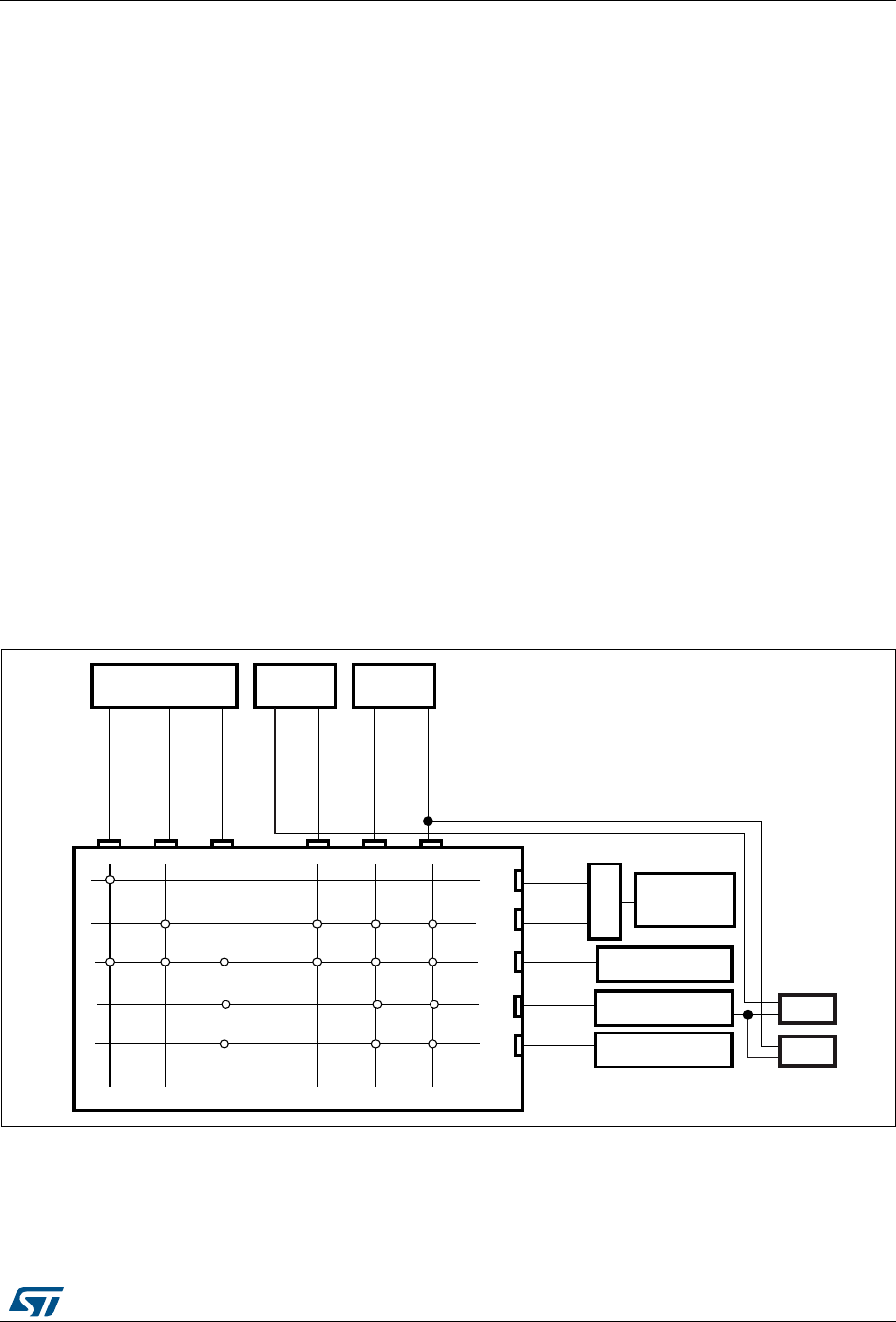
DocID026448 Rev 1 35/836
RM0383 Memory and bus architecture
65
2 Memory and bus architecture
2.1 System architecture
In STM32F411xC/E, the main system consists of 32-bit multilayer AHB bus matrix that
interconnects:
•Six masters:
–Cortex
®-M4 with FPU core I-bus, D-bus and S-bus
– DMA1 memory bus
– DMA2 memory bus
– DMA2 peripheral bus
•Five slaves:
– Internal Flash memory ICode bus
– Internal Flash memory DCode bus
– Main internal SRAM
– AHB1 peripherals including AHB to APB bridges and APB peripherals
– AHB2 peripherals
The bus matrix provides access from a master to a slave, enabling concurrent access and
efficient operation even when several high-speed peripherals work simultaneously. This
architecture is shown in Figure 1.
Figure 1. System architecture
1. STM32F411xC/E: 256 KBytes / 512KBytes Flash with 128 KBytes SRAM
$50
&RUWH[0
*3
'0$
*3
'0$
%XVPDWUL[6
6 6 6 6 6 6
,&2'(
'&2'(
$&&(/
)ODVK
65$0
$+%
SHULSK
0
0
0
0
,EXV
'EXV
6EXV
'0$B3,
'0$B0(0
'0$B0(0
'0$B3
069
0 $+%
SHULSK $3%
$3%
VHHQRWH
VHHQRWH

Memory and bus architecture RM0383
36/836 DocID026448 Rev 1
2.1.1 I-bus
This bus connects the Instruction bus of the Cortex®-M4 with FPU core to the BusMatrix.
This bus is used by the core to fetch instructions. The target of this bus is a memory
containing code (internal Flash memory/SRAM).
2.1.2 D-bus
This bus connects the databus of the Cortex®-M4 with FPU to the BusMatrix. This bus is
used by the core for literal load and debug access. The target of this bus is a memory
containing code or data (internal Flash memory/SRAM).
2.1.3 S-bus
This bus connects the system bus of the Cortex®-M4 with FPU core to a BusMatrix. This
bus is used to access data located in a peripheral or in SRAM. Instructions may also be
fetch on this bus (less efficient than ICode). The targets of this bus are the internal SRAM,
the AHB1 peripherals including the APB peripherals and the AHB2 peripherals.
2.1.4 DMA memory bus
This bus connects the DMA memory bus master interface to the BusMatrix. It is used by the
DMA to perform transfer to/from memories. The targets of this bus are data memories:
internal Flash memory, internal SRAM and additionally for S4 the AHB1/AHB2 peripherals
including the APB peripherals.
2.1.5 DMA peripheral bus
This bus connects the DMA peripheral master bus interface to the BusMatrix. This bus is
used by the DMA to access AHB peripherals or to perform memory-to-memory transfers.
The targets of this bus are the AHB and APB peripherals plus data memories: Flash
memory and internal SRAM.
2.1.6 BusMatrix
The BusMatrix manages the access arbitration between masters. The arbitration uses a
round-robin algorithm.
2.1.7 AHB/APB bridges (APB)
The two AHB/APB bridges, APB1 and APB2, provide full synchronous connections between
the AHB and the two APB buses, allowing flexible selection of the peripheral frequency.
Refer to the device datasheets for more details on APB1 and APB2 maximum frequencies,
and to Table 1 for the address mapping of AHB and APB peripherals.
After each device reset, all peripheral clocks are disabled (except for the SRAM and Flash
memory interface). Before using a peripheral you have to enable its clock in the
RCC_AHBxENR or RCC_APBxENR register.
Note: When a 16- or an 8-bit access is performed on an APB register, the access is transformed
into a 32-bit access: the bridge duplicates the 16- or 8-bit data to feed the 32-bit vector.

DocID026448 Rev 1 37/836
RM0383 Memory and bus architecture
65
2.2 Memory organization
Program memory, data memory, registers and I/O ports are organized within the same linear
4 Gbyte address space.
The bytes are coded in memory in little endian format. The lowest numbered byte in a word
is considered the word’s least significant byte and the highest numbered byte, the word’s
most significant.
For the detailed mapping of peripheral registers, please refer to the related chapters.
The addressable memory space is divided into 8 main blocks, each of 512 MB.
All the memory areas that are not allocated to on-chip memories and peripherals are
considered “Reserved”). Refer to the memory map figure in the product datasheet.
2.3 Memory map
See the datasheet corresponding to your device for a comprehensive diagram of the
memory map. Table 1 gives the boundary addresses of the peripherals available in
STM32F411xC/E device.
Table 1. STM32F411xC/E register boundary addresses
Boundary address Peripheral Bus Register map
0x5000 0000 - 0x5003 FFFF USB OTG FS AHB2 Section 22.16.6: OTG_FS register map on
page 744
0x4002 6400 - 0x4002 67FF DMA2
AHB1
Section 9.5.11: DMA register map on page 194
0x4002 6000 - 0x4002 63FF DMA1
0x4002 3C00 - 0x4002 3FFF Flash interface
register Section 3.8: Flash interface registers on page 58
0x4002 3800 - 0x4002 3BFF RCC Section 6.3.22: RCC register map on page 133
0x4002 3000 - 0x4002 33FF CRC Section 4.4.4: CRC register map on page 68
0x4002 1C00 - 0x4002 1FFF GPIOH
Section 8.4.11: GPIO register map on page 160
0x4002 1000 - 0x4002 13FF GPIOE
0x4002 0C00 - 0x4002 0FFF GPIOD
0x4002 0800 - 0x4002 0BFF GPIOC
0x4002 0400 - 0x4002 07FF GPIOB
0x4002 0000 - 0x4002 03FF GPIOA

Memory and bus architecture RM0383
38/836 DocID026448 Rev 1
2.3.1 Embedded SRAM
STM32F411xC/E devices feature 128 Kbytes of system SRAM.
The embedded SRAM can be accessed as bytes, half-words (16 bits) or full words (32 bits).
Read and write operations are performed at CPU speed with 0 wait state.
0x4001 5000 - 0x4001 53FFF SPI5/I2S5
APB2
Section 20.5.10: SPI register map on page 602
0x4001 4800 - 0x4001 4BFF TIM11 Section 14.5.11: TIM10/11 register map on
page 407
0x4001 4400 - 0x4001 47FF TIM10
0x4001 4000 - 0x4001 43FF TIM9 Section 14.4.13: TIM9 register map on page 397
0x4001 3C00 - 0x4001 3FFF EXTI Section 10.3.7: EXTI register map on page 208
0x4001 3800 - 0x4001 3BFF SYSCFG Section 7.2.8: SYSCFG register map
0x4001 3400 - 0x4001 37FF SPI4/I2S4 Section 20.5.10: SPI register map on page 602
0x4001 3000 - 0x4001 33FF SPI1/I2S1
0x4001 2C00 - 0x4001 2FFF SDIO Section 21.9.16: SDIO register map on page 657
0x4001 2000 - 0x4001 23FF ADC1 Section 11.12.16: ADC register map on page 235
0x4001 1400 - 0x4001 17FF USART6 Section 19.6.8: USART register map on page 548
0x4001 1000 - 0x4001 13FF USART1
0x4001 0000 - 0x4001 03FF TIM1 Section 12.4.21: TIM1 register map on page 304
0x4000 7000 - 0x4000 73FF PWR
APB1
Section 5.5: PWR register map on page 86
0x4000 5C00 - 0x4000 5FFF I2C3
Section 18.6.11: I2C register map on page 4960x4000 5800 - 0x4000 5BFF I2C2
0x4000 5400 - 0x4000 57FF I2C1
0x4000 4400 - 0x4000 47FF USART2 Section 19.6.8: USART register map on page 548
0x4000 4000 - 0x4000 43FF I2S3ext
Section 20.5.10: SPI register map on page 602
0x4000 3C00 - 0x4000 3FFF SPI3 / I2S3
0x4000 3800 - 0x4000 3BFF SPI2 / I2S2
0x4000 3400 - 0x4000 37FF I2S2ext
0x4000 3000 - 0x4000 33FF IWDG Section 15.4.5: IWDG register map on page 415
0x4000 2C00 - 0x4000 2FFF WWDG Section 16.6.4: WWDG register map on page 422
0x4000 2800 - 0x4000 2BFF RTC & BKP Registers Section 17.6.21: RTC register map on page 459
0x4000 0C00 - 0x4000 0FFF TIM5
Section 13.4.21: TIMx register map on page 364
0x4000 0800 - 0x4000 0BFF TIM4
0x4000 0400 - 0x4000 07FF TIM3
0x4000 0000 - 0x4000 03FF TIM2
Table 1. STM32F411xC/E register boundary addresses (continued)
Boundary address Peripheral Bus Register map

DocID026448 Rev 1 39/836
RM0383 Memory and bus architecture
65
The CPU can access the embedded SRAM through the System Bus or through the I-
Code/D-Code buses when boot from SRAM is selected or when physical remap is selected
(Section 7.2.1: SYSCFG memory remap register (SYSCFG_MEMRMP) in the SYSCFG
controller). To get the max performance on SRAM execution, physical remap should be
selected (boot or software selection).
2.3.2 Flash memory overview
The Flash memory interface manages CPU AHB I-Code and D-Code accesses to the Flash
memory. It implements the erase and program Flash memory operations and the read and
write protection mechanisms. It accelerates code execution with a system of instruction
prefetch and cache lines.
The Flash memory is organized as follows:
•A main memory block divided into sectors.
•System memory from which the device boots in System memory boot mode
•512 OTP (one-time programmable) bytes for user data.
•Option bytes to configure read and write protection, BOR level, watchdog
software/hardware and reset when the device is in Standby or Stop mode.
Refer to Section 3: Embedded Flash memory interface for more details.
2.3.3 Bit banding
The Cortex®-M4 with FPU memory map includes two bit-band regions. These regions map
each word in an alias region of memory to a bit in a bit-band region of memory. Writing to a
word in the alias region has the same effect as a read-modify-write operation on the
targeted bit in the bit-band region.
In the STM32F4xx devices both the peripheral registers and the SRAM are mapped to a bit-
band region, so that single bit-band write and read operations are allowed. The operations
are only available for Cortex®-M4 with FPU accesses, and not from other bus masters (e.g.
DMA).
A mapping formula shows how to reference each word in the alias region to a corresponding
bit in the bit-band region. The mapping formula is:
bit_word_addr = bit_band_base + (byte_offset x 32) + (bit_number × 4)
where:
–bit_word_addr is the address of the word in the alias memory region that maps to
the targeted bit
–bit_band_base is the starting address of the alias region
–byte_offset is the number of the byte in the bit-band region that contains the
targeted bit
–bit_number is the bit position (0-7) of the targeted bit
Example
The following example shows how to map bit 2 of the byte located at SRAM address
0x20000300 to the alias region:
0x22006008 = 0x22000000 + (0x300*32) + (2*4)
Writing to address 0x22006008 has the same effect as a read-modify-write operation on bit
2 of the byte at SRAM address 0x20000300.
Memory and bus architecture RM0383
40/836 DocID026448 Rev 1
Reading address 0x22006008 returns the value (0x01 or 0x00) of bit 2 of the byte at SRAM
address 0x20000300 (0x01: bit set; 0x00: bit reset).
For more information on bit-banding, please refer to the Cortex®-M4 with FPU programming
manual (see Related documents on page 1).
2.4 Boot configuration
Due to its fixed memory map, the code area starts from address 0x0000 0000 (accessed
through the ICode/DCode buses) while the data area (SRAM) starts from address
0x2000 0000 (accessed through the system bus). The Cortex®-M4 with FPU CPU always
fetches the reset vector on the ICode bus, which implies to have the boot space available
only in the code area (typically, Flash memory). STM32F4xx microcontrollers implement a
special mechanism to be able to boot from other memories (like the internal SRAM).
In the STM32F4xx, three different boot modes can be selected through the BOOT[1:0] pins
as shown in Table 2.
The values on the BOOT pins are latched on the 4th rising edge of SYSCLK after a reset. It
is up to the user to set the BOOT1 and BOOT0 pins after reset to select the required boot
mode.
BOOT0 is a dedicated pin while BOOT1 is shared with a GPIO pin. Once BOOT1 has been
sampled, the corresponding GPIO pin is free and can be used for other purposes.
The BOOT pins are also resampled when the device exits the Standby mode. Consequently,
they must be kept in the required Boot mode configuration when the device is in the Standby
mode. After this startup delay is over, the CPU fetches the top-of-stack value from address
0x0000 0000, then starts code execution from the boot memory starting from 0x0000 0004.
Note: When the device boots from SRAM, in the application initialization code, you have to
relocate the vector table in SRAM using the NVIC exception table and the offset register.
Table 2. Boot modes
Boot mode selection pins Boot mode Aliasing
BOOT1 BOOT0
x 0 Main Flash memory Main Flash memory is selected as the boot space
0 1 System memory System memory is selected as the boot space
1 1 Embedded SRAM Embedded SRAM is selected as the boot space

DocID026448 Rev 1 41/836
RM0383 Memory and bus architecture
65
Embedded bootloader
The embedded bootloader mode is used to reprogram the Flash memory using one of the
following serial interfaces:
•USART1 (PA9/PA10)
•USART2 (PD5/PD6)
•I2C1 (PB6/PB7)
•I2C2 (PB10/PB3)
•I2C3 (PA8/PB4)
•SPI1 (PA4/PA5/PA6/PA7)
•SPI2 (PB12/PB13/PB14/PB15)
•SPI3 (PA15/PC10/PC11/PC12)
•USB OTG FS (PA11/12) in Device mode (DFU: device firmware upgrade).
The USART peripherals operate at the internal 16 MHz oscillator (HSI) frequency, while the
USB OTG FS require an external clock (HSE) multiple of 1 MHz (ranging from 4 to 26 MHz).
The embedded bootloader code is located in system memory. It is programmed by ST
during production. For additional information, refer to application note AN2606.
Physical remap in STM32F411xC/E
Once the boot pins are selected, the application software can modify the memory
accessible in the code area (in this way the code can be executed through the ICode bus in
place of the System bus). This modification is performed by programming the Section 7.2.1:
SYSCFG memory remap register (SYSCFG_MEMRMP) in the SYSCFG controller.
The following memories can thus be remapped:
•Main Flash memory
•System memory
•Embedded SRAM1
Table 3. Memory mapping vs. Boot mode/physical remap in STM32F411xC/E
Addresses Boot/Remap in main
Flash memory Boot/Remap in
embedded SRAM Boot/Remap in
System memory
0x2000 0000 - 0x2002 0000 SRAM1 (128 KB) SRAM1 (128KB) SRAM1 (128KB)
0x1FFF 0000 - 0x1FFF 77FF System memory System memory System memory
0x0804 0000 - 0x1FFE FFFF Reserved Reserved Reserved
0x0800 0000 - 0x0807 FFFF Flash memory Flash memory Flash memory
0x0400 000 - 0x07FF FFFF Reserved Reserved Reserved
0x0000 0000 - 0x0007 FFFF(1)
1. Even when aliased in the boot memory space, the related memory is still accessible at its original memory
space.
Flash (512 KB) Aliased SRAM1 (128 KB)
Aliased
System memory
(30 KB) Aliased
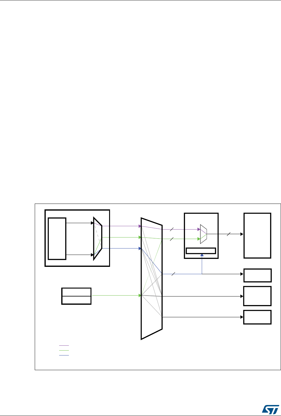
Embedded Flash memory interface RM0383
42/836 DocID026448 Rev 1
3 Embedded Flash memory interface
3.1 Introduction
The Flash memory interface manages CPU AHB I-Code and D-Code accesses to the Flash
memory. It implements the erase and program Flash memory operations and the read and
write protection mechanisms.
The Flash memory interface accelerates code execution with a system of instruction
prefetch and cache lines.
3.2 Main features
•Flash memory read operations
•Flash memory program/erase operations
•Read / write protections
•Prefetch on I-Code
•64 cache lines of 128 bits on I-Code
•8 cache lines of 128 bits on D-Code
Figure 2 shows the Flash memory interface connection inside the system architecture.
Figure 2. Flash memory interface connection inside system architecture
(STM32F411xC/E)
&RUWH[
FRUH
'0$
'0$
'FRGHEXV
,&RGHEXV
&RUWH[0ZLWK)38
,&RGH
'&RGH
6EXV
$+%
SHULSK
)ODVK
PHPRU\
)ODVKLQWHUIDFH
65$0DQG
([WHUQDO
PHPRULHV
$+%
SHULSK
)/,7)UHJLVWHUV
$+%
ELW
LQVWUXFWLRQ
EXV
$FFHVVWRLQVWUXFWLRQLQ)ODVKPHPRU\
$FFHVVWRGDWDDQGOLWHUDOSRROLQ)ODVKPHPRU\
)/,7)UHJLVWHUDFFHVV
069
$+%
ELW
GDWDEXV
$+%
ELW
V\VWHPEXV
)ODVK
PHPRU\
EXV
ELWV
DocID026448 Rev 1 43/836
RM0383 Embedded Flash memory interface
65
3.3 Embedded Flash memory in STM32F411xC/E
The Flash memory has the following main features:
•Capacity up to 512 KBytes for STM32F411xC/E
•128 bits wide data read
•Byte, half-word, word and double word write
•Sector and mass erase
•Memory organization
The Flash memory is organized as follows:
– A main memory block divided into 4 sectors of 16 KBytes, 1 sector of 64 KBytes, 3
sectors of 128 Kbytes (STM32F411xC/E).
– System memory from which the device boots in System memory boot mode
– 512 OTP (one-time programmable) bytes for user data
The OTP area contains 16 additional bytes used to lock the corresponding OTP
data block.
– Option bytes to configure read and write protection, BOR level, watchdog
software/hardware and reset when the device is in Standby or Stop mode.
•Low-power modes (for details refer to the Power control (PWR) section of the reference
manual)
Table 4. Flash module organization (STM32F411xC/E)
Block Name Block base addresses Size
Main memory
Sector 0 0x0800 0000 - 0x0800 3FFF 16 Kbytes
Sector 1 0x0800 4000 - 0x0800 7FFF 16 Kbytes
Sector 2 0x0800 8000 - 0x0800 BFFF 16 Kbytes
Sector 3 0x0800 C000 - 0x0800 FFFF 16 Kbytes
Sector 4 0x0801 0000 - 0x0801 FFFF 64 Kbytes
Sector 5 0x0802 0000 - 0x0803 FFFF 128 Kbytes
Sector 6 0x0804 0000 - 0x0805 FFFF 128 Kbytes
Sector 7 0x0806 0000 - 0x0807 FFFF 128 Kbytes
System memory 0x1FFF 0000 - 0x1FFF 77FF 30 Kbytes
OTP area 0x1FFF 7800 - 0x1FFF 7A0F 528 bytes
Option bytes 0x1FFF C000 - 0x1FFF C00F 16 bytes

Embedded Flash memory interface RM0383
44/836 DocID026448 Rev 1
3.4 Read interface
3.4.1 Relation between CPU clock frequency and Flash memory read time
To correctly read data from Flash memory, the number of wait states (LATENCY) must be
correctly programmed in the Flash access control register (FLASH_ACR) according to the
frequency of the CPU clock (HCLK) and the supply voltage of the device.
The prefetch buffer must be disabled when the supply voltage is below 2.1 V. The
correspondence between wait states and CPU clock frequency is given in Table 5.
- when VOS[1:0] = 0x01, the maximum value of fHCLK = 64 MHz.
- when VOS[1:0] = 0x10, the maximum value of fHCLK = 84 MHz.
- when VOS[1:0] = 0x11, the maximum value of fHCLK = 100 MHz.
After reset, the CPU clock frequency is 16 MHz and 0 wait state (WS) is configured in the
FLASH_ACR register.
It is highly recommended to use the following software sequences to tune the number of
wait states needed to access the Flash memory with the CPU frequency.
Increasing the CPU frequency
1. Program the new number of wait states to the LATENCY bits in the FLASH_ACR
register
2. Check that the new number of wait states is taken into account to access the Flash
memory by reading the FLASH_ACR register
3. Modify the CPU clock source by writing the SW bits in the RCC_CFGR register
4. If needed, modify the CPU clock prescaler by writing the HPRE bits in RCC_CFGR
5. Check that the new CPU clock source or/and the new CPU clock prescaler value is/are
taken into account by reading the clock source status (SWS bits) or/and the AHB
prescaler value (HPRE bits), respectively, in the RCC_CFGR register.
Table 5. Number of wait states according to CPU clock (HCLK) frequency
Wait states (WS)
(LATENCY)
HCLK (MHz)
Voltage range
2.7 V - 3.6 V
Voltage range
2.4 V - 2.7 V
Voltage range
2.1 V - 2.4 V
Voltage range
1.71 V - 2.1 V
0 WS (1 CPU cycle) 0 < HCLK≤ 30 0 < HCLK ≤ 24 0 < HCLK ≤ 18 0 < HCLK ≤ 16
1 WS (2 CPU cycles) 30 < HCLK ≤ 64 24 < HCLK ≤ 48 18 < HCLK ≤ 36 16 <HCLK ≤ 32
2 WS (3 CPU cycles) 64 < HCLK ≤ 90 48 < HCLK ≤ 72 36 < HCLK ≤ 54 32 < HCLK ≤ 48
3 WS (4 CPU cycles) 90 < HCLK ≤ 100 72 < HCLK ≤ 96 54 < HCLK ≤ 72 48 < HCLK ≤ 64
4 WS (5 CPU cycles) - 96 < HCLK ≤ 100 72 < HCLK ≤ 90 64 < HCLK ≤ 80
5 WS (6 CPU cycles) - - 90 < HCLK ≤ 100 80 < HCLK ≤ 96
6 WS (7 CPU cycles) - - - 96 < HCLK ≤ 100

DocID026448 Rev 1 45/836
RM0383 Embedded Flash memory interface
65
Decreasing the CPU frequency
1. Modify the CPU clock source by writing the SW bits in the RCC_CFGR register
2. If needed, modify the CPU clock prescaler by writing the HPRE bits in RCC_CFGR
3. Check that the new CPU clock source or/and the new CPU clock prescaler value is/are
taken into account by reading the clock source status (SWS bits) or/and the AHB
prescaler value (HPRE bits), respectively, in the RCC_CFGR register
4. Program the new number of wait states to the LATENCY bits in FLASH_ACR
5. Check that the new number of wait states is used to access the Flash memory by
reading the FLASH_ACR register
Note: A change in CPU clock configuration or wait state (WS) configuration may not be effective
straight away. To make sure that the current CPU clock frequency is the one you have
configured, you can check the AHB prescaler factor and clock source status values. To
make sure that the number of WS you have programmed is effective, you can read the
FLASH_ACR register.
3.4.2 Adaptive real-time memory accelerator (ART Accelerator™)
The proprietary Adaptive real-time (ART) memory accelerator is optimized for STM32
industry-standard ARM® Cortex®-M4 with FPU processors. It balances the inherent
performance advantage of the ARM® Cortex®-M4 with FPU over Flash memory
technologies, which normally requires the processor to wait for the Flash memory at higher
operating frequencies.
To release the processor full performance, the accelerator implements an instruction
prefetch queue and branch cache which increases program execution speed from the 128-
bit Flash memory. Based on CoreMark benchmark, the performance achieved thanks to the
ART accelerator is equivalent to 0 wait state program execution from Flash memory at a
CPU frequency up to 100 MHz.
Instruction prefetch
Each Flash memory read operation provides 128 bits from either four instructions of 32 bits
or 8 instructions of 16 bits according to the program launched. So, in case of sequential
code, at least four CPU cycles are needed to execute the previous read instruction line.
Prefetch on the I-Code bus can be used to read the next sequential instruction line from the
Flash memory while the current instruction line is being requested by the CPU. Prefetch is
enabled by setting the PRFTEN bit in the FLASH_ACR register. This feature is useful if at
least one wait state is needed to access the Flash memory.
Figure 3 shows the execution of sequential 32-bit instructions with and without prefetch
when 3 WSs are needed to access the Flash memory.
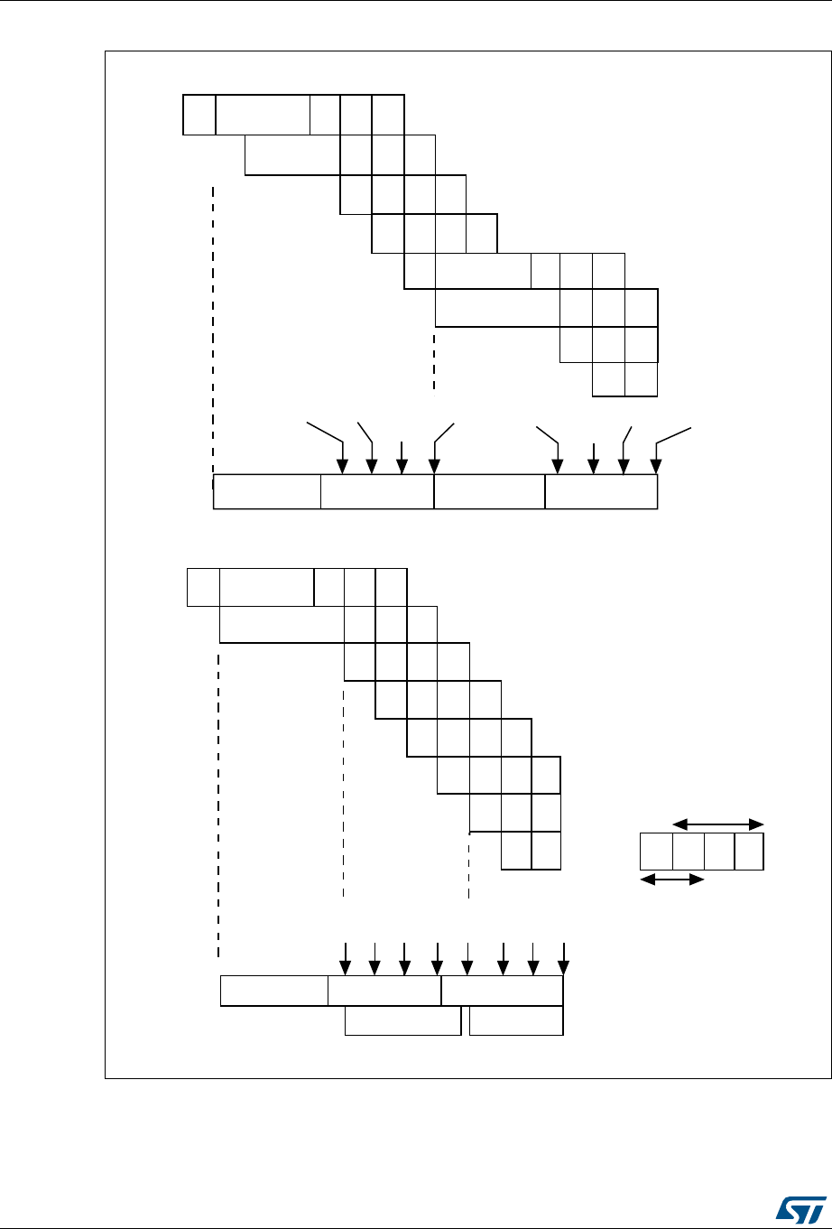
Embedded Flash memory interface RM0383
46/836 DocID026448 Rev 1
Figure 3. Sequential 32-bit instruction execution
When the code is not sequential (branch), the instruction may not be present in the currently
used instruction line or in the prefetched instruction line. In this case (miss), the penalty in
terms of number of cycles is at least equal to the number of wait states.
&
&
&
&
$
$
$
$
%
%
%
%
&
&
&
&
$
$
$
%
%
2EADINS 'IVESINS 2EADINS 'IVESINS
INS
FETCH
INS
FETCH
INS
FETCH
INS
FETCH
INS
FETCH
INS
FETCH
INS
FETCH
INS
FETCH
7!)4
7!)4
$%
&
&
&
&
$
$
$
%
%
&
&
&
&
$
$
$
%
%
7AITDATA
%
2EADINS 'IVESINS 'IVESINS
2EADINS 2EADINS
INS INS
FETCH
INS INS
7ITHOUTPREFETCH
7ITHPREFETCH
&$%
#ORTEX-PIPELINE
!("PROTOCOL
ADDRESSREQUESTED
&&ETCHSTAGE
$$ECODESTAGE
%%XECUTESTAGE
INS
FETCH
INS
FETCH
INS
FETCH FETCH FETCH FETCH
INS
FETCH
-36

DocID026448 Rev 1 47/836
RM0383 Embedded Flash memory interface
65
Instruction cache memory
To limit the time lost due to jumps, it is possible to retain 64 lines of 128 bits in an instruction
cache memory. This feature can be enabled by setting the instruction cache enable (ICEN)
bit in the FLASH_ACR register. Each time a miss occurs (requested data not present in the
currently used instruction line, in the prefetched instruction line or in the instruction cache
memory), the line read is copied into the instruction cache memory. If some data contained
in the instruction cache memory are requested by the CPU, they are provided without
inserting any delay. Once all the instruction cache memory lines have been filled, the LRU
(least recently used) policy is used to determine the line to replace in the instruction memory
cache. This feature is particularly useful in case of code containing loops.
Data management
Literal pools are fetched from Flash memory through the D-Code bus during the execution
stage of the CPU pipeline. The CPU pipeline is consequently stalled until the requested
literal pool is provided. To limit the time lost due to literal pools, accesses through the AHB
databus D-Code have priority over accesses through the AHB instruction bus I-Code.
If some literal pools are frequently used, the data cache memory can be enabled by setting
the data cache enable (DCEN) bit in the FLASH_ACR register. This feature works like the
instruction cache memory, but the retained data size is limited to 8 rows of 128 bits.
Note: Data in user configuration sector are not cacheable.
3.5 Erase and program operations
For any Flash memory program operation (erase or program), the CPU clock frequency
(HCLK) must be at least 1 MHz. The contents of the Flash memory are not guaranteed if a
device reset occurs during a Flash memory operation.
Any attempt to read the Flash memory on STM32F4xx while it is being written or erased,
causes the bus to stall. Read operations are processed correctly once the program
operation has completed. This means that code or data fetches cannot be performed while
a write/erase operation is ongoing.
3.5.1 Unlocking the Flash control register
After reset, write is not allowed in the Flash control register (FLASH_CR) to protect the
Flash memory against possible unwanted operations due, for example, to electric
disturbances. The following sequence is used to unlock this register:
1. Write KEY1 = 0x45670123 in the Flash key register (FLASH_KEYR)
2. Write KEY2 = 0xCDEF89AB in the Flash key register (FLASH_KEYR)
Any wrong sequence will return a bus error and lock up the FLASH_CR register until the
next reset.
The FLASH_CR register can be locked again by software by setting the LOCK bit in the
FLASH_CR register.
Note: The FLASH_CR register is not accessible in write mode when the BSY bit in the FLASH_SR
register is set. Any attempt to write to it with the BSY bit set will cause the AHB bus to stall
until the BSY bit is cleared.

Embedded Flash memory interface RM0383
48/836 DocID026448 Rev 1
3.5.2 Program/erase parallelism
The Parallelism size is configured through the PSIZE field in the FLASH_CR register. It
represents the number of bytes to be programmed each time a write operation occurs to the
Flash memory. PSIZE is limited by the supply voltage and by whether the external VPP
supply is used or not. It must therefore be correctly configured in the FLASH_CR register
before any programming/erasing operation.
A Flash memory erase operation can only be performed by sector, or for the whole Flash
memory (mass erase). The erase time depends on PSIZE programmed value. For more
details on the erase time, refer to the electrical characteristics section of the device
datasheet.
Table 6 provides the correct PSIZE values.
Note: Any program or erase operation started with inconsistent program parallelism/voltage range
settings may lead to unpredicted results. Even if a subsequent read operation indicates that
the logical value was effectively written to the memory, this value may not be retained.
To use VPP
, an external high-voltage supply (between 8 and 9 V) must be applied to the VPP
pad. The external supply must be able to sustain this voltage range even if the DC
consumption exceeds 10 mA. It is advised to limit the use of VPP to initial programming on
the factory line. The VPP supply must not be applied for more than an hour, otherwise the
Flash memory might be damaged.
3.5.3 Erase
The Flash memory erase operation can be performed at sector level or on the whole Flash
memory (Mass Erase). Mass Erase does not affect the OTP sector or the configuration
sector.
Sector Erase
To erase a sector, follow the procedure below:
1. Check that no Flash memory operation is ongoing by checking the BSY bit in the
FLASH_SR register
2. Set the SER bit and select the sector out of the 7 sectors (STM32F411xC/E) in the
main memory block you wish to erase (SNB) in the FLASH_CR register
3. Set the STRT bit in the FLASH_CR register
4. Wait for the BSY bit to be cleared
Mass Erase
To perform Mass Erase, the following sequence is recommended:
Table 6. Program/erase parallelism
Voltage range 2.7 - 3.6 V
with External VPP
Voltage range
2.7 - 3.6 V Voltage range
2.4 - 2.7 V Voltage range
2.1 - 2.4 V Voltage range
1.7 V - 2.1 V
Parallelism size x64 x32 x16 x8
PSIZE(1:0)11100100

DocID026448 Rev 1 49/836
RM0383 Embedded Flash memory interface
65
1. Check that no Flash memory operation is ongoing by checking the BSY bit in the
FLASH_SR register
2. Set the MER bit in the FLASH_CR register
3. Set the STRT bit in the FLASH_CR register
4. Wait for the BSY bit to be cleared
Note: If MERx and SER bits are both set in the FLASH_CR register, mass erase is performed.
If both MERx and SER bits are reset and the STRT bit is set, an unpredictable behavior may
occur without generating any error flag. This condition should be forbidden.
3.5.4 Programming
Standard programming
The Flash memory programming sequence is as follows:
1. Check that no main Flash memory operation is ongoing by checking the BSY bit in the
FLASH_SR register.
2. Set the PG bit in the FLASH_CR register
3. Perform the data write operation(s) to the desired memory address (inside main
memory block or OTP area):
– Byte access in case of x8 parallelism
– Half-word access in case of x16 parallelism
– Word access in case of x32 parallelism
– Double word access in case of x64 parallelism
4. Wait for the BSY bit to be cleared.
Note: Successive write operations are possible without the need of an erase operation when
changing bits from ‘1’ to ‘0’. Writing ‘1’ requires a Flash memory erase operation.
If an erase and a program operation are requested simultaneously, the erase operation is
performed first.
Programming errors
It is not allowed to program data to the Flash memory that would cross the 128-bit row
boundary. In such a case, the write operation is not performed and a program alignment
error flag (PGAERR) is set in the FLASH_SR register.
The write access type (byte, half-word, word or double word) must correspond to the type of
parallelism chosen (x8, x16, x32 or x64). If not, the write operation is not performed and a
program parallelism error flag (PGPERR) is set in the FLASH_SR register.
If the standard programming sequence is not respected (for example, if there is an attempt
to write to a Flash memory address when the PG bit is not set), the operation is aborted and
a program sequence error flag (PGSERR) is set in the FLASH_SR register.
Programming and caches
If a Flash memory write access concerns some data in the data cache, the Flash write
access modifies the data in the Flash memory and the data in the cache.
If an erase operation in Flash memory also concerns data in the data or instruction cache,
you have to make sure that these data are rewritten before they are accessed during code
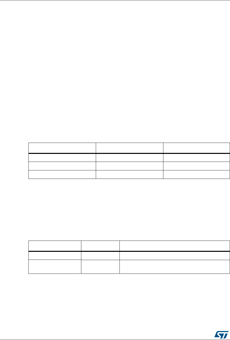
Embedded Flash memory interface RM0383
50/836 DocID026448 Rev 1
execution. If this cannot be done safely, it is recommended to flush the caches by setting the
DCRST and ICRST bits in the FLASH_CR register.
Note: The I/D cache should be flushed only when it is disabled (I/DCEN = 0).
3.5.5 Interrupts
Setting the end of operation interrupt enable bit (EOPIE) in the FLASH_CR register enables
interrupt generation when an erase or program operation ends, that is when the busy bit
(BSY) in the FLASH_SR register is cleared (operation completed, correctly or not). In this
case, the end of operation (EOP) bit in the FLASH_SR register is set.
If an error occurs during a program, an erase, or a read operation request, one of the
following error flags is set in the FLASH_SR register:
•PGAERR, PGPERR, PGSERR (Program error flags)
•WRPERR (Protection error flag)
In this case, if the error interrupt enable bit (ERRIE) is set in the FLASH_SR register, an
interrupt is generated and the operation error bit (OPERR) is set in the FLASH_SR register.
Note: If several successive errors are detected (for example, in case of DMA transfer to the Flash
memory), the error flags cannot be cleared until the end of the successive write requests.
3.6 Option bytes
3.6.1 Description of user option bytes
The option bytes are configured by the end user depending on the application requirements.
Table 8 shows the organization of these bytes inside the user configuration sector.
Table 7. Flash interrupt request
Interrupt event Event flag Enable control bit
End of operation EOP EOPIE
Write protection error WRPERR ERRIE
Programming error PGAERR, PGPERR, PGSERR ERRIE
Table 8. Option byte organization
Address [63:16] [15:0]
0x1FFF C000 Reserved ROP & user option bytes (RDP & USER)
0x1FFF C008 Reserved Write protection nWRP bits for sectors 0 to 7
(STM32F411xC/E)

DocID026448 Rev 1 51/836
RM0383 Embedded Flash memory interface
65
Table 9. Description of the option bytes
Option bytes (word, address 0x1FFF C000)
RDP: Read protection option byte.
The read protection is used to protect the software code stored in Flash memory.
Bit 15:8
0xAA: Level 0, no protection
0xCC: Level 2, chip protection (debug and boot from RAM features
disabled)
Others: Level 1, read protection of memories (debug features limited)
USER: User option byte
This byte is used to configure the following features:
Select the watchdog event: Hardware or software
Reset event when entering the Stop mode
Reset event when entering the Standby mode
Bit 7
nRST_STDBY
0: Reset generated when entering the Standby mode
1: No reset generated
Bit 6
nRST_STOP
0: Reset generated when entering the Stop mode
1: No reset generated
Bit 5
WDG_SW
0: Hardware watchdog
1: Software watchdog
Bit 4 0x0: Not used. Always readout as “0”.
Bits 3:2
BOR_LEV: BOR reset Level
These bits contain the supply level threshold that activates/releases the reset.
They can be written to program a new BOR level value into Flash memory.
00: BOR Level 3 (VBOR3), brownout threshold level 3
01: BOR Level 2 (VBOR2), brownout threshold level 2
10: BOR Level 1 (VBOR1), brownout threshold level 1
11: BOR off, POR/PDR reset threshold level is applied
For full details on BOR characteristics, refer to the Electrical characteristics
section of the product datasheet.
Bits 1:0 0x1: Not used
Option bytes (word, address 0x1FFF C008)
Bit 15
SPRMOD: Selection of Protection Mode of nWPRi bits
0: nWPRi bits used for sector i write protection (Default)
1: nWPRi bits used for sector i PCROP protection (Sector)
Bits 14:6 Reserved

Embedded Flash memory interface RM0383
52/836 DocID026448 Rev 1
3.6.2 Programming user option bytes
To run any operation on this sector, the option lock bit (OPTLOCK) in the Flash option
control register (FLASH_OPTCR) must be cleared. To be allowed to clear this bit, you have
to perform the following sequence:
1. Write OPTKEY1 = 0x0819 2A3B in the Flash option key register (FLASH_OPTKEYR)
2. Write OPTKEY2 = 0x4C5D 6E7F in the Flash option key register (FLASH_OPTKEYR)
The user option bytes can be protected against unwanted erase/program operations by
setting the OPTLOCK bit by software.
Modifying user option bytes
To modify the user option value, follow the sequence below:
1. Check that no Flash memory operation is ongoing by checking the BSY bit in the
FLASH_SR register
2. Write the desired option value in the FLASH_OPTCR register.
3. Set the option start bit (OPTSTRT) in the FLASH_OPTCR register
4. Wait for the BSY bit to be cleared.
Note: The value of an option is automatically modified by first erasing the user configuration sector
and then programming all the option bytes with the values contained in the FLASH_OPTCR
register.
3.6.3 Read protection (RDP)
The user area in the Flash memory can be protected against read operations by an
entrusted code. Three read protection levels are defined:
•Level 0: no read protection
When the read protection level is set to Level 0 by writing 0xAA into the read protection
option byte (RDP), all read/write operations (if no write protection is set) from/to the
nWRP: Flash memory write protection option bytes
Sector 0 to 7 (STM32F411xC/E) can be write protected.
Bits 5:0
nWRPi
If SPRMOD is reset (default value) :
0: Write protection active on sector i.
1: Write protection not active on sector i.
If SPRMOD is set (active):
0: PCROP protection not active on sector i.
1: PCROP protection active on sector i.
Table 9. Description of the option bytes (continued)

DocID026448 Rev 1 53/836
RM0383 Embedded Flash memory interface
65
Flash memory are possible in all boot configurations (Flash user boot, debug or boot
from RAM).
•Level 1: read protection enabled
It is the default read protection level after option byte erase. The read protection Level
1 is activated by writing any value (except for 0xAA and 0xCC used to set Level 0 and
Level 2, respectively) into the RDP option byte. When the read protection Level 1 is set:
– No access (read, erase, program) to Flash memory can be performed while the
debug feature is connected or while booting from RAM or system memory
bootloader. A bus error is generated in case of read request.
– When booting from Flash memory, accesses (read, erase, program) to Flash
memory from user code are allowed.
When Level 1 is active, programming the protection option byte (RDP) to Level 0
causes the Flash memory to be mass-erased. As a result the user code area is cleared
before the read protection is removed. The mass erase only erases the user code area.
The other option bytes including write protections remain unchanged from before the
mass-erase operation. The OTP area is not affected by mass erase and remains
unchanged. Mass erase is performed only when Level 1 is active and Level 0
requested. When the protection level is increased (0->1, 1->2, 0->2) there is no mass
erase.
•Level 2: debug/chip read protection disabled
The read protection Level 2 is activated by writing 0xCC to the RDP option byte. When
the read protection Level 2 is set:
– All protections provided by Level 1 are active.
– Booting from RAM or system memory bootloader is no more allowed.
– JTAG, SWV (single-wire viewer), ETM, and boundary scan are disabled.
– User option bytes can no longer be changed.
– When booting from Flash memory, accesses (read, erase and program) to Flash
memory from user code are allowed.
Memory read protection Level 2 is an irreversible operation. When Level 2 is activated,
the level of protection cannot be decreased to Level 0 or Level 1.
Note: The JTAG port is permanently disabled when Level 2 is active (acting as a JTAG fuse). As a
consequence, boundary scan cannot be performed. STMicroelectronics is not able to
perform analysis on defective parts on which the Level 2 protection has been set.

Embedded Flash memory interface RM0383
54/836 DocID026448 Rev 1
-- Table 10. Access versus read protection level
Memory area Protection
Level
Debug features, Boot from RAM or
from System memory bootloader Booting from Flash memory
Read Write Erase Read Write Erase
Main Flash Memory
Level 1 NO NO(1) YES
Level 2 NO YES
Option Bytes
Level 1 YES YES
Level 2 NO NO
OTP
Level 1 NO NA YES NA
Level 2 NO NA YES NA
1. The main Flash memory only erased when the RDP changes from level 1 to 0. The OTP area remains unchanged.
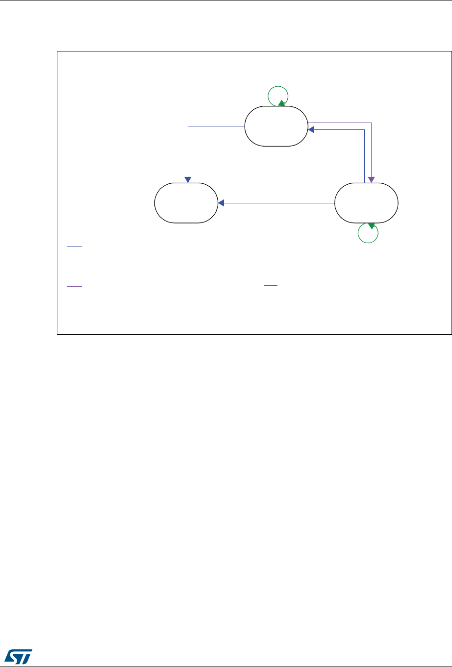
DocID026448 Rev 1 55/836
RM0383 Embedded Flash memory interface
65
Figure 4 shows how to go from one RDP level to another.
Figure 4. RDP levels
3.6.4 Write protections
Up to 7 (STM32F411xC/E) user sectors in Flash memory can be protected against
unwanted write operations due to loss of program counter contexts. When the non-write
protection nWRPi bit (0 ≤i≤7) in the FLASH_OPTCR registers is low, the corresponding
sector cannot be erased or programmed. Consequently, a mass erase cannot be performed
if one of the sectors is write-protected.
If an erase/program operation to a write-protected part of the Flash memory is attempted
(sector protected by write protection bit, OTP part locked or part of the Flash memory that
can never be written like the ICP), the write protection error flag (WRPERR) is set in the
FLASH_SR register.
Note: When the memory read protection level is selected (RDP level = 1), it is not possible to
program or erase Flash memory sector i if the CPU debug features are connected (JTAG or
single wire) or boot code is being executed from RAM, even if nWRPi = 1.
Write protection error flag
If an erase/program operation to a write protected area of the Flash memory is performed,
the Write Protection Error flag (WRPERR) is set in the FLASH_SR register.
,EVEL
LEVE,LEVE,
H!!0$2H##0$2
2$0!!H
2$0##H
DEFAULT
/PTIONSWRITE2$0LEVELINCREASEINCLUDES
/PTIONSERASE
.EWOPTIONSPROGRAM
/PTIONSWRITE2$0LEVELDECREASEINCLUDES
-ASSERASE
/PTIONSERASE
.EWOPTIONSPROGRAM
/PTIONSWRITE2$0LEVELIDENTICALINCLUDES
/PTIONSERASE
.EWOPTIONSPROGRAM
2$0!!H
/THERSOPTIONSMODIFIED
2$0!!H##H
/THERSOPTIONSMODIFIED
7RITEOPTIONS
INCLUDING
2$0!!H
7RITEOPTIONS
INCLUDING
2$0##H
7RITEOPTIONS
INCLUDING
2$0##H
7RITEOPTIONSINCLUDING
2$0##H!!H
AI

Embedded Flash memory interface RM0383
56/836 DocID026448 Rev 1
If an erase operation is requested, the WRPERR bit is set when:
•Mass, bank, sector erase are configured (MER and SER = 1)
•A sector erase is requested and the Sector Number SNB field is not valid
•A mass erase is requested while at least one of the user sector is write protected by
option bit (MER = 1 and nWRPi = 0 with 0 ≤ i ≤ 7 bits in the FLASH_OPTCRx register
•A sector erase is requested on a write protected sector. (SER = 1, SNB = i and
nWRPi = 0 with 0 ≤ i ≤ 7 bits in the FLASH_OPTCRx register)
•The Flash memory is readout protected and an intrusion is detected.
If a program operation is requested, the WRPERR bit is set when:
•A write operation is performed on system memory or on the reserved part of the user
specific sector.
•A write operation is performed to the user configuration sector
•A write operation is performed on a sector write protected by option bit.
•A write operation is requested on an OTP area which is already locked
•The Flash memory is read protected and an intrusion is detected.
3.6.5 Proprietary code readout protection (PCROP)
Flash memory user sectors (0 to7) can be protected against D-bus read accesses by using
the proprietary readout protection (PCROP).
The PCROP protection is selected as follows, through the SPRMOD option bit in the
FLASH_CR register:
•SPRMOD = 0: nWRPi control the write protection of respective user sectors
•SPRMOD = 1: nWRPi control the read and write protection (PCROP) of respective
user sectors.
When a sector is readout protected (PCROP mode activated), it can only be accessed for
code fetch through ICODE Bus on Flash interface:
•Any read access performed through the D-bus triggers a RDERR flag error.
•Any program/erase operation on a PCROPed sector triggers a WRPERR flag error.
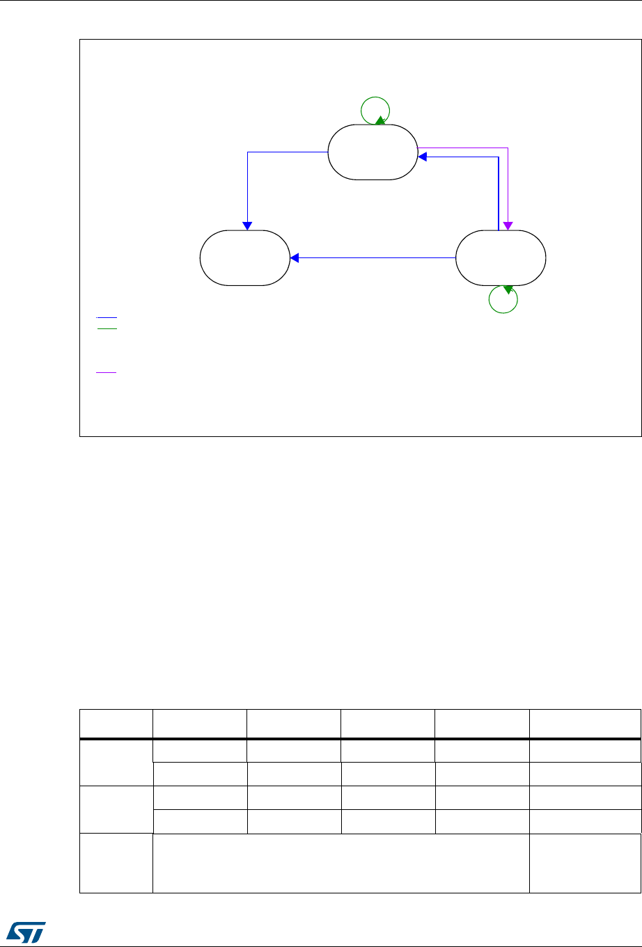
DocID026448 Rev 1 57/836
RM0383 Embedded Flash memory interface
65
Figure 5. PCROP levels
The deactivation of the SPRMOD and/or the unprotection of PCROPed user sectors can
only occur when, at the same time, the RDP level changes from 1 to 0. If this condition is not
respected, the user option byte modification is cancelled and the write error WRPERR flag
is set. The modification of the users option bytes (BOR_LEV, RST_STDBY, ..) is allowed
since none of the active nWRPi bits is reset and SPRMOD is kept active.
Note: The active value of nWRPi bits is inverted when PCROP mode is active (SPRMOD =1).
If SPRMOD = 1 and nWRPi =1, then user sector i of bank 1, respectively bank 2 is
read/write protected (PCROP).
3.7 One-time programmable bytes
Table 11 shows the organization of the one-time programmable (OTP) part of the OTP area.
,EVEL
,EVEL
2$0X##
2$0X!!
2$0X##
DEFAULT
5SEROPTIONSECTORERASE
0ROGRAMNEWOPTIONS
'LOBALMASSERASE
5SEROPTIONSECTIONERASE
0ROGRAMNEWOPTIONS
7RITEOPTIONS
30-/$ACTIVE
ANDVALIDN720I
.ORESTRICTIONON
7RITEOPTIONS
7RITEOPTIONS
30-/$ACTIVE
ANDVALIDN720I
,EVEL
2$0X!!
7RITEOPTIONS
30-/$ACTIVE
ANDVALIDN720I
7RITEOPTIONS
30-/$ACTIVE
ANDVALIDN720I 7RITEOPTIONS
30-/$ACTIVE
ANDVALIDN720I
6ALIDN720IMEANSTHATNONEOFTHEN720BITSSETCANBERESETTRANSITIONFROMTO
-36
Table 11. OTP area organization
Block [128:96] [95:64] [63:32] [31:0] Address byte 0
0
OTP0 OTP0 OTP0 OTP0 0x1FFF 7800
OTP0 OTP0 OTP0 OTP0 0x1FFF 7810
1
OTP1 OTP1 OTP1 OTP1 0x1FFF 7820
OTP1 OTP1 OTP1 OTP1 0x1FFF 7830
.
.
.
.
.
.
.
.
.
Embedded Flash memory interface RM0383
58/836 DocID026448 Rev 1
The OTP area is divided into 16 OTP data blocks of 32 bytes and one lock OTP block of 16
bytes. The OTP data and lock blocks cannot be erased. The lock block contains 16 bytes
LOCKBi (0 ≤ i ≤ 15) to lock the corresponding OTP data block (blocks 0 to 15). Each OTP
data block can be programmed until the value 0x00 is programmed in the corresponding
OTP lock byte. The lock bytes must only contain 0x00 and 0xFF values, otherwise the OTP
bytes might not be taken into account correctly.
3.8 Flash interface registers
3.8.1 Flash access control register (FLASH_ACR)
The Flash access control register is used to enable/disable the acceleration features and
control the Flash memory access time according to CPU frequency.
Address offset: 0x00
Reset value: 0x0000 0000
Access: no wait state, word, half-word and byte access
15
OTP15 OTP15 OTP15 OTP15 0x1FFF 79E0
OTP15 OTP15 OTP15 OTP15 0x1FFF 79F0
Lock block LOCKB15 ...
LOCKB12
LOCKB11 ...
LOCKB8
LOCKB7 ...
LOCKB4
LOCKB3 ...
LOCKB0 0x1FFF 7A00
Table 11. OTP area organization (continued)
Block [128:96] [95:64] [63:32] [31:0] Address byte 0
31 30 29 28 27 26 25 24 23 22 21 20 19 18 17 16
Reserved
15 14 13 12 11 10 9 8 7 6 5 4 3 2 1 0
Reserved
DCRST ICRST DCEN ICEN PRFTEN
Reserved
LATENCY
rwwrwrw rw rwrwrwrw
Bits 31:13 Reserved, must be kept cleared.
Bit 12 DCRST: Data cache reset
0: Data cache is not reset
1: Data cache is reset
This bit can be written only when the D cache is disabled.
Bit 11 ICRST: Instruction cache reset
0: Instruction cache is not reset
1: Instruction cache is reset
This bit can be written only when the I cache is disabled.
Bit 10 DCEN: Data cache enable
0: Data cache is disabled
1: Data cache is enabled
Bit 9 ICEN: Instruction cache enable
0: Instruction cache is disabled
1: Instruction cache is enabled

DocID026448 Rev 1 59/836
RM0383 Embedded Flash memory interface
65
3.8.2 Flash key register (FLASH_KEYR)
The Flash key register is used to allow access to the Flash control register and so, to allow
program and erase operations.
Address offset: 0x04
Reset value: 0x0000 0000
Access: no wait state, word access
3.8.3 Flash option key register (FLASH_OPTKEYR)
The Flash option key register is used to allow program and erase operations in the user
configuration sector.
Address offset: 0x08
Reset value: 0x0000 0000
Access: no wait state, word access
Bit 8 PRFTEN: Prefetch enable
0: Prefetch is disabled
1: Prefetch is enabled
Bits 7:4 Reserved, must be kept cleared.
Bits 3:0 LATENCY: Latency
These bits represent the ratio of the CPU clock period to the Flash memory access time.
0000: Zero wait state
0001: One wait state
0010: Two wait states
-
-
-
1110: Fourteen wait states
1111: Fifteen wait states
31 30 29 28 27 26 25 24 23 22 21 20 19 18 17 16
KEY[31:16]
wwwwww w w w w w w w w w w
1514131211109876543210
KEY[15:0]
wwwwww w w w w w w w w w w
Bits 31:0 FKEYR: FPEC key
The following values must be programmed consecutively to unlock the FLASH_CR register
and allow programming/erasing it:
a) KEY1 = 0x45670123
b) KEY2 = 0xCDEF89AB
31 30 29 28 27 26 25 24 23 22 21 20 19 18 17 16
OPTKEYR[31:16
wwwwww w w w w w ww w w w
Embedded Flash memory interface RM0383
60/836 DocID026448 Rev 1
3.8.4 Flash status register (FLASH_SR)
The Flash status register gives information on ongoing program and erase operations.
Address offset: 0x0C
Reset value: 0x0000 0000
Access: no wait state, word, half-word and byte access
15 14 13 12 11 10 9 8 7 6 5 4 3 2 1 0
OPTKEYR[15:0]
wwwwww w w w w w ww w w w
Bits 31:0 OPTKEYR: Option byte key
The following values must be programmed consecutively to unlock the FLASH_OPTCR
register and allow programming it:
a) OPTKEY1 = 0x08192A3B
b) OPTKEY2 = 0x4C5D6E7F
31 30 29 28 27 26 25 24 23 22 21 20 19 18 17 16
Reserved BSY
r
15 14 13 12 11 10 9 8 7 6 5 4 3 2 1 0
Reserved RDERR PGSERR PGPERR PGAERR WRPERR Reserved OPERR EOP
rw rc_w1 rc_w1 rc_w1 rc_w1 rc_w1 rc_w1
Bits 31:17 Reserved, must be kept cleared.
Bit 16 BSY: Busy
This bit indicates that a Flash memory operation is in progress. It is set at the beginning of a
Flash memory operation and cleared when the operation finishes or an error occurs.
0: no Flash memory operation ongoing
1: Flash memory operation ongoing
Bits 15:9 Reserved, must be kept cleared.
Bit 8 RDERR: Read Protection Error (pcrop)
Set by hardware when an address to be read through the Dbus belongs to a read protected
part of the flash.
Reset by writing 1.
Bit 7 PGSERR: Programming sequence error
Set by hardware when a write access to the Flash memory is performed by the code while
the control register has not been correctly configured.
Cleared by writing 1.
Bit 6 PGPERR: Programming parallelism error
Set by hardware when the size of the access (byte, half-word, word, double word) during the
program sequence does not correspond to the parallelism configuration PSIZE (x8, x16,
x32, x64).
Cleared by writing 1.

DocID026448 Rev 1 61/836
RM0383 Embedded Flash memory interface
65
3.8.5 Flash control register (FLASH_CR)
The Flash control register is used to configure and start Flash memory operations.
Address offset: 0x10
Reset value: 0x8000 0000
Access: no wait state when no Flash memory operation is ongoing, word, half-word and
byte access.
Bit 5 PGAERR: Programming alignment error
Set by hardware when the data to program cannot be contained in the same 128-bit Flash
memory row.
Cleared by writing 1.
Bit 4 WRPERR: Write protection error
Set by hardware when an address to be erased/programmed belongs to a write-protected
part of the Flash memory.
Cleared by writing 1.
Bits 3:2 Reserved, must be kept cleared.
Bit 1 OPERR: Operation error
Set by hardware when a flash operation (programming / erase /read) request is detected and
can not be run because of parallelism, alignment, or write protection error. This bit is set only
if error interrupts are enabled (ERRIE = 1).
Bit 0 EOP: End of operation
Set by hardware when one or more Flash memory operations (program/erase) has/have
completed successfully. It is set only if the end of operation interrupts are enabled (EOPIE =
1).
Cleared by writing a 1.
31 30 29 28 27 26 25 24 23 22 21 20 19 18 17 16
LOCK Reserved ERRIE EOPIE Reserved STRT
rs rw rw rs
15 14 13 12 11 10 9 8 7 6 5 4 3 2 1 0
Reserved PSIZE[1:0] Res. SNB[3:0] MER SER PG
rw rw rw rw rw rw rw rw rw
Bit 31 LOCK: Lock
Write to 1 only. When it is set, this bit indicates that the FLASH_CR register is locked. It is
cleared by hardware after detecting the unlock sequence.
In the event of an unsuccessful unlock operation, this bit remains set until the next reset.
Bits 30:26 Reserved, must be kept cleared.
Bit 25 ERRIE: Error interrupt enable
This bit enables the interrupt generation when the OPERR bit in the FLASH_SR register is
set to 1.
0: Error interrupt generation disabled
1: Error interrupt generation enabled

Embedded Flash memory interface RM0383
62/836 DocID026448 Rev 1
3.8.6 Flash option control register (FLASH_OPTCR)
The FLASH_OPTCR register is used to modify the user option bytes.
Address offset: 0x14
Reset value: 0x0FFF AAED. The option bits are loaded with values from Flash memory at
reset release.
Bit 24 EOPIE: End of operation interrupt enable
This bit enables the interrupt generation when the EOP bit in the FLASH_SR register goes
to 1.
0: Interrupt generation disabled
1: Interrupt generation enabled
Bits 23:17 Reserved, must be kept cleared.
Bit 16 STRT: Start
This bit triggers an erase operation when set. It is set only by software and cleared when the
BSY bit is cleared.
Bits 15:10 Reserved, must be kept cleared.
Bits 9:8 PSIZE: Program size
These bits select the program parallelism.
00 program x8
01 program x16
10 program x32
11 program x64
Bit 7 Reserved, must be kept cleared.
Bits 6:3 SNB: Sector number
These bits select the sector to erase.
0000 sector 0
0001 sector 1
...
0101 sector 5
0110 sector 6
0111 sector 7
1000 not allowed
...
1011 not allowed
1100 user specific sector
1101 user configuration sector
1110 not allowed
1111 not allowed
Bit 2 MER: Mass Erase
Erase activated for all user sectors.
Bit 1 SER: Sector Erase
Sector Erase activated.
Bit 0 PG: Programming
Flash programming activated.

DocID026448 Rev 1 63/836
RM0383 Embedded Flash memory interface
65
Access: no wait state when no Flash memory operation is ongoing, word, half-word and
byte access.
31 30 29 28 27 26 25 24 23 22 21 20 19 18 17 16
SPR
MOD Reserved
nWRP[7:0]
rw rw rw rw rw rw rw rw rw
15 14 13 12 11 10 9 8 7 6 5 4 3 2 1 0
RDP[7:0] nRST_
STDBY
nRST_
STOP
WDG_
SW Reserv
ed
BOR_LEV OPTST
RT
OPTLO
CK
rw rw rw rw rw rw rw rw rw rw rw rw rw rs rs
Bit 31 SPRMOD: Selection of Protection Mode of nWPRi bits
0: PCROP disabled, nWPRi bits used for Write Protection on sector i
1: PCROP enabled, nWPRi bits used for PCROP Protection on sector i
Bits 30:24 Reserved, must be kept cleared.
Bits 23:16 nWRP[7:0]: Not write protect
These bits contain the value of the write-protection option bytes of sectors after reset. They
can be written to program a new write protect value into Flash memory.
0: Write protection active on selected sector
1: Write protection not active on selected sector
These bits contain the value of the write-protection and read-protection (PCROP) option
bytes for sectors 0 to 5 after reset. They can be written to program a new write-protect or
PCROP value into Flash memory.
If SPRMOD is reset:
0: Write protection active on sector i
1: Write protection not active on sector i
If SPRMOD is set:
0: PCROP protection not active on sector i
1: PCROP protection active on sector i
Bits 15:8 RDP: Read protect
These bits contain the value of the read-protection option level after reset. They can be
written to program a new read protection value into Flash memory.
0xAA: Level 0, read protection not active
0xCC: Level 2, chip read protection active
Others: Level 1, read protection of memories active
Bits 7:5 USER: User option bytes
These bits contain the value of the user option byte after reset. They can be written to
program a new user option byte value into Flash memory.
Bit 7: nRST_STDBY
Bit 6: nRST_STOP
Bit 5: WDG_SW
Note: When changing the WDG mode from hardware to software or from software to
hardware, a system reset is required to make the change effective.
Bit 4 Reserved, must be kept cleared. Always read as “0”.

Embedded Flash memory interface RM0383
64/836 DocID026448 Rev 1
Bits 3:2 BOR_LEV: BOR reset Level
These bits contain the supply level threshold that activates/releases the reset. They can be
written to program a new BOR level. By default, BOR is off. When the supply voltage (VDD)
drops below the selected BOR level, a device reset is generated.
00: BOR Level 3 (VBOR3), brownout threshold level 3
01: BOR Level 2 (VBOR2), brownout threshold level 2
10: BOR Level 1 (VBOR1), brownout threshold level 1
11: BOR off, POR/PDR reset threshold level is applied
Note: For full details about BOR characteristics, refer to the “Electrical characteristics” section
in the device datasheet.
Bit 1 OPTSTRT: Option start
This bit triggers a user option operation when set. It is set only by software and cleared when
the BSY bit is cleared.
Bit 0 OPTLOCK: Option lock
Write to 1 only. When this bit is set, it indicates that the FLASH_OPTCR register is locked.
This bit is cleared by hardware after detecting the unlock sequence.
In the event of an unsuccessful unlock operation, this bit remains set until the next reset.
DocID026448 Rev 1 65/836
RM0383 Embedded Flash memory interface
65
3.8.7 Flash interface register map
Table 12. Flash register map and reset values
Offset Register
31
30
29
28
27
26
25
24
23
22
21
20
19
18
17
16
15
14
13
12
11
10
9
8
7
6
5
4
3
2
1
0
0x00
FLASH_ACR
Reserved
DCRST
ICRST
DCEN
ICEN
PRFTEN
Reserved
LATENCY
Reset value 00000 0 0 0 0
0x04
FLASH_KEYR KEY[31:16] KEY[15:0]
Reset value 00000000000000000000000000000 0 0 0
0x08
FLASH_
OPTKEYR OPTKEYR[31:16] OPTKEYR[15:0]
Reset value 00000000000000000000000000000 0 0 0
0x0C
FLASH_SR
Reserved
BSY
Reserved
RDERR
PGSERR
PGPERR
PGAERR
WRPERR
Reserved
OPERR
EOP
Reset value 0 00000 0 0
0x10
FLASH_CR
LOCK
Reserved
ERRIE
EOPIE
Reserved
STRT
Reserved
PSIZE[1:0]
Reserved
SNB[3:0]
MER
SER
PG
Reset value 1 00 0 00 00000 0 0
0x14
FLASH_OPTCR
SPRMOD
Reserved
nWRP[7:0] RDP[7:0]
nRST_STDBY
nRST_STOP
WDG_SW
Reserved
BOR_LEV
OPTSTRT
OPTLOCK
Reset value 0 1111111110101010111 1 1 0 1
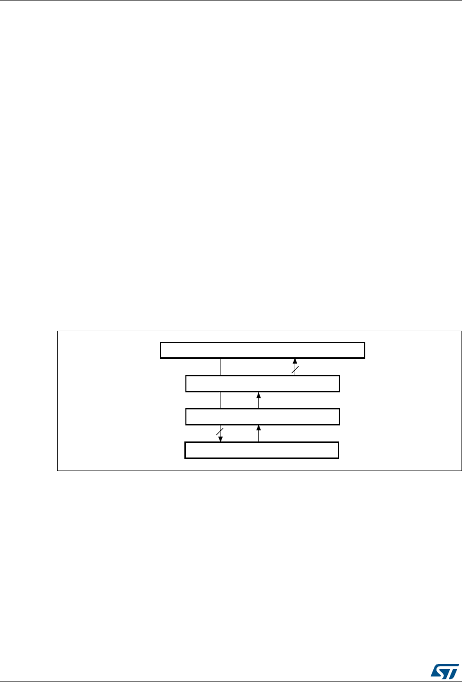
CRC calculation unit RM0383
66/836 DocID026448 Rev 1
4 CRC calculation unit
4.1 CRC introduction
The CRC (cyclic redundancy check) calculation unit is used to get a CRC code from a 32-bit
data word and a fixed generator polynomial.
Among other applications, CRC-based techniques are used to verify data transmission or
storage integrity. In the scope of the EN/IEC 60335-1 standard, they offer a means of
verifying the Flash memory integrity. The CRC calculation unit helps compute a signature of
the software during runtime, to be compared with a reference signature generated at link-
time and stored at a given memory location.
4.2 CRC main features
•Uses CRC-32 (Ethernet) polynomial: 0x4C11DB7
–X
32 + X26 + X23 + X22 + X16 + X12 + X11 + X10 +X8 + X7 + X5 + X4 + X2+ X +1
•Single input/output 32-bit data register
•CRC computation done in 4 AHB clock cycles (HCLK)
•General-purpose 8-bit register (can be used for temporary storage)
The block diagram is shown in Figure 6.
Figure 6. CRC calculation unit block diagram
4.3 CRC functional description
The CRC calculation unit mainly consists of a single 32-bit data register, which:
•is used as an input register to enter new data in the CRC calculator (when writing into
the register)
•holds the result of the previous CRC calculation (when reading the register)
Each write operation into the data register creates a combination of the previous CRC value
and the new one (CRC computation is done on the whole 32-bit data word, and not byte per
byte).
The write operation is stalled until the end of the CRC computation, thus allowing back-to-
back write accesses or consecutive write and read accesses.
AHB bus
32-bit (read access)
Data register (output)
CRC computation (polynomial: 0x4C11DB7)
32-bit (write access)
Data register (input)
ai14968

DocID026448 Rev 1 67/836
RM0383 CRC calculation unit
68
The CRC calculator can be reset to 0xFFFF FFFF with the RESET control bit in the
CRC_CR register. This operation does not affect the contents of the CRC_IDR register.
4.4 CRC registers
The CRC calculation unit contains two data registers and a control register.The peripheral
The CRC registers have to be accessed by words (32 bits).
4.4.1 Data register (CRC_DR)
Address offset: 0x00
Reset value: 0xFFFF FFFF
4.4.2 Independent data register (CRC_IDR)
Address offset: 0x04
Reset value: 0x0000 0000
31 30 29 28 27 26 25 24 23 22 21 20 19 18 17 16
DR [31:16]
rw rw rw rw rw rw rw rw rw rw rw rw rw rw rw rw
1514131211109876543210
DR [15:0]
rw rw rw rw rw rw rw rw rw rw rw rw rw rw rw rw
Bits 31:0 Data register bits
Used as an input register when writing new data into the CRC calculator.
Holds the previous CRC calculation result when it is read.
31 30 29 28 27 26 25 24 23 22 21 20 19 18 17 16
Reserved
1514131211109876543210
Reserved
IDR[7:0]
rw rw rw rw rw rw rw rw
Bits 31:8 Reserved, must be kept at reset value.
Bits 7:0 General-purpose 8-bit data register bits
Can be used as a temporary storage location for one byte.
This register is not affected by CRC resets generated by the RESET bit in the CRC_CR
register.
CRC calculation unit RM0383
68/836 DocID026448 Rev 1
4.4.3 Control register (CRC_CR)
Address offset: 0x08
Reset value: 0x0000 0000
4.4.4 CRC register map
The following table the CRC register map and reset values.
31 30 29 28 27 26 25 24 23 22 21 20 19 18 17 16
Reserved
1514131211109876543210
Reserved
RESET
w
Bits 31:1 Reserved, must be kept at reset value.
Bit 0 RESET bit
Resets the CRC calculation unit and sets the data register to 0xFFFF FFFF.
This bit can only be set, it is automatically cleared by hardware.
Table 13. CRC calculation unit register map and reset values
Offset Register 31-24 23-16 15-8 7 6 5 4 3 2 1 0
0x00
CRC_DR Data register
Reset
value 0xFFFF FFFF
0x04
CRC_IDR
Reserved
Independent data register
Reset
value 0x00
0x08
CRC_CR
Reserved
RESET
Reset
value 0
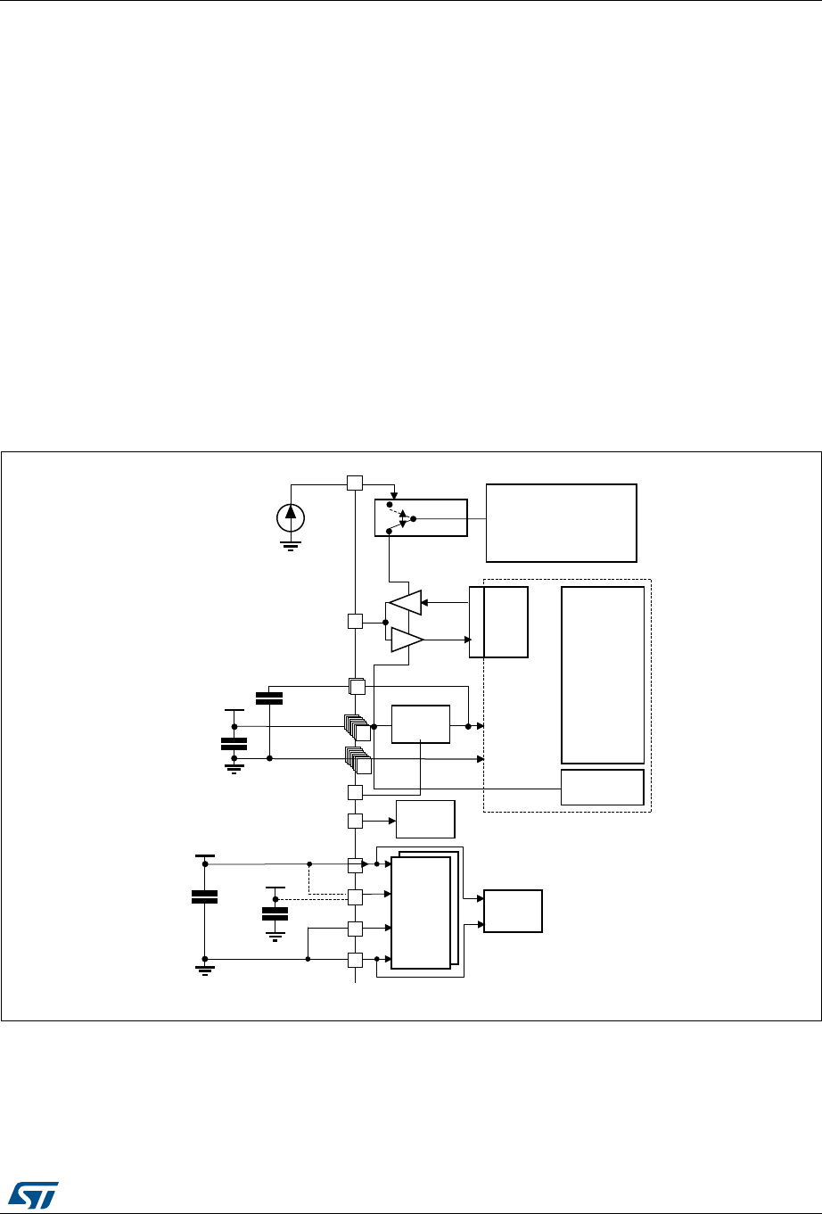
DocID026448 Rev 1 69/836
RM0383 Power controller (PWR)
86
5 Power controller (PWR)
5.1 Power supplies
There are two main power supply schemes:
•VDD = 1.7 to 3.6 V: external power supply for I/Os with the internal regulator disabled,
provided externally through VDD pins. Requires the use of an external power supply
supervisor connected to the VDD and PDR_ON pins.
•VDD = 1.8 to 3.6 V: external power supply for I/Os and the internal regulator (when
enabled), provided externally through VDD pins.
The real-time clock (RTC) and the RTC backup registers can be powered from the VBAT
voltage when the main VDD supply is powered off.
Note: Depending on the operating power supply range, some peripheral may be used with limited
functionality and performance. For more details refer to section "General operating
conditions" in STM32F4xx datasheets.
Figure 7. Power supply overview
1. VDDA and VSSA must be connected to VDD and VSS, respectively.
069
ĂĐŬƵƉĐŝƌĐƵŝƚƌLJ
;K^ϯϮ<͕Zd͕
tĂŬĞƵƉůŽŐŝĐ
ĂĐŬƵƉƌĞŐŝƐƚĞƌƐͿ ͕
<ĞƌŶĞůůŽŐŝĐ
;Wh͕ĚŝŐŝƚĂů
ΘZDͿ
ŶĂůŽŐ͗
ZƐ ͕
W>> ͕͘͘
WŽǁĞƌ
ƐǁŝƚĐŚ
sd
'W/KƐ
Khd
/E
ϲп ϭ ϬϬŶ&
нϭпϰ͘ϳђ&
sdс
ϭ ͘ϲϱƚŽϯ͘ϲs
sŽůƚĂŐĞ
ƌĞŐƵůĂƚŽƌ
s
>ĞǀĞůƐŚŝĨƚĞƌ
/K
>ŽŐŝĐ
s
ϭϬϬŶ&
нϭђ&
&ůĂƐŚŵĞŵŽƌLJ
sWͺϭ
sWͺϮ
ϮпϮ͘Ϯђ&
Žƌϭdžϰ͘ϳђ&
zW^^ͺZ'
WZͺKE
ZĞƐĞƚ
ĐŽŶƚƌŽůůĞƌ
s
ϭ ͬϮ ͬ͘͘͘ ϲ
s^^
ϭ ͬϮ ͬ͘͘͘ ϱ
s
sZ&н
sZ&Ͳ
s^^
sZ&
ϭϬϬŶ&
нϭђ&

Power controller (PWR) RM0383
70/836 DocID026448 Rev 1
5.1.1 Independent A/D converter supply and reference voltage
To improve conversion accuracy, the ADC has an independent power supply which can be
separately filtered and shielded from noise on the PCB.
•The ADC voltage supply input is available on a separate VDDA pin.
•An isolated supply ground connection is provided on pin VSSA.
To ensure a better accuracy of low voltage inputs, the user can connect a separate external
reference voltage ADC input on VREF
. The voltage on VREF ranges from 1.7 V to VDDA.
5.1.2 Battery backup domain
Backup domain description
To retain the content of the RTC backup registers and supply the RTC when VDD is turned
off, VBAT pin can be connected to an optional standby voltage supplied by a battery or by
another source.
To allow the RTC to operate even when the main digital supply (VDD) is turned off, the VBAT
pin powers the following blocks:
•The RTC
•The LSE oscillator
•PC13 to PC15 I/Os
The switch to the VBAT supply is controlled by the power-down reset embedded in the Reset
block.
Warning: During tRSTTEMPO (temporization at VDD startup) or after a PDR
is detected, the power switch between VBAT and VDD remains
connected to VBAT.
During the startup phase, if VDD is established in less than
tRSTTEMPO (Refer to the datasheet for the value of tRSTTEMPO)
and VDD > VBAT + 0.6 V, a current may be injected into VBAT
through an internal diode connected between VDD and the
power switch (VBAT).
If the power supply/battery connected to the VBAT pin cannot
support this current injection, it is strongly recommended to
connect an external low-drop diode between this power
supply and the VBAT pin.
If no external battery is used in the application, it is recommended to connect the VBAT pin to
VDD with a 100 nF external decoupling ceramic capacitor in parallel.
When the backup domain is supplied by VDD (analog switch connected to VDD), the
following functions are available:
•PC14 and PC15 can be used as either GPIO or LSE pins
•PC13 can be used as a GPIO or additional functions can be configured (refer to
Table 25: RTC additional functions for more details about this pin configuration)
Note: Due to the fact that the switch only sinks a limited amount of current (3 mA), the use of
GPIOs PC13 to PC15 are restricted: only one I/O at a time can be used as an output, the

DocID026448 Rev 1 71/836
RM0383 Power controller (PWR)
86
speed has to be limited to 2 MHz with a maximum load of 30 pF and these I/Os must not be
used as a current source (e.g. to drive an LED).
When the backup domain is supplied by VBAT (analog switch connected to VBAT because
VDD is not present), the following functions are available:
•PC14 and PC15 can be used as LSE pins only
•PC13 can be used as the RTC additional function pin (refer to Table 25: RTC additional
functions for more details about this pin configuration)
Backup domain access
After reset, the backup domain (RTC registers and RTC backup register) is protected
against possible unwanted write accesses. To enable access to the backup domain,
proceed as follows:
•Access to the RTC and RTC backup registers
1. Enable the power interface clock by setting the PWREN bits in the RCC_APB1ENR
register (see Section 6.3.11: RCC APB1 peripheral clock enable register
(RCC_APB1ENR))
2. Set the DBP bit in the Section 5.4.1 to enable access to the backup domain
3. Select the RTC clock source: see Section 6.2.8: RTC/AWU clock
4. Enable the RTC clock by programming the RTCEN [15] bit in the Section 6.3.17: RCC
Backup domain control register (RCC_BDCR)
RTC and RTC backup registers
The real-time clock (RTC) is an independent BCD timer/counter. The RTC provides a time-
of-day clock/calendar, two programmable alarm interrupts, and a periodic programmable
wakeup flag with interrupt capability. The RTC contains 20 backup data registers (80 bytes)
which are reset when a tamper detection event occurs. For more details refer to Section 17:
Real-time clock (RTC).
5.1.3 Voltage regulator
An embedded linear voltage regulator supplies all the digital circuitries except for the backup
domain and the Standby circuitry. The regulator output voltage is around 1.2 V.
This voltage regulator requires one or two external capacitors to be connected to one or two
dedicated pins, VCAP_1 and for some packages VCAP_2. Specific pins must be connected
either to VSS or VDD to activate or deactivate the voltage regulator. These pins depend on
the package.
When activated by software, the voltage regulator is always enabled after Reset. It works in
three different modes depending on the application modes.
•In Run mode, the regulator supplies full power to the 1.2 V domain (core, memories
and digital peripherals). In this mode, the regulator output voltage (around 1.2 V) can
be scaled by software to different voltage values:
Scale 1, scale 2, or scale 3 can be configured through the VOS[1:0] bits of the
PWR_CR register. After reset the VOS register is set to scale 2. When the PLL is
OFF, the voltage regulator is set to scale 3 independently of the VOS register
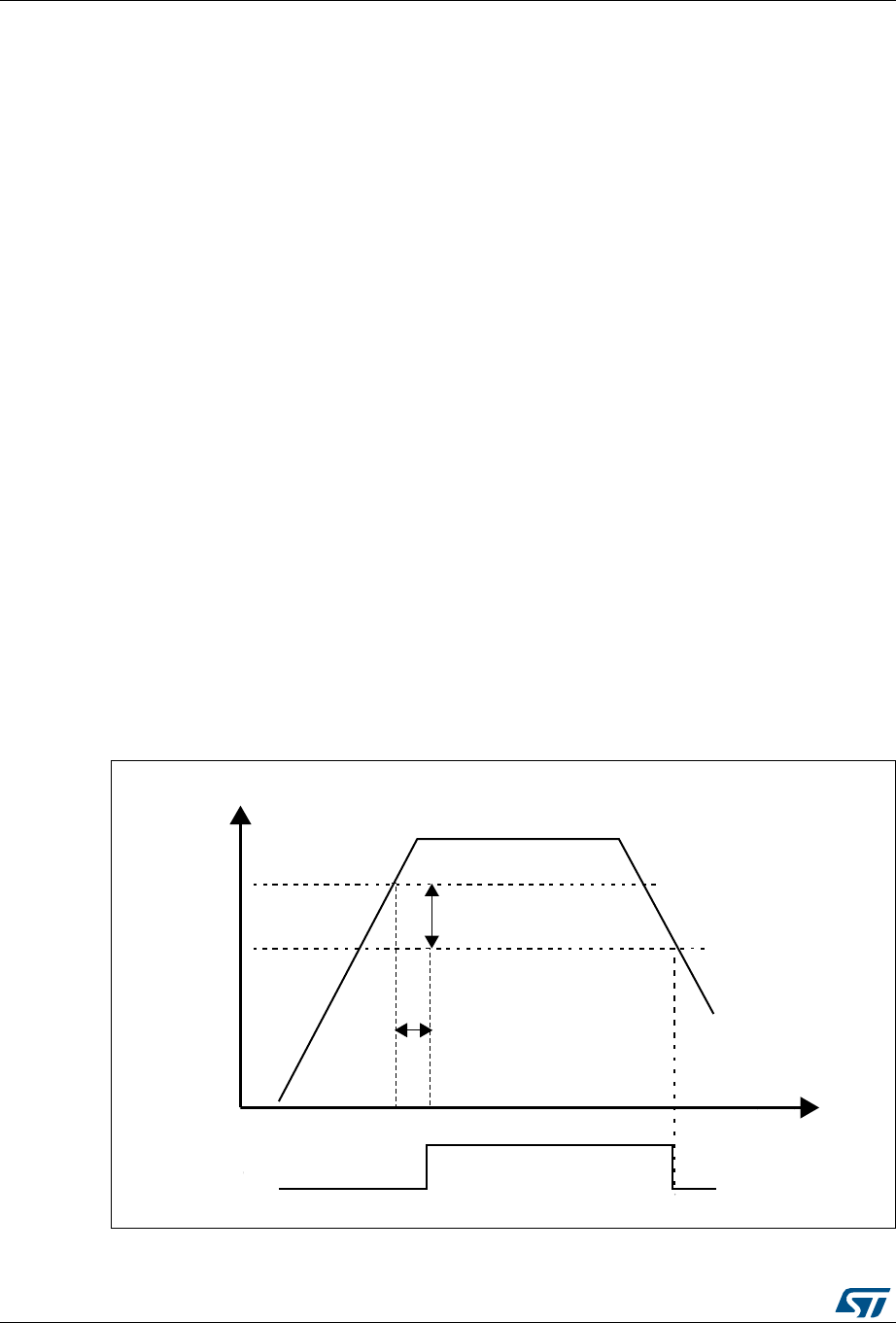
Power controller (PWR) RM0383
72/836 DocID026448 Rev 1
content. The VOS register content is only taken into account once the PLL is
activated and the HSI or HSE is selected as clock source.
The voltage scaling allows optimizing the power consumption when the device is
clocked below the maximum system frequency.
•In Stop mode, the main regulator or the low-power regulator supplies low power to the
1.2 V domain, thus preserving the content of registers and internal SRAM. The voltage
regulator can be put either in main regulator mode (MR) or in low-power mode (LPR).
The programmed voltage scale remains the same during Stop mode:
Voltage scale 3 is automatically selected when the microcontroller enters Stop
mode (see Section 5.4.1: PWR power control register (PWR_CR)).
•In Standby mode, the regulator is powered down. The content of the registers and
SRAM are lost except for the Standby circuitry and the backup domain.
Note: For more details, refer to the voltage regulator section in the STM32F411xC/E datasheet.
5.2 Power supply supervisor
5.2.1 Power-on reset (POR)/power-down reset (PDR)
The device has an integrated POR/PDR circuitry that allows proper operation starting
from 1.8 V.
To use the device below 1.8 V, the internal power supervisor must be switched off using the
PDR_ON pin (please refer to section Power supply supervisor of the
STM32F411xC/Edatasheet).The device remains in Reset mode when VDD/VDDA is below a
specified threshold, VPOR/PDR, without the need for an external reset circuit. For more
details concerning the power on/power-down reset threshold, refer to the electrical
characteristics of the datasheet.
Figure 8. Power-on reset/power-down reset waveform
6$$6$$!
M6
HYSTERESIS
0$2
0$2
-36
2ESET
4EMPORIZATION
T2344%-0/
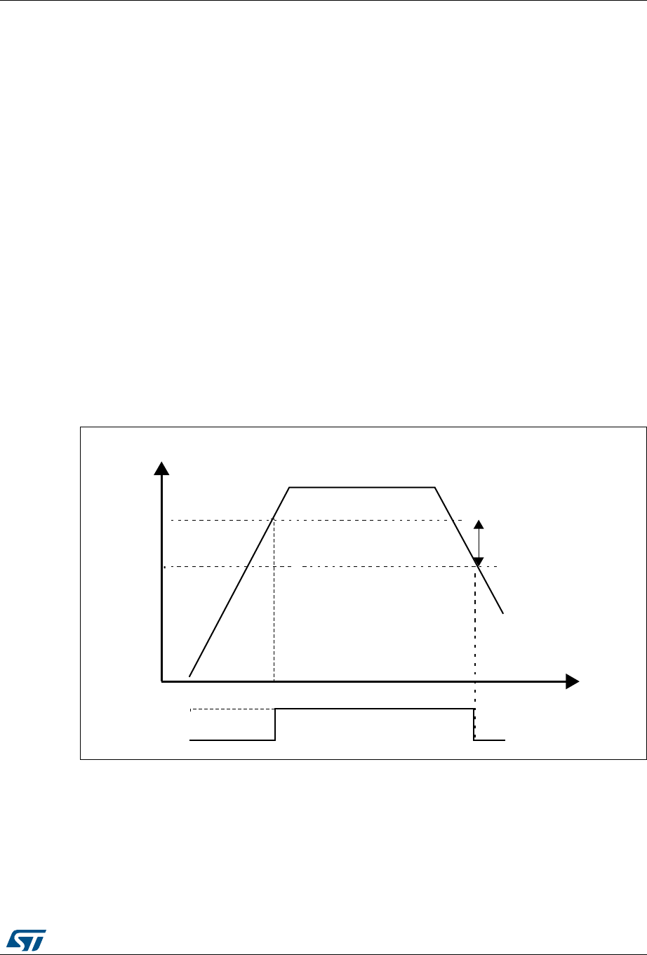
DocID026448 Rev 1 73/836
RM0383 Power controller (PWR)
86
5.2.2 Brownout reset (BOR)
During power on, the Brownout reset (BOR) keeps the device under reset until the supply
voltage reaches the specified VBOR threshold.
VBOR is configured through device option bytes. By default, BOR is off. 3 programmable
VBOR threshold levels can be selected:
•BOR Level 3 (VBOR3). Brownout threshold level 3.
•BOR Level 2 (VBOR2). Brownout threshold level 2.
•BOR Level 1 (VBOR1). Brownout threshold level 1.
Note: For full details about BOR characteristics, refer to the "Electrical characteristics" section in
the device datasheet.
When the supply voltage (VDD) drops below the selected VBOR threshold, a device reset is
generated.
The BOR can be disabled by programming the device option bytes. In this case, the
power-on and power-down is then monitored by the POR/ PDRor by an external power
supervisor if the PDR is switched off through the PDR_ON pin (see Section 5.2.1: Power-on
reset (POR)/power-down reset (PDR)).
The BOR threshold hysteresis is ~100 mV (between the rising and the falling edge of the
supply voltage).
Figure 9. BOR thresholds
5.2.3 Programmable voltage detector (PVD)
You can use the PVD to monitor the VDD power supply by comparing it to a threshold
selected by the PLS[2:0] bits in the PWR power control register (PWR_CR).
The PVD is enabled by setting the PVDE bit.
-36
6$$6$$!
M6
HYSTERESIS
"/2THRESHOLD
2ESET
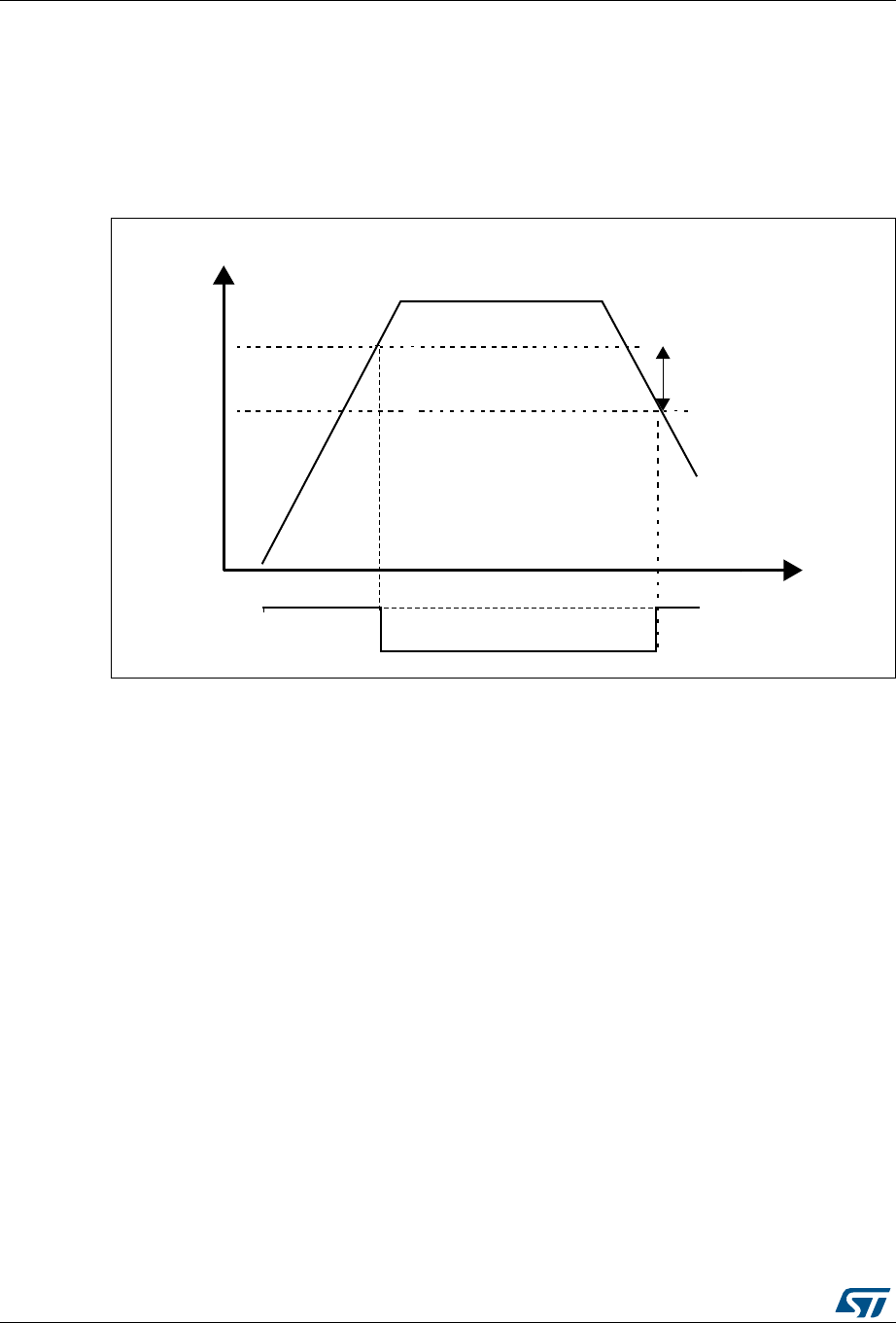
Power controller (PWR) RM0383
74/836 DocID026448 Rev 1
A PVDO flag is available, in the PWR power control/status register (PWR_CSR), to indicate
if VDD is higher or lower than the PVD threshold. This event is internally connected to the
EXTI line16 and can generate an interrupt if enabled through the EXTI registers. The PVD
output interrupt can be generated when VDD drops below the PVD threshold and/or when
VDD rises above the PVD threshold depending on EXTI line16 rising/falling edge
configuration. As an example the service routine could perform emergency shutdown tasks.
Figure 10. PVD thresholds
5.3 Low-power modes
By default, the microcontroller is in Run mode after a system or a power-on reset. In Run
mode the CPU is clocked by HCLK and the program code is executed. Several low-power
modes are available to save power when the CPU does not need to be kept running, for
example when waiting for an external event. It is up to the user to select the mode that gives
the best compromise between low-power consumption, short startup time and available
wakeup sources.
The devices feature three low-power modes:
•Sleep mode (Cortex®-M4 with FPU core stopped, peripherals kept running)
•Stop mode (all clocks are stopped)
•Standby mode (1.2 V domain powered off)
In addition, the power consumption in Run mode can be reduce by one of the following
means:
•Slowing down the system clocks
•Gating the clocks to the APBx and AHBx peripherals when they are unused.
-36
6$$
M6
HYSTERESIS
06$THRESHOLD
06$OUTPUT

DocID026448 Rev 1 75/836
RM0383 Power controller (PWR)
86
5.3.1 Slowing down system clocks
In Run mode the speed of the system clocks (SYSCLK, HCLK, PCLK1, PCLK2) can be
reduced by programming the prescaler registers. These prescalers can also be used to slow
down peripherals before entering Sleep mode.
For more details refer to Section 6.3.3: RCC clock configuration register (RCC_CFGR).
5.3.2 Peripheral clock gating
In Run mode, the HCLKx and PCLKx for individual peripherals and memories can be
stopped at any time to reduce power consumption.
To further reduce power consumption in Sleep mode the peripheral clocks can be disabled
prior to executing the WFI or WFE instructions.
Peripheral clock gating is controlled by the AHB1 peripheral clock enable register
(RCC_AHB1ENR), AHB2 peripheral clock enable register (RCC_AHB2ENR) (see
Section 6.3.9: RCC AHB1 peripheral clock enable register (RCC_AHB1ENR),
Section 6.3.10: RCC AHB2 peripheral clock enable register (RCC_AHB2ENR)).
Disabling the peripherals clocks in Sleep mode can be performed automatically by resetting
the corresponding bit in RCC_AHBxLPENR and RCC_APBxLPENR registers.
Table 14. Low-power mode summary
Mode name Entry Wakeup Effect on 1.2 V
domain clocks
Effect on
VDD
domain
clocks
Voltage regulator
Sleep
(Sleep now or
Sleep-on-exit)
WFI Any interrupt CPU CLK OFF
no effect on other
clocks or analog
clock sources
None ON
WFE Wakeup event
Stop SLEEPDEEP bit
+ WFI or WFE
Any EXTI line (configured
in the EXTI registers,
internal and external lines)
All 1.2 V domain
clocks OFF
HSI and
HSE
oscillators
OFF
Main regulator or
Low-Power
regulator (depends
on PWR power
control register
(PWR_CR)
Standby PDDS bit +
SLEEPDEEP bit
+ WFI or WFE
WKUP pin rising edge,
RTC alarm (Alarm A or
Alarm B), RTC Wakeup
event, RTC tamper events,
RTC time stamp event,
external reset in NRST
pin, IWDG reset
OFF

Power controller (PWR) RM0383
76/836 DocID026448 Rev 1
5.3.3 Sleep mode
Entering Sleep mode
The Sleep mode is entered by executing the WFI (Wait For Interrupt) or WFE (Wait for
Event) instructions. Two options are available to select the Sleep mode entry mechanism,
depending on the SLEEPONEXIT bit in the Cortex®-M4 with FPU System Control register:
•Sleep-now: if the SLEEPONEXIT bit is cleared, the MCU enters Sleep mode as soon
as WFI or WFE instruction is executed.
•Sleep-on-exit: if the SLEEPONEXIT bit is set, the MCU enters Sleep mode as soon as
it exits the lowest priority ISR.
Refer to Table 15 and Table 16 for details on how to enter Sleep mode.
Exiting Sleep mode
If the WFI instruction is used to enter Sleep mode, any peripheral interrupt acknowledged by
the nested vectored interrupt controller (NVIC) can wake up the device from Sleep mode.
If the WFE instruction is used to enter Sleep mode, the MCU exits Sleep mode as soon as
an event occurs. The wakeup event can be generated either by:
•Enabling an interrupt in the peripheral control register but not in the NVIC, and enabling
the SEVONPEND bit in the Cortex®-M4 with FPU System Control register. When the
MCU resumes from WFE, the peripheral interrupt pending bit and the peripheral NVIC
IRQ channel pending bit (in the NVIC interrupt clear pending register) have to be
cleared.
•Or configuring an external or internal EXTI line in event mode. When the CPU resumes
from WFE, it is not necessary to clear the peripheral interrupt pending bit or the NVIC
IRQ channel pending bit as the pending bit corresponding to the event line is not set.
This mode offers the lowest wakeup time as no time is wasted in interrupt entry/exit.
Refer to Table 15 and Table 16 for more details on how to exit Sleep mode.
Table 15. Sleep-now entry and exit
Sleep-now mode Description
Mode entry
WFI (Wait for Interrupt) or WFE (Wait for Event) while:
– SLEEPDEEP = 0 and
– SLEEPONEXIT = 0
Refer to the Cortex®-M4 with FPU System Control register.
Mode exit
If WFI was used for entry:
Interrupt: Refer to Table 37: Vector table for STM32F411xC/E
If WFE was used for entry
Wakeup event: Refer to Section 10.2.3: Wakeup event management
Wakeup latency None

DocID026448 Rev 1 77/836
RM0383 Power controller (PWR)
86
5.3.4 Stop mode
The Stop mode is based on the Cortex®-M4 with FPU deepsleep mode combined with
peripheral clock gating. The voltage regulator can be configured either in normal or low-
power mode. In Stop mode, all clocks in the 1.2 V domain are stopped, the PLLs, the HSI
and the HSE RC oscillators are disabled. Internal SRAM and register contents are
preserved.
Some settings in the PWR_CR register allow to further reduce the power consumption.
When the Flash memory is in power-down mode, an additional startup delay is incurred
when waking up from Stop mode (see Table 17: Stop operating modes and Section 5.4.1:
PWR power control register (PWR_CR)).
Table 16. Sleep-on-exit entry and exit
Sleep-on-exit Description
Mode entry
WFI (wait for interrupt) while:
– SLEEPDEEP = 0 and
– SLEEPONEXIT = 1
Refer to the Cortex®-M4 with FPU System Control register.
Mode exit Interrupt: refer to Table 37: Vector table for STM32F411xC/E
Wakeup latency None
Table 17. Stop operating modes
Stop mode MRLV bit LPLV bit FPDS bit LPDS bit Wakeup latency
Normal mode
STOP MR 0 - 0 0 HSI RC startup time
STOP MRFPD 0 - 1 0
HSI RC startup time +
Flash wakeup time from Deep
Power Down mode
STOP LP0001
HSI RC startup time +
regulator wakeup time from LP
mode
STOP LPFPD - 0 1 1
HSI RC startup time +
Flash wakeup time from Deep
Power Down mode +
regulator wakeup time from LP
mode
STOP MRLV 1 - - 0
HSI RC startup time +
Flash wakeup time from Deep
Power Down mode +
Main regulator from low voltage
mode
STOP LPLV-1-1
HSI RC startup time +
Flash wakeup time from Deep
Power Down mode +
regulator wakeup time from Low
Voltage LP mode

Power controller (PWR) RM0383
78/836 DocID026448 Rev 1
Entering Stop mode
Refer to Table 18 for details on how to enter the Stop mode.
To further reduce power consumption in Stop mode, the internal voltage regulator can be put
in low-power mode. This is configured by the LPDS bit of the PWR power control register
(PWR_CR).
If Flash memory programming is ongoing, the Stop mode entry is delayed until the memory
access is finished.
If an access to the APB domain is ongoing, The Stop mode entry is delayed until the APB
access is finished.
In Stop mode, the following features can be selected by programming individual control bits:
•Independent watchdog (IWDG): the IWDG is started by writing to its Key register or by
hardware option. Once started it cannot be stopped except by a Reset. See
Section 15.3 in Section 15: Independent watchdog (IWDG).
•Real-time clock (RTC): this is configured by the RTCEN bit in the Section 6.3.17: RCC
Backup domain control register (RCC_BDCR)
•Internal RC oscillator (LSI RC): this is configured by the LSION bit in the
Section 6.3.18: RCC clock control & status register (RCC_CSR).
•External 32.768 kHz oscillator (LSE OSC): this is configured by the LSEON bit in the
Section 6.3.17: RCC Backup domain control register (RCC_BDCR).
The ADC can also consume power during the Stop mode, unless it is disabled before
entering it. To disable it, the ADON bit in the ADC_CR2 register must be written to 0.
Note: If the application needs to disable the external clock before entering Stop mode, the HSEON
bit must first be disabled and the system clock switched to HSI.
Otherwise, if the HSEON bit is kept enabled while the external clock (external oscillator) can
be removed before entering stop mode, the clock security system (CSS) feature must be
enabled to detect any external oscillator failure and avoid a malfunction behavior when
entering stop mode.
Exiting Stop mode
Refer to Table 18 for more details on how to exit Stop mode.
When exiting Stop mode by issuing an interrupt or a wakeup event, the HSI RC oscillator is
selected as system clock.
When the voltage regulator operates in low-power mode, an additional startup delay is
incurred when waking up from Stop mode. By keeping the internal regulator ON during Stop
mode, the consumption is higher although the startup time is reduced.

DocID026448 Rev 1 79/836
RM0383 Power controller (PWR)
86
5.3.5 Standby mode
The Standby mode allows to achieve the lowest power consumption. It is based on the
Cortex®-M4 with FPU deepsleep mode, with the voltage regulator disabled. The 1.2 V
domain is consequently powered off. The PLLs, the HSI oscillator and the HSE oscillator are
also switched off. SRAM and register contents are lost except for registers in the backup
domain (RTC registers and RTC backup register), and Standby circuitry (see Figure 7).
Entering Standby mode
Refer to Table 19 for more details on how to enter Standby mode.
In Standby mode, the following features can be selected by programming individual control
bits:
•Independent watchdog (IWDG): the IWDG is started by writing to its Key register or by
hardware option. Once started it cannot be stopped except by a reset. See
Section 15.3 in Section 15: Independent watchdog (IWDG).
•Real-time clock (RTC): this is configured by the RTCEN bit in the backup domain
control register (RCC_BDCR)
•Internal RC oscillator (LSI RC): this is configured by the LSION bit in the Control/status
register (RCC_CSR).
•External 32.768 kHz oscillator (LSE OSC): this is configured by the LSEON bit in the
backup domain control register (RCC_BDCR)
Exiting Standby mode
The microcontroller exits Standby mode when an external Reset (NRST pin), an IWDG
Reset, a rising edge on WKUP pin, an RTC alarm, a tamper event, or a time stamp event is
detected. All registers are reset after wakeup from Standby except for PWR power
control/status register (PWR_CSR).
Table 18. Stop mode entry and exit
Stop mode Description
Mode entry
WFI (Wait for Interrupt) or WFE (Wait for Event) while:
– Set SLEEPDEEP bit in Cortex®-M4 with FPU System Control register
– Clear PDDS bit in Power Control register (PWR_CR)
– Select the voltage regulator mode by configuring LPDS bit in PWR_CR.
Note: To enter the Stop mode, all EXTI Line pending bits (in Pending
register (EXTI_PR)), all peripheral interrupts pending bits, the RTC Alarm
(Alarm A and Alarm B), RTC wakeup, RTC tamper, and RTC time stamp
flags, must be reset. Otherwise, the Stop mode entry procedure is ignored
and program execution continues.
Mode exit
If WFI was used for entry:
All EXTI lines configured in Interrupt mode (the corresponding EXTI
Interrupt vector must be enabled in the NVIC). Refer to Table 37: Vector
table for STM32F411xC/E.
If WFE was used for entry:
All EXTI Lines configured in event mode. Refer to Section 10.2.3:
Wakeup event management on page 202
Wakeup latency Table 17: Stop operating modes

Power controller (PWR) RM0383
80/836 DocID026448 Rev 1
After waking up from Standby mode, program execution restarts in the same way as after a
Reset (boot pins sampling, vector reset is fetched, etc.). The SBF status flag in the PWR
power control/status register (PWR_CSR) indicates that the MCU was in Standby mode.
Refer to Table 19 for more details on how to exit Standby mode.
I/O states in Standby mode
In Standby mode, all I/O pins are high impedance except for:
•Reset pad (still available)
•RTC_AF1 pin (PC13) if configured for tamper, time stamp, RTC Alarm out, or RTC
clock calibration out
•WKUP pin (PA0), if enabled
Debug mode
By default, the debug connection is lost if the application puts the MCU in Stop or Standby
mode while the debug features are used. This is due to the fact that the Cortex®-M4 with
FPU core is no longer clocked.
However, by setting some configuration bits in the DBGMCU_CR register, the software can
be debugged even when using the low-power modes extensively. For more details, refer to
Section 23.16.1: Debug support for low-power modes.
5.3.6 Programming the RTC alternate functions to wake up the device from
the Stop and Standby modes
The MCU can be woken up from a low-power mode by an RTC alternate function.
The RTC alternate functions are the RTC alarms (Alarm A and Alarm B), RTC wakeup, RTC
tamper event detection and RTC time stamp event detection.
These RTC alternate functions can wake up the system from the Stop and Standby low-
power modes.
The system can also wake up from low-power modes without depending on an external
interrupt (Auto-wakeup mode), by using the RTC alarm or the RTC wakeup events.
The RTC provides a programmable time base for waking up from the Stop or Standby mode
at regular intervals.
Table 19. Standby mode entry and exit
Standby mode Description
Mode entry
WFI (Wait for Interrupt) or WFE (Wait for Event) while:
– Set SLEEPDEEP in Cortex®-M4 with FPU System Control register
– Set PDDS bit in Power Control register (PWR_CR)
– Clear WUF bit in Power Control/Status register (PWR_CSR)
– Clear the RTC flag corresponding to the chosen wakeup source (RTC
Alarm A, RTC Alarm B, RTC wakeup, Tamper or Timestamp flags)
Mode exit WKUP pin rising edge, RTC alarm (Alarm A and Alarm B), RTC wakeup,
tamper event, time stamp event, external reset in NRST pin, IWDG reset.
Wakeup latency Reset phase.

DocID026448 Rev 1 81/836
RM0383 Power controller (PWR)
86
For this purpose, two of the three alternate RTC clock sources can be selected by
programming the RTCSEL[1:0] bits in the Section 6.3.17: RCC Backup domain control
register (RCC_BDCR):
•Low-power 32.768 kHz external crystal oscillator (LSE OSC)
This clock source provides a precise time base with a very low-power consumption
(additional consumption of less than 1 µA under typical conditions)
•Low-power internal RC oscillator (LSI RC)
This clock source has the advantage of saving the cost of the 32.768 kHz crystal. This
internal RC oscillator is designed to use minimum power.
RTC alternate functions to wake up the device from the Stop mode
•To wake up the device from the Stop mode with an RTC alarm event, it is necessary to:
a) Configure the EXTI Line 17 to be sensitive to rising edges (Interrupt or Event
modes)
b) Enable the RTC Alarm Interrupt in the RTC_CR register
c) Configure the RTC to generate the RTC alarm
•To wake up the device from the Stop mode with an RTC tamper or time stamp event, it
is necessary to:
a) Configure the EXTI Line 21 to be sensitive to rising edges (Interrupt or Event
modes)
b) Enable the RTC time stamp Interrupt in the RTC_CR register or the RTC tamper
interrupt in the RTC_TAFCR register
c) Configure the RTC to detect the tamper or time stamp event
•To wake up the device from the Stop mode with an RTC wakeup event, it is necessary
to:
a) Configure the EXTI Line 22 to be sensitive to rising edges (Interrupt or Event
modes)
b) Enable the RTC wakeup interrupt in the RTC_CR register
c) Configure the RTC to generate the RTC Wakeup event
RTC alternate functions to wake up the device from the Standby mode
•To wake up the device from the Standby mode with an RTC alarm event, it is necessary
to:
a) Enable the RTC alarm interrupt in the RTC_CR register
b) Configure the RTC to generate the RTC alarm
•To wake up the device from the Standby mode with an RTC tamper or time stamp
event, it is necessary to:
a) Enable the RTC time stamp interrupt in the RTC_CR register or the RTC tamper
interrupt in the RTC_TAFCR register
b) Configure the RTC to detect the tamper or time stamp event
•To wake up the device from the Standby mode with an RTC wakeup event, it is
necessary to:
a) Enable the RTC wakeup interrupt in the RTC_CR register
b) Configure the RTC to generate the RTC wakeup event

Power controller (PWR) RM0383
82/836 DocID026448 Rev 1
Safe RTC alternate function wakeup flag clearing sequence
If the selected RTC alternate function is set before the PWR wakeup flag (WUTF) is cleared,
it will not be detected on the next event as detection is made once on the rising edge.
To avoid bouncing on the pins onto which the RTC alternate functions are mapped, and exit
correctly from the Stop and Standby modes, it is recommended to follow the sequence
below before entering the Standby mode:
•When using RTC alarm to wake up the device from the low-power modes:
a) Disable the RTC alarm interrupt (ALRAIE or ALRBIE bits in the RTC_CR register)
b) Clear the RTC alarm (ALRAF/ALRBF) flag
c) Clear the PWR Wakeup (WUF) flag
d) Enable the RTC alarm interrupt
e) Re-enter the low-power mode
•When using RTC wakeup to wake up the device from the low-power modes:
a) Disable the RTC Wakeup interrupt (WUTIE bit in the RTC_CR register)
b) Clear the RTC Wakeup (WUTF) flag
c) Clear the PWR Wakeup (WUF) flag
d) Enable the RTC Wakeup interrupt
e) Re-enter the low-power mode
•When using RTC tamper to wake up the device from the low-power modes:
a) Disable the RTC tamper interrupt (TAMPIE bit in the RTC_TAFCR register)
b) Clear the Tamper (TAMP1F/TSF) flag
c) Clear the PWR Wakeup (WUF) flag
d) Enable the RTC tamper interrupt
e) Re-enter the low-power mode
•When using RTC time stamp to wake up the device from the low-power modes:
a) Disable the RTC time stamp interrupt (TSIE bit in RTC_CR)
b) Clear the RTC time stamp (TSF) flag
c) Clear the PWR Wakeup (WUF) flag
d) Enable the RTC TimeStamp interrupt
e) Re-enter the low-power mode

DocID026448 Rev 1 83/836
RM0383 Power controller (PWR)
86
5.4 Power control registers
5.4.1 PWR power control register (PWR_CR)
Address offset: 0x00
Reset value: 0x0000 8000 (reset by wakeup from Standby mode)
31 30 29 28 27 26 25 24 23 22 21 20 19 18 17 16
Reserved
FISSR FMSSR
Reserved
rw rw
1514131211109876543210
VOS ADCDC1
Res
MRLV
DS
LPLV
DS FPDS DBP PLS[2:0] PVDE CSBF CWUF PDDS LPDS
rw rw rw rw rw rw rw rw rw rw rw w w rw rw
Bits 31:22 Reserved, must be kept at reset value.
Bit 21 FISSR: Flash Interface Stop while System Run
0: Flash Interface clock run (Default value).
1: Flash Interface clock off.
Note: This bit could not be set while executing with the Flash itself. It should be done with
specific routine executed from RAM.
Bit 20 FMSSR: Flash Memory Sleep System Run.
0: Flash standard mode (Default value)
1: Flash forced to be in STOP or DeepPower Down mode (depending of FPDS value bit) by
hardware.
Note: This bit could not be set while executing with the Flash itself. It should be done with
specific routine executed from RAM.
Bits 19:16 Reserved, must be kept at reset value.
Bits 15:14 VOS[1:0]: Regulator voltage scaling output selection
These bits control the main internal voltage regulator output voltage to achieve a trade-off
between performance and power consumption when the device does not operate at the
maximum frequency (refer to the corresponding datasheet for more details).
These bits can be modified only when the PLL is OFF. The new value programmed is active
only when the PLL is ON. When the PLL is OFF, the voltage regulator is set to scale 3
independently of the VOS register content.
00: Reserved (Scale 3 mode selected)
01: Scale 3 mode <= 64 MHz
10: Scale 2 mode (reset value) <= 84 MHz
11: Scale 1 mode <= 100 MHz
Bit 13 ADCDC1:
0: No effect.
1: Refer to AN4073 for details on how to use this bit.
Note: This bit can only be set when operating at supply voltage range 2.7 to 3.6V and when
the Prefetch is OFF.

Power controller (PWR) RM0383
84/836 DocID026448 Rev 1
Bit 12 Reserved, must be kept at reset value.
Bit 11 MRLVDS: Main regulator Low Voltage in Deep Sleep
0: Main regulator in Voltage scale 3 when the device is in Stop mode.
1: Main regulator in Low Voltage and Flash memory in Deep Sleep mode when the device is
in Stop mode.
Bit 10 LPLVDS: Low-power regulator Low Voltage in Deep Sleep
0: Low-power regulator on if LPDS bit is set when the device is in Stop mode.
1: Low-power regulator in Low Voltage and Flash memory in Deep Sleep mode if LPDS bit is
set when device is in Stop mode.
Bit 9 FPDS: Flash power-down in Stop mode
When set, the Flash memory enters power-down mode when the device enters Stop mode.
This allows to achieve a lower consumption in stop mode but a longer restart time.
0: Flash memory not in power-down when the device is in Stop mode
1: Flash memory in power-down when the device is in Stop mode
Bit 8 DBP: Disable backup domain write protection
In reset state, the RCC_BDCR register, the RTC registers (including the backup registers),
and the BRE bit of the PWR_CSR register, are protected against parasitic write access. This
bit must be set to enable write access to these registers.
0: Access to RTC and RTC Backup registers.
1: Access to RTC and RTC Backup registers.
Bits 7:5 PLS[2:0]: PVD level selection
These bits are written by software to select the voltage threshold detected by the Power
Voltage Detector
000: 2.2 V
001: 2.3 V
010: 2.4 V
011: 2.5 V
100: 2.6 V
101: 2.7 V
110: 2.8 V
111: 2.9 V
Note: Refer to the electrical characteristics of the datasheet for more details.
Bit 4 PVDE: Power voltage detector enable
This bit is set and cleared by software.
0: PVD disabled
1: PVD enabled
Bit 3 CSBF: Clear standby flag
This bit is always read as 0.
0: No effect.
1: Clear the SBF Standby Flag (write).
Bit 2 CWUF: Clear wakeup flag
This bit is always read as 0.
0: No effect.
1: Clear the WUF Wakeup Flag after 2 System clock cycles.

DocID026448 Rev 1 85/836
RM0383 Power controller (PWR)
86
5.4.2 PWR power control/status register (PWR_CSR)
Address offset: 0x04
Reset value: 0x0000 0000 (not reset by wakeup from Standby mode)
Additional APB cycles are needed to read this register versus a standard APB read.
Bit 1 PDDS: Power-down deepsleep
This bit is set and cleared by software. It works together with the LPDS bit.
0: Enter Stop mode when the CPU enters deepsleep. The regulator status depends on the
LPDS bit.
1: Enter Standby mode when the CPU enters deepsleep.
Bit 0 LPDS: Low-power deepsleep
This bit is set and cleared by software. It works together with the PDDS bit.
0: Voltage regulator on during Stop mode.
1: Low-power Voltage regulator on during Stop mode.
31 30 29 28 27 26 25 24 23 22 21 20 19 18 17 16
Reserved
1514131211109876543210
Res
VOS
RDY Reserved BRE EWUP Reserved BRR PVDO SBF WUF
r rwrw rrrr
Bits 31:15 Reserved, must be kept at reset value.
Bit 14 VOSRDY: Regulator voltage scaling output selection ready bit
0: Not ready
1: Ready
Bits 13:10 Reserved, must be kept at reset value.
Bit 9 BRE: Backup regulator enable
When set, the Backup regulator (used to maintain the backup domain content) is enabled. If
BRE is reset, the backup regulator is switched off. Once set, the application must wait that
the Backup Regulator Ready flag (BRR) is set to indicate that the data written into the
backup registers will be maintained in the Standby and VBAT modes.
0: Backup regulator disabled
1: Backup regulator enabled
Note: This bit is not reset when the device wakes up from Standby mode, by a system reset,
or by a power reset.
Bit 8 EWUP: Enable WKUP pin
This bit is set and cleared by software.
0: WKUP pin is used for general purpose I/O. An event on the WKUP pin does not wakeup
the device from Standby mode.
1: WKUP pin is used for wakeup from Standby mode and forced in input pull down
configuration (rising edge on WKUP pin wakes-up the system from Standby mode).
Note: This bit is reset by a system reset.
Bits 7:4 Reserved, must be kept at reset value.

Power controller (PWR) RM0383
86/836 DocID026448 Rev 1
5.5 PWR register map
The following table summarizes the PWR registers.
Refer to Table 1 on page 37 for the register boundary addresses.
Bit 3 BRR: Backup regulator ready
Set by hardware to indicate that the Backup Regulator is ready.
0: Backup Regulator not ready
1: Backup Regulator ready
Note: This bit is not reset when the device wakes up from Standby mode or by a system reset
or power reset.
Bit 2 PVDO: PVD output
This bit is set and cleared by hardware. It is valid only if PVD is enabled by the PVDE bit.
0: VDD is higher than the PVD threshold selected with the PLS[2:0] bits.
1: VDD is lower than the PVD threshold selected with the PLS[2:0] bits.
Note: The PVD is stopped by Standby mode. For this reason, this bit is equal to 0 after
Standby or reset until the PVDE bit is set.
Bit 1 SBF: Standby flag
This bit is set by hardware and cleared only by a POR/PDR (power-on reset/power-down
reset) or by setting the CSBF bit in the PWR_CR register.
0: Device has not been in Standby mode
1: Device has been in Standby mode
Bit 0 WUF: Wakeup flag
This bit is set by hardware and cleared either by a system reset or by setting the CWUF bit in
the PWR_CR register.
0: No wakeup event occurred
1: A wakeup event was received from the WKUP pin or from the RTC alarm (Alarm A or
Alarm B), RTC Tamper event, RTC TimeStamp event or RTC Wakeup).
Note: An additional wakeup event is detected if the WKUP pin is enabled (by setting the
EWUP bit) when the WKUP pin level is already high.
Table 20. PWR - register map and reset values
Offset Register
31
30
29
28
27
26
25
24
23
22
21
20
19
18
17
16
15
14
13
12
11
10
9
8
7
6
5
4
3
2
1
0
0x000 PWR_CR Reserved
FISSR
FMSSR
Reser
ved
VOS[1:0]
ADCDC1
MRLVDS
LPLVDS
FPDS
DBP
PLS[2:0]
PVDE
CSBF
CWUF
PDDS
LPDS
Reset value 0 0 1 1 0 000000000000
0x004 PWR_CSR Reserved
VOSRDY
Reserved
BRE
EWUP
Reserved
BRR
PVDO
SBF
WUF
Reset value 0 0 0 0 0 0 0

DocID026448 Rev 1 87/836
RM0383 Reset and clock control (RCC) for STM32F411xC/E
135
6 Reset and clock control (RCC) for STM32F411xC/E
6.1 Reset
There are three types of reset, defined as system Reset, power Reset and backup domain
Reset.
6.1.1 System reset
A system reset sets all registers to their reset values except the reset flags in the clock
controller CSR register and the registers in the Backup domain.
A system reset is generated when one of the following events occurs:
1. A low level on the NRST pin (external reset)
2. Window watchdog end of count condition (WWDG reset)
3. Independent watchdog end of count condition (IWDG reset)
4. A software reset (SW reset) (see Software reset)
5. Low-power management reset (see Low-power management reset)
Software reset
The reset source can be identified by checking the reset flags in the RCC clock control &
status register (RCC_CSR).
The SYSRESETREQ bit in Cortex®-M4 with FPU Application Interrupt and Reset Control
Register must be set to force a software reset on the device. Refer to the Cortex®-M4 with
FPU technical reference manual for more details.
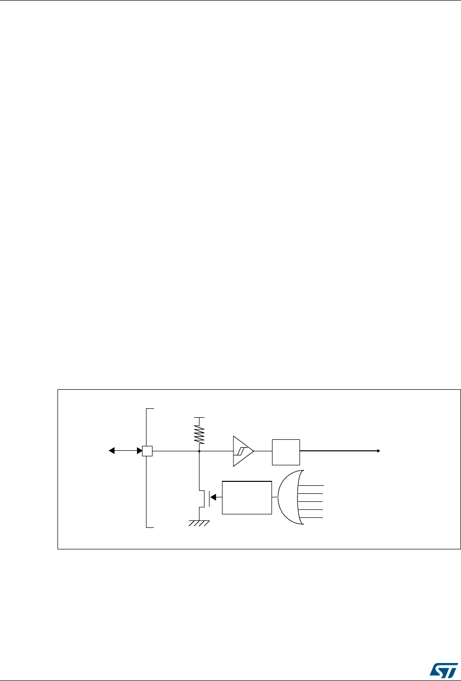
Reset and clock control (RCC) for STM32F411xC/E RM0383
88/836 DocID026448 Rev 1
Low-power management reset
There are two ways of generating a low-power management reset:
1. Reset generated when entering the Standby mode:
This type of reset is enabled by resetting the nRST_STDBY bit in the user option bytes.
In this case, whenever a Standby mode entry sequence is successfully executed, the
device is reset instead of entering the Standby mode.
2. Reset when entering the Stop mode:
This type of reset is enabled by resetting the nRST_STOP bit in the user option bytes.
In this case, whenever a Stop mode entry sequence is successfully executed, the
device is reset instead of entering the Stop mode.
For further information on the user option bytes, refer to the STM32F411xC/E Flash
programming manual available from your ST sales office.
6.1.2 Power reset
A power reset is generated when one of the following events occurs:
1. Power-on/power-down reset (POR/PDR reset) or brownout (BOR) reset
2. When exiting the Standby mode
A power reset sets all registers to their reset values except the Backup domain.
These sources act on the NRST pin and it is always kept low during the delay phase. The
RESET service routine vector is fixed at address 0x0000_0004 in the memory map.
The system reset signal provided to the device is output on the NRST pin. The pulse
generator guarantees a minimum reset pulse duration of 20 µs for each internal reset
source. In case of an external reset, the reset pulse is generated while the NRST pin is
asserted low.
Figure 11. Simplified diagram of the reset circuit
1567
538
9''9''$
::'*UHVHW
,:'*UHVHW
3XOVH
JHQHUDWRU 3RZHUUHVHW
([WHUQDO
UHVHW
PLQV
6\VWHPUHVHW
)LOWHU
6RIWZDUHUHVHW
/RZSRZHUPDQDJHPHQWUHVHW
DLF

DocID026448 Rev 1 89/836
RM0383 Reset and clock control (RCC) for STM32F411xC/E
135
6.1.3 Backup domain reset
The backup domain reset sets all RTC registers and the RCC_BDCR register to their reset
values.
A backup domain reset is generated when one of the following events occurs:
1. Software reset, triggered by setting the BDRST bit in the RCC Backup domain control
register (RCC_BDCR).
2. VDD or VBAT power on, if both supplies have previously been powered off.
6.2 Clocks
Three different clock sources can be used to drive the system clock (SYSCLK):
•HSI oscillator clock
•HSE oscillator clock
•Main PLL (PLL) clock
The devices have the two following secondary clock sources:
•32 kHz low-speed internal RC (LSI RC) which drives the independent watchdog and,
optionally, the RTC used for Auto-wakeup from the Stop/Standby mode.
•32.768 kHz low-speed external crystal (LSE crystal) which optionally drives the RTC
clock (RTCCLK)
Each clock source can be switched on or off independently when it is not used, to optimize
power consumption.
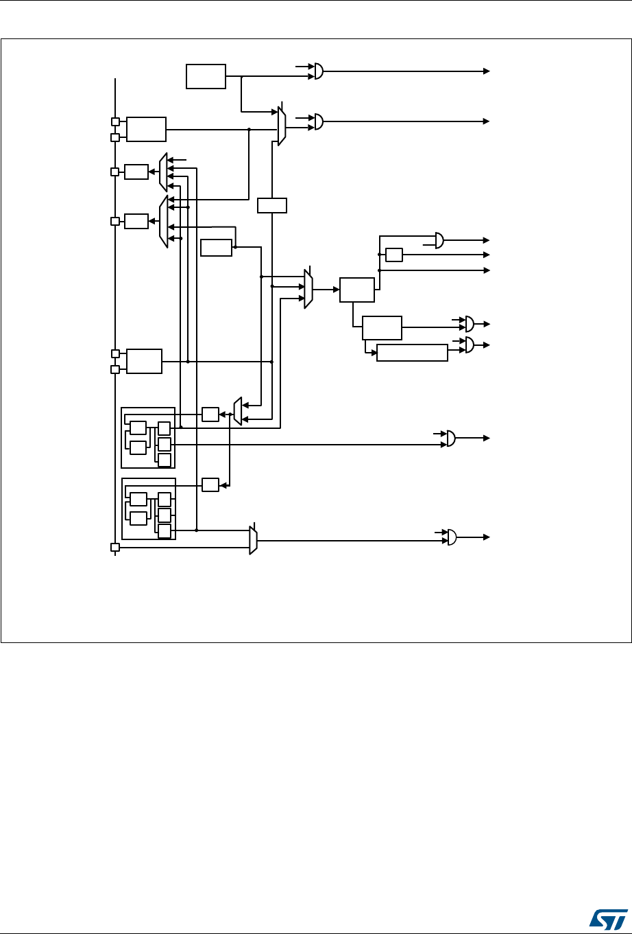
Reset and clock control (RCC) for STM32F411xC/E RM0383
90/836 DocID026448 Rev 1
Figure 12. Clock tree
1. For full details about the internal and external clock source characteristics, refer to the Electrical characteristics section in
the device datasheet.
069
$+%
35(6&
$3%[
35(6&
LI$3%[SUHVF [
HOVH[
/6(
3//,6&/.
)&/.&RUWH[
IUHHUXQQLQJFORFN
$3%[
FORFNV
$3%[
WLPHU
FORFNV
0+]
FORFNV
0&2
3HULSKHUDO
FORFNHQDEOH
0&2
26&B287
/6(26&
N+]
/6,5&
N+]
WRLQGHSHQGHQW
ZDWFKGRJ
/6(
/6,
WR57&
57&&/.
57&6(/>@
,:'*&/.
0+]
+6(26&
26&B,1
26&B287
+6,5&
0+]
3//&/.
+6,
+6,
+6(
6:
6<6&/.
0+]PD[
+&/.
WR$+%EXVFRUH
0HPRU\DQG'0$
0+]PD[
WR&RUWH[6\VWHPWLPHU
&ORFN
(QDEOH
3//&.
,6FORFNV
3HULSKHUDO
FORFNHQDEOH
:DWFKGRJ
HQDEOH
57&
HQDEOH
WR
6<6&/.
([WFORFN
,665&
+6(B57&
+6(
,6B&.,1
26&B,1
3HULSKHUDO
FORFNHQDEOH
3//,6
9&2
[1
3
4
5
3//
9&2
[1
3
4
5
0
0
3HULSKHUDO
FORFNHQDEOH
WR
WR

DocID026448 Rev 1 91/836
RM0383 Reset and clock control (RCC) for STM32F411xC/E
135
The clock controller provides a high degree of flexibility to the application in the choice of the
external crystal or the oscillator to run the core and peripherals at the highest frequency
and, guarantee the appropriate frequency for peripherals that need a specific clock like USB
OTG FS, I2S and SDIO.
Several prescalers are used to configure the AHB frequency, the high-speed APB (APB2)
and the low-speed APB (APB1) domains. The maximum frequency of the AHB domain is
100 MHz. The maximum allowed frequency of the high-speed APB2 domain is 100 MHz.
The maximum allowed frequency of the low-speed APB1 domain is 50 MHz
All peripheral clocks are derived from the system clock (SYSCLK) except for:
•The USB OTG FS clock (48 MHz) and the SDIO clock (≤ 48 MHz) which are coming
from a specific output of PLL (PLL48CLK)
•The I2S clock
To achieve high-quality audio performance, the I2S clock can be derived either from a
specific PLL (PLLI2S) or from an external clock mapped on the I2S_CKIN pin. For
more information about I2S clock frequency and precision, refer to Section 20.4.4:
Clock generator.
The RCC feeds the external clock of the Cortex System Timer (SysTick) with the AHB clock
(HCLK) divided by 8. The SysTick can work either with this clock or with the Cortex clock
(HCLK), configurable in the SysTick control and status register.
The timer clock frequencies for STM32F411xC/E are automatically set by hardware. There
are two cases:
1. If the APB prescaler is 1, the timer clock frequencies are set to the same frequency as
that of the APB domain to which the timers are connected.
2. Otherwise, they are set to twice (×2) the frequency of the APB domain to which the
timers are connected.
The timer clock frequencies are automatically set by hardware. There are two cases
depending on the value of TIMPRE bit in RCC_DCKCFGR register:
•If TIMPRE bit is reset:
If the APB prescaler is configured to a division factor of 1, the timer clock frequencies
(TIMxCLK) are set to HCLK. Otherwise, the timer clock frequencies are twice the
frequency of the APB domain to which the timers are connected: TIMxCLK = 2xPCLKx.
•If TIMPRE bit is set:
If the APB prescaler is configured to a division factor of 1 or 2, the timer clock
frequencies (TIMxCLK) are set to HCLK. Otherwise, the timer clock frequencies is four
times the frequency of the APB domain to which the timers are connected: TIMxCLK =
4xPCLKx.
FCLK acts as Cortex®-M4 with FPU free-running clock. For more details, refer to the
Cortex®-M4 with FPU technical reference manual.
6.2.1 HSE clock
The high speed external clock signal (HSE) can be generated from two possible clock
sources:
•HSE external crystal/ceramic resonator
•HSE external user clock
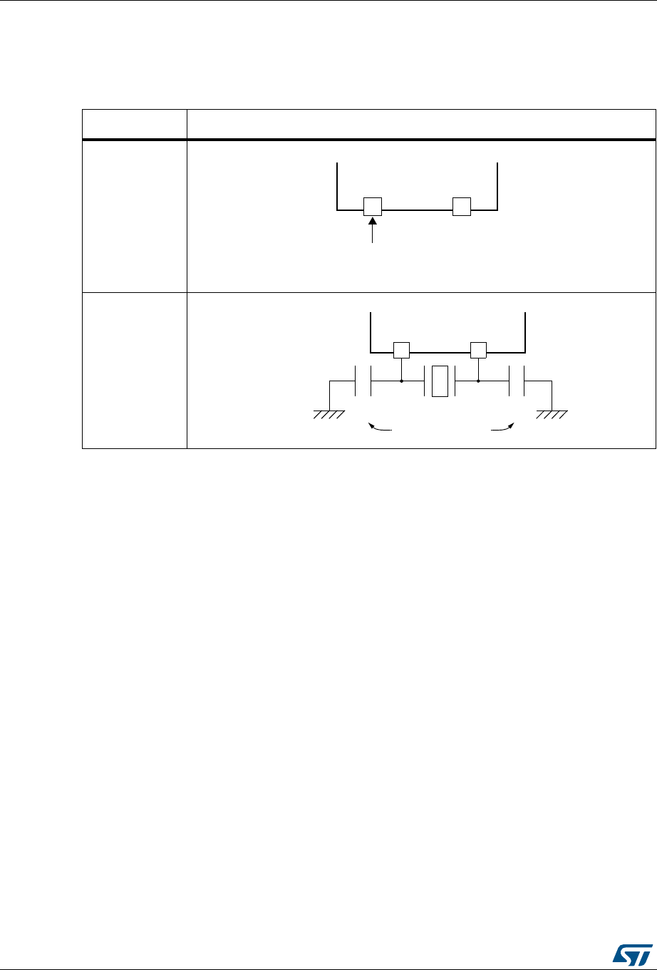
Reset and clock control (RCC) for STM32F411xC/E RM0383
92/836 DocID026448 Rev 1
The resonator and the load capacitors have to be placed as close as possible to the
oscillator pins in order to minimize output distortion and startup stabilization time. The
loading capacitance values must be adjusted according to the selected oscillator.
External source (HSE bypass)
In this mode, an external clock source must be provided. You select this mode by setting the
HSEBYP and HSEON bits in the RCC clock control register (RCC_CR). The external clock
signal (square, sinus or triangle) with ~50% duty cycle has to drive the OSC_IN pin while the
OSC_OUT pin should be left HI-Z. See Figure 13.
External crystal/ceramic resonator (HSE crystal)
The HSE has the advantage of producing a very accurate rate on the main clock.
The associated hardware configuration is shown in Figure 13. Refer to the electrical
characteristics section of the datasheet for more details.
The HSERDY flag in the RCC clock control register (RCC_CR) indicates if the high-speed
external oscillator is stable or not. At startup, the clock is not released until this bit is set by
hardware. An interrupt can be generated if enabled in the RCC clock interrupt register
(RCC_CIR).
The HSE Crystal can be switched on and off using the HSEON bit in the RCC clock control
register (RCC_CR).
6.2.2 HSI clock
The HSI clock signal is generated from an internal 16 MHz RC oscillator and can be used
directly as a system clock, or used as PLL input.
The HSI RC oscillator has the advantage of providing a clock source at low cost (no external
components). It also has a faster startup time than the HSE crystal oscillator however, even
Figure 13. HSE/ LSE clock sources
Hardware configuration
External clock
Crystal/ceramic
resonators
OSC_OUT
External
source
(HI-Z)
OSC_IN OSC_OUT
Load
capacitors
CL2
CL1

DocID026448 Rev 1 93/836
RM0383 Reset and clock control (RCC) for STM32F411xC/E
135
with calibration the frequency is less accurate than an external crystal oscillator or ceramic
resonator.
Calibration
RC oscillator frequencies can vary from one chip to another due to manufacturing process
variations, this is why each device is factory calibrated by ST for 1% accuracy at TA= 25 °C.
After reset, the factory calibration value is loaded in the HSICAL[7:0] bits in the RCC clock
control register (RCC_CR).
If the application is subject to voltage or temperature variations this may affect the RC
oscillator speed. You can trim the HSI frequency in the application using the HSITRIM[4:0]
bits in the RCC clock control register (RCC_CR).
The HSIRDY flag in the RCC clock control register (RCC_CR) indicates if the HSI RC is
stable or not. At startup, the HSI RC output clock is not released until this bit is set by
hardware.
The HSI RC can be switched on and off using the HSION bit in the RCC clock control
register (RCC_CR).
The HSI signal can also be used as a backup source (Auxiliary clock) if the HSE crystal
oscillator fails. Refer to Section 6.2.7: Clock security system (CSS) on page 94.
6.2.3 PLL configuration
The STM32F411xC/E devices feature two PLLs:
•A main PLL (PLL) clocked by the HSE or HSI oscillator and featuring two different
output clocks:
– The first output is used to generate the high speed system clock (up to 100 MHz)
– The second output is used to generate the clock for the USB OTG FS (48 MHz)
and the SDIO (≤ 50 MHz).
•A dedicated PLL (PLLI2S) used to generate an accurate clock to achieve high-quality
audio performance on the I2S interface.
Since the main-PLL configuration parameters cannot be changed once PLL is enabled, it is
recommended to configure PLL before enabling it (selection of the HSI or HSE oscillator as
PLL clock source, and configuration of division factors M, P, Q and multiplication factor N).
The PLLI2S uses the same input clock as the main PLL (HSI or HSE). However, the PLLI2S
has dedicated enable/disable and division factors configuration bits. Refer to Section 6.3.1:
RCC clock control register (RCC_CR), Section 6.3.2: RCC PLL configuration register
(RCC_PLLCFGR) and Section 6.3.20: RCC PLLI2S configuration register
(RCC_PLLI2SCFGR). Once the PLLI2S is enabled, the configuration parameters cannot be
changed.
The two PLLs are disabled by hardware when entering Stop and Standby modes, or when
an HSE failure occurs when HSE or PLL (clocked by HSE) are used as system clock. RCC
PLL configuration register (RCC_PLLCFGR) and RCC clock configuration register
(RCC_CFGR) can be used to configure PLL and PLLI2S, respectively.

Reset and clock control (RCC) for STM32F411xC/E RM0383
94/836 DocID026448 Rev 1
6.2.4 LSE clock
The LSE clock is generated using a 32.768kHz low speed external crystal or ceramic
resonator. It has the advantage providing a low-power but highly accurate clock source to
the real-time clock peripheral (RTC) for clock/calendar or other timing functions.
The LSE oscillator is switched on and off using the LSEON bit in RCC Backup domain
control register (RCC_BDCR).
The LSERDY flag in the RCC Backup domain control register (RCC_BDCR) indicates if the
LSE crystal is stable or not. At startup, the LSE crystal output clock signal is not released
until this bit is set by hardware. An interrupt can be generated if enabled in the RCC clock
interrupt register (RCC_CIR).
External source (LSE bypass)
In this mode, an external clock source must be provided. It must have a frequency up to
1 MHz. You select this mode by setting the LSEBYP and LSEON bits in the RCC Backup
domain control register (RCC_BDCR). The external clock signal (square, sinus or triangle)
with ~50% duty cycle has to drive the OSC32_IN pin while the OSC32_OUT pin should be
left HI-Z. See Figure 13.
6.2.5 LSI clock
The LSI RC acts as an low-power clock source that can be kept running in Stop and
Standby mode for the independent watchdog (IWDG) and Auto-wakeup unit (AWU). The
clock frequency is around 32 kHz. For more details, refer to the electrical characteristics
section of the datasheets.
The LSI RC can be switched on and off using the LSION bit in the RCC clock control &
status register (RCC_CSR).
The LSIRDY flag in the RCC clock control & status register (RCC_CSR) indicates if the low-
speed internal oscillator is stable or not. At startup, the clock is not released until this bit is
set by hardware. An interrupt can be generated if enabled in the RCC clock interrupt register
(RCC_CIR).
6.2.6 System clock (SYSCLK) selection
After a system reset, the HSI oscillator is selected as the system clock. When a clock source
is used directly or through PLL as the system clock, it is not possible to stop it.
A switch from one clock source to another occurs only if the target clock source is ready
(clock stable after startup delay or PLL locked). If a clock source that is not yet ready is
selected, the switch occurs when the clock source is ready. Status bits in the RCC clock
control register (RCC_CR) indicate which clock(s) is (are) ready and which clock is currently
used as the system clock.
6.2.7 Clock security system (CSS)
The clock security system can be activated by software. In this case, the clock detector is
enabled after the HSE oscillator startup delay, and disabled when this oscillator is stopped.
If a failure is detected on the HSE clock, this oscillator is automatically disabled, a clock
failure event is sent to the break inputs of advanced-control timer TIM1, and an interrupt is
generated to inform the software about the failure (clock security system interrupt CSSI),

DocID026448 Rev 1 95/836
RM0383 Reset and clock control (RCC) for STM32F411xC/E
135
allowing the MCU to perform rescue operations. The CSSI is linked to the Cortex®-M4 with
FPU NMI (non-maskable interrupt) exception vector.
Note: When the CSS is enabled, if the HSE clock happens to fail, the CSS generates an interrupt,
which causes the automatic generation of an NMI. The NMI is executed indefinitely unless
the CSS interrupt pending bit is cleared. As a consequence, the application has to clear the
CSS interrupt in the NMI ISR by setting the CSSC bit in the Clock interrupt register
(RCC_CIR).
If the HSE oscillator is used directly or indirectly as the system clock (indirectly meaning that
it is directly used as PLL input clock, and that PLL clock is the system clock) and a failure is
detected, then the system clock switches to the HSI oscillator and the HSE oscillator is
disabled.
If the HSE oscillator clock was the clock source of PLL used as the system clock when the
failure occurred, PLL is also disabled. In this case, if the PLLI2S was enabled, it is also
disabled when the HSE fails.
6.2.8 RTC/AWU clock
Once the RTCCLK clock source has been selected, the only possible way of modifying the
selection is to reset the power domain.
The RTCCLK clock source can be either the HSE 1 MHz (HSE divided by a programmable
prescaler), the LSE or the LSI clock. This is selected by programming the RTCSEL[1:0] bits
in the RCC Backup domain control register (RCC_BDCR) and the RTCPRE[4:0] bits in RCC
clock configuration register (RCC_CFGR). This selection cannot be modified without
resetting the Backup domain.
If the LSE is selected as the RTC clock, the RTC will work normally if the backup or the
system supply disappears. If the LSI is selected as the AWU clock, the AWU state is not
guaranteed if the system supply disappears. If the HSE oscillator divided by a value
between 2 and 31 is used as the RTC clock, the RTC state is not guaranteed if the backup
or the system supply disappears.
The LSE clock is in the Backup domain, whereas the HSE and LSI clocks are not. As a
consequence:
•If LSE is selected as the RTC clock:
– The RTC continues to work even if the VDD supply is switched off, provided the
VBAT supply is maintained.
•If LSI is selected as the Auto-wakeup unit (AWU) clock:
– The AWU state is not guaranteed if the VDD supply is powered off. Refer to
Section 6.2.5: LSI clock on page 94 for more details on LSI calibration.
•If the HSE clock is used as the RTC clock:
– The RTC state is not guaranteed if the VDD supply is powered off or if the internal
voltage regulator is powered off (removing power from the 1.2 V domain).
Note: To read the RTC calendar register when the APB1 clock frequency is less than seven times
the RTC clock frequency (fAPB1 < 7xfRTCLCK), the software must read the calendar time and
date registers twice. The data are correct if the second read access to RTC_TR gives the
same result than the first one. Otherwise a third read access must be performed.

Reset and clock control (RCC) for STM32F411xC/E RM0383
96/836 DocID026448 Rev 1
6.2.9 Watchdog clock
If the independent watchdog (IWDG) is started by either hardware option or software
access, the LSI oscillator is forced ON and cannot be disabled. After the LSI oscillator
temporization, the clock is provided to the IWDG.
6.2.10 Clock-out capability
Two microcontroller clock output (MCO) pins are available:
•MCO1
You can output four different clock sources onto the MCO1 pin (PA8) using the
configurable prescaler (from 1 to 5):
–HSI clock
– LSE clock
– HSE clock
– PLL clock
The desired clock source is selected using the MCO1PRE[2:0] and MCO1[1:0] bits in
the RCC clock configuration register (RCC_CFGR).
•MCO2
You can output four different clock sources onto the MCO2 pin (PC9) using the
configurable prescaler (from 1 to 5):
– HSE clock
– PLL clock
– System clock (SYSCLK)
– PLLI2S clock
The desired clock source is selected using the MCO2PRE[2:0] and MCO2 bits in the
RCC clock configuration register (RCC_CFGR).
For the different MCO pins, the corresponding GPIO port has to be programmed in alternate
function mode.
The selected clock to output onto MCO must not exceed 100 MHz (the maximum I/O
speed).
6.2.11 Internal/external clock measurement using TIM5/TIM11
It is possible to indirectly measure the frequencies of all on-board clock source generators
by means of the input capture of TIM5 channel4 and TIM11 channel1 as shown in Figure 14
and Figure 15.
Internal/external clock measurement using TIM5 channel4
TIM5 has an input multiplexer which allows choosing whether the input capture is triggered
by the I/O or by an internal clock. This selection is performed through the TI4_RMP [1:0] bits
in the TIM5_OR register.
The primary purpose of having the LSE connected to the channel4 input capture is to be
able to precisely measure the HSI (this requires to have the HSI used as the system clock
source). The number of HSI clock counts between consecutive edges of the LSE signal
provides a measurement of the internal clock period. Taking advantage of the high precision
of LSE crystals (typically a few tens of ppm) we can determine the internal clock frequency
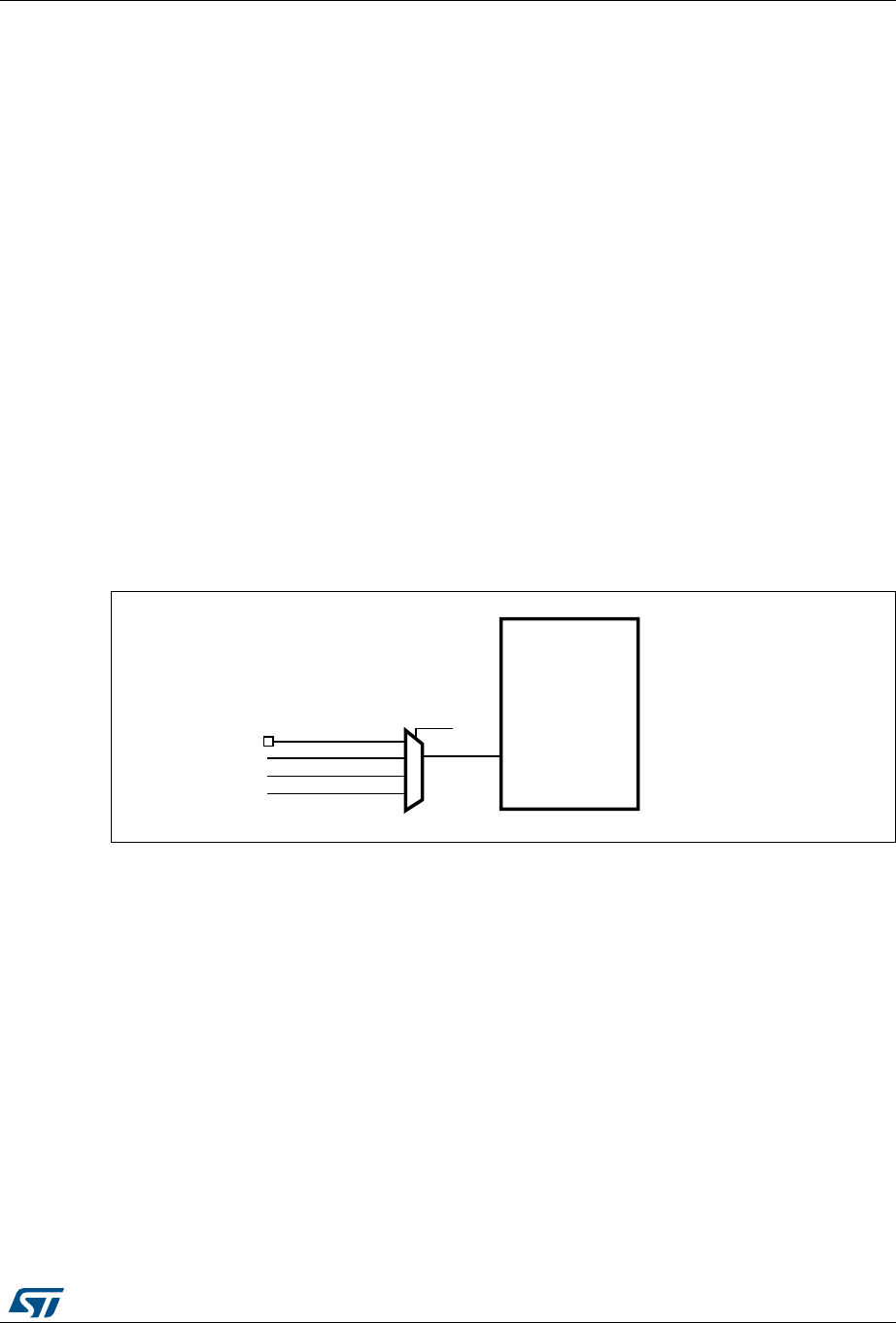
DocID026448 Rev 1 97/836
RM0383 Reset and clock control (RCC) for STM32F411xC/E
135
with the same resolution, and trim the source to compensate for manufacturing-process
and/or temperature- and voltage-related frequency deviations.
The HSI oscillator has dedicated, user-accessible calibration bits for this purpose.
The basic concept consists in providing a relative measurement (e.g. HSI/LSE ratio): the
precision is therefore tightly linked to the ratio between the two clock sources. The greater
the ratio, the better the measurement.
It is also possible to measure the LSI frequency: this is useful for applications that do not
have a crystal. The ultralow-power LSI oscillator has a large manufacturing process
deviation: by measuring it versus the HSI clock source, it is possible to determine its
frequency with the precision of the HSI. The measured value can be used to have more
accurate RTC time base timeouts (when LSI is used as the RTC clock source) and/or an
IWDG timeout with an acceptable accuracy.
Use the following procedure to measure the LSI frequency:
1. Enable the TIM5 timer and configure channel4 in Input capture mode.
2. Set the TI4_RMP bits in the TIM5_OR register to 0x01 to connect the LSI clock
internally to TIM5 channel4 input capture for calibration purposes.
3. Measure the LSI clock frequency using the TIM5 capture/compare 4 event or interrupt.
4. Use the measured LSI frequency to update the prescaler of the RTC depending on the
desired time base and/or to compute the IWDG timeout.
Figure 14. Frequency measurement with TIM5 in Input capture mode
Internal/external clock measurement using TIM11 channel1
TIM11 has an input multiplexer which allows choosing whether the input capture is triggered
by the I/O or by an internal clock. This selection is performed through TI1_RMP [1:0] bits in
the TIM11_OR register. The HSE_RTC clock (HSE divided by a programmable prescaler) is
connected to channel 1 input capture to have a rough indication of the external crystal
frequency. This requires that the HSI is the system clock source. This can be useful for
instance to ensure compliance with the IEC 60730/IEC 61335 standards which require to be
able to determine harmonic or subharmonic frequencies (–50/+100% deviations).
4)-
4)
4)?2-0;=
'0)/
24#?7AKE5P?)4
,3%
,3)
AI6

Reset and clock control (RCC) for STM32F411xC/E RM0383
98/836 DocID026448 Rev 1
Figure 15. Frequency measurement with TIM11 in Input capture mode
4)-
4)
4)?2-0;=
'0)/
(3%?24#-(Z
AI

DocID026448 Rev 1 99/836
RM0383 Reset and clock control (RCC) for STM32F411xC/E
135
6.3 RCC registers
Refer to Section 1.1: List of abbreviations for registers for a list of abbreviations used in
register descriptions.
6.3.1 RCC clock control register (RCC_CR)
Address offset: 0x00
Reset value: 0x0000 XX81 where X is undefined.
Access: no wait state, word, half-word and byte access
31 30 29 28 27 26 25 24 23 22 21 20 19 18 17 16
Reserved
PLLI2S
RDY
PLLI2S
ON PLLRDY PLLON
Reserved
CSS
ON
HSE
BYP
HSE
RDY HSE ON
r rw r rw rw rw r rw
15 14 13 12 11 10 9 8 7 6 5 4 3 2 1 0
HSICAL[7:0] HSITRIM[4:0] Res.
HSI
RDY HSION
rrrrrr r rrwrwrwrwrw rrw
Bits 31:28 Reserved, must be kept at reset value.
Bit 27 PLLI2SRDY: PLLI2S clock ready flag
Set by hardware to indicate that the PLLI2S is locked.
0: PLLI2S unlocked
1: PLLI2S locked
Bit 26 PLLI2SON: PLLI2S enable
Set and cleared by software to enable PLLI2S.
Cleared by hardware when entering Stop or Standby mode.
0: PLLI2S OFF
1: PLLI2S ON
Bit 25 PLLRDY: Main PLL (PLL) clock ready flag
Set by hardware to indicate that PLL is locked.
0: PLL unlocked
1: PLL locked
Bit 24 PLLON: Main PLL (PLL) enable
Set and cleared by software to enable PLL.
Cleared by hardware when entering Stop or Standby mode. This bit cannot be reset if PLL
clock is used as the system clock.
0: PLL OFF
1: PLL ON
Bits 23:20 Reserved, must be kept at reset value.
Bit 19 CSSON: Clock security system enable
Set and cleared by software to enable the clock security system. When CSSON is set, the
clock detector is enabled by hardware when the HSE oscillator is ready, and disabled by
hardware if an oscillator failure is detected.
0: Clock security system OFF (Clock detector OFF)
1: Clock security system ON (Clock detector ON if HSE oscillator is stable, OFF if not)

Reset and clock control (RCC) for STM32F411xC/E RM0383
100/836 DocID026448 Rev 1
Bit 18 HSEBYP: HSE clock bypass
Set and cleared by software to bypass the oscillator with an external clock. The external
clock must be enabled with the HSEON bit, to be used by the device.
The HSEBYP bit can be written only if the HSE oscillator is disabled.
0: HSE oscillator not bypassed
1: HSE oscillator bypassed with an external clock
Bit 17 HSERDY: HSE clock ready flag
Set by hardware to indicate that the HSE oscillator is stable. After the HSEON bit is cleared,
HSERDY goes low after 6 HSE oscillator clock cycles.
0: HSE oscillator not ready
1: HSE oscillator ready
Bit 16 HSEON: HSE clock enable
Set and cleared by software.
Cleared by hardware to stop the HSE oscillator when entering Stop or Standby mode. This
bit cannot be reset if the HSE oscillator is used directly or indirectly as the system clock.
0: HSE oscillator OFF
1: HSE oscillator ON
Bits 15:8 HSICAL[7:0]: Internal high-speed clock calibration
These bits are initialized automatically at startup.
Bits 7:3 HSITRIM[4:0]: Internal high-speed clock trimming
These bits provide an additional user-programmable trimming value that is added to the
HSICAL[7:0] bits. It can be programmed to adjust to variations in voltage and temperature
that influence the frequency of the internal HSI RC.
Bit 2 Reserved, must be kept at reset value.
Bit 1 HSIRDY: Internal high-speed clock ready flag
Set by hardware to indicate that the HSI oscillator is stable. After the HSION bit is cleared,
HSIRDY goes low after 6 HSI clock cycles.
0: HSI oscillator not ready
1: HSI oscillator ready
Bit 0 HSION: Internal high-speed clock enable
Set and cleared by software.
Set by hardware to force the HSI oscillator ON when leaving the Stop or Standby mode or in
case of a failure of the HSE oscillator used directly or indirectly as the system clock. This bit
cannot be cleared if the HSI is used directly or indirectly as the system clock.
0: HSI oscillator OFF
1: HSI oscillator ON

DocID026448 Rev 1 101/836
RM0383 Reset and clock control (RCC) for STM32F411xC/E
135
6.3.2 RCC PLL configuration register (RCC_PLLCFGR)
Address offset: 0x04
Reset value: 0x2400 3010
Access: no wait state, word, half-word and byte access.
This register is used to configure the PLL clock outputs according to the formulas:
•f(VCO clock) = f(PLL clock input) × (PLLN / PLLM)
•f(PLL general clock output) = f(VCO clock) / PLLP
•f(USB OTG FS, SDIO, RNG clock output) = f(VCO clock) / PLLQ
31 30 29 28 27 26 25 24 23 22 21 20 19 18 17 16
Reserved PLLQ3 PLLQ2 PLLQ1 PLLQ0 Reserv
ed
PLLSRC Reserved PLLP1 PLLP0
rw rw rw rw rw rw rw
15 14 13 12 11 10 9 8 7 6 5 4 3 2 1 0
Reserv
ed
PLLN PLLM5 PLLM4 PLLM3 PLLM2 PLLM1 PLLM0
rw rw rw rw rw rw rw rw rw rw rw rw rw rw rw
Bit 31:28 Reserved, must be kept at reset value.
Bits 27:24 PLLQ: Main PLL (PLL) division factor for USB OTG FS, SDIO and random number generator
clocks
Set and cleared by software to control the frequency of USB OTG FS clock, the random
number generator clock and the SDIO clock. These bits should be written only if PLL is
disabled.
Caution: The USB OTG FS requires a 48 MHz clock to work correctly. The SDIO and the
random number generator need a frequency lower than or equal to 48 MHz to work
correctly.
USB OTG FS clock frequency = VCO frequency / PLLQ with 2 ≤ PLLQ ≤ 15
0000: PLLQ = 0, wrong configuration
0001: PLLQ = 1, wrong configuration
0010: PLLQ = 2
0011: PLLQ = 3
0100: PLLQ = 4
...
1111: PLLQ = 15
Bit 23 Reserved, must be kept at reset value.
Bit 22 PLLSRC: Main PLL(PLL) and audio PLL (PLLI2S) entry clock source
Set and cleared by software to select PLL and PLLI2S clock source. This bit can be written
only when PLL and PLLI2S are disabled.
0: HSI clock selected as PLL and PLLI2S clock entry
1: HSE oscillator clock selected as PLL and PLLI2S clock entry
Bits 21:18 Reserved, must be kept at reset value.

Reset and clock control (RCC) for STM32F411xC/E RM0383
102/836 DocID026448 Rev 1
Bits 17:16 PLLP: Main PLL (PLL) division factor for main system clock
Set and cleared by software to control the frequency of the general PLL output clock. These
bits can be written only if PLL is disabled.
Caution: The software has to set these bits correctly not to exceed 100 MHz on this domain.
PLL output clock frequency = VCO frequency / PLLP with PLLP = 2, 4, 6, or 8
00: PLLP = 2
01: PLLP = 4
10: PLLP = 6
11: PLLP = 8
Bits 14:6 PLLN: Main PLL (PLL) multiplication factor for VCO
Set and cleared by software to control the multiplication factor of the VCO. These bits can
be written only when PLL is disabled. Only half-word and word accesses are allowed to
write these bits.
Caution: The software has to set these bits correctly to ensure that the VCO output
frequency is between 100 and 432 MHz. (check also Section 6.3.20: RCC PLLI2S
configuration register (RCC_PLLI2SCFGR))
VCO output frequency = VCO input frequency × PLLN with 50 ≤ PLLN ≤ 432
000000000: PLLN = 0, wrong configuration
000000001: PLLN = 1, wrong configuration
...
000110010: PLLN = 50
...
001100011: PLLN = 99
001100100: PLLN = 100
...
110110000: PLLN = 432
110110001: PLLN = 433, wrong configuration
...
111111111: PLLN = 511, wrong configuration
Note: Multiplication factors possible for VCO input frequency higher than 1 MHz but care
must be taken to fulfill the minimum VCO output frequency as specified above.
Bits 5:0 PLLM: Division factor for the main PLL (PLL) input clock
Set and cleared by software to divide the PLL and PLLI2S input clock before the VCO.
These bits can be written only when the PLL and PLLI2S are disabled.
Caution: The software has to set these bits correctly to ensure that the VCO input frequency
ranges from 1 to 2 MHz. It is recommended to select a frequency of 2 MHz to limit
PLL jitter.
VCO input frequency = PLL input clock frequency / PLLM with 2 ≤ PLLM ≤ 63
000000: PLLM = 0, wrong configuration
000001: PLLM = 1, wrong configuration
000010: PLLM = 2
000011: PLLM = 3
000100: PLLM = 4
...
111110: PLLM = 62
111111: PLLM = 63

DocID026448 Rev 1 103/836
RM0383 Reset and clock control (RCC) for STM32F411xC/E
135
6.3.3 RCC clock configuration register (RCC_CFGR)
Address offset: 0x08
Reset value: 0x0000 0000
Access: 0 ≤ wait state ≤ 2, word, half-word and byte access
1 or 2 wait states inserted only if the access occurs during a clock source switch.
31 30 29 28 27 26 25 24 23 22 21 20 19 18 17 16
MCO2 MCO2 PRE[2:0] MCO1 PRE[2:0] I2SSC
RMCO1 RTCPRE[4:0]
rw rw rw rw rw rw rw rw rw rw rw rw rw rw
15 14 13 12 11 10 9 8 7 6 5 4 3 2 1 0
PPRE2[2:0] PPRE1[2:0]
Reserved
HPRE[3:0] SWS1 SWS0 SW1 SW0
rw rw rw rw rw rw rw rw rw rw r r rw rw
Bits 31:30 MCO2[1:0]: Microcontroller clock output 2
Set and cleared by software. Clock source selection may generate glitches on MCO2. It is
highly recommended to configure these bits only after reset before enabling the external
oscillators and the PLLs.
00: System clock (SYSCLK) selected
01: PLLI2S clock selected
10: HSE oscillator clock selected
11: PLL clock selected
Bits 29:27 MCO2PRE: MCO2 prescaler
Set and cleared by software to configure the prescaler of the MCO2. Modification of this
prescaler may generate glitches on MCO2. It is highly recommended to change this
prescaler only after reset before enabling the external oscillators and the PLLs.
0xx: no division
100: division by 2
101: division by 3
110: division by 4
111: division by 5
Bits 26:24 MCO1PRE: MCO1 prescaler
Set and cleared by software to configure the prescaler of the MCO1. Modification of this
prescaler may generate glitches on MCO1. It is highly recommended to change this
prescaler only after reset before enabling the external oscillators and the PLL.
0xx: no division
100: division by 2
101: division by 3
110: division by 4
111: division by 5
Bit 23 I2SSRC: I2S clock selection
Set and cleared by software. This bit allows to select the I2S clock source between the
PLLI2S clock and the external clock. It is highly recommended to change this bit only after
reset and before enabling the I2S module.
0: PLLI2S clock used as I2S clock source
1: External clock mapped on the I2S_CKIN pin used as I2S clock source

Reset and clock control (RCC) for STM32F411xC/E RM0383
104/836 DocID026448 Rev 1
Bits 22:21 MCO1: Microcontroller clock output 1
Set and cleared by software. Clock source selection may generate glitches on MCO1. It is
highly recommended to configure these bits only after reset before enabling the external
oscillators and PLL.
00: HSI clock selected
01: LSE oscillator selected
10: HSE oscillator clock selected
11: PLL clock selected
Bits 20:16 RTCPRE: HSE division factor for RTC clock
Set and cleared by software to divide the HSE clock input clock to generate a 1 MHz clock
for RTC.
Caution: The software has to set these bits correctly to ensure that the clock supplied to the
RTC is 1 MHz. These bits must be configured if needed before selecting the RTC
clock source.
00000: no clock
00001: no clock
00010: HSE/2
00011: HSE/3
00100: HSE/4
...
11110: HSE/30
11111: HSE/31
Bits 15:13 PPRE2: APB high-speed prescaler (APB2)
Set and cleared by software to control APB high-speed clock division factor.
Caution: The software has to set these bits correctly not to exceed 84 MHz on this domain.
The clocks are divided with the new prescaler factor from 1 to 16 AHB cycles after
PPRE2 write.
0xx: AHB clock not divided
100: AHB clock divided by 2
101: AHB clock divided by 4
110: AHB clock divided by 8
111: AHB clock divided by 16
Bits 12:10 PPRE1: APB Low speed prescaler (APB1)
Set and cleared by software to control APB low-speed clock division factor.
Caution: The software has to set these bits correctly not to exceed 42 MHz on this domain.
The clocks are divided with the new prescaler factor from 1 to 16 AHB cycles after
PPRE1 write.
0xx: AHB clock not divided
100: AHB clock divided by 2
101: AHB clock divided by 4
110: AHB clock divided by 8
111: AHB clock divided by 16
Bits 9:8 Reserved, must be kept at reset value.

DocID026448 Rev 1 105/836
RM0383 Reset and clock control (RCC) for STM32F411xC/E
135
6.3.4 RCC clock interrupt register (RCC_CIR)
Address offset: 0x0C
Reset value: 0x0000 0000
Access: no wait state, word, half-word and byte access
Bits 7:4 HPRE: AHB prescaler
Set and cleared by software to control AHB clock division factor.
Caution: The clocks are divided with the new prescaler factor from 1 to 16 AHB cycles after
HPRE write.
Caution: The AHB clock frequency must be at least 25 MHz when the Ethernet is used.
0xxx: system clock not divided
1000: system clock divided by 2
1001: system clock divided by 4
1010: system clock divided by 8
1011: system clock divided by 16
1100: system clock divided by 64
1101: system clock divided by 128
1110: system clock divided by 256
1111: system clock divided by 512
Bits 3:2 SWS: System clock switch status
Set and cleared by hardware to indicate which clock source is used as the system clock.
00: HSI oscillator used as the system clock
01: HSE oscillator used as the system clock
10: PLL used as the system clock
11: not applicable
Bits 1:0 SW: System clock switch
Set and cleared by software to select the system clock source.
Set by hardware to force the HSI selection when leaving the Stop or Standby mode or in
case of failure of the HSE oscillator used directly or indirectly as the system clock.
00: HSI oscillator selected as system clock
01: HSE oscillator selected as system clock
10: PLL selected as system clock
11: not allowed
31 30 29 28 27 26 25 24 23 22 21 20 19 18 17 16
Reserved
CSSC
Reserved
PLLI2S
RDYC
PLL
RDYC
HSE
RDYC
HSI
RDYC
LSE
RDYC
LSI
RDYC
wwwwwww
15 14 13 12 11 10 9 8 7 6 5 4 3 2 1 0
Reserved
PLLI2S
RDYIE
PLL
RDYIE
HSE
RDYIE
HSI
RDYIE
LSE
RDYIE
LSI
RDYIE CSSF
Reserved
PLLI2S
RDYF
PLL
RDYF
HSE
RDYF
HSI
RDYF
LSE
RDYF
LSI
RDYF
rw rw rw rw rw rw r r r r r r r

Reset and clock control (RCC) for STM32F411xC/E RM0383
106/836 DocID026448 Rev 1
Bits 31:24 Reserved, must be kept at reset value.
Bit 23 CSSC: Clock security system interrupt clear
This bit is set by software to clear the CSSF flag.
0: No effect
1: Clear CSSF flag
Bit 22 Reserved, must be kept at reset value.
Bit 21 PLLI2SRDYC: PLLI2S ready interrupt clear
This bit is set by software to clear the PLLI2SRDYF flag.
0: No effect
1: PLLI2SRDYF cleared
Bit 20 PLLRDYC: Main PLL(PLL) ready interrupt clear
This bit is set by software to clear the PLLRDYF flag.
0: No effect
1: PLLRDYF cleared
Bit 19 HSERDYC: HSE ready interrupt clear
This bit is set by software to clear the HSERDYF flag.
0: No effect
1: HSERDYF cleared
Bit 18 HSIRDYC: HSI ready interrupt clear
This bit is set software to clear the HSIRDYF flag.
0: No effect
1: HSIRDYF cleared
Bit 17 LSERDYC: LSE ready interrupt clear
This bit is set by software to clear the LSERDYF flag.
0: No effect
1: LSERDYF cleared
Bit 16 LSIRDYC: LSI ready interrupt clear
This bit is set by software to clear the LSIRDYF flag.
0: No effect
1: LSIRDYF cleared
Bits 15:14 Reserved, must be kept at reset value.
Bit 13 PLLI2SRDYIE: PLLI2S ready interrupt enable
Set and cleared by software to enable/disable interrupt caused by PLLI2S lock.
0: PLLI2S lock interrupt disabled
1: PLLI2S lock interrupt enabled
Bit 12 PLLRDYIE: Main PLL (PLL) ready interrupt enable
Set and cleared by software to enable/disable interrupt caused by PLL lock.
0: PLL lock interrupt disabled
1: PLL lock interrupt enabled
Bit 11 HSERDYIE: HSE ready interrupt enable
Set and cleared by software to enable/disable interrupt caused by the HSE oscillator
stabilization.
0: HSE ready interrupt disabled
1: HSE ready interrupt enabled

DocID026448 Rev 1 107/836
RM0383 Reset and clock control (RCC) for STM32F411xC/E
135
Bit 10 HSIRDYIE: HSI ready interrupt enable
Set and cleared by software to enable/disable interrupt caused by the HSI oscillator
stabilization.
0: HSI ready interrupt disabled
1: HSI ready interrupt enabled
Bit 9 LSERDYIE: LSE ready interrupt enable
Set and cleared by software to enable/disable interrupt caused by the LSE oscillator
stabilization.
0: LSE ready interrupt disabled
1: LSE ready interrupt enabled
Bit 8 LSIRDYIE: LSI ready interrupt enable
Set and cleared by software to enable/disable interrupt caused by LSI oscillator
stabilization.
0: LSI ready interrupt disabled
1: LSI ready interrupt enabled
Bit 7 CSSF: Clock security system interrupt flag
Set by hardware when a failure is detected in the HSE oscillator.
Cleared by software setting the CSSC bit.
0: No clock security interrupt caused by HSE clock failure
1: Clock security interrupt caused by HSE clock failure
Bit 6 Reserved, must be kept at reset value.
Bit 5 PLLI2SRDYF: PLLI2S ready interrupt flag
Set by hardware when the PLLI2S locks and PLLI2SRDYDIE is set.
Cleared by software setting the PLLRI2SDYC bit.
0: No clock ready interrupt caused by PLLI2S lock
1: Clock ready interrupt caused by PLLI2S lock
Bit 4 PLLRDYF: Main PLL (PLL) ready interrupt flag
Set by hardware when PLL locks and PLLRDYDIE is set.
Cleared by software setting the PLLRDYC bit.
0: No clock ready interrupt caused by PLL lock
1: Clock ready interrupt caused by PLL lock
Bit 3 HSERDYF: HSE ready interrupt flag
Set by hardware when External High Speed clock becomes stable and HSERDYDIE is set.
Cleared by software setting the HSERDYC bit.
0: No clock ready interrupt caused by the HSE oscillator
1: Clock ready interrupt caused by the HSE oscillator
Bit 2 HSIRDYF: HSI ready interrupt flag
Set by hardware when the Internal High Speed clock becomes stable and HSIRDYDIE is
set.
Cleared by software setting the HSIRDYC bit.
0: No clock ready interrupt caused by the HSI oscillator
1: Clock ready interrupt caused by the HSI oscillator
Bit 1 LSERDYF: LSE ready interrupt flag
Set by hardware when the External Low Speed clock becomes stable and LSERDYDIE is
set.
Cleared by software setting the LSERDYC bit.
0: No clock ready interrupt caused by the LSE oscillator
1: Clock ready interrupt caused by the LSE oscillator

Reset and clock control (RCC) for STM32F411xC/E RM0383
108/836 DocID026448 Rev 1
6.3.5 RCC AHB1 peripheral reset register (RCC_AHB1RSTR)
Address offset: 0x10
Reset value: 0x0000 0000
Access: no wait state, word, half-word and byte access.
Bit 0 LSIRDYF: LSI ready interrupt flag
Set by hardware when the internal low speed clock becomes stable and LSIRDYDIE is set.
Cleared by software setting the LSIRDYC bit.
0: No clock ready interrupt caused by the LSI oscillator
1: Clock ready interrupt caused by the LSI oscillator
31 30 29 28 27 26 25 24 23 22 21 20 19 18 17 16
Reserved
DMA2
RST
DMA1
RST Reserved
rw rw
15 14 13 12 11 10 9 8 7 6 5 4 3 2 1 0
Reserved
CRCRST
Reserved
GPIOH
RST Reserved
GPIOE
RST
GPIOD
RST
GPIOC
RST
GPIOB
RST
GPIOA
RST
rw rw rw rw rw rw rw
Bits 31:23 Reserved, must be kept at reset value.
Bit 22 DMA2RST: DMA2 reset
Set and cleared by software.
0: does not reset DMA2
1: resets DMA2
Bit 21 DMA1RST: DMA1 reset
Set and cleared by software.
0: does not reset DMA1
1: resets DMA1
Bits 20:13 Reserved, must be kept at reset value.
Bit 12 CRCRST: CRC reset
Set and cleared by software.
0: does not reset CRC
1: resets CRC
Bits 11:8 Reserved, must be kept at reset value.
Bit 7 GPIOHRST: IO port H reset
Set and cleared by software.
0: does not reset IO port H
1: resets IO port H
Bits 6:5 Reserved, must be kept at reset value.
Bit 4 GPIOERST: IO port E reset
Set and cleared by software.
0: does not reset IO port E
1: resets IO port E

DocID026448 Rev 1 109/836
RM0383 Reset and clock control (RCC) for STM32F411xC/E
135
Bit 3 GPIODRST: IO port D reset
Set and cleared by software.
0: does not reset IO port D
1: resets IO port D
Bit 2 GPIOCRST: IO port C reset
Set and cleared by software.
0: does not reset IO port C
1: resets IO port C
Bit 1 GPIOBRST: IO port B reset
Set and cleared by software.
0: does not reset IO port B
1:resets IO port B
Bit 0 GPIOARST: IO port A reset
Set and cleared by software.
0: does not reset IO port A
1: resets IO port A

Reset and clock control (RCC) for STM32F411xC/E RM0383
110/836 DocID026448 Rev 1
6.3.6 RCC AHB2 peripheral reset register (RCC_AHB2RSTR)
Address offset: 0x14
Reset value: 0x0000 0000
Access: no wait state, word, half-word and byte access
6.3.7 RCC APB1 peripheral reset register for (RCC_APB1RSTR)
Address offset: 0x20
Reset value: 0x0000 0000
Access: no wait state, word, half-word and byte access.
31 30 29 28 27 26 25 24 23 22 21 20 19 18 17 16
Reserved
15 14 13 12 11 10 9 8 7 6 5 4 3 2 1 0
Reserved
OTGFS
RST Reserved
rw
Bits 31:8 Reserved, must be kept at reset value.
Bit 6:0 Reserved, must be kept at reset value.
31 30 29 28 27 26 25 24 23 22 21 20 19 18 17 16
Reserved
PWR
RST Reserved
I2C3
RST
I2C2
RST
I2C1
RST Reserved
USART2
RST Reser-
ved
rw rw rw rw rw
1514131211109876543210
SPI3
RST
SPI2
RST Reserved
WWDG
RST Reserved
TIM5
RST
TIM4
RST
TIM3
RST
TIM2
RST
rw rw rw rw rw rw rw
Bits 31:29 Reserved, must be kept at reset value.
Bit 28 PWRRST: Power interface reset
Set and cleared by software.
0: does not reset the power interface
1: resets the power interface
Bits 27:24 Reserved, must be kept at reset value.
Bit 23 I2C3RST: I2C3 reset
Set and cleared by software.
0: does not reset I2C3
1: resets I2C3
Bit 22 I2C2RST: I2C2 reset
Set and cleared by software.
0: does not reset I2C2
1: resets I2C2

DocID026448 Rev 1 111/836
RM0383 Reset and clock control (RCC) for STM32F411xC/E
135
Bit 21 I2C1RST: I2C1 reset
Set and cleared by software.
0: does not reset I2C1
1: resets I2C1
Bits 20:18 Reserved, must be kept at reset value.
Bit 17 USART2RST: USART2 reset
Set and cleared by software.
0: does not reset USART2
1: resets USART2
Bit 16 Reserved, must be kept at reset value.
Bit 15 SPI3RST: SPI3 reset
Set and cleared by software.
0: does not reset SPI3
1: resets SPI3
Bit 14 SPI2RST: SPI2 reset
Set and cleared by software.
0: does not reset SPI2
1: resets SPI2
Bits 13:12 Reserved, must be kept at reset value.
Bit 11 WWDGRST: Window watchdog reset
Set and cleared by software.
0: does not reset the window watchdog
1: resets the window watchdog
Bits 10:4 Reserved, must be kept at reset value.
Bit 3 TIM5RST: TIM5 reset
Set and cleared by software.
0: does not reset TIM5
1: resets TIM5
Bit 2 TIM4RST: TIM4 reset
Set and cleared by software.
0: does not reset TIM4
1: resets TIM4
Bit 1 TIM3RST: TIM3 reset
Set and cleared by software.
0: does not reset TIM3
1: resets TIM3
Bit 0 TIM2RST: TIM2 reset
Set and cleared by software.
0: does not reset TIM2
1: resets TIM2

Reset and clock control (RCC) for STM32F411xC/E RM0383
112/836 DocID026448 Rev 1
6.3.8 RCC APB2 peripheral reset register (RCC_APB2RSTR)
Address offset: 0x24
Reset value: 0x0000 0000
Access: no wait state, word, half-word and byte access.
31 30 29 28 27 26 25 24 23 22 21 20 19 18 17 16
Reserved
SPI5
RST Reser-
ved
TIM11
RST
TIM10
RST
TIM9
RST
rw rw rw rw
15 14 13 12 11 10 9 8 7 6 5 4 3 2 1 0
Reser-
ved
SYSCFG
RST
SPI4
RST
SPI1
RST
SDIO
RST Reserved
ADC1
RST Reserved
USART6
RST
USART1
RST Reserved
TIM1
RST
rw rw rw rw rw rw rw rw
Bits 31:21 Reserved, must be kept at reset value.
Bit 20 SPI5RST: SPI5RST
This bit is set and cleared by software.
0: does not reset SPI5
1: resets SPI5
Bit 19 Reserved, must be kept at reset value.
Bit 18 TIM11RST: TIM11 reset
Set and cleared by software.
0: does not reset TIM11
1: resets TIM11
Bit 17 TIM10RST: TIM10 reset
Set and cleared by software.
0: does not reset TIM10
1: resets TIM10
Bit 16 TIM9RST: TIM9 reset
Set and cleared by software.
0: does not reset TIM9
1: resets TIM9
Bit 15 Reserved, must be kept at reset value.
Bit 14 SYSCFGRST: System configuration controller reset
Set and cleared by software.
0: does not reset the System configuration controller
1: resets the System configuration controller
Bit 13 SPI4RST: SPI4 reset
Set and reset by software.
0: does not reset SPI4
1: resets SPI4
Bit 12 SPI1RST: SPI1 reset
Set and cleared by software.
0: does not reset SPI1
1: resets SPI1

DocID026448 Rev 1 113/836
RM0383 Reset and clock control (RCC) for STM32F411xC/E
135
Bit 11 SDIORST: SDIO reset
Set and cleared by software.
0: does not reset the SDIO module
1: resets the SDIO module
Bits 10:9 Reserved, must be kept at reset value.
Bit 8 ADC1RST: ADC interface reset
Set and cleared by software.
0: does not reset the ADC interface
1: resets the ADC interface
Bits 7:6 Reserved, must be kept at reset value.
Bit 5 USART6RST: USART6 reset
Set and cleared by software.
0: does not reset USART6
1: resets USART6
Bit 4 USART1RST: USART1 reset
Set and cleared by software.
0: does not reset USART1
1: resets USART1
Bits 3:1 Reserved, must be kept at reset value.
Bit 0 TIM1RST: TIM1 reset
Set and cleared by software.
0: does not reset TIM1
1: resets TIM1

Reset and clock control (RCC) for STM32F411xC/E RM0383
114/836 DocID026448 Rev 1
6.3.9 RCC AHB1 peripheral clock enable register (RCC_AHB1ENR)
Address offset: 0x30
Reset value: 0x0000 0000
Access: no wait state, word, half-word and byte access.
31 30 29 28 27 26 25 24 23 22 21 20 19 18 17 16
Reserved DMA2EN DMA1EN Reserved
rw rw
15 14 13 12 11 10 9 8 7 6 5 4 3 2 1 0
Reserved CRCEN Reserved
GPIOH
EN Reserved GPIOEEN GPIOD
EN
GPIOC
EN
GPIOB
EN
GPIOA
EN
rw rw rw rw rw rw rw
Bits 31:23 Reserved, must be kept at reset value.
Bit 22 DMA2EN: DMA2 clock enable
Set and cleared by software.
0: DMA2 clock disabled
1: DMA2 clock enabled
Bit 21 DMA1EN: DMA1 clock enable
Set and cleared by software.
0: DMA1 clock disabled
1: DMA1 clock enabled
Bits 20:13 Reserved, must be kept at reset value.
Bit 12 CRCEN: CRC clock enable
Set and cleared by software.
0: CRC clock disabled
1: CRC clock enabled
Bits 11:8 Reserved, must be kept at reset value.
Bit 7 GPIOHEN: IO port H clock enable
Set and reset by software.
0: IO port H clock disabled
1: IO port H clock enabled
Bits 6:5 Reserved, must be kept at reset value.
Bit 4 GPIOEEN: IO port E clock enable
Set and cleared by software.
0: IO port E clock disabled
1: IO port E clock enabled
Bit 3 GPIODEN: IO port D clock enable
Set and cleared by software.
0: IO port D clock disabled
1: IO port D clock enabled
Bit 2 GPIOCEN: IO port C clock enable
Set and cleared by software.
0: IO port C clock disabled
1: IO port C clock enabled

DocID026448 Rev 1 115/836
RM0383 Reset and clock control (RCC) for STM32F411xC/E
135
6.3.10 RCC AHB2 peripheral clock enable register (RCC_AHB2ENR)
Address offset: 0x34
Reset value: 0x0000 0000
Access: no wait state, word, half-word and byte access.
6.3.11 RCC APB1 peripheral clock enable register (RCC_APB1ENR)
Address offset: 0x40
Reset value: 0x0000 0000
Access: no wait state, word, half-word and byte access.
Bit 1 GPIOBEN: IO port B clock enable
Set and cleared by software.
0: IO port B clock disabled
1: IO port B clock enabled
Bit 0 GPIOAEN: IO port A clock enable
Set and cleared by software.
0: IO port A clock disabled
1: IO port A clock enabled
31 30 29 28 27 26 25 24 23 22 21 20 19 18 17 16
Reserved
15 14 13 12 11 10 9 8 7 6 5 4 3 2 1 0
Reserved
OTGFS
EN Reserved
rw
Bits 31:8 Reserved, must be kept at reset value.
Bit 7 OTGFSEN: USB OTG FS clock enable
Set and cleared by software.
0: USB OTG FS clock disabled
1: USB OTG FS clock enabled
Bits 6:0 Reserved, must be kept at reset value.
31 30 29 28 27 26 25 24 23 22 21 20 19 18 17 16
Reserved
PWR
EN Reserved
I2C3
EN
I2C2
EN
I2C1
EN Reserved
USART2
EN Reser-
ved
rw rw rw rw rw
15 14 13 12 11 10 9 8 7 6 5 4 3 2 1 0
SPI3
EN
SPI2
EN Reserved
WWDG
EN Reserved
TIM5
EN
TIM4
EN
TIM3
EN
TIM2
EN
rw rw rw rw rw rw rw

Reset and clock control (RCC) for STM32F411xC/E RM0383
116/836 DocID026448 Rev 1
Bits 31:29 Reserved, must be kept at reset value.
Bit 28 PWREN: Power interface clock enable
Set and cleared by software.
0: Power interface clock disabled
1: Power interface clock enable
Bits 27:24 Reserved, must be kept at reset value.
Bit 23 I2C3EN: I2C3 clock enable
Set and cleared by software.
0: I2C3 clock disabled
1: I2C3 clock enabled
Bit 22 I2C2EN: I2C2 clock enable
Set and cleared by software.
0: I2C2 clock disabled
1: I2C2 clock enabled
Bit 21 I2C1EN: I2C1 clock enable
Set and cleared by software.
0: I2C1 clock disabled
1: I2C1 clock enabled
Bits 20:18 Reserved, must be kept at reset value.
Bit 17 USART2EN: USART2 clock enable
Set and cleared by software.
0: USART2 clock disabled
1: USART2 clock enabled
Bit 16 Reserved, must be kept at reset value.
Bit 15 SPI3EN: SPI3 clock enable
Set and cleared by software.
0: SPI3 clock disabled
1: SPI3 clock enabled
Bit 14 SPI2EN: SPI2 clock enable
Set and cleared by software.
0: SPI2 clock disabled
1: SPI2 clock enabled
Bits 13:12 Reserved, must be kept at reset value.
Bit 11 WWDGEN: Window watchdog clock enable
Set and cleared by software.
0: Window watchdog clock disabled
1: Window watchdog clock enabled
Bits 10:4 Reserved, must be kept at reset value.
Bit 3 TIM5EN: TIM5 clock enable
Set and cleared by software.
0: TIM5 clock disabled
1: TIM5 clock enabled

DocID026448 Rev 1 117/836
RM0383 Reset and clock control (RCC) for STM32F411xC/E
135
Bit 2 TIM4EN: TIM4 clock enable
Set and cleared by software.
0: TIM4 clock disabled
1: TIM4 clock enabled
Bit 1 TIM3EN: TIM3 clock enable
Set and cleared by software.
0: TIM3 clock disabled
1: TIM3 clock enabled
Bit 0 TIM2EN: TIM2 clock enable
Set and cleared by software.
0: TIM2 clock disabled
1: TIM2 clock enabled

Reset and clock control (RCC) for STM32F411xC/E RM0383
118/836 DocID026448 Rev 1
6.3.12 RCC APB2 peripheral clock enable register
(RCC_APB2ENR)
Address offset: 0x44
Reset value: 0x0000 0000
Access: no wait state, word, half-word and byte access.
31 30 29 28 27 26 25 24 23 22 21 20 19 18 17 16
Reserved
SPI5EN Reser-
ved
TIM11
EN
TIM10
EN
TIM9
EN
rw rw rw rw
15 14 13 12 11 10 9 8 7 6 5 4 3 2 1 0
Reser-
ved
SYSCF
G EN SPI4EN SPI1
EN
SDIO
EN Reserved
ADC1
EN Reserved
USART6
EN
USART1
EN Reserved
TIM1
EN
rw rw rw rw rw rw rw rw
Bits 31:21 Reserved, must be kept at reset value.
Bit 20 SPI5EN:SPI5 clock enable
This bit is set and cleared by software
0: SPI5 clock disabled
1: SPI5 clock enabled
Bit 19 Reserved, must be kept at reset value.
Bit 18 TIM11EN: TIM11 clock enable
Set and cleared by software.
0: TIM11 clock disabled
1: TIM11 clock enabled
Bit 17 TIM10EN: TIM10 clock enable
Set and cleared by software.
0: TIM10 clock disabled
1: TIM10 clock enabled
Bit 16 TIM9EN: TIM9 clock enable
Set and cleared by software.
0: TIM9 clock disabled
1: TIM9 clock enabled
Bit 15 Reserved, must be kept at reset value.
Bit 14 SYSCFGEN: System configuration controller clock enable
Set and cleared by software.
0: System configuration controller clock disabled
1: System configuration controller clock enabled
Bit 13 SPI4EN: SPI4 clock enable
Set and reset by software.
0: SPI4 clock disabled
1: SPI4 clock enable
Bit 12 SPI1EN: SPI1 clock enable
Set and cleared by software.
0: SPI1 clock disabled
1: SPI1 clock enabled

DocID026448 Rev 1 119/836
RM0383 Reset and clock control (RCC) for STM32F411xC/E
135
Bit 11 SDIOEN: SDIO clock enable
Set and cleared by software.
0: SDIO module clock disabled
1: SDIO module clock enabled
Bit 8 ADC1EN: ADC1 clock enable
Set and cleared by software.
0: ADC1 clock disabled
1: ADC1 clock disabled
Bits 7:6 Reserved, must be kept at reset value.
Bit 5 USART6EN: USART6 clock enable
Set and cleared by software.
0: USART6 clock disabled
1: USART6 clock enabled
Bit 4 USART1EN: USART1 clock enable
Set and cleared by software.
0: USART1 clock disabled
1: USART1 clock enabled
Bits 3:1 Reserved, must be kept at reset value.
Bit 0 TIM1EN: TIM1 clock enable
Set and cleared by software.
0: TIM1 clock disabled
1: TIM1 clock enabled

Reset and clock control (RCC) for STM32F411xC/E RM0383
120/836 DocID026448 Rev 1
6.3.13 RCC AHB1 peripheral clock enable in low power mode register
(RCC_AHB1LPENR)
Address offset: 0x50
Reset value: 0x0061 900F
Access: no wait state, word, half-word and byte access.
31 30 29 28 27 26 25 24 23 22 21 20 19 18 17 16
Reserved
DMA2
LPEN
DMA1
LPEN Reserved
SRAM1
LPEN
rw rw rw
15 14 13 12 11 10 9 8 7 6 5 4 3 2 1 0
FLITF
LPEN Reserved
CRC
LPEN Reserved
GPIOH
LPEN Reserved
GPIOE
LPEN
GPIOD
LPEN
GPIOC
LPEN
GPIOB
LPEN
GPIOA
LPEN
rw rw rw rw rw rw rw rw
Bits 31:23 Reserved, must be kept at reset value.
Bit 22 DMA2LPEN: DMA2 clock enable during Sleep mode
Set and cleared by software.
0: DMA2 clock disabled during Sleep mode
1: DMA2 clock enabled during Sleep mode
Bit 21 DMA1LPEN: DMA1 clock enable during Sleep mode
Set and cleared by software.
0: DMA1 clock disabled during Sleep mode
1: DMA1 clock enabled during Sleep mode
Bits 20:17 Reserved, must be kept at reset value.
Bit 16 SRAM1LPEN: SRAM1interface clock enable during Sleep mode
Set and cleared by software.
0: SRAM1 interface clock disabled during Sleep mode
1: SRAM1 interface clock enabled during Sleep mode
Bit 15 FLITFLPEN: Flash interface clock enable during Sleep mode
Set and cleared by software.
0: Flash interface clock disabled during Sleep mode
1: Flash interface clock enabled during Sleep mode
Bits 14:13 Reserved, must be kept at reset value.
Bit 12 CRCLPEN: CRC clock enable during Sleep mode
Set and cleared by software.
0: CRC clock disabled during Sleep mode
1: CRC clock enabled during Sleep mode
Bits 11:8 Reserved, must be kept at reset value.
Bit 7 GPIOHLPEN: IO port H clock enable during sleep mode
Set and reset by software.
0: IO port H clock disabled during sleep mode
1: IO port H clock enabled during sleep mode
Bits 6:5 Reserved, must be kept at reset value.

DocID026448 Rev 1 121/836
RM0383 Reset and clock control (RCC) for STM32F411xC/E
135
6.3.14 RCC AHB2 peripheral clock enable in low power mode register
(RCC_AHB2LPENR)
Address offset: 0x54
Reset value: 0x0000 0080
Access: no wait state, word, half-word and byte access.
Bit 4 GPIOELPEN: IO port E clock enable during Sleep mode
Set and cleared by software.
0: IO port E clock disabled during Sleep mode
1: IO port E clock enabled during Sleep mode
Bit 3 GPIODLPEN: IO port D clock enable during Sleep mode
Set and cleared by software.
0: IO port D clock disabled during Sleep mode
1: IO port D clock enabled during Sleep mode
Bit 2 GPIOCLPEN: IO port C clock enable during Sleep mode
Set and cleared by software.
0: IO port C clock disabled during Sleep mode
1: IO port C clock enabled during Sleep mode
Bit 1 GPIOBLPEN: IO port B clock enable during Sleep mode
Set and cleared by software.
0: IO port B clock disabled during Sleep mode
1: IO port B clock enabled during Sleep mode
Bit 0 GPIOALPEN: IO port A clock enable during sleep mode
Set and cleared by software.
0: IO port A clock disabled during Sleep mode
1: IO port A clock enabled during Sleep mode
31 30 29 28 27 26 25 24 23 22 21 20 19 18 17 16
Reserved
15 14 13 12 11 10 9 8 7 6 5 4 3 2 1 0
Reserved
OTGFS
LPEN Reserved
rw
Bits 31:8 Reserved, must be kept at reset value.
Bit 7 OTGFSLPEN: USB OTG FS clock enable during Sleep mode
Set and cleared by software.
0: USB OTG FS clock disabled during Sleep mode
1: USB OTG FS clock enabled during Sleep mode
Bits 6:0 Reserved, must be kept at reset value.

Reset and clock control (RCC) for STM32F411xC/E RM0383
122/836 DocID026448 Rev 1
6.3.15 RCC APB1 peripheral clock enable in low power mode register
(RCC_APB1LPENR)
Address offset: 0x60
Reset value: 0x10E2 C80F
Access: no wait state, word, half-word and byte access.
31 30 29 28 27 26 25 24 23 22 21 20 19 18 17 16
Reserved
PWR
LPEN Reserved
I2C3
LPEN
I2C2
LPEN
I2C1
LPEN Reserved
USART2
LPEN Reser-
ved
rw rw rw rw rw
15 14 13 12 11 10 9 8 7 6 5 4 3 2 1 0
SPI3
LPEN
SPI2
LPEN Reserved
WWDG
LPEN Reserved
TIM5
LPEN
TIM4
LPEN
TIM3
LPEN
TIM2
LPEN
rw rw rw rw rw rw rw
Bits 31:29 Reserved, must be kept at reset value.
Bit 28 PWRLPEN: Power interface clock enable during Sleep mode
Set and cleared by software.
0: Power interface clock disabled during Sleep mode
1: Power interface clock enabled during Sleep mode
Bits 27:24 Reserved, must be kept at reset value.
Bit 23 I2C3LPEN: I2C3 clock enable during Sleep mode
Set and cleared by software.
0: I2C3 clock disabled during Sleep mode
1: I2C3 clock enabled during Sleep mode
Bit 22 I2C2LPEN: I2C2 clock enable during Sleep mode
Set and cleared by software.
0: I2C2 clock disabled during Sleep mode
1: I2C2 clock enabled during Sleep mode
Bit 21 I2C1LPEN: I2C1 clock enable during Sleep mode
Set and cleared by software.
0: I2C1 clock disabled during Sleep mode
1: I2C1 clock enabled during Sleep mode
Bits 20:18 Reserved, must be kept at reset value.
Bit 17 USART2LPEN: USART2 clock enable during Sleep mode
Set and cleared by software.
0: USART2 clock disabled during Sleep mode
1: USART2 clock enabled during Sleep mode
Bit 16 Reserved, must be kept at reset value.
Bit 15 SPI3LPEN: SPI3 clock enable during Sleep mode
Set and cleared by software.
0: SPI3 clock disabled during Sleep mode
1: SPI3 clock enabled during Sleep mode

DocID026448 Rev 1 123/836
RM0383 Reset and clock control (RCC) for STM32F411xC/E
135
Bit 14 SPI2LPEN: SPI2 clock enable during Sleep mode
Set and cleared by software.
0: SPI2 clock disabled during Sleep mode
1: SPI2 clock enabled during Sleep mode
Bits 13:12 Reserved, must be kept at reset value.
Bit 11 WWDGLPEN: Window watchdog clock enable during Sleep mode
Set and cleared by software.
0: Window watchdog clock disabled during sleep mode
1: Window watchdog clock enabled during sleep mode
Bits 10:4 Reserved, must be kept at reset value.
Bit 3 TIM5LPEN: TIM5 clock enable during Sleep mode
Set and cleared by software.
0: TIM5 clock disabled during Sleep mode
1: TIM5 clock enabled during Sleep mode
Bit 2 TIM4LPEN: TIM4 clock enable during Sleep mode
Set and cleared by software.
0: TIM4 clock disabled during Sleep mode
1: TIM4 clock enabled during Sleep mode
Bit 1 TIM3LPEN: TIM3 clock enable during Sleep mode
Set and cleared by software.
0: TIM3 clock disabled during Sleep mode
1: TIM3 clock enabled during Sleep mode
Bit 0 TIM2LPEN: TIM2 clock enable during Sleep mode
Set and cleared by software.
0: TIM2 clock disabled during Sleep mode
1: TIM2 clock enabled during Sleep mode

Reset and clock control (RCC) for STM32F411xC/E RM0383
124/836 DocID026448 Rev 1
6.3.16 RCC APB2 peripheral clock enabled in low power mode register
(RCC_APB2LPENR)
Address offset: 0x64
Reset value: 0x0007 7930
Access: no wait state, word, half-word and byte access.
31 30 29 28 27 26 25 24 23 22 21 20 19 18 17 16
Reserved
SPI5
LPEN Reser-
ved
TIM11
LPEN
TIM10
LPEN
TIM9
LPEN
rw rw rw rw
15 14 13 12 11 10 9 8 7 6 5 4 3 2 1 0
Reser-
ved
SYSC
FG
LPEN
SPI4LP
EN
SPI1
LPEN
SDIO
LPEN Reserved
ADC1
LPEN Reserved
USART6
LPEN
USART1
LPEN Reserved
TIM1
LPEN
rw rw rw rw rw rw rw rw
Bits 31:21 Reserved, must be kept at reset value.
Bit 20 SPI5LPEN: SPI5 clock enable during Sleep mode
This bit is set and cleared by software
0: SPI5 clock disabled during Sleep mode
1: SPI5 clock enabled during Sleep mode
Bit 19 Reserved, must be kept at reset value.
Bit 18 TIM11LPEN: TIM11 clock enable during Sleep mode
Set and cleared by software.
0: TIM11 clock disabled during Sleep mode
1: TIM11 clock enabled during Sleep mode
Bit 17 TIM10LPEN: TIM10 clock enable during Sleep mode
Set and cleared by software.
0: TIM10 clock disabled during Sleep mode
1: TIM10 clock enabled during Sleep mode
Bit 16 TIM9LPEN: TIM9 clock enable during sleep mode
Set and cleared by software.
0: TIM9 clock disabled during Sleep mode
1: TIM9 clock enabled during Sleep mode
Bit 15 Reserved, must be kept at reset value.
Bit 14 SYSCFGLPEN: System configuration controller clock enable during Sleep mode
Set and cleared by software.
0: System configuration controller clock disabled during Sleep mode
1: System configuration controller clock enabled during Sleep mode
Bit 13 SPI4LPEN: SPI4 clock enable during sleep mode
Set and reset by software.
0: SPI4 clock disabled during sleep mode
1: SPI4 clock enabled during sleep mode

DocID026448 Rev 1 125/836
RM0383 Reset and clock control (RCC) for STM32F411xC/E
135
Bit 12 SPI1LPEN: SPI1 clock enable during Sleep mode
Set and cleared by software.
0: SPI1 clock disabled during Sleep mode
1: SPI1 clock enabled during Sleep mode
Bit 11 SDIOLPEN: SDIO clock enable during Sleep mode
Set and cleared by software.
0: SDIO module clock disabled during Sleep mode
1: SDIO module clock enabled during Sleep mode
Bits 10:9 Reserved, must be kept at reset value.
Bit 8 ADC1LPEN: ADC1 clock enable during Sleep mode
Set and cleared by software.
0: ADC1 clock disabled during Sleep mode
1: ADC1 clock disabled during Sleep mode
Bits 7:6 Reserved, must be kept at reset value.
Bit 5 USART6LPEN: USART6 clock enable during Sleep mode
Set and cleared by software.
0: USART6 clock disabled during Sleep mode
1: USART6 clock enabled during Sleep mode
Bit 4 USART1LPEN: USART1 clock enable during Sleep mode
Set and cleared by software.
0: USART1 clock disabled during Sleep mode
1: USART1 clock enabled during Sleep mode
Bits 3:1 Reserved, must be kept at reset value.
Bit 0 TIM1LPEN: TIM1 clock enable during Sleep mode
Set and cleared by software.
0: TIM1 clock disabled during Sleep mode
1: TIM1 clock enabled during Sleep mode
Reset and clock control (RCC) for STM32F411xC/E RM0383
126/836 DocID026448 Rev 1
6.3.17 RCC Backup domain control register (RCC_BDCR)
Address offset: 0x70
Reset value: 0x0000 0000, reset by Backup domain reset.
Access: 0 ≤ wait state ≤ 3, word, half-word and byte access
Wait states are inserted in case of successive accesses to this register.
The LSEON, LSEBYP, RTCSEL and RTCEN bits in the RCC Backup domain control
register (RCC_BDCR) are in the Backup domain. As a result, after Reset, these bits are
write-protected and the DBP bit in the PWR power control register (PWR_CR) has to be set
before these can be modified. Refer to Section 5.1.2 on page 70 for further information.
These bits are only reset after a Backup domain Reset (see Section 6.1.3: Backup domain
reset). Any internal or external Reset will not have any effect on these bits.
31 30 29 28 27 26 25 24 23 22 21 20 19 18 17 16
Reserved BDRST
rw
15 14 13 12 11 10 9 8 7 6 5 4 3 2 1 0
RTCEN Reserved RTCSEL[1:0] Reserved LSEMO
D
LSEBYP LSERDY LSEON
rw rw rw rw r rw
Bits 31:17 Reserved, must be kept at reset value.
Bit 16 BDRST: Backup domain software reset
Set and cleared by software.
0: Reset not activated
1: Resets the entire Backup domain
Bit 15 RTCEN: RTC clock enable
Set and cleared by software.
0: RTC clock disabled
1: RTC clock enabled
Bits 14:10 Reserved, must be kept at reset value.
Bits 9:8 RTCSEL[1:0]: RTC clock source selection
Set by software to select the clock source for the RTC. Once the RTC clock source has been
selected, it cannot be changed anymore unless the Backup domain is reset. The BDRST bit
can be used to reset them.
00: No clock
01: LSE oscillator clock used as the RTC clock
10: LSI oscillator clock used as the RTC clock
11: HSE oscillator clock divided by a programmable prescaler (selection through the
RTCPRE[4:0] bits in the RCC clock configuration register (RCC_CFGR)) used as the RTC
clock
Bits 7:4 Reserved, must be kept at reset value.
Bit 3 LSEMOD: External low-speed oscillator bypass
Set and reset by software to select crystal mode for low speed oscillator. Two power modes
are available.
0: LSE oscillator “low power” mode selection
1: LSE oscillator “high drive” mode selection
DocID026448 Rev 1 127/836
RM0383 Reset and clock control (RCC) for STM32F411xC/E
135
6.3.18 RCC clock control & status register (RCC_CSR)
Address offset: 0x74
Reset value: 0x0E00 0000, reset by system reset, except reset flags by power reset only.
Access: 0 ≤ wait state ≤ 3, word, half-word and byte access
Wait states are inserted in case of successive accesses to this register.
Bit 2 LSEBYP: External low-speed oscillator bypass
Set and cleared by software to bypass oscillator in debug mode. This bit can be written only
when the LSE clock is disabled.
0: LSE oscillator not bypassed
1: LSE oscillator bypassed
Bit 1 LSERDY: External low-speed oscillator ready
Set and cleared by hardware to indicate when the external 32 kHz oscillator is stable. After
the LSEON bit is cleared, LSERDY goes low after 6 external low-speed oscillator clock
cycles.
0: LSE clock not ready
1: LSE clock ready
Bit 0 LSEON: External low-speed oscillator enable
Set and cleared by software.
0: LSE clock OFF
1: LSE clock ON
31 30 29 28 27 26 25 24 23 22 21 20 19 18 17 16
LPWR
RSTF
WWDG
RSTF
IWDG
RSTF
SFT
RSTF
POR
RSTF
PIN
RSTF
BORRS
TF RMVF
Reserved
rw rw rw rw rw rw rw rw
15 14 13 12 11 10 9 8 7 6 5 4 3 2 1 0
Reserved
LSIRDY LSION
rrw
Bit 31 LPWRRSTF: Low-power reset flag
Set by hardware when a Low-power management reset occurs.
Cleared by writing to the RMVF bit.
0: No Low-power management reset occurred
1: Low-power management reset occurred
For further information on Low-power management reset, refer to Low-power management
reset.
Bit 30 WWDGRSTF: Window watchdog reset flag
Set by hardware when a window watchdog reset occurs.
Cleared by writing to the RMVF bit.
0: No window watchdog reset occurred
1: Window watchdog reset occurred
Bit 29 IWDGRSTF: Independent watchdog reset flag
Set by hardware when an independent watchdog reset from VDD domain occurs.
Cleared by writing to the RMVF bit.
0: No watchdog reset occurred
1: Watchdog reset occurred

Reset and clock control (RCC) for STM32F411xC/E RM0383
128/836 DocID026448 Rev 1
Bit 28 SFTRSTF: Software reset flag
Set by hardware when a software reset occurs.
Cleared by writing to the RMVF bit.
0: No software reset occurred
1: Software reset occurred
Bit 27 PORRSTF: POR/PDR reset flag
Set by hardware when a POR/PDR reset occurs.
Cleared by writing to the RMVF bit.
0: No POR/PDR reset occurred
1: POR/PDR reset occurred
Bit 26 PINRSTF: PIN reset flag
Set by hardware when a reset from the NRST pin occurs.
Cleared by writing to the RMVF bit.
0: No reset from NRST pin occurred
1: Reset from NRST pin occurred
Bit 25 BORRSTF: BOR reset flag
Cleared by software by writing the RMVF bit.
Set by hardware when a POR/PDR or BOR reset occurs.
0: No POR/PDR or BOR reset occurred
1: POR/PDR or BOR reset occurred
Bit 24 RMVF: Remove reset flag
Set by software to clear the reset flags.
0: No effect
1: Clear the reset flags
Bits 23:2 Reserved, must be kept at reset value.
Bit 1 LSIRDY: Internal low-speed oscillator ready
Set and cleared by hardware to indicate when the internal RC 40 kHz oscillator is stable.
After the LSION bit is cleared, LSIRDY goes low after 3 LSI clock cycles.
0: LSI RC oscillator not ready
1: LSI RC oscillator ready
Bit 0 LSION: Internal low-speed oscillator enable
Set and cleared by software.
0: LSI RC oscillator OFF
1: LSI RC oscillator ON

DocID026448 Rev 1 129/836
RM0383 Reset and clock control (RCC) for STM32F411xC/E
135
6.3.19 RCC spread spectrum clock generation register (RCC_SSCGR)
Address offset: 0x80
Reset value: 0x0000 0000
Access: no wait state, word, half-word and byte access.
The spread spectrum clock generation is available only for the main PLL.
The RCC_SSCGR register must be written either before the main PLL is enabled or after
the main PLL disabled.
Note: For full details about PLL spread spectrum clock generation (SSCG) characteristics, refer to
the “Electrical characteristics” section in your device datasheet.
31 30 29 28 27 26 25 24 23 22 21 20 19 18 17 16
SSCG
EN
SPR
EAD
SEL Reserved INCSTEP
rw rw rw rw rw rw rw rw rw rw rw rw rw
1514131211109 8 765432 1 0
INCSTEP MODPER
rw rw rw rw rw rw rw rw rw rw rw rw rw rw rw rw
Bit 31 SSCGEN: Spread spectrum modulation enable
Set and cleared by software.
0: Spread spectrum modulation DISABLE. (To write after clearing CR[24]=PLLON bit)
1: Spread spectrum modulation ENABLE. (To write before setting CR[24]=PLLON bit)
Bit 30 SPREADSEL: Spread Select
Set and cleared by software.
To write before to set CR[24]=PLLON bit.
0: Center spread
1: Down spread
Bits 29:28 Reserved, must be kept at reset value.
Bits 27:13 INCSTEP: Incrementation step
Set and cleared by software. To write before setting CR[24]=PLLON bit.
Configuration input for modulation profile amplitude.
Bits 12:0 MODPER: Modulation period
Set and cleared by software. To write before setting CR[24]=PLLON bit.
Configuration input for modulation profile period.

Reset and clock control (RCC) for STM32F411xC/E RM0383
130/836 DocID026448 Rev 1
6.3.20 RCC PLLI2S configuration register (RCC_PLLI2SCFGR)
Address offset: 0x84
Reset value: 0x2400 3000
Access: no wait state, word, half-word and byte access.
This register is used to configure the PLLI2S clock outputs according to the formulas:
•f(VCO clock) = f(PLLI2S clock input) × (PLLI2SN / PLLI2SM)
•f(PLL I2S clock output) = f(VCO clock) / PLLI2SR
31 30 29 28 27 26 25 24 23 22 21 20 19 18 17 16
Reserved
PLLI2S
R2
PLLI2S
R1
PLLI2S
R0 Reserved
rw rw rw
15 14 13 12 11 10 9 8 7 6 5 4 3 2 1 0
Reserved
PLLI2SN[8:0] PLLI2SM[5:0]
rw rw rw rw rw rw rw rw rw rw rw rw rw rw rw
Bit 31 Reserved, must be kept at reset value.
Bits 30:28 PLLI2SR: PLLI2S division factor for I2S clocks
Set and cleared by software to control the I2S clock frequency. These bits should be written
only if the PLLI2S is disabled. The factor must be chosen in accordance with the prescaler
values inside the I2S peripherals, to reach 0.3% error when using standard crystals and 0%
error with audio crystals. For more information about I2S clock frequency and precision,
refer to Section 20.4.4: Clock generator in the I2S chapter.
Caution: The I2Ss requires a frequency lower than or equal to 192 MHz to work correctly.
I2S clock frequency = VCO frequency / PLLR with 2 ≤ PLLR ≤ 7
000: PLLR = 0, wrong configuration
001: PLLR = 1, wrong configuration
010: PLLR = 2
...
111: PLLR = 7

DocID026448 Rev 1 131/836
RM0383 Reset and clock control (RCC) for STM32F411xC/E
135
Bits 27:15 Reserved, must be kept at reset value.
Bits 14:6 PLLI2SN: PLLI2S multiplication factor for VCO
Set and cleared by software to control the multiplication factor of the VCO. These bits can
be written only when the PLLI2S is disabled. Only half-word and word accesses are allowed
to write these bits.
Caution: The software has to set these bits correctly to ensure that the VCO output
frequency is between 100 and 432 MHz. With VCO input frequency ranges from 1
to 2 MHz (refer to Figure 13 and divider factor M of the RCC PLL configuration
register (RCC_PLLCFGR))
VCO output frequency = VCO input frequency × PLLI2SN with 50 ≤ PLLI2SN ≤ 432
000000000: PLLI2SN = 0, wrong configuration
000000001: PLLI2SN = 1, wrong configuration
...
001100010: PLLI2SN = 50
...
001100011: PLLI2SN = 99
001100100: PLLI2SN = 100
001100101: PLLI2SN = 101
001100110: PLLI2SN = 102
...
110110000: PLLI2SN = 432
110110000: PLLI2SN = 433, wrong configuration
...
111111111: PLLI2SN = 511, wrong configuration
Note: Between 50 and 99 multiplication factors are possible for VCO input frequency higher
than 1 MHz. However care must be taken to fulfill the minimum VCO output frequency
as specified above.
Bits 5:0 PLLI2SM: Division factor for the main PLL (PLL) and audio PLL (PLLI2S) input clock
Set and cleared by software to divide the PLL and PLLI2S input clock before the VCO.
These bits can be written only when the PLL and PLLI2S are disabled.
Caution: The software has to set these bits correctly to ensure that the VCO input frequency
ranges from 1 to 2 MHz.It is recommended to select a frequency of 2 MHz to limit
PLL jitter.
VCO input frequency = PLL input clock frequency / PLLI2SM with 2≤ PLLI2SM ≤ 63
000000: PLLI2SM = 0, wrong configuration
000001: PLLI2SM = 1, wrong configuration...
000010: PLLI2SM = 2
000011: PLLI2SM = 3
000100: PLLI2SM = 4
.......
111110: PLLI2SM = 62
111111: PLLI2SM = 63

Reset and clock control (RCC) for STM32F411xC/E RM0383
132/836 DocID026448 Rev 1
6.3.21 RCC Dedicated Clocks Configuration Register (RCC_DCKCFGR)
Address offset: 0x8C
Reset value: 0x0000 0000
Access: no wait state, word, half-word and byte access.
31 30 29 28 27 26 25 24 23 22 21 20 19 18 17 16
Reserved TIMPRE Reserved
rw
15 14 13 12 11 10 9 8 7 6 5 4 3 2 1 0
Reserved
Bits 31:25 Reserved, must be kept at reset value.
Bit 24 TIMPRE: Timers clocks prescalers selection
Set and reset by software to control the clock frequency of all the timers connected to APB1
and APB2 domain.
0: If the APB prescaler (PPRE1, PPRE2 in the RCC_CFGR register) is configured to a
division factor of 1, TIMxCLK = HCKL . Otherwise, the timer clock frequencies are set to
twice to the frequency of the APB domain to which the timers are connected:
TIMxCLK = 2xPCLKx.
1:If the APB prescaler ( PPRE1, PPRE2 in the RCC_CFGR register) is configured to a
division factor of 1 or 2, TIMxCLK = HCKL. Otherwise, the timer clock frequencies are set to
four times to the frequency of the APB domain to which the timers are connected:
TIMxCLK = 4xPCLKx.
Bits 23: 0 Reserved, must be kept at reset value.
DocID026448 Rev 1 133/836
RM0383 Reset and clock control (RCC) for STM32F411xC/E
135
6.3.22 RCC register map
Table 21 gives the register map and reset values
Table 21. RCC register map and reset values for STM32F411xC/E
Addr.
offset Register
name
31
30
29
28
27
26
25
24
23
22
21
20
19
18
17
16
15
14
13
12
11
10
9
8
7
6
5
4
3
2
1
0
0x00 RCC_CR Reserved
PLL I2SRDY
PLL I2SON
PLL RDY
PLL ON
Reserved
CSSON
HSEBYP
HSERDY
HSEON
HSICAL 7
HSICAL 6
HSICAL 5
HSICAL 4
HSICAL 3
HSICAL 2
HSICAL 1
HSICAL 0
HSITRIM 4
HSITRIM 3
HSITRIM 2
HSITRIM 1
HSITRIM 0
Reserved
HSIRDY
HSION
0x04 RCC_
PLLCFGR Reserved
PLLQ 3
PLLQ 2
PLLQ 1
PLLQ 0
Reserved
PLLSRC
Reserved
PLLP 1
PLLP 0
Reserved
PLLN 8
PLLN 7
PLLN 6
PLLN 5
PLLN 4
PLLN 3
PLLN 2
PLLN 1
PLLN 0
PLLM 5
PLLM 4
PLLM 3
PLLM 2
PLLM 1
PLLM 0
0x08 RCC_CFGR
MCO2 1
MCO2 0
MCO2PRE2
MCO2PRE1
MCO2PRE0
MCO1PRE2
MCO1PRE1
MCO1PRE0
I2SSRC
MCO1 1
MCO1 0
RTCPRE 4
RTCPRE 3
RTCPRE 2
RTCPRE 1
RTCPRE 0
PPRE2 2
PPRE2 1
PPRE2 0
PPRE1 2
PPRE1 1
PPRE1 0
Reserved
HPRE 3
HPRE 2
HPRE 1
HPRE 0
SWS 1
SWS 0
SW 1
SW 0
0x0C RCC_CIR Reserved
CSSC
Reserved
PLLI2SRDYC
PLLRDYC
HSERDYC
HSIRDYC
LSERDYC
LSIRDYC
Reserved
PLLI2SRDYIE
PLLRDYIE
HSERDYIE
HSIRDYIE
LSERDYIE
LSIRDYIE
CSSF
Reserved
PLLI2SRDYF
PLLRDYF
HSERDYF
HSIRDYF
LSERDYF
LSIRDYF
0x10 RCC_
AHB1RSTR Reserved
DMA2RST
DMA1RST
Reserved
CRCRST
Reserved
GPIOHRST
Reser
ved
GPIOERST
GPIODRST
GPIOCRST
GPIOBRST
GPIOARST
0x14 RCC_
AHB2RSTR Reserved
OTGFSRST
Reserved
0x18 Reserved Reserved
0x1C Reserved Reserved
0x20 RCC_
APB1RSTR
Reserved
PWRRST
Reserved
I2C3RST
I2C2RST
I2C1RST
Reserved
USART2RST
Reserved
SPI3RST
SPI2RST
Reserved
WWDGRST
Reserved
TIM5RST
TIM4RST
TIM3RST
TIM2RST
0x24 RCC_
APB2RSTR Reserved
SPI5RST
Reserved
TIM11RST
TIM10RST
TIM9RST
Reserved
SYSCFGRST
SP45RST
SPI1RST
SDIORST
Reserved
ADC1RST
Reserved
USART6RST
USART1RST
Reserved
TIM1RST
0x28 Reserved Reserved
0x2C Reserved Reserved
0x30 RCC_
AHB1ENR Reserved
DMA2EN
DMA1EN
Reserved
CRCEN
Reserved
GPIOHEN
Reserved
GPIOEEN
GPIODEN
GPIOCEN
GPIOBEN
GPIOAEN
0x34 RCC_
AHB2ENR Reserved
OTGFSEN
Reserved
0x38 Reserved Reserved
0x3C Reserved Reserved
Reset and clock control (RCC) for STM32F411xC/E RM0383
134/836 DocID026448 Rev 1
0x40 RCC_APB1E
NR
Reserved
PWREN
Reserved
I2C3EN
I2C2EN
I2C1EN
Reserved
USART2EN
Reserved
SPI3EN
SPI2EN
Reserved
WWDGEN
Reserved
TIM5EN
TIM4EN
TIM3EN
TIM2EN
0x44 RCC_APB2E
NR Reserved
SPI5EN
Reserved
TIM11EN
TIM10EN
TIM9EN
Reserved
SYSCFGEN
SPI4EN
SPI1EN
SDIOEN
Reserved
ADC1EN
Reserved
USART6EN
USART1EN
Reserved
TIM1EN
0x48 Reserved Reserved
0x4C Reserved Reserved
0x50 RCC_AHB1L
PENR Reserved
DMA2LPEN
DMA1LPEN
Reserved
SRAM1LPEN
FLITFLPEN
Reserved
CRCLPEN
Reserved
GPIOHLPEN
Reserved
GPIOELPEN
GPIODLPEN
GPIOCLPEN
GPIOBLPEN
GPIOALPEN
0x54 RCC_AHB2L
PENR Reserved
OTGFSLPEN
Reserved
0x58 Reserved Reserved
0x5C Reserved Reserved
0x60 RCC_APB1L
PENR
Reserved
PWRLPEN
Reserved
I2C3LPEN
I2C2LPEN
I2C1LPEN
Reserved
USART2LPEN
Reserved
SPI3LPEN
SPI2LPEN
Reserved
WWDGLPEN
Reserved
TIM5LPEN
TIM4LPEN
TIM3LPEN
TIM2LPEN
0x64 RCC_APB2L
PENR Reserved
SPI5LPEN
Reserved
TIM11LPEN
TIM10LPEN
TIM9LPEN
Reserved
SYSCFGLPEN
SPI4LPEN
SPI1LPEN
SDIOLPEN
Reserved
ADC1LPEN
Reserved
USART6LPEN
USART1LPEN
Reserved
TIM1LPEN
0x68 Reserved Reserved
0x6C Reserved Reserved
0x70 RCC_BDCR Reserved
BDRST
RTCEN
Reserved
RTCSEL 1
RTCSEL 0
Reserved
LSEMOD
LSEBYP
LSERDY
LSEON
0x74 RCC_CSR
LPWRRSTF
WWDGRSTF
WDGRSTF
SFTRSTF
PORRSTF
PADRSTF
BORRSTF
RMVF
Reserved
LSIRDY
LSION
0x78 Reserved Reserved
0x7C Reserved Reserved
0x80 RCC_SSCGR
SSCGEN
SPREADSEL
Reserved
INCSTEP MODPER
0x84 RCC_PLLI2S
CFGR
Reserved
PLLI2SRx Reserved PLLI2SNx PLLI2SMx
Table 21. RCC register map and reset values for STM32F411xC/E (continued)
Addr.
offset Register
name
31
30
29
28
27
26
25
24
23
22
21
20
19
18
17
16
15
14
13
12
11
10
9
8
7
6
5
4
3
2
1
0

DocID026448 Rev 1 135/836
RM0383 Reset and clock control (RCC) for STM32F411xC/E
135
Refer to Table 3 on page 41 for the register boundary addresses.
0x88 Reserved
0x8C RCC_DCKCF
GR Reserved
TIMPRE
Reserved
Table 21. RCC register map and reset values for STM32F411xC/E (continued)
Addr.
offset Register
name
31
30
29
28
27
26
25
24
23
22
21
20
19
18
17
16
15
14
13
12
11
10
9
8
7
6
5
4
3
2
1
0

System configuration controller (SYSCFG) RM0383
136/836 DocID026448 Rev 1
7 System configuration controller (SYSCFG)
The system configuration controller is mainly used to remap the memory accessible in the
code area and manage the external interrupt line connection to the GPIOs.
7.1 I/O compensation cell
By default the I/O compensation cell is not used. However when the I/O output buffer speed
is configured in 50 MHz or 100 MHz mode, it is recommended to use the compensation cell
for slew rate control on I/O tf(IO)out)/tr(IO)out commutation to reduce the I/O noise on power
supply.
When the compensation cell is enabled, a READY flag is set to indicate that the
compensation cell is ready and can be used. The I/O compensation cell can be used only
when the supply voltage ranges from 2.4 to 3.6 V.
7.2 SYSCFG registers
7.2.1 SYSCFG memory remap register (SYSCFG_MEMRMP)
This register is used for specific configurations on memory remap:
•Two bits are used to configure the type of memory accessible at address 0x0000 0000.
These bits are used to select the physical remap by software and so, bypass the BOOT
pins.
•After reset these bits take the value selected by the BOOT pins. When booting from
main Flash memory with BOOT0 pin set to 0 this register takes the value 0x00.
In remap mode, the CPU can access the external memory via ICode bus instead of System
bus which boosts up the performance.
Address offset: 0x00
Reset value: 0x0000 000X (X is the memory mode selected by the BOOT pins)
)
31 30 29 28 27 26 25 24 23 22 21 20 19 18 17 16
Reserved
1514131211109876543210
Reserved
MEM_MODE
rw rw

DocID026448 Rev 1 137/836
RM0383 System configuration controller (SYSCFG)
141
7.2.2 SYSCFG peripheral mode configuration register (SYSCFG_PMC)
Address offset: 0x04
Reset value: 0x0000 0000
7.2.3 SYSCFG external interrupt configuration register 1
(SYSCFG_EXTICR1)
Address offset: 0x08
Reset value: 0x0000 0000
Bits 31:2 Reserved, must be kept at reset value.
Bits 1:0 MEM_MODE: Memory mapping selection
Set and cleared by software. This bit controls the memory internal mapping at
address 0x0000 0000. After reset these bits take the value selected by the Boot
pins .
00: Main Flash memory mapped at 0x0000 0000
01: System Flash memory mapped at 0x0000 0000
11: Embedded SRAM mapped at 0x0000 0000
Note: Refer to Section 2.3: Memory map for details about the memory mapping at
address 0x0000 0000.
31 30 29 28 27 26 25 24 23 22 21 20 19 18 17 16
Reserved
ADC1D
C2
rw
15 14 13 12 11 10 9 8 7 6 5 4 3 2 1 0
Reserved
Bits 31:17 Reserved, must be kept at reset value.
Bit 16 ADCxDC2:
0: No effect.
1: Refer to AN4073 on how to use this bit .
Note: These bits can be set only if the following conditions are met:
- ADC clock higher or equal to 30 MHz.
- Only one ADCxDC2 bit must be selected if ADC conversions do not start
at the same time and the sampling times differ.
- These bits must not be set when the ADCDC1 bit is set in PWR_CR
register.
Bits 15:0 Reserved, must be kept at reset value.
31 30 29 28 27 26 25 24 23 22 21 20 19 18 17 16
Reserved
1514131211109876543210
EXTI3[3:0] EXTI2[3:0] EXTI1[3:0] EXTI0[3:0]
rw rw rw rw rw rw rw rw rw rw rw rw rw rw rw rw
System configuration controller (SYSCFG) RM0383
138/836 DocID026448 Rev 1
7.2.4 SYSCFG external interrupt configuration register 2
(SYSCFG_EXTICR2)
Address offset: 0x0C
Reset value: 0x0000 0000
Bits 31:16 Reserved, must be kept at reset value.
Bits 15:0 EXTIx[3:0]: EXTI x configuration (x = 0 to 3)
These bits are written by software to select the source input for the EXTIx
external interrupt.
0000: PA[x] pin
0001: PB[x] pin
0010: PC[x] pin
0011: PD[x] pin
0100: PE[x] pin
0101: Reserved
0110: Reserved
0111: PH[x] pin
31 30 29 28 27 26 25 24 23 22 21 20 19 18 17 16
Reserved
1514131211109876543210
EXTI7[3:0] EXTI6[3:0] EXTI5[3:0] EXTI4[3:0]
rw rw rw rw rw rw rw rw rw rw rw rw rw rw rw rw
Bits 31:16 Reserved, must be kept at reset value.
Bits 15:0 EXTIx[3:0]: EXTI x configuration (x = 4 to 7)
These bits are written by software to select the source input for the EXTIx
external interrupt.
0000: PA[x] pin
0001: PB[x] pin
0010: PC[x] pin
0011: PD[x] pin
0100: PE[x] pin
0101: Reserved
0110: Reserved
0111: PH[x] pin

DocID026448 Rev 1 139/836
RM0383 System configuration controller (SYSCFG)
141
7.2.5 SYSCFG external interrupt configuration register 3
(SYSCFG_EXTICR3)
Address offset: 0x10
Reset value: 0x0000 0000
7.2.6 SYSCFG external interrupt configuration register 4
(SYSCFG_EXTICR4)
Address offset: 0x14
Reset value: 0x0000 0000
31 30 29 28 27 26 25 24 23 22 21 20 19 18 17 16
Reserved
1514131211109876543210
EXTI11[3:0] EXTI10[3:0] EXTI9[3:0] EXTI8[3:0]
rw rw rw rw rw rw rw rw rw rw rw rw rw rw rw rw
Bits 31:16 Reserved, must be kept at reset value.
Bits 15:0 EXTIx[3:0]: EXTI x configuration (x = 8 to 11)
These bits are written by software to select the source input for the EXTIx external
interrupt.
0000: PA[x] pin
0001: PB[x] pin
0010: PC[x] pin
0011: PD[x] pin
0100: PE[x] pin
0101: Reserved
0110: Reserved
0111: PH[x] pin
31 30 29 28 27 26 25 24 23 22 21 20 19 18 17 16
Reserved
1514131211109876543210
EXTI15[3:0] EXTI14[3:0] EXTI13[3:0] EXTI12[3:0]
rw rw rw rw rw rw rw rw rw rw rw rw rw rw rw rw
Bits 31:16 Reserved, must be kept at reset value.
Bits 15:0 EXTIx[3:0]: EXTI x configuration (x = 12 to 15)
These bits are written by software to select the source input for the EXTIx external
interrupt.
0000: PA[x] pin
0001: PB[x] pin
0010: PC[x] pin
0011: PD[x] pin
0100: PE[x] pin
0101: Reserved
0110: Reserved
0111: PH[x] pin

System configuration controller (SYSCFG) RM0383
140/836 DocID026448 Rev 1
7.2.7 Compensation cell control register (SYSCFG_CMPCR)
Address offset: 0x20
Reset value: 0x0000 0000
31 30 29 28 27 26 25 24 23 22 21 20 19 18 17 16
Reserved
1514131211109 8 7 654321 0
Reserved
READY
Reserved CMP_PD
rrw
Bits 31:9 Reserved, must be kept at reset value.
Bit 8 READY: Compensation cell ready flag
0: I/O compensation cell not ready
1: O compensation cell ready
Bits 7:2 Reserved, must be kept at reset value.
Bit 0 CMP_PD: Compensation cell power-down
0: I/O compensation cell power-down mode
1: I/O compensation cell enabled
DocID026448 Rev 1 141/836
RM0383 System configuration controller (SYSCFG)
141
7.2.8 SYSCFG register map
The following table gives the SYSCFG register map and the reset values.
Refer to Table 3 on page 41 for the register boundary addresses.
Table 22. SYSCFG register map and reset values
Offset Register
31
30
29
28
27
26
25
24
23
22
21
20
19
18
17
16
15
14
13
12
11
10
9
8
7
6
5
4
3
2
1
0
0x00
SYSCFG_
MEMRMP Reserved
MEM_MODE
Reset value xx
0x04 SYSCFG_PMC Reserved
ADC1DC2
Reserved
Reset value 0
0x08 SYSCFG_EXTICR1 Reserved EXTI3[3:0] EXTI2[3:0] EXTI1[3:0] EXTI0[3:0]
Reset value 0000000000000000
0x0C SYSCFG_EXTICR2 Reserved EXTI7[3:0] EXTI6[3:0] EXTI5[3:0] EXTI4[3:0]
Reset value 0000000000000000
0x10 SYSCFG_EXTICR3 Reserved EXTI11[3:0] EXTI10[3:0] EXTI9[3:0] EXTI8[3:0]
Reset value 0000000000000000
0x14 SYSCFG_EXTICR4 Reserved EXTI15[3:0] EXTI14[3:0] EXTI13[3:0] EXTI12[3:0]
Reset value 0000000000000000
0x20 SYSCFG_CMPCR Reserved
READY
Reserved
CMP_PD
Reset value 00

General-purpose I/Os (GPIO) RM0383
142/836 DocID026448 Rev 1
8 General-purpose I/Os (GPIO)
GPIO F/G/H/I/J/K (except GPIOH0 and GPIOH1) are not available in STM32F411xC/E.
8.1 GPIO introduction
Each general-purpose I/O port has four 32-bit configuration registers (GPIOx_MODER,
GPIOx_OTYPER, GPIOx_OSPEEDR and GPIOx_PUPDR), two 32-bit data registers
(GPIOx_IDR and GPIOx_ODR), a 32-bit set/reset register (GPIOx_BSRR), a 32-bit locking
register (GPIOx_LCKR) and two 32-bit alternate function selection register (GPIOx_AFRH
and GPIOx_AFRL).
8.2 GPIO main features
•Up to 16 I/Os under control
•Output states: push-pull or open drain + pull-up/down
•Output data from output data register (GPIOx_ODR) or peripheral (alternate function
output)
•Speed selection for each I/O
•Input states: floating, pull-up/down, analog
•Input data to input data register (GPIOx_IDR) or peripheral (alternate function input)
•Bit set and reset register (GPIOx_BSRR) for bitwise write access to GPIOx_ODR
•Locking mechanism (GPIOx_LCKR) provided to freeze the I/O configuration
•Analog function
•Alternate function input/output selection registers (at most 16 AFs per I/O)
•Fast toggle capable of changing every two clock cycles
•Highly flexible pin multiplexing allows the use of I/O pins as GPIOs or as one of several
peripheral functions
8.3 GPIO functional description
Subject to the specific hardware characteristics of each I/O port listed in the datasheet, each
port bit of the general-purpose I/O (GPIO) ports can be individually configured by software in
several modes:
•Input floating
•Input pull-up
•Input-pull-down
•Analog
•Output open-drain with pull-up or pull-down capability
•Output push-pull with pull-up or pull-down capability
•Alternate function push-pull with pull-up or pull-down capability
•Alternate function open-drain with pull-up or pull-down capability
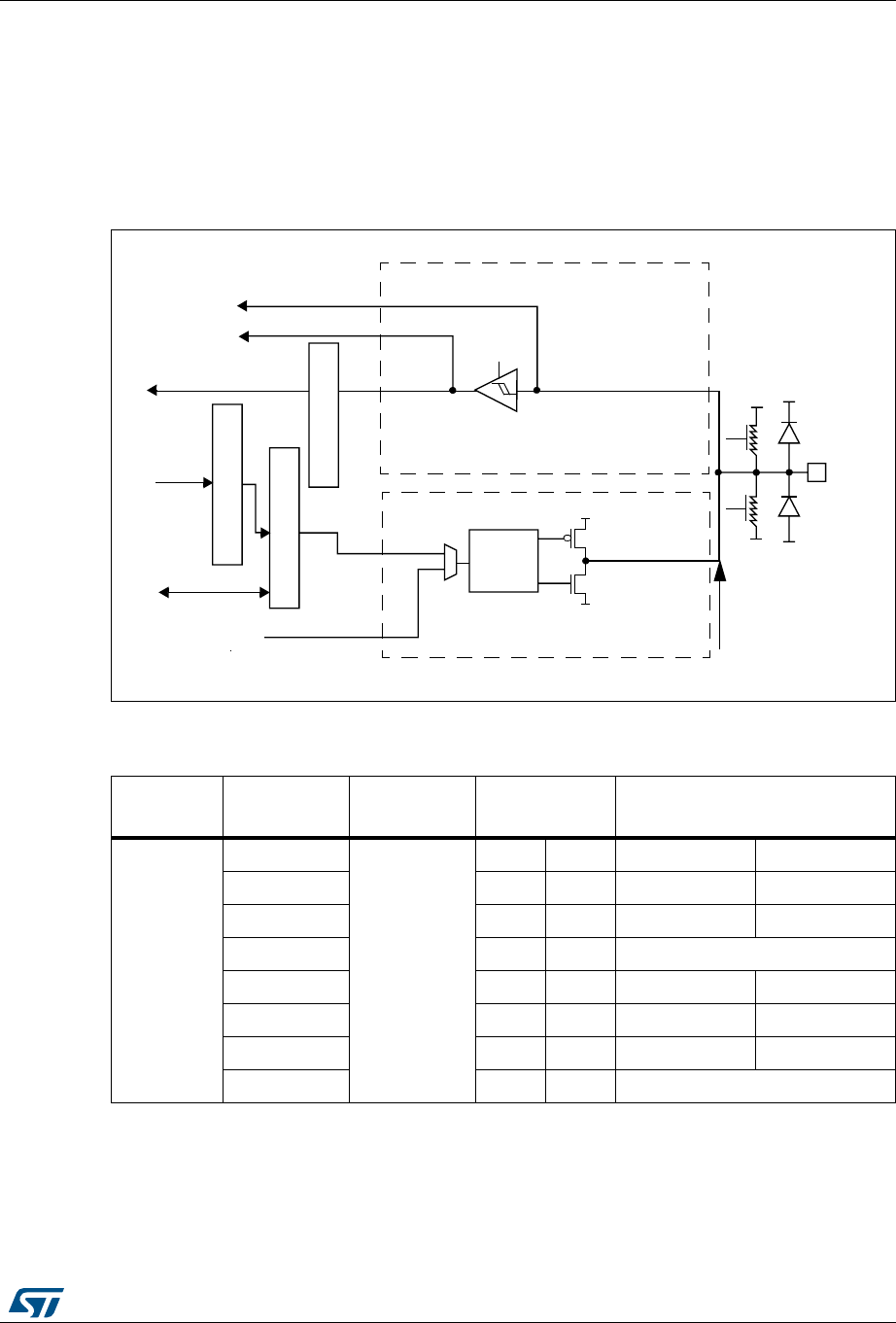
DocID026448 Rev 1 143/836
RM0383 General-purpose I/Os (GPIO)
161
Each I/O port bit is freely programmable, however the I/O port registers have to be
accessed as 32-bit words, half-words or bytes. The purpose of the GPIOx_BSRR register is
to allow atomic read/modify accesses to any of the GPIO registers. In this way, there is no
risk of an IRQ occurring between the read and the modify access.
show the basic structure of a 5 V tolerant I/O port bit. Table 26 gives the possible port bit
configurations.
Figure 16. Basic structure of a five-volt tolerant I/O port bit
1. VDD_FT is a potential specific to five-volt tolerant I/Os and different from VDD.
Table 23. Port bit configuration table(1)
MODER(i)
[1:0] OTYPER(i) OSPEEDR(i)
[B:A] PUPDR(i)
[1:0] I/O configuration
01
0
SPEED
[B:A]
0 0 GP output PP
0 0 1 GP output PP + PU
0 1 0 GP output PP + PD
0 1 1 Reserved
1 0 0 GP output OD
1 0 1 GP output OD + PU
1 1 0 GP output OD + PD
1 1 1 Reserved (GP output OD)
!LTERNATEFUNCTIONOUTPUT
!LTERNATEFUNCTIONINPUT
0USHPULL
OPENDRAINOR
DISABLED
/UTPUTDATAREGISTER
2EADWRITE
&ROMONCHIP
PERIPHERAL
4OONCHIP
PERIPHERAL
/UTPUT
CONTROL
!NALOG
ONOFF 0ULL
0ULL
ONOFF
)/PIN
6$$
6$$
633
633
44,3CHMITT
TRIGGER
633
6$$?&4
0ROTECTION
DIODE
0ROTECTION
DIODE
ONOFF
)NPUTDRIVER
/UTPUTDRIVER
DOWN
UP
0-/3
.-/3
2EAD
"ITSETRESETREGISTERS
7RITE
!NALOG
)NPUTDATAREGISTER
AIB
General-purpose I/Os (GPIO) RM0383
144/836 DocID026448 Rev 1
8.3.1 General-purpose I/O (GPIO)
During and just after reset, the alternate functions are not active and the I/O ports are
configured in input floating mode.
The debug pins are in AF pull-up/pull-down after reset:
•PA15: JTDI in pull-up
•PA14: JTCK/SWCLK in pull-down
•PA13: JTMS/SWDAT in pull-up
•PB4: NJTRST in pull-up
•PB3: JTDO in floating state
When the pin is configured as output, the value written to the output data register
(GPIOx_ODR) is output on the I/O pin. It is possible to use the output driver in push-pull
mode or open-drain mode (only the N-MOS is activated when 0 is output).
The input data register (GPIOx_IDR) captures the data present on the I/O pin at every AHB
clock cycle.
All GPIO pins have weak internal pull-up and pull-down resistors, which can be activated or
not depending on the value in the GPIOx_PUPDR register.
10
0
SPEED
[B:A]
0 0 AF PP
0 0 1 AF PP + PU
0 1 0 AF PP + PD
0 1 1 Reserved
100AFOD
101AFOD + PU
110AFOD + PD
1 1 1 Reserved
00
x x x 0 0 Input Floating
x x x 0 1 Input PU
x x x 1 0 Input PD
x x x 1 1 Reserved (input floating)
11
x x x 0 0 Input/output Analog
xxx01
Reservedxxx10
xxx11
1. GP = general-purpose, PP = push-pull, PU = pull-up, PD = pull-down, OD = open-drain, AF = alternate
function.
Table 23. Port bit configuration table(1) (continued)
MODER(i)
[1:0] OTYPER(i) OSPEEDR(i)
[B:A] PUPDR(i)
[1:0] I/O configuration

DocID026448 Rev 1 145/836
RM0383 General-purpose I/Os (GPIO)
161
8.3.2 I/O pin multiplexer and mapping
The microcontroller I/O pins are connected to onboard peripherals/modules through a
multiplexer that allows only one peripheral’s alternate function (AF) connected to an I/O pin
at a time. In this way, there can be no conflict between peripherals sharing the same I/O pin.
Each I/O pin has a multiplexer with sixteen alternate function inputs (AF0 to AF15) that can
be configured through the GPIOx_AFRL (for pin 0 to 7) and GPIOx_AFRH (for pin 8 to 15)
registers:
•After reset all I/Os are connected to the system’s alternate function 0 (AF0)
•The peripherals’ alternate functions are mapped from AF1 to AF13
•Cortex®-M4 with FPU EVENTOUT is mapped on AF15
This structure is shown in Figure 17 below.
In addition to this flexible I/O multiplexing architecture, each peripheral has alternate
functions mapped onto different I/O pins to optimize the number of peripherals available in
smaller packages.
To use an I/O in a given configuration, proceed as follows:
•System function
Connect the I/O to AF0 and configure it depending on the function used:
– JTAG/SWD, after each device reset these pins are assigned as dedicated pins
immediately usable by the debugger host (not controlled by the GPIO controller)
– RTC_REFIN: this pin should be configured in Input floating mode
– MCO1 and MCO2: these pins have to be configured in alternate function mode.
Note: You can disable some or all of the JTAG/SWD pins and so release the associated pins for
GPIO usage.
For more details please refer to Section 6.2.10: Clock-out capability.

General-purpose I/Os (GPIO) RM0383
146/836 DocID026448 Rev 1
•GPIO
Configure the desired I/O as output or input in the GPIOx_MODER register.
•Peripheral alternate function
For the ADC, configure the desired I/O as analog in the GPIOx_MODER register.
For other peripherals:
– Configure the desired I/O as an alternate function in the GPIOx_MODER register
– Select the type, pull-up/pull-down and output speed via the GPIOx_OTYPER,
GPIOx_PUPDR and GPIOx_OSPEEDER registers, respectively
– Connect the I/O to the desired AFx in the GPIOx_AFRL or GPIOx_AFRH register
•EVENTOUT
Configure the I/O pin used to output the Cortex®-M4 with FPU EVENTOUT signal by
connecting it to AF15
Note: EVENTOUT is not mapped onto the following I/O pins: PC13, PC14, PC15, PH0 and PH1.
Please refer to the “Alternate function mapping” table in the datasheets for the detailed
mapping of the system and peripherals’ alternate function I/O pins.
Table 24. Flexible SWJ-DP pin assignment
Available debug ports
SWJ I/O pin assigned
PA13 /
JTMS/
SWDIO
PA14 /
JTCK/
SWCLK
PA15 /
JTDI PB3 /
JTDO PB4/
NJTRST
Full SWJ (JTAG-DP + SW-DP) - Reset state X X X X X
Full SWJ (JTAG-DP + SW-DP) but without
NJTRST XXXX
JTAG-DP Disabled and SW-DP Enabled X X
JTAG-DP Disabled and SW-DP Disabled Released
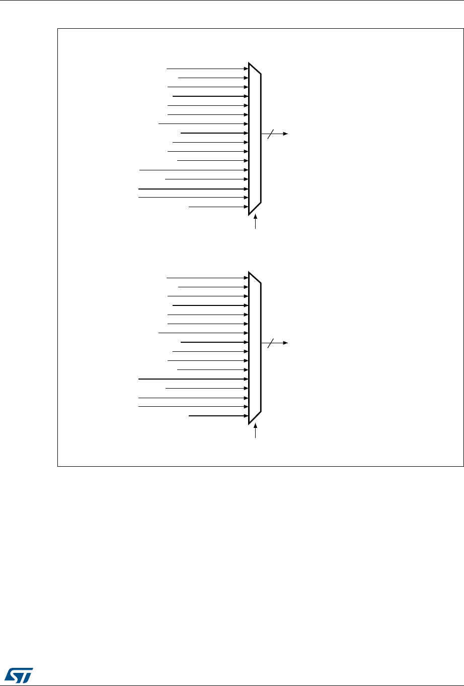
DocID026448 Rev 1 147/836
RM0383 General-purpose I/Os (GPIO)
161
Figure 17. Selecting an alternate function onSTM32F411xC/E
1. Configured in FS.
8.3.3 I/O port control registers
Each of the GPIOs has four 32-bit memory-mapped control registers (GPIOx_MODER,
GPIOx_OTYPER, GPIOx_OSPEEDR, GPIOx_PUPDR) to configure up to 16 I/Os. The
GPIOx_MODER register is used to select the I/O direction (input, output, AF, analog). The
GPIOx_OTYPER and GPIOx_OSPEEDR registers are used to select the output type (push-
pull or open-drain) and speed (the I/O speed pins are directly connected to the
corresponding GPIOx_OSPEEDR register bits whatever the I/O direction). The
GPIOx_PUPDR register is used to select the pull-up/pull-down whatever the I/O direction.
D^ϯϯϬϰϭsϭ
&ŽƌƉŝŶƐϬƚŽϳ͕ƚŚĞ'W/Kdžͺ&Z>ϯϭ͗ϬƌĞŐŝƐƚĞƌƐĞůĞĐƚƐƚŚĞĚĞĚŝĐĂƚĞĚĂůƚĞƌŶĂƚĞĨƵŶĐƚŝŽŶ
&Ϭ;ƐLJƐƚĞŵͿ
&ϭ;d/Dϭͬd/DϮͿ
&Ϯ;d/Dϯ͘͘ϱͿ
&ϯ;d/Dϵ͘͘ϭϭͿ
&ϰ;/Ϯϭ͘͘ϯͿ
&ϱ;^W/ϭ͘͘ϰͿ
&ϲ;^W/ϯ͘͘ϱͿ
&ϳ;h^Zdϭ͘͘ϮͿ
&ϴ;h^ZdϲͿ
&ϵ;/ϮϮ͘͘ϯͿ
&ϭϬ;Kd'ͺ&^Ϳ
&ϭϭ
&ϭϮ;^/KͿ
&ϭϯ
&ϭϰ
&ϭϱ;sEdKhdͿ
WŝŶdž;džсϬ͘͘ϳͿ
&Z>ϯϭ͗Ϭ
&ŽƌƉŝŶƐϴƚŽϭϱ͕ƚŚĞ'W/Kdžͺ&Z,ϯϭ͗ϬƌĞŐŝƐƚĞƌƐĞůĞĐƚƐƚŚĞĚĞĚŝĐĂƚĞĚĂůƚĞƌŶĂƚĞĨƵŶĐƚŝŽŶ
WŝŶdž;džсϴ͘͘ϭϱͿ
ϭ
&Ϭ;ƐLJƐƚĞŵͿ
&ϭ;d/Dϭͬd/DϮͿ
&Ϯ;d/Dϯ͘͘ϱͿ
&ϯ;d/Dϵ͘͘ϭϭͿ
&ϰ;/Ϯϭ͘͘ϯͿ
&ϱ;^W/ϭ͘͘ϰͿ
&ϲ;^W/ϯ͘͘ϱͿ
&ϳ;h^Zdϭ͘͘ϮͿ
&ϴ;h^ZdϲͿ
&ϵ;/ϮϮ͘͘ϯͿ
&ϭϬ;Kd'ͺ&^Ϳ
&ϭϭ
&ϭϮ;^/KͿ
&ϭϯ
&ϭϰ
&ϭϱ;sEdKhdͿ
&Z,ϯϭ͗Ϭ
ϭ

General-purpose I/Os (GPIO) RM0383
148/836 DocID026448 Rev 1
8.3.4 I/O port data registers
Each GPIO has two 16-bit memory-mapped data registers: input and output data registers
(GPIOx_IDR and GPIOx_ODR). GPIOx_ODR stores the data to be output, it is read/write
accessible. The data input through the I/O are stored into the input data register
(GPIOx_IDR), a read-only register.
See Section 8.4.5: GPIO port input data register (GPIOx_IDR) (x = A..E and H) and
Section 8.4.6: GPIO port output data register (GPIOx_ODR) (x = A..E and H) for the register
descriptions.
8.3.5 I/O data bitwise handling
The bit set reset register (GPIOx_BSRR) is a 32-bit register which allows the application to
set and reset each individual bit in the output data register (GPIOx_ODR). The bit set reset
register has twice the size of GPIOx_ODR.
To each bit in GPIOx_ODR, correspond two control bits in GPIOx_BSRR: BSRR(i) and
BSRR(i+SIZE). When written to 1, bit BSRR(i) sets the corresponding ODR(i) bit. When
written to 1, bit BSRR(i+SIZE) resets the ODR(i) corresponding bit.
Writing any bit to 0 in GPIOx_BSRR does not have any effect on the corresponding bit in
GPIOx_ODR. If there is an attempt to both set and reset a bit in GPIOx_BSRR, the set
action takes priority.
Using the GPIOx_BSRR register to change the values of individual bits in GPIOx_ODR is a
“one-shot” effect that does not lock the GPIOx_ODR bits. The GPIOx_ODR bits can always
be accessed directly. The GPIOx_BSRR register provides a way of performing atomic
bitwise handling.
There is no need for the software to disable interrupts when programming the GPIOx_ODR
at bit level: it is possible to modify one or more bits in a single atomic AHB1 write access.
8.3.6 GPIO locking mechanism
It is possible to freeze the GPIO control registers by applying a specific write sequence to
the GPIOx_LCKR register. The frozen registers are GPIOx_MODER, GPIOx_OTYPER,
GPIOx_OSPEEDR, GPIOx_PUPDR, GPIOx_AFRL and GPIOx_AFRH.
To write the GPIOx_LCKR register, a specific write / read sequence has to be applied. When
the right LOCK sequence is applied to bit 16 in this register, the value of LCKR[15:0] is used
to lock the configuration of the I/Os (during the write sequence the LCKR[15:0] value must
be the same). When the LOCK sequence has been applied to a port bit, the value of the port
bit can no longer be modified until the next reset. Each GPIOx_LCKR bit freezes the
corresponding bit in the control registers (GPIOx_MODER, GPIOx_OTYPER,
GPIOx_OSPEEDR, GPIOx_PUPDR, GPIOx_AFRL and GPIOx_AFRH).
The LOCK sequence (refer to Section 8.4.8: GPIO port configuration lock register
(GPIOx_LCKR) (x = A..E and H)) can only be performed using a word (32-bit long) access
to the GPIOx_LCKR register due to the fact that GPIOx_LCKR bit 16 has to be set at the
same time as the [15:0] bits.
For more details please refer to LCKR register description in Section 8.4.8: GPIO port
configuration lock register (GPIOx_LCKR) (x = A..E and H).
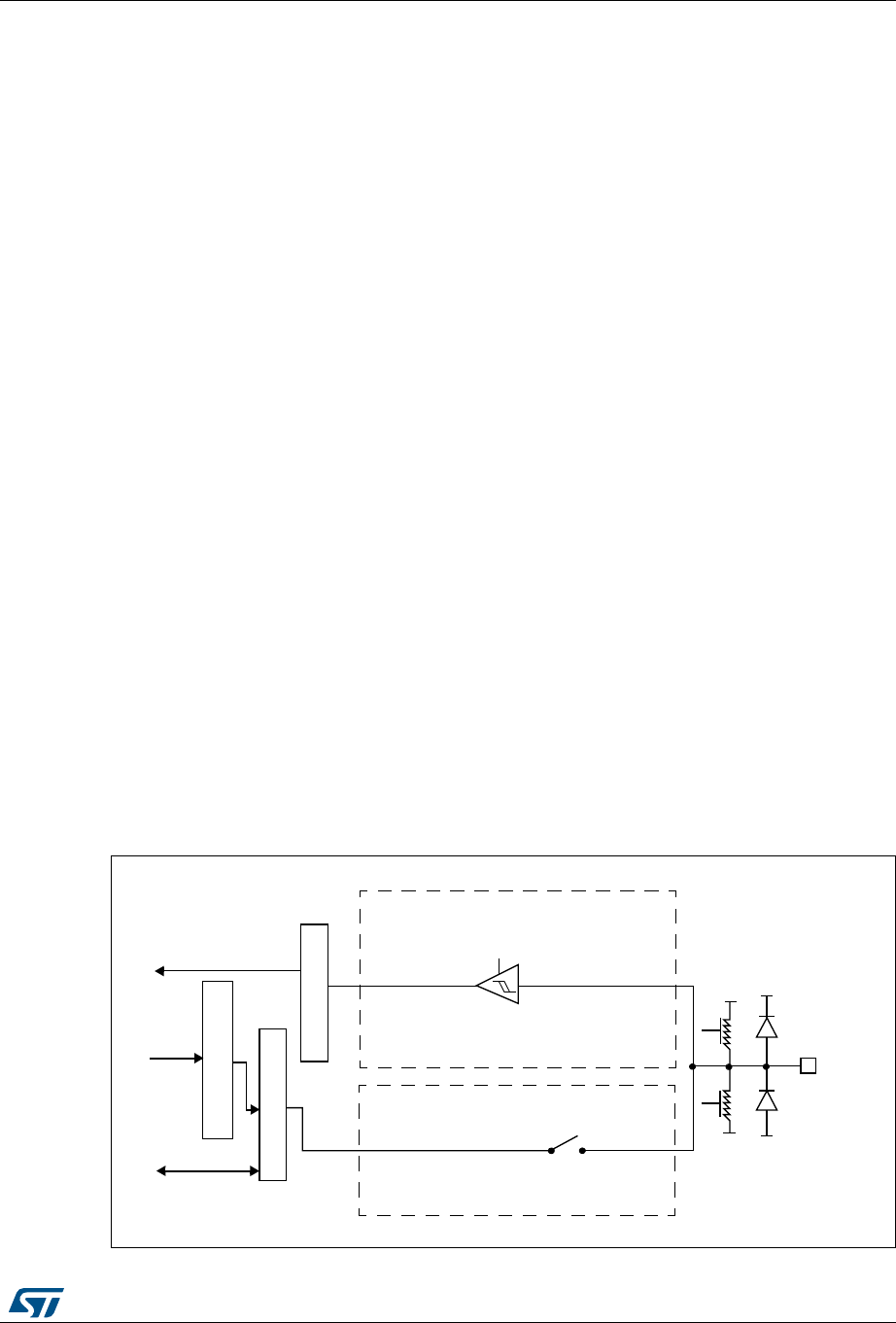
DocID026448 Rev 1 149/836
RM0383 General-purpose I/Os (GPIO)
161
8.3.7 I/O alternate function input/output
Two registers are provided to select one out of the sixteen alternate function inputs/outputs
available for each I/O. With these registers, you can connect an alternate function to some
other pin as required by your application.
This means that a number of possible peripheral functions are multiplexed on each GPIO
using the GPIOx_AFRL and GPIOx_AFRH alternate function registers. The application can
thus select any one of the possible functions for each I/O. The AF selection signal being
common to the alternate function input and alternate function output, a single channel is
selected for the alternate function input/output of one I/O.
To know which functions are multiplexed on each GPIO pin, refer to the datasheets.
Note: The application is allowed to select one of the possible peripheral functions for each I/O at a
time.
8.3.8 External interrupt/wakeup lines
All ports have external interrupt capability. To use external interrupt lines, the port must be
configured in input mode, refer to Section 10.2: External interrupt/event controller (EXTI)
and Section 10.2.3: Wakeup event management.
8.3.9 Input configuration
When the I/O port is programmed as Input:
•the output buffer is disabled
•the Schmitt trigger input is activated
•the pull-up and pull-down resistors are activated depending on the value in the
GPIOx_PUPDR register
•The data present on the I/O pin are sampled into the input data register every AHB
clock cycle
•A read access to the input data register provides the I/O State
Figure 18 shows the input configuration of the I/O port bit.
Figure 18. Input floating/pull up/pull down configurations
ONOFF
PULL
PULL
ONOFF
)/PIN
6$$
633
44,3CHMITT
TRIGGER
633
6$$
PROTECTION
DIODE
PROTECTION
DIODE
ON
INPUTDRIVER
OUTPUTDRIVER
DOWN
UP
)NPUTDATAREGISTER
/UTPUTDATAREGISTER
2EADWRITE
2EAD
"ITSETRESETREGISTERS
7RITE
AIB
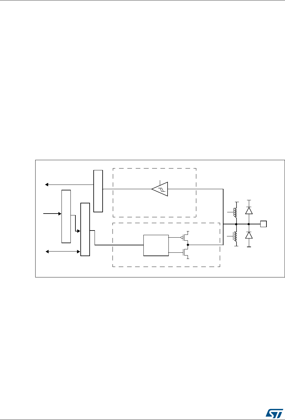
General-purpose I/Os (GPIO) RM0383
150/836 DocID026448 Rev 1
8.3.10 Output configuration
When the I/O port is programmed as output:
•The output buffer is enabled:
– Open drain mode: A “0” in the Output register activates the N-MOS whereas a “1”
in the Output register leaves the port in Hi-Z (the P-MOS is never activated)
– Push-pull mode: A “0” in the Output register activates the N-MOS whereas a “1” in
the Output register activates the P-MOS
•The Schmitt trigger input is activated
•The weak pull-up and pull-down resistors are activated or not depending on the value
in the GPIOx_PUPDR register
•The data present on the I/O pin are sampled into the input data register every AHB
clock cycle
•A read access to the input data register gets the I/O state
•A read access to the output data register gets the last written value
Figure 19 shows the output configuration of the I/O port bit.
Figure 19. Output configuration
8.3.11 Alternate function configuration
When the I/O port is programmed as alternate function:
•The output buffer can be configured as open-drain or push-pull
•The output buffer is driven by the signal coming from the peripheral (transmitter enable
and data)
•The Schmitt trigger input is activated
•The weak pull-up and pull-down resistors are activated or not depending on the value
in the GPIOx_PUPDR register
•The data present on the I/O pin are sampled into the input data register every AHB
clock cycle
•A read access to the input data register gets the I/O state
Figure 20 shows the Alternate function configuration of the I/O port bit.
0USHPULLOR
/PENDRAIN
/UTPUT
CONTROL
6
$$
6
33
44,3CHMITT
TRIGGER
ON
)NPUTDRIVER
/UTPUTDRIVER
0-/3
.-/3
)NPUTDATAREGISTER
/UTPUTDATAREGISTER
2EADWRITE
2EAD
"ITSETRESETREGISTERS
7RITE
ONOFF
PULL
PULL
ONOFF
6
$$
6
33
6
33
6
$$
PROTECTION
DIODE
PROTECTION
DIODE
DOWN
UP
)/PIN
AIB
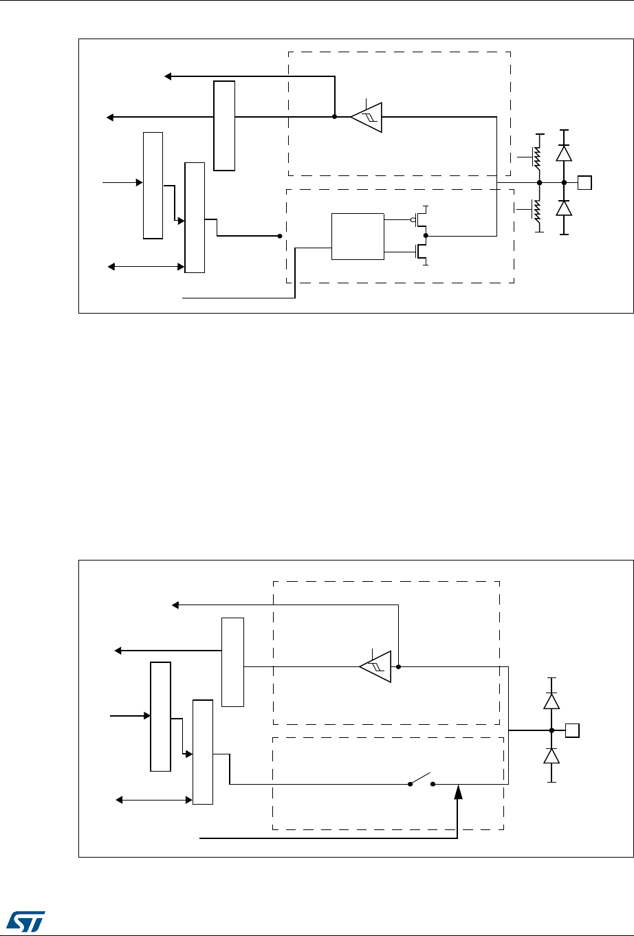
DocID026448 Rev 1 151/836
RM0383 General-purpose I/Os (GPIO)
161
Figure 20. Alternate function configuration
8.3.12 Analog configuration
When the I/O port is programmed as analog configuration:
•The output buffer is disabled
•The Schmitt trigger input is deactivated, providing zero consumption for every analog
value of the I/O pin. The output of the Schmitt trigger is forced to a constant value (0).
•The weak pull-up and pull-down resistors are disabled
•Read access to the input data register gets the value “0”
Note: In the analog configuration, the I/O pins cannot be 5 Volt tolerant.
Figure 21 shows the high-impedance, analog-input configuration of the I/O port bit.
Figure 21. High impedance-analog configuration
!LTERNATEFUNCTIONOUTPUT
!LTERNATEFUNCTIONINPUT
PUSHPULLOR
OPENDRAIN
&ROMONCHIP
PERIPHERAL
4OONCHIP
PERIPHERAL
/UTPUT
CONTROL
6$$
633
44,3CHMITT
TRIGGER
ON
)NPUTDRIVER
/UTPUTDRIVER
0-/3
.-/3
)NPUTDATAREGISTER
/UTPUTDATAREGISTER
2EADWRITE
2EAD
"ITSETRESETREGISTERS
7RITE
ONOFF
ONOFF
6$$
633 633
6$$
PROTECTION
DIODE
PROTECTION
DIODE
0ULL
0ULL
)/PIN
DOWN
UP
AIB
&ROMONCHIP
PERIPHERAL
4OONCHIP
PERIPHERAL
!NALOG
TRIGGER
OFF
)NPUTDRIVER
)NPUTDATAREGISTER
/UTPUTDATAREGISTER
2EADWRITE
2EAD
"ITSETRESETREGISTERS
7RITE
!NALOG
6
33
6
$$
PROTECTION
DIODE
PROTECTION
DIODE
)/PIN
AI
44,3CHMITT

General-purpose I/Os (GPIO) RM0383
152/836 DocID026448 Rev 1
8.3.13 Using the OSC32_IN/OSC32_OUT pins as GPIO PC14/PC15
port pins
The LSE oscillator pins OSC32_IN and OSC32_OUT can be used as general-purpose
PC14 and PC15 I/Os, respectively, when the LSE oscillator is off. The PC14 and PC15 I/Os
are only configured as LSE oscillator pins OSC32_IN and OSC32_OUT when the LSE
oscillator is ON. This is done by setting the LSEON bit in the RCC_BDCR register. The LSE
has priority over the GPIO function.
Note: The PC14/PC15 GPIO functionality is lost when the 1.2 V domain is powered off (by the
device entering the standby mode) or when the backup domain is supplied by VBAT (VDD no
more supplied). In this case the I/Os are set in analog input mode.
8.3.14 Using the OSC_IN/OSC_OUT pins as GPIO PH0/PH1 port pins
The HSE oscillator pins OSC_IN/OSC_OUT can be used as general-purpose PH0/PH1
I/Os, respectively, when the HSE oscillator is OFF. (after reset, the HSE oscillator is off). The
PH0/PH1 I/Os are only configured as OSC_IN/OSC_OUT HSE oscillator pins when the
HSE oscillator is ON. This is done by setting the HSEON bit in the RCC_CR register. The
HSE has priority over the GPIO function.
8.3.15 Selection of RTC additional functions
The STM32F4xx feature one GPIO pins RTC_AF1 that can be used for the detection of a
tamper or time stamp event, or RTC_ALARM, or RTC_CALIB RTC outputs.
•The RTC_AF1 (PC13) can be used for the following purposes:
RTC_ALARM output: this output can be RTC Alarm A, RTC Alarm B or RTC Wakeup
depending on the OSEL[1:0] bits in the RTC_CR register
•RTC_CALIB output: this feature is enabled by setting the COE[23] in the RTC_CR
register
•RTC_TAMP1: tamper event detection
•RTC_TS: time stamp event detection
The selection of the corresponding pin is performed through the RTC_TAFCR register as
follows:
•TAMP1INSEL is used to select which pin is used as the RTC_TAMP1 tamper input
•TSINSEL is used to select which pin is used as the RTC_TS time stamp input
•ALARMOUTTYPE is used to select whether the RTC_ALARM is output in push-pull or
open-drain mode
The output mechanism follows the priority order listed in Table 25

DocID026448 Rev 1 153/836
RM0383 General-purpose I/Os (GPIO)
161
8.4 GPIO registers
This section gives a detailed description of the GPIO registers.
For a summary of register bits, register address offsets and reset values, refer to Table 26.
The GPIO registers can be accessed by byte (8 bits), half-words (16 bits) or words (32 bits).
8.4.1 GPIO port mode register (GPIOx_MODER) (x = A..E and H)
Address offset: 0x00
Reset values:
•0x0C00 0000 for port A
•0x0000 0280 for port B
•0x0000 0000 for other ports
Table 25. RTC additional functions(1)
Pin
configuration
and function enabled enabled Tamper
enabled
Time
stamp
enabled
TAMP1INSEL
TAMPER1
pin selection
TSINSEL
TIMESTAMP
pin
selection
ALARMOUTTYP
E configuration
Alarm out
output OD 1 Don’t care Don’t
care
Don’t
care Don’t care Don’t care 0
Alarm out
output PP 1 Don’t care Don’t
care
Don’t
care Don’t care Don’t care 1
Calibration
out output PP 01
Don’t
care
Don’t
care Don’t care Don’t care Don’t care
TAMPER1
input floating 0 0 1 0 0 Don’t care Don’t care
TIMESTAMP
and
TAMPER1
input floating
00110 0Don’t care
TIMESTAMP
input floating 0 0 0 1 Don’t care 0 Don’t care
Standard
GPIO 0 0 0 0 Don’t care Don’t care Don’t care
1. OD: open drain; PP: push-pull.
31 30 29 28 27 26 25 24 23 22 21 20 19 18 17 16
MODER15[1:0] MODER14[1:0] MODER13[1:0] MODER12[1:0] MODER11[1:0] MODER10[1:0] MODER9[1:0] MODER8[1:0]
rw rw rw rw rw rw rw rw rw rw rw rw rw rw rw rw
1514131211109876543210
MODER7[1:0] MODER6[1:0] MODER5[1:0] MODER4[1:0] MODER3[1:0] MODER2[1:0] MODER1[1:0] MODER0[1:0]
rw rw rw rw rw rw rw rw rw rw rw rw rw rw rw rw

General-purpose I/Os (GPIO) RM0383
154/836 DocID026448 Rev 1
8.4.2 GPIO port output type register (GPIOx_OTYPER)
(x = A..E and H)
Address offset: 0x04
Reset value: 0x0000 0000
Bits 2y:2y+1 MODERy[1:0]: Port x configuration bits (y = 0..15)
These bits are written by software to configure the I/O direction mode.
00: Input (reset state)
01: General purpose output mode
10: Alternate function mode
11: Analog mode
31 30 29 28 27 26 25 24 23 22 21 20 19 18 17 16
Reserved
1514131211109876543210
OT15 OT14 OT13 OT12 OT11 OT10 OT9 OT8 OT7 OT6 OT5 OT4 OT3 OT2 OT1 OT0
rw rw rw rw rw rw rw rw rw rw rw rw rw rw rw rw
Bits 31:16 Reserved, must be kept at reset value.
Bits 15:0 OTy: Port x configuration bits (y = 0..15)
These bits are written by software to configure the output type of the I/O port.
0: Output push-pull (reset state)
1: Output open-drain

DocID026448 Rev 1 155/836
RM0383 General-purpose I/Os (GPIO)
161
8.4.3 GPIO port output speed register (GPIOx_OSPEEDR)
(x = A..E and H)
Address offset: 0x08
Reset values:
•0x0C00 0000 for port A
•0x0000 00C0 for port B
•0x0000 0000 for other ports
31 30 29 28 27 26 25 24 23 22 21 20 19 18 17 16
OSPEEDR15
[1:0]
OSPEEDR14
[1:0]
OSPEEDR13
[1:0]
OSPEEDR12
[1:0]
OSPEEDR11
[1:0]
OSPEEDR10
[1:0]
OSPEEDR9
[1:0]
OSPEEDR8
[1:0]
rw rw rw rw rw rw rw rw rw rw rw rw rw rw rw rw
15 14 13 12 11 10 9 8 7 6 5 4 3 2 1 0
OSPEEDR7[1:0] OSPEEDR6[1:0] OSPEEDR5[1:0] OSPEEDR4[1:0] OSPEEDR3[1:0] OSPEEDR2[1:0] OSPEEDR1
[1:0]
OSPEEDR0
1:0]
rw rw rw rw rw rw rw rw rw rw rw rw rw rw rw rw
Bits 2y:2y+1 OSPEEDRy[1:0]: Port x configuration bits (y = 0..15)
These bits are written by software to configure the I/O output speed.
00: Low speed
01: Medium speed
10: Fast speed
11: High speed
Note: Refer to the product datasheets for the values of OSPEEDRy bits versus VDD
range and external load.
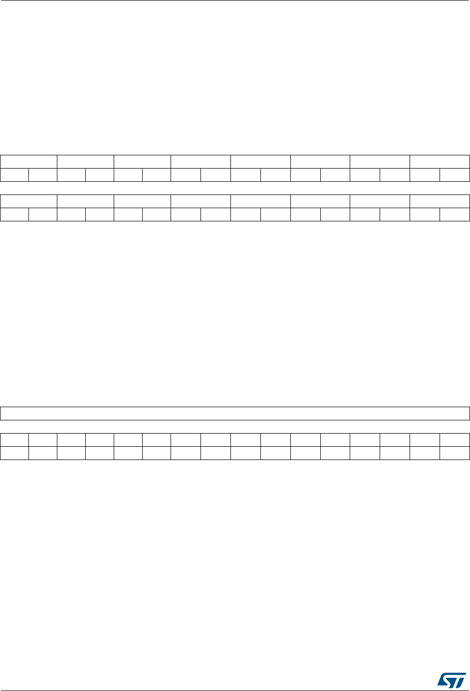
General-purpose I/Os (GPIO) RM0383
156/836 DocID026448 Rev 1
8.4.4 GPIO port pull-up/pull-down register (GPIOx_PUPDR)
(x = A..E and H)
Address offset: 0x0C
Reset values:
•0x6400 0000 for port A
•0x0000 0100 for port B
•0x0000 0000 for other ports
8.4.5 GPIO port input data register (GPIOx_IDR) (x = A..E and H)
Address offset: 0x10
Reset value: 0x0000 XXXX (where X means undefined)
31 30 29 28 27 26 25 24 23 22 21 20 19 18 17 16
PUPDR15[1:0] PUPDR14[1:0] PUPDR13[1:0] PUPDR12[1:0] PUPDR11[1:0] PUPDR10[1:0] PUPDR9[1:0] PUPDR8[1:0]
rw rw rw rw rw rw rw rw rw rw rw rw rw rw rw rw
1514131211109876543210
PUPDR7[1:0] PUPDR6[1:0] PUPDR5[1:0] PUPDR4[1:0] PUPDR3[1:0] PUPDR2[1:0] PUPDR1[1:0] PUPDR0[1:0]
rw rw rw rw rw rw rw rw rw rw rw rw rw rw rw rw
Bits 2y:2y+1 PUPDRy[1:0]: Port x configuration bits (y = 0..15)
These bits are written by software to configure the I/O pull-up or pull-down
00: No pull-up, pull-down
01: Pull-up
10: Pull-down
11: Reserved
31 30 29 28 27 26 25 24 23 22 21 20 19 18 17 16
Reserved
1514131211109876543210
IDR15 IDR14 IDR13 IDR12 IDR11 IDR10 IDR9 IDR8 IDR7 IDR6 IDR5 IDR4 IDR3 IDR2 IDR1 IDR0
rrrrrr r r r r rrrrrr
Bits 31:16 Reserved, must be kept at reset value.
Bits 15:0 IDRy: Port input data (y = 0..15)
These bits are read-only and can be accessed in word mode only. They contain the input
value of the corresponding I/O port.

DocID026448 Rev 1 157/836
RM0383 General-purpose I/Os (GPIO)
161
8.4.6 GPIO port output data register (GPIOx_ODR) (x = A..E and H)
Address offset: 0x14
Reset value: 0x0000 0000
8.4.7 GPIO port bit set/reset register (GPIOx_BSRR) (x = A..E and H)
Address offset: 0x18
Reset value: 0x0000 0000
8.4.8 GPIO port configuration lock register (GPIOx_LCKR)
(x = A..E and H)
This register is used to lock the configuration of the port bits when a correct write sequence
is applied to bit 16 (LCKK). The value of bits [15:0] is used to lock the configuration of the
GPIO. During the write sequence, the value of LCKR[15:0] must not change. When the
31 30 29 28 27 26 25 24 23 22 21 20 19 18 17 16
Reserved
1514131211109876543210
ODR15 ODR14 ODR13 ODR12 ODR11 ODR10 ODR9 ODR8 ODR7 ODR6 ODR5 ODR4 ODR3 ODR2 ODR1 ODR0
rw rw rw rw rw rw rw rw rw rw rw rw rw rw rw rw
Bits 31:16 Reserved, must be kept at reset value.
Bits 15:0 ODRy: Port output data (y = 0..15)
These bits can be read and written by software.
Note: For atomic bit set/reset, the ODR bits can be individually set and reset by writing to the
GPIOx_BSRR register (x = A..E and H).
31 30 29 28 27 26 25 24 23 22 21 20 19 18 17 16
BR15 BR14 BR13 BR12 BR11 BR10 BR9 BR8 BR7 BR6 BR5 BR4 BR3 BR2 BR1 BR0
wwwwwwwwwwwwwwww
1514131211109876543210
BS15 BS14 BS13 BS12 BS11 BS10 BS9 BS8 BS7 BS6 BS5 BS4 BS3 BS2 BS1 BS0
wwwwwwwwwwwwwwww
Bits 31:16 BRy: Port x reset bit y (y = 0..15)
These bits are write-only and can be accessed in word, half-word or byte mode. A read to
these bits returns the value 0x0000.
0: No action on the corresponding ODRx bit
1: Resets the corresponding ODRx bit
Note: If both BSx and BRx are set, BSx has priority.
Bits 15:0 BSy: Port x set bit y (y= 0..15)
These bits are write-only and can be accessed in word, half-word or byte mode. A read to
these bits returns the value 0x0000.
0: No action on the corresponding ODRx bit
1: Sets the corresponding ODRx bit

General-purpose I/Os (GPIO) RM0383
158/836 DocID026448 Rev 1
LOCK sequence has been applied on a port bit, the value of this port bit can no longer be
modified until the next reset.
Note: A specific write sequence is used to write to the GPIOx_LCKR register. Only word access
(32-bit long) is allowed during this write sequence.
Each lock bit freezes a specific configuration register (control and alternate function
registers).
Address offset: 0x1C
Reset value: 0x0000 0000
Access: 32-bit word only, read/write register
31 30 29 28 27 26 25 24 23 22 21 20 19 18 17 16
Reserved LCKK
rw
15 14 13 12 11 10 9 8 7 6 5 4 3 2 1 0
LCK15 LCK14 LCK13 LCK12 LCK11 LCK10 LCK9 LCK8 LCK7 LCK6 LCK5 LCK4 LCK3 LCK2 LCK1 LCK0
rw rw rw rw rw rw rw rw rw rw rw rw rw rw rw rw
Bits 31:17 Reserved, must be kept at reset value.
Bit 16 LCKK[16]: Lock key
This bit can be read any time. It can only be modified using the lock key write sequence.
0: Port configuration lock key not active
1: Port configuration lock key active. The GPIOx_LCKR register is locked until an MCU reset
occurs.
LOCK key write sequence:
WR LCKR[16] = ‘1’ + LCKR[15:0]
WR LCKR[16] = ‘0’ + LCKR[15:0]
WR LCKR[16] = ‘1’ + LCKR[15:0]
RD LCKR
RD LCKR[16] = ‘1’ (this read operation is optional but it confirms that the lock is active)
Note: During the LOCK key write sequence, the value of LCK[15:0] must not change.
Any error in the lock sequence aborts the lock.
After the first lock sequence on any bit of the port, any read access on the LCKK bit will
return ‘1’ until the next CPU reset.
Bits 15:0 LCKy: Port x lock bit y (y= 0..15)
These bits are read/write but can only be written when the LCKK bit is ‘0.
0: Port configuration not locked
1: Port configuration locked

DocID026448 Rev 1 159/836
RM0383 General-purpose I/Os (GPIO)
161
8.4.9 GPIO alternate function low register (GPIOx_AFRL) (x = A..E and H)
Address offset: 0x20
Reset value: 0x0000 0000
8.4.10 GPIO alternate function high register (GPIOx_AFRH)
(x = A..E and H)
Address offset: 0x24
Reset value: 0x0000 0000
31 30 29 28 27 26 25 24 23 22 21 20 19 18 17 16
AFRL7[3:0] AFRL6[3:0] AFRL5[3:0] AFRL4[3:0]
rw rw rw rw rw rw rw rw rw rw rw rw rw rw rw rw
1514131211109876543210
AFRL3[3:0] AFRL2[3:0] AFRL1[3:0] AFRL0[3:0]
rw rw rw rw rw rw rw rw rw rw rw rw rw rw rw rw
Bits 31:0 AFRLy: Alternate function selection for port x bit y (y = 0..7)
These bits are written by software to configure alternate function I/Os
AFRLy selection:
0000: AF0
0001: AF1
0010: AF2
0011: AF3
0100: AF4
0101: AF5
0110: AF6
0111: AF7
1000: AF8
1001: AF9
1010: AF10
1011: AF11
1100: AF12
1101: AF13
1110: AF14
1111: AF15
31 30 29 28 27 26 25 24 23 22 21 20 19 18 17 16
AFRH15[3:0] AFRH14[3:0] AFRH13[3:0] AFRH12[3:0]
rw rw rw rw rw rw rw rw rw rw rw rw rw rw rw rw
1514131211109876543210
AFRH11[3:0] AFRH10[3:0] AFRH9[3:0] AFRH8[3:0]
rw rw rw rw rw rw rw rw rw rw rw rw rw rw rw rw
Bits 31:0 AFRHy: Alternate function selection for port x bit y (y = 8..15)
These bits are written by software to configure alternate function I/Os
AFRHy selection:
0000: AF0
0001: AF1
0010: AF2
0011: AF3
0100: AF4
0101: AF5
0110: AF6
0111: AF7
1000: AF8
1001: AF9
1010: AF10
1011: AF11
1100: AF12
1101: AF13
1110: AF14
1111: AF15

General-purpose I/Os (GPIO) RM0383
160/836 DocID026448 Rev 1
8.4.11 GPIO register map
The following table gives the GPIO register map and the reset values.
Table 26. GPIO register map and reset values
Offset Register
31
30
29
28
27
26
25
24
23
22
21
20
19
18
17
16
15
14
13
12
11
10
9
8
7
6
5
4
3
2
1
0
0x00
GPIOA_
MODER
MODER15[1:0]
MODER14[1:0]
MODER13[1:0]
MODER12[1:0]
MODER11[1:0]
MODER10[1:0]
MODER9[1:0]
MODER8[1:0]
MODER7[1:0]
MODER6[1:0]
MODER5[1:0]
MODER4[1:0]
MODER3[1:0]
MODER2[1:0]
MODER1[1:0]
MODER0[1:0]
Reset value 00001100000000000000000000000000
0x00
GPIOB_
MODER
MODER15[1:0]
MODER14[1:0]
MODER13[1:0]
MODER12[1:0]
MODER11[1:0]
MODER10[1:0]
MODER9[1:0]
MODER8[1:0]
MODER7[1:0]
MODER6[1:0]
MODER5[1:0]
MODER4[1:0]
MODER3[1:0]
MODER2[1:0]
MODER1[1:0]
MODER0[1:0]
Reset value 00000000000000000000001010000000
0x00
GPIOx_MODER
(where x = C..E
and H)
MODER15[1:0]
MODER14[1:0]
MODER13[1:0]
MODER12[1:0]
MODER11[1:0]
MODER10[1:0]
MODER9[1:0]
MODER8[1:0]
MODER7[1:0]
MODER6[1:0]
MODER5[1:0]
MODER4[1:0]
MODER3[1:0]
MODER2[1:0]
MODER1[1:0]
MODER0[1:0]
Reset value 00000000000000000000000000000000
0x04
GPIOx_
OTYPER
(where x = A..E
and H) Reserved
OT15
OT14
OT13
OT12
OT11
OT10
OT9
OT8
OT7
OT6
OT5
OT4
OT3
OT2
OT1
OT0
Reset value 0000000000000000
0x08
GPIOx_
OSPEEDER
(where x = C..E
andH)
OSPEEDR15[1:0]
OSPEEDR14[1:0]
OSPEEDR13[1:0]
OSPEEDR12[1:0]
OSPEEDR11[1:0]
OSPEEDR10[1:0]
OSPEEDR9[1:0]
OSPEEDR8[1:0]
OSPEEDR7[1:0]
OSPEEDR6[1:0]
OSPEEDR5[1:0]
OSPEEDR4[1:0]
OSPEEDR3[1:0]
OSPEEDR2[1:0]
OSPEEDR1[1:0]
OSPEEDR0[1:0]
Reset value 00000000000000000000000000000000
0x08
GPIOA_
OSPEEDER
OSPEEDR15[1:0]
OSPEEDR14[1:0]
OSPEEDR13[1:0]
OSPEEDR12[1:0]
OSPEEDR11[1:0]
OSPEEDR10[1:0]
OSPEEDR9[1:0]
OSPEEDR8[1:0]
OSPEEDR7[1:0]
OSPEEDR6[1:0]
OSPEEDR5[1:0]
OSPEEDR4[1:0]
OSPEEDR3[1:0]
OSPEEDR2[1:0]
OSPEEDR1[1:0]
OSPEEDR0[1:0]
Reset value 00001100000000000000000000000000
0x08
GPIOB_
OSPEEDER
OSPEEDR15[1:0]
OSPEEDR14[1:0]
OSPEEDR13[1:0]
OSPEEDR12[1:0]
OSPEEDR11[1:0]
OSPEEDR10[1:0]
OSPEEDR9[1:0]
OSPEEDR8[1:0]
OSPEEDR7[1:0]
OSPEEDR6[1:0]
OSPEEDR5[1:0]
OSPEEDR4[1:0]
OSPEEDR3[1:0]
OSPEEDR2[1:0]
OSPEEDR1[1:0]
OSPEEDR0[1:0]
Reset value 00000000000000000000000011000000
DocID026448 Rev 1 161/836
RM0383 General-purpose I/Os (GPIO)
161
Refer to Table 1 on page 37 for the register boundary addresses.
0x0C
GPIOA_PUPDR
PUPDR15[1:0]
PUPDR14[1:0]
PUPDR13[1:0]
PUPDR12[1:0]
PUPDR11[1:0]
PUPDR10[1:0]
PUPDR9[1:0]
PUPDR8[1:0]
PUPDR7[1:0]
PUPDR6[1:0]
PUPDR5[1:0]
PUPDR4[1:0]
PUPDR3[1:0]
PUPDR2[1:0]
PUPDR1[1:0]
PUPDR0[1:0]
Reset value 01100100000000000000000000000000
0x0C
GPIOB_PUPDR
PUPDR15[1:0]
PUPDR14[1:0]
PUPDR13[1:0]
PUPDR12[1:0]
PUPDR11[1:0]
PUPDR10[1:0]
PUPDR9[1:0]
PUPDR8[1:0]
PUPDR7[1:0]
PUPDR6[1:0]
PUPDR5[1:0]
PUPDR4[1:0]
PUPDR3[1:0]
PUPDR2[1:0]
PUPDR1[1:0]
PUPDR0[1:0]
Reset value 00000000000000000000000100000000
0x0C
GPIOx_PUPDR
(where x = C..E
and H)
PUPDR15[1:0]
PUPDR14[1:0]
PUPDR13[1:0]
PUPDR12[1:0]
PUPDR11[1:0]
PUPDR10[1:0]
PUPDR9[1:0]
PUPDR8[1:0]
PUPDR7[1:0]
PUPDR6[1:0]
PUPDR5[1:0]
PUPDR4[1:0]
PUPDR3[1:0]
PUPDR2[1:0]
PUPDR1[1:0]
PUPDR0[1:0]
Reset value 00000000000000000000000000000000
0x10
GPIOx_IDR
(where x = A..E
and H) Reserved
IDR15
IDR14
IDR13
IDR12
IDR11
IDR10
IDR9
IDR8
IDR7
IDR6
IDR5
IDR4
IDR3
IDR2
IDR1
IDR0
Reset value xxxxxxxxxxxxxxxx
0x14
GPIOx_ODR
(where x = A..E
and H) Reserved
ODR15
ODR14
ODR13
ODR12
ODR11
ODR10
ODR9
ODR8
ODR7
ODR6
ODR5
ODR4
ODR3
ODR2
ODR1
ODR0
Reset value 0000000000000000
0x18
GPIOx_BSRR
(where x = A..E
and H)
BR15
BR14
BR13
BR12
BR11
BR10
BR9
BR8
BR7
BR6
BR5
BR4
BR3
BR2
BR1
BR0
BS15
BS14
BS13
BS12
BS11
BS10
BS9
BS8
BS7
BS6
BS5
BS4
BS3
BS2
BS1
BS0
Reset value 00000000000000000000000000000000
0x1C
GPIOx_LCKR
(where x = A..E
and H) Reserved
LCKK
LCK15
LCK14
LCK13
LCK12
LCK11
LCK10
LCK9
LCK8
LCK7
LCK6
LCK5
LCK4
LCK3
LCK2
LCK1
LCK0
Reset value 00000000000000000
0x20
GPIOx_AFRL
(where x = A..E
and H)
AFRL7[3:0] AFRL6[3:0] AFRL5[3:0] AFRL4[3:0] AFRL3[3:0] AFRL2[3:0] AFRL1[3:0] AFRL0[3:0]
Reset value 00000000000000000000000000000000
0x24
GPIOx_AFRH
(where x = A..E
and H)
AFRH15[3:0] AFRH14[3:0] AFRH13[3:0] AFRH12[3:0] AFRH11[3:0] AFRH10[3:0] AFRH9[3:0] AFRH8[3:0]
Reset value 00000000000000000000000000000000
Table 26. GPIO register map and reset values (continued)
Offset Register
31
30
29
28
27
26
25
24
23
22
21
20
19
18
17
16
15
14
13
12
11
10
9
8
7
6
5
4
3
2
1
0

DMA controller (DMA) RM0383
162/836 DocID026448 Rev 1
9 DMA controller (DMA)
9.1 DMA introduction
Direct memory access (DMA) is used in order to provide high-speed data transfer between
peripherals and memory and between memory and memory. Data can be quickly moved by
DMA without any CPU action. This keeps CPU resources free for other operations.
The DMA controller combines a powerful dual AHB master bus architecture with
independent FIFO to optimize the bandwidth of the system, based on a complex bus matrix
architecture.
The two DMA controllers have 16 streams in total (8 for each controller), each dedicated to
managing memory access requests from one or more peripherals. Each stream can have
up to 8 channels (requests) in total. And each has an arbiter for handling the priority
between DMA requests.
9.2 DMA main features
The main DMA features are:
•Dual AHB master bus architecture, one dedicated to memory accesses and one
dedicated to peripheral accesses
•AHB slave programming interface supporting only 32-bit accesses
•8 streams for each DMA controller, up to 8 channels (requests) per stream
•Four-word depth 32 first-in, first-out memory buffers (FIFOs) per stream, that can be
used in FIFO mode or direct mode:
– FIFO mode: with threshold level software selectable between 1/4, 1/2 or 3/4 of the
FIFO size
– Direct mode
Each DMA request immediately initiates a transfer from/to the memory. When it is
configured in direct mode (FIFO disabled), to transfer data in memory-to-
peripheral mode, the DMA preloads only one data from the memory to the internal

DocID026448 Rev 1 163/836
RM0383 DMA controller (DMA)
197
FIFO to ensure an immediate data transfer as soon as a DMA request is triggered
by a peripheral.
•Each stream can be configured by hardware to be:
– a regular channel that supports peripheral-to-memory, memory-to-peripheral and
memory-to-memory transfers
– a double buffer channel that also supports double buffering on the memory side
•Each of the 8 streams are connected to dedicated hardware DMA channels (requests)
•Priorities between DMA stream requests are software-programmable (4 levels
consisting of very high, high, medium, low) or hardware in case of equality (request 0
has priority over request 1, etc.)
•Each stream also supports software trigger for memory-to-memory transfers (only
available for the DMA2 controller)
•Each stream request can be selected among up to 8 possible channel requests. This
selection is software-configurable and allows several peripherals to initiate DMA
requests
•The number of data items to be transferred can be managed either by the DMA
controller or by the peripheral:
– DMA flow controller: the number of data items to be transferred is software-
programmable from 1 to 65535
– Peripheral flow controller: the number of data items to be transferred is unknown
and controlled by the source or the destination peripheral that signals the end of
the transfer by hardware
•Independent source and destination transfer width (byte, half-word, word): when the
data widths of the source and destination are not equal, the DMA automatically
packs/unpacks the necessary transfers to optimize the bandwidth. This feature is only
available in FIFO mode
•Incrementing or nonincrementing addressing for source and destination
•Supports incremental burst transfers of 4, 8 or 16 beats. The size of the burst is
software-configurable, usually equal to half the FIFO size of the peripheral
•Each stream supports circular buffer management
•5 event flags (DMA Half Transfer, DMA Transfer complete, DMA Transfer Error, DMA
FIFO Error, Direct Mode Error) logically ORed together in a single interrupt request for
each stream
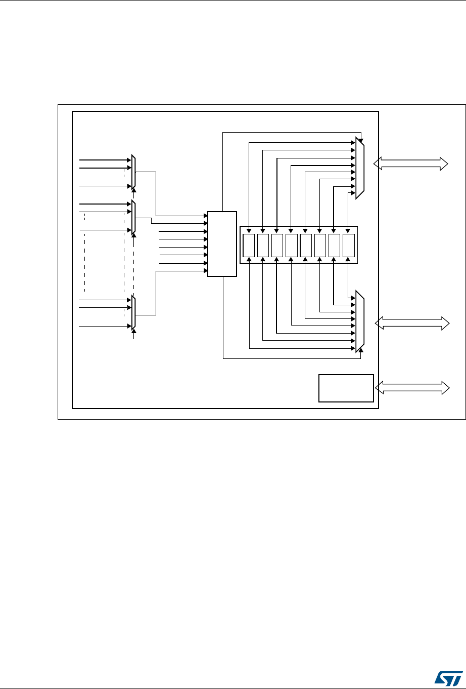
DMA controller (DMA) RM0383
164/836 DocID026448 Rev 1
9.3 DMA functional description
9.3.1 General description
Figure 22 shows the block diagram of a DMA.
Figure 22. DMA block diagram
The DMA controller performs direct memory transfer: as an AHB master, it can take the
control of the AHB bus matrix to initiate AHB transactions.
It can carry out the following transactions:
•peripheral-to-memory
•memory-to-peripheral
•memory-to-memory
The DMA controller provides two AHB master ports: the AHB memory port, intended to be
connected to memories and the AHB peripheral port, intended to be connected to
peripherals. However, to allow memory-to-memory transfers, the AHB peripheral port must
also have access to the memories.
The AHB slave port is used to program the DMA controller (it supports only 32-bit
accesses).
See Figure 23 for the implementation of the system of two DMA controllers.
AHB master
Memory port
FIFO
AHB master
Peripheral port
STREAM 0
FIFO STREAM 1
STREAM 0
STREAM 1
FIFO STREAM 2STREAM 2
FIFO STREAM 7
STREAM 7
REQ_STREAM0
REQ_STR0_CH0
REQ_STR0_CH1
DMA controller
FIFO STREAM 3STREAM 3
FIFO STREAM 4STREAM 4
FIFO STREAM 5STREAM 5
FIFO STREAM 6STREAM 6
Arbiter
REQ_STREAM1
REQ_STREAM2
REQ_STREAM3
REQ_STREAM4
REQ_STREAM5
REQ_STREAM6
REQ_STREAM7
REQ_STR0_CH7
REQ_STR1_CH0
REQ_STR1_CH1
REQ_STR1_CH7
REQ_STR7_CH0
REQ_STR7_CH1
REQ_STR7_CH7
AHB slave
programming
interface
Programming port
Channel
selection
ai15945
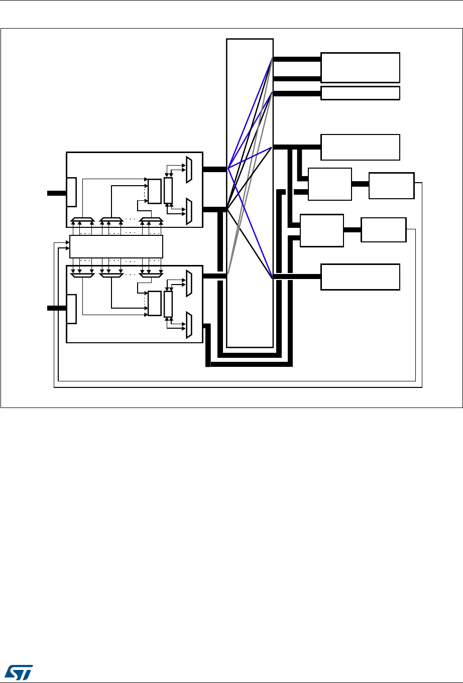
DocID026448 Rev 1 165/836
RM0383 DMA controller (DMA)
197
Figure 23. System implementation of the two DMA controllers( STM32F411xC/E)
1. The DMA1 controller AHB peripheral port is not connected to the bus matrix like in the case of the DMA2 controller, thus
only DMA2 streams are able to perform memory-to-memory transfers.
9.3.2 DMA transactions
A DMA transaction consists of a sequence of a given number of data transfers. The number
of data items to be transferred and their width (8-bit, 16-bit or 32-bit) are software-
programmable.
Each DMA transfer consists of three operations:
•A loading from the peripheral data register or a location in memory, addressed through
the DMA_SxPAR or DMA_SxM0AR register
•A storage of the data loaded to the peripheral data register or a location in memory
addressed through the DMA_SxPAR or DMA_SxM0AR register
•A post-decrement of the DMA_SxNDTR register, which contains the number of
transactions that still have to be performed
After an event, the peripheral sends a request signal to the DMA controller. The DMA
controller serves the request depending on the channel priorities. As soon as the DMA
controller accesses the peripheral, an Acknowledge signal is sent to the peripheral by the
069
'0$FRQWUROOHU
$+%SHULSK
$UELWHU
$+%PHPRU\
),)2
'0$FRQWUROOHU
$+%PHPRU\
%XV0DWUL[
$+%PXOWLOD\HU
$UELWHU
$+%SHULSK
0$33,1*
),)2
)ODVK
PHPRU\
65$0
$+%SHULSKHUDOV
$+%$3%
EULGJH
GXDO$+%
$3% $3%
$+%$3%
EULGJH
GXDO$+%
$3% $3%
SHULSKHUDOV
$+%VODYH
$+%VODYH
SRUWSRUWSRUWSRUW
'0$UHTXHVW
SHULSKHUDOV
$+%SHULSKHUDOV
7R$+%
SHULSKHUDOV
7R$+%
SHULSKHUDOV
'&2'(
,&2'(
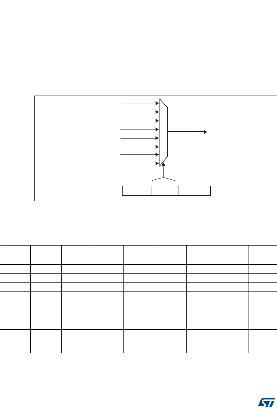
DMA controller (DMA) RM0383
166/836 DocID026448 Rev 1
DMA controller. The peripheral releases its request as soon as it gets the Acknowledge
signal from the DMA controller. Once the request has been deasserted by the peripheral,
the DMA controller releases the Acknowledge signal. If there are more requests, the
peripheral can initiate the next transaction.
9.3.3 Channel selection
Each stream is associated with a DMA request that can be selected out of 8 possible
channel requests. The selection is controlled by the CHSEL[2:0] bits in the DMA_SxCR
register.
Figure 24. Channel selection
The 8 requests from the peripherals (TIM, ADC, SPI, I2C, etc.) are independently connected
to each channel and their connection depends on the product implementation.
Table 79 and Table 81 give examples of DMA request mappings.
REQ_STREAMx
REQ_STRx_CH7
REQ_STRx_CH6
REQ_STRx_CH5
REQ_STRx_CH4
REQ_STRx_CH3
REQ_STRx_CH2
REQ_STRx_CH1
REQ_STRx_CH0
CHSEL[2:0]
312927 0
DMA_SxCR
ai15947
Table 27. DMA1 request mapping (STM32F411xC/E)
Peripheral
requests Stream 0 Stream 1 Stream 2 Stream 3 Stream 4 Stream 5 Stream 6 Stream 7
Channel 0 SPI3_RX I2C1_TX SPI3_RX SPI2_RX SPI2_TX SPI3_TX SPI3_TX
Channel 1 I2C1_RX I2C3_RX I2C1_RX I2C1_TX I2C1_TX
Channel 2 TIM4_CH1 I2S3_EXT_RX TIM4_CH2 I2S2_EXT_TX I2S3_EXT_TX TIM4_UP TIM4_CH3
Channel 3 I2S3_EXT_RX TIM2_UP
TIM2_CH3 I2C3_RX I2S2_EXT_RX I2C3_TX TIM2_CH1 TIM2_CH2
TIM2_CH4
TIM2_UP
TIM2_CH4
Channel 4 USART2_RX USART2_TX
Channel 5 TIM3_CH4
TIM3_UP
TIM3_CH1
TIM3_TRIG TIM3_CH2 TIM3_CH3
Channel 6 TIM5_CH3
TIM5_UP
TIM5_CH4
TIM5_TRIG TIM5_CH1 TIM5_CH4
TIM5_TRIG TIM5_CH2 I2C3_TX TIM5_UP USART2_RX
Channel 7 I2C2_RX I2C2_RX I2C2_TX

DocID026448 Rev 1 167/836
RM0383 DMA controller (DMA)
197
9.3.4 Arbiter
An arbiter manages the 8 DMA stream requests based on their priority for each of the two
AHB master ports (memory and peripheral ports) and launches the peripheral/memory
access sequences.
Priorities are managed in two stages:
•Software: each stream priority can be configured in the DMA_SxCR register. There are
four levels:
– Very high priority
– High priority
– Medium priority
– Low priority
•Hardware: If two requests have the same software priority level, the stream with the
lower number takes priority over the stream with the higher number. For example,
Stream 2 takes priority over Stream 4.
9.3.5 DMA streams
Each of the 8 DMA controller streams provides a unidirectional transfer link between a
source and a destination.
Each stream can be configured to perform:
•Regular type transactions: memory-to-peripherals, peripherals-to-memory or memory-
to-memory transfers
•Double-buffer type transactions: double buffer transfers using two memory pointers for
the memory (while the DMA is reading/writing from/to a buffer, the application can
write/read to/from the other buffer).
The amount of data to be transferred (up to 65535) is programmable and related to the
source width of the peripheral that requests the DMA transfer connected to the peripheral
Table 28. DMA2 request mapping (STM32F411xC/E)
Peripheral
requests Stream 0 Stream 1 Stream 2 Stream 3 Stream 4 Stream 5 Stream 6 Stream 7
Channel 0 ADC1 ADC1
TIM1_CH1
TIM1_CH2
TIM1_CH3
Channel 1
Channel 2 SPI1_TX SPI5_RX SPI5_TX
Channel 3 SPI1_RX SPI1_RX SPI1_TX SPI1_TX
Channel 4 SPI4_RX SPI4_TX USART1_RX SDIO SPI4_RX USART1_RX SDIO USART1_TX
Channel 5 USART6_RX USART6_RX SPI4_RX SPI4_TX SPI5_TX USART6_TX USART6_TX
Channel 6 TIM1_TRIG TIM1_CH1 TIM1_CH2 TIM1_CH1
TIM1_CH4
TIM1_TRIG
TIM1_COM
TIM1_UP TIM1_CH3
Channel 7 SPI5_RX SPI5_TX

DMA controller (DMA) RM0383
168/836 DocID026448 Rev 1
AHB port. The register that contains the amount of data items to be transferred is
decremented after each transaction.
9.3.6 Source, destination and transfer modes
Both source and destination transfers can address peripherals and memories in the entire
4 GB area, at addresses comprised between 0x0000 0000 and 0xFFFF FFFF.
The direction is configured using the DIR[1:0] bits in the DMA_SxCR register and offers
three possibilities: memory-to-peripheral, peripheral-to-memory or memory-to-memory
transfers. Table 29 describes the corresponding source and destination addresses.
When the data width (programmed in the PSIZE or MSIZE bits in the DMA_SxCR register)
is a half-word or a word, respectively, the peripheral or memory address written into the
DMA_SxPAR or DMA_SxM0AR/M1AR registers has to be aligned on a word or half-word
address boundary, respectively.
Peripheral-to-memory mode
Figure 25 describes this mode.
When this mode is enabled (by setting the bit EN in the DMA_SxCR register), each time a
peripheral request occurs, the stream initiates a transfer from the source to fill the FIFO.
When the threshold level of the FIFO is reached, the contents of the FIFO are drained and
stored into the destination.
The transfer stops once the DMA_SxNDTR register reaches zero, when the peripheral
requests the end of transfers (in case of a peripheral flow controller) or when the EN bit in
the DMA_SxCR register is cleared by software.
In direct mode (when the DMDIS value in the DMA_SxFCR register is ‘0’), the threshold
level of the FIFO is not used: after each single data transfer from the peripheral to the FIFO,
the corresponding data are immediately drained and stored into the destination.
The stream has access to the AHB source or destination port only if the arbitration of the
corresponding stream is won. This arbitration is performed using the priority defined for
each stream using the PL[1:0] bits in the DMA_SxCR register.
Table 29. Source and destination address
Bits DIR[1:0] of the
DMA_SxCR register Direction Source address Destination address
00 Peripheral-to-memory DMA_SxPAR DMA_SxM0AR
01 Memory-to-peripheral DMA_SxM0AR DMA_SxPAR
10 Memory-to-memory DMA_SxPAR DMA_SxM0AR
11 reserved - -
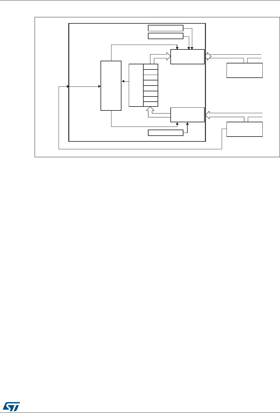
DocID026448 Rev 1 169/836
RM0383 DMA controller (DMA)
197
Figure 25. Peripheral-to-memory mode
1. For double-buffer mode.
Memory-to-peripheral mode
Figure 26 describes this mode.
When this mode is enabled (by setting the EN bit in the DMA_SxCR register), the stream
immediately initiates transfers from the source to entirely fill the FIFO.
Each time a peripheral request occurs, the contents of the FIFO are drained and stored into
the destination. When the level of the FIFO is lower than or equal to the predefined
threshold level, the FIFO is fully reloaded with data from the memory.
The transfer stops once the DMA_SxNDTR register reaches zero, when the peripheral
requests the end of transfers (in case of a peripheral flow controller) or when the EN bit in
the DMA_SxCR register is cleared by software.
In direct mode (when the DMDIS value in the DMA_SxFCR register is '0'), the threshold
level of the FIFO is not used. Once the stream is enabled, the DMA preloads the first data to
transfer into an internal FIFO. As soon as the peripheral requests a data transfer, the DMA
transfers the preloaded value into the configured destination. It then reloads again the
empty internal FIFO with the next data to be transfer. The preloaded data size corresponds
to the value of the PSIZE bitfield in the DMA_SxCR register.
The stream has access to the AHB source or destination port only if the arbitration of the
corresponding stream is won. This arbitration is performed using the priority defined for
each stream using the PL[1:0] bits in the DMA_SxCR register.
Memory bus
Peripheral bus
REQ_STREAMx Arbiter
DMA_SxM1AR(1)
FIFO
AHB memory
port
AHB peripheral
port
DMA_SxPAR
FIFO
level
DMA controller DMA_SxM0AR
destination
source
peripheral
Memory
Peripheral DMA request
ai15948
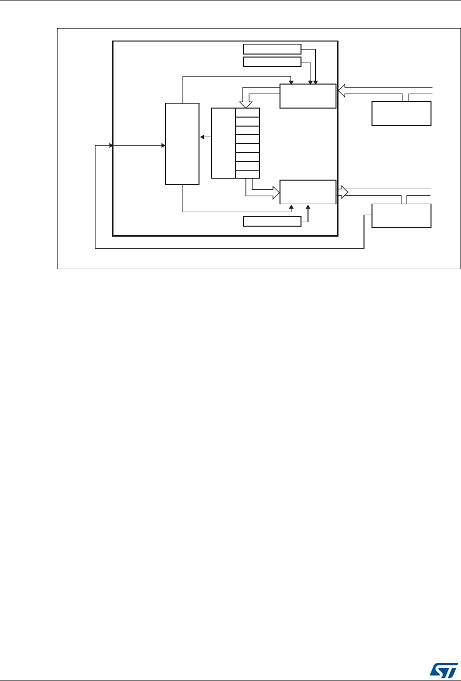
DMA controller (DMA) RM0383
170/836 DocID026448 Rev 1
Figure 26. Memory-to-peripheral mode
1. For double-buffer mode.
Memory-to-memory mode
The DMA channels can also work without being triggered by a request from a peripheral.
This is the memory-to-memory mode, described in Figure 27.
When the stream is enabled by setting the Enable bit (EN) in the DMA_SxCR register, the
stream immediately starts to fill the FIFO up to the threshold level. When the threshold level
is reached, the FIFO contents are drained and stored into the destination.
The transfer stops once the DMA_SxNDTR register reaches zero or when the EN bit in the
DMA_SxCR register is cleared by software.
The stream has access to the AHB source or destination port only if the arbitration of the
corresponding stream is won. This arbitration is performed using the priority defined for
each stream using the PL[1:0] bits in the DMA_SxCR register.
Note: When memory-to-memory mode is used, the Circular and direct modes are not allowed.
Only the DMA2 controller is able to perform memory-to-memory transfers.
Peripheral bus
Memory bus
REQ_STREAMx Arbiter
DMA_SxM1AR
(1)
FIFO
AHB memory
port
AHB peripheral
port
DMA_SxPAR
FIFO
level
DMA controller
DMA_SxM0AR
source
destination
Peripheral
Memory
Peripheral DMA request
ai15949
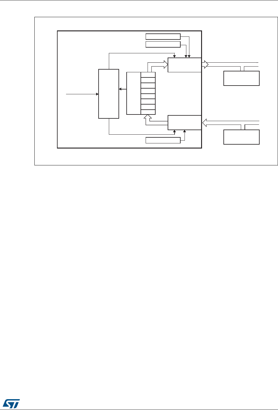
DocID026448 Rev 1 171/836
RM0383 DMA controller (DMA)
197
Figure 27. Memory-to-memory mode
1. For double-buffer mode.
9.3.7 Pointer incrementation
Peripheral and memory pointers can optionally be automatically post-incremented or kept
constant after each transfer depending on the PINC and MINC bits in the DMA_SxCR
register.
Disabling the Increment mode is useful when the peripheral source or destination data are
accessed through a single register.
If the Increment mode is enabled, the address of the next transfer will be the address of the
previous one incremented by 1 (for bytes), 2 (for half-words) or 4 (for words) depending on
the data width programmed in the PSIZE or MSIZE bits in the DMA_SxCR register.
In order to optimize the packing operation, it is possible to fix the increment offset size for
the peripheral address whatever the size of the data transferred on the AHB peripheral port.
The PINCOS bit in the DMA_SxCR register is used to align the increment offset size with
the data size on the peripheral AHB port, or on a 32-bit address (the address is then
incremented by 4). The PINCOS bit has an impact on the AHB peripheral port only.
If PINCOS bit is set, the address of the next transfer is the address of the previous one
incremented by 4 (automatically aligned on a 32-bit address) whatever the PSIZE value.
The AHB memory port, however, is not impacted by this operation.
9.3.8 Circular mode
The Circular mode is available to handle circular buffers and continuous data flows (e.g.
ADC scan mode). This feature can be enabled using the CIRC bit in the DMA_SxCR
register.
Memory bus
Peripheral bus
Stream enable
Arbiter
DMA_SxM1AR(1)
FIFO
AHB memory
port
AHB peripheral
port
DMA_SxPAR
FIFO
level
DMA controller DMA_SxM0AR
destination
source
Memory 1
Memory 2
FIFO
ai15950

DMA controller (DMA) RM0383
172/836 DocID026448 Rev 1
When the circular mode is activated, the number of data items to be transferred is
automatically reloaded with the initial value programmed during the stream configuration
phase, and the DMA requests continue to be served.
Note: In the circular mode, it is mandatory to respect the following rule in case of a burst mode
configured for memory:
DMA_SxNDTR = Multiple of ((Mburst beat) × (Msize)/(Psize)), where:
– (Mburst beat) = 4, 8 or 16 (depending on the MBURST bits in the DMA_SxCR
register)
– ((Msize)/(Psize)) = 1, 2, 4, 1/2 or 1/4 (Msize and Psize represent the MSIZE and
PSIZE bits in the DMA_SxCR register. They are byte dependent)
– DMA_SxNDTR = Number of data items to transfer on the AHB peripheral port
For example: Mburst beat = 8 (INCR8), MSIZE = ‘00’ (byte) and PSIZE = ‘01’ (half-word), in
this case: DMA_SxNDTR must be a multiple of (8 × 1/2 = 4).
If this formula is not respected, the DMA behavior and data integrity are not guaranteed.
NDTR must also be a multiple of the Peripheral burst size multiplied by the peripheral data
size, otherwise this could result in a bad DMA behavior.
9.3.9 Double buffer mode
This mode is available for all the DMA1 and DMA2 streams.
The Double buffer mode is enabled by setting the DBM bit in the DMA_SxCR register.
A double-buffer stream works as a regular (single buffer) stream with the difference that it
has two memory pointers. When the Double buffer mode is enabled, the Circular mode is
automatically enabled (CIRC bit in DMA_SxCR is don’t care) and at each end of transaction,
the memory pointers are swapped.
In this mode, the DMA controller swaps from one memory target to another at each end of
transaction. This allows the software to process one memory area while the second memory
area is being filled/used by the DMA transfer. The double-buffer stream can work in both
directions (the memory can be either the source or the destination) as described in
Table 30: Source and destination address registers in Double buffer mode (DBM=1).
Note: In Double buffer mode, it is possible to update the base address for the AHB memory port
on-the-fly (DMA_SxM0AR or DMA_SxM1AR) when the stream is enabled, by respecting the
following conditions:
•When the CT bit is ‘0’ in the DMA_SxCR register, the DMA_SxM1AR register can be
written. Attempting to write to this register while CT = '1' sets an error flag (TEIF) and
the stream is automatically disabled.
•When the CT bit is ‘1’ in the DMA_SxCR register, the DMA_SxM0AR register can be
written. Attempting to write to this register while CT = '0', sets an error flag (TEIF) and
the stream is automatically disabled.
To avoid any error condition, it is advised to change the base address as soon as the TCIF
flag is asserted because, at this point, the targeted memory must have changed from
memory 0 to 1 (or from 1 to 0) depending on the value of CT in the DMA_SxCR register in
accordance with one of the two above conditions.
For all the other modes (except the Double buffer mode), the memory address registers are
write-protected as soon as the stream is enabled.

DocID026448 Rev 1 173/836
RM0383 DMA controller (DMA)
197
9.3.10 Programmable data width, packing/unpacking, endianess
The number of data items to be transferred has to be programmed into DMA_SxNDTR
(number of data items to transfer bit, NDT) before enabling the stream (except when the
flow controller is the peripheral, PFCTRL bit in DMA_SxCR is set).
When using the internal FIFO, the data widths of the source and destination data are
programmable through the PSIZE and MSIZE bits in the DMA_SxCR register (can be 8-,
16- or 32-bit).
When PSIZE and MSIZE are not equal:
•The data width of the number of data items to transfer, configured in the DMA_SxNDTR
register is equal to the width of the peripheral bus (configured by the PSIZE bits in the
DMA_SxCR register). For instance, in case of peripheral-to-memory, memory-to-
peripheral or memory-to-memory transfers and if the PSIZE[1:0] bits are configured for
half-word, the number of bytes to be transferred is equal to 2 × NDT.
•The DMA controller only copes with little-endian addressing for both source and
destination. This is described in Table 31: Packing/unpacking & endian behavior (bit
PINC = MINC = 1).
This packing/unpacking procedure may present a risk of data corruption when the operation
is interrupted before the data are completely packed/unpacked. So, to ensure data
coherence, the stream may be configured to generate burst transfers: in this case, each
group of transfers belonging to a burst are indivisible (refer to Section 9.3.11: Single and
burst transfers).
In direct mode (DMDIS = 0 in the DMA_SxFCR register), the packing/unpacking of data is
not possible. In this case, it is not allowed to have different source and destination transfer
data widths: both are equal and defined by the PSIZE bits in the DMA_SxCR MSIZE bits are
don’t care).
Table 30. Source and destination address registers in Double buffer mode (DBM=1)
Bits DIR[1:0] of the
DMA_SxCR register Direction Source address Destination address
00 Peripheral-to-memory DMA_SxPAR DMA_SxM0AR /
DMA_SxM1AR
01 Memory-to-peripheral DMA_SxM0AR /
DMA_SxM1AR DMA_SxPAR
10 Not allowed(1)
1. When the Double buffer mode is enabled, the Circular mode is automatically enabled. Since the memory-
to-memory mode is not compatible with the Circular mode, when the Double buffer mode is enabled, it is
not allowed to configure the memory-to-memory mode.
11 Reserved - -

DMA controller (DMA) RM0383
174/836 DocID026448 Rev 1
Note: Peripheral port may be the source or the destination (it could also be the memory source in
the case of memory-to-memory transfer).
PSIZE, MSIZE and NDT[15:0] have to be configured so as to ensure that the last transfer
will not be incomplete. This can occur when the data width of the peripheral port (PSIZE
bits) is lower than the data width of the memory port (MSIZE bits). This constraint is
summarized in Table 32.
Table 31. Packing/unpacking & endian behavior (bit PINC = MINC = 1)
AHB
memory
port
width
AHB
peripheral
port width
Number
of data
items to
transfer
(NDT)
Memory
transfer
number
Memory port
address / byte
lane
Peripher
al
transfer
number
Peripheral port address / byte lane
PINCOS = 1 PINCOS = 0
88 4
1
2
3
4
0x0 / B0[7:0]
0x1 / B1[7:0]
0x2 / B2[7:0]
0x3 / B3[7:0]
1
2
3
4
0x0 / B0[7:0]
0x4 / B1[7:0]
0x8 / B2[7:0]
0xC / B3[7:0]
0x0 / B0[7:0]
0x1 / B1[7:0]
0x2 / B2[7:0]
0x3 / B3[7:0]
816 2
1
2
3
4
0x0 / B0[7:0]
0x1 / B1[7:0]
0x2 / B2[7:0]
0x3 / B3[7:0]
1
2
0x0 / B1|B0[15:0]
0x4 / B3|B2[15:0]
0x0 / B1|B0[15:0]
0x2 / B3|B2[15:0]
832 1
1
2
3
4
0x0 / B0[7:0]
0x1 / B1[7:0]
0x2 / B2[7:0]
0x3 / B3[7:0]
10x0 / B3|B2|B1|B0[31:0] 0x0 / B3|B2|B1|B0[31:0]
16 8 4
1
2
0x0 / B1|B0[15:0]
0x2 / B3|B2[15:0]
1
2
3
4
0x0 / B0[7:0]
0x4 / B1[7:0]
0x8 / B2[7:0]
0xC / B3[7:0]
0x0 / B0[7:0]
0x1 / B1[7:0]
0x2 / B2[7:0]
0x3 / B3[7:0]
16 16 2
1
2
0x0 / B1|B0[15:0]
0x2 / B1|B0[15:0]
1
2
0x0 / B1|B0[15:0]
0x4 / B3|B2[15:0]
0x0 / B1|B0[15:0]
0x2 / B3|B2[15:0]
16 32 1 1
2
0x0 / B1|B0[15:0]
0x2 / B3|B2[15:0]
10x0 / B3|B2|B1|B0[31:0] 0x0 / B3|B2|B1|B0[31:0]
32 8 4
10x0 / B3|B2|B1|B0[31:0] 1
2
3
4
0x0 / B0[7:0]
0x4 / B1[7:0]
0x8 / B2[7:0]
0xC / B3[7:0]
0x0 / B0[7:0]
0x1 / B1[7:0]
0x2 / B2[7:0]
0x3 / B3[7:0]
32 16 2 10x0 /B3|B2|B1|B0[31:0] 1
2
0x0 / B1|B0[15:0]
0x4 / B3|B2[15:0]
0x0 / B1|B0[15:0]
0x2 / B3|B2[15:0]
32 32 1 1 0x0 /B3|B2|B1|B0 [31:0] 1 0x0 /B3|B2|B1|B0 [31:0] 0x0 / B3|B2|B1|B0[31:0]
Table 32. Restriction on NDT versus PSIZE and MSIZE
PSIZE[1:0] of DMA_SxCR MSIZE[1:0] of DMA_SxCR NDT[15:0] of DMA_SxNDTR
00 (8-bit) 01 (16-bit) must be a multiple of 2
00 (8-bit) 10 (32-bit) must be a multiple of 4
01 (16-bit) 10 (32-bit) must be a multiple of 2

DocID026448 Rev 1 175/836
RM0383 DMA controller (DMA)
197
9.3.11 Single and burst transfers
The DMA controller can generate single transfers or incremental burst transfers of 4, 8 or 16
beats.
The size of the burst is configured by software independently for the two AHB ports by using
the MBURST[1:0] and PBURST[1:0] bits in the DMA_SxCR register.
The burst size indicates the number of beats in the burst, not the number of bytes
transferred.
To ensure data coherence, each group of transfers that form a burst are indivisible: AHB
transfers are locked and the arbiter of the AHB bus matrix does not degrant the DMA master
during the sequence of the burst transfer.
Depending on the single or burst configuration, each DMA request initiates a different
number of transfers on the AHB peripheral port:
•When the AHB peripheral port is configured for single transfers, each DMA request
generates a data transfer of a byte, half-word or word depending on the PSIZE[1:0] bits
in the DMA_SxCR register
•When the AHB peripheral port is configured for burst transfers, each DMA request
generates 4,8 or 16 beats of byte, half word or word transfers depending on the
PBURST[1:0] and PSIZE[1:0] bits in the DMA_SxCR register.
The same as above has to be considered for the AHB memory port considering the
MBURST and MSIZE bits.
In direct mode, the stream can only generate single transfers and the MBURST[1:0] and
PBURST[1:0] bits are forced by hardware.
The address pointers (DMA_SxPAR or DMA_SxM0AR registers) must be chosen so as to
ensure that all transfers within a burst block are aligned on the address boundary equal to
the size of the transfer.
The burst configuration has to be selected in order to respect the AHB protocol, where
bursts must not cross the 1 KB address boundary because the minimum address space that
can be allocated to a single slave is 1 KB. This means that the 1 KB address boundary
should not be crossed by a burst block transfer, otherwise an AHB error would be
generated, that is not reported by the DMA registers.
9.3.12 FIFO
FIFO structure
The FIFO is used to temporarily store data coming from the source before transmitting them
to the destination.
Each stream has an independent 4-word FIFO and the threshold level is software-
configurable between 1/4, 1/2, 3/4 or full.
To enable the use of the FIFO threshold level, the direct mode must be disabled by setting
the DMDIS bit in the DMA_SxFCR register.
The structure of the FIFO differs depending on the source and destination data widths, and
is described in Figure 28: FIFO structure.
DMA controller (DMA) RM0383
176/836 DocID026448 Rev 1
Figure 28. FIFO structure
FIFO threshold and burst configuration
Caution is required when choosing the FIFO threshold (bits FTH[1:0] of the DMA_SxFCR
register) and the size of the memory burst (MBURST[1:0] of the DMA_SxCR register): The
content pointed by the FIFO threshold must exactly match to an integer number of memory
burst transfers. If this is not in the case, a FIFO error (flag FEIFx of the DMA_HISR or
DMA_LISR register) will be generated when the stream is enabled, then the stream will be
automatically disabled. The allowed and forbidden configurations are described in the
Table 33: FIFO threshold configurations.
Table 33. FIFO threshold configurations
MSIZE FIFO level MBURST = INCR4 MBURST = INCR8 MBURST = INCR16
Byte
1/4 1 burst of 4 beats forbidden
forbidden1/2 2 bursts of 4 beats 1 burst of 8 beats
3/4 3 bursts of 4 beats forbidden
Full 4 bursts of 4 beats 2 bursts of 8 beats 1 burst of 16 beats
Source: byte
4 words
byte lane 0
byte lane 1
byte lane 2
byte lane 3
1/4 1/2 3/4 FullEmpty
B0
B1
B2
B3
B4
B5
B6
B7
B8
B9
B10
B 11
B12
B13
B14
B15
Destination: word
Source: byte Destination: half-word
4 words
byte lane 0
byte lane 1
byte lane 2
byte lane 3
1/4 1/2 3/4 FullEmpty
B0
B1
B2
B3
B4
B5
B6
B7
B8
B9
B10
B 11
B12
B13
B14
B15
W0W1W2W3
H0
H1
H2
H3
H4
H5
H6
H7
Source: half-word Destination: word
4 words
byte lane 0
byte lane 1
byte lane 2
byte lane 3
1/4 1/2 3/4 FullEmpty
H0
W0W1W2W3
H1
H2
H3
H4
H5
H6
H7
B15 B14 B13 B12 B11 B10 B9 B8 B7 B6 B5 B4 B3 B2 B1 B0
B15 B14 B13 B12 B11 B10 B9 B8 B7 B6 B5 B4 B3 B2 B1 B0
H7 H6 H5 H4 H3 H2 H1 H0
H7, H6, H5, H4, H3, H2, H1, H0
W3, W2, W1, W0
W3, W2, W1, W0
Source: half-word
4-words
byte lane 0
byte lane 1
byte lane 2
byte lane 3
1/4 1/2 3/4 FullEmpty
Destination: byte
H7 H6 H5 H4 H3 H2 H1 H0
B0
B1
B2
B3
B4
B5
B6
B7
B8
B9
B10
B 11
B12
B13
B14
B15
H0
H1
H2
H3
H4
H5
H6
H7
B15 B14 B13 B12 B11 B10 B9 B8
B7 B6 B5 B4 B3 B2 B1 B0
ai15951

DocID026448 Rev 1 177/836
RM0383 DMA controller (DMA)
197
In all cases, the burst size multiplied by the data size must not exceed the FIFO size (data
size can be: 1 (byte), 2 (half-word) or 4 (word)).
Incomplete Burst transfer at the end of a DMA transfer may happen if one of the following
conditions occurs:
•For the AHB peripheral port configuration: the total number of data items (set in the
DMA_SxNDTR register) is not a multiple of the burst size multiplied by the data size
•For the AHB memory port configuration: the number of remaining data items in the
FIFO to be transferred to the memory is not a multiple of the burst size multiplied by the
data size
In such cases, the remaining data to be transferred will be managed in single mode by the
DMA, even if a burst transaction was requested during the DMA stream configuration.
Note: When burst transfers are requested on the peripheral AHB port and the FIFO is used
(DMDIS = 1 in the DMA_SxCR register), it is mandatory to respect the following rule to
avoid permanent underrun or overrun conditions, depending on the DMA stream direction:
If (PBURST × PSIZE) = FIFO_SIZE (4 words), FIFO_Threshold = 3/4 is forbidden with
PSIZE = 1, 2 or 4 and PBURST = 4, 8 or 16.
This rule ensures that enough FIFO space at a time will be free to serve the request from
the peripheral.
FIFO flush
The FIFO can be flushed when the stream is disabled by resetting the EN bit in the
DMA_SxCR register and when the stream is configured to manage peripheral-to-memory or
memory-to-memory transfers: If some data are still present in the FIFO when the stream is
disabled, the DMA controller continues transferring the remaining data to the destination
(even though stream is effectively disabled). When this flush is completed, the transfer
complete status bit (TCIFx) in the DMA_LISR or DMA_HISR register is set.
The remaining data counter DMA_SxNDTR keeps the value in this case to indicate how
many data items are currently available in the destination memory.
Note that during the FIFO flush operation, if the number of remaining data items in the FIFO
to be transferred to memory (in bytes) is less than the memory data width (for example 2
bytes in FIFO while MSIZE is configured to word), data will be sent with the data width set in
the MSIZE bit in the DMA_SxCR register. This means that memory will be written with an
Half-word
1/4 forbidden
forbidden
forbidden
1/2 1 burst of 4 beats
3/4 forbidden
Full 2 bursts of 4 beats 1 burst of 8 beats
Word
1/4
forbidden
forbidden
1/2
3/4
Full 1 burst of 4 beats
Table 33. FIFO threshold configurations (continued)
MSIZE FIFO level MBURST = INCR4 MBURST = INCR8 MBURST = INCR16

DMA controller (DMA) RM0383
178/836 DocID026448 Rev 1
undesired value. The software may read the DMA_SxNDTR register to determine the
memory area that contains the good data (start address and last address).
If the number of remaining data items in the FIFO is lower than a burst size (if the MBURST
bits in DMA_SxCR register are set to configure the stream to manage burst on the AHB
memory port), single transactions will be generated to complete the FIFO flush.
Direct mode
By default, the FIFO operates in direct mode (DMDIS bit in the DMA_SxFCR is reset) and
the FIFO threshold level is not used. This mode is useful when the system requires an
immediate and single transfer to or from the memory after each DMA request.
When the DMA is configured in direct mode (FIFO disabled), to transfer data in memory-to-
peripheral mode, the DMA preloads one data from the memory to the internal FIFO to
ensure an immediate data transfer as soon as a DMA request is triggered by a peripheral.
To avoid saturating the FIFO, it is recommended to configure the corresponding stream with
a high priority.
This mode is restricted to transfers where:
•The source and destination transfer widths are equal and both defined by the
PSIZE[1:0] bits in DMA_SxCR (MSIZE[1:0] bits are don’t care)
•Burst transfers are not possible (PBURST[1:0] and MBURST[1:0] bits in DMA_SxCR
are don’t care)
Direct mode must not be used when implementing memory-to-memory transfers.
9.3.13 DMA transfer completion
Different events can generate an end of transfer by setting the TCIFx bit in the DMA_LISR
or DMA_HISR status register:
•In DMA flow controller mode:
– The DMA_SxNDTR counter has reached zero in the memory-to-peripheral mode
– The stream is disabled before the end of transfer (by clearing the EN bit in the
DMA_SxCR register) and (when transfers are peripheral-to-memory or memory-
to-memory) all the remaining data have been flushed from the FIFO into the
memory
•In Peripheral flow controller mode:
– The last external burst or single request has been generated from the peripheral
and (when the DMA is operating in peripheral-to-memory mode) the remaining
data have been transferred from the FIFO into the memory
– The stream is disabled by software, and (when the DMA is operating in peripheral-
to-memory mode) the remaining data have been transferred from the FIFO into
the memory
Note: The transfer completion is dependent on the remaining data in FIFO to be transferred into
memory only in the case of peripheral-to-memory mode. This condition is not applicable in
memory-to-peripheral mode.
If the stream is configured in noncircular mode, after the end of the transfer (that is when the
number of data to be transferred reaches zero), the DMA is stopped (EN bit in DMA_SxCR
register is cleared by Hardware) and no DMA request is served unless the software
reprograms the stream and re-enables it (by setting the EN bit in the DMA_SxCR register).

DocID026448 Rev 1 179/836
RM0383 DMA controller (DMA)
197
9.3.14 DMA transfer suspension
At any time, a DMA transfer can be suspended to be restarted later on or to be definitively
disabled before the end of the DMA transfer.
There are two cases:
•The stream disables the transfer with no later-on restart from the point where it was
stopped. There is no particular action to do, except to clear the EN bit in the
DMA_SxCR register to disable the stream. The stream may take time to be disabled
(ongoing transfer is completed first). The transfer complete interrupt flag (TCIF in the
DMA_LISR or DMA_HISR register) is set in order to indicate the end of transfer. The
value of the EN bit in DMA_SxCR is now ‘0’ to confirm the stream interruption. The
DMA_SxNDTR register contains the number of remaining data items at the moment
when the stream was stopped so that the software can determine how many data items
have been transferred before the stream was interrupted.
•The stream suspends the transfer before the number of remaining data items to be
transferred in the DMA_SxNDTR register reaches 0. The aim is to restart the transfer
later by re-enabling the stream. In order to restart from the point where the transfer was
stopped, the software has to read the DMA_SxNDTR register after disabling the stream
by writing the EN bit in DMA_SxCR register (and then checking that it is at ‘0’) to know
the number of data items already collected. Then:
– The peripheral and/or memory addresses have to be updated in order to adjust
the address pointers
– The SxNDTR register has to be updated with the remaining number of data items
to be transferred (the value read when the stream was disabled)
– The stream may then be re-enabled to restart the transfer from the point it was
stopped
Note: Note that a Transfer complete interrupt flag (TCIF in DMA_LISR or DMA_HISR) is set to
indicate the end of transfer due to the stream interruption.
9.3.15 Flow controller
The entity that controls the number of data to be transferred is known as the flow controller.
This flow controller is configured independently for each stream using the PFCTRL bit in the
DMA_SxCR register.
The flow controller can be:
•The DMA controller: in this case, the number of data items to be transferred is
programmed by software into the DMA_SxNDTR register before the DMA stream is
enabled.
•The peripheral source or destination: this is the case when the number of data items to
be transferred is unknown. The peripheral indicates by hardware to the DMA controller
when the last data are being transferred. This feature is only supported for peripherals
which are able to signal the end of the transfer, that is:
–SDIO
When the peripheral flow controller is used for a given stream, the value written into the
DMA_SxNDTR has no effect on the DMA transfer. Actually, whatever the value written, it will

DMA controller (DMA) RM0383
180/836 DocID026448 Rev 1
be forced by hardware to 0xFFFF as soon as the stream is enabled, to respect the following
schemes:
•Anticipated stream interruption: EN bit in DMA_SxCR register is reset to 0 by the
software to stop the stream before the last data hardware signal (single or burst) is sent
by the peripheral. In such a case, the stream is switched off and the FIFO flush is
triggered in the case of a peripheral-to-memory DMA transfer. The TCIFx flag of the
corresponding stream is set in the status register to indicate the DMA completion. To
know the number of data items transferred during the DMA transfer, read the
DMA_SxNDTR register and apply the following formula:
– Number_of_data_transferred = 0xFFFF – DMA_SxNDTR
•Normal stream interruption due to the reception of a last data hardware signal: the
stream is automatically interrupted when the peripheral requests the last transfer
(single or burst) and when this transfer is complete. the TCIFx flag of the corresponding
stream is set in the status register to indicate the DMA transfer completion. To know the
number of data items transferred, read the DMA_SxNDTR register and apply the same
formula as above.
•The DMA_SxNDTR register reaches 0: the TCIFx flag of the corresponding stream is
set in the status register to indicate the forced DMA transfer completion. The stream is
automatically switched off even though the last data hardware signal (single or burst)
has not been yet asserted. The already transferred data will not be lost. This means
that a maximum of 65535 data items can be managed by the DMA in a single
transaction, even in peripheral flow control mode.
Note: When configured in memory-to-memory mode, the DMA is always the flow controller and
the PFCTRL bit is forced to 0 by hardware.
The Circular mode is forbidden in the peripheral flow controller mode.
9.3.16 Summary of the possible DMA configurations
Table 34 summarizes the different possible DMA configurations.
Table 34. Possible DMA configurations
DMA transfer
mode Source Destination Flow
controller Circular
mode Transfer
type Direct
mode Double
buffer mode
Peripheral-to-
memory
AHB
peripheral port
AHB
memory port
DMA possible
single possible
possible
burst forbidden
Peripheral forbidden
single possible
forbidden
burst forbidden
Memory-to-
peripheral
AHB
memory port
AHB
peripheral port
DMA possible
single possible
possible
burst forbidden
Peripheral forbidden
single possible
forbidden
burst forbidden
Memory-to-
memory
AHB
peripheral port
AHB
memory port DMA only forbidden
single
forbidden forbidden
burst

DocID026448 Rev 1 181/836
RM0383 DMA controller (DMA)
197
9.3.17 Stream configuration procedure
The following sequence should be followed to configure a DMA stream x (where x is the
stream number):
1. If the stream is enabled, disable it by resetting the EN bit in the DMA_SxCR register,
then read this bit in order to confirm that there is no ongoing stream operation. Writing
this bit to 0 is not immediately effective since it is actually written to 0 once all the
current transfers have finished. When the EN bit is read as 0, this means that the
stream is ready to be configured. It is therefore necessary to wait for the EN bit to be
cleared before starting any stream configuration. All the stream dedicated bits set in the
status register (DMA_LISR and DMA_HISR) from the previous data block DMA
transfer should be cleared before the stream can be re-enabled.
2. Set the peripheral port register address in the DMA_SxPAR register. The data will be
moved from/ to this address to/ from the peripheral port after the peripheral event.
3. Set the memory address in the DMA_SxMA0R register (and in the DMA_SxMA1R
register in the case of a double buffer mode). The data will be written to or read from
this memory after the peripheral event.
4. Configure the total number of data items to be transferred in the DMA_SxNDTR
register. After each peripheral event or each beat of the burst, this value is
decremented.
5. Select the DMA channel (request) using CHSEL[2:0] in the DMA_SxCR register.
6. If the peripheral is intended to be the flow controller and if it supports this feature, set
the PFCTRL bit in the DMA_SxCR register.
7. Configure the stream priority using the PL[1:0] bits in the DMA_SxCR register.
8. Configure the FIFO usage (enable or disable, threshold in transmission and reception)
9. Configure the data transfer direction, peripheral and memory incremented/fixed mode,
single or burst transactions, peripheral and memory data widths, Circular mode,
Double buffer mode and interrupts after half and/or full transfer, and/or errors in the
DMA_SxCR register.
10. Activate the stream by setting the EN bit in the DMA_SxCR register.
As soon as the stream is enabled, it can serve any DMA request from the peripheral
connected to the stream.
Once half the data have been transferred on the AHB destination port, the half-transfer flag
(HTIF) is set and an interrupt is generated if the half-transfer interrupt enable bit (HTIE) is
set. At the end of the transfer, the transfer complete flag (TCIF) is set and an interrupt is
generated if the transfer complete interrupt enable bit (TCIE) is set.
Warning: To switch off a peripheral connected to a DMA stream
request, it is mandatory to, first, switch off the DMA stream to
which the peripheral is connected, then to wait for EN bit = 0.
Only then can the peripheral be safely disabled.

DMA controller (DMA) RM0383
182/836 DocID026448 Rev 1
9.3.18 Error management
The DMA controller can detect the following errors:
•Transfer error: the transfer error interrupt flag (TEIFx) is set when:
– A bus error occurs during a DMA read or a write access
– A write access is requested by software on a memory address register in Double
buffer mode whereas the stream is enabled and the current target memory is the
one impacted by the write into the memory address register (refer to Section 9.3.9:
Double buffer mode)
•FIFO error: the FIFO error interrupt flag (FEIFx) is set if:
– A FIFO underrun condition is detected
– A FIFO overrun condition is detected (no detection in memory-to-memory mode
because requests and transfers are internally managed by the DMA)
– The stream is enabled while the FIFO threshold level is not compatible with the
size of the memory burst (refer to Table 33: FIFO threshold configurations)
•Direct mode error: the direct mode error interrupt flag (DMEIFx) can only be set in the
peripheral-to-memory mode while operating in direct mode and when the MINC bit in
the DMA_SxCR register is cleared. This flag is set when a DMA request occurs while
the previous data have not yet been fully transferred into the memory (because the
memory bus was not granted). In this case, the flag indicates that 2 data items were be
transferred successively to the same destination address, which could be an issue if
the destination is not able to manage this situation
In direct mode, the FIFO error flag can also be set under the following conditions:
•In the peripheral-to-memory mode, the FIFO can be saturated (overrun) if the memory
bus is not granted for several peripheral requests
•In the memory-to-peripheral mode, an underrun condition may occur if the memory bus
has not been granted before a peripheral request occurs
If the TEIFx or the FEIFx flag is set due to incompatibility between burst size and FIFO
threshold level, the faulty stream is automatically disabled through a hardware clear of its
EN bit in the corresponding stream configuration register (DMA_SxCR).
If the DMEIFx or the FEIFx flag is set due to an overrun or underrun condition, the faulty
stream is not automatically disabled and it is up to the software to disable or not the stream
by resetting the EN bit in the DMA_SxCR register. This is because there is no data loss
when this kind of errors occur.
When the stream's error interrupt flag (TEIF, FEIF, DMEIF) in the DMA_LISR or DMA_HISR
register is set, an interrupt is generated if the corresponding interrupt enable bit (TEIE,
FEIE, DMIE) in the DMA_SxCR or DMA_SxFCR register is set.
Note: When a FIFO overrun or underrun condition occurs, the data are not lost because the
peripheral request is not acknowledged by the stream until the overrun or underrun
condition is cleared. If this acknowledge takes too much time, the peripheral itself may
detect an overrun or underrun condition of its internal buffer and data might be lost.
DocID026448 Rev 1 183/836
RM0383 DMA controller (DMA)
197
9.4 DMA interrupts
For each DMA stream, an interrupt can be produced on the following events:
•Half-transfer reached
•Transfer complete
•Transfer error
•Fifo error (overrun, underrun or FIFO level error)
•Direct mode error
Separate interrupt enable control bits are available for flexibility as shown in Table 35.
Note: Before setting an Enable control bit to ‘1’, the corresponding event flag should be cleared,
otherwise an interrupt is immediately generated.
9.5 DMA registers
The DMA registers have to be accessed by words (32 bits).
9.5.1 DMA low interrupt status register (DMA_LISR)
Address offset: 0x00
Reset value: 0x0000 0000
Table 35. DMA interrupt requests
Interrupt event Event flag Enable control bit
Half-transfer HTIF HTIE
Transfer complete TCIF TCIE
Transfer error TEIF TEIE
FIFO overrun/underrun FEIF FEIE
Direct mode error DMEIF DMEIE
31 30 29 28 27 26 25 24 23 22 21 20 19 18 17 16
Reserved TCIF3 HTIF3 TEIF3 DMEIF3 Reserv
ed
FEIF3 TCIF2 HTIF2 TEIF2 DMEIF2 Reserv
ed
FEIF2
rrrrrr r r r r r r r r
15 14 13 12 11 10 9 8 7 6 5 4 3 2 1 0
Reserved TCIF1 HTIF1 TEIF1 DMEIF1 Reserv
ed
FEIF1 TCIF0 HTIF0 TEIF0 DMEIF0 Reserv
ed
FEIF0
rrrrrr r r r r r r r r
Bits 31:28, 15:12 Reserved, must be kept at reset value.
Bits 27, 21, 11, 5 TCIFx: Stream x transfer complete interrupt flag (x = 3..0)
This bit is set by hardware. It is cleared by software writing 1 to the corresponding bit in the
DMA_LIFCR register.
0: No transfer complete event on stream x
1: A transfer complete event occurred on stream x

DMA controller (DMA) RM0383
184/836 DocID026448 Rev 1
9.5.2 DMA high interrupt status register (DMA_HISR)
Address offset: 0x04
Reset value: 0x0000 0000
Bits 26, 20, 10, 4 HTIFx: Stream x half transfer interrupt flag (x=3..0)
This bit is set by hardware. It is cleared by software writing 1 to the corresponding bit in the
DMA_LIFCR register.
0: No half transfer event on stream x
1: A half transfer event occurred on stream x
Bits 25, 19, 9, 3 TEIFx: Stream x transfer error interrupt flag (x=3..0)
This bit is set by hardware. It is cleared by software writing 1 to the corresponding bit in the
DMA_LIFCR register.
0: No transfer error on stream x
1: A transfer error occurred on stream x
Bits 24, 18, 8, 2 DMEIFx: Stream x direct mode error interrupt flag (x=3..0)
This bit is set by hardware. It is cleared by software writing 1 to the corresponding bit in the
DMA_LIFCR register.
0: No Direct Mode Error on stream x
1: A Direct Mode Error occurred on stream x
Bits 23, 17, 7, 1 Reserved, must be kept at reset value.
Bits 22, 16, 6, 0 FEIFx: Stream x FIFO error interrupt flag (x=3..0)
This bit is set by hardware. It is cleared by software writing 1 to the corresponding bit in the
DMA_LIFCR register.
0: No FIFO Error event on stream x
1: A FIFO Error event occurred on stream x
31 30 29 28 27 26 25 24 23 22 21 20 19 18 17 16
Reserved
TCIF7 HTIF7 TEIF7 DMEIF7 Reserv
ed
FEIF7 TCIF6 HTIF6 TEIF6 DMEIF6 Reserv
ed
FEIF6
rr r r r r r r r r
15 14 13 12 11 10 9 8 7 6 5 4 3 2 1 0
Reserved
TCIF5 HTIF5 TEIF5 DMEIF5 Reserv
ed
FEIF5 TCIF4 HTIF4 TEIF4 DMEIF4 Reserv
ed
FEIF4
rr r r r r r r r r
Bits 31:28, 15:12 Reserved, must be kept at reset value.
Bits 27, 21, 11, 5 TCIFx: Stream x transfer complete interrupt flag (x=7..4)
This bit is set by hardware. It is cleared by software writing 1 to the corresponding bit in the
DMA_HIFCR register.
0: No transfer complete event on stream x
1: A transfer complete event occurred on stream x
Bits 26, 20, 10, 4 HTIFx: Stream x half transfer interrupt flag (x=7..4)
This bit is set by hardware. It is cleared by software writing 1 to the corresponding bit in the
DMA_HIFCR register.
0: No half transfer event on stream x
1: A half transfer event occurred on stream x

DocID026448 Rev 1 185/836
RM0383 DMA controller (DMA)
197
9.5.3 DMA low interrupt flag clear register (DMA_LIFCR)
Address offset: 0x08
Reset value: 0x0000 0000
Bits 25, 19, 9, 3 TEIFx: Stream x transfer error interrupt flag (x=7..4)
This bit is set by hardware. It is cleared by software writing 1 to the corresponding bit in the
DMA_HIFCR register.
0: No transfer error on stream x
1: A transfer error occurred on stream x
Bits 24, 18, 8, 2 DMEIFx: Stream x direct mode error interrupt flag (x=7..4)
This bit is set by hardware. It is cleared by software writing 1 to the corresponding bit in the
DMA_HIFCR register.
0: No Direct mode error on stream x
1: A Direct mode error occurred on stream x
Bits 23, 17, 7, 1 Reserved, must be kept at reset value.
Bits 22, 16, 6, 0 FEIFx: Stream x FIFO error interrupt flag (x=7..4)
This bit is set by hardware. It is cleared by software writing 1 to the corresponding bit in the
DMA_HIFCR register.
0: No FIFO error event on stream x
1: A FIFO error event occurred on stream x
31 30 29 28 27 26 25 24 23 22 21 20 19 18 17 16
Reserved CTCIF3 CHTIF3 CTEIF3 CDMEIF3 Reserved CFEIF3 CTCIF2 CHTIF2 CTEIF2 CDMEIF2 Reserved CFEIF2
www w w w w w w w
15 14 13 12 11 10 9 8 7 6 5 4 3 2 1 0
Reserved CTCIF1 CHTIF1 CTEIF1 CDMEIF1 Reserved CFEIF1 CTCIF0 CHTIF0 CTEIF0 CDMEIF0 Reserved CFEIF0
www w w w w w w w
Bits 31:28, 15:12 Reserved, must be kept at reset value.
Bits 27, 21, 11, 5 CTCIFx: Stream x clear transfer complete interrupt flag (x = 3..0)
Writing 1 to this bit clears the corresponding TCIFx flag in the DMA_LISR register
Bits 26, 20, 10, 4 CHTIFx: Stream x clear half transfer interrupt flag (x = 3..0)
Writing 1 to this bit clears the corresponding HTIFx flag in the DMA_LISR register
Bits 25, 19, 9, 3 CTEIFx: Stream x clear transfer error interrupt flag (x = 3..0)
Writing 1 to this bit clears the corresponding TEIFx flag in the DMA_LISR register
Bits 24, 18, 8, 2 CDMEIFx: Stream x clear direct mode error interrupt flag (x = 3..0)
Writing 1 to this bit clears the corresponding DMEIFx flag in the DMA_LISR register
Bits 23, 17, 7, 1 Reserved, must be kept at reset value.
Bits 22, 16, 6, 0 CFEIFx: Stream x clear FIFO error interrupt flag (x = 3..0)
Writing 1 to this bit clears the corresponding CFEIFx flag in the DMA_LISR register

DMA controller (DMA) RM0383
186/836 DocID026448 Rev 1
9.5.4 DMA high interrupt flag clear register (DMA_HIFCR)
Address offset: 0x0C
Reset value: 0x0000 0000
31 30 29 28 27 26 25 24 23 22 21 20 19 18 17 16
Reserved CTCIF7 CHTIF7 CTEIF7 CDMEIF7 Reserved CFEIF7 CTCIF6 CHTIF6 CTEIF6 CDMEIF6 Reserved CFEIF6
www w w w w w w w
15 14 13 12 11 10 9 8 7 6 5 4 3 2 1 0
Reserved CTCIF5 CHTIF5 CTEIF5 CDMEIF5 Reserved CFEIF5 CTCIF4 CHTIF4 CTEIF4 CDMEIF4 Reserved CFEIF4
www w w w w w w w
Bits 31:28, 15:12 Reserved, must be kept at reset value.
Bits 27, 21, 11, 5 CTCIFx: Stream x clear transfer complete interrupt flag (x = 7..4)
Writing 1 to this bit clears the corresponding TCIFx flag in the DMA_HISR register
Bits 26, 20, 10, 4 CHTIFx: Stream x clear half transfer interrupt flag (x = 7..4)
Writing 1 to this bit clears the corresponding HTIFx flag in the DMA_HISR register
Bits 25, 19, 9, 3 CTEIFx: Stream x clear transfer error interrupt flag (x = 7..4)
Writing 1 to this bit clears the corresponding TEIFx flag in the DMA_HISR register
Bits 24, 18, 8, 2 CDMEIFx: Stream x clear direct mode error interrupt flag (x = 7..4)
Writing 1 to this bit clears the corresponding DMEIFx flag in the DMA_HISR register
Bits 23, 17, 7, 1 Reserved, must be kept at reset value.
Bits 22, 16, 6, 0 CFEIFx: Stream x clear FIFO error interrupt flag (x = 7..4)
Writing 1 to this bit clears the corresponding CFEIFx flag in the DMA_HISR register

DocID026448 Rev 1 187/836
RM0383 DMA controller (DMA)
197
9.5.5 DMA stream x configuration register (DMA_SxCR) (x = 0..7)
This register is used to configure the concerned stream.
Address offset: 0x10 + 0x18 × stream number
Reset value: 0x0000 0000
31 30 29 28 27 26 25 24 23 22 21 20 19 18 17 16
Reserved CHSEL[3:0] MBURST [1:0] PBURST[1:0] Reserv
ed
CT DBM or
reserved PL[1:0]
rw rw rw rw rw rw rw rw rw or r rw rw
15 14 13 12 11 10 9 8 7 6 5 4 3 2 1 0
PINCOS MSIZE[1:0] PSIZE[1:0] MINC PINC CIRC DIR[1:0] PFCTRL TCIE HTIE TEIE DMEIE EN
rw rw rw rw rw rw rw rw rw rw rw rw rw rw rw rw
Bits 31:28 Reserved, must be kept at reset value.
Bits 27:25 CHSEL[2:0]: Channel selection
These bits are set and cleared by software.
000: channel 0 selected
001: channel 1 selected
010: channel 2 selected
011: channel 3 selected
100: channel 4 selected
101: channel 5 selected
110: channel 6 selected
111: channel 7 selected
These bits are protected and can be written only if EN is ‘0’
Bits 24:23 MBURST: Memory burst transfer configuration
These bits are set and cleared by software.
00: single transfer
01: INCR4 (incremental burst of 4 beats)
10: INCR8 (incremental burst of 8 beats)
11: INCR16 (incremental burst of 16 beats)
These bits are protected and can be written only if EN is ‘0’
In direct mode, these bits are forced to 0x0 by hardware as soon as bit EN= '1'.
Bits 22:21 PBURST[1:0]: Peripheral burst transfer configuration
These bits are set and cleared by software.
00: single transfer
01: INCR4 (incremental burst of 4 beats)
10: INCR8 (incremental burst of 8 beats)
11: INCR16 (incremental burst of 16 beats)
These bits are protected and can be written only if EN is ‘0’
In direct mode, these bits are forced to 0x0 by hardware.
Bit 20 Reserved, must be kept at reset value.
Bit 19 CT: Current target (only in double buffer mode)
This bits is set and cleared by hardware. It can also be written by software.
0: The current target memory is Memory 0 (addressed by the DMA_SxM0AR pointer)
1: The current target memory is Memory 1 (addressed by the DMA_SxM1AR pointer)
This bit can be written only if EN is ‘0’ to indicate the target memory area of the first transfer.
Once the stream is enabled, this bit operates as a status flag indicating which memory area
is the current target.

DMA controller (DMA) RM0383
188/836 DocID026448 Rev 1
Bit 18 DBM: Double buffer mode
This bits is set and cleared by software.
0: No buffer switching at the end of transfer
1: Memory target switched at the end of the DMA transfer
This bit is protected and can be written only if EN is ‘0’.
Bits 17:16 PL[1:0]: Priority level
These bits are set and cleared by software.
00: Low
01: Medium
10: High
11: Very high
These bits are protected and can be written only if EN is ‘0’.
Bit 15 PINCOS: Peripheral increment offset size
This bit is set and cleared by software
0: The offset size for the peripheral address calculation is linked to the PSIZE
1: The offset size for the peripheral address calculation is fixed to 4 (32-bit alignment).
This bit has no meaning if bit PINC = '0'.
This bit is protected and can be written only if EN = '0'.
This bit is forced low by hardware when the stream is enabled (bit EN = '1') if the direct
mode is selected or if PBURST are different from “00”.
Bits 14:13 MSIZE[1:0]: Memory data size
These bits are set and cleared by software.
00: byte (8-bit)
01: half-word (16-bit)
10: word (32-bit)
11: reserved
These bits are protected and can be written only if EN is ‘0’.
In direct mode, MSIZE is forced by hardware to the same value as PSIZE as soon as bit EN
= '1'.
Bits 12:11 PSIZE[1:0]: Peripheral data size
These bits are set and cleared by software.
00: Byte (8-bit)
01: Half-word (16-bit)
10: Word (32-bit)
11: reserved
These bits are protected and can be written only if EN is ‘0’
Bit 10 MINC: Memory increment mode
This bit is set and cleared by software.
0: Memory address pointer is fixed
1: Memory address pointer is incremented after each data transfer (increment is done
according to MSIZE)
This bit is protected and can be written only if EN is ‘0’.
Bit 9 PINC: Peripheral increment mode
This bit is set and cleared by software.
0: Peripheral address pointer is fixed
1: Peripheral address pointer is incremented after each data transfer (increment is done
according to PSIZE)
This bit is protected and can be written only if EN is ‘0’.

DocID026448 Rev 1 189/836
RM0383 DMA controller (DMA)
197
Bit 8 CIRC: Circular mode
This bit is set and cleared by software and can be cleared by hardware.
0: Circular mode disabled
1: Circular mode enabled
When the peripheral is the flow controller (bit PFCTRL=1) and the stream is enabled (bit
EN=1), then this bit is automatically forced by hardware to 0.
It is automatically forced by hardware to 1 if the DBM bit is set, as soon as the stream is
enabled (bit EN ='1').
Bits 7:6 DIR[1:0]: Data transfer direction
These bits are set and cleared by software.
00: Peripheral-to-memory
01: Memory-to-peripheral
10: Memory-to-memory
11: reserved
These bits are protected and can be written only if EN is ‘0’.
Bit 5 PFCTRL: Peripheral flow controller
This bit is set and cleared by software.
0: The DMA is the flow controller
1: The peripheral is the flow controller
This bit is protected and can be written only if EN is ‘0’.
When the memory-to-memory mode is selected (bits DIR[1:0]=10), then this bit is
automatically forced to 0 by hardware.
Bit 4 TCIE: Transfer complete interrupt enable
This bit is set and cleared by software.
0: TC interrupt disabled
1: TC interrupt enabled
Bit 3 HTIE: Half transfer interrupt enable
This bit is set and cleared by software.
0: HT interrupt disabled
1: HT interrupt enabled
Bit 2 TEIE: Transfer error interrupt enable
This bit is set and cleared by software.
0: TE interrupt disabled
1: TE interrupt enabled
Bit 1 DMEIE: Direct mode error interrupt enable
This bit is set and cleared by software.
0: DME interrupt disabled
1: DME interrupt enabled

DMA controller (DMA) RM0383
190/836 DocID026448 Rev 1
9.5.6 DMA stream x number of data register (DMA_SxNDTR) (x = 0..7)
Address offset: 0x14 + 0x18 × stream number
Reset value: 0x0000 0000
Bit 0 EN: Stream enable / flag stream ready when read low
This bit is set and cleared by software.
0: Stream disabled
1: Stream enabled
This bit may be cleared by hardware:
– on a DMA end of transfer (stream ready to be configured)
– if a transfer error occurs on the AHB master buses
– when the FIFO threshold on memory AHB port is not compatible with the size of the
burst
When this bit is read as 0, the software is allowed to program the Configuration and FIFO
bits registers. It is forbidden to write these registers when the EN bit is read as 1.
Note: Before setting EN bit to '1' to start a new transfer, the event flags corresponding to the
stream in DMA_LISR or DMA_HISR register must be cleared.
31 30 29 28 27 26 25 24 23 22 21 20 19 18 17 16
Reserved
15 14 13 12 11 10 9 8 7 6 5 4 3 2 1 0
NDT[15:0]
rw rw rw rw rw rw rw rw rw rw rw rw rw rw rw rw
Bits 31:16 Reserved, must be kept at reset value.
Bits 15:0 NDT[15:0]: Number of data items to transfer
Number of data items to be transferred (0 up to 65535). This register can be written only
when the stream is disabled. When the stream is enabled, this register is read-only,
indicating the remaining data items to be transmitted. This register decrements after each
DMA transfer.
Once the transfer has completed, this register can either stay at zero (when the stream is in
normal mode) or be reloaded automatically with the previously programmed value in the
following cases:
– when the stream is configured in Circular mode.
– when the stream is enabled again by setting EN bit to '1'
If the value of this register is zero, no transaction can be served even if the stream is
enabled.
DocID026448 Rev 1 191/836
RM0383 DMA controller (DMA)
197
9.5.7 DMA stream x peripheral address register (DMA_SxPAR) (x = 0..7)
Address offset: 0x18 + 0x18 × stream number
Reset value: 0x0000 0000
9.5.8 DMA stream x memory 0 address register (DMA_SxM0AR) (x = 0..7)
Address offset: 0x1C + 0x18 × stream number
Reset value: 0x0000 0000
9.5.9 DMA stream x memory 1 address register (DMA_SxM1AR) (x = 0..7)
Address offset: 0x20 + 0x18 × stream number
Reset value: 0x0000 0000
31 30 29 28 27 26 25 24 23 22 21 20 19 18 17 16
PAR[31:16]
rw rw rw rw rw rw rw rw rw rw rw rw rw rw rw rw
15 14 13 12 11 10 9 8 7 6 5 4 3 2 1 0
PAR[15:0]
rw rw rw rw rw rw rw rw rw rw rw rw rw rw rw rw
Bits 31:0 PAR[31:0]: Peripheral address
Base address of the peripheral data register from/to which the data will be read/written.
These bits are write-protected and can be written only when bit EN = '0' in the DMA_SxCR register.
31 30 29 28 27 26 25 24 23 22 21 20 19 18 17 16
M0A[31:16]
rw rw rw rw rw rw rw rw rw rw rw rw rw rw rw rw
15 14 13 12 11 10 9 8 7 6 5 4 3 2 1 0
M0A[15:0]
rw rw rw rw rw rw rw rw rw rw rw rw rw rw rw rw
Bits 31:0 M0A[31:0]: Memory 0 address
Base address of Memory area 0 from/to which the data will be read/written.
These bits are write-protected. They can be written only if:
– the stream is disabled (bit EN= '0' in the DMA_SxCR register) or
– the stream is enabled (EN=’1’ in DMA_SxCR register) and bit CT = '1' in the
DMA_SxCR register (in Double buffer mode).
31 30 29 28 27 26 25 24 23 22 21 20 19 18 17 16
M1A[31:16]
rw rw rw rw rw rw rw rw rw rw rw rw rw rw rw rw
15 14 13 12 11 10 9 8 7 6 5 4 3 2 1 0
M1A[15:0]
rw rw rw rw rw rw rw rw rw rw rw rw rw rw rw rw

DMA controller (DMA) RM0383
192/836 DocID026448 Rev 1
9.5.10 DMA stream x FIFO control register (DMA_SxFCR) (x = 0..7)
Address offset: 0x24 + 0x24 × stream number
Reset value: 0x0000 0021
Bits 31:0 M1A[31:0]: Memory 1 address (used in case of Double buffer mode)
Base address of Memory area 1 from/to which the data will be read/written.
This register is used only for the Double buffer mode.
These bits are write-protected. They can be written only if:
– the stream is disabled (bit EN= '0' in the DMA_SxCR register) or
– the stream is enabled (EN=’1’ in DMA_SxCR register) and bit CT = '0' in the
DMA_SxCR register.
31 30 29 28 27 26 25 24 23 22 21 20 19 18 17 16
Reserved
15 14 13 12 11 10 9 8 7 6 5 4 3 2 1 0
Reserved FEIE Reser
ved
FS[2:0] DMDIS FTH[1:0]
rw r r r rw rw rw
Bits 31:8 Reserved, must be kept at reset value.
Bit 7 FEIE: FIFO error interrupt enable
This bit is set and cleared by software.
0: FE interrupt disabled
1: FE interrupt enabled
Bit 6 Reserved, must be kept at reset value.

DocID026448 Rev 1 193/836
RM0383 DMA controller (DMA)
197
Bits 5:3 FS[2:0]: FIFO status
These bits are read-only.
000: 0 < fifo_level < 1/4
001: 1/4 ≤ fifo_level < 1/2
010: 1/2 ≤ fifo_level < 3/4
011: 3/4 ≤ fifo_level < full
100: FIFO is empty
101: FIFO is full
others: no meaning
These bits are not relevant in the direct mode (DMDIS bit is zero).
Bit 2 DMDIS: Direct mode disable
This bit is set and cleared by software. It can be set by hardware.
0: Direct mode enabled
1: Direct mode disabled
This bit is protected and can be written only if EN is ‘0’.
This bit is set by hardware if the memory-to-memory mode is selected (DIR bit in
DMA_SxCR are “10”) and the EN bit in the DMA_SxCR register is ‘1’ because the direct
mode is not allowed in the memory-to-memory configuration.
Bits 1:0 FTH[1:0]: FIFO threshold selection
These bits are set and cleared by software.
00: 1/4 full FIFO
01: 1/2 full FIFO
10: 3/4 full FIFO
11: full FIFO
These bits are not used in the direct mode when the DMIS value is zero.
These bits are protected and can be written only if EN is ‘1’.
DMA controller (DMA) RM0383
194/836 DocID026448 Rev 1
9.5.11 DMA register map
Table 36 summarizes the DMA registers.
Table 36. DMA register map and reset values
Offset Register
31
30
29
28
27
26
25
24
23
22
21
20
19
18
17
16
15
14
13
12
11
10
9
8
7
6
5
4
3
2
1
0
0x0000 DMA_LISR Reserved
TCIF3
HTIF3
TEIF3
DMEIF3
Reserved
FEIF3
TCIF2
HTIF2
TEIF2
DMEIF2
Reserved
FEIF2
Reserved
TCIF1
HTIF1
TEIF1
DMEIF1
Reserved
FEIF1
TCIF0
HTIF0
TEIF0
DMEIF0
Reserved
FEIF0
Reset value 0000 00000 0 0000 00000 0
0x0004 DMA_HISR Reserved
TCIF7
HTIF7
TEIF7
DMEIF7
Reserved
FEIF7
TCIF6
HTIF6
TEIF6
DMEIF6
Reserved
FEIF6
Reserved
TCIF5
HTIF5
TEIF5
DMEIF5
Reserved
FEIF5
TCIF4
HTIF4
TEIF4
DMEIF4
Reserved
FEIF4
Reset value 0000 00000 0 0000 00000 0
0x0008 DMA_LIFCR Reserved
CTCIF3
CHTIF3
TEIF3
CDMEIF3
Reserved
CFEIF3
CTCIF2
CHTIF2
CTEIF2
CDMEIF2
Reserved
CFEIF2
Reserved
CTCIF1
CHTIF1
CTEIF1
CDMEIF1
Reserved
CFEIF1
CTCIF0
CHTIF0
CTEIF0
CDMEIF0
Reserved
CFEIF0
Reset value 0000 00000 0 0000 00000 0
0x000C DMA_HIFCR Reserved
CTCIF7
CHTIF7
CTEIF7
CDMEIF7
Reserved
CFEIF7
CTCIF6
CHTIF6
CTEIF6
CDMEIF6
Reserved
CFEIF6
Reserved
CTCIF5
CHTIF5
CTEIF5
CDMEIF5
Reserved
CFEIF5
CTCIF4
CHTIF4
CTEIF4
CDMEIF4
Reserved
CFEIF4
Reset value 0000 00000 0 0000 00000 0
0x0010 DMA_S0CR Reserved
CHSEL[2:0]
MBURST[1:0]
PBURST[1:0]
Reserved
CT
DBM
PL[1:0]
PINCOS
MSIZE[1:0]
PSIZE[1:0]
MINC
PINC
CIRC
DIR[1:0]
PFCTRL
TCIE
HTIE
TEIE
DMEIE
EN
Reset value 0000000 00000000000000000000
0x0014 DMA_S0NDTR Reserved NDT[15:.]
Reset value 0000000000000000
0x0018 DMA_S0PAR PA[31:0]
Reset value 00000000000000000000000000000000
0x001C DMA_S0M0AR M0A[31:0]
Reset value 00000000000000000000000000000000
0x0020 DMA_S0M1AR M1A[31:0]
Reset value 00000000000000000000000000000000
0x0024 DMA_S0FCR Reserved
FEIE
Reserved
FS[2:0]
DMDIS
FTH
[1:0]
Reset value 0 100001
0x0028 DMA_S1CR Reserved
CHSEL
[2:0]
MBURST[1:]
PBURST[1:0]
ACK
CT
DBM
PL[1:0]
PINCOS
MSIZE[1:0]
PSIZE[1:0]
MINC
PINC
CIRC
DIR[1:0]
PFCTRL
TCIE
HTIE
TEIE
DMEIE
EN
Reset value 0000000000000000000000000000
0x002C DMA_S1NDTR Reserved NDT[15:.]
Reset value 0000000000000000
0x0030 DMA_S1PAR PA[31:0]
Reset value 00000000000000000000000000000000
DocID026448 Rev 1 195/836
RM0383 DMA controller (DMA)
197
0x0034 DMA_S1M0AR M0A[31:0]
Reset value 00000000000000000000000000000000
0x0038 DMA_S1M1AR M1A[31:0]
Reset value 00000000000000000000000000000000
0x003C DMA_S1FCR Reserved
FEIE
Reserved
FS[2:0]
DMDIS
FTH
[1:0]
Reset value 0 100001
0x0040 DMA_S2CR Reserved
CHSEL
[2:0]
MBURST[1:0]
PBURST[1:0]
ACK
CT
DBM
PL[1:0]
PINCOS
MSIZE[1:0]
PSIZE[1:0]
MINC
PINC
CIRC
DIR
[1:0]
PFCTRL
TCIE
HTIE
TEIE
DMEIE
EN
Reset value 0000000000000000000000000000
0x0044 DMA_S2NDTR Reserved NDT[15:.]
Reset value 0000000000000000
0x0048 DMA_S2PAR PA[31:0]
Reset value 00000000000000000000000000000000
0x004C DMA_S2M0AR M0A[31:0]
Reset value 00000000000000000000000000000000
0x0050 DMA_S2M1AR M1A[31:0]
Reset value 00000000000000000000000000000000
0x0054 DMA_S2FCR Reserved
FEIE
Reserved
FS[2:0]
DMDIS
FTH
[1:0]
Reset value 0 100001
0x0058 DMA_S3CR Reserved
CHSEL[2:0]
MBURST[1:0]
PBURST[1:0]
ACK
CT
DBM
PL[1:0]
PINCOS
MSIZE[1:0]
PSIZE[1:0]
MINC
PINC
CIRC
DIR[1:0]
PFCTRL
TCIE
HTIE
TEIE
DMEIE
EN
Reset value 0000000000000000000000000000
0x005C DMA_S3NDTR Reserved NDT[15:.]
Reset value 0000000000000000
0x0060 DMA_S3PAR PA[31:0]
Reset value 00000000000000000000000000000000
0x0064 DMA_S3M0AR M0A[31:0]
Reset value 00000000000000000000000000000000
0x0068 DMA_S3M1AR M1A[31:0]
Reset value 00000000000000000000000000000000
0x006C DMA_S3FCR Reserved
FEIE
Reserved
FS[2:0]
DMDIS
FTH
[1:0]
Reset value 0 100001
Table 36. DMA register map and reset values (continued)
Offset Register
31
30
29
28
27
26
25
24
23
22
21
20
19
18
17
16
15
14
13
12
11
10
9
8
7
6
5
4
3
2
1
0
DMA controller (DMA) RM0383
196/836 DocID026448 Rev 1
0x0070 DMA_S4CRReserved
CHSEL[2:0]
MBURST[1:0]
PBURST[1:0]
ACK
CT
DBM
PL[1:0]
PINCOS
MSIZE[1:0]
PSIZE[1:0]
MINC
PINC
CIRC
DIR
[1:0]
PFCTRL
TCIE
HTIE
TEIE
DMEIE
EN
Reset value 0000000000000000000000000000
0x0074 DMA_S4NDTR Reserved NDT[15:.]
Reset value 0000000000000000
0x0078 DMA_S4PAR PA[31:0]
Reset value 00000000000000000000000000000000
0x007C DMA_S4M0AR M0A[31:0]
Reset value 00000000000000000000000000000000
0x0080 DMA_S4M1AR M1A[31:0]
Reset value 00000000000000000000000000000000
0x0084 DMA_S4FCR Reserved
FEIE
Reserved
FS[2:0]
DMDIS
FTH
[1:0]
Reset value 0 100001
0x0088 DMA_S5CR Reserved
CHSEL[2:0]
MBURST[1:0]
PBURST[1:0]
ACK
CT
DBM
PL[1:0]
PINCOS
MSIZE[1:0]
PSIZE[1:0]
MINC
PINC
CIRC
DIR[1:0]
PFCTRL
TCIE
HTIE
TEIE
DMEIE
EN
Reset value 0000000000000000000000000000
0x008C DMA_S5NDTR Reserved NDT[15:.]
Reset value 0000000000000000
0x0090 DMA_S5PAR PA[31:0]
Reset value 00000000000000000000000000000000
0x0094 DMA_S5M0AR M0A[31:0]
Reset value 00000000000000000000000000000000
0x0098 DMA_S5M1AR M1A[31:0]
Reset value 00000000000000000000000000000000
0x009C DMA_S5FCR Reserved
FEIE
Reserved
FS[2:0]
DMDIS
FTH
[1:0]
Reset value 0 100001
0x00A0 DMA_S6CR Reserved
CHSEL[2:0]
MBURST[1:0]
PBURST[1:0]
ACK
CT
DBM
PL[1:0]
PINCOS
MSIZE[1:0]
PSIZE[1:0]
MINC
PINC
CIRC
DIR[1:0]
PFCTRL
TCIE
HTIE
TEIE
DMEIE
EN
Reset value 0000000000000000000000000000
0x00A4 DMA_S6NDTR Reserved NDT[15:.]
Reset value 0000000000000000
0x00A8 DMA_S6PAR PA[31:0]
Reset value 00000000000000000000000000000000
0x00AC DMA_S6M0AR M0A[31:0]
Reset value 00000000000000000000000000000000
0x00B0 DMA_S6M1AR M1A[31:0]
Reset value 00000000000000000000000000000000
0x00B4 DMA_S6FCR Reserved
FEIE
Reserved
FS[2:0]
DMDIS
FTH
[1:0]
Reset value 0 100001
Table 36. DMA register map and reset values (continued)
Offset Register
31
30
29
28
27
26
25
24
23
22
21
20
19
18
17
16
15
14
13
12
11
10
9
8
7
6
5
4
3
2
1
0

DocID026448 Rev 1 197/836
RM0383 DMA controller (DMA)
197
Refer to Table 3 on page 41 for the register boundary addresses.
0x00B8 DMA_S7CR Reserved
CHSEL[2:0]
MBURST[1:0]
PBURST[1:0]
ACK
CT
DBM
PL[1:0]
PINCOS
MSIZE[1:0]
PSIZE[1:0]
MINC
PINC
CIRC
DIR[1:0]
PFCTRL
TCIE
HTIE
TEIE
DMEIE
EN
Reset value 000000000000 000000000000000
0x00BC DMA_S7NDTR Reserved NDT[15:.]
Reset value 0000000000000000
0x00C0 DMA_S7PAR PA[31:0]
Reset value 00000000000000000000000000000000
0x00C4 DMA_S7M0AR M0A[31:0]
Reset value 00000000000000000000000000000000
0x00C8 DMA_S7M1AR M1A[31:0]
Reset value 00000000000000000000000000000000
0x00CC DMA_S7FCR Reserved
FEIE
Reserved
FS[2:0]
DMDIS
FTH
[1:0]
Reset value 0 100001
Table 36. DMA register map and reset values (continued)
Offset Register
31
30
29
28
27
26
25
24
23
22
21
20
19
18
17
16
15
14
13
12
11
10
9
8
7
6
5
4
3
2
1
0

Interrupts and events RM0383
198/836 DocID026448 Rev 1
10 Interrupts and events
10.1 Nested vectored interrupt controller (NVIC)
10.1.1 NVIC features
The nested vector interrupt controller NVIC includes the following features:
•52 maskable interrupt channels (not including the 16 interrupt lines of Cortex®-M4 with
FPU)
•16 programmable priority levels (4 bits of interrupt priority are used)
•low-latency exception and interrupt handling
•power management control
•implementation of system control registers
The NVIC and the processor core interface are closely coupled, which enables low latency
interrupt processing and efficient processing of late arriving interrupts.
All interrupts including the core exceptions are managed by the NVIC. For more information
on exceptions and NVIC programming, refer to programming manual PM0214.
10.1.2 SysTick calibration value register
The SysTick calibration value is fixed to 10500, which gives a reference time base of 1 ms
with the SysTick clock set to 10.5 MHz (HCLK/8, with HCLK set to 84 MHz).
10.1.3 Interrupt and exception vectors
See Table 37, for the vector table for the STM32F411xC/E devices.
10.2 External interrupt/event controller (EXTI)
The external interrupt/event controller consists of up to 23 edge detectors for generating
event/interrupt requests. Each input line can be independently configured to select the type
(interrupt or event) and the corresponding trigger event (rising or falling or both). Each line
can also masked independently. A pending register maintains the status line of the interrupt
requests.
Table 37. Vector table for STM32F411xC/E
Position
Priority
Type of
priority Acronym Description Address
- - - Reserved 0x0000 0000
-3 fixed Reset Reset 0x0000 0004

DocID026448 Rev 1 199/836
RM0383 Interrupts and events
208
-2 fixed NMI Non maskable interrupt, Clock Security
System 0x0000 0008
-1 fixed HardFault All class of fault 0x0000 000C
0 settable MemManage Memory management 0x0000 0010
1 settable BusFault Pre-fetch fault, memory access fault 0x0000 0014
2settable UsageFault Undefined instruction or illegal state 0x0000 0018
- - - Reserved 0x0000 001C -
0x0000 002B
3settable SVCall System Service call via SWI instruction 0x0000 002C
4settable Debug Monitor Debug Monitor 0x0000 0030
- - Reserved 0x0000 0034
5settable PendSV Pendable request for system service 0x0000 0038
6settable Systick System tick timer 0x0000 003C
0 7 settable WWDG Window Watchdog interrupt 0x0000 0040
1 8 settable EXTI16 / PVD EXTI Line 16 interrupt / PVD through EXTI
line detection interrupt 0x0000 0044
2 9 settable EXTI21 / TAMP_STAMP
EXTI Line 21 interrupt /
Tamper and TimeStamp interrupts through
the EXTI line
0x0000 0048
3 10 settable EXTI22 / RTC_WKUP
EXTI Line 22 interrupt /
RTC Wakeup interrupt through the EXTI
line
0x0000 004C
4 11 settable FLASH Flash global interrupt 0x0000 0050
5 12 settable RCC RCC global interrupt 0x0000 0054
6 13 settable EXTI0 EXTI Line0 interrupt 0x0000 0058
7 14 settable EXTI1 EXTI Line1 interrupt 0x0000 005C
8 15 settable EXTI2 EXTI Line2 interrupt 0x0000 0060
9 16 settable EXTI3 EXTI Line3 interrupt 0x0000 0064
10 17 settable EXTI4 EXTI Line4 interrupt 0x0000 0068
11 18 settable DMA1_Stream0 DMA1 Stream0 global interrupt 0x0000 006C
12 19 settable DMA1_Stream1 DMA1 Stream1 global interrupt 0x0000 0070
13 20 settable DMA1_Stream2 DMA1 Stream2 global interrupt 0x0000 0074
14 21 settable DMA1_Stream3 DMA1 Stream3 global interrupt 0x0000 0078
Table 37. Vector table for STM32F411xC/E (continued)
Position
Priority
Type of
priority Acronym Description Address

Interrupts and events RM0383
200/836 DocID026448 Rev 1
15 22 settable DMA1_Stream4 DMA1 Stream4 global interrupt 0x0000 007C
16 23 settable DMA1_Stream5 DMA1 Stream5 global interrupt 0x0000 0080
17 24 settable DMA1_Stream6 DMA1 Stream6 global interrupt 0x0000 0084
18 25 settable ADC ADC1 global interrupts 0x0000 0088
23 30 settable EXTI9_5 EXTI Line[9:5] interrupts 0x0000 009C
24 31 settable TIM1_BRK_TIM9 TIM1 Break interrupt and TIM9 global
interrupt 0x0000 00A0
25 32 settable TIM1_UP_TIM10 TIM1 Update interrupt and TIM10 global
interrupt 0x0000 00A4
26 33 settable TIM1_TRG_COM_TIM11 TIM1 Trigger and Commutation interrupts
and TIM11 global interrupt 0x0000 00A8
27 34 settable TIM1_CC TIM1 Capture Compare interrupt 0x0000 00AC
28 35 settable TIM2 TIM2 global interrupt 0x0000 00B0
29 36 settable TIM3 TIM3 global interrupt 0x0000 00B4
30 37 settable TIM4 TIM4 global interrupt 0x0000 00B8
31 38 settable I2C1_EV I2C1 event interrupt 0x0000 00BC
32 39 settable I2C1_ER I2C1 error interrupt 0x0000 00C0
33 40 settable I2C2_EV I2C2 event interrupt 0x0000 00C4
34 41 settable I2C2_ER I2C2 error interrupt 0x0000 00C8
35 42 settable SPI1 SPI1 global interrupt 0x0000 00CC
36 43 settable SPI2 SPI2 global interrupt 0x0000 00D0
37 44 settable USART1 USART1 global interrupt 0x0000 00D4
38 45 settable USART2 USART2 global interrupt 0x0000 00D8
40 47 settable EXTI15_10 EXTI Line[15:10] interrupts 0x0000 00E0
41 48 settable EXTI17 / RTC_Alarm EXTI Line 17 interrupt / RTC Alarms (A and
B) through EXTI line interrupt 0x0000 00E4
42 49 settable EXTI18 / OTG_FS
WKUP
EXTI Line 18 interrupt / USB On-The-Go
FS Wakeup through EXTI line interrupt 0x0000 00E8
47 54 settable DMA1_Stream7 DMA1 Stream7 global interrupt 0x0000 00FC
49 56 settable SDIO SDIO global interrupt 0x0000 0104
50 57 settable TIM5 TIM5 global interrupt 0x0000 0108
51 58 settable SPI3 SPI3 global interrupt 0x0000 010C
Table 37. Vector table for STM32F411xC/E (continued)
Position
Priority
Type of
priority Acronym Description Address

DocID026448 Rev 1 201/836
RM0383 Interrupts and events
208
10.2.1 EXTI main features
The main features of the EXTI controller are the following:
•independent trigger and mask on each interrupt/event line
•dedicated status bit for each interrupt line
•generation of up to 23 software event/interrupt requests
•detection of external signals with a pulse width lower than the APB2 clock period. Refer
to the electrical characteristics section of the STM32F4xx datasheets for details on this
parameter.
56 63 settable DMA2_Stream0 DMA2 Stream0 global interrupt 0x0000 0120
57 64 settable DMA2_Stream1 DMA2 Stream1 global interrupt 0x0000 0124
58 65 settable DMA2_Stream2 DMA2 Stream2 global interrupt 0x0000 0128
59 66 settable DMA2_Stream3 DMA2 Stream3 global interrupt 0x0000 012C
60 67 settable DMA2_Stream4 DMA2 Stream4 global interrupt 0x0000 0130
67 74 settable OTG_FS USB On The Go FS global interrupt 0x0000 014C
68 75 settable DMA2_Stream5 DMA2 Stream5 global interrupt 0x0000 0150
69 76 settable DMA2_Stream6 DMA2 Stream6 global interrupt 0x0000 0154
70 77 settable DMA2_Stream7 DMA2 Stream7 global interrupt 0x0000 0158
71 78 settable USART6 USART6 global interrupt 0x0000 015C
72 79 settable I2C3_EV I2C3 event interrupt 0x0000 0160
73 80 settable I2C3_ER I2C3 error interrupt 0x0000 0164
81 88 Settable FPU FPU global interrupt 0x0000 0184
84 91 settable SPI4 SPI 4 global interrupt 0x0000 0190
85 92 settable SPI5 SPI 5 global interrupt 0x0000 0194
Table 37. Vector table for STM32F411xC/E (continued)
Position
Priority
Type of
priority Acronym Description Address
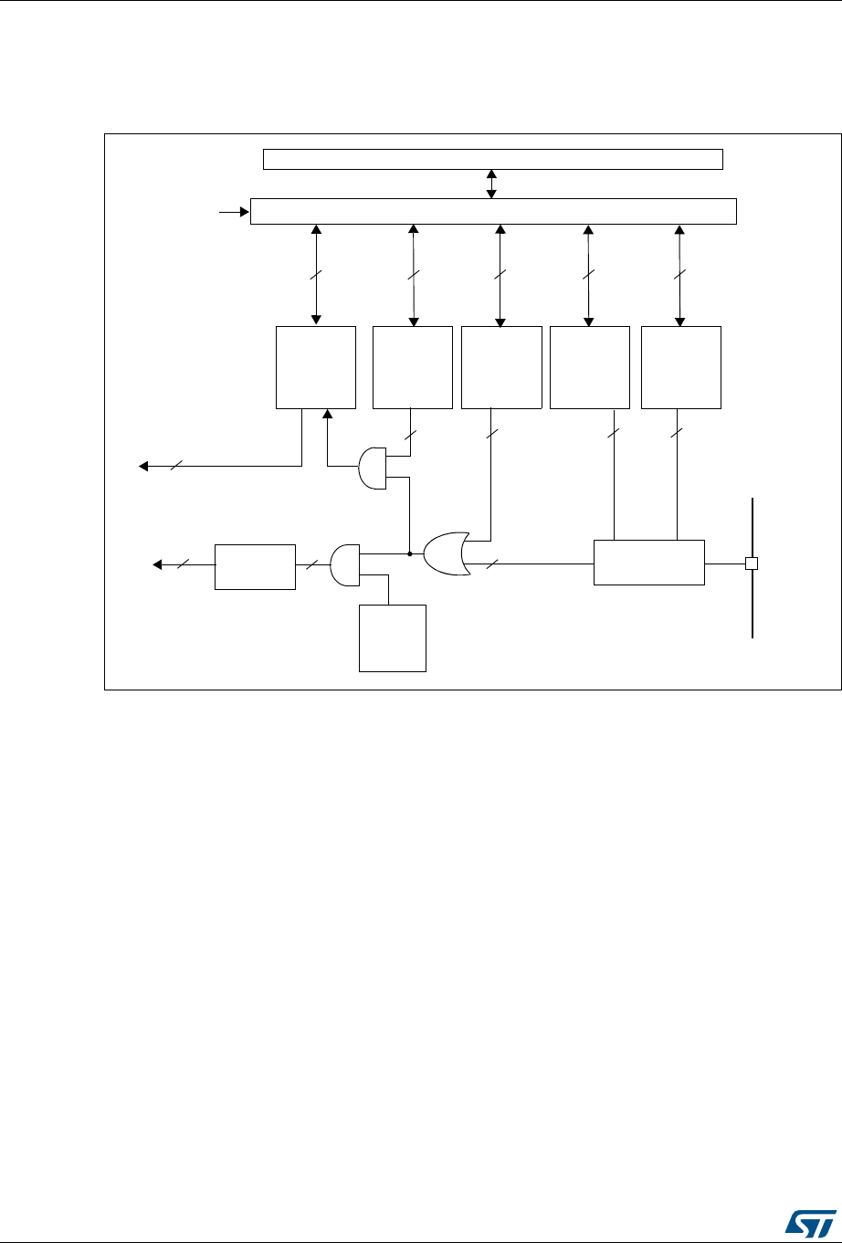
Interrupts and events RM0383
202/836 DocID026448 Rev 1
10.2.2 EXTI block diagram
Figure 29 shows the block diagram.
Figure 29. External interrupt/event controller block diagram
10.2.3 Wakeup event management
The STM32F4xx are able to handle external or internal events in order to wake up the core
(WFE). The wakeup event can be generated either by:
•enabling an interrupt in the peripheral control register but not in the NVIC, and enabling
the SEVONPEND bit in the Cortex®-M4 with FPU System Control register. When the
MCU resumes from WFE, the peripheral interrupt pending bit and the peripheral NVIC
IRQ channel pending bit (in the NVIC interrupt clear pending register) have to be
cleared.
•or configuring an external or internal EXTI line in event mode. When the CPU resumes
from WFE, it is not necessary to clear the peripheral interrupt pending bit or the NVIC
IRQ channel pending bit as the pending bit corresponding to the event line is not set.
To use an external line as a wakeup event, refer to Section 10.2.4: Functional description.
10.2.4 Functional description
To generate the interrupt, the interrupt line should be configured and enabled. This is done
by programming the two trigger registers with the desired edge detection and by enabling
the interrupt request by writing a ‘1’ to the corresponding bit in the interrupt mask register.
When the selected edge occurs on the external interrupt line, an interrupt request is
3HULSKHUDOLQWHUIDFH
(GJHGHWHFW
FLUFXLW
$0%$$3%EXV
3&/.
7R19,&LQWHUUXSW
FRQWUROOHU
6RIWZDUH
LQWHUUXSW
HYHQW
UHJLVWHU
5LVLQJ
WULJJHU
VHOHFWLRQ
UHJLVWHU
(YHQW
PDVN
UHJLVWHU
3XOVH
JHQHUDWRU
,QSXW
OLQH
3HQGLQJ
UHTXHVW
UHJLVWHU
069
,QWHUUXSW
PDVN
UHJLVWHU
)DOOLQJ
WULJJHU
VHOHFWLRQ
UHJLVWHU

DocID026448 Rev 1 203/836
RM0383 Interrupts and events
208
generated. The pending bit corresponding to the interrupt line is also set. This request is
reset by writing a ‘1’ in the pending register.
To generate the event, the event line should be configured and enabled. This is done by
programming the two trigger registers with the desired edge detection and by enabling the
event request by writing a ‘1’ to the corresponding bit in the event mask register. When the
selected edge occurs on the event line, an event pulse is generated. The pending bit
corresponding to the event line is not set.
An interrupt/event request can also be generated by software by writing a ‘1’ in the software
interrupt/event register.
Hardware interrupt selection
To configure the 23 lines as interrupt sources, use the following procedure:
•Configure the mask bits of the 23 interrupt lines (EXTI_IMR)
•Configure the Trigger selection bits of the interrupt lines (EXTI_RTSR and EXTI_FTSR)
•Configure the enable and mask bits that control the NVIC IRQ channel mapped to the
external interrupt controller (EXTI) so that an interrupt coming from one of the 23 lines
can be correctly acknowledged.
Hardware event selection
To configure the 23 lines as event sources, use the following procedure:
•Configure the mask bits of the 23 event lines (EXTI_EMR)
•Configure the Trigger selection bits of the event lines (EXTI_RTSR and EXTI_FTSR)
Software interrupt/event selection
The 23 lines can be configured as software interrupt/event lines. The following is the
procedure to generate a software interrupt.
•Configure the mask bits of the 23 interrupt/event lines (EXTI_IMR, EXTI_EMR)
•Set the required bit in the software interrupt register (EXTI_SWIER)
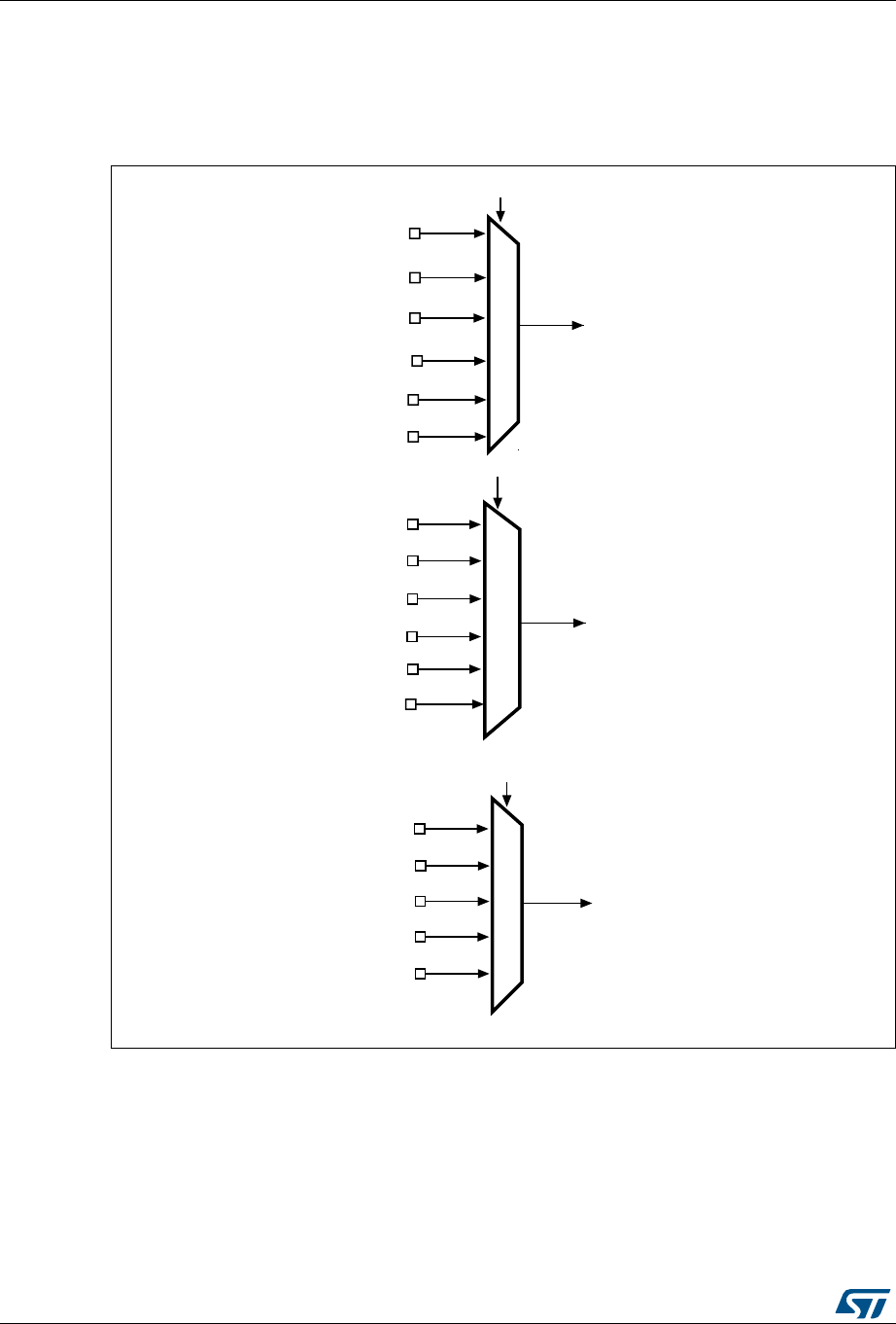
Interrupts and events RM0383
204/836 DocID026448 Rev 1
10.2.5 External interrupt/event line mapping
Up to 81 GPIOs (STM32F411xC/E) are connected to the 16 external interrupt/event lines in
the following manner:
Figure 30. External interrupt/event GPIO mapping
The five other EXTI lines are connected as follows:
•EXTI line 16 is connected to the PVD output
•EXTI line 17 is connected to the RTC Alarm event
•EXTI line 18 is connected to the USB OTG FS Wakeup event
•EXTI line 21 is connected to the RTC Tamper and TimeStamp events
•EXTI line 22 is connected to the RTC Wakeup event
3$
3%
3&
3'
3(
3$
3%
3&
3'
3(
3$
3%
3&
3'
3(
(;7,
(;7,
(;7,
(;7,>@ELWVLQWKH6<6&)*B(;7,&5UHJLVWHU
(;7,>@ELWVLQWKH6<6&)*B(;7,&5UHJLVWHU
(;7,>@ELWVLQWKH6<6&)*B(;7,&5UHJLVWHU
069
3+
3+
DocID026448 Rev 1 205/836
RM0383 Interrupts and events
208
10.3 EXTI registers
Refer to Section 1.1 on page 33 for a list of abbreviations used in register descriptions.
10.3.1 Interrupt mask register (EXTI_IMR)
Address offset: 0x00
Reset value: 0x0000 0000
10.3.2 Event mask register (EXTI_EMR)
Address offset: 0x04
Reset value: 0x0000 0000
31 30 29 28 27 26 25 24 23 22 21 20 19 18 17 16
Reserved MR22 MR21 Reserved MR18 MR17 MR16
rw rw rw rw rw
15 14 13 12 11 10 9 8 7 6 5 4 3 2 1 0
MR15 MR14 MR13 MR12 MR11 MR10 MR9 MR8 MR7 MR6 MR5 MR4 MR3 MR2 MR1 MR0
rw rw rw rw rw rw rw rw rw rw rw rw rw rw rw rw
Bits 31:23 Reserved, must be kept at reset value.
Bits 22:0 MRx: Interrupt mask on line x
0: Interrupt request from line x is masked
1: Interrupt request from line x is not masked
31 30 29 28 27 26 25 24 23 22 21 20 19 18 17 16
Reserved MR22 MR21 Reserved MR18 MR17 MR16
rw rw rw rw rw
15 14 13 12 11 10 9 8 7 6 5 4 3 2 1 0
MR15 MR14 MR13 MR12 MR11 MR10 MR9 MR8 MR7 MR6 MR5 MR4 MR3 MR2 MR1 MR0
rw rw rw rw rw rw rw rw rw rw rw rw rw rw rw rw
Bits 31:23 Reserved, must be kept at reset value.
Bits 22:0 MRx: Event mask on line x
0: Event request from line x is masked
1: Event request from line x is not masked

Interrupts and events RM0383
206/836 DocID026448 Rev 1
10.3.3 Rising trigger selection register (EXTI_RTSR)
Address offset: 0x08
Reset value: 0x0000 0000
Note: The external wakeup lines are edge triggered, no glitch must be generated on these lines.
If a rising edge occurs on the external interrupt line while writing to the EXTI_RTSR register,
the pending bit is be set.
Rising and falling edge triggers can be set for the same interrupt line. In this configuration,
both generate a trigger condition.
10.3.4 Falling trigger selection register (EXTI_FTSR)
Address offset: 0x0C
Reset value: 0x0000 0000
Note: The external wakeup lines are edge triggered, no glitch must be generated on these lines.
If a falling edge occurs on the external interrupt line while writing to the EXTI_FTSR register,
the pending bit is not set.
Rising and falling edge triggers can be set for the same interrupt line. In this configuration,
both generate a trigger condition.
31 30 29 28 27 26 25 24 23 22 21 20 19 18 17 16
Reserved TR22 TR21 Reserved TR18 TR17 TR16
rw rw rw rw rw
1514131211109 8 765432 1 0
TR15 TR14 TR13 TR12 TR11 TR10 TR9 TR8 TR7 TR6 TR5 TR4 TR3 TR2 TR1 TR0
rw rw rw rw rw rw rw rw rw rw rw rw rw rw rw rw
Bits 31:23 Reserved, must be kept at reset value.
Bits 22:0 TRx: Rising trigger event configuration bit of line x
0: Rising trigger disabled (for Event and Interrupt) for input line
1: Rising trigger enabled (for Event and Interrupt) for input line
31 30 29 28 27 26 25 24 23 22 21 20 19 18 17 16
Reserved TR22 TR21 Reserved TR18 TR17 TR16
rw rw rw rw rw
1514131211109 8 765432 1 0
TR15 TR14 TR13 TR12 TR11 TR10 TR9 TR8 TR7 TR6 TR5 TR4 TR3 TR2 TR1 TR0
rw rw rw rw rw rw rw rw rw rw rw rw rw rw rw rw
Bits 31:23 Reserved, must be kept at reset value.
Bits 22:0 TRx: Falling trigger event configuration bit of line x
0: Falling trigger disabled (for Event and Interrupt) for input line
1: Falling trigger enabled (for Event and Interrupt) for input line.
DocID026448 Rev 1 207/836
RM0383 Interrupts and events
208
10.3.5 Software interrupt event register (EXTI_SWIER)
Address offset: 0x10
Reset value: 0x0000 0000
10.3.6 Pending register (EXTI_PR)
Address offset: 0x14
Reset value: undefined
31 30 29 28 27 26 25 24 23 22 21 20 19 18 17 16
Reserved
SWIER
22
SWIER
21 Reserved
SWIER
18
SWIER
17
SWIER
16
rw rw rw rw rw
1514131211109 8 765432 1 0
SWIER
15
SWIER
14
SWIER
13
SWIER
12
SWIER
11
SWIER
10
SWIER
9
SWIER
8
SWIER
7
SWIER
6
SWIER
5
SWIER
4
SWIER
3
SWIER
2
SWIER
1
SWIER
0
rw rw rw rw rw rw rw rw rw rw rw rw rw rw rw rw
Bits 31:23 Reserved, must be kept at reset value.
Bits 22:0 SWIERx: Software Interrupt on line x
If interrupt are enabled on line x in the EXTI_IMR register, writing '1' to SWIERx bit when it is
set at '0' sets the corresponding pending bit in the EXTI_PR register, thus resulting in an
interrupt request generation.
This bit is cleared by clearing the corresponding bit in EXTI_PR (by writing a 1 to the bit).
31 30 29 28 27 26 25 24 23 22 21 20 19 18 17 16
Reserved PR22 PR21 Reserved PR18 PR17 PR16
rc_w1 rc_w1 rc_w1 rc_w1 rc_w1
1514131211109 8 765432 1 0
PR15 PR14 PR13 PR12 PR11 PR10 PR9 PR8 PR7 PR6 PR5 PR4 PR3 PR2 PR1 PR0
rc_w1 rc_w1 rc_w1 rc_w1 rc_w1 rc_w1 rc_w1 rc_w1 rc_w1 rc_w1 rc_w1 rc_w1 rc_w1 rc_w1 rc_w1 rc_w1
Bits 31:23 Reserved, must be kept at reset value.
Bits 22:0 PRx: Pending bit
0: No trigger request occurred
1: selected trigger request occurred
This bit is set when the selected edge event arrives on the external interrupt line.
This bit is cleared by programming it to ‘1’.
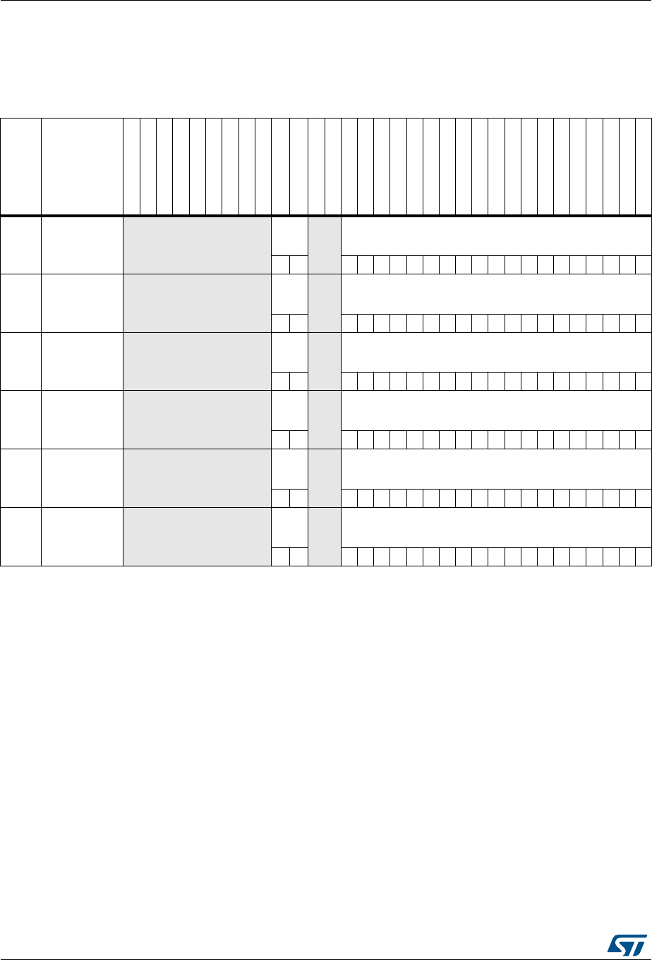
Interrupts and events RM0383
208/836 DocID026448 Rev 1
10.3.7 EXTI register map
Table 38 gives the EXTI register map and the reset values.
Refer to Table 3 on page 41 for the register boundary addresses.
Table 38. External interrupt/event controller register map and reset values
Offset Register
31
30
29
28
27
26
25
24
23
22
21
20
19
18
17
16
15
14
13
12
11
10
9
8
7
6
5
4
3
2
1
0
0x00 EXTI_IMR Reserved
MR
[22:21] Reser
ved
MR[18:0]
Reset value 0 0 0000000000000000000
0x04 EXTI_EMR Reserved
MR
[22:21] Reser
ved
MR[18:0]
Reset value 0 0 0000000000000000000
0x08 EXTI_RTSR Reserved
TR
[22:21] Reser
ved
TR[18:0]
Reset value 0 0 0000000000000000000
0x0C EXTI_FTSR Reserved
TR
[22:21] Reser
ved
TR[18:0]
Reset value 0 0 0000000000000000000
0x10 EXTI_SWIER Reserved
SWIER
[22:21] Reser
ved
SWIER[18:0]
Reset value 0 0 0000000000000000000
0x14 EXTI_PR Reserved
PR
[22:21] Reser
ved
PR[18:0]
Reset value 0 0 0000000000000000000

DocID026448 Rev 1 209/836
RM0383 Analog-to-digital converter (ADC)
237
11 Analog-to-digital converter (ADC)
ADC2 and ADC3 are not available in STM32F411xC/E.
11.1 ADC introduction
The 12-bit ADC is a successive approximation analog-to-digital converter. It has up to 19
multiplexed channels allowing it to measure signals from 16 external sources, two internal
sources, and the VBAT channel. The A/D conversion of the channels can be performed in
single, continuous, scan or discontinuous mode. The result of the ADC is stored into a left-
or right-aligned 16-bit data register.
The analog watchdog feature allows the application to detect if the input voltage goes
beyond the user-defined, higher or lower thresholds.
11.2 ADC main features
•12-bit, 10-bit, 8-bit or 6-bit configurable resolution
•Interrupt generation at the end of conversion, end of injected conversion, and in case of
analog watchdog or overrun events
•Single and continuous conversion modes
•Scan mode for automatic conversion of channel 0 to channel ‘n’
•Data alignment with in-built data coherency
•Channel-wise programmable sampling time
•External trigger option with configurable polarity for both regular and injected
conversions
•Discontinuous mode
•ADC supply requirements: 2.4 V to 3.6 V at full speed and down to 1.8 V at slower
speed
•ADC input range: VREF– ≤ VIN ≤ VREF+
•DMA request generation during regular channel conversion
Figure 31 shows the block diagram of the ADC.
Note: VREF–, if available (depending on package), must be tied to VSSA.
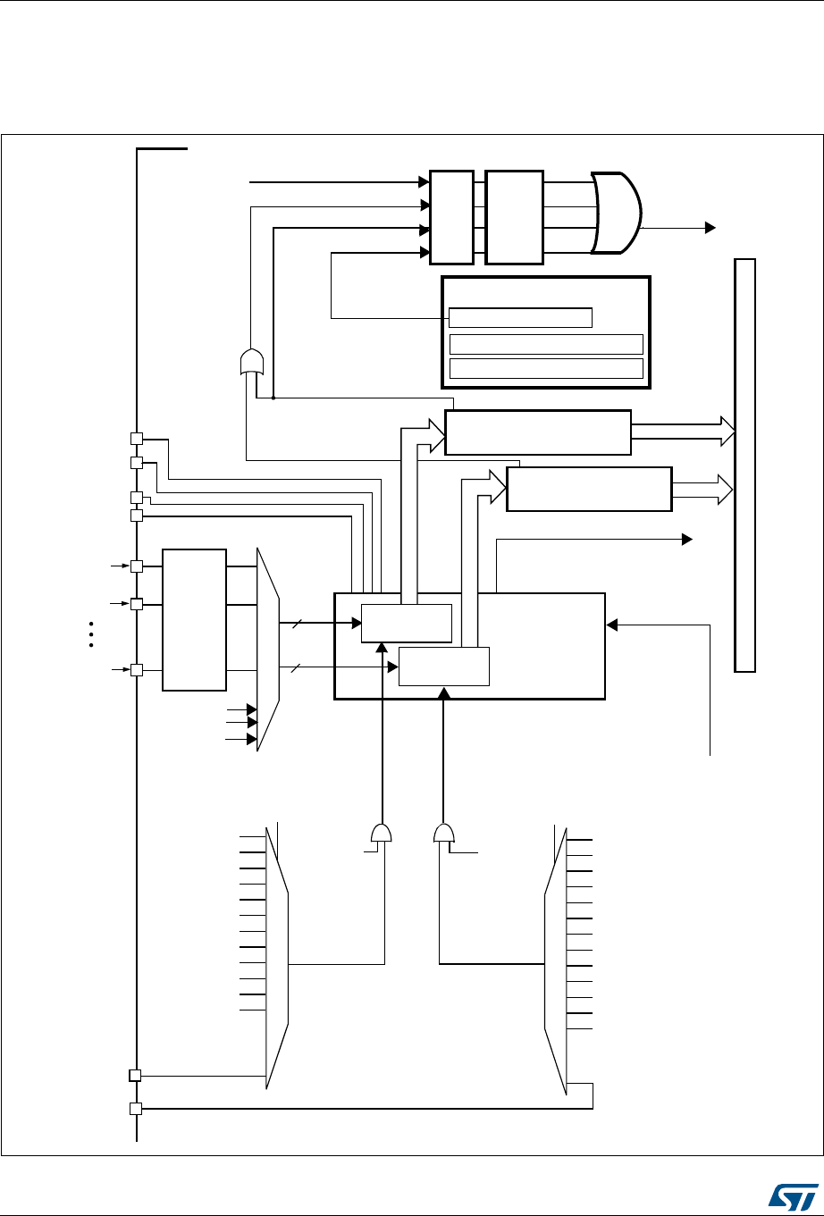
Analog-to-digital converter (ADC) RM0383
210/836 DocID026448 Rev 1
11.3 ADC functional description
Figure 31 shows a single ADC block diagram and Table 39 gives the ADC pin description.
Figure 31. Single ADC block diagram
!$#X?).
!$#X?).
!NALOG TO DIGITAL
CONVERTER
!$#X?).
!NALOG
MUX
!$##,+
!$#)NTERRUPTTO.6)#
'0)/
PORTS
!NALOGWATCHDOG
!DDRESSDATABUS
,OWERTHRESHOLDBITS
#OMPARERESULT
(IGHERTHRESHOLDBITS
&LAGS ENABLEBITS
%/#
!7$
!NALOGWATCHDOGEVENT
6$$!
633!
62%&
62%&
)NTERRUPT
%84)?
4)-?#(
&ROM!$#PRESCALER
BITS
%NDOFCONVERSION
CHANNELS
)NJECTED
CHANNELS
%NDOFINJECTEDCONVERSION *%/#
%/#)%
!7$)%
*%/#)%
UPTO
UPTO
2EGULARDATAREGISTER
XBITS
)NJECTEDDATAREGISTERS
2EGULAR
3TARTTRIGGER
REGULARGROUP
%843%,;=BITS
%84%.
4)-?#(
%84)?
4)-?42'/
4)-?#(
4)-?42'/
3TARTTRIGGER
INJECTEDGROUP
*%843%,;=BITS
4)-?#(
*%84%. ;=BITS
;=BITS
$-!REQUEST
4EMPSENSOR
62%&).4
/62/62)%
$-!OVERRUN
6"!4
4)-?#(
4)-?42'/
4)-?#(
4)-?#(
4)-?42'/
4)-?#(
4)-?#(
4)-?#(
4)-?#(
4)-?#(
4)-?#(
4)-?#(
4)-?#(
4)-?#(
4)-?#(
4)-?42'/
4)-?#(
4)-?42'/
4)-?#(
-36

DocID026448 Rev 1 211/836
RM0383 Analog-to-digital converter (ADC)
237
11.3.1 ADC on-off control
The ADC is powered on by setting the ADON bit in the ADC_CR2 register. When the ADON
bit is set for the first time, it wakes up the ADC from the Power-down mode.
Conversion starts when either the SWSTART or the JSWSTART bit is set.
You can stop conversion and put the ADC in power down mode by clearing the ADON bit. In
this mode the ADC consumes almost no power (only a few µA).
11.3.2 ADC clock
The ADC features two clock schemes:
•Clock for the analog circuitry: ADCCLK
This clock is generated from the APB2 clock divided by a programmable prescaler that
allows the ADC to work at fPCLK2/2, /4, /6 or /8. Refer to the datasheets for the
maximum value of ADCCLK.
•Clock for the digital interface (used for registers read/write access)
This clock is equal to the APB2 clock. The digital interface clock can be
enabled/disabled individually for each ADC through the RCC APB2 peripheral clock
enable register (RCC_APB2ENR).
11.3.3 Channel selection
There are 16 multiplexed channels. It is possible to organize the conversions in two groups:
regular and injected. A group consists of a sequence of conversions that can be done on
any channel and in any order. For instance, it is possible to implement the conversion
sequence in the following order: ADC_IN3, ADC_IN8, ADC_IN2, ADC_IN2, ADC_IN0,
ADC_IN2, ADC_IN2, ADC_IN15.
•A regular group is composed of up to 16 conversions. The regular channels and their
order in the conversion sequence must be selected in the ADC_SQRx registers. The
total number of conversions in the regular group must be written in the L[3:0] bits in the
ADC_SQR1 register.
•An injected group is composed of up to 4 conversions. The injected channels and
their order in the conversion sequence must be selected in the ADC_JSQR register.
Table 39. ADC pins
Name Signal type Remarks
VREF+
Input, analog reference
positive
The higher/positive reference voltage for the ADC,
1.8 V ≤ VREF+ ≤ VDDA
VDDA Input, analog supply
Analog power supply equal to VDD and
2.4 V ≤ VDDA ≤ VDD (3.6 V) for full speed
1.8 V ≤ VDDA ≤ VDD (3.6 V) for reduced speed
VREF–
Input, analog reference
negative
The lower/negative reference voltage for the ADC,
VREF– = VSSA
VSSA
Input, analog supply
ground Ground for analog power supply equal to VSS
ADCx_IN[15:0] Analog input signals 16 analog input channels

Analog-to-digital converter (ADC) RM0383
212/836 DocID026448 Rev 1
The total number of conversions in the injected group must be written in the L[1:0] bits
in the ADC_JSQR register.
If the ADC_SQRx or ADC_JSQR registers are modified during a conversion, the current
conversion is reset and a new start pulse is sent to the ADC to convert the newly chosen
group.
Temperature sensor, VREFINT and VBAT internal channels
•The temperature sensor is internally connected to ADC1_IN18 channel which is shared
with VBAT. Only one conversion, temperature sensor or VBAT, must be selected at a
time. When the temperature sensor and VBAT conversion are set simultaneously, only
the VBAT conversion is performed.
The internal reference voltage VREFINT is connected to ADC1_IN17.
The VBAT channel is connected to channel ADC1_IN18. It can also be converted as an
injected or regular channel.
Note: The temperature sensor, VREFINT and the VBAT channel are available only on the master
ADC1 peripheral.
11.3.4 Single conversion mode
In Single conversion mode the ADC does one conversion. This mode is started with the
CONT bit at 0 by either:
•setting the SWSTART bit in the ADC_CR2 register (for a regular channel only)
•setting the JSWSTART bit (for an injected channel)
•external trigger (for a regular or injected channel)
Once the conversion of the selected channel is complete:
•If a regular channel was converted:
– The converted data are stored into the 16-bit ADC_DR register
– The EOC (end of conversion) flag is set
– An interrupt is generated if the EOCIE bit is set
•If an injected channel was converted:
– The converted data are stored into the 16-bit ADC_JDR1 register
– The JEOC (end of conversion injected) flag is set
– An interrupt is generated if the JEOCIE bit is set
Then the ADC stops.
11.3.5 Continuous conversion mode
In continuous conversion mode, the ADC starts a new conversion as soon as it finishes one.
This mode is started with the CONT bit at 1 either by external trigger or by setting the
SWSTRT bit in the ADC_CR2 register (for regular channels only).
After each conversion:
•If a regular group of channels was converted:
– The last converted data are stored into the 16-bit ADC_DR register
– The EOC (end of conversion) flag is set
– An interrupt is generated if the EOCIE bit is set
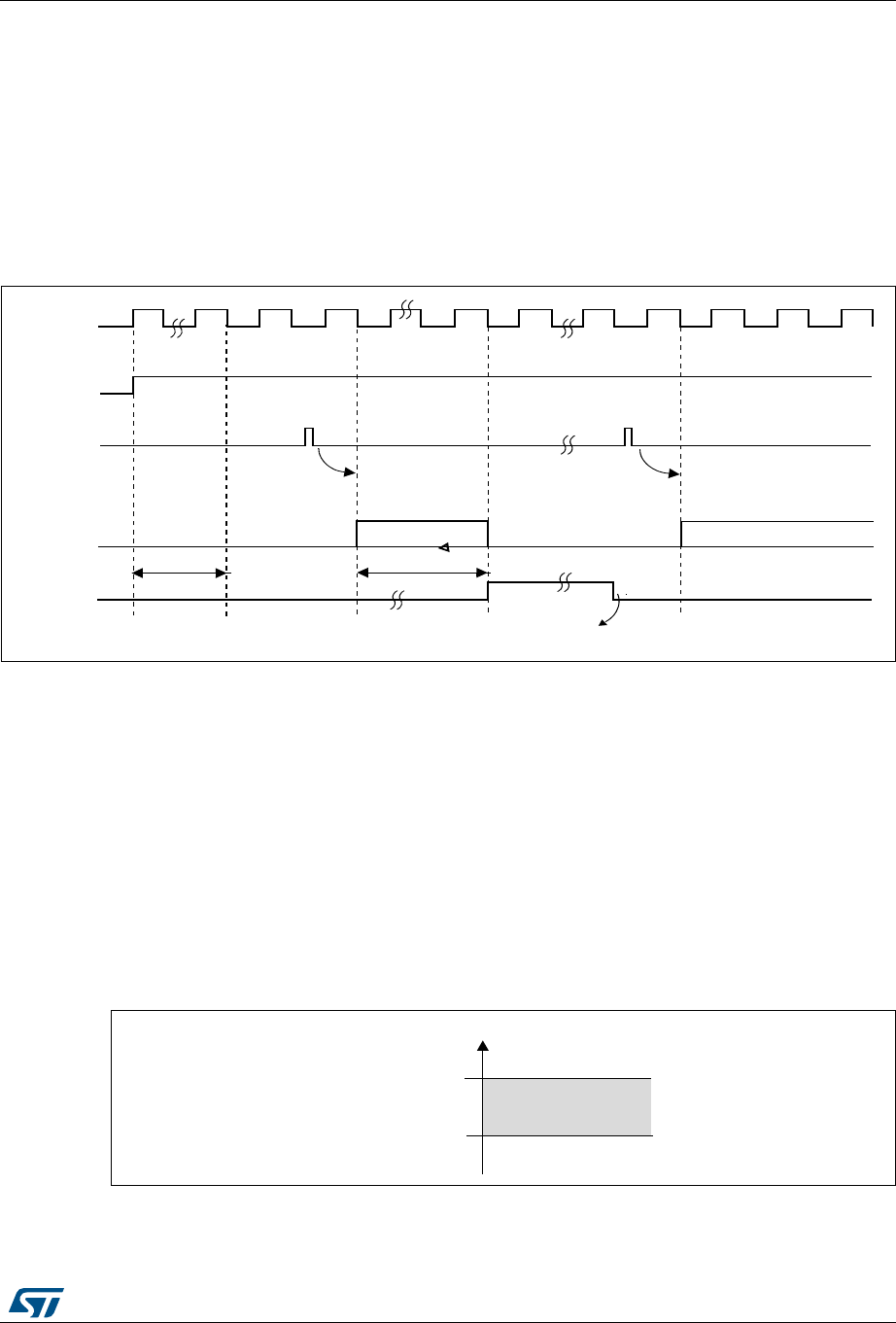
DocID026448 Rev 1 213/836
RM0383 Analog-to-digital converter (ADC)
237
Note: Injected channels cannot be converted continuously. The only exception is when an injected
channel is configured to be converted automatically after regular channels in continuous
mode (using JAUTO bit), refer to Auto-injection section).
11.3.6 Timing diagram
As shown in Figure 32, the ADC needs a stabilization time of tSTAB before it starts
converting accurately. After the start of the ADC conversion and after 15 clock cycles, the
EOC flag is set and the 16-bit ADC data register contains the result of the conversion.
Figure 32. Timing diagram
11.3.7 Analog watchdog
The AWD analog watchdog status bit is set if the analog voltage converted by the ADC is
below a lower threshold or above a higher threshold. These thresholds are programmed in
the 12 least significant bits of the ADC_HTR and ADC_LTR 16-bit registers. An interrupt can
be enabled by using the AWDIE bit in the ADC_CR1 register.
The threshold value is independent of the alignment selected by the ALIGN bit in the
ADC_CR2 register. The analog voltage is compared to the lower and higher thresholds
before alignment.
Table 40 shows how the ADC_CR1 register should be configured to enable the analog
watchdog on one or more channels.
Figure 33. Analog watchdog’s guarded area
!$#?#,+
%/#
.EXT!$#CONVERSION
!$#CONVERSION
#ONVERSIONTIME
T34!"
!$#
3OFTWARECLEARSTHE%/#BIT
TOTALCONVTIME
3TARTSTCONVERSION 3TARTNEXTCONVERSION
AIB
!$/.
3734!24
*3734!24
!NALOGVOLTAGE
(IGHERTHRESHOLD
,OWERTHRESHOLD
'UARDEDAREA
(42
,4 2
AI

Analog-to-digital converter (ADC) RM0383
214/836 DocID026448 Rev 1
11.3.8 Scan mode
This mode is used to scan a group of analog channels.
The Scan mode is selected by setting the SCAN bit in the ADC_CR1 register. Once this bit
has been set, the ADC scans all the channels selected in the ADC_SQRx registers (for
regular channels) or in the ADC_JSQR register (for injected channels). A single conversion
is performed for each channel of the group. After each end of conversion, the next channel
in the group is converted automatically. If the CONT bit is set, regular channel conversion
does not stop at the last selected channel in the group but continues again from the first
selected channel.
If the DMA bit is set, the direct memory access (DMA) controller is used to transfer the data
converted from the regular group of channels (stored in the ADC_DR register) to SRAM
after each regular channel conversion.
The EOC bit is set in the ADC_SR register:
•At the end of each regular group sequence if the EOCS bit is cleared to 0
•At the end of each regular channel conversion if the EOCS bit is set to 1
The data converted from an injected channel are always stored into the ADC_JDRx
registers.
11.3.9 Injected channel management
Triggered injection
To use triggered injection, the JAUTO bit must be cleared in the ADC_CR1 register.
1. Start the conversion of a group of regular channels either by external trigger or by
setting the SWSTART bit in the ADC_CR2 register.
2. If an external injected trigger occurs or if the JSWSTART bit is set during the
conversion of a regular group of channels, the current conversion is reset and the
injected channel sequence switches to Scan-once mode.
3. Then, the regular conversion of the regular group of channels is resumed from the last
interrupted regular conversion.
If a regular event occurs during an injected conversion, the injected conversion is not
Table 40. Analog watchdog channel selection
Channels guarded by the analog
watchdog
ADC_CR1 register control bits (x = don’t care)
AWDSGL bit AWDEN bit JAWDEN bit
None x 0 0
All injected channels 0 0 1
All regular channels 0 1 0
All regular and injected channels 0 1 1
Single(1) injected channel
1. Selected by the AWDCH[4:0] bits
101
Single(1) regular channel 1 1 0
Single (1) regular or injected channel 1 1 1
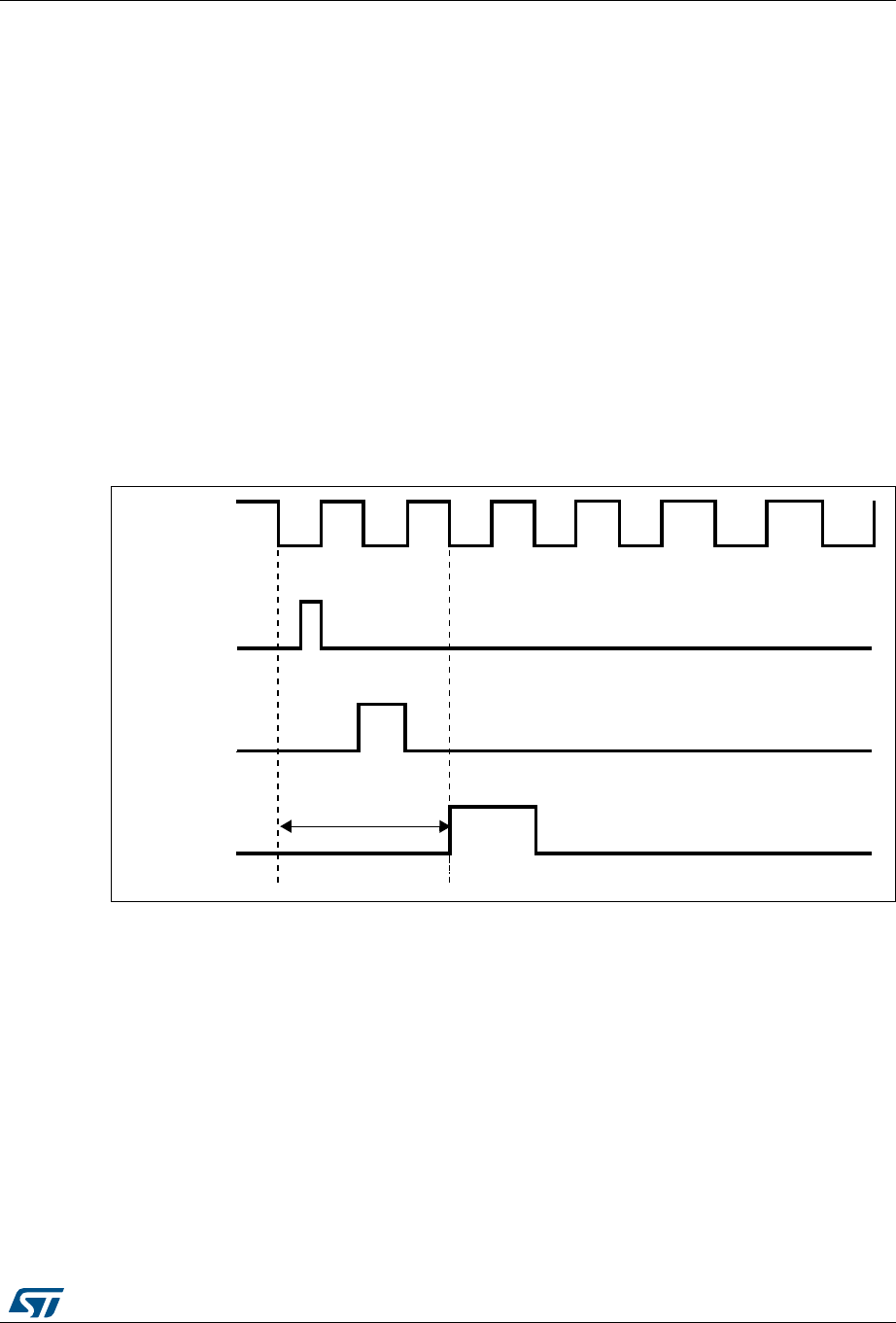
DocID026448 Rev 1 215/836
RM0383 Analog-to-digital converter (ADC)
237
interrupted but the regular sequence is executed at the end of the injected sequence.
Figure 34 shows the corresponding timing diagram.
Note: When using triggered injection, one must ensure that the interval between trigger events is
longer than the injection sequence. For instance, if the sequence length is 30 ADC clock
cycles (that is two conversions with a sampling time of 3 clock periods), the minimum
interval between triggers must be 31 ADC clock cycles.
Auto-injection
If the JAUTO bit is set, then the channels in the injected group are automatically converted
after the regular group of channels. This can be used to convert a sequence of up to 20
conversions programmed in the ADC_SQRx and ADC_JSQR registers.
In this mode, external trigger on injected channels must be disabled.
If the CONT bit is also set in addition to the JAUTO bit, regular channels followed by injected
channels are continuously converted.
Note: It is not possible to use both the auto-injected and discontinuous modes simultaneously.
Figure 34. Injected conversion latency
1. The maximum latency value can be found in the electrical characteristics of the STM32F411xC/E
datasheets.
11.3.10 Discontinuous mode
Regular group
This mode is enabled by setting the DISCEN bit in the ADC_CR1 register. It can be used to
convert a short sequence of n conversions (n ≤ 8) that is part of the sequence of conversions
selected in the ADC_SQRx registers. The value of n is specified by writing to the
DISCNUM[2:0] bits in the ADC_CR1 register.
When an external trigger occurs, it starts the next n conversions selected in the ADC_SQRx
registers until all the conversions in the sequence are done. The total sequence length is
defined by the L[3:0] bits in the ADC_SQR1 register.
!$##,+
)NJECTIONEVENT
2ESET!$#
3/# MAXLATENCY
AI

Analog-to-digital converter (ADC) RM0383
216/836 DocID026448 Rev 1
Example:
•n = 3, channels to be converted = 0, 1, 2, 3, 6, 7, 9, 10
•1st trigger: sequence converted 0, 1, 2. An EOC event is generated at each
conversion.
•2nd trigger: sequence converted 3, 6, 7. An EOC event is generated at each
conversion
•3rd trigger: sequence converted 9, 10.An EOC event is generated at each conversion
•4th trigger: sequence converted 0, 1, 2. An EOC event is generated at each conversion
Note: When a regular group is converted in discontinuous mode, no rollover occurs.
When all subgroups are converted, the next trigger starts the conversion of the first
subgroup. In the example above, the 4th trigger reconverts the channels 0, 1 and 2 in the
1st subgroup.
Injected group
This mode is enabled by setting the JDISCEN bit in the ADC_CR1 register. It can be used to
convert the sequence selected in the ADC_JSQR register, channel by channel, after an
external trigger event.
When an external trigger occurs, it starts the next channel conversions selected in the
ADC_JSQR registers until all the conversions in the sequence are done. The total sequence
length is defined by the JL[1:0] bits in the ADC_JSQR register.
Example:
n = 1, channels to be converted = 1, 2, 3
1st trigger: channel 1 converted
2nd trigger: channel 2 converted
3rd trigger: channel 3 converted and JEOC event generated
4th trigger: channel 1
Note: When all injected channels are converted, the next trigger starts the conversion of the first
injected channel. In the example above, the 4th trigger reconverts the 1st injected channel
1.
It is not possible to use both the auto-injected and discontinuous modes simultaneously.
Discontinuous mode must not be set for regular and injected groups at the same time.
Discontinuous mode must be enabled only for the conversion of one group.
11.4 Data alignment
The ALIGN bit in the ADC_CR2 register selects the alignment of the data stored after
conversion. Data can be right- or left-aligned as shown in Figure 35 and Figure 36.
The converted data value from the injected group of channels is decreased by the user-
defined offset written in the ADC_JOFRx registers so the result can be a negative value.
The SEXT bit represents the extended sign value.
For channels in a regular group, no offset is subtracted so only twelve bits are significant.
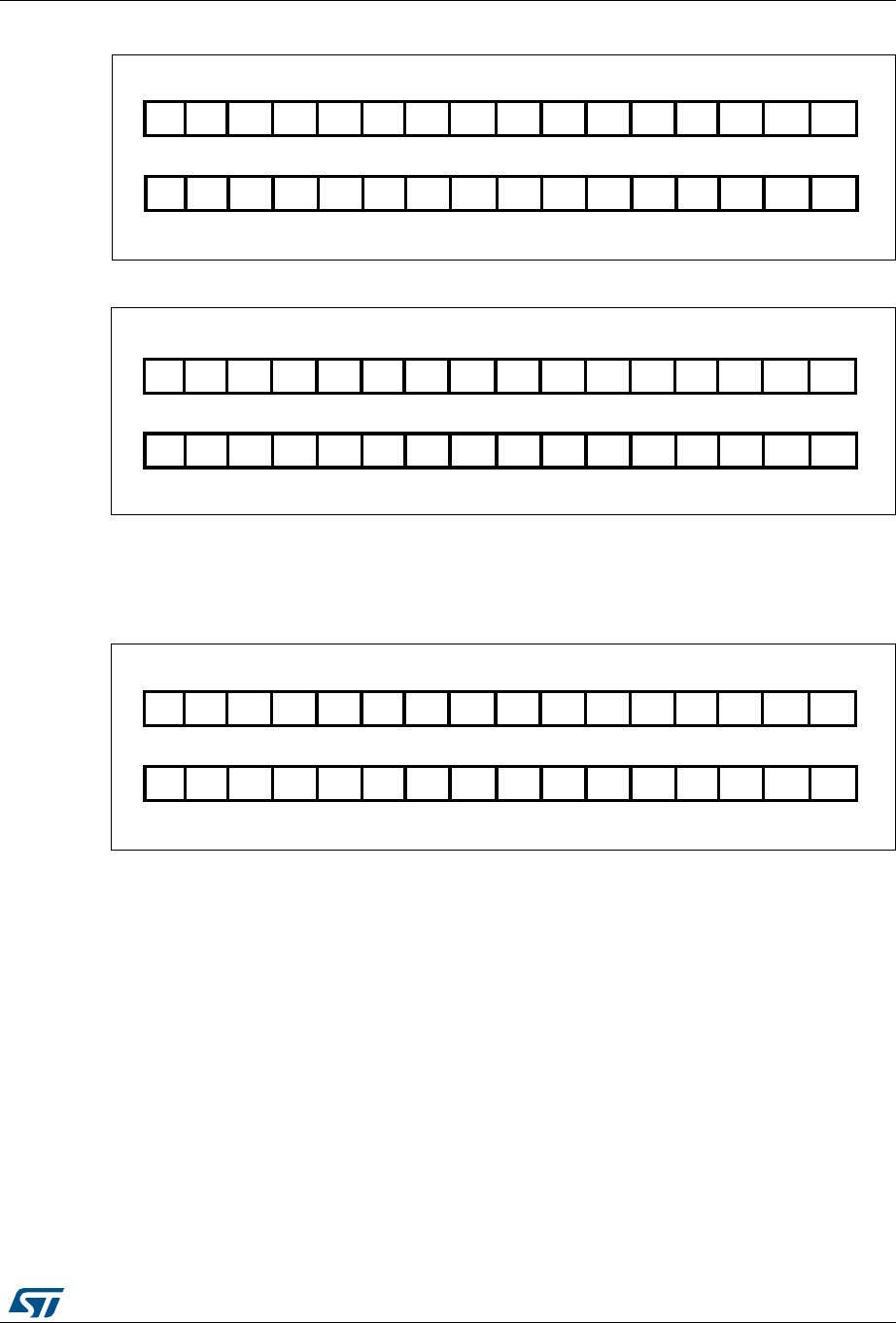
DocID026448 Rev 1 217/836
RM0383 Analog-to-digital converter (ADC)
237
Figure 35. Right alignment of 12-bit data
Figure 36. Left alignment of 12-bit data
Special case: when left-aligned, the data are aligned on a half-word basis except when the
resolution is set to 6-bit. in that case, the data are aligned on a byte basis as shown in
Figure 37.
Figure 37. Left alignment of 6-bit data
11.5 Channel-wise programmable sampling time
The ADC samples the input voltage for a number of ADCCLK cycles that can be modified
using the SMP[2:0] bits in the ADC_SMPR1 and ADC_SMPR2 registers. Each channel can
be sampled with a different sampling time.
The total conversion time is calculated as follows:
Tconv = Sampling time + 12 cycles
Example:
With ADCCLK = 30 MHz and sampling time = 3 cycles:
Tconv = 3 + 12 = 15 cycles = 0.5 µs with APB2 at 60 MHz
$$$ $ $ $ $ $ $ $$$3%843%843%843%84
$$
$$
)NJECTEDGROUP
2EGULARGROUP
$ $ $ $ $ $ $ $
AI
$$
$ $ $ $ $ $$$$$3%84
)NJECTEDGROUP
2EGULARGROUP
AI
$ $ $ $ $ $ $ $ $ $ $ $
$$
3%843%843%843%843%843%84
)NJECTEDGROUP
2EGULARGROUP
AI
$ $ $ $ $ $
3%843%84 $ $ $ $ 3%84
Analog-to-digital converter (ADC) RM0383
218/836 DocID026448 Rev 1
11.6 Conversion on external trigger and trigger polarity
Conversion can be triggered by an external event (e.g. timer capture, EXTI line). If the
EXTEN[1:0] control bits (for a regular conversion) or JEXTEN[1:0] bits (for an injected
conversion) are different from “0b00”, then external events are able to trigger a conversion
with the selected polarity. Table 41 provides the correspondence between the EXTEN[1:0]
and JEXTEN[1:0] values and the trigger polarity.
Note: The polarity of the external trigger can be changed on the fly.
The EXTSEL[3:0] and JEXTSEL[3:0] control bits are used to select which out of 16 possible
events can trigger conversion for the regular and injected groups.
Table 42 gives the possible external trigger for regular conversion.
Table 43 gives the possible external trigger for injected conversion.
Table 41. Configuring the trigger polarity
Source EXTEN[1:0] / JEXTEN[1:0]
Trigger detection disabled 00
Detection on the rising edge 01
Detection on the falling edge 10
Detection on both the rising and falling edges 11
Table 42. External trigger for regular channels
Source Type EXTSEL[3:0]
TIM1_CH1 event
Internal signal from on-chip
timers
0000
TIM1_CH2 event 0001
TIM1_CH3 event 0010
TIM2_CH2 event 0011
TIM2_CH3 event 0100
TIM2_CH4 event 0101
TIM2_TRGO event 0110
TIM3_CH1 event 0111
TIM3_TRGO event 1000
TIM4_CH4 event 1001
TIM5_CH1 event 1010
TIM5_CH2 event 1011
TIM5_CH3 event 1100
Reserved 1101
Reserved 1110
EXTI line11 External pin 1111

DocID026448 Rev 1 219/836
RM0383 Analog-to-digital converter (ADC)
237
Software source trigger events can be generated by setting SWSTART (for regular
conversion) or JSWSTART (for injected conversion) in ADC_CR2.
A regular group conversion can be interrupted by an injected trigger.
Note: The trigger selection can be changed on the fly. However, when the selection changes,
there is a time frame of 1 APB clock cycle during which the trigger detection is disabled.
This is to avoid spurious detection during transitions.
11.7 Fast conversion mode
It is possible to perform faster conversion by reducing the ADC resolution. The RES bits are
used to select the number of bits available in the data register. The minimum conversion
time for each resolution is then as follows:
•12 bits: 3 + 12 = 15 ADCCLK cycles
•10 bits: 3 + 10 = 13 ADCCLK cycles
•8 bits: 3 + 8 = 11 ADCCLK cycles
•6 bits: 3 + 6 = 9 ADCCLK cycles
Table 43. External trigger for injected channels
Source Connection type JEXTSEL[3:0]
TIM1_CH4 event
Internal signal from on-chip
timers
0000
TIM1_TRGO event 0001
TIM2_CH1 event 0010
TIM2_TRGO event 0011
TIM3_CH2 event 0100
TIM3_CH4 event 0101
TIM4_CH1 event 0110
TIM4_CH2 event 0111
TIM4_CH3 event 1000
TIM4_TRGO event 1001
TIM5_CH4 event 1010
TIM5_TRGO event 1011
Reserved 1100
Reserved 1101
Reserved 1110
EXTI line15 External pin 1111

Analog-to-digital converter (ADC) RM0383
220/836 DocID026448 Rev 1
11.8 Data management
11.8.1 Using the DMA
Since converted regular channel values are stored into a unique data register, it is useful to
use DMA for conversion of more than one regular channel. This avoids the loss of the data
already stored in the ADC_DR register.
When the DMA mode is enabled (DMA bit set to 1 in the ADC_CR2 register), after each
conversion of a regular channel, a DMA request is generated. This allows the transfer of the
converted data from the ADC_DR register to the destination location selected by the
software.
Despite this, if data are lost (overrun), the OVR bit in the ADC_SR register is set and an
interrupt is generated (if the OVRIE enable bit is set). DMA transfers are then disabled and
DMA requests are no longer accepted. In this case, if a DMA request is made, the regular
conversion in progress is aborted and further regular triggers are ignored. It is then
necessary to clear the OVR flag and the DMAEN bit in the used DMA stream, and to re-
initialize both the DMA and the ADC to have the wanted converted channel data transferred
to the right memory location. Only then can the conversion be resumed and the data
transfer, enabled again. Injected channel conversions are not impacted by overrun errors.
When OVR = 1 in DMA mode, the DMA requests are blocked after the last valid data have
been transferred, which means that all the data transferred to the RAM can be considered
as valid.
At the end of the last DMA transfer (number of transfers configured in the DMA controller’s
DMA_SxNTR register):
•No new DMA request is issued to the DMA controller if the DDS bit is cleared to 0 in the
ADC_CR2 register (this avoids generating an overrun error). However the DMA bit is
not cleared by hardware. It must be written to 0, then to 1 to start a new transfer.
•Requests can continue to be generated if the DDS bit is set to 1. This allows
configuring the DMA in double-buffer circular mode.
To recover the ADC from OVR state when the DMA is used, follow the steps below:
1. Reinitialize the DMA (adjust destination address and NDTR counter)
2. Clear the ADC OVR bit in ADC_SR register
3. Trigger the ADC to start the conversion.
11.8.2 Managing a sequence of conversions without using the DMA
If the conversions are slow enough, the conversion sequence can be handled by the
software. In this case the EOCS bit must be set in the ADC_CR2 register for the EOC status
bit to be set at the end of each conversion, and not only at the end of the sequence. When
EOCS = 1, overrun detection is automatically enabled. Thus, each time a conversion is
complete, EOC is set and the ADC_DR register can be read. The overrun management is
the same as when the DMA is used.
To recover the ADC from OVR state when the EOCS is set, follow the steps below:
1. Clear the ADC OVR bit in ADC_SR register
2. Trigger the ADC to start the conversion.
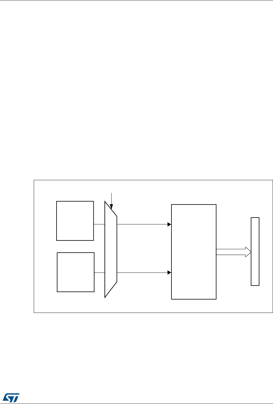
DocID026448 Rev 1 221/836
RM0383 Analog-to-digital converter (ADC)
237
11.8.3 Conversions without DMA and without overrun detection
It may be useful to let the ADC convert one or more channels without reading the data each
time (if there is an analog watchdog for instance). For that, the DMA must be disabled
(DMA = 0) and the EOC bit must be set at the end of a sequence only (EOCS = 0). In this
configuration, overrun detection is disabled.
11.9 Temperature sensor
The temperature sensor can be used to measure the ambient temperature (TA) of the
device.
Figure 38 shows the block diagram of the temperature sensor.
When not in use, the sensor can be put in power down mode.
Note: The TSVREFE bit must be set to enable the conversion of both internal channels: the
ADC1_IN16 or ADC1_IN18 (temperature sensor) and the ADC1_IN17 (VREFINT).
Main features
•Supported temperature range: –40 to 125 °C
•Precision: ±1.5 °C
Figure 38. Temperature sensor and VREFINT channel block diagram
1. VSENSE is input to ADC1_IN18
-36
4EMPERATURE
SENSOR
63%.3%
4362%&%CONTROLBIT
!$#
!DDRESSDATABUS
62%&).4
!$#?).
!$#?).
)NTERNAL
POWERBLOCK !$#?).
CONVERTEDDATA

Analog-to-digital converter (ADC) RM0383
222/836 DocID026448 Rev 1
Reading the temperature
To use the sensor:
3. Select ADC1_IN16 or ADC1_IN18 input channel.
4. Select a sampling time greater than the minimum sampling time specified in the
datasheet.
5. Set the TSVREFE bit in the ADC_CCR register to wake up the temperature sensor
from power down mode
6. Start the ADC conversion by setting the SWSTART bit (or by external trigger)
7. Read the resulting VSENSE data in the ADC data register
8. Calculate the temperature using the following formula:
Temperature (in °C) = {(VSENSE – V25) / Avg_Slope} + 25
Where:
–V
25 = VSENSE value for 25° C
– Avg_Slope = average slope of the temperature vs. VSENSE curve (given in mV/°C
or µV/°C)
Refer to the datasheet’s electrical characteristics section for the actual values of V25
and Avg_Slope.
Note: The sensor has a startup time after waking from power down mode before it can output
VSENSE at the correct level. The ADC also has a startup time after power-on, so to minimize
the delay, the ADON and TSVREFE bits should be set at the same time.
The temperature sensor output voltage changes linearly with temperature. The offset of this
linear function depends on each chip due to process variation (up to 45 °C from one chip to
another).
The internal temperature sensor is more suited for applications that detect temperature
variations instead of absolute temperatures. If accurate temperature reading is required, an
external temperature sensor should be used.
11.10 Battery charge monitoring
The VBATE bit in the ADC_CCR register is used to switch to the battery voltage. As the
VBAT voltage could be higher than VDDA, to ensure the correct operation of the ADC, the
VBAT pin is internally connected to a bridge divider.
When the VBATE is set, the bridge is automatically enabled to connect:
•VBAT/4 to the ADC1_IN18 input channel
Note: The VBAT and temperature sensor are connected to the same ADC internal channel
(ADC1_IN18). Only one conversion, either temperature sensor or VBAT, must be selected
at a time. When both conversion are enabled simultaneously, only the VBAT conversion is
performed.
11.11 ADC interrupts
An interrupt can be produced on the end of conversion for regular and injected groups,
when the analog watchdog status bit is set and when the overrun status bit is set. Separate
interrupt enable bits are available for flexibility.

DocID026448 Rev 1 223/836
RM0383 Analog-to-digital converter (ADC)
237
Two other flags are present in the ADC_SR register, but there is no interrupt associated with
them:
•JSTRT (Start of conversion for channels of an injected group)
•STRT (Start of conversion for channels of a regular group)
Table 44. ADC interrupts
Interrupt event Event flag Enable control bit
End of conversion of a regular group EOC EOCIE
End of conversion of an injected group JEOC JEOCIE
Analog watchdog status bit is set AWD AWDIE
Overrun OVR OVRIE

Analog-to-digital converter (ADC) RM0383
224/836 DocID026448 Rev 1
11.12 ADC registers
Refer to Section 1.1 on page 33 for a list of abbreviations used in register descriptions.
The peripheral registers must be written at word level (32 bits). Read accesses can be done
by bytes (8 bits), half-words (16 bits) or words (32 bits).
11.12.1 ADC status register (ADC_SR)
Address offset: 0x00
Reset value: 0x0000 0000
31 30 29 28 27 26 25 24 23 22 21 20 19 18 17 16
Reserved
1514131211109876543210
Reserved
OVR STRT JSTRT JEOC EOC AWD
rc_w0 rc_w0 rc_w0 rc_w0 rc_w0 rc_w0
Bits 31:6 Reserved, must be kept at reset value.
Bit 5 OVR: Overrun
This bit is set by hardware when data are lost . It is cleared by software. Overrun detection is
enabled only when DMA = 1 or EOCS = 1.
0: No overrun occurred
1: Overrun has occurred
Bit 4 STRT: Regular channel start flag
This bit is set by hardware when regular channel conversion starts. It is cleared by software.
0: No regular channel conversion started
1: Regular channel conversion has started
Bit 3 JSTRT: Injected channel start flag
This bit is set by hardware when injected group conversion starts. It is cleared by software.
0: No injected group conversion started
1: Injected group conversion has started
Bit 2 JEOC: Injected channel end of conversion
This bit is set by hardware at the end of the conversion of all injected channels in the group.
It is cleared by software.
0: Conversion is not complete
1: Conversion complete
Bit 1 EOC: Regular channel end of conversion
This bit is set by hardware at the end of the conversion of a regular group of channels. It is
cleared by software or by reading the ADC_DR register.
0: Conversion not complete (EOCS=0), or sequence of conversions not complete (EOCS=1)
1: Conversion complete (EOCS=0), or sequence of conversions complete (EOCS=1)
Bit 0 AWD: Analog watchdog flag
This bit is set by hardware when the converted voltage crosses the values programmed in
the ADC_LTR and ADC_HTR registers. It is cleared by software.
0: No analog watchdog event occurred
1: Analog watchdog event occurred

DocID026448 Rev 1 225/836
RM0383 Analog-to-digital converter (ADC)
237
11.12.2 ADC control register 1 (ADC_CR1)
Address offset: 0x04
Reset value: 0x0000 0000
31 30 29 28 27 26 25 24 23 22 21 20 19 18 17 16
Reserved OVRIE RES AWDEN JAWDEN Reserved
rw rw rw rw rw
15 14 13 12 11 10 9 8 7 6 5 4 3 2 1 0
DISCNUM[2:0] JDISCE
N
DISC
EN JAUTO AWDSG
LSCAN JEOCIE AWDIE EOCIE AWDCH[4:0]
rw rw rw rw rw rw rw rw rw rw rw rw rw rw rw rw
Bits 31:27 Reserved, must be kept at reset value.
Bit 26 OVRIE: Overrun interrupt enable
This bit is set and cleared by software to enable/disable the Overrun interrupt.
0: Overrun interrupt disabled
1: Overrun interrupt enabled. An interrupt is generated when the OVR bit is set.
Bits 25:24 RES[1:0]: Resolution
These bits are written by software to select the resolution of the conversion.
00: 12-bit (15 ADCCLK cycles)
01: 10-bit (13 ADCCLK cycles)
10: 8-bit (11 ADCCLK cycles)
11: 6-bit (9 ADCCLK cycles)
Bit 23 AWDEN: Analog watchdog enable on regular channels
This bit is set and cleared by software.
0: Analog watchdog disabled on regular channels
1: Analog watchdog enabled on regular channels
Bit 22 JAWDEN: Analog watchdog enable on injected channels
This bit is set and cleared by software.
0: Analog watchdog disabled on injected channels
1: Analog watchdog enabled on injected channels
Bits 21:16 Reserved, must be kept at reset value.
Bits 15:13 DISCNUM[2:0]: Discontinuous mode channel count
These bits are written by software to define the number of regular channels to be converted
in discontinuous mode, after receiving an external trigger.
000: 1 channel
001: 2 channels
...
111: 8 channels
Bit 12 JDISCEN: Discontinuous mode on injected channels
This bit is set and cleared by software to enable/disable discontinuous mode on the injected
channels of a group.
0: Discontinuous mode on injected channels disabled
1: Discontinuous mode on injected channels enabled

Analog-to-digital converter (ADC) RM0383
226/836 DocID026448 Rev 1
Bit 11 DISCEN: Discontinuous mode on regular channels
This bit is set and cleared by software to enable/disable Discontinuous mode on regular
channels.
0: Discontinuous mode on regular channels disabled
1: Discontinuous mode on regular channels enabled
Bit 10 JAUTO: Automatic injected group conversion
This bit is set and cleared by software to enable/disable automatic injected group conversion
after regular group conversion.
0: Automatic injected group conversion disabled
1: Automatic injected group conversion enabled
Bit 9 AWDSGL: Enable the watchdog on a single channel in scan mode
This bit is set and cleared by software to enable/disable the analog watchdog on the channel
identified by the AWDCH[4:0] bits.
0: Analog watchdog enabled on all channels
1: Analog watchdog enabled on a single channel
Bit 8 SCAN: Scan mode
This bit is set and cleared by software to enable/disable the Scan mode. In Scan mode, the
inputs selected through the ADC_SQRx or ADC_JSQRx registers are converted.
0: Scan mode disabled
1: Scan mode enabled
Note: An EOC interrupt is generated if the EOCIE bit is set:
– At the end of each regular group sequence if the EOCS bit is cleared to 0
– At the end of each regular channel conversion if the EOCS bit is set to 1
Note: A JEOC interrupt is generated only on the end of conversion of the last channel if the
JEOCIE bit is set.
Bit 7 JEOCIE: Interrupt enable for injected channels
This bit is set and cleared by software to enable/disable the end of conversion interrupt for
injected channels.
0: JEOC interrupt disabled
1: JEOC interrupt enabled. An interrupt is generated when the JEOC bit is set.
Bit 6 AWDIE: Analog watchdog interrupt enable
This bit is set and cleared by software to enable/disable the analog watchdog interrupt.
0: Analog watchdog interrupt disabled
1: Analog watchdog interrupt enabled
Bit 5 EOCIE: Interrupt enable for EOC
This bit is set and cleared by software to enable/disable the end of conversion interrupt.
0: EOC interrupt disabled
1: EOC interrupt enabled. An interrupt is generated when the EOC bit is set.
Bits 4:0 AWDCH[4:0]: Analog watchdog channel select bits
These bits are set and cleared by software. They select the input channel to be guarded by
the analog watchdog.
Note: 00000: ADC analog input Channel0
00001: ADC analog input Channel1
...
01111: ADC analog input Channel15
10000: ADC analog input Channel16
Other values reserved

DocID026448 Rev 1 227/836
RM0383 Analog-to-digital converter (ADC)
237
11.12.3 ADC control register 2 (ADC_CR2)
Address offset: 0x08
Reset value: 0x0000 0000
31 30 29 28 27 26 25 24 23 22 21 20 19 18 17 16
reserved
SWST
ART EXTEN EXTSEL[3:0] reserved
JSWST
ART JEXTEN JEXTSEL[3:0]
rw rw rw rw rw rw rw rw rw rw rw rw rw rw
15 14 13 12 11 10 9 8 7 6 5 4 3 2 1 0
reserved
ALIGN EOCS DDS DMA
Reserved
CONT ADON
rw rw rw rw rw rw
Bit 31 Reserved, must be kept at reset value.
Bit 30 SWSTART: Start conversion of regular channels
This bit is set by software to start conversion and cleared by hardware as soon as the
conversion starts.
0: Reset state
1: Starts conversion of regular channels
Note: This bit can be set only when ADON = 1 otherwise no conversion is launched.
Bits 29:28 EXTEN: External trigger enable for regular channels
These bits are set and cleared by software to select the external trigger polarity and enable
the trigger of a regular group.
00: Trigger detection disabled
01: Trigger detection on the rising edge
10: Trigger detection on the falling edge
11: Trigger detection on both the rising and falling edges
Bits 27:24 EXTSEL[3:0]: External event select for regular group
These bits select the external event used to trigger the start of conversion of a regular group:
0000: Timer 1 CC1 event
0001: Timer 1 CC2 event
0010: Timer 1 CC3 event
0011: Timer 2 CC2 event
0100: Timer 2 CC3 event
0101: Timer 2 CC4 event
0110: Timer 2 TRGO event
0111: Timer 3 CC1 event
1000: Timer 3 TRGO event
1001: Timer 4 CC4 event
1010: Timer 5 CC1 event
1011: Timer 5 CC2 event
1100: Timer 5 CC3 event
1101: Reserved
1110: Reserved
1111: EXTI line11
Bit 23 Reserved, must be kept at reset value.

Analog-to-digital converter (ADC) RM0383
228/836 DocID026448 Rev 1
Bit 22 JSWSTART: Start conversion of injected channels
This bit is set by software and cleared by hardware as soon as the conversion starts.
0: Reset state
1: Starts conversion of injected channels
Note: This bit can be set only when ADON = 1 otherwise no conversion is launched.
Bits 21:20 JEXTEN: External trigger enable for injected channels
These bits are set and cleared by software to select the external trigger polarity and enable
the trigger of an injected group.
00: Trigger detection disabled
01: Trigger detection on the rising edge
10: Trigger detection on the falling edge
11: Trigger detection on both the rising and falling edges
Bits 19:16 JEXTSEL[3:0]: External event select for injected group
These bits select the external event used to trigger the start of conversion of an injected
group.
0000: Timer 1 CC4 event
0001: Timer 1 TRGO event
0010: Timer 2 CC1 event
0011: Timer 2 TRGO event
0100: Timer 3 CC2 event
0101: Timer 3 CC4 event
0110: Timer 4 CC1 event
0111: Timer 4 CC2 event
1000: Timer 4 CC3 event
1001: Timer 4 TRGO event
1010: Timer 5 CC4 event
1011: Timer 5 TRGO event
1100: Reserved
1101: Reserved
1110: Reserved
1111: EXTI line15
Bits 15:12 Reserved, must be kept at reset value.
Bit 11 ALIGN: Data alignment
This bit is set and cleared by software. Refer to Figure 35 and Figure 36.
0: Right alignment
1: Left alignment
Bit 10 EOCS: End of conversion selection
This bit is set and cleared by software.
0: The EOC bit is set at the end of each sequence of regular conversions. Overrun detection
is enabled only if DMA=1.
1: The EOC bit is set at the end of each regular conversion. Overrun detection is enabled.
Bit 9 DDS: DMA disable selection (for single ADC mode)
This bit is set and cleared by software.
0: No new DMA request is issued after the last transfer (as configured in the DMA controller)
1: DMA requests are issued as long as data are converted and DMA=1
Bit 8 DMA: Direct memory access mode (for single ADC mode)
This bit is set and cleared by software. Refer to the DMA controller chapter for more details.
0: DMA mode disabled
1: DMA mode enabled

DocID026448 Rev 1 229/836
RM0383 Analog-to-digital converter (ADC)
237
11.12.4 ADC sample time register 1 (ADC_SMPR1)
Address offset: 0x0C
Reset value: 0x0000 0000
11.12.5 ADC sample time register 2 (ADC_SMPR2)
Address offset: 0x10
Reset value: 0x0000 0000
Bits 7:2 Reserved, must be kept at reset value.
Bit 1 CONT: Continuous conversion
This bit is set and cleared by software. If it is set, conversion takes place continuously until it
is cleared.
0: Single conversion mode
1: Continuous conversion mode
Bit 0 ADON: A/D Converter ON / OFF
This bit is set and cleared by software.
Note: 0: Disable ADC conversion and go to power down mode
1: Enable ADC
31 30 29 28 27 26 25 24 23 22 21 20 19 18 17 16
Reserved
SMP18[2:0] SMP17[2:0] SMP16[2:0] SMP15[2:1]
rw rw rw rw rw rw rw rw rw rw rw
15 14 13 12 11 10 9 8 7 6 5 4 3 2 1 0
SMP15_0 SMP14[2:0] SMP13[2:0] SMP12[2:0] SMP11[2:0] SMP10[2:0]
rw rw rw rw rw rw rw rw rw rw rw rw rw rw rw rw
Bits 31: 27 Reserved, must be kept at reset value.
Bits 26:0 SMPx[2:0]: Channel x sampling time selection
These bits are written by software to select the sampling time individually for each channel.
During sampling cycles, the channel selection bits must remain unchanged.
Note: 000: 3 cycles
001: 15 cycles
010: 28 cycles
011: 56 cycles
100: 84 cycles
101: 112 cycles
110: 144 cycles
111: 480 cycles
31 30 29 28 27 26 25 24 23 22 21 20 19 18 17 16
Reserved SMP9[2:0] SMP8[2:0] SMP7[2:0] SMP6[2:0] SMP5[2:1]
rw rw rw rw rw rw rw rw rw rw rw rw rw rw
1514131211109876543210
SMP
5_0 SMP4[2:0] SMP3[2:0] SMP2[2:0] SMP1[2:0] SMP0[2:0]
rw rw rw rw rw rw rw rw rw rw rw rw rw rw rw rw
Analog-to-digital converter (ADC) RM0383
230/836 DocID026448 Rev 1
11.12.6 ADC injected channel data offset register x (ADC_JOFRx) (x=1..4)
Address offset: 0x14-0x20
Reset value: 0x0000 0000
11.12.7 ADC watchdog higher threshold register (ADC_HTR)
Address offset: 0x24
Reset value: 0x0000 0FFF
Bits 31:30 Reserved, must be kept at reset value.
Bits 29:0 SMPx[2:0]: Channel x sampling time selection
These bits are written by software to select the sampling time individually for each channel.
During sample cycles, the channel selection bits must remain unchanged.
Note: 000: 3 cycles
001: 15 cycles
010: 28 cycles
011: 56 cycles
100: 84 cycles
101: 112 cycles
110: 144 cycles
111: 480 cycles
31 30 29 28 27 26 25 24 23 22 21 20 19 18 17 16
Reserved
1514131211109876543210
Reserved JOFFSETx[11:0]
rw rw rw rw rw rw rw rw rw rw rw rw
Bits 31:12 Reserved, must be kept at reset value.
Bits 11:0 JOFFSETx[11:0]: Data offset for injected channel x
These bits are written by software to define the offset to be subtracted from the raw
converted data when converting injected channels. The conversion result can be read from
in the ADC_JDRx registers.
31 30 29 28 27 26 25 24 23 22 21 20 19 18 17 16
Reserved
1514131211109876543210
Reserved
HT[11:0]
rw rw rw rw rw rw rw rw rw rw rw rw
Bits 31:12 Reserved, must be kept at reset value.
Bits 11:0 HT[11:0]: Analog watchdog higher threshold
These bits are written by software to define the higher threshold for the analog watchdog.
DocID026448 Rev 1 231/836
RM0383 Analog-to-digital converter (ADC)
237
11.12.8 ADC watchdog lower threshold register (ADC_LTR)
Address offset: 0x28
Reset value: 0x0000 0000
11.12.9 ADC regular sequence register 1 (ADC_SQR1)
Address offset: 0x2C
Reset value: 0x0000 0000
31 30 29 28 27 26 25 24 23 22 21 20 19 18 17 16
Reserved
1514131211109876543210
Reserved
LT[11:0]
rw rw rw rw rw rw rw rw rw rw rw rw
Bits 31:12 Reserved, must be kept at reset value.
Bits 11:0 LT[11:0]: Analog watchdog lower threshold
These bits are written by software to define the lower threshold for the analog watchdog.
31 30 29 28 27 26 25 24 23 22 21 20 19 18 17 16
Reserved L[3:0] SQ16[4:1]
rw rw rw rw rw rw rw rw
15 14 13 12 11 10 9 8 7 6 5 4 3 2 1 0
SQ16_0 SQ15[4:0] SQ14[4:0] SQ13[4:0]
rw rw rw rw rw rw rw rw rw rw rw rw rw
Bits 31:24 Reserved, must be kept at reset value.
Bits 23:20 L[3:0]: Regular channel sequence length
These bits are written by software to define the total number of conversions in the regular
channel conversion sequence.
0000: 1 conversion
0001: 2 conversions
...
1111: 16 conversions
Bits 19:15 SQ16[4:0]: 16th conversion in regular sequence
These bits are written by software with the channel number (0..18) assigned as the 16th in
the conversion sequence.
Bits 14:10 SQ15[4:0]: 15th conversion in regular sequence
Bits 9:5 SQ14[4:0]: 14th conversion in regular sequence
Bits 4:0 SQ13[4:0]: 13th conversion in regular sequence

Analog-to-digital converter (ADC) RM0383
232/836 DocID026448 Rev 1
11.12.10 ADC regular sequence register 2 (ADC_SQR2)
Address offset: 0x30
Reset value: 0x0000 0000
11.12.11 ADC regular sequence register 3 (ADC_SQR3)
Address offset: 0x34
Reset value: 0x0000 0000
31 30 29 28 27 26 25 24 23 22 21 20 19 18 17 16
Reserved SQ12[4:0] SQ11[4:0] SQ10[4:1]
rw rw rw rw rw rw rw rw rw rw rw rw rw rw
15 14 13 12 11 10 9 8 7 6 5 4 3 2 1 0
SQ10_0 SQ9[4:0] SQ8[4:0] SQ7[4:0]
rw rw rw rw rw rw rw rw rw rw rw rw rw rw rw rw
Bits 31:30 Reserved, must be kept at reset value.
Bits 29:26 SQ12[4:0]: 12th conversion in regular sequence
These bits are written by software with the channel number (0..18) assigned as the 12th in
the sequence to be converted.
Bits 24:20 SQ11[4:0]: 11th conversion in regular sequence
Bits 19:15 SQ10[4:0]: 10th conversion in regular sequence
Bits 14:10 SQ9[4:0]: 9th conversion in regular sequence
Bits 9:5 SQ8[4:0]: 8th conversion in regular sequence
Bits 4:0 SQ7[4:0]: 7th conversion in regular sequence
31 30 29 28 27 26 25 24 23 22 21 20 19 18 17 16
Reserved SQ6[4:0] SQ5[4:0] SQ4[4:1]
rw rw rw rw rw rw rw rw rw rw rw rw rw rw
1514131211109876543210
SQ4_0 SQ3[4:0] SQ2[4:0] SQ1[4:0]
rw rw rw rw rw rw rw rw rw rw rw rw rw rw rw rw
Bits 31:30 Reserved, must be kept at reset value.
Bits 29:25 SQ6[4:0]: 6th conversion in regular sequence
These bits are written by software with the channel number (0..18) assigned as the 6th in the
sequence to be converted.
Bits 24:20 SQ5[4:0]: 5th conversion in regular sequence
Bits 19:15 SQ4[4:0]: 4th conversion in regular sequence
Bits 14:10 SQ3[4:0]: 3rd conversion in regular sequence
Bits 9:5 SQ2[4:0]: 2nd conversion in regular sequence
Bits 4:0 SQ1[4:0]: 1st conversion in regular sequence
DocID026448 Rev 1 233/836
RM0383 Analog-to-digital converter (ADC)
237
11.12.12 ADC injected sequence register (ADC_JSQR)
Address offset: 0x38
Reset value: 0x0000 0000
Note: When JL[1:0]=3 (4 injected conversions in the sequencer), the ADC converts the channels
in the following order: JSQ1[4:0], JSQ2[4:0], JSQ3[4:0], and JSQ4[4:0].
When JL=2 (3 injected conversions in the sequencer), the ADC converts the channels in the
following order: JSQ2[4:0], JSQ3[4:0], and JSQ4[4:0].
When JL=1 (2 injected conversions in the sequencer), the ADC converts the channels in
starting from JSQ3[4:0], and then JSQ4[4:0].
When JL=0 (1 injected conversion in the sequencer), the ADC converts only JSQ4[4:0]
channel.
11.12.13 ADC injected data register x (ADC_JDRx) (x= 1..4)
Address offset: 0x3C - 0x48
Reset value: 0x0000 0000
31 30 29 28 27 26 25 24 23 22 21 20 19 18 17 16
Reserved JL[1:0] JSQ4[4:1]
rw rw rw rw rw rw
1514131211109876543210
JSQ4[0] JSQ3[4:0] JSQ2[4:0] JSQ1[4:0]
rw rw rw rw rw rw rw rw rw rw rw rw rw rw rw rw
Bits 31:22 Reserved, must be kept at reset value.
Bits 21:20 JL[1:0]: Injected sequence length
These bits are written by software to define the total number of conversions in the injected
channel conversion sequence.
00: 1 conversion
01: 2 conversions
10: 3 conversions
11: 4 conversions
Bits 19:15 JSQ4[4:0]: 4th conversion in injected sequence (when JL[1:0]=3, see note below)
These bits are written by software with the channel number (0..18) assigned as the 4th in the
sequence to be converted.
Bits 14:10 JSQ3[4:0]: 3rd conversion in injected sequence (when JL[1:0]=3, see note below)
Bits 9:5 JSQ2[4:0]: 2nd conversion in injected sequence (when JL[1:0]=3, see note below)
Bits 4:0 JSQ1[4:0]: 1st conversion in injected sequence (when JL[1:0]=3, see note below)
31 30 29 28 27 26 25 24 23 22 21 20 19 18 17 16
Reserved
1514131211109876543210
JDATA[15:0]
rrrrrr r r r r rrrrrr

Analog-to-digital converter (ADC) RM0383
234/836 DocID026448 Rev 1
11.12.14 ADC regular data register (ADC_DR)
Address offset: 0x4C
Reset value: 0x0000 0000
Bits 31:16 Reserved, must be kept at reset value.
Bits 15:0 JDATA[15:0]: Injected data
These bits are read-only. They contain the conversion result from injected channel x. The
data are left -or right-aligned as shown in Figure 35 and Figure 36.
31 30 29 28 27 26 25 24 23 22 21 20 19 18 17 16
Reserved
15 14 13 12 11 10 9 8 7 6 5 4 3 2 1 0
DATA[15:0]
rrrrrrr r r r r r r r r r
Bits 31:16 Reserved, must be kept at reset value.
Bits 15:0 DATA[15:0]: Regular data
These bits are read-only. They contain the conversion result from the regular
channels. The data are left- or right-aligned as shown in Figure 35 and
Figure 36.
DocID026448 Rev 1 235/836
RM0383 Analog-to-digital converter (ADC)
237
11.12.15 ADC common control register (ADC_CCR)
Address offset: 0x04 (this offset address is relative to ADC1 base address + 0x300)
Reset value: 0x0000 0000
11.12.16 ADC register map
The following table summarizes the ADC registers.
31 30 29 28 27 26 25 24 23 22 21 20 19 18 17 16
Reserved TSVREFE VBATE Reserved ADCPRE
rw rw rw rw
15141312111098 7 654321 0
Reserved
Bits 31:24 Reserved, must be kept at reset value.
Bit 23 TSVREFE: Temperature sensor and VREFINT enable
This bit is set and cleared by software to enable/disable the temperature sensor and the
VREFINT channel.
0: Temperature sensor and VREFINT channel disabled
1: Temperature sensor and VREFINT channel enabled
Note: VBATE must be disabled when TSVREFE is set. If both bits are set, only the VBAT
conversion is performed.
Bit 22 VBATE: VBAT enable
This bit is set and cleared by software to enable/disable the VBAT channel.
0: VBAT channel disabled
1: VBAT channel enabled
Bits 21:18 Reserved, must be kept at reset value.
Bits 17:16 ADCPRE: ADC prescaler
Set and cleared by software to select the frequency of the clock to the ADC. .
Note: 00: PCLK2 divided by 2
01: PCLK2 divided by 4
10: PCLK2 divided by 6
11: PCLK2 divided by 8
Bits 15:0 Reserved, must be kept at reset value.
Table 45. ADC global register map
Offset Register
0x000 - 0x04C ADC1
0x050 - 0x0FC Reserved
0x100 - 0x14C Reserved
0x118 - 0x1FC Reserved
0x200 - 0x24C Reserved
0x250 - 0x2FC Reserved
0x300 - 0x308 Common registers
Analog-to-digital converter (ADC) RM0383
236/836 DocID026448 Rev 1
Table 46. ADC register map and reset values for each ADC
Offset Register
31
30
29
28
27
26
25
24
23
22
21
20
19
18
17
16
15
14
13
12
11
10
9
8
7
6
5
4
3
2
1
0
0x00 ADC_SR Reserved
OVR
STRT
JSTRT
JEOC
EOC
AWD
Reset value 000000
0x04 ADC_CR1 Reserved
OVRIE
RES[1:0]
AWDEN
JAWDEN
Reserved
DISC
NUM [2:0]
JDISCEN
DISCEN
JAUTO
AWD SGL
SCAN
JEOCIE
AWDIE
EOCIE
AWDCH[4:0]
Reset value 00000 0000000000000000
0x08 ADC_CR2
Re
se
rv
ed
SWSTART
EXTEN[1:0]
EXTSEL [3:0]
Re
se
rv
ed
JSWSTART
JEXTEN[1:0]
JEXTSEL
[3:0] Reserved
ALIGN
EOCS
DDS
DMA
Reserved
CONT
ADON
Reset value 0000000 0000000 00 0 00
0x0C ADC_SMPR1 Sample time bits SMPx_x
Reset value 00000000000000000000000000000000
0x10 ADC_SMPR2 Sample time bits SMPx_x
Reset value 00000000000000000000000000000000
0x14 ADC_JOFR1 Reserved JOFFSET1[11:0]
Reset value 000000000000
0x18 ADC_JOFR2 Reserved JOFFSET2[11:0]
Reset value 000000000000
0x1C ADC_JOFR3 Reserved JOFFSET3[11:0]
Reset value 000000000000
0x20 ADC_JOFR4 Reserved JOFFSET4[11:0]
Reset value 000000000000
0x24 ADC_HTR Reserved HT[11:0]
Reset value 111111111111
0x28 ADC_LTR Reserved LT[11:0]
Reset value 000000000000
0x2C ADC_SQR1 Reserved L[3:0] Regular channel sequence SQx_x bits
Reset value 000000000000000000000000
0x30
ADC_SQR2
Reserved
Regular channel sequence SQx_x bits
Reset value 000000000000000000000000000000
0x34
ADC_SQR3
Reserved
Regular channel sequence SQx_x bits
Reset value 000000000000000000000000000000
0x38 ADC_JSQR Reserved JL[1:0] Injected channel sequence JSQx_x bits
Reset value 0000000000000000000000
0x3C ADC_JDR1 Reserved JDATA[15:0]
Reset value 0000000000000000
0x40 ADC_JDR2 Reserved JDATA[15:0]
Reset value 0000000000000000
0x44 ADC_JDR3 Reserved JDATA[15:0]
Reset value 0000000000000000
0x48 ADC_JDR4 Reserved JDATA[15:0]
Reset value 0000000000000000
0x4C ADC_DR Reserved Regular DATA[15:0]
Reset value 0000000000000000

DocID026448 Rev 1 237/836
RM0383 Analog-to-digital converter (ADC)
237
Refer to Table 3 on page 41 for the register boundary addresses.
Table 47. ADC register map and reset values (common ADC registers)
Offset Register
31
30
29
28
27
26
25
24
23
22
21
20
19
18
17
16
15
14
13
12
11
10
9
8
7
6
5
4
3
2
1
0
0x04 ADC_CCR Reserved
TSVREFE
VBATE
Reserved
ADCPRE[1:0]
Reserved
Reset value 0 0 0 0

Advanced-control timer (TIM1) RM0383
238/836 DocID026448 Rev 1
12 Advanced-control timer (TIM1)
TIM8 is not available in STM32F411xC/E.
12.1 TIM1 introduction
The advanced-control timers (TIM1) consist of a 16-bit auto-reload counter driven by a
programmable prescaler.
It may be used for a variety of purposes, including measuring the pulse lengths of input
signals (input capture) or generating output waveforms (output compare, PWM,
complementary PWM with dead-time insertion).
Pulse lengths and waveform periods can be modulated from a few microseconds to several
milliseconds using the timer prescaler and the RCC clock controller prescalers.
The advanced-control (TIM1) and general-purpose (TIMx) timers are completely
independent, and do not share any resources. They can be synchronized together as
described in Section 12.3.20.
12.2 TIM1 main features
TIM1 timer features include:
•16-bit up, down, up/down auto-reload counter.
•16-bit programmable prescaler allowing dividing (also “on the fly”) the counter clock
frequency either by any factor between 1 and 65536.
•Up to 4 independent channels for:
– Input Capture
– Output Compare
– PWM generation (Edge and Center-aligned Mode)
– One-pulse mode output
•Complementary outputs with programmable dead-time
•Synchronization circuit to control the timer with external signals and to interconnect
several timers together.
•Repetition counter to update the timer registers only after a given number of cycles of
the counter.
•Break input to put the timer’s output signals in reset state or in a known state.
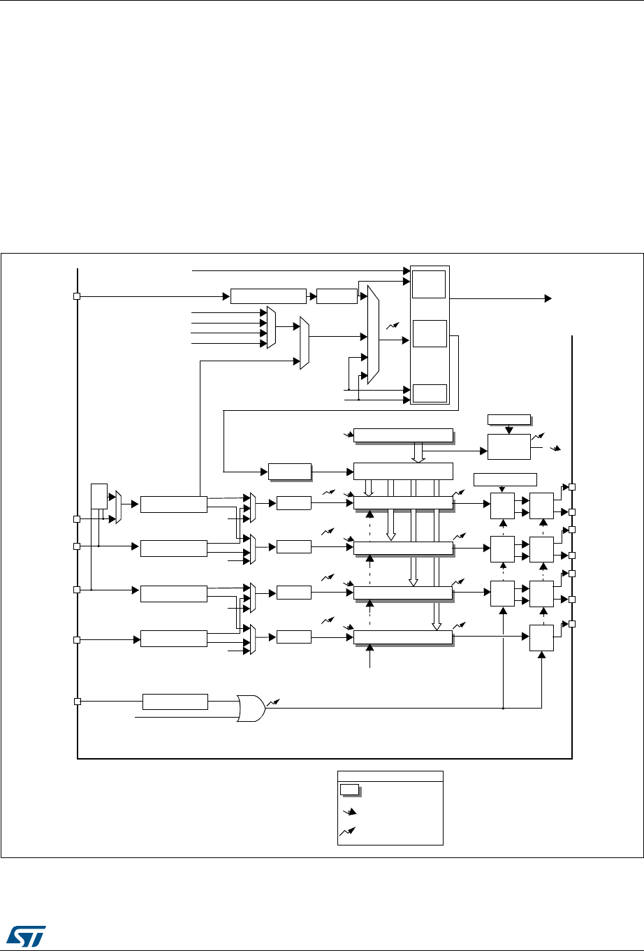
DocID026448 Rev 1 239/836
RM0383 Advanced-control timer (TIM1)
305
•Interrupt/DMA generation on the following events:
– Update: counter overflow/underflow, counter initialization (by software or
internal/external trigger)
– Trigger event (counter start, stop, initialization or count by internal/external trigger)
– Input capture
– Output compare
– Break input
•Supports incremental (quadrature) encoder and hall-sensor circuitry for positioning
purposes
•Trigger input for external clock or cycle-by-cycle current management
Figure 39. Advanced-control timer block diagram
3UHVFDOHU
$XWR5HORDG5HJLVWHU
&2817(5
&DSWXUH&RPSDUH5HJLVWHU
&DSWXUH&RPSDUH5HJLVWHU
8
8
8
&&,
&&,
(75
7ULJJHU
&RQWUROOHU
6WRS&OHDURU8S'RZQ
7,)3
7,)3
,75
,75
,75
75*, &RQWUROOHU
(QFRGHU
,QWHUIDFH
&DSWXUH&RPSDUH5HJLVWHU
8
&&,
RXWSXW
FRQWURO
'7*
'7*
>@UHJLVWHUV
42'/
2&5()
2&5()
2&5()
5(35HJLVWHU
8
5HSHWLWLRQ
FRXQWHU
8,
5HVHW(QDEOH8S'RZQ&RXQW
&DSWXUH&RPSDUH5HJLVWHU
8
&&,
2&5()
#+?03#
7, 3UHVFDOHU
3UHVFDOHU
,&36
,&36
,&
,&
3UHVFDOHU
3UHVFDOHU
,QSXW)LOWHU
(GJHGHWHFWRU
,&36
,&36
7,)3
RXWSXW
FRQWURO
'7*
RXWSXW
FRQWURO
'7*
RXWSXW
FRQWURO
5HJ
HYHQW
1RWHV
3UHORDGUHJLVWHUVWUDQVIHUUHG
WRDFWLYHUHJLVWHUVRQ8HYHQW
DFFRUGLQJWRFRQWUROELW
LQWHUUXSW'0$RXWSXW
,QSXW)LOWHU
3RODULW\6HOHFWLRQ(GJH
'HWHFWRU3UHVFDOHU
(753
7*,
75&
75&
,&
,&
,75
(75)
75&
7,)B('
,QSXW)LOWHU
(GJHGHWHFWRU
,QSXW)LOWHU
(GJHGHWHFWRU
,QSXW)LOWHU
(GJHGHWHFWRU
&&,
&&,
&&,
&&,
7,)3
7,)3
7,)3
7,)3
75&
75&
7,)3
7,)3
7,)3
%,
4)
4)
4)
8/2
4)-X?#(
4)-X?#(
4)-X?#(
4)-X?#(
%5.
4)-X?"+).
/#
/#
/#
4)-X?#(
4)-X?#(
4)-X?#(
4)-X?#(.
/#.
4)-X?#(.
/#.
4)-X?#(.
/#.
/#
4)-X?#(
4)-X?%42
TOOTHERTIMERS
0RGH
6ODYH
36& &17
,QWHUQDO&ORFN&.B,17
#+?#.4
(75)
&ORFNIDLOXUHHYHQWIURPFORFNFRQWUROOHU
3RODULW\6HOHFWLRQ
&66&ORFN6HFXULW\V\VWHP
#+?4)-FROM2##
TO!$#
,75
069

Advanced-control timer (TIM1) RM0383
240/836 DocID026448 Rev 1
12.3 TIM1 functional description
12.3.1 Time-base unit
The main block of the programmable advanced-control timer is a 16-bit counter with its
related auto-reload register. The counter can count up, down or both up and down. The
counter clock can be divided by a prescaler.
The counter, the auto-reload register and the prescaler register can be written or read by
software. This is true even when the counter is running.
The time-base unit includes:
•Counter register (TIMx_CNT)
•Prescaler register (TIMx_PSC)
•Auto-reload register (TIMx_ARR)
•Repetition counter register (TIMx_RCR)
The auto-reload register is preloaded. Writing to or reading from the auto-reload register
accesses the preload register. The content of the preload register are transferred into the
shadow register permanently or at each update event (UEV), depending on the auto-reload
preload enable bit (ARPE) in TIMx_CR1 register. The update event is sent when the counter
reaches the overflow (or underflow when downcounting) and if the UDIS bit equals 0 in the
TIMx_CR1 register. It can also be generated by software. The generation of the update
event is described in detailed for each configuration.
The counter is clocked by the prescaler output CK_CNT, which is enabled only when the
counter enable bit (CEN) in TIMx_CR1 register is set (refer also to the slave mode controller
description to get more details on counter enabling).
Note that the counter starts counting 1 clock cycle after setting the CEN bit in the TIMx_CR1
register.
Prescaler description
The prescaler can divide the counter clock frequency by any factor between 1 and 65536. It
is based on a 16-bit counter controlled through a 16-bit register (in the TIMx_PSC register).
It can be changed on the fly as this control register is buffered. The new prescaler ratio is
taken into account at the next update event.
Figure 40 and Figure 41 give some examples of the counter behavior when the prescaler
ratio is changed on the fly:
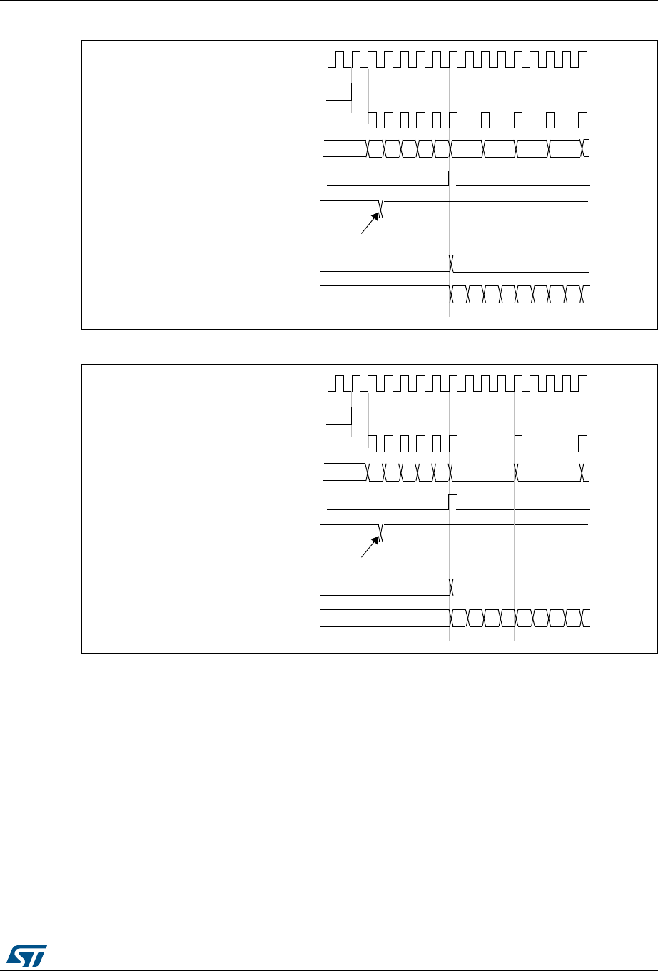
DocID026448 Rev 1 241/836
RM0383 Advanced-control timer (TIM1)
305
Figure 40. Counter timing diagram with prescaler division change from 1 to 2
Figure 41. Counter timing diagram with prescaler division change from 1 to 4
12.3.2 Counter modes
Upcounting mode
In upcounting mode, the counter counts from 0 to the auto-reload value (content of the
TIMx_ARR register), then restarts from 0 and generates a counter overflow event.
If the repetition counter is used, the update event (UEV) is generated after upcounting is
repeated for the number of times programmed in the repetition counter register
(TIMx_RCR). Else the update event is generated at each counter overflow.
Setting the UG bit in the TIMx_EGR register (by software or by using the slave mode
controller) also generates an update event.
The UEV event can be disabled by software by setting the UDIS bit in the TIMx_CR1
register. This is to avoid updating the shadow registers while writing new values in the
CK_PSC
00
CEN
Timer clock = CK_CNT
Counter register
Update event (UEV)
0
F9 FA FB FCF7
Prescaler control register 01
Write a new value in TIMx_PSC
01 02 03
Prescaler buffer 01
Prescaler counter 01 0 1 0 1 0 1
F8
CK_PSC
00
CEN
Timer clock = CK_CNT
Counter register
Update event (UEV)
0
F9 FA FB FCF7
Prescaler control register 03
Write a new value in TIMx_PSC
Prescaler buffer 03
Prescaler counter 01 2 3 0 1 2 3
F8 01
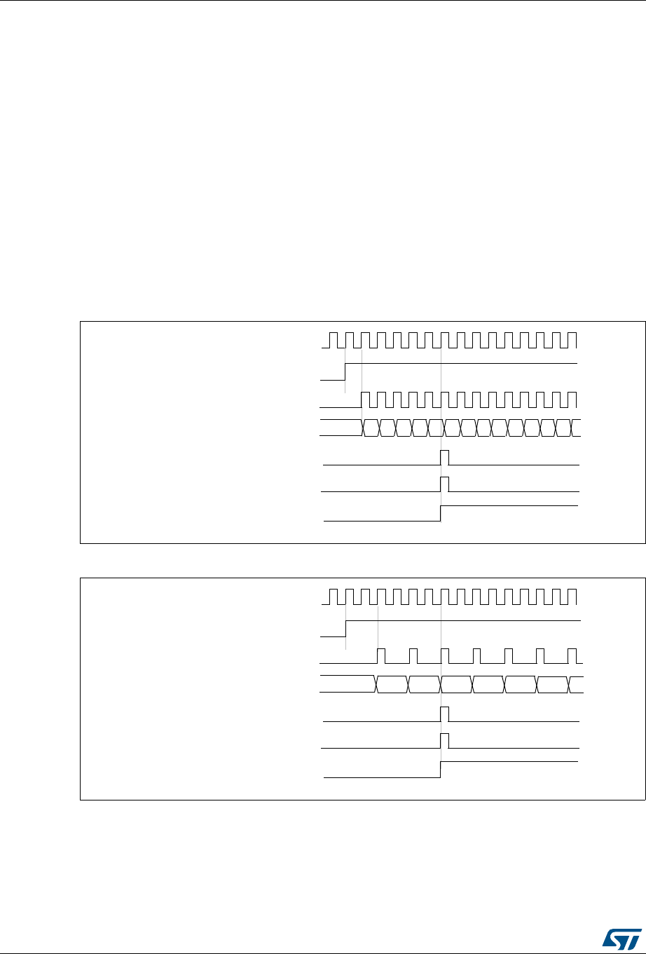
Advanced-control timer (TIM1) RM0383
242/836 DocID026448 Rev 1
preload registers. Then no update event occurs until the UDIS bit has been written to 0.
However, the counter restarts from 0, as well as the counter of the prescaler (but the
prescale rate does not change). In addition, if the URS bit (update request selection) in
TIMx_CR1 register is set, setting the UG bit generates an update event UEV but without
setting the UIF flag (thus no interrupt or DMA request is sent). This is to avoid generating
both update and capture interrupts when clearing the counter on the capture event.
When an update event occurs, all the registers are updated and the update flag (UIF bit in
TIMx_SR register) is set (depending on the URS bit):
•The repetition counter is reloaded with the content of TIMx_RCR register,
•The auto-reload shadow register is updated with the preload value (TIMx_ARR),
•The buffer of the prescaler is reloaded with the preload value (content of the TIMx_PSC
register).
The following figures show some examples of the counter behavior for different clock
frequencies when TIMx_ARR=0x36.
Figure 42. Counter timing diagram, internal clock divided by 1
Figure 43. Counter timing diagram, internal clock divided by 2
CK_PSC
00
CNT_EN
Timer clock = CK_CNT
Counter register
Update interrupt flag (UIF)
Counter overflow
Update event (UEV)
01 02 03 04 05 06 0732 33 34 35 3631
CK_PSC
0035 0000 0001 0002 0003
CNT_EN
Timer clock = CK_CNT
Counter register
Update interrupt flag (UIF)
0034 0036
Counter overflow
Update event (UEV)
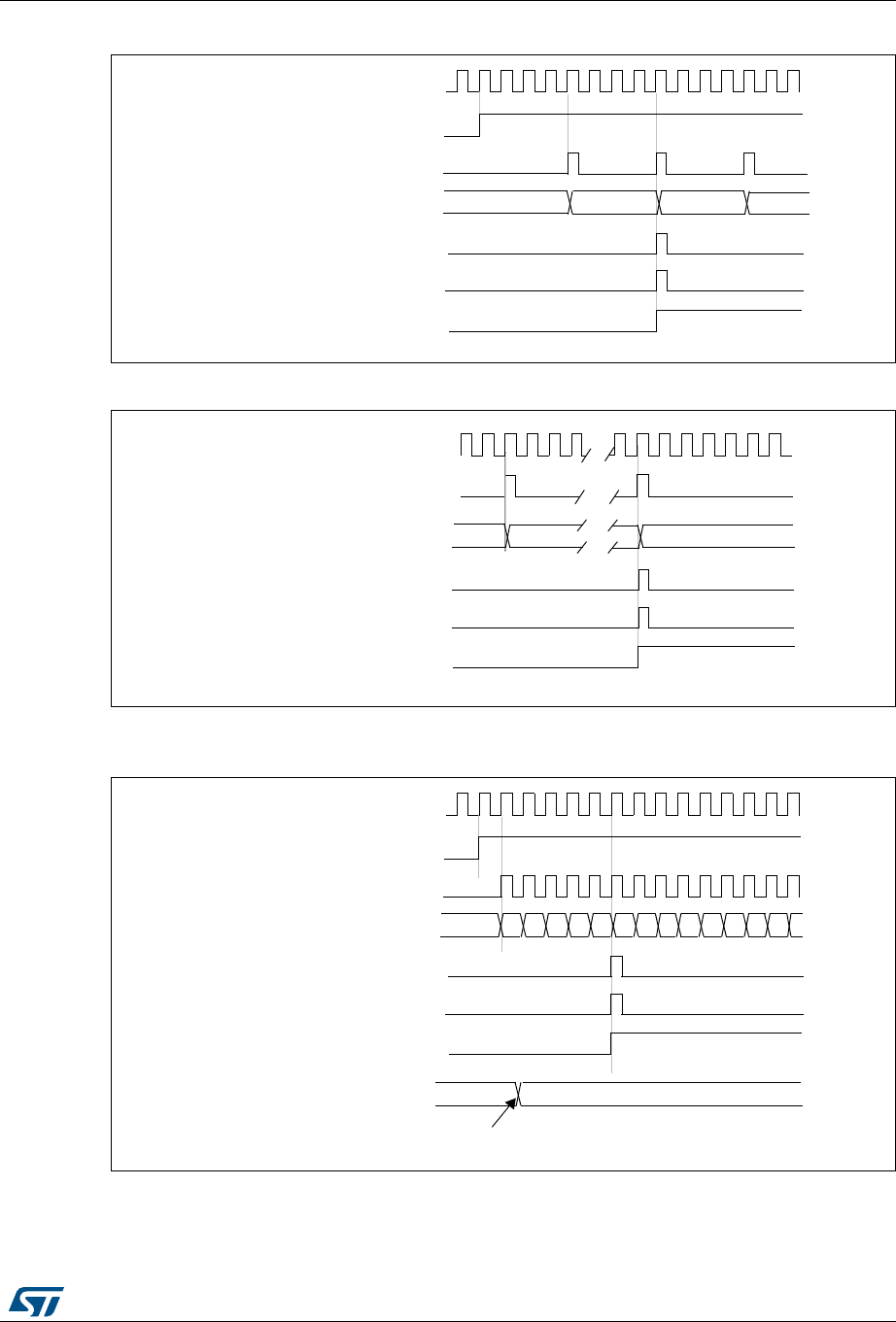
DocID026448 Rev 1 243/836
RM0383 Advanced-control timer (TIM1)
305
Figure 44. Counter timing diagram, internal clock divided by 4
Figure 45. Counter timing diagram, internal clock divided by N
Figure 46. Counter timing diagram, update event when ARPE=0 (TIMx_ARR not
preloaded)
CK_PSC
0000 0001
CNT_EN
Timer clock = CK_CNT
Counter register
Update interrupt flag (UIF)
0035 0036
Counter overflow
Update event (UEV)
Timer clock = CK_CNT
Counter register 00
1F 20
Update interrupt flag (UIF)
Counter overflow
Update event (UEV)
CK_PSC
CK_PSC
00
CEN
Timer clock = CK_CNT
Counter register
Update interrupt flag (UIF)
Counter overflow
Update event (UEV)
01 02 03 04 05 06 0732 33 34 35 3631
Auto-reload register FF 36
Write a new value in TIMx_ARR
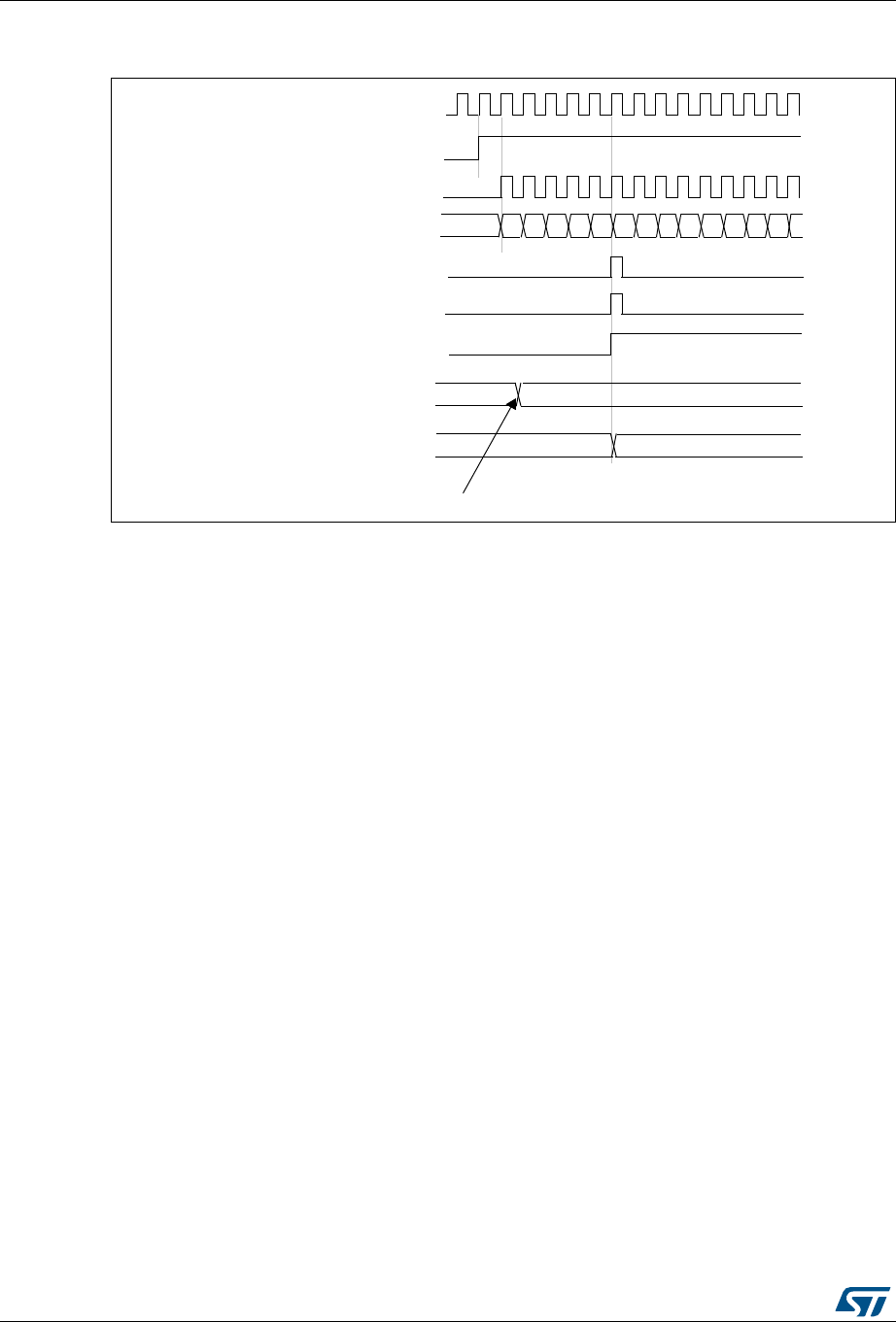
Advanced-control timer (TIM1) RM0383
244/836 DocID026448 Rev 1
Figure 47. Counter timing diagram, update event when ARPE=1
(TIMx_ARR preloaded)
Downcounting mode
In downcounting mode, the counter counts from the auto-reload value (content of the
TIMx_ARR register) down to 0, then restarts from the auto-reload value and generates a
counter underflow event.
If the repetition counter is used, the update event (UEV) is generated after downcounting is
repeated for the number of times programmed in the repetition counter register plus one
(TIMx_RCR+1). Else the update event is generated at each counter underflow.
Setting the UG bit in the TIMx_EGR register (by software or by using the slave mode
controller) also generates an update event.
The UEV update event can be disabled by software by setting the UDIS bit in TIMx_CR1
register. This is to avoid updating the shadow registers while writing new values in the
preload registers. Then no update event occurs until UDIS bit has been written to 0.
However, the counter restarts from the current auto-reload value, whereas the counter of the
prescaler restarts from 0 (but the prescale rate doesn’t change).
In addition, if the URS bit (update request selection) in TIMx_CR1 register is set, setting the
UG bit generates an update event UEV but without setting the UIF flag (thus no interrupt or
DMA request is sent). This is to avoid generating both update and capture interrupts when
clearing the counter on the capture event.
When an update event occurs, all the registers are updated and the update flag (UIF bit in
TIMx_SR register) is set (depending on the URS bit):
•The repetition counter is reloaded with the content of TIMx_RCR register
•The buffer of the prescaler is reloaded with the preload value (content of the TIMx_PSC
register)
•The auto-reload active register is updated with the preload value (content of the
TIMx_ARR register). Note that the auto-reload is updated before the counter is
reloaded, so that the next period is the expected one
CK_PSC
00
CEN
Timer clock = CK_CNT
Counter register
Update interrupt flag (UIF)
Counter overflow
Update event (UEV)
01 02 03 04 05 06 07F1 F2 F3 F4 F5F0
Auto-reload preload register F5 36
Auto-reload shadow register F5 36
Write a new value in TIMx_ARR
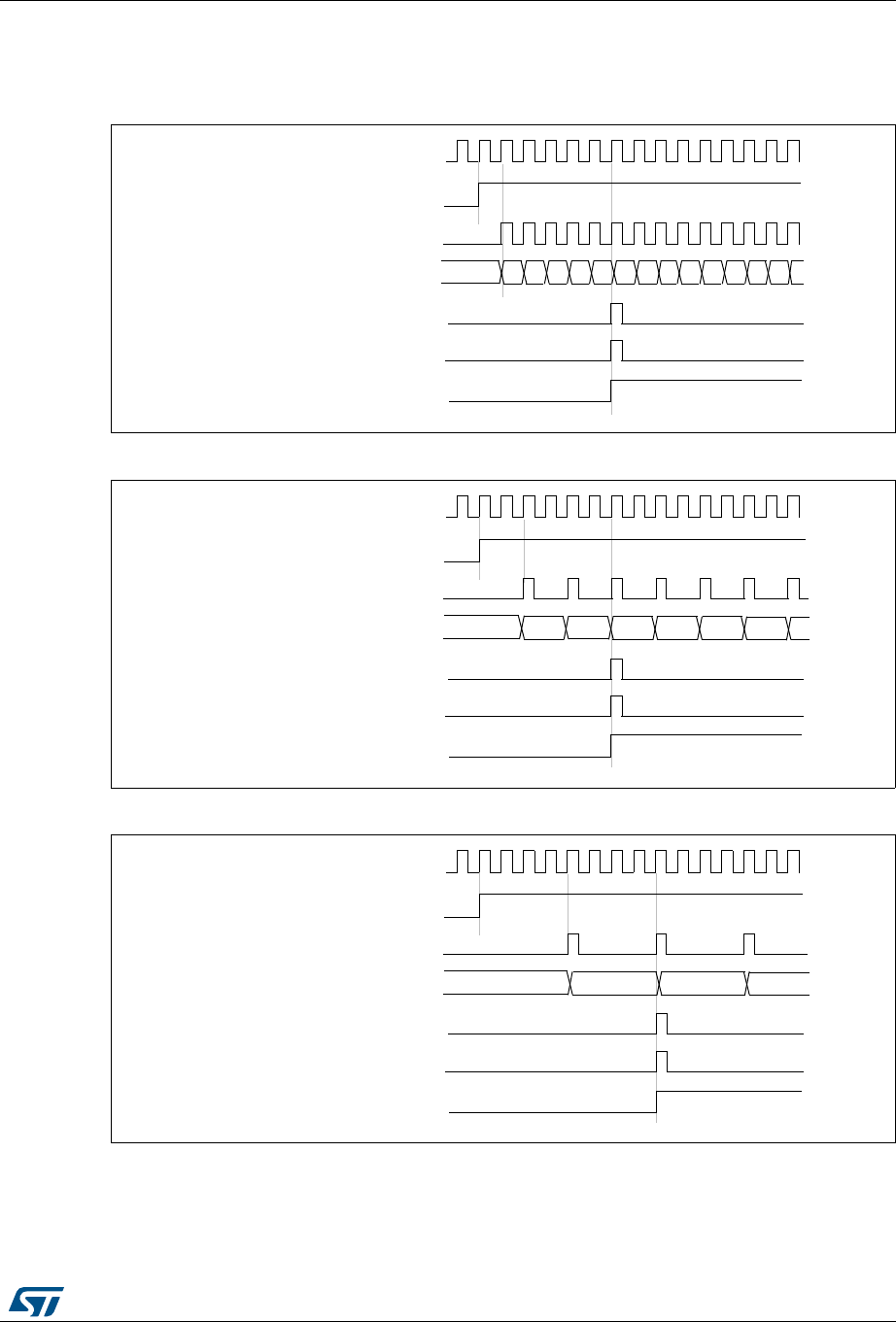
DocID026448 Rev 1 245/836
RM0383 Advanced-control timer (TIM1)
305
The following figures show some examples of the counter behavior for different clock
frequencies when TIMx_ARR=0x36.
Figure 48. Counter timing diagram, internal clock divided by 1
Figure 49. Counter timing diagram, internal clock divided by 2
Figure 50. Counter timing diagram, internal clock divided by 4
CK_PSC
36
CNT_EN
Timer clock = CK_CNT
Counter register
Update interrupt flag (UIF)
Counter underflow (cnt_udf)
Update event (UEV)
35 34 33 32 31 30 2F04 03 02 01 0005
CK_PSC
0001 0036 0035 0034 0033
CNT_EN
Timer clock = CK_CNT
Counter register
Update interrupt flag (UIF)
0002 0000
Counter underflow
Update event (UEV)
CK_PSC
0036 0035
CNT_EN
Timer clock = CK_CNT
Counter register
Update interrupt flag (UIF)
0001 0000
Counter underflow
Update event (UEV)
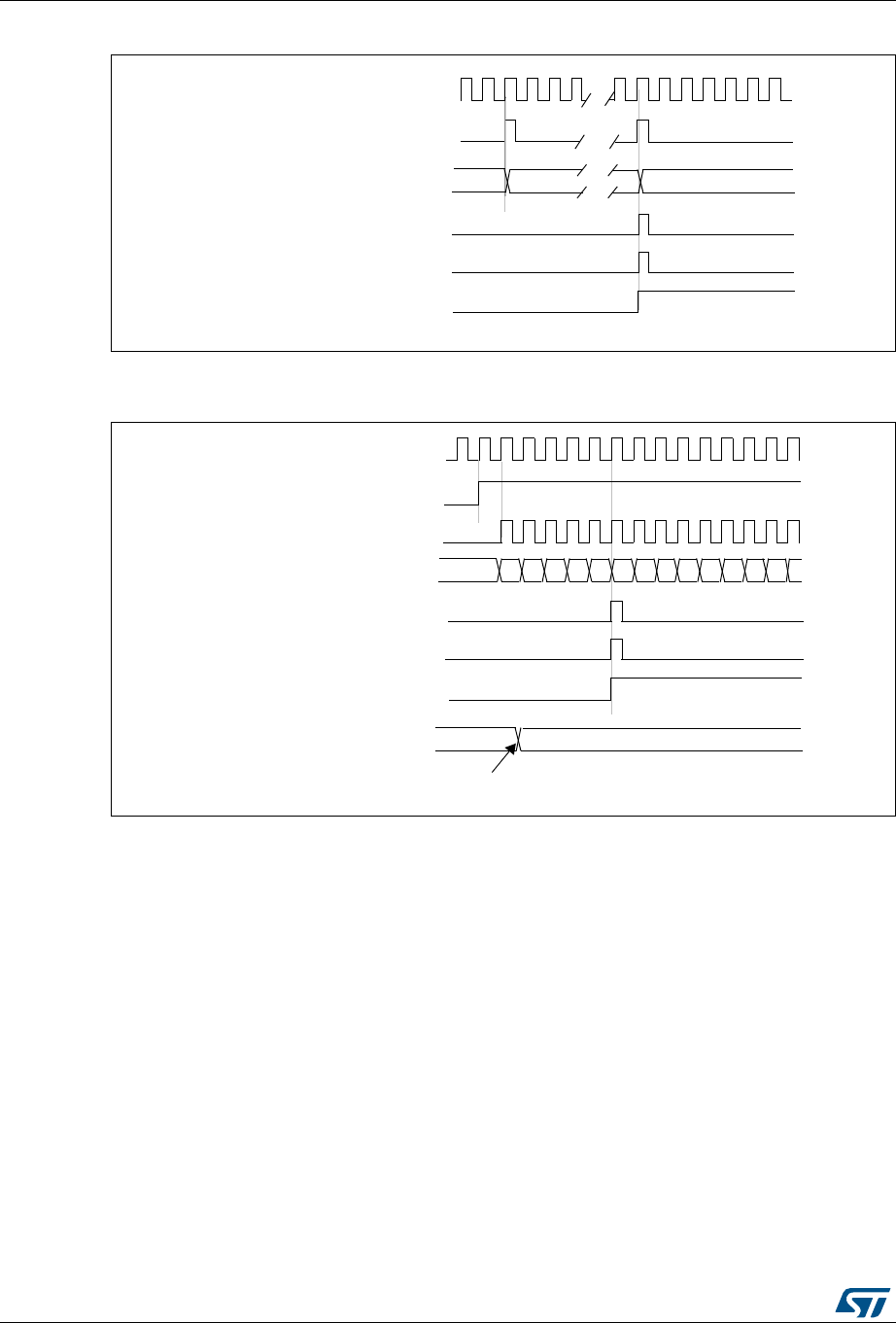
Advanced-control timer (TIM1) RM0383
246/836 DocID026448 Rev 1
Figure 51. Counter timing diagram, internal clock divided by N
Figure 52. Counter timing diagram, update event when repetition counter
is not used
Center-aligned mode (up/down counting)
In center-aligned mode, the counter counts from 0 to the auto-reload value (content of the
TIMx_ARR register) – 1, generates a counter overflow event, then counts from the auto-
reload value down to 1 and generates a counter underflow event. Then it restarts counting
from 0.
Center-aligned mode is active when the CMS bits in TIMx_CR1 register are not equal to
'00'. The Output compare interrupt flag of channels configured in output is set when: the
counter counts down (Center aligned mode 1, CMS = "01"), the counter counts up (Center
aligned mode 2, CMS = "10") the counter counts up and down (Center aligned mode 3,
CMS = "11").
In this mode, the DIR direction bit in the TIMx_CR1 register cannot be written. It is updated
by hardware and gives the current direction of the counter.
The update event can be generated at each counter overflow and at each counter underflow
or by setting the UG bit in the TIMx_EGR register (by software or by using the slave mode
controller) also generates an update event. In this case, the counter restarts counting from
0, as well as the counter of the prescaler.
Timer clock = CK_CNT
Counter register 36
20 1F
Update interrupt flag (UIF)
Counter underflow
Update event (UEV)
CK_PSC
00
CK_PSC
36
CEN
Timer clock = CK_CNT
Counter register
Update interrupt flag (UIF)
Counter underflow
Update event (UEV)
35 34 33 32 31 30 2F04 03 02 01 0005
Auto-reload register FF 36
Write a new value in TIMx_ARR
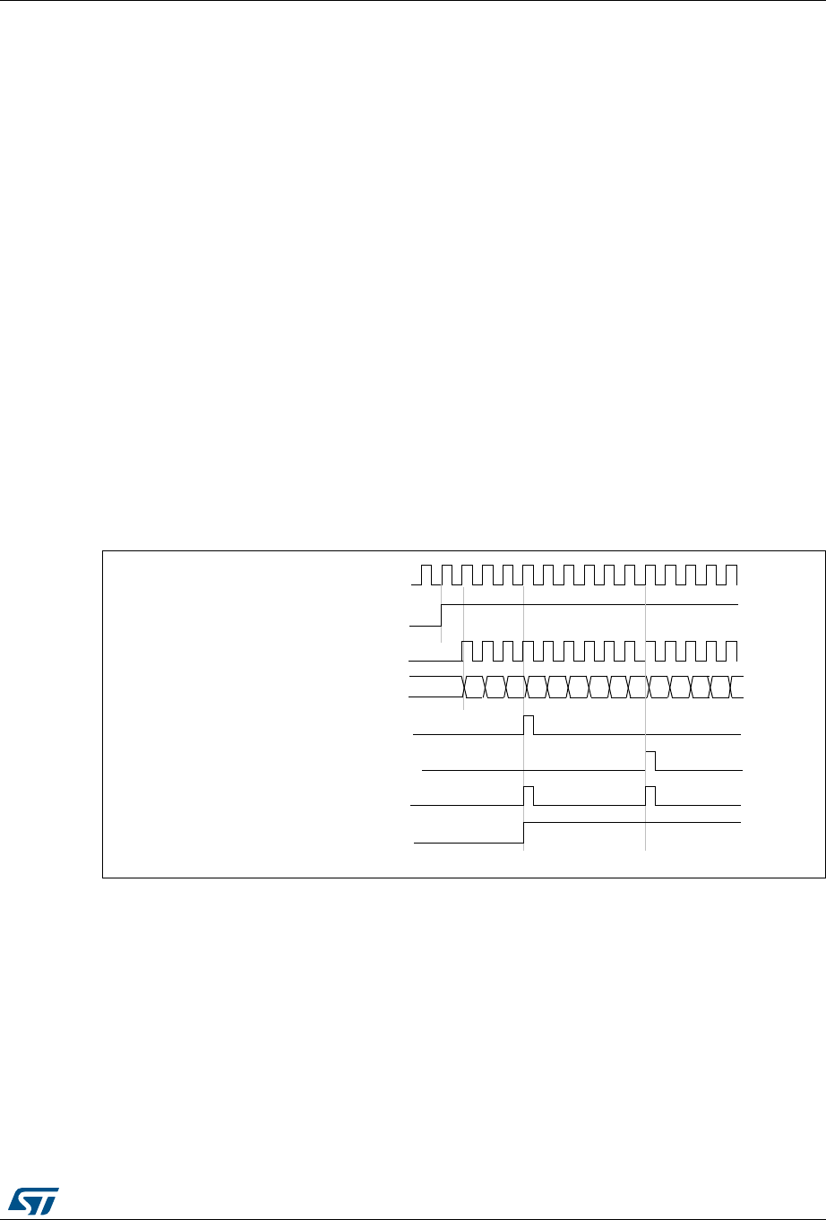
DocID026448 Rev 1 247/836
RM0383 Advanced-control timer (TIM1)
305
The UEV update event can be disabled by software by setting the UDIS bit in the TIMx_CR1
register. This is to avoid updating the shadow registers while writing new values in the
preload registers. Then no update event occurs until UDIS bit has been written to 0.
However, the counter continues counting up and down, based on the current auto-reload
value.
In addition, if the URS bit (update request selection) in TIMx_CR1 register is set, setting the
UG bit generates an UEV update event but without setting the UIF flag (thus no interrupt or
DMA request is sent). This is to avoid generating both update and capture interrupts when
clearing the counter on the capture event.
When an update event occurs, all the registers are updated and the update flag (UIF bit in
TIMx_SR register) is set (depending on the URS bit):
•The repetition counter is reloaded with the content of TIMx_RCR register
•The buffer of the prescaler is reloaded with the preload value (content of the TIMx_PSC
register)
•The auto-reload active register is updated with the preload value (content of the
TIMx_ARR register). Note that if the update source is a counter overflow, the auto-
reload is updated before the counter is reloaded, so that the next period is the expected
one (the counter is loaded with the new value).
The following figures show some examples of the counter behavior for different clock
frequencies.
Figure 53. Counter timing diagram, internal clock divided by 1, TIMx_ARR = 0x6
1. Here, center-aligned mode 1 is used (for more details refer to Section 12.4: TIM1 registers on page 278).
CK_PSC
02
CNT_EN
Timer clock = CK_CNT
Counter register
Update interrupt flag (UIF)
Counter underflow
Update event (UEV)
03 04 05 06 05 04 0303 02 01 00 0104
Counter overflow
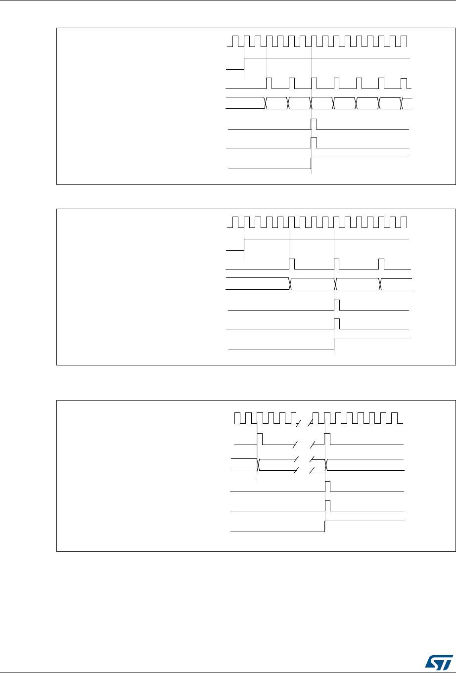
Advanced-control timer (TIM1) RM0383
248/836 DocID026448 Rev 1
Figure 54. Counter timing diagram, internal clock divided by 2
Figure 55. Counter timing diagram, internal clock divided by 4, TIMx_ARR=0x36
1. Center-aligned mode 2 or 3 is used with an UIF on overflow.
Figure 56. Counter timing diagram, internal clock divided by N
CK_PSC
0002 0000 0001 0002 0003
CNT_EN
Timer clock = CK_CNT
Counter register
Update interrupt flag (UIF)
0003 0001
Counter underflow
Update event (UEV)
CK_PSC
0036 0035
CNT_EN
Timer clock = CK_CNT
Counter register
Update interrupt flag (UIF)
0034 0035
Counter overflow
Update event (UEV)
Timer clock = CK_CNT
Counter register 00
20 1F
Update interrupt flag (UIF)
Counter underflow
Update event (UEV)
CK_PSC
01
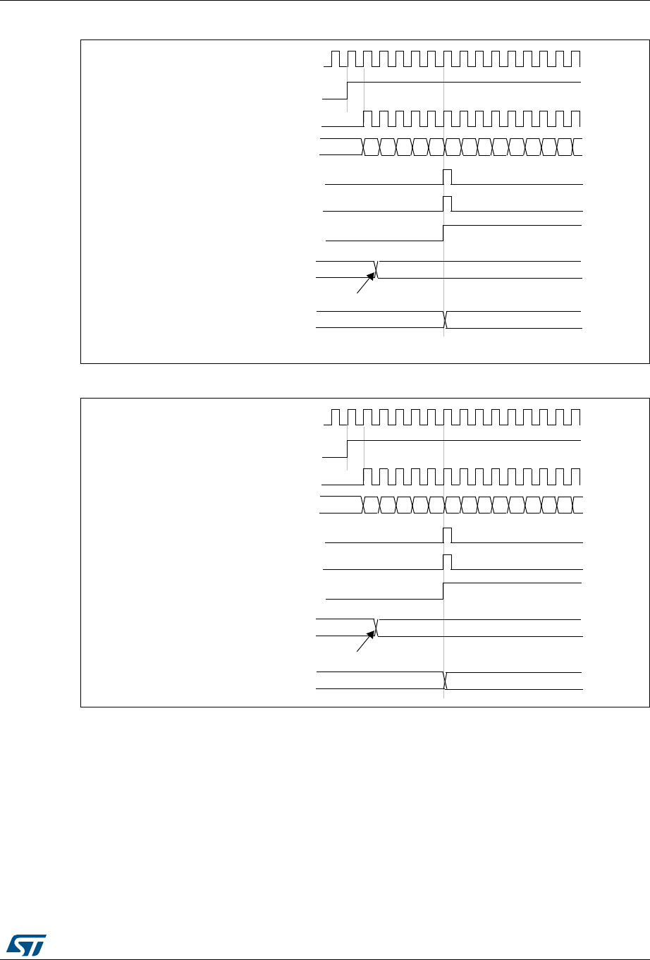
DocID026448 Rev 1 249/836
RM0383 Advanced-control timer (TIM1)
305
Figure 57. Counter timing diagram, update event with ARPE=1 (counter underflow)
Figure 58. Counter timing diagram, Update event with ARPE=1 (counter overflow)
12.3.3 Repetition counter
Section 12.3.1: Time-base unit describes how the update event (UEV) is generated with
respect to the counter overflows/underflows. It is actually generated only when the repetition
counter has reached zero. This can be useful when generating PWM signals.
This means that data are transferred from the preload registers to the shadow registers
(TIMx_ARR auto-reload register, TIMx_PSC prescaler register, but also TIMx_CCRx
capture/compare registers in compare mode) every N+1 counter overflows or underflows,
where N is the value in the TIMx_RCR repetition counter register.
CK_PSC
00
CEN
Timer clock = CK_CNT
Counter register
Update interrupt flag (UIF)
Counter underflow
Update event (UEV)
01 02 03 04 05 06 0705 04 03 02 0106
Auto-reload preload register FD 36
Write a new value in TIMx_ARR
Auto-reload active register FD 36
CK_PSC
36
CEN
Timer clock = CK_CNT
Counter register
Update interrupt flag (UIF)
Counter overflow
Update event (UEV)
35 34 33 32 31 30 2FF8 F9 FA FB FCF7
Auto-reload preload register FD 36
Write a new value in TIMx_ARR
Auto-reload active register FD 36
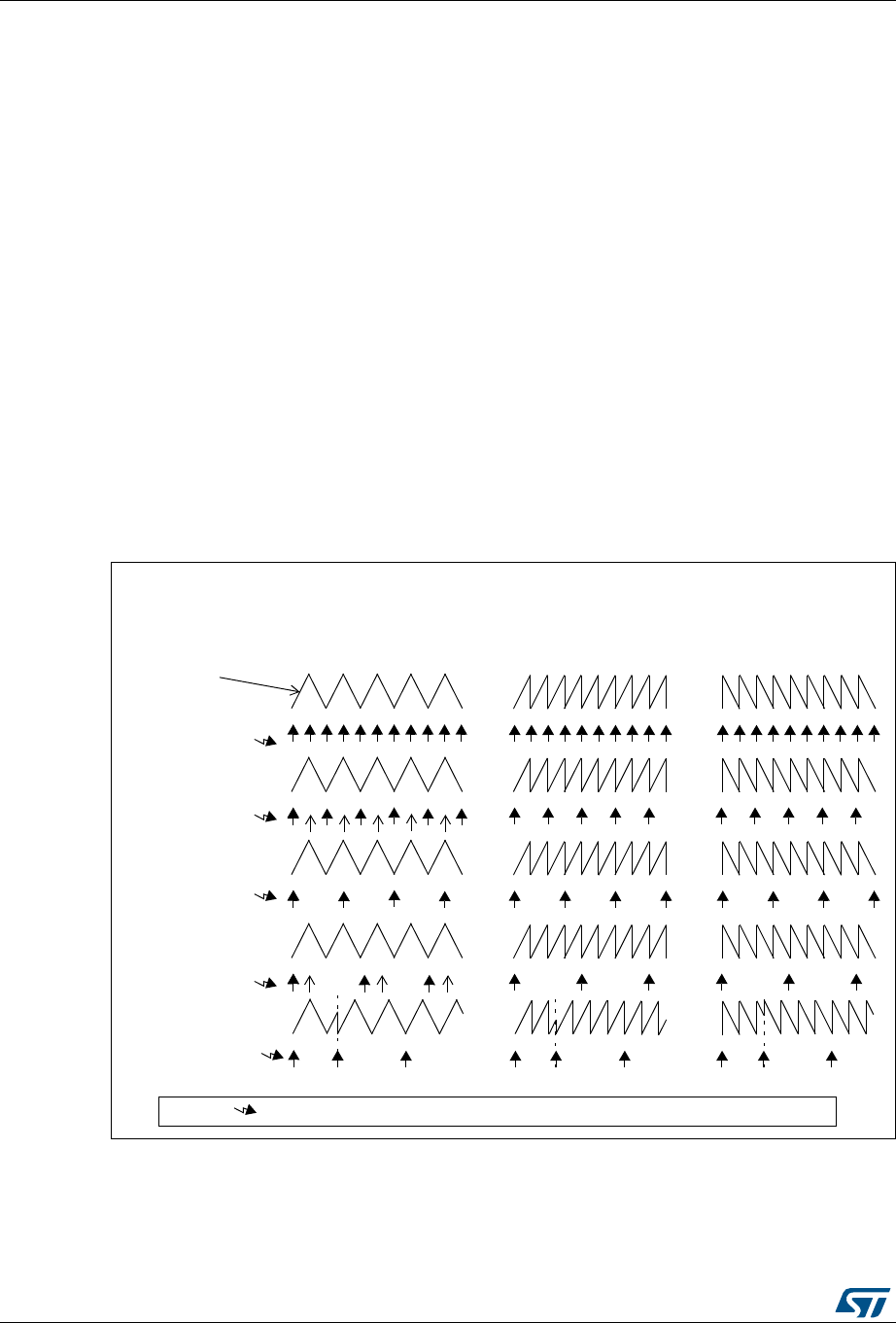
Advanced-control timer (TIM1) RM0383
250/836 DocID026448 Rev 1
The repetition counter is decremented:
•At each counter overflow in upcounting mode,
•At each counter underflow in downcounting mode,
•At each counter overflow and at each counter underflow in center-aligned mode.
Although this limits the maximum number of repetition to 128 PWM cycles, it makes it
possible to update the duty cycle twice per PWM period. When refreshing compare
registers only once per PWM period in center-aligned mode, maximum resolution is
2xTck, due to the symmetry of the pattern.
The repetition counter is an auto-reload type; the repetition rate is maintained as defined by
the TIMx_RCR register value (refer to Figure 59). When the update event is generated by
software (by setting the UG bit in TIMx_EGR register) or by hardware through the slave
mode controller, it occurs immediately whatever the value of the repetition counter is and the
repetition counter is reloaded with the content of the TIMx_RCR register.
In center-aligned mode, for odd values of RCR, the update event occurs either on the
overflow or on the underflow depending on when the RCR register was written and when
the counter was started. If the RCR was written before starting the counter, the UEV occurs
on the overflow. If the RCR was written after starting the counter, the UEV occurs on the
underflow. For example for RCR = 3, the UEV is generated on each 4th overflow or
underflow event depending on when RCR was written.
Figure 59. Update rate examples depending on mode and TIMx_RCR register settings
Center-aligned mode Edge-aligned mode
UEV Update Event
: Preload registers transferred to active registers and update interrupt generated
Counter
TIMx_RCR = 0
TIMx_RCR = 1
TIMx_RCR = 2
TIMx_RCR = 3
UEV
TIMx_RCR
= 3
and
re-synchronization
(by SW) (by SW)
TIMx_CNT
(by SW)
Upcounting Downcounting
UEV
UEV
UEV
UEV
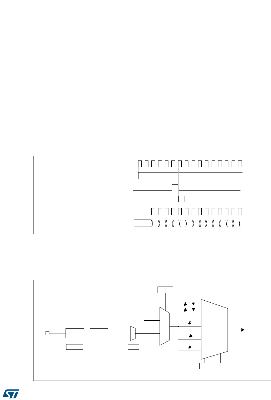
DocID026448 Rev 1 251/836
RM0383 Advanced-control timer (TIM1)
305
12.3.4 Clock selection
The counter clock can be provided by the following clock sources:
•Internal clock (CK_INT)
•External clock mode1: external input pin
•External clock mode2: external trigger input ETR
•Internal trigger inputs (ITRx): using one timer as prescaler for another timer, for
example, you can configure Timer 1 to act as a prescaler for Timer 2. Refer to Using
one timer as prescaler for another for more details.
Internal clock source (CK_INT)
If the slave mode controller is disabled (SMS=000), then the CEN, DIR (in the TIMx_CR1
register) and UG bits (in the TIMx_EGR register) are actual control bits and can be changed
only by software (except UG which remains cleared automatically). As soon as the CEN bit
is written to 1, the prescaler is clocked by the internal clock CK_INT.
Figure 60 shows the behavior of the control circuit and the upcounter in normal mode,
without prescaler.
Figure 60. Control circuit in normal mode, internal clock divided by 1
External clock source mode 1
This mode is selected when SMS=111 in the TIMx_SMCR register. The counter can count at
each rising or falling edge on a selected input.
Figure 61. TI2 external clock connection example
Internal clock
00
Counter clock = CK_CNT = CK_PSC
Counter register 01 02 03 04 05 06 0732 33 34 35 3631
CEN=CNT_EN
UG
CNT_INIT
CK_INT
encoder
mode
external clock
mode 1
external clock
mode 2
internal clock
mode
ETRF
TRGI
TI1F
TI2F or
or
or
(internal clock)
CK_PSC
ECE
TIMx_SMCR
SMS[2:0]
ITRx
TI1_ED
TI1FP1
TI2FP2
ETRF
TIMx_SMCR
TS[2:0]
TI2 0
1
TIMx_CCER
CC2P
Filter
ICF[3:0]
TIMx_CCMR1
Edge
Detector
TI2F_Rising
TI2F_Falling 110
0xx
100
101
111
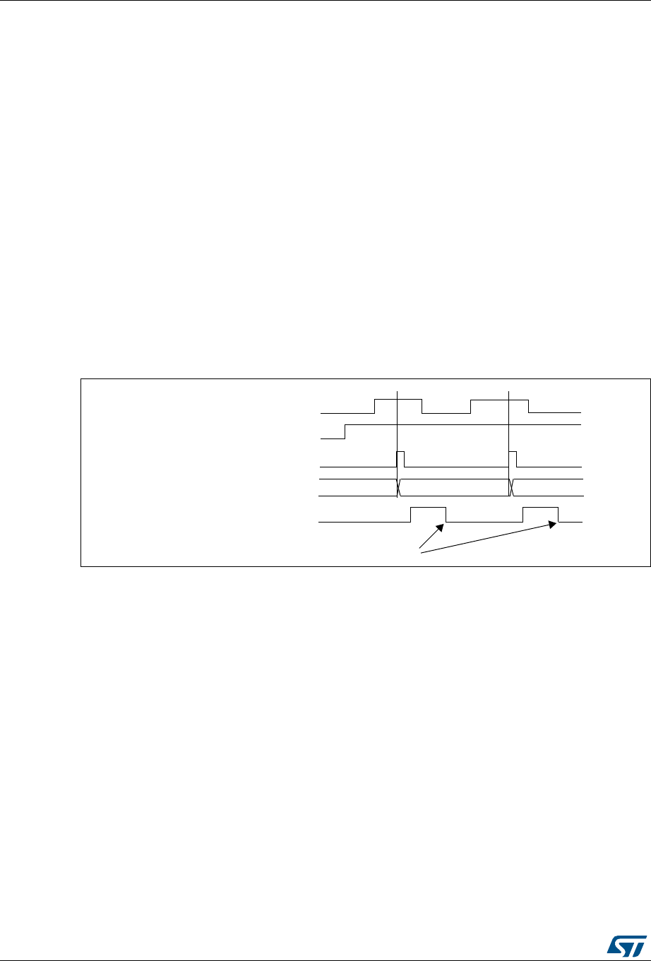
Advanced-control timer (TIM1) RM0383
252/836 DocID026448 Rev 1
For example, to configure the upcounter to count in response to a rising edge on the TI2
input, use the following procedure:
1. Configure channel 2 to detect rising edges on the TI2 input by writing CC2S = ‘01’ in
the TIMx_CCMR1 register.
2. Configure the input filter duration by writing the IC2F[3:0] bits in the TIMx_CCMR1
register (if no filter is needed, keep IC2F=0000).
3. Select rising edge polarity by writing CC2P=0 and CC2NP=0 in the TIMx_CCER
register.
4. Configure the timer in external clock mode 1 by writing SMS=111 in the TIMx_SMCR
register.
5. Select TI2 as the trigger input source by writing TS=110 in the TIMx_SMCR register.
6. Enable the counter by writing CEN=1 in the TIMx_CR1 register.
Note: The capture prescaler is not used for triggering, so you don’t need to configure it.
When a rising edge occurs on TI2, the counter counts once and the TIF flag is set.
The delay between the rising edge on TI2 and the actual clock of the counter is due to the
resynchronization circuit on TI2 input.
Figure 62. Control circuit in external clock mode 1
Counter clock = CK_CNT = CK_PSC
Counter register 35 3634
TI2
CNT_EN
TIF
Write TIF=0
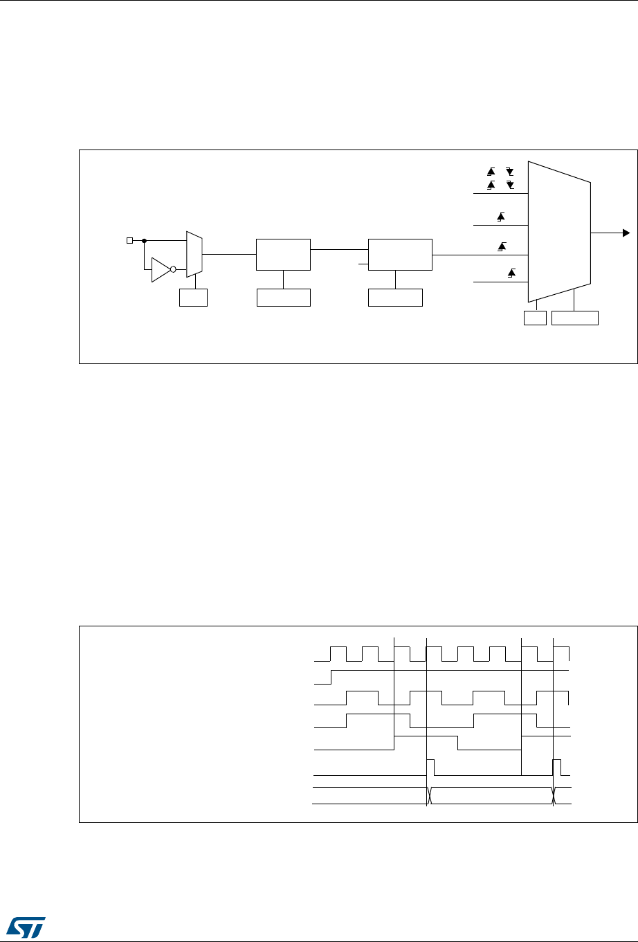
DocID026448 Rev 1 253/836
RM0383 Advanced-control timer (TIM1)
305
External clock source mode 2
This mode is selected by writing ECE=1 in the TIMx_SMCR register.
The counter can count at each rising or falling edge on the external trigger input ETR.
Figure 63 gives an overview of the external trigger input block.
Figure 63. External trigger input block
For example, to configure the upcounter to count each 2 rising edges on ETR, use the
following procedure:
1. As no filter is needed in this example, write ETF[3:0]=0000 in the TIMx_SMCR register.
2. Set the prescaler by writing ETPS[1:0]=01 in the TIMx_SMCR register
3. Select rising edge detection on the ETR pin by writing ETP=0 in the TIMx_SMCR
register
4. Enable external clock mode 2 by writing ECE=1 in the TIMx_SMCR register.
5. Enable the counter by writing CEN=1 in the TIMx_CR1 register.
The counter counts once each 2 ETR rising edges.
The delay between the rising edge on ETR and the actual clock of the counter is due to the
resynchronization circuit on the ETRP signal.
Figure 64. Control circuit in external clock mode 2
ETR 0
1
TIMx_SMCR
ETP
divider
/1, /2, /4, /8
ETPS[1:0]
ETRP filter
ETF[3:0]
downcounter
fDTS
TIMx_SMCR
TIMx_SMCR
ETR pin
CK_INT
encoder
mode
external clock
mode 1
external clock
mode 2
internal clock
mode
ETRF
TRGI
TI1F
TI2F or
or
or
(internal clock)
CK_PSC
ECE
TIMx_SMCR
SMS[2:0]
Counter clock = CK_CNT = CK_PSC
Counter register 35 3634
ETR
CNT_EN
fCK_INT
ETRP
ETRF
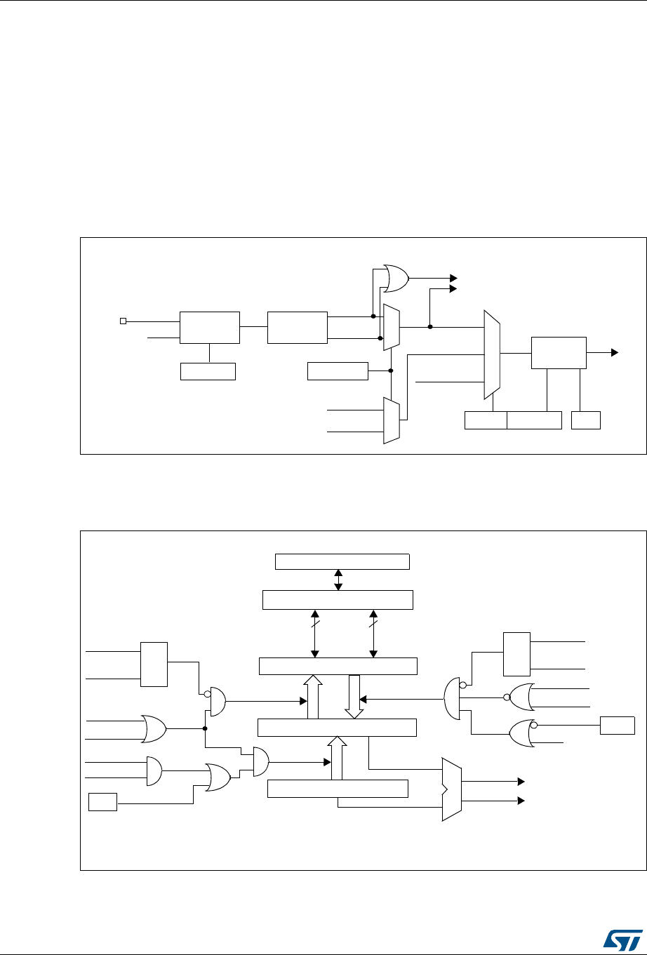
Advanced-control timer (TIM1) RM0383
254/836 DocID026448 Rev 1
12.3.5 Capture/compare channels
Each Capture/Compare channel is built around a capture/compare register (including a
shadow register), a input stage for capture (with digital filter, multiplexing and prescaler) and
an output stage (with comparator and output control).
Figure 65 to Figure 68 give an overview of one Capture/Compare channel.
The input stage samples the corresponding TIx input to generate a filtered signal TIxF.
Then, an edge detector with polarity selection generates a signal (TIxFPx) which can be
used as trigger input by the slave mode controller or as the capture command. It is
prescaled before the capture register (ICxPS).
Figure 65. Capture/compare channel (example: channel 1 input stage)
The output stage generates an intermediate waveform which is then used for reference:
OCxRef (active high). The polarity acts at the end of the chain.
Figure 66. Capture/compare channel 1 main circuit
TI1 0
1
TIMx_CCER
CC1P/CC1NP
divider
/1, /2, /4, /8
ICPS[1:0]
TI1F_ED
filter
ICF[3:0]
downcounter
TIMx_CCMR1
Edge
Detector
TI1F_Rising
TI1F_Falling
to the slave mode controller
TI1FP1
11
01
TIMx_CCMR1
CC1S[1:0]
IC1
TI2FP1
TRC
(from channel 2)
(from slave mode
controller)
10
fDTS
TIMx_CCER
CC1E
IC1PS
TI1F
0
1
TI2F_rising
TI2F_falling
(from channel 2)
CC1E
Capture/compare shadow register
comparator
Capture/compare preload register
Counter
IC1PS
CC1S[0]
CC1S[1]
capture
input
mode
S
R
read CCR1H
read CCR1L
read_in_progress
capture_transfer CC1S[0]
CC1S[1]
S
R
write CCR1H
write CCR1L
write_in_progress
output
mode
UEV
OC1PE
(from time
compare_transfer
APB Bus
88
high
low
(if 16-bit)
MCU-peripheral interface
TIM1_CCMR1
OC1PE
base unit)
CNT>CCR1
CNT=CCR1
TIM1_EGR
CC1G
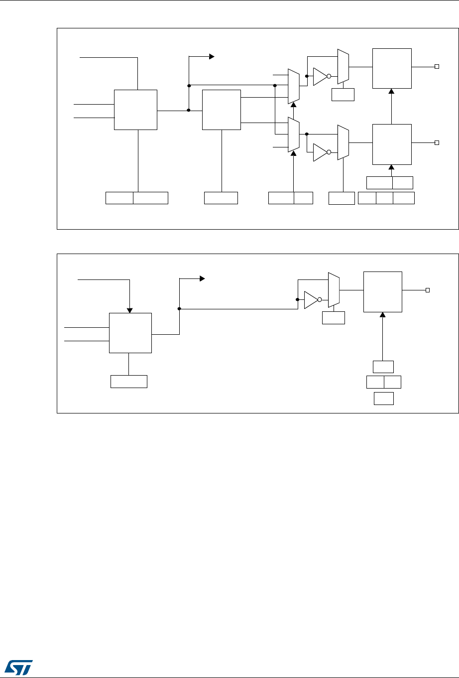
DocID026448 Rev 1 255/836
RM0383 Advanced-control timer (TIM1)
305
Figure 67. Output stage of capture/compare channel (channel 1 to 3)
Figure 68. Output stage of capture/compare channel (channel 4)
The capture/compare block is made of one preload register and one shadow register. Write
and read always access the preload register.
In capture mode, captures are actually done in the shadow register, which is copied into the
preload register.
In compare mode, the content of the preload register is copied into the shadow register
which is compared to the counter.
12.3.6 Input capture mode
In Input capture mode, the Capture/Compare Registers (TIMx_CCRx) are used to latch the
value of the counter after a transition detected by the corresponding ICx signal. When a
capture occurs, the corresponding CCXIF flag (TIMx_SR register) is set and an interrupt or
a DMA request can be sent if they are enabled. If a capture occurs while the CCxIF flag was
already high, then the over-capture flag CCxOF (TIMx_SR register) is set. CCxIF can be
cleared by software by writing it to ‘0’ or by reading the captured data stored in the
TIMx_CCRx register. CCxOF is cleared when you write it to ‘0’.
Output mode
CNT>CCR1
CNT=CCR1 controller
TIM1_CCMR1
OC1M[2:0]
OC1REF
OC1CE
Dead-time
generator
OC1_DT
OC1N_DT
DTG[7:0]
TIM1_BDTR
‘0’
‘0’
CC1E
TIM1_CCER
CC1NE
0
1
CC1P
TIM1_CCER
0
1
CC1NP
TIM1_CCER
Output
enable
circuit
OC1
Output
enable
circuit
OC1N
CC1E TIM1_CCER
CC1NE
OSSI TIM1_BDTR
MOE OSSR
0x
10
11
11
01
x0
ETR
controller
To the master mode
Output mode
CNT > CCR4
CNT = CCR4 controller
TIM1_CCMR2
OC2M[2:0]
OC4 REF
0
1
CC4P
TIM1_CCER
Output
enable
circuit
OC4
CC4E TIM1_CCER
OSSI TIM1_BDTR
MOE
To the master mode
controller
TIM1_CR2
OIS4
ETR

Advanced-control timer (TIM1) RM0383
256/836 DocID026448 Rev 1
The following example shows how to capture the counter value in TIMx_CCR1 when TI1
input rises. To do this, use the following procedure:
•Select the active input: TIMx_CCR1 must be linked to the TI1 input, so write the CC1S
bits to 01 in the TIMx_CCMR1 register. As soon as CC1S becomes different from 00,
the channel is configured in input and the TIMx_CCR1 register becomes read-only.
•Program the input filter duration you need with respect to the signal you connect to the
timer (by programming ICxF bits in the TIMx_CCMRx register if the input is a TIx input).
Let’s imagine that, when toggling, the input signal is not stable during at must 5 internal
clock cycles. We must program a filter duration longer than these 5 clock cycles. We
can validate a transition on TI1 when 8 consecutive samples with the new level have
been detected (sampled at fDTS frequency). Then write IC1F bits to 0011 in the
TIMx_CCMR1 register.
•Select the edge of the active transition on the TI1 channel by writing CC1P and CC1NP
bits to 0 in the TIMx_CCER register (rising edge in this case).
•Program the input prescaler. In our example, we wish the capture to be performed at
each valid transition, so the prescaler is disabled (write IC1PS bits to ‘00’ in the
TIMx_CCMR1 register).
•Enable capture from the counter into the capture register by setting the CC1E bit in the
TIMx_CCER register.
•If needed, enable the related interrupt request by setting the CC1IE bit in the
TIMx_DIER register, and/or the DMA request by setting the CC1DE bit in the
TIMx_DIER register.
When an input capture occurs:
•The TIMx_CCR1 register gets the value of the counter on the active transition.
•CC1IF flag is set (interrupt flag). CC1OF is also set if at least two consecutive captures
occurred whereas the flag was not cleared.
•An interrupt is generated depending on the CC1IE bit.
•A DMA request is generated depending on the CC1DE bit.
In order to handle the overcapture, it is recommended to read the data before the
overcapture flag. This is to avoid missing an overcapture which could happen after reading
the flag and before reading the data.
Note: IC interrupt and/or DMA requests can be generated by software by setting the
corresponding CCxG bit in the TIMx_EGR register.
12.3.7 PWM input mode
This mode is a particular case of input capture mode. The procedure is the same except:
•Two ICx signals are mapped on the same TIx input.
•These 2 ICx signals are active on edges with opposite polarity.
•One of the two TIxFP signals is selected as trigger input and the slave mode controller
is configured in reset mode.
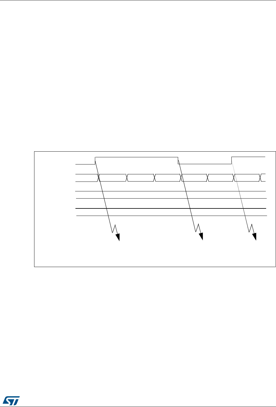
DocID026448 Rev 1 257/836
RM0383 Advanced-control timer (TIM1)
305
For example, you can measure the period (in TIMx_CCR1 register) and the duty cycle (in
TIMx_CCR2 register) of the PWM applied on TI1 using the following procedure (depending
on CK_INT frequency and prescaler value):
•Select the active input for TIMx_CCR1: write the CC1S bits to 01 in the TIMx_CCMR1
register (TI1 selected).
•Select the active polarity for TI1FP1 (used both for capture in TIMx_CCR1 and counter
clear): write the CC1P and CC1NP bits to ‘0’ (active on rising edge).
•Select the active input for TIMx_CCR2: write the CC2S bits to 10 in the TIMx_CCMR1
register (TI1 selected).
•Select the active polarity for TI1FP2 (used for capture in TIMx_CCR2): write the CC2P
and CC2NP bits to ‘1’ (active on falling edge).
•Select the valid trigger input: write the TS bits to 101 in the TIMx_SMCR register
(TI1FP1 selected).
•Configure the slave mode controller in reset mode: write the SMS bits to 100 in the
TIMx_SMCR register.
•Enable the captures: write the CC1E and CC2E bits to ‘1’ in the TIMx_CCER register.
Figure 69. PWM input mode timing
12.3.8 Forced output mode
In output mode (CCxS bits = 00 in the TIMx_CCMRx register), each output compare signal
(OCxREF and then OCx/OCxN) can be forced to active or inactive level directly by software,
independently of any comparison between the output compare register and the counter.
To force an output compare signal (OCXREF/OCx) to its active level, you just need to write
101 in the OCxM bits in the corresponding TIMx_CCMRx register. Thus OCXREF is forced
high (OCxREF is always active high) and OCx get opposite value to CCxP polarity bit.
For example: CCxP=0 (OCx active high) => OCx is forced to high level.
The OCxREF signal can be forced low by writing the OCxM bits to 100 in the TIMx_CCMRx
register.
TI1
TIMx_CNT 0000 0001 0002 0003 0004 00000004
TIMx_CCR1
TIMx_CCR2
0004
0002
IC1 capture
IC2 capture
reset counter
IC2 capture
pulse width
IC1 capture
period
measurementmeasurement
ai15413

Advanced-control timer (TIM1) RM0383
258/836 DocID026448 Rev 1
Anyway, the comparison between the TIMx_CCRx shadow register and the counter is still
performed and allows the flag to be set. Interrupt and DMA requests can be sent
accordingly. This is described in the output compare mode section below.
12.3.9 Output compare mode
This function is used to control an output waveform or indicating when a period of time has
elapsed.
When a match is found between the capture/compare register and the counter, the output
compare function:
•Assigns the corresponding output pin to a programmable value defined by the output
compare mode (OCxM bits in the TIMx_CCMRx register) and the output polarity (CCxP
bit in the TIMx_CCER register). The output pin can keep its level (OCXM=000), be set
active (OCxM=001), be set inactive (OCxM=010) or can toggle (OCxM=011) on match.
•Sets a flag in the interrupt status register (CCxIF bit in the TIMx_SR register).
•Generates an interrupt if the corresponding interrupt mask is set (CCXIE bit in the
TIMx_DIER register).
•Sends a DMA request if the corresponding enable bit is set (CCxDE bit in the
TIMx_DIER register, CCDS bit in the TIMx_CR2 register for the DMA request
selection).
The TIMx_CCRx registers can be programmed with or without preload registers using the
OCxPE bit in the TIMx_CCMRx register.
In output compare mode, the update event UEV has no effect on OCxREF and OCx output.
The timing resolution is one count of the counter. Output compare mode can also be used to
output a single pulse (in One Pulse mode).
Procedure:
1. Select the counter clock (internal, external, prescaler).
2. Write the desired data in the TIMx_ARR and TIMx_CCRx registers.
3. Set the CCxIE bit if an interrupt request is to be generated.
4. Select the output mode. For example:
– Write OCxM = 011 to toggle OCx output pin when CNT matches CCRx
– Write OCxPE = 0 to disable preload register
– Write CCxP = 0 to select active high polarity
– Write CCxE = 1 to enable the output
5. Enable the counter by setting the CEN bit in the TIMx_CR1 register.
The TIMx_CCRx register can be updated at any time by software to control the output
waveform, provided that the preload register is not enabled (OCxPE=’0’, else TIMx_CCRx
shadow register is updated only at the next update event UEV). An example is given in
Figure 70.
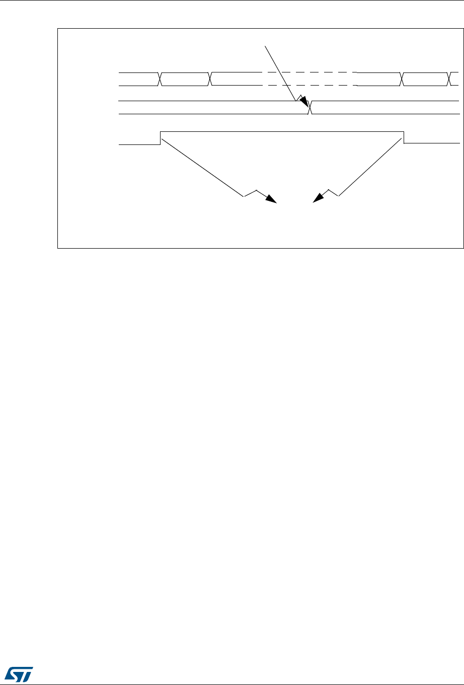
DocID026448 Rev 1 259/836
RM0383 Advanced-control timer (TIM1)
305
Figure 70. Output compare mode, toggle on OC1.
12.3.10 PWM mode
Pulse Width Modulation mode allows you to generate a signal with a frequency determined
by the value of the TIMx_ARR register and a duty cycle determined by the value of the
TIMx_CCRx register.
The PWM mode can be selected independently on each channel (one PWM per OCx
output) by writing ‘110’ (PWM mode 1) or ‘111’ (PWM mode 2) in the OCxM bits in the
TIMx_CCMRx register. You must enable the corresponding preload register by setting the
OCxPE bit in the TIMx_CCMRx register, and eventually the auto-reload preload register (in
upcounting or center-aligned modes) by setting the ARPE bit in the TIMx_CR1 register.
As the preload registers are transferred to the shadow registers only when an update event
occurs, before starting the counter, you have to initialize all the registers by setting the UG
bit in the TIMx_EGR register.
OCx polarity is software programmable using the CCxP bit in the TIMx_CCER register. It
can be programmed as active high or active low. OCx output is enabled by a combination of
the CCxE, CCxNE, MOE, OSSI and OSSR bits (TIMx_CCER and TIMx_BDTR registers).
Refer to the TIMx_CCER register description for more details.
In PWM mode (1 or 2), TIMx_CNT and TIMx_CCRx are always compared to determine
whether TIMx_CCRx ≤TIMx_CNT or TIMx_CNT ≤TIMx_CCRx (depending on the direction
of the counter).
The timer is able to generate PWM in edge-aligned mode or center-aligned mode
depending on the CMS bits in the TIMx_CR1 register.
oc1ref=OC1
TIM1_CNT B200 B201
0039
TIM1_CCR1 003A
Write B201h in the CC1R register
Match detected on CCR1
Interrupt generated if enabled
003B
B201
003A
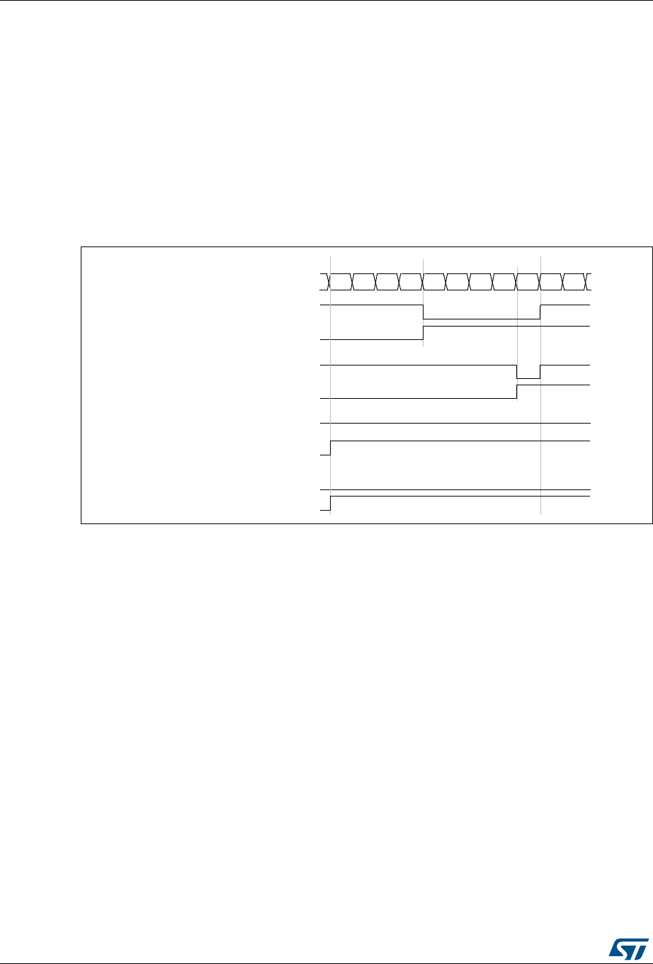
Advanced-control timer (TIM1) RM0383
260/836 DocID026448 Rev 1
PWM edge-aligned mode
•Upcounting configuration
Upcounting is active when the DIR bit in the TIMx_CR1 register is low. Refer to
Section : Upcounting mode on page 241.
In the following example, we consider PWM mode 1. The reference PWM signal
OCxREF is high as long as TIMx_CNT < TIMx_CCRx else it becomes low. If the
compare value in TIMx_CCRx is greater than the auto-reload value (in TIMx_ARR)
then OCxREF is held at ‘1’. If the compare value is 0 then OCxRef is held at ‘0’.
Figure 71 shows some edge-aligned PWM waveforms in an example where
TIMx_ARR=8.
Figure 71. Edge-aligned PWM waveforms (ARR=8)
•Downcounting configuration
Downcounting is active when DIR bit in TIMx_CR1 register is high. Refer to Section :
Downcounting mode on page 244
In PWM mode 1, the reference signal OCxRef is low as long as
TIMx_CNT > TIMx_CCRx else it becomes high. If the compare value in TIMx_CCRx is
greater than the auto-reload value in TIMx_ARR, then OCxREF is held at ‘1’. 0% PWM
is not possible in this mode.
PWM center-aligned mode
Center-aligned mode is active when the CMS bits in TIMx_CR1 register are different from
‘00’ (all the remaining configurations having the same effect on the OCxRef/OCx signals).
The compare flag is set when the counter counts up, when it counts down or both when it
counts up and down depending on the CMS bits configuration. The direction bit (DIR) in the
TIMx_CR1 register is updated by hardware and must not be changed by software. Refer to
Section : Center-aligned mode (up/down counting) on page 246.
Figure 72 shows some center-aligned PWM waveforms in an example where:
•TIMx_ARR=8,
•PWM mode is the PWM mode 1,
•The flag is set when the counter counts down corresponding to the center-aligned
mode 1 selected for CMS=01 in TIMx_CR1 register.
Counter register
‘1’
01234567801
‘0’
OCXREF
CCxIF
OCXREF
CCxIF
OCXREF
CCxIF
OCXREF
CCxIF
CCRx=4
CCRx=8
CCRx>8
CCRx=0
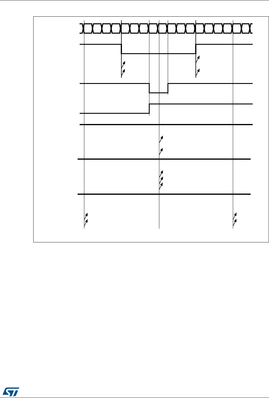
DocID026448 Rev 1 261/836
RM0383 Advanced-control timer (TIM1)
305
Figure 72. Center-aligned PWM waveforms (ARR=8)
Hints on using center-aligned mode:
•When starting in center-aligned mode, the current up-down configuration is used. It
means that the counter counts up or down depending on the value written in the DIR bit
in the TIMx_CR1 register. Moreover, the DIR and CMS bits must not be changed at the
same time by the software.
•Writing to the counter while running in center-aligned mode is not recommended as it
can lead to unexpected results. In particular:
– The direction is not updated if you write a value in the counter that is greater than
the auto-reload value (TIMx_CNT>TIMx_ARR). For example, if the counter was
counting up, it continues to count up.
– The direction is updated if you write 0 or write the TIMx_ARR value in the counter
but no Update Event UEV is generated.
•The safest way to use center-aligned mode is to generate an update by software
(setting the UG bit in the TIMx_EGR register) just before starting the counter and not to
write the counter while it is running.
##X)&
#OUNTERREGISTER
##2X
/#X2%&
#-3
#-3
#-3
##X)&
##2X
/#X2%&
#-3OR
##X)&
##2X
/#X2%&
#-3
#-3
#-3
gg
##X)&
##2X
/#X2%&
#-3
#-3
#-3
gg
##X)&
##2X
/#X2%&
#-3
#-3
#-3
gg
AIB
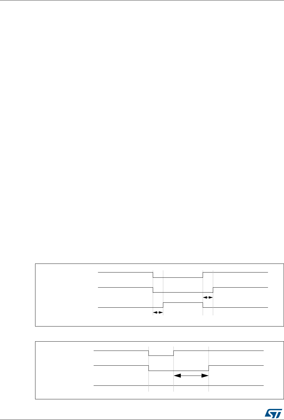
Advanced-control timer (TIM1) RM0383
262/836 DocID026448 Rev 1
12.3.11 Complementary outputs and dead-time insertion
The advanced-control timers (TIM1) can output two complementary signals and manage the
switching-off and the switching-on instants of the outputs.
This time is generally known as dead-time and you have to adjust it depending on the
devices you have connected to the outputs and their characteristics (intrinsic delays of level-
shifters, delays due to power switches...)
You can select the polarity of the outputs (main output OCx or complementary OCxN)
independently for each output. This is done by writing to the CCxP and CCxNP bits in the
TIMx_CCER register.
The complementary signals OCx and OCxN are activated by a combination of several
control bits: the CCxE and CCxNE bits in the TIMx_CCER register and the MOE, OISx,
OISxN, OSSI and OSSR bits in the TIMx_BDTR and TIMx_CR2 registers. Refer to
Table 50: Output control bits for complementary OCx and OCxN channels with break
feature on page 296 for more details. In particular, the dead-time is activated when
switching to the IDLE state (MOE falling down to 0).
Dead-time insertion is enabled by setting both CCxE and CCxNE bits, and the MOE bit if the
break circuit is present. DTG[7:0] bits of the TIMx_BDTR register are used to control the
dead-time generation for all channels. From a reference waveform OCxREF, it generates 2
outputs OCx and OCxN. If OCx and OCxN are active high:
•The OCx output signal is the same as the reference signal except for the rising edge,
which is delayed relative to the reference rising edge.
•The OCxN output signal is the opposite of the reference signal except for the rising
edge, which is delayed relative to the reference falling edge.
If the delay is greater than the width of the active output (OCx or OCxN) then the
corresponding pulse is not generated.
The following figures show the relationships between the output signals of the dead-time
generator and the reference signal OCxREF. (we suppose CCxP=0, CCxNP=0, MOE=1,
CCxE=1 and CCxNE=1 in these examples)
Figure 73. Complementary output with dead-time insertion.
Figure 74. Dead-time waveforms with delay greater than the negative pulse.
delay
delay
OCxREF
OCx
OCxN
delay
OCxREF
OCx
OCxN

DocID026448 Rev 1 263/836
RM0383 Advanced-control timer (TIM1)
305
Figure 75. Dead-time waveforms with delay greater than the positive pulse.
The dead-time delay is the same for each of the channels and is programmable with the
DTG bits in the TIMx_BDTR register. Refer to Section 12.4.18: TIM1 break and dead-time
register (TIMx_BDTR) on page 300 for delay calculation.
Re-directing OCxREF to OCx or OCxN
In output mode (forced, output compare or PWM), OCxREF can be re-directed to the OCx
output or to OCxN output by configuring the CCxE and CCxNE bits in the TIMx_CCER
register.
This allows you to send a specific waveform (such as PWM or static active level) on one
output while the complementary remains at its inactive level. Other alternative possibilities
are to have both outputs at inactive level or both outputs active and complementary with
dead-time.
Note: When only OCxN is enabled (CCxE=0, CCxNE=1), it is not complemented and becomes
active as soon as OCxREF is high. For example, if CCxNP=0 then OCxN=OCxRef. On the
other hand, when both OCx and OCxN are enabled (CCxE=CCxNE=1) OCx becomes
active when OCxREF is high whereas OCxN is complemented and becomes active when
OCxREF is low.
12.3.12 Using the break function
When using the break function, the output enable signals and inactive levels are modified
according to additional control bits (MOE, OSSI and OSSR bits in the TIMx_BDTR register,
OISx and OISxN bits in the TIMx_CR2 register). In any case, the OCx and OCxN outputs
cannot be set both to active level at a given time. Refer to Table 50: Output control bits for
complementary OCx and OCxN channels with break feature on page 296 for more details.
The break source can be either the break input pin or a clock failure event, generated by the
Clock Security System (CSS), from the Reset Clock Controller. For further information on
the Clock Security System, refer to Section 6.2.7: Clock security system (CSS).
When exiting from reset, the break circuit is disabled and the MOE bit is low. You can enable
the break function by setting the BKE bit in the TIMx_BDTR register. The break input
polarity can be selected by configuring the BKP bit in the same register. BKE and BKP can
be modified at the same time. When the BKE and BKP bits are written, a delay of 1 APB
clock cycle is applied before the writing is effective. Consequently, it is necessary to wait 1
APB clock period to correctly read back the bit after the write operation.
Because MOE falling edge can be asynchronous, a resynchronization circuit has been
inserted between the actual signal (acting on the outputs) and the synchronous control bit
(accessed in the TIMx_BDTR register). It results in some delays between the asynchronous
and the synchronous signals. In particular, if you write MOE to 1 whereas it was low, you
delay
OCxREF
OCx
OCxN

Advanced-control timer (TIM1) RM0383
264/836 DocID026448 Rev 1
must insert a delay (dummy instruction) before reading it correctly. This is because you write
the asynchronous signal and read the synchronous signal.
When a break occurs (selected level on the break input):
•The MOE bit is cleared asynchronously, putting the outputs in inactive state, idle state
or in reset state (selected by the OSSI bit). This feature functions even if the MCU
oscillator is off.
•Each output channel is driven with the level programmed in the OISx bit in the
TIMx_CR2 register as soon as MOE=0. If OSSI=0 then the timer releases the enable
output else the enable output remains high.
•When complementary outputs are used:
– The outputs are first put in reset state inactive state (depending on the polarity).
This is done asynchronously so that it works even if no clock is provided to the
timer.
– If the timer clock is still present, then the dead-time generator is reactivated in
order to drive the outputs with the level programmed in the OISx and OISxN bits
after a dead-time. Even in this case, OCx and OCxN cannot be driven to their
active level together. Note that because of the resynchronization on MOE, the
dead-time duration is a bit longer than usual (around 2 ck_tim clock cycles).
– If OSSI=0 then the timer releases the enable outputs else the enable outputs
remain or become high as soon as one of the CCxE or CCxNE bits is high.
•The break status flag (BIF bit in the TIMx_SR register) is set. An interrupt can be
generated if the BIE bit in the TIMx_DIER register is set. A DMA request can be sent if
the BDE bit in the TIMx_DIER register is set.
•If the AOE bit in the TIMx_BDTR register is set, the MOE bit is automatically set again
at the next update event UEV. This can be used to perform a regulation, for instance.
Else, MOE remains low until you write it to ‘1’ again. In this case, it can be used for
security and you can connect the break input to an alarm from power drivers, thermal
sensors or any security components.
Note: The break inputs is acting on level. Thus, the MOE cannot be set while the break input is
active (neither automatically nor by software). In the meantime, the status flag BIF cannot
be cleared.
The break can be generated by the BRK input which has a programmable polarity and an
enable bit BKE in the TIMx_BDTR Register.
There are two solutions to generate a break:
•By using the BRK input which has a programmable polarity and an enable bit BKE in
the TIMx_BDTR register
•By software through the BG bit of the TIMx_EGR register.
In addition to the break input and the output management, a write protection has been
implemented inside the break circuit to safeguard the application. It allows you to freeze the
configuration of several parameters (dead-time duration, OCx/OCxN polarities and state
when disabled, OCxM configurations, break enable and polarity). You can choose from 3
levels of protection selected by the LOCK bits in the TIMx_BDTR register. Refer to
Section 12.4.18: TIM1 break and dead-time register (TIMx_BDTR) on page 300. The LOCK
bits can be written only once after an MCU reset.
Figure 76 shows an example of behavior of the outputs in response to a break.
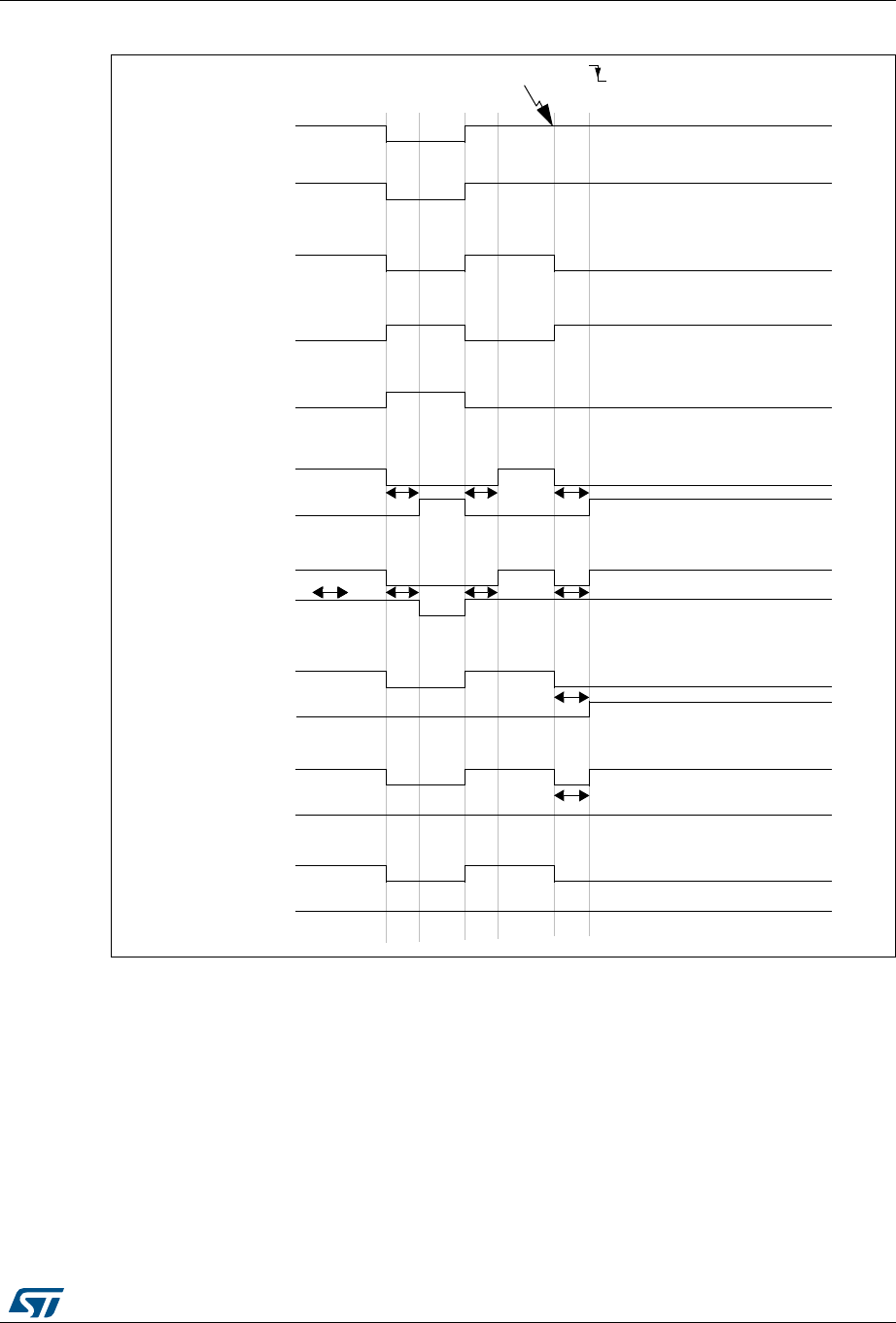
DocID026448 Rev 1 265/836
RM0383 Advanced-control timer (TIM1)
305
Figure 76. Output behavior in response to a break.
delay
OCxREF
BREAK (MOE
OCx
(OCxN not implemented, CCxP=0, OISx=1)
OCx
(OCxN not implemented, CCxP=0, OISx=0)
OCx
(OCxN not implemented, CCxP=1, OISx=1)
OCx
(OCxN not implemented, CCxP=1, OISx=0)
OCx
OCxN
(CCxE=1, CCxP=0, OISx=0, CCxNE=1, CCxNP=0, OISxN=1)
delaydelay
delay
OCx
OCxN
(CCxE=1, CCxP=0, OISx=1, CCxNE=1, CCxNP=1, OISxN=1)
delaydelay
delay
OCx
OCxN
(CCxE=1, CCxP=0, OISx=0, CCxNE=0, CCxNP=0, OISxN=1)
)
delay
OCx
OCxN
(CCxE=1, CCxP=0, OISx=1, CCxNE=0, CCxNP=0, OISxN=0)
OCx
OCxN
(CCxE=1, CCxP=0, CCxNE=0, CCxNP=0, OISx=OISxN=0 or OISx=OISxN=1)
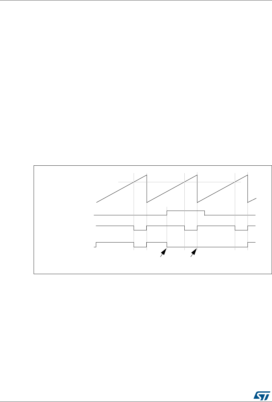
Advanced-control timer (TIM1) RM0383
266/836 DocID026448 Rev 1
12.3.13 Clearing the OCxREF signal on an external event
The OCxREF signal for a given channel can be driven Low by applying a High level to the
ETRF input (OCxCE enable bit of the corresponding TIMx_CCMRx register set to ‘1’). The
OCxREF signal remains Low until the next update event, UEV, occurs.
This function can only be used in output compare and PWM modes, and does not work in
forced mode.
For example, the ETR signal can be connected to the output of a comparator to be used for
current handling. In this case, the ETR must be configured as follow:
1. The External Trigger Prescaler should be kept off: bits ETPS[1:0] of the TIMx_SMCR
register set to ‘00’.
2. The external clock mode 2 must be disabled: bit ECE of the TIMx_SMCR register set to
‘0’.
3. The External Trigger Polarity (ETP) and the External Trigger Filter (ETF) can be
configured according to the user needs.
Figure 77 shows the behavior of the OCxREF signal when the ETRF Input becomes High,
for both values of the enable bit OCxCE. In this example, the timer TIMx is programmed in
PWM mode.
Figure 77. Clearing TIMx OCxREF
Note: In case of a PWM with a 100% duty cycle (if CCRx>ARR), then OCxREF is enabled again at
the next counter overflow.
OCxREF
counter (CNT)
OCxREF
ETRF
(OCxCE=’0’)
(OCxCE=’1’)
ETRF
becomes high
ETRF
still high
(CCRx)
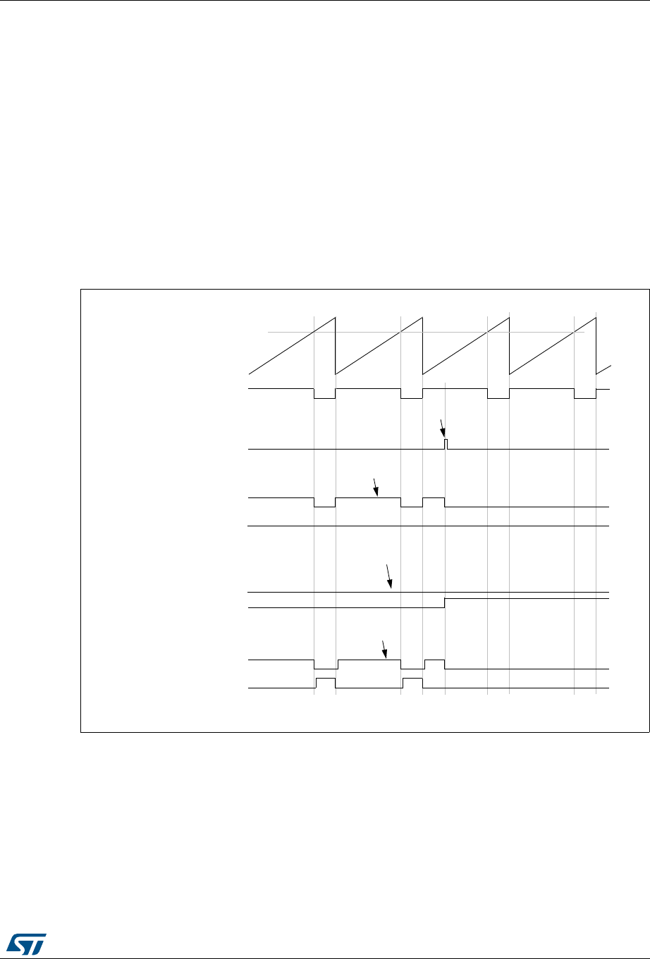
DocID026448 Rev 1 267/836
RM0383 Advanced-control timer (TIM1)
305
12.3.14 6-step PWM generation
When complementary outputs are used on a channel, preload bits are available on the
OCxM, CCxE and CCxNE bits. The preload bits are transferred to the shadow bits at the
COM commutation event. Thus you can program in advance the configuration for the next
step and change the configuration of all the channels at the same time. COM can be
generated by software by setting the COM bit in the TIMx_EGR register or by hardware (on
TRGI rising edge).
A flag is set when the COM event occurs (COMIF bit in the TIMx_SR register), which can
generate an interrupt (if the COMIE bit is set in the TIMx_DIER register) or a DMA request
(if the COMDE bit is set in the TIMx_DIER register).
Figure 78 describes the behavior of the OCx and OCxN outputs when a COM event occurs,
in 3 different examples of programmed configurations.
Figure 78. 6-step generation, COM example (OSSR=1)
(CCRx)
OCx
OCxN
Write COM to 1
counter (CNT)
OCxREF
COM event
CCxE=1
CCxNE=0
OCxM=100
OCx
OCxN
CCxE=0
CCxNE=1
OCxM=101
OCx
OCxN
CCxE=1
CCxNE=0
OCxM=100
Example 1
Example 2
Example 3
write OCxM to 100
CCxE=1
CCxNE=0
OCxM=100 (forced inactive)
CCxE=1
CCxNE=0
OCxM=100 (forced inactive)
Write CCxNE to 1
and OCxM to 101
write CCxNE to 0
and OCxM to 100
CCxE=1
CCxNE=0
OCxM=100 (forced inactive)
ai14910
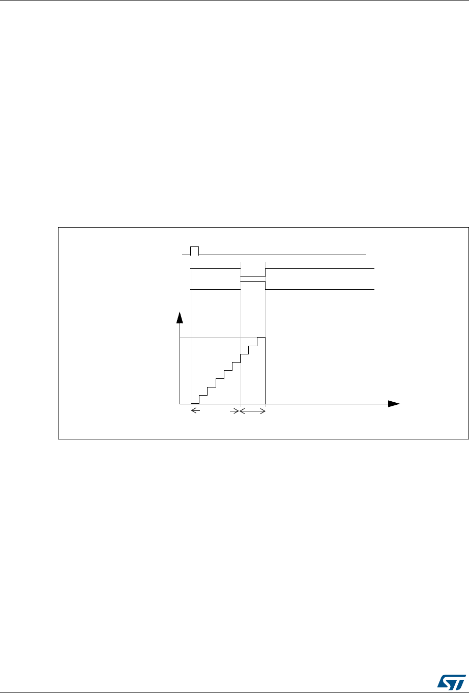
Advanced-control timer (TIM1) RM0383
268/836 DocID026448 Rev 1
12.3.15 One-pulse mode
One-pulse mode (OPM) is a particular case of the previous modes. It allows the counter to
be started in response to a stimulus and to generate a pulse with a programmable length
after a programmable delay.
Starting the counter can be controlled through the slave mode controller. Generating the
waveform can be done in output compare mode or PWM mode. You select One-pulse mode
by setting the OPM bit in the TIMx_CR1 register. This makes the counter stop automatically
at the next update event UEV.
A pulse can be correctly generated only if the compare value is different from the counter
initial value. Before starting (when the timer is waiting for the trigger), the configuration must
be:
•In upcounting: CNT < CCRx ≤ARR (in particular, 0 < CCRx)
•In downcounting: CNT > CCRx
Figure 79. Example of one pulse mode.
For example you may want to generate a positive pulse on OC1 with a length of tPULSE and
after a delay of tDELAY as soon as a positive edge is detected on the TI2 input pin.
Let’s use TI2FP2 as trigger 1:
•Map TI2FP2 to TI2 by writing CC2S=’01’ in the TIMx_CCMR1 register.
•TI2FP2 must detect a rising edge, write CC2P=’0’ and CC2NP=’0’ in the TIMx_CCER
register.
•Configure TI2FP2 as trigger for the slave mode controller (TRGI) by writing TS=’110’ in
the TIMx_SMCR register.
•TI2FP2 is used to start the counter by writing SMS to ‘110’ in the TIMx_SMCR register
(trigger mode).
TI2
OC1REF
Counter
t
0
TIM1_ARR
TIM1_CCR1
OC1
tDELAY tPULSE

DocID026448 Rev 1 269/836
RM0383 Advanced-control timer (TIM1)
305
The OPM waveform is defined by writing the compare registers (taking into account the
clock frequency and the counter prescaler).
•The tDELAY is defined by the value written in the TIMx_CCR1 register.
•The tPULSE is defined by the difference between the auto-reload value and the compare
value (TIMx_ARR - TIMx_CCR1).
•Let’s say you want to build a waveform with a transition from ‘0’ to ‘1’ when a compare
match occurs and a transition from ‘1’ to ‘0’ when the counter reaches the auto-reload
value. To do this you enable PWM mode 2 by writing OC1M=111 in the TIMx_CCMR1
register. You can optionally enable the preload registers by writing OC1PE=’1’ in the
TIMx_CCMR1 register and ARPE in the TIMx_CR1 register. In this case you have to
write the compare value in the TIMx_CCR1 register, the auto-reload value in the
TIMx_ARR register, generate an update by setting the UG bit and wait for external
trigger event on TI2. CC1P is written to ‘0’ in this example.
In our example, the DIR and CMS bits in the TIMx_CR1 register should be low.
You only want 1 pulse (Single mode), so you write '1 in the OPM bit in the TIMx_CR1
register to stop the counter at the next update event (when the counter rolls over from the
auto-reload value back to 0). When OPM bit in the TIMx_CR1 register is set to '0', so the
Repetitive Mode is selected.
Particular case: OCx fast enable:
In One-pulse mode, the edge detection on TIx input set the CEN bit which enables the
counter. Then the comparison between the counter and the compare value makes the
output toggle. But several clock cycles are needed for these operations and it limits the
minimum delay tDELAY min we can get.
If you want to output a waveform with the minimum delay, you can set the OCxFE bit in the
TIMx_CCMRx register. Then OCxRef (and OCx) are forced in response to the stimulus,
without taking in account the comparison. Its new level is the same as if a compare match
had occurred. OCxFE acts only if the channel is configured in PWM1 or PWM2 mode.
12.3.16 Encoder interface mode
To select Encoder Interface mode write SMS=‘001’ in the TIMx_SMCR register if the
counter is counting on TI2 edges only, SMS=’010’ if it is counting on TI1 edges only and
SMS=’011’ if it is counting on both TI1 and TI2 edges.
Select the TI1 and TI2 polarity by programming the CC1P and CC2P bits in the TIMx_CCER
register. When needed, you can program the input filter as well. CC1NP and CC2NP must
be kept low.
The two inputs TI1 and TI2 are used to interface to an incremental encoder. Refer to
Table 48. The counter is clocked by each valid transition on TI1FP1 or TI2FP2 (TI1 and TI2
after input filter and polarity selection, TI1FP1=TI1 if not filtered and not inverted,
TI2FP2=TI2 if not filtered and not inverted) assuming that it is enabled (CEN bit in
TIMx_CR1 register written to ‘1’). The sequence of transitions of the two inputs is evaluated
and generates count pulses as well as the direction signal. Depending on the sequence the
counter counts up or down, the DIR bit in the TIMx_CR1 register is modified by hardware
accordingly. The DIR bit is calculated at each transition on any input (TI1 or TI2), whatever
the counter is counting on TI1 only, TI2 only or both TI1 and TI2.
Encoder interface mode acts simply as an external clock with direction selection. This
means that the counter just counts continuously between 0 and the auto-reload value in the
TIMx_ARR register (0 to ARR or ARR down to 0 depending on the direction). So you must

Advanced-control timer (TIM1) RM0383
270/836 DocID026448 Rev 1
configure TIMx_ARR before starting. in the same way, the capture, compare, prescaler,
repetition counter, trigger output features continue to work as normal. Encoder mode and
External clock mode 2 are not compatible and must not be selected together.
In this mode, the counter is modified automatically following the speed and the direction of
the incremental encoder and its content, therefore, always represents the encoder’s
position. The count direction correspond to the rotation direction of the connected sensor.
The table summarizes the possible combinations, assuming TI1 and TI2 don’t switch at the
same time.
An external incremental encoder can be connected directly to the MCU without external
interface logic. However, comparators are normally be used to convert the encoder’s
differential outputs to digital signals. This greatly increases noise immunity. The third
encoder output which indicate the mechanical zero position, may be connected to an
external interrupt input and trigger a counter reset.
Figure 80 gives an example of counter operation, showing count signal generation and
direction control. It also shows how input jitter is compensated where both edges are
selected. This might occur if the sensor is positioned near to one of the switching points. For
this example we assume that the configuration is the following:
•CC1S=’01’ (TIMx_CCMR1 register, TI1FP1 mapped on TI1).
•CC2S=’01’ (TIMx_CCMR2 register, TI1FP2 mapped on TI2).
•CC1P=’0’, CC1NP=’0’, and IC1F = ‘0000’ (TIMx_CCER register, TI1FP1 non-inverted,
TI1FP1=TI1).
•CC2P=’0’, CC2NP=’0’, and IC2F = ‘0000’ (TIMx_CCER register, TI1FP2 non-inverted,
TI1FP2= TI2).
•SMS=’011’ (TIMx_SMCR register, both inputs are active on both rising and falling
edges).
•CEN=’1’ (TIMx_CR1 register, Counter enabled).
Table 48. Counting direction versus encoder signals
Active edge
Level on
opposite
signal (TI1FP1
for TI2,
TI2FP2 for
TI1)
TI1FP1 signal TI2FP2 signal
Rising Falling Rising Falling
Counting on
TI1 only
High Down Up No Count No Count
Low Up Down No Count No Count
Counting on
TI2 only
High No Count No Count Up Down
Low No Count No Count Down Up
Counting on
TI1 and TI2
High Down Up Up Down
Low Up Down Down Up
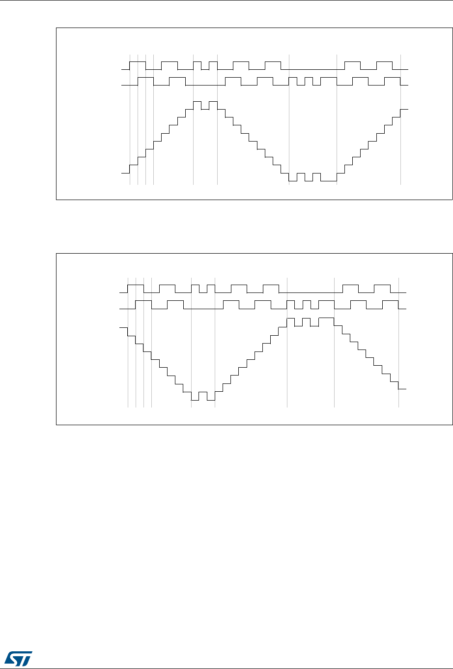
DocID026448 Rev 1 271/836
RM0383 Advanced-control timer (TIM1)
305
Figure 80. Example of counter operation in encoder interface mode.
Figure 81 gives an example of counter behavior when TI1FP1 polarity is inverted (same
configuration as above except CC1P=’1’).
Figure 81. Example of encoder interface mode with TI1FP1 polarity inverted.
The timer, when configured in Encoder Interface mode provides information on the sensor’s
current position. You can obtain dynamic information (speed, acceleration, deceleration) by
measuring the period between two encoder events using a second timer configured in
capture mode. The output of the encoder which indicates the mechanical zero can be used
for this purpose. Depending on the time between two events, the counter can also be read
at regular times. You can do this by latching the counter value into a third input capture
register if available (then the capture signal must be periodic and can be generated by
another timer). when available, it is also possible to read its value through a DMA request
generated by a real-time clock.
TI1
forward forwardbackwardjitter jitter
up down up
TI2
Counter
TI1
forward forwardbackwardjitter jitter
up
down
TI2
Counter
down

Advanced-control timer (TIM1) RM0383
272/836 DocID026448 Rev 1
12.3.17 Timer input XOR function
The TI1S bit in the TIMx_CR2 register, allows the input filter of channel 1 to be connected to
the output of a XOR gate, combining the three input pins TIMx_CH1, TIMx_CH2 and
TIMx_CH3.
The XOR output can be used with all the timer input functions such as trigger or input
capture. An example of this feature used to interface Hall sensors is given in
Section 12.3.18 below.
12.3.18 Interfacing with Hall sensors
This is done using the advanced-control timers (TIM1) to generate PWM signals to drive the
motor and another timer TIMx (TIM2, TIM3, TIM4 or TIM5) referred to as “interfacing timer”
in Figure 82. The “interfacing timer” captures the 3 timer input pins (TIMx_CH1, TIMx_CH2,
and TIMx_CH3) connected through a XOR to the TI1 input channel (selected by setting the
TI1S bit in the TIMx_CR2 register).
The slave mode controller is configured in reset mode; the slave input is TI1F_ED. Thus,
each time one of the 3 inputs toggles, the counter restarts counting from 0. This creates a
time base triggered by any change on the Hall inputs.
On the “interfacing timer”, capture/compare channel 1 is configured in capture mode,
capture signal is TRC (see Figure 65: Capture/compare channel (example: channel 1 input
stage) on page 254). The captured value, which corresponds to the time elapsed between 2
changes on the inputs, gives information about motor speed.
The “interfacing timer” can be used in output mode to generate a pulse which changes the
configuration of the channels of the advanced-control timer (TIM1) (by triggering a COM
event). The TIM1 timer is used to generate PWM signals to drive the motor. To do this, the
interfacing timer channel must be programmed so that a positive pulse is generated after a
programmed delay (in output compare or PWM mode). This pulse is sent to the advanced-
control timer (TIM1) through the TRGO output.
Example: you want to change the PWM configuration of your advanced-control timer TIM1
after a programmed delay each time a change occurs on the Hall inputs connected to one of
the TIMx timers.
•Configure 3 timer inputs ORed to the TI1 input channel by writing the TI1S bit in the
TIMx_CR2 register to ‘1’,
•Program the time base: write the TIMx_ARR to the max value (the counter must be
cleared by the TI1 change. Set the prescaler to get a maximum counter period longer
than the time between 2 changes on the sensors,
•Program channel 1 in capture mode (TRC selected): write the CC1S bits in the
TIMx_CCMR1 register to ‘11’. You can also program the digital filter if needed,
•Program channel 2 in PWM 2 mode with the desired delay: write the OC2M bits to ‘111’
and the CC2S bits to ‘00’ in the TIMx_CCMR1 register,
•Select OC2REF as trigger output on TRGO: write the MMS bits in the TIMx_CR2
register to ‘101’,
In the advanced-control timer TIM1, the right ITR input must be selected as trigger input, the
timer is programmed to generate PWM signals, the capture/compare control signals are
preloaded (CCPC=1 in the TIMx_CR2 register) and the COM event is controlled by the
trigger input (CCUS=1 in the TIMx_CR2 register). The PWM control bits (CCxE, OCxM) are
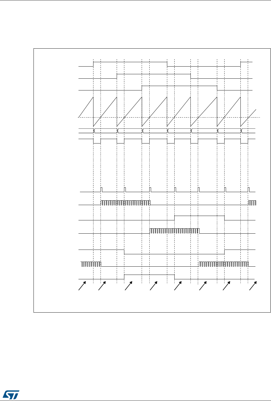
DocID026448 Rev 1 273/836
RM0383 Advanced-control timer (TIM1)
305
written after a COM event for the next step (this can be done in an interrupt subroutine
generated by the rising edge of OC2REF).
Figure 82 describes this example.
Figure 82. Example of hall sensor interface
&RXQWHU&17
75*2 2&5()
&&5
2&
2&1
&20
:ULWH&&[(&&[1(
7,+
7,+
7,+
&&5
2&
2&1
2&
2&1
&
DQG2&[0IRUQH[WVWHS
,QWHUIDFLQJWLPHU$GYDQFHGFRQWUROWLPHUV7,0
069
&$ &$ & &$ &$%
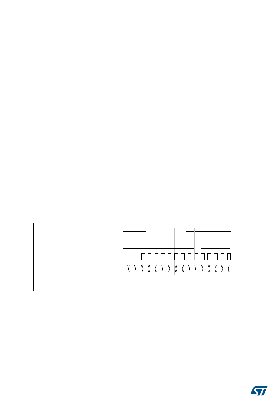
Advanced-control timer (TIM1) RM0383
274/836 DocID026448 Rev 1
12.3.19 TIMx and external trigger synchronization
The TIMx timer can be synchronized with an external trigger in several modes: Reset mode,
Gated mode and Trigger mode.
Slave mode: Reset mode
The counter and its prescaler can be reinitialized in response to an event on a trigger input.
Moreover, if the URS bit from the TIMx_CR1 register is low, an update event UEV is
generated. Then all the preloaded registers (TIMx_ARR, TIMx_CCRx) are updated.
In the following example, the upcounter is cleared in response to a rising edge on TI1 input:
•Configure the channel 1 to detect rising edges on TI1. Configure the input filter duration
(in this example, we don’t need any filter, so we keep IC1F=0000). The capture
prescaler is not used for triggering, so you don’t need to configure it. The CC1S bits
select the input capture source only, CC1S = 01 in the TIMx_CCMR1 register. Write
CC1P=0 and CC1NP=’0’ in TIMx_CCER register to validate the polarity (and detect
rising edges only).
•Configure the timer in reset mode by writing SMS=100 in TIMx_SMCR register. Select
TI1 as the input source by writing TS=101 in TIMx_SMCR register.
•Start the counter by writing CEN=1 in the TIMx_CR1 register.
The counter starts counting on the internal clock, then behaves normally until TI1 rising
edge. When TI1 rises, the counter is cleared and restarts from 0. In the meantime, the
trigger flag is set (TIF bit in the TIMx_SR register) and an interrupt request, or a DMA
request can be sent if enabled (depending on the TIE and TDE bits in TIMx_DIER register).
The following figure shows this behavior when the auto-reload register TIMx_ARR=0x36.
The delay between the rising edge on TI1 and the actual reset of the counter is due to the
resynchronization circuit on TI1 input.
Figure 83. Control circuit in reset mode
00
Counter clock = ck_cnt = ck_psc
Counter register 01 02 03 00 01 02 0332 33 34 35 36
UG
TI1
3130
TIF
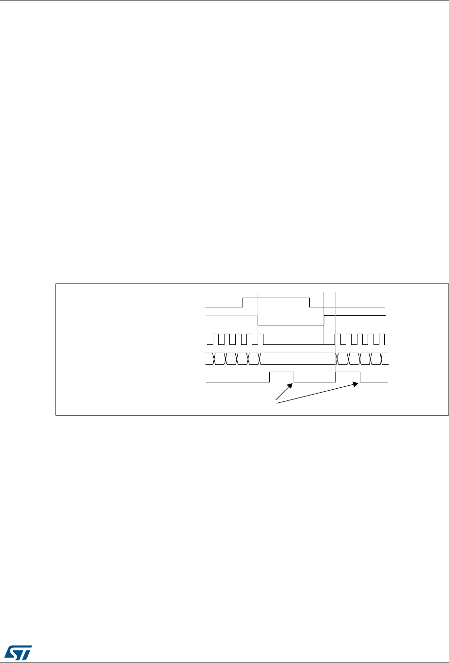
DocID026448 Rev 1 275/836
RM0383 Advanced-control timer (TIM1)
305
Slave mode: Gated mode
The counter can be enabled depending on the level of a selected input.
In the following example, the upcounter counts only when TI1 input is low:
•Configure the channel 1 to detect low levels on TI1. Configure the input filter duration
(in this example, we don’t need any filter, so we keep IC1F=0000). The capture
prescaler is not used for triggering, so you don’t need to configure it. The CC1S bits
select the input capture source only, CC1S=01 in TIMx_CCMR1 register. Write
CC1P=1 and CC1NP=’0’ in TIMx_CCER register to validate the polarity (and detect
low level only).
•Configure the timer in gated mode by writing SMS=101 in TIMx_SMCR register. Select
TI1 as the input source by writing TS=101 in TIMx_SMCR register.
•Enable the counter by writing CEN=1 in the TIMx_CR1 register (in gated mode, the
counter doesn’t start if CEN=0, whatever is the trigger input level).
The counter starts counting on the internal clock as long as TI1 is low and stops as soon as
TI1 becomes high. The TIF flag in the TIMx_SR register is set both when the counter starts
or stops.
The delay between the rising edge on TI1 and the actual stop of the counter is due to the
resynchronization circuit on TI1 input.
Figure 84. Control circuit in gated mode
Counter clock = ck_cnt = ck_psc
Counter register 35 36 37 3832 33 34
TI1
3130
CNT_EN
TIF
Write TIF=0
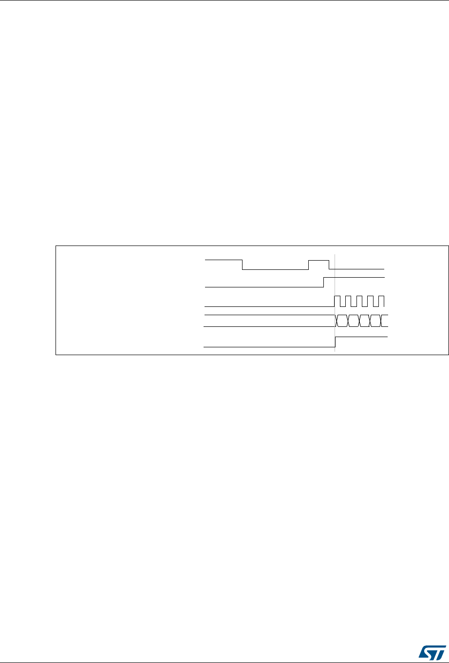
Advanced-control timer (TIM1) RM0383
276/836 DocID026448 Rev 1
Slave mode: Trigger mode
The counter can start in response to an event on a selected input.
In the following example, the upcounter starts in response to a rising edge on TI2 input:
•Configure the channel 2 to detect rising edges on TI2. Configure the input filter duration
(in this example, we don’t need any filter, so we keep IC2F=0000). The capture
prescaler is not used for triggering, so you don’t need to configure it. The CC2S bits are
configured to select the input capture source only, CC2S=01 in TIMx_CCMR1 register.
Write CC2P=1 and CC2NP=0 in TIMx_CCER register to validate the polarity (and
detect low level only).
•Configure the timer in trigger mode by writing SMS=110 in TIMx_SMCR register. Select
TI2 as the input source by writing TS=110 in TIMx_SMCR register.
When a rising edge occurs on TI2, the counter starts counting on the internal clock and the
TIF flag is set.
The delay between the rising edge on TI2 and the actual start of the counter is due to the
resynchronization circuit on TI2 input.
Figure 85. Control circuit in trigger mode
Slave mode: external clock mode 2 + trigger mode
The external clock mode 2 can be used in addition to another slave mode (except external
clock mode 1 and encoder mode). In this case, the ETR signal is used as external clock
input, and another input can be selected as trigger input (in reset mode, gated mode or
trigger mode). It is recommended not to select ETR as TRGI through the TS bits of
TIMx_SMCR register.
In the following example, the upcounter is incremented at each rising edge of the ETR
signal as soon as a rising edge of TI1 occurs:
1. Configure the external trigger input circuit by programming the TIMx_SMCR register as
follows:
– ETF = 0000: no filter
– ETPS = 00: prescaler disabled
– ETP = 0: detection of rising edges on ETR and ECE=1 to enable the external clock
mode 2.
Counter clock = ck_cnt = ck_psc
Counter register 35 36 37 3834
TI2
CNT_EN
TIF
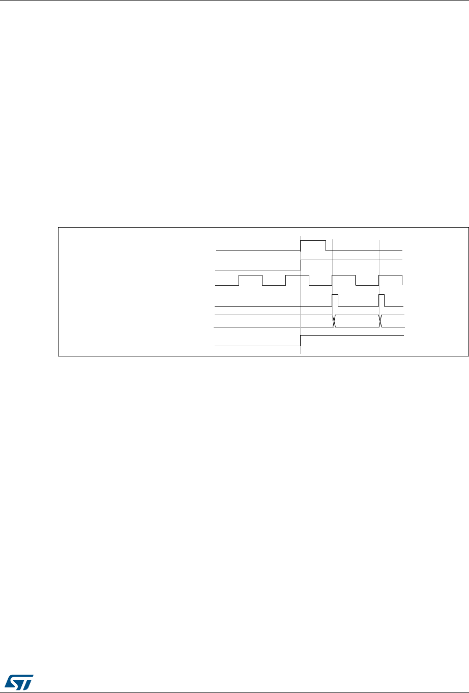
DocID026448 Rev 1 277/836
RM0383 Advanced-control timer (TIM1)
305
2. Configure the channel 1 as follows, to detect rising edges on TI:
– IC1F=0000: no filter.
– The capture prescaler is not used for triggering and does not need to be
configured.
– CC1S=01 in TIMx_CCMR1 register to select only the input capture source
– CC1P=0 and CC1NP=’0’ in TIMx_CCER register to validate the polarity (and
detect rising edge only).
3. Configure the timer in trigger mode by writing SMS=110 in TIMx_SMCR register. Select
TI1 as the input source by writing TS=101 in TIMx_SMCR register.
A rising edge on TI1 enables the counter and sets the TIF flag. The counter then counts on
ETR rising edges.
The delay between the rising edge of the ETR signal and the actual reset of the counter is
due to the resynchronization circuit on ETRP input.
Figure 86. Control circuit in external clock mode 2 + trigger mode
12.3.20 Timer synchronization
The TIM timers are linked together internally for timer synchronization or chaining. Refer to
Section 13.3.15: Timer synchronization on page 336 for details.
12.3.21 Debug mode
When the microcontroller enters debug mode (Cortex®-M4 with FPU core halted), the TIMx
counter either continues to work normally or stops, depending on DBG_TIMx_STOP
configuration bit in DBG module. For more details, refer to Section 23.16.2: Debug support
for timers, watchdog and I2C.
Counter clock = CK_CNT = CK_PSC
Counter register 35 3634
ETR
CEN/CNT_EN
TIF
TI1

Advanced-control timer (TIM1) RM0383
278/836 DocID026448 Rev 1
12.4 TIM1 registers
Refer to Section 1.1 on page 33 for a list of abbreviations used in register descriptions.
The peripheral registers must be written by half-words (16 bits) or words (32 bits). Read
accesses can be done by bytes (8 bits), half-word (16 bits) or words (32 bits).
12.4.1 TIM1 control register 1 (TIMx_CR1)
Address offset: 0x00
Reset value: 0x0000
1514131211109876543210
Reserved CKD[1:0] ARPE CMS[1:0] DIR OPM URS UDIS CEN
rw rw rw rw rw rw rw rw rw rw
Bits 15:10 Reserved, must be kept at reset value.
Bits 9:8 CKD[1:0]: Clock division
This bit-field indicates the division ratio between the timer clock (CK_INT) frequency and the
dead-time and sampling clock (tDTS)used by the dead-time generators and the digital filters
(ETR, TIx),
00: tDTS=tCK_INT
01: tDTS=2*tCK_INT
10: tDTS=4*tCK_INT
11: Reserved, do not program this value
Bit 7 ARPE: Auto-reload preload enable
0: TIMx_ARR register is not buffered
1: TIMx_ARR register is buffered
Bits 6:5 CMS[1:0]: Center-aligned mode selection
00: Edge-aligned mode. The counter counts up or down depending on the direction bit
(DIR).
01: Center-aligned mode 1. The counter counts up and down alternatively. Output compare
interrupt flags of channels configured in output (CCxS=00 in TIMx_CCMRx register) are set
only when the counter is counting down.
10: Center-aligned mode 2. The counter counts up and down alternatively. Output compare
interrupt flags of channels configured in output (CCxS=00 in TIMx_CCMRx register) are set
only when the counter is counting up.
11: Center-aligned mode 3. The counter counts up and down alternatively. Output compare
interrupt flags of channels configured in output (CCxS=00 in TIMx_CCMRx register) are set
both when the counter is counting up or down.
Note: It is not allowed to switch from edge-aligned mode to center-aligned mode as long as
the counter is enabled (CEN=1)
Bit 4 DIR: Direction
0: Counter used as upcounter
1: Counter used as downcounter
Note: This bit is read only when the timer is configured in Center-aligned mode or Encoder
mode.

DocID026448 Rev 1 279/836
RM0383 Advanced-control timer (TIM1)
305
12.4.2 TIM1 control register 2 (TIMx_CR2)
Address offset: 0x04
Reset value: 0x0000
Bit 3 OPM: One pulse mode
0: Counter is not stopped at update event
1: Counter stops counting at the next update event (clearing the bit CEN)
Bit 2 URS: Update request source
This bit is set and cleared by software to select the UEV event sources.
0: Any of the following events generate an update interrupt or DMA request if enabled.
These events can be:
– Counter overflow/underflow
– Setting the UG bit
– Update generation through the slave mode controller
1: Only counter overflow/underflow generates an update interrupt or DMA request if
enabled.
Bit 1 UDIS: Update disable
This bit is set and cleared by software to enable/disable UEV event generation.
0: UEV enabled. The Update (UEV) event is generated by one of the following events:
– Counter overflow/underflow
– Setting the UG bit
– Update generation through the slave mode controller
Buffered registers are then loaded with their preload values.
1: UEV disabled. The Update event is not generated, shadow registers keep their value
(ARR, PSC, CCRx). However the counter and the prescaler are reinitialized if the UG bit is
set or if a hardware reset is received from the slave mode controller.
Bit 0 CEN: Counter enable
0: Counter disabled
1: Counter enabled
Note: External clock, gated mode and encoder mode can work only if the CEN bit has been
previously set by software. However trigger mode can set the CEN bit automatically by
hardware.
1514131211109876543210
Res. OIS4 OIS3N OIS3 OIS2N OIS2 OIS1N OIS1 TI1S MMS[2:0] CCDS CCUS Res. CCPC
rw rw rw rw rw rw rw rw rw rw rw rw rw rw
Bit 15 Reserved, must be kept at reset value.
Bit 14 OIS4: Output Idle state 4 (OC4 output)
refer to OIS1 bit
Bit 13 OIS3N: Output Idle state 3 (OC3N output)
refer to OIS1N bit
Bit 12 OIS3: Output Idle state 3 (OC3 output)
refer to OIS1 bit

Advanced-control timer (TIM1) RM0383
280/836 DocID026448 Rev 1
Bit 11 OIS2N: Output Idle state 2 (OC2N output)
refer to OIS1N bit
Bit 10 OIS2: Output Idle state 2 (OC2 output)
refer to OIS1 bit
Bit 9 OIS1N: Output Idle state 1 (OC1N output)
0: OC1N=0 after a dead-time when MOE=0
1: OC1N=1 after a dead-time when MOE=0
Note: This bit can not be modified as long as LOCK level 1, 2 or 3 has been programmed
(LOCK bits in TIMx_BDTR register).
Bit 8 OIS1: Output Idle state 1 (OC1 output)
0: OC1=0 (after a dead-time if OC1N is implemented) when MOE=0
1: OC1=1 (after a dead-time if OC1N is implemented) when MOE=0
Note: This bit can not be modified as long as LOCK level 1, 2 or 3 has been programmed
(LOCK bits in TIMx_BDTR register).
Bit 7 TI1S: TI1 selection
0: The TIMx_CH1 pin is connected to TI1 input
1: The TIMx_CH1, CH2 and CH3 pins are connected to the TI1 input (XOR combination)
Bits 6:4 MMS[2:0]: Master mode selection
These bits allow to select the information to be sent in master mode to slave timers for
synchronization (TRGO). The combination is as follows:
000: Reset - the UG bit from the TIMx_EGR register is used as trigger output (TRGO). If the
reset is generated by the trigger input (slave mode controller configured in reset mode) then
the signal on TRGO is delayed compared to the actual reset.
001: Enable - the Counter Enable signal CNT_EN is used as trigger output (TRGO). It is
useful to start several timers at the same time or to control a window in which a slave timer is
enable. The Counter Enable signal is generated by a logic OR between CEN control bit and
the trigger input when configured in gated mode. When the Counter Enable signal is
controlled by the trigger input, there is a delay on TRGO, except if the master/slave mode is
selected (see the MSM bit description in TIMx_SMCR register).
010: Update - The update event is selected as trigger output (TRGO). For instance a master
timer can then be used as a prescaler for a slave timer.
011: Compare Pulse - The trigger output send a positive pulse when the CC1IF flag is to be
set (even if it was already high), as soon as a capture or a compare match occurred.
(TRGO).
100: Compare - OC1REF signal is used as trigger output (TRGO)
101: Compare - OC2REF signal is used as trigger output (TRGO)
110: Compare - OC3REF signal is used as trigger output (TRGO)
111: Compare - OC4REF signal is used as trigger output (TRGO)
Bit 3 CCDS: Capture/compare DMA selection
0: CCx DMA request sent when CCx event occurs
1: CCx DMA requests sent when update event occurs

DocID026448 Rev 1 281/836
RM0383 Advanced-control timer (TIM1)
305
Bit 2 CCUS: Capture/compare control update selection
0: When capture/compare control bits are preloaded (CCPC=1), they are updated by setting
the COMG bit only
1: When capture/compare control bits are preloaded (CCPC=1), they are updated by setting
the COMG bit or when an rising edge occurs on TRGI
Note: This bit acts only on channels that have a complementary output.
Bit 1 Reserved, must be kept at reset value.
Bit 0 CCPC: Capture/compare preloaded control
0: CCxE, CCxNE and OCxM bits are not preloaded
1: CCxE, CCxNE and OCxM bits are preloaded, after having been written, they are updated
only when a commutation event (COM) occurs (COMG bit set or rising edge detected on
TRGI, depending on the CCUS bit).
Note: This bit acts only on channels that have a complementary output.

Advanced-control timer (TIM1) RM0383
282/836 DocID026448 Rev 1
12.4.3 TIM1 slave mode control register (TIMx_SMCR)
Address offset: 0x08
Reset value: 0x0000
1514131211109876543210
ETP ECE ETPS[1:0] ETF[3:0] MSM TS[2:0] Res. SMS[2:0]
rw rw rw rw rw rw rw rw rw rw rw rw Res. rw rw rw
Bit 15 ETP: External trigger polarity
This bit selects whether ETR or ETR is used for trigger operations
0: ETR is non-inverted, active at high level or rising edge.
1: ETR is inverted, active at low level or falling edge.
Bit 14 ECE: External clock enable
This bit enables External clock mode 2.
0: External clock mode 2 disabled
1: External clock mode 2 enabled. The counter is clocked by any active edge on the ETRF
signal.
Note: 1: Setting the ECE bit has the same effect as selecting external clock mode 1 with
TRGI connected to ETRF (SMS=111 and TS=111).
2: It is possible to simultaneously use external clock mode 2 with the following slave
modes: reset mode, gated mode and trigger mode. Nevertheless, TRGI must not be
connected to ETRF in this case (TS bits must not be 111).
3: If external clock mode 1 and external clock mode 2 are enabled at the same time,
the external clock input is ETRF.
Bits 13:12 ETPS[1:0]: External trigger prescaler
External trigger signal ETRP frequency must be at most 1/4 of TIMxCLK frequency. A
prescaler can be enabled to reduce ETRP frequency. It is useful when inputting fast external
clocks.
00: Prescaler OFF
01: ETRP frequency divided by 2
10: ETRP frequency divided by 4
11: ETRP frequency divided by 8

DocID026448 Rev 1 283/836
RM0383 Advanced-control timer (TIM1)
305
Bits 11:8 ETF[3:0]: External trigger filter
This bit-field then defines the frequency used to sample ETRP signal and the length of the
digital filter applied to ETRP. The digital filter is made of an event counter in which N events
are needed to validate a transition on the output:
0000: No filter, sampling is done at fDTS
0001: fSAMPLING=fCK_INT
, N=2
0010: fSAMPLING=fCK_INT
, N=4
0011: fSAMPLING=fCK_INT
, N=8
0100: fSAMPLING=fDTS/2, N=6
0101: fSAMPLING=fDTS/2, N=8
0110: fSAMPLING=fDTS/4, N=6
0111: fSAMPLING=fDTS/4, N=8
1000: fSAMPLING=fDTS/8, N=6
1001: fSAMPLING=fDTS/8, N=8
1010: fSAMPLING=fDTS/16, N=5
1011: fSAMPLING=fDTS/16, N=6
1100: fSAMPLING=fDTS/16, N=8
1101: fSAMPLING=fDTS/32, N=5
1110: fSAMPLING=fDTS/32, N=6
1111: fSAMPLING=fDTS/32, N=8
Bit 7 MSM: Master/slave mode
0: No action
1: The effect of an event on the trigger input (TRGI) is delayed to allow a perfect
synchronization between the current timer and its slaves (through TRGO). It is useful if we
want to synchronize several timers on a single external event.
Bits 6:4 TS[2:0]: Trigger selection
This bit-field selects the trigger input to be used to synchronize the counter.
000: Internal Trigger 0 (ITR0)
001: Internal Trigger 1 (ITR1)
010: Internal Trigger 2 (ITR2)
011: Internal Trigger 3 (ITR3)
100: TI1 Edge Detector (TI1F_ED)
101: Filtered Timer Input 1 (TI1FP1)
110: Filtered Timer Input 2 (TI2FP2)
111: External Trigger input (ETRF)
See Table 49: TIMx Internal trigger connection on page 284 for more details on ITRx meaning
for each Timer.
Note: These bits must be changed only when they are not used (e.g. when SMS=000) to
avoid wrong edge detections at the transition.
Bit 3 Reserved, must be kept at reset value.

Advanced-control timer (TIM1) RM0383
284/836 DocID026448 Rev 1
12.4.4 TIM1 DMA/interrupt enable register (TIMx_DIER)
Address offset: 0x0C
Reset value: 0x0000
Bits 2:0 SMS: Slave mode selection
When external signals are selected the active edge of the trigger signal (TRGI) is linked to
the polarity selected on the external input (see Input Control register and Control Register
description.
000: Slave mode disabled - if CEN = ‘1’ then the prescaler is clocked directly by the internal
clock.
001: Encoder mode 1 - Counter counts up/down on TI2FP2 edge depending on TI1FP1
level.
010: Encoder mode 2 - Counter counts up/down on TI1FP1 edge depending on TI2FP2
level.
011: Encoder mode 3 - Counter counts up/down on both TI1FP1 and TI2FP2 edges
depending on the level of the other input.
100: Reset Mode - Rising edge of the selected trigger input (TRGI) reinitializes the counter
and generates an update of the registers.
101: Gated Mode - The counter clock is enabled when the trigger input (TRGI) is high. The
counter stops (but is not reset) as soon as the trigger becomes low. Both start and stop of
the counter are controlled.
110: Trigger Mode - The counter starts at a rising edge of the trigger TRGI (but it is not
reset). Only the start of the counter is controlled.
111: External Clock Mode 1 - Rising edges of the selected trigger (TRGI) clock the counter.
Note: The gated mode must not be used if TI1F_ED is selected as the trigger input
(TS=’100’). Indeed, TI1F_ED outputs 1 pulse for each transition on TI1F, whereas the
gated mode checks the level of the trigger signal.
Table 49. TIMx Internal trigger connection
Slave TIM ITR0 (TS = 000) ITR1 (TS = 001) ITR2 (TS = 010) ITR3 (TS = 011)
TIM1 TIM5 TIM2 TIM3 TIM4
1514131211109876543210
Res. TDE COMDE CC4DE CC3DE CC2DE CC1DE UDE BIE TIE COMIE CC4IE CC3IE CC2IE CC1IE UIE
rw rw rw rw rw rw rw rw rw rw rw rw rw rw rw
Bit 15 Reserved, must be kept at reset value.
Bit 14 TDE: Trigger DMA request enable
0: Trigger DMA request disabled
1: Trigger DMA request enabled
Bit 13 COMDE: COM DMA request enable
0: COM DMA request disabled
1: COM DMA request enabled
Bit 12 CC4DE: Capture/Compare 4 DMA request enable
0: CC4 DMA request disabled
1: CC4 DMA request enabled

DocID026448 Rev 1 285/836
RM0383 Advanced-control timer (TIM1)
305
Bit 11 CC3DE: Capture/Compare 3 DMA request enable
0: CC3 DMA request disabled
1: CC3 DMA request enabled
Bit 10 CC2DE: Capture/Compare 2 DMA request enable
0: CC2 DMA request disabled
1: CC2 DMA request enabled
Bit 9 CC1DE: Capture/Compare 1 DMA request enable
0: CC1 DMA request disabled
1: CC1 DMA request enabled
Bit 8 UDE: Update DMA request enable
0: Update DMA request disabled
1: Update DMA request enabled
Bit 7 BIE: Break interrupt enable
0: Break interrupt disabled
1: Break interrupt enabled
Bit 6 TIE: Trigger interrupt enable
0: Trigger interrupt disabled
1: Trigger interrupt enabled
Bit 5 COMIE: COM interrupt enable
0: COM interrupt disabled
1: COM interrupt enabled
Bit 4 CC4IE: Capture/Compare 4 interrupt enable
0: CC4 interrupt disabled
1: CC4 interrupt enabled
Bit 3 CC3IE: Capture/Compare 3 interrupt enable
0: CC3 interrupt disabled
1: CC3 interrupt enabled
Bit 2 CC2IE: Capture/Compare 2 interrupt enable
0: CC2 interrupt disabled
1: CC2 interrupt enabled
Bit 1 CC1IE: Capture/Compare 1 interrupt enable
0: CC1 interrupt disabled
1: CC1 interrupt enabled
Bit 0 UIE: Update interrupt enable
0: Update interrupt disabled
1: Update interrupt enabled

Advanced-control timer (TIM1) RM0383
286/836 DocID026448 Rev 1
12.4.5 TIM1 status register (TIMx_SR)
Address offset: 0x10
Reset value: 0x0000
1514131211109876543210
Reserved CC4OF CC3OF CC2OF CC1OF Res. BIF TIF COMIF CC4IF CC3IF CC2IF CC1IF UIF
rc_w0 rc_w0 rc_w0 rc_w0 Res. rc_w0 rc_w0 rc_w0 rc_w0 rc_w0 rc_w0 rc_w0 rc_w0
Bits 15:13 Reserved, must be kept at reset value.
Bit 12 CC4OF: Capture/Compare 4 overcapture flag
refer to CC1OF description
Bit 11 CC3OF: Capture/Compare 3 overcapture flag
refer to CC1OF description
Bit 10 CC2OF: Capture/Compare 2 overcapture flag
refer to CC1OF description
Bit 9 CC1OF: Capture/Compare 1 overcapture flag
This flag is set by hardware only when the corresponding channel is configured in input
capture mode. It is cleared by software by writing it to ‘0’.
0: No overcapture has been detected.
1: The counter value has been captured in TIMx_CCR1 register while CC1IF flag was
already set
Bit 8 Reserved, must be kept at reset value.
Bit 7 BIF: Break interrupt flag
This flag is set by hardware as soon as the break input goes active. It can be cleared by
software if the break input is not active.
0: No break event occurred.
1: An active level has been detected on the break input.
Bit 6 TIF: Trigger interrupt flag
This flag is set by hardware on trigger event (active edge detected on TRGI input when the
slave mode controller is enabled in all modes but gated mode. It is set when the counter
starts or stops when gated mode is selected.It is cleared by software.
0: No trigger event occurred.
1: Trigger interrupt pending.
Bit 5 COMIF: COM interrupt flag
This flag is set by hardware on COM event (when Capture/compare Control bits - CCxE,
CCxNE, OCxM - have been updated). It is cleared by software.
0: No COM event occurred.
1: COM interrupt pending.
Bit 4 CC4IF: Capture/Compare 4 interrupt flag
refer to CC1IF description
Bit 3 CC3IF: Capture/Compare 3 interrupt flag
refer to CC1IF description

DocID026448 Rev 1 287/836
RM0383 Advanced-control timer (TIM1)
305
12.4.6 TIM1 event generation register (TIMx_EGR)
Address offset: 0x14
Reset value: 0x0000
Bit 2 CC2IF: Capture/Compare 2 interrupt flag
refer to CC1IF description
Bit 1 CC1IF: Capture/Compare 1 interrupt flag
If channel CC1 is configured as output:
This flag is set by hardware when the counter matches the compare value, with some
exception in center-aligned mode (refer to the CMS bits in the TIMx_CR1 register
description). It is cleared by software.
0: No match.
1: The content of the counter TIMx_CNT matches the content of the TIMx_CCR1 register.
When the contents of TIMx_CCR1 are greater than the contents of TIMx_ARR, the CC1IF
bit goes high on the counter overflow (in upcounting and up/down-counting modes) or
underflow (in downcounting mode)
If channel CC1 is configured as input:
This bit is set by hardware on a capture. It is cleared by software or by reading the
TIMx_CCR1 register.
0: No input capture occurred
1: The counter value has been captured in TIMx_CCR1 register (An edge has been
detected on IC1 which matches the selected polarity)
Bit 0 UIF: Update interrupt flag
This bit is set by hardware on an update event. It is cleared by software.
0: No update occurred.
1: Update interrupt pending. This bit is set by hardware when the registers are updated:
–At overflow or underflow regarding the repetition counter value (update if repetition
counter = 0) and if the UDIS=0 in the TIMx_CR1 register.
–When CNT is reinitialized by software using the UG bit in TIMx_EGR register, if URS=0
and UDIS=0 in the TIMx_CR1 register.
–When CNT is reinitialized by a trigger event (refer to Section 12.4.3: TIM1 slave mode
control register (TIMx_SMCR)), if URS=0 and UDIS=0 in the TIMx_CR1 register.
1514131211109876543210
Reserved BG TG COMG CC4G CC3G CC2G CC1G UG
wwwwwwww
Bits 15:8 Reserved, must be kept at reset value.
Bit 7 BG: Break generation
This bit is set by software in order to generate an event, it is automatically cleared by
hardware.
0: No action
1: A break event is generated. MOE bit is cleared and BIF flag is set. Related interrupt or
DMA transfer can occur if enabled.

Advanced-control timer (TIM1) RM0383
288/836 DocID026448 Rev 1
Bit 6 TG: Trigger generation
This bit is set by software in order to generate an event, it is automatically cleared by
hardware.
0: No action
1: The TIF flag is set in TIMx_SR register. Related interrupt or DMA transfer can occur if
enabled.
Bit 5 COMG: Capture/Compare control update generation
This bit can be set by software, it is automatically cleared by hardware
0: No action
1: When CCPC bit is set, it allows to update CCxE, CCxNE and OCxM bits
Note: This bit acts only on channels having a complementary output.
Bit 4 CC4G: Capture/Compare 4 generation
refer to CC1G description
Bit 3 CC3G: Capture/Compare 3 generation
refer to CC1G description
Bit 2 CC2G: Capture/Compare 2 generation
refer to CC1G description
Bit 1 CC1G: Capture/Compare 1 generation
This bit is set by software in order to generate an event, it is automatically cleared by
hardware.
0: No action
1: A capture/compare event is generated on channel 1:
If channel CC1 is configured as output:
CC1IF flag is set, Corresponding interrupt or DMA request is sent if enabled.
If channel CC1 is configured as input:
The current value of the counter is captured in TIMx_CCR1 register. The CC1IF flag is set,
the corresponding interrupt or DMA request is sent if enabled. The CC1OF flag is set if the
CC1IF flag was already high.
Bit 0 UG: Update generation
This bit can be set by software, it is automatically cleared by hardware.
0: No action
1: Reinitialize the counter and generates an update of the registers. Note that the prescaler
counter is cleared too (anyway the prescaler ratio is not affected). The counter is cleared if
the center-aligned mode is selected or if DIR=0 (upcounting), else it takes the auto-reload
value (TIMx_ARR) if DIR=1 (downcounting).

DocID026448 Rev 1 289/836
RM0383 Advanced-control timer (TIM1)
305
12.4.7 TIM1 capture/compare mode register 1 (TIMx_CCMR1)
Address offset: 0x18
Reset value: 0x0000
The channels can be used in input (capture mode) or in output (compare mode). The
direction of a channel is defined by configuring the corresponding CCxS bits. All the other
bits of this register have a different function in input and in output mode. For a given bit,
OCxx describes its function when the channel is configured in output, ICxx describes its
function when the channel is configured in input. So you must take care that the same bit
can have a different meaning for the input stage and for the output stage.
Output compare mode:
1514131211109876543210
OC2
CE OC2M[2:0] OC2
PE
OC2
FE CC2S[1:0]
OC1
CE OC1M[2:0] OC1
PE
OC1
FE CC1S[1:0]
IC2F[3:0] IC2PSC[1:0] IC1F[3:0] IC1PSC[1:0]
rw rw rw rw rw rw rw rw rw rw rw rw rw rw rw rw
Bit 15 OC2CE: Output Compare 2 clear enable
Bits 14:12 OC2M[2:0]: Output Compare 2 mode
Bit 11 OC2PE: Output Compare 2 preload enable
Bit 10 OC2FE: Output Compare 2 fast enable
Bits 9:8 CC2S[1:0]: Capture/Compare 2 selection
This bit-field defines the direction of the channel (input/output) as well as the used input.
00: CC2 channel is configured as output
01: CC2 channel is configured as input, IC2 is mapped on TI2
10: CC2 channel is configured as input, IC2 is mapped on TI1
11: CC2 channel is configured as input, IC2 is mapped on TRC. This mode is working only if
an internal trigger input is selected through the TS bit (TIMx_SMCR register)
Note: CC2S bits are writable only when the channel is OFF (CC2E = ‘0’ in TIMx_CCER).
Bit 7 OC1CE: Output Compare 1 clear enable
OC1CE: Output Compare 1 Clear Enable
0: OC1Ref is not affected by the ETRF Input
1: OC1Ref is cleared as soon as a High level is detected on ETRF input

Advanced-control timer (TIM1) RM0383
290/836 DocID026448 Rev 1
Bits 6:4 OC1M: Output Compare 1 mode
These bits define the behavior of the output reference signal OC1REF from which OC1 and
OC1N are derived. OC1REF is active high whereas OC1 and OC1N active level depends
on CC1P and CC1NP bits.
000: Frozen - The comparison between the output compare register TIMx_CCR1 and the
counter TIMx_CNT has no effect on the outputs.(this mode is used to generate a timing
base).
001: Set channel 1 to active level on match. OC1REF signal is forced high when the counter
TIMx_CNT matches the capture/compare register 1 (TIMx_CCR1).
010: Set channel 1 to inactive level on match. OC1REF signal is forced low when the
counter TIMx_CNT matches the capture/compare register 1 (TIMx_CCR1).
011: Toggle - OC1REF toggles when TIMx_CNT=TIMx_CCR1.
100: Force inactive level - OC1REF is forced low.
101: Force active level - OC1REF is forced high.
110: PWM mode 1 - In upcounting, channel 1 is active as long as TIMx_CNT<TIMx_CCR1
else inactive. In downcounting, channel 1 is inactive (OC1REF=‘0’) as long as
TIMx_CNT>TIMx_CCR1 else active (OC1REF=’1’).
111: PWM mode 2 - In upcounting, channel 1 is inactive as long as TIMx_CNT<TIMx_CCR1
else active. In downcounting, channel 1 is active as long as TIMx_CNT>TIMx_CCR1 else
inactive.
Note: 1: These bits can not be modified as long as LOCK level 3 has been programmed
(LOCK bits in TIMx_BDTR register) and CC1S=’00’ (the channel is configured in
output).
2: In PWM mode 1 or 2, the OCREF level changes only when the result of the
comparison changes or when the output compare mode switches from “frozen” mode
to “PWM” mode.
3: On channels having a complementary output, this bit field is preloaded. If the CCPC
bit is set in the TIMx_CR2 register then the OC1M active bits take the new value from
the preloaded bits only when a COM event is generated.
Bit 3 OC1PE: Output Compare 1 preload enable
0: Preload register on TIMx_CCR1 disabled. TIMx_CCR1 can be written at anytime, the
new value is taken in account immediately.
1: Preload register on TIMx_CCR1 enabled. Read/Write operations access the preload
register. TIMx_CCR1 preload value is loaded in the active register at each update event.
Note: 1: These bits can not be modified as long as LOCK level 3 has been programmed
(LOCK bits in TIMx_BDTR register) and CC1S=’00’ (the channel is configured in
output).
2: The PWM mode can be used without validating the preload register only in one
pulse mode (OPM bit set in TIMx_CR1 register). Else the behavior is not guaranteed.
Bit 2 OC1FE: Output Compare 1 fast enable
This bit is used to accelerate the effect of an event on the trigger in input on the CC output.
0: CC1 behaves normally depending on counter and CCR1 values even when the trigger is
ON. The minimum delay to activate CC1 output when an edge occurs on the trigger input is
5 clock cycles.
1: An active edge on the trigger input acts like a compare match on CC1 output. Then, OC is
set to the compare level independently from the result of the comparison. Delay to sample
the trigger input and to activate CC1 output is reduced to 3 clock cycles. OCFE acts only if
the channel is configured in PWM1 or PWM2 mode.

DocID026448 Rev 1 291/836
RM0383 Advanced-control timer (TIM1)
305
Input capture mode
Bits 1:0 CC1S: Capture/Compare 1 selection
This bit-field defines the direction of the channel (input/output) as well as the used input.
00: CC1 channel is configured as output
01: CC1 channel is configured as input, IC1 is mapped on TI1
10: CC1 channel is configured as input, IC1 is mapped on TI2
11: CC1 channel is configured as input, IC1 is mapped on TRC. This mode is working only if
an internal trigger input is selected through TS bit (TIMx_SMCR register)
Note: CC1S bits are writable only when the channel is OFF (CC1E = ‘0’ in TIMx_CCER).
Bits 15:12 IC2F: Input capture 2 filter
Bits 11:10 IC2PSC[1:0]: Input capture 2 prescaler
Bits 9:8 CC2S: Capture/Compare 2 selection
This bit-field defines the direction of the channel (input/output) as well as the used input.
00: CC2 channel is configured as output
01: CC2 channel is configured as input, IC2 is mapped on TI2
10: CC2 channel is configured as input, IC2 is mapped on TI1
11: CC2 channel is configured as input, IC2 is mapped on TRC. This mode is working only if an
internal trigger input is selected through TS bit (TIMx_SMCR register)
Note: CC2S bits are writable only when the channel is OFF (CC2E = ‘0’ in TIMx_CCER).
Bits 7:4 IC1F[3:0]: Input capture 1 filter
This bit-field defines the frequency used to sample TI1 input and the length of the digital filter applied
to TI1. The digital filter is made of an event counter in which N events are needed to validate a
transition on the output:
0000: No filter, sampling is done at fDTS
0001: fSAMPLING=fCK_INT
, N=2
0010: fSAMPLING=fCK_INT
, N=4
0011: fSAMPLING=fCK_INT
, N=8
0100: fSAMPLING=fDTS/2, N=6
0101: fSAMPLING=fDTS/2, N=8
0110: fSAMPLING=fDTS/4, N=6
0111: fSAMPLING=fDTS/4, N=8
1000: fSAMPLING=fDTS/8, N=6
1001: fSAMPLING=fDTS/8, N=8
1010: fSAMPLING=fDTS/16, N=5
1011: fSAMPLING=fDTS/16, N=6
1100: fSAMPLING=fDTS/16, N=8
1101: fSAMPLING=fDTS/32, N=5
1110: fSAMPLING=fDTS/32, N=6
1111: fSAMPLING=fDTS/32, N=8
Bits 3:2 IC1PSC: Input capture 1 prescaler
This bit-field defines the ratio of the prescaler acting on CC1 input (IC1).
The prescaler is reset as soon as CC1E=’0’ (TIMx_CCER register).
00: no prescaler, capture is done each time an edge is detected on the capture input
01: capture is done once every 2 events
10: capture is done once every 4 events
11: capture is done once every 8 events

Advanced-control timer (TIM1) RM0383
292/836 DocID026448 Rev 1
12.4.8 TIM1 capture/compare mode register 2 (TIMx_CCMR2)
Address offset: 0x1C
Reset value: 0x0000
Refer to the above CCMR1 register description.
Output compare mode
Bits 1:0 CC1S: Capture/Compare 1 Selection
This bit-field defines the direction of the channel (input/output) as well as the used input.
00: CC1 channel is configured as output
01: CC1 channel is configured as input, IC1 is mapped on TI1
10: CC1 channel is configured as input, IC1 is mapped on TI2
11: CC1 channel is configured as input, IC1 is mapped on TRC. This mode is working only if an
internal trigger input is selected through TS bit (TIMx_SMCR register)
Note: CC1S bits are writable only when the channel is OFF (CC1E = ‘0’ in TIMx_CCER).
1514131211109876543210
OC4
CE OC4M[2:0] OC4
PE
OC4
FE CC4S[1:0]
OC3
CE. OC3M[2:0] OC3
PE
OC3
FE CC3S[1:0]
IC4F[3:0] IC4PSC[1:0] IC3F[3:0] IC3PSC[1:0]
rw rw rw rw rw rw rw rw rw rw rw rw rw rw rw rw
Bit 15 OC4CE: Output compare 4 clear enable
Bits 14:12 OC4M: Output compare 4 mode
Bit 11 OC4PE: Output compare 4 preload enable
Bit 10 OC4FE: Output compare 4 fast enable
Bits 9:8 CC4S: Capture/Compare 4 selection
This bit-field defines the direction of the channel (input/output) as well as the used input.
00: CC4 channel is configured as output
01: CC4 channel is configured as input, IC4 is mapped on TI4
10: CC4 channel is configured as input, IC4 is mapped on TI3
11: CC4 channel is configured as input, IC4 is mapped on TRC. This mode is working only if
an internal trigger input is selected through TS bit (TIMx_SMCR register)
Note: CC4S bits are writable only when the channel is OFF (CC4E = ‘0’ in TIMx_CCER).
Bit 7 OC3CE: Output compare 3 clear enable
Bits 6:4 OC3M: Output compare 3 mode
Bit 3 OC3PE: Output compare 3 preload enable
Bit 2 OC3FE: Output compare 3 fast enable
Bits 1:0 CC3S: Capture/Compare 3 selection
This bit-field defines the direction of the channel (input/output) as well as the used input.
00: CC3 channel is configured as output
01: CC3 channel is configured as input, IC3 is mapped on TI3
10: CC3 channel is configured as input, IC3 is mapped on TI4
11: CC3 channel is configured as input, IC3 is mapped on TRC. This mode is working only if
an internal trigger input is selected through TS bit (TIMx_SMCR register)
Note: CC3S bits are writable only when the channel is OFF (CC3E = ‘0’ in TIMx_CCER).

DocID026448 Rev 1 293/836
RM0383 Advanced-control timer (TIM1)
305
Input capture mode
12.4.9 TIM1 capture/compare enable register (TIMx_CCER)
Address offset: 0x20
Reset value: 0x0000
Bits 15:12 IC4F: Input capture 4 filter
Bits 11:10 IC4PSC: Input capture 4 prescaler
Bits 9:8 CC4S: Capture/Compare 4 selection
This bit-field defines the direction of the channel (input/output) as well as the used input.
00: CC4 channel is configured as output
01: CC4 channel is configured as input, IC4 is mapped on TI4
10: CC4 channel is configured as input, IC4 is mapped on TI3
11: CC4 channel is configured as input, IC4 is mapped on TRC. This mode is working only if
an internal trigger input is selected through TS bit (TIMx_SMCR register)
Note: CC4S bits are writable only when the channel is OFF (CC4E = ‘0’ in TIMx_CCER).
Bits 7:4 IC3F: Input capture 3 filter
Bits 3:2 IC3PSC: Input capture 3 prescaler
Bits 1:0 CC3S: Capture/compare 3 selection
This bit-field defines the direction of the channel (input/output) as well as the used input.
00: CC3 channel is configured as output
01: CC3 channel is configured as input, IC3 is mapped on TI3
10: CC3 channel is configured as input, IC3 is mapped on TI4
11: CC3 channel is configured as input, IC3 is mapped on TRC. This mode is working only if
an internal trigger input is selected through TS bit (TIMx_SMCR register)
Note: CC3S bits are writable only when the channel is OFF (CC3E = ‘0’ in TIMx_CCER).
1514131211109876543210
Reserved
CC4P CC4E CC3NP CC3NE CC3P CC3E CC2NP CC2NE CC2P CC2E CC1NP CC1NE CC1P CC1E
rw rw rw rw rw rw rw rw rw rw rw rw rw rw
Bits 15:14 Reserved, must be kept at reset value.
Bit 13 CC4P: Capture/Compare 4 output polarity
refer to CC1P description
Bit 12 CC4E: Capture/Compare 4 output enable
refer to CC1E description
Bit 11 CC3NP: Capture/Compare 3 complementary output polarity
refer to CC1NP description
Bit 10 CC3NE: Capture/Compare 3 complementary output enable
refer to CC1NE description
Bit 9 CC3P: Capture/Compare 3 output polarity
refer to CC1P description
Bit 8 CC3E: Capture/Compare 3 output enable
refer to CC1E description

Advanced-control timer (TIM1) RM0383
294/836 DocID026448 Rev 1
Bit 7 CC2NP: Capture/Compare 2 complementary output polarity
refer to CC1NP description
Bit 6 CC2NE: Capture/Compare 2 complementary output enable
refer to CC1NE description
Bit 5 CC2P: Capture/Compare 2 output polarity
refer to CC1P description
Bit 4 CC2E: Capture/Compare 2 output enable
refer to CC1E description
Bit 3 CC1NP: Capture/Compare 1 complementary output polarity
CC1 channel configured as output:
0: OC1N active high.
1: OC1N active low.
CC1 channel configured as input:
This bit is used in conjunction with CC1P to define the polarity of TI1FP1 and TI2FP1. Refer
to CC1P description.
Note: On channels having a complementary output, this bit is preloaded. If the CCPC bit is
set in the TIMx_CR2 register then the CC1NP active bit takes the new value from the
preloaded bit only when a Commutation event is generated.
Note: This bit is not writable as soon as LOCK level 2 or 3 has been programmed (LOCK bits
in TIMx_BDTR register) and CC1S=”00” (the channel is configured in output).
Bit 2 CC1NE: Capture/Compare 1 complementary output enable
0: Off - OC1N is not active. OC1N level is then function of MOE, OSSI, OSSR, OIS1, OIS1N
and CC1E bits.
1: On - OC1N signal is output on the corresponding output pin depending on MOE, OSSI,
OSSR, OIS1, OIS1N and CC1E bits.
Note: On channels having a complementary output, this bit is preloaded. If the CCPC bit is
set in the TIMx_CR2 register then the CC1NE active bit takes the new value from the
preloaded bit only when a Commutation event is generated.

DocID026448 Rev 1 295/836
RM0383 Advanced-control timer (TIM1)
305
Bit 1 CC1P: Capture/Compare 1 output polarity
CC1 channel configured as output:
0: OC1 active high
1: OC1 active low
CC1 channel configured as input:
CC1NP/CC1P bits select the active polarity of TI1FP1 and TI2FP1 for trigger or capture
operations.
00: non-inverted/rising edge
The circuit is sensitive to TIxFP1 rising edge (capture or trigger operations in reset, external
clock or trigger mode), TIxFP1 is not inverted (trigger operation in gated mode or encoder
mode).
01: inverted/falling edge
The circuit is sensitive to TIxFP1 falling edge (capture or trigger operations in reset, external
clock or trigger mode), TIxFP1 is inverted (trigger operation in gated mode or encoder
mode).
10: reserved, do not use this configuration.
11: non-inverted/both edges
The circuit is sensitive to both TIxFP1 rising and falling edges (capture or trigger operations
in reset, external clock or trigger mode), TIxFP1 is not inverted (trigger operation in gated
mode). This configuration must not be used in encoder mode.
Note: On channels having a complementary output, this bit is preloaded. If the CCPC bit is
set in the TIMx_CR2 register then the CC1P active bit takes the new value from the
preloaded bit only when a Commutation event is generated.
Note: This bit is not writable as soon as LOCK level 2 or 3 has been programmed (LOCK bits
in TIMx_BDTR register).
Bit 0 CC1E: Capture/Compare 1 output enable
CC1 channel configured as output:
0: Off - OC1 is not active. OC1 level is then function of MOE, OSSI, OSSR, OIS1, OIS1N
and CC1NE bits.
1: On - OC1 signal is output on the corresponding output pin depending on MOE, OSSI,
OSSR, OIS1, OIS1N and CC1NE bits.
CC1 channel configured as input:
This bit determines if a capture of the counter value can actually be done into the input
capture/compare register 1 (TIMx_CCR1) or not.
0: Capture disabled.
1: Capture enabled.
Note: On channels having a complementary output, this bit is preloaded. If the CCPC bit is
set in the TIMx_CR2 register then the CC1E active bit takes the new value from the
preloaded bit only when a Commutation event is generated.

Advanced-control timer (TIM1) RM0383
296/836 DocID026448 Rev 1
Table 50. Output control bits for complementary OCx and OCxN channels with
break feature
Control bits Output states(1)
MOE
bit OSSI
bit OSSR
bit CCxE
bit CCxNE
bit OCx output state OCxN output state
1X
00 0
Output Disabled (not driven by
the timer)
OCx=0, OCx_EN=0
Output Disabled (not driven by the
timer)
OCxN=0, OCxN_EN=0
00 1
Output Disabled (not driven by
the timer)
OCx=0, OCx_EN=0
OCxREF + Polarity OCxN=OCxREF
xor CCxNP, OCxN_EN=1
01 0
OCxREF + Polarity
OCx=OCxREF xor CCxP,
OCx_EN=1
Output Disabled (not driven by the
timer)
OCxN=0, OCxN_EN=0
01 1
OCREF + Polarity + dead-time
OCx_EN=1
Complementary to OCREF (not
OCREF) + Polarity + dead-time
OCxN_EN=1
10 0
Output Disabled (not driven by
the timer)
OCx=CCxP, OCx_EN=0
Output Disabled (not driven by the
timer)
OCxN=CCxNP, OCxN_EN=0
10 1
Off-State (output enabled with
inactive state)
OCx=CCxP, OCx_EN=1
OCxREF + Polarity
OCxN=OCxREF xor CCxNP,
OCxN_EN=1
11 0
OCxREF + Polarity
OCx=OCxREF xor CCxP,
OCx_EN=1
Off-State (output enabled with
inactive state)
OCxN=CCxNP, OCxN_EN=1
11 1
OCREF + Polarity + dead-time
OCx_EN=1
Complementary to OCREF (not
OCREF) + Polarity + dead-time
OCxN_EN=1
0
0
X
00
Output Disabled (not driven by
the timer)
OCx=CCxP, OCx_EN=0
Output Disabled (not driven by the
timer)
OCxN=CCxNP, OCxN_EN=0
0 0 1 Output Disabled (not driven by the timer)
Asynchronously: OCx=CCxP, OCx_EN=0, OCxN=CCxNP,
OCxN_EN=0
Then if the clock is present: OCx=OISx and OCxN=OISxN after a
dead-time, assuming that OISx and OISxN do not correspond to OCX
and OCxN both in active state.
010
011
100
Output Disabled (not driven by
the timer)
OCx=CCxP, OCx_EN=0
Output Disabled (not driven by the
timer)
OCxN=CCxNP, OCxN_EN=0
1 0 1 Off-State (output enabled with inactive state)
Asynchronously: OCx=CCxP, OCx_EN=1, OCxN=CCxNP,
OCxN_EN=1
Then if the clock is present: OCx=OISx and OCxN=OISxN after a
dead-time, assuming that OISx and OISxN do not correspond to OCX
and OCxN both in active state
110
111
DocID026448 Rev 1 297/836
RM0383 Advanced-control timer (TIM1)
305
Note: The state of the external I/O pins connected to the complementary OCx and OCxN channels
depends on the OCx and OCxN channel state and the GPIO registers.
12.4.10 TIM1 counter (TIMx_CNT)
Address offset: 0x24
Reset value: 0x0000
12.4.11 TIM1 prescaler (TIMx_PSC)
Address offset: 0x28
Reset value: 0x0000
12.4.12 TIM1 auto-reload register (TIMx_ARR)
Address offset: 0x2C
Reset value: 0x0000
1. When both outputs of a channel are not used (CCxE = CCxNE = 0), the OISx, OISxN, CCxP and CCxNP bits must be kept
cleared.
1514131211109876543210
CNT[15:0]
rw rw rw rw rw rw rw rw rw rw rw rw rw rw rw rw
Bits 15:0 CNT[15:0]: Counter value
1514131211109876543210
PSC[15:0]
rw rw rw rw rw rw rw rw rw rw rw rw rw rw rw rw
Bits 15:0 PSC[15:0]: Prescaler value
The counter clock frequency (CK_CNT) is equal to fCK_PSC / (PSC[15:0] + 1).
PSC contains the value to be loaded in the active prescaler register at each update event
(including when the counter is cleared through UG bit of TIMx_EGR register or through
trigger controller when configured in “reset mode”).
1514131211109876543210
ARR[15:0]
rw rw rw rw rw rw rw rw rw rw rw rw rw rw rw rw
Bits 15:0 ARR[15:0]: Auto-reload value
ARR is the value to be loaded in the actual auto-reload register.
Refer to Section 12.3.1: Time-base unit on page 240 for more details about ARR update
and behavior.
The counter is blocked while the auto-reload value is null.

Advanced-control timer (TIM1) RM0383
298/836 DocID026448 Rev 1
12.4.13 TIM1 repetition counter register (TIMx_RCR)
Address offset: 0x30
Reset value: 0x0000
12.4.14 TIM1 capture/compare register 1 (TIMx_CCR1)
Address offset: 0x34
Reset value: 0x0000
1514131211109876543210
Reserved REP[7:0]
rw rw rw rw rw rw rw rw
Bits 15:8 Reserved, must be kept at reset value.
Bits 7:0 REP[7:0]: Repetition counter value
These bits allow the user to set-up the update rate of the compare registers (i.e. periodic
transfers from preload to active registers) when preload registers are enable, as well as the
update interrupt generation rate, if this interrupt is enable.
Each time the REP_CNT related downcounter reaches zero, an update event is generated
and it restarts counting from REP value. As REP_CNT is reloaded with REP value only at
the repetition update event U_RC, any write to the TIMx_RCR register is not taken in
account until the next repetition update event.
It means in PWM mode (REP+1) corresponds to:
– the number of PWM periods in edge-aligned mode
– the number of half PWM period in center-aligned mode.
1514131211109876543210
CCR1[15:0]
rw rw rw rw rw rw rw rw rw rw rw rw rw rw rw rw
Bits 15:0 CCR1[15:0]: Capture/Compare 1 value
If channel CC1 is configured as output:
CCR1 is the value to be loaded in the actual capture/compare 1 register (preload value).
It is loaded permanently if the preload feature is not selected in the TIMx_CCMR1 register
(bit OC1PE). Else the preload value is copied in the active capture/compare 1 register when
an update event occurs.
The active capture/compare register contains the value to be compared to the counter
TIMx_CNT and signaled on OC1 output.
If channel CC1 is configured as input:
CCR1 is the counter value transferred by the last input capture 1 event (IC1).

DocID026448 Rev 1 299/836
RM0383 Advanced-control timer (TIM1)
305
12.4.15 TIM1 capture/compare register 2 (TIMx_CCR2)
Address offset: 0x38
Reset value: 0x0000
12.4.16 TIM1 capture/compare register 3 (TIMx_CCR3)
Address offset: 0x3C
Reset value: 0x0000
1514131211109876543210
CCR2[15:0]
rw rw rw rw rw rw rw rw rw rw rw rw rw rw rw rw
Bits 15:0 CCR2[15:0]: Capture/Compare 2 value
If channel CC2 is configured as output:
CCR2 is the value to be loaded in the actual capture/compare 2 register (preload value).
It is loaded permanently if the preload feature is not selected in the TIMx_CCMR2 register
(bit OC2PE). Else the preload value is copied in the active capture/compare 2 register when
an update event occurs.
The active capture/compare register contains the value to be compared to the counter
TIMx_CNT and signalled on OC2 output.
If channel CC2 is configured as input:
CCR2 is the counter value transferred by the last input capture 2 event (IC2).
1514131211109876543210
CCR3[15:0]
rw rw rw rw rw rw rw rw rw rw rw rw rw rw rw rw
Bits 15:0 CCR3[15:0]: Capture/Compare value
If channel CC3 is configured as output:
CCR3 is the value to be loaded in the actual capture/compare 3 register (preload value).
It is loaded permanently if the preload feature is not selected in the TIMx_CCMR3 register
(bit OC3PE). Else the preload value is copied in the active capture/compare 3 register when
an update event occurs.
The active capture/compare register contains the value to be compared to the counter
TIMx_CNT and signalled on OC3 output.
If channel CC3 is configured as input:
CCR3 is the counter value transferred by the last input capture 3 event (IC3).

Advanced-control timer (TIM1) RM0383
300/836 DocID026448 Rev 1
12.4.17 TIM1 capture/compare register 4 (TIMx_CCR4)
Address offset: 0x40
Reset value: 0x0000
12.4.18 TIM1 break and dead-time register (TIMx_BDTR)
Address offset: 0x44
Reset value: 0x0000
Note: As the bits AOE, BKP, BKE, OSSI, OSSR and DTG[7:0] can be write-locked depending on
the LOCK configuration, it can be necessary to configure all of them during the first write
access to the TIMx_BDTR register.
1514131211109876543210
CCR4[15:0]
rw rw rw rw rw rw rw rw rw rw rw rw rw rw rw rw
Bits 15:0 CCR4[15:0]: Capture/Compare value
If channel CC4 is configured as output:
CCR4 is the value to be loaded in the actual capture/compare 4 register (preload value).
It is loaded permanently if the preload feature is not selected in the TIMx_CCMR4 register
(bit OC4PE). Else the preload value is copied in the active capture/compare 4 register when
an update event occurs.
The active capture/compare register contains the value to be compared to the counter
TIMx_CNT and signalled on OC4 output.
If channel CC4 is configured as input:
CCR4 is the counter value transferred by the last input capture 4 event (IC4).
1514131211109876543210
MOE AOE BKP BKE OSSR OSSI LOCK[1:0] DTG[7:0]
rw rw rw rw rw rw rw rw rw rw rw rw rw rw rw rw
Bit 15 MOE: Main output enable
This bit is cleared asynchronously by hardware as soon as the break input is active. It is set
by software or automatically depending on the AOE bit. It is acting only on the channels
which are configured in output.
0: OC and OCN outputs are disabled or forced to idle state.
1: OC and OCN outputs are enabled if their respective enable bits are set (CCxE, CCxNE in
TIMx_CCER register).
See OC/OCN enable description for more details (Section 12.4.9: TIM1 capture/compare
enable register (TIMx_CCER) on page 293).
Bit 14 AOE: Automatic output enable
0: MOE can be set only by software
1: MOE can be set by software or automatically at the next update event (if the break input is
not be active)
Note: This bit can not be modified as long as LOCK level 1 has been programmed (LOCK bits
in TIMx_BDTR register).

DocID026448 Rev 1 301/836
RM0383 Advanced-control timer (TIM1)
305
Bit 13 BKP: Break polarity
0: Break input BRK is active low
1: Break input BRK is active high
Note: This bit can not be modified as long as LOCK level 1 has been programmed (LOCK bits
in TIMx_BDTR register).
Note: Any write operation to this bit takes a delay of 1 APB clock cycle to become effective.
Bit 12 BKE: Break enable
0: Break inputs (BRK and CSS clock failure event) disabled
1; Break inputs (BRK and CSS clock failure event) enabled
Note: This bit cannot be modified when LOCK level 1 has been programmed (LOCK bits in
TIMx_BDTR register).
Note: Any write operation to this bit takes a delay of 1 APB clock cycle to become effective.
Bit 11 OSSR: Off-state selection for Run mode
This bit is used when MOE=1 on channels having a complementary output which are
configured as outputs. OSSR is not implemented if no complementary output is implemented
in the timer.
See OC/OCN enable description for more details (Section 12.4.9: TIM1 capture/compare
enable register (TIMx_CCER) on page 293).
0: When inactive, OC/OCN outputs are disabled (OC/OCN enable output signal=0).
1: When inactive, OC/OCN outputs are enabled with their inactive level as soon as CCxE=1
or CCxNE=1. Then, OC/OCN enable output signal=1
Note: This bit can not be modified as soon as the LOCK level 2 has been programmed (LOCK
bits in TIMx_BDTR register).
Bit 10 OSSI: Off-state selection for Idle mode
This bit is used when MOE=0 on channels configured as outputs.
See OC/OCN enable description for more details (Section 12.4.9: TIM1 capture/compare
enable register (TIMx_CCER) on page 293).
0: When inactive, OC/OCN outputs are disabled (OC/OCN enable output signal=0).
1: When inactive, OC/OCN outputs are forced first with their idle level as soon as CCxE=1 or
CCxNE=1. OC/OCN enable output signal=1)
Note: This bit can not be modified as soon as the LOCK level 2 has been programmed (LOCK
bits in TIMx_BDTR register).
Bits 9:8 LOCK[1:0]: Lock configuration
These bits offer a write protection against software errors.
00: LOCK OFF - No bit is write protected.
01: LOCK Level 1 = DTG bits in TIMx_BDTR register, OISx and OISxN bits in TIMx_CR2
register and BKE/BKP/AOE bits in TIMx_BDTR register can no longer be written.
10: LOCK Level 2 = LOCK Level 1 + CC Polarity bits (CCxP/CCxNP bits in TIMx_CCER
register, as long as the related channel is configured in output through the CCxS bits) as well
as OSSR and OSSI bits can no longer be written.
11: LOCK Level 3 = LOCK Level 2 + CC Control bits (OCxM and OCxPE bits in
TIMx_CCMRx registers, as long as the related channel is configured in output through the
CCxS bits) can no longer be written.
Note: The LOCK bits can be written only once after the reset. Once the TIMx_BDTR register
has been written, their content is frozen until the next reset.

Advanced-control timer (TIM1) RM0383
302/836 DocID026448 Rev 1
12.4.19 TIM1 DMA control register (TIMx_DCR)
Address offset: 0x48
Reset value: 0x0000
Bits 7:0 DTG[7:0]: Dead-time generator setup
This bit-field defines the duration of the dead-time inserted between the complementary
outputs. DT correspond to this duration.
DTG[7:5]=0xx => DT=DTG[7:0]x tdtg with tdtg=tDTS.
DTG[7:5]=10x => DT=(64+DTG[5:0])xtdtg with Tdtg=2xtDTS.
DTG[7:5]=110 => DT=(32+DTG[4:0])xtdtg with Tdtg=8xtDTS.
DTG[7:5]=111 => DT=(32+DTG[4:0])xtdtg with Tdtg=16xtDTS.
Example if TDTS=125ns (8MHz), dead-time possible values are:
0 to 15875 ns by 125 ns steps,
16 us to 31750 ns by 250 ns steps,
32 us to 63us by 1 us steps,
64 us to 126 us by 2 us steps
Note: This bit-field can not be modified as long as LOCK level 1, 2 or 3 has been programmed
(LOCK bits in TIMx_BDTR register).
1514131211109876543210
Reserved DBL[4:0] Reserved DBA[4:0]
rw rw rw rw rw rw rw rw rw rw
Bits 15:13 Reserved, must be kept at reset value.
Bits 12:8 DBL[4:0]: DMA burst length
This 5-bit vector defines the number of DMA transfers (the timer detects a burst transfer
when a read or a write access to the TIMx_DMAR register address is performed).
the TIMx_DMAR address)
00000: 1 transfer
00001: 2 transfers
00010: 3 transfers
...
10001: 18 transfers
Bits 7:5 Reserved, must be kept at reset value.
Bits 4:0 DBA[4:0]: DMA base address
This 5-bits vector defines the base-address for DMA transfers (when read/write access are
done through the TIMx_DMAR address). DBA is defined as an offset starting from the
address of the TIMx_CR1 register.
Example:
00000: TIMx_CR1,
00001: TIMx_CR2,
00010: TIMx_SMCR,
...
Example: Let us consider the following transfer: DBL = 7 transfers and DBA = TIMx_CR1. In
this case the transfer is done to/from 7 registers starting from the TIMx_CR1 address.

DocID026448 Rev 1 303/836
RM0383 Advanced-control timer (TIM1)
305
12.4.20 TIM1 DMA address for full transfer (TIMx_DMAR)
Address offset: 0x4C
Reset value: 0x0000
Example of how to use the DMA burst feature
In this example the timer DMA burst feature is used to update the contents of the CCRx
registers (x = 2, 3, 4) with the DMA transferring half words into the CCRx registers.
This is done in the following steps:
1. Configure the corresponding DMA channel as follows:
– DMA channel peripheral address is the DMAR register address
– DMA channel memory address is the address of the buffer in the RAM containing
the data to be transferred by DMA into CCRx registers.
– Number of data to transfer = 3 (See note below).
– Circular mode disabled.
2. Configure the DCR register by configuring the DBA and DBL bit fields as follows:
DBL = 3 transfers, DBA = 0xE.
3. Enable the TIMx update DMA request (set the UDE bit in the DIER register).
4. Enable TIMx
5. Enable the DMA channel
Note: This example is for the case where every CCRx register to be updated once. If every CCRx
register is to be updated twice for example, the number of data to transfer should be 6. Let's
take the example of a buffer in the RAM containing data1, data2, data3, data4, data5 and
data6. The data is transferred to the CCRx registers as follows: on the first update DMA
request, data1 is transferred to CCR2, data2 is transferred to CCR3, data3 is transferred to
CCR4 and on the second update DMA request, data4 is transferred to CCR2, data5 is
transferred to CCR3 and data6 is transferred to CCR4.
1514131211109876543210
DMAB[15:0]
rw rw rw rw rw rw rw rw rw rw rw rw rw rw rw rw
Bits 15:0 DMAB[15:0]: DMA register for burst accesses
A read or write operation to the DMAR register accesses the register located at the address
(TIMx_CR1 address) + (DBA + DMA index) x 4
where TIMx_CR1 address is the address of the control register 1, DBA is the DMA base
address configured in TIMx_DCR register, DMA index is automatically controlled by the
DMA transfer, and ranges from 0 to DBL (DBL configured in TIMx_DCR).
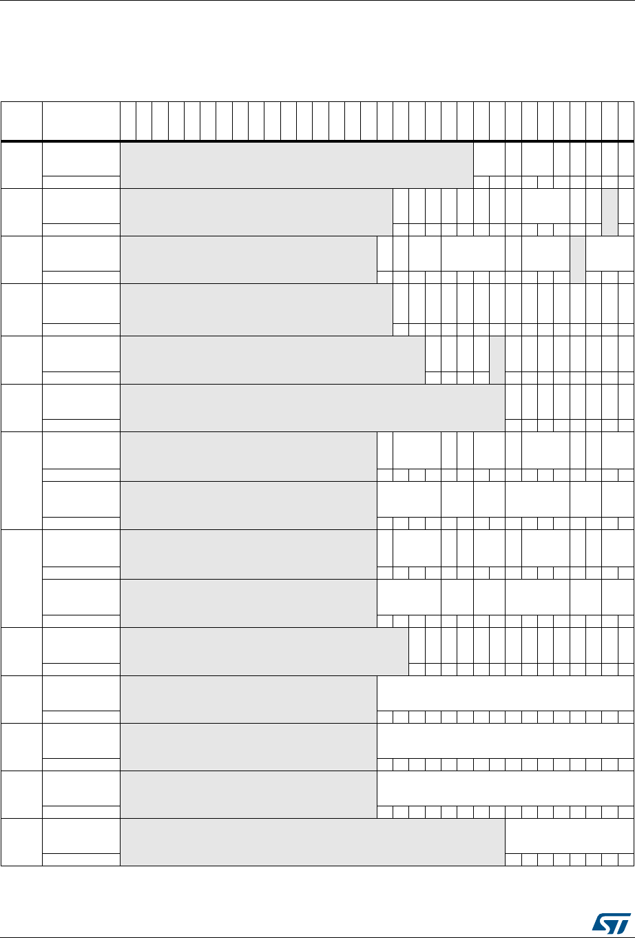
Advanced-control timer (TIM1) RM0383
304/836 DocID026448 Rev 1
12.4.21 TIM1 register map
TIM1 registers are mapped as 16-bit addressable registers as described in the table below:
Table 51. TIM1 register map and reset values
Offset Register
31
30
29
28
27
26
25
24
23
22
21
20
19
18
17
16
15
14
13
12
11
10
9
8
7
6
5
4
3
2
1
0
0x00 TIMx_CR1 Reserved
CKD
[1:0]
ARPE
CMS
[1:0]
DIR
OPM
URS
UDIS
CEN
Reset value 0000000000
0x04 TIMx_CR2 Reserved
OIS4
OIS3N
OIS3
OIS2N
OIS2
OIS1N
OIS1
TI1S
MMS[2:0]
CCDS
CCUS
Reserved
CCPC
Reset value 0000000000000 0
0x08 TIMx_SMCR Reserved
ETP
ECE
ETPS
[1:0] ETF[3:0]
MSM
TS[2:0]
Reserved
SMS[2:0]
Reset value 000000000000 000
0x0C TIMx_DIER Reserved
TDE
COMDE
CC4DE
CC3DE
CC2DE
CC1DE
UDE
BIE
TIE
COMIE
CC4IE
CC3IE
CC2IE
CC1IE
UIE
Reset value 000000000000000
0x10 TIMx_SR Reserved
CC4OF
CC3OF
CC2OF
CC1OF
Reserved
BIF
TIF
COMIF
CC4IF
CC3IF
CC2IF
CC1IF
UIF
Reset value 0000 00000000
0x14 TIMx_EGR Reserved
BG
TG
COMG
CC4G
CC3G
CC2G
CC1G
UG
Reset value 00000000
0x18
TIMx_CCMR1
Output Compare
mode Reserved
OC2CE
OC2M
[2:0]
OC2PE
OC2FE
CC2S
[1:0]
OC1CE
OC1M
[2:0]
OC1PE
OC1FE
CC1S
[1:0]
Reset value 0000000000000000
TIMx_CCMR1
Input Capture
mode Reserved IC2F[3:0]
IC2
PSC
[1:0]
CC2S
[1:0] IC1F[3:0]
IC1
PSC
[1:0]
CC1S
[1:0]
Reset value 0000000000000000
0x1C
TIMx_CCMR2
Output Compare
mode Reserved
O24CE
OC4M
[2:0]
OC4PE
OC4FE
CC4S
[1:0]
OC3CE
OC3M
[2:0]
OC3PE
OC3FE
CC3S
[1:0]
Reset value 0000000000000000
TIMx_CCMR2
Input Capture
mode Reserved IC4F[3:0]
IC4
PSC
[1:0]
CC4S
[1:0] IC3F[3:0]
IC3
PSC
[1:0]
CC3S
[1:0]
Reset value 0000000000000000
0x20 TIMx_CCER Reserved
CC4P
CC4E
CC3NP
CC3NE
CC3P
CC3E
CC2NP
CC2NE
CC2P
CC2E
CC1NP
CC1NE
CC1P
CC1E
Reset value 00000000000000
0x24 TIMx_CNT Reserved CNT[15:0]
Reset value 0000000000000000
0x28 TIMx_PSC Reserved PSC[15:0]
Reset value 0000000000000000
0x2C TIMx_ARR Reserved ARR[15:0]
Reset value 0000000000000000
0x30 TIMx_RCR Reserved REP[7:0]
Reset value 00000000
DocID026448 Rev 1 305/836
RM0383 Advanced-control timer (TIM1)
305
Refer to Table 3 on page 41 for the register boundary addresses.
0x34 TIMx_CCR1 Reserved CCR1[15:0]
Reset value 0000000000000000
0x38 TIMx_CCR2 Reserved CCR2[15:0]
Reset value 0000000000000000
0x3C TIMx_CCR3 Reserved CCR3[15:0]
Reset value 0000000000000000
0x40 TIMx_CCR4 Reserved CCR4[15:0]
Reset value 0000000000000000
0x44 TIMx_BDTR Reserved
MOE
AOE
BKP
BKE
OSSR
OSSI
LOCK
[1:0] DT[7:0]
Reset value 0000000000000000
0x48 TIMx_DCR Reserved DBL[4:0] Reserved DBA[4:0]
Reset value 00000 00000
0x4C TIMx_DMAR Reserved DMAB[15:0]
Reset value 0000000000000000
Table 51. TIM1 register map and reset values (continued)
Offset Register
31
30
29
28
27
26
25
24
23
22
21
20
19
18
17
16
15
14
13
12
11
10
9
8
7
6
5
4
3
2
1
0

General-purpose timers (TIM2 to TIM5) RM0383
306/836 DocID026448 Rev 1
13 General-purpose timers (TIM2 to TIM5)
13.1 TIM2 to TIM5 introduction
The general-purpose timers consist of a 16-bit or 32-bit auto-reload counter driven by a
programmable prescaler.
They may be used for a variety of purposes, including measuring the pulse lengths of input
signals (input capture) or generating output waveforms (output compare and PWM).
Pulse lengths and waveform periods can be modulated from a few microseconds to several
milliseconds using the timer prescaler and the RCC clock controller prescalers.
The timers are completely independent, and do not share any resources. They can be
synchronized together as described in Section 13.3.15.
13.2 TIM2 to TIM5 main features
General-purpose TIMx timer features include:
•16-bit (TIM3 and TIM4) or 32-bit (TIM2 and TIM5) up, down, up/down auto-reload
counter.
•16-bit programmable prescaler used to divide (also “on the fly”) the counter clock
frequency by any factor between 1 and 65536.
•Up to 4 independent channels for:
– Input capture
– Output compare
– PWM generation (Edge- and Center-aligned modes)
– One-pulse mode output
•Synchronization circuit to control the timer with external signals and to interconnect
several timers.
•Interrupt/DMA generation on the following events:
– Update: counter overflow/underflow, counter initialization (by software or
internal/external trigger)
– Trigger event (counter start, stop, initialization or count by internal/external trigger)
– Input capture
– Output compare
•Supports incremental (quadrature) encoder and hall-sensor circuitry for positioning
purposes
•Trigger input for external clock or cycle-by-cycle current management
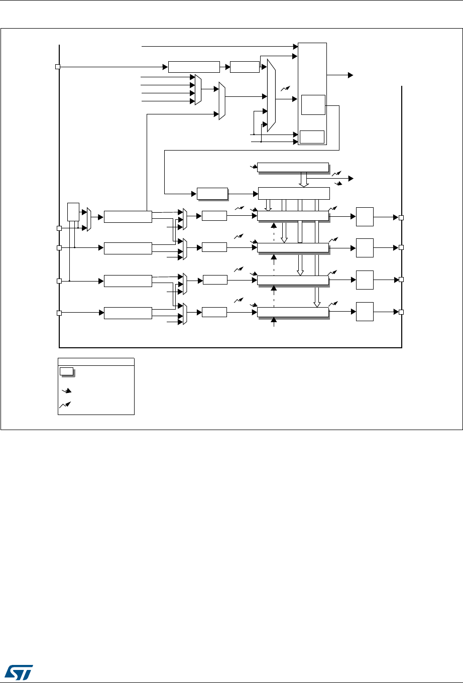
DocID026448 Rev 1 307/836
RM0383 General-purpose timers (TIM2 to TIM5)
365
Figure 87. General-purpose timer block diagram
13.3 TIM2 to TIM5 functional description
13.3.1 Time-base unit
The main block of the programmable timer is a 16-bit/32-bit counter with its related auto-
reload register. The counter can count up. The counter clock can be divided by a prescaler.
The counter, the auto-reload register and the prescaler register can be written or read by
software. This is true even when the counter is running.
The time-base unit includes:
•Counter Register (TIMx_CNT)
•Prescaler Register (TIMx_PSC):
•Auto-Reload Register (TIMx_ARR)
$XWRUHORDGUHJLVWHU
&DSWXUHFRPSDUHUHJLVWHU
&DSWXUHFRPSDUHUHJLVWHU
5
5
5
##)
##)
7ULJJHU
FRQWUROOHU
6WRSFOHDURUXSGRZQ
4)&0
4)&0
)42
)42
)42
)42
42')
(QFRGHU
,QWHUIDFH
&DSWXUHFRPSDUHUHJLVWHU
5
##)
OUTPUT
FRQWURO
/#
42'/
/#2%&
/#2%&
/#2%&
5
5)
5HVHWHQDEOHXSGRZQFRXQW
&DSWXUHFRPSDUHUHJLVWHU
5
##)
/#2%&
3UHVFDOHU
3UHVFDOHU
)#03
)#03
)#
)#
3UHVFDOHU
3UHVFDOHU
,QSXWILOWHU
HGJHGHWHFWRU
)#03
)#03
4)&0
/#
/#
/#
2EG
EVENT
.OTES
0RELOADREGISTERSTRANSFERRED
TOACTIVEREGISTERSON5EVENT
ACCORDINGTOCONTROLBIT
INTERRUPT$-!OUTPUT
4')
42#
42#
)#
)#
)42
42#
4)&?%$
,QSXWILOWHU
HGJHGHWHFWRU
,QSXWILOWHU
HGJHGHWHFWRU
,QSXWILOWHU
HGJHGHWHFWRU
##)
##)
##)
##)
4)&0
4)&0
4)&0
4)&0
42#
42#
4)&0
4)&0
4)&0
4)
4)
4)
4)
;25
7,0[B&+
7,0[B&+
7,0[B&+
7,0[B&+
7,0[B&+
WRRWKHUWLPHUV
3UHVFDOHU FRXQWHU
&.B36& 36& &17
&.B&17
FRQWUROOHU
PRGH
6ODYH
(75 ,QSXWILOWHU
3RODULW\VHOHFWLRQHGJH
GHWHFWRUSUHVFDOHU
(753
(75)
7,0[B(75
(75)
WR$'&
OUTPUT
FRQWURO
OUTPUT
FRQWURO
OUTPUT
FRQWURO
069
7,0[B&+
7,0[B&+
7,0[B&+
7,0[B&/.IURP5&&
,QWHUQDO&ORFN&.B,17
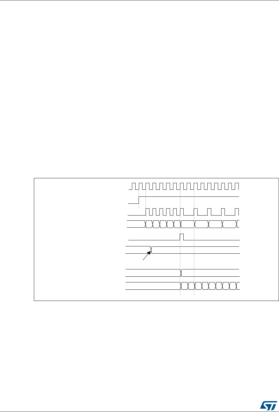
General-purpose timers (TIM2 to TIM5) RM0383
308/836 DocID026448 Rev 1
The auto-reload register is preloaded. Writing to or reading from the auto-reload register
accesses the preload register. The content of the preload register are transferred into the
shadow register permanently or at each update event (UEV), depending on the auto-reload
preload enable bit (ARPE) in TIMx_CR1 register. The update event is sent when the counter
reaches the overflow (or underflow when downcounting) and if the UDIS bit equals 0 in the
TIMx_CR1 register. It can also be generated by software. The generation of the update
event is described in detail for each configuration.
The counter is clocked by the prescaler output CK_CNT, which is enabled only when the
counter enable bit (CEN) in TIMx_CR1 register is set (refer also to the slave mode controller
description to get more details on counter enabling).
Note that the actual counter enable signal CNT_EN is set 1 clock cycle after CEN.
Prescaler description
The prescaler can divide the counter clock frequency by any factor between 1 and 65536. It
is based on a 16-bit counter controlled through a 16-bit/32-bit register (in the TIMx_PSC
register). It can be changed on the fly as this control register is buffered. The new prescaler
ratio is taken into account at the next update event.
Figure 88 and Figure 89 give some examples of the counter behavior when the prescaler
ratio is changed on the fly:
Figure 88. Counter timing diagram with prescaler division change from 1 to 2
CK_PSC
00
CNT_EN
Timer clock = CK_CNT
Counter register
Update event (UEV)
0
F9 FA FB FCF7
Prescaler control register 01
Write a new value in TIMx_PSC
01 02 03
Prescaler buffer 01
Prescaler counter 01 0 1 0 1 0 1
F8
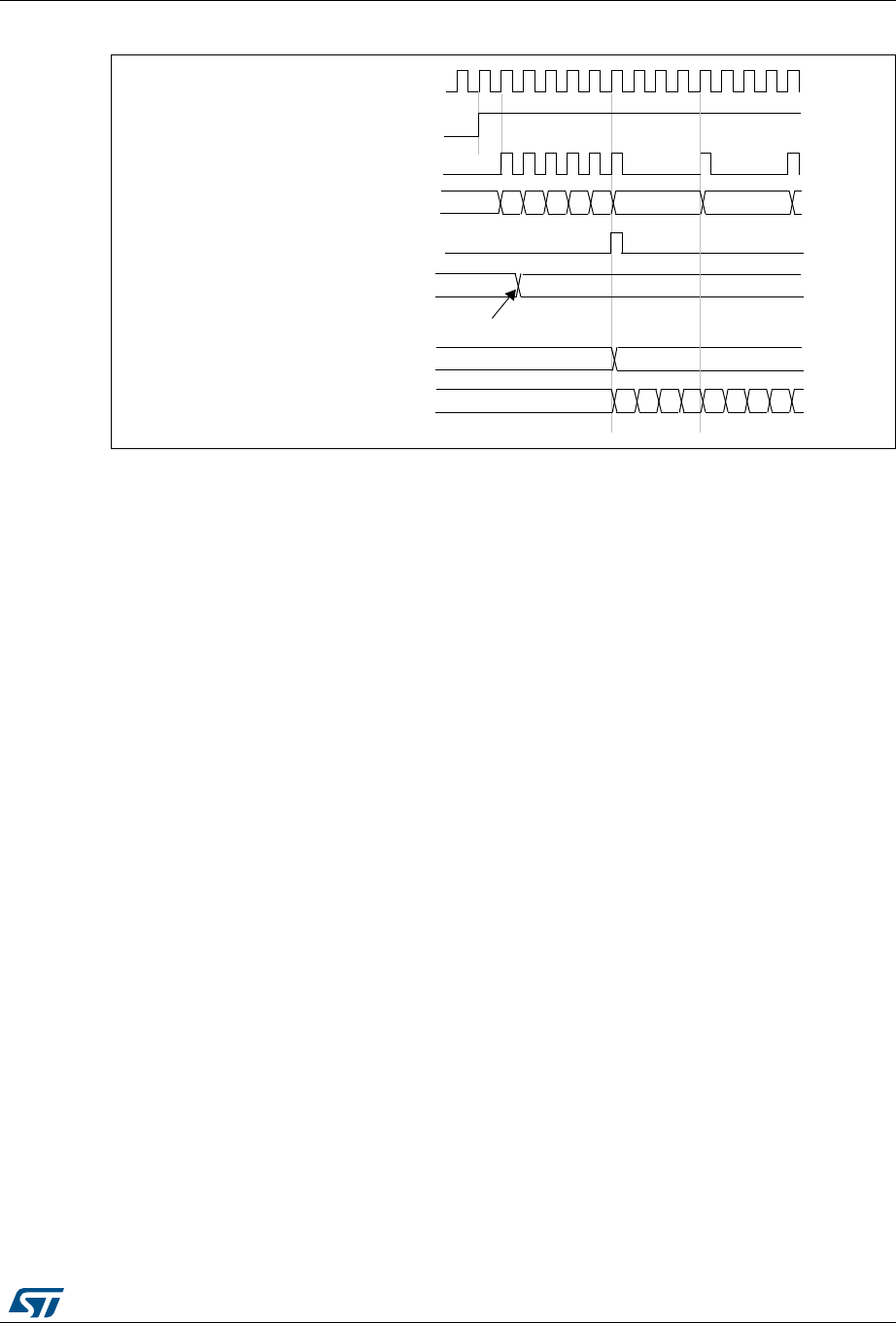
DocID026448 Rev 1 309/836
RM0383 General-purpose timers (TIM2 to TIM5)
365
Figure 89. Counter timing diagram with prescaler division change from 1 to 4
13.3.2 Counter modes
Upcounting mode
In upcounting mode, the counter counts from 0 to the auto-reload value (content of the
TIMx_ARR register), then restarts from 0 and generates a counter overflow event.
An Update event can be generated at each counter overflow or by setting the UG bit in the
TIMx_EGR register (by software or by using the slave mode controller).
The UEV event can be disabled by software by setting the UDIS bit in TIMx_CR1 register.
This is to avoid updating the shadow registers while writing new values in the preload
registers. Then no update event occurs until the UDIS bit has been written to 0. However,
the counter restarts from 0, as well as the counter of the prescaler (but the prescale rate
does not change). In addition, if the URS bit (update request selection) in TIMx_CR1
register is set, setting the UG bit generates an update event UEV but without setting the UIF
flag (thus no interrupt or DMA request is sent). This is to avoid generating both update and
capture interrupts when clearing the counter on the capture event.
When an update event occurs, all the registers are updated and the update flag (UIF bit in
TIMx_SR register) is set (depending on the URS bit):
•The buffer of the prescaler is reloaded with the preload value (content of the TIMx_PSC
register)
•The auto-reload shadow register is updated with the preload value (TIMx_ARR)
The following figures show some examples of the counter behavior for different clock
frequencies when TIMx_ARR=0x36.
CK_PSC
00
CNT_EN
Timer clock = CK_CNT
Counter register
Update event (UEV)
0
F9 FA FB FCF7
Prescaler control register 03
Write a new value in TIMx_PSC
Prescaler buffer 03
Prescaler counter 01 2 3 0 1 2 3
F8 01
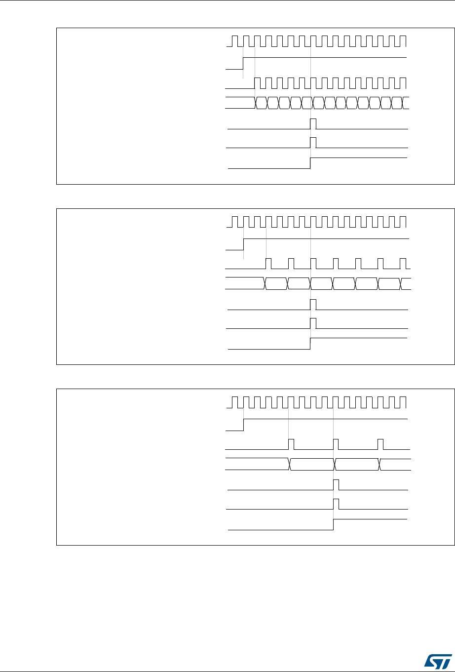
General-purpose timers (TIM2 to TIM5) RM0383
310/836 DocID026448 Rev 1
Figure 90. Counter timing diagram, internal clock divided by 1
Figure 91. Counter timing diagram, internal clock divided by 2
Figure 92. Counter timing diagram, internal clock divided by 4
CK_INT
00
CNT_EN
Timer clock = CK_CNT
Counter register
Update interrupt flag (UIF)
Counter overflow
Update event (UEV)
01 02 03 04 05 06 0732 33 34 35 3631
CK_INT
0035 0000 0001 0002 0003
CNT_EN
Timer clock = CK_CNT
Counter register
Update interrupt flag (UIF)
0034 0036
Counter overflow
Update event (UEV)
0000 0001
CNT_EN
TImer clock = CK_CNT
Counter register
Update interrupt flag (UIF)
0035 0036
Counter overflow
Update event (UEV)
CK_INT
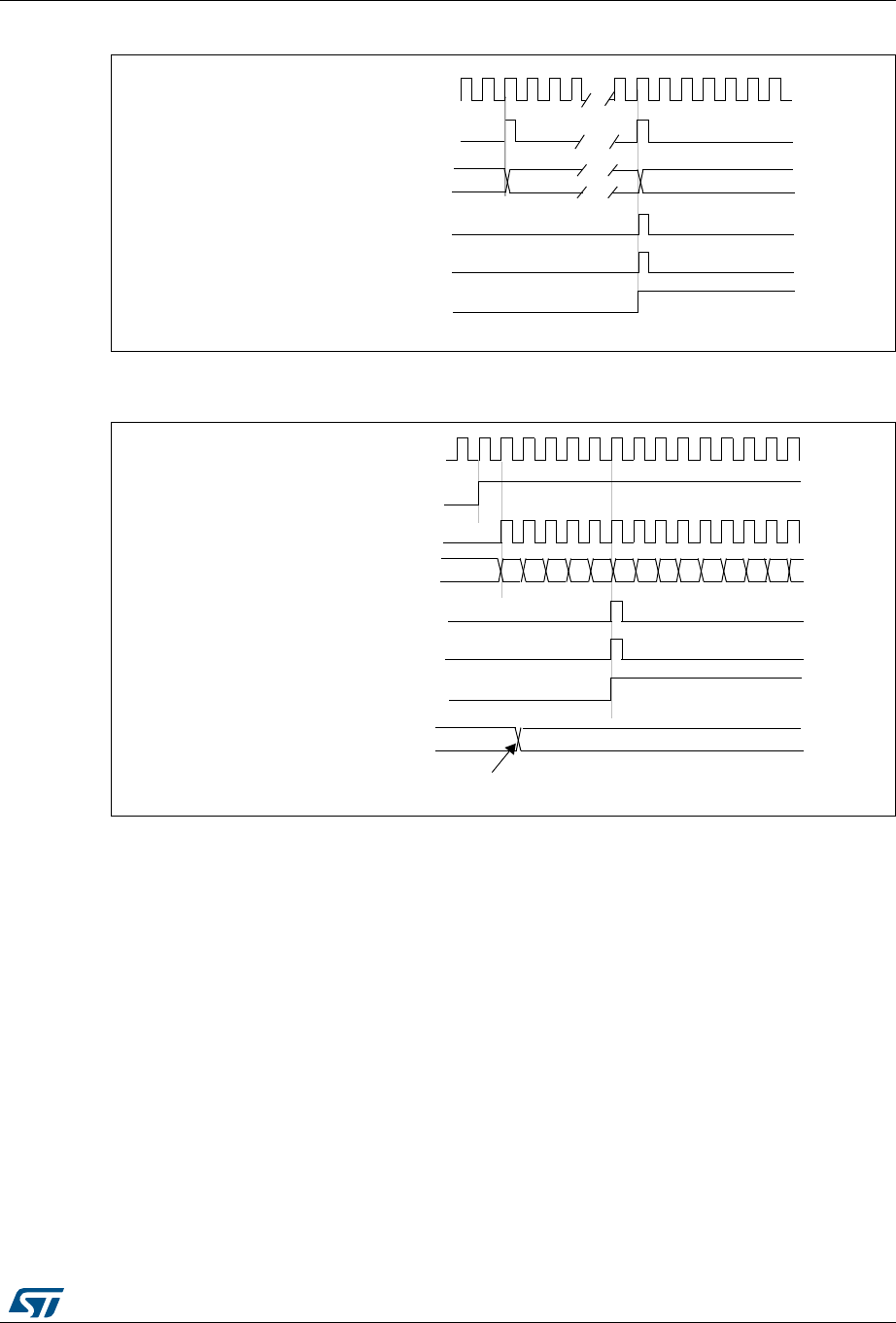
DocID026448 Rev 1 311/836
RM0383 General-purpose timers (TIM2 to TIM5)
365
Figure 93. Counter timing diagram, internal clock divided by N
Figure 94. Counter timing diagram, Update event when ARPE=0 (TIMx_ARR not
preloaded)
Timer clock = CK_CNT
Counter register 00
1F 20
Update interrupt flag (UIF)
Counter overflow
Update event (UEV)
CK_INT
00
CNT_EN
Timer clock = CK_CNT
Counter register
Update interrupt flag (UIF)
Counter overflow
Update event (UEV)
01 02 03 04 05 06 0732 33 34 35 3631
Auto-reload register FF 36
Write a new value in TIMx_ARR
CK_INT

General-purpose timers (TIM2 to TIM5) RM0383
312/836 DocID026448 Rev 1
Figure 95. Counter timing diagram, Update event when ARPE=1 (TIMx_ARR
preloaded)
Downcounting mode
In downcounting mode, the counter counts from the auto-reload value (content of the
TIMx_ARR register) down to 0, then restarts from the auto-reload value and generates a
counter underflow event.
An Update event can be generate at each counter underflow or by setting the UG bit in the
TIMx_EGR register (by software or by using the slave mode controller)
The UEV update event can be disabled by software by setting the UDIS bit in TIMx_CR1
register. This is to avoid updating the shadow registers while writing new values in the
preload registers. Then no update event occurs until UDIS bit has been written to 0.
However, the counter restarts from the current auto-reload value, whereas the counter of the
prescaler restarts from 0 (but the prescale rate doesn’t change).
In addition, if the URS bit (update request selection) in TIMx_CR1 register is set, setting the
UG bit generates an update event UEV but without setting the UIF flag (thus no interrupt or
DMA request is sent). This is to avoid generating both update and capture interrupts when
clearing the counter on the capture event.
When an update event occurs, all the registers are updated and the update flag (UIF bit in
TIMx_SR register) is set (depending on the URS bit):
•The buffer of the prescaler is reloaded with the preload value (content of the TIMx_PSC
register).
•The auto-reload active register is updated with the preload value (content of the
TIMx_ARR register). Note that the auto-reload is updated before the counter is
reloaded, so that the next period is the expected one.
The following figures show some examples of the counter behavior for different clock
frequencies when TIMx_ARR=0x36.
00
CNT_EN
Timer clock = CK_CNT
Counter register
Update interrupt flag (UIF)
Counter overflow
Update event (UEV)
01 02 03 04 05 06 07F1 F2 F3 F4 F5F0
Auto-reload preload register F5 36
Auto-reload shadow register F5 36
Write a new value in TIMx_ARR
CK_PSC
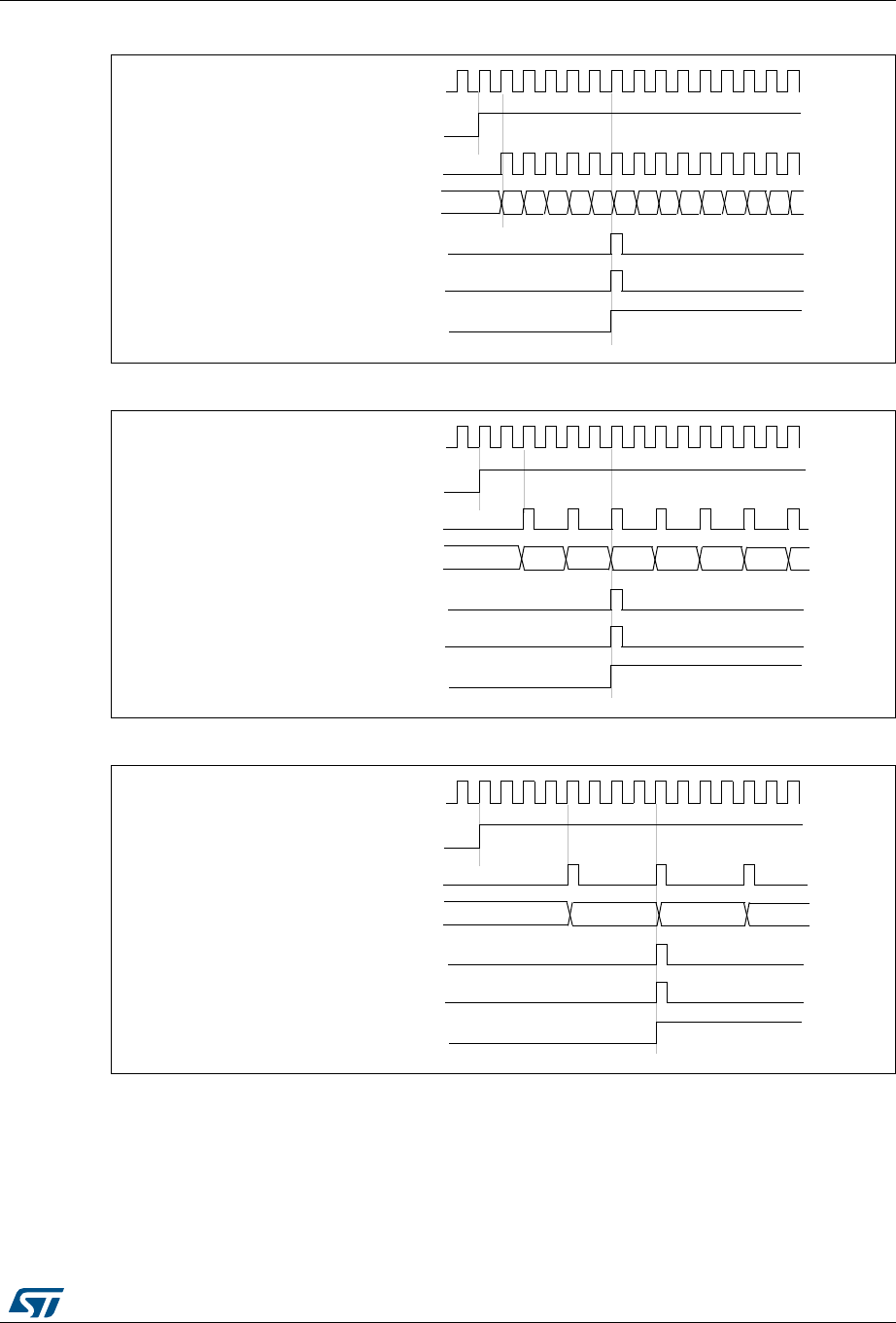
DocID026448 Rev 1 313/836
RM0383 General-purpose timers (TIM2 to TIM5)
365
Figure 96. Counter timing diagram, internal clock divided by 1
Figure 97. Counter timing diagram, internal clock divided by 2
Figure 98. Counter timing diagram, internal clock divided by 4
CK_INT
36
CNT_EN
Timer clock = CK_CNT
Counter register
Update interrupt flag (UIF)
Counter underflow (cnt_udf)
Update event (UEV)
35 34 33 32 31 30 2F04 03 02 01 0005
CK_INT
0001 0036 0035 0034 0033
CNT_EN
Timer clock = CK_CNT
Counter register
Update interrupt flag (UIF)
0002 0000
Counter underflow
Update event (UEV)
0036 0035
CNT_EN
Timer clock = CK_CNT
Counter register
Update interrupt flag (UIF)
0001 0000
Counter underflow
Update event (UEV)
CK_INT
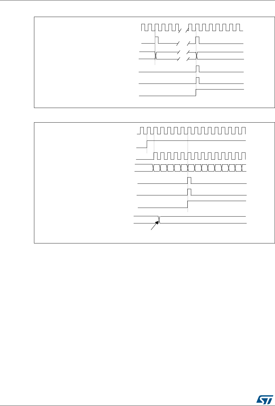
General-purpose timers (TIM2 to TIM5) RM0383
314/836 DocID026448 Rev 1
Figure 99. Counter timing diagram, internal clock divided by N
Figure 100. Counter timing diagram, Update event
Center-aligned mode (up/down counting)
In center-aligned mode, the counter counts from 0 to the auto-reload value (content of the
TIMx_ARR register) – 1, generates a counter overflow event, then counts from the auto-
reload value down to 1 and generates a counter underflow event. Then it restarts counting
from 0.
Center-aligned mode is active when the CMS bits in TIMx_CR1 register are not equal to
'00'. The Output compare interrupt flag of channels configured in output is set when: the
counter counts down (Center aligned mode 1, CMS = "01"), the counter counts up (Center
aligned mode 2, CMS = "10") the counter counts up and down (Center aligned mode 3,
CMS = "11").
In this mode, the direction bit (DIR from TIMx_CR1 register) cannot be written. It is updated
by hardware and gives the current direction of the counter.
The update event can be generated at each counter overflow and at each counter underflow
or by setting the UG bit in the TIMx_EGR register (by software or by using the slave mode
controller) also generates an update event. In this case, the counter restarts counting from
0, as well as the counter of the prescaler.
Timer clock = CK_CNT
Counter register 36
20 1F
Update interrupt flag (UIF)
Counter underflow
Update event (UEV)
CK_INT
00
36
CNT_EN
Timer clock = CK_CNT
Counter register
Update interrupt flag (UIF)
Counter underflow
Update event (UEV)
35 34 33 32 31 30 2F04 03 02 01 0005
Auto-reload register FF 36
Write a new value in TIMx_ARR
CK_INT
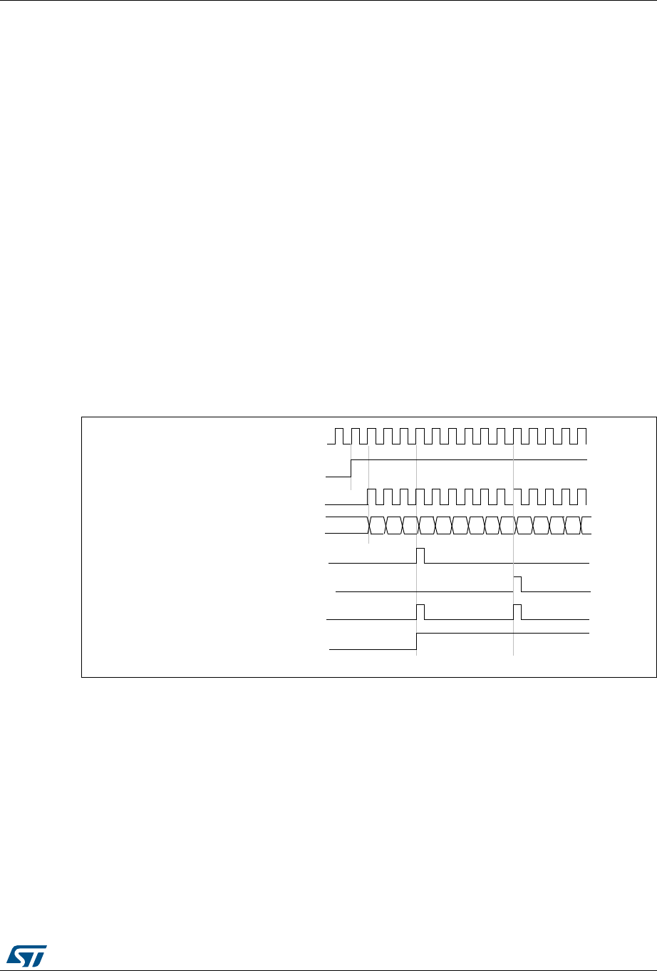
DocID026448 Rev 1 315/836
RM0383 General-purpose timers (TIM2 to TIM5)
365
The UEV update event can be disabled by software by setting the UDIS bit in TIMx_CR1
register. This is to avoid updating the shadow registers while writing new values in the
preload registers. Then no update event occurs until the UDIS bit has been written to 0.
However, the counter continues counting up and down, based on the current auto-reload
value.
In addition, if the URS bit (update request selection) in TIMx_CR1 register is set, setting the
UG bit generates an update event UEV but without setting the UIF flag (thus no interrupt or
DMA request is sent). This is to avoid generating both update and capture interrupt when
clearing the counter on the capture event.
When an update event occurs, all the registers are updated and the update flag (UIF bit in
TIMx_SR register) is set (depending on the URS bit):
•The buffer of the prescaler is reloaded with the preload value (content of the TIMx_PSC
register).
•The auto-reload active register is updated with the preload value (content of the
TIMx_ARR register). Note that if the update source is a counter overflow, the auto-
reload is updated before the counter is reloaded, so that the next period is the expected
one (the counter is loaded with the new value).
The following figures show some examples of the counter behavior for different clock
frequencies.
Figure 101. Counter timing diagram, internal clock divided by 1, TIMx_ARR=0x6
1. Here, center-aligned mode 1 is used (for more details refer to Section 13.4.1: TIMx control register 1 (TIMx_CR1)
on page 342).
CK_INT
02
CNT_EN
Timer clock = CK_CNT
Counter register
Update interrupt flag (UIF)
Counter underflow
Update event (UEV)
03 04 05 06 05 04 0303 02 01 00 0104
Counter overflow

General-purpose timers (TIM2 to TIM5) RM0383
316/836 DocID026448 Rev 1
Figure 102. Counter timing diagram, internal clock divided by 2
Figure 103. Counter timing diagram, internal clock divided by 4, TIMx_ARR=0x36
1. Center-aligned mode 2 or 3 is used with an UIF on overflow.
Figure 104. Counter timing diagram, internal clock divided by N
0002 0000 0001 0002 0003
CNT_EN
TImer clock = CK_CNT
Counter register
Update interrupt flag (UIF)
0003 0001
Counter underflow
Update event (UEV)
CK_INT
CK_INT
0036 0035
CNT_EN
Timer clock = CK_CNT
Counter register
Update interrupt flag (UIF)
0034 0035
Counter overflow (cnt_ovf)
Update event (UEV)
Timer clock = CK_CNT
Counter register 00
20 1F
Update interrupt flag (UIF)
Counter underflow
Update event (UEV)
CK_INT
01

DocID026448 Rev 1 317/836
RM0383 General-purpose timers (TIM2 to TIM5)
365
Figure 105. Counter timing diagram, Update event with ARPE=1 (counter underflow)
Figure 106. Counter timing diagram, Update event with ARPE=1 (counter overflow)
13.3.3 Clock selection
The counter clock can be provided by the following clock sources:
•Internal clock (CK_INT)
•External clock mode1: external input pin (TIx)
•External clock mode2: external trigger input (ETR) available on TIM2, TIM3 and TIM4
only.
•Internal trigger inputs (ITRx): using one timer as prescaler for another timer, for
example, you can configure Timer to act as a prescaler for Timer 2. Refer to : Using
one timer as prescaler for another on page 336 for more details.
00
CNT_EN
Timer clock = CK_CNT
Counter register
Update interrupt flag (UIF)
Counter underflow
Update event (UEV)
01 02 03 04 05 06 0705 04 03 02 0106
Auto-reload preload register FD 36
Write a new value in TIMx_ARR
Auto-reload active register FD 36
CK_INT
36
CNT_EN
Timer clock = CK_CNT
Counter register
Update interrupt flag (UIF)
Counter overflow
Update event (UEV)
35 34 33 32 31 30 2FF8 F9 FA FB FCF7
Auto-reload preload register FD 36
Write a new value in TIMx_ARR
Auto-reload active register FD 36
CK_INT
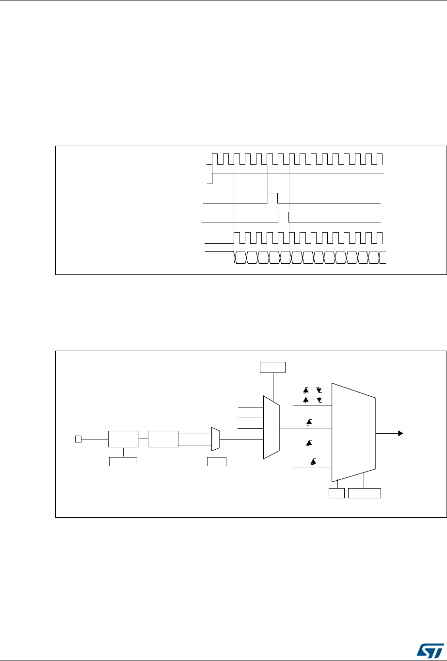
General-purpose timers (TIM2 to TIM5) RM0383
318/836 DocID026448 Rev 1
Internal clock source (CK_INT)
If the slave mode controller is disabled (SMS=000 in the TIMx_SMCR register), then the
CEN, DIR (in the TIMx_CR1 register) and UG bits (in the TIMx_EGR register) are actual
control bits and can be changed only by software (except UG which remains cleared
automatically). As soon as the CEN bit is written to 1, the prescaler is clocked by the internal
clock CK_INT.
Figure 107 shows the behavior of the control circuit and the upcounter in normal mode,
without prescaler.
Figure 107. Control circuit in normal mode, internal clock divided by 1
External clock source mode 1
This mode is selected when SMS=111 in the TIMx_SMCR register. The counter can count at
each rising or falling edge on a selected input.
Figure 108. TI2 external clock connection example
For example, to configure the upcounter to count in response to a rising edge on the TI2
input, use the following procedure:
1. Configure channel 2 to detect rising edges on the TI2 input by writing CC2S= ‘01 in the
TIMx_CCMR1 register.
2. Configure the input filter duration by writing the IC2F[3:0] bits in the TIMx_CCMR1
register (if no filter is needed, keep IC2F=0000).
CK_INT
00
Counter clock = CK_CNT = CK_PSC
COUNTER REGISTER 01 02 03 04 05 06 0732 33 34 35 3631
CEN=CNT_EN
UG
CNT_INIT
CK_INT
encoder
mode
external clock
mode 1
external clock
mode 2
internal clock
mode
ETRF
TRGI
TI1F
TI2F or
or
or
(internal clock)
CK_PSC
ECE
TIMx_SMCR
SMS[2:0]
ITRx
TI1F_ED
TI1FP1
TI2FP2
ETRF
TIMx_SMCR
TS[2:0]
TI2 0
1
TIMx_CCER
CC2P
Filter
ICF[3:0]
TIMx_CCMR1
Edge
Detector
TI2F_Rising
TI2F_Falling 110
001
100
101
111
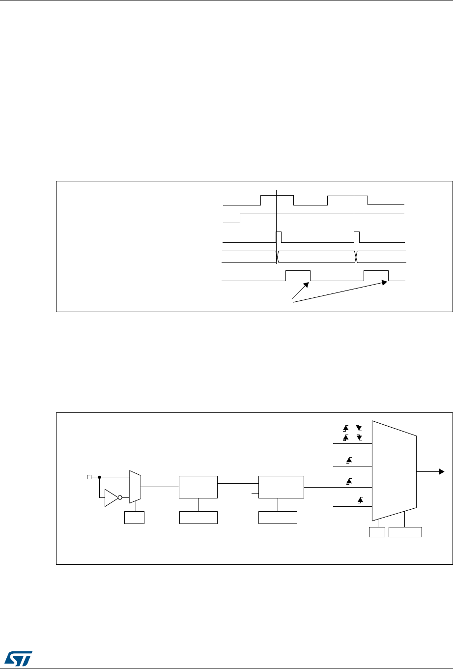
DocID026448 Rev 1 319/836
RM0383 General-purpose timers (TIM2 to TIM5)
365
Note: The capture prescaler is not used for triggering, so you don’t need to configure it.
3. Select rising edge polarity by writing CC2P=0 and CC2NP=0 in the TIMx_CCER
register.
4. Configure the timer in external clock mode 1 by writing SMS=111 in the TIMx_SMCR
register.
5. Select TI2 as the input source by writing TS=110 in the TIMx_SMCR register.
6. Enable the counter by writing CEN=1 in the TIMx_CR1 register.
When a rising edge occurs on TI2, the counter counts once and the TIF flag is set.
The delay between the rising edge on TI2 and the actual clock of the counter is due to the
resynchronization circuit on TI2 input.
Figure 109. Control circuit in external clock mode 1
External clock source mode 2
This mode is selected by writing ECE=1 in the TIMx_SMCR register.
The counter can count at each rising or falling edge on the external trigger input ETR.
Figure 110 gives an overview of the external trigger input block.
Figure 110. External trigger input block
For example, to configure the upcounter to count each 2 rising edges on ETR, use the
following procedure:
Counter clock = CK_CNT = CK_PSC
Counter register 35 3634
TI2
CNT_EN
TIF
Write TIF=0
ETR 0
1
TIMx_SMCR
ETP
divider
/1, /2, /4, /8
ETPS[1:0]
ETRP filter
ETF[3:0]
downcounter
CK_INT
TIMx_SMCR
TIMx_SMCR
ETR pin
CK_INT
encoder
mode
external clock
mode 1
external clock
mode 2
internal clock
mode
ETRF
TRGI
TI1F
TI2F or
or
or
(internal clock)
CK_PSC
ECE
TIMx_SMCR
SMS[2:0]
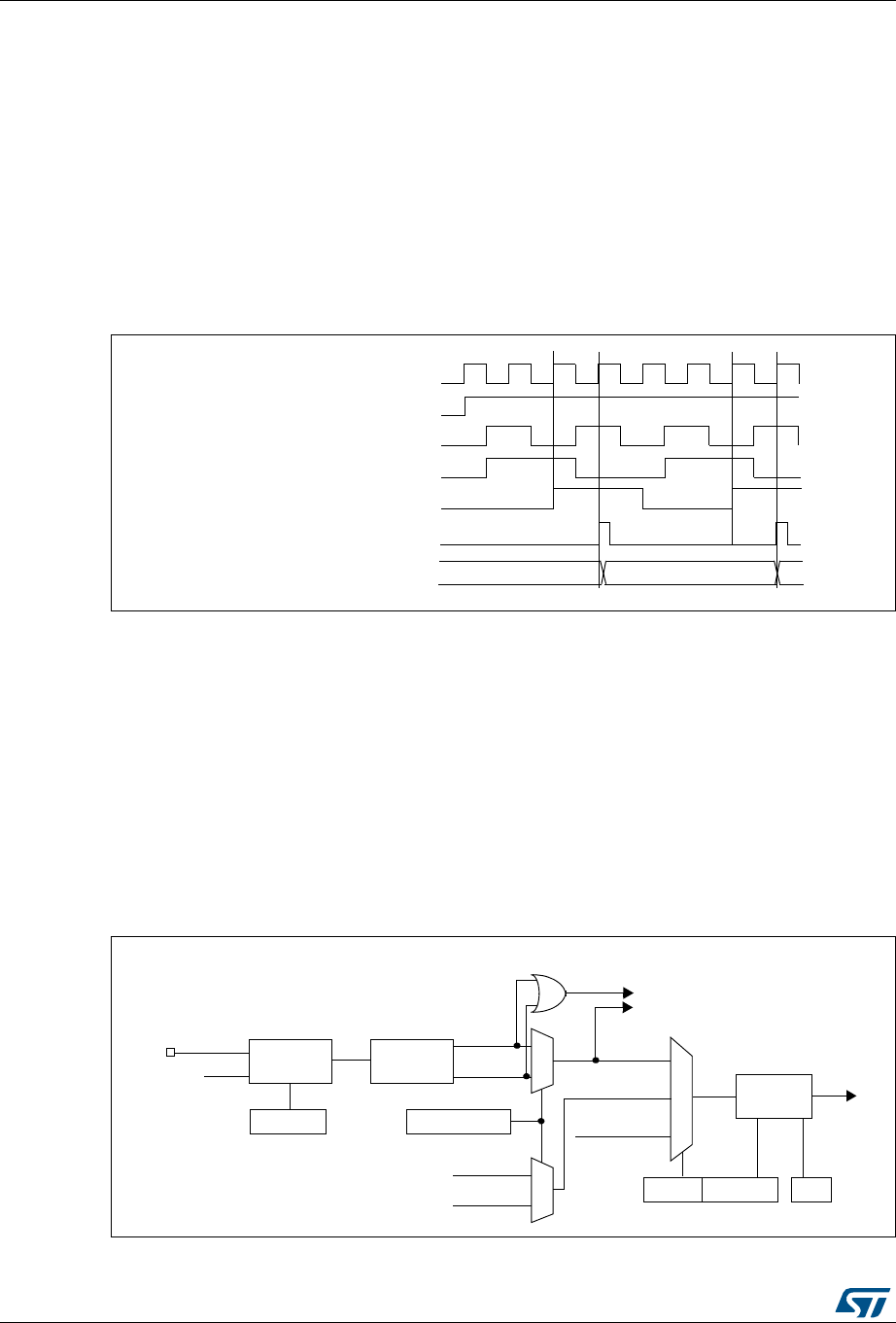
General-purpose timers (TIM2 to TIM5) RM0383
320/836 DocID026448 Rev 1
1. As no filter is needed in this example, write ETF[3:0]=0000 in the TIMx_SMCR register.
2. Set the prescaler by writing ETPS[1:0]=01 in the TIMx_SMCR register
3. Select rising edge detection on the ETR pin by writing ETP=0 in the TIMx_SMCR
register
4. Enable external clock mode 2 by writing ECE=1 in the TIMx_SMCR register.
5. Enable the counter by writing CEN=1 in the TIMx_CR1 register.
The counter counts once each 2 ETR rising edges.
The delay between the rising edge on ETR and the actual clock of the counter is due to the
resynchronization circuit on the ETRP signal.
Figure 111. Control circuit in external clock mode 2
13.3.4 Capture/compare channels
Each Capture/Compare channel is built around a capture/compare register (including a
shadow register), a input stage for capture (with digital filter, multiplexing and prescaler) and
an output stage (with comparator and output control).
The following figure gives an overview of one Capture/Compare channel.
The input stage samples the corresponding TIx input to generate a filtered signal TIxF.
Then, an edge detector with polarity selection generates a signal (TIxFPx) which can be
used as trigger input by the slave mode controller or as the capture command. It is
prescaled before the capture register (ICxPS).
Figure 112. Capture/compare channel (example: channel 1 input stage)
Counter clock = CK_CNT = CK_PSC
Counter register 35 3634
ETR
CNT_EN
CK_INT
ETRP
ETRF
TI1
TIMx_CCER
CC1P/CC1NP
divider
/1, /2, /4, /8
ICPS[1:0]
TI1F_ED
filter
ICF[3:0]
downcounter
TIMx_CCMR1
Edge
Detector
TI1F_Rising
TI1F_Falling
to the slave mode controller
TI1FP1
11
01
TIMx_CCMR1
CC1S[1:0]
IC1
TI2FP1
TRC
(from channel 2)
(from slave mode
controller)
10
fDTS
TIMx_CCER
CC1E
IC1PS
TI1F
TI2F_rising
TI2F_falling
(from channel 2)
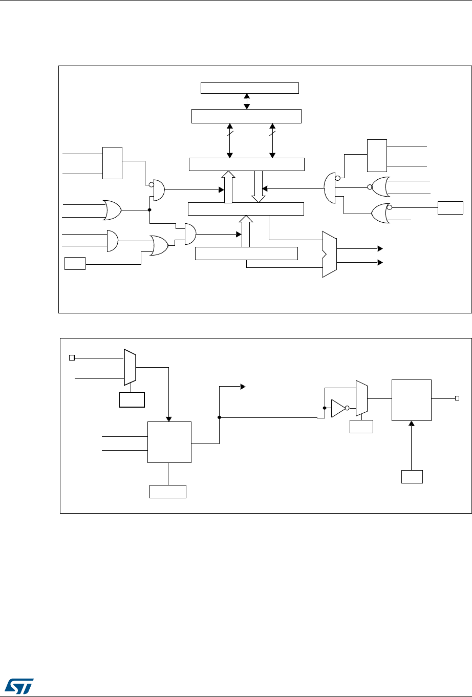
DocID026448 Rev 1 321/836
RM0383 General-purpose timers (TIM2 to TIM5)
365
The output stage generates an intermediate waveform which is then used for reference:
OCxRef (active high). The polarity acts at the end of the chain.
Figure 113. Capture/compare channel 1 main circuit
Figure 114. Output stage of capture/compare channel (channel 1)
The capture/compare block is made of one preload register and one shadow register. Write
and read always access the preload register.
In capture mode, captures are actually done in the shadow register, which is copied into the
preload register.
In compare mode, the content of the preload register is copied into the shadow register
which is compared to the counter.
CC1E
Capture/Compare Shadow Register
comparator
Capture/Compare Preload Register
Counter
IC1PS
CC1S[0]
CC1S[1]
capture
input
mode
S
R
read CCR1H
read CCR1L
read_in_progress
capture_transfer CC1S[0]
CC1S[1]
S
R
write CCR1H
write CCR1L
write_in_progress
output
mode
UEV
OC1PE
(from time
compare_transfer
APB Bus
88
high
low
(if 16-bit)
MCU-peripheral interface
TIMx_CCMR1
OC1PE
base unit)
CNT>CCR1
CNT=CCR1
TIMx_EGR
CC1G
KƵƚƉƵƚŵŽĚĞ
EdхZϭ
EdсZϭ ĐŽŶƚƌŽůůĞƌ
d/DdžͺDZϭ
KϭDϮ͗Ϭ
ŽĐϭƌĞĨ
Ϭ
ϭ
ϭW
d/DdžͺZ
KƵƚƉƵƚ
ŶĂďůĞ
ŝƌĐƵŝƚ
Kϭ
ϭ
d/DdžͺZ
dŽƚŚĞŵĂƐƚĞƌŵŽĚĞ
ĐŽŶƚƌŽůůĞƌ
dZ&
Ϭ
ϭ
KZ&ͺ>Z
KZ&ͺ>Zͺ/Ed
K^
d/Ddžͺ^DZ
Ăŝϭϳϭϴϳ

General-purpose timers (TIM2 to TIM5) RM0383
322/836 DocID026448 Rev 1
13.3.5 Input capture mode
In Input capture mode, the Capture/Compare Registers (TIMx_CCRx) are used to latch the
value of the counter after a transition detected by the corresponding ICx signal. When a
capture occurs, the corresponding CCXIF flag (TIMx_SR register) is set and an interrupt or
a DMA request can be sent if they are enabled. If a capture occurs while the CCxIF flag was
already high, then the over-capture flag CCxOF (TIMx_SR register) is set. CCxIF can be
cleared by software by writing it to 0 or by reading the captured data stored in the
TIMx_CCRx register. CCxOF is cleared when you write it to 0.
The following example shows how to capture the counter value in TIMx_CCR1 when TI1
input rises. To do this, use the following procedure:
•Select the active input: TIMx_CCR1 must be linked to the TI1 input, so write the CC1S
bits to 01 in the TIMx_CCMR1 register. As soon as CC1S becomes different from 00,
the channel is configured in input and the TIMx_CCR1 register becomes read-only.
•Program the input filter duration you need with respect to the signal you connect to the
timer (by programming the ICxF bits in the TIMx_CCMRx register if the input is one of
the TIx inputs). Let’s imagine that, when toggling, the input signal is not stable during at
must 5 internal clock cycles. We must program a filter duration longer than these 5
clock cycles. We can validate a transition on TI1 when 8 consecutive samples with the
new level have been detected (sampled at fDTS frequency). Then write IC1F bits to
0011 in the TIMx_CCMR1 register.
•Select the edge of the active transition on the TI1 channel by writing the CC1P and
CC1NP bits to 00 in the TIMx_CCER register (rising edge in this case).
•Program the input prescaler. In our example, we wish the capture to be performed at
each valid transition, so the prescaler is disabled (write IC1PS bits to 00 in the
TIMx_CCMR1 register).
•Enable capture from the counter into the capture register by setting the CC1E bit in the
TIMx_CCER register.
•If needed, enable the related interrupt request by setting the CC1IE bit in the
TIMx_DIER register, and/or the DMA request by setting the CC1DE bit in the
TIMx_DIER register.
When an input capture occurs:
•The TIMx_CCR1 register gets the value of the counter on the active transition.
•CC1IF flag is set (interrupt flag). CC1OF is also set if at least two consecutive captures
occurred whereas the flag was not cleared.
•An interrupt is generated depending on the CC1IE bit.
•A DMA request is generated depending on the CC1DE bit.
In order to handle the overcapture, it is recommended to read the data before the
overcapture flag. This is to avoid missing an overcapture which could happen after reading
the flag and before reading the data.
Note: IC interrupt and/or DMA requests can be generated by software by setting the
corresponding CCxG bit in the TIMx_EGR register.
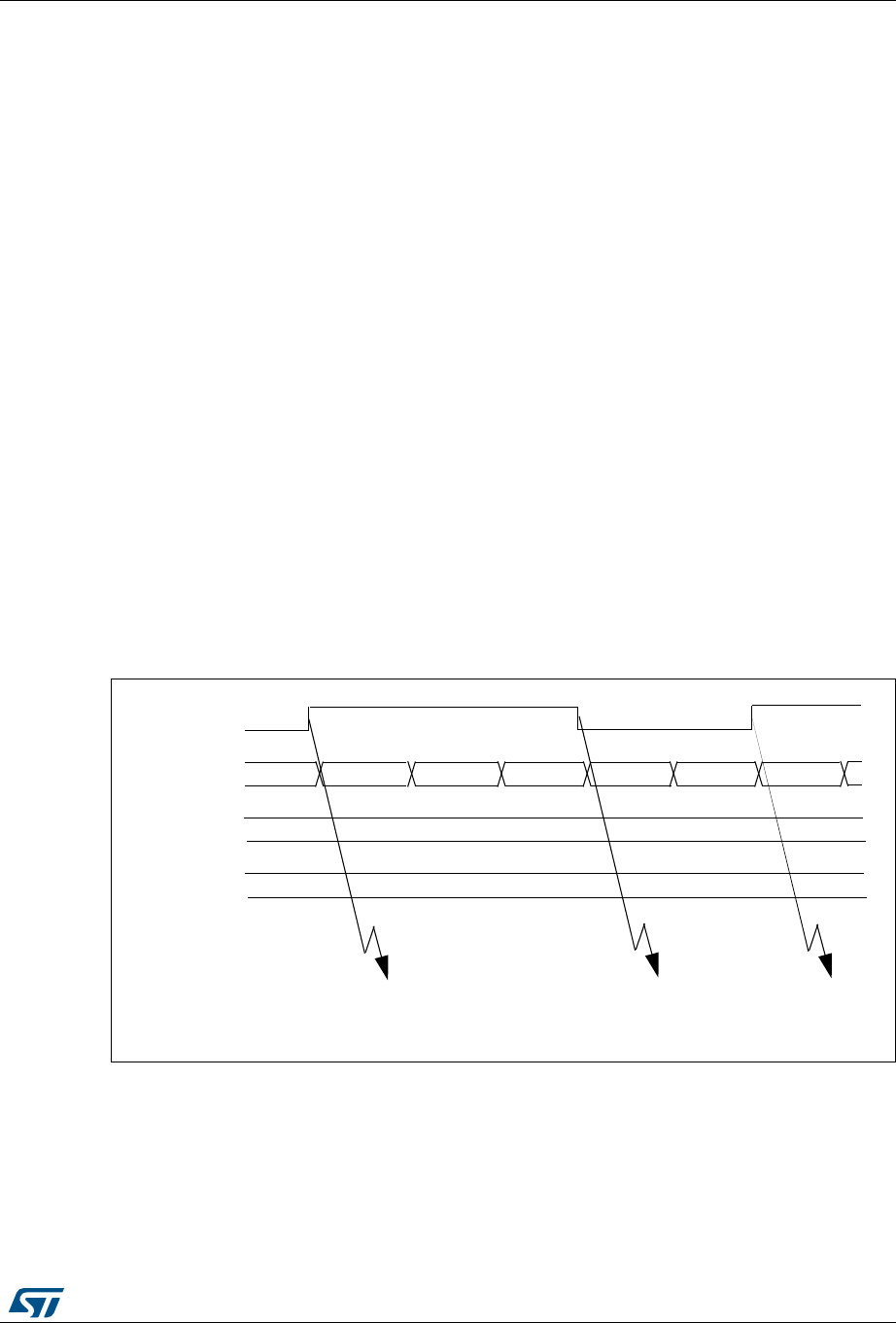
DocID026448 Rev 1 323/836
RM0383 General-purpose timers (TIM2 to TIM5)
365
13.3.6 PWM input mode
This mode is a particular case of input capture mode. The procedure is the same except:
•Two ICx signals are mapped on the same TIx input.
•These 2 ICx signals are active on edges with opposite polarity.
•One of the two TIxFP signals is selected as trigger input and the slave mode controller
is configured in reset mode.
For example, you can measure the period (in TIMx_CCR1 register) and the duty cycle (in
TIMx_CCR2 register) of the PWM applied on TI1 using the following procedure (depending
on CK_INT frequency and prescaler value):
•Select the active input for TIMx_CCR1: write the CC1S bits to 01 in the TIMx_CCMR1
register (TI1 selected).
•Select the active polarity for TI1FP1 (used both for capture in TIMx_CCR1 and counter
clear): write the CC1P to ‘0’ and the CC1NP bit to ‘0’ (active on rising edge).
•Select the active input for TIMx_CCR2: write the CC2S bits to 10 in the TIMx_CCMR1
register (TI1 selected).
•Select the active polarity for TI1FP2 (used for capture in TIMx_CCR2): write the CC2P
bit to ‘1’ and the CC2NP bit to ’0’(active on falling edge).
•Select the valid trigger input: write the TS bits to 101 in the TIMx_SMCR register
(TI1FP1 selected).
•Configure the slave mode controller in reset mode: write the SMS bits to 100 in the
TIMx_SMCR register.
•Enable the captures: write the CC1E and CC2E bits to ‘1 in the TIMx_CCER register.
Figure 115. PWM input mode timing
TI1
TIMx_CNT 0000 0001 0002 0003 0004 00000004
TIMx_CCR1
TIMx_CCR2
0004
0002
IC1 capture
IC2 capture
reset counter
IC2 capture
pulse width
IC1 capture
period
measurementmeasurement
ai15413

General-purpose timers (TIM2 to TIM5) RM0383
324/836 DocID026448 Rev 1
13.3.7 Forced output mode
In output mode (CCxS bits = 00 in the TIMx_CCMRx register), each output compare signal
(OCxREF and then OCx) can be forced to active or inactive level directly by software,
independently of any comparison between the output compare register and the counter.
To force an output compare signal (ocxref/OCx) to its active level, you just need to write 101
in the OCxM bits in the corresponding TIMx_CCMRx register. Thus ocxref is forced high
(OCxREF is always active high) and OCx get opposite value to CCxP polarity bit.
e.g.: CCxP=0 (OCx active high) => OCx is forced to high level.
ocxref signal can be forced low by writing the OCxM bits to 100 in the TIMx_CCMRx
register.
Anyway, the comparison between the TIMx_CCRx shadow register and the counter is still
performed and allows the flag to be set. Interrupt and DMA requests can be sent
accordingly. This is described in the Output Compare Mode section.
13.3.8 Output compare mode
This function is used to control an output waveform or indicating when a period of time has
elapsed.
When a match is found between the capture/compare register and the counter, the output
compare function:
•Assigns the corresponding output pin to a programmable value defined by the output
compare mode (OCxM bits in the TIMx_CCMRx register) and the output polarity (CCxP
bit in the TIMx_CCER register). The output pin can keep its level (OCXM=000), be set
active (OCxM=001), be set inactive (OCxM=010) or can toggle (OCxM=011) on match.
•Sets a flag in the interrupt status register (CCxIF bit in the TIMx_SR register).
•Generates an interrupt if the corresponding interrupt mask is set (CCXIE bit in the
TIMx_DIER register).
•Sends a DMA request if the corresponding enable bit is set (CCxDE bit in the
TIMx_DIER register, CCDS bit in the TIMx_CR2 register for the DMA request
selection).
The TIMx_CCRx registers can be programmed with or without preload registers using the
OCxPE bit in the TIMx_CCMRx register.
In output compare mode, the update event UEV has no effect on ocxref and OCx output.
The timing resolution is one count of the counter. Output compare mode can also be used to
output a single pulse (in One-pulse mode).
Procedure:
1. Select the counter clock (internal, external, prescaler).
2. Write the desired data in the TIMx_ARR and TIMx_CCRx registers.
3. Set the CCxIE and/or CCxDE bits if an interrupt and/or a DMA request is to be
generated.
4. Select the output mode. For example, you must write OCxM=011, OCxPE=0, CCxP=0
and CCxE=1 to toggle OCx output pin when CNT matches CCRx, CCRx preload is not
used, OCx is enabled and active high.
5. Enable the counter by setting the CEN bit in the TIMx_CR1 register.
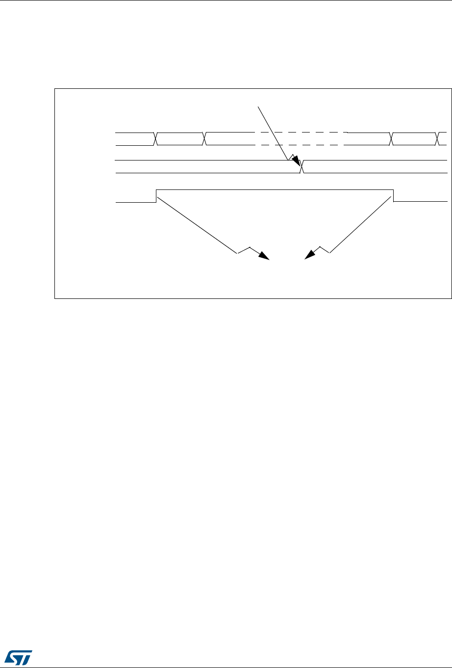
DocID026448 Rev 1 325/836
RM0383 General-purpose timers (TIM2 to TIM5)
365
The TIMx_CCRx register can be updated at any time by software to control the output
waveform, provided that the preload register is not enabled (OCxPE=0, else TIMx_CCRx
shadow register is updated only at the next update event UEV). An example is given in
Figure 116.
Figure 116. Output compare mode, toggle on OC1
13.3.9 PWM mode
Pulse width modulation mode allows you to generate a signal with a frequency determined
by the value of the TIMx_ARR register and a duty cycle determined by the value of the
TIMx_CCRx register.
The PWM mode can be selected independently on each channel (one PWM per OCx
output) by writing 110 (PWM mode 1) or ‘111 (PWM mode 2) in the OCxM bits in the
TIMx_CCMRx register. You must enable the corresponding preload register by setting the
OCxPE bit in the TIMx_CCMRx register, and eventually the auto-reload preload register by
setting the ARPE bit in the TIMx_CR1 register.
As the preload registers are transferred to the shadow registers only when an update event
occurs, before starting the counter, you have to initialize all the registers by setting the UG
bit in the TIMx_EGR register.
OCx polarity is software programmable using the CCxP bit in the TIMx_CCER register. It
can be programmed as active high or active low. OCx output is enabled by the CCxE bit in
the TIMx_CCER register. Refer to the TIMx_CCERx register description for more details.
In PWM mode (1 or 2), TIMx_CNT and TIMx_CCRx are always compared to determine
whether TIMx_CCRx≤TIMx_CNT or TIMx_CNT≤TIMx_CCRx (depending on the direction of
the counter). However, to comply with the ETRF (OCREF can be cleared by an external
event through the ETR signal until the next PWM period), the OCREF signal is asserted
only:
•When the result of the comparison changes, or
•When the output compare mode (OCxM bits in TIMx_CCMRx register) switches from
the “frozen” configuration (no comparison, OCxM=‘000) to one of the PWM modes
(OCxM=‘110 or ‘111).
OC1REF=OC1
TIMx_CNT B200 B201
0039
TIMx_CCR1 003A
Write B201h in the CC1R register
Match detected on CCR1
Interrupt generated if enabled
003B
B201
003A
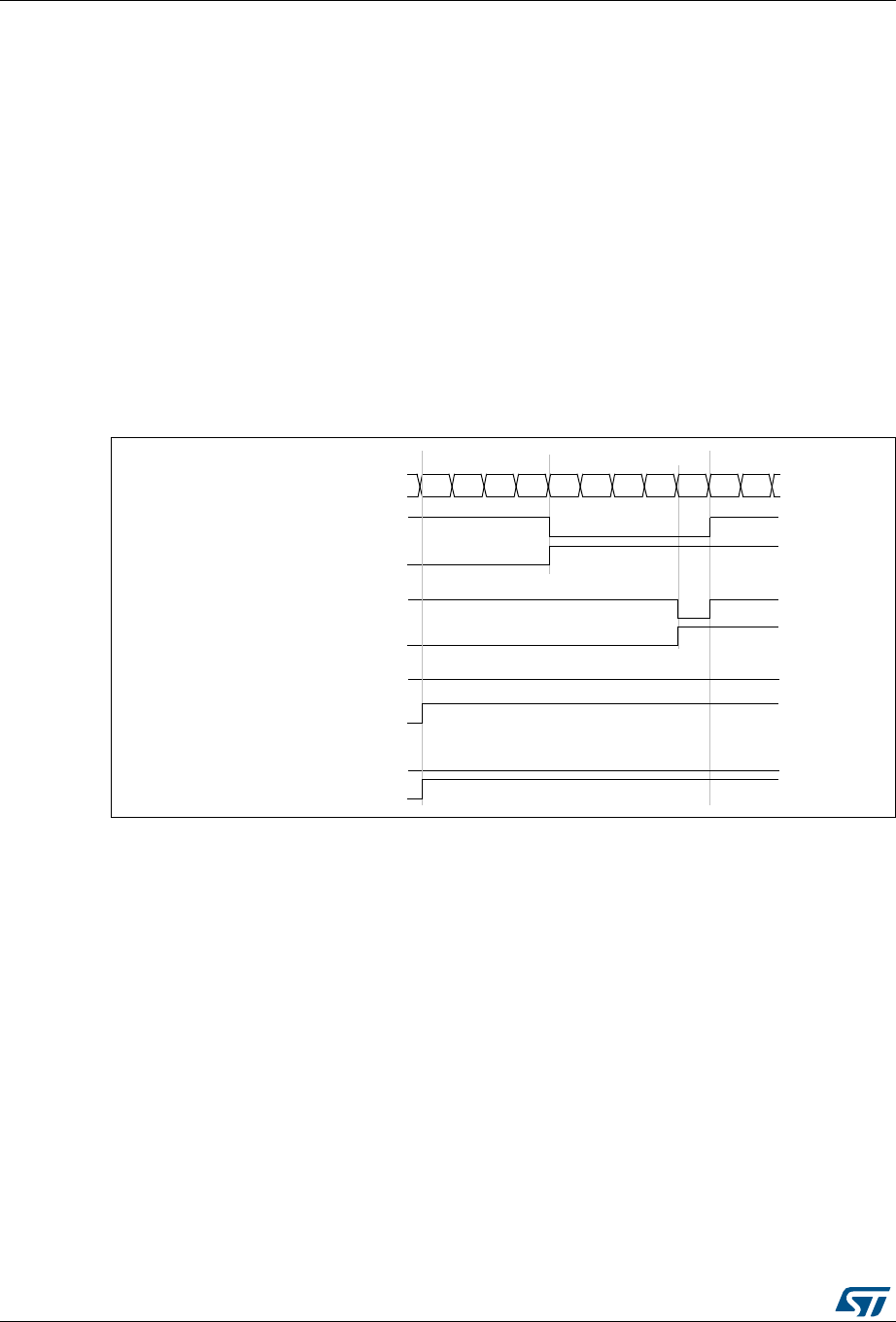
General-purpose timers (TIM2 to TIM5) RM0383
326/836 DocID026448 Rev 1
This forces the PWM by software while the timer is running.
The timer is able to generate PWM in edge-aligned mode or center-aligned mode
depending on the CMS bits in the TIMx_CR1 register.
PWM edge-aligned mode
Upcounting configuration
Upcounting is active when the DIR bit in the TIMx_CR1 register is low. Refer to Section :
Upcounting mode on page 309.
In the following example, we consider PWM mode 1. The reference PWM signal OCxREF is
high as long as TIMx_CNT <TIMx_CCRx else it becomes low. If the compare value in
TIMx_CCRx is greater than the auto-reload value (in TIMx_ARR) then OCxREF is held at ‘1.
If the compare value is 0 then OCxREF is held at ‘0. Figure 117 shows some edge-aligned
PWM waveforms in an example where TIMx_ARR=8.
Figure 117. Edge-aligned PWM waveforms (ARR=8)
Downcounting configuration
Downcounting is active when DIR bit in TIMx_CR1 register is high. Refer to Section :
Downcounting mode on page 312.
In PWM mode 1, the reference signal ocxref is low as long as TIMx_CNT>TIMx_CCRx else
it becomes high. If the compare value in TIMx_CCRx is greater than the auto-reload value in
TIMx_ARR, then ocxref is held at ‘1. 0% PWM is not possible in this mode.
PWM center-aligned mode
Center-aligned mode is active when the CMS bits in TIMx_CR1 register are different from
‘00 (all the remaining configurations having the same effect on the ocxref/OCx signals). The
compare flag is set when the counter counts up, when it counts down or both when it counts
up and down depending on the CMS bits configuration. The direction bit (DIR) in the
TIMx_CR1 register is updated by hardware and must not be changed by software. Refer to
Section : Center-aligned mode (up/down counting) on page 314.
Counter register
‘1
01234567801
‘0
OCxREF
CCxIF
OCxREF
CCxIF
OCxREF
CCxIF
OCxREF
CCxIF
CCRx=4
CCRx=8
CCRx>8
CCRx=0
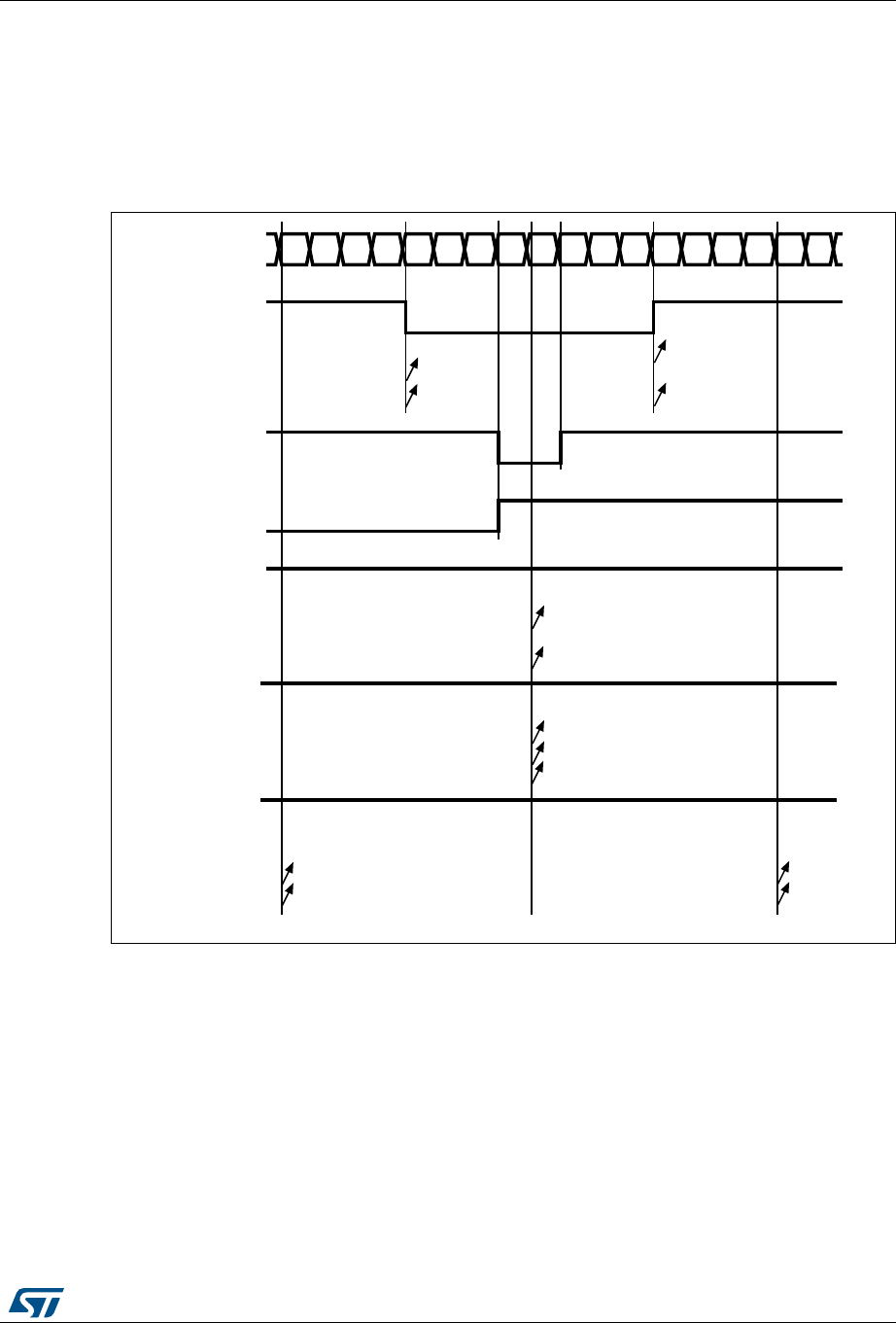
DocID026448 Rev 1 327/836
RM0383 General-purpose timers (TIM2 to TIM5)
365
Figure 118 shows some center-aligned PWM waveforms in an example where:
•TIMx_ARR=8,
•PWM mode is the PWM mode 1,
•The flag is set when the counter counts down corresponding to the center-aligned
mode 1 selected for CMS=01 in TIMx_CR1 register.
Figure 118. Center-aligned PWM waveforms (ARR=8)
Hints on using center-aligned mode:
•When starting in center-aligned mode, the current up-down configuration is used. It
means that the counter counts up or down depending on the value written in the DIR bit
##X)&
#OUNTERREGISTER
##2X
/#X2%&
#-3
#-3
#-3
##X)&
##2X
/#X2%&
#-3OR
##X)&
##2X
/#X2%&
#-3
#-3
#-3
gg
##X)&
##2X
/#X2%&
#-3
#-3
#-3
gg
##X)&
##2X
/#X2%&
#-3
#-3
#-3
gg
AIB
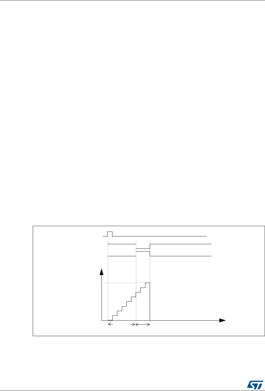
General-purpose timers (TIM2 to TIM5) RM0383
328/836 DocID026448 Rev 1
in the TIMx_CR1 register. Moreover, the DIR and CMS bits must not be changed at the
same time by the software.
•Writing to the counter while running in center-aligned mode is not recommended as it
can lead to unexpected results. In particular:
– The direction is not updated if you write a value in the counter that is greater than
the auto-reload value (TIMx_CNT>TIMx_ARR). For example, if the counter was
counting up, it continues to count up.
– The direction is updated if you write 0 or write the TIMx_ARR value in the counter
but no Update Event UEV is generated.
•The safest way to use center-aligned mode is to generate an update by software
(setting the UG bit in the TIMx_EGR register) just before starting the counter and not to
write the counter while it is running.
13.3.10 One-pulse mode
One-pulse mode (OPM) is a particular case of the previous modes. It allows the counter to
be started in response to a stimulus and to generate a pulse with a programmable length
after a programmable delay.
Starting the counter can be controlled through the slave mode controller. Generating the
waveform can be done in output compare mode or PWM mode. You select One-pulse mode
by setting the OPM bit in the TIMx_CR1 register. This makes the counter stop automatically
at the next update event UEV.
A pulse can be correctly generated only if the compare value is different from the counter
initial value. Before starting (when the timer is waiting for the trigger), the configuration must
be:
•In upcounting: CNT<CCRx≤ARR (in particular, 0<CCRx),
•In downcounting: CNT>CCRx.
Figure 119. Example of one-pulse mode
For example you may want to generate a positive pulse on OC1 with a length of tPULSE and
after a delay of tDELAY as soon as a positive edge is detected on the TI2 input pin.
TI2
OC1REF
Counter
t
0
TIM1_ARR
TIM1_CCR1
OC1
tDELAY tPULSE

DocID026448 Rev 1 329/836
RM0383 General-purpose timers (TIM2 to TIM5)
365
Let’s use TI2FP2 as trigger 1:
•Map TI2FP2 on TI2 by writing CC2S=01 in the TIMx_CCMR1 register.
•TI2FP2 must detect a rising edge, write CC2P=0 and CC2NP=’0’ in the TIMx_CCER
register.
•Configure TI2FP2 as trigger for the slave mode controller (TRGI) by writing TS=110 in
the TIMx_SMCR register.
•TI2FP2 is used to start the counter by writing SMS to ‘110 in the TIMx_SMCR register
(trigger mode).
The OPM waveform is defined by writing the compare registers (taking into account the
clock frequency and the counter prescaler).
•The tDELAY is defined by the value written in the TIMx_CCR1 register.
•The tPULSE is defined by the difference between the auto-reload value and the compare
value (TIMx_ARR - TIMx_CCR + 1).
•Let’s say you want to build a waveform with a transition from ‘0 to ‘1 when a compare
match occurs and a transition from ‘1 to ‘0 when the counter reaches the auto-reload
value. To do this you enable PWM mode 2 by writing OC1M=111 in the TIMx_CCMR1
register. You can optionally enable the preload registers by writing OC1PE=1 in the
TIMx_CCMR1 register and ARPE in the TIMx_CR1 register. In this case you have to
write the compare value in the TIMx_CCR1 register, the auto-reload value in the
TIMx_ARR register, generate an update by setting the UG bit and wait for external
trigger event on TI2. CC1P is written to ‘0 in this example.
In our example, the DIR and CMS bits in the TIMx_CR1 register should be low.
You only want 1 pulse (Single mode), so you write '1 in the OPM bit in the TIMx_CR1
register to stop the counter at the next update event (when the counter rolls over from the
auto-reload value back to 0). When OPM bit in the TIMx_CR1 register is set to '0', so the
Repetitive Mode is selected.
Particular case: OCx fast enable:
In One-pulse mode, the edge detection on TIx input set the CEN bit which enables the
counter. Then the comparison between the counter and the compare value makes the
output toggle. But several clock cycles are needed for these operations and it limits the
minimum delay tDELAY min we can get.
If you want to output a waveform with the minimum delay, you can set the OCxFE bit in the
TIMx_CCMRx register. Then OCxRef (and OCx) is forced in response to the stimulus,
without taking in account the comparison. Its new level is the same as if a compare match
had occurred. OCxFE acts only if the channel is configured in PWM1 or PWM2 mode.
13.3.11 Clearing the OCxREF signal on an external event
The OCxREF signal for a given channel can be driven Low by applying a High level to the
ETRF input (OCxCE enable bit of the corresponding TIMx_CCMRx register set to '1'). The
OCxREF signal remains Low until the next update event, UEV, occurs.
This function can only be used in output compare and PWM modes, and does not work in
forced mode.
For example, the ETR signal can be connected to the output of a comparator to be used for
current handling. In this case, ETR must be configured as follows:
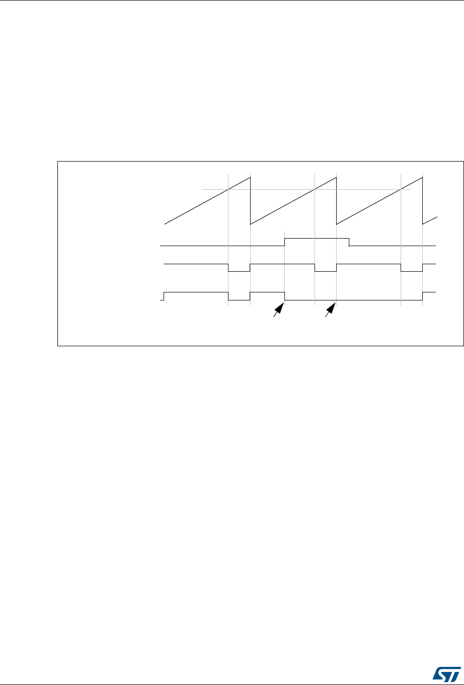
General-purpose timers (TIM2 to TIM5) RM0383
330/836 DocID026448 Rev 1
1. The external trigger prescaler should be kept off: bits ETPS[1:0] in the TIMx_SMCR
register are cleared to 00.
2. The external clock mode 2 must be disabled: bit ECE in the TIM1_SMCR register is
cleared to 0.
3. The external trigger polarity (ETP) and the external trigger filter (ETF) can be
configured according to the application’s needs.
Figure 120 shows the behavior of the OCxREF signal when the ETRF input becomes high,
for both values of the OCxCE enable bit. In this example, the timer TIMx is programmed in
PWM mode.
Figure 120. Clearing TIMx OCxREF
1. In case of a PWM with a 100% duty cycle (if CCRx>ARR), OCxREF is enabled again at the next counter
overflow.
13.3.12 Encoder interface mode
To select Encoder Interface mode write SMS=‘001 in the TIMx_SMCR register if the counter
is counting on TI2 edges only, SMS=010 if it is counting on TI1 edges only and SMS=011 if
it is counting on both TI1 and TI2 edges.
Select the TI1 and TI2 polarity by programming the CC1P and CC2P bits in the TIMx_CCER
register. When needed, you can program the input filter as well.
The two inputs TI1 and TI2 are used to interface to an incremental encoder. Refer to
Table 52. The counter is clocked by each valid transition on TI1FP1 or TI2FP2 (TI1 and TI2
after input filter and polarity selection, TI1FP1=TI1 if not filtered and not inverted,
TI2FP2=TI2 if not filtered and not inverted) assuming that it is enabled (CEN bit in
TIMx_CR1 register written to ‘1). The sequence of transitions of the two inputs is evaluated
and generates count pulses as well as the direction signal. Depending on the sequence the
counter counts up or down, the DIR bit in the TIMx_CR1 register is modified by hardware
accordingly. The DIR bit is calculated at each transition on any input (TI1 or TI2), whatever
the counter is counting on TI1 only, TI2 only or both TI1 and TI2.
Encoder interface mode acts simply as an external clock with direction selection. This
means that the counter just counts continuously between 0 and the auto-reload value in the
TIMx_ARR register (0 to ARR or ARR down to 0 depending on the direction). So you must
configure TIMx_ARR before starting. In the same way, the capture, compare, prescaler,
trigger output features continue to work as normal.
OCxREF
counter (CNT)
OCxREF
ETRF
(OCxCE=0)
(OCxCE=1)
ETRF
becomes high
ETRF
still high
(CCRx)

DocID026448 Rev 1 331/836
RM0383 General-purpose timers (TIM2 to TIM5)
365
In this mode, the counter is modified automatically following the speed and the direction of
the incremental encoder and its content, therefore, always represents the encoder’s
position. The count direction correspond to the rotation direction of the connected sensor.
The table summarizes the possible combinations, assuming TI1 and TI2 don’t switch at the
same time.
An external incremental encoder can be connected directly to the MCU without external
interface logic. However, comparators are normally be used to convert the encoder’s
differential outputs to digital signals. This greatly increases noise immunity. The third
encoder output which indicate the mechanical zero position, may be connected to an
external interrupt input and trigger a counter reset.
Figure 121 gives an example of counter operation, showing count signal generation and
direction control. It also shows how input jitter is compensated where both edges are
selected. This might occur if the sensor is positioned near to one of the switching points. For
this example we assume that the configuration is the following:
•CC1S= ‘01’ (TIMx_CCMR1 register, TI1FP1 mapped on TI1)
•CC2S= ‘01’ (TIMx_CCMR2 register, TI2FP2 mapped on TI2)
•CC1P= ‘0’, CC1NP = ‘0’, IC1F =’0000’ (TIMx_CCER register, TI1FP1 noninverted,
TI1FP1=TI1)
•CC2P= ‘0’, CC2NP = ‘0’, IC2F =’0000’ (TIMx_CCER register, TI2FP2 noninverted,
TI2FP2=TI2)
•SMS= ‘011’ (TIMx_SMCR register, both inputs are active on both rising and falling
edges)
•CEN = 1 (TIMx_CR1 register, Counter is enabled)
Table 52. Counting direction versus encoder signals
Active edge Level on opposite
signal (TI1FP1 for
TI2, TI2FP2 for TI1)
TI1FP1 signal TI2FP2 signal
Rising Falling Rising Falling
Counting on
TI1 only
High Down Up No Count No Count
Low Up Down No Count No Count
Counting on
TI2 only
High No Count No Count Up Down
Low No Count No Count Down Up
Counting on
TI1 and TI2
High Down Up Up Down
Low Up Down Down Up
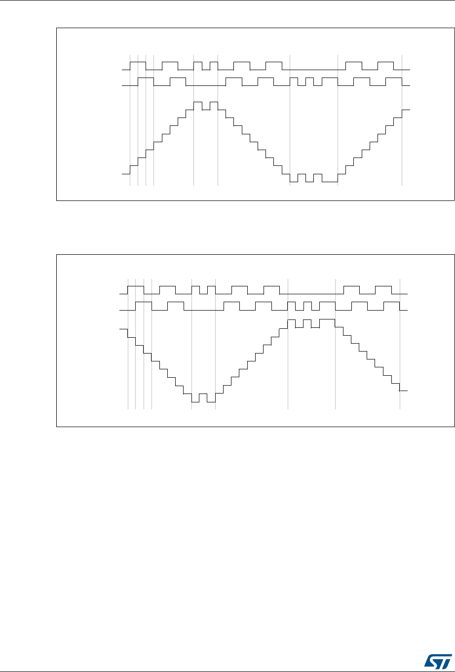
General-purpose timers (TIM2 to TIM5) RM0383
332/836 DocID026448 Rev 1
Figure 121. Example of counter operation in encoder interface mode
Figure 122 gives an example of counter behavior when TI1FP1 polarity is inverted (same
configuration as above except CC1P=1).
Figure 122. Example of encoder interface mode with TI1FP1 polarity inverted
The timer, when configured in Encoder Interface mode provides information on the sensor’s
current position. You can obtain dynamic information (speed, acceleration, deceleration) by
measuring the period between two encoder events using a second timer configured in
capture mode. The output of the encoder which indicates the mechanical zero can be used
for this purpose. Depending on the time between two events, the counter can also be read
at regular times. You can do this by latching the counter value into a third input capture
register if available (then the capture signal must be periodic and can be generated by
another timer). when available, it is also possible to read its value through a DMA request
generated by a Real-Time clock.
TI1
forward forwardbackwardjitter jitter
up down up
TI2
Counter
TI1
forward forwardbackwardjitter jitter
up
down
TI2
Counter
down
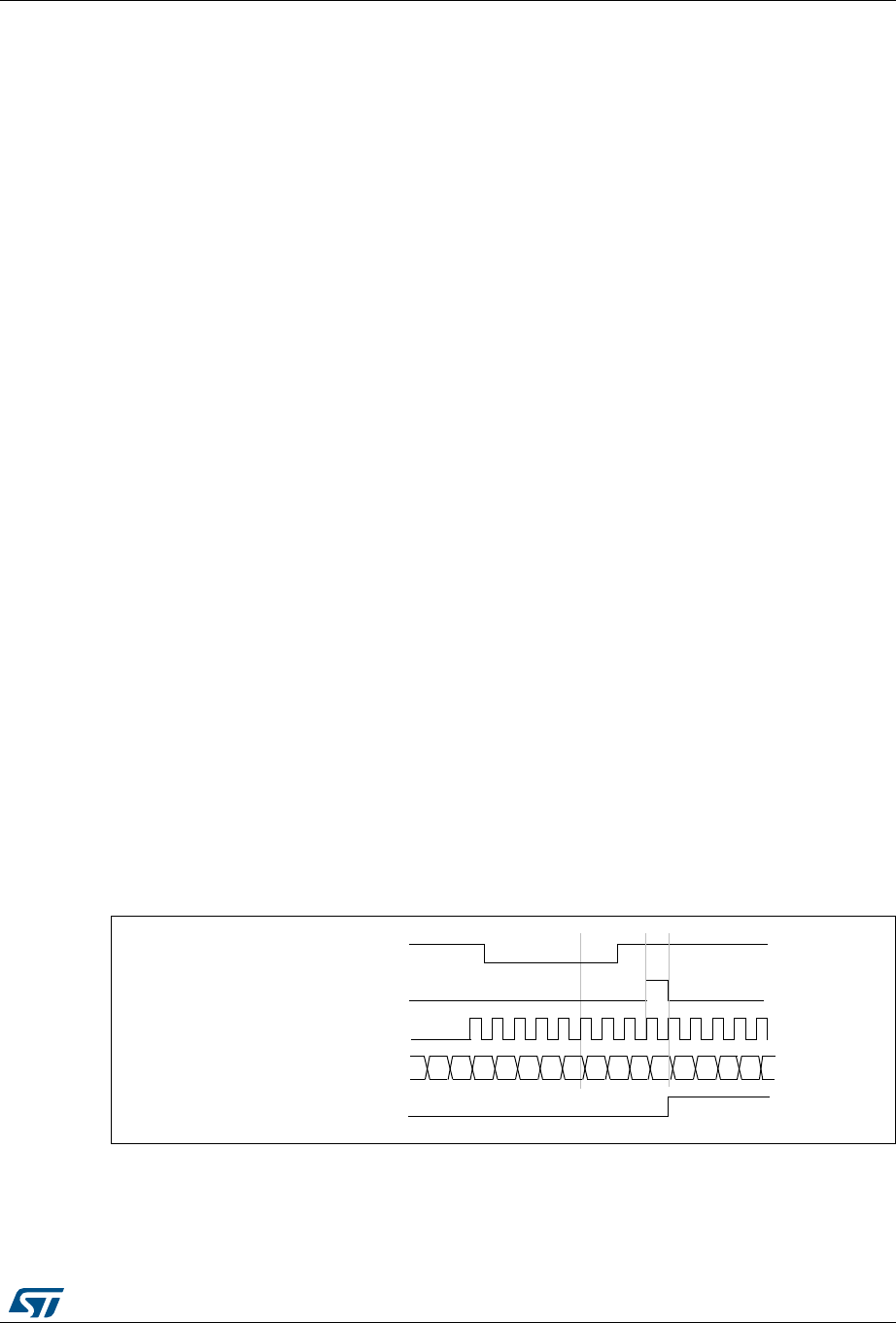
DocID026448 Rev 1 333/836
RM0383 General-purpose timers (TIM2 to TIM5)
365
13.3.13 Timer input XOR function
The TI1S bit in the TIM_CR2 register, allows the input filter of channel 1 to be connected to
the output of a XOR gate, combining the three input pins TIMx_CH1 to TIMx_CH3.
The XOR output can be used with all the timer input functions such as trigger or input
capture.
13.3.14 Timers and external trigger synchronization
The TIMx Timers can be synchronized with an external trigger in several modes: Reset
mode, Gated mode and Trigger mode.
Slave mode: Reset mode
The counter and its prescaler can be reinitialized in response to an event on a trigger input.
Moreover, if the URS bit from the TIMx_CR1 register is low, an update event UEV is
generated. Then all the preloaded registers (TIMx_ARR, TIMx_CCRx) are updated.
In the following example, the upcounter is cleared in response to a rising edge on TI1 input:
•Configure the channel 1 to detect rising edges on TI1. Configure the input filter duration
(in this example, we don’t need any filter, so we keep IC1F=0000). The capture
prescaler is not used for triggering, so you don’t need to configure it. The CC1S bits
select the input capture source only, CC1S = 01 in the TIMx_CCMR1 register. Write
CC1P=0 and CC1NP=0 in TIMx_CCER register to validate the polarity (and detect
rising edges only).
•Configure the timer in reset mode by writing SMS=100 in TIMx_SMCR register. Select
TI1 as the input source by writing TS=101 in TIMx_SMCR register.
•Start the counter by writing CEN=1 in the TIMx_CR1 register.
The counter starts counting on the internal clock, then behaves normally until TI1 rising
edge. When TI1 rises, the counter is cleared and restarts from 0. In the meantime, the
trigger flag is set (TIF bit in the TIMx_SR register) and an interrupt request, or a DMA
request can be sent if enabled (depending on the TIE and TDE bits in TIMx_DIER register).
The following figure shows this behavior when the auto-reload register TIMx_ARR=0x36.
The delay between the rising edge on TI1 and the actual reset of the counter is due to the
resynchronization circuit on TI1 input.
Figure 123. Control circuit in reset mode
Slave mode: Gated mode
The counter can be enabled depending on the level of a selected input.
00
Counter clock = CK_CNT = CK_PSC
Counter register 01 02 03 00 01 02 0332 33 34 35 36
UG
TI1
3130
TIF
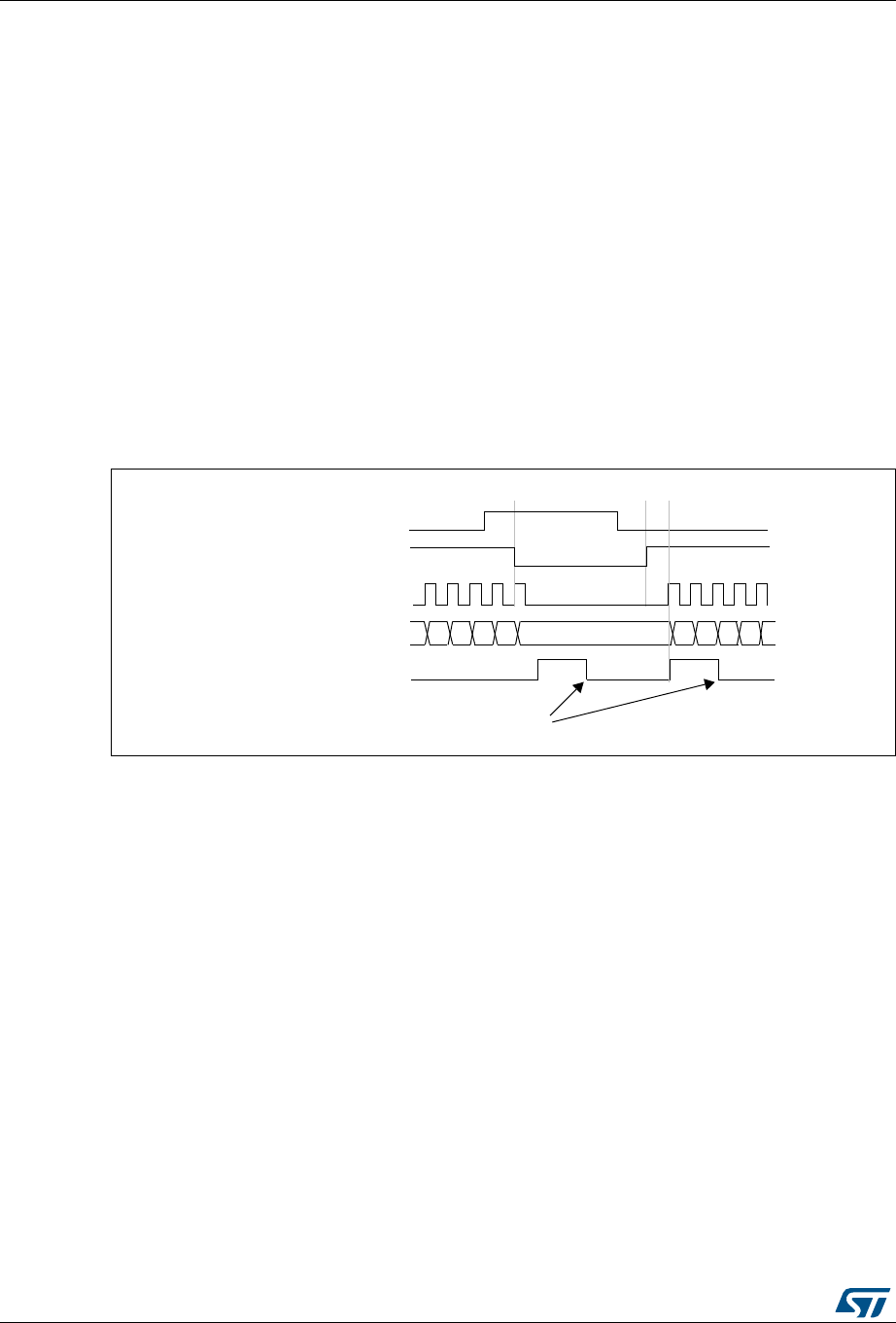
General-purpose timers (TIM2 to TIM5) RM0383
334/836 DocID026448 Rev 1
In the following example, the upcounter counts only when TI1 input is low:
•Configure the channel 1 to detect low levels on TI1. Configure the input filter duration
(in this example, we don’t need any filter, so we keep IC1F=0000). The capture
prescaler is not used for triggering, so you don’t need to configure it. The CC1S bits
select the input capture source only, CC1S=01 in TIMx_CCMR1 register. Write
CC1P=1 in TIMx_CCER register to validate the polarity (and detect low level only).
•Configure the timer in gated mode by writing SMS=101 in TIMx_SMCR register. Select
TI1 as the input source by writing TS=101 in TIMx_SMCR register.
•Enable the counter by writing CEN=1 in the TIMx_CR1 register (in gated mode, the
counter doesn’t start if CEN=0, whatever is the trigger input level).
The counter starts counting on the internal clock as long as TI1 is low and stops as soon as
TI1 becomes high. The TIF flag in the TIMx_SR register is set both when the counter starts
or stops.
The delay between the rising edge on TI1 and the actual stop of the counter is due to the
resynchronization circuit on TI1 input.
Figure 124. Control circuit in gated mode
1. The configuration “CCxP=CCxNP=1” (detection of both rising and falling edges) does not have any effect
in gated mode because gated mode acts on a level and not on an edge.
Slave mode: Trigger mode
The counter can start in response to an event on a selected input.
In the following example, the upcounter starts in response to a rising edge on TI2 input:
•Configure the channel 2 to detect rising edges on TI2. Configure the input filter duration
(in this example, we don’t need any filter, so we keep IC2F=0000). The capture
prescaler is not used for triggering, so you don’t need to configure it. CC2S bits are
selecting the input capture source only, CC2S=01 in TIMx_CCMR1 register. Write
CC2P=1 in TIMx_CCER register to validate the polarity (and detect low level only).
•Configure the timer in trigger mode by writing SMS=110 in TIMx_SMCR register. Select
TI2 as the input source by writing TS=110 in TIMx_SMCR register.
When a rising edge occurs on TI2, the counter starts counting on the internal clock and the
TIF flag is set.
The delay between the rising edge on TI2 and the actual start of the counter is due to the
resynchronization circuit on TI2 input.
Counter clock = CK_CNT = CK_PSC
Counter register 35 36 37 3832 33 34
TI1
3130
CNT_EN
TIF
Write TIF=0

DocID026448 Rev 1 335/836
RM0383 General-purpose timers (TIM2 to TIM5)
365
Figure 125. Control circuit in trigger mode
Slave mode: External Clock mode 2 + trigger mode
The external clock mode 2 can be used in addition to another slave mode (except external
clock mode 1 and encoder mode). In this case, the ETR signal is used as external clock
input, and another input can be selected as trigger input when operating in reset mode,
gated mode or trigger mode. It is recommended not to select ETR as TRGI through the TS
bits of TIMx_SMCR register.
In the following example, the upcounter is incremented at each rising edge of the ETR
signal as soon as a rising edge of TI1 occurs:
1. Configure the external trigger input circuit by programming the TIMx_SMCR register as
follows:
– ETF = 0000: no filter
– ETPS = 00: prescaler disabled
– ETP = 0: detection of rising edges on ETR and ECE=1 to enable the external clock
mode 2.
2. Configure the channel 1 as follows, to detect rising edges on TI:
– IC1F = 0000: no filter.
– The capture prescaler is not used for triggering and does not need to be
configured.
– CC1S = 01 in TIMx_CCMR1 register to select only the input capture source
– CC1P = 0 in TIMx_CCER register to validate the polarity (and detect rising edge
only).
3. Configure the timer in trigger mode by writing SMS=110 in TIMx_SMCR register. Select
TI1 as the input source by writing TS=101 in TIMx_SMCR register.
A rising edge on TI1 enables the counter and sets the TIF flag. The counter then counts on
ETR rising edges.
The delay between the rising edge of the ETR signal and the actual reset of the counter is
due to the resynchronization circuit on ETRP input.
Counter clock = CK_CNT = CK_PSC
Counter register 35 36 37 3834
TI2
CNT_EN
TIF
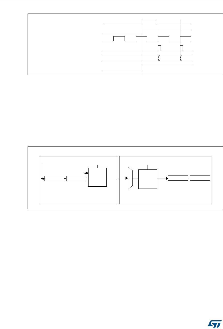
General-purpose timers (TIM2 to TIM5) RM0383
336/836 DocID026448 Rev 1
Figure 126. Control circuit in external clock mode 2 + trigger mode
13.3.15 Timer synchronization
The TIMx timers are linked together internally for timer synchronization or chaining. When
one Timer is configured in Master Mode, it can reset, start, stop or clock the counter of
another Timer configured in Slave Mode.
Figure 127: Master/Slave timer example presents an overview of the trigger selection and
the master mode selection blocks.
Using one timer as prescaler for another
Figure 127. Master/Slave timer example
For example, you can configure Timer 1 to act as a prescaler for Timer 2. Refer to
Figure 127. To do this:
•Configure Timer 1 in master mode so that it outputs a periodic trigger signal on each
update event UEV. If you write MMS=010 in the TIM1_CR2 register, a rising edge is
output on TRGO1 each time an update event is generated.
•To connect the TRGO1 output of Timer 1 to Timer 2, Timer 2 must be configured in
slave mode using ITR0 as internal trigger. You select this through the TS bits in the
TIM2_SMCR register (writing TS=000).
•Then you put the slave mode controller in external clock mode 1 (write SMS=111 in the
TIM2_SMCR register). This causes Timer 2 to be clocked by the rising edge of the
periodic Timer 1 trigger signal (which correspond to the timer 1 counter overflow).
•Finally both timers must be enabled by setting their respective CEN bits (TIMx_CR1
register).
Note: If OCx is selected on Timer 1 as trigger output (MMS=1xx), its rising edge is used to clock
the counter of timer 2.
Counter clock = CK_CNT = CK_PSC
Counter register 35 3634
ETR
CEN/CNT_EN
TIF
TI1
TRGO1
UEV ITR0
Prescaler Counter
SMSTSMMS
TIM1 TIM2
Master
mode
control
Slave
mode
control
CK_PSC
Prescaler Counter
Clock
Input
selection
trigger
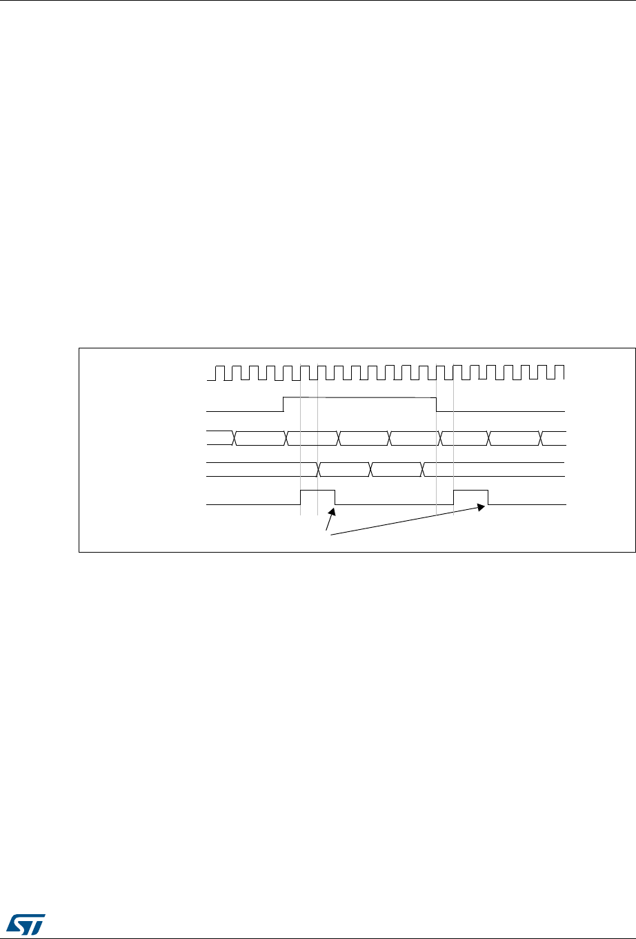
DocID026448 Rev 1 337/836
RM0383 General-purpose timers (TIM2 to TIM5)
365
Using one timer to enable another timer
In this example, we control the enable of Timer 2 with the output compare 1 of Timer 1.
Refer to Figure 127 for connections. Timer 2 counts on the divided internal clock only when
OC1REF of Timer 1 is high. Both counter clock frequencies are divided by 3 by the
prescaler compared to CK_INT (fCK_CNT = fCK_INT/3).
•Configure Timer 1 master mode to send its Output Compare 1 Reference (OC1REF)
signal as trigger output (MMS=100 in the TIM1_CR2 register).
•Configure the Timer 1 OC1REF waveform (TIM1_CCMR1 register).
•Configure Timer 2 to get the input trigger from Timer 1 (TS=000 in the TIM2_SMCR
register).
•Configure Timer 2 in gated mode (SMS=101 in TIM2_SMCR register).
•Enable Timer 2 by writing ‘1 in the CEN bit (TIM2_CR1 register).
•Start Timer 1 by writing ‘1 in the CEN bit (TIM1_CR1 register).
Note: The counter 2 clock is not synchronized with counter 1, this mode only affects the Timer 2
counter enable signal.
Figure 128. Gating timer 2 with OC1REF of timer 1
In the example in Figure 162, the Timer 2 counter and prescaler are not initialized before
being started. So they start counting from their current value. It is possible to start from a
given value by resetting both timers before starting Timer 1. You can then write any value
you want in the timer counters. The timers can easily be reset by software using the UG bit
in the TIMx_EGR registers.
In the next example, we synchronize Timer 1 and Timer 2. Timer 1 is the master and starts
from 0. Timer 2 is the slave and starts from 0xE7. The prescaler ratio is the same for both
TIMER 2-TIF
Write TIF=0
FC FD FE FF 00
3045 3047 3048
CK_INT
TIMER1-OC1REF
TIMER1-CNT
TIMER2-CNT
01
3046
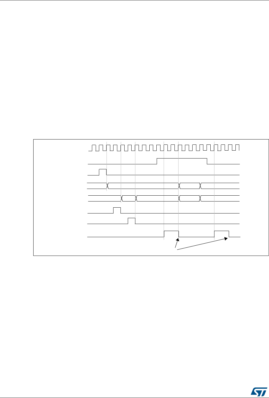
General-purpose timers (TIM2 to TIM5) RM0383
338/836 DocID026448 Rev 1
timers. Timer 2 stops when Timer 1 is disabled by writing ‘0 to the CEN bit in the TIM1_CR1
register:
•Configure Timer 1 master mode to send its Output Compare 1 Reference (OC1REF)
signal as trigger output (MMS=100 in the TIM1_CR2 register).
•Configure the Timer 1 OC1REF waveform (TIM1_CCMR1 register).
•Configure Timer 2 to get the input trigger from Timer 1 (TS=000 in the TIM2_SMCR
register).
•Configure Timer 2 in gated mode (SMS=101 in TIM2_SMCR register).
•Reset Timer 1 by writing ‘1 in UG bit (TIM1_EGR register).
•Reset Timer 2 by writing ‘1 in UG bit (TIM2_EGR register).
•Initialize Timer 2 to 0xE7 by writing ‘0xE7’ in the timer 2 counter (TIM2_CNTL).
•Enable Timer 2 by writing ‘1 in the CEN bit (TIM2_CR1 register).
•Start Timer 1 by writing ‘1 in the CEN bit (TIM1_CR1 register).
•Stop Timer 1 by writing ‘0 in the CEN bit (TIM1_CR1 register).
Figure 129. Gating timer 2 with Enable of timer 1
Using one timer to start another timer
In this example, we set the enable of Timer 2 with the update event of Timer 1. Refer to
Figure 127 for connections. Timer 2 starts counting from its current value (which can be
nonzero) on the divided internal clock as soon as the update event is generated by Timer 1.
When Timer 2 receives the trigger signal its CEN bit is automatically set and the counter
counts until we write ‘0 to the CEN bit in the TIM2_CR1 register. Both counter clock
frequencies are divided by 3 by the prescaler compared to CK_INT (fCK_CNT = fCK_INT/3).
•Configure Timer 1 master mode to send its Update Event (UEV) as trigger output
(MMS=010 in the TIM1_CR2 register).
•Configure the Timer 1 period (TIM1_ARR registers).
•Configure Timer 2 to get the input trigger from Timer 1 (TS=000 in the TIM2_SMCR
register).
•Configure Timer 2 in trigger mode (SMS=110 in TIM2_SMCR register).
•Start Timer 1 by writing ‘1 in the CEN bit (TIM1_CR1 register).
TIMER 2-TIF
Write TIF=0
75 00 01
CK_INT
TIMER1-CEN=CNT_EN
TIMER1-CNT
TIMER2-CNT
02
TIMER1-CNT_INIT
AB 00 E7 E8 E9
TIMER2-CNT_INIT
TIMER2
write CNT
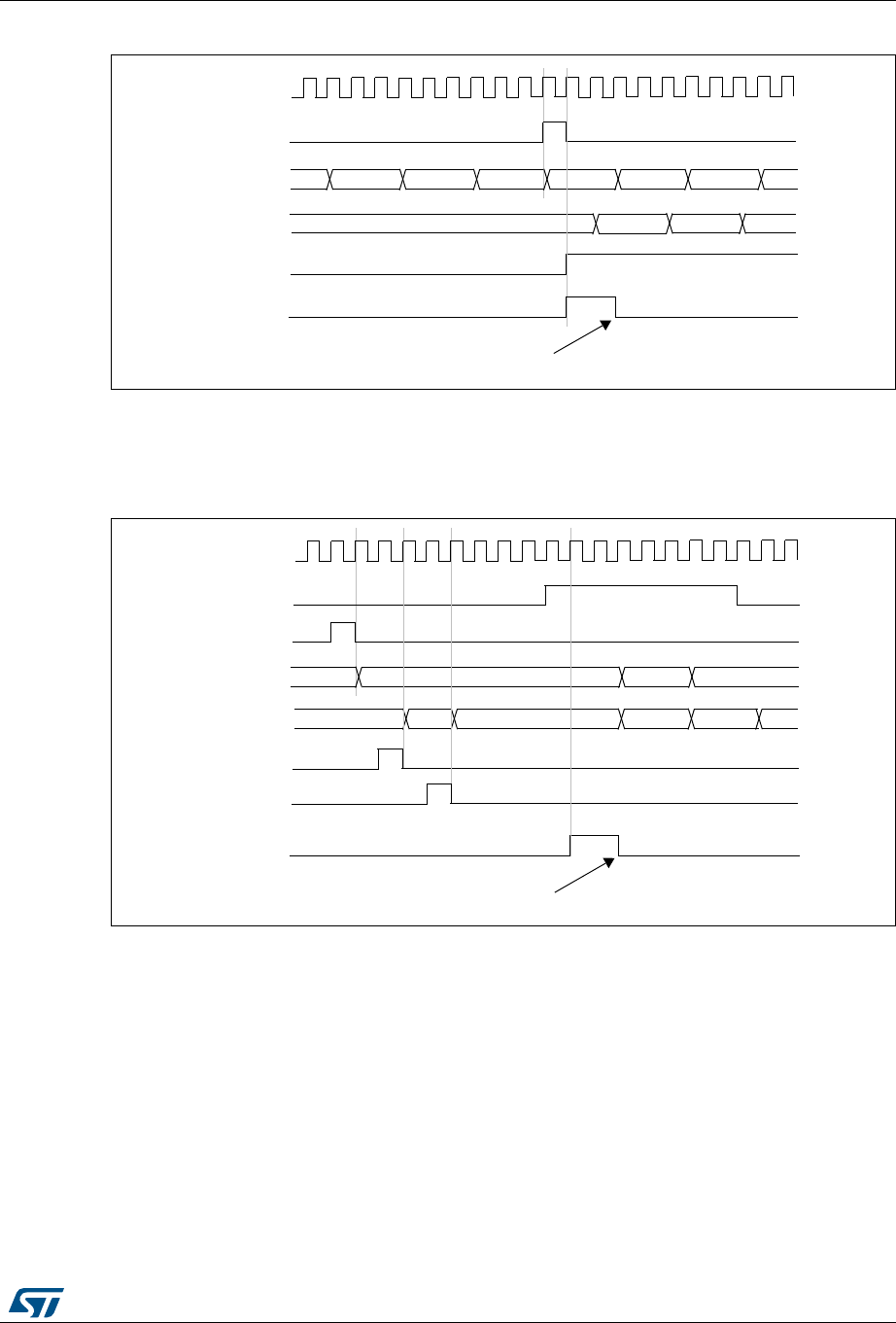
DocID026448 Rev 1 339/836
RM0383 General-purpose timers (TIM2 to TIM5)
365
Figure 130. Triggering timer 2 with update of timer 1
As in the previous example, you can initialize both counters before starting counting.
Figure 131 shows the behavior with the same configuration as in Figure 162 but in trigger
mode instead of gated mode (SMS=110 in the TIM2_SMCR register).
Figure 131. Triggering timer 2 with Enable of timer 1
TIMER 2-TIF
Write TIF=0
FD FE FF 00 01
45 47 48
CK_INT
TIMER1-UEV
TIMER1-CNT
TIMER2-CNT
02
46
TIMER2-CEN=CNT_EN
TIMER 2-TIF
Write TIF=0
75 00 01
CK_INT
TIMER1-CEN=CNT_EN
TIMER1-CNT
TIMER2-CNT
02
TIMER1-CNT_INIT
CD 00 E7 E8 EA
TIMER2-CNT_INIT
TIMER2
write CNT
E9

General-purpose timers (TIM2 to TIM5) RM0383
340/836 DocID026448 Rev 1
Using one timer as prescaler for another timer
For example, you can configure Timer 1 to act as a prescaler for Timer 2. Refer to
Figure 127 for connections. To do this:
•Configure Timer 1 master mode to send its Update Event (UEV) as trigger output
(MMS=010 in the TIM1_CR2 register). then it outputs a periodic signal on each counter
overflow.
•Configure the Timer 1 period (TIM1_ARR registers).
•Configure Timer 2 to get the input trigger from Timer 1 (TS=000 in the TIM2_SMCR
register).
•Configure Timer 2 in external clock mode 1 (SMS=111 in TIM2_SMCR register).
•Start Timer 2 by writing ‘1 in the CEN bit (TIM2_CR1 register).
•Start Timer 1 by writing ‘1 in the CEN bit (TIM1_CR1 register).
Starting 2 timers synchronously in response to an external trigger
In this example, we set the enable of timer 1 when its TI1 input rises, and the enable of
Timer 2 with the enable of Timer 1. Refer to Figure 127 for connections. To ensure the
counters are aligned, Timer 1 must be configured in Master/Slave mode (slave with respect
to TI1, master with respect to Timer 2):
•Configure Timer 1 master mode to send its Enable as trigger output (MMS=001 in the
TIM1_CR2 register).
•Configure Timer 1 slave mode to get the input trigger from TI1 (TS=100 in the
TIM1_SMCR register).
•Configure Timer 1 in trigger mode (SMS=110 in the TIM1_SMCR register).
•Configure the Timer 1 in Master/Slave mode by writing MSM=1 (TIM1_SMCR register).
•Configure Timer 2 to get the input trigger from Timer 1 (TS=000 in the TIM2_SMCR
register).
•Configure Timer 2 in trigger mode (SMS=110 in the TIM2_SMCR register).
When a rising edge occurs on TI1 (Timer 1), both counters starts counting synchronously on
the internal clock and both TIF flags are set.
Note: In this example both timers are initialized before starting (by setting their respective UG
bits). Both counters starts from 0, but you can easily insert an offset between them by
writing any of the counter registers (TIMx_CNT). You can see that the master/slave mode
insert a delay between CNT_EN and CK_PSC on timer 1.
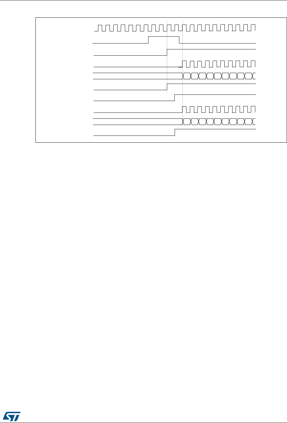
DocID026448 Rev 1 341/836
RM0383 General-purpose timers (TIM2 to TIM5)
365
Figure 132. Triggering timer 1 and 2 with timer 1 TI1 input
13.3.16 Debug mode
When the microcontroller enters debug mode (Cortex®-M4 with FPU core - halted), the
TIMx counter either continues to work normally or stops, depending on DBG_TIMx_STOP
configuration bit in DBGMCU module. For more details, refer to Section 23.16.2: Debug
support for timers, watchdog and I2C.
00 01
CK_INT
TIMER1-CEN=CNT_EN
TIMER1-CNT
TIMER 1-TI1
TIMER 1-CK_PSC
02 03 04 05 06 07 08 09
TIMER1-TIF
00 01
TIMER2-CEN=CNT_EN
TIMER2-CNT
TIMER 2-CK_PSC
02 03 04 05 06 07 08 09
TIMER2-TIF

General-purpose timers (TIM2 to TIM5) RM0383
342/836 DocID026448 Rev 1
13.4 TIM2 to TIM5 registers
Refer to Section 1.1 on page 33 for a list of abbreviations used in register descriptions.
The 32-bit peripheral registers have to be written by words (32 bits). All other peripheral
registers have to be written by half-words (16 bits) or words (32 bits). Read accesses can be
done by bytes (8 bits), half-words (16 bits) or words (32 bits).
13.4.1 TIMx control register 1 (TIMx_CR1)
Address offset: 0x00
Reset value: 0x0000
1514131211109876543210
Reserved CKD[1:0] ARPE CMS DIR OPM URS UDIS CEN
rw rw rw rw rw rw rw rw rw rw
Bits 15:10 Reserved, must be kept at reset value.
Bits 9:8 CKD: Clock division
This bit-field indicates the division ratio between the timer clock (CK_INT) frequency and
sampling clock used by the digital filters (ETR, TIx),
00: tDTS = tCK_INT
01: tDTS = 2 × tCK_INT
10: tDTS = 4 × tCK_INT
11: Reserved
Bit 7 ARPE: Auto-reload preload enable
0: TIMx_ARR register is not buffered
1: TIMx_ARR register is buffered
Bits 6:5 CMS: Center-aligned mode selection
00: Edge-aligned mode. The counter counts up or down depending on the direction bit
(DIR).
01: Center-aligned mode 1. The counter counts up and down alternatively. Output compare
interrupt flags of channels configured in output (CCxS=00 in TIMx_CCMRx register) are set
only when the counter is counting down.
10: Center-aligned mode 2. The counter counts up and down alternatively. Output compare
interrupt flags of channels configured in output (CCxS=00 in TIMx_CCMRx register) are set
only when the counter is counting up.
11: Center-aligned mode 3. The counter counts up and down alternatively. Output compare
interrupt flags of channels configured in output (CCxS=00 in TIMx_CCMRx register) are set
both when the counter is counting up or down.
Note: It is not allowed to switch from edge-aligned mode to center-aligned mode as long as
the counter is enabled (CEN=1)
Bit 4 DIR: Direction
0: Counter used as upcounter
1: Counter used as downcounter
Note: This bit is read only when the timer is configured in Center-aligned mode or Encoder
mode.
Bit 3 OPM: One-pulse mode
0: Counter is not stopped at update event
1: Counter stops counting at the next update event (clearing the bit CEN)

DocID026448 Rev 1 343/836
RM0383 General-purpose timers (TIM2 to TIM5)
365
Bit 2 URS: Update request source
This bit is set and cleared by software to select the UEV event sources.
0: Any of the following events generate an update interrupt or DMA request if enabled.
These events can be:
– Counter overflow/underflow
– Setting the UG bit
– Update generation through the slave mode controller
1: Only counter overflow/underflow generates an update interrupt or DMA request if
enabled.
Bit 1 UDIS: Update disable
This bit is set and cleared by software to enable/disable UEV event generation.
0: UEV enabled. The Update (UEV) event is generated by one of the following events:
– Counter overflow/underflow
– Setting the UG bit
– Update generation through the slave mode controller
Buffered registers are then loaded with their preload values.
1: UEV disabled. The Update event is not generated, shadow registers keep their value
(ARR, PSC, CCRx). However the counter and the prescaler are reinitialized if the UG bit is
set or if a hardware reset is received from the slave mode controller.
Bit 0 CEN: Counter enable
0: Counter disabled
1: Counter enabled
Note: External clock, gated mode and encoder mode can work only if the CEN bit has been
previously set by software. However trigger mode can set the CEN bit automatically by
hardware.
CEN is cleared automatically in one-pulse mode, when an update event occurs.

General-purpose timers (TIM2 to TIM5) RM0383
344/836 DocID026448 Rev 1
13.4.2 TIMx control register 2 (TIMx_CR2)
Address offset: 0x04
Reset value: 0x0000
1514131211109876543210
Reserved TI1S MMS[2:0] CCDS Reserved
rw rw rw rw rw
Bits 15:8 Reserved, must be kept at reset value.
Bit 7 TI1S: TI1 selection
0: The TIMx_CH1 pin is connected to TI1 input
1: The TIMx_CH1, CH2 and CH3 pins are connected to the TI1 input (XOR combination)
Bits 6:4 MMS[2:0]: Master mode selection
These bits allow to select the information to be sent in master mode to slave timers for
synchronization (TRGO). The combination is as follows:
000: Reset - the UG bit from the TIMx_EGR register is used as trigger output (TRGO). If the
reset is generated by the trigger input (slave mode controller configured in reset mode) then
the signal on TRGO is delayed compared to the actual reset.
001: Enable - the Counter enable signal, CNT_EN, is used as trigger output (TRGO). It is
useful to start several timers at the same time or to control a window in which a slave timer is
enabled. The Counter Enable signal is generated by a logic OR between CEN control bit
and the trigger input when configured in gated mode.
When the Counter Enable signal is controlled by the trigger input, there is a delay on TRGO,
except if the master/slave mode is selected (see the MSM bit description in TIMx_SMCR
register).
010: Update - The update event is selected as trigger output (TRGO). For instance a master
timer can then be used as a prescaler for a slave timer.
011: Compare Pulse - The trigger output send a positive pulse when the CC1IF flag is to be
set (even if it was already high), as soon as a capture or a compare match occurred.
(TRGO)
100: Compare - OC1REF signal is used as trigger output (TRGO)
101: Compare - OC2REF signal is used as trigger output (TRGO)
110: Compare - OC3REF signal is used as trigger output (TRGO)
111: Compare - OC4REF signal is used as trigger output (TRGO)
Bit 3 CCDS: Capture/compare DMA selection
0: CCx DMA request sent when CCx event occurs
1: CCx DMA requests sent when update event occurs
Bits 2:0 Reserved, must be kept at reset value.

DocID026448 Rev 1 345/836
RM0383 General-purpose timers (TIM2 to TIM5)
365
13.4.3 TIMx slave mode control register (TIMx_SMCR)
Address offset: 0x08
Reset value: 0x0000
1514131211109876543210
ETP ECE ETPS[1:0] ETF[3:0] MSM TS[2:0] Res. SMS[2:0]
rw rw rw rw rw rw rw rw rw rw rw rw rw rw rw
Bit 15 ETP: External trigger polarity
This bit selects whether ETR or ETR is used for trigger operations
0: ETR is noninverted, active at high level or rising edge
1: ETR is inverted, active at low level or falling edge
Bit 14 ECE: External clock enable
This bit enables External clock mode 2.
0: External clock mode 2 disabled
1: External clock mode 2 enabled. The counter is clocked by any active edge on the ETRF
signal.
1: Setting the ECE bit has the same effect as selecting external clock mode 1 with TRGI
connected to ETRF (SMS=111 and TS=111).
2: It is possible to simultaneously use external clock mode 2 with the following slave modes:
reset mode, gated mode and trigger mode. Nevertheless, TRGI must not be connected to
ETRF in this case (TS bits must not be 111).
3: If external clock mode 1 and external clock mode 2 are enabled at the same time, the
external clock input is ETRF.
Bits 13:12 ETPS: External trigger prescaler
External trigger signal ETRP frequency must be at most 1/4 of CK_INT frequency. A
prescaler can be enabled to reduce ETRP frequency. It is useful when inputting fast external
clocks.
00: Prescaler OFF
01: ETRP frequency divided by 2
10: ETRP frequency divided by 4
11: ETRP frequency divided by 8
Bits 11:8 ETF[3:0]: External trigger filter
This bit-field then defines the frequency used to sample ETRP signal and the length of the
digital filter applied to ETRP. The digital filter is made of an event counter in which N events
are needed to validate a transition on the output:
0000: No filter, sampling is done at fDTS
0001: fSAMPLING=fCK_INT
, N=2
0010: fSAMPLING=fCK_INT
, N=4
0011: fSAMPLING=fCK_INT
, N=8
0100: fSAMPLING=fDTS/2, N=6
0101: fSAMPLING=fDTS/2, N=8
0110: fSAMPLING=fDTS/4, N=6
0111: fSAMPLING=fDTS/4, N=8
1000: fSAMPLING=fDTS/8, N=6
1001: fSAMPLING=fDTS/8, N=8
1010: fSAMPLING=fDTS/16, N=5
1011: fSAMPLING=fDTS/16, N=6
1100: fSAMPLING=fDTS/16, N=8
1101: fSAMPLING=fDTS/32, N=5
1110: fSAMPLING=fDTS/32, N=6
1111: fSAMPLING=fDTS/32, N=8

General-purpose timers (TIM2 to TIM5) RM0383
346/836 DocID026448 Rev 1
Bit 7 MSM: Master/Slave mode
0: No action
1: The effect of an event on the trigger input (TRGI) is delayed to allow a perfect
synchronization between the current timer and its slaves (through TRGO). It is useful if we
want to synchronize several timers on a single external event.
Bits 6:4 TS: Trigger selection
This bit-field selects the trigger input to be used to synchronize the counter.
000: Internal Trigger 0 (ITR0).
001: Internal Trigger 1 (ITR1).
010: Internal Trigger 2 (ITR2).
011: Internal Trigger 3 (ITR3).
100: TI1 Edge Detector (TI1F_ED)
101: Filtered Timer Input 1 (TI1FP1)
110: Filtered Timer Input 2 (TI2FP2)
111: External Trigger input (ETRF)
See Table 53: TIMx internal trigger connection on page 347 for more details on ITRx
meaning for each Timer.
Note: These bits must be changed only when they are not used (e.g. when SMS=000) to
avoid wrong edge detections at the transition.
Bit 3 Reserved, must be kept at reset value.
Bits 2:0 SMS: Slave mode selection
When external signals are selected the active edge of the trigger signal (TRGI) is linked to
the polarity selected on the external input (see Input Control register and Control Register
description.
000: Slave mode disabled - if CEN = ‘1 then the prescaler is clocked directly by the internal
clock.
001: Encoder mode 1 - Counter counts up/down on TI2FP2 edge depending on TI1FP1
level.
010: Encoder mode 2 - Counter counts up/down on TI1FP1 edge depending on TI2FP2
level.
011: Encoder mode 3 - Counter counts up/down on both TI1FP1 and TI2FP2 edges
depending on the level of the other input.
100: Reset Mode - Rising edge of the selected trigger input (TRGI) reinitializes the counter
and generates an update of the registers.
101: Gated Mode - The counter clock is enabled when the trigger input (TRGI) is high. The
counter stops (but is not reset) as soon as the trigger becomes low. Both start and stop of
the counter are controlled.
110: Trigger Mode - The counter starts at a rising edge of the trigger TRGI (but it is not
reset). Only the start of the counter is controlled.
111: External Clock Mode 1 - Rising edges of the selected trigger (TRGI) clock the counter.
Note: The gated mode must not be used if TI1F_ED is selected as the trigger input (TS=100).
Indeed, TI1F_ED outputs 1 pulse for each transition on TI1F, whereas the gated mode
checks the level of the trigger signal.

DocID026448 Rev 1 347/836
RM0383 General-purpose timers (TIM2 to TIM5)
365
Table 53. TIMx internal trigger connection
Slave TIM ITR0 (TS = 000) ITR1 (TS = 001) ITR2 (TS = 010) ITR3 (TS = 011)
TIM2 TIM1 Reserved TIM3 TIM4
TIM3 TIM1 TIM2 TIM5 TIM4
TIM4 TIM1 TIM2 TIM3 Reserved
TIM5 TIM2 TIM3 TIM4 Reserved

General-purpose timers (TIM2 to TIM5) RM0383
348/836 DocID026448 Rev 1
13.4.4 TIMx DMA/Interrupt enable register (TIMx_DIER)
Address offset: 0x0C
Reset value: 0x0000
1514131211109876543210
Res. TDE Res CC4DE CC3DE CC2DE CC1DE UDE Res. TIE Res CC4IE CC3IE CC2IE CC1IE UIE
rw rw rw rw rw rw rw rw rw rw rw rw
Bit 15 Reserved, must be kept at reset value.
Bit 14 TDE: Trigger DMA request enable
0: Trigger DMA request disabled.
1: Trigger DMA request enabled.
Bit 13 Reserved, always read as 0
Bit 12 CC4DE: Capture/Compare 4 DMA request enable
0: CC4 DMA request disabled.
1: CC4 DMA request enabled.
Bit 11 CC3DE: Capture/Compare 3 DMA request enable
0: CC3 DMA request disabled.
1: CC3 DMA request enabled.
Bit 10 CC2DE: Capture/Compare 2 DMA request enable
0: CC2 DMA request disabled.
1: CC2 DMA request enabled.
Bit 9 CC1DE: Capture/Compare 1 DMA request enable
0: CC1 DMA request disabled.
1: CC1 DMA request enabled.
Bit 8 UDE: Update DMA request enable
0: Update DMA request disabled.
1: Update DMA request enabled.
Bit 7 Reserved, must be kept at reset value.
Bit 6 TIE: Trigger interrupt enable
0: Trigger interrupt disabled.
1: Trigger interrupt enabled.
Bit 5 Reserved, must be kept at reset value.
Bit 4 CC4IE: Capture/Compare 4 interrupt enable
0: CC4 interrupt disabled.
1: CC4 interrupt enabled.
Bit 2 CC2IE: Capture/Compare 2 interrupt enable
0: CC2 interrupt disabled
1: CC2 interrupt enabled
Bit 1 CC1IE: Capture/Compare 1 interrupt enable
0: CC1 interrupt disabled
1: CC1 interrupt enabled
Bit 0 UIE: Update interrupt enable
0: Update interrupt disabled
1: Update interrupt enabled

DocID026448 Rev 1 349/836
RM0383 General-purpose timers (TIM2 to TIM5)
365
13.4.5 TIMx status register (TIMx_SR)
Address offset: 0x10
Reset value: 0x0000
1514131211109876543210
Reserved CC4OF CC3OF CC2OF CC1OF Reserved TIF Res CC4IF CC3IF CC2IF CC1IF UIF
rc_w0 rc_w0 rc_w0 rc_w0 rc_w0 rc_w0 rc_w0 rc_w0 rc_w0 rc_w0
Bits 15:13 Reserved, must be kept at reset value.
Bit 12 CC4OF: Capture/Compare 4 overcapture flag
refer to CC1OF description
Bit 11 CC3OF: Capture/Compare 3 overcapture flag
refer to CC1OF description
Bit 10 CC2OF: Capture/compare 2 overcapture flag
refer to CC1OF description
Bit 9 CC1OF: Capture/Compare 1 overcapture flag
This flag is set by hardware only when the corresponding channel is configured in input
capture mode. It is cleared by software by writing it to ‘0.
0: No overcapture has been detected
1: The counter value has been captured in TIMx_CCR1 register while CC1IF flag was
already set
Bits 8:7 Reserved, must be kept at reset value.
Bit 6 TIF: Trigger interrupt flag
This flag is set by hardware on trigger event (active edge detected on TRGI input when the
slave mode controller is enabled in all modes but gated mode. It is set when the counter
starts or stops when gated mode is selected. It is cleared by software.
0: No trigger event occurred
1: Trigger interrupt pending
Bit 5 Reserved, must be kept at reset value.
Bit 4 CC4IF: Capture/Compare 4 interrupt flag
refer to CC1IF description
Bit 3 CC3IF: Capture/Compare 3 interrupt flag
refer to CC1IF description

General-purpose timers (TIM2 to TIM5) RM0383
350/836 DocID026448 Rev 1
Bit 2 CC2IF: Capture/Compare 2 interrupt flag
refer to CC1IF description
Bit 1 CC1IF: Capture/compare 1 interrupt flag
If channel CC1 is configured as output:
This flag is set by hardware when the counter matches the compare value, with some
exception in center-aligned mode (refer to the CMS bits in the TIMx_CR1 register
description). It is cleared by software.
0: No match
1: The content of the counter TIMx_CNT matches the content of the TIMx_CCR1 register.
When the contents of TIMx_CCR1 are greater than the contents of TIMx_ARR, the CC1IF bit
goes high on the counter overflow (in upcounting and up/down-counting modes) or underflow
(in downcounting mode)
If channel CC1 is configured as input:
This bit is set by hardware on a capture. It is cleared by software or by reading the
TIMx_CCR1 register.
0: No input capture occurred
1: The counter value has been captured in TIMx_CCR1 register (An edge has been detected
on IC1 which matches the selected polarity)
Bit 0 UIF: Update interrupt flag
″This bit is set by hardware on an update event. It is cleared by software.
0: No update occurred.
1: Update interrupt pending. This bit is set by hardware when the registers are updated:
″At overflow or underflow (for TIM2 to TIM5) and if UDIS=0 in the TIMx_CR1 register.
″When CNT is reinitialized by software using the UG bit in TIMx_EGR register, if URS=0
and UDIS=0 in the TIMx_CR1 register.
When CNT is reinitialized by a trigger event (refer to the synchro control register description),
if URS=0 and UDIS=0 in the TIMx_CR1 register.

DocID026448 Rev 1 351/836
RM0383 General-purpose timers (TIM2 to TIM5)
365
13.4.6 TIMx event generation register (TIMx_EGR)
Address offset: 0x14
Reset value: 0x0000
1514131211109876543210
Reserved TG Res. CC4G CC3G CC2G CC1G UG
w wwwww
Bits 15:7 Reserved, must be kept at reset value.
Bit 6 TG: Trigger generation
This bit is set by software in order to generate an event, it is automatically cleared by
hardware.
0: No action
1: The TIF flag is set in TIMx_SR register. Related interrupt or DMA transfer can occur if
enabled.
Bit 5 Reserved, must be kept at reset value.
Bit 4 CC4G: Capture/compare 4 generation
refer to CC1G description
Bit 3 CC3G: Capture/compare 3 generation
refer to CC1G description
Bit 2 CC2G: Capture/compare 2 generation
refer to CC1G description
Bit 1 CC1G: Capture/compare 1 generation
This bit is set by software in order to generate an event, it is automatically cleared by
hardware.
0: No action
1: A capture/compare event is generated on channel 1:
If channel CC1 is configured as output:
CC1IF flag is set, Corresponding interrupt or DMA request is sent if enabled.
If channel CC1 is configured as input:
The current value of the counter is captured in TIMx_CCR1 register. The CC1IF flag is set,
the corresponding interrupt or DMA request is sent if enabled. The CC1OF flag is set if the
CC1IF flag was already high.
Bit 0 UG: Update generation
This bit can be set by software, it is automatically cleared by hardware.
0: No action
1: Re-initialize the counter and generates an update of the registers. Note that the prescaler
counter is cleared too (anyway the prescaler ratio is not affected). The counter is cleared if
the center-aligned mode is selected or if DIR=0 (upcounting), else it takes the auto-reload
value (TIMx_ARR) if DIR=1 (downcounting).

General-purpose timers (TIM2 to TIM5) RM0383
352/836 DocID026448 Rev 1
13.4.7 TIMx capture/compare mode register 1 (TIMx_CCMR1)
Address offset: 0x18
Reset value: 0x0000
The channels can be used in input (capture mode) or in output (compare mode). The
direction of a channel is defined by configuring the corresponding CCxS bits. All the other
bits of this register have a different function in input and in output mode. For a given bit,
OCxx describes its function when the channel is configured in output, ICxx describes its
function when the channel is configured in input. So you must take care that the same bit
can have a different meaning for the input stage and for the output stage.
Output compare mode
1514131211109876543210
OC2CE OC2M[2:0] OC2PE OC2FE CC2S[1:0] OC1CE OC1M[2:0] OC1PE OC1FE CC1S[1:0]
IC2F[3:0] IC2PSC[1:0] IC1F[3:0] IC1PSC[1:0]
rw rw rw rw rw rw rw rw rw rw rw rw rw rw rw rw
Bit 15 OC2CE: Output compare 2 clear enable
Bits 14:12 OC2M[2:0]: Output compare 2 mode
Bit 11 OC2PE: Output compare 2 preload enable
Bit 10 OC2FE: Output compare 2 fast enable
Bits 9:8 CC2S[1:0]: Capture/Compare 2 selection
This bit-field defines the direction of the channel (input/output) as well as the used input.
00: CC2 channel is configured as output
01: CC2 channel is configured as input, IC2 is mapped on TI2
10: CC2 channel is configured as input, IC2 is mapped on TI1
11: CC2 channel is configured as input, IC2 is mapped on TRC. This mode is working only if
an internal trigger input is selected through the TS bit (TIMx_SMCR register)
Note: CC2S bits are writable only when the channel is OFF (CC2E = 0 in TIMx_CCER).
Bit 7 OC1CE: Output compare 1 clear enable
OC1CE: Output Compare 1 Clear Enable
0: OC1Ref is not affected by the ETRF input
1: OC1Ref is cleared as soon as a High level is detected on ETRF input

DocID026448 Rev 1 353/836
RM0383 General-purpose timers (TIM2 to TIM5)
365
Bits 6:4 OC1M: Output compare 1 mode
These bits define the behavior of the output reference signal OC1REF from which OC1 and
OC1N are derived. OC1REF is active high whereas OC1 and OC1N active level depends
on CC1P and CC1NP bits.
000: Frozen - The comparison between the output compare register TIMx_CCR1 and the
counter TIMx_CNT has no effect on the outputs.(this mode is used to generate a timing
base).
001: Set channel 1 to active level on match. OC1REF signal is forced high when the counter
TIMx_CNT matches the capture/compare register 1 (TIMx_CCR1).
010: Set channel 1 to inactive level on match. OC1REF signal is forced low when the
counter TIMx_CNT matches the capture/compare register 1 (TIMx_CCR1).
011: Toggle - OC1REF toggles when TIMx_CNT=TIMx_CCR1.
100: Force inactive level - OC1REF is forced low.
101: Force active level - OC1REF is forced high.
110: PWM mode 1 - In upcounting, channel 1 is active as long as TIMx_CNT<TIMx_CCR1
else inactive. In downcounting, channel 1 is inactive (OC1REF=‘0) as long as
TIMx_CNT>TIMx_CCR1 else active (OC1REF=1).
111: PWM mode 2 - In upcounting, channel 1 is inactive as long as TIMx_CNT<TIMx_CCR1
else active. In downcounting, channel 1 is active as long as TIMx_CNT>TIMx_CCR1 else
inactive.
Note: In PWM mode 1 or 2, the OCREF level changes only when the result of the
comparison changes or when the output compare mode switches from “frozen” mode
to “PWM” mode.
Bit 3 OC1PE: Output compare 1 preload enable
0: Preload register on TIMx_CCR1 disabled. TIMx_CCR1 can be written at anytime, the
new value is taken in account immediately.
1: Preload register on TIMx_CCR1 enabled. Read/Write operations access the preload
register. TIMx_CCR1 preload value is loaded in the active register at each update event.
Note: 1: These bits can not be modified as long as LOCK level 3 has been programmed
(LOCK bits in TIMx_BDTR register) and CC1S=00 (the channel is configured in
output).
2: The PWM mode can be used without validating the preload register only in one-
pulse mode (OPM bit set in TIMx_CR1 register). Else the behavior is not guaranteed.
Bit 2 OC1FE: Output compare 1 fast enable
This bit is used to accelerate the effect of an event on the trigger in input on the CC output.
0: CC1 behaves normally depending on counter and CCR1 values even when the trigger is
ON. The minimum delay to activate CC1 output when an edge occurs on the trigger input is
5 clock cycles.
1: An active edge on the trigger input acts like a compare match on CC1 output. Then, OC
is set to the compare level independently from the result of the comparison. Delay to sample
the trigger input and to activate CC1 output is reduced to 3 clock cycles. OCFE acts only if
the channel is configured in PWM1 or PWM2 mode.
Bits 1:0 CC1S: Capture/Compare 1 selection
This bit-field defines the direction of the channel (input/output) as well as the used input.
00: CC1 channel is configured as output.
01: CC1 channel is configured as input, IC1 is mapped on TI1.
10: CC1 channel is configured as input, IC1 is mapped on TI2.
11: CC1 channel is configured as input, IC1 is mapped on TRC. This mode is working only if
an internal trigger input is selected through TS bit (TIMx_SMCR register)
Note: CC1S bits are writable only when the channel is OFF (CC1E = 0 in TIMx_CCER).

General-purpose timers (TIM2 to TIM5) RM0383
354/836 DocID026448 Rev 1
Input capture mode
Bits 15:12 IC2F: Input capture 2 filter
Bits 11:10 IC2PSC[1:0]: Input capture 2 prescaler
Bits 9:8 CC2S: Capture/compare 2 selection
This bit-field defines the direction of the channel (input/output) as well as the used input.
00: CC2 channel is configured as output.
01: CC2 channel is configured as input, IC2 is mapped on TI2.
10: CC2 channel is configured as input, IC2 is mapped on TI1.
11: CC2 channel is configured as input, IC2 is mapped on TRC. This mode is working only if
an internal trigger input is selected through TS bit (TIMx_SMCR register)
Note: CC2S bits are writable only when the channel is OFF (CC2E = 0 in TIMx_CCER).
Bits 7:4 IC1F: Input capture 1 filter
This bit-field defines the frequency used to sample TI1 input and the length of the digital filter
applied to TI1. The digital filter is made of an event counter in which N events are needed to
validate a transition on the output:
0000: No filter, sampling is done at fDTS
0001: fSAMPLING=fCK_INT
, N=2
0010: fSAMPLING=fCK_INT
, N=4
0011: fSAMPLING=fCK_INT
, N=8
0100: fSAMPLING=fDTS/2, N=6
0101: fSAMPLING=fDTS/2, N=8
0110: fSAMPLING=fDTS/4, N=6
0111: fSAMPLING=fDTS/4, N=8
1000: fSAMPLING=fDTS/8, N=6
1001: fSAMPLING=fDTS/8, N=8
1010: fSAMPLING=fDTS/16, N=5
1011: fSAMPLING=fDTS/16, N=6
1100: fSAMPLING=fDTS/16, N=8
1101: fSAMPLING=fDTS/32, N=5
1110: fSAMPLING=fDTS/32, N=6
1111: fSAMPLING=fDTS/32, N=8
Bits 3:2 IC1PSC: Input capture 1 prescaler
This bit-field defines the ratio of the prescaler acting on CC1 input (IC1).
The prescaler is reset as soon as CC1E=0 (TIMx_CCER register).
00: no prescaler, capture is done each time an edge is detected on the capture input
01: capture is done once every 2 events
10: capture is done once every 4 events
11: capture is done once every 8 events
Bits 1:0 CC1S: Capture/Compare 1 selection
This bit-field defines the direction of the channel (input/output) as well as the used input.
00: CC1 channel is configured as output
01: CC1 channel is configured as input, IC1 is mapped on TI1
10: CC1 channel is configured as input, IC1 is mapped on TI2
11: CC1 channel is configured as input, IC1 is mapped on TRC. This mode is working only if
an internal trigger input is selected through TS bit (TIMx_SMCR register)
Note: CC1S bits are writable only when the channel is OFF (CC1E = 0 in TIMx_CCER).

DocID026448 Rev 1 355/836
RM0383 General-purpose timers (TIM2 to TIM5)
365
13.4.8 TIMx capture/compare mode register 2 (TIMx_CCMR2)
Address offset: 0x1C
Reset value: 0x0000
Refer to the above CCMR1 register description.
Output compare mode
1514131211109876543210
OC4CE OC4M[2:0] OC4PE OC4FE CC4S[1:0] OC3CE OC3M[2:0] OC3PE OC3FE CC3S[1:0]
IC4F[3:0] IC4PSC[1:0] IC3F[3:0] IC3PSC[1:0]
rw rw rw rw rw rw rw rw rw rw rw rw rw rw rw rw
Bit 15 OC4CE: Output compare 4 clear enable
Bits 14:12 OC4M: Output compare 4 mode
Bit 11 OC4PE: Output compare 4 preload enable
Bit 10 OC4FE: Output compare 4 fast enable
Bits 9:8 CC4S: Capture/Compare 4 selection
This bit-field defines the direction of the channel (input/output) as well as the used input.
00: CC4 channel is configured as output
01: CC4 channel is configured as input, IC4 is mapped on TI4
10: CC4 channel is configured as input, IC4 is mapped on TI3
11: CC4 channel is configured as input, IC4 is mapped on TRC. This mode is working only if
an internal trigger input is selected through TS bit (TIMx_SMCR register)
Note: CC4S bits are writable only when the channel is OFF (CC4E = 0 in TIMx_CCER).
Bit 7 OC3CE: Output compare 3 clear enable
Bits 6:4 OC3M: Output compare 3 mode
Bit 3 OC3PE: Output compare 3 preload enable
Bit 2 OC3FE: Output compare 3 fast enable
Bits 1:0 CC3S: Capture/Compare 3 selection
This bit-field defines the direction of the channel (input/output) as well as the used input.
00: CC3 channel is configured as output
01: CC3 channel is configured as input, IC3 is mapped on TI3
10: CC3 channel is configured as input, IC3 is mapped on TI4
11: CC3 channel is configured as input, IC3 is mapped on TRC. This mode is working only if
an internal trigger input is selected through TS bit (TIMx_SMCR register)
Note: CC3S bits are writable only when the channel is OFF (CC3E = 0 in TIMx_CCER).

General-purpose timers (TIM2 to TIM5) RM0383
356/836 DocID026448 Rev 1
Input capture mode
13.4.9 TIMx capture/compare enable register (TIMx_CCER)
Address offset: 0x20
Reset value: 0x0000
Bits 15:12 IC4F: Input capture 4 filter
Bits 11:10 IC4PSC: Input capture 4 prescaler
Bits 9:8 CC4S: Capture/Compare 4 selection
This bit-field defines the direction of the channel (input/output) as well as the used input.
00: CC4 channel is configured as output
01: CC4 channel is configured as input, IC4 is mapped on TI4
10: CC4 channel is configured as input, IC4 is mapped on TI3
11: CC4 channel is configured as input, IC4 is mapped on TRC. This mode is working only if
an internal trigger input is selected through TS bit (TIMx_SMCR register)
Note: CC4S bits are writable only when the channel is OFF (CC4E = 0 in TIMx_CCER).
Bits 7:4 IC3F: Input capture 3 filter
Bits 3:2 IC3PSC: Input capture 3 prescaler
Bits 1:0 CC3S: Capture/Compare 3 selection
This bit-field defines the direction of the channel (input/output) as well as the used input.
00: CC3 channel is configured as output
01: CC3 channel is configured as input, IC3 is mapped on TI3
10: CC3 channel is configured as input, IC3 is mapped on TI4
11: CC3 channel is configured as input, IC3 is mapped on TRC. This mode is working only if
an internal trigger input is selected through TS bit (TIMx_SMCR register)
Note: CC3S bits are writable only when the channel is OFF (CC3E = 0 in TIMx_CCER).
1514131211109876543210
CC4NP Res. CC4P CC4E CC3NP Res. CC3P CC3E CC2NP Res. CC2P CC2E CC1NP Res. CC1P CC1E
rw rw rw rw rw rw rw rw rw rw rw rw
Bit 15 CC4NP: Capture/Compare 4 output Polarity.
Refer to CC1NP description
Bit 14 Reserved, must be kept at reset value.
Bit 13 CC4P: Capture/Compare 4 output Polarity.
refer to CC1P description
Bit 12 CC4E: Capture/Compare 4 output enable.
refer to CC1E description
Bit 11 CC3NP: Capture/Compare 3 output Polarity.
refer to CC1NP description
Bit 10 Reserved, must be kept at reset value.
Bit 9 CC3P: Capture/Compare 3 output Polarity.
refer to CC1P description
Bit 8 CC3E: Capture/Compare 3 output enable.
refer to CC1E description

DocID026448 Rev 1 357/836
RM0383 General-purpose timers (TIM2 to TIM5)
365
Bit 7 CC2NP: Capture/Compare 2 output Polarity.
refer to CC1NP description
Bit 6 Reserved, must be kept at reset value.
Bit 5 CC2P: Capture/Compare 2 output Polarity.
refer to CC1P description
Bit 4 CC2E: Capture/Compare 2 output enable.
refer to CC1E description
Bit 3 CC1NP: Capture/Compare 1 output Polarity.
CC1 channel configured as output:
CC1NP must be kept cleared in this case.
CC1 channel configured as input:
This bit is used in conjunction with CC1P to define TI1FP1/TI2FP1 polarity. refer to CC1P
description.
Bit 2 Reserved, must be kept at reset value.
Bit 1 CC1P: Capture/Compare 1 output Polarity.
CC1 channel configured as output:
0: OC1 active high
1: OC1 active low
CC1 channel configured as input:
CC1NP/CC1P bits select TI1FP1 and TI2FP1 polarity for trigger or capture operations.
00: noninverted/rising edge
Circuit is sensitive to TIxFP1 rising edge (capture, trigger in reset, external clock or trigger
mode), TIxFP1 is not inverted (trigger in gated mode, encoder mode).
01: inverted/falling edge
Circuit is sensitive to TIxFP1 falling edge (capture, trigger in reset, external clock or trigger
mode), TIxFP1 is inverted (trigger in gated mode, encoder mode).
10: reserved, do not use this configuration.
11: noninverted/both edges
Circuit is sensitive to both TIxFP1 rising and falling edges (capture, trigger in reset, external
clock or trigger mode), TIxFP1 is not inverted (trigger in gated mode). This configuration
must not be used for encoder mode.
Bit 0 CC1E: Capture/Compare 1 output enable.
CC1 channel configured as output:
0: Off - OC1 is not active
1: On - OC1 signal is output on the corresponding output pin
CC1 channel configured as input:
This bit determines if a capture of the counter value can actually be done into the input
capture/compare register 1 (TIMx_CCR1) or not.
0: Capture disabled
1: Capture enabled
Table 54. Output control bit for standard OCx channels
CCxE bit OCx output state
0 Output Disabled (OCx=0, OCx_EN=0)
1 OCx=OCxREF + Polarity, OCx_EN=1

General-purpose timers (TIM2 to TIM5) RM0383
358/836 DocID026448 Rev 1
Note: The state of the external IO pins connected to the standard OCx channels depends on the
OCx channel state and the GPIO registers.
13.4.10 TIMx counter (TIMx_CNT)
Address offset: 0x24
Reset value: 0x0000
13.4.11 TIMx prescaler (TIMx_PSC)
Address offset: 0x28
Reset value: 0x0000
13.4.12 TIMx auto-reload register (TIMx_ARR)
Address offset: 0x2C
Reset value: 0x0000
13.4.13 TIMx capture/compare register 1 (TIMx_CCR1)
Address offset: 0x34
Reset value: 0x0000 0000
1514131211109876543210
CNT[15:0]
rw rw rw rw rw rw rw rw rw rw rw rw rw rw rw rw
Bits 15:0 CNT[15:0]: Counter value
1514131211109876543210
PSC[15:0]
rw rw rw rw rw rw rw rw rw rw rw rw rw rw rw rw
Bits 15:0 PSC[15:0]: Prescaler value
The counter clock frequency CK_CNT is equal to fCK_PSC / (PSC[15:0] + 1).
PSC contains the value to be loaded in the active prescaler register at each update event.
1514131211109876543210
ARR[15:0]
rw rw rw rw rw rw rw rw rw rw rw rw rw rw rw rw
Bits 15:0 ARR[15:0]: Auto-reload value
ARR is the value to be loaded in the actual auto-reload register.
Refer to the Section 13.3.1: Time-base unit on page 307 for more details about ARR update
and behavior.
The counter is blocked while the auto-reload value is null.
31 30 29 28 27 26 25 24 23 22 21 20 19 18 17 16
CCR1[31:16] (depending on timers)
rw rw rw rw rw rw rw rw rw rw rw rw rw rw rw rw
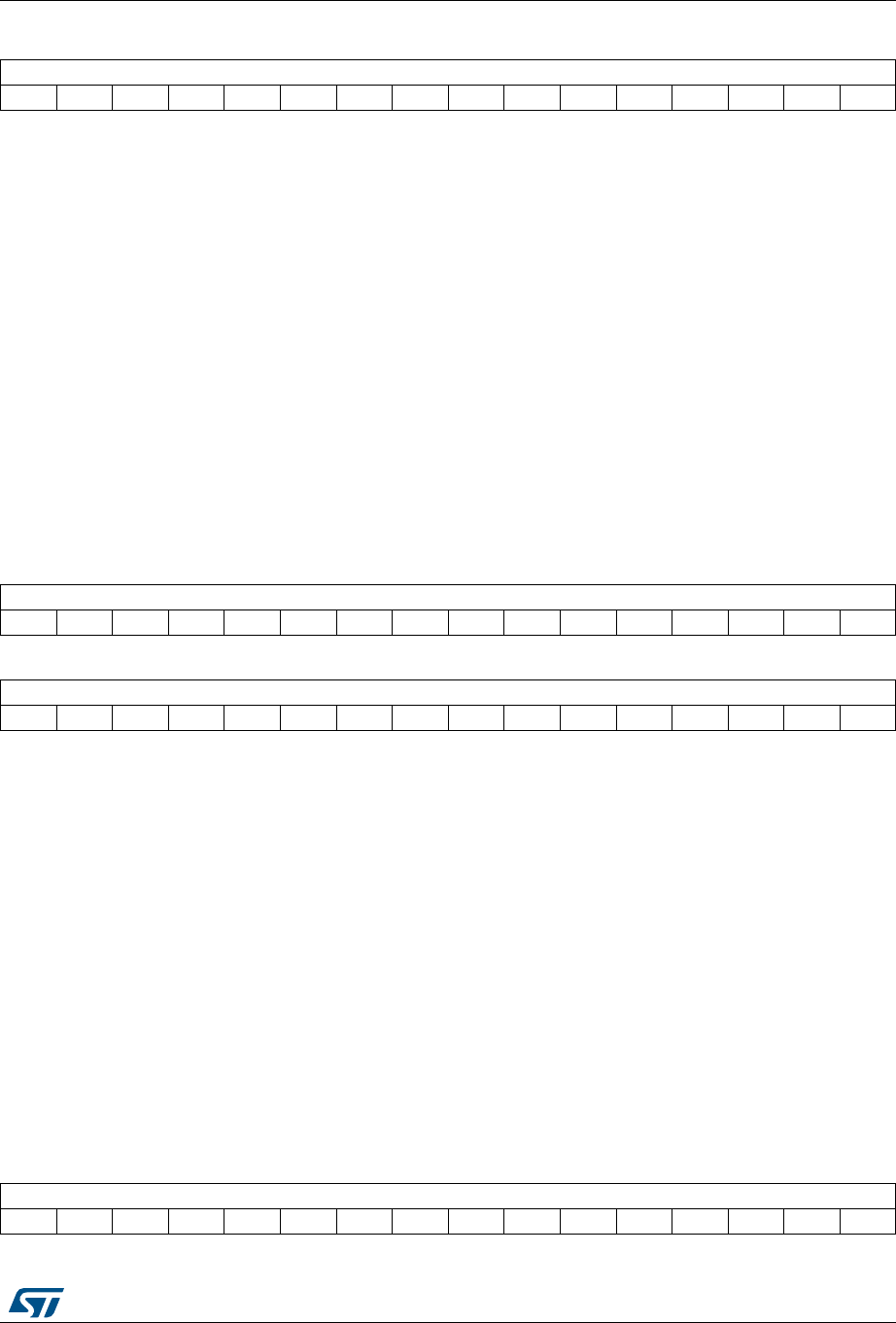
DocID026448 Rev 1 359/836
RM0383 General-purpose timers (TIM2 to TIM5)
365
13.4.14 TIMx capture/compare register 2 (TIMx_CCR2)
Address offset: 0x38
Reset value: 0x0000 0000
13.4.15 TIMx capture/compare register 3 (TIMx_CCR3)
Address offset: 0x3C
Reset value: 0x0000 0000
1514131211109876543210
CCR1[15:0]
rw rw rw rw rw rw rw rw rw rw rw rw rw rw rw rw
Bits 31:16 CCR1[31:16]: High Capture/Compare 1 value (on TIM2 and TIM5).
Bits 15:0 CCR1[15:0]: Low Capture/Compare 1 value
If channel CC1 is configured as output:
CCR1 is the value to be loaded in the actual capture/compare 1 register (preload value).
It is loaded permanently if the preload feature is not selected in the TIMx_CCMR1 register
(bit OC1PE). Else the preload value is copied in the active capture/compare 1 register when
an update event occurs.
The active capture/compare register contains the value to be compared to the counter
TIMx_CNT and signaled on OC1 output.
If channel CC1is configured as input:
CCR1 is the counter value transferred by the last input capture 1 event (IC1).
31 30 29 28 27 26 25 24 23 22 21 20 19 18 17 16
CCR2[31:16] (depending on timers)
rw rw rw rw rw rw rw rw rw rw rw rw rw rw rw rw
1514131211109876543210
CCR2[15:0]
rw rw rw rw rw rw rw rw rw rw rw rw rw rw rw rw
Bits 31:16 CCR2[31:16]: High Capture/Compare 2 value (on TIM2 and TIM5).
Bits 15:0 CCR2[15:0]: Low Capture/Compare 2 value
If channel CC2 is configured as output:
CCR2 is the value to be loaded in the actual capture/compare 2 register (preload value).
It is loaded permanently if the preload feature is not selected in the TIMx_CCMR register (bit
OC2PE). Else the preload value is copied in the active capture/compare 2 register when an
update event occurs.
The active capture/compare register contains the value to be compared to the counter
TIMx_CNT and signalled on OC2 output.
If channel CC2 is configured as input:
CCR2 is the counter value transferred by the last input capture 2 event (IC2).
31 30 29 28 27 26 25 24 23 22 21 20 19 18 17 16
CCR3[31:16] (depending on timers)
rw rw rw rw rw rw rw rw rw rw rw rw rw rw rw rw

General-purpose timers (TIM2 to TIM5) RM0383
360/836 DocID026448 Rev 1
13.4.16 TIMx capture/compare register 4 (TIMx_CCR4)
Address offset: 0x40
Reset value: 0x0000 0000
13.4.17 TIMx DMA control register (TIMx_DCR)
Address offset: 0x48
Reset value: 0x0000
1514131211109876543210
CCR3[15:0]
rw rw rw rw rw rw rw rw rw rw rw rw rw rw rw rw
Bits 31:16 CCR3[31:16]: High Capture/Compare 3 value (on TIM2 and TIM5).
Bits 15:0 CCR3[15:0]: Low Capture/Compare value
If channel CC3 is configured as output:
CCR3 is the value to be loaded in the actual capture/compare 3 register (preload value).
It is loaded permanently if the preload feature is not selected in the TIMx_CCMR register (bit
OC3PE). Else the preload value is copied in the active capture/compare 3 register when an
update event occurs.
The active capture/compare register contains the value to be compared to the counter
TIMx_CNT and signaled on OC3 output.
If channel CC3 is configured as input:
CCR3 is the counter value transferred by the last input capture 3 event (IC3).
31 30 29 28 27 26 25 24 23 22 21 20 19 18 17 16
CCR4[31:16] (depending on timers)
rw rw rw rw rw rw rw rw rw rw rw rw rw rw rw rw
1514131211109876543210
CCR4[15:0]
rw rw rw rw rw rw rw rw rw rw rw rw rw rw rw rw
Bits 31:16 CCR4[31:16]: High Capture/Compare 4 value (on TIM2 and TIM5).
Bits 15:0 CCR4[15:0]: Low Capture/Compare value
1. if CC4 channel is configured as output (CC4S bits):
CCR4 is the value to be loaded in the actual capture/compare 4 register (preload value).
It is loaded permanently if the preload feature is not selected in the TIMx_CCMR register
(bit OC4PE). Else the preload value is copied in the active capture/compare 4 register
when an update event occurs.
The active capture/compare register contains the value to be compared to the counter
TIMx_CNT and signalled on OC4 output.
2. if CC4 channel is configured as input (CC4S bits in TIMx_CCMR4 register):
CCR4 is the counter value transferred by the last input capture 4 event (IC4).
1514131211109876543210
Reserved DBL[4:0] Reserved DBA[4:0]
rw rw rw rw rw rw rw rw rw rw

DocID026448 Rev 1 361/836
RM0383 General-purpose timers (TIM2 to TIM5)
365
13.4.18 TIMx DMA address for full transfer (TIMx_DMAR)
Address offset: 0x4C
Reset value: 0x0000
Example of how to use the DMA burst feature
In this example the timer DMA burst feature is used to update the contents of the CCRx
registers (x = 2, 3, 4) with the DMA transferring half words into the CCRx registers.
This is done in the following steps:
Bits 15:13 Reserved, must be kept at reset value.
Bits 12:8 DBL[4:0]: DMA burst length
This 5-bit vector defines the number of DMA transfers (the timer recognizes a burst transfer
when a read or a write access is done to the TIMx_DMAR address).
00000: 1 transfer,
00001: 2 transfers,
00010: 3 transfers,
...
10001: 18 transfers.
Bits 7:5 Reserved, must be kept at reset value.
Bits 4:0 DBA[4:0]: DMA base address
This 5-bit vector defines the base-address for DMA transfers (when read/write access are
done through the TIMx_DMAR address). DBA is defined as an offset starting from the
address of the TIMx_CR1 register.
Example:
00000: TIMx_CR1,
00001: TIMx_CR2,
00010: TIMx_SMCR,
...
Example: Let us consider the following transfer: DBL = 7 transfers & DBA = TIMx_CR1. In this
case the transfer is done to/from 7 registers starting from the TIMx_CR1 address.
1514131211109876543210
DMAB[15:0]
rw rw rw rw rw rw rw rw rw rw rw rw rw rw rw rw
Bits 15:0 DMAB[15:0]: DMA register for burst accesses
A read or write operation to the DMAR register accesses the register located at the address
(TIMx_CR1 address) + (DBA + DMA index) x 4
where TIMx_CR1 address is the address of the control register 1, DBA is the DMA base
address configured in TIMx_DCR register, DMA index is automatically controlled by the
DMA transfer, and ranges from 0 to DBL (DBL configured in TIMx_DCR).

General-purpose timers (TIM2 to TIM5) RM0383
362/836 DocID026448 Rev 1
1. Configure the corresponding DMA channel as follows:
– DMA channel peripheral address is the DMAR register address
– DMA channel memory address is the address of the buffer in the RAM containing
the data to be transferred by DMA into CCRx registers.
– Number of data to transfer = 3 (See note below).
– Circular mode disabled.
2. Configure the DCR register by configuring the DBA and DBL bit fields as follows:
DBL = 3 transfers, DBA = 0xE.
3. Enable the TIMx update DMA request (set the UDE bit in the DIER register).
4. Enable TIMx
5. Enable the DMA channel
Note: This example is for the case where every CCRx register to be updated once. If every CCRx
register is to be updated twice for example, the number of data to transfer should be 6. Let's
take the example of a buffer in the RAM containing data1, data2, data3, data4, data5 and
data6. The data is transferred to the CCRx registers as follows: on the first update DMA
request, data1 is transferred to CCR2, data2 is transferred to CCR3, data3 is transferred to
CCR4 and on the second update DMA request, data4 is transferred to CCR2, data5 is
transferred to CCR3 and data6 is transferred to CCR4.

DocID026448 Rev 1 363/836
RM0383 General-purpose timers (TIM2 to TIM5)
365
13.4.19 TIM2 option register (TIM2_OR)
Address offset: 0x50
Reset value: 0x0000
13.4.20 TIM5 option register (TIM5_OR)
Address offset: 0x50
Reset value: 0x0000
15 14 13 12 11 10 9 8 7 6 5 4 3 2 1 0
Reserved ITR1_RMP Reserved
rw rw
Bits 15:12 Reserved, must be kept at reset value.
Bits 11:10 ITR1_RMP: Internal trigger 1 remap
Set and cleared by software.
00: Reserved
01: PTP trigger output is connected to TIM2_ITR1
10: OTG FS SOF is connected to the TIM2_ITR1 input
11: OTG HS SOF is connected to the TIM2_ITR1 input
Bits 9:0 Reserved, must be kept at reset value.
15 14 13 12 11 10 9 8 7 6 5 4 3 2 1 0
Reserved TI4_RMP Reserved
rw rw
Bits 15:8 Reserved, must be kept at reset value.
Bits 7:6 TI4_RMP: Timer Input 4 remap
Set and cleared by software.
00: TIM5 Channel4 is connected to the GPIO: Refer to the Alternate function mapping table
in the datasheets.
01: the LSI internal clock is connected to the TIM5_CH4 input for calibration purposes
10: the LSE internal clock is connected to the TIM5_CH4 input for calibration purposes
11: the RTC wakeup interrupt is connected to TIM5_CH4 input for calibration purposes.
Wakeup interrupt should be enabled.
Bits 5:0 Reserved, must be kept at reset value.
General-purpose timers (TIM2 to TIM5) RM0383
364/836 DocID026448 Rev 1
13.4.21 TIMx register map
TIMx registers are mapped as described in the table below:
Table 55. TIM2 to TIM5 register map and reset values
Offset Register
31
30
29
28
27
26
25
24
23
22
21
20
19
18
17
16
15
14
13
12
11
10
9
8
7
6
5
4
3
2
1
0
0x00
TIMx_CR1
Reserved
CKD
[1:0]
ARPE
CMS
[1:0]
DIR
OPM
URS
UDIS
CEN
Reset value 0000000000
0x04
TIMx_CR2
Reserved
TI1S
MMS[2:0]
CCDS
Reserved
Reset value 00000
0x08
TIMx_SMCR
Reserved
ETP
ECE
ETPS
[1:0] ETF[3:0]
MSM
TS[2:0]
Reserved
SMS[2:0]
Reset value 000000000000 000
0x0C
TIMx_DIER
Reserved
TDE
COMDE
CC4DE
CC3DE
CC2DE
CC1DE
UDE
Reserved
TIE
Reserved
CC4IE
CC3IE
CC2IE
CC1IE
UIE
Reset value 0000000 0 00000
0x10
TIMx_SR
Reserved
CC4OF
CC3OF
CC2OF
CC1OF
Reserved
TIF
Reserved
CC4IF
CC3IF
CC2IF
CC1IF
UIF
Reset value 0000 0 00000
0x14
TIMx_EGR
Reserved
TG
Reserved
CC4G
CC3G
CC2G
CC1G
UG
Reset value 000000
0x18
TIMx_CCMR1
Output Compare
mode Reserved
OC2CE
OC2M
[2:0]
OC2PE
OC2FE
CC2S
[1:0]
OC1CE
OC1M
[2:0]
OC1PE
OC1FE
CC1S
[1:0]
Reset value 0000000000000000
TIMx_CCMR1
Input Capture
mode Reserved
IC2F[3:0]
IC2
PSC
[1:0]
CC2S
[1:0] IC1F[3:0]
IC1
PSC
[1:0]
CC1S
[1:0]
Reset value 0000000000000000
0x1C
TIMx_CCMR2
Output Compare
mode Reserved
O24CE
OC4M
[2:0]
OC4PE
OC4FE
CC4S
[1:0]
OC3CE
OC3M
[2:0]
OC3PE
OC3FE
CC3S
[1:0]
Reset value 0000000000000000
TIMx_CCMR2
Input Capture
mode Reserved
IC4F[3:0]
IC4
PSC
[1:0]
CC4S
[1:0] IC3F[3:0]
IC3
PSC
[1:0]
CC3S
[1:0]
Reset value 0 000000000000000
0x20
TIMx_CCER
Reserved
CC4NP
Reserved
CC4P
CC4E
CC3NP
Reserved
CC3P
CC3E
CC2NP
Reserved
CC2P
CC2E
CC1NP
Reserved
CC1P
CC1E
Reset value 0 0 0 0 0 0 0 0 0 0 0 0
0x24
TIMx_CNT CNT[31:16]
(TIM2 and TIM5 only, reserved on the other timers) CNT[15:0]
Reset value 000000000000000000 0 0 000000000000
DocID026448 Rev 1 365/836
RM0383 General-purpose timers (TIM2 to TIM5)
365
Refer to Table 3 on page 41 for the register boundary addresses.
0x28
TIMx_PSC
Reserved
PSC[15:0]
Reset value 0000000000000000
0x2C
TIMx_ARR ARR[31:16]
(TIM2 and TIM5 only, reserved on the other timers) ARR[15:0]
Reset value 000000000000000000 0 0 000000000000
0x30 Reserved
0x34
TIMx_CCR1 CCR1[31:16]
(TIM2 and TIM5 only, reserved on the other timers) CCR1[15:0]
Reset value 000000000000000000 0 0 000000000000
0x38
TIMx_CCR2 CCR2[31:16]
(TIM2 and TIM5 only, reserved on the other timers) CCR2[15:0]
Reset value 000000000000000000 0 0 000000000000
0x3C
TIMx_CCR3 CCR3[31:16]
(TIM2 and TIM5 only, reserved on the other timers) CCR3[15:0]
Reset value 000000000000000000 0 0 000000000000
0x40
TIMx_CCR4 CCR4[31:16]
(TIM2 and TIM5 only, reserved on the other timers) CCR4[15:0]
Reset value 000000000000000000 0 0 000000000000
0x44 Reserved
0x48
TIMx_DCR
Reserved
DBL[4:0]
Reserved
DBA[4:0]
Reset value 00000 00000
0x4C
TIMx_DMAR
Reserved
DMAB[15:0]
Reset value 0000000000000000
0x50
TIM2_OR
Reserved Reserved
ITR1_
RMP Reserved
Reset value 00
0x50
TIM5_OR
Reserved Reserved
IT4_
RMP Reserved
Reset value 00
Table 55. TIM2 to TIM5 register map and reset values (continued)
Offset Register
31
30
29
28
27
26
25
24
23
22
21
20
19
18
17
16
15
14
13
12
11
10
9
8
7
6
5
4
3
2
1
0

General-purpose timers (TIM9 to TIM11) RM0383
366/836 DocID026448 Rev 1
14 General-purpose timers (TIM9 to TIM11)
TIM8 is not available in STM32F411xC/E.
14.1 TIM9/10/11 introduction
The TIM9/10/11 general-purpose timers consist of a 16-bit auto-reload counter driven by a
programmable prescaler.
They may be used for a variety of purposes, including measuring the pulse lengths of input
signals (input capture) or generating output waveforms (output compare, PWM).
Pulse lengths and waveform periods can be modulated from a few microseconds to several
milliseconds using the timer prescaler and the RCC clock controller prescalers.
The TIM9/10/11 timers are completely independent, and do not share any resources. They
can be synchronized together as described in Section 14.3.12.
14.2 TIM9/10/11 main features
14.2.1 TIM9 main features
The features of the TIM9 general-purpose timer include:
•16-bit auto-reload upcounter
•16-bit programmable prescaler used to divide the counter clock frequency by any factor
between 1 and 65536 (can be changed “on the fly”)
•Up to 2 independent channels for:
– Input capture
– Output compare
– PWM generation (edge-aligned mode)
– One-pulse mode output
•Synchronization circuit to control the timer with external signals and to interconnect
several timers together
•Interrupt generation on the following events:
– Update: counter overflow, counter initialization (by software or internal trigger)
– Trigger event (counter start, stop, initialization or count by internal trigger)
– Input capture
– Output compare
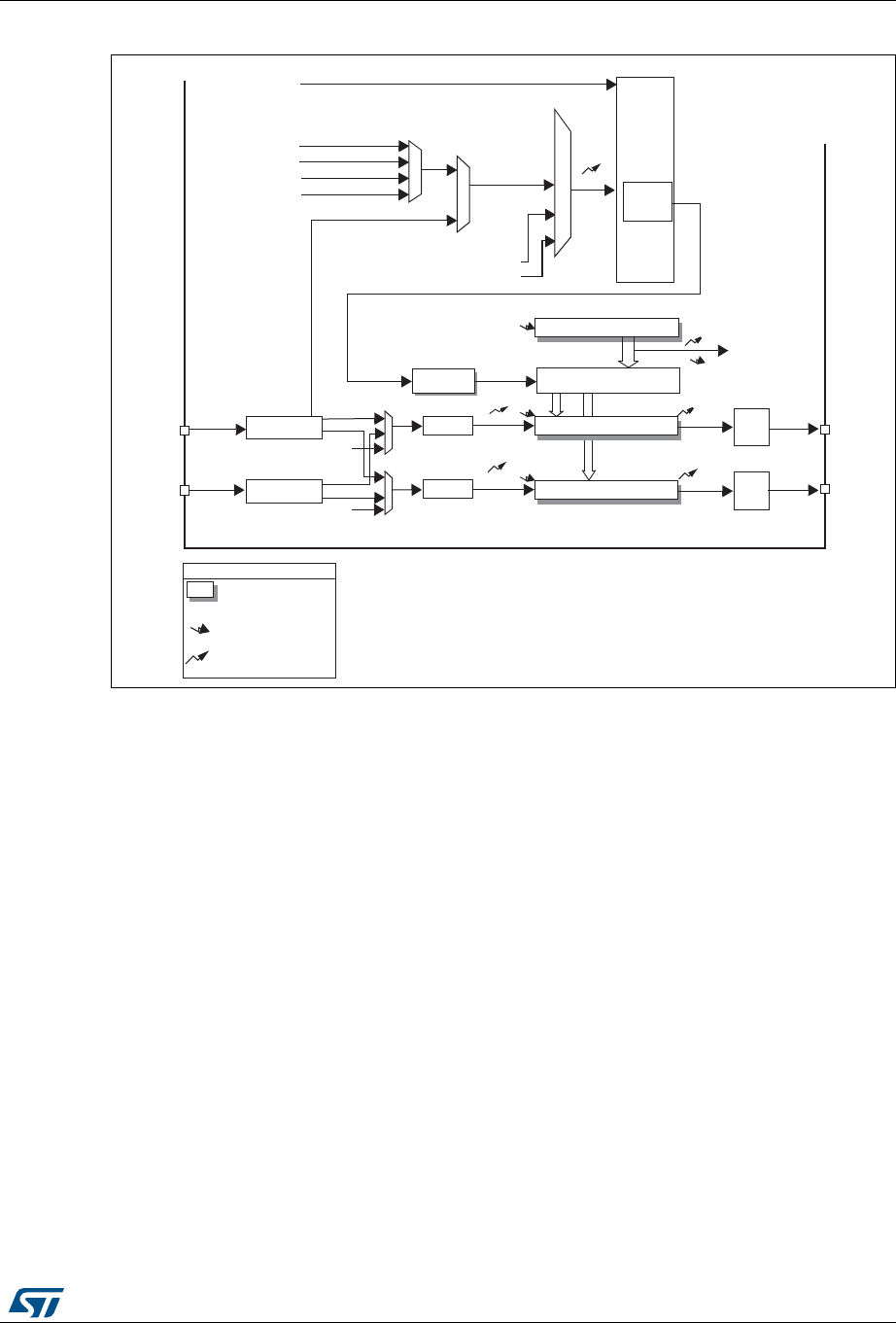
DocID026448 Rev 1 367/836
RM0383 General-purpose timers (TIM9 to TIM11)
409
Figure 133. General-purpose timer block diagram (TIM9)
14.2.2 TIM10/TIM11 main features
The features of general-purpose timers TIM10/TIM11 include:
•16-bit auto-reload upcounter
•16-bit programmable prescaler used to divide the counter clock frequency by any factor
between 1 and 65536 (can be changed “on the fly”)
•independent channel for:
– Input capture
– Output compare
– PWM generation (edge-aligned mode)
– One-pulse mode output
•Interrupt generation on the following events:
– Update: counter overflow, counter initialization (by software)
– Input capture
– Output compare
Auto-reload register
Capture/Compare 1 register
Capture/Compare 2 register
U
U
U
CC1I
CC2I
Tr i g g e r
controller
Stop, Clear
TI1FP1
TI2FP2
ITR0
ITR1
ITR2
ITR3
TRGI
output
control
OC1
OC1REF
OC2REF
U
UI
Reset, Enable, Count
IC1
IC2
Prescaler
Prescaler
Input filter &
Edge detector
IC2PS
IC1PS
TI1FP1
output
control
OC2
Reg
event
Notes:
Preload registers transferred
to active registers on
U
event
according to control bit
interrupt
TGI
TRC
TRC
ITR
TRC
TI1F_ED
Input filter &
Edge detector
CC1I
CC2I
TI1FP2
TI2FP1
TI2FP2
TI1
TI2
TIMx_CH1
TIMx_CH2
TIMx_CH1
TIMx_CH2
Prescaler
COUNTER
+/-
CK_PSC
PSC CNT
CK_CNT
controller
mode
Slave
Internal clock (CK_INT)
ai17190
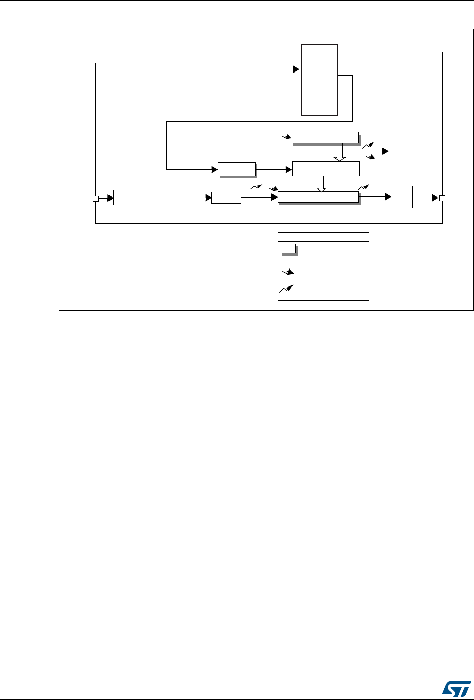
General-purpose timers (TIM9 to TIM11) RM0383
368/836 DocID026448 Rev 1
Figure 134. General-purpose timer block diagram (TIM10/11)
!UTORELOADREGISTER
#APTURE#OMPAREREGISTER
5
5
##)
3TOP#LEAR
OUTPUT
CONTROL
/#
/#2%&
5
5)
)#
0RESCALER
)NPUTFILTER
EDGEDETECTOR
)#03
4)&0
2EG
EVENT
.OTES
0RELOADREGISTERSTRANSFERRED
TOACTIVEREGISTERSON5EVENT
ACCORDINGTOCONTROLBIT
INTERRUPT$-!OUTPUT
##)
4)
4)-X?#(
PRESCALER COUNTER
#+?03# 03# #.4
#+?#.4
)NTERNALCLOCK#+?).4
AIC
4RIGGER
#ONTROLLER
%NABLE
COUNTER
4)-X?#(

DocID026448 Rev 1 369/836
RM0383 General-purpose timers (TIM9 to TIM11)
409
14.3 TIM9 to TIM11 functional description
14.3.1 Time-base unit
The main block of the timer is a 16-bit counter with its related auto-reload register.
The counter clock can be divided by a prescaler.
The counter, the auto-reload register and the prescaler register can be written or read by
software. This is true even when the counter is running.
The time-base unit includes:
•Counter register (TIMx_CNT)
•Prescaler register (TIMx_PSC)
•Auto-reload register (TIMx_ARR)
The auto-reload register is preloaded. Writing to or reading from the auto-reload register
accesses the preload register. The content of the preload register are transferred into the
shadow register permanently or at each update event (UEV), depending on the auto-reload
preload enable bit (ARPE) in TIMx_CR1 register. The update event is sent when the counter
reaches the overflow and if the UDIS bit equals 0 in the TIMx_CR1 register. It can also be
generated by software. The generation of the update event is described in details for each
configuration.
The counter is clocked by the prescaler output CK_CNT, which is enabled only when the
counter enable bit (CEN) in TIMx_CR1 register is set (refer also to the slave mode controller
description to get more details on counter enabling).
Note that the counter starts counting 1 clock cycle after setting the CEN bit in the TIMx_CR1
register.
Prescaler description
The prescaler can divide the counter clock frequency by any factor between 1 and 65536. It
is based on a 16-bit counter controlled through a 16-bit register (in the TIMx_PSC register).
It can be changed on the fly as this control register is buffered. The new prescaler ratio is
taken into account at the next update event.
Figure 135 and Figure 136 give some examples of the counter behavior when the prescaler
ratio is changed on the fly.
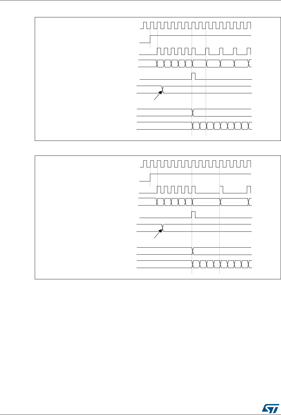
General-purpose timers (TIM9 to TIM11) RM0383
370/836 DocID026448 Rev 1
Figure 135. Counter timing diagram with prescaler division change from 1 to 2
Figure 136. Counter timing diagram with prescaler division change from 1 to 4
14.3.2 Counter modes
Upcounting mode
In upcounting mode, the counter counts from 0 to the auto-reload value (content of the
TIMx_ARR register), then restarts from 0 and generates a counter overflow event.
Setting the UG bit in the TIMx_EGR register (by software ) also generates an update event.
The UEV event can be disabled by software by setting the UDIS bit in the TIMx_CR1
register. This is to avoid updating the shadow registers while writing new values in the
preload registers. Then no update event occurs until the UDIS bit has been written to 0.
However, the counter restarts from 0, as well as the counter of the prescaler (but the
prescale rate does not change). In addition, if the URS bit (update request selection) in
TIMx_CR1 register is set, setting the UG bit generates an update event UEV but without
CK_PSC
00
CEN
Timer clock = CK_CNT
Counter register
Update event (UEV)
0
F9 FA FB FCF7
Prescaler control register 01
Write a new value in TIMx_PSC
01 02 03
Prescaler buffer 01
Prescaler counter 01 0 1 0 1 0 1
F8
CK_PSC
00
CEN
Timer clock = CK_CNT
Counter register
Update event (UEV)
0
F9 FA FB FCF7
Prescaler control register 03
Write a new value in TIMx_PSC
Prescaler buffer 03
Prescaler counter 01 2 3 0 1 2 3
F8 01
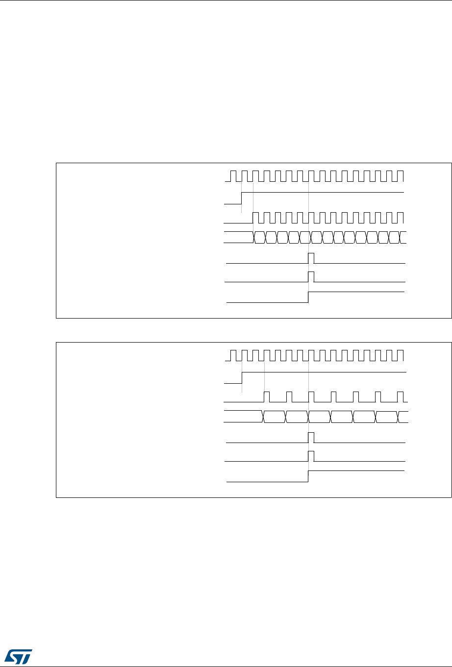
DocID026448 Rev 1 371/836
RM0383 General-purpose timers (TIM9 to TIM11)
409
setting the UIF flag (thus no interrupt is sent). This is to avoid generating both update and
capture interrupts when clearing the counter on the capture event.
When an update event occurs, all the registers are updated and the update flag (UIF bit in
TIMx_SR register) is set (depending on the URS bit):
•The auto-reload shadow register is updated with the preload value (TIMx_ARR),
•The buffer of the prescaler is reloaded with the preload value (content of the TIMx_PSC
register).
The following figures show some examples of the counter behavior for different clock
frequencies when TIMx_ARR=0x36.
Figure 137. Counter timing diagram, internal clock divided by 1
Figure 138. Counter timing diagram, internal clock divided by 2
CK_PSC
00
CNT_EN
Timer clock = CK_CNT
Counter register
Update interrupt flag (UIF)
Counter overflow
Update event (UEV)
01 02 03 04 05 06 0732 33 34 35 3631
CK_PSC
0035 0000 0001 0002 0003
CNT_EN
Timer clock = CK_CNT
Counter register
Update interrupt flag (UIF)
0034 0036
Counter overflow
Update event (UEV)
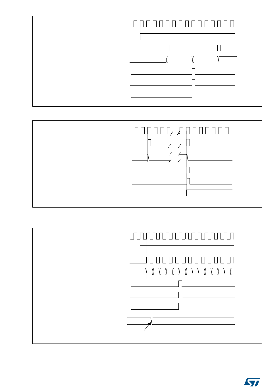
General-purpose timers (TIM9 to TIM11) RM0383
372/836 DocID026448 Rev 1
Figure 139. Counter timing diagram, internal clock divided by 4
Figure 140. Counter timing diagram, internal clock divided by N
Figure 141. Counter timing diagram, update event when ARPE=0 (TIMx_ARR not
preloaded)
CK_PSC
0000 0001
CNT_EN
Timer clock = CK_CNT
Counter register
Update interrupt flag (UIF)
0035 0036
Counter overflow
Update event (UEV)
Timer clock = CK_CNT
Counter register 00
1F 20
Update interrupt flag (UIF)
Counter overflow
Update event (UEV)
CK_PSC
CK_PSC
00
CEN
Timer clock = CK_CNT
Counter register
Update interrupt flag (UIF)
Counter overflow
Update event (UEV)
01 02 03 04 05 06 0732 33 34 35 3631
Auto-reload register FF 36
Write a new value in TIMx_ARR
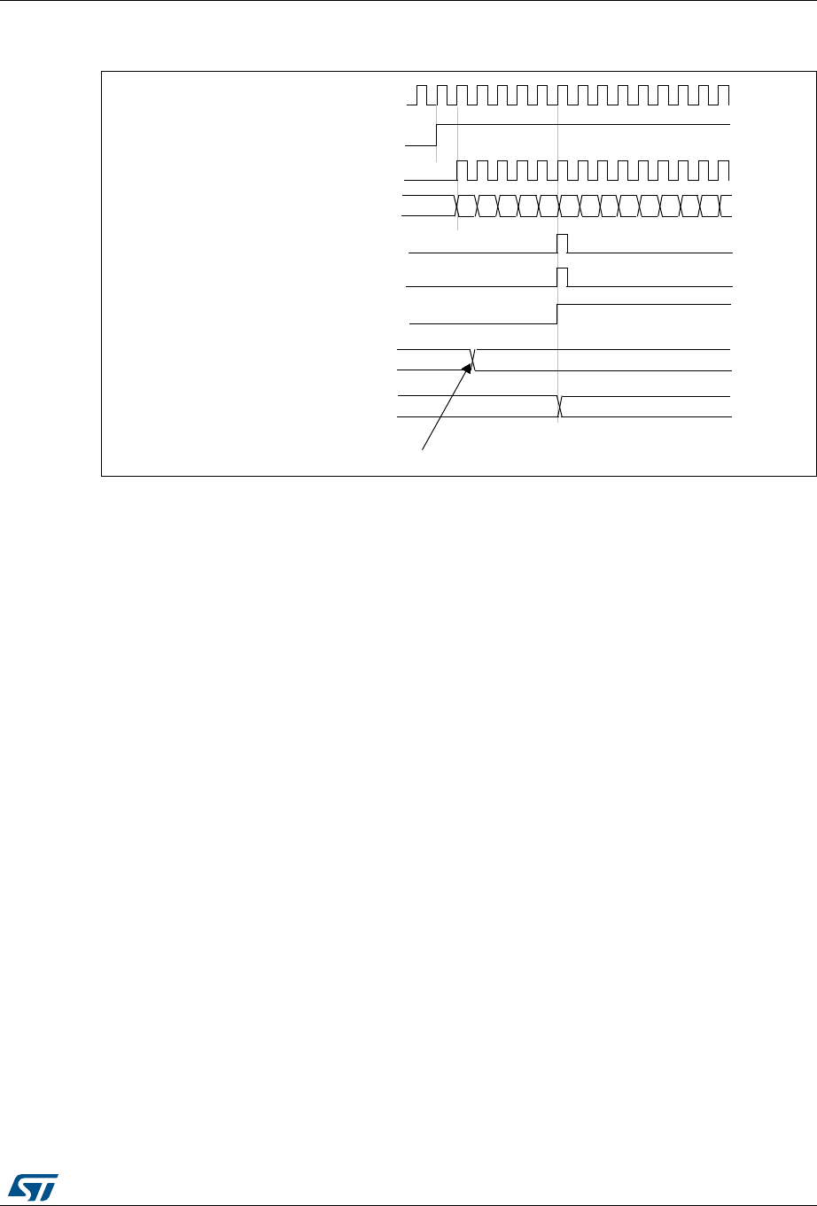
DocID026448 Rev 1 373/836
RM0383 General-purpose timers (TIM9 to TIM11)
409
Figure 142. Counter timing diagram, update event when ARPE=1 (TIMx_ARR
preloaded)
14.3.3 Clock selection
The counter clock can be provided by the following clock sources:
•Internal clock (CK_INT)
•External clock mode1 (for TIM9): external input pin (TIx)
•Internal trigger inputs (ITRx) (for TIM9): connecting the trigger output from another
timer. Refer to Section : Using one timer as prescaler for another for more details.
Internal clock source (CK_INT)
The internal clock source is the default clock source for TIM10/TIM11.
For TIM9, the internal clock source is selected when the slave mode controller is disabled
(SMS=’000’). The CEN bit in the TIMx_CR1 register and the UG bit in the TIMx_EGR
register are then used as control bits and can be changed only by software (except for UG
which remains cleared). As soon as the CEN bit is programmed to 1, the prescaler is
clocked by the internal clock CK_INT.
Figure 143 shows the behavior of the control circuit and the upcounter in normal mode,
without prescaler.
CK_PSC
00
CEN
Timer clock = CK_CNT
Counter register
Update interrupt flag (UIF)
Counter overflow
Update event (UEV)
01 02 03 04 05 06 07F1 F2 F3 F4 F5F0
Auto-reload preload register F5 36
Auto-reload shadow register F5 36
Write a new value in TIMx_ARR
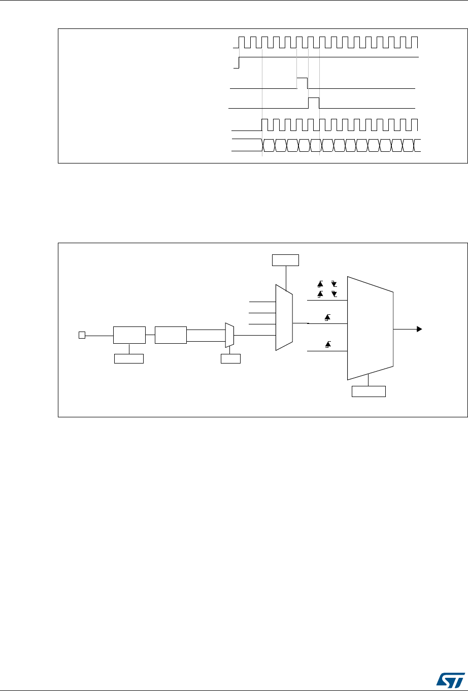
General-purpose timers (TIM9 to TIM11) RM0383
374/836 DocID026448 Rev 1
Figure 143. Control circuit in normal mode, internal clock divided by 1
External clock source mode 1(TIM9)
This mode is selected when SMS=’111’ in the TIMx_SMCR register. The counter can count
at each rising or falling edge on a selected input.
Figure 144. TI2 external clock connection example
For example, to configure the upcounter to count in response to a rising edge on the TI2
input, use the following procedure:
1. Configure channel 2 to detect rising edges on the TI2 input by writing CC2S = ‘01’ in
the TIMx_CCMR1 register.
2. Configure the input filter duration by writing the IC2F[3:0] bits in the TIMx_CCMR1
register (if no filter is needed, keep IC2F=’0000’).
3. Select the rising edge polarity by writing CC2P=’0’ and CC2NP=’0’ in the TIMx_CCER
register.
4. Configure the timer in external clock mode 1 by writing SMS=’111’ in the TIMx_SMCR
register.
5. Select TI2 as the trigger input source by writing TS=’110’ in the TIMx_SMCR register.
6. Enable the counter by writing CEN=’1’ in the TIMx_CR1 register.
Note: The capture prescaler is not used for triggering, so you don’t need to configure it.
When a rising edge occurs on TI2, the counter counts once and the TIF flag is set.
The delay between the rising edge on TI2 and the actual clock of the counter is due to the
resynchronization circuit on TI2 input.
Internal clock
00
Counter clock = CK_CNT = CK_PSC
Counter register 01 02 03 04 05 06 0732 33 34 35 3631
CEN=CNT_EN
UG
CNT_INIT
CK_INT
external clock
mode 1
internal clock
mode
TRGI
TI1F
TI2F or
or
or
(internal clock)
CK_PSC
TIMx_SMCR
SMS[2:0]
ITRx
TI1_ED
TI1FP1
TI2FP2
TIMx_SMCR
TS[2:0]
TI2 0
1
TIMx_CCER
CC2P
Filter
ICF[3:0]
TIMx_CCMR1
Edge
Detector
TI2F_Rising
TI2F_Falling 110
0xx
100
101
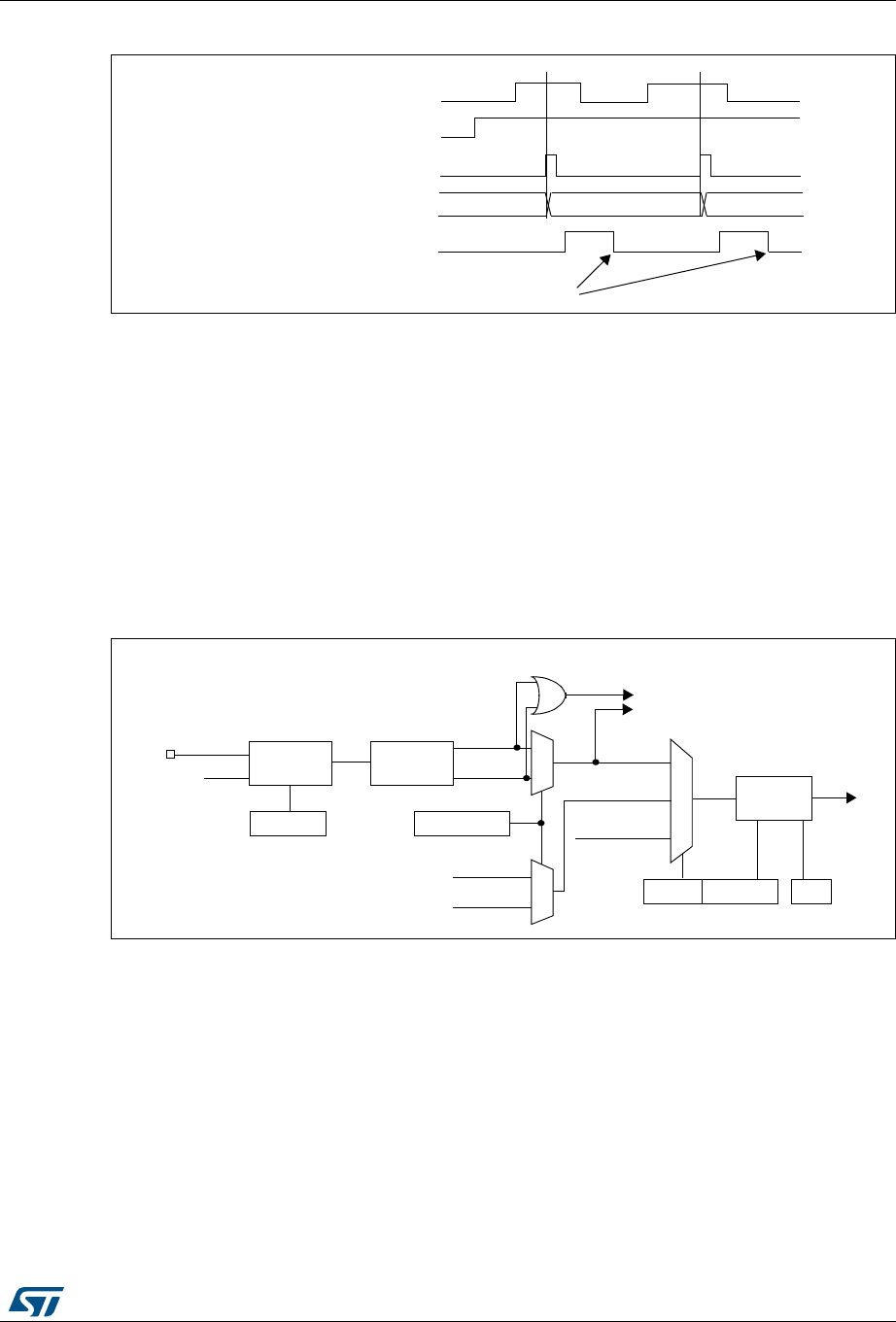
DocID026448 Rev 1 375/836
RM0383 General-purpose timers (TIM9 to TIM11)
409
Figure 145. Control circuit in external clock mode 1
14.3.4 Capture/compare channels
Each Capture/Compare channel is built around a capture/compare register (including a
shadow register), a input stage for capture (with digital filter, multiplexing and prescaler) and
an output stage (with comparator and output control).
Figure 146 to Figure 148 give an overview of one capture/compare channel.
The input stage samples the corresponding TIx input to generate a filtered signal TIxF.
Then, an edge detector with polarity selection generates a signal (TIxFPx) which can be
used as trigger input by the slave mode controller or as the capture command. It is
prescaled before the capture register (ICxPS).
Figure 146. Capture/compare channel (example: channel 1 input stage)
The output stage generates an intermediate waveform which is then used for reference:
OCxRef (active high). The polarity acts at the end of the chain.
Counter clock = CK_CNT = CK_PSC
Counter register 35 3634
TI2
CNT_EN
TIF
Write TIF=0
TI1 0
1
TIMx_CCER
CC1P/CC1NP
divider
/1, /2, /4, /8
ICPS[1:0]
TI1F_ED
filter
ICF[3:0]
downcounter
TIMx_CCMR1
Edge
Detector
TI1F_Rising
TI1F_Falling
to the slave mode controller
TI1FP1
11
01
TIMx_CCMR1
CC1S[1:0]
IC1
TI2FP1
TRC
(from channel 2)
(from slave mode
controller)
10
fDTS
TIMx_CCER
CC1E
IC1PS
TI1F
0
1
TI2F_rising
TI2F_falling
(from channel 2)
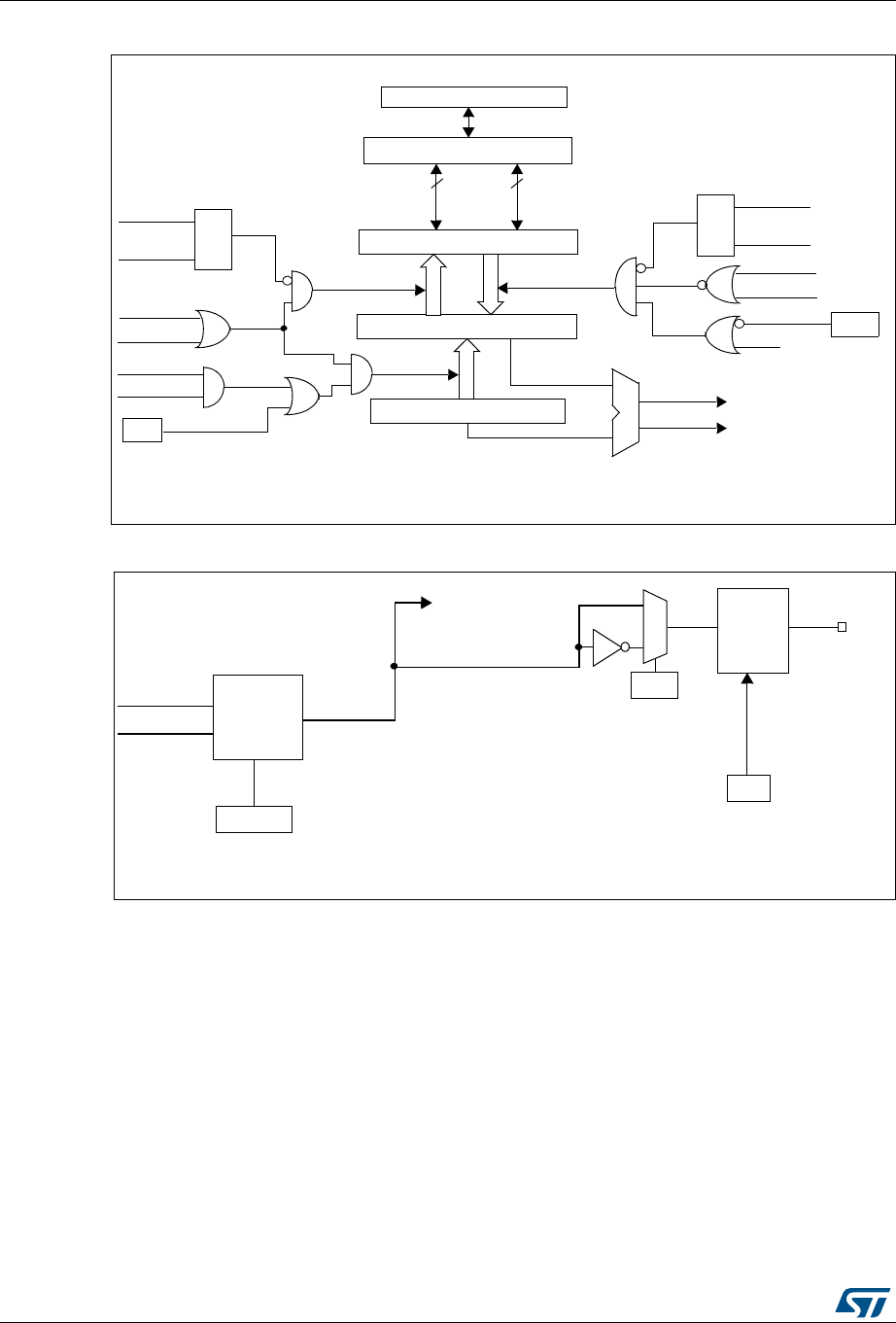
General-purpose timers (TIM9 to TIM11) RM0383
376/836 DocID026448 Rev 1
Figure 147. Capture/compare channel 1 main circuit
Figure 148. Output stage of capture/compare channel (channel 1)
The capture/compare block is made of one preload register and one shadow register. Write
and read always access the preload register.
In capture mode, captures are actually done in the shadow register, which is copied into the
preload register.
In compare mode, the content of the preload register is copied into the shadow register
which is compared to the counter.
14.3.5 Input capture mode
In Input capture mode, the Capture/Compare Registers (TIMx_CCRx) are used to latch the
value of the counter after a transition detected by the corresponding ICx signal. When a
capture occurs, the corresponding CCXIF flag (TIMx_SR register) is set and an interrupt or
a DMA request can be sent if they are enabled. If a capture occurs while the CCxIF flag was
already high, then the over-capture flag CCxOF (TIMx_SR register) is set. CCxIF can be
CC1E
Capture/compare shadow register
comparator
Capture/compare preload register
Counter
IC1PS
CC1S[0]
CC1S[1]
capture
input
mode
S
R
read CCR1H
read CCR1L
read_in_progress
capture_transfer CC1S[0]
CC1S[1]
S
R
write CCR1H
write CCR1L
write_in_progress
output
mode
UEV
OC1PE
(from time
compare_transfer
APB Bus
88
high
low
(if 16-bit)
MCU-peripheral interface
TIM1_CCMR1
OC1PE
base unit)
CNT>CCR1
CNT=CCR1
TIM1_EGR
CC1G
/UTPUTMODE
#.4##2
#.4##2 CONTROLLER
4)-X?##-2
/#-;=
/#?2%&
##0
4)-X?##%2
/UTPUT
ENABLE
CIRCUIT
/#
##% 4)-X?##%2
4OTHEMASTERMODE
CONTROLLER
AI

DocID026448 Rev 1 377/836
RM0383 General-purpose timers (TIM9 to TIM11)
409
cleared by software by writing it to ‘0’ or by reading the captured data stored in the
TIMx_CCRx register. CCxOF is cleared when you write it to ‘0’.
The following example shows how to capture the counter value in TIMx_CCR1 when TI1
input rises. To do this, use the following procedure:
1. Select the active input: TIMx_CCR1 must be linked to the TI1 input, so write the CC1S
bits to ‘01’ in the TIMx_CCMR1 register. As soon as CC1S becomes different from ‘00’,
the channel is configured in input mode and the TIMx_CCR1 register becomes read-
only.
2. Program the input filter duration you need with respect to the signal you connect to the
timer (by programming the ICxF bits in the TIMx_CCMRx register if the input is one of
the TIx inputs). Let’s imagine that, when toggling, the input signal is not stable during at
must 5 internal clock cycles. We must program a filter duration longer than these 5
clock cycles. We can validate a transition on TI1 when 8 consecutive samples with the
new level have been detected (sampled at fDTS frequency). Then write IC1F bits to
‘0011’ in the TIMx_CCMR1 register.
3. Select the edge of the active transition on the TI1 channel by programming CC1P and
CC1NP bits to ‘00’ in the TIMx_CCER register (rising edge in this case).
4. Program the input prescaler. In our example, we wish the capture to be performed at
each valid transition, so the prescaler is disabled (write IC1PS bits to ‘00’ in the
TIMx_CCMR1 register).
5. Enable capture from the counter into the capture register by setting the CC1E bit in the
TIMx_CCER register.
6. If needed, enable the related interrupt request by setting the CC1IE bit in the
TIMx_DIER register.
When an input capture occurs:
•The TIMx_CCR1 register gets the value of the counter on the active transition.
•CC1IF flag is set (interrupt flag). CC1OF is also set if at least two consecutive captures
occurred whereas the flag was not cleared.
•An interrupt is generated depending on the CC1IE bit.
In order to handle the overcapture, it is recommended to read the data before the
overcapture flag. This is to avoid missing an overcapture which could happen after reading
the flag and before reading the data.
Note: IC interrupt requests can be generated by software by setting the corresponding CCxG bit in
the TIMx_EGR register.
14.3.6 PWM input mode (only for TIM9)
This mode is a particular case of input capture mode. The procedure is the same except:
•Two ICx signals are mapped on the same TIx input.
•These 2 ICx signals are active on edges with opposite polarity.
•One of the two TIxFP signals is selected as trigger input and the slave mode controller
is configured in reset mode.
For example, you can measure the period (in TIMx_CCR1 register) and the duty cycle (in
TIMx_CCR2 register) of the PWM applied on TI1 using the following procedure (depending
on CK_INT frequency and prescaler value):
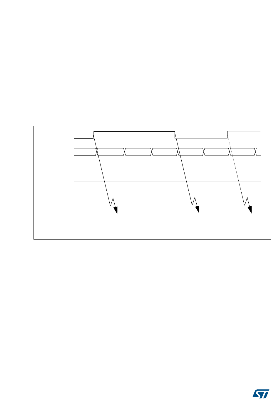
General-purpose timers (TIM9 to TIM11) RM0383
378/836 DocID026448 Rev 1
1. Select the active input for TIMx_CCR1: write the CC1S bits to ‘01’ in the TIMx_CCMR1
register (TI1 selected).
2. Select the active polarity for TI1FP1 (used both for capture in TIMx_CCR1 and counter
clear): program the CC1P and CC1NP bits to ‘00’ (active on rising edge).
3. Select the active input for TIMx_CCR2: write the CC2S bits to ‘10’ in the TIMx_CCMR1
register (TI1 selected).
4. Select the active polarity for TI1FP2 (used for capture in TIMx_CCR2): program the
CC2P and CC2NP bits to ‘11’ (active on falling edge).
5. Select the valid trigger input: write the TS bits to ‘101’ in the TIMx_SMCR register
(TI1FP1 selected).
6. Configure the slave mode controller in reset mode: write the SMS bits to ‘100’ in the
TIMx_SMCR register.
7. Enable the captures: write the CC1E and CC2E bits to ‘1’ in the TIMx_CCER register.
Figure 149. PWM input mode timing
1. The PWM input mode can be used only with the TIMx_CH1/TIMx_CH2 signals due to the fact that only
TI1FP1 and TI2FP2 are connected to the slave mode controller.
14.3.7 Forced output mode
In output mode (CCxS bits = ‘00’ in the TIMx_CCMRx register), each output compare signal
(OCxREF and then OCx) can be forced to active or inactive level directly by software,
independently of any comparison between the output compare register and the counter.
To force an output compare signal (OCXREF/OCx) to its active level, you just need to write
‘101’ in the OCxM bits in the corresponding TIMx_CCMRx register. Thus OCXREF is forced
high (OCxREF is always active high) and OCx get opposite value to CCxP polarity bit.
For example: CCxP=’0’ (OCx active high) => OCx is forced to high level.
The OCxREF signal can be forced low by writing the OCxM bits to ‘100’ in the
TIMx_CCMRx register.
Anyway, the comparison between the TIMx_CCRx shadow register and the counter is still
performed and allows the flag to be set. Interrupt requests can be sent accordingly. This is
described in the output compare mode section below.
TI1
TIMx_CNT 0000 0001 0002 0003 0004 00000004
TIMx_CCR1
TIMx_CCR2
0004
0002
IC1 capture
IC2 capture
reset counter
IC2 capture
pulse width
IC1 capture
period
measurementmeasurement
ai15413

DocID026448 Rev 1 379/836
RM0383 General-purpose timers (TIM9 to TIM11)
409
14.3.8 Output compare mode
This function is used to control an output waveform or indicating when a period of time has
elapsed.
When a match is found between the capture/compare register and the counter, the output
compare function:
1. Assigns the corresponding output pin to a programmable value defined by the output
compare mode (OCxM bits in the TIMx_CCMRx register) and the output polarity (CCxP
bit in the TIMx_CCER register). The output pin can keep its level (OCXM=’000’), be set
active (OCxM=’001’), be set inactive (OCxM=’010’) or can toggle (OCxM=’011’) on
match.
2. Sets a flag in the interrupt status register (CCxIF bit in the TIMx_SR register).
3. Generates an interrupt if the corresponding interrupt mask is set (CCXIE bit in the
TIMx_DIER register).
The TIMx_CCRx registers can be programmed with or without preload registers using the
OCxPE bit in the TIMx_CCMRx register.
In output compare mode, the update event UEV has no effect on OCxREF and OCx output.
The timing resolution is one count of the counter. Output compare mode can also be used to
output a single pulse (in One-pulse mode).
Procedure:
1. Select the counter clock (internal, external, prescaler).
2. Write the desired data in the TIMx_ARR and TIMx_CCRx registers.
3. Set the CCxIE bit if an interrupt request is to be generated.
4. Select the output mode. For example:
– Write OCxM = ‘011’ to toggle OCx output pin when CNT matches CCRx
– Write OCxPE = ‘0’ to disable preload register
– Write CCxP = ‘0’ to select active high polarity
– Write CCxE = ‘1’ to enable the output
5. Enable the counter by setting the CEN bit in the TIMx_CR1 register.
The TIMx_CCRx register can be updated at any time by software to control the output
waveform, provided that the preload register is not enabled (OCxPE=’0’, else TIMx_CCRx
shadow register is updated only at the next update event UEV). An example is given in
Figure 150.
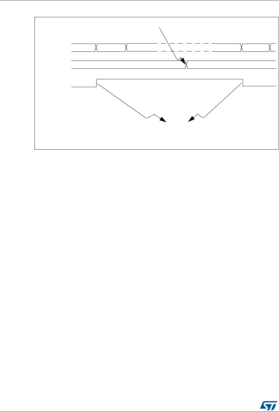
General-purpose timers (TIM9 to TIM11) RM0383
380/836 DocID026448 Rev 1
Figure 150. Output compare mode, toggle on OC1.
14.3.9 PWM mode
Pulse Width Modulation mode allows you to generate a signal with a frequency determined
by the value of the TIMx_ARR register and a duty cycle determined by the value of the
TIMx_CCRx register.
The PWM mode can be selected independently on each channel (one PWM per OCx
output) by writing ‘110’ (PWM mode 1) or ‘111’ (PWM mode 2) in the OCxM bits in the
TIMx_CCMRx register. You must enable the corresponding preload register by setting the
OCxPE bit in the TIMx_CCMRx register, and eventually the auto-reload preload register (in
upcounting or center-aligned modes) by setting the ARPE bit in the TIMx_CR1 register.
As the preload registers are transferred to the shadow registers only when an update event
occurs, before starting the counter, you have to initialize all the registers by setting the UG
bit in the TIMx_EGR register.
The OCx polarity is software programmable using the CCxP bit in the TIMx_CCER register.
It can be programmed as active high or active low. The OCx output is enabled by the CCxE
bit in the TIMx_CCER register. Refer to the TIMx_CCERx register description for more
details.
In PWM mode (1 or 2), TIMx_CNT and TIMx_CCRx are always compared to determine
whether TIMx_CNT ≤TIMx_CCRx.
The timer is able to generate PWM in edge-aligned mode only since the counter is
upcounting.
PWM edge-aligned mode
In the following example, we consider PWM mode 1. The reference PWM signal OCxREF is
high as long as TIMx_CNT < TIMx_CCRx else it becomes low. If the compare value in
TIMx_CCRx is greater than the auto-reload value (in TIMx_ARR) then OCxREF is held at
‘1’. If the compare value is 0 then OCxRef is held at ‘0’. Figure 151 shows some edge-
aligned PWM waveforms in an example where TIMx_ARR=8.
oc1ref=OC1
TIM1_CNT B200 B201
0039
TIM1_CCR1 003A
Write B201h in the CC1R register
Match detected on CCR1
Interrupt generated if enabled
003B
B201
003A
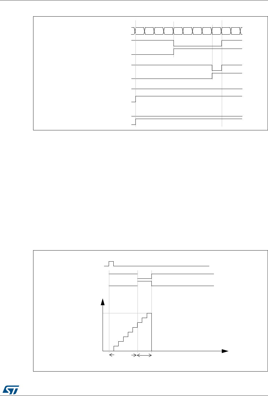
DocID026448 Rev 1 381/836
RM0383 General-purpose timers (TIM9 to TIM11)
409
Figure 151. Edge-aligned PWM waveforms (ARR=8)
14.3.10 One-pulse mode
One-pulse mode (OPM) is a particular case of the previous modes. It allows the counter to
be started in response to a stimulus and to generate a pulse with a programmable length
after a programmable delay.
Starting the counter can be controlled through the slave mode controller. Generating the
waveform can be done in output compare mode or PWM mode. You select One-pulse mode
by setting the OPM bit in the TIMx_CR1 register. This makes the counter stop automatically
at the next update event UEV.
A pulse can be correctly generated only if the compare value is different from the counter
initial value. Before starting (when the timer is waiting for the trigger), the configuration must
be as follows:
CNT < CCRx≤ARR (in particular, 0 < CCRx)
Figure 152. Example of one pulse mode.
Counter register 01234567801
OCXREF
CCxIF
OCXREF
CCxIF
OCXREF
CCxIF
OCXREF
CCxIF
CCRx=4
CCRx=8
CCRx>8
CCRx=0
TI2
OC1REF
Counter
t
0
TIM1_ARR
TIM1_CCR1
OC1
tDELAY tPULSE

General-purpose timers (TIM9 to TIM11) RM0383
382/836 DocID026448 Rev 1
For example you may want to generate a positive pulse on OC1 with a length of tPULSE and
after a delay of tDELAY as soon as a positive edge is detected on the TI2 input pin.
Use TI2FP2 as trigger 1:
1. Map TI2FP2 to TI2 by writing CC2S=’01’ in the TIMx_CCMR1 register.
2. TI2FP2 must detect a rising edge, write CC2P=’0’ and CC2NP = ‘0’ in the TIMx_CCER
register.
3. Configure TI2FP2 as trigger for the slave mode controller (TRGI) by writing TS=’110’ in
the TIMx_SMCR register.
4. TI2FP2 is used to start the counter by writing SMS to ‘110’ in the TIMx_SMCR register
(trigger mode).
The OPM waveform is defined by writing the compare registers (taking into account the
clock frequency and the counter prescaler).
•The tDELAY is defined by the value written in the TIMx_CCR1 register.
•The tPULSE is defined by the difference between the auto-reload value and the compare
value (TIMx_ARR - TIMx_CCR1).
•Let’s say you want to build a waveform with a transition from ‘0’ to ‘1’ when a compare
match occurs and a transition from ‘1’ to ‘0’ when the counter reaches the auto-reload
value. To do this you enable PWM mode 2 by writing OC1M=’111’ in the TIMx_CCMR1
register. You can optionally enable the preload registers by writing OC1PE=’1’ in the
TIMx_CCMR1 register and ARPE in the TIMx_CR1 register. In this case you have to
write the compare value in the TIMx_CCR1 register, the auto-reload value in the
TIMx_ARR register, generate an update by setting the UG bit and wait for external
trigger event on TI2. CC1P is written to ‘0’ in this example.
You only want 1 pulse (Single mode), so you write '1 in the OPM bit in the TIMx_CR1
register to stop the counter at the next update event (when the counter rolls over from the
auto-reload value back to 0). When OPM bit in the TIMx_CR1 register is set to '0', so the
Repetitive Mode is selected.
Particular case: OCx fast enable
In One-pulse mode, the edge detection on TIx input set the CEN bit which enables the
counter. Then the comparison between the counter and the compare value makes the
output toggle. But several clock cycles are needed for these operations and it limits the
minimum delay tDELAY min we can get.
If you want to output a waveform with the minimum delay, you can set the OCxFE bit in the
TIMx_CCMRx register. Then OCxRef (and OCx) are forced in response to the stimulus,
without taking in account the comparison. Its new level is the same as if a compare match
had occurred. OCxFE acts only if the channel is configured in PWM1 or PWM2 mode.
14.3.11 TIM9 external trigger synchronization
The TIM9 timer can be synchronized with an external trigger in several modes: Reset mode,
Gated mode and Trigger mode.
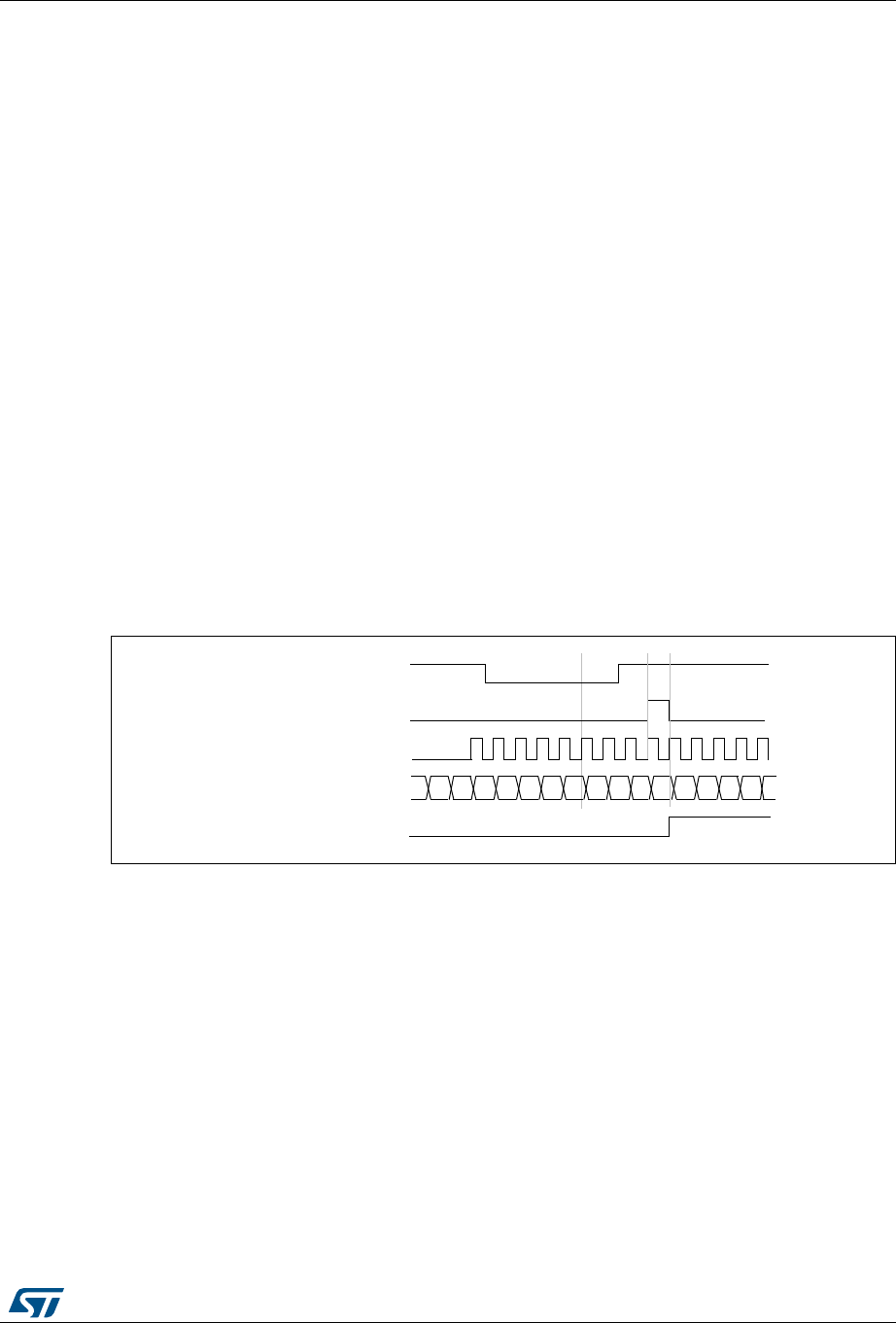
DocID026448 Rev 1 383/836
RM0383 General-purpose timers (TIM9 to TIM11)
409
Slave mode: Reset mode
The counter and its prescaler can be reinitialized in response to an event on a trigger input.
Moreover, if the URS bit from the TIMx_CR1 register is low, an update event UEV is
generated. Then all the preloaded registers (TIMx_ARR, TIMx_CCRx) are updated.
In the following example, the upcounter is cleared in response to a rising edge on TI1 input:
1. Configure the channel 1 to detect rising edges on TI1. Configure the input filter duration
(in this example, we don’t need any filter, so we keep IC1F=’0000’). The capture
prescaler is not used for triggering, so you don’t need to configure it. The CC1S bits
select the input capture source only, CC1S = ‘01’ in the TIMx_CCMR1 register.
Program CC1P and CC1NP to ‘00’ in TIMx_CCER register to validate the polarity (and
detect rising edges only).
2. Configure the timer in reset mode by writing SMS=’100’ in TIMx_SMCR register. Select
TI1 as the input source by writing TS=’101’ in TIMx_SMCR register.
3. Start the counter by writing CEN=’1’ in the TIMx_CR1 register.
The counter starts counting on the internal clock, then behaves normally until TI1 rising
edge. When TI1 rises, the counter is cleared and restarts from 0. In the meantime, the
trigger flag is set (TIF bit in the TIMx_SR register) and an interrupt request can be sent if
enabled (depending on the TIE bit in TIMx_DIER register).
The following figure shows this behavior when the auto-reload register TIMx_ARR=0x36.
The delay between the rising edge on TI1 and the actual reset of the counter is due to the
resynchronization circuit on TI1 input.
Figure 153. Control circuit in reset mode
Slave mode: Gated mode
The counter can be enabled depending on the level of a selected input.
In the following example, the upcounter counts only when TI1 input is low:
1. Configure the channel 1 to detect low levels on TI1. Configure the input filter duration
(in this example, we don’t need any filter, so we keep IC1F=’0000’). The capture
prescaler is not used for triggering, so you don’t need to configure it. The CC1S bits
select the input capture source only, CC1S=’01’ in TIMx_CCMR1 register. Program
CC1P=’1’ and CC1NP= ‘0’ in TIMx_CCER register to validate the polarity (and detect
low level only).
2. Configure the timer in gated mode by writing SMS=’101’ in TIMx_SMCR register.
Select TI1 as the input source by writing TS=’101’ in TIMx_SMCR register.
3. Enable the counter by writing CEN=’1’ in the TIMx_CR1 register (in gated mode, the
counter doesn’t start if CEN=’0’, whatever is the trigger input level).
00
Counter clock = ck_cnt = ck_psc
Counter register 01 02 03 00 01 02 0332 33 34 35 36
UG
TI1
3130
TIF
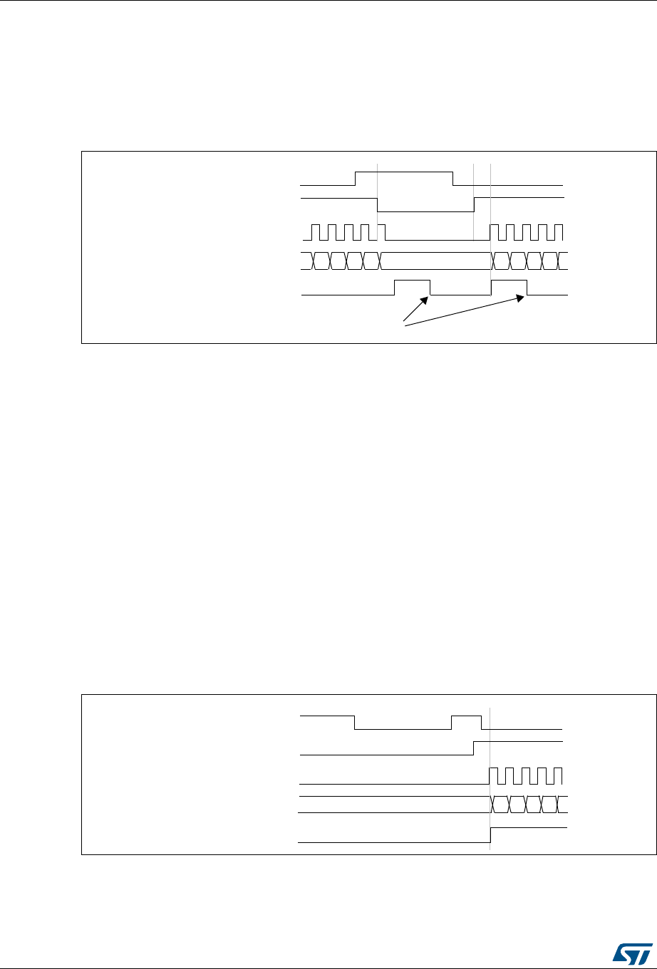
General-purpose timers (TIM9 to TIM11) RM0383
384/836 DocID026448 Rev 1
The counter starts counting on the internal clock as long as TI1 is low and stops as soon as
TI1 becomes high. The TIF flag in the TIMx_SR register is set both when the counter starts
or stops.
The delay between the rising edge on TI1 and the actual stop of the counter is due to the
resynchronization circuit on TI1 input.
Figure 154. Control circuit in gated mode
Slave mode: Trigger mode
The counter can start in response to an event on a selected input.
In the following example, the upcounter starts in response to a rising edge on TI2 input:
1. Configure the channel 2 to detect rising edges on TI2. Configure the input filter duration
(in this example, we don’t need any filter, so we keep IC2F=’0000’). The capture
prescaler is not used for triggering, so you don’t need to configure it. The CC2S bits are
configured to select the input capture source only, CC2S=’01’ in TIMx_CCMR1 register.
Program CC2P=’1’ and CC2NP=’0’ in TIMx_CCER register to validate the polarity (and
detect low level only).
2. Configure the timer in trigger mode by writing SMS=’110’ in TIMx_SMCR register.
Select TI2 as the input source by writing TS=’110’ in TIMx_SMCR register.
When a rising edge occurs on TI2, the counter starts counting on the internal clock and the
TIF flag is set.
The delay between the rising edge on TI2 and the actual start of the counter is due to the
resynchronization circuit on TI2 input.
Figure 155. Control circuit in trigger mode
Counter clock = ck_cnt = ck_psc
Counter register 35 36 37 3832 33 34
TI1
3130
cnt_en
TIF
Write TIF=0
Counter clock = ck_cnt = ck_psc
Counter register 35 36 37 3834
TI2
cnt_en
TIF

DocID026448 Rev 1 385/836
RM0383 General-purpose timers (TIM9 to TIM11)
409
14.3.12 Timer synchronization (TIM9)
The TIM timers are linked together internally for timer synchronization or chaining. Refer to
Section 13.3.15: Timer synchronization on page 336 for details.
14.3.13 Debug mode
When the microcontroller enters debug mode (Cortex®-M4 with FPU core halted), the TIMx
counter either continues to work normally or stops, depending on DBG_TIMx_STOP
configuration bit in DBG module. For more details, refer to Section 23.16.2: Debug support
for timers, watchdog and I2C.
14.4 TIM9 registers
Refer to Section 1.1 for a list of abbreviations used in register descriptions.
The peripheral registers have to be written by half-words (16 bits) or words (32 bits). Read
accesses can be done by bytes (8 bits), half-words (16 bits) or words (32 bits).
14.4.1 TIM9 control register 1 (TIMx_CR1)
Address offset: 0x00
Reset value: 0x0000
1514131211109876543210
Reserved CKD[1:0] ARPE Reserved OPM URS UDIS CEN
rw rw rw rw rw rw rw
Bits 15:10 Reserved, must be kept at reset value.
Bits 9:8 CKD: Clock division
This bit-field indicates the division ratio between the timer clock (CK_INT) frequency and
sampling clock used by the digital filters (TIx),
00: tDTS = tCK_INT
01: tDTS = 2 × tCK_INT
10: tDTS = 4 × tCK_INT
11: Reserved
Bit 7 ARPE: Auto-reload preload enable
0: TIMx_ARR register is not buffered.
1: TIMx_ARR register is buffered.
Bits 6:4 Reserved, must be kept at reset value.
Bit 3 OPM: One-pulse mode
0: Counter is not stopped on the update event
1: Counter stops counting on the next update event (clearing the CEN bit).

General-purpose timers (TIM9 to TIM11) RM0383
386/836 DocID026448 Rev 1
Bit 2 URS: Update request source
This bit is set and cleared by software to select the UEV event sources.
0: Any of the following events generates an update interrupt if enabled:
– Counter overflow
– Setting the UG bit
1: Only counter overflow generates an update interrupt if enabled.
Bit 1 UDIS: Update disable
This bit is set and cleared by software to enable/disable update event (UEV) generation.
0: UEV enabled. An UEV is generated by one of the following events:
– Counter overflow
– Setting the UG bit
Buffered registers are then loaded with their preload values.
1: UEV disabled. No UEV is generated, shadow registers keep their value (ARR, PSC,
CCRx). The counter and the prescaler are reinitialized if the UG bit is set.
Bit 0 CEN: Counter enable
0: Counter disabled
1: Counter enabled
CEN is cleared automatically in one-pulse mode, when an update event occurs.

DocID026448 Rev 1 387/836
RM0383 General-purpose timers (TIM9 to TIM11)
409
14.4.2 TIM9 slave mode control register (TIMx_SMCR)
Address offset: 0x08
Reset value: 0x0000
1514131211109876543210
Reserved MSM TS[2:0] Res. SMS[2:0]
rw rw rw rw rw rw rw
Bits 15:8 Reserved, must be kept at reset value.
Bit 7 MSM: Master/Slave mode
0: No action
1: The effect of an event on the trigger input (TRGI) is delayed to allow a perfect
synchronization between the current timer and its slaves (through TRGO). It is useful in
order to synchronize several timers on a single external event.
Bits 6:4 TS: Trigger selection
This bitfield selects the trigger input to be used to synchronize the counter.
000: Internal Trigger 0 (ITR0)
001: Internal Trigger 1 (ITR1)
010: Internal Trigger 2 (ITR2)
011: Internal Trigger 3 (ITR3)
100: TI1 Edge Detector (TI1F_ED)
101: Filtered Timer Input 1 (TI1FP1)
110: Filtered Timer Input 2 (TI2FP2)
111: Reserved.
See Table 56: TIMx internal trigger connection on page 388 for more details on the meaning
of ITRx for each timer.
Note: These bits must be changed only when they are not used (e.g. when SMS=’000’) to
avoid wrong edge detections at the transition.
Bit 3 Reserved, must be kept at reset value.
Bits 2:0 SMS: Slave mode selection
When external signals are selected, the active edge of the trigger signal (TRGI) is linked to
the polarity selected on the external input (see Input control register and Control register
descriptions.
000: Slave mode disabled - if CEN = 1 then the prescaler is clocked directly by the internal
clock
001: Reserved
010: Reserved
011: Reserved
100: Reset mode - Rising edge of the selected trigger input (TRGI) reinitializes the counter
and generates an update of the registers
101: Gated mode - The counter clock is enabled when the trigger input (TRGI) is high. The
counter stops (but is not reset) as soon as the trigger becomes low. Counter starts and stops
are both controlled
110: Trigger mode - The counter starts on a rising edge of the trigger TRGI (but it is not
reset). Only the start of the counter is controlled
111: External clock mode 1 - Rising edges of the selected trigger (TRGI) clock the counter
Note: The Gated mode must not be used if TI1F_ED is selected as the trigger input
(TS=’100’). Indeed, TI1F_ED outputs 1 pulse for each transition on TI1F, whereas the
Gated mode checks the level of the trigger signal.
General-purpose timers (TIM9 to TIM11) RM0383
388/836 DocID026448 Rev 1
14.4.3 TIM9 Interrupt enable register (TIMx_DIER)
Address offset: 0x0C
Reset value: 0x0000
Table 56. TIMx internal trigger connection
Slave TIM ITR0 (TS =’ 000’) ITR1 (TS = ‘001’) ITR2 (TS = ‘010’) ITR3 (TS = ’011’)
TIM2 TIM1 Reserved TIM3 TIM4
TIM3 TIM1 TIM2 TIM5 TIM4
TIM4 TIM1 TIM2 TIM3 Reserved
TIM5 TIM2 TIM3 TIM4 Reserved
TIM9 TIM2 TIM3 TIM10 TIM11
1514131211109876543210
Reserved TIE Res CC2IE CC1IE UIE
rw rw rw rw
Bits 15:7 Reserved, must be kept at reset value.
Bit 6 TIE: Trigger interrupt enable
0: Trigger interrupt disabled.
1: Trigger interrupt enabled.
Bit 5:3 Reserved, must be kept at reset value.
Bit 2 CC2IE: Capture/Compare 2 interrupt enable
0: CC2 interrupt disabled.
1: CC2 interrupt enabled.
Bit 1 CC1IE: Capture/Compare 1 interrupt enable
0: CC1 interrupt disabled.
1: CC1 interrupt enabled.
Bit 0 UIE: Update interrupt enable
0: Update interrupt disabled.
1: Update interrupt enabled.

DocID026448 Rev 1 389/836
RM0383 General-purpose timers (TIM9 to TIM11)
409
14.4.4 TIM9 status register (TIMx_SR)
Address offset: 0x10
Reset value: 0x0000
1514131211109876543210
Reserved CC2OF CC1OF Reserved TIF Reserved CC2IF CC1IF UIF
rc_w0 rc_w0 rc_w0 rc_w0 rc_w0 rc_w0
Bits 15:11 Reserved, must be kept at reset value.
Bit 10 CC2OF: Capture/compare 2 overcapture flag
refer to CC1OF description
Bit 9 CC1OF: Capture/Compare 1 overcapture flag
This flag is set by hardware only when the corresponding channel is configured in input
capture mode. It is cleared by software by writing it to ‘0’.
0: No overcapture has been detected.
1: The counter value has been captured in TIMx_CCR1 register while CC1IF flag was
already set
Bits 8:7 Reserved, must be kept at reset value.
Bit 6 TIF: Trigger interrupt flag
This flag is set by hardware on trigger event (active edge detected on TRGI input when the
slave mode controller is enabled in all modes but gated mode. It is set when the counter
starts or stops when gated mode is selected. It is cleared by software.
0: No trigger event occurred.
1: Trigger interrupt pending.
Bits 5:3 Reserved, must be kept at reset value.

General-purpose timers (TIM9 to TIM11) RM0383
390/836 DocID026448 Rev 1
14.4.5 TIM9 event generation register (TIMx_EGR)
Address offset: 0x14
Reset value: 0x0000
Bit 2 CC2IF: Capture/Compare 2 interrupt flag
refer to CC1IF description
Bit 1 CC1IF: Capture/compare 1 interrupt flag
If channel CC1 is configured as output:
This flag is set by hardware when the counter matches the compare value. It is cleared by
software.
0: No match.
1: The content of the counter TIMx_CNT matches the content of the TIMx_CCR1 register.
When the contents of TIMx_CCR1 are greater than the contents of TIMx_ARR, the CC1IF
bit goes high on the counter overflow.
If channel CC1 is configured as input:
This bit is set by hardware on a capture. It is cleared by software or by reading the
TIMx_CCR1 register.
0: No input capture occurred.
1: The counter value has been captured in TIMx_CCR1 register (an edge has been detected
on IC1 which matches the selected polarity).
Bit 0 UIF: Update interrupt flag
This bit is set by hardware on an update event. It is cleared by software.
0: No update occurred.
1: Update interrupt pending. This bit is set by hardware when the registers are updated:
– At overflow and if UDIS=’0’ in the TIMx_CR1 register.
– When CNT is reinitialized by software using the UG bit in TIMx_EGR register, if URS=’0’ and
UDIS=’0’ in the TIMx_CR1 register.
– When CNT is reinitialized by a trigger event (refer to the synchro control register
description), if URS=’0’ and UDIS=’0’ in the TIMx_CR1 register.
1514131211109876543210
Reserved TG Reserved CC2G CC1G UG
w www
Bits 15:7 Reserved, must be kept at reset value.
Bit 6 TG: Trigger generation
This bit is set by software in order to generate an event, it is automatically cleared by
hardware.
0: No action
1: The TIF flag is set in the TIMx_SR register. Related interrupt can occur if enabled
Bits 5:3 Reserved, must be kept at reset value.

DocID026448 Rev 1 391/836
RM0383 General-purpose timers (TIM9 to TIM11)
409
Bit 2 CC2G: Capture/compare 2 generation
refer to CC1G description
Bit 1 CC1G: Capture/compare 1 generation
This bit is set by software to generate an event, it is automatically cleared by hardware.
0: No action
1: A capture/compare event is generated on channel 1:
If channel CC1 is configured as output:
the CC1IF flag is set, the corresponding interrupt is sent if enabled.
If channel CC1 is configured as input:
The current counter value is captured in the TIMx_CCR1 register. The CC1IF flag is set, the
corresponding interrupt is sent if enabled. The CC1OF flag is set if the CC1IF flag was
already high.
Bit 0 UG: Update generation
This bit can be set by software, it is automatically cleared by hardware.
0: No action
1: Re-initializes the counter and generates an update of the registers. The prescaler counter
is also cleared and the prescaler ratio is not affected. The counter is cleared.

General-purpose timers (TIM9 to TIM11) RM0383
392/836 DocID026448 Rev 1
14.4.6 TIM9 capture/compare mode register 1 (TIMx_CCMR1)
Address offset: 0x18
Reset value: 0x0000
The channels can be used in input (capture mode) or in output (compare mode). The
direction of a channel is defined by configuring the corresponding CCxS bits. All the other
bits in this register have different functions in input and output modes. For a given bit, OCxx
describes its function when the channel is configured in output mode, ICxx describes its
function when the channel is configured in input mode. So you must take care that the same
bit can have different meanings for the input stage and the output stage.
Output compare mode
1514131211109876543210
Res. OC2M[2:0] OC2PE OC2FE CC2S[1:0] Res. OC1M[2:0] OC1PE OC1FE CC1S[1:0]
IC2F[3:0] IC2PSC[1:0] IC1F[3:0] IC1PSC[1:0]
rw rw rw rw rw rw rw rw rw rw rw rw rw rw rw rw
Bits 14:12 OC2M[2:0]: Output compare 2 mode
Bit 11 OC2PE: Output compare 2 preload enable
Bit 10 OC2FE: Output compare 2 fast enable
Bits 9:8 CC2S[1:0]: Capture/Compare 2 selection
This bitfield defines the direction of the channel (input/output) as well as the used input.
00: CC2 channel is configured as output
01: CC2 channel is configured as input, IC2 is mapped on TI2
10: CC2 channel is configured as input, IC2 is mapped on TI1
11: CC2 channel is configured as input, IC2 is mapped on TRC. This mode works only if an
internal trigger input is selected through the TS bit (TIMx_SMCR register
Note: The CC2S bits are writable only when the channel is OFF (CC2E = 0 in TIMx_CCER).
Bits 6:4 OC1M: Output compare 1 mode
These bits define the behavior of the output reference signal OC1REF from which OC1 and
OC1N are derived. OC1REF is active high whereas the active levels of OC1 and OC1N
depend on the CC1P and CC1NP bits, respectively.
000: Frozen - The comparison between the output compare register TIMx_CCR1 and the
counter TIMx_CNT has no effect on the outputs.(this mode is used to generate a timing
base).
001: Set channel 1 to active level on match. The OC1REF signal is forced high when the
TIMx_CNT counter matches the capture/compare register 1 (TIMx_CCR1).
010: Set channel 1 to inactive level on match. The OC1REF signal is forced low when the
TIMx_CNT counter matches the capture/compare register 1 (TIMx_CCR1).
011: Toggle - OC1REF toggles when TIMx_CNT=TIMx_CCR1
100: Force inactive level - OC1REF is forced low
101: Force active level - OC1REF is forced high
110: PWM mode 1 - In upcounting, channel 1 is active as long as TIMx_CNT<TIMx_CCR1
else it is inactive. In downcounting, channel 1 is inactive (OC1REF=‘0) as long as
TIMx_CNT>TIMx_CCR1, else it is active (OC1REF=’1’)
111: PWM mode 2 - In upcounting, channel 1 is inactive as long as TIMx_CNT<TIMx_CCR1
else it is active. In downcounting, channel 1 is active as long as TIMx_CNT>TIMx_CCR1
else it is inactive.
Note: In PWM mode 1 or 2, the OCREF level changes only when the result of the
comparison changes or when the output compare mode switches from “frozen” mode
to “PWM” mode.

DocID026448 Rev 1 393/836
RM0383 General-purpose timers (TIM9 to TIM11)
409
Bit 3 OC1PE: Output compare 1 preload enable
0: Preload register on TIMx_CCR1 disabled. TIMx_CCR1 can be written at anytime, the
new value is taken into account immediately
1: Preload register on TIMx_CCR1 enabled. Read/Write operations access the preload
register. TIMx_CCR1 preload value is loaded into the active register at each update event
Note: The PWM mode can be used without validating the preload register only in one-pulse
mode (OPM bit set in the TIMx_CR1 register). Else the behavior is not guaranteed.
Bit 2 OC1FE: Output compare 1 fast enable
This bit is used to accelerate the effect of an event on the trigger in input on the CC output.
0: CC1 behaves normally depending on the counter and CCR1 values even when the
trigger is ON. The minimum delay to activate the CC1 output when an edge occurs on the
trigger input is 5 clock cycles
1: An active edge on the trigger input acts like a compare match on the CC1 output. Then,
OC is set to the compare level independently of the result of the comparison. Delay to
sample the trigger input and to activate CC1 output is reduced to 3 clock cycles. OC1FE
acts only if the channel is configured in PWM1 or PWM2 mode.
Bits 1:0 CC1S: Capture/Compare 1 selection
This bitfield defines the direction of the channel (input/output) as well as the used input.
00: CC1 channel is configured as output
01: CC1 channel is configured as input, IC1 is mapped on TI1
10: CC1 channel is configured as input, IC1 is mapped on TI2
11: CC1 channel is configured as input, IC1 is mapped on TRC. This mode works only if an
internal trigger input is selected through the TS bit (TIMx_SMCR register)
Note: The CC1S bits are writable only when the channel is OFF (CC1E = 0 in TIMx_CCER).

General-purpose timers (TIM9 to TIM11) RM0383
394/836 DocID026448 Rev 1
Input capture mode
Bits 15:12 IC2F: Input capture 2 filter
Bits 11:10 IC2PSC[1:0]: Input capture 2 prescaler
Bits 9:8 CC2S: Capture/compare 2 selection
This bitfield defines the direction of the channel (input/output) as well as the used input.
00: CC2 channel is configured as output
01: CC2 channel is configured as input, IC2 is mapped on TI2
10: CC2 channel is configured as input, IC2 is mapped on TI1
11: CC2 channel is configured as input, IC2 is mapped on TRC. This mode works only if an
internal trigger input is selected through the TS bit (TIMx_SMCR register)
Note: The CC2S bits are writable only when the channel is OFF (CC2E = 0 in TIMx_CCER).
Bits 7:4 IC1F: Input capture 1 filter
This bitfield defines the frequency used to sample the TI1 input and the length of the digital
filter applied to TI1. The digital filter is made of an event counter in which N events are
needed to validate a transition on the output:
0000: No filter, sampling is done at fDTS1000: fSAMPLING=fDTS/8, N=6
0001: fSAMPLING=fCK_INT
, N=21001: fSAMPLING=fDTS/8, N=8
0010: fSAMPLING=fCK_INT
, N=41010: fSAMPLING=fDTS/16, N=5
0011: fSAMPLING=fCK_INT
, N=8 1011: fSAMPLING=fDTS/16, N=6
0100: fSAMPLING=fDTS/2, N=61100: fSAMPLING=fDTS/16, N=8
0101: fSAMPLING=fDTS/2, N=81101: fSAMPLING=fDTS/32, N=5
0110: fSAMPLING=fDTS/4, N=61110: fSAMPLING=fDTS/32, N=6
0111: fSAMPLING=fDTS/4, N=81111: fSAMPLING=fDTS/32, N=8
Bits 3:2 IC1PSC: Input capture 1 prescaler
This bitfield defines the ratio of the prescaler acting on the CC1 input (IC1).
The prescaler is reset as soon as CC1E=’0’ (TIMx_CCER register).
00: no prescaler, capture is done each time an edge is detected on the capture input
01: capture is done once every 2 events
10: capture is done once every 4 events
11: capture is done once every 8 events
Bits 1:0 CC1S: Capture/Compare 1 selection
This bitfield defines the direction of the channel (input/output) as well as the used input.
00: CC1 channel is configured as output
01: CC1 channel is configured as input, IC1 is mapped on TI1
10: CC1 channel is configured as input, IC1 is mapped on TI2
11: CC1 channel is configured as input, IC1 is mapped on TRC. This mode is working only if
an internal trigger input is selected through TS bit (TIMx_SMCR register)
Note: The CC1S bits are writable only when the channel is OFF (CC1E = 0 in TIMx_CCER).

DocID026448 Rev 1 395/836
RM0383 General-purpose timers (TIM9 to TIM11)
409
14.4.7 TIM9 capture/compare enable register (TIMx_CCER)
Address offset: 0x20
Reset value: 0x0000
1514131211109876543210
Reserved CC2NP Res. CC2P CC2E CC1NP Res. CC1P CC1E
rw rw rw rw rw rw
Bits 15:8 Reserved, must be kept at reset value.
Bit 7 CC2NP: Capture/Compare 2 output Polarity
refer to CC1NP description
Bits 6 Reserved, must be kept at reset value.
Bit 5 CC2P: Capture/Compare 2 output Polarity
refer to CC1P description
Bit 4 CC2E: Capture/Compare 2 output enable
refer to CC1E description
Bit 3 CC1NP: Capture/Compare 1 complementary output Polarity
CC1 channel configured as output: CC1NP must be kept cleared
CC1 channel configured as input: CC1NP is used in conjunction with CC1P to define
TI1FP1/TI2FP1 polarity (refer to CC1P description).
Bit 2 Reserved, must be kept at reset value.
Bit 1 CC1P: Capture/Compare 1 output Polarity.
CC1 channel configured as output:
0: OC1 active high.
1: OC1 active low.
CC1 channel configured as input:
CC1NP/CC1P bits select TI1FP1 and TI2FP1 polarity for trigger or capture operations.
00: noninverted/rising edge
Circuit is sensitive to TIxFP1 rising edge (capture, trigger in reset, external clock or trigger
mode), TIxFP1 is not inverted (trigger in gated mode, encoder mode).
01: inverted/falling edge
Circuit is sensitive to TIxFP1 falling edge (capture, trigger in reset, external clock or trigger
mode), TIxFP1 is inverted (trigger in gated mode, encoder mode).
10: reserved, do not use this configuration.
Note: 11: noninverted/both edges
Circuit is sensitive to both TIxFP1 rising and falling edges (capture, trigger in reset,
external clock or trigger mode), TIxFP1 is not inverted (trigger in gated mode). This
configuration must not be used for encoder mode.
Bit 0 CC1E: Capture/Compare 1 output enable.
CC1 channel configured as output:
0: Off - OC1 is not active.
1: On - OC1 signal is output on the corresponding output pin.
CC1 channel configured as input:
This bit determines if a capture of the counter value can actually be done into the input
capture/compare register 1 (TIMx_CCR1) or not.
0: Capture disabled.
1: Capture enabled.
General-purpose timers (TIM9 to TIM11) RM0383
396/836 DocID026448 Rev 1
Note: The states of the external I/O pins connected to the standard OCx channels depend on the
state of the OCx channel and on the GPIO registers.
14.4.8 TIM9 counter (TIMx_CNT)
Address offset: 0x24
Reset value: 0x0000 0000
14.4.9 TIM9 prescaler (TIMx_PSC)
Address offset: 0x28
Reset value: 0x0000
14.4.10 TIM9 auto-reload register (TIMx_ARR)
Address offset: 0x2C
Reset value: 0x0000
Table 57. Output control bit for standard OCx channels
CCxE bit OCx output state
0 Output disabled (OCx=’0’, OCx_EN=’0’)
1 OCx=OCxREF + Polarity, OCx_EN=’1’
1514131211109876543210
CNT[15:0]
rw rw rw rw rw rw rw rw rw rw rw rw rw rw rw rw
Bits 15:0 CNT[15:0]: Counter value
1514131211109876543210
PSC[15:0]
rw rw rw rw rw rw rw rw rw rw rw rw rw rw rw rw
Bits 15:0 PSC[15:0]: Prescaler value
The counter clock frequency CK_CNT is equal to fCK_PSC / (PSC[15:0] + 1).
PSC contains the value to be loaded into the active prescaler register at each update event.
1514131211109876543210
ARR[15:0]
rw rw rw rw rw rw rw rw rw rw rw rw rw rw rw rw
Bits 15:0 ARR[15:0]: Auto-reload value
ARR is the value to be loaded into the actual auto-reload register.
Refer to the Section 14.3.1: Time-base unit on page 369 for more details about ARR update
and behavior.
The counter is blocked while the auto-reload value is null.

DocID026448 Rev 1 397/836
RM0383 General-purpose timers (TIM9 to TIM11)
409
14.4.11 TIM9 capture/compare register 1 (TIMx_CCR1)
Address offset: 0x34
Reset value: 0x0000
14.4.12 TIM9 capture/compare register 2 (TIMx_CCR2)
Address offset: 0x38
Reset value: 0x0000
14.4.13 TIM9 register map
TIM9 registers are mapped as 16-bit addressable registers as described below:
1514131211109876543210
CCR1[15:0]
rw rw rw rw rw rw rw rw rw rw rw rw rw rw rw rw
Bits 15:0 CCR1[15:0]: Capture/Compare 1 value
If channel CC1 is configured as output:
CCR1 is the value to be loaded into the actual capture/compare 1 register (preload value).
It is loaded permanently if the preload feature is not selected in the TIMx_CCMR1 register
(OC1PE bit). Else the preload value is copied into the active capture/compare 1 register
when an update event occurs.
The active capture/compare register contains the value to be compared to the TIMx_CNT
counter and signaled on the OC1 output.
If channel CC1is configured as input:
CCR1 is the counter value transferred by the last input capture 1 event (IC1).
1514131211109876543210
CCR2[15:0]
rw rw rw rw rw rw rw rw rw rw rw rw rw rw rw rw
Bits 15:0 CCR2[15:0]: Capture/Compare 2 value
If channel CC2 is configured as output:
CCR2 is the value to be loaded into the actual capture/compare 2 register (preload value).
It is loaded permanently if the preload feature is not selected in the TIMx_CCMR2 register
(OC2PE bit). Else the preload value is copied into the active capture/compare 2 register
when an update event occurs.
The active capture/compare register contains the value to be compared to the TIMx_CNT
counter and signalled on the OC2 output.
If channel CC2 is configured as input:
CCR2 is the counter value transferred by the last input capture 2 event (IC2).
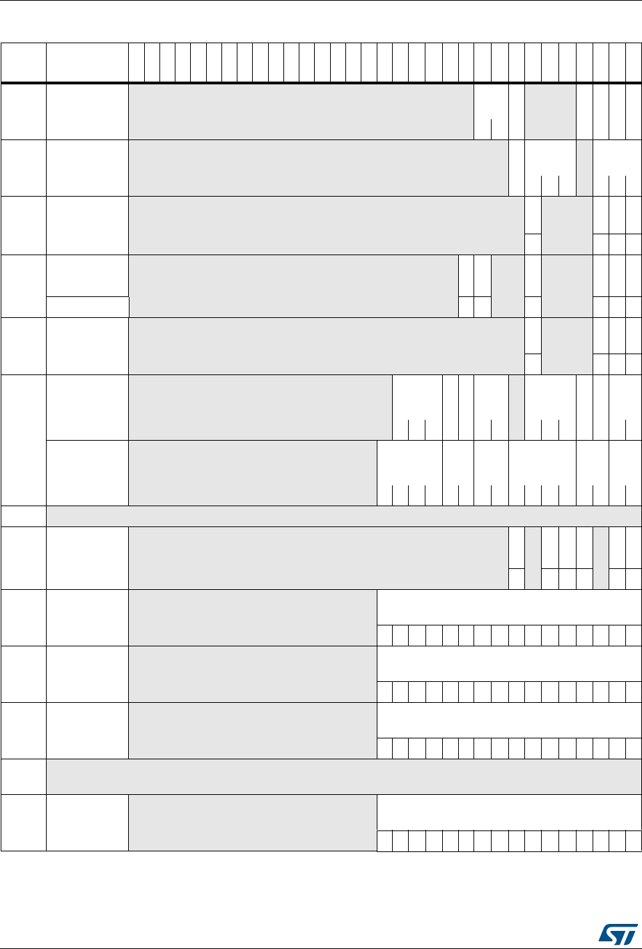
General-purpose timers (TIM9 to TIM11) RM0383
398/836 DocID026448 Rev 1
Table 58. TIM9 register map and reset values
Offset Register
31
30
29
28
27
26
25
24
23
22
21
20
19
18
17
16
15
14
13
12
11
10
9
8
7
6
5
4
3
2
1
0
0x00
TIMx_CR1
Reserved
CKD
[1:0]
ARPE
Reserved
OPM
URS
UDIS
CEN
Reset value 000 0000
0x08
TIMx_SMCR
Reserved
MSM
TS[2:0]
Reserved
SMS[2:0]
Reset value 000 0 000
0x0C
TIMx_DIER
Reserved
TIE
Reserved
CC2IE
CC1IE
UIE
Reset value 0000
0x10
TIMx_SR
Reserved
CC2OF
CC1OF
Reserved
TIF
Reserved
CC2IF
CC1IF
UIF
Reset value 00 0 000
0x14
TIMx_EGR
Reserved
TG
Reserved
CC2G
CC1G
UG
Reset value 0000
0x18
TIMx_CCMR1
Output Compare
mode Reserved
OC2M
[2:0]
OC2PE
OC2FE
CC2S
[1:0]
Reserved
OC1M
[2:0]
OC1PE
OC1FE
CC1
S
[1:0]
Reset value 0 0 0 0 0 0 0 0 0 0 0 0 0 0
TIMx_CCMR1
Input Capture
mode Reserved
IC2F[3:0]
IC2
PSC
[1:0]
CC2S
[1:0] IC1F[3:0]
IC1
PSC
[1:0]
CC1
S
[1:0]
Reset value 0 0 0 0 0 0 0 0 0 0 0 0 0 0 0 0
0x1C Reserved
0x20
TIMx_CCER
Reserved
CC2NP
Reserved
CC2P
CC2E
CC1NP
Reserved
CC1P
CC1E
Reset value 000000
0x24
TIMx_CNT
Reserved
CNT[15:0]
Reset value 0 0 0 0 0 0 0 0 0 0 0 0 0 0 0 0
0x28
TIMx_PSC
Reserved
PSC[15:0]
Reset value 0 0 0 0 0 0 0 0 0 0 0 0 0 0 0 0
0x2C
TIMx_ARR
Reserved
ARR[15:0]
Reset value 0 0 0 0 0 0 0 0 0 0 0 0 0 0 0 0
0x30 Reserved
0x34
TIMx_CCR1
Reserved
CCR1[15:0]
Reset value 0 0 0 0 0 0 0 0 0 0 0 0 0 0 0 0

DocID026448 Rev 1 399/836
RM0383 General-purpose timers (TIM9 to TIM11)
409
Refer to Table 3 on page 41 for the register boundary addresses.
0x38
TIMx_CCR2
Reserved
CCR2[15:0]
Reset value 0 0 0 0 0 0 0 0 0 0 0 0 0 0 0 0
0x3C to
0x4C Reserved
Table 58. TIM9 register map and reset values (continued)
Offset Register
31
30
29
28
27
26
25
24
23
22
21
20
19
18
17
16
15
14
13
12
11
10
9
8
7
6
5
4
3
2
1
0

General-purpose timers (TIM9 to TIM11) RM0383
400/836 DocID026448 Rev 1
14.5 TIM10/11 registers
The peripheral registers have to be written by half-words (16 bits) or words (32 bits). Read
accesses can be done by bytes (8 bits), half-words (16 bits) or words (32 bits).
14.5.1 TIM10/11 control register 1 (TIMx_CR1)
Address offset: 0x00
Reset value: 0x0000
1514131211109876543210
Reserved CKD[1:0] ARPE Reserved URS UDIS CEN
rw rw rw rw rw rw
Bits 15:10 Reserved, must be kept at reset value.
Bits 9:8 CKD: Clock division
This bit-field indicates the division ratio between the timer clock (CK_INT) frequency and
sampling clock used by the digital filters (TIx),
00: tDTS = tCK_INT
01: tDTS = 2 × tCK_INT
10: tDTS = 4 × tCK_INT
11: Reserved
Bit 7 ARPE: Auto-reload preload enable
0: TIMx_ARR register is not buffered
1: TIMx_ARR register is buffered
Bits 6:3 Reserved, must be kept at reset value.
Bit 2 URS: Update request source
This bit is set and cleared by software to select the update interrupt (UEV) sources.
0: Any of the following events generate an UEV if enabled:
– Counter overflow
– Setting the UG bit
1: Only counter overflow generates an UEV if enabled.
Bit 1 UDIS: Update disable
This bit is set and cleared by software to enable/disable update interrupt (UEV) event
generation.
0: UEV enabled. An UEV is generated by one of the following events:
– Counter overflow
– Setting the UG bit.
Buffered registers are then loaded with their preload values.
1: UEV disabled. No UEV is generated, shadow registers keep their value (ARR, PSC,
CCRx). The counter and the prescaler are reinitialized if the UG bit is set.
Bit 0 CEN: Counter enable
0: Counter disabled
1: Counter enabled

DocID026448 Rev 1 401/836
RM0383 General-purpose timers (TIM9 to TIM11)
409
14.5.2 TIM status register (TIMx_SR)
Address offset: 0x10
Reset value: 0x0000
14.5.3 TIM event generation register (TIMx_EGR)
Address offset: 0x14
Reset value: 0x0000
1514131211109876543210
Reserved CC1OF Reserved CC1IF UIF
rc_w0 rc_w0 rc_w0
Bits 15:10 Reserved, must be kept at reset value.
Bit 9 CC1OF: Capture/Compare 1 overcapture flag
This flag is set by hardware only when the corresponding channel is configured in input
capture mode. It is cleared by software by writing it to ‘0’.
0: No overcapture has been detected.
1: The counter value has been captured in TIMx_CCR1 register while CC1IF flag was
already set
Bits 8:2 Reserved, must be kept at reset value.
Bit 1 CC1IF: Capture/compare 1 interrupt flag
If channel CC1 is configured as output:
This flag is set by hardware when the counter matches the compare value. It is cleared by
software.
0: No match.
1: The content of the counter TIMx_CNT matches the content of the TIMx_CCR1 register.
When the contents of TIMx_CCR1 are greater than the contents of TIMx_ARR, the CC1IF bit
goes high on the counter overflow.
If channel CC1 is configured as input:
This bit is set by hardware on a capture. It is cleared by software or by reading the
TIMx_CCR1 register.
0: No input capture occurred.
1: The counter value has been captured in TIMx_CCR1 register (an edge has been detected
on IC1 which matches the selected polarity).
Bit 0 UIF: Update interrupt flag
This bit is set by hardware on an update event. It is cleared by software.
0: No update occurred.
1: Update interrupt pending. This bit is set by hardware when the registers are updated:
– At overflow and if UDIS=’0’ in the TIMx_CR1 register.
– When CNT is reinitialized by software using the UG bit in TIMx_EGR register, if
URS=’0’ and UDIS=’0’ in the TIMx_CR1 register.
1514131211109876543210
Reserved CC1G UG
ww
General-purpose timers (TIM9 to TIM11) RM0383
402/836 DocID026448 Rev 1
14.5.4 TIM10/11 capture/compare mode register 1
(TIMx_CCMR1)
Address offset: 0x18
Reset value: 0x0000
The channels can be used in input (capture mode) or in output (compare mode). The
direction of a channel is defined by configuring the corresponding CCxS bits. All the other
bits of this register have a different function in input and in output mode. For a given bit,
OCxx describes its function when the channel is configured in output, ICxx describes its
function when the channel is configured in input. So you must take care that the same bit
can have a different meaning for the input stage and for the output stage.
Bits 15:2 Reserved, must be kept at reset value.
Bit 1 CC1G: Capture/compare 1 generation
This bit is set by software in order to generate an event, it is automatically cleared by
hardware.
0: No action
1: A capture/compare event is generated on channel 1:
If channel CC1 is configured as output:
CC1IF flag is set, Corresponding interrupt or is sent if enabled.
If channel CC1 is configured as input:
The current value of the counter is captured in TIMx_CCR1 register. The CC1IF flag is set,
the corresponding interrupt is sent if enabled. The CC1OF flag is set if the CC1IF flag was
already high.
Bit 0 UG: Update generation
This bit can be set by software, it is automatically cleared by hardware.
0: No action
1: Re-initialize the counter and generates an update of the registers. Note that the prescaler
counter is cleared too (anyway the prescaler ratio is not affected). The counter is cleared.
1514131211109876543210
Reserved OC1M[2:0] OC1PE OC1FE
CC1S[1:0]
Reserved IC1F[3:0] IC1PSC[1:0]
rw rw rw rw rw rw rw rw

DocID026448 Rev 1 403/836
RM0383 General-purpose timers (TIM9 to TIM11)
409
Output compare mode
Bits 15:7 Reserved, must be kept at reset value.
Bits 6:4 OC1M: Output compare 1 mode
These bits define the behavior of the output reference signal OC1REF from which OC1 is
derived. OC1REF is active high whereas OC1 active level depends on CC1P bit.
000: Frozen. The comparison between the output compare register TIMx_CCR1 and the
counter TIMx_CNT has no effect on the outputs.
001: Set channel 1 to active level on match. OC1REF signal is forced high when the counter
TIMx_CNT matches the capture/compare register 1 (TIMx_CCR1).
010: Set channel 1 to inactive level on match. OC1REF signal is forced low when the
counter TIMx_CNT matches the capture/compare register 1 (TIMx_CCR1).
011: Toggle - OC1REF toggles when TIMx_CNT = TIMx_CCR1.
100: Force inactive level - OC1REF is forced low.
101: Force active level - OC1REF is forced high.
110: PWM mode 1 - Channel 1 is active as long as TIMx_CNT < TIMx_CCR1 else inactive.
111: PWM mode 2 - Channel 1 is inactive as long as TIMx_CNT < TIMx_CCR1 else active.
Note: In PWM mode 1 or 2, the OCREF level changes when the result of the comparison
changes or when the output compare mode switches from frozen to PWM mode.
Bit 3 OC1PE: Output compare 1 preload enable
0: Preload register on TIMx_CCR1 disabled. TIMx_CCR1 can be written at anytime, the
new value is taken in account immediately.
1: Preload register on TIMx_CCR1 enabled. Read/Write operations access the preload
register. TIMx_CCR1 preload value is loaded in the active register at each update event.
Note: The PWM mode can be used without validating the preload register only in one pulse
mode (OPM bit set in TIMx_CR1 register). Else the behavior is not guaranteed.
Bit 2 OC1FE: Output compare 1 fast enable
This bit is used to accelerate the effect of an event on the trigger in input on the CC output.
0: CC1 behaves normally depending on counter and CCR1 values even when the trigger is
ON. The minimum delay to activate CC1 output when an edge occurs on the trigger input is
5 clock cycles.
1: An active edge on the trigger input acts like a compare match on CC1 output. OC is then
set to the compare level independently of the result of the comparison. Delay to sample the
trigger input and to activate CC1 output is reduced to 3 clock cycles. OC1FE acts only if the
channel is configured in PWM1 or PWM2 mode.
Bits 1:0 CC1S: Capture/Compare 1 selection
This bit-field defines the direction of the channel (input/output) as well as the used input.
00: CC1 channel is configured as output.
01: CC1 channel is configured as input, IC1 is mapped on TI1.
10:
11:
Note: CC1S bits are writable only when the channel is OFF (CC1E = 0 in TIMx_CCER).

General-purpose timers (TIM9 to TIM11) RM0383
404/836 DocID026448 Rev 1
Input capture mode
Bits 15:8 Reserved, must be kept at reset value.
Bits 7:4 IC1F: Input capture 1 filter
This bit-field defines the frequency used to sample TI1 input and the length of the digital filter
applied to TI1. The digital filter is made of an event counter in which N events are needed to
validate a transition on the output:
0000: No filter, sampling is done at fDTS1000: fSAMPLING=fDTS/8, N=6
0001: fSAMPLING=fCK_INT
, N=21001: fSAMPLING=fDTS/8, N=8
0010: fSAMPLING=fCK_INT
, N=41010: fSAMPLING=fDTS/16, N=5
0011: fSAMPLING=fCK_INT
, N=81011: fSAMPLING=fDTS/16, N=6
0100: fSAMPLING=fDTS/2, N=61100: fSAMPLING=fDTS/16, N=8
0101: fSAMPLING=fDTS/2, N=81101: fSAMPLING=fDTS/32, N=5
0110: fSAMPLING=fDTS/4, N=61110: fSAMPLING=fDTS/32, N=6
0111: fSAMPLING=fDTS/4, N=81111: fSAMPLING=fDTS/32, N=8
Bits 3:2 IC1PSC: Input capture 1 prescaler
This bit-field defines the ratio of the prescaler acting on CC1 input (IC1).
The prescaler is reset as soon as CC1E=’0’ (TIMx_CCER register).
00: no prescaler, capture is done each time an edge is detected on the capture input
01: capture is done once every 2 events
10: capture is done once every 4 events
11: capture is done once every 8 events
Bits 1:0 CC1S: Capture/Compare 1 selection
This bit-field defines the direction of the channel (input/output) as well as the used input.
00: CC1 channel is configured as output
01: CC1 channel is configured as input, IC1 is mapped on TI1
10: Reserved
11: Reserved
Note: CC1S bits are writable only when the channel is OFF (CC1E = 0 in TIMx_CCER).
DocID026448 Rev 1 405/836
RM0383 General-purpose timers (TIM9 to TIM11)
409
14.5.5 TIM10/11 capture/compare enable register
(TIMx_CCER)
Address offset: 0x20
Reset value: 0x0000
Note: The state of the external I/O pins connected to the standard OCx channels depends on the
OCx channel state and the GPIO registers.
1514131211109876543210
Reserved
CC1NP
Res.
CC1P CC1E
rw rw rw
Bits 15:4 Reserved, must be kept at reset value.
Bit 3 CC1NP: Capture/Compare 1 complementary output Polarity.
CC1 channel configured as output: CC1NP must be kept cleared.
CC1 channel configured as input: CC1NP bit is used in conjunction with CC1P to define
TI1FP1 polarity (refer to CC1P description).
Bit 2 Reserved, must be kept at reset value.
Bit 1 CC1P: Capture/Compare 1 output Polarity.
CC1 channel configured as output:
0: OC1 active high
1: OC1 active low
CC1 channel configured as input:
The CC1P bit selects TI1FP1 and TI2FP1 polarity for trigger or capture operations.
00: noninverted/rising edge
Circuit is sensitive to TI1FP1 rising edge (capture mode), TI1FP1 is not inverted.
01: inverted/falling edge
Circuit is sensitive to TI1FP1 falling edge (capture mode), TI1FP1 is inverted.
10: reserved, do not use this configuration.
11: noninverted/both edges
Circuit is sensitive to both TI1FP1 rising and falling edges (capture mode), TI1FP1 is not
inverted.
Bit 0 CC1E: Capture/Compare 1 output enable.
CC1 channel configured as output:
0: Off - OC1 is not active
1: On - OC1 signal is output on the corresponding output pin
CC1 channel configured as input:
This bit determines if a capture of the counter value can actually be done into the input
capture/compare register 1 (TIMx_CCR1) or not.
0: Capture disabled
1: Capture enabled
Table 59. Output control bit for standard OCx channels
CCxE bit OCx output state
0 Output Disabled (OCx=’0’, OCx_EN=’0’)
1 OCx=OCxREF + Polarity, OCx_EN=’1’

General-purpose timers (TIM9 to TIM11) RM0383
406/836 DocID026448 Rev 1
14.5.6 TIM10/11 counter (TIMx_CNT)
Address offset: 0x24
Reset value: 0x0000
14.5.7 TIM10/11 prescaler (TIMx_PSC)
Address offset: 0x28
Reset value: 0x0000
14.5.8 TIM10/11 auto-reload register (TIMx_ARR)
Address offset: 0x2C
Reset value: 0x0000
1514131211109876543210
CNT[15:0]
rw rw rw rw rw rw rw rw rw rw rw rw rw rw rw rw
Bits 15:0 CNT[15:0]: Counter value
1514131211109876543210
PSC[15:0]
rw rw rw rw rw rw rw rw rw rw rw rw rw rw rw rw
Bits 15:0 PSC[15:0]: Prescaler value
The counter clock frequency CK_CNT is equal to fCK_PSC / (PSC[15:0] + 1).
PSC contains the value to be loaded in the active prescaler register at each update event.
1514131211109876543210
ARR[15:0]
rw rw rw rw rw rw rw rw rw rw rw rw rw rw rw rw
Bits 15:0 ARR[15:0]: Auto-reload value
ARR is the value to be loaded in the actual auto-reload register.
Refer to Section 14.3.1: Time-base unit on page 369 for more details about ARR update and
behavior.
The counter is blocked while the auto-reload value is null.

DocID026448 Rev 1 407/836
RM0383 General-purpose timers (TIM9 to TIM11)
409
14.5.9 TIM10/11 capture/compare register 1 (TIMx_CCR1)
Address offset: 0x34
Reset value: 0x0000
14.5.10 TIM11 option register 1 (TIM11_OR)
Address offset: 0x50
Reset value: 0x0x0000
14.5.11 TIM10/11 register map
TIMx registers are mapped as 16-bit addressable registers as described in the tables below:
1514131211109876543210
CCR1[15:0]
rw rw rw rw rw rw rw rw rw rw rw rw rw rw rw rw
Bits 15:0 CCR1[15:0]: Capture/Compare 1 value
If channel CC1 is configured as output:
CCR1 is the value to be loaded in the actual capture/compare 1 register (preload value).
It is loaded permanently if the preload feature is not selected in the TIMx_CCMR1 register (bit
OC1PE). Else the preload value is copied in the active capture/compare 1 register when an
update event occurs.
The active capture/compare register contains the value to be compared to the counter
TIMx_CNT and signaled on OC1 output.
If channel CC1is configured as input:
CCR1 is the counter value transferred by the last input capture 1 event (IC1).
1514131211109876543210
Reserved TI1_RMP[1:0]
rw
Bits 15:2 Reserved, must be kept at reset value.
Bits 1:0 TI1_RMP[1:0]: TIM11 Input 1 remapping capability
Set and cleared by software.
00,01,11: TIM11 Channel1 is connected to the GPIO (refer to the Alternate function mapping
table in the datasheets).
10: HSE_RTC clock (HSE divided by programmable prescaler) is connected to the
TIM11_CH1 input for measurement purposes.
General-purpose timers (TIM9 to TIM11) RM0383
408/836 DocID026448 Rev 1
Table 60. TIM10/11 register map and reset values
Offset Register
31
30
29
28
27
26
25
24
23
22
21
20
19
18
17
16
15
14
13
12
11
10
9
8
7
6
5
4
3
2
1
0
0x00
TIMx_CR1
Reserved
CKD
[1:0]
ARPE
Reserved
URS
UDIS
CEN
Reset value 000 0 0 0
0x08
TIMx_SMCR
Reserved
Reset value
0x0C
TIMx_DIER
Reserved
CC1IE
UIE
Reset value 00
0x10
TIMx_SR
Reserved
CC1OF
Reserved
CC1IF
UIF
Reset value 000
0x14
TIMx_EGR
Reserved
CC1G
UG
Reset value 00
0x18
TIMx_CCMR1
Output compare
mode Reserved
OC1M
[2:0]
OC1PE
OC1FE
CC1S
[1:0]
Reset value 00000 0 0
TIMx_CCMR1
Input capture
mode Reserved
IC1F[3:0]
IC1
PSC
[1:0]
CC1S
[1:0]
Reset value 000000 0 0
0x1C Reserved
0x20
TIMx_CCER
Reserved
CC1NP
Reserved
CC1P
CC1E
Reset value 000
0x24
TIMx_CNT
Reserved
CNT[15:0]
Reset value 000000000000000 0
0x28
TIMx_PSC
Reserved
PSC[15:0]
Reset value 000000000000000 0
Reset value 000000000000000 0
0x30 Reserved
0x34
TIMx_CCR1
Reserved
CCR1[15:0]
Reset value 000000000000000 0
0x38 to
0x4C Reserved

DocID026448 Rev 1 409/836
RM0383 General-purpose timers (TIM9 to TIM11)
409
Refer to Table 3 on page 41 for the register boundary addresses.
0x50
TIMx_OR
Reserved
TI1_RMP
Reset value 00
Table 60. TIM10/11 register map and reset values (continued)
Offset Register
31
30
29
28
27
26
25
24
23
22
21
20
19
18
17
16
15
14
13
12
11
10
9
8
7
6
5
4
3
2
1
0

Independent watchdog (IWDG) RM0383
410/836 DocID026448 Rev 1
15 Independent watchdog (IWDG)
15.1 IWDG introduction
The STM32F411xC/E device has two embedded watchdog peripherals which offer a
combination of high safety level, timing accuracy and flexibility of use. Both watchdog
peripherals (Independent and Window) serve to detect and resolve malfunctions due to
software failure, and to trigger system reset or an interrupt (window watchdog only) when
the counter reaches a given timeout value.
The independent watchdog (IWDG) is clocked by its own dedicated low-speed clock (LSI)
and thus stays active even if the main clock fails. The window watchdog (WWDG) clock is
prescaled from the APB1 clock and has a configurable time-window that can be
programmed to detect abnormally late or early application behavior.
The IWDG is best suited to applications which require the watchdog to run as a totally
independent process outside the main application, but have lower timing accuracy
constraints. The WWDG is best suited to applications which require the watchdog to react
within an accurate timing window. For further information on the window watchdog, refer to
Section 16 on page 416.
15.2 IWDG main features
•Free-running downcounter
•clocked from an independent RC oscillator (can operate in Standby and Stop modes)
•Reset (if watchdog activated) when the downcounter value of 0x000 is reached
15.3 IWDG functional description
Figure 156 shows the functional blocks of the independent watchdog module.
When the independent watchdog is started by writing the value 0xCCCC in the Key register
(IWDG_KR), the counter starts counting down from the reset value of 0xFFF. When it
reaches the end of count value (0x000) a reset signal is generated (IWDG reset).
Whenever the key value 0xAAAA is written in the IWDG_KR register, the IWDG_RLR value
is reloaded in the counter and the watchdog reset is prevented.
15.3.1 Hardware watchdog
If the “Hardware watchdog” feature is enabled through the device option bits, the watchdog
is automatically enabled at power-on, and will generate a reset unless the Key register is
written by the software before the counter reaches end of count.
15.3.2 Register access protection
Write access to the IWDG_PR and IWDG_RLR registers is protected. To modify them, you
must first write the code 0x5555 in the IWDG_KR register. A write access to this register
with a different value will break the sequence and register access will be protected again.
This implies that it is the case of the reload operation (writing 0xAAAA).
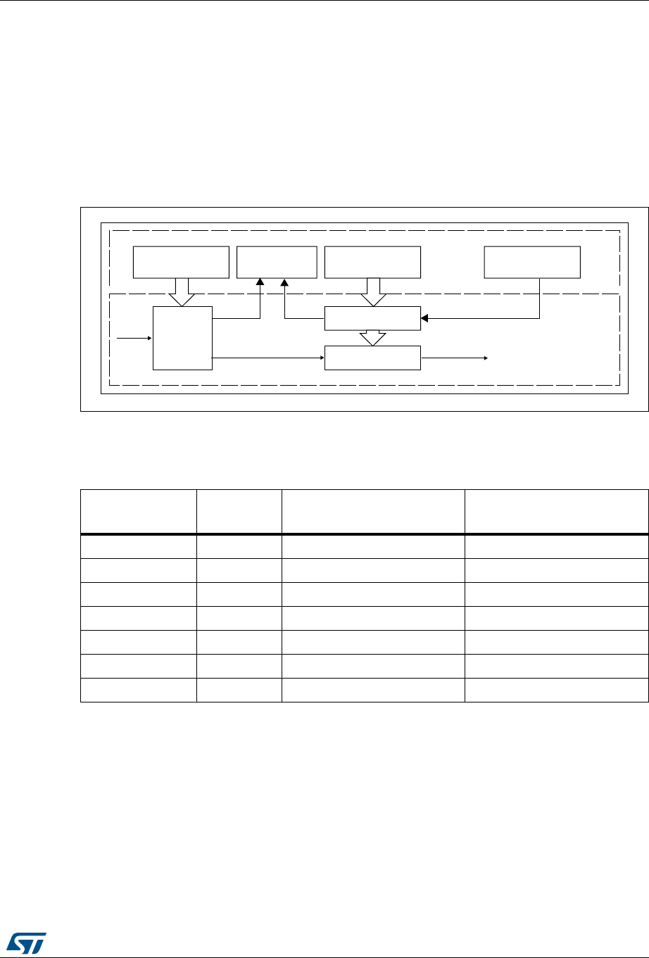
DocID026448 Rev 1 411/836
RM0383 Independent watchdog (IWDG)
415
A status register is available to indicate that an update of the prescaler or the down-counter
reload value is on going.
15.3.3 Debug mode
When the microcontroller enters debug mode (Cortex®-M4 with FPU core halted), the IWDG
counter either continues to work normally or stops, depending on DBG_IWDG_STOP
configuration bit in DBG module. For more details, refer to Section 23.16.2: Debug support
for timers, watchdog and I2C.
Figure 156. Independent watchdog block diagram
Note: The watchdog function is implemented in the VDD voltage domain that is still functional in
Stop and Standby modes.
15.4 IWDG registers
Refer to Section 1.1 on page 33 for a list of abbreviations used in register descriptions.
The peripheral registers have to be accessed by half-words (16 bits) or words (32 bits).
)7$'RESET
PRESCALER
)7$'?02
0RESCALERREGISTER
)7$'?2,2
2ELOADREGISTER
BIT
,3)
K(Z
)7$'?+2
+EYREGISTER
#/2%
6$$VOLTAGEDOMAIN
)7$'?32
3TATUSREGISTER
-36
BITRELOADVALUE
BITDOWNCOUNTER
Table 61. Min/max IWDG timeout period at 32 kHz (LSI)(1)
1. These timings are given for a 32 kHz clock but the microcontroller’s internal RC frequency can vary from 30
to 60 kHz. Moreover, given an exact RC oscillator frequency, the exact timings still depend on the phasing
of the APB interface clock versus the LSI clock so that there is always a full RC period of uncertainty.
Prescaler divider PR[2:0] bits Min timeout (ms) RL[11:0]=
0x000 Max timeout (ms) RL[11:0]=
0xFFF
/4 0 0.125 512
/8 1 0.25 1024
/16 2 0.5 2048
/32 3 1 4096
/64 4 2 8192
/128 5 4 16384
/256 6 32768

Independent watchdog (IWDG) RM0383
412/836 DocID026448 Rev 1
15.4.1 Key register (IWDG_KR)
Address offset: 0x00
Reset value: 0x0000 0000 (reset by Standby mode)
313029282726252423222120191817161514131211109876543210
Reserved KEY[15:0]
wwwwwww w w wwwwwww
Bits 31:16 Reserved, must be kept at reset value.
Bits 15:0 KEY[15:0]: Key value (write only, read 0000h)
These bits must be written by software at regular intervals with the key value AAAAh,
otherwise the watchdog generates a reset when the counter reaches 0.
Writing the key value 5555h to enable access to the IWDG_PR and IWDG_RLR registers
(see Section 15.3.2)
Writing the key value CCCCh starts the watchdog (except if the hardware watchdog option is
selected)

DocID026448 Rev 1 413/836
RM0383 Independent watchdog (IWDG)
415
15.4.2 Prescaler register (IWDG_PR)
Address offset: 0x04
Reset value: 0x0000 0000
15.4.3 Reload register (IWDG_RLR)
Address offset: 0x08
Reset value: 0x0000 0FFF (reset by Standby mode)
15.4.4 Status register (IWDG_SR)
Address offset: 0x0C
313029282726252423222120191817161514131211109876543210
Reserved PR[2:0]
rw rw rw
Bits 31:3 Reserved, must be kept at reset value.
Bits 2:0 PR[2:0]: Prescaler divider
These bits are write access protected seeSection 15.3.2. They are written by software to
select the prescaler divider feeding the counter clock. PVU bit of IWDG_SR must be reset in
order to be able to change the prescaler divider.
000: divider /4
001: divider /8
010: divider /16
011: divider /32
100: divider /64
101: divider /128
110: divider /256
111: divider /256
Note: Reading this register returns the prescaler value from the VDD voltage domain. This
value may not be up to date/valid if a write operation to this register is ongoing. For this
reason the value read from this register is valid only when the PVU bit in the IWDG_SR
register is reset.
313029282726252423222120191817161514131211109876543210
Reserved
RL[11:0]
rw rw rw rw rw rw rw rw rw rw rw rw
Bits 31:12 Reserved, must be kept at reset value.
Bits11:0 RL[11:0]: Watchdog counter reload value
These bits are write access protected see Section 15.3.2. They are written by software to
define the value to be loaded in the watchdog counter each time the value AAAAh is written
in the IWDG_KR register. The watchdog counter counts down from this value. The timeout
period is a function of this value and the clock prescaler. Refer to Table 61.
The RVU bit in the IWDG_SR register must be reset in order to be able to change the reload
value.
Note: Reading this register returns the reload value from the VDD voltage domain. This value
may not be up to date/valid if a write operation to this register is ongoing on this
register. For this reason the value read from this register is valid only when the RVU bit
in the IWDG_SR register is reset.

Independent watchdog (IWDG) RM0383
414/836 DocID026448 Rev 1
Reset value: 0x0000 0000 (not reset by Standby mode)
Note: If several reload values or prescaler values are used by application, it is mandatory to wait
until RVU bit is reset before changing the reload value and to wait until PVU bit is reset
before changing the prescaler value. However, after updating the prescaler and/or the
reload value it is not necessary to wait until RVU or PVU is reset before continuing code
execution (even in case of low-power mode entry, the write operation is taken into account
and will complete)
3130292827262524232221201918171615141312111098765432 1 0
Reserved RVU PVU
rr
Bits 31:2 Reserved, must be kept at reset value.
Bit 1 RVU: Watchdog counter reload value update
This bit is set by hardware to indicate that an update of the reload value is ongoing. It is reset
by hardware when the reload value update operation is completed in the VDD voltage domain
(takes up to 5 RC 40 kHz cycles).
Reload value can be updated only when RVU bit is reset.
Bit 0 PVU: Watchdog prescaler value update
This bit is set by hardware to indicate that an update of the prescaler value is ongoing. It is
reset by hardware when the prescaler update operation is completed in the VDD voltage
domain (takes up to 5 RC 40 kHz cycles).
Prescaler value can be updated only when PVU bit is reset.

DocID026448 Rev 1 415/836
RM0383 Independent watchdog (IWDG)
415
15.4.5 IWDG register map
The following table gives the IWDG register map and reset values.
Refer to Table 3 on page 41 for the register boundary addresses.
Table 62. IWDG register map and reset values
Offset Register
31
30
29
28
27
26
25
24
23
22
21
20
19
18
17
16
15
14
13
12
11
10
9
8
7
6
5
4
3
2
1
0
0x00
IWDG_KR Reserved KEY[15:0]
Reset value 0000000000000000
0x04
IWDG_PR Reserved PR[2:0]
Reset value 000
0x08
IWDG_RLR Reserved RL[11:0]
Reset value 111111111111
0x0C
IWDG_SR Reserved
RVU
PVU
Reset value 00

Window watchdog (WWDG) RM0383
416/836 DocID026448 Rev 1
16 Window watchdog (WWDG)
16.1 WWDG introduction
The window watchdog is used to detect the occurrence of a software fault, usually
generated by external interference or by unforeseen logical conditions, which causes the
application program to abandon its normal sequence. The watchdog circuit generates an
MCU reset on expiry of a programmed time period, unless the program refreshes the
contents of the downcounter before the T6 bit becomes cleared. An MCU reset is also
generated if the 7-bit downcounter value (in the control register) is refreshed before the
downcounter has reached the window register value. This implies that the counter must be
refreshed in a limited window.
16.2 WWDG main features
•Programmable free-running downcounter
•Conditional reset
– Reset (if watchdog activated) when the downcounter value becomes less than
0x40
– Reset (if watchdog activated) if the downcounter is reloaded outside the window
(see Figure 158)
•Early wakeup interrupt (EWI): triggered (if enabled and the watchdog activated) when
the downcounter is equal to 0x40.
16.3 WWDG functional description
If the watchdog is activated (the WDGA bit is set in the WWDG_CR register) and when the
7-bit downcounter (T[6:0] bits) rolls over from 0x40 to 0x3F (T6 becomes cleared), it initiates
a reset. If the software reloads the counter while the counter is greater than the value stored
in the window register, then a reset is generated.
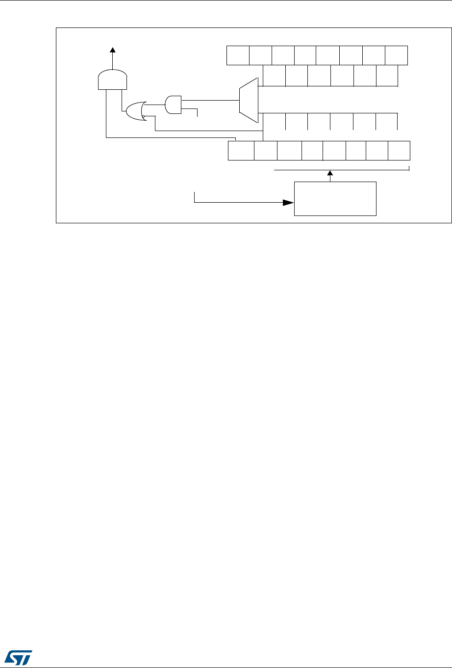
DocID026448 Rev 1 417/836
RM0383 Window watchdog (WWDG)
422
Figure 157. Watchdog block diagram
The application program must write in the WWDG_CR register at regular intervals during
normal operation to prevent an MCU reset. This operation must occur only when the counter
value is lower than the window register value. The value to be stored in the WWDG_CR
register must be between 0xFF and 0xC0:
Enabling the watchdog
The watchdog is always disabled after a reset. It is enabled by setting the WDGA bit in the
WWDG_CR register, then it cannot be disabled again except by a reset.
Controlling the downcounter
This downcounter is free-running: It counts down even if the watchdog is disabled. When
the watchdog is enabled, the T6 bit must be set to prevent generating an immediate reset.
The T[5:0] bits contain the number of increments which represents the time delay before the
watchdog produces a reset. The timing varies between a minimum and a maximum value
due to the unknown status of the prescaler when writing to the WWDG_CR register (see
Figure 158).The Configuration register (WWDG_CFR) contains the high limit of the window:
To prevent a reset, the downcounter must be reloaded when its value is lower than the
window register value and greater than 0x3F. Figure 158 describes the window watchdog
process.
Note: The T6 bit can be used to generate a software reset (the WDGA bit is set and the T6 bit is
cleared).
Advanced watchdog interrupt feature
The Early Wakeup Interrupt (EWI) can be used if specific safety operations or data logging
must be performed before the actual reset is generated. The EWI interrupt is enabled by
setting the EWI bit in the WWDG_CFR register. When the downcounter reaches the value
0x40, an EWI interrupt is generated and the corresponding interrupt service routine (ISR)
can be used to trigger specific actions (such as communications or data logging), before
resetting the device.
In some applications, the EWI interrupt can be used to manage a software system check
and/or system recovery/graceful degradation, without generating a WWDG reset. In this
RESET
WDGA
6-bit downcounter (CNT)
T6
Watchdog control register (WWDG_CR)
T1
T2
T3
T4
T5
-W6 W0
Watchdog configuration register (WWDG_CFR)
W1
W2
W3
W4
W5
comparator
T6:0 > W6:0 CMP
= 1 when
Write WWDG_CR
WDG prescaler
(WDGTB)
PCLK1
T0
(from RCC clock controller)
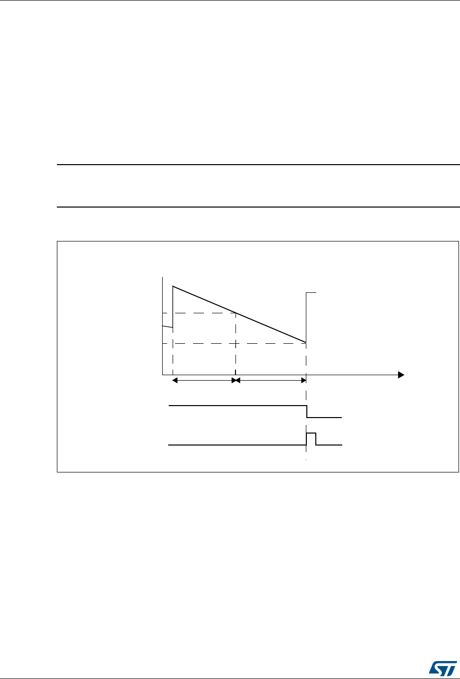
Window watchdog (WWDG) RM0383
418/836 DocID026448 Rev 1
case, the corresponding interrupt service routine (ISR) should reload the WWDG counter to
avoid the WWDG reset, then trigger the required actions.
The EWI interrupt is cleared by writing '0' to the EWIF bit in the WWDG_SR register.
Note: When the EWI interrupt cannot be served, e.g. due to a system lock in a higher priority task,
the WWDG reset will eventually be generated.
16.4 How to program the watchdog timeout
You can use the formula in Figure 158 to calculate the WWDG timeout.
Warning: When writing to the WWDG_CR register, always write 1 in the
T6 bit to avoid generating an immediate reset.
Figure 158. Window watchdog timing diagram
The formula to calculate the timeout value is given by:
where:
tWWDG: WWDG timeout
tPCLK1: APB1 clock period measured in ms
Refer to the table below for the minimum and maximum values of the TWWDG.
AIB
7;=
4;=#.4DOWNCOUNTER
2EFRESHNOTALLOWED
X&
2EFRESHALLOWED 4IME
4BIT
2%3%4
tWWDG tPCLK1 4096×2WDGTB
×t5:0[]1+()×=ms()

DocID026448 Rev 1 419/836
RM0383 Window watchdog (WWDG)
422
16.5 Debug mode
When the microcontroller enters debug mode (Cortex®-M4 with FPU core halted), the
WWDG counter either continues to work normally or stops, depending on
DBG_WWDG_STOP configuration bit in DBG module. For more details, refer to
Section 23.16.2: Debug support for timers, watchdog and I2C.

Window watchdog (WWDG) RM0383
420/836 DocID026448 Rev 1
16.6 WWDG registers
Refer to Section 1.1 on page 33 for a list of abbreviations used in register descriptions.
The peripheral registers have to be accessed by half-words (16 bits) or words (32 bits).
16.6.1 Control register (WWDG_CR)
Address offset: 0x00
Reset value: 0x0000 007F
31 30 29 28 27 26 25 24 23 22 21 20 19 18 17 16
Reserved
1514131211109876543210
Reserved WDGA T[6:0]
rs rw
Bits 31:8 Reserved, must be kept at reset value.
Bit 7 WDGA: Activation bit
This bit is set by software and only cleared by hardware after a reset. When WDGA = 1, the
watchdog can generate a reset.
0: Watchdog disabled
1: Watchdog enabled
Bits 6:0 T[6:0]: 7-bit counter (MSB to LSB)
These bits contain the value of the watchdog counter. It is decremented every (4096 x
2WDGTB) PCLK1 cycles. A reset is produced when it rolls over from 0x40 to 0x3F (T6
becomes cleared).

DocID026448 Rev 1 421/836
RM0383 Window watchdog (WWDG)
422
16.6.2 Configuration register (WWDG_CFR)
Address offset: 0x04
Reset value: 0x0000 007F
16.6.3 Status register (WWDG_SR)
Address offset: 0x08
Reset value: 0x0000 0000
31 30 29 28 27 26 25 24 23 22 21 20 19 18 17 16
Reserved
1514131211109876543210
Reserved
EWI WDGTB[1:0] W[6:0]
rs rw rw
Bit 31:10 Reserved, must be kept at reset value.
Bit 9 EWI: Early wakeup interrupt
When set, an interrupt occurs whenever the counter reaches the value 0x40. This interrupt is
only cleared by hardware after a reset.
Bits 8:7 WDGTB[1:0]: Timer base
The time base of the prescaler can be modified as follows:
00: CK Counter Clock (PCLK1 div 4096) div 1
01: CK Counter Clock (PCLK1 div 4096) div 2
10: CK Counter Clock (PCLK1 div 4096) div 4
11: CK Counter Clock (PCLK1 div 4096) div 8
Bits 6:0 W[6:0]: 7-bit window value
These bits contain the window value to be compared to the downcounter.
31 30 29 28 27 26 25 24 23 22 21 20 19 18 17 16
Reserved
1514131211109876543210
Reserved EWIF
rc_w0
Bits 31:1 Reserved, must be kept at reset value.
Bit 0 EWIF: Early wakeup interrupt flag
This bit is set by hardware when the counter has reached the value 0x40. It must be cleared
by software by writing ‘0. A write of ‘1 has no effect. This bit is also set if the interrupt is not
enabled.
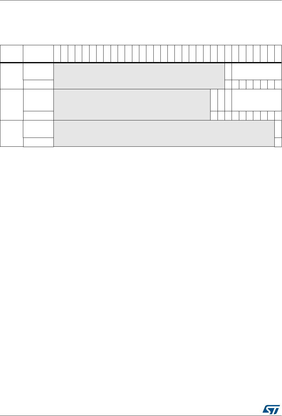
Window watchdog (WWDG) RM0383
422/836 DocID026448 Rev 1
16.6.4 WWDG register map
The following table gives the WWDG register map and reset values.
Refer to Table 3 on page 41 for the register boundary addresses.
Table 63. WWDG register map and reset values
Offset Register
31
30
29
28
27
26
25
24
23
22
21
20
19
18
17
16
15
14
13
12
11
10
9
8
7
6
5
4
3
2
1
0
0x00
WWDG_CR
Reserved
WDGA
T[6:0]
Reset value 01111111
0x04
WWDG_CFR
Reserved
EWI
WDGTB1
WDGTB0
W[6:0]
Reset value 0001111111
0x08
WWDG_SR
Reserved
EWIF
Reset value 0

DocID026448 Rev 1 423/836
RM0383 Real-time clock (RTC)
461
17 Real-time clock (RTC)
17.1 Introduction
The real-time clock (RTC) is an independent BCD timer/counter. The RTC provides a time-
of-day clock/calendar, two programmable alarm interrupts, and a periodic programmable
wakeup flag with interrupt capability. The RTC also includes an automatic wakeup unit to
manage low power modes.
Two 32-bit registers contain the seconds, minutes, hours (12- or 24-hour format), day (day
of week), date (day of month), month, and year, expressed in binary coded decimal format
(BCD). The sub-seconds value is also available in binary format
Compensations for 28-, 29- (leap year), 30-, and 31-day months are performed
automatically. Daylight saving time compensation can also be performed.
Additional 32-bit registers contain the programmable alarm subseconds, seconds, minutes,
hours, day, and date.
A digital calibration feature is available to compensate for any deviation in crystal oscillator
accuracy.
After backup domain reset, all RTC registers are protected against possible parasitic write
accesses.
As long as the supply voltage remains in the operating range, the RTC never stops,
regardless of the device status (Run mode, low power mode or under reset).
17.2 RTC main features
The RTC unit main features are the following (see Figure 159: RTC block diagram):
•Calendar with subseconds, seconds, minutes, hours (12 or 24 format), day (day of
week), date (day of month), month, and year.
•Daylight saving compensation programmable by software.
•Two programmable alarms with interrupt function. The alarms can be triggered by any
combination of the calendar fields.
•Automatic wakeup unit generating a periodic flag that triggers an automatic wakeup
interrupt.
•Reference clock detection: a more precise second source clock (50 or 60 Hz) can be
used to enhance the calendar precision.
•Accurate synchronization with an external clock using the subsecond shift feature.
•Maskable interrupts/events:
–Alarm A
–Alarm B
– Wakeup interrupt
–Timestamp
– Tamper detection
•Digital calibration circuit (periodic counter correction)
– 5 ppm accuracy
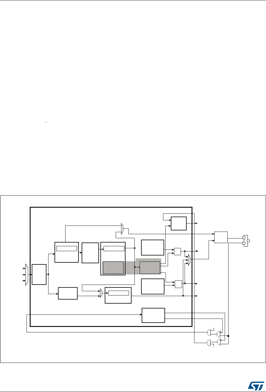
Real-time clock (RTC) RM0383
424/836 DocID026448 Rev 1
– 0.95 ppm accuracy, obtained in a calibration window of several seconds
•Timestamp function for event saving (1 event)
•Tamper detection:
– Tamper event with configurable filter and internal pull-up.
•20 backup registers (80 bytes). The backup registers are reset when a tamper
detection event occurs.
•Alternate function output (RTC_OUT) which selects one of the following two outputs:
– RTC_CALIB: 512 Hz or 1 Hz clock output (with an LSE frequency of 32.768 kHz).
This output is enabled by setting the COE bit in the RTC_CR register. It is routed
to the device RTC_AF1 function.
– RTC_ALARM (Alarm A, Alarm B or wakeup).
This output is selected by configuring the OSEL[1:0] bits in the RTC_CR register.
It is routed to the device RTC_AF1 function.
• RTC additional function inputs:
– RTC_TS: timestamp event detection. It is routed to the device RTC_AF1 function.
– RTC_TAMP1: TAMPER1 event detection. It is routed to the device RTC_AF1
function.
– RTC_REFIN: reference clock input (usually the mains, 50 or 60 Hz).
Refer to Section 8.3.15: Selection of RTC additional functions and the STM32F411xx
datasheet pin definition table.
Figure 159. RTC block diagram
1. The RTC_AF1 additional function is connected to PC13.
069
FNBDSUH
GHIDXOW+]
FN VSUH
GHIDXOW+]
57&B&$/,%
+]
57&B:875
57&&/.
:87)
+6(B57&
0+]PD[
/6(+]
/6,
$V\Q FK
ELWSUHVFDOHU
GHIDXOW
6\QFKURQRXV
ELWSUHVFDOHU
GHIDXOW &DOHQGDU
ELWZDNHXS
DXWRUHORDGWLPHU
$ODUP$
57&B$/50$5
UHJLVWHUV $/5$)
57&B$/$50
57&B35(5 57&B35(5
6KDGRZUHJLVWHUV
57&B75
57&B'5
&RDUVH
&DOLEUDWLRQ
57&B&$/,%5
$/5%)
7LPHVWDPS
UHJLVWH UV 76)
2XWSXW
FRQWURO 57&B$)
57&B287
+]
57&B$/50$665
$ODUP%
57&B$/50%5
UHJLVWHUV
57&B$/50%665
6PRRWK
FDOLEUDWLRQ
57&B&$/5
3UHVFDOHU
:8&.6(/>@
%DFNXSDQG
57&WDPSHU
FRQWUROUHJLVWHUV
57&B7$03
57&B76
7$03(
76(
6KDGRZUHJLVWHU
57&B665

DocID026448 Rev 1 425/836
RM0383 Real-time clock (RTC)
461
17.3 RTC functional description
17.3.1 Clock and prescalers
The RTC clock source (RTCCLK) is selected through the clock controller among the LSE
clock, the LSI oscillator clock, and the HSE clock. For more information on the RTC clock
source configuration, refer to Section 6: Reset and clock control (RCC) for
STM32F411xC/ESTM32F411xC/E.
A programmable prescaler stage generates a 1 Hz clock which is used to update the
calendar. To minimize power consumption, the prescaler is split into 2 programmable
prescalers (see Figure 159: RTC block diagram):
•A 7-bit asynchronous prescaler configured through the PREDIV_A bits of the
RTC_PRER register.
•A 15-bit synchronous prescaler configured through the PREDIV_S bits of the
RTC_PRER register.
Note: When both prescalers are used, it is recommended to configure the asynchronous prescaler
to a high value to minimize consumption.
The asynchronous prescaler division factor is set to 128, and the synchronous division
factor to 256, to obtain an internal clock frequency of 1 Hz (ck_spre) with an LSE frequency
of 32.768 kHz.
The minimum division factor is 1 and the maximum division factor is 222.
This corresponds to a maximum input frequency of around 4 MHz.
fck_apre is given by the following formula:
The ck_apre clock is used to clock the binary RTC_SSR subseconds downcounter. When it
reaches 0, RTC_SSR is reloaded with the content of PREDIV_S.
fck_spre is given by the following formula:
The ck_spre clock can be used either to update the calendar or as timebase for the 16-bit
wakeup auto-reload timer. To obtain short timeout periods, the 16-bit wakeup auto-reload
timer can also run with the RTCCLK divided by the programmable 4-bit asynchronous
prescaler (see Section 17.3.4: Periodic auto-wakeup for details).
17.3.2 Real-time clock and calendar
The RTC calendar time and date registers are accessed through shadow registers which
are synchronized with PCLK1 (APB1 clock).
•RTC_SSR for the subseconds
•RTC_TR for the time
•RTC_DR for the date
fCK_APRE
fRTCCLK
PREDIV_A 1+
---------------------------------------
=
fCK_SPRE
fRTCCLK
PREDIV_S 1+()PREDIV_A 1+()×
-----------------------------------------------------------------------------------------------
=

Real-time clock (RTC) RM0383
426/836 DocID026448 Rev 1
Every two RTCCLK periods, the current calendar value is copied into the shadow registers,
and the RSF bit of RTC_ISR register is set (see Section 17.6.4). The copy is not performed
in Stop and Standby mode. When exiting these modes, the shadow registers are updated
after up to 2 RTCCLK periods.
When the application reads the calendar registers, it accesses the content of the shadow
registers. It is possible to make a direct access to the calendar registers by setting the
BYPSHAD control bit in the RTC_CR register. By default, this bit is cleared, and the user
accesses the shadow registers.
When reading the RTC_SSR, RTC_TR or RTC_DR registers in BYPSHAD=0 mode, the
frequency of the APB clock (fAPB) must be at least 7 times the frequency of the RTC clock
(fRTCCLK).
The shadow registers are reset by system reset.
17.3.3 Programmable alarms
The RTC unit provides two programmable alarms, Alarm A and Alarm B.
The programmable alarm functions are enabled through the ALRAIE and ALRBIE bits in the
RTC_CR register. The ALRAF and ALRBF flags are set to 1 if the calendar subseconds,
seconds, minutes, hours, date or day match the values programmed in the alarm registers
RTC_ALRMASSR/RTC_ALRMAR and RTC_ALRMBSSR/RTC_ALRMBR, respectively.
Each calendar field can be independently selected through the MSKx bits of the
RTC_ALRMAR and RTC_ALRMBR registers, and through the MASKSSx bits of the
RTC_ALRMASSR and RTC_ALRMBSSR registers. The alarm interrupts are enabled
through the ALRAIE and ALRBIE bits in the RTC_CR register.
Alarm A and Alarm B (if enabled by bits OSEL[1:0] in RTC_CR register) can be routed to the
RTC_ALARM output. RTC_ALARM polarity can be configured through bit POL in the
RTC_CR register.
Caution: If the seconds field is selected (MSK0 bit reset in RTC_ALRMAR or RTC_ALRMBR), the
synchronous prescaler division factor set in the RTC_PRER register must be at least 3 to
ensure correct behavior.
17.3.4 Periodic auto-wakeup
The periodic wakeup flag is generated by a 16-bit programmable auto-reload down-counter.
The wakeup timer range can be extended to 17 bits.
The wakeup function is enabled through the WUTE bit in the RTC_CR register.
The wakeup timer clock input can be:
•RTC clock (RTCCLK) divided by 2, 4, 8, or 16.
When RTCCLK is LSE(32.768kHz), this allows to configure the wakeup interrupt period
from 122 µs to 32 s, with a resolution down to 61µs.
•ck_spre (usually 1 Hz internal clock)
When ck_spre frequency is 1Hz, this allows to achieve a wakeup time from 1 s to
around 36 hours with one-second resolution. This large programmable time range is
divided in 2 parts:
– from 1s to 18 hours when WUCKSEL [2:1] = 10
– and from around 18h to 36h when WUCKSEL[2:1] = 11. In this last case 216 is
added to the 16-bit counter current value.When the initialization sequence is

DocID026448 Rev 1 427/836
RM0383 Real-time clock (RTC)
461
complete (see Programming the wakeup timer on page 428), the timer starts
counting down.When the wakeup function is enabled, the down-counting remains
active in low power modes. In addition, when it reaches 0, the WUTF flag is set in
the RTC_ISR register, and the wakeup counter is automatically reloaded with its
reload value (RTC_WUTR register value).
The WUTF flag must then be cleared by software.
When the periodic wakeup interrupt is enabled by setting the WUTIE bit in the RTC_CR2
register, it can exit the device from low power modes.
The periodic wakeup flag can be routed to the RTC_ALARM output provided it has been
enabled through bits OSEL[1:0] of RTC_CR register. RTC_ALARMpolarity can be
configured through the POL bit in the RTC_CR register.
System reset, as well as low power modes (Sleep, Stop and Standby) have no influence on
the wakeup timer.
17.3.5 RTC initialization and configuration
RTC register access
The RTC registers are 32-bit registers. The APB interface introduces 2 wait-states in RTC
register accesses except on read accesses to calendar shadow registers when
BYPSHAD=0.
RTC register write protection
After system reset, the RTC registers are protected against parasitic write access with the
DBP bit of the PWR power control register (PWR_CR). The DBP bit must be set to enable
RTC registers write access.
After backup domain reset, all the RTC registers are write-protected. Writing to the RTC
registers is enabled by writing a key into the Write Protection register, RTC_WPR.
The following steps are required to unlock the write protection on all the RTC registers
except for RTC_ISR[13:8], RTC_TAFCR, and RTC_BKPxR.
1. Write ‘0xCA’ into the RTC_WPR register.
2. Write ‘0x53’ into the RTC_WPR register.
Writing a wrong key reactivates the write protection.
The protection mechanism is not affected by system reset.
Calendar initialization and configuration
To program the initial time and date calendar values, including the time format and the
prescaler configuration, the following sequence is required:
1. Set INIT bit to 1 in the RTC_ISR register to enter initialization mode. In this mode, the
calendar counter is stopped and its value can be updated.
2. Poll INITF bit of in the RTC_ISR register. The initialization phase mode is entered when
INITF is set to 1. It takes from 1 to 2 RTCCLK clock cycles (due to clock
synchronization).
3. To generate a 1 Hz clock for the calendar counter, program first the synchronous
prescaler factor in RTC_PRER register, and then program the asynchronous prescaler

Real-time clock (RTC) RM0383
428/836 DocID026448 Rev 1
factor. Even if only one of the two fields needs to be changed, 2 separate write
accesses must be performed to the RTC_PRER register.
4. Load the initial time and date values in the shadow registers (RTC_TR and RTC_DR),
and configure the time format (12 or 24 hours) through the FMT bit in the RTC_CR
register.
5. Exit the initialization mode by clearing the INIT bit. The actual calendar counter value is
then automatically loaded and the counting restarts after 4 RTCCLK clock cycles.
When the initialization sequence is complete, the calendar starts counting.
Note: After a system reset, the application can read the INITS flag in the RTC_ISR register to
check if the calendar has been initialized or not. If this flag equals 0, the calendar has not
been initialized since the year field is set at its backup domain reset default value (0x00).
To read the calendar after initialization, the software must first check that the RSF flag is set
in the RTC_ISR register.
Daylight saving time
The daylight saving time management is performed through bits SUB1H, ADD1H, and BKP
of the RTC_CR register.
Using SUB1H or ADD1H, the software can subtract or add one hour to the calendar in one
single operation without going through the initialization procedure.
In addition, the software can use the BKP bit to memorize this operation.
Programming the alarm
A similar procedure must be followed to program or update the programmable alarm (Alarm
A or Alarm B):
1. Clear ALRAE or ALRBIE in RTC_CR to disable Alarm A or Alarm B.
2. Poll ALRAWF or ALRBWF in RTC_ISR until it is set to make sure the access to alarm
registers is allowed. This takes 1 to 2 RTCCLK clock cycles (due to clock
synchronization).
3. Program the Alarm A or Alarm B registers (RTC_ALRMASSR/RTC_ALRMAR or
RTC_ALRMBSSR/RTC_ALRMBR).
4. Set ALRAE or ALRBIE in the RTC_CR register to enable Alarm A or Alarm B again.
Note: Each change of the RTC_CR register is taken into account after 1 to 2 RTCCLK clock cycles
due to clock synchronization.
Programming the wakeup timer
The following sequence is required to configure or change the wakeup timer auto-reload
value (WUT[15:0] in RTC_WUTR):
1. Clear WUTE in RTC_CR to disable the wakeup timer.
2. Poll WUTWF until it is set in RTC_ISR to make sure the access to wakeup auto-reload
counter and to WUCKSEL[2:0] bits is allowed. It takes 1 to 2 RTCCLK clock cycles
(due to clock synchronization).
3. Program the wakeup auto-reload value WUT[15:0], and the wakeup clock selection
(WUCKSEL[2:0] bits in RTC_CR).Set WUTE in RTC_CR to enable the timer again.
The wakeup timer restarts down-counting.

DocID026448 Rev 1 429/836
RM0383 Real-time clock (RTC)
461
17.3.6 Reading the calendar
To read the RTC calendar registers (RTC_SSR, RTC_TR and RTC_DR) properly, the APB1
clock frequency (fPCLK1) must be equal to or greater than seven times the fRTCCLK RTC
clock frequency. This ensures a secure behavior of the synchronization mechanism.
If the APB1 clock frequency is less than seven times the RTC clock frequency, the software
must read the calendar time and date registers twice. If the second read of the RTC_TR
gives the same result as the first read, this ensures that the data is correct. Otherwise a third
read access must be done. In any case the APB1 clock frequency must never be lower than
the RTC clock frequency.
The RSF bit is set in RTC_ISR register each time the calendar registers are copied into the
RTC_SSR, RTC_TR and RTC_DR shadow registers. The copy is performed every two
RTCCLK cycles. To ensure consistency between the 3 values, reading either RTC_SSR or
RTC_TR locks the values in the higher-order calendar shadow registers until RTC_DR is
read. In case the software makes read accesses to the calendar in a time interval smaller
than 2 RTCCLK periods: RSF must be cleared by software after the first calendar read, and
then the software must wait until RSF is set before reading again the RTC_SSR, RTC_TR
and RTC_DR registers.
After waking up from low power mode (Stop or Standby), RSF must be cleared by software.
The software must then wait until it is set again before reading the RTC_SSR, RTC_TR and
RTC_DR registers.
The RSF bit must be cleared after wakeup and not before entering low power mode.
Note: After a system reset, the software must wait until RSF is set before reading the RTC_SSR,
RTC_TR and RTC_DR registers. Indeed, a system reset resets the shadow registers to
their default values.
After an initialization (refer to Calendar initialization and configuration on page 427): the
software must wait until RSF is set before reading the RTC_SSR, RTC_TR and RTC_DR
registers.
After synchronization (refer to Section 17.3.8: RTC synchronization): the software must wait
until RSF is set before reading the RTC_SSR, RTC_TR and RTC_DR registers.
When the BYPSHAD control bit is set in the RTC_CR register (bypass shadow
registers)
Reading the calendar registers gives the values from the calendar counters directly, thus
eliminating the need to wait for the RSF bit to be set. This is especially useful after exiting
from low power modes (STOP or Standby), since the shadow registers are not updated
during these modes.
When the BYPSHAD bit is set to 1, the results of the different registers might not be
coherent with each other if an RTCCLK edge occurs between two read accesses to the
registers. Additionally, the value of one of the registers may be incorrect if an RTCCLK edge
occurs during the read operation. The software must read all the registers twice, and then
compare the results to confirm that the data is coherent and correct. Alternatively, the
software can just compare the two results of the least-significant calendar register.
Note: While BYPSHAD=1, instructions which read the calendar registers require one extra APB
cycle to complete.

Real-time clock (RTC) RM0383
430/836 DocID026448 Rev 1
17.3.7 Resetting the RTC
The calendar shadow registers (RTC_SSR,RTC_TR and RTC_DR) and some bits of the
RTC status register (RTC_ISR) are reset to their default values by all available system reset
sources.
On the contrary, the following registers are resetted to their default values by a backup
domain reset and are not affected by a system reset: the RTC current calendar registers,
the RTC control register (RTC_CR), the prescaler register (RTC_PRER), the RTC
calibration registers (RTC_CALIBR or RTC_CALR), the RTC shift register (RTC_SHIFTR),
the RTC timestamp registers (RTC_TSSSR, RTC_TSTR and RTC_TSDR), the RTC tamper
and alternate function configuration register (RTC_TAFCR), the RTC backup registers
(RTC_BKPxR), the wakeup timer register (RTC_WUTR), the Alarm A and Alarm B registers
(RTC_ALRMASSR/RTC_ALRMAR and RTC_ALRMBSSR/RTC_ALRMBR).
In addition, the RTC keeps on running under system reset if the reset source is different
from a backup domain reset. When a backup domain reset occurs, the RTC is stopped and
all the RTC registers are set to their reset values.
17.3.8 RTC synchronization
The RTC can be synchronized to a remote clock with a high degree of precision. After
reading the sub-second field (RTC_SSR or RTC_TSSSR), a calculation can be made of the
precise offset between the times being maintained by the remote clock and the RTC. The
RTC can then be adjusted to eliminate this offset by “shifting” its clock by a fraction of a
second using RTC_SHIFTR.
RTC_SSR contains the value of the synchronous prescaler’s counter. This allows one to
calculate the exact time being maintained by the RTC down to a resolution of
1 / (PREDIV_S + 1) seconds. As a consequence, the resolution can be improved by
increasing the synchronous prescaler value (PREDIV_S[14:0]. The maximum resolution
allowed (30.52 μs with a 32768 Hz clock) is obtained with PREDIV_S set to 0x7FFF.
However, increasing PREDIV_S means that PREDIV_A must be decreased in order to
maintain the synchronous prescaler’s output at 1 Hz. In this way, the frequency of the
asynchronous prescaler’s output increases, which may increase the RTC dynamic
consumption.
The RTC can be finely adjusted using the RTC shift control register (RTC_SHIFTR). Writing
to RTC_SHIFTR can shift (either delay or advance) the clock by up to a second with a
resolution of 1 / (PREDIV_S + 1) seconds. The shift operation consists of adding the
SUBFS[14:0] value to the synchronous prescaler counter SS[15:0]: this will delay the clock.
If at the same time the ADD1S bit is set, this results in adding one second and at the same
time subtracting a fraction of second, so this will advance the clock.
Caution: Before initiating a shift operation, the user must check that SS[15] = 0 in order to ensure that
no overflow will occur.
As soon as a shift operation is initiated by a write to the RTC_SHIFTR register, the SHPF
flag is set by hardware to indicate that a shift operation is pending. This bit is cleared by
hardware as soon as the shift operation has completed.
Caution: This synchronization feature is not compatible with the reference clock detection feature:
firmware must not write to RTC_SHIFTR when REFCKON=1.

DocID026448 Rev 1 431/836
RM0383 Real-time clock (RTC)
461
17.3.9 RTC reference clock detection
The RTC calendar update can be synchronized to a reference clock RTC_REFIN, usually
the mains (50 or 60 Hz). The RTC_REFIN reference clock should have a higher precision
than the 32.768 kHz LSE clock. When the RTC_REFIN detection is enabled (REFCKON bit
of RTC_CR set to 1), the calendar is still clocked by the LSE, and RTC_REFIN is used to
compensate for the imprecision of the calendar update frequency (1 Hz).
Each 1 Hz clock edge is compared to the nearest reference clock edge (if one is found
within a given time window). In most cases, the two clock edges are properly aligned. When
the 1 Hz clock becomes misaligned due to the imprecision of the LSE clock, the RTC shifts
the 1 Hz clock a bit so that future 1 Hz clock edges are aligned. Thanks to this mechanism,
the calendar becomes as precise as the reference clock.
The RTC detects if the reference clock source is present by using the 256 Hz clock
(ck_apre) generated from the 32.768 kHz quartz. The detection is performed during a time
window around each of the calendar updates (every 1 s). The window equals 7 ck_apre
periods when detecting the first reference clock edge. A smaller window of 3 ck_apre
periods is used for subsequent calendar updates.
Each time the reference clock is detected in the window, the asynchronous prescaler which
outputs the ck_apre clock is forced to reload. This has no effect when the reference clock
and the 1 Hz clock are aligned because the prescaler is being reloaded at the same
moment. When the clocks are not aligned, the reload shifts future 1 Hz clock edges a little
for them to be aligned with the reference clock.
If the reference clock halts (no reference clock edge occurred during the 3 ck_apre window),
the calendar is updated continuously based solely on the LSE clock. The RTC then waits for
the reference clock using a large 7 ck_apre period detection window centered on the
ck_spre edge.
When the reference clock detection is enabled, PREDIV_A and PREDIV_S must be set to
their default values:
•PREDIV_A = 0x007F
•PREDIV_S = 0x00FF
Note: The reference clock detection is not available in Standby mode.
Caution: The reference clock detection feature cannot be used in conjunction with the coarse digital
calibration: RTC_CALIBR must be kept at 0x0000 0000 when REFCKON=1.
17.3.10 RTC coarse digital calibration
Two digital calibration methods are available: coarse and smooth calibration. To perform
coarse calibration refer to Section 17.6.7: RTC calibration register (RTC_CALIBR).
The two calibration methods are not intended to be used together, the application must
select one of the two methods. Coarse calibration is provided for compatibly reasons. To
perform smooth calibration refer to Section 17.3.11: RTC smooth digital calibration and the
Section 17.6.16: RTC calibration register (RTC_CALR)
The coarse digital calibration can be used to compensate crystal inaccuracy by adding
(positive calibration) or masking (negative calibration) clock cycles at the output of the
asynchronous prescaler (ck_apre).
Positive and negative calibration are selected by setting the DCS bit in RTC_CALIBR
register to ‘0’ and ‘1’, respectively.

Real-time clock (RTC) RM0383
432/836 DocID026448 Rev 1
When positive calibration is enabled (DCS = ‘0’), 2 ck_apre cycles are added every minute
(around 15360 ck_apre cycles) for 2xDC minutes. This causes the calendar to be updated
sooner, thereby adjusting the effective RTC frequency to be a bit higher.
When negative calibration is enabled (DCS = ‘1’), 1 ck_apre cycle is removed every minute
(around 15360 ck_apre cycles) for 2xDC minutes. This causes the calendar to be updated
later, thereby adjusting the effective RTC frequency to be a bit lower.
DC is configured through bits DC[4:0] of RTC_CALIBR register. This number ranges from 0
to 31 corresponding to a time interval (2xDC) ranging from 0 to 62.
The coarse digital calibration can be configured only in initialization mode, and starts when
the INIT bit is cleared. The full calibration cycle lasts 64 minutes. The first 2xDC minutes of
the 64 -minute cycle are modified as just described.
Negative calibration can be performed with a resolution of about 2 ppm while positive
calibration can be performed with a resolution of about 4 ppm. The maximum calibration
ranges from −63 ppm to 126 ppm.
The calibration can be performed either on the LSE or on the HSE clock.
Caution: Digital calibration may not work correctly if PREDIV_A < 6.
Case of RTCCLK=32.768 kHz and PREDIV_A+1=128
The following description assumes that ck_apre frequency is 256 Hz obtained with an LSE
clock nominal frequency of 32.768 kHz, and PREDIV_A set to 127 (default value).
The ck_spre clock frequency is only modified during the first 2xDC minutes of the 64-minute
cycle. For example, when DC equals 1, only the first 2 minutes are modified. This means
that the first 2xDC minutes of each 64-minute cycle have, once per minute, one second
either shortened by 256 or lengthened by 128 RTCCLK cycles, given that each ck_apre
cycle represents 128 RTCCLK cycles (with PREDIV_A+1=128).
Therefore each calibration step has the effect of adding 512 or subtracting 256 oscillator
cycles for every 125829120 RTCCLK cycles (64min x 60 s/min x 32768 cycles/s). This is
equivalent to +4.069 ppm or-2.035 ppm per calibration step. As a result, the calibration
resolution is +10.5 or −5.27 seconds per month, and the total calibration ranges from +5.45
to −2.72 minutes per month.
In order to measure the clock deviation, a 512 Hz clock is output for calibration.Refer to
Section 17.3.14: Calibration clock output.
17.3.11 RTC smooth digital calibration
RTC frequency can be digitally calibrated with a resolution of about 0.954 ppm with a range
from -487.1 ppm to +488.5 ppm. The correction of the frequency is performed using series
of small adjustments (adding and/or subtracting individual RTCCLK pulses). These
adjustments are fairly well distributed so that the RTC is well calibrated even when observed
over short durations of time.
The smooth digital calibration is performed during a cycle of about 220 RTCCLK pulses, or
32 seconds when the input frequency is 32768 Hz. This cycle is maintained by a 20-bit
counter, cal_cnt[19:0], clocked by RTCCLK.

DocID026448 Rev 1 433/836
RM0383 Real-time clock (RTC)
461
The smooth calibration register (RTC_CALR) specifies the number of RTCCLK clock cycles
to be masked during the 32-second cycle:
•Setting the bit CALM[0] to 1 causes exactly one pulse to be masked during the 32-
second cycle.
•Setting CALM[1] to 1 causes two additional cycles to be masked
•Setting CALM[2] to 1 causes four additional cycles to be masked
•and so on up to CALM[8] set to 1 which causes 256 clocks to be masked.
Note: CALM[8:0] (RTC_CALRx) specifies the number of RTCCLK pulses to be masked during the
32-second cycle. Setting the bit CALM[0] to ‘1’ causes exactly one pulse to be masked
during the 32-second cycle at the moment when cal_cnt[19:0] is 0x80000; CALM[1]=1
causes two other cycles to be masked (when cal_cnt is 0x40000 and 0xC0000); CALM[2]=1
causes four other cycles to be masked (cal_cnt = 0x20000/0x60000/0xA0000/ 0xE0000);
and so on up to CALM[8]=1 which causes 256 clocks to be masked (cal_cnt = 0xXX800).
While CALM allows the RTC frequency to be reduced by up to 487.1 ppm with fine
resolution, the bit CALP can be used to increase the frequency by 488.5 ppm. Setting CALP
to ‘1’ effectively inserts an extra RTCCLK pulse every 211 RTCCLK cycles, which means
that 512 clocks are added during every 32-second cycle.
Using CALM together with CALP, an offset ranging from -511 to +512 RTCCLK cycles can
be added during the 32-second cycle, which translates to a calibration range of -487.1 ppm
to +488.5 ppm with a resolution of about 0.954 ppm.
The formula to calculate the effective calibrated frequency (FCAL) given the input frequency
(FRTCCLK) is as follows:
FCAL = FRTCCLK x [1 + (CALP x 512 - CALM) / (220 + CALM - CALP x 512)]
Calibration when PREDIV_A<3
The CALP bit can not be set to 1 when the asynchronous prescaler value (PREDIV_A bits in
RTC_PRER register) is less than 3. If CALP was already set to 1 and PREDIV_A bits are
set to a value less than 3, CALP is ignored and the calibration operates as if CALP was
equal to 0.
To perform a calibration with PREDIV_A less than 3, the synchronous prescaler value
(PREDIV_S) should be reduced so that each second is accelerated by 8 RTCCLK clock
cycles, which is equivalent to adding 256 clock cycles every 32 seconds. As a result,
between 255 and 256 clock pulses (corresponding to a calibration range from 243.3 to
244.1 ppm) can effectively be added during each 32-second cycle using only the CALM bits.
With a nominal RTCCLK frequency of 32768 Hz, when PREDIV_A equals 1 (division factor
of 2), PREDIV_S should be set to 16379 rather than 16383 (4 less). The only other
interesting case is when PREDIV_A equals 0, PREDIV_S should be set to 32759 rather
than 32767 (8 less).
If PREDIV_S is reduced in this way, the formula given the effective frequency of the
calibrated input clock is as follows:
FCAL = FRTCCLK x [1 + (256 - CALM) / (220 + CALM - 256)]
In this case, CALM[7:0] equals 0x100 (the midpoint of the CALM range) is the correct
setting if RTCCLK is exactly 32768.00 Hz.

Real-time clock (RTC) RM0383
434/836 DocID026448 Rev 1
Verifying the RTC calibration
RTC precision is performed by measuring the precise frequency of RTCCLK and calculating
the correct CALM value and CALP values. An optional 1 Hz output is provided to allow
applications to measure and verify the RTC precision.Measuring the precise frequency of
the RTC over a limited interval can result in a measurement error of up to 2 RTCCLK clock
cycles over the measurement period, depending on how the digital calibration cycle is
aligned with the measurement period.
However, this measurement error can be eliminated if the measurement period is the same
length as the calibration cycle period. In this case, the only error observed is the error due to
the resolution of the digital calibration.
•By default, the calibration cycle period is 32 seconds.
Using this mode and measuring the accuracy of the 1 Hz output over exactly 32
seconds guarantees that the measure is within 0.477 ppm (0.5 RTCCLK cycles over 32
seconds, due to the limitation of the calibration resolution).
•CALW16 bit of the RTC_CALR register can be set to 1 to force a 16- second calibration
cycle period.
In this case, the RTC precision can be measured during 16 seconds with a maximum
error of 0.954 ppm (0.5 RTCCLK cycles over 16 seconds). However, since the
calibration resolution is reduced, the long term RTC precision is also reduced to 0.954
ppm: CALM[0] bit is stuck at 0 when CALW16 is set to 1.
•CALW8 bit of the RTC_CALR register can be set to 1 to force a 8- second calibration
cycle period.
In this case, the RTC precision can be measured during 8 seconds with a maximum
error of 1.907 ppm (0.5 RTCCLK cycles over 8s). The long term RTC precision is also
reduced to 1.907 ppm: CALM[1:0] bits are stuck at 00 when CALW8 is set to 1.
Re-calibration on-the-fly
The calibration register (RTC_CALR) can be updated on-the-fly while RTC_ISR/INITF=0, by
using the follow process:
1. Poll the RTC_ISR/RECALPF (re-calibration pending flag).
2. If it is set to 0, write a new value to RTC_CALR, if necessary. RECALPF is then
automatically set to 1
3. Within three ck_apre cycles after the write operation to RTC_CALR, the new calibration
settings take effect.
17.3.12 Timestamp function
Timestamp is enabled by setting the TSE bit of RTC_CR register to 1.
The calendar is saved in the timestamp registers (RTC_TSSSR, RTC_TSTR, RTC_TSDR)
when a timestamp event is detected on the pin to which the TIMESTAMP additional function
is mapped. When a timestamp event occurs, the timestamp flag bit (TSF) in RTC_ISR
register is set.
By setting the TSIE bit in the RTC_CR register, an interrupt is generated when a timestamp
event occurs.
If a new timestamp event is detected while the timestamp flag (TSF) is already set, the
timestamp overflow flag (TSOVF) flag is set and the timestamp registers (RTC_TSTR and
RTC_TSDR) maintain the results of the previous event.

DocID026448 Rev 1 435/836
RM0383 Real-time clock (RTC)
461
Note: TSF is set 2 ck_apre cycles after the timestamp event occurs due to synchronization
process.
There is no delay in the setting of TSOVF. This means that if two timestamp events are
close together, TSOVF can be seen as '1' while TSF is still '0'. As a consequence, it is
recommended to poll TSOVF only after TSF has been set.
Caution: If a timestamp event occurs immediately after the TSF bit is supposed to be cleared, then
both TSF and TSOVF bits are set. To avoid masking a timestamp event occurring at the
same moment, the application must not write ‘0’ into TSF bit unless it has already read it to
‘1’.
Optionally, a tamper event can cause a timestamp to be recorded. See the description of the
TAMPTS control bit in Section 17.6.17: RTC tamper and alternate function configuration
register (RTC_TAFCR). If the timestamp event is on the same pin as a tamper event
configured in filtered mode (TAMPFLT set to a non-zero value), the timestamp on tamper
detection event mode must be selected by setting TAMPTS='1' in RTC_TAFCR register.
TIMESTAMP additional function
The TIMESTAMP additional function is mapped to RTC_AF1.
17.3.13 Tamper detection
One tamper detection input is available. It can be configured either for edge detection, or for
level detection with filtering.
RTC backup registers
The backup registers (RTC_BKPxR) are twenty 32-bit registers for storing 80 bytes of user
application data. They are implemented in the backup domain that remains powered-on by
VBAT when the VDD power is switched off. They are not reset by system reset or when the
device wakes up from Standby mode. They are reset by a backup domain reset
The backup registers are reset when a tamper detection event occurs (see Section 17.6.20:
RTC backup registers (RTC_BKPxR) and Tamper detection initialization on page 435.
Tamper detection initialization
The tamper detection input is associated with the TAMP1F flag in the RTC_ISR register. The
input can be enabled by setting the TAMP1E bit to 1 in the RTC_TAFCR register.
A tamper detection event resets all backup registers (RTC_BKPxR).
By setting the TAMPIE bit in the RTC_TAFCR register, an interrupt is generated when a
tamper detection event occurs.
Timestamp on tamper event
With TAMPTS set to ‘1 , any tamper event causes a timestamp to occur. In this case, either
the TSF bit or the TSOVF bit are set in RTC_ISR, in the same manner as if a normal
timestamp event occurs. The tamper flag register (TAMP1F) is set at the same time that
TSF or TSOVF is set.
Edge detection on tamper inputs
If the TAMPFLT bits are “00”, the TAMPER pin generates tamper detection events
(RTC_TAMP[2:1]) when either a rising edge is observed or an falling edge is observed

Real-time clock (RTC) RM0383
436/836 DocID026448 Rev 1
depending on the corresponding TAMPxTRG bit. The internal pull-up resistors on the
TAMPER input are deactivated when edge detection is selected.
Caution: To avoid losing tamper detection events, the signal used for edge detection is logically
ANDed with TAMPxE in order to detect a tamper detection event in case it occurs before the
TAMPERx pin is enabled.
•When TAMPxTRG = 0: if the TAMPERx additional function is already high before
tamper detection is enabled (TAMPxE bit set to 1), a tamper event is detected as soon
as TAMPERx is enabled, even if there was no rising edge on TAMPERx after TAMPxE
was set.
•When TAMPxTRG = 1: if the TAMPERx additional function is already low before
tamper detection is enabled, a tamper event is detected as soon as TAMPERx is
enabled (even if there was no falling edge on TAMPERx after TAMPxE was set.
After a tamper event has been detected and cleared, the TAMPERx additional function
should be disabled and then re-enabled (TAMPxE set to 1) before re-programming the
backup registers (RTC_BKPxR). This prevents the application from writing to the backup
registers while the TAMPERx value still indicates a tamper detection. This is equivalent to a
level detection on the TAMPERx additional function.
Note: Tamper detection is still active when VDD power is switched off. To avoid unwanted resetting
of the backup registers, the pin to which the TAMPER additional function is mapped should
be externally tied to the correct level.
Level detection with filtering on tamper input
Level detection with filtering is performed by setting TAMPFLT to a non-zero value. A tamper
detection event is generated when either 2, 4, or 8 (depending on TAMPFLT) consecutive
samples are observed at the level designated by the TAMPxTRG bits (TAMP1TRG).
The TAMPER input is pre-charged through the I/O internal pull-up resistance before its state
is sampled, unless disabled by setting TAMPPUDIS to 1,The duration of the precharge is
determined by the TAMPPRCH bits, allowing for larger capacitances on the tamper inputs.
The trade-off between tamper detection latency and power consumption through the pull-up
can be optimized by using TAMPFREQ to determine the frequency of the sampling for level
detection.
Note: Refer to the datasheets for the electrical characteristics of the pull-up resistors.
TAMPER additional function detection
The TAMPER1 addtional function is mapped to the RTC_AF1 pin.
17.3.14 Calibration clock output
When the COE bit is set to 1 in the RTC_CR register, a reference clock is provided on the
RTC_CALIB device output. If the COSEL bit in the RTC_CR register is reset and
PREDIV_A = 0x7F, the RTC_CALIB frequency is fRTCCLK/64. This corresponds to a
calibration output at 512 Hz for an RTCCLK frequency at 32.768 kHz.
The RTC_CALIB output is not impacted by the calibration value programmed in
RTC_CALIBR register. The RTC_CALIB duty cycle is irregular: there is a light jitter on falling
edges. It is therefore recommended to use rising edges.
If COSEL is set and “PREDIV_S+1” is a non-zero multiple of 256 (i.e: PREDIV_S[7:0] =
0xFF), the RTC_CALIB frequency is fRTCCLK/(256 * (PREDIV_A+1)). This corresponds to a

DocID026448 Rev 1 437/836
RM0383 Real-time clock (RTC)
461
calibration output at 1 Hz for prescaler default values (PREDIV_A = Ox7F, PREDIV_S =
0xFF), with an RTCCLK frequency at 32.768 kHz.
Calibration alternate function output
When the COE bit in the RTC_CR register is set to 1, the calibration alternate function
(RTC_CALIB) is enabled on RTC_OUT.
Note: When RTC_CALIB or RTC_ALARM is selected, RTC_OUT is automatically configured in
output alternate function.
17.3.15 Alarm output
Three functions can be selected on Alarm output: ALRAF. These functions reflect the
contents of the corresponding flags in the RTC_ISR register.
The OSEL[1:0] control bits in the RTC_CR register are used to activate the alarm alternate
function output (RTC_ALARM) in RTC_AF1, and to select the function which is output on
RTC_ALARM.
The polarity of the output is determined by the POL control bit in RTC_CR so that the
opposite of the selected flag bit is output when POL is set to 1.
Alarm alternate function output
RTC_ALARM can be configured in output open drain or output push-pull using the control
bit ALARMOUTTYPE in the RTC_TAFCR register.
Note: Once RTC_ALARM is enabled, it has priority over RTC_CALIB (COE bit is don't care on
RTC_AF1).
When RTC_CALIB or RTC_ALARM is selected, RTC_OUT is automatically configured in
output alternate function.
17.4 RTC and low power modes
17.5 RTC interrupts
All RTC interrupts are connected to the EXTI controller.
To enable the RTC Alarm interrupt, the following sequence is required:
Table 64. Effect of low power modes on RTC
Mode Description
Sleep No effect
RTC interrupts cause the device to exit the Sleep mode.
Stop
The RTC remains active when the RTC clock source is LSE or LSI. RTC alarm, RTC
tamper event, RTC time stamp event, and RTC Wakeup cause the device to exit the Stop
mode.
Standby
The RTC remains active when the RTC clock source is LSE or LSI. RTC alarm, RTC
tamper event, RTC time stamp event, and RTC Wakeup cause the device to exit the
Standby mode.
Real-time clock (RTC) RM0383
438/836 DocID026448 Rev 1
1. Configure and enable the EXTI Line 17 in interrupt mode and select the rising edge
sensitivity.
2. Configure and enable the RTC_Alarm IRQ channel in the NVIC.
3. Configure the RTC to generate RTC alarms (Alarm A or Alarm B).
To enable the RTC Wakeup interrupt, the following sequence is required:
1. Configure and enable the EXTI Line 22 in interrupt mode and select the rising edge
sensitivity.
2. Configure and enable the RTC_WKUP IRQ channel in the NVIC.
3. Configure the RTC to generate the RTC wakeup timer event.
To enable the RTC Tamper interrupt, the following sequence is required:
1. Configure and enable the EXTI Line 21 in interrupt mode and select the rising edge
sensitivity.
2. Configure and Enable the TAMP_STAMP IRQ channel in the NVIC.
3. Configure the RTC to detect the RTC tamper event.
To enable the RTC TimeStamp interrupt, the following sequence is required:
1. Configure and enable the EXTI Line 21 in interrupt mode and select the rising edge
sensitivity.
2. Configure and Enable the TAMP_STAMP IRQ channel in the NVIC.
3. Configure the RTC to detect the RTC timestamp event.
Table 65. Interrupt control bits
Interrupt event Event flag Enable
control
bit
Exit the
Sleep
mode
Exit the
Stop
mode
Exit the
Standby
mode
Alarm A ALRAF ALRAIE yes yes(1)
1. Wakeup from STOP and Standby modes is possible only when the RTC clock source is LSE or LSI.
yes(1)
Alarm B ALRBF ALRBIE yes yes(1) yes(1)
Wakeup WUTF WUTIE yes yes(1) yes(1)
TimeStamp TSF TSIE yes yes(1) yes(1)
Tamper1 detection TAMP1F TAMPIE yes yes(1) yes(1)

DocID026448 Rev 1 439/836
RM0383 Real-time clock (RTC)
461
17.6 RTC registers
Refer to Section 1.1 of the reference manual for a list of abbreviations used in register
descriptions.
The peripheral registers have to be accessed by words (32 bits).
17.6.1 RTC time register (RTC_TR)
The RTC_TR is the calendar time shadow register. This register must be written in
initialization mode only. Refer to Calendar initialization and configuration on page 427 and
Reading the calendar on page 429.
Address offset: 0x00
Backup domain reset value: 0x0000 0000
System reset: 0x0000 0000 when BYPSHAD = 0. Not affected when BYPSHAD = 1.
Note: This register is write protected. The write access procedure is described in RTC register
write protection on page 427.
31 30 29 28 27 26 25 24 23 22 21 20 19 18 17 16
Reserved PM HT[1:0] HU[3:0]
rw rw rw rw rw rw rw
1514131211109876543210
Res. MNT[2:0] MNU[3:0] Res. ST[2:0] SU[3:0]
rw rw rw rw rw rw rw rw rw rw rw rw rw rw
Bits 31-24 Reserved
Bit 23 Reserved, must be kept at reset value.
Bit 22 PM: AM/PM notation
0: AM or 24-hour format
1: PM
Bits 21:20 HT[1:0]: Hour tens in BCD format
Bits 19:16 HU[3:0]: Hour units in BCD format
Bit 15 Reserved, must be kept at reset value.
Bits 14:12 MNT[2:0]: Minute tens in BCD format
Bit 11:8 MNU[3:0]: Minute units in BCD format
Bit 7 Reserved, must be kept at reset value.
Bits 6:4 ST[2:0]: Second tens in BCD format
Bits 3:0 SU[3:0]: Second units in BCD format

Real-time clock (RTC) RM0383
440/836 DocID026448 Rev 1
17.6.2 RTC date register (RTC_DR)
The RTC_DR is the calendar date shadow register. This register must be written in
initialization mode only. Refer to Calendar initialization and configuration on page 427 and
Reading the calendar on page 429.
Address offset: 0x04
Backup domain reset value: 0x0000_2101
System reset: 0x0000 2101 when BYPSHAD = 0. Not affected when BYPSHAD = 1.
Note: This register is write protected. The write access procedure is described in RTC register
write protection on page 427.
31 30 29 28 27 26 25 24 23 22 21 20 19 18 17 16
Reserved YT[3:0] YU[3:0]
rw rw rw rw rw rw rw rw
1514131211109876543210
WDU[2:0] MT MU[3:0] Reserved DT[1:0] DU[3:0]
rw rw rw rw rw rw rw rw rw rw rw rw rw rw
Bits 31-24 Reserved
Bits 23:20 YT[3:0]: Year tens in BCD format
Bits 19:16 YU[3:0]: Year units in BCD format
Bits 15:13 WDU[2:0]: Week day units
000: forbidden
001: Monday
...
111: Sunday
Bit 12 MT: Month tens in BCD format
Bits 11:8 MU: Month units in BCD format
Bits 7:6 Reserved, must be kept at reset value.
Bits 5:4 DT[1:0]: Date tens in BCD format
Bits 3:0 DU[3:0]: Date units in BCD format

DocID026448 Rev 1 441/836
RM0383 Real-time clock (RTC)
461
17.6.3 RTC control register (RTC_CR)
Address offset: 0x08
Backup domain reset value: 0x0000 0000
System reset: not affected
31 30 29 28 27 26 25 24 23 22 21 20 19 18 17 16
Reserved COE OSEL[1:0] POL BKP SUB1H ADD1H
rw rw rw rw rw rw w w
15 14 13 12 11 10 9 8 7 6 5 4 3 2 1 0
TSIE WUTIE ALRBIE ALRAIE TSE WUTE ALRBE ALRAE DCE FMT BYPS
HAD REFCKON TSEDGE WUCKSEL[2:0]
rw rw rw rw rw rw rw rw rw rw rw rw rw rw rw rw
Bits 31:24 Reserved, must be kept at reset value.
Bit 23 COE: Calibration output enable
This bit enables the RTC_CALIB output
0: Calibration output disabled
1: Calibration output enabled
Bits 22:21 OSEL[1:0]: Output selection
These bits are used to select the flag to be routed to RTC_ALARM output
00: Output disabled
01: Alarm A output enabled
10:Alarm B output enabled
11: Wakeup output enabled
Bit 20 POL: Output polarity
This bit is used to configure the polarity of RTC_ALARM output
0: The pin is high when ALRAF/ALRBF/WUTF is asserted (depending on OSEL[1:0])
1: The pin is low when ALRAF/ALRBF/WUTF is asserted (depending on OSEL[1:0]).
Bit 19 COSEL: Calibration output selection
When COE=1, this bit selects which signal is output on RTC_CALIB.
0: Calibration output is 512 Hz
1: Calibration output is 1 Hz
These frequencies are valid for RTCCLK at 32.768 kHz and prescalers at their default
values (PREDIV_A=127 and PREDIV_S=255). Refer to Section 17.3.14: Calibration clock
output
Bit 18 BKP: Backup
This bit can be written by the user to memorize whether the daylight saving time change has
been performed or not.
Bit 17 SUB1H: Subtract 1 hour (winter time change)
When this bit is set outside initialization mode, 1 hour is subtracted to the calendar time if the
current hour is not 0. This bit is always read as 0.
Setting this bit has no effect when current hour is 0.
0: No effect
1: Subtracts 1 hour to the current time. This can be used for winter time change.

Real-time clock (RTC) RM0383
442/836 DocID026448 Rev 1
Bit 16 ADD1H: Add 1 hour (summer time change)
When this bit is set outside initialization mode, 1 hour is added to the calendar time. This bit
is always read as 0.
0: No effect
1: Adds 1 hour to the current time. This can be used for summer time change
Bit 15 TSIE: Timestamp interrupt enable
0: Timestamp Interrupt disable
1: Timestamp Interrupt enable
Bit 14 WUTIE: Wakeup timer interrupt enable
0: Wakeup timer interrupt disabled
1: Wakeup timer interrupt enabled
Bit 13 ALRBIE: Alarm B interrupt enable
0: Alarm B Interrupt disable
1: Alarm B Interrupt enable
Bit 12 ALRAIE: Alarm A interrupt enable
0: Alarm A interrupt disabled
1: Alarm A interrupt enabled
Bit 11 TSE: Time stamp enable
0: Time stamp disable
1: Time stamp enable
Bit 10 WUTE: Wakeup timer enable
0: Wakeup timer disabled
1: Wakeup timer enabled
Bit 9 ALRBE: Alarm B enable
0: Alarm B disabled
1: Alarm B enabled
Bit 8 ALRAE: Alarm A enable
0: Alarm A disabled
1: Alarm A enabled
Bit 7 DCE: Coarse digital calibration enable
0: Digital calibration disabled
1: Digital calibration enabled
PREDIV_A must be 6 or greater
Bit 6 FMT: Hour format
0: 24 hour/day format
1: AM/PM hour format
Bit 5 BYPSHAD: Bypass the shadow registers
0: Calendar values (when reading from RTC_SSR, RTC_TR, and RTC_DR) are taken from
the shadow registers, which are updated once every two RTCCLK cycles.
1: Calendar values (when reading from RTC_SSR, RTC_TR, and RTC_DR) are taken
directly from the calendar counters.
Note: If the frequency of the APB1 clock is less than seven times the frequency of RTCCLK,
BYPSHAD must be set to ‘1’.

DocID026448 Rev 1 443/836
RM0383 Real-time clock (RTC)
461
Note: WUT = Wakeup unit counter value. WUT = (0x0000 to 0xFFFF) + 0x10000 added when
WUCKSEL[2:1 = 11].
Bits 7, 6 and 4 of this register can be written in initialization mode only (RTC_ISR/INITF = 1).
Bits 2 to 0 of this register can be written only when RTC_CR WUTE bit = 0 and RTC_ISR
WUTWF bit = 1.
It is recommended not to change the hour during the calendar hour increment as it could
mask the incrementation of the calendar hour.
ADD1H and SUB1H changes are effective in the next second.
This register is write protected. The write access procedure is described in RTC register
write protection on page 427.
17.6.4 RTC initialization and status register (RTC_ISR)
Address offset: 0x0C
Backup domain reset value: 0x0000 0007
System reset value: Not affected except INIT, INITF and RSF which are cleared to 0.
Bit 4 REFCKON: Reference clock detection enable (50 or 60 Hz)
0: Reference clock detection disabled
1: Reference clock detection enabled
Note: PREDIV_S must be 0x00FF.
Bit 3 TSEDGE: Timestamp event active edge
0: TIMESTAMP rising edge generates a timestamp event
1: TIMESTAMP falling edge generates a timestamp event
TSE must be reset when TSEDGE is changed to avoid unwanted TSF setting
Bits 2:0 WUCKSEL[2:0]: Wakeup clock selection
000: RTC/16 clock is selected
001: RTC/8 clock is selected
010: RTC/4 clock is selected
011: RTC/2 clock is selected
10x: ck_spre (usually 1 Hz) clock is selected
11x: ck_spre (usually 1 Hz) clock is selected and 216 is added to the WUT counter value
(see note below)
31 30 29 28 27 26 25 24 23 22 21 20 19 18 17 16
Reserved
RECAL
PF
r
1514131211109876543210
Res. Res. TAMP
1F TSOVF TSF WUTF ALRBF ALRAF INIT INITF RSF INITS SHPF WUT
WF
ALRB
WF
ALRA
WF
rc_w0rc_w0rc_w0rc_w0rc_w0rc_w0rwrrc_w0rrrrr

Real-time clock (RTC) RM0383
444/836 DocID026448 Rev 1
Bits 31:17 Reserved
Bit 16 RECALPF: Recalibration pending Flag
The RECALPF status flag is automatically set to ‘1’ when software writes to the RTC_CALR
register, indicating that the RTC_CALR register is blocked. When the new calibration
settings are taken into account, this bit returns to ‘0’. Refer to Section : Re-calibration on-the-
fly.
Bits 15:14 Reserved, must be kept at reset value.
Bit 13 TAMP1F: Tamper detection flag
This flag is set by hardware when a tamper detection event is detected.
It is cleared by software writing 0.
Bit 12 TSOVF: Timestamp overflow flag
This flag is set by hardware when a timestamp event occurs while TSF is already set.
This flag is cleared by software by writing 0. It is recommended to check and then clear
TSOVF only after clearing the TSF bit. Otherwise, an overflow might not be noticed if a
timestamp event occurs immediately before the TSF bit is cleared.
Bit 11 TSF: Timestamp flag
This flag is set by hardware when a timestamp event occurs.
This flag is cleared by software by writing 0.
Bit 10 WUTF: Wakeup timer flag
This flag is set by hardware when the wakeup auto-reload counter reaches 0.
This flag is cleared by software by writing 0.
This flag must be cleared by software at least 1.5 RTCCLK periods before WUTF is set to 1
again.
Bit 9 ALRBF: Alarm B flag
This flag is set by hardware when the time/date registers (RTC_TR and RTC_DR) match the
Alarm B register (RTC_ALRMBR).
This flag is cleared by software by writing 0.
Bit 8 ALRAF: Alarm A flag
This flag is set by hardware when the time/date registers (RTC_TR and RTC_DR) match the
Alarm A register (RTC_ALRMAR).
This flag is cleared by software by writing 0.
Bit 7 INIT: Initialization mode
0: Free running mode
1: Initialization mode used to program time and date register (RTC_TR and RTC_DR), and
prescaler register (RTC_PRER). Counters are stopped and start counting from the new
value when INIT is reset.
Bit 6 INITF: Initialization flag
When this bit is set to 1, the RTC is in initialization state, and the time, date and prescaler
registers can be updated.
0: Calendar registers update is not allowed
1: Calendar registers update is allowed.
Bit 5 RSF: Registers synchronization flag
This bit is set by hardware each time the calendar registers are copied into the shadow
registers (RTC_SSRx, RTC_TRx and RTC_DRx). This bit is cleared by hardware in
initialization mode, while a shift operation is pending (SHPF=1), or when in bypass shadow
register mode (BYPSHAD=1). This bit can also be cleared by software.
0: Calendar shadow registers not yet synchronized
1: Calendar shadow registers synchronized

DocID026448 Rev 1 445/836
RM0383 Real-time clock (RTC)
461
Note: The ALRAF, ALRBF, WUTF and TSF bits are cleared 2 APB clock cycles after programming
them to 0.
This register is write protected (except for RTC_ISR[13:8] bits). The write access procedure
is described in RTC register write protection on page 427.
17.6.5 RTC prescaler register (RTC_PRER)
Address offset: 0x10
Backup domain reset value: 0x007F 00FF
System reset: not affected
Bit 4 INITS: Initialization status flag
This bit is set by hardware when the calendar year field is different from 0 (backup domain
reset value state).
0: Calendar has not been initialized
1: Calendar has been initialized
Bit 3 SHPF: Shift operation pending
0: No shift operation is pending
1: A shift operation is pending
This flag is set by hardware as soon as a shift operation is initiated by a write to the
RTC_SHIFTR. It is cleared by hardware when the corresponding shift operation has been
executed. Writing to SHPF has no effect.
Bit 2 WUTWF: Wakeup timer write flag
This bit is set by hardware when the wakeup timer values can be changed, after the WUTE
bit has been set to 0 in RTC_CR.
0: Wakeup timer configuration update not allowed
1: Wakeup timer configuration update allowed
Bit 1 ALRBWF: Alarm B write flag
This bit is set by hardware when Alarm B values can be changed, after the ALRBIE bit has
been set to 0 in RTC_CR.
It is cleared by hardware in initialization mode.
0: Alarm B update not allowed
1: Alarm B update allowed.
Bit 0 ALRAWF: Alarm A write flag
This bit is set by hardware when Alarm A values can be changed, after the ALRAE bit has
been set to 0 in RTC_CR.
It is cleared by hardware in initialization mode.
0: Alarm A update not allowed
1: Alarm A update allowed
31 30 29 28 27 26 25 24 23 22 21 20 19 18 17 16
Reserved
PREDIV_A[6:0]
rw rw rw rw rw rw rw
1514131211109876543210
Res. PREDIV_S[14:0]
rw rw rw rw rw rw rw rw rw rw rw rw rw rw rw
Real-time clock (RTC) RM0383
446/836 DocID026448 Rev 1
Note: This register must be written in initialization mode only. The initialization must be performed
in two separate write accesses. Refer to Calendar initialization and configuration on
page 427
This register is write protected. The write access procedure is described in RTC register
write protection on page 427.
17.6.6 RTC wakeup timer register (RTC_WUTR)
Address offset: 0x14
Backup domain reset value: 0x0000 FFFF
System reset: not affected
Note: This register can be written only when WUTWF is set to 1 in RTC_ISR.
This register is write protected. The write access procedure is described in RTC register
write protection on page 427.
17.6.7 RTC calibration register (RTC_CALIBR)
Address offset: 0x18
Backup domain reset value: 0x0000 0000
Bits 31:24 Reserved
Bit 23 Reserved, must be kept at reset value.
Bits 22:16 PREDIV_A[6:0]: Asynchronous prescaler factor
This is the asynchronous division factor:
ck_apre frequency = RTCCLK frequency/(PREDIV_A+1)
Bit 15 Reserved, must be kept at reset value.
Bits 14:0 PREDIV_S[14:0]: Synchronous prescaler factor
This is the synchronous division factor:
ck_spre frequency = ck_apre frequency/(PREDIV_S+1)
31 30 29 28 27 26 25 24 23 22 21 20 19 18 17 16
Reserved
1514131211109876543210
WUT[15:0]
rw rw rw rw rw rw rw rw rw rw rw rw rw rw rw rw
Bits 31:16 Reserved
Bits 15:0 WUT[15:0]: Wakeup auto-reload value bits
When the wakeup timer is enabled (WUTE set to 1), the WUTF flag is set every (WUT[15:0]
+ 1) ck_wut cycles. The ck_wut period is selected through WUCKSEL[2:0] bits of the
RTC_CR register
When WUCKSEL[2] = 1, the wakeup timer becomes 17-bits and WUCKSEL[1] effectively
becomes WUT[16] the most-significant bit to be reloaded into the timer.
Note: The first assertion of WUTF occurs (WUT+1) ck_wut cycles after WUTE is set. Setting
WUT[15:0] to 0x0000 with WUCKSEL[2:0] =011 (RTCCLK/2) is forbidden.

DocID026448 Rev 1 447/836
RM0383 Real-time clock (RTC)
461
System reset: not affected
Note: This register can be written in initialization mode only (RTC_ISR/INITF = ‘1’).
This register is write protected. The write access procedure is described in RTC register
write protection on page 427.
17.6.8 RTC alarm A register (RTC_ALRMAR)
Address offset: 0x1C
Backup domain reset value: 0x0000 0000
System reset: not affected
31 30 29 28 27 26 25 24 23 22 21 20 19 18 17 16
Reserved
15 14 13 12 11 10 9 8 7 6 5 4 3 2 1 0
Reserved DCS Reserved DC[4:0]
rw rw rw rw rw rw
Bits 31:8 Reserved
Bit 7 DCS: Digital calibration sign
0: Positive calibration: calendar update frequency is increased
1: Negative calibration: calendar update frequency is decreased
Bits 6:5 Reserved, must be kept at reset value.
Bits 4:0 DC[4:0]: Digital calibration
DCS = 0 (positive calibration)
00000: + 0 ppm
00001: + 4 ppm (rounded value)
00010: + 8 ppm (rounded value)
..
11111: + 126 ppm (rounded value)
DCS = 1 (negative calibration)
00000: − 0 ppm
00001: − 2 ppm (rounded value)
00010: − 4 ppm (rounded value)
..
11111: − 63 ppm (rounded value)
Refer to Case of RTCCLK=32.768 kHz and PREDIV_A+1=128 on page 432 for the exact
step value.
31 30 29 28 27 26 25 24 23 22 21 20 19 18 17 16
MSK4 WDSEL DT[1:0] DU[3:0] MSK3 PM HT[1:0] HU[3:0]
rw rw rw rw rw rw rw rw rw rw rw rw rw rw rw rw
1514131211109876543210
MSK2 MNT[2:0] MNU[3:0] MSK1 ST[2:0] SU[3:0]
rw rw rw rw rw rw rw rw rw rw rw rw rw rw rw rw

Real-time clock (RTC) RM0383
448/836 DocID026448 Rev 1
Note: This register can be written only when ALRAWF is set to 1 in RTC_ISR, or in initialization
mode.
This register is write protected. The write access procedure is described in RTC register
write protection on page 427.
17.6.9 RTC alarm B register (RTC_ALRMBR)
Address offset: 0x20
Backup domain reset value: 0x0000 0000
System reset: not affected
Bit 31 MSK4: Alarm A date mask
0: Alarm A set if the date/day match
1: Date/day don’t care in Alarm A comparison
Bit 30 WDSEL: Week day selection
0: DU[3:0] represents the date units
1: DU[3:0] represents the week day. DT[1:0] is don’t care.
Bits 29:28 DT[1:0]: Date tens in BCD format.
Bits 27:24 DU[3:0]: Date units or day in BCD format.
Bit 23 MSK3: Alarm A hours mask
0: Alarm A set if the hours match
1: Hours don’t care in Alarm A comparison
Bit 22 PM: AM/PM notation
0: AM or 24-hour format
1: PM
Bits 21:20 HT[1:0]: Hour tens in BCD format.
Bits 19:16 HU[3:0]: Hour units in BCD format.
Bit 15 MSK2: Alarm A minutes mask
0: Alarm A set if the minutes match
1: Minutes don’t care in Alarm A comparison
Bits 14:12 MNT[2:0]: Minute tens in BCD format.
Bits 11:8 MNU[3:0]: Minute units in BCD format.
Bit 7 MSK1: Alarm A seconds mask
0: Alarm A set if the seconds match
1: Seconds don’t care in Alarm A comparison
Bits 6:4 ST[2:0]: Second tens in BCD format.
Bits 3:0 SU[3:0]: Second units in BCD format.
31 30 29 28 27 26 25 24 23 22 21 20 19 18 17 16
MSK4 WDSEL DT[1:0] DU[3:0] MSK3 PM HT[1:0] HU[3:0]
rw rw rw rw rw rw rw rw rw rw rw rw rw rw rw rw

DocID026448 Rev 1 449/836
RM0383 Real-time clock (RTC)
461
Note: This register can be written only when ALRBWF is set to 1 in RTC_ISR, or in initialization
mode.
This register is write protected. The write access procedure is described in RTC register
write protection on page 427.
17.6.10 RTC write protection register (RTC_WPR)
Address offset: 0x24
Backup domain reset value: 0x0000 0000
15 14 13 12 11 10 9 8 7 6 5 4 3 2 1 0
MSK2 MNT[2:0] MNU[3:0] MSK1 ST[2:0] SU[3:0]
rw rw rw rw rw rw rw rw rw rw rw rw rw rw rw rw
Bit 31 MSK4: Alarm B date mask
0: Alarm B set if the date and day match
1: Date and day don’t care in Alarm B comparison
Bit 30 WDSEL: Week day selection
0: DU[3:0] represents the date units
1: DU[3:0] represents the week day. DT[1:0] is don’t care.
Bits 29:28 DT[1:0]: Date tens in BCD format
Bits 27:24 DU[3:0]: Date units or day in BCD format
Bit 23 MSK3: Alarm B hours mask
0: Alarm B set if the hours match
1: Hours don’t care in Alarm B comparison
Bit 22 PM: AM/PM notation
0: AM or 24-hour format
1: PM
Bits 21:20 HT[1:0]: Hour tens in BCD format
Bits 19:16 HU[3:0]: Hour units in BCD format
Bit 15 MSK2: Alarm B minutes mask
0: Alarm B set if the minutes match
1: Minutes don’t care in Alarm B comparison
Bits 14:12 MNT[2:0]: Minute tens in BCD format
Bits 11:8 MNU[3:0]: Minute units in BCD format
Bit 7 MSK1: Alarm B seconds mask
0: Alarm B set if the seconds match
1: Seconds don’t care in Alarm B comparison
Bits 6:4 ST[2:0]: Second tens in BCD format
Bits 3:0 SU[3:0]: Second units in BCD format
31 30 29 28 27 26 25 24 23 22 21 20 19 18 17 16
Reserved

Real-time clock (RTC) RM0383
450/836 DocID026448 Rev 1
17.6.11 RTC sub second register (RTC_SSR)
Address offset: 0x28
Backup domain reset value: 0x0000 0000
System reset: 0x0000 0000 when BYPSHAD = 0. Not affected when BYPSHAD = 1.
1514131211109876543210
Reserved KEY
wwwwwwww
Bits 31:8 Reserved, must be kept at reset value.
Bits 7:0 KEY: Write protection key
This byte is written by software.
Reading this byte always returns 0x00.
Refer to RTC register write protection for a description of how to unlock RTC register write
protection.
31 30 29 28 27 26 25 24 23 22 21 20 19 18 17 16
Reserved
rrrrrrrrrrrrrrrr
15 14 13 12 11 10 9 8 7 6 5 4 3 2 1 0
SS[15:0]
rrrr rrrrrrrrrr r r
Bits 31:16 Reserved
Bits 15:0 SS: Sub second value
SS[15:0] is the value in the synchronous prescaler’s counter. The fraction of a second is
given by the formula below:
Second fraction = ( PREDIV_S - SS ) / ( PREDIV_S + 1 )
Note: SS can be larger than PREDIV_S only after a shift operation. In that case, the correct
time/date is one second less than as indicated by RTC_TR/RTC_DR.

DocID026448 Rev 1 451/836
RM0383 Real-time clock (RTC)
461
17.6.12 RTC shift control register (RTC_SHIFTR)
Address offset: 0x2C
Backup domain reset value: 0x0000 0000
System reset: not affected
Note: This register is write protected. The write access procedure is described in RTC register
write protection on page 427
17.6.13 RTC time stamp time register (RTC_TSTR)
Address offset: 0x30
Backup domain reset value: 0x0000 0000
System reset: not affected
31 30 29 28 27 26 25 24 23 22 21 20 19 18 17 16
ADD1S Reserved
wrrrrrrrrrrrrrrr
15 14 13 12 11 10 9 8 7 6 5 4 3 2 1 0
Res. SUBFS[14:0]
r www wwwwwwwwww w w
Bit 31 ADD1S: Add one second
0: No effect
1: Add one second to the clock/calendar
This bit is write only and is always read as zero. Writing to this bit has no effect when a shift
operation is pending (when SHPF=1, in RTC_ISR).
This function is intended to be used with SUBFS (see description below) in order to
effectively add a fraction of a second to the clock in an atomic operation.
Bits 30:15 Reserved
Bits 14:0 SUBFS: Subtract a fraction of a second
These bits are write only and is always read as zero. Writing to this bit has no effect when a
shift operation is pending (when SHPF=1, in RTC_ISR).
The value which is written to SUBFS is added to the synchronous prescaler’s counter. Since
this counter counts down, this operation effectively subtracts from (delays) the clock by:
Delay (seconds) = SUBFS / ( PREDIV_S + 1 )
A fraction of a second can effectively be added to the clock (advancing the clock) when the
ADD1S function is used in conjunction with SUBFS, effectively advancing the clock by:
Advance (seconds) = ( 1 - ( SUBFS / ( PREDIV_S + 1 ) ) ) .
Note: Writing to SUBFS causes RSF to be cleared. Software can then wait until RSF=1 to be
sure that the shadow registers have been updated with the shifted time.
Refer to Section 17.3.8: RTC synchronization.
31 30 29 28 27 26 25 24 23 22 21 20 19 18 17 16
Reserved
PM HT[1:0] HU[3:0]
rrrrrrr

Real-time clock (RTC) RM0383
452/836 DocID026448 Rev 1
Note: The content of this register is valid only when TSF is set to 1 in RTC_ISR. It is cleared when
TSF bit is reset.
17.6.14 RTC time stamp date register (RTC_TSDR)
Address offset: 0x34
Backup domain reset value: 0x0000 0000
System reset: not affected
Note: The content of this register is valid only when TSF is set to 1 in RTC_ISR. It is cleared when
TSF bit is reset.
15 14 13 12 11 10 9 8 7 6 5 4 3 2 1 0
Res. MNT[2:0] MNU[3:0] Res. ST[2:0] SU[3:0]
rrr rrrr rrrrr r r
Bits 31:23 Reserved, must be kept at reset value.
Bit 22 PM: AM/PM notation
0: AM or 24-hour format
1: PM
Bits 21:20 HT[1:0]: Hour tens in BCD format.
Bits 19:16 HU[3:0]: Hour units in BCD format.
Bit 15 Reserved, must be kept at reset value.
Bits 14:12 MNT[2:0]: Minute tens in BCD format.
Bits 11:8 MNU[3:0]: Minute units in BCD format.
Bit 7 Reserved, must be kept at reset value.
Bits 6:4 ST[2:0]: Second tens in BCD format.
Bits 3:0 SU[3:0]: Second units in BCD format.
31 30 29 28 27 26 25 24 23 22 21 20 19 18 17 16
Reserved
1514131211109876543210
WDU[1:0] MT MU[3:0]
Reserved
DT[1:0] DU[3:0]
rrrrrrrr rrrrrr
Bits 31:16 Reserved, must be kept at reset value.
Bits 15:13 WDU[1:0]: Week day units
Bit 12 MT: Month tens in BCD format
Bits 11:8 MU[3:0]: Month units in BCD format
Bits 7:6 Reserved, must be kept at reset value.
Bits 5:4 DT[1:0]: Date tens in BCD format
Bit 3:0 DU[3:0]: Date units in BCD format
DocID026448 Rev 1 453/836
RM0383 Real-time clock (RTC)
461
17.6.15 RTC timestamp sub second register (RTC_TSSSR)
Address offset: 0x38
Backup domain reset value: 0x0000 0000
System reset: not affected
Note: The content of this register is valid only when RTC_ISR/TSF is set. It is cleared when the
RTC_ISR/TSF bit is reset.
17.6.16 RTC calibration register (RTC_CALR)
Address offset: 0x3C
Backup domain reset value: 0x0000 0000
System reset: not affected
31 30 29 28 27 26 25 24 23 22 21 20 19 18 17 16
Reserved
rrrrrrrrrrrrrrrr
15 14 13 12 11 10 9 8 7 6 5 4 3 2 1 0
SS[15:0]
rrrr rrrrrrrrrr r r
Bits 31:16 Reserved
Bits 15:0 SS: Sub second value
SS[15:0] is the value of the synchronous prescaler’s counter when the timestamp event
occurred.
31 30 29 28 27 26 25 24 23 22 21 20 19 18 17 16
Reserved
rrrrrrrrrrrrrrrr
15141312111098765432 1 0
CALP CALW8 CALW16 Reserved CALM[8:0]
rw rw rw r r r r rw rw rw rw rw rw rw rw rw

Real-time clock (RTC) RM0383
454/836 DocID026448 Rev 1
Note: This register is write protected. The write access procedure is described in RTC register
write protection on page 427
Bits 31:16 Reserved
Bit 15 CALP: Increase frequency of RTC by 488.5 ppm
0: No RTCCLK pulses are added.
1: One RTCCLK pulse is effectively inserted every 211 pulses (frequency increased by
488.5 ppm).
This feature is intended to be used in conjunction with CALM, which lowers the frequency of
the calendar with a fine resolution. if the input frequency is 32768 Hz, the number of
RTCCLK pulses added during a 32-second window is calculated as follows: (512 * CALP) -
CALM.
Refer to Section 17.3.11: RTC smooth digital calibration.
Bit 14 CALW8: Use an 8-second calibration cycle period
When CALW8 is set to ‘1’, the 8-second calibration cycle period is selected.
CALM[1:0] are stuck at “00” when CALW8=’1’.
Refer to Section 17.3.11: RTC smooth digital calibration.
Bit 13 CALW16: Use a 16-second calibration cycle period
When CALW16 is set to ‘1’, the 16-second calibration cycle period is selected. This bit must
not be set to ‘1’ if CALW8=1.
Note: CALM[0] is stuck at ‘0’ when CALW16=’1’.
Refer to Section 17.3.11: RTC smooth digital calibration.
Bits 12:9 Reserved
Bits 8:0 CALM[8:0]: Calibration minus
The frequency of the calendar is reduced by masking CALM out of 220 RTCCLK pulses (32
seconds if the input frequency is 32768 Hz). This decreases the frequency of the calendar
with a resolution of 0.9537 ppm.
To increase the frequency of the calendar, this feature should be used in conjunction with
CALP.
See Section 17.3.11: RTC smooth digital calibration on page 432.

DocID026448 Rev 1 455/836
RM0383 Real-time clock (RTC)
461
17.6.17 RTC tamper and alternate function configuration register
(RTC_TAFCR)
Address offset: 0x40
Backup domain reset value: 0x0000 0000
System reset: not affected
31 30 29 28 27 26 25 24 23 22 21 20 19 18 17 16
Reserved
ALARMOUT
TYPE
TSIN
SEL
TAMP1
INSEL
rw rw rw
1514131211109876543 2 10
TAMP-
PUDIS
TAMP-
PRCH[1:0] TAMPFLT[1:0] TAMPFREQ[2:0] TAMPT
SReserved
TAMPIE TAMP1
TRG
TAMP1
E
rw rw rw rw rw rw rw rw rw rw rw rw
Bits 31:19 Reserved. Always read as 0.
Bit 18 ALARMOUTTYPE: RTC_ALARM output type
0: RTC_ALARM is an open-drain output
1: RTC_ALARM is a push-pull output
Bit 17 TSINSEL: TIMESTAMP mapping
0: RTC_AF1 used as TIMESTAMP
1: Reserved
Bit 16 TAMP1INSEL: TAMPER1 mapping
0: RTC_AF1 used as TAMPER1
1: Reserved
Bit 15 TAMPPUDIS: TAMPER pull-up disable
This bit determines if each of the tamper pins are pre-charged before each sample.
0: Precharge tamper pins before sampling (enable internal pull-up)
1: Disable precharge of tamper pins
Note:
Bits 14:13 TAMPPRCH[1:0]: Tamper precharge duration
These bit determines the duration of time during which the pull-up/is activated before each
sample. TAMPPRCH is valid for each of the tamper inputs.
0x0: 1 RTCCLK cycle
0x1: 2 RTCCLK cycles
0x2: 4 RTCCLK cycles
0x3: 8 RTCCLK cycles
Bits 12:11 TAMPFLT[1:0]: Tamper filter count
These bits determines the number of consecutive samples at the specified level
(TAMP*TRG) necessary to activate a Tamper event. TAMPFLT is valid for each of the tamper
inputs.
0x0: Tamper is activated on edge of tamper input transitions to the active level (no internal
pull-up on tamper input).
0x1: Tamper is activated after 2 consecutive samples at the active level.
0x2: Tamper is activated after 4 consecutive samples at the active level.
0x3: Tamper is activated after 8 consecutive samples at the active level.

Real-time clock (RTC) RM0383
456/836 DocID026448 Rev 1
17.6.18 RTC alarm A sub second register (RTC_ALRMASSR)
Address offset: 0x44
Backup domain reset value: 0x0000 0000
System reset: not affected
Bits 10:8 TAMPFREQ[2:0]: Tamper sampling frequency
Determines the frequency at which each of the tamper inputs are sampled.
0x0: RTCCLK / 32768 (1 Hz when RTCCLK = 32768 Hz)
0x1: RTCCLK / 16384 (2 Hz when RTCCLK = 32768 Hz)
0x2: RTCCLK / 8192 (4 Hz when RTCCLK = 32768 Hz)
0x3: RTCCLK / 4096 (8 Hz when RTCCLK = 32768 Hz)
0x4: RTCCLK / 2048 (16 Hz when RTCCLK = 32768 Hz)
0x5: RTCCLK / 1024 (32 Hz when RTCCLK = 32768 Hz)
0x6: RTCCLK / 512 (64 Hz when RTCCLK = 32768 Hz)
0x7: RTCCLK / 256 (128 Hz when RTCCLK = 32768 Hz)
Bit 7 TAMPTS: Activate timestamp on tamper detection event
0: Tamper detection event does not cause a timestamp to be saved
1: Save timestamp on tamper detection event
TAMPTS is valid even if TSE=0 in the RTC_CR register.
Bits 6:3 Reserved. Always read as 0.
Bit 2 TAMPIE: Tamper interrupt enable
0: Tamper interrupt disabled
1: Tamper interrupt enabled
Bit 1 TAMP1TRG: Active level for tamper 1
if TAMPFLT != 00 (Cat.2, Cat.3, Cat.4 and Cat.5 device only)
0: TAMPER1 staying low triggers a tamper detection event.
1: TAMPER1 staying high triggers a tamper detection event.
if TAMPFLT = 00:
0: TAMPER1 rising edge triggers a tamper detection event.
1: TAMPER1 falling edge triggers a tamper detection event.
Caution: When TAMPFLT = 0, TAMP1E must be reset when TAMP1TRG is changed to avoid
spuriously setting TAMP1F.
Bit 0 TAMP1E: Tamper 1 detection enable
0: Tamper 1 detection disabled
1: Tamper 1 detection enabled
31 30 29 28 27 26 25 24 23 22 21 20 19 18 17 16
Reserved MASKSS[3:0] Reserved
rrrrrwrwrwrwrrrrrrrr
15141312111098765432 1 0
Reserved SS[14:0]
r rwrwrw rwrwrwrwrwrwrwrwrww rw rw

DocID026448 Rev 1 457/836
RM0383 Real-time clock (RTC)
461
Note: This register can be written only when ALRAE is reset in RTC_CR register, or in initialization
mode.
This register is write protected. The write access procedure is described in RTC register
write protection on page 427
17.6.19 RTC alarm B sub second register (RTC_ALRMBSSR)
Address offset: 0x48
Backup domain reset value: 0x0000 0000
System reset: not affected
Bits 31:28 Reserved
Bits 27:24 MASKSS[3:0]: Mask the most-significant bits starting at this bit
0: No comparison on sub seconds for Alarm A. The alarm is set when the seconds unit is
incremented (assuming that the rest of the fields match).
1: SS[14:1] are don’t care in Alarm A comparison. Only SS[0] is compared.
2: SS[14:2] are don’t care in Alarm A comparison. Only SS[1:0] are compared.
3: SS[14:3] are don’t care in Alarm A comparison. Only SS[2:0] are compared.
...
12: SS[14:12] are don’t care in Alarm A comparison. SS[11:0] are compared.
13: SS[14:13] are don’t care in Alarm A comparison. SS[12:0] are compared.
14: SS[14] is don’t care in Alarm A comparison. SS[13:0] are compared.
15: All 15 SS bits are compared and must match to activate alarm.
The overflow bits of the synchronous counter (bits 15) is never compared. This bit can be
different from 0 only after a shift operation.
Bits 23:15 Reserved
Bits 14:0 SS[14:0]: Sub seconds value
This value is compared with the contents of the synchronous prescaler’s counter to
determine if Alarm A is to be activated. Only bits 0 up MASKSS-1 are compared.
31 30 29 28 27 26 25 24 23 22 21 20 19 18 17 16
Reserved MASKSS[3:0] Reserved
rrrrrwrwrwrwrrrrrrrr
15141312111098765432 1 0
Reserved SS[14:0]
r rwrwrw rwrwrwrwrwrwrwrwrww rw rw

Real-time clock (RTC) RM0383
458/836 DocID026448 Rev 1
Note: This register can be written only when ALRBIE is reset in RTC_CR register, or in
initialization mode.
This register is write protected.The write access procedure is described in Section : RTC
register write protection
Bits 31:28 Reserved
Bits 27:24 MASKSS[3:0]: Mask the most-significant bits starting at this bit
0x0: No comparison on sub seconds for Alarm B. The alarm is set when the seconds unit is
incremented (assuming that the rest of the fields match).
0x1: SS[14:1] are don’t care in Alarm B comparison. Only SS[0] is compared.
0x2: SS[14:2] are don’t care in Alarm B comparison. Only SS[1:0] are compared.
0x3: SS[14:3] are don’t care in Alarm B comparison. Only SS[2:0] are compared.
...
0xC: SS[14:12] are don’t care in Alarm B comparison. SS[11:0] are compared.
0xD: SS[14:13] are don’t care in Alarm B comparison. SS[12:0] are compared.
0xE: SS[14] is don’t care in Alarm B comparison. SS[13:0] are compared.
0xF: All 15 SS bits are compared and must match to activate alarm.
The overflow bits of the synchronous counter (bits 15) is never compared. This bit can be
different from 0 only after a shift operation.
Bits 23:15 Reserved
Bits 14:0 SS[14:0]: Sub seconds value
This value is compared with the contents of the synchronous prescaler’s counter to
determine if Alarm B is to be activated. Only bits 0 up to MASKSS-1 are compared.
DocID026448 Rev 1 459/836
RM0383 Real-time clock (RTC)
461
17.6.20 RTC backup registers (RTC_BKPxR)
Address offset: 0x50 to 0x9C
Backup domain reset value: 0x0000 0000
System reset: not affected
17.6.21 RTC register map
31 30 29 28 27 26 25 24 23 22 21 20 19 18 17 16
BKP[31:16]
rw rw rw rw rw rw rw rw rw rw rw rw rw rw rw rw
1514131211109876543210
BKP[15:0]
rw rw rw rw rw rw rw rw rw rw rw rw rw w rw rw
Bits 31:0 BKP[31:0]
The application can write or read data to and from these registers.
They are powered-on by VBAT when VDD is switched off, so that they are not reset by
System reset, and their contents remain valid when the device operates in low-power mode.
This register is reset on a tamper detection event, as long as TAMPxF=1
Table 66. RTC register map and reset values
Offset Register
31
30
29
28
27
26
25
24
23
22
21
20
19
18
17
16
15
14
13
12
11
10
9
8
7
6
5
4
3
2
1
0
0x00
RTC_TR
Reserved
PM
HT
[1:0] HU[3:0]
Reserved
MNT[2:0] MNU[3:0]
Reserved
ST[2:0] SU[3:0]
Reset value 0 0 0 0 0 0 0 0 0 0 0 0 0 0 0 0 0 0 0 0 0
0x04
RTC_DR
Reserved
YT[3:0] YU[3:0] WDU[2:0]
MT
MU[3:0]
Reserved
DT
[1:0] DU[3:0]
Reset value 0 0 100001 0000 01
0x08
RTC_CR
Reserved
COE
OSEL
[1:0]
POL
COSEL
BKP
SUB1H
ADD1H
TSIE
WUTIE
ALRBIE
ALRAIE
TSE
WUTE
ALRBE
ALRAE
DCE
FMT
BYPSHAD
REFCKON
TSEDGE
WCKSEL
[2:0]
Reset value 00 0000000 0 0 00000000000 0 0
0x0C
RTC_ISR
Reserved
TAMP1F
TSOVF
TSF
WUTF
ALRBF
ALRAF
INIT
INITF
RSF
INITS
SHPF
WUTWF
ALRBWF
ALRAWF
Reset value 0 00000000001 0 1
0x10
RTC_PRER
Reserved
PREDIV_A[6:0]
Reserved
PREDIV_S[14:0]
Reset value 1 1 1 1 1 1 1 0000000111111 1 1
0x14
RTC_WUTR
Reserved
WUT[15:0]
Reset value 1 1 111111111111 1 1
Real-time clock (RTC) RM0383
460/836 DocID026448 Rev 1
0x18
RTC_CALIBR
Reserved
DCS
Reserved
DC[4:0]
Reset value 000000
0x1C
RTC_ALRMAR
MSK4
WDSEL
DT
[1:0] DU[3:0]
MSK3
PM
HT
[1:0] HU[3:0]
MSK2
MNT[2:0] MNU[3:0]
MSK1
ST[2:0] SU[3:0]
Reset value 00000 0 0 00 0 0000000 0 000000000000 00
0x20
RTC_ALRMBR
MSK4
WDSEL
DT
[1:0] DU[3:0]
MSK3
PM
HT
[1:0] HU[3:0]
MSK2
MNT[2:0] MNU[3:0]
MSK2
ST[2:0] SU[3:0]
Reset value 00000 0 0 00 0 0000000 0 000000000000 00
0x24
RTC_WPR
Reserved
KEY[7:0]
Reset value 000000 0 0
0x28
RTC_SSR
Reserved
SS[15:0]
Reset value 0 0 000000000000 0 0
0x30
RTC_TSTR
Reserved
PM
HT[1:0]
HU[3:0]
Reserved
MNT[2:0]
MNU[3:0]
Reserved
ST[2:0] SU[3:0]
Reset value 0 0 0 0 0 0 0 0 0 0 0 0 0 0 0 0 0 0 0 0 0
0x38
RTC_TSSSR
Reserved
SS[15:0]
Reset value 0 0 000000000000 0 0
0x3C
RTC_ CALR
Reserved
CALP
CALW8
CALW16
Reserved
CALM[8:0]
Reset value 0 0 0 0000000 00
0x40
RTC_TAFCR
Reserved
ALARMOUTTYPE
TSINSEL
TAMP1INSEL
TAMPPUDIS
TAMPPRCH[1:0]
TAMPFLT[1:0]
TAMPFREQ[2:0]
TAMPTS
Reserved
TAMPIE
TAMP1ETRG
TAMP1E
Reset value 0000 0 0 000000 0 0 0
0x44
RTC_
ALRMASSR Reserved
MASKSS[3:0]
Reserved
SS[14:0]
Reset value 0 0 0 0 0 000000000000 00
0x48
RTC_
ALRMBSSR Reserved
MASKSS[3:0]
Reserved
SS[14:0]
Reset value 0 0 0 0 0 000000000000 00
Table 66. RTC register map and reset values (continued)
Offset Register
31
30
29
28
27
26
25
24
23
22
21
20
19
18
17
16
15
14
13
12
11
10
9
8
7
6
5
4
3
2
1
0

DocID026448 Rev 1 461/836
RM0383 Real-time clock (RTC)
461
Refer to Table 3 on page 41 for the register boundary addresses.
Caution: In Table 66, the reset value is the value after a backup domain reset. The majority of the
registers are not affected by a system reset. For more information, please refer to
Section 17.3.7: Resetting the RTC.
0x50
to 0x9C
RTC_BKP0R BKP[31:0]
Reset value 00000 0 0 00 0 0000000 0 000000000000 00
to
RTC_BKP19R BKP[31:0]
Reset value 00000 0 0 00 0 0000000 0 000000000000 00
Table 66. RTC register map and reset values (continued)
Offset Register
31
30
29
28
27
26
25
24
23
22
21
20
19
18
17
16
15
14
13
12
11
10
9
8
7
6
5
4
3
2
1
0

Inter-integrated circuit (I2C) interface RM0383
462/836 DocID026448 Rev 1
18 Inter-integrated circuit (I2C) interface
18.1 I2C introduction
I2C (inter-integrated circuit) bus Interface serves as an interface between the microcontroller
and the serial I2C bus. It provides multimaster capability, and controls all I2C bus-specific
sequencing, protocol, arbitration and timing. It supports the standard mode (Sm, up to 100
kHz) and Fm mode (Fm, up to 400 kHz). The I2C bus frequency can be increased up to 1
MHz. For more details about the complete solution, please contact your local ST sales
representative.
It may be used for a variety of purposes, including CRC generation and verification, SMBus
(system management bus) and PMBus (power management bus).

DocID026448 Rev 1 463/836
RM0383 Inter-integrated circuit (I2C) interface
497
18.2 I2C main features
•Parallel-bus/I2C protocol converter
•Multimaster capability: the same interface can act as Master or Slave
•I2C Master features:
– Clock generation
– Start and Stop generation
•I2C Slave features:
– Programmable I2C Address detection
– Dual Addressing Capability to acknowledge 2 slave addresses
– Stop bit detection
•Generation and detection of 7-bit/10-bit addressing and General Call
•Supports different communication speeds:
– Standard Speed (up to 100 kHz)
– Fast Speed (up to 400 kHz)
– The I2C bus frequency can be increased up to 1 MHz. For more details about the
complete solution, please contact your local ST sales representative
•Analog noise filter
•Programmable digital noise filter
•Status flags:
– Transmitter/Receiver mode flag
– End-of-Byte transmission flag
–I
2C busy flag
•Error flags:
– Arbitration lost condition for master mode
– Acknowledgment failure after address/ data transmission
– Detection of misplaced start or stop condition
– Overrun/Underrun if clock stretching is disabled
•2 Interrupt vectors:
– 1 Interrupt for successful address/ data communication
– 1 Interrupt for error condition
•Optional clock stretching
•1-byte buffer with DMA capability
•Configurable PEC (packet error checking) generation or verification:
– PEC value can be transmitted as last byte in Tx mode
– PEC error checking for last received byte
•SMBus 2.0 Compatibility:
– 25 ms clock low timeout delay
– 10 ms master cumulative clock low extend time
– 25 ms slave cumulative clock low extend time
– Hardware PEC generation/verification with ACK control
– Address Resolution Protocol (ARP) supported
•PMBus Compatibility
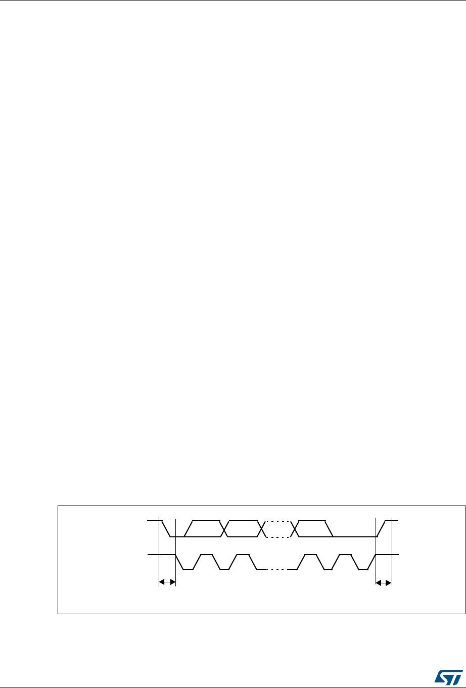
Inter-integrated circuit (I2C) interface RM0383
464/836 DocID026448 Rev 1
Note: Some of the above features may not be available in certain products. The user should refer
to the product data sheet, to identify the specific features supported by the I2C interface
implementation.
18.3 I2C functional description
In addition to receiving and transmitting data, this interface converts it from serial to parallel
format and vice versa. The interrupts are enabled or disabled by software. The interface is
connected to the I2C bus by a data pin (SDA) and by a clock pin (SCL). It can be connected
with a standard (up to 100 kHz) or fast (up to 400 kHz) I2C bus.
18.3.1 Mode selection
The interface can operate in one of the four following modes:
•Slave transmitter
•Slave receiver
•Master transmitter
•Master receiver
By default, it operates in slave mode. The interface automatically switches from slave to
master, after it generates a START condition and from master to slave, if an arbitration loss
or a Stop generation occurs, allowing multimaster capability.
Communication flow
In Master mode, the I2C interface initiates a data transfer and generates the clock signal. A
serial data transfer always begins with a start condition and ends with a stop condition. Both
start and stop conditions are generated in master mode by software.
In Slave mode, the interface is capable of recognizing its own addresses (7 or 10-bit), and
the General Call address. The General Call address detection may be enabled or disabled
by software.
Data and addresses are transferred as 8-bit bytes, MSB first. The first byte(s) following the
start condition contain the address (one in 7-bit mode, two in 10-bit mode). The address is
always transmitted in Master mode.
A 9th clock pulse follows the 8 clock cycles of a byte transfer, during which the receiver must
send an acknowledge bit to the transmitter. Refer to Figure 160.
Figure 160. I2C bus protocol
Acknowledge may be enabled or disabled by software. The I2C interface addresses (dual
addressing 7-bit/ 10-bit and/or general call address) can be selected by software.
SCL
SDA
12 8 9
MSB ACK
Stop
Start
condition
condition
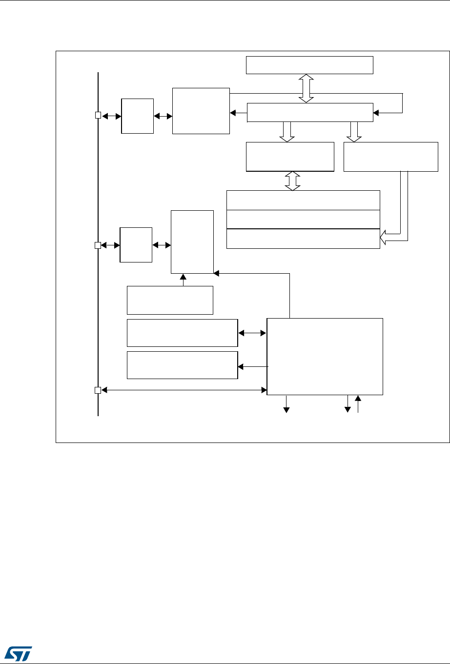
DocID026448 Rev 1 465/836
RM0383 Inter-integrated circuit (I2C) interface
497
The block diagram of the I2C interface is shown in Figure 161.
Figure 161. I2C block diagram
1. SMBA is an optional signal in SMBus mode. This signal is not applicable if SMBus is disabled.
18.3.2 I2C slave mode
By default the I2C interface operates in Slave mode. To switch from default Slave mode to
Master mode a Start condition generation is needed.
The peripheral input clock must be programmed in the I2C_CR2 register in order to
generate correct timings. The peripheral input clock frequency must be at least:
•2 MHz in Sm mode
•4 MHz in Fm mode
As soon as a start condition is detected, the address is received from the SDA line and sent
to the shift register. Then it is compared with the address of the interface (OAR1) and with
OAR2 (if ENDUAL=1) or the General Call address (if ENGC = 1).
$ATASHIFTREGISTER
#OMPARATOR
/WNADDRESSREGISTER
#LOCKCONTROL
3TATUSREGISTERS
#ONTROLREGISTERS
#ONTROL
#LOCK
CONTROL
$ATA
CONTROL
3#,
LOGIC
$UALADDRESSREGISTER
$ATAREGISTER
0%#REGISTER
)NTERRUPTS
0%#CALCULATION
3-"!
3$!
2EGISTER##2
3232
#2#2
$-!REQUESTS!#+
-36
.OISE
FILTER
.OISE
FILTER

Inter-integrated circuit (I2C) interface RM0383
466/836 DocID026448 Rev 1
Note: In 10-bit addressing mode, the comparison includes the header sequence (11110xx0),
where xx denotes the two most significant bits of the address.
Header or address not matched: the interface ignores it and waits for another Start
condition.
Header matched (10-bit mode only): the interface generates an acknowledge pulse if the
ACK bit is set and waits for the 8-bit slave address.
Address matched: the interface generates in sequence:
•An acknowledge pulse if the ACK bit is set
•The ADDR bit is set by hardware and an interrupt is generated if the ITEVFEN bit is
set.
•If ENDUAL=1, the software has to read the DUALF bit to check which slave address
has been acknowledged.
In 10-bit mode, after receiving the address sequence the slave is always in Receiver mode.
It will enter Transmitter mode on receiving a repeated Start condition followed by the header
sequence with matching address bits and the least significant bit set (11110xx1).
The TRA bit indicates whether the slave is in Receiver or Transmitter mode.
Slave transmitter
Following the address reception and after clearing ADDR, the slave sends bytes from the
DR register to the SDA line via the internal shift register.
The slave stretches SCL low until ADDR is cleared and DR filled with the data to be sent
(see Figure 162 Transfer sequencing EV1 EV3).
When the acknowledge pulse is received:
•The TxE bit is set by hardware with an interrupt if the ITEVFEN and the ITBUFEN bits
are set.
If TxE is set and some data were not written in the I2C_DR register before the end of the
next data transmission, the BTF bit is set and the interface waits until BTF is cleared by a
read to I2C_SR1 followed by a write to the I2C_DR register, stretching SCL low.

DocID026448 Rev 1 467/836
RM0383 Inter-integrated circuit (I2C) interface
497
Figure 162. Transfer sequence diagram for slave transmitter
1. The EV1 and EV3_1 events stretch SCL low until the end of the corresponding software sequence.
2. The EV3 event stretches SCL low if the software sequence is not completed before the end of the next byte
transmission
Slave receiver
Following the address reception and after clearing ADDR, the slave receives bytes from the
SDA line into the DR register via the internal shift register. After each byte the interface
generates in sequence:
•An acknowledge pulse if the ACK bit is set
•The RxNE bit is set by hardware and an interrupt is generated if the ITEVFEN and
ITBUFEN bit is set.
If RxNE is set and the data in the DR register is not read before the end of the next data
reception, the BTF bit is set and the interface waits until BTF is cleared by a read from the
I2C_DR register, stretching SCL low (see Figure 163 Transfer sequencing).
7-bit slave transmitter
10-bit slave transmitter
Legend: S= Start, S
r
= Repeated Start, P= Stop, A= Acknowledge, NA= Non-acknowledge,
EVx= Event (with interrupt if ITEVFEN=1)
EV1: ADDR=1, cleared by reading SR1 followed by reading SR2
EV3-1: TxE=1, shift register empty, data register empty, write Data1 in DR.
EV3: TxE=1, shift register not empty, data register empty, cleared by writing DR
EV3-2: AF=1; AF is cleared by writing ‘0’ in AF bit of SR1 register.
S Address AData1A Data2A ..... DataNNAP
EV1 EV3-1 EV3EV3EV3EV3-2
SHeader A Address A
EV1
SrHeader A Data1A .... DataNNA
P
EV1 EV3_1 EV3EV3EV3-2
ai18209

Inter-integrated circuit (I2C) interface RM0383
468/836 DocID026448 Rev 1
Figure 163. Transfer sequence diagram for slave receiver
1. The EV1 event stretches SCL low until the end of the corresponding software sequence.
2. The EV2 event stretches SCL low if the software sequence is not completed before the end of the next byte
reception.
3. After checking the SR1 register content, the user should perform the complete clearing sequence for each
flag found set.
Thus, for ADDR and STOPF flags, the following sequence is required inside the I2C interrupt routine:
READ SR1
if (ADDR == 1) {READ SR1; READ SR2}
if (STOPF == 1) {READ SR1; WRITE CR1}
The purpose is to make sure that both ADDR and STOPF flags are cleared if both are found set.
Closing slave communication
After the last data byte is transferred a Stop Condition is generated by the master. The
interface detects this condition and sets:
•The STOPF bit and generates an interrupt if the ITEVFEN bit is set.
The STOPF bit is cleared by a read of the SR1 register followed by a write to the CR1
register (see Figure 163: Transfer sequence diagram for slave receiver EV4).
18.3.3 I2C master mode
In Master mode, the I2C interface initiates a data transfer and generates the clock signal. A
serial data transfer always begins with a Start condition and ends with a Stop condition.
Master mode is selected as soon as the Start condition is generated on the bus with a
START bit.
The following is the required sequence in master mode.
•Program the peripheral input clock in I2C_CR2 Register in order to generate correct
timings
•Configure the clock control registers
•Configure the rise time register
•Program the I2C_CR1 register to enable the peripheral
•Set the START bit in the I2C_CR1 register to generate a Start condition
The peripheral input clock frequency must be at least:
•2 MHz in Sm mode
•4 MHz in Fm mode
7-bit slave receiver
10-bit slave receiver
Legend: S= Start, S
r
= Repeated Start, P= Stop, A= Acknowledge,
EVx= Event (with interrupt if ITEVFEN=1)
EV1: ADDR=1, cleared by reading SR1 followed by reading SR2
EV2: RxNE=1 cleared by reading DR register.
EV4: STOPF=1, cleared by reading SR1 register followed by writing to the CR1 register
S Address AData1AData2A ..... DataNA P
EV1 EV2 EV2 EV2 EV4
SHeader A Address AData1A ..... DataNA P
EV1 EV2 EV2 EV4
ai18208

DocID026448 Rev 1 469/836
RM0383 Inter-integrated circuit (I2C) interface
497
SCL master clock generation
The CCR bits are used to generate the high and low level of the SCL clock, starting from the
generation of the rising and falling edge (respectively). As a slave may stretch the SCL line,
the peripheral checks the SCL input from the bus at the end of the time programmed in
TRISE bits after rising edge generation.
•If the SCL line is low, it means that a slave is stretching the bus, and the high level
counter stops until the SCL line is detected high. This allows to guarantee the minimum
HIGH period of the SCL clock parameter.
•If the SCL line is high, the high level counter keeps on counting.
Indeed, the feedback loop from the SCL rising edge generation by the peripheral to the SCL
rising edge detection by the peripheral takes time even if no slave stretches the clock. This
loopback duration is linked to the SCL rising time (impacting SCL VIH input detection), plus
delay due to the noise filter present on the SCL input path, plus delay due to internal SCL
input synchronization with APB clock. The maximum time used by the feedback loop is
programmed in the TRISE bits, so that the SCL frequency remains stable whatever the SCL
rising time.
Start condition
Setting the START bit causes the interface to generate a Start condition and to switch to
Master mode (MSL bit set) when the BUSY bit is cleared.
Note: In master mode, setting the START bit causes the interface to generate a ReStart condition
at the end of the current byte transfer.
Once the Start condition is sent:
•The SB bit is set by hardware and an interrupt is generated if the ITEVFEN bit is set.
Then the master waits for a read of the SR1 register followed by a write in the DR register
with the Slave address (see Figure 164 and Figure 165 Transfer sequencing EV5).
Slave address transmission
Then the slave address is sent to the SDA line via the internal shift register.
•In 10-bit addressing mode, sending the header sequence causes the following event:
– The ADD10 bit is set by hardware and an interrupt is generated if the ITEVFEN bit
is set.
Then the master waits for a read of the SR1 register followed by a write in the DR
register with the second address byte (see Figure 164 and Figure 165 Transfer
sequencing).
– The ADDR bit is set by hardware and an interrupt is generated if the ITEVFEN bit
is set.
Then the master waits for a read of the SR1 register followed by a read of the SR2
register (see Figure 164 and Figure 165 Transfer sequencing).
•In 7-bit addressing mode, one address byte is sent.
As soon as the address byte is sent,
– The ADDR bit is set by hardware and an interrupt is generated if the ITEVFEN bit
is set.
Then the master waits for a read of the SR1 register followed by a read of the SR2
register (see Figure 164 and Figure 165 Transfer sequencing).

Inter-integrated circuit (I2C) interface RM0383
470/836 DocID026448 Rev 1
The master can decide to enter Transmitter or Receiver mode depending on the LSB of the
slave address sent.
•In 7-bit addressing mode,
– To enter Transmitter mode, a master sends the slave address with LSB reset.
– To enter Receiver mode, a master sends the slave address with LSB set.
•In 10-bit addressing mode,
– To enter Transmitter mode, a master sends the header (11110xx0) and then the
slave address, (where xx denotes the two most significant bits of the address).
– To enter Receiver mode, a master sends the header (11110xx0) and then the
slave address. Then it should send a repeated Start condition followed by the
header (11110xx1), (where xx denotes the two most significant bits of the
address).
The TRA bit indicates whether the master is in Receiver or Transmitter mode.
Master transmitter
Following the address transmission and after clearing ADDR, the master sends bytes from
the DR register to the SDA line via the internal shift register.
The master waits until the first data byte is written into I2C_DR (see Figure 164 Transfer
sequencing EV8_1).
When the acknowledge pulse is received, the TxE bit is set by hardware and an interrupt is
generated if the ITEVFEN and ITBUFEN bits are set.
If TxE is set and a data byte was not written in the DR register before the end of the last data
transmission, BTF is set and the interface waits until BTF is cleared by a write to I2C_DR,
stretching SCL low.
Closing the communication
After the last byte is written to the DR register, the STOP bit is set by software to generate a
Stop condition (see Figure 164 Transfer sequencing EV8_2). The interface automatically
goes back to slave mode (MSL bit cleared).
Note: Stop condition should be programmed during EV8_2 event, when either TxE or BTF is set.

DocID026448 Rev 1 471/836
RM0383 Inter-integrated circuit (I2C) interface
497
Figure 164. Transfer sequence diagram for master transmitter
1. The EV5, EV6, EV9, EV8_1 and EV8_2 events stretch SCL low until the end of the corresponding software sequence.
2. The EV8 event stretches SCL low if the software sequence is not complete before the end of the next byte transmission.
7-bit master transmitter
10-bit master transmitter
Legend: S= Start, Sr = Repeated Start, P= Stop, A= Acknowledge,
EVx= Event (with interrupt if ITEVFEN = 1)
EV5: SB=1, cleared by reading SR1 register followed by writing DR register with Address.
EV6: ADDR=1, cleared by reading SR1 register followed by reading SR2.
EV8_1: TxE=1, shift register empty, data register empty, write Data1 in DR.
EV8: TxE=1, shift register not empty, data register empty, cleared by writing DR register.
EV8_2: TxE=1, BTF = 1, Program Stop request. TxE and BTF are cleared by hardware by the Stop condition
EV9: ADD10=1, cleared by reading SR1 register followed by writing DR register.
SAddress AData1A Data2A ..... DataNA P
EV5 EV6 EV8_1 EV8EV8EV8EV8_2
SHeader A Address AData1A ..... DataNA P
EV5 EV9 EV6 EV8_1 EV8EV8EV8_2
ai18210

Inter-integrated circuit (I2C) interface RM0383
472/836 DocID026448 Rev 1
Master receiver
Following the address transmission and after clearing ADDR, the I2C interface enters
Master Receiver mode. In this mode the interface receives bytes from the SDA line into the
DR register via the internal shift register. After each byte the interface generates in
sequence:
1. An acknowledge pulse if the ACK bit is set
2. The RxNE bit is set and an interrupt is generated if the ITEVFEN and ITBUFEN bits are
set (see Figure 165 Transfer sequencing EV7).
If the RxNE bit is set and the data in the DR register is not read before the end of the last
data reception, the BTF bit is set by hardware and the interface waits until BTF is cleared by
a read in the DR register, stretching SCL low.
Closing the communication
The master sends a NACK for the last byte received from the slave. After receiving this
NACK, the slave releases the control of the SCL and SDA lines. Then the master can send
a Stop/Restart condition.
1. To generate the nonacknowledge pulse after the last received data byte, the ACK bit
must be cleared just after reading the second last data byte (after second last RxNE
event).
2. In order to generate the Stop/Restart condition, software must set the STOP/START bit
after reading the second last data byte (after the second last RxNE event).
3. In case a single byte has to be received, the Acknowledge disable is made during EV6
(before ADDR flag is cleared) and the STOP condition generation is made after EV6.
After the Stop condition generation, the interface goes automatically back to slave mode
(MSL bit cleared).

DocID026448 Rev 1 473/836
RM0383 Inter-integrated circuit (I2C) interface
497
Figure 165. Transfer sequence diagram for master receiver
1. If a single byte is received, it is NA.
2. The EV5, EV6 and EV9 events stretch SCL low until the end of the corresponding software sequence.
3. The EV7 event stretches SCL low if the software sequence is not completed before the end of the next byte reception.
4. The EV7_1 software sequence must be completed before the ACK pulse of the current byte transfer.
The procedures described below are recommended if the EV7-1 software sequence is not
completed before the ACK pulse of the current byte transfer.
These procedures must be followed to make sure:
•The ACK bit is set low on time before the end of the last data reception
•The STOP bit is set high after the last data reception without reception of
supplementary data.
For 2-byte reception:
•Wait until ADDR = 1 (SCL stretched low until the ADDR flag is cleared)
•Set ACK low, set POS high
•Clear ADDR flag
•Wait until BTF = 1 (Data 1 in DR, Data2 in shift register, SCL stretched low until a data
1 is read)
•Set STOP high
•Read data 1 and 2
BITMASTERRECEIVER
BITMASTERRECEIVER
,EGEND33TART3R2EPEATED3TART03TOP!!CKNOWLEDGE.!.ONACKNOWLEDGE
%6X%VENTWITHINTERRUPTIF)4%6&%.
%63"CLEAREDBYREADING32REGISTERFOLLOWEDBYWRITING$2REGISTER
%6!$$2CLEAREDBYREADING32REGISTERFOLLOWEDBYREADING32)NBITMASTERRECEIVERMODETHISSE
QUENCESHOULDBEFOLLOWEDBYWRITING#2WITH34!24
%62X.%CLEAREDBYREADING$2REGISTER
%6?2X.%CLEAREDBYREADING$2REGISTERPROGRAM!#+AND34/0REQUEST
%6!$$CLEAREDBYREADING32REGISTERFOLLOWEDBYWRITING$2REGISTER
3 !DDRESS ! $ATA ! $ATA ! $ATA. .! 0
%6 %6 %6 %6 %6? %6
3 (EADER ! !DDRESS !
%6 %6 %6
3R(EADER ! $ATA !
%6 %6 %6
$ATA !
%6
$ATA. .! 0
%6? %6
AID
)NCASEOFTHERECEPTIONOFBYTETHE!CKNOWLEDGEDISABLEMUSTBEPERFORMEDDURING%6EVENTIEBEFORECLEARING!$$2FLAG

Inter-integrated circuit (I2C) interface RM0383
474/836 DocID026448 Rev 1
For N >2 -byte reception, from N-2 data reception
•Wait until BTF = 1 (data N-2 in DR, data N-1 in shift register, SCL stretched low until
data N-2 is read)
•Set ACK low
•Read data N-2
•Wait until BTF = 1 (data N-1 in DR, data N in shift register, SCL stretched low until a
data N-1 is read)
•Set STOP high
•Read data N-1 and N
18.3.4 Error conditions
The following are the error conditions which may cause communication to fail.
Bus error (BERR)
This error occurs when the I2C interface detects an external Stop or Start condition during
an address or a data transfer. In this case:
•the BERR bit is set and an interrupt is generated if the ITERREN bit is set
•in Slave mode: data are discarded and the lines are released by hardware:
– in case of a misplaced Start, the slave considers it is a restart and waits for an
address, or a Stop condition
– in case of a misplaced Stop, the slave behaves like for a Stop condition and the
lines are released by hardware
•In Master mode: the lines are not released and the state of the current transmission is
not affected. It is up to the software to abort or not the current transmission
Acknowledge failure (AF)
This error occurs when the interface detects a nonacknowledge bit. In this case:
•the AF bit is set and an interrupt is generated if the ITERREN bit is set
•a transmitter which receives a NACK must reset the communication:
– If Slave: lines are released by hardware
– If Master: a Stop or repeated Start condition must be generated by software
Arbitration lost (ARLO)
This error occurs when the I2C interface detects an arbitration lost condition. In this case,
•the ARLO bit is set by hardware (and an interrupt is generated if the ITERREN bit is
set)
•the I2C Interface goes automatically back to slave mode (the MSL bit is cleared). When
the I2C loses the arbitration, it is not able to acknowledge its slave address in the same
transfer, but it can acknowledge it after a repeated Start from the winning master.
•lines are released by hardware

DocID026448 Rev 1 475/836
RM0383 Inter-integrated circuit (I2C) interface
497
Overrun/underrun error (OVR)
An overrun error can occur in slave mode when clock stretching is disabled and the I2C
interface is receiving data. The interface has received a byte (RxNE=1) and the data in DR
has not been read, before the next byte is received by the interface. In this case,
•The last received byte is lost.
•In case of Overrun error, software should clear the RxNE bit and the transmitter should
re-transmit the last received byte.
Underrun error can occur in slave mode when clock stretching is disabled and the I2C
interface is transmitting data. The interface has not updated the DR with the next byte
(TxE=1), before the clock comes for the next byte. In this case,
•The same byte in the DR register will be sent again
•The user should make sure that data received on the receiver side during an underrun
error are discarded and that the next bytes are written within the clock low time
specified in the I2C bus standard.
For the first byte to be transmitted, the DR must be written after ADDR is cleared and before
the first SCL rising edge. If not possible, the receiver must discard the first data.
18.3.5 Programmable noise filter
In Fm mode, the I2C standard requires that spikes are suppressed to a length of 50 ns on
SDA and SCL lines.
An analog noise filter is implemented in the SDA and SCL I/Os. This filter is enabled by
default and can be disabled by setting the ANOFF bit in the I2C_FLTR register.
A digital noise filter can be enabled by configuring the DNF[3:0] bits to a non-zero value.
This suppresses the spikes on SDA and SCL inputs with a length of up to DNF[3:0] *
TPCLK1.
Enabling the digital noise filter increases the SDA hold time by (DNF[3:0] +1)* TPCLK.
To be compliant with the maximum hold time of the I2C-bus specification version 2.1
(Thd:dat), the DNF bits must be programmed using the constraints shown in Table 67, and
assuming that the analog filter is disabled.
Note: DNF[3:0] must only be configured when the I2C is disabled (PE = 0). If the analog filter is
also enabled, the digital filter is added to the analog filter.
Table 67. Maximum DNF[3:0] value to be compliant with Thd:dat(max)
PCLK1 frequency Maximum DNF value
Sm mode Fm mode
2 <= FPCLK1 <= 5 2 0
5 < FPCLK1 <= 10 12 0
10 < FPCLK1 <= 20 15 1
20 < FPCLK1 <= 30 15 7
30 < FPCLK1 <= 40 15 13
40 < FPCLK1 <= 50 15 15

Inter-integrated circuit (I2C) interface RM0383
476/836 DocID026448 Rev 1
Note: For each frequency range, the constraint is given based on the worst case which is the
minimum frequency of the range. Greater DNF values can be used if the system can
support maximum hold time violation.
18.3.6 SDA/SCL line control
•If clock stretching is enabled:
– Transmitter mode: If TxE=1 and BTF=1: the interface holds the clock line low
before transmission to wait for the microcontroller to write the byte in the Data
Register (both buffer and shift register are empty).
– Receiver mode: If RxNE=1 and BTF=1: the interface holds the clock line low after
reception to wait for the microcontroller to read the byte in the Data Register (both
buffer and shift register are full).
•If clock stretching is disabled in Slave mode:
– Overrun Error in case of RxNE=1 and no read of DR has been done before the
next byte is received. The last received byte is lost.
– Underrun Error in case TxE=1 and no write into DR has been done before the next
byte must be transmitted. The same byte will be sent again.
– Write Collision not managed.
18.3.7 SMBus
Introduction
The System Management Bus (SMBus) is a two-wire interface through which various
devices can communicate with each other and with the rest of the system. It is based on I2C
principles of operation. SMBus provides a control bus for system and power management
related tasks. A system may use SMBus to pass messages to and from devices instead of
toggling individual control lines.
The System Management Bus Specification refers to three types of devices. A slave is a
device that is receiving or responding to a command. A master is a device that issues
commands, generates the clocks, and terminates the transfer. A host is a specialized
master that provides the main interface to the system's CPU. A host must be a master-slave
and must support the SMBus host notify protocol. Only one host is allowed in a system.
Similarities between SMBus and I2C
•2 wire bus protocol (1 Clk, 1 Data) + SMBus Alert line optional
•Master-slave communication, Master provides clock
•Multi master capability
•SMBus data format similar to I2C 7-bit addressing format (Figure 160).
Differences between SMBus and I2C
The following table describes the differences between SMBus and I2C.

DocID026448 Rev 1 477/836
RM0383 Inter-integrated circuit (I2C) interface
497
SMBus application usage
With System Management Bus, a device can provide manufacturer information, tell the
system what its model/part number is, save its state for a suspend event, report different
types of errors, accept control parameters, and return its status. SMBus provides a control
bus for system and power management related tasks.
Device identification
Any device that exists on the System Management Bus as a slave has a unique address
called the Slave Address. For the list of reserved slave addresses, refer to the SMBus
specification version. 2.0 (http://smbus.org/).
Bus protocols
The SMBus specification supports up to 9 bus protocols. For more details of these protocols
and SMBus address types, refer to SMBus specification version. 2.0 (http://smbus.org/).
These protocols should be implemented by the user software.
Address resolution protocol (ARP)
SMBus slave address conflicts can be resolved by dynamically assigning a new unique
address to each slave device. The Address Resolution Protocol (ARP) has the following
attributes:
•Address assignment uses the standard SMBus physical layer arbitration mechanism
•Assigned addresses remain constant while device power is applied; address retention
through device power loss is also allowed
•No additional SMBus packet overhead is incurred after address assignment. (i.e.
subsequent accesses to assigned slave addresses have the same overhead as
accesses to fixed address devices.)
•Any SMBus master can enumerate the bus
Unique device identifier (UDID)
In order to provide a mechanism to isolate each device for the purpose of address
assignment, each device must implement a unique device identifier (UDID).
For the details on 128 bit UDID and more information on ARP, refer to SMBus specification
version 2.0 (http://smbus.org/).
Table 68. SMBus vs. I2C
SMBus I2C
Max. speed 100 kHz Max. speed 400 kHz
Min. clock speed 10 kHz No minimum clock speed
35 ms clock low timeout No timeout
Logic levels are fixed Logic levels are VDD dependent
Different address types (reserved, dynamic etc.) 7-bit, 10-bit and general call slave address types
Different bus protocols (quick command, process
call etc.) No bus protocols

Inter-integrated circuit (I2C) interface RM0383
478/836 DocID026448 Rev 1
SMBus alert mode
SMBus Alert is an optional signal with an interrupt line for devices that want to trade their
ability to master for a pin. SMBA is a wired-AND signal just as the SCL and SDA signals are.
SMBA is used in conjunction with the SMBus General Call Address. Messages invoked with
the SMBus are 2 bytes long.
A slave-only device can signal the host through SMBA that it wants to talk by setting ALERT
bit in I2C_CR1 register. The host processes the interrupt and simultaneously accesses all
SMBA devices through the Alert Response Address (known as ARA having a value 0001
100X). Only the device(s) which pulled SMBA low will acknowledge the Alert Response
Address. This status is identified using SMBALERT Status flag in I2C_SR1 register. The
host performs a modified Receive Byte operation. The 7 bit device address provided by the
slave transmit device is placed in the 7 most significant bits of the byte. The eighth bit can
be a zero or one.
If more than one device pulls SMBA low, the highest priority (lowest address) device will win
communication rights via standard arbitration during the slave address transfer. After
acknowledging the slave address the device must disengage its SMBA pull-down. If the
host still sees SMBA low when the message transfer is complete, it knows to read the ARA
again.
A host which does not implement the SMBA signal may periodically access the ARA.
For more details on SMBus Alert mode, refer to SMBus specification version 2.0
(http://smbus.org/).
Timeout error
There are differences in the timing specifications between I2C and SMBus.
SMBus defines a clock low timeout, TIMEOUT of 35 ms. Also SMBus specifies TLOW:
SEXT as the cumulative clock low extend time for a slave device. SMBus specifies TLOW:
MEXT as the cumulative clock low extend time for a master device. For more details on
these timeouts, refer to SMBus specification version 2.0 (http://smbus.org/).
The status flag Timeout or Tlow Error in I2C_SR1 shows the status of this feature.
How to use the interface in SMBus mode
To switch from I2C mode to SMBus mode, the following sequence should be performed.
•Set the SMBus bit in the I2C_CR1 register
•Configure the SMBTYPE and ENARP bits in the I2C_CR1 register as required for the
application
If you want to configure the device as a master, follow the Start condition generation
procedure in Section 18.3.3: I2C master mode. Otherwise, follow the sequence in
Section 18.3.2: I2C slave mode.
The application has to control the various SMBus protocols by software.
•SMB Device Default Address acknowledged if ENARP=1 and SMBTYPE=0
•SMB Host Header acknowledged if ENARP=1 and SMBTYPE=1
•SMB Alert Response Address acknowledged if SMBALERT=1

DocID026448 Rev 1 479/836
RM0383 Inter-integrated circuit (I2C) interface
497
18.3.8 DMA requests
DMA requests (when enabled) are generated only for data transfer. DMA requests are
generated by Data Register becoming empty in transmission and Data Register becoming
full in reception. The DMA must be initialized and enabled before the I2C data transfer. The
DMAEN bit must be set in the I2C_CR2 register before the ADDR event. In master mode or
in slave mode when clock stretching is enabled, the DMAEN bit can also be set during the
ADDR event, before clearing the ADDR flag. The DMA request must be served before the
end of the current byte transfer. When the number of data transfers which has been
programmed for the corresponding DMA stream is reached, the DMA controller sends an
End of Transfer EOT signal to the I2C interface and generates a Transfer Complete interrupt
if enabled:
•Master transmitter: In the interrupt routine after the EOT interrupt, disable DMA
requests then wait for a BTF event before programming the Stop condition.
•Master receiver
– When the number of bytes to be received is equal to or greater than two, the DMA
controller sends a hardware signal, EOT_1, corresponding to the last but one data
byte (number_of_bytes – 1). If, in the I2C_CR2 register, the LAST bit is set, I2C
automatically sends a NACK after the next byte following EOT_1. The user can
generate a Stop condition in the DMA Transfer Complete interrupt routine if
enabled.
– When a single byte must be received: the NACK must be programmed during EV6
event, i.e. program ACK=0 when ADDR=1, before clearing ADDR flag. Then the
user can program the STOP condition either after clearing ADDR flag, or in the
DMA Transfer Complete interrupt routine.
Transmission using DMA
DMA mode can be enabled for transmission by setting the DMAEN bit in the I2C_CR2
register. Data will be loaded from a Memory area configured using the DMA peripheral (refer
to the DMA specification) to the I2C_DR register whenever the TxE bit is set. To map a DMA
stream x for I2C transmission (where x is the stream number), perform the following
sequence:
1. Set the I2C_DR register address in the DMA_SxPAR register. The data will be moved
to this address from the memory after each TxE event.
2. Set the memory address in the DMA_SxMA0R register (and in DMA_SxMA1R register
in the case of a bouble buffer mode). The data will be loaded into I2C_DR from this
memory after each TxE event.
3. Configure the total number of bytes to be transferred in the DMA_SxNDTR register.
After each TxE event, this value will be decremented.
4. Configure the DMA stream priority using the PL[0:1] bits in the DMA_SxCR register
5. Set the DIR bit in the DMA_SxCR register and configure interrupts after half transfer or
full transfer depending on application requirements.
6. Activate the stream by setting the EN bit in the DMA_SxCR register.
When the number of data transfers which has been programmed in the DMA Controller
registers is reached, the DMA controller sends an End of Transfer EOT/ EOT_1 signal to the
I2C interface and the DMA generates an interrupt, if enabled, on the DMA stream interrupt
vector.
Note: Do not enable the ITBUFEN bit in the I2C_CR2 register if DMA is used for transmission.

Inter-integrated circuit (I2C) interface RM0383
480/836 DocID026448 Rev 1
Reception using DMA
DMA mode can be enabled for reception by setting the DMAEN bit in the I2C_CR2 register.
Data will be loaded from the I2C_DR register to a Memory area configured using the DMA
peripheral (refer to the DMA specification) whenever a data byte is received. To map a DMA
stream x for I2C reception (where x is the stream number), perform the following sequence:
1. Set the I2C_DR register address in DMA_SxPAR register. The data will be moved from
this address to the memory after each RxNE event.
2. Set the memory address in the DMA_SxMA0R register (and in DMA_SxMA1R register
in the case of a bouble buffer mode). The data will be loaded from the I2C_DR register
to this memory area after each RxNE event.
3. Configure the total number of bytes to be transferred in the DMA_SxNDTR register.
After each RxNE event, this value will be decremented.
4. Configure the stream priority using the PL[0:1] bits in the DMA_SxCR register
5. Reset the DIR bit and configure interrupts in the DMA_SxCR register after half transfer
or full transfer depending on application requirements.
6. Activate the stream by setting the EN bit in the DMA_SxCR register.
When the number of data transfers which has been programmed in the DMA Controller
registers is reached, the DMA controller sends an End of Transfer EOT/ EOT_1 signal to the
I2C interface and DMA generates an interrupt, if enabled, on the DMA stream interrupt
vector.
Note: Do not enable the ITBUFEN bit in the I2C_CR2 register if DMA is used for reception.
18.3.9 Packet error checking
A PEC calculator has been implemented to improve the reliability of communication. The
PEC is calculated by using the C(x) = x8 + x2 + x + 1 CRC-8 polynomial serially on each bit.
•PEC calculation is enabled by setting the ENPEC bit in the I2C_CR1 register. PEC is a
CRC-8 calculated on all message bytes including addresses and R/W bits.
– In transmission: set the PEC transfer bit in the I2C_CR1 register after the TxE
event corresponding to the last byte. The PEC will be transferred after the last
transmitted byte.
– In reception: set the PEC bit in the I2C_CR1 register after the RxNE event
corresponding to the last byte so that the receiver sends a NACK if the next
received byte is not equal to the internally calculated PEC. In case of Master-
Receiver, a NACK must follow the PEC whatever the check result. The PEC must

DocID026448 Rev 1 481/836
RM0383 Inter-integrated circuit (I2C) interface
497
be set before the ACK of the CRC reception in slave mode. It must be set when
the ACK is set low in master mode.
•A PECERR error flag/interrupt is also available in the I2C_SR1 register.
•If DMA and PEC calculation are both enabled:-
– In transmission: when the I2C interface receives an EOT signal from the DMA
controller, it automatically sends a PEC after the last byte.
– In reception: when the I2C interface receives an EOT_1 signal from the DMA
controller, it will automatically consider the next byte as a PEC and will check it. A
DMA request is generated after PEC reception.
•To allow intermediate PEC transfers, a control bit is available in the I2C_CR2 register
(LAST bit) to determine if it is really the last DMA transfer or not. If it is the last DMA
request for a master receiver, a NACK is automatically sent after the last received byte.
•PEC calculation is corrupted by an arbitration loss.
18.4 I2C interrupts
The table below gives the list of I2C interrupt requests.
Note: SB, ADDR, ADD10, STOPF, BTF, RxNE and TxE are logically ORed on the same interrupt
channel.
BERR, ARLO, AF, OVR, PECERR, TIMEOUT and SMBALERT are logically ORed on the
same interrupt channel.
Table 69. I2C Interrupt requests
Interrupt event Event flag Enable control bit
Start bit sent (Master) SB
ITEVFEN
Address sent (Master) or Address matched (Slave) ADDR
10-bit header sent (Master) ADD10
Stop received (Slave) STOPF
Data byte transfer finished BTF
Receive buffer not empty RxNE
ITEVFEN and ITBUFEN
Transmit buffer empty TxE
Bus error BERR
ITERREN
Arbitration loss (Master) ARLO
Acknowledge failure AF
Overrun/Underrun OVR
PEC error PECERR
Timeout/Tlow error TIMEOUT
SMBus Alert SMBALERT
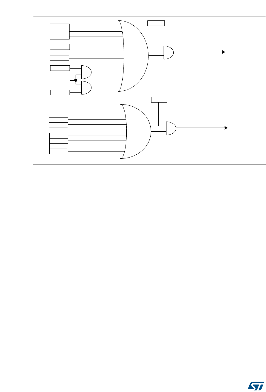
Inter-integrated circuit (I2C) interface RM0383
482/836 DocID026448 Rev 1
Figure 166. I2C interrupt mapping diagram
ADDR
SB
ADD10
RxNE
TxE
BTF
it_event
ARLO
BERR
AF
OVR
PECERR
TIMEOUT
SMBALERT
ITERREN
it_error
ITEVFEN
ITBUFEN
STOPF

DocID026448 Rev 1 483/836
RM0383 Inter-integrated circuit (I2C) interface
497
18.5 I2C debug mode
When the microcontroller enters the debug mode (Cortex®-M4 with FPU core halted), the
SMBUS timeout either continues to work normally or stops, depending on the
DBG_I2Cx_SMBUS_TIMEOUT configuration bits in the DBG module. For more details,
refer to Section 23.16.2: Debug support for timers, watchdog and I2C on page 818.
18.6 I2C registers
Refer to Section 1.1 on page 33 for a list of abbreviations used in register descriptions.
The peripheral registers have to be accessed by half-words (16 bits) or words (32 bits).
18.6.1 I2C Control register 1 (I2C_CR1)
Address offset: 0x00
Reset value: 0x0000
15141312111098 7 6543210
SWRST Res. ALERT PEC POS ACK STOP START NO
STRETCH ENGC ENPEC ENARP SMB
TYPE Res.
SMBU
SPE
rw rw rw rw rw rw rw rw rw rw rw rw rw rw
Bit 15 SWRST: Software reset
When set, the I2C is under reset state. Before resetting this bit, make sure the I2C lines are
released and the bus is free.
0: I2C Peripheral not under reset
1: I2C Peripheral under reset state
Note: This bit can be used to reinitialize the peripheral after an error or a locked state. As an
example, if the BUSY bit is set and remains locked due to a glitch on the bus, the
SWRST bit can be used to exit from this state.
Bit 14 Reserved, must be kept at reset value
Bit 13 ALERT: SMBus alert
This bit is set and cleared by software, and cleared by hardware when PE=0.
0: Releases SMBA pin high. Alert Response Address Header followed by NACK.
1: Drives SMBA pin low. Alert Response Address Header followed by ACK.
Bit 12 PEC: Packet error checking
This bit is set and cleared by software, and cleared by hardware when PEC is transferred or
by a START or Stop condition or when PE=0.
0: No PEC transfer
1: PEC transfer (in Tx or Rx mode)
Note: PEC calculation is corrupted by an arbitration loss.
Bit 11 POS: Acknowledge/PEC Position (for data reception)
This bit is set and cleared by software and cleared by hardware when PE=0.
0: ACK bit controls the (N)ACK of the current byte being received in the shift register. The
PEC bit indicates that current byte in shift register is a PEC.
1: ACK bit controls the (N)ACK of the next byte which will be received in the shift register.
The PEC bit indicates that the next byte in the shift register is a PEC
Note: The POS bit must be used only in 2-byte reception configuration in master mode. It
must be configured before data reception starts, as described in the 2-byte reception
procedure recommended in Section : Master receiver on page 472.

Inter-integrated circuit (I2C) interface RM0383
484/836 DocID026448 Rev 1
Bit 10 ACK: Acknowledge enable
This bit is set and cleared by software and cleared by hardware when PE=0.
0: No acknowledge returned
1: Acknowledge returned after a byte is received (matched address or data)
Bit 9 STOP: Stop generation
The bit is set and cleared by software, cleared by hardware when a Stop condition is
detected, set by hardware when a timeout error is detected.
In Master Mode:
0: No Stop generation.
1: Stop generation after the current byte transfer or after the current Start condition is sent.
In Slave mode:
0: No Stop generation.
1: Release the SCL and SDA lines after the current byte transfer.
Bit 8 START: Start generation
This bit is set and cleared by software and cleared by hardware when start is sent or PE=0.
In Master Mode:
0: No Start generation
1: Repeated start generation
In Slave mode:
0: No Start generation
1: Start generation when the bus is free
Bit 7 NOSTRETCH: Clock stretching disable (Slave mode)
This bit is used to disable clock stretching in slave mode when ADDR or BTF flag is set, until
it is reset by software.
0: Clock stretching enabled
1: Clock stretching disabled
Bit 6 ENGC: General call enable
0: General call disabled. Address 00h is NACKed.
1: General call enabled. Address 00h is ACKed.
Bit 5 ENPEC: PEC enable
0: PEC calculation disabled
1: PEC calculation enabled
Bit 4 ENARP: ARP enable
0: ARP disable
1: ARP enable
SMBus Device default address recognized if SMBTYPE=0
SMBus Host address recognized if SMBTYPE=1
Bit 3 SMBTYPE: SMBus type
0: SMBus Device
1: SMBus Host

DocID026448 Rev 1 485/836
RM0383 Inter-integrated circuit (I2C) interface
497
Note: When the STOP, START or PEC bit is set, the software must not perform any write access
to I2C_CR1 before this bit is cleared by hardware. Otherwise there is a risk of setting a
second STOP, START or PEC request.
18.6.2 I2C Control register 2 (I2C_CR2)
Address offset: 0x04
Reset value: 0x0000
Bit 2 Reserved, must be kept at reset value
Bit 1 SMBUS: SMBus mode
0: I2C mode
1: SMBus mode
Bit 0 PE: Peripheral enable
0: Peripheral disable
1: Peripheral enable
Note: If this bit is reset while a communication is on going, the peripheral is disabled at the
end of the current communication, when back to IDLE state.
All bit resets due to PE=0 occur at the end of the communication.
In master mode, this bit must not be reset before the end of the communication.
1514131211109876543210
Reserved LAST DMA
EN
ITBUF
EN
ITEVTE
N
ITERR
EN Reserved FREQ[5:0]
rw rw rw rw rw rw rw rw rw rw rw
Bits 15:13 Reserved, must be kept at reset value
Bit 12 LAST: DMA last transfer
0: Next DMA EOT is not the last transfer
1: Next DMA EOT is the last transfer
Note: This bit is used in master receiver mode to permit the generation of a NACK on the last
received data.
Bit 11 DMAEN: DMA requests enable
0: DMA requests disabled
1: DMA request enabled when TxE=1 or RxNE =1
Bit 10 ITBUFEN: Buffer interrupt enable
0: TxE = 1 or RxNE = 1 does not generate any interrupt.
1: TxE = 1 or RxNE = 1 generates Event Interrupt (whatever the state of DMAEN)

Inter-integrated circuit (I2C) interface RM0383
486/836 DocID026448 Rev 1
Bit 9 ITEVTEN: Event interrupt enable
0: Event interrupt disabled
1: Event interrupt enabled
This interrupt is generated when:
– SB = 1 (Master)
– ADDR = 1 (Master/Slave)
– ADD10= 1 (Master)
– STOPF = 1 (Slave)
– BTF = 1 with no TxE or RxNE event
– TxE event to 1 if ITBUFEN = 1
– RxNE event to 1if ITBUFEN = 1
ITERREN: Error interrupt enable
0: Error interrupt disabled
1: Error interrupt enabled
This interrupt is generated when:
–BERR = 1
–ARLO = 1
–AF = 1
–OVR = 1
– PECERR = 1
–TIMEOUT = 1
– SMBALERT = 1
Bits 7:6 Reserved, must be kept at reset value
Bits 5:0 FREQ[5:0]: Peripheral clock frequency
The FREQ bits must be configured with the APB clock frequency value (I2C peripheral
connected to APB). The FREQ field is used by the peripheral to generate data setup and
hold times compliant with the I2C specifications. The minimum allowed frequency is 2 MHz,
the maximum frequency is limited by the maximum APB frequency (42 MHz) and an intrinsic
limitation of 46 MHz.
0b000000: Not allowed
0b000001: Not allowed
0b000010: 2 MHz
...
0b101010: 42MHz
Higher than 0b101010: Not allowed

DocID026448 Rev 1 487/836
RM0383 Inter-integrated circuit (I2C) interface
497
18.6.3 I2C Own address register 1 (I2C_OAR1)
Address offset: 0x08
Reset value: 0x0000
18.6.4 I2C Own address register 2 (I2C_OAR2)
Address offset: 0x0C
Reset value: 0x0000
15141312111098 7 654321 0
ADD
MODE Reserved
ADD[9:8] ADD[7:1] ADD0
rw rw rw rw rw rw rw rw rw rw rw
Bit 15 ADDMODE Addressing mode (slave mode)
0: 7-bit slave address (10-bit address not acknowledged)
1: 10-bit slave address (7-bit address not acknowledged)
Bit 14 Should always be kept at 1 by software.
Bits 13:10 Reserved, must be kept at reset value
Bits 9:8 ADD[9:8]: Interface address
7-bit addressing mode: don’t care
10-bit addressing mode: bits9:8 of address
Bits 7:1 ADD[7:1]: Interface address
bits 7:1 of address
Bit 0 ADD0: Interface address
7-bit addressing mode: don’t care
10-bit addressing mode: bit 0 of address
151413121110987 654321 0
Reserved ADD2[7:1] ENDUAL
rw rw rw rw rw rw rw rw
Bits 15:8 Reserved, must be kept at reset value
Bits 7:1 ADD2[7:1]: Interface address
bits 7:1 of address in dual addressing mode
Bit 0 ENDUAL: Dual addressing mode enable
0: Only OAR1 is recognized in 7-bit addressing mode
1: Both OAR1 and OAR2 are recognized in 7-bit addressing mode

Inter-integrated circuit (I2C) interface RM0383
488/836 DocID026448 Rev 1
18.6.5 I2C Data register (I2C_DR)
Address offset: 0x10
Reset value: 0x0000
18.6.6 I2C Status register 1 (I2C_SR1)
Address offset: 0x14
Reset value: 0x0000
151413121110987 654321 0
Reserved
DR[7:0]
rw rw rw rw rw rw rw rw
Bits 15:8 Reserved, must be kept at reset value
Bits 7:0 DR[7:0] 8-bit data register
Byte received or to be transmitted to the bus.
– Transmitter mode: Byte transmission starts automatically when a byte is written in the DR
register. A continuous transmit stream can be maintained if the next data to be transmitted is
put in DR once the transmission is started (TxE=1)
– Receiver mode: Received byte is copied into DR (RxNE=1). A continuous transmit stream
can be maintained if DR is read before the next data byte is received (RxNE=1).
Note: In slave mode, the address is not copied into DR.
Write collision is not managed (DR can be written if TxE=0).
If an ARLO event occurs on ACK pulse, the received byte is not copied into DR
and so cannot be read.
151413121110987 654321 0
SMB
ALERT
TIME
OUT Res.
PEC
ERR OVR AF ARLO BERR TxE RxNE Res. STOPF ADD10 BTF ADDR SB
rc_w0rc_w0 rc_w0rc_w0rc_w0rc_w0rc_w0r r rrrr r

DocID026448 Rev 1 489/836
RM0383 Inter-integrated circuit (I2C) interface
497
Bit 15 SMBALERT: SMBus alert
In SMBus host mode:
0: no SMBALERT
1: SMBALERT event occurred on pin
In SMBus slave mode:
0: no SMBALERT response address header
1: SMBALERT response address header to SMBALERT LOW received
– Cleared by software writing 0, or by hardware when PE=0.
Bit 14 TIMEOUT: Timeout or Tlow error
0: No timeout error
1: SCL remained LOW for 25 ms (Timeout)
or
Master cumulative clock low extend time more than 10 ms (Tlow:mext)
or
Slave cumulative clock low extend time more than 25 ms (Tlow:sext)
– When set in slave mode: slave resets the communication and lines are released by
hardware
– When set in master mode: Stop condition sent by hardware
– Cleared by software writing 0, or by hardware when PE=0.
Note: This functionality is available only in SMBus mode.
Bit 13 Reserved, must be kept at reset value
Bit 12 PECERR: PEC Error in reception
0: no PEC error: receiver returns ACK after PEC reception (if ACK=1)
1: PEC error: receiver returns NACK after PEC reception (whatever ACK)
– Cleared by software writing 0, or by hardware when PE=0.
– Note: When the received CRC is wrong, PECERR is not set in slave mode if the PEC control
bit is not set before the end of the CRC reception. Nevertheless, reading the PEC value
determines whether the received CRC is right or wrong.
Bit 11 OVR: Overrun/Underrun
0: No overrun/underrun
1: Overrun or underrun
– Set by hardware in slave mode when NOSTRETCH=1 and:
– In reception when a new byte is received (including ACK pulse) and the DR register has not
been read yet. New received byte is lost.
– In transmission when a new byte should be sent and the DR register has not been written
yet. The same byte is sent twice.
– Cleared by software writing 0, or by hardware when PE=0.
Note: If the DR write occurs very close to SCL rising edge, the sent data is unspecified and a
hold timing error occurs
Bit 10 AF: Acknowledge failure
0: No acknowledge failure
1: Acknowledge failure
– Set by hardware when no acknowledge is returned.
– Cleared by software writing 0, or by hardware when PE=0.

Inter-integrated circuit (I2C) interface RM0383
490/836 DocID026448 Rev 1
Bit 9 ARLO: Arbitration lost (master mode)
0: No Arbitration Lost detected
1: Arbitration Lost detected
Set by hardware when the interface loses the arbitration of the bus to another master
– Cleared by software writing 0, or by hardware when PE=0.
After an ARLO event the interface switches back automatically to Slave mode (MSL=0).
Note: In SMBUS, the arbitration on the data in slave mode occurs only during the data phase,
or the acknowledge transmission (not on the address acknowledge).
Bit 8 BERR: Bus error
0: No misplaced Start or Stop condition
1: Misplaced Start or Stop condition
– Set by hardware when the interface detects an SDA rising or falling edge while SCL is high,
occurring in a non-valid position during a byte transfer.
– Cleared by software writing 0, or by hardware when PE=0.
Bit 7 TxE: Data register empty (transmitters)
0: Data register not empty
1: Data register empty
– Set when DR is empty in transmission. TxE is not set during address phase.
– Cleared by software writing to the DR register or by hardware after a start or a stop condition
or when PE=0.
TxE is not set if either a NACK is received, or if next byte to be transmitted is PEC (PEC=1)
Note: TxE is not cleared by writing the first data being transmitted, or by writing data when
BTF is set, as in both cases the data register is still empty.
Bit 6 RxNE: Data register not empty (receivers)
0: Data register empty
1: Data register not empty
– Set when data register is not empty in receiver mode. RxNE is not set during address phase.
– Cleared by software reading or writing the DR register or by hardware when PE=0.
RxNE is not set in case of ARLO event.
Note: RxNE is not cleared by reading data when BTF is set, as the data register is still full.
Bit 5 Reserved, must be kept at reset value
Bit 4 STOPF: Stop detection (slave mode)
0: No Stop condition detected
1: Stop condition detected
– Set by hardware when a Stop condition is detected on the bus by the slave after an
acknowledge (if ACK=1).
– Cleared by software reading the SR1 register followed by a write in the CR1 register, or by
hardware when PE=0
Note: The STOPF bit is not set after a NACK reception.
It is recommended to perform the complete clearing sequence (READ SR1 then
WRITE CR1) after the STOPF is set. Refer to Figure 163: Transfer sequence diagram
for slave receiver on page 468.

DocID026448 Rev 1 491/836
RM0383 Inter-integrated circuit (I2C) interface
497
Bit 3 ADD10: 10-bit header sent (Master mode)
0: No ADD10 event occurred.
1: Master has sent first address byte (header).
– Set by hardware when the master has sent the first byte in 10-bit address mode.
– Cleared by software reading the SR1 register followed by a write in the DR register of the
second address byte, or by hardware when PE=0.
Note: ADD10 bit is not set after a NACK reception
Bit 2 BTF: Byte transfer finished
0: Data byte transfer not done
1: Data byte transfer succeeded
– Set by hardware when NOSTRETCH=0 and:
– In reception when a new byte is received (including ACK pulse) and DR has not been read
yet (RxNE=1).
– In transmission when a new byte should be sent and DR has not been written yet (TxE=1).
– Cleared by software by either a read or write in the DR register or by hardware after a start or
a stop condition in transmission or when PE=0.
Note: The BTF bit is not set after a NACK reception
The BTF bit is not set if next byte to be transmitted is the PEC (TRA=1 in I2C_SR2
register and PEC=1 in I2C_CR1 register)
Bit 1 ADDR: Address sent (master mode)/matched (slave mode)
This bit is cleared by software reading SR1 register followed reading SR2, or by hardware
when PE=0.
Address matched (Slave)
0: Address mismatched or not received.
1: Received address matched.
– Set by hardware as soon as the received slave address matched with the OAR registers
content or a general call or a SMBus Device Default Address or SMBus Host or SMBus Alert
is recognized. (when enabled depending on configuration).
Note: In slave mode, it is recommended to perform the complete clearing sequence (READ
SR1 then READ SR2) after ADDR is set. Refer to Figure 163: Transfer sequence
diagram for slave receiver on page 468.
Address sent (Master)
0: No end of address transmission
1: End of address transmission
– For 10-bit addressing, the bit is set after the ACK of the 2nd byte.
– For 7-bit addressing, the bit is set after the ACK of the byte.
Note: ADDR is not set after a NACK reception
Bit 0 SB: Start bit (Master mode)
0: No Start condition
1: Start condition generated.
– Set when a Start condition generated.
– Cleared by software by reading the SR1 register followed by writing the DR register, or by
hardware when PE=0

Inter-integrated circuit (I2C) interface RM0383
492/836 DocID026448 Rev 1
18.6.7 I2C Status register 2 (I2C_SR2)
Address offset: 0x18
Reset value: 0x0000
Note: Reading I2C_SR2 after reading I2C_SR1 clears the ADDR flag, even if the ADDR flag was
set after reading I2C_SR1. Consequently, I2C_SR2 must be read only when ADDR is found
set in I2C_SR1 or when the STOPF bit is cleared.
15 14 13 12 11 10 9 8 7 6 5 4 3 2 1 0
PEC[7:0] DUALF SMB
HOST
SMBDE
FAULT
GEN
CALL Res. TRA BUSY MSL
rr r rrrrr r r r r r r r
Bits 15:8 PEC[7:0] Packet error checking register
This register contains the internal PEC when ENPEC=1.
Bit 7 DUALF: Dual flag (Slave mode)
0: Received address matched with OAR1
1: Received address matched with OAR2
– Cleared by hardware after a Stop condition or repeated Start condition, or when PE=0.
Bit 6 SMBHOST: SMBus host header (Slave mode)
0: No SMBus Host address
1: SMBus Host address received when SMBTYPE=1 and ENARP=1.
– Cleared by hardware after a Stop condition or repeated Start condition, or when PE=0.
Bit 5 SMBDEFAULT: SMBus device default address (Slave mode)
0: No SMBus Device Default address
1: SMBus Device Default address received when ENARP=1
– Cleared by hardware after a Stop condition or repeated Start condition, or when PE=0.
Bit 4 GENCALL: General call address (Slave mode)
0: No General Call
1: General Call Address received when ENGC=1
– Cleared by hardware after a Stop condition or repeated Start condition, or when PE=0.
Bit 3 Reserved, must be kept at reset value

DocID026448 Rev 1 493/836
RM0383 Inter-integrated circuit (I2C) interface
497
Note: Reading I2C_SR2 after reading I2C_SR1 clears the ADDR flag, even if the ADDR flag was
set after reading I2C_SR1. Consequently, I2C_SR2 must be read only when ADDR is found
set in I2C_SR1 or when the STOPF bit is cleared.
18.6.8 I2C Clock control register (I2C_CCR)
Address offset: 0x1C
Reset value: 0x0000
Note: fPCLK1 must be at least 2 MHz to achieve Sm mode I²C frequencies. It must be at least 4
MHz to achieve Fm mode I²C frequencies. It must be a multiple of 10MHz to reach the
400 kHz maximum I²C Fm mode clock.
The CCR register must be configured only when the I2C is disabled (PE = 0).
Bit 2 TRA: Transmitter/receiver
0: Data bytes received
1: Data bytes transmitted
This bit is set depending on the R/W bit of the address byte, at the end of total address
phase.
It is also cleared by hardware after detection of Stop condition (STOPF=1), repeated Start
condition, loss of bus arbitration (ARLO=1), or when PE=0.
Bit 1 BUSY: Bus busy
0: No communication on the bus
1: Communication ongoing on the bus
– Set by hardware on detection of SDA or SCL low
– cleared by hardware on detection of a Stop condition.
It indicates a communication in progress on the bus. This information is still updated when
the interface is disabled (PE=0).
Bit 0 MSL: Master/slave
0: Slave Mode
1: Master Mode
– Set by hardware as soon as the interface is in Master mode (SB=1).
– Cleared by hardware after detecting a Stop condition on the bus or a loss of arbitration
(ARLO=1), or by hardware when PE=0.
151413121110987 654321 0
F/S DUTY
Reserved
CCR[11:0]
rw rw rw rw rw rw rw rw rw rw rw rw rw rw
Bit 15 F/S: I2C master mode selection
0: Sm mode I2C
1: Fm mode I2C

Inter-integrated circuit (I2C) interface RM0383
494/836 DocID026448 Rev 1
18.6.9 I2C TRISE register (I2C_TRISE)
Address offset: 0x20
Reset value: 0x0002
Bit 14 DUTY: Fm mode duty cycle
0: Fm mode tlow/thigh = 2
1: Fm mode tlow/thigh = 16/9 (see CCR)
Bits 13:12 Reserved, must be kept at reset value
Bits 11:0 CCR[11:0]: Clock control register in Fm/Sm mode (Master mode)
Controls the SCL clock in master mode.
Sm mode or SMBus:
Thigh = CCR * TPCLK1
Tlow = CCR * TPCLK1
Fm mode:
If DUTY = 0:
Thigh = CCR * TPCLK1
Tlow = 2 * CCR * TPCLK1
If DUTY = 1: (to reach 400 kHz)
Thigh = 9 * CCR * TPCLK1
Tlow = 16 * CCR * TPCLK1
For instance: in Sm mode, to generate a 100 kHz SCL frequency:
If FREQR = 08, TPCLK1 = 125 ns so CCR must be programmed with 0x28
(0x28 <=> 40d x 125 ns = 5000 ns.)
Note: The minimum allowed value is 0x04, except in FAST DUTY mode where the minimum
allowed value is 0x01
thigh = tr(SCL) + tw(SCLH). See device datasheet for the definitions of parameters.
tlow = tf(SCL) + tw(SCLL). See device datasheet for the definitions of parameters.
I2C communication speed, fSCL ~ 1/(thigh + tlow). The real frequency may differ due to
the analog noise filter input delay.
The CCR register must be configured only when the I2C is disabled (PE = 0).
151413121110987 654321 0
Reserved TRISE[5:0]
rw rw rw rw rw rw
Bits 15:6 Reserved, must be kept at reset value
Bits 5:0 TRISE[5:0]: Maximum rise time in Fm/Sm mode (Master mode)
These bits should provide the maximum duration of the SCL feedback loop in master mode.
The purpose is to keep a stable SCL frequency whatever the SCL rising edge duration.
These bits must be programmed with the maximum SCL rise time given in the I2C bus
specification, incremented by 1.
For instance: in Sm mode, the maximum allowed SCL rise time is 1000 ns.
If, in the I2C_CR2 register, the value of FREQ[5:0] bits is equal to 0x08 and TPCLK1 = 125 ns
therefore the TRISE[5:0] bits must be programmed with 09h.
(1000 ns / 125 ns = 8 + 1)
The filter value can also be added to TRISE[5:0].
If the result is not an integer, TRISE[5:0] must be programmed with the integer part, in order
to respect the tHIGH parameter.
Note: TRISE[5:0] must be configured only when the I2C is disabled (PE = 0).

DocID026448 Rev 1 495/836
RM0383 Inter-integrated circuit (I2C) interface
497
18.6.10 I2C FLTR register (I2C_FLTR)
Address offset: 0x24
Reset value: 0x0000
151413121110987 654321 0
Reserved ANOFF DNF[3:0]
rw rw rw rw rw
Bits 15:5 Reserved, must be kept at reset value
Bit 4 ANOFF: Analog noise filter OFF
0: Analog noise filter enable
1: Analog noise filter disable
Note: ANOFF must be configured only when the I2C is disabled (PE = 0).
Bits 3:0 DNF[3:0]: Digital noise filter
These bits are used to configure the digital noise filter on SDA and SCL inputs. The digital filter
will suppress the spikes with a length of up to DNF[3:0] * TPCLK1.
0000: Digital noise filter disable
0001: Digital noise filter enabled and filtering capability up to 1* TPCLK1.
...
1111: Digital noise filter enabled and filtering capability up to 15* TPCLK1.
Note: DNF[3:0] must be configured only when the I2C is disabled (PE = 0). If the analog filter
is also enabled, the digital filter is added to the analog filter.
Inter-integrated circuit (I2C) interface RM0383
496/836 DocID026448 Rev 1
18.6.11 I2C register map
The table below provides the I2C register map and reset values.
Table 70. I2C register map and reset values
Offset Register
31
30
29
28
27
26
25
24
23
22
21
20
19
18
17
16
15
14
13
12
11
10
9
8
7
6
5
4
3
2
1
0
0x00
I2C_CR1
Reserved
SWRST
Reserved
ALERT
PEC
POS
ACK
STOP
START
NOSTRETCH
ENGC
ENPEC
ENARP
SMBTYPE
Reserved
SMBUS
PE
Reset value 0 0 000 0 0 00000 00
0x04
I2C_CR2
Reserved
LAST
DMAEN
ITBUFEN
ITEVTEN
ITERREN
Reserved
FREQ[5:0]
Reset value 000 0 0 000000
0x08
I2C_OAR1
Reserved
ADDMODE
Reserved
ADD[9:8] ADD[7:1]
ADD0
Reset value 0 0 0 00000000
0x0C
I2C_OAR2
Reserved
ADD2[7:1]
ENDUAL
Reset value 00000000
0x10
I2C_DR
Reserved
DR[7:0]
Reset value 00000000
0x14
I2C_SR1
Reserved
SMBALERT
TIMEOUT
Reserved
PECERR
OVR
AF
ARLO
BERR
TxE
RxNE
Reserved
STOPF
ADD10
BTF
ADDR
SB
Reset value 00 000 0 0 00 00000
0x18
I2C_SR2
Reserved
PEC[7:0]
DUALF
SMBHOST
SMBDEFAULT
GENCALL
Reserved
TRA
BUSY
MSL
Reset value 00 0 000 0 0 0000 000
0x1C
I2C_CCR
Reserved
F/S
DUTY
Reserved
CCR[11:0]
Reset value 00 00 0 0 00000000
0x20
I2C_TRISE
Reserved
TRISE[5:0]
Reset value 000010

DocID026448 Rev 1 497/836
RM0383 Inter-integrated circuit (I2C) interface
497
Refer to Table 3 on page 41 for the register boundary addresses table.
0x24
I2C_FLTR
Reserved
ANOFF
DNF[3:0]
Reset value 00000
Table 70. I2C register map and reset values (continued)
Offset Register
31
30
29
28
27
26
25
24
23
22
21
20
19
18
17
16
15
14
13
12
11
10
9
8
7
6
5
4
3
2
1
0

Universal synchronous asynchronous receiver transmitter (USART) RM0383
498/836 DocID026448 Rev 1
19 Universal synchronous asynchronous receiver
transmitter (USART)
19.1 USART introduction
The universal synchronous asynchronous receiver transmitter (USART) offers a flexible
means of full-duplex data exchange with external equipment requiring an industry standard
NRZ asynchronous serial data format. The USART offers a very wide range of baud rates
using a fractional baud rate generator.
It supports synchronous one-way communication and half-duplex single wire
communication. It also supports the LIN (local interconnection network), Smartcard Protocol
and IrDA (infrared data association) SIR ENDEC specifications, and modem operations
(CTS/RTS). It allows multiprocessor communication.
High speed data communication is possible by using the DMA for multibuffer configuration.

DocID026448 Rev 1 499/836
RM0383 Universal synchronous asynchronous receiver transmitter (USART)
548
19.2 USART main features
•Full duplex, asynchronous communications
•NRZ standard format (Mark/Space)
•Configurable oversampling method by 16 or by 8 to give flexibility between speed and
clock tolerance
•Fractional baud rate generator systems
– Common programmable transmit and receive baud rate (refer to the datasheets
for the value of the baud rate at the maximum APB frequency.
•Programmable data word length (8 or 9 bits)
•Configurable stop bits - support for 1 or 2 stop bits
•LIN Master Synchronous Break send capability and LIN slave break detection
capability
– 13-bit break generation and 10/11 bit break detection when USART is hardware
configured for LIN
•Transmitter clock output for synchronous transmission
•IrDA SIR encoder decoder
– Support for 3/16 bit duration for normal mode
•Smartcard emulation capability
– The Smartcard interface supports the asynchronous protocol Smartcards as
defined in the ISO 7816-3 standards
– 0.5, 1.5 stop bits for Smartcard operation
•Single-wire half-duplex communication
•Configurable multibuffer communication using DMA (direct memory access)
– Buffering of received/transmitted bytes in reserved SRAM using centralized DMA
•Separate enable bits for transmitter and receiver
•Transfer detection flags:
– Receive buffer full
– Transmit buffer empty
– End of transmission flags
•Parity control:
– Transmits parity bit
– Checks parity of received data byte
•Four error detection flags:
– Overrun error
– Noise detection
– Frame error
– Parity error
•Ten interrupt sources with flags:
– CTS changes
– LIN break detection
– Transmit data register empty
– Transmission complete

Universal synchronous asynchronous receiver transmitter (USART) RM0383
500/836 DocID026448 Rev 1
– Receive data register full
– Idle line received
– Overrun error
– Framing error
– Noise error
– Parity error
•Multiprocessor communication - enter into mute mode if address match does not occur
•Wake up from mute mode (by idle line detection or address mark detection)
•Two receiver wakeup modes: Address bit (MSB, 9th bit), Idle line
19.3 USART functional description
The interface is externally connected to another device by three pins (see Figure 167). Any
USART bidirectional communication requires a minimum of two pins: Receive Data In (RX)
and Transmit Data Out (TX):
RX: Receive Data Input is the serial data input. Oversampling techniques are used for data
recovery by discriminating between valid incoming data and noise.
TX: Transmit Data Output. When the transmitter is disabled, the output pin returns to its I/O
port configuration. When the transmitter is enabled and nothing is to be transmitted, the TX
pin is at high level. In single-wire and smartcard modes, this I/O is used to transmit and
receive the data (at USART level, data are then received on SW_RX).
Through these pins, serial data is transmitted and received in normal USART mode as
frames comprising:
•An Idle Line prior to transmission or reception
•A start bit
•A data word (8 or 9 bits) least significant bit first
•0.5,1, 1.5, 2 Stop bits indicating that the frame is complete
•This interface uses a fractional baud rate generator - with a 12-bit mantissa and 4-bit
fraction
•A status register (USART_SR)
•Data Register (USART_DR)
•A baud rate register (USART_BRR) - 12-bit mantissa and 4-bit fraction.
•A Guardtime Register (USART_GTPR) in case of Smartcard mode.
Refer to Section 19.6: USART registers on page 538 for the definitions of each bit.
The following pin is required to interface in synchronous mode:
•SCLK: Transmitter clock output. This pin outputs the transmitter data clock for
synchronous transmission corresponding to SPI master mode (no clock pulses on start
bit and stop bit, and a software option to send a clock pulse on the last data bit). In
parallel data can be received synchronously on RX. This can be used to control
peripherals that have shift registers (e.g. LCD drivers). The clock phase and polarity
are software programmable. In smartcard mode, SCLK can provide the clock to the
smartcard.
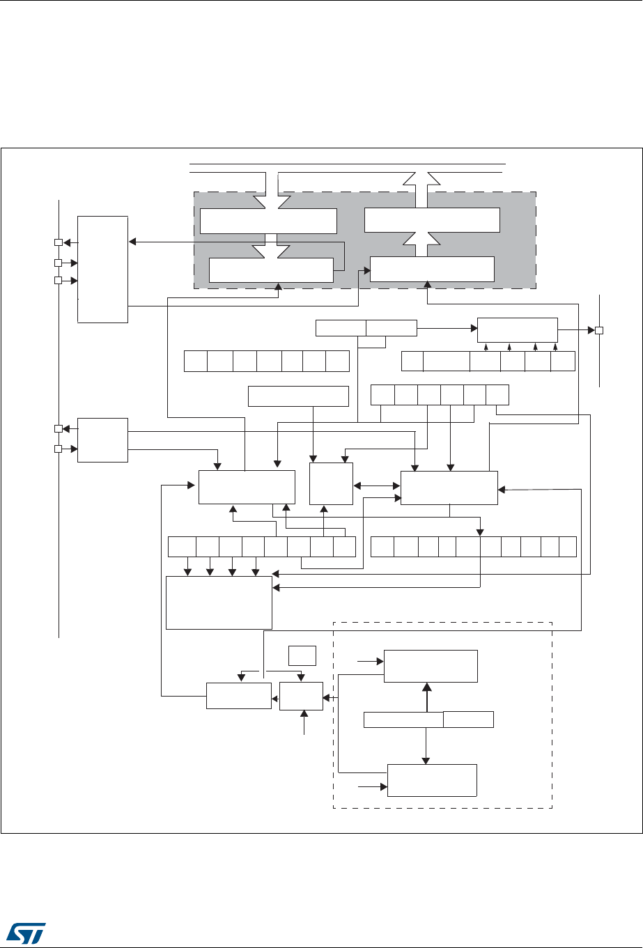
DocID026448 Rev 1 501/836
RM0383 Universal synchronous asynchronous receiver transmitter (USART)
548
The following pins are required in Hardware flow control mode:
•nCTS: Clear To Send blocks the data transmission at the end of the current transfer
when high
•nRTS: Request to send indicates that the USART is ready to receive a data (when
low).
Figure 167. USART block diagram
Wakeup
unit
Receiver
control
SR
Transmit
control
TXETC RXNEIDLEORE NF FE
USART
control
interrupt
CR1
MWAKE
Receive data register (RDR)
Receive Shift Register
Read
Transmit data register (TDR)
Transmit Shift Register
Write
SW_RX
TX
(Data register) DR
Transmitter
clock
Receiver
clock
Receiver rate
Transmitter rate
f
PCLKx(x=1,2)
control
control
/
[8 x (2 - OVER8)]
Conventional baud rate generator
SBKRWURETE
IDLERXNE
TCIETXEIE
CR1
UE PCE PS
PEIE
PE
PWDATA
IRLP
SCEN IREN
DMAR
DMAT
USART Address
CR2
CR3
IrDA
SIR
ENDEC
block
LINE CKEN CPOL CPHA LBCL
SCLK control SCLK
CR2
GT
STOP[1:0]
NACK
DIV_Mantissa
15 0
RE
USART_BRR
/USARTDIV
TE
HD
(CPU or DMA)
(CPU or DMA)
PRDATA
Hardware
flow
controller
CTS LBD
RX
nRTS
nCTS
GTPR
PSC
IE IE
DIV_Fraction
4
USARTDIV = DIV_Mantissa + (DIV_Fraction / 8 × (2 – OVER8))
SAMPLING
CR1
OVER8
DIVIDER
ai16099
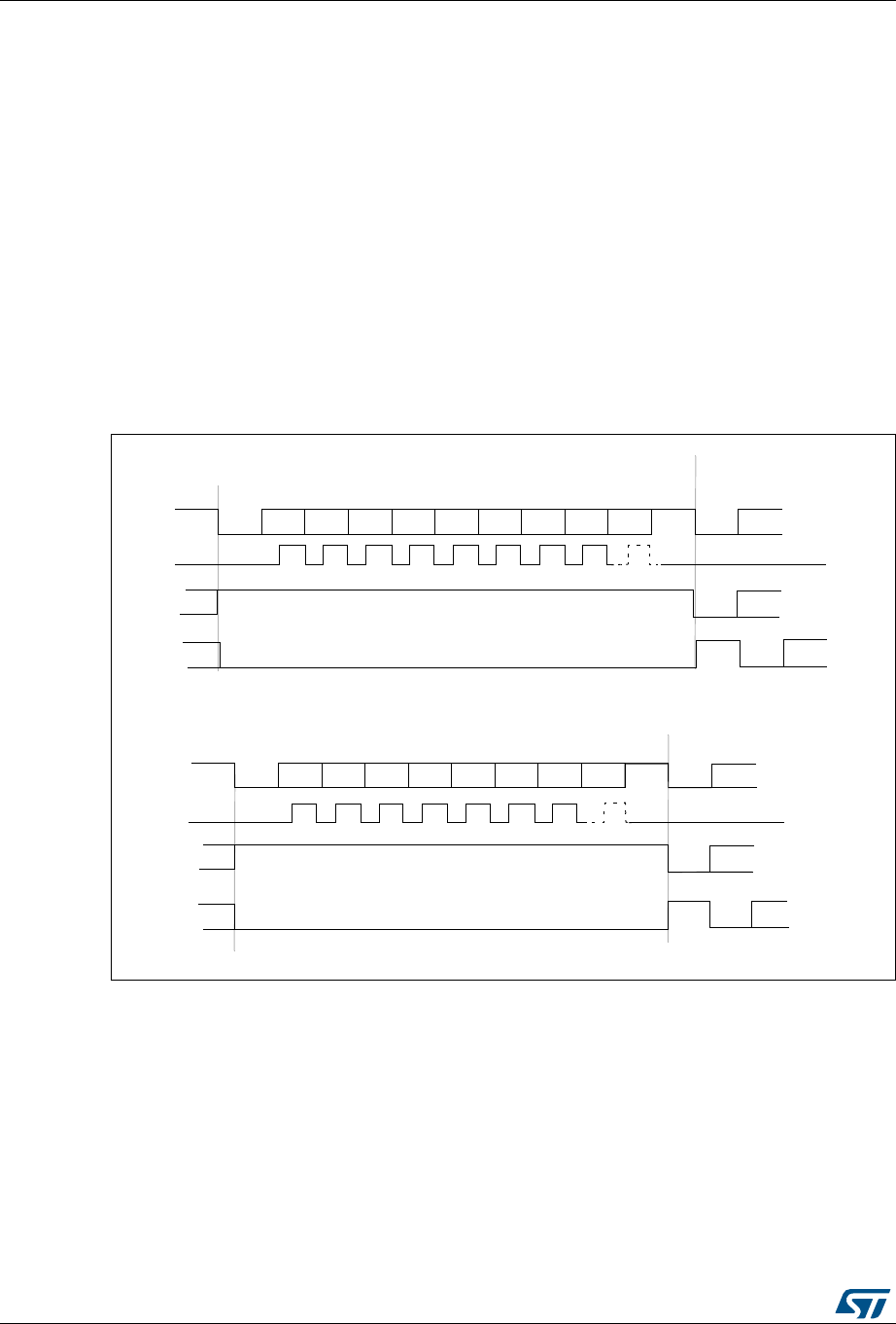
Universal synchronous asynchronous receiver transmitter (USART) RM0383
502/836 DocID026448 Rev 1
19.3.1 USART character description
Word length may be selected as being either 8 or 9 bits by programming the M bit in the
USART_CR1 register (see Figure 168).
The TX pin is in low state during the start bit. It is in high state during the stop bit.
An Idle character is interpreted as an entire frame of “1”s followed by the start bit of the
next frame which contains data (The number of “1” ‘s will include the number of stop bits).
A Break character is interpreted on receiving “0”s for a frame period. At the end of the
break frame the transmitter inserts either 1 or 2 stop bits (logic “1” bit) to acknowledge the
start bit.
Transmission and reception are driven by a common baud rate generator, the clock for each
is generated when the enable bit is set respectively for the transmitter and receiver.
The details of each block is given below.
Figure 168. Word length programming
Bit0 Bit1 Bit2 Bit3 Bit4 Bit5 Bit6 Bit7 Bit8
Start
bit Stop
bit
Next
Start
bit
Idle frame
Bit0 Bit1 Bit2 Bit3 Bit4 Bit5 Bit6 Bit7
Start
Bit Stop
bit
Next
start
bit
Idle frame Start
bit
9-bit word length (M bit is set), 1 stop bit
8-bit word length (M bit is reset), 1 stop bit
Possible
parity
bit
Possible
Parity
Bit
Break frame Start
bit
Stop
bit
Data frame
Break frame Start
bit
Stop
bit
Data frame
Next data frame
Next data frame
Start
bit
****
** LBCL bit controls last data clock pulse
Clock
Clock
** LBCL bit controls last data clock pulse
**
**

DocID026448 Rev 1 503/836
RM0383 Universal synchronous asynchronous receiver transmitter (USART)
548
19.3.2 Transmitter
The transmitter can send data words of either 8 or 9 bits depending on the M bit status.
When the transmit enable bit (TE) is set, the data in the transmit shift register is output on
the TX pin and the corresponding clock pulses are output on the SCLK pin.
Character transmission
During an USART transmission, data shifts out least significant bit first on the TX pin. In this
mode, the USART_DR register consists of a buffer (TDR) between the internal bus and the
transmit shift register (see Figure 167).
Every character is preceded by a start bit which is a logic level low for one bit period. The
character is terminated by a configurable number of stop bits.
The following stop bits are supported by USART: 0.5, 1, 1.5 and 2 stop bits.
Note: The TE bit should not be reset during transmission of data. Resetting the TE bit during the
transmission will corrupt the data on the TX pin as the baud rate counters will get frozen.
The current data being transmitted will be lost.
An idle frame will be sent after the TE bit is enabled.
Configurable stop bits
The number of stop bits to be transmitted with every character can be programmed in
Control register 2, bits 13,12.
•1 stop bit: This is the default value of number of stop bits.
•2 Stop bits: This will be supported by normal USART, single-wire and modem modes.
•0.5 stop bit: To be used when receiving data in Smartcard mode.
•1.5 stop bits: To be used when transmitting and receiving data in Smartcard mode.
An idle frame transmission will include the stop bits.
A break transmission will be 10 low bits followed by the configured number of stop bits
(when m = 0) and 11 low bits followed by the configured number of stop bits (when m = 1). It
is not possible to transmit long breaks (break of length greater than 10/11 low bits).
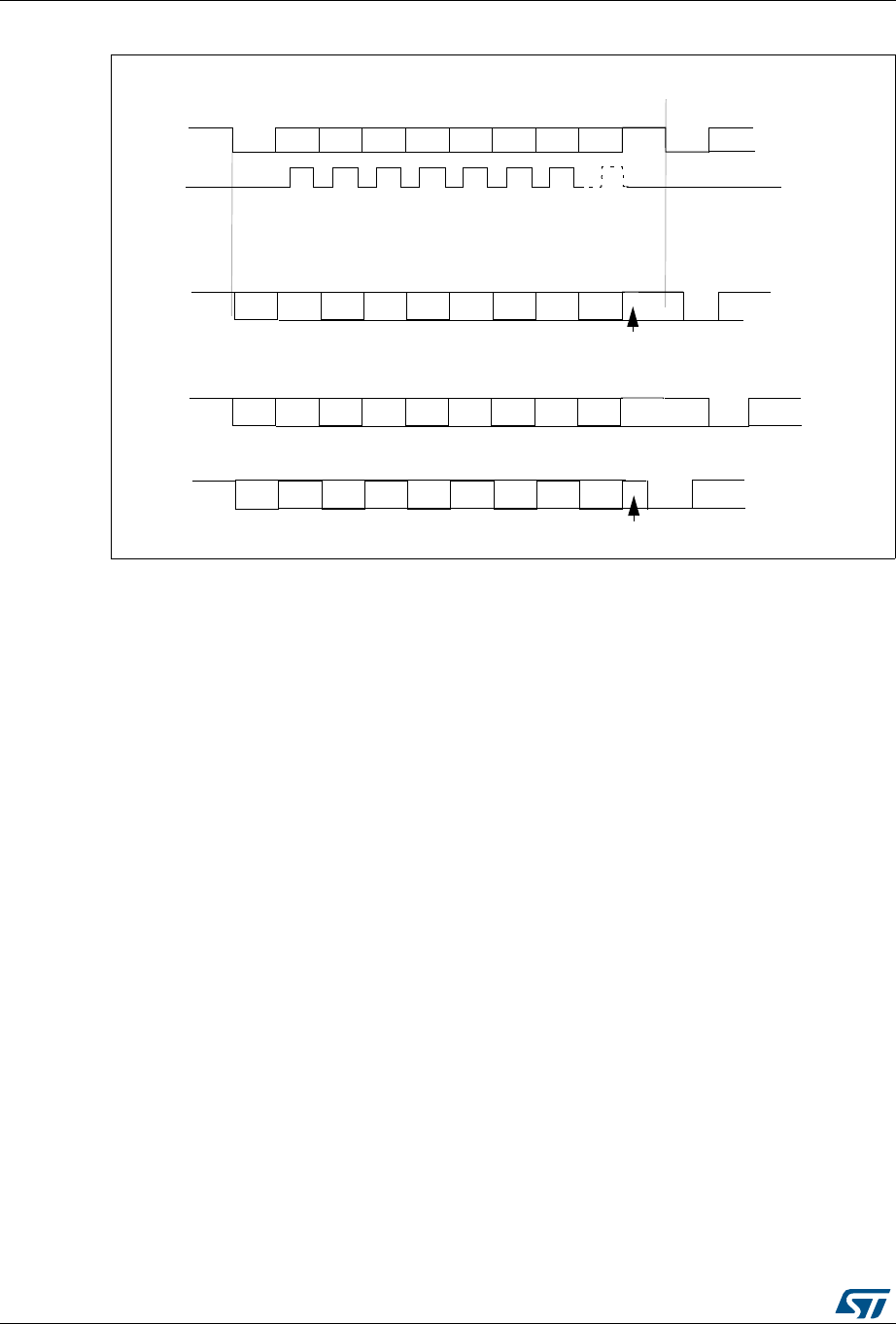
Universal synchronous asynchronous receiver transmitter (USART) RM0383
504/836 DocID026448 Rev 1
Figure 169. Configurable stop bits
Procedure:
1. Enable the USART by writing the UE bit in USART_CR1 register to 1.
2. Program the M bit in USART_CR1 to define the word length.
3. Program the number of stop bits in USART_CR2.
4. Select DMA enable (DMAT) in USART_CR3 if Multi buffer Communication is to take
place. Configure the DMA register as explained in multibuffer communication.
5. Select the desired baud rate using the USART_BRR register.
6. Set the TE bit in USART_CR1 to send an idle frame as first transmission.
7. Write the data to send in the USART_DR register (this clears the TXE bit). Repeat this
for each data to be transmitted in case of single buffer.
8. After writing the last data into the USART_DR register, wait until TC=1. This indicates
that the transmission of the last frame is complete. This is required for instance when
the USART is disabled or enters the Halt mode to avoid corrupting the last
transmission.
Single byte communication
Clearing the TXE bit is always performed by a write to the data register.
The TXE bit is set by hardware and it indicates:
•The data has been moved from TDR to the shift register and the data transmission has
started.
•The TDR register is empty.
•The next data can be written in the USART_DR register without overwriting the
previous data.
This flag generates an interrupt if the TXEIE bit is set.
Bit0 Bit1 Bit2 Bit3 Bit4 Bit5 Bit6 Bit7
Start
Bit Stop
bit
Next
start
bit
8-bit Word length (M bit is reset) Possible
parity
bit
Data frame
Next data frame
****
** LBCL bit controls last data clock pulse
CLOCK **
Bit0 Bit1 Bit2 Bit3 Bit4 Bit5 Bit6 Bit7
Start
Bit 2 Stop
Bits
Next
Start
Bit
Possible
parity
bit
Data frame
Next data frame
Bit0 Bit1 Bit2 Bit3 Bit4 Bit5 Bit6 Bit7
Start
Bit
Next
start
bit
Possible
Parity
Bit
Data frame
Next data frame
1/2 stop bit
Bit0 Bit1 Bit2 Bit3 Bit4 Bit5 Bit6 Bit7
Start
Bit
Next
start
bit
Possible
Parity
Bit
Data frame
Next data frame
1 1/2 stop bits
a) 1 Stop Bit
b) 1 1/2 stop Bits
c) 2 Stop Bits
d) 1/2 Stop Bit
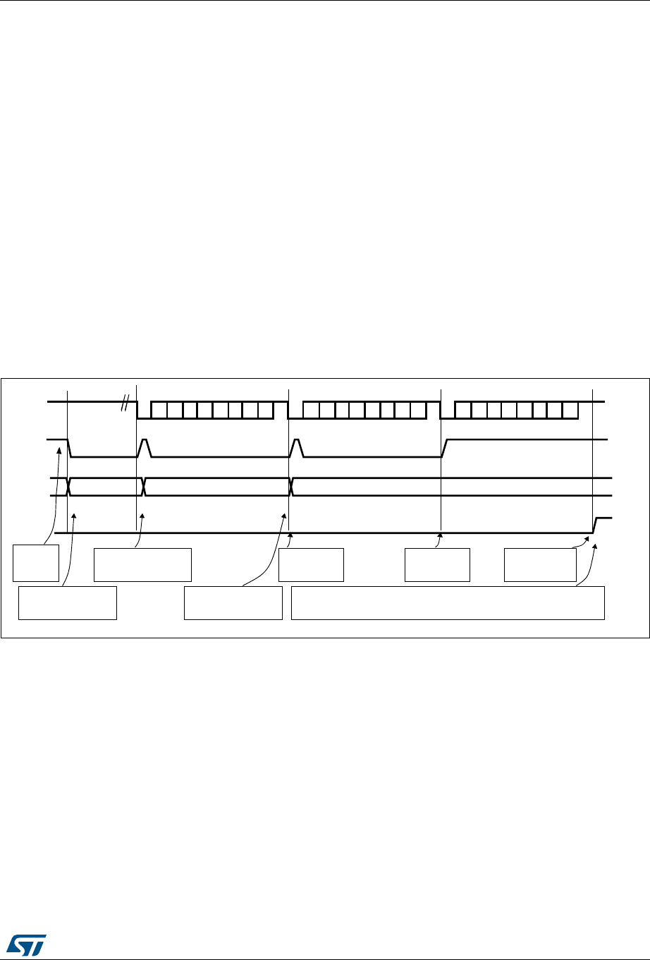
DocID026448 Rev 1 505/836
RM0383 Universal synchronous asynchronous receiver transmitter (USART)
548
When a transmission is taking place, a write instruction to the USART_DR register stores
the data in the TDR register and which is copied in the shift register at the end of the current
transmission.
When no transmission is taking place, a write instruction to the USART_DR register places
the data directly in the shift register, the data transmission starts, and the TXE bit is
immediately set.
If a frame is transmitted (after the stop bit) and the TXE bit is set, the TC bit goes high. An
interrupt is generated if the TCIE bit is set in the USART_CR1 register.
After writing the last data into the USART_DR register, it is mandatory to wait for TC=1
before disabling the USART or causing the microcontroller to enter the low power mode
(see Figure 170: TC/TXE behavior when transmitting).
The TC bit is cleared by the following software sequence:
1. A read from the USART_SR register
2. A write to the USART_DR register
Note: The TC bit can also be cleared by writing a ‘0 to it. This clearing sequence is recommended
only for Multibuffer communication.
Figure 170. TC/TXE behavior when transmitting
Break characters
Setting the SBK bit transmits a break character. The break frame length depends on the M
bit (see Figure 168).
If the SBK bit is set to ‘1 a break character is sent on the TX line after completing the current
character transmission. This bit is reset by hardware when the break character is completed
(during the stop bit of the break character). The USART inserts a logic 1 bit at the end of the
last break frame to guarantee the recognition of the start bit of the next frame.
Note: If the software resets the SBK bit before the commencement of break transmission, the
break character will not be transmitted. For two consecutive breaks, the SBK bit should be
set after the stop bit of the previous break.
Idle characters
Setting the TE bit drives the USART to send an idle frame before the first data frame.
TX line
USART_DR
Frame 1
TXE flag
F2
TC flag
F3
Frame 2
software waits until TXE=1
and writes F2 into DR
software waits until TXE=1
and writes F3 into DR
TC is not set
because TXE=0
software waits until TC=1
Frame 3
TC is set because
TXE=1
set by hardware
cleared by software
set by hardware
cleared by software set by hardware
set
Idle preamble
by hardware
F1
software
enables the
USART
TC is not set
because TXE=0
software waits until TXE=1
and writes F1 into DR
ai17121b
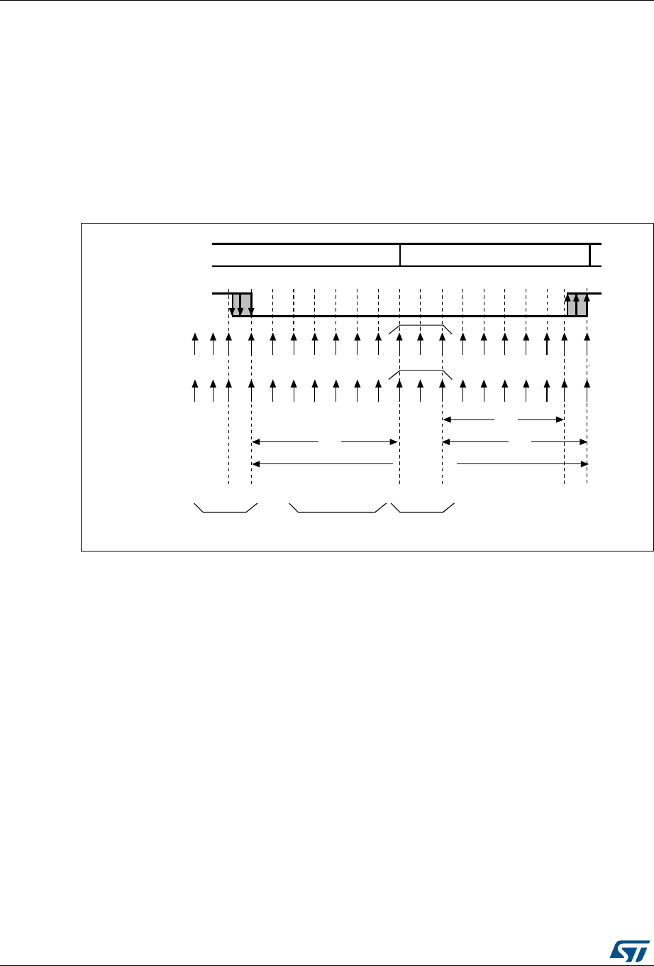
Universal synchronous asynchronous receiver transmitter (USART) RM0383
506/836 DocID026448 Rev 1
19.3.3 Receiver
The USART can receive data words of either 8 or 9 bits depending on the M bit in the
USART_CR1 register.
Start bit detection
The start bit detection sequence is the same when oversampling by 16 or by 8.
In the USART, the start bit is detected when a specific sequence of samples is recognized.
This sequence is: 1 1 1 0 X 0 X 0 X 0 0 0 0.
Figure 171. Start bit detection when oversampling by 16 or 8
Note: If the sequence is not complete, the start bit detection aborts and the receiver returns to the
idle state (no flag is set) where it waits for a falling edge.
The start bit is confirmed (RXNE flag set, interrupt generated if RXNEIE=1) if the 3 sampled
bits are at 0 (first sampling on the 3rd, 5th and 7th bits finds the 3 bits at 0 and second
sampling on the 8th, 9th and 10th bits also finds the 3 bits at 0).
The start bit is validated (RXNE flag set, interrupt generated if RXNEIE=1) but the NE noise
flag is set if, for both samplings, at least 2 out of the 3 sampled bits are at 0 (sampling on the
3rd, 5th and 7th bits and sampling on the 8th, 9th and 10th bits). If this condition is not met,
the start detection aborts and the receiver returns to the idle state (no flag is set).
If, for one of the samplings (sampling on the 3rd, 5th and 7th bits or sampling on the 8th, 9th
and 10th bits), 2 out of the 3 bits are found at 0, the start bit is validated but the NE noise
flag bit is set.
Character reception
During an USART reception, data shifts in least significant bit first through the RX pin. In this
mode, the USART_DR register consists of a buffer (RDR) between the internal bus and the
received shift register.
Procedure:
RX line
sampled values
Idle Start bitRX state
Real
sample
clock
Ideal
sample
clock
010X0X0000XXXXXX
Conditions
to validate
the start bit At least 2 bits
out of 3 at 0
At least 2 bits
out of 3 at 0
Falling edge
detection
11
1 2 3 4 5 6 7 8 9 10 11 12 13 14 15 16
X X X X X X X X 9 10 111213141516
6/16
7/16
One-bit time
7/16
X
ai15471

DocID026448 Rev 1 507/836
RM0383 Universal synchronous asynchronous receiver transmitter (USART)
548
1. Enable the USART by writing the UE bit in USART_CR1 register to 1.
2. Program the M bit in USART_CR1 to define the word length.
3. Program the number of stop bits in USART_CR2.
4. Select DMA enable (DMAR) in USART_CR3 if multibuffer communication is to take
place. Configure the DMA register as explained in multibuffer communication. STEP 3
5. Select the desired baud rate using the baud rate register USART_BRR
6. Set the RE bit USART_CR1. This enables the receiver which begins searching for a
start bit.
When a character is received
•The RXNE bit is set. It indicates that the content of the shift register is transferred to the
RDR. In other words, data has been received and can be read (as well as its
associated error flags).
•An interrupt is generated if the RXNEIE bit is set.
•The error flags can be set if a frame error, noise or an overrun error has been detected
during reception.
•In multibuffer, RXNE is set after every byte received and is cleared by the DMA read to
the Data Register.
•In single buffer mode, clearing the RXNE bit is performed by a software read to the
USART_DR register. The RXNE flag can also be cleared by writing a zero to it. The
RXNE bit must be cleared before the end of the reception of the next character to avoid
an overrun error.
Note: The RE bit should not be reset while receiving data. If the RE bit is disabled during
reception, the reception of the current byte will be aborted.
Break character
When a break character is received, the USART handles it as a framing error.
Idle character
When an idle frame is detected, there is the same procedure as a data received character
plus an interrupt if the IDLEIE bit is set.
Overrun error
An overrun error occurs when a character is received when RXNE has not been reset. Data
can not be transferred from the shift register to the RDR register until the RXNE bit is
cleared.

Universal synchronous asynchronous receiver transmitter (USART) RM0383
508/836 DocID026448 Rev 1
The RXNE flag is set after every byte received. An overrun error occurs if RXNE flag is set
when the next data is received or the previous DMA request has not been serviced. When
an overrun error occurs:
•The ORE bit is set.
•The RDR content will not be lost. The previous data is available when a read to
USART_DR is performed.
•The shift register will be overwritten. After that point, any data received during overrun
is lost.
•An interrupt is generated if either the RXNEIE bit is set or both the EIE and DMAR bits
are set.
•The ORE bit is reset by a read to the USART_SR register followed by a USART_DR
register read operation.
Note: The ORE bit, when set, indicates that at least 1 data has been lost. There are two
possibilities:
•if RXNE=1, then the last valid data is stored in the receive register RDR and can be
read,
•if RXNE=0, then it means that the last valid data has already been read and thus there
is nothing to be read in the RDR. This case can occur when the last valid data is read in
the RDR at the same time as the new (and lost) data is received. It may also occur
when the new data is received during the reading sequence (between the USART_SR
register read access and the USART_DR read access).
Selecting the proper oversampling method
The receiver implements different user-configurable oversampling techniques (except in
synchronous mode) for data recovery by discriminating between valid incoming data and
noise.
The oversampling method can be selected by programming the OVER8 bit in the
USART_CR1 register and can be either 16 or 8 times the baud rate clock (Figure 172 and
Figure 173).
Depending on the application:
•select oversampling by 8 (OVER8=1) to achieve higher speed (up to fPCLK/8). In this
case the maximum receiver tolerance to clock deviation is reduced (refer to
Section 19.3.5: USART receiver tolerance to clock deviation on page 521)
•select oversampling by 16 (OVER8=0) to increase the tolerance of the receiver to clock
deviations. In this case, the maximum speed is limited to maximum fPCLK/16
Programming the ONEBIT bit in the USART_CR3 register selects the method used to
evaluate the logic level. There are two options:
•the majority vote of the three samples in the center of the received bit. In this case,
when the 3 samples used for the majority vote are not equal, the NF bit is set
•a single sample in the center of the received bit
Depending on the application:
– select the three samples’ majority vote method (ONEBIT=0) when operating in a
noisy environment and reject the data when a noise is detected (refer to
Figure 71) because this indicates that a glitch occurred during the sampling.
– select the single sample method (ONEBIT=1) when the line is noise-free to
increase the receiver’s tolerance to clock deviations (see Section 19.3.5: USART
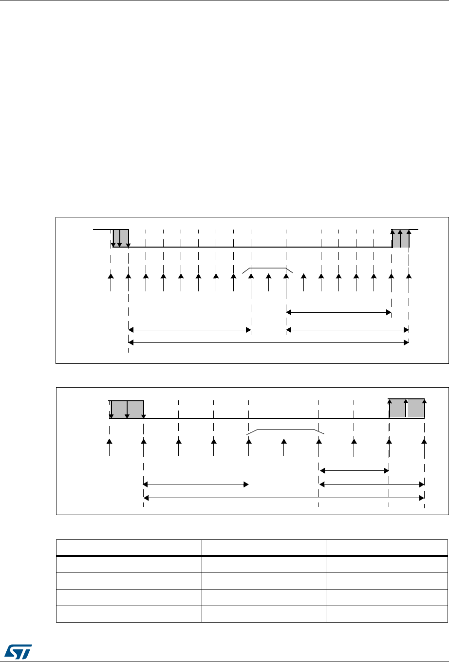
DocID026448 Rev 1 509/836
RM0383 Universal synchronous asynchronous receiver transmitter (USART)
548
receiver tolerance to clock deviation on page 521). In this case the NF bit will
never be set.
When noise is detected in a frame:
•The NF bit is set at the rising edge of the RXNE bit.
•The invalid data is transferred from the Shift register to the USART_DR register.
•No interrupt is generated in case of single byte communication. However this bit rises
at the same time as the RXNE bit which itself generates an interrupt. In case of
multibuffer communication an interrupt will be issued if the EIE bit is set in the
USART_CR3 register.
The NF bit is reset by a USART_SR register read operation followed by a USART_DR
register read operation.
Note: Oversampling by 8 is not available in the Smartcard, IrDA and LIN modes. In those modes,
the OVER8 bit is forced to ‘0 by hardware.
Figure 172. Data sampling when oversampling by 16
Figure 173. Data sampling when oversampling by 8
Table 71. Noise detection from sampled data
Sampled value NE status Received bit value
000 0 0
001 1 0
010 1 0
011 1 1
RX LINE
Sample
clock 1234567891011
12 13 14 15 16
sampled values
One bit time
6/16
7/16 7/16
RX LINE
One bit time
3/8 3/8
12345678
2/8
Sample
clock(x8)
sampled values

Universal synchronous asynchronous receiver transmitter (USART) RM0383
510/836 DocID026448 Rev 1
Framing error
A framing error is detected when:
The stop bit is not recognized on reception at the expected time, following either a de-
synchronization or excessive noise.
When the framing error is detected:
•The FE bit is set by hardware
•The invalid data is transferred from the Shift register to the USART_DR register.
•No interrupt is generated in case of single byte communication. However this bit rises
at the same time as the RXNE bit which itself generates an interrupt. In case of
multibuffer communication an interrupt will be issued if the EIE bit is set in the
USART_CR3 register.
The FE bit is reset by a USART_SR register read operation followed by a USART_DR
register read operation.
Configurable stop bits during reception
The number of stop bits to be received can be configured through the control bits of Control
Register 2 - it can be either 1 or 2 in normal mode and 0.5 or 1.5 in Smartcard mode.
1. 0.5 stop bit (reception in Smartcard mode): No sampling is done for 0.5 stop bit. As
a consequence, no framing error and no break frame can be detected when 0.5 stop bit
is selected.
2. 1 stop bit: Sampling for 1 stop Bit is done on the 8th, 9th and 10th samples.
3. 1.5 stop bits (Smartcard mode): When transmitting in smartcard mode, the device
must check that the data is correctly sent. Thus the receiver block must be enabled (RE
=1 in the USART_CR1 register) and the stop bit is checked to test if the smartcard has
detected a parity error. In the event of a parity error, the smartcard forces the data
signal low during the sampling - NACK signal-, which is flagged as a framing error.
Then, the FE flag is set with the RXNE at the end of the 1.5 stop bit. Sampling for 1.5
stop bits is done on the 16th, 17th and 18th samples (1 baud clock period after the
beginning of the stop bit). The 1.5 stop bit can be decomposed into 2 parts: one 0.5
baud clock period during which nothing happens, followed by 1 normal stop bit period
during which sampling occurs halfway through. Refer to Section 19.3.11: Smartcard on
page 529 for more details.
4. 2 stop bits: Sampling for 2 stop bits is done on the 8th, 9th and 10th samples of the
first stop bit. If a framing error is detected during the first stop bit the framing error flag
will be set. The second stop bit is not checked for framing error. The RXNE flag will be
set at the end of the first stop bit.
100 1 0
101 1 1
110 1 1
111 0 1
Table 71. Noise detection from sampled data (continued)
Sampled value NE status Received bit value

DocID026448 Rev 1 511/836
RM0383 Universal synchronous asynchronous receiver transmitter (USART)
548
19.3.4 Fractional baud rate generation
The baud rate for the receiver and transmitter (Rx and Tx) are both set to the same value as
programmed in the Mantissa and Fraction values of USARTDIV.
Equation 1: Baud rate for standard USART (SPI mode included)
Equation 2: Baud rate in Smartcard, LIN and IrDA modes
USARTDIV is an unsigned fixed point number that is coded on the USART_BRR register.
•When OVER8=0, the fractional part is coded on 4 bits and programmed by the
DIV_fraction[3:0] bits in the USART_BRR register
•When OVER8=1, the fractional part is coded on 3 bits and programmed by the
DIV_fraction[2:0] bits in the USART_BRR register, and bit DIV_fraction[3] must be kept
cleared.
Note: The baud counters are updated to the new value in the baud registers after a write operation
to USART_BRR. Hence the baud rate register value should not be changed during
communication.
How to derive USARTDIV from USART_BRR register values when OVER8=0
Example 1:
If DIV_Mantissa = 0d27 and DIV_Fraction = 0d12 (USART_BRR = 0x1BC), then
Mantissa (USARTDIV) = 0d27
Fraction (USARTDIV) = 12/16 = 0d0.75
Therefore USARTDIV = 0d27.75
Example 2:
To program USARTDIV = 0d25.62
This leads to:
DIV_Fraction = 16*0d0.62 = 0d9.92
The nearest real number is 0d10 = 0xA
DIV_Mantissa = mantissa (0d25.620) = 0d25 = 0x19
Then, USART_BRR = 0x19A hence USARTDIV = 0d25.625
Example 3:
To program USARTDIV = 0d50.99
This leads to:
Tx/Rx baud fCK
8 2 OVER8–()USARTDIV××
-------------------------------------------------------------------------------------
=
Tx/Rx baud fCK
16 USARTDIV×
----------------------------------------------
=

Universal synchronous asynchronous receiver transmitter (USART) RM0383
512/836 DocID026448 Rev 1
DIV_Fraction = 16*0d0.99 = 0d15.84
The nearest real number is 0d16 = 0x10 => overflow of DIV_frac[3:0] => carry must be
added up to the mantissa
DIV_Mantissa = mantissa (0d50.990 + carry) = 0d51 = 0x33
Then, USART_BRR = 0x330 hence USARTDIV = 0d51.000
How to derive USARTDIV from USART_BRR register values when OVER8=1
Example 1:
If DIV_Mantissa = 0x27 and DIV_Fraction[2:0]= 0d6 (USART_BRR = 0x1B6), then
Mantissa (USARTDIV) = 0d27
Fraction (USARTDIV) = 6/8 = 0d0.75
Therefore USARTDIV = 0d27.75
Example 2:
To program USARTDIV = 0d25.62
This leads to:
DIV_Fraction = 8*0d0.62 = 0d4.96
The nearest real number is 0d5 = 0x5
DIV_Mantissa = mantissa (0d25.620) = 0d25 = 0x19
Then, USART_BRR = 0x195 => USARTDIV = 0d25.625
Example 3:
To program USARTDIV = 0d50.99
This leads to:
DIV_Fraction = 8*0d0.99 = 0d7.92
The nearest real number is 0d8 = 0x8 => overflow of the DIV_frac[2:0] => carry must be
added up to the mantissa
DIV_Mantissa = mantissa (0d50.990 + carry) = 0d51 = 0x33
Then, USART_BRR = 0x0330 => USARTDIV = 0d51.000
Table 72. Error calculation for programmed baud rates at fPCLK = 8 MHz or fPCLK = 12 MHz,
oversampling by 16(1)
Oversampling by 16 (OVER8=0)
Baud rate7 fPCLK = 8 MHz fPCLK = 12 MHz
S.No Desired Actual
Value
programmed
in the baud
rate register
% Error =
(Calculated -
Desired) B.rate /
Desired B.rate
Actual
Value
programmed
in the baud
rate register
% Error
1 1.2 KBps 1.2 KBps 416.6875 0 1.2 KBps 625 0
2 2.4 KBps 2.4 KBps 208.3125 0.01 2.4 KBps 312.5 0

DocID026448 Rev 1 513/836
RM0383 Universal synchronous asynchronous receiver transmitter (USART)
548
3 9.6 KBps 9.604 KBps 52.0625 0.04 9.6 KBps 78.125 0
4 19.2 KBps 19.185 KBps 26.0625 0.08 19.2 KBps 39.0625 0
5 38.4 KBps 38.462 KBps 13 0.16 38.339 KBps 19.5625 0.16
6 57.6 KBps 57.554 KBps 8.6875 0.08 57.692 KBps 13 0.16
7 115.2 KBps 115.942 KBps 4.3125 0.64 115.385 KBps 6.5 0.16
8 230.4 KBps 228.571 KBps 2.1875 0.79 230.769 KBps 3.25 0.16
9 460.8 KBps 470.588 KBps 1.0625 2.12 461.538 KBps 1.625 0.16
10 921.6 KBps NA NA NA NA NA NA
11 2 MBps NA NA NA NA NA NA
12 3 MBps NA NA NA NA NA NA
1. The lower the CPU clock the lower the accuracy for a particular baud rate. The upper limit of the achievable baud rate can
be fixed with these data.
Table 72. Error calculation for programmed baud rates at fPCLK = 8 MHz or fPCLK = 12 MHz,
oversampling by 16(1) (continued)
Oversampling by 16 (OVER8=0)
Baud rate7 fPCLK = 8 MHz fPCLK = 12 MHz
S.No Desired Actual
Value
programmed
in the baud
rate register
% Error =
(Calculated -
Desired) B.rate /
Desired B.rate
Actual
Value
programmed
in the baud
rate register
% Error
Table 73. Error calculation for programmed baud rates at fPCLK = 8 MHz or fPCLK =12 MHz,
oversampling by 8(1)
Oversampling by 8 (OVER8 = 1)
Baud rate fPCLK = 8 MHz fPCLK = 12 MHz
S.No Desired Actual
Value
programmed
in the baud
rate register
% Error =
(Calculated -
Desired)
B.rate /
Desired
B.rate
Actual
Value
programmed
in the baud
rate register
% Error
1 1.2 KBps 1.2 KBps 833.375 0 1.2 KBps 1250 0
2 2.4 KBps 2.4 KBps 416.625 0.01 2.4 KBps 625 0
3 9.6 KBps 9.604 KBps 104.125 0.04 9.6 KBps 156.25 0
4 19.2 KBps 19.185 KBps 52.125 0.08 19.2 KBps 78.125 0
5 38.4 KBps 38.462 KBps 26 0.16 38.339 KBps 39.125 0.16
6 57.6 KBps 57.554 KBps 17.375 0.08 57.692 KBps 26 0.16
7 115.2 KBps 115.942 KBps 8.625 0.64 115.385 KBps 13 0.16
8 230.4 KBps 228.571 KBps 4.375 0.79 230.769 KBps 6.5 0.16
9 460.8 KBps 470.588 KBps 2.125 2.12 461.538 KBps 3.25 0.16
Universal synchronous asynchronous receiver transmitter (USART) RM0383
514/836 DocID026448 Rev 1
10 921.6 KBps 888.889 KBps 1.125 3.55 923.077 KBps 1.625 0.16
11 2 MBps NA NA NA NA NA NA
12 3 MBps NA NA NA NA NA NA
1. The lower the CPU clock the lower the accuracy for a particular baud rate. The upper limit of the achievable baud rate can
be fixed with these data.
Table 73. Error calculation for programmed baud rates at fPCLK = 8 MHz or fPCLK =12 MHz,
oversampling by 8(1) (continued)
Oversampling by 8 (OVER8 = 1)
Baud rate fPCLK = 8 MHz fPCLK = 12 MHz
S.No Desired Actual
Value
programmed
in the baud
rate register
% Error =
(Calculated -
Desired)
B.rate /
Desired
B.rate
Actual
Value
programmed
in the baud
rate register
% Error
Table 74. Error calculation for programmed baud rates at fPCLK = 16 MHz or fPCLK = 24 MHz,
oversampling by 16(1)
Oversampling by 16 (OVER8 = 0)
Baud rate fPCLK = 16 MHz fPCLK = 24 MHz
S.No Desired Actual
Value
programmed
in the baud
rate register
% Error =
(Calculated -
Desired) B.rate /
Desired B.rate
Actual
Value
programmed
in the baud
rate register
% Error
1 1.2 KBps 1.2 KBps 833.3125 0 1.2 1250 0
2 2.4 KBps 2.4 KBps 416.6875 0 2.4 625 0
3 9.6 KBps 9.598 KBps 104.1875 0.02 9.6 156.25 0
4 19.2 KBps 19.208 KBps 52.0625 0.04 19.2 78.125 0
5 38.4 KBps 38.369 KBps 26.0625 0.08 38.4 39.0625 0
6 57.6 KBps 57.554 KBps 17.375 0.08 57.554 26.0625 0.08
7 115.2 KBps 115.108 KBps 8.6875 0.08 115.385 13 0.16
8 230.4 KBps 231.884 KBps 4.3125 0.64 230.769 6.5 0.16
9 460.8 KBps 457.143 KBps 2.1875 0.79 461.538 3.25 0.16
10 921.6 KBps 941.176 KBps 1.0625 2.12 923.077 1.625 0.16
11 2 MBps NA NA NA NA NA NA
12 3 MBps NA NA NA NA NA NA
1. The lower the CPU clock the lower the accuracy for a particular baud rate. The upper limit of the achievable baud rate can
be fixed with these data.
DocID026448 Rev 1 515/836
RM0383 Universal synchronous asynchronous receiver transmitter (USART)
548
Table 75. Error calculation for programmed baud rates at fPCLK = 16 MHz or fPCLK = 24 MHz,
oversampling by 8(1)
Oversampling by 8 (OVER8=1)
Baud rate fPCLK = 16 MHz fPCLK = 24 MHz
S.No Desired Actual
Value
programmed
in the baud
rate register
% Error =
(Calculated -
Desired) B.rate /
Desired B.rate
Actual
Value
programmed
in the baud
rate register
% Error
1 1.2 KBps 1.2 KBps 1666.625 0 1.2 KBps 2500 0
2 2.4 KBps 2.4 KBps 833.375 0 2.4 KBps 1250 0
3 9.6 KBps 9.598 KBps 208.375 0.02 9.6 KBps 312.5 0
4 19.2 KBps 19.208 KBps 104.125 0.04 19.2 KBps 156.25 0
5 38.4 KBps 38.369 KBps 52.125 0.08 38.4 KBps 78.125 0
6 57.6 KBps 57.554 KBps 34.75 0.08 57.554 KBps 52.125 0.08
7 115.2 KBps 115.108 KBps 17.375 0.08 115.385 KBps 26 0.16
8 230.4 KBps 231.884 KBps 8.625 0.64 230.769 KBps 13 0.16
9 460.8 KBps 457.143 KBps 4.375 0.79 461.538 KBps 6.5 0.16
10 921.6 KBps 941.176 KBps 2.125 2.12 923.077 KBps 3.25 0.16
11 2 MBps 2000 KBps 1 0 2000 KBps 1.5 0
12 3 MBps NA NA NA 3000 KBps 1 0
1. The lower the CPU clock the lower the accuracy for a particular baud rate. The upper limit of the achievable baud rate can
be fixed with these data.
Table 76. Error calculation for programmed baud rates at fPCLK = 8 MHz or fPCLK = 16 MHz,
oversampling by 16(1)
Oversampling by 16 (OVER8=0)
Baud rate fPCLK = 8 MHz fPCLK = 16 MHz
S.No Desired Actual
Value
programme
d in the
baud rate
register
% Error =
(Calculated -
Desired)B.Rate
/Desired B.Rate
Actual
Value
programmed
in the baud
rate register
% Error
1. 2.4 KBps 2.400 KBps 208.3125 0.00% 2.400 KBps 416.6875 0.00%
2. 9.6 KBps 9.604 KBps 52.0625 0.04% 9.598 KBps 104.1875 0.02%
3. 19.2 KBps 19.185 KBps 26.0625 0.08% 19.208 KBps 52.0625 0.04%
4. 57.6 KBps 57.554 KBps 8.6875 0.08% 57.554 KBps 17.3750 0.08%
5. 115.2 KBps 115.942 KBps 4.3125 0.64% 115.108 KBps 8.6875 0.08%
6. 230.4 KBps 228.571
KBps 2.1875 0.79% 231.884 KBps 4.3125 0.64%

Universal synchronous asynchronous receiver transmitter (USART) RM0383
516/836 DocID026448 Rev 1
7. 460.8 KBps 470.588
KBps 1.0625 2.12% 457.143 KBps 2.1875 0.79%
8. 896 KBps NA NA NA 888.889 KBps 1.1250 0.79%
9. 921.6 KBps NA NA NA 941.176 KBps 1.0625 2.12%
10. 1.792 MBps NA NA NA NA NA NA
11. 1.8432 MBps NA NA NA NA NA NA
12. 3.584 MBps NA NA NA NA NA NA
13. 3.6864 MBps NA NA NA NA NA NA
14. 7.168 MBps NA NA NA NA NA NA
15. 7.3728 MBps NA NA NA NA NA NA
1. The lower the CPU clock the lower the accuracy for a particular baud rate. The upper limit of the achievable baud rate can
be fixed with these data.
Table 77. Error calculation for programmed baud rates at fPCLK = 8 MHz or fPCLK = 16 MHz,
oversampling by 8(1)
Oversampling by 8 (OVER8=1)
Baud rate fPCLK = 8 MHz fPCLK = 16 MHz
S.No Desired Actual
Value
programmed
in the baud
rate register
% Error =
(Calculated -
Desired)B.Rate
/Desired B.Rate
Actual
Value
programmed
in the baud
rate register
%
Error
1. 2.4 KBps 2.400 KBps 416.625 0.01% 2.400 KBps 833.375 0.00%
2. 9.6 KBps 9.604 KBps 104.125 0.04% 9.598 KBps 208.375 0.02%
3. 19.2 KBps 19.185 KBps 52.125 0.08% 19.208 KBps 104.125 0.04%
4. 57.6 KBps 57.557 KBps 17.375 0.08% 57.554 KBps 34.750 0.08%
5. 115.2 KBps 115.942 KBps 8.625 0.64% 115.108 KBps 17.375 0.08%
6. 230.4 KBps 228.571 KBps 4.375 0.79% 231.884 KBps 8.625 0.64%
7. 460.8 KBps 470.588 KBps 2.125 2.12% 457.143 KBps 4.375 0.79%
8. 896 KBps 888.889 KBps 1.125 0.79% 888.889 KBps 2.250 0.79%
9. 921.6 KBps 888.889 KBps 1.125 3.55% 941.176 KBps 2.125 2.12%
10. 1.792 MBps NA NA NA 1.7777 MBps 1.125 0.79%
Table 76. Error calculation for programmed baud rates at fPCLK = 8 MHz or fPCLK = 16 MHz,
oversampling by 16(1) (continued)
Oversampling by 16 (OVER8=0)
Baud rate fPCLK = 8 MHz fPCLK = 16 MHz
S.No Desired Actual
Value
programme
d in the
baud rate
register
% Error =
(Calculated -
Desired)B.Rate
/Desired B.Rate
Actual
Value
programmed
in the baud
rate register
% Error

DocID026448 Rev 1 517/836
RM0383 Universal synchronous asynchronous receiver transmitter (USART)
548
11. 1.8432 MBps NA NA NA 1.7777 MBps 1.125 3.55%
12. 3.584 MBps NA NA NA NA NA NA
13. 3.6864 MBps NA NA NA NA NA NA
14. 7.168 MBps NA NA NA NA NA NA
15. 7.3728 MBps NA NA NA NA NA NA
1. The lower the CPU clock the lower the accuracy for a particular baud rate. The upper limit of the achievable baud rate can
be fixed with these data.
Table 77. Error calculation for programmed baud rates at fPCLK = 8 MHz or fPCLK = 16 MHz,
oversampling by 8(1) (continued)
Oversampling by 8 (OVER8=1)
Baud rate fPCLK = 8 MHz fPCLK = 16 MHz
S.No Desired Actual
Value
programmed
in the baud
rate register
% Error =
(Calculated -
Desired)B.Rate
/Desired B.Rate
Actual
Value
programmed
in the baud
rate register
%
Error
Table 78. Error calculation for programmed baud rates at fPCLK = 30 MHz or fPCLK = 60 MHz,
oversampling by 16(1)(2)
Oversampling by 16 (OVER8=0)
Baud rate fPCLK = 30 MHz fPCLK = 60 MHz
S.No Desired Actual
Value
programme
d in the
baud rate
register
% Error =
(Calculated -
Desired)B.Rate
/Desired B.Rate
Actual
Value
programmed
in the baud
rate register
%
Error
1. 2.4 KBps 2.400 KBps 781.2500 0.00% 2.400 KBps 1562.5000 0.00%
2. 9.6 KBps 9.600 KBps 195.3125 0.00% 9.600 KBps 390.6250 0.00%
3. 19.2 KBps 19.194 KBps 97.6875 0.03% 19.200 KBps 195.3125 0.00%
4. 57.6 KBps 57.582KBps 32.5625 0.03% 57.582 KBps 65.1250 0.03%
5. 115.2 KBps 115.385 KBps 16.2500 0.16% 115.163 KBps 32.5625 0.03%
6. 230.4 KBps 230.769 KBps 8.1250 0.16% 230.769KBps 16.2500 0.16%
7. 460.8 KBps 461.538 KBps 4.0625 0.16% 461.538 KBps 8.1250 0.16%
8. 896 KBps 909.091 KBps 2.0625 1.46% 895.522 KBps 4.1875 0.05%
9. 921.6 KBps 909.091 KBps 2.0625 1.36% 923.077 KBps 4.0625 0.16%
10. 1.792 MBps 1.1764 MBps 1.0625 1.52% 1.8182 MBps 2.0625 1.36%
11. 1.8432
MBps 1.8750 MBps 1.0000 1.73% 1.8182 MBps 2.0625 1.52%
12. 3.584 MBps NA NA NA 3.2594 MBps 1.0625 1.52%
13. 3.6864
MBps NA NA NA 3.7500 MBps 1.0000 1.73%

Universal synchronous asynchronous receiver transmitter (USART) RM0383
518/836 DocID026448 Rev 1
14. 7.168 MBps NA NA NA NA NA NA
15. 7.3728
MBps NA NA NA NA NA NA
1. The lower the CPU clock the lower the accuracy for a particular baud rate. The upper limit of the achievable baud rate can
be fixed with these data.
2. Only USART1 and USART6 are clocked with PCLK2. Other USARTs are clocked with PCLK1. Refer to the device
datasheets for the maximum values for PCLK1 and PCLK2.
Table 78. Error calculation for programmed baud rates at fPCLK = 30 MHz or fPCLK = 60 MHz,
oversampling by 16(1)(2) (continued)
Oversampling by 16 (OVER8=0)
Baud rate fPCLK = 30 MHz fPCLK = 60 MHz
S.No Desired Actual
Value
programme
d in the
baud rate
register
% Error =
(Calculated -
Desired)B.Rate
/Desired B.Rate
Actual
Value
programmed
in the baud
rate register
%
Error
Table 79. Error calculation for programmed baud rates at fPCLK = 30 MHz or fPCLK = 60 MHz,
oversampling by 8(1) (2)
Oversampling by 8 (OVER8=1)
Baud rate fPCLK = 30 MHz fPCLK =60 MHz
S.No Desired Actual
Value
programme
d in the
baud rate
register
% Error =
(Calculated -
Desired)B.Rate
/Desired B.Rate
Actual
Value
programmed
in the baud
rate register
%
Error
1. 2.4 KBps 2.400 KBps 1562.5000 0.00% 2.400 KBps 3125.0000 0.00%
2. 9.6 KBps 9.600 KBps 390.6250 0.00% 9.600 KBps 781.2500 0.00%
3. 19.2 KBps 19.194 KBps 195.3750 0.03% 19.200 KBps 390.6250 0.00%
4. 57.6 KBps 57.582 KBps 65.1250 0.16% 57.582 KBps 130.2500 0.03%
5. 115.2 KBps 115.385 KBps 32.5000 0.16% 115.163 KBps 65.1250 0.03%
6. 230.4 KBps 230.769 KBps 16.2500 0.16% 230.769 KBps 32.5000 0.16%
7. 460.8 KBps 461.538 KBps 8.1250 0.16% 461.538 KBps 16.2500 0.16%
8. 896 KBps 909.091 KBps 4.1250 1.46% 895.522 KBps 8.3750 0.05%
9. 921.6 KBps 909.091 KBps 4.1250 1.36% 923.077 KBps 8.1250 0.16%
10. 1.792 MBps 1.7647 MBps 2.1250 1.52% 1.8182 MBps 4.1250 1.46%
11. 1.8432 MBps 1.8750 MBps 2.0000 1.73% 1.8182 MBps 4.1250 1.36%
12. 3.584 MBps 3.7500 MBps 1.0000 4.63% 3.5294 MBps 2.1250 1.52%
13. 3.6864 MBps 3.7500 MBps 1.0000 1.73% 3.7500 MBps 2.0000 1.73%
14. 7.168 MBps NA NA NA 7.5000 MBps 1.0000 4.63%
15. 7.3728 MBps NA NA NA 7.5000 MBps 1.0000 1.73%

DocID026448 Rev 1 519/836
RM0383 Universal synchronous asynchronous receiver transmitter (USART)
548
1. The lower the CPU clock the lower the accuracy for a particular baud rate. The upper limit of the achievable baud rate can
be fixed with these data.
2. Only USART1 and USART6 are clocked with PCLK2. Other USARTs are clocked with PCLK1. Refer to the device
datasheets for the maximum values for PCLK1 and PCLK2.
Table 80. Error calculation for programmed baud rates at fPCLK = 42 MHz or fPCLK = 84 Hz,
oversampling by 16(1)(2)
Oversampling by 16 (OVER8=0)
Baud rate fPCLK = 42 MHz fPCLK = 84 MHz
S.No Desired Actual
Value
programme
d in the
baud rate
register
% Error =
(Calculated -
Desired)B.Rate
/Desired B.Rate
Actual
Value
programmed
in the baud
rate register
%
Error
1 1.2 KBps 1.2 KBps 2187.5 0 1.2 KBps 4375 0
2 2.4 KBps 2.4 KBps 1093.75 0 2.4 KBps 2187.5 0
3 9.6 KBps 9.6 KBps 273.4375 0 9.6 KBps 546.875 0
4 19.2 KBps 19.195 KBps 136.75 0.02 19.2 KBps 273.4375 0
5 38.4 KBps 38.391 KBps 68.375 0.02 38.391 KBps 136.75 0.02
6 57.6 KBps 57.613 KBps 45.5625 0.02 57.613 KBps 91.125 0.02
7 115.2 KBps 115.068 KBps 22.8125 0.11 115.226 KBps 45.5625 0.02
8 230.4 KBps 230.769 KBps 11.375 0.16 230.137 KBps 22.8125 0.11
9 460.8 KBps 461.538 KBps 5.6875 0.16 461.538 KBps 11.375 0.16
10 921.6 KBps 913.043 KBps 2.875 0.93 923.076 KBps 5.6875 0.93
11 1.792 MBps 1.826 MBps 1.4375 1.9 1.787 MBps 2.9375 0.27
12 1.8432
MBps 1.826 MBps 1.4375 0.93 1.826 MBps 2.875 0.93
13 3.584 MBps N.A N.A N.A 3.652 MBps 1.4375 1.9
14 3.6864
MBps N.A N.A N.A 3.652 MBps 1.4375 0.93
15 7.168 MBps N.A N.A N.A N.A N.A N.A
16 7.3728
MBps N.A N.A N.A N.A N.A N.A
18 9 MBps N.A N.A N.A N.A N.A N.A
20 10.5 MBps N.A N.A N.A N.A N.A N.A
1. The lower the CPU clock the lower the accuracy for a particular baud rate. The upper limit of the achievable baud rate can
be fixed with these data.
2. Only USART1 and USART6 are clocked with PCLK2. Other USARTs are clocked with PCLK1. Refer to the device
datasheets for the maximum values for PCLK1 and PCLK2.

Universal synchronous asynchronous receiver transmitter (USART) RM0383
520/836 DocID026448 Rev 1
Table 81. Error calculation for programmed baud rates at fPCLK = 42 MHz or fPCLK = 84 MHz,
oversampling by 8(1)(2)
Oversampling by 8 (OVER8=1)
Baud rate fPCLK = 42 MHz fPCLK = 84 MHz
S.No Desired Actual
Value
programme
d in the
baud rate
register
% Error =
(Calculated -
Desired)B.Rate
/Desired B.Rate
Actual
Value
programmed
in the baud
rate register
%
Error
1. 1.2 KBps 1.2 KBps 4375 0 1.2 KBps 8750 0
2. 2.4 KBps 2.4 KBps 2187.5 0 2.4 KBps 4375 0
3. 9.6 KBps 9.6 KBps 546.875 0 9.6 KBps 1093.75 0
4. 19.2 KBps 19.195 KBps 273.5 0.02 19.2 KBps 546.875 0
5. 38.4 KBps 38.391 KBps 136.75 0.02 38.391 KBps 273.5 0.02
6. 57.6 KBps 57.613 KBps 91.125 0.02 57.613 KBps 182.25 0.02
7. 115.2 KBps 115.068 KBps 45.625 0.11 115.226 KBps 91.125 0.02
8. 230.4 KBps 230.769 KBps 22.75 0.11 230.137 KBps 45.625 0.11
9. 460.8 KBps 461.538 KBps 11.375 0.16 461.538 KBps 22.75 0.16
10. 921.6 KBps 913.043 KBps 5.75 0.93 923.076 KBps 11.375 0.93
11. 1.792 MBps 1.826 MBps 2.875 1.9 1.787Mbps 5.875 0.27
12. 1.8432 MBps 1.826 MBps 2.875 0.93 1.826 MBps 5.75 0.93
13. 3.584 MBps 3.5 MBps 1.5 2.34 3.652 MBps 2.875 1.9
14. 3.6864 MBps 3.82 MBps 1.375 3.57 3.652 MBps 2.875 0.93
15. 7.168 MBps N.A N.A N.A 7 MBps 1.5 2.34
16. 7.3728 MBps N.A N.A N.A 7.636 MBps 1.375 3.57
18. 9 MBps N.A N.A N.A 9.333 MBps 1.125 3.7
20. 10.5 MBps N.A N.A N.A 10.5 MBps 1 0
1. The lower the CPU clock the lower the accuracy for a particular baud rate. The upper limit of the achievable baud rate can
be fixed with these data.
2. Only USART1 and USART6 are clocked with PCLK2. Other USARTs are clocked with PCLK1. Refer to the device
datasheets for the maximum values for PCLK1 and PCLK2.

DocID026448 Rev 1 521/836
RM0383 Universal synchronous asynchronous receiver transmitter (USART)
548
19.3.5 USART receiver tolerance to clock deviation
The USART asynchronous receiver works correctly only if the total clock system deviation is
smaller than the USART receiver’s tolerance. The causes which contribute to the total
deviation are:
•DTRA: Deviation due to the transmitter error (which also includes the deviation of the
transmitter’s local oscillator)
•DQUANT: Error due to the baud rate quantization of the receiver
•DREC: Deviation of the receiver’s local oscillator
•DTCL: Deviation due to the transmission line (generally due to the transceivers which
can introduce an asymmetry between the low-to-high transition timing and the high-to-
low transition timing)
DTRA + DQUANT + DREC + DTCL < USART receiver’s tolerance
The USART receiver’s tolerance to properly receive data is equal to the maximum tolerated
deviation and depends on the following choices:
•10- or 11-bit character length defined by the M bit in the USART_CR1 register
•oversampling by 8 or 16 defined by the OVER8 bit in the USART_CR1 register
•use of fractional baud rate or not
•use of 1 bit or 3 bits to sample the data, depending on the value of the ONEBIT bit in
the USART_CR3 register
Note: The figures specified in Table 82 and Table 83 may slightly differ in the special case when
the received frames contain some Idle frames of exactly 10-bit times when M=0 (11-bit times
when M=1).
19.3.6 Multiprocessor communication
There is a possibility of performing multiprocessor communication with the USART (several
USARTs connected in a network). For instance one of the USARTs can be the master, its TX
output is connected to the RX input of the other USART. The others are slaves, their
respective TX outputs are logically ANDed together and connected to the RX input of the
master.
Table 82. USART receiver’s tolerance when DIV fraction is 0
M bit
OVER8 bit = 0 OVER8 bit = 1
ONEBIT=0 ONEBIT=1 ONEBIT=0 ONEBIT=1
0 3.75% 4.375% 2.50% 3.75%
1 3.41% 3.97% 2.27% 3.41%
Table 83. USART receiver tolerance when DIV_Fraction is different from 0
M bit
OVER8 bit = 0 OVER8 bit = 1
ONEBIT=0 ONEBIT=1 ONEBIT=0 ONEBIT=1
0 3.33% 3.88% 2% 3%
1 3.03% 3.53% 1.82% 2.73%
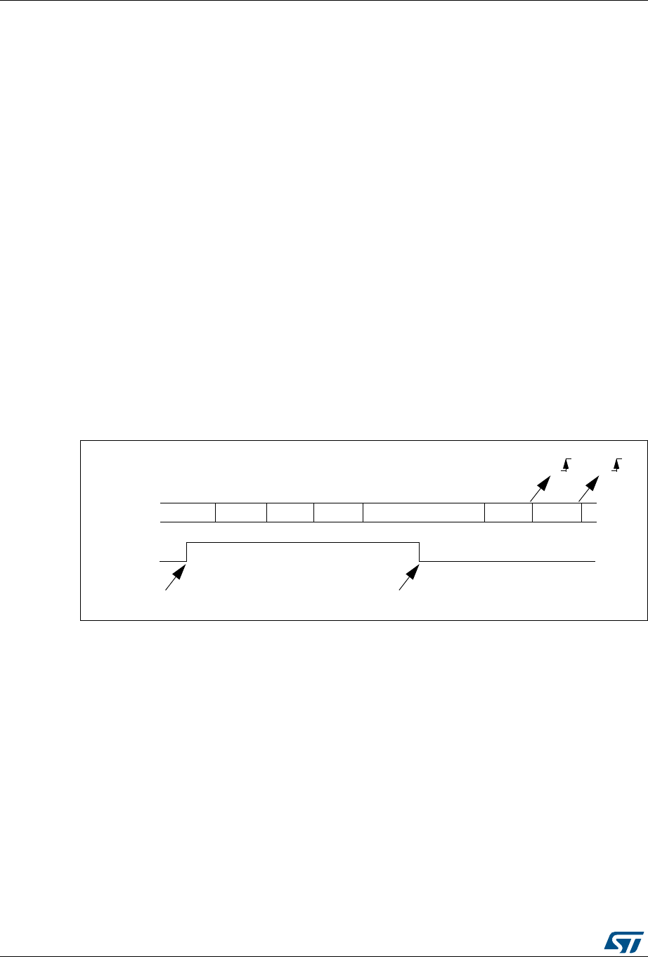
Universal synchronous asynchronous receiver transmitter (USART) RM0383
522/836 DocID026448 Rev 1
In multiprocessor configurations it is often desirable that only the intended message
recipient should actively receive the full message contents, thus reducing redundant USART
service overhead for all non addressed receivers.
The non addressed devices may be placed in mute mode by means of the muting function.
In mute mode:
•None of the reception status bits can be set.
•All the receive interrupts are inhibited.
•The RWU bit in USART_CR1 register is set to 1. RWU can be controlled automatically
by hardware or written by the software under certain conditions.
The USART can enter or exit from mute mode using one of two methods, depending on the
WAKE bit in the USART_CR1 register:
•Idle Line detection if the WAKE bit is reset,
•Address Mark detection if the WAKE bit is set.
Idle line detection (WAKE=0)
The USART enters mute mode when the RWU bit is written to 1.
It wakes up when an Idle frame is detected. Then the RWU bit is cleared by hardware but
the IDLE bit is not set in the USART_SR register. RWU can also be written to 0 by software.
An example of mute mode behavior using Idle line detection is given in Figure 174.
Figure 174. Mute mode using Idle line detection
Address mark detection (WAKE=1)
In this mode, bytes are recognized as addresses if their MSB is a ‘1 else they are
considered as data. In an address byte, the address of the targeted receiver is put on the 4
LSB. This 4-bit word is compared by the receiver with its own address which is programmed
in the ADD bits in the USART_CR2 register.
The USART enters mute mode when an address character is received which does not
match its programmed address. In this case, the RWU bit is set by hardware. The RXNE
flag is not set for this address byte and no interrupt nor DMA request is issued as the
USART would have entered mute mode.
It exits from mute mode when an address character is received which matches the
programmed address. Then the RWU bit is cleared and subsequent bytes are received
normally. The RXNE bit is set for the address character since the RWU bit has been
cleared.
RWU written to 1
Data 1 IDLE
RX Data 2 Data 3 Data 4 Data 6Data 5
RWU Mute Mode Normal Mode
Idle frame detected
RXNE RXNE
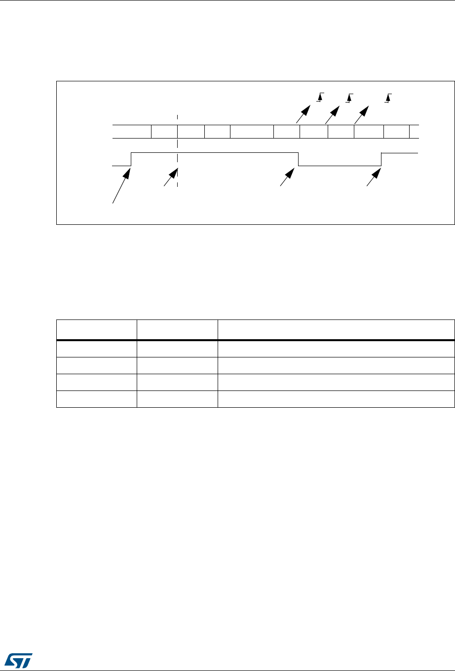
DocID026448 Rev 1 523/836
RM0383 Universal synchronous asynchronous receiver transmitter (USART)
548
The RWU bit can be written to as 0 or 1 when the receiver buffer contains no data (RXNE=0
in the USART_SR register). Otherwise the write attempt is ignored.
An example of mute mode behavior using address mark detection is given in Figure 175.
Figure 175. Mute mode using address mark detection
19.3.7 Parity control
Parity control (generation of parity bit in transmission and parity checking in reception) can
be enabled by setting the PCE bit in the USART_CR1 register. Depending on the frame
length defined by the M bit, the possible USART frame formats are as listed in Table 84.
Even parity
The parity bit is calculated to obtain an even number of “1s” inside the frame made of the 7
or 8 LSB bits (depending on whether M is equal to 0 or 1) and the parity bit.
E.g.: data=00110101; 4 bits set => parity bit will be 0 if even parity is selected (PS bit in
USART_CR1 = 0).
Odd parity
The parity bit is calculated to obtain an odd number of “1s” inside the frame made of the 7 or
8 LSB bits (depending on whether M is equal to 0 or 1) and the parity bit.
E.g.: data=00110101; 4 bits set => parity bit will be 1 if odd parity is selected (PS bit in
USART_CR1 = 1).
RWU written to 1
IDLE
RX Addr=0
RWU Mute Mode Normal Mode
Matching address
RXNE RXNE
(RXNE was cleared)
Data 2 Data 3 Data 4 Data 5Data 1 IDLE Addr=1 Addr=2
Mute Mode
In this example, the current address of the receiver is 1
(programmed in the USART_CR2 register)
nonmatching address nonmatching address
RXNE
Table 84. Frame formats
M bit PCE bit USART frame(1)
1. Legends: SB: start bit, STB: stop bit, PB: parity bit.
0 0 | SB | 8 bit data | STB |
0 1 | SB | 7-bit data | PB | STB |
1 0 | SB | 9-bit data | STB |
1 1 | SB | 8-bit data PB | STB |

Universal synchronous asynchronous receiver transmitter (USART) RM0383
524/836 DocID026448 Rev 1
Parity checking in reception
If the parity check fails, the PE flag is set in the USART_SR register and an interrupt is
generated if PEIE is set in the USART_CR1 register. The PE flag is cleared by a software
sequence (a read from the status register followed by a read or write access to the
USART_DR data register).
Note: In case of wakeup by an address mark: the MSB bit of the data is taken into account to
identify an address but not the parity bit. And the receiver does not check the parity of the
address data (PE is not set in case of a parity error).
Parity generation in transmission
If the PCE bit is set in USART_CR1, then the MSB bit of the data written in the data register
is transmitted but is changed by the parity bit (even number of “1s” if even parity is selected
(PS=0) or an odd number of “1s” if odd parity is selected (PS=1)).
Note: The software routine that manages the transmission can activate the software sequence
which clears the PE flag (a read from the status register followed by a read or write access
to the data register). When operating in half-duplex mode, depending on the software, this
can cause the PE flag to be unexpectedly cleared.
19.3.8 LIN (local interconnection network) mode
The LIN mode is selected by setting the LINEN bit in the USART_CR2 register. In LIN
mode, the following bits must be kept cleared:
•STOP[1:0] and CLKEN in the USART_CR2 register
•SCEN, HDSEL and IREN in the USART_CR3 register.
LIN transmission
The same procedure explained in Section 19.3.2 has to be applied for LIN Master
transmission than for normal USART transmission with the following differences:
•Clear the M bit to configure 8-bit word length.
•Set the LINEN bit to enter LIN mode. In this case, setting the SBK bit sends 13 ‘0 bits
as a break character. Then a bit of value ‘1 is sent to allow the next start detection.
LIN reception
A break detection circuit is implemented on the USART interface. The detection is totally
independent from the normal USART receiver. A break can be detected whenever it occurs,
during Idle state or during a frame.
When the receiver is enabled (RE=1 in USART_CR1), the circuit looks at the RX input for a
start signal. The method for detecting start bits is the same when searching break
characters or data. After a start bit has been detected, the circuit samples the next bits
exactly like for the data (on the 8th, 9th and 10th samples). If 10 (when the LBDL = 0 in
USART_CR2) or 11 (when LBDL=1 in USART_CR2) consecutive bits are detected as ‘0,
and are followed by a delimiter character, the LBD flag is set in USART_SR. If the LBDIE
bit=1, an interrupt is generated. Before validating the break, the delimiter is checked for as it
signifies that the RX line has returned to a high level.
If a ‘1 is sampled before the 10 or 11 have occurred, the break detection circuit cancels the
current detection and searches for a start bit again.
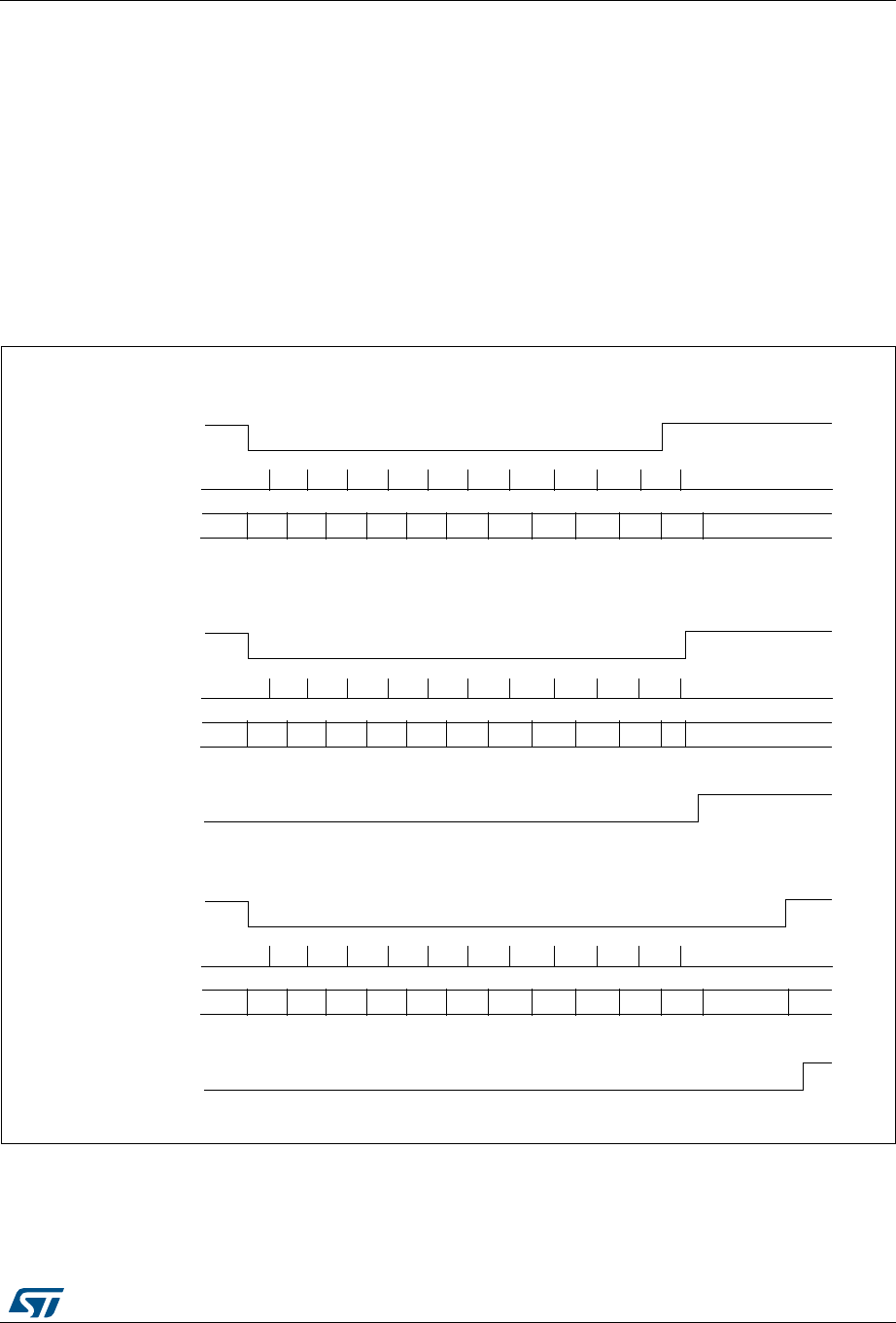
DocID026448 Rev 1 525/836
RM0383 Universal synchronous asynchronous receiver transmitter (USART)
548
If the LIN mode is disabled (LINEN=0), the receiver continues working as normal USART,
without taking into account the break detection.
If the LIN mode is enabled (LINEN=1), as soon as a framing error occurs (i.e. stop bit
detected at ‘0, which will be the case for any break frame), the receiver stops until the break
detection circuit receives either a ‘1, if the break word was not complete, or a delimiter
character if a break has been detected.
The behavior of the break detector state machine and the break flag is shown on the
Figure 176: Break detection in LIN mode (11-bit break length - LBDL bit is set) on page 525.
Examples of break frames are given on Figure 177: Break detection in LIN mode vs.
Framing error detection on page 526.
Figure 176. Break detection in LIN mode (11-bit break length - LBDL bit is set)
Case 1: break signal not long enough => break discarded, LBD is not set
Break Frame
RX line
Break State machine
Capture Strobe
0
Bit1 Bit2 Bit3 Bit4 Bit5 Bit6 Bit7 Bit8 Bit9
Idle Idle
Read Samples
Bit0
0000000001
Bit10
Break Frame
RX line
Break State machine
Capture Strobe
0
Bit1 Bit2 Bit3 Bit4 Bit5 Bit6 Bit7 Bit8 Bit9
Idle Idle
Read Samples
Bit0
0000000000
B10
Case 2: break signal just long enough => break detected, LBD is set
LBD
Break Frame
RX line
Break State machine
Capture Strobe
0
Bit1 Bit2 Bit3 Bit4 Bit5 Bit6 Bit7 Bit8 Bit9
Idle Idle
Read Samples
Bit0
0000000000
Bit10
Case 3: break signal long enough => break detected, LBD is set
wait delimiter
LBD
delimiter is immediate
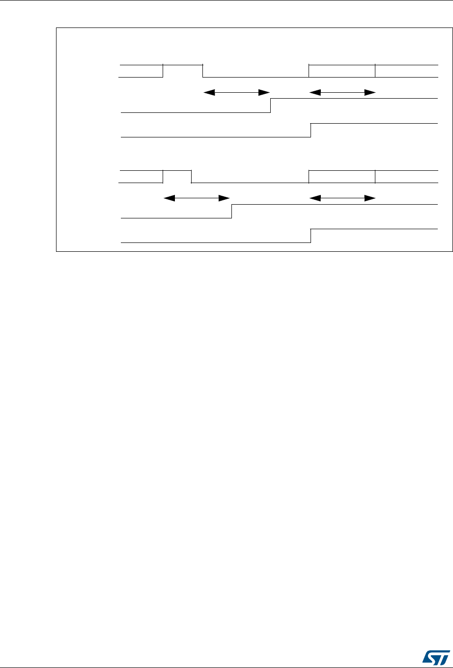
Universal synchronous asynchronous receiver transmitter (USART) RM0383
526/836 DocID026448 Rev 1
Figure 177. Break detection in LIN mode vs. Framing error detection
19.3.9 USART synchronous mode
The synchronous mode is selected by writing the CLKEN bit in the USART_CR2 register to
1. In synchronous mode, the following bits must be kept cleared:
•LINEN bit in the USART_CR2 register,
•SCEN, HDSEL and IREN bits in the USART_CR3 register.
The USART allows the user to control a bidirectional synchronous serial communications in
master mode. The SCLK pin is the output of the USART transmitter clock. No clock pulses
are sent to the SCLK pin during start bit and stop bit. Depending on the state of the LBCL bit
in the USART_CR2 register clock pulses will or will not be generated during the last valid
data bit (address mark). The CPOL bit in the USART_CR2 register allows the user to select
the clock polarity, and the CPHA bit in the USART_CR2 register allows the user to select the
phase of the external clock (see Figure 178, Figure 179 & Figure 180).
During the Idle state, preamble and send break, the external SCLK clock is not activated.
In synchronous mode the USART transmitter works exactly like in asynchronous mode. But
as SCLK is synchronized with TX (according to CPOL and CPHA), the data on TX is
synchronous.
In this mode the USART receiver works in a different manner compared to the
asynchronous mode. If RE=1, the data is sampled on SCLK (rising or falling edge,
depending on CPOL and CPHA), without any oversampling. A setup and a hold time must
be respected (which depends on the baud rate: 1/16 bit time).
Note: The SCLK pin works in conjunction with the TX pin. Thus, the clock is provided only if the
transmitter is enabled (TE=1) and a data is being transmitted (the data register USART_DR
Case 1: break occurring after an Idle
IDLE data2 (0x55)data 1 data 3 (header)
In these examples, we suppose that LBDL=1 (11-bit break length), M=0 (8-bit data)
RX line
RXNE / FE
LBD
1 data time 1 data time
Case 1: break occurring while a data is being received
data 2 data2 (0x55)data 1 data 3 (header)
RX line
RXNE / FE
LBD
1 data time 1 data time
BREAK
BREAK
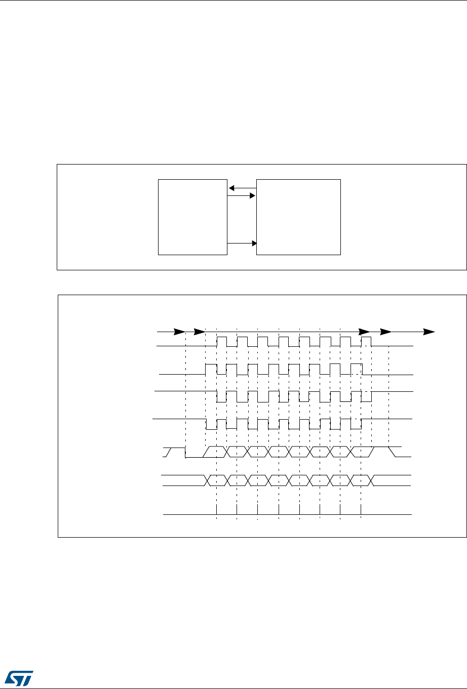
DocID026448 Rev 1 527/836
RM0383 Universal synchronous asynchronous receiver transmitter (USART)
548
has been written). This means that it is not possible to receive a synchronous data without
transmitting data.
The LBCL, CPOL and CPHA bits have to be selected when both the transmitter and the
receiver are disabled (TE=RE=0) to ensure that the clock pulses function correctly. These
bits should not be changed while the transmitter or the receiver is enabled.
It is advised that TE and RE are set in the same instruction in order to minimize the setup
and the hold time of the receiver.
The USART supports master mode only: it cannot receive or send data related to an input
clock (SCLK is always an output).
Figure 178. USART example of synchronous transmission
Figure 179. USART data clock timing diagram (M=0)
RX
TX
SCLK
USART
Data out
Data in
Synchronous device
Clock
(e.g. slave SPI)
M=0 (8 data bits)
Clock (CPOL=0, CPHA=1)
Clock (CPOL=1, CPHA=0)
Clock (CPOL=1, CPHA=1)
Start LSB MSB Stop
* LBCL bit controls last data clock pulse
Start
Idle or preceding
transmission
Data on TX
Stop
Clock (CPOL=0, CPHA=0)
01 234 56 7
*
*
*
*
Idle or next
transmission
*
Capture Strobe
LSB MSB
Data on RX 01 234 56 7
(from master)
(from slave)
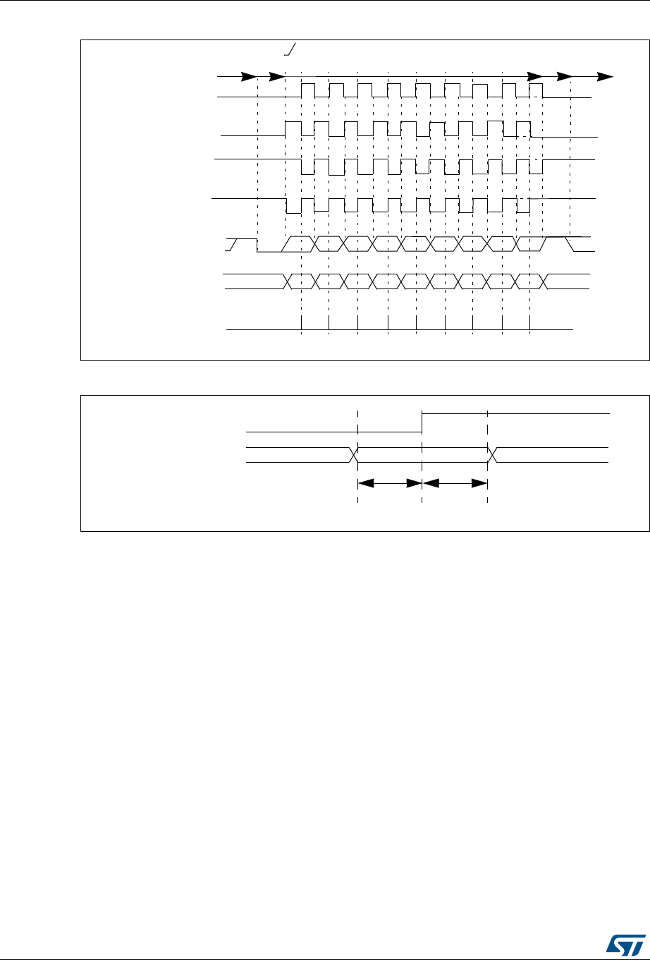
Universal synchronous asynchronous receiver transmitter (USART) RM0383
528/836 DocID026448 Rev 1
Figure 180. USART data clock timing diagram (M=1)
Figure 181. RX data setup/hold time
Note: The function of SCLK is different in Smartcard mode. Refer to the Smartcard mode chapter
for more details.
19.3.10 Single-wire half-duplex communication
The single-wire half-duplex mode is selected by setting the HDSEL bit in the USART_CR3
register. In this mode, the following bits must be kept cleared:
•LINEN and CLKEN bits in the USART_CR2 register,
•SCEN and IREN bits in the USART_CR3 register.
The USART can be configured to follow a single-wire half-duplex protocol where the TX and
RX lines are internally connected. The selection between half- and full-duplex
communication is made with a control bit ‘HALF DUPLEX SEL’ (HDSEL in USART_CR3).
As soon as HDSEL is written to 1:
•the TX and RX lines are internally connected
•the RX pin is no longer used
•the TX pin is always released when no data is transmitted. Thus, it acts as a standard
I/O in idle or in reception. It means that the I/O must be configured so that TX is
configured as floating input (or output high open-drain) when not driven by the USART.
Idle or next
M=1 (9 data bits)
Clock (CPOL=0, CPHA=1)
Clock (CPOL=1, CPHA=0)
Clock (CPOL=1, CPHA=1)
Start LSB MSB Stop
* LBCL bit controls last data clock pulse
Start
Idle or preceding
transmission
Data on TX
Stop
Clock (CPOL=0, CPHA=0)
01 234 56 7
*
*
*
*
8
transmission
Capture Strobe
LSB MSB
Data on RX 01 234 56 7
(from slave)
(from master)
*
8
valid DATA bit
tSETUP tHOLD
SCLK (capture strobe on SCLK
rising edge in this example)
Data on RX
(from slave)
tSETUP = tHOLD 1/16 bit time
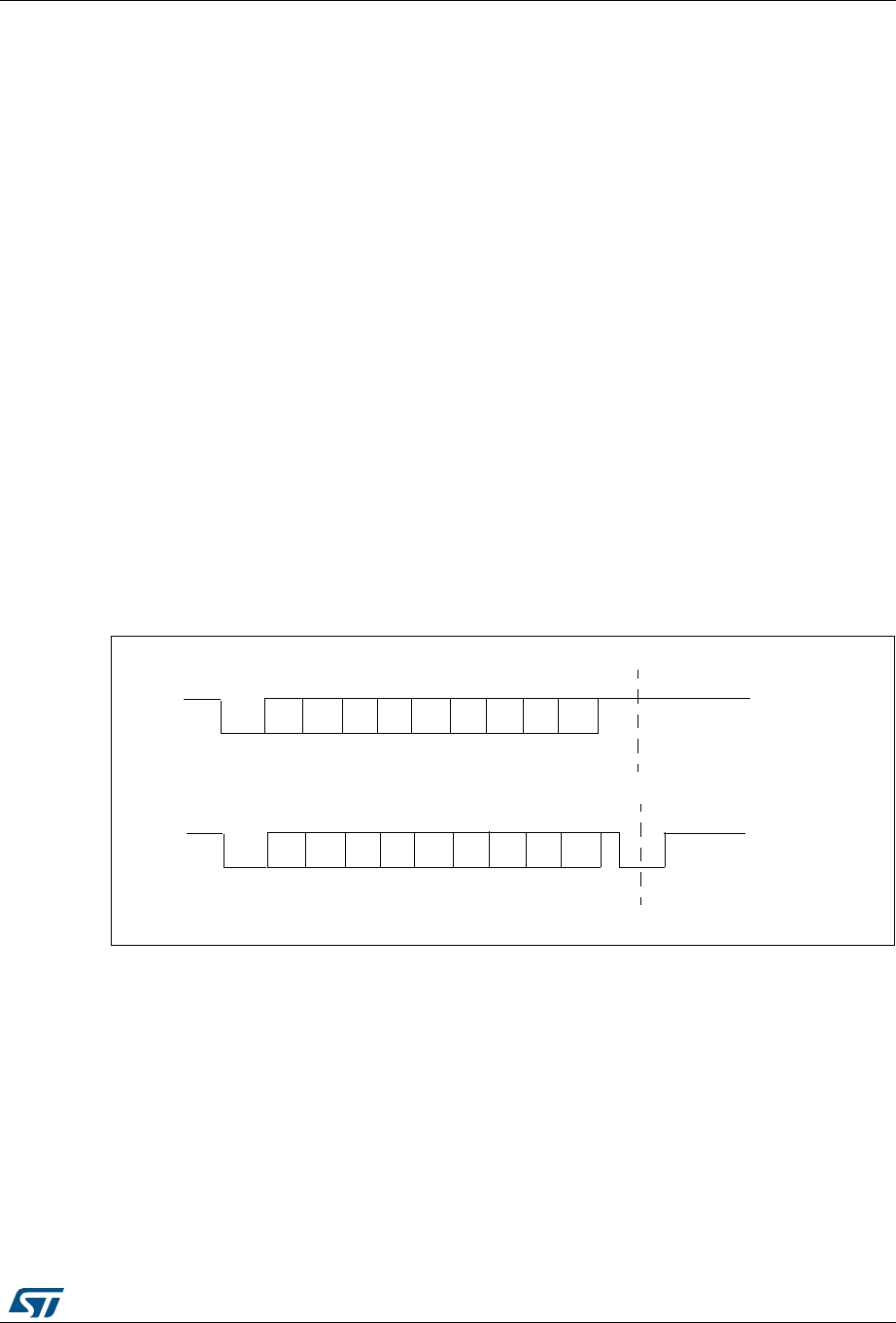
DocID026448 Rev 1 529/836
RM0383 Universal synchronous asynchronous receiver transmitter (USART)
548
Apart from this, the communications are similar to what is done in normal USART mode.
The conflicts on the line must be managed by the software (by the use of a centralized
arbiter, for instance). In particular, the transmission is never blocked by hardware and
continue to occur as soon as a data is written in the data register while the TE bit is set.
19.3.11 Smartcard
The Smartcard mode is selected by setting the SCEN bit in the USART_CR3 register. In
smartcard mode, the following bits must be kept cleared:
•LINEN bit in the USART_CR2 register,
•HDSEL and IREN bits in the USART_CR3 register.
Moreover, the CLKEN bit may be set in order to provide a clock to the smartcard.
The Smartcard interface is designed to support asynchronous protocol Smartcards as
defined in the ISO 7816-3 standard. The USART should be configured as:
•8 bits plus parity: where M=1 and PCE=1 in the USART_CR1 register
•1.5 stop bits when transmitting and receiving: where STOP=11 in the USART_CR2
register.
Note: It is also possible to choose 0.5 stop bit for receiving but it is recommended to use 1.5 stop
bits for both transmitting and receiving to avoid switching between the two configurations.
Figure 182 shows examples of what can be seen on the data line with and without parity
error.
Figure 182. ISO 7816-3 asynchronous protocol
When connected to a Smartcard, the TX output of the USART drives a bidirectional line that
is also driven by the Smartcard. The TX pin must be configured as open-drain.
Smartcard is a single wire half duplex communication protocol.
•Transmission of data from the transmit shift register is guaranteed to be delayed by a
minimum of 1/2 baud clock. In normal operation a full transmit shift register will start
shifting on the next baud clock edge. In Smartcard mode this transmission is further
delayed by a guaranteed 1/2 baud clock.
•If a parity error is detected during reception of a frame programmed with a 0.5 or 1.5
stop bit period, the transmit line is pulled low for a baud clock period after the
completion of the receive frame. This is to indicate to the Smartcard that the data
transmitted to USART has not been correctly received. This NACK signal (pulling
transmit line low for 1 baud clock) will cause a framing error on the transmitter side
S0123 5
467P
Start
bit
Guard time
S0123 5
467P
Start
bit
Line pulled low
by receiver during stop in
case of parity error
Guard time
Without Parity error
With Parity error
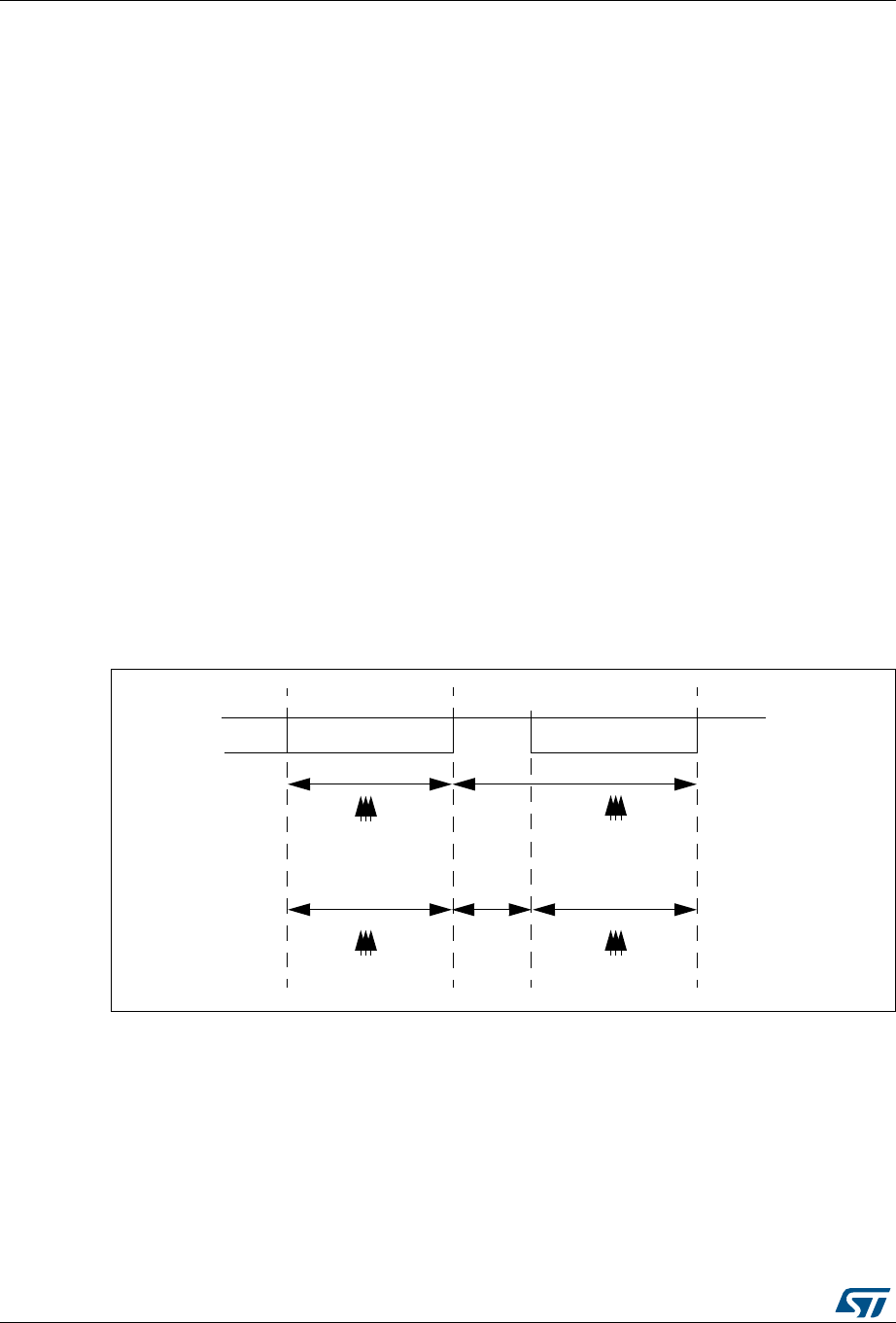
Universal synchronous asynchronous receiver transmitter (USART) RM0383
530/836 DocID026448 Rev 1
(configured with 1.5 stop bits). The application can handle re-sending of data according
to the protocol. A parity error is ‘NACK’ed by the receiver if the NACK control bit is set,
otherwise a NACK is not transmitted.
•The assertion of the TC flag can be delayed by programming the Guard Time register.
In normal operation, TC is asserted when the transmit shift register is empty and no
further transmit requests are outstanding. In Smartcard mode an empty transmit shift
register triggers the guard time counter to count up to the programmed value in the
Guard Time register. TC is forced low during this time. When the guard time counter
reaches the programmed value TC is asserted high.
•The de-assertion of TC flag is unaffected by Smartcard mode.
•If a framing error is detected on the transmitter end (due to a NACK from the receiver),
the NACK will not be detected as a start bit by the receive block of the transmitter.
According to the ISO protocol, the duration of the received NACK can be 1 or 2 baud
clock periods.
•On the receiver side, if a parity error is detected and a NACK is transmitted the receiver
will not detect the NACK as a start bit.
Note: A break character is not significant in Smartcard mode. A 0x00 data with a framing error will
be treated as data and not as a break.
No Idle frame is transmitted when toggling the TE bit. The Idle frame (as defined for the
other configurations) is not defined by the ISO protocol.
Figure 183 details how the NACK signal is sampled by the USART. In this example the
USART is transmitting a data and is configured with 1.5 stop bits. The receiver part of the
USART is enabled in order to check the integrity of the data and the NACK signal.
Figure 183. Parity error detection using the 1.5 stop bits
The USART can provide a clock to the smartcard through the SCLK output. In smartcard
mode, SCLK is not associated to the communication but is simply derived from the internal
peripheral input clock through a 5-bit prescaler. The division ratio is configured in the
prescaler register USART_GTPR. SCLK frequency can be programmed from fCK/2 to
fCK/62, where fCK is the peripheral input clock.
1 bit time 1.5 bit time
0.5 bit time 1 bit time
sampling at
8th, 9th, 10th
sampling at
8th, 9th, 10th
sampling at
8th, 9th, 10th
sampling at
16th, 17th, 18th
Bit 7 Parity Bit 1.5 Stop Bit

DocID026448 Rev 1 531/836
RM0383 Universal synchronous asynchronous receiver transmitter (USART)
548
19.3.12 IrDA SIR ENDEC block
The IrDA mode is selected by setting the IREN bit in the USART_CR3 register. In IrDA
mode, the following bits must be kept cleared:
•LINEN, STOP and CLKEN bits in the USART_CR2 register,
•SCEN and HDSEL bits in the USART_CR3 register.
The IrDA SIR physical layer specifies use of a Return to Zero, Inverted (RZI) modulation
scheme that represents logic 0 as an infrared light pulse (see Figure 184).
The SIR Transmit encoder modulates the Non Return to Zero (NRZ) transmit bit stream
output from USART. The output pulse stream is transmitted to an external output driver and
infrared LED. USART supports only bit rates up to 115.2Kbps for the SIR ENDEC. In normal
mode the transmitted pulse width is specified as 3/16 of a bit period.
The SIR receive decoder demodulates the return-to-zero bit stream from the infrared
detector and outputs the received NRZ serial bit stream to USART. The decoder input is
normally HIGH (marking state) in the Idle state. The transmit encoder output has the
opposite polarity to the decoder input. A start bit is detected when the decoder input is low.
•IrDA is a half duplex communication protocol. If the Transmitter is busy (i.e. the USART
is sending data to the IrDA encoder), any data on the IrDA receive line will be ignored
by the IrDA decoder and if the Receiver is busy (USART is receiving decoded data
from the USART), data on the TX from the USART to IrDA will not be encoded by IrDA.
While receiving data, transmission should be avoided as the data to be transmitted
could be corrupted.
•A ‘0 is transmitted as a high pulse and a ‘1 is transmitted as a ‘0. The width of the pulse
is specified as 3/16th of the selected bit period in normal mode (see Figure 185).
•The SIR decoder converts the IrDA compliant receive signal into a bit stream for
USART.
•The SIR receive logic interprets a high state as a logic one and low pulses as logic
zeros.
•The transmit encoder output has the opposite polarity to the decoder input. The SIR
output is in low state when Idle.
•The IrDA specification requires the acceptance of pulses greater than 1.41 us. The
acceptable pulse width is programmable. Glitch detection logic on the receiver end
filters out pulses of width less than 2 PSC periods (PSC is the prescaler value
programmed in the IrDA low-power Baud Register, USART_GTPR). Pulses of width
less than 1 PSC period are always rejected, but those of width greater than one and
less than two periods may be accepted or rejected, those greater than 2 periods will be
accepted as a pulse. The IrDA encoder/decoder doesn’t work when PSC=0.
•The receiver can communicate with a low-power transmitter.
•In IrDA mode, the STOP bits in the USART_CR2 register must be configured to “1 stop
bit”.
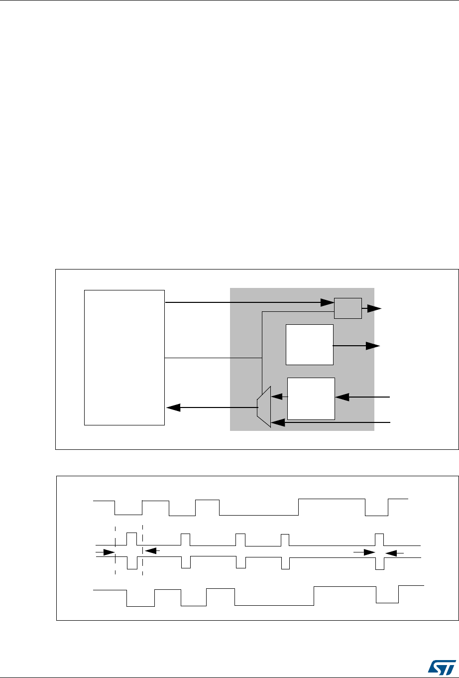
Universal synchronous asynchronous receiver transmitter (USART) RM0383
532/836 DocID026448 Rev 1
IrDA low-power mode
Transmitter:
In low-power mode the pulse width is not maintained at 3/16 of the bit period. Instead, the
width of the pulse is 3 times the low-power baud rate which can be a minimum of 1.42 MHz.
Generally this value is 1.8432 MHz (1.42 MHz < PSC< 2.12 MHz). A low-power mode
programmable divisor divides the system clock to achieve this value.
Receiver:
Receiving in low-power mode is similar to receiving in normal mode. For glitch detection the
USART should discard pulses of duration shorter than 1/PSC. A valid low is accepted only if
its duration is greater than 2 periods of the IrDA low-power Baud clock (PSC value in
USART_GTPR).
Note: A pulse of width less than two and greater than one PSC period(s) may or may not be
rejected.
The receiver set up time should be managed by software. The IrDA physical layer
specification specifies a minimum of 10 ms delay between transmission and reception (IrDA
is a half duplex protocol).
Figure 184. IrDA SIR ENDEC- block diagram
Figure 185. IrDA data modulation (3/16) -Normal mode
USART
SIR
Transmit
Encoder
SIR
Receive
Decoder
OR USART_TX
IrDA_OUT
IrDA_IN
USART_RX
TX
RX
SIREN
TX
IrDA_OUT
IrDA_IN
RX
Start
bit
0101001101
3/16
stop bit
bit period
0101001101

DocID026448 Rev 1 533/836
RM0383 Universal synchronous asynchronous receiver transmitter (USART)
548
19.3.13 Continuous communication using DMA
The USART is capable of continuous communication using the DMA. The DMA requests for
Rx buffer and Tx buffer are generated independently.
Transmission using DMA
DMA mode can be enabled for transmission by setting DMAT bit in the USART_CR3
register. Data is loaded from a SRAM area configured using the DMA peripheral (refer to the
DMA specification) to the USART_DR register whenever the TXE bit is set. To map a DMA
channel for USART transmission, use the following procedure (x denotes the channel
number):
1. Write the USART_DR register address in the DMA control register to configure it as the
destination of the transfer. The data will be moved to this address from memory after
each TXE event.
2. Write the memory address in the DMA control register to configure it as the source of
the transfer. The data will be loaded into the USART_DR register from this memory
area after each TXE event.
3. Configure the total number of bytes to be transferred to the DMA control register.
4. Configure the channel priority in the DMA register
5. Configure DMA interrupt generation after half/ full transfer as required by the
application.
6. Clear the TC bit in the SR register by writing 0 to it.
7. Activate the channel in the DMA register.
When the number of data transfers programmed in the DMA Controller is reached, the DMA
controller generates an interrupt on the DMA channel interrupt vector.
In transmission mode, once the DMA has written all the data to be transmitted (the TCIF flag
is set in the DMA_ISR register), the TC flag can be monitored to make sure that the USART
communication is complete. This is required to avoid corrupting the last transmission before
disabling the USART or entering the Stop mode. The software must wait until TC=1. The TC
flag remains cleared during all data transfers and it is set by hardware at the last frame’s
end of transmission.
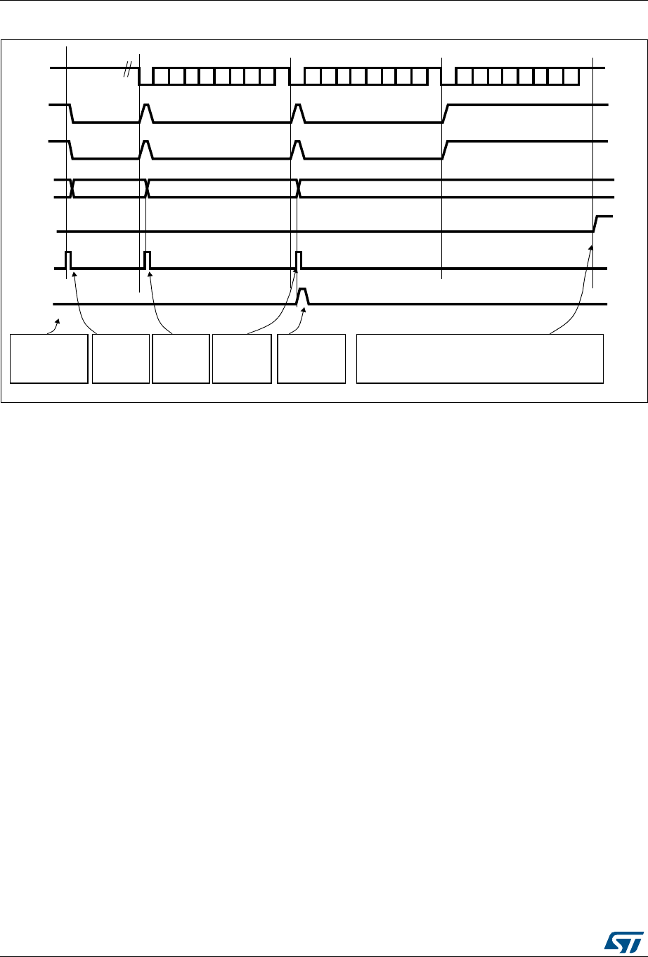
Universal synchronous asynchronous receiver transmitter (USART) RM0383
534/836 DocID026448 Rev 1
Figure 186. Transmission using DMA
Reception using DMA
DMA mode can be enabled for reception by setting the DMAR bit in USART_CR3 register.
Data is loaded from the USART_DR register to a SRAM area configured using the DMA
peripheral (refer to the DMA specification) whenever a data byte is received. To map a DMA
channel for USART reception, use the following procedure:
1. Write the USART_DR register address in the DMA control register to configure it as the
source of the transfer. The data will be moved from this address to the memory after
each RXNE event.
2. Write the memory address in the DMA control register to configure it as the destination
of the transfer. The data will be loaded from USART_DR to this memory area after each
RXNE event.
3. Configure the total number of bytes to be transferred in the DMA control register.
4. Configure the channel priority in the DMA control register
5. Configure interrupt generation after half/ full transfer as required by the application.
6. Activate the channel in the DMA control register.
When the number of data transfers programmed in the DMA Controller is reached, the DMA
controller generates an interrupt on the DMA channel interrupt vector. The DMAR bit should
be cleared by software in the USART_CR3 register during the interrupt subroutine.
Note: If DMA is used for reception, do not enable the RXNEIE bit.
48LINE
53!24?$2
&RAME
48%FLAG
&
4#FLAG
&
&RAME
VRIWZDUHZDLWVXQWLO7&
&RAME
SETBYHARDWARE
CLEAREDBY$-!READ
SETBYHARDWARE
CLEAREDBY$-!READ SETBYHARDWARE
SET
)DLEPREAMBLE
BYHARDWARE
&
VRIWZDUHFRQILJXUHV
WKH'0$WRVHQG
GDWDDQGHQDEOHVWKH
86$57
$-!REQUEST IGNOREDBYTHE$-!
$-!WRITES
FLAG$-!4#)& SETBYHARDWARE CLEAR
BYSOFTWARE
53!24?$2
BECAUSE$-!TRANSFERISCOMPLETE
'0$ZULWHV)
LQWR
86$57B'5
'0$ZULWHV)
LQWR
86$57B'5
'0$ZULWHV)
LQWR
86$57B'5
7KH'0$WUDQVIHU
LVFRPSOHWH
7&,) LQ
'0$B,65
4RA NSFERCOMPLETE
AIB
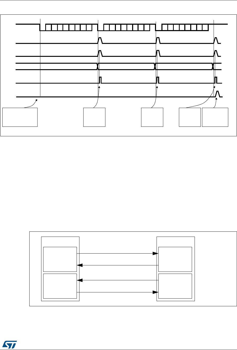
DocID026448 Rev 1 535/836
RM0383 Universal synchronous asynchronous receiver transmitter (USART)
548
Figure 187. Reception using DMA
Error flagging and interrupt generation in multibuffer communication
In case of multibuffer communication if any error occurs during the transaction the error flag
will be asserted after the current byte. An interrupt will be generated if the interrupt enable
flag is set. For framing error, overrun error and noise flag which are asserted with RXNE in
case of single byte reception, there will be separate error flag interrupt enable bit (EIE bit in
the USART_CR3 register), which if set will issue an interrupt after the current byte with
either of these errors.
19.3.14 Hardware flow control
It is possible to control the serial data flow between 2 devices by using the nCTS input and
the nRTS output. The Figure 188 shows how to connect 2 devices in this mode:
Figure 188. Hardware flow control between 2 USARTs
RTS and CTS flow control can be enabled independently by writing respectively RTSE and
CTSE bits to 1 (in the USART_CR3 register).
48LINE
53!24?$2
&RA ME
28.%FLAG
& &
&RAME &RAME
SETBYHARDWARE
CLEAREDBY$-!READ
&
VRIWZDUHFRQILJXUHVWKH
'0$WRUHFHLYHGDWD
EORFNVDQGHQDEOHV
WKH86$57
$-!REQUEST
$-!READS53!24?$2
$-!4#)&FLAG SETBYHARDWARE CLEARED
BYSOFTWARE
'0$UHDGV)
IURP
86$57B'5
4RA NSFERCOMPLETE
'0$UHDGV)
IURP
86$57B'5
'0$UHDGV)
IURP
86$57B'5
7KH'0$WUDQVIHU
LVFRPSOHWH
7&,) LQ
'0$B,65
AIB
USART 1
RX circuit
TX circuit
USART 2
TX circuit
RX circuit
RXTX
TX
RX
nCTS nRTS
nRTS nCTS
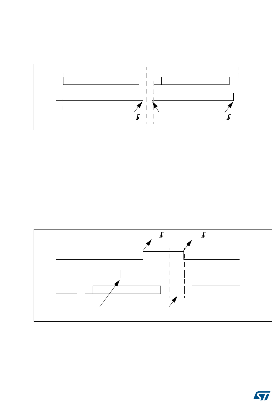
Universal synchronous asynchronous receiver transmitter (USART) RM0383
536/836 DocID026448 Rev 1
RTS flow control
If the RTS flow control is enabled (RTSE=1), then nRTS is asserted (tied low) as long as the
USART receiver is ready to receive a new data. When the receive register is full, nRTS is
deasserted, indicating that the transmission is expected to stop at the end of the current
frame. Figure 189 shows an example of communication with RTS flow control enabled.
Figure 189. RTS flow control
CTS flow control
If the CTS flow control is enabled (CTSE=1), then the transmitter checks the nCTS input
before transmitting the next frame. If nCTS is asserted (tied low), then the next data is
transmitted (assuming that a data is to be transmitted, in other words, if TXE=0), else the
transmission does not occur. When nCTS is deasserted during a transmission, the current
transmission is completed before the transmitter stops.
When CTSE=1, the CTSIF status bit is automatically set by hardware as soon as the nCTS
input toggles. It indicates when the receiver becomes ready or not ready for communication.
An interrupt is generated if the CTSIE bit in the USART_CR3 register is set. The figure
below shows an example of communication with CTS flow control enabled.
Figure 190. CTS flow control
Note: Special behavior of break frames: when the CTS flow is enabled, the transmitter does not
check the nCTS input state to send a break.
Start
Bit Stop
Bit
Data 1 IdleStart
Bit
Stop
Bit
Data 2
RX
nRTS
RXNE Data 1 read RXNE
Data 2 can now be transmitted
Start
Bit
Stop
Bit
Data 2 Idle Start
Bit Data 3
TX
nCTS
CTS
Transmission of Data 3
Data 1 Stop
Bit
is delayed until nCTS = 0
CTS
Data 2 Data 3empty empty
Transmit data register
TDR
Writing data 3 in TDR
DocID026448 Rev 1 537/836
RM0383 Universal synchronous asynchronous receiver transmitter (USART)
548
19.4 USART interrupts
The USART interrupt events are connected to the same interrupt vector (see Figure 191).
•During transmission: Transmission Complete, Clear to Send or Transmit Data Register
empty interrupt.
•While receiving: Idle Line detection, Overrun error, Receive Data register not empty,
Parity error, LIN break detection, Noise Flag (only in multi buffer communication) and
Framing Error (only in multi buffer communication).
These events generate an interrupt if the corresponding Enable Control Bit is set.
Figure 191. USART interrupt mapping diagram
Table 85. USART interrupt requests
Interrupt event Event flag Enable control
bit
Transmit Data Register Empty TXE TXEIE
CTS flag CTS CTSIE
Transmission Complete TC TCIE
Received Data Ready to be Read RXNE
RXNEIE
Overrun Error Detected ORE
Idle Line Detected IDLE IDLEIE
Parity Error PE PEIE
Break Flag LBD LBDIE
Noise Flag, Overrun error and Framing Error in multibuffer
communication NF or ORE or FE EIE
TC
TCIE
TXE
TXEIE
IDLE
IDLEIE
RXNEIE
ORE
RXNEIE
RXNE
PE
PEIE
FE
NE
ORE EIE
DMAR
USART
LBD
LBDIE
CTS
CTSIE
interrupt
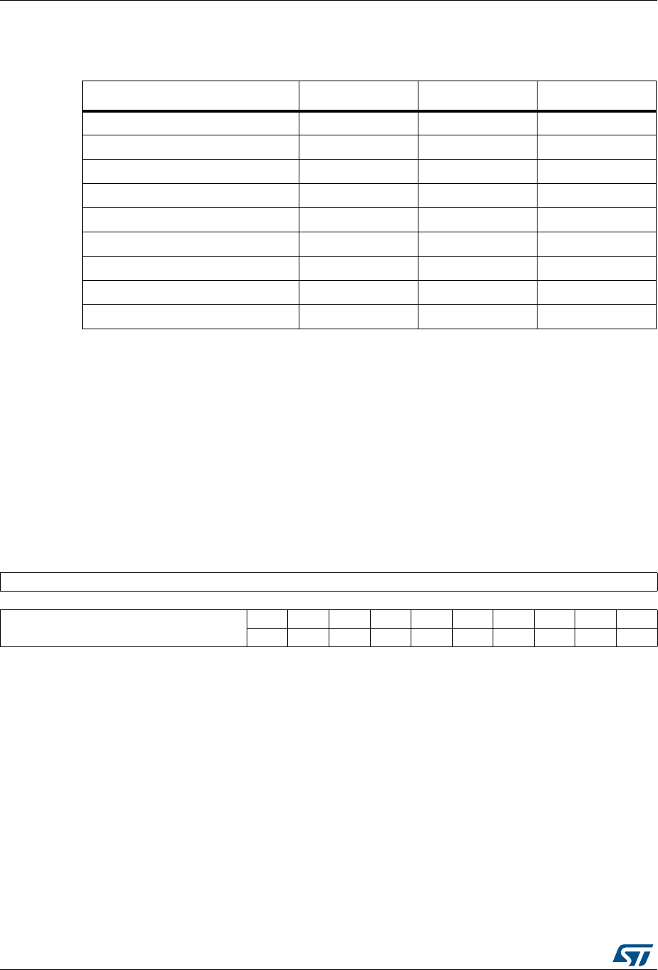
Universal synchronous asynchronous receiver transmitter (USART) RM0383
538/836 DocID026448 Rev 1
19.5 USART mode configuration
19.6 USART registers
Refer to Section 1.1 on page 33 for a list of abbreviations used in register descriptions.
The peripheral registers have to be accessed by half-words (16 bits) or words (32 bits).
19.6.1 Status register (USART_SR)
Address offset: 0x00
Reset value: 0x00C0 0000
Table 86. USART mode configuration(1)
1. X = supported; NA = not applicable.
USART modes USART1 USART2 USART6
Asynchronous mode X X X
Hardware flow control X X X
Multibuffer communication (DMA) X X X
Multiprocessor communication X X X
Synchronous X X X
Smartcard X X X
Half-duplex (single-wire mode) X X X
IrDA X X X
LIN X X X
31 30 29 28 27 26 25 24 23 22 21 20 19 18 17 16
Reserved
1514131211109876543210
Reserved
CTS LBD TXE TC RXNE IDLE ORE NF FE PE
rc_w0rc_w0rrc_w0rc_w0rrrrr
Bits 31:10 Reserved, must be kept at reset value
Bit 9 CTS: CTS flag
This bit is set by hardware when the nCTS input toggles, if the CTSE bit is set. It is cleared
by software (by writing it to 0). An interrupt is generated if CTSIE=1 in the USART_CR3
register.
Note: 0: No change occurred on the nCTS status line
1: A change occurred on the nCTS status line
Bit 8 LBD: LIN break detection flag
This bit is set by hardware when the LIN break is detected. It is cleared by software (by
writing it to 0). An interrupt is generated if LBDIE = 1 in the USART_CR2 register.
0: LIN Break not detected
1: LIN break detected
Note: An interrupt is generated when LBD=1 if LBDIE=1

DocID026448 Rev 1 539/836
RM0383 Universal synchronous asynchronous receiver transmitter (USART)
548
Bit 7 TXE: Transmit data register empty
This bit is set by hardware when the content of the TDR register has been transferred into
the shift register. An interrupt is generated if the TXEIE bit =1 in the USART_CR1 register. It
is cleared by a write to the USART_DR register.
0: Data is not transferred to the shift register
1: Data is transferred to the shift register)
Note: This bit is used during single buffer transmission.
Bit 6 TC: Transmission complete
This bit is set by hardware if the transmission of a frame containing data is complete and if
TXE is set. An interrupt is generated if TCIE=1 in the USART_CR1 register. It is cleared by
a software sequence (a read from the USART_SR register followed by a write to the
USART_DR register). The TC bit can also be cleared by writing a '0' to it. This clearing
sequence is recommended only for multibuffer communication.
0: Transmission is not complete
1: Transmission is complete
Bit 5 RXNE: Read data register not empty
This bit is set by hardware when the content of the RDR shift register has been transferred
to the USART_DR register. An interrupt is generated if RXNEIE=1 in the USART_CR1
register. It is cleared by a read to the USART_DR register. The RXNE flag can also be
cleared by writing a zero to it. This clearing sequence is recommended only for multibuffer
communication.
0: Data is not received
1: Received data is ready to be read.
Bit 4 IDLE: IDLE line detected
This bit is set by hardware when an Idle Line is detected. An interrupt is generated if the
IDLEIE=1 in the USART_CR1 register. It is cleared by a software sequence (an read to the
USART_SR register followed by a read to the USART_DR register).
0: No Idle Line is detected
1: Idle Line is detected
Note: The IDLE bit will not be set again until the RXNE bit has been set itself (i.e. a new idle
line occurs).
Bit 3 ORE: Overrun error
This bit is set by hardware when the word currently being received in the shift register is
ready to be transferred into the RDR register while RXNE=1. An interrupt is generated if
RXNEIE=1 in the USART_CR1 register. It is cleared by a software sequence (an read to the
USART_SR register followed by a read to the USART_DR register).
0: No Overrun error
1: Overrun error is detected
Note: When this bit is set, the RDR register content will not be lost but the shift register will be
overwritten. An interrupt is generated on ORE flag in case of Multi Buffer
communication if the EIE bit is set.

Universal synchronous asynchronous receiver transmitter (USART) RM0383
540/836 DocID026448 Rev 1
Bit 2 NF: Noise detected flag
This bit is set by hardware when noise is detected on a received frame. It is cleared by a
software sequence (an read to the USART_SR register followed by a read to the
USART_DR register).
0: No noise is detected
1: Noise is detected
Note: This bit does not generate interrupt as it appears at the same time as the RXNE bit
which itself generates an interrupting interrupt is generated on NF flag in case of Multi
Buffer communication if the EIE bit is set.
Note: When the line is noise-free, the NF flag can be disabled by programming the ONEBIT
bit to 1 to increase the USART tolerance to deviations (Refer to Section 19.3.5: USART
receiver tolerance to clock deviation on page 521).
Bit 1 FE: Framing error
This bit is set by hardware when a de-synchronization, excessive noise or a break character
is detected. It is cleared by a software sequence (an read to the USART_SR register
followed by a read to the USART_DR register).
0: No Framing error is detected
1: Framing error or break character is detected
Note: This bit does not generate interrupt as it appears at the same time as the RXNE bit
which itself generates an interrupt. If the word currently being transferred causes both
frame error and overrun error, it will be transferred and only the ORE bit will be set.
An interrupt is generated on FE flag in case of Multi Buffer communication if the EIE bit
is set.
Bit 0 PE: Parity error
This bit is set by hardware when a parity error occurs in receiver mode. It is cleared by a
software sequence (a read from the status register followed by a read or write access to the
USART_DR data register). The software must wait for the RXNE flag to be set before
clearing the PE bit.
An interrupt is generated if PEIE = 1 in the USART_CR1 register.
0: No parity error
1: Parity error
DocID026448 Rev 1 541/836
RM0383 Universal synchronous asynchronous receiver transmitter (USART)
548
19.6.2 Data register (USART_DR)
Address offset: 0x04
Reset value: 0xXXXX XXXX
19.6.3 Baud rate register (USART_BRR)
Note: The baud counters stop counting if the TE or RE bits are disabled respectively.
Address offset: 0x08
Reset value: 0x0000 0000
19.6.4 Control register 1 (USART_CR1)
Address offset: 0x0C
Reset value: 0x0000 0000
Bits 31:9 Reserved, must be kept at reset value
Bits 8:0 DR[8:0]: Data value
Contains the Received or Transmitted data character, depending on whether it is read from
or written to.
The Data register performs a double function (read and write) since it is composed of two
registers, one for transmission (TDR) and one for reception (RDR)
The TDR register provides the parallel interface between the internal bus and the output shift
register (see Figure 1).
The RDR register provides the parallel interface between the input shift register and the
internal bus.
When transmitting with the parity enabled (PCE bit set to 1 in the USART_CR1 register), the
value written in the MSB (bit 7 or bit 8 depending on the data length) has no effect because
it is replaced by the parity.
When receiving with the parity enabled, the value read in the MSB bit is the received parity
bit.
31 30 29 28 27 26 25 24 23 22 21 20 19 18 17 16
Reserved
1514131211109876543210
DIV_Mantissa[11:0] DIV_Fraction[3:0]
rw rw rw rw rw rw rw rw rw rw rw rw rw rw rw rw
Bits 31:16 Reserved, must be kept at reset value
Bits 15:4 DIV_Mantissa[11:0]: mantissa of USARTDIV
These 12 bits define the mantissa of the USART Divider (USARTDIV)
Bits 3:0 DIV_Fraction[3:0]: fraction of USARTDIV
These 4 bits define the fraction of the USART Divider (USARTDIV). When OVER8=1, the
DIV_Fraction3 bit is not considered and must be kept cleared.
31 30 29 28 27 26 25 24 23 22 21 20 19 18 17 16
Reserved
15 14 13 12 11 10 9 8 7 6 5 4 3 2 1 0
OVER8 Reserved UE M WAKE PCE PS PEIE TXEIE TCIE RXNEIE IDLEIE TE RE RWU SBK
rw Res. rw rw rw rw rw rw rw rw rw rw rw rw rw rw

Universal synchronous asynchronous receiver transmitter (USART) RM0383
542/836 DocID026448 Rev 1
Bits 31:16 Reserved, must be kept at reset value
Bit 15 OVER8: Oversampling mode
0: oversampling by 16
1: oversampling by 8
Note: Oversampling by 8 is not available in the Smartcard, IrDA and LIN modes: when
SCEN=1,IREN=1 or LINEN=1 then OVER8 is forced to ‘0 by hardware.
Bit 14 Reserved, must be kept at reset value
Bit 13 UE: USART enable
When this bit is cleared the USART prescalers and outputs are stopped and the end of the
current
byte transfer in order to reduce power consumption. This bit is set and cleared by software.
0: USART prescaler and outputs disabled
1: USART enabled
Bit 12 M: Word length
This bit determines the word length. It is set or cleared by software.
0: 1 Start bit, 8 Data bits, n Stop bit
1: 1 Start bit, 9 Data bits, n Stop bit
Note: The M bit must not be modified during a data transfer (both transmission and reception)
Bit 11 WAKE: Wakeup method
This bit determines the USART wakeup method, it is set or cleared by software.
0: Idle Line
1: Address Mark
Bit 10 PCE: Parity control enable
This bit selects the hardware parity control (generation and detection). When the parity
control is enabled, the computed parity is inserted at the MSB position (9th bit if M=1; 8th bit
if M=0) and parity is checked on the received data. This bit is set and cleared by software.
Once it is set, PCE is active after the current byte (in reception and in transmission).
0: Parity control disabled
1: Parity control enabled
Bit 9 PS: Parity selection
This bit selects the odd or even parity when the parity generation/detection is enabled (PCE
bit set). It is set and cleared by software. The parity will be selected after the current byte.
0: Even parity
1: Odd parity
Bit 8 PEIE: PE interrupt enable
This bit is set and cleared by software.
0: Interrupt is inhibited
1: An USART interrupt is generated whenever PE=1 in the USART_SR register
Bit 7 TXEIE: TXE interrupt enable
This bit is set and cleared by software.
0: Interrupt is inhibited
1: An USART interrupt is generated whenever TXE=1 in the USART_SR register
Bit 6 TCIE: Transmission complete interrupt enable
This bit is set and cleared by software.
0: Interrupt is inhibited
1: An USART interrupt is generated whenever TC=1 in the USART_SR register

DocID026448 Rev 1 543/836
RM0383 Universal synchronous asynchronous receiver transmitter (USART)
548
Bit 5 RXNEIE: RXNE interrupt enable
This bit is set and cleared by software.
0: Interrupt is inhibited
1: An USART interrupt is generated whenever ORE=1 or RXNE=1 in the USART_SR
register
Bit 4 IDLEIE: IDLE interrupt enable
This bit is set and cleared by software.
0: Interrupt is inhibited
1: An USART interrupt is generated whenever IDLE=1 in the USART_SR register
Bit 3 TE: Transmitter enable
This bit enables the transmitter. It is set and cleared by software.
0: Transmitter is disabled
1: Transmitter is enabled
Note: 1: During transmission, a “0” pulse on the TE bit (“0” followed by “1”) sends a preamble
(idle line) after the current word, except in smartcard mode.
2: When TE is set there is a 1 bit-time delay before the transmission starts.
Bit 2 RE: Receiver enable
This bit enables the receiver. It is set and cleared by software.
0: Receiver is disabled
1: Receiver is enabled and begins searching for a start bit
Bit 1 RWU: Receiver wakeup
This bit determines if the USART is in mute mode or not. It is set and cleared by software
and can be cleared by hardware when a wakeup sequence is recognized.
0: Receiver in active mode
1: Receiver in mute mode
Note: 1: Before selecting Mute mode (by setting the RWU bit) the USART must first receive a
data byte, otherwise it cannot function in Mute mode with wakeup by Idle line detection.
2: In Address Mark Detection wakeup configuration (WAKE bit=1) the RWU bit cannot
be modified by software while the RXNE bit is set.
Bit 0 SBK: Send break
This bit set is used to send break characters. It can be set and cleared by software. It should
be set by software, and will be reset by hardware during the stop bit of break.
0: No break character is transmitted
1: Break character will be transmitted

Universal synchronous asynchronous receiver transmitter (USART) RM0383
544/836 DocID026448 Rev 1
19.6.5 Control register 2 (USART_CR2)
Address offset: 0x10
Reset value: 0x0000 0000
31 30 29 28 27 26 25 24 23 22 21 20 19 18 17 16
Reserved
1514131211109876543210
Res.
LINEN STOP[1:0] CLKEN CPOL CPHA LBCL Res. LBDIE LBDL Res. ADD[3:0]
rw rw rw rw rw rw rw rw rw rw rw rw rw rw
Bits 31:15 Reserved, must be kept at reset value
Bit 14 LINEN: LIN mode enable
This bit is set and cleared by software.
0: LIN mode disabled
1: LIN mode enabled
The LIN mode enables the capability to send LIN Synch Breaks (13 low bits) using the SBK bit in
the USART_CR1 register, and to detect LIN Sync breaks.
Bits 13:12 STOP: STOP bits
These bits are used for programming the stop bits.
00: 1 Stop bit
01: 0.5 Stop bit
10: 2 Stop bits
Note: 11: 1.5 Stop bit
Bit 11 CLKEN: Clock enable
This bit allows the user to enable the SCLK pin.
0: SCLK pin disabled
1: SCLK pin enabled
Bit 10 CPOL: Clock polarity
This bit allows the user to select the polarity of the clock output on the SCLK pin in synchronous
mode. It works in conjunction with the CPHA bit to produce the desired clock/data relationship
0: Steady low value on SCLK pin outside transmission window.
1: Steady high value on SCLK pin outside transmission window.
Bit 9 CPHA: Clock phase
This bit allows the user to select the phase of the clock output on the SCLK pin in synchronous
mode. It works in conjunction with the CPOL bit to produce the desired clock/data relationship (see
figures 179 to 180)
Note: 0: The first clock transition is the first data capture edge
1: The second clock transition is the first data capture edge
Bit 8 LBCL: Last bit clock pulse
This bit allows the user to select whether the clock pulse associated with the last data bit
transmitted (MSB) has to be output on the SCLK pin in synchronous mode.
0: The clock pulse of the last data bit is not output to the SCLK pin
1: The clock pulse of the last data bit is output to the SCLK pin
1: The last bit is the 8th or 9th data bit transmitted depending on the 8 or 9 bit format selected
by the M bit in the USART_CR1 register.
Bit 7 Reserved, must be kept at reset value
DocID026448 Rev 1 545/836
RM0383 Universal synchronous asynchronous receiver transmitter (USART)
548
Note: These 3 bits (CPOL, CPHA, LBCL) should not be written while the transmitter is enabled.
19.6.6 Control register 3 (USART_CR3)
Address offset: 0x14
Reset value: 0x0000 0000
Bit 6 LBDIE: LIN break detection interrupt enable
Break interrupt mask (break detection using break delimiter).
0: Interrupt is inhibited
1: An interrupt is generated whenever LBD=1 in the USART_SR register
Bit 5 LBDL: lin break detection length
This bit is for selection between 11 bit or 10 bit break detection.
0: 10-bit break detection
1: 11-bit break detection
Bit 4 Reserved, must be kept at reset value
Bits 3:0 ADD[3:0]: Address of the USART node
This bit-field gives the address of the USART node.
This is used in multiprocessor communication during mute mode, for wake up with address mark
detection.
31 30 29 28 27 26 25 24 23 22 21 20 19 18 17 16
Reserved
15 14 13 12 11 10 9 8 7 6 5 4 3 2 1 0
Reserved
ONEBIT CTSIE CTSE RTSE DMAT DMAR SCEN NACK HDSEL IRLP IREN EIE
rw rw rw rw rw rw rw rw rw rw rw rw
Bits 31:12 Reserved, must be kept at reset value
Bit 11 ONEBIT: One sample bit method enable
This bit allows the user to select the sample method. When the one sample bit method is
selected the noise detection flag (NF) is disabled.
0: Three sample bit method
1: One sample bit method
Bit 10 CTSIE: CTS interrupt enable
Note: 0: Interrupt is inhibited
1: An interrupt is generated whenever CTS=1 in the USART_SR register
Bit 9 CTSE: CTS enable
0: CTS hardware flow control disabled
Note: 1: CTS mode enabled, data is only transmitted when the nCTS input is asserted (tied
to 0). If the nCTS input is deasserted while a data is being transmitted, then the
transmission is completed before stopping. If a data is written into the data register
while nCTS is deasserted, the transmission is postponed until nCTS is asserted.
Bit 8 RTSE: RTS enable
0: RTS hardware flow control disabled
Note: 1: RTS interrupt enabled, data is only requested when there is space in the receive
buffer. The transmission of data is expected to cease after the current character has
been transmitted. The nRTS output is asserted (tied to 0) when a data can be
received.

Universal synchronous asynchronous receiver transmitter (USART) RM0383
546/836 DocID026448 Rev 1
Bit 7 DMAT: DMA enable transmitter
This bit is set/reset by software
1: DMA mode is enabled for transmission.
0: DMA mode is disabled for transmission.
Bit 6 DMAR: DMA enable receiver
This bit is set/reset by software
1: DMA mode is enabled for reception
0: DMA mode is disabled for reception
Bit 5 SCEN: Smartcard mode enable
This bit is used for enabling Smartcard mode.
Note: 0: Smartcard Mode disabled
1: Smartcard Mode enabled
Bit 4 NACK: Smartcard NACK enable
Note: 0: NACK transmission in case of parity error is disabled
1: NACK transmission during parity error is enabled
Bit 3 HDSEL: Half-duplex selection
Selection of Single-wire Half-duplex mode
0: Half duplex mode is not selected
1: Half duplex mode is selected
Bit 2 IRLP: IrDA low-power
This bit is used for selecting between normal and low-power IrDA modes
0: Normal mode
1: Low-power mode
Bit 1 IREN: IrDA mode enable
This bit is set and cleared by software.
0: IrDA disabled
1: IrDA enabled
Bit 0 EIE: Error interrupt enable
Error Interrupt Enable Bit is required to enable interrupt generation in case of a framing
error, overrun error or noise flag (FE=1 or ORE=1 or NF=1 in the USART_SR register) in
case of Multi Buffer Communication (DMAR=1 in the USART_CR3 register).
0: Interrupt is inhibited
1: An interrupt is generated whenever DMAR=1 in the USART_CR3 register and FE=1 or
ORE=1 or NF=1 in the USART_SR register.

DocID026448 Rev 1 547/836
RM0383 Universal synchronous asynchronous receiver transmitter (USART)
548
19.6.7 Guard time and prescaler register (USART_GTPR)
Address offset: 0x18
Reset value: 0x0000 0000
31 30 29 28 27 26 25 24 23 22 21 20 19 18 17 16
Reserved
1514131211109876543210
GT[7:0] PSC[7:0]
rw rw rw rw rw rw rw rw rw rw rw rw rw rw rw rw
Bits 31:16 Reserved, must be kept at reset value
Bits 15:8 GT[7:0]: Guard time value
This bit-field gives the Guard time value in terms of number of baud clocks.
Note: This is used in Smartcard mode. The Transmission Complete flag is set after this guard
time value.
Bits 7:0 PSC[7:0]: Prescaler value
–In IrDA Low-power mode:
PSC[7:0] = IrDA Low-Power Baud Rate
Used for programming the prescaler for dividing the system clock to achieve the low-power
frequency:
The source clock is divided by the value given in the register (8 significant bits):
00000000: Reserved - do not program this value
00000001: divides the source clock by 1
00000010: divides the source clock by 2
...
–In normal IrDA mode: PSC must be set to 00000001.
– In smartcard mode:
PSC[4:0]: Prescaler value
Used for programming the prescaler for dividing the system clock to provide the smartcard
clock.
The value given in the register (5 significant bits) is multiplied by 2 to give the division factor
of the source clock frequency:
00000: Reserved - do not program this value
00001: divides the source clock by 2
00010: divides the source clock by 4
00011: divides the source clock by 6
...
Note: 1: Bits [7:5] have no effect if Smartcard mode is used.
Universal synchronous asynchronous receiver transmitter (USART) RM0383
548/836 DocID026448 Rev 1
19.6.8 USART register map
The table below gives the USART register map and reset values.
Refer to Table 3 on page 41 for the register boundary addresses.
Table 87. USART register map and reset values
Offset Register
31
30
29
28
27
26
25
24
23
22
21
20
19
18
17
16
15
14
13
12
11
10
9
8
7
6
5
4
3
2
1
0
0x00
USART_SR
Reserved
CTS
LBD
TXE
TC
RXNE
IDLE
ORE
NF
FE
PE
Reset value 0011000000
0x04
USART_DR
Reserved
DR[8:0]
Reset value 000000000
0x08
USART_BRR
Reserved
DIV_Mantissa[15:4] DIV_Fraction
[3:0]
Reset value 0000000000000000
0x0C
USART_CR1
Reserved
OVER8
Reserved
UE
M
WAKE
PCE
PS
PEIE
TXEIE
TCIE
RXNEIE
IDLEIE
TE
RE
RWU
SBK
Reset value 0 00000000000000
0x10
USART_CR2
Reserved
LINEN
STOP
[1:0]
CLKEN
CPOL
CPHA
LBCL
Reserved
LBDIE
LBDL
Reserved
ADD[3:0]
Reset value 0000000 00 0000
0x14
USART_CR3
Reserved
ONEBIT
CTSIE
CTSE
RTSE
DMAT
DMAR
SCEN
NACK
HDSEL
IRLP
IREN
EIE
Reset value 000000000000
0x18
USART_GTPR
Reserved
GT[7:0] PSC[7:0]
Reset value 0000000000000000

DocID026448 Rev 1 549/836
RM0383 Serial peripheral interface (SPI)
602
20 Serial peripheral interface (SPI)
20.1 SPI introduction
The SPI interface provides two main functions, supporting either the SPI protocol or the I2S
audio protocol. By default, it is the SPI function that is selected. It is possible to switch the
interface from SPI to I2S by software.
The serial peripheral interface (SPI) allows half/ full-duplex, synchronous, serial
communication with external devices. The interface can be configured as the master and in
this case it provides the communication clock (SCK) to the external slave device. The
interface is also capable of operating in multimaster configuration.
It may be used for a variety of purposes, including simplex synchronous transfers on two
lines with a possible bidirectional data line or reliable communication using CRC checking.
The I2S is also a synchronous serial communication interface. It can address four different
audio standards including the I2S Philips standard, the MSB- and LSB-justified standards,
and the PCM standard. It can operate as a slave or a master device in full-duplex mode
(using 4 pins) or in half-duplex mode (using 3 pins). Master clock can be provided by the
interface to an external slave component when the I2S is configured as the communication
master.
Warning: Since some SPI1 and SPI3/I2S3 pins may be mapped onto
some pins used by the JTAG interface (SPI1_NSS onto JTDI,
SPI3_NSS/I2S3_WS onto JTDI and SPI3_SCK/I2S3_CK onto
JTDO), you may either:
– map SPI/I2S onto other pins
– disable the JTAG and use the SWD interface prior to
configuring the pins listed as SPI I/Os (when debugging the
application) or
– disable both JTAG/SWD interfaces (for standalone
applications).
For more information on the configuration of the JTAG/SWD
interface pins, please refer to Section 8.3.2: I/O pin
multiplexer and mapping.

Serial peripheral interface (SPI) RM0383
550/836 DocID026448 Rev 1
20.2 SPI and I2S main features
20.2.1 SPI features
•Full-duplex synchronous transfers on three lines
•Simplex synchronous transfers on two lines with or without a bidirectional data line
•8- or 16-bit transfer frame format selection
•Master or slave operation
•Multimaster mode capability
•8 master mode baud rate prescalers (fPCLK/2 max.)
•Slave mode frequency (fPCLK/2 max)
•Faster communication for both master and slave
•NSS management by hardware or software for both master and slave: dynamic change
of master/slave operations
•Programmable clock polarity and phase
•Programmable data order with MSB-first or LSB-first shifting
•Dedicated transmission and reception flags with interrupt capability
•SPI bus busy status flag
•SPI TI mode
•Hardware CRC feature for reliable communication:
– CRC value can be transmitted as last byte in Tx mode
– Automatic CRC error checking for last received byte
•Master mode fault, overrun and CRC error flags with interrupt capability
•1-byte transmission and reception buffer with DMA capability: Tx and Rx requests

DocID026448 Rev 1 551/836
RM0383 Serial peripheral interface (SPI)
602
20.2.2 I2S features
•Full duplex communication
•Half-duplex communication (only transmitter or receiver)
•Master or slave operations
•8-bit programmable linear prescaler to reach accurate audio sample frequencies (from
8 kHz to 192 kHz)
•Data format may be 16-bit, 24-bit or 32-bit
•Packet frame is fixed to 16-bit (16-bit data frame) or 32-bit (16-bit, 24-bit, 32-bit data
frame) by audio channel
•Programmable clock polarity (steady state)
•Underrun flag in slave transmission mode, overrun flag in reception mode (master and
slave), and Frame Error flag in reception and transmission mode (slave only)
•16-bit register for transmission and reception with one data register for both channel
sides
•Supported I2S protocols:
–I
2S Phillps standard
– MSB-justified standard (left-justified)
– LSB-justified standard (right-justified)
– PCM standard (with short and long frame synchronization on 16-bit channel frame
or 16-bit data frame extended to 32-bit channel frame)
•Data direction is always MSB first
•DMA capability for transmission and reception (16-bit wide)
•Master clock may be output to drive an external audio component. Ratio is fixed at
256 × FS (where FS is the audio sampling frequency)
•Both I2S (I2S2 and I2S3) have a dedicated PLL (PLLI2S) to generate an even more
accurate clock.
•I2S (I2S2 and I2S3) clock can be derived from an external clock mapped on the
I2S_CKIN pin.
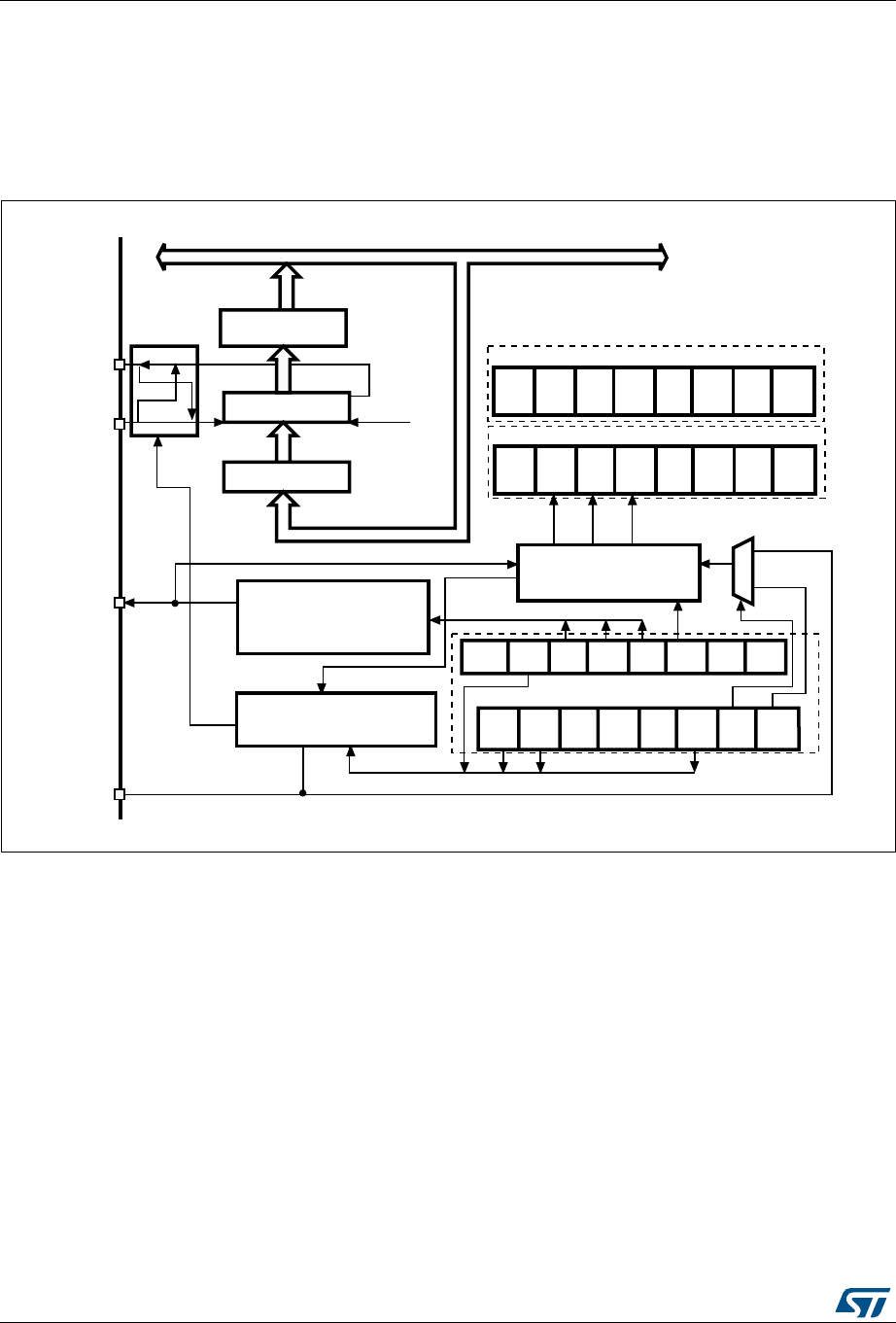
Serial peripheral interface (SPI) RM0383
552/836 DocID026448 Rev 1
20.3 SPI functional description
20.3.1 General description
The block diagram of the SPI is shown in Figure 192.
Figure 192. SPI block diagram
Usually, the SPI is connected to external devices through 4 pins:
•MISO: Master In / Slave Out data. This pin can be used to transmit data in slave mode
and receive data in master mode.
•MOSI: Master Out / Slave In data. This pin can be used to transmit data in master
mode and receive data in slave mode.
•SCK: Serial Clock output for SPI masters and input for SPI slaves.
•NSS: Slave select. This is an optional pin to select a slave device. This pin acts as a
‘chip select’ to let the SPI master communicate with slaves individually and to avoid
contention on the data lines. Slave NSS inputs can be driven by standard IO ports on
the master device. The NSS pin may also be used as an output if enabled (SSOE bit)
and driven low if the SPI is in master configuration. In this manner, all NSS pins from
devices connected to the Master NSS pin see a low level and become slaves when
they are configured in NSS hardware mode. When configured in master mode with
NSS configured as an input (MSTR=1 and SSOE=0) and if NSS is pulled low, the SPI
-/3)
-)3/
"AUDRATEGENERATOR
3#+
-ASTERCONTROLLOGIC
#OMMUNICATION
CONTROL
30% "2 "2 "2 -342 #0/, #0(!
"2;=
28.%
,3"
")$)
-/$%
")$)
/% 33- 33)
"39 /62 -/$ 28.%48%
%22
48%
$&&
33/%
#2#
%.
28
/.,9
#2#
.EXT
#2#
%22
.33
)%
&
&)234
30)?#2
30)?#2
30)?32
48$-
!%.
28$-
!%.
)%)%
!DDRESSANDDATABUS
2EAD
2XBUFFER
3HIFTREGISTER
,3"FIRST
4XBUFFER
7RITE
AI
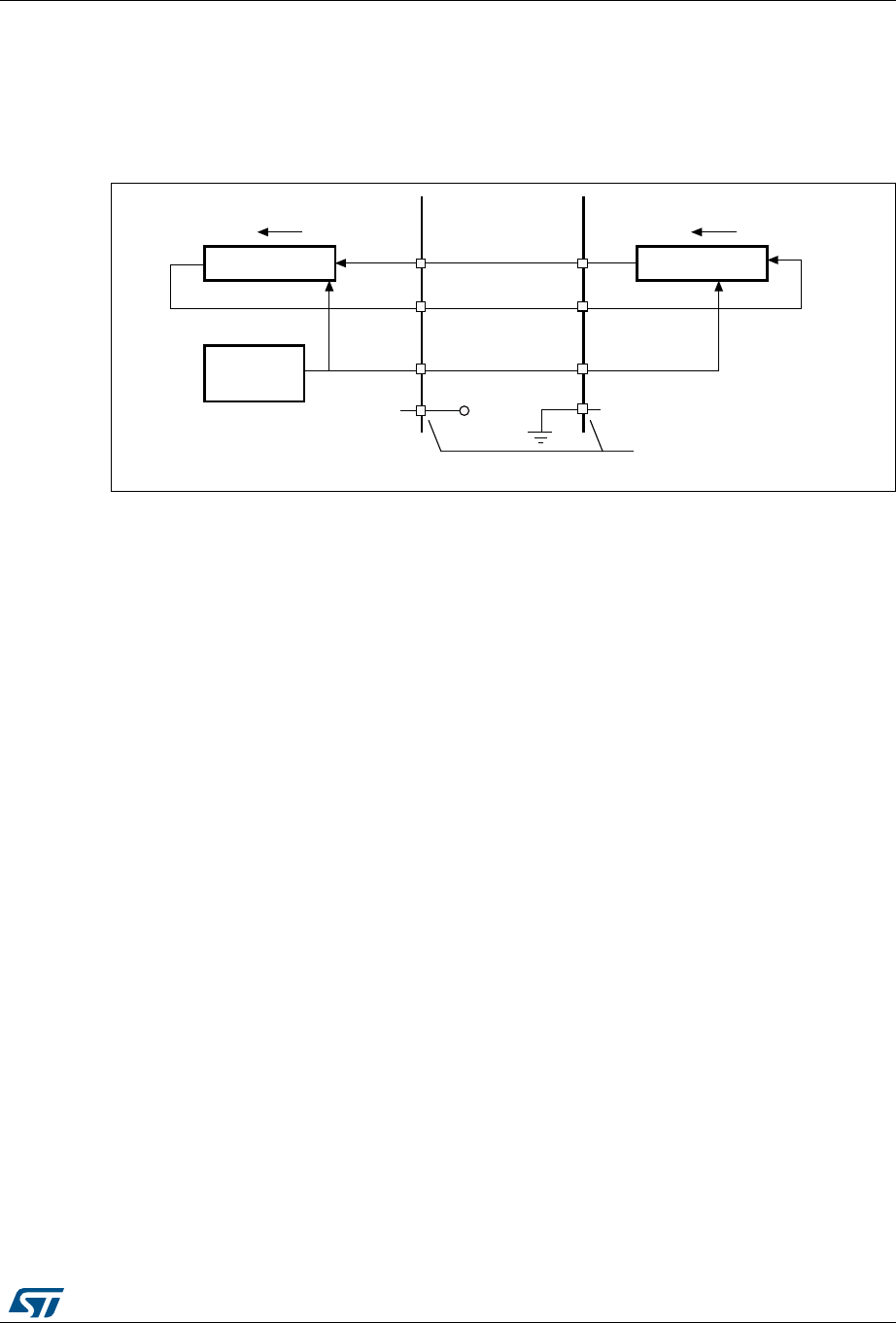
DocID026448 Rev 1 553/836
RM0383 Serial peripheral interface (SPI)
602
enters the master mode fault state: the MSTR bit is automatically cleared and the
device is configured in slave mode (refer to Section 20.3.10: Error flags on page 573).
A basic example of interconnections between a single master and a single slave is
illustrated in Figure 193.
Figure 193. Single master/ single slave application
1. Here, the NSS pin is configured as an input.
The MOSI pins are connected together and the MISO pins are connected together. In this
way data is transferred serially between master and slave (most significant bit first).
The communication is always initiated by the master. When the master device transmits
data to a slave device via the MOSI pin, the slave device responds via the MISO pin. This
implies full-duplex communication with both data out and data in synchronized with the
same clock signal (which is provided by the master device via the SCK pin).
Slave select (NSS) pin management
Hardware or software slave select management can be set using the SSM bit in the
SPI_CR1 register.
•Software NSS management (SSM = 1)
The slave select information is driven internally by the value of the SSI bit in the
SPI_CR1 register. The external NSS pin remains free for other application uses.
•Hardware NSS management (SSM = 0)
Two configurations are possible depending on the NSS output configuration (SSOE bit
in register SPI_CR2).
– NSS output enabled (SSM = 0, SSOE = 1)
This configuration is used only when the device operates in master mode. The
NSS signal is driven low when the master starts the communication and is kept
low until the SPI is disabled.
– NSS output disabled (SSM = 0, SSOE = 0)
This configuration allows multimaster capability for devices operating in master
mode. For devices set as slave, the NSS pin acts as a classical NSS input: the
slave is selected when NSS is low and deselected when NSS high.
8-bit shift register
SPI clock
generator
8-bit shift register
MISO
MOSIMOSI
MISO
SCK SCK
SlaveMaster
NSS
(1)
NSS
(1)
V
DD
MSBit LSBit MSBit LSBit
Not used if NSS is managed
by software
ai14745

Serial peripheral interface (SPI) RM0383
554/836 DocID026448 Rev 1
Clock phase and clock polarity
Four possible timing relationships may be chosen by software, using the CPOL and CPHA
bits in the SPI_CR1 register. The CPOL (clock polarity) bit controls the steady state value of
the clock when no data is being transferred. This bit affects both master and slave modes. If
CPOL is reset, the SCK pin has a low-level idle state. If CPOL is set, the SCK pin has a
high-level idle state.
If the CPHA (clock phase) bit is set, the second edge on the SCK pin (falling edge if the
CPOL bit is reset, rising edge if the CPOL bit is set) is the MSBit capture strobe. Data are
latched on the occurrence of the second clock transition. If the CPHA bit is reset, the first
edge on the SCK pin (falling edge if CPOL bit is set, rising edge if CPOL bit is reset) is the
MSBit capture strobe. Data are latched on the occurrence of the first clock transition.
The combination of the CPOL (clock polarity) and CPHA (clock phase) bits selects the data
capture clock edge.
Figure 194, shows an SPI transfer with the four combinations of the CPHA and CPOL bits.
The diagram may be interpreted as a master or slave timing diagram where the SCK pin,
the MISO pin, the MOSI pin are directly connected between the master and the slave
device.
Note: Prior to changing the CPOL/CPHA bits the SPI must be disabled by resetting the SPE bit.
Master and slave must be programmed with the same timing mode.
The idle state of SCK must correspond to the polarity selected in the SPI_CR1 register (by
pulling up SCK if CPOL=1 or pulling down SCK if CPOL=0).
The Data Frame Format (8- or 16-bit) is selected through the DFF bit in SPI_CR1 register,
and determines the data length during transmission/reception.
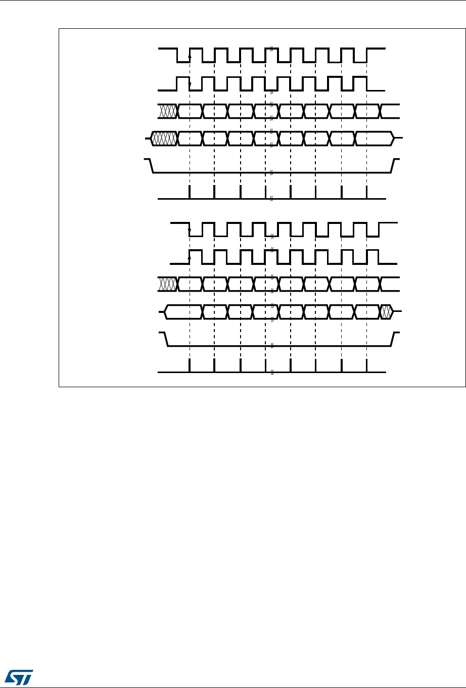
DocID026448 Rev 1 555/836
RM0383 Serial peripheral interface (SPI)
602
Figure 194. Data clock timing diagram
1. These timings are shown with the LSBFIRST bit reset in the SPI_CR1 register.
Data frame format
Data can be shifted out either MSB-first or LSB-first depending on the value of the
LSBFIRST bit in the SPI_CR1 Register.
Each data frame is 8 or 16 bits long depending on the size of the data programmed using
the DFF bit in the SPI_CR1 register. The selected data frame format is applicable for
transmission and/or reception.
20.3.2 Configuring the SPI in slave mode
In the slave configuration, the serial clock is received on the SCK pin from the master
device. The value set in the BR[2:0] bits in the SPI_CR1 register, does not affect the data
transfer rate.
Note: It is recommended to enable the SPI slave before the master sends the clock. If not,
undesired data transmission might occur. The data register of the slave needs to be ready
before the first edge of the communication clock or before the end of the ongoing
communication. It is mandatory to have the polarity of the communication clock set to the
steady state value before the slave and the master are enabled.
Follow the procedure below to configure the SPI in slave mode:
#0/,
#0/,
-3"IT ,3"IT
-3"IT ,3"IT
-)3/
-/3)
.33
TOSLAVE
#APTURESTROBE
#0(!
#0/,
#0/,
-3"IT ,3"IT
-3"IT ,3"IT
-)3/
-/3)
.33
TOSLAVE
#APTURESTROBE
#0(!
ORBITSDEPENDINGONTHE$ATAFRAMEFORMATBITSEE$&&IN30)?#2
ORBITSDEPENDINGONTHE$ATAFRAMEFORMATBITSEE$&&IN30)?#2
AIB

Serial peripheral interface (SPI) RM0383
556/836 DocID026448 Rev 1
Procedure
1. Set the DFF bit to define 8- or 16-bit data frame format
2. Select the CPOL and CPHA bits to define one of the four relationships between the
data transfer and the serial clock (see Figure 194). For correct data transfer, the CPOL
and CPHA bits must be configured in the same way in the slave device and the master
device. This step is not required when the TI mode is selected through the FRF bit in
the SPI_CR2 register.
3. The frame format (MSB-first or LSB-first depending on the value of the LSBFIRST bit in
the SPI_CR1 register) must be the same as the master device. This step is not
required when TI mode is selected.
4. In Hardware mode (refer to Slave select (NSS) pin management on page 553), the
NSS pin must be connected to a low level signal during the complete byte transmit
sequence. In NSS software mode, set the SSM bit and clear the SSI bit in the SPI_CR1
register. This step is not required when TI mode is selected.
5. Set the FRF bit in the SPI_CR2 register to select the TI mode protocol for serial
communications.
6. Clear the MSTR bit and set the SPE bit (both in the SPI_CR1 register) to assign the
pins to alternate functions.
In this configuration the MOSI pin is a data input and the MISO pin is a data output.
Transmit sequence
The data byte is parallel-loaded into the Tx buffer during a write cycle.
The transmit sequence begins when the slave device receives the clock signal and the most
significant bit of the data on its MOSI pin. The remaining bits (the 7 bits in 8-bit data frame
format, and the 15 bits in 16-bit data frame format) are loaded into the shift-register. The
TXE flag in the SPI_SR register is set on the transfer of data from the Tx Buffer to the shift
register and an interrupt is generated if the TXEIE bit in the SPI_CR2 register is set.
Receive sequence
For the receiver, when data transfer is complete:
•The Data in shift register is transferred to Rx Buffer and the RXNE flag (SPI_SR
register) is set
•An Interrupt is generated if the RXNEIE bit is set in the SPI_CR2 register.
After the last sampling clock edge the RXNE bit is set, a copy of the data byte received in
the shift register is moved to the Rx buffer. When the SPI_DR register is read, the SPI
peripheral returns this buffered value.
Clearing of the RXNE bit is performed by reading the SPI_DR register.
SPI TI protocol in slave mode
In slave mode, the SPI interface is compatible with the TI protocol. The FRF bit of the
SPI_CR2 register can be used to configure the slave SPI serial communications to be
compliant with this protocol.
The clock polarity and phase are forced to conform to the TI protocol requirements whatever
the values set in the SPI_CR1 register. NSS management is also specific to the TI protocol
which makes the configuration of NSS management through the SPI_CR1 and SPI_CR2
registers (such as SSM, SSI, SSOE) transparent for the user.
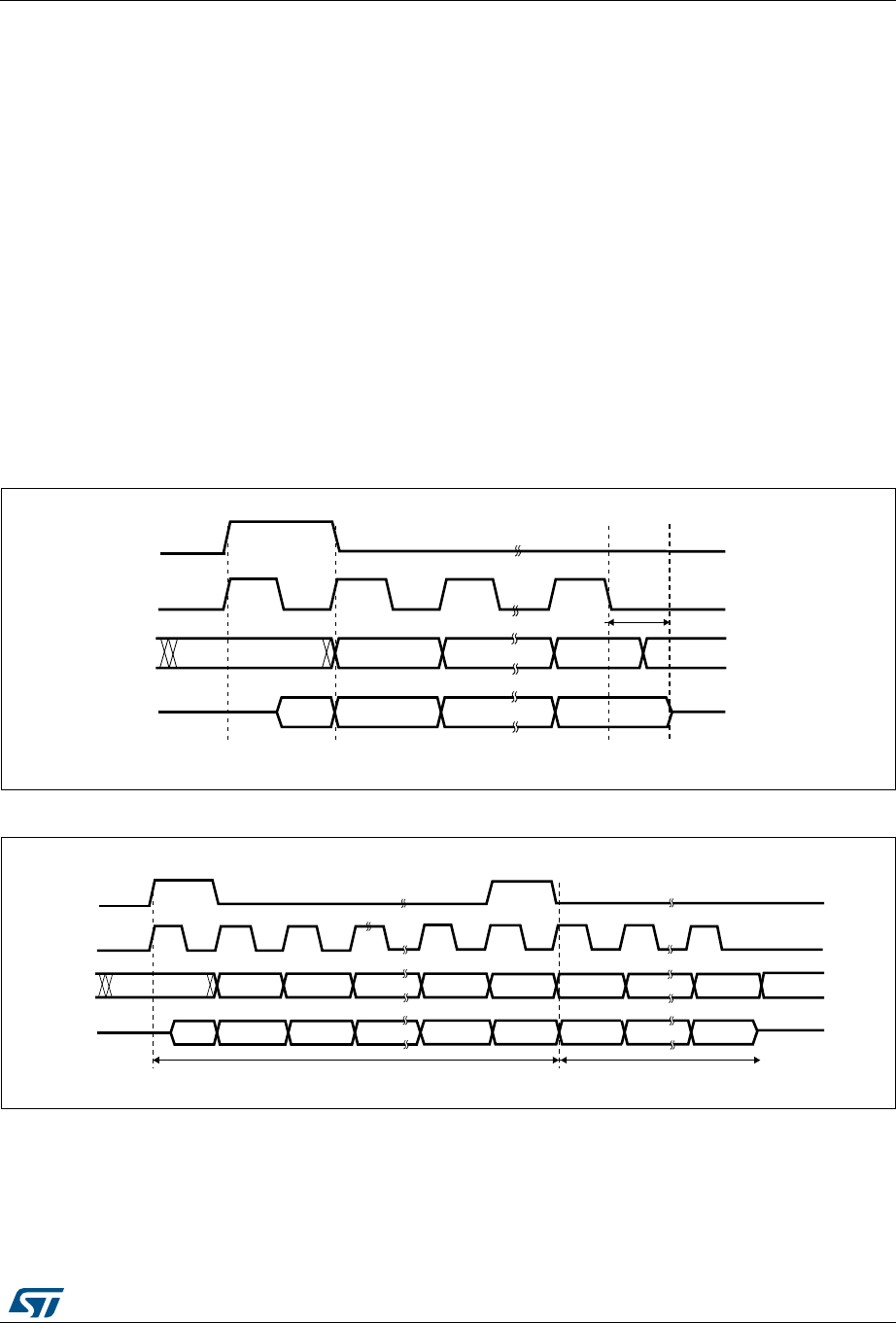
DocID026448 Rev 1 557/836
RM0383 Serial peripheral interface (SPI)
602
In Slave mode (Figure 195: TI mode - Slave mode, single transfer and Figure 196: TI mode
- Slave mode, continuous transfer), the SPI baud rate prescaler is used to control the
moment when the MISO pin state changes to HI-Z. Any baud rate can be used thus allowing
to determine this moment with optimal flexibility. However, the baud rate is generally set to
the external master clock baud rate. The time for the MISO signal to become HI-Z (trelease)
depends on internal resynchronizations and on the baud rate value set in through BR[2:0] of
SPI_CR1 register. It is given by the formula:
Note: This feature is not available for Motorola SPI communications (FRF bit set to 0).
To detect TI frame errors in Slave transmitter only mode by using the Error interrupt (ERRIE
= 1), the SPI must be configured in 2-line unidirectional mode by setting BIDIMODE and
BIDIOE to 1 in the SPI_CR1 register. When BIDIMODE is set to 0, OVR is set to 1 because
the data register is never read and error interrupt are always generated, while when
BIDIMODE is set to 1, data are not received and OVR is never set.
Figure 195. TI mode - Slave mode, single transfer
Figure 196. TI mode - Slave mode, continuous transfer
tbaud_rate
2
----------------------4t
pclk
×+trelease
tbaud_rate
2
----------------------6t
pclk
×+<<
AI
-3").
-/3)
INPUT
.33
INPUT
3#+
INPUT
TRIGGER
EDGE
SAMPLING
EDGE
TRIGGER
EDGE
SAMPLING
EDGE
TRIGGER
EDGE
SAMPLING
EDGE
$/.4#!2% ,3"). $/.4#!2%
-)3/
OUTPUT OR -3"/54 ,3"/54
T2ELEASE
AI
-3").
-/3)
INPUT
.33
INPUT
3#+
INPUT
TRIGGER SAMPLING TRIGGER SAMPLING TRIGGER SAMPLING
$/.4#!2% ,3"). $/.4#!2%
-)3/
OUTPUT OR -3"/54 ,3"/54
-3"). ,3").
-3"/54 ,3"/54
&2!-% &2!-%

Serial peripheral interface (SPI) RM0383
558/836 DocID026448 Rev 1
20.3.3 Configuring the SPI in master mode
In the master configuration, the serial clock is generated on the SCK pin.
Procedure
1. Select the BR[2:0] bits to define the serial clock baud rate (see SPI_CR1 register).
2. Select the CPOL and CPHA bits to define one of the four relationships between the
data transfer and the serial clock (see Figure 194). This step is not required when the
TI mode is selected.
3. Set the DFF bit to define 8- or 16-bit data frame format
4. Configure the LSBFIRST bit in the SPI_CR1 register to define the frame format. This
step is not required when the TI mode is selected.
5. If the NSS pin is required in input mode, in hardware mode, connect the NSS pin to a
high-level signal during the complete byte transmit sequence. In NSS software mode,
set the SSM and SSI bits in the SPI_CR1 register. If the NSS pin is required in output
mode, the SSOE bit only should be set. This step is not required when the TI mode is
selected.
6. Set the FRF bit in SPI_CR2 to select the TI protocol for serial communications.
7. The MSTR and SPE bits must be set (they remain set only if the NSS pin is connected
to a high-level signal).
In this configuration the MOSI pin is a data output and the MISO pin is a data input.
Transmit sequence
The transmit sequence begins when a byte is written in the Tx Buffer.
The data byte is parallel-loaded into the shift register (from the internal bus) during the first
bit transmission and then shifted out serially to the MOSI pin MSB first or LSB first
depending on the LSBFIRST bit in the SPI_CR1 register. The TXE flag is set on the transfer
of data from the Tx Buffer to the shift register and an interrupt is generated if the TXEIE bit in
the SPI_CR2 register is set.
Receive sequence
For the receiver, when data transfer is complete:
•The data in the shift register is transferred to the RX Buffer and the RXNE flag is set
•An interrupt is generated if the RXNEIE bit is set in the SPI_CR2 register
At the last sampling clock edge the RXNE bit is set, a copy of the data byte received in the
shift register is moved to the Rx buffer. When the SPI_DR register is read, the SPI
peripheral returns this buffered value.
Clearing the RXNE bit is performed by reading the SPI_DR register.
A continuous transmit stream can be maintained if the next data to be transmitted is put in
the Tx buffer once the transmission is started. Note that TXE flag should be ‘1 before any
attempt to write the Tx buffer is made.
Note: When a master is communicating with SPI slaves which need to be de-selected between
transmissions, the NSS pin must be configured as GPIO or another GPIO must be used and
toggled by software.
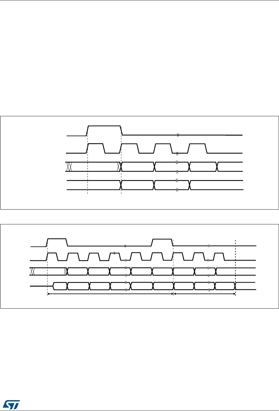
DocID026448 Rev 1 559/836
RM0383 Serial peripheral interface (SPI)
602
SPI TI protocol in master mode
In master mode, the SPI interface is compatible with the TI protocol. The FRF bit of the
SPI_CR2 register can be used to configure the master SPI serial communications to be
compliant with this protocol.
The clock polarity and phase are forced to conform to the TI protocol requirements whatever
the values set in the SPI_CR1 register. NSS management is also specific to the TI protocol
which makes the configuration of NSS management through the SPI_CR1 and SPI_CR2
registers (SSM, SSI, SSOE) transparent for the user.
Figure 197: TI mode - master mode, single transfer and Figure 198: TI mode - master mode,
continuous transfer) show the SPI master communication waveforms when the TI mode is
selected in master mode.
Figure 197. TI mode - master mode, single transfer
Figure 198. TI mode - master mode, continuous transfer
AI
-3").
-/3)
INPUT
.33
OUTPUT
3#+
OUTPUT
TRIGGER
EDGE
SAMPLING
EDGE
TRIGGER
EDGE
SAMPLING
EDGE
TRIGGER
EDGE
SAMPLING
EDGE
$/.4#!2% ,3"). $/.4#!2%
-)3/
OUTPUT OR -3"/54 ,3"/54
AI
-3"/54
-/3)
OUTPUT
.33
OUTPUT
3#+
OUTPUT
TRIGGER SAMPLING TRIGGER SAMPLING TRIGGER SAMPLING
$/.4#!2% ,3"/54
$/.4#!2%
-)3/
INTPUT OR -3"). ,3").
-3"/54 ,3"/54
-3"). ,3").
&2!-% &2!-%

Serial peripheral interface (SPI) RM0383
560/836 DocID026448 Rev 1
20.3.4 Configuring the SPI for half-duplex communication
The SPI is capable of operating in half-duplex mode in 2 configurations.
•1 clock and 1 bidirectional data wire
•1 clock and 1 data wire (receive-only or transmit-only)
1 clock and 1 bidirectional data wire (BIDIMODE=1)
This mode is enabled by setting the BIDIMODE bit in the SPI_CR1 register. In this mode
SCK is used for the clock and MOSI in master or MISO in slave mode is used for data
communication. The transfer direction (Input/Output) is selected by the BIDIOE bit in the
SPI_CR1 register. When this bit is 1, the data line is output otherwise it is input.
1 clock and 1 unidirectional data wire (BIDIMODE=0)
In this mode, the application can use the SPI either in transmit-only mode or in receive-only
mode.
•Transmit-only mode is similar to full-duplex mode (BIDIMODE=0, RXONLY=0): the
data are transmitted on the transmit pin (MOSI in master mode or MISO in slave mode)
and the receive pin (MISO in master mode or MOSI in slave mode) can be used as a
general-purpose IO. In this case, the application just needs to ignore the Rx buffer (if
the data register is read, it does not contain the received value).
•In receive-only mode, the application can disable the SPI output function by setting the
RXONLY bit in the SPI_CR2 register. In this case, it frees the transmit IO pin (MOSI in
master mode or MISO in slave mode), so it can be used for other purposes.
To start the communication in receive-only mode, configure and enable the SPI:
•In master mode, the communication starts immediately and stops when the SPE bit is
cleared and the current reception stops. There is no need to read the BSY flag in this
mode. It is always set when an SPI communication is ongoing.
•In slave mode, the SPI continues to receive as long as the NSS is pulled down (or the
SSI bit is cleared in NSS software mode) and the SCK is running.
20.3.5 Data transmission and reception procedures
Rx and Tx buffers
In reception, data are received and then stored into an internal Rx buffer while In
transmission, data are first stored into an internal Tx buffer before being transmitted.
A read access of the SPI_DR register returns the Rx buffered value whereas a write access
to the SPI_DR stores the written data into the Tx buffer.

DocID026448 Rev 1 561/836
RM0383 Serial peripheral interface (SPI)
602
Start sequence in master mode
•In full-duplex (BIDIMODE=0 and RXONLY=0)
– The sequence begins when data are written into the SPI_DR register (Tx buffer).
– The data are then parallel loaded from the Tx buffer into the 8-bit shift register
during the first bit transmission and then shifted out serially to the MOSI pin.
– At the same time, the received data on the MISO pin is shifted in serially to the 8-
bit shift register and then parallel loaded into the SPI_DR register (Rx buffer).
•In unidirectional receive-only mode (BIDIMODE=0 and RXONLY=1)
– The sequence begins as soon as SPE=1
– Only the receiver is activated and the received data on the MISO pin are shifted in
serially to the 8-bit shift register and then parallel loaded into the SPI_DR register
(Rx buffer).
•In bidirectional mode, when transmitting (BIDIMODE=1 and BIDIOE=1)
– The sequence begins when data are written into the SPI_DR register (Tx buffer).
– The data are then parallel loaded from the Tx buffer into the 8-bit shift register
during the first bit transmission and then shifted out serially to the MOSI pin.
– No data are received.
•In bidirectional mode, when receiving (BIDIMODE=1 and BIDIOE=0)
– The sequence begins as soon as SPE=1 and BIDIOE=0.
– The received data on the MOSI pin are shifted in serially to the 8-bit shift register
and then parallel loaded into the SPI_DR register (Rx buffer).
– The transmitter is not activated and no data are shifted out serially to the MOSI
pin.
Start sequence in slave mode
•In full-duplex mode (BIDIMODE=0 and RXONLY=0)
– The sequence begins when the slave device receives the clock signal and the first
bit of the data on its MOSI pin. The 7 remaining bits are loaded into the shift
register.
– At the same time, the data are parallel loaded from the Tx buffer into the 8-bit shift
register during the first bit transmission, and then shifted out serially to the MISO
pin. The software must have written the data to be sent before the SPI master
device initiates the transfer.
•In unidirectional receive-only mode (BIDIMODE=0 and RXONLY=1)
– The sequence begins when the slave device receives the clock signal and the first
bit of the data on its MOSI pin. The 7 remaining bits are loaded into the shift
register.
– The transmitter is not activated and no data are shifted out serially to the MISO
pin.
•In bidirectional mode, when transmitting (BIDIMODE=1 and BIDIOE=1)
– The sequence begins when the slave device receives the clock signal and the first
bit in the Tx buffer is transmitted on the MISO pin.
– The data are then parallel loaded from the Tx buffer into the 8-bit shift register
during the first bit transmission and then shifted out serially to the MISO pin. The

Serial peripheral interface (SPI) RM0383
562/836 DocID026448 Rev 1
software must have written the data to be sent before the SPI master device
initiates the transfer.
– No data are received.
•In bidirectional mode, when receiving (BIDIMODE=1 and BIDIOE=0)
– The sequence begins when the slave device receives the clock signal and the first
bit of the data on its MISO pin.
– The received data on the MISO pin are shifted in serially to the 8-bit shift register
and then parallel loaded into the SPI_DR register (Rx buffer).
– The transmitter is not activated and no data are shifted out serially to the MISO
pin.
Handling data transmission and reception
The TXE flag (Tx buffer empty) is set when the data are transferred from the Tx buffer to the
shift register. It indicates that the internal Tx buffer is ready to be loaded with the next data.
An interrupt can be generated if the TXEIE bit in the SPI_CR2 register is set. Clearing the
TXE bit is performed by writing to the SPI_DR register.
Note: The software must ensure that the TXE flag is set to 1 before attempting to write to the Tx
buffer. Otherwise, it overwrites the data previously written to the Tx buffer.
The RXNE flag (Rx buffer not empty) is set on the last sampling clock edge, when the data
are transferred from the shift register to the Rx buffer. It indicates that data are ready to be
read from the SPI_DR register. An interrupt can be generated if the RXNEIE bit in the
SPI_CR2 register is set. Clearing the RXNE bit is performed by reading the SPI_DR
register.
For some configurations, the BSY flag can be used during the last data transfer to wait until
the completion of the transfer.
Full-duplex transmit and receive procedure in master or slave mode (BIDIMODE=0 and
RXONLY=0)
The software has to follow this procedure to transmit and receive data (see Figure 199 and
Figure 200):
1. Enable the SPI by setting the SPE bit to 1.
2. Write the first data item to be transmitted into the SPI_DR register (this clears the TXE
flag).
3. Wait until TXE=1 and write the second data item to be transmitted. Then wait until
RXNE=1 and read the SPI_DR to get the first received data item (this clears the RXNE
bit). Repeat this operation for each data item to be transmitted/received until the n–1
received data.
4. Wait until RXNE=1 and read the last received data.
5. Wait until TXE=1 and then wait until BSY=0 before disabling the SPI.
This procedure can also be implemented using dedicated interrupt subroutines launched at
each rising edges of the RXNE or TXE flag.
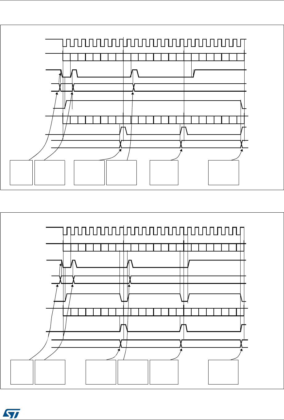
DocID026448 Rev 1 563/836
RM0383 Serial peripheral interface (SPI)
602
Figure 199. TXE/RXNE/BSY behavior in Master / full-duplex mode (BIDIMODE=0 and
RXONLY=0) in the case of continuous transfers
Figure 200. TXE/RXNE/BSY behavior in Slave / full-duplex mode (BIDIMODE=0,
RXONLY=0) in the case of continuous transfers
MISO/MOSI (in)
Tx buffer
DATA1 = 0xA1
TXE flag
0xF2
BSY flag
0xF3
software
writes 0xF1
into SPI_DR
software waits
until TXE=1 and
writes 0xF2 into
SPI_DR
software waits
until RXNE=1
and reads 0xA1
from SPI_DR
set by hardware
cleared by software
set by hardware
cleared by software set by hardware
set by hardware
SCK
DATA 2 = 0xA2 DATA 3 = 0xA3
reset by hardware
Example in Master mode with CPOL=1, CPHA=1
0xF1
RXNE flag
(write SPI_DR)
Rx buffer
set by hardware
MISO/MOSI (out)
DATA1 = 0xF1 DATA2 = 0xF2 DATA3 = 0xF3
(read SPI_DR) 0xA1 0xA2 0xA3
software waits
until TXE=1 and
writes 0xF3 into
SPI_DR
software waits
until RXNE=1
and reads 0xA2
from SPI_ DR
software waits
until RXNE=1
and reads 0xA3
from SPI_DR
b0b1b2b3 b4b5b6b7b0b1b2b3 b4b5b6b7b0b1b2b3 b4b5b6b7
b0b1b2b3 b4b5b6b7b0b1b2b3 b4b5b6b7b0b1b2b3 b4b5b6b7
cleared by software
ai17343
0xF1
set by cleared by software
MISO/MOSI (in)
Tx buffer
DATA 1 = 0xA1
TXE flag
0xF2
BSY flag
0xF3
software
writes 0xF1
into SPI_DR
software waits
until TXE=1 and
writes 0xF2 into
SPI_DR
software waits
until RXNE=1
and reads 0xA1
from SPI_DR
set by hardware
cleared by software
set by hardware
cleared by software set by hardware
SCK
DATA 2 = 0xA2 DATA 3 = 0xA3
reset by hardware
Example in Slave mode with CPOL=1, CPHA=1
RXNE flag
(write to SPI_DR)
Rx buffer
set by hardware
MISO/MOSI (out)
DATA 1 = 0xF1 DATA 2 = 0xF2 DATA 3 = 0xF3
(read from SPI_DR) 0xA1 0xA2 0xA3
software waits
until TXE=1 and
writes 0xF3 into
SPI_DR
software waits
until RXNE=1
and reads 0xA2
from SPI_ DR
software waits
until RXNE=1
and reads 0xA3
from SPI_DR
b0b1b2b3 b4b5b6b7b0b1b2b3 b4b5b6b7b0b1b2b3 b4b5b6b7
b0b1b2b3 b4b5b6b7b0b1b2b3 b4b5b6b7b0b1b2b3 b4b5b6b7
cleared by software
ai17344
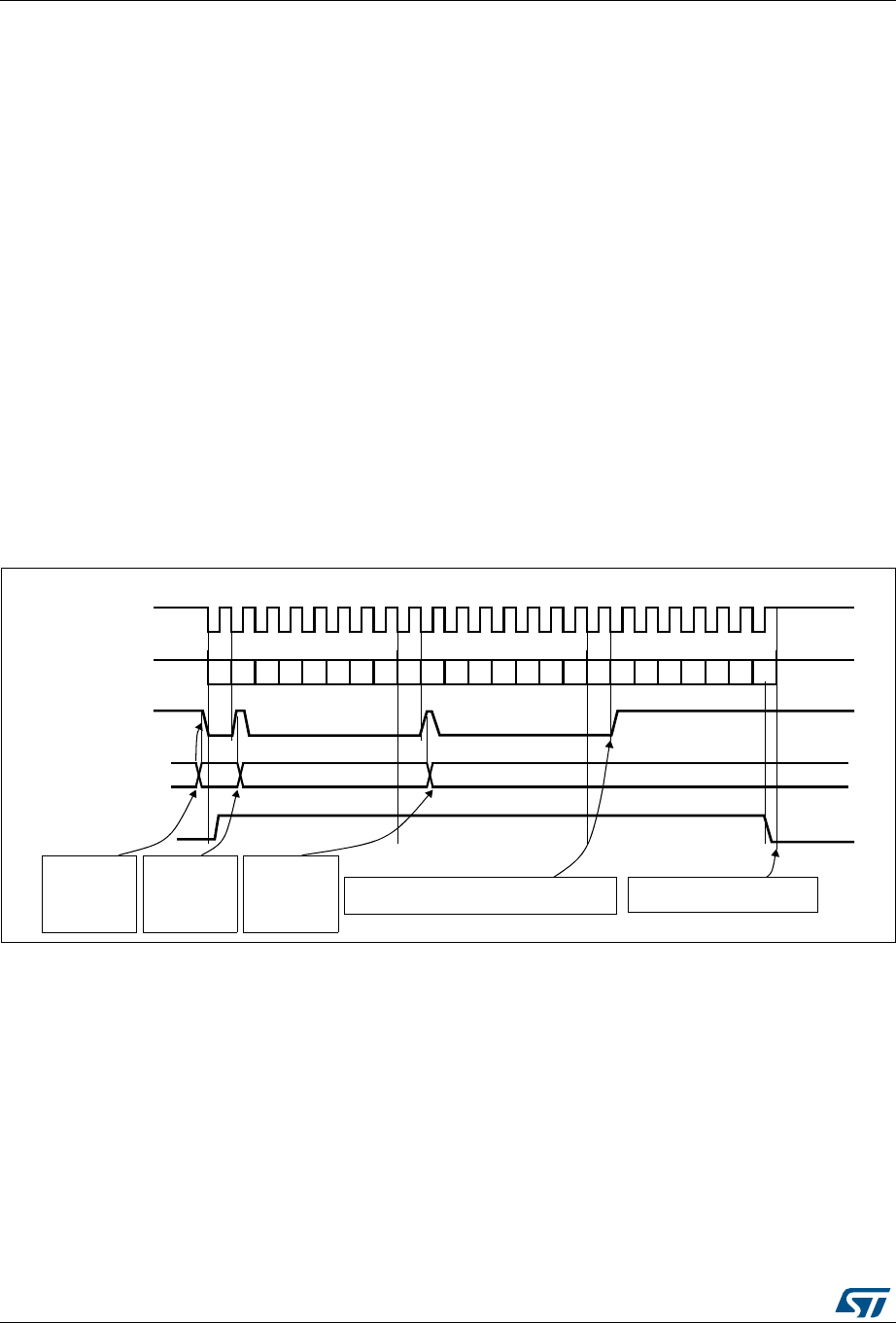
Serial peripheral interface (SPI) RM0383
564/836 DocID026448 Rev 1
Transmit-only procedure (BIDIMODE=0 RXONLY=0)
In this mode, the procedure can be reduced as described below and the BSY bit can be
used to wait until the completion of the transmission (see Figure 201 and Figure 202).
1. Enable the SPI by setting the SPE bit to 1.
2. Write the first data item to send into the SPI_DR register (this clears the TXE bit).
3. Wait until TXE=1 and write the next data item to be transmitted. Repeat this step for
each data item to be transmitted.
4. After writing the last data item into the SPI_DR register, wait until TXE=1, then wait until
BSY=0, this indicates that the transmission of the last data is complete.
This procedure can be also implemented using dedicated interrupt subroutines launched at
each rising edge of the TXE flag.
Note: During discontinuous communications, there is a 2 APB clock period delay between the
write operation to SPI_DR and the BSY bit setting. As a consequence, in transmit-only
mode, it is mandatory to wait first until TXE is set and then until BSY is cleared after writing
the last data.
After transmitting two data items in transmit-only mode, the OVR flag is set in the SPI_SR
register since the received data are never read.
Figure 201. TXE/BSY behavior in Master transmit-only mode (BIDIMODE=0 and RXONLY=0) in
case of continuous transfers
0xF1
Tx buffer
TXE flag
0xF2
BSY flag
0xF3
software writes
0xF1 into
SPI_DR
software waits
until TXE=1 and
writes 0xF2 into
SPI_DR
set by hardware
cleared by software
set by hardware
cleared by software set by hardware
set by hardware
SCK
reset by hardware
Example in Master mode with CPOL=1, CPHA=1
(write to SPI_DR)
MISO/MOSI (out)
DATA 1 = 0xF1 DATA 2 = 0xF2 DATA 3 = 0xF3
software waits
until TXE=1 and
writes 0xF3 into
SPI_DR
software waits until BSY=0software waits until TXE=1
b0b1b2b3 b4b5b6b7b0b1b2b3 b4b5b6b7b0b1b2b3 b4b5b6b7
ai17345
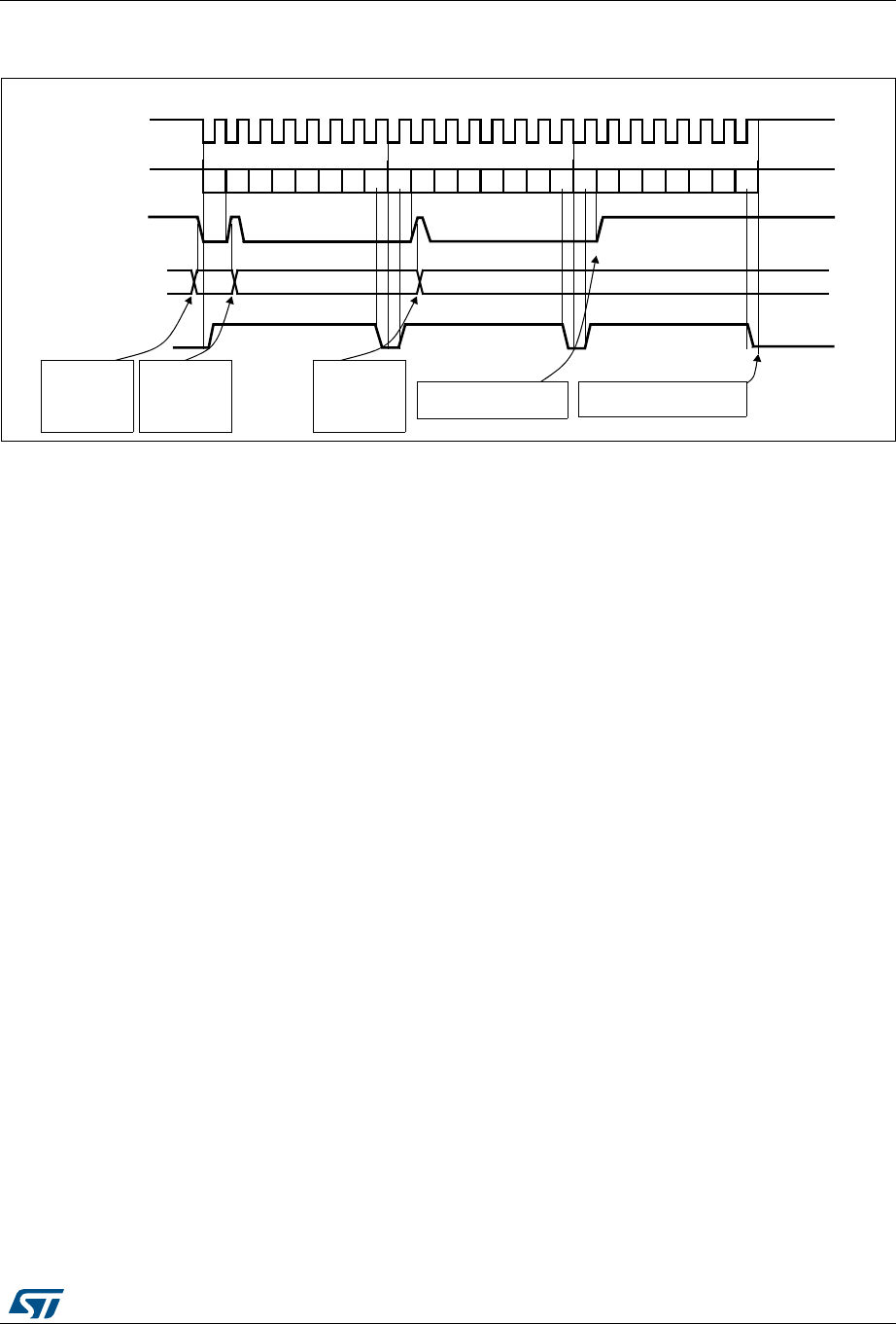
DocID026448 Rev 1 565/836
RM0383 Serial peripheral interface (SPI)
602
Figure 202. TXE/BSY in Slave transmit-only mode (BIDIMODE=0 and RXONLY=0) in the case of
continuous transfers
Bidirectional transmit procedure (BIDIMODE=1 and BIDIOE=1)
In this mode, the procedure is similar to the procedure in Transmit-only mode except that
the BIDIMODE and BIDIOE bits both have to be set in the SPI_CR2 register before enabling
the SPI.
Unidirectional receive-only procedure (BIDIMODE=0 and RXONLY=1)
In this mode, the procedure can be reduced as described below (see Figure 203):
1. Set the RXONLY bit in the SPI_CR2 register.
2. Enable the SPI by setting the SPE bit to 1:
a) In master mode, this immediately activates the generation of the SCK clock, and
data are serially received until the SPI is disabled (SPE=0).
b) In slave mode, data are received when the SPI master device drives NSS low and
generates the SCK clock.
3. Wait until RXNE=1 and read the SPI_DR register to get the received data (this clears
the RXNE bit). Repeat this operation for each data item to be received.
This procedure can also be implemented using dedicated interrupt subroutines launched at
each rising edge of the RXNE flag.
Note: If it is required to disable the SPI after the last transfer, follow the recommendation
described in Section 20.3.8: Disabling the SPI on page 570.
0xF1
Tx buffer
TXE flag
0xF2
BSY flag
0xF3
software writes
0xF1 into
SPI_DR
software waits
until TXE=1 and
writes 0xF2 into
SPI_DR
set by hardware
cleared by software
set by hardware
cleared by software set by hardware
set by hardware
SCK
reset by hardware
Example in slave mode with CPOL=1, CPHA=1
(write to SPI_DR)
MISO/MOSI (out)
DATA 1 = 0xF1 DATA 2 = 0xF2 DATA 3 = 0xF3
software waits
until TXE=1 and
writes 0xF3 into
SPI_DR
software waits until BSY=0software waits until TXE=1
b0b1b2b3 b4b5b6b7b0b1b2b3 b4b5b6b7b0b1b2b3 b4b5b6b7
ai17346
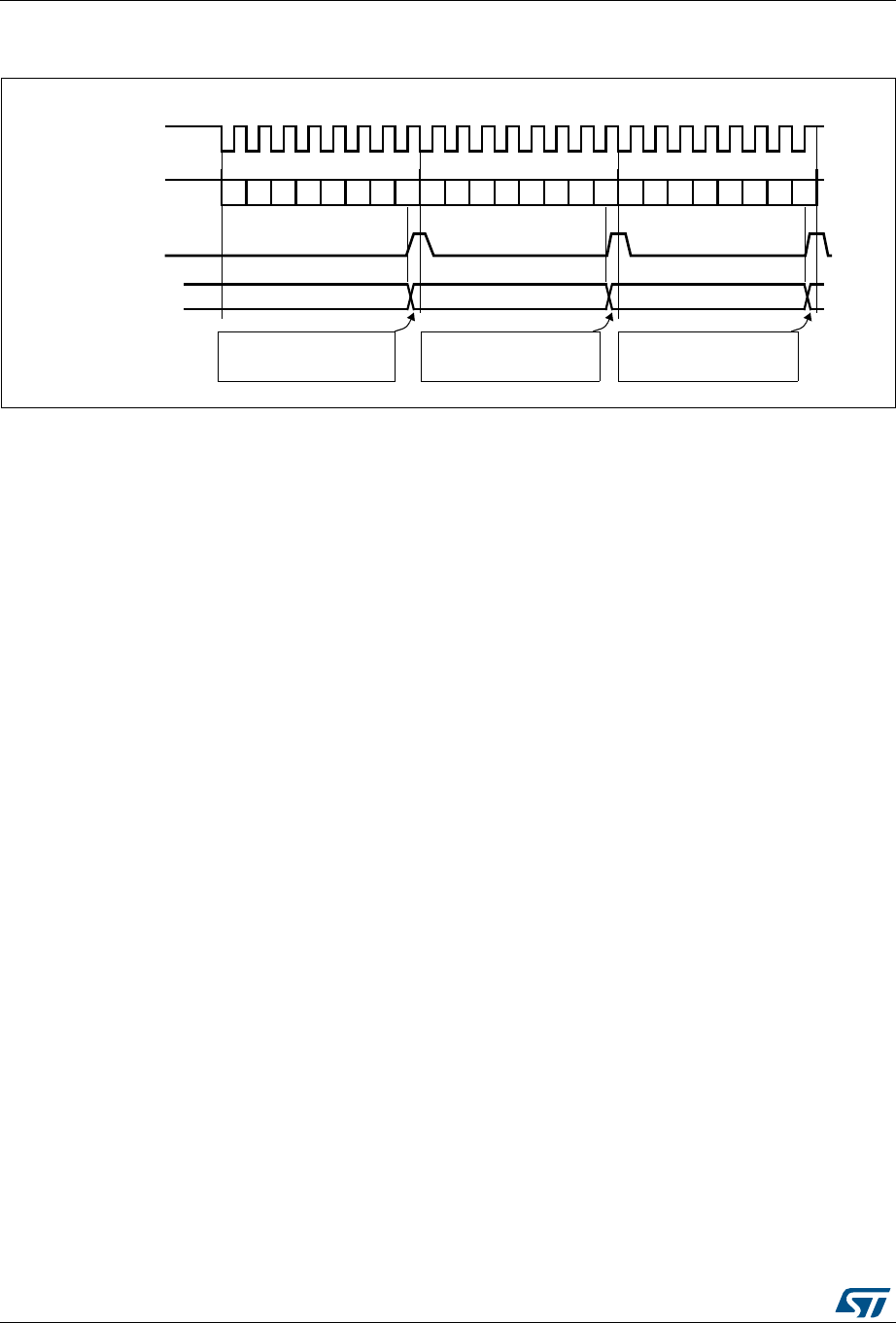
Serial peripheral interface (SPI) RM0383
566/836 DocID026448 Rev 1
Figure 203. RXNE behavior in receive-only mode (BIDIRMODE=0 and RXONLY=1) in the case of
continuous transfers
Bidirectional receive procedure (BIDIMODE=1 and BIDIOE=0)
In this mode, the procedure is similar to the Receive-only mode procedure except that the
BIDIMODE bit has to be set and the BIDIOE bit cleared in the SPI_CR2 register before
enabling the SPI.
Continuous and discontinuous transfers
When transmitting data in master mode, if the software is fast enough to detect each rising
edge of TXE (or TXE interrupt) and to immediately write to the SPI_DR register before the
ongoing data transfer is complete, the communication is said to be continuous. In this case,
there is no discontinuity in the generation of the SPI clock between each data item and the
BSY bit is never cleared between each data transfer.
On the contrary, if the software is not fast enough, this can lead to some discontinuities in
the communication. In this case, the BSY bit is cleared between each data transmission
(see Figure 204).
In Master receive-only mode (RXONLY=1), the communication is always continuous and
the BSY flag is always read at 1.
In slave mode, the continuity of the communication is decided by the SPI master device. In
any case, even if the communication is continuous, the BSY flag goes low between each
transfer for a minimum duration of one SPI clock cycle (see Figure 202).
MISO/MOSI (in)
DATA 1 = 0xA1
software waits until RXNE=1
and reads 0xA1 from SPI_DR
SCK
DATA 2 = 0xA2 DATA 3 = 0xA3
Example with CPOL=1, CPHA=1, RXONLY=1
RXNE flag
Rx buffer
set by hardware
(read from SPI_DR) 0xA1 0xA2 0xA3
software waits until RXNE=1
and reads 0xA2 from SPI_DR
software waits until RXNE=1
and reads 0xA3 from SPI_DR
b0b1b2b3 b4b5b6b7b0b1b2b3 b4b5b6b7b0b1b2b3 b4b5b6b7
cleared by software
ai17347
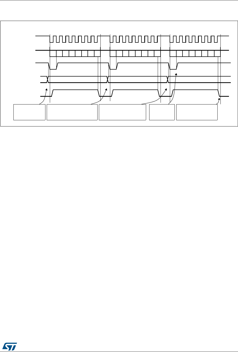
DocID026448 Rev 1 567/836
RM0383 Serial peripheral interface (SPI)
602
Figure 204. TXE/BSY behavior when transmitting (BIDIRMODE=0 and RXONLY=0) in the case of
discontinuous transfers
20.3.6 CRC calculation
A CRC calculator has been implemented for communication reliability. Separate CRC
calculators are implemented for transmitted data and received data. The CRC is calculated
using a programmable polynomial serially on each bit. It is calculated on the sampling clock
edge defined by the CPHA and CPOL bits in the SPI_CR1 register.
Note: This SPI offers two kinds of CRC calculation standard which depend directly on the data
frame format selected for the transmission and/or reception: 8-bit data (CR8) and 16-bit data
(CRC16).
CRC calculation is enabled by setting the CRCEN bit in the SPI_CR1 register. This action
resets the CRC registers (SPI_RXCRCR and SPI_TXCRCR). In full duplex or transmitter
only mode, when the transfers are managed by the software (CPU mode), it is necessary to
write the bit CRCNEXT immediately after the last data to be transferred is written to the
SPI_DR. At the end of this last data transfer, the SPI_TXCRCR value is transmitted.
In receive only mode and when the transfers are managed by software (CPU mode), it is
necessary to write the CRCNEXT bit after the second last data has been received. The CRC
is received just after the last data reception and the CRC check is then performed.
At the end of data and CRC transfers, the CRCERR flag in the SPI_SR register is set if
corruption occurs during the transfer.
If data are present in the TX buffer, the CRC value is transmitted only after the transmission
of the data byte. During CRC transmission, the CRC calculator is switched off and the
register value remains unchanged.
SPI communication using the CRC is possible through the following procedure:
MOSI (out)
Tx buffer
DATA 1 = 0xF1
TXE flag
0xF1
BSY flag
0xF2
software writes 0xF1
into SPI_DR
software waits until TXE=1 but is
late to write 0xF2 into SPI_DR
software waits until TXE=1 but
is late to write 0xF3 into
SPI_DR
SCK
3Fx0 = 3 ATAD2Fx0 = 2 ATAD
Example with CPOL=1, CPHA=1
0xF3
software waits
until TXE=1
software waits until BSY=0
(write to SPI_DR)
b0b1b2b3 b4b5b6b7b0b1b2b3 b4b5b6b7b0b1b2b3 b4b5b6b7
ai17348

Serial peripheral interface (SPI) RM0383
568/836 DocID026448 Rev 1
1. Program the CPOL, CPHA, LSBFirst, BR, SSM, SSI and MSTR values.
2. Program the polynomial in the SPI_CRCPR register.
3. Enable the CRC calculation by setting the CRCEN bit in the SPI_CR1 register. This
also clears the SPI_RXCRCR and SPI_TXCRCR registers.
4. Enable the SPI by setting the SPE bit in the SPI_CR1 register.
5. Start the communication and sustain the communication until all but one byte or half-
word have been transmitted or received.
– In full duplex or transmitter-only mode, when the transfers are managed by
software, when writing the last byte or half word to the Tx buffer, set the
CRCNEXT bit in the SPI_CR1 register to indicate that the CRC will be transmitted
after the transmission of the last byte.
– In receiver only mode, set the bit CRCNEXT just after the reception of the second
to last data to prepare the SPI to enter in CRC Phase at the end of the reception of
the last data. CRC calculation is frozen during the CRC transfer.
6. After the transfer of the last byte or half word, the SPI enters the CRC transfer and
check phase. In full duplex mode or receiver-only mode, the received CRC is
compared to the SPI_RXCRCR value. If the value does not match, the CRCERR flag in
SPI_SR is set and an interrupt can be generated when the ERRIE bit in the SPI_CR2
register is set.
Note: When the SPI is in slave mode, be careful to enable CRC calculation only when the clock is
stable, that is, when the clock is in the steady state. If not, a wrong CRC calculation may be
done. In fact, the CRC is sensitive to the SCK slave input clock as soon as CRCEN is set,
and this, whatever the value of the SPE bit.
With high bitrate frequencies, be careful when transmitting the CRC. As the number of used
CPU cycles has to be as low as possible in the CRC transfer phase, it is forbidden to call
software functions in the CRC transmission sequence to avoid errors in the last data and
CRC reception. In fact, CRCNEXT bit has to be written before the end of the
transmission/reception of the last data.
For high bit rate frequencies, it is advised to use the DMA mode to avoid the degradation of
the SPI speed performance due to CPU accesses impacting the SPI bandwidth.
When the devices are configured as slaves and the NSS hardware mode is used, the NSS
pin needs to be kept low between the data phase and the CRC phase.
When the SPI is configured in slave mode with the CRC feature enabled, CRC calculation
takes place even if a high level is applied on the NSS pin. This may happen for example in
case of a multislave environment where the communication master addresses slaves
alternately.
Between a slave deselection (high level on NSS) and a new slave selection (low level on
NSS), the CRC value should be cleared on both master and slave sides in order to
resynchronize the master and slave for their respective CRC calculation.
To clear the CRC, follow the procedure below:
1. Disable SPI (SPE = 0)
2. Clear the CRCEN bit
3. Set the CRCEN bit
4. Enable the SPI (SPE = 1)

DocID026448 Rev 1 569/836
RM0383 Serial peripheral interface (SPI)
602
20.3.7 Status flags
Four status flags are provided for the application to completely monitor the state of the SPI
bus.
Tx buffer empty flag (TXE)
When it is set, this flag indicates that the Tx buffer is empty and the next data to be
transmitted can be loaded into the buffer. The TXE flag is cleared when writing to the
SPI_DR register.
Rx buffer not empty (RXNE)
When set, this flag indicates that there are valid received data in the Rx buffer. It is cleared
when SPI_DR is read.
BUSY flag
This BSY flag is set and cleared by hardware (writing to this flag has no effect). The BSY
flag indicates the state of the communication layer of the SPI.
When BSY is set, it indicates that the SPI is busy communicating. There is one exception in
master mode / bidirectional receive mode (MSTR=1 and BDM=1 and BDOE=0) where the
BSY flag is kept low during reception.
The BSY flag is useful to detect the end of a transfer if the software wants to disable the SPI
and enter Halt mode (or disable the peripheral clock). This avoids corrupting the last
transfer. For this, the procedure described below must be strictly respected.
The BSY flag is also useful to avoid write collisions in a multimaster system.
The BSY flag is set when a transfer starts, with the exception of master mode / bidirectional
receive mode (MSTR=1 and BDM=1 and BDOE=0).
It is cleared:
•when a transfer is finished (except in master mode if the communication is continuous)
•when the SPI is disabled
•when a master mode fault occurs (MODF=1)
When communication is not continuous, the BSY flag is low between each communication.
When communication is continuous:
•in master mode, the BSY flag is kept high during all the transfers
•in slave mode, the BSY flag goes low for one SPI clock cycle between each transfer
Note: Do not use the BSY flag to handle each data transmission or reception. It is better to use the
TXE and RXNE flags instead.

Serial peripheral interface (SPI) RM0383
570/836 DocID026448 Rev 1
20.3.8 Disabling the SPI
When a transfer is terminated, the application can stop the communication by disabling the
SPI peripheral. This is done by clearing the SPE bit.
For some configurations, disabling the SPI and entering the Halt mode while a transfer is
ongoing can cause the current transfer to be corrupted and/or the BSY flag might become
unreliable.
To avoid any of those effects, it is recommended to respect the following procedure when
disabling the SPI:
In master or slave full-duplex mode (BIDIMODE=0, RXONLY=0)
1. Wait until RXNE=1 to receive the last data
2. Wait until TXE=1
3. Then wait until BSY=0
4. Disable the SPI (SPE=0) and, eventually, enter the Halt mode (or disable the peripheral
clock)
In master or slave unidirectional transmit-only mode (BIDIMODE=0,
RXONLY=0) or bidirectional transmit mode (BIDIMODE=1, BIDIOE=1)
After the last data is written into the SPI_DR register:
1. Wait until TXE=1
2. Then wait until BSY=0
3. Disable the SPI (SPE=0) and, eventually, enter the Halt mode (or disable the peripheral
clock)
In master unidirectional receive-only mode (MSTR=1, BIDIMODE=0,
RXONLY=1) or bidirectional receive mode (MSTR=1, BIDIMODE=1, BIDIOE=0)
This case must be managed in a particular way to ensure that the SPI does not initiate a
new transfer. The sequence below is valid only for SPI Motorola configuration (FRF bit set to
0):
1. Wait for the second to last occurrence of RXNE=1 (n–1)
2. Then wait for one SPI clock cycle (using a software loop) before disabling the SPI
(SPE=0)
3. Then wait for the last RXNE=1 before entering the Halt mode (or disabling the
peripheral clock)
When the SPI is configured in TI mode (Bit FRF set to 1), the following procedure has to be
respected to avoid generating an undesired pulse on NSS when the SPI is disabled:
1. Wait for the second to last occurrence of RXNE = 1 (n-1).
2. Disable the SPI (SPE = 0) in the following window frame using a software loop:
– After at least one SPI clock cycle,
– Before the beginning of the LSB data transfer.
Note: In master bidirectional receive mode (MSTR=1 and BDM=1 and BDOE=0), the BSY flag is
kept low during transfers.

DocID026448 Rev 1 571/836
RM0383 Serial peripheral interface (SPI)
602
In slave receive-only mode (MSTR=0, BIDIMODE=0, RXONLY=1) or
bidirectional receive mode (MSTR=0, BIDIMODE=1, BIDOE=0)
1. You can disable the SPI (write SPE=1) at any time: the current transfer will complete
before the SPI is effectively disabled
2. Then, if you want to enter the Halt mode, you must first wait until BSY = 0 before
entering the Halt mode (or disabling the peripheral clock).
20.3.9 SPI communication using DMA (direct memory addressing)
To operate at its maximum speed, the SPI needs to be fed with the data for transmission
and the data received on the Rx buffer should be read to avoid overrun. To facilitate the
transfers, the SPI features a DMA capability implementing a simple request/acknowledge
protocol.
A DMA access is requested when the enable bit in the SPI_CR2 register is enabled.
Separate requests must be issued to the Tx and Rx buffers (see Figure 205 and
Figure 206):
•In transmission, a DMA request is issued each time TXE is set to 1. The DMA then
writes to the SPI_DR register (this clears the TXE flag).
•In reception, a DMA request is issued each time RXNE is set to 1. The DMA then reads
the SPI_DR register (this clears the RXNE flag).
When the SPI is used only to transmit data, it is possible to enable only the SPI Tx DMA
channel. In this case, the OVR flag is set because the data received are not read.
When the SPI is used only to receive data, it is possible to enable only the SPI Rx DMA
channel.
In transmission mode, when the DMA has written all the data to be transmitted (flag TCIF is
set in the DMA_ISR register), the BSY flag can be monitored to ensure that the SPI
communication is complete. This is required to avoid corrupting the last transmission before
disabling the SPI or entering the Stop mode. The software must first wait until TXE=1 and
then until BSY=0.
Note: During discontinuous communications, there is a 2 APB clock period delay between the
write operation to SPI_DR and the BSY bit setting. As a consequence, it is mandatory to
wait first until TXE=1 and then until BSY=0 after writing the last data.
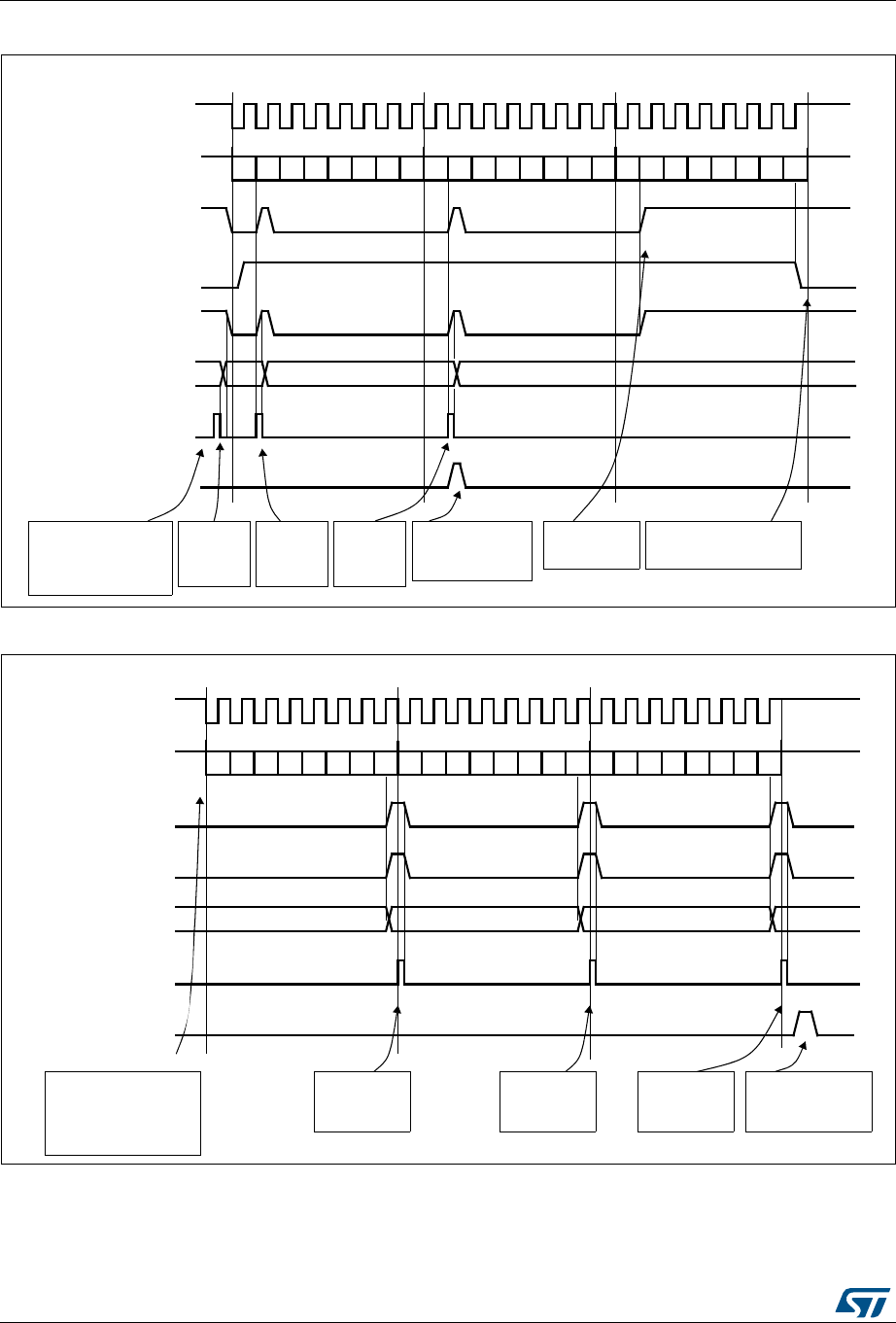
Serial peripheral interface (SPI) RM0383
572/836 DocID026448 Rev 1
Figure 205. Transmission using DMA
Figure 206. Reception using DMA
0xF1
Tx buffer
TXE flag
0xF2
BSY flag
0xF3
set by hardware
clear by DMA write
set by hardware
cleared by DMA write set by hardware
set by hardware
SCK
reset
Example with CPOL=1, CPHA=1
(write to SPI_DR)
MISO/MOSI (out)
DATA 1 = 0xF1 DATA 2 = 0xF2 DATA 3 = 0xF3
software configures the
DMA SPI Tx channel
to send 3 data items
and enables the SPI
DMA writes to SPI_DR
DMA requestignored by the DMA because
DMA TCIF flagset by hardware clear by software
DMA writes
DATA1 into
SPI_DR
by hardware
DMA writes
DATA2 into
SPI_DR
DMA writes
DATA3 into
SPI_DR
software waits until BSY=0
(DMA transfer complete)
DMA transfer is
complete (TCIF=1 in
DMA_ISR)
software waits
until TXE=1
DMA transfer is complete
b0b1b2b3 b4b5b6b7b0b1b2b3 b4b5b6b7b0b1b2b3 b4b5b6b7
ai17349
MISO/MOSI (in)
DATA 1 = 0xA1
software configures the
DMA SPI Rx channel
to receive 3 data items
and enables the SPI
SCK
DATA 2 = 0xA2 DATA 3 = 0xA3
Example with CPOL=1, CPHA=1
RXNE flag
Rx buffer
set by hardware
(read from SPI_DR) 0xA1 0xA2 0xA3
DMA request
DMA reads
DATA3 from
SPI_DR
flag DMA TCIF
set by hardware clear
by software
DMA read from SPI_DR
The DMA transfer is
complete (TCIF=1 in
DMA_ISR)
DMA reads
DATA2 from
SPI_DR
DMA reads
DATA1 from
SPI_DR
(DMA transfer complete)
b0b1b2b3 b4b5b6b7b0b1b2b3 b4b5b6b7b0b1b2b3 b4b5b6b7
clear by DMA read
ai17350

DocID026448 Rev 1 573/836
RM0383 Serial peripheral interface (SPI)
602
DMA capability with CRC
When SPI communication is enabled with CRC communication and DMA mode, the
transmission and reception of the CRC at the end of communication are automatic that is
without using the bit CRCNEXT. After the CRC reception, the CRC must be read in the
SPI_DR register to clear the RXNE flag.
At the end of data and CRC transfers, the CRCERR flag in SPI_SR is set if corruption
occurs during the transfer.
20.3.10 Error flags
Master mode fault (MODF)
Master mode fault occurs when the master device has its NSS pin pulled low (in NSS
hardware mode) or SSI bit low (in NSS software mode), this automatically sets the MODF
bit. Master mode fault affects the SPI peripheral in the following ways:
•The MODF bit is set and an SPI interrupt is generated if the ERRIE bit is set.
•The SPE bit is cleared. This blocks all output from the device and disables the SPI
interface.
•The MSTR bit is cleared, thus forcing the device into slave mode.
Use the following software sequence to clear the MODF bit:
1. Make a read or write access to the SPI_SR register while the MODF bit is set.
2. Then write to the SPI_CR1 register.
To avoid any multiple slave conflicts in a system comprising several MCUs, the NSS pin
must be pulled high during the MODF bit clearing sequence. The SPE and MSTR bits can
be restored to their original state after this clearing sequence.
As a security, hardware does not allow the setting of the SPE and MSTR bits while the
MODF bit is set.
In a slave device the MODF bit cannot be set. However, in a multimaster configuration, the
device can be in slave mode with this MODF bit set. In this case, the MODF bit indicates
that there might have been a multimaster conflict for system control. An interrupt routine can
be used to recover cleanly from this state by performing a reset or returning to a default
state.
Overrun condition
An overrun condition occurs when the master device has sent data bytes and the slave
device has not cleared the RXNE bit resulting from the previous data byte transmitted.
When an overrun condition occurs:
•the OVR bit is set and an interrupt is generated if the ERRIE bit is set.
In this case, the receiver buffer contents will not be updated with the newly received data
from the master device. A read from the SPI_DR register returns this byte. All other
subsequently transmitted bytes are lost.
Clearing the OVR bit is done by a read from the SPI_DR register followed by a read access
to the SPI_SR register.
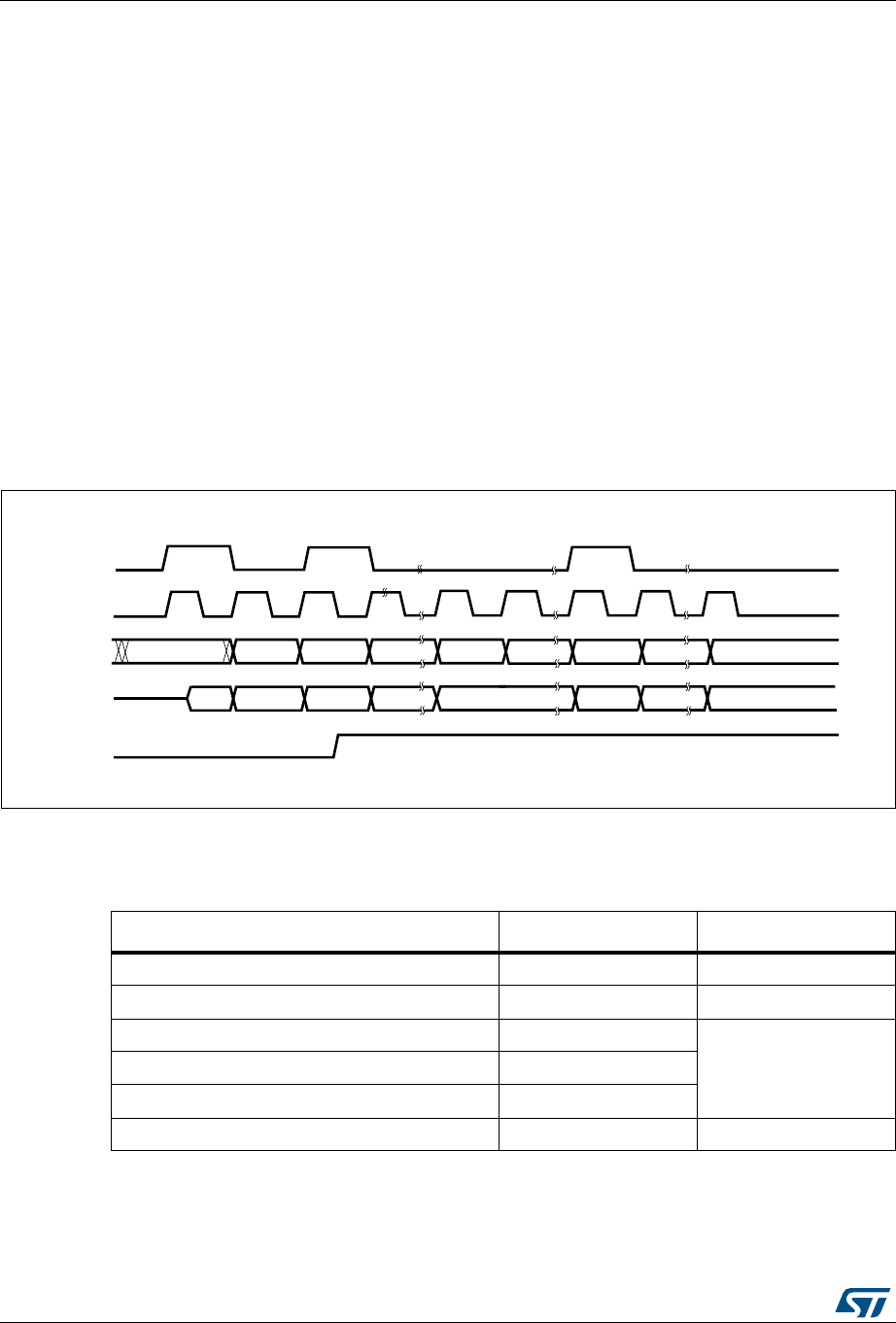
Serial peripheral interface (SPI) RM0383
574/836 DocID026448 Rev 1
CRC error
This flag is used to verify the validity of the value received when the CRCEN bit in the
SPI_CR1 register is set. The CRCERR flag in the SPI_SR register is set if the value
received in the shift register does not match the receiver SPI_RXCRCR value.
TI mode frame format error
A TI mode frame format error is detected when an NSS pulse occurs during an ongoing
communication when the SPI is acting in slave mode and configured to conform to the TI
mode protocol. When this error occurs, the FRE flag is set in the SPI_SR register. The SPI
is not disabled when an error occurs, the NSS pulse is ignored, and the SPI waits for the
next NSS pulse before starting a new transfer. The data may be corrupted since the error
detection may result in the lost of two data bytes.
The FRE flag is cleared when SPI_SR register is read. If the bit ERRIE is set, an interrupt is
generated on the NSS error detection. In this case, the SPI should be disabled because
data consistency is no more guaranteed and communications should be reinitiated by the
master when the slave SPI is re-enabled.
Figure 207. TI mode frame format error detection
20.3.11 SPI interrupts
AI
-3").
-/3)
INPUT
.33
OUTPUT
3#+
OUTPUT
TRIGGER SAMPLING TRIGGER SAMPLING TRIGGER SAMPLING
$/.4#!2%
-)3/
OUTPUT OR -3"/54 ,3"/54
-3"). ,3").
-3"/54 ,3"/54
TRIGGER SAMPLING TRIGGER SAMPLING TRIGGER SAMPLING TRIGGER SAMPLING
,3"). $/.4#!2%
4)&2&%
Table 88. SPI interrupt requests
Interrupt event Event flag Enable Control bit
Transmit buffer empty flag TXE TXEIE
Receive buffer not empty flag RXNE RXNEIE
Master Mode fault event MODF
ERRIEOverrun error OVR
CRC error flag CRCERR
TI frame format error FRE ERRIE
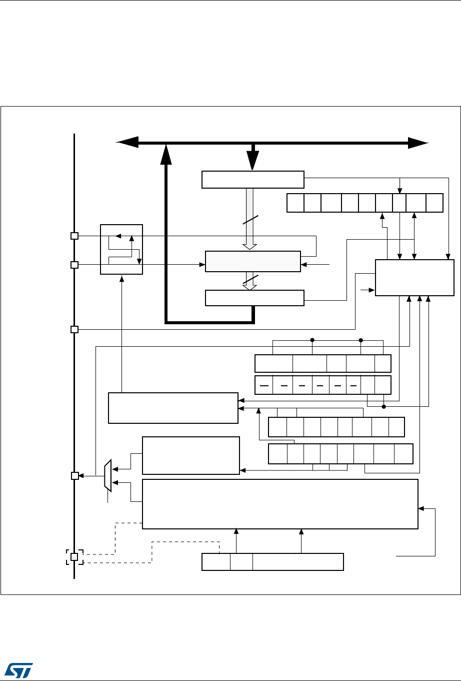
DocID026448 Rev 1 575/836
RM0383 Serial peripheral interface (SPI)
602
20.4 I2S functional description
20.4.1 I2S general description
The block diagram of the I2S is shown in Figure 208.
Figure 208. I2S block diagram
1. I2S2ext_SD and I2S3ext_SD are the extended SD pins that control the I2S full duplex mode.
4XBUFFER
3HIFTREGISTER
BIT
#OMMUNICATION
2XBUFFER
BIT
-/3) 3$
-ASTERCONTROLLOGIC
-)3/
)3EXT?3$
)3EXT?3$
30)
BAUDRATEGENERATOR
#+
)3-/$
,3"FIRST
,3"
&IRST 30% "2 "2 "2 -342 #0/, #0(!
"IDI
MODE
"IDI
/%
#2#
%.
#2#
.EXT $&& 2X
ONLY 33- 33)
!DDRESSANDDATABUS
CONTROL
.3373
"39 /62 -/$& #2#
%22
#(
3)$% 4X% 2X.%
)3CLOCKGENERATOR
-#+
)3?#+
)3
-/$ )3%
#(
$!4,%. ,%.
#+
0/,
)3#&' )334$
-#+/%/$$ )3$)6;=
;= ;= ;=
5$2
)3X#,+
-36
&2%

Serial peripheral interface (SPI) RM0383
576/836 DocID026448 Rev 1
The SPI could function as an audio I2S interface when the I2S capability is enabled (by
setting the I2SMOD bit in the SPI_I2SCFGR register). This interface uses almost the same
pins, flags and interrupts as the SPI.
The I2S shares three common pins with the SPI:
•SD: Serial Data (mapped on the MOSI pin) to transmit or receive the two time-
multiplexed data channels (in half-duplex mode only).
•WS: Word Select (mapped on the NSS pin) is the data control signal output in master
mode and input in slave mode.
•CK: Serial Clock (mapped on the SCK pin) is the serial clock output in master mode
and serial clock input in slave mode.
•I2S2ext_SD and I2S3ext_SD: additional pins (mapped on the MISO pin) to control the
I2S full duplex mode.
An additional pin could be used when a master clock output is needed for some external
audio devices:
•MCK: Master Clock (mapped separately) is used, when the I2S is configured in master
mode (and when the MCKOE bit in the SPI_I2SPR register is set), to output this
additional clock generated at a preconfigured frequency rate equal to 256 × FS, where
FS is the audio sampling frequency.
The I2S uses its own clock generator to produce the communication clock when it is set in
master mode. This clock generator is also the source of the master clock output. Two
additional registers are available in I2S mode. One is linked to the clock generator
configuration SPI_I2SPR and the other one is a generic I2S configuration register
SPI_I2SCFGR (audio standard, slave/master mode, data format, packet frame, clock
polarity, etc.).
The SPI_CR1 register and all CRC registers are not used in the I2S mode. Likewise, the
SSOE bit in the SPI_CR2 register and the MODF and CRCERR bits in the SPI_SR are not
used.
The I2S uses the same SPI register for data transfer (SPI_DR) in 16-bit wide mode.
20.4.2 I2S full duplex
To support I2S full duplex mode, two extra I2S instances called extended I2Ss (I2S2_ext,
I2S3_ext) are available in addition to I2S2 and I2S3 (see Figure 209). The first I2S full-
duplex interface is consequently based on I2S2 and I2S2_ext, and the second one on I2S3
and I2S3_ext.
Note: I2S2_ext an I2S3_ext are used only in full-duplex mode.
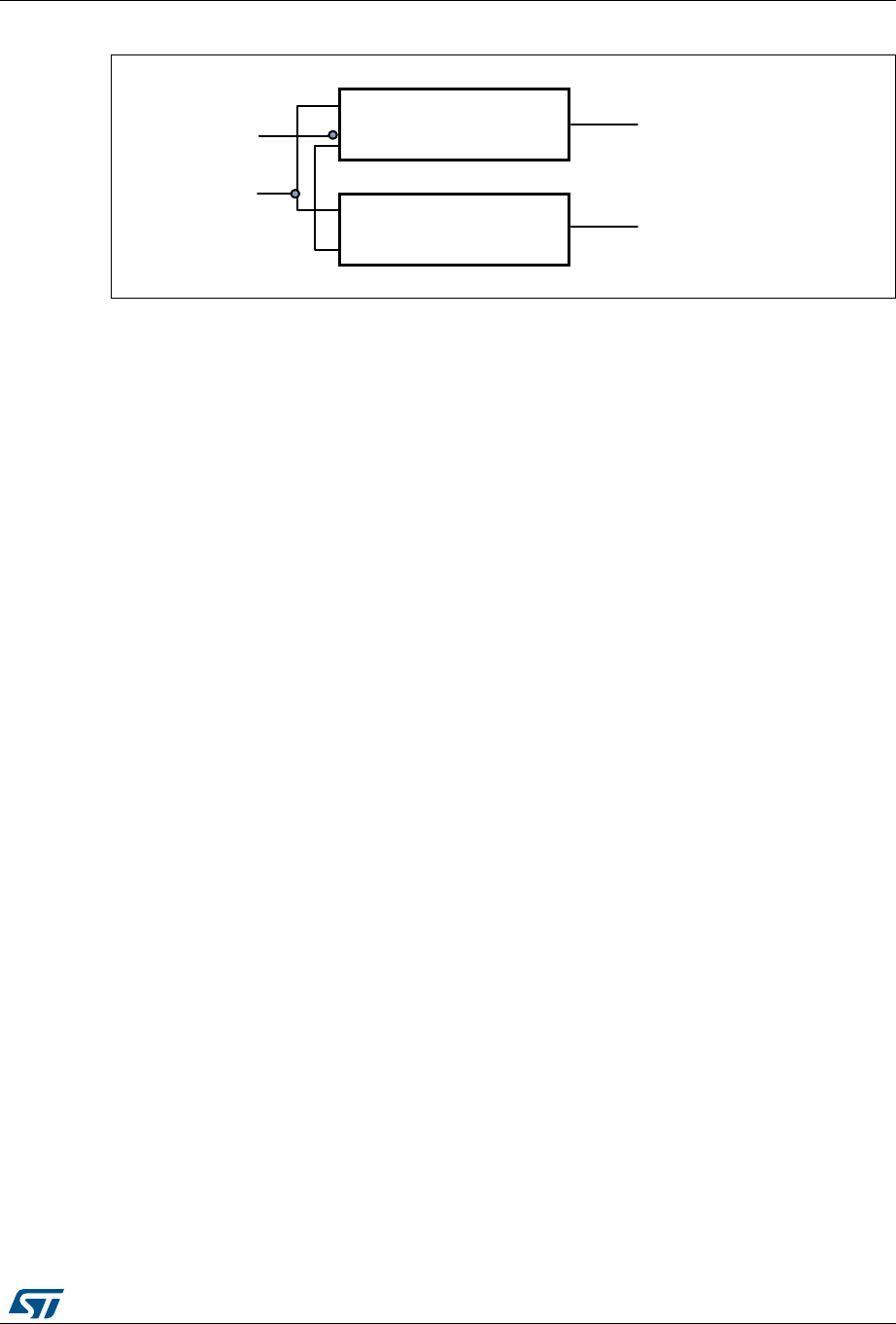
DocID026448 Rev 1 577/836
RM0383 Serial peripheral interface (SPI)
602
Figure 209. I2S full duplex block diagram
1. Where x can be 2 or 3.
I2Sx can operate in master mode. As a result:
• Only I2Sx can output SCK and WS in half duplex mode
• Only I2Sx can deliver SCK and WS to I2S2_ext and I2S3_ext in full duplex mode.
The extended I2Ss (I2Sx_ext) can be used only in full duplex mode. The I2Sx_ext operate
always in slave mode.
Both I2Sx and I2Sx_ext can be configured as transmitters or receivers.
20.4.3 Supported audio protocols
The four-line bus has to handle only audio data generally time-multiplexed on two channels:
the right channel and the left channel. However there is only one 16-bit register for the
transmission and the reception. So, it is up to the software to write into the data register the
adequate value corresponding to the considered channel side, or to read the data from the
data register and to identify the corresponding channel by checking the CHSIDE bit in the
SPI_SR register. Channel Left is always sent first followed by the channel right (CHSIDE
has no meaning for the PCM protocol).
Four data and packet frames are available. Data may be sent with a format of:
•16-bit data packed in 16-bit frame
•16-bit data packed in 32-bit frame
•24-bit data packed in 32-bit frame
•32-bit data packed in 32-bit frame
When using 16-bit data extended on 32-bit packet, the first 16 bits (MSB) are the significant
bits, the 16-bit LSB is forced to 0 without any need for software action or DMA request (only
one read/write operation).
The 24-bit and 32-bit data frames need two CPU read or write operations to/from the
SPI_DR or two DMA operations if the DMA is preferred for the application. For 24-bit data
frame specifically, the 8 nonsignificant bits are extended to 32 bits with 0-bits (by hardware).
For all data formats and communication standards, the most significant bit is always sent
first (MSB first).
The I2S interface supports four audio standards, configurable using the I2SSTD[1:0] and
PCMSYNC bits in the SPI_I2SCFGR register.
-36
30))3X
)3X?EXT
30)X?-/3))3X?3$INOUT
)3? 73
)3X?3#+
)3X?EXT3$INOUT
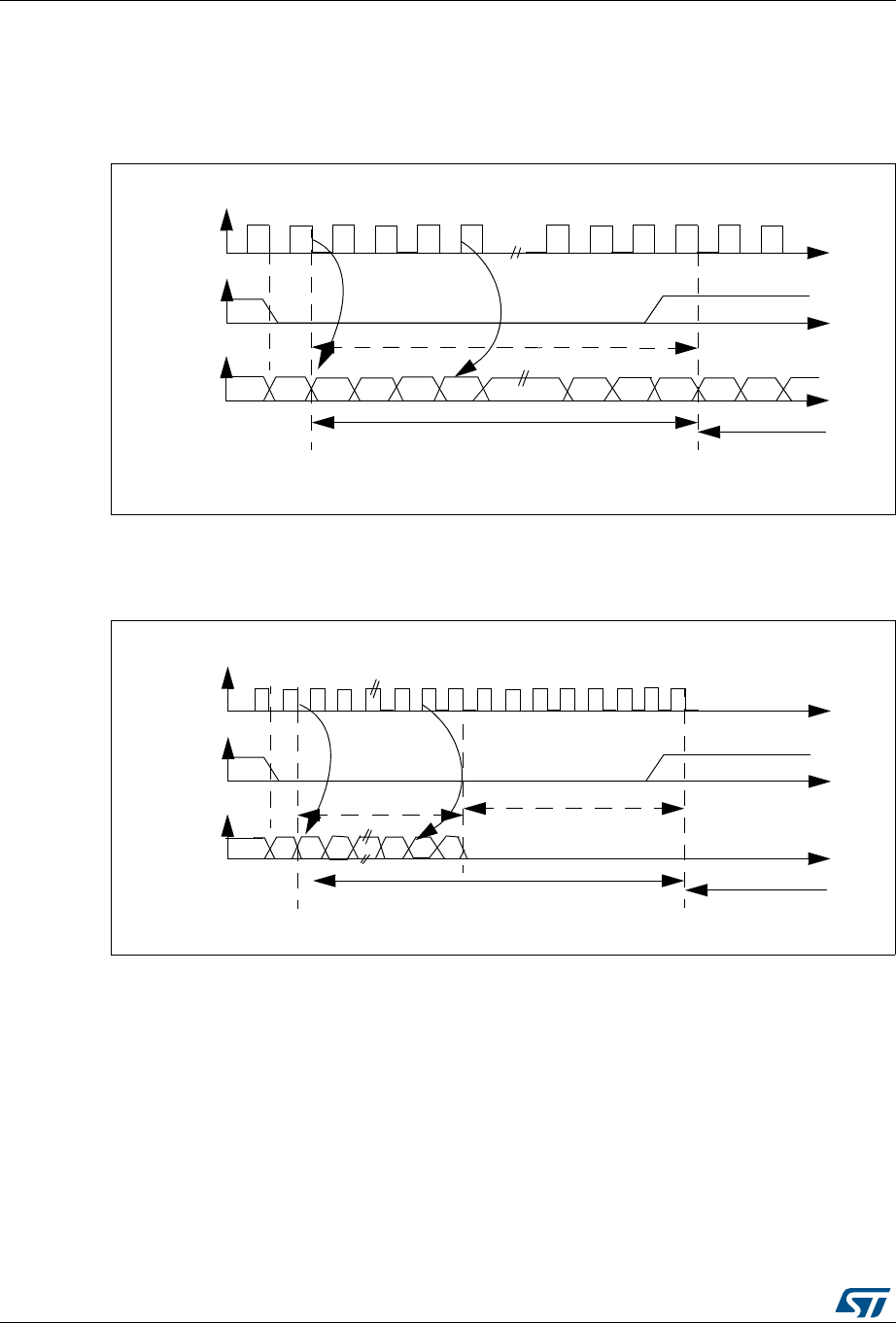
Serial peripheral interface (SPI) RM0383
578/836 DocID026448 Rev 1
I2S Philips standard
For this standard, the WS signal is used to indicate which channel is being transmitted. It is
activated one CK clock cycle before the first bit (MSB) is available.
Figure 210. I2S Philips protocol waveforms (16/32-bit full accuracy, CPOL = 0)
Data are latched on the falling edge of CK (for the transmitter) and are read on the rising
edge (for the receiver). The WS signal is also latched on the falling edge of CK.
Figure 211. I2S Philips standard waveforms (24-bit frame with CPOL = 0)
This mode needs two write or read operations to/from the SPI_DR.
•In transmission mode:
if 0x8EAA33 has to be sent (24-bit):
MSB LSB MSB
CK
WS
SD
Channel left
Channel right
May be 16-bit, 32-bit
Transmission Reception
CK
WS
SD
Channel left 32-bit
Channel right
MSB LSB
8-bit remaining
0 forced
24-bit data
Transmission Reception
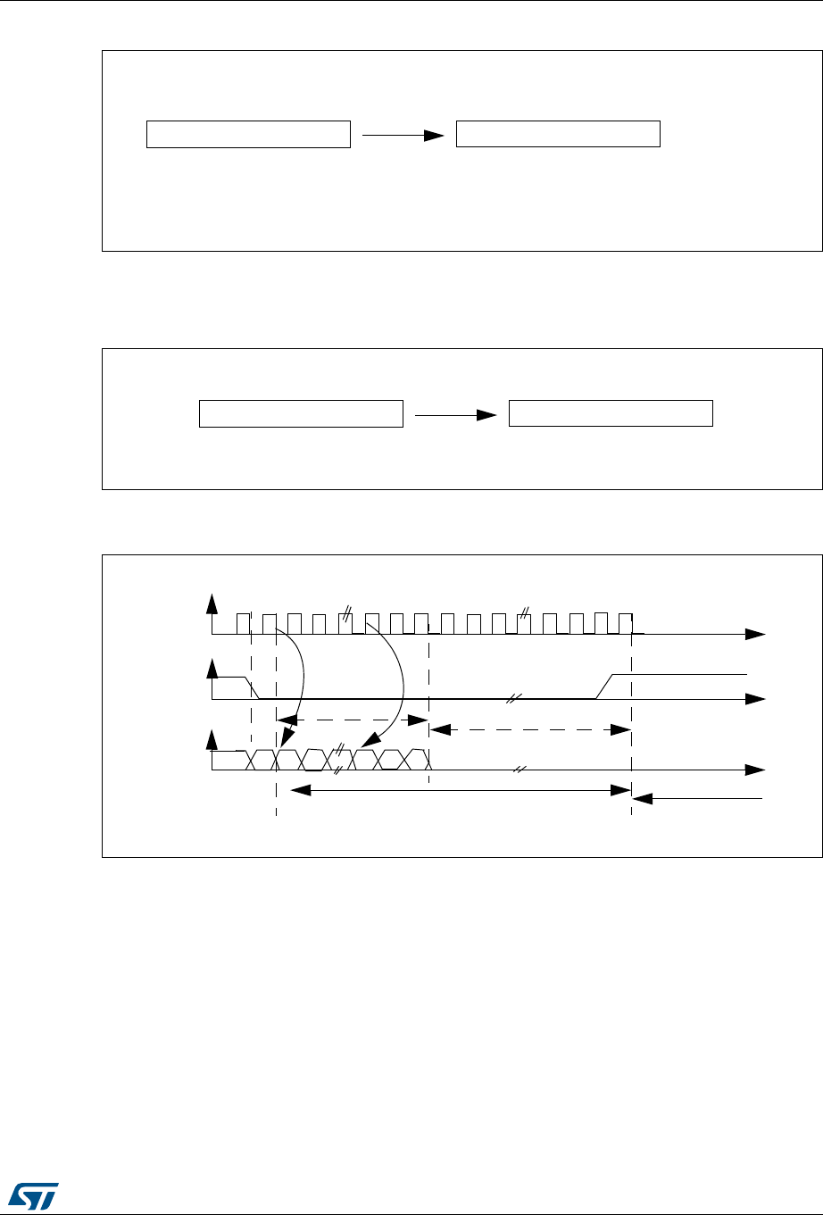
DocID026448 Rev 1 579/836
RM0383 Serial peripheral interface (SPI)
602
Figure 212. Transmitting 0x8EAA33
•In reception mode:
if data 0x8EAA33 is received:
Figure 213. Receiving 0x8EAA33
Figure 214. I2S Philips standard (16-bit extended to 32-bit packet frame with
CPOL = 0)
When 16-bit data frame extended to 32-bit channel frame is selected during the I2S
configuration phase, only one access to SPI_DR is required. The 16 remaining bits are
forced by hardware to 0x0000 to extend the data to 32-bit format.
If the data to transmit or the received data are 0x76A3 (0x76A30000 extended to 32-bit), the
operation shown in Figure 215 is required.
0x8EAA 0x33XX
Only the 8 MSBs are sent to complete the 24 bits
First write to Data register Second write to Data register
8 LSB bits have no meaning and could be
anything
0x8EAA 0x3300
Only the 8MSB are right
First read from Data register Second read from Data register
The 8 LSB will always be 00
CK
WS
SD
Channel left 32-bit
Channel right
MSB LSB
16-bit remaining
16-bit data
0 forced
Transmission Reception
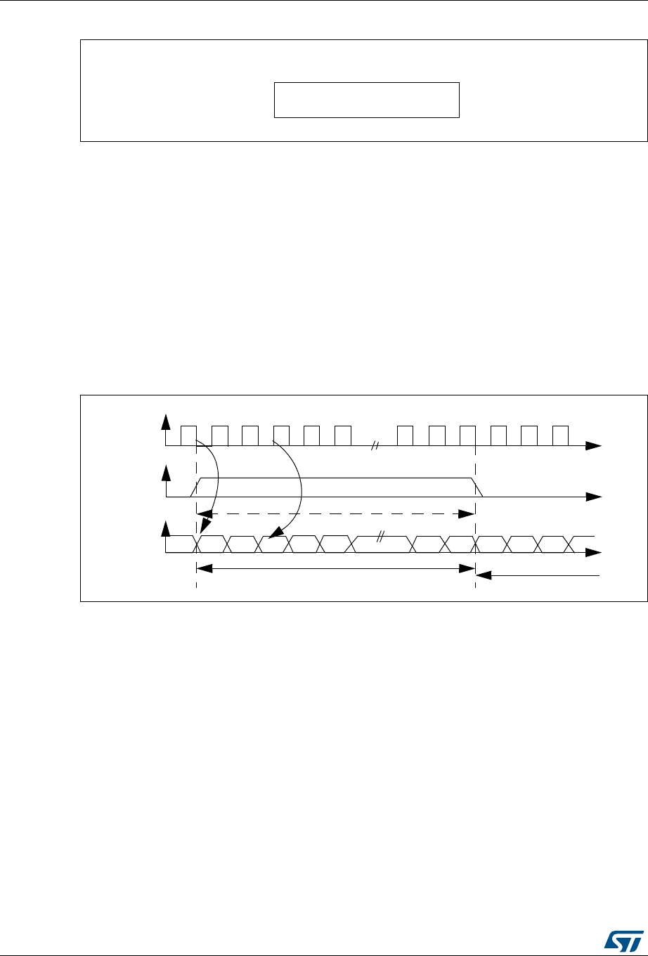
Serial peripheral interface (SPI) RM0383
580/836 DocID026448 Rev 1
Figure 215. Example
For transmission, each time an MSB is written to SPI_DR, the TXE flag is set and its
interrupt, if allowed, is generated to load SPI_DR with the new value to send. This takes
place even if 0x0000 have not yet been sent because it is done by hardware.
For reception, the RXNE flag is set and its interrupt, if allowed, is generated when the first
16 MSB half-word is received.
In this way, more time is provided between two write or read operations, which prevents
underrun or overrun conditions (depending on the direction of the data transfer).
MSB justified standard
For this standard, the WS signal is generated at the same time as the first data bit, which is
the MSBit.
Figure 216. MSB Justified 16-bit or 32-bit full-accuracy length with CPOL = 0
Data are latched on the falling edge of CK (for transmitter) and are read on the rising edge
(for the receiver).
0X76A3
Only one access to SPI_DR
MSB LSB MSB
CK
WS
SD
Channel left
Channel right
May be 16-bit, 32-bit
Transmission Reception
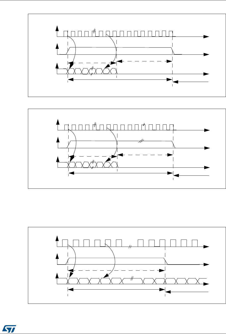
DocID026448 Rev 1 581/836
RM0383 Serial peripheral interface (SPI)
602
Figure 217. MSB Justified 24-bit frame length with CPOL = 0
Figure 218. MSB Justified 16-bit extended to 32-bit packet frame with CPOL = 0
LSB justified standard
This standard is similar to the MSB justified standard (no difference for the 16-bit and 32-bit
full-accuracy frame formats).
Figure 219. LSB justified 16-bit or 32-bit full-accuracy with CPOL = 0
CK
WS
SD
Channel left 32-bit
Channel right
MSB LSB
8-bit remaining
0 forced
24-bit data
Transmission Reception
CK
WS
SD
Channel left 32-bit
Channel right
MSB LSB
16-bit remaining
0 forced
16-bit data
Transmission Reception
MSB LSB MSB
CK
WS
SD
Channel left
Channel right
May be 16-bit, 32-bit
Transmission Reception
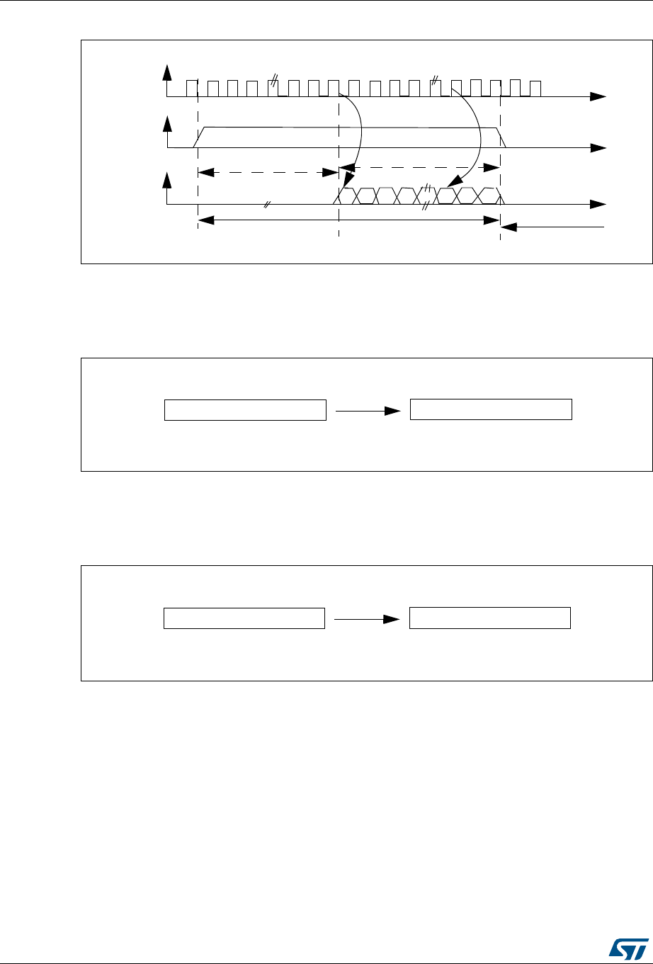
Serial peripheral interface (SPI) RM0383
582/836 DocID026448 Rev 1
Figure 220. LSB Justified 24-bit frame length with CPOL = 0
•In transmission mode:
If data 0x3478AE have to be transmitted, two write operations to the SPI_DR register
are required from software or by DMA. The operations are shown below.
Figure 221. Operations required to transmit 0x3478AE
•In reception mode:
If data 0x3478AE are received, two successive read operations from SPI_DR are
required on each RXNE event.
Figure 222. Operations required to receive 0x3478AE
CK
WS
SD
Channel left 32-bit
Channel right
MSB LSB
24-bit remaining
0 forced
8-bit data
Transmission Reception
0xXX34 0x78AE
First write to Data register Second write to Data register
Only the 8 LSB bits of the half-word
are significant. Whatever the 8 MSBs
a field of 0x00 is forced instead
conditioned by TXE = ‘1’ conditioned by TXE = ‘1’
0x0034 0x78AE
First read from Data register Second read from Data register
Only the 8 LSB bits of the half-word
are significant. Whatever the 8 MSBs,
a field of 0x00 is forced instead
conditioned by RXNE = ‘1’ conditioned by RXNE = ‘1’
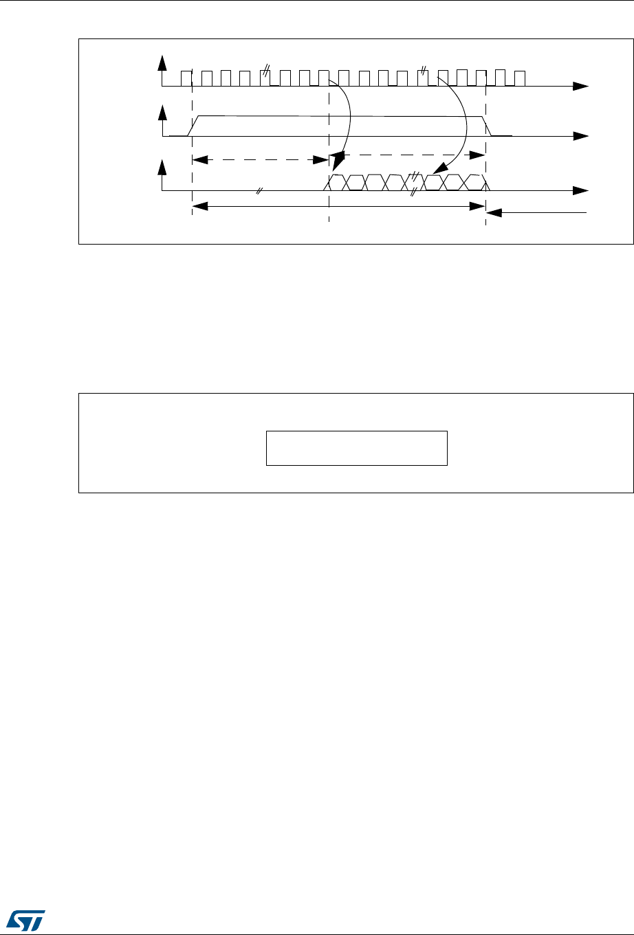
DocID026448 Rev 1 583/836
RM0383 Serial peripheral interface (SPI)
602
Figure 223. LSB justified 16-bit extended to 32-bit packet frame with CPOL = 0
When 16-bit data frame extended to 32-bit channel frame is selected during the I2S
configuration phase, Only one access to SPI_DR is required. The 16 remaining bits are
forced by hardware to 0x0000 to extend the data to 32-bit format. In this case it corresponds
to the half-word MSB.
If the data to transmit or the received data are 0x76A3 (0x0000 76A3 extended to 32-bit),
the operation shown in Figure 224 is required.
Figure 224. Example of LSB justified 16-bit extended to 32-bit packet frame
In transmission mode, when TXE is asserted, the application has to write the data to be
transmitted (in this case 0x76A3). The 0x000 field is transmitted first (extension on 32-bit).
TXE is asserted again as soon as the effective data (0x76A3) is sent on SD.
In reception mode, RXNE is asserted as soon as the significant half-word is received (and
not the 0x0000 field).
In this way, more time is provided between two write or read operations to prevent underrun
or overrun conditions.
PCM standard
For the PCM standard, there is no need to use channel-side information. The two PCM
modes (short and long frame) are available and configurable using the PCMSYNC bit in
SPI_I2SCFGR.
CK
WS
SD
Channel left 32-bit
Channel right
MSB LSB
16-bit remaining
0 forced
16-bit data
Transmission Reception
0X76A3
Only one access to SPI_DR
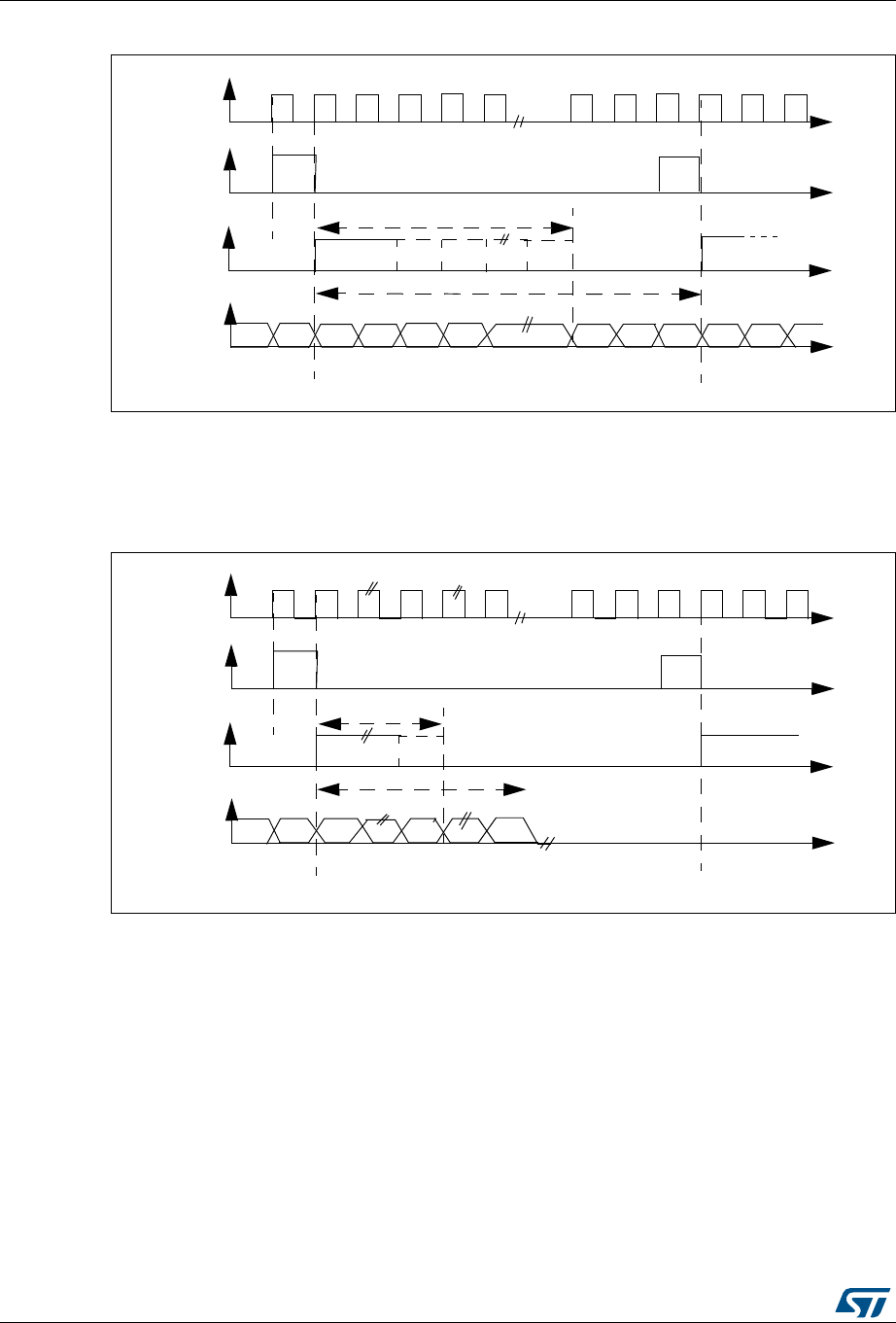
Serial peripheral interface (SPI) RM0383
584/836 DocID026448 Rev 1
Figure 225. PCM standard waveforms (16-bit)
For long frame synchronization, the WS signal assertion time is fixed 13 bits in master
mode.
For short frame synchronization, the WS synchronization signal is only one cycle long.
Figure 226. PCM standard waveforms (16-bit extended to 32-bit packet frame)
Note: For both modes (master and slave) and for both synchronizations (short and long), the
number of bits between two consecutive pieces of data (and so two synchronization signals)
needs to be specified (DATLEN and CHLEN bits in the SPI_I2SCFGR register) even in
slave mode.
20.4.4 Clock generator
The I2S bitrate determines the dataflow on the I2S data line and the I2S clock signal
frequency.
I2S bitrate = number of bits per channel × number of channels × sampling audio frequency
For a 16-bit audio, left and right channel, the I2S bitrate is calculated as follows:
I2S bitrate = 16 × 2 × FS
MSB LSB MSB
CK
WS
SD
16-bit
WS fixed to 13-bit
short
frame
long
frame
MSB
CK
WS
SD
16-bit
WS
fixed to 13-bit
short
frame
long
frame
LSB
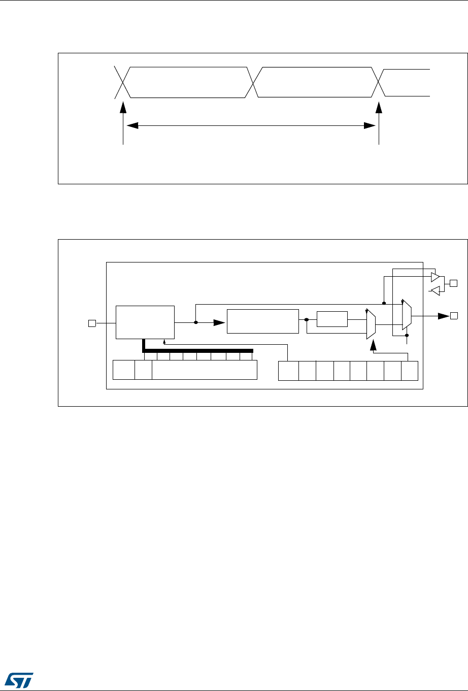
DocID026448 Rev 1 585/836
RM0383 Serial peripheral interface (SPI)
602
It will be: I2S bitrate = 32 x 2 x FS if the packet length is 32-bit wide.
Figure 227. Audio sampling frequency definition
When the master mode is configured, a specific action needs to be taken to properly
program the linear divider in order to communicate with the desired audio frequency.
Figure 228. I2S clock generator architecture
1. Where x could be 2 or 3.
Figure 227 presents the communication clock architecture. To achieve high-quality audio
performance, the I2SxCLK clock source can be either the PLLI2S output (through R division
factor) or an external clock (mapped to I2S_CKIN pin).
The audio sampling frequency can be 192 kHz, 96 kHz, or 48 kHz. In order to reach the
desired frequency, the linear divider needs to be programmed according to the formulas
below:
When the master clock is generated (MCKOE in the SPI_I2SPR register is set):
FS = I2SxCLK / [(16*2)*((2*I2SDIV)+ODD)*8)] when the channel frame is 16-bit wide
FS = I2SxCLK / [(32*2)*((2*I2SDIV)+ODD)*4)] when the channel frame is 32-bit wide
When the master clock is disabled (MCKOE bit cleared):
FS = I2SxCLK / [(16*2)*((2*I2SDIV)+ODD))] when the channel frame is 16-bit wide
FS = I2SxCLK / [(32*2)*((2*I2SDIV)+ODD))] when the channel frame is 32-bit wide
Table 89 provides example precision values for different clock configurations.
Note: Other configurations are possible that allow optimum clock precision.
16-bit or 32-bit Left channel 16-bit or 32-bit Right channel
sampling point sampling point
32-bits or 64-bits
FS
FS: Audio sampling frequency
8-bit
Divider +
Linear
CK
ODD I2SDIV[7:0]
I2SxCLK
CHLENI2SMOD
reshaping stage
Divider by 4 Div2
1
0
MCKOE
MCKOE
MCK
0
1

Serial peripheral interface (SPI) RM0383
586/836 DocID026448 Rev 1
20.4.5 I2S master mode
The I2S can be configured as follows:
•In master mode for transmission or reception (half-duplex mode using I2Sx)
•In master mode transmission and reception (full duplex mode using I2Sx and
I2Sx_ext).
This means that the serial clock is generated on the CK pin as well as the Word Select
signal WS. Master clock (MCK) may be output or not, thanks to the MCKOE bit in the
SPI_I2SPR register.
Table 89. Audio frequency precision (for PLLM VCO = 1 MHz or 2 MHz)(1)
Master
clock Target fS
(Hz) Data
format PLLI2SN PLLI2SR I2SDIV I2SODD Real fS (Hz) Error
Disabled
8000
16-bit 192 2 187 1 8000 0.0000%
32-bit 192 3 62 1 8000 0.0000%
16000
16-bit 192 3 62 1 16000 0.0000%
32-bit 256 2 62 1 16000 0.0000%
32000
16-bit 256 2 62 1 32000 0.0000%
32-bit 256 5 12 1 32000 0.0000%
48000
16-bit 192 5 12 1 48000 0.0000%
32-bit 384 5 12 1 48000 0.0000%
96000
16-bit 384 5 12 1 96000 0.0000%
32-bit 424 3 11 1 96014.49219 0.0151%
22050
16-bit 290 3 68 1 22049.87695 0.0006%
32-bit 302 2 53 1 22050.23438 0.0011%
44100
16-bit 302 2 53 1 44100.46875 0.0011%
32-bit 429 4 19 0 44099.50781 0.0011%
192000
16-bit 424 3 11 1 192028.9844 0.0151%
32-bit 258 3 3 1 191964.2813 0.0186%
Enabled
8000 don't care 256 5 12 1 8000 0.0000%
16000 don't care 213 2 13 0 16000.60059 0.0038%
32000 don't care 213 2 6 1 32001.20117 0.0038%
48000 don't care 258 3 3 1 47991.07031 0.0186%
96000 don't care 344 2 3 1 95982.14063 0.0186%
22050 don't care 429 4 9 1 22049.75391 0.0011%
44100 don't care 271 2 6 0 44108.07422 0.0183%
1. This table gives only example values for different clock configurations. Other configurations allowing optimum clock
precision are possible.

DocID026448 Rev 1 587/836
RM0383 Serial peripheral interface (SPI)
602
Procedure
1. Select the I2SDIV[7:0] bits in the SPI_I2SPR register to define the serial clock baud
rate to reach the proper audio sample frequency. The ODD bit in the SPI_I2SPR
register also has to be defined.
2. Select the CKPOL bit to define the steady level for the communication clock. Set the
MCKOE bit in the SPI_I2SPR register if the master clock MCK needs to be provided to
the external DAC/ADC audio component (the I2SDIV and ODD values should be
computed depending on the state of the MCK output, for more details refer to
Section 20.4.4: Clock generator).
3. Set the I2SMOD bit in SPI_I2SCFGR to activate the I2S functionalities and choose the
I2S standard through the I2SSTD[1:0] and PCMSYNC bits, the data length through the
DATLEN[1:0] bits and the number of bits per channel by configuring the CHLEN bit.
Select also the I2S master mode and direction (Transmitter or Receiver) through the
I2SCFG[1:0] bits in the SPI_I2SCFGR register.
4. If needed, select all the potential interruption sources and the DMA capabilities by
writing the SPI_CR2 register.
5. The I2SE bit in SPI_I2SCFGR register must be set.
WS and CK are configured in output mode. MCK is also an output, if the MCKOE bit in
SPI_I2SPR is set.
Transmission sequence
The transmission sequence begins when a half-word is written into the Tx buffer.
Assumedly, the first data written into the Tx buffer correspond to the channel Left data.
When data are transferred from the Tx buffer to the shift register, TXE is set and data
corresponding to the channel Right have to be written into the Tx buffer. The CHSIDE flag
indicates which channel is to be transmitted. It has a meaning when the TXE flag is set
because the CHSIDE flag is updated when TXE goes high.
A full frame has to be considered as a Left channel data transmission followed by a Right
channel data transmission. It is not possible to have a partial frame where only the left
channel is sent.
The data half-word is parallel loaded into the 16-bit shift register during the first bit
transmission, and then shifted out, serially, to the MOSI/SD pin, MSB first. The TXE flag is
set after each transfer from the Tx buffer to the shift register and an interrupt is generated if
the TXEIE bit in the SPI_CR2 register is set.
For more details about the write operations depending on the I2S standard mode selected,
refer to Section 20.4.3: Supported audio protocols).
To ensure a continuous audio data transmission, it is mandatory to write the SPI_DR with
the next data to transmit before the end of the current transmission.
To switch off the I2S, by clearing I2SE, it is mandatory to wait for TXE = 1 and BSY = 0.
Reception sequence
The operating mode is the same as for the transmission mode except for the point 3 (refer to
the procedure described in Section 20.4.5: I2S master mode), where the configuration
should set the master reception mode through the I2SCFG[1:0] bits.
Whatever the data or channel length, the audio data are received by 16-bit packets. This
means that each time the Rx buffer is full, the RXNE flag is set and an interrupt is generated

Serial peripheral interface (SPI) RM0383
588/836 DocID026448 Rev 1
if the RXNEIE bit is set in SPI_CR2 register. Depending on the data and channel length
configuration, the audio value received for a right or left channel may result from one or two
receptions into the Rx buffer.
Clearing the RXNE bit is performed by reading the SPI_DR register.
CHSIDE is updated after each reception. It is sensitive to the WS signal generated by the
I2S cell.
For more details about the read operations depending on the I2S standard mode selected,
refer to Section 20.4.3: Supported audio protocols.
If data are received while the previously received data have not been read yet, an overrun is
generated and the OVR flag is set. If the ERRIE bit is set in the SPI_CR2 register, an
interrupt is generated to indicate the error.
To switch off the I2S, specific actions are required to ensure that the I2S completes the
transfer cycle properly without initiating a new data transfer. The sequence depends on the
configuration of the data and channel lengths, and on the audio protocol mode selected. In
the case of:
•16-bit data length extended on 32-bit channel length (DATLEN = 00 and CHLEN = 1)
using the LSB justified mode (I2SSTD = 10)
a) Wait for the second to last RXNE = 1 (n – 1)
b) Then wait 17 I2S clock cycles (using a software loop)
c) Disable the I2S (I2SE = 0)
•16-bit data length extended on 32-bit channel length (DATLEN = 00 and CHLEN = 1) in
MSB justified, I2S or PCM modes (I2SSTD = 00, I2SSTD = 01 or I2SSTD = 11,
respectively)
a) Wait for the last RXNE
b) Then wait 1 I2S clock cycle (using a software loop)
c) Disable the I2S (I2SE = 0)
•For all other combinations of DATLEN and CHLEN, whatever the audio mode selected
through the I2SSTD bits, carry out the following sequence to switch off the I2S:
a) Wait for the second to last RXNE = 1 (n – 1)
b) Then wait one I2S clock cycle (using a software loop)
c) Disable the I2S (I2SE = 0)
Note: The BSY flag is kept low during transfers.
20.4.6 I2S slave mode
The I2S can be configured as follows:
•In slave mode for transmission or reception (half-duplex mode using I2Sx)
•In slave mode transmission and reception (full duplex mode using I2Sx and I2Sx_ext).
The operating mode is following mainly the same rules as described for the I2S master
configuration. In slave mode, there is no clock to be generated by the I2S interface. The
clock and WS signals are input from the external master connected to the I2S interface.
There is then no need, for the user, to configure the clock.
The configuration steps to follow are listed below:

DocID026448 Rev 1 589/836
RM0383 Serial peripheral interface (SPI)
602
1. Set the I2SMOD bit in the SPI_I2SCFGR register to reach the I2S functionalities and
choose the I2S standard through the I2SSTD[1:0] bits, the data length through the
DATLEN[1:0] bits and the number of bits per channel for the frame configuring the
CHLEN bit. Select also the mode (transmission or reception) for the slave through the
I2SCFG[1:0] bits in SPI_I2SCFGR register.
2. If needed, select all the potential interrupt sources and the DMA capabilities by writing
the SPI_CR2 register.
3. The I2SE bit in SPI_I2SCFGR register must be set.
Transmission sequence
The transmission sequence begins when the external master device sends the clock and
when the NSS_WS signal requests the transfer of data. The slave has to be enabled before
the external master starts the communication. The I2S data register has to be loaded before
the master initiates the communication.
For the I2S, MSB justified and LSB justified modes, the first data item to be written into the
data register corresponds to the data for the left channel. When the communication starts,
the data are transferred from the Tx buffer to the shift register. The TXE flag is then set in
order to request the right channel data to be written into the I2S data register.
The CHSIDE flag indicates which channel is to be transmitted. Compared to the master
transmission mode, in slave mode, CHSIDE is sensitive to the WS signal coming from the
external master. This means that the slave needs to be ready to transmit the first data
before the clock is generated by the master. WS assertion corresponds to left channel
transmitted first.
Note: The I2SE has to be written at least two PCLK cycles before the first clock of the master
comes on the CK line.
The data half-word is parallel-loaded into the 16-bit shift register (from the internal bus)
during the first bit transmission, and then shifted out serially to the MOSI/SD pin MSB first.
The TXE flag is set after each transfer from the Tx buffer to the shift register and an interrupt
is generated if the TXEIE bit in the SPI_CR2 register is set.
Note that the TXE flag should be checked to be at 1 before attempting to write the Tx buffer.
For more details about the write operations depending on the I2S standard mode selected,
refer to Section 20.4.3: Supported audio protocols.
To secure a continuous audio data transmission, it is mandatory to write the SPI_DR
register with the next data to transmit before the end of the current transmission. An
underrun flag is set and an interrupt may be generated if the data are not written into the
SPI_DR register before the first clock edge of the next data communication. This indicates
to the software that the transferred data are wrong. If the ERRIE bit is set into the SPI_CR2
register, an interrupt is generated when the UDR flag in the SPI_SR register goes high. In
this case, it is mandatory to switch off the I2S and to restart a data transfer starting from the
left channel.
To switch off the I2S, by clearing the I2SE bit, it is mandatory to wait for TXE = 1 and BSY =
0.
Reception sequence
The operating mode is the same as for the transmission mode except for the point 1 (refer to
the procedure described in Section 20.4.6: I2S slave mode), where the configuration should
set the master reception mode using the I2SCFG[1:0] bits in the SPI_I2SCFGR register.

Serial peripheral interface (SPI) RM0383
590/836 DocID026448 Rev 1
Whatever the data length or the channel length, the audio data are received by 16-bit
packets. This means that each time the RX buffer is full, the RXNE flag in the SPI_SR
register is set and an interrupt is generated if the RXNEIE bit is set in the SPI_CR2 register.
Depending on the data length and channel length configuration, the audio value received for
a right or left channel may result from one or two receptions into the RX buffer.
The CHSIDE flag is updated each time data are received to be read from SPI_DR. It is
sensitive to the external WS line managed by the external master component.
Clearing the RXNE bit is performed by reading the SPI_DR register.
For more details about the read operations depending the I2S standard mode selected, refer
to Section 20.4.3: Supported audio protocols.
If data are received while the precedent received data have not yet been read, an overrun is
generated and the OVR flag is set. If the bit ERRIE is set in the SPI_CR2 register, an
interrupt is generated to indicate the error.
To switch off the I2S in reception mode, I2SE has to be cleared immediately after receiving
the last RXNE = 1.
Note: The external master components should have the capability of sending/receiving data in 16-
bit or 32-bit packets via an audio channel.
20.4.7 Status flags
Three status flags are provided for the application to fully monitor the state of the I2S bus.
Busy flag (BSY)
The BSY flag is set and cleared by hardware (writing to this flag has no effect). It indicates
the state of the communication layer of the I2S.
When BSY is set, it indicates that the I2S is busy communicating. There is one exception in
master receive mode (I2SCFG = 11) where the BSY flag is kept low during reception.
The BSY flag is useful to detect the end of a transfer if the software needs to disable the I2S.
This avoids corrupting the last transfer. For this, the procedure described below must be
strictly respected.
The BSY flag is set when a transfer starts, except when the I2S is in master receiver mode.
The BSY flag is cleared:
•when a transfer completes (except in master transmit mode, in which the
communication is supposed to be continuous)
•when the I2S is disabled
When communication is continuous:
•In master transmit mode, the BSY flag is kept high during all the transfers
•In slave mode, the BSY flag goes low for one I2S clock cycle between each transfer
Note: Do not use the BSY flag to handle each data transmission or reception. It is better to use the
TXE and RXNE flags instead.

DocID026448 Rev 1 591/836
RM0383 Serial peripheral interface (SPI)
602
Tx buffer empty flag (TXE)
When set, this flag indicates that the Tx buffer is empty and the next data to be transmitted
can then be loaded into it. The TXE flag is reset when the Tx buffer already contains data to
be transmitted. It is also reset when the I2S is disabled (I2SE bit is reset).
RX buffer not empty (RXNE)
When set, this flag indicates that there are valid received data in the RX Buffer. It is reset
when SPI_DR register is read.
Channel Side flag (CHSIDE)
In transmission mode, this flag is refreshed when TXE goes high. It indicates the channel
side to which the data to transfer on SD has to belong. In case of an underrun error event in
slave transmission mode, this flag is not reliable and I2S needs to be switched off and
switched on before resuming the communication.
In reception mode, this flag is refreshed when data are received into SPI_DR. It indicates
from which channel side data have been received. Note that in case of error (like OVR) this
flag becomes meaningless and the I2S should be reset by disabling and then enabling it
(with configuration if it needs changing).
This flag has no meaning in the PCM standard (for both Short and Long frame modes).
When the OVR or UDR flag in the SPI_SR is set and the ERRIE bit in SPI_CR2 is also set,
an interrupt is generated. This interrupt can be cleared by reading the SPI_SR status
register (once the interrupt source has been cleared).
20.4.8 Error flags
There are three error flags for the I2S cell.
Underrun flag (UDR)
In slave transmission mode this flag is set when the first clock for data transmission appears
while the software has not yet loaded any value into SPI_DR. It is available when the
I2SMOD bit in SPI_I2SCFGR is set. An interrupt may be generated if the ERRIE bit in
SPI_CR2 is set.
The UDR bit is cleared by a read operation on the SPI_SR register.
Overrun flag (OVR)
This flag is set when data are received and the previous data have not yet been read from
SPI_DR. As a result, the incoming data are lost. An interrupt may be generated if the ERRIE
bit is set in SPI_CR2.
In this case, the receive buffer contents are not updated with the newly received data from
the transmitter device. A read operation to the SPI_DR register returns the previous
correctly received data. All other subsequently transmitted half-words are lost.
Clearing the OVR bit is done by a read operation on the SPI_DR register followed by a read
access to the SPI_SR register.
Frame error flag (FRE)
This flag can be set by hardware only if the I2S is configured in Slave mode. It is set if the
external master is changing the WS line at a moment when the slave is not expected this
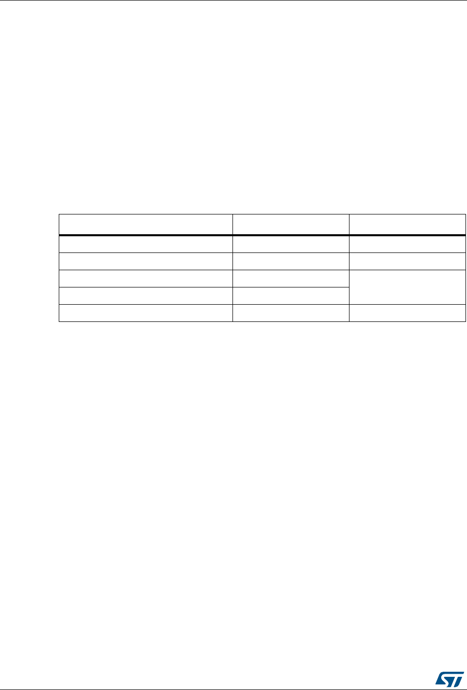
Serial peripheral interface (SPI) RM0383
592/836 DocID026448 Rev 1
change. If the synchronization is lost, to recover from this state and resynchronize the
external master device with the I2S slave device, follow the steps below:
1. Disable the I2S
2. Re-enable it when the correct level is detected on the WS line (WS line is high in I2S
mode, or low for MSB- or LSB-justified or PCM modes).
Desynchronization between the master and slave device may be due to noisy environment
on the SCK communication clock or on the WS frame synchronization line. An error interrupt
can be generated if the ERRIE bit is set. The desynchronization flag (FRE) is cleared by
software when the status register is read.
20.4.9 I2S interrupts
Table 90 provides the list of I2S interrupts.
20.4.10 DMA features
DMA is working in exactly the same way as for the SPI mode. There is no difference on the
I2S. Only the CRC feature is not available in I2S mode since there is no data transfer
protection system.
Table 90. I2S interrupt requests
Interrupt event Event flag Enable Control bit
Transmit buffer empty flag TXE TXEIE
Receive buffer not empty flag RXNE RXNEIE
Overrun error OVR
ERRIE
Underrun error UDR
Frame error flag FRE ERRIE

DocID026448 Rev 1 593/836
RM0383 Serial peripheral interface (SPI)
602
20.5 SPI and I2S registers
Refer to Section 1.1 on page 33for a list of abbreviations used in register descriptions.
The peripheral registers have to be accessed by half-words (16 bits) or words (32 bits).
20.5.1 SPI control register 1 (SPI_CR1)(not used in I2S mode)
Address offset: 0x00
Reset value: 0x0000
1514131211109876543210
BIDI
MODE
BIDI
OE
CRC
EN
CRC
NEXT DFF RX
ONLY SSM SSI LSB
FIRST SPE BR [2:0] MSTR CPOL CPHA
rw rw rw rw rw rw rw rw rw rw rw rw rw rw rw rw
Bit 15 BIDIMODE: Bidirectional data mode enable
0: 2-line unidirectional data mode selected
1: 1-line bidirectional data mode selected
Note: This bit is not used in I2S mode
Bit 14 BIDIOE: Output enable in bidirectional mode
This bit combined with the BIDImode bit selects the direction of transfer in bidirectional mode
0: Output disabled (receive-only mode)
1: Output enabled (transmit-only mode)
Note: This bit is not used in I2S mode.
In master mode, the MOSI pin is used while the MISO pin is used in slave mode.
Bit 13 CRCEN: Hardware CRC calculation enable
0: CRC calculation disabled
1: CRC calculation enabled
Note: This bit should be written only when SPI is disabled (SPE = ‘0’) for correct operation.
It is not used in I2S mode.
Bit 12 CRCNEXT: CRC transfer next
0: Data phase (no CRC phase)
1: Next transfer is CRC (CRC phase)
Note: When the SPI is configured in full duplex or transmitter only modes, CRCNEXT must be
written as soon as the last data is written to the SPI_DR register.
When the SPI is configured in receiver only mode, CRCNEXT must be set after the
second last data reception.
This bit should be kept cleared when the transfers are managed by DMA.
It is not used in I2S mode.
Bit 11 DFF: Data frame format
0: 8-bit data frame format is selected for transmission/reception
1: 16-bit data frame format is selected for transmission/reception
Note: This bit should be written only when SPI is disabled (SPE = ‘0’) for correct operation.
It is not used in I2S mode.

Serial peripheral interface (SPI) RM0383
594/836 DocID026448 Rev 1
Bit 10 RXONLY: Receive only
This bit combined with the BIDImode bit selects the direction of transfer in 2-line
unidirectional mode. This bit is also useful in a multislave system in which this particular
slave is not accessed, the output from the accessed slave is not corrupted.
0: Full duplex (Transmit and receive)
1: Output disabled (Receive-only mode)
Note: This bit is not used in I2S mode
Bit 9 SSM: Software slave management
When the SSM bit is set, the NSS pin input is replaced with the value from the SSI bit.
0: Software slave management disabled
1: Software slave management enabled
Note: This bit is not used in I2S mode and SPI TI mode
Bit 8 SSI: Internal slave select
This bit has an effect only when the SSM bit is set. The value of this bit is forced onto the
NSS pin and the IO value of the NSS pin is ignored.
Note: This bit is not used in I2S mode and SPI TI mode
Bit 7 LSBFIRST: Frame format
0: MSB transmitted first
1: LSB transmitted first
Note: This bit should not be changed when communication is ongoing.
It is not used in I2S mode and SPI TI mode
Bit 6 SPE: SPI enable
0: Peripheral disabled
1: Peripheral enabled
Note: This bit is not used in I2S mode.
When disabling the SPI, follow the procedure described in Section 20.3.8: Disabling the
SPI.
Bits 5:3 BR[2:0]: Baud rate control
000: fPCLK/2
001: fPCLK/4
010: fPCLK/8
011: fPCLK/16
100: fPCLK/32
101: fPCLK/64
110: fPCLK/128
111: fPCLK/256
Note: These bits should not be changed when communication is ongoing.
They are not used in I2S mode.

DocID026448 Rev 1 595/836
RM0383 Serial peripheral interface (SPI)
602
20.5.2 SPI control register 2 (SPI_CR2)
Address offset: 0x04
Reset value: 0x0000
Bit 2 MSTR: Master selection
0: Slave configuration
1: Master configuration
Note: This bit should not be changed when communication is ongoing.
It is not used in I2S mode.
Bit1 CPOL: Clock polarity
0: CK to 0 when idle
1: CK to 1 when idle
Note: This bit should not be changed when communication is ongoing.
It is not used in I2S mode and SPI TI mode.
Bit 0 CPHA: Clock phase
0: The first clock transition is the first data capture edge
1: The second clock transition is the first data capture edge
Note: This bit should not be changed when communication is ongoing.
It is not used in I2S mode and SPI TI mode.
15 14 13 12 11 10 9 8 7 6 5 4 3 2 1 0
Reserved
TXEIE RXNEIE ERRIE FRF
Res. SSOE TXDMAEN RXDMAEN
rw rw rw rw rw rw rw
Bits 15:8 Reserved, must be kept at reset value.
Bit 7 TXEIE: Tx buffer empty interrupt enable
0: TXE interrupt masked
1: TXE interrupt not masked. Used to generate an interrupt request when the TXE flag is set.
Bit 6 RXNEIE: RX buffer not empty interrupt enable
0: RXNE interrupt masked
1: RXNE interrupt not masked. Used to generate an interrupt request when the RXNE flag is
set.
Bit 5 ERRIE: Error interrupt enable
This bit controls the generation of an interrupt when an error condition occurs )(CRCERR,
OVR, MODF in SPI mode, FRE in TI mode and UDR, OVR, and FRE in I2S mode).
0: Error interrupt is masked
1: Error interrupt is enabled
Bit 4 FRF: Frame format
0: SPI Motorola mode
1 SPI TI mode
Note: This bit is not used in I2S mode.
Bit 3 Reserved. Forced to 0 by hardware.

Serial peripheral interface (SPI) RM0383
596/836 DocID026448 Rev 1
20.5.3 SPI status register (SPI_SR)
Address offset: 0x08
Reset value: 0x0002
Bit 2 SSOE: SS output enable
0: SS output is disabled in master mode and the cell can work in multimaster configuration
1: SS output is enabled in master mode and when the cell is enabled. The cell cannot work
in a multimaster environment.
Note: This bit is not used in I2S mode and SPI TI mode.
Bit 1 TXDMAEN: Tx buffer DMA enable
When this bit is set, the DMA request is made whenever the TXE flag is set.
0: Tx buffer DMA disabled
1: Tx buffer DMA enabled
Bit 0 RXDMAEN: Rx buffer DMA enable
When this bit is set, the DMA request is made whenever the RXNE flag is set.
0: Rx buffer DMA disabled
1: Rx buffer DMA enabled
1514131211109876543210
Reserved FRE BSY OVR MODF CRC
ERR UDR CHSID
ETXE RXNE
rrrrrc_w0rrrr
Bits 15:9 Reserved. Forced to 0 by hardware.
Bit 8 FRE: Frame format error
0: No frame format error
1: A frame format error occurred
This flag is set by hardware and cleared by software when the SPIx_SR register is read.
Note: This flag is used when the SPI operates in TI slave mode or I2S slave mode (refer to
Section 20.3.10).
Bit 7 BSY: Busy flag
0: SPI(or I2S) not busy
1: SPI(or I2S)is busy in communication or Tx buffer is not empty
This flag is set and cleared by hardware.
Note: BSY flag must be used with caution: refer to Section 20.3.7: Status flags and
Section 20.3.8: Disabling the SPI.
Bit 6 OVR: Overrun flag
0: No overrun occurred
1: Overrun occurred
This flag is set by hardware and reset by a software sequence.Refer to Section 20.4.8 on
page 591 for the software sequence.
Bit 5 MODF: Mode fault
0: No mode fault occurred
1: Mode fault occurred
This flag is set by hardware and reset by a software sequence. Refer to Section 20.3.10 on
page 573 for the software sequence.
Note: This bit is not used in I2S mode

DocID026448 Rev 1 597/836
RM0383 Serial peripheral interface (SPI)
602
20.5.4 SPI data register (SPI_DR)
Address offset: 0x0C
Reset value: 0x0000
Bit 4 CRCERR: CRC error flag
0: CRC value received matches the SPI_RXCRCR value
1: CRC value received does not match the SPI_RXCRCR value
This flag is set by hardware and cleared by software writing 0.
Note: This bit is not used in I2S mode.
Bit 3 UDR: Underrun flag
0: No underrun occurred
1: Underrun occurred
This flag is set by hardware and reset by a software sequence. Refer to Section 20.4.8 on
page 591 for the software sequence.
Note: This bit is not used in SPI mode.
Bit 2 CHSIDE: Channel side
0: Channel Left has to be transmitted or has been received
1: Channel Right has to be transmitted or has been received
Note: This bit is not used for SPI mode and is meaningless in PCM mode.
Bit 1 TXE: Transmit buffer empty
0: Tx buffer not empty
1: Tx buffer empty
Bit 0 RXNE: Receive buffer not empty
0: Rx buffer empty
1: Rx buffer not empty
1514131211109876543210
DR[15:0]
rw rw rw rw rw rw rw rw rw rw rw rw rw rw rw rw
Bits 15:0 DR[15:0]: Data register
Data received or to be transmitted.
The data register is split into 2 buffers - one for writing (Transmit Buffer) and another one for
reading (Receive buffer). A write to the data register will write into the Tx buffer and a read
from the data register will return the value held in the Rx buffer.
Note: These notes apply to SPI mode:
Depending on the data frame format selection bit (DFF in SPI_CR1 register), the data
sent or received is either 8-bit or 16-bit. This selection has to be made before enabling
the SPI to ensure correct operation.
For an 8-bit data frame, the buffers are 8-bit and only the LSB of the register
(SPI_DR[7:0]) is used for transmission/reception. When in reception mode, the MSB of
the register (SPI_DR[15:8]) is forced to 0.
For a 16-bit data frame, the buffers are 16-bit and the entire register, SPI_DR[15:0] is
used for transmission/reception.

Serial peripheral interface (SPI) RM0383
598/836 DocID026448 Rev 1
20.5.5 SPI CRC polynomial register (SPI_CRCPR)(not used in I2S
mode)
Address offset: 0x10
Reset value: 0x0007
20.5.6 SPI RX CRC register (SPI_RXCRCR)(not used in I2S mode)
Address offset: 0x14
Reset value: 0x0000
20.5.7 SPI TX CRC register (SPI_TXCRCR)(not used in I2S mode)
Address offset: 0x18
Reset value: 0x0000
1514131211109876543210
CRCPOLY[15:0]
rw rw rw rw rw rw rw rw rw rw rw rw rw rw rw rw
Bits 15:0 CRCPOLY[15:0]: CRC polynomial register
This register contains the polynomial for the CRC calculation.
The CRC polynomial (0007h) is the reset value of this register. Another polynomial can be
configured as required.
Note: These bits are not used for the I2S mode.
1514131211109876543210
RXCRC[15:0]
rrrrrrrrrrrrrrrr
Bits 15:0 RXCRC[15:0]: Rx CRC register
When CRC calculation is enabled, the RxCRC[15:0] bits contain the computed CRC value of
the subsequently received bytes. This register is reset when the CRCEN bit in SPI_CR1
register is written to 1. The CRC is calculated serially using the polynomial programmed in
the SPI_CRCPR register.
Only the 8 LSB bits are considered when the data frame format is set to be 8-bit data (DFF
bit of SPI_CR1 is cleared). CRC calculation is done based on any CRC8 standard.
The entire 16-bits of this register are considered when a 16-bit data frame format is selected
(DFF bit of the SPI_CR1 register is set). CRC calculation is done based on any CRC16
standard.
Note: A read to this register when the BSY Flag is set could return an incorrect value.
Theser bits are not used for I2S mode
1514131211109876543210
TXCRC[15:0]
rrrrrrrrrrrrrrrr

DocID026448 Rev 1 599/836
RM0383 Serial peripheral interface (SPI)
602
20.5.8 SPI_I2S configuration register (SPI_I2SCFGR)
Address offset: 0x1C
Reset value: 0x0000
Bits 15:0 TXCRC[15:0]: Tx CRC register
When CRC calculation is enabled, the TxCRC[7:0] bits contain the computed CRC value of
the subsequently transmitted bytes. This register is reset when the CRCEN bit of SPI_CR1
is written to 1. The CRC is calculated serially using the polynomial programmed in the
SPI_CRCPR register.
Only the 8 LSB bits are considered when the data frame format is set to be 8-bit data (DFF
bit of SPI_CR1 is cleared). CRC calculation is done based on any CRC8 standard.
The entire 16-bits of this register are considered when a 16-bit data frame format is selected
(DFF bit of the SPI_CR1 register is set). CRC calculation is done based on any CRC16
standard.
Note: A read to this register when the BSY flag is set could return an incorrect value.
These bits are not used for I2S mode.
15 14 13 12 11 10 9 8 7 6 5 4 3 2 1 0
Reserved
I2SMOD I2SE I2SCFG PCMSY
NC Res.
I2SSTD CKPOL DATLEN CHLEN
rw rw rw rw rw rw rw rw rw rw rw
Bits 15:12 Reserved, must be kept at reset value.
Bit 11 I2SMOD: I2S mode selection
0: SPI mode is selected
1: I2S mode is selected
Note: This bit should be configured when the SPI or I2S is disabled
Bit 10 I2SE: I2S Enable
0: I2S peripheral is disabled
1: I2S peripheral is enabled
Note: This bit is not used in SPI mode.
Bits 9:8 I2SCFG: I2S configuration mode
00: Slave - transmit
01: Slave - receive
10: Master - transmit
11: Master - receive
Note: This bit should be configured when the I2S is disabled.
It is not used in SPI mode.
Bit 7 PCMSYNC: PCM frame synchronization
0: Short frame synchronization
1: Long frame synchronization
Note: This bit has a meaning only if I2SSTD = 11 (PCM standard is used)
It is not used in SPI mode.
Bit 6 Reserved: forced at 0 by hardware

Serial peripheral interface (SPI) RM0383
600/836 DocID026448 Rev 1
20.5.9 SPI_I2S prescaler register (SPI_I2SPR)
Address offset: 0x20
Reset value: 0000 0010 (0x0002)
Bits 5:4 I2SSTD: I2S standard selection
00: I2S Philips standard.
01: MSB justified standard (left justified)
10: LSB justified standard (right justified)
11: PCM standard
For more details on I2S standards, refer to Section 20.4.3 on page 577. Not used in SPI mode.
Note: For correct operation, these bits should be configured when the I2S is disabled.
Bit 3 CKPOL: Steady state clock polarity
0: I2S clock steady state is low level
1: I2S clock steady state is high level
Note: For correct operation, this bit should be configured when the I2S is disabled.
This bit is not used in SPI mode
Bits 2:1 DATLEN: Data length to be transferred
00: 16-bit data length
01: 24-bit data length
10: 32-bit data length
11: Not allowed
Note: For correct operation, these bits should be configured when the I2S is disabled.
This bit is not used in SPI mode.
Bit 0 CHLEN: Channel length (number of bits per audio channel)
0: 16-bit wide
1: 32-bit wide
The bit write operation has a meaning only if DATLEN = 00 otherwise the channel length is fixed to
32-bit by hardware whatever the value filled in. Not used in SPI mode.
Note: For correct operation, this bit should be configured when the I2S is disabled.
1514131211109 876543210
Reserved MCKOE ODD I2SDIV
rw rw rw

DocID026448 Rev 1 601/836
RM0383 Serial peripheral interface (SPI)
602
Bits 15:10 Reserved, must be kept at reset value.
Bit 9 MCKOE: Master clock output enable
0: Master clock output is disabled
1: Master clock output is enabled
Note: This bit should be configured when the I2S is disabled. It is used only when the I2S is in master
mode.
This bit is not used in SPI mode.
Bit 8 ODD: Odd factor for the prescaler
0: real divider value is = I2SDIV *2
1: real divider value is = (I2SDIV * 2)+1
Refer to Section 20.4.4 on page 584. Not used in SPI mode.
Note: This bit should be configured when the I2S is disabled. It is used only when the I2S is in master
mode.
Bits 7:0 I2SDIV: I2S Linear prescaler
I2SDIV [7:0] = 0 or I2SDIV [7:0] = 1 are forbidden values.
Refer to Section 20.4.4 on page 584. Not used in SPI mode.
Note: These bits should be configured when the I2S is disabled. It is used only when the I2S is in
master mode.
Serial peripheral interface (SPI) RM0383
602/836 DocID026448 Rev 1
20.5.10 SPI register map
The table provides shows the SPI register map and reset values.
Refer to Table 3 on page 41 for the register boundary addresses.
Table 91. SPI register map and reset values
Offset Register
31
30
29
28
27
26
25
24
23
22
21
20
19
18
17
16
15
14
13
12
11
10
9
8
7
6
5
4
3
2
1
0
0x00
SPI_CR1
Reserved
BIDIMODE
BIDIOE
CRCEN
CRCNEXT
DFF
RXONLY
SSM
SSI
LSBFIRST
SPE
BR [2:0]
MSTR
CPOL
CPHA
Reset value 0000000000000000
0x08
SPI_SR
Reserved
FRE
BSY
OVR
MODF
CRCERR
UDR
CHSIDE
TXE
RXNE
Reset value 000000010
0x0C
SPI_DR
Reserved
DR[15:0]
Reset value 0000000000000000
0x10
SPI_CRCPR
Reserved
CRCPOLY[15:0]
Reset value 0000000000000111
0x14
SPI_RXCRCR
Reserved
RxCRC[15:0]
Reset value 0000000000000000
0x18
SPI_TXCRCR
Reserved
TxCRC[15:0]
Reset value 0000000000000000
0x1C
SPI_I2SCFGR
Reserved
I2SMOD
I2SE
I2SCFG
PCMSYNC
Reserved
I2SSTD
CKPOL
DATLEN
CHLEN
Reset value 00000 000000
0x20
SPI_I2SPR
Reserved
MCKOE
ODD
I2SDIV
Reset value 0000000010

DocID026448 Rev 1 603/836
RM0383 Secure digital input/output interface (SDIO)
658
21 Secure digital input/output interface (SDIO)
21.1 SDIO main features
The SD/SDIO MMC card host interface (SDIO) provides an interface between the APB2
peripheral bus and MultiMediaCards (MMCs), SD memory cards, SDIO cards and CE-ATA
devices.
The MultiMediaCard system specifications are available through the MultiMediaCard
Association website at http://www.jedec.org/, published by the MMCA technical committee.
SD memory card and SD I/O card system specifications are available through the SD card
Association website at www.sdcard.org.
CE-ATA system specifications are available through the CE-ATA workgroup website.
The SDIO features include the following:
•Full compliance with MultiMediaCard System Specification Version 4.2. Card support
for three different databus modes: 1-bit (default), 4-bit and 8-bit
•Full compatibility with previous versions of MultiMediaCards (forward compatibility)
•Full compliance with SD Memory Card Specifications Version 2.0
•Full compliance with SD I/O Card Specification Version 2.0: card support for two
different databus modes: 1-bit (default) and 4-bit
•Full support of the CE-ATA features (full compliance with CE-ATA digital protocol
Rev1.1)
•Data transfer up to 48 MHz for the 8 bit mode
•Data and command output enable signals to control external bidirectional drivers.
Note: The SDIO does not have an SPI-compatible communication mode.
The SD memory card protocol is a superset of the MultiMediaCard protocol as defined in the
MultiMediaCard system specification V2.11. Several commands required for SD memory
devices are not supported by either SD I/O-only cards or the I/O portion of combo cards.
Some of these commands have no use in SD I/O devices, such as erase commands, and
thus are not supported in the SDIO. In addition, several commands are different between
SD memory cards and SD I/O cards and thus are not supported in the SDIO. For details
refer to SD I/O card Specification Version 1.0. CE-ATA is supported over the MMC electrical
interface using a protocol that utilizes the existing MMC access primitives. The interface
electrical and signaling definition is as defined in the MMC reference.
The MultiMediaCard/SD bus connects cards to the controller.
The current version of the SDIO supports only one SD/SDIO/MMC4.2 card at any one time
and a stack of MMC4.1 or previous.
21.2 SDIO bus topology
Communication over the bus is based on command and data transfers.
The basic transaction on the MultiMediaCard/SD/SD I/O bus is the command/response
transaction. These types of bus transaction transfer their information directly within the
command or response structure. In addition, some operations have a data token.
Secure digital input/output interface (SDIO) RM0383
604/836 DocID026448 Rev 1
Data transfers to/from SD/SDIO memory cards are done in data blocks. Data transfers
to/from MMC are done data blocks or streams. Data transfers to/from the CE-ATA Devices
are done in data blocks.
Figure 229. SDIO “no response” and “no data” operations
Figure 230. SDIO (multiple) block read operation
Figure 231. SDIO (multiple) block write operation
Operation (no response) Operation (no data)
SDIO_CMD
SDIO_D
From host to card(s) From host to card From card to host
ResponseCommand Command
ai14734
ai14735
Command Response
Data block crc Data block crc Data block crc
Block read operation
Multiple block read operation Data stop operation
From host to card From card to host
data from card to host Stop command
stops data transfer
Command Response
SDIO_CMD
SDIO_D
ai14737
Block write operation Data stop operation
Multiple block write operation
From host to card From card to host
Data from host to card
Stop command
stops data transfer
Optional cards Busy.
Needed for CE-ATA
Command Response Command Response
Data block crc
Busy Busy Data block crc Busy
SDIO_CMD
SDIO_D
DocID026448 Rev 1 605/836
RM0383 Secure digital input/output interface (SDIO)
658
Note: The SDIO will not send any data as long as the Busy signal is asserted (SDIO_D0 pulled
low).
Figure 232. SDIO sequential read operation
Figure 233. SDIO sequential write operation
21.3 SDIO functional description
The SDIO consists of two parts:
•The SDIO adapter block provides all functions specific to the MMC/SD/SD I/O card
such as the clock generation unit, command and data transfer.
•The APB2 interface accesses the SDIO adapter registers, and generates interrupt and
DMA request signals.
ai14738
Data stop operation
From card to host Stop command
stops data transfer
Command Response Command Response
Data transfer operation
Data stream
From host to
card(s)
Data from card to host
SDIO_CMD
SDIO_D
ai14739
Data stop operation
From card to host Stop command
stops data transfer
Command Response Command Response
Data transfer operation
Data stream
From host to
card(s)
Data from host to card
SDIO_CMD
SDIO_D
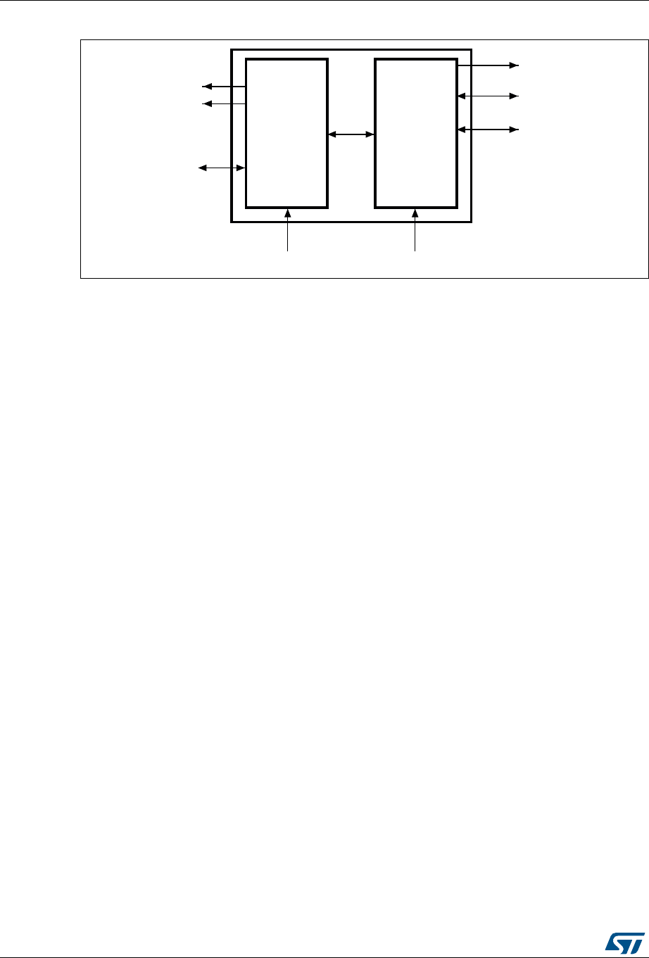
Secure digital input/output interface (SDIO) RM0383
606/836 DocID026448 Rev 1
Figure 234. SDIO block diagram
By default SDIO_D0 is used for data transfer. After initialization, the host can change the
databus width.
If a MultiMediaCard is connected to the bus, SDIO_D0, SDIO_D[3:0] or SDIO_D[7:0] can be
used for data transfer. MMC V3.31 or previous, supports only 1 bit of data so only SDIO_D0
can be used.
If an SD or SD I/O card is connected to the bus, data transfer can be configured by the host
to use SDIO_D0 or SDIO_D[3:0]. All data lines are operating in push-pull mode.
SDIO_CMD has two operational modes:
•Open-drain for initialization (only for MMCV3.31 or previous)
•Push-pull for command transfer (SD/SD I/O card MMC4.2 use push-pull drivers also for
initialization)
SDIO_CK is the clock to the card: one bit is transferred on both command and data lines
with each clock cycle. The clock frequency can vary between 0 MHz and 20 MHz (for a
MultiMediaCard V3.31), between 0 and 48 MHz for a MultiMediaCard V4.0/4.2, or between
0 and 25 MHz (for an SD/SD I/O card).
The SDIO uses two clock signals:
•SDIO adapter clock (SDIOCLK = 48 MHz)
•APB2 bus clock (PCLK2)
PCLK2 and SDIO_CK clock frequencies must respect the following condition:
The signals shown in Table 92 are used on the MultiMediaCard/SD/SD I/O card bus.
!0"BUS
!0"
)NTERRUPTSAND
0#,+
3$)/?#+
ADAPTER
INTERFACE
$-!REQUEST
3$)/#,+
3$)/
3$)/
3$)/?$;=
3$)/?#-$
AI
Frequenc PCLK2()38⁄Frequency SDIO_CK()×≥
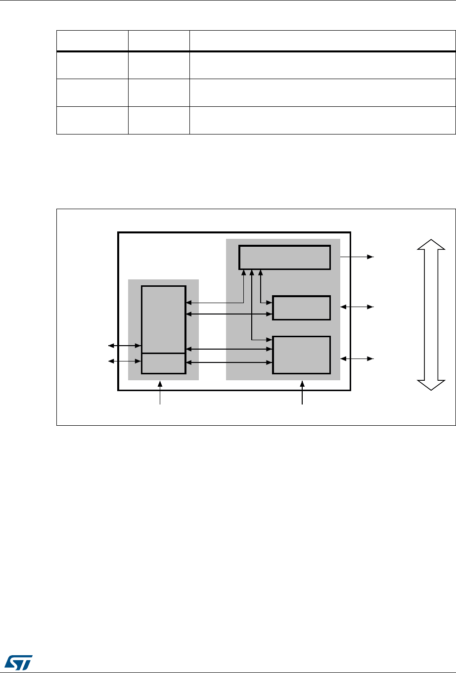
DocID026448 Rev 1 607/836
RM0383 Secure digital input/output interface (SDIO)
658
21.3.1 SDIO adapter
Figure 235 shows a simplified block diagram of an SDIO adapter.
Figure 235. SDIO adapter
The SDIO adapter is a multimedia/secure digital memory card bus master that provides an
interface to a multimedia card stack or to a secure digital memory card. It consists of five
subunits:
•Adapter register block
•Control unit
•Command path
•Data path
•Data FIFO
Note: The adapter registers and FIFO use the APB2 bus clock domain (PCLK2). The control unit,
command path and data path use the SDIO adapter clock domain (SDIOCLK).
Adapter register block
The adapter register block contains all system registers. This block also generates the
signals that clear the static flags in the multimedia card. The clear signals are generated
when 1 is written into the corresponding bit location in the SDIO Clear register.
Table 92. SDIO I/O definitions
Pin Direction Description
SDIO_CK Output MultiMediaCard/SD/SDIO card clock. This pin is the clock from
host to card.
SDIO_CMD Bidirectional MultiMediaCard/SD/SDIO card command. This pin is the
bidirectional command/response signal.
SDIO_D[7:0] Bidirectional MultiMediaCard/SD/SDIO card data. These pins are the
bidirectional databus.
4O!0"
INTERFACE
AI
#ONTROLUNIT
#OMMAND
PATH
$ATAPATH
!DAPTER
REGISTERS
&)&/
3$)/?#+
3$)/?#-$
3$)/?$;=
0#,+ 3$)/#,+
#ARDBUS
3$)/ADAPTER
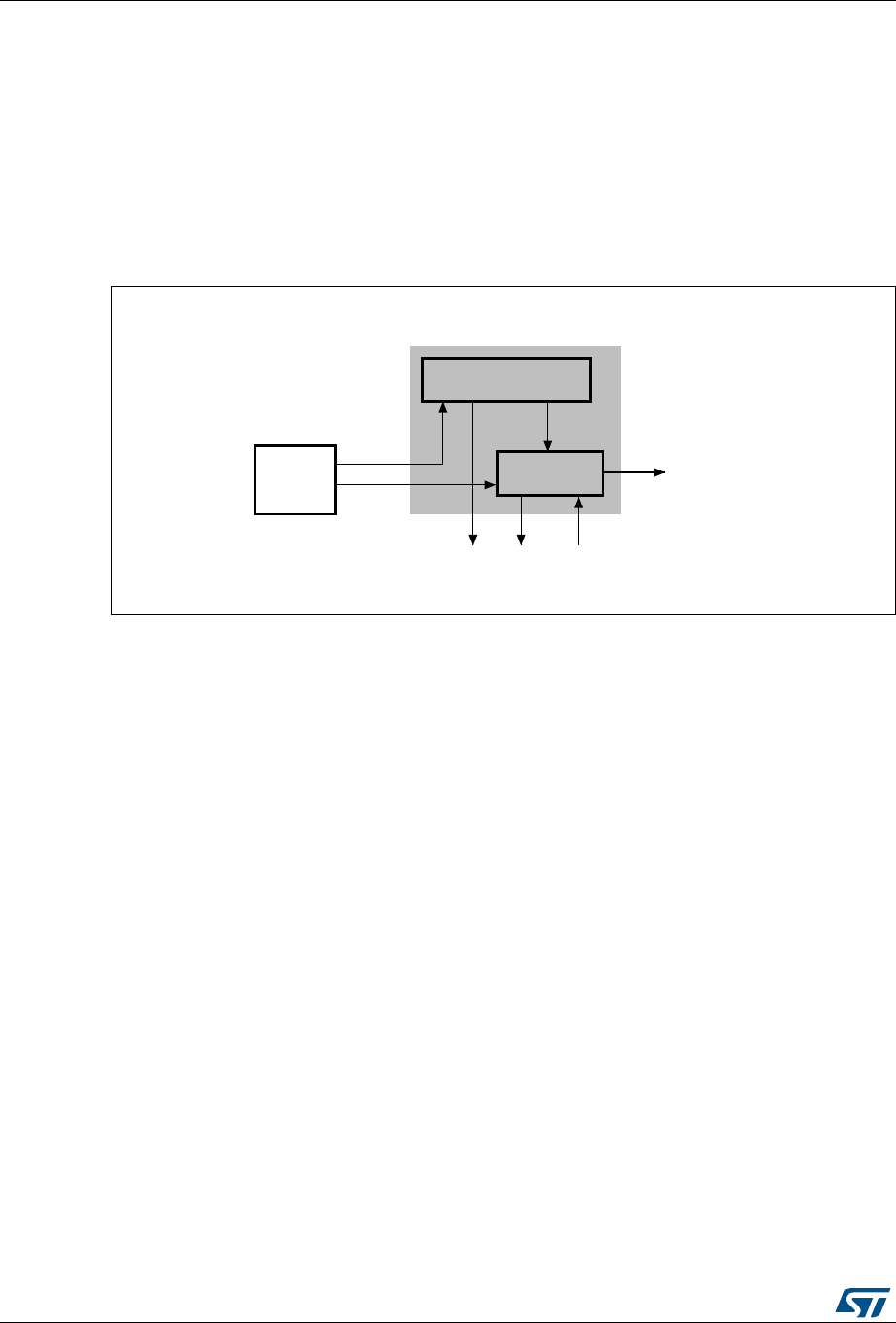
Secure digital input/output interface (SDIO) RM0383
608/836 DocID026448 Rev 1
Control unit
The control unit contains the power management functions and the clock divider for the
memory card clock.
There are three power phases:
•power-off
•power-up
•power-on
Figure 236. Control unit
The control unit is illustrated in Figure 236. It consists of a power management subunit and
a clock management subunit.
The power management subunit disables the card bus output signals during the power-off
and power-up phases.
The clock management subunit generates and controls the SDIO_CK signal. The SDIO_CK
output can use either the clock divide or the clock bypass mode. The clock output is
inactive:
•after reset
•during the power-off or power-up phases
•if the power saving mode is enabled and the card bus is in the Idle state (eight clock
periods after both the command and data path subunits enter the Idle phase)
Command path
The command path unit sends commands to and receives responses from the cards.
ai14804
Power management
Clock
management
Adapter
registers
SDIO_CK
Control unit
To command and data path
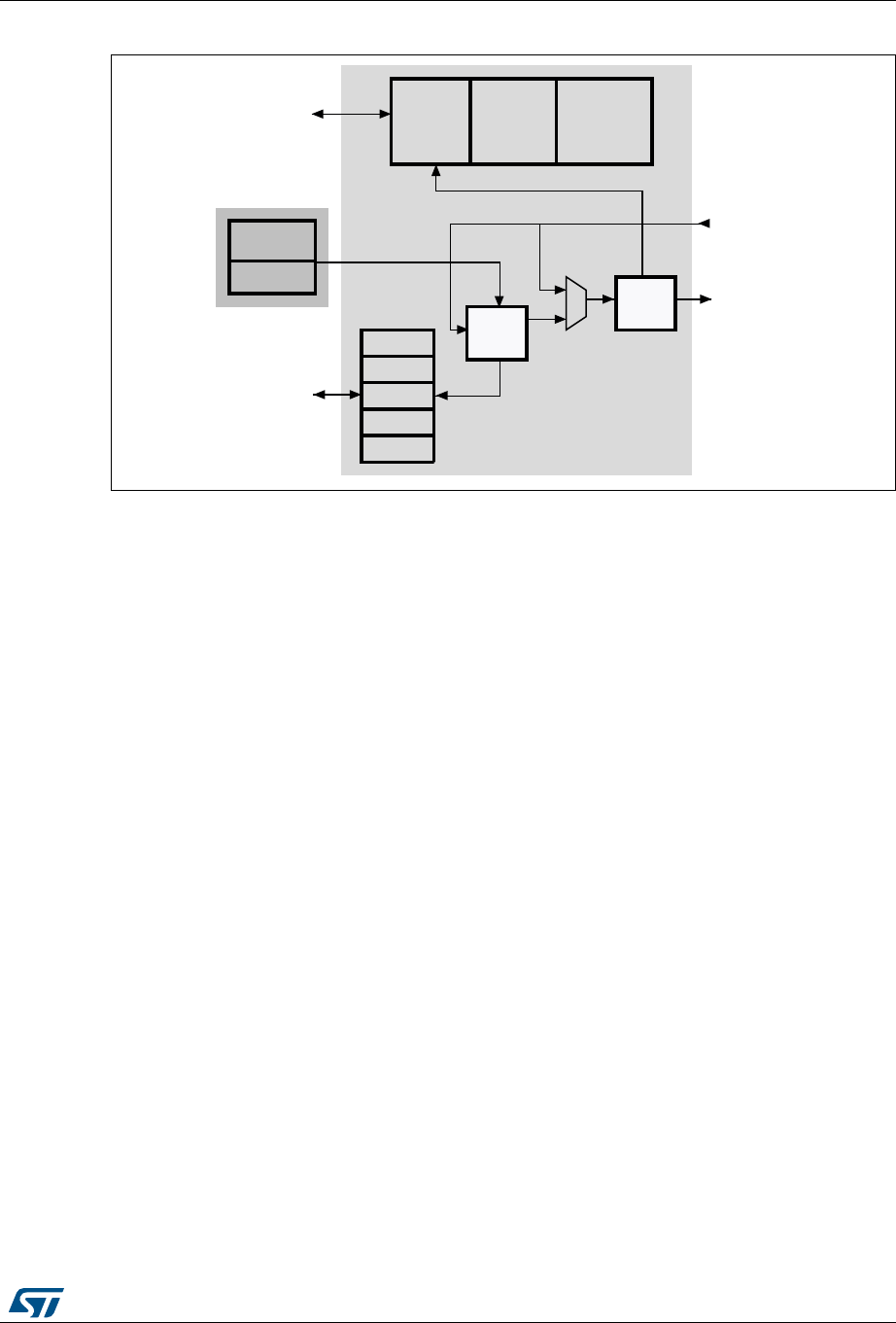
DocID026448 Rev 1 609/836
RM0383 Secure digital input/output interface (SDIO)
658
Figure 237. SDIO adapter command path
•Command path state machine (CPSM)
– When the command register is written to and the enable bit is set, command
transfer starts. When the command has been sent, the command path state
machine (CPSM) sets the status flags and enters the Idle state if a response is not
required. If a response is required, it waits for the response (see Figure 238 on
page 610). When the response is received, the received CRC code and the
internally generated code are compared, and the appropriate status flags are set.
AI
#-$
3TATUS
FLAG
#ONTROL
LOGIC
#OMMAND
TIMER
#2#
!RGUMENT
3HIFT
REGISTER
#-$
2ESPONSE
REGISTERS
4OCONTROLUNIT
3$)/?#-$IN
3$)/?#-$OUT
4O!0"INTERFACE
!DAPTERREGISTERS
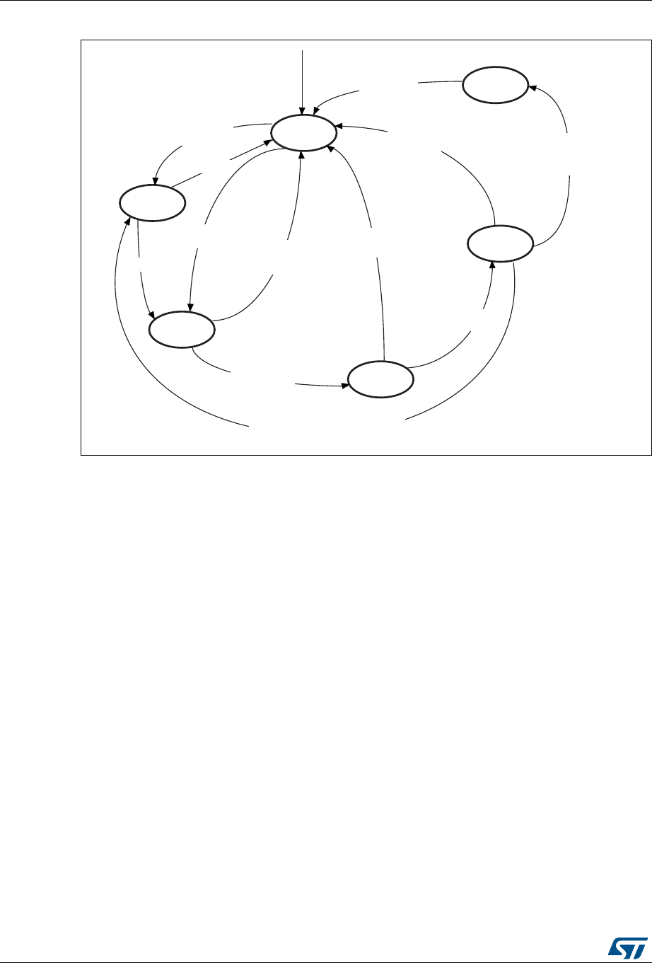
Secure digital input/output interface (SDIO) RM0383
610/836 DocID026448 Rev 1
Figure 238. Command path state machine (CPSM)
When the Wait state is entered, the command timer starts running. If the timeout is reached
before the CPSM moves to the Receive state, the timeout flag is set and the Idle state is
entered.
Note: The command timeout has a fixed value of 64 SDIO_CK clock periods.
If the interrupt bit is set in the command register, the timer is disabled and the CPSM waits
for an interrupt request from one of the cards. If a pending bit is set in the command register,
the CPSM enters the Pend state, and waits for a CmdPend signal from the data path
subunit. When CmdPend is detected, the CPSM moves to the Send state. This enables the
data counter to trigger the stop command transmission.
Note: The CPSM remains in the Idle state for at least eight SDIO_CK periods to meet the NCC and
NRC timing constraints. NCC is the minimum delay between two host commands, and NRC is
the minimum delay between the host command and the card response.
Idle
Pend
Send
Wait
Receive
Last Data
CPSM
disabled
Enabled and
command start CPSM disabled or
no response
Wait for response
Response
started
Response received or
disabled or command
CRC failed
CPSM Disabled or
command timeout
CPSM Enabled and
pending command
ai14806b
Wait_CPL
Response Received in CE-ATA
mode and no interrupt and
wait for CE-ATA Command
Completion signal enabled
Response Received in CE-ATA mode and
no interrupt and wait for CE-ATA
Command Completion signal disabled
CE-ATA Command
Completion signal
received or
CPSM disabled or
Command CRC failed
On reset
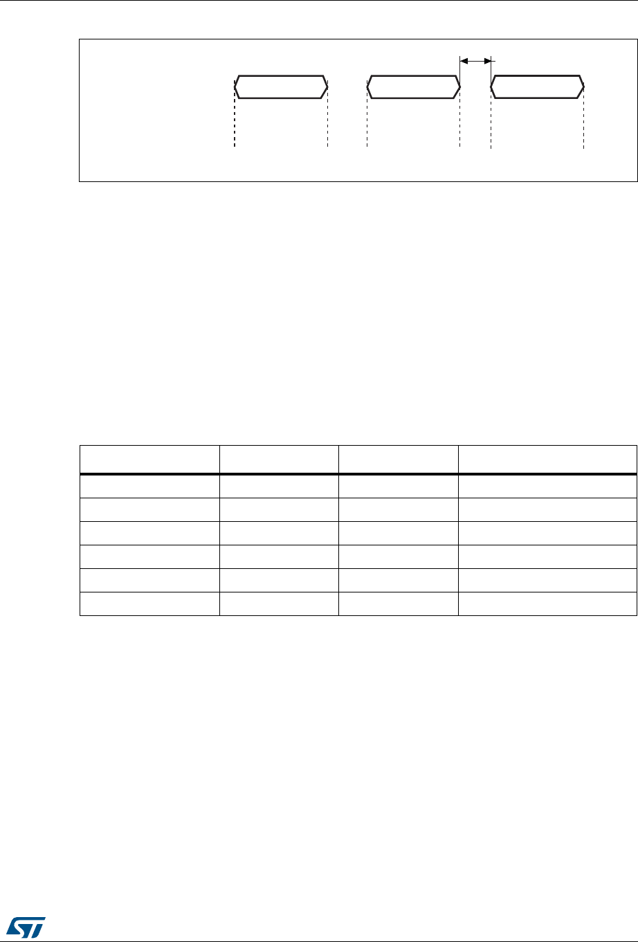
DocID026448 Rev 1 611/836
RM0383 Secure digital input/output interface (SDIO)
658
Figure 239. SDIO command transfer
•Command format
– Command: a command is a token that starts an operation. Command are sent
from the host either to a single card (addressed command) or to all connected
cards (broadcast command are available for MMC V3.31 or previous). Commands
are transferred serially on the CMD line. All commands have a fixed length of 48
bits. The general format for a command token for MultiMediaCards, SD-Memory
cards and SDIO-Cards is shown in Table 93. CE-ATA commands are an extension
of MMC commands V4.2, and so have the same format.
The command path operates in a half-duplex mode, so that commands and
responses can either be sent or received. If the CPSM is not in the Send state, the
SDIO_CMD output is in the Hi-Z state, as shown in Figure 239 on page 611. Data
on SDIO_CMD are synchronous with the rising edge of SDIO_CK. Table shows
the command format.
– Response: a response is a token that is sent from an addressed card (or
synchronously from all connected cards for MMC V3.31 or previous), to the host
as an answer to a previously received command. Responses are transferred
serially on the CMD line.
The SDIO supports two response types. Both use CRC error checking:
•48 bit short response
•136 bit long response
Note: If the response does not contain a CRC (CMD1 response), the device driver must ignore the
CRC failed status.
Table 93. Command format
Bit position Width Value Description
47 1 0 Start bit
46 1 1 Transmission bit
[45:40] 6 - Command index
[39:8] 32 - Argument
[7:1] 7 - CRC7
011End bit
SDIO_CK
SDIO_CMD
Command Response Command
State Idle Send Wait Receive Idle Send
Hi-Z Controller drives Hi-Z Card drives Hi-Z Controller drives
ai14707
at least 8 SDIO_CK cycles
Secure digital input/output interface (SDIO) RM0383
612/836 DocID026448 Rev 1
The command register contains the command index (six bits sent to a card) and the
command type. These determine whether the command requires a response, and whether
the response is 48 or 136 bits long (see Section 21.9.4 on page 646). The command path
implements the status flags shown in Table 96:
The CRC generator calculates the CRC checksum for all bits before the CRC code. This
includes the start bit, transmitter bit, command index, and command argument (or card
status). The CRC checksum is calculated for the first 120 bits of CID or CSD for the long
response format. Note that the start bit, transmitter bit and the six reserved bits are not used
in the CRC calculation.
The CRC checksum is a 7-bit value:
CRC[6:0] = Remainder [(M(x) * x7) / G(x)]
G(x) = x7 + x3 + 1
M(x) = (start bit) * x39 + ... + (last bit before CRC) * x0, or
M(x) = (start bit) * x119 + ... + (last bit before CRC) * x0
Table 94. Short response format
Bit position Width Value Description
47 1 0 Start bit
46 1 0 Transmission bit
[45:40] 6 - Command index
[39:8] 32 - Argument
[7:1] 7 - CRC7(or 1111111)
011End bit
Table 95. Long response format
Bit position Width Value Description
135 1 0 Start bit
134 1 0 Transmission bit
[133:128] 6 111111 Reserved
[127:1] 127 - CID or CSD (including internal CRC7)
0 1 1 End bit
Table 96. Command path status flags
Flag Description
CMDREND Set if response CRC is OK.
CCRCFAIL Set if response CRC fails.
CMDSENT Set when command (that does not require response) is sent
CTIMEOUT Response timeout.
CMDACT Command transfer in progress.
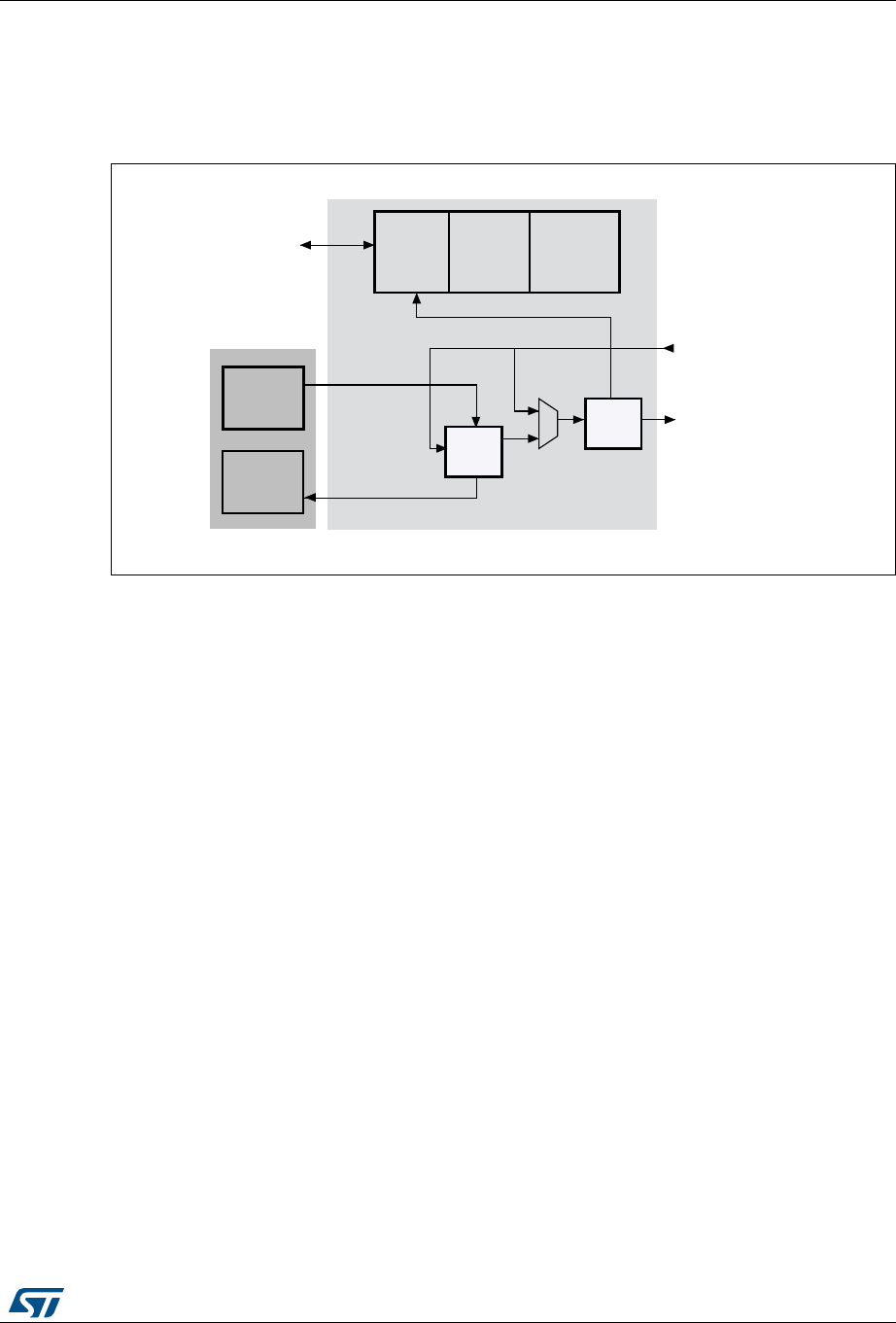
DocID026448 Rev 1 613/836
RM0383 Secure digital input/output interface (SDIO)
658
Data path
The data path subunit transfers data to and from cards. Figure 240 shows a block diagram
of the data path.
Figure 240. Data path
The card databus width can be programmed using the clock control register. If the 4-bit wide
bus mode is enabled, data is transferred at four bits per clock cycle over all four data signals
(SDIO_D[3:0]). If the 8-bit wide bus mode is enabled, data is transferred at eight bits per
clock cycle over all eight data signals (SDIO_D[7:0]). If the wide bus mode is not enabled,
only one bit per clock cycle is transferred over SDIO_D0.
Depending on the transfer direction (send or receive), the data path state machine (DPSM)
moves to the Wait_S or Wait_R state when it is enabled:
•Send: the DPSM moves to the Wait_S state. If there is data in the transmit FIFO, the
DPSM moves to the Send state, and the data path subunit starts sending data to a
card.
•Receive: the DPSM moves to the Wait_R state and waits for a start bit. When it
receives a start bit, the DPSM moves to the Receive state, and the data path subunit
starts receiving data from a card.
Data path state machine (DPSM)
The DPSM operates at SDIO_CK frequency. Data on the card bus signals is synchronous to
the rising edge of SDIO_CK. The DPSM has six states, as shown in Figure 241: Data path
state machine (DPSM).
ai14808
Transmit
Status
flag
Control
logic
Data
timer
CRC
Receive
Shift
register
To control unit
SDIO_Din[7:0]
SDIO_Dout[7:0]
Data FIFO
Data path
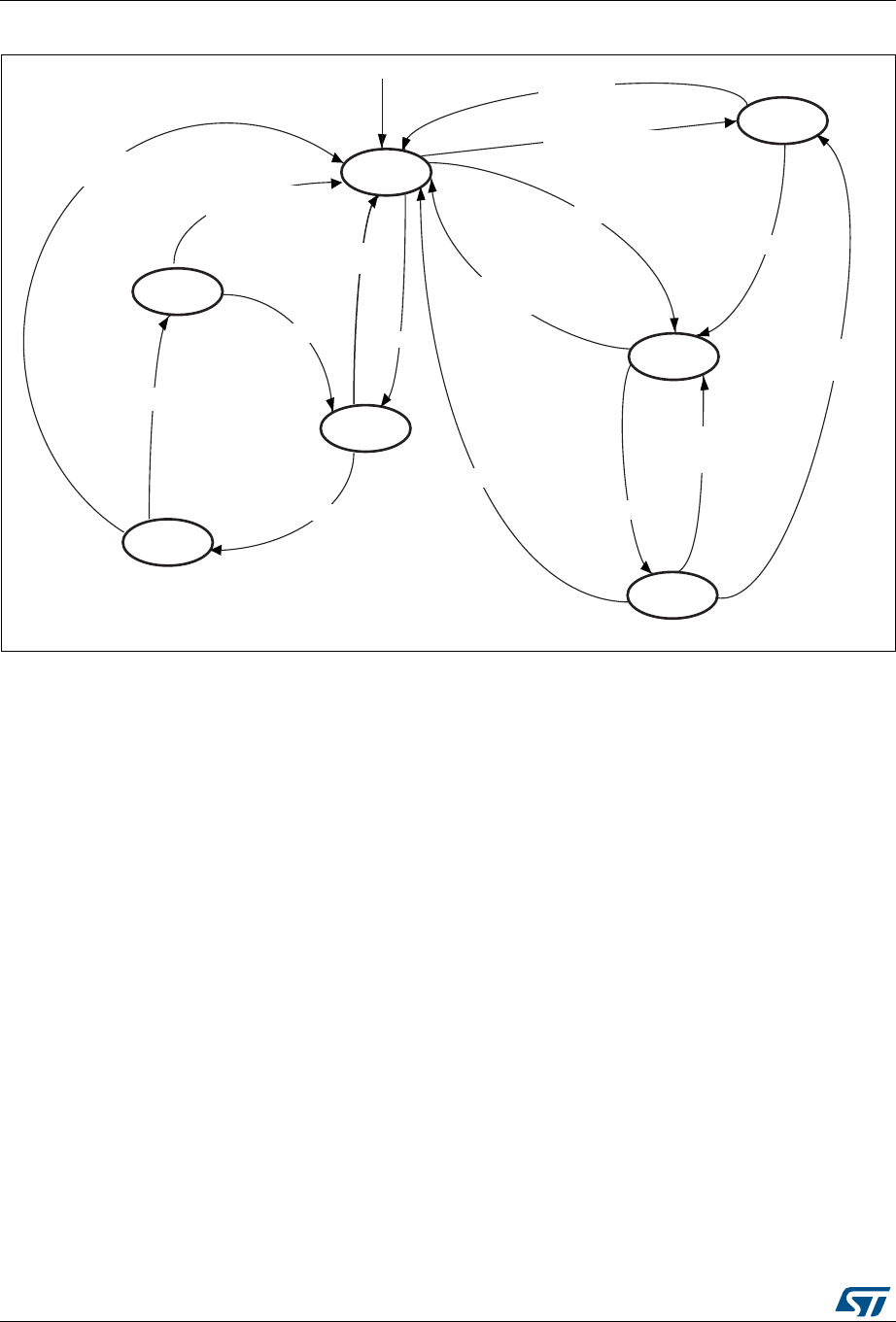
Secure digital input/output interface (SDIO) RM0383
614/836 DocID026448 Rev 1
Figure 241. Data path state machine (DPSM)
•Idle: the data path is inactive, and the SDIO_D[7:0] outputs are in Hi-Z. When the data
control register is written and the enable bit is set, the DPSM loads the data counter
with a new value and, depending on the data direction bit, moves to either the Wait_S
or the Wait_R state.
•Wait_R: if the data counter equals zero, the DPSM moves to the Idle state when the
receive FIFO is empty. If the data counter is not zero, the DPSM waits for a start bit on
SDIO_D. The DPSM moves to the Receive state if it receives a start bit before a
timeout, and loads the data block counter. If it reaches a timeout before it detects a
start bit, or a start bit error occurs, it moves to the Idle state and sets the timeout status
flag.
•Receive: serial data received from a card is packed in bytes and written to the data
FIFO. Depending on the transfer mode bit in the data control register, the data transfer
mode can be either block or stream:
– In block mode, when the data block counter reaches zero, the DPSM waits until it
receives the CRC code. If the received code matches the internally generated
CRC code, the DPSM moves to the Wait_R state. If not, the CRC fail status flag is
set and the DPSM moves to the Idle state.
– In stream mode, the DPSM receives data while the data counter is not zero. When
the counter is zero, the remaining data in the shift register is written to the data
FIFO, and the DPSM moves to the Wait_R state.
If a FIFO overrun error occurs, the DPSM sets the FIFO error flag and moves to the
Idle state:
•Wait_S: the DPSM moves to the Idle state if the data counter is zero. If not, it waits until
the data FIFO empty flag is deasserted, and moves to the Send state.
Idle
Busy
Send
Wait_R
Receive
End of packet
Disabled or CRC fail
or timeout
Not busy
Disabled or
end of data
Data ready
End of packet or
end of data or
FIFO overrun
Enable and not send
Disabled or
Rx FIFO empty or timeout or
start bit error
Disabled or FIFO underrun or
end of data or CRC fail
ai14809b
Wait_S
Start bit
On reset
Disabled or CRC fail
Enable and send
DPSM disabled
Read Wait
DPSM enabled and
Read Wait Started
and SD I/O mode enabled
ReadWait Stop
Data received and
Read Wait Started and
SD I/O mode enabled

DocID026448 Rev 1 615/836
RM0383 Secure digital input/output interface (SDIO)
658
Note: The DPSM remains in the Wait_S state for at least two clock periods to meet the NWR timing
requirements, where NWR is the number of clock cycles between the reception of the card
response and the start of the data transfer from the host.
•Send: the DPSM starts sending data to a card. Depending on the transfer mode bit in
the data control register, the data transfer mode can be either block or stream:
– In block mode, when the data block counter reaches zero, the DPSM sends an
internally generated CRC code and end bit, and moves to the Busy state.
– In stream mode, the DPSM sends data to a card while the enable bit is high and
the data counter is not zero. It then moves to the Idle state.
If a FIFO underrun error occurs, the DPSM sets the FIFO error flag and moves to the
Idle state.
•Busy: the DPSM waits for the CRC status flag:
– If it does not receive a positive CRC status, it moves to the Idle state and sets the
CRC fail status flag.
– If it receives a positive CRC status, it moves to the Wait_S state if SDIO_D0 is not
low (the card is not busy).
If a timeout occurs while the DPSM is in the Busy state, it sets the data timeout flag and
moves to the Idle state.
The data timer is enabled when the DPSM is in the Wait_R or Busy state, and
generates the data timeout error:
– When transmitting data, the timeout occurs if the DPSM stays in the Busy state for
longer than the programmed timeout period
– When receiving data, the timeout occurs if the end of the data is not true, and if the
DPSM stays in the Wait_R state for longer than the programmed timeout period.
•Data: data can be transferred from the card to the host or vice versa. Data is
transferred via the data lines. They are stored in a FIFO of 32 words, each word is 32
bits wide.
Data FIFO
The data FIFO (first-in-first-out) subunit is a data buffer with a transmit and receive unit.
The FIFO contains a 32-bit wide, 32-word deep data buffer, and transmit and receive logic.
Because the data FIFO operates in the APB2 clock domain (PCLK2), all signals from the
subunits in the SDIO clock domain (SDIOCLK) are resynchronized.
Table 97. Data token format
Description Start bit Data CRC16 End bit
Block Data 0 - yes 1
Stream Data 0 - no 1

Secure digital input/output interface (SDIO) RM0383
616/836 DocID026448 Rev 1
Depending on the TXACT and RXACT flags, the FIFO can be disabled, transmit enabled, or
receive enabled. TXACT and RXACT are driven by the data path subunit and are mutually
exclusive:
– The transmit FIFO refers to the transmit logic and data buffer when TXACT is
asserted
– The receive FIFO refers to the receive logic and data buffer when RXACT is
asserted
•Transmit FIFO:
Data can be written to the transmit FIFO through the APB2 interface when the SDIO is
enabled for transmission.
The transmit FIFO is accessible via 32 sequential addresses. The transmit FIFO
contains a data output register that holds the data word pointed to by the read pointer.
When the data path subunit has loaded its shift register, it increments the read pointer
and drives new data out.
If the transmit FIFO is disabled, all status flags are deasserted. The data path subunit
asserts TXACT when it transmits data.
•Receive FIFO
When the data path subunit receives a word of data, it drives the data on the write
databus. The write pointer is incremented after the write operation completes. On the
read side, the contents of the FIFO word pointed to by the current value of the read
pointer is driven onto the read databus. If the receive FIFO is disabled, all status flags
are deasserted, and the read and write pointers are reset. The data path subunit
asserts RXACT when it receives data. Table 99 lists the receive FIFO status flags. The
receive FIFO is accessible via 32 sequential addresses.
Table 98. Transmit FIFO status flags
Flag Description
TXFIFOF Set to high when all 32 transmit FIFO words contain valid data.
TXFIFOE Set to high when the transmit FIFO does not contain valid data.
TXFIFOHE Set to high when 8 or more transmit FIFO words are empty. This flag can be used
as a DMA request.
TXDAVL Set to high when the transmit FIFO contains valid data. This flag is the inverse of
the TXFIFOE flag.
TXUNDERR Set to high when an underrun error occurs. This flag is cleared by writing to the
SDIO Clear register.

DocID026448 Rev 1 617/836
RM0383 Secure digital input/output interface (SDIO)
658
21.3.2 SDIO APB2 interface
The APB2 interface generates the interrupt and DMA requests, and accesses the SDIO
adapter registers and the data FIFO. It consists of a data path, register decoder, and
interrupt/DMA logic.
SDIO interrupts
The interrupt logic generates an interrupt request signal that is asserted when at least one
of the selected status flags is high. A mask register is provided to allow selection of the
conditions that will generate an interrupt. A status flag generates the interrupt request if a
corresponding mask flag is set.
SDIO/DMA interface - procedure for data transfers between the SDIO and
memory
In the example shown, the transfer is from the SDIO host controller to an MMC (512 bytes
using CMD24 (WRITE_BLOCK). The SDIO FIFO is filled by data stored in a memory using
the DMA controller.
1. Do the card identification process
2. Increase the SDIO_CK frequency
3. Select the card by sending CMD7
4. Configure the DMA2 as follows:
a) Enable DMA2 controller and clear any pending interrupts.
b) Program the DMA2_Stream3 or DMA2_Stream6 Channel4 source address
register with the memory location’s base address and DMA2_Stream3 or
Table 99. Receive FIFO status flags
Flag Description
RXFIFOF Set to high when all 32 receive FIFO words contain valid data
RXFIFOE Set to high when the receive FIFO does not contain valid data.
RXFIFOHF Set to high when 8 or more receive FIFO words contain valid data. This flag can be
used as a DMA request.
RXDAVL Set to high when the receive FIFO is not empty. This flag is the inverse of the
RXFIFOE flag.
RXOVERR Set to high when an overrun error occurs. This flag is cleared by writing to the SDIO
Clear register.

Secure digital input/output interface (SDIO) RM0383
618/836 DocID026448 Rev 1
DMA2_Stream6 Channel4 destination address register with the SDIO_FIFO
register address.
c) Program DMA2_Stream3 or DMA2_Stream6 Channel4 control register (memory
increment, not peripheral increment, peripheral and source width is word size).
d) Program DMA2_Stream3 or DMA2_Stream6 Channel4 to select the peripheral as
flow controller (set PFCTRL bit in DMA_S3CR or DMA_S6CR configuration
register).
e) Configure the incremental burst transfer to 4 beats (at least from peripheral side)
in DMA2_Stream3 or DMA2_Stream6 Channel4.
f) Enable DMA2_Stream3 or DMA2_Stream6 Channel4
5. Send CMD24 (WRITE_BLOCK) as follows:
a) Program the SDIO data length register (SDIO data timer register should be
already programmed before the card identification process).
b) Program the SDIO argument register with the address location of the card where
data is to be transferred.
c) Program the SDIO command register: CmdIndex with 24 (WRITE_BLOCK);
WaitResp with ‘1’ (SDIO card host waits for a response); CPSMEN with ‘1’ (SDIO
card host enabled to send a command). Other fields are at their reset value.
d) Wait for SDIO_STA[6] = CMDREND interrupt, then program the SDIO data control
register: DTEN with ‘1’ (SDIO card host enabled to send data); DTDIR with ‘0’
(from controller to card); DTMODE with ‘0’ (block data transfer); DMAEN with ‘1’
(DMA enabled); DBLOCKSIZE with 0x9 (512 bytes). Other fields are don’t care.
e) Wait for SDIO_STA[10] = DBCKEND.
6. Check that no channels are still enabled by polling the DMA Enabled Channel Status
register.
21.4 Card functional description
21.4.1 Card identification mode
While in card identification mode the host resets all cards, validates the operation voltage
range, identifies cards and sets a relative card address (RCA) for each card on the bus. All
data communications in the card identification mode use the command line (CMD) only.
21.4.2 Card reset
The GO_IDLE_STATE command (CMD0) is the software reset command and it puts the
MultiMediaCard and SD memory in the Idle state. The IO_RW_DIRECT command (CMD52)
resets the SD I/O card. After power-up or CMD0, all cards output bus drivers are in the high-
impedance state and the cards are initialized with a default relative card address
(RCA=0x0001) and with a default driver stage register setting (lowest speed, highest driving
current capability).
21.4.3 Operating voltage range validation
All cards can communicate with the SDIO card host using any operating voltage within the
specification range. The supported minimum and maximum VDD values are defined in the
operation conditions register (OCR) on the card.

DocID026448 Rev 1 619/836
RM0383 Secure digital input/output interface (SDIO)
658
Cards that store the card identification number (CID) and card specific data (CSD) in the
payload memory are able to communicate this information only under data-transfer VDD
conditions. When the SDIO card host module and the card have incompatible VDD ranges,
the card is not able to complete the identification cycle and cannot send CSD data. For this
purpose, the special commands, SEND_OP_COND (CMD1), SD_APP_OP_COND (ACMD41
for SD Memory), and IO_SEND_OP_COND (CMD5 for SD I/O), are designed to provide a
mechanism to identify and reject cards that do not match the VDD range desired by the
SDIO card host. The SDIO card host sends the required VDD voltage window as the
operand of these commands. Cards that cannot perform data transfer in the specified range
disconnect from the bus and go to the inactive state.
By using these commands without including the voltage range as the operand, the SDIO
card host can query each card and determine the common voltage range before placing out-
of-range cards in the inactive state. This query is used when the SDIO card host is able to
select a common voltage range or when the user requires notification that cards are not
usable.
21.4.4 Card identification process
The card identification process differs for MultiMediaCards and SD cards. For
MultiMediaCard cards, the identification process starts at clock rate Fod. The SDIO_CMD
line output drivers are open-drain and allow parallel card operation during this process. The
registration process is accomplished as follows:
1. The bus is activated.
2. The SDIO card host broadcasts SEND_OP_COND (CMD1) to receive operation
conditions.
3. The response is the wired AND operation of the operation condition registers from all
cards.
4. Incompatible cards are placed in the inactive state.
5. The SDIO card host broadcasts ALL_SEND_CID (CMD2) to all active cards.
6. The active cards simultaneously send their CID numbers serially. Cards with outgoing
CID bits that do not match the bits on the command line stop transmitting and must wait
for the next identification cycle. One card successfully transmits a full CID to the SDIO
card host and enters the Identification state.
7. The SDIO card host issues SET_RELATIVE_ADDR (CMD3) to that card. This new
address is called the relative card address (RCA); it is shorter than the CID and
addresses the card. The assigned card changes to the Standby state, it does not react
to further identification cycles, and its output switches from open-drain to push-pull.
8. The SDIO card host repeats steps 5 through 7 until it receives a timeout condition.
For the SD card, the identification process starts at clock rate Fod, and the SDIO_CMD line
output drives are push-pull drivers instead of open-drain. The registration process is
accomplished as follows:

Secure digital input/output interface (SDIO) RM0383
620/836 DocID026448 Rev 1
1. The bus is activated.
2. The SDIO card host broadcasts SD_APP_OP_COND (ACMD41).
3. The cards respond with the contents of their operation condition registers.
4. The incompatible cards are placed in the inactive state.
5. The SDIO card host broadcasts ALL_SEND_CID (CMD2) to all active cards.
6. The cards send back their unique card identification numbers (CIDs) and enter the
Identification state.
7. The SDIO card host issues SET_RELATIVE_ADDR (CMD3) to an active card with an
address. This new address is called the relative card address (RCA); it is shorter than
the CID and addresses the card. The assigned card changes to the Standby state. The
SDIO card host can reissue this command to change the RCA. The RCA of the card is
the last assigned value.
8. The SDIO card host repeats steps 5 through 7 with all active cards.
For the SD I/O card, the registration process is accomplished as follows:
1. The bus is activated.
2. The SDIO card host sends IO_SEND_OP_COND (CMD5).
3. The cards respond with the contents of their operation condition registers.
4. The incompatible cards are set to the inactive state.
5. The SDIO card host issues SET_RELATIVE_ADDR (CMD3) to an active card with an
address. This new address is called the relative card address (RCA); it is shorter than
the CID and addresses the card. The assigned card changes to the Standby state. The
SDIO card host can reissue this command to change the RCA. The RCA of the card is
the last assigned value.
21.4.5 Block write
During block write (CMD24 - 27) one or more blocks of data are transferred from the host to
the card with a CRC appended to the end of each block by the host. A card supporting block
write is always able to accept a block of data defined by WRITE_BL_LEN. If the CRC fails,
the card indicates the failure on the SDIO_D line and the transferred data are discarded and
not written, and all further transmitted blocks (in multiple block write mode) are ignored.
If the host uses partial blocks whose accumulated length is not block aligned and, block
misalignment is not allowed (CSD parameter WRITE_BLK_MISALIGN is not set), the card
will detect the block misalignment error before the beginning of the first misaligned block.
(ADDRESS_ERROR error bit is set in the status register). The write operation will also be
aborted if the host tries to write over a write-protected area. In this case, however, the card
will set the WP_VIOLATION bit.
Programming of the CID and CSD registers does not require a previous block length setting.
The transferred data is also CRC protected. If a part of the CSD or CID register is stored in
ROM, then this unchangeable part must match the corresponding part of the receive buffer.
If this match fails, then the card reports an error and does not change any register contents.
Some cards may require long and unpredictable times to write a block of data. After
receiving a block of data and completing the CRC check, the card begins writing and holds
the SDIO_D line low if its write buffer is full and unable to accept new data from a new
WRITE_BLOCK command. The host may poll the status of the card with a SEND_STATUS
command (CMD13) at any time, and the card will respond with its status. The
READY_FOR_DATA status bit indicates whether the card can accept new data or whether
the write process is still in progress. The host may deselect the card by issuing CMD7 (to

DocID026448 Rev 1 621/836
RM0383 Secure digital input/output interface (SDIO)
658
select a different card), which will place the card in the Disconnect state and release the
SDIO_D line(s) without interrupting the write operation. When selecting the card again, it will
reactivate busy indication by pulling SDIO_D to low if programming is still in progress and
the write buffer is unavailable.
21.4.6 Block read
In Block read mode the basic unit of data transfer is a block whose maximum size is defined
in the CSD (READ_BL_LEN). If READ_BL_PARTIAL is set, smaller blocks whose start and
end addresses are entirely contained within one physical block (as defined by
READ_BL_LEN) may also be transmitted. A CRC is appended to the end of each block,
ensuring data transfer integrity. CMD17 (READ_SINGLE_BLOCK) initiates a block read and
after completing the transfer, the card returns to the Transfer state.
CMD18 (READ_MULTIPLE_BLOCK) starts a transfer of several consecutive blocks.
The host can abort reading at any time, within a multiple block operation, regardless of its
type. Transaction abort is done by sending the stop transmission command.
If the card detects an error (for example, out of range, address misalignment or internal
error) during a multiple block read operation (both types) it stops the data transmission and
remains in the data state. The host must than abort the operation by sending the stop
transmission command. The read error is reported in the response to the stop transmission
command.
If the host sends a stop transmission command after the card transmits the last block of a
multiple block operation with a predefined number of blocks, it is responded to as an illegal
command, since the card is no longer in the data state. If the host uses partial blocks whose
accumulated length is not block-aligned and block misalignment is not allowed, the card
detects a block misalignment error condition at the beginning of the first misaligned block
(ADDRESS_ERROR error bit is set in the status register).
21.4.7 Stream access, stream write and stream read
(MultiMediaCard only)
In stream mode, data is transferred in bytes and no CRC is appended at the end of each
block.
Stream write (MultiMediaCard only)
WRITE_DAT_UNTIL_STOP (CMD20) starts the data transfer from the SDIO card host to the
card, beginning at the specified address and continuing until the SDIO card host issues a
stop command. When partial blocks are allowed (CSD parameter WRITE_BL_PARTIAL is
set), the data stream can start and stop at any address within the card address space,
otherwise it can only start and stop at block boundaries. Because the amount of data to be
transferred is not determined in advance, a CRC cannot be used. When the end of the
memory range is reached while sending data and no stop command is sent by the SD card
host, any additional transferred data are discarded.

Secure digital input/output interface (SDIO) RM0383
622/836 DocID026448 Rev 1
The maximum clock frequency for a stream write operation is given by the following
equation fields of the card-specific data register:
•Maximumspeed = maximum write frequency
•TRANSPEED = maximum data transfer rate
•writebllen = maximum write data block length
•NSAC = data read access time 2 in CLK cycles
•TAAC = data read access time 1
•R2WFACTOR = write speed factor
If the host attempts to use a higher frequency, the card may not be able to process the data
and stop programming, set the OVERRUN error bit in the status register, and while ignoring
all further data transfer, wait (in the receive data state) for a stop command. The write
operation is also aborted if the host tries to write over a write-protected area. In this case,
however, the card sets the WP_VIOLATION bit.
Stream read (MultiMediaCard only)
READ_DAT_UNTIL_STOP (CMD11) controls a stream-oriented data transfer.
This command instructs the card to send its data, starting at a specified address, until the
SDIO card host sends STOP_TRANSMISSION (CMD12). The stop command has an
execution delay due to the serial command transmission and the data transfer stops after
the end bit of the stop command. When the end of the memory range is reached while
sending data and no stop command is sent by the SDIO card host, any subsequent data
sent are considered undefined.
The maximum clock frequency for a stream read operation is given by the following
equation and uses fields of the card specific data register.
•Maximumspeed = maximum read frequency
•TRANSPEED = maximum data transfer rate
•readbllen = maximum read data block length
•writebllen = maximum write data block length
•NSAC = data read access time 2 in CLK cycles
•TAAC = data read access time 1
•R2WFACTOR = write speed factor
If the host attempts to use a higher frequency, the card is not able to sustain data transfer. If
this happens, the card sets the UNDERRUN error bit in the status register, aborts the
transmission and waits in the data state for a stop command.
21.4.8 Erase: group erase and sector erase
The erasable unit of the MultiMediaCard is the erase group. The erase group is measured in
write blocks, which are the basic writable units of the card. The size of the erase group is a
card-specific parameter and defined in the CSD.
Maximumspeed MIN TRANSPEED 82
writebllen
×()NSAC–()
TAAC R2WFACTOR×
-------------------------------------------------------------------------(, )=
Maximumspeed MIN TRANSPEED 82
readbllen
×()NSAC–()
TAAC R2WFACTOR×
------------------------------------------------------------------------(, )=

DocID026448 Rev 1 623/836
RM0383 Secure digital input/output interface (SDIO)
658
The host can erase a contiguous range of Erase Groups. Starting the erase process is a
three-step sequence.
First the host defines the start address of the range using the ERASE_GROUP_START
(CMD35) command, next it defines the last address of the range using the
ERASE_GROUP_END (CMD36) command and, finally, it starts the erase process by issuing
the ERASE (CMD38) command. The address field in the erase commands is an Erase
Group address in byte units. The card ignores all LSBs below the Erase Group size,
effectively rounding the address down to the Erase Group boundary.
If an erase command is received out of sequence, the card sets the ERASE_SEQ_ERROR
bit in the status register and resets the whole sequence.
If an out-of-sequence (neither of the erase commands, except SEND_STATUS) command
received, the card sets the ERASE_RESET status bit in the status register, resets the erase
sequence and executes the last command.
If the erase range includes write protected blocks, they are left intact and only unprotected
blocks are erased. The WP_ERASE_SKIP status bit in the status register is set.
The card indicates that an erase is in progress by holding SDIO_D low. The actual erase
time may be quite long, and the host may issue CMD7 to deselect the card.
21.4.9 Wide bus selection or deselection
Wide bus (4-bit bus width) operation mode is selected or deselected using
SET_BUS_WIDTH (ACMD6). The default bus width after power-up or GO_IDLE_STATE
(CMD0) is 1 bit. SET_BUS_WIDTH (ACMD6) is only valid in a transfer state, which means
that the bus width can be changed only after a card is selected by
SELECT/DESELECT_CARD (CMD7).
21.4.10 Protection management
Three write protection methods for the cards are supported in the SDIO card host module:
1. internal card write protection (card responsibility)
2. mechanical write protection switch (SDIO card host module responsibility only)
3. password-protected card lock operation
Internal card write protection
Card data can be protected against write and erase. By setting the permanent or temporary
write-protect bits in the CSD, the entire card can be permanently write-protected by the
manufacturer or content provider. For cards that support write protection of groups of
sectors by setting the WP_GRP_ENABLE bit in the CSD, portions of the data can be
protected, and the write protection can be changed by the application. The write protection
is in units of WP_GRP_SIZE sectors as specified in the CSD. The SET_WRITE_PROT and
CLR_WRITE_PROT commands control the protection of the addressed group. The
SEND_WRITE_PROT command is similar to a single block read command. The card sends
a data block containing 32 write protection bits (representing 32 write protect groups starting
at the specified address) followed by 16 CRC bits. The address field in the write protect
commands is a group address in byte units.
The card ignores all LSBs below the group size.

Secure digital input/output interface (SDIO) RM0383
624/836 DocID026448 Rev 1
Mechanical write protect switch
A mechanical sliding tab on the side of the card allows the user to set or clear the write
protection on a card. When the sliding tab is positioned with the window open, the card is
write-protected, and when the window is closed, the card contents can be changed. A
matched switch on the socket side indicates to the SDIO card host module that the card is
write-protected. The SDIO card host module is responsible for protecting the card. The
position of the write protect switch is unknown to the internal circuitry of the card.
Password protect
The password protection feature enables the SDIO card host module to lock and unlock a
card with a password. The password is stored in the 128-bit PWD register and its size is set
in the 8-bit PWD_LEN register. These registers are nonvolatile so that a power cycle does
not erase them. Locked cards respond to and execute certain commands. This means that
the SDIO card host module is allowed to reset, initialize, select, and query for status,
however it is not allowed to access data on the card. When the password is set (as indicated
by a nonzero value of PWD_LEN), the card is locked automatically after power-up. As with
the CSD and CID register write commands, the lock/unlock commands are available in the
transfer state only. In this state, the command does not include an address argument and
the card must be selected before using it. The card lock/unlock commands have the
structure and bus transaction types of a regular single-block write command. The
transferred data block includes all of the required information for the command (the
password setting mode, the PWD itself, and card lock/unlock). The command data block
size is defined by the SDIO card host module before it sends the card lock/unlock
command, and has the structure shown in Table 113.
The bit settings are as follows:
•ERASE: setting it forces an erase operation. All other bits must be zero, and only the
command byte is sent
•LOCK_UNLOCK: setting it locks the card. LOCK_UNLOCK can be set simultaneously
with SET_PWD, however not with CLR_PWD
•CLR_PWD: setting it clears the password data
•SET_PWD: setting it saves the password data to memory
•PWD_LEN: it defines the length of the password in bytes
•PWD: the password (new or currently used, depending on the command)
The following sections list the command sequences to set/reset a password, lock/unlock the
card, and force an erase.
Setting the password
1. Select a card (SELECT/DESELECT_CARD, CMD7), if none is already selected.
2. Define the block length (SET_BLOCKLEN, CMD16) to send, given by the 8-bit card
lock/unlock mode, the 8-bit PWD_LEN, and the number of bytes of the new password.
When a password replacement is done, the block size must take into account that both
the old and the new passwords are sent with the command.
3. Send LOCK/UNLOCK (CMD42) with the appropriate data block size on the data line
including the 16-bit CRC. The data block indicates the mode (SET_PWD = 1), the
length (PWD_LEN), and the password (PWD) itself. When a password replacement is
done, the length value (PWD_LEN) includes the length of both passwords, the old and

DocID026448 Rev 1 625/836
RM0383 Secure digital input/output interface (SDIO)
658
the new one, and the PWD field includes the old password (currently used) followed by
the new password.
4. When the password is matched, the new password and its size are saved into the PWD
and PWD_LEN fields, respectively. When the old password sent does not correspond
(in size and/or content) to the expected password, the LOCK_UNLOCK_FAILED error
bit is set in the card status register, and the password is not changed.
The password length field (PWD_LEN) indicates whether a password is currently set. When
this field is nonzero, there is a password set and the card locks itself after power-up. It is
possible to lock the card immediately in the current power session by setting the
LOCK_UNLOCK bit (while setting the password) or sending an additional command for card
locking.
Resetting the password
1. Select a card (SELECT/DESELECT_CARD, CMD7), if none is already selected.
2. Define the block length (SET_BLOCKLEN, CMD16) to send, given by the 8-bit card
lock/unlock mode, the 8-bit PWD_LEN, and the number of bytes in the currently used
password.
3. Send LOCK/UNLOCK (CMD42) with the appropriate data block size on the data line
including the 16-bit CRC. The data block indicates the mode (CLR_PWD = 1), the
length (PWD_LEN) and the password (PWD) itself. The LOCK_UNLOCK bit is ignored.
4. When the password is matched, the PWD field is cleared and PWD_LEN is set to 0.
When the password sent does not correspond (in size and/or content) to the expected
password, the LOCK_UNLOCK_FAILED error bit is set in the card status register, and
the password is not changed.
Locking a card
1. Select a card (SELECT/DESELECT_CARD, CMD7), if none is already selected.
2. Define the block length (SET_BLOCKLEN, CMD16) to send, given by the 8-bit card
lock/unlock mode (byte 0 in Table 113), the 8-bit PWD_LEN, and the number of bytes
of the current password.
3. Send LOCK/UNLOCK (CMD42) with the appropriate data block size on the data line
including the 16-bit CRC. The data block indicates the mode (LOCK_UNLOCK = 1), the
length (PWD_LEN), and the password (PWD) itself.
4. When the password is matched, the card is locked and the CARD_IS_LOCKED status
bit is set in the card status register. When the password sent does not correspond (in
size and/or content) to the expected password, the LOCK_UNLOCK_FAILED error bit
is set in the card status register, and the lock fails.
It is possible to set the password and to lock the card in the same sequence. In this case,
the SDIO card host module performs all the required steps for setting the password (see
Setting the password on page 624), however it is necessary to set the LOCK_UNLOCK bit
in Step 3 when the new password command is sent.
When the password is previously set (PWD_LEN is not 0), the card is locked automatically
after power-on reset. An attempt to lock a locked card or to lock a card that does not have a
password fails and the LOCK_UNLOCK_FAILED error bit is set in the card status register.

Secure digital input/output interface (SDIO) RM0383
626/836 DocID026448 Rev 1
Unlocking the card
1. Select a card (SELECT/DESELECT_CARD, CMD7), if none is already selected.
2. Define the block length (SET_BLOCKLEN, CMD16) to send, given by the 8-bit
cardlock/unlock mode (byte 0 in Table 113), the 8-bit PWD_LEN, and the number of
bytes of the current password.
3. Send LOCK/UNLOCK (CMD42) with the appropriate data block size on the data line
including the 16-bit CRC. The data block indicates the mode (LOCK_UNLOCK = 0), the
length (PWD_LEN), and the password (PWD) itself.
4. When the password is matched, the card is unlocked and the CARD_IS_LOCKED
status bit is cleared in the card status register. When the password sent is not correct in
size and/or content and does not correspond to the expected password, the
LOCK_UNLOCK_FAILED error bit is set in the card status register, and the card
remains locked.
The unlocking function is only valid for the current power session. When the PWD field is not
clear, the card is locked automatically on the next power-up.
An attempt to unlock an unlocked card fails and the LOCK_UNLOCK_FAILED error bit is set
in the card status register.
Forcing erase
If the user has forgotten the password (PWD content), it is possible to access the card after
clearing all the data on the card. This forced erase operation erases all card data and all
password data.
1. Select a card (SELECT/DESELECT_CARD, CMD7), if none is already selected.
2. Set the block length (SET_BLOCKLEN, CMD16) to 1 byte. Only the 8-bit card
lock/unlock byte (byte 0 in Table 113) is sent.
3. Send LOCK/UNLOCK (CMD42) with the appropriate data byte on the data line including
the 16-bit CRC. The data block indicates the mode (ERASE = 1). All other bits must be
zero.
4. When the ERASE bit is the only bit set in the data field, all card contents are erased,
including the PWD and PWD_LEN fields, and the card is no longer locked. When any
other bits are set, the LOCK_UNLOCK_FAILED error bit is set in the card status
register and the card retains all of its data, and remains locked.
An attempt to use a force erase on an unlocked card fails and the LOCK_UNLOCK_FAILED
error bit is set in the card status register.
21.4.11 Card status register
The response format R1 contains a 32-bit field named card status. This field is intended to
transmit the card status information (which may be stored in a local status register) to the
host. If not specified otherwise, the status entries are always related to the previously issued
command.
Table 100 defines the different entries of the status. The type and clear condition fields in
the table are abbreviated as follows:

DocID026448 Rev 1 627/836
RM0383 Secure digital input/output interface (SDIO)
658
Type:
•E: error bit
•S: status bit
•R: detected and set for the actual command response
•X: detected and set during command execution. The SDIO card host must poll the card
by issuing the status command to read these bits.
Clear condition:
•A: according to the card current state
•B: always related to the previous command. Reception of a valid command clears it
(with a delay of one command)
•C: clear by read
Table 100. Card status
Bits Identifier Type Value Description Clear
condition
31 ADDRESS_
OUT_OF_RANGE E R X ’0’= no error
’1’= error
The command address argument was out
of the allowed range for this card.
A multiple block or stream read/write
operation is (although started in a valid
address) attempting to read or write
beyond the card capacity.
C
30 ADDRESS_MISALIGN - ’0’= no error
’1’= error
The commands address argument (in
accordance with the currently set block
length) positions the first data block
misaligned to the card physical blocks.
A multiple block read/write operation
(although started with a valid
address/block-length combination) is
attempting to read or write a data block
which is not aligned with the physical
blocks of the card.
C
29 BLOCK_LEN_ERROR - ’0’= no error
’1’= error
Either the argument of a
SET_BLOCKLEN command exceeds the
maximum value allowed for the card, or
the previously defined block length is
illegal for the current command (e.g. the
host issues a write command, the current
block length is smaller than the maximum
allowed value for the card and it is not
allowed to write partial blocks)
C
28 ERASE_SEQ_ERROR - ’0’= no error
’1’= error
An error in the sequence of erase
commands occurred. C
27 ERASE_PARAM E X ’0’= no error
’1’= error
An invalid selection of erase groups for
erase occurred. C
26 WP_VIOLATION E X ’0’= no error
’1’= error
Attempt to program a write-protected
block. C

Secure digital input/output interface (SDIO) RM0383
628/836 DocID026448 Rev 1
25 CARD_IS_LOCKED S R
‘0’ = card
unlocked
‘1’ = card locked
When set, signals that the card is locked
by the host A
24 LOCK_UNLOCK_
FAILED E X ’0’= no error
’1’= error
Set when a sequence or password error
has been detected in lock/unlock card
command
C
23 COM_CRC_ERROR E R ’0’= no error
’1’= error
The CRC check of the previous command
failed. B
22 ILLEGAL_COMMAND E R ’0’= no error
’1’= error Command not legal for the card state B
21 CARD_ECC_FAILED E X ’0’= success
’1’= failure
Card internal ECC was applied but failed
to correct the data. C
20 CC_ERROR E R ’0’= no error
’1’= error
(Undefined by the standard) A card error
occurred, which is not related to the host
command.
C
19 ERROR E X ’0’= no error
’1’= error
(Undefined by the standard) A generic
card error related to the (and detected
during) execution of the last host
command (e.g. read or write failures).
C
18 Reserved
17 Reserved
16 CID/CSD_OVERWRITE E X ’0’= no error ‘1’=
error
Can be either of the following errors:
– The CID register has already been
written and cannot be overwritten
– The read-only section of the CSD does
not match the card contents
– An attempt to reverse the copy (set as
original) or permanent WP
(unprotected) bits was made
C
15 WP_ERASE_SKIP E X ’0’= not protected
’1’= protected
Set when only partial address space
was erased due to existing write C
14 CARD_ECC_DISABLED S X ’0’= enabled
’1’= disabled
The command has been executed without
using the internal ECC. A
13 ERASE_RESET - ’0’= cleared
’1’= set
An erase sequence was cleared before
executing because an out of erase
sequence command was received
(commands other than CMD35, CMD36,
CMD38 or CMD13)
C
Table 100. Card status (continued)
Bits Identifier Type Value Description Clear
condition

DocID026448 Rev 1 629/836
RM0383 Secure digital input/output interface (SDIO)
658
21.4.12 SD status register
The SD status contains status bits that are related to the SD memory card proprietary
features and may be used for future application-specific usage. The size of the SD Status is
one data block of 512 bits. The contents of this register are transmitted to the SDIO card
host if ACMD13 is sent (CMD55 followed with CMD13). ACMD13 can be sent to a card in
transfer state only (card is selected).
Table 101 defines the different entries of the SD status register. The type and clear condition
fields in the table are abbreviated as follows:
Type:
•E: error bit
•S: status bit
•R: detected and set for the actual command response
•X: detected and set during command execution. The SDIO card Host must poll the card
by issuing the status command to read these bits
12:9 CURRENT_STATE S R
0 = Idle
1 = Ready
2 = Ident
3 = Stby
4 = Tran
5 = Data
6 = Rcv
7 = Prg
8 = Dis
9 = Btst
10-15 = reserved
The state of the card when receiving the
command. If the command execution
causes a state change, it will be visible to
the host in the response on the next
command. The four bits are interpreted as
a binary number between 0 and 15.
B
8 READY_FOR_DATA S R ’0’= not ready ‘1’
= ready
Corresponds to buffer empty signalling on
the bus -
7 SWITCH_ERROR E X ’0’= no error
’1’= switch error
If set, the card did not switch to the
expected mode as requested by the
SWITCH command
B
6 Reserved
5 APP_CMD S R ‘0’ = Disabled
‘1’ = Enabled
The card will expect ACMD, or an
indication that the command has been
interpreted as ACMD
C
4 Reserved for SD I/O Card
3 AKE_SEQ_ERROR E R ’0’= no error
’1’= error
Error in the sequence of the
authentication process C
2 Reserved for application specific commands
1
Reserved for manufacturer test mode
0
Table 100. Card status (continued)
Bits Identifier Type Value Description Clear
condition

Secure digital input/output interface (SDIO) RM0383
630/836 DocID026448 Rev 1
Clear condition:
•A: according to the card current state
•B: always related to the previous command. Reception of a valid command clears it
(with a delay of one command)
•C: clear by read
Table 101. SD status
Bits Identifier Type Value Description Clear
condition
511: 510 DAT_BUS_WIDTH S R
’00’= 1 (default)
‘01’= reserved
‘10’= 4 bit width
‘11’= reserved
Shows the currently defined
databus width that was
defined by
SET_BUS_WIDTH
command
A
509 SECURED_MODE S R ’0’= Not in the mode
’1’= In Secured Mode
Card is in Secured Mode of
operation (refer to the “SD
Security Specification”).
A
508: 496 Reserved
495: 480 SD_CARD_TYPE S R
’00xxh’= SD Memory Cards as
defined in Physical Spec Ver1.01-
2.00 (’x’= don’t care). The
following cards are currently
defined:
’0000’= Regular SD RD/WR Card.
’0001’= SD ROM Card
In the future, the 8 LSBs will
be used to define different
variations of an SD memory
card (each bit will define
different SD types). The 8
MSBs will be used to define
SD Cards that do not comply
with current SD physical
layer specification.
A
479: 448 SIZE_OF_PROTE
CT ED_AREA S R Size of protected area (See
below) (See below) A
447: 440 SPEED_CLASS S R Speed Class of the card (See
below) (See below) A
439: 432 PERFORMANCE_
MOVE S R
Performance of move indicated by
1 [MB/s] step.
(See below)
(See below) A
431:428 AU_SIZE S R Size of AU
(See below) (See below) A
427:424 Reserved
423:408 ERASE_SIZE S R Number of AUs to be erased at a
time (See below) A
407:402 ERASE_TIMEOUT S R
Timeout value for erasing areas
specified by
UNIT_OF_ERASE_AU
(See below) A
401:400 ERASE_OFFSET S R Fixed offset value added to erase
time. (See below) A
399:312 Reserved
311:0 Reserved for Manufacturer
DocID026448 Rev 1 631/836
RM0383 Secure digital input/output interface (SDIO)
658
SIZE_OF_PROTECTED_AREA
Setting this field differs between standard- and high-capacity cards. In the case of a
standard-capacity card, the capacity of protected area is calculated as follows:
Protected area = SIZE_OF_PROTECTED_AREA_* MULT * BLOCK_LEN.
SIZE_OF_PROTECTED_AREA is specified by the unit in MULT*BLOCK_LEN.
In the case of a high-capacity card, the capacity of protected area is specified in this field:
Protected area = SIZE_OF_PROTECTED_AREA
SIZE_OF_PROTECTED_AREA is specified by the unit in bytes.
SPEED_CLASS
This 8-bit field indicates the speed class and the value can be calculated by PW/2 (where
PW is the write performance).
PERFORMANCE_MOVE
This 8-bit field indicates Pm (performance move) and the value can be set by 1 [MB/sec]
steps. If the card does not move used RUs (recording units), Pm should be considered as
infinity. Setting the field to FFh means infinity.
AU_SIZE
This 4-bit field indicates the AU size and the value can be selected in the power of 2 base
from 16 KB.
Table 102. Speed class code field
SPEED_CLASS Value definition
00h Class 0
01h Class 2
02h Class 4
03h Class 6
04h – FFh Reserved
Table 103. Performance move field
PERFORMANCE_MOVE Value definition
00h Not defined
01h 1 [MB/sec]
02h 02h 2 [MB/sec]
--------- ---------
FEh 254 [MB/sec]
FFh Infinity
Secure digital input/output interface (SDIO) RM0383
632/836 DocID026448 Rev 1
The maximum AU size, which depends on the card capacity, is defined in Table 105. The
card can be set to any AU size between RU size and maximum AU size.
ERASE_SIZE
This 16-bit field indicates NERASE. When NERASE numbers of AUs are erased, the
timeout value is specified by ERASE_TIMEOUT (Refer to ERASE_TIMEOUT). The host
should determine the proper number of AUs to be erased in one operation so that the host
can show the progress of the erase operation. If this field is set to 0, the erase timeout
calculation is not supported.
ERASE_TIMEOUT
This 6-bit field indicates TERASE and the value indicates the erase timeout from offset
when multiple AUs are being erased as specified by ERASE_SIZE. The range of
Table 104. AU_SIZE field
AU_SIZE Value definition
00h Not defined
01h 16 KB
02h 32 KB
03h 64 KB
04h 128 KB
05h 256 KB
06h 512 KB
07h 1 MB
08h 2 MB
09h 4 MB
Ah – Fh Reserved
Table 105. Maximum AU size
Capacity 16 MB-64 MB 128 MB-256 MB 512 MB 1 GB-32 GB
Maximum AU Size 512 KB 1 MB 2 MB 4 MB
Table 106. Erase size field
ERASE_SIZE Value definition
0000h Erase timeout calculation is not supported.
0001h 1 AU
0002h 2 AU
0003h 3 AU
--------- ---------
FFFFh 65535 AU
DocID026448 Rev 1 633/836
RM0383 Secure digital input/output interface (SDIO)
658
ERASE_TIMEOUT can be defined as up to 63 seconds and the card manufacturer can
choose any combination of ERASE_SIZE and ERASE_TIMEOUT depending on the
implementation. Determining ERASE_TIMEOUT determines the ERASE_SIZE.
ERASE_OFFSET
This 2-bit field indicates TOFFSET and one of four values can be selected. This field is
meaningless if the ERASE_SIZE and ERASE_TIMEOUT fields are set to 0.
21.4.13 SD I/O mode
SD I/O interrupts
To allow the SD I/O card to interrupt the MultiMediaCard/SD module, an interrupt function is
available on a pin on the SD interface. Pin 8, used as SDIO_D1 when operating in the 4-bit
SD mode, signals the cards interrupt to the MultiMediaCard/SD module. The use of the
interrupt is optional for each card or function within a card. The SD I/O interrupt is level-
sensitive, which means that the interrupt line must be held active (low) until it is either
recognized and acted upon by the MultiMediaCard/SD module or deasserted due to the end
of the interrupt period. After the MultiMediaCard/SD module has serviced the interrupt, the
interrupt status bit is cleared via an I/O write to the appropriate bit in the SD I/O card’s
internal registers. The interrupt output of all SD I/O cards is active low and the application
must provide external pull-up resistors on all data lines (SDIO_D[3:0]). The
MultiMediaCard/SD module samples the level of pin 8 (SDIO_D/IRQ) into the interrupt
detector only during the interrupt period. At all other times, the MultiMediaCard/SD module
ignores this value.
The interrupt period is applicable for both memory and I/O operations. The definition of the
interrupt period for operations with single blocks is different from the definition for multiple-
block data transfers.
Table 107. Erase timeout field
ERASE_TIMEOUT Value definition
00 Erase timeout calculation is not supported.
01 1 [sec]
02 2 [sec]
03 3 [sec]
--------- ---------
63 63 [sec]
Table 108. Erase offset field
ERASE_OFFSET Value definition
0h 0 [sec]
1h 1 [sec]
2h 2 [sec]
3h 3 [sec]

Secure digital input/output interface (SDIO) RM0383
634/836 DocID026448 Rev 1
SD I/O suspend and resume
Within a multifunction SD I/O or a card with both I/O and memory functions, there are
multiple devices (I/O and memory) that share access to the MMC/SD bus. To share access
to the MMC/SD module among multiple devices, SD I/O and combo cards optionally
implement the concept of suspend/resume. When a card supports suspend/resume, the
MMC/SD module can temporarily halt a data transfer operation to one function or memory
(suspend) to free the bus for a higher-priority transfer to a different function or memory. After
this higher-priority transfer is complete, the original transfer is resumed (restarted) where it
left off. Support of suspend/resume is optional on a per-card basis. To perform the
suspend/resume operation on the MMC/SD bus, the MMC/SD module performs the
following steps:
1. Determines the function currently using the SDIO_D [3:0] line(s)
2. Requests the lower-priority or slower transaction to suspend
3. Waits for the transaction suspension to complete
4. Begins the higher-priority transaction
5. Waits for the completion of the higher priority transaction
6. Restores the suspended transaction
SD I/O ReadWait
The optional ReadWait (RW) operation is defined only for the SD 1-bit and 4-bit modes. The
ReadWait operation allows the MMC/SD module to signal a card that it is reading multiple
registers (IO_RW_EXTENDED, CMD53) to temporarily stall the data transfer while allowing
the MMC/SD module to send commands to any function within the SD I/O device. To
determine when a card supports the ReadWait protocol, the MMC/SD module must test
capability bits in the internal card registers. The timing for ReadWait is based on the
interrupt period.
21.4.14 Commands and responses
Application-specific and general commands
The SD card host module system is designed to provide a standard interface for a variety of
applications types. In this environment, there is a need for specific customer/application
features. To implement these features, two types of generic commands are defined in the
standard: application-specific commands (ACMD) and general commands (GEN_CMD).
When the card receives the APP_CMD (CMD55) command, the card expects the next
command to be an application-specific command. ACMDs have the same structure as
regular MultiMediaCard commands and can have the same CMD number. The card
recognizes it as ACMD because it appears after APP_CMD (CMD55). When the command
immediately following the APP_CMD (CMD55) is not a defined application-specific
command, the standard command is used. For example, when the card has a definition for
SD_STATUS (ACMD13), and receives CMD13 immediately following APP_CMD (CMD55),
this is interpreted as SD_STATUS (ACMD13). However, when the card receives CMD7
immediately following APP_CMD (CMD55) and the card does not have a definition for
ACMD7, this is interpreted as the standard (SELECT/DESELECT_CARD) CMD7.
To use one of the manufacturer-specific ACMDs the SD card Host must perform the
following steps:

DocID026448 Rev 1 635/836
RM0383 Secure digital input/output interface (SDIO)
658
1. Send APP_CMD (CMD55)
The card responds to the MultiMediaCard/SD module, indicating that the APP_CMD bit
is set and an ACMD is now expected.
2. Send the required ACMD
The card responds to the MultiMediaCard/SD module, indicating that the APP_CMD bit
is set and that the accepted command is interpreted as an ACMD. When a nonACMD
is sent, it is handled by the card as a normal MultiMediaCard command and the
APP_CMD bit in the card status register stays clear.
When an invalid command is sent (neither ACMD nor CMD) it is handled as a standard
MultiMediaCard illegal command error.
The bus transaction for a GEN_CMD is the same as the single-block read or write
commands (WRITE_BLOCK, CMD24 or READ_SINGLE_BLOCK,CMD17). In this case, the
argument denotes the direction of the data transfer rather than the address, and the data
block has vendor-specific format and meaning.
The card must be selected (in transfer state) before sending GEN_CMD (CMD56). The data
block size is defined by SET_BLOCKLEN (CMD16). The response to GEN_CMD (CMD56)
is in R1b format.
Command types
Both application-specific and general commands are divided into the four following types:
•broadcast command (BC): sent to all cards; no responses returned.
•broadcast command with response (BCR): sent to all cards; responses received
from all cards simultaneously.
•addressed (point-to-point) command (AC): sent to the card that is selected; does
not include a data transfer on the SDIO_D line(s).
•addressed (point-to-point) data transfer command (ADTC): sent to the card that is
selected; includes a data transfer on the SDIO_D line(s).
Command formats
See Table 93 on page 611 for command formats.
Commands for the MultiMediaCard/SD module
Table 109. Block-oriented write commands
CMD
index Type Argument Response
format Abbreviation Description
CMD23 ac
[31:16] set to 0
[15:0] number
of blocks
R1 SET_BLOCK_COUNT
Defines the number of blocks which
are going to be transferred in the
multiple-block read or write command
that follows.
CMD24 adtc [31:0] data
address R1 WRITE_BLOCK Writes a block of the size selected by
the SET_BLOCKLEN command.
CMD25 adtc [31:0] data
address R1 WRITE_MULTIPLE_BLOCK
Continuously writes blocks of data
until a STOP_TRANSMISSION
follows or the requested number of
blocks has been received.

Secure digital input/output interface (SDIO) RM0383
636/836 DocID026448 Rev 1
CMD26 adtc [31:0] stuff bits R1 PROGRAM_CID
Programming of the card identification
register. This command must be
issued only once per card. The card
contains hardware to prevent this
operation after the first programming.
Normally this command is reserved
for manufacturer.
CMD27 adtc [31:0] stuff bits R1 PROGRAM_CSD Programming of the programmable
bits of the CSD.
Table 109. Block-oriented write commands (continued)
CMD
index Type Argument Response
format Abbreviation Description
Table 110. Block-oriented write protection commands
CMD
index Type Argument Response
format Abbreviation Description
CMD28 ac [31:0] data
address R1b SET_WRITE_PROT
If the card has write protection features,
this command sets the write protection bit
of the addressed group. The properties of
write protection are coded in the card-
specific data (WP_GRP_SIZE).
CMD29 ac [31:0] data
address R1b CLR_WRITE_PROT
If the card provides write protection
features, this command clears the write
protection bit of the addressed group.
CMD30 adtc
[31:0] write
protect data
address
R1 SEND_WRITE_PROT
If the card provides write protection
features, this command asks the card to
send the status of the write protection
bits.
CMD31 Reserved
Table 111. Erase commands
CMD
index Type Argument Response
format Abbreviation Description
CMD32
...
CMD34
Reserved. These command indexes cannot be used in order to maintain backward compatibility with older
versions of the MultiMediaCard.
CMD35 ac [31:0] data address R1 ERASE_GROUP_START
Sets the address of the first erase
group within a range to be selected
for erase.
CMD36 ac [31:0] data address R1 ERASE_GROUP_END
Sets the address of the last erase
group within a continuous range to be
selected for erase.
CMD37 Reserved. This command index cannot be used in order to maintain backward compatibility with older
versions of the MultiMediaCards
CMD38 ac [31:0] stuff bits R1 ERASE Erases all previously selected write
blocks.

DocID026448 Rev 1 637/836
RM0383 Secure digital input/output interface (SDIO)
658
Table 112. I/O mode commands
CMD
index Type Argument Response
format Abbreviation Description
CMD39 ac
[31:16] RCA
[15:15] register
write flag
[14:8] register
address
[7:0] register data
R4 FAST_IO
Used to write and read 8-bit (register) data
fields. The command addresses a card and a
register and provides the data for writing if
the write flag is set. The R4 response
contains data read from the addressed
register. This command accesses
application-dependent registers that are not
defined in the MultiMediaCard standard.
CMD40 bcr [31:0] stuff bits R5 GO_IRQ_STATE Places the system in the interrupt mode.
CMD41 Reserved
Table 113. Lock card
CMD
index Type Argument Response
format Abbreviation Description
CMD42 adtc [31:0] stuff bits R1b LOCK_UNLOCK
Sets/resets the password or locks/unlocks
the card. The size of the data block is set
by the SET_BLOCK_LEN command.
CMD43
...
CMD54
Reserved
Table 114. Application-specific commands
CMD
index Type Argument Response
format Abbreviation Description
CMD55 ac [31:16] RCA
[15:0] stuff bits R1 APP_CMD
Indicates to the card that the next command
bits is an application specific command rather
than a standard command
CMD56 adtc [31:1] stuff bits
[0]: RD/WR
Used either to transfer a data block to the card
or to get a data block from the card for general
purpose/application-specific commands. The
size of the data block shall be set by the
SET_BLOCK_LEN command.
CMD57
...
CMD59
Reserved.
CMD60
...
CMD63
Reserved for manufacturer.
Secure digital input/output interface (SDIO) RM0383
638/836 DocID026448 Rev 1
21.5 Response formats
All responses are sent via the MCCMD command line SDIO_CMD. The response
transmission always starts with the left bit of the bit string corresponding to the response
code word. The code length depends on the response type.
A response always starts with a start bit (always 0), followed by the bit indicating the
direction of transmission (card = 0). A value denoted by x in the tables below indicates a
variable entry. All responses, except for the R3 response type, are protected by a CRC.
Every command code word is terminated by the end bit (always 1).
There are five types of responses. Their formats are defined as follows:
21.5.1 R1 (normal response command)
Code length = 48 bits. The 45:40 bits indicate the index of the command to be responded to,
this value being interpreted as a binary-coded number (between 0 and 63). The status of the
card is coded in 32 bits.
21.5.2 R1b
It is identical to R1 with an optional busy signal transmitted on the data line. The card may
become busy after receiving these commands based on its state prior to the command
reception.
21.5.3 R2 (CID, CSD register)
Code length = 136 bits. The contents of the CID register are sent as a response to the
CMD2 and CMD10 commands. The contents of the CSD register are sent as a response to
CMD9. Only the bits [127...1] of the CID and CSD are transferred, the reserved bit [0] of
these registers is replaced by the end bit of the response. The card indicates that an erase
is in progress by holding MCDAT low. The actual erase time may be quite long, and the host
may issue CMD7 to deselect the card.
Table 115. R1 response
Bit position Width (bits Value Description
47 1 0 Start bit
46 1 0 Transmission bit
[45:40] 6 X Command index
[39:8] 32 X Card status
[7:1] 7 X CRC7
011 End bit
DocID026448 Rev 1 639/836
RM0383 Secure digital input/output interface (SDIO)
658
21.5.4 R3 (OCR register)
Code length: 48 bits. The contents of the OCR register are sent as a response to CMD1.
The level coding is as follows: restricted voltage windows = low, card busy = low.
21.5.5 R4 (Fast I/O)
Code length: 48 bits. The argument field contains the RCA of the addressed card, the
register address to be read out or written to, and its content.
Table 116. R2 response
Bit position Width (bits Value Description
135 1 0 Start bit
134 1 0 Transmission bit
[133:128] 6 ‘111111’ Command index
[127:1] 127 X Card status
011 End bit
Table 117. R3 response
Bit position Width (bits Value Description
47 1 0 Start bit
46 1 0 Transmission bit
[45:40] 6 ‘111111’ Reserved
[39:8] 32 X OCR register
[7:1] 7 ‘1111111’ Reserved
011 End bit
Table 118. R4 response
Bit position Width (bits Value Description
47 1 0 Start bit
46 1 0 Transmission bit
[45:40] 6 ‘100111’ CMD39
[39:8] Argument field
[31:16] 16 X RCA
[15:8] 8 X register address
[7:0] 8 X read register contents
[7:1] 7 X CRC7
0 1 1 End bit

Secure digital input/output interface (SDIO) RM0383
640/836 DocID026448 Rev 1
21.5.6 R4b
For SD I/O only: an SDIO card receiving the CMD5 will respond with a unique SDIO
response R4. The format is:
Once an SD I/O card has received a CMD5, the I/O portion of that card is enabled to
respond normally to all further commands. This I/O enable of the function within the I/O card
will remain set until a reset, power cycle or CMD52 with write to I/O reset is received by the
card. Note that an SD memory-only card may respond to a CMD5. The proper response for
a memory-only card would be Present memory = 1 and Number of I/O functions = 0. A
memory-only card built to meet the SD Memory Card specification version 1.0 would detect
the CMD5 as an illegal command and not respond. The I/O aware host will send CMD5. If
the card responds with response R4, the host determines the card’s configuration based on
the data contained within the R4 response.
21.5.7 R5 (interrupt request)
Only for MultiMediaCard. Code length: 48 bits. If the response is generated by the host, the
RCA field in the argument will be 0x0.
Table 119. R4b response
Bit position Width (bits Value Description
47 1 0 Start bit
46 1 0 Transmission bit
[45:40] 6 x Reserved
[39:8] Argument field
39 16 X Card is ready
[38:36] 3 X Number of I/O functions
35 1 X Present memory
[34:32] 3 X Stuff bits
[31:8] 24 X I/O ORC
[7:1] 7 X Reserved
0 1 1 End bit
Table 120. R5 response
Bit position Width (bits Value Description
47 1 0 Start bit
46 1 0 Transmission bit
[45:40] 6 ‘101000’ CMD40
[39:8] Argument field
[31:16] 16 X RCA [31:16] of winning
card or of the host
[15:0] 16 X Not defined. May be used
for IRQ data
[7:1] 7 X CRC7
0 1 1 End bit

DocID026448 Rev 1 641/836
RM0383 Secure digital input/output interface (SDIO)
658
21.5.8 R6
Only for SD I/O. The normal response to CMD3 by a memory device. It is shown in
Table 121.
The card [23:8] status bits are changed when CMD3 is sent to an I/O-only card. In this case,
the 16 bits of response are the SD I/O-only values:
•Bit [15] COM_CRC_ERROR
•Bit [14] ILLEGAL_COMMAND
•Bit [13] ERROR
•Bits [12:0] Reserved
21.6 SDIO I/O card-specific operations
The following features are SD I/O-specific operations:
•SDIO read wait operation by SDIO_D2 signalling
•SDIO read wait operation by stopping the clock
•SDIO suspend/resume operation (write and read suspend)
•SDIO interrupts
The SDIO supports these operations only if the SDIO_DCTRL[11] bit is set, except for read
suspend that does not need specific hardware implementation.
21.6.1 SDIO I/O read wait operation by SDIO_D2 signalling
It is possible to start the readwait interval before the first block is received: when the data
path is enabled (SDIO_DCTRL[0] bit set), the SDIO-specific operation is enabled
(SDIO_DCTRL[11] bit set), read wait starts (SDI0_DCTRL[10] =0 and SDI_DCTRL[8] =1)
and data direction is from card to SDIO (SDIO_DCTRL[1] = 1), the DPSM directly moves
from Idle to Readwait. In Readwait the DPSM drives SDIO_D2 to 0 after 2 SDIO_CK clock
cycles. In this state, when you set the RWSTOP bit (SDIO_DCTRL[9]), the DPSM remains
in Wait for two more SDIO_CK clock cycles to drive SDIO_D2 to 1 for one clock cycle (in
accordance with SDIO specification). The DPSM then starts waiting again until it receives
data from the card. The DPSM will not start a readwait interval while receiving a block even
if read wait start is set: the readwait interval will start after the CRC is received. The
Table 121. R6 response
Bit position Width (bits) Value Description
47 1 0 Start bit
46 1 0 Transmission bit
[45:40] 6 ‘101000’ CMD40
[39:8] Argument
field
[31:16] 16 X RCA [31:16] of winning card or of the host
[15:0] 16 X Not defined. May be used for IRQ data
[7:1] 7 X CRC7
0 1 1 End bit

Secure digital input/output interface (SDIO) RM0383
642/836 DocID026448 Rev 1
RWSTOP bit has to be cleared to start a new read wait operation. During the readwait
interval, the SDIO can detect SDIO interrupts on SDIO_D1.
21.6.2 SDIO read wait operation by stopping SDIO_CK
If the SDIO card does not support the previous read wait method, the SDIO can perform a
read wait by stopping SDIO_CK (SDIO_DCTRL is set just like in the method presented in
Section 21.6.1, but SDIO_DCTRL[10] =1): DSPM stops the clock two SDIO_CK cycles after
the end bit of the current received block and starts the clock again after the read wait start bit
is set.
As SDIO_CK is stopped, any command can be issued to the card. During a read/wait
interval, the SDIO can detect SDIO interrupts on SDIO_D1.
21.6.3 SDIO suspend/resume operation
While sending data to the card, the SDIO can suspend the write operation. the
SDIO_CMD[11] bit is set and indicates to the CPSM that the current command is a suspend
command. The CPSM analyzes the response and when the ACK is received from the card
(suspend accepted), it acknowledges the DPSM that goes Idle after receiving the CRC
token of the current block.
The hardware does not save the number of the remaining block to be sent to complete the
suspended operation (resume).
The write operation can be suspended by software, just by disabling the DPSM
(SDIO_DCTRL[0] =0) when the ACK of the suspend command is received from the card.
The DPSM enters then the Idle state.
To suspend a read: the DPSM waits in the Wait_r state as the function to be suspended
sends a complete packet just before stopping the data transaction. The application
continues reading RxFIFO until the FIF0 is empty, and the DPSM goes Idle automatically.
21.6.4 SDIO interrupts
SDIO interrupts are detected on the SDIO_D1 line once the SDIO_DCTRL[11] bit is set.
21.7 CE-ATA specific operations
The following features are CE-ATA specific operations:
•sending the command completion signal disable to the CE-ATA device
•receiving the command completion signal from the CE-ATA device
•signaling the completion of the CE-ATA command to the CPU, using the status bit
and/or interrupt.
The SDIO supports these operations only for the CE-ATA CMD61 command, that is, if
SDIO_CMD[14] is set.
21.7.1 Command completion signal disable
Command completion signal disable is sent 8 bit cycles after the reception of a short
response if the ‘enable CMD completion’ bit, SDIO_CMD[12], is not set and the ‘not interrupt
Enable’ bit, SDIO_CMD[13], is set.

DocID026448 Rev 1 643/836
RM0383 Secure digital input/output interface (SDIO)
658
The CPSM enters the Pend state, loading the command shift register with the disable
sequence “00001” and, the command counter with 43. Eight cycles after, a trigger moves
the CPSM to the Send state. When the command counter reaches 48, the CPSM becomes
Idle as no response is awaited.
21.7.2 Command completion signal enable
If the ‘enable CMD completion’ bit SDIO_CMD[12] is set and the ‘not interrupt Enable’ bit
SDIO_CMD[13] is set, the CPSM waits for the command completion signal in the Waitcpl
state.
When ‘0’ is received on the CMD line, the CPSM enters the Idle state. No new command
can be sent for 7 bit cycles. Then, for the last 5 cycles (out of the 7) the CMD line is driven to
‘1’ in push-pull mode.
21.7.3 CE-ATA interrupt
The command completion is signaled to the CPU by the status bit SDIO_STA[23]. This static
bit can be cleared with the clear bit SDIO_ICR[23].
The SDIO_STA[23] status bit can generate an interrupt on each interrupt line, depending on
the mask bit SDIO_MASKx[23].
21.7.4 Aborting CMD61
If the command completion disable signal has not been sent and CMD61 needs to be
aborted, the command state machine must be disabled. It then becomes Idle, and the
CMD12 command can be sent. No command completion disable signal is sent during the
operation.
21.8 HW flow control
The HW flow control functionality is used to avoid FIFO underrun (TX mode) and overrun
(RX mode) errors.
The behavior is to stop SDIO_CK and freeze SDIO state machines. The data transfer is
stalled while the FIFO is unable to transmit or receive data. Only state machines clocked by
SDIOCLK are frozen, the APB2 interface is still alive. The FIFO can thus be filled or emptied
even if flow control is activated.
To enable HW flow control, the SDIO_CLKCR[14] register bit must be set to 1. After reset
Flow Control is disabled.
21.9 SDIO registers
The device communicates to the system via 32-bit-wide control registers accessible via
APB2.
The peripheral registers have to be accessed by words (32 bits).
21.9.1 SDIO power control register (SDIO_POWER)
Address offset: 0x00
Secure digital input/output interface (SDIO) RM0383
644/836 DocID026448 Rev 1
Reset value: 0x0000 0000
Note: At least seven HCLK clock periods are needed between two write accesses to this register.
Note: After a data write, data cannot be written to this register for three SDIOCLK (48 MHz) clock
periods plus two PCLK2 clock periods.
21.9.2 SDI clock control register (SDIO_CLKCR)
Address offset: 0x04
Reset value: 0x0000 0000
The SDIO_CLKCR register controls the SDIO_CK output clock.
313029282726252423222120191817161514131211109876543210
Reserved
PWRC
TRL
rw rw
Bits 31:2 Reserved, must be kept at reset value
Bits 1:0 PWRCTRL: Power supply control bits.
These bits are used to define the current functional state of the card clock:
00: Power-off: the clock to card is stopped.
01: Reserved
10: Reserved power-up
11: Power-on: the card is clocked.
313029282726252423222120191817161514131211109876543210
Reserved
HWFC_EN
NEGEDGE
WID
BUS
BYPASS
PWRSAV
CLKEN
CLKDIV
rw rw rw rw rw rw rw rw rw rw rw rw rw rw rw
Bits 31:15 Reserved, must be kept at reset value
Bit 14 HWFC_EN: HW Flow Control enable
0b: HW Flow Control is disabled
1b: HW Flow Control is enabled
When HW Flow Control is enabled, the meaning of the TXFIFOE and RXFIFOF interrupt
signals, please see SDIO Status register definition in Section 21.9.11.
Bit 13 NEGEDGE:SDIO_CK dephasing selection bit
0b: SDIO_CK generated on the rising edge of the master clock SDIOCLK
1b: SDIO_CK generated on the falling edge of the master clock SDIOCLK
Bits 12:11 WIDBUS: Wide bus mode enable bit
00: Default bus mode: SDIO_D0 used
01: 4-wide bus mode: SDIO_D[3:0] used
10: 8-wide bus mode: SDIO_D[7:0] used

DocID026448 Rev 1 645/836
RM0383 Secure digital input/output interface (SDIO)
658
Note: While the SD/SDIO card or MultiMediaCard is in identification mode, the SDIO_CK
frequency must be less than 400 kHz.
The clock frequency can be changed to the maximum card bus frequency when relative
card addresses are assigned to all cards.
After a data write, data cannot be written to this register for three SDIOCLK (48 MHz) clock
periods plus two PCLK2 clock periods. SDIO_CK can also be stopped during the read wait
interval for SD I/O cards: in this case the SDIO_CLKCR register does not control SDIO_CK.
21.9.3 SDIO argument register (SDIO_ARG)
Address offset: 0x08
Reset value: 0x0000 0000
The SDIO_ARG register contains a 32-bit command argument, which is sent to a card as
part of a command message.
Bit 10 BYPASS: Clock divider bypass enable bit
0: Disable bypass: SDIOCLK is divided according to the CLKDIV value before driving the
SDIO_CK output signal.
1: Enable bypass: SDIOCLK directly drives the SDIO_CK output signal.
Bit 9 PWRSAV: Power saving configuration bit
For power saving, the SDIO_CK clock output can be disabled when the bus is idle by setting
PWRSAV:
0: SDIO_CK clock is always enabled
1: SDIO_CK is only enabled when the bus is active
Bit 8 CLKEN: Clock enable bit
0: SDIO_CK is disabled
1: SDIO_CK is enabled
Bits 7:0 CLKDIV: Clock divide factor
This field defines the divide factor between the input clock (SDIOCLK) and the output clock
(SDIO_CK): SDIO_CK frequency = SDIOCLK / [CLKDIV + 2].
313029282726252423222120191817161514131211109876543210
CMDARG
rw rw rw rw rw rw rw rw rw rw rw rw rw rw rw rw rw rw rw rw rw rw rw rw rw rw rw rw rw rw rw rw
Bits 31:0 CMDARG: Command argument
Command argument sent to a card as part of a command message. If a command contains
an argument, it must be loaded into this register before writing a command to the command
register.

Secure digital input/output interface (SDIO) RM0383
646/836 DocID026448 Rev 1
21.9.4 SDIO command register (SDIO_CMD)
Address offset: 0x0C
Reset value: 0x0000 0000
The SDIO_CMD register contains the command index and command type bits. The
command index is sent to a card as part of a command message. The command type bits
control the command path state machine (CPSM).
Note: After a data write, data cannot be written to this register for three SDIOCLK (48 MHz) clock
periods plus two PCLK2 clock periods.
MultiMediaCards can send two kinds of response: short responses, 48 bits long, or long
responses,136 bits long. SD card and SD I/O card can send only short responses, the
313029282726252423222120191817161514131211109876543210
Reserved
CE-ATACMD
nIEN
ENCMDcompl
SDIOSuspend
CPSMEN
WAITPEND
WAITINT
WAITRESP
CMDINDEX
rw rw rw rw rw rw rw rw rw rw rw rw rw rw rw
Bits 31:15 Reserved, must be kept at reset value
Bit 14 ATACMD: CE-ATA command
If ATACMD is set, the CPSM transfers CMD61.
Bit 13 nIEN: not Interrupt Enable
if this bit is 0, interrupts in the CE-ATA device are enabled.
Bit 12 ENCMDcompl: Enable CMD completion
If this bit is set, the command completion signal is enabled.
Bit 11 SDIOSuspend: SD I/O suspend command
If this bit is set, the command to be sent is a suspend command (to be used only with SDIO
card).
Bit 10 CPSMEN: Command path state machine (CPSM) Enable bit
If this bit is set, the CPSM is enabled.
Bit 9 WAITPEND: CPSM Waits for ends of data transfer (CmdPend internal signal).
If this bit is set, the CPSM waits for the end of data transfer before it starts sending a
command.
Bit 8 WAITINT: CPSM waits for interrupt request
If this bit is set, the CPSM disables command timeout and waits for an interrupt request.
Bits 7:6 WAITRESP: Wait for response bits
They are used to configure whether the CPSM is to wait for a response, and if yes, which
kind of response.
00: No response, expect CMDSENT flag
01: Short response, expect CMDREND or CCRCFAIL flag
10: No response, expect CMDSENT flag
11: Long response, expect CMDREND or CCRCFAIL flag
Bits 5:0 CMDINDEX: Command index
The command index is sent to the card as part of a command message.
DocID026448 Rev 1 647/836
RM0383 Secure digital input/output interface (SDIO)
658
argument can vary according to the type of response: the software will distinguish the type
of response according to the sent command. CE-ATA devices send only short responses.
21.9.5 SDIO command response register (SDIO_RESPCMD)
Address offset: 0x10
Reset value: 0x0000 0000
The SDIO_RESPCMD register contains the command index field of the last command
response received. If the command response transmission does not contain the command
index field (long or OCR response), the RESPCMD field is unknown, although it must
contain 111111b (the value of the reserved field from the response).
21.9.6 SDIO response 1..4 register (SDIO_RESPx)
Address offset: (0x10 + (4 × x)); x = 1..4
Reset value: 0x0000 0000
The SDIO_RESP1/2/3/4 registers contain the status of a card, which is part of the received
response.
The Card Status size is 32 or 127 bits, depending on the response type.
The most significant bit of the card status is received first. The SDIO_RESP3 register LSB is
always 0b.
313029282726252423222120191817161514131211109876543210
Reserved
RESPCMD
rrrrrr
Bits 31:6 Reserved, must be kept at reset value
Bits 5:0 RESPCMD: Response command index
Read-only bit field. Contains the command index of the last command response received.
313029282726252423222120191817161514131211109876543210
CARDSTATUSx
rrrrrrrrrrrrrrrrrrrrrrrrrrrrrrrr
Bits 31:0 CARDSTATUSx: see Table 122.
Table 122. Response type and SDIO_RESPx registers
Register Short response Long response
SDIO_RESP1 Card Status[31:0] Card Status [127:96]
SDIO_RESP2 Unused Card Status [95:64]
SDIO_RESP3 Unused Card Status [63:32]
SDIO_RESP4 Unused Card Status [31:1]0b
Secure digital input/output interface (SDIO) RM0383
648/836 DocID026448 Rev 1
21.9.7 SDIO data timer register (SDIO_DTIMER)
Address offset: 0x24
Reset value: 0x0000 0000
The SDIO_DTIMER register contains the data timeout period, in card bus clock periods.
A counter loads the value from the SDIO_DTIMER register, and starts decrementing when
the data path state machine (DPSM) enters the Wait_R or Busy state. If the timer reaches 0
while the DPSM is in either of these states, the timeout status flag is set.
Note: A data transfer must be written to the data timer register and the data length register before
being written to the data control register.
21.9.8 SDIO data length register (SDIO_DLEN)
Address offset: 0x28
Reset value: 0x0000 0000
The SDIO_DLEN register contains the number of data bytes to be transferred. The value is
loaded into the data counter when data transfer starts.
Note: For a block data transfer, the value in the data length register must be a multiple of the block
size (see SDIO_DCTRL). A data transfer must be written to the data timer register and the
data length register before being written to the data control register.
For an SDIO multibyte transfer the value in the data length register must be between 1 and
512.
313029282726252423222120191817161514131211109876543210
DATATIME
rw rw rw rw rw rw rw rw rw rw rw rw rw rw rw rw rw rw rw rw rw rw rw rw rw rw rw rw rw rw rw rw
Bits 31:0 DATATIME: Data timeout period
Data timeout period expressed in card bus clock periods.
313029282726252423222120191817161514131211109876543210
Reserved DATALENGTH
rw rw rw rw rw rw rw rw rw rw rw rw rw rw rw rw rw rw rw rw rw rw rw rw rw
Bits 31:25 Reserved, must be kept at reset value
Bits 24:0 DATALENGTH: Data length value
Number of data bytes to be transferred.

DocID026448 Rev 1 649/836
RM0383 Secure digital input/output interface (SDIO)
658
21.9.9 SDIO data control register (SDIO_DCTRL)
Address offset: 0x2C
Reset value: 0x0000 0000
The SDIO_DCTRL register control the data path state machine (DPSM).
313029282726252423222120191817161514131211109876543210
Reserved
SDIOEN
RWMOD
RWSTOP
RWSTART
DBLOCKSIZE
DMAEN
DTMODE
DTDIR
DTEN
rw rw rw rw rw rw rw rw rw rw rw rw
Bits 31:12 Reserved, must be kept at reset value
Bit 11 SDIOEN: SD I/O enable functions
If this bit is set, the DPSM performs an SD I/O-card-specific operation.
Bit 10 RWMOD: Read wait mode
0: Read Wait control stopping SDIO_D2
1: Read Wait control using SDIO_CK
Bit 9 RWSTOP: Read wait stop
0: Read wait in progress if RWSTART bit is set
1: Enable for read wait stop if RWSTART bit is set
Bit 8 RWSTART: Read wait start
If this bit is set, read wait operation starts.
Bits 7:4 DBLOCKSIZE: Data block size
Define the data block length when the block data transfer mode is selected:
0000: (0 decimal) lock length = 20 = 1 byte
0001: (1 decimal) lock length = 21 = 2 bytes
0010: (2 decimal) lock length = 22 = 4 bytes
0011: (3 decimal) lock length = 23 = 8 bytes
0100: (4 decimal) lock length = 24 = 16 bytes
0101: (5 decimal) lock length = 25 = 32 bytes
0110: (6 decimal) lock length = 26 = 64 bytes
0111: (7 decimal) lock length = 27 = 128 bytes
1000: (8 decimal) lock length = 28 = 256 bytes
1001: (9 decimal) lock length = 29 = 512 bytes
1010: (10 decimal) lock length = 210 = 1024 bytes
1011: (11 decimal) lock length = 211 = 2048 bytes
1100: (12 decimal) lock length = 212 = 4096 bytes
1101: (13 decimal) lock length = 213 = 8192 bytes
1110: (14 decimal) lock length = 214 = 16384 bytes
1111: (15 decimal) reserved
Bit 3 DMAEN: DMA enable bit
0: DMA disabled.
1: DMA enabled.

Secure digital input/output interface (SDIO) RM0383
650/836 DocID026448 Rev 1
Note: After a data write, data cannot be written to this register for three SDIOCLK (48 MHz) clock
periods plus two PCLK2 clock periods.
The meaning of the DTMODE bit changes according to the value of the SDIOEN bit. When
SDIOEN=0 and DTMODE=1, the MultiMediaCard stream mode is enabled, and when
SDIOEN=1 and DTMODE=1, the peripheral enables an SDIO multibyte transfer.
21.9.10 SDIO data counter register (SDIO_DCOUNT)
Address offset: 0x30
Reset value: 0x0000 0000
The SDIO_DCOUNT register loads the value from the data length register (see
SDIO_DLEN) when the DPSM moves from the Idle state to the Wait_R or Wait_S state. As
data is transferred, the counter decrements the value until it reaches 0. The DPSM then
moves to the Idle state and the data status end flag, DATAEND, is set.
Note: This register should be read only when the data transfer is complete.
Bit 2 DTMODE: Data transfer mode selection 1: Stream or SDIO multibyte data transfer.
0: Block data transfer
1: Stream or SDIO multibyte data transfer
Bit 1 DTDIR: Data transfer direction selection
0: From controller to card.
1: From card to controller.
Bit 0 DTEN: Data transfer enabled bit
Data transfer starts if 1b is written to the DTEN bit. Depending on the direction bit, DTDIR,
the DPSM moves to the Wait_S, Wait_R state or Readwait if RW Start is set immediately at
the beginning of the transfer. It is not necessary to clear the enable bit after the end of a data
transfer but the SDIO_DCTRL must be updated to enable a new data transfer
313029282726252423222120191817161514131211109876543210
Reserved DATACOUNT
rrrrrrrrrrrrrrrrrrrrrrrrr
Bits 31:25 Reserved, must be kept at reset value
Bits 24:0 DATACOUNT: Data count value
When this bit is read, the number of remaining data bytes to be transferred is returned. Write
has no effect.

DocID026448 Rev 1 651/836
RM0383 Secure digital input/output interface (SDIO)
658
21.9.11 SDIO status register (SDIO_STA)
Address offset: 0x34
Reset value: 0x0000 0000
The SDIO_STA register is a read-only register. It contains two types of flag:
•Static flags (bits [23:22,10:0]): these bits remain asserted until they are cleared by
writing to the SDIO Interrupt Clear register (see SDIO_ICR)
•Dynamic flags (bits [21:11]): these bits change state depending on the state of the
underlying logic (for example, FIFO full and empty flags are asserted and deasserted
as data while written to the FIFO)
313029282726252423222120191817161514131211109876543210
Reserved
CEATAEND
SDIOIT
RXDAVL
TXDAVL
RXFIFOE
TXFIFOE
RXFIFOF
TXFIFOF
RXFIFOHF
TXFIFOHE
RXACT
TXACT
CMDACT
DBCKEND
STBITERR
DATAEND
CMDSENT
CMDREND
RXOVERR
TXUNDERR
DTIMEOUT
CTIMEOUT
DCRCFAIL
CCRCFAIL
rrrrrrrrrrrrrrrrrrrrrrrr
Bits 31:24 Reserved, must be kept at reset value
Bit 23 CEATAEND: CE-ATA command completion signal received for CMD61
Bit 22 SDIOIT: SDIO interrupt received
Bit 21 RXDAVL: Data available in receive FIFO
Bit 20 TXDAVL: Data available in transmit FIFO
Bit 19 RXFIFOE: Receive FIFO empty
Bit 18 TXFIFOE: Transmit FIFO empty
When HW Flow Control is enabled, TXFIFOE signals becomes activated when the FIFO
contains 2 words.
Bit 17 RXFIFOF: Receive FIFO full
When HW Flow Control is enabled, RXFIFOF signals becomes activated 2 words before the
FIFO is full.
Bit 16 TXFIFOF: Transmit FIFO full
Bit 15 RXFIFOHF: Receive FIFO half full: there are at least 8 words in the FIFO
Bit 14 TXFIFOHE: Transmit FIFO half empty: at least 8 words can be written into the FIFO
Bit 13 RXACT: Data receive in progress
Bit 12 TXACT: Data transmit in progress
Bit 11 CMDACT: Command transfer in progress
Bit 10 DBCKEND: Data block sent/received (CRC check passed)
Bit 9 STBITERR: Start bit not detected on all data signals in wide bus mode
Bit 8 DATAEND: Data end (data counter, SDIDCOUNT, is zero)
Bit 7 CMDSENT: Command sent (no response required)
Bit 6 CMDREND: Command response received (CRC check passed)
Bit 5 RXOVERR: Received FIFO overrun error

Secure digital input/output interface (SDIO) RM0383
652/836 DocID026448 Rev 1
21.9.12 SDIO interrupt clear register (SDIO_ICR)
Address offset: 0x38
Reset value: 0x0000 0000
The SDIO_ICR register is a write-only register. Writing a bit with 1b clears the corresponding
bit in the SDIO_STA Status register.
Bit 4 TXUNDERR: Transmit FIFO underrun error
Bit 3 DTIMEOUT: Data timeout
Bit 2 CTIMEOUT: Command response timeout
The Command TimeOut period has a fixed value of 64 SDIO_CK clock periods.
Bit 1 DCRCFAIL: Data block sent/received (CRC check failed)
Bit 0 CCRCFAIL: Command response received (CRC check failed)
313029282726252423222120191817161514131211109876543210
Reserved
CEATAENDC
SDIOITC
Reserved
DBCKENDC
STBITERRC
DATAENDC
CMDSENTC
CMDRENDC
RXOVERRC
TXUNDERRC
DTIMEOUTC
CTIMEOUTC
DCRCFAILC
CCRCFAILC
rw rw rw rw rw rw rw rw rw rw rw rw rw
Bits 31:24 Reserved, must be kept at reset value
Bit 23 CEATAENDC: CEATAEND flag clear bit
Set by software to clear the CEATAEND flag.
0: CEATAEND not cleared
1: CEATAEND cleared
Bit 22 SDIOITC: SDIOIT flag clear bit
Set by software to clear the SDIOIT flag.
0: SDIOIT not cleared
1: SDIOIT cleared
Bits 21:11 Reserved, must be kept at reset value
Bit 10 DBCKENDC: DBCKEND flag clear bit
Set by software to clear the DBCKEND flag.
0: DBCKEND not cleared
1: DBCKEND cleared
Bit 9 STBITERRC: STBITERR flag clear bit
Set by software to clear the STBITERR flag.
0: STBITERR not cleared
1: STBITERR cleared
Bit 8 DATAENDC: DATAEND flag clear bit
Set by software to clear the DATAEND flag.
0: DATAEND not cleared
1: DATAEND cleared

DocID026448 Rev 1 653/836
RM0383 Secure digital input/output interface (SDIO)
658
Bit 7 CMDSENTC: CMDSENT flag clear bit
Set by software to clear the CMDSENT flag.
0: CMDSENT not cleared
1: CMDSENT cleared
Bit 6 CMDRENDC: CMDREND flag clear bit
Set by software to clear the CMDREND flag.
0: CMDREND not cleared
1: CMDREND cleared
Bit 5 RXOVERRC: RXOVERR flag clear bit
Set by software to clear the RXOVERR flag.
0: RXOVERR not cleared
1: RXOVERR cleared
Bit 4 TXUNDERRC: TXUNDERR flag clear bit
Set by software to clear TXUNDERR flag.
0: TXUNDERR not cleared
1: TXUNDERR cleared
Bit 3 DTIMEOUTC: DTIMEOUT flag clear bit
Set by software to clear the DTIMEOUT flag.
0: DTIMEOUT not cleared
1: DTIMEOUT cleared
Bit 2 CTIMEOUTC: CTIMEOUT flag clear bit
Set by software to clear the CTIMEOUT flag.
0: CTIMEOUT not cleared
1: CTIMEOUT cleared
Bit 1 DCRCFAILC: DCRCFAIL flag clear bit
Set by software to clear the DCRCFAIL flag.
0: DCRCFAIL not cleared
1: DCRCFAIL cleared
Bit 0 CCRCFAILC: CCRCFAIL flag clear bit
Set by software to clear the CCRCFAIL flag.
0: CCRCFAIL not cleared
1: CCRCFAIL cleared

Secure digital input/output interface (SDIO) RM0383
654/836 DocID026448 Rev 1
21.9.13 SDIO mask register (SDIO_MASK)
Address offset: 0x3C
Reset value: 0x0000 0000
The interrupt mask register determines which status flags generate an interrupt request by
setting the corresponding bit to 1b.
313029282726252423222120191817161514131211109876543210
Reserved
CEATAENDIE
SDIOITIE
RXDAVLIE
TXDAVLIE
RXFIFOEIE
TXFIFOEIE
RXFIFOFIE
TXFIFOFIE
RXFIFOHFIE
TXFIFOHEIE
RXACTIE
TXACTIE
CMDACTIE
DBCKENDIE
STBITERRIE
DATAENDIE
CMDSENTIE
CMDRENDIE
RXOVERRIE
TXUNDERRIE
DTIMEOUTIE
CTIMEOUTIE
DCRCFAILIE
CCRCFAILIE
rw rw rw rw rw rw rw rw rw rw rw rw rw rw rw rw rw rw rw rw rw rw rw rw
Bits 31:24 Reserved, must be kept at reset value
Bit 23 CEATAENDIE: CE-ATA command completion signal received interrupt enable
Set and cleared by software to enable/disable the interrupt generated when receiving the
CE-ATA command completion signal.
0: CE-ATA command completion signal received interrupt disabled
1: CE-ATA command completion signal received interrupt enabled
Bit 22 SDIOITIE: SDIO mode interrupt received interrupt enable
Set and cleared by software to enable/disable the interrupt generated when receiving the
SDIO mode interrupt.
0: SDIO Mode Interrupt Received interrupt disabled
1: SDIO Mode Interrupt Received interrupt enabled
Bit 21 RXDAVLIE: Data available in Rx FIFO interrupt enable
Set and cleared by software to enable/disable the interrupt generated by the presence of
data available in Rx FIFO.
0: Data available in Rx FIFO interrupt disabled
1: Data available in Rx FIFO interrupt enabled
Bit 20 TXDAVLIE: Data available in Tx FIFO interrupt enable
Set and cleared by software to enable/disable the interrupt generated by the presence of
data available in Tx FIFO.
0: Data available in Tx FIFO interrupt disabled
1: Data available in Tx FIFO interrupt enabled
Bit 19 RXFIFOEIE: Rx FIFO empty interrupt enable
Set and cleared by software to enable/disable interrupt caused by Rx FIFO empty.
0: Rx FIFO empty interrupt disabled
1: Rx FIFO empty interrupt enabled
Bit 18 TXFIFOEIE: Tx FIFO empty interrupt enable
Set and cleared by software to enable/disable interrupt caused by Tx FIFO empty.
0: Tx FIFO empty interrupt disabled
1: Tx FIFO empty interrupt enabled
Bit 17 RXFIFOFIE: Rx FIFO full interrupt enable
Set and cleared by software to enable/disable interrupt caused by Rx FIFO full.
0: Rx FIFO full interrupt disabled
1: Rx FIFO full interrupt enabled

DocID026448 Rev 1 655/836
RM0383 Secure digital input/output interface (SDIO)
658
Bit 16 TXFIFOFIE: Tx FIFO full interrupt enable
Set and cleared by software to enable/disable interrupt caused by Tx FIFO full.
0: Tx FIFO full interrupt disabled
1: Tx FIFO full interrupt enabled
Bit 15 RXFIFOHFIE: Rx FIFO half full interrupt enable
Set and cleared by software to enable/disable interrupt caused by Rx FIFO half full.
0: Rx FIFO half full interrupt disabled
1: Rx FIFO half full interrupt enabled
Bit 14 TXFIFOHEIE: Tx FIFO half empty interrupt enable
Set and cleared by software to enable/disable interrupt caused by Tx FIFO half empty.
0: Tx FIFO half empty interrupt disabled
1: Tx FIFO half empty interrupt enabled
Bit 13 RXACTIE: Data receive acting interrupt enable
Set and cleared by software to enable/disable interrupt caused by data being received (data
receive acting).
0: Data receive acting interrupt disabled
1: Data receive acting interrupt enabled
Bit 12 TXACTIE: Data transmit acting interrupt enable
Set and cleared by software to enable/disable interrupt caused by data being transferred
(data transmit acting).
0: Data transmit acting interrupt disabled
1: Data transmit acting interrupt enabled
Bit 11 CMDACTIE: Command acting interrupt enable
Set and cleared by software to enable/disable interrupt caused by a command being
transferred (command acting).
0: Command acting interrupt disabled
1: Command acting interrupt enabled
Bit 10 DBCKENDIE: Data block end interrupt enable
Set and cleared by software to enable/disable interrupt caused by data block end.
0: Data block end interrupt disabled
1: Data block end interrupt enabled
Bit 9 STBITERRIE: Start bit error interrupt enable
Set and cleared by software to enable/disable interrupt caused by start bit error.
0: Start bit error interrupt disabled
1: Start bit error interrupt enabled
Bit 8 DATAENDIE: Data end interrupt enable
Set and cleared by software to enable/disable interrupt caused by data end.
0: Data end interrupt disabled
1: Data end interrupt enabled
Bit 7 CMDSENTIE: Command sent interrupt enable
Set and cleared by software to enable/disable interrupt caused by sending command.
0: Command sent interrupt disabled
1: Command sent interrupt enabled

Secure digital input/output interface (SDIO) RM0383
656/836 DocID026448 Rev 1
21.9.14 SDIO FIFO counter register (SDIO_FIFOCNT)
Address offset: 0x48
Reset value: 0x0000 0000
The SDIO_FIFOCNT register contains the remaining number of words to be written to or
read from the FIFO. The FIFO counter loads the value from the data length register (see
SDIO_DLEN) when the data transfer enable bit, DTEN, is set in the data control register
(SDIO_DCTRL register) and the DPSM is at the Idle state. If the data length is not word-
aligned (multiple of 4), the remaining 1 to 3 bytes are regarded as a word.
Bit 6 CMDRENDIE: Command response received interrupt enable
Set and cleared by software to enable/disable interrupt caused by receiving command
response.
0: Command response received interrupt disabled
1: command Response Received interrupt enabled
Bit 5 RXOVERRIE: Rx FIFO overrun error interrupt enable
Set and cleared by software to enable/disable interrupt caused by Rx FIFO overrun error.
0: Rx FIFO overrun error interrupt disabled
1: Rx FIFO overrun error interrupt enabled
Bit 4 TXUNDERRIE: Tx FIFO underrun error interrupt enable
Set and cleared by software to enable/disable interrupt caused by Tx FIFO underrun error.
0: Tx FIFO underrun error interrupt disabled
1: Tx FIFO underrun error interrupt enabled
Bit 3 DTIMEOUTIE: Data timeout interrupt enable
Set and cleared by software to enable/disable interrupt caused by data timeout.
0: Data timeout interrupt disabled
1: Data timeout interrupt enabled
Bit 2 CTIMEOUTIE: Command timeout interrupt enable
Set and cleared by software to enable/disable interrupt caused by command timeout.
0: Command timeout interrupt disabled
1: Command timeout interrupt enabled
Bit 1 DCRCFAILIE: Data CRC fail interrupt enable
Set and cleared by software to enable/disable interrupt caused by data CRC failure.
0: Data CRC fail interrupt disabled
1: Data CRC fail interrupt enabled
Bit 0 CCRCFAILIE: Command CRC fail interrupt enable
Set and cleared by software to enable/disable interrupt caused by command CRC failure.
0: Command CRC fail interrupt disabled
1: Command CRC fail interrupt enabled
313029282726252423222120191817161514131211109876543210
Reserved FIFOCOUNT
rrrrrrrrrrrrrrrrrrrrrrrr
Bits 31:24 Reserved, must be kept at reset value
Bits 23:0 FIFOCOUNT: Remaining number of words to be written to or read from the FIFO.
DocID026448 Rev 1 657/836
RM0383 Secure digital input/output interface (SDIO)
658
21.9.15 SDIO data FIFO register (SDIO_FIFO)
Address offset: 0x80
Reset value: 0x0000 0000
The receive and transmit FIFOs can be read or written as 32-bit wide registers. The FIFOs
contain 32 entries on 32 sequential addresses. This allows the CPU to use its load and store
multiple operands to read from/write to the FIFO.
21.9.16 SDIO register map
The following table summarizes the SDIO registers.
313029282726252423222120191817161514131211109876543210
FIF0Data
rw rw rw rw rw rw rw rw rw rw rw rw rw rw rw rw rw rw rw rw rw rw rw rw rw rw rw rw rw rw rw rw
bits 31:0 FIFOData: Receive and transmit FIFO data
The FIFO data occupies 32 entries of 32-bit words, from address:
SDIO base + 0x080 to SDIO base + 0xFC.
Table 123. SDIO register map
Offset Register
31
30
29
28
27
26
25
24
23
22
21
20
19
18
17
16
15
14
13
12
11
10
9
8
7
6
5
4
3
2
1
0
0x00 SDIO_POWER
Reserved
PWRCTRL
0x04 SDIO_CLKCR
Reserved
HWFC_EN
NEGEDGE
WIDBUS
BYPASS
PWRSAV
CLKEN
CLKDIV
0x08 SDIO_ARG CMDARG
0x0C SDIO_CMD
Reserved
CE-ATACMD
nIEN
ENCMDcompl
SDIOSuspend
CPSMEN
WAITPEND
WAITINT
WAITRESP
CMDINDEX
0x10 SDIO_RESPCMD Reserved RESPCMD
0x14 SDIO_RESP1 CARDSTATUS1
0x18 SDIO_RESP2 CARDSTATUS2
0x1C SDIO_RESP3 CARDSTATUS3
0x20 SDIO_RESP4 CARDSTATUS4
0x24 SDIO_DTIMER DATATIME
0x28 SDIO_DLEN Reserved DATALENGTH
0x2C SDIO_DCTRL
Reserved
SDIOEN
RWMOD
RWSTOP
RWSTART
DBLOCKSIZE
DMAEN
DTMODE
DTDIR
DTEN
0x30 SDIO_DCOUNT Reserved DATACOUNT

Secure digital input/output interface (SDIO) RM0383
658/836 DocID026448 Rev 1
0x34 SDIO_STA
Reserved
CEATAEND
SDIOIT
RXDAVL
TXDAVL
RXFIFOE
TXFIFOE
RXFIFOF
TXFIFOF
RXFIFOHF
TXFIFOHE
RXACT
TXACT
CMDACT
DBCKEND
STBITERR
DATAEND
CMDSENT
CMDREND
RXOVERR
TXUNDERR
DTIMEOUT
CTIMEOUT
DCRCFAIL
CCRCFAIL
0x38 SDIO_ICR
Reserved
CEATAENDC
SDIOITC
Reserved
DBCKENDC
STBITERRC
DATAENDC
CMDSENTC
CMDRENDC
RXOVERRC
TXUNDERRC
DTIMEOUTC
CTIMEOUTC
DCRCFAILC
CCRCFAILC
0x3C SDIO_MASK
Reserved
CEATAENDIE
SDIOITIE
RXDAVLIE
TXDAVLIE
RXFIFOEIE
TXFIFOEIE
RXFIFOFIE
TXFIFOFIE
RXFIFOHFIE
TXFIFOHEIE
RXACTIE
TXACTIE
CMDACTIE
DBCKENDIE
STBITERRIE
DATAENDIE
CMDSENTIE
CMDRENDIE
RXOVERRIE
TXUNDERRIE
DTIMEOUTIE
CTIMEOUTIE
DCRCFAILIE
CCRCFAILIE
0x48 SDIO_FIFOCNT Reserved FIFOCOUNT
0x80 SDIO_FIFO FIF0Data
Table 123. SDIO register map (continued)
Offset Register
31
30
29
28
27
26
25
24
23
22
21
20
19
18
17
16
15
14
13
12
11
10
9
8
7
6
5
4
3
2
1
0

DocID026448 Rev 1 659/836
RM0383 USB on-the-go full-speed (OTG_FS)
796
22 USB on-the-go full-speed (OTG_FS)
22.1 OTG_FS introduction
Portions Copyright (c) 2004, 2005 Synopsys, Inc. All rights reserved. Used with permission.
This section presents the architecture and the programming model of the OTG_FS
controller.
The following acronyms are used throughout the section:
References are made to the following documents:
•USB On-The-Go Supplement, Revision 1.3
•Universal Serial Bus Revision 2.0 Specification
The OTG_FS is a dual-role device (DRD) controller that supports both device and host
functions and is fully compliant with the On-The-Go Supplement to the USB 2.0
Specification. It can also be configured as a host-only or device-only controller, fully
compliant with the USB 2.0 Specification. In host mode, the OTG_FS supports full-speed
(FS, 12 Mbits/s) and low-speed (LS, 1.5 Mbits/s) transfers whereas in device mode, it only
supports full-speed (FS, 12 Mbits/s) transfers. The OTG_FS supports both HNP and SRP.
The only external device required is a charge pump for VBUS in host mode.
FS full-speed
LS Low-speed
MAC Media access controller
OTG On-the-go
PFC Packet FIFO controller
PHY Physical layer
USB Universal serial bus
UTMI USB 2.0 transceiver macrocell interface (UTMI)

USB on-the-go full-speed (OTG_FS) RM0383
660/836 DocID026448 Rev 1
22.2 OTG_FS main features
The main features can be divided into three categories: general, host-mode and device-
mode features.
22.2.1 General features
The OTG_FS interface general features are the following:
•It is USB-IF certified to the Universal Serial Bus Specification Rev 2.0
•It includes full support (PHY) for the optional On-The-Go (OTG) protocol detailed in the
On-The-Go Supplement Rev 1.3 specification
– Integrated support for A-B Device Identification (ID line)
– Integrated support for host Negotiation Protocol (HNP) and Session Request
Protocol (SRP)
– It allows host to turn VBUS off to conserve battery power in OTG applications
– It supports OTG monitoring of VBUS levels with internal comparators
– It supports dynamic host-peripheral switch of role
•It is software-configurable to operate as:
– SRP capable USB FS Peripheral (B-device)
– SRP capable USB FS/LS host (A-device)
– USB On-The-Go Full-Speed Dual Role device
•It supports FS SOF and LS Keep-alives with
– SOF pulse PAD connectivity
– SOF pulse internal connection to timer2 (TIM2)
– Configurable framing period
– Configurable end of frame interrupt
•It includes power saving features such as system stop during USB Suspend, switch-off
of clock domains internal to the digital core, PHY and DFIFO power management
•It features a dedicated RAM of 1.25 Kbytes with advanced FIFO control:
– Configurable partitioning of RAM space into different FIFOs for flexible and
efficient use of RAM
– Each FIFO can hold multiple packets
– Dynamic memory allocation
– Configurable FIFO sizes that are not powers of 2 to allow the use of contiguous
memory locations
•It guarantees max USB bandwidth for up to one frame (1ms) without system
intervention

DocID026448 Rev 1 661/836
RM0383 USB on-the-go full-speed (OTG_FS)
796
22.2.2 Host-mode features
The OTG_FS interface main features and requirements in host-mode are the following:
•External charge pump for VBUS voltage generation.
•Up to 8 host channels (pipes): each channel is dynamically reconfigurable to allocate
any type of USB transfer.
•Built-in hardware scheduler holding:
– Up to 8 interrupt plus isochronous transfer requests in the periodic hardware
queue
– Up to 8 control plus bulk transfer requests in the non-periodic hardware queue
•Management of a shared RX FIFO, a periodic TX FIFO and a nonperiodic TX FIFO for
efficient usage of the USB data RAM.
22.2.3 Peripheral-mode features
The OTG_FS interface main features in peripheral-mode are the following:
•1 bidirectional control endpoint0
•3 IN endpoints (EPs) configurable to support Bulk, Interrupt or Isochronous transfers
•3 OUT endpoints configurable to support Bulk, Interrupt or Isochronous transfers
•Management of a shared Rx FIFO and a Tx-OUT FIFO for efficient usage of the USB
data RAM
•Management of up to 4 dedicated Tx-IN FIFOs (one for each active IN EP) to put less
load on the application
•Support for the soft disconnect feature.
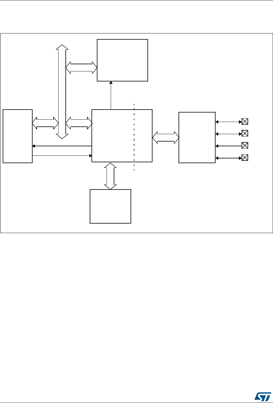
USB on-the-go full-speed (OTG_FS) RM0383
662/836 DocID026448 Rev 1
22.3 OTG_FS functional description
Figure 242. OTG full-speed block diagram
22.3.1 OTG full-speed core
The USB OTG FS receives the 48 MHz ±0.25% clock from the reset and clock controller
(RCC), via an external quartz. The USB clock is used for driving the 48 MHz domain at full-
speed (12 Mbit/s) and must be enabled prior to configuring the OTG FS core.
The CPU reads and writes from/to the OTG FS core registers through the AHB peripheral
bus. It is informed of USB events through the single USB OTG interrupt line described in
Section 22.15: OTG_FS interrupts.
The CPU submits data over the USB by writing 32-bit words to dedicated OTG_FS locations
(push registers). The data are then automatically stored into Tx-data FIFOs configured
within the USB data RAM. There is one Tx-FIFO push register for each in-endpoint
(peripheral mode) or out-channel (host mode).
The CPU receives the data from the USB by reading 32-bit words from dedicated OTG_FS
addresses (pop registers). The data are then automatically retrieved from a shared Rx-FIFO
configured within the 1.25 KB USB data RAM. There is one Rx-FIFO pop register for each
out-endpoint or in-channel.
The USB protocol layer is driven by the serial interface engine (SIE) and serialized over the
USB by the full-/low-speed transceiver module within the on-chip physical layer (PHY).
$0
$-
)$
6"53
/4'
&3
0(9
53"
/4'&3
#ORE 54-)&3
+BYTES
53"DATA
&)&/S
!("0ERIPHERAL
0OWER
#LOCK
#42,
53")NTERRUPT
53"SUSPEND
53"#LOCKAT-(Z
#ORTEX-
WITH&05
3YSTEMCLOCK
DOMAIN
53"CLOCK
DOMAIN
5NIVERSALSERIALBUS
2!-BUS
-36

DocID026448 Rev 1 663/836
RM0383 USB on-the-go full-speed (OTG_FS)
796
22.3.2 Full-speed OTG PHY
The embedded full-speed OTG PHY is controlled by the OTG FS core and conveys USB
control & data signals through the full-speed subset of the UTMI+ Bus (UTMIFS). It provides
the physical support to USB connectivity.
The full-speed OTG PHY includes the following components:
•FS/LS transceiver module used by both host and device. It directly drives transmission
and reception on the single-ended USB lines.
•integrated ID pull-up resistor used to sample the ID line for A/B device identification.
•DP/DM integrated pull-up and pull-down resistors controlled by the OTG_FS core
depending on the current role of the device. As a peripheral, it enables the DP pull-up
resistor to signal full-speed peripheral connections as soon as VBUS is sensed to be at
a valid level (B-session valid). In host mode, pull-down resistors are enabled on both
DP/DM. Pull-up and pull-down resistors are dynamically switched when the device’s
role is changed via the host negotiation protocol (HNP).
•Pull-up/pull-down resistor ECN circuit. The DP pull-up consists of 2 resistors controlled
separately from the OTG_FS as per the resistor Engineering Change Notice applied to
USB Rev2.0. The dynamic trimming of the DP pull-up strength allows for better noise
rejection and Tx/Rx signal quality.
•VBUS sensing comparators with hysteresis used to detect VBUS Valid, A-B Session
Valid and session-end voltage thresholds. They are used to drive the session request
protocol (SRP), detect valid startup and end-of-session conditions, and constantly
monitor the VBUS supply during USB operations.
•VBUS pulsing method circuit used to charge/discharge VBUS through resistors during
the SRP (weak drive).
Caution: To guarantee a correct operation for the USB OTG FS peripheral, the AHB frequency should
be higher than 14.2 MHz.
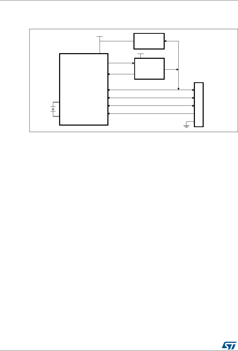
USB on-the-go full-speed (OTG_FS) RM0383
664/836 DocID026448 Rev 1
22.4 OTG dual role device (DRD)
Figure 243. OTG A-B device connection
1. External voltage regulator only needed when building a VBUS powered device
2. STMPS2141STR needed only if the application has to support a VBUS powered device. A basic power
switch can be used if 5 V are available on the application board.
22.4.1 ID line detection
The host or peripheral (the default) role is assumed depending on the ID input pin. The ID
line status is determined on plugging in the USB, depending on which side of the USB cable
is connected to the micro-AB receptacle.
•If the B-side of the USB cable is connected with a floating ID wire, the integrated pull-
up resistor detects a high ID level and the default Peripheral role is confirmed. In this
configuration the OTG_FS complies with the standard FSM described by section 6.8.2:
On-The-Go B-device of the On-The-Go Specification Rev1.3 supplement to the
USB2.0.
•If the A-side of the USB cable is connected with a grounded ID, the OTG_FS issues an
ID line status change interrupt (CIDSCHG bit in OTG_FS_GINTSTS) for host software
initialization, and automatically switches to the host role. In this configuration the
OTG_FS complies with the standard FSM described by section 6.8.1: On-The-Go A-
device of the On-The-Go Specification Rev1.3 supplement to the USB2.0.
22.4.2 HNP dual role device
The HNP capable bit in the Global USB configuration register (HNPCAP bit in OTG_FS_
GUSBCFG) enables the OTG_FS core to dynamically change its role from A-host to A-
peripheral and vice-versa, or from B-Peripheral to B-host and vice-versa according to the
host negotiation protocol (HNP). The current device status can be read by the combined
values of the Connector ID Status bit in the Global OTG control and status register (CIDSTS
bit in OTG_FS_GOTGCTL) and the current mode of operation bit in the global interrupt and
status register (CMOD bit in OTG_FS_GINTSTS).
The HNP program model is described in detail in Section 22.17: OTG_FS programming
model.
34-&XX
34-&XX
34-03342
#URRENTLIMITED
POWERDISTRIBUTION
SWITCH
6$$
6"53
$0
633
0!
0!
0!
53"MICRO!"CONNECTOR
$-
'0)/)21
'0)/
%.
/VERCURRENT
60WR
6TO6
$$
VOLTAGEREGULATOR
6$$
)$
0!
/3#?).
/3#?/54
-36

DocID026448 Rev 1 665/836
RM0383 USB on-the-go full-speed (OTG_FS)
796
22.4.3 SRP dual role device
The SRP capable bit in the global USB configuration register (SRPCAP bit in
OTG_FS_GUSBCFG) enables the OTG_FS core to switch off the generation of VBUS for
the A-device to save power. Note that the A-device is always in charge of driving VBUS
regardless of the host or peripheral role of the OTG_FS.
the SRP A/B-device program model is described in detail in Section 22.17: OTG_FS
programming model.
22.5 USB peripheral
This section gives the functional description of the OTG_FS in the USB peripheral mode.
The OTG_FS works as an USB peripheral in the following circumstances:
•OTG B-Peripheral
– OTG B-device default state if B-side of USB cable is plugged in
•OTG A-Peripheral
– OTG A-device state after the HNP switches the OTG_FS to its peripheral role
•B-device
– If the ID line is present, functional and connected to the B-side of the USB cable,
and the HNP-capable bit in the Global USB Configuration register (HNPCAP bit in
OTG_FS_GUSBCFG) is cleared (see On-The-Go Rev1.3 par. 6.8.3).
•Peripheral only (see Figure 244: USB peripheral-only connection)
– The force device mode bit in the Global USB configuration register (FDMOD in
OTG_FS_GUSBCFG) is set to 1, forcing the OTG_FS core to work as a USB
peripheral-only (see On-The-Go Rev1.3 par. 6.8.3). In this case, the ID line is
ignored even if present on the USB connector.
Note: To build a bus-powered device implementation in case of the B-device or peripheral-only
configuration, an external regulator has to be added that generates the VDD chip-supply
from VBUS.
The VBUS pin can be freed by disabling the VBUS sensing option. This is done by setting the
NOVBUSSENS bit in the OTG_FS_GCCFG register. In this case the VBUS is considered
internally to be always at VBUS valid level (5 V).
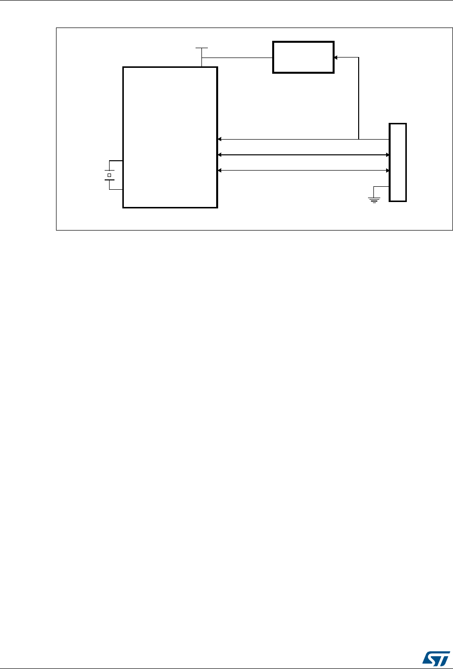
USB on-the-go full-speed (OTG_FS) RM0383
666/836 DocID026448 Rev 1
Figure 244. USB peripheral-only connection
1. Use a regulator to build a bus-powered device.
22.5.1 SRP-capable peripheral
The SRP capable bit in the Global USB configuration register (SRPCAP bit in
OTG_FS_GUSBCFG) enables the OTG_FS to support the session request protocol (SRP).
In this way, it allows the remote A-device to save power by switching off VBUS while the USB
session is suspended.
The SRP peripheral mode program model is described in detail in the B-device session
request protocol section.
22.5.2 Peripheral states
Powered state
The VBUS input detects the B-Session valid voltage by which the USB peripheral is allowed
to enter the powered state (see USB2.0 par9.1). The OTG_FS then automatically connects
the DP pull-up resistor to signal full-speed device connection to the host and generates the
session request interrupt (SRQINT bit in OTG_FS_GINTSTS) to notify the powered state.
The VBUS input also ensures that valid VBUS levels are supplied by the host during USB
operations. If a drop in VBUS below B-session valid happens to be detected (for instance
because of a power disturbance or if the host port has been switched off), the OTG_FS
automatically disconnects and the session end detected (SEDET bit in
OTG_FS_GOTGINT) interrupt is generated to notify that the OTG_FS has exited the
powered state.
In the powered state, the OTG_FS expects to receive some reset signaling from the host.
No other USB operation is possible. When a reset signaling is received the reset detected
interrupt (USBRST in OTG_FS_GINTSTS) is generated. When the reset signaling is
complete, the enumeration done interrupt (ENUMDNE bit in OTG_FS_GINTSTS) is
generated and the OTG_FS enters the Default state.
34-&XX
34-&XX
6TO6$$
6OLATGEREGULATOR
6$$
6"53
$0
633
0!
0!
0!
53"3TD"CONNECTOR
$-
/3#?).
/3#?/54
-36

DocID026448 Rev 1 667/836
RM0383 USB on-the-go full-speed (OTG_FS)
796
Soft disconnect
The powered state can be exited by software with the soft disconnect feature. The DP pull-
up resistor is removed by setting the soft disconnect bit in the device control register (SDIS
bit in OTG_FS_DCTL), causing a device disconnect detection interrupt on the host side
even though the USB cable was not really removed from the host port.
Default state
In the Default state the OTG_FS expects to receive a SET_ADDRESS command from the
host. No other USB operation is possible. When a valid SET_ADDRESS command is
decoded on the USB, the application writes the corresponding number into the device
address field in the device configuration register (DAD bit in OTG_FS_DCFG). The
OTG_FS then enters the address state and is ready to answer host transactions at the
configured USB address.
Suspended state
The OTG_FS peripheral constantly monitors the USB activity. After counting 3 ms of USB
idleness, the early suspend interrupt (ESUSP bit in OTG_FS_GINTSTS) is issued, and
confirmed 3 ms later, if appropriate, by the suspend interrupt (USBSUSP bit in
OTG_FS_GINTSTS). The device suspend bit is then automatically set in the device status
register (SUSPSTS bit in OTG_FS_DSTS) and the OTG_FS enters the suspended state.
The suspended state may optionally be exited by the device itself. In this case the
application sets the remote wakeup signaling bit in the device control register (RWUSIG bit
in OTG_FS_DCTL) and clears it after 1 to 15 ms.
When a resume signaling is detected from the host, the resume interrupt (WKUPINT bit in
OTG_FS_GINTSTS) is generated and the device suspend bit is automatically cleared.
22.5.3 Peripheral endpoints
The OTG_FS core instantiates the following USB endpoints:
•Control endpoint 0:
– Bidirectional and handles control messages only
– Separate set of registers to handle in and out transactions
– Proper control (OTG_FS_DIEPCTL0/OTG_FS_DOEPCTL0), transfer
configuration (OTG_FS_DIEPTSIZ0/OTG_FS_DIEPTSIZ0), and status-interrupt
(OTG_FS_DIEPINTx/)OTG_FS_DOEPINT0) registers. The available set of bits
inside the control and transfer size registers slightly differs from that of other
endpoints
•3 IN endpoints
– Each of them can be configured to support the isochronous, bulk or interrupt
transfer type
– Each of them has proper control (OTG_FS_DIEPCTLx), transfer configuration
(OTG_FS_DIEPTSIZx), and status-interrupt (OTG_FS_DIEPINTx) registers
– The Device IN endpoints common interrupt mask register (OTG_FS_DIEPMSK) is
available to enable/disable a single kind of endpoint interrupt source on all of the
IN endpoints (EP0 included)
– Support for incomplete isochronous IN transfer interrupt (IISOIXFR bit in
OTG_FS_GINTSTS), asserted when there is at least one isochronous IN endpoint

USB on-the-go full-speed (OTG_FS) RM0383
668/836 DocID026448 Rev 1
on which the transfer is not completed in the current frame. This interrupt is
asserted along with the end of periodic frame interrupt
(OTG_FS_GINTSTS/EOPF).
•3 OUT endpoints
– Each of them can be configured to support the isochronous, bulk or interrupt
transfer type
– Each of them has a proper control (OTG_FS_DOEPCTLx), transfer configuration
(OTG_FS_DOEPTSIZx) and status-interrupt (OTG_FS_DOEPINTx) register
– Device Out endpoints common interrupt mask register (OTG_FS_DOEPMSK) is
available to enable/disable a single kind of endpoint interrupt source on all of the
OUT endpoints (EP0 included)
– Support for incomplete isochronous OUT transfer interrupt (INCOMPISOOUT bit
in OTG_FS_GINTSTS), asserted when there is at least one isochronous OUT
endpoint on which the transfer is not completed in the current frame. This interrupt
is asserted along with the end of periodic frame interrupt
(OTG_FS_GINTSTS/EOPF).
Endpoint control
•The following endpoint controls are available to the application through the device
endpoint-x IN/OUT control register (DIEPCTLx/DOEPCTLx):
– Endpoint enable/disable
– Endpoint activate in current configuration
– Program USB transfer type (isochronous, bulk, interrupt)
– Program supported packet size
– Program Tx-FIFO number associated with the IN endpoint
– Program the expected or transmitted data0/data1 PID (bulk/interrupt only)
– Program the even/odd frame during which the transaction is received or
transmitted (isochronous only)
– Optionally program the NAK bit to always negative-acknowledge the host
regardless of the FIFO status
– Optionally program the STALL bit to always stall host tokens to that endpoint
– Optionally program the SNOOP mode for OUT endpoint not to check the CRC
field of received data
Endpoint transfer
The device endpoint-x transfer size registers (DIEPTSIZx/DOEPTSIZx) allow the application
to program the transfer size parameters and read the transfer status. Programming must be
done before setting the endpoint enable bit in the endpoint control register. Once the
endpoint is enabled, these fields are read-only as the OTG FS core updates them with the
current transfer status.
The following transfer parameters can be programmed:
•Transfer size in bytes
•Number of packets that constitute the overall transfer size

DocID026448 Rev 1 669/836
RM0383 USB on-the-go full-speed (OTG_FS)
796
Endpoint status/interrupt
The device endpoint-x interrupt registers (DIEPINTx/DOPEPINTx) indicate the status of an
endpoint with respect to USB- and AHB-related events. The application must read these
registers when the OUT endpoint interrupt bit or the IN endpoint interrupt bit in the core
interrupt register (OEPINT bit in OTG_FS_GINTSTS or IEPINT bit in OTG_FS_GINTSTS,
respectively) is set. Before the application can read these registers, it must first read the
device all endpoints interrupt (OTG_FS_DAINT) register to get the exact endpoint number
for the device endpoint-x interrupt register. The application must clear the appropriate bit in
this register to clear the corresponding bits in the DAINT and GINTSTS registers
The peripheral core provides the following status checks and interrupt generation:
•Transfer completed interrupt, indicating that data transfer was completed on both the
application (AHB) and USB sides
•Setup stage has been done (control-out only)
•Associated transmit FIFO is half or completely empty (in endpoints)
•NAK acknowledge has been transmitted to the host (isochronous-in only)
•IN token received when Tx-FIFO was empty (bulk-in/interrupt-in only)
•Out token received when endpoint was not yet enabled
•Babble error condition has been detected
•Endpoint disable by application is effective
•Endpoint NAK by application is effective (isochronous-in only)
•More than 3 back-to-back setup packets were received (control-out only)
•Timeout condition detected (control-in only)
•Isochronous out packet has been dropped, without generating an interrupt
22.6 USB host
This section gives the functional description of the OTG_FS in the USB host mode. The
OTG_FS works as a USB host in the following circumstances:
•OTG A-host
– OTG A-device default state when the A-side of the USB cable is plugged in
•OTG B-host
– OTG B-device after HNP switching to the host role
•A-device
– If the ID line is present, functional and connected to the A-side of the USB cable,
and the HNP-capable bit is cleared in the Global USB Configuration register
(HNPCAP bit in OTG_FS_GUSBCFG). Integrated pull-down resistors are
automatically set on the DP/DM lines.
•Host only (see figure Figure 245: USB host-only connection).
– The force host mode bit in the global USB configuration register (FHMOD bit in
OTG_FS_GUSBCFG) forces the OTG_FS core to work as a USB host-only. In this
case, the ID line is ignored even if present on the USB connector. Integrated pull-
down resistors are automatically set on the DP/DM lines.
Note: On-chip 5 V VBUS generation is not supported. For this reason, a charge pump or, if 5 V are
available on the application board, a basic power switch must be added externally to drive
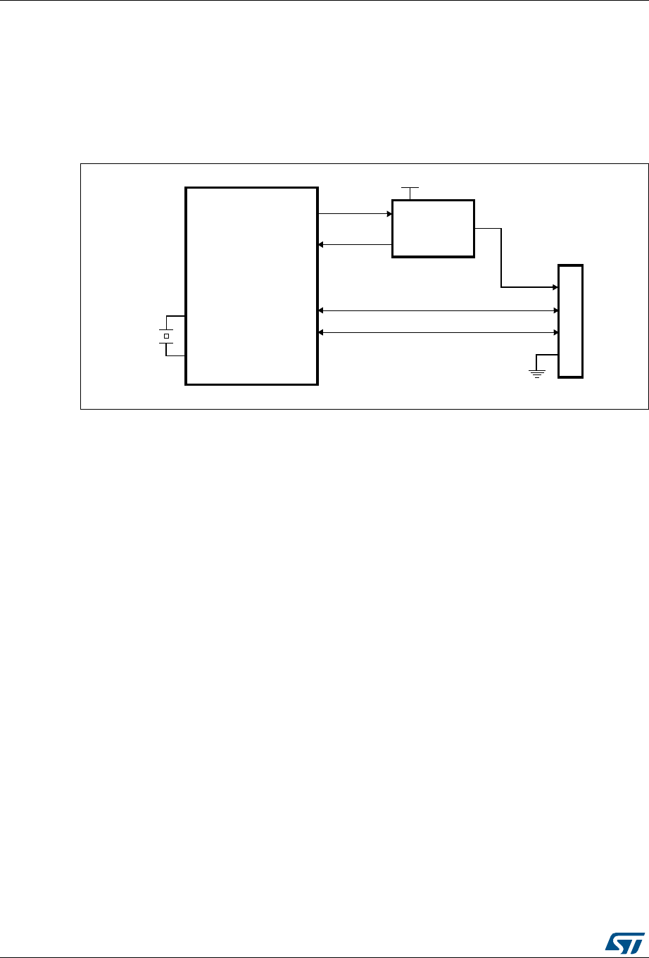
USB on-the-go full-speed (OTG_FS) RM0383
670/836 DocID026448 Rev 1
the 5 V VBUS line. The external charge pump can be driven by any GPIO output. This is
required for the OTG A-host, A-device and host-only configurations.
The VBUS input ensures that valid VBUS levels are supplied by the charge pump during USB
operations while the charge pump overcurrent output can be input to any GPIO pin
configured to generate port interrupts. The overcurrent ISR must promptly disable the VBUS
generation.
Figure 245. USB host-only connection
1. STMPS2141STR needed only if the application has to support a VBUS powered device. A basic power
switch can be used if 5 V are available on the application board.
2. VDD range is between 2 V and 3.6 V.
22.6.1 SRP-capable host
SRP support is available through the SRP capable bit in the global USB configuration
register (SRPCAP bit in OTG_FS_GUSBCFG). With the SRP feature enabled, the host can
save power by switching off the VBUS power while the USB session is suspended.
The SRP host mode program model is described in detail in the A-device session request
protocol) section.
22.6.2 USB host states
Host port power
On-chip 5 V VBUS generation is not supported. For this reason, a charge pump or, if 5 V are
available on the application board, a basic power switch, must be added externally to drive
the 5 V VBUS line. The external charge pump can be driven by any GPIO output. When the
application decides to power on VBUS using the chosen GPIO, it must also set the port
power bit in the host port control and status register (PPWR bit in OTG_FS_HPRT).
VBUS valid
When HNP or SRP is enabled the VBUS sensing pin (PA9) pin should be connected to
VBUS. The VBUS input ensures that valid VBUS levels are supplied by the charge pump
during USB operations. Any unforeseen VBUS voltage drop below the VBUS valid threshold
(4.25 V) leads to an OTG interrupt triggered by the session end detected bit (SEDET bit in
OTG_FS_GOTGINT). The application is then required to remove the VBUS power and clear
the port power bit.
34-&XX
34-&XX
34-03342
#URRENTLIMITED
POWERDISTRIBUTION
SWITCH
6$$
6"53
$0
633
0
0!
0!
53"3TD!CONNECTOR
$-
'0)/)21
'0)/
%.
/VERCURRENT
60WR
/3#?).
/3#?/54
-36

DocID026448 Rev 1 671/836
RM0383 USB on-the-go full-speed (OTG_FS)
796
When HNP and SRP are both disabled, the VBUS sensing pin (PA9) should not be
connected to VBUS. This pin can be can be used as GPIO.
The charge pump overcurrent flag can also be used to prevent electrical damage. Connect
the overcurrent flag output from the charge pump to any GPIO input and configure it to
generate a port interrupt on the active level. The overcurrent ISR must promptly disable the
VBUS generation and clear the port power bit.
Host detection of a peripheral connection
If SRP or HNP are enabled, even if USB peripherals or B-devices can be attached at any
time, the OTG_FS will not detect any bus connection . When VBUS is at a valid level and a
remote B-device is attached, the OTG_FS core issues a host port interrupt triggered by the
device connected bit in the host port control and status register (PCDET bit in
OTG_FS_HPRT).
When HNP and SRP are both disabled, USB peripherals or B-device are detected as soon
as they are connected. The OTG_FS core issues a host port interrupt triggered by the
device connected bit in the host port control and status (PCDET bit in OTG_FS_HPRT).
Host detection of peripheral a disconnection
The peripheral disconnection event triggers the disconnect detected interrupt (DISCINT bit
in OTG_FS_GINTSTS).
Host enumeration
After detecting a peripheral connection the host must start the enumeration process by
sending USB reset and configuration commands to the new peripheral.
Before starting to drive a USB reset, the application waits for the OTG interrupt triggered by
the debounce done bit (DBCDNE bit in OTG_FS_GOTGINT), which indicates that the bus is
stable again after the electrical debounce caused by the attachment of a pull-up resistor on
DP (FS) or DM (LS).
The application drives a USB reset signaling (single-ended zero) over the USB by keeping
the port reset bit set in the host port control and status register (PRST bit in
OTG_FS_HPRT) for a minimum of 10 ms and a maximum of 20 ms. The application takes
care of the timing count and then of clearing the port reset bit.
Once the USB reset sequence has completed, the host port interrupt is triggered by the port
enable/disable change bit (PENCHNG bit in OTG_FS_HPRT). This informs the application
that the speed of the enumerated peripheral can be read from the port speed field in the
host port control and status register (PSPD bit in OTG_FS_HPRT) and that the host is
starting to drive SOFs (FS) or Keep alives (LS). The host is now ready to complete the
peripheral enumeration by sending peripheral configuration commands.
Host suspend
The application decides to suspend the USB activity by setting the port suspend bit in the
host port control and status register (PSUSP bit in OTG_FS_HPRT). The OTG_FS core
stops sending SOFs and enters the suspended state.
The suspended state can be optionally exited on the remote device’s initiative (remote
wakeup). In this case the remote wakeup interrupt (WKUPINT bit in OTG_FS_GINTSTS) is
generated upon detection of a remote wakeup signaling, the port resume bit in the host port
control and status register (PRES bit in OTG_FS_HPRT) self-sets, and resume signaling is

USB on-the-go full-speed (OTG_FS) RM0383
672/836 DocID026448 Rev 1
automatically driven over the USB. The application must time the resume window and then
clear the port resume bit to exit the suspended state and restart the SOF.
If the suspended state is exited on the host initiative, the application must set the port
resume bit to start resume signaling on the host port, time the resume window and finally
clear the port resume bit.
22.6.3 Host channels
The OTG_FS core instantiates 8 host channels. Each host channel supports an USB host
transfer (USB pipe). The host is not able to support more than 8 transfer requests at the
same time. If more than 8 transfer requests are pending from the application, the host
controller driver (HCD) must re-allocate channels when they become available from
previous duty, that is, after receiving the transfer completed and channel halted interrupts.
Each host channel can be configured to support in/out and any type of periodic/nonperiodic
transaction. Each host channel makes us of proper control (HCCHARx), transfer
configuration (HCTSIZx) and status/interrupt (HCINTx) registers with associated mask
(HCINTMSKx) registers.
Host channel control
•The following host channel controls are available to the application through the host
channel-x characteristics register (HCCHARx):
– Channel enable/disable
– Program the FS/LS speed of target USB peripheral
– Program the address of target USB peripheral
– Program the endpoint number of target USB peripheral
– Program the transfer IN/OUT direction
– Program the USB transfer type (control, bulk, interrupt, isochronous)
– Program the maximum packet size (MPS)
– Program the periodic transfer to be executed during odd/even frames
Host channel transfer
The host channel transfer size registers (HCTSIZx) allow the application to program the
transfer size parameters, and read the transfer status. Programming must be done before
setting the channel enable bit in the host channel characteristics register. Once the endpoint
is enabled the packet count field is read-only as the OTG FS core updates it according to
the current transfer status.
•The following transfer parameters can be programmed:
– transfer size in bytes
– number of packets making up the overall transfer size
– initial data PID
Host channel status/interrupt
The host channel-x interrupt register (HCINTx) indicates the status of an endpoint with
respect to USB- and AHB-related events. The application must read these register when the
host channels interrupt bit in the core interrupt register (HCINT bit in OTG_FS_GINTSTS) is
set. Before the application can read these registers, it must first read the host all channels
interrupt (HCAINT) register to get the exact channel number for the host channel-x interrupt

DocID026448 Rev 1 673/836
RM0383 USB on-the-go full-speed (OTG_FS)
796
register. The application must clear the appropriate bit in this register to clear the
corresponding bits in the HAINT and GINTSTS registers. The mask bits for each interrupt
source of each channel are also available in the OTG_FS_HCINTMSK-x register.
•The host core provides the following status checks and interrupt generation:
– Transfer completed interrupt, indicating that the data transfer is complete on both
the application (AHB) and USB sides
– Channel has stopped due to transfer completed, USB transaction error or disable
command from the application
– Associated transmit FIFO is half or completely empty (IN endpoints)
– ACK response received
– NAK response received
– STALL response received
– USB transaction error due to CRC failure, timeout, bit stuff error, false EOP
– Babble error
– fraMe overrun
– dAta toggle error
22.6.4 Host scheduler
The host core features a built-in hardware scheduler which is able to autonomously re-order
and manage the USB transaction requests posted by the application. At the beginning of
each frame the host executes the periodic (isochronous and interrupt) transactions first,
followed by the nonperiodic (control and bulk) transactions to achieve the higher level of
priority granted to the isochronous and interrupt transfer types by the USB specification.
The host processes the USB transactions through request queues (one for periodic and one
for nonperiodic). Each request queue can hold up to 8 entries. Each entry represents a
pending transaction request from the application, and holds the IN or OUT channel number
along with other information to perform a transaction on the USB. The order in which the
requests are written to the queue determines the sequence of the transactions on the USB
interface.
At the beginning of each frame, the host processes the periodic request queue first, followed
by the nonperiodic request queue. The host issues an incomplete periodic transfer interrupt
(IPXFR bit in OTG_FS_GINTSTS) if an isochronous or interrupt transaction scheduled for
the current frame is still pending at the end of the current frame. The OTG HS core is fully
responsible for the management of the periodic and nonperiodic request queues.The
periodic transmit FIFO and queue status register (HPTXSTS) and nonperiodic transmit
FIFO and queue status register (HNPTXSTS) are read-only registers which can be used by
the application to read the status of each request queue. They contain:
•The number of free entries currently available in the periodic (nonperiodic) request
queue (8 max)
•Free space currently available in the periodic (nonperiodic) Tx-FIFO (out-transactions)
•IN/OUT token, host channel number and other status information.
As request queues can hold a maximum of 8 entries each, the application can push to
schedule host transactions in advance with respect to the moment they physically reach the
SB for a maximum of 8 pending periodic transactions plus 8 pending nonperiodic
transactions.
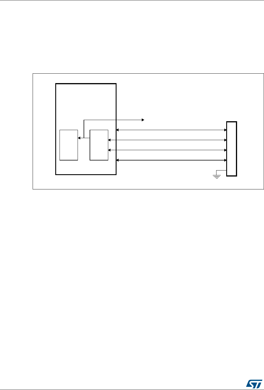
USB on-the-go full-speed (OTG_FS) RM0383
674/836 DocID026448 Rev 1
To post a transaction request to the host scheduler (queue) the application must check that
there is at least 1 entry available in the periodic (nonperiodic) request queue by reading the
PTXQSAV bits in the OTG_FS_HNPTXSTS register or NPTQXSAV bits in the
OTG_FS_HNPTXSTS register.
22.7 SOF trigger
Figure 246. SOF connectivity
The OTG FS core provides means to monitor, track and configure SOF framing in the host
and peripheral, as well as an SOF pulse output connectivity feature.
Such utilities are especially useful for adaptive audio clock generation techniques, where
the audio peripheral needs to synchronize to the isochronous stream provided by the PC, or
the host needs to trim its framing rate according to the requirements of the audio peripheral.
22.7.1 Host SOFs
In host mode the number of PHY clocks occurring between the generation of two
consecutive SOF (FS) or Keep-alive (LS) tokens is programmable in the host frame interval
register (HFIR), thus providing application control over the SOF framing period. An interrupt
is generated at any start of frame (SOF bit in OTH_FS_GINTSTS). The current frame
number and the time remaining until the next SOF are tracked in the host frame number
register (HFNUM).
An SOF pulse signal, generated at any SOF starting token and with a width of 12 system
clock cycles, can be made available externally on the SOF pin using the SOFOUTEN bit in
the global control and configuration register. The SOF pulse is also internally connected to
the input trigger of timer 2 (TIM2), so that the input capture feature, the output compare
feature and the timer can be triggered by the SOF pulse. The TIM2 connection is enabled
register.
22.7.2 Peripheral SOFs
In device mode, the start of frame interrupt is generated each time an SOF token is received
on the USB (SOF bit in OTH_FS_GINTSTS). The corresponding frame number can be read
34-&XX
34-&XX
6"53
$
633
0!
0!
0!
53"MICRO!"CONNECTOR
$
)$4)-
)42 3/&
PULSE
3/&GEN
0!
0!
3/&PULSEOUTPUTTO
EXTERNALAUDIOCONTROL
-36

DocID026448 Rev 1 675/836
RM0383 USB on-the-go full-speed (OTG_FS)
796
from the device status register (FNSOF bit in OTG_FS_DSTS). An SOF pulse signal with a
width of 12 system clock cycles is also generated and can be made available externally on
the SOF pin by using the SOF output enable bit in the global control and configuration
register (SOFOUTEN bit in OTG_FS_GCCFG). The SOF pulse signal is also internally
connected to the TIM2 input trigger, so that the input capture feature, the output compare
feature and the timer can be triggered by the SOF pulse. The TIM2 connection is enabled .
The end of periodic frame interrupt (GINTSTS/EOPF) is used to notify the application when
80%, 85%, 90% or 95% of the time frame interval elapsed depending on the periodic frame
interval field in the device configuration register (PFIVL bit in OTG_FS_DCFG). This feature
can be used to determine if all of the isochronous traffic for that frame is complete.
22.8 Power options
The power consumption of the OTG PHY is controlled by three bits in the general core
configuration register:
•PHY power down (GCCFG/PWRDWN)
It switches on/off the full-speed transceiver module of the PHY. It must be preliminarily
set to allow any USB operation.
•A-VBUS sensing enable (GCCFG/VBUSASEN)
It switches on/off the VBUS comparators associated with A-device operations. It must
be set when in A-device (USB host) mode and during HNP.
•B-VBUS sensing enable (GCCFG/VBUSASEN)
It switches on/off the VBUS comparators associated with B-device operations. It must
be set when in B-device (USB peripheral) mode and during HNP.
Power reduction techniques are available while in the USB suspended state, when the USB
session is not yet valid or the device is disconnected.
•Stop PHY clock (STPPCLK bit in OTG_FS_PCGCCTL)
When setting the stop PHY clock bit in the clock gating control register, most of the
48 MHz clock domain internal to the OTG full-speed core is switched off by clock
gating. The dynamic power consumption due to the USB clock switching activity is cut
even if the 48 MHz clock input is kept running by the application
Most of the transceiver is also disabled, and only the part in charge of detecting the
asynchronous resume or remote wakeup event is kept alive.
•Gate HCLK (GATEHCLK bit in OTG_FS_PCGCCTL)
When setting the Gate HCLK bit in the clock gating control register, most of the system
clock domain internal to the OTG_FS core is switched off by clock gating. Only the
register read and write interface is kept alive. The dynamic power consumption due to
the USB clock switching activity is cut even if the system clock is kept running by the
application for other purposes.
•USB system stop
When the OTG_FS is in the USB suspended state, the application may decide to
drastically reduce the overall power consumption by a complete shut down of all the
clock sources in the system. USB System Stop is activated by first setting the Stop
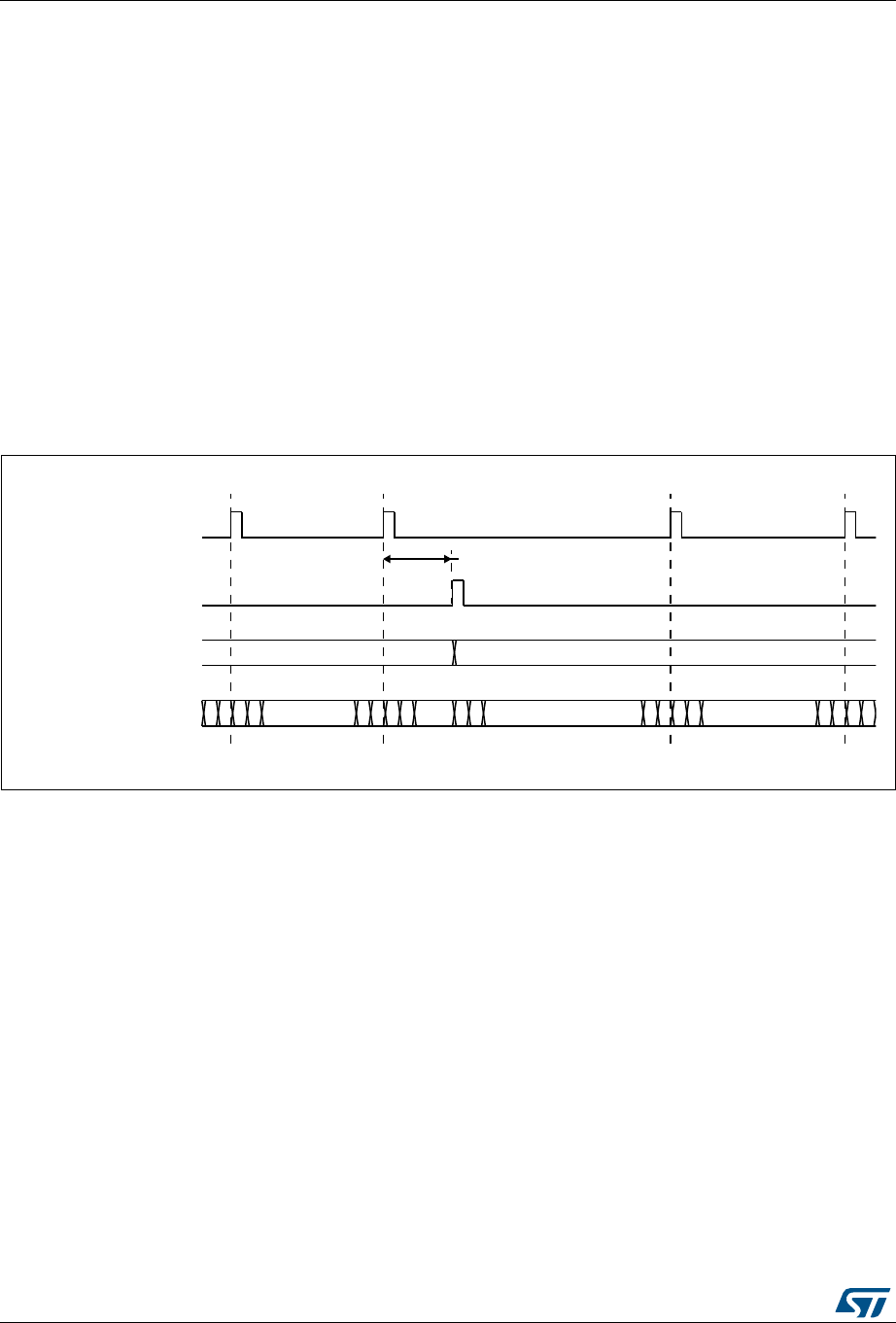
USB on-the-go full-speed (OTG_FS) RM0383
676/836 DocID026448 Rev 1
PHY clock bit and then configuring the system deep sleep mode in the power control
system module (PWR).
The OTG_FS core automatically reactivates both system and USB clocks by
asynchronous detection of remote wakeup (as an host) or resume (as a device)
signaling on the USB.
To save dynamic power, the USB data FIFO is clocked only when accessed by the OTG_FS
core.
22.9 Dynamic update of the OTG_FS_HFIR register
The USB core embeds a dynamic trimming capability of micro-SOF framing period in host
mode allowing to synchronize an external device with the micro-SOF frames.
When the OTG_HS_HFIR register is changed within a current micro-SOF frame, the SOF
period correction is applied in the next frame as described in Figure 247.
Figure 247. Updating OTG_FS_HFIR dynamically
22.10 USB data FIFOs
The USB system features 1.25 Kbyte of dedicated RAM with a sophisticated FIFO control
mechanism. The packet FIFO controller module in the OTG_FS core organizes RAM space
into Tx-FIFOs into which the application pushes the data to be temporarily stored before the
USB transmission, and into a single Rx FIFO where the data received from the USB are
temporarily stored before retrieval (popped) by the application. The number of instructed
FIFOs and how these are organized inside the RAM depends on the device’s role. In
peripheral mode an additional Tx-FIFO is instructed for each active IN endpoint. Any FIFO
size is software configured to better meet the application requirements.
xxxx
,ATENCY
3/&
RELOAD
/4'?&3?(&)2
WRITE
VALUE
&RAME
TIMER
/LD/4'?&3?()&2VALUE
PERIODS
/4'?&3?()&2VALUE
PERIODS()&2WRITELATENCY
.EW/4'?&3?()&2VALUE
PERIODS
/4'?&3?(&)2
AI
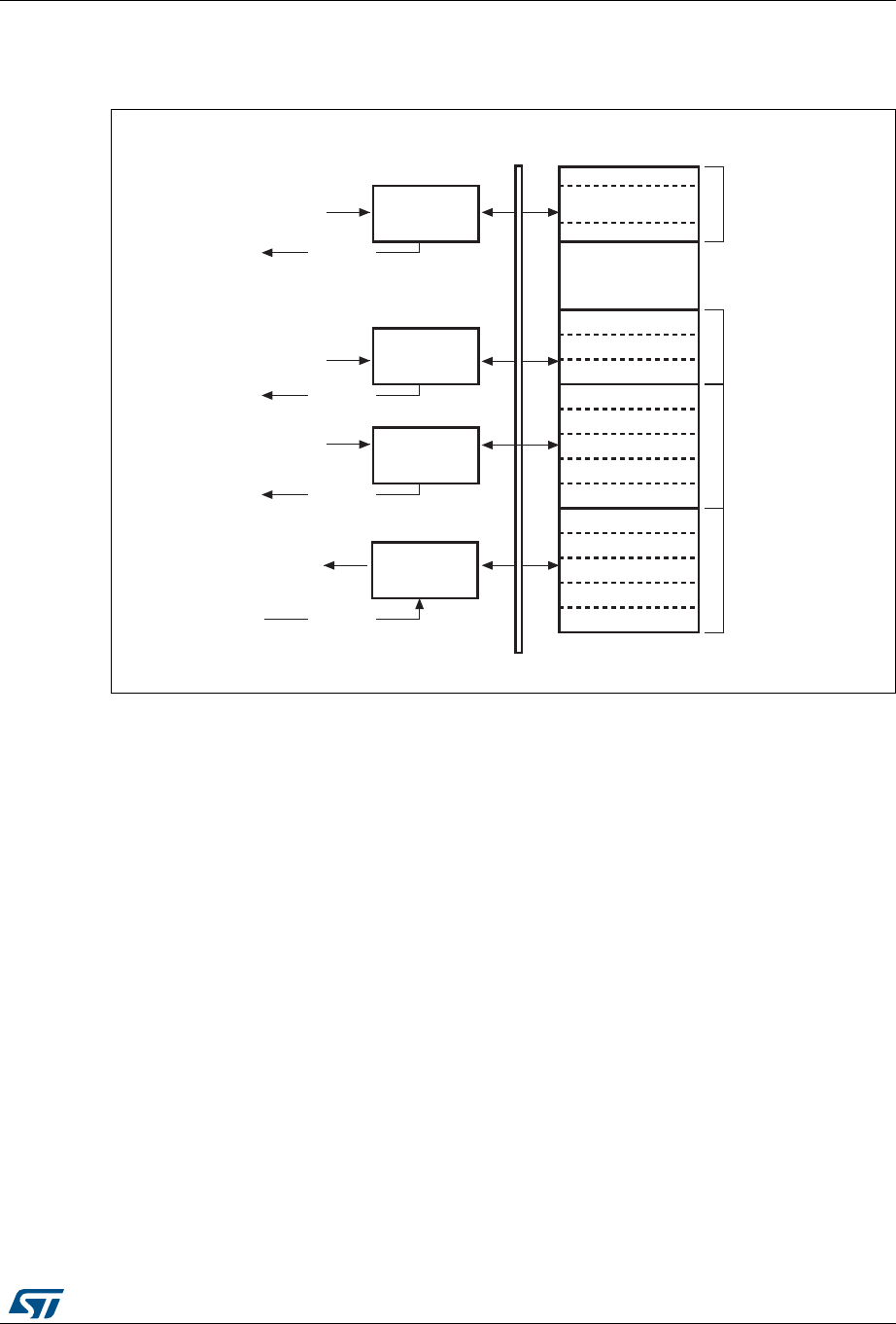
DocID026448 Rev 1 677/836
RM0383 USB on-the-go full-speed (OTG_FS)
796
22.11 Peripheral FIFO architecture
Figure 248. Device-mode FIFO address mapping and AHB FIFO access mapping
22.11.1 Peripheral Rx FIFO
The OTG peripheral uses a single receive FIFO that receives the data directed to all OUT
endpoints. Received packets are stacked back-to-back until free space is available in the
Rx-FIFO. The status of the received packet (which contains the OUT endpoint destination
number, the byte count, the data PID and the validity of the received data) is also stored by
the core on top of the data payload. When no more space is available, host transactions are
NACKed and an interrupt is received on the addressed endpoint. The size of the receive
FIFO is configured in the receive FIFO Size register (GRXFSIZ).
The single receive FIFO architecture makes it more efficient for the USB peripheral to fill in
the receive RAM buffer:
•All OUT endpoints share the same RAM buffer (shared FIFO)
•The OTG FS core can fill in the receive FIFO up to the limit for any host sequence of
OUT tokens
The application keeps receiving the Rx-FIFO non-empty interrupt (RXFLVL bit in
OTG_FS_GINTSTS) as long as there is at least one packet available for download. It reads
the packet information from the receive status read and pop register (GRXSTSP) and finally
pops data off the receive FIFO by reading from the endpoint-related pop address.
IN endpoint Tx FIFO #n
DFIFO push access
from AHB
Any OUT endpoint DFIFO pop
access from AHB
Dedicated Tx
FIFO #n control
(optional)
Dedicated Tx
FIFO #1 control
(optional)
Rx FIFO control
IN endpoint Tx FIFO #1
DFIFO push access
from AHB
MAC pop
MAC pop
MAC push
Single data
FIFO
Tx FIFO #n
packet
Tx FIFO #0 packet
DIEPTXF2[31:16]
DIEPTXFx[15:0]
DIEPTXF2[15:0]
DIEPTXF1[31:16]
DIEPTXF1[15:0]
GNPTXFSIZ[31:16]
ai15611
IN endpoint Tx FIFO #0
DFIFO push access
from AHB
Dedicated Tx
FIFO #0 control
(optional)
MAC pop
Tx FIFO #1 packet
Rx packets
(Rx start
address
fixed to 0)
.
.
..
.
..
.
.
GNPTXFSIZ[15:0]
GRXFSIZ[31:16]
A1 = 0
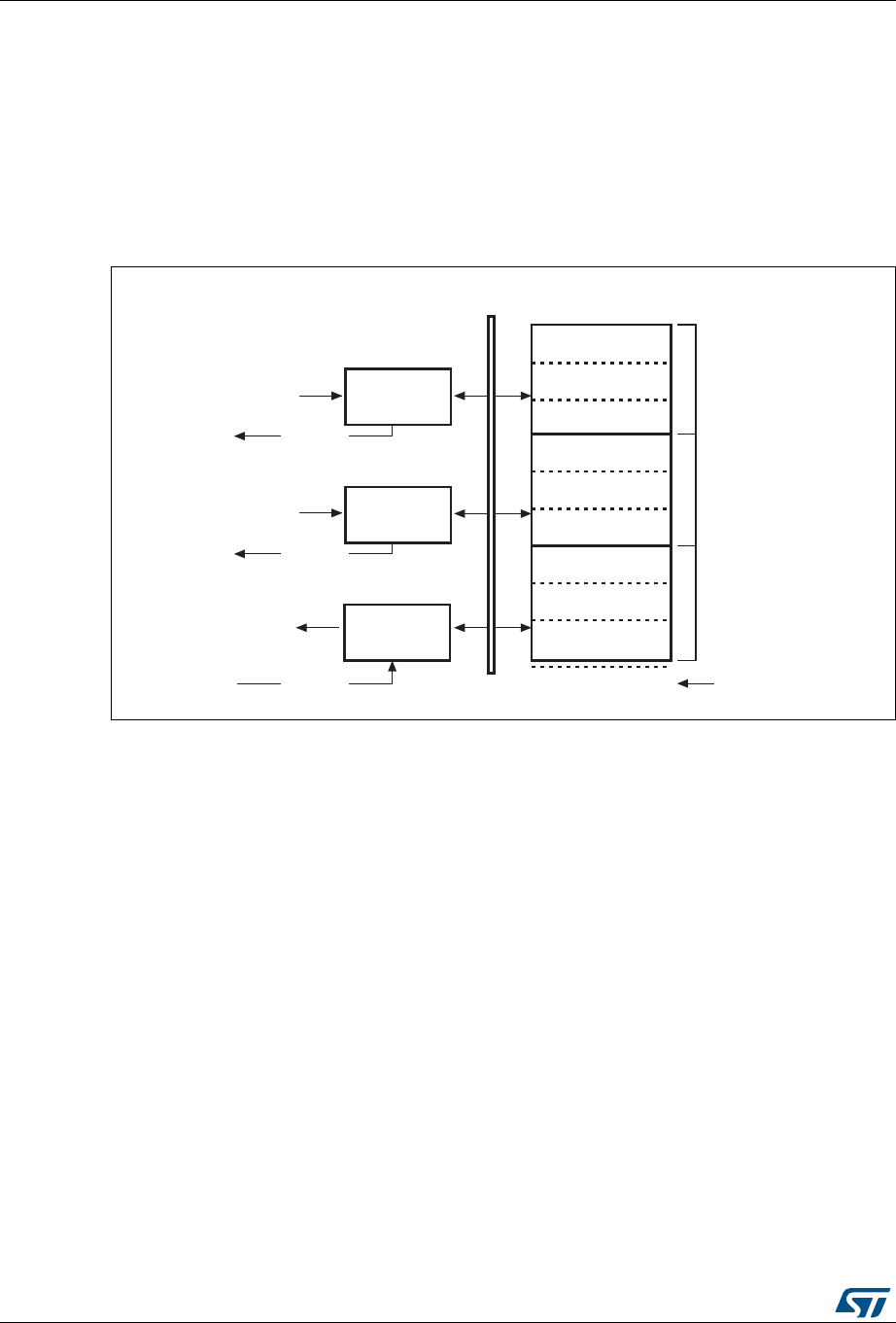
USB on-the-go full-speed (OTG_FS) RM0383
678/836 DocID026448 Rev 1
22.11.2 Peripheral Tx FIFOs
The core has a dedicated FIFO for each IN endpoint. The application configures FIFO sizes
by writing the non periodic transmit FIFO size register (OTG_FS_TX0FSIZ) for IN endpoint0
and the device IN endpoint transmit FIFOx registers (DIEPTXFx) for IN endpoint-x.
22.12 Host FIFO architecture
Figure 249. Host-mode FIFO address mapping and AHB FIFO access mapping
22.12.1 Host Rx FIFO
The host uses one receiver FIFO for all periodic and nonperiodic transactions. The FIFO is
used as a receive buffer to hold the received data (payload of the received packet) from the
USB until it is transferred to the system memory. Packets received from any remote IN
endpoint are stacked back-to-back until free space is available. The status of each received
packet with the host channel destination, byte count, data PID and validity of the received
data are also stored into the FIFO. The size of the receive FIFO is configured in the receive
FIFO size register (GRXFSIZ).
The single receive FIFO architecture makes it highly efficient for the USB host to fill in the
receive data buffer:
•All IN configured host channels share the same RAM buffer (shared FIFO)
•The OTG FS core can fill in the receive FIFO up to the limit for any sequence of IN
tokens driven by the host software
The application receives the Rx FIFO not-empty interrupt as long as there is at least one
packet available for download. It reads the packet information from the receive status read
and pop register and finally pops the data off the receive FIFO.
Any periodic channel
DFIFO push access
from AHB
Any channel DFIFO pop
access from AHB
Periodic Tx
FIFO control
(optional)
Non-periodic
Tx FIFO control
Rx FIFO control
Any non-periodic
channel DFIFO push
access from AHB
MAC pop
MAC pop
MAC push
Single data
FIFO
Periodic Tx packets
Periodic Tx packets
Rx packets
HPTXFSIZ[31:16]
HPTXFSIZ[15:0]
NPTXFSIZ[31:16]
NPTXFSIZ[15:0]
RXFSIZ[31:16]
Rx start address
fixed to 0
A1 = 0
ai15610

DocID026448 Rev 1 679/836
RM0383 USB on-the-go full-speed (OTG_FS)
796
22.12.2 Host Tx FIFOs
The host uses one transmit FIFO for all non-periodic (control and bulk) OUT transactions
and one transmit FIFO for all periodic (isochronous and interrupt) OUT transactions. FIFOs
are used as transmit buffers to hold the data (payload of the transmit packet) to be
transmitted over the USB. The size of the periodic (nonperiodic) Tx FIFO is configured in the
host periodic (nonperiodic) transmit FIFO size (HPTXFSIZ/HNPTXFSIZ) register.
The two Tx FIFO implementation derives from the higher priority granted to the periodic type
of traffic over the USB frame. At the beginning of each frame, the built-in host scheduler
processes the periodic request queue first, followed by the nonperiodic request queue.
The two transmit FIFO architecture provides the USB host with separate optimization for
periodic and nonperiodic transmit data buffer management:
•All host channels configured to support periodic (nonperiodic) transactions in the OUT
direction share the same RAM buffer (shared FIFOs)
•The OTG FS core can fill in the periodic (nonperiodic) transmit FIFO up to the limit for
any sequence of OUT tokens driven by the host software
The OTG_FS core issues the periodic Tx FIFO empty interrupt (PTXFE bit in
OTG_FS_GINTSTS) as long as the periodic Tx-FIFO is half or completely empty,
depending on the value of the periodic Tx-FIFO empty level bit in the AHB configuration
register (PTXFELVL bit in OTG_FS_GAHBCFG). The application can push the transmission
data in advance as long as free space is available in both the periodic Tx FIFO and the
periodic request queue. The host periodic transmit FIFO and queue status register
(HPTXSTS) can be read to know how much space is available in both.
OTG_FS core issues the non periodic Tx FIFO empty interrupt (NPTXFE bit in
OTG_FS_GINTSTS) as long as the nonperiodic Tx FIFO is half or completely empty
depending on the non periodic Tx FIFO empty level bit in the AHB configuration register
(TXFELVL bit in OTG_FS_GAHBCFG). The application can push the transmission data as
long as free space is available in both the nonperiodic Tx FIFO and nonperiodic request
queue. The host nonperiodic transmit FIFO and queue status register (HNPTXSTS) can be
read to know how much space is available in both.
22.13 FIFO RAM allocation
22.13.1 Device mode
Receive FIFO RAM allocation: the application should allocate RAM for SETUP Packets:
10 locations must be reserved in the receive FIFO to receive SETUP packets on control
endpoint. The core does not use these locations, which are reserved for SETUP packets, to
write any other data. One location is to be allocated for Global OUT NAK. Status information
is written to the FIFO along with each received packet. Therefore, a minimum space of
(Largest Packet Size / 4) + 1 must be allocated to receive packets. If multiple isochronous
endpoints are enabled, then at least two (Largest Packet Size / 4) + 1 spaces must be
allocated to receive back-to-back packets. Typically, two (Largest Packet Size / 4) + 1
spaces are recommended so that when the previous packet is being transferred to the CPU,
the USB can receive the subsequent packet.
Along with the last packet for each endpoint, transfer complete status information is also
pushed to the FIFO. Typically, one location for each OUT endpoint is recommended.

USB on-the-go full-speed (OTG_FS) RM0383
680/836 DocID026448 Rev 1
Transmit FIFO RAM allocation: the minimum RAM space required for each IN Endpoint
Transmit FIFO is the maximum packet size for that particular IN endpoint.
Note: More space allocated in the transmit IN Endpoint FIFO results in better performance on the
USB.
22.13.2 Host mode
Receive FIFO RAM allocation
Status information is written to the FIFO along with each received packet. Therefore, a
minimum space of (Largest Packet Size / 4) + 1 must be allocated to receive packets. If
multiple isochronous channels are enabled, then at least two (Largest Packet Size / 4) + 1
spaces must be allocated to receive back-to-back packets. Typically, two (Largest Packet
Size / 4) + 1 spaces are recommended so that when the previous packet is being
transferred to the CPU, the USB can receive the subsequent packet.
Along with the last packet in the host channel, transfer complete status information is also
pushed to the FIFO. So one location must be allocated for this.
Transmit FIFO RAM allocation
The minimum amount of RAM required for the host Non-periodic Transmit FIFO is the
largest maximum packet size among all supported non-periodic OUT channels.
Typically, two Largest Packet Sizes worth of space is recommended, so that when the
current packet is under transfer to the USB, the CPU can get the next packet.
The minimum amount of RAM required for host periodic Transmit FIFO is the largest
maximum packet size out of all the supported periodic OUT channels. If there is at least one
Isochronous OUT endpoint, then the space must be at least two times the maximum packet
size of that channel.
Note: More space allocated in the Transmit Non-periodic FIFO results in better performance on
the USB.
22.14 USB system performance
Best USB and system performance is achieved owing to the large RAM buffers, the highly
configurable FIFO sizes, the quick 32-bit FIFO access through AHB push/pop registers and,
especially, the advanced FIFO control mechanism. Indeed, this mechanism allows the

DocID026448 Rev 1 681/836
RM0383 USB on-the-go full-speed (OTG_FS)
796
OTG_FS to fill in the available RAM space at best regardless of the current USB sequence.
With these features:
•The application gains good margins to calibrate its intervention in order to optimize the
CPU bandwidth usage:
– It can accumulate large amounts of transmission data in advance compared to
when they are effectively sent over the USB
– It benefits of a large time margin to download data from the single receive FIFO
•The USB Core is able to maintain its full operating rate, that is to provide maximum full-
speed bandwidth with a great margin of autonomy versus application intervention:
– It has a large reserve of transmission data at its disposal to autonomously manage
the sending of data over the USB
– It has a lot of empty space available in the receive buffer to autonomously fill it in
with the data coming from the USB
As the OTG_FS core is able to fill in the 1.25 Kbyte RAM buffer very efficiently, and as
1.25 Kbyte of transmit/receive data is more than enough to cover a full speed frame, the
USB system is able to withstand the maximum full-speed data rate for up to one USB frame
(1 ms) without any CPU intervention.
22.15 OTG_FS interrupts
When the OTG_FS controller is operating in one mode, either device or host, the application
must not access registers from the other mode. If an illegal access occurs, a mode
mismatch interrupt is generated and reflected in the Core interrupt register (MMIS bit in the
OTG_FS_GINTSTS register). When the core switches from one mode to the other, the
registers in the new mode of operation must be reprogrammed as they would be after a
power-on reset.
Figure 250 shows the interrupt hierarchy.
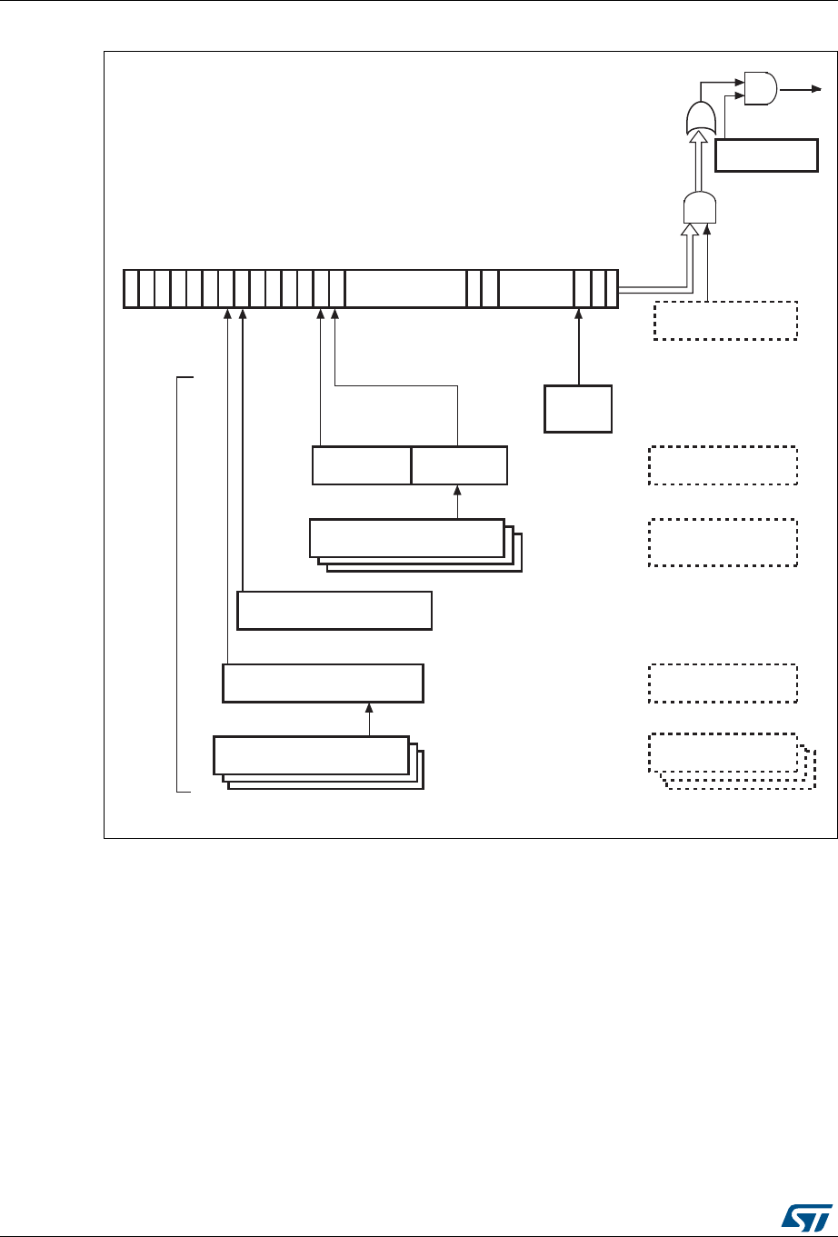
USB on-the-go full-speed (OTG_FS) RM0383
682/836 DocID026448 Rev 1
Figure 250. Interrupt hierarchy
1. The core interrupt register bits are shown in OTG_FS core interrupt register (OTG_FS_GINTSTS) on
page 697.
22.16 OTG_FS control and status registers
By reading from and writing to the control and status registers (CSRs) through the AHB
slave interface, the application controls the OTG_FS controller. These registers are 32 bits
wide, and the addresses are 32-bit block aligned. The OTG_FS registers must be accessed
by words (32 bits).
31 30 29 28 27 26 25 24 23 20 19 18 17:10 9 8 7:3 2 1 0
AND
OR
Interrupt
Global interrupt
mask (Bit 0)
AHB configuration
register
Core interrupt mask
register
OTG
interrupt
register
Core interrupt
register(1)
Device IN/OUT endpoint
interrupt registers 0 to 3
Device all endpoints
interrupt register
16:9
OUT endpoints
3:0
IN endpoints
Interrupt
sources
Host port control and status
register
Host all channels interrupt
register
Host channels interrupt
mask registers 0 to 7
Host all channels
interrupt mask register
Host channels interrupt
registers 0 to 7
22 21
Device all endpoints
interrupt mask register
Device IN/OUT
endpoints common
interrupt mask register
ai15616b

DocID026448 Rev 1 683/836
RM0383 USB on-the-go full-speed (OTG_FS)
796
CSRs are classified as follows:
•Core global registers
•Host-mode registers
•Host global registers
•Host port CSRs
•Host channel-specific registers
•Device-mode registers
•Device global registers
•Device endpoint-specific registers
•Power and clock-gating registers
•Data FIFO (DFIFO) access registers
Only the Core global, Power and clock-gating, Data FIFO access, and host port control and
status registers can be accessed in both host and device modes. When the OTG_FS
controller is operating in one mode, either device or host, the application must not access
registers from the other mode. If an illegal access occurs, a mode mismatch interrupt is
generated and reflected in the Core interrupt register (MMIS bit in the OTG_FS_GINTSTS
register). When the core switches from one mode to the other, the registers in the new mode
of operation must be reprogrammed as they would be after a power-on reset.
22.16.1 CSR memory map
The host and device mode registers occupy different addresses. All registers are
implemented in the AHB clock domain.
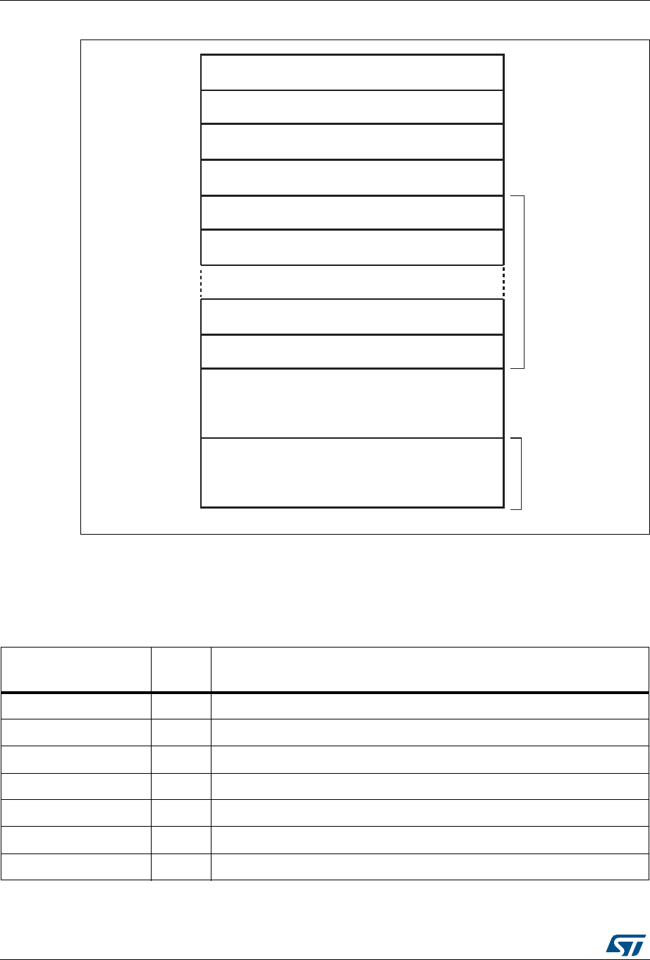
USB on-the-go full-speed (OTG_FS) RM0383
684/836 DocID026448 Rev 1
Figure 251. CSR memory map
1. x = 3 in device mode and x = 7 in host mode.
Global CSR map
These registers are available in both host and device modes.
0000h
Core global CSRs (1 Kbyte)
0400h
Host mode CSRs (1 Kbyte)
0800h
Device mode CSRs (1.5 Kbyte)
0E00h
Power and clock gating CSRs (0.5 Kbyte)
1000h
Device EP 0/Host channel 0 FIFO (4 Kbyte)
2000h
Device EP1/Host channel 1 FIFO (4 Kbyte)
3000h
Device EP (x – 1)
(1)
/Host channel (x – 1)
(1)
FIFO (4 Kbyte)
Device EP x
(1)
/Host channel x
(1)
FIFO (4 Kbyte)
Reserved
DFIFO
push/pop
to this region
2 0000h
3 FFFFh
Direct access to data FIFO RAM
for debugging (128 Kbyte)
DFIFO
debug read/
write to this
region
ai15615b
Table 124. Core global control and status registers (CSRs)
Acronym Address
offset Register name
OTG_FS_GOTGCTL 0x000 OTG_FS control and status register (OTG_FS_GOTGCTL) on page 688
OTG_FS_GOTGINT 0x004 OTG_FS interrupt register (OTG_FS_GOTGINT) on page 690
OTG_FS_GAHBCFG 0x008 OTG_FS AHB configuration register (OTG_FS_GAHBCFG) on page 692
OTG_FS_GUSBCFG 0x00C OTG_FS USB configuration register (OTG_FS_GUSBCFG) on page 693
OTG_FS_GRSTCTL 0x010 OTG_FS reset register (OTG_FS_GRSTCTL) on page 695
OTG_FS_GINTSTS 0x014 OTG_FS core interrupt register (OTG_FS_GINTSTS) on page 697
OTG_FS_GINTMSK 0x018 OTG_FS interrupt mask register (OTG_FS_GINTMSK) on page 701

DocID026448 Rev 1 685/836
RM0383 USB on-the-go full-speed (OTG_FS)
796
Host-mode CSR map
These registers must be programmed every time the core changes to host mode.
OTG_FS_GRXSTSR 0x01C OTG_FS Receive status debug read/OTG status read and pop registers
(OTG_FS_GRXSTSR/OTG_FS_GRXSTSP) on page 704
OTG_FS_GRXSTSP 0x020
OTG_FS_GRXFSIZ 0x024 OTG_FS Receive FIFO size register (OTG_FS_GRXFSIZ) on page 705
OTG_FS_HNPTXFSIZ/
OTG_FS_DIEPTXF0(1) 0x028
OTG_FS Host non-periodic transmit FIFO size register
(OTG_FS_HNPTXFSIZ)/Endpoint 0 Transmit FIFO size
(OTG_FS_DIEPTXF0)
OTG_FS_HNPTXSTS 0x02C OTG_FS non-periodic transmit FIFO/queue status register
(OTG_FS_HNPTXSTS) on page 706
OTG_FS_GCCFG 0x038 OTG_FS general core configuration register (OTG_FS_GCCFG) on
page 707
OTG_FS_CID 0x03C OTG_FS core ID register (OTG_FS_CID) on page 708
OTG_FS_HPTXFSIZ 0x100 OTG_FS Host periodic transmit FIFO size register (OTG_FS_HPTXFSIZ) on
page 709
OTG_FS_DIEPTXFx
0x104
0x124
...
0x138
OTG_FS device IN endpoint transmit FIFO size register
(OTG_FS_DIEPTXFx) (x = 1..3, where x is the FIFO_number) on page 710
1. The general rule is to use OTG_FS_HNPTXFSIZ for host mode and OTG_FS_DIEPTXF0 for device mode.
Table 124. Core global control and status registers (CSRs) (continued)
Acronym Address
offset Register name
Table 125. Host-mode control and status registers (CSRs)
Acronym Offset
address Register name
OTG_FS_HCFG 0x400 OTG_FS Host configuration register (OTG_FS_HCFG) on page 710
OTG_FS_HFIR 0x404 OTG_FS Host frame interval register (OTG_FS_HFIR) on page 711
OTG_FS_HFNUM 0x408 OTG_FS Host frame number/frame time remaining register
(OTG_FS_HFNUM) on page 712
OTG_FS_HPTXSTS 0x410 OTG_FS_Host periodic transmit FIFO/queue status register
(OTG_FS_HPTXSTS) on page 712
OTG_FS_HAINT 0x414 OTG_FS Host all channels interrupt register (OTG_FS_HAINT) on
page 713
OTG_FS_HAINTMSK 0x418 OTG_FS Host all channels interrupt mask register (OTG_FS_HAINTMSK)
on page 714
OTG_FS_HPRT 0x440 OTG_FS Host port control and status register (OTG_FS_HPRT) on
page 714

USB on-the-go full-speed (OTG_FS) RM0383
686/836 DocID026448 Rev 1
Device-mode CSR map
These registers must be programmed every time the core changes to device mode.
OTG_FS_HCCHARx
0x500
0x520
...
0x6E0h
OTG_FS Host channel-x characteristics register (OTG_FS_HCCHARx)
(x = 0..7, where x = Channel_number) on page 717
OTG_FS_HCINTx 508h OTG_FS Host channel-x interrupt register (OTG_FS_HCINTx) (x = 0..7,
where x = Channel_number) on page 718
OTG_FS_HCINTMSKx 50Ch OTG_FS Host channel-x interrupt mask register (OTG_FS_HCINTMSKx)
(x = 0..7, where x = Channel_number) on page 719
OTG_FS_HCTSIZx 510h OTG_FS Host channel-x transfer size register (OTG_FS_HCTSIZx)
(x = 0..7, where x = Channel_number) on page 720
Table 125. Host-mode control and status registers (CSRs) (continued)
Acronym Offset
address Register name
Table 126. Device-mode control and status registers
Acronym Offset
address Register name
OTG_FS_DCFG 0x800 OTG_FS device configuration register (OTG_FS_DCFG) on page 721
OTG_FS_DCTL 0x804 OTG_FS device control register (OTG_FS_DCTL) on page 722
OTG_FS_DSTS 0x808 OTG_FS device status register (OTG_FS_DSTS) on page 723
OTG_FS_DIEPMSK 0x810 OTG_FS device IN endpoint common interrupt mask register
(OTG_FS_DIEPMSK) on page 724
OTG_FS_DOEPMSK 0x814 OTG_FS device OUT endpoint common interrupt mask register
(OTG_FS_DOEPMSK) on page 725
OTG_FS_DAINT 0x818 OTG_FS device all endpoints interrupt register (OTG_FS_DAINT) on
page 726
OTG_FS_DAINTMSK 0x81C OTG_FS all endpoints interrupt mask register (OTG_FS_DAINTMSK)
on page 727
OTG_FS_DVBUSDIS 0x828 OTG_FS device VBUS discharge time register (OTG_FS_DVBUSDIS)
on page 727
OTG_FS_DVBUSPULS
E0x82C OTG_FS device VBUS pulsing time register (OTG_FS_DVBUSPULSE)
on page 728
OTG_FS_DIEPEMPMSK 0x834 OTG_FS device IN endpoint FIFO empty interrupt mask register:
(OTG_FS_DIEPEMPMSK) on page 728
OTG_FS_DIEPCTL0 0x900 OTG_FS device control IN endpoint 0 control register
(OTG_FS_DIEPCTL0) on page 729

DocID026448 Rev 1 687/836
RM0383 USB on-the-go full-speed (OTG_FS)
796
Data FIFO (DFIFO) access register map
These registers, available in both host and device modes, are used to read or write the FIFO
space for a specific endpoint or a channel, in a given direction. If a host channel is of type
IN, the FIFO can only be read on the channel. Similarly, if a host channel is of type OUT, the
FIFO can only be written on the channel.
OTG_FS_DIEPCTLx
0x920
0x940
...
0xAE0
OTG device endpoint-x control register (OTG_FS_DIEPCTLx) (x = 1..3,
where x = Endpoint_number) on page 730
OTG_FS_DIEPINTx 0x908 OTG_FS device endpoint-x interrupt register (OTG_FS_DIEPINTx)
(x = 0..3, where x = Endpoint_number) on page 737
OTG_FS_DIEPTSIZ0 0x910 OTG_FS device IN endpoint 0 transfer size register
(OTG_FS_DIEPTSIZ0) on page 739
OTG_FS_DTXFSTSx 0x918
OTG_FS device IN endpoint transmit FIFO status register
(OTG_FS_DTXFSTSx) (x = 0..3, where x = Endpoint_number) on
page 742
OTG_FS_DIEPTSIZx
0x930
0x950
...
0xAF0
OTG_FS device OUT endpoint-x transfer size register
(OTG_FS_DOEPTSIZx) (x = 1..3, where x = Endpoint_number) on
page 742
OTG_FS_DOEPCTL0 0xB00 OTG_FS device control OUT endpoint 0 control register
(OTG_FS_DOEPCTL0) on page 733
OTG_FS_DOEPCTLx
0xB20
0xB40
...
0xCC0
0xCE0
0xCFD
OTG device endpoint-x control register (OTG_FS_DIEPCTLx) (x = 1..3,
where x = Endpoint_number) on page 730
OTG_FS_DOEPINTx 0xB08 OTG_FS device endpoint-x interrupt register (OTG_FS_DIEPINTx)
(x = 0..3, where x = Endpoint_number) on page 737
OTG_FS_DOEPTSIZx 0xB10
OTG_FS device OUT endpoint-x transfer size register
(OTG_FS_DOEPTSIZx) (x = 1..3, where x = Endpoint_number) on
page 742
Table 126. Device-mode control and status registers (continued)
Acronym Offset
address Register name
USB on-the-go full-speed (OTG_FS) RM0383
688/836 DocID026448 Rev 1
Power and clock gating CSR map
There is a single register for power and clock gating. It is available in both host and device
modes.
22.16.2 OTG_FS global registers
These registers are available in both host and device modes, and do not need to be
reprogrammed when switching between these modes.
Bit values in the register descriptions are expressed in binary unless otherwise specified.
OTG_FS control and status register (OTG_FS_GOTGCTL)
Address offset: 0x000
Reset value: 0x0000 0800
The OTG_FS_GOTGCTL register controls the behavior and reflects the status of the OTG
function of the core.
Table 127. Data FIFO (DFIFO) access register map
FIFO access register section Address range Access
Device IN Endpoint 0/Host OUT Channel 0: DFIFO Write Access
Device OUT Endpoint 0/Host IN Channel 0: DFIFO Read Access 0x1000–0x1FFC w
r
Device IN Endpoint 1/Host OUT Channel 1: DFIFO Write Access
Device OUT Endpoint 1/Host IN Channel 1: DFIFO Read Access 0x2000–0x2FFC w
r
... ... ...
Device IN Endpoint x(1)/Host OUT Channel x(1): DFIFO Write Access
Device OUT Endpoint x(1)/Host IN Channel x(1): DFIFO Read Access
1. Where x is 3 in device mode and 7 in host mode.
0xX000–0xXFFC w
r
Table 128. Power and clock gating control and status registers
Register name Acronym Offset address: 0xE00–0xFFF
Power and clock gating control register PCGCR 0xE00-0xE04
Reserved 0xE05–0xFFF
313029282726252423222120191817161514131211109876543210
Reserved
BSVLD
ASVLD
DBCT
CIDSTS
Reserved
DHNPEN
HSHNPEN
HNPRQ
HNGSCS
Reserved
SRQ
SRQSCS
rrrr rwrwrwr rwr

DocID026448 Rev 1 689/836
RM0383 USB on-the-go full-speed (OTG_FS)
796
Bits 31:20 Reserved, must be kept at reset value.
Bit 19 BSVLD: B-session valid
Indicates the device mode transceiver status.
0: B-session is not valid.
1: B-session is valid.
In OTG mode, you can use this bit to determine if the device is connected or disconnected.
Note: Only accessible in device mode.
Bit 18 ASVLD: A-session valid
Indicates the host mode transceiver status.
0: A-session is not valid
1: A-session is valid
Note: Only accessible in host mode.
Bit 17 DBCT: Long/short debounce time
Indicates the debounce time of a detected connection.
0: Long debounce time, used for physical connections (100 ms + 2.5 µs)
1: Short debounce time, used for soft connections (2.5 µs)
Note: Only accessible in host mode.
Bit 16 CIDSTS: Connector ID status
Indicates the connector ID status on a connect event.
0: The OTG_FS controller is in A-device mode
1: The OTG_FS controller is in B-device mode
Note: Accessible in both device and host modes.
Bits 15:12 Reserved, must be kept at reset value.
Bit 11 DHNPEN: Device HNP enabled
The application sets this bit when it successfully receives a SetFeature.SetHNPEnable
command from the connected USB host.
0: HNP is not enabled in the application
1: HNP is enabled in the application
Note: Only accessible in device mode.
Bit 10 HSHNPEN: host set HNP enable
The application sets this bit when it has successfully enabled HNP (using the
SetFeature.SetHNPEnable command) on the connected device.
0: Host Set HNP is not enabled
1: Host Set HNP is enabled
Note: Only accessible in host mode.
Bit 9 HNPRQ: HNP request
The application sets this bit to initiate an HNP request to the connected USB host. The
application can clear this bit by writing a 0 when the host negotiation success status change
bit in the OTG_FS_GOTGINT register (HNSSCHG bit in OTG_FS_GOTGINT) is set. The
core clears this bit when the HNSSCHG bit is cleared.
0: No HNP request
1: HNP request
Note: Only accessible in device mode.
USB on-the-go full-speed (OTG_FS) RM0383
690/836 DocID026448 Rev 1
OTG_FS interrupt register (OTG_FS_GOTGINT)
Address offset: 0x04
Reset value: 0x0000 0000
The application reads this register whenever there is an OTG interrupt and clears the bits in
this register to clear the OTG interrupt.
Bit 8 HNGSCS: Host negotiation success
The core sets this bit when host negotiation is successful. The core clears this bit when the
HNP Request (HNPRQ) bit in this register is set.
0: Host negotiation failure
1: Host negotiation success
Note: Only accessible in device mode.
Bits 7:2 Reserved, must be kept at reset value.
Bit 1 SRQ: Session request
The application sets this bit to initiate a session request on the USB. The application can
clear this bit by writing a 0 when the host negotiation success status change bit in the
OTG_FS_GOTGINT register (HNSSCHG bit in OTG_FS_GOTGINT) is set. The core clears
this bit when the HNSSCHG bit is cleared.
If you use the USB 1.1 full-speed serial transceiver interface to initiate the session request,
the application must wait until VBUS discharges to 0.2 V, after the B-Session Valid bit in this
register (BSVLD bit in OTG_FS_GOTGCTL) is cleared. This discharge time varies between
different PHYs and can be obtained from the PHY vendor.
0: No session request
1: Session request
Note: Only accessible in device mode.
Bit 0 SRQSCS: Session request success
The core sets this bit when a session request initiation is successful.
0: Session request failure
1: Session request success
Note: Only accessible in device mode.
313029282726252423222120191817161514131211109876543210
Reserved
DBCDNE
ADTOCHG
HNGDET
Reserved
HNSSCHG
SRSSCHG
Reserved
SEDET
Res.
rc_
w1
rc_
w1
rc_
w1
rc_
w1
rc_
w1
rc_
w1
Bits 31:20 Reserved, must be kept at reset value.
Bit 19 DBCDNE: Debounce done
The core sets this bit when the debounce is completed after the device connect. The
application can start driving USB reset after seeing this interrupt. This bit is only valid when
the HNP Capable or SRP Capable bit is set in the OTG_FS_GUSBCFG register (HNPCAP
bit or SRPCAP bit in OTG_FS_GUSBCFG, respectively).
Note: Only accessible in host mode.

DocID026448 Rev 1 691/836
RM0383 USB on-the-go full-speed (OTG_FS)
796
Bit 18 ADTOCHG: A-device timeout change
The core sets this bit to indicate that the A-device has timed out while waiting for the B-device
to connect.
Note: Accessible in both device and host modes.
Bit 17 HNGDET: Host negotiation detected
The core sets this bit when it detects a host negotiation request on the USB.
Note: Accessible in both device and host modes.
Bits 16:10 Reserved, must be kept at reset value.
Bit 9 HNSSCHG: Host negotiation success status change
The core sets this bit on the success or failure of a USB host negotiation request. The
application must read the host negotiation success bit of the OTG_FS_GOTGCTL register
(HNGSCS in OTG_FS_GOTGCTL) to check for success or failure.
Note: Accessible in both device and host modes.
Bits 7:3 Reserved, must be kept at reset value.
Bit 8 SRSSCHG: Session request success status change
The core sets this bit on the success or failure of a session request. The application must
read the session request success bit in the OTG_FS_GOTGCTL register (SRQSCS bit in
OTG_FS_GOTGCTL) to check for success or failure.
Note: Accessible in both device and host modes.
Bit 2 SEDET: Session end detected
The core sets this bit to indicate that the level of the voltage on VBUS is no longer valid for a
B-Peripheral session when VBUS < 0.8 V.
Bits 1:0 Reserved, must be kept at reset value.

USB on-the-go full-speed (OTG_FS) RM0383
692/836 DocID026448 Rev 1
OTG_FS AHB configuration register (OTG_FS_GAHBCFG)
Address offset: 0x008
Reset value: 0x0000 0000
This register can be used to configure the core after power-on or a change in mode. This
register mainly contains AHB system-related configuration parameters. Do not change this
register after the initial programming. The application must program this register before
starting any transactions on either the AHB or the USB.
313029282726252423222120191817161514131211109876543210
Reserved
PTXFELVL
TXFELVL
Reserved
GINTMSK
rw rw rw
Bits 31:20 Reserved, must be kept at reset value.
Bit 8 PTXFELVL: Periodic TxFIFO empty level
Indicates when the periodic TxFIFO empty interrupt bit in the OTG_FS_GINTSTS register
(PTXFE bit in OTG_FS_GINTSTS) is triggered.
0: PTXFE (in OTG_FS_GINTSTS) interrupt indicates that the Periodic TxFIFO is half empty
1: PTXFE (in OTG_FS_GINTSTS) interrupt indicates that the Periodic TxFIFO is completely
empty
Note: Only accessible in host mode.
Bit 7 TXFELVL: TxFIFO empty level
In device mode, this bit indicates when IN endpoint Transmit FIFO empty interrupt (TXFE in
OTG_FS_DIEPINTx.) is triggered.
0: the TXFE (in OTG_FS_DIEPINTx) interrupt indicates that the IN Endpoint TxFIFO is half
empty
1: the TXFE (in OTG_FS_DIEPINTx) interrupt indicates that the IN Endpoint TxFIFO is
completely empty
In host mode, this bit indicates when the nonperiodic Tx FIFO empty interrupt (NPTXFE bit in
OTG_FS_GINTSTS) is triggered:
0: the NPTXFE (in OTG_FS_GINTSTS) interrupt indicates that the nonperiodic Tx FIFO is
half empty
1: the NPTXFE (in OTG_FS_GINTSTS) interrupt indicates that the nonperiodic Tx FIFO is
completely empty
Bits 6:1 Reserved, must be kept at reset value.
Bit 0 GINTMSK: Global interrupt mask
The application uses this bit to mask or unmask the interrupt line assertion to itself.
Irrespective of this bit’s setting, the interrupt status registers are updated by the core.
0: Mask the interrupt assertion to the application.
1: Unmask the interrupt assertion to the application.
Note: Accessible in both device and host modes.

DocID026448 Rev 1 693/836
RM0383 USB on-the-go full-speed (OTG_FS)
796
OTG_FS USB configuration register (OTG_FS_GUSBCFG)
Address offset: 0x00C
Reset value: 0x0000 0A00
This register can be used to configure the core after power-on or a changing to host mode
or device mode. It contains USB and USB-PHY related configuration parameters. The
application must program this register before starting any transactions on either the AHB or
the USB. Do not make changes to this register after the initial programming.
3130292827262524232221201918171615141312111098 7 6543210
CTXPKT
FDMOD
FHMOD
Reserved
TRDT
HNPCAP
SRPCAP
Res.
PHYSEL
Reserved
TOCAL
rw rw rw rw
r/rw
r/rw
wo rw
Bits 31:20 Reserved, must be kept at reset value.
Bit 31 CTXPKT: Corrupt Tx packet
This bit is for debug purposes only. Never set this bit to 1.
Note: Accessible in both device and host modes.
Bit 30 FDMOD: Force device mode
Writing a 1 to this bit forces the core to device mode irrespective of the OTG_FS_ID input
pin.
0: Normal mode
1: Force device mode
After setting the force bit, the application must wait at least 25 ms before the change takes
effect.
Note: Accessible in both device and host modes.
Bit 29 FHMOD: Force host mode
Writing a 1 to this bit forces the core to host mode irrespective of the OTG_FS_ID input pin.
0: Normal mode
1: Force host mode
After setting the force bit, the application must wait at least 25 ms before the change takes
effect.
Note: Accessible in both device and host modes.
Bits 28:14 Reserved, must be kept at reset value.
Bits 13:10 TRDT: USB turnaround time
Sets the turnaround time in PHY clocks.
To calculate the value of TRDT, use the following formula:
TRDT = 4 × AHB clock + 1 PHY clock
Examples:
1. if AHB clock = 72 MHz (PHY Clock is 48), the TRDT is set to 9.
2. if AHB clock = 48 MHz (PHY Clock is 48), the TRDT is set to 5.
Note: Only accessible in device mode.

USB on-the-go full-speed (OTG_FS) RM0383
694/836 DocID026448 Rev 1
Bit 9 HNPCAP: HNP-capable
The application uses this bit to control the OTG_FS controller’s HNP capabilities.
0: HNP capability is not enabled.
1: HNP capability is enabled.
Note: Accessible in both device and host modes.
Bit 8 SRPCAP: SRP-capable
The application uses this bit to control the OTG_FS controller’s SRP capabilities. If the core
operates as a non-SRP-capable
B-device, it cannot request the connected A-device (host) to activate VBUS and start a
session.
0: SRP capability is not enabled.
1: SRP capability is enabled.
Note: Accessible in both device and host modes.
Bit 7 Reserved, must be kept at reset value.
Bit 6 PHYSEL: Full Speed serial transceiver select
This bit is always 1 with write-only access.
Bits 5:3 Reserved, must be kept at reset value.
Bits 2:0 TOCAL: FS timeout calibration
The number of PHY clocks that the application programs in this field is added to the full-
speed interpacket timeout duration in the core to account for any additional delays
introduced by the PHY. This can be required, because the delay introduced by the PHY in
generating the line state condition can vary from one PHY to another.
The USB standard timeout value for full-speed operation is 16 to 18 (inclusive) bit times. The
application must program this field based on the speed of enumeration. The number of bit
times added per PHY clock is 0.25 bit times.

DocID026448 Rev 1 695/836
RM0383 USB on-the-go full-speed (OTG_FS)
796
OTG_FS reset register (OTG_FS_GRSTCTL)
Address offset: 0x10
Reset value: 0x2000 0000
The application uses this register to reset various hardware features inside the core.
313029282726252423222120191817161514131211109876543210
AHBIDL
Reserved TXFNUM
TXFFLSH
RXFFLSH
Reserved
FCRST
HSRST
CSRST
rrw rs rs rs rs rs
Bit 31 AHBIDL: AHB master idle
Indicates that the AHB master state machine is in the Idle condition.
Note: Accessible in both device and host modes.
Bits 30:11 Reserved, must be kept at reset value.
Bits 10:6 TXFNUM: TxFIFO number
This is the FIFO number that must be flushed using the TxFIFO Flush bit. This field must not
be changed until the core clears the TxFIFO Flush bit.
00000:
– Non-periodic TxFIFO flush in host mode
– Tx FIFO 0 flush in device mode
00001:
– Periodic TxFIFO flush in host mode
– TXFIFO 1 flush in device mode
00010: TXFIFO 2 flush in device mode
...
00101: TXFIFO 15 flush in device mode
10000: Flush all the transmit FIFOs in device or host mode.
Note: Accessible in both device and host modes.
Bit 5 TXFFLSH: TxFIFO flush
This bit selectively flushes a single or all transmit FIFOs, but cannot do so if the core is in the
midst of a transaction.
The application must write this bit only after checking that the core is neither writing to the
TxFIFO nor reading from the TxFIFO. Verify using these registers:
Read—NAK Effective Interrupt ensures the core is not reading from the FIFO
Write—AHBIDL bit in OTG_FS_GRSTCTL ensures the core is not writing anything to the
FIFO.
Note: Accessible in both device and host modes.
Bit 4 RXFFLSH: RxFIFO flush
The application can flush the entire RxFIFO using this bit, but must first ensure that the core
is not in the middle of a transaction.
The application must only write to this bit after checking that the core is neither reading from
the RxFIFO nor writing to the RxFIFO.
The application must wait until the bit is cleared before performing any other operations. This
bit requires 8 clocks (slowest of PHY or AHB clock) to clear.
Note: Accessible in both device and host modes.
Bit 3 Reserved, must be kept at reset value.

USB on-the-go full-speed (OTG_FS) RM0383
696/836 DocID026448 Rev 1
Bit 2 FCRST: Host frame counter reset
The application writes this bit to reset the frame number counter inside the core. When the
frame counter is reset, the subsequent SOF sent out by the core has a frame number of 0.
Note: Only accessible in host mode.
Bit 1 HSRST: HCLK soft reset
The application uses this bit to flush the control logic in the AHB Clock domain. Only AHB
Clock Domain pipelines are reset.
FIFOs are not flushed with this bit.
All state machines in the AHB clock domain are reset to the Idle state after terminating the
transactions on the AHB, following the protocol.
CSR control bits used by the AHB clock domain state machines are cleared.
To clear this interrupt, status mask bits that control the interrupt status and are generated by
the AHB clock domain state machine are cleared.
Because interrupt status bits are not cleared, the application can get the status of any core
events that occurred after it set this bit.
This is a self-clearing bit that the core clears after all necessary logic is reset in the core. This
can take several clocks, depending on the core’s current state.
Note: Accessible in both device and host modes.
Bit 0 CSRST: Core soft reset
Resets the HCLK and PCLK domains as follows:
Clears the interrupts and all the CSR register bits except for the following bits:
– RSTPDMODL bit in OTG_FS_PCGCCTL
– GAYEHCLK bit in OTG_FS_PCGCCTL
– PWRCLMP bit in OTG_FS_PCGCCTL
– STPPCLK bit in OTG_FS_PCGCCTL
– FSLSPCS bit in OTG_FS_HCFG
– DSPD bit in OTG_FS_DCFG
All module state machines (except for the AHB slave unit) are reset to the Idle state, and all
the transmit FIFOs and the receive FIFO are flushed.
Any transactions on the AHB Master are terminated as soon as possible, after completing the
last data phase of an AHB transfer. Any transactions on the USB are terminated immediately.
The application can write to this bit any time it wants to reset the core. This is a self-clearing
bit and the core clears this bit after all the necessary logic is reset in the core, which can take
several clocks, depending on the current state of the core. Once this bit has been cleared,
the software must wait at least 3 PHY clocks before accessing the PHY domain
(synchronization delay). The software must also check that bit 31 in this register is set to 1
(AHB Master is Idle) before starting any operation.
Typically, the software reset is used during software development and also when you
dynamically change the PHY selection bits in the above listed USB configuration registers.
When you change the PHY, the corresponding clock for the PHY is selected and used in the
PHY domain. Once a new clock is selected, the PHY domain has to be reset for proper
operation.
Note: Accessible in both device and host modes.

DocID026448 Rev 1 697/836
RM0383 USB on-the-go full-speed (OTG_FS)
796
OTG_FS core interrupt register (OTG_FS_GINTSTS)
Address offset: 0x014
Reset value: 0x0400 0020
This register interrupts the application for system-level events in the current mode (device
mode or host mode).
Some of the bits in this register are valid only in host mode, while others are valid in device
mode only. This register also indicates the current mode. To clear the interrupt status bits of
the rc_w1 type, the application must write 1 into the bit.
The FIFO status interrupts are read-only; once software reads from or writes to the FIFO
while servicing these interrupts, FIFO interrupt conditions are cleared automatically.
The application must clear the OTG_FS_GINTSTS register at initialization before
unmasking the interrupt bit to avoid any interrupts generated prior to initialization.
313029282726252423222120191817161514131211109876543210
WKUINT
SRQINT
DISCINT
CIDSCHG
Reserved
PTXFE
HCINT
HPRTINT
Reserved
IPXFR/INCOMPISOOUT
IISOIXFR
OEPINT
IEPINT
Reserved
EOPF
ISOODRP
ENUMDNE
USBRST
USBSUSP
ESUSP
Reserved
GOUTNAKEFF
GINAKEFF
NPTXFE
RXFLVL
SOF
OTGINT
MMIS
CMOD
rc_w1 rrr Res.rc_w1rr rc_w1 rrrr
rc_w1
r
rc_w1
r
Bit 31 WKUPINT: Resume/remote wakeup detected interrupt
In device mode, this interrupt is asserted when a resume is detected on the USB. In host
mode, this interrupt is asserted when a remote wakeup is detected on the USB.
Note: Accessible in both device and host modes.
Bit 30 SRQINT: Session request/new session detected interrupt
In host mode, this interrupt is asserted when a session request is detected from the device.
In device mode, this interrupt is asserted when VBUS is in the valid range for a B-peripheral
device. Accessible in both device and host modes.
Bit 29 DISCINT: Disconnect detected interrupt
Asserted when a device disconnect is detected.
Note: Only accessible in host mode.
Bit 28 CIDSCHG: Connector ID status change
The core sets this bit when there is a change in connector ID status.
Note: Accessible in both device and host modes.
Bit 27 Reserved, must be kept at reset value.
Bit 26 PTXFE: Periodic TxFIFO empty
Asserted when the periodic transmit FIFO is either half or completely empty and there is
space for at least one entry to be written in the periodic request queue. The half or
completely empty status is determined by the periodic TxFIFO empty level bit in the
OTG_FS_GAHBCFG register (PTXFELVL bit in OTG_FS_GAHBCFG).
Note: Only accessible in host mode.

USB on-the-go full-speed (OTG_FS) RM0383
698/836 DocID026448 Rev 1
Bit 25 HCINT: Host channels interrupt
The core sets this bit to indicate that an interrupt is pending on one of the channels of the
core (in host mode). The application must read the OTG_FS_HAINT register to determine
the exact number of the channel on which the interrupt occurred, and then read the
corresponding OTG_FS_HCINTx register to determine the exact cause of the interrupt. The
application must clear the appropriate status bit in the OTG_FS_HCINTx register to clear
this bit.
Note: Only accessible in host mode.
Bit 24 HPRTINT: Host port interrupt
The core sets this bit to indicate a change in port status of one of the OTG_FS controller
ports in host mode. The application must read the OTG_FS_HPRT register to determine the
exact event that caused this interrupt. The application must clear the appropriate status bit in
the OTG_FS_HPRT register to clear this bit.
Note: Only accessible in host mode.
Bits 23:22 Reserved, must be kept at reset value.
Bit 21 IPXFR: Incomplete periodic transfer
In host mode, the core sets this interrupt bit when there are incomplete periodic transactions
still pending, which are scheduled for the current frame.
INCOMPISOOUT: Incomplete isochronous OUT transfer
In device mode, the core sets this interrupt to indicate that there is at least one isochronous
OUT endpoint on which the transfer is not completed in the current frame. This interrupt is
asserted along with the End of periodic frame interrupt (EOPF) bit in this register.
Bit 20 IISOIXFR: Incomplete isochronous IN transfer
The core sets this interrupt to indicate that there is at least one isochronous IN endpoint on
which the transfer is not completed in the current frame. This interrupt is asserted along with
the End of periodic frame interrupt (EOPF) bit in this register.
Note: Only accessible in device mode.
Bit 19 OEPINT: OUT endpoint interrupt
The core sets this bit to indicate that an interrupt is pending on one of the OUT endpoints of
the core (in device mode). The application must read the OTG_FS_DAINT register to
determine the exact number of the OUT endpoint on which the interrupt occurred, and then
read the corresponding OTG_FS_DOEPINTx register to determine the exact cause of the
interrupt. The application must clear the appropriate status bit in the corresponding
OTG_FS_DOEPINTx register to clear this bit.
Note: Only accessible in device mode.
Bit 18 IEPINT: IN endpoint interrupt
The core sets this bit to indicate that an interrupt is pending on one of the IN endpoints of the
core (in device mode). The application must read the OTG_FS_DAINT register to determine
the exact number of the IN endpoint on which the interrupt occurred, and then read the
corresponding OTG_FS_DIEPINTx register to determine the exact cause of the interrupt.
The application must clear the appropriate status bit in the corresponding
OTG_FS_DIEPINTx register to clear this bit.
Note: Only accessible in device mode.
Bits 17:16 Reserved, must be kept at reset value.
Bit 15 EOPF: End of periodic frame interrupt
Indicates that the period specified in the periodic frame interval field of the OTG_FS_DCFG
register (PFIVL bit in OTG_FS_DCFG) has been reached in the current frame.
Note: Only accessible in device mode.

DocID026448 Rev 1 699/836
RM0383 USB on-the-go full-speed (OTG_FS)
796
Bit 14 ISOODRP: Isochronous OUT packet dropped interrupt
The core sets this bit when it fails to write an isochronous OUT packet into the RxFIFO
because the RxFIFO does not have enough space to accommodate a maximum size packet
for the isochronous OUT endpoint.
Note: Only accessible in device mode.
Bit 13 ENUMDNE: Enumeration done
The core sets this bit to indicate that speed enumeration is complete. The application must
read the OTG_FS_DSTS register to obtain the enumerated speed.
Note: Only accessible in device mode.
Bit 12 USBRST: USB reset
The core sets this bit to indicate that a reset is detected on the USB.
Note: Only accessible in device mode.
Bit 11 USBSUSP: USB suspend
The core sets this bit to indicate that a suspend was detected on the USB. The core enters
the Suspended state when there is no activity on the data lines for a period of 3 ms.
Note: Only accessible in device mode.
Bit 10 ESUSP: Early suspend
The core sets this bit to indicate that an Idle state has been detected on the USB for 3 ms.
Note: Only accessible in device mode.
Bits 9:8 Reserved, must be kept at reset value.
Bit 7 GONAKEFF: Global OUT NAK effective
Indicates that the Set global OUT NAK bit in the OTG_FS_DCTL register (SGONAK bit in
OTG_FS_DCTL), set by the application, has taken effect in the core. This bit can be cleared
by writing the Clear global OUT NAK bit in the OTG_FS_DCTL register (CGONAK bit in
OTG_FS_DCTL).
Note: Only accessible in device mode.
Bit 6 GINAKEFF: Global IN non-periodic NAK effective
Indicates that the Set global non-periodic IN NAK bit in the OTG_FS_DCTL register
(SGINAK bit in OTG_FS_DCTL), set by the application, has taken effect in the core. That is,
the core has sampled the Global IN NAK bit set by the application. This bit can be cleared by
clearing the Clear global non-periodic IN NAK bit in the OTG_FS_DCTL register (CGINAK
bit in OTG_FS_DCTL).
This interrupt does not necessarily mean that a NAK handshake is sent out on the USB. The
STALL bit takes precedence over the NAK bit.
Note: Only accessible in device mode.
Bit 5 NPTXFE: Non-periodic TxFIFO empty
This interrupt is asserted when the non-periodic TxFIFO is either half or completely empty,
and there is space for at least one entry to be written to the non-periodic transmit request
queue. The half or completely empty status is determined by the non-periodic TxFIFO empty
level bit in the OTG_FS_GAHBCFG register (TXFELVL bit in OTG_FS_GAHBCFG).
Note: Accessible in host mode only.
Bit 4 RXFLVL: RxFIFO non-empty
Indicates that there is at least one packet pending to be read from the RxFIFO.
Note: Accessible in both host and device modes.

USB on-the-go full-speed (OTG_FS) RM0383
700/836 DocID026448 Rev 1
Bit 3 SOF: Start of frame
In host mode, the core sets this bit to indicate that an SOF (FS), or Keep-Alive (LS) is
transmitted on the USB. The application must write a 1 to this bit to clear the interrupt.
In device mode, in the core sets this bit to indicate that an SOF token has been received on
the USB. The application can read the Device Status register to get the current frame
number. This interrupt is seen only when the core is operating in FS.
Note: Accessible in both host and device modes.
Bit 2 OTGINT: OTG interrupt
The core sets this bit to indicate an OTG protocol event. The application must read the OTG
Interrupt Status (OTG_FS_GOTGINT) register to determine the exact event that caused this
interrupt. The application must clear the appropriate status bit in the OTG_FS_GOTGINT
register to clear this bit.
Note: Accessible in both host and device modes.
Bit 1 MMIS: Mode mismatch interrupt
The core sets this bit when the application is trying to access:
– A host mode register, when the core is operating in device mode
– A device mode register, when the core is operating in host mode
The register access is completed on the AHB with an OKAY response, but is ignored by the
core internally and does not affect the operation of the core.
Note: Accessible in both host and device modes.
Bit 0 CMOD: Current mode of operation
Indicates the current mode.
0: Device mode
1: Host mode
Note: Accessible in both host and device modes.

DocID026448 Rev 1 701/836
RM0383 USB on-the-go full-speed (OTG_FS)
796
OTG_FS interrupt mask register (OTG_FS_GINTMSK)
Address offset: 0x018
Reset value: 0x0000 0000
This register works with the Core interrupt register to interrupt the application. When an
interrupt bit is masked, the interrupt associated with that bit is not generated. However, the
Core Interrupt (OTG_FS_GINTSTS) register bit corresponding to that interrupt is still set.
313029282726252423222120191817161514131211109876543210
WUIM
SRQIM
DISCINT
CIDSCHGM
Reserved
PTXFEM
HCIM
PRTIM
Reserved
IPXFRM/IISOOXFRM
IISOIXFRM
OEPINT
IEPINT
EPMISM
Reserved
EOPFM
ISOODRPM
ENUMDNEM
USBRST
USBSUSPM
ESUSPM
Reserved
GONAKEFFM
GINAKEFFM
NPTXFEM
RXFLVLM
SOFM
OTGINT
MMISM
Reserved
rwrwrwrw rwrw r rwrwrwrwrw rwrwrwrwrwrw rwrwrwrwrwrwrw
Bit 31 WUIM: Resume/remote wakeup detected interrupt mask
0: Masked interrupt
1: Unmasked interrupt
Note: Accessible in both host and device modes.
Bit 30 SRQIM: Session request/new session detected interrupt mask
0: Masked interrupt
1: Unmasked interrupt
Note: Accessible in both host and device modes.
Bit 29 DISCINT: Disconnect detected interrupt mask
0: Masked interrupt
1: Unmasked interrupt
Note: Only accessible in device mode.
Bit 28 CIDSCHGM: Connector ID status change mask
0: Masked interrupt
1: Unmasked interrupt
Note: Accessible in both host and device modes.
Bit 27 Reserved, must be kept at reset value.
Bit 26 PTXFEM: Periodic TxFIFO empty mask
0: Masked interrupt
1: Unmasked interrupt
Note: Only accessible in host mode.
Bit 25 HCIM: Host channels interrupt mask
0: Masked interrupt
1: Unmasked interrupt
Note: Only accessible in host mode.
Bit 24 PRTIM: Host port interrupt mask
0: Masked interrupt
1: Unmasked interrupt
Note: Only accessible in host mode.

USB on-the-go full-speed (OTG_FS) RM0383
702/836 DocID026448 Rev 1
Bits 23:22 Reserved, must be kept at reset value.
Bit 21 IPXFRM: Incomplete periodic transfer mask
0: Masked interrupt
1: Unmasked interrupt
Note: Only accessible in host mode.
IISOOXFRM: Incomplete isochronous OUT transfer mask
0: Masked interrupt
1: Unmasked interrupt
Note: Only accessible in device mode.
Bit 20 IISOIXFRM: Incomplete isochronous IN transfer mask
0: Masked interrupt
1: Unmasked interrupt
Note: Only accessible in device mode.
Bit 19 OEPINT: OUT endpoints interrupt mask
0: Masked interrupt
1: Unmasked interrupt
Note: Only accessible in device mode.
Bit 18 IEPINT: IN endpoints interrupt mask
0: Masked interrupt
1: Unmasked interrupt
Note: Only accessible in device mode.
Bit 17 EPMISM: Endpoint mismatch interrupt mask
0: Masked interrupt
1: Unmasked interrupt
Note: Only accessible in device mode.
Bit 16 Reserved, must be kept at reset value.
Bit 15 EOPFM: End of periodic frame interrupt mask
0: Masked interrupt
1: Unmasked interrupt
Note: Only accessible in device mode.
Bit 14 ISOODRPM: Isochronous OUT packet dropped interrupt mask
0: Masked interrupt
1: Unmasked interrupt
Note: Only accessible in device mode.
Bit 13 ENUMDNEM: Enumeration done mask
0: Masked interrupt
1: Unmasked interrupt
Note: Only accessible in device mode.
Bit 12 USBRST: USB reset mask
0: Masked interrupt
1: Unmasked interrupt
Note: Only accessible in device mode.

DocID026448 Rev 1 703/836
RM0383 USB on-the-go full-speed (OTG_FS)
796
Bit 11 USBSUSPM: USB suspend mask
0: Masked interrupt
1: Unmasked interrupt
Note: Only accessible in device mode.
Bit 10 ESUSPM: Early suspend mask
0: Masked interrupt
1: Unmasked interrupt
Note: Only accessible in device mode.
Bits 9:8 Reserved, must be kept at reset value.
Bit 7 GONAKEFFM: Global OUT NAK effective mask
0: Masked interrupt
1: Unmasked interrupt
Note: Only accessible in device mode.
Bit 6 GINAKEFFM: Global non-periodic IN NAK effective mask
0: Masked interrupt
1: Unmasked interrupt
Note: Only accessible in device mode.
Bit 5 NPTXFEM: Non-periodic TxFIFO empty mask
0: Masked interrupt
1: Unmasked interrupt
Note: Only accessible in Host mode.
Bit 4 RXFLVLM: Receive FIFO non-empty mask
0: Masked interrupt
1: Unmasked interrupt
Note: Accessible in both device and host modes.
Bit 3 SOFM: Start of frame mask
0: Masked interrupt
1: Unmasked interrupt
Note: Accessible in both device and host modes.
Bit 2 OTGINT: OTG interrupt mask
0: Masked interrupt
1: Unmasked interrupt
Note: Accessible in both device and host modes.
Bit 1 MMISM: Mode mismatch interrupt mask
0: Masked interrupt
1: Unmasked interrupt
Note: Accessible in both device and host modes.
Bit 0 Reserved, must be kept at reset value.
USB on-the-go full-speed (OTG_FS) RM0383
704/836 DocID026448 Rev 1
OTG_FS Receive status debug read/OTG status read and pop registers
(OTG_FS_GRXSTSR/OTG_FS_GRXSTSP)
Address offset for Read: 0x01C
Address offset for Pop: 0x020
Reset value: 0x0000 0000
A read to the Receive status debug read register returns the contents of the top of the
Receive FIFO. A read to the Receive status read and pop register additionally pops the top
data entry out of the RxFIFO.
The receive status contents must be interpreted differently in host and device modes. The
core ignores the receive status pop/read when the receive FIFO is empty and returns a
value of 0x0000 0000. The application must only pop the Receive Status FIFO when the
Receive FIFO non-empty bit of the Core interrupt register (RXFLVL bit in
OTG_FS_GINTSTS) is asserted.
Host mode:
Device mode:
313029282726252423222120191817161514131211109876543210
Reserved PKTSTS DPID BCNT CHNUM
rr r r
Bits 31:21 Reserved, must be kept at reset value.
Bits 20:17 PKTSTS: Packet status
Indicates the status of the received packet
0010: IN data packet received
0011: IN transfer completed (triggers an interrupt)
0101: Data toggle error (triggers an interrupt)
0111: Channel halted (triggers an interrupt)
Others: Reserved
Bits 16:15 DPID: Data PID
Indicates the Data PID of the received packet
00: DATA0
10: DATA1
01: DATA2
11: MDATA
Bits 14:4 BCNT: Byte count
Indicates the byte count of the received IN data packet.
Bits 3:0 CHNUM: Channel number
Indicates the channel number to which the current received packet belongs.
313029282726252423222120191817161514131211109876543210
Reserved
FRMNUM PKTSTS DPID BCNT EPNUM
rrr r r

DocID026448 Rev 1 705/836
RM0383 USB on-the-go full-speed (OTG_FS)
796
OTG_FS Receive FIFO size register (OTG_FS_GRXFSIZ)
Address offset: 0x024
Reset value: 0x0000 0200
The application can program the RAM size that must be allocated to the RxFIFO.
Bits 31:25 Reserved, must be kept at reset value.
Bits 24:21 FRMNUM: Frame number
This is the least significant 4 bits of the frame number in which the packet is received on the
USB. This field is supported only when isochronous OUT endpoints are supported.
Bits 20:17 PKTSTS: Packet status
Indicates the status of the received packet
0001: Global OUT NAK (triggers an interrupt)
0010: OUT data packet received
0011: OUT transfer completed (triggers an interrupt)
0100: SETUP transaction completed (triggers an interrupt)
0110: SETUP data packet received
Others: Reserved
Bits 16:15 DPID: Data PID
Indicates the Data PID of the received OUT data packet
00: DATA0
10: DATA1
01: DATA2
11: MDATA
Bits 14:4 BCNT: Byte count
Indicates the byte count of the received data packet.
Bits 3:0 EPNUM: Endpoint number
Indicates the endpoint number to which the current received packet belongs.
313029282726252423222120191817161514131211109876543210
Reserved RXFD
r/rw
Bits 31:16 Reserved, must be kept at reset value.
Bits 15:0 RXFD: RxFIFO depth
This value is in terms of 32-bit words.
Minimum value is 16
Maximum value is 256
The power-on reset value of this register is specified as the largest Rx data FIFO depth.

USB on-the-go full-speed (OTG_FS) RM0383
706/836 DocID026448 Rev 1
OTG_FS Host non-periodic transmit FIFO size register
(OTG_FS_HNPTXFSIZ)/Endpoint 0 Transmit FIFO size (OTG_FS_DIEPTXF0)
Address offset: 0x028
Reset value: 0x0000 0200
Host mode
Device mode
OTG_FS non-periodic transmit FIFO/queue status register
(OTG_FS_HNPTXSTS)
Address offset: 0x02C
Reset value: 0x0008 0200
Note: In Device mode, this register is not valid.
This read-only register contains the free space information for the non-periodic TxFIFO and
the non-periodic transmit request queue.
313029282726252423222120191817161514131211109876543210
NPTXFD/TX0FD NPTXFSA/TX0FSA
r/rw r/rw
Bits 31:16 NPTXFD: Non-periodic TxFIFO depth
This value is in terms of 32-bit words.
Minimum value is 16
Maximum value is 256
Bits 15:0 NPTXFSA: Non-periodic transmit RAM start address
This field contains the memory start address for non-periodic transmit FIFO RAM.
Bits 31:16 TX0FD: Endpoint 0 TxFIFO depth
This value is in terms of 32-bit words.
Minimum value is 16
Maximum value is 256
Bits 15:0 TX0FSA: Endpoint 0 transmit RAM start address
This field contains the memory start address for the endpoint 0 transmit FIFO RAM.
313029282726252423222120191817161514131211109876543210
Reserved
NPTXQTOP NPTQXSAV NPTXFSAV
rr r

DocID026448 Rev 1 707/836
RM0383 USB on-the-go full-speed (OTG_FS)
796
OTG_FS general core configuration register (OTG_FS_GCCFG)
Address offset: 0x038
Reset value: 0x0000 0000
Bit 31 Reserved, must be kept at reset value.
Bits 30:24 NPTXQTOP: Top of the non-periodic transmit request queue
Entry in the non-periodic Tx request queue that is currently being processed by the MAC.
Bits 30:27: Channel/endpoint number
Bits 26:25:
– 00: IN/OUT token
– 01: Zero-length transmit packet (device IN/host OUT)
– 11: Channel halt command
Bit 24: Terminate (last entry for selected channel/endpoint)
Bits 23:16 NPTQXSAV: Non-periodic transmit request queue space available
Indicates the amount of free space available in the non-periodic transmit request queue.
This queue holds both IN and OUT requests in host mode. Device mode has only IN
requests.
00: Non-periodic transmit request queue is full
01: 1 location available
10: 2 locations available
bxn: n locations available (0 ≤ n ≤ 8)
Others: Reserved
Bits 15:0 NPTXFSAV: Non-periodic TxFIFO space available
Indicates the amount of free space available in the non-periodic TxFIFO.
Values are in terms of 32-bit words.
00: Non-periodic TxFIFO is full
01: 1 word available
10: 2 words available
0xn: n words available (where 0 ≤ n ≤ 256)
Others: Reserved
313029282726252423222120191817161514131211109876543210
Reserved
NOVBUSSENS
SOFOUTEN
VBUSBSEN
VBUSASEN
Reserved
.PWRDWN
Reserved
rw rw rw rw rw

USB on-the-go full-speed (OTG_FS) RM0383
708/836 DocID026448 Rev 1
OTG_FS core ID register (OTG_FS_CID)
Address offset: 0x03C
Reset value:0x0000 1100
This is a read only register containing the Product ID.
Bits 31:22 Reserved, must be kept at reset value.
Bit 21 NOVBUSSENS: VBUS sensing disable option
When this bit is set, VBUS is considered internally to be always at VBUS valid level (5 V). This
option removes the need for a dedicated VBUS pad, and leave this pad free to be used for
other purposes such as a shared functionality. VBUS connection can be remapped on
another general purpose input pad and monitored by software.
This option is only suitable for host-only or device-only applications.
0: VBUS sensing available by hardware
1: VBUS sensing not available by hardware.
Bit 20 SOFOUTEN: SOF output enable
0: SOF pulse not available on PAD
1: SOF pulse available on PAD
Bit 19 VBUSBSEN: Enable the VBUS sensing “B” device
0: VBUS sensing “B” disabled
1: VBUS sensing “B” enabled
Bit 18 VBUSASEN: Enable the VBUS sensing “A” device
0: VBUS sensing “A” disabled
1: VBUS sensing “A” enabled
Bit 17 Reserved, must be kept at reset value.
Bit 16 PWRDWN: Power down
Used to activate the transceiver in transmission/reception
0: Power down active
1: Power down deactivated (“Transceiver active”)
Bits 15:0 Reserved, must be kept at reset value.
313029282726252423222120191817161514131211109876543210
PRODUCT_ID
rw rw rw rw rw rw rw rw rw rw rw rw rw rw rw rw rw rw rw rw rw rw rw rw rw rw rw rw rw rw rw rw
Bits 31:0 PRODUCT_ID: Product ID field
Application-programmable ID field.

DocID026448 Rev 1 709/836
RM0383 USB on-the-go full-speed (OTG_FS)
796
OTG_FS Host periodic transmit FIFO size register (OTG_FS_HPTXFSIZ)
Address offset: 0x100
Reset value: 0x0200 0600
313029282726252423222120191817161514131211109876543210
PTXFSIZ PTXSA
r/r
w
r/r
w
r/r
w
r/r
w
r/r
w
r/r
w
r/r
w
r/r
w
r/r
w
r/r
w
r/r
w
r/r
w
r/r
w
r/r
w
r/r
w
r/r
w
r/r
w
r/r
w
r/r
w
r/r
w
r/r
w
r/r
w
r/r
w
r/r
w
r/r
w
r/r
w
r/r
w
r/r
w
r/r
w
r/r
w
r/r
w
r/r
w
Bits 31:16 PTXFD: Host periodic TxFIFO depth
This value is in terms of 32-bit words.
Minimum value is 16
Bits 15:0 PTXSA: Host periodic TxFIFO start address
The power-on reset value of this register is the sum of the largest Rx data FIFO depth and
largest non-periodic Tx data FIFO depth.

USB on-the-go full-speed (OTG_FS) RM0383
710/836 DocID026448 Rev 1
OTG_FS device IN endpoint transmit FIFO size register (OTG_FS_DIEPTXFx)
(x = 1..3, where x is the FIFO_number)
Address offset: 0x104 + (FIFO_number – 1) × 0x04
Reset value: 0x02000400
22.16.3 Host-mode registers
Bit values in the register descriptions are expressed in binary unless otherwise specified.
Host-mode registers affect the operation of the core in the host mode. Host mode registers
must not be accessed in device mode, as the results are undefined. Host mode registers
can be categorized as follows:
OTG_FS Host configuration register (OTG_FS_HCFG)
Address offset: 0x400
Reset value: 0x0000 0000
This register configures the core after power-on. Do not make changes to this register after
initializing the host.
313029282726252423222120191817161514131211109876543210
INEPTXFD INEPTXSA
r/r
w
r/r
w
r/r
w
r/r
w
r/r
w
r/r
w
r/r
w
r/r
w
r/r
w
r/r
w
r/r
w
r/r
w
r/r
w
r/r
w
r/r
w
r/r
w
r/r
w
r/r
w
r/r
w
r/r
w
r/r
w
r/r
w
r/r
w
r/r
w
r/r
w
r/r
w
r/r
w
r/r
w
r/r
w
r/r
w
r/r
w
r/r
w
Bits 31:16 INEPTXFD: IN endpoint TxFIFO depth
This value is in terms of 32-bit words.
Minimum value is 16
The power-on reset value of this register is specified as the largest IN endpoint FIFO
number depth.
Bits 15:0 INEPTXSA: IN endpoint FIFOx transmit RAM start address
This field contains the memory start address for IN endpoint transmit FIFOx. The address
must be aligned with a 32-bit memory location.
313029282726252423222120191817161514131211109876543210
Reserved
FSLSS
FSLSPCS
rrwrw
Bits 31:3 Reserved, must be kept at reset value.
Bit 2 FSLSS: FS- and LS-only support
The application uses this bit to control the core’s enumeration speed. Using this bit, the
application can make the core enumerate as an FS host, even if the connected device
supports HS traffic. Do not make changes to this field after initial programming.
1: FS/LS-only, even if the connected device can support HS (read-only)

DocID026448 Rev 1 711/836
RM0383 USB on-the-go full-speed (OTG_FS)
796
OTG_FS Host frame interval register (OTG_FS_HFIR)
Address offset: 0x404
Reset value: 0x0000 EA60
This register stores the frame interval information for the current speed to which the
OTG_FS controller has enumerated.
Bits 1:0 FSLSPCS: FS/LS PHY clock select
When the core is in FS host mode
01: PHY clock is running at 48 MHz
Others: Reserved
When the core is in LS host mode
00: Reserved
01: Select 48 MHz PHY clock frequency
10: Select 6 MHz PHY clock frequency
11: Reserved
Note: The FSLSPCS must be set on a connection event according to the speed of the
connected device (after changing this bit, a software reset must be performed).
313029282726252423222120191817161514131211109876543210
Reserved FRIVL
rw rw rw rw rw rw rw rw rw rw rw rw rw rw rw rw
Bits 31:16 Reserved, must be kept at reset value.
Bits 15:0 FRIVL: Frame interval
The value that the application programs to this field specifies the interval between two
consecutive SOFs (FS) or Keep-Alive tokens (LS). This field contains the number of PHY
clocks that constitute the required frame interval. The application can write a value to this
register only after the Port enable bit of the host port control and status register (PENA bit in
OTG_FS_HPRT) has been set. If no value is programmed, the core calculates the value
based on the PHY clock specified in the FS/LS PHY Clock Select field of the host
configuration register (FSLSPCS in OTG_FS_HCFG). Do not change the value of this field
after the initial configuration.
1 ms × (PHY clock frequency)

USB on-the-go full-speed (OTG_FS) RM0383
712/836 DocID026448 Rev 1
OTG_FS Host frame number/frame time remaining register (OTG_FS_HFNUM)
Address offset: 0x408
Reset value: 0x0000 3FFF
This register indicates the current frame number. It also indicates the time remaining (in
terms of the number of PHY clocks) in the current frame.
OTG_FS_Host periodic transmit FIFO/queue status register
(OTG_FS_HPTXSTS)
Address offset: 0x410
Reset value: 0x0008 0100
This read-only register contains the free space information for the periodic TxFIFO and the
periodic transmit request queue.
313029282726252423222120191817161514131211109876543210
FTREM FRNUM
rrrrrrrrrrrrrrrrrrrrrrrrrrrrrrrr
Bits 31:16 FTREM: Frame time remaining
Indicates the amount of time remaining in the current frame, in terms of PHY clocks. This
field decrements on each PHY clock. When it reaches zero, this field is reloaded with the
value in the Frame interval register and a new SOF is transmitted on the USB.
Bits 15:0 FRNUM: Frame number
This field increments when a new SOF is transmitted on the USB, and is cleared to 0 when
it reaches 0x3FFF.
313029282726252423222120191817161514131211109876543210
PTXQTOP PTXQSAV PTXFSAVL
rrrrrrrrrrrrrrrrrwrwrwrwrwrwrwrwrwrwrwrwrwrwrwrw
Bits 31:24 PTXQTOP: Top of the periodic transmit request queue
This indicates the entry in the periodic Tx request queue that is currently being processed by
the MAC.
This register is used for debugging.
Bit 31: Odd/Even frame
– 0: send in even frame
– 1: send in odd frame
Bits 30:27: Channel/endpoint number
Bits 26:25: Type
– 00: IN/OUT
– 01: Zero-length packet
– 11: Disable channel command
Bit 24: Terminate (last entry for the selected channel/endpoint)

DocID026448 Rev 1 713/836
RM0383 USB on-the-go full-speed (OTG_FS)
796
OTG_FS Host all channels interrupt register (OTG_FS_HAINT)
Address offset: 0x414
Reset value: 0x0000 000
When a significant event occurs on a channel, the host all channels interrupt register
interrupts the application using the host channels interrupt bit of the Core interrupt register
(HCINT bit in OTG_FS_GINTSTS). This is shown in Figure 250. There is one interrupt bit
per channel, up to a maximum of 16 bits. Bits in this register are set and cleared when the
application sets and clears bits in the corresponding host channel-x interrupt register.
Bits 23:16 PTXQSAV: Periodic transmit request queue space available
Indicates the number of free locations available to be written in the periodic transmit request
queue. This queue holds both IN and OUT requests.
00: Periodic transmit request queue is full
01: 1 location available
10: 2 locations available
bxn: n locations available (0 ≤ n ≤ 8)
Others: Reserved
Bits 15:0 PTXFSAVL: Periodic transmit data FIFO space available
Indicates the number of free locations available to be written to in the periodic TxFIFO.
Values are in terms of 32-bit words
0000: Periodic TxFIFO is full
0001: 1 word available
0010: 2 words available
bxn: n words available (where 0 ≤n≤PTXFD)
Others: Reserved
313029282726252423222120191817161514131211109876543210
Reserved HAINT
rrrrrrrrrrrrrrrr
Bits 31:16 Reserved, must be kept at reset value.
Bits 15:0 HAINT: Channel interrupts
One bit per channel: Bit 0 for Channel 0, bit 15 for Channel 15
USB on-the-go full-speed (OTG_FS) RM0383
714/836 DocID026448 Rev 1
OTG_FS Host all channels interrupt mask register (OTG_FS_HAINTMSK)
Address offset: 0x418
Reset value: 0x0000 0000
The host all channel interrupt mask register works with the host all channel interrupt register
to interrupt the application when an event occurs on a channel. There is one interrupt mask
bit per channel, up to a maximum of 16 bits.
OTG_FS Host port control and status register (OTG_FS_HPRT)
Address offset: 0x440
Reset value: 0x0000 0000
This register is available only in host mode. Currently, the OTG host supports only one port.
A single register holds USB port-related information such as USB reset, enable, suspend,
resume, connect status, and test mode for each port. It is shown in Figure 250. The rc_w1
bits in this register can trigger an interrupt to the application through the host port interrupt
bit of the core interrupt register (HPRTINT bit in OTG_FS_GINTSTS). On a Port Interrupt,
the application must read this register and clear the bit that caused the interrupt. For the
rc_w1 bits, the application must write a 1 to the bit to clear the interrupt.
313029282726252423222120191817161514131211109876543210
Reserved
HAINTM
rw rw rw rw rw rw rw rw rw rw rw rw rw rw rw rw
Bits 31:16 Reserved, must be kept at reset value.
Bits 15:0 HAINTM: Channel interrupt mask
0: Masked interrupt
1: Unmasked interrupt
One bit per channel: Bit 0 for channel 0, bit 15 for channel 15
3130292827262524232221201918171615141312111098765 43210
Reserved
PSPD PTCTL
PPWR
PLSTS
Reserved
PRST
PSUSP
PRES
POCCHNG
POCA
PENCHNG
PENA
PCDET
PCSTS
r r rw rw rw rw rw r r rw rs rw rc_
w1 rrc_
w1
rc_
w0
rc_
w1 r
Bits 31:19 Reserved, must be kept at reset value.
Bits 18:17 PSPD: Port speed
Indicates the speed of the device attached to this port.
01: Full speed
10: Low speed
11: Reserved

DocID026448 Rev 1 715/836
RM0383 USB on-the-go full-speed (OTG_FS)
796
Bits 16:13 PTCTL: Port test control
The application writes a nonzero value to this field to put the port into a Test mode, and the
corresponding pattern is signaled on the port.
0000: Test mode disabled
0001: Test_J mode
0010: Test_K mode
0011: Test_SE0_NAK mode
0100: Test_Packet mode
0101: Test_Force_Enable
Others: Reserved
Bit 12 PPWR: Port power
The application uses this field to control power to this port, and the core clears this bit on an
overcurrent condition.
0: Power off
1: Power on
Bits 11:10 PLSTS: Port line status
Indicates the current logic level USB data lines
Bit 10: Logic level of OTG_FS_FS_DP
Bit 11: Logic level of OTG_FS_FS_DM
Bit 9 Reserved, must be kept at reset value.
Bit 8 PRST: Port reset
When the application sets this bit, a reset sequence is started on this port. The application
must time the reset period and clear this bit after the reset sequence is complete.
0: Port not in reset
1: Port in reset
The application must leave this bit set for a minimum duration of at least 10 ms to start a
reset on the port. The application can leave it set for another 10 ms in addition to the
required minimum duration, before clearing the bit, even though there is no maximum limit
set by the USB standard.
Bit 7 PSUSP: Port suspend
The application sets this bit to put this port in Suspend mode. The core only stops sending
SOFs when this is set. To stop the PHY clock, the application must set the Port clock stop
bit, which asserts the suspend input pin of the PHY.
The read value of this bit reflects the current suspend status of the port. This bit is cleared
by the core after a remote wakeup signal is detected or the application sets the Port reset bit
or Port resume bit in this register or the Resume/remote wakeup detected interrupt bit or
Disconnect detected interrupt bit in the Core interrupt register (WKUINT or DISCINT in
OTG_FS_GINTSTS, respectively).
0: Port not in Suspend mode
1: Port in Suspend mode
Bit 6 PRES: Port resume
The application sets this bit to drive resume signaling on the port. The core continues to
drive the resume signal until the application clears this bit.
If the core detects a USB remote wakeup sequence, as indicated by the Port
resume/remote wakeup detected interrupt bit of the Core interrupt register (WKUINT bit in
OTG_FS_GINTSTS), the core starts driving resume signaling without application
intervention and clears this bit when it detects a disconnect condition. The read value of this
bit indicates whether the core is currently driving resume signaling.
0: No resume driven
1: Resume driven

USB on-the-go full-speed (OTG_FS) RM0383
716/836 DocID026448 Rev 1
Bit 5 POCCHNG: Port overcurrent change
The core sets this bit when the status of the Port overcurrent active bit (bit 4) in this register
changes.
Bit 4 POCA: Port overcurrent active
Indicates the overcurrent condition of the port.
0: No overcurrent condition
1: Overcurrent condition
Bit 3 PENCHNG: Port enable/disable change
The core sets this bit when the status of the Port enable bit 2 in this register changes.
Bit 2 PENA: Port enable
A port is enabled only by the core after a reset sequence, and is disabled by an overcurrent
condition, a disconnect condition, or by the application clearing this bit. The application
cannot set this bit by a register write. It can only clear it to disable the port. This bit does not
trigger any interrupt to the application.
0: Port disabled
1: Port enabled
Bit 1 PCDET: Port connect detected
The core sets this bit when a device connection is detected to trigger an interrupt to the
application using the host port interrupt bit in the Core interrupt register (HPRTINT bit in
OTG_FS_GINTSTS). The application must write a 1 to this bit to clear the interrupt.
Bit 0 PCSTS: Port connect status
0: No device is attached to the port
1: A device is attached to the port

DocID026448 Rev 1 717/836
RM0383 USB on-the-go full-speed (OTG_FS)
796
OTG_FS Host channel-x characteristics register (OTG_FS_HCCHARx)
(x = 0..7, where x = Channel_number)
Address offset: 0x500 + (Channel_number × 0x20)
Reset value: 0x0000 0000
313029282726252423222120191817161514131211109876543210
CHENA
CHDIS
ODDFRM
DAD MCNT
EPTYP
LSDEV
Reserved
EPDIR
EPNUM MPSIZ
rs rs rw rw rw rw rw rw rw rw rw rw rw rw rw rw rw rw rw rw rw rw rw rw rw rw rw rw rw rw rw
Bit 31 CHENA: Channel enable
This field is set by the application and cleared by the OTG host.
0: Channel disabled
1: Channel enabled
Bit 30 CHDIS: Channel disable
The application sets this bit to stop transmitting/receiving data on a channel, even before
the transfer for that channel is complete. The application must wait for the Channel disabled
interrupt before treating the channel as disabled.
Bit 29 ODDFRM: Odd frame
This field is set (reset) by the application to indicate that the OTG host must perform a
transfer in an odd frame. This field is applicable for only periodic (isochronous and interrupt)
transactions.
0: Even frame
1: Odd frame
Bits 28:22 DAD: Device address
This field selects the specific device serving as the data source or sink.
Bits 21:20 MCNT: Multicount
This field indicates to the host the number of transactions that must be executed per frame
for this periodic endpoint. For non-periodic transfers, this field is not used
00: Reserved. This field yields undefined results
01: 1 transaction
10: 2 transactions per frame to be issued for this endpoint
11: 3 transactions per frame to be issued for this endpoint
Note: This field must be set to at least 01.
Bits 19:18 EPTYP: Endpoint type
Indicates the transfer type selected.
00: Control
01: Isochronous
10: Bulk
11: Interrupt
Bit 17 LSDEV: Low-speed device
This field is set by the application to indicate that this channel is communicating to a low-
speed device.
Bit 16 Reserved, must be kept at reset value.
USB on-the-go full-speed (OTG_FS) RM0383
718/836 DocID026448 Rev 1
OTG_FS Host channel-x interrupt register (OTG_FS_HCINTx) (x = 0..7, where
x = Channel_number)
Address offset: 0x508 + (Channel_number × 0x20)
Reset value: 0x0000 0000
This register indicates the status of a channel with respect to USB- and AHB-related events.
It is shown in Figure 250. The application must read this register when the host channels
interrupt bit in the Core interrupt register (HCINT bit in OTG_FS_GINTSTS) is set. Before
the application can read this register, it must first read the host all channels interrupt
(OTG_FS_HAINT) register to get the exact channel number for the host channel-x interrupt
register. The application must clear the appropriate bit in this register to clear the
corresponding bits in the OTG_FS_HAINT and OTG_FS_GINTSTS registers.
Bit 15 EPDIR: Endpoint direction
Indicates whether the transaction is IN or OUT.
0: OUT
1: IN
Bits 14:11 EPNUM: Endpoint number
Indicates the endpoint number on the device serving as the data source or sink.
Bits 10:0 MPSIZ: Maximum packet size
Indicates the maximum packet size of the associated endpoint.
313029282726252423222120191817161514131211109876543210
Reserved
DTERR
FRMOR
BBERR
TXERR
Reserved
ACK
NAK
STALL
Reserved
CHH
XFRC
rc_
w1
rc_
w1
rc_
w1
rc_
w1
rc_
w1
rc_
w1
rc_
w1
rc_
w1
rc_
w1
Bits 31:11 Reserved, must be kept at reset value.
Bit 10 DTERR: Data toggle error
Bit 9 FRMOR: Frame overrun
Bit 8 BBERR: Babble error
Bit 7 TXERR: Transaction error
Indicates one of the following errors occurred on the USB.
CRC check failure
Timeout
Bit stuff error
False EOP
Bit 6 Reserved, must be kept at reset value.
Bit 5 ACK: ACK response received/transmitted interrupt
Bit 4 NAK: NAK response received interrupt
Bit 3 STALL: STALL response received interrupt

DocID026448 Rev 1 719/836
RM0383 USB on-the-go full-speed (OTG_FS)
796
OTG_FS Host channel-x interrupt mask register (OTG_FS_HCINTMSKx)
(x = 0..7, where x = Channel_number)
Address offset: 0x50C + (Channel_number × 0x20)
Reset value: 0x0000 0000
This register reflects the mask for each channel status described in the previous section.
Bit 2 Reserved, must be kept at reset value.
Bit 1 CHH: Channel halted
Indicates the transfer completed abnormally either because of any USB transaction error or
in response to disable request by the application.
Bit 0 XFRC: Transfer completed
Transfer completed normally without any errors.
313029282726252423222120191817161514131211109876543210
Reserved
DTERRM
FRMORM
BBERRM
TXERRM
NYET
ACKM
NAKM
STALLM
Reserved
CHHM
XFRCM
rw rw rw rw rw rw rw rw rw rw
Bits 31:11 Reserved, must be kept at reset value.
Bit 10 DTERRM: Data toggle error mask
0: Masked interrupt
1: Unmasked interrupt
Bit 9 FRMORM: Frame overrun mask
0: Masked interrupt
1: Unmasked interrupt
Bit 8 BBERRM: Babble error mask
0: Masked interrupt
1: Unmasked interrupt
Bit 7 TXERRM: Transaction error mask
0: Masked interrupt
1: Unmasked interrupt
Bit 6 NYET: response received interrupt mask
0: Masked interrupt
1: Unmasked interrupt
Bit 5 ACKM: ACK response received/transmitted interrupt mask
0: Masked interrupt
1: Unmasked interrupt
Bit 4 NAKM: NAK response received interrupt mask
0: Masked interrupt
1: Unmasked interrupt
Bit 3 STALLM: STALL response received interrupt mask
0: Masked interrupt
1: Unmasked interrupt

USB on-the-go full-speed (OTG_FS) RM0383
720/836 DocID026448 Rev 1
OTG_FS Host channel-x transfer size register (OTG_FS_HCTSIZx) (x = 0..7,
where x = Channel_number)
Address offset: 0x510 + (Channel_number × 0x20)
Reset value: 0x0000 0000
Bit 2 Reserved, must be kept at reset value.
Bit 1 CHHM: Channel halted mask
0: Masked interrupt
1: Unmasked interrupt
Bit 0 XFRCM: Transfer completed mask
0: Masked interrupt
1: Unmasked interrupt
313029282726252423222120191817161514131211109876543210
Reserved
DPID PKTCNT XFRSIZ
rw rw rw rw rw rw rw rw rw rw rw rw rw rw rw rw rw rw rw rw rw rw rw rw rw rw rw rw rw rw rw rw
Bit 31 Reserved, must be kept at reset value.
Bits 30:29 DPID: Data PID
The application programs this field with the type of PID to use for the initial transaction. The
host maintains this field for the rest of the transfer.
00: DATA0
01: DATA2
10: DATA1
11: MDATA (non-control)/SETUP (control)
Bits 28:19 PKTCNT: Packet count
This field is programmed by the application with the expected number of packets to be
transmitted (OUT) or received (IN).
The host decrements this count on every successful transmission or reception of an OUT/IN
packet. Once this count reaches zero, the application is interrupted to indicate normal
completion.
Bits 18:0 XFRSIZ: Transfer size
For an OUT, this field is the number of data bytes the host sends during the transfer.
For an IN, this field is the buffer size that the application has reserved for the transfer. The
application is expected to program this field as an integer multiple of the maximum packet
size for IN transactions (periodic and non-periodic).

DocID026448 Rev 1 721/836
RM0383 USB on-the-go full-speed (OTG_FS)
796
22.16.4 Device-mode registers
OTG_FS device configuration register (OTG_FS_DCFG)
Address offset: 0x800
Reset value: 0x0220 0000
This register configures the core in device mode after power-on or after certain control
commands or enumeration. Do not make changes to this register after initial programming.
313029282726252423222120191817161514131211109876543210
Reserved
PFIVL
DAD
Reserved
NZLSOHSK
DSPD
rw rw rw rw rw rw rw rw rw rw rw
Bits 31:13 Reserved, must be kept at reset value.
Bits 12:11 PFIVL: Periodic frame interval
Indicates the time within a frame at which the application must be notified using the end of
periodic frame interrupt. This can be used to determine if all the isochronous traffic for that
frame is complete.
00: 80% of the frame interval
01: 85% of the frame interval
10: 90% of the frame interval
11: 95% of the frame interval
Bits 10:4 DAD: Device address
The application must program this field after every SetAddress control command.
Bit 3 Reserved, must be kept at reset value.
Bit 2 NZLSOHSK: Non-zero-length status OUT handshake
The application can use this field to select the handshake the core sends on receiving a
nonzero-length data packet during the OUT transaction of a control transfer’s Status stage.
1: Send a STALL handshake on a nonzero-length status OUT transaction and do not send
the received OUT packet to the application.
0: Send the received OUT packet to the application (zero-length or nonzero-length) and
send a handshake based on the NAK and STALL bits for the endpoint in the Device
endpoint control register.
Bits 1:0 DSPD: Device speed
Indicates the speed at which the application requires the core to enumerate, or the
maximum speed the application can support. However, the actual bus speed is determined
only after the chirp sequence is completed, and is based on the speed of the USB host to
which the core is connected.
00: Reserved
01: Reserved
10: Reserved
11: Full speed (USB 1.1 transceiver clock is 48 MHz)

USB on-the-go full-speed (OTG_FS) RM0383
722/836 DocID026448 Rev 1
OTG_FS device control register (OTG_FS_DCTL)
Address offset: 0x804
Reset value: 0x0000 0000
313029282726252423222120191817161514131211109876543210
Reserved
POPRGDNE
CGONAK
SGONAK
CGINAK
SGINAK
TCTL
GONSTS
GINSTS
SDIS
RWUSIG
rwwwwwrwrwrwr rrwrw
Bits 31:12 Reserved, must be kept at reset value.
Bit 11 POPRGDNE: Power-on programming done
The application uses this bit to indicate that register programming is completed after a
wakeup from power down mode.
Bit 10 CGONAK: Clear global OUT NAK
A write to this field clears the Global OUT NAK.
Bit 9 SGONAK: Set global OUT NAK
A write to this field sets the Global OUT NAK.
The application uses this bit to send a NAK handshake on all OUT endpoints.
The application must set the this bit only after making sure that the Global OUT NAK
effective bit in the Core interrupt register (GONAKEFF bit in OTG_FS_GINTSTS) is cleared.
Bit 8 CGINAK: Clear global IN NAK
A write to this field clears the Global IN NAK.
Bit 7 SGINAK: Set global IN NAK
A write to this field sets the Global non-periodic IN NAK.The application uses this bit to send
a NAK handshake on all non-periodic IN endpoints.
The application must set this bit only after making sure that the Global IN NAK effective bit
in the Core interrupt register (GINAKEFF bit in OTG_FS_GINTSTS) is cleared.
Bits 6:4 TCTL: Test control
000: Test mode disabled
001: Test_J mode
010: Test_K mode
011: Test_SE0_NAK mode
100: Test_Packet mode
101: Test_Force_Enable
Others: Reserved
Bit 3 GONSTS: Global OUT NAK status
0: A handshake is sent based on the FIFO Status and the NAK and STALL bit settings.
1: No data is written to the RxFIFO, irrespective of space availability. Sends a NAK
handshake on all packets, except on SETUP transactions. All isochronous OUT packets are
dropped.
DocID026448 Rev 1 723/836
RM0383 USB on-the-go full-speed (OTG_FS)
796
Table 129 contains the minimum duration (according to device state) for which the Soft
disconnect (SDIS) bit must be set for the USB host to detect a device disconnect. To
accommodate clock jitter, it is recommended that the application add some extra delay to
the specified minimum duration.
OTG_FS device status register (OTG_FS_DSTS)
Address offset: 0x808
Reset value: 0x0000 0010
This register indicates the status of the core with respect to USB-related events. It must be
read on interrupts from the device all interrupts (OTG_FS_DAINT) register.
Bit 2 GINSTS: Global IN NAK status
0: A handshake is sent out based on the data availability in the transmit FIFO.
1: A NAK handshake is sent out on all non-periodic IN endpoints, irrespective of the data
availability in the transmit FIFO.
Bit 1 SDIS: Soft disconnect
The application uses this bit to signal the USB OTG core to perform a soft disconnect. As
long as this bit is set, the host does not see that the device is connected, and the device
does not receive signals on the USB. The core stays in the disconnected state until the
application clears this bit.
0: Normal operation. When this bit is cleared after a soft disconnect, the core generates a
device connect event to the USB host. When the device is reconnected, the USB host
restarts device enumeration.
1: The core generates a device disconnect event to the USB host.
Bit 0 RWUSIG: Remote wakeup signaling
When the application sets this bit, the core initiates remote signaling to wake up the USB
host. The application must set this bit to instruct the core to exit the Suspend state. As
specified in the USB 2.0 specification, the application must clear this bit 1 ms to 15 ms after
setting it.
Table 129. Minimum duration for soft disconnect
Operating speed Device state Minimum duration
Full speed Suspended 1 ms + 2.5 µs
Full speed Idle 2.5 µs
Full speed Not Idle or Suspended (Performing transactions) 2.5 µs
313029282726252423222120191817161514131211109876543210
Reserved
FNSOF
Reserved
EERR
ENUMSPD
SUSPSTS
rrrrrrrrrrrrrr rrrr
Bits 31:22 Reserved, must be kept at reset value.
Bits 21:8 FNSOF: Frame number of the received SOF
Bits 7:4 Reserved, must be kept at reset value.

USB on-the-go full-speed (OTG_FS) RM0383
724/836 DocID026448 Rev 1
OTG_FS device IN endpoint common interrupt mask register
(OTG_FS_DIEPMSK)
Address offset: 0x810
Reset value: 0x0000 0000
This register works with each of the OTG_FS_DIEPINTx registers for all endpoints to
generate an interrupt per IN endpoint. The IN endpoint interrupt for a specific status in the
OTG_FS_DIEPINTx register can be masked by writing to the corresponding bit in this
register. Status bits are masked by default.
Bit 3 EERR: Erratic error
The core sets this bit to report any erratic errors.
Due to erratic errors, the OTG_FS controller goes into Suspended state and an interrupt is
generated to the application with Early suspend bit of the OTG_FS_GINTSTS register
(ESUSP bit in OTG_FS_GINTSTS). If the early suspend is asserted due to an erratic error,
the application can only perform a soft disconnect recover.
Bits 2:1 ENUMSPD: Enumerated speed
Indicates the speed at which the OTG_FS controller has come up after speed detection
through a chirp sequence.
01: Reserved
10: Reserved
11: Full speed (PHY clock is running at 48 MHz)
Others: reserved
Bit 0 SUSPSTS: Suspend status
In device mode, this bit is set as long as a Suspend condition is detected on the USB. The
core enters the Suspended state when there is no activity on the USB data lines for a period
of 3 ms. The core comes out of the suspend:
– When there is an activity on the USB data lines
– When the application writes to the Remote wakeup signaling bit in the OTG_FS_DCTL
register (RWUSIG bit in OTG_FS_DCTL).
313029282726252423222120191817161514131211109876543210
Reserved
INEPNEM
INEPNMM
ITTXFEMSK
TOM
Reserved
EPDM
XFRCM
rw rw rw rw rw rw
Bits 31:7 Reserved, must be kept at reset value.
Bit 6 INEPNEM: IN endpoint NAK effective mask
0: Masked interrupt
1: Unmasked interrupt
Bit 5 INEPNMM: IN token received with EP mismatch mask
0: Masked interrupt
1: Unmasked interrupt
Bit 4 ITTXFEMSK: IN token received when TxFIFO empty mask
0: Masked interrupt
1: Unmasked interrupt

DocID026448 Rev 1 725/836
RM0383 USB on-the-go full-speed (OTG_FS)
796
OTG_FS device OUT endpoint common interrupt mask register
(OTG_FS_DOEPMSK)
Address offset: 0x814
Reset value: 0x0000 0000
This register works with each of the OTG_FS_DOEPINTx registers for all endpoints to
generate an interrupt per OUT endpoint. The OUT endpoint interrupt for a specific status in
the OTG_FS_DOEPINTx register can be masked by writing into the corresponding bit in this
register. Status bits are masked by default.
Bit 3 TOM: Timeout condition mask (Non-isochronous endpoints)
0: Masked interrupt
1: Unmasked interrupt
Bit 2 Reserved, must be kept at reset value.
Bit 1 EPDM: Endpoint disabled interrupt mask
0: Masked interrupt
1: Unmasked interrupt
Bit 0 XFRCM: Transfer completed interrupt mask
0: Masked interrupt
1: Unmasked interrupt
313029282726252423222120191817161514131211109876543210
Reserved
OTEPDM
STUPM
Reserved
EPDM
XFRCM
rw rw rw rw
Bits 31:5 Reserved, must be kept at reset value.
Bit 4 OTEPDM: OUT token received when endpoint disabled mask
Applies to control OUT endpoints only.
0: Masked interrupt
1: Unmasked interrupt
Bit 3 STUPM: SETUP phase done mask
Applies to control endpoints only.
0: Masked interrupt
1: Unmasked interrupt
Bit 2 Reserved, must be kept at reset value.
Bit 1 EPDM: Endpoint disabled interrupt mask
0: Masked interrupt
1: Unmasked interrupt
Bit 0 XFRCM: Transfer completed interrupt mask
0: Masked interrupt
1: Unmasked interrupt

USB on-the-go full-speed (OTG_FS) RM0383
726/836 DocID026448 Rev 1
OTG_FS device all endpoints interrupt register (OTG_FS_DAINT)
Address offset: 0x818
Reset value: 0x0000 0000
When a significant event occurs on an endpoint, a OTG_FS_DAINT register interrupts the
application using the Device OUT endpoints interrupt bit or Device IN endpoints interrupt bit
of the OTG_FS_GINTSTS register (OEPINT or IEPINT in OTG_FS_GINTSTS,
respectively). There is one interrupt bit per endpoint, up to a maximum of 16 bits for OUT
endpoints and 16 bits for IN endpoints. For a bidirectional endpoint, the corresponding IN
and OUT interrupt bits are used. Bits in this register are set and cleared when the
application sets and clears bits in the corresponding Device Endpoint-x interrupt register
(OTG_FS_DIEPINTx/OTG_FS_DOEPINTx).
313029282726252423222120191817161514131211109876543210
OEPINT IEPINT
rrrrrrrrrrrrrrrrrrrrrrrrrrrrrrrr
Bits 31:16 OEPINT: OUT endpoint interrupt bits
One bit per OUT endpoint:
Bit 16 for OUT endpoint 0, bit 18 for OUT endpoint 3.
Bits 15:0 IEPINT: IN endpoint interrupt bits
One bit per IN endpoint:
Bit 0 for IN endpoint 0, bit 3 for endpoint 3.
DocID026448 Rev 1 727/836
RM0383 USB on-the-go full-speed (OTG_FS)
796
OTG_FS all endpoints interrupt mask register (OTG_FS_DAINTMSK)
Address offset: 0x81C
Reset value: 0x0000 0000
The OTG_FS_DAINTMSK register works with the Device endpoint interrupt register to
interrupt the application when an event occurs on a device endpoint. However, the
OTG_FS_DAINT register bit corresponding to that interrupt is still set.
OTG_FS device VBUS discharge time register (OTG_FS_DVBUSDIS)
Address offset: 0x0828
Reset value: 0x0000 17D7
This register specifies the VBUS discharge time after VBUS pulsing during SRP.
313029282726252423222120191817161514131211109876543210
OEPM IEPM
rw rw rw rw rw rw rw rw rw rw rw rw rw rw rw rw rw rw rw rw rw rw rw rw rw rw rw rw rw rw rw rw
Bits 31:16 OEPM: OUT EP interrupt mask bits
One per OUT endpoint:
Bit 16 for OUT EP 0, bit 18 for OUT EP 3
0: Masked interrupt
1: Unmasked interrupt
Bits 15:0 IEPM: IN EP interrupt mask bits
One bit per IN endpoint:
Bit 0 for IN EP 0, bit 3 for IN EP 3
0: Masked interrupt
1: Unmasked interrupt
313029282726252423222120191817161514131211109876543210
Reserved VBUSDT
rw rw rw rw rw rw rw rw rw rw rw rw rw rw rw rw
Bits 31:16 Reserved, must be kept at reset value.
Bits 15:0 VBUSDT: Device VBUS discharge time
Specifies the VBUS discharge time after VBUS pulsing during SRP. This value equals:
VBUS discharge time in PHY clocks / 1 024
Depending on your VBUS load, this value may need adjusting.
USB on-the-go full-speed (OTG_FS) RM0383
728/836 DocID026448 Rev 1
OTG_FS device VBUS pulsing time register (OTG_FS_DVBUSPULSE)
Address offset: 0x082C
Reset value: 0x0000 05B8
This register specifies the VBUS pulsing time during SRP.
OTG_FS device IN endpoint FIFO empty interrupt mask register:
(OTG_FS_DIEPEMPMSK)
Address offset: 0x834
Reset value: 0x0000 0000
This register is used to control the IN endpoint FIFO empty interrupt generation
(TXFE_OTG_FS_DIEPINTx).
313029282726252423222120191817161514131211109876543210
Reserved
DVBUSP
rw rw rw rw rw rw rw rw rw rw rw rw
Bits 31:12 Reserved, must be kept at reset value.
Bits 11:0 DVBUSP: Device VBUS pulsing time
Specifies the VBUS pulsing time during SRP. This value equals:
VBUS pulsing time in PHY clocks / 1 024
313029282726252423222120191817161514131211109876543210
Reserved INEPTXFEM
rw rw rw rw rw rw rw rw rw rw rw rw rw rw rw rw
Bits 31:16 Reserved, must be kept at reset value.
Bits 15:0 INEPTXFEM: IN EP Tx FIFO empty interrupt mask bits
These bits act as mask bits for OTG_FS_DIEPINTx.
TXFE interrupt one bit per IN endpoint:
Bit 0 for IN endpoint 0, bit 3 for IN endpoint 3
0: Masked interrupt
1: Unmasked interrupt

DocID026448 Rev 1 729/836
RM0383 USB on-the-go full-speed (OTG_FS)
796
OTG_FS device control IN endpoint 0 control register (OTG_FS_DIEPCTL0)
Address offset: 0x900
Reset value: 0x0000 0000
This section describes the OTG_FS_DIEPCTL0 register. Nonzero control endpoints use
registers for endpoints 1–3.
313029282726252423222120191817161514131211109876543210
EPENA
EPDIS
Reserved
SNAK
CNAK
TXFNUM
STALL
Reserved
EPTYP
NAKSTS
Reserved
USBAEP
Reserved MPSIZ
r r w w rw rw rw rw rs r r r r rw rw
Bit 31 EPENA: Endpoint enable
The application sets this bit to start transmitting data on the endpoint 0.
The core clears this bit before setting any of the following interrupts on this endpoint:
– Endpoint disabled
– Transfer completed
Bit 30 EPDIS: Endpoint disable
The application sets this bit to stop transmitting data on an endpoint, even before the
transfer for that endpoint is complete. The application must wait for the Endpoint disabled
interrupt before treating the endpoint as disabled. The core clears this bit before setting the
Endpoint disabled interrupt. The application must set this bit only if Endpoint enable is
already set for this endpoint.
Bits 29:28 Reserved, must be kept at reset value.
Bit 27 SNAK: Set NAK
A write to this bit sets the NAK bit for the endpoint.
Using this bit, the application can control the transmission of NAK handshakes on an
endpoint. The core can also set this bit for an endpoint after a SETUP packet is received on
that endpoint.
Bit 26 CNAK: Clear NAK
A write to this bit clears the NAK bit for the endpoint.
Bits 25:22 TXFNUM: TxFIFO number
This value is set to the FIFO number that is assigned to IN endpoint 0.
Bit 21 STALL: STALL handshake
The application can only set this bit, and the core clears it when a SETUP token is received
for this endpoint. If a NAK bit, a Global IN NAK or Global OUT NAK is set along with this bit,
the STALL bit takes priority.
Bit 20 Reserved, must be kept at reset value.
Bits 19:18 EPTYP: Endpoint type
Hardcoded to ‘00’ for control.

USB on-the-go full-speed (OTG_FS) RM0383
730/836 DocID026448 Rev 1
OTG device endpoint-x control register (OTG_FS_DIEPCTLx) (x = 1..3, where
x = Endpoint_number)
Address offset: 0x900 + (Endpoint_number × 0x20)
Reset value: 0x0000 0000
The application uses this register to control the behavior of each logical endpoint other than
endpoint 0.
Bit 17 NAKSTS: NAK status
Indicates the following:
0: The core is transmitting non-NAK handshakes based on the FIFO status
1: The core is transmitting NAK handshakes on this endpoint.
When this bit is set, either by the application or core, the core stops transmitting data, even
if there are data available in the TxFIFO. Irrespective of this bit’s setting, the core always
responds to SETUP data packets with an ACK handshake.
Bit 16 Reserved, must be kept at reset value.
Bit 15 USBAEP: USB active endpoint
This bit is always set to 1, indicating that control endpoint 0 is always active in all
configurations and interfaces.
Bits 14:2 Reserved, must be kept at reset value.
Bits 1:0 MPSIZ: Maximum packet size
The application must program this field with the maximum packet size for the current logical
endpoint.
00: 64 bytes
01: 32 bytes
10: 16 bytes
11: 8 bytes
313029282726252423222120191817161514131211109876543210
EPENA
EPDIS
SODDFRM
SD0PID/SEVNFRM
SNAK
CNAK
TXFNUM
Stall
Reserved
EPTYP
NAKSTS
EONUM/DPID
USBAEP
Reserved
MPSIZ
rsrswwwwrwrwrwrw
rw/
rs rw rw r r rw rw rw rw rw rw rw rw rw rw rw rw
Bit 31 EPENA: Endpoint enable
The application sets this bit to start transmitting data on an endpoint.
The core clears this bit before setting any of the following interrupts on this endpoint:
– SETUP phase done
– Endpoint disabled
– Transfer completed

DocID026448 Rev 1 731/836
RM0383 USB on-the-go full-speed (OTG_FS)
796
Bit 30 EPDIS: Endpoint disable
The application sets this bit to stop transmitting/receiving data on an endpoint, even before
the transfer for that endpoint is complete. The application must wait for the Endpoint
disabled interrupt before treating the endpoint as disabled. The core clears this bit before
setting the Endpoint disabled interrupt. The application must set this bit only if Endpoint
enable is already set for this endpoint.
Bit 29 SODDFRM: Set odd frame
Applies to isochronous IN and OUT endpoints only.
Writing to this field sets the Even/Odd frame (EONUM) field to odd frame.
Bit 28 SD0PID: Set DATA0 PID
Applies to interrupt/bulk IN endpoints only.
Writing to this field sets the endpoint data PID (DPID) field in this register to DATA0.
SEVNFRM: Set even frame
Applies to isochronous IN endpoints only.
Writing to this field sets the Even/Odd frame (EONUM) field to even frame.
Bit 27 SNAK: Set NAK
A write to this bit sets the NAK bit for the endpoint.
Using this bit, the application can control the transmission of NAK handshakes on an
endpoint. The core can also set this bit for OUT endpoints on a Transfer completed interrupt,
or after a SETUP is received on the endpoint.
Bit 26 CNAK: Clear NAK
A write to this bit clears the NAK bit for the endpoint.
Bits 25:22 TXFNUM: TxFIFO number
These bits specify the FIFO number associated with this endpoint. Each active IN endpoint
must be programmed to a separate FIFO number.
This field is valid only for IN endpoints.
Bit 21 STALL: STALL handshake
Applies to non-control, non-isochronous IN endpoints only (access type is rw).
The application sets this bit to stall all tokens from the USB host to this endpoint. If a NAK
bit, Global IN NAK, or Global OUT NAK is set along with this bit, the STALL bit takes priority.
Only the application can clear this bit, never the core.
Applies to control endpoints only (access type is rs).
The application can only set this bit, and the core clears it, when a SETUP token is received
for this endpoint. If a NAK bit, Global IN NAK, or Global OUT NAK is set along with this bit,
the STALL bit takes priority. Irrespective of this bit’s setting, the core always responds to
SETUP data packets with an ACK handshake.
Bit 20 Reserved, must be kept at reset value.
Bits 19:18 EPTYP: Endpoint type
This is the transfer type supported by this logical endpoint.
00: Control
01: Isochronous
10: Bulk
11: Interrupt

USB on-the-go full-speed (OTG_FS) RM0383
732/836 DocID026448 Rev 1
Bit 17 NAKSTS: NAK status
It indicates the following:
0: The core is transmitting non-NAK handshakes based on the FIFO status.
1: The core is transmitting NAK handshakes on this endpoint.
When either the application or the core sets this bit:
For non-isochronous IN endpoints: The core stops transmitting any data on an IN endpoint,
even if there are data available in the TxFIFO.
For isochronous IN endpoints: The core sends out a zero-length data packet, even if there
are data available in the TxFIFO.
Irrespective of this bit’s setting, the core always responds to SETUP data packets with an
ACK handshake.
Bit 16 EONUM: Even/odd frame
Applies to isochronous IN endpoints only.
Indicates the frame number in which the core transmits/receives isochronous data for this
endpoint. The application must program the even/odd frame number in which it intends to
transmit/receive isochronous data for this endpoint using the SEVNFRM and SODDFRM
fields in this register.
0: Even frame
1: Odd frame
DPID: Endpoint data PID
Applies to interrupt/bulk IN endpoints only.
Contains the PID of the packet to be received or transmitted on this endpoint. The
application must program the PID of the first packet to be received or transmitted on this
endpoint, after the endpoint is activated. The application uses the SD0PID register field to
program either DATA0 or DATA1 PID.
0: DATA0
1: DATA1
Bit 15 USBAEP: USB active endpoint
Indicates whether this endpoint is active in the current configuration and interface. The core
clears this bit for all endpoints (other than EP 0) after detecting a USB reset. After receiving
the SetConfiguration and SetInterface commands, the application must program endpoint
registers accordingly and set this bit.
Bits 14:11 Reserved, must be kept at reset value.
Bits 10:0 MPSIZ: Maximum packet size
The application must program this field with the maximum packet size for the current logical
endpoint. This value is in bytes.

DocID026448 Rev 1 733/836
RM0383 USB on-the-go full-speed (OTG_FS)
796
OTG_FS device control OUT endpoint 0 control register
(OTG_FS_DOEPCTL0)
Address offset: 0xB00
Reset value: 0x0000 8000
This section describes the OTG_FS_DOEPCTL0 register. Nonzero control endpoints use
registers for endpoints 1–3.
313029282726252423222120191817161514131211109876543210
EPENA
EPDIS
Reserved
SNAK
CNAK
Reserved
Stall
SNPM
EPTYP
NAKSTS
Reserved
USBAEP
Reserved MPSIZ
w r w w rs rw r r r r r r
Bit 31 EPENA: Endpoint enable
The application sets this bit to start transmitting data on endpoint 0.
The core clears this bit before setting any of the following interrupts on this endpoint:
– SETUP phase done
– Endpoint disabled
– Transfer completed
Bit 30 EPDIS: Endpoint disable
The application cannot disable control OUT endpoint 0.
Bits 29:28 Reserved, must be kept at reset value.
Bit 27 SNAK: Set NAK
A write to this bit sets the NAK bit for the endpoint.
Using this bit, the application can control the transmission of NAK handshakes on an
endpoint. The core can also set this bit on a Transfer completed interrupt, or after a SETUP
is received on the endpoint.
Bit 26 CNAK: Clear NAK
A write to this bit clears the NAK bit for the endpoint.
Bits 25:22 Reserved, must be kept at reset value.
Bit 21 STALL: STALL handshake
The application can only set this bit, and the core clears it, when a SETUP token is received
for this endpoint. If a NAK bit or Global OUT NAK is set along with this bit, the STALL bit
takes priority. Irrespective of this bit’s setting, the core always responds to SETUP data
packets with an ACK handshake.
Bit 20 SNPM: Snoop mode
This bit configures the endpoint to Snoop mode. In Snoop mode, the core does not check
the correctness of OUT packets before transferring them to application memory.
Bits 19:18 EPTYP: Endpoint type
Hardcoded to 2’b00 for control.

USB on-the-go full-speed (OTG_FS) RM0383
734/836 DocID026448 Rev 1
OTG_FS device endpoint-x control register (OTG_FS_DOEPCTLx) (x = 1..3,
where x = Endpoint_number)
Address offset for OUT endpoints: 0xB00 + (Endpoint_number × 0x20)
Reset value: 0x0000 0000
The application uses this register to control the behavior of each logical endpoint other than
endpoint 0.
Bit 17 NAKSTS: NAK status
Indicates the following:
0: The core is transmitting non-NAK handshakes based on the FIFO status.
1: The core is transmitting NAK handshakes on this endpoint.
When either the application or the core sets this bit, the core stops receiving data, even if
there is space in the RxFIFO to accommodate the incoming packet. Irrespective of this bit’s
setting, the core always responds to SETUP data packets with an ACK handshake.
Bit 16 Reserved, must be kept at reset value.
Bit 15 USBAEP: USB active endpoint
This bit is always set to 1, indicating that a control endpoint 0 is always active in all
configurations and interfaces.
Bits 14:2 Reserved, must be kept at reset value.
Bits 1:0 MPSIZ: Maximum packet size
The maximum packet size for control OUT endpoint 0 is the same as what is programmed in
control IN endpoint 0.
00: 64 bytes
01: 32 bytes
10: 16 bytes
11: 8 bytes
313029282726252423222120191817161514131211109876543210
EPENA
EPDIS
SODDFRM/SD1PID
SD0PID/SEVNFRM
SNAK
CNAK
Reserved
Stall
SNPM
EPTYP
NAKSTS
EONUM/DPID
USBAEP
Reserved
MPSIZ
rsrswwww rw/
rs rw rw rw r r rw rw rw rw rw rw rw rw rw rw rw rw
Bit 31 EPENA: Endpoint enable
Applies to IN and OUT endpoints.
The application sets this bit to start transmitting data on an endpoint.
The core clears this bit before setting any of the following interrupts on this endpoint:
– SETUP phase done
– Endpoint disabled
– Transfer completed

DocID026448 Rev 1 735/836
RM0383 USB on-the-go full-speed (OTG_FS)
796
Bit 30 EPDIS: Endpoint disable
The application sets this bit to stop transmitting/receiving data on an endpoint, even before
the transfer for that endpoint is complete. The application must wait for the Endpoint
disabled interrupt before treating the endpoint as disabled. The core clears this bit before
setting the Endpoint disabled interrupt. The application must set this bit only if Endpoint
enable is already set for this endpoint.
Bit 29 SD1PID: Set DATA1 PID
Applies to interrupt/bulk IN and OUT endpoints only. Writing to this field sets the endpoint
data PID (DPID) field in this register to DATA1.
SODDFRM: Set odd frame
Applies to isochronous IN and OUT endpoints only. Writing to this field sets the Even/Odd
frame (EONUM) field to odd frame.
Bit 28 SD0PID: Set DATA0 PID
Applies to interrupt/bulk OUT endpoints only.
Writing to this field sets the endpoint data PID (DPID) field in this register to DATA0.
SEVNFRM: Set even frame
Applies to isochronous OUT endpoints only.
Writing to this field sets the Even/Odd frame (EONUM) field to even frame.
Bit 27 SNAK: Set NAK
A write to this bit sets the NAK bit for the endpoint.
Using this bit, the application can control the transmission of NAK handshakes on an
endpoint. The core can also set this bit for OUT endpoints on a Transfer Completed
interrupt, or after a SETUP is received on the endpoint.
Bit 26 CNAK: Clear NAK
A write to this bit clears the NAK bit for the endpoint.
Bits 25:22 Reserved, must be kept at reset value.
Bit 21 STALL: STALL handshake
Applies to non-control, non-isochronous OUT endpoints only (access type is rw).
The application sets this bit to stall all tokens from the USB host to this endpoint. If a NAK
bit, Global IN NAK, or Global OUT NAK is set along with this bit, the STALL bit takes
priority. Only the application can clear this bit, never the core.
Applies to control endpoints only (access type is rs).
The application can only set this bit, and the core clears it, when a SETUP token is received
for this endpoint. If a NAK bit, Global IN NAK, or Global OUT NAK is set along with this bit,
the STALL bit takes priority. Irrespective of this bit’s setting, the core always responds to
SETUP data packets with an ACK handshake.
Bit 20 SNPM: Snoop mode
This bit configures the endpoint to Snoop mode. In Snoop mode, the core does not check
the correctness of OUT packets before transferring them to application memory.
Bits 19:18 EPTYP: Endpoint type
This is the transfer type supported by this logical endpoint.
00: Control
01: Isochronous
10: Bulk
11: Interrupt

USB on-the-go full-speed (OTG_FS) RM0383
736/836 DocID026448 Rev 1
Bit 17 NAKSTS: NAK status
Indicates the following:
0: The core is transmitting non-NAK handshakes based on the FIFO status.
1: The core is transmitting NAK handshakes on this endpoint.
When either the application or the core sets this bit:
The core stops receiving any data on an OUT endpoint, even if there is space in the
RxFIFO to accommodate the incoming packet.
Irrespective of this bit’s setting, the core always responds to SETUP data packets with an
ACK handshake.
Bit 16 EONUM: Even/odd frame
Applies to isochronous IN and OUT endpoints only.
Indicates the frame number in which the core transmits/receives isochronous data for this
endpoint. The application must program the even/odd frame number in which it intends to
transmit/receive isochronous data for this endpoint using the SEVNFRM and SODDFRM
fields in this register.
0: Even frame
1: Odd frame
DPID: Endpoint data PID
Applies to interrupt/bulk OUT endpoints only.
Contains the PID of the packet to be received or transmitted on this endpoint. The
application must program the PID of the first packet to be received or transmitted on this
endpoint, after the endpoint is activated. The application uses the SD0PID register field to
program either DATA0 or DATA1 PID.
0: DATA0
1: DATA1
Bit 15 USBAEP: USB active endpoint
Indicates whether this endpoint is active in the current configuration and interface. The core
clears this bit for all endpoints (other than EP 0) after detecting a USB reset. After receiving
the SetConfiguration and SetInterface commands, the application must program endpoint
registers accordingly and set this bit.
Bits 14:11 Reserved, must be kept at reset value.
Bits 10:0 MPSIZ: Maximum packet size
The application must program this field with the maximum packet size for the current logical
endpoint. This value is in bytes.

DocID026448 Rev 1 737/836
RM0383 USB on-the-go full-speed (OTG_FS)
796
OTG_FS device endpoint-x interrupt register (OTG_FS_DIEPINTx) (x = 0..3,
where x = Endpoint_number)
Address offset: 0x908 + (Endpoint_number × 0x20)
Reset value: 0x0000 0080
This register indicates the status of an endpoint with respect to USB- and AHB-related
events. It is shown in Figure 250. The application must read this register when the IN
endpoints interrupt bit of the Core interrupt register (IEPINT in OTG_FS_GINTSTS) is set.
Before the application can read this register, it must first read the device all endpoints
interrupt (OTG_FS_DAINT) register to get the exact endpoint number for the Device
endpoint-x interrupt register. The application must clear the appropriate bit in this register to
clear the corresponding bits in the OTG_FS_DAINT and OTG_FS_GINTSTS registers.
313029282726252423222120191817161514131211109876543210
Reserved
TXFE
INEPNE
Reserved
ITTXFE
TOC
Reserved
EPDISD
XFRC
r
rc_
w1
/rw
rc_
w1
rc_
w1
rc_
w1
rc_
w1
Bits 31:8 Reserved, must be kept at reset value.
Bit 7 TXFE: Transmit FIFO empty
This interrupt is asserted when the TxFIFO for this endpoint is either half or completely
empty. The half or completely empty status is determined by the TxFIFO Empty Level bit in
the OTG_FS_GAHBCFG register (TXFELVL bit in OTG_FS_GAHBCFG).
Bit 6 INEPNE: IN endpoint NAK effective
This bit can be cleared when the application clears the IN endpoint NAK by writing to the
CNAK bit in OTG_FS_DIEPCTLx.
This interrupt indicates that the core has sampled the NAK bit set (either by the application
or by the core). The interrupt indicates that the IN endpoint NAK bit set by the application
has taken effect in the core.
This interrupt does not guarantee that a NAK handshake is sent on the USB. A STALL bit
takes priority over a NAK bit.
Bit 5 Reserved, must be kept at reset value.
Bit 4 ITTXFE: IN token received when TxFIFO is empty
Applies to non-periodic IN endpoints only.
Indicates that an IN token was received when the associated TxFIFO (periodic/non-periodic)
was empty. This interrupt is asserted on the endpoint for which the IN token was received.
Bit 3 TOC: Timeout condition
Applies only to Control IN endpoints.
Indicates that the core has detected a timeout condition on the USB for the last IN token on
this endpoint.
Bit 2 Reserved, must be kept at reset value.
Bit 1 EPDISD: Endpoint disabled interrupt
This bit indicates that the endpoint is disabled per the application’s request.
Bit 0 XFRC: Transfer completed interrupt
This field indicates that the programmed transfer is complete on the AHB as well as on the
USB, for this endpoint.

USB on-the-go full-speed (OTG_FS) RM0383
738/836 DocID026448 Rev 1
OTG_FS device endpoint-x interrupt register (OTG_FS_DOEPINTx) (x = 0..3,
where x = Endpoint_number)
Address offset: 0xB08 + (Endpoint_number × 0x20)
Reset value: 0x0000 0080
This register indicates the status of an endpoint with respect to USB- and AHB-related
events. It is shown in Figure 250. The application must read this register when the OUT
Endpoints Interrupt bit of the OTG_FS_GINTSTS register (OEPINT bit in
OTG_FS_GINTSTS) is set. Before the application can read this register, it must first read
the OTG_FS_DAINT register to get the exact endpoint number for the OTG_FS_DOEPINTx
register. The application must clear the appropriate bit in this register to clear the
corresponding bits in the OTG_FS_DAINT and OTG_FS_GINTSTS registers.
313029282726252423222120191817161514131211109876543210
Reserved
Reserved
B2BSTUP
Reserved
OTEPDIS
STUP
Reserved
EPDISD
XFRC
rc_
w1
/rw
rc_
w1
rc_
w1
rc_
w1
rc_
w1
Bits 31:7 Reserved, must be kept at reset value.
Bit 6 B2BSTUP: Back-to-back SETUP packets received
Applies to control OUT endpoint only.
This bit indicates that the core has received more than three back-to-back SETUP packets
for this particular endpoint.
Bit 5 Reserved, must be kept at reset value.
Bit 4 OTEPDIS: OUT token received when endpoint disabled
Applies only to control OUT endpoints.
Indicates that an OUT token was received when the endpoint was not yet enabled. This
interrupt is asserted on the endpoint for which the OUT token was received.
Bit 3 STUP: SETUP phase done
Applies to control OUT endpoint only.
Indicates that the SETUP phase for the control endpoint is complete and no more back-to-
back SETUP packets were received for the current control transfer. On this interrupt, the
application can decode the received SETUP data packet.
Bit 2 Reserved, must be kept at reset value.
Bit 1 EPDISD: Endpoint disabled interrupt
This bit indicates that the endpoint is disabled per the application’s request.
Bit 0 XFRC: Transfer completed interrupt
This field indicates that the programmed transfer is complete on the AHB as well as on the
USB, for this endpoint.

DocID026448 Rev 1 739/836
RM0383 USB on-the-go full-speed (OTG_FS)
796
OTG_FS device IN endpoint 0 transfer size register (OTG_FS_DIEPTSIZ0)
Address offset: 0x910
Reset value: 0x0000 0000
The application must modify this register before enabling endpoint 0. Once endpoint 0 is
enabled using the endpoint enable bit in the device control endpoint 0 control registers
(EPENA in OTG_FS_DIEPCTL0), the core modifies this register. The application can only
read this register once the core has cleared the Endpoint enable bit.
Nonzero endpoints use the registers for endpoints 1–3.
313029282726252423222120191817161514131211109876543210
Reserved
PKTCNT
Reserved
XFRSIZ
rw rw rw rw rw rw rw rw rw
Bits 31:21 Reserved, must be kept at reset value.
Bits 20:19 PKTCNT: Packet count
Indicates the total number of USB packets that constitute the Transfer Size amount of data
for endpoint 0.
This field is decremented every time a packet (maximum size or short packet) is read from
the TxFIFO.
Bits 18:7 Reserved, must be kept at reset value.
Bits 6:0 XFRSIZ: Transfer size
Indicates the transfer size in bytes for endpoint 0. The core interrupts the application only
after it has exhausted the transfer size amount of data. The transfer size can be set to the
maximum packet size of the endpoint, to be interrupted at the end of each packet.
The core decrements this field every time a packet from the external memory is written to
the TxFIFO.

USB on-the-go full-speed (OTG_FS) RM0383
740/836 DocID026448 Rev 1
OTG_FS device OUT endpoint 0 transfer size register (OTG_FS_DOEPTSIZ0)
Address offset: 0xB10
Reset value: 0x0000 0000
The application must modify this register before enabling endpoint 0. Once endpoint 0 is
enabled using the Endpoint enable bit in the OTG_FS_DOEPCTL0 registers (EPENA bit in
OTG_FS_DOEPCTL0), the core modifies this register. The application can only read this
register once the core has cleared the Endpoint enable bit.
Nonzero endpoints use the registers for endpoints 1–3.
313029282726252423222120191817161514131211109876543210
Reserved
STUPC
NT Reserved
PKTCNT
Reserved XFRSIZ
rw rw rw rw rw rw rw rw rw rw
Bit 31 Reserved, must be kept at reset value.
Bits 30:29 STUPCNT: SETUP packet count
This field specifies the number of back-to-back SETUP data packets the endpoint can
receive.
01: 1 packet
10: 2 packets
11: 3 packets
Bits 28:20 Reserved, must be kept at reset value.
Bit 19 PKTCNT: Packet count
This field is decremented to zero after a packet is written into the RxFIFO.
Bits 18:7 Reserved, must be kept at reset value.
Bits 6:0 XFRSIZ: Transfer size
Indicates the transfer size in bytes for endpoint 0. The core interrupts the application only
after it has exhausted the transfer size amount of data. The transfer size can be set to the
maximum packet size of the endpoint, to be interrupted at the end of each packet.
The core decrements this field every time a packet is read from the RxFIFO and written to
the external memory.

DocID026448 Rev 1 741/836
RM0383 USB on-the-go full-speed (OTG_FS)
796
OTG_FS device endpoint-x transfer size register (OTG_FS_DIEPTSIZx)
(x = 1..3, where x = Endpoint_number)
Address offset: 0x910 + (Endpoint_number × 0x20)
Reset value: 0x0000 0000
The application must modify this register before enabling the endpoint. Once the endpoint is
enabled using the Endpoint enable bit in the OTG_FS_DIEPCTLx registers (EPENA bit in
OTG_FS_DIEPCTLx), the core modifies this register. The application can only read this
register once the core has cleared the Endpoint enable bit.
313029282726252423222120191817161514131211109876543210
Reserved
MCNT PKTCNT XFRSIZ
rw/
r/r
w
rw/
r/r
w
rw rw rw rw rw rw rw rw rw rw rw rw rw rw rw rw rw rw rw rw rw rw rw rw rw rw rw rw rw
Bit 31 Reserved, must be kept at reset value.
Bits 30:29 MCNT: Multi count
For periodic IN endpoints, this field indicates the number of packets that must be transmitted
per frame on the USB. The core uses this field to calculate the data PID for isochronous IN
endpoints.
01: 1 packet
10: 2 packets
11: 3 packets
Bit 28:19 PKTCNT: Packet count
Indicates the total number of USB packets that constitute the Transfer Size amount of data
for this endpoint.
This field is decremented every time a packet (maximum size or short packet) is read from
the TxFIFO.
Bits 18:0 XFRSIZ: Transfer size
This field contains the transfer size in bytes for the current endpoint. The core only interrupts
the application after it has exhausted the transfer size amount of data. The transfer size can
be set to the maximum packet size of the endpoint, to be interrupted at the end of each
packet.
The core decrements this field every time a packet from the external memory is written to the
TxFIFO.
USB on-the-go full-speed (OTG_FS) RM0383
742/836 DocID026448 Rev 1
OTG_FS device IN endpoint transmit FIFO status register
(OTG_FS_DTXFSTSx) (x = 0..3, where x = Endpoint_number)
Address offset for IN endpoints: 0x918 + (Endpoint_number × 0x20) This read-only register
contains the free space information for the Device IN endpoint TxFIFO.
OTG_FS device OUT endpoint-x transfer size register (OTG_FS_DOEPTSIZx)
(x = 1..3, where x = Endpoint_number)
Address offset: 0xB10 + (Endpoint_number × 0x20)
Reset value: 0x0000 0000
The application must modify this register before enabling the endpoint. Once the endpoint is
enabled using Endpoint Enable bit of the OTG_FS_DOEPCTLx registers (EPENA bit in
OTG_FS_DOEPCTLx), the core modifies this register. The application can only read this
register once the core has cleared the Endpoint enable bit.
313029282726252423222120191817161514131211109876543210
Reserved INEPTFSAV
rrrrrrrrrrrrrrrr
31:16 Reserved, must be kept at reset value.
15:0 INEPTFSAV: IN endpoint TxFIFO space available
Indicates the amount of free space available in the Endpoint TxFIFO.
Values are in terms of 32-bit words:
0x0: Endpoint TxFIFO is full
0x1: 1 word available
0x2: 2 words available
0xn: n words available
Others: Reserved
3130 29282726252423222120191817161514131211109876543210
Reserved
RXDPID/S
TUPCNT PKTCNT XFRSIZ
rw/r/
rw
rw/r/
rw rw rw rw rw rw rw rw rw rw rw rw rw rw rw rw rw rw rw rw rw rw rw rw rw rw rw rw rw rw
Bit 31 Reserved, must be kept at reset value.
Bits 30:29 RXDPID: Received data PID
Applies to isochronous OUT endpoints only.
This is the data PID received in the last packet for this endpoint.
00: DATA0
01: DATA2
10: DATA1
11: MDATA

DocID026448 Rev 1 743/836
RM0383 USB on-the-go full-speed (OTG_FS)
796
22.16.5 OTG_FS power and clock gating control register
(OTG_FS_PCGCCTL)
Address offset: 0xE00
Reset value: 0x0000 0000
This register is available in host and device modes.
STUPCNT: SETUP packet count
Applies to control OUT Endpoints only.
This field specifies the number of back-to-back SETUP data packets the endpoint can
receive.
01: 1 packet
10: 2 packets
11: 3 packets
Bit 28:19 PKTCNT: Packet count
Indicates the total number of USB packets that constitute the Transfer Size amount of data
for this endpoint.
This field is decremented every time a packet (maximum size or short packet) is written to
the RxFIFO.
Bits 18:0 XFRSIZ: Transfer size
This field contains the transfer size in bytes for the current endpoint. The core only interrupts
the application after it has exhausted the transfer size amount of data. The transfer size can
be set to the maximum packet size of the endpoint, to be interrupted at the end of each
packet.
The core decrements this field every time a packet is read from the RxFIFO and written to
the external memory.
3130 29282726252423222120191817161514131211109876543210
Reserved
PHYSUSP
Reserved
GATEHCLK
STPPCLK
rw rw rw
Bit 31:5 Reserved, must be kept at reset value.
Bit 4 PHYSUSP: PHY Suspended
Indicates that the PHY has been suspended. This bit is updated once the PHY is suspended
after the application has set the STPPCLK bit (bit 0).
Bits 3:2 Reserved, must be kept at reset value.
Bit 1 GATEHCLK: Gate HCLK
The application sets this bit to gate HCLK to modules other than the AHB Slave and Master
and wakeup logic when the USB is suspended or the session is not valid. The application
clears this bit when the USB is resumed or a new session starts.
Bit 0 STPPCLK: Stop PHY clock
The application sets this bit to stop the PHY clock when the USB is suspended, the session
is not valid, or the device is disconnected. The application clears this bit when the USB is
resumed or a new session starts.
USB on-the-go full-speed (OTG_FS) RM0383
744/836 DocID026448 Rev 1
22.16.6 OTG_FS register map
The table below gives the USB OTG register map and reset values.
Table 130. OTG_FS register map and reset values
Offset Register
31
30
29
28
27
26
25
24
23
22
21
20
19
18
17
16
15
14
13
12
11
10
9
8
7
6
5
4
3
2
1
0
0x000
OTG_FS_GOT
GCTL Reserved
BSVLD
ASVLD
DBCT
CIDSTS
Reserved
DHNPEN
HSHNPEN
HNPRQ
HNGSCS
Reserved
SRQ
SRQSCS
Reset value 0 0 0 1 0 0 0 0 0 0
0x004
OTG_FS_GOT
GINT Reserved
DBCDNE
ADTOCHG
HNGDET
Reserved
HNSSCHG
SRSSCHG
Reserved
SEDET
Res.
Reset value 0 0 0 0 0 0
0x008
OTG_FS_GAH
BCFG Reserved
PTXFELVL
TXFELVL
Reserved
GINTMSK
Reset value 00 0
0x00C
OTG_FS_GUS
BCFG
CTXPKT
FDMOD
FHMOD
Reserved TRDT
HNPCAP
SRPCAP
Reserved
PHYSEL
Reserved TOCAL
Reset value 010100 1 000
0x010
OTG_FS_GRST
CTL
AHBIDL
Reserved TXFNUM
RXFFLSH
Reserved
FCRST
HSRST
CSRST
Reset value 1 000 0000000
0x014
OTG_FS_GINT
STS
WKUINT
SRQINT
DISCINT
CIDSCHG
Reserved
PTXFE
HCINT
HPRTINT
Reserved
IPXFR/INCOMPISOOUT
IISOIXFR
OEPINT
IEPINT
Reserved
EOPF
ISOODRP
ENUMDNE
USBRST
USBSUSP
ESUSP
Reserved
GOUTNAKEFF
GINAKEFF
NPTXFE
RXFLVL
SOF
OTGINT
MMIS
CMOD
Reset value 0000 1 00 0000 000000 00100000
0x018
OTG_FS_GINT
MSK
WUIM
SRQIM
DISCINT
CIDSCHGM
Reserved
PTXFEM
HCIM
PRTIM
Reserved
IPXFRM/IISOOXFRM
IISOIXFRM
OEPINT
IEPINT
EPMISM
Reserved
EOPFM
ISOODRPM
ENUMDNEM
USBRST
USBSUSPM
ESUSPM
Reserved
GONAKEFFM
GINAKEFFM
NPTXFEM
RXFLVLM
SOFM
OTGINT
MMISM
Reserved
Reset value 0000 000 00000 000000 0000000
0x01C
OTG_FS_GRXS
TSR (host
mode) Reserved PKTSTS DPID BCNT CHNUM
Reset value 0000 000000000000000
OTG_FS_GRXS
TSR (Device
mode) Reserved FRMNUM PKTSTS DPID BCNT EPNUM
Reset value 0000000000000000000000000
0x020
OTG_FS_GRXS
TSR (host
mode) Reserved PKTSTS DPID BCNT CHNUM
Reset value 0000 000000000000000
OTG_FS_GRXS
TSPR (Device
mode) Reserved FRMNUM PKTSTS DPID BCNT EPNUM
Reset value 0000000000000000000000000
DocID026448 Rev 1 745/836
RM0383 USB on-the-go full-speed (OTG_FS)
796
0x024
OTG_FS_GRXF
SIZ Reserved RXFD
Reset value 0000001000000000
0x028
OTG_FS_HNPT
XFSIZ/
OTG_FS_DIEP
TXF0
NPTXFD/TX0FD NPTXFSA/TX0FSA
Reset value 00000000000000000000001000000000
0x02C
OTG_FS_HNPT
XSTS
Res.
NPTXQTOP NPTQXSAV NPTXFSAV
Reset value 0000000000001000000001000000000
0x038
OTG_FS_
GCCFG Reserved
NOVBUSSENS
SOFOUTEN
VBUSBSEN
VBUSASEN
Reserved
.PWRDWN
Reserved
Reset value 0 0 0 0 0
0x03C OTG_FS_CID PRODUCT_ID
Reset value 00000000000000000001000100000000
0x100
OTG_FS_HPTX
FSIZ PTXFSIZ PTXSA
Reset value 00000111011010000001000000100100
0x104
OTG_FS_DIEP
TXF1 INEPTXFD INEPTXSA
Reset value 00000010000000000000010000000000
0x108
OTG_FS_DIEP
TXF2 INEPTXFD INEPTXSA
Reset value 00000010000000000000010000000000
0x10C
OTG_FS_DIEP
TXF3 INEPTXFD INEPTXSA
Reset value 00000010000000000000010000000000
0x400 OTG_FS_HCFG Reserved
FSLSS
FSLSPCS
Reset value 000
0x404 OTG_FS_HFIR Reserved FRIVL
Reset value 1110101001100000
0x408
OTG_FS_HFNU
MFTREM FRNUM
Reset value 00000000000000000011111111111111
0x410
OTG_FS_HPTX
STS PTXQTOP PTXQSAV PTXFSAVL
Reset value 00 00 0 00 0YYYYYYYYYYYYYYYYYYYYYYYY
0x414
OTG_FS_HAIN
TReserved HAINT
Reset value 0000000000000000
0x418
OTG_FS_HAIN
TMSK Reserved HAINTM
Reset value 0000000000000000
0x440 OTG_FS_HPRT Reserved PSPD PTCTL
PPWR
PLSTS
Reserved
PRST
PSUSP
PRES
POCCHNG
POCA
PENCHNG
PENA
PCDET
PCSTS
Reset value 0000000000000000000
0x500
OTG_FS_HCC
HAR0
CHENA
CHDIS
ODDFRM
DAD MCNT
EPTYP
LSDEV
Reserved
EPDIR
EPNUM MPSIZ
Reset value 000000000000000 0000000000000000
0x520
OTG_FS_HCC
HAR1
CHENA
CHDIS
ODDFRM
DAD MCNT
EPTYP
LSDEV
Reserved
EPDIR
EPNUM MPSIZ
Reset value 000000000000000 0000000000000000
Table 130. OTG_FS register map and reset values (continued)
Offset Register
31
30
29
28
27
26
25
24
23
22
21
20
19
18
17
16
15
14
13
12
11
10
9
8
7
6
5
4
3
2
1
0
USB on-the-go full-speed (OTG_FS) RM0383
746/836 DocID026448 Rev 1
0x540
OTG_FS_HCC
HAR2
CHENA
CHDIS
ODDFRM
DAD MCNT
EPTYP
LSDEV
Reserved
EPDIR
EPNUM MPSIZ
Reset value 000000000000000 0000000000000000
0x560
OTG_FS_HCC
HAR3
CHENA
CHDIS
ODDFRM
DAD MCNT
EPTYP
LSDEV
Reserved
EPDIR
EPNUM MPSIZ
Reset value 000000000000000 0000000000000000
0x580
OTG_FS_HCC
HAR4
CHENA
CHDIS
ODDFRM
DAD MCNT
EPTYP
LSDEV
Reserved
EPDIR
EPNUM MPSIZ
Reset value 000000000000000 0000000000000000
0x5A0
OTG_FS_HCC
HAR5
CHENA
CHDIS
ODDFRM
DAD MCNT
EPTYP
LSDEV
Reserved
EPDIR
EPNUM MPSIZ
Reset value 000000000000000 0000000000000000
0x5C0
OTG_FS_HCC
HAR6
CHENA
CHDIS
ODDFRM
DAD MCNT
EPTYP
LSDEV
Reserved
EPDIR
EPNUM MPSIZ
Reset value 000000000000000 0000000000000000
0x5E0
OTG_FS_HCC
HAR7
CHENA
CHDIS
ODDFRM
DAD MCNT
EPTYP
LSDEV
Reserved
EPDIR
EPNUM MPSIZ
Reset value 000000000000000 0000000000000000
0x508
OTG_FS_HCIN
T0 Reserved
DTERR
FRMOR
BBERR
TXERR
Reserved
ACK
NAK
STALL
Reserved
CHH
XFRC
Reset value 0000 000 00
0x528
OTG_FS_HCIN
T1 Reserved
DTERR
FRMOR
BBERR
TXERR
Reserved
ACK
NAK
STALL
Reserved
CHH
XFRC
Reset value 0000 000 00
0x548
OTG_FS_HCIN
T2 Reserved
DTERR
FRMOR
BBERR
TXERR
Reserved
ACK
NAK
STALL
Reserved
CHH
XFRC
Reset value 0000 000 00
0x568
OTG_FS_HCIN
T3 Reserved
DTERR
FRMOR
BBERR
TXERR
Reserved
ACK
NAK
STALL
Reserved
CHH
XFRC
Reset value 0000 000 00
0x588
OTG_FS_HCIN
T4 Reserved
DTERR
FRMOR
BBERR
TXERR
Reserved
ACK
NAK
STALL
Reserved
CHH
XFRC
Reset value 0000 000 00
0x5A8
OTG_FS_HCIN
T5 Reserved
DTERR
FRMOR
BBERR
TXERR
Reserved
ACK
NAK
STALL
Reserved
CHH
XFRC
Reset value 0000 000 00
0x5C8
OTG_FS_HCIN
T6 Reserved
DTERR
FRMOR
BBERR
TXERR
Reserved
ACK
NAK
STALL
Reserved
CHH
XFRC
Reset value 0000 000 00
0x5E8
OTG_FS_HCIN
T7 Reserved
DTERR
FRMOR
BBERR
TXERR
Reserved
ACK
NAK
STALL
Reserved
CHH
XFRC
Reset value 0000 000 00
0x50C
OTG_FS_HCIN
TMSK0 Reserved
DTERRM
FRMORM
BBERRM
TXERRM
NYET
ACKM
NAKM
STALLM
Reserved
CHHM
XFRCM
Reset value 00000000 00
Table 130. OTG_FS register map and reset values (continued)
Offset Register
31
30
29
28
27
26
25
24
23
22
21
20
19
18
17
16
15
14
13
12
11
10
9
8
7
6
5
4
3
2
1
0
DocID026448 Rev 1 747/836
RM0383 USB on-the-go full-speed (OTG_FS)
796
0x52C
OTG_FS_HCIN
TMSK1 Reserved
DTERRM
FRMORM
BBERRM
TXERRM
NYET
ACKM
NAKM
STALLM
Reserved
CHHM
XFRCM
Reset value 00000000 00
0x54C
OTG_FS_HCIN
TMSK2 Reserved
DTERRM
FRMORM
BBERRM
TXERRM
NYET
ACKM
NAKM
STALLM
Reserved
CHHM
XFRCM
Reset value 00000000 00
0x56C
OTG_FS_HCIN
TMSK3 Reserved
DTERRM
FRMORM
BBERRM
TXERRM
NYET
ACKM
NAKM
STALLM
Reserved
CHHM
XFRCM
Reset value 00000000 00
0x58C
OTG_FS_HCIN
TMSK4 Reserved
DTERRM
FRMORM
BBERRM
TXERRM
NYET
ACKM
NAKM
STALLM
Reserved
CHHM
XFRCM
Reset value 00000000 00
0x5AC
OTG_FS_HCIN
TMSK5 Reserved
DTERRM
FRMORM
BBERRM
TXERRM
NYET
ACKM
NAKM
STALLM
Reserved
CHHM
XFRCM
Reset value 00000000 00
0x5CC
OTG_FS_HCIN
TMSK6 Reserved
DTERRM
FRMORM
BBERRM
TXERRM
NYET
ACKM
NAKM
STALLM
Reserved
CHHM
XFRCM
Reset value 00000000 00
0x5EC
OTG_FS_HCIN
TMSK7 Reserved
DTERRM
FRMORM
BBERRM
TXERRM
NYET
ACKM
NAKM
STALLM
Reserved
CHHM
XFRCM
Reset value 00000000 00
0x510
OTG_FS_HCTS
IZ0
Reserved
DPID PKTCNT XFRSIZ
Reset value 0000000000000000000000000000000
0x530
OTG_FS_HCTS
IZ1
Reserved
DPID PKTCNT XFRSIZ
Reset value 0000000000000000000000000000000
0x550
OTG_FS_HCTS
IZ2
Reserved
DPID PKTCNT XFRSIZ
Reset value 0000000000000000000000000000000
0x570
OTG_FS_HCTS
IZ3
Reserved
DPID PKTCNT XFRSIZ
Reset value 0000000000000000000000000000000
0x590
OTG_FS_HCTS
IZ4
Reserved
DPID PKTCNT XFRSIZ
Reset value 0000000000000000000000000000000
0x5B0
OTG_FS_HCTS
IZ5
Reserved
DPID PKTCNT XFRSIZ
Reset value 0000000000000000000000000000000
0x5D0
OTG_FS_HCTS
IZ6
Reserved
DPID PKTCNT XFRSIZ
Reset value 0000000000000000000000000000000
0x5F0
OTG_FS_HCTS
IZ7
Reserved
DPID PKTCNT XFRSIZ
Reset value 0000000000000000000000000000000
Table 130. OTG_FS register map and reset values (continued)
Offset Register
31
30
29
28
27
26
25
24
23
22
21
20
19
18
17
16
15
14
13
12
11
10
9
8
7
6
5
4
3
2
1
0
USB on-the-go full-speed (OTG_FS) RM0383
748/836 DocID026448 Rev 1
0x800 OTG_FS_DCFG Reserved
PFIVL
DAD
Reserved
NZLSOHSK
DSPD
Reset value 000000000 000
0x804 OTG_FS_DCTL Reserved
POPRGDNE
CGONAK
SGONAK
CGINAK
SGINAK
TCTL
GONSTS
GINSTS
SDIS
RWUSIG
Reset value 000000000000
0x808 OTG_FS_DSTS Reserved FNSOF Reserved
EERR
ENUMSPD
SUSPSTS
Reset value 00000000000000 0000
0x810
OTG_FS_DIEP
MSK Reserved
INEPNEM
INEPNMM
ITTXFEMSK
TOM
Reserved
EPDM
XFRCM
Reset value 0000 00
0x814
OTG_FS_DOEP
MSK Reserved
OTEPDM
STUPM
Reserved
EPDM
XFRCM
Reset value 00 00
0x818
OTG_FS_DAIN
TOEPINT IEPINT
Reset value 00000000000000000000000000000000
0x81C
OTG_FS_DAIN
TMSK OEPM IEPM
Reset value 00000000000000000000000000000000
0x828
OTG_FS_DVBU
SDIS Reserved VBUSDT
Reset value 0001011111010111
0x82C
OTG_FS_DVBU
SPULSE Reserved DVBUSP
Reset value 010110111000
0x834
OTG_FS_DIEP
EMPMSK Reserved INEPTXFEM
Reset value 0000000000000000
0x900
OTG_FS_DIEP
CTL0
EPENA
EPDIS
Reserved
SNAK
CNAK
TXFNUM
Stall
Reserved
EPTY
P
NAKSTS
Reserved
USBAEP
Reserved
MPSI
Z
Reset value 00 0000000 000 1 00
0x918
TG_FS_DTXFS
TS0 Reserved INEPTFSAV
Reset value 0000001000000000
0x920
OTG_FS_DIEP
CTL1
EPENA
EPDIS
SODDFRM/SD1PID
SD0PID/SEVNFRM
SNAK
CNAK
TXFNUM
Stall
Reserved
EPTYP
NAKSTS
EONUM/DPID
USBAEP
Reserved MPSIZ
Reset value 00000000000 00000 00000000000
0x938
TG_FS_DTXFS
TS1 Reserved INEPTFSAV
Reset value 0000001000000000
Table 130. OTG_FS register map and reset values (continued)
Offset Register
31
30
29
28
27
26
25
24
23
22
21
20
19
18
17
16
15
14
13
12
11
10
9
8
7
6
5
4
3
2
1
0
DocID026448 Rev 1 749/836
RM0383 USB on-the-go full-speed (OTG_FS)
796
0x940
OTG_FS_DIEP
CTL2
EPENA
EPDIS
SODDFRM
SD0PID/SEVNFRM
SNAK
CNAK
TXFNUM
Stall
Reserved
EPTYP
NAKSTS
EONUM/DPID
USBAEP
Reserved MPSIZ
Reset value 00000000000 00000 00000000000
0x958
TG_FS_DTXFS
TS2 Reserved INEPTFSAV
Reset value 0000001000000000
0x960
OTG_FS_DIEP
CTL3
EPENA
EPDIS
SODDFRM
SD0PID/SEVNFRM
SNAK
CNAK
TXFNUM
Stall
Reserved
EPTYP
NAKSTS
EONUM/DPID
USBAEP
Reserved MPSIZ
Reset value 00000000000 00000 00000000000
0x978
TG_FS_DTXFS
TS3 Reserved INEPTFSAV
Reset value 0000001000000000
0xB00
OTG_FS_DOEP
CTL0
EPENA
EPDIS
Reserved
SNAK
CNAK
Reserved
Stall
SNPM
EPTY
P
NAKSTS
Reserved
USBAEP
Reserved
MPSI
Z
Reset value 0 0 0 0 0 0 0 0 0 1 0 0
0xB20
OTG_FS_DOEP
CTL1
EPENA
EPDIS
SODDFRM
SD0PID/SEVNFRM
SNAK
CNAK
Reserved
Stall
SNPM
EPTYP
NAKSTS
EONUM/DPID
USBAEP
Reserved MPSIZ
Reset value 000000 0000000 00000000000
0xB40
OTG_FS_DOEP
CTL2
EPENA
EPDIS
SODDFRM
SD0PID/SEVNFRM
SNAK
CNAK
Reserved
Stall
SNPM
EPTYP
NAKSTS
EONUM/DPID
USBAEP
Reserved MPSIZ
Reset value 000000 0000000 00000000000
0xB60
OTG_FS_DOEP
CTL3
EPENA
EPDIS
SODDFRM
SD0PID/SEVNFRM
SNAK
CNAK
Reserved
Stall
SNPM
EPTYP
NAKSTS
EONUM/DPID
USBAEP
Reserved MPSIZ
Reset value 000000 0000000 00000000000
0x908
OTG_FS_DIEPI
NT0 Reserved
TXFE
INEPNE
Reserved
ITTXFE
TOC
Reserved
EPDISD
XFRC
Reset value 10 00 00
0x928
OTG_FS_DIEPI
NT1 Reserved
TXFE
INEPNE
Reserved
ITTXFE
TOC
Reserved
EPDISD
XFRC
Reset value 10 00 00
0x948
OTG_FS_DIEPI
NT2 Reserved
TXFE
INEPNE
Reserved
ITTXFE
TOC
Reserved
EPDISD
XFRC
Reset value 10 00 00
Table 130. OTG_FS register map and reset values (continued)
Offset Register
31
30
29
28
27
26
25
24
23
22
21
20
19
18
17
16
15
14
13
12
11
10
9
8
7
6
5
4
3
2
1
0
USB on-the-go full-speed (OTG_FS) RM0383
750/836 DocID026448 Rev 1
Refer to Table 3 on page 41 for the register boundary addresses.
0x968
OTG_FS_DIEPI
NT3 Reserved
TXFE
INEPNE
Reserved
ITTXFE
TOC
Reserved
EPDISD
XFRC
Reset value 10 00 00
0xB08
OTG_FS_DOEP
INT0 Reserved
Reserved
B2BSTUP
Reserved
OTEPDIS
STUP
Reserved
EPDISD
XFRC
Reset value 00000
0xB28
OTG_FS_DOEP
INT1 Reserved
Reserved
B2BSTUP
Reserved
OTEPDIS
STUP
Reserved
EPDISD
XFRC
Reset value 00000
0xB48
OTG_FS_DOEP
INT2 Reserved
Reserved
B2BSTUP
Reserved
OTEPDIS
STUP
Reserved
EPDISD
XFRC
Reset value 00000
0xB68
OTG_FS_DOEP
INT3 Reserved
Reserved
B2BSTUP
Reserved
OTEPDIS
STUP
Reserved
EPDISD
XFRC
Reset value 00000
0x910
OTG_FS_DIEP
TSIZ0 Reserved
PKTC
NT Reserved XFRSIZ
Reset value 00 0000000
0x930
OTG_FS_DIEP
TSIZ1
Reserved
MCNT PKTCNT XFRSIZ
Reset value 0000000000000000000000000000000
0x950
OTG_FS_DIEP
TSIZ2
Reserved
MCNT PKTCNT XFRSIZ
Reset value 0000000000000000000000000000000
0x970
OTG_FS_DIEP
TSIZ3
Reserved
MCNT PKTCNT XFRSIZ
Reset value 0000000000000000000000000000000
0xB10
OTG_FS_DOEP
TSIZ0
Reserved
STUP
CNT Reserved
PKTCNT
Reserved XFRSIZ
Reset value 00 0 0000000
0xB30
OTG_FS_DOEP
TSIZ1
Reserved
RXDPID/
STUPCNT
PKTCNT XFRSIZ
Reset value 0000000000000000000000000000000
0xB50
OTG_FS_DOEP
TSIZ2
Reserved
RXDPID/
STUPCNT
PKTCNT XFRSIZ
Reset value 0000000000000000000000000000000
0xB70
OTG_FS_DOEP
TSIZ3
Reserved
RXDPID/
STUPCNT
PKTCNT XFRSIZ
Reset value 0000000000000000000000000000000
0xE00
OTG_FS_PCG
CCTL Reserved
PHYSUSP
Reserved
GATEHCLK
STPPCLK
Reset value
Table 130. OTG_FS register map and reset values (continued)
Offset Register
31
30
29
28
27
26
25
24
23
22
21
20
19
18
17
16
15
14
13
12
11
10
9
8
7
6
5
4
3
2
1
0

DocID026448 Rev 1 751/836
RM0383 USB on-the-go full-speed (OTG_FS)
796
22.17 OTG_FS programming model
22.17.1 Core initialization
The application must perform the core initialization sequence. If the cable is connected
during power-up, the current mode of operation bit in the OTG_FS_GINTSTS (CMOD bit in
OTG_FS_GINTSTS) reflects the mode. The OTG_FS controller enters host mode when an
“A” plug is connected or device mode when a “B” plug is connected.
This section explains the initialization of the OTG_FS controller after power-on. The
application must follow the initialization sequence irrespective of host or device mode
operation. All core global registers are initialized according to the core’s configuration:
1. Program the following fields in the OTG_FS_GAHBCFG register:
– Global interrupt mask bit GINTMSK = 1
– RxFIFO non-empty (RXFLVL bit in OTG_FS_GINTSTS)
– Periodic TxFIFO empty level
2. Program the following fields in the OTG_FS_GUSBCFG register:
– HNP capable bit
– SRP capable bit
– FS timeout calibration field
– USB turnaround time field
3. The software must unmask the following bits in the OTG_FS_GINTMSK register:
OTG interrupt mask
Mode mismatch interrupt mask
4. The software can read the CMOD bit in OTG_FS_GINTSTS to determine whether the
OTG_FS controller is operating in host or device mode.

USB on-the-go full-speed (OTG_FS) RM0383
752/836 DocID026448 Rev 1
22.17.2 Host initialization
To initialize the core as host, the application must perform the following steps:
1. Program the HPRTINT in the OTG_FS_GINTMSK register to unmask
2. Program the OTG_FS_HCFG register to select full-speed host
3. Program the PPWR bit in OTG_FS_HPRT to 1. This drives VBUS on the USB.
4. Wait for the PCDET interrupt in OTG_FS_HPRT0. This indicates that a device is
connecting to the port.
5. Program the PRST bit in OTG_FS_HPRT to 1. This starts the reset process.
6. Wait at least 10 ms for the reset process to complete.
7. Program the PRST bit in OTG_FS_HPRT to 0.
8. Wait for the PENCHNG interrupt in OTG_FS_HPRT.
9. Read the PSPD bit in OTG_FS_HPRT to get the enumerated speed.
10. Program the HFIR register with a value corresponding to the selected PHY clock 1
11. Program the FSLSPCS field in the OTG_FS_HCFG register following the speed of the
device detected in step 9. If FSLSPCS has been changed a port reset must be
performed.
12. Program the OTG_FS_GRXFSIZ register to select the size of the receive FIFO.
13. Program the OTG_FS_HNPTXFSIZ register to select the size and the start address of
the Non-periodic transmit FIFO for non-periodic transactions.
14. Program the OTG_FS_HPTXFSIZ register to select the size and start address of the
periodic transmit FIFO for periodic transactions.
To communicate with devices, the system software must initialize and enable at least one
channel.
22.17.3 Device initialization
The application must perform the following steps to initialize the core as a device on power-
up or after a mode change from host to device.
1. Program the following fields in the OTG_FS_DCFG register:
– Device speed
– Non-zero-length status OUT handshake
2. Program the OTG_FS_GINTMSK register to unmask the following interrupts:
– USB reset
– Enumeration done
– Early suspend
– USB suspend
–SOF
3. Program the VBUSBSEN bit in the OTG_FS_GCCFG register to enable VBUS sensing
in “B” device mode and supply the 5 volts across the pull-up resistor on the DP line.
4. Wait for the USBRST interrupt in OTG_FS_GINTSTS. It indicates that a reset has been
detected on the USB that lasts for about 10 ms on receiving this interrupt.
Wait for the ENUMDNE interrupt in OTG_FS_GINTSTS. This interrupt indicates the end of
reset on the USB. On receiving this interrupt, the application must read the OTG_FS_DSTS

DocID026448 Rev 1 753/836
RM0383 USB on-the-go full-speed (OTG_FS)
796
register to determine the enumeration speed and perform the steps listed in Endpoint
initialization on enumeration completion on page 770.
At this point, the device is ready to accept SOF packets and perform control transfers on
control endpoint 0.
22.17.4 Host programming model
Channel initialization
The application must initialize one or more channels before it can communicate with
connected devices. To initialize and enable a channel, the application must perform the
following steps:
1. Program the OTG_FS_GINTMSK register to unmask the following:
2. Channel interrupt
– Non-periodic transmit FIFO empty for OUT transactions (applicable when
operating in pipelined transaction-level with the packet count field programmed
with more than one).
– Non-periodic transmit FIFO half-empty for OUT transactions (applicable when
operating in pipelined transaction-level with the packet count field programmed
with more than one).
3. Program the OTG_FS_HAINTMSK register to unmask the selected channels’
interrupts.
4. Program the OTG_FS_HCINTMSK register to unmask the transaction-related
interrupts of interest given in the host channel interrupt register.
5. Program the selected channel’s OTG_FS_HCTSIZx register with the total transfer size,
in bytes, and the expected number of packets, including short packets. The application
must program the PID field with the initial data PID (to be used on the first OUT
transaction or to be expected from the first IN transaction).
6. Program the OTG_FS_HCCHARx register of the selected channel with the device’s
endpoint characteristics, such as type, speed, direction, and so forth. (The channel can
be enabled by setting the channel enable bit to 1 only when the application is ready to
transmit or receive any packet).
Halting a channel
The application can disable any channel by programming the OTG_FS_HCCHARx register
with the CHDIS and CHENA bits set to 1. This enables the OTG_FS host to flush the posted
requests (if any) and generates a channel halted interrupt. The application must wait for the
CHH interrupt in OTG_FS_HCINTx before reallocating the channel for other transactions.
The OTG_FS host does not interrupt the transaction that has already been started on the
USB.
Before disabling a channel, the application must ensure that there is at least one free space
available in the non-periodic request queue (when disabling a non-periodic channel) or the
periodic request queue (when disabling a periodic channel). The application can simply
flush the posted requests when the Request queue is full (before disabling the channel), by
programming the OTG_FS_HCCHARx register with the CHDIS bit set to 1, and the CHENA
bit cleared to 0.
The application is expected to disable a channel on any of the following conditions:
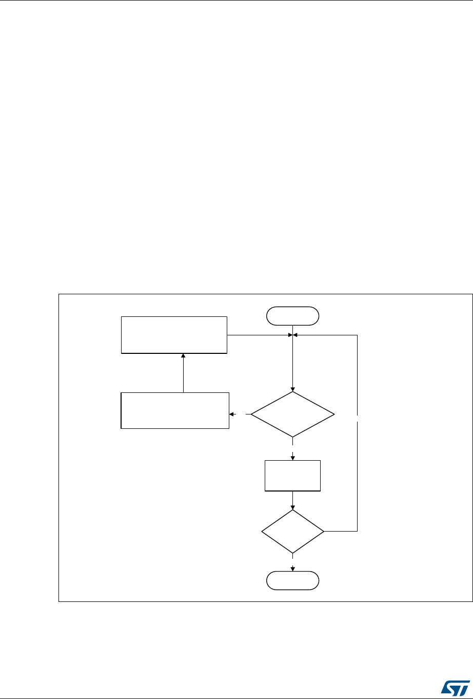
USB on-the-go full-speed (OTG_FS) RM0383
754/836 DocID026448 Rev 1
1. When an STALL, TXERR, BBERR or DTERR interrupt in OTG_FS_HCINTx is received
for an IN or OUT channel. The application must be able to receive other interrupts
(DTERR, Nak, Data, TXERR) for the same channel before receiving the halt.
2. When a DISCINT (Disconnect Device) interrupt in OTG_FS_GINTSTS is received.
(The application is expected to disable all enabled channels).
3. When the application aborts a transfer before normal completion.
Operational model
The application must initialize a channel before communicating to the connected device.
This section explains the sequence of operation to be performed for different types of USB
transactions.
•Writing the transmit FIFO
The OTG_FS host automatically writes an entry (OUT request) to the periodic/non-
periodic request queue, along with the last DWORD write of a packet. The application
must ensure that at least one free space is available in the periodic/non-periodic
request queue before starting to write to the transmit FIFO. The application must
always write to the transmit FIFO in DWORDs. If the packet size is non-DWORD
aligned, the application must use padding. The OTG_FS host determines the actual
packet size based on the programmed maximum packet size and transfer size.
Figure 252. Transmit FIFO write task
MPS: Maximum packet size
Start
ai15673b
Wait for NPTXFE/PTXFE
interrupt in
OTG_FS_GINTSTS
Read GNPTXSTS/HPTXFSIZ
registers for available FIFO
and queue spaces
1 MPS or
LPS FIFO space
available?
Write 1 packet
data to
transmit FIFO
More packets
to send?
Done
No
No Ye s
Ye s
LPS: Last packet size
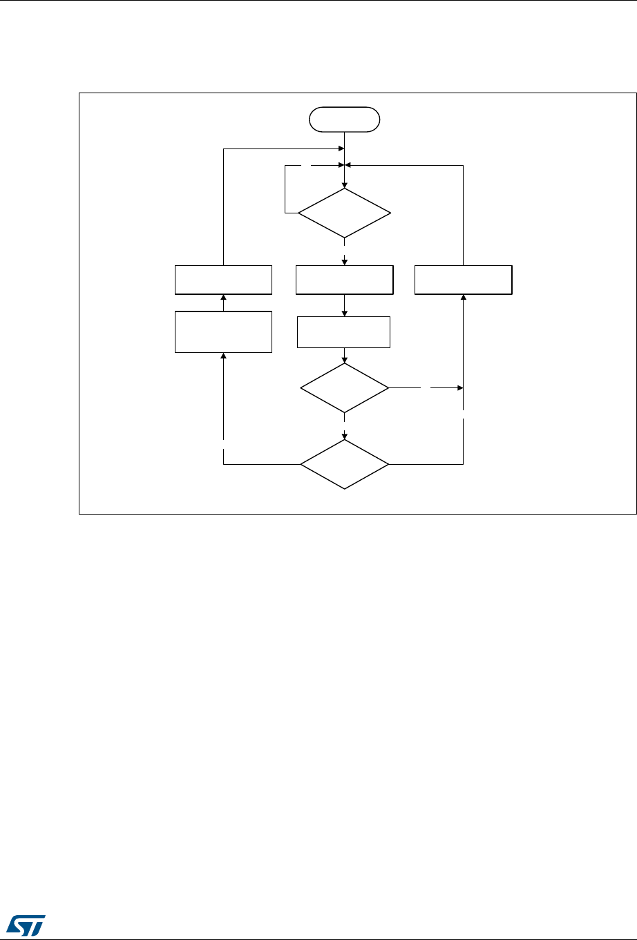
DocID026448 Rev 1 755/836
RM0383 USB on-the-go full-speed (OTG_FS)
796
•Reading the receive FIFO
The application must ignore all packet statuses other than IN data packet (bx0010).
Figure 253. Receive FIFO read task
•Bulk and control OUT/SETUP transactions
A typical bulk or control OUT/SETUP pipelined transaction-level operation is shown in
Figure 254. See channel 1 (ch_1). Two bulk OUT packets are transmitted. A control
RXFLVL
interrupt ?
Read the received
packet from the
Receive FIFO
Read
OTG_FS_GRXSTSP
PKTSTS
0b0010?
Yes
Yes
Unmask RXFLVL
interrupt
BCNT > 0?
No
Mask RXFLVL
interrupt
Yes
Unmask RXFLVL
interrupt
No
No
Start
ai15674

USB on-the-go full-speed (OTG_FS) RM0383
756/836 DocID026448 Rev 1
SETUP transaction operates in the same way but has only one packet. The
assumptions are:
– The application is attempting to send two maximum-packet-size packets (transfer
size = 1, 024 bytes).
– The non-periodic transmit FIFO can hold two packets (128 bytes for FS).
– The non-periodic request queue depth = 4.
•Normal bulk and control OUT/SETUP operations
The sequence of operations in (channel 1) is as follows:
a) Initialize channel 1
b) Write the first packet for channel 1
c) Along with the last Word write, the core writes an entry to the non-periodic request
queue
d) As soon as the non-periodic queue becomes non-empty, the core attempts to
send an OUT token in the current frame
e) Write the second (last) packet for channel 1
f) The core generates the XFRC interrupt as soon as the last transaction is
completed successfully
g) In response to the XFRC interrupt, de-allocate the channel for other transfers
h) Handling non-ACK responses
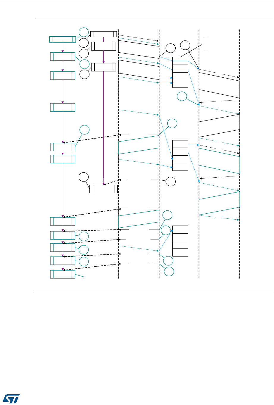
DocID026448 Rev 1 757/836
RM0383 USB on-the-go full-speed (OTG_FS)
796
Figure 254. Normal bulk/control OUT/SETUP and bulk/control IN transactions
The channel-specific interrupt service routine for bulk and control OUT/SETUP
transactions is shown in the following code samples.
•Interrupt service routine for bulk/control OUT/SETUP and bulk/control IN
transactions
a) Bulk/Control OUT/SETUP
Unmask (NAK/TXERR/STALL/XFRC)
if (XFRC)
{
Reset Error Count
Mask ACK
ACK
HostApplication DeviceAHB USB
OUT
DATA0
MPS
1
MPS
1
MPS
w rite_t x _fifo
(ch_1)
init_reg(ch _1)
set _ ch_e n
(ch_2)
init_reg(ch_2)
w rite_t x _fifo
(ch_1)
set _ ch_e n
(ch_2)
ch_2
ch_2
ch_1
ch_1
De-allocate
(ch_1)
IN
ch_2
ch_2
ch_2
ch_1
ACK
OUT
set _ ch_e n
(ch_2)
Non-Periodic Request
Queue
Assume that this queue
can hold 4 entries.
4
1
6
ACK
DATA0
IN
ACK
read_rx_sts
read_rx_fifo
1
MPS
set _ ch_e n
(ch_2)
1
MPS
read_rx_stsre
ad_rx_fifo
read_rx_sts
Disable
(ch_2)
1
234
5
6
7
De-allocate
(ch_2)
CHH interruptr
ch_2
2
3
5
7
8
9
12
13
read_rx_sts 10
11
DATA1
MPS
DATA1
ai15675
RXFLVL interrupt
XFRC interrupt
RXFLVL interrupt
RXFLVL interrupt
RXFLVL interrupt
XFRC interrupt

USB on-the-go full-speed (OTG_FS) RM0383
758/836 DocID026448 Rev 1
De-allocate Channel
}
else if (STALL)
{
Transfer Done = 1
Unmask CHH
Disable Channel
}
else if (NAK or TXERR )
{
Rewind Buffer Pointers
Unmask CHH
Disable Channel
if (TXERR)
{
Increment Error Count
Unmask ACK
}
else
{
Reset Error Count
}
}
else if (CHH)
{
Mask CHH
if (Transfer Done or (Error_count == 3))
{
De-allocate Channel
}
else
{
Re-initialize Channel
}
}
else if (ACK)
{
Reset Error Count
Mask ACK
}
The application is expected to write the data packets into the transmit FIFO as and
when the space is available in the transmit FIFO and the Request queue. The
application can make use of the NPTXFE interrupt in OTG_FS_GINTSTS to find the
transmit FIFO space.
b) Bulk/Control IN
Unmask (TXERR/XFRC/BBERR/STALL/DTERR)
if (XFRC)
{
Reset Error Count
Unmask CHH
Disable Channel

DocID026448 Rev 1 759/836
RM0383 USB on-the-go full-speed (OTG_FS)
796
Reset Error Count
Mask ACK
}
else if (TXERR or BBERR or STALL)
{
Unmask CHH
Disable Channel
if (TXERR)
{
Increment Error Count
Unmask ACK
}
}
else if (CHH)
{
Mask CHH
if (Transfer Done or (Error_count == 3))
{
De-allocate Channel
}
else
{
Re-initialize Channel
}
}
else if (ACK)
{
Reset Error Count
Mask ACK
}
else if (DTERR)
{
Reset Error Count
}
The application is expected to write the requests as and when the Request queue space is
available and until the XFRC interrupt is received.
•Bulk and control IN transactions
A typical bulk or control IN pipelined transaction-level operation is shown in Figure 255.
See channel 2 (ch_2). The assumptions are:
– The application is attempting to receive two maximum-packet-size packets
(transfer size = 1 024 bytes).
– The receive FIFO can contain at least one maximum-packet-size packet and two
status Words per packet (72 bytes for FS).
– The non-periodic request queue depth = 4.
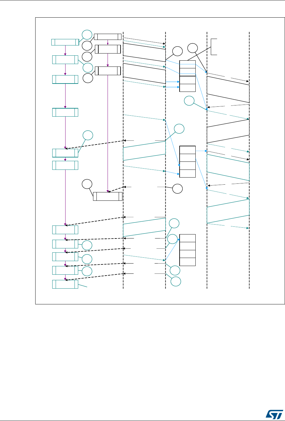
USB on-the-go full-speed (OTG_FS) RM0383
760/836 DocID026448 Rev 1
Figure 255. Bulk/control IN transactions
The sequence of operations is as follows:
a) Initialize channel 2.
b) Set the CHENA bit in HCCHAR2 to write an IN request to the non-periodic request
queue.
c) The core attempts to send an IN token after completing the current OUT
transaction.
d) The core generates an RXFLVL interrupt as soon as the received packet is written
to the receive FIFO.
e) In response to the RXFLVL interrupt, mask the RXFLVL interrupt and read the
received packet status to determine the number of bytes received, then read the
receive FIFO accordingly. Following this, unmask the RXFLVL interrupt.
ACK
HostApplication DeviceAHB USB
OUT
DATA0
MPS
1
MPS
1
MPS
w rit e_ tx _ fifo
(ch_1)
init_reg(ch _1)
set _ ch_e n
(ch_2)
init_reg(ch_2)
w rit e_ tx _ fifo
(ch_1)
set _ ch_e n
(ch_2)
ch_2
ch_2
ch_1
ch_1
De-allocate
(ch_1)
IN
ch_2
ch_2
ch_2
ch_1
ACK
OUT
set _ ch_e n
(ch_2)
Non-Periodic Request
Queue
Assume that this queue
can hold 4 entries.
4
1
6
ACK
DATA0
IN
ACK
read_rx_sts
read_rx_fifo
1
MPS
set _ ch_e n
(ch_2)
1
MPS
read_rx_stsre
ad_rx_fifo
read_rx_sts
Disable
(ch_2)
1
234
5
6
7
De-allocate
(ch_2)
CHH interruptr
ch_2
2
3
5
7
8
9
12
13
read_rx_sts 10
11
DATA1
MPS
DATA1
ai15675
RXFLVL interrupt
XFRC interrupt
RXFLVL interrupt
RXFLVL interrupt
RXFLVL interrupt
XFRC interrupt

DocID026448 Rev 1 761/836
RM0383 USB on-the-go full-speed (OTG_FS)
796
f) The core generates the RXFLVL interrupt for the transfer completion status entry
in the receive FIFO.
g) The application must read and ignore the receive packet status when the receive
packet status is not an IN data packet (PKTSTS in GRXSTSR ≠0b0010).
h) The core generates the XFRC interrupt as soon as the receive packet status is
read.
i) In response to the XFRC interrupt, disable the channel and stop writing the
OTG_FS_HCCHAR2 register for further requests. The core writes a channel
disable request to the non-periodic request queue as soon as the
OTG_FS_HCCHAR2 register is written.
j) The core generates the RXFLVL interrupt as soon as the halt status is written to
the receive FIFO.
k) Read and ignore the receive packet status.
l) The core generates a CHH interrupt as soon as the halt status is popped from the
receive FIFO.
m) In response to the CHH interrupt, de-allocate the channel for other transfers.
n) Handling non-ACK responses
•Control transactions
Setup, Data, and Status stages of a control transfer must be performed as three
separate transfers. Setup-, Data- or Status-stage OUT transactions are performed
similarly to the bulk OUT transactions explained previously. Data- or Status-stage IN
transactions are performed similarly to the bulk IN transactions explained previously.
For all three stages, the application is expected to set the EPTYP field in
OTG_FS_HCCHAR1 to Control. During the Setup stage, the application is expected to
set the PID field in OTG_FS_HCTSIZ1 to SETUP.
•Interrupt OUT transactions
A typical interrupt OUT operation is shown in Figure 256. The assumptions are:
– The application is attempting to send one packet in every frame (up to 1 maximum
packet size), starting with the odd frame (transfer size = 1 024 bytes)
– The periodic transmit FIFO can hold one packet (1 KB)
– Periodic request queue depth = 4
The sequence of operations is as follows:
a) Initialize and enable channel 1. The application must set the ODDFRM bit in
OTG_FS_HCCHAR1.
b) Write the first packet for channel 1.
c) Along with the last Word write of each packet, the OTG_FS host writes an entry to
the periodic request queue.
d) The OTG_FS host attempts to send an OUT token in the next (odd) frame.
e) The OTG_FS host generates an XFRC interrupt as soon as the last packet is
transmitted successfully.
f) In response to the XFRC interrupt, reinitialize the channel for the next transfer.
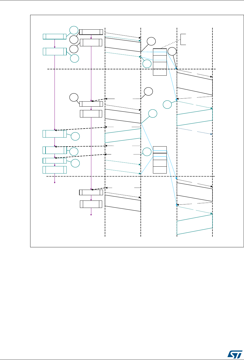
USB on-the-go full-speed (OTG_FS) RM0383
762/836 DocID026448 Rev 1
Figure 256. Normal interrupt OUT/IN transactions
•Interrupt service routine for interrupt OUT/IN transactions
a) Interrupt OUT
Unmask (NAK/TXERR/STALL/XFRC/FRMOR)
if (XFRC)
{
Reset Error Count
Mask ACK
De-allocate Channel
}
else
if (STALL or FRMOR)
{
Mask ACK
Unmask CHH
Host
Application DeviceAHB USB
OUT
DATA0
MPS
1
MPS
1
MPS
write_tx_fifo
(ch_1)
init_reg(ch_1)
set_ch_en
(ch_2)
init_reg(ch _2)
write_tx_fifo
(ch_1)
IN
OUT
DATA1
MPS
Periodic Request Queue
Assume that this queue
can hold 4 entries.
1
5
DATA0
IN
RXFLVL interrupt
1
MPS
read_rx_sts
read_rx_fifo
read_rx_sts
1
2
3
4
6
2
3
6
78
9
Odd
(micro)
frame
Even
(micro)
frame
init_reg(ch_1)
set_ch_en
(ch_2)
init_reg(ch _2)
write_tx_fifo
(ch_1)
init_reg(ch_1)
1
MPS
DATA1
5
4
ACK
ACK
ACK
ch_1
ch_2
ch_2
ch_1
ai15676
RXFLVL interrupt
XFRC interrupt
XFRC interrupt
XFRC interrupt

DocID026448 Rev 1 763/836
RM0383 USB on-the-go full-speed (OTG_FS)
796
Disable Channel
if (STALL)
{
Transfer Done = 1
}
}
else
if (NAK or TXERR)
{
Rewind Buffer Pointers
Reset Error Count
Mask ACK
Unmask CHH
Disable Channel
}
else
if (CHH)
{
Mask CHH
if (Transfer Done or (Error_count == 3))
{
De-allocate Channel
}
else
{
Re-initialize Channel (in next b_interval - 1 Frame)
}
}
else
if (ACK)
{
Reset Error Count
Mask ACK
}
The application uses the NPTXFE interrupt in OTG_FS_GINTSTS to find the transmit
FIFO space.
b) Interrupt IN
Unmask (NAK/TXERR/XFRC/BBERR/STALL/FRMOR/DTERR)
if (XFRC)
{
Reset Error Count
Mask ACK
if (OTG_FS_HCTSIZx.PKTCNT == 0)
{
De-allocate Channel
}
else
{
Transfer Done = 1
Unmask CHH
Disable Channel

USB on-the-go full-speed (OTG_FS) RM0383
764/836 DocID026448 Rev 1
}
}
else
if (STALL or FRMOR or NAK or DTERR or BBERR)
{
Mask ACK
Unmask CHH
Disable Channel
if (STALL or BBERR)
{
Reset Error Count
Transfer Done = 1
}
else
if (!FRMOR)
{
Reset Error Count
}
}
else
if (TXERR)
{
Increment Error Count
Unmask ACK
Unmask CHH
Disable Channel
}
else
if (CHH)
{
Mask CHH
if (Transfer Done or (Error_count == 3))
{
De-allocate Channel
}
else
Re-initialize Channel (in next b_interval - 1 /Frame)
}
}
else
if (ACK)
{
Reset Error Count
Mask ACK
}

DocID026448 Rev 1 765/836
RM0383 USB on-the-go full-speed (OTG_FS)
796
•Interrupt IN transactions
The assumptions are:
– The application is attempting to receive one packet (up to 1 maximum packet size)
in every frame, starting with odd (transfer size = 1 024 bytes).
– The receive FIFO can hold at least one maximum-packet-size packet and two
status Words per packet (1 031 bytes).
– Periodic request queue depth = 4.
•Normal interrupt IN operation
The sequence of operations is as follows:
a) Initialize channel 2. The application must set the ODDFRM bit in
OTG_FS_HCCHAR2.
b) Set the CHENA bit in OTG_FS_HCCHAR2 to write an IN request to the periodic
request queue.
c) The OTG_FS host writes an IN request to the periodic request queue for each
OTG_FS_HCCHAR2 register write with the CHENA bit set.
d) The OTG_FS host attempts to send an IN token in the next (odd) frame.
e) As soon as the IN packet is received and written to the receive FIFO, the OTG_FS
host generates an RXFLVL interrupt.
f) In response to the RXFLVL interrupt, read the received packet status to determine
the number of bytes received, then read the receive FIFO accordingly. The
application must mask the RXFLVL interrupt before reading the receive FIFO, and
unmask after reading the entire packet.
g) The core generates the RXFLVL interrupt for the transfer completion status entry
in the receive FIFO. The application must read and ignore the receive packet
status when the receive packet status is not an IN data packet (PKTSTS in
GRXSTSR ≠0b0010).
h) The core generates an XFRC interrupt as soon as the receive packet status is
read.
i) In response to the XFRC interrupt, read the PKTCNT field in OTG_FS_HCTSIZ2.
If the PKTCNT bit in OTG_FS_HCTSIZ2 is not equal to 0, disable the channel
before re-initializing the channel for the next transfer, if any). If PKTCNT bit in
OTG_FS_HCTSIZ2 = 0, reinitialize the channel for the next transfer. This time, the
application must reset the ODDFRM bit in OTG_FS_HCCHAR2.

USB on-the-go full-speed (OTG_FS) RM0383
766/836 DocID026448 Rev 1
•Isochronous OUT transactions
A typical isochronous OUT operation is shown in Figure 257. The assumptions are:
– The application is attempting to send one packet every frame (up to 1 maximum
packet size), starting with an odd frame. (transfer size = 1 024 bytes).
– The periodic transmit FIFO can hold one packet (1 KB).
– Periodic request queue depth = 4.
The sequence of operations is as follows:
a) Initialize and enable channel 1. The application must set the ODDFRM bit in
OTG_FS_HCCHAR1.
b) Write the first packet for channel 1.
c) Along with the last Word write of each packet, the OTG_FS host writes an entry to
the periodic request queue.
d) The OTG_FS host attempts to send the OUT token in the next frame (odd).
e) The OTG_FS host generates the XFRC interrupt as soon as the last packet is
transmitted successfully.
f) In response to the XFRC interrupt, reinitialize the channel for the next transfer.
g) Handling non-ACK responses
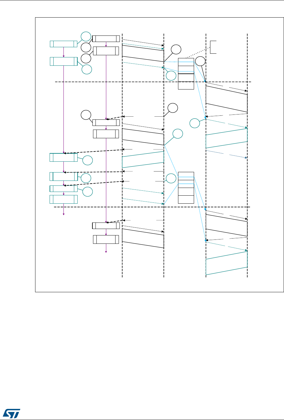
DocID026448 Rev 1 767/836
RM0383 USB on-the-go full-speed (OTG_FS)
796
Figure 257. Normal isochronous OUT/IN transactions
•Interrupt service routine for isochronous OUT/IN transactions
Code sample: Isochronous OUT
Unmask (FRMOR/XFRC)
if (XFRC)
{
De-allocate Channel
}
else
if (FRMOR)
{
Unmask CHH
Disable Channel
}
Host
Application DeviceAHB USB
OUT
DATA0
MPS
1
MPS
1
MPS
write_tx_fifo
(ch_1)
init_reg(ch_1)
set_ch_en
(ch_2)
init_reg(ch _2)
write_tx_fifo
(ch_1)
IN
OUT
DATA1
MPS
Periodic Request Queue
Assume that this queue
can hold 4 entries.
1
5
DATA0
IN
RXFLVL interrupt
1
MPS
read_rx_sts
read_rx_fifo
read_rx_sts
1
2
3
4
6
2
3
6
78
9
Odd
(micro)
frame
Even
(micro)
frame
init_reg(ch_1)
set_ch_en
(ch_2)
init_reg(ch _2)
write_tx_fifo
(ch_1)
init_reg(ch_1)
1
MPS
DATA1
5
4
ACK
ACK
ACK
ch_1
ch_2
ch_2
ch_1
ai15676
RXFLVL interrupt
XFRC interrupt
XFRC interrupt
XFRC interrupt

USB on-the-go full-speed (OTG_FS) RM0383
768/836 DocID026448 Rev 1
else
if (CHH)
{
Mask CHH
De-allocate Channel
}
Code sample: Isochronous IN
Unmask (TXERR/XFRC/FRMOR/BBERR)
if (XFRC or FRMOR)
{
if (XFRC and (OTG_FS_HCTSIZx.PKTCNT == 0))
{
Reset Error Count
De-allocate Channel
}
else
{
Unmask CHH
Disable Channel
}
}
else
if (TXERR or BBERR)
{
Increment Error Count
Unmask CHH
Disable Channel
}
else
if (CHH)
{
Mask CHH
if (Transfer Done or (Error_count == 3))
{
De-allocate Channel
}
else
{
Re-initialize Channel
}
}

DocID026448 Rev 1 769/836
RM0383 USB on-the-go full-speed (OTG_FS)
796
•Isochronous IN transactions
The assumptions are:
– The application is attempting to receive one packet (up to 1 maximum packet size)
in every frame starting with the next odd frame (transfer size = 1 024 bytes).
– The receive FIFO can hold at least one maximum-packet-size packet and two
status Word per packet (1 031 bytes).
– Periodic request queue depth = 4.
The sequence of operations is as follows:
a) Initialize channel 2. The application must set the ODDFRM bit in
OTG_FS_HCCHAR2.
b) Set the CHENA bit in OTG_FS_HCCHAR2 to write an IN request to the periodic
request queue.
c) The OTG_FS host writes an IN request to the periodic request queue for each
OTG_FS_HCCHAR2 register write with the CHENA bit set.
d) The OTG_FS host attempts to send an IN token in the next odd frame.
e) As soon as the IN packet is received and written to the receive FIFO, the OTG_FS
host generates an RXFLVL interrupt.
f) In response to the RXFLVL interrupt, read the received packet status to determine
the number of bytes received, then read the receive FIFO accordingly. The
application must mask the RXFLVL interrupt before reading the receive FIFO, and
unmask it after reading the entire packet.
g) The core generates an RXFLVL interrupt for the transfer completion status entry in
the receive FIFO. This time, the application must read and ignore the receive
packet status when the receive packet status is not an IN data packet (PKTSTS bit
in OTG_FS_GRXSTSR ≠0b0010).
h) The core generates an XFRC interrupt as soon as the receive packet status is
read.
i) In response to the XFRC interrupt, read the PKTCNT field in OTG_FS_HCTSIZ2.
If PKTCNT≠0 in OTG_FS_HCTSIZ2, disable the channel before re-initializing the
channel for the next transfer, if any. If PKTCNT = 0 in OTG_FS_HCTSIZ2,
reinitialize the channel for the next transfer. This time, the application must reset
the ODDFRM bit in OTG_FS_HCCHAR2.
•Selecting the queue depth
Choose the periodic and non-periodic request queue depths carefully to match the
number of periodic/non-periodic endpoints accessed.
The non-periodic request queue depth affects the performance of non-periodic
transfers. The deeper the queue (along with sufficient FIFO size), the more often the
core is able to pipeline non-periodic transfers. If the queue size is small, the core is
able to put in new requests only when the queue space is freed up.
The core’s periodic request queue depth is critical to perform periodic transfers as
scheduled. Select the periodic queue depth, based on the number of periodic transfers
scheduled in a microframe. If the periodic request queue depth is smaller than the
periodic transfers scheduled in a microframe, a frame overrun condition occurs.
•Handling babble conditions
OTG_FS controller handles two cases of babble: packet babble and port babble.
Packet babble occurs if the device sends more data than the maximum packet size for

USB on-the-go full-speed (OTG_FS) RM0383
770/836 DocID026448 Rev 1
the channel. Port babble occurs if the core continues to receive data from the device at
EOF2 (the end of frame 2, which is very close to SOF).
When OTG_FS controller detects a packet babble, it stops writing data into the Rx
buffer and waits for the end of packet (EOP). When it detects an EOP, it flushes already
written data in the Rx buffer and generates a Babble interrupt to the application.
When OTG_FS controller detects a port babble, it flushes the RxFIFO and disables the
port. The core then generates a Port disabled interrupt (HPRTINT in
OTG_FS_GINTSTS, PENCHNG in OTG_FS_HPRT). On receiving this interrupt, the
application must determine that this is not due to an overcurrent condition (another
cause of the Port Disabled interrupt) by checking POCA in OTG_FS_HPRT, then
perform a soft reset. The core does not send any more tokens after it has detected a
port babble condition.
22.17.5 Device programming model
Endpoint initialization on USB reset
1. Set the NAK bit for all OUT endpoints
– SNAK = 1 in OTG_FS_DOEPCTLx (for all OUT endpoints)
2. Unmask the following interrupt bits
– INEP0 = 1 in OTG_FS_DAINTMSK (control 0 IN endpoint)
– OUTEP0 = 1 in OTG_FS_DAINTMSK (control 0 OUT endpoint)
–STUP=1 in DOEPMSK
– XFRC = 1 in DOEPMSK
– XFRC = 1 in DIEPMSK
– TOC = 1 in DIEPMSK
3. Set up the Data FIFO RAM for each of the FIFOs
– Program the OTG_FS_GRXFSIZ register, to be able to receive control OUT data
and setup data. If thresholding is not enabled, at a minimum, this must be equal to
1 max packet size of control endpoint 0 + 2 Words (for the status of the control
OUT data packet) + 10 Words (for setup packets).
– Program the OTG_FS_TX0FSIZ register (depending on the FIFO number chosen)
to be able to transmit control IN data. At a minimum, this must be equal to 1 max
packet size of control endpoint 0.
4. Program the following fields in the endpoint-specific registers for control OUT endpoint
0 to receive a SETUP packet
– STUPCNT = 3 in OTG_FS_DOEPTSIZ0 (to receive up to 3 back-to-back SETUP
packets)
At this point, all initialization required to receive SETUP packets is done.
Endpoint initialization on enumeration completion
1. On the Enumeration Done interrupt (ENUMDNE in OTG_FS_GINTSTS), read the
OTG_FS_DSTS register to determine the enumeration speed.
2. Program the MPSIZ field in OTG_FS_DIEPCTL0 to set the maximum packet size. This
step configures control endpoint 0. The maximum packet size for a control endpoint
depends on the enumeration speed.

DocID026448 Rev 1 771/836
RM0383 USB on-the-go full-speed (OTG_FS)
796
At this point, the device is ready to receive SOF packets and is configured to perform control
transfers on control endpoint 0.
Endpoint initialization on SetAddress command
This section describes what the application must do when it receives a SetAddress
command in a SETUP packet.
1. Program the OTG_FS_DCFG register with the device address received in the
SetAddress command
1. Program the core to send out a status IN packet
Endpoint initialization on SetConfiguration/SetInterface command
This section describes what the application must do when it receives a SetConfiguration or
SetInterface command in a SETUP packet.
1. When a SetConfiguration command is received, the application must program the
endpoint registers to configure them with the characteristics of the valid endpoints in
the new configuration.
2. When a SetInterface command is received, the application must program the endpoint
registers of the endpoints affected by this command.
3. Some endpoints that were active in the prior configuration or alternate setting are not
valid in the new configuration or alternate setting. These invalid endpoints must be
deactivated.
4. Unmask the interrupt for each active endpoint and mask the interrupts for all inactive
endpoints in the OTG_FS_DAINTMSK register.
5. Set up the Data FIFO RAM for each FIFO.
6. After all required endpoints are configured; the application must program the core to
send a status IN packet.
At this point, the device core is configured to receive and transmit any type of data packet.
Endpoint activation
This section describes the steps required to activate a device endpoint or to configure an
existing device endpoint to a new type.
1. Program the characteristics of the required endpoint into the following fields of the
OTG_FS_DIEPCTLx register (for IN or bidirectional endpoints) or the
OTG_FS_DOEPCTLx register (for OUT or bidirectional endpoints).
– Maximum packet size
– USB active endpoint = 1
– Endpoint start data toggle (for interrupt and bulk endpoints)
– Endpoint type
– TxFIFO number
2. Once the endpoint is activated, the core starts decoding the tokens addressed to that
endpoint and sends out a valid handshake for each valid token received for the
endpoint.
Endpoint deactivation
This section describes the steps required to deactivate an existing endpoint.

USB on-the-go full-speed (OTG_FS) RM0383
772/836 DocID026448 Rev 1
1. In the endpoint to be deactivated, clear the USB active endpoint bit in the
OTG_FS_DIEPCTLx register (for IN or bidirectional endpoints) or the
OTG_FS_DOEPCTLx register (for OUT or bidirectional endpoints).
2. Once the endpoint is deactivated, the core ignores tokens addressed to that endpoint,
which results in a timeout on the USB.
Note: The application must meet the following conditions to set up the device core to handle
traffic:
NPTXFEM and RXFLVLM in the OTG_FS_GINTMSK register must be cleared.
22.17.6 Operational model
SETUP and OUT data transfers
This section describes the internal data flow and application-level operations during data
OUT transfers and SETUP transactions.
•Packet read
This section describes how to read packets (OUT data and SETUP packets) from the
receive FIFO.
1. On catching an RXFLVL interrupt (OTG_FS_GINTSTS register), the application must
read the Receive status pop register (OTG_FS_GRXSTSP).
2. The application can mask the RXFLVL interrupt (in OTG_FS_GINTSTS) by writing to
RXFLVL = 0 (in OTG_FS_GINTMSK), until it has read the packet from the receive
FIFO.
3. If the received packet’s byte count is not 0, the byte count amount of data is popped
from the receive Data FIFO and stored in memory. If the received packet byte count is
0, no data is popped from the receive data FIFO.
4. The receive FIFO’s packet status readout indicates one of the following:
a) Global OUT NAK pattern:
PKTSTS = Global OUT NAK, BCNT = 0x000, EPNUM = Don’t Care (0x0),
DPID = Don’t Care (0b00).
These data indicate that the global OUT NAK bit has taken effect.
b) SETUP packet pattern:
PKTSTS = SETUP, BCNT = 0x008, EPNUM = Control EP Num, DPID = D0.
These data indicate that a SETUP packet for the specified endpoint is now
available for reading from the receive FIFO.
c) Setup stage done pattern:
PKTSTS = Setup Stage Done, BCNT = 0x0, EPNUM = Control EP Num,
DPID = Don’t Care (0b00).
These data indicate that the Setup stage for the specified endpoint has completed
and the Data stage has started. After this entry is popped from the receive FIFO,
the core asserts a Setup interrupt on the specified control OUT endpoint.
d) Data OUT packet pattern:
PKTSTS = DataOUT, BCNT = size of the received data OUT packet (0 ≤ BCNT
≤ 1 024), EPNUM = EPNUM on which the packet was received, DPID = Actual
Data PID.
e) Data transfer completed pattern:
PKTSTS = Data OUT Transfer Done, BCNT = 0x0, EPNUM = OUT EP Num
on which the data transfer is complete, DPID = Don’t Care (0b00).
These data indicate that an OUT data transfer for the specified OUT endpoint has
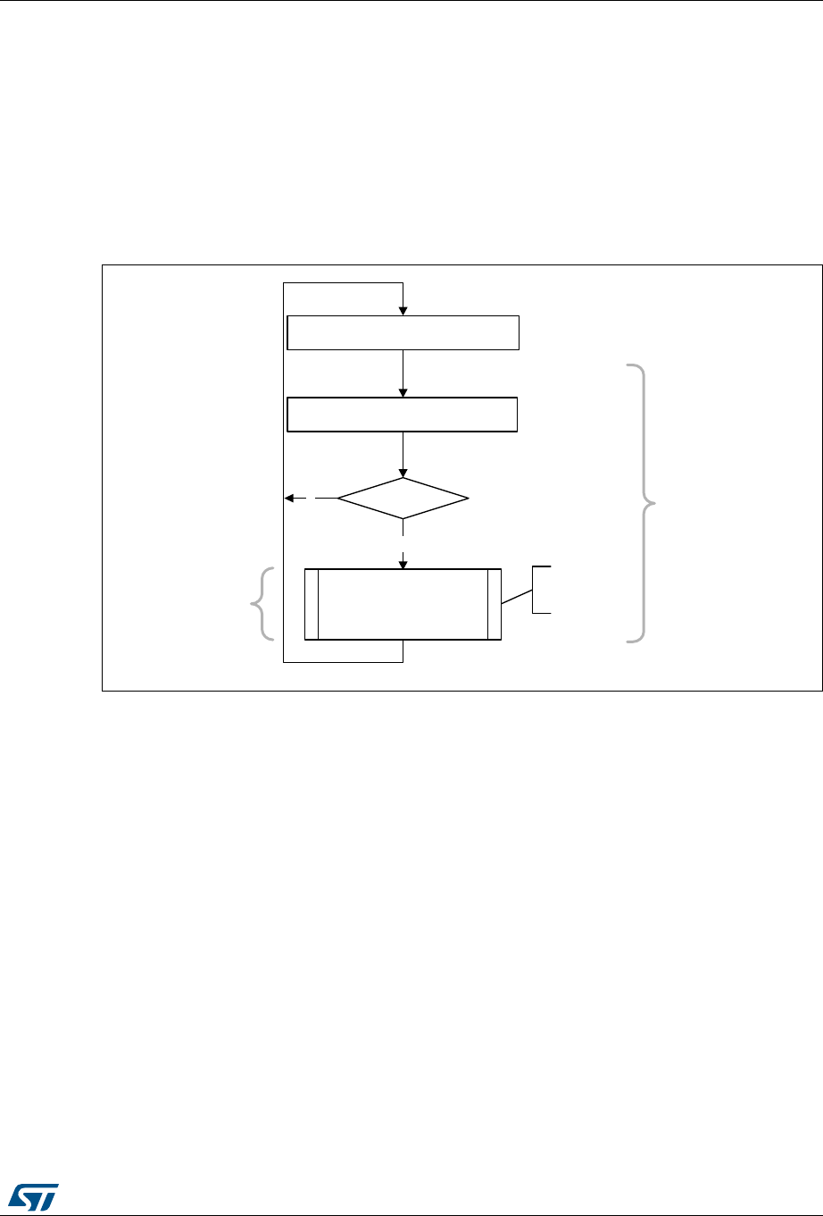
DocID026448 Rev 1 773/836
RM0383 USB on-the-go full-speed (OTG_FS)
796
completed. After this entry is popped from the receive FIFO, the core asserts a
Transfer Completed interrupt on the specified OUT endpoint.
5. After the data payload is popped from the receive FIFO, the RXFLVL interrupt
(OTG_FS_GINTSTS) must be unmasked.
6. Steps 1–5 are repeated every time the application detects assertion of the interrupt line
due to RXFLVL in OTG_FS_GINTSTS. Reading an empty receive FIFO can result in
undefined core behavior.
Figure 258 provides a flowchart of the above procedure.
Figure 258. Receive FIFO packet read
•SETUP transactions
This section describes how the core handles SETUP packets and the application’s
sequence for handling SETUP transactions.
•Application requirements
1. To receive a SETUP packet, the STUPCNT field (OTG_FS_DOEPTSIZx) in a control
OUT endpoint must be programmed to a non-zero value. When the application
programs the STUPCNT field to a non-zero value, the core receives SETUP packets
and writes them to the receive FIFO, irrespective of the NAK status and EPENA bit
setting in OTG_FS_DOEPCTLx. The STUPCNT field is decremented every time the
control endpoint receives a SETUP packet. If the STUPCNT field is not programmed to
a proper value before receiving a SETUP packet, the core still receives the SETUP
packet and decrements the STUPCNT field, but the application may not be able to
word_cnt =
BCNT[11:2] +C
(BCNT[1]
| BCNT[1])
rcv_out_pkt()
rd_data = rd_reg (OTG_FS_GRXSTSP);
mem[0: word_cnt – 1] =
rd_rxfifo(rd_data.EPNUM,
word_cnt)
N
rd_data.BCNT = 0
wait until RXFLVL in OTG_FS_GINTSTSG
packet
store in
memory
Y
ai15677b

USB on-the-go full-speed (OTG_FS) RM0383
774/836 DocID026448 Rev 1
determine the correct number of SETUP packets received in the Setup stage of a
control transfer.
– STUPCNT = 3 in OTG_FS_DOEPTSIZx
2. The application must always allocate some extra space in the Receive data FIFO, to be
able to receive up to three SETUP packets on a control endpoint.
– The space to be reserved is 10 Words. Three Words are required for the first
SETUP packet, 1 Word is required for the Setup stage done Word and 6 Words
are required to store two extra SETUP packets among all control endpoints.
– 3 Words per SETUP packet are required to store 8 bytes of SETUP data and 4
bytes of SETUP status (Setup packet pattern). The core reserves this space in the
receive data.
– FIFO to write SETUP data only, and never uses this space for data packets.
3. The application must read the 2 Words of the SETUP packet from the receive FIFO.
4. The application must read and discard the Setup stage done Word from the receive
FIFO.
•Internal data flow
5. When a SETUP packet is received, the core writes the received data to the receive
FIFO, without checking for available space in the receive FIFO and irrespective of the
endpoint’s NAK and STALL bit settings.
– The core internally sets the IN NAK and OUT NAK bits for the control IN/OUT
endpoints on which the SETUP packet was received.
6. For every SETUP packet received on the USB, 3 Words of data are written to the
receive FIFO, and the STUPCNT field is decremented by 1.
– The first Word contains control information used internally by the core
– The second Word contains the first 4 bytes of the SETUP command
– The third Word contains the last 4 bytes of the SETUP command
7. When the Setup stage changes to a Data IN/OUT stage, the core writes an entry
(Setup stage done Word) to the receive FIFO, indicating the completion of the Setup
stage.
8. On the AHB side, SETUP packets are emptied by the application.
9. When the application pops the Setup stage done Word from the receive FIFO, the core
interrupts the application with an STUP interrupt (OTG_FS_DOEPINTx), indicating it
can process the received SETUP packet.
– The core clears the endpoint enable bit for control OUT endpoints.
•Application programming sequence
1. Program the OTG_FS_DOEPTSIZx register.
– STUPCNT =3
2. Wait for the RXFLVL interrupt (OTG_FS_GINTSTS) and empty the data packets from
the receive FIFO.
3. Assertion of the STUP interrupt (OTG_FS_DOEPINTx) marks a successful completion
of the SETUP Data Transfer.
– On this interrupt, the application must read the OTG_FS_DOEPTSIZx register to
determine the number of SETUP packets received and process the last received
SETUP packet.
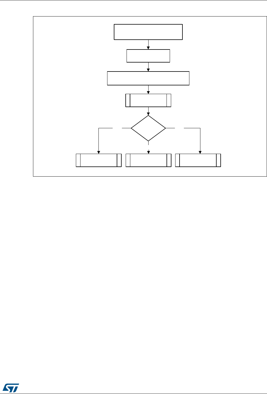
DocID026448 Rev 1 775/836
RM0383 USB on-the-go full-speed (OTG_FS)
796
Figure 259. Processing a SETUP packet
•Handling more than three back-to-back SETUP packets
Per the USB 2.0 specification, normally, during a SETUP packet error, a host does not send
more than three back-to-back SETUP packets to the same endpoint. However, the USB 2.0
specification does not limit the number of back-to-back SETUP packets a host can send to
the same endpoint. When this condition occurs, the OTG_FS controller generates an
interrupt (B2BSTUP in OTG_FS_DOEPINTx).
•Setting the global OUT NAK
Internal data flow:
1. When the application sets the Global OUT NAK (SGONAK bit in OTG_FS_DCTL), the
core stops writing data, except SETUP packets, to the receive FIFO. Irrespective of the
space availability in the receive FIFO, non-isochronous OUT tokens receive a NAK
handshake response, and the core ignores isochronous OUT data packets
2. The core writes the Global OUT NAK pattern to the receive FIFO. The application must
reserve enough receive FIFO space to write this data pattern.
3. When the application pops the Global OUT NAK pattern Word from the receive FIFO,
the core sets the GONAKEFF interrupt (OTG_FS_GINTSTS).
4. Once the application detects this interrupt, it can assume that the core is in Global OUT
NAK mode. The application can clear this interrupt by clearing the SGONAK bit in
OTG_FS_DCTL.
Application programming sequence
Wait for STUP in OTG_FS_DOEPINTx
rem_supcnt =
rd_reg(DOEPTSIZx)
setup_cmd[31:0] = mem[4 – 2 * rem_supcnt]
setup_cmd[63:32] = mem[5 – 2 * rem_supcnt]
ctrl-rd/wr/2 stage
Find setup cmd type
Write
2-stage
Read
setup_np_in_pkt
Status IN phase
rcv_out_pkt
Data OUT phase
setup_np_in_pkt
Data IN phase
ai15678

USB on-the-go full-speed (OTG_FS) RM0383
776/836 DocID026448 Rev 1
1. To stop receiving any kind of data in the receive FIFO, the application must set the
Global OUT NAK bit by programming the following field:
– SGONAK = 1 in OTG_FS_DCTL
2. Wait for the assertion of the GONAKEFF interrupt in OTG_FS_GINTSTS. When
asserted, this interrupt indicates that the core has stopped receiving any type of data
except SETUP packets.
3. The application can receive valid OUT packets after it has set SGONAK in
OTG_FS_DCTL and before the core asserts the GONAKEFF interrupt
(OTG_FS_GINTSTS).
4. The application can temporarily mask this interrupt by writing to the GINAKEFFM bit in
the OTG_FS_GINTMSK register.
– GINAKEFFM = 0 in the OTG_FS_GINTMSK register
5. Whenever the application is ready to exit the Global OUT NAK mode, it must clear the
SGONAK bit in OTG_FS_DCTL. This also clears the GONAKEFF interrupt
(OTG_FS_GINTSTS).
– OTG_FS_DCTL = 1 in CGONAK
6. If the application has masked this interrupt earlier, it must be unmasked as follows:
– GINAKEFFM = 1 in GINTMSK
•Disabling an OUT endpoint
The application must use this sequence to disable an OUT endpoint that it has enabled.
Application programming sequence:
1. Before disabling any OUT endpoint, the application must enable Global OUT NAK
mode in the core.
– SGONAK = 1 in OTG_FS_DCTL
2. Wait for the GONAKEFF interrupt (OTG_FS_GINTSTS)
3. Disable the required OUT endpoint by programming the following fields:
– EPDIS = 1 in OTG_FS_DOEPCTLx
– SNAK = 1 in OTG_FS_DOEPCTLx
4. Wait for the EPDISD interrupt (OTG_FS_DOEPINTx), which indicates that the OUT
endpoint is completely disabled. When the EPDISD interrupt is asserted, the core also
clears the following bits:
– EPDIS = 0 in OTG_FS_DOEPCTLx
– EPENA = 0 in OTG_FS_DOEPCTLx
5. The application must clear the Global OUT NAK bit to start receiving data from other
non-disabled OUT endpoints.
– SGONAK = 0 in OTG_FS_DCTL
•Generic non-isochronous OUT data transfers
This section describes a regular non-isochronous OUT data transfer (control, bulk, or
interrupt).
Application requirements:

DocID026448 Rev 1 777/836
RM0383 USB on-the-go full-speed (OTG_FS)
796
1. Before setting up an OUT transfer, the application must allocate a buffer in the memory
to accommodate all data to be received as part of the OUT transfer.
2. For OUT transfers, the transfer size field in the endpoint’s transfer size register must be
a multiple of the maximum packet size of the endpoint, adjusted to the Word boundary.
– transfer size[EPNUM] = n × (MPSIZ[EPNUM] + 4 – (MPSIZ[EPNUM] mod 4))
– packet count[EPNUM] = n
–n > 0
3. On any OUT endpoint interrupt, the application must read the endpoint’s transfer size
register to calculate the size of the payload in the memory. The received payload size
can be less than the programmed transfer size.
– Payload size in memory = application programmed initial transfer size – core
updated final transfer size
– Number of USB packets in which this payload was received = application
programmed initial packet count – core updated final packet count
Internal data flow:
1. The application must set the transfer size and packet count fields in the endpoint-
specific registers, clear the NAK bit, and enable the endpoint to receive the data.
2. Once the NAK bit is cleared, the core starts receiving data and writes it to the receive
FIFO, as long as there is space in the receive FIFO. For every data packet received on
the USB, the data packet and its status are written to the receive FIFO. Every packet
(maximum packet size or short packet) written to the receive FIFO decrements the
packet count field for that endpoint by 1.
– OUT data packets received with bad data CRC are flushed from the receive FIFO
automatically.
– After sending an ACK for the packet on the USB, the core discards non-
isochronous OUT data packets that the host, which cannot detect the ACK, re-
sends. The application does not detect multiple back-to-back data OUT packets
on the same endpoint with the same data PID. In this case the packet count is not
decremented.
– If there is no space in the receive FIFO, isochronous or non-isochronous data
packets are ignored and not written to the receive FIFO. Additionally, non-
isochronous OUT tokens receive a NAK handshake reply.
– In all the above three cases, the packet count is not decremented because no data
are written to the receive FIFO.
3. When the packet count becomes 0 or when a short packet is received on the endpoint,
the NAK bit for that endpoint is set. Once the NAK bit is set, the isochronous or non-
isochronous data packets are ignored and not written to the receive FIFO, and non-
isochronous OUT tokens receive a NAK handshake reply.
4. After the data are written to the receive FIFO, the application reads the data from the
receive FIFO and writes it to external memory, one packet at a time per endpoint.
5. At the end of every packet write on the AHB to external memory, the transfer size for
the endpoint is decremented by the size of the written packet.

USB on-the-go full-speed (OTG_FS) RM0383
778/836 DocID026448 Rev 1
6. The OUT data transfer completed pattern for an OUT endpoint is written to the receive
FIFO on one of the following conditions:
– The transfer size is 0 and the packet count is 0
– The last OUT data packet written to the receive FIFO is a short packet
(0 ≤ packet size < maximum packet size)
7. When either the application pops this entry (OUT data transfer completed), a transfer
completed interrupt is generated for the endpoint and the endpoint enable is cleared.
Application programming sequence:
1. Program the OTG_FS_DOEPTSIZx register for the transfer size and the corresponding
packet count.
2. Program the OTG_FS_DOEPCTLx register with the endpoint characteristics, and set
the EPENA and CNAK bits.
– EPENA = 1 in OTG_FS_DOEPCTLx
– CNAK = 1 in OTG_FS_DOEPCTLx
3. Wait for the RXFLVL interrupt (in OTG_FS_GINTSTS) and empty the data packets
from the receive FIFO.
– This step can be repeated many times, depending on the transfer size.
4. Asserting the XFRC interrupt (OTG_FS_DOEPINTx) marks a successful completion of
the non-isochronous OUT data transfer.
5. Read the OTG_FS_DOEPTSIZx register to determine the size of the received data
payload.
•Generic isochronous OUT data transfer
This section describes a regular isochronous OUT data transfer.
Application requirements:
1. All the application requirements for non-isochronous OUT data transfers also apply to
isochronous OUT data transfers.
2. For isochronous OUT data transfers, the transfer size and packet count fields must
always be set to the number of maximum-packet-size packets that can be received in a
single frame and no more. Isochronous OUT data transfers cannot span more than 1
frame.
3. The application must read all isochronous OUT data packets from the receive FIFO
(data and status) before the end of the periodic frame (EOPF interrupt in
OTG_FS_GINTSTS).
4. To receive data in the following frame, an isochronous OUT endpoint must be enabled
after the EOPF (OTG_FS_GINTSTS) and before the SOF (OTG_FS_GINTSTS).
Internal data flow:
1. The internal data flow for isochronous OUT endpoints is the same as that for non-
isochronous OUT endpoints, but for a few differences.
2. When an isochronous OUT endpoint is enabled by setting the Endpoint Enable and
clearing the NAK bits, the Even/Odd frame bit must also be set appropriately. The core
receives data on an isochronous OUT endpoint in a particular frame only if the
following condition is met:
– EONUM (in OTG_FS_DOEPCTLx) = SOFFN[0] (in OTG_FS_DSTS)
3. When the application completely reads an isochronous OUT data packet (data and
status) from the receive FIFO, the core updates the RXDPID field in

DocID026448 Rev 1 779/836
RM0383 USB on-the-go full-speed (OTG_FS)
796
OTG_FS_DOEPTSIZx with the data PID of the last isochronous OUT data packet read
from the receive FIFO.
Application programming sequence:
1. Program the OTG_FS_DOEPTSIZx register for the transfer size and the corresponding
packet count
2. Program the OTG_FS_DOEPCTLx register with the endpoint characteristics and set
the Endpoint Enable, ClearNAK, and Even/Odd frame bits.
– EPENA = 1
–CNAK=1
– EONUM = (0: Even/1: Odd)
3. Wait for the RXFLVL interrupt (in OTG_FS_GINTSTS) and empty the data packets
from the receive FIFO
– This step can be repeated many times, depending on the transfer size.
4. The assertion of the XFRC interrupt (in OTG_FS_DOEPINTx) marks the completion of
the isochronous OUT data transfer. This interrupt does not necessarily mean that the
data in memory are good.
5. This interrupt cannot always be detected for isochronous OUT transfers. Instead, the
application can detect the IISOOXFRM interrupt in OTG_FS_GINTSTS.
6. Read the OTG_FS_DOEPTSIZx register to determine the size of the received transfer
and to determine the validity of the data received in the frame. The application must
treat the data received in memory as valid only if one of the following conditions is met:
– RXDPID = D0 (in OTG_FS_DOEPTSIZx) and the number of USB packets in
which this payload was received = 1
– RXDPID = D1 (in OTG_FS_DOEPTSIZx) and the number of USB packets in
which this payload was received = 2
– RXDPID = D2 (in OTG_FS_DOEPTSIZx) and the number of USB packets in
which this payload was received = 3
The number of USB packets in which this payload was received =
Application programmed initial packet count – Core updated final packet count
The application can discard invalid data packets.
•Incomplete isochronous OUT data transfers
This section describes the application programming sequence when isochronous OUT data
packets are dropped inside the core.
Internal data flow:
1. For isochronous OUT endpoints, the XFRC interrupt (in OTG_FS_DOEPINTx) may not
always be asserted. If the core drops isochronous OUT data packets, the application
could fail to detect the XFRC interrupt (OTG_FS_DOEPINTx) under the following
circumstances:
– When the receive FIFO cannot accommodate the complete ISO OUT data packet,
the core drops the received ISO OUT data
– When the isochronous OUT data packet is received with CRC errors
– When the isochronous OUT token received by the core is corrupted
– When the application is very slow in reading the data from the receive FIFO
2. When the core detects an end of periodic frame before transfer completion to all
isochronous OUT endpoints, it asserts the incomplete Isochronous OUT data interrupt

USB on-the-go full-speed (OTG_FS) RM0383
780/836 DocID026448 Rev 1
(IISOOXFRM in OTG_FS_GINTSTS), indicating that an XFRC interrupt (in
OTG_FS_DOEPINTx) is not asserted on at least one of the isochronous OUT
endpoints. At this point, the endpoint with the incomplete transfer remains enabled, but
no active transfers remain in progress on this endpoint on the USB.
Application programming sequence:
1. Asserting the IISOOXFRM interrupt (OTG_FS_GINTSTS) indicates that in the current
frame, at least one isochronous OUT endpoint has an incomplete transfer.
2. If this occurs because isochronous OUT data is not completely emptied from the
endpoint, the application must ensure that the application empties all isochronous OUT
data (data and status) from the receive FIFO before proceeding.
– When all data are emptied from the receive FIFO, the application can detect the
XFRC interrupt (OTG_FS_DOEPINTx). In this case, the application must re-
enable the endpoint to receive isochronous OUT data in the next frame.
3. When it receives an IISOOXFRM interrupt (in OTG_FS_GINTSTS), the application
must read the control registers of all isochronous OUT endpoints
(OTG_FS_DOEPCTLx) to determine which endpoints had an incomplete transfer in the
current microframe. An endpoint transfer is incomplete if both the following conditions
are met:
– EONUM bit (in OTG_FS_DOEPCTLx) = SOFFN[0] (in OTG_FS_DSTS)
– EPENA = 1 (in OTG_FS_DOEPCTLx)
4. The previous step must be performed before the SOF interrupt (in OTG_FS_GINTSTS)
is detected, to ensure that the current frame number is not changed.
5. For isochronous OUT endpoints with incomplete transfers, the application must discard
the data in the memory and disable the endpoint by setting the EPDIS bit in
OTG_FS_DOEPCTLx.
6. Wait for the EPDIS interrupt (in OTG_FS_DOEPINTx) and enable the endpoint to
receive new data in the next frame.
– Because the core can take some time to disable the endpoint, the application may
not be able to receive the data in the next frame after receiving bad isochronous
data.
•Stalling a non-isochronous OUT endpoint
This section describes how the application can stall a non-isochronous endpoint.
1. Put the core in the Global OUT NAK mode.
2. Disable the required endpoint
– When disabling the endpoint, instead of setting the SNAK bit in
OTG_FS_DOEPCTL, set STALL = 1 (in OTG_FS_DOEPCTL).
The STALL bit always takes precedence over the NAK bit.
3. When the application is ready to end the STALL handshake for the endpoint, the
STALL bit (in OTG_FS_DOEPCTLx) must be cleared.
4. If the application is setting or clearing a STALL for an endpoint due to a
SetFeature.Endpoint Halt or ClearFeature.Endpoint Halt command, the STALL bit must
be set or cleared before the application sets up the Status stage transfer on the control
endpoint.
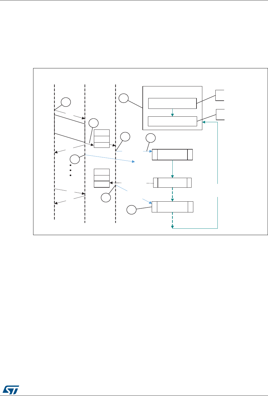
DocID026448 Rev 1 781/836
RM0383 USB on-the-go full-speed (OTG_FS)
796
Examples
This section describes and depicts some fundamental transfer types and scenarios.
•Bulk OUT transaction
Figure 260 depicts the reception of a single Bulk OUT Data packet from the USB to the AHB
and describes the events involved in the process.
Figure 260. Bulk OUT transaction
After a SetConfiguration/SetInterface command, the application initializes all OUT endpoints
by setting CNAK = 1 and EPENA = 1 (in OTG_FS_DOEPCTLx), and setting a suitable
XFRSIZ and PKTCNT in the OTG_FS_DOEPTSIZx register.
1. host attempts to send data (OUT token) to an endpoint.
2. When the core receives the OUT token on the USB, it stores the packet in the RxFIFO
because space is available there.
3. After writing the complete packet in the RxFIFO, the core then asserts the RXFLVL
interrupt (in OTG_FS_GINTSTS).
4. On receiving the PKTCNT number of USB packets, the core internally sets the NAK bit
for this endpoint to prevent it from receiving any more packets.
5. The application processes the interrupt and reads the data from the RxFIFO.
6. When the application has read all the data (equivalent to XFRSIZ), the core generates
an XFRC interrupt (in OTG_FS_DOEPINTx).
7. The application processes the interrupt and uses the setting of the XFRC interrupt bit
(in OTG_FS_DOEPINTx) to determine that the intended transfer is complete.
init_out_ep
Host DeviceUSB
OUT
ACK
RXFLVL intr i
wr_reg (DOEPTSIZx)
wr_reg(DOEPCTLx)
64 bytes
OUT
NAK
xact _1
Application
XFRC
intr
DOEPCTLx.NAK=1
PKTCNT 0
XFRSIZ = 0
r
idle until intr
rcv_out _pkt()
idle until intr
On new xfer
or RxFIFO
not empty
1
2
3
4
5
6
7
8
XFRSIZ = 64 bytes
PKTCNT = 1
EPENA = 1
CNAK = 1
ai15679b

USB on-the-go full-speed (OTG_FS) RM0383
782/836 DocID026448 Rev 1
IN data transfers
•Packet write
This section describes how the application writes data packets to the endpoint FIFO when
dedicated transmit FIFOs are enabled.
1. The application can either choose the polling or the interrupt mode.
– In polling mode, the application monitors the status of the endpoint transmit data
FIFO by reading the OTG_FS_DTXFSTSx register, to determine if there is enough
space in the data FIFO.
– In interrupt mode, the application waits for the TXFE interrupt (in
OTG_FS_DIEPINTx) and then reads the OTG_FS_DTXFSTSx register, to
determine if there is enough space in the data FIFO.
– To write a single non-zero length data packet, there must be space to write the
entire packet in the data FIFO.
– To write zero length packet, the application must not look at the FIFO space.
2. Using one of the above mentioned methods, when the application determines that
there is enough space to write a transmit packet, the application must first write into the
endpoint control register, before writing the data into the data FIFO. Typically, the
application, must do a read modify write on the OTG_FS_DIEPCTLx register to avoid
modifying the contents of the register, except for setting the Endpoint Enable bit.
The application can write multiple packets for the same endpoint into the transmit FIFO, if
space is available. For periodic IN endpoints, the application must write packets only for one
microframe. It can write packets for the next periodic transaction only after getting transfer
complete for the previous transaction.
•Setting IN endpoint NAK
Internal data flow:
1. When the application sets the IN NAK for a particular endpoint, the core stops
transmitting data on the endpoint, irrespective of data availability in the endpoint’s
transmit FIFO.
2. Non-isochronous IN tokens receive a NAK handshake reply
– Isochronous IN tokens receive a zero-data-length packet reply
3. The core asserts the INEPNE (IN endpoint NAK effective) interrupt in
OTG_FS_DIEPINTx in response to the SNAK bit in OTG_FS_DIEPCTLx.
4. Once this interrupt is seen by the application, the application can assume that the
endpoint is in IN NAK mode. This interrupt can be cleared by the application by setting
the CNAK bit in OTG_FS_DIEPCTLx.
Application programming sequence:

DocID026448 Rev 1 783/836
RM0383 USB on-the-go full-speed (OTG_FS)
796
1. To stop transmitting any data on a particular IN endpoint, the application must set the
IN NAK bit. To set this bit, the following field must be programmed.
– SNAK = 1 in OTG_FS_DIEPCTLx
2. Wait for assertion of the INEPNE interrupt in OTG_FS_DIEPINTx. This interrupt
indicates that the core has stopped transmitting data on the endpoint.
3. The core can transmit valid IN data on the endpoint after the application has set the
NAK bit, but before the assertion of the NAK Effective interrupt.
4. The application can mask this interrupt temporarily by writing to the INEPNEM bit in
DIEPMSK.
– INEPNEM = 0 in DIEPMSK
5. To exit Endpoint NAK mode, the application must clear the NAK status bit (NAKSTS) in
OTG_FS_DIEPCTLx. This also clears the INEPNE interrupt (in OTG_FS_DIEPINTx).
– CNAK = 1 in OTG_FS_DIEPCTLx
6. If the application masked this interrupt earlier, it must be unmasked as follows:
– INEPNEM = 1 in DIEPMSK
•IN endpoint disable
Use the following sequence to disable a specific IN endpoint that has been previously
enabled.
Application programming sequence:
1. The application must stop writing data on the AHB for the IN endpoint to be disabled.
2. The application must set the endpoint in NAK mode.
– SNAK = 1 in OTG_FS_DIEPCTLx
3. Wait for the INEPNE interrupt in OTG_FS_DIEPINTx.
4. Set the following bits in the OTG_FS_DIEPCTLx register for the endpoint that must be
disabled.
– EPDIS = 1 in OTG_FS_DIEPCTLx
– SNAK = 1 in OTG_FS_DIEPCTLx
5. Assertion of the EPDISD interrupt in OTG_FS_DIEPINTx indicates that the core has
completely disabled the specified endpoint. Along with the assertion of the interrupt, the
core also clears the following bits:
– EPENA = 0 in OTG_FS_DIEPCTLx
– EPDIS = 0 in OTG_FS_DIEPCTLx
6. The application must read the OTG_FS_DIEPTSIZx register for the periodic IN EP, to
calculate how much data on the endpoint were transmitted on the USB.
7. The application must flush the data in the Endpoint transmit FIFO, by setting the
following fields in the OTG_FS_GRSTCTL register:
– TXFNUM (in OTG_FS_GRSTCTL) = Endpoint transmit FIFO number
– TXFFLSH in (OTG_FS_GRSTCTL) = 1
The application must poll the OTG_FS_GRSTCTL register, until the TXFFLSH bit is cleared
by the core, which indicates the end of flush operation. To transmit new data on this
endpoint, the application can re-enable the endpoint at a later point.

USB on-the-go full-speed (OTG_FS) RM0383
784/836 DocID026448 Rev 1
•Generic non-periodic IN data transfers
Application requirements:
1. Before setting up an IN transfer, the application must ensure that all data to be
transmitted as part of the IN transfer are part of a single buffer.
2. For IN transfers, the Transfer Size field in the Endpoint Transfer Size register denotes a
payload that constitutes multiple maximum-packet-size packets and a single short
packet. This short packet is transmitted at the end of the transfer.
– To transmit a few maximum-packet-size packets and a short packet at the end of
the transfer:
Transfer size[EPNUM] = x × MPSIZ[EPNUM] + sp
If (sp > 0), then packet count[EPNUM] = x + 1.
Otherwise, packet count[EPNUM] = x
– To transmit a single zero-length data packet:
Transfer size[EPNUM] = 0
Packet count[EPNUM] = 1
– To transmit a few maximum-packet-size packets and a zero-length data packet at
the end of the transfer, the application must split the transfer into two parts. The
first sends maximum-packet-size data packets and the second sends the zero-
length data packet alone.
First transfer: transfer size[EPNUM] = x × MPSIZ[epnum]; packet count = n;
Second transfer: transfer size[EPNUM] = 0; packet count = 1;
3. Once an endpoint is enabled for data transfers, the core updates the Transfer size
register. At the end of the IN transfer, the application must read the Transfer size
register to determine how much data posted in the transmit FIFO have already been
sent on the USB.
4. Data fetched into transmit FIFO = Application-programmed initial transfer size – core-
updated final transfer size
– Data transmitted on USB = (application-programmed initial packet count – Core
updated final packet count) × MPSIZ[EPNUM]
– Data yet to be transmitted on USB = (Application-programmed initial transfer size
– data transmitted on USB)
Internal data flow:
1. The application must set the transfer size and packet count fields in the endpoint-
specific registers and enable the endpoint to transmit the data.
2. The application must also write the required data to the transmit FIFO for the endpoint.
3. Every time a packet is written into the transmit FIFO by the application, the transfer size
for that endpoint is decremented by the packet size. The data is fetched from the
memory by the application, until the transfer size for the endpoint becomes 0. After
writing the data into the FIFO, the “number of packets in FIFO” count is incremented
(this is a 3-bit count, internally maintained by the core for each IN endpoint transmit
FIFO. The maximum number of packets maintained by the core at any time in an IN
endpoint FIFO is eight). For zero-length packets, a separate flag is set for each FIFO,
without any data in the FIFO.
4. Once the data are written to the transmit FIFO, the core reads them out upon receiving
an IN token. For every non-isochronous IN data packet transmitted with an ACK

DocID026448 Rev 1 785/836
RM0383 USB on-the-go full-speed (OTG_FS)
796
handshake, the packet count for the endpoint is decremented by one, until the packet
count is zero. The packet count is not decremented on a timeout.
5. For zero length packets (indicated by an internal zero length flag), the core sends out a
zero-length packet for the IN token and decrements the packet count field.
6. If there are no data in the FIFO for a received IN token and the packet count field for
that endpoint is zero, the core generates an “IN token received when TxFIFO is empty”
(ITTXFE) Interrupt for the endpoint, provided that the endpoint NAK bit is not set. The
core responds with a NAK handshake for non-isochronous endpoints on the USB.
7. The core internally rewinds the FIFO pointers and no timeout interrupt is generated.
8. When the transfer size is 0 and the packet count is 0, the transfer complete (XFRC)
interrupt for the endpoint is generated and the endpoint enable is cleared.
Application programming sequence:
1. Program the OTG_FS_DIEPTSIZx register with the transfer size and corresponding
packet count.
2. Program the OTG_FS_DIEPCTLx register with the endpoint characteristics and set the
CNAK and EPENA (Endpoint Enable) bits.
3. When transmitting non-zero length data packet, the application must poll the
OTG_FS_DTXFSTSx register (where x is the FIFO number associated with that
endpoint) to determine whether there is enough space in the data FIFO. The
application can optionally use TXFE (in OTG_FS_DIEPINTx) before writing the data.
•Generic periodic IN data transfers
This section describes a typical periodic IN data transfer.
Application requirements:
1. Application requirements 1, 2, 3, and 4 of Generic non-periodic IN data transfers on
page 784 also apply to periodic IN data transfers, except for a slight modification of
requirement 2.
– The application can only transmit multiples of maximum-packet-size data packets
or multiples of maximum-packet-size packets, plus a short packet at the end. To
transmit a few maximum-packet-size packets and a short packet at the end of the
transfer, the following conditions must be met:
transfer size[EPNUM] = x × MPSIZ[EPNUM] + sp
(where x is an integer ≥ 0, and 0 ≤ sp < MPSIZ[EPNUM])
If (sp > 0), packet count[EPNUM] = x + 1
Otherwise, packet count[EPNUM] = x;
MCNT[EPNUM] = packet count[EPNUM]
– The application cannot transmit a zero-length data packet at the end of a transfer.
It can transmit a single zero-length data packet by itself. To transmit a single zero-
length data packet:
– transfer size[EPNUM] = 0
packet count[EPNUM] = 1
MCNT[EPNUM] = packet count[EPNUM]

USB on-the-go full-speed (OTG_FS) RM0383
786/836 DocID026448 Rev 1
2. The application can only schedule data transfers one frame at a time.
– (MCNT – 1) × MPSIZ ≤ XFERSIZ ≤ MCNT × MPSIZ
– PKTCNT = MCNT (in OTG_FS_DIEPTSIZx)
– If XFERSIZ < MCNT × MPSIZ, the last data packet of the transfer is a short
packet.
– Note that: MCNT is in OTG_FS_DIEPTSIZx, MPSIZ is in OTG_FS_DIEPCTLx,
PKTCNT is in OTG_FS_DIEPTSIZx and XFERSIZ is in OTG_FS_DIEPTSIZx
3. The complete data to be transmitted in the frame must be written into the transmit FIFO
by the application, before the IN token is received. Even when 1 Word of the data to be
transmitted per frame is missing in the transmit FIFO when the IN token is received, the
core behaves as when the FIFO is empty. When the transmit FIFO is empty:
– A zero data length packet would be transmitted on the USB for isochronous IN
endpoints
– A NAK handshake would be transmitted on the USB for interrupt IN endpoints
Internal data flow:
1. The application must set the transfer size and packet count fields in the endpoint-
specific registers and enable the endpoint to transmit the data.
2. The application must also write the required data to the associated transmit FIFO for
the endpoint.
3. Every time the application writes a packet to the transmit FIFO, the transfer size for that
endpoint is decremented by the packet size. The data are fetched from application
memory until the transfer size for the endpoint becomes 0.
4. When an IN token is received for a periodic endpoint, the core transmits the data in the
FIFO, if available. If the complete data payload (complete packet, in dedicated FIFO
mode) for the frame is not present in the FIFO, then the core generates an IN token
received when TxFIFO empty interrupt for the endpoint.
– A zero-length data packet is transmitted on the USB for isochronous IN endpoints
– A NAK handshake is transmitted on the USB for interrupt IN endpoints
5. The packet count for the endpoint is decremented by 1 under the following conditions:
– For isochronous endpoints, when a zero- or non-zero-length data packet is
transmitted
– For interrupt endpoints, when an ACK handshake is transmitted
– When the transfer size and packet count are both 0, the transfer completed
interrupt for the endpoint is generated and the endpoint enable is cleared.
6. At the “Periodic frame Interval” (controlled by PFIVL in OTG_FS_DCFG), when the
core finds non-empty any of the isochronous IN endpoint FIFOs scheduled for the
current frame non-empty, the core generates an IISOIXFR interrupt in
OTG_FS_GINTSTS.

DocID026448 Rev 1 787/836
RM0383 USB on-the-go full-speed (OTG_FS)
796
Application programming sequence:
1. Program the OTG_FS_DIEPCTLx register with the endpoint characteristics and set the
CNAK and EPENA bits.
2. Write the data to be transmitted in the next frame to the transmit FIFO.
3. Asserting the ITTXFE interrupt (in OTG_FS_DIEPINTx) indicates that the application
has not yet written all data to be transmitted to the transmit FIFO.
4. If the interrupt endpoint is already enabled when this interrupt is detected, ignore the
interrupt. If it is not enabled, enable the endpoint so that the data can be transmitted on
the next IN token attempt.
5. Asserting the XFRC interrupt (in OTG_FS_DIEPINTx) with no ITTXFE interrupt in
OTG_FS_DIEPINTx indicates the successful completion of an isochronous IN transfer.
A read to the OTG_FS_DIEPTSIZx register must give transfer size = 0 and packet
count = 0, indicating all data were transmitted on the USB.
6. Asserting the XFRC interrupt (in OTG_FS_DIEPINTx), with or without the ITTXFE
interrupt (in OTG_FS_DIEPINTx), indicates the successful completion of an interrupt
IN transfer. A read to the OTG_FS_DIEPTSIZx register must give transfer size = 0 and
packet count = 0, indicating all data were transmitted on the USB.
7. Asserting the incomplete isochronous IN transfer (IISOIXFR) interrupt in
OTG_FS_GINTSTS with none of the aforementioned interrupts indicates the core did
not receive at least 1 periodic IN token in the current frame.
•Incomplete isochronous IN data transfers
This section describes what the application must do on an incomplete isochronous IN data
transfer.
Internal data flow:
1. An isochronous IN transfer is treated as incomplete in one of the following conditions:
a) The core receives a corrupted isochronous IN token on at least one isochronous
IN endpoint. In this case, the application detects an incomplete isochronous IN
transfer interrupt (IISOIXFR in OTG_FS_GINTSTS).
b) The application is slow to write the complete data payload to the transmit FIFO
and an IN token is received before the complete data payload is written to the
FIFO. In this case, the application detects an IN token received when TxFIFO
empty interrupt in OTG_FS_DIEPINTx. The application can ignore this interrupt,
as it eventually results in an incomplete isochronous IN transfer interrupt
(IISOIXFR in OTG_FS_GINTSTS) at the end of periodic frame.
The core transmits a zero-length data packet on the USB in response to the
received IN token.
2. The application must stop writing the data payload to the transmit FIFO as soon as
possible.
3. The application must set the NAK bit and the disable bit for the endpoint.
4. The core disables the endpoint, clears the disable bit, and asserts the Endpoint Disable
interrupt for the endpoint.

USB on-the-go full-speed (OTG_FS) RM0383
788/836 DocID026448 Rev 1
Application programming sequence:
1. The application can ignore the IN token received when TxFIFO empty interrupt in
OTG_FS_DIEPINTx on any isochronous IN endpoint, as it eventually results in an
incomplete isochronous IN transfer interrupt (in OTG_FS_GINTSTS).
2. Assertion of the incomplete isochronous IN transfer interrupt (in OTG_FS_GINTSTS)
indicates an incomplete isochronous IN transfer on at least one of the isochronous IN
endpoints.
3. The application must read the Endpoint Control register for all isochronous IN
endpoints to detect endpoints with incomplete IN data transfers.
4. The application must stop writing data to the Periodic Transmit FIFOs associated with
these endpoints on the AHB.
5. Program the following fields in the OTG_FS_DIEPCTLx register to disable the
endpoint:
– SNAK = 1 in OTG_FS_DIEPCTLx
– EPDIS = 1 in OTG_FS_DIEPCTLx
6. The assertion of the Endpoint Disabled interrupt in OTG_FS_DIEPINTx indicates that
the core has disabled the endpoint.
– At this point, the application must flush the data in the associated transmit FIFO or
overwrite the existing data in the FIFO by enabling the endpoint for a new transfer
in the next microframe. To flush the data, the application must use the
OTG_FS_GRSTCTL register.
•Stalling non-isochronous IN endpoints
This section describes how the application can stall a non-isochronous endpoint.
Application programming sequence:
1. Disable the IN endpoint to be stalled. Set the STALL bit as well.
2. EPDIS = 1 in OTG_FS_DIEPCTLx, when the endpoint is already enabled
– STALL = 1 in OTG_FS_DIEPCTLx
– The STALL bit always takes precedence over the NAK bit
3. Assertion of the Endpoint Disabled interrupt (in OTG_FS_DIEPINTx) indicates to the
application that the core has disabled the specified endpoint.
4. The application must flush the non-periodic or periodic transmit FIFO, depending on
the endpoint type. In case of a non-periodic endpoint, the application must re-enable
the other non-periodic endpoints that do not need to be stalled, to transmit data.
5. Whenever the application is ready to end the STALL handshake for the endpoint, the
STALL bit must be cleared in OTG_FS_DIEPCTLx.
6. If the application sets or clears a STALL bit for an endpoint due to a
SetFeature.Endpoint Halt command or ClearFeature.Endpoint Halt command, the
STALL bit must be set or cleared before the application sets up the Status stage
transfer on the control endpoint.
Special case: stalling the control OUT endpoint
The core must stall IN/OUT tokens if, during the data stage of a control transfer, the host
sends more IN/OUT tokens than are specified in the SETUP packet. In this case, the
application must enable the ITTXFE interrupt in OTG_FS_DIEPINTx and the OTEPDIS
interrupt in OTG_FS_DOEPINTx during the data stage of the control transfer, after the core
has transferred the amount of data specified in the SETUP packet. Then, when the

DocID026448 Rev 1 789/836
RM0383 USB on-the-go full-speed (OTG_FS)
796
application receives this interrupt, it must set the STALL bit in the corresponding endpoint
control register, and clear this interrupt.
22.17.7 Worst case response time
When the OTG_FS controller acts as a device, there is a worst case response time for any
tokens that follow an isochronous OUT. This worst case response time depends on the AHB
clock frequency.
The core registers are in the AHB domain, and the core does not accept another token
before updating these register values. The worst case is for any token following an
isochronous OUT, because for an isochronous transaction, there is no handshake and the
next token could come sooner. This worst case value is 7 PHY clocks when the AHB clock
is the same as the PHY clock. When the AHB clock is faster, this value is smaller.
If this worst case condition occurs, the core responds to bulk/interrupt tokens with a NAK
and drops isochronous and SETUP tokens. The host interprets this as a timeout condition
for SETUP and retries the SETUP packet. For isochronous transfers, the Incomplete
isochronous IN transfer interrupt (IISOIXFR) and Incomplete isochronous OUT transfer
interrupt (IISOOXFR) inform the application that isochronous IN/OUT packets were
dropped.
Choosing the value of TRDT in OTG_FS_GUSBCFG
The value in TRDT (OTG_FS_GUSBCFG) is the time it takes for the MAC, in terms of PHY
clocks after it has received an IN token, to get the FIFO status, and thus the first data from
the PFC block. This time involves the synchronization delay between the PHY and AHB
clocks. The worst case delay for this is when the AHB clock is the same as the PHY clock.
In this case, the delay is 5 clocks.
Once the MAC receives an IN token, this information (token received) is synchronized to the
AHB clock by the PFC (the PFC runs on the AHB clock). The PFC then reads the data from
the SPRAM and writes them into the dual clock source buffer. The MAC then reads the data
out of the source buffer (4 deep).
If the AHB is running at a higher frequency than the PHY, the application can use a smaller
value for TRDT (in OTG_FS_GUSBCFG).
Figure 261 has the following signals:
•tkn_rcvd: Token received information from MAC to PFC
•dynced_tkn_rcvd: Doubled sync tkn_rcvd, from PCLK to HCLK domain
•spr_read: Read to SPRAM
•spr_addr: Address to SPRAM
•spr_rdata: Read data from SPRAM
•srcbuf_push: Push to the source buffer
•srcbuf_rdata: Read data from the source buffer. Data seen by MAC
The application can use the following formula to calculate the value of TRDT:
4 × AHB clock + 1 PHY clock = (2 clock sync + 1 clock memory address + 1 clock
memory data from sync RAM) + (1 PHY clock (next PHY clock MAC can sample the 2
clock FIFO outputs)
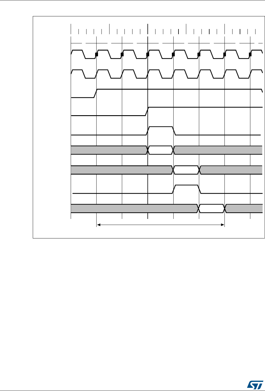
USB on-the-go full-speed (OTG_FS) RM0383
790/836 DocID026448 Rev 1
Figure 261. TRDT max timing case
22.17.8 OTG programming model
The OTG_FS controller is an OTG device supporting HNP and SRP. When the core is
connected to an “A” plug, it is referred to as an A-device. When the core is connected to a
“B” plug it is referred to as a B-device. In host mode, the OTG_FS controller turns off VBUS
to conserve power. SRP is a method by which the B-device signals the A-device to turn on
VBUS power. A device must perform both data-line pulsing and VBUS pulsing, but a host can
detect either data-line pulsing or VBUS pulsing for SRP. HNP is a method by which the B-
device negotiates and switches to host role. In Negotiated mode after HNP, the B-device
suspends the bus and reverts to the device role.
A-device session request protocol
The application must set the SRP-capable bit in the Core USB configuration register. This
enables the OTG_FS controller to detect SRP as an A-device.
12345678
0ns 50ns 100ns 150ns 200ns
HCLK
PCLK
tkn_rcvd
dsynced_tkn_rcvd
spr_read
spr_addr
spr_rdata
srcbuf_push
srcbuf_rdata
5 Clocks
D1
A1
D1
ai15680

DocID026448 Rev 1 791/836
RM0383 USB on-the-go full-speed (OTG_FS)
796
Figure 262. A-device SRP
1. DRV_VBUS = VBUS drive signal to the PHY
VBUS_VALID = VBUS valid signal from PHY
A_VALID = A-peripheral VBUS level signal to PHY
D+ = Data plus line
D- = Data minus line
1. To save power, the application suspends and turns off port power when the bus is idle
by writing the port suspend and port power bits in the host port control and status
register.
2. PHY indicates port power off by deasserting the VBUS_VALID signal.
3. The device must detect SE0 for at least 2 ms to start SRP when VBUS power is off.
4. To initiate SRP, the device turns on its data line pull-up resistor for 5 to 10 ms. The
OTG_FS controller detects data-line pulsing.
5. The device drives VBUS above the A-device session valid (2.0 V minimum) for VBUS
pulsing.
The OTG_FS controller interrupts the application on detecting SRP. The Session
request detected bit is set in Global interrupt status register (SRQINT set in
OTG_FS_GINTSTS).
6. The application must service the Session request detected interrupt and turn on the
port power bit by writing the port power bit in the host port control and status register.
The PHY indicates port power-on by asserting the VBUS_VALID signal.
7. When the USB is powered, the device connects, completing the SRP process.
ai15681
DRV_VBUS
VBUS_VALID
A_VALID
D+
D-
Suspend
VBUS pulsing
Data line pulsing Connect
1
6
25
3
47
Low
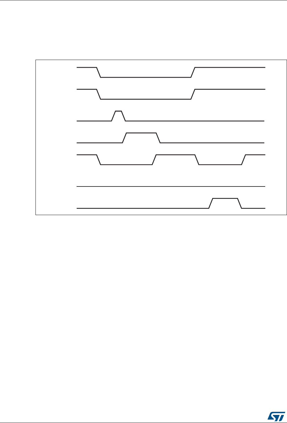
USB on-the-go full-speed (OTG_FS) RM0383
792/836 DocID026448 Rev 1
B-device session request protocol
The application must set the SRP-capable bit in the Core USB configuration register. This
enables the OTG_FS controller to initiate SRP as a B-device. SRP is a means by which the
OTG_FS controller can request a new session from the host.
Figure 263. B-device SRP
1. VBUS_VALID = VBUS valid signal from PHY
B_VALID = B-peripheral valid session to PHY
DISCHRG_VBUS = discharge signal to PHY
SESS_END = session end signal to PHY
CHRG_VBUS = charge VBUS signal to PHY
DP = Data plus line
DM = Data minus line
1. To save power, the host suspends and turns off port power when the bus is idle.
The OTG_FS controller sets the early suspend bit in the Core interrupt register after 3
ms of bus idleness. Following this, the OTG_FS controller sets the USB suspend bit in
the Core interrupt register.
The OTG_FS controller informs the PHY to discharge VBUS.
2. The PHY indicates the session’s end to the device. This is the initial condition for SRP.
The OTG_FS controller requires 2 ms of SE0 before initiating SRP.
For a USB 1.1 full-speed serial transceiver, the application must wait until VBUS
discharges to 0.2 V after BSVLD (in OTG_FS_GOTGCTL) is deasserted. This
ai15682
VBUS_VALID
B_VALID
DISCHRG_VBUS
SESS_END
DP
DM
CHRG_VBUS
Suspend
Data line pulsing Connect
VBUS pulsing
1
6
2
3
4
58
7
Low
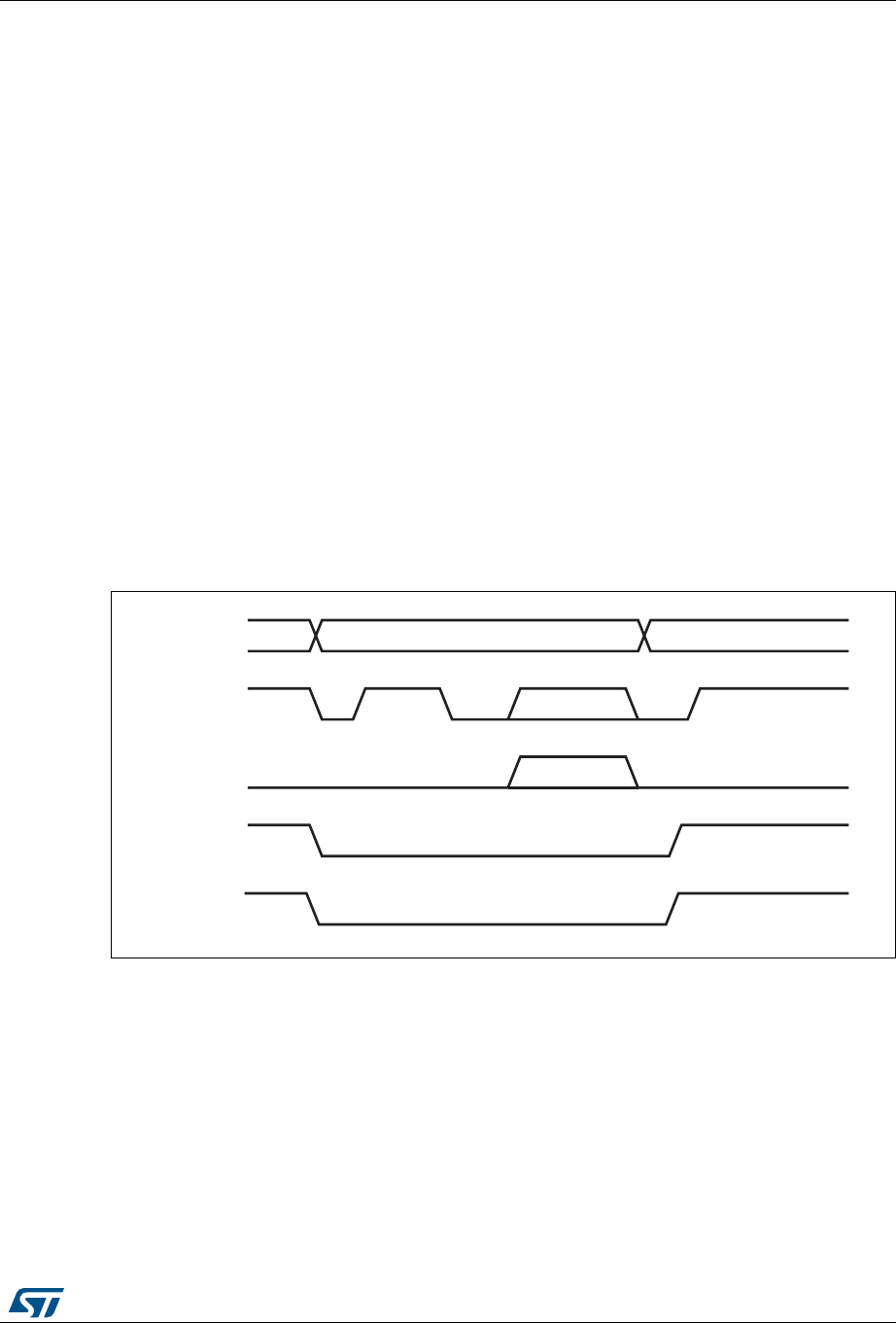
DocID026448 Rev 1 793/836
RM0383 USB on-the-go full-speed (OTG_FS)
796
discharge time can be obtained from the transceiver vendor and varies from one
transceiver to another.
3. The USB OTG core informs the PHY to speed up VBUS discharge.
4. The application initiates SRP by writing the session request bit in the OTG Control and
status register. The OTG_FS controller perform data-line pulsing followed by VBUS
pulsing.
5. The host detects SRP from either the data-line or VBUS pulsing, and turns on VBUS.
The PHY indicates VBUS power-on to the device.
6. The OTG_FS controller performs VBUS pulsing.
The host starts a new session by turning on VBUS, indicating SRP success. The
OTG_FS controller interrupts the application by setting the session request success
status change bit in the OTG interrupt status register. The application reads the session
request success bit in the OTG control and status register.
7. When the USB is powered, the OTG_FS controller connects, completing the SRP
process.
A-device host negotiation protocol
HNP switches the USB host role from the A-device to the B-device. The application must set
the HNP-capable bit in the Core USB configuration register to enable the OTG_FS
controller to perform HNP as an A-device.
Figure 264. A-device HNP
1. DPPULLDOWN = signal from core to PHY to enable/disable the pull-down on the DP line inside the PHY.
DMPULLDOWN = signal from core to PHY to enable/disable the pull-down on the DM line inside the PHY.
1. The OTG_FS controller sends the B-device a SetFeature b_hnp_enable descriptor to
enable HNP support. The B-device’s ACK response indicates that the B-device
supports HNP. The application must set host Set HNP Enable bit in the OTG Control
ai15683
OTG core
DP
DM
DPPULLDOWN
DMPULLDOWN
Host Device Host
1
Suspend 2
3
45
Reset
6
Traffic 7
8
Connect
Traffic

USB on-the-go full-speed (OTG_FS) RM0383
794/836 DocID026448 Rev 1
and status register to indicate to the OTG_FS controller that the B-device supports
HNP.
2. When it has finished using the bus, the application suspends by writing the Port
suspend bit in the host port control and status register.
3. When the B-device observes a USB suspend, it disconnects, indicating the initial
condition for HNP. The B-device initiates HNP only when it must switch to the host role;
otherwise, the bus continues to be suspended.
The OTG_FS controller sets the host negotiation detected interrupt in the OTG
interrupt status register, indicating the start of HNP.
The OTG_FS controller deasserts the DM pull down and DM pull down in the PHY to
indicate a device role. The PHY enables the OTG_FS_DP pull-up resistor to indicate a
connect for B-device.
The application must read the current mode bit in the OTG Control and status register
to determine device mode operation.
4. The B-device detects the connection, issues a USB reset, and enumerates the
OTG_FS controller for data traffic.
5. The B-device continues the host role, initiating traffic, and suspends the bus when
done.
The OTG_FS controller sets the early suspend bit in the Core interrupt register after 3
ms of bus idleness. Following this, the OTG_FS controller sets the USB Suspend bit in
the Core interrupt register.
6. In Negotiated mode, the OTG_FS controller detects the suspend, disconnects, and
switches back to the host role. The OTG_FS controller asserts the DM pull down and
DM pull down in the PHY to indicate its assumption of the host role.
7. The OTG_FS controller sets the Connector ID status change interrupt in the OTG
Interrupt Status register. The application must read the connector ID status in the OTG
Control and Status register to determine the OTG_FS controller operation as an A-
device. This indicates the completion of HNP to the application. The application must
read the Current mode bit in the OTG control and status register to determine host
mode operation.
8. The B-device connects, completing the HNP process.
B-device host negotiation protocol
HNP switches the USB host role from B-device to A-device. The application must set the
HNP-capable bit in the Core USB configuration register to enable the OTG_FS controller to
perform HNP as a B-device.

DocID026448 Rev 1 795/836
RM0383 USB on-the-go full-speed (OTG_FS)
796
Figure 265. B-device HNP
1. DPPULLDOWN = signal from core to PHY to enable/disable the pull-down on the DP line inside the PHY.
DMPULLDOWN = signal from core to PHY to enable/disable the pull-down on the DM line inside the PHY.
1. The A-device sends the SetFeature b_hnp_enable descriptor to enable HNP support.
The OTG_FS controller’s ACK response indicates that it supports HNP. The application
must set the device HNP enable bit in the OTG Control and status register to indicate
HNP support.
The application sets the HNP request bit in the OTG Control and status register to
indicate to the OTG_FS controller to initiate HNP.
2. When it has finished using the bus, the A-device suspends by writing the Port suspend
bit in the host port control and status register.
The OTG_FS controller sets the Early suspend bit in the Core interrupt register after 3
ms of bus idleness. Following this, the OTG_FS controller sets the USB suspend bit in
the Core interrupt register.
The OTG_FS controller disconnects and the A-device detects SE0 on the bus,
indicating HNP. The OTG_FS controller asserts the DP pull down and DM pull down in
the PHY to indicate its assumption of the host role.
The A-device responds by activating its OTG_FS_DP pull-up resistor within 3 ms of
detecting SE0. The OTG_FS controller detects this as a connect.
The OTG_FS controller sets the host negotiation success status change interrupt in the
OTG Interrupt status register, indicating the HNP status. The application must read the
host negotiation success bit in the OTG Control and status register to determine host
ai15684
OTG core
DP
DM
DPPULLDOWN
DMPULLDOWN
HostDevice Device
1
Suspend 2
3
45
Reset
6
Traffic 7
8
Connect
Traffic

USB on-the-go full-speed (OTG_FS) RM0383
796/836 DocID026448 Rev 1
negotiation success. The application must read the current Mode bit in the Core
interrupt register (OTG_FS_GINTSTS) to determine host mode operation.
3. The application sets the reset bit (PRST in OTG_FS_HPRT) and the OTG_FS
controller issues a USB reset and enumerates the A-device for data traffic.
4. The OTG_FS controller continues the host role of initiating traffic, and when done,
suspends the bus by writing the Port suspend bit in the host port control and status
register.
5. In Negotiated mode, when the A-device detects a suspend, it disconnects and switches
back to the host role. The OTG_FS controller deasserts the DP pull down and DM pull
down in the PHY to indicate the assumption of the device role.
6. The application must read the current mode bit in the Core interrupt
(OTG_FS_GINTSTS) register to determine the host mode operation.
7. The OTG_FS controller connects, completing the HNP process.
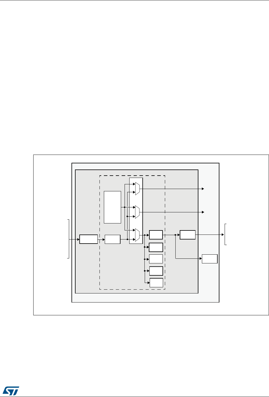
DocID026448 Rev 1 797/836
RM0383 Debug support (DBG)
829
23 Debug support (DBG)
23.1 Overview
The STM32F411xC/E is built around a Cortex®-M4 with FPU core which contains hardware
extensions for advanced debugging features. The debug extensions allow the core to be
stopped either on a given instruction fetch (breakpoint) or data access (watchpoint). When
stopped, the core’s internal state and the system’s external state may be examined. Once
examination is complete, the core and the system may be restored and program execution
resumed.
The debug features are used by the debugger host when connecting to and debugging the
STM32F411xC/E MCUs.
Two interfaces for debug are available:
•Serial wire
•JTAG debug port
Figure 266. Block diagram of STM32 MCU and Cortex®-M4 with FPU-level
debug support
Note: The debug features embedded in the Cortex®-M4 with FPU core are a subset of the ARM®
CoreSight Design Kit.
ESTRICTED$I
#ORTEX-
CORE
37*$0 !("!0
"RIDGE
.6)#
$74
&0"
)4-
40)5
$#ODE
INTERFACE
3YSTEM
INTERFACE
)NTERNALPRIVATE
PERIPHERALBUS00"
%XTERNALPRIVATE
PERIPHERALBUS00"
"USMATRIX
$ATA
4R A CE PO R T
$"'-#5
34-&XXDEBUGSUPPORT
#ORTEX-DEBUGSUPPORT
*4-3
*4$)
*4$/
.*4234
*4#+
37$)/
37#,+
42!#%37/
42!#%37/
42!#%#+
42!#%$;=
-36

Debug support (DBG) RM0383
798/836 DocID026448 Rev 1
The ARM® Cortex®-M4 with FPU core provides integrated on-chip debug support. It is
comprised of:
•SWJ-DP: Serial wire / JTAG debug port
•AHP-AP: AHB access port
•ITM: Instrumentation trace macrocell
•FPB: Flash patch breakpoint
•DWT: Data watchpoint trigger
•TPUI: Trace port unit interface (available on larger packages, where the corresponding
pins are mapped)
•ETM: Embedded Trace Macrocell (available on larger packages, where the
corresponding pins are mapped)
It also includes debug features dedicated to the STM32F411xC/E:
•Flexible debug pinout assignment
•MCU debug box (support for low-power modes, control over peripheral clocks, etc.)
Note: For further information on debug functionality supported by the ARM® Cortex®-M4 with FPU
core, refer to the Cortex®-M4 with FPU-r0p1 Technical Reference Manual and to the
CoreSight Design Kit-r0p1 TRM (see Section 23.2: Reference ARM® documentation).
23.2 Reference ARM® documentation
•Cortex®-M4 with FPU r0p1 Technical Reference Manual (TRM)
(see Related documents on page 1)
•ARM® Debug Interface V5
•ARM® CoreSight Design Kit revision r0p1 Technical Reference Manual
23.3 SWJ debug port (serial wire and JTAG)
The core of the STM32F411xC/E integrates the Serial Wire / JTAG Debug Port (SWJ-DP). It
is an ARM® standard CoreSight debug port that combines a JTAG-DP (5-pin) interface and
a SW-DP (2-pin) interface.
•The JTAG Debug Port (JTAG-DP) provides a 5-pin standard JTAG interface to the
AHP-AP port.
•The Serial Wire Debug Port (SW-DP) provides a 2-pin (clock + data) interface to the
AHP-AP port.
In the SWJ-DP, the two JTAG pins of the SW-DP are multiplexed with some of the five JTAG
pins of the JTAG-DP.
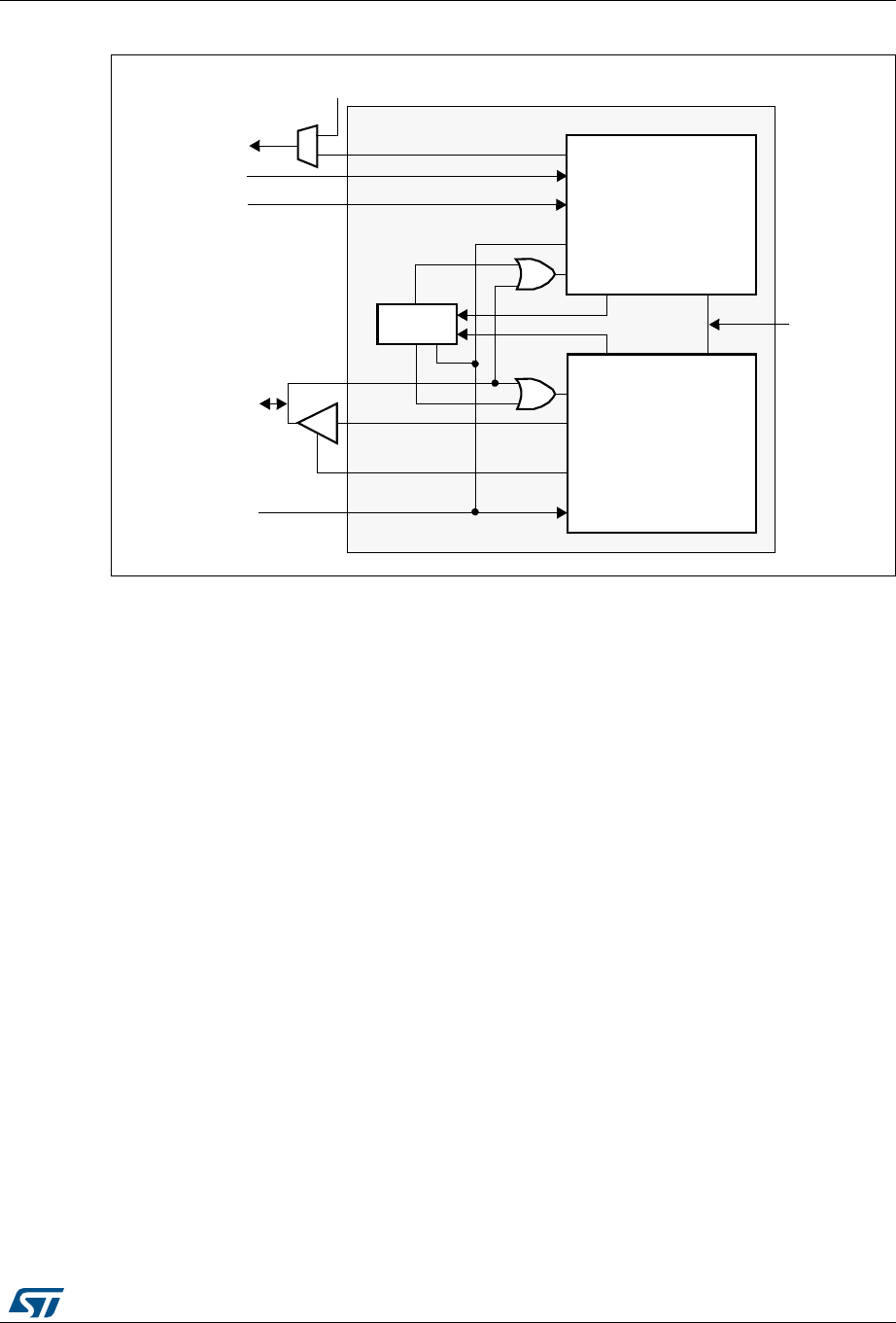
DocID026448 Rev 1 799/836
RM0383 Debug support (DBG)
829
Figure 267. SWJ debug port
Figure 267 shows that the asynchronous TRACE output (TRACESWO) is multiplexed with
TDO. This means that the asynchronous trace can only be used with SW-DP, not JTAG-DP.
23.3.1 Mechanism to select the JTAG-DP or the SW-DP
By default, the JTAG-Debug Port is active.
If the debugger host wants to switch to the SW-DP, it must provide a dedicated JTAG
sequence on TMS/TCK (respectively mapped to SWDIO and SWCLK) which disables the
JTAG-DP and enables the SW-DP. This way it is possible to activate the SWDP using only
the SWCLK and SWDIO pins.
This sequence is:
1. Send more than 50 TCK cycles with TMS (SWDIO) =1
2. Send the 16-bit sequence on TMS (SWDIO) = 0111100111100111 (MSB transmitted
first)
3. Send more than 50 TCK cycles with TMS (SWDIO) =1
23.4 Pinout and debug port pins
The STM32F411xC/E MCUs are available in various packages with different numbers of
available pins. As a result, some functionality (ETM) related to pin availability may differ
between packages.
TRACESWO
JTDO
JTDI
NJTRST nTRST
TDI
TDO
SWJ-DP
TDO
TDI
nTRST
TCK
TMS nPOTRST
JTAG-DP
nPOTRST
From
power-on
reset
DBGRESETn
DBGDI
DBGDO
DBGDOEN
DBGCLK
SW-DP
SWCLKTCK
SWDOEN
SWDO
SWDITMS
SWD/JTAG
select
JTMS/SWDIO
JTCK/SWCLK
(asynchronous trace)
ai17139
Debug support (DBG) RM0383
800/836 DocID026448 Rev 1
23.4.1 SWJ debug port pins
Five pins are used as outputs from the STM32F411xC/E for the SWJ-DP as alternate
functions of general-purpose I/Os. These pins are available on all packages.
23.4.2 Flexible SWJ-DP pin assignment
After RESET (SYSRESETn or PORESETn), all five pins used for the SWJ-DP are assigned
as dedicated pins immediately usable by the debugger host (note that the trace outputs are
not assigned except if explicitly programmed by the debugger host).
However, the STM32F411xC/E MCU offers the possibility of disabling some or all of the
SWJ-DP ports and so, of releasing the associated pins for general-purpose IO (GPIO)
usage. For more details on how to disable SWJ-DP port pins, please refer to Section 8.3.2:
I/O pin multiplexer and mapping.
Note: When the APB bridge write buffer is full, it takes one extra APB cycle when writing the
GPIO_AFR register. This is because the deactivation of the JTAGSW pins is done in two
cycles to guarantee a clean level on the nTRST and TCK input signals of the core.
•Cycle 1: the JTAGSW input signals to the core are tied to 1 or 0 (to 1 for nTRST, TDI
and TMS, to 0 for TCK)
•Cycle 2: the GPIO controller takes the control signals of the SWJTAG IO pins (like
controls of direction, pull-up/down, Schmitt trigger activation, etc.).
Table 131. SWJ debug port pins
SWJ-DP pin name JTAG debug port SW debug port Pin
assign
ment
Type Description Type Debug assignment
JTMS/SWDIO I JTAG Test Mode
Selection IO Serial Wire Data
Input/Output PA13
JTCK/SWCLK I JTAG Test Clock I Serial Wire Clock PA14
JTDI I JTAG Test Data Input - - PA15
JTDO/TRACESWO O JTAG Test Data Output - TRACESWO if async trace
is enabled PB3
NJTRST I JTAG Test nReset - - PB4
Table 132. Flexible SWJ-DP pin assignment
Available debug ports
SWJ IO pin assigned
PA13 /
JTMS /
SWDIO
PA14 /
JTCK /
SWCLK
PA15 /
JTDI PB3 /
JTDO PB4 /
NJTRST
Full SWJ (JTAG-DP + SW-DP) - Reset State X X X X X
Full SWJ (JTAG-DP + SW-DP) but without NJTRST X X X X
JTAG-DP Disabled and SW-DP Enabled X X
JTAG-DP Disabled and SW-DP Disabled Released

DocID026448 Rev 1 801/836
RM0383 Debug support (DBG)
829
23.4.3 Internal pull-up and pull-down on JTAG pins
It is necessary to ensure that the JTAG input pins are not floating since they are directly
connected to flip-flops to control the debug mode features. Special care must be taken with
the SWCLK/TCK pin which is directly connected to the clock of some of these flip-flops.
To avoid any uncontrolled IO levels, the device embeds internal pull-ups and pull-downs on
the JTAG input pins:
NJTRST: Internal pull-upJTDI: Internal pull-upJTMS/SWDIO: Internal pull-upTCK/SWCLK:
Internal pull-downOnce a JTAG IO is released by the user software, the GPIO controller
takes control again. The reset states of the GPIO control registers put the I/Os in the
equivalent state:
•NJTRST: AF input pull-up
•JTDI: AF input pull-up
•JTMS/SWDIO: AF input pull-up
•JTCK/SWCLK: AF input pull-down
•JTDO: AF output floating
The software can then use these I/Os as standard GPIOs.
Note: The JTAG IEEE standard recommends to add pull-ups on TDI, TMS and nTRST but there is
no special recommendation for TCK. However, for JTCK, the device needs an integrated
pull-down.
Having embedded pull-ups and pull-downs removes the need to add external resistors.

Debug support (DBG) RM0383
802/836 DocID026448 Rev 1
23.4.4 Using serial wire and releasing the unused debug pins as GPIOs
To use the serial wire DP to release some GPIOs, the user software mustchange the GPIO
(PA15, PB3 and PB4) configuration mode in the GPIO_MODER register. This releases
PA15, PB3 and PB4 which now become available as GPIOs.
When debugging, the host performs the following actions:
•Under system reset, all SWJ pins are assigned (JTAG-DP + SW-DP).
•Under system reset, the debugger host sends the JTAG sequence to switch from the
JTAG-DP to the SW-DP.
•Still under system reset, the debugger sets a breakpoint on vector reset.
•The system reset is released and the Core halts.
•All the debug communications from this point are done using the SW-DP. The other
JTAG pins can then be reassigned as GPIOs by the user software.
Note: For user software designs, note that:
To release the debug pins, remember that they will be first configured either in input-pull-up
(nTRST, TMS, TDI) or pull-down (TCK) or output tristate (TDO) for a certain duration after
reset until the instant when the user software releases the pins.
When debug pins (JTAG or SW or TRACE) are mapped, changing the corresponding IO pin
configuration in the IOPORT controller has no effect.
23.5 STM32F411xC/E JTAG TAP connection
The STM32F411xC/E MCUs integrate two serially connected JTAG TAPs, the boundary
scan TAP (IR is 5-bit wide) and the Cortex®-M4 with FPU TAP (IR is 4-bit wide).
To access the TAP of the Cortex®-M4 with FPU for debug purposes:
1. First, it is necessary to shift the BYPASS instruction of the boundary scan TAP.
2. Then, for each IR shift, the scan chain contains 9 bits (=5+4) and the unused TAP
instruction must be shifted in using the BYPASS instruction.
3. For each data shift, the unused TAP, which is in BYPASS mode, adds 1 extra data bit in
the data scan chain.
Note: Important: Once Serial-Wire is selected using the dedicated ARM® JTAG sequence, the
boundary scan TAP is automatically disabled (JTMS forced high).
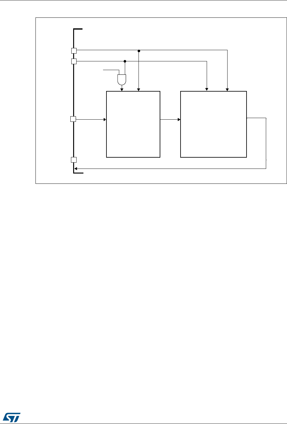
DocID026448 Rev 1 803/836
RM0383 Debug support (DBG)
829
Figure 268. JTAG TAP connections
"OUNDARYSCAN
4!0
.*4234
#ORTEX-4!0
*4-3
4-3 N42344-3 N4234
*4$)
*4$/
4$) 4$/ 4$) 4$/
37$0
34-&XXX
3ELECTED
)2ISBITWIDE )2ISBITWIDE
-36

Debug support (DBG) RM0383
804/836 DocID026448 Rev 1
23.6 ID codes and locking mechanism
There are several ID codes inside the STM32F411xx MCUs. ST strongly recommends tools
designers to lock their debuggers using the MCU DEVICE ID code located in the external
PPB memory map at address 0xE0042000.
23.6.1 MCU device ID code
The STM32F411xC/E MCUs integrate an MCU ID code. This ID identifies the ST MCU part-
number and the die revision. It is part of the DBG_MCU component and is mapped on the
external PPB bus (see Section 23.16 on page 817). This code is accessible using the JTAG
debug port (4 to 5 pins) or the SW debug port (two pins) or by the user software. It is even
accessible while the MCU is under system reset.
DBGMCU_IDCODE
Address: 0xE004 2000
Only 32-bits access supported. Read-only.
23.6.2 Boundary scan TAP
JTAG ID code
The TAP of the STM32F411xC/E BSC (boundary scan) integrates a JTAG ID code equal to
0x06431041 .
23.6.3 Cortex®-M4 with FPU TAP
The TAP of the ARM® Cortex®-M4 with FPU integrates a JTAG ID code. This ID code is the
ARM® default one and has not been modified. This code is only accessible by the JTAG
Debug Port.
This code is (corresponds to Cortex®-M4 with FPU r0p1, see Section 23.2: Reference
ARM® documentation).
31 30 29 28 27 26 25 24 23 22 21 20 19 18 17 16
REV_ID
rrrrrr r r r r rrrrrr
1514131211109876543210
Reserved DEV_ID
rrrrrrrrrrrr
Bits 31:16 REV_ID(15:0) Revision identifier
This field indicates the revision of the device:
0x1000 = Revision A
Bits 15:12 Reserved, must be kept at reset value.
Bits 11:0 DEV_ID(11:0): Device identifier
The device ID is 0x431 for the STM32F411xC/E

DocID026448 Rev 1 805/836
RM0383 Debug support (DBG)
829
Only the DEV_ID(11:0) should be used for identification by the debugger/programmer tools.
23.6.4 Cortex®-M4 with FPU JEDEC-106 ID code
The ARM® Cortex®-M4 with FPU integrates a JEDEC-106 ID code. It is located in the 4KB
ROM table mapped on the internal PPB bus at address 0xE00FF000_0xE00FFFFF.
This code is accessible by the JTAG Debug Port (4 to 5 pins) or by the SW Debug Port (two
pins) or by the user software.
23.7 JTAG debug port
A standard JTAG state machine is implemented with a 4-bit instruction register (IR) and five
data registers (for full details, refer to the Cortex®-M4 with FPU r0p1 Technical Reference
Manual (TRM), for references, please see Section 23.2: Reference ARM® documentation).
Table 133. JTAG debug port data registers
IR(3:0) Data register Details
1111 BYPASS
[1 bit]
1110 IDCODE
[32 bits]
ID CODE
0x4BA00477 (ARM® Cortex®-M4 with FPU r0p1 ID Code)
1010 DPACC
[35 bits]
Debug port access register
This initiates a debug port and allows access to a debug port register.
– When transferring data IN:
Bits 34:3 = DATA[31:0] = 32-bit data to transfer for a write request
Bits 2:1 = A[3:2] = 2-bit address of a debug port register.
Bit 0 = RnW = Read request (1) or write request (0).
– When transferring data OUT:
Bits 34:3 = DATA[31:0] = 32-bit data which is read following a read
request
Bits 2:0 = ACK[2:0] = 3-bit Acknowledge:
010 = OK/FAULT
001 = WAIT
OTHER = reserved
Refer to Table 134 for a description of the A(3:2) bits

Debug support (DBG) RM0383
806/836 DocID026448 Rev 1
1011 APACC
[35 bits]
Access port access register
Initiates an access port and allows access to an access port register.
– When transferring data IN:
Bits 34:3 = DATA[31:0] = 32-bit data to shift in for a write request
Bits 2:1 = A[3:2] = 2-bit address (sub-address AP registers).
Bit 0 = RnW= Read request (1) or write request (0).
– When transferring data OUT:
Bits 34:3 = DATA[31:0] = 32-bit data which is read following a read
request
Bits 2:0 = ACK[2:0] = 3-bit Acknowledge:
010 = OK/FAULT
001 = WAIT
OTHER = reserved
There are many AP Registers (see AHB-AP) addressed as the
combination of:
– The shifted value A[3:2]
– The current value of the DP SELECT register
1000 ABORT
[35 bits]
Abort register
– Bits 31:1 = Reserved
– Bit 0 = DAPABORT: write 1 to generate a DAP abort.
Table 133. JTAG debug port data registers (continued)
IR(3:0) Data register Details

DocID026448 Rev 1 807/836
RM0383 Debug support (DBG)
829
23.8 SW debug port
23.8.1 SW protocol introduction
This synchronous serial protocol uses two pins:
•SWCLK: clock from host to target
•SWDIO: bidirectional
The protocol allows two banks of registers (DPACC registers and APACC registers) to be
read and written to.
Bits are transferred LSB-first on the wire.
For SWDIO bidirectional management, the line must be pulled-up on the board (100 KΩ
recommended by ARM®).
Each time the direction of SWDIO changes in the protocol, a turnaround time is inserted
where the line is not driven by the host nor the target. By default, this turnaround time is one
bit time, however this can be adjusted by configuring the SWCLK frequency.
23.8.2 SW protocol sequence
Each sequence consist of three phases:
1. Packet request (8 bits) transmitted by the host
2. Acknowledge response (3 bits) transmitted by the target
3. Data transfer phase (33 bits) transmitted by the host or the target
Table 134. 32-bit debug port registers addressed through the shifted value A[3:2]
Address A(3:2) value Description
0x0 00 Reserved, must be kept at reset value.
0x4 01
DP CTRL/STAT register. Used to:
– Request a system or debug power-up
– Configure the transfer operation for AP accesses
– Control the pushed compare and pushed verify operations.
– Read some status flags (overrun, power-up acknowledges)
0x8 10
DP SELECT register: Used to select the current access port and the
active 4-words register window.
– Bits 31:24: APSEL: select the current AP
– Bits 23:8: reserved
– Bits 7:4: APBANKSEL: select the active 4-words register window on the
current AP
– Bits 3:0: reserved
0xC 11
DP RDBUFF register: Used to allow the debugger to get the final result
after a sequence of operations (without requesting new JTAG-DP
operation)

Debug support (DBG) RM0383
808/836 DocID026448 Rev 1
Refer to the Cortex®-M4 with FPUr0p1 TRM for a detailed description of DPACC and
APACC registers.
The packet request is always followed by the turnaround time (default 1 bit) where neither
the host nor target drive the line.
The ACK Response must be followed by a turnaround time only if it is a READ transaction
or if a WAIT or FAULT acknowledge has been received.
The DATA transfer must be followed by a turnaround time only if it is a READ transaction.
23.8.3 SW-DP state machine (reset, idle states, ID code)
The State Machine of the SW-DP has an internal ID code which identifies the SW-DP. It
follows the JEP-106 standard. This ID code is the default ARM® one and is set to
0x2BA01477 (corresponding to Cortex®-M4 with FPU r0p1).
Table 135. Packet request (8-bits)
Bit Name Description
0 Start Must be “1”
1 APnDP 0: DP Access
1: AP Access
2RnW 0: Write Request
1: Read Request
4:3 A(3:2) Address field of the DP or AP registers (refer to Table 134)
5 Parity Single bit parity of preceding bits
6Stop 0
7Park Not driven by the host. Must be read as “1” by the target because of
the pull-up
Table 136. ACK response (3 bits)
Bit Name Description
0..2 ACK
001: FAULT
010: WAIT
100: OK
Table 137. DATA transfer (33 bits)
Bit Name Description
0..31 WDATA or RDATA Write or Read data
32 Parity Single parity of the 32 data bits

DocID026448 Rev 1 809/836
RM0383 Debug support (DBG)
829
Note: Note that the SW-DP state machine is inactive until the target reads this ID code.
•The SW-DP state machine is in RESET STATE either after power-on reset, or after the
DP has switched from JTAG to SWD or after the line is high for more than 50 cycles
•The SW-DP state machine is in IDLE STATE if the line is low for at least two cycles
after RESET state.
•After RESET state, it is mandatory to first enter into an IDLE state AND to perform a
READ access of the DP-SW ID CODE register. Otherwise, the target will issue a
FAULT acknowledge response on another transactions.
Further details of the SW-DP state machine can be found in the Cortex®-M4 with FPU r0p1
TRM and the CoreSight Design Kit r0p1 TRM.
23.8.4 DP and AP read/write accesses
•Read accesses to the DP are not posted: the target response can be immediate (if
ACK=OK) or can be delayed (if ACK=WAIT).
•Read accesses to the AP are posted. This means that the result of the access is
returned on the next transfer. If the next access to be done is NOT an AP access, then
the DP-RDBUFF register must be read to obtain the result.
The READOK flag of the DP-CTRL/STAT register is updated on every AP read access
or RDBUFF read request to know if the AP read access was successful.
•The SW-DP implements a write buffer (for both DP or AP writes), that enables it to
accept a write operation even when other transactions are still outstanding. If the write
buffer is full, the target acknowledge response is “WAIT”. With the exception of
IDCODE read or CTRL/STAT read or ABORT write which are accepted even if the write
buffer is full.
•Because of the asynchronous clock domains SWCLK and HCLK, two extra SWCLK
cycles are needed after a write transaction (after the parity bit) to make the write
effective internally. These cycles should be applied while driving the line low (IDLE
state)
This is particularly important when writing the CTRL/STAT for a power-up request. If the
next transaction (requiring a power-up) occurs immediately, it will fail.
23.8.5 SW-DP registers
Access to these registers are initiated when APnDP=0
Table 138. SW-DP registers
A(3:2) R/W CTRLSEL bit
of SELECT
register Register Notes
00 Read - IDCODE The manufacturer code is not set to ST
code. 0x2BA01477 (identifies the SW-DP)
00 Write - ABORT -

Debug support (DBG) RM0383
810/836 DocID026448 Rev 1
23.8.6 SW-AP registers
Access to these registers are initiated when APnDP=1
There are many AP Registers (see AHB-AP) addressed as the combination of:
•The shifted value A[3:2]
•The current value of the DP SELECT register
01 Read/Write 0 DP-
CTRL/STAT
Purpose is to:
– request a system or debug power-up
– configure the transfer operation for AP
accesses
– control the pushed compare and pushed
verify operations.
– read some status flags (overrun, power-
up acknowledges)
01 Read/Write 1 WIRE
CONTROL
Purpose is to configure the physical serial
port protocol (like the duration of the
turnaround time)
10 Read READ
RESEND
Enables recovery of the read data from a
corrupted debugger transfer, without
repeating the original AP transfer.
10 Write SELECT The purpose is to select the current access
port and the active 4-words register window
11 Read/Write READ
BUFFER
This read buffer is useful because AP
accesses are posted (the result of a read AP
request is available on the next AP
transaction).
This read buffer captures data from the AP,
presented as the result of a previous read,
without initiating a new transaction
Table 138. SW-DP registers (continued)
A(3:2) R/W CTRLSEL bit
of SELECT
register Register Notes

DocID026448 Rev 1 811/836
RM0383 Debug support (DBG)
829
23.9 AHB-AP (AHB access port) - valid for both JTAG-DP
and SW-DP
Features:
•System access is independent of the processor status.
•Either SW-DP or JTAG-DP accesses AHB-AP.
•The AHB-AP is an AHB master into the Bus Matrix. Consequently, it can access all the
data buses (Dcode Bus, System Bus, internal and external PPB bus) but the ICode
bus.
•Bitband transactions are supported.
•AHB-AP transactions bypass the FPB.
The address of the 32-bits AHP-AP resisters are 6-bits wide (up to 64 words or 256 bytes)
and consists of:
c) Bits [7:4] = the bits [7:4] APBANKSEL of the DP SELECT register
d) Bits [3:2] = the 2 address bits of A(3:2) of the 35-bit packet request for SW-DP.
The AHB-AP of the Cortex®-M4 with FPU includes 9 x 32-bits registers:
Refer to the Cortex®-M4 with FPU r0p1 TRM for further details.
Table 139. Cortex®-M4 with FPU AHB-AP registers
Address
offset Register name Notes
0x00 AHB-AP Control and Status
Word
Configures and controls transfers through the AHB
interface (size, hprot, status on current transfer, address
increment type
0x04 AHB-AP Transfer Address -
0x0C AHB-AP Data Read/Write -
0x10 AHB-AP Banked Data 0
Directly maps the 4 aligned data words without rewriting
the Transfer Address Register.
0x14 AHB-AP Banked Data 1
0x18 AHB-AP Banked Data 2
0x1C AHB-AP Banked Data 3
0xF8 AHB-AP Debug ROM Address Base Address of the debug interface
0xFC AHB-AP ID Register -

Debug support (DBG) RM0383
812/836 DocID026448 Rev 1
23.10 Core debug
Core debug is accessed through the core debug registers. Debug access to these registers
is by means of the Advanced High-performance Bus (AHB-AP) port. The processor can
access these registers directly over the internal Private Peripheral Bus (PPB).
It consists of 4 registers:
Note: Important: these registers are not reset by a system reset. They are only reset by a power-
on reset.
Refer to the Cortex®-M4 with FPU r0p1 TRM for further details.
To Halt on reset, it is necessary to:
•enable the bit0 (VC_CORRESET) of the Debug and Exception Monitor Control
Register
•enable the bit0 (C_DEBUGEN) of the Debug Halting Control and Status Register.
Table 140. Core debug registers
Register Description
DHCSR
The 32-bit Debug Halting Control and Status Register
This provides status information about the state of the processor enable core debug
halt and step the processor
DCRSR The 17-bit Debug Core Register Selector Register:
This selects the processor register to transfer data to or from.
DCRDR
The 32-bit Debug Core Register Data Register:
This holds data for reading and writing registers to and from the processor selected
by the DCRSR (Selector) register.
DEMCR
The 32-bit Debug Exception and Monitor Control Register:
This provides Vector Catching and Debug Monitor Control. This register contains a
bit named TRCENA which enable the use of a TRACE.

DocID026448 Rev 1 813/836
RM0383 Debug support (DBG)
829
23.11 Capability of the debugger host to connect under system
reset
The reset system of the STM32F411xC/E MCU comprises the following reset sources:
•POR (power-on reset) which asserts a RESET at each power-up.
•Internal watchdog reset
•Software reset
•External reset
The Cortex®-M4 with FPU differentiates the reset of the debug part (generally
PORRESETn) and the other one (SYSRESETn)
This way, it is possible for the debugger to connect under System Reset, programming the
Core Debug Registers to halt the core when fetching the reset vector. Then the host can
release the system reset and the core will immediately halt without having executed any
instructions. In addition, it is possible to program any debug features under System Reset.
Note: It is highly recommended for the debugger host to connect (set a breakpoint in the reset
vector) under system reset.
23.12 FPB (Flash patch breakpoint)
The FPB unit:
•implements hardware breakpoints
•patches code and data from code space to system space. This feature gives the
possibility to correct software bugs located in the Code Memory Space.
The use of a Software Patch or a Hardware Breakpoint is exclusive.
The FPB consists of:
•2 literal comparators for matching against literal loads from Code Space and remapping
to a corresponding area in the System Space.
•6 instruction comparators for matching against instruction fetches from Code Space.
They can be used either to remap to a corresponding area in the System Space or to
generate a Breakpoint Instruction to the core.

Debug support (DBG) RM0383
814/836 DocID026448 Rev 1
23.13 DWT (data watchpoint trigger)
The DWT unit consists of four comparators. They are configurable as:
•a hardware watchpoint or
•a trigger to an ETM or
•a PC sampler or
•a data address sampler
The DWT also provides some means to give some profiling informations. For this, some
counters are accessible to give the number of:
•Clock cycle
•Folded instructions
•Load store unit (LSU) operations
•Sleep cycles
•CPI (clock per instructions)
•Interrupt overhead
23.14 ITM (instrumentation trace macrocell)
23.14.1 General description
The ITM is an application-driven trace source that supports printf style debugging to trace
Operating System (OS) and application events, and emits diagnostic system information.
The ITM emits trace information as packets which can be generated as:
•Software trace. Software can write directly to the ITM stimulus registers to emit
packets.
•Hardware trace. The DWT generates these packets, and the ITM emits them.
•Time stamping. Timestamps are emitted relative to packets. The ITM contains a 21-bit
counter to generate the timestamp. The Cortex®-M4 with FPU clock or the bit clock rate
of the Serial Wire Viewer (SWV) output clocks the counter.
The packets emitted by the ITM are output to the TPIU (Trace Port Interface Unit). The
formatter of the TPIU adds some extra packets (refer to TPIU) and then output the complete
packets sequence to the debugger host.
The bit TRCEN of the Debug Exception and Monitor Control Register must be enabled
before you program or use the ITM.
23.14.2 Time stamp packets, synchronization and overflow packets
Time stamp packets encode time stamp information, generic control and synchronization. It
uses a 21-bit timestamp counter (with possible prescalers) which is reset at each time
stamp packet emission. This counter can be either clocked by the CPU clock or the SWV
clock.
A synchronization packet consists of 6 bytes equal to 0x80_00_00_00_00_00 which is
emitted to the TPIU as 00 00 00 00 00 80 (LSB emitted first).
A synchronization packet is a timestamp packet control. It is emitted at each DWT trigger.

DocID026448 Rev 1 815/836
RM0383 Debug support (DBG)
829
For this, the DWT must be configured to trigger the ITM: the bit CYCCNTENA (bit0) of the
DWT Control Register must be set. In addition, the bit2 (SYNCENA) of the ITM Trace
Control Register must be set.
Note: If the SYNENA bit is not set, the DWT generates Synchronization triggers to the TPIU which
will send only TPIU synchronization packets and not ITM synchronization packets.
An overflow packet consists is a special timestamp packets which indicates that data has
been written but the FIFO was full.
Table 141. Main ITM registers
Address Register Details
@E0000FB0 ITM lock access Write 0xC5ACCE55 to unlock Write Access to the other ITM
registers
@E0000E80 ITM trace control
Bits 31-24 = Always 0
Bits 23 = Busy
Bits 22-16 = 7-bits ATB ID which identifies the source of the
trace data.
Bits 15-10 = Always 0
Bits 9:8 = TSPrescale = Time Stamp Prescaler
Bits 7-5 = Reserved
Bit 4 = SWOENA = Enable SWV behavior (to clock the
timestamp counter by the SWV clock).
Bit 3 = DWTENA: Enable the DWT Stimulus
Bit 2 = SYNCENA: this bit must be to 1 to enable the DWT to
generate synchronization triggers so that the TPIU can then
emit the synchronization packets.
Bit 1 = TSENA (Timestamp Enable)
Bit 0 = ITMENA: Global Enable Bit of the ITM
@E0000E40 ITM trace privilege
Bit 3: mask to enable tracing ports31:24
Bit 2: mask to enable tracing ports23:16
Bit 1: mask to enable tracing ports15:8
Bit 0: mask to enable tracing ports7:0
@E0000E00 ITM trace enable Each bit enables the corresponding Stimulus port to generate
trace.
@E0000000-
E000007C
Stimulus port
registers 0-31
Write the 32-bits data on the selected Stimulus Port (32
available) to be traced out.

Debug support (DBG) RM0383
816/836 DocID026448 Rev 1
Example of configuration
To output a simple value to the TPIU:
•Configure the TPIU and assign TRACE I/Os by configuring the DBGMCU_CR (refer to
Section 23.17.2: TRACE pin assignment and Section 23.16.3: Debug MCU
configuration register)
•Write 0xC5ACCE55 to the ITM Lock Access Register to unlock the write access to the
ITM registers
•Write 0x00010005 to the ITM Trace Control Register to enable the ITM with Sync
enabled and an ATB ID different from 0x00
•Write 0x1 to the ITM Trace Enable Register to enable the Stimulus Port 0
•Write 0x1 to the ITM Trace Privilege Register to unmask stimulus ports 7:0
•Write the value to output in the Stimulus Port Register 0: this can be done by software
(using a printf function)
23.15 ETM (Embedded trace macrocell)
23.15.1 General description
The ETM enables the reconstruction of program execution. Data are traced using the Data
Watchpoint and Trace (DWT) component or the Instruction Trace Macrocell (ITM) whereas
instructions are traced using the Embedded Trace Macrocell (ETM).
The ETM transmits information as packets and is triggered by embedded resources. These
resources must be programmed independently and the trigger source is selected using the
Trigger Event Register (0xE0041008). An event could be a simple event (address match
from an address comparator) or a logic equation between 2 events. The trigger source is
one of the fourth comparators of the DWT module, The following events can be monitored:
•Clock cycle matching
•Data address matching
For more informations on the trigger resources refer to Section 23.13: DWT (data
watchpoint trigger).
The packets transmitted by the ETM are output to the TPIU (Trace Port Interface Unit). The
formatter of the TPIU adds some extra packets (refer to Section 23.17: TPIU (trace port
interface unit)) and then outputs the complete packet sequence to the debugger host.
23.15.2 Signal protocol, packet types
This part is described in the chapter 7 ETMv3 Signal Protocol of the ARM® IHI 0014N
document.

DocID026448 Rev 1 817/836
RM0383 Debug support (DBG)
829
23.15.3 Main ETM registers
For more information on registers refer to the chapter 3 of the ARM® IHI 0014N
specification.
23.15.4 Configuration example
To output a simple value to the TPIU:
•Configure the TPIU and enable the I/IO_TRACEN to assign TRACE I/Os in the
STM32F411xC/E debug configuration register.
•Write 0xC5ACCE55 to the ETM Lock Access Register to unlock the write access to the
ITM registers
•Write 0x00001D1E to the control register (configure the trace)
•Write 0000406F to the Trigger Event register (define the trigger event)
•Write 0000006F to the Trace Enable Event register (define an event to start/stop)
•Write 00000001 to the Trace Start/stop register (enable the trace)
•Write 0000191E to the ETM Control Register (end of configuration)
23.16 MCU debug component (DBGMCU)
The MCU debug component helps the debugger provide support for:
•Low-power modes
•Clock control for timers, watchdog and I2C during a breakpoint
•Control of the trace pins assignment
Table 142. Main ETM registers
Address Register Details
0xE0041FB0 ETM Lock Access Write 0xC5ACCE55 to unlock the write access to the
other ETM registers.
0xE0041000 ETM Control This register controls the general operation of the ETM,
for instance how tracing is enabled.
0xE0041010 ETM Status This register provides information about the current status
of the trace and trigger logic.
0xE0041008 ETM Trigger Event This register defines the event that will control trigger.
0xE004101C ETM Trace Enable
Control This register defines which comparator is selected.
0xE0041020 ETM Trace Enable Event This register defines the trace enabling event.
0xE0041024 ETM Trace Start/Stop This register defines the traces used by the trigger source
to start and stop the trace, respectively.

Debug support (DBG) RM0383
818/836 DocID026448 Rev 1
23.16.1 Debug support for low-power modes
To enter low-power mode, the instruction WFI or WFE must be executed.
The MCU implements several low-power modes which can either deactivate the CPU clock
or reduce the power of the CPU.
The core does not allow FCLK or HCLK to be turned off during a debug session. As these
are required for the debugger connection, during a debug, they must remain active. The
MCU integrates special means to allow the user to debug software in low-power modes.
For this, the debugger host must first set some debug configuration registers to change the
low-power mode behavior:
•In Sleep mode, DBG_SLEEP bit of DBGMCU_CR register must be previously set by
the debugger. This will feed HCLK with the same clock that is provided to FCLK
(system clock previously configured by the software).
•In Stop mode, the bit DBG_STOP must be previously set by the debugger. This will
enable the internal RC oscillator clock to feed FCLK and HCLK in STOP mode.
23.16.2 Debug support for timers, watchdog and I2C
During a breakpoint, it is necessary to choose how the counter of timers and watchdog
should behave:
•They can continue to count inside a breakpoint. This is usually required when a PWM is
controlling a motor, for example.
•They can stop to count inside a breakpoint. This is required for watchdog purposes.
For the I2C, the user can choose to block the SMBUS timeout during a breakpoint.
23.16.3 Debug MCU configuration register
This register allows the configuration of the MCU under DEBUG. This concerns:
•Low-power mode support
•Timer and watchdog counter support
•Trace pin assignment
This DBGMCU_CR is mapped on the External PPB bus at address 0xE0042004
It is asynchronously reset by the PORESET (and not the system reset). It can be written by
the debugger under system reset.
If the debugger host does not support these features, it is still possible for the user software
to write to these registers.

DocID026448 Rev 1 819/836
RM0383 Debug support (DBG)
829
DBGMCU_CR register
Address: 0xE004 2004
Only 32-bit access supported
POR Reset: 0x0000 0000 (not reset by system reset)
31 30 29 28 27 26 25 24 23 22 21 20 19 18 17 16
Reserved
15 14 13 12 11 10 9 8 7 6 5 4 3 2 1 0
Reserved
TRACE_
MODE
[1:0]
TRACE
_IOEN Reserved
DBG_
STAND
BY
DBG_
STOP
DBG_
SLEEP
rw rw rw rw rw rw
Bits 31:8 Reserved, must be kept at reset value.
Bits 7:5 TRACE_MODE[1:0] and TRACE_IOEN: Trace pin assignment control
– With TRACE_IOEN=0:
TRACE_MODE=xx: TRACE pins not assigned (default state)
– With TRACE_IOEN=1:
– TRACE_MODE=00: TRACE pin assignment for Asynchronous Mode
– TRACE_MODE=01: TRACE pin assignment for Synchronous Mode with a
TRACEDATA size of 1
– TRACE_MODE=10: TRACE pin assignment for Synchronous Mode with a
TRACEDATA size of 2
– TRACE_MODE=11: TRACE pin assignment for Synchronous Mode with a
TRACEDATA size of 4
Bits 4:3 Reserved, must be kept at reset value.

Debug support (DBG) RM0383
820/836 DocID026448 Rev 1
23.16.4 Debug MCU APB1 freeze register (DBGMCU_APB1_FZ)
The DBGMCU_APB1_FZ register is used to configure the MCU under Debug. It concerns
APB1 peripherals. It is mapped on the external PPB bus at address 0xE004 2008.
The register is asynchronously reset by the POR (and not the system reset). It can be
written by the debugger under system reset.
Address : 0xE004 2008
Only 32-bits access are supported.
Power-on reset (POR): 0x0000 0000 (not reset by system reset)
Bit 2 DBG_STANDBY: Debug Standby mode
0: (FCLK=Off, HCLK=Off) The whole digital part is unpowered.
From software point of view, exiting from Standby is identical than fetching reset vector
(except a few status bit indicated that the MCU is resuming from Standby)
1: (FCLK=On, HCLK=On) In this case, the digital part is not unpowered and FCLK and
HCLK are provided by the internal RC oscillator which remains active. In addition, the MCU
generate a system reset during Standby mode so that exiting from Standby is identical than
fetching from reset
Bit 1 DBG_STOP: Debug Stop mode
0: (FCLK=Off, HCLK=Off) In STOP mode, the clock controller disables all clocks (including
HCLK and FCLK). When exiting from STOP mode, the clock configuration is identical to the
one after RESET (CPU clocked by the 8 MHz internal RC oscillator (HSI)). Consequently,
the software must reprogram the clock controller to enable the PLL, the Xtal, etc.
1: (FCLK=On, HCLK=On) In this case, when entering STOP mode, FCLK and HCLK are
provided by the internal RC oscillator which remains active in STOP mode. When exiting
STOP mode, the software must reprogram the clock controller to enable the PLL, the Xtal,
etc. (in the same way it would do in case of DBG_STOP=0)
Bit 0 DBG_SLEEP: Debug Sleep mode
0: (FCLK=On, HCLK=Off) In Sleep mode, FCLK is clocked by the system clock as
previously configured by the software while HCLK is disabled.
In Sleep mode, the clock controller configuration is not reset and remains in the previously
programmed state. Consequently, when exiting from Sleep mode, the software does not
need to reconfigure the clock controller.
1: (FCLK=On, HCLK=On) In this case, when entering Sleep mode, HCLK is fed by the same
clock that is provided to FCLK (system clock as previously configured by the software).

DocID026448 Rev 1 821/836
RM0383 Debug support (DBG)
829
23.16.5 Debug MCU APB2 Freeze register (DBGMCU_APB2_FZ)
The DBGMCU_APB2_FZ register is used to configure the MCU under Debug. It concerns
APB2 peripherals.
31 30 29 28 27 26 25 24 23 22 21 20 19 18 17 16
Reserved
DBG_I2C3_SMBUS_TIMEOUT
DBG_I2C2_SMBUS_TIMEOUT
DBG_I2C1_SMBUS_TIMEOUT
Reserved
rw rw rw
1514131211109876543210
Reserved
DBG_IWDG_STOP
DBG_WWDG_STOP
DBG_RTC_STOP
Reserved
DBG_TIM5_STOP
DBG_TIM4_STOP
DBG_TIM3_STOP
DBG_TIM2_STOP
Bits 31:24 Reserved, must be kept at reset value.
Bit 23 DBG_I2C3_SMBUS_TIMEOUT: SMBUS timeout mode stopped when Core is halted
0: Same behavior as in normal mode
1: The SMBUS timeout is frozen
Bit 22 DBG_I2C2_SMBUS_TIMEOUT: SMBUS timeout mode stopped when Core is halted
0: Same behavior as in normal mode
1: The SMBUS timeout is frozen
Bit 21 DBG_I2C1_SMBUS_TIMEOUT: SMBUS timeout mode stopped when Core is halted
0: Same behavior as in normal mode
1: The SMBUS timeout is frozen
Bit 20:13 Reserved, must be kept at reset value.
Bit 12 DBG_IWDG_STOP: Debug independent watchdog stopped when core is halted
0: The independent watchdog counter clock continues even if the core is halted
1: The independent watchdog counter clock is stopped when the core is halted
Bit 11 DBG_WWDG_STOP: Debug Window Watchdog stopped when Core is halted
0: The window watchdog counter clock continues even if the core is halted
1: The window watchdog counter clock is stopped when the core is halted
Bit 10 DBG_RTC_STOP: RTC stopped when Core is halted
0: The RTC counter clock continues even if the core is halted
1: The RTC counter clock is stopped when the core is halted
Bit 9:4 Reserved, must be kept at reset value.
Bits 3:0 DBG_TIMx_STOP: TIMx counter stopped when core is halted (x=2..5)
0: The clock of the involved Timer Counter is fed even if the core is halted
1: The clock of the involved Timer counter is stopped when the core is halted

Debug support (DBG) RM0383
822/836 DocID026448 Rev 1
This register is mapped on the external PPB bus at address 0xE004 200C
It is asynchronously reset by the POR (and not the system reset). It can be written by the
debugger under system reset.
Address: 0xE004 200C
Only 32-bit access is supported.
POR: 0x0000 0000 (not reset by system reset)
23.17 TPIU (trace port interface unit)
23.17.1 Introduction
The TPIU acts as a bridge between the on-chip trace data from the ITM and the ETM.
The output data stream encapsulates the trace source ID, that is then captured by a trace
port analyzer (TPA).
The core embeds a simple TPIU, especially designed for low-cost debug (consisting of a
special version of the CoreSight TPIU).
31 30 29 28 27 26 25 24 23 22 21 20 19 18 17 16
Reserved
DBG_TIM11
_STOP
DBG_TIM10
_STOP
DBG_TIM9_
STOP
rw rw rw
15 14 13 12 11 10 9 8 7 6 5 4 3 2 1 0
Reserved
DBG_TIM1_
STOP
rw
Bits 31:19 Reserved, must be kept at reset value.
Bits 18:16 DBG_TIMx_STOP: TIMx counter stopped when core is halted (x=9..11)
0: The clock of the involved Timer Counter is fed even if the core is halted
1: The clock of the involved Timer counter is stopped when the core is halted
Bits 15:2 Reserved, must be kept at reset value.
Bit 0 DBG_TIM1_STOP: TIM1 counter stopped when core is halted
0: The clock of the involved Timer Counter is fed even if the core is halted
1: The clock of the involved Timer counter is stopped when the core is halted
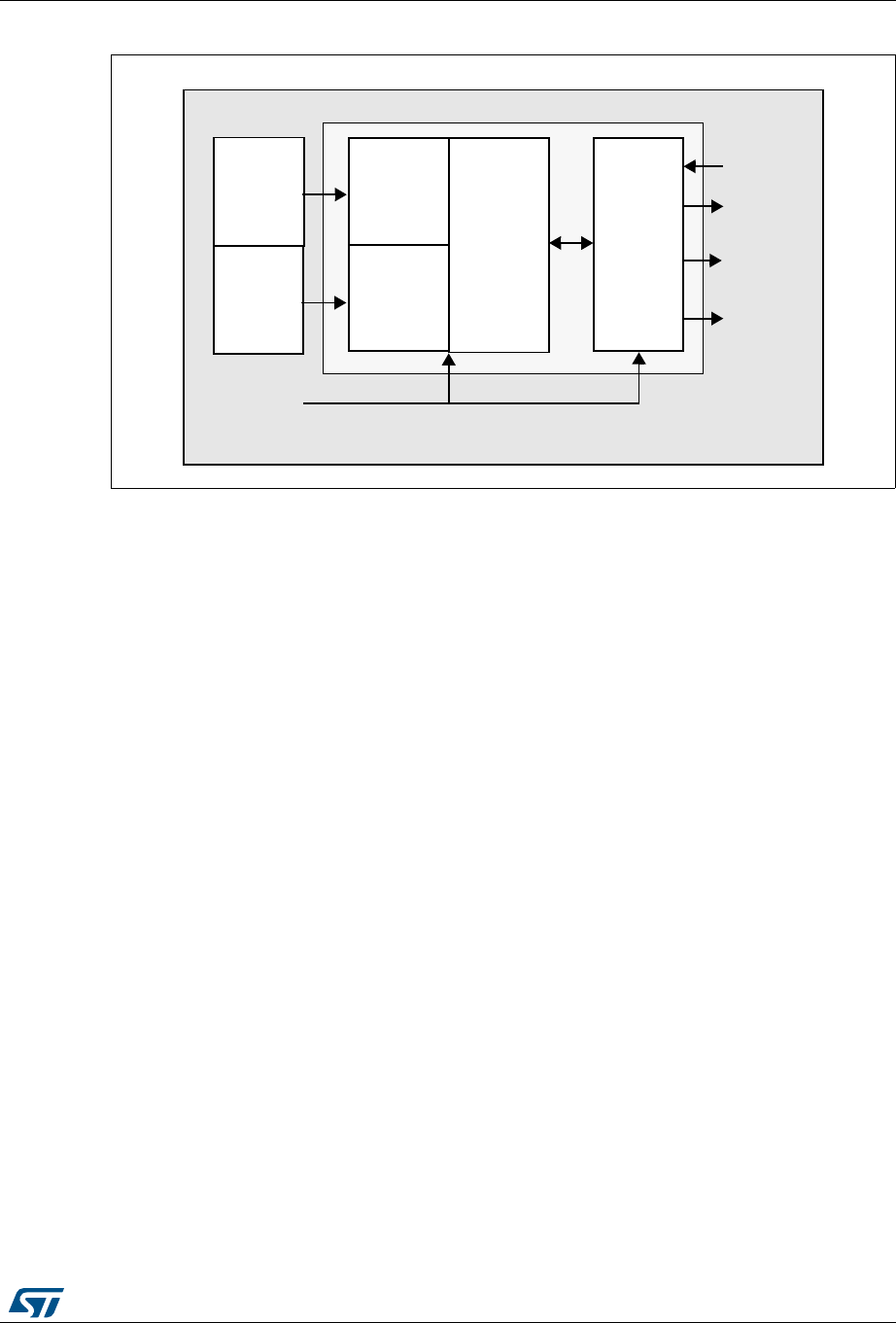
DocID026448 Rev 1 823/836
RM0383 Debug support (DBG)
829
Figure 269. TPIU block diagram
formatter
Trace out
(serializer)
TRACECLKIN
TRACECK
TRACEDATA
[3:0]
TRACESWO
CLK domain TRACECLKIN domain
External PPB bus
TPIU
TPIU
Asynchronous
FIFO
Asynchronous
FIFO
ETM
ITM
ai17114

Debug support (DBG) RM0383
824/836 DocID026448 Rev 1
23.17.2 TRACE pin assignment
•Asynchronous mode
The asynchronous mode requires 1 extra pin and is available on all packages. It is only
available if using Serial Wire mode (not in JTAG mode).
•Synchronous mode
The synchronous mode requires from 2 to 6 extra pins depending on the data trace
size and is only available in the larger packages. In addition it is available in JTAG
mode and in Serial Wire mode and provides better bandwidth output capabilities than
asynchronous trace.
TPUI TRACE pin assignment
By default, these pins are NOT assigned. They can be assigned by setting the
TRACE_IOEN and TRACE_MODE bits in the MCU Debug component configuration
register. This configuration has to be done by the debugger host.
In addition, the number of pins to assign depends on the trace configuration (asynchronous
or synchronous).
•Asynchronous mode: 1 extra pin is needed
•Synchronous mode: from 2 to 5 extra pins are needed depending on the size of the
data trace port register (1, 2 or 4):
– TRACECK
– TRACED(0) if port size is configured to 1, 2 or 4
– TRACED(1) if port size is configured to 2 or 4
– TRACED(2) if port size is configured to 4
– TRACED(3) if port size is configured to 4
To assign the TRACE pin, the debugger host must program the bits TRACE_IOEN and
TRACE_MODE[1:0] of the Debug MCU configuration Register (DBGMCU_CR). By default
the TRACE pins are not assigned.
This register is mapped on the external PPB and is reset by the PORESET (and not by the
SYSTEM reset). It can be written by the debugger under SYSTEM reset.
Table 143. Asynchronous TRACE pin assignment
TPUI pin name Trace synchronous mode pin assignment
Type Description
TRACESWO O TRACE Async Data Output PB3
Table 144. Synchronous TRACE pin assignment
TPUI pin name Trace synchronous mode STM32F411xC/E
pin assignment
Type Description
TRACECK O TRACE Clock PE2
TRACED[3:0] O TRACE Sync Data Outputs
Can be 1, 2 or 4. PE[6:3]

DocID026448 Rev 1 825/836
RM0383 Debug support (DBG)
829
Note: By default, the TRACECLKIN input clock of the TPIU is tied to GND. It is assigned to HCLK
two clock cycles after the bit TRACE_IOEN has been set.
The debugger must then program the Trace Mode by writing the PROTOCOL[1:0] bits in the
SPP_R (Selected Pin Protocol) register of the TPIU.
•PROTOCOL=00: Trace Port Mode (synchronous)
•PROTOCOL=01 or 10: Serial Wire (Manchester or NRZ) Mode (asynchronous mode).
Default state is 01
It then also configures the TRACE port size by writing the bits [3:0] in the CPSPS_R
(Current Sync Port Size Register) of the TPIU:
•0x1 for 1 pin (default state)
•0x2 for 2 pins
•0x8 for 4 pins
23.17.3 TPUI formatter
The formatter protocol outputs data in 16-byte frames:
•seven bytes of data
•eight bytes of mixed-use bytes consisting of:
– 1 bit (LSB) to indicate it is a DATA byte (‘0) or an ID byte (‘1).
– 7 bits (MSB) which can be data or change of source ID trace.
•one byte of auxiliary bits where each bit corresponds to one of the eight mixed-use
bytes:
– if the corresponding byte was a data, this bit gives bit0 of the data.
– if the corresponding byte was an ID change, this bit indicates when that ID change
takes effect.
Table 145. Flexible TRACE pin assignment
DBGMCU_CR
register Pins
assigned for:
TRACE IO pin assigned
TRACE
_IOEN
TRACE
_MODE
[1:0]
PB3 /JTDO/
TRACESWO
PE2/
TRACECK
PE3 /
TRACED[0] PE4 /
TRACED[1] PE5 /
TRACED[2] PE6 /
TRACED[3]
0XX
No Trace
(default state) Released (1) -
100
Asynchronous
Trace TRACESWO - - Released
(usable as GPIO)
101
Synchronous
Trace 1 bit
Released (1)
TRACECK TRACED[0] ---
110
Synchronous
Trace 2 bit TRACECK TRACED[0] TRACED[1] - -
111
Synchronous
Trace 4 bit TRACECK TRACED[0] TRACED[1] TRACED[2] TRACED[3]
1. When Serial Wire mode is used, it is released. But when JTAG is used, it is assigned to JTDO.

Debug support (DBG) RM0383
826/836 DocID026448 Rev 1
Note: Refer to the ARM® CoreSight Architecture Specification v1.0 (ARM® IHI 0029B) for further
information
23.17.4 TPUI frame synchronization packets
The TPUI can generate two types of synchronization packets:
•The Frame Synchronization packet (or Full Word Synchronization packet)
It consists of the word: 0x7F_FF_FF_FF (LSB emitted first). This sequence can not
occur at any other time provided that the ID source code 0x7F has not been used.
It is output periodically between frames.
In continuous mode, the TPA must discard all these frames once a synchronization
frame has been found.
•The Half-Word Synchronization packet
It consists of the half word: 0x7F_FF (LSB emitted first).
It is output periodically between or within frames.
These packets are only generated in continuous mode and enable the TPA to detect
that the TRACE port is in IDLE mode (no TRACE to be captured). When detected by
the TPA, it must be discarded.
23.17.5 Transmission of the synchronization frame packet
There is no Synchronization Counter register implemented in the TPIU of the core.
Consequently, the synchronization trigger can only be generated by the DWT. Refer to the
registers DWT Control Register (bits SYNCTAP[11:10]) and the DWT Current PC Sampler
Cycle Count Register.
The TPUI Frame synchronization packet (0x7F_FF_FF_FF) is emitted:
•after each TPIU reset release. This reset is synchronously released with the rising
edge of the TRACECLKIN clock. This means that this packet is transmitted when the
TRACE_IOEN bit in the DBGMCU_CFG register is set. In this case, the word
0x7F_FF_FF_FF is not followed by any formatted packet.
•at each DWT trigger (assuming DWT has been previously configured). Two cases
occur:
– If the bit SYNENA of the ITM is reset, only the word 0x7F_FF_FF_FF is emitted
without any formatted stream which follows.
– If the bit SYNENA of the ITM is set, then the ITM synchronization packets will
follow (0x80_00_00_00_00_00), formatted by the TPUI (trace source ID added).
23.17.6 Synchronous mode
The trace data output size can be configured to 4, 2 or 1 pin: TRACED(3:0)
The output clock is output to the debugger (TRACECK)
Here, TRACECLKIN is driven internally and is connected to HCLK only when TRACE is
used.
Note: In this synchronous mode, it is not required to provide a stable clock frequency.
The TRACE I/Os (including TRACECK) are driven by the rising edge of TRACLKIN (equal
to HCLK). Consequently, the output frequency of TRACECK is equal to HCLK/2.

DocID026448 Rev 1 827/836
RM0383 Debug support (DBG)
829
23.17.7 Asynchronous mode
This is a low cost alternative to output the trace using only 1 pin: this is the asynchronous
output pin TRACESWO. Obviously there is a limited bandwidth.
TRACESWO is multiplexed with JTDO when using the SW-DP pin. This way, this
functionality is available in all STM32F411xC/E packages.
This asynchronous mode requires a constant frequency for TRACECLKIN. For the standard
UART (NRZ) capture mechanism, 5% accuracy is needed. The Manchester encoded
version is tolerant up to 10%.
23.17.8 TRACECLKIN connection inside the STM32F411xC/E
In the STM32F411xC/E, this TRACECLKIN input is internally connected to HCLK. This
means that when in asynchronous trace mode, the application is restricted to use to time
frames where the CPU frequency is stable.
Note: Important: when using asynchronous trace: it is important to be aware that:
The default clock of the STM32F411xC/E MCUs is the internal RC oscillator. Its frequency
under reset is different from the one after reset release. This is because the RC calibration
is the default one under system reset and is updated at each system reset release.
Consequently, the trace port analyzer (TPA) should not enable the trace (with the
TRACE_IOEN bit) under system reset, because a Synchronization Frame Packet will be
issued with a different bit time than trace packets which will be transmitted after reset
release.
23.17.9 TPIU registers
The TPIU APB registers can be read and written only if the bit TRCENA of the Debug
Exception and Monitor Control Register (DEMCR) is set. Otherwise, the registers are read
as zero (the output of this bit enables the PCLK of the TPIU).
Table 146. Important TPIU registers
Address Register Description
0xE0040004 Current port size
Allows the trace port size to be selected:
Bit 0: Port size = 1
Bit 1: Port size = 2
Bit 2: Port size = 3, not supported
Bit 3: Port Size = 4
Only 1 bit must be set. By default, the port size is one bit. (0x00000001)
0xE00400F0 Selected pin
protocol
Allows the Trace Port Protocol to be selected:
Bit1:0=
00: Sync Trace Port Mode
01: Serial Wire Output - manchester (default value)
10: Serial Wire Output - NRZ
11: reserved

Debug support (DBG) RM0383
828/836 DocID026448 Rev 1
23.17.10 Example of configuration
•Set the bit TRCENA in the Debug Exception and Monitor Control Register (DEMCR)
•Write the TPIU Current Port Size Register to the desired value (default is 0x1 for a 1-bit
port size)
•Write TPIU Formatter and Flush Control Register to 0x102 (default value)
•Write the TPIU Select Pin Protocol to select the sync or async mode. Example: 0x2 for
async NRZ mode (UART like)
•Write the DBGMCU control register to 0x20 (bit IO_TRACEN) to assign TRACE I/Os
for async mode. A TPIU Sync packet is emitted at this time (FF_FF_FF_7F)
•Configure the ITM and write the ITM Stimulus register to output a value
23.18 DBG register map
The following table summarizes the Debug registers.
.
0xE0040304 Formatter and flush
control
Bits 31-9 = always ‘0
Bit 8 = TrigIn = always ‘1 to indicate that triggers are indicated
Bits 7-4 = always 0
Bits 3-2 = always 0
Bit 1 = EnFCont. In Sync Trace mode (Select_Pin_Protocol register
bit1:0=00), this bit is forced to ‘1: the formatter is automatically enabled
in continuous mode. In asynchronous mode (Select_Pin_Protocol
register bit1:0 <> 00), this bit can be written to activate or not the
formatter.
Bit 0 = always 0
The resulting default value is 0x102
Note: In synchronous mode, because the TRACECTL pin is not mapped
outside the chip, the formatter is always enabled in continuous mode -this
way the formatter inserts some control packets to identify the source of
the trace packets).
0xE0040300 Formatter and flush
status Not used in Cortex®-M4 with FPU, always read as 0x00000008
Table 146. Important TPIU registers (continued)
Address Register Description
Table 147. DBG register map and reset values
Addr. Register
31
30
29
28
27
26
25
24
23
22
21
20
19
18
17
16
15
14
13
12
11
10
9
8
7
6
5
4
3
2
1
0
0xE004
2000
DBGMCU
_IDCODE REV_ID
Reserved
DEV_ID
Reset value(1) XXXXXXXXXXXXXXXX XXXXXXXXXXXX
DocID026448 Rev 1 829/836
RM0383 Debug support (DBG)
829
0xE004
2004
DBGMCU_CR Reserved
DBG_TIM5_STOP
Reserved
DBG_I2C2_SMBUS_TIMEOUT
Reserved
TRACE_
MODE[1:0]
TRACE_IOEN
Reserved
DBG_STANDBY
DBG_STOP
DBG_SLEEP
Reset value 0 0 000 000
0xE004
2008
DBGMCU_
APB1_FZ Reserved
DBG_I2C3_SMBUS_TIMEOUT
DBG_I2C2_SMBUS_TIMEOUT
DBG_I2C1_SMBUS_TIMEOUT
Reserved
DBG_IWDG_STOP
DBG_WWDG_STOP
Reserved
DBG_RTC_STOP
Reserved
DBG_TIM5_STOP
DBG_TIM4_STOP
DBG_TIM3_STOP
DBG_TIM2_STOP
Reset value 000 00 0 0000
0xE004
200C
DBGMCU_
APB2_FZ Reserved
DBG_TIM11_STOP
DBG_TIM10_STOP
DBG_TIM9_STOP
Reserved
DBG_TIM1_STOP
Reset value 0 0 0 0
1. The reset value is product dependent. For more information, refer to Section 23.6.1: MCU device ID code.
Table 147. DBG register map and reset values (continued)
Addr. Register
31
30
29
28
27
26
25
24
23
22
21
20
19
18
17
16
15
14
13
12
11
10
9
8
7
6
5
4
3
2
1
0

DocID026448 Rev 1 829/836
RM0383 Device electronic signature
830
24 Device electronic signature
The electronic signature is stored in the Flash memory area. It can be read using the
JTAG/SWD or the CPU. It contains factory-programmed identification data that allow the
user firmware or other external devices to automatically match its interface to the
characteristics of the STM32F4xx microcontrollers.
24.1 Unique device ID register (96 bits)
The unique device identifier is ideally suited:
•for use as serial numbers (for example USB string serial numbers or other end
applications)
•for use as security keys in order to increase the security of code in Flash memory while
using and combining this unique ID with software cryptographic primitives and
protocols before programming the internal Flash memory
•to activate secure boot processes, etc.
The 96-bit unique device identifier provides a reference number which is unique for any
device and in any context. These bits can never be altered by the user.
The 96-bit unique device identifier can also be read in single bytes/half-words/words in
different ways and then be concatenated using a custom algorithm.
Base address: 0x1FFF 7A10
Address offset: 0x00
Read only = 0xXXXX XXXX where X is factory-programmed
Address offset: 0x04
Read only = 0xXXXX XXXX where X is factory-programmed
313029282726252423222120191817161514131211109876543210
U_ID(31:0)
rrrrrrrrrrrrrrrrrrrrrrrrrrrrrrrr
Bits 31:0 U_ID(31:0): 31:0 unique ID bits
31 30 29 28 27 26 25 24 23 22 21 20 19 18 17 16
U_ID(63:48)
rrrrrrrrrrrrrrrr
15 14 13 12 11 10 9 8 7 6 5 4 3 2 1 0
U_ID(47:32)
rrrrrrrrrrrrrrrr
Bits 31:0 U_ID(63:32): 63:32 unique ID bits
Device electronic signature RM0383
830/836 DocID026448 Rev 1
Address offset: 0x08
Read only = 0xXXXX XXXX where X is factory-programmed
24.2 Flash size
Base address: 0x1FFF 7A22
Address offset: 0x00
Read only = 0xXXXX where X is factory-programmed
31 30 29 28 27 26 25 24 23 22 21 20 19 18 17 16
U_ID(95:80)
rrrrrrrrrrrrrrrr
1514131211109876543210
U_ID(79:64)
rrrrrrrrrrrrrrrr
Bits 31:0 U_ID(95:64): 95:64 Unique ID bits.
1514131211109876543210
F_SIZE
rrrrrrrrrrrrrrrr
Bits 15:0 F_ID(15:0): Flash memory size
This bitfield indicates the size of the device Flash memory expressed in Kbytes.
As an example, 0x0400 corresponds to 1024 Kbytes.

RM0383 Index
DocID026448 Rev 1 831/836
Index
A
ADC_CCR . . . . . . . . . . . . . . . . . . . . . . . . . . .235
ADC_CR1 . . . . . . . . . . . . . . . . . . . . . . . . . . .225
ADC_CR2 . . . . . . . . . . . . . . . . . . . . . . . . . . .227
ADC_DR . . . . . . . . . . . . . . . . . . . . . . . . . . . .234
ADC_HTR . . . . . . . . . . . . . . . . . . . . . . . . . . .230
ADC_JDRx . . . . . . . . . . . . . . . . . . . . . . . . . . .233
ADC_JOFRx . . . . . . . . . . . . . . . . . . . . . . . . .230
ADC_JSQR . . . . . . . . . . . . . . . . . . . . . . . . . .233
ADC_LTR . . . . . . . . . . . . . . . . . . . . . . . . . . . .231
ADC_SMPR1 . . . . . . . . . . . . . . . . . . . . . . . . .229
ADC_SMPR2 . . . . . . . . . . . . . . . . . . . . . . . . .229
ADC_SQR1 . . . . . . . . . . . . . . . . . . . . . . . . . .231
ADC_SQR2 . . . . . . . . . . . . . . . . . . . . . . . . . .232
ADC_SQR3 . . . . . . . . . . . . . . . . . . . . . . . . . .232
ADC_SR . . . . . . . . . . . . . . . . . . . . . . . . . . . . .224
C
CRC_DR . . . . . . . . . . . . . . . . . . . . . . . . . . . . .67
CRC_IDR . . . . . . . . . . . . . . . . . . . . . . . . . . . . .67
D
DBGMCU_APB1 . . . . . . . . . . . . . . . . . . . . . .819
DBGMCU_APB2_FZ . . . . . . . . . . . . . . . . . . .820
DBGMCU_CR . . . . . . . . . . . . . . . . . . . . . . . .818
DBGMCU_IDCODE . . . . . . . . . . . . . . . . . . . .804
DMA_HIFCR . . . . . . . . . . . . . . . . . . . . . . . . .186
DMA_HISR . . . . . . . . . . . . . . . . . . . . . . . . . . .184
DMA_LIFCR . . . . . . . . . . . . . . . . . . . . . . . . . .185
DMA_LISR . . . . . . . . . . . . . . . . . . . . . . . . . . .183
DMA_SxCR . . . . . . . . . . . . . . . . . . . . . . . . . .187
DMA_SxFCR . . . . . . . . . . . . . . . . . . . . . . . . .192
DMA_SxM0AR . . . . . . . . . . . . . . . . . . . . . . . .191
DMA_SxM1AR . . . . . . . . . . . . . . . . . . . . . . . .191
DMA_SxNDTR . . . . . . . . . . . . . . . . . . . . . . . .190
DMA_SxPAR . . . . . . . . . . . . . . . . . . . . . . . . .191
E
EXTI_EMR . . . . . . . . . . . . . . . . . . . . . . . . . . .205
EXTI_FTSR . . . . . . . . . . . . . . . . . . . . . . . . . .206
EXTI_IMR . . . . . . . . . . . . . . . . . . . . . . . . . . . .205
EXTI_PR . . . . . . . . . . . . . . . . . . . . . . . . . . . .207
EXTI_RTSR . . . . . . . . . . . . . . . . . . . . . . . . . .206
EXTI_SWIER . . . . . . . . . . . . . . . . . . . . . . . . .207
F
FLITF_FCR . . . . . . . . . . . . . . . . . . . . . . . . . . . 61
FLITF_FKEYR . . . . . . . . . . . . . . . . . . . . . . . . . 59
FLITF_FOPTCR . . . . . . . . . . . . . . . . . . . . . . . 62
FLITF_FOPTKEYR . . . . . . . . . . . . . . . . . . . . . 59
FLITF_FSR . . . . . . . . . . . . . . . . . . . . . . . . . . . 60
G
GPIOx_AFRH . . . . . . . . . . . . . . . . . . . . . . . . 159
GPIOx_AFRL . . . . . . . . . . . . . . . . . . . . . . . . 159
GPIOx_BSRR . . . . . . . . . . . . . . . . . . . . . . . . 157
GPIOx_IDR . . . . . . . . . . . . . . . . . . . . . . . . . . 156
GPIOx_LCKR . . . . . . . . . . . . . . . . . . . . . . . . 157
GPIOx_MODER . . . . . . . . . . . . . . . . . . . . . . 153
GPIOx_ODR . . . . . . . . . . . . . . . . . . . . . . . . . 157
GPIOx_OSPEEDR . . . . . . . . . . . . . . . . . . . . 155
GPIOx_OTYPER . . . . . . . . . . . . . . . . . . . . . . 154
GPIOx_PUPDR . . . . . . . . . . . . . . . . . . . . . . . 156
I
I2C_CCR . . . . . . . . . . . . . . . . . . . . . . . . . . . . 493
I2C_CR1 . . . . . . . . . . . . . . . . . . . . . . . . . . . . 483
I2C_CR2 . . . . . . . . . . . . . . . . . . . . . . . . . . . . 485
I2C_DR . . . . . . . . . . . . . . . . . . . . . . . . . . . . . 488
I2C_OAR1 . . . . . . . . . . . . . . . . . . . . . . . . . . . 487
I2C_OAR2 . . . . . . . . . . . . . . . . . . . . . . . . . . . 487
I2C_SR1 . . . . . . . . . . . . . . . . . . . . . . . . . . . . 488
I2C_SR2 . . . . . . . . . . . . . . . . . . . . . . . . . . . . 492
I2C_TRISE . . . . . . . . . . . . . . . . . . . . . . . . . . 494
IWDG_KR . . . . . . . . . . . . . . . . . . . . . . . . . . . 412
IWDG_PR . . . . . . . . . . . . . . . . . . . . . . . . . . . 413
IWDG_RLR . . . . . . . . . . . . . . . . . . . . . . . . . . 413
IWDG_SR . . . . . . . . . . . . . . . . . . . . . . . . . . . 413
O
OTG_FS_CID . . . . . . . . . . . . . . . . . . . . . . . . 708
OTG_FS_DAINT . . . . . . . . . . . . . . . . . . . . . . 726
OTG_FS_DAINTMSK . . . . . . . . . . . . . . . . . . 727
OTG_FS_DCFG . . . . . . . . . . . . . . . . . . . . . . 721
OTG_FS_DCTL . . . . . . . . . . . . . . . . . . . . . . . 722
OTG_FS_DIEPCTL0 . . . . . . . . . . . . . . . . . . . 729
OTG_FS_DIEPEMPMSK . . . . . . . . . . . . . . . 728
OTG_FS_DIEPINTx . . . . . . . . . . . . . . . . . . . 737
OTG_FS_DIEPMSK . . . . . . . . . . . . . . . . . . . 724
OTG_FS_DIEPTSIZ0 . . . . . . . . . . . . . . . . . . 739

Index RM0383
832/836 DocID026448 Rev 1
OTG_FS_DIEPTSIZx . . . . . . . . . . . . . . . . . . 741
OTG_FS_DIEPTXFx . . . . . . . . . . . . . . . . . . . 710
OTG_FS_DOEPCTL0 . . . . . . . . . . . . . . . . . . 733
OTG_FS_DOEPCTLx . . . . . . . . . . . . . . . . . . 734
OTG_FS_DOEPINTx . . . . . . . . . . . . . . . . . . . 738
OTG_FS_DOEPMSK . . . . . . . . . . . . . . . . . . 725
OTG_FS_DOEPTSIZ0 . . . . . . . . . . . . . . . . . 740
OTG_FS_DOEPTSIZx . . . . . . . . . . . . . . . . . . 742
OTG_FS_DSTS . . . . . . . . . . . . . . . . . . . . . . . 723
OTG_FS_DTXFSTSx . . . . . . . . . . . . . . . . . . 742
OTG_FS_DVBUSDIS . . . . . . . . . . . . . . . . . . 727
OTG_FS_DVBUSPULSE . . . . . . . . . . . . . . . 728
OTG_FS_GAHBCFG . . . . . . . . . . . . . . . . . . . 692
OTG_FS_GCCFG . . . . . . . . . . . . . . . . . . . . . 707
OTG_FS_GINTMSK . . . . . . . . . . . . . . . . . . . 701
OTG_FS_GINTSTS . . . . . . . . . . . . . . . . . . . . 697
OTG_FS_GNPTXFSIZ . . . . . . . . . . . . . . . . . 706
OTG_FS_GNPTXSTS . . . . . . . . . . . . . . . . . . 706
OTG_FS_GOTGCTL . . . . . . . . . . . . . . . . . . . 688
OTG_FS_GOTGINT . . . . . . . . . . . . . . . . . . . 690
OTG_FS_GRSTCTL . . . . . . . . . . . . . . . . . . . 695
OTG_FS_GRXFSIZ . . . . . . . . . . . . . . . . . . . . 705
OTG_FS_GRXSTSP . . . . . . . . . . . . . . . . . . . 704
OTG_FS_GRXSTSR . . . . . . . . . . . . . . . . . . . 704
OTG_FS_GUSBCFG . . . . . . . . . . . . . . . . . . . 693
OTG_FS_HAINT . . . . . . . . . . . . . . . . . . . . . . 713
OTG_FS_HAINTMSK . . . . . . . . . . . . . . . . . . 714
OTG_FS_HCCHARx . . . . . . . . . . . . . . . . . . . 717
OTG_FS_HCFG . . . . . . . . . . . . . . . . . . . . . . 710
OTG_FS_HCINTMSKx . . . . . . . . . . . . . . . . . 719
OTG_FS_HCINTx . . . . . . . . . . . . . . . . . . . . . 718
OTG_FS_HCTSIZx . . . . . . . . . . . . . . . . . . . . 720
OTG_FS_HFIR . . . . . . . . . . . . . . . . . . . . . . . 711
OTG_FS_HFNUM . . . . . . . . . . . . . . . . . . . . . 712
OTG_FS_HPRT . . . . . . . . . . . . . . . . . . . . . . . 714
OTG_FS_HPTXFSIZ . . . . . . . . . . . . . . . . . . . 709
OTG_FS_HPTXSTS . . . . . . . . . . . . . . . . . . . 712
OTG_FS_PCGCCTL . . . . . . . . . . . . . . . . . . . 743
P
PWR_CR . . . . . . . . . . . . . . . . . . . . . . . . . . . . . 83
PWR_CSR . . . . . . . . . . . . . . . . . . . . . . . . . . . . 85
R
RCC_AHB1ENR . . . . . . . . . . . . . . . . . . . . . . 114
RCC_AHB1LPENR . . . . . . . . . . . . . . . . . . . . 120
RCC_AHB1RSTR . . . . . . . . . . . . . . . . . . . . . 108
RCC_AHB2ENR . . . . . . . . . . . . . . . . . . . . . . 115
RCC_AHB2LPENR . . . . . . . . . . . . . . . . . . . . 121
RCC_AHB2RSTR . . . . . . . . . . . . . . . . . . . . . 110
RCC_APB1ENR . . . . . . . . . . . . . . . . . . . . . . 115

DocID026448 Rev 1 833/836
RM0383 Index
834
RCC_APB1LPENR . . . . . . . . . . . . . . . . . . . . 122
RCC_APB2ENR . . . . . . . . . . . . . . . . . . . . . . 118
RCC_APB2LPENR . . . . . . . . . . . . . . . . . . . . 124
RCC_BDCR . . . . . . . . . . . . . . . . . . . . . . . . . . 126
RCC_CFGR . . . . . . . . . . . . . . . . . . . . . . . . . . 103
RCC_CIR . . . . . . . . . . . . . . . . . . . . . . . . . . . . 105
RCC_CR . . . . . . . . . . . . . . . . . . . . . . . . . . . . . 99
RCC_CSR . . . . . . . . . . . . . . . . . . . . . . . . . . . 127
RCC_PLLCFGR . . . . . . . . . . . . . . . . . . . . . 101, 130
RCC_SSCGR . . . . . . . . . . . . . . . . . . . . . . . . 129
RTC_ALRMAR . . . . . . . . . . . . . . . . . . . . . . . 447
RTC_ALRMBR . . . . . . . . . . . . . . . . . . . . . . . 448
RTC_ALRMBSSR . . . . . . . . . . . . . . . . . . . . . 457
RTC_BKxR . . . . . . . . . . . . . . . . . . . . . . . . . . 459
RTC_CALIBR . . . . . . . . . . . . . . . . . . . . . . . . 446
RTC_CALR . . . . . . . . . . . . . . . . . . . . . . . . . . 453
RTC_CR . . . . . . . . . . . . . . . . . . . . . . . . . . . . 441
RTC_DR . . . . . . . . . . . . . . . . . . . . . . . . . . . . 440
RTC_ISR . . . . . . . . . . . . . . . . . . . . . . . . . . . . 443
RTC_PRER . . . . . . . . . . . . . . . . . . . . . . . . . . 445
RTC_SHIFTR . . . . . . . . . . . . . . . . . . . . . . . . 451
RTC_SSR . . . . . . . . . . . . . . . . . . . . . . . . . . . 450
RTC_TR . . . . . . . . . . . . . . . . . . . . . . . . . . . . . 439
RTC_TSDR . . . . . . . . . . . . . . . . . . . . . . . . . . 452
RTC_TSSSR . . . . . . . . . . . . . . . . . . . . . . . . . 453
RTC_TSTR . . . . . . . . . . . . . . . . . . . . . . . . . . 451
RTC_WPR . . . . . . . . . . . . . . . . . . . . . . . . . . . 449
RTC_WUTR . . . . . . . . . . . . . . . . . . . . . . . . . . 446
S
SDIO_CLKCR . . . . . . . . . . . . . . . . . . . . . . . . 644
SDIO_DCOUNT . . . . . . . . . . . . . . . . . . . . . . . 650
SDIO_DCTRL . . . . . . . . . . . . . . . . . . . . . . . . 649
SDIO_DLEN . . . . . . . . . . . . . . . . . . . . . . . . . 648
SDIO_DTIMER . . . . . . . . . . . . . . . . . . . . . . . 648
SDIO_FIFO . . . . . . . . . . . . . . . . . . . . . . . . . . 657
SDIO_FIFOCNT . . . . . . . . . . . . . . . . . . . . . . 656
SDIO_ICR . . . . . . . . . . . . . . . . . . . . . . . . . . . 652
SDIO_MASK . . . . . . . . . . . . . . . . . . . . . . . . . 654
SDIO_POWER . . . . . . . . . . . . . . . . . . . . . . . 643
SDIO_RESPCMD . . . . . . . . . . . . . . . . . . . . . 647
SDIO_RESPx . . . . . . . . . . . . . . . . . . . . . . . . 647
SDIO_STA . . . . . . . . . . . . . . . . . . . . . . . . . . . 651
SPI_CR1 . . . . . . . . . . . . . . . . . . . . . . . . . . . . 593
SPI_CR2 . . . . . . . . . . . . . . . . . . . . . . . . . . . . 595
SPI_CRCPR . . . . . . . . . . . . . . . . . . . . . . . . . 598
SPI_DR . . . . . . . . . . . . . . . . . . . . . . . . . . . . . 597
SPI_I2SCFGR . . . . . . . . . . . . . . . . . . . . . . . . 599
SPI_I2SPR . . . . . . . . . . . . . . . . . . . . . . . . . . . 600
SPI_RXCRCR . . . . . . . . . . . . . . . . . . . . . . . . 598
SPI_SR . . . . . . . . . . . . . . . . . . . . . . . . . . . . . 596

Index RM0383
834/836 DocID026448 Rev 1
SPI_TXCRCR . . . . . . . . . . . . . . . . . . . . . . . . 598
SYSCFG_EXTICR1 . . . . . . . . . . . . . . . . . . . . 137
SYSCFG_EXTICR2 . . . . . . . . . . . . . . . . . . . . 138
SYSCFG_EXTICR3 . . . . . . . . . . . . . . . . . . . . 139
SYSCFG_EXTICR4 . . . . . . . . . . . . . . . . . . . . 139
SYSCFG_MEMRMP . . . . . . . . . . . . . . . . . . . 136
T
TIM2_OR . . . . . . . . . . . . . . . . . . . . . . . . . . . . 363
TIM5_OR . . . . . . . . . . . . . . . . . . . . . . . . . . . . 363
TIMx_ARR . . . . . . . . . . . . . . . . . . . . . . . . . . 358, 396, 406
TIMx_BDTR . . . . . . . . . . . . . . . . . . . . . . . . . . 300
TIMx_CCER . . . . . . . . . . . . . . . . . . . . . . . . . 293, 356, 395, 405
TIMx_CCMR1 . . . . . . . . . . . . . . . . . . . . . . . 289, 352, 392, 402
TIMx_CCMR2 . . . . . . . . . . . . . . . . . . . . . . . 292, 355
TIMx_CCR1 . . . . . . . . . . . . . . . . . . . . . . . . . 298, 358, 397, 407
TIMx_CCR2 . . . . . . . . . . . . . . . . . . . . . . . . . 299, 359, 397
TIMx_CCR3 . . . . . . . . . . . . . . . . . . . . . . . . . 299, 359
TIMx_CCR4 . . . . . . . . . . . . . . . . . . . . . . . . . 300, 360
TIMx_CNT . . . . . . . . . . . . . . . . . . . . . . . . . . 297, 358, 396, 406
TIMx_CR1 . . . . . . . . . . . . . . . . . . . . . . . . . . 278, 342, 385, 400
TIMx_CR2 . . . . . . . . . . . . . . . . . . . . . . . . . . 279, 344
TIMx_DCR . . . . . . . . . . . . . . . . . . . . . . . . . . 302, 360
TIMx_DIER . . . . . . . . . . . . . . . . . . . . . . . . . 284, 348, 388
TIMx_DMAR . . . . . . . . . . . . . . . . . . . . . . . . 303, 361
TIMx_EGR . . . . . . . . . . . . . . . . . . . . . . . . . . 287, 351, 390, 401
TIMx_PSC . . . . . . . . . . . . . . . . . . . . . . . . . . 297, 358, 396, 406
TIMx_RCR . . . . . . . . . . . . . . . . . . . . . . . . . . . 298
TIMx_SMCR . . . . . . . . . . . . . . . . . . . . . . . . 282, 345, 387
TIMx_SR . . . . . . . . . . . . . . . . . . . . . . . . . . . 286, 349, 389, 401
U
USART_BRR . . . . . . . . . . . . . . . . . . . . . . . . . 541
USART_CR1 . . . . . . . . . . . . . . . . . . . . . . . . . 541
USART_CR2 . . . . . . . . . . . . . . . . . . . . . . . . . 544
USART_CR3 . . . . . . . . . . . . . . . . . . . . . . . . . 545
USART_DR . . . . . . . . . . . . . . . . . . . . . . . . . . 541
USART_GTPR . . . . . . . . . . . . . . . . . . . . . . . . 547
USART_SR . . . . . . . . . . . . . . . . . . . . . . . . . . 538
W
WWDG_CFR . . . . . . . . . . . . . . . . . . . . . . . . . 421
WWDG_CR . . . . . . . . . . . . . . . . . . . . . . . . . . 420
WWDG_SR . . . . . . . . . . . . . . . . . . . . . . . . . . 421

DocID026448 Rev 1 835/836
RM0383 Revision history
835
Revision history
Table 148. Document revision history
Date Version Changes
24-July-2014 1 Initial version

RM0383
836/836 DocID026448 Rev 1
IMPORTANT NOTICE – PLEASE READ CAREFULLY
STMicroelectronics NV and its subsidiaries (“ST”) reserve the right to make changes, corrections, enhancements, modifications, and
improvements to ST products and/or to this document at any time without notice. Purchasers should obtain the latest relevant information on
ST products before placing orders. ST products are sold pursuant to ST’s terms and conditions of sale in place at the time of order
acknowledgement.
Purchasers are solely responsible for the choice, selection, and use of ST products and ST assumes no liability for application assistance or
the design of Purchasers’ products.
No license, express or implied, to any intellectual property right is granted by ST herein.
Resale of ST products with provisions different from the information set forth herein shall void any warranty granted by ST for such product.
ST and the ST logo are trademarks of ST. All other product or service names are the property of their respective owners.
Information in this document supersedes and replaces information previously supplied in any prior versions of this document.
© 2014 STMicroelectronics – All rights reserved
