Shane Cook CUDA Programming A Developer's Guide To Parallel Computing With GPUs Morgan Kaufmann (2012)
User Manual: Pdf
Open the PDF directly: View PDF ![]() .
.
Page Count: 591 [warning: Documents this large are best viewed by clicking the View PDF Link!]
- Front Cover
- CUDA Programming: A Developer’s Guide to Parallel Computing with GPUs
- Copyright
- Contents
- Preface
- Chapter 1 - A Short History of Supercomputing
- Chapter 2 - Understanding Parallelism with GPUs
- Chapter 3 - CUDA Hardware Overview
- Chapter 4 - Setting Up CUDA
- Chapter 5 - Grids, Blocks, and Threads
- Chapter 6 - Memory Handling with CUDA
- Chapter 7 - Using CUDA in Practice
- Chapter 8 - Multi-CPU and Multi-GPU Solutions
- Chapter 9 - Optimizing Your Application
- Chapter 10 - Libraries and SDK
- Chapter 11 - Designing GPU-Based Systems
- Chapter 12 - Common Problems, Causes, and Solutions
- Index
CUDA Programming
A Developer’s Guide to Parallel
Computing with GPUs
This page intentionally left blank

CUDA Programming
A Developer’s Guide to Parallel
Computing with GPUs
Shane Cook
AMSTERDAM • BOSTON • HEIDELBERG • LONDON
NEW YORK • OXFORD • PARIS • SAN DIEGO
SAN FRANCISCO • SINGAPORE • SYDNEY • TOKYO
Morgan Kaufmann is an Imprint of Elsevier

Acquiring Editor: Todd Green
Development Editor: Robyn Day
Project Manager: Andre Cuello
Designer: Kristen Davis
Morgan Kaufmann is an imprint of Elsevier
225 Wyman Street, Waltham, MA 02451, USA
Ó2013 Elsevier Inc. All rights reserved.
No part of this publication may be reproduced or transmitted in any form or by any means, electronic or
mechanical, including photocopying, recording, or any information storage and retrieval system, without
permission in writing from the publisher. Details on how to seek permission, further information about the
Publisher’s permissions policies and our arrangements with organizations such as the Copyright Clearance
Center and the Copyright Licensing Agency, can be found at our website: www.elsevier.com/permissions.
This book and the individual contributions contained in it are protected under copyright by the Publisher
(other than as may be noted herein).
Notices
Knowledge and best practice in this field are constantly changing. As new research and experience broaden our
understanding, changes in research methods or professional practices, may become necessary. Practitioners
and researchers must always rely on their own experience and knowledge in evaluating and using any information
or methods described herein. In using such information or methods they should be mindful of their own safety and
the safety of others, including parties for whom they have a professional responsibility.
To the fullest extent of the law, neither the Publisher nor the authors, contributors, or editors, assume any
liability for any injury and/or damage to persons or property as a matter of products liability, negligence or
otherwise, or from any use or operation of any methods, products, instructions, or ideas contained in the
material herein.
Library of Congress Cataloging-in-Publication Data
Application submitted
British Library Cataloguing-in-Publication Data
A catalogue record for this book is available from the British Library.
ISBN: 978-0-12-415933-4
For information on all MK publications
visit our website at http://store.elsevier.com
Printed in the United States of America
13 14 10 9 8 7 6 5 4 3 2 1
Contents
Preface ................................................................................................................................................ xiii
CHAPTER 1 A Short History of Supercomputing................................................1
Introduction ................................................................................................................ 1
Von Neumann Architecture........................................................................................ 2
Cray............................................................................................................................. 5
Connection Machine................................................................................................... 6
Cell Processor............................................................................................................. 7
Multinode Computing ................................................................................................ 9
The Early Days of GPGPU Coding ......................................................................... 11
The Death of the Single-Core Solution ................................................................... 12
NVIDIA and CUDA................................................................................................. 13
GPU Hardware ......................................................................................................... 15
Alternatives to CUDA .............................................................................................. 16
OpenCL ............................................................................................................... 16
DirectCompute .................................................................................................... 17
CPU alternatives.................................................................................................. 17
Directives and libraries ....................................................................................... 18
Conclusion ................................................................................................................ 19
CHAPTER 2 Understanding Parallelism with GPUs ......................................... 21
Introduction .............................................................................................................. 21
Traditional Serial Code ............................................................................................ 21
Serial/Parallel Problems ........................................................................................... 23
Concurrency.............................................................................................................. 24
Locality................................................................................................................ 25
Types of Parallelism ................................................................................................. 27
Task-based parallelism ........................................................................................ 27
Data-based parallelism ........................................................................................ 28
Flynn’s Taxonomy .................................................................................................... 30
Some Common Parallel Patterns.............................................................................. 31
Loop-based patterns ............................................................................................ 31
Fork/join pattern.................................................................................................. 33
Tiling/grids .......................................................................................................... 35
Divide and conquer ............................................................................................. 35
Conclusion ................................................................................................................ 36
CHAPTER 3 CUDA Hardware Overview........................................................... 37
PC Architecture ........................................................................................................ 37
GPU Hardware ......................................................................................................... 42
v
CPUs and GPUs ....................................................................................................... 46
Compute Levels........................................................................................................ 46
Compute 1.0 ........................................................................................................ 47
Compute 1.1 ........................................................................................................ 47
Compute 1.2 ........................................................................................................ 49
Compute 1.3 ........................................................................................................ 49
Compute 2.0 ........................................................................................................ 49
Compute 2.1 ........................................................................................................ 51
CHAPTER 4 Setting Up CUDA........................................................................ 53
Introduction .............................................................................................................. 53
Installing the SDK under Windows ......................................................................... 53
Visual Studio ............................................................................................................ 54
Projects ................................................................................................................ 55
64-bit users .......................................................................................................... 55
Creating projects ................................................................................................. 57
Linux......................................................................................................................... 58
Kernel base driver installation (CentOS, Ubuntu 10.4) ..................................... 59
Mac ........................................................................................................................... 62
Installing a Debugger ............................................................................................... 62
Compilation Model................................................................................................... 66
Error Handling.......................................................................................................... 67
Conclusion ................................................................................................................ 68
CHAPTER 5 Grids, Blocks, and Threads......................................................... 69
What it all Means ..................................................................................................... 69
Threads ..................................................................................................................... 69
Problem decomposition....................................................................................... 69
How CPUs and GPUs are different .................................................................... 71
Task execution model.......................................................................................... 72
Threading on GPUs............................................................................................. 73
A peek at hardware ............................................................................................. 74
CUDA kernels ..................................................................................................... 77
Blocks ....................................................................................................................... 78
Block arrangement .............................................................................................. 80
Grids ......................................................................................................................... 83
Stride and offset .................................................................................................. 84
Xand Ythread indexes........................................................................................ 85
Warps ........................................................................................................................ 91
Branching ............................................................................................................ 92
GPU utilization.................................................................................................... 93
Block Scheduling ..................................................................................................... 95
vi Contents

A Practical ExampledHistograms .......................................................................... 97
Conclusion .............................................................................................................. 103
Questions ........................................................................................................... 104
Answers ............................................................................................................. 104
CHAPTER 6 Memory Handling with CUDA .................................................... 107
Introduction ............................................................................................................ 107
Caches..................................................................................................................... 108
Types of data storage ........................................................................................ 110
Register Usage........................................................................................................ 111
Shared Memory ...................................................................................................... 120
Sorting using shared memory ........................................................................... 121
Radix sort .......................................................................................................... 125
Merging lists...................................................................................................... 131
Parallel merging ................................................................................................ 137
Parallel reduction............................................................................................... 140
A hybrid approach............................................................................................. 144
Shared memory on different GPUs................................................................... 148
Shared memory summary ................................................................................. 148
Questions on shared memory............................................................................ 149
Answers for shared memory ............................................................................. 149
Constant Memory ................................................................................................... 150
Constant memory caching................................................................................. 150
Constant memory broadcast.............................................................................. 152
Constant memory updates at runtime ............................................................... 162
Constant question .............................................................................................. 166
Constant answer ................................................................................................ 167
Global Memory ...................................................................................................... 167
Score boarding................................................................................................... 176
Global memory sorting ..................................................................................... 176
Sample sort........................................................................................................ 179
Questions on global memory ............................................................................ 198
Answers on global memory .............................................................................. 199
Texture Memory ..................................................................................................... 200
Texture caching ................................................................................................. 200
Hardware manipulation of memory fetches ..................................................... 200
Restrictions using textures ................................................................................ 201
Conclusion .............................................................................................................. 202
CHAPTER 7 Using CUDA in Practice............................................................ 203
Introduction ............................................................................................................ 203
Serial and Parallel Code......................................................................................... 203
Design goals of CPUs and GPUs ..................................................................... 203
Contents vii
Algorithms that work best on the CPU versus the GPU.................................. 206
Processing Datasets ................................................................................................ 209
Using ballot and other intrinsic operations....................................................... 211
Profiling .................................................................................................................. 219
An Example Using AES ........................................................................................ 231
The algorithm .................................................................................................... 232
Serial implementations of AES ........................................................................ 236
An initial kernel ................................................................................................ 239
Kernel performance........................................................................................... 244
Transfer performance ........................................................................................ 248
A single streaming version ............................................................................... 249
How do we compare with the CPU .................................................................. 250
Considerations for running on other GPUs ...................................................... 260
Using multiple streams...................................................................................... 263
AES summary ................................................................................................... 264
Conclusion .............................................................................................................. 265
Questions ........................................................................................................... 265
Answers ............................................................................................................. 265
References .............................................................................................................. 266
CHAPTER 8 Multi-CPU and Multi-GPU Solutions .......................................... 267
Introduction ............................................................................................................ 267
Locality................................................................................................................... 267
Multi-CPU Systems................................................................................................ 267
Multi-GPU Systems................................................................................................ 268
Algorithms on Multiple GPUs ............................................................................... 269
Which GPU?........................................................................................................... 270
Single-Node Systems.............................................................................................. 274
Streams ................................................................................................................... 275
Multiple-Node Systems .......................................................................................... 290
Conclusion .............................................................................................................. 301
Questions ........................................................................................................... 302
Answers ............................................................................................................. 302
CHAPTER 9 Optimizing Your Application...................................................... 305
Strategy 1: Parallel/Serial GPU/CPU Problem Breakdown .................................. 305
Analyzing the problem...................................................................................... 305
Time................................................................................................................... 305
Problem decomposition..................................................................................... 307
Dependencies..................................................................................................... 308
Dataset size........................................................................................................ 311
viii Contents

Resolution.......................................................................................................... 312
Identifying the bottlenecks................................................................................ 313
Grouping the tasks for CPU and GPU.............................................................. 317
Section summary............................................................................................... 320
Strategy 2: Memory Considerations ...................................................................... 320
Memory bandwidth ........................................................................................... 320
Source of limit................................................................................................... 321
Memory organization ........................................................................................ 323
Memory accesses to computation ratio ............................................................ 325
Loop and kernel fusion ..................................................................................... 331
Use of shared memory and cache..................................................................... 332
Section summary............................................................................................... 333
Strategy 3: Transfers .............................................................................................. 334
Pinned memory ................................................................................................. 334
Zero-copy memory............................................................................................ 338
Bandwidth limitations ....................................................................................... 347
GPU timing ....................................................................................................... 351
Overlapping GPU transfers ............................................................................... 356
Section summary............................................................................................... 360
Strategy 4: Thread Usage, Calculations, and Divergence ..................................... 361
Thread memory patterns ................................................................................... 361
Inactive threads.................................................................................................. 364
Arithmetic density............................................................................................. 365
Some common compiler optimizations ............................................................ 369
Divergence......................................................................................................... 374
Understanding the low-level assembly code .................................................... 379
Register usage ................................................................................................... 383
Section summary............................................................................................... 385
Strategy 5: Algorithms ........................................................................................... 386
Sorting ............................................................................................................... 386
Reduction........................................................................................................... 392
Section summary............................................................................................... 414
Strategy 6: Resource Contentions .......................................................................... 414
Identifying bottlenecks...................................................................................... 414
Resolving bottlenecks ....................................................................................... 427
Section summary............................................................................................... 434
Strategy 7: Self-Tuning Applications..................................................................... 435
Identifying the hardware ................................................................................... 436
Device utilization .............................................................................................. 437
Sampling performance ...................................................................................... 438
Section summary............................................................................................... 439
Conclusion .............................................................................................................. 439
Questions on Optimization................................................................................ 439
Answers ............................................................................................................. 440
Contents ix
CHAPTER 10 Libraries and SDK .................................................................. 441
Introduction.......................................................................................................... 441
Libraries ............................................................................................................... 441
General library conventions ........................................................................... 442
NPP (Nvidia Performance Primitives) ........................................................... 442
Thrust .............................................................................................................. 451
CuRAND......................................................................................................... 467
CuBLAS (CUDA basic linear algebra) library.............................................. 471
CUDA Computing SDK ...................................................................................... 475
Device Query .................................................................................................. 476
Bandwidth test ................................................................................................ 478
SimpleP2P....................................................................................................... 479
asyncAPI and cudaOpenMP........................................................................... 482
Aligned types .................................................................................................. 489
Directive-Based Programming ............................................................................ 491
OpenACC........................................................................................................ 492
Writing Your Own Kernels.................................................................................. 499
Conclusion ........................................................................................................... 502
CHAPTER 11 Designing GPU-Based Systems................................................ 503
Introduction.......................................................................................................... 503
CPU Processor ..................................................................................................... 505
GPU Device ......................................................................................................... 507
Large memory support ................................................................................... 507
ECC memory support..................................................................................... 508
Tesla compute cluster driver (TCC)............................................................... 508
Higher double-precision math ........................................................................ 508
Larger memory bus width .............................................................................. 508
SMI ................................................................................................................. 509
Status LEDs .................................................................................................... 509
PCI-E Bus ............................................................................................................ 509
GeForce cards ...................................................................................................... 510
CPU Memory ....................................................................................................... 510
Air Cooling .......................................................................................................... 512
Liquid Cooling..................................................................................................... 513
Desktop Cases and Motherboards ....................................................................... 517
Mass Storage........................................................................................................ 518
Motherboard-based I/O................................................................................... 518
Dedicated RAID controllers........................................................................... 519
HDSL .............................................................................................................. 520
Mass storage requirements ............................................................................. 521
Networking ..................................................................................................... 521
Power Considerations .......................................................................................... 522
xContents

Operating Systems ............................................................................................... 525
Windows ......................................................................................................... 525
Linux............................................................................................................... 525
Conclusion ........................................................................................................... 526
CHAPTER 12 Common Problems, Causes, and Solutions............................... 527
Introduction.......................................................................................................... 527
Errors With CUDA Directives............................................................................. 527
CUDA error handling ..................................................................................... 527
Kernel launching and bounds checking ......................................................... 528
Invalid device handles .................................................................................... 529
Volatile qualifiers ............................................................................................ 530
Compute level–dependent functions .............................................................. 532
Device, global, and host functions................................................................. 534
Kernels within streams ................................................................................... 535
Parallel Programming Issues ............................................................................... 536
Race hazards ................................................................................................... 536
Synchronization .............................................................................................. 537
Atomic operations........................................................................................... 541
Algorithmic Issues ............................................................................................... 544
Back-to-back testing ....................................................................................... 544
Memory leaks ................................................................................................. 546
Long kernels ................................................................................................... 546
Finding and Avoiding Errors ............................................................................... 547
How many errors does your GPU program have?......................................... 547
Divide and conquer......................................................................................... 548
Assertions and defensive programming ......................................................... 549
Debug level and printing ................................................................................ 551
Version control................................................................................................ 555
Developing for Future GPUs............................................................................... 555
Kepler.............................................................................................................. 555
What to think about........................................................................................ 558
Further Resources ................................................................................................ 560
Introduction..................................................................................................... 560
Online courses ................................................................................................ 560
Taught courses ................................................................................................ 561
Books .............................................................................................................. 562
NVIDIA CUDA certification.......................................................................... 562
Conclusion ........................................................................................................... 562
References............................................................................................................ 563
Index ................................................................................................................................................. 565
Contents xi
This page intentionally left blank
Preface
Over the past five years there has been a revolution in computing brought about by a company that for
successive years has emerged as one of the premier gaming hardware manufacturersdNVIDIA. With
the introduction of the CUDA (Compute Unified Device Architecture) programming language, for the
first time these hugely powerful graphics coprocessors could be used by everyday C programmers to
offload computationally expensive work. From the embedded device industry, to home users, to
supercomputers, everything has changed as a result of this.
One of the major changes in the computer software industry has been the move from serial
programming to parallel programming. Here, CUDA has produced great advances. The graphics
processor unit (GPU) by its very nature is designed for high-speed graphics, which are inherently
parallel. CUDA takes a simple model of data parallelism and incorporates it into a programming
model without the need for graphics primitives.
In fact, CUDA, unlike its predecessors, does not require any understanding or knowledge of
graphics or graphics primitives. You do not have to be a games programmer either. The CUDA
language makes the GPU look just like another programmable device.
Throughout this book I will assume readers have no prior knowledge of CUDA, or of parallel
programming. I assume they have only an existing knowledge of the C/C++ programming language.
As we progress and you become more competent with CUDA, we’ll cover more advanced topics,
taking you from a parallel unaware programmer to one who can exploit the full potential of CUDA.
For programmers already familiar with parallel programming concepts and CUDA, we’ll be
discussing in detail the architecture of the GPUs and how to get the most from each, including the latest
Fermi and Kepler hardware. Literally anyone who can program in C or C++ can program with CUDA
in a few hours given a little training. Getting from novice CUDA programmer, with a several times
speedup to 10 times–plus speedup is what you should be capable of by the end of this book.
The book is very much aimed at learning CUDA, but with a focus on performance, having first
achieved correctness. Your level of skill and understanding of writing high-performance code, espe-
cially for GPUs, will hugely benefit from this text.
This book is a practical guide to using CUDA in real applications, by real practitioners. At the same
time, however, we cover the necessary theory and background so everyone, no matter what their
background, can follow along and learn how to program in CUDA, making this book ideal for both
professionals and those studying GPUs or parallel programming.
The book is set out as follows:
Chapter 1: A Short History of Supercomputing. This chapter is a broad introduction to the
evolution of streaming processors covering some key developments that brought us to GPU
processing today.
Chapter 2: Understanding Parallelism with GPUs. This chapter is an introduction to the
concepts of parallel programming, such as how serial and parallel programs are different and
how to approach solving problems in different ways. This chapter is primarily aimed at existing
serial programmers to give a basis of understanding for concepts covered later in the book.
xiii
Chapter 3: CUDA Hardware Overview. This chapter provides a fairly detailed explanation of the
hardware and architecture found around and within CUDA devices. To achieve the best
performance from CUDA programming, a reasonable understanding of the hardware both
within and outside the device is required.
Chapter 4: Setting Up CUDA. Installation and setup of the CUDA SDK under Windows, Mac,
and the Linux variants. We also look at the main debugging environments available for CUDA.
Chapter 5: Grids, Blocks, and Threads. A detailed explanation of the CUDA threading model,
including some examples of how the choices here impact performance.
Chapter 6: Memory Handling with CUDA. Understanding the different memory types and how
they are used within CUDA is the single largest factor influencing performance. Here we take
a detailed explanation, with examples, of how the various memory types work and the pitfalls
of getting it wrong.
Chapter 7: Using CUDA in Practice. Detailed examination as to how central processing units
(CPUs) and GPUs best cooperate with a number of problems and the issues involved in CPU/
GPU programming.
Chapter 8: Multi-CPU and Multi-GPU Solutions. We look at how to program and use multiple
GPUs within an application.
Chapter 9: Optimizing Your Application. A detailed breakdown of the main areas that limit
performance in CUDA. We look at the tools and techniques that are available for analysis of
CUDA code.
Chapter 10: Libraries and SDK. A look at some of the CUDA SDK samples and the libraries
supplied with CUDA, and how you can use these within your applications.
Chapter 11: Designing GPU-Based Systems. This chapter takes a look at some of the issues
involved with building your own GPU server or cluster.
Chapter 12: Common Problems, Causes, and Solutions. A look at the type of mistakes most
programmers make when developing applications in CUDA and how these can be detected and
avoided.
xiv Preface

A Short History of Supercomputing 1
INTRODUCTION
So why in a book about CUDA are we looking at supercomputers? Supercomputers are typically at the
leading edge of the technology curve. What we see here is what will be commonplace on the desktop in
5 to 10 years. In 2010, the annual International Supercomputer Conference in Hamburg, Germany,
announced that a NVIDIA GPU-based machine had been listed as the second most powerful computer
in the world, according to the top 500 list (http://www.top500.org). Theoretically, it had more peak
performance than the mighty IBM Roadrunner, or the then-leader, the Cray Jaguar, peaking at near to 3
petaflops of performance. In 2011, NVIDIA CUDA-powered GPUs went on to claim the title of the
fastest supercomputer in the world. It was suddenly clear to everyone that GPUs had arrived in a very
big way on the high-performance computing landscape, as well as the humble desktop PC.
Supercomputing is the driver of many of the technologies we see in modern-day processors.
Thanks to the need for ever-faster processors to process ever-larger datasets, the industry produces
ever-faster computers. It is through some of these evolutions that GPU CUDA technology has come
about today.
Both supercomputers and desktop computing are moving toward a heterogeneous computing
routedthat is, they are trying to achieve performance with a mix of CPU (Central Processor Unit) and
GPU (Graphics Processor Unit) technology. Two of the largest worldwide projects using GPUs are
BOINC and Folding@Home, both of which are distributed computing projects. They allow ordinary
people to make a real contribution to specific scientific projects. Contributions from CPU/GPU hosts
on projects supporting GPU accelerators hugely outweigh contributions from CPU-only hosts. As of
November 2011, there were some 5.5 million hosts contributing a total of around 5.3 petaflops, around
half that of the world’s fastest supercomputer, in 2011, the Fujitsu “K computer” in Japan.
The replacement for Jaguar, currently the fastest U.S. supercomputer, code-named Titan, is
planned for 2013. It will use almost 300,000 CPU cores and up to 18,000 GPU boards to achieve
between 10 and 20 petaflops per second of performance. With support like this from around the world,
GPU programming is set to jump into the mainstream, both in the HPC industry and also on the
desktop.
You can now put together or purchase a desktop supercomputer with several teraflops of perfor-
mance. At the beginning of 2000, some 12 years ago, this would have given you first place in the top
500 list, beating IBM ASCI Red with its 9632 Pentium processors. This just shows how much a little
over a decade of computing progress has achieved and opens up the question about where we will be
a decade from now. You can be fairly certain GPUs will be at the forefront of this trend for some time
CHAPTER
CUDA Programming. http://dx.doi.org/10.1016/B978-0-12-415933-4.00001-6
Copyright Ó2013 Elsevier Inc. All rights reserved.
1
to come. Thus, learning how to program GPUs effectively is a key skill any good developer needs
to acquire.
VON NEUMANN ARCHITECTURE
Almost all processors work on the basis of the process developed by Von Neumann, considered one of
the fathers of computing. In this approach, the processor fetches instructions from memory, decodes,
and then executes that instruction.
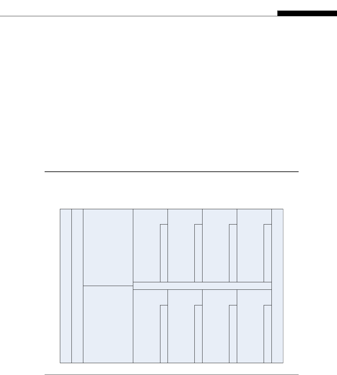
A modern processor typically runs at anything up to 4 GHz in speed. Modern DDR-3 memory, when
paired with say a standard Intel I7 device, can run at anything up to 2 GHz. However, the I7 has at least four
processors or cores in one device, or double that if you count its hyperthreading ability as a real processor.
A DDR-3 triple-channel memory setup on a I7 Nehalem system would produce the theoretical
bandwidth figures shown in Table 1.1. Depending on the motherboard, and exact memory pattern, the
actual bandwidth could be considerably less.
You run into the first problem with memory bandwidth when you consider the processor clock
speed. If you take a processor running at 4 GHz, you need to potentially fetch, every cycle, an
instruction (an operator) plus some data (an operand).
Each instruction is typically 32 bits, so if you execute nothing but a set of linear instructions, with no
data, on every core, you get 4.8 GB/s O4¼1.2 GB instructions per second. This assumes the processor
can dispatch one instruction per clock on average*. However, you typically also need to fetch and write
back data, which if we say is on a 1:1 ratio with instructions, means we effectively halve our throughput.
The ratio of clock speed to memory is an important limiter for both CPU and GPU throughput and
something we’ll look at later. We find when you look into it, most applications, with a few exceptions on
both CPU and GPU, are often memory bound and not processor cycle or processor clock/load bound.
CPU vendors try to solve this problem by using cache memory and burst memory access. This
exploits the principle of locality. It you look at a typical C program, you might see the following type of
operation in a function:
void some_function
{
int array[100];
int i ¼0;
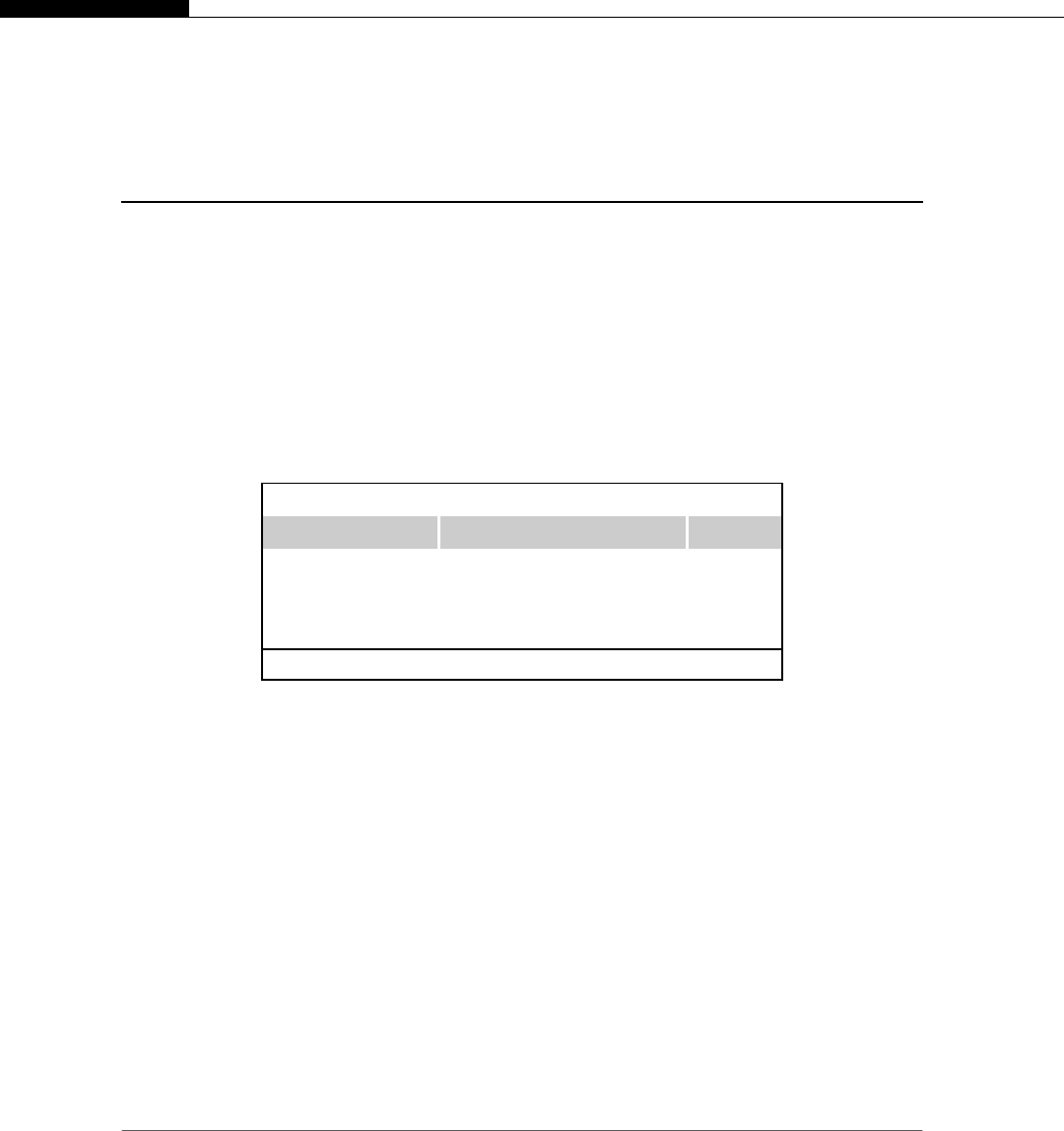
Table 1.1 Bandwidth on I7 Nehalem Processor
QPI Clock Theoretical Bandwidth Per Core
4.8 GT/s
(standard part)
19.2 GB/s 4.8 GB/s
6.4 GT/s
(extreme edition)
25.6 GB/s 6.4 GB/s
Note: QPI ¼Quick Path Interconnect.
*
The actual achieved dispatch rate can be higher or lower than one, which we use here for simplicity.
2 CHAPTER 1 A Short History of Supercomputing
for (i¼0; i<100; iþþ)
{
array[i] ¼i * 10;
}
}
If you look at how the processor would typically implement this, you would see the address of
array loaded into some memory access register. The parameter iwould be loaded into another
register. The loop exit condition, 100, is loaded into another register or possibly encoded into the
instruction stream as a literal value. The computer would then iterate around the same instructions,
over and over again 100 times. For each value calculated, we have control, memory, and calculation
instructions, fetched and executed.
This is clearly inefficient, as the computer is executing the same instructions, but with
different data values. Thus, the hardware designers implement into just about all processors
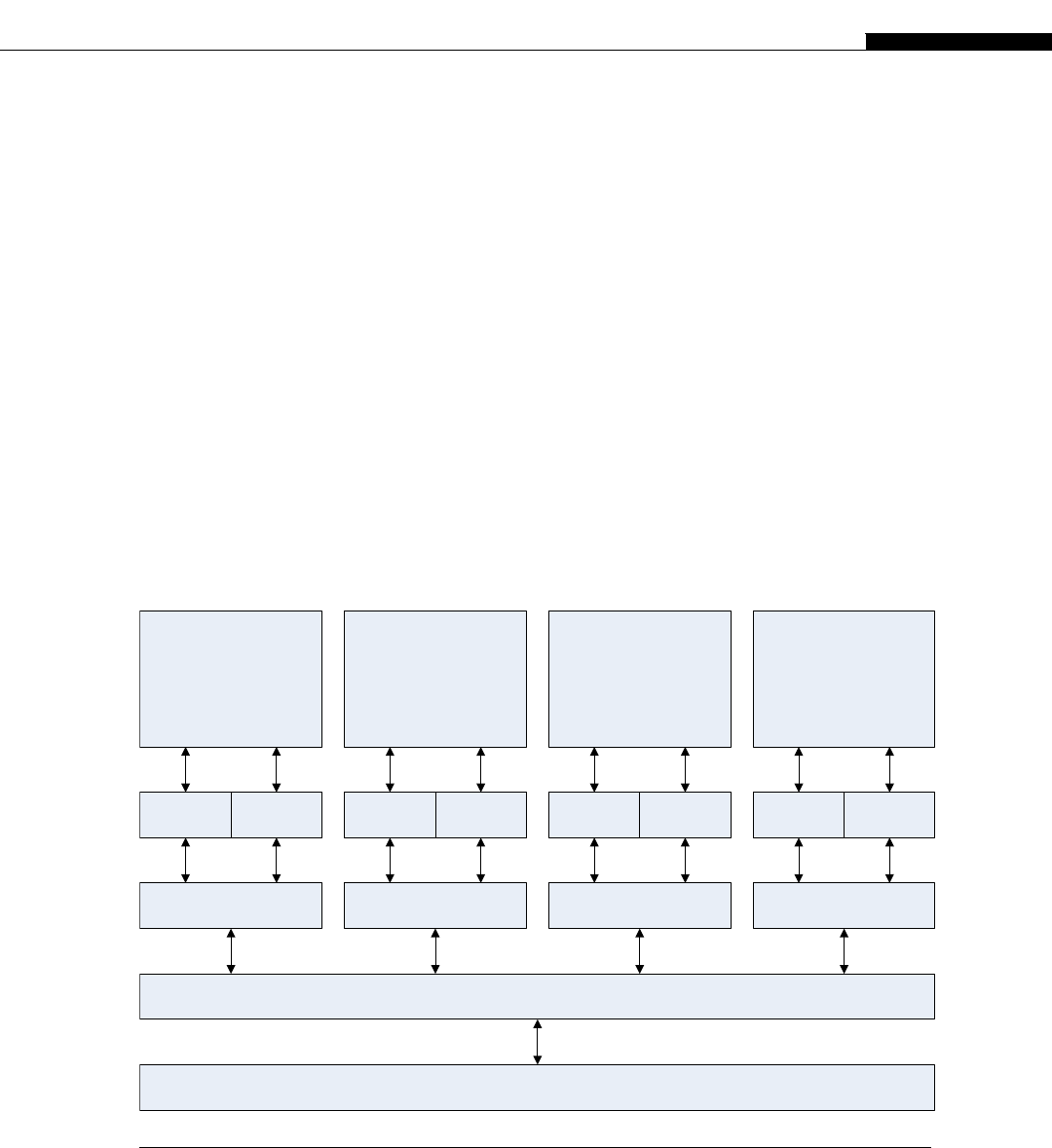
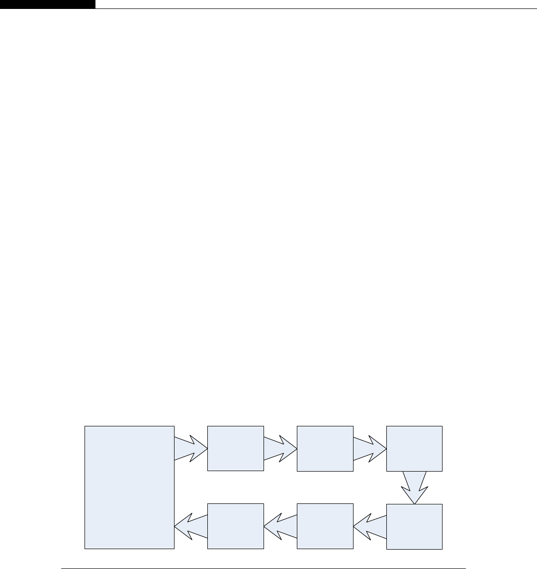
a small amount of cache, and in more complex processors, many levels of cache (Figure 1.1).
When the processor would fetch something from memory, the processor first queries the cache,
and if the data or instructions are present there, the high-speed cache provides them to the
processor.
DRAM
L3 Cache
L2 Cache
L1 Instruction L1 Data
Processor Core
L2 Cache
L1 Instruction L1 Data
Processor Core
L2 Cache
L1 Instruction L1 Data
Processor Core
L2 Cache
L1 Instruction L1 Data
Processor Core
FIGURE 1.1
Typical modern CPU cache organization.
Von Neumann Architecture 3
If the data is not in the first level (L1) cache, then a fetch from the second or third level (L2 or L3)
cache is required, or from the main memory if no cache line has this data already. The first level cache
typically runs at or near the processor clock speed, so for the execution of our loop, potentially we do
get near the full processor speed, assuming we write cache as well as read cache. However, there is
a cost for this: The size of the L1 cache is typically only 16 K or 32 K in size. The L2 cache is
somewhat slower, but much larger, typically around 256 K. The L3 cache is much larger, usually
several megabytes in size, but again much slower than the L2 cache.
With real-life examples, the loop iterations are much, much larger, maybe many megabytes in size.
Even if the program can remain in cache memory, the dataset usually cannot, so the processor, despite
all this cache trickery, is quite often limited by the memory throughput or bandwidth.
When the processor fetches an instruction or data item from the cache instead of the main memory,
it’s called a cache hit. The incremental benefit of using progressively larger caches drops off quite
rapidly. This in turn means the ever-larger caches we see on modern processors are a less and less
useful means to improve performance, unless they manage to encompass the entire dataset of the
problem.
The Intel I7-920 processor has some 8 MB of internal L3 cache. This cache memory is not free, and
if we look at the die for the Intel I7 processor, we see around 30% of the size of the chip is dedicated to
the L3 cache memory (Figure 1.2).
As cache sizes grow, so does the physical size of the silicon used to make the processors. The
larger the chip, the more expensive it is to manufacture and the higher the likelihood that it will
contain an error and be discarded during the manufacturing process. Sometimes these faulty devices
are sold cheaply as either triple- or dual-core devices, with the faulty cores disabled. However,
the effect of larger, progressively more inefficient caches ultimately results in higher costs to the
end user.
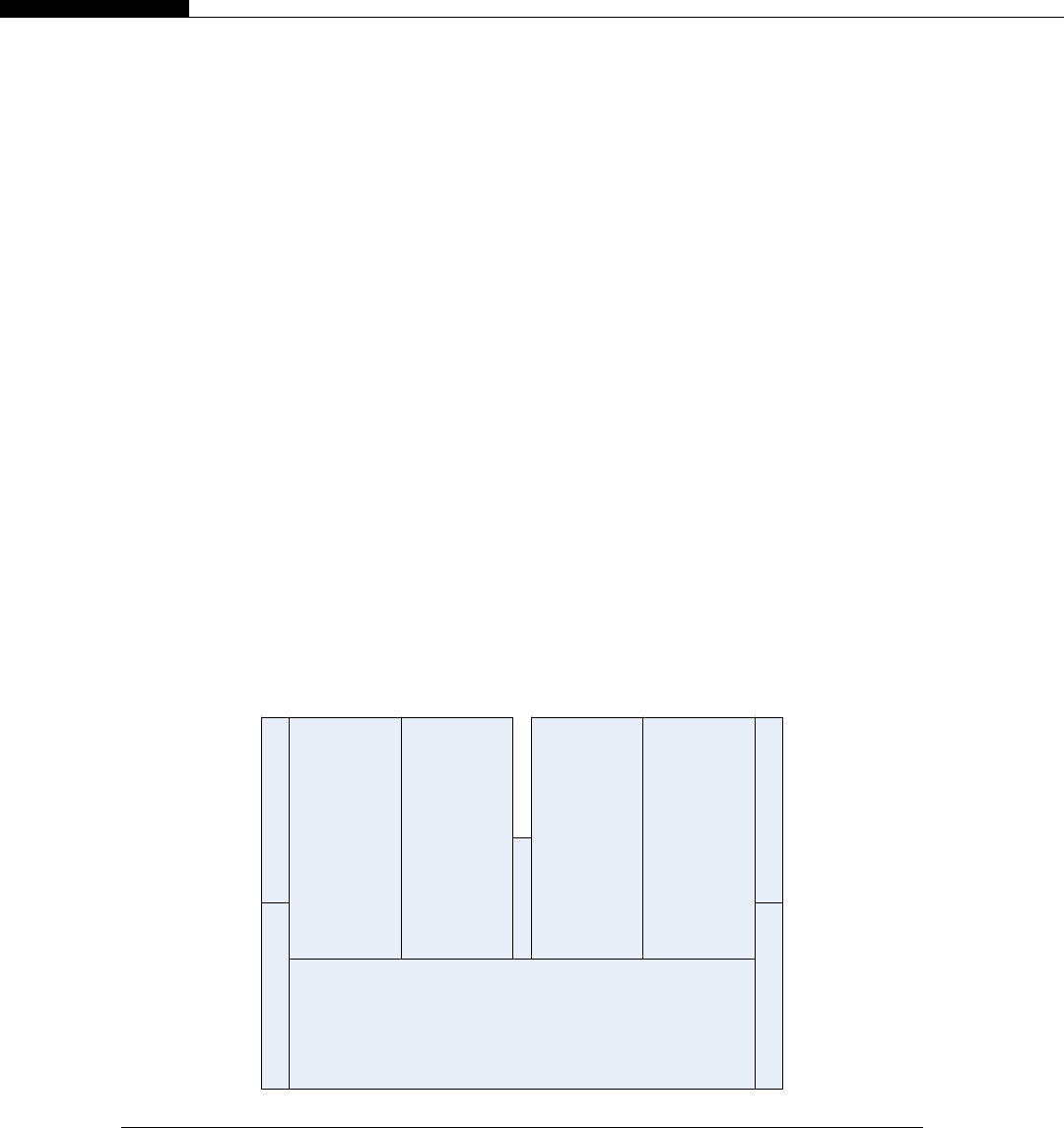
M
i
s
c
I
O
Core 1
Q
P
I
1Shared L3 Cache
Core 2 Core 4Core 3
Q
u
e
u
e
M
i
s
c
I
O
Q
P
I
2
FIGURE 1.2
Layout of I7 Nehalem processor on processor die.
4 CHAPTER 1 A Short History of Supercomputing
CRAY
The computing revolution that we all know today started back in the 1950s with the advent of the first
microprocessors. These devices, by today’s standards, are slow and you most likely have a far more
powerful processor in your smartphone. However, these led to the evolution of supercomputers, which are
machines usually owned by governments, large academic institutions, or corporations. They are thou-
sands of times more powerful than the computers in general use today. They cost millions of dollars to
produce, occupy huge amounts of space, usually have special cooling requirements, and require a team of
engineers to look after them. They consume huge amounts of power, to the extent they are often as
expensive to run each year as they cost to build. In fact, power is one of the key considerations when
planning such an installation and one of the main limiting factors in the growth of today’s supercomputers.
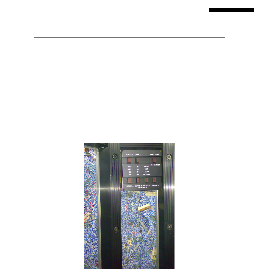
One of the founders of modern supercomputers was Seymour Cray with his Cray-1, produced by
Cray Research back in 1976. It had many thousands of individual cables required to connect every-
thing togetherdso much so they used to employ women because their hands were smaller than those
of most men and they could therefore more easily wire up all the thousands of individual cables.
These machines would typically have an uptime (the actual running time between breakdowns)
measured in hours. Keeping them running for a whole day at a time would be considered a huge
FIGURE 1.3
Wiring inside the Cray-2 supercomputer.
Cray 5

achievement. This seems quite backward by today’s standards. However, we owe a lot of what we have
today to research carried out by Seymour Cray and other individuals of this era.
Cray went on to produce some of the most groundbreaking supercomputers of his time under various
Cray names. The original Cray-1 cost some $8.8 million USD and achieved a massive 160 MFLOPS
(million floating-point operations per second). Computing speed today is measured in TFLOPS
(tera floating-point operations per second), a million times larger than the old MFLOPS measurement
(10
12
vs. 10
6
). A single Fermi GPU card today has a theoretical peak in excess of 1 teraflop of
performance.
The Cray-2 was a significant improvement on the Cray-1. It used a shared memory architecture,
split into banks. These were connected to one, two, or four processors. It led the way for the creation of
today’s server-based symmetrical multiprocessor (SMP) systems in which multiple CPUs shared the
same memory space. Like many machines of its era, it was a vector-based machine. In a vector
machine the same operation acts on many operands. These still exist today, in part as processor
extensions such as MMX, SSE, and AVX. GPU devices are, at their heart, vector processors that share
many similarities with the older supercomputer designs.
The Cray also had hardware support for scatter- and gather-type primitives, something we’ll see is
quite important in parallel computing and something we look at in subsequent chapters.
Cray still exists today in the supercomputer market, and as of 2010 held the top 500 position with
their Jaguar supercomputer at the Oak Ridge National Laboratory (http://www.nccs.gov/computing-
resources/jaguar/). I encourage you to read about the history of this great company, which you can
find on Cray’s website (http://www.cray.com), as it gives some insight into the evolution of computers
and as to where we are today.
CONNECTION MACHINE
Back in 1982 a corporation called Thinking Machines came up with a very interesting design, that of
the Connection Machine.
It was a relatively simple concept that led to a revolution in today’s parallel computers. They used
a few simple parts over and over again. They created a 16-core CPU, and then installed some 4096 of
these devices in one machine. The concept was different. Instead of one fast processor churning
through a dataset, there were 64 K processors doing this task.
Let’s take the simple example of manipulating the color of an RGB (red, green, blue) image. Each
color is made up of a single byte, with 3 bytes representing the color of a single pixel. Let’s suppose we
want to reduce the blue level to zero.
Let’s assume the memory is configured in three banks of red, blue, and green, rather than being
interleaved. With a conventional processor, we would have a loop running through the blue memory
and decrement every pixel color level by one. The operation is the same on each item of data, yet each
time we fetch, decode, and execute the instruction stream on each loop iteration.
The Connection Machine used something called SIMD (single instruction, multiple data), which is
used today in modern processors and known by names such as SSE (Streaming SIMD Extensions),
MMX (Multi-Media eXtension), and AVX (Advanced Vector eXtensions). The concept is to define
a data range and then have the processor apply that operation to the data range. However, SSE and
MMX are based on having one processor core. The Connection Machine had 64 K processor cores,
each executing SIMD instructions on its dataset.
6 CHAPTER 1 A Short History of Supercomputing
Processors such as the Intel I7 are 64-bit processors, meaning they can process up to 64 bits at
a time (8 bytes). The SSE SIMD instruction set extends this to 128 bits. With SIMD instructions on
such a processor, we eliminate all redundant instruction memory fetches, and generate one sixteenth of
the memory read and write cycles compared with fetching and writing 1 byte at a time. AVX extends
this to 256 bits, making it even more effective.
For a high-definition (HD) video image of 1920 1080 resolution, the data size is 2,073,600 bytes,
or around 2 MB per color plane. Thus, we generate around 260,000 SIMD cycles for a single
conventional processor using SSE/MMX. By SIMD cycle, we mean one read, compute, and write
cycle. The actual number of processor clocks may be considerably different than this, depending on the
particular processor architecture.
The Connection Machine used 64 K processors. Thus, the 2 MB frame would have resulted in about
32 SIMD cycles for each processor. Clearly, this type of approach is vastly superior to the modern
processor SIMD approach. However, there is of course a caveat. Synchronizing and communication
between processors becomes the major issue when moving from a rather coarse-threaded approach of
today’s CPUs to a hugely parallel approach used by such machines.
CELL PROCESSOR
Another interesting development in supercomputers stemmed from IBM’s invention of the Cell
processor (Figure 1.4). This worked on the idea of having a regular processor act as a supervisory
R
A
M
B
U
S
I
N
T
E
R
F
A
C
E
M
E
M
O
R
Y
C
O
N
T
R
O
L
L
E
R
L2 Cache
(512K)
Power PC Core
SPE
SPE
Interconnect Bus
SPE SPE SPE
SPE SPE SPE
I/O
C
O
N
T
R
O
L
L
E
R
L
O
C
A
L
M
E
M
O
R
Y
L
O
C
A
L
M
E
M
O
R
Y
L
O
C
A
L
M
E
M
O
R
Y
L
O
C
A
L
M
E
M
O
R
Y
L
O
C
A
L
M
E
M
O
R
Y
L
O
C
A
L
M
E
M
O
R
Y
L
O
C
A
L
M
E
M
O
R
Y
L
O
C
A
L
M
E
M
O
R
Y
FIGURE 1.4
IBM cell processor die layout (8 SPE version).
Cell Processor 7
processor, connected to a number of high-speed stream processors. The regular PowerPC (PPC)
processor in the Cell acts as an interface to the stream processors and the outside world. The
stream SIMD processors, or SPEs as IBM called them, would process datasets managed by the
regular processor.
The Cell is a particularly interesting processor for us, as it’s a similar design to what NVIDIA later
used in the G80 and subsequent GPUs. Sony also used it in their PS3 console machines in the games
industry, a very similar field to the main use of GPUs.
To program the Cell, you write a program to execute on the PowerPC core processor. It then
invokes a program, using an entirely different binary, on each of the stream processing elements
(SPEs). Each SPE is actually a core in itself. It can execute an independent program from its own local
memory, which is different from the SPE next to it. In addition, the SPEs can communicate with one
another and the PowerPC core over a shared interconnect. However, this type of hybrid architecture is
not easy to program. The programmer must explicitly manage the eight SPEs, both in terms of
programs and data, as well as the serial program running on the PowerPC core.
With the ability to talk directly to the coordinating processor, a series of simple steps can be
achieved. With our RGB example earlier, the PPC core fetches a chunk of data to work on. It allocates
these to the eight SPEs. As we do the same thing in each SPE, each SPE fetches the byte, decrements it,
and writes its bit back to its local memory. When all SPEs are done, the PC core fetches the data from
each SPE. It then writes its chunk of data (or tile) to the memory area where the whole image is being
assembled. The Cell processor is designed to be used in groups, thus repeating the design of the
Connection Machine we covered earlier.
The SPEs could also be ordered to perform a stream operation, involving multiple steps, as each
SPE is connected to a high-speed ring (Figure 1.5).
The problem with this sort of streaming or pipelining approach is it runs only as fast as the slowest
node. It mirrors a production line in a factory. The whole line can only run as fast as the slowest point.
Each SPE (worker) only has a small set of tasks to perform, so just like the assembly line worker, it can
do this very quickly and efficiently. However, just like any processor, there is a bandwidth limit and
overhead of passing data to the next stage. Thus, while you gain efficiencies from executing
a consistent program on each SPE, you lose on interprocessor communication and are ultimately
Power PC Core
SPE 0
(Clamp)
SPE 1
(DCT)
SPE 2
(Filter 1)
SPE 3
(Filter 2)
SPE 5
(Restore)
SPE 4
(IDCT)
FIGURE 1.5
Example routing stream processor routing on Cell.
8 CHAPTER 1 A Short History of Supercomputing

limited by the slowest process step. This is a common problem with any pipeline-based model of
execution.
The alternative approach of putting everything on one SPE and then having each SPE process a small
chunk of data is often a more efficient approach. This is the equivalent to training all assembly line
workers to assemble a complete widget. For simple tasks, this is easy, but each SPE has limits on available
program and data memory. The PowerPC core must now also deliver and collect data from eight SPEs,
instead of just two, so the management overhead and communication between host and SPEs increases.
IBM used a high-powered version of the Cell processor in their Roadrunner supercomputer,
which as of 2010 was the third fastest computer on the top 500 list. It consists of 12,960 PowerPC
cores, plus a total of 103,680 stream processors. Each PowerPC board is supervised by a dual-core
AMD (Advanced Micro Devices) Opteron processor, of which there are 6912 in total. The Opteron
processors act as coordinators among the nodes. Roadrunner has a theoretical throughput of 1.71
petaflops, cost $125 million USD to build, occupies 560 square meters, and consumes 2.35 MW of
electricity when operating!
MULTINODE COMPUTING
As you increase the requirements (CPU, memory, storage space) needed on a single machine, costs
rapidly increase. While a 2.6 GHz processor may cost you $250 USD, the same processor at 3.4 GHz
may be $1400 for less than a 1 GHz increase in clock speed. A similar relationship is seen for both
speed and size memory, and storage capacity.
Not only do costs scale as computing requirements scale, but so do the power requirements and the
consequential heat dissipation issues. Processors can hit 4–5 GHz, given sufficient supply of power and
cooling.
In computing you often find the law of diminishing returns. There is only so much you can put into
a single case. You are limited by cost, space, power, and heat. The solution is to select a reasonable
balance of each and to replicate this many times.
Cluster computing became popular in 1990s along with ever-increasing clock rates. The concept
was a very simple one. Take a number of commodity PCs bought or made from off-the-shelf parts and
connect them to an off-the-shelf 8-, 16-, 24-, or 32-port Ethernet switch and you had up to 32 times the
performance of a single box. Instead of paying $1600 for a high performance processor, you paid $250
and bought six medium performance processors. If your application needed huge memory capacity, the
chances were that maxing out the DIMMs on many machines and adding them together was more than
sufficient. Used together, the combined power of many machines hugely outperformed any single
machine you could possible buy with a similar budget.
All of a sudden universities, schools, offices, and computer departments could build machines
much more powerful than before and were not locked out of the high-speed computing market due to
lack of funds. Cluster computing back then was like GPU computing todayda disruptive technology
that changed the face of computing. Combined with the ever-increasing single-core clock speeds it
provided a cheap way to achieve parallel processing within single-core CPUs.
Clusters of PCs typically ran a variation of LINUX with each node usually fetching its boot
instructions and operating system (OS) from a central master node. For example, at CudaDeveloper we
have a tiny cluster of low-powered, atom-based PCs with embedded CUDA GPUs. It’s very cheap to
Multinode Computing 9
buy and set up a cluster. Sometimes they can simply be made from a number of old PCs that are being
replaced, so the hardware is effectively free.
However, the problem with cluster computing is it’s only as fast as the amount of internode
communication that is necessary for the problem. If you have 32 nodes and the problem breaks down into
32 nice chunks and requires no internode communication, you have an application that is ideal for
a cluster. If every data point takes data from every node, you have a terrible problem to put into a cluster.
Clusters are seen inside modern CPUs and GPUs. Look back at Figure 1.1, the CPU cache hier-
archy. If we consider each CPU core as a node, the L2 cache as DRAM (Dynamic Random Access
Memory), the L3 cache as the network switch, and the DRAM as mass storage, we have a cluster in
miniature (Figure 1.6).
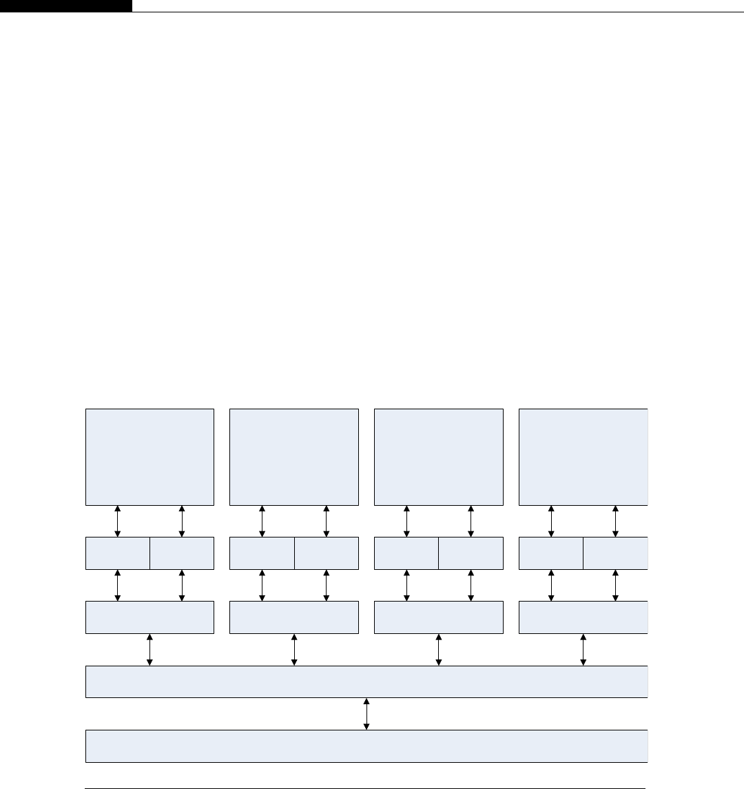
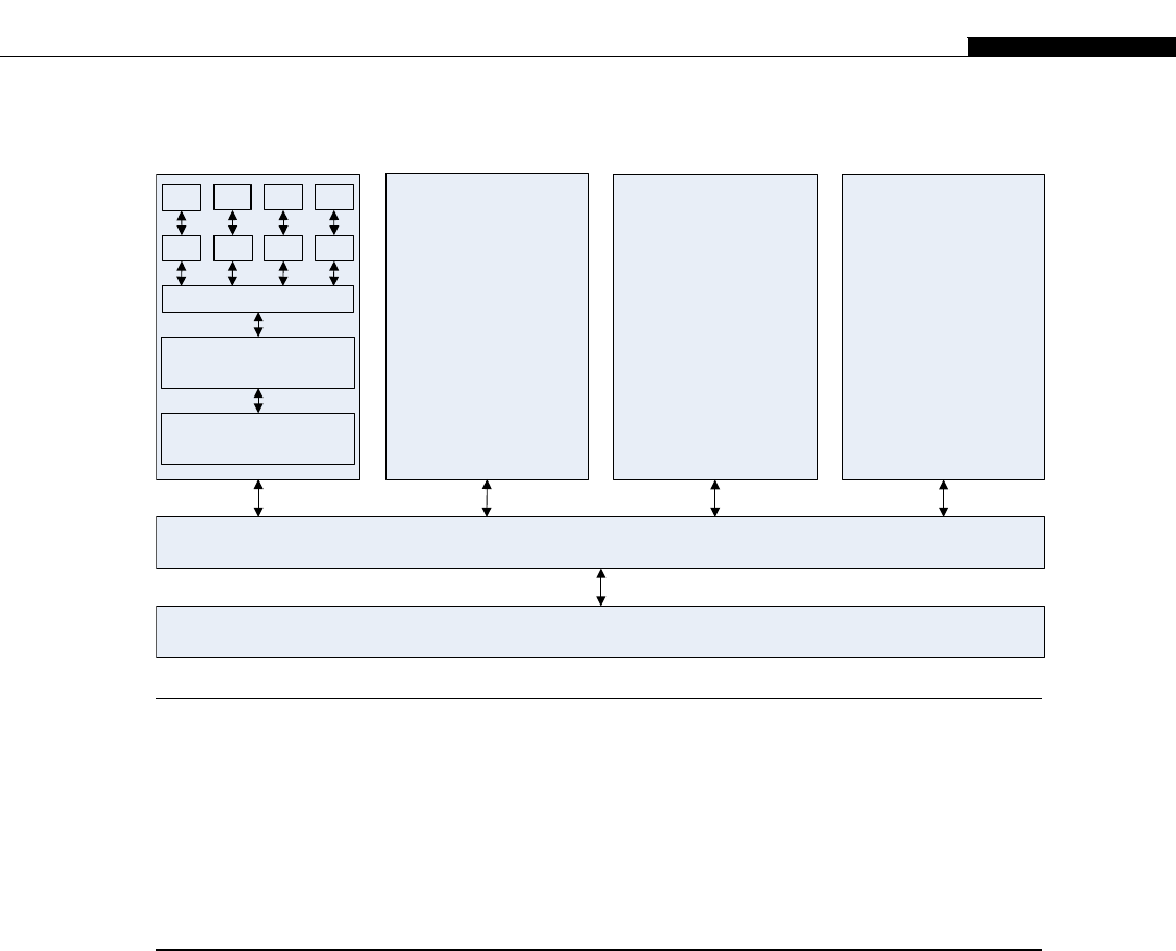
The architecture inside a modern GPU is really no different. You have a number of streaming
multiprocessors (SMs) that are akin to CPU cores. These are connected to a shared memory/L1
cache. This is connected to an L2 cache that acts as an inter-SM switch. Data can be held in global
memory storage where it’s then extracted and used by the host, or sent via the PCI-E switch directly
to the memory on another GPU. The PCI-E switch is many times faster than any network’s
interconnect.
The node may itself be replicated many times, as shown in Figure 1.7. This replication within
a controlled environment forms a cluster. One evolution of the cluster designs are distributed
Network Storage
Network Switch
Network Interface
DRAM Local
Storage
Processor Node
Network Interface
DRAM Local
Storage
Processor Node
Network Interface
DRAM Local
Storage
Processor Node
Network Interface
DRAM Local
Storage
Processor Node
FIGURE 1.6
Typical cluster layout.
10 CHAPTER 1 A Short History of Supercomputing
applications. Distributed applications run on many nodes, each of which may contain many processing
elements including GPUs. Distributed applications may, but do not need to, run in a controlled
environment of a managed cluster. They can connect arbitrary machines together to work on some
common problem, BOINC and Folding@Home being two of the largest examples of such applications
that connect machines together over the Internet.
THE EARLY DAYS OF GPGPU CODING
Graphics processing units (GPUs) are devices present in most modern PCs. They provide a number of
basic operations to the CPU, such as rendering an image in memory and then displaying that image
onto the screen. A GPU will typically process a complex set of polygons, a map of the scene to be
rendered. It then applies textures to the polygons and then performs shading and lighting calculations.
The NVIDIA 5000 series cards brought for the first time photorealistic effects, such as shown in the
Dawn Fairy demo from 2003.
Have a look at http://www.nvidia.com/object/cool_stuff.html#/demos anddownloadsomeof
the older demos and you’ll see just how much GPUs have evolved over the past decade. See
Table 1.2.
One of the important steps was the development of programmable shaders. These were effectively
little programs that the GPU ran to calculate different effects. No longer was the rendering fixed in the
GPU; through downloadable shaders, it could be manipulated. This was the first evolution of general-
Host Memory / CPU
PCI-E Switch
PCI-E Interface
GMEM
SM
GPU
L1
L2 Cache
SM SM SM
L1 L1 L1
GPU GPU
FIGURE 1.7
GPUs compared to a cluster.
The Early Days of GPGPU Coding 11

purpose graphical processor unit (GPGPU) programming, in that the design had taken its first steps in
moving away from fixed function units.
However, these shaders were operations that by their very nature took a set of 3D points that
represented a polygon map. The shaders applied the same operation to many such datasets, in a hugely
parallel manner, giving huge throughput of computing power.
Now although polygons are sets of three points, and some other datasets such as RGB photos can be
represented by sets of three points, a lot of datasets are not. A few brave researchers made use of GPU
technology to try and speed up general-purpose computing. This led to the development of a number of
initiatives (e.g., BrookGPU, Cg, CTM, etc.), all of which were aimed at making the GPU a real
programmable device in the same way as the CPU. Unfortunately, each had its own advantages and
problems. None were particularly easy to learn or program in and were never taught to people in large
numbers. In short, there was never a critical mass of programmers or a critical mass of interest from
programmers in this hard-to-learn technology. They never succeeded in hitting the mass market,
something CUDA has for the first time managed to do, and at the same time provided programmers
with a truly general-purpose language for GPUs.
THE DEATH OF THE SINGLE-CORE SOLUTION
One of the problems with today’s modern processors is they have hit a clock rate limit at around 4 GHz.
At this point they just generate too much heat for the current technology and require special and
expensive cooling solutions. This is because as we increase the clock rate, the power consumption
rises. In fact, the power consumption of a CPU, if you fix the voltage, is approximately the cube of its
clock rate. To make this worse, as you increase the heat generated by the CPU, for the same clock rate,
the power consumption also increases due to the properties of the silicon. This conversion of power
into heat is a complete waste of energy. This increasingly inefficient use of power eventually means
you are unable to either power or cool the processor sufficiently and you reach the thermal limits of the
device or its housing, the so-called power wall.
Faced with not being able to increase the clock rate, making forever-faster processors, the processor
manufacturers had to come up with another game plan. The two main PC processor manufacturers, Intel
Table 1.2 GPU Technology Demonstrated over the Years
Demo Card Year
Dawn GeForce FX 2003
Dusk Ultra GeForce FX 2003
Nalu GeForce 6 2004
Luna GeForce 7 2005
Froggy GeForce 8 2006
Human Head GeForce 8 2007
Medusa GeForce 200 2008
Supersonic Sled GeForce 400 2010
A New Dawn GeForce 600 2012
12 CHAPTER 1 A Short History of Supercomputing

and AMD, have had to adopt a different approach. They have been forced down the route of adding more
cores to processors, rather than continuously trying to increase CPU clock rates and/or extract more
instructions per clock through instruction-level parallelism. We have dual, tri, quad, hex, 8, 12, and soon
even 16 and 32 cores and so on. This is the future of where computing is now going for everyone, the
GPU and CPU communities. The Fermi GPU is effectively already a 16-core device in CPU terms.
There is a big problem with this approachdit requires programmers to switch from their traditional
serial, single-thread approach, to dealing with multiple threads all executing at once. Now the
programmer has to think about two, four, six, or eight program threads and how they interact and
communicate with one another. When dual-core CPUs arrived, it was fairly easy, in that there were
usually some background tasks being done that could be offloaded onto a second core. When quad-
core CPUs arrived, not many programs were changed to support it. They just carried on being sold as
single-thread applications. Even the games industry didn’t really move to quad-core programming
very quickly, which is the one industry you’d expect to want to get the absolute most out of today’s
technology.
In some ways the processor manufacturers are to blame for this, because the single-core application
runs just fine on one-quarter of the quad-core device. Some devices even increase the clock rate
dynamically when only one core is active, encouraging programmers to be lazy and not make use of
the available hardware.
There are economic reasons too. The software development companies need to get the product to
market as soon as possible. Developing a better quad-core solution is all well and good, but not if the
market is being grabbed by a competitor who got there first. As manufacturers still continue to make
single- and dual-core devices, the market naturally settles on the lowest configuration, with the widest
scope for sales. Until the time that quad-core CPUs are the minimum produced, market forces work
against the move to multicore programming in the CPU market.
NVIDIA AND CUDA
If you look at the relative computational power in GPUs and CPUs, we get an interesting graph
(Figure 1.8). We start to see a divergence of CPU and GPU computational power until 2009 when we
see the GPU finally break the 1000 gigaflops or 1 teraflop barrier. At this point we were moving from
the G80 hardware to the G200 and then in 2010 to the Fermi evolution. This is driven by the intro-
duction of massively parallel hardware. The G80 is a 128 CUDA core device, the G200 is a 256 CUDA
core device, and the Fermi is a 512 CUDA core device.
We see NVIDIA GPUs make a leap of 300 gigaflops from the G200 architecture to the Fermi
architecture, nearly a 30% improvement in throughput. By comparison, Intel’s leap from their core 2
architecture to the Nehalem architecture sees only a minor improvement. Only with the change to
Sandy Bridge architecture do we see significant leaps in CPU performance. This is not to say one is
better than the other, for the traditional CPUs are aimed at serial code execution and are extremely
good at it. They contain special hardware such as branch prediction units, multiple caches, etc., all of
which target serial code execution. The GPUs are not designed for this serial execution flow and only
achieve their peak performance when fully utilized in a parallel manner.
In 2007, NVIDIA saw an opportunity to bring GPUs into the mainstream by adding an easy-to-use
programming interface, which it dubbed CUDA, or Compute Unified Device Architecture. This
NVIDIA and CUDA 13
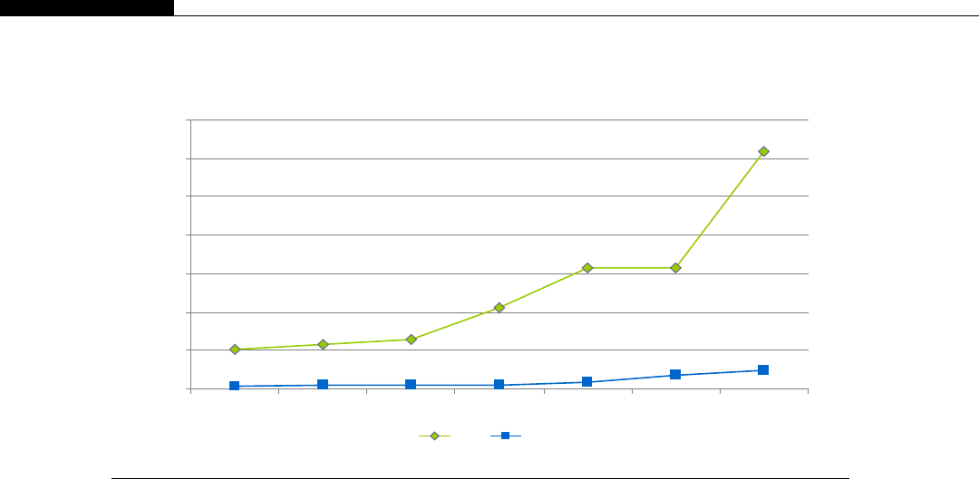
opened up the possibility to program GPUs without having to learn complex shader languages, or to
think only in terms of graphics primitives.
CUDA is an extension to the C language that allows GPU code to be written in regular C. The code
is either targeted for the host processor (the CPU) or targeted at the device processor (the GPU). The
host processor spawns multithread tasks (or kernels as they are known in CUDA) onto the GPU device.
The GPU has its own internal scheduler that will then allocate the kernels to whatever GPU hardware is
present. We’ll cover scheduling in detail later. Provided there is enough parallelism in the task, as the
number of SMs in the GPU grows, so should the speed of the program.
However, herein hides a big problem. You have to ask what percentage of the code can be run in
parallel. The maximum speedup possible is limited by the amount of serial code. If you have an infinite
amount of processing power and could do the parallel tasks in zero time, you would still be left with the
time from the serial code part. Therefore, we have to consider at the outset if we can indeed parallelize
a significant amount of the workload.
NVIDIA is committed to providing support to CUDA. Considerable information, examples, and
tools to help with development are available from its website at http://www.nvidia.com under CudaZone.
CUDA, unlike its predecessors, has now actually started to gain momentum and for the first time it
looks like there will be a programming language that will emerge as the one of choice for GPU
programming. Given that the number of CUDA-enabled GPUs now number in the millions, there is
a huge market out there waiting for CUDA-enabled applications.
There are currently many CUDA-enabled applications and the list grows monthly. NVIDIA showcases
many of these on its community website at http://www.nvidia.com/object/cuda_apps_flash_new.html.
In areas where programs have to do a lot of computational workdfor example, making a DVD
from your home movies (video transcoding)dwe see most mainstream video packages now sup-
porting CUDA. The average speedup is 5 to 10 times in this domain.
518 576 648
1062
1581 1581
3090
42.6 51.2 55 58 86 187 243
0
500
1000
1500
2000
2500
3000
3500
2006 2007 2008 2009 2010 2011 2012
GPU CPU
FIGURE 1.8
CPU and GPU peak performance in gigaflops.
14 CHAPTER 1 A Short History of Supercomputing

Along with the introduction of CUDA came the Tesla series of cards. These cards are not graphics
cards, and in fact they have no DVI or VGA connectors on them. They are dedicated compute cards
aimed at scientific computing. Here we see huge speedups in scientific calculations. These cards can
either be installed in a regular desktop PC or in dedicated server racks. NVIDIA provides such
a system at http://www.nvidia.com/object/preconfigured_clusters.html, which claims to provide up to
30 times the power of a conventional cluster. CUDA and GPUs are reshaping the world of high-
performance computing.
GPU HARDWARE
The NVIDIA G80 series processor and beyond implemented a design that is similar to both the
Connection Machine and IBM’s Cell processor. Each graphics card consists of a number of SMs. To
each SM is attached eight or more SPs (Stream Processors). The original 9800 GTX card has eight
SMs, giving a total of 128 SPs. However, unlike the Roadrunner, each GPU board can be purchased
for a few hundred USD and it doesn’t take 2.35 MW to power it. Power considerations are not to be
overlooked, as we’ll discuss later when we talk about building GPU servers.
The GPU cards can broadly be considered as accelerator or coprocessor cards. A GPU card, currently,
must operate in conjunction with a CPU-based host. In this regard it follows very much the approach of
the Cell processor with the regular serial core and N SIMD SPE cores. Each GPU device contains a set of
SMs, each of which contain a set of SPs or CUDA cores. The SPs execute work as parallel sets of up to
32 units. They eliminate a lot of the complex circuitry needed on CPUs to achieve high-speed serial
execution through instruction-level parallelism. They replace this with a programmer-specified explicit
parallelism model, allowing more compute capacity to be squeezed onto the same area of silicon.
The overall throughput of GPUs is largely determined by the number of SPs present, the bandwidth
to the global memory, and how well the programmer makes use of the parallel architecture he or she is
working with. See Table 1.3 for a listing of current NVIDIA GPU cards.
Which board is correct for a given application is a balance between memory and GPU processing
power needed for a given application. Note the 9800 GX2, 295, 590, 690, and K10 cards are actually
dual cards, so to make full use of these they need to be programmed as two devices not one. The one
caveat GPU here is that the figures quoted are for single-precision (32-bit) floating-point performance,
not double-precision (64-bit) precision. Also be careful with the GF100 (Fermi) series, as the Tesla
variant has double the number of double-precision units found in the standard desktop units, so
achieves significantly better double-precision throughput. The Kepler K 20, yet to be released, will
also have significant double precision performance over and above its already released K10 cousin.
Note also, although not shown here, as the generations have evolved, the power consumption, clock
for clock, per SM has come down. However, the overall power consumption has increased consid-
erably and this is one of the key considerations in any multi-GPU-based solution. Typically, we see
dual-GPU-based cards (9800 GX2, 295, 590, 690) having marginally lower power consumption
figures than the equivalent two single cards due to the use of shared circuitry and/or reduced clock
frequencies.
NVIDIA provides various racks (the M series computing modules) containing two to four Tesla cards
connected on a shared PCI-E bus for high-density computing. It’s quite possible to build your own GPU
cluster or microsupercomputer from standard PC parts, and we show you how to do this later in the book.
GPU Hardware 15

The great thing about CUDA is that, despite all the variability in hardware, programs written for the
original CUDA devices can run on today’s CUDA devices. The CUDA compilation model applies the
same principle as used in Javadruntime compilation of a virtual instruction set. This allows modern
GPUs to execute code from even the oldest generation GPUs. In many cases they benefit significantly
from the original programmer reworking the program for the features of the newer GPUs. In fact, there
is considerable scope for tuning for the various hardware revisions, which we’ll cover toward the end
of the book.
ALTERNATIVES TO CUDA
OpenCL
So what of the other GPU manufacturers, ATI (now AMD) being the prime example? AMD’s product
range is as impressive as the NVIDIA range in terms of raw computer power. However, AMD brought
Table 1.3 Current Series of NVIDIA GPU Cards
GPU
Series Device
Number of
SPs
Max
Memory
GFlops
(FMAD)
Bandwidth
(GB/s)
Power
(Watts)
9800 GT G92 96 2GB 504 57 125
9800 GTX G92 128 2GB 648 70 140
9800 GX2 G92 256 1GB 1152 2 x 64 197
260 G200 216 2GB 804 110 182
285 G200 240 2GB 1062 159 204
295 G200 480 1.8GB 1788 2 x 110 289
470 GF100 448 1.2GB 1088 134 215
480 GF100 448 1.5GB 1344 177 250
580 GF110 512 1.5GB 1581 152 244
590 GF110 1024 3GB 2488 2 x 164 365
680 GK104 1536 2GB 3090 192 195
690 GK104 3072 4GB 5620 2 x 192 300
Tesla
C870
G80 128 1.5GB 518 77 171
Tesla
C1060
G200 240 4GB 933 102 188
Tesla
C2070
GF100 448 6GB 1288 144 247
Tesla K10 GK104 3072 8GB 5184 2 x 160 250
16 CHAPTER 1 A Short History of Supercomputing

its stream computing technology to the marketplace a long time after NVIDIA brought out CUDA. As
a consequence, NVIDA has far more applications available for CUDA than AMD/ATI does for its
competing stream technology.
OpenCL and Direct compute is not something we’ll cover in this book, but they deserve a mention
in terms of alternatives to CUDA. CUDA is currently only officially executable on NVIDIA hardware.
While NVIDIA has a sizeable chunk of the GPU market, its competitors also hold a sizeable chunk. As
developers, we want to develop products for as large a market as possible, especially if we’re talking
about the consumer market. As such, people should be aware there are alternatives to CUDA, which
support both NVIDIA’s and others’ hardware.
OpenCL is an open and royalty-free standard supported by NVIDIA, AMD, and others. The
OpenCL trademark is owned by Apple. It sets out an open standard that allows the use of compute
devices. A compute device can be a GPU, CPU, or other specialist device for which an OpenCL driver
exists. As of 2012, OpenCL supports all major brands of GPU devices, including CPUs with at least
SSE3 support.
Anyone who is familiar with CUDA can pick up OpenCL relatively easily, as the fundamental
concepts are quite similar. However, OpenCL is somewhat more complex to use than CUDA, in that much
of the work the CUDA runtime API does for the programmer needs to be explicitly performed in OpenCL.
You can read more about OpenCL at http://www.khronos.org/opencl/. There are also now a number
of books written on OpenCL. I’d personally recommend learning CUDA prior to OpenCL as CUDA is
somewhat of a higher-level language extension than OpenCL.
DirectCompute
DirectCompute is Microsoft’s alternative to CUDA and OpenCL. It is a proprietary product linked to
the Windows operating system, and in particular, the DirectX 11 API. The DirectX API was a huge
leap forward for any of those who remember programming video cards before it. It meant the
developers had to learn only one library API to program all graphics cards, rather than write or license
drivers for each major video card manufacturer.
DirectX 11 is the latest standard and supported under Windows 7. With Microsoft’s name behind
the standard, you might expect to see some quite rapid adoption among the developer community. This
is especially the case with developers already familiar with DirectX APIs. If you are familiar with
CUDA and DirectCompute, then it is quite an easy task to port a CUDA application over to Direct-
Compute. According to Microsoft, this is something you can typically do in an afternoon’s work if you
are familiar with both systems. However, being Windows centric, we’ll exclude DirectCompute from
many high-end systems where the various flavors of UNIX dominate.
Microsoft are also set to launch Cþþ AMP, an additional set of standard template libraries (STLs),
which may appeal more to programmers already familiar with Cþþ-style STLs.
CPU alternatives
The main parallel processing languages extensions are MPI, OpenMP, and pthreads if you are
developing for Linux. For Windows there is the Windows threading model and OpenMP. MPI and
pthreads are supported as various ports from the Unix world.
Alternatives to CUDA 17

MPI (Message Passing Interface) is perhaps the most widely known messaging interface. It is
process-based and generally found in large computing labs. It requires an administrator to
configure the installation correctly and is best suited to controlled environments. Parallelism is
expressed by spawning hundreds of processes over a cluster of nodes and explicitly exchanging
messages, typically over high-speed network-based communication links (Ethernet or
InfiniBand). MPI is widely used and taught. It’s a good solution within a controlled cluster
environment.
OpenMP (Open Multi-Processing) is a system designed for parallelism within a node or
computer system. It works entirely differently, in that the programmer specifies various
parallel directives through compiler pragmas. The compiler then attempts to automatically
split the problem into Nparts, according to the number of available processor cores. OpenMP
support is built into many compilers, including the NVCC compiler used for CUDA. OpenMP
tends to hit problems with scaling due to the underlying CPU architecture. Often the memory
bandwidth in the CPU is just not large enough for all the cores continuously streaming data to
or from memory.
Pthreads is a library that is used significantly for multithread applications on Linux. As with
OpenMP, pthreads uses threads and not processes as it is designed for parallelism within
a single node. However, unlike OpenMP, the programmer is responsible for thread management
and synchronization. This provides more flexibility and consequently better performance for
well-written programs.
ZeroMQ (0MQ) is also something that deserves a mention. This is a simple library that you link to,
and we will use it later in the book for developing a multinode, multi-GPU example. ZeroMQ
supports thread-, process-, and network-based communications models with a single cross-
platform API. It is also available on both Linux and Windows platforms. It’s designed for
distributed computing, so the connections are dynamic and nodes fail gracefully.
Hadoop is also something that you may consider. Hadoop is an open-source version of Google’s
MapReduce framework. It’s aimed primarily at the Linux platform. The concept is that you take
a huge dataset and break (or map) it into a number of chunks. However, instead of sending the
data to the node, the dataset is already split over hundreds or thousands of nodes using a parallel
file system. Thus, the program, the reduce step, is instead sent to the node that contains the data.
The output is written to the local node and remains there. Subsequent MapReduce programs take
the previous output and again transform it in some way. As data is in fact mirrored to multiple
nodes, this allows for a highly fault-tolerant as well as high-throughput system.
Directives and libraries
There are a number of compiler vendors, PGI, CAPS, and Cray being the most well-known, that
support the recently announced OpenACC set of compiler directives for GPUs. These, in essence,
replicate the approach of OpenMP, in that the programmer inserts a number of compiler directives
marking regions as “to be executed on the GPU.” The compiler then does the grunt work of moving
data to or from the GPU, invoking kernels, etc.
As with the use of pthreads over OpenMP, with the lower level of control pthreads provides, you
can achieve higher performance. The same is true of CUDA versus OpenACC. This extra level of
control comes with a much higher level of required programming knowledge, a higher risk of errors,
18 CHAPTER 1 A Short History of Supercomputing

and the consequential time impact that may have on a development schedule. Currently, OpenACC
requires directives to specify what areas of code should be run on the GPU, but also in which type of
memory data should exist. NVIDIA claims you can get in the order of 5-plus speedup using such
directives. It’s a good solution for those programmers who need to get something working quickly. It’s
also great for those people for whom programming is a secondary consideration who just want the
answer to their problem in a reasonable timeframe.
The use of libraries is also another key area where you can obtain some serious productivity gains,
as well as execution time speedups. Libraries like SDK provide Thrust, which provides common
functions implemented in a very efficient way. Libraries like CUBLAS are some of the best around for
linear algebra. Libraries exist for many well-known applications such as Matlab and Mathematica.
Language bindings exist for Python, Perl, Java, and many others. CUDA can even be integrated with
Excel.
As with many aspects of software development in the modern age, the chances are that someone
has done what you are about to develop already. Search the Internet and see what is already there
before you spend weeks developing a library that, unless you are a CUDA expert, is unlikely to be
faster than one that is already available.
CONCLUSION
So maybe you’re thinking, why develop in CUDA? The answer is that CUDA is currently the easiest
language to develop in, in terms of support, debugging tools, and drivers. CUDA has a head start on
everything else and has a huge lead in terms of maturity. If your application needs to support hardware
other than NVIDIA’s, then the best route currently is to develop under CUDA and then port the
application to one of the other APIs. As such, we’ll concentrate on CUDA, for if you become an expert
with CUDA, it’s easy to pick up alternative APIs should you need to. Understanding how CUDAworks
will allow you to better exploit and understand the limitations of any higher-level API.
The journey from a single-thread CPU programmer to a fully fledged parallel programmer on
GPUs is one that I hope you will find interesting. Even if you never program a GPU in the future, the
insight you gain will be of tremendous help in allowing you to design multithread programs. If you,
like us, see the world changing to a parallel programming model, you’ll want to be at the forefront of
that wave of innovation and technological challenge. The single-thread industry is one that is slowly
moving to obsolescence. To be a valuable asset and an employable individual, you need to have skills
that reflect where the computing world is headed to, not those that are becoming progressively
obsolete.
GPUs are changing the face of computing. All of a sudden the computing power of supercomputers
from a decade ago can be slotted under your desk. No longer must you wait in a queue to submit work
batches and wait months for a committee to approve your request to use limited computer resources at
overstretched computing installations. You can go out, spend up to 5000–10,000 USD, and have
a supercomputer on your desk, or a development machine that runs CUDA for a fraction of that. GPUs
are a disruptive technological change that will make supercomputer-like levels of performance
available for everyone.
Conclusion 19
This page intentionally left blank

Understanding Parallelism
with GPUs 2
INTRODUCTION
This chapter aims to provide a broad introduction to the concepts of parallel programming and
how these relate to GPU technology. It’s primarily aimed at those people reading this text with
a background in serial programming, but a lack of familiarity with parallel processing concepts. We
look at these concepts in the primary context of GPUs.
TRADITIONAL SERIAL CODE
A significant number of programmers graduated when serial programs dominated the landscape
and parallel programming attracted just a handful of enthusiasts. Most people who go to
university get a degree related to IT because they are interested in technology. However, they also
appreciate they need to have a job or career that pays a reasonable salary. Thus, in specializing, at
least some consideration is given to the likely availability of positions after university. With the
exception of research or academic posts, the number of commercial roles in parallel programming
has always been, at best, small. Most programmers developed applications in a simple serial
fashion based broadly on how universities taught them to program, which in turn was driven by
market demand.
The landscape of parallel programming is scattered, with many technologies and languages that
never quite made it to the mainstream. There was never really the large-scale market need for parallel
hardware and, as a consequence, significant numbers of parallel programmers. Every year or two the
various CPU vendors would bring out a new processor generation that executed code faster than the
previous generation, thereby perpetuating serial code.
Parallel programs by comparison were often linked closely to the hardware. Their goal was to
achieve faster performance and often that was at the cost of portability. Feature X was implemented
differently, or was not available in the next generation of parallel hardware. Periodically a revolu-
tionary new architecture would appear that required a complete rewrite of all code. If your
knowledge as a programmer was centered around processor X, it was valuable in the marketplace
only so long as processor X was in use. Therefore, it made a lot more commercial sense to learn to
program x86-type architecture than some exotic parallel architecture that would only be around for
a few years.
CHAPTER
CUDA Programming. http://dx.doi.org/10.1016/B978-0-12-415933-4.00002-8
Copyright Ó2013 Elsevier Inc. All rights reserved.
21

However, over this time, a couple of standards did evolve that we still have today. The OpenMP
standard addresses parallelism within a single node and is designed for shared memory machines that
contain multicore processors. It does not have any concept of anything outside a single node or box.
Thus, you are limited to problems that fit within a single box in terms of processing power, memory
capacity, and storage space. Programming, however, is relatively easy as most of the low-level
threading code (otherwise written using Windows threads or POSIX threads) is taken care of for you by
OpenMP.
The MPI (Message Passing Interface) standard addresses parallelism between nodes and is aimed
at clusters of machines within well-defined networks. It is often used in supercomputer installations
where there may be many thousands of individual nodes. Each node holds a small section of the
problem. Thus, common resources (CPU, cache, memory, storage, etc.) are multiplied by the number
of nodes in the network. The Achilles’ heel of any network is the various interconnects, the parts that
connect the networked machines together. Internode communication is usually the dominating factor
determining the maximum speed in any cluster-based solution.
Both OpenMP and MPI can be used together to exploit parallelism within nodes as well as across
a network of machines. However, the APIs and the approaches used are entirely different, meaning
they are often not used together. The OpenMP directives allow the programmer to take a high-level
view of parallelism via specifying parallel regions. MPI by contrast uses an explicit interprocess
communication model making the programmer do a lot more work.
Having invested the time to become familiar with one API, programmers are often loathe to
learn another. Thus, problems that fit within one computer are often implemented with OpenMP
solutions, whereas really large problems are implemented with cluster-based solutions such as
MPI.
CUDA, the GPU programming language we’ll explore in this text, can be used in conjunction
with both OpenMP and MPI. There is also an OpenMP-like directive version of CUDA (OpenACC)
that may be somewhat easier for those familiar with OpenMP to pick up. OpenMP, MPI, and
CUDA are increasingly taught at undergraduate and graduate levels in many university computer
courses.
However, the first experience most serial programmers had with parallel programming was the
introduction of multicore CPUs. These, like the parallel environments before them, were largely
ignored by all but a few enthusiasts. The primary use of multicore CPUs was for OS-based parallelism.
This is a model based on task parallelism that we’ll look at a little later.
As it became obvious that technology was marching toward the multicore route, more and more
programmers started to take notice of the multicore era. Almost all desktops ship today with either
a dual- or quad-core processor. Thus, programmers started using threads to allow the multiple cores on
the CPU to be exploited.
A thread is a separate execution flow within a program that may diverge and converge as and when
required with the main execution flow. Typically, CPU programs will have no more than twice the
number of threads active than the number of physical processor cores. As with single-core processors,
typically each OS task is time-sliced, given a small amount of time in turn, to give the illusion of
running more tasks than there are physical CPU cores.
However, as the number of threads grows, this becomes more obvious to the end user. In the
background the OS is having to context switch (swap in and out a set of registers) every time it
needs to switch between tasks. As context switching is an expensive operation, typically
22 CHAPTER 2 Understanding Parallelism with GPUs

thousands of cycles, CPU applications tend to have a fairly low number of threads compared
with GPUs.
SERIAL/PARALLEL PROBLEMS
Threads brought with them many of the issues of parallel programming, such as sharing resources.
Typically, this is done with a semaphore, which is simply a lock or token. Whoever has the token can
use the resource and everyone else has to wait for the user of the token to release it. As long as there is
only a single token, everything works fine.
Problems occur when there are two or more tokens that must be shared by the same threads. In such
situations, thread 0 grabs token 0, while thread 1 grabs token 1. Thread 0 now tries to grab token 1,
while thread 1 tries to grab token 0. As the tokens are unavailable, both thread 0 and thread 1 sleep until
the token becomes available. As neither thread ever releases the one token they already own, all
threads wait forever. This is known as a deadlock, and it is something that can and will happen without
proper design.
The opposite also happensdsharing of resources by chance. With any sort of locking system, all
parties to a resource must behave correctly. That is, they must request the token, wait if necessary, and,
only when they have the token, perform the operation. This relies on the programmer to identify shared
resources and specifically put in place mechanisms to coordinate updates by multiple threads.
However, there are usually several programmers in any given team. If just one of them doesn’t follow
this convention, or simply does not know this is a shared resource, you may appear to have a working
program, but only by chance.
One of the projects I worked on for a large company had exactly this problem. All threads requested
a lock, waited, and updated the shared resource. Everything worked fine and the particular code passed
quality assurance and all tests. However, in the field occasionally users would report the value of
a certain field being reset to 0, seemingly randomly. Random bugs are always terrible to track down,
because being able to consistently reproduce a problem is often the starting point of tracking down the
error.
An intern who happened to be working for the company actually found the issue. In a completely
unrelated section of the code a pointer was not initialized under certain conditions. Due to the way the
program ran, some of the time, depending on the thread execution order, the pointer would point to our
protected data. The other code would then initialize “its variable” by writing 0 to the pointer, thus
eliminating the contents of our “protected” and thread-shared parameter.
This is one of the unfortunate areas of thread-based operations; they operate with a shared memory
space. This can be both an advantage in terms of not having to formally exchange data via messages,
and a disadvantage in the lack of protection of shared data.
The alternative to threads is processes. These are somewhat heavier in terms of OS load in that both
code and data contexts must be maintained by the OS. A thread by contrast needs to only maintain
a code context (the program/instruction counter plus a set of registers) and shares the same data space.
Both threads and processes may be executing entirely different sections of a program at any point
in time.
Processes by default operate in an independent memory area. This usually is enough to ensure one
process is unable to affect the data of other processes. Thus, the stray pointer issue should result in an
Serial/Parallel Problems 23

exception for out-of-bounds memory access, or at the very least localize the bug to the particular
process. Data consequently has to be transferred by formally passing messages to or from processes.
In many respects the threading model sits well with OpenMP, while the process model sits well
with MPI. In terms of GPUs, they map to a hybrid of both approaches. CUDA uses a grid of blocks.
This can be thought of as a queue (or a grid) of processes (blocks) with no interprocess communi-
cation. Within each block there are many threads which operate cooperatively in batches called warps.
We will look at this further in the coming chapters.
CONCURRENCY
The first aspect of concurrency is to think about the particular problem, without regard for any
implementation, and consider what aspects of it could run in parallel.
If possible, try to think of a formula that represents each output point as some function of the input data.
This may be too cumbersome for some algorithms, for example, those that iterate over a large number of
steps. For these, consider each step or iteration individually. Can the data points for the step be represented
as a transformation of the input dataset? If so, then you simply have a set of kernels (steps) that run in
sequence.These can simply be pushed into a queue (or stream) that the hardware will schedule sequentially.
A significant number of problems are known as “embarrassingly parallel,” a term that rather
underplays what is being achieved. If you can construct a formula where the output data points can be
represented without relation to each otherdfor example, a matrix multiplicationdbe very happy.
These types of problems can be implemented extremely well on GPUs and are easy to code.
If one or more steps of the algorithm can be represented in this way, but maybe one stage cannot,
also be very happy. This single stage may turn out to be a bottleneck and may require a little thought,
but the rest of the problem will usually be quite easy to code on a GPU.
If the problem requires every data point to know about the value of its surrounding neighbors then
the speedup will ultimately be limited. In such cases, throwing more processors at the problem works
up to a point. At this point the computation slows down due to the processors (or threads) spending
more time sharing data than doing any useful work. The point at which you hit this will depend largely
on the amount and cost of the communication overhead.
CUDA is ideal for an embarrassingly parallel problem, where little or no interthread or interblock
communication is required. It supports interthread communication with explicit primitives using on-
chip resources. Interblock communication is, however, only supported by invoking multiple kernels in
series, communicating between kernel runs using off-chip global memory. It can also be performed in
a somewhat restricted way through atomic operations to or from global memory.
CUDA splits problems into grids of blocks, each containing multiple threads. The blocks may run
in any order. Only a subset of the blocks will ever execute at any one point in time. A block must
execute from start to completion and may be run on one of NSMs (symmetrical multiprocessors).
Blocks are allocated from the grid of blocks to any SM that has free slots. Initially this is done on
a round-robin basis so each SM gets an equal distribution of blocks. For most kernels, the number of
blocks needs to be in the order of eight or more times the number of physical SMs on the GPU.
To use a military analogy, we have an army (a grid) of soldiers (threads). The army is split into
a number of units (blocks), each commanded by a lieutenant. The unit is split into squads of 32 soldiers
(a warp), each commanded by a sergeant (See Figure 2.1).
24 CHAPTER 2 Understanding Parallelism with GPUs
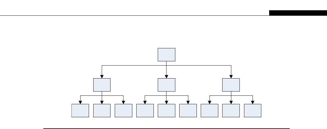
To perform some action, central command (the kernel/host program) must provide some action
plus some data. Each soldier (thread) works on his or her individual part of the problem. Threads may
from time to time swap data with one another under the coordination of either the sergeant (the warp)
or the lieutenant (the block). However, any coordination with other units (blocks) has to be performed
by central command (the kernel/host program).
Thus, it’s necessary to think of orchestrating thousands of threads in this very hierarchical manner
when you think about how a CUDA program will implement concurrency. This may sound quite
complex at first. However, for most embarrassingly parallel programs it’s just a case of thinking of one
thread generating a single output data point. A typical GPU has on the order of 24 K active threads. On
Fermi GPUs you can define 65,535 65,535 1536 threads in total, 24 K of which are active at any
time. This is usually enough to cover most problems within a single node.
Locality
Computing has, over the last decade or so, moved from one limited by computational throughput of the
processor, to one where moving the data is the primary limiting factor. When designing a processor in
terms of processor real estate, compute units (or ALUsdalgorithmic logic units) are cheap. They can
run at high speed, and consume little power and physical die space. However, ALUs are of little use
without operands. Considerable amounts of power and time are consumed in moving the operands to
and from these functional units.
In modern computer designs this is addressed by the use of multilevel caches. Caches work on the
principle of either spatial (close in the address space) or temporal (close in time) locality. Thus, data
that has been accessed before, will likely be accessed again (temporal locality), and data that is close to
the last accessed data will likely be accessed in the future (spatial locality).
Caches work well where the task is repeated many times. Consider for the moment a tradesperson,
a plumber with a toolbox (a cache) that can hold four tools. A number of the jobs he will attend are
similar, so the same four tools are repeatedly used (a cache hit).
However, a significant number of jobs require additional tools. If the tradesperson does not know in
advance what the job will entail, he arrives and starts work. Partway through the job he needs an
additional tool. As it’s not in his toolbox (L1 cache), he retrieves the item from the van (L2 cache).
Grid
Block
N-1
Warp
N-1
Warp
N
Warp
N+1
Block
N
Warp
N-1
Warp
N
Warp
N+1
Block
N+1
Warp
N-1
Warp
N
Warp
N+1
FIGURE 2.1
GPU-based view of threads.
Concurrency 25

Occasionally he needs a special tool or part and must leave the job, drive down to the local
hardware store (global memory), fetch the needed item, and return. Neither the tradesperson nor the
client knows how long (the latency) this operation will actually take. There may be congestion on the
freeway and/or queues at the hardware store (other processes competing for main memory access).
Clearly, this is not a very efficient use of the tradesperson’s time. Each time a different tool or part is
needed, it needs to be fetched by the tradesperson from either the van or the hardware store. While
fetching new tools the tradesperson is not working on the problem at hand.
While this might seem bad, fetching data from a hard drive or SSD (solid-state drive) is akin to
ordering an item at the hardware store. In comparative form, data from a hard drive arrives by regular
courier several days later. Data from the SSD may arrive by overnight courier, but it’s still very slow
compared to accessing data in global memory.
In some more modern processor designs we have hardware threads. Some Intel processors feature
hyperthreading, with two hardware threads per CPU core. To keep with the same analogy, this is
equivalent to the tradesperson having an assistant and starting two jobs. Every time a new tool/part is
required, the assistant is sent to fetch the new tool/part and the tradesperson switches to the alternate
job. Providing the assistant is able to return with the necessary tool/part before the alternate job also
needs an additional tool/part, the tradesperson continues to work.
Although an improvement, this has not solved the latency issuedhow long it takes to fetch new
tools/parts from the hardware store (global memory). Typical latencies to global memory are in the
order of hundreds of clocks. Increasingly, the answer to this problem from traditional processor design
has been to increase the size of the cache. In effect, arrive with a bigger van so fewer trips to the
hardware store are necessary.
There is, however, an increasing cost to this approach, both in terms of capital outlay for a larger
van and the time it takes to search a bigger van for the tool/part. Thus, the approach taken by most
designs today is to arrive with a van (L2 cache) and a truck (L3 cache). In the extreme case of the server
processors, a huge 18-wheeler is brought in to try to ensure the tradesperson is kept busy for just that
little bit longer.
All of this work is necessary because of one fundamental reason. The CPUs are designed to run
software where the programmer does not have to care about locality. Locality is an issue, regardless of
whether the processor tries to hide it from the programmer or not. The denial that this is an issue is
what leads to the huge amount of hardware necessary to deal with memory latency.
The design of GPUs takes a different approach. It places the GPU programmer in charge of dealing
with locality and instead of an 18-wheeler truck gives him or her a number of small vans and a very
large number of tradespeople.
Thus, in the first instance the programmer must deal with locality. He or she needs to think in
advance about what tools/parts (memory locations/data structures) will be needed for a given job.
These then need to be collected in a single trip to the hardware store (global memory) and placed in the
correct van (on chip memory) for a given job at the outset. Given that this data has been collected, as
much work as possible needs to be performed with the data to avoid having to fetch and return it only
to fetch it again later for another purpose.
Thus, the continual cycle of work-stall-fetch from global memory, work-stall-fetch from global
memory, etc. is broken. We can see the same analogy on a production line. Workers are supplied with
baskets of parts to process, rather than each worker individually fetching widgets one at a time from the
store manager’s desk. To do otherwise is simply a hugely inefficient use of the available workers’ time.
26 CHAPTER 2 Understanding Parallelism with GPUs

This simple process of planning ahead allows the programmer to schedule memory loads into the
on-chip memory before they are needed. This works well with both an explicit local memory model
such as the GPU’s shared memory as well as a CPU-based cache. In the shared memory case you tell
the memory management unit to request this data and then go off and perform useful work on another
piece of data. In the cache case you can use special cache instructions that allow prefilling of the cache
with data you expect the program to use later.
The downside of the cache approach over the shared memory approach is eviction and dirty data.
Data in a cache is said to be dirty if it has been written by the program. To free up the space in the cache
for new useful data, the dirty data has to be written back to global memory before the cache space can
be used again. This means instead of one trip to global memory of an unknown latency, we now have
twodone to write the old data and one to get the new data.
Thebig advantage of the programmer-controlled on-chip memory is that the programmeris in controlof
when the writes happen. If you are performing some local transformation of the data, there may be no need
to write the intermediate transformation back to global memory. With a cache, the cache controller does not
know what needs to be written and what can be discarded. Thus, it writes everything, potentially creating
lots of useless memory traffic that may in turn cause unnecessary congestion on the memory interface.
Although many do, not every algorithm lends itself to this type of “known in advance” memory
pattern that the programmer can optimize for. At the same time, not every programmer wants to deal
with locality issues, either initially or sometimes at all. It’s a perfectly valid approach to develop
a program, prove the concept, and then deal with locality issues.
To facilitate such an approach and to deal with the issues of algorithms that did not have
a well-defined data/execution pattern, later generations of GPUs (compute 2.x onward) have both L1
and L2 caches. These can be configured with a preference toward cache or shared memory, allowing
the programmer flexibility to configure the hardware for a given problem.
TYPES OF PARALLELISM
Task-based parallelism
If we look at a typical operating system, we see it exploit a type of parallelism called task parallelism.
The processes are diverse and unrelated. A user might be reading an article on a website while playing
music from his or her music library in the background. More than one CPU core can be exploited by
running each application on a different core.
In terms of parallel programming, this can be exploited by writing a program as a number of
sections that “pipe” (send via messages) the information from one application to another. The Linux
pipe operator (the jsymbol) does just this, via the operating system. The output of one program, such
as grep, is the input of the next, such as sort. Thus, a set of input files can be easily scanned for
a certain set of characters (the grep program) and that output set then sorted (the sort program). Each
program can be scheduled to a separate CPU core.
This pattern of parallelism is known as pipeline parallelism. The output on one program provides
the input for the next. With a diverse set of components, such as the various text-based tools in Linux,
a huge variety of useful functions can be performed by the user. As the programmer cannot know at the
outset everyone’s needs, by providing components that operate together and can be connected easily,
the programmer can target a very wide and diverse user base.
Types of Parallelism 27

This type of parallelism is very much geared toward coarse-grained parallelism. That is, there are
a number of powerful processors, each of which can perform a significant chunk of work.
In terms of GPUs we see coarse-grained parallelism only in terms of a GPU card and the execution
of GPU kernels. GPUs support the pipeline parallelism pattern in two ways. First, kernels can be
pushed into a single stream and separate streams executed concurrently. Second, multiple GPUs can
work together directly through either passing data via the host or passing data via messages directly to
one another over the PCI-E bus. This latter approach, the peer-to-peer (P2P) mechanism, was intro-
duced in the CUDA 4.x SDK and requires certain OS/hardware/driver-level support.
One of the issues with a pipeline-based pattern is, like any production line, it can only run as fast as
the slowest component. Thus, if the pipeline consists of five elements, each of which takes one second,
we can produce one output per second. However, if just one of these elements takes two seconds, the
throughput of the entire pipeline is reduced to one output every two seconds.
The approach to solving this is twofold. Let’s consider the production line analogy for a moment.
Fred’s station takes two seconds because his task is complex. If we provide Fred with an assistant, Tim,
and split his task in half with Tim, we’re back to one second per stage. We now have six stages instead
of five, but the throughput of the pipeline is now again one widget per second.
You can put up to four GPUs into a desktop PC with some thought and care about the design (see
Chapter 11 on designing GPU systems). Thus, if we have a single GPU and it’s taking too long to
process a particular workflow, we can simply add another one and increase the overall processing
power of the node. However, we then have to think about the division of work between the two GPUs.
There may not be an easy 50/50 split. If we can only extract a 70/30 split, clearly the maximum benefit
will be 7/10 (70%) of the existing runtime. If we could introduce another GPU and then maybe move
another task, which occupied say 20% of the time, we’d end up with a 50/30/20 split. Again the
speedup compared to one GPU would be 1/2 or 50% of the original time. We’re still left with the worst-
case time dominating the overall execution time.
The same issue applies to providing a speedup when using a single CPU/GPU combination. If we
move 80% of the work off the CPU and onto the GPU, with the GPU computing this in just 10% of the
time, what is the speedup? Well the CPU now takes 20% of the original time and the GPU 10% of the
original time, but in parallel. Thus, the dominating factor is still the CPU. As the GPU is running in
parallel and consumes less time than the CPU fraction, we can discount this time entirely. Thus, the
maximum speedup is one divided by the fraction of the program that takes the longest time to execute.
This is known as Amdahl’s law and is often quoted as the limiting factor in any speedup. It allows you to
know at the outset what the maximum speedup achievable is, without writing a single line of code. Ulti-
mately, you will have serial operations. Even if you move everything onto the GPU, you will still have to use
the CPU to load and store data to and from storage devices. You will also have to transfer data to and from
the GPU to facilitate input and output (I/O). Thus, maximum theoretical speedup is determined by the
fraction of the program that performs the computation/algorithmic part, plus the remaining serial fraction.
Data-based parallelism
Computation power has been greatly increasing over the past couple of decades. We now have teraflop-
capable GPUs. However, what has not kept pace with this evolution of compute power is the access
time for data. The idea of data-based parallelism is that instead of concentrating on what tasks have to
be performed, we look first to the data and how it needs to be transformed.
28 CHAPTER 2 Understanding Parallelism with GPUs

Task-based parallelism tends to fit more with coarse-grained parallelism approaches. Let’s use an
example of performing four different transformations on four separate, unrelated, and similarly sized
arrays. We have four CPU cores, and a GPU with four SMs. In a task-based decomposition of the
problem, we would assign one array to each of the CPU cores or SMs in the GPU. The parallel
decomposition of the problem is driven by thinking about the tasks or transformations, not the data.
On the CPU side we could create four threads or processes to achieve this. On the GPU side we
would need to use four blocks and pass the address of every array to every block. On the newer Fermi
and Kepler devices, we could also create four separate kernels, one to process each array and run it
concurrently.
A data-based decomposition would instead split the first array into four blocks and assign one CPU
core or one GPU SM to each section of the array. Once completed, the remaining three arrays would be
processed in a similar way. In terms of the GPU implementation, this would be four kernels, each of
which contained four or more blocks. The parallel decomposition here is driven by thinking about the
data first and the transformations second.
As our CPU has only four cores, it makes a lot of sense to decompose the data into four blocks. We
could have thread 0 process element 0, thread 1 process element 1, thread 2 process element 2, thread
3 process element 3, and so on. Alternatively, the array could be split into four parts and each thread
could start processing its section of the array.
In the first case, thread 0 fetches element 0. As CPUs contain multiple levels of cache, this brings the
data into the device. Typically the L3 cache is shared by all cores. Thus, the memory access from the
first fetch is distributed to all cores in the CPU. By contrast in the second case, four separate memory
fetches are needed and four separate L3 cache lines are utilized. The latter approach is often better
where the CPU cores need to write data back to memory. Interleaving the data elements by core means
the cache has to coordinate and combine the writes from different cores, which is usually a bad idea.
If the algorithm permits, we can exploit a certain type of data parallelism, the SIMD (single
instruction, multiple data) model. This would make use of special SIMD instructions such as MMX,
SSE, AVX, etc. present in many x86-based CPUs. Thus, thread 0 could actually fetch multiple adjacent
elements and process them with a single SIMD instruction.
If we consider the same problem on the GPU, each array needs to have a separate transformation
performed on it. This naturally maps such that one transformation equates to a single GPU kernel (or
program). Each SM, unlike a CPU core, is designed to run multiple blocks of data with each block split
into multiple threads. Thus, we need a further level of decomposition to use the GPU efficiently. We’d
typically allocate, at least initially, a combination of blocks and threads such that a single thread
processed a single element of data. As with the CPU, there are benefits from processing multiple
elements per thread. This is somewhat limited on GPUs as only load/store/move explicit SIMD
primitives are supported, but this in turn allows for enhanced levels of instruction-level parallelism
(ILP), which we’ll see later is actually quite beneficial.
With a Fermi and Kepler GPUs, we have a shared L2 cache that replicates the L3 cache function on
the CPU. Thus, as with the CPU, a memory fetch from one thread can be distributed to other threads
directly from the cache. On older hardware, there is no cache. However, on GPUs adjacent memory
locations are coalesced (combined) together by the hardware, resulting in a single and more efficient
memory fetch. We look at this in detail in Chapter 6 on memory.
One important distinction between the caches found in GPUs and CPUs is cache coherency. In
a cache-coherent system a write to a memory location needs to be communicated to all levels of cache
Types of Parallelism 29

in all cores. Thus, all processor cores see the same view of memory at any point in time. This is one of
the key factors that limits the number of cores in a processor. Communication becomes increasingly
more expensive in terms of time as the processor core count increases. The worst case in a cache-
coherent system is where each core writes adjacent memory locations as each write forces a global
update to every core’s cache.
A non cache-coherent system by comparison does not automatically update the other core’s caches.
It relies on the programmer to write the output of each processor core to separate areas/addresses. This
supports the view of a program where a single core is responsible for a single or small set of outputs.
CPUs follow the cache-coherent approach whereas the GPU does not and thus is able to scale to a far
larger number of cores (SMs) per device.
Let’s assume for simplicity that we implement a kernel as four blocks. Thus, we have four kernels
on the GPU and four processes or threads on the CPU. The CPU may support mechanisms such as
hyperthreading to enable processing of additional threads/processes due to a stall event, a cache miss,
for example. Thus, we could increase this number to eight and we might see an increase in perfor-
mance. However, at some point, sometimes even at less than the number of cores, the CPU hits a point
where there are just too many threads.
At this point the memory bandwidth becomes flooded and cache utilization drops off, resulting in
less performance, not more.
On the GPU side, four blocks is nowhere near enough to satisfy four SMs. Each SM can actually
schedule up to eight blocks (16 on Kepler). Thus, we’d need 8 4¼32 blocks to load the four SMs
correctly. As we have four independent operations, we can launch four simultaneous kernels on Fermi
hardware via the streams feature (see Chapter 8 on using multiple GPUs). Consequently, we can
launch 16 blocks in total and work on the four arrays in parallel. As with the CPU, however, it would be
more efficient to work on one array at a time as this would likely result in better cache utilization. Thus,
on the GPU we need to ensure we always have enough blocks (typically a minimum of 8 to 16 times
the number of SMs on the GPU device).
FLYNN’S TAXONOMY
We mentioned the term SIMD earlier. This classification comes from Flynn’s taxonomy, a classifica-
tion of different computer architectures. The various types are as follows:
• SIMDdsingle instruction, multiple data
• MIMDdmultiple instructions, multiple data
• SISDdsingle instruction, single data
• MISDdmultiple instructions, single data
The standard serial programming most people will be familiar with follows the SISD model. That is,
there is a single instruction stream working on a single data item at any one point in time. This equates
to a single-core CPU able to perform one task at a time. Of course it’s quite possible to provide the
illusion of being able to perform more than a single task by simply switching between tasks very
quickly, so-called time-slicing.
MIMD systems are what we see today in dual- or quad-core desktop machines. They have a work
pool of threads/processes that the OS will allocate to one of NCPU cores. Each thread/process has an
30 CHAPTER 2 Understanding Parallelism with GPUs

independent stream of instructions, and thus the hardware contains all the control logic for decoding
many separate instruction streams.
SIMD systems try to simplify this approach, in particular with the data parallelism model. They
follow a single instruction stream at any one point in time. Thus, they require a single set of logic inside
the device to decode and execute the instruction stream, rather than multiple-instruction decode paths.
By removing this silicon real estate from the device, they can be smaller, cheaper, consume less power,
and run at higher clock rates than their MIMD cousins.
Many algorithms make use of a small number of data points in one way or another. The data points
can often be arranged as a SIMD instruction. Thus, all data points may have some fixed offset added,
followed by a multiplication, a gain factor for example. This can be easily implemented as SIMD
instructions. In effect, you are programming “for this range of data, perform this operation” instead of
“for this data point, perform this operation.” As the data operation or transformation is constant for all
elements in the range, it can be fetched and decoded from the program memory only once. As the range is
defined and contiguous, the data can be loaded en masse from the memory, rather than one word at a time.
However, algorithms where one element has transformation A applied while another element has
transformation B applied, and all others have transformation C applied, are difficult to implement using
SIMD. The exception is where this algorithm is hard-coded into the hardware because it’s very common.
Such examples include AES (Advanced Encryption Standard) and H.264 (a video compression standard).
The GPU takes a slightly different approach to SIMD. It implements a model NVIDIA calls SIMT
(single instruction, multiple thread). In this model the instruction side of the SIMD instruction is not
a fixed function as it is within the CPU hardware. The programmer instead defines, through a kernel,
what each thread will do. Thus, the kernel will read the data uniformly and the kernel code will execute
transformation A, B, or C as necessary. In practice, what happens is that A, B, and C are executed in
sequence by repeating the instruction stream and masking out the nonparticipating threads. However,
conceptually this is a much easier model to work with than one that only supports SIMD.
SOME COMMON PARALLEL PATTERNS
A number of parallel problems can be thought of as patterns. We see patterns in many software
programs, although not everyone is aware of them. Thinking in terms of patterns allows us to broadly
deconstruct or abstract a problem, and therefore more easily think about how to solve it.
Loop-based patterns
Almost anyone who has done any programming is familiar with loops. They vary primarily in terms of
entry and exit conditions (for,do.while,while), and whether they create dependencies between loop
iterations or not.
A loop-based iteration dependency is where one iteration of the loop depends on one or more
previous iterations. We want to remove these if at all possible as they make implementing parallel
algorithms more difficult. If in fact this can’t be done, the loop is typically broken into a number of
blocks that are executed in parallel. The result from block 0 is then retrospectively applied to block 1,
then to block 2, and so on. There is an example later in this text where we adopt just such an approach
when handling the prefix-sum algorithm.
Some Common Parallel Patterns 31

Loop-based iteration is one of the easiest patterns to parallelize. With inter-loop dependencies
removed, it’s then simply a matter of deciding how to split, or partition, the work between the available
processors. This should be done with a view to minimizing communication between processors and
maximizing the use of on-chip resources (registers and shared memory on a GPU; L1/L2/L3 cache on
a CPU). Communication overhead typically scales badly and is often the bottleneck in poorly designed
systems.
The macro-level decomposition should be based on the number of logical processing units
available. For the CPU, this is simply the number of logical hardware threads available. For the GPU,
this is the number of SMs multiplied by the maximum load we can give to each SM, 1 to 16 blocks
depending on resource usage and GPU model. Notice we use the term logical and not physical
hardware thread. Some Intel CPUs in particular support more than one logical thread per physical CPU
core, so-called hyperthreading. GPUs run multiple blocks on a single SM, so we have to at least
multiply the number of SMs by the maximum number of blocks each SM can support.
Using more than one thread per physical device maximizes the throughput of such devices, in terms
of giving them something to do while they may be waiting on either a memory fetch or I/O-type
operation. Selecting some multiple of this minimum number can also be useful in terms of load
balancing on the GPU and allows for improvements when new GPUs are released. This is particularly
the case when the partition of the data would generate an uneven workload, where some blocks take
much longer than others. In this case, using many times the number of SMs as the basis of the par-
titioning of the data allows slack SMs to take work from a pool of available blocks.
However, on the CPU side, over subscribing the number of threads tends to lead to poor perfor-
mance. This is largely due to context switching being performed in software by the OS. Increased
contention for the cache and memory bandwidth also contributes significantly should you try to run too
many threads. Thus, an existing multicore CPU solution, taken as is, typically has far too large
a granularity for a GPU. You will almost always have to repartition the data into many smaller blocks
to solve the same problem on the GPU.
When considering loop parallelism and porting an existing serial implementation, be critically
aware of hidden dependencies. Look carefully at the loop to ensure one iteration does not calculate
a value used later. Be wary of loops that count down as opposed to the standard zero to max value
construct, which is the most common type of loop found. Why did the original programmer count
backwards? It is likely this may be because there is some dependency in the loop and parallelizing it
without understanding the dependencies will likely break it.
We also have to consider loops where we have an inner loop and one or more outer loops. How
should these be parallelized? On a CPU the approach would be to parallelize only the outer loop as you
have only a limited number of threads. This works well, but as before it depends on there being no loop
iteration dependencies.
On the GPU the inner loop, provided it is small, is typically implemented by threads within
a single block. As the loop iterations are grouped, adjacent threads usually access adjacent memory
locations. This often allows us to exploit locality, something very important in CUDA programming.
Any outer loop(s) are then implemented as blocks of the threads. These are concepts we cover in
detail in Chapter 5.
Consider also that most loops can be flattened, thus reducing an inner and outer loop to a single
loop. Think about an image processing algorithm that iterates along the Xpixel axis in the inner loop
and the Ypixel axis in the outer loop. It’s possible to flatten this loop by considering all pixels as
32 CHAPTER 2 Understanding Parallelism with GPUs
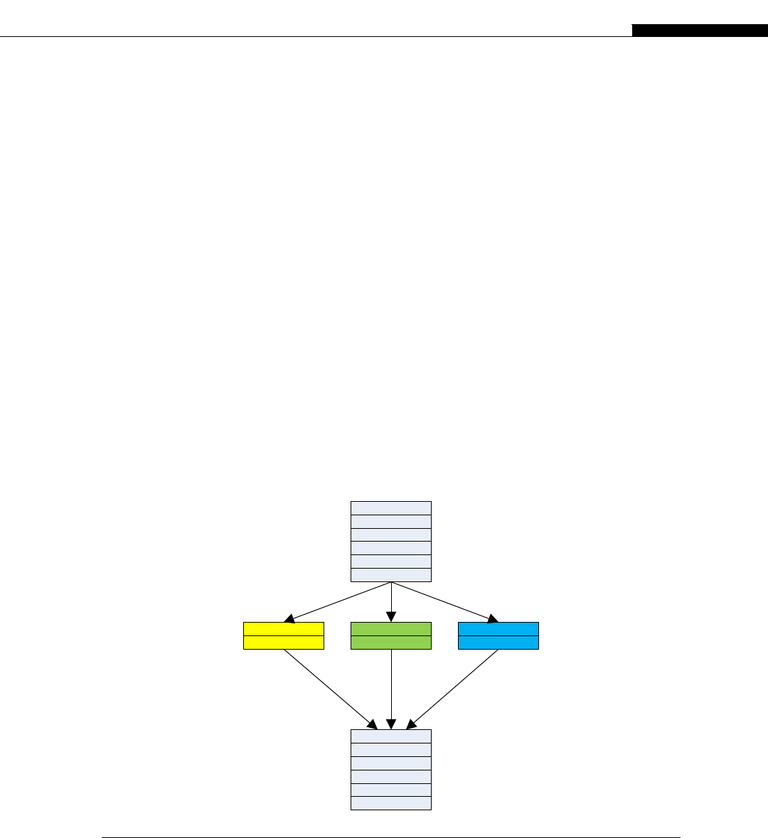
a single-dimensional array and iterating over pixels as opposed to image coordinates. This requires
a little more thought on the programming side, but it may be useful if one or more loops contain a very
small number of iterations. Such small loops present considerable loop overhead compared to the work
done per iteration. They are, thus, typically not efficient.
Fork/join pattern
The fork/join pattern is a common pattern in serial programming where there are synchronization
points and only certain aspects of the program are parallel. The serial code runs and at some point hits
a section where the work can be distributed to Pprocessors in some manner. It then “forks” or spawns
Nthreads/processes that perform the calculation in parallel. These then execute independently and
finally converge or join once all the calculations are complete. This is typically the approach found in
OpenMP, where you define a parallel region with pragma statements. The code then splits into
Nthreads and later converges to a single thread again.
In Figure 2.2, we see a queue of data items. As we have three processing elements (e.g., CPU
cores), these are split into three queues of data, one per processing element. Each is processed
independently and then written to the appropriate place in the destination queue.
The fork/join pattern is typically implemented with static partitioning of the data. That is, the serial
code will launch Nthreads and divide the dataset equally between the Nthreads. If each packet of data
takes the same time to process, then this works well. However, as the overall time to execute is the time
of the slowest thread, giving one thread too much work means it becomes the single factor determining
the total time.
1
2
3
4
5
6
1 2 3
4 5 6
1
2
3
4
5
6
FIGURE 2.2
A queue of data processed by Nthreads.
Some Common Parallel Patterns 33

Systems such as OpenMP also have dynamic scheduling allocation, which mirrors the approach taken
by GPUs. Here a thread pool is created (a block pool for GPUs) and only once one task is completed is
more work allocated. Thus, if 1 task takes 10x time and 20 tasks take just 1x time each, they are allocated
only to free cores. With a dual-core CPU, core 1 gets the big 10x task and five of the smaller 1x tasks. Core
2 gets 15 of the smaller 1x tasks, and therefore both CPU core 1 and 2 complete around the same time.
In this particular example, we’ve chosen to fork three threads, yet there are six data items in the
queue. Why not fork six threads? The reality is that in most problems there can actually be millions of
data items and attempting to fork a million threads will cause almost all OSs to fail in one way or another.
Typically an OS will apply a “fair” scheduling policy. Thus, each of the million threads would need
to be processed in turn by one of perhaps four available processor cores. Each thread also requires its
own memory space. In Windows a thread can come with a 1 MB stack allocation, meaning we’d
rapidly run out of memory prior to being able to fork enough threads.
Therefore on CPUs, typically programmers and many multithreaded libraries will use the number
of logical processor threads available as the number of processes to fork. As CPU threads are typically
also expensive to create and destroy, and also to limit maximum utilization, often a thread pool of
workers is used who then fetch work from a queue of possible tasks.
On GPUs we have the opposite problem, in that we in fact need thousands or tens of thousands of
threads. We have exactly the thread pool concept we find on more advanced CPU schedulers, except
it’s more like a block pool than a thread pool. The GPU has an upper limit on the number of concurrent
blocks it can execute. Each block contains a number of threads. Both the number of threads per block
and the overall number of concurrently running blocks vary by GPU generation.
The fork/join pattern is often used when there is an unknown amount of concurrency in a problem.
Traversing a tree structure or a path exploration type algorithm may spawn (fork) additional threads
when it encounters another node or path. When the path has been fully explored these threads may then
join back into the pool of threads or simply complete to be respawned later.
This pattern is not natively supported on a GPU, as it uses a fixed number of blocks/threads at
kernel launch time. Additional blocks cannot be launched by the kernel, only the host program. Thus,
such algorithms on the GPU side are typically implemented as a series of GPU kernel launches, each of
which needs to generate the next state. An alternative is to coordinate or signal the host and have it
launch additional, concurrent kernels. Neither solution works particularly well, as GPUs are designed
for a static amount of concurrency. Kepler introduces a concept, dynamic parallelism, which addresses
this issue. See chapter 12 for more information on this.
Within a block of threads on a GPU there are a number of methods to communication between
threads and to coordinate a certain amount of problem growth or varying levels of concurrency within
a kernel. For example, if you have an 8 8 matrix you may have many places where just 64 threads are
active. However, there may be others where 256 threads can be used. You can launch 256 threads and
leave most of them idle until such time as needed. Such idle threads occupy resources and may limit
the overall throughput, but do not consume any execution time on the GPU whilst idle. This allows the
use of shared memory, fast memory close to the processor, rather than creating a number of distinct
steps that need to be synchronized by using the much slower global memory and multiple kernel
launches. We look at memory types in Chapter 6.
Finally, the later-generation GPUs support fast atomic operations and synchronization primitives
that communicate data between threads in addition to simply synchronizing. We look at some
examples of this later in the text.
34 CHAPTER 2 Understanding Parallelism with GPUs

Tiling/grids
The approach CUDA uses with all problems is to require the programmer to break the problem into
smaller parts. Most parallel approaches make use of this concept in one way or another. Even in huge
supercomputers problems such climate models must be broken down into hundreds of thousands of
blocks, each of which is then allocated to one of the thousands of processing elements present in the
machine. This type of parallel decomposition has the huge advantage that it scales really well.
A GPU is in many ways similar to a symmetrical multiprocessor system on a single processor. Each
SM is a processor in its own right, capable of running up multiple blocks of threads, typically 256 or
512 threads per block. A number of SMs exist on a single GPU and share a common global memory
space. Together as a single GPU they can operate at peak speeds of up to 3 teraflops/s (GTX680).
While peak performance may be impressive, achieving anything like this is not possible without
specially crafted programs, as this peak performance does not include things such as memory access,
which is somewhat key to any real program. To achieve good performance on any platform requires
a good knowledge of the hardware and the understanding of two key conceptsdconcurrency and locality.
There is concurrency in many problems. It’s just that as someone who may come from a serial
background, you may not immediately see the concurrency in a problem. The tiling model is thus an
easy model to conceptualize. Imagine the problem in two dimensionsda flat arrangement of
datadand simply overlay a grid onto the problem space. For a three-dimensional problem imagine the
problem as a Rubik’s Cubeda set of blocks that map onto the problem space.
CUDA provides the simple two-dimensional grid model. For a significant number of problems this
is entirely sufficient. If you have a linear distribution of work within a single block, you have an ideal
decomposition into CUDA blocks. As we can assign up to sixteen blocks per SM and we can have up to
16 SMs (32 on some GPUs), any number of blocks of 256 or larger is fine. In practice, we’d like to limit
the number of elements within the block to 128, 256, or 512, so this in itself may drive much larger
numbers of blocks with a typical dataset.
When considering concurrency, consider also if there is ILP that can be exploited. Conceptually it’s
easier to think about a single thread being associated with a single output data item. If, however, we can
fill the GPU with threads on this basis and there is still more data that could be processed, can we still
improve the throughput? The answer is yes, but only through the use of ILP.
ILP exploits the fact that instruction streams can be pipelined within the processor. Thus, it is more
efficient to push four add operations into the queue, wait, and then collect them one at a time
(push-push-push-push-wait), rather than perform them one at a time (push-wait-push-wait-push-wait-
push-wait). For most GPUs, you’ll find an ILP level of four operations per thread works best. There are
some detailed studies and examples of this in Chapter 9. Thus, if possible we’d like to process
Nelements per thread, but not to the extent that it reduces the overall number of active threads.
Divide and conquer
The divide-and-conquer pattern is also a pattern for breaking down large problems into smaller
sections, each of which can be conquered. Taken together these individual computations allow a much
larger problem to be solved.
Typically you see divide-and-conquer algorithms used with recursion. Quick sort is a classic
example of this. It recursively partitions the data into two sets, those above a pivot point and those below
the pivot point. When the partition finally consists of just two items, they are compared and swapped.
Some Common Parallel Patterns 35

Most recursive algorithms can also be represented as an iterative model, which is usually somewhat
easier to map onto the GPU as it fits better into the primary tile-based decomposition model of
the GPU.
Recursive algorithms are also supported on Fermi-class GPUs, although as with the CPU you have
to be aware of the maximum call depth and translate this into stack usage. The available stack can be
queried with API call cudaDeviceGetLimit(). It can also be set with the API call
cudaDeviceSetLimit(). Failure to allocate enough stack space, as with CPUs, will result in the
program failing. Some debugging tools such as Parallel Nsight and CUDA-GDB can detect such stack
overflow issues.
In selecting a recursive algorithm be aware that you are making a tradeoff of development time
versus performance. It may be easier to conceptualize and therefore code a recursive algorithm than to
try to convert such an approach to an iterative one. However, each recursive call causes any formal
parameters to be pushed onto the stack along with any local variables. GPUs and CPUs implement
a stack in the same way, simply an area of memory from the global memory space. Although CPUs and
the Fermi-class GPUs cache this area, compared to passing values using registers, this is slow. Use
iterative solutions where possible as they will generally perform much better and run on a wider range
of GPU hardware.
CONCLUSION
We’ve looked here at a broad overview of some parallel processing concepts and how these are applied
to the GPU industry in particular. It’s not the purpose of this text to write a volume on parallel pro-
cessing, for there are entire books devoted to just this subject. We want readers to have some feeling for
the issues that parallel programming bring to the table that would not otherwise be thought about in
a serial programming environment.
In subsequent chapters we cover some of these concepts in detail in terms of practical examples.
We also look at parallel prefix-sum, an algorithm that allows multiple writers of data to share
a common array without writing over one another’s data. Such algorithms are never needed for serial
based programming.
With parallelism comes a certain amount of complexity and the need for a programmer to think and
plan ahead to consider the key issues of concurrency and locality. Always keep these two key concepts
in mind when designing any software for the GPU.
36 CHAPTER 2 Understanding Parallelism with GPUs

CUDA Hardware Overview 3
PC ARCHITECTURE
Let’s start by looking at the typical Core 2 architecture we still find today in many PCs and how it
impacts our usage of GPU accelerators (Figure 3.1).
Notice that all GPU devices are connected to the processor via the PCI-E bus. In this case we’ve
assumed a PCI-E 2.0 specification bus, which is currently the fastest bus available, giving a transfer
rate of 5 GB/s. PCI-E 3.0 has become available at the time of this writing and should significantly
improve the bandwidth available.
However, to get data from the processor, we need to go through the Northbridge device over the
slow FSB (front-side bus). The FSB can run anything up to 1600 MHz clock rate, although in many
designs it is much slower. This is typically only one-third of the clock rate of a fast processor.
Memory is also accessed through the Northbridge, and peripherals through the Northbridge and
Southbridge chipset. The Northbridge deals with all the high-speed components like memory, CPU,
PCI-E bus connections, etc. The Southbridge chip deals with the slower devices such as hard disks,
USB, keyboard, network connections, etc. Of course, it’s quite possible to connect a hard-disk
controller to the PCI-E connection, and in practice, this is the only true way of getting RAID high-
speed data access on such a system.
PCI-E (Peripheral Communications Interconnect Express) is an interesting bus as, unlike its
predecessor, PCI (Peripheral Component Interconnect), it’s based on guaranteed bandwidth. In the
old PCI system each component could use the full bandwidth of the bus, but only one device at
a time. Thus, the more cards you added, the less available bandwidth each card would receive. PCI-E
solved this problem by the introduction of PCI-E lanes. These are high-speed serial links that can be
combined together to form X1, X2, X4, X8, or X16 links. Most GPUs now use at least the PCI-E
2.0, X16 specification, as shown in Figure 3.1. With this setup, we have a 5 GB/s full-duplex bus,
meaning we get the same upload and download speed, at the same time. Thus, we can transfer 5 GB/
s to the card, while at the same time receiving 5 GB/s from the card. However, this does not mean
we can transfer 10 GB/s to the card if we’re not receiving any data (i.e., the bandwidth is not
cumulative).
In a typical supercomputer environment, or even in a desktop application, we are dealing with
a large dataset. A supercomputer may deal with petabytes of data. A desktop PC may be dealing with
as little as a several GB high-definition video. In both cases, there is considerable data to fetch from the
attached peripherals. A single 100 MB/s hard disk will load 6 GB of data in one minute. At this rate it
takes over two and a half hours to read the entire contents of a standard 1 TB disk.
CHAPTER
CUDA Programming. http://dx.doi.org/10.1016/B978-0-12-415933-4.00003-X
Copyright Ó2013 Elsevier Inc. All rights reserved.
37
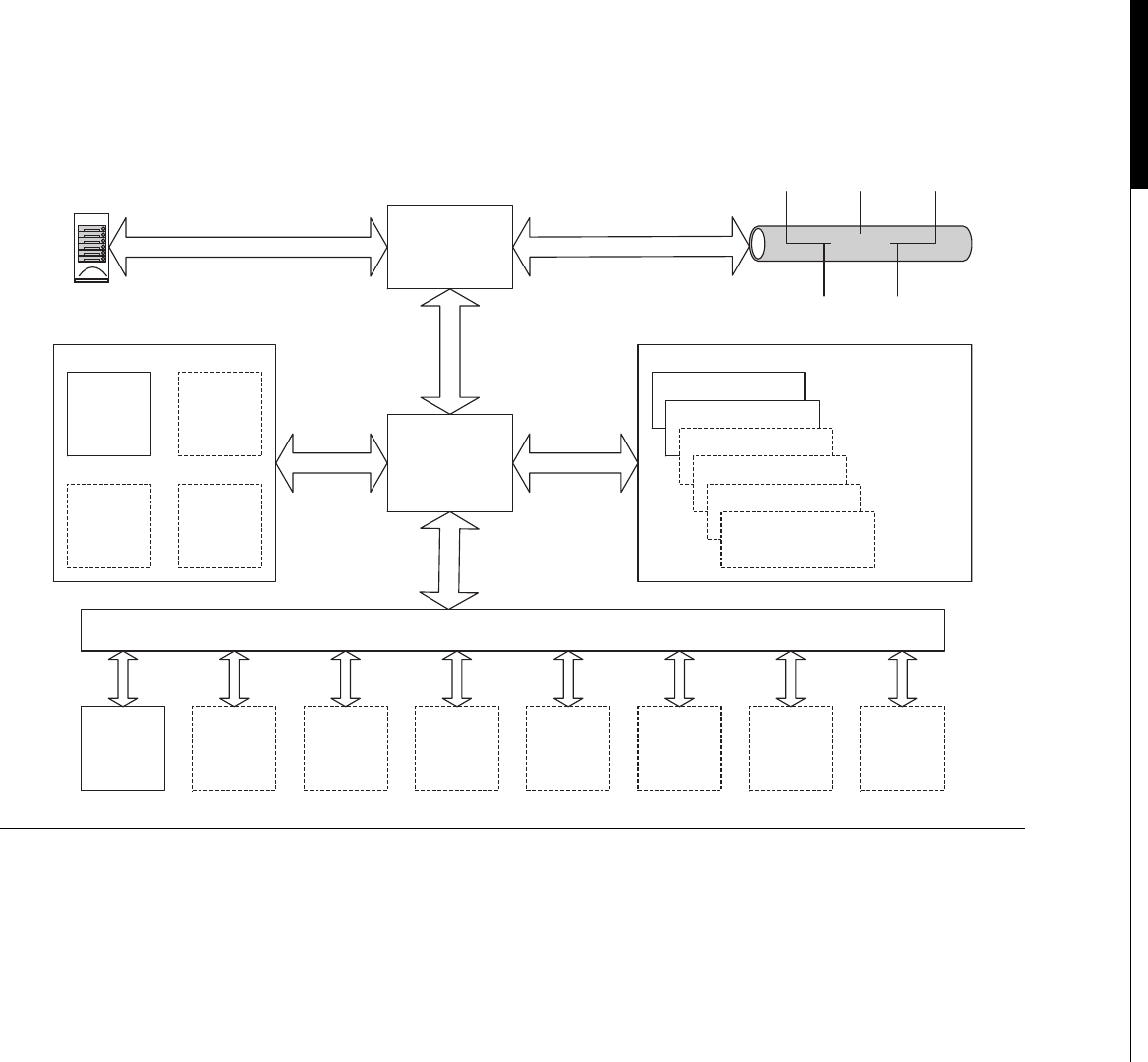
CPU 1 (Athlon, P4, Opteron, Xeon)
DRAM Memory (DDR-2/DDR-3) - 2Ghz, 24MB, 30GB/Sec
FSB
Core 1 Core 2
Core 3 Core 4
DRAM Bank 0
DRAM Bank 1
DRAM Bank 2
DRAM Bank 3
DRAM Bank 4
DRAM Bank 5
Northbridge FSB
Southbridge
Raid drive
SATA (300MB/S) Ethernet
10/100/1000Bits/S
FSB
FSB
PCI-E Bus (5GB/S)
GPU 0 GPU 1 GPU 2 GPU 3 GPU 4 GPU 5 GPU 6 GPU 7
FIGURE 3.1
Typical Core 2 series layout.
38 CHAPTER 3 CUDA Hardware Overview

IfusingMPI(MessagePassingInterface),commonlyusedinclusters,thelatencyforthis
arrangement can be considerable if the Ethernet connections are attached to the Southbridge instead
of the PCI-E bus. Consequently, dedicated high-speed interconnects like InfiniBand or 10 Gigabit
Ethernet cards are often used on the PCI-E bus. This removes slots otherwise available for GPUs.
Previously, as there was no direct GPU MPI interface, all communications in such a system are
routed over the PCI-E bus to the CPU and back again. The GPU-Direct technology, available in the
CUDA 4.0 SDK, solved this issue and it’s now possible for certain InfiniBand cards to talk directly to
the GPU without having to go through the CPU first. This update to the SDK also allows direct GPU
to GPU communication.
We saw a number of major changes with the advent of the Nehalem architecture. The main change
was to replace the Northbridge and the Southbridge chipset with the X58 chipset. The Nehalem
architecture brought us QPI (Quick Path Interconnect), which was actually a huge advance over the
FSB (Front Side Bus) approach and is similar to AMD’s HyperTransport. QPI is a high-speed inter-
connect that can be used to talk to other devices or CPUs. In a typical Nehalem system it will connect
to the memory subsystem, and through an X58 chipset, the PCI-E subsystem (Figure 3.2). The QPI
runs at either 4.8 GT/s or 6.4 GT/s in the Extreme/Xeon processor versions.
With the X58 and 1366 processor socket, a total of 36 PCI-E lanes are available, which means up to
two cards are supported at X16, or four cards at X8. Prior to the introduction of the LGA2011 socket,
this provided the best bandwidth solution for a GPU machine to date.
The X58 design is also available in a lesser P55 chipset where you get only 16 lanes. This means
one GPU card at X16, or two cards at X8.
From the I7/X58 chipset design, Intel moved onto the Sandybridge design, shown in Figure 3.3.
One of the most noticeable improvements was the support for the SATA-3 standard, which supports
600 MB/s transfer rates. This, combined with SSDs, allows for considerable input/output (I/O)
performance with loading and saving data.
The other major advance with the Sandybridge design was the introduction of the AVX (Advanced
Vector Extensions) instruction set, also supported by AMD processors. AVX allows for vector
instructions that provide up to four double-precision (256 bit/32 byte) wide vector operations. It’s
a very interesting development and something that can be used to considerably speed up compute-
bound applications on the CPU.
Notice, however, the big downside of socket 1155 Sandybridge design: It supports only 16 PCI-E
lanes, limiting the PCI-E bandwidth to 16 GB/s theoretical, 10 GB/s actual bandwidth. Intel has gone
down the route of integrating more and more into the CPU with their desktop processors. Only the
socket 2011 Sandybridge-E, the server offering, has a reasonable number of PCI-E lanes (40).
So how does AMD compare with the Intel designs? Unlike Intel, which has gradually moved away
from large numbers of PCI-E lanes, in all but their server line, AMD have remained fairly constant.
Their FX chipset, provides for either two X16 devices or four X8 PCI-E devices. The AMD3þsocket
paired with the 990FX chipset makes for a good workhorse, as it provides SATA 6 GB/s ports paired
with up to four X16 PCI-E slots (usually running at X8 speed).
One major difference between Intel and AMD is the price point for the number of cores. If you
count only real processor cores and ignore logical (hyperthreaded) ones, for the same price point, you
typically get more cores on the AMD device. However, the cores on the Intel device tend to perform
better. Therefore, it depends a lot on the number of GPUs you need to support and the level of loading
of the given cores.
PC Architecture 39
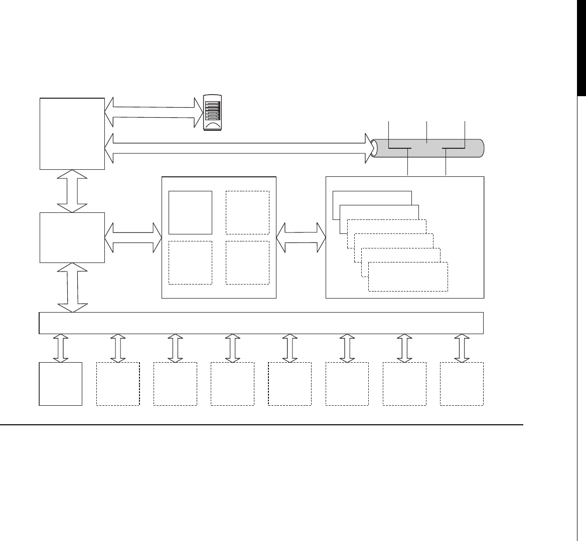
CPU 1 (I7) DRAM Memory (/DDR-3) - 2Ghz, 24MB, 30GB/Sec
QPI (25GB/s)
Core 1 Core 2
Core 3 Core 4
DRAM Bank 0
DRAM Bank 1
DRAM Bank 2
DRAM Bank 3
DRAM Bank 4
DRAM Bank 5
I/O Hub
(IOH)
I/O Controller
Hub Raid drive
SATA(300MB/S)
Ethernet10/100/1000 Bits/S
DMI 2GB/s
PCI-E 2.0
Up to 36
Lanes
PCI-E Bus (5GB/S)
GPU 0 GPU 1 GPU 2 GPU 3 GPU 4 GPU 5 GPU 6 GPU 7
25GB/s
FIGURE 3.2
Nehalem/X58 system.
40 CHAPTER 3 CUDA Hardware Overview
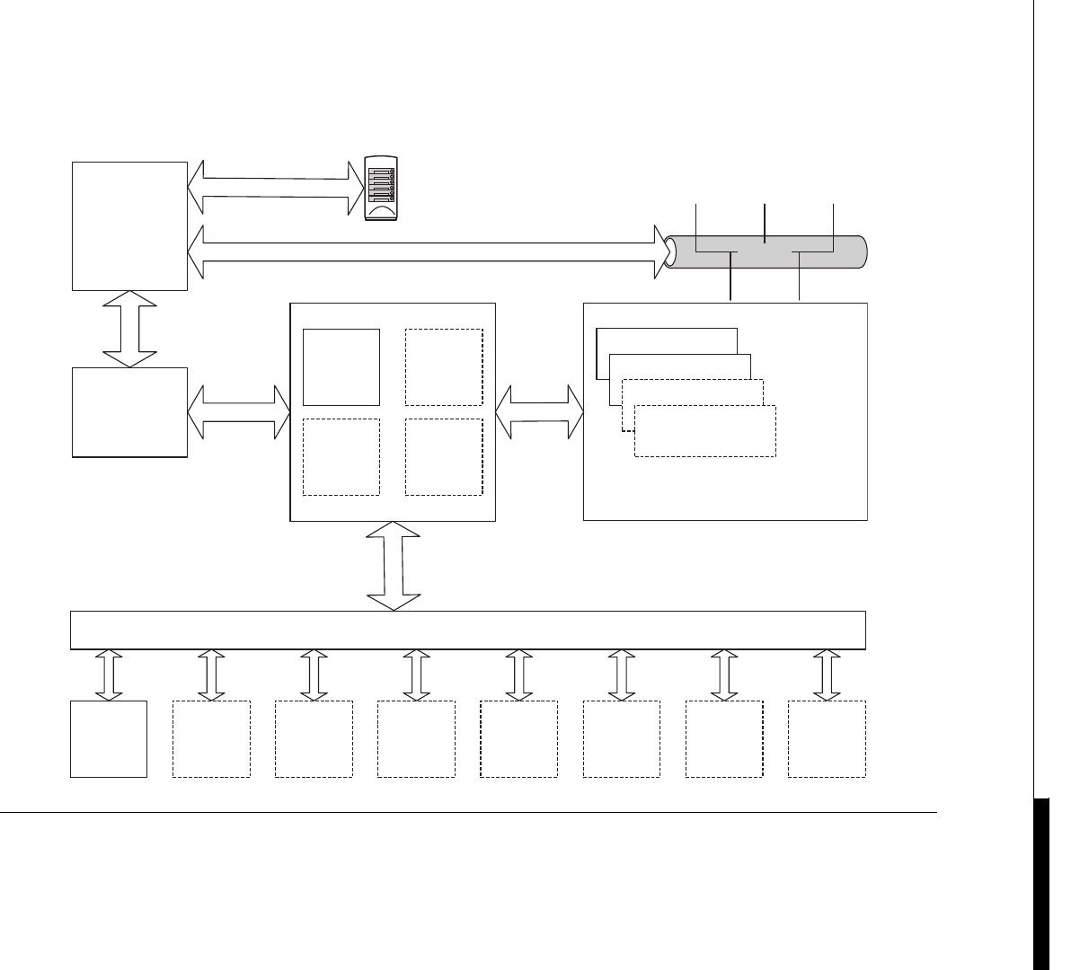
CPU 1 (I5/I3 SandyBridge) DRAM Memory (DDR-2) - 2Ghz, 16MB, 18GB/Sec
DMI (20 GB/s)
Core 1 Core 2
Core 3 Core 4
DRAM Bank 0
DRAM Bank 1
DRAM Bank 2
DRAM Bank 3
I/O Hub
(IOH)
I/O Controller
Hub Raid drive
SATA(600MB/S)
Ethernet10/100/1000 Bits/S
DMI 2GB/s
PCI-E Bus (5GB/S)
GPU 0 GPU 1 GPU 2 GPU 3 GPU 4 GPU 5 GPU 6 GPU 7
18GB/s
PCI-E2.0
16 Lanes
10 GB/s
FIGURE 3.3
Sandybridge design.
PC Architecture 41

As with the Intel design, you see similar levels of bandwidth around the system, with the exception
of bandwidth to main memory. Intel uses triple or quad channel memory on their top-end systems and
dual-channel memory on the lower-end systems. AMD uses only dual-channel memory, leading to
significantly less CPU host-memory bandwidth being available (Figure 3.4).
One significant advantage of the AMD chipsets over the Intel ones is the support for up to six SATA
(Serial ATA) 6 GB/s ports. If you consider that the slowest component in any system usually limits the
overall throughput, this is something that needs some consideration. However, SATA3 can very
quickly overload the bandwidth of Southbridge when using multiple SSDs (solid state drives). A PCI-E
bus solution may be a better one, but it obviously requires additional costs.
GPU HARDWARE
GPU hardware is radically different than CPU hardware. Figure 3.5 shows how a multi-GPU system
looks conceptually from the other side of the PCI-E bus.
Notice the GPU hardware consists of a number of key blocks:
• Memory (global, constant, shared)
• Streaming multiprocessors (SMs)
• Streaming processors (SPs)
The main thing to notice here is that a GPU is really an array of SMs, each of which has Ncores (8
in G80 and GT200, 32–48 in Fermi, 8 plus in Kepler; see Figure 3.6). This is the key aspect that allows
scaling of the processor. A GPU device consists of one or more SMs. Add more SMs to the device and
you make the GPU able to process more tasks at the same time, or the same task quicker, if you have
enough parallelism in the task.
Like CPUs, if the programmer writes code that limits the processor usage to Ncores, let’s say dual-
core, when the CPU manufacturers bring out a quad-core device, the user sees no benefit. This is
exactly what happened in the transition from dual- to quad-core CPUs, and lots of software then had to
be rewritten to take advantage of the additional cores. NVIDIA hardware will increase in performance
by growing a combination of the number of SMs and number of cores per SM. When designing
software, be aware that the next generation may double the number of either.
Now let’s take a closer look at the SMs themselves. There are number of key components making
up each SM, however, not all are shown here for reasons of simplicity. The most significant part is that
there are multiple SPs in each SM. There are 8 SPs shown here; in Fermi this grows to 32–48 SPs and
in Kepler to 192. There is no reason to think the next hardware revision will not continue to increase
the number of SPs/SMs.
Each SM has access to something called a register file, which is much like a chunk of memory that
runs at the same speed as the SP units, so there is effectively zero wait time on this memory. The size of
this memory varies from generation to generation. It is used for storing the registers in use within the
threads running on an SP. There is also a shared memory block accessible only to the individual SM;
this can be used as a program-managed cache. Unlike a CPU cache, there is no hardware evicting
cache data behind your backdit’s entirely under programmer control.
Each SM has a separate bus into the texture memory, constant memory, and global memory
spaces. Texture memory is a special view onto the global memory, which is useful for data where
42 CHAPTER 3 CUDA Hardware Overview
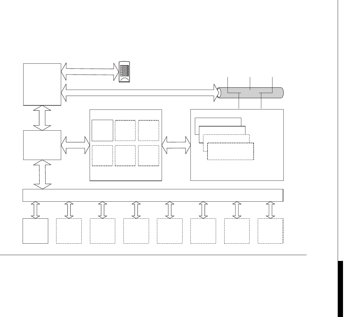
CPU 1 (AMD3+) DRAM Memory (DDR-3) - 2Ghz, 16MB, 17GB/Sec
HT (25GB/s)
Core 1 Core 2 Core 3
DRAM Bank 0
DRAM Bank 1
DRAM Bank 2
DRAM Bank 3
Northbridge
Southbridge Raid drive
SATA(600MB/S)
Ethernet10/100/1000 Bits/S
A-Link 2GB/s
PCI-E 2.0
Up to 38
Lanes
PCI-E Bus (5GB/S)
GPU 0 GPU 1 GPU 2 GPU 3 GPU 4 GPU 5 GPU 6 GPU 7
17GB/s
Core 4 Core 5 Core 6
FIGURE 3.4
AMD.
GPU Hardware 43

GPU #0
Constant Memory Bus
Shared Memory (16x 1K)
SP0 SP1
0 1
Crossbar
2 3
SP2
4 5
SP3
6 7
SP4
8 9
SP5
A B
SP6
C D
SP7
E F
Bus
SM0
Global Memory MMU (448 / 512 Bit) - 120GB/S - 256K to 4GB
Optional
+64 Bits
Global Memory Bus
Constant Shared
Memory across
all MPs (64K)
SM1 SM2 SM3 Optional
SMn
PCI-E 2.0 Interconnect (5GB/S)
GPU
#1
GPU
#2
GPU
#3
FIGURE 3.5
Block diagram of a GPU (G80/GT200) card.
44 CHAPTER 3 CUDA Hardware Overview
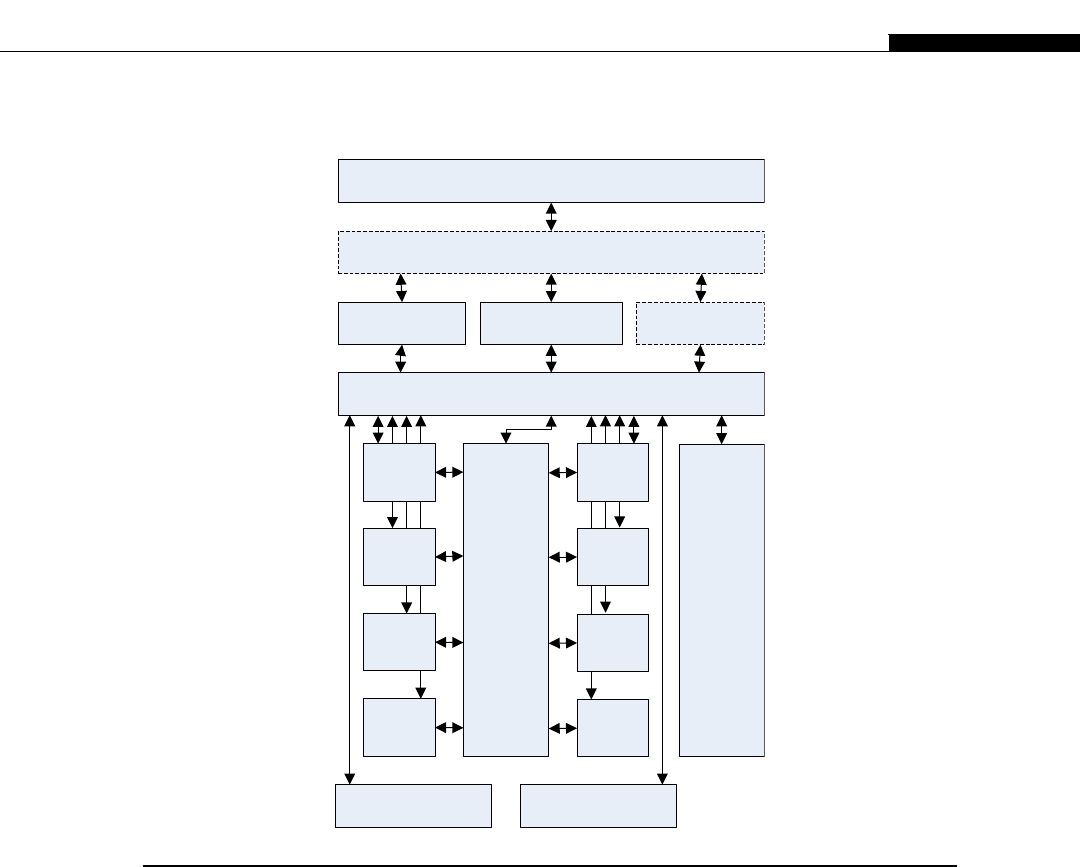
there is interpolation, for example, with 2D or 3D lookup tables. It has a special feature of
hardware-based interpolation. Constant memory is used for read-only data and is cached on all
hardware revisions. Like texture memory, constant memory is simply a view into the main global
memory.
Global memory is supplied via GDDR (Graphic Double Data Rate) on the graphics card. This is
a high-performance version of DDR (Double Data Rate) memory. Memory bus width can be up to 512 bits
wide, giving a bandwidth of 5 to 10 times more than found on CPUs, up to 190 GB/s with the Fermi
hardware.
Each SM also has two or more special-purpose units (SPUs), which perform special hardware
instructions, such as the high-speed 24-bit sin/cosine/exponent operations. Double-precision units are
also present on GT200 and Fermi hardware.
SP SP
SP SP
SP SP
SP SP
SPU SPU
Register
File
Texture Cache Constant Cache
L2 Cache
Simertric Multi-processor (SM)
Shared
Memory
L1 Cache
Global Memory
FIGURE 3.6
Inside an SM.
GPU Hardware 45

CPUS AND GPUS
Now that you have some idea what the GPU hardware looks like, you might say that this is all very
interesting, but what does it mean for us in terms of programming?
Anyone who has ever worked on a large project will know it’s typically partitioned into sections
and allocated to specific groups. There may be a specification group, a design group, a coding group,
and a testing group. There are absolutely huge benefits to having people in each team who understand
completely the job of the person before and after them in the chain of development.
Take, for example, testing. If the designer did not consider testing, he or she would not
have included any means to test in software-specific hardware failures. If the test team could only test
hardware failure by having the hardware fail, it would have to physically modify hardware to cause
such failures. This is hard. It’s much easier for the software people to design a flag that inverts the
hardware-based error flag in software, thus allowing the failure functionality to be tested easily.
Working on the testing team you might see how hard it is to do it any other way, but with a blinkered
view of your discipline, you might say that testing is not your role.
Some of the best engineers are those with a view of the processes before and after them. As
software people, it’s always good to know how the hardware actually works. For serial code execution,
it may be interesting to know how things work, but usually not essential. The vast majority of
developers have never taken a computer architecture course or read a book on it, which is a great
shame. It’s one of the main reasons we see such inefficient software written these days. I grew up
learning BASIC at age 11, and was programming Z80 assembly language at 14, but it was only during
my university days that I really started to understand computer architecture to any great depth.
Working in an embedded field gives you a very hands-on approach to hardware. There is no nice
Windows operating system to set up the processor for you. Programming is a very low-level affair. With
embedded applications, there are typically millions of boxes shipped. Sloppy code means poor use of the
CPU and available memory, which could translate into needing a faster CPU or more memory. An
additional 50 cent cost on a million boxes is half a million dollars. This translates into a lot of design and
programming hours, so clearly it’s more cost effective to write better code than buy additional hardware.
Parallel programming, even today, is very much tied to the hardware. If you just want to write code
and don’t care about performance, parallel programming is actually quite easy. To really get perfor-
mance out of the hardware, you need to understand how it works. Most people can drive a car safely
and slowly in first gear, but if you are unaware that there are other gears, or do not have the knowledge
to engage them, you will never get from point A to point B very quickly. Learning about the hardware
is a little like learning to change gear in a car with a manual gearboxda little tricky at first, but
something that comes naturally after awhile. By the same analogy, you can also buy a car with an
automatic gearbox, akin to using a library already coded by someone who understands the low-level
mechanics of the hardware. However, doing this without understanding the basics of how it works will
often lead to a suboptimal implementation.
COMPUTE LEVELS
CUDA supports a number of compute levels. The original G80 series graphics cards shipped with the
first version of CUDA. The compute capability is fixed into the hardware. To upgrade to a newer
46 CHAPTER 3 CUDA Hardware Overview

version users had to upgrade their hardware. Although this might sound like NVIDIA trying to force
users to buy more cards, it in fact brings many benefits. When upgrading a compute level, you can
often move from an older platform to a newer one, usually doubling the compute capacity of the card
for a similar price to the original card. Given that NVIDIA typically brings out a new platform at least
every couple of years, we have seen to date a huge increase in available compute power over the few
years CUDA has been available.
A full list of the differences between each compute level can be found in the NVIDIA CUDA
Programming Guide, Appendix G, which is shipped as part of the CUDA SDK. Therefore, we will
only cover the major differences found at each compute level, that is, what you need to know as
a developer.
Compute 1.0
Compute level 1.0 is found on the older graphics cards, for example, the original 8800 Ultras and many
of the 8000 series cards as well as the Tesla C/D/S870s. The main features lacking in compute 1.0
cards are those for atomic operations. Atomic operations are those where we can guarantee a complete
operation without any other thread interrupting. In effect, the hardware implements a barrier point at
the entry of the atomic function and guarantees the completion of the operation (add, sub, min, max,
logical and, or, xor, etc.) as one operation. Compute 1.0 cards are effectively now obsolete, so this
restriction, for all intents and purposes, can be ignored.
Compute 1.1
Compute level 1.1 is found in many of the later shipping 9000 series cards, such as the 9800 GTX,
which were extremely popular. These are based on the G92 hardware as opposed to the G80 hardware
of compute 1.0 devices.
One major change brought in with compute 1.1 devices was support, on many but not all devices,
for overlapped data transfer and kernel execution. The SDK call to cudaGetDeviceProperties()
returns the deviceOverlap property, which defines if this functionality is available. This allows
for a very nice and important optimization called double buffering, which works as shown in
Figure 3.7.
To use this method we require double the memory space we’d normally use, which may well be an
issue if your target market only had a 512 MB card. However, with Tesla cards, used mainly for
scientific computing, you can have up to 6 GB of GPU memory, which makes such techniques very
useful. Let’s look at what happens:
Cycle 0: Having allocated two areas of memory in the GPU memory space, the CPU fills the first
buffer.
Cycle 1: The CPU then invokes a CUDA kernel (a GPU task) on the GPU, which returns
immediately to the CPU (a nonblocking call). The CPU then fetches the next data packet, from
a disk, the network, or wherever. Meanwhile, the GPU is processing away in the background on
the data packet provided. When the CPU is ready, it starts filling the other buffer.
Cycle 2: When the CPU is done filling the buffer, it invokes a kernel to process buffer 1. It then
checks if the kernel from cycle 1, which was processing buffer 0, has completed. If not, it waits
Compute Levels 47
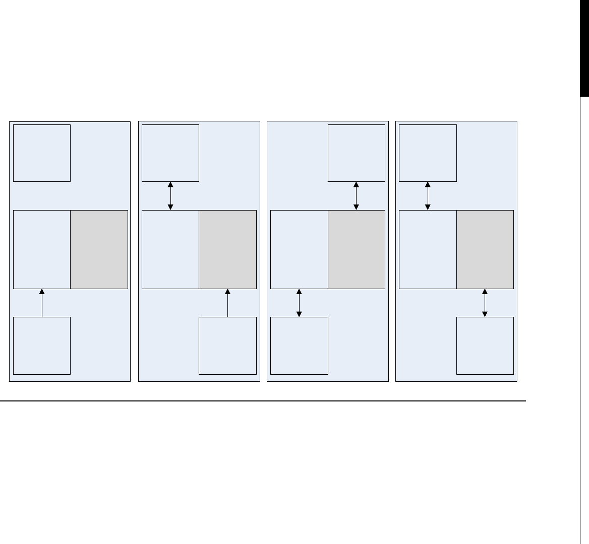
Buffer 0 Buffer 1
CPU
(Fill Buffer 0)
GPU
(Idle)
Cycle 0
Buffer 0 Buffer 1
CPU
(Fill Buffer 1)
GPU
(Process Buffer 0)
Cycle 1
Buffer 0 Buffer 1
CPU
(Read Buffer 0
Fill Buffer 0)
GPU
(Process Buffer 1)
Cycle 2
Buffer 0 Buffer 1
CPU
(Read Buffer 1
Fill Buffer 1)
GPU
(Process Buffer 0)
Cycle n
FIGURE 3.7
Double buffering with a single GPU.
48 CHAPTER 3 CUDA Hardware Overview

until this kernel has finished and then fetches the data from buffer 0 and then loads the next data
block into the same buffer. During this time the kernel kicked off at the start of the cycle is
processing data on the GPU in buffer 1.
Cycle N:We then repeat cycle 2, alternating between which buffer we read and write to on the CPU
with the buffer being processed on the GPU.
GPU-to-CPU and CPU-to-GPU transfers are made over the relatively slow (5 GB/s) PCI-E bus and
this dual-buffering method largely hides this latency and keeps both the CPU and GPU busy.
Compute 1.2
Compute 1.2 devices appeared with the low-end GT200 series hardware. These were the initial
GTX260 and GTX280 cards. With the GT200 series hardware, NVIDIA approximately doubled the
number of CUDA core processors on a single card, through doubling the number of multiprocessors
present on the card. We’ll cover CUDA cores and multiprocessors later. In effect, this doubled the
performance of the cards compared to the G80/G92 range before them.
Along with doubling the number of multiprocessors, NVIDIA increased the number of concurrent
warps a multiprocessor could execute from 24 to 32. Warps are blocks of code that execute within
a multiprocessor, and increasing the amount of available warps per multiprocessor gives us more scope
to get better performance, which we’ll look at later.
Issues with restrictions on coalesced access to the global memory and bank conflicts in the shared
memory found in compute 1.0 and compute 1.1 devices were greatly reduced. This make the GT200
series hardware far easier to program and it greatly improved the performance of many previous,
poorly written CUDA programs.
Compute 1.3
The compute 1.3 devices were introduced with the move from GT200 to the GT200 a/b revisions of the
hardware. This followed shortly after the initial release of the GT200 series. Almost all higher-end
cards from this era were compute 1.3 compatible.
The major change that occurs with compute 1.3 hardware is the introduction of support for
limited double-precision calculations. GPUs are primarily aimed at graphics and here there is
a huge need for fast single-precision calculations, but limited need for double-precision ones.
Typically, you see an order of magnitude drop in performance using double-precision as opposed
to single-precision floating-point operations, so time should be taken to see if there is any way
single-precision arithmetic can be used to get the most out of this hardware. In many cases,
a mixture of single and double-precision operations can be used, which is ideal since it exploits
both the dedicated single-precision and double-precision hardware present.
Compute 2.0
Compute 2.0 devices saw the switch to Fermi hardware. The original guide for tuning applications for
the Fermi architecture can be found on the NVIDIA website at http://developer.nvidia.com/cuda/
nvidia-gpu-computing-documentation.
Compute Levels 49
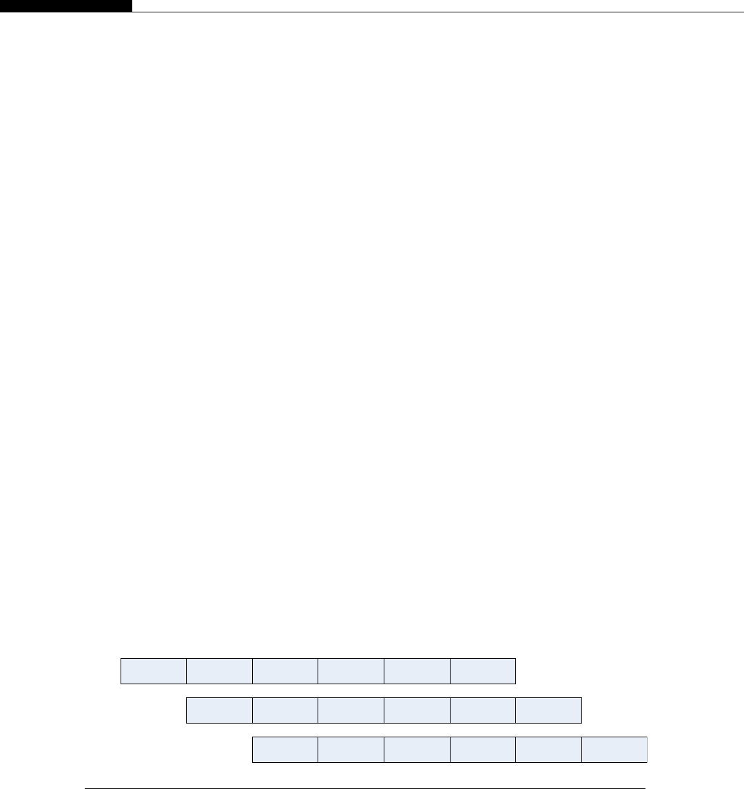
Some of the main changes in compute 2.x hardware are as follows:
• Introduction of 16 K to 48 K of L1 cache memory on each SP.
• Introduction of a shared L2 cache for all SMs.
• Support in Tesla-based devices for ECC (Error Correcting Code)-based memory checking and error
correction.
• Support in Tesla-based devices for dual-copy engines.
• Extension in size of the shared memory from 16 K per SM up to 48 K per SM.
• For optimum coalescing of data, it must be 128-byte aligned.
• The number of shared memory banks increased from 16 to 32.
Let’s look at the implications of some of these changes in detail. First, let’s pick up on the
introduction of the L1 cache and what this means. An L1 (level one) cache is a cache present on
a device and is the fastest cache type available. Compute 1.x hardware has no cache, except for the
texture and constant memory caches. The introduction of a cache makes it much easier for many
programmers to write programs that work well on GPU hardware. It also allows for applications that
do not follow a known memory pattern at compile time. However, to exploit the cache, the application
either needs to have a sequential memory pattern or have at least some data reuse.
The L2 cache is up to 768 K in size on Fermi and, importantly, is a unified cache, meaning it is
shared and provides a consistent view for all the SMs. This allows for much faster interblock
communication through global atomic operations. Compared to having to go out to the global memory
on the GPU, using the shared cache is an order of magnitude faster.
Support for ECC memory is a must for data centers. ECC memory provides for automatic error
detection and correction. Electrical devices emit small amounts of radiation. When in close proximity
to other devices, this radiation can change the contents of memory cells in the other device. Although
the probability of this happening is tiny, as you increase the exposure of the equipment by densely
packing it into data centers, the probability of something going wrong rises to an unacceptable level.
ECC, therefore, detects and corrects single-bit upset conditions that you may find in large data centers.
This reduces the amount of available RAM and negatively impacts memory bandwidth. Because this is
a major drawback on graphics cards, ECC is only available on Tesla products.
Dual-copy engines allow you to extend the dual-buffer example we looked at earlier to use multiple
streams. Streams are a concept we’ll look at in detail later, but basically, they allow for Nindependent
kernels to be executed in a pipeline fashion as shown in Figure 3.8.
Copy To Device Kernel Copy From
Device Copy To Device Kernel Copy From
Device
Copy To Device Kernel Copy From
Device Copy To Device Kernel Copy From
Device
Copy To Device Kernel Copy From
Device Copy To Device Kernel
Stream 0
Stream 1
Stream 2 Copy From
Device
FIGURE 3.8
Stream pipelining.
50 CHAPTER 3 CUDA Hardware Overview

Notice how the kernel sections run one after another in the figure. The copy operations are hidden
by the execution of a kernel on another stream. The kernels and the copy engines execute concurrently,
thus making the most use of the relevant units.
Note that the dual-copy engines are physically available on almost all the top-end Fermi GPUs,
such as the GTX480 or GTX580 device. However, only the Tesla cards make both engines visible to
the CUDA driver.
Shared memory also changed drastically, in that it was transformed into a combined L1 cache. The
L1 cache size is 64 K. However, to preserve backward compatibility, a minimum of 16 K must be
allocated to the shared memory, meaning the L1 cache is really only 48 K in size. Using a switch,
shared memory and L1 cache usage can be swapped, giving 48 K of shared memory and 16 K of L1
cache. Going from 16 K of shared memory to 48 K of shared memory is a huge benefit for certain
programs.
Alignment requirements for optimal use became more strict than in previous generations, due to the
introduction of the L1 and L2 cache. Both use a cache line size of 128 bytes. A cache line is the
minimum amount of data the memory can fetch. Thus, if your program fetches subsequent elements of
the data, this works really well. This is typically what most CUDA programs do, with groups of threads
fetching adjacent memory addresses. The one requirement that comes out of this change is to have
128-byte alignment of the dataset.
However, if your program has a sparse and distributed memory pattern per thread, you need to
disable this feature and switch to the 32-bit mode of cache operation.
Finally, one of the last major changes we’ll pick up on is the increase of shared memory banks from
16 to 32 bits. This is a major benefit over the previous generations. It allows each thread of the current
warp (32 threads) to write to exactly one bank of 32 bits in the shared memory without causing a shared
bank conflict.
Compute 2.1
Compute 2.1 is seen on certain devices aimed specifically at the games market, such as the GTX460
and GTX560. These devices change the architecture of the device as follows:
• 48 CUDA cores per SM instead of the usual 32 per SM.
• Eight single-precision, special-function units for transcendental per SM instead of the usual four.
• Dual-warp dispatcher instead of the usual single-warp dispatcher.
The x60 series cards have always had a very high penetration into the midrange games market, so if
your application is targeted at the consumer market, it is important to be aware of the implication of
these changes.
Noticeably different on the compute 2.1 hardware is the sacrifice of dual-precision hardware to
increase the number of CUDA cores. For single-precision and integer calculation–dominated kernels,
this is a good tradeoff. Most games make little use of double-precision floating-point data, but
significant use of single-precision floating-point and integer math.
Warps, which we will cover in detail later, are groups of threads. On compute 2.0 hardware, the
single-warp dispatcher takes two clock cycles to dispatch instructions of an entire warp. On compute
2.1 hardware, instead of the usual two instruction dispatchers per two clock cycles, we now have four.
In the hardware, there are three banks of 16 CUDA cores, 48 CUDA cores in total, instead of the usual
Compute Levels 51

two banks of 16 CUDA cores. If NVIDIA could have just squeezed in another set of 16 CUDA cores,
you’d have an ideal solution. Maybe we’ll see this in future hardware.
The compute 2.1 hardware is actually a superscalar approach, similar to what is found on CPUs
from the original Pentium CPU onwards. To make use of all the cores, the hardware needs to identify
instruction-level parallelism (ILP) within a single thread. This is a significant divergence from the
universal thread-level parallelism (TLP) approach recommended in the past. For ILP to be present
there need to be instructions that are independent of one another. One of the easiest ways to do this is
via the special vector class covered later in the book.
Performance of compute 2.1 hardware varies. Some well-known applications like Folding at Home
perform really well with the compute 2.1 hardware. Other applications such as video encoding
packages, where it’s harder to extract ILP and memory bandwidth is a key factor, typically perform
much worse.
The final details of Kepler and the new compute 3.0 platform were, at the time of writing, still
largely unreleased. A discussion of the Kepler features already announced can be found in Chapter 12,
under ‘Developing for Future GPUs’.
52 CHAPTER 3 CUDA Hardware Overview

Setting Up CUDA 4
INTRODUCTION
This chapter is here for anyone who is completely new to CUDA. We look at how to install CUDA on
the various OSs, what tools you can use, and how CUDA compiles. Finally, we look at how to have the
API help you identify the coding and API errors everyone makes.
CUDA is supported on three major OSs: Windows, Mac, and Linux. By far the easiest platform
to use and learn CUDA with is the OS you are most familiar with using for programming
development. For an absolute beginner, the Windows OS in conjunction with Microsoft Visual
Cþþ is likely to be the best choice. Both the Windows and Mac installations are fairly much point
and click. Both provide fairly standard integrated development environments that work well with
CUDA.
INSTALLING THE SDK UNDER WINDOWS
To install CUDA onto a PC running Windows, you’ll need to download the following components
from the NVIDIA developer portal at http://developer.nvidia.com/cuda-toolkit-41. Note by the time
this book hit the press release 5 of the toolkit was in its release candidate phase. Please check the
NVIDIA website for the latest version.
You will need an already installed version of Microsoft Visual Studio 2005, 2008, or 2010. The first
step is to download and install the latest set of NVIDIA development drivers for your relevant
operating system from the previous link. Then you will need either the 32- or 64-bit version of the
CUDA toolkit and GPU computing and SDK code samples. Make sure you pick the correct version for
your OS. Install them in this order:
1. NVIDIA development drivers
2. CUDA toolkit
3. CUDA SDK
4. GPU computing SDK
5. Parallel Nsight debugger
CHAPTER
CUDA Programming. http://dx.doi.org/10.1016/B978-0-12-415933-4.00004-1
Copyright Ó2013 Elsevier Inc. All rights reserved.
53
Under Windows 7, the SDK installs all of its files into “ProgramData,” which is a hidden directory
of the C drive. To view the files you either need to always go via the CUDA SDK icon created on the
desktop or go to “Folder Options” in Windows and tell it to show hidden files (Figure 4.1).
VISUAL STUDIO
CUDA supports Visual Studio versions from 2005 to 2010 including, for the most part, the express
versions. The express versions are available free of charge from Microsoft. The professional versions
are also available to registered students free of charge via the DreamSpark program at https://www.
dreamspark.com.
To register all you need to do is supply your university or college details and identification
numbers and you can download Visual Studio and many other programming tools. The program
is also not just restricted to U.S.-based academic institutions, but available to students
worldwide.
On the whole, Visual Studio 2008 has the best support for CUDA and compiles somewhat quicker
than Visual Studio 2010. Visual Studio 2010 has, however, one very useful feature, which is automatic
FIGURE 4.1
“Folder Options” to see hidden files.
54 CHAPTER 4 Setting Up CUDA
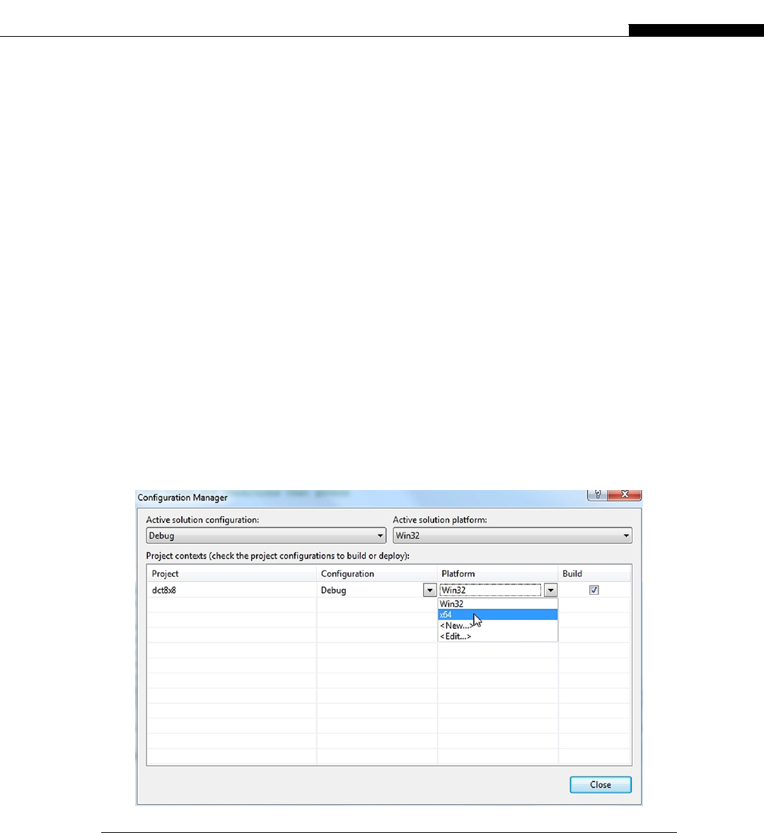
syntax checking of source code. Thus, if you use a type that is not defined, it underlines the error in red,
just as Microsoft Word underlines spelling errors. This is an incredibly useful feature as it saves a lot of
unnecessary compilation cycles for obvious issues. Thus, I’d recommend the 2010 version, especially
if you can download it for free from DreamSpark.
Projects
One quick way of creating a project is to take one of the SDK examples, remove all the unnecessary
project files, and insert your own source files. Note your CUDA source code should have a “.cu”
extension so that it will be compiled by the NVIDIA compiler instead of Visual C. However, as we see
later, you can also simply create a basic project framework using the project template wizard.
64-bit users
When using Windows 64-bit version, be aware that some of the project files are set up to run as 32-bit
applications by default. Thus, when you try to build them you may get the error message: Fatal Error
LNK1181: cannot open input file ‘cutil32D.lib’.
This was not installed, as you most likely installed only the 64-bit version of the SDK along with
the 64-bit version of Windows. To correct this issue all we have to do is set the target from 64 bits to 32
bits, which we do using the Build menu in Visual Studio, and then change the platform to X64 as
shown in Figure 4.2.
FIGURE 4.2
Visual C platform selection.
Visual Studio 55
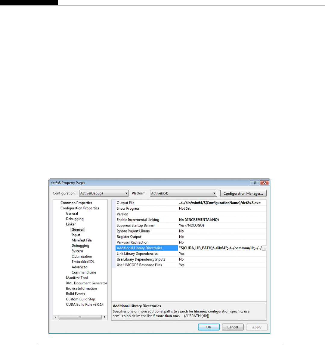
You may be prompted at the point you initiate a rebuild to save the project. Just add “_X86” to the
end of the project name and save. The project will then build under a 64-bit environment and link in the
correct library files.
You may also find an issue with a missing library, such as “cutil32.lib,” for example. When the SDK
is installed, it sets an environment variable, $(CUDA_LIB_PATH). This is usually set to: C:\Program
Files\NVIDIA GPU Computing Toolkit\CUDA\v4.1\lib\X64.
You may find the path setup in the default project files may not have $(CUDA_LIB_PATH) as one of
the entries. To add it, click on the project and then select “Project/Properties.” This brings up the
dialog box shown in Figure 4.3.
Clicking on the “.” button on the far right brings up a dialog where you can add the library path
(Figure 4.4). Simply add “$(CUDA_LIB_PATH)” as a new line and the project should now link.
If you wish to build both 64-bit CUDA applications and 32-bit CUDA applications, both the 32- and
64-bit CUDA toolkits need to be installed. The samples from the SDK also require both the 32- and 64-bit
versions of the SDK to be installed to be able to build both 32- and 64-bit versions of the samples.
You can build the necessary libraries by going to the following directories and building the
solution files:
C:\ProgramData\NVIDIA Corporation\NVIDIA GPU Computing SDK 4.1\C\common
C:\ProgramData\NVIDIA Corporation\NVIDIA GPU Computing SDK 4.1\shared
FIGURE 4.3
Additional library path.
56 CHAPTER 4 Setting Up CUDA
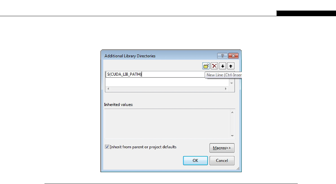
You will find the necessary libraries in
C:\ProgramData\NVIDIA Corporation\NVIDIA GPU Computing SDK 4.1\C\common\lib\X64.
You can also add these manually to any project that is missing them. Unfortunately, the SDK
samples are not set up so they automatically build the necessary libraries when needed. The
binaries for the libraries also are not supplied, which makes actually building the SDK samples
a little frustrating.
Creating projects
To create a new CUDA-enabled application, simply create a CUDA application using the
“File/New/Project Wizard” as shown in Figure 4.5. The wizard will then create a single project
containing the file “kernel.cu,” which contains a mix of code, some of which executes on the CPU
and some of which executes on the GPU. The GPU code is contained in the function addKernel.
This function simply takes a pointer to a destination array, c, and a couple of pointers to two input
arrays, aand b. It then adds the contents of the aand barrays together and stores the result in the
destination array, c. It’s a very simple example of the framework needed to execute a CUDA
program.
Also included is the basic code to copy data to a device, invoke the kernel, and copy data back from
the device to the host. It’s a very useful starter project to get you compiling something under CUDA.
We cover the standard framework needed to get a CUDA program working later in the text. It’s useful
to look at the code and try to understand it if you can. However, don’t worry at this stage if it doesn’t
make sense as we’ll build gradually on how to write programs for CUDA.
FIGURE 4.4
Adding library directories.
Visual Studio 57
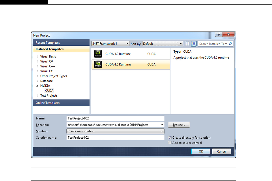
LINUX
CUDA is supported for the following Linux distributions. The supported versions will vary depending
on which version of the CUDA toolkit you are installing.
• Fedora 14
• Redhat 6.0 and 5.5/CentOS 6.2 (the free version of Redhat)
• Ubuntu 11.04
• OpenSUSE 11.2
The first step in installing CUDA on a Linux platform is to make sure you have the latest set of kernel
software. Use the following command from a terminal window to do this:
sudo yum update
The sudo command will log you in as the administrator. The yum command is the standard
installation tool for the Linux RPM package. You are simply asking it to check for all installed
packages and see if any updates are available. This ensures your system is fully up to date before
installing any drivers. Many of the GUI-based installations also have GUI-based versions of the
software updates that replace the older command line update interface.
Once the kernel has been updated to the latest level, run the following command:
sudo yum install gcc-cþþ kernel-devel
FIGURE 4.5
CUDA Project Wizard.
58 CHAPTER 4 Setting Up CUDA

This will install the standard GNU Cþþ environment as well as the kernel source you’ll need to
rebuild the kernel. Be aware that package names are case-sensitive. This will prompt you for around
a 21 MB download and take a couple of minutes to install. Again, if you prefer, you can install the
package via the GUI software installer for the particular OS.
Finally, as you are likely to be drawing some graphical output, you’ll need an OpenGL develop-
ment environment. Install this with the following command:
sudo yum install freeglut-devel libXi-devel libXmu-devel
Now you’re ready to install the CUDA drivers. Make sure you install at least version 4.1 of the CUDA
toolkit. There are a number of ways to install the updated NVIDIA drivers. NVIDIA does not release the
source code to the drivers, so by default most Linux distributions install a very basic graphics driver.
Kernel base driver installation (CentOS, Ubuntu 10.4)
The CUDA releases should be used with a specific set of development drivers. Installing drivers by
methods other than the one listed here may result in CUDA not working. Note the versions of the OS
supported for the given version of the CUDA toolkit. These may not be the latest version of the
particular Linux distribution. Using a later distribution will likely not work. Thus, the first installation
step is to replace any existing drivers with the version specified for your specific Linux distribution.
See Figure 4.6.
Once the download is complete, you need to boot Linux in text-only mode. Unlike Windows, which
is always in graphics mode, text mode is required to install the drivers under Linux. You can make the
system boot into text on most distributions using the following command from a Terminal window
(usually under the Systems menu in the GUI):
sudo init 3
This will reboot the Linux machine and bring it back up in text mode. You can use sudo init 5 to
restore the graphics mode later.
If you get an error such as “User <user_name>is not in sudoers file,” login as root using the su
command. Edit the “/etc/sudoers” file and append the following line:
your_user_name ALL¼(ALL) ALL
Be careful to replace your_user_name with your login name.
Certain distributions (e.g., Ubuntu) insist on booting to the GUI, regardless of the init mode. One
method of resolving is as follows, from a text window. Edit the grub startup file:
sudo chmod þw /etc/default/grub
sudo nano /etc/default/grub
Change the following lines:
GRUB_CMDLINE_LINUX_DEFAULT¼"quiet splash"
GRUB_CMDLINE_LINUX_DEFAULT¼""
to
# GRUB_CMDLINE_LINUX_DEFAULT¼"quiet splash"
GRUB_CMDLINE_LINUX_DEFAULT¼"text"
Linux 59
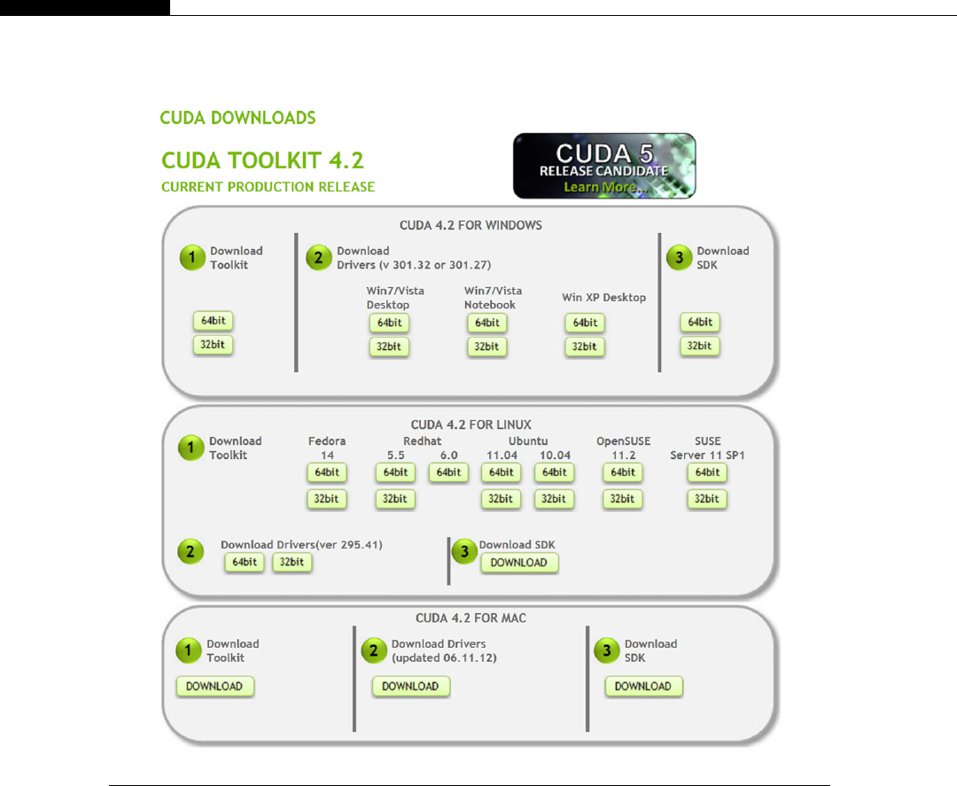
Now update grub using
sudo update-grub
Finally, reboot your machine and it should come up in text-only mode. Use the original lines to boot
to the GUI again once the drivers are installed.
Now navigate to the area you stored the “.run” file you downloaded from the NVIDIA website.
Then type
sudo sh NVIDIA-Linux-x86_64-285.05.33.run
FIGURE 4.6
Supported Linux downloads and supported driver versions as of September 2012.
60 CHAPTER 4 Setting Up CUDA

The exact version of the driver you download will of course be different. You will be asked to
agree to the NVIDIA license and will then have to wait a few minutes while everything installs.
During this process the installer will attempt to replace the default Nouveau driver with the necessary
NVIDIA drivers. If asked if you want to do this, select “Yes.” This is an error-prone process and not
every distribution works out of the box. If the NVIDIA installer is unable to remove the Nouveau
driver then it may be necessary to blacklist the driver so the NVIDIA installer can install the correct
drivers.
When you have the NVIDIA drivers installed correctly, type
sudo init 5
The machine will then reboot into the regular graphics mode. See earlier for Ubuntu.
The next task is to install the toolkit. There are a number availabledselect Fedora, Red Hat,
Ubuntu, OpenSUSE, or SUSE depending on your distribution. As before, simply navigate to where
you installed the SDK and run it by typing
sudo sh <sdk_version>.run
where <sdk_version> is the file you downloaded. It will then install all the tools needed and print
a message saying the installation was successful. It then mentions you have to update the PATH and
LD_LIBRARY_PATH environment variables, which you have to do by hand. To do this, you need to edit
the “/etc/profile” startup file. Add the following lines:
export PATH¼/usr/local/cuda/bin:$PATH
export LD_LIBRARY_PATH¼/usr/local/cuda/lib:$LD_LIBRARY_PATH
Note that the file has to be writable. Use the “sudo chmod +w /etc/profile” to make it writable if
required. You can edit this file with your favorite editor using such a command as “sudo nano/etc/
profile”.
Now log out and log back in again and type
env
This will list all of the current environment variable settings. Check for the two new entries you just
amended. CUDA is now installed into the “/usr/local/bin” directory.
Next we’ll need the GNU Cþþ compiler. Install the package “gþþ” from whatever software
installer you are using on your system.
The next step is to install the SDK sample codes, so we have something to build and test. Download
these from the NVIDIA site and run them, again using the sh sdk_version.run command (replace
sdk_version with the actual one you download). Do not run this install as root as you will otherwise
have to be logged in as root to build any of the samples.
By default the SDK will install to a subdirectory of your user account area. It may complain it can’t
find the CUDA installation and will use the default directory (the same one CUDA was installed to
earlier). You can safely ignore this message.
Once the GPU computing SDK is installed, you then need to go to the “Common” subdirectory and
run make to create a set of libraries.
Once this is done the SDK samples should build, allowing you to execute your first CUDA program
in Linux and of course see if the driver is working correctly.
Linux 61

MAC
The Macintosh version is available, as with the other versions, from http://developer.nvidia.com/cuda-
toolkit-41. Simply download and install the packages in the following order:
• Development drivers
• CUDA toolkit
• CUDA tools SDK and code samples
CUDA 4.1 requires Mac OS release 10.6.8 (Snow Leopard) or later. The latest release (10.7.x) or
LionreleaseisavailableasadownloadfromtheApplestoreorviaaseparatepurchasefrom
Apple.
The SDK installs into the “GPU Computing” directory under the “Developer” higher-level
directory. Simply browse the “Developer/GPU Computing/C/bin/darwin/release” directory and you
will find precompiled executables. Running the deviceQuery tool is useful to verify you have correctly
installed the drivers and runtime environment.
To compile the samples, you will need XCode installed. This is the equivalent of GCC (GNU C
Compiler) for the Mac. XCode can be downloaded from the Apple store. It’s not a free product, but is
available free of charge to anyone on the Apple Developer program, which includes both development
of Macintosh and iPhone/iPad applications. It was also released shortly after the Lion OS as a free
download for Lion OS owners.
Once XCode is installed, simply open a terminal window. To do this, go to Finder, open Utilities,
and then double-click on the Terminal window. Type the following:
cd /Developer/’GPU Computing/C/src/project’
make–i
Replace project with the name of the particular SDK application you wish to compile. If you
receive compilation errors, you have either not downloaded the XCode package or have an older
version than is required.
INSTALLING A DEBUGGER
CUDA provides a debug environment called Parallel Nsight on the Windows platform. This provides
support for debugging CPU and GPU code and highlights areas where things are working less than
efficiently. It also helps tremendously when trying to debug multithreaded applications.
Nsight is completely free and is a hugely useful tool. All it requires is that you register as a CUDA-
registered developer, which is again entirely free. Once registered, you will be able to download the
tool from the NVIDIA website.
Note that you must have Visual Studio 2008 or later (not the express version) and you must have
installed Service Pack 1. There is a link within the release notes of Nsight to the SP1 download you
need to install.
Parallel Nsight comes as two parts, an application that integrates itself into Visual Studio as
shown in Figure 4.7, and a separate monitoring application. The monitoring application works in
conjunction with the main application. The monitor is usually resident, but does not have to be, on
62 CHAPTER 4 Setting Up CUDA
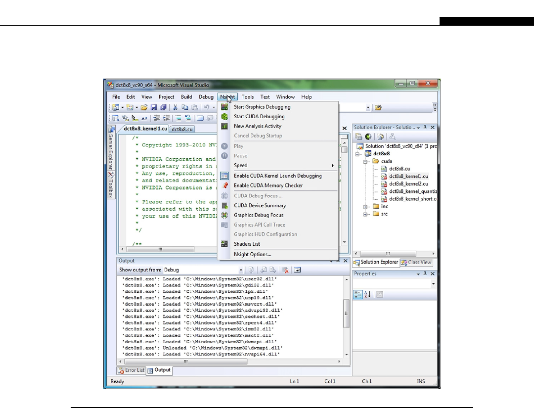
the same machine as the Visual Studio environment. Parallel Nsight works best with two CUDA
capable GPUs, a dedicated GPU to run the code on and one to use as the regular display. Thus, the
GPU running the target code cannot be used to run a second display. As most GPU cards have
dual-monitor outputs, you can simply run two monitors off the display card should you have
a dual-monitor setup. Note in the latest release, 2.2, the need for two GPUs was dropped.
It’s also possible to set up the tool to acquire data from a remote GPU. However, in most cases it’s
easier to buy a low-end GPU and install it into your PC or workstation. The first step needed to set
up Parallel Nsight on Windows is to disable TDR (Figure 4.8). TDR (Timeout Detection and
Recovery) is a mechanism in Windows that detects crashes in the driver-level code. If the driver stops
responding to events, Windows resets the driver. As the driver will halt when you define a breakpoint,
this feature needs to be disabled.
To set the value, simply run the monitor and click on the “Nsight Monitor Options” hyperlink at the
bottom right of the monitor dialog box. This will bring up the dialog shown in Figure 4.8. Setting the
FIGURE 4.7
Nsight integrated into Microsoft Visual Studio.
Installing a Debugger 63
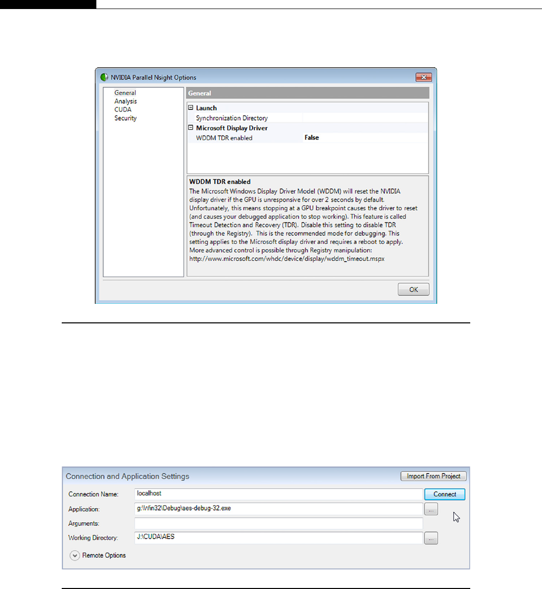
“WDDM TDR enabled” will modify the registry to disable this feature. Reboot your PC, and Parallel
Nsight will no longer warn you TDR is enabled.
To use Parallel Nsight on a remote machine, simply install the monitor package only on the remote
Windows PC. When you first run the monitor, it will warn you Windows Firewall has blocked “Public
network” (Internet based) access to the monitor, which is entirely what you want. However, the tool
needs to have access to the local network, so allow this exception to any firewall rules you have set up
on the monitor machine. As with a local node, you will have to fix the TDR issue and reboot once
installed.
FIGURE 4.8
Disabling Windows kernel timeout.
FIGURE 4.9
Parallel Nsight remote connection.
64 CHAPTER 4 Setting Up CUDA
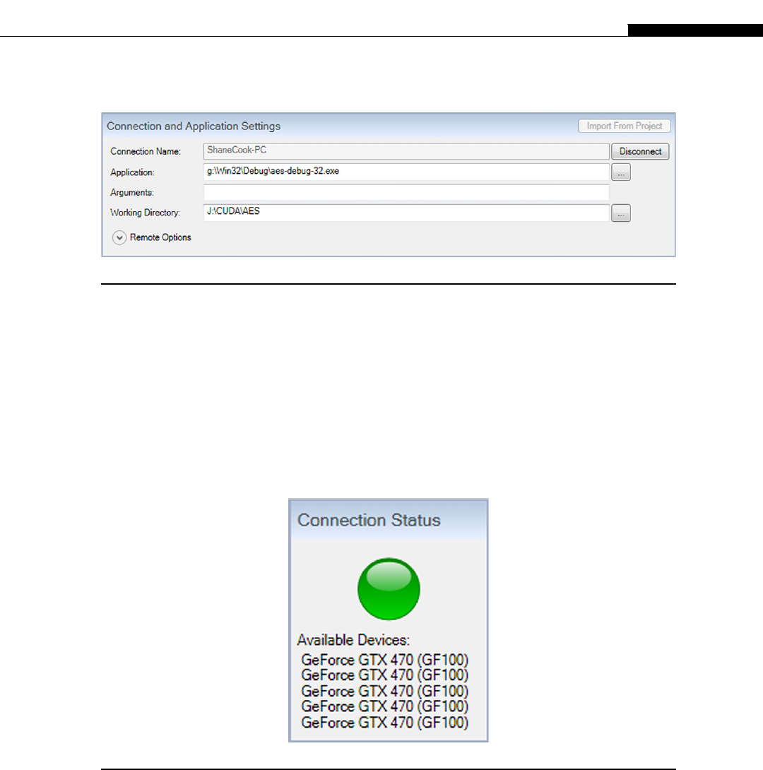
The next step is to run Visual Studio on the host PC and select a new analysis activity. You will see
a section near the top of the window that looks like Figure 4.9. Notice the “Connection Name” says
localhost, which just means your local machine. Open Windows Explorer and browse the local
network to see the name of the Windows PC you would like to use to remotely debug. Replace
localhost with the name shown in Windows Explorer. Then press the “Connect” button. You should
see two confirmations that the connection has been made as shown in Figure 4.10.
First, the “Connect” button will change to a “Disconnect.” Second, the “Connection Status” box
should turn green and show all the possible GPUs on the target machine (Figure 4.11). In this case
we’re connecting to a test PC that has five GTX470 GPU cards set up on it.
Clicking on the “Launch” button on the “Application Control” panel next to the “Connection
Status” panel will remotely launch the application on the target machine. However, prior to this all the
necessary files need to be copied to the remote machine. This takes a few seconds or so, but is all
automatic. Overall, it’s a remarkably simple way of analyzing/debugging a remote application.
FIGURE 4.10
Parallel Nsight connected remotely.
FIGURE 4.11
Parallel Nsight connection status.
Installing a Debugger 65

You may wish to set up Parallel Nsight in this manner if, for example, you have a laptop and wish to
debug, or simply remotely run, an application that will run on a GPU server. Such usage includes when
a GPU server or servers are shared by people who use it at different times, teaching classes, for
example. You may also have remote developers who need to run code on specially set up test servers,
perhaps because those servers also contain huge quantities of data and it’s not practical or desirable to
transfer that data to a local development machine. It also means you don’t need to install Visual Cþþ
on each of the remote servers you might have.
On the Linux and Mac side the debugger environment is CUDA-GDB. This provides an extended
GNU debugger package. As with Parallel Nsight it allows debugging of both host and CUDA code,
which includes setting a breakpoint in the CUDA code, single step, select a debug thread, etc. Both
CUDA-GDB and the Visual Profiler tools are installed by default when you install the SDK, rather than
being a separate download as with Parallel Nsight. As of 2012, Parallel Nsight was also released under
the Eclipse environment for Linux.
The major difference between Windows and Mac/Linux was the profiling tool support. The Parallel
Nsight tool is in this respect vastly superior to the Visual Profiler. The Visual Profiler is also available
on Windows. It provides a fairly high-level overview and recommendations as to what to address in the
code, and therefore is very suited to those starting out using CUDA. Parallel Nsight, by contrast, is
aimed at a far more advanced user. We cover usage of both Parallel Nsight and Visual Profiler later in
subsequent chapters. However, the focus throughout this text is on the use of Parallel Nsight as the
primary debugging/analysis tool for GPU development.
For advanced CUDA development I’d strongly recommend using Parallel Nsight for debugging
and analysis. For most people new to CUDA the combination of the Visual Profiler and CUDA-GDB
work well enough to allow for development.
COMPILATION MODEL
The NVIDIA compiler, NVCC, sits in the background and is invoked when a CUDA source file needs
to be compiled. The file extensions shown in Table 4.1 are used to define files as with CUDA source
files or regular source files. This determines which compiler will be invoked, NVCC or the host
compiler.
The generated executable file, or fat binary, contains one or more binary executable images for the
different GPU generations. It also contains a PTX image, allowing the CUDA runtime to do just-in-
time (JIT) compilation. This is very similar to Java byte code where the target is a virtual architecture,
and this is compiled to the actual target hardware at the point the program is invoked. The PTX JIT
Table 4.1 Different CUDA File Types
File Extension Meaning Processed By
.cu Mixed host and device source file. NVCC
.cup A preprocessed expanded version of .cu file. NVCC
.c, .cc, .cpp A host C or Cþþ source file. Host compiler
.ptx, .gpu Intermediate virtual assembly files. NVCC
.cubin Binary image of GPU code. NVCC
66 CHAPTER 4 Setting Up CUDA

compilation only happens if the executable does not contain a binary image that is identical to the GPU
in use. Consequently, all future architectures are backward compatible with the basic-level virtual
architecture. Even GPUs for which the program was not compiled will execute legacy GPU code by
simply compiling at runtime the PTX code embedded in the executable.
Just as with Java, code depositories are supported. Defining the environment variable
CUDA_DEVCODE_CACHE to point to a directory will cause the runtime to save the compiled binary for later
use, thus avoiding the startup delay necessary to compile the PTX code for the unknown GPU variant
every time it is invoked.
We cover in the later chapters how you can view the real target assembly code, the result of the PTX
to target translation.
ERROR HANDLING
Error handling in CUDA, as with C in general, is not as good as it could be. There are few runtime
checks performed, and if you do something stupid, the runtime will usually allow it. This results in
GPU programs that exit strangely. If you are lucky, you will get an error message which, like compiler
errors, you learn to interpret over time.
Almost all function calls in CUDA return the error type cudaError_t, which is simply an
integer value. Any value other than cudaSuccess will indicate a fatal error. This is usually caused
by your program not setting up something correctly prior to use, or using an object after it
has been destroyed. It can also be caused by the GPU kernel timeout present in Microsoft
Windows if the kernel runs for more than a few seconds and you have not disabled this when
installing tools such as Parallel Nsight (see previous section). Out-of-bounds memory accesses
may generate exceptions that will often print various error messages to stderr (standard error
output).
As every function returns an error code, every function call must be checked and some handler
written. This makes for very tiresome and highly indented programming. For example,
if (cudaMalloc(.)¼¼ cudaSuccess)
{
if (cudaEventCreate(&event) ¼¼ cudaSucess)
{
.
}
}
else
{
.
}
To avoid this type of repetitive programming, throughout the book we will use the following macro
definition to making calls to the CUDA API:
#define CUDA_CALL(x) {const cudaError_t a ¼(x); if (a !¼cudaSuccess) { printf("\nCUDA
Error: %s (err_num¼%d) \n", cudaGetErrorString(a), a); cudaDeviceReset(); assert(0);} }
What this macro does is to allow you to specify xas some function call, for example,
Error Handling 67

CUDA_CALL(cudaEventCreate(&kernel_start));
This then creates a temporary variable aand assigns to it the return value of the function, which is of
type cudaError_t. It then checks if this is not equal to cudaSuccess, that is, the call encountered some
error. If there was an error detected, it prints to the screen the error returned plus a short description of
what the error means. It also uses the assert macro, which identifies the source file and line in which the
error occurs so you can easily track down the point at which the error is being detected.
This technique works for all the CUDA calls except for the invocation of kernels. Kernels are the
programs you write to run on the GPU. These are executed using the <<< and >>> operators as follows:
my_kernel <<<num_blocks, num_threads>>>(param1, param2,.);
For error checking of kernels, we’ll use the following function:
__host__ void cuda_error_check(const char * prefix, const char * postfix)
{
if (cudaPeekAtLastError() !¼cudaSuccess)
{
printf("\n%s%s%s", prefix, cudaGetErrorString(cudaGetLastError()), postfix);
cudaDeviceReset();
wait_exit();
exit(1);
}
}
This function should be called immediately after executing the kernel call. It checks for any
immediate errors, and if so, prints an error message, resets the GPU, optionally waits for a key press via
the wait_exit function, and then exits the program.
Note that this is not foolproof, as the kernel call is asynchronous with the CPU code. That is, the
GPU code is running in the background at the time we call cudaPeekAtLastError. If there has been
no error detected at this time, then we see no error printed and the function continues to the next
code line. Often that next code line will be a copy back from GPU memory to CPU memory. The
error in the kernel may cause a subsequent API call to fail, which is almost always the next API call
after the kernel call. Surrounding all calls to the API with the CUDA_CALL macro will flag the error at
this point.
You can also force the kernel to complete prior to the error checking by simply inserting a call to
cudaDeviceSynchronize prior to the cudaPeekAtLastError call. However, only do this on the debug
version of the program or where you want the CPU to idle while the GPU is busy. As you should
understand by the end of this text, such synchronous operation is good for debugging, but will harm
performance, so you should be careful these calls do not remain in production code if they were
inserted solely for debugging.
CONCLUSION
You should now have a working installation of the CUDA SDK, including the GPU computing SDK
samples and a debugging environment. You should be able to build a simple GPU SDK sample, such as
the deviceQuery project, and have it identify the GPUs in your system when run.
68 CHAPTER 4 Setting Up CUDA

Grids, Blocks, and Threads 5
WHAT IT ALL MEANS
NVIDIA chose a rather interesting model for its scheduling, a variant of SIMD it calls SPMD (single
program, multiple data). This is based on the underlying hardware implementation in many respects.
At the heart of parallel programming is the idea of a thread, a single flow of execution through the
program in the same way a piece of cotton flows through a garment. In the same way threads of cotton
are woven into cloth, threads used together make up a parallel program. The CUDA programming
model groups threads into special groups it calls warps, blocks, and grids, which we will look at in turn.
THREADS
A thread is the fundamental building block of a parallel program. Most C programmers are familiar
with the concept if they have done any multicore programming. Even if you have never launched
a thread in any code, you will be familiar with executing at least one thread, the single thread of
execution through any serial piece of code.
With the advent of dual, quad, hex core processors, and beyond, more emphasis is explicitly placed
on the programmer to make use of such hardware. Most programs written in the past few decades, with
the exception of perhaps the past decade, were single-thread programs because the primary hardware
on which they would execute was a single-core CPU. Sure, you had clusters and supercomputers that
sought to exploit a high level of parallelism by duplicating the hardware and having thousands of
commodity servers instead of a handful of massively powerful mac
ines. However, these were mostly restricted to universities and large institutions, not generally
available to the masses.
Thinking in terms of lots of threads is hard. It’s much easier to think in terms of one task at a time.
Serial programming languages like C/Cþþ were born from a time when serial processing speed
doubled every few years. There was little need to do the hard parallel programming. That stopped
almost a decade ago, and now, like it or not, to improve program speed requires us to think in terms of
parallel design.
Problem decomposition
Parallelism in the CPU domain tends to be driven by the desire to run more than one (single-threaded)
program on a single CPU. This is the task-level parallelism that we covered earlier. Programs, which
CHAPTER
CUDA Programming. http://dx.doi.org/10.1016/B978-0-12-415933-4.00005-3
Copyright Ó2013 Elsevier Inc. All rights reserved.
69
are data intensive, like video encoding, for example, use the data parallelism model and split the task in
Nparts where Nis the number of CPU cores available. You might, for example, have each CPU core
calculate one “frame” of data where there are no interdependencies between frames. You may also
choose to split each frame into Nsegments and allocate each one of the segments to an individual core.
In the GPU domain, you see exactly these choices when attempting to speed up rendering of 3D
worlds in computer games by using more than one GPU. You can send complete, alternate frames to
each GPU (Figure 5.1). Alternatively, you can ask one GPU to render the different parts of the screen.
However, there is a trade off here. If the dataset is self-contained, you can use less memory and transfer
less data by only providing the GPU (or CPU) with the subset of the data you need to calculate. In the SFR
GPU example used here, there may be no need for GPU3, which is rendering the floor to know the content
of data from GPU0, which is probably rendering the sky. However, there may be shadows from a flying
object, or the lighting level of the floor may need to vary based on the time of day. In such instances, it
might be more beneficial to go with the alternate frame rendering approach because of this shared data.
We refer to SFR type splits as coarse-grained parallelism. Large chunks of data are split in some
way between Npowerful devices and then reconstructed later as the processed data. When designing
applications for a parallel environment, choices at this level seriously impact the performance of your
programs. The best choice here is very much linked to the actual hardware you will be using, as you
will see with the various applications we develop throughout this book.
With a small number of powerful devices, such as in CPUs, the issue is often how to split the
workload evenly. This is often easier to reason with because you are typically talking about only
a small number of devices. With huge numbers of smaller devices, as with GPUs, they average out
peaks in workload much better, but suffer from issues around synchronization and coordination.
In the same way as you have macro (large-scale) and micro (small-scale) economics, you have
coarse and fine-grained parallelism. However, you only really find fine-grained parallelism at the
Frame N+3 - GPU3
Frame N+2 - GPU2
Frame N+1 - GPU1
Frame N - GPU0
FIGURE 5.1
Alternate frame rendering (AFR) vs. Split Frame
Rendering (SFR).
Top - GPU0
Middle-Top - GPU1
Middle-Bottom - GPU2
Bottom - GPU3
FIGURE 5.2
Coarse-grained parallelism.
70 CHAPTER 5 Grids, Blocks, and Threads

programmer level on devices that support huge numbers of threads, such as GPUs. CPUs, by contrast,
also support threads, but with a large overhead and thus are considered to be useful for more coar-
se-grained parallelism problems. CPUs, unlike GPUs, follow the MIMD (Multiple Instruction
Multiple Data) model in that they support multiple independent instruction streams. This is a more
flexible approach, but incurs additional overhead in terms of fetching multiple independent instruction
streams as opposed to amortizing the single instruction stream over multiple processors.
To put this in context, let’s consider a digital photo where you apply an image correction function to
increase the brightness. On a GPU you might choose to assign one thread for every pixel in the image.
On a quad-core CPU, you would likely assign one-quarter of the image to each CPU core.
How CPUs and GPUs are different
GPUs and CPUs are architecturally very different devices. CPUs are designed for running a small
number of potentially quite complex tasks. GPUs are designed for running a large number of quite
simple tasks. The CPU design is aimed at systems that execute a number of discrete and unconnected
tasks. The GPU design is aimed at problems that can be broken down into thousands of tiny fragments
and worked on individually. Thus, CPUs are very suitable for running operating systems and appli-
cation software where there are a vast variety of tasks a computer may be performing at any given time.
CPUs and GPUs consequently support threads in very different ways. The CPU has a small number
of registers per core that must be used to execute any given task. To achieve this, they rapidly context
switch between tasks. Context switching on CPUs is expensive in terms of time, in that the entire
register set must be saved to RAM and the next one restored from RAM. GPUs, by comparison, also
use the same concept of context switching, but instead of having a single set of registers, they have
multiple banks of registers. Consequently, a context switch simply involves setting a bank selector to
switch in and out the current set of registers, which is several orders of magnitude faster than having to
save to RAM.
Both CPUs and GPUs must deal with stall conditions. These are generally caused by I/O operations
and memory fetches. The CPU does this by context switching. Providing there are enough tasks and
the runtime of a thread is not too small, this works reasonably well. If there are not enough processes to
keep the CPU busy, it will idle. If there are too many small tasks, each blocking after a short period, the
CPU will spend most of its time context switching and very little time doing useful work. CPU
scheduling policies are often based on time slicing, dividing the time equally among the threads. As the
number of threads increases, the percentage of time spent context switching becomes increasingly
large and the efficiency starts to rapidly drop off.
GPUs are designed to handle stall conditions and expect this to happen with high frequency. The
GPU model is a data-parallel one and thus it needs thousands of threads to work efficiently. It uses
this pool of available work to ensure it always has something useful to work on. Thus, when it hits
a memory fetch operation or has to wait on the result of a calculation, the streaming processors
simply switch to another instruction stream and return to the stalled instruction stream sometime
later.
One of the major differences between CPUs and GPUs is the sheer number of processors on each
device. CPUs are typically dual- or quad-core devices. That is to say they have a number of execution
cores available to run programs on. The current Fermi GPUs have 16 SMs, which can be thought of
a lot like CPU cores. CPUs often run single-thread programs, meaning they calculate just a single data
Threads 71
point per core, per iteration. GPUs run in parallel by default. Thus, instead of calculating just a single
data point per SM, GPUs calculate 32 per SM. This gives a 4 times advantage in terms of number of
cores (SMs) over a typical quad core CPU, but also a 32 times advantage in terms of data throughput.
Of course, CPU programs can also use all the available cores and extensions like MMX, SSE, and
AVX. The question is how many CPU applications actually use these types of extensions.
GPUs also provide something quite uniquedhigh-speed memory next to the SM, so-called
shared memory. In many respects this implements the design philosophy of the Connection Machine
and the Cell processor, in that it provides local workspace for the device outside of the standard
register file. Thus, the programmer can leave data in this memory, safe in the knowledge the
hardware will not evict it behind his or her back. It is also the primary mechanism communication
between threads.
Task execution model
There are two major differences in the task execution model. The first is that groups of NSPs execute
in a lock-step basis (Figure 5.3), running the same program but on different data. The second is that,
because of this huge register file, switching threads has effectively zero overhead. Thus, the GPU can
support a very large number of threads and is designed in this way.
Now what exactly do we mean by lock-step basis? Each instruction in the instruction queue is
dispatched to every SP within an SM. Remember each SM can be thought of as single processor with
Ncores (SPs) embedded within it.
A conventional CPU will fetch a separate instruction stream for each CPU core. The GPU SPMD
model used here allows an instruction fetch for Nlogical execution units, meaning you have 1/Nthe
instructions memory bandwidth requirements of a conventional processor. This is a very similar
approach to the vector or SIMD processors found in many high-end supercomputers.
However, this is not without its costs. As you will see later, if the program does not follow a nice
neat execution flow where all Nthreads follow the same control path, for each branch, you will require
additional execution cycles.
SM 0
Instruction2
Instruction1
Instruction0
SP 0 SP 1 SP 2 SP 3 SP 4 SP 5 SP 6 SP 7
FIGURE 5.3
Lock-step instruction dispatch.
72 CHAPTER 5 Grids, Blocks, and Threads

Threading on GPUs
So coming back to threads, let’s look at a section of code and see what this means from a programming
perspective.
void some_func(void)
{
int i;
for (i¼0;i<128;iþþ)
{
a[i] ¼b[i] * c[i];
}
}
This piece of code is very simple. It stores the result of a multiplication of band cvalue for a given
index in the result variable afor that same index. The for loop iterates 128 times (indexes 0 to 127). In
CUDA you could translate this to 128 threads, each of which executes the line
a[i] ¼b[i] * c[i];
This is possible because there is no dependency between one iteration of the loop and the next.
Thus, to transform this into a parallel program is actually quite easy. This is called loop parallelization
and is very much the basis for one of the more popular parallel language extensions, OpenMP.
On a quad-core CPU you could also translate this to four blocks, where CPU core 1 handles
indexes 0–31, core 2 indexes 32–63, core 3 indexes 64–95, and core 4 indexes 96–127. Some
compilers will either automatically translate such blocks or translate them where the programmer
marks that this loop can be parallelized. The Intel compiler is particularly good at this. Such
compilers can be used to create embedded SSE instructions to vectorize a loop in this way, in
addition to spawning multiple threads. This gives two levels of parallelism and is not too different
from the GPU model.
In CUDA, you translate this loop by creating a kernel function, which is a function that executes on
the GPU only and cannot be executed directly on the CPU. In the CUDA programming model the CPU
handles the serial code execution, which is where it excels. When you come to a computationally
intense section of code the CPU hands it over to the GPU to make use of the huge computational power
it has. Some of you might remember the days when CPUs would use a floating-point coprocessor.
Applications that used a large amount of floating-point math ran many times faster on machines fitted
with such coprocessors. Exactly the same is true for GPUs. They are used to accelerate computa-
tionally intensive sections of a program.
The GPU kernel function, conceptually, looks identical to the loop body, but with the loop structure
removed. Thus, you have the following:
__global__ void some_kernel_func(int * const a, const int * const b, const int * const c)
{
a[i] ¼b[i] * c[i];
}
Notice you have lost the loop and the loop control variable, i. You also have a __global__
prefix added to the C function that tells the compiler to generate GPU code and not CPU
Threads 73

code when compiling this function, and to make that GPU code globally visible from within
the CPU.
The CPU and GPU have separate memory spaces, meaning you cannot access CPU parameters in
the GPU code and vice versa. There are some special ways of doing exactly this, which we’ll cover
later in the book, but for now we will deal with them as separate memory spaces. As a consequence, the
global arrays a,b, and cat the CPU level are no longer visible on the GPU level. You have to declare
memory space on the GPU, copy over the arrays from the CPU, and pass the kernel function pointers to
the GPU memory space to both read and write from. When you are done, you copy that memory back
into the CPU. We’ll look at this a little later.
The next problem you have is that iis no longer defined; instead, the value of iis defined for you
by the thread you are currently running. You will be launching 128 instances of this function, and
initially this will be in the form of 128 threads. CUDA provides a special parameter, different for each
thread, which defines the thread ID or number. You can use this to directly index into the array. This is
very similar to MPI, where you get the process rank for each process.
The thread information is provided in a structure. As it’s a structure element, we will store it in
a variable, thread_idx for now to avoid having to reference the structure every time. Thus, the code
becomes:
__global__ void some_kernel_func(int * const a, const int * const b, const int * const c)
{
const unsigned int thread_idx ¼threadIdx.x;
a[thread_idx] ¼b[thread_idx] * c[thread_idx];
}
Note, some people prefer idx or tid as the name for the thread index since these are somewhat
shorter to type.
What is happening, now, is that for thread 0, the thread_idx calculation returns 0. For thread 1, it
returns 1, and so on, up to thread 127, which uses index 127. Each thread does exactly two reads from
memory, one multiply and one store operation, and then terminates. Notice how the code executed by
each thread is identical, but the data changes. This is at the heart of the CUDA and SPMD model.
In OpenMP and MPI, you have similar blocks of code. They extract, for a given iteration of the
loop, the thread ID or thread rank allocated to that thread. This is then used to index into the dataset.
A peek at hardware
Now remember you only actually have Ncores on each SM, so how can you run 128 threads? Well,
like the CPU, each thread group is placed into the SM and the NSPs start running the code. The first
thing you do after extracting the thread index is fetch a parameter from the band carray. Unfortu-
nately, this doesn’t happen immediately. In fact, some 400–600 GPU clocks can go by before the
memory subsystem comes back with the requested data. During this time the set of Nthreads gets
suspended.
Threads are, in practice, actually grouped into 32 thread groups, and when all 32 threads are
waiting on something such as memory access, they are suspended. The technical term for these groups
of threads is a warp (32 threads) and a half warp (16 threads), something we’ll return to later.
Thus, the 128 threads translate into four groups of 32 threads. The first set all run together to extract
the thread ID and then calculate the address in the arrays and issue a memory fetch request (see
74 CHAPTER 5 Grids, Blocks, and Threads

Figure 5.4). The next instruction, a multiply, requires both operands to have been provided, so the
thread is suspended. When all 32 threads in that block of 32 threads are suspended, the hardware
switches to another warp.
In Figure 5.5, you can see that when warp 0 is suspended pending its memory access completing,
warp 1 becomes the executing warp. The GPU continues in this manner until all warps have moved to
the suspended state (see Figure 5.6).
Prior to issuing the memory fetch, fetches from consecutive threads are usually coalesced or grouped
together. This reduces the overall latency (time to respond to the request), as there is an overhead
associated in the hardware with managing each request. As a result of the coalescing, the memory fetch
returns with the data for a whole group of threads, usually enough to enable an entire warp.
These threads are then placed in the ready state and become available for the GPU to switch in the
next time it hits a blocking operation, such as another memory fetch from another set of threads.
Having executed all the warps (groups of 32 threads) the GPU becomes idle waiting for any one of
the pending memory accesses to complete. At some point later, you’ll get a sequence of memory
blocks being returned from the memory subsystem. It is likely, but not guaranteed, that these will come
back in the order in which they were requested.
Let’s assume that addresses 0–31 were returned at the same time. Warp 0 moves to the ready queue,
and since there is no warp currently executing, warp 0 automatically moves to the executing state (see
Figure 5.7). Gradually all the pending memory requests will complete, resulting in all of the warp
blocks moving back to the ready queue.
Scheduling Cycle 0
Warp 0
(Theads 0 to
31)
Warp 1
(Theads 32
to 63)
Warp 2
(Theads 64
to 95)
Warp 3
(Theads 96
to 127)
Ready
Queue
Executing
Suspended
Memory
Request
Pending
FIGURE 5.4
Cycle 0.
Threads 75
Scheduling Cycle 1
Warp 0
(Theads 0 to
31)
Warp 1
(Theads 32
to 63)
Warp 2
(Theads 64
to 95)
Warp 3
(Theads 96
to 127)
Ready
Queue
Executing
Suspended
Memory
Request
Pending
Address 0 to
31
FIGURE 5.5
Cycle 1.
Scheduling Cycle 8
Warp 0
(Theads 0 to
31)
Warp 2
(Theads 64
to 95)
Warp 3
(Theads 96
to 127)
Ready
Queue
Executing
Suspended
Memory
Request
Pending
Address 0 to
31
Address 32
to 63
Address 64
to 95
Address 96
to 127
Warp 1
(Theads 32
to 63)
FIGURE 5.6
Cycle 8.
76 CHAPTER 5 Grids, Blocks, and Threads
Once warp 0 has executed, its final instruction is a write to the destination array a. As there are no
dependent instructions on this operation, warp 0 is then complete and is retired. The other warps move
through this same cycle and eventually they have all issued a store request. Each warp is then retired,
and the kernel completes, returning control to the CPU.
CUDA kernels
Now let’s look a little more at how exactly you invoke a kernel. CUDA defines an extension to the C
language used to invoke a kernel. Remember, a kernel is just a name for a function that executes on the
GPU. To invoke a kernel you use the following syntax:
kernel_function<<<num_blocks, num_threads>>>(param1, param2, .)
There are some other parameters you can pass, and we’ll come back to this, but for now you have two
important parameters to look at: num_blocks and num_threads. These can be either variables or literal
values. I’d recommend the use of variables because you’ll use them later when tuning performance.
The num_blocks parameter is something you have not yet covered and is covered in detail in the
next section. For now all you need to do is ensure you have at least one block of threads.
The num_threads parameter is simply the number of threads you wish to launch into the kernel. For
this simple example, this directly translates to the number of iterations of the loop. However, be aware
that the hardware limits you to 512 threads per block on the early hardware and 1024 on the later
Scheduling Cycle 9
Warp 0
(Theads 0 to
31)
Warp 1
(Theads 32
to 63)
Warp 2
(Theads 64
to 95)
Warp 3
(Theads 96
to 127)
Ready
Queue
Executing
Suspended
Memory
Request
Pending
Address 64
to 95
Address 96
to 127
FIGURE 5.7
Cycle 9.
Threads 77

hardware. In this example, it is not an issue, but for any real program it is almost certainly an issue.
You’ll see in the following section how to overcome this.
The next part of the kernel call is the parameters passed. Parameters can be passed via registers
or constant memory, the choice of which is based on the compilers. If using registers, you will use
one register for every thread per parameter passed. Thus, for 128 threads with three parameters,
you use 3 128 ¼384 registers. This may sound like a lot, but remember that you have at least
8192registersineachSMandpotentiallymoreonlater hardware revisions. So with 128 threads,
you have a total of 64 registers (8192 registers O128 threads) available to you, if you run just one
block of threads on an SM.
However, running one block of 128 threads per SM is a very bad idea, even if you can use
64 registers per thread. As soon as you access memory, the SM would effectively idle. Only in
the very limited case of heavy arithmetic intensity utilizing the 64 registers should you even
consider this sort of approach. In practice, multiple blocks are run on each SM to avoid any
idle states.
BLOCKS
Now 512 threads are not really going to get you very far on a GPU. This may sound like a huge number
to many programmers from the CPU domain, but on a GPU you usually need thousands or tens of
thousands of concurrent threads to really achieve the throughput available on the device.
We touched on this previously in the last section on threads, with the num_blocks parameter for the
kernel invocation. This is the first parameter within the <<< and >>> symbols:
kernel_function<<<num_blocks, num_threads>>>(param1, param2,...)
If you change this from one to two, you double the number of threads you are asking the GPU to
invoke on the hardware. Thus, the same call,
some_kernel_func<<< 2, 128 >>>(a, b, c);
will call the GPU function named some_kernel_func 2128 times, each with a different thread. This,
however, complicates the calculation of the thread_idx parameter, effectively the array index posi-
tion. This previous, simple kernel needs a slight amendment to account for this.
__global__ void some_kernel_func(int * const a, const int * const b, const int * const c)
{
const unsigned int thread_idx ¼(blockIdx.x * blockDim.x) þthreadIdx.x;
a[thread_idx] ¼b[thread_idx] * c[thread_idx];
}
To calculate the thread_idx parameter, you must now take into account the number of blocks. For
the first block, blockIdx.x will contain zero, so effectively the thread_idx parameter is equal to the
threadIdx.x parameter you used earlier. However, for block two, blockIdx.x will hold the value 1.
The parameter blockDim.x holds the value 128, which is, in effect, the number of threads you
requested per block in this example. Thus, you have a 1 128 thread base addresses, before adding in
the thread offset from the threadIdx.x parameter.
78 CHAPTER 5 Grids, Blocks, and Threads

Have you noticed the small error we have introduced in adding in another block? You will now
launch 256 threads in total and index the array from 0 to 255. If you don’t also change the size of the
array, from 128 elements to 256 elements, you will access and write beyond the end of the array. This
array out-of-bounds error will not be caught by the compiler and the code may actually run, depending
on what is located after the destination array, a. Be careful when invoking a kernel that you do not
access out of bounds elements.
For this example, we will stick with the 128-byte array size and change the kernel to invoke two
blocks of 64 threads each:
some_kernel_func<<< 2, 64 >>>(a, b, c);
Thus, you get what is shown in Figure 5.8.
Notice how, despite now having two blocks, the thread_idx parameter still equates to the array
index, exactly as before. So what is the point of using blocks? In this trivial example, absolutely
nothing. However, in any real-world problem, you have far more than 512 elements to deal with. In
fact, if you look at the limit on the number of blocks, you find you have 65,536 blocks you can use.
At 65,536 blocks, with 512 threads per block, you can schedule 33,554,432 (around 33.5 million)
threads in total. At 512 threads, you can have up to three blocks per SM. Actually, this limit is based on
the total number of threads per SM, which is 1536 in the latest Fermi hardware, and as little as 768 in
the original G80 hardware.
If you schedule the maximum of 1024 threads per block on the Fermi hardware, 65,536 blocks
would translate into around 64 million threads. Unfortunately, at 1024 threads, you only get one thread
block per SM. Consequently, you’d need some 65,536 SMs in a single GPU before you could not
allocate at least one block per SM. Currently, the maximum number of SMs found on any card is 30.
Thus, there is some provision for the number of SMs to grow before you have more SMs than the
number of blocks the hardware can support. This is one of the beauties of CUDAdthe fact it can scale
to thousands of execution units. The limit of the parallelism is only really the limit of the amount of
parallelism that can be found in the application.
With 64 million threads, assuming one thread per array element, you can process up to 64 million
elements. Assuming each element is a single-precision floating-point number, requiring 4 bytes of
data, you’d need around 256 million bytes, or 256 MB, of data storage space. Almost all GPU cards
support at least this amount of memory space, so working with threads and blocks alone you can
achieve quite a large amount of parallelism and data coverage.
Block 0
Warp 1
(Thread
32 to 63)
Block 1
Warp 0
(Thread
64 to 95)
Block 1
Warp 1
(Thread
96 to 127)
Address
32 to 63
Address
64 to 95
Address
96 to 127
Block 0
Warp 0
(Thread
0 to 31)
Address
0 to 31
FIGURE 5.8
Block mapping to address.
Blocks 79

For anyone worried about large datasets, where large problems can run into gigabytes, terabytes, or
petabytes of data, there is a solution. For this, you generally either process more than one element per
thread or use another dimension of blocks, which we’ll cover in the next section.
Block arrangement
To ensure that we understand the block arrangement, we’re going to write a short kernel program to
print the block, thread, warp, and thread index to the screen. Now, unless you have at least version 3.2 of
the SDK, the printf statement is not supported in kernels. So we’ll ship the data back to the CPU and
print it to the console window. The kernel program is thus as follows:
__global__ void what_is_my_id(unsigned int * const block,
unsigned int * const thread,
unsigned int * const warp,
unsigned int * const calc_thread)
{
/* Thread id is block index * block size þthread offset into the block */
const unsigned int thread_idx ¼(blockIdx.x * blockDim.x) þthreadIdx.x;
block[thread_idx] ¼blockIdx.x;
thread[thread_idx] ¼threadIdx.x;
/* Calculate warp using built in variable warpSize */
warp[thread_idx] ¼threadIdx.x / warpSize;
calc_thread[thread_idx] ¼thread_idx;
}
Now on the CPU you have to run a section of code, as follows, to allocate memory for the arrays on
the GPU and then transfer the arrays back from the GPU and display them on the CPU.
#include <stdio.h>
#include <stdlib.h>
#include <conio.h>
__global__ void what_is_my_id(unsigned int * const block,
unsigned int * const thread,
unsigned int * const warp,
unsigned int * const calc_thread)
{
/* Thread id is block index * block size þthread offset into the block */
const unsigned int thread_idx ¼(blockIdx.x * blockDim.x) þthreadIdx.x;
block[thread_idx] ¼blockIdx.x;
thread[thread_idx] ¼threadIdx.x;
/* Calculate warp using built in variable warpSize */
warp[thread_idx] ¼threadIdx.x / warpSize;
calc_thread[thread_idx] ¼thread_idx;
}
80 CHAPTER 5 Grids, Blocks, and Threads

#define ARRAY_SIZE 128
#define ARRAY_SIZE_IN_BYTES (sizeof(unsigned int) * (ARRAY_SIZE))
/* Declare statically four arrays of ARRAY_SIZE each */
unsigned int cpu_block[ARRAY_SIZE];
unsigned int cpu_thread[ARRAY_SIZE];
unsigned int cpu_warp[ARRAY_SIZE];
unsigned int cpu_calc_thread[ARRAY_SIZE];
int main(void)
{
/* Total thread count ¼2*64¼128 */
const unsigned int num_blocks ¼2;
const unsigned int num_threads ¼64;
char ch;
/* Declare pointers for GPU based params */
unsigned int * gpu_block;
unsigned int * gpu_thread;
unsigned int * gpu_warp;
unsigned int * gpu_calc_thread;
/* Declare loop counter for use later */
unsigned int i;
/* Allocate four arrays on the GPU */
cudaMalloc((void **)&gpu_block, ARRAY_SIZE_IN_BYTES);
cudaMalloc((void **)&gpu_thread, ARRAY_SIZE_IN_BYTES);
cudaMalloc((void **)&gpu_warp, ARRAY_SIZE_IN_BYTES);
cudaMalloc((void **)&gpu_calc_thread, ARRAY_SIZE_IN_BYTES);
/* Execute our kernel */
what_is_my_id<<<num_blocks, num_threads>>>(gpu_block, gpu_thread, gpu_warp,
gpu_calc_thread);
/* Copy back the gpu results to the CPU */
cudaMemcpy(cpu_block, gpu_block, ARRAY_SIZE_IN_BYTES,
cudaMemcpyDeviceToHost);
cudaMemcpy(cpu_thread, gpu_thread, ARRAY_SIZE_IN_BYTES,
cudaMemcpyDeviceToHost);
cudaMemcpy(cpu_warp, gpu_warp, ARRAY_SIZE_IN_BYTES,
cudaMemcpyDeviceToHost);
cudaMemcpy(cpu_calc_thread, gpu_calc_thread, ARRAY_SIZE_IN_BYTES,
cudaMemcpyDeviceToHost);
/* Free the arrays on the GPU as now we’re done with them */
Blocks 81

cudaFree(gpu_block);
cudaFree(gpu_thread);
cudaFree(gpu_warp);
cudaFree(gpu_calc_thread);
/* Iterate through the arrays and print */
for (i¼0; i < ARRAY_SIZE; iþþ)
{
printf("Calculated Thread: %3u - Block: %2u - Warp %2u - Thread %3u\n",
cpu_calc_thread[i], cpu_block[i], cpu_warp[i], cpu_thread[i]);
}
ch ¼getch();
}
In this example, what you see is that each block is located immediately after the one before
it. As you have only a single dimension to the array, laying out the thread blocks in a similar
way is an easy way to conceptualize a problem. The output of the previous program is as
follows:
Calculated Thread: 0 - Block: 0 - Warp 0 - Thread 0
Calculated Thread: 1 - Block: 0 - Warp 0 - Thread 1
Calculated Thread: 2 - Block: 0 - Warp 0 - Thread 2
Calculated Thread: 3 - Block: 0 - Warp 0 - Thread 3
Calculated Thread: 4 - Block: 0 - Warp 0 - Thread 4
.
Calculated Thread: 30 - Block: 0 - Warp 0 - Thread 30
Calculated Thread: 31 - Block: 0 - Warp 0 - Thread 31
Calculated Thread: 32 - Block: 0 - Warp 1 - Thread 32
Calculated Thread: 33 - Block: 0 - Warp 1 - Thread 33
Calculated Thread: 34 - Block: 0 - Warp 1 - Thread 34
.
Calculated Thread: 62 - Block: 0 - Warp 1 - Thread 62
Calculated Thread: 63 - Block: 0 - Warp 1 - Thread 63
Calculated Thread: 64 - Block: 1 - Warp 0 - Thread 0
Calculated Thread: 65 - Block: 1 - Warp 0 - Thread 1
Calculated Thread: 66 - Block: 1 - Warp 0 - Thread 2
Calculated Thread: 67 - Block: 1 - Warp 0 - Thread 3
.
Calculated Thread: 94 - Block: 1 - Warp 0 - Thread 30
Calculated Thread: 95 - Block: 1 - Warp 0 - Thread 31
Calculated Thread: 96 - Block: 1 - Warp 1 - Thread 32
Calculated Thread: 97 - Block: 1 - Warp 1 - Thread 33
Calculated Thread: 98 - Block: 1 - Warp 1 - Thread 34
Calculated Thread: 99 - Block: 1 - Warp 1 - Thread 35
Calculated Thread: 100 - Block: 1 - Warp 1 - Thread 36
.
Calculated Thread: 126 - Block: 1 - Warp 1 - Thread 62
Calculated Thread: 127 - Block: 1 - Warp 1 - Thread 63
82 CHAPTER 5 Grids, Blocks, and Threads
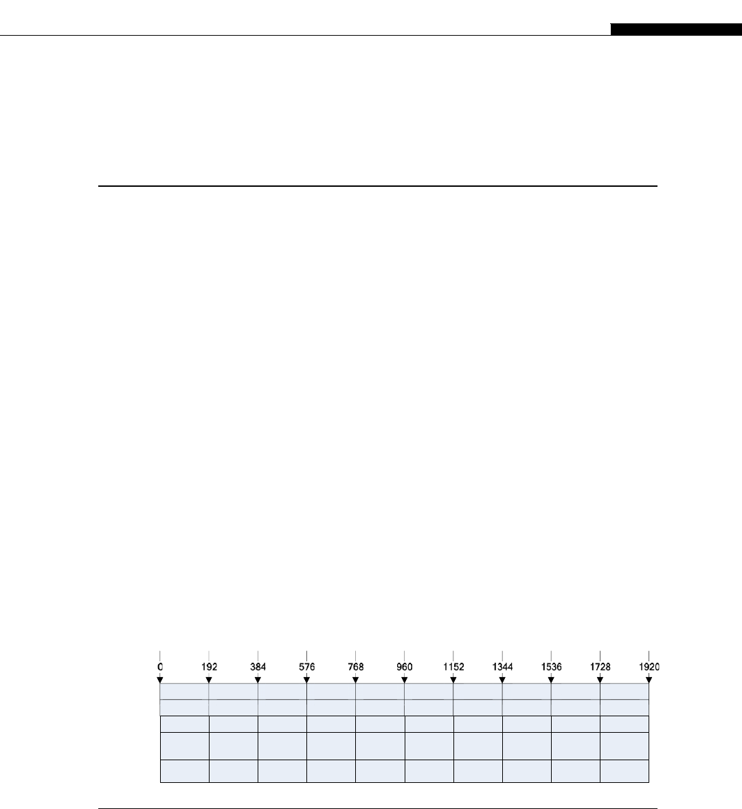
As you can see, the calculated thread, or the thread ID, goes from 0 to 127. Within that you allocate
two blocks of 64 threads each. The thread indexes within each of these blocks go from 0 to 63. You also
see that each block generates two warps.
GRIDS
A grid is simply a set of blocks where you have an Xand a Yaxis, in effect a 2D mapping. The final Y
mapping gives you YXTpossibilities for a thread index. Let’s look at this using an example, but
limiting the Yaxis to a single row to start off with.
If you were to look at a typical HD image, you have a 1920 1080 resolution. The number of
threads in a block should always be a multiple of the warp size, which is currently defined as 32. As
you can only schedule a full warp on the hardware, if you don’t do this, then the remaining part of the
warp goes unused and you have to introduce a condition to ensure you don’t process elements off the
end of the Xaxis. This, as you’ll see later, slows everything down.
To avoid poor memory coalescing, you should always try to arrange the memory and thread usage
so they map. This will be covered in more detail in the next chapter on memory. Failure to do so will
result in something in the order of a five times drop in performance.
To avoid tiny blocks, as they don’t make full use of the hardware, we’ll pick 192 threads per block.
In most cases, this is the minimum number of threads you should think about using. This gives you
exactly 10 blocks across each row of the image, which is an easy number to work with (Figure 5.9).
Using a thread size that is a multiple of the Xaxis and the warp size makes life a lot easier.
Along the top on the Xaxis, you have the thread index. The row index forms the Yaxis. The height of the
row is exactly one pixel. As you have 1080 rows of 10 blocks, you have in total 1080 10 ¼10,800 blocks.
As each block has 192 threads, you are scheduling just over two million threads, one for each pixel.
This particular layout is useful where you have one operation on a single pixel or data point, or
where you have some operation on a number of data points in the same row. On the Fermi hardware, at
eight blocks per SM, you’d need a total of 1350 SMs (10,800 total blocks O8 scheduled blocks) to run
out of parallelism at the application level. On the Fermi hardware currently available, you have only 16
SMs (GTX580), so each SM would be given 675 blocks to process.
This is all very well, but what if your data is not row based? As with arrays, you are not limited to
a single dimension. You can have a 2D thread block arrangement. A lot of image algorithms, for
Block 0 Block 1 Block 2 Block 3 Block 4 Block 5 Block 6 Block 7 Block 8 Block 9Row 0
Block 10 Block 11 Block 12 Block 13 Block 14 Block 15 Block 16 Block 17 Block 18 Block 19Row 1
Block 20 Block 21 Block 22 Block 23 Block 24 Block 25 Block 26 Block 27 Block 28 Block 29Row 2
Row ....
Block
10,790
Block
10,791
Block
10,792
Block
10,793
Block
10,794
Block
10,795
Block
10,796
Block
10,797
Block
10,798
Block
10,799
Row 1079
B
B
B
3
B
B
B
5
B
B
6
B
B
7
B
B
8
B
9
FIGURE 5.9
Block allocation to rows.
Grids 83
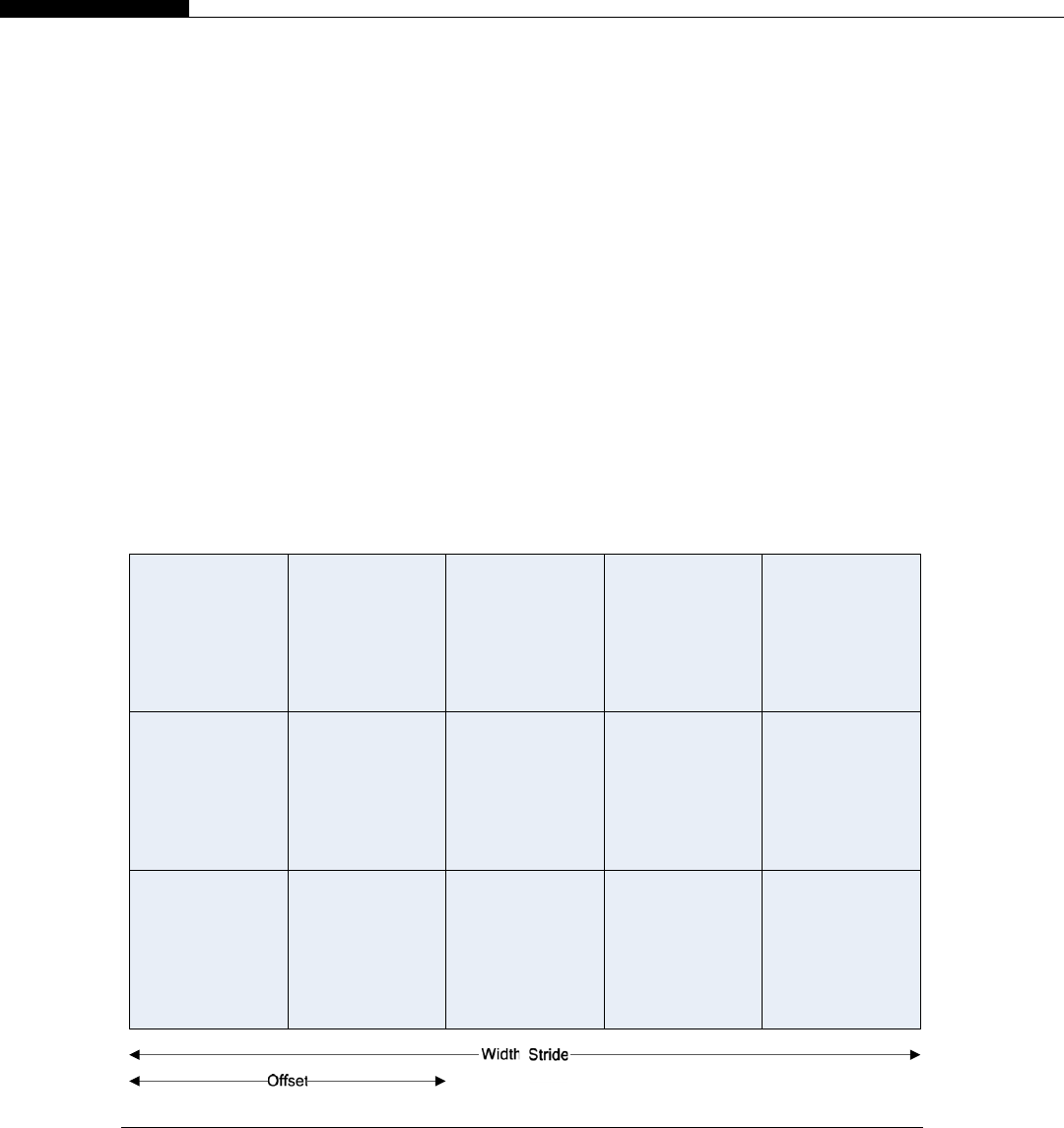
example, use 8 8 blocks of pixels. We’re using pixels here to show this arrangement, as it’s easy for
most people to conceptualize. Your data need not be pixel based. You typically represent pixels as
a red, green, and blue component. You could equally have x,y, and zspatial coordinates as a single data
point, or a simple 2D or 3D matrix holding the data points.
Stride and offset
As with arrays in C, thread blocks can be thought of as 2D structures. However, for 2D thread blocks,
we need to introduce some new concepts. Just like in array indexing, to index into a Yelement of 2D
array, you need to know the width of the array, the number of Xelements. Consider the array in
Figure 5.10.
The width of the array is referred to as the stride of the memory access. The offset is the column
value being accessed, starting at the left, which is always element 0. Thus, you have array element 5
being accessed with the index [1][5] or via the address calculation (row (sizeof(array_element)
width))) þ((sizeof(array_element) offset)). This is the calculation the compiler effectively uses, in
an optimized form, when you do multidimensional array indexing in C code.
Array Element 0
X = 0
Y = 0
Array Element 1
X = 1
Y = 0
Array Element 2
X = 2
Y = 0
Array Element 3
X = 3
Y = 0
Array Element 4
X = 4
Y = 0
Array Element 5
X = 0
Y = 1
Array Element 6
X = 1
Y = 1
Array Element 7
X = 2
Y = 1
Array Element 8
X = 3
Y = 1
Array Element 9
X = 4
Y = 1
Array Element 10
X = 0
Y = 2
Array Element 11
X = 1
Y = 2
Array Element 12
X = 2
Y = 2
Array Element 13
X = 3
Y = 2
Array Element 14
X = 0
Y = 2
FIGURE 5.10
Array mapping to elements.
84 CHAPTER 5 Grids, Blocks, and Threads

Now, how is this relevant to threads and blocks in CUDA? CUDA is designed to allow for data
decomposition into parallel threads and blocks. It allows you to define 1D, 2D, or 3D indexes (YX
T) when referring to the parallel structure of the program. This maps directly onto the way a typical area
of memory is set out, allowing the data you are processing to be allocated to individual SMs. The process
of keeping data close to the processor hugely increases performance, both on the GPU and CPU.
However, there is one caveat you must be aware of when laying out such arrays. The width value of
the array must always be a multiple of the warp size. If it is not, pad the array to the next largest
multiple of the warp size. Padding to the next multiple of the warp size should introduce only a very
modest increase in the size of the dataset. Be aware, however, you’ll need to deal with the padded
boundary, or halo cells, differently than the rest of the cells. You can do this using divergence in the
execution flow (e.g., using an if statement) or you can simply calculate the padded cells and discard
the result. We’ll cover divergence and the problems it causes later in the book.
Xand Ythread indexes
Having a 2D array in terms of blocks means you get two thread indexes, as you will be accessing the
data in a 2D way:
const unsigned int idx ¼(blockIdx.x * blockDim.x) þthreadIdx.x;
const unsigned int idy ¼(blockIdx.y * blockDim.y) þthreadIdx.y;
some_array[idy][idx] þ¼ 1.0;
Notice the use of blockDim.x and blockDim.y, which the CUDA runtime completes for you,
specifying the dimension on the Xand Yaxis. So let’s modify the existing program to work on
a3216 array. As you want to schedule four blocks, you can schedule them as stripes across the array,
or as squares within the array, as shown in Figure 5.11.
You could also rotate the striped version 90 degrees and have a column per thread block. Never do
this, as it will result in completely noncoalesced memory accesses that will drop the performance of
your application by an order of magnitude or more. Be careful when parallelizing loops so that the
access pattern always runs sequentially through memory in rows and never columns. This applies
equally to CPU and GPU code.
Now why might you choose the square layout over the rectangle layout? Well, two reasons. The
first is that threads within the same block can communicate using shared memory, a very quick way
to cooperate with one another. The second consideration is you get marginally quicker memory
access with single 128-byte transaction instead of two, 64-byte transactions, due to accessing within
a warp being coalesced and 128 bytes being the size of a cache line in the Fermi hardware. In the
square layout notice you have threads 0 to 15 mapped to one block and the next memory location
belongs to another block. As a consequence you get two transactions instead of one, as with the
rectangular layout. However, if the array was slightly larger, say 64 16, then you would not see this
issue, as you’d have 32 threads accessing contiguous memory, and thus a single 128-byte fetch from
memory issued.
Use the following to modify the program to use either of the two layouts:
dim3 threads_rect(32,4);
dim3 blocks_rect(1,4);
Grids 85
or
dim3 threads_square(16,8);
dim3 blocks_square(2,2);
In either arrangement you have the same total number of threads (32 4¼128, 16 8¼128). It’s
simply the layout of the threads that is different.
The dim3 type is simply a special CUDA type that you have to use to create a 2D layout of threads. In the
rectangle example, you’re saying you want 32 threads along the Xaxis by 4 threads along the Yaxis, within
a single block. You’re then saying you want the blocks to be laid out as one block wide by four blocks high.
You’ll need to invoke the kernel with
some_kernel_func<<< blocks_rect, threads_rect >>>(a, b, c);
or
some_kernel_func<<< blocks_square, threads_square >>>(a, b, c);
As you no longer want just a single thread ID, but an Xand Yposition, you’ll need to update the
kernel to reflect this. However, you also need to linearize the thread ID because there are situations
where you may want an absolute thread index. For this we need to introduce a couple of new concepts,
shown in Figure 5.12.
You can see a number of new parameters, which are:
gridDim.x–The size in blocks of the X dimension of the grid.
gridDim.y–The size in blocks of the Y dimension of the grid.
blockDim.x–The size in threads of the X dimension of a single block.
blockDim.y–The size in threads of the Y dimension of a single block.
Thread 0-15, Block 0 Thread 16-31, Block 0
Thread 32-47, Block 0 Thread 48-63, Block 0
Thread 64-79, Block 0 Thread 80-95, Block 0
Thread 96-111, Block 0 Thread 112-127, Block 0
Thread 0-15, Block 1 Thread 16-31, Block 1
Thread 32-47, Block 1 Thread 48-63, Block 1
Thread 64-79, Block 1 Thread 80-95, Block 1
Thread 96-111, Block 1 Thread 112-127, Block 1
Thread 0-15, Block 2 Thread 16-31, Block 2
Thread 32-47, Block 2 Thread 48-63, Block 3
Thread 64-79, Block 3 Thread 80-95, Block 3
Thread 96-111, Block 3 Thread 112-127, Block 3
Thread 0-15, Block 4 Thread 16-31, Block 4
Thread 32-47, Block 4 Thread 48-63, Block 4
Thread 64-79, Block 4 Thread 80-95, Block 4
Thread 96-111, Block 4 Thread 112-127, Block 4
Thread 0-15, Block 0
Thread 16-31, Block 0
Thread 32-47, Block 0
Thread 48-63, Block 0
Thread 64-79, Block 0
Thread 80-95, Block 0
Thread 96-111, Block 0
Thread 112-127, Block 0
Thread 0-15, Block 1
Thread 16-31, Block 1
Thread 32-47, Block 1
Thread 48-63, Block 1
Thread 64-79, Block 1
Thread 80-95, Block 1
Thread 96-111, Block 1
Thread 112-127, Block 1
Thread 0-15, Block 2
Thread 16-31, Block 2
Thread 32-47, Block 2
Thread 48-63, Block 3
Thread 64-79, Block 3
Thread 80-95, Block 3
Thread 96-111, Block 3
Thread 112-127, Block 3
Thread 0-15, Block 4
Thread 16-31, Block 4
Thread 32-47, Block 4
Thread 48-63, Block 4
Thread 64-79, Block 4
Thread 80-95, Block 4
Thread 96-111, Block 4
Thread 112-127, Block 4
OR
FIGURE 5.11
Alternative thread block layouts.
86 CHAPTER 5 Grids, Blocks, and Threads
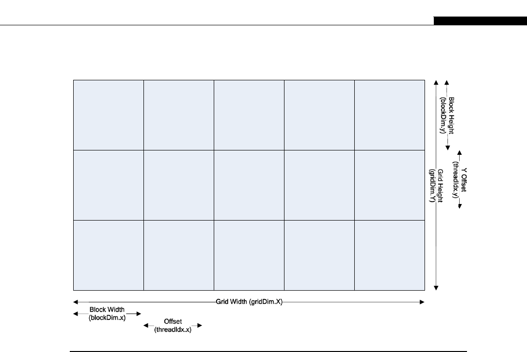
theadIdx.x–The offset within a block of the X thread index.
theadIdx.y–The offset within a block of the Y thread index.
You can work out the absolute thread index by working out the Yposition and multiplying this by
number of threads in a row. You then simply add in the Xoffset from the start of the row. Thus, the
thread index calculation is
thread_idx ¼((gridDim.x * blockDim.x) * idy) þidx;
So you need to modify the kernel to additionally return the Xand Ypositions plus some other useful
bits of information, as follows:
__global__ void what_is_my_id_2d_A(
unsigned int * const block_x,
unsigned int * const block_y,
unsigned int * const thread,
unsigned int * const calc_thread,
unsigned int * const x_thread,
unsigned int * const y_thread,
unsigned int * const grid_dimx,
Array Element 0
X = 0
Y = 0
Array Element 1
X = 1
Y = 0
Array Element 2
X = 2
Y = 0
Array Element 3
X = 3
Y = 0
Array Element 4
X = 4
Y = 0
Array Element 5
X = 0
Y = 1
Array Element 6
X = 1
Y = 1
Array Element 7
X = 2
Y = 1
Array Element 8
X = 3
Y = 1
Array Element 9
X = 4
Y = 1
Array Element 10
X = 0
Y = 2
Array Element 11
X = 1
Y = 2
Array Element 12
X = 2
Y = 2
Array Element 13
X = 3
Y = 2
Array Element 14
X = 0
Y = 2
FIGURE 5.12
Grid, block, and thread dimensions.
Grids 87

unsigned int * const block_dimx,
unsigned int * const grid_dimy,
unsigned int * const block_dimy)
{
const unsigned int idx ¼(blockIdx.x * blockDim.x) þthreadIdx.x;
const unsigned int idy ¼(blockIdx.y * blockDim.y) þthreadIdx.y;
const unsigned int thread_idx ¼((gridDim.x * blockDim.x) * idy) þidx;
block_x[thread_idx] ¼blockIdx.x;
block_y[thread_idx] ¼blockIdx.y;
thread[thread_idx] ¼threadIdx.x;
calc_thread[thread_idx] ¼thread_idx;
x_thread[thread_idx] ¼idx;
y_thread[thread_idx] ¼idy;
grid_dimx[thread_idx] ¼gridDim.x;
block_dimx[thread_idx] ¼blockDim.x;
grid_dimy[thread_idx] ¼gridDim.y;
block_dimy[thread_idx] ¼blockDim.y;
}
We’ll call the kernel twice to demonstrate how you can arrange array blocks and threads.
As you’re now passing an additional dataset to compute, you need an additional cudaMalloc,
cudaFree, and cudaMemcpy to copy the data from the device. As you’re using two dimensions, you’ll
also need to modify the array size to allocate and transfer the correct size of data.
#define ARRAY_SIZE_X 32
#define ARRAY_SIZE_Y 16
#define ARRAY_SIZE_IN_BYTES ((ARRAY_SIZE_X) * (ARRAY_SIZE_Y) * (sizeof(unsigned int)))
/* Declare statically six arrays of ARRAY_SIZE each */
unsigned int cpu_block_x[ARRAY_SIZE_Y][ARRAY_SIZE_X];
unsigned int cpu_block_y[ARRAY_SIZE_Y][ARRAY_SIZE_X];
unsigned int cpu_thread[ARRAY_SIZE_Y][ARRAY_SIZE_X];
unsigned int cpu_warp[ARRAY_SIZE_Y][ARRAY_SIZE_X];
unsigned int cpu_calc_thread[ARRAY_SIZE_Y][ARRAY_SIZE_X];
unsigned int cpu_xthread[ARRAY_SIZE_Y][ARRAY_SIZE_X];
unsigned int cpu_ythread[ARRAY_SIZE_Y][ARRAY_SIZE_X];
unsigned int cpu_grid_dimx[ARRAY_SIZE_Y][ARRAY_SIZE_X];
unsigned int cpu_block_dimx[ARRAY_SIZE_Y][ARRAY_SIZE_X];
unsigned int cpu_grid_dimy[ARRAY_SIZE_Y][ARRAY_SIZE_X];
unsigned int cpu_block_dimy[ARRAY_SIZE_Y][ARRAY_SIZE_X];
int main(void)
{
/* Total thread count ¼32 * 4 ¼128 */
const dim3 threads_rect(32, 4); /* 32 * 4 */
const dim3 blocks_rect(1,4);
88 CHAPTER 5 Grids, Blocks, and Threads

/* Total thread count ¼16 * 8 ¼128 */
const dim3 threads_square(16, 8); /* 16 * 8 */
const dim3 blocks_square(2,2);
/* Needed to wait for a character at exit */
char ch;
/* Declare pointers for GPU based params */
unsigned int * gpu_block_x;
unsigned int * gpu_block_y;
unsigned int * gpu_thread;
unsigned int * gpu_warp;
unsigned int * gpu_calc_thread;
unsigned int * gpu_xthread;
unsigned int * gpu_ythread;
unsigned int * gpu_grid_dimx;
unsigned int * gpu_block_dimx;
unsigned int * gpu_grid_dimy;
unsigned int * gpu_block_dimy;
/* Allocate four arrays on the GPU */
cudaMalloc((void **)&gpu_block_x, ARRAY_SIZE_IN_BYTES);
cudaMalloc((void **)&gpu_block_y, ARRAY_SIZE_IN_BYTES);
cudaMalloc((void **)&gpu_thread, ARRAY_SIZE_IN_BYTES);
cudaMalloc((void **)&gpu_calc_thread, ARRAY_SIZE_IN_BYTES);
cudaMalloc((void **)&gpu_xthread, ARRAY_SIZE_IN_BYTES);
cudaMalloc((void **)&gpu_ythread, ARRAY_SIZE_IN_BYTES);
cudaMalloc((void **)&gpu_grid_dimx, ARRAY_SIZE_IN_BYTES);
cudaMalloc((void **)&gpu_block_dimx, ARRAY_SIZE_IN_BYTES);
cudaMalloc((void **)&gpu_grid_dimy, ARRAY_SIZE_IN_BYTES);
cudaMalloc((void **)&gpu_block_dimy, ARRAY_SIZE_IN_BYTES);
for (int kernel¼0; kernel < 2; kernelþþ)
{
switch (kernel)
{
case 0:
{
/* Execute our kernel */
what_is_my_id_2d_A<<<blocks_rect, threads_rect>>>(gpu_block_x, gpu_block_y,
gpu_thread, gpu_calc_thread, gpu_xthread, gpu_ythread, gpu_grid_dimx, gpu_block_dimx,
gpu_grid_dimy, gpu_block_dimy);
} break;
case 1:
{
Grids 89

/* Execute our kernel */
what_is_my_id_2d_A<<<blocks_square, threads_square>>>(gpu_block_x, gpu_block_y,
gpu_thread, gpu_calc_thread, gpu_xthread, gpu_ythread, gpu_grid_dimx, gpu_block_dimx,
gpu_grid_dimy, gpu_block_dimy);
} break;
default: exit(1); break;
}
/* Copy back the gpu results to the CPU */
cudaMemcpy(cpu_block_x, gpu_block_x, ARRAY_SIZE_IN_BYTES,
cudaMemcpyDeviceToHost);
cudaMemcpy(cpu_block_y, gpu_block_y, ARRAY_SIZE_IN_BYTES,
cudaMemcpyDeviceToHost);
cudaMemcpy(cpu_thread, gpu_thread, ARRAY_SIZE_IN_BYTES,
cudaMemcpyDeviceToHost);
cudaMemcpy(cpu_calc_thread, gpu_calc_thread, ARRAY_SIZE_IN_BYTES,
cudaMemcpyDeviceToHost);
cudaMemcpy(cpu_xthread, gpu_xthread, ARRAY_SIZE_IN_BYTES,
cudaMemcpyDeviceToHost);
cudaMemcpy(cpu_ythread, gpu_ythread, ARRAY_SIZE_IN_BYTES,
cudaMemcpyDeviceToHost);
cudaMemcpy(cpu_grid_dimx, gpu_grid_dimx, ARRAY_SIZE_IN_BYTES,
cudaMemcpyDeviceToHost);
cudaMemcpy(cpu_block_dimx,gpu_block_dimx, ARRAY_SIZE_IN_BYTES,
cudaMemcpyDeviceToHost);
cudaMemcpy(cpu_grid_dimy, gpu_grid_dimy, ARRAY_SIZE_IN_BYTES,
cudaMemcpyDeviceToHost);
cudaMemcpy(cpu_block_dimy, gpu_block_dimy, ARRAY_SIZE_IN_BYTES,
cudaMemcpyDeviceToHost);
printf("\nKernel %d\n", kernel);
/* Iterate through the arrays and print */
for (int y¼0; y < ARRAY_SIZE_Y; yþþ)
{
for (int x¼0; x < ARRAY_SIZE_X; xþþ)
{
printf("CT: %2u BKX: %1u BKY: %1u TID: %2u YTID: %2u XTID: %2u GDX: %1u BDX: %
1u GDY %1u BDY %1u\n", cpu_calc_thread[y][x], cpu_block_x[y][x], cpu_block_y[y][x],
cpu_thread[y][x], cpu_ythread[y][x], cpu_xthread[y][x], cpu_grid_dimx[y][x],
cpu_block_dimx[y][x], cpu_grid_dimy[y][x], cpu_block_dimy[y][x]);
/* Wait for any key so we can see the console window */
ch ¼getch();
}
}
/* Wait for any key so we can see the console window */
printf("Press any key to continue\n");
90 CHAPTER 5 Grids, Blocks, and Threads

ch ¼getch();
}
/* Free the arrays on the GPU as now we’re done with them */
cudaFree(gpu_block_x);
cudaFree(gpu_block_y);
cudaFree(gpu_thread);
cudaFree(gpu_calc_thread);
cudaFree(gpu_xthread);
cudaFree(gpu_ythread);
cudaFree(gpu_grid_dimx);
cudaFree(gpu_block_dimx);
cudaFree(gpu_grid_dimy);
cudaFree(gpu_block_dimy);
}
The output is too large to list here. If you run the program in the downloadable source code section,
you’ll see you iterate through the threads and blocks as illustrated in Figure 5.12.
WARPS
We touched a little on warp scheduling when talking about threads. Warps are the basic unit of
execution on the GPU. The GPU is effectively a collection of SIMD vector processors. Each group of
threads, or warps, is executed together. This means, in the ideal case, only one fetch from memory for
the current instruction and a broadcast of that instruction to the entire set of SPs in the warp. This is
much more efficient than the CPU model, which fetches independent execution streams to support
task-level parallelism. In the CPU model, for every core you have running an independent task, you
can conceptually divide the memory bandwidth, and thus the effective instruction throughput, by the
number of cores. In practice, on CPUs, the multilevel, on-chip caches hide a lot of this providing the
program fits within the cache.
You find vector-type instructions on conventional CPUs, in the form of SSE, MMX, and AVX
instructions. These execute the same single instruction on multiple data operands. Thus, you can
say, for Nvalues, increment all values by one. With SSE, you get 128-bit registers, so you can
operate on four parameters at any given time. AVX extends this to 256 bits. This is quite powerful,
but until recently, unless you were using the Intel compiler, there was little native support for this
type of optimization. AVX is now supported by the current GNU gcc compiler. Microsoft Visual
Studio 2010 supports it through the use of a “/arch:AVX” compiler switch. Given this lack of
support until relatively recently, vector-type instructions are not as widely used as they could be,
although this is likely to change significantly now that support is no longer restricted to the Intel
compiler.
With GPU programming, you have no choice: It’s vector architecture and expects you to write code
that runs on thousands of threads. You can actually write a single-thread GPU program with a simple
if statement checking if the thread ID is zero, but this will get you terrible performance compared with
the CPU. It can, however, be useful just to get an initial serial CPU implementation working. This
Warps 91

approach allows you to check things, such as whether memory copying to/from the GPU is working
correctly, before introducing parallelism into the application.
Warps on the GPU are currently 32 elements, although nVidia reserves the right to change this in
the future. Therefore, they provide an intrinsic variable, warpSize, for you to use to obtain the warp
size on the current hardware. As with any magic number, you should not hard code an assumed warp
size of 32. Many SSE-optimized programs were hard coded to assume an SSE size of 128 bits. When
AVX was released, simply recompiling the code was not sufficient. Don’t make the same mistake and
hard code such details into your programs.
So why should you be interested in the size of a warp? The reasons are many, so we’ll look briefly
at each.
Branching
The first reason to be interested in the size of a warp is because of branching. Because a warp is a single
unit of execution, branching (e.g., if,else,for,while,do,switch, etc.) causes a divergence in the
flow of execution. On a CPU there is complex hardware to do branch prediction, predicting from past
execution which path a given piece of code will take. The instruction flow is then prefetched and
pumped into the CPU instruction pipeline ahead of time. Assuming the prediction is correct, the CPU
avoids a “stall event.” Stall events are very bad, as the CPU then has to undo any speculative instruction
execution, fetch instructions from the other branch path, and refill the pipeline.
The GPU is a much simpler device and has none of this complexity. It simply executes one path of
the branch and then the other. Those threads that take the branch are executed and those that do not are
marked as inactive. Once the taken branch is resolved, the other side of the branch is executed, until the
threads converge once more. Take the following code:
__global__ some_func(void)
{
if (some_condition)
{
action_a();
}
else
{
action_b();
}
}
As soon as you evaluate some_condition, you will have divergence in at least one block or there is
no point in having the test in the program. Let’s say all the even thread numbers take the true path and
all the odd threads take the false path. The warp scoreboard then looks as shown in Figure 5.13.
0
+
1
-
2
+
3
-
4
+
5
-
6
+
7
-
8
+
9
-
10
+
11
-
12
+
13
-
14
+
15
-
16
+
FIGURE 5.13
Predicate thread/branch selection.
92 CHAPTER 5 Grids, Blocks, and Threads

For simplicity, I’ve drawn only 16 of the 32 threads, and you’ll see why in a minute. All those
threads marked þtake the true or positive path and all those marked take the false or negative path.
As the hardware can only fetch a single instruction stream per warp, half of the threads stall and
half progress down one path. This is really bad news as you now have only 50% utilization of the
hardware. This is a bit like having a dual-core CPU and only using one core. Many lazy programmers
get away with it, but the performance is terrible compared to what it could be.
Now as it happens, there is a trick here that can avoid this issue. The actual scheduler in terms of
instruction execution is half-warp based, not warp based. This means if you can arrange the divergence
to fall on a half warp (16-thread) boundary, you can actually execute both sides of the branch
condition, the if-else construct in the example program. You can achieve 100% utilization of the
device in this way.
If you have two types of processing of the data, interleaving the data on a 16-word boundary can
result in quite good performance. The code would simply branch on the thread ID, as follows:
if ((thread_idx % 32) < 16)
{
action_a();
}
else
{
action_b();
}
The modulus operator in C (%) returns the remainder of the integer division of the operand. In
effect, you count from 0 to 31 and then loop back to 0 again. Ideally, the function action_a() has each
of its 16 threads access a single float or integer value. This causes a single 64-byte memory fetch. The
following half warp does the same and thus you issue a single 128-byte memory fetch, which it just so
happens is the size of the cache line and therefore the optimal memory fetch size for a warp.
GPU utilization
So why else might you be interested in warps? To avoid underutilizing the GPU. The CUDA model
uses huge numbers of threads to hide memory latency (the time it takes for a memory request to
come back). Typically, latency to the global memory (DRAM) is around 400–600 cycles. During
this time the GPU is busy doing other tasks, rather than idly waiting for the memory fetch to
complete.
When you allocate a kernel to a GPU, the maximum number of threads you can put onto an SM is
currently 768 to 2048, depending on the compute level. This is implementation dependent, so it may
change with future hardware revisions. Take a quick look at utilization with different numbers of
threads in Table 5.1.
Compute 1.0 and 1.2 devices are the G80/G92 series devices. Compute 1.3 devices are the GT200
series. Compute 2.0/2.1 devices are the Fermi range. Compute 3.0 is Kepler.
Notice that the only consistent value that gets you 100% utilization across all levels of the hardware
is 256 threads. Thus, for maximum compatibility, you should aim for either 192 or 256 threads. The
dataset should, however, match the thread layout to achieve certain optimizations. You should,
therefore, also consider the 192-thread layout where you have a three-point data layout.
Warps 93
Another alternative to having a fixed number of threads is to simply look up the compute level from
the device and select a the smallest number of threads, that gives the highest device utilization.
Now you might want to also consider the number of blocks that can be scheduled into a given SM.
This really only makes a difference when you have synchronization points in the kernel. These
are points where every thread must wait on every other thread to reach the same point, for example,
when you’re doing a staged read and all threads must do the read. Due to the nature of the execution,
some warps may make good progress and some may make poor progress to the
synchronization point.
The time, or latency, to execute a given block is undefined. This is not good from a load balancing
point of view. You want lots of threads available to be run. With 256 threads, 32 threads per warp give
you 8 warps on compute 2.x hardware. You can schedule up to 24 warps (32 24 ¼768 threads) at
any one time into a given SM for compute 1.x devices and 48 (32 48 ¼1536 threads) for compute
2.x devices. A block cannot be retired from an SM until it’s completed its entire execution. With
compute 2.0x devices or higher that support 1024 threads per block, you can be waiting for that single
warp to complete while all other warps are idle, effectively making the SM also idle.
Thus, the larger the thread block, the more potential you have to wait for a slow warp to catch up,
because the GPU can’t continue until all threads have passed the checkpoint. Therefore, you might
have chosen a smaller number of threads, say 128 threads in the past, to reduce this potential waiting
time. However, this hurts the performance on Fermi-level hardware as the device utilization drops to
two-thirds. As you can see from Table 5.1, on compute 2.0 devices (Fermi), you need to have at least
192 threads per block to make good use of the SM.
However, you should not get too tied up concerning the number of warps, as they are really just
a measure of the overall number of threads present on the SMs. Table 5.3 shows the total number of
threads running, and it’s this total number that is really the interesting part, along with the percentage
utilization shown in Table 5.1.
Notice with 128 or less threads per block, as you move from the compute 1.3 hardware (the GT200
series) to the compute 2.x hardware (Fermi), you see no difference in the total number of threads
running. This is because there are limits to the number of blocks an SM can schedule. The number of
Table 5.1 Utilization %
Threads per Block/
Compute Capability 1.0 1.1 1.2 1.3 2.0 2.1 3.0
64 67 67 50 50 33 33 50
96 100 100 75 75 50 50 75
128 100 100 100 100 67 67 100
192 100 100 94 94 100 100 94
256 100 100 100 100 100 100 100
384 100 100 75 75 100 100 94
512 67 67 100 100 100 100 100
768 N/A N/A N/A N/A 100 100 75
1024 N/A N/A N/A N/A 67 67 100
94 CHAPTER 5 Grids, Blocks, and Threads

threads an SM could support was increased, but not the number of blocks. Thus, to achieve better
scaling you need to ensure you have at least 192 threads and preferably considerably more.
BLOCK SCHEDULING
Suppose you have 1024 blocks to schedule, and eight SMs to schedule these onto. With the Fermi
hardware, each SM can accept up to 8 blocks, but only if there is a low thread count per block. With
a reasonable thread count, you typically see 6 to 8 blocks per SM.
Now 1024 blocks divided between six SMs is 170 complete blocks each, plus 4 blocks left over.
We’ll look at the leftover blocks in a minute, because it causes an interesting problem.
Table 5.3 Total Threads per SM
Threads per Block/
Compute Capability 1.0 1.1 1.2 1.3 2.0 2.1 3.0
64 512 512 512 512 512 512 1024
96 768 768 768 768 768 768 1536
128 768 768 1024 1024 1024 1024 2048
192 768 768 960 960 1536 1536 1920
256 768 768 1024 1024 1536 1536 2048
384 768 768 768 768 1536 1536 1920
512 512 512 1024 1024 1536 1536 2048
768 N/A N/A N/A N/A 1536 1536 1536
1024 N/A N/A N/A N/A 1024 1024 2048
Table 5.2 Blocks per SM
Threads per Block/
Compute Capability 1.0 1.1 1.2 1.3 2.0 2.1 3.0
64 8 8 888816
96 8 8 888812
128 6 6 888816
192 4 4 558810
256 3 3 44668
384 2 2 22445
512 1 1 22334
768 N/A N/A 1 1 2 2 2
1024 N/A N/A 1 1 1 1 2
Block Scheduling 95

With the 1020 blocks that can be allocated to the SMs, how should they be allocated? The hardware
could allocate 6 blocks to the first SM, 6 to the second, and so on. Alternatively, it could distribute
1 block to each SM in turn, so SM 0 gets block 0, SM 1 gets block 1, SM 2 gets block 2, etc. NVIDIA
doesn’t specify what method it uses, but it’s fairly likely to be the latter to achieve a reasonable load
balance across the SMs.
If you have 19 blocks and four SMs, allocating blocks to an SM until it’s full is not a good idea. The
first three SMs would get 6 blocks each, and the last SM, a single block. The last SM would likely
finish quickly and sit idle waiting for the other SMs. The utilization of the available hardware is poor.
If you allocate blocks to alternate SMs on a rotating basis, each SM gets 4 blocks (4 SMs 4
blocks ¼16 total) and three SMs get an additional block each. Assuming each block takes the same
time to execute you have reduced the execution time by 17%, simply by balancing the blocks among
the SMs, rather than overloading some SMs while underloading others.
Now in practice you will usually have thousands or tens of thousands of blocks to get through in
a typical application. Having done the initial allocation of blocks to an SM, the block dispatcher is then
idle until one block finishes on any of the SMs. At this point the block is retired and the resources used
by that block become free. As all the blocks are the same size, any block in the list of waiting blocks
can be scheduled. The order of execution of blocks is deliberately undefined and there should be no
implicit assumption that blocks will execute in any order when programming a solution to a problem.
This can have serious problems if there is some associative operation being performed, such as
floating-point addition, which is not in practice associative. The order of execution of adds through
an array in floating-point math will affect the result. This is due to the rounding errors and the way in
which floating-point math works. The result is correct in all cases. It’s not a parallel execution
problem, but an ordering problem. You see exactly the same issue with single-thread CPU code. If
you add a set of random numbers from bottom to top, or top to bottom, in a floating-point array on
a CPU or GPU, you will get different answers. Perhaps worse still is that on a GPU, due to the
undefined block scheduling, multiple runs on the same data can result in different but correct
answers. There are methods to deal with this and it is something we cover later in the book. So for
now, just be aware that because the result is different than before, it doesn’t necessarily make the
result incorrect.
Coming back to the problem of having leftover blocks, you will have this scenario anytime the
number of blocks is not a multiple of the number of SMs. Typically you see CUDA devices ship with an
odd number of SMs, due to it being difficult to make large, complex processors. As the physical amount
of silicon used in creating a processor increases, the likelihood there is a failure in some section
increases considerably. NVIDIA, like many processor manufacturers, simply disables faulty SMs and
ships devices as lower-specification units. This increases yields and provides some economic value to
otherwise faulty devices. However, for the programmer, this means the total number of SMs is not
always even a multiple of two. The Fermi 480 series cards, and also the Tesla S2050/S2070/C2050/
C2070 series, have a 16 SM device with 1 SM disabled, thus making 15 SMs. This was resolved in the
580 series, but this problem is likely to be repeated as we see future GPU generations released.
Having a few leftover blocks is really only an issue if you have a very long kernel and need to wait
for each kernel to complete. You might see this, for example, in a finite time step simulation. If you had
16 blocks, assuming a Fermi 480 series card, 15 blocks would be allocated to each of the SMs. The
remaining block will be scheduled only after one of the other 15 blocks has completed. If each kernel
took 10 minutes to execute, it’s likely all the blocks would finish at approximately the same time. The
96 CHAPTER 5 Grids, Blocks, and Threads

GPU would then schedule one additional block and the complete kernel invocation would wait for an
additional 10 minutes for this single block to execute. At the same time, the other 14 available SMs
would be idle. The solution to this problem is to provide better granularity to break down the small
number of blocks into a much larger number.
In a server environment you may not have just 15 SMs, but actually multiple nodes each having
multiple GPUs. If their only task is this kernel, then they will likely sit idle toward the end of the kernel
invocation. In this instance it might prove better to redesign the kernel in some way to ensure the
number of blocks is an exact multiple of the number of SMs on each node.
From a load balancing perspective, this problem is clearly not good. As a consequence, in the later
CUDA runtime, you have support for overlapping kernels and running multiple, separate kernels on
the same CUDA device. Using this method, you can maintain the throughput if you have more than one
source of jobs to schedule onto the cluster of GPUs. As the CUDA devices start to idle, they instead
pick up another kernel from a stream of available kernels.
A PRACTICAL EXAMPLEdHISTOGRAMS
Histograms are commonly found in programming problems. They work by counting the distribution of
data over a number of “bins.” Where the data point contains a value that is associated with a given bin,
the value in that bin is incremented.
In the simplest example, you have 256 bins and data that range from 0 to 255. You iterate through
an array of bytes. If the value of the element in the array is 0, you increment bin 0. If the value of the
element is 10, you increment bin 10, etc.
The algorithm from a serial perspective is quite simple:
for (unsigned int i¼0; i< max; iþþ)
{
bin[array[i]]þþ;
}
Here you extract the value from the array, indexed by i. You then increment the appropriate bin
using the þþ operator.
The serial implementation suffers from a problem when you convert it to a parallel problem. If you
execute this with 256 threads, you get more than one thread simultaneously incrementing the value in
the same bin.
If you look at how the C language gets converted to an assembler, you see it can take a series of
assembler instructions to execute this code. These would break down into
1. Read the value from the array into a register.
2. Work out the base address and offset to the correct bin element.
3. Fetch the existing bin value.
4. Increment the bin value by one.
5. Write the new bin value back to the bin in memory.
The problem is steps three, four, and five are not atomic. An atomic operation is one that cannot be
interrupted prior to completion. If you execute this pseudocode in a lockstep manner, as CUDA does
A Practical ExampledHistograms 97

with its thread model, you hit a problem. Two or more threads fetch the same value at step three. They
all increment it and write it back. The last thread to do the write wins. The value should have been
incremented Ntimes, but it’s incremented only once. All threads read the same value to apply the
increment to, thus you lose Nincrements to the value.
The problem here is that you have a data dependency you do not see on the serial execution version.
Each increment of the bin value must complete before the read and increment by the next thread. You
have a shared resource between threads.
This is not an uncommon problem and CUDA provides a primitive for this called
atomicAdd(&value);
This operation guarantees the addition operation is serialized among all threads.
Having now solved this problem, you come to the real choice heredhow to structure the tasks you
have to cover into threads, blocks, and grids. There are two approaches: the task decomposition model
or the data decomposition model. Both generally need to be considered.
With the task decomposition model, you simply allocate one thread to every element in input array
and have it do an atomic add. This is the simplest solution to program, but has some major disad-
vantages. You must remember that this is actually a shared resource. If you have 256 bins and an array
of 1024 elements, assuming an equal distribution, you have 4 elements contending for each bin. With
large arrays (there is no point in processing small arrays with CUDA) this problem becomes the
dominant factor determining the total execution time.
If you assume an equal distribution of values inthehistogram,whichisoftennotthecase,
the number of elements contending for any single bin is simply the array size in elements
divided by the number of bins. With a 512 MB array (524,288 elements) you would have
131,072 elements contending for each bin. In the worst case, all elements write to the same
bin, so you have, in effect, a serial program due to the serialization of the atomic memory
writes.
In either example, the execution time is limited by the hardware’s ability to handle this contention
and the read/write memory bandwidth.
Let’s see how this works in reality. Here is the GPU program to do this.
/* Each thread writes to one block of 256 elements of global memory and contends for
write access */
__global__ void myhistogram256Kernel_01(
const unsigned char const * d_hist_data,
unsigned int * const d_bin_data)
{
/* Work out our thread id */
const unsigned int idx ¼(blockIdx.x * blockDim.x) þthreadIdx.x;
const unsigned int idy ¼(blockIdx.y * blockDim.y) þthreadIdx.y;
const unsigned int tid ¼idx þidy * blockDim.x * gridDim.x;
/* Fetch the data value */
98 CHAPTER 5 Grids, Blocks, and Threads
const unsigned char value ¼d_hist_data[tid];
atomicAdd(&(d_bin_data[value]),1);
}
With a GTX460 card, we measured 1025 MB/s with this approach. What is interesting is that it
does not scale with the number of elements in the array. You get a consistently poor performance,
regardless of the array size. Note that the GPU used for this test, a 1 GB GTX460, has a memory
bandwidth of 115 GB/s, so this shows just how terrible a performance you can achieve by imple-
menting the naive solution.
This figure, although bad, simply tells you that you are limited by some factor and it’s your job as
a programmer to figure out which factor and eliminate it. The most likely factor affecting performance
in this type of program is memory bandwidth. You are fetching Nvalues from the input array and
compressing those down to Nwrites to a small, 1 K (256 elements 4 bytes per integer counter)
memory section.
If you look at the memory reads first, you will see each thread reads one byte element of the array.
Reads are combined together (coalesced) at the half-warp level (16 threads). The minimum transfer
size is 32 bytes, so you’re wasting read memory bandwidth by about 50%, which is pretty poor. The
optimal memory fetch for a half warp is the maximum supported size, which is 128 bytes. For this,
each thread has to fetch 4 bytes of memory. You can do this by having each thread process four
histogram entries instead of one.
We can issue a 4-byte read, by reading a single integer, and then extracting the component parts of
that integer as shown in Figure 5.14. This should provide better read coalescing and therefore better
performance. The modified kernel is as follows:
/* Each read is 4 bytes, not one, 32 x 4 ¼128 byte reads */
__global__ void myhistogram256Kernel_02(
const unsigned int const * d_hist_data,
unsigned int * const d_bin_data)
{
/* Work out our thread id */
const unsigned int idx ¼(blockIdx.x * blockDim.x) þthreadIdx.x;
Byte 0 Byte 1 Byte 2 Byte 3
Word 0 (4 x 8 bytes)
FIGURE 5.14
Word-to-byte mapping.
A Practical ExampledHistograms 99

const unsigned int idy ¼(blockIdx.y * blockDim.y) þthreadIdx.y;
const unsigned int tid ¼idx þidy * blockDim.x * gridDim.x;
/* Fetch the data value as 32 bit */
const unsigned int value_u32 ¼d_hist_data[tid];
atomicAdd(&(d_bin_data[ ((value_u32 & 0x000000FF) ) ]),1);
atomicAdd(&(d_bin_data[ ((value_u32 & 0x0000FF00) >> 8 ) ]),1);
atomicAdd(&(d_bin_data[ ((value_u32 & 0x00FF0000) >> 16 ) ]),1);
atomicAdd(&(d_bin_data[ ((value_u32 & 0xFF000000) >> 24 ) ]),1);
}
When running the kernel we notice we have achieved for all our effort zero speedup. This is, in fact,
quite common when trying to optimize programs. It’s a pretty strong indicator you did not understand
the cause of the bottleneck.
One issue to note here is that in compute 2.x, hardware does not suffer with only being able to coalesce
data from a half warp and can do full-warp coalescing. Thus, on the test device, a GTX460 (compute 2.1
hardware), the 32 single byte fetches issued by a single warp were coalesced into a 32-byte read.
The obvious candidate is the atomic write operation, rather than the usual memory bandwidth
culprit. For this you need to look at the alternative approach given by the data decomposition
model. Here you look at the data flow side of the equation, looking for data reuse and optimizing
the data size into that which works effectively with shared resources, such as a cache or shared
memory.
You can see that the contention for the 256 bins is a problem. With multiple blocks writing to
memory from multiple SMs, the hardware needs to sync the value of the bin array across the
caches in all processors. To do this it needs to fetch the current value from memory, increment it,
and then write it back. There is some potential for this to be held permanently in the L2 cache,
which is shared between the SMs in the Fermi generation of hardware. With compute 1.x hard-
ware, you are reading and writing to the global memory, so this approach is an order of magnitude
slower.
Even if you can use the L2 cache on the Fermi hardware, you are still having to go out of the SM to
sync with all the other SMs. On top of this the write pattern you are generating is a scattered pattern,
dependent very much on the nature of the input data for the histogram. This means no or very little
coalescing, which again badly hurts performance.
An alternative approach is to build the histogram within each SM and then write out the histogram
to the main memory at the end. This is the approach you must always try to achieve, whether for CPU
or GPU programming. The more you make use of resources close to the processor (SM in this case),
the faster the program runs.
We mentioned earlier that we can use shared memory, a special form of memory that is on chip and
thus very fast. You can create a 256-bin histogram in the shared memory and then do the atomic add at
the end to the global memory. Assuming you process only one histogram per block, you do not
100 CHAPTER 5 Grids, Blocks, and Threads

decrease the number of global memory reads or writes, but you do coalesce all the writes to memory.
The kernel for this approach is as follows:
__shared__ unsigned int d_bin_data_shared[256];
/* Each read is 4 bytes, not one, 32 x 4 ¼128 byte reads */
__global__ void myhistogram256Kernel_03(
const unsigned int const * d_hist_data,
unsigned int * const d_bin_data)
{
/* Work out our thread id */
const unsigned int idx ¼(blockIdx.x * blockDim.x) þthreadIdx.x;
const unsigned int idy ¼(blockIdx.y * blockDim.y) þthreadIdx.y;
const unsigned int tid ¼idx þidy * blockDim.x * gridDim.x;
/* Clear shared memory */
d_bin_data_shared[threadIdx.x] ¼0;
/* Fetch the data value as 32 bit */
const unsigned int value_u32 ¼d_hist_data[tid];
/* Wait for all threads to update shared memory */
__syncthreads();
atomicAdd(&(d_bin_data_shared[ ((value_u32 & 0x000000FF) ) ]),1);
atomicAdd(&(d_bin_data_shared[ ((value_u32 & 0x0000FF00) >> 8 ) ]),1);
atomicAdd(&(d_bin_data_shared[ ((value_u32 & 0x00FF0000) >> 16 ) ]),1);
atomicAdd(&(d_bin_data_shared[ ((value_u32 & 0xFF000000) >> 24 ) ]),1);
/* Wait for all threads to update shared memory */
__syncthreads();
/* The write the accumulated data back to global memory in blocks, not scattered */
atomicAdd(&(d_bin_data[threadIdx.x]), d_bin_data_shared[threadIdx.x]);
}
The kernel must do an additional clear operation on the shared memory, as you otherwise have
random data left there from other kernels. Notice also you need to wait (__syncthreads) until all the
threads in a block have managed to clear their memory cell in the shared memory before you start
allowing threads to update any of the shared memory cells. You need to do the same sync operation at
the end, to ensure every thread has completed before you write the result back to the global memory.
You should see that, suddenly, you get a huge six times jump in performance, simply by virtue of
arranging the writes in order so they can be coalesced. You can now achieve 6800 MB/s processing
speed. Note, however, you can only do this with compute 1.2 or higher devices as only these support
shared memory atomic operations.
Now that you have the ordering correct, you need to look at reducing the global memory traffic. You
have to read every value from the source data, and you only read each value once. You are already using the
A Practical ExampledHistograms 101

optimal transfer size for read accesses, so let’s look at the data being written. If you process Nhistograms
per block instead of one histogram per block you reduce the write bandwidth by a factor of N.
Table 5.4 shows the value achieved on the 512 MB histogram based on processing different values
of Nwith a Fermi 460 card (which contains seven SMs). You can see a peak of 7886 MB/s at an Nvalue
of 64. The kernel is as follows:
/* Each read is 4 bytes, not one, 32 x 4 ¼128 byte reads */
/* Accumulate into shared memory N times */
__global__ void myhistogram256Kernel_07(const unsigned int const * d_hist_data,
unsigned int * const d_bin_data,
unsigned int N)
{
/* Work out our thread id */
const unsigned int idx ¼(blockIdx.x * (blockDim.x*N) ) þthreadIdx.x;
const unsigned int idy ¼(blockIdx.y * blockDim.y ) þthreadIdx.y;
const unsigned int tid ¼idx þidy * (blockDim.x*N) * (gridDim.x);
/* Clear shared memory */
d_bin_data_shared[threadIdx.x] ¼0;
/* Wait for all threads to update shared memory */
__syncthreads();
for (unsigned int i¼0, tid_offset¼0; i< N; iþþ, tid_offsetþ¼256)
{
const unsigned int value_u32 ¼d_hist_data[tidþtid_offset];
atomicAdd(&(d_bin_data_shared[ ((value_u32 & 0x000000FF) ) ]),1);
atomicAdd(&(d_bin_data_shared[ ((value_u32 & 0x0000FF00) >> 8 ) ]),1);
atomicAdd(&(d_bin_data_shared[ ((value_u32 & 0x00FF0000) >> 16 ) ]),1);
atomicAdd(&(d_bin_data_shared[ ((value_u32 & 0xFF000000) >> 24 ) ]),1);
}
/* Wait for all threads to update shared memory */
__syncthreads();
/* The write the accumulated data back to global memory in blocks, not scattered */
atomicAdd(&(d_bin_data[threadIdx.x]), d_bin_data_shared[threadIdx.x]);
}
Let’s examine this a little, because it’s important to understand what you are doing here. You
have a loop ithat runs for Niterations. This is the number of times you will process 256 bytes of
data into the shared memory histogram. There are 256 threads invoked for the kernel, one for each
bin. As such, the only loop you need is a loop over the number of histograms to process. When
you’ve done one iteration, you move 256 bytes on in memory to process the next histogram
(tid_offset þ¼ 256).
Notice also that as you’re using atomic operations throughout, you need sync points only at the start
and end of the kernel. Adding unnecessary synchronization points typically slows down the program,
but can lead to a more uniform access pattern in memory.
102 CHAPTER 5 Grids, Blocks, and Threads

Now what is interesting here is that, after you start to process 32 or more histograms per block, you
see no effective increase in throughput. The global memory bandwidth is dropping by a factor of two
every time you increase that value of N. If global memory bandwidth is indeed the problem, you should
see a linear speed up here for every factor of Nyou add. So what is going on?
The main problem is the atomic operations. Every thread must content for access to the shared data
area, along with other threads. The data pattern has a huge influence on the execution time, which is
not a good design.
We’ll return to this issue later when we look at how you can write such algorithms without having
to use atomic operations.
CONCLUSION
We covered a lot in this chapter and you should now be familiar with how CUDA breaks tasks into
grids, blocks, and threads. We covered the scheduling of blocks and warps on the hardware and the
need to ensure you always have enough threads on the hardware.
The threading model used in CUDA is fundamental to understanding how to program GPUs
efficiently. You should understand how CPUs and GPUs are fundamentally different beasts to program,
but at the same time how they are related to one another.
You have seen how arrangement of threads relative to the data you are going to process is important
and impacts performance. You have also seen, in particular with applications that need to share data, it
Table 5.4 Histogram Results
Factor MB/s Total Blocks Whole Blocks per SM Remainder Blocks
1 6766 524,288 74,898 3
2 7304 262,144 37,449 1
4 7614 131,072 18,724 6
8 7769 65,536 9362 3
16 7835 32,768 4681 1
32 7870 16,384 2340 6
64 7886 8192 1170 3
128 7884 4096 585 1
256 7868 2048 292 6
512 7809 1024 146 3
1024 7737 512 73 1
2048 7621 256 36 6
4096 7093 128 18 3
8192 6485 64 9 1
16,384 6435 32 4 6
32,768 5152 16 2 3
65,536 2756 8 1 1
Conclusion 103

is not always an easy task to parallelize a particular problem. You should note that often taking time to
consider the correct approach is somewhat more important than diving in with the first solution that
seems to fit.
We also covered the use of atomics and some of the problems of serialization these cause. We
touched on the problems branching can cause and you should have in the back of your mind the need to
ensure all threads follow the same control path. We look at atomics and branching in more detail later
in the book.
You have had some exposure to the extended C syntax used within CUDA and should feel
comfortable in writing a CUDA program with a clear understanding of what will happen.
By reading this chapter you have gained a great deal of knowledge and hopefully should no longer
feel that CUDA or parallel programming is a bit like a black art.
Questions
1. Identify the best and worst data pattern for the histogram algorithm developed in this chapter. Is
there a common usage case that is problematic? How might you overcome this?
2. Without running the algorithm, what do you think is the likely impact of running this code on older
hardware based on the G80 design?
3. When processing an array in memory on a CPU, is it best to transverse in row-column order or
column-row order? Does this change when you move the code to a GPU?
4. Consider a section of code that uses four blocks of 256 threads and the same code that uses one block
of 1024 threads. Which is likely to complete first and why? Each block uses four syncthreads()
calls at various points through the code. The blocks require no interblock cooperation.
5. What are the advantages and disadvantages of an SIMD-based implementation that we find in
GPUs versus the MIMD implementation we find in multicore CPUs?
Answers
1. The best case is uniform distribution of data. This is because this loads the buckets equally and you
therefore get an equal distribution of atomic operations on the available shared memory banks.
The worst case is identical data values. This causes all threads to continuously hit the same shared
memory bucket, causing serialization of the entire program through both the atomic operations
and bank conflicts in the shared memory.
Unfortunately, one very common usage is with sorted data. This provides a variation on the worst-case
usage. Here one bank after another gets continuously hit with atomic writes, effectively serializing
the problem.
One solution is to step through the dataset such that each iteration writes to a new bucket. This requires
knowledge of the data distribution. For example, consider the case of 256 data points modeling
a linear function using 32 buckets. Let’s assume data points 0 to 31 fall into the first bucket and
this is replicated for every bucket. By processing one value for each bucket, you can distribute
writes to the buckets and avoid contention. In this example, you would read data points 0, 32,
64, 96, 1, 33, 65, 97, 2, 34, 66, 98, etc.
2. The G80 devices (compute 1.0, compute 1.1) don’t support shared memory atomics, so the code
will not compile. Assuming you modified it to use global memory atomics, we saw a seven-fold
decrease in performance in the example provided earlier in the chapter.
104 CHAPTER 5 Grids, Blocks, and Threads

3. The row-column ordering is best because the CPU will likely use a prefetch technique, ensuring the
subsequent data to be accessed will be in the cache. At the very least, an entire cache line will be
fetched from memory. Thus, when the CPU comes to the second iteration of the row-based access,
a[0] will have fetched a[1] into the cache.
The column transversal will result in much slower code because the fetch of a single cache line on the
CPU is unlikely to fetch data used in the subsequent loop iteration unless the row size is very small.
On the GPU each thread fetches one or more elements of the row, so the loop transversal, at a high
level, is usually by column, with an entire row being made up of individual threads. As with the
CPU the entire cache line will be fetched on compute 2.x hardware. However, unlike the CPU,
this cache line will likely be immediately consumed by the multiple threads.
4. During a syncthreads() operation, the entire block stalls until every one of the threads meets the
syncthreads() checkpoint. At this point they all become available for scheduling again. Having
a very large number of threads per block can mean the SM runs out of other available warps to
schedule while waiting for the threads in a single block to meet the checkpoint. The execution
flow as to which thread gets to execute when is undefined. This means some threads can make
much better progress than others to the syncthreads() checkpoint. This is the result of a design
decision in favor of throughput over latency at the hardware level. A very high thread count per
block is generally only useful where the threads in the block need to communicate with one
another, without having to do interblock communication via the global memory.
5. The SIMD model amortizes the instruction fetch time over many execution units where the
instruction stream is identical. However, where the instruction stream diverges, execution must
be serialized. The MIMD model is designed for divergent execution flow and doesn’t need to
stall threads when the flow diverges. However, the multiple fetch and decoding units require
more silicon and higher instruction bandwidth requirements to maintain multiple independent
execution paths.
A mixture of SIMD and MIMD is often the best way of dealing with both control flow and identical
operations of large datasets. You see this in CPUs in terms of SSE/MMX/AVX support. You see this
in GPUs in terms of warps and blocks allowing for divergence at a higher granularity.
Conclusion 105
This page intentionally left blank

Memory Handling with CUDA 6
INTRODUCTION
In the conventional CPU model we have what is called a linear or flat memory model. This is where any
single CPU core can access any memory location without restriction. In practice, for CPU hardware, you
typically see a level one (L1), level two (L2), and level three (L3) cache. Those people who have
optimized CPU code or come from a high-performance computing (HPC) background will be all too
familiar with this. For most programmers, however, it’s something they can easily abstract away.
Abstraction has been a trend in modern programming language, where the programmer is further
and further removed from the underlying hardware. While this can lead to higher levels of productivity,
as problems can be specified at a very high level, it relies hugely on clever compilers to implement
these abstractions into a level understood by the hardware. While this is great in theory, the reality can
be somewhat less than the marketing dream. I’m sure in the decades to come we’ll see huge
improvements in compilers and languages such that they will take advantage of parallel hardware
automatically. However, until this point, and certainly until we get there, the need to understand how
the hardware functions will be key to extracting the best performance from any platform.
For real performance on a CPU-based system, you need to understand how the cache works. We’ll
look at this on the CPU side and then look at the similarities with the GPU. The idea of a cache is that
most programs execute in a serial fashion, with various looping constructs, in terms of their execution
flow. If the program calls a function, the chances are the program will call it again soon. If the program
accesses a particular memory location, the chances are most programs will access that same location
again within a short time period. This is the principle of temporal locality, that it is highly likely that
you will reuse data and reexecute the same code having used/executed it once already.
Fetching data from DRAM, the main memory of a computer system is very slow. DRAM has
historically always been very slow compared to processor clock speeds. As processor clock speeds
have increased, DRAM speeds have fallen further and further behind.
DDR-3 DRAM in today’s processors runs up to 1.6 Ghz as standard, although this can be pushed to
up to 2.6 Ghz with certain high speed modules and the correct processor. However, each of the CPU
cores is typically running at around 3 GHz. Without a cache to provide quick access to areas of memory,
the bandwidth of the DRAM will be insufficient for the CPU. As both code and data exist in the DRAM
space, the CPU is effectively instruction throughput limited (how many instructions it executes in
a given timeframe) if it cannot fetch either the program or data from the DRAM fast enough.
This is the concept of memory bandwidth, the amount of data we can read or store to DRAM in
a given period of time. However, there is another important concept, latency. Latency is the amount of
time it takes to respond to a fetch request. This can be hundreds of processor cycles. If the program
CHAPTER
CUDA Programming. http://dx.doi.org/10.1016/B978-0-12-415933-4.00006-5
Copyright Ó2013 Elsevier Inc. All rights reserved.
107

wants four elements from memory it makes sense therefore to issue all requests together and then wait
for them to arrive, rather than issue one request, wait until it arrives, issue the next request, wait, and so
on. Without a cache, a processor would be very much memory bandwidth and latency limited.
To think of bandwidth and latency in everyday terms, imagine a supermarket checkout process.
There are Ncheckouts available in a given store, not all of which may be staffed. With only two
checkouts active (staffed), a big queue will form behind them as the customers back up, having to wait to
pay for their shopping. The throughput or bandwidth is the number of customers processed in a given
time period (e.g., one minute). The time the customer has to wait in the queue is a measure of the latency,
that is, how long after joining the queue did the customer wait to pay for his or her shopping and leave.
As the queue becomes large, the shop owner may open more checkout points and the queue
disperses between the new checkout points and the old ones. With two new checkout points opened,
the bandwidth of the checkout area is doubled, because now twice as many people can be served in the
same time period. The latency is also halved, because, on average, the queue is only half as big and
everyone therefore waits only half the time.
However, this does not come for free. It costs money to employ more checkout assistants and more
of the retail space has to be allocated to checkout points rather than shelf space for products. The same
tradeoff occurs in processor design, in terms of the memory bus width and the clock rate of the memory
devices. There is only so much silicon space on the device and often the width of the external memory
bus is limited by the number of physical pins on the processor.
One other concept we also need to think about is transaction overhead. There is a certain overhead
in processing the payment for every customer. Some may have two or three items in a basket while
others may have overflowing shopping carts. The shop owners love the shopping cart shoppers because
they can be processed efficiently, that is, more of the checkout person’s time is spent checking out
groceries, rather than in the overhead of processing the payment.
We see the same in GPUs. Some memory transactions are lightweight compared to the fixed
overhead to process them. The number of memory cells fetched relative to the overhead time is low, or,
in other words, the percentage of peak efficiency is poor. Others are large and take a bunch of time to
serve, but can be serviced efficiently and achieve near peak memory transfer rates. These translate to
byte-based memory transactions at one end of the spectrum and to long word-based transactions at the
other end. To achieve peak memory efficiency, we need lots of large transactions and very few, if any,
small ones.
CACHES
A cache is a high-speed memory bank that is physically close to the processor core. Caches are
expensive in terms of silicon real estate, which in turn translates into bigger chips, lower yields, and
more expensive processors. Thus, the Intel Xeon chips with the huge L3 caches found in a lot of server
machines are far more expensive to manufacture than the desktop version that has less cache on the
processor die.
The maximum speed of a cache is proportional to the size of the cache. The L1 cache is the fastest,
but is limited in size to usually around 16 K, 32 K, or 64 K. It is usually allocated to a single CPU core.
The L2 cache is slower, but much larger, typically 256 K to 512 K. The L3 cache may or may not be
present and is often several megabytes in size. The L2 and/or L3 cache may be shared between
108 CHAPTER 6 Memory Handling with CUDA
processor cores or maintained as separate caches linked directly to given processor cores. Generally, at
least the L3 cache is a shared cache between processor cores on a conventional CPU. This allows for
fast intercore communication via this shared memory within the device.
The G80 and GT200 series GPUs have no equivalent CPU-like cache to speak of. They do,
however, have a hardware-managed cache that behaves largely like a read-only CPU cache in terms of
constant and texture memory. The GPU relies instead primarily on a programmer-managed cache, or
shared memory section.
The Fermi GPU implementation was the first to introduce the concept of a nonprogrammer-
managed data cache. The architecture additionally has, per SM, an L1 cache that is both programmer
managed and hardware managed. It also has a shared L2 cache across all SMs.
So does it matter if the cache is shared across processor cores or SMs? Why is this arrangement
relevant? This has an interesting implication for communicating with other devices using the same
shared cache. It allows interprocessor communication, without having to go all the way out to global
memory. This is particularly useful for atomic operations where, because the L2 cache is unified, all
SMs see a consistent version of the value at a given memory location. The processor does not have to
write to the slow global memory, to read it back again, just to ensure consistency between processor
SP
SP
SP
SP
SP
SP
SP
SP
SP
SP
SP
SP
SP
SP
SP
SP
SP
SP
SP
SP
SP
SP
SP
SP
SP
SP
SP
SP
SP
SP
SP
SP
Independent L1 Cache (16-48K)
SP
SP
SP
SP
SP
SP
SP
SP
SP
SP
SP
SP
SP
SP
SP
SP
SP
SP
SP
SP
SP
SP
SP
SP
SP
SP
SP
SP
SP
SP
SP
SP
Independent L1 Cache (16-48K)
SP
SP
SP
SP
SP
SP
SP
SP
SP
SP
SP
SP
SP
SP
SP
SP
SP
SP
SP
SP
SP
SP
SP
SP
SP
SP
SP
SP
SP
SP
SP
SP
Independent L1 Cache (16-48K)
Shared L2 Cache (256K)
FIGURE 6.1
SM L1/L2 data path.
Caches 109
cores. On G80/GT200 series hardware, where there is no unified cache, we see exactly this deficiency
and consequently quite slow atomic operations compared with Fermi and later hardware.
Caches are useful for most programs. Significant numbers of programmers either care little for or
have a limited understanding of how to achieve good performance in software. Introducing a cache
means most programs work reasonably well and the programmer does not have to care too much about
how the hardware works. This ease of programming is useful for initial development, but in most cases
you can do somewhat better.
The difference between a novice CUDA programmer and someone who is an expert can be up to an
order of magnitude. I hope that through reading this book, you’ll be able to get several times speedup
from your existing code and move toward being routinely able to write CUDA code, which signifi-
cantly outperforms the equivalent serial code.
Types of data storage
On a GPU, we have a number of levels of areas where you can place data, each defined by its potential
bandwidth and latency, as shown in Table 6.1.
At the highest and most preferred level are registers inside the device. Then we have shared
memory, effectively a programmer-managed L1 cache, constant memory, texture memory, regular
device memory, and finally host memory. Notice how the order of magnitude changes between the
slowest and fastest type of storage. We will now look at the usage of each of these in turn and how you
can maximize the gain from using each type.
Traditionally, most texts would start off by looking at global memory, as this often plays a key role
in performance. If you get the global memory pattern wrong then you can forget anything else until you
get the correct pattern. We take a different approach here, in that we look first at how to use the device
efficiently internally, and from there move out toward global and host memory. Thus, you will
understand efficiency at each level and have an idea of how to extract it.
Most CUDA programs are developed progressively, using global memory exclusively at least
initially. Once there is an initial implementation, then the use of other memory types such as zero copy
and shared, constant, and ultimately registers is considered. For an optimal program, you need to be
thinking about these issues while you are developing a program. Thus, instead of the faster memory
types being an afterthought, they are considered at the outset and you know exactly where and how to
improve the program. You should be continuously thinking about not only how to access global
memory efficiently, but also how those accesses, especially for data that is reused in some way, can be
eliminated.
Table 6.1 Access Time by Memory Type
Storage
Type Registers
Shared
Memory
Texture
Memory
Constant
Memory
Global
Memory
Bandwidth ~8 TB/s ~1.5 TB/s ~200 MB/s ~200 MB/s ~200 MB/s
Latency 1 cycle 1 to 32 cycles ~400 to 600 ~400 to 600 ~400 to 600
110 CHAPTER 6 Memory Handling with CUDA

REGISTER USAGE
The GPU, unlike its CPU cousin, has thousands of registers per SM (streaming multiprocessor). An
SM can be thought of like a multithreaded CPU core. On a typical CPU we have two, four, six, or eight
cores. On a GPU we have NSM cores. On a Fermi GF100 series, there are 16 SMs on the top-end
device. The GT200 series has up to 32 SMs per device. The G80 series has up to 16 SMs per device.
It may seem strange that Fermi has less SMs than its predecessors. This is until you realize that
each Fermi SM contains more SPs (streaming processors) and that it is these that do the “grunt” work.
Due to the different number of SPs per core, you see a major difference in the number of threads per
core. A typical CPU will support one or two hardware threads per core. A GPU by contrast has
between 8 and 192 SPs per core, meaning each SM can at any time be executing this number of
concurrent hardware threads.
In practice on GPUs, application threads are pipelined, context switched, and dispatched to
multiple SMs, meaning the number of active threads across all SMs in a GPU device is usually in the
tens of thousands range.
One major difference we see between CPU and GPU architectures is how CPUs and GPUs map
registers. The CPU runs lots of threads by using register renaming and the stack. To run a new task the
CPU needs to do a context switch, which involves storing the state of all registers onto the stack (the
system memory) and then restoring the state from the last run of the new thread. This can take several
hundred CPU cycles. If you load too many threads onto a CPU it will spend all of the time simply
swapping out and in registers as it context switches. The effective throughput of useful work rapidly
drops off as soon as you load too many threads onto a CPU.
The GPU by contrast is the exact opposite. It uses threads to hide memory fetch and instruction
execution latency, so too few threads on the GPU means the GPU will become idle, usually waiting on
memory transactions. The GPU also does not use register renaming, but instead dedicates real registers
to each and every thread. Thus, when a context switch is required, it has near zero overhead. All that
happens on a context switch is the selector (or pointer) to the current register set is updated to point to
the register set of the next warp that will execute.
Notice I used the concept of warps here, which was covered in detail in the Chapter 5 on threading.
A warp is simply a grouping of threads that are scheduled together. In the current hardware, this is 32
threads. Thus, we swap in or swap out, and schedule, groups of 32 threads within a single SM.
Each SM can schedule a number of blocks. Blocks at the SM level are simply logical groups of
independent warps. The number of registers per kernel thread is calculated at compile time. All blocks
are of the same size and have a known number of threads, and the register usage per block is known and
fixed. Consequently, the GPU can allocate a fixed set of registers for each block scheduled onto the
hardware.
At a thread level, this is transparent to the programmer. However, a kernel that requests too many
registers per thread can limit the number of blocks the GPU can schedule on an SM, and thus the total
number of threads that will be run. Too few threads and you start underutilizing the hardware and the
performance starts to rapidly drop off. Too many threads can mean you run short of resources and
whole blocks of threads are dropped from being scheduled to the SM.
Be careful of this effect, as it can cause sudden performance drops in the application. If previously
the application was using four blocks and now it uses more registers, causing only three blocks to be
Register Usage 111

available, you may well see a one-quarter drop in GPU throughput. You can see this type of problem
with various profiling tools available, covered in Chapter 7 in the profiling section.
Depending on the particular hardware you are using, there is 8 K, 16 K, 32 K or 64 K of register
space per SM for all threads within an SM. You need to remember that one register is required per
thread. Thus, a simple local float variable in C results in Nregisters usage, where Nis the number of
threads that are scheduled. With the Fermi-level hardware, you get 32 K of register space per SM. With
256 threads per block, you would have ((32,768/4 bytes per register)/256 threads) ¼32 registers per
thread available. To achieve the maximum number of registers available on Fermi, 64 (128 on G80/
GT200), you’d need to half the thread count to just 128 threads. You could have a single block per SM,
with the maximum permitted number of registers in that block. Equally, you could have eight blocks of
32 threads (8 32 ¼256 threads in total), each using the maximum number of registers.
If you can make use of the maximum number of registers, for example, using them to work on
a section of an array, then this approach can work quite well. It works because such a set of values is
usually Nelements from a dataset. If each element is independent, you can create instruction-level
parallelism (ILP) within a single thread. This is exploited by the hardware in terms of pipelining many
independent instructions. You’ll see later an example of this working in practice.
However, for most kernels, the number of registers required is somewhat lower. If you drop your
register requirements from 128 to 64, you can schedule another block into the same SM. For example,
with 32 registers, you can schedule four blocks. In doing so, you are increasing the total thread count.
On Fermi, you can have up to 1536 threads per SM and, for the general case, the higher the level of
occupancy you can achieve, the faster your program will execute. You will reach a point where you
have enough thread-level parallelism (TLP) to hide the memory latency. To continue to increase
performance further, you either need to move to larger memory transactions or introduce ILP, that is,
process more than one element of the dataset within a single thread.
There is, however, a limit on the number of warps that can be scheduled to an SM. Thus, dropping
the number of registers from 32 to 16 does not get eight blocks. For that we are limited to 192 threads,
as shown in Table 6.2.
Table 6.2 refers to the Fermi architecture. For the Kepler architecture, simply double the number of
registers and blocks shown here. We’ve used 192 and 256 threads here as they provide good utilization
of the hardware. Notice that the kernel usage of 16 versus 20 registers does not introduce any addi-
tional blocks to the SM. This is due to the limit on the number of warps that can be allocated to an SM.
So in this case, you can easily increase register usage without impacting the total number of threads
that are running on a given SM.
Table 6.2 Register Availability by Thread Usage on Fermi
No. of Threads Maximum Register Usage
192 16 20 24 28 32 64
Blocks Scheduled 8 8 7652
No. of Threads Maximum Register Usage
256 16 20 24 28 32 64
Blocks Scheduled 6 6 5442
112 CHAPTER 6 Memory Handling with CUDA

You want to use registers to avoid usage of the slower memory types, but you have to be careful that
you use them effectively. For example, suppose we had a loop that set each bit in turn, depending on the
value of some Boolean variable. Effectively, we’d be packing and unpacking 32 Booleans into 32 bits
of a word. We could write this as a loop, each time modifying the memory location by the new
Boolean, shifted to the correct position within the word, as shown in the following:
for (i¼0; i<31; iþþ)
{
packed_result j¼ (pack_array[i] << i);
}
Here we are reading array element ifrom an array of elements to pack into an integer,
packed_result. We’re left shifting the Boolean by the necessary number of bits and then using
a bitwise or operation with the previous result.
If the parameter packed_result exists in memory, you’d be doing 32 memory read and writes. We
could equally place the parameter packed_result in a local variable, which in turn the compiler would
place into a register. As we accumulate into the register instead of in main memory, and later write only
the result to main memory, we save 31 of the 32 memory reads and writes.
Looking back at Table 6.1, you can see it takes several hundred cycles to do a global memory
operation. Let’s assume 500 cycles for one global memory read or write operation. For every value
you’d need to read, apply the or operation, and write the result back. Therefore, you’d have 32 read
þ32 write ¼64 500 cycles ¼32,000 cycles. The register version would eliminate 31 read and 32
write operations, replacing the 500-cycle operations with single-cycle operations. Thus, you’d have
ð1memory readÞþð1memory writeÞþð31 register readÞþð31 register writeÞor
ð1500Þþð1500Þþð31 1Þþð31 1Þ¼1062 cycles versus 32;000 cycles
Clearly, this is a huge reduction in the number of cycles. We have a 31 times improvement to perform
a relatively common operation in certain problem domains.
We see similar relationships with common reduction operations like sum,min,max, etc. A reduction
operation is where a dataset is reduced by some function to a smaller set, typically a single item. Thus,
max (10, 12, 1, 4, 5) would return a single value, 12, the maximum of the given dataset.
Accumulating into a register saves huge numbers of memory writes. In our bit packing example,
we reduce our memory writes by a factor of 31. Whether you are using a CPU or GPU, this type of
register optimization will make a huge difference in the speed of execution of your programs.
However, this burdens the programmer with having to think about which parameters are in registers
and which are in memory, which registers need to be copied back to memory, etc. This might seem like
quite a bit of trouble to go to, and for the average programmer, often it is. Therefore, we see
a proliferation of code that works directly on memory. For the most part, cache memory you find on
CPUs significantly masks this problem. The accumulated value is typically held in the L1 cache. If
a write-back policy is used on the cache, where the values do not need to be written out to main
memory until later, the performance is not too bad. Note that the L1 cache is still slower than registers,
so the solution will be suboptimal and may be several times slower than it could be.
Some compilers may detect such inefficiencies and implement a load into a register during the
optimizer phase. Others may not. Relying on the optimizer to fix poor programming puts you at the
Register Usage 113

mercy of how good the compiler is, or is not. You may find that, as the optimization level is increased,
errors creep into the program. This may not be the fault of the compiler. The C language definition is
quite complex. As the optimization level is increased, subtle bugs may appear due to a missed volatile
qualifier or the like. Automatic test scripts and back-to-back testing against a nonoptimized version are
good solutions to ensure correctness.
You should also be aware that optimizing compiler vendors don’t always choose to implement the
best solution. If just 1% of programs fail when a certain optimization strategy is employed by the
compiler vendor, then it’s unlikely to be employed due to the support issues this may generate.
The GPU has a computation rate many times in excess of its memory bandwidth capacity. The
Fermi hardware has around 190 GB/s peak bandwidth to memory, with a peak compute performance of
over one teraflop. This is over five times the memory bandwidth. On the Kepler GTX680/Tesla K10 the
compute power increases to 3 Teraflops, yet with a memory bandwidth almost identical to the
GTX580. In the bit packing example, without register optimization and on a system with no cache, you
would require one read and one write per loop iteration. Each integer or floating-point value is 4 bytes
in length. The best possible performance we could, theoretically, achieve in this example, due to the
need to read and write a total of 8 bytes, would be one-eighth of the memory bandwidth. Using the 190
GB/s figure, this would equate to around 25 billion operations per second.
In practice you’d never get near this, because there are loop indexes and iterations to take into
account as well as simply the raw memory bandwidth. However, this sort of back-of-the-envelope
calculation provides you with some idea of the upper bounds of your application before you start
coding anything.
Applying our factor of 31 reductions to the number of memory operations allows you to achieve
a theoretical peak of 31 times this figure, some 775 billion iterations per second. We’ll in practice hit
other limits, within the device. However, you can see we’d easily achieve many times better perfor-
mance than a simple global memory version by simply accumulating to or making use of registers
wherever possible.
To get some real figures here, we’ll write a program to do this bit packing on global memory and
then with registers. The results are as follows:
ID:0 GeForce GTX 470:Reg. version faster by: 2.22ms (Reg¼0.26ms, GMEM¼2.48ms)
ID:1 GeForce 9800 GT:Reg. version faster by: 52.87ms (Reg¼9.27ms, GMEM¼62.14ms)
ID:2 GeForce GTX 260:Reg. version faster by: 5.00ms (Reg¼0.62ms, GMEM¼5.63ms)
ID:3 GeForce GTX 460:Reg. version faster by: 1.56ms (Reg¼0.34ms, GMEM¼1.90ms)
The two kernels to generate these are as follows:
__global__ void test_gpu_register(u32 * const data, const u32 num_elements)
{
const u32 tid ¼(blockIdx.x * blockDim.x) þthreadIdx.x;
if (tid < num_elements)
{
u32 d_tmp [0;
for (int i¼0;i<KERNEL_LOOP;iþþ)
{
d_tmp j¼ (packed_array[i] << i);
}
114 CHAPTER 6 Memory Handling with CUDA

data[tid] ¼d_tmp;
}
}
__device__ static u32 d_tmp [0;
__global__ void test_gpu_gmem(u32 * const data, const u32 num_elements)
{
const u32 tid ¼(blockIdx.x * blockDim.x) þthreadIdx.x;
if (tid < num_elements)
{
for (int i¼0;i<KERNEL_LOOP;iþþ)
{
d_tmp j¼ (packed_array[i] << i);
}
data[tid] ¼d_tmp;
}
}
The only difference in the two kernels is that one uses a global variable, d_tmp, while the other uses
a local register. Looking at the results you can see the speedups in Table 6.3. You see an average
speedup of 7.7 times. Perhaps, most surprisingly, the fastest speedup comes from the devices that have
the largest number of SMs, which points to a problem that I hope you may have spotted. In the global
memory version of the kernel, every thread from every block reads and writes to d_tmp. There is no
guarantee as to in which order this will happen, so the program’s output is indeterminate. The kernel
executes perfectly well, with no CUDA errors detected, yet the answer will always be nonsense. This
type of error is a remarkably common type of mistake when converting serial code to parallel code.
Strange answers should always point you toward something being wrong. So how is this issue
corrected? In the register version, each thread writes to a unique register. In the GMEM (Global
Memory) version, it must do the same. Therefore, you simply replace the original definition of
d_tmp:
__device__ static u32 d_tmp ¼0;
With
Table 6.3 Speedup Using Registers over GMEM
Card Register Version
GMEM (Global Memory)
Version Speedup
GTX470 0.26 2.48 9.5
9800GT 9.27 62.14 6.7
GTX260 0.62 5.63 9.1
GTX460 0.34 1.9 5.6
Average 7.7
Register Usage 115
__device__ static u32 d_tmp[NUM_ELEM];
The kernel needs to be updated as follows:
__global__ void test_gpu_register(u32 * const data, const u32 num_elements)
{
const u32 tid ¼(blockIdx.x * blockDim.x) þthreadIdx.x;
if (tid < num_elements)
{
u32 d_tmp ¼0;
for (int i¼0;i<KERNEL_LOOP;iþþ)
{
d_tmp j¼ (packed_array[i] << i);
}
data[tid] ¼d_tmp;
}
}
Now each thread gets to read and write from an independent area of global memory. What of the
speedup now? See Table 6.4.
As you can see from Table 6.4, the average speedup drops to just 1.7 times. If it were not for the
9800GT (a compute 1.1 device) you’d see the average almost hit two times speedup in this simple
piece of code. Where possible, you always need to avoid global memory writes through some other
means. Converging on a single memory address, as in the first example, forces the hardware to serialize
the memory operations, leading to terrible performance.
Now it’s quite easy to make this code even faster. Loops are typically very inefficient, in that they
cause branching, which can cause pipeline stalls. More importantly, they consume instructions that
don’t contribute to the final result. The loop code will contain an increment for the loop counter, a test
of the end loop condition, and a branch for every iteration. In comparison, the useful instructions per
iteration will load the value from pack_array, shift it left Nbits, and or it with the existing d_tmp value.
Just looking at the operations, we see 50% or so of the operations are based around the loop. You can
look directly at the following PTX (Parallel Thread eXecution) code to verify this. The instructions
that perform the loop, to make reading the virtual assembly code easier, are highlighted in bold.
Table 6.4 Real Speedup from Using Registers over GMEM
Card Register Version GMEM Version Speedup
GTX470 0.26 0.51 2
9800GT 9.27 10.31 1.1
GTX260 0.62 1.1 1.8
GTX460 0.34 0.62 1.8
Average 1.7
116 CHAPTER 6 Memory Handling with CUDA

.entry _Z18test_gpu_register1Pjj (
.param .u64 __cudaparm__Z18test_gpu_register1Pjj_data,
.param .u32 __cudaparm__Z18test_gpu_register1Pjj_num_elements)
{
.reg .u32 %r<27>;
.reg .u64 %rd<9>;
.reg .pred %p<5>;
// __cuda_local_var_108903_15_non_const_tid ¼0
// __cuda_local_var_108906_13_non_const_d_tmp ¼4
// i ¼8
.loc 16 36 0
$LDWbegin__Z18test_gpu_register1Pjj:
$LDWbeginblock_180_1:
.loc 16 38 0
mov.u32 %r1, %tid.x;
mov.u32 %r2, %ctaid.x;
mov.u32 %r3, %ntid.x;
mul.lo.u32 %r4, %r2, %r3;
add.u32 %r5, %r1, %r4;
mov.s32 %r6, %r5;
.loc 16 39 0
ld.param.u32 %r7, [__cudaparm__Z18test_gpu_register1Pjj_num_elements];
mov.s32 %r8, %r6;
setp.le.u32 %p1, %r7, %r8;
@%p1 bra $L_0_3074;
$LDWbeginblock_180_3:
.loc 16 41 0
mov.u32 %r9, 0;
mov.s32 %r10, %r9;
$LDWbeginblock_180_5:
.loc 16 43 0
mov.s32 %r11, 0;
mov.s32 %r12, %r11;
mov.s32 %r13, %r12;
mov.u32 %r14, 31;
setp.gt.s32 %p2, %r13, %r14;
@%p2 bra $L_0_3586;
$L_0_3330:
.loc 16 45 0
mov.s32 %r15, %r12;
cvt.s64.s32 %rd1, %r15;
cvta.global.u64 %rd2, packed_array;
add.u64 %rd3, %rd1, %rd2;
ld.s8 %r16, [%rd3þ0];
mov.s32 %r17, %r12;
shl.b32 %r18, %r16, %r17;
mov.s32 %r19, %r10;
or.b32 %r20, %r18, %r19;
Register Usage 117

mov.s32 %r10, %r20;
.loc 16 43 0
mov.s32 %r21, %r12;
add.s32 %r22, %r21, 1;
mov.s32 %r12, %r22;
$Lt_0_1794:
mov.s32 %r23, %r12;
mov.u32 %r24, 31;
setp.le.s32 %p3, %r23, %r24;
@%p3 bra $L_0_3330;
$L_0_3586:
$LDWendblock_180_5:
.loc 16 48 0
mov.s32 %r25, %r10;
ld.param.u64 %rd4, [__cudaparm__Z18test_gpu_register1Pjj_data];
cvt.u64.u32 %rd5, %r6;
mul.wide.u32 %rd6, %r6, 4;
add.u64 %rd7, %rd4, %rd6;
st.global.u32 [%rd7þ0], %r25;
$LDWendblock_180_3:
$L_0_3074:
$LDWendblock_180_1:
.loc 16 50 0
exit;
$LDWend__Z18test_gpu_register1Pjj:
}
Thus, the PTX code first tests if the for loop will actually enter the loop. This is done in the block
labeled $LDWbeginblock_180_5. The code at the $Lt_0_1794 label then performs the loop operation,
jumping back to label $L_0_3330 until such time as the loop has completed 32 iterations. The other
code in the section labeled $L_0_3330 performs the operation:
d_tmp j¼ (packed_array[i] << i);
Notice, in addition to the loop overhead, because packed_array is indexed by a variable the code
has to work out the address on every iteration of the loop:
cvt.s64.s32 %rd1, %r15;
cvta.global.u64 %rd2, packed_array;
add.u64 %rd3, %rd1, %rd2;
This is rather inefficient. Compare this to a loop unrolled version and we see something quite
interesting:
.entry _Z18test_gpu_register2Pjj (
.param .u64 __cudaparm__Z18test_gpu_register2Pjj_data,
.param .u32 __cudaparm__Z18test_gpu_register2Pjj_num_elements)
{
.reg .u32 %r<104>;
.reg .u64 %rd<6>;
118 CHAPTER 6 Memory Handling with CUDA

.reg .pred %p<3>;
// __cuda_local_var_108919_15_non_const_tid ¼0
.loc 16 52 0
$LDWbegin__Z18test_gpu_register2Pjj:
$LDWbeginblock_181_1:
.loc 16 54 0
mov.u32 %r1, %tid.x;
mov.u32 %r2, %ctaid.x;
mov.u32 %r3, %ntid.x;
mul.lo.u32 %r4, %r2, %r3;
add.u32 %r5, %r1, %r4;
mov.s32 %r6, %r5;
.loc 16 55 0
ld.param.u32 %r7, [__cudaparm__Z18test_gpu_register2Pjj_num_elements];
mov.s32 %r8, %r6;
setp.le.u32 %p1, %r7, %r8;
@%p1 bra $L_1_1282;
.loc 16 57 0
ld.global.s8 %r9, [packed_arrayþ0];
ld.global.s8 %r10, [packed_arrayþ1];
shl.b32 %r11, %r10, 1;
or.b32 %r12, %r9, %r11;
ld.global.s8 %r13, [packed_arrayþ2];
shl.b32 %r14, %r13, 2;
or.b32 %r15, %r12, %r14;
[Repeated code for pack_arrayþ3 to packed_arrayþ29 removed for clarity]
ld.global.s8 %r97, [packed_arrayþ30];
shl.b32 %r98, %r97, 30;
or.b32 %r99, %r96, %r98;
ld.global.s8 %r100, [packed_arrayþ31];
shl.b32 %r101, %r100, 31;
or.b32 %r102, %r99, %r101;
ld.param.u64 %rd1, [__cudaparm__Z18test_gpu_register2Pjj_data];
cvt.u64.u32 %rd2, %r6;
mul.wide.u32 %rd3, %r6, 4;
add.u64 %rd4, %rd1, %rd3;
st.global.u32 [%rd4þ0], %r102;
$L_1_1282:
$LDWendblock_181_1:
.loc 16 90 0
exit;
$LDWend__Z18test_gpu_register2Pjj:
}
Almost all the instructions now contribute to the result. The loop overhead is gone. The address
calculation for packed_array is reduced to a compile time–resolved base plus offset type address.
Register Usage 119

Everything is much simpler, but much longer, both in the C code and also in the virtual PTX
assembly code.
The point here is not to understand PTX, but to see the vast difference small changes in C code can
have on the virtual assembly generated. It’s to understand that techniques like loop unrolling can be
hugely beneficial in many cases. We look at PTX and how it gets translated in the actual code that gets
executed in more detail in Chapter 9 on optimization.
So what does this do in terms of speedup? See Table 6.5. You can see that on the 9800GT or the
GTX260, there was no effect at all. However, on the more modern compute 2.x hardware, the GTX460
and GTX470, you see a 2.4and 3.4speedup, respectively. If you look back to the pure GMEM
implementation, on the GTX470 this is a 6.4speedup. To put this in perspective, if the original
program took six and a half hours to run, then the optimized version would take just one hour.
Register optimization can have a huge impact on your code execution timing. Take the time to look
at the PTX code being generated for the inner loops of your program. Can you unroll the loop to
expand it into a single, or set, of expressions? Think about this with your code and you’ll see a huge
performance leap. It is better to register usage, such as eliminating memory accesses, or provide
additional ILP as one of the best ways to speed up a GPU kernel.
SHARED MEMORY
Shared memory is effectively a user-controlled L1 cache. The L1 cache and shared memory share a 64 K
memory segment per SM. In Kepler this can be configured in 16 K blocks in favor of the L1 or shared
memory as you prefer for your application. In Fermi the choice is 16 K or 48K in favor of the L1 or shared
memory. Pre-Fermi hardware (compute 1.) has a fixed 16 K of shared memory and no L1 cache. The
shared memory has in the order of 1.5 TB/s bandwidth with extremely low latency. Clearly, this is hugely
superior to the up to 190 GB/s available from global memory, but around one-fifth of the speed of registers.
In practice, global memory speeds on low-end cards are as little as one-tenth that of the high-end cards.
However, the shared memory speed is driven by the core clock rate, which remains much more consistent
(around a 20% variation) across the entire range of GPUs. This means that to get the most from any card,
not just the high-end cards, you must use shared memory effectively in addition to using registers.
In fact, just by looking at the bandwidth figuresd1.5 TB/s for shared memory and 190 GB/s for
the best global memory accessdyou can see that there is a 7:1 ratio. To put it another way, there is
potential for a 7speedup if you can make effective use of shared memory. Clearly, shared memory is
a concept that every CUDA programmer who cares about performance needs to understand well.
Table 6.5 Effects of Loop Unrolling
Card Register Version Unrolled Version Speedup
GTX470 0.27 0.08 3.4
9800GT 9.28 9.27 1
GTX260 0.62 0.62 1
GTX460 0.34 0.14 2.4
Average 2
120 CHAPTER 6 Memory Handling with CUDA

However, the GPU operates a load-store model of memory, in that any operand must be loaded into
a register prior to any operation. Thus, the loading of a value into shared memory, as opposed to just
loading it into a register, must be justified by data reuse, coalescing global memory, or data sharing
between threads. Otherwise, better performance is achieved by directly loading the global memory
values into registers.
Shared memory is a bank-switched architecture. On Fermi it is 32 banks wide, and on G200 and
G80 hardware it is 16 banks wide. Each bank of data is 4 bytes in size, enough for a single-precision
floating-point data item or a standard 32-bit integer value. Kepler also introduces a special 64 bit wide
mode so larger double precision values no longer span two banks. Each bank can service only a single
operation per cycle, regardless of how many threads initiate this action. Thus, if every thread in a warp
accesses a separate bank address, every thread’s operation is processed in that single cycle. Note there
is no need for a one-to-one sequential access, just that every thread accesses a separate bank in the
shared memory. There is, effectively, a crossbar switch connecting any single bank to any single
thread. This is very useful when you need to swap the words, for example, in a sorting algorithm, an
example of which we’ll look at later.
There is also one other very useful case with shared memory and that is where every thread in
a warp reads the same bank address. As with constant memory, this triggers a broadcast mechanism to
all threads within the warp. Usually thread zero writes the value to communicate a common value with
the other threads in the warp. See Figure 6.2.
However, if we have any other pattern, we end up with bank conflicts of varying degrees. This
means you stall the other threads in the warp that idle while the threads accessing the shared memory
address queue up one after another. One important aspect of this is that it is not hidden by a switch to
another warp, so we do in fact stall the SM. Thus, bank conflicts are to be avoided if at all possible as
the SM will idle until all the bank requests have been fulfilled.
However, this is often not practical, such as in the histogram example we looked at in Chapter 5.
Here the data is unknown, so which bank it falls into is entirely dependent on the data pattern.
The worst case is where every thread writes to the same bank, in which case we get 32 serial
accesses to the same bank. We see this typically where the thread accesses a bank by a stride other than
32. Where the stride decreases by a power of two (e.g., in a parallel reduction), we can also see this,
with each successive round causing more and more bank conflicts.
Sorting using shared memory
Let’s introduce a practical example here, using sorting. A sorting algorithm works by taking a random
dataset and generating a sorted dataset. We thus need Ninput data items and Noutput data items. The
key aspect with sorting is to ensure you minimize the number of reads and writes to memory. Many
sorting algorithms are actually multipass, meaning we read every element of N,Mtimes, which is
clearly not good.
The quicksort algorithm is the preferred algorithm for sorting in the serial world. Being a divide-
and-conquer algorithm, it would appear to be a good choice for a parallel approach. However, by
default it uses recursion, which is only supported in CUDA compute 2.x devices. Typical parallel
implementations spawn a new thread for every split of the data. The current CUDA model (see also
discussion on Kepler’s Dynamic Parallelism in chapter 12) requires a specification of the total number
of threads at kernel launch, or a series of kernel launches per level. The data causes significant branch
Shared Memory 121
Bank 00
Bank 01
Bank 02
Bank 03
Bank 04
Bank 05
Bank 06
Bank 07
Bank 08
Bank 09
Bank 10
Bank 11
Bank 12
Bank 13
Bank 14
Bank 15
Bank 16
Bank 17
Bank 18
Bank 19
Bank 20
Bank 21
Bank 22
Bank 23
Bank 24
Bank 25
Bank 26
Bank 27
Bank 28
Bank 29
Bank 30
Bank 31
Thread 00
Thread 01
Thread 02
Thread 03
Thread 04
Thread 05
Thread 06
Thread 07
Thread 08
Thread 09
Thread 10
Thread 11
Thread 12
Thread 13
Thread 14
Thread 15
Thread 16
Thread 17
Thread 18
Thread 19
Thread 20
Thread 21
Thread 22
Thread 23
Thread 24
Thread 25
Thread 26
Thread 27
Thread 28
Thread 29
Thread 30
Thead 31
1:1 Write = Ideal case 1:1 Write = Ideal case 1:1 Read = Ideal case 1:4 Read = 4 Bank Conflicts
FIGURE 6.2
Shared memory patterns.
122 CHAPTER 6 Memory Handling with CUDA
divergence, which again is not good for GPUs. There are ways to address some of these issues.
However, these issues make quicksort not the best algorithm to use on a pre-Kepler GK110/ Tesla K20
GPU. In fact, you often find the best serial algorithm is not the best parallel algorithm and it is better to
start off with an open mind about what will work best.
One common algorithm found in the parallel world is the merge sort (Figure 6.3). It works by
recursively partitioning the data into small and smaller packets, until eventually you have only two
values to sort. Each sorted list is then merged together to produce an entire sorted list.
Recursion is not supported in CUDA prior to compute 2., so how can such an algorithm be
performed? Any recursive algorithm will at some point have a dataset of size N. On GPUs the thread
block size or the warp size is the ideal size for N. Thus, to implement a recursive algorithm all you have
to do is break the data into blocks of 32 or larger elements as the smallest case of N.
With merge sort, if you take a set of elements such as {1,5,2,8,9,3,2,1} we can split the data at
element four and obtain two datasets, {1,5,2,8} and {9,3,2,1}. You can now use two threads to apply
a sorting algorithm to the two datasets. Instantly you have gone from p¼1top¼2, where pis the
number of parallel execution paths.
Splitting the data from two sets into four sets gives you {1,5}, {2,8}, {9,3}, and {2,1}. It’s now
trivial to execute four threads, each of which compares the two numbers and swaps them if necessary.
Thus, you end up with four sorted datasets: {1,5}, {2,8}, {3,9}, and {1,2}. The sorting phase is now
complete. The maximum parallelism that can be expressed in this phase is N/2 independent threads.
Thus, with a 512 MB dataset, you have 128K 32-bit elements, for which we can use a maximum of
64K threads (N¼128K, N/2 ¼64K). Since a GTX580 GPU has 16 SMs, each of which can support up
to 1536 threads, we get up to 24K threads supported per GPU. With around two and a half passes, you
can therefore iterate through the 64K data pairs that need to be sorted with such a decomposition.
However, you now run into the classic problem with merge sort, the merge phase. Here the lists are
combined by moving the smallest element of each list into the output list. This is then repeated until all
members of the input lists are consumed. With the previous example, the sorted lists are {1,5}, {2,8},
{3,9}, and {1,2}. In a traditional merge sort, these get combined into {1,2,5,8} and {1,2,3,9}. These
1 5 2 8 9 3 2 1
1 5 2 8 9 3 2 1
1 5 2 8 9 3 2 1
1 82 5 31 2 9
1 92 531 2 8
1 5 2 8 3 9 1 2
FIGURE 6.3
Simple merge sort example.
Shared Memory 123
two lists are then further combined in the same manner to produce one final sorted list,
{1,1,2,2,3,5,8,9}.
Thus, as each merge stage is completed, the amount of available parallelism halves. As an alternative
approach where Nis small, you can simply scan Nsets of lists and immediately place the value in the
correct output list, skipping any intermediate merge stages as shown in Figure 6.4. The issue is that the
sort performed at the stage highlighted for elimination in Figure 6.4 is typically done with two threads.
As anything below 32 threads means we’re using less than one warp, this is inefficient on a GPU.
The downside of this approach if that it means you would need to read the first element of the sorted
list set from every set. With 64 K sets, this is 64 K reads, or 256 MB of data that has to be fetched from
memory. Clearly, this is not a good solution when the number of lists is very large.
Thus, our approach is to try to achieve a much better solution to the merge problem by limiting the
amount of recursion applied to the original problem and stopping at the number of threads in a warp,
32, instead of two elements per sorted set, as with a traditional merge sort. This reduces the number of
sets in the previous example from 64 K sorted sets to just 4 K sets. It also increases the maximum
amount of parallelism available from N/2 to N/32. In the 128 K element example we looked at
previously, this would mean we would need 4 K processing elements. This would distribute 256
processing elements (warps) to every SM on a GTX580. As each Fermi SM can execute a maximum of
48 warps, multiple blocks will need to be iterated through, which allows for smaller problem sizes and
speedups on future hardware. See Figure 6.5.
Shared memory is bank switched. We have 32 threads within a single warp. However, if any of those
threads access the same bank, there will be a bank conflict. If any of the threads diverge in execution
flow, you could be running at up to 1/32 of the speed in the worst case. Threads can use registers that are
private to a thread. They can only communicate with one another using shared memory.
By arranging a dataset in rows of 32 elements in the shared memory, and accessing it in columns by
thread, you can achieve bank conflict–free access to the memory (Figure 6.6).
For coalesced access to global memory, something we’ll cover in the next section, you’d need to
fetch the data from global memory in rows of 32 elements. Then you can apply any sorting algorithm
Eliminate
1 5 2 8 9 3 2 1
1 5 2 8 9 3 2 1
1 5 2 8 9 3 2 1
1 82 5 31 2 9
1 92 531 2 8
1 5 2 8 3 9 1 2
FIGURE 6.4
Merging Nlists simultaneously.
124 CHAPTER 6 Memory Handling with CUDA
to the column without worrying about shared memory conflicts. The only thing you need to consider is
branch divergence. You need to try to ensure that every thread follows the same execution flow, even
though they are processing quite different data elements.
One side effect of this strategy is we will end up having to make a tradeoff. Assuming we have
a single warp per SM, we will have no shared memory bank conflicts. However, a single warp per SM
will not hide the latency of global memory reads and writes. At least for the memory fetch and write-
back stage, we need lots of threads. However, during the sort phase, multiple warps may conflict with
one another. A single warp would not have any bank conflicts, yet this would not hide the instruction
execution latency. So in practice, we’ll need multiple warps in all phases of the sort.
Radix sort
One algorithm that has a fixed number of iterations and a consistent execution flow is the radix sort. It
works by sorting based on the least significant bit and then working up to the most significant bit. With
a 32-bit integer, using a single radix bit, you will have 32 iterations of the sort, no matter how large the
dataset. Let’s consider an example with the following dataset:
{ 122, 10, 2, 1, 2, 22, 12, 9 }
The binary representation of each of these would be
122 ¼01111010
10 ¼00001010
2¼00000010
22 ¼00010010
12 ¼00001100
9¼00001001
128 Elements
2 x 64 Elements
4 x 32 Elements
Set 0 Set 1 3teS2teS
FIGURE 6.5
Shared memory–based decomposition.
Bank 0
Bank 8
Bank 31
FIGURE 6.6
Shared memory bank access.
Shared Memory 125

In the first pass of the list, all elements with a 0 in the least significant bit (the right side) would
form the first list. Those with a 1 as the least significant bit would form the second list. Thus, the two
lists are
0¼{ 122, 10, 2, 22, 12 }
1¼{9}
The two lists are appended in this order, becoming
{ 122, 10, 2, 22, 12, 9 }
The process is then repeated for bit one, generating the next two lists based on the ordering of the
previous cycle:
0¼{ 12, 9 }
1¼{ 122, 10, 2, 22 }
The combined list is then
{ 12, 9, 122, 10, 2, 22 }
Scanning the list by bit two, we generate
0¼{ 9, 122, 10, 2, 22 }
1¼{12}
¼{ 9, 122, 10, 2, 22, 12 }
And so the program continues until it has processed all 32 bits of the list in 32 passes. To build the
list you need Nþ2Nmemory cells, one for the source data, one of the 0 list, and one of the 1 list. We
do not strictly need 2Nadditional cells, as we could, for example, count from the start of the memory
for the 0 list and count backward from the end of the memory for the 1 list. However, to keep it simple,
we’ll use two separate lists.
The serial code for the radix sort is shown as follows:
__host__ void cpu_sort(u32 * const data,
const u32 num_elements)
{
static u32 cpu_tmp_0[NUM_ELEM];
static u32 cpu_tmp_1[NUM_ELEM];
for (u32 bit¼0;bit<32;bitþþ)
{
u32 base_cnt_0 ¼0;
u32 base_cnt_1 ¼0;
for (u32 i¼0; i<num_elements; iþþ)
{
const u32 d ¼data[i];
const u32 bit_mask ¼(1 << bit);
if ( (d & bit_mask) > 0 )
{
126 CHAPTER 6 Memory Handling with CUDA
cpu_tmp_1[base_cnt_1] ¼d;
base_cnt_1þþ;
}
else
{
cpu_tmp_0[base_cnt_0] ¼d;
base_cnt_0þþ;
}
}
// Copy data back to source - first the zero list
for (u32 i¼0; i<base_cnt_0; iþþ)
{
data[i] ¼cpu_tmp_0[i];
}
// Copy data back to source - then the one list
for (u32 i¼0; i<base_cnt_1; iþþ)
{
data[base_cnt_0þi] ¼cpu_tmp_1[i];
}
}
}
The code works by being passed two values, a pointer to the data to sort and the number of elements
in the dataset. It overwrites the unsorted data so the returned set is sorted. The outer loop iterates over
all 32 bits in a 32-bit integer word and the inner loop iterates over all elements in the list. Thus, the
algorithm requires 32Niterations in which the entire dataset will be read and written 32 times.
Where the size of the data is less than 32 bits (e.g., with 16- or 8-bit integer values), the sort runs
two or four times faster due to having to do one-half and one-quarter of the work, respectively. An
implementation of the radix sort is available in the Thrust library shipped with v4.0 onwards of the
CUDA SDK so you don’t have to implement your own radix sort (Figure 6.7).
Within the inner loop the data is split into two lists, the 0 list and the 1 list depending on which bit
of the word is being processed. The data is then reconstructed from the two lists, the 0 list always being
written before the 1 list.
The GPU version is a little more complex, in that we need to take care of multiple threads.
0xFF000003
0xFF000002
0xFF000001
0xFF000000
1
0
1
0
Data Data & 0x01 Zero List One List Combined Lists Data & 0x10
0xFF000002
0xFF000000
0xFF000003
0xFF000001
0xFF000002
0xFF000000
0xFF000003
0xFF000001
1
0
1
0
0xFF000000
0xFF000001
0xFF000002
0xFF000003
0xFF000000
0xFF000001
0xFF000002
0xFF000003
Zero List One List Combined List (Sorted)
FIGURE 6.7
Simple radix sort.
Shared Memory 127

__device__ void radix_sort(u32 * const sort_tmp,
const u32 num_lists,
const u32 num_elements,
const u32 tid,
u32 * const sort_tmp_0,
u32 * const sort_tmp_1)
{
// Sort into num_list, lists
// Apply radix sort on 32 bits of data
for (u32 bit¼0;bit<32;bitþþ)
{
u32 base_cnt_0 ¼0;
u32 base_cnt_1 ¼0;
for (u32 i¼0; i<num_elements; iþ¼num_lists)
{
const u32 elem ¼sort_tmp[iþtid];
const u32 bit_mask ¼(1 << bit);
if ( (elem & bit_mask) > 0 )
{
sort_tmp_1[base_cnt_1þtid]¼elem;
base_cnt_1þ¼num_lists;
}
else
{
sort_tmp_0[base_cnt_0þtid]¼elem;
base_cnt_0þ¼num_lists;
}
}
// Copy data back to source - first the zero list
for (u32 i¼0; i<base_cnt_0; iþ¼num_lists)
{
sort_tmp[iþtid]¼sort_tmp_0[iþtid];
}
// Copy data back to source - then the one list
for (u32 i¼0; i<base_cnt_1; iþ¼num_lists)
{
sort_tmp[base_cnt_0þiþtid]¼sort_tmp_1[iþtid];
}
}
__syncthreads();
}
The GPU kernel is written here as a device function, a function only capable of being called within
a GPU kernel. This is the equivalent of declaring a function as “static” in C or “private” in Cþþ.
128 CHAPTER 6 Memory Handling with CUDA
Notice the inner loop has changed and instead of incrementing by one, the program increments by
num_lists a value passed into the function. This is the number of independent lists of data the radix
sort should produce. This value should equal the number of threads used to invoke the kernel block.
The ideal value to avoid bank conflicts will be the warp size, 32. However, this is a less than ideal value
in terms of hiding instruction and memory latency.
What this GPU version of this radix sort will produce is num_lists of independent sorted lists using
num_lists threads. Since the SM in the GPU can run 32 threads at the same speed as just one thread
and it has 32 shared memory banks, you might imagine the ideal value for num_lists would be 32. See
Table 6.6 and Figure 6.8.
As you can see from the table and figure, the radix sort is actually very efficient. You see an
approximate linear speedup, up to 128 threads. This is not too surprising because each doubling of the
number of threads results in each thread processing half as much data as before. The point of interest is
where this linear relationship stops because it shows us when we have hit some limit in the hardware.
At 256 threads it starts to tail off with only a two-thirds speedup, so we know the ideal case is 128
threads. However, we also have to consider how using 128 threads might limit the usage in the SM, in
particular in compute 2.x hardware. Therefore, we might select 256 threads depending on how
Table 6.6 Parallel Radix Sort Results (ms)
Device/Threads 1 2 4 8 16 32 64 128 256
GTX470 39.4 20.8 10.9 5.74 2.91 1.55 0.83 0.48 0.3
9800GT 67 35.5 18.6 9.53 4.88 2.66 1.44 0.82 0.56
GTX260 82.4 43.5 22.7 11.7 5.99 3.24 1.77 1.02 0.66
GTX460 31.9 16.9 8.83 4.56 2.38 1.27 0.69 0.4 0.26
0
10
20
30
40
50
60
70
80
90
1 2 4 8 16 32 64 128 256
GTX470 9800GT GTX260 GTX460
FIGURE 6.8
Parallel radix sort graph.
Shared Memory 129

multiple blocks interact. As it happens, shared memory is the main factor we need to consider limiting
the number of blocks we’re likely to be able to put into each SM.
If you look at the initial radix sort function, it is not very efficient. How would you optimize this
function? The most obvious change is that you do not need separate 0 and 1 lists. The 0 list can be
created from reusing the space in the original list. This not only allows you to discard the 1 list, but also
removes a copy back to the source list. This saves a lot of unnecessary work.
Finally, did you notice that the bit mask is actually constant within a single iteration of the bit
loop? It is thus an invariant within the iloop and can be moved out to the bit loop. This is a stan-
dard compiler optimization called invariant analysis. Most compilers would move this outside the
iloop. Compiler optimization is notoriously badly documented and can change from one compiler to
another and even between versions of compilers. Relying on optimization steps of compilers is
therefore, generally, bad programming practice and best avoided. Therefore, we’ll explicitly move the
calculation to ensure it gets executed in the correct place. See Chapter 9 on optimization for coverage
of typical compiler optimizations.
The slightly more optimal code we end up with is as follows:
__device__ void radix_sort2(u32 * const sort_tmp,
const u32 num_lists,
const u32 num_elements,
const u32 tid,
u32 * const sort_tmp_1)
{
// Sort into num_list, lists
// Apply radix sort on 32 bits of data
for (u32 bit¼0;bit<32;bitþþ)
{
const u32 bit_mask ¼(1 << bit);
u32 base_cnt_0 ¼0;
u32 base_cnt_1 ¼0;
for (u32 i¼0; i<num_elements; iþ¼num_lists)
{
const u32 elem ¼sort_tmp[iþtid];
if ( (elem & bit_mask) > 0 )
{
sort_tmp_1[base_cnt_1þtid] ¼elem;
base_cnt_1þ¼num_lists;
}
else
{
sort_tmp[base_cnt_0þtid] ¼elem;
base_cnt_0þ¼num_lists;
}
}
// Copy data back to source from the one’s list
130 CHAPTER 6 Memory Handling with CUDA

for (u32 i¼0; i<base_cnt_1; iþ¼num_lists)
{
sort_tmp[base_cnt_0þiþtid] ¼sort_tmp_1[iþtid];
}
}
__syncthreads();
}
There are further optimizations that can be made, but the key issue here is that we’re now using
only one temporary storage area, which in turn allows the processing of more elements. This is
important because, as we’ll see later, the number of lists is an important factor. So how do these
changes affect the performance of the radix sort?
If you look at Table 6.7, you’ll see the worst case, using a single thread, has come down from 82 ms
to 52 ms. The best case in the previous run, 0.26 ms, has come down to 0.21 ms, which is about a 20%
improvement in execution speed.
Merging lists
Merge lists of sorted elements is another algorithm that is commonly used in parallel programming.
However, let’s start by looking at some serial code to merge an arbitrary number of sorted lists into
a single sorted list, as this is the simplest case.
void merge_array(const u32 * const src_array,
u32 * const dest_array,
const u32 num_lists,
const u32 num_elements)
{
const u32 num_elements_per_list ¼(num_elements / num_lists);
u32 list_indexes[MAX_NUM_LISTS];
for (u32 list¼0; list < num_lists; listþþ)
{
list_indexes[list] ¼0;
}
for (u32 i¼0; i<num_elements;iþþ)
Table 6.7 Optimized Radix Sort Results (ms)
Device/Threads 1 2 4 8 16 32 64 128 256
GTX470 26.51 14.35 7.65 3.96 2.05 1.09 0.61 0.36 0.24
9800GT 42.8 23.22 12.37 6.41 3.3 1.78 0.98 0.63 0.4
GTX260 52.54 28.46 15.14 7.81 4.01 2.17 1.2 0.7 0.46
GTX460 21.62 11.81 6.34 3.24 1.69 0.91 0.51 0.31 0.21
Shared Memory 131
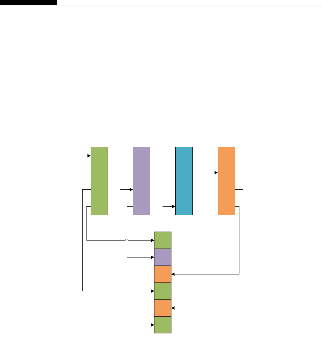
{
dest_array[i] ¼find_min(src_array,
list_indexes,
num_lists,
num_elements_per_list);
}
}
Assuming there are num_lists lists to collect data from, you need some way to track where we are
in the list. The program uses the array list_indexes for this. As the number of lists is likely to be
small, you can use the stack and thus declare the array as a local variable. Note this would be a bad idea
with a GPU kernel, as the stack allocation may get placed into slow global memory, depending on the
particular GPU variant. Shared memory would likely be the optimal location on the GPU, depending
on the number of lists needed.
12
8
5
1
List
Pointer
13
9
9
2
List
Pointer
20
19
15
14
List
Pointer
11
9
6
3
List
Pointer
1
2
3
5
6
8
List 0 List 1 List 2 List 3
Merged List
FIGURE 6.9
Multiple lists partially merged.
132 CHAPTER 6 Memory Handling with CUDA

First, the index values are all set to zero. Then the program iterates over all elements and assigns the
value in the sorted array from the result of a function, find_min.Thefind_min function identifies the
smallest value from a set of num_lists values.
u32 find_min(const u32 * const src_array,
u32 * const list_indexes,
const u32 num_lists,
const u32 num_elements_per_list)
{
u32 min_val ¼0xFFFFFFFF;
u32 min_idx ¼0;
// Iterate over each of the lists
for (u32 i¼0; i<num_lists; iþþ)
{
// If the current list has already been emptied
// then ignore it
if (list_indexes[i] < num_elements_per_list)
{
const u32 src_idx ¼iþ(list_indexes[i] * num_lists);
const u32 data ¼src_array[src_idx];
if (data <¼min_val)
{
min_val ¼data;
min_idx ¼i;
}
}
}
list_indexes[min_idx]þþ;
return min_val;
}
The function works by iterating through the lists of sorted values and maintaining an index into
where it is in each list. If it identifies a smaller value than min_val, it simply updates min_val to this
new value. When it has scanned all the lists, it increments the relevant list index and returns the value
it found.
Now let’s look at the GPU implementation of this algorithm. First, the top-level function:
__global__ void gpu_sort_array_array(
u32 * const data,
const u32 num_lists,
const u32 num_elements)
{
const u32 tid ¼(blockIdx.x * blockDim.x) þthreadIdx.x;
Shared Memory 133

__shared__ u32 sort_tmp[NUM_ELEM];
__shared__ u32 sort_tmp_1[NUM_ELEM];
copy_data_to_shared(data, sort_tmp, num_lists,
num_elements, tid);
radix_sort2(sort_tmp, num_lists, num_elements,
tid, sort_tmp_1);
merge_array6(sort_tmp, data, num_lists,
num_elements, tid);
}
This is quite a simple program for now. It will be invoked with a single block of Nthreads. We’ll
develop this as an example of how to use shared memory. Looking at the first function, we see the
following:
__device__ void copy_data_to_shared(const u32 * const data,
u32 * const sort_tmp,
const u32 num_lists,
const u32 num_elements,
const u32 tid)
{
// Copy data into temp store
for (u32 i¼0; i<num_elements; iþ¼num_lists)
{
sort_tmp[iþtid] ¼data[iþtid];
}
__syncthreads();
}
Here the program reads data from global memory in rows and not columns into the shared memory.
This step is important for two reasons. First, the program will repeatedly read and write from this
memory. Therefore, you want the fastest store possible, so we need to use shared memory instead of
global memory. Second, global memory provides the best performance when accessed by rows.
Column access produces a scattered memory pattern that the hardware is unable to coalesce, unless
every thread accesses the same column value and these addresses are adjacent. Thus, in most cases the
GPU has to issue far more memory fetch operations than are necessary and the speed of the program
will drop by an order of magnitude.
When you compile this program, if you have the -v flag set on the nvcc compiler options, it will
print an innocent looking message saying it created a stack frame. For example,
1>ptxas info : Function properties for _Z12merge_arrayPKjPjjjj
1> 40 bytes stack frame, 40 bytes spill stores, 40 bytes spill loads
When a function makes a call into a subfunction and passes parameters, those parameters must
somehow be provided to the called function. The program makes just such a call:
dest_array[i] ¼find_min(src_array,
134 CHAPTER 6 Memory Handling with CUDA

list_indexes,
num_lists,
num_elements_per_list);
There are two options that can be employed, to pass the necessary values through registers, or to
create an area of memory called a stack frame. Most modern processors have a large register set (32
or more registers). Thus, for a single level of calls, often this is enough. Older architectures use
stack frames and push the values onto the stack. The called function then pops the values off the
stack. As you require memory to do this, on the GPU this would mean using “local” memory, which
is local only in terms of which thread can access it. In fact, “local” memory can be held in global
memory, so this is hugely inefficient, especially on the older architectures (1.x) where it’s not
cached. At this point we need to rewrite the merge routine to avoid the function call. The new
routine is thus:
// Uses a single thread for merge
__device__ void merge_array1(const u32 * const src_array,
u32 * const dest_array,
const u32 num_lists,
const u32 num_elements,
const u32 tid)
{
__shared__ u32 list_indexes[MAX_NUM_LISTS];
// Multiple threads
list_indexes[tid] ¼0;
__syncthreads();
// Single threaded
if (tid ¼¼ 0)
{
const u32 num_elements_per_list ¼(num_elements / num_lists);
for (u32 i¼0; i<num_elements;iþþ)
{
u32 min_val ¼0xFFFFFFFF;
u32 min_idx ¼0;
// Iterate over each of the lists
for (u32 list¼0; list<num_lists; listþþ)
{
// If the current list has already been
// emptied then ignore it
if (list_indexes[list] < num_elements_per_list)
{
const u32 src_idx ¼list þ(list_indexes[list] * num_lists);
const u32 data ¼src_array[src_idx];
Shared Memory 135
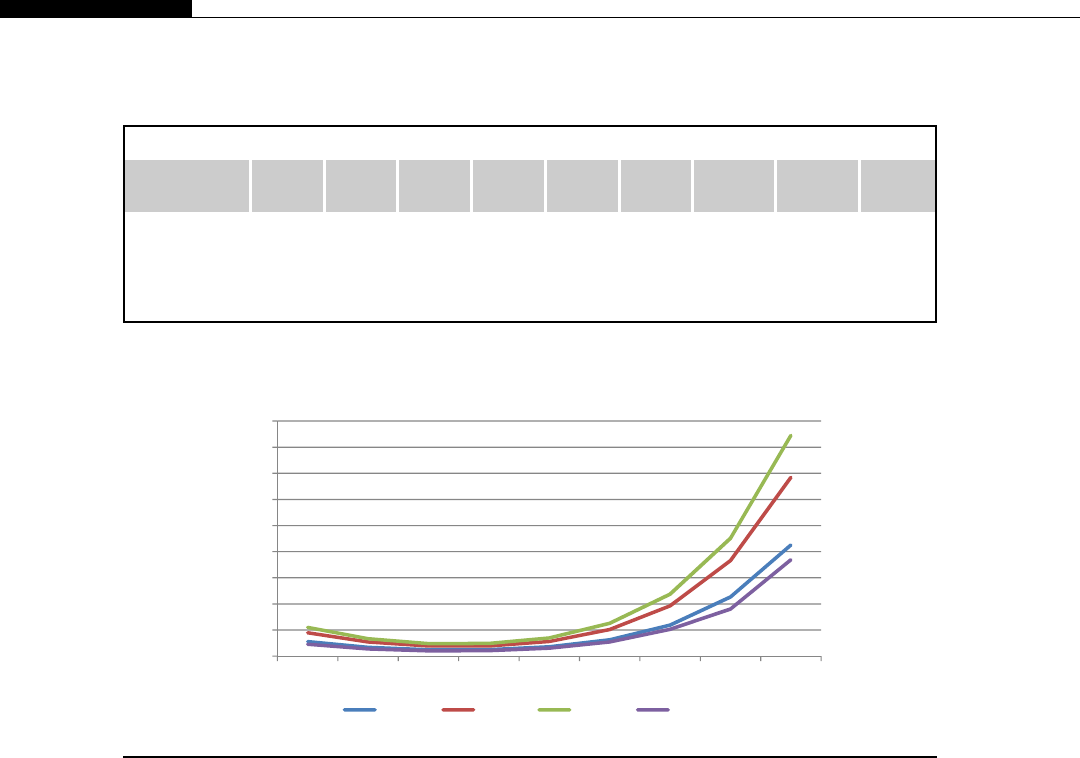
if (data <¼min_val)
{
min_val ¼data;
min_idx ¼list;
}
}
}
list_indexes[min_idx]þþ;
dest_array[i] ¼min_val;
}
}
}
This function now combines the original merge_arrary function and its find_min function.
Recompiling now results in no additional stack frame. Running the code, we find the results shown in
Table 6.8. If you graph this, it’s somewhat easier to see (Figure 6.10).
Table 6.8 Initial Single-Thread Merge Sort Results
Device/
Threads 1 2 4 8 16 32 64 128 256
GTX470 27.9 16.91 12.19 12.31 17.82 31.46 59.42 113.3 212.7
9800GT 44.83 27.21 19.55 19.53 28.07 51.08 96.32 183.08 342.16
GTX260 55.03 33.38 24.05 24.15 34.88 62.9 118.71 225.73 422.55
GTX460 22.76 13.85 10.11 10.41 15.29 27.18 51.46 90.26 184.54
0
50
100
150
200
250
300
350
400
450
1 2 4 8 16 32 64 128 256
GTX470 9800GT GTX260 GTX460
FIGURE 6.10
Initial single-thread merge sort graph.
136 CHAPTER 6 Memory Handling with CUDA
What is surprising from this graph is the worst performer is actually the GTX260, which is slower
than the previous generation 9800GT. It’s interesting to also note the GTX460 is faster than the
GTX470 in this particular test. To understand this, you need to look at the specific devices used, as
shown in Table 6.9.
You can see the 9800GT has a higher internal clock rate than the GTX260. The same is true of the
GTX460 and GTX470. Since the program is using just a single SM, and memory access is dominated
by shared memory access time, this is entirely to be expected.
However, perhaps the most interesting feature you can see from the graph is that increasing the
number of threads beyond a certain point actually makes the calculation go slower. This initially seems
counterintuitive if you have never seen this relationship before. What this type of result points to is that
there is some conflict of resources or the problem does not scale in a linear manner when you increase
the number of threads.
The problem is the latter. The merge step is single thread and must look at Nlists for every element.
As the number of lists are increased, the problem space becomes 2N,4N,8N, etc. in line with the
number of threads. The optimal point for this algorithm, based on the timings, is actually between four
and eight lists of data. This is not very good, as it considerably limits the potential amount of
parallelism.
Parallel merging
For better performance, clearly more than one thread in the merge stage is required. However, this
introduces a problem, in that we’re writing to a single list. To do this, the threads need to cooperate in
some manner. This makes the merge somewhat more complex.
// Uses multiple threads for merge
// Deals with multiple identical entries in the data
__device__ void merge_array6(const u32 * const src_array,
u32 * const dest_array,
const u32 num_lists,
const u32 num_elements,
const u32 tid)
{
const u32 num_elements_per_list ¼(num_elements / num_lists);
__shared__ u32 list_indexes[MAX_NUM_LISTS];
list_indexes[tid] ¼0;
// Wait for list_indexes[tid] to be cleared
Table 6.9 Device Clock Rate and Bandwidth
Device 9800GT GTX260 GTX460 GTX470
Core clock 650 Mz 625 MHz 726 MHz 608 MHz
Memory bandwidth 61 GB/s 123 GB/s 115 GB/s 134 GB/s
Shared Memory 137

__syncthreads();
// Iterate over all elements
for (u32 i¼0; i<num_elements;iþþ)
{
// Create a value shared with the other threads
__shared__ u32 min_val;
__shared__ u32 min_tid;
// Use a temp register for work purposes
u32 data;
// If the current list has not already been
// emptied then read from it, else ignore it
if (list_indexes[tid] < num_elements_per_list)
{
// Work out from the list_index, the index into
// the linear array
const u32 src_idx ¼tid þ(list_indexes[tid] * num_lists);
// Read the data from the list for the given
// thread
data ¼src_array[src_idx];
}
else
{
data ¼0xFFFFFFFF;
}
// Have thread zero clear the min values
if (tid ¼¼ 0)
{
// Write a very large value so the first
// thread thread wins the min
min_val ¼0xFFFFFFFF;
min_tid ¼0xFFFFFFFF;
}
// Wait for all threads
__syncthreads();
// Have every thread try to store it’s value into
// min_val. Only the thread with the lowest value
// will win
atomicMin(&min_val, data);
// Make sure all threads have taken their turn.
__syncthreads();
138 CHAPTER 6 Memory Handling with CUDA

// If this thread was the one with the minimum
if (min_val ¼¼ data)
{
// Check for equal values
// Lowest tid wins and does the write
atomicMin(&min_tid, tid);
}
// Make sure all threads have taken their turn.
__syncthreads();
// If this thread has the lowest tid
if (tid ¼¼ min_tid)
{
// Incremene the list pointer for this thread
list_indexes[tid]þþ;
// Store the winning value
dest_array[i] ¼data;
}
}
}
This version uses num_lists threads to do the merge operation. However, only a single thread
writes to the output data list at a time, thus ensuring the single output list is correct at all times.
It makes use of the atomicMin function. Instead of one thread reading all the values from the lists
and computing the minimum, each thread calls atomicMin with the value of its list entry. Once all
threads have called the atomicMin function, each thread reads it back and compares this with the value
it tried to write. If the values are the same, then the thread was the winning thread. However, there is
one further problem in that there may be several winning threads, because the data item can be
repeated in one or more lists. Thus, a second elimination step is required by only those threads with
identical data. Most of the time, this second step will not be necessary. However, in the worst case of
sorting a list of identical numbers, it would cause every thread to have to go through two elimination
steps.
So how does this version perform? As you can see from Table 6.10 and Figure 6.11,we
have reduced the total execution time using the larger number of threads (128 and 256 threads) by
Table 6.10 atomicMin Parallel Merge Sort Results (ms)
Device/Threads 1 2 4 8 16 32 64 128 256
GTX470 29.15 17.38 10.96 7.77 6.74 7.43 9.15 13.55 22.99
GTX260 55.97 32.67 19.87 13.22 10.51 10.86 13.96 19.97 36.68
GTX460 23.78 14.23 9.06 6.54 5.86 6.67 8.41 12.59 21.58
Shared Memory 139
a factor of 10. However, single-thread timing is unchanged. More important, however, is the fastest
time has moved from the 8- to the 16-thread version and has halved in terms of absolute time.
One thing I should mention here is that atomicMin on shared memory requires a compute 1.2
device or higher. The 9800GT is only a compute 1.1 device, so is not shown here as it cannot run the
kernel.
If we look a little closer at the hardware counters with a tool like Parallel Nsight, we can see that
beyond 32 threads the number of divergent branches and the number of shared memory accesses start
to grow very rapidly. We currently have a good solution, but what alternative approaches are there and
are they any quicker?
Parallel reduction
One common approach to this problem is parallel reduction. This can be applied for many problems,
amin operation being just one of them. It works by using half the number of threads of the elements in
the dataset. Every thread calculates the minimum of its own element and some other element. The
resultant element is forwarded to the next round. The number of threads is then reduced by half and the
process repeated until there is just a single element remaining, which is the result of the operation.
With CUDA you must remember that the execution unit for a given SM is a warp. Thus, any amount
of threads less than one warp is underutilizing the hardware. Also, while divergent threads must all be
executed, divergent warps do not have to be.
When selecting the “other element” for a given thread to work with, you can do so to do a reduction
within the warp, thus causing significant branch divergence within it. This will hinder the performance,
as each divergent branch doubles the work for the SM. A better approach is to drop whole warps by
selecting the other element from the other half of the dataset.
In Figure 6.12 you see the item being compared with one from the other half of the dataset. Shaded
cells show the active threads.
0
10
20
30
40
50
60
1248163264128256
GTX470 GTX260 GTX460
FIGURE 6.11
atomicMin parallel merge sort graph.
140 CHAPTER 6 Memory Handling with CUDA
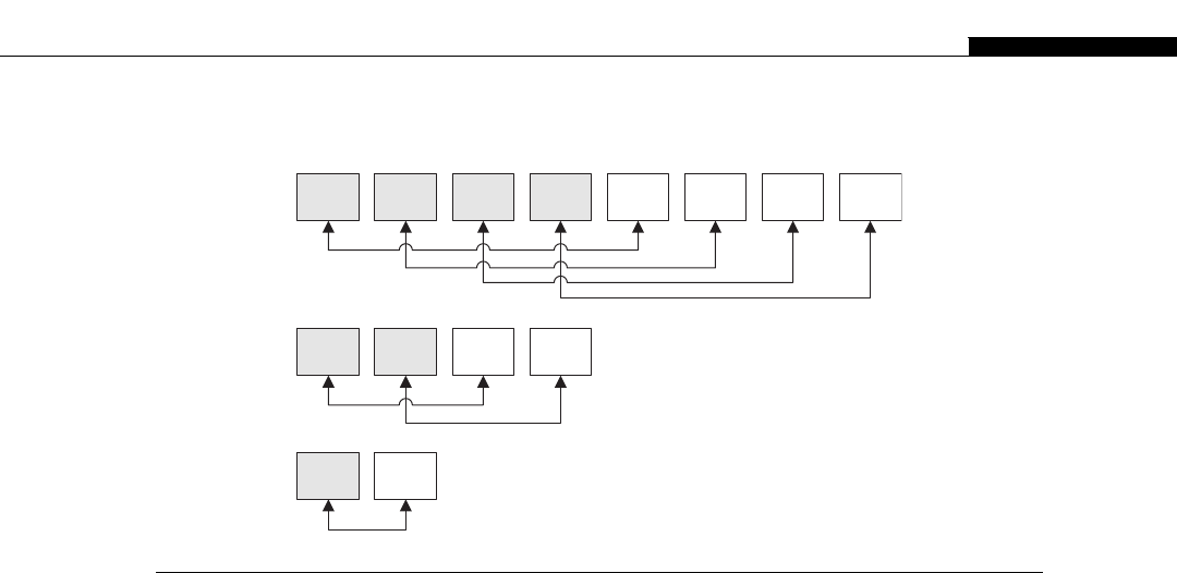
// Uses multiple threads for reduction type merge
__device__ void merge_array5(const u32 * const src_array,
u32 * const dest_array,
const u32 num_lists,
const u32 num_elements,
const u32 tid)
{
const u32 num_elements_per_list ¼(num_elements / num_lists);
__shared__ u32 list_indexes[MAX_NUM_LISTS];
__shared__ u32 reduction_val[MAX_NUM_LISTS];
__shared__ u32 reduction_idx[MAX_NUM_LISTS];
// Clear the working sets
list_indexes[tid] ¼0;
reduction_val[tid] ¼0;
reduction_idx[tid] ¼0;
__syncthreads();
for (u32 i¼0; i<num_elements;iþþ)
{
// We need (num_lists / 2) active threads
u32 tid_max ¼num_lists >> 1;
u32 data;
// If the current list has already been
// emptied then ignore it
3 2 1 0
1 0
7 6 5 4 3 2 1 0
FIGURE 6.12
Final stages of GPU parallel reduction.
Shared Memory 141

if (list_indexes[tid] < num_elements_per_list)
{
// Work out from the list_index, the index into
// the linear array
const u32 src_idx ¼tid þ(list_indexes[tid] * num_lists);
// Read the data from the list for the given
// thread
data ¼src_array[src_idx];
}
else
{
data ¼0xFFFFFFFF;
}
// Store the current data value and index
reduction_val[tid] ¼data;
reduction_idx[tid] ¼tid;
// Wait for all threads to copy
__syncthreads();
// Reduce from num_lists to one thread zero
while (tid_max !¼0)
{
// Gradually reduce tid_max from
// num_lists to zero
if (tid < tid_max)
{
// Calculate the index of the other half
const u32 val2_idx ¼tid þtid_max;
// Read in the other half
const u32 val2 ¼reduction_val[val2_idx];
// If this half is bigger
if (reduction_val[tid] > val2)
{
// The store the smaller value
reduction_val[tid] ¼val2;
reduction_idx[tid] ¼reduction_idx[val2_idx];
}
}
// Divide tid_max by two
tid_max >>¼1;
__syncthreads();
142 CHAPTER 6 Memory Handling with CUDA

}
if (tid ¼¼ 0)
{
// Incremenet the list pointer for this thread
list_indexes[reduction_idx[0]]þþ;
// Store the winning value
dest_array[i] ¼reduction_val[0];
}
// Wait for tid zero
__syncthreads();
}
}
This code works by creating a temporary list of data in shared memory, which it populates with
a dataset from each cycle from the num_list datasets. Where a list has already been emptied, the
dataset is populated with 0xFFFFFFFF, which will exclude the value from the list. The while loop
gradually reduces the number of active threads until there is only a single thread active, thread zero.
This then copies the data and increments the list indexes to ensure the value is not processed twice.
Notice the use of the __syncthreads directive within the loop and at the end. The program needs to
sync across warps when there are more than 32 threads (one warp) in use.
So how does this perform? As you can see from Table 6.11 and Figure 6.13, this approach is
significantly slower than the atomicMin version, the fastest reduction being 8.4 ms versus the 5.86 ms
atomicMin (GTX460, 16 threads). This is almost 50% slower than the atomicMin version. However,
one thing to note is that it’s a little under twice the speed of the atomicMin when using 256 threads
(12.27 ms versus 21.58 ms). This is, however, still twice as slow as the 16-thread version.
Although this version is slower, it has the advantage of not requiring the use of the atomicMin
function. This function is only available on compute 1.2 devices, which is generally only an issue if
you need to consider the consumer market or you need to support really old Tesla systems. The main
issue, however, is that atomicMin can only be used with integer values. A significant number of real-
world problems are floating-point based. In such cases we need both algorithms.
However, what we can take from both the atomicMin and the parallel reduction method is that the
traditional merge sort using two lists is not the ideal case on a GPU. You get increasing performance from
Table 6.11 Parallel Reduction Results (ms)
Device/Threads 1 2 4 8 16 32 64 128 256
GTX470 28.4 17.67 12.44 10.32 9.98 10.59 11.62 12.94 14.61
9800GT 45.66 28.35 19.82 16.25 15.61 17.03 19.03 21.45 25.33
GTX260 56.07 34.71 24.22 19.84 19.04 20.6 23.2 26.28 31.01
GTX460 23.22 14.52 10.3 8.63 8.4 8.94 9.82 10.96 12.27
Shared Memory 143

the increasing parallelism in the radix sort as you increase the number of lists. However, you get
decreasing performance from the merge stage as you increase the parallelism and move beyond 16 lists.
A hybrid approach
There is potential here to exploit the benefits of both algorithms by creating a hybrid approach. We can
rewrite the merge sort as follows:
#define REDUCTION_SIZE 8
#define REDUCTION_SIZE_BIT_SHIFT 3
#define MAX_ACTIVE_REDUCTIONS ( (MAX_NUM_LISTS) / REDUCTION_SIZE )
// Uses multiple threads for merge
// Does reduction into a warp and then into a single value
__device__ void merge_array9(const u32 * const src_array,
u32 * const dest_array,
const u32 num_lists,
const u32 num_elements,
const u32 tid)
{
// Read initial value from the list
u32 data ¼src_array[tid];
// Shared memory index
const u32 s_idx ¼tid >> REDUCTION_SIZE_BIT_SHIFT;
// Calcuate number of 1st stage reductions
const u32 num_reductions ¼num_lists >> REDUCTION_SIZE_BIT_SHIFT;
0
10
20
30
40
50
60
1248163264128256
GTX470 9800GT GTX260 GTX460
FIGURE 6.13
Parallel reduction graph.
144 CHAPTER 6 Memory Handling with CUDA

const u32 num_elements_per_list ¼(num_elements / num_lists);
// Declare a number of list pointers and
// set to the start of the list
__shared__ u32 list_indexes[MAX_NUM_LISTS];
list_indexes[tid] ¼0;
// Iterate over all elements
for (u32 i¼0; i<num_elements;iþþ)
{
// Create a value shared with the other threads
__shared__ u32 min_val[MAX_ACTIVE_REDUCTIONS];
__shared__ u32 min_tid;
// Have one thread from warp zero clear the
// min value
if (tid < num_lists)
{
// Write a very large value so the first
// thread thread wins the min
min_val[s_idx] ¼0xFFFFFFFF;
min_tid ¼0xFFFFFFFF;
}
// Wait for warp zero to clear min vals
__syncthreads();
// Have every thread try to store it’s value into
// min_val for it’s own reduction elements. Only
// the thread with the lowest value will win.
atomicMin(&min_val[s_idx], data);
// If we have more than one reduction then
// do an additional reduction step
if (num_reductions > 0)
{
// Wait for all threads
__syncthreads();
// Have each thread in warp zero do an
// additional min over all the partial
// mins to date
if ( (tid < num_reductions) )
{
atomicMin(&min_val[0], min_val[tid]);
}
Shared Memory 145

// Make sure all threads have taken their turn.
__syncthreads();
}
// If this thread was the one with the minimum
if (min_val[0] ¼¼ data)
{
// Check for equal values
// Lowest tid wins and does the write
atomicMin(&min_tid, tid);
}
// Make sure all threads have taken their turn.
__syncthreads();
// If this thread has the lowest tid
if (tid ¼¼ min_tid)
{
// Incremenet the list pointer for this thread
list_indexes[tid]þþ;
// Store the winning value
dest_array[i] ¼data;
// If the current list has not already been
// emptied then read from it, else ignore it
if (list_indexes[tid] < num_elements_per_list)
data ¼src_array[tid þ(list_indexes[tid] * num_lists)];
else
data ¼0xFFFFFFFF;
}
// Wait for min_tid thread
__syncthreads();
}
}
One of the main problems of the simple 1-to-Nreduction is it becomes increasingly slower as the
value of Nincreases. We can see from previous tests that the ideal value of Nis around 16 elements. The
kernel works by creating a partial reduction of Nvalues and then a final reduction of those Nvalues into
a single value. In this way it’s similar to the reduction example, but skips most of the iterations.
Notice that min_val has been extended from a single value into an array of shared values. This is
necessary so each independent thread can minimize the values over its dataset. Each min value is 32
bits wide so it exists in a separate shared memory bank, meaning there are no bank conflicts provided
the maximum number of first-level reductions results in 32 or less elements.
The value of REDUCTION_SIZE has been set to eight, which means the program will do a min over
groups of eight values prior to a final min. With the maximum of 256 elements, we get exactly 32
146 CHAPTER 6 Memory Handling with CUDA
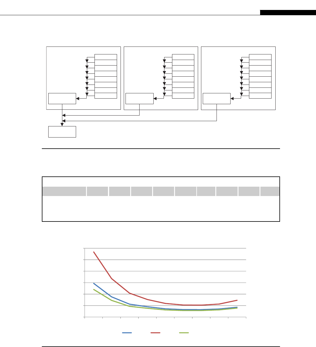
SM Bank NSM Bank 1
SM Bank 0
Min(L0)Min(L1)Min(Ln)
Min(L0..N)
N+LdaerhT1+LdaerhTLdaerhT
FIGURE 6.14
Hybrid parallel reduction.
Table 6.12 Hybrid Atomic and Parallel Reductions Results (ms)
Device/Threads 1 2 4 8 16 32 64 128 256
GTX470 29.41 17.62 11.24 8.98 7.2 6.49 6.46 7.01 8.57
GTX260 56.85 33.54 20.83 15.29 11.87 10.5 10.36 11.34 14.65
GTX460 24.12 14.54 9.36 7.64 6.22 5.67 5.68 6.27 7.81
0
10
20
30
40
50
60
1248163264128256
GTX470 GTX260 GTX460
FIGURE 6.15
Hybrid atomic and parallel reduction graph.
Shared Memory 147

seperate banks being used to do the reduction. In the 256 elements we have a 256:32:1 reduction. With
a 128-element list we have a 128:16:1 reduction, etc.
The other major change is now only the thread that writes out the winning element reads a new
value into data, a register-based value that is per thread. Previously, all threads re-read in the value
from their respective lists. As only one thread won each round, only one list pointer changed. Thus, as
Nincreased, this became increasingly inefficent. However, this doesn’t help as much as you might at
first imagine.
So how does this version perform? Notice in Table 6.12 that the minimum time, 5.86 ms from the
atomicMin example, has fallen to 5.67 ms. This is not spectacular, but what is interesting to note is the
shape of the graph (Figure 6.15). No longer is the graph such an inclined U shape. Both the 32- and 64-
thread versions beat the simple atomicMin based on 16 threads. We’re starting to smooth out the
upward incline introduced by the merge step as shown in table 6.12 and figure 6.15.
Shared memory on different GPUs
Not all GPUs are created equal. With the move to compute 2.x devices, the amount of shared memory
became configurable. By default, compute 2.x (Fermi) devices are configured to provide 48K of shared
memory instead of the 16 K of shared memory on compute 1.x devices.
The amount of shared memory can change between hardware releases. To write programs that scale
in performance with new GPU releases, you have to write portable code. To support this, CUDA allows
you to query the device for the amount of shared memory available with the following code:
struct cudaDeviceProp device_prop;
CUDA_CALL(cudaGetDeviceProperties(&device_prop, device_num));
printf("\nSharedMemory: %u", device_prop.sharedMemPerBlock);
Having more shared memory available allows us to select one of two strategies. We can either
extend the amount of shared memory used from 16 K to 48 K or we can simply schedule more blocks
into a single SM. The best choice will really depend on the application at hand. With our sorting
example, 48 K of shared memory would allow the number of lists per SM to be reduced by a factor of
three. As we saw earlier, the number of lists to merge has a significant impact on the overall execution
time.
Shared memory summary
So far we have looked only at sorting within a single SM, in fact within a single block. Moving from
a single-block version to a multiple-block version introduces another set of merges. Each block will
produce an independent sorted list. These lists then have to be merged, but this time in global memory.
The list size moves outside that which can be held in shared memory. The same then becomes true
when using multiple GPUsdyou generate Nor more sorted lists where Nequals the number of GPUs
in the system.
We’ve looked primarily at interthread cooperation with shared memory in this section. The
merging example was selected to demonstrate this in a manner that was not too complex and easy to
follow. Parallel sorting has a large body of research behind it. More complex algorithms may well be
more efficient, in terms of the memory usage and/or SM utilization. The point here was to use
148 CHAPTER 6 Memory Handling with CUDA

a practical example that could be easily followed and process lots of data that did not simply reduce to
a single value.
We’ll continue to look at sorting later and look at how interblock communication and coordination
can be achieved in addition to thread-level communication.
Questions on shared memory
1. Looking at the radix_sort algorithm, how might the use of shared memory be reduced? Why
would this be useful?
2. Are all the synchronization points necessary? In each instance a synchronization primitive is used.
Discuss why. Are there conditions where they are not necessary?
3. What would be the effect of using Cþþ templates in terms of execution time?
4. How would you further optimize this sorting algorithm?
Answers for shared memory
1. There are a number of solutions. One is to use only the memory allocated to the sort. This can be
done using an MSB radix sort and swapping the 1s with elements at the end of the list. The 0 list
counts forward and the 1 list counts backward. When they meet, the next digit is sorted until the
LSB is sorted. Reducing the memory usage is useful because it allows larger lists in the shared
memory, reducing the total number of lists needed, which significantly impacts execution time.
2. The main concept to understand here is the synchronization points are necessary only when more
than one warp is used. Within a warp all instructions execute synchronously. A branch causes the
nonbranched threads to stall. At the point the branch converges, you are guaranteed all instructions
are in sync, although the warps can then instantly diverge again. Note that memory must be
declared as volatile or you must have syncthread points within the warp if you wish to
guarantee visibility of writes between threads. See Chapter 12 on common problems for
a discussion on the use of the volatile qualifier.
3. Templates would allow much of the runtime evaluation of the num_lists parameter to be replaced
with compile time substitution. The parameter must always be a power of 2, and in practice will be
limited to a maximum of 256. Thus, a number of templates can be created and the appropriate
function called at runtime. Given a fixed number of iterations known at compiler time instead of
runtime, the compiler can efficiently unroll loops and substitute variable reads with literals.
Additionally, templates can be used to support multiple implementations for different data
types, for example, using the atomicMin version for integer data while using a parallel reduction
for floating-point data.
4. This is rather an open-ended question. There are many valid answers. As the number of sorted
lists to merge increases, the problem becomes significantly larger. Elimination of the merge
step would be a good solution. This could be achieved by partially sorting the original list
into Nsublists by value. Each sublist can then be sorted and the lists concatenated, rather than
merged. This approach is the basis of another type of sort, sample sort, an algorithm we look
at later in this chapter.
Consider also the size of the dataset in the example, 1024 elements. With 256 threads there are just
four elements per list. A radix sort using a single bit is very inefficient for this number of
Shared Memory 149

elements, requiring 128 iterations. A comparison-based sort is much quicker for such small
values of N.
In this example, we used a single bit for the radix sort. Multiple bits can be used, which reduces the
number of passes over the dataset at the expense of more intermediate storage. We currently use an
iterative method to sort elements into sequential lists. It’s quite possible to work where the data will
move to by counting the radix bits and using a prefix sum calculation to work out the index of
where the data should be written. We look at prefix sum later in this chapter.
CONSTANT MEMORY
Constant memory is a form of virtual addressing of global memory. There is no special reserved
constant memory block. Constant memory has two special properties you might be interested in. First,
it is cached, and second, it supports broadcasting a single value to all the elements within a warp.
Constant memory, as its name suggests, is for read-only memory. This is memory that is
either declared at compile time as read only or defined at runtime as read only by the host. It is,
therefore, constant only in respect of the GPU’s view onto memory. The size of constant memory is
restricted to 64 K.
To declare a section of memory as constant at compile time, you simply use the __constant__
keyword. For example:
___constant__ float my_array[1024] ¼{ 0.0F, 1.0F, 1.34F, .};
To change the contents of the constant memory section at runtime, you simply use the
cudaCopyToSymbol function call prior to invoking the GPU kernel. If you do not define the constant
memory at either compile time or host runtime then the contents of the memory section are undefined.
Constant memory caching
Compute 1.x devices
On compute 1.x devices (pre-Fermi), constant memory has the property of being cached in a small
8K L1 cache, so subsequent accesses can be very fast. This is providing that there is some potential
for data reuse in the memory pattern the application is using. It is also highly optimized for
broadcast access such that threads accessing the same memory address can be serviced in a single
cycle.
With a 64 K segment size and an 8 K cache size, you have an 8:1 ratio of memory size to cache,
which is really very good. If you can contain or localize accesses to 8 K chunks within this constant
section you’ll achieve very good program performance. On certain devices you will find localizing the
data to even smaller chunks will provide higher performance.
With a nonuniform access to constant memory a cache miss results in Nfetches from global
memory in addition to the fetch from the constant cache. Thus, a memory pattern that exhibits poor
locality and/or poor data reuse should not be accessed as constant memory. Also, each divergence in
the memory fetch pattern causes serialization in terms of having to wait for the constant memory. Thus,
a warp with 32 separate fetches to the constant cache would take at least 32 times longer than an access
to a single data item. This would grow significantly if it also included cache misses.
150 CHAPTER 6 Memory Handling with CUDA

Single-cycle access is a huge improvement on the several hundred cycles required for a fetch from
global memory. However, the several hundred–cycle access to global memory will likely be hidden by
task switches to other warps, if there are enough available warps for the SM to execute. Thus, the
benefit of using constant memory for its cache properties relies on the time taken to fetch data from
global memory and the amount of data reuse the algorithm has. As with shared memory, the low-end
devices have much less global memory bandwidth, so they benefit proportionally more from such
techniques than the high-end devices.
Most algorithms can have their data broken down into “tiles” (i.e., smaller datasets) from a much
larger problem. In fact, as soon as you have a problem that can’t physically fit on one machine, you
have to do tiling of the data. The same tiling can be done on a multicore CPU with each one of the N
cores taking 1/Nof the data. You can think of each SM on the GPU as being a core on a CPU that is
able to support hundreds of threads.
Imagine overlaying a grid onto the data you are processing where the total number of cells, or
blocks, in the grid equals the number of cores (SMs) you wish to split the data into. Take these SM-
based blocks and further divide them into at least eight additional blocks. You’ve now decomposed
your data area into NSMs, each of which is allocated Mblocks.
In practice, this split is usually too large and would not allow for future generations of GPUs to
increase the number of SMs or the number of available blocks and see any benefit. It also does not
work well where the number of SMs is unknown, for example, when writing a commercial program
that will be run on consumer hardware. The largest number of SMs per device to date has been 32
(GT200 series). The Kepler and Fermi range aimed at compyte have a maximum of 15 and 16 SMs
respectively. The range designed primarily for gaming have up to 8 SMs.
One other important consideration is what interthread communication you need, if any. This can
only reasonably be done using threads and these are limited to 1024 per block on Fermi and Kepler,
less on earlier devices. You can, of course, process multiple items of data per thread, so this is not such
a hard limit as it might first appear.
Finally, you need to consider load balancing. Many of the early card releases of GPU families had
non power of two numbers of SMs (GTX460 ¼7, GTX260 ¼30, etc.). Therefore, using too few
blocks leads to too little granularity and thus unoccupied SMs in the final stages of computation.
Tiling, in terms of constant memory, means splitting the data into blocks of no more than 64 K
each. Ideally, the tiles should be 8 K or less. Sometimes tiling involves having to deal with halo or
ghost cells that occupy the boundaries, so values have to be propagated between tiles. Where halos are
required, larger block sizes work better than smaller cells because the area that needs to communicated
between blocks is much smaller.
When using tiling there is actually quite a lot to think about. Often the best solution is simply to run
through all combinations of number of threads, elements processed per thread, number of blocks, and
tile widths, and search for the optimal solution for the given problem. We look at how to do this in
Chapter 9 on optimization.
Compute 2.x devices
On Fermi (compute 2.x) hardware and later, there is a level two (L2) cache. Fermi uses an L2 cache
shared between each SM. All memory accesses are cached automatically by the L2 cache. Additionally,
the L1 cache size can be increased from 16 K to 48 K by sacrificing 32 K of the shared memory per SM.
Because all memory is cached on Fermi, how constant memory is used needs some consideration.
Constant Memory 151

Fermi, unlike compute 1.x devices, allows any constant section of data to be treated as constant
memory, even if it is not explicitly declared as such. Constant memory on 1.x devices has to be
explicitly managed with special-purpose calls like cudaMemcpyToSymbol or declared at compile time.
With Fermi, any nonthread-based access to an area of memory declared as constant (simply with the
standard const keyword) goes through the constant cache. By nonthread-based access, this is an access
that does not include threadIdx.x in the array indexing calculation.
If you need access to constant data on a per-thread-based access, then you need to use the compile
time (__constant__) or runtime function (cudaMemcpyToSymbol) as with compute 1.x devices.
However, be aware that the L2 cache will still be there and is much larger than the constant cache. If
you are implementing a tiling algorithm that needs halo or ghost cells between blocks, the solution will
often involve copying the halo cells into constant or shared memory. Due to Fermi’s L2 cache, this
strategy will usually be slower than simply copying the tiled cells to shared or constant memory and
then accessing the halo cells from global memory. The L2 cache will have collected the halo cells from
the prior block’s access of the memory. Therefore, the halo cells are quickly available from the L2
cache and come into the device much quicker than you would on compute 1.x hardware where a global
memory fetch would have to go all the way out to the global memory.
Constant memory broadcast
Constant memory has one very useful feature. It can be used for the purpose of distributing, or
broadcasting, data to every thread in a warp. This broadcast takes place in just a single cycle, making
this ability very useful. In comparison, a coalesced access to global memory on compute 1.x hardware
would require a memory fetch taking hundreds of cycles of latency to complete. Once it has arrived
from the memory subsystem, it would be distributed in the same manner to all threads, but only after
a significant wait for the memory subsystem to provide the data. Unfortunately, this is an all too
common problem, in that memory speeds have failed to keep pace with processor clock speeds.
Think of fetching data from global memory in the same terms as you might consider fetching data
from disk. You would never write a program that fetched the data from disk multiple times, because it
would be far too slow. You have to think about what data to fetch, and once you have it, how to reuse
that data as much as possible, while some background process triggers the next block of data to be
brought in from the disk.
By using the broadcast mechanism, which is also present on Fermi for L2 cache–based accesses,
you can distribute data very quickly to multiple threads within a warp. This is particularly useful
where you have some common transformation being performed by all threads. Each thread reads
element Nfrom constant memory, which triggers a broadcast to all threads in the warp. Some
processing is performed on the value fetched from constant memory, perhaps in combination with
a read/write to global memory. You then fetch element Nþ1 from constant memory, again via
a broadcast, and so on. As the constant memory area is providing almost L1 cache speeds, this type
of algorithm works well.
However, be aware that if a constant is really a literal value, it is better to define it as a literal value
using a #define statement, as this frees up constant memory. So don’t place literals like PI into
constant memory, rather define them as literal #define instead. In practice, it makes little difference in
speed, only memory usage, as to which method is chosen. Let’s look at an example program:
152 CHAPTER 6 Memory Handling with CUDA

#include "const_common.h"
#include "stdio.h"
#include "conio.h"
#include "assert.h"
#define CUDA_CALL(x) {const cudaError_t a ¼(x); if (a !¼cudaSuccess) { printf("\nCUDA
Error: %s (err_num¼%d) \n", cudaGetErrorString(a), a); cudaDeviceReset(); assert(0);} }
#define KERNEL_LOOP 65536
__constant__ static const u32 const_data_01 ¼0x55555555;
__constant__ static const u32 const_data_02 ¼0x77777777;
__constant__ static const u32 const_data_03 ¼0x33333333;
__constant__ static const u32 const_data_04 ¼0x11111111;
__global__ void const_test_gpu_literal(u32 * const data, const u32 num_elements)
{
const u32 tid ¼(blockIdx.x * blockDim.x) þthreadIdx.x;
if (tid < num_elements)
{
u32 d ¼0x55555555;
for (int i¼0;i<KERNEL_LOOP;iþþ)
{
d^¼0x55555555;
dj¼ 0x77777777;
d&¼0x33333333;
dj¼ 0x11111111;
}
data[tid] ¼d;
}
}
__global__ void const_test_gpu_const(u32 * const data, const u32 num_elements)
{
const u32 tid ¼(blockIdx.x * blockDim.x) þthreadIdx.x;
if (tid < num_elements)
{
u32 d ¼const_data_01;
for (int i¼0;i<KERNEL_LOOP;iþþ)
{
d^¼const_data_01;
dj¼ const_data_02;
d&¼const_data_03;
dj¼ const_data_04;
}
Constant Memory 153

data[tid] ¼d;
}
}
__host__ void wait_exit(void)
{
char ch;
printf("\nPress any key to exit");
ch ¼getch();
}
__host__ void cuda_error_check(
const char * prefix,
const char * postfix)
{
if (cudaPeekAtLastError() !¼cudaSuccess)
{
printf("\n%s%s%s", prefix, cudaGetErrorString(cudaGetLastError()), postfix);
cudaDeviceReset();
wait_exit();
exit(1);
}
}
__host__ void gpu_kernel(void)
{
const u32 num_elements ¼(128*1024);
const u32 num_threads ¼256;
const u32 num_blocks ¼(num_elementsþ(num_threads-1)) / num_threads;
const u32 num_bytes ¼num_elements * sizeof(u32);
int max_device_num;
const int max_runs ¼6;
CUDA_CALL(cudaGetDeviceCount(&max_device_num));
for (int device_num¼0; device_num < max_device_num; device_numþþ)
{
CUDA_CALL(cudaSetDevice(device_num));
for (int num_test¼0;num_test < max_runs; num_testþþ)
{
u32 * data_gpu;
cudaEvent_t kernel_start1, kernel_stop1;
cudaEvent_t kernel_start2, kernel_stop2;
float delta_time1 ¼0.0F, delta_time2¼0.0F;
struct cudaDeviceProp device_prop;
char device_prefix[261];
154 CHAPTER 6 Memory Handling with CUDA

CUDA_CALL(cudaMalloc(&data_gpu, num_bytes));
CUDA_CALL(cudaEventCreate(&kernel_start1));
CUDA_CALL(cudaEventCreate(&kernel_start2));
CUDA_CALL(cudaEventCreateWithFlags(&kernel_stop1, cudaEventBlockingSync));
CUDA_CALL(cudaEventCreateWithFlags(&kernel_stop2, cudaEventBlockingSync));
// printf("\nLaunching %u blocks, %u threads", num_blocks, num_threads);
CUDA_CALL(cudaGetDeviceProperties(&device_prop, device_num));
sprintf(device_prefix, "ID:%d %s:", device_num, device_prop.name);
// Warm up run
// printf("\nLaunching literal kernel warm-up");
const_test_gpu_literal <<<num_blocks, num_threads>>>(data_gpu, num_elements);
cuda_error_check("Error ", " returned from literal startup kernel");
// Do the literal kernel
// printf("\nLaunching literal kernel");
CUDA_CALL(cudaEventRecord(kernel_start1,0));
const_test_gpu_literal <<<num_blocks, num_threads>>>(data_gpu, num_elements);
cuda_error_check("Error ", " returned from literal runtime kernel");
CUDA_CALL(cudaEventRecord(kernel_stop1,0));
CUDA_CALL(cudaEventSynchronize(kernel_stop1));
CUDA_CALL(cudaEventElapsedTime(&delta_time1, kernel_start1, kernel_stop1));
// printf("\nLiteral Elapsed time: %.3fms", delta_time1);
// Warm up run
// printf("\nLaunching constant kernel warm-up");
const_test_gpu_const <<<num_blocks, num_threads>>>(data_gpu, num_elements);
cuda_error_check("Error ", " returned from constant startup kernel");
// Do the constant kernel
// printf("\nLaunching constant kernel");
CUDA_CALL(cudaEventRecord(kernel_start2,0));
const_test_gpu_const <<<num_blocks, num_threads>>>(data_gpu, num_elements);
cuda_error_check("Error ", " returned from constant runtime kernel");
CUDA_CALL(cudaEventRecord(kernel_stop2,0));
CUDA_CALL(cudaEventSynchronize(kernel_stop2));
CUDA_CALL(cudaEventElapsedTime(&delta_time2, kernel_start2, kernel_stop2));
// printf("\nConst Elapsed time: %.3fms", delta_time2);
Constant Memory 155

if (delta_time1 > delta_time2)
printf("\n%sConstant version is faster by: %.2fms (Const¼%.2fms vs. Literal¼
%.2fms)", device_prefix, delta_time1-delta_time2, delta_time1, delta_time2);
else
printf("\n%sLiteral version is faster by: %.2fms (Const¼%.2fms vs. Literal¼
%.2fms)", device_prefix, delta_time2-delta_time1, delta_time1, delta_time2);
CUDA_CALL(cudaEventDestroy(kernel_start1));
CUDA_CALL(cudaEventDestroy(kernel_start2));
CUDA_CALL(cudaEventDestroy(kernel_stop1));
CUDA_CALL(cudaEventDestroy(kernel_stop2));
CUDA_CALL(cudaFree(data_gpu));
}
CUDA_CALL(cudaDeviceReset());
printf("\n");
}
wait_exit();
}
This program consists of two GPU kernels, const_test_gpu_literal and const_test_gpu_const.
Notice how each is declared with the __global__ prefix to say this function has public scope. Each of
these kernels fetches some data as either constant data or literal data within the for loop, and uses it to
manipulate the local variable d. It then writes this manipulated value out to global memory. This is
necessary only to avoid the compiler optimizing away the code.
The next section of code gets the number of CUDA devices present and iterates through the devices
using the cudaSetDevice call. Note that this is possible because at the end of the loop the host code
calls cudaDeviceReset to clear the current context.
Having set the device, the program allocates some global memory and creates two events, a start
and a stop timer event. These events are fed into the execution stream, along with the kernel call. Thus,
you end up with the stream containing a start event, a kernel call, and a stop event. These events would
normally happen asynchronously with the CPU, that is, they do not block the execution of the CPU and
execute in parallel. This causes some problems when trying to do timing, as a CPU timer would see no
elapsed time. The program, therefore, calls cudaEventSynchronize to wait on the last event, the kernel
stop event, to complete. It then calculates the delta time between the start and stop events and thus
knows the execution time of the kernel.
This is repeated for the constant and literal kernels, including the execution of a warm-up call to
avoid any initial effects of filling any caches. The results are shown as follows:
ID:0 GeForce GTX 470:Constant version is faster by: 0.00ms (C¼345.23ms, L¼345.23ms)
ID:0 GeForce GTX 470:Constant version is faster by: 0.01ms (C¼330.95ms, L¼330.94ms)
ID:0 GeForce GTX 470:Literal version is faster by: 0.01ms (C¼336.60ms, L¼336.60ms)
ID:0 GeForce GTX 470:Constant version is faster by: 5.67ms (C¼336.60ms, L¼330.93ms)
ID:0 GeForce GTX 470:Constant version is faster by: 5.59ms (C¼336.60ms, L¼331.01ms)
ID:0 GeForce GTX 470:Constant version is faster by: 14.30ms (C¼345.23ms, L¼330.94ms)
156 CHAPTER 6 Memory Handling with CUDA

ID:1 GeForce 9800 GT:Literal version is faster by: 4.04ms (C¼574.85ms, L¼578.89ms)
ID:1 GeForce 9800 GT:Literal version is faster by: 3.55ms (C¼578.18ms, L¼581.73ms)
ID:1 GeForce 9800 GT:Literal version is faster by: 4.68ms (C¼575.85ms, L¼580.53ms)
ID:1 GeForce 9800 GT:Constant version is faster by: 5.25ms (C¼581.06ms, L¼575.81ms)
ID:1 GeForce 9800 GT:Literal version is faster by: 4.01ms (C¼572.08ms, L¼576.10ms)
ID:1 GeForce 9800 GT:Constant version is faster by: 8.47ms (C¼578.40ms, L¼569.93ms)
ID:2 GeForce GTX 260:Literal version is faster by: 0.27ms (C¼348.74ms, L¼349.00ms)
ID:2 GeForce GTX 260:Literal version is faster by: 0.26ms (C¼348.72ms, L¼348.98ms)
ID:2 GeForce GTX 260:Literal version is faster by: 0.26ms (C¼348.74ms, L¼349.00ms)
ID:2 GeForce GTX 260:Literal version is faster by: 0.26ms (C¼348.74ms, L¼349.00ms)
ID:2 GeForce GTX 260:Literal version is faster by: 0.13ms (C¼348.83ms, L¼348.97ms)
ID:2 GeForce GTX 260:Literal version is faster by: 0.27ms (C¼348.73ms, L¼348.99ms)
ID:3 GeForce GTX 460:Literal version is faster by: 0.59ms (C¼541.43ms, L¼542.02ms)
ID:3 GeForce GTX 460:Literal version is faster by: 0.17ms (C¼541.20ms, L¼541.37ms)
ID:3 GeForce GTX 460:Constant version is faster by: 0.45ms (C¼542.29ms, L¼541.83ms)
ID:3 GeForce GTX 460:Constant version is faster by: 0.27ms (C¼542.17ms, L¼541.89ms)
ID:3 GeForce GTX 460:Constant version is faster by: 1.17ms (C¼543.55ms, L¼542.38ms)
ID:3 GeForce GTX 460:Constant version is faster by: 0.24ms (C¼542.92ms, L¼542.68ms)
What is interesting to note is that there is very little, if any, difference in the execution time if you
look at this as a percentage of the total execution time. Consequently we see a fairly random distri-
bution as to which version, the constant or the literal, is faster. Now how does this compare with using
global memory? To test this, we simply replace the literal kernel with one that uses global memory as
shown in the following:
__device__ static u32 data_01 ¼0x55555555;
__device__ static u32 data_02 ¼0x77777777;
__device__ static u32 data_03 ¼0x33333333;
__device__ static u32 data_04 ¼0x11111111;
__global__ void const_test_gpu_gmem(u32 * const data, const u32 num_elements)
{
const u32 tid ¼(blockIdx.x * blockDim.x) þthreadIdx.x;
if (tid < num_elements)
{
u32 d ¼0x55555555;
for (int i¼0;i<KERNEL_LOOP;iþþ)
{
d^¼data_01;
dj¼ data_02;
d&¼data_03;
dj¼ data_04;
}
data[tid] ¼d;
Constant Memory 157

}
}
Notice that to declare a global variable in the GPU memory space, you simply prefix it by
a__device__ specifier. We have fairly much the same kernel as before, reading four values from
memory Ntimes. However, in this example, I’ve had to reduce KERNEL_LOOP from 64 K down to 4 K as
otherwise the kernel takes a very long time to execute. So when comparing the timings, remember
we’re doing just one-sixteenth of the work. The results are interesting.
ID:0 GeForce GTX 470:Constant version is faster by: 16.68ms (G¼37.38ms, C¼20.70ms)
ID:0 GeForce GTX 470:Constant version is faster by: 16.45ms (G¼37.50ms, C¼21.06ms)
ID:0 GeForce GTX 470:Constant version is faster by: 15.71ms (G¼37.30ms, C¼21.59ms)
ID:0 GeForce GTX 470:Constant version is faster by: 16.66ms (G¼37.36ms, C¼20.70ms)
ID:0 GeForce GTX 470:Constant version is faster by: 15.84ms (G¼36.55ms, C¼20.71ms)
ID:0 GeForce GTX 470:Constant version is faster by: 16.33ms (G¼37.39ms, C¼21.06ms)
ID:1 GeForce 9800 GT:Constant version is faster by: 1427.19ms (G¼1463.58ms, C¼36.39ms)
ID:1 GeForce 9800 GT:Constant version is faster by: 1425.98ms (G¼1462.05ms, C¼36.07ms)
ID:1 GeForce 9800 GT:Constant version is faster by: 1426.95ms (G¼1463.15ms, C¼36.20ms)
ID:1 GeForce 9800 GT:Constant version is faster by: 1426.13ms (G¼1462.56ms, C¼36.44ms)
ID:1 GeForce 9800 GT:Constant version is faster by: 1427.25ms (G¼1463.65ms, C¼36.40ms)
ID:1 GeForce 9800 GT:Constant version is faster by: 1427.53ms (G¼1463.70ms, C¼36.17ms)
ID:2 GeForce GTX 260:Constant version is faster by: 54.33ms (G¼76.13ms, C¼21.81ms)
ID:2 GeForce GTX 260:Constant version is faster by: 54.31ms (G¼76.11ms, C¼21.80ms)
ID:2 GeForce GTX 260:Constant version is faster by: 54.30ms (G¼76.10ms, C¼21.80ms)
ID:2 GeForce GTX 260:Constant version is faster by: 54.29ms (G¼76.12ms, C¼21.83ms)
ID:2 GeForce GTX 260:Constant version is faster by: 54.31ms (G¼76.12ms, C¼21.81ms)
ID:2 GeForce GTX 260:Constant version is faster by: 54.32ms (G¼76.13ms, C¼21.80ms)
ID:3 GeForce GTX 460:Constant version is faster by: 20.87ms (G¼54.85ms, C¼33.98ms)
ID:3 GeForce GTX 460:Constant version is faster by: 19.64ms (G¼53.57ms, C¼33.93ms)
ID:3 GeForce GTX 460:Constant version is faster by: 20.87ms (G¼54.86ms, C¼33.99ms)
ID:3 GeForce GTX 460:Constant version is faster by: 20.81ms (G¼54.77ms, C¼33.95ms)
ID:3 GeForce GTX 460:Constant version is faster by: 20.99ms (G¼54.87ms, C¼33.89ms)
ID:3 GeForce GTX 460:Constant version is faster by: 21.02ms (G¼54.93ms, C¼33.91ms)
Notice that on every generation of hardware the constant cache performs better than the global
memory access. On the compute 1.1 hardware (9800GT) you have a 40:1 speedup. On the compute 1.3
hardware (GTX260) you have a 3:1 speedup. On the compute 2.0 hardware (GTX470) you have
a 1.8:1 speedup. On the compute 2.1 hardware (GTX460) you have a 1.6:1 speedup.
What is perhaps most interesting is that the Fermi devices (GTX460 and GTX470) would appear to
show significant speedups using the constant cache, rather than the L1/L2 cache used for global
memory access. Thus, even with Fermi, the use of constant cache appears to significantly improve
throughput. However, is this really the case?
To examine this further, you need to look at the PTX (virtual assembly) code generated. To see this,
you need to use the -keep option for the compiler. For the constant kernel, the PTX code for this single
function is shown as follows:
158 CHAPTER 6 Memory Handling with CUDA

.const .u32 const_data_01 ¼1431655765;
.const .u32 const_data_02 ¼2004318071;
.const .u32 const_data_03 ¼858993459;
.const .u32 const_data_04 ¼286331153;
.entry _Z20const_test_gpu_constPjj (
.param .u64 __cudaparm__Z20const_test_gpu_constPjj_data,
.param .u32 __cudaparm__Z20const_test_gpu_constPjj_num_elements)
{
.reg .u32 %r<29>;
.reg .u64 %rd<6>;
.reg .pred %p<5>;
// __cuda_local_var_108907_15_non_const_tid ¼0
// __cuda_local_var_108910_13_non_const_d ¼4
// i ¼8
.loc 16 40 0
$LDWbegin__Z20const_test_gpu_constPjj:
$LDWbeginblock_181_1:
.loc 16 42 0
mov.u32 %r1, %tid.x;
mov.u32 %r2, %ctaid.x;
mov.u32 %r3, %ntid.x;
mul.lo.u32 %r4, %r2, %r3;
add.u32 %r5, %r1, %r4;
mov.s32 %r6, %r5;
.loc 16 43 0
ld.param.u32 %r7, [__cudaparm__Z20const_test_gpu_constPjj_num_elements];
mov.s32 %r8, %r6;
setp.le.u32 %p1, %r7, %r8;
@%p1 bra $L_1_3074;
$LDWbeginblock_181_3:
.loc 16 45 0
mov.u32 %r9, 1431655765;
mov.s32 %r10, %r9;
$LDWbeginblock_181_5:
.loc 16 47 0
mov.s32 %r11, 0;
mov.s32 %r12, %r11;
mov.s32 %r13, %r12;
mov.u32 %r14, 4095;
setp.gt.s32 %p2, %r13, %r14;
@%p2 bra $L_1_3586;
$L_1_3330:
.loc 16 49 0
mov.s32 %r15, %r10;
xor.b32 %r16, %r15, 1431655765;
mov.s32 %r10, %r16;
.loc 16 50 0
Constant Memory 159

mov.s32 %r17, %r10;
or.b32 %r18, %r17, 2004318071;
mov.s32 %r10, %r18;
.loc 16 51 0
mov.s32 %r19, %r10;
and.b32 %r20, %r19, 858993459;
mov.s32 %r10, %r20;
.loc 16 52 0
mov.s32 %r21, %r10;
or.b32 %r22, %r21, 286331153;
mov.s32 %r10, %r22;
.loc 16 47 0
mov.s32 %r23, %r12;
add.s32 %r24, %r23, 1;
mov.s32 %r12, %r24;
$Lt_1_1794:
mov.s32 %r25, %r12;
mov.u32 %r26, 4095;
setp.le.s32 %p3, %r25, %r26;
@%p3 bra $L_1_3330;
$L_1_3586:
$LDWendblock_181_5:
.loc 16 55 0
mov.s32 %r27, %r10;
ld.param.u64 %rd1, [__cudaparm__Z20const_test_gpu_constPjj_data];
cvt.u64.u32 %rd2, %r6;
mul.wide.u32 %rd3, %r6, 4;
add.u64 %rd4, %rd1, %rd3;
st.global.u32 [%rd4þ0], %r27;
$LDWendblock_181_3:
$L_1_3074:
$LDWendblock_181_1:
.loc 16 57 0
exit;
$LDWend__Z20const_test_gpu_constPjj:
} // _Z20const_test_gpu_constPjj
Understanding the exact meaning of the assembly code is not necessary. We’ve shown the function
in full to give you some idea of how a small section of C code actually expands to the assembly level.
PTX code uses the format
<operator><destination register><source reg A><source reg B>
Thus,
xor.b32 %r16, %r15, 1431655765;
takes the value in register 15 and does a 32-bit, bitwise xor operation with the literal value
1431655765. It then stores the result in register 16. Notice the numbers highlighted in bold within the
160 CHAPTER 6 Memory Handling with CUDA

previous PTX listing. The compiler has replaced the constant values used on the kernel with literals.
This is why it’s always worthwhile looking into what is going on if the results are not what are
expected. An extract of the GMEM PTX code for comparison is as follows:
ld.global.u32 %r16, [data_01];
xor.b32 %r17, %r15, %r16;
The program is now loading a value from global memory. The constant version was not actually
doing any memory reads at all. The compiler had done a substitution of the constant values for literal
values when translating the C code into PTX assembly. This can be solved by declaring the constant
version as an array, rather than a number of scalar variables. Thus, the new function becomes:
__constant__ static const u32 const_data[4] ¼{ 0x55555555, 0x77777777, 0x33333333,
0x11111111 };
__global__ void const_test_gpu_const(u32 * const data, const u32 num_elements)
{
const u32 tid ¼(blockIdx.x * blockDim.x) þthreadIdx.x;
if (tid < num_elements)
{
u32 d ¼const_data[0];
for (int i¼0;i<KERNEL_LOOP;iþþ)
{
d^¼const_data[0];
dj¼ const_data[1];
d&¼const_data[2];
dj¼ const_data[3];
}
data[tid] ¼d;
}
}
In the generated PTX code you now see
ld.const.u32 %r15, [const_dataþ0];
mov.s32 %r16, %r10;
xor.b32 %r17, %r15, %r16;
mov.s32 %r10, %r17;
.loc 16 47 0
ld.const.u32 %r18, [const_dataþ4];
mov.s32 %r19, %r10;
or.b32 %r20, %r18, %r19;
mov.s32 %r10, %r20;
You now have an indexed address from the start of the constant array, which is what you’d expect to
see. How does this affect the results?
Constant Memory 161

ID:0 GeForce GTX 470:Constant version is faster by: 0.34ms (G¼36.67ms, C¼36.32ms)
ID:0 GeForce GTX 470:Constant version is faster by: 1.11ms (G¼37.36ms, C¼36.25ms)
ID:0 GeForce GTX 470:GMEM version is faster by: 0.45ms (G¼36.62ms, C¼37.07ms)
ID:0 GeForce GTX 470:GMEM version is faster by: 1.21ms (G¼35.86ms, C¼37.06ms)
ID:0 GeForce GTX 470:GMEM version is faster by: 0.63ms (G¼36.48ms, C¼37.11ms)
ID:0 GeForce GTX 470:Constant version is faster by: 0.23ms (G¼37.39ms, C¼37.16ms)
ID:1 GeForce 9800 GT:Constant version is faster by: 1496.41ms (G¼1565.96ms, C¼69.55ms)
ID:1 GeForce 9800 GT:Constant version is faster by: 1496.72ms (G¼1566.42ms, C¼69.71ms)
ID:1 GeForce 9800 GT:Constant version is faster by: 1498.14ms (G¼1567.78ms, C¼69.64ms)
ID:1 GeForce 9800 GT:Constant version is faster by: 1496.12ms (G¼1565.81ms, C¼69.69ms)
ID:1 GeForce 9800 GT:Constant version is faster by: 1496.91ms (G¼1566.61ms, C¼69.70ms)
ID:1 GeForce 9800 GT:Constant version is faster by: 1495.76ms (G¼1565.49ms, C¼69.73ms)
ID:2 GeForce GTX 260:Constant version is faster by: 34.21ms (G¼76.12ms, C¼41.91ms)
ID:2 GeForce GTX 260:Constant version is faster by: 34.22ms (G¼76.13ms, C¼41.91ms)
ID:2 GeForce GTX 260:Constant version is faster by: 34.19ms (G¼76.10ms, C¼41.91ms)
ID:2 GeForce GTX 260:Constant version is faster by: 34.20ms (G¼76.11ms, C¼41.91ms)
ID:2 GeForce GTX 260:Constant version is faster by: 34.21ms (G¼76.12ms, C¼41.91ms)
ID:2 GeForce GTX 260:Constant version is faster by: 34.20ms (G¼76.12ms, C¼41.92ms)
ID:3 GeForce GTX 460:GMEM version is faster by: 0.20ms (G¼54.18ms, C¼54.38ms)
ID:3 GeForce GTX 460:GMEM version is faster by: 0.17ms (G¼54.86ms, C¼55.03ms)
ID:3 GeForce GTX 460:GMEM version is faster by: 0.25ms (G¼54.83ms, C¼55.07ms)
ID:3 GeForce GTX 460:GMEM version is faster by: 0.81ms (G¼54.24ms, C¼55.05ms)
ID:3 GeForce GTX 460:GMEM version is faster by: 1.51ms (G¼53.54ms, C¼55.05ms)
ID:3 GeForce GTX 460:Constant version is faster by: 1.14ms (G¼54.83ms, C¼53.69ms)
Now we see the results we’d expect to see: On Fermi (compute2.x hardware), globalmemory accesses
that are within the L1 cache and constant memory accesses are the same speed. Constant memory,
however, shows significant benefits on compute 1.x devices where the global memory is not cached.
Constant memory updates at runtime
Constant memory of the GPU is not really constant memory, in that there is no dedicated special area
of memory set aside for constant memory. The 64 K limit is exactly a 16-bit offset, allowing very quick
16-bit addressing. This presents some opportunities and some problems. First, constant memory can be
updated in chunks or tiles of up to 64 K at a time. This is done with the cudaMemcpyToSymbol API call.
Revising our constant program somewhat, let’s look at how this works.
#include "stdio.h"
#include "conio.h"
#include "assert.h"
typedef unsigned short int u16;
typedef unsigned int u32;
#define CUDA_CALL(x) {const cudaError_t a ¼(x); if (a !¼cudaSuccess) { printf("\nCUDA
Error: %s (err_num¼%d) \n", cudaGetErrorString(a), a); cudaDeviceReset(); assert(0);} }
162 CHAPTER 6 Memory Handling with CUDA

#define KERNEL_LOOP 4096
__constant__ static const u32 const_data_gpu[KERNEL_LOOP];
__device__ static u32 gmem_data_gpu[KERNEL_LOOP];
static u32 const_data_host[KERNEL_LOOP];
__global__ void const_test_gpu_gmem(u32 * const data, const u32 num_elements)
{
const u32 tid ¼(blockIdx.x * blockDim.x) þthreadIdx.x;
if (tid < num_elements)
{
u32 d ¼gmem_data_gpu[0];
for (int i¼0;i<KERNEL_LOOP;iþþ)
{
d^¼gmem_data_gpu[i];
dj¼ gmem_data_gpu[i];
d&¼gmem_data_gpu[i];
dj¼ gmem_data_gpu[i];
}
data[tid] ¼d;
}
}
__global__ void const_test_gpu_const(u32 * const data, const u32 num_elements)
{
const u32 tid ¼(blockIdx.x * blockDim.x) þthreadIdx.x;
if (tid < num_elements)
{
u32 d ¼const_data_gpu[0];
for (int i¼0;i<KERNEL_LOOP;iþþ)
{
d^¼const_data_gpu[i];
dj¼ const_data_gpu[i];
d&¼const_data_gpu[i];
dj¼ const_data_gpu[i];
}
data[tid] ¼d;
}
}
__host__ void wait_exit(void)
{
char ch;
Constant Memory 163

printf("\nPress any key to exit");
ch ¼getch();
}
__host__ void cuda_error_check(const char * prefix, const char * postfix)
{
if (cudaPeekAtLastError() !¼cudaSuccess)
{
printf("\n%s%s%s", prefix, cudaGetErrorString(cudaGetLastError()), postfix);
cudaDeviceReset();
wait_exit();
exit(1);
}
}
__host__ void generate_rand_data(u32 * host_data_ptr)
{
for (u32 i¼0; i < KERNEL_LOOP; iþþ)
{
host_data_ptr[i] ¼(u32) rand();
}
}
__host__ void gpu_kernel(void)
{
const u32 num_elements ¼(128*1024);
const u32 num_threads ¼256;
const u32 num_blocks ¼(num_elementsþ(num_threads-1)) / num_threads;
const u32 num_bytes ¼num_elements * sizeof(u32);
int max_device_num;
const int max_runs ¼6;
CUDA_CALL(cudaGetDeviceCount(&max_device_num));
for (int device_num¼0; device_num < max_device_num; device_numþþ)
{
CUDA_CALL(cudaSetDevice(device_num));
u32 * data_gpu;
cudaEvent_t kernel_start1, kernel_stop1;
cudaEvent_t kernel_start2, kernel_stop2;
float delta_time1 ¼0.0F, delta_time2¼0.0F;
struct cudaDeviceProp device_prop;
char device_prefix[261];
CUDA_CALL(cudaMalloc(&data_gpu, num_bytes));
CUDA_CALL(cudaEventCreate(&kernel_start1));
164 CHAPTER 6 Memory Handling with CUDA

CUDA_CALL(cudaEventCreate(&kernel_start2));
CUDA_CALL(cudaEventCreateWithFlags(&kernel_stop1, cudaEventBlockingSync));
CUDA_CALL(cudaEventCreateWithFlags(&kernel_stop2, cudaEventBlockingSync));
// printf("\nLaunching %u blocks, %u threads", num_blocks, num_threads);
CUDA_CALL(cudaGetDeviceProperties(&device_prop, device_num));
sprintf(device_prefix, "ID:%d %s:", device_num, device_prop.name);
for (int num_test¼0;num_test < max_runs; num_testþþ)
{
// Generate some random data on the host side
// Replace with function to obtain data block from disk, network or other
// data source
generate_rand_data(const_data_host);
// Copy host memory to constant memory section in GPU
CUDA_CALL(cudaMemcpyToSymbol(const_data_gpu, const_data_host,
KERNEL_LOOP * sizeof(u32)));
// Warm up run
// printf("\nLaunching gmem kernel warm-up");
const_test_gpu_gmem <<<num_blocks, num_threads>>>(data_gpu, num_elements);
cuda_error_check("Error ", " returned from gmem startup kernel");
// Do the gmem kernel
// printf("\nLaunching gmem kernel");
CUDA_CALL(cudaEventRecord(kernel_start1,0));
const_test_gpu_gmem <<<num_blocks, num_threads>>>(data_gpu, num_elements);
cuda_error_check("Error ", " returned from gmem runtime kernel");
CUDA_CALL(cudaEventRecord(kernel_stop1,0));
CUDA_CALL(cudaEventSynchronize(kernel_stop1));
CUDA_CALL(cudaEventElapsedTime(&delta_time1, kernel_start1, kernel_stop1));
// printf("\nGMEM Elapsed time: %.3fms", delta_time1);
// Copy host memory to global memory section in GPU
CUDA_CALL(cudaMemcpyToSymbol(gmem_data_gpu, const_data_host,
KERNEL_LOOP * sizeof(u32)));
// Warm up run
// printf("\nLaunching constant kernel warm-up");
const_test_gpu_const <<<num_blocks, num_threads>>>(data_gpu, num_elements);
cuda_error_check("Error ", " returned from constant startup kernel");
// Do the constant kernel
// printf("\nLaunching constant kernel");
CUDA_CALL(cudaEventRecord(kernel_start2,0));
Constant Memory 165

const_test_gpu_const <<<num_blocks, num_threads>>>(data_gpu, num_elements);
cuda_error_check("Error ", " returned from constant runtime kernel");
CUDA_CALL(cudaEventRecord(kernel_stop2,0));
CUDA_CALL(cudaEventSynchronize(kernel_stop2));
CUDA_CALL(cudaEventElapsedTime(&delta_time2, kernel_start2, kernel_stop2));
// printf("\nConst Elapsed time: %.3fms", delta_time2);
if (delta_time1 > delta_time2)
printf("\n%sConstant version is faster by: %.2fms (G¼%.2fms, C¼%.2fms)",
device_prefix, delta_time1-delta_time2, delta_time1, delta_time2);
else
printf("\n%sGMEM version is faster by: %.2fms (G¼%.2fms, C¼%.2fms)",
device_prefix, delta_time2-delta_time1, delta_time1, delta_time2);
}
CUDA_CALL(cudaEventDestroy(kernel_start1));
CUDA_CALL(cudaEventDestroy(kernel_start2));
CUDA_CALL(cudaEventDestroy(kernel_stop1));
CUDA_CALL(cudaEventDestroy(kernel_stop2));
CUDA_CALL(cudaFree(data_gpu));
CUDA_CALL(cudaDeviceReset());
printf("\n");
}
wait_exit();
}
Notice how the cudaMemcpyToSymbol call works. You can copy to any named global symbol on the
GPU, regardless of whether that symbol is in global memory or constant memory. Thus, if you chunk
the data to 64 K chunks, you can access it from the constant cache. This is very useful if all threads are
accessing the same data element, as you get the broadcast and cache effect from the constant memory
section.
Notice also that the memory allocation, creation of events, destruction of the events and freeing of
device memory is now done outside the main loop. CUDA API calls such as these are actually very
costly in terms of CPU time. The CPU load of this program drops considerably with this simple
change. Always try to set up everything at the start and destroy or free it at the end. Never do this in the
loop body or it will greatly slow down the application.
Constant question
1. If you have a data structure that is 16 K in size and exhibits a random pattern of access per block but
a unified access pattern per warp, would it be best to place it into registers, constant memory, or
shared memory? Why?
166 CHAPTER 6 Memory Handling with CUDA

Constant answer
1. Although it is a little tricky to get a large array into registers, tiling into blocks of registers per
thread would allow for the fastest access, regardless of access pattern. However, you are limited
to 32 K (compute <1.2), 64 K (compute 1,2, 1.3), or 128 K (compute 2.x) or 256 K (compute
3.x) register space per SM. You have to allocate some of this to working registers on a per-
thread basis. On Fermi you can have a maximum of 64 registers per thread, so with 32 allocated
to data and 32 as the working set, you would have just 128 active threads, or four active warps.
As soon as the program accessed off-chip memory (e.g., global memory) the latency may stall
the SM. Therefore, the kernel would need a high ratio of operations on the register block to
make this a good solution.
Placing it into shared memory would likely be the best case, although depending on the actual access
pattern you may see shared memory bank conflicts. The uniform warp access would allow
broadcast from the shared memory to all the threads in a single warp. It is only in the case where
the warp from two blocks accessed the same bank that would you get a shared memory conflict.
However, 16 K of shared memory would consume entirely the shared memory in one SM on compute
1.x devices and limit you to three blocks maximum on compute 2.x/3.x hardware.
Constant memory would also be a reasonable choice on compute 1.x devices. Constant memory would
have the benefit of broadcast to the threads. However, the 16 K of data may well swamp the cache
memory. Also, and more importantly, the constant cache is optimized for linear access, that is, it
fetches cache lines upon a single access. Thus, accesses near the original access are cached.
Accesses to a noncached cache line result in a cache miss penalty that is larger than a fetch to
global memory without a cache miss.
Global memory may well be faster on compute 2.x/3.x devices, as the unified access per warp should
be translated by the compiler into the uniform warp-level global memory access. This provides the
broadcast access constant memory would have provided on compute 1.x devices.
GLOBAL MEMORY
Global memory is perhaps the most interesting of the memory types in that it’s the one you absolutely
have to understand. GPU global memory is global because it’s writable from both the GPU and the
CPU. It can actually be accessed from any device on the PCI-E bus. GPU cards can transfer data to and
from one another, directly, without needing the CPU. This peer-to-peer feature, introduced in the
CUDA 4.x SDK, is not yet supported on all platforms. Currently, the Windows 7/Vista platforms are
only supported on Tesla hardware, via the TCC driver model. Those using Linux or Windows XP can
use this feature with both consumer and Tesla cards.
The memory from the GPU is accessible to the CPU host processor in one of three ways:
• Explicitly with a blocking transfer.
• Explicitly with a nonblocking transfer.
• Implicitly using zero memory copy.
The memory on the GPU device sits on the other side of the PCI-E bus. This is a bidirectional bus that,
in theory, supports transfers of up to 8 GB/s (PCI-E 2.0) in each direction. In practice, the PCI-E
bandwidth is typically 4–5 GB/s in each direction. Depending on the hardware you are using,
Global Memory 167
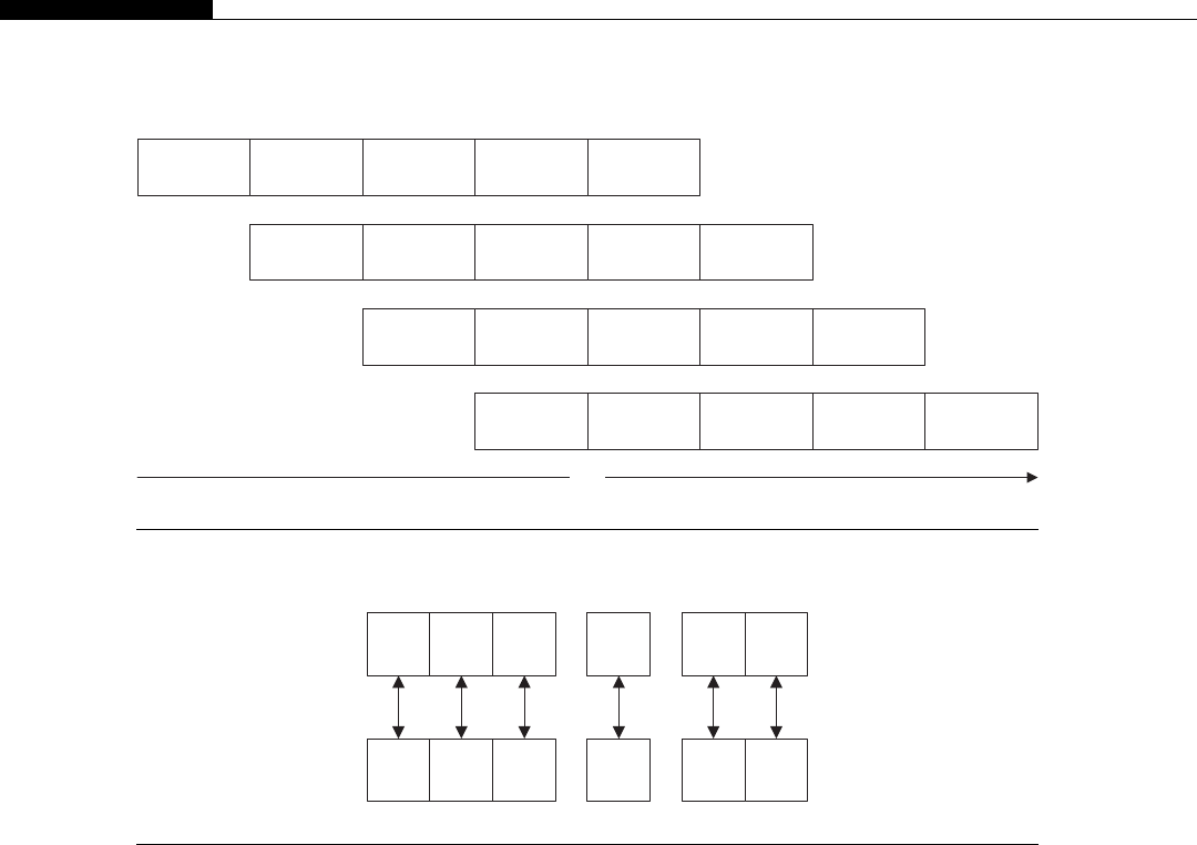
nonblocking and implicit memory transfers may not be supported. We’ll look at these issues in more
detail in Chapter 9.
The usual model of execution involves the CPU transferring a block of data to the GPU, the GPU
kernel processing it, and then the CPU initiating a transfer of the data back to the host memory. A
slightly more advanced model of this is where we use streams (covered later) to overlap transfers and
kernels to ensure the GPU is always kept busy, as shown in Figure 6.16.
Once you have the data in the GPU, the question then becomes how do you access it efficiently on
the GPU? Remember the GPU can be rated at over 3 teraflops in terms of compute power, but typically
the main memory bandwidth is in the order of 190 GB/s down to as little as 25 GB/s. By comparison,
a typical Intel I7 Nehalem or AMD Phenom CPU achieves in the order of 25–30 GB/s, depending on
the particular device speed and width of the memory bus used.
Graphics cards use high-speed GDDR, or graphics dynamic memory, which achieves very high
sustained bandwidth, but like all memory, has a high latency. Latency is the time taken to return the
first byte of the data access. Therefore, in the same way that we can pipeline kernels, as is shown in
Time
Transfer To GPU KernelCPU Gather Transfer
From CPU Process
Transfer To GPU KernelCPU Gather Transfer
From CPU Process
Transfer To GPU KernelCPU Gather Transfer
From CPU Process
Transfer To GPU KernelCPU Gather Transfer
From CPU Process
FIGURE 6.16
Overlapping kernel and memory transfers.
Addr
0
Addr
1
Addr
2
Addr
N
Addr
30
Addr
31
TID
0
TID
1
TID
2
TID
N
TID
30
TID
31
FIGURE 6.17
Addresses accessed by thread ID.
168 CHAPTER 6 Memory Handling with CUDA
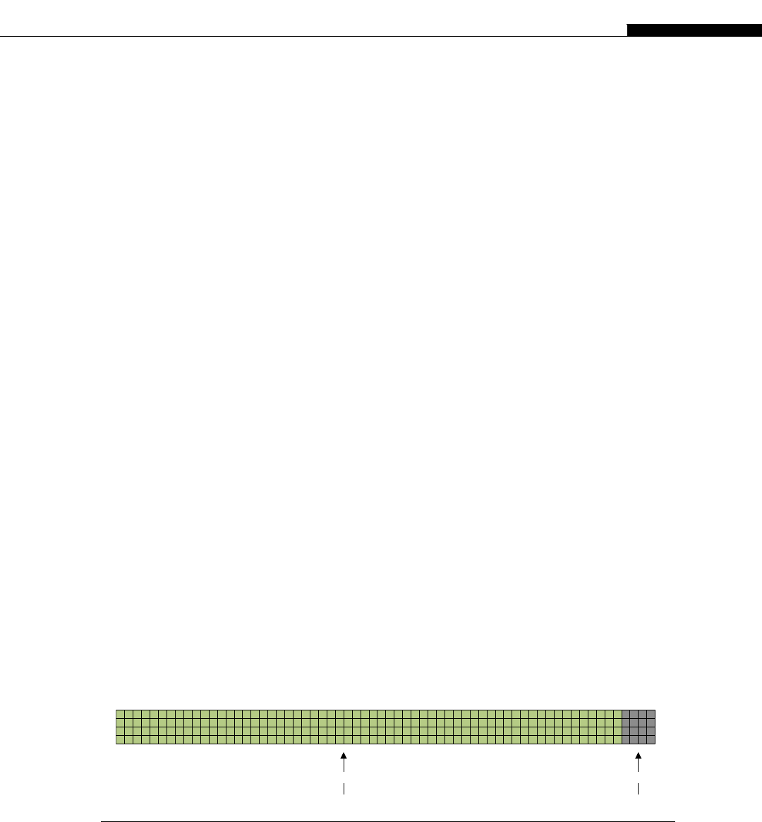
Figure 6.16, the memory accesses are pipelined. By creating a ratio of typically 10:1 of threads to
number of memory accesses, you can hide memory latency, but only if you access global memory in
a pattern that is coalesced.
So what is a coalescable pattern? This is where all the threads access a contiguous and aligned
memory block, as shown in Figure 6.17. Here we have shown Addr as the logical address offset from
the base location, assuming we are accessing byte-based data. TID represents the thread number. If we
have a one-to-one sequential and aligned access to memory, the address accesses of each thread are
combined together and a single memory transaction is issued. Assuming we’re accessing a single
precision float or integer value, each thread will be accessing 4 bytes of memory. Memory is coalesced
on a warp basis (the older G80 hardware uses half warps), meaning we get 32 4¼128 byte access to
memory.
Coalescing sizes supported are 32, 64, and 128 bytes, meaning warp accesses to byte, 16- and 32-
bit data will always be coalesced if the access is a sequential pattern and aligned to a 32-byte boundary.
The alignment is achieved by using a special malloc instruction, replacing the standard cudaMalloc
with cudaMallocPitch, which has the following syntax:
extern __host__ cudaError_t CUDARTAPI cudaMallocPitch(void **devPtr, size_t *pitch,
size_t width, size_t height);
This translates to cudaMallocPitch (pointer to device memory pointer, pointer to pitch, desired
width of the row in bytes, height of the array in bytes).
Thus, if you have an array of 100 rows of 60 float elements, using the conventional cudaMalloc,
you would allocate 100 60 sizeof(float) bytes, or 100 60 4¼24,000 bytes. Accessing array
index [1][0] (i.e., row one, element zero) would result in noncoalesced access. This is because the
length of a single row of 60 elements would be 240 bytes, which is of course not a power of two.
The first address in the series of addresses from each thread would not meet the alignment
requirements for coalescing. Using the cudaMallocPitch function the size of each row is padded by an
amount necessary for the alignment requirements of the given device (Figure 6.18). In our example, it
would in most cases be extended to 64 elements per row, or 256 bytes. The pitch the device actually
uses is returned in the pitch parameters passed to cudaMallocPitch.
Let’s have a look at how this works in practice. Nonaligned accesses result in multiple memory
fetches being issued. While waiting for a memory fetch, all threads in a warp are stalled until all
memory fetches are returned from the hardware. Thus, to achieve the best throughput you need to issue
a small number of large memory fetch requests, as a result of aligned and sequential coalesced accesses.
Used Data Padding
FIGURE 6.18
Padding achieved with cudaMallocPitch.
Global Memory 169
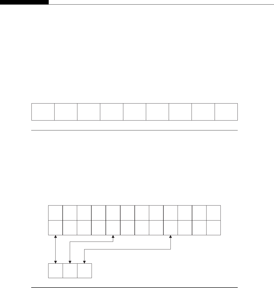
So what happens if you have data that is interleaved in some way, for example, a structure?
typedef struct
{
unsigned int a;
unsigned int b;
unsigned int c;
unsigned int d;
} MY_TYPE_T;
MY_TYPE_T some_array[1024]; /* 1024 * 4 bytes ¼4K */
Figure 6.19 shows how C will lay this structure out in memory.
Elements are laid out in memory in the sequence in which they are defined within the structure. The
access pattern for such a structure is shown in Figure 6.20. As you can see from the figure, the
addresses of the structure elements are not contiguous in memory. This means you get no coalescing
and the memory bandwidth suddenly drops off by an order of magnitude. Depending on the size of our
data elements, it may be possible to have each thread read a larger value and then internally within the
threads mask off the necessary bits. For example, if you have byte-based data you can do the following:
Index 0
Element A
Index 0
Element B
Index 0
Element C
Index 0
Element D
Index 1
Element A
Index 1
Element B
Index 1
Element C
Index 1
Element D
Index N
Element
A, B, C, D
FIGURE 6.19
Array elements in memory.
Word
0
TID
0
TID
1
TID
2
Word
1
Word
2
Word
3
Word
4
Word
5
Word
6
Word
7
Word
8
Word
9
Word
10
Word
11
A B C D A B C D A B C D
FIGURE 6.20
Words accessed by thread (no coalescing).
170 CHAPTER 6 Memory Handling with CUDA

const unsigned int value_u32 ¼some_data[tid];
const unsigned char value_01 ¼(value_u32 & 0x000000FF) );
const unsigned char value_02 ¼(value_u32 & 0x0000FF00) >> 8 );
const unsigned char value_03 ¼(value_u32 & 0x00FF0000) >> 16 );
const unsigned char value_04 ¼(value_u32 & 0xFF000000) >> 24 );
It’s also possible to maintain the one thread to one data element mapping by simply treating the array
of structure elements as an array of words. We can then allocate one thread to each element of the
structure. This type of solution is, however, not suitable if there is some data flow relationship between the
structure members, so thread 1 needs the x,y, and zcoordinate of a structure, for example. In this case, it’s
best to reorder the data, perhaps in the loading or transfer phase on the CPU, into Ndiscrete arrays. In this
way, the arrays individually sit concurrently in memory. We can simply access array a,b,c,ordinstead of
the struct->a notation we’d use with a structure dereference. Instead of an interleaved and uncoalesced
pattern, we get four coalesced accesses from each thread into different memory regions, maintaining
optimal global memory bandwidth usage.
Let’s look at an example of global memory reads. In this example, we’ll sum the values of all the
elements in the structure using the two methods. First, we’ll add all the values from an array of
structures and then from a structure of arrays.
// Define the number of elements we’ll use
#define NUM_ELEMENTS 4096
// Define an interleaved type
// 16 bytes, 4 bytes per member
typedef struct
{
u32 a;
u32 b;
u32 c;
u32 d;
} INTERLEAVED_T;
// Define an array type based on the interleaved structure
typedef INTERLEAVED_T INTERLEAVED_ARRAY_T[NUM_ELEMENTS];
// Alternative - structure of arrays
typedef u32 ARRAY_MEMBER_T[NUM_ELEMENTS];
typedef struct
{
ARRAY_MEMBER_T a;
ARRAY_MEMBER_T b;
ARRAY_MEMBER_T c;
ARRAY_MEMBER_T d;
} NON_INTERLEAVED_T;
In this section of code, we declare two types; the first is INTERLEAVED_T, an array of structures of
which the members are ato d. We then declare NON_INTERLEAVED_T as a structure that contains four
Global Memory 171

arrays, ato d. As the types are named, with the first one we expect the data to be interleaved in memory.
With the second one, we expect a number of contiguous memory areas.
Let’s look first at the CPU code.
__host__ float add_test_non_interleaved_cpu(
NON_INTERLEAVED_T * const host_dest_ptr,
const NON_INTERLEAVED_T * const host_src_ptr,
const u32 iter,
const u32 num_elements)
{
float start_time ¼get_time();
for (u32 tid ¼0; tid < num_elements; tidþþ)
{
for (u32 i¼0; i<iter; iþþ)
{
host_dest_ptr->a[tid] þ¼ host_src_ptr->a[tid];
host_dest_ptr->b[tid] þ¼ host_src_ptr->b[tid];
host_dest_ptr->c[tid] þ¼ host_src_ptr->c[tid];
host_dest_ptr->d[tid] þ¼ host_src_ptr->d[tid];
}
}
const float delta ¼get_time() - start_time;
return delta;
}
__host__ float add_test_interleaved_cpu(
INTERLEAVED_T * const host_dest_ptr,
const INTERLEAVED_T * const host_src_ptr,
const u32 iter,
const u32 num_elements)
{
float start_time ¼get_time();
for (u32 tid ¼0; tid < num_elements; tidþþ)
{
for (u32 i¼0; i<iter; iþþ)
{
host_dest_ptr[tid].a þ¼ host_src_ptr[tid].a;
host_dest_ptr[tid].b þ¼ host_src_ptr[tid].b;
host_dest_ptr[tid].c þ¼ host_src_ptr[tid].c;
host_dest_ptr[tid].d þ¼ host_src_ptr[tid].d;
}
}
const float delta ¼get_time() - start_time;
172 CHAPTER 6 Memory Handling with CUDA

return delta;
}
The two functions to add the data are broadly similar. Each function iterates over all elements in the
list iter times and adds into the destination data structure a value from the source data structure. Each
function also returns the time it takes to execute. As these will run on the CPU, we use the wall clock
time on the CPU.
The GPU code is largely similar, with the outer loop, tid, replaced with Nthreads from invoking
a kernel.
__global__ void add_kernel_interleaved(
INTERLEAVED_T * const dest_ptr,
const INTERLEAVED_T * const src_ptr,
const u32 iter,
const u32 num_elements)
{
const u32 tid ¼(blockIdx.x * blockDim.x) þthreadIdx.x;
if (tid < num_elements)
{
for (u32 i¼0; i<iter; iþþ)
{
dest_ptr[tid].a þ¼ src_ptr[tid].a;
dest_ptr[tid].b þ¼ src_ptr[tid].b;
dest_ptr[tid].c þ¼ src_ptr[tid].c;
dest_ptr[tid].d þ¼ src_ptr[tid].d;
}
}
}
__global__ void add_kernel_non_interleaved(
NON_INTERLEAVED_T * const dest_ptr,
const NON_INTERLEAVED_T * const src_ptr,
const u32 iter,
const u32 num_elements)
{
const u32 tid ¼(blockIdx.x * blockDim.x) þthreadIdx.x;
if (tid < num_elements)
{
for (u32 i¼0; i<iter; iþþ)
{
dest_ptr->a[tid] þ¼ src_ptr->a[tid];
dest_ptr->b[tid] þ¼ src_ptr->b[tid];
dest_ptr->c[tid] þ¼ src_ptr->c[tid];
dest_ptr->d[tid] þ¼ src_ptr->d[tid];
Global Memory 173

}
}
}
The caller of the GPU function is a fairly standard copy to device and time routine. I’ll list here only
the interleaved version, as the two functions are largely identical.
__host__ float add_test_interleaved(
INTERLEAVED_T * const host_dest_ptr,
const INTERLEAVED_T * const host_src_ptr,
const u32 iter,
const u32 num_elements)
{
// Set launch params
const u32 num_threads ¼256;
const u32 num_blocks ¼(num_elements þ(num_threads-1)) / num_threads;
// Allocate memory on the device
const size_t num_bytes ¼(sizeof(INTERLEAVED_T) * num_elements);
INTERLEAVED_T * device_dest_ptr;
INTERLEAVED_T * device_src_ptr;
CUDA_CALL(cudaMalloc((void **) &device_src_ptr, num_bytes));
CUDA_CALL(cudaMalloc((void **) &device_dest_ptr, num_bytes));
// Create a stop and stop event for timing
cudaEvent_t kernel_start, kernel_stop;
cudaEventCreate(&kernel_start, 0);
cudaEventCreate(&kernel_stop, 0);
// Create a non zero stream
cudaStream_t test_stream;
CUDA_CALL(cudaStreamCreate(&test_stream));
// Copy src data to GPU
CUDA_CALL(cudaMemcpy(device_src_ptr, host_src_ptr, num_bytes,
cudaMemcpyHostToDevice));
// Push start event ahread of kernel call
CUDA_CALL(cudaEventRecord(kernel_start, 0));
// Call the GPU kernel
add_kernel_interleaved<<<num_blocks, num_threads>>>(device_dest_ptr, device_src_ptr,
iter, num_elements);
// Push stop event after of kernel call
CUDA_CALL(cudaEventRecord(kernel_stop, 0));
174 CHAPTER 6 Memory Handling with CUDA

// Wait for stop event
CUDA_CALL(cudaEventSynchronize(kernel_stop));
// Get delta between start and stop,
// i.e. the kernel execution time
float delta ¼0.0F;
CUDA_CALL(cudaEventElapsedTime(&delta, kernel_start, kernel_stop));
// Clean up
CUDA_CALL(cudaFree(device_src_ptr));
CUDA_CALL(cudaFree(device_dest_ptr));
CUDA_CALL(cudaEventDestroy(kernel_start));
CUDA_CALL(cudaEventDestroy(kernel_stop));
CUDA_CALL(cudaStreamDestroy(test_stream));
return delta;
}
When we run this code, we achive the following results:
Running Interleaved / Non Interleaved memory test using 65536 bytes (4096 elements)
ID:0 GeForce GTX 470: Interleaved time: 181.83ms
ID:0 GeForce GTX 470: Non Interleaved time: 45.13ms
ID:1 GeForce 9800 GT: Interleaved time: 2689.15ms
ID:1 GeForce 9800 GT: Non Interleaved time: 234.98ms
ID:2 GeForce GTX 260: Interleaved time: 444.16ms
ID:2 GeForce GTX 260: Non Interleaved time: 139.35ms
ID:3 GeForce GTX 460: Interleaved time: 199.15ms
ID:3 GeForce GTX 460: Non Interleaved time: 63.49ms
CPU (serial): Interleaved time: 1216.00ms
CPU (serial): Non Interleaved time: 13640.00ms
What we see is quite interesting, and largely to be expected. The interleaved memory access pattern
has an execution time three to four times longer than the noninterleaved pattern on compute 2.x
hardware. The compute 1.3 GTX260 demonstrates a 3slow down when using the interleaved
memory pattern. The compute 1.1 9800GT, however, exhibits an 11slow down, due to the more
stringent coalescing requirements for these older devices.
We can look a bit deeper into the memory access pattern between the slow interleaved pattern and
the much faster noninterleaved pattern with a tool such as Parallel Nsight. We can see that the number
of memory transactions (CUDA Memory Statistics experiment) used in the noninterleaved version is
approximately one-quarter that of the interleaved version, resulting in the noninterleaved version
shifting one-quarter of the data to/from memory than the interleaved version does.
One other interesting thing to note is the CPU shows exactly the opposite effect. This may seem
strange, until you think about the access pattern and the cache reuse. A CPU accessing element ain the
Global Memory 175

interleaved example will have brought structure elements b,c, and dinto the cache on the access to
asince they will likely be in the same cache line. However, the noninterleaved version will be accessing
memory in four seperate and physically dispersed areas. There would be four times the number of
memory bus transactions and any read-ahead policy the CPU might be using would not be as effective.
Thus, if your existing CPU application uses an interleaved arrangement of structure elements,
simply copying it to a GPU will work, but at a considerable cost due to poor memory coalescing.
Simply reordering the declarations and access mechanism, as we’ve done in this example, could allow
you to achieve a significant speedup for very little effort.
Score boarding
One other interesting property of global memory is that it works with a scoreboard. If we initiate a load
from global memory (e.g., a¼some_array[0]), then all that happens is that the memory fetch is
initiated and local variable ais listed as having a pending memory transaction. Unlike traditional CPU
code, we do not see a stall or even a context switch to another warp until such time as the variable ais
later used in an expression. Only at this time do we actually need the contents of variable a. Thus, the
GPU follows a lazy evaluation model.
You can think of this a bit like ordering a taxi and then getting ready to leave. It may take only five
minutes to get ready, but the taxi may take up to 15 minutes to arrive. By ordering it before we actually
need it, it starts its journey while we are busy on the task of getting ready to leave. If we wait until we are
ready before ordering the taxi, we serialize the task of getting ready to leave with waiting for the taxi.
The same is true of the memory transactions. By comparison, they are like the slow taxi, taking
forever in terms of GPU cycles to arrive. Until such time as we actually need the memory transaction to
have arrived, the GPU can be busy calculating other aspects of the algorithm. This is achieved very
simply by placing the memory fetches at the start of the kernel, and then using them much later during
the kernel. We, in effect, overlap the memory fetch latency with useful GPU computations, reducing
the effect of memory latency on our kernel.
Global memory sorting
Picking up from where we left off with shared memory sorting, how do you think the same algorithm
would work for global memory–based sorting? What needs to be considered? First and foremost, you
need to think about memory coalescing. Our sorting algorithm was specifically developed to run with
the 32 banks of shared memory and accesses the shared memory in columns. If you look again at
Figure 6.8, you’ll see this also achieves coalesced access to global memory if all threads were to read at
once.
The coalesced access occurs during the radix sort, as each thread marches through its own list.
Every thread’s access is coalesced (combined) together by the hardware. Writes are noncoalesced as
the 1 list can vary in size. However, the zeros are both read and written to the same address range, thus
providing coalesced access.
In the merge phase, during the startup condition one value from each list is read from global into
shared memory. In every iteration of the merge, a single value is written out to global memory, and
a single value is read into shared memory to replace the value written out. There is a reasonable amount
of work being done for every memory access. Thus, despite the poor coalescing, the memory latency
should be largely hidden. Let’s look at how this works in practice.
176 CHAPTER 6 Memory Handling with CUDA
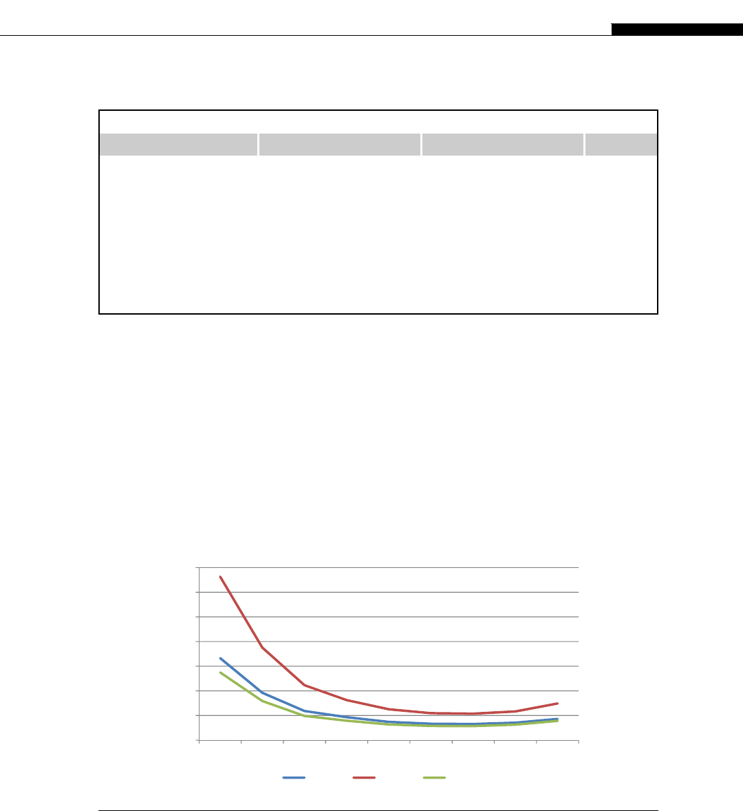
What you can see from Table 6.13 and Figure 6.21 is that 32 threads work quite well, but this is
marginally beaten by 64 threads on all the tested devices. It’s likely that having another warp to execute is
hiding a small amount of the latency and will also improve slightly the memory bandwidth utilization.
Moving beyond 64 threads slows things down, so if we now fix the number of threads at 64 and
increase the dataset size what do we see? See Table 6.14 and Figure 6.22 for the results. In fact we see
an almost perfect linear relationship when using a single SM, as we are currently doing.
As Table 6.14 shows, 1024 KB (1 MB) of data takes 1486 ms to sort on the GTX460. This means
we can sort 1 MB of data in around 1.5 seconds (1521 ms exactly) and around 40 MB per minute,
regardless of the size of the data.
A 1 GB dataset would therefore take around 25–26 minutes to sort, which is not very impressive.
So what is the issue? Well currently we’re using just a single block, which in turn limits us to a single
SM. The test GPUs consists of 14 SMs on the GTX470, 27 SMs on the GTX260, and 7 SMs on the
Table 6.13 Single SM GMEM Sort (1K Elements)
Threads GTX470 GTX260 GTX460
1 33.27 66.32 27.47
2 19.21 37.53 15.87
4 11.82 22.29 9.83
8 9.31 16.24 7.88
16 7.41 12.52 6.36
32 6.63 10.95 5.75
64 6.52 10.72 5.71
128 7.06 11.63 6.29
256 8.61 14.88 7.82
0
10
20
30
40
50
60
70
1248163264128256
GTX470 260GTX GTX460
FIGURE 6.21
Graph of single SM GMEM sort (1K elements).
Global Memory 177
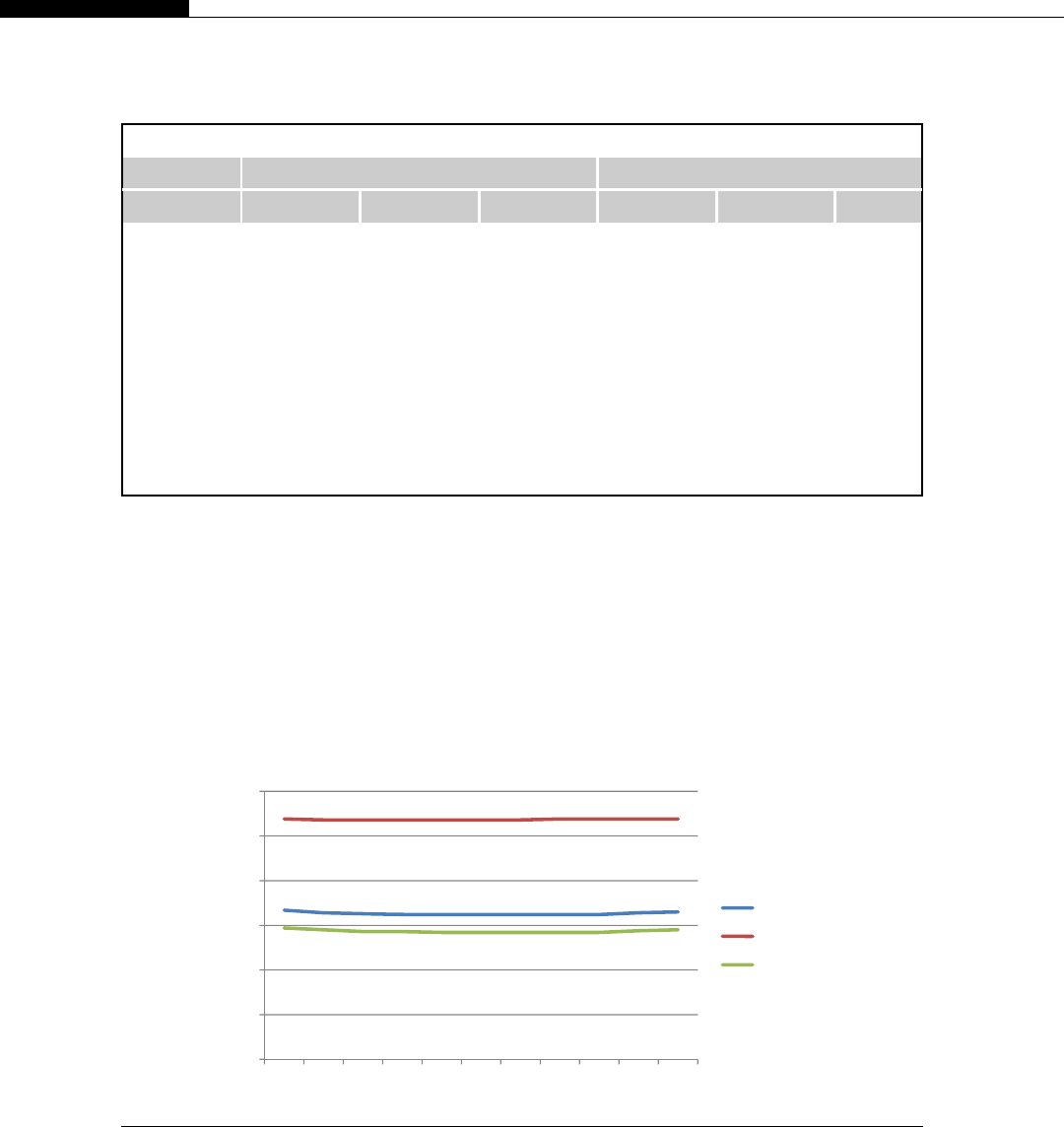
GTX460. Clearly, we’re using a small fraction of the real potential of the card. This has been done
largely to simplify the solution, so let’s look now at using multiple blocks.
The output of one SM is a single linear sorted list. The output of two SMs is therefore two linear
sorted lists, which is not what we want. Consider the following dump of output from a two-block
version of the sort. The original values were in reverse sorting order from 0x01 to 0x100. The first value
shown is the array index, followed by the value at that array index.
Table 6.14 GMEM Sort by Size
Absolute Time (ms) Time per KB (ms)
Size (Kb) GTX470 GTX260 GTX460 GTX470 GTX260 GTX460
1 1.67 2.69 1.47 1.67 2.69 1.47
2 3.28 5.36 2.89 1.64 2.68 1.45
4 6.51 10.73 5.73 1.63 2.68 1.43
8 12.99 21.43 11.4 1.62 2.68 1.43
16 25.92 42.89 22.75 1.62 2.68 1.42
32 51.81 85.82 45.47 1.62 2.68 1.42
64 103.6 171.78 90.94 1.62 2.68 1.42
128 207.24 343.74 181.89 1.62 2.69 1.42
256 414.74 688.04 364.09 1.62 2.69 1.42
512 838.25 1377.23 737.85 1.64 2.69 1.44
1024 1692.07 2756.87 1485.94 1.65 2.69 1.45
0
0.5
1
1.5
2
2.5
3
1 2 4 8 16 32 64 128 256 512 1024
GTX470
260GTX
GTX460
FIGURE 6.22
GMEM graph sorted by size.
178 CHAPTER 6 Memory Handling with CUDA

000:00000041 001:00000042 002:00000043 003:00000044 004:00000045 005:00000046
006:00000047 007:00000048
008:00000049 009:0000004a 010:0000004b 011:0000004c 012:0000004d 013:0000004e
014:0000004f 015:00000050
016:00000051 017:00000052 018:00000053 019:00000054 020:00000055 021:00000056
022:00000057 023:00000058
024:00000059 025:0000005a 026:0000005b 027:0000005c 028:0000005d 029:0000005e
030:0000005f 031:00000060
032:00000061 033:00000062 034:00000063 035:00000064 036:00000065 037:00000066
038:00000067 039:00000068
040:00000069 041:0000006a 042:0000006b 043:0000006c 044:0000006d 045:0000006e
046:0000006f 047:00000070
048:00000071 049:00000072 050:00000073 051:00000074 052:00000075 053:00000076
054:00000077 055:00000078
056:00000079 057:0000007a 058:0000007b 059:0000007c 060:0000007d 061:0000007e
062:0000007f 063:00000080
064:00000001 065:00000002 066:00000003 067:00000004 068:00000005 069:00000006
070:00000007 071:00000008
072:00000009 073:0000000a 074:0000000b 075:0000000c 076:0000000d 077:0000000e
078:0000000f 079:00000010
080:00000011 081:00000012 082:00000013 083:00000014 084:00000015 085:00000016
086:00000017 087:00000018
088:00000019 089:0000001a 090:0000001b 091:0000001c 092:0000001d 093:0000001e
094:0000001f 095:00000020
096:00000021 097:00000022 098:00000023 099:00000024 100:00000025 101:00000026
102:00000027 103:00000028
104:00000029 105:0000002a 106:0000002b 107:0000002c 108:0000002d 109:0000002e
110:0000002f 111:00000030
112:00000031 113:00000032 114:00000033 115:00000034 116:00000035 117:00000036
118:00000037 119:00000038
120:00000039 121:0000003a 122:0000003b 123:0000003c 124:0000003d 125:0000003e
126:0000003f 127:00000040
We can see there are two sorted lists here, one from 0x41 to 0x80 and the other from 0x01 to 0x40.
You might say that’s not a great problem, and we just need to merge the list again. This is where we hit
the second issue; think about the memory access on a per-thread basis.
Assume we use just two threads, one per list. Thread 0 accesses element 0. Thread 1 accesses
element 64. It’s not possible for the hardware to coalesce the two accesses, so the hardware has to issue
two independent memory fetches.
Even if we were to do the merge in zero time, assuming we have a maximum of 16 SMs and using all
of them did not flood the bandwidth of the device, in the best case we’d get 16 40 MB/min ¼640
MB/min or around 10.5 MB/s. Perhaps an alternative approach is required.
Sample sort
Sample sort tries to get around the problem of merge sort, that is, that you have to perform a merge
step. It works on the principle of splitting the data into Nindependent blocks of data such that each
Global Memory 179
block is partially sorted and we can guarantee the numbers in block Nare less than those in block Nþ1
and larger than those in block N1.
We’ll look first at an example using three processors sorting 24 data items. The first phase selects S
equidistant samples from the dataset. Sis chosen as a fraction of N, the total number of elements in the
entire dataset. It is important that Sis representative of the dataset. Equidistant points are best used
where the data is reasonably uniformly distributed over the data range. If the data contains large peaks
that are not very wide in terms of sample points, a higher number of samples may have to be used, or
one where the samples concentrate around the known peaks. We’ll chose equidistant points and
assume the more common uniform distribution of points.
The samples are then sorted such that the lowest value is first in the list, assuming an ascending
order sort. The sample data is then split into bins according to how many processors are available. The
data is scanned to determine how many samples fit in each bin. The number of samples in each bin is
then added to form a prefix sum that is used to index into an array.
A prefix sum is simply the sum of all elements prior to the current element. Looking at the example,
we can see nine elements were allocated to bin 0. Therefore, the start of the second dataset is element
9. The next list size, as it happens from the dataset, was also nine. Nine plus the previous sum is 18, and
thus we know the index of the next dataset and so on.
The data is then shuffled, so all the bin 0 elements are written to the first index of the prefix sum
(zero), bin 1 written to the next, and so on. This achieves a partial sort of the data such that all the
samples in bin N1 are less than those in bin N, which in turn are less than those in bin Nþ1. The
bins are then dispatched to Pprocessors that sort the lists in parallel. If an in-place sort is used, then the
list is sorted once the last block of data is sorted, without any merge step. Figure 6.24 is this same
example using six processing elements.
Notice that when we used three processors based on six samples, the bin sizes were 9, 9, 6. With six
processors the bin sizes are 6, 3, 5, 4, 1, 5. What we’re actually interested in is the largest value, as on
Pprocessors the largest block will determine the total time taken. In this example, the maximum is
10 3 79 21 12 7 1 4 2 23 420 19 57 8 9 92 35 13 661 17 47
0 1 2 3 4 5 6 7 8 9 10 11 12 13 14 15 16 17 18 19 20 21 22 23
9 7 23 57 35 17
97 23 573517
9 entries
0..8
9 entries
9..22
6 entries
>= 23
Select Samples
Sort Samples
Count Bins
0 9 18 Starting Index Points
3 7 7 1 4 2 4 8 1
109 2112 20199 13 17
23 57 92 35 66 47
0 1 2 3 4 5 6 7 8 9 10 11 12 13 14 15 16 17 18 19 20 21 22 23
Sort on P0Sort on P1Sort on P2
23 57 9235 6647
10 9 21 12 20 19 913 17
3 771 42 4 81
Sort on P0to P2
Append Lists
FIGURE 6.23
Sample sort using three processors.
180 CHAPTER 6 Memory Handling with CUDA
reduced from nine elements to six elements, so a doubling of the number of processors has reduced the
maximum number of data points by only one-third.
The actual distribution will depend very much on the dataset. The most common dataset is actually
a mostly sorted list or one that is sorted with some new data items that must be added. This tends to
give a fairly equal distribution for most datasets. For problem datasets it’s possible to adjust the
sampling policy accordingly.
With a GPU we don’t just have six processors; we have NSMs, each of which we need to run
a number of blocks on. Each block would ideally be around 256 threads based simply on ideal memory
latency hiding, although we saw that 64 threads worked best with the radix sort we developed earlier in
the chapter. With the GTX470 device, we have 14 SMs with a maximum of eight blocks per SM.
Therefore, we need at least 112 blocks just to keep every SM busy. We’ll find out in practice which is
the best in due course. It is likely we will need substantially more blocks to load balance the work.
The first task, however, is to develop a CPU version of the sample sort algorithm and to understand
it. We’ll look at each operation in turn and how it could be converted to a parallel solution.
To follow the development of the code in the subsequent sections, it’s important you understand the
sample sort algorithm we just covered. It’s one of the more complex sorting algorithms and was chosen
both for performance reasons and also because it allows us to look at a real problem involving difficult
issues in terms of GPU implementation. If you browsed over the algorithm, please re-read the last few
pages until you are sure you understand how the algorithm works before proceeding.
Selecting samples
The first part of the sample sort is to select Nsamples from the source data. The CPU version works
with a standard loop where the source data loop index is incremented by sample_interval elements.
The sample index counter, however, is incremented only by one per iteration.
__host__ TIMER_T select_samples_cpu(
u32 * const sample_data,
10 3 79 21 12 7 1 4 2 23 420 19 57 8 9 92 35 13 661 17 47
0 1 2 3 4 5 6 7 8 9 10 11 12 13 14 15 16 17 18 19 20 21 22 23
9 7 23 57 35 17
97 23 573517
6 entries
0..6
3 entries
7..8
5 entries
>= 57
Select Samples
Sort Samples
Count Bins
0 6 9 Starting Index Points
0 1 2 3 4 5 6 7 8 9 10 11 12 13 14 15 16 17 18 19 20 21 22 23 Sort on P0to P5
Append Lists
103 7 9 211271 42 234 2019 578 9 923513 661 17 47
5 entries
9..16
4 entries
17..22
1 entry
23..34
14 18 22
Sort on P0Sort on P1Sort on P2Sort on P3
Sort
on
P4
Sort on P5
FIGURE 6.24
Sample sort using six processors.
Global Memory 181

const u32 sample_interval,
const u32 num_elements,
const u32 * const src_data)
{
const TIMER_T start_time ¼get_time();
u32 sample_idx ¼0;
for (u32 src_idx¼0; src_idx<num_elements; src_idxþ¼sample_interval)
{
sample_data[sample_idx] ¼src_data[src_idx];
sample_idxþþ;
}
const TIMER_T end_time ¼get_time();
return end_time - start_time;
}
In the GPU version we can use a classic loop elimination method and simply create one thread per
sample point, spread across as many blocks as necessary. Thus, the first statement
const u32 tid ¼(blockIdx.x * blockDim.x) þthreadIdx.x;
simply takes the block index and multiplies it by the number of threads per block and then adds in the
current thread to our combined thread index.
__global__ void select_samples_gpu_kernel(u32 * const sample_data,
const u32 sample_interval, const u32 * const src_data)
{
const u32 tid ¼(blockIdx.x * blockDim.x) þthreadIdx.x;
sample_data[tid] ¼src_data[tid*sample_interval];
}
__host__ TIMER_T select_samples_gpu(
u32 * const sample_data,
const u32 sample_interval,
const u32 num_elements,
const u32 num_samples,
const u32 * const src_data,
const u32 num_threads_per_block,
const char * prefix)
{
// Invoke one block of N threads per sample
const u32 num_blocks ¼num_samples / num_threads_per_block;
// Check for non equal block size
assert((num_blocks * num_threads_per_block) ¼¼ num_samples);
start_device_timer();
select_samples_gpu_kernel<<<num_blocks, num_threads_per_block>>>(sample_data,
sample_interval, src_data);
cuda_error_check(prefix, "Error invoking select_samples_gpu_kernel");
182 CHAPTER 6 Memory Handling with CUDA

const TIMER_T func_time ¼stop_device_timer();
return func_time;
}
Finally, to work out the index into the source data we simply multiply our sample data index (tid)
by the size of the sample interval. For the sake of simplicity we’ll only look at the case where the
dataset sizes are multiples of one another.
Notice both the CPU and GPU versions return the time taken for the operation, something we’ll do
in each section of the sort to know the various timings of each operation.
Sorting the samples
Next we need to sort the samples we’ve selected. On the CPU we can simply call the qsort (quicksort)
routine from the standard C library.
__host__ TIMER_T sort_samples_cpu(
u32 * const sample_data,
const u32 num_samples)
{
const TIMER_T start_time ¼get_time();
qsort(sample_data, num_samples, sizeof(u32),
&compare_func);
const TIMER_T end_time ¼get_time();
return end_time - start_time;
}
On the GPU, however, these standard libraries are not available, so we’ll use the radix sort we
developed earlier. Note, radix sort is also provided by the Thrust library, so you don’t have to write it as
we’ve done here. I won’t replicate the code here since we’ve already looked at it in detail in the shared
memory section.
One thing to note, however, is the version we developed before does a radix sort on a single SM in
shared memory and then uses a shared memory reduction for the merge operation. This is not an
optimal solution, but we’ll use it for at least the initial tests.
Counting the sample bins
Next we need to know how many values exist in each sample bin. The CPU code for this is as follows:
__host__ TIMER_T count_bins_cpu(const u32 num_samples,
const u32 num_elements,
const u32 * const src_data,
const u32 * const sample_data,
u32 * const bin_count)
{
const TIMER_T start_time ¼get_time();
for (u32 src_idx¼0; src_idx<num_elements; src_idxþþ)
Global Memory 183

{
const u32 data_to_find ¼src_data[src_idx];
const u32 idx ¼bin_search3(sample_data,
data_to_find,
num_samples);
bin_count[idx]þþ;
}
const TIMER_T end_time ¼get_time();
return end_time - start_time;
}
To count the values in each bin we simply iterate over the source dataset and for every element call
a search function that identifies in which bin a given data value will belong. We then increment the bin
counter for that given index.
For the search we have two options: a binary search or a sequential search. A binary search takes
advantage of the fact we have a sorted list of samples from the previous step. It works by dividing the
list into two halves and asking whether the value it seeks is in the top or bottom half of the dataset. It
then divides the list again and again until such time as it finds the value.
The worst case sort time for a binary search is log
2
(N). We’ll hit the worst case in many instances
because most of the data is missing from the sample list. Therefore, we’ll assume we’ll hit the worst
case in all cases when comparing the two approaches.
The sequential search worst case is N. That is, we start at the beginning of the list and do not find
the item at all, having transversed the list from start to finish. However, with a sorted list and a uniform
distribution of data the most likely case is N/2. Thus, for a sample set of 1024 elements, a binary search
would take just 10 iterations compared with 512 iterations for the sequential search. Clearly, the binary
search is the best approach in terms of the search space covered.
However, we have to consider that a binary search is not very good for a GPU from the perspective
of coalesced memory accesses and branch divergence. As soon as one thread diverges in a warp, the
hardware needs two control paths. We may well have the situation where the warps diverge such that
we have entirely independent control for each thread. In this case we can multiply the time taken by the
number of divergent threads. This will always be a maximum of the number of iterations, which is the
log
2
(N). Thus, our sample size needs to be huge before we see anything like the maximum amount of
divergencedall threads in a warp.
Each thread is accessing potentially a different area of memory in the sample set, so there is no
coalescing and therefore there is a drop of an order of magnitude in terms of global memory band-
width. In practice, this should be largely hidden by the L1 and L2 cache on compute 2.x devices,
depending on the size of the sample space. We could also store the sample space in shared memory,
meaning we can discount the coalescing issues.
The standard C library again provides a bsearch function, which returns the value it finds in the array.
However, we’re not interested in the nearest value, but actually the array index. Therefore, we’ll write
a basic binary search function and use this on both the GPU and CPU. Notice the use of both __host__
and __device__ specifiers to run the identical source, but not binary, code on both the CPU and GPU.
__host__ __device__ u32 bin_search3(
const u32 * const src_data,
const u32 search_value,
184 CHAPTER 6 Memory Handling with CUDA

const u32 num_elements)
{
// Take the middle of the two sections
u32 size ¼(num_elements >> 1);
u32 start_idx ¼0;
bool found ¼false;
do
{
const u32 src_idx ¼(start_idxþsize);
const u32 test_value ¼src_data[src_idx];
if (test_value ¼¼ search_value)
found ¼true;
else
if (search_value > test_value)
start_idx ¼(start_idxþsize);
if (found ¼¼ false)
size >>¼1;
} while ( (found ¼¼ false) && (size !¼0) );
return (start_idx þsize);
}
The binary search routine works by reducing the size parameter to zero. It returns the index or the
bin in which the search value should be placed.
// Single data point, atomic add to gmem
__global__ void count_bins_gpu_kernel5(
const u32 num_samples,
const u32 * const src_data,
const u32 * const sample_data,
u32 * const bin_count)
{
const u32 tid ¼(blockIdx.x * blockDim.x) þthreadIdx.x;
// Read the sample point
const u32 data_to_find ¼src_data[tid];
// Obtain the index of the element in the search list
const u32 idx ¼bin_search3(sample_data, data_to_find, num_samples);
atomicAdd(&bin_count[idx],1);
}
__host__ TIMER_T count_bins_gpu(
Global Memory 185

const u32 num_samples,
const u32 num_elements,
const u32 * const src_data,
const u32 * const sample_data,
u32 * const bin_count,
const u32 num_threads,
const char * prefix)
{
const u32 num_blocks ¼num_elements / num_threads;
start_device_timer();
count_bins_gpu_kernel5<<<num_blocks, num_threads>>>(num_samples, src_data,
sample_data, bin_count);
cuda_error_check(prefix, "Error invoking count_bins_gpu_kernel");
const TIMER_T func_time ¼stop_device_timer();
return func_time;
}
Unlike the function to select samples where the maximum number of threads was limited by the
number of samples, here we are limited only by the number of elements in the source array. Thus, the
host function launches a kernel that contains one thread per element.
The kernel function works out its element, and reads it from the source dataset in a nice coalesced
manner. Using more threads per block here allows for increased read bandwidth from the global memory.
Each thread of a warp will jump off into the binary search, and will, after not too many iterations,
return. With a random list of elements you get some thread divergence. However, in the more common
case of a mostly sorted list, all threads tend to follow the same route, thus causing very little thread
divergence in practice.
When all the threads of a warp have returned from the binary search, they increment the values in
one of Nbins held in global memory via an atomic write. Atomic operations to global memory are
operations that are guaranteed to complete, uninterrupted, regardless of which thread on which SM
initiated the action. Thus, we can safely have many threads write to the same address. Obviously
only one can physically write, so any clash of values results in serialization of the requests.
Unfortunately with a mostly sorted list we find that, because blocks are allocated in turn, most
active blocks are in a similar area of memory. While this is very good for locality, it does mean all the
threads are hitting the same memory area for the writes. With a sorted list we thus see a degradation of
speed in this approach, but not a significant one, as we’ll see later.
Prefix sum
A prefix sum is useful in that it can be used to create a table of values that index into an array that has
variable-length records. The size of each bin in our case is a variable length and each bin is stored
sequentially in memory one after another. Thus, we can calculate a prefix sum array and then use
array element 0 to access the start of bin 0, array element one to access the start of bin one, etc.
The code for the prefix sum on the CPU is quite simple:
186 CHAPTER 6 Memory Handling with CUDA

__host__ TIMER_T calc_bin_idx_cpu(const u32 num_samples,
const u32 * const bin_count,
u32 * const dest_bin_idx)
{
const TIMER_T start_time ¼get_time();
u32 prefix_sum ¼0;
for (u32 i¼0; i<num_samples; iþþ)
{
dest_bin_idx[i] ¼prefix_sum;
prefix_sum þ¼ bin_count[i];
}
const TIMER_T end_time ¼get_time();
return end_time - start_time;
}
Here we simply iterate over the array bin_count, which contains how many elements there are in
each bin. The prefix sum starts at zero and we store to the array prefix_sum the sum of the bin counts
the loop has seen so far.
The main problem with this piece of code and with prefix sum in general is that at first it seems like
an inherently serial problem. You cannot calculate the last value without its prior value. A loop iterating
over all elements is actually a very efficient way to calculate this for a single-processor system. So how
can a prefix sum be calculated in a parallel way so we can make use of more than just one SM?
It turns out that this simple implementation of prefix sum is actually quite fast for small numbers of
elements. However, as the number of sample elements becomes larger (4096 plus), a somewhat faster
and more complex approach is needed.
You can calculate prefix sum in parallel by splitting the array into a number of blocks and
calculating the prefix sum on those blocks. The end point of each prefix sum block is placed into
another array. Another prefix sum is then done, in place, on this array. The result of this prefix sum is
then added to each element in the original prefix sum calculation. This produces a parallel prefix sum
that we can easily use on the GPU (Figure 6.25).
For the prefix sum blocks we’ll use a single thread per block. As each thread processes the same
number of elements and simply iterates around a loop, there is no thread divergence. However, the
read memory access is poorly coalesced because thread 0 will be accessing addresses starting at
a zero offset, while thread 1 will be accessing addresses starting at a (NUM_SAMPLES/NUM_BLOCKS)
offset.
We want to run this on multiple SMs, which in turn means having to create multiple blocks. We
need a synchronization point in the center where we do a prefix sum. This can’t happen until all the
blocks have completed. Therefore, we will need to launch a kernel to do the initial prefix sum, another
to do the prefix sum over the results, and a final kernel to do the addition step.
This is actually quite beneficial as it gives us the opportunity to change the number of blocks and
threads used. While we might use one thread per prefix sum block, the addition kernel parallelism is
limited only by the number of sample points. Thus, we can run Nblocks of Mthreads where NMis
the number of samples, maximizing the usage of the GPU.
Global Memory 187
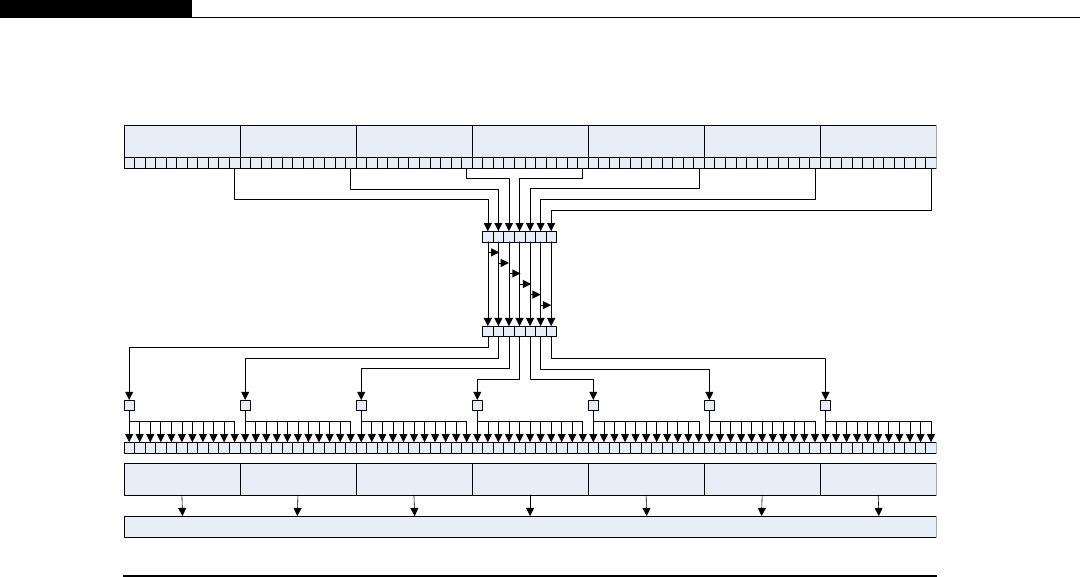
As with most algorithms that are more complex, there is a tradeoff point where the simpler
algorithm is faster. For the serial prefix sum versus the blocked prefix sum, this is around 4096
sample points. We could take this further and implement a more complex prefix sum in the first
phase, but unless we have really large datasets, the prefix sum will not be a key factor in the sorting
time.
Let’s look at the GPU code in detail.
__global__ void calc_prefix_sum_kernel(
const u32 num_samples_per_thread,
const u32 * const bin_count,
u32 * const prefix_idx,
u32 * const block_sum)
{
const u32 tid ¼(blockIdx.x * blockDim.x) þthreadIdx.x;
const u32 tid_offset ¼tid * num_samples_per_thread;
u32 prefix_sum;
if (tid ¼¼ 0)
prefix_sum ¼0;
else
prefix_sum ¼bin_count[tid_offset-1];
for (u32 i¼0; i<num_samples_per_thread; iþþ)
{
Prefix Sum
Block 0
Addition
Block 0
Addition
Block 1
Addition
Block 2
Addition
Block 3
Addition
Block 4
Addition
Block 5
Addition
Block 6
Prefix Sum
Block 1
Prefix Sum
Block 2
Prefix Sum
Block 3
Prefix Sum
Block 4
Prefix Sum
Block 5
Prefix Sum
Block 6
Result = Combined Prefix Scan
Max from each prefix block
Prefix sum over max
FIGURE 6.25
Parallel prefix sum.
188 CHAPTER 6 Memory Handling with CUDA

prefix_idx[iþtid_offset] ¼prefix_sum;
prefix_sum þ¼ bin_count[iþtid_offset];
}
// Store the block prefix sum as the value from the last element
block_sum[tid] ¼prefix_idx[(num_samples_per_thread-1uL)þtid_offset];
}
First, we calculate our tid number based on the block and thread. Then we calculate the
tid_offset based on the number of samples a thread will be calculating the prefix sum for.
Then for the first block the result must be zero. For the others, we include the first element of the bin
count. We then simply implement the code we saw earlier, but add in tid_offset to read/write to the
appropriate elements.
__global__ void add_prefix_sum_total_kernel(
u32 * const prefix_idx,
const u32 * const total_count)
{
const u32 tid ¼(blockIdx.x * blockDim.x) þthreadIdx.x;
prefix_idx[tid] þ¼ total_count[blockIdx.x];
}
The addition kernel is very simple. The program simply calculates the threads individual tid and
uses this to index into the destination array. The value to add is taken from the block count. Implicit in
this implementation is the assumption the caller invokes Nthreads where Nis the number of samples
per thread used in the previous kernel. We do this explicitly because it allows the use of blockIdx.x
(the block number) without the need to access a thread index. This allows the fetch to fall into the
unified constant cache and cause a broadcast operation to all elements within the thread block.
In addition, we have the simple prefix sum kernel, called when there are a small number of
elements to process. The parallel version, because it has to do an additional block prefix step, another
addition, plus synchronization, takes longer in such cases. Only with larger block sizes where we can
make better use of the hardware do we see a significant speedup with the more complex version.
__global__ void calc_prefix_sum_kernel_single(
const u32 num_samples,
const u32 * const bin_count,
u32 * const dest_bin_idx)
{
u32 prefix_sum ¼0;
for (u32 i¼0; i<num_samples; iþþ)
{
dest_bin_idx[i] ¼prefix_sum;
prefix_sum þ¼ bin_count[i];
}
}
And finally the host function that sequences the kernels:
Global Memory 189

__host__ TIMER_T calc_bin_idx_gpu(
const u32 num_elements,
const u32 * const bin_count,
u32 * const dest_bin_idx,
const u32 num_threads_per_block,
u32 num_blocks,
const char * prefix,
u32 * const block_sum,
u32 * const block_sum_prefix)
{
start_device_timer();
if (num_elements >¼4096)
{
const u32 num_threads_total ¼num_threads_per_block
* num_blocks;
const u32 num_elements_per_thread ¼num_elements / num_threads_total;
// Make sure the caller passed arguments which correctly divide the elements to blocks
and threads
assert( (num_elements_per_thread *
num_threads_total) ¼¼ num_elements );
// First calculate the prefix sum over a block
calc_prefix_sum_kernel<<<num_blocks,
num_threads_per_block>>>(num_elements_per_thread, bin_count, dest_bin_idx, block_sum);
cuda_error_check(prefix, "Error invoking calc_prefix_sum_kernel");
// Calculate prefix for the block sums
// Single threaded
calc_prefix_sum_kernel_single<<<1,1>>>(num_threads_total, block_sum,
block_sum_prefix);
cuda_error_check(prefix, "Error invoking calc_prefix_sum_kernel_single");
// Add the prefix sums totals back into the original prefix blocks
// Switch to N threads per block
num_blocks ¼num_elements /
num_elements_per_thread;
add_prefix_sum_total_kernel<<<num_blocks, num_elements_per_thread>>>(dest_bin_idx,
block_sum_prefix);
cuda_error_check(prefix, "add_prefix_sum_total_kernel");
}
else
{
// Calculate prefix for the block sums
190 CHAPTER 6 Memory Handling with CUDA

// Single threaded
calc_prefix_sum_kernel_single<<<1,1>>>(num_elements, bin_count, dest_bin_idx);
cuda_error_check(prefix, "Error invoking calc_prefix_sum_kernel_single");
}
const TIMER_T func_time ¼stop_device_timer();
return func_time;
}
In this function we first check if it is best to use the simple prefix sum or the more complex prefix
sum calculation. For the more complex solution, we work out how many elements each thread will
initially process. We then call the three kernels in sequence. The function parameterized
num_threads_per_block and num_blocks allow us to vary these parameters to allow for tuning.
At 4K sample points we see a transition between the two functions where the simpler version is
around the same speed as the more complex version. As we get up to 16 K samples, the more complex
version is already faster by a factor of four.
Sorting into bins
To avoid the merge operation, the samples must be pre-sorted into Nbins. This involves at least one run
through the entire array and a shuffle of data into the correct bins. The CPU code for this is as follows:
__host__ TIMER_T sort_to_bins_cpu(
const u32 num_samples,
const u32 num_elements,
const u32 * const src_data,
const u32 * const sample_data,
const u32 * const bin_count,
const u32 * const dest_bin_idx,
u32 * const dest_data)
{
const TIMER_T start_time ¼get_time();
u32 dest_bin_idx_tmp[NUM_SAMPLES];
// Copy the dest_bin_idx array to temp storage
for (u32 bin¼0;bin<NUM_SAMPLES;binþþ)
{
dest_bin_idx_tmp[bin] ¼dest_bin_idx[bin];
}
// Iterate over all source data points
for (u32 src_idx¼0; src_idx<num_elements; src_idxþþ)
{
// Read the source data
const u32 data ¼src_data[src_idx];
// Identify the bin in which the source data
// should reside
const u32 bin ¼bin_search3(sample_data,
Global Memory 191

data,
num_samples);
// Fetch the current index for that bin
const u32 dest_idx ¼dest_bin_idx_tmp[bin];
// Write the data using the current index
// of the correct bin
dest_data[dest_idx] ¼data;
// Increment the bin index
dest_bin_idx_tmp[bin]þþ;
}
const TIMER_T end_time ¼get_time();
return end_time - start_time;
}
Each data point in the source array needs to be placed into one of Nbins that are linear in memory.
The start and end of each bin has been calculated as an offset into the array. We need to preserve this
data, but at the same time create Nindex pointers that track where we are in each bin. Thus, initially
a copy of the dest_bin_idx array, the array storing the prefix indexes, must be made.
We then iterate over all the source points. For every source point a binary search is used to identify
in which bin the data point should be placed. We then copy the data to the appropriate bin and
increment the bin index pointer for that bin.
When trying to convert this algorithm to a parallel one, you hit the common problem of multiple
threads trying to write to the same data item. There are two choices in this case. The first is to separate
the data into Nseparate blocks and process each separately and then merge the final output. This was
the approach used in the prefix sum kernel we looked at previously. There is, however, an alternative
approach, which we’ll use here.
__global__ void sort_to_bins_gpu_kernel(
const u32 num_samples,
const u32 * const src_data,
const u32 * const sample_data,
u32 * const dest_bin_idx_tmp,
u32 * const dest_data)
{
// Calculate the thread we’re using
const u32 tid ¼(blockIdx.x * blockDim.x) þthreadIdx.x;
// Read the sample point
const u32 data ¼src_data[tid];
// Identify the bin in which the
// source data should reside
const u32 bin ¼bin_search3(sample_data,
data,
192 CHAPTER 6 Memory Handling with CUDA

num_samples);
// Increment the current index for that bin
const u32 dest_idx ¼atomicAdd(&dest_bin_idx_tmp[bin],1);
// Write the data using the
// current index of the correct bin
dest_data[dest_idx] ¼data;
}
This is the approach of using atomics that in most cases allows for a much simpler implementation.
However, this usually comes atthe cost of performance. We can, of course, at a later date simplyreplace the
atomic usage with an algorithm that splits and then merges the data. It’s a tradeoff between programming
effort in terms of higher complexity, which means longer development time and a higher number of errors,
versus the sometimes very small gain in performance. If you have sufficient time, try both approaches.
At the very least this provides a solution for older hardware where atomic support is somewhat limited.
The atomic sort_to_bins_gpu_kernel function simply unrolls the loop construct over the number
of source elements from the CPU code into Nparallel threads. These are then implemented as
a combination of threads and blocks to invoke one thread per data element.
The thread reads the source element and does a binary search on the sample data space to find the
appropriate bin for the element. We, however, then need single-thread access to increment the counter
that stores the index into which the element must be written. You cannot simply increment the counter
as shown in the CPU code,
// Increment the bin index
dest_bin_idx_tmp[bin]þþ;
Instead, we use an atomic call, atomicAdd:
// Increment the current index for that bin
const u32 dest_idx ¼atomicAdd(&dest_bin_idx_tmp[bin],1);
The atomicAdd function, when used on global memory, will add the second formal parameter, in
this case 1, to the value at the address of the first parameter. If more than one thread calls this function,
we’re guaranteed that every addition will be completed. The atomicAdd function returns the value that
it held prior to the addition. Thus, we can use the return value as a unique index into the array to write
the new value to the bin.
However, be aware that this algorithm will change the ordering of the elements within the bins, as
the blocks may run in any order. Thus, this is not a simple memory copy, due to the potential for more
than one thread to try to write to the same bin at once. Also note that with a mostly sorted list, most
threads will be hitting the same atomic address. This causes a slower execution, as you might expect,
compared with that where the data is uniformly distributed.
Sorting the bins
Having sorted the data into bins, we then need to sort each individual bin in some parallel manner. On
the CPU side we simply call qsort (quick sort) on each bin. On the GPU side we use the radix sort.
__host__ TIMER_T sort_bins_gpu(
Global Memory 193

const u32 num_samples,
const u32 num_elements,
u32 * const data,
const u32 * const sample_data,
const u32 * const bin_count,
const u32 * const dest_bin_idx,
u32 * const sort_tmp,
const u32 num_threads,
const char * prefix)
{
start_device_timer();
const u32 num_blocks ¼num_samples / num_threads;
sort_bins_gpu_kernel3<<<num_blocks, num_threads>>>(num_samples, num_elements, data,
sample_data, bin_count, dest_bin_idx, sort_tmp);
cuda_error_check(prefix, "Error invoking sort_bins_gpu_kernel");
const TIMER_T func_time ¼stop_device_timer();
return func_time;
}
We use a host function to invoke num_samples threads that are split into blocks depending on the
number of threads requested per block.
__global__ void sort_bins_gpu_kernel3(
const u32 num_samples,
const u32 num_elements,
u32 * const data,
const u32 * const sample_data,
const u32 * const bin_count,
const u32 * const dest_bin_idx,
u32 * const sort_tmp)
{
// Calculate the thread we’re using
const u32 tid ¼(blockIdx.x * blockDim.x) þthreadIdx.x;
if (tid !¼(num_samples-1))
radix_sort(data, dest_bin_idx[tid], dest_bin_idx[tidþ1], sort_tmp);
else
radix_sort(data, dest_bin_idx[tid], num_elements, sort_tmp);
}
The kernel is a two-level kernel, as the array dest_bin_idx holds only the start index. For the last
element, accessing [tidþ1] would cause an array overflow issue, so the very last thread needs to be
handled slightly differently.
194 CHAPTER 6 Memory Handling with CUDA

Sorting the multiple blocks is done with a modified version of the radix_sort kernel we developed
in Chapter 5.
__device__ void radix_sort(
u32 * const data,
const u32 start_idx,
const u32 end_idx,
u32 * const sort_tmp_1)
{
// Sort into num_list, lists
// Apply radix sort on 32 bits of data
for (u32 bit¼0;bit<32;bitþþ)
{
// Mask off all but the bit we’re interested in
const u32 bit_mask ¼(1u << bit);
// Set up the zero and one counter
u32 base_cnt_0 ¼start_idx;
u32 base_cnt_1 ¼start_idx;
for (u32 i¼start_idx; i<end_idx; iþþ)
{
// Fetch the test data element
const u32 elem ¼data[i];
// If the element is in the one list
if ( (elem & bit_mask) > 0u )
{
// Copy to the one list
sort_tmp_1[base_cnt_1þþ]¼elem;
}
else
{
// Copy to the zero list (inplace)
data[base_cnt_0þþ]¼elem;
}
}
// Copy data back to source from the one’s list
for (u32 i¼start_idx; i<base_cnt_1; iþþ)
{
data[base_cnt_0þþ]¼sort_tmp_1[i];
}
}
}
The radix sort simply iterates over the dataset it has been provided for a given block. For each bit it
places the value into either the 0 or 1 list. The caller defines the start and end indexes of the array over
which the sort will take place.
Global Memory 195

Analyzing the results
With a sample size of 16 K and a source dataset size of 1 MB we see the following results on a mostly
sorted list:
ID:3 GeForce GTX 460: Test 32 - Selecting 16384 from 1048576 elements using 512 blocks
of 32 threads
Select Sample Time - CPU: 0.19 GPU:0.03
Sort Sample Time - CPU: 2.13 GPU:125.57
Count Bins Time - CPU: 157.59 GPU:17.00
Calc. Bin Idx Time - CPU: 0.03 GPU:0.58
Sort to Bins Time - CPU: 163.81 GPU:16.94
Sort Bins Time - CPU: 72.06 GPU:64.46
Total Time - CPU: 395.81 GPU:224.59
Qsort Time - CPU: 185.41 GPU:N/A
ID:3 GeForce GTX 460: Test 32 - Selecting 16384 from 1048576 elements using 256 blocks
of 64 threads
Select Sample Time - CPU: 0.53 GPU:0.03
Sort Sample Time - CPU: 2.06 GPU:125.57
Count Bins Time - CPU: 157.75 GPU:19.07
Calc. Bin Idx Time - CPU: 0.13 GPU:0.26
Sort to Bins Time - CPU: 164.09 GPU:19.09
Sort Bins Time - CPU: 72.31 GPU:62.11
Total Time - CPU: 396.88 GPU:226.13
Qsort Time - CPU: 184.50 GPU:N/A
ID:3 GeForce GTX 460: Test 32 - Selecting 16384 from 1048576 elements using 128 blocks
of 128 threads
Select Sample Time - CPU: 0.28 GPU:0.03
Sort Sample Time - CPU: 2.09 GPU:125.57
Count Bins Time - CPU: 157.91 GPU:13.96
Calc. Bin Idx Time - CPU: 0.09 GPU:0.26
Sort to Bins Time - CPU: 164.22 GPU:14.00
Sort Bins Time - CPU: 71.19 GPU:91.33
Total Time - CPU: 395.78 GPU:245.16
Qsort Time - CPU: 185.19 GPU:N/A
ID:3 GeForce GTX 460: Test 32 - Selecting 16384 from 1048576 elements using 64 blocks of
256 threads
Select Sample Time - CPU: 0.22 GPU:0.03
Sort Sample Time - CPU: 2.00 GPU:125.57
Count Bins Time - CPU: 158.78 GPU:12.43
Calc. Bin Idx Time - CPU: 0.13 GPU:0.49
Sort to Bins Time - CPU: 164.38 GPU:12.39
Sort Bins Time - CPU: 71.16 GPU:84.89
Total Time - CPU: 396.66 GPU:235.80
Qsort Time - CPU: 186.13 GPU:N/A
196 CHAPTER 6 Memory Handling with CUDA
Notice how the entire sort process (224–245 ms) is dominated by the sorting of the sample dataset
on the GPU (~125 ms). As the sample dataset becomes large the sort-and-merge approach used for this
phase doesn’t work well.
One solution to this problem would be to run the sample sort on the sample data; where the sample
dataset is large, this is a good approach. However, for a 16 K sample set, it takes around 9 ms to run the
sample sort compared with a 2 ms quick sort time from the CPU.
It always makes sense to use whatever device works best at a given solution. For small sample
sizes, the CPU will usually be faster than the GPU. The GPU requires reasonably sized datasets, after
which point it easily surpasses the CPU. Therefore, the optimal solution is simply to run quick sort on
the sample set on the CPU and then transfer this to the GPU for the large-scale parallel “grunt” work of
the sorting.
When we use this approach the timings drop significantly.
ID:3 GeForce GTX 460: Test 32 - Selecting 16384 from 1048576 elements using 512 blocks
of 32 threads
Select Sample Time - CPU: 0.09 GPU:0.09
Sort Sample Time - CPU: 2.09 GPU:2.09
Count Bins Time - CPU: 157.69 GPU:17.02
Calc. Bin Idx Time - CPU: 0.09 GPU:0.58
Sort to Bins Time - CPU: 163.78 GPU:16.94
Sort Bins Time - CPU: 71.97 GPU:64.47
Total Time - CPU: 395.72 GPU:101.19
Qsort Time - CPU: 184.78 GPU:N/A
You can see the sample sort time is around 55% of the time of the quick sort on the CPU with a 16 K
sample size (101 ms GPU, 185 ms CPU). If we vary the sample size, we increase the amount of
available parallelism in the problem. See Table 6.15 and Figure 6.26.
What you can see from Table 6.15 and Figure 6.26 is that as the number of samples increases, the
time drops dramatically. The best time is achieved for the GTX460 at 128K samples, or one-eighth of
the number of the data to be sorted. The GTX470, with its much larger number of SMs, starts to rapidly
outperform the GTX460 from 2048 sample points onward. The GTX260 by comparison (the previous
generation of hardware) needs many more sample points to come close to the Fermi performance.
At 128K sample points the sorting of the samples again becomes significant (see Table 6.16) and
our strategy of using quick sort on the CPU becomes the bottleneck. If we look in detail at the results
from the GTX470, we see that at 256K sample points up to 50% of the time is spent sorting the sample
data. At this point a sample sort of the sample data becomes a good option (Table 6.16).
Table 6.15 Sample Sort Results (ms)
Device/
Samples 256 512 1024 2048 4096 8K 16K 32K 64K 128K 256K
Qsort 184 184 184 184 184 184 184 184 184 184 184
GTX460 506 273 158 151 115 105 101 101 69 64 85
GTX470 546 290 161 94 91 72 62 60 43 46 68
GTX260 1082 768 635 485 370 286 215 190 179 111 88
Global Memory 197
To give some comparison with almost sorted data versus entirely random data, we’ll run the same
test over a random dataset (Table 6.17). Various tests have shown the best performance was achieved
with 128 threads per block.
As you can see from Table 6.17 the faster run was the GTX470 at 67 ms. This is five times faster
than the serial quick sort on the CPU host. Around 32 K samples with 128 threads per block would
appear to be the optimal launch configuration for 1 MB of data. See Figure 6.27.
Questions on global memory
1. Discuss the reasons why sample sort is quicker when the list is mostly sorted?
2. How might you improve the sample sort algorithm presented here?
3. Do you foresee any problems using larger dataset sizes? What might you have to change to run
larger datasets?
0
200
400
600
800
1000
1200
256 512 1024 2048 4096 8K 16K 32K 64K 128K 256
K
Qsort GTX 460 GTX 470 260 GTX
FIGURE 6.26
Graph of sample sort results.
Table 6.16 GTX470 Sample Sort Results (Mostly Sorted Data)
Operation/
Samples 256 512 1024 2048 4096 8 K 16 K 32 K 64 K 128 K 256 K
Select samples 0 0.03 0 0.09 0.06 0.28 0.5 0.5 0.84 0.97 1.78
Sort samples 0 0.06 0.6 0.28 0.38 0.97 2.03 4.34 9.38 19.72 41.72
Count bins 14.6 14.2 13.62 12.38 10.66 9.34 9.26 8.38 6.03 5.35 5.38
Prefix sum 0.13 0.27 0.53 1.05 0.19 0.33 0.62 1.2 0.57 0.87 1.46
Sort to bins 14.6 14.2 13.65 12.4 10.7 9.37 9.33 8.45 6.09 5.41 5.46
Sort bins 517 261 133.5 68.29 69.86 52.5 40.9 37.2 20.2 13.94 12.15
Total 546 290 162 94 92 73 63 60 43 46 68
198 CHAPTER 6 Memory Handling with CUDA
Answers on global memory
1. Sample sort is quicker when using a mostly sorted list because the thread divergence is significantly
less. Each bin has almost the same number of values. We end up with a near-optimal distribution of
work to each of the SMs providing there are enough samples chosen from the dataset to generate
a reasonable number of blocks.
2. One of the key issues with the algorithm is the noncoalesced access to global memory during the
radix sort. This is caused by doing an in-place sort using the prefix calculation and the lower and
upper bounds for each block. If you instead split each sample set so that it was interleaved by the
number of threads, as was the radix sort in the shared memory example, we’d get coalesced access
for most of the sort. The drawback of this is potentially wasted memory since some lists are a few
entries long and others can be hundreds of entries long.
The other obvious solution is to improve the sorting of the samples. At 128 K samples, the sorting of
sample data is contributing 43% of the total sort time. However, in practice, we’d never want to use
so many samples, and the 32 K results are a more realistic use case. At this point sorting the samples
contributes just 7% (see Table 6.16). The largest contributors are sorting the bins (62%), sorting to
the bins (14%), and counting the bins (14%). The radix sort is clearly the place to start.
Table 6.17 Sample Sort on Random Data
Device/
Sample 256 512 1024 2048 4096 8192 16K 32K 64K 128K 256K
Qsort 337 337 337 337 337 337 337 337 337 337 337
GTX460 735 470 235 139 92 91 75 73 81 108 178
GTX470 831 535 263 156 97 70 77 68 67 90 155
GTX260 1311 919 463 255 170 124 106 100 106 123 160
0
200
400
600
800
1000
1200
1400
256 512 1024 2048 4096 8192 16K 32K 64K 128K 256
K
Qsort GTX 460 GTX 470 260GTX
FIGURE 6.27
Chart of sample sort on random data.
Global Memory 199

3. As the data size increases, you rapidly hit the maximum number of allowed blocks (65,535 on
compute 2.x or lower platforms) using a single dimension. At this point you need to convert the
num_block calculation in the various kernel invocations to a dim3 type to include an xand y
components in the block layout and possibly multiple grids, if the data size is really large. You
then, of course, also need to modify the kernels to calculate correctly the block index based on
block dimension and grid size.
TEXTURE MEMORY
Texture memory is not something we will cover in any detail in this text. However, we will mention it
for some of the special uses it has in case it may be of some use in your applications. Texture memory
can be used for two primary purposes:
• Caching on compute 1.x and 3.x hardware.
• Hardware-based manipulation of memory reads.
Texture caching
As compute 1.x hardware has no cache to speak of, the 6–8K of texture memory per SM provides the
only method to truly cache data on such devices. However, with the advent of Fermi and its up to 48 K
L1 cache and up to 768 K shared L2 cache, this made the usage of texture memory for its cache
properties largely obsolete. The texture cache is still present on Fermi to ensure backward compati-
bility with previous generations of code.
The texture cache is optimized for locality, that is, it expects data to be provided to adjacent threads.
This is largely the same cache policy as the L1 cache on Fermi. Unless you are using the other aspects
of texture memory, texture memory brings you little benefit for the considerable programming effort
required to use it on Fermi. However, on Kepler, the texture cache gets a special compute path,
removing the complexity associated with programming it. See Kepler in chapter 12 for details. Note
the constant memory cache is the only other cache on compute 1.x hardware that is organized for
broadcast access, that is, all threads accessing the same memory address.
On compute 1.x hardware, however, the texture cache can be of considerable use. If you consider
a memory read that exhibits some locality, you can save a considerable number of memory fetches.
Suppose we needed to perform a gather operation from memory, that is, to read an out-of-sequence set of
memory addresses into Nthreads. Unless the thread pattern creates an aligned and sequential memory
pattern, the coalescing hardware will issue multiple reads. If we instead load the data via the texture
memory, most of the reads will hit the texture cache, resulting in a considerable performance benefit.
You can, of course, equally use shared memory for this purpose, reading in a coalesced way from
memory and then performing a read from the shared memory. As the shared memory of a compute 1.x
device is limited to 16 K, you may decide to allocate shared memory to a specific purpose and use
texture memory where the memory pattern is not so deterministic.
Hardware manipulation of memory fetches
The second and perhaps more useful aspect of texture-based memory is that it allows some of the
hardware aspects of GPUs to be automatically applied when accessing memory cells.
200 CHAPTER 6 Memory Handling with CUDA
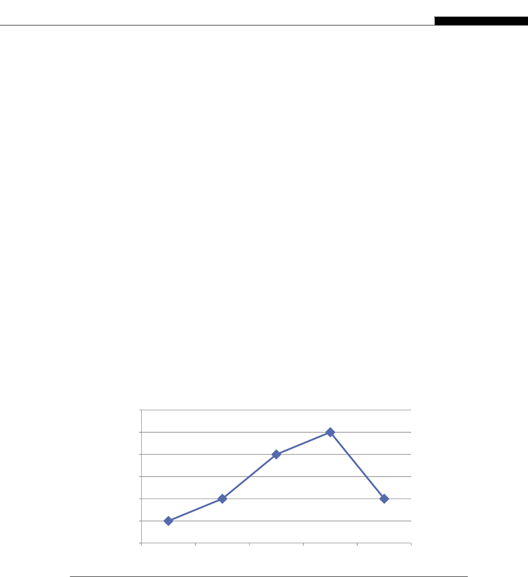
One useful feature is a low-resolution linear interpolation in hardware. Typically, linear interpo-
lation is used to represent a function where the output is not easy or is computationally expensive to
express mathematically. Thus, the input from a sensor might have a correction applied to its value at
the low or high end of its range. Rather than model this you simply place a number of points in a table
that represent discrete values across the range. For the points falling between the real points you use
linear interpolation to work out the approximate value.
Consider an interpolation table of
P¼10, 20, 40, 50, 20
X¼0, 2, 4, 6, 8
If we have a new value, 5 for X, what is its interpolated value of P? The value 5 falls exactly halfway
between the two points we have defined, 2 and 4. As the value for 2 is 20 and the value for 4 is 40 we
can easily calculate the value for 5 as 30. See Figure 6.28.
With texture memory, you can set it up such that Pis defined as an array normalized from the value
0to1or1toþ1. Fetches are then automatically interpolated in hardware. Combined with the cache
properties, this can be a quick method of handling data that is not easily represented as a pure
calculation. Bilinear and trilinear interpolation in hardware is also supported for two-dimensional and
three-dimensional arrays, respectively.
One other nice feature of textures is the automatic handling of boundary conditions on array
indexes. You can configure the handling of texture arrays to either wrap around or clamp at the array
boundary. This can be useful, as it allows the normal case to be handled for all elements without
having to embed special edge handling code. Special case code typically causes thread divergence
and may not be necessary at all with the caching features of Fermi (see Chapter 9 on optimization).
Restrictions using textures
Textures come from the graphics world of the GPU and therefore are less flexible than the standard
CUDA types. Textures must be declared as a fixed type, i.e. one of the various aligned vector types
0
10
20
30
40
50
60
02468
FIGURE 6.28
Interpolation.
Texture Memory 201

(u8, u16, u32, s8, s16, s32) at compile time. How the values are interpreted is specified at runtime.
Texture memory is read only to the GPU kernel and must be explicitly accessed via a special texture
API (e.g., tex1Dfetch(), etc.) and arrays bound to textures.
Textures have their uses, especially on compute 1.x hardware. The uses for textures are quite
specific and not always worth the trouble of learning yet another API. Thus, we have not covered the
API side in this section, but simply stated some of the typical uses for textures. Concentrate on getting
global/shared memory and register usage mastered and then look at texture memory, if it’s applicable
to your application.
For further information on textures, see the CUDA C Programming Guide.
CONCLUSION
We’ve looked at some of the aspects of using the different memory systems within the GPU. Program
performance, both in the CPU and GPU domains, is generally dominated by memory throughput. You
should have understood the principle of locality (i.e., the closer to the device the data is, the faster it
can be accessed) and the cost of accessing off-chip resources.
Understanding the three major classes of storage availabledregisters, shared memory, and global
memorydshould allow you to write programs that use each type efficiently and correctly.
With global memory you need to think about generating patterns that provide for good coalescing
of data and reduce the number of transactions the device needs to issue to the memory subsystem.
Consider using constant memory when you are going to be distributing the same value to many
threads, or the same value to many blocks of thread.
With shared memory you need to think about data reuse. If there is no data reuse, then use registers
and read directly from constant/global memory. Where there is potential for reuse or you need more
register space, use shared memory.
Always use registers when possible, that is, declare data as local variables when possible. Think
about each read to memory and if it will be reused. Avoid multiple writes to memory by writing to
a register and writing back to memory later. Registers are the only way of achieving near full
throughput of the device, but are a scarce and valuable resource. Be aware that excessive register usage
can cause slowdowns due to spilling of registers to ‘local’ memory.
Now that you understand the principles of these memory types, we will, in subsequent chapters,
look more at optimization and how these memory types can be used in practice.
202 CHAPTER 6 Memory Handling with CUDA

Using CUDA in Practice 7
INTRODUCTION
In this chapter we’ll look at a few examples of the not-so-common uses of GPUs to provide insight into
how to solve a number of different types of computer problems. We’ll look at the problems involved in
using GPUs for such computations.
SERIAL AND PARALLEL CODE
Design goals of CPUs and GPUs
CPUs and GPUs, although both execute programs, are a world apart in their design goals. CPUs use an
MIMD (multiple instruction, multiple data) approach, while GPUs use an SIMT (single instruction,
multiple thread) instruction model.
The CPU approach to parallelism is to execute multiple independent instruction streams. Within
those instruction streams it seeks to extract instruction level parallelism. That is, it fills a very long
pipeline of instructions and looks for instructions that can be sent to independent execution units.
These execution units usually consist of one or more floating-point units, one or more integer units,
a branch prediction unit, and one or more load/store units.
Branch prediction is something computer architects have worked extensively on for over a decade
or so. The problem with branching is that the single instruction stream turns into two streams, the
branch taken path and the branch not taken path. Programming constructs such as for, while loops
typically branch backwards to the start of the loop until the loop completes. Thus, in a lot of cases, the
branch can be predicted statically. Some compilers help with this in setting a bit within the branch
instruction to say if the branch is likely to be met or not. Thus, loops that branch backwards can be
predicated as taken, whereas conditionals are usually predicated as not taken, thus avoiding the branch
altogether. This has the added advantage that the next instructions have typically already been pre-
fetched into the cache.
Branch prediction evolved from the simple but quite effective static model, to use a dynamic model
that records previous branching history. Multiple levels of complex branch prediction are actually
present in modern processors due to the very high cost of a mispredicted branch and the consequential
refilling of the long execution pipeline.
Along with branch prediction, a technique called speculative execution is used. Given the CPU will
likely have predicted a branch correctly, it makes sense to start executing the instruction stream at that
CHAPTER
CUDA Programming. http://dx.doi.org/10.1016/B978-0-12-415933-4.00007-7
Copyright Ó2013 Elsevier Inc. All rights reserved.
203

branch address. However, this adds to the cost of branch misprediction, as now the instruction stream
that has been executed has to be undone or discarded.
The optimal model for both branch prediction and speculative execution is simply to execute both
paths of the branch and then commit the results when the actual branch is known. As branches are often
nested, in practice such an approach requires multiple levels of hardware and is therefore rarely used.
Finally, we have the other major difference, seen until recently, which is the amount and number of
cache memory levels. The CPU programming model works on the nice principle of abstraction, that is, the
programmer doesn’t have to care where the memory is because the hardware takes care of it. For most
programs, except those that need to run fast, this works quite well. It used to be that instruction cycles were
expensive, but with ever-increasing chip density, instruction cycles are now cheap. Accessing memory is
now the bottleneck on modern processor design and this is addressed by the multiple levels of cache.
GPUs, until the introduction of Fermi, took an alternative approach to this design. Fermi designers
believe the programmer is best placed to make use of the high-speed memory that can be placed close to the
processor, in this case, the shared memory on each SM. This is the same as the L1 cache found on
a conventional processor, a small area of low latency and higher bandwidth memory. If you think about
most programs, this makes a lot of sense. A programmer knows the program better than anyone else and
therefore should be able to identify which off-chip memory accesses can be prevented by using shared
memory.
Fermi expanded the on-chip memory space to 64K, 16 K of which must be allocated to an L1 cache.
So that there was always some shared memory present, they did not allow the entire space to be allocated
to either cache or shared memory. By default, Fermi allocates 48 K to shared memory and 16 K to cache.
However, you can switch this and have 48 K of cache and 16 K of shared memory. Kepler also introduces
a 32K/32K split option. In programs that make no use of shared memory, setting this switch can
significantly to prefer L1 cache instead of shared memory improve performance for memory-bound
kernels. This is done with a call to
cudaFuncSetCacheConfig(cudaFuncCachePreferL1);
In the sample sort program we use to look at optimizing later in this chapter, this simple change reduced
the overall execution time by 15%. This is a huge bonus for enabling a feature that is disabled by default.
With the inclusion of an L1 cache, GPUs and CPUs moved closer to one another in terms of the data
fetched from memory. With previous GPU generations, memory accesses needed to be coalesced to
achieve any sort of performance. Consider a noncoalesced memory fetch on the G80 and GT200 based
hardware. If thread 0 reads from memory address 0x1000, thread 1 reads from 0x2000, thread 3 reads from
0x3000, etc., this results in one memory fetch per thread of 32 bytes. Not 32 bits, but 32 bytes, the
minimum memory transaction size. The next access (0x1004,0x2004,0x3004, etc.) did exactly the same.
In Fermi, as with CPUs, a cache line of 128 bytes is fetched per memory access. Thus, subsequent
access by an adjacent thread will usually hit the cache instead of having to go out to global memory on
the device. This allows for a far more flexible programming model and is more akin to the CPU
programming model most programmers are familiar with.
One of the aspects of GPU design that differs significantly from CPU design is the SIMT model of
execution. In the MIMD model, there is separate hardware for each thread, allowing entirely separate
instruction streams. In the case where the threads are processing the same instruction flow, but with
different data, this approach is very wasteful of hardware resources. The GPU thus provides a single
set of hardware to run Nthreads, where Nis currently 32, the warp size.
204 CHAPTER 7 Using CUDA in Practice

This has a significant impact on GPU program design. SIMT implementation in the GPU is similar
to the old vector architecture SIMD model. This was largely abandoned in the early 1970s when the
ever-increasing speed of serial CPUs made the “hard” programming of SIMD machines less than
appealing. SIMT solves one of the key issues, in that programmers are no longer forced to write code in
which every thread follows the same execution path. Threads can diverge and then converge at some
later point. The downside of this flexibility is that there is only one set of hardware to follow multiple
divergent program paths. Thus, each path must be executed in turn, or serialized, until the control flow
converges once more. As a programmer you must be aware of this and think about it in the design of
your kernels.
Finally, we’ll come to one other significant difference between CPUs and GPUs. On the CPU
model, there is serial control flow. Executing an instruction that requires a number of cycles to
complete will stall the current thread. This is one of the reasons why Intel uses hyperthreading. The
hardware internally switches to another thread when the current one stalls. GPUs have not just one
other thread, but are designed to have thousands of other threads that they can potentially switch to.
Such a stall happens as a result of both instruction latency and memory latency, that is, where the
processor is waiting on the completion of an operation. The threading model is designed to hide both.
However, the GPU has one other benefit in that it uses lazy evaluation. That is, it will not stall the
current thread until there is an access to the dependent register. Thus, you may read a value into
a register early in the kernel, and the thread will not stall until such time as (sometime later) the register
is actually used. The CPU model stalls at a memory load or long latency instruction. Consider the
following program segments.
Segment 1:
int sum¼0;
for (int i¼0; i< 128; iþþ)
{
sum þ¼ src_array[i];
}
If we look at the first segment, the program must calculate the address of src_array[i], then load
the data, and finally add it to the existing value of sum. Each operation is dependent on the previous
operation.
Segment 2:
int sum¼0;
int sum1¼0, sum2¼0, sum3¼0, sum4¼0;
for (int i¼0; i< 128; iþ¼4)
{
sum1 þ¼ src_array[i];
sum2 þ¼ src_array[iþ1];
sum3 þ¼ src_array[iþ2];
sum4 þ¼ src_array[iþ3];
}
sum ¼sum1 þsum2 þsum3 þsum4;
If we look at the second segment, we iterate in steps of four. Four independent sum values are used,
allowing four independent summations to be computed in the hardware. How many operations are
Serial and Parallel Code 205

actually run in parallel depends on the number of execution units available on the processor. This could
be execution units, in terms of processor cores (using threads), and/or execution units within a super-
scalar processor design.
Segment 3:
int sum¼0;
int sum1¼0, sum2¼0, sum3¼0, sum4¼0;
for (int i¼0; i< 128; iþ¼4)
{
const int a1 ¼src_array[i];
const int a2 ¼src_array[iþ1];
const int a3 ¼src_array[iþ2];
const int a4 ¼src_array[iþ3];
sum1 þ¼ a1;
sum2 þ¼ a2;
sum3 þ¼ a3;
sum4 þ¼ a4;
}
sum ¼sum1 þsum2 þsum3 þsum4;
Finally, looking at the third segment, we move the load from memory operations out of the
computation steps. Thus, the load operation for a1 has three further load operations after it, plus some
array index calculations, prior to its usage in the sum1 calculation.
In the eager evaluation model used by CPUs we stall at the first read into a1, and on each
subsequent read. With the lazy evaluation model used by GPUs we stall only on consumption of the
data, the additions in the third code segment, if that data is not currently available. As most CPU and
GPU designs are superscalar processors, using pipelined instructions, both benefit from such an
approach within a single thread of execution.
Algorithms that work best on the CPU versus the GPU
There are many hundreds of computer science algorithms that for decades have been developed and
optimized for serial CPUs. Not all of these can be applied easily to parallel problems. However, the
vast majority of problems exhibit parallelism in one form or another. A significant number of problems
can be broken down into operations on a dataset. In many cases, these operations are inherently
parallel if viewed from either a data or task parallelism viewpoint.
One of the most important algorithms in parallel work is something called scan, otherwise known
as prefix sum. In the world of serial computing this does not exist as it’s not needed. Suppose we have
a variable number of elements per output of some function. We could allocate a fixed amount of
storage per output, such as an array, but this would mean there would be gaps in the memory. Output
0 might generate 10 entries, output 1, 5 entries, and output 3, 9 entries. We’d need an array with at least
10 entries, so we would have 6 wasted slots.
Prefix sum stores, in a separate array, the number of elements used for each output. The actual data
is then compressed (i.e., all the blanks removed) to form a single linear array. The problem we have
now is where does output for thread 2 write its values to? To calculate the output index for each output,
we simply add up all the outputs prior to the current one. Thus, output 2 must write to array index 10 as
206 CHAPTER 7 Using CUDA in Practice

output 1 wrote 10 elements (0.9). Output 2 will write 5 elements (10.14), so output 3 will start
writing at element 15, and so on.
We covered in Chapter 6 on memory access an example using Sample Sort, which uses prefix sum,
so I will not repeat here how they can be calculated in parallel. The important point to understand is
that through the use of prefix sum we can convert a great many algorithms to Nindependent outputs.
It’s important that we can write outputs independently and are not limited by atomics, in effect,
contention of resources. Such limits, depending on how overloaded they are, can severely slow a kernel
execution.
Not all parallel architectures are created equal. Many parallel programs and parallel languages
assume the MIMD model, that is, that threads are independent and do not need to execute in groups (or
warps) as on the GPU. Thus, not even all parallel programs can work on GPUs unchanged. In fact, this
has been one problem with parallel programs to date; optimization for a specific architecture often ties
the application to that particular hardware.
Standards like MPI and OpenMP don’t really fit well to the GPU model. OpenMP is perhaps the
closest, in that it requires a shared view of memory. In OpenMP the compiler takes care of spawning
threads that share a common data area. The programmer specifies which loop can be parallelized
through various compiler pragmas and the compiler takes care of all that nasty “parallel stuff.” MPI, on
the other hand, considers all processes to be identical and is more suited to clusters of nodes than
single-node machines.
You might take the approach of allocating one GPU thread per MPI process, or one block per MPI
process. Neither would work particularly well on the GPU, unless you could identify that groups of
MPI processes were, in fact, following the same execution flow and could combine them into warps on
the GPU. Typically, MPI is implemented as shared CPU/GPU pairs with the CPU handling the network
and disk input/output (I/O). Implementations using GPU Direct allow transfers to certain InfiniBand
network cards via a common shared-memory host page. Direct peer-to-peer (P2P) transfers over the
PCI-E bus without the use of host memory is preferable, however. The RDMA (remote DMA) is
a feature of the new Kepler architecture that enables such features and thus makes GPUs much more of
a standalone peer on such networks.
With GPUs being included in an ever-higher number into data centers and supercomputer instal-
lations, both OpenMP and MPI will inevitably evolve to accommodate hardware designed to accel-
erate computations. In Chapter 10 we discuss the use of OpenACC, the directive-based approach to
GPU computing. The OpenMP4ACC (OpenMP for accelerators) standard may well move such
directives into the mainstream OpenMP standard.
With the GPU you have to consider that there are a limited number of threads that can easily work
together on any given problem. Typically, we’re looking at up to 1024 threads on Fermi and Kepler,
less on older hardware. In reality, any reasonably complex kernel is limited to 256 or 512 threads due
to register usage limitations. The interthread communication considerations dominate any decom-
position of the problem. Interthread communication is performed via high-speed shared memory, so
threads in the same block can communicate quickly and with little latency. By contrast, interblock
communication can only be performed via separate kernel invocations, and global memory that is an
order of magnitude slower. Kepler also extends this model to allow interwarp-based communication
without the use of shared memory.
The other major consideration for GPU algorithms is the memory available on the device. The
largest single GPU memory space available is 6 GB on the Tesla M2090 cards. Compared with
Serial and Parallel Code 207

typically 16 to 64 GB on the host, this may be problematic. However, this can be solved by using
multiple GPU cards, with many high-end motherboards able to take up to four PCI-E cards, thus
providing up to 24 GB per node of GPU memory.
Recursion is also problematic on GPUs, as it’s only supported on compute 2.x GPUs, and then only
for __device__ functions and not __global__ functions. The upcoming dynamic parallelism feature
found in the Kepler K20 design will help in many respects with recursive algorithms.
Many CPU algorithms make use of recursion. Often it’s convenient to break down a problem into
a smaller problem that is then broken down further and so on until it becomes a trivial problem. Binary
search is a classic example of this. Binary search splits a sorted list of numbers in half and simply asks
the question of whether the data we’re looking for exists in the left or right set. It then repeats the split
until either the item is found or the problem becomes just two items and is thus trivial to solve.
However, any recursive algorithm can also be represented as an iterative algorithm. The binary search
problem just mentioned is shown as an iterative solution within the sample sort example (see Chapter 6).
Quick sort is also a common example of an algorithm that is typically implemented recursively. The
algorithm picks a pivot point and then sorts all items less than the pivot point to the left and less than or
equal to the pivot point to the right. You now have 2 independent datasets that can be sorted by two
independent threads. This then becomes 4 threads on the next iteration, then 8, then 16, and so on.
The GPU kernel invocation requires a fixed number of threads. It cannot currently exploit dynamic
parallelism, although this will change with the Kepler K20 release. Dynamic parallelism is where the
amount of parallelism in the problem changes over time. In the quick sort problem it grows by a factor
of two at every level. In path finding–type problems, discovery of a new node may introduce 30,000 or
more additional paths into a problem.
How do you replicate such algorithms on a GPU? There are a number of approaches. The easiest is
when the parallelism scales in some known manner, as with quick sort. You can then simply invoke one
kernel per level or one kernel per Nlevels of the algorithm back-to-back in a single stream. As one
level finishes, it writes its state to global memory and the next kernel execution picks up on the next
level. As the kernels are already pushed into a stream ready to execute, there is no CPU intervention
needed to launch the next stream. See Figure 7.1.
Where the parallelism grows by some indeterminate amount per iteration, you can also store the
state in global memory. You have to then communicate back to the host the number of the amount of
1
22
3 333
4 44444 44
FIGURE 7.1
Kernel invocations for a recursive algorithm.
208 CHAPTER 7 Using CUDA in Practice

parallelism that the next iteration will explore. You can do this with an atomic write to shared memory
within the block and then an atomic add to global memory prior to block completion. Then use
amemcpy to copy the data back to the host that can use this to adjust the next kernel launch.
As an example with the first level of quick sort, you can use one block of data with a single thread.
You then continue invoking single-thread block kernels until you reach some multiple of the number of
SMs on the GPU. At the point where you would saturate the number of blocks on the SM, up to 16
blocks per SM, you extend the number of threads per block. At the point you reach 256 threads per
block, you start again extending the number of blocks.
This approach, although relatively easy to implement, has some disadvantages. First, at least
initially there is not enough work to saturate the GPU. With just one thread at the first level, the kernel
overhead is significant. Even at level four, we’re invoking just eight blocks, filling half the 16 SMs on
a GTX580 device. Not until we reach level five would we have one block per SM. With 16 SMs, eight
blocks per SM, and 256 threads per SM, we’d need 32 K points before all SMs were working at full
efficiency. This would require 16 kernel invocations.
With compute 2.x devices this is not such an issue, as the initial few layers can simply be calculated
using a recursive call, until you reach the desired depth into the structure to warrant relaunching the
kernel with many more thread blocks. An alternative approach is to do some of the initial work on the
CPU and only go to the GPU once there is enough parallelism in the problem. Don’t think everything
has to be done on the GPU. The CPU can be a very useful partner, especially for this type of less-
parallel work.
One other solution to these types of problems is to use a special type of scan operation called
a segmented scan. With a segmented scan you have a regular scan operation over a dataset (min,max,
sum, etc.) plus an additional array that splits the source array into variable size blocks. A single thread
or multiple threads are assigned per region to calculate the operation. As the additional array can also
be updated at runtime, this can reduce the need to invoke multiple kernels if the segmented scan can be
kept within a single block. Otherwise, you might just as well adopt the simpler solution, which in many
cases works just as well and allows the flexibility of changing the number of threads/blocks as the
problem grows and shrinks in parallelism.
All of these approaches try to deal with problems GPUs were not natively designed to deal with. As
a programmer you should be aware of how well an algorithm does or does not fit the design model of
the hardware. Recursive problems with today’s GPUs are often best framed as iterative problems.
Selecting an algorithm that is appropriate to the hardware and getting the data in the correct layout is
often key to good performance on the GPU.
PROCESSING DATASETS
With a typical data acquisition you will get data that is interesting, periods of data of no interest, and
noise on the signal. One simple way of removing noise is to filter data above or below some threshold.
With the dataset shown in Figure 7.2, we’ve placed a white line to show where the threshold level has
been set. As you raise the threshold, you filter out low levels of noise. At the far right of the acquisition
data you may wish to remove it altogether because you are only interested in the data peaks.
With a dataset that you expect to have a very small number of items being filtered you can easily
append to the same data list, as the frequency of the append operation itself is very low. However, as
Processing Datasets 209
the frequency of the filtered data becomes higher, the contention for the single list becomes a bottle-
neck. While this approach may work for a small number of parallel operations, say up to four that you
might find on a quad-core CPU, the write to a single list, with locking approach does not scale.
A much better approach is to have a number of lists and then combine the lists together at a later
stage. In fact, almost all parallel data processing algorithms use this approach in one way or another to
avoid the serial bottleneck trying to update common data structure causes. This approach also maps
very well to the model CUDA uses to decompose problems, the tiling approach.
We should also recognize that a filtering operation is actually a common parallel pattern, a split
operation. A split operation takes a given dataset and splits it into Nparts based on some primary key.
In our filtering example we’re using the threshold condition as the primary key and trying to extract the
data that is above a given threshold. We may or may not be interested in keeping the data that is below
the threshold. The split operation simply generates two lists, one matching some criteria and the other
for the data that did not match.
When performing such an operation in parallel, we have a number of considerations. The first
problem is we do not know how many data items will meet the matching criteria and how many would
therefore be on the nonmatching list. The second is that we have many processing elements that need
to cooperate in some way to build an output list. Finally, any ordering present in the original dataset
must usually be maintained.
The scan primitive is incredibly powerful and can be used in a number of data processing scenarios.
Suppose, for example, we have a list of students in a database in no particular order. We might want to
extract, from that student list, all students who are in class CS-192. We thus end up with two datasets,
those matching the criteria and those that do not.
Suppose we have a weather station near the equator that is collecting the temperature once per
minute over several years. We might want to know how many sample points, or minutes, the
temperature was in excess of 40 degrees centigrade over the sample period.
Equally, the data we are looking at may be financial datadfor example, the value of transactions.
You might wish to screen the data to know if there are transactions over a certain value, and how many.
Certain high-value transactions may have a regulatory requirement to report or record, for example, to
avoid money laundering. Your company policy may also dictate that transactions over a certain value
require some additional checks. We want to extract from a vast set of data, easily and quickly, those
that are of interest.
If the data is data from a scientific instrument, you may wish to screen the packet of data for
“interesting” anomalies. Those packets that contain some anomaly are forwarded for further analysis,
FIGURE 7.2
Sample data and threshold level.
210 CHAPTER 7 Using CUDA in Practice

while the regular packets are sent elsewhere or discarded. How we define “interesting” varies
according to the application, but the fundamental need to be able to scan and filter data is something we
find in many domains.
Scanning one million data elements on a CPU can be time consuming. It’s the standard “for iequals
0 to size of dataset” problem. Using a GPU we can scan the dataset in parallel. If the dataset is large,
the only limit to this is the number of GPUs we can assign to the problem. As the largest GPU card to
date, the Tesla M2090 can hold 6 GB of data, however, you are limited to a problem size of 18–24 GB
per node before you need to use host or even disk-based storage.
Next we will look at using some of the less well-known features of CUDA to address data pro-
cessing. This is, of course, applicable to any form of data as almost all problems involve processing
input data in one form or another.
Using ballot and other intrinsic operations
As of compute 2.0 devices, NVIDIA introduced a very useful function:
unsigned int __ballot(int predicate);
This function evaluates the predicate value passed to it by a given thread. A predicate, in this
context, is simply a true or false value. If the predicate value is nonzero, it returns a value with the Nth
bit set, where Nis the value of the thread (threadIdx.x). This atomic operation can be implemented as
C source code as follows:
__device__ unsigned int __ballot_non_atom(int predicate)
{
if (predicate !¼0)
return (1 << (threadIdx.x % 32));
else
return 0;
}
The nonatomic version just shown is a similar speed to the intrinsic version, but will work on all
compute versions. We’ll use it later to provide backward compatibility with older hardware.
The usefulness of ballot may not be immediately obvious, unless you combine it with another
atomic operation, atomicOr. The prototype for this is
int atomicOr(int * address, int val);
It reads the value pointed to by address, performs a bitwise OR operation (the joperator in C) with
the contents of val, and writes the value back to the address. It also returns the old value. It can be used
in conjunction with the __ballot function as follows:
volatile __shared__ u32 warp_shared_ballot[MAX_WARPS_PER_BLOCK];
// Current warp number - divide by 32
const u32 warp_num ¼threadIdx.x >> 5;
atomicOr( &warp_shared_ballot[warp_num],
__ballot(data[tid] > threshold) );
Processing Datasets 211

In this call we use an array that can be either in shared memory or global memory, but obviously
shared memory is preferable due to it’s speed. We write to an array index based on the warp number,
which we implicitly assume here is 32. Thus, each thread of every warp contributes 1 bit to the result
for that warp.
For the predicate condition, we asked if the value in data[tid], our source data, is greater
than a given threshold. Each thread reads one element from this dataset. The results of each thread
are combined to form a bitwise OR of the result where thread 0 sets (or not) bit 0, thread 1 sets (or
not) bit 1, etc.
We can then make use of another compiler intrinsic, the __popc function. This returns the number
of bits set within a 32-bit parameter. It can be used to accumulate a block-based sum for all warps in the
block, as follows:
atomicAdd(&block_shared_accumulate,
__popc(warp_shared_ballot[warp_num]));
Thus, we can accumulate for a given CUDA block the number of threads in every warp that had the
condition we used for the predicate set. In this example, the condition is that the data value was larger
than a threshold. A block-based sum is useful in many algorithms, but a CUDA kernel will consist of
many blocks, typically thousands. If you’d like to know how many data items match the predicate
across the whole dataset, you have to add up the sums from each block.
There are a number of choices for doing this. For a small number of blocks, we can simply ship the
resultant block counts back to the CPU and have the CPU perform a summation. This may be a useful
strategy if the CPU would otherwise be idle and there are other streams of GPU work that could be
performed on the GPU (see Chapter 8 for a discussion of how to do this).
Another strategy is to write all the partial sums from the blocks to global memory on the GPU.
However, to complete a summation of all the individual block components, all the blocks in all the
SMs have to have completed the evaluation of the predicate. The only way to ensure this is to complete
the current kernel and invoke another one. Then all global memory values previously written have to
be re-read in some way, likely via a parallel reduction, and a final sum calculated. Although this might
be the way taught in traditional CPU parallel programming, it’s not the best way from a performance
perspective on a GPU.
If we look at the number of blocks that are resident on a Fermi SM, up to eight blocks can be
resident, although typically you see a maximum of six. Let’s assume the maximum for now is eight
blocks. There are 16 SMs in the largest Fermi device. Thus, there are a maximum of 8 16 ¼128
blocks resident on the device at any one time. We can therefore simply accumulate to a single value in
global memory using the atomicAdd function as we produce only one update per block.
Statistically, the probability of more than one block arriving at the atomic add instruction, at the
same time, is quite small. Given that the memory transactions to read the source data will likely arrive
in sequence, this in fact nicely sequences the execution flow within the SMs and consequently ensures
the atomic add operations do not compete with one another.
Using this technique takes around 5 ms to scan one million elements, excluding the transfer time to
and from the GPU. We exclude the transfer time because it’s likely the data will remain entirely
resident on the GPU. Consequently, we could process around two hundred million queries like this on
the dataset per second. In practice, the predicates may be much more complex and we’ll look at how
this impacts the performance later.
212 CHAPTER 7 Using CUDA in Practice

For the moment, let’s look at the complete function to do this in a little more detail:
__device__ int predicate_gt(const u32 a, const u32 b)
{
return (a > b);
}
__global__ void kernel_gt_u32(const u32 * const data,
u32 * const block_results,
u32 * const acum,
const u32 num_elements,
const u32 threshold)
{
kernel_ballot_u32_acum(data, block_results, acum,
num_elements, threshold,
&predicate_gt);
}
We declare a couple of functions: a device function that calculates the predicate condition and a global
function that provides a wrapper to call the ballot function. To the ballot function we pass the dataset to
search through an area of memory to place the block results into, an area of memory to place the accu-
mulated result into, the number of elements to process, and finally a threshold for the comparison.
Notice with such a format we could easily implement other operations such as less than, equal to,
etc. by writing a new predicate function and wrapper, as follows:
// Pad the SM array by 16 elements to ensure alignment
// on 32 element boundary to avoid bank conflicts
#define SM_PADDING 16
// Max threads is 1024 so therefore max warps
// is 1024 / 32 ¼48
#define MAX_WARPS_PER_BLOCK (48 þ(SM_PADDING))
#define WARP_SIZE 32
// SM output per warp
volatile __shared__ u32 warp_shared_ballot[MAX_WARPS_PER_BLOCK];
// SM output per block
volatile __shared__ u32 block_shared_accumulate;
// Ballot and accumulate if predicate function is non zero
__device__ void kernel_ballot_u32_acum(
const u32 * const data,
u32 * const block_results,
u32 * const gmem_acum,
const u32 num_elements,
const u32 threshold,
Processing Datasets 213

int (*predicate_func)(const u32 a, const u32 b) )
{
// Calculate absolute thread number
const u32 tid ¼(blockIdx.x * blockDim.x) þthreadIdx.x;
// Current warp number - divide by 32
const u32 warp_num ¼threadIdx.x >> 5;
// Total number of warp number - divide by 32
const u32 number_of_warps ¼blockDim.x >> 5;
// If not off the end of the array then contribute
if (tid < num_elements)
{
// Have the first thread of every warp
// clear the shared memory entry
if ((threadIdx.x % WARP_SIZE) ¼¼ 0)
{
warp_shared_ballot[warp_num] ¼0;
}
// Call __ballot to set the N’th bit in the word
// with a warp if the predicate is true
// OR the bits from all threads in the warp into
// one value per warp held in shared memory
atomicOr( &warp_shared_ballot[warp_num],
__ballot_non_atom( predicate_func(data[tid], threshold)) );
}
// Wait for all warps to complete
__syncthreads();
// From the first warp, activate up to 32 threads
// Actual number of threads needed is the number
// warps in the block
// All other warps drop out at this point
if (threadIdx.x < number_of_warps)
{
// Have thread zero, zero the accumulator
if (threadIdx.x ¼¼ 0)
{
block_shared_accumulate ¼0;
}
// Add to the single accumulator the number
// of bits set from each warp.
214 CHAPTER 7 Using CUDA in Practice

// Max threads equals number of warps
// which is typically 8 (256 threads), but
// max 32 (1024 threads)
atomicAdd(&block_shared_accumulate,
__popc(warp_shared_ballot[threadIdx.x]));
// No sync is required as only warp zero
// accumulates
// Have thread zero write out the result
if (threadIdx.x ¼¼ 0)
{
// Read from SMEM the result for the block
const u32 block_result ¼block_shared_accumulate;
// Store the value for the block
block_results[blockIdx.x] ¼block_result;
// Add the value into GMEM total for all blocks
atomicAdd( gmem_acum, block_result );
}
}
}
The first part of the function calculates the absolute thread ID:
// Calculate absolute thread number
const u32 tid ¼(blockIdx.x * blockDim.x) þthreadIdx.x;
This function is designed to work with a single dimension of threads. With large datasets (around
16 million elements plus), we’ll need to make use of another dimension, as we would otherwise launch
more than 64K blocks.
// Current warp number - divide by 32
const u32 warp_num ¼threadIdx.x >> 5;
// Total number of warp number - divide by 32
const u32 number_of_warps ¼blockDim.x >> 5;
We then calculate our current warp by simply dividing (right shifting) the current thread index by
32. We do the same with the block dimension to work out the number of warps in the current block.
// If not off the end of the array then contribute
if (tid < num_elements)
{
We then have to check if our absolute thread ID, tid, is within the dataset. In cases where the
number of elements is not a power of two the tid calculation for the last block would end up after the
Processing Datasets 215

end of the source data. We neither want to read or write out-of-bounds arrays, so this check is
necessary.
Note that this also implicitly means we cannot perform a __syncthreads operation within this if block,
as all threads, even those off the end of the array, must participate in such a synchronization operation.
// Have the first thread of every warp
// clear the shared memory entry
if ((threadIdx.x % WARP_SIZE) ¼¼ 0)
{
warp_shared_ballot[warp_num] ¼0;
}
Next we have to clear the value of the shared memory we’re about to use. Shared memory can hold
the value from the last kernel run and is not implicitly initialized to zero. As we need only a single
writer, the first thread in each warp clears the value. Note we do not require any synchronization here
because the first thread in every warp does the write. Branching within a warp in this way causes the
other threads to implicitly wait at the end of the if statement.
// Call __ballot to set the N’th bit in the word
// with a warp if the predicate is true
// OR the bits from all threads in the warp into
// one value per warp held in shared memory
atomicOr( &warp_shared_ballot[warp_num],
__ballot_non_atom( predicate_func(data[tid], threshold)) );
We can now have every thread in every active warp call the atomicOr function with the address of
the shared memory element for this current warp. We pass to the OR operation the value returned from
the __ballot call. We pass to __ballot the return value from calling the predicate_func function
pointer, passing it the two data items to evaluate. This then jumps off and does the evaluation, in this
case calling the predicate_gt function defined earlier.
// Wait for all warps to complete
__syncthreads();
Now we have to wait for all warps within the block to execute before we can do the second part, the
block level accumulate.
// From the first warp, activate up to 32 threads
// Actual number of threads needed is the number
// warps in the block
// All other warps drop out at this point
if (threadIdx.x < number_of_warps)
{
As the maximum number of threads per block is 1024, the maximum number of warps per block is
32 (1024 O32 ¼32). Thus, we can process the accumulate using just a single warp. We could have
used thread 0 from each warp as we did before, but in this case we want the other warps to complete,
not be left executing a single thread each.
216 CHAPTER 7 Using CUDA in Practice

// Have thread zero, zero the accumulator
if (threadIdx.x ¼¼ 0)
{
block_shared_accumulate ¼0;
}
Again we have no idea of the existing value in the shared memory element we’re about to use to
accumulate into, so we need to zero it. Note that, as we now have only one warp running, no
synchronization is required. Thread 0 will enter the condition while threads 1.31 will pass over it and
implicitly wait for thread 0 to reconverge with them.
// Add to the single accumulator the number
// of bits set from each warp.
// Max threads equals number of warps
// which is typically 8 (256 threads), but
// max 32 (1024 threads)
atomicAdd(&block_shared_accumulate,
__popc(warp_shared_ballot[threadIdx.x]));
We now add to the block-based shared memory accumulator the number of bits that were set in
the result produced for the other warps in the block. These are in adjacent elements of shared
memory, one element per warp. Thus, there are no read shared memory bank conflicts. However, the
threads need to serialize the writes to the accumulator to ensure correctness. As you typically have
256 threads per block, this gives eight warps. This serialization does not really warrant a parallel-
type reduction. However, with a larger number of warps a parallel reduction might work slightly
faster.
// No sync is required as only warp zero
// accumulates
// Have thread zero write out the result
if (threadIdx.x ¼¼ 0)
{
As we need only one writer, we select thread 0 to perform the next operation.
// Read from SMEM the result for the block
const u32 block_result ¼block_shared_accumulate;
// Store the value for the block
block_results[blockIdx.x] ¼block_result;
// Add the value into GMEM total for all blocks
atomicAdd( gmem_acum, block_result );
Finally, we read the block level accumulator from shared memory into a register, as we’ll make use
of it twice. We then write the block result to global memory, something we only have to do if we’re
interested in the block results in addition to the overall accumulated result.
Processing Datasets 217

We then call the atomicAdd function to add into the single global accumulator the overall result. Note
that we cannot zero the result of the final accumulator in any of the blocks. It must be done by the host
prior to the call to the function. The reason for this is simple. The blocks, and the warps within those
blocks, may execute in any order. Thus, we cannot say something like if (threadIdx.x ¼¼ 0) &&
(blockIdx.x ¼¼0) then zero the accumulator. Doing this may work because it just so happens that
warp 0 of block 0 executed first, but this is poor practice. CUDA’s execution model is such that blocks
can be, and are, executed out of order. You cannot assume any implicit order of block execution.
With a minor modification to supply the missing __ballot function for the GTX 260 (a compute
1.3 device), we can run this kernel on a range of devices. Note we can’t use the 9800GT as it’s
a compute 1.1 device and therefore does not support shared memory based atomic operations.
Processing 48 MB of data, 12M elements
ID:0 GeForce GTX 470: GPU Reduction Passed. Time 8.34 ms
ID:2 GeForce GTX 260: GPU Reduction Passed. Time 12.49 ms
ID:3 GeForce GTX 460: GPU Reduction Passed. Time 17.35 ms
What is perhaps strange at first glance is that the GTX260 is 50% faster than the more modern
GTX460. However, the GTX260 has approximately four times the number of SMs. Each SM has its
own internal set of shared memory so the GTX260 has a much wider bandwidth to the shared memory
than the GTX460.
We can also make one small modification. As we’re using the atomicOr function we actually don’t
need the additional atomic functionality of __ballot, so we can in all cases use the nonatomic version.
This revises the timing a little.
Processing 48 MB of data, 12M elements
ID:0 GeForce GTX 470: GPU Reduction Passed. Time 7.35 ms
ID:2 GeForce GTX 260: GPU Reduction Passed. Time 12.53 ms
ID:3 GeForce GTX 460: GPU Reduction Passed. Time 14.11 ms
Result: 8742545
You can see that this drops the time significantly on Fermi devices, as the GTX260 is already using
the nonatomic version. The time for the GTX470 is reduced by 15% and the time for the GTX460 is
reduced by 21%. This slightly improved time allows us to scan some 1632 million elements per second
on a single GTX470. This will, however, be reduced if we use more complex predicates and/or
a dataset requiring more than one block dimension.
To get a feel for this, what happens to the timing if we change the results to within a boundary,
rather than simply larger than a threshold? For this we need to modify the predicate condition as
follows:
__device__ int predicate_within(const u32 a,
const u32 b,
const u32 c)
{
return ( (a > b) && (a < c) );
}
Thus, we have introduced another condition, potentially increasing significantly the overall timing.
What is the effect in practice?
218 CHAPTER 7 Using CUDA in Practice

Processing 48 MB of data, 12M elements
ID:0 GeForce GTX 470: GPU Reduction Passed. Time 7.49 ms
ID:2 GeForce GTX 260: GPU Reduction Passed. Time 12.62 ms
ID:3 GeForce GTX 460: GPU Reduction Passed. Time 14.23 ms
Result: 7679870
You can see that the effect of adding another condition is marginal at best, with a 0.1 ms difference
in execution time. This would imply the predicate could become reasonably complex without causing
a significant slowdown.
The fact that we can use very complex predicate conditions allows for very complex operations
to be coded efficiently on a GPU. Even codes where the data points must be gathered in some way
can use such a set of primitives. All we need to do in such cases is adjust the predicate to take
more data.
PROFILING
We’ll pick up the example we looked at in Chapter 6, sample sort, and use it to look at how we can use
profiling tools to identify problems in the implementation of a given algorithm.
The sample sort example already contains a number of timing elements, which we can use to adjust
various parameters. Please re-read the sample sort example in Chapter 6 if you’re not familiar with
how sample sort works.
The major parameters are the number of samples and the number of threads. If we ask the program
to explore the possible search space, doubling the number of samples per iterations and using 32, 64,
128, or 256 threads, we find the following promising cases.
ID:0 GeForce GTX 470: Test 16 - Selecting 16384 from 1048576 elements using 64 blocks of
256 threads
Num Threads: 32 64 128 256
Select Sample Time- CPU: 0.56 GPU: 0.56 0.19 0.06 0.38
Sort Sample Time - CPU: 5.06 GPU: 5.06 5.06 5.06 5.06
Count Bins Time - CPU: 196.88 GPU: 7.28 4.80 4.59 4.47
Calc. Bin Idx Time- CPU: 0.13 GPU: 1.05 0.71 0.70 0.98
Sort to Bins Time - CPU: 227.56 GPU: 7.63 4.85 4.62 4.49
Sort Bins Time - CPU: 58.06 GPU:64.77 47.88 60.58 54.51
Total Time - CPU: 488.25 GPU:86.34 63.49 75.61 69.88
QSORT Time - CPU: 340.44
ID:0 GeForce GTX 470: Test 16 - Selecting 32768 from 1048576 elements using 128 blocks
of 256 threads
Num Threads: 32 64 128 256
Select Sample Time- CPU: 0.63 GPU: 0.63 0.63 0.75 0.38
Sort Sample Time - CPU: 10.88 GPU:10.88 11.06 10.63 10.69
Count Bins Time - CPU: 222.19 GPU: 7.85 5.51 5.39 5.22
Calc. Bin Idx Time- CPU: 0.19 GPU: 1.76 0.99 0.98 1.16
Sort to Bins Time - CPU: 266.06 GPU: 8.19 5.53 5.40 5.24
Sort Bins Time - CPU: 37.38 GPU:57.57 39.40 44.81 41.66
Profiling 219

Total Time - CPU: 537.31 GPU:86.88 63.13 67.96 64.35
QSORT Time - CPU: 340.44
ID:0 GeForce GTX 470: Test 16 - Selecting 65536 from 1048576 elements using 256 blocks
of 256 threads
Num Threads: 32 64 128 256
Select Sample Time- CPU: 1.00 GPU: 1.00 0.88 0.81 0.94
Sort Sample Time - CPU: 22.69 GPU:22.69 22.50 22.44 23.00
Count Bins Time - CPU: 239.75 GPU: 8.32 5.90 5.79 5.62
Calc. Bin Idx Time- CPU: 0.25 GPU: 1.49 1.98 1.60 1.65
Sort to Bins Time - CPU: 300.88 GPU: 8.69 5.97 5.82 5.67
Sort Bins Time - CPU: 24.38 GPU:52.32 33.55 30.85 32.21
Total Time - CPU: 588.94 GPU:94.50 70.78 67.32 69.09
QSORT Time - CPU: 340.44
If we view one example as a pie chart, it makes it easy to see where we’re spending our time
(Figure 7.3).
So it’s clear from the chart that approximately three-quarters of the time is used for sorting and one-
quarter for setting up the sample sort. However, as we increase the number of samples used, this
changes (Figure 7.4).
As you can see from Figure 7.4, suddenly the time to sort the sample jumps to around one-third of
the total time. We also see quite a lot of variability depending on the number of samples and the
number of threads used. We’ll concentrate on optimizing the middle case, 32 K samples using
64 threads per block.
Parallel Nsight provides a very useful feature listed under the “New Analysis Activity.” Parallel
Nsight is a free debugging and analysis tool that is incredibly useful for identifying bottlenecks.
The first option in Nsight to be sure is to select the “Profile” activity type (Figure 7.5). By
default this will run a couple of experiments, “Achieved Occupancy” and “Instruction Statistics.”
Running these on the sample sort example produces a summary. At the top of the summary page is
16K Samples
Select Sample Time,
0.19
Sort Sample Time,
5.06
Count Bins Time,
4.8
Calc. Bin Idx Time,
0.71
Sort to Bins Time,
4.85
Sort Bins Time,
47.88
FIGURE 7.3
Sample sort time distribution, 16 K samples.
220 CHAPTER 7 Using CUDA in Practice
a dropdown box. Selecting “CUDA Launches” shows some useful information, as shown in
Figure 7.6.
The first view is the “Occupancy View” (bottom left corner in Figure 7.6). What you should
notice here is that there is a summary of the launch parameters for the kernel and what factors are
limiting occupancy in red. In our case, the block limit per device, eight blocks, is limiting the
maximum number of active warps on the device. Remember that warps are groups of threads from
which the scheduler can select. The scheduler switches between warps to hide memory and
instruction latency. If there are not enough warps resident, then this may limit performance if the
GPU has no other warps to run.
We have launched around 16 warps, when the maximum per device is 48, achieving one-third
of the maximum occupancy of the device. This would suggest that we should improve occupancy
by increasing the number of warps per device, which in turn means increasing the number of
threads. However, measured results show this produces the opposite effect, actually reducing
performance.
The second screen that is interesting is the “Instruction Stats” (Figure 7.7). What is noticeable here
(IPC section) is there is a large block of issued instructions that were never executed. The executed
instructions are shown, on screen, in the pink section on the first bar chart on the bottom left where the
lower line is drawn through the bars. The blue bars indicate that instructions are being reissued due
to serialization. Serialization is where, for whatever reason, threads are not able to execute as
a complete warp (set of 32 threads). This is usually associated with divergent control flow,
uncoalesced memory accesses, or operations that have limited throughput because of conflicts
(shared memory or atomics).
Also notice the distribution of work to the SMs is uneven (SM Activity block, Figure 7.7). We
launched 512 blocks of 64 threads. Given 14 SMs on the GTX470 device being used, we’d expect just
over 36 blocks (72 warps) per SM. In practice, some SMs got 68 warps while others got 78 warps
(Warps Launched section, Figure 7.7). Also notice that, despite being given the same number of warps,
some SMs take longer, implying all warps are not being given an equal amount of work in terms of
execution time.
64K Samples, 128 threads
Select Sample
Time, 0.81
Sort Sample
Time, 22.44
Count Bins Time ,
5.79
Calc. Bin Idx
Time, 1.6
Sort to Bins Time,
5.82
Sort Bins Time,
30.85
FIGURE 7.4
Sample sort time distribution, 64 K samples.
Profiling 221

FIGURE 7.5
Parallel Nsight launch options.
222 CHAPTER 7 Using CUDA in Practice
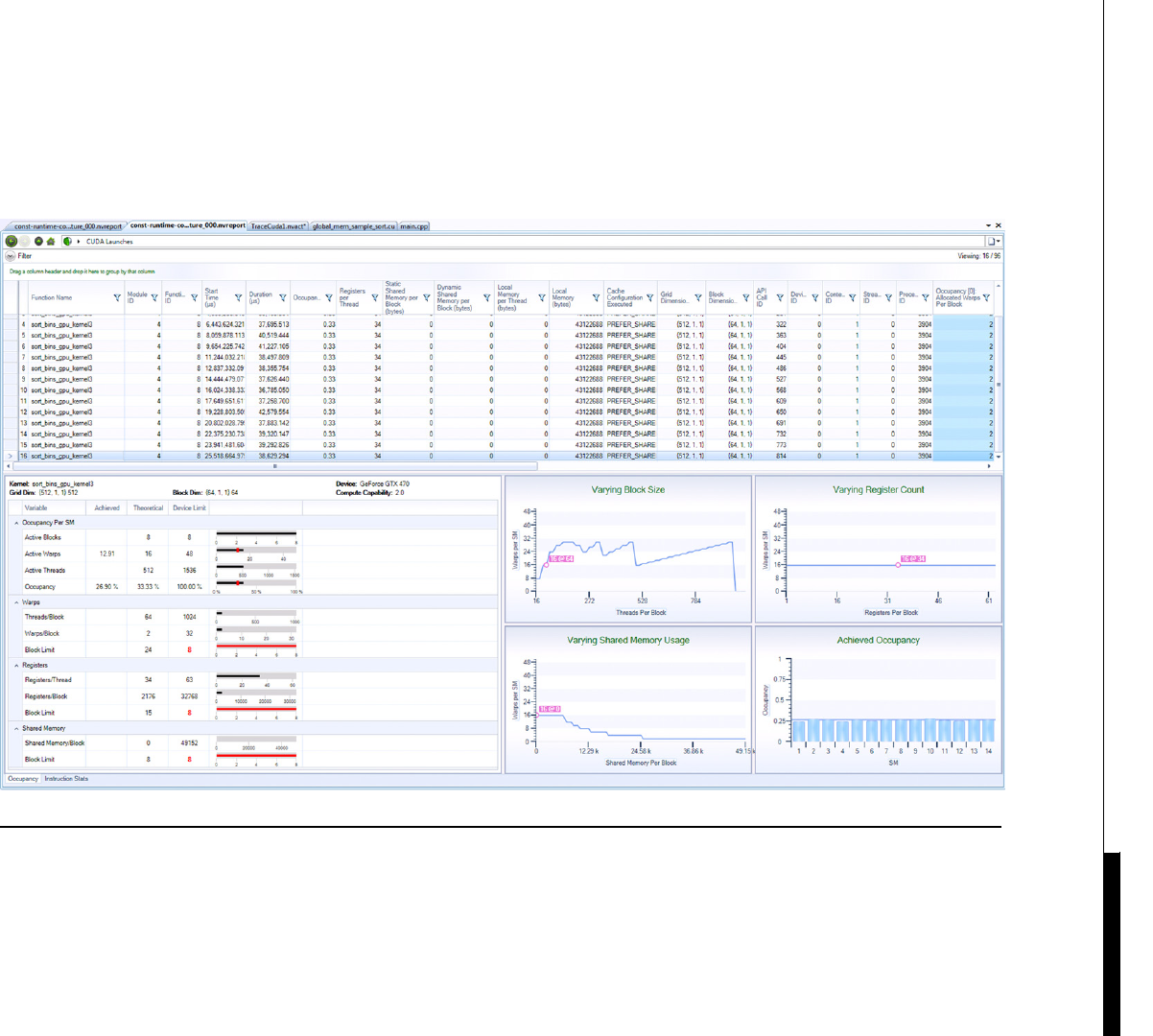
FIGURE 7.6
Parallel Nsight analysis.
Profiling 223
FIGURE 7.7
Parallel Nsight analysis.
224 CHAPTER 7 Using CUDA in Practice

When we move to 256 threads per block, the variability we see in issued versus executed
instructions grows. The number of scheduled blocks drops from eight to just three due to the use of
34 registers per thread. Although not an issue with 64 threads per block, 256 threads per block limits
the overall number of blocks that can be scheduled per SM. However, despite this, the number of warps
scheduled climbs to 24 instead of 16, providing a 50% occupancy rate. Does further increasing
occupancy help?
Simply asking the compiler to use a maximum of 32 registers (the -maxregcount¼32 compiler flag)
proves to be a terrible optimization. The compiler then uses just 18 registers, allowing for six blocks to
be scheduled, the maximum permitted. This increases the theoretical occupancy to 100%, but results in
an increase in execution time from 63 ms to 86 ms.
This is due to the GPU having to push registers into “local” storage, which on Fermi is the L1 cache
and global memory on the earlier-generation GPUs. On earlier-generation GPUs the time taken to use
global memory would more than eliminate any gain due to better occupancy. On Fermi, pushing more
data into the L1 cache reduces the available cache space for other purposes.
We can also go down the opposite path, to increase register usage. The original C code for the
function that performs the sort bins time output shown earlier is as follows:
__device__ void radix_sort(
u32 * const data,
const u32 start_idx,
const u32 end_idx,
u32 * const sort_tmp_1)
{
// Sort into num_list, lists
// Apply radix sort on 32 bits of data
for (u32 bit¼0;bit<32;bitþþ)
{
// Mask off all but the bit we’re interested in
const u32 bit_mask ¼(1u << bit);
// Set up the zero and one counter
u32 base_cnt_0 ¼start_idx;
u32 base_cnt_1 ¼start_idx;
for (u32 i¼start_idx; i<end_idx; iþþ)
{
// Fetch the test data element
const u32 elem ¼data[i];
// If the element is in the one list
if ( (elem & bit_mask) > 0u )
{
// Copy to the one list
sort_tmp_1[base_cnt_1þþ]¼elem;
}
else
Profiling 225

{
// Copy to the zero list (inplace)
data[base_cnt_0þþ]¼elem;
}
}
// Copy data back to source from the one’s list
for (u32 i¼start_idx; i<base_cnt_1; iþþ)
{
data[base_cnt_0þþ]¼sort_tmp_1[i];
}
}
}
If we look at the PTX code generated for the kernel (see Chapter 9 for details on how to do this) we
see the following code extract:
mov.s64 %rd5, %rd2;
cvt.u64.u32 %rd6, %r17;
mul.wide.u32 %rd7, %r17, 4;
add.u64 %rd8, %rd5, %rd7;
ld.u32 %r20, [%rd8þ0];
mov.s32 %r21, %r20;
This equates to the C source code line for
// Fetch the test data element
const u32 elem ¼data[i];
There are a number of issues here. First, array indexing is causing the use of a multiply instruction. As
elem is used immediately in the next C instruction to branch, the data load needs to have completed, so the
thread stalls at this point. Multiply and divide instructions usually require many cycles to complete the
instruction pipeline and there may be limited execution units that can perform such complex instructions.
We can replace all array indexes with a pointer to the array and then increment the pointer after
each usage. Thus, the code extract we looked at earlier becomes
// Fetch the test data element
const u32 elem ¼(*data_in_ptr);
data_in_ptrþþ;
This means the compiler now translates this to the following PTX code:
; const u32 elem ¼(*data_in_ptr);
mov.s64 %rd20, %rd14;
ld.u32 %r18, [%rd20þ0];
mov.s32 %r19, %r18;
; data_in_ptrþþ;
mov.s64 %rd21, %rd14;
add.u64 %rd22, %rd21, 4;
mov.s64 %rd14, %rd22;
226 CHAPTER 7 Using CUDA in Practice

We still have a total of six instructions, but now the first set does the load and the second set the
increment of the pointer. The increment of the pointer is now a simple addition, much simpler than
a multiply, and the result is not needed until the next iteration of the loop.
Applying the same strategy to the other array operations yields a reduction in execution time from
39.4 ms to 36.3 ms, a drop of 3 ms or around 10%. However, what about this variability in work done
by each warp? Where does this come from?
Sample sort sorts data into blocks, or bins, which we independently sort using a single warp. If we
do a dump of the values from single warp, we see something interesting.
Bin Usage - Max:331 Min:0 Avg:32 Zero:10275
0000:00000022 0001:00000000 0002:0000003e 0003:0000001d 0004:00000028 0005:00000000
0006:00000018 0007:0000003d
0008:00000052 0009:00000000 0010:0000001d 0011:00000000 0012:00000061 0013:00000000
0014:00000000 0015:00000000
0016:00000024 0017:0000009d 0018:00000021 0019:00000000 0020:0000002b 0021:00000021
0022:00000000 0023:00000000
0024:00000025 0025:00000000 0026:00000056 0027:00000050 0028:00000019 0029:00000000
0030:00000025 0031:0000001d
There are a significant number of bins where the entries are zero. There are others where the total
number of entries is very large. As one thread processes each bin, to iterate over the entire dataset, we
need to iterate for the maximum of the bins from a given warp. The first warp shown has a maximum
value of 0x9d (157 decimals) and a minimum value of zero. By the time we’re at iteration 157, only
a single thread from the entire warp is active. We see this reflected in the large difference between
issued and executed instructions we saw earlier (Instructions per clock, Figure 7.7). It’s the bins with
very large iteration counts that are taking the time.
We see a reduction in the execution time of the radix sort when we double the number of samples,
because the peaks are pushed down and split out into more bins. However, sorting the samples then
becomes the dominating issue. The problem is the distribution of samples to bins.
The large number of zero bins is actually caused by duplicates in the sample dataset. The source
data array is filled with data via a simple call to rand(), which returns a not-so-random number. After
a certain period these repeat. As the samples are selected at a uniform distance to one another, the
sample set contains many duplicates. Removing this error in the random dataset removes almost all
zeros from the bin count, but has an unintended effect that the execution time now climbs back up to
the original 40 ms.
We can, however, apply another technique to this problem, that of loop unrolling and tail reduction,
both of which we cover in Chapter 9. We replace the following code segment:
for (u32 i¼start_idx; i<end_idx; iþþ)
{
// Fetch the test data element
const u32 elem ¼(*data_in_ptr);
data_in_ptrþþ;
with
// Unroll 4 times
u32 i¼start_idx;
Profiling 227

if ( (end_idx - start_idx) >¼4)
{
for (; i< (end_idx-4); iþ¼4)
{
// Fetch the test first and second data element
const u32 elem_1 ¼(*data_in_ptr);
const u32 elem_2 ¼(*(data_in_ptrþ1));
const u32 elem_3 ¼(*(data_in_ptrþ2));
const u32 elem_4 ¼(*(data_in_ptrþ3));
data_in_ptrþ¼4;
Suppose the difference between start_idx and end_idx is 32, one of the common cases. The
number of iterations in the first loop will be 32. However, by unrolling the loop by a factor of four, we
reduce the number of operations by a factor of four, that is, eight iterations. There are a few other
important effects of loop unrolling. Notice we need, in the case of a factor of four, three additional
registers to store three additional data points. We also need to handle the end loop condition where we
may still have zero to three elements to process.
Looking at the PTX code we see:
;const u32 elem_1 ¼(*data_in_ptr);
mov.s64 %rd20, %rd14;
ld.u32 %r23, [%rd20þ0];
mov.s32 %r24, %r23;
;const u32 elem_2 ¼(*(data_in_ptrþ1));
mov.s64 %rd21, %rd14;
ld.u32 %r25, [%rd21þ4];
mov.s32 %r26, %r25;
;const u32 elem_3 ¼(*(data_in_ptrþ2));
mov.s64 %rd22, %rd14;
ld.u32 %r27, [%rd22þ8];
mov.s32 %r28, %r27;
;const u32 elem_4 ¼(*(data_in_ptrþ3));
mov.s64 %rd23, %rd14;
ld.u32 %r29, [%rd23þ12];
mov.s32 %r30, %r29;
;data_in_ptrþ¼4;
mov.s64 %rd24, %rd14;
add.u64 %rd25, %rd24, 16;
mov.s64 %rd14, %rd25;
We’re doing something quite important here, introducing instruction level parallelism through the
use of independent elements per thread. Table 7.1 and Figure 7.8 show the effect loop unrolling has.
As you can see from Table 7.1 and Figure 7.8, introducing a small amount of thread level paral-
lelism significantly drops the execution time of the radix sort. However, notice something else: The
228 CHAPTER 7 Using CUDA in Practice
number of registers never climbs above 44, even though we can use up to 63 in Fermi. What is
happening at this point is the compiler introduces a call stack and no longer grows the number of
registers used.
We’ve applied a couple of optimization techniques to the source code, which you might reasonably
expect a compiler to automatically apply. We’ll not remove any of these, so any gain should come from
the compiler adding additional optimizations. Let’s see if this is the case by switching to the release
mode, which enables all the compiler optimizations by default (Table 7.2 and Figure 7.9).
We see from Table 7.2 and Figure 7.9 a very similar pattern to the release or optimized
version, indicating that the optimizations we have just applied are not themselves applied
automatically by the compiler. What is also noticable is again we see the same pattern, that
four elements per thread helps considerably, but beyond this the effect is marginal. Notice, even
with optimizations enabled, the compiler does not automatically unroll the loop. Thus, we’ll stick
with manual unrolling by four, as the additional speed versus extra register usage is not a good
tradeoff.
You might have expected the compiler to have pulled, or hoisted, out the read operations and
placed them at the start of an unrolled loop. In many cases it will do this, except in the difficult cases,
which are unfortunately all too often what we hit. Where you have a read followed by write followed
by another read, the compiler cannot easily know if the write operation wrote to the same data area
that is being read from. Thus, it must maintain the read-write-read sequence to ensure correctness. As
Table 7.1 Unroll Level Versus Time and Register Usage
Unroll 0 246810121416
Time 40 37.02 33.98 33.17 32.78 32.64 32.25 33.17 32.51
Registers 38 38 40 42 44 44 44 44 44
30
32
34
36
38
40
42
44
46
0246810121416
Time Registers
FIGURE 7.8
Unroll level versus time and register usage.
Profiling 229
the programmer however, you know if the read operations are affected by the preceding write
operations and can replace the read-write-read sequence with a much more efficient read-read-write
sequence.
As we’ve now radically changed the timing on one aspect, dropping it from 40 ms to 25 ms, we
should rerun the scan of the problem space to see if this now changes the optimum number of samples/
threads.
One thing that becomes noticable is the release version of QSort is actually much faster, over twice
the speed in fact. This makes it considerably harder to produce a faster sort. However, quick sort is now
a large component of the sample sort, as we presort the samples on the CPU. Thus, this reduction in
execution time helps considerably. The best timing is as follows:
ID:0 GeForce GTX 470: Test 16 - Selecting 32768 from 1048576 elements using 128 blocks
of 256 threads
Num Threads: 32 64 128 256
Select Sample Time- CPU: 0.38 GPU: 0.38 0.19 0.50 0.31
Sort Sample Time - CPU: 4.63 GPU: 4.63 4.69 4.31 4.31
Count Bins Time - CPU: 64.50 GPU: 5.71 5.65 5.59 5.31
Calc. Bin Idx Time- CPU: 0.06 GPU: 1.55 0.79 0.86 0.79
Sort to Bins Time - CPU: 80.44 GPU: 6.25 6.08 5.96 5.71
Sort Bins Time - CPU: 62.81 GPU:27.37 25.10 36.28 39.87
Table 7.2 Debug Versus Release Version Timing
Unroll 0 2 4 6 8 10 12 14 16
Debug 40 37.02 33.98 33.17 32.78 32.64 32.25 33.17 32.51
Release 32.34 26.25 25.07 24.7 24.36 24.26 24.1 24.13 24.24
20
25
30
35
40
45
0246810121416
Debug Release
FIGURE 7.9
Debug versus release timing.
230 CHAPTER 7 Using CUDA in Practice

Total Time - CPU: 212.81 GPU:45.89 42.49 53.50 56.31
QSORT Time - CPU: 187.69
ID:0 GeForce GTX 470: Test 16 - Selecting 65536 from 1048576 elements using 256 blocks
of 256 threads
Num Threads: 32 64 128 256
Select Sample Time- CPU: 0.50 GPU: 0.50 0.50 0.44 0.50
Sort Sample Time - CPU: 9.56 GPU: 9.56 9.63 9.56 9.63
Count Bins Time - CPU: 95.88 GPU: 6.70 6.67 6.60 6.34
Calc. Bin Idx Time- CPU: 0.06 GPU: 1.17 1.22 1.36 1.19
Sort to Bins Time - CPU: 119.88 GPU: 7.27 7.06 6.94 6.73
Sort Bins Time - CPU: 52.94 GPU:24.23 16.84 25.22 29.95
Total Time - CPU: 278.81 GPU:49.43 41.91 50.12 54.35
QSORT Time - CPU: 187.69
So in fact both the 16 K and 32 K sample versions come out above even, with 0.6 ms between
them.Thisisa4.4speedup over the CPU-based quick sort. Cache utilization is a key factor in
play here. See the “Thread Memory Patterns” section in Chapter 9 where we look at the impact
of this.
In summary, we used Parallel Nsight to show the impact of altering the number of and size of the
blocks we used and saw how this could radically affect the overall performance. We then drilled down
into this data and noticed there was, ultimately, a problem with the design of the sample sort. Seri-
alization caused through the differing number of elements processed per thread was the cause of this.
Despite this issue, we could optimize the implementation through thread level parallelism by using
multiple elements per thread. Enabling additional compiler level optimization brought considerable
additional benefits to both CPU and GPU code.
AN EXAMPLE USING AES
The AES (Advanced Encryption Standard) is an algorithm used to provide encryption in programs like
WinZip, Bitlocker, TrueCrypt, etc. Depending on your industry, encryption may be something you
already use or something that may seem irrelevant. Many companies make the mistake of thinking the
data they create doesn’t need to be kept securely on a local machine. All the nasty programs and
hackers are outside the company firewall and therefore any data kept locally doesn’t need security.
This type of thinking is flawed, as very often a machine, employee, or contractor may create holes in
such a firewall to enable working at home or outside the office, etc. Security needs to have a multi-
layered approach.
The idea of encryption is that we take some data and apply an algorithm to it that obscures the data.
Thus, the data, or the machine holding that data, such as a laptop, can be compromised, lost, or stolen,
but the data itself is not accessible. Significant numbers of data breaches are a result of compromised
machines. Moving the protection to the data means that to access it requires a “key.” Applying that key
and a given algorithm results in the data becoming unencrypted.
Encryption can also be used for secure connections between hosts on an insecure network such as
the Internet. If you have a distributed application over a public network, how do you ensure that if you
send a packet of data to another machine that packet is not intercepted and changed? Standards such as
An Example Using AES 231

OpenSSL (Open Secure Socket Layer) are used by browsers when logging into secure servers such as
those for online banking to ensure no one listens in on the exchange of login data.
When you design software, you will need to consider the security aspects of it and how data is
transmitted to and from various machines in any solution. The ITEF (Internet Engineering Task Force),
the body that approves new Internet standards, requires all standard proposals to include a section on
security. The fines levied against organizations for loss of consumer or corporate data are significant. It
therefore pays to have a good understanding of at least some encryption standards if you are in any way
networking computers or storing sensitive or personal data.
AES is mandated by many U.S. government organizations when storing data. As an algorithm in
use today, we’ll use this as a case study to see how you might approach AES-based encryption using
a GPU. However, before we can dive into the implementation details, we first need to analyze the
algorithm, understand it, and look for elements that can be computed in parallel. The AES algorithm
contains many complexities, yet at the same time is understandable to someone with no cryptographic
background. It is therefore a useful algorithm to look at to see how we can apply some of the tech-
niques discussed to date.
The algorithm
AES is a block-based encryption algorithm. An encryption algorithm is often referred to as
acipher. Thus, the text to be encoded is referred to as plain text when not encoded and cipher
text when encoded. To encode plain text into cipher text requires an algorithm and a key. The key
is simply a series of numbers that acts very much like a mechanical key, the algorithm being
the lock.
AES supports a number of modes of operation, the simplest being ECB (Electronic Cook Book),
the one we’ll look at here. AES splits up the data to be encoded into a number of blocks 128 bits in
length (16 bytes). Each block in ECB mode is independently encoded based on a series of values
derived from the encryption key. The encoding takes place in a series of “rounds,” each of which uses
a new derived key to further encrypt the data. See Figure 7.10.
The 128-bit key is independently adapted for each round and is independent of the text to be
encoded or the previous round of encryption. Thus, the extraction of the keys for the various rounds
can be done independently of the encoding round for the AES algorithm. Usually, as the key is constant
for all blocks, this will be done before any encryption begins.
AES uses 128-, 192-, or 256-bit keys, although the block size (the size of the plain text) is always
128 bits. The number of rounds used changes according to the key length chosen: 10, 12, and 14
rounds, respectively.
The plain text is represented as a 4 4 matrix of byte data, known as the state space.
An encryption round itself consists of the following:
• SubstitutiondBytes within the 4 4 matrix are swapped with other bytes from a lookup table.
• Row rotate leftdRows 1, 2, and 3 are rotated left by one, two, or three positions, respectively.
Row 0 is unchanged.
• Mix columnsdEach column has a step applied to diffuse the values.
• Round keydThe data is XOR’d with the appropriate current round key extracted from the
original key.
232 CHAPTER 7 Using CUDA in Practice
The initial round, also known as round zero, consists only of the round key operation. The final round
drops the mix columns operation. Decryption is simply the inverse of the encryption process, starting
at the last round and working backwards to the start.
Thus, to implement the algorithm, we need to look in detail at the five key aspects, those just shown
plus the extraction of the round keys from the original 128 bit key.
Substitution
The substitution step swaps every byte in the 4 4 data block, the state space, with a value from
a constant lookup table known as the Rijndael s-box.
unsigned char s_box[256] ¼
{
/*0123456789ABCDEF*/
0x63, 0x7C, 0x77, 0x7B, 0xF2, 0x6B, 0x6F, 0xC5, 0x30, 0x01, 0x67, 0x2B, 0xFE, 0xD7, 0xAB, 0x76, /* 0 */
0xCA, 0x82, 0xC9, 0x7D, 0xFA, 0x59, 0x47, 0xF0, 0xAD, 0xD4, 0xA2, 0xAF, 0x9C, 0xA4, 0x72, 0xC0, /* 1 */
0xB7, 0xFD, 0x93, 0x26, 0x36, 0x3F, 0xF7, 0xCC, 0x34, 0xA5, 0xE5, 0xF1, 0x71, 0xD8, 0x31, 0x15, /* 2 */
0x04, 0xC7, 0x23, 0xC3, 0x18, 0x96, 0x05, 0x9A, 0x07, 0x12, 0x80, 0xE2, 0xEB, 0x27, 0xB2, 0x75, /* 3 */
0x09, 0x83, 0x2C, 0x1A, 0x1B, 0x6E, 0x5A, 0xA0, 0x52, 0x3B, 0xD6, 0xB3, 0x29, 0xE3, 0x2F, 0x84, /* 4 */
0x53, 0xD1, 0x00, 0xED, 0x20, 0xFC, 0xB1, 0x5B, 0x6A, 0xCB, 0xBE, 0x39, 0x4A, 0x4C, 0x58, 0xCF, /* 5 */
0xD0, 0xEF, 0xAA, 0xFB, 0x43, 0x4D, 0x33, 0x85, 0x45, 0xF9, 0x02, 0x7F, 0x50, 0x3C, 0x9F, 0xA8, /* 6 */
0x51, 0xA3, 0x40, 0x8F, 0x92, 0x9D, 0x38, 0xF5, 0xBC, 0xB6, 0xDA, 0x21, 0x10, 0xFF, 0xF3, 0xD2, /* 7 */
0xCD, 0x0C, 0x13, 0xEC, 0x5F, 0x97, 0x44, 0x17, 0xC4, 0xA7, 0x7E, 0x3D, 0x64, 0x5D, 0x19, 0x73, /* 8 */
0x60, 0x81, 0x4F, 0xDC, 0x22, 0x2A, 0x90, 0x88, 0x46, 0xEE, 0xB8, 0x14, 0xDE, 0x5E, 0x0B, 0xDB, /* 9 */
0xE0, 0x32, 0x3A, 0x0A, 0x49, 0x06, 0x24, 0x5C, 0xC2, 0xD3, 0xAC, 0x62, 0x91, 0x95, 0xE4, 0x79, /* A */
0xE7, 0xC8, 0x37, 0x6D, 0x8D, 0xD5, 0x4E, 0xA9, 0x6C, 0x56, 0xF4, 0xEA, 0x65, 0x7A, 0xAE, 0x08, /* B */
Plain Text 128-Bit Key
Initial Round
N Rounds
Last Round
Encrypted Text
FIGURE 7.10
AES overview.
An Example Using AES 233
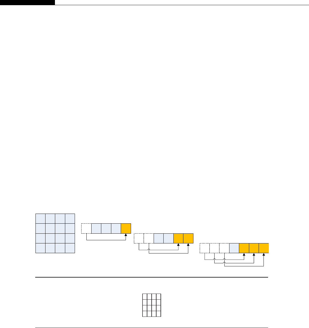
0xBA, 0x78, 0x25, 0x2E, 0x1C, 0xA6, 0xB4, 0xC6, 0xE8, 0xDD, 0x74, 0x1F, 0x4B, 0xBD, 0x8B, 0x8A, /* C */
0x70, 0x3E, 0xB5, 0x66, 0x48, 0x03, 0xF6, 0x0E, 0x61, 0x35, 0x57, 0xB9, 0x86, 0xC1, 0x1D, 0x9E, /* D */
0xE1, 0xF8, 0x98, 0x11, 0x69, 0xD9, 0x8E, 0x94, 0x9B, 0x1E, 0x87, 0xE9, 0xCE, 0x55, 0x28, 0xDF, /* E */
0x8C, 0xA1,0x89, 0x0D, 0xBF,0xE6, 0x42, 0x68, 0x41,0x99, 0x2D, 0x0F,0xB0, 0x54,0xBB,0x16 /* F */
};
For each of the 16-byte elements in the state space we have to extract out a single hex digit. The first
digit, or high nibble of the byte, (0.F), is used as row reference. The second digit of the byte, or low
nibble, is used as the column index. Thus, a value of 0x3E in the state space would result in a row value
of 3 and a column value of E. If we look up this in the s_box table, we get 0xB2. Thus, the byte 0x3E in
the state space is replaced by 0xB2. The same operation is performed for all the other bytes in the state
space.
Row rotate left
In this step, rows 1, 2, and 3 are rotated left by one, two, or three positions, respectively. Row 0 is left
unchanged. A rotate left operation takes the row and shuffles all bytes to the left by one position. The
byte at the far left wraps around and becomes the byte on the far right. In Figure 7.11 I’ve pulled out
each row to show how the rotation of the bytes works.
Mix columns
The Rijndael mix column step is a complex piece of code. It multiples the column rby a 4 4 matrix.
The matrix is shown in Figure 7.12.
A 1 in the matrix means leave the value unchanged. A 2 indicates multiplication by 2. A 3 indicates
a multiplication by 2 plus an XOR with the original value. In the 3 case, should the resultant value be
larger than 0xFF, then an additional XOR with 0x1B needs to be performed. This is a simplification of
Galois multiplication. A typical implementation in C code is shown here (Wikipedia, Jan. 31, 2012).
0 4 8 C
1 5 9 D
2 6 A E
3 7 B F
15 9 D1
2 6 A E 2 6
3 7 B F 3 7 B
FIGURE 7.11
AES row rotate left.
2311
1231
1123
3112
FIGURE 7.12
Mix columns matrix.
234 CHAPTER 7 Using CUDA in Practice

void mix_column(unsigned char *r)
{
unsigned char a[4];
unsigned char b[4];
unsigned char c;
unsigned char h;
for(c¼0;c<4;cþþ)
{
a[c] ¼r[c];
h¼r[c] & 0x80; /* hi bit */
b[c] ¼r[c] << 1;
if(h ¼¼ 0x80)
b[c] ^¼0x1b; /* Rijndael’s Galois field */
}
r[0] ¼b[0] ^ a[3] ^ a[2] ^ b[1] ^ a[1];
r[1] ¼b[1] ^ a[0] ^ a[3] ^ b[2] ^ a[2];
r[2] ¼b[2] ^ a[1] ^ a[0] ^ b[3] ^ a[3];
r[3] ¼b[3] ^ a[2] ^ a[1] ^ b[0] ^ a[0];
}
This is not the most optimal, but the most likely example implementation you will find of this
standard algorithm. In the preceding code, the input parameter rpoints to a 1 4 matrix that is a single
column from the state space. It is copied to a temporary array afor use later. An array bis generated
that holds the multiply by 2 (the <<1) operation. The multiply by 3 is actually a multiply by 2 followed
by an XOR (^) operation. Thus, the final step becomes a series of XOR operations of the original data
in aplus the result of the matrix multiplication in b. See Figure 7.13.
We’ll look a little more at this step later, as it’s one of the more time-consuming elements.
Add round key
The round key is the key extracted from the original cipher key for a given round or iteration of the
encryption algorithm. It’s in the form of a 4 4 matrix and is simply XOR’d with the current result.
Extracting the round keys
The AES algorithm uses a number of round keys, one for each round. Generating the keys is an iterative
process where new keys depend on previous ones. The first part of the operation is to take the existing
key and copy it as key 0, thus generating a 4 4 matrix providing the single starting round key.
The next Nround keys must be constructed one at a time. The first column of any round key takes
the last column of the previous round key as its starting point. The operation for the first column in the
new key contains some addition operations over and above the standard column generation function.
For the first column of the key only, we need to do a column-based rotate such that the values move
up the column. The value at the top of the column, row 0, moves to row 3. An identical operation is to
rotate the row left on the cipher data, but instead of a row, the rotate is over a column. We then again
use the substitution method and the Rijndael s-box to substitute values as we did for the cipher text.
An Example Using AES 235
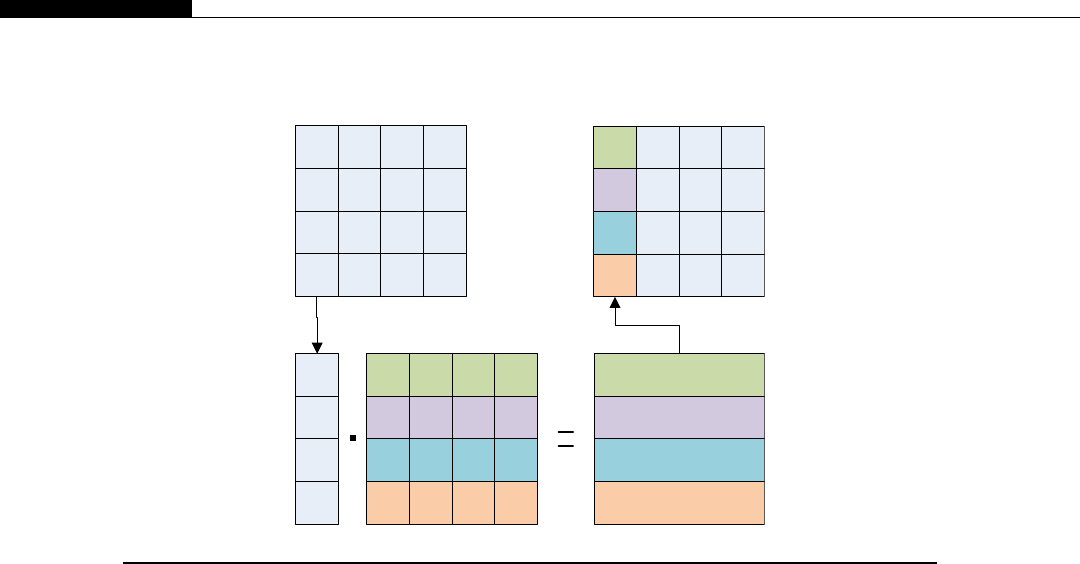
The operation for all elements is then the same. The newly calculated value must be XOR’d with
the key value at index minus 4. For columns 1, 2, and 3 we’re now done. However, column 0 has an
addition operation. The first element of column zero is then XOR’d with 0x01,0x02,0x04,0x08,0x10,
0x20,0x40,0x80,0x1b,or0x36, the RCON value, depending on the current round (Figure 7.14).
Thus, the first column of round key 1 becomes the next extracted column. The calculation of columns
1, 2, and 3 is simpler (Figure 7.15). The column rotation and XOR with the RCON values is dropped.
Thus, we simply have an XOR with the column at row minus 4. At column 4, the pattern repeats.
As the key generation always uses values from the previous key, this means the keys need to be
generated in sequence. This in turn may form the bottleneck of any parallel implementation if many
keys are needed. Thankfully for most uses, only a single set of keys is required. Thus, this step can be
performed prior to any encoding or decoding and the keys simply stored in an array. As it’s not time
consuming for a single key, it can be done on either the CPU or GPU.
Serial implementations of AES
AES has been the subject of a lot of study. It was designed to run on 8-, 16-, or 32-bit machines without
significant processing load. However, as we have seen from looking at the algorithm, it’s not a simple
algorithm to implement. Let’s consider some of the design tradeoffs when thinking about optimizing
such an algorithm for a GPU.
Access size
The first issue is that it is designed around byte-based access, to support 8-bit simple processors. All
modern processors are at least 32-bit designs. Thus, if we use just single byte operations, 75% of the
0 4 8 C
1 5 9 D
2 6 A E
3 7 B F
2 3 1 1
1 3 1
1 1 2 3
3 1 1 2
2
0 = 2s0^ 3s1 ^ 1s2^ 1s3s0
s1
s2
s3
4 8 C
5 9 D
6 A E
7 B F
0
1
2
3
1 = 1s0^ 2s1 ^ 3s2^ 1s3
2 = 1s0^ 1s1 ^ 2s2^ 3s3
3 = 3s0^ 1s1 ^ 1s2^ 2s3
FIGURE 7.13
Mix columns with column 0 (repeated for columns 1, 2, and 3).
236 CHAPTER 7 Using CUDA in Practice
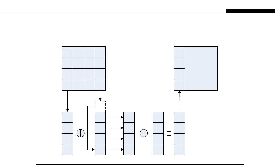
space in the register and the potential work goes unused. Clearly with a 32-bit processor, an x86 or
a Fermi GPU, we need to design a solution such that it uses 32 bits.
We can naturally combine a single row into one 32-bit word. We can also combine the entire 4 4
matrix into a 16-byte vector (128 bits). Such vectors are supported by the Intel AVX (Advanced Vector
eXtension) instruction set. The GPU uint4 type would also allow for the GPU to fetch and store this
data to/from memory in a single instruction. However, unlike Intel’s AVX, the GPU has no per thread
wide vector instructions other than storing to or from memory.
We have to consider that any encoding of the state or key matrix that is larger than a single byte
would necessitate bit mask and shift operations if the operation needed to be individually applied to
a single byte. Providing these were not considerable, the benefit of less memory reads/writes, though
fetching the data in larger transactions, would easily outweigh register-based mask and shift operations.
Memory versus operations tradeoff
With most algorithms it’s possible to trade an increased memory footprint for a decreased execution
time. It depends significantly on the speed of memory versus the cost and number of arithmetic
instructions being traded.
There are implementations of AES that simply expand the operations of the substitution, shift rows
left, and mix columns operation to a series of lookups. With a 32-bit processor, this apparently requires
a 4 K constant table and a small number of lookup and bitwise operations. Providing the 4 K lookup table
remains in the cache, the execution time is greatly reduced using such a method on most processors. We
will, however, implement at least initially the full algorithm before we look to this type of optimization.
0 4 8 C
1 5 9 D
2 6 A E
3 7 B F
Round key zero
C
D
E
F
C
Round key one
0
1
2
3
1
0
0
0
C
F
D
F
C
F
D
F
RCON[0]
ROXROX
S0
S1
S2
S3
SBOX
Lookup
FIGURE 7.14
AES round key generation (first column).
An Example Using AES 237
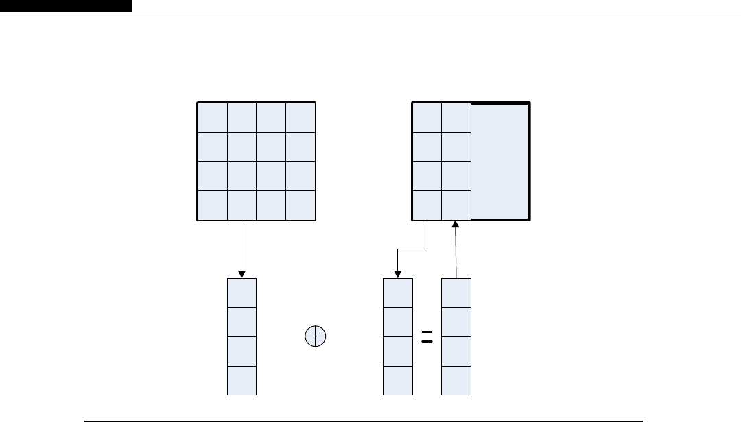
Hardware acceleration
The Intel AES-NI extension to the x86 processor instruction set is available on most Intel Sandybridge
I5 and I7 processors as well as the Westmere-based I7 Xeon processors and their successors. The AES-
NI instruction set consists of the following instructions:
• AESENC (cipher data, round key)dStandard round of encoding completely in hardware.
• AESENCLAST (cipher data, round key)dLast round of encoding completely in hardware.
• AESKEYGENASSIST (round key, cipher key, round number)dAssist in the generation of the
round keys.
• ASDEC (cipher data, round key)dStandard round of decryption in hardware.
• ASDECLAST (cipher data, round key)dLast round of decryption in hardware.
Thus, the entire AES encryption and decryption process can be done entirely in hardware. Special
128-bit xmm1 and xmm2 registers are used to contain the operands in single registers. We see that
in practice when such AES-NI is used with real applications, there is something in the order of
a2or more performance improvement over a nonaccelerated processor (Toms Hardware, “AES-
NI Benchmark Results: Bitlocker, Everest, And WinZip 14,” http://www.tomshardware.co.uk/
clarkdale-aes-ni-encryption,review-31801-7.html). Of course with handwritten assembler and
optimal scheduling conditions over many cores, it’s possible to get significantly more. This,
however, gives us a feel for the likely benefit of coding such a solution and therefore it seems worth
the effort.
0 4 8 C
1 5 9 D
2 6 A E
3 7 B F
Round key zero
D
E
F
C
Round key one
4
5
6
7
9
B
9
B
C
F
D
F
XOR
9
B
9
B
FIGURE 7.15
AES round key generation (columns 1, 2, and 3).
238 CHAPTER 7 Using CUDA in Practice

An initial kernel
Let’s look at an initial kernel for this algorithm.
__host__ __device__ void AES_encrypt_4x4_reg(uint4 * const cipher_block,
KEY_T * const cipher_key,
const u32 num_rounds)
{
First, we have the function prototype. Here we pass in a pointer to a cipher block as a uint4 vector
type. A single uint4 vector (four integers) is sufficient to hold a single set of 16 bytes, the 128-bit
cipher data. Next we have the cipher key, which is a set of 10 uint4 keys. Finally, we have a specifier
for the number of rounds, which we will replace with a fixed value at some point later. Note both the
__host__ and __device__ qualifiers that allow the function to be called from both the CPU and GPU.
const u8 * const s_box_ptr ¼s_box;
// Read 4 x 32 bit values from data block
u32 w0 ¼cipher_block->w;
u32 w1 ¼cipher_block->x;
u32 w2 ¼cipher_block->y;
u32 w3 ¼cipher_block->z;
Next we extract from the uint4 vector type the four unsigned integer component parts.
register u8 a0 ¼EXTRACT_D0(w0);
register u8 a1 ¼EXTRACT_D0(w1);
register u8 a2 ¼EXTRACT_D0(w2);
register u8 a3 ¼EXTRACT_D0(w3);
register u8 a4 ¼EXTRACT_D1(w0);
register u8 a5 ¼EXTRACT_D1(w1);
register u8 a6 ¼EXTRACT_D1(w2);
register u8 a7 ¼EXTRACT_D1(w3);
register u8 a8 ¼EXTRACT_D2(w0);
register u8 a9 ¼EXTRACT_D2(w1);
register u8 a10 ¼EXTRACT_D2(w2);
register u8 a11 ¼EXTRACT_D2(w3);
register u8 a12 ¼EXTRACT_D3(w0);
register u8 a13 ¼EXTRACT_D3(w1);
register u8 a14 ¼EXTRACT_D3(w2);
register u8 a15 ¼EXTRACT_D3(w3);
We next extract individual bytes from the four words into individual registers. Note the use of the
u8 type rather than the base C type, allowing an easy redefinition of this type. Note also the EXTRACT
macro, which is used to allow support for both big-endian and little-endian representation of the bytes
within the 32-bit words.
// Initial round - add key only
u32 round_num ¼0;
// Fetch cipher key from memory
w0 ¼(*cipher_key)[round_num].w;
An Example Using AES 239

w1 ¼(*cipher_key)[round_num].x;
w2 ¼(*cipher_key)[round_num].y;
w3 ¼(*cipher_key)[round_num].z;
We then read a set of four values from the key, again from a uint4 type into four 32-bit values.
a0 ^¼EXTRACT_D0(w0);
a4 ^¼EXTRACT_D1(w0);
a8 ^¼EXTRACT_D2(w0);
a12 ^¼EXTRACT_D3(w0);
a1 ^¼EXTRACT_D0(w1);
a5 ^¼EXTRACT_D1(w1);
a9 ^¼EXTRACT_D2(w1);
a13 ^¼EXTRACT_D3(w1);
a2 ^¼EXTRACT_D0(w2);
a6 ^¼EXTRACT_D1(w2);
a10 ^¼EXTRACT_D2(w2);
a14 ^¼EXTRACT_D3(w2);
a3 ^¼EXTRACT_D0(w3);
a7 ^¼EXTRACT_D1(w3);
a11 ^¼EXTRACT_D2(w3);
a15 ^¼EXTRACT_D3(w3);
round_numþþ;
The first round of the key encoding simply uses an XOR operation on the values in the columns.
while (round_num <¼num_rounds)
{
// Fetch cipher key from memory
w0 ¼(*cipher_key)[round_num].w;
w1 ¼(*cipher_key)[round_num].x;
w2 ¼(*cipher_key)[round_num].y;
w3 ¼(*cipher_key)[round_num].z;
// Substitution step
a0 ¼s_box_ptr[a0];
a1 ¼s_box_ptr[a1];
a2 ¼s_box_ptr[a2];
a3 ¼s_box_ptr[a3];
a4 ¼s_box_ptr[a4];
a5 ¼s_box_ptr[a5];
a6 ¼s_box_ptr[a6];
a7 ¼s_box_ptr[a7];
a8 ¼s_box_ptr[a8];
a9 ¼s_box_ptr[a9];
240 CHAPTER 7 Using CUDA in Practice

a10 ¼s_box_ptr[a10];
a11 ¼s_box_ptr[a11];
a12 ¼s_box_ptr[a12];
a13 ¼s_box_ptr[a13];
a14 ¼s_box_ptr[a14];
a15 ¼s_box_ptr[a15];
We then enter the main loop of the kernel. We run for num_rounds of iterations. As we later need the
key and the key is to be fetched from memory, we initiate the read from memory as early as possible.
Next we have the substitution step, which simply replaces the existing values with new ones from the
s_box array shown earlier.
// Rotate Rows
u8 tmp0, tmp1, tmp2, tmp3;
// a0, a4, a8, a12 remains unchanged
// a1, a5, a9, a13 rotate 1
// a5, a9, a13, a1
tmp0 ¼a1;
a1 ¼a5;
a5 ¼a9;
a9 ¼a13;
a13 ¼tmp0;
// a2, a6, a10, a14 rotate 2
// a10, a14, a2, a6
tmp0 ¼a14;
tmp1 ¼a10;
a14 ¼a6;
a10 ¼a2;
a6 ¼tmp0;
a2 ¼tmp1;
// a3, a7, a11, a15 rotate 3
// a15, a3, a7, a11
tmp0 ¼a3;
tmp1 ¼a7;
tmp2 ¼a11;
tmp3 ¼a15;
a15 ¼tmp2;
a11 ¼tmp1;
a7 ¼tmp0;
a3 ¼tmp3;
The next step is to rotate rows 1, 2, and 3. As we have stored one byte per register, we cannot simply
do a 32-bit rotate. As there is no native support in the GPU instruction set for such an operation, this is
of little real relevance.
An Example Using AES 241

if (round_num !¼10)
{
// Column Mix
const u8 b0 ¼MIX_COL(a0);
const u8 b1 ¼MIX_COL(a1);
const u8 b2 ¼MIX_COL(a2);
const u8 b3 ¼MIX_COL(a3);
const u8 b4 ¼MIX_COL(a4);
const u8 b5 ¼MIX_COL(a5);
const u8 b6 ¼MIX_COL(a6);
const u8 b7 ¼MIX_COL(a7);
const u8 b8 ¼MIX_COL(a8);
const u8 b9 ¼MIX_COL(a9);
const u8 b10 ¼MIX_COL(a10);
const u8 b11 ¼MIX_COL(a11);
const u8 b12 ¼MIX_COL(a12);
const u8 b13 ¼MIX_COL(a13);
const u8 b14 ¼MIX_COL(a14);
const u8 b15 ¼MIX_COL(a15);
tmp0 ¼XOR_5(b0, a3, a2, b1, a1 );
tmp1 ¼XOR_5(b1, a0, a3, b2, a2 );
tmp2 ¼XOR_5(b2, a1, a0, b3, a3 );
tmp3 ¼XOR_5(b3, a2, a1, b0, a0 );
const u8 tmp4 ¼XOR_5(b4, a7, a6, b5, a5 );
const u8 tmp5 ¼XOR_5(b5, a4, a7, b6, a6 );
const u8 tmp6 ¼XOR_5(b6, a5, a4, b7, a7 );
const u8 tmp7 ¼XOR_5(b7, a6, a5, b4, a4 );
const u8 tmp8 ¼XOR_5(b8, a11, a10, b9, a9 );
const u8 tmp9 ¼XOR_5(b9, a8, a11, b10, a10 );
const u8 tmp10 ¼XOR_5(b10, a9, a8, b11, a11 );
const u8 tmp11 ¼XOR_5(b11, a10, a9, b8, a8 );
const u8 tmp12 ¼XOR_5(b12, a15, a14, b13, a13 );
const u8 tmp13 ¼XOR_5(b13, a12, a15, b14, a14 );
const u8 tmp14 ¼XOR_5(b14, a13, a12, b15, a15 );
const u8 tmp15 ¼XOR_5(b15, a14, a13, b12, a12 );
a0 ¼tmp0;
a1 ¼tmp1;
a2 ¼tmp2;
a3 ¼tmp3;
a4 ¼tmp4;
a5 ¼tmp5;
a6 ¼tmp6;
a7 ¼tmp7;
a8 ¼tmp8;
a9 ¼tmp9;
242 CHAPTER 7 Using CUDA in Practice

a10 ¼tmp10;
a11 ¼tmp11;
a12 ¼tmp12;
a13 ¼tmp13;
a14 ¼tmp14;
a15 ¼tmp15;
}
The next step is to mix the columns operation, which is done in every round except the last one. The
previous mix column code shown earlier has had the cloop unrolled to form the MIX_COL macro.
Additionally, to control the order of the XOR, we implement an XOR_5, which is a five-input XOR macro.
// Addkey
a0 ^¼EXTRACT_D0(w0);
a4 ^¼EXTRACT_D1(w0);
a8 ^¼EXTRACT_D2(w0);
a12 ^¼EXTRACT_D3(w0);
a1 ^¼EXTRACT_D0(w1);
a5 ^¼EXTRACT_D1(w1);
a9 ^¼EXTRACT_D2(w1);
a13 ^¼EXTRACT_D3(w1);
a2 ^¼EXTRACT_D0(w2);
a6 ^¼EXTRACT_D1(w2);
a10 ^¼EXTRACT_D2(w2);
a14 ^¼EXTRACT_D3(w2);
a3 ^¼EXTRACT_D0(w3);
a7 ^¼EXTRACT_D1(w3);
a11 ^¼EXTRACT_D2(w3);
a15 ^¼EXTRACT_D3(w3);
round_numþþ;
}
We then implement the XOR operation with the key fetched at the start of the loop.
cipher_block->w ¼(ENCODE_D0(a0) jENCODE_D1(a4) jENCODE_D2(a8) jENCODE_D3(a12));
cipher_block->x ¼(ENCODE_D0(a1) jENCODE_D1(a5) jENCODE_D2(a9) jENCODE_D3(a13));
cipher_block->y ¼(ENCODE_D0(a2) jENCODE_D1(a6) jENCODE_D2(a10) jENCODE_D3(a14));
cipher_block->z ¼(ENCODE_D0(a3) jENCODE_D1(a7) jENCODE_D2(a11) jENCODE_D3(a15));
}
Finally, the resultant key is combined into a 32-bit value and written back to the uint4 cipher word. At
this point we’ve completed all 10 rounds and the cipher block is encoded based on the set of 10 round keys.
For completeness purposes, the macros used are defined as follows:
#define EXTRACT_D0(x) ( ( (x) >> 24uL ) )
#define EXTRACT_D1(x) ( ( (x) >> 16uL ) & 0xFFuL )
An Example Using AES 243

#define EXTRACT_D2(x) ( ( (x) >> 8uL ) & 0xFFuL )
#define EXTRACT_D3(x) ( ( (x) ) & 0xFFuL )
#define ENCODE_D0(x) ( (x) << 24uL )
#define ENCODE_D1(x) ( (x) << 16uL )
#define ENCODE_D2(x) ( (x) << 8uL )
#define ENCODE_D3(x) ( (x) )
#define MIX_COL(a) ( ((a) & 0x80uL) ? ((((a) << 1uL) & 0xFFuL) ^ 0x1Bu) : ((a) << 1uL) )
#define XOR_5(a,b,c,d,e) ( (((a)^(b)) ^ ((c)^(d))) ^ (e) )
Kernel performance
So how does such a kernel perform? How do we measure, understand, and predict performance? Initially,
looking at the disassembled code for a compute 2.x target, we see something you might not expect.
Declaring the registers as unsigned 8 bits results in sections of code to shift and mask data. The extract data
macros are deliberately written to mask off the bits that are not used, so this is entirely unnecessary. In fact,
we generate around four times the amount of code if we use a u8 type instead of a u32 type.
Changing the u8 definition to a u32 definition means we potentially waste a lot of register space, but
it eliminates huge numbers of instructions. In practice, the GPU implements u8 registers as u32
registers, so this doesn’t actually cost us anything in terms of register space.
Next we come to the number of registers used. Our initial kernel uses 43 registers, which is not
altogether too surprising but is somewhat disappointing. If you load up the CUDA Occupancy
Calculator, found in the “Tools” directory of the SDK, we can see that 43 registers will limit us to just
a single block per SM of no more than 320 threads. This is just 10 active warps and nowhere near the
maximum (24 on compute 1.3 devices, 48 on compute 2.x devices, 64 on compute 3.devices). We
need to have more blocks than this, so there is a greater mix of instructions for the warp scheduler to
select from. There are limits on, for example, the number of XOR operations an SM can perform (see
Chapter 9) and 10 warps will not hide the memory latency.
Thus, to achieve the best throughput, we don’t want to execute just a series of the same instructions
one after another. By having more than one block per SM there is a good probability that while one
block is performing the XOR section, another block may be doing the s_box substitution operation.
This involves a number of address calculations and memory lookups. We need to somehow decrease
the register count.
The compiler provides a switch for this. How does this perform? We’ll call the function with 16
blocks of 256 threads. Thus, we should see the improvement as and when we can schedule more blocks
per SM. We’ll run this test on a NVIDIA ION (compute 1.2)–based laptop, which has two SMs.
// Encodes multiple blocks based on different key sets
__global__ void AES_encrypt_gpu(uint4 * const cipher_blocks,
KEY_T * const cipher_keys,
const u32 num_cipher_blocks,
const u32 num_cipher_keys,
const u32 num_rounds)
{
const int idx ¼(blockIdx.x * blockDim.x) þthreadIdx.x;
244 CHAPTER 7 Using CUDA in Practice

if (idx < num_cipher_blocks)
{
AES_encrypt_4x4_reg(&(cipher_blocks[idx]),
&(cipher_keys[0]),
num_rounds);
}
}
As our encrypt function is a device function, we need a global function to call it. The global
function extracts the appropriate block of cipher data and uses the same cipher key for all blocks.
This represents what most encoding algorithms would do.
We see that for the original case, we get 6.91 ms to encode 512 keys simultaneously (two blocks of
256 threads each, one block per SM). Forcing the compiler to use just 32 registers should result in two
blocks per SM, four blocks in total. Selecting 24 registers will result in three blocks per SM, six blocks
in total. Indeed, we see a drop to 4.74 ms when using 32 registers, a huge improvement. However,
when we try 24 registers, this time increases to 5.24 ms. Why is this?
Asking the compiler to use less registers does not cause them to magically disappear. The compiler
has a number of strategies it can use. First, it can reload registers from memory. This may sound a bit
counterintuitive, as we know global memory is very slow compared to registers. However, the addi-
tional block may bring in another set of warps that in turn may hide this memory latency. In the case of
moving from 256 threads (1 block, 8 warps) to 512 threads (2 blocks, 16 warps), we gain significantly
in terms of instruction mix and number of potential warps schedulable per SM.
The second strategy is to move registers into other memory types: shared, constant, or local
memory. If you use the -v option during compilation, the compiler tells you what amount of each
memory type it is using. Shared memory is slower than registers. Constant memory is cached, but
again slower than registers. Local memory is the L1 cache on Fermi (compute 2.x) and global memory
on compute 1.x devices.
Finally, the compiler can reuse registers if it can correctly identify the scope and usage of the
registers within a section.
As we push the compiler to use ever fewer registers it eventually spills the registers into local
memory. Although not too bad on Fermi, performance on our compute 1.2 test platform is thus terrible
as, in fact, we’re then using global memory. The additional gain of a third block is just simply not
enough to overcome this rather huge penalty. Thus, we see the kernel slow down instead of speed up.
We achieved a 30% execution time reduction simply by setting a compiler switch, which is pretty
impressive for five minutes of work. However, can we do any better by rewriting the C code? What is
making the regular compilation take a massive 43 registers? What can we do to reduce this?
Taking the existing code, we can comment out certain sections. This tells us easily what addi-
tional registers that code section requires. Thus, we start by localizing all registers to individual
blocks. We can create a new scope level in C by simply placing braces (the {} symbols) around
a block of code. This should allow the scope of a variable or constant to be identified and localized to
within a section.
It turns out the most expensive part of the code is the mix columns section. Looking at the code it’s
not too surprising. We calculate 16 b<n> values based on the 16 a<n> values, plus an additional
16 tmp<n> values. However, these are really just sets of four column parameters. The compiler should,
An Example Using AES 245

when building the dependency tree, see it and rearrange the order of execution. Thus, instead of 32
additional registers, it needs only 8. However, it does not do this reordering, perhaps because it simply
does not model such a large number of parameters efficiently. Whatever the cause, it’s using far more
registers than it needs to. We can therefore rewrite the mix column section:
// Column Mix
const u8 b0 ¼MIX_COL(a0);
const u8 b1 ¼MIX_COL(a1);
const u8 b2 ¼MIX_COL(a2);
const u8 b3 ¼MIX_COL(a3);
const u8 tmp0 ¼XOR_5(b0, a3, a2, b1, a1 );
const u8 tmp1 ¼XOR_5(b1, a0, a3, b2, a2 );
const u8 tmp2 ¼XOR_5(b2, a1, a0, b3, a3 );
const u8 tmp3 ¼XOR_5(b3, a2, a1, b0, a0 );
a0 ¼tmp0;
a1 ¼tmp1;
a2 ¼tmp2;
a3 ¼tmp3;
For simplicity, only the operation on a single column is shown here. This, however, moves the
usage of the variables closer to the setting of the variable or constant. This improves the instruction mix
and also reduces the scope of where a variable or constant needs to exist. In effect, we make it easier for
the compiler to identify and reuse these registers.
We also change the reading of the key values. Previously we’d calculate the address calculation for
each access:
w0 ¼(*cipher_key)[round_num].w;
Here the cipher_key pointer is being dereferenced, then indexed by round_num, with a zero-byte
offset for the structure member w. This calculation would normally be made once and the offset part
(w,x,y,orz) would then be added. To avoid creating a dependency on the next instruction the compiler
actually repeats this instruction four times, once for each w<n> value. As the instruction latency is on
the order of 20 cycles, this approach produces four answers in quick succession. However, it uses more
registers than performing the calculation once and then adding the offset. As more blocks will bring us
significantly more warps that in turn hide more latency, this is a good tradeoff. Thus, we replace this
section of code with a new one:
// Fetch cipher key from memory
const uint4 * const key_ptr ¼&((*cipher_key)[0]);
w0 ¼key_ptr->w;
w1 ¼key_ptr->x;
w2 ¼key_ptr->y;
w3 ¼key_ptr->z;
Here we introduce a new pointer parameter that performs the base address calculation once.
Accessing the members w,x,y,orzthrough the pointer just requires a simple addition of literal 0, 4, 8,
or 12 to the base address when the compiler calculates the address offsets.
Note we also tried simply reading the uint4 key into a uint4 local constant. Unfortunately, this
resulted in the compiler placing the uint4 constant into local memory (lmem), which is exactly what we
246 CHAPTER 7 Using CUDA in Practice

do not want, and perhaps something later versions of the compiler may resolve. The LLVM compiler
(CUDA 4.1) seems to prefer to place vector types into local memory rather than registers.
Finally, we moved the definition of round_num from the start of the function to just before the while
loop and replaced its usage in round zero with an explicit zero index.
These steps brought the kernel register usage down from 43 registers to just 25 registers and
dropped the execution time to just 4.32 ms, somewhat faster than the forced register allocation version.
Forcing this to just 24 again resulted in slower code due to the compiler’s usage of local memory.
Unfortunately, we really want a maximum of 24 registers, not 25, as this will increase the block count
and bring in another set of warps, increasing the overall amount of parallelism.
Let’s replace
while (round_num <¼num_rounds)
with
while (round_num <¼NUM_ROUNDS)
This will eliminate the need to hold the formal parameter num_rounds in a register and allow the
compiler to instead use a literal value of 10, the value of the #define for NUM_ROUNDS. Using a literal
value serves two purposes. First, it allows the comparison of the register holding num_rounds with an
immediate value, rather than a comparison of two registers. Second, it means the bounds of the loop are
known, which in turn allows the compiler to safely unroll the entire loop or sections of the loop as
needed.
This indeed allows the compiler to use just 24 registers, the magic boundary number we need to
potentially schedule another block. The savings are significant, although with 256 threads per block we
do not bring in any additional blocks. Despite this the time for 16 blocks does drop. However, the
timing becomes erratic and quite variable, with some runs now taking longer than before. We’re now
starting to see the warps compete with one another. With such a small sample size (16 cipher blocks)
the results become highly variable from run to run. Therefore, we’ll increase the number of cipher
blocks to 2048 K and average the results.
The strategy CUDA adopts when allocating registers is to try for the smallest number of registers
possible. With our transition from 25 to 24 registers, using 256 threads per block, we can still only
schedule two blocks. However, if we halve the number of threads per block, we can squeeze in another
block of 128 threads. Thus, we can run five blocks per SM at 128 threads, 24 registers (640 total). This
is compared with four blocks at 25 registers per block (512 threads). Does this make a difference? Yes,
it does (see Table 7.3).
If we use a 64-thread version as a baseline, we hit the maximum limit of eight blocks, which in turn
limits us to a total of 512 threads. The 128-thread version is limited to five blocks, 640 threads in total.
The 256-thread version is limited to two blocks, again 512 threads total.
Table 7.3 Effect of Using Different Numbers of Threads
64 Threads 128 Threads 256 Threads
1150 ms 1100 ms 1220 ms
100% 96% 111%
An Example Using AES 247

You might expect the 64-thread version and the 256-thread version, given they both run a total of
512 threads, to take the same time. The 64-thread version is faster because it provides a better
instruction mix, with different blocks performing different parts of the algorithm. The 256-thread
version tends to have its threads all doing the same thing at the same time. Remember in this compute
1.2 device there is no L1/L2 cache, so this is simply a comparison of instruction and memory
throughput. It’s also far easier for the CUDA runtime to get a better load balance between the two SMs
due to the smaller scheduling unit.
Squeezing in that extra 64 threads by selecting a small number of threads per block gains us
120 ms, a 15% improvement over the 256-thread version on this compute 1.2 device. We can only do
this because we are within the 24 register threshold.
With a small laptop ION-based GPU, we’re encoding around 1.8 million cipher blocks per second,
which is approximately 28 MB/s including transfer times. Excluding the transfer times, this approx-
imately doubles. This is the next area to address.
Transfer performance
It’s necessary to transfer data to the GPU over the PCI-E data bus. Compared to access to memory, this
bus is very slow. Chapter 9 explores in detail PCI-E transfer sizes and the effects of using paged or
pinned memory. Pinned memory is memory that cannot be paged (swapped) out to disk by the virtual
memory management of the OS. PCI-E transfer can, in fact, only be done using pinned memory, and if
the application does not allocate pinned memory, the CUDA driver does this in the background for
you. Unfortunately, this results in a needless copy operation from the regular (paged) memory to or
from pinned memory. We can of course eliminate this by allocating pinned memory ourselves.
In the application, we simply replace the following lines when allocating memory in the host
application:
uint4 * cipher_data_host ¼(uint4 *) malloc(size_of_cipher_data_in_bytes);
KEY_T * cipher_key_host ¼(KEY_T *) malloc(size_of_cipher_key_size_in_bytes);
with
uint4 * cipher_data_host;
KEY_T * cipher_key_host;
CUDA_CALL(cudaMallocHost(&cipher_data_host, size_of_cipher_data_in_bytes));
CUDA_CALL(cudaMallocHost(&cipher_key_host, size_of_cipher_key_size_in_bytes));
And at the end, when cleaning up the memory allocation on the host, we replace
free(cipher_key_host);
free(cipher_data_host);
with
CUDA_CALL(cudaFreeHost(cipher_data_host));
CUDA_CALL(cudaFreeHost(cipher_key_host));
So how does this affect performance? It reduces our 1100 ms time down to 1070 ms, a drop of some
30 ms, just a 3% decrease in the execution time. The actual gain is very dependent on the processor and
248 CHAPTER 7 Using CUDA in Practice

chipset being used. Typically you see anything up to 20% performance gain in transfer time using this
method. However, the laptop we are using for this test is using an X1 PCI-E 2.0 link. The fact that we
see a minor but consistent improvement would suggest removing the redundant copy is insignificant in
comparison to the actual copy time over this rather slow link.
Despite the miserable gain pinned memory has brought us on this platform, we need to use pinned
memory for the next step in the optimization of the transfers.
A single streaming version
We cover streams in detail in Chapter 8, as they are essential in using more than one GPU on a problem.
We’ll use them here on a single-GPU problem, as they allow us to both execute memory transfers and
perform kernels at the same time. In effect, you must try to overlap the kernel execution with the transfer
time. If we’re lucky the transfer time is less than or equal to the calculation time. Thus, the transfer time
is effectively hidden behind the compute time of a different stream and becomes free.
Streams are simply virtual work queues that we’ll use here in a relatively simple manner. Initially
we’ll create a single stream and move from a synchronous operation to an asynchronous operation with
respect to the CPU. With this approach we will likely see a slight improvement due to the decreased
synchronization needed for an asynchronous operation, but I’d expect this to be minor. Only once you
introduce multiple streams can you really expect to see any significant speedup.
Stream 0 is the default stream; the stream used if you do not specify one. This is a synchronous
stream that helps significantly when debugging an application but is not the most efficient use of the
GPU. Thus, we must first create an alternative stream. We then need to push the memory copy, events,
and kernel operations into the stream.
The first thing we need to do is to create an alternative stream. This is done with
cudaStream_t aes_async_stream;
CUDA_CALL(cudaStreamCreate(&aes_async_stream));
Conversely, we need to destroy the stream at the end of the host program once we’re finished
with it:
CUDA_CALL(cudaStreamDestroy(aes_async_stream));
Next the copy and event operations need to have the new stream added. Thus, we change
// Copy to GPU and then zero host cipher memory
CUDA_CALL(cudaEventRecord(start_round_timer));
CUDA_CALL(cudaMemcpyAsync(cipher_data_device, cipher_data_host,
size_of_cipher_data_in_bytes, cudaMemcpyHostToDevice));
CUDA_CALL(cudaMemcpyAsync(cipher_key_device, cipher_key_host,
size_of_cipher_key_size_in_bytes, cudaMemcpyHostToDevice));
to
// Copy to GPU and then zero host cipher memory
CUDA_CALL(cudaEventRecord(start_round_timer, aes_async_stream));
An Example Using AES 249

CUDA_CALL(cudaMemcpyAsync(cipher_data_device, cipher_data_host,
size_of_cipher_data_in_bytes, cudaMemcpyHostToDevice, aes_async_stream));
CUDA_CALL(cudaMemcpyAsync(cipher_key_device, cipher_key_host,
size_of_cipher_key_size_in_bytes, cudaMemcpyHostToDevice, aes_async_stream));
Notice how the newly created stream is used as the last parameter in each of the calls. The
stream parameter is an optional parameter. Then we need to launch the kernel into the correct
stream, which we again do by specifying the stream. As the stream parameter is actually the fourth
parameter, we need to use zero as parameter 3. Parameter 3 is the amount of dynamic shared
memory the kernel will use. As we are using no dynamically allocated shared memory, we set this
to zero. Thus,
AES_encrypt_gpu<<<num_blocks, num_threads>>> (cipher_data_device, cipher_key_device,
num_cipher_blocks, num_cipher_keys);
becomes
AES_encrypt_gpu<<<num_blocks, num_threads, 0, aes_async_stream>>> (cipher_data_device,
cipher_key_device, num_cipher_blocks, num_cipher_keys);
We do the same for the copy back and stop timer event. As the stop timer event is at the end of the
kernel, we also need to ensure we wait for this event.
CUDA_CALL(cudaEventSynchronize(stop_round_timer));
As the kernel, copy, and event operations are now entirely asynchronous it is critical that the data
returned from the kernel is not used until such time as the kernel is actually complete. Forgetting to add
such a synchronize operation after the final memory copy back to the host is often a cause for failure
when moving to an asynchronous operation.
How does this change help? Running the test program reveals the time drops from 1070 ms to just
940 ms, a drop of just over 12% in execution time. This is quite significant really, considering all we
have done is to remove the implicit synchronization steps the CUDA driver was inserting when using
stream 0.
How do we compare with the CPU
Intel provides a special extension to the AVX instruction set called AES-NI. This is based on a 128-bit-
wide processing of the entire AES key state and key expansion. This equates to the u4 type we’ve been
using so far for memory load/stores. AES-NI has hardware support for both encode/decode and the
expand key operation. Therefore, let’s look at how we can make use of this.
Intel provides a AES-NI sample library, which is available at http://software.intel.com/en-us/
articles/download-the-intel-aesni-sample-library/. The library, once downloaded, needs to be built,
as there are no precompiled binary libraries to link to. This is still via an old command line interface.
Those running Microsoft Visual Studio need to run a command vcvars32.bat, which sets a number of
command line environment variables for the command line version. This in practice maps to the
vsvars32.bat file, which actually sets the environment variables.
Once the library is built, you need to add the library search path, and include the search path and
library to the additional libraries in your Visual Studio project.
250 CHAPTER 7 Using CUDA in Practice

The Intel version of AES has one key difference to the GPU one we’ve developed to date. The
original specification of AES lays out data in a column format, so A, B, C, and D are located in the
same column. The Intel ASE-NI expects this to be transposed, so A, B, C, and D are all on the same
row. AES-NI also, due to Intel’s byte ordering, requires the bytes to be ordered in memory in the
reverse order compared to the order we have now.
Thus, we have two choices: either restructure the code to match the Intel AES-NI ordering, or
perform a transformation on the data to convert one to the other. To allow memory blocks to be directly
compared on the host, we’ll adapt our current solution to match the AES-NI format. As we also need
AES-NI support, we’ll move all future development onto our Sandybridge-E (Core i7 3930 K @ 3.2
Ghz) platform with GTX470 GPUs. Thus, any further timings will no longer be comparable with our
atom-based ION system used to date for this development.
The other major issue we should note at this point is the uint4 type is encoded on the GPU as x,y,
z,wand not w,x,y,z. Both my GPU and CPU version gave the same wrong answer, as it was based on
the same wrong code. This was easily corrected once you understood the rather strange ordering of the
uint4 type (this is usually a red, green, blue, alpha representation where wis the alpha channel).
Clearly, we should have based the CPU version on either an existing library or used the AES-NI library
sooner to have detected such issues. The AES-NI code is quite simple, as shown here:
void aes_encode_block_aes_ni(const u32 num_cipher_blocks,
const u32 num_cipher_keys,
const u8 * initial_keys,
u8 * src_data_blocks,
u8 * dest_data_blocks)
{
// Encode the data blocks
TIMER_T encode_key_time ¼get_time();
// Encode using one or more blocks and single key
intel_AES_enc128( (_AES_IN UCHAR *) src_data_blocks,
(_AES_OUT UCHAR *) dest_data_blocks,
(_AES_IN UCHAR *) initial_keys,
(_AES_IN size_t) num_cipher_blocks );
encode_key_time ¼(get_time() - encode_key_time);
if (num_cipher_blocks > 1)
{
printf("\n\nEncrypting using AES-NI : %.u blocks", num_cipher_blocks);
printf("\nEncrypt Encode : %.3fms", encode_key_time);
}
}
The interface for the AES code needs to be a byte-based interface. Here we show some sample code
used to encode a single block of data num_cipher_blocks based on a single key. A similar set of code is
used for the decode operation.
void aes_decode_block_aes_ni(const u32 num_src_cipher_blocks,
const u32 num_cipher_keys,
const u8 * key,
An Example Using AES 251

const u8 * src_data_blocks,
u8 * const dest_data_blocks)
{
// Decode one or more blocks using a single key
TIMER_T decode_key_time ¼get_time();
intel_AES_dec128( (_AES_IN UCHAR *) src_data_blocks,
(_AES_OUT UCHAR *) dest_data_blocks,
(_AES_IN UCHAR * ) key,
(_AES_IN size_t) num_src_cipher_blocks );
decode_key_time ¼(get_time() - decode_key_time);
if (num_src_cipher_blocks > 1)
{
printf("\n\nDecrypting using AES-NI : %.u blocks", num_src_cipher_blocks);
printf("\nDecrypt Decode :%.3fms", decode_key_time);
}
}
The key expansion operation is implicit in this operation as we pass an unexpanded key of just 16
bytes. However, it is done, internally, only once per encrypt/decrypt phase.
We’ll develop a program that will generate a set of four million random data blocks (around 64 MB
of data), and encode it using a single key. We’ll then decode this data and check that the decoded data is
the same as the original. We’ll run AES-NI, Serial, and CUDA versions of these operations and cross-
check the results from each to ensure all implementations agree.
Once the GPU and CPU versions matched the AES-NI library, we were able to see just how fast the
AES-NI instruction set is. On our Sandybridge-E system, the software-based serial expand key and
decode block operation took 3880 ms, whereas the hardware-enabled AES-NI version took just 20 ms.
By comparison, the CUDA version took 103 ms excluding any transfer times to or from the device. In
fact, the copy to and copy from device operations took 27 ms and 26 ms, respectively. Given we’re
using a GTX470 as our test device, and not a Tesla, we’d not be able to overlap both the transfer in and
the transfer out as there is only a single memory transfer engine enabled in this device. Therefore, the
absolute best case we could possibly achieve would be to entirely hide the kernel execution time
behind one of these transfers, effectively eliminating it. However, to do this we’d need a 5
improvement in the kernel’s execution time. Let’s look therefore at the decode kernel in its revised
form to be byte-for-byte compatible with the AES-NI output.
#define AES_U8_DECODE u32
__host__ __device__ void AES_decrypt_4x4_reg(const uint4 * const src_cipher_block,
uint4 * const dest_cipher_block,
KEY_T * const cipher_key)
{
// Read 4 x 32 bit values from data block as 128 bit read
uint4 key ¼*src_cipher_block;
// Store into four 32 bit registers
u32 w0 ¼key.x;
u32 w1 ¼key.y;
252 CHAPTER 7 Using CUDA in Practice

u32 w2 ¼key.z;
u32 w3 ¼key.w;
// Allocate room for sixteen 32 bit registers
register AES_U8_DECODE a0, a4, a8, a12;
register AES_U8_DECODE a1, a5, a9, a13;
register AES_U8_DECODE a2, a6, a10, a14;
register AES_U8_DECODE a3, a7, a11, a15;
// Expand the 32 bit words into 16 registers
EXTRACT_WORD(w0, a0, a1, a2, a3);
EXTRACT_WORD(w1, a4, a5, a6, a7);
EXTRACT_WORD(w2, a8, a9, a10, a11);
EXTRACT_WORD(w3, a12, a13, a14, a15);
// Always start at round ten
u32 round_num ¼NUM_ROUNDS;
// Setup some pointers to the lookup gmul tables
const GMUL_U8 * const gmul_14_ptr ¼gmul_tab_14;
const GMUL_U8 * const gmul_09_ptr ¼gmul_tab_09;
const GMUL_U8 * const gmul_13_ptr ¼gmul_tab_13;
const GMUL_U8 * const gmul_11_ptr ¼gmul_tab_11;
// Define either a host or device point for the s_box function
#ifdef __CUDA_ARCH__
const S_BOX_U8 * const s_box_ptr ¼s_box_inv_device;
#else
const S_BOX_U8 * const s_box_ptr ¼s_box_inv_host;
#endif
// Count down from round ten to round one
while (round_num > 0)
{
// Add Round Key
{
// Fetch cipher key from memory as a 128 bit read
key ¼((*cipher_key)[round_num]);
// Convert to four 32 bit values
w0 ¼key.x;
w1 ¼key.y;
w2 ¼key.z;
w3 ¼key.w;
// Extract the key values, XOR’ing them with
// the current values
EXTRACT_WORD_XOR(w0, a0, a1, a2, a3);
EXTRACT_WORD_XOR(w1, a4, a5, a6, a7);
An Example Using AES 253

EXTRACT_WORD_XOR(w2, a8, a9, a10, a11);
EXTRACT_WORD_XOR(w3, a12, a13, a14, a15);
}
// Invert Column Mix on every round except the first
if (round_num !¼10)
{
AES_U8_DECODE tmp0, tmp1, tmp2, tmp3;
// Invert mix column operation on each column
INV_MIX_COLUMN_PTR(a0, a1, a2, a3,
tmp0, tmp1, tmp2, tmp3,
gmul_14_ptr, gmul_09_ptr, gmul_13_ptr, gmul_11_ptr);
INV_MIX_COLUMN_PTR(a4, a5, a6, a7,
tmp0, tmp1, tmp2, tmp3,
gmul_14_ptr, gmul_09_ptr, gmul_13_ptr, gmul_11_ptr);
INV_MIX_COLUMN_PTR(a8, a9, a10, a11,
tmp0, tmp1, tmp2, tmp3,
gmul_14_ptr, gmul_09_ptr, gmul_13_ptr, gmul_11_ptr);
INV_MIX_COLUMN_PTR(a12, a13, a14, a15,
tmp0, tmp1, tmp2, tmp3,
gmul_14_ptr, gmul_09_ptr, gmul_13_ptr, gmul_11_ptr);
}
// Invert Shift Rows
{
// a0, a4, a8, a12 remains unchanged
// a1, a5, a9, a13 rotate right 1
AES_U8_DECODE tmp0;
ROTR_1(a1, a5, a9, a13, tmp0);
// a2, a6, a10, a14 rotate right 2
AES_U8_DECODE tmp1;
ROTR_2(a2, a6, a10, a14, tmp0, tmp1);
// a3, a7, a11, a15 rotate right 3
ROTR_3(a3, a7, a11, a15, tmp0);
}
// Invert Substitute bytes
{
SBOX_SUB(s_box_ptr, a0, a4, a8, a12);
SBOX_SUB(s_box_ptr, a1, a5, a9, a13);
SBOX_SUB(s_box_ptr, a2, a6, a10, a14);
SBOX_SUB(s_box_ptr, a3, a7, a11, a15);
}
254 CHAPTER 7 Using CUDA in Practice

// Decrement the round counter
round_num--;
}
// Execute round zero - only an XOR
// Read ahead of time, round zero of the cipher key
key ¼((*cipher_key)[0]);
// Pack the values back into registers
w0 ¼ENCODE_WORD( a0, a1, a2, a3 );
w1 ¼ENCODE_WORD( a4, a5, a6, a7 );
w2 ¼ENCODE_WORD( a8, a9, a10, a11 );
w3 ¼ENCODE_WORD( a12, a13, a14, a15 );
// XOR the results with the last key
key.x ^¼w0;
key.y ^¼w1;
key.z ^¼w2;
key.w ^¼w3;
// Use a 128 bit memory write to store the decoded block
*dest_cipher_block ¼key;
}
The function first reads encrypted data and then decodes it into a set of 16 registers. The deco-
de function is the inverse of the encode function. Therefore, we count the rounds down from 10 to 0.
The decode side is more complex than encode, mainly because of the Galois multiplication that is
used. The multiplication is precalculated into a table. Thus, the simple series of XOR operations now
needs to perform a number of data-dependent lookups into one of four tables, each of which is 1 K
bytes in size. This, however, generates a poor scattered memory access pattern.
We then rotate the values in the rows and finally perform the s_box substitution as before. As with
the inverted mix column operation, the s_box function generates a scattered memory read pattern.
Finally, a single 128-byte write is used to write out the data to global memory.
Another significant problem with this initial implementation is that this to uses far too many
registers, 44 in total. It’s a complex kernel. We succeed in the goal of keeping the computation within
registers until the very last moment. Forcing this (via the maxrregcount¼42 compiler flag) to 42
registers allows the scheduling of one additional block into the SM. This in turn reduces the execution
time to 97 ms. Forcing register usage down means more spilling to global memory, and in this case, we
see the memory bandwidth requirements jump by 25%. This suggests there is room to improve by
reducing the register usage, but it needs to be done by other means.
We can achieve the desired effect of allowing more blocks to get scheduled by reducing the number
of threads per block. Dropping down from 128 threads to 96 threads per block allows us to schedule the
same number of warps as before, but with eight blocks instead of six. This drops the execution time to
96 ms. As the kernel uses no synchronization points, this is entirely down to the better instruction mix
the additional blocks bring and also the effects of caching.
If we look at the memory view in Figure 7.16 from one of the experiments Parallel Nsight can run
for use, we see that we have very high L1 cache usage, but nonetheless 281 MB is spilling out of this to
An Example Using AES 255
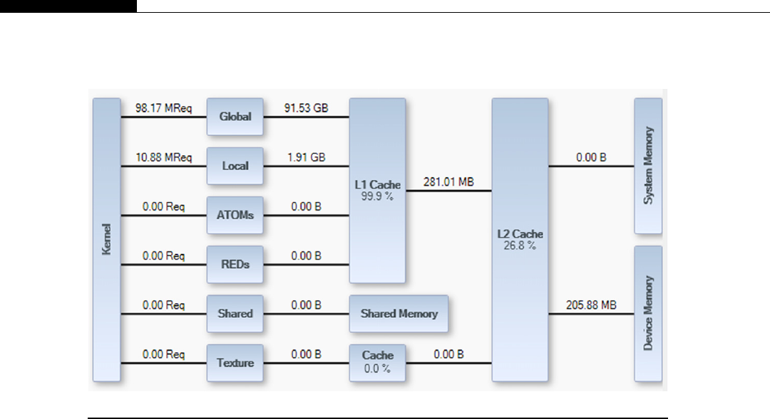
FIGURE 7.16
Initial memory bandwidth view.
the L2. Worse still, 205 MB of that is spilling into global memory. The kernel reads and writes to
global memory so we will have some global memory traffic, but how much should we expect? We have
4,195,328 blocks with each block being 16 bytes in size. Therefore, we have 67,125,248 or exactly 64
MB of data to read. Equally, we write out a decrypted block, so we have 64 MB of data to write out.
The statistics for global memory are shown for the device as a whole and shows we’re reading/writing
a total of 205MB. Therefore, we are generating 160% of the global memory traffic necessary, which in
turn is limiting the performance.
Currently, the L1 cache is operating at peak efficiency, but there is 16 K of shared memory we’re
not using at all. It does not have the coalescing requirements global memory has, so it would be a good
candidate for a small data region with a scattered memory pattern. However, unlike the L1 cache, the
shared memory has a per-block visibility, which would mean having to duplicate the data for every
resident block on the SM.
The constant memory cache is not shown in Figure 7.16, but it would also be large enough to hold
the Galios multiplication (gmul) and/or s_box tables. However, the constant cache has only one 32-bit
element bandwidth per clock and is designed for the same element being accessed by every thread.
Thus, the shared memory is a better candidate.
However, let’s first look at the two problem areas, s_box and the gmul tables. Both were declared as
32-bit unsigned types, to avoid huge numbers of instructions being added to shift and mask the 32-bit
words. Given the memory traffic we’re generating, this was probably not a good choice. Changing
these to a u8 type, we see the off-chip memory accesses drop from 205 MB to 183 MB and the
execution time drop from 96 ms to 63 ms. Clearly, this was causing a significant amount of overfetch
from the global memory and reducing it helps considerably.
256 CHAPTER 7 Using CUDA in Practice

With a reduced memory footprint, each gmul table is now 256 bytes in size, so the four tables fit easily
with 1 K. As we can place a maximum of eight blocks per SM, 8 K of shared memory is now sufficient
to accommodate the gmul tables.
Performing this shared memory optimization, however, has a problem. Indeed we move 18 GB of
memory bandwidth from the L1 cache to the shared memory, and the main memory bandwidth drops
by 7 MB. However, we have to move 1 K of data at the start of each block, as the shared memory is not
persistent or shared between blocks. The L1 cache, however, is shared between the blocks and is
currently doing a very good job of dealing with this scattered memory pattern, as the tables are entirely
resident within the cache. The net improvement of speed for our 8 K of shared memory usage is almost
zero, so this optimization was removed, leaving the tables in the L1 cache instead. Note this would
have brought considerable improvement on compute 1.x devices, compared to global memory
accesses, where there are no L1/L2 caches.
Looking back at Figure 7.16, did you notice something interesting? Did you notice we were using
1.91 GB of local storage? Local storage is the compiler spilling registers to the memory system. Prior to
compute 2.0 devices this would actually go to global memory space. From compute 2.0 onward it gets
contained within the L1 cache if possible, but can still cause significant unwanted global memory traffic.
When compiling, the -v option will display a summary of the register usage from the kernel.
Anytime you see the following message you have local memory being used:
nn bytes stack frame, nn bytes spill stores, nn bytes spill loads
The main issue here is the uint4 type being used. In combination with the high register usage
elsewhere this uint4 load from global memory is immediately being spilled to local memory. A 128-
bit uint4 load was deliberately chosen to minimize the number of load transactions to global memory.
By spilling it to local memory instead of holding in registers, the compiler is unnecessarily polluting
the caches and causing writes back to global memory.
We can explicitly move this data item into shared memory instead of local memory by simply
declaring it as an array of __shared__ and indexing it by threadIdx.x. As shared memory is a per-
block form of local memory, we can move the spilled register explicitly into the shared memory.
Moving this parameter generates the memory view shown in Figure 7.17.
Notice how simply moving this data item to shared memory drops the local memory usage from
1.91 GB to just 256 MB, and the traffic to global memory from 183 MB to 133 MB. Our shared
memory traffic is approximately double what it was before to the L1, which is largely due to the shared
memory bank conflicts. These are caused by placing a 128-bit (16-byte) value into a 32-bit (4-byte)
shared memory system. The compiler, however, still insists on creating a stack frame, much smaller
than before, but it’s still there. The overall execution time remains stubbornly stuck at 63 ms.
To see exactly what parameters are being spilled you have to look at the PTX code, the assembly
code, generated within a given kernel. Any PTX instructions such as st.local or ld.local are oper-
ating on local data. Local data is also declared with local as a prefix. It turns out the remaining local data
is actually the parameter data used between the __global__ caller and the __device__ function, that is,
__global__ void AES_decode_kernel_multi_block_single_key(uint4 * const src_block,
uint4 * const dest_blocks,
KEY_T * const expanded_key,
const u32 num_cipher_blocks)
{
const u32 tid ¼(blockIdx.x * blockDim.x) þthreadIdx.x;
An Example Using AES 257
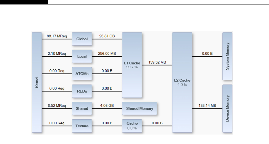
if (tid < num_cipher_blocks)
AES_decrypt_4x4_reg( &(src_block[tid]), &(dest_blocks[tid]), &(expanded_key[0]) );
}
__host__ __device__ void AES_decrypt_4x4_reg(
const uint4 * const src_cipher_block,
uint4 * const dest_cipher_block,
KEY_T * const cipher_key)
{
.
}
The fact that we have passed a number of parameters to the device function, which in turn allows it
to be called by a number of global functions and the host function, causes the compiler to insert a stack
frame. We rarely if ever want the compiler to call a stack and instead want it to inline the call to the
device function, thereby eliminating any need to use a stack. We can do this using the
__forceinline__ directive when declaring the function as shown here:
__host__ __device__ __forceinline__ void AES_decrypt_4x4_reg(
const uint4 * const src_cipher_block,
uint4 * const dest_cipher_block,
KEY_T * const cipher_key)
{
.
}
FIGURE 7.17
Memory transfers after using shared memory.
258 CHAPTER 7 Using CUDA in Practice
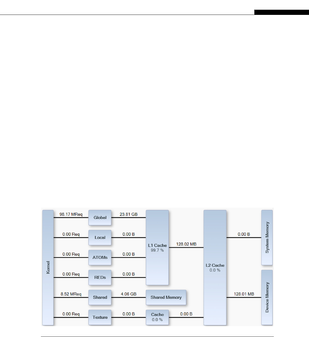
Recompiling the code no longer produces the stack frame message. Due to the function now being
a consolidated whole, the compiler can much better apply optimization techniques to it. The register usage
drops to just 33 instead of the forced 42 registers we were using before to accommodate eight blocks. We
can verify local memory is no longer being used by looking at the memory overview in Figure 7.18.
We can see in Figure 7.18 the local memory traffic now falls to zero. What little L2 cache usage
there was is eliminated. The global memory usage falls by another 5 MB to 128 MB, the magic figure
we were expecting the global memory bandwidth to be based on for the size of data we’re processing.
The execution time reduces marginally but still remains at 63 ms.
The kernel makes considerable use of the XOR operation, which is one of the instructions that is
not available at full rate within the device. Thus, by ensuring we keep the maximum number of blocks
in the SM, we ensure a good instruction mix and that everything doesn’t start backing up behind the
units performing the XOR operations.
At 96 threads per block with the previous high 42 register count we could schedule eight blocks
using 24 warps. This is around 50% of the available capacity of the SM in terms of the number of
warps it could run. However, we can see from looking at the Parallel Nsight “Issue Stalls” exper-
iment how much of the SM capacity we’re actually using. We stall just 0.01% of the time, which
means the SM is already almost at peak capacity. Increasing the occupancy figure by increasing the
list of possible warps, therefore, is unlikely to help significantly. Increasing the number of threads
from 96 to 128 allows us to increase the number of warps available for scheduling from 24 to 28.
This eliminates the remaining fractional stall issue and increases the fraction of the time that both
warp scheduler have warps available, gaining us a 1.5 ms reduction in the timing. This brings the
total execution time to 61.5 ms.
FIGURE 7.18
Memory usage after stack elimination.
An Example Using AES 259

Considerations for running on other GPUs
Having now developed a program for a single, modern GPU, how well does i work on other GPUs?
Often, especially if you are writing commercial applications, your program will need to work well on
each level of hardware in the marketplace. Although programs will run on most GPU generations, you
should be aware of what adaptations may be required to achieve good performance on that hardware.
We’ll look at this with the AES program we’ve developed here.
Out first target is the GTX460 card, a compute 2.1 card based on Fermi. Major differences are the
compute 2.1 architecture (7 SMs 48 CUDA cores vs. 14 SMs 32 CUDA cores), reduced L2 cache size
(512 K vs. 640 K), reduced L1 cache size per CUDA core (48 K L1 shared between 48 CUDA cores vs.
48K L1 shared between 32 CUDA cores), and the reduced memory bandwidth (115 GB/s vs. 134 GB/s).
Based purely on total CUDA core count (336 vs. 448), we’d expect around 75% of the perfor-
mance. However, adjusting for clock speed differences, this gives us a little less than 10% performance
difference between the two devices. Memory bandwidth is 15% less on the GTX460.
For the decrypt function the time actually measured is 100 ms compared with 61.5ms, which is
somewhat disappointing. Looking at the execution profile we see that the SMs on the GTX460 are able
to clock through more instructions, so the ratio of when the data arrives to the compute has changed.
We again see a tiny amount of stalling in the SMs. With 128 threads per block we manage to get seven
blocks scheduled (28 warps). If we could just reduce the register usage slightly we could execute
another block and make better use of the SM. We therefore apply the same technique we used in the
encode operation and move the inverse mix columns operation closer to the decode operation. Thus,
// Add Round Key
{
// Fetch cipher key from memory as a 128 bit read
*key_ptr ¼((*cipher_key)[round_num]);
// Extract the key values, XOR’ing them with
// the current values
EXTRACT_WORD_XOR2((key_ptr->x), a0, a1, a2, a3);
EXTRACT_WORD_XOR2((key_ptr->y), a4, a5, a6, a7);
EXTRACT_WORD_XOR2((key_ptr->z), a8, a9, a10, a11);
EXTRACT_WORD_XOR2((key_ptr->w), a12, a13, a14, a15);
}
// Invert Column Mix on every round except the first
if (round_num !¼10)
{
INV_MIX_COLUMN_PTR2(a0, a1, a2, a3,
gmul_14_ptr, gmul_09_ptr, gmul_13_ptr, gmul_11_ptr);
INV_MIX_COLUMN_PTR2(a4, a5, a6, a7,
gmul_14_ptr, gmul_09_ptr, gmul_13_ptr, gmul_11_ptr);
INV_MIX_COLUMN_PTR2(a8, a9, a10, a11,
gmul_14_ptr, gmul_09_ptr, gmul_13_ptr, gmul_11_ptr);
INV_MIX_COLUMN_PTR2(a12, a13, a14, a15,
260 CHAPTER 7 Using CUDA in Practice

gmul_14_ptr, gmul_09_ptr, gmul_13_ptr, gmul_11_ptr);
}
becomes
// Add Round Key
{
// Fetch cipher key from memory as a 128 bit read
*key_ptr ¼((*cipher_key)[round_num]);
// Extract the key values, XOR’ing them with
// the current values
EXTRACT_WORD_XOR2((key_ptr->x), a0, a1, a2, a3);
if (round_num !¼10)
INV_MIX_COLUMN_PTR2(a0, a1, a2, a3,
gmul_14_ptr, gmul_09_ptr, gmul_13_ptr, gmul_11_ptr);
EXTRACT_WORD_XOR2((key_ptr->y), a4, a5, a6, a7);
if (round_num !¼10)
INV_MIX_COLUMN_PTR2(a4, a5, a6, a7,
gmul_14_ptr, gmul_09_ptr, gmul_13_ptr, gmul_11_ptr);
EXTRACT_WORD_XOR2((key_ptr->z), a8, a9, a10, a11);
if (round_num !¼10)
INV_MIX_COLUMN_PTR2(a8, a9, a10, a11,
gmul_14_ptr, gmul_09_ptr, gmul_13_ptr, gmul_11_ptr);
EXTRACT_WORD_XOR2((key_ptr->w), a12, a13, a14, a15);
if (round_num !¼10)
INV_MIX_COLUMN_PTR2(a12, a13, a14, a15,
gmul_14_ptr, gmul_09_ptr, gmul_13_ptr, gmul_11_ptr);
}
This fusing of the operation allows the register usage to drop to the magic 31 registers, which in
turn allows us to schedule another block, giving a total of 32 warps per SM. This compensates for the
compute 2.1 devices having a higher ratio of compute to load/store units than compute 2.0 devices.
We see a small drop from 100 ms to 98 ms. However, our compute 2.0 device (the GTX470) was
already using its compute cores to full capacity. This change, which introduces a few more tests,
costs us 0.5 ms, bringing us back up to 62 ms on the compute 2.0 device. You may sometimes find
this, especially with compute 2.0/compute 2.1 devices where the balance of execution units within an
SM is different.
The second target is the GTX260, a compute 1.3 device. The major difference here is the complete
lack of L1 and L2 caches. SM architecture is different with 27 SMs versus 14 SMs, for a total of 216
CUDA cores versus 448 CUDA cores. Memory bandwidth is 112 GB/s versus 134 GB/s some 16%
less and on par with the GTX460.
The initial run was 650 ms for the decode function, over 10 times slower than the GTX470. Why is
this? One of the key reasons is the compute 1.x platform does not support a unified addressing mode.
Thus, an explicit declaration of intended memory usage is needed. In the case of the gmul tables, they
are generated on the device through a small compute kernel. As such, these tables exist in global
An Example Using AES 261

memory. On compute 2.x platforms global memory is cached, whereas on compute 1.x platforms you
have to explicitly make it cacheable. We can do this in a couple of ways.
First, we need to specify that the memory used for gmul is constant, which in turn means we can’t
write to it from the device. As we have a copy of the data on the host we can either copy it to the device
via the cudaMemcpyToSymbol call or simply declare it on the device as constant memory and initialize it
there statically. Thus, the code to calculate the gmul table was replaced with a simple expanded
definition of the table lookup. This then resides in the constant cache. Rerunning the code we see
a drop from 650 ms to 265 ms, a drop in execution time of nearly 60%. However, the GTX260 is still
a factor of 4.2slower than the GTX470 and 2.7slower than the GTX460.
Finally, an older GT9800 card has approximately half the number of CUDA cores of the GTX260
and half the memory bandwidth. As might be expected, we see the 265 ms approximately double
(1.8) to 478 ms.
The issue with both GTX260 and GT9800 is the organization of the data. Having the data match the
format used for AES-NI means the data for a single key value is laid out sequentially in memory. To
achieve much better performance we need to organize the memory such that each successive 32-bit
value from the key appears as a column in memory rather than a row. The typical sequential
arrangement that is ideal for the CPU is far from ideal for the GPU.
The actual output of our AES encryption/decryption is shown here:
Intel AES NI support enabled.
Logical CUDA device 0 mapped to physical device 0. Device ID: GeForce GTX 470 on PCI-E 5
Logical CUDA device 1 mapped to physical device 1. Device ID: GeForce GTX 470 on PCI-E 4
Logical CUDA device 2 mapped to physical device 2. Device ID: GeForce GTX 470 on PCI-E 3
Logical CUDA device 3 mapped to physical device 3. Device ID: GeForce GTX 470 on PCI-E 2
Logical CUDA device 4 mapped to physical device 4. Device ID: GeForce GTX 470 on PCI-E 1
test_single_block_single_key_encode_decode
AES NI Key : 2b, 7e, 15, 16, 28, ae, d2, a6, ab, f7, 15, 88, 09, cf, 4f, 3c,
AES NI Plaintext : 6b, c1, be, e2, 2e, 40, 9f, 96, e9, 3d, 7e, 11, 73, 93, 17, 2a,
AES NI Ciphertext : 3a, d7, 7b, b4, 0d, 7a, 36, 60, a8, 9e, ca, f3, 24, 66, ef, 97,
Expected Ciphertext : 3a, d7, 7b, b4, 0d, 7a, 36, 60, a8, 9e, ca, f3, 24, 66, ef, 97,
Single block single key AES-NI decode Passed
GPU Intial Key : 16157e2b, a6d2ae28, 8815f7ab, 3c4fcf09,
GPU Plaintext : e2bec16b, 969f402e, 117e3de9, 2a179373,
CPU Ciphertext : b47bd73a, 60367a0d, f3ca9ea8, 97ef6624,
GPU Ciphertext : b47bd73a, 60367a0d, f3ca9ea8, 97ef6624,
Expected Ciphertext : b47bd73a, 60367a0d, f3ca9ea8, 97ef6624,
Single block single key serial decode Passed
Single block single key parallel decode Passed
Single block single key parallel decode and AES-NI match Passed
Encrypting on GPU : 4194304 blocks (32768 Blocks x 128 Threads)
Encrypt Copy To Device : 28.469ms
Encrypt Expand Key Kernel : 0.025ms
Encrypt Encode Key Kernel : 45.581ms
Encrypt Copy From Device : 25.428ms
262 CHAPTER 7 Using CUDA in Practice

Encrypt Total Time : 99.503ms
Encrypting on CPU : 4194304 blocks
Encrypt Encode : 3900.000ms
Encrypting using AES-NI : 4194304 blocks
Encrypt Encode : 20.000ms
CPU and GPU encode result Passed.
CPU and GPU AES-NI encode result Passed.
Decrypting on GPU : 4194304 blocks (32768 Blocks x 128 Threads)
Decrypt Copy To Device : 27.531ms
Decrypt Expand Key Kernel : 0.028ms
Decrypt Decode Key Kernel : 62.027ms
Decrypt Copy From Device : 25.914ms
Decrypt Total Time : 115.500ms
Decrypting on CPU : 4194304 blocks
Decrypt Decode : 2760.000ms
Decrypting using AES-NI : 4194304 blocks
Decrypt Decode : 20.000ms
CPU and GPU decode result Passed.
CPU and AES-NI decode result Passed.
Notice that with encrypt we’ve managed to get within approximately 2of the AES-NI hardware,
and for decrypt approximately within 3. We’re using here a GTX470, which is hardware from the
time of the regular Sandybridge CPU, rather than the more modern Sandybridge-E device. The regular
Sandybridge device’s AES-NI performance is approximately half of the Sandybridge-E, which puts us
on similar timings. The Kepler-based GTX680 would be a representative device to pair with a San-
dybridge-E CPU. This would bring us in the order of a 2performance improvement, bringing the
GPU in line with the hardware-based AES-NI performance.
The issue of what GPUs to support is a tricky one. There are a lot of older GPUs in the consumer
market, so applications have to work well on these if you have a consumer application. Yet in large
installations, simply the power bill means it makes no sense at all to keep the old GPUs running if they
can be replaced with newer ones. The introduction of Kepler will hugely accelerate the retirement of
the older Tesla boards.
If you need to support older hardware, then the best approach is to develop on that hardware from
day one. You will then have a baseline application that will work reasonably well on the later-
generation cards. Many of the optimizations you’d need to do for these cards would show significantly
less benefit on the later-generation cards. However, almost all would show some benefit, it’s just
a question of what return you get for the time you invest.
Using multiple streams
An example of multistream and multistream/multi-GPU programming is provided in Chapter 8. We’ll
therefore not cover how to implement a streamed version of this algorithm. However, we’ll discuss some
of the issues you’d need to think about to implement one, with this algorithm or a problem of your own.
An Example Using AES 263

Multiple streams are useful in that they allow some overlap of kernel execution with PCI-E
transfers. Their usefulness, however, is seriously hampered by the fact that one PCI-E transfer engine
is only ever enabled on consumer cards. Only the Tesla series cards have both PCI-E transfer engines
enabled, allowing for simultaneous bidirectional transfers.
We typically want to transfer data to the card, process some data, and then transfer the data out of the
card. With a single PCI-E transfer engine enabled, we have just a single queue for all the memory transfers
in the hardware. Despite being in separate streams, memory transfer requests feed into a single queue on
Fermi and earlier hardware. Thus, the typical workflow pattern of transfer from host to device, invoke
kernel, and then transfer from device to host creates a stall in the workflow. The transfer out of the device
blocks the transfer into the device from the next stream. Thus, all streams actually run in series.
The next issue we need to think about when using multiple streams is the resource usage. You need
Nsets of host and device memory, where Nis the number of streams you wish to run. When you have
multiple GPUs, this makes a lot of sense, as each GPU contributes significantly to the overall result.
However, with a single-consumer GPU the gain is less easy to quantify. It works well only where either
the input or output of the GPU workload is small in comparison to one another and the total transfer
time is less than the kernel execution time.
In our application, we transfer in a set of blocks to be encoded in a single key set to use for the
encoding. We transfer out the encoded blocks. The transfer in and transfer out are all but identical in
size. The kernel execution time is around twice the size of the transfers. This means we have the
opportunity to hide the input transfer time and only suffer the output transfer time.
A single GPU can support up to 16 hardware streams (32 in Kepler), so it would be possible to
perform 16 inbound transfers, 16 kernels, and then 16 outbound transfers and still be within the bounds
of the memory on the device and the host. Transfers become more of an issue, as you will see in Chapter
9, where we introduce more than one GPU into the system. Due to contention for host resources, the
transfer time itself may become longer the more concurrent transfers are in flight over the PCI-E bus.
AES summary
There were a number of issues we saw with AES that are worth summarizing here.
• The ideal memory pattern for the CPU and GPU versions are different. Optimizing the memory
pattern for the GPU would have brought considerable benefits (typically at least 2on Fermi),
especially on the earlier GPUs where this is far more critical.
• For compute 1.x devices read-only memory needs to be explicitly declared as constant memory,
rather than auto-designated by the compiler.
• It may be necessary to reorder or transform the kernel to allow the compiler to more easily see
optimization opportunities.
• Efficient register usage and count were critical to achieving good performance.
• You can share read-only data between blocks using the L1 cache, whereas holding the same read-
only data shared memory necessitates Ncopies where Nis the number of resident blocks.
• Complex and thread-divergent algorithms, for example, the gmul function when decoding, can be
replaced by nonthread-divergent memory lookups in the cache or shared memory. The cache
was added specifically for such data-driven scattered memory patterns.
• Check the allocation of variables to registers and eliminate stack or local memory usage where
possible.
• Always check correctness early in the solution, preferably with code developed independently.
264 CHAPTER 7 Using CUDA in Practice

• Always look at the actual timing of the program. Your mental model of how things work will not
always be correct and often you will overlook something. Always look to the data for what effect
each change has.
CONCLUSION
We’ve looked at a couple of applications of GPU technology, deliberately chosen for not being
a simple matrix multiply shown in so many other examples of CUDA programming. We looked at
using GPUs to filter data, which is useful from the perspective of searching data for interesting facts
and also from a pure signal processing perspective. We’ve also looked how to implement AES,
a standard encryption algorithm on GPUs. Even if you never have to implement this in CUDA, you
should now understand and feel happy about implementing or using such algorithms.
You should also have picked up on some of the tradeoffs and design points when targeting multiple
compute levels and how design decisions early on in project development can affect the outcome later.
Thinking about the usage of registers, shared memory, cache, and access patterns to global memory are all
key aspects of a design that should be understood and worked out before you write a single line of code.
One of the biggest issues programmers have today is growing up in a world where they are isolated
from the hardware on which they are programming. To achieve great performance and not just average
performance, it pays to understand, and understand thoroughly, the environment in which you are
developing. Concepts such as various levels of memory hierarchy don’t really exist in traditional
programming languages. The C language was invented back in the early 1970s and only in the C11 (as in
2011) standard do we finally see thread and local thread storage start to appear. CUDA, and its native
language C, follows the principle of trusting the programmer. It exposes aspects of the hardware to you,
and you should therefore consider it your responsibility to understand those features and use them well.
With a few examples now covered, we’ll move on to using multiple GPUs and optimizing appli-
cations, an area where we can extract massive speedups within a node simply by plugging more cards
into the PCI-E bus and adapting our applications to be multi-GPU aware. The Kepler Tesla K10 product
is the first Tesla dual-GPU solution, perhaps one of many we may see in the coming years. Multi-GPU
programming, after CUDA 4.0, is actually not hard, as you’ll see in the subsequent chapters.
Questions
1. What was the main reason why the AES application ran significantly slower on the GTX260 and
GT9800 cards compared with the GTX460 and GTX470 cards? What would you do to address
this?
2. In the AES application, why did changing the s_box and gmul tables from u32 to u8 improve
performance?
3. What is thread level parallelism? Does it help, and if so why?
4. What problems are associated with using atomic operations?
Answers
1. The GTX260 and GT9800 cards are compute 1.3 and compute 1.1 cards, respectively. As such, they
have no level one (L1) or level two (L2) caches as found on the compute 2.x cards. In the memory
Conclusion 265

figures shown we were using the L1 cache with a 99% hit rate. Going from L1 to global memory
means we move from terabytes of bandwidth to just the low hundreds of megabytes of bandwidth.
The memory coalescing also radically changes. The compute 2.x hardware fetches memory in 128-
byte cache lines. If the thread fetches a single 128-byte value, uint4 for example, the hardware
can service this. On compute 1.x hardware coalescing requirements are much stricter.
The uint4 type as currently compiled is hurting the algorithm. On compute 2.x hardware a four-word
vector load from memory is used followed by a four-word vector to shared memory. On the
compute 1.x hardware, the CUDA 4.1 compiler generates code to load each 32-bit word
separately and thus generates four more times the traffic in each direction than is necessary. The
encrypted cipher data needs to be placed into a suitable form for coalescing.
The constant cache is helpful. However, removing the uint4 type from the shared memory, replacing it
with register-held u32 values, and then using the shared memory for the gmul and s_box tables
would be more beneficial. You should also consider that on older devices, the texture cache can
be a worthwhile additional resource worth the effort of exploiting.
2. The s_box and gmul tables are accessed with a data-dependent pattern. We have a total of four
tables, each of which is 256 entries in size. Using a u8 type means we use 5 K of memory,
which fits into both the L1 cache and the constant cache. Using u32 values removed a number
of cvt (convert type) instructions, but shifts four times the data from the L1 or constant cache.
The extra compute overhead is easily worth the cost of not moving so much data. As a u32
type, the caches need to store 20 K of data, easily exceeding the normal 16 K L1 cache
allocation and the 8 K constant cache working set.
3. Thread level parallelism exploits the fact that most hardware is pipelined and thus able to accept
nondependent instructions on successive clocks without blocking. A value of four independent
items per thread is typically a good value to exploit to achieve thread level parallelism,
something we look at in Chapter 9.
4. There are two main issues to consider. First, atomic operations, if oversubscribed, cause
serialization. Thus, a warp of 32 values writing to the same memory address, be it shared or
global memory, will serialize. Atomics, at least on Fermi, are warp-wide operations. Thus,
having each thread in a warp perform an atomic operation to independent addressable locations
will result in 32 atomic operations without serialization.
The second problem is ordering of atomic writes. If all values in a warp write to one address, the order
of the operation is not defined. You can obviously observe the order and it’s likely that this will
remain consistent for a given device. Another device may, however, work differently. Thus, in
using such knowledge, you’d be building a failure point into your application.
References
Wikipedia, Rijndael Mix Columns. Available at: http://en.wikipedia.org/wiki/Rijndael_mix_columns, accessed
Jan. 31, 2012
Federal Information Processing Standards Publication 197, Advanced Encryption Standard (AES). Available at:
http://csrc.nist.gov/publications/fips/fips197/fips-197.pdf, accessed Feb. 5, 2012.
Toms Hardware, AES-NI Benchmark Results: Bitlocker, Everest, and WinZip 14. Available at: http://www.
tomshardware.co.uk/clarkdale-aes-ni-encryption, review-31801–7.html, accessed Apr. 26, 2012
266 CHAPTER 7 Using CUDA in Practice

Multi-CPU and Multi-GPU
Solutions 8
INTRODUCTION
In modern computing systems it’s common to have multiple devices, both CPUs and GPUs. In terms of
CPUs we’ll talk about sockets and cores. A socket is a physical socket on the motherboard into which
a CPU is placed. A CPU may contain one or more cores. Each core is effectively a separate entity.
A number of CPU and GPU sockets are located on a single node or computer system.
Knowing the physical arrangement of cores, sockets, and nodes allows for far more effective
scheduling or distribution of tasks.
LOCALITY
The principle of locality is seen quite well in GPUs and CPUs. Memory closer to the device (shared
memory on the GPU, cache on the CPU) is quicker to access. Communication within asocket
(i.e., between cores) is much quicker than communication to another core in a different socket.
Communication to a core on another node is at least an order of magnitude slower than within
the node.
Clearly, having software that is aware of this can make a huge difference to the overall performance
of any system. Such socket-aware software can split data along the lines of the hardware layout,
ensuring one core is working on a consistent dataset and cores that need to cooperate are within the
same socket or node.
MULTI-CPU SYSTEMS
The most common multi-CPU system people will encounter is the single-socket, multicore desktop.
Almost any PC you buy today will have a multicore CPU. Even in laptops and media PCs, you will find
multicore CPUs. If we look at Steam’s regular hardware (consumer/gaming) survey, it reveals that as
of mid 2012 approximately 50% of users had dual-core systems and an additional 40% had quad-core
or higher systems.
The second type of multi-CPU systems you encounter is in workstations and low-end servers.
These are often dual-socket machines, typically powered by multicore Xeon or Opteron CPUs.
CHAPTER
CUDA Programming. http://dx.doi.org/10.1016/B978-0-12-415933-4.00008-9
Copyright Ó2013 Elsevier Inc. All rights reserved.
267

The final type of multi-CPU systems you come across are data center–based servers where you can
have typically 4, 8, or 16 sockets, each with a multicore CPU. Such hardware is often used to create
a virtualized set of machines, allowing companies to centrally support large numbers of virtual PCs
from one large server.
One of the major problems you have with any multiprocessor system is memory coherency. Both
CPUs and GPUs allocate memory to individual devices. In the case of GPUs, this is the global memory
on each GPU card. In the CPU case, this is the system memory on the motherboard.
When you have independent programs using just a single core, you can scale quite well with this
approach, as each program can be localized to a given core. The program then accesses its own data
and makes good use of the CPU core’s cache. However, as soon as you have two cores cooperating
with one another, you have a problem.
To speed up access to memory locations, CPUs make extensive use of caches. When the value of
a parameter is updated (e.g., xþþ), is xactually written to memory? Suppose two cores need to update
x, because one core is assigned a debit processing task and the other a credit processing task. Both
cores must have a consistent view of the memory location holding the parameter x.
This is the issue of cache coherency and it is what limits the maximum number of cores that can
practically cooperate on a single node. What happens in the hardware is that when core 1 writes to x,it
informs all other cores that the value of xhas now changed and then does a slow write out to the main
memory instead of a quick write back to cache access.
In a simple coherency model, the other cores then mark the entry for xin their caches as invalid.
The next access to xthen causes xto be reloaded from the slow main memory. As subsequent cores
write to x, the process is repeated and the next core to access parameter xmust again fetch it from
memory and write it back again. In effect, the parameter xbecomes noncached, which on a CPU means
a huge performance hit.
In more complex coherency models, instead of invalidating xthe invalidation request is replaced
with an update request. Thus, every write has to be distributed to Ncaches. As the number of Ngrows,
the time to synchronize the caches becomes impractical. This often limits the practical number of
nodes you can place into a symmetrical multiprocessor (SMP) system.
Now remember that caches are supposed to run at high speed. Within a single socket, this is not
hard. However, as soon as you have to go outside of the socket, it’s difficult to maintain the high clock
rates and thus everything starts to slow down. The more sockets you have, the more difficult it becomes
to keep everything synchronized.
The next major problem we have is memory access time. To make programming such machines
easier, often the memory is logically arranged as a huge linear address space. However, as soon as
a core from socket 1 tries to access a memory address from socket 2, it has to be serviced by socket 2,
as only socket 2 can physically address that memory. This is called nonuniform memory access
(NUMA). Although conceptually it makes a programmer’s life easier, in practice you need to think
about memory locality or you write programs that perform very slowly.
MULTI-GPU SYSTEMS
Just like the CPU world, a lot of systems now have multiple GPUs inside them. From the enthusiast
who has triple- or quad-SLI systems, or has dual cards like the 9800GX2, GTX295, GTX590 and
268 CHAPTER 8 Multi-CPU and Multi-GPU Solutions

GTX690, down to the guy who upgraded his low-powered ION desktop with a dedicated GPU card,
there are many people with multi-GPU systems. As a programmer you should always endeavor to
produce the best experience possible on whatever hardware is available.
If the user has a dual-GPU system and you use only one GPU, you are being as lazy as those CPU
programmers who can’t be bothered to learn how to use more than one core. There are plenty of
programs that monitor GPU load. The tech-savvy users or reviewers will slate your product for not
going that extra mile.
If you are writing scientific applications or working with known hardware, rather than a consumer
application, you should also be investigating multi-GPU solutions. Almost all PCs support at least two
PCI-E slots, allowing at least two GPU cards to be put into almost any PC. CUDA does not use or require
SLI (Scalable Link Interface), so not having an SLI-certified motherboard is no obstacle to using multiple
GPUs in CUDA applications. Adding one additional GPU card, you will typically see a doubling in the
level of performance, halving the current execution time. Rarely do you get such a speedup so easily.
ALGORITHMS ON MULTIPLE GPUS
The CUDA environment does not support, natively, a cooperative multi-GPU model. The model is
based more on a single-core, single-GPU relationship. This works really well for tasks that are
independent of one another, but is rather a pain if you wish to write a task that needs to have the GPUs
cooperate in some way.
For example, an application like BOINC works well under this model. BOINC is an application
which allows users to donate spare computing power to solving the world’s problems. On a multi-GPU
system it spawns Ntasks, where Nis equal to the number of GPUs in the system. Each task gets
a separate data packet or job from a central server. As GPUs finish tasks, it simply requests additional
tasks from the central server (task dispatcher).
Now if you look at a different example, where we need cooperation, the story is different. At the
simplest level, encoding video is typically done by applying a JPEG-type algorithm to each individual
frame and then looking for the motion vectors between frames. Thus, we have an operation within
a frame that can be distributed to NGPUs, but then an operation that requires the GPUs to share data
and has a dependency on the first task (JPEG compression) completing.
There are a couple of ways of dealing with this. The easiest is to use two passes, one kernel that
simply does the JPEG compression on Nindependent frames, and a second kernel that does the motion
vector analysis–based compression. We can do this because motion vector–based compression uses
a finite window of frames, so frame 1 does not affect frame 1000. Thus, we can split the work into N
independent jobs. The downside of this approach, as with any multipass algorithm, is we read the data
more than once. As the dataset is typically quite large and will involve slow mass storage devices, this
is generally a bad approach.
A single-pass method is more efficient, but more difficult to program. You can transform the
problem, if you consider the set of frames on which you do motion vector compression to be the dataset.
Each set of frames is independent and can be dispatched to a separate GPU card. The GPU kernel first
does JPEG compression on all frames within the set it was provided. It then calculates, over those same
frames, the motion aspects. By using this approach, you have managed to keep the data on the GPU card.
This eliminates the major bottleneck with this type of problemdthat of moving data around the system.
Algorithms on Multiple GPUS 269

In this instance we managed to restructure the algorithm so it could be broken down into inde-
pendent chunks of data. This may not always be possible and many types of problems require at least
a small amount of data from the other GPUs. As soon as you require another GPU’s data, you have to
explicitly share that data and explicitly sequence the access to that data between the GPUs. Prior to the
4.0 SDK, there was no support for this in the CUDA environment. If it is at all possible to break down
the problem into independent chunks, take this approach.
There are a couple of alternatives to this approach. You can use the GPU peer-to-peer commu-
nication model provided as of the 4.0 SDK version, or you can use CPU-level primitives to cooperate
at the CPU level. The former does not work on all OSs, most noticeably Windows 7 with consumer
hardware. The CPU solution requires OS-specific communication primitives, unless a common third-
party solution is used.
WHICH GPU?
When there is more than one GPU on a system, are they the same or different? How does the
programmer know? Does it matter?
Well it often matters, but it depends largely on the application. Embedded in the CUDA binary
there are usually several binary images, one of each generation of GPUs. At a minimum a binary for
the lowest compute–capability GPU should be present. However, additional binaries, optimized for
higher-level compute devices, may also be present. The CUDA runtime will automatically select the
highest level of binary based on the compute device when executing a kernel.
Certain functions, such as atomics, are only available on certain compute-level devices; running
such code on a lower-level compute device results in the kernel failing to run. Therefore, for certain
programs at least, we have to care which GPU is used. Other programs run much better or worse on
newer hardware, due to the effects of caching and block size selection by the application. Others may
have been written to use large numbers of registers on the G80/G200 series devices, something that
was reduced on the Fermi architecture and then restored with Kepler.
Thus, some user or administration-level knowledge is required about which is the best platform
on which to run a given kernel, or the programmer has to adapt the program so it runs well on all
platforms. This can be done by either avoiding compute device–specific routines, which can often
make things much harder to program, or by providing some alternative kernels that avoid the
compute-level issue. However, the latter is often driven by commercial concerns. Programmer time
costs money and you have to assess if the market segment you are targeting contains enough users
with older hardware to justify the extra development and testing effort. In terms of the consumer
market, as of August 2012, around one quarter of the market is still using pre-Fermi hardware. See
Figure 8.1.
How does the programmer select a GPU device? We’ve seen a number of examples so far where we
have used four devices and compared the results of each device. You should have seen from the various
code examples that you need to set a device via a call to
cudaError_t cudaSetDevice(int device_num);
or the simplified version often used in this text,
CUDA_CALL(cudaSetDevice(0));
270 CHAPTER 8 Multi-CPU and Multi-GPU Solutions
The parameter device_num is a number from zero (the default device) to the number of devices in
the system. To query the number of devices, simply use the following call:
cudaError_t cudaGetDeviceCount(int * device_count);
CUDA_CALL(cudaGetDeviceCount(&num_devices));
Notice in both calls we make use of the CUDA_CALL macro we developed in Chapter 4. This simply
takes the return value, checks it for an error, prints a suitable error message, and exits if there is
a failure. See Chapter 4 on setting up CUDA for more information on exactly how this works.
Now that we know how many devices there are and how to select one, the question is which one to
select. For this we need to know the details of a particular device. We can query this with the following
call:
cudaError_t cudaGetDeviceProperties(struct cudaDeviceProp * properties, int device);
struct cudaDeviceProp device_0_prop;
CUDA_CALL(cudaGetDeviceProperties(&device_0_prop, 0));
The structure properties is made up of the structure members shown in Table 8.1.
Not all of these may be of interest, but certain ones will. The most important of these are the major
and minor compute-level revisions. Note also that warpSize is present here, the implication being that
warp size will change on different devices, although in practice it has remained at 32 for all devices
released to date.
When selecting a device, it’s not necessary to check each item to ensure it’s what the particular
user program needs. You can simply populate the same structure with the properties you would like
(0 equates to don’t care) and have the CUDA runtime select a suitable device for you. For example:
struct cudaDeviceProp device_prop;
int chosen_device;
memset(device_prop, 0, sizeof(cudaDeviceProp));
device_prop.major ¼2;
device_prop.minor ¼0;
Compute 1.0
4% Compue 1.1+1.2
9%
Compute 1.3
12%
Compute 2.x
69%
Compute 3.x
6%
FIGURE 8.1
Consumer distribution of compute levels August 2012.
Which GPU? 271

Table 8.1 Device Properties Explained
Structure Member Meaning
Tesla
Only Unit
char name[256]; Name of the device such as GTX460. String
size_t totalGlobalMem; The maximum amount of global
memory present on the device.
Bytes
size_t sharedMemPerBlock; The maximum amount of supported
shared memory per block.
Bytes
int regsPerBlock; The maximum number of allowed
registers per block.
Registers
int warpSize; The warp size of the device. Threads
size_t memPitch; Maximum supported pitch for memcpy
operations using pitched allocated
memory.
Bytes
int maxThreadsPerBlock; The maximum number of threads
supported per block.
Threads
int maxThreadsDim[3]; The maximum number of threads
supported per dimension.
Threads
int maxGridSize[3]; The maximum number of blocks
supported per grid dimension.
Blocks
int clockRate; The clock rate of the GPU in KHz. KHz
size_t totalConstMem; The maximum amount of constant
memory available on the device.
Bytes
int major; The major compute revision. Int
int minor; The minor compute revision. Int
size_t textureAlignment; The minimum alignment required for
textures.
Bytes
int deviceOverlap; Set to 1 if the device supports
overlapping memory transfers and
kernels (deprecated).
Flag
int multiProcessorCount; The number of SMs present on the
device.
Int
int kernelExecTimeoutEnabled; Set to 1 if the kernel timeout feature is
enabled (enabled by default).
Flag
int integrated; Set to 1 if the device is an integrated
device, that is, a device that shares the
CPU ram directly.
Flag
int canMapHostMemory; Set to 1 if the device can map CPU host
memory into the GPU virtual memory
space.
Flag
int computeMode; The current compute mode
(cudaComputeModeDefault,
cudaComputeModeExclusive,
cudaComputeModeProhibited).
Allows sharing of device, exclusive
access to a device, or specifies if device
access is prohibited.
x Enum
272 CHAPTER 8 Multi-CPU and Multi-GPU Solutions

if (cudaChooseDevice(&chosen_device, device_prop) !¼cudaErrorInvalidValue)
{
CUDA_CALL(cudaSetDevice(chosen_device));
}
In this code we create a device properties’ structure, clear it with a memset call, and then request
a compute 2.0 device (any Fermi device). We then ask CUDA to set the context to the specified
device.
Table 8.1 Device Properties Explained (continued)
Structure Member Meaning
Tesla
Only Unit
int maxTexture1D; The maximum 1D texture size
supported.
Bytes
int maxTexture2D[2]; The maximum 2D texture size
supported.
Bytes
int maxTexture3D[3]; The maximum 3D texture size
supported.
Bytes
int maxTexture1DLayered[2]; The maximum 1D layered texture
dimensions.
Bytes
int maxTexture2DLayered[3]; The maximum 2D layered texture
dimensions.
Bytes
size_t surfaceAlignment; Alignment requirements for surfaces. Bytes
int concurrentKernels; Set to 1 if concurrent kernels from
the same context are supported.
Flag
int ECCEnabled; Set to 1 if ECC memory is enabled. x Flag
int pciBusID; PCI bus ID of the device. Int
int pciDeviceID; PCI device ID of the device. Int
int pciDomainID; PCI domain ID of the device. Int
int tccDriver; Set to 1 if TCC driver mode is enabled. x Flag
int asyncEngineCount; Number of asynchronous copy engines
present on the device.
x*Int
int unifiedAddressing; Set to 1 if the device and host share
a unified address space.
x** Flag
int memoryClockRate; The maximum supported memory clock
rate in KHz.
Khz
int memoryBusWidth; Memory bus width in bits. Bits
int l2CacheSize; The size of the level two (L2) cache
(0 ¼not present).
Bytes
int
maxThreadsPerMultiProcessor;
The maximum number of threads
supported on a single SM.
Threads
*
Dual-copy engines are supported on Telsa devices only. Consumer-level devices are restricted to support only a single-copy
engine.
**
Unified address is supported only on 64-bit platforms. On Windows it requires the TCC driver, which in turn requires a Tesla
card. On UNIX platforms this is not the case.
Which GPU? 273
SINGLE-NODE SYSTEMS
In versions of CUDA prior to the 4.0 SDK single-node systems were the only multi-GPU model
available as shown in Figure 8.2. A single CPU-based task would be associated with a single-GPU
context. A task in this context would be either a process or a thread. Behind the scenes the CUDA
runtime would bind the CPU process/thread ID to the GPU context. Thus, all subsequent CUDA calls
(e.g., cudaMalloc) would allocate memory on the device that was bound to this context.
This approach had a number of drawbacks but some advantages. From a programming perspective,
the process/thread model on the host side is fragmented by the OS type. A process is a program that
runs as an independent schedulable unit on a CPU and has its own data space. To conserve memory,
multiple instances of the same process usually share the code space and the OS maintains a set of
registers (or context) for each process.
A thread, by contrast, is a much more lightweight element of the CPU scheduling. It shares both the
code and data space used by its parent process. However, as with a process, each thread requires the OS
to maintain a state (instruction pointer, stack pointer, registers, etc.).
Threads may communicate and cooperate with other threads within the same process. Processes
may communicate and cooperate with other processes through interprocess communication. Such
communication between processes may be within a CPU core, within a CPU socket, within a CPU
node, within a rack, within a computer system, or even between computer systems.
The actual API changes depending on the level of communication and OS. The API used on
Windows is entirely different from that used on Linux. POSIX threads, or pthreads, is a commonly
used threading model on Linux. This is not natively supported in Windows, although it is available as
GPU
Client 0
GPU
Client 1
GPU
Client 2
CPU
Server 1
CPU
Server 0
CPU
Server 2
FIGURE 8.2
Multiple clients, multiple servers.
274 CHAPTER 8 Multi-CPU and Multi-GPU Solutions

a port. The Cþþ Boost library supports a common threading package, thread, which provides support
for both Linux and Windows.
CPU threads are similar to the GPU threads we’ve used when executing kernels, except that they
don’t execute in groups or warps as the GPU ones do. GPU threads communicate via shared memory
and explicitly synchronize to ensure every thread has read/written to that memory. The shared memory
is local to an SM, which means threads can only communicate with other threads within the same SM
(in theory). Because a block is the scheduling unit to an SM, thread communication is actually limited
to a per-block basis.
Processes on the CPU can be thought of in the same way as blocks on the GPU. A process is
scheduled to run on one of NCPU cores. A block is scheduled to run one of NSMs on the GPU. In this
sense the SMs act like CPU cores.
CPU processes can communicate to one another via host memory on the same socket. However,
due to processes using a separate memory space, this can only happen with the assistance of
a third-party interprocess communications library, as neither process can physically see the address
space of the other. The same is not true, however, for GPU blocks, as they access a common address
space on the GPU global memory.
Systems with multiple CPUs using shared host memory can also communicate with one another
via this shared host memory, but again with the help of a third-party interprocess communication
library. Multiple GPUs can communicate to one another on the same host, using host memory, or, as
of CUDA SDK 4.0, directly via the PCI-E bus peer-to-peer communication model. Note, however,
peer-to-peer is only supported for 64-bit OSs using Fermi or later cards. For Windows this is only
supported with the TCC (Tesla compute cluster) driver, which effectively means it’s only supported
for Tesla cards.
However, as soon as you no longer have the possibility to use shared host memory between CPU
cores/sockets, you are forced to make use of some other network transport mechanism (TCP/IP,
InfiniBand, etc.). The standard for this type of communication has become MPI (Message Passing
Interface). There are also alternatives such as ZeroMQ (0MQ) that are less well known but equally
effective.
Note that both of these make use of shared host memory transfers when communicating
internally within a single host node. However, models that support threading (e.g., pthreads,
ZeroMQ) perform interthread-based communication much quicker than those based on the process
model such as MPI.
We’ll focus here on the case where we have a single CPU socket, running a single-threaded CPU
program with multiple GPUs present. This is the most common use case with consumer-level hardware
and therefore the most useful case to cover. See Chapter 10 for more advanced topics such as peer to
peer transfers between multiple GPUs.
STREAMS
Streams are virtual work queues on the GPU. They are used for asynchronous operation, that is, when
you would like the GPU to operate separately from the CPU. Certain operations implicitly cause
a synchronization point, for example, the default memory copies to and from the host or device. For the
most part this is what the programmer wants, in that after copying the results back from the GPU they
Streams 275

will instantly do something with those results on the CPU. If the results were to partially appear, then
the application would work when debugged or single stepped, but fail when run at full speedda
debugging nightmare.
By creating a stream you can push work and events into the stream which will then execute the
work in the order in which it is pushed into the stream. Streams and events are associated with the GPU
context in which they were created. Thus, to show how to create a couple of streams and events on
multiple GPUs we will setup a small program to demonstrate this.
void fill_array(u32 * data, const u32 num_elements)
{
for (u32 i¼0; i< num_elements; iþþ)
{
data[i] ¼i;
}
}
void check_array(char * device_prefix,
u32 * data,
const u32 num_elements)
{
bool error_found ¼false;
for (u32 i¼0; i< num_elements; iþþ)
{
if (data[i] !¼(i*2))
{
printf("%sError: %u %u",
device_prefix,
i,
data[i]);
error_found ¼true;
}
}
if (error_found ¼¼ false)
printf("%sArray check passed", device_prefix);
}
In the first function we simply fill the array with a value from 0 to num_elements. The second
function simply checks that the GPU result is what we’d expect. Obviously both functions would be
replaced with real code to do something a little more useful, in practice.
__global__ void gpu_test_kernel(u32 * data)
{
const int tid ¼(blockIdx.x * blockDim.x)
þthreadIdx.x;
data[tid] *¼2;
}
276 CHAPTER 8 Multi-CPU and Multi-GPU Solutions

Next we declare the kernel function itself. This does little more than multiply every data element
by 2. Nothing very useful, but just something we can easily check to ensure every element of the
array has been correctly processed.
// Define maximum number of supported devices
#define MAX_NUM_DEVICES (4)
// Define the number of elements to use in the array
#define NUM_ELEM (1024*1024*8)
// Define one stream per GPU
cudaStream_t stream[MAX_NUM_DEVICES];
// Define a string to prefix output messages with so
// we know which GPU generated it
char device_prefix[MAX_NUM_DEVICES][300];
// Define one working array per device, on the device
u32 * gpu_data[MAX_NUM_DEVICES];
// Define CPU source and destination arrays, one per GPU
u32 * cpu_src_data[MAX_NUM_DEVICES];
u32 * cpu_dest_data[MAX_NUM_DEVICES];
Finally, we come to the main part of the program. This function declares a number of values, each
of which is indexed by device_num. This allows us to use the same code for every device and just
increment the index.
// Host program to be called from main
__host__ void gpu_kernel(void)
{
// No dynamic allocation of shared memory required
const int shared_memory_usage ¼0;
// Define the size in bytes of a single GPU’s worth
// of data
const size_t single_gpu_chunk_size ¼(sizeof(u32) *
NUM_ELEM);
// Define the number of threads and blocks to launch
const int num_threads ¼256;
const int num_blocks ¼((NUM_ELEM þ(num_threads-1))
/ num_threads);
// Identify how many devices and clip to the maximum
// defined
int num_devices;
CUDA_CALL(cudaGetDeviceCount(&num_devices));
Streams 277

if (num_devices > MAX_NUM_DEVICES)
num_devices ¼MAX_NUM_DEVICES;
The first task is to identify how many GPUs we have available with the cudaGetDeviceCount call.
To ensure we don’t have more than we planned, this number is clipped to the maximum supported,
a simple #define. Allowing for four dual GPU cards, eight would be better maximum value than the
four selected here.
// Run one memcpy and kernel on each device
for (int device_num¼0;
device_num < num_devices;
device_numþþ)
{
// Select the correct device
CUDA_CALL(cudaSetDevice(device_num));
The first section of each loop then sets the current device context to the device_num parameter to
ensure all subsequent calls then work with that device.
// Generate a prefix for all screen messages
struct cudaDeviceProp device_prop;
CUDA_CALL(cudaGetDeviceProperties(&device_prop,
device_num));
sprintf(&device_prefix[device_num][0], "\nID:%d %s:", device_num, device_prop.name);
// Create a new stream on that device
CUDA_CALL(cudaStreamCreate(&stream[device_num]));
// Allocate memory on the GPU
CUDA_CALL(cudaMalloc((void**)&gpu_data[device_num],
single_gpu_chunk_size));
// Allocate page locked memory on the CPU
CUDA_CALL(cudaMallocHost((void **)
&cpu_src_data[device_num],
single_gpu_chunk_size));
CUDA_CALL(cudaMallocHost((void **)
&cpu_dest_data[device_num],
single_gpu_chunk_size));
// Fill it with a known pattern
fill_array(cpu_src_data[device_num], NUM_ELEM);
// Copy a chunk of data from the CPU to the GPU
// asynchronous
278 CHAPTER 8 Multi-CPU and Multi-GPU Solutions

CUDA_CALL(cudaMemcpyAsync(gpu_data[device_num],
cpu_src_data[device_num],
single_gpu_chunk_size,
cudaMemcpyHostToDevice,
stream[device_num]));
// Invoke the GPU kernel using the newly created
// stream - asynchronous invokation
gpu_test_kernel<<<num_blocks,
num_threads,
shared_memory_usage,
stream[device_num]>>>(gpu_data[device_num]);
cuda_error_check(device_prefix[device_num],
"Failed to invoke gpu_test_kernel");
// Now push memory copies to the host into
// the streams
// Copy a chunk of data from the GPU to the CPU
// asynchronous
CUDA_CALL(cudaMemcpyAsync(cpu_dest_data[device_num],
gpu_data[device_num],
single_gpu_chunk_size,
cudaMemcpyDeviceToHost,
stream[device_num]));
}
We create a stream, or work queue, for each GPU present in the system. Into this stream we place
a copy from the host (CPU) memory to the GPU global memory followed by a kernel call and then
a copy back to the CPU. They will execute in this order, so the kernel will not start executing until the
preceding memory copy has completed.
Note the usage of page-locked memory on the host, allocated using cudaMallocHost instead of the
regular C malloc function. Page-locked memory is memory that cannot be swapped out to disk. As the
memory copy operations are being performed via a direct memory access (DMA) over the PCI-E bus,
the memory at the CPU end must always physically be in memory. Memory allocated with malloc can
be swapped out to disk, which would cause a failure if a DMA was attempted to or from it. As we used
the cudaMallocHost function to allocate the memory, you must also use the cudaFreeHost function to
deallocate the memory.
// Process the data as it comes back from the GPUs
// Overlaps CPU execution with GPU execution
for (int device_num¼0;
device_num < num_devices;
device_numþþ)
{
// Select the correct device
CUDA_CALL(cudaSetDevice(device_num));
Streams 279

// Wait for all commands in the stream to complete
CUDA_CALL(cudaStreamSynchronize(stream[device_num]));
Finally, once the kernel streams have been filled, it’s time to wait for the GPU kernels to complete.
At this point the GPU may not have even started, as all we’ve done is to push commands into a stream
or command queue.
// GPU data and stream are now used, so
// clear them up
CUDA_CALL(cudaStreamDestroy(stream[device_num]));
CUDA_CALL(cudaFree(gpu_data[device_num]));
// Data has now arrived in
// cpu_dest_data[device_num]
check_array( device_prefix[device_num],
cpu_dest_data[device_num],
NUM_ELEM);
// Clean up CPU allocations
CUDA_CALL(cudaFreeHost(cpu_src_data[device_num]));
CUDA_CALL(cudaFreeHost(cpu_dest_data[device_num]));
// Release the device context
CUDA_CALL(cudaDeviceReset());
}
}
The CPU then waits for each device in turn to complete, and when this is done, it checks the contents
and then frees the GPU and CPU resources associated with each stream. However, what happens if the
GPU devices in the system are different and they take differing amounts of time to execute the kernel?
First, we need to add some timing code to see how long each kernel takes in practice. To do this we have
to add events to the work queue. Now events are special in that we can query an event regardless of the
currently selected GPU. To do this we need to declare a start and stop event:
// Define a start and stop event per stream
cudaEvent_t kernel_start_event[MAX_NUM_DEVICES];
cudaEvent_t memcpy_to_start_event[MAX_NUM_DEVICES];
cudaEvent_t memcpy_from_start_event[MAX_NUM_DEVICES];
cudaEvent_t memcpy_from_stop_event[MAX_NUM_DEVICES];
Next, they need to be pushed into the stream or work queue:
// Push the start event into the stream
CUDA_CALL(cudaEventRecord(memcpy_to_start_event[device_num], stream[device_num]));
We push one start event at the start of the memory copy to the device, one prior to kernel invo-
cation, one prior to the memory copy back to host, and, finally, one at the end of the memory copy. This
allows us to see each stage of the GPU operations.
280 CHAPTER 8 Multi-CPU and Multi-GPU Solutions

Finally, we need to get the elapsed time and print it to the screen:
// Wait for all commands in the stream to complete
CUDA_CALL(cudaStreamSynchronize(stream[device_num]));
// Get the elapsed time between the copy
// and kernel start
CUDA_CALL(cudaEventElapsedTime(&time_copy_to_ms,
memcpy_to_start_event[device_num],
kernel_start_event[device_num]));
// Get the elapsed time between the kernel start
// and copy back start
CUDA_CALL(cudaEventElapsedTime(&time_kernel_ms,
kernel_start_event[device_num],
memcpy_from_start_event[device_num]));
// Get the elapsed time between the copy back start
// and copy back start
CUDA_CALL(cudaEventElapsedTime(&time_copy_from_ms,
memcpy_from_start_event[device_num],
memcpy_from_stop_event[device_num]));
// Get the elapsed time between the overall start
// and stop events
CUDA_CALL(cudaEventElapsedTime(&time_exec_ms,
memcpy_to_start_event[device_num],
memcpy_from_stop_event[device_num]));
// Print the elapsed time
const float gpu_time ¼(time_copy_to_ms þtime_kernel_ms þtime_copy_from_ms);
printf("%sCopy To : %.2f ms",
device_prefix[device_num], time_copy_to_ms);
printf("%sKernel : %.2f ms",
device_prefix[device_num], time_kernel_ms);
printf("%sCopy Back : %.2f ms",
device_prefix[device_num], time_copy_from_ms);
printf("%sComponent Time : %.2f ms",
device_prefix[device_num], gpu_time);
printf("%sExecution Time : %.2f ms",
device_prefix[device_num], time_exec_ms);
printf("\n");
Streams 281

We also need to redefine the kernel so it does considerably more work, so we can actually see some
reasonable execution times on the kernel:
__global__ void gpu_test_kernel(u32 * data, const u32 iter)
{
const int tid ¼(blockIdx.x * blockDim.x)
þthreadIdx.x;
for (u32 i¼0; i<iter; iþþ)
{
data[tid] *¼2;
data[tid] /¼2;
}
}
When we run the program we see the following result:
ID:0 GeForce GTX 470:Copy To : 20.22 ms
ID:0 GeForce GTX 470:Kernel : 4883.55 ms
ID:0 GeForce GTX 470:Copy Back : 10.01 ms
ID:0 GeForce GTX 470:Component Time : 4913.78 ms
ID:0 GeForce GTX 470:Execution Time : 4913.78 ms
ID:0 GeForce GTX 470:Array check passed
ID:1 GeForce 9800 GT:Copy To : 20.77 ms
ID:1 GeForce 9800 GT:Kernel : 25279.57 ms
ID:1 GeForce 9800 GT:Copy Back : 10.02 ms
ID:1 GeForce 9800 GT:Component Time : 25310.37 ms
ID:1 GeForce 9800 GT:Execution Time : 25310.37 ms
ID:1 GeForce 9800 GT:Array check passed
ID:2 GeForce GTX 260:Copy To : 20.88 ms
ID:2 GeForce GTX 260:Kernel : 14268.92 ms
ID:2 GeForce GTX 260:Copy Back : 10.00 ms
ID:2 GeForce GTX 260:Component Time : 14299.80 ms
ID:2 GeForce GTX 260:Execution Time : 14299.80 ms
ID:2 GeForce GTX 260:Array check passed
ID:3 GeForce GTX 460:Copy To : 20.11 ms
ID:3 GeForce GTX 460:Kernel : 6652.78 ms
ID:3 GeForce GTX 460:Copy Back : 9.94 ms
ID:3 GeForce GTX 460:Component Time : 6682.83 ms
ID:3 GeForce GTX 460:Execution Time : 6682.83 ms
ID:3 GeForce GTX 460:Array check passed
You can see from the results that the memory copy operations are within a small tolerance of one
another. This is not too surprising as each device is running on an x8 PCI-E 2.0 link. The PCI link
speed is considerably slower than even the slowest device’s memory speed, so we are in fact limited by
the PCI-E bus speed with regard to such transfers.
282 CHAPTER 8 Multi-CPU and Multi-GPU Solutions

What is interesting, however, is the kernel execution speed varies quite dramatically, from 5
seconds to 25 seconds. Thus, if we provide data to each device strictly in turn such a cycle would take
around 51 seconds (5s þ25s þ14s þ7s). However, at the time the program waits for device 1
9800GT, the slowest device, devices 2 (GTX260) and 3 (GTX460) are already complete. They could
have been issued with more work in this time period.
We can solve this problem by querying the end event, rather than simply waiting on the end event.
That is to say we look to see if the kernel has completed, and if not, move onto the next device and
come back to the slow device later. This can be done using the following function:
cudaError_t cudaEventQuery (cudaEvent_t event);
ThisfunctiontakesaspecifiedeventandreturnscudaSuccess if the event has already
happened, or cudaErrorNotReady if the event has not yet occurred. Note, this means we can’t use
the regular CUDA_CALL macro, as the cudaErrorNotReady state is not really an error state, just status
information.
We also need to specify how CUDA handles its tracking of pending GPU tasks via the following
call:
// Give back control to CPU thread
CUDA_CALL(cudaSetDeviceFlags(cudaDeviceScheduleYield));
This call is done prior to any other CUDA calls and simply tells the driver that it should in all
cases yield the CPU thread to other CPU threads when waiting for an operation. This can mean
some additional latency in terms of the driver having to wait for its turn in the CPU work queue,
but allows for other CPU tasks to progress. The alternative is that the driver spins the CPU thread
(polls the device), which is certainly not what we want when there are other devices that could be
ready.
To avoid polling the event queue ourselves and thus having the program behave poorly in relation
to other CPU tasks, the program needs to put itself to sleep and then wake up sometime later and
check the event queue again. The process to do this in Linux and Windows is slightly different, so
we’ll use a custom function, snooze, which works on both platforms.
// Give up control of CPU threads for some milliseconds
void snooze(const unsigned int ms)
{
#ifdef _WIN32
Sleep(ms);
#else
if ((ms/1000) <¼0)
sleep(1);
else
sleep(ms/1000);
#endif
}
Finally, we will reorder the processing of the data to remove the cudaStreamSynchronize call and
place this code into a function. We’ll also remove the cleanup code and place this outside of the main
loop. This particular action is important, as doing this within the loop, depending on the function, can
Streams 283

cause serialization of the driver calls. Thus, the revised code for the querying of the event queue is as
follows:
printf("\nWaiting");
u32 results_to_process ¼num_devices;
u32 sleep_count ¼0;
// While there are results still to process
while(results_to_process !¼0)
{
// Process the data as it comes back from the GPUs
// Overlaps CPU execution with GPU execution
for (int device_num¼0;
device_num < num_devices;
device_numþþ)
{
// If results are pending from this device
if (processed_result[device_num] ¼¼ false)
{
// Try to process the data from the device
processed_result[device_num] ¼
process_result(device_num);
// If we were able to process the data
if (processed_result[device_num] ¼¼ true)
{
// Then decrease the number of pending
// results
results_to_process--;
// print the time host waited
printf("%sHost wait time : %u ms\n",
device_prefix[device_num],
sleep_count * 100);
// If there are still more to process
// print start of progress indicator
if (results_to_process !¼0)
printf("\nWaiting");
fflush(stdout);
}
else
{
printf(".");
fflush(stdout);
}
284 CHAPTER 8 Multi-CPU and Multi-GPU Solutions

}
// Try again in 100ms
sleep_countþþ;
snooze(100);
}
}
for (int device_num¼0;
device_num < num_devices;
device_numþþ)
{
cleanup(device_num);
}
The while loop simply runs until each device has provided results. We set up an array,
processed_results[num_devices], which holds false initially. As each GPU provides the results, the
number of results pending is decremented and the array-processed results are marked to say this GPU
has already provided the results. Where results are not yet available from any GPU, the CPU thread
sleeps for 100 ms and then tries again. This results in the following output:
Waiting.................
ID:0 GeForce GTX 470:Copy To : 20.84 ms
ID:0 GeForce GTX 470:Kernel : 4883.16 ms
ID:0 GeForce GTX 470:Copy Back : 10.24 ms
ID:0 GeForce GTX 470:Component Time : 4914.24 ms
ID:0 GeForce GTX 470:Execution Time : 4914.24 ms
ID:0 GeForce GTX 470:Array check passed
ID:0 GeForce GTX 470:Host wait time : 5200 ms
Waiting....
ID:3 GeForce GTX 460:Copy To : 20.58 ms
ID:3 GeForce GTX 460:Kernel : 6937.48 ms
ID:3 GeForce GTX 460:Copy Back : 10.21 ms
ID:3 GeForce GTX 460:Component Time : 6968.27 ms
ID:3 GeForce GTX 460:Execution Time : 6968.27 ms
ID:3 GeForce GTX 460:Array check passed
ID:3 GeForce GTX 460:Host wait time : 7100 ms
Waiting............
ID:2 GeForce GTX 260:Copy To : 21.43 ms
ID:2 GeForce GTX 260:Kernel : 14269.09 ms
ID:2 GeForce GTX 260:Copy Back : 10.03 ms
ID:2 GeForce GTX 260:Component Time : 14300.55 ms
ID:2 GeForce GTX 260:Execution Time : 14300.55 ms
ID:2 GeForce GTX 260:Array check passed
ID:2 GeForce GTX 260:Host wait time : 14600 ms
Waiting........
ID:1 GeForce 9800 GT:Copy To : 21.19 ms
Streams 285

ID:1 GeForce 9800 GT:Kernel : 25275.88 ms
ID:1 GeForce 9800 GT:Copy Back : 11.01 ms
ID:1 GeForce 9800 GT:Component Time : 25308.08 ms
ID:1 GeForce 9800 GT:Execution Time : 25308.08 ms
ID:1 GeForce 9800 GT:Array check passed
ID:1 GeForce 9800 GT:Host wait time : 25300 ms
Notice how the order of the results now comes in as expected. The fastest device, the GTX470,
takes just 5 seconds, while the slowest, the 9800 GT, takes 25 seconds. The CPU thread, for the most
part, is idle during this time and could be doing something useful such as distributing more work to the
GPUs when they finish. Let’s look at how this would work in practice.
To start with, we need to abstract the task of pushing work into the stream or work queue. We can
then use this for the initial stream filling, plus filling the stream when the work is complete.
__host__ void get_and_push_work(const int num_devices,
const size_t single_gpu_chunk_size,
const u32 new_work_blocks)
{
// Work out the total number to process
// Number already scheduled plus new work
u32 results_to_process ¼num_devices þ
new_work_blocks;
// Keep track of the number of calculations in flow
u32 results_being_calculated ¼num_devices;
// Keep track of how long the CPU needs to sleep
u32 sleep_count ¼0;
// While there are results still to process
while(results_to_process !¼0)
{
// Process the data as it comes back from the GPUs
// Overlaps CPU execution with GPU execution
for (int device_num¼0;
device_num < num_devices;
device_numþþ)
{
// Assume will process nothing
bool processed_a_result ¼false;
// If results are pending from this device
if (processed_result[device_num] ¼¼ false)
{
// Try to process the data from the device
processed_result[device_num] ¼
process_result(device_num);
286 CHAPTER 8 Multi-CPU and Multi-GPU Solutions

// If we were able to process the data
if (processed_result[device_num] ¼¼ true)
{
// Then decrease the number of pending
// results
results_to_process--;
// Increment the number this device
// processed
num_processed[device_num]þþ;
// Decreate the number in flow
results_being_calculated--;
// Note we processed at least
// one result
processed_a_result ¼true;
// print the time host waited
printf("%sHost wait time : %u ms\n",
device_prefix[device_num],
sleep_count * 100);
// If there are still more blocks
// to process
if (results_to_process >
results_being_calculated)
{
// Give more work to the
// finished GPU
push_work_into_queue(device_num,
single_gpu_chunk_size);
// Set flag to say GPU has work
processed_result[device_num] ¼
false;
// Increment the number of
// active tasks
results_being_calculatedþþ;
// Format output
printf("\n");
}
fflush(stdout);
}
}
Streams 287

// If we processed no results then sleep
if (processed_a_result ¼¼ false)
{
sleep_countþþ;
printf(".");
fflush(stdout);
// Try again in 100ms
snooze(100);
}
}
}
}
Here the program simply keeps track of the number of active GPU tasks and counts down the
number of results still to process. This results in the allocation of work blocks shown in Figure 8.3 to
GPUs when we allocate a total of 64 work units.
As you can see from the bar chart, the GTX470 can in the same time process 25þunits of work
compared to the 9800 GT, which can process 5þunits, a ratio of 5:1. Simply cycling around and
waiting on the stream sync operation would have caused an exactly equal work distribution when, as
you find in many real-world systems, there is a mix of GPUs. Many gamers will have one card for
gaming (GTX670) and then usually an older card dedicated to PhysX (GTX260), giving just such
a scenario. In fact, the lesser cards if taken together contribute 37 work units, 10 more than the 27
contributed by the main card alone. This, in turn, more than doubles the available work throughput on
the machine.
This is all very well, but we can actually do much better. We’re actually not making the best use of
each GPU in the system. Streams are designed to both provide an alternative to stream 0, the default
stream, and provide multiple work queues for the GPU to work on. This is useful if the kernel is too
small to exploit the full GPU, which is unlikely, or the more common case where the CPU may take
0 5 10 15 20 25 3
GTX470
9800 GT
GTX260
GTX460
Number of work units
0
FIGURE 8.3
Distribution of work units to multiple GPUs.
288 CHAPTER 8 Multi-CPU and Multi-GPU Solutions

some time to provide the GPU with additional work. In the example we have here, the CPU is simply
checking the array against a set of expected values, but it could be doing a much slower operation such
as loading the next work unit from disk. In this case we’d like the GPU to remain busy during this
period also. For this we use a scheme called double buffering.
Double buffering works by having the GPU work with one buffer while the CPU is working with
the other buffer. Thus, even while the CPU is processing one dataset, the GPU is still performing useful
work, rather than waiting on the CPU. The CPU process may be something as simple as loading or
saving data to disk. It might also include some additional processing and/or combination of data from
multiple GPUs.
To do this we need to introduce another dimension to every array based on MAX_NUM_DEVICES.
For example:
// Define N streams per GPU
cudaStream_t stream[MAX_NUM_DEVICES][MAX_NUM_STREAMS];
Then we have the option to support two or more streams per device. Using two streams per
device has a small problem, in that if we allocate work units to GPUs with equal priority, they all get
the same total number of work units. This, in practice, means we end up at the end of the work
queue, still waiting on the slowest device. The solution to this is to allocate work units to the GPUs
in proportion to their speed.
If you look back at Figure 8.3, you can see that the GT9800 is the slowest device. The
GTX260 is approximately twice as fast, the GTX460 twice as fast again, and the GTX470 around
20% faster than the GTX460. Given that we want at least two streams to allow for double
buffering, if we increase the number of streams allocated in proportion to the speed of the device,
we get a work distribution that keeps all devices busy for about the same amount of time. We can
do this with a simply array:
// Define the number of active streams per device
const u32 streams_per_device[MAX_NUM_DEVICES] ¼
{
10, /* GTX470 */
2, /* 9800 GT */
4, /* GTX260 */
8, /* 460 GTX */
};
Thus, initially we allocate 10 work units to device 0, the GTX470. However, we allocate only 2
work units to the GT9800, and so on. At the point we run out of work units each device has the queue
length of approximately the value shown in the array. As this equates to approximately the same time,
all devices finish within a short period of one another.
Here the list of the relative speeds of the various GPUs is constructed statically. If you always have
the same hardware in the target machine, then this approach is fine. However, if you don’t know what
the target hardware is, you can do some initial timing runs and then complete such a table at runtime.
The important point to remember is the minimum value in the list should always be at least 2 to achieve
double buffering. The other values should be some multiple of 2, which reflects the relative timing to
the slowest device.
Streams 289

One of the things that can be seen in the previous example, where we just used a single stream per
GPU, is the GPU load varies. Sometimes it drops to 25% or less. In effect, we’re seeing stalls in the
GPU workload. Giving it multiple items to process without further CPU intervention increases the
GPU load to an almost continuous 100% and all devices. This also has the benefit of reducing
the sensitivity of the GPU kernel to CPU loading by other tasks, as it gives each GPU a large amount of
work to do before the CPU must service it again.
In fact, if you run the single-stream kernel versus the multiple-stream kernel, we see a drop from
151 seconds to 139 seconds, an 8% decrease in execution time. The CPU side of the task is quite small,
so it’s able to relatively quickly fill the single entry queue. However, with a more complex CPU task,
the overlapping of CPU time and GPU time becomes more important and you’ll see this 8% value
grow quite considerably.
As with any additional complexity you add to a program, it costs time to develop and can introduce
additional errors. For most programs, using at least two streams per device will help improve the
overall throughput enough to justify the additional programming effort.
MULTIPLE-NODE SYSTEMS
A single computer forms a single node on a network. Connect lots of single machines together and you
have a cluster of machines. Typically, such a cluster will be composed of a set of rack-mounted nodes.
The rack may then itself be interconnected with one or more additional racks.
The largest single GPU system in the world as of 2012, Tianhe-1A, consists of over 14,000 CPUs
with over 7000 Tesla Fermi GPUs. These are split into 112 cabinets (racks), each of which contains 64
compute nodes. It runs a custom interconnect that supports up to 160 GB/s of communications
bandwidth.
Now, in practice, most researchers and commercial organizations will never have access to
something of this scale. However, what they typically will be able to purchase is a number networked
nodes connected to a single 16 to 48 port gigabit Ethernet switch. This will typically take the form of
a single 19-inch rack unit that is placed in an air conditioned computer room.
The ideal ratio of CPU cores to GPUs depends on the application and what percentage of the code
is serial. If it is very little, then the simple one CPU core to multiple GPUs works well enough not to
have to bother with any additional programming. However, if the CPU load is significant, it’s likely
this will limit the throughput. To overcome this we need to allocate less GPUs per CPU core, moving to
a 1:2 or 1:1 ratio as the application demands. The simplest and most scalable method is via assigning
one process to each set of CPU/GPUs on the node.
Once we move to this model it allows for much larger scaling, in that we can have two nodes,
each of which have four GPUs and one or more CPU cores. If the problem can be further
decomposed into eight blocks instead of four, then we should see a doubling of performance. In
practice, as we have seen before, this will not happen due to the introduction of communications
overhead. As the number of nodes grows, so does the impact of network communications on the
problem. Therefore, you generally find a networkofnodeswithahighernumberofGPUsper
node will outperform a network with the same number of GPUs distributed to more nodes. Local
node resources (disk, memory, CPU) can have a big impact on the best topology for a given
problem.
290 CHAPTER 8 Multi-CPU and Multi-GPU Solutions
To move to such a system, we need a communications mechanism that allows us to schedule work
to a given CPU/GPUs set, regardless of where they are on the network. For this we’ll use ZeroMQ,
a very lightweight and fairly user-friendly communications library. Now we could use a sockets
library, but this would be a lot more low level and for the most part harder to program correctly. We
could also use MPI, which is a fairly standard protocol definition on Linux platforms, but generally
needs a bit of setup and is more suited for very controlled environments. ZeroMQ handles errors well,
allowing nodes to disappear and reappear without bringing the whole program down in a nasty mess.
ZeroMQ (or 0MQ) is a small, lightweight library that you simply link to. There are no compiler
wrappers or the like, just a simple library. Once initialized, ZeroMQ runs in the background and allows
the application to use synchronous or asynchronous communication without having to worry about
buffer management. If you’d like to send a 10 MB file to another node, then send it, and ZeroMQ will
internally handle any buffering. It makes a good interface for writing distributed applications. It is
available free of charge from http://www.zeromq.org/.
ZeroMQ supports a number of transports between threads (INPROC), between processes (IPC),
broadcast to many nodes (MULTICAST), and a network-based system (TCP). We’ll make use of the
latter, as it allows the most flexibility in terms of connecting multiple nodes anywhere on the network
(or Internet).
The first task we need to cover with ZeroMQ is to set up a connection point. We’ll be using the
master/worker paradigm, as shown in Figure 8.4. This is where we have one master (server) that
GPU
0, 1, 2, 3
GPU
4, 5, 6, 7
GPU
8, 9, 10, 11
CPU
Client 1
CPU
Client 0
CPU
Client 2
Job 0
Job 1
Job 2
Job 0
Job 1
Job 2
Job 0
Job 1
Job 2
Job
Dispatcher
(Server 0)
FIGURE 8.4
Single server, multiple clients.
Multiple-Node Systems 291

distributes work packets to the worker (client) machines. Each client machine connects to a specific
point on the network, provided by the server, and then waits for work to be given to it. Note that a client
here is a CPU/GPUs set, not a physical node. Thus, a quad-core CPU with four GPUs attached with
a 1:1 mapping of CPU cores to GPU devices would represent four clients. Equally, a quad-core CPU
with a 1:4 mapping of CPU cores to GPU devices would appear as a single client.
In ZeroMQ terminology, the server will bind with a port, that is, it will create an access point. All
clients will then connect to that known access point. At this point no application data has been
transmitted. However, in the background, ZeroMQ will have set up an internal queue for each client
that connects to the port.
The next step is to decide on a messaging pattern, the simplest being the request/reply pattern. This
is similar to MPI in that we have a send and recv function, and that for every send, there must be
a response. This is done as follows:
Client:
zmq::context_t context(1);
zmq::socket_t socket(context, ZMQ_REQ);
socket.connect("tcp://localhost:5555");
Server:
zmq::context_t context(1);
zmq::socket_t socket(context, ZMQ_REP);
socket.bind("tcp://*:5555");
The CPU client then maintains a work queue, usually at least two items to allow for GPU double
buffering, plus at least one inbound and one outbound network message.
The protocol used in the application is that the CPU client connects to the server and asks the server
for a batch of work. The server then responds with a range that it would like the client to work on. The
client then does any work necessary on the CPU to generate data for that work packet. This might be,
for example, generating all possible combinations for a given model value to test against some
prediction.
// Host program to be called from main
__host__ void gpu_kernel_client(const u32 pid)
{
printf("\nRunning as Client");
// Init Network
zmq::context_t context(1);
zmq::socket_t socket(context, ZMQ_REQ);
socket.connect("tcp://localhost:5555");
// GPU params
size_t chunk_size;
u32 active_streams;
u32 num_devices;
292 CHAPTER 8 Multi-CPU and Multi-GPU Solutions

// Setup all available devices
setup_devices(&num_devices,
&active_streams,
&chunk_size);
u32 results_to_process;
get_work_range_from_server(pid,
&results_to_process,
&socket);
// Generate CPU data for input data
generate_cpu_data_range(0, results_to_process);
// Keep track of pending results
u32 pending_results ¼results_to_process;
// While there is still work to be completed
while (pending_results !¼0)
{
// Try to distribute work to each GPU
u32 work_distributed ¼distribute_work(num_devices,
chunk_size,
pending_results);
// Collect work from GPU
u32 work_collected ¼collect_work(num_devices,
chunk_size);
// Decrement remaining count
pending_results -¼work_collected;
// Post completed work units to server
if (work_collected > 0)
{
send_completed_units_to_server(pid,
chunk_size,
&socket);
}
// If no work was distributed, or collected
// and we’ve not finished yet then sleep
if ( (work_distributed ¼¼ 0) &&
(work_collected ¼¼ 0) &&
(pending_results !¼0) )
{
printf(".");
fflush(stdout);
Multiple-Node Systems 293

snooze(100);
}
}
// Print summary of how many each device processed
for (u32 device_num¼0u;
device_num < num_devices;
device_numþþ)
{
printf("%s processed: %u",
device_prefix[device_num],
num_processed[device_num]);
}
printf("\nTotal: src:%u dest:%u",
unprocessed_idx, completed_idx);
cleanup_devices(num_devices);
}
The client code, after receiving the initial work from the server and generating the GPU work
queue, runs over a loop until the work is complete. This loop distributes work to the available GPUs,
processes work that is already complete, and posts any completed work to the server. Finally, if it was
not able to do any of the above, it sleeps for 100 ms and then tries again. We then print a summary of
how many work units each device processed when the program exits.
Notice the scheduling is different than it was in the previous example. We now need to have some
additional buffer space to post out the completed units to the server and some time to push the data into
the transmission queue. Thus, we no longer immediately reschedule work onto the GPU, but schedule
additional work later. This allows for a simpler approach where we distribute work, collect any finished
work, process it locally if necessary, and post it to the server.
__host__ u32 distribute_work(const int num_devices,
const size_t chunk_size,
u32 pending_results)
{
u32 work_units_scheduled ¼0;
// Cycle through each device
for (u32 device_num ¼0;
device_num < num_devices;
device_numþþ)
{
u32 stream_num ¼0;
bool allocated_work ¼false;
while ( (allocated_work ¼¼ false) &&
(stream_num < streams_per_device[device_num]) )
294 CHAPTER 8 Multi-CPU and Multi-GPU Solutions

{
// If there is more work to schedule
if (pending_results > 0)
{
// If the device is available
if (processed_result[device_num][stream_num] ¼¼ true)
{
// Allocate a job to the GPU
push_work_into_queue(device_num,
chunk_size,
stream_num);
// Set flag to say GPU has work pending
processed_result[device_num][stream_num] ¼false;
// Keep track of how many new
// units were issued
work_units_scheduledþþ;
// Move onto next device
allocated_work ¼true;
pending_results--;
}
}
stream_numþþ;
}
}
return work_units_scheduled;
}
Here we iterate over the processed_results array to see if any elements in the stream have been
processed in the previous cycle and are now free again to be used. We then allocate the pending work
such that one work unit it allocated per GPU device into an available stream slot.
__host__ void push_work_into_queue(const u32 device_num,
const size_t chunk_size,
const u32 stream_num)
{
// No dynamic allocation of shared memory required
const int shared_memory_usage ¼0;
// Define the number of threads and blocks to launch
const int num_threads ¼256;
const int num_blocks ¼((NUM_ELEM þ(num_threads-1))
/ num_threads);
// Copy in the source data form the host queue
Multiple-Node Systems 295

memcpy(cpu_src_data[device_num][stream_num],
cpu_unprocessed_data[unprocessed_idx % MAX_IN_QUEUED_PACKETS],
chunk_size);
// Processed this packet
unprocessed_idxþþ;
// Select the correct device
CUDA_CALL(cudaSetDevice(device_num));
// Push the start event into the stream
CUDA_CALL(cudaEventRecord(memcpy_to_start_event[device_num][stream_num], stream
[device_num][stream_num]));
// Copy a chunk of data from the CPU to the GPU
// asynchronous
CUDA_CALL(cudaMemcpyAsync(gpu_data[device_num][stream_num],
cpu_src_data[device_num][stream_num], chunk_size, cudaMemcpyHostToDevice, stream
[device_num][stream_num]));
// Push the start event into the stream
CUDA_CALL(cudaEventRecord(kernel_start_event[device_num][stream_num], stream
[device_num][stream_num]));
// Invoke the GPU kernel using the newly created
// stream - asynchronous invokation
gpu_test_kernel<<<num_blocks,
num_threads,
shared_memory_usage,
stream[device_num][stream_num]>>>
(gpu_data[device_num][stream_num],
kernel_iter);
cuda_error_check(device_prefix[device_num],
"Failed to invoke gpu_test_kernel");
// Push the start event into the stream
CUDA_CALL(cudaEventRecord(memcpy_from_start_event[device_num][stream_num], stream
[device_num][stream_num]));
// Copy a chunk of data from the GPU to the CPU
// asynchronous
CUDA_CALL(cudaMemcpyAsync(cpu_dest_data[device_num][stream_num], gpu_data[device_num]
[stream_num], single_gpu_chunk_size, cudaMemcpyDeviceToHost, stream[device_num]
[stream_num]));
// Push the stop event into the stream
296 CHAPTER 8 Multi-CPU and Multi-GPU Solutions

CUDA_CALL(cudaEventRecord(memcpy_from_stop_event[device_num][stream_num], stream
[device_num][stream_num]));
}
The push_work_into_stream function is much the same as before. However, it now accepts
astream_num parameter, allowing us to fill in any available slot in the stream. It also now copies data
into CPU memory from cpu_unprocessed_data, an array of regular memory on the CPU host side.
Note this is not the page-mapped host memory used by the GPU’s aynchronous memory operations.
The CPU host needs to be free to calculate/update this memory as needed without worrying about
synchronizing it with the ongoing GPU kernels.
__host__ u32 collect_work(const int num_devices,
const size_t chunk_size)
{
// Keep track of the number of results processed
u32 results_processed ¼0;
// Cycle through each device
for (u32 device_num¼0;
device_num < num_devices;
device_numþþ)
{
// Then cycle through streams
for(u32 stream_num¼0;
stream_num < streams_per_device[device_num];
stream_numþþ)
{
// If results are pending from this device
if (processed_result[device_num][stream_num] ¼¼ false)
{
// Try to process the data from the device
processed_result[device_num][stream_num] ¼process_result(device_num, stream_num,
chunk_size);
// If we were able to process the data
if (processed_result[device_num][stream_num] ¼¼ true)
{
// Increment the number this device
// processed
num_processed[device_num]þþ;
// Increment this run’s count
results_processedþþ;
}
}
}
}
Multiple-Node Systems 297

return results_processed;
}
The collect result function simply iterates over all devices and each stream of every device and
calls the process_result function to try to process any available results.
__host__ bool process_result(const u32 device_num,
const u32 stream_num,
const size_t chunk_size)
{
bool result;
bool stop_event_hit ¼(cudaEventQuery(memcpy_from_stop_event[device_num][stream_num])
¼¼ cudaSuccess);
// Space is avaiable if network_out_idx is not
// more than the total queue length behind
bool output_space_avail ¼((completed_idx - network_out_idx) <
MAX_OUT_QUEUED_PACKETS);
// If the stop event has been hit AND
// we have room in the output queue
if (stop_event_hit && output_space_avail)
{
float time_copy_to_ms ¼0.0F;
float time_copy_from_ms ¼0.0F;
float time_kernel_ms ¼0.0F;
float time_exec_ms ¼0.0F;
// Select the correct device
CUDA_CALL(cudaSetDevice(device_num));
// Get the elapsed time between the copy
// and kernel start
CUDA_CALL(cudaEventElapsedTime(&time_copy_to_ms, memcpy_to_start_event[device_num]
[stream_num], kernel_start_event[device_num][stream_num]));
// Get the elapsed time between the kernel start
// and copy back start
CUDA_CALL(cudaEventElapsedTime(&time_kernel_ms,
kernel_start_event[device_num][stream_num],
memcpy_from_start_event[device_num][stream_num]));
// Get the elapsed time between the copy back start
// and copy back start
CUDA_CALL(cudaEventElapsedTime(&time_copy_from_ms,
memcpy_from_start_event[device_num][stream_num],
298 CHAPTER 8 Multi-CPU and Multi-GPU Solutions

memcpy_from_stop_event[device_num][stream_num]));
// Get the elapsed time between the overall start
// and stop events
CUDA_CALL(cudaEventElapsedTime(&time_exec_ms,
memcpy_to_start_event[device_num][stream_num],
memcpy_from_stop_event[device_num][stream_num]));
// Print the elapsed time
const float gpu_time ¼(time_copy_to_ms þ
time_kernel_ms þ
time_copy_from_ms);
printf("%sCopy To : %.2f ms",
device_prefix[device_num], time_copy_to_ms);
printf("%sKernel : %.2f ms",
device_prefix[device_num], time_kernel_ms);
printf("%sCopy Back : %.2f ms",
device_prefix[device_num],
time_copy_from_ms);
printf("%sComponent Time : %.2f ms",
device_prefix[device_num], gpu_time);
printf("%sExecution Time : %.2f ms",
device_prefix[device_num], time_exec_ms);
fflush(stdout);
// Data has now arrived in
// cpu_dest_data[device_num]
check_array( device_prefix[device_num],
cpu_dest_data[device_num][stream_num],
NUM_ELEM);
// Copy results into completed work queue
memcpy(cpu_completed_data[completed_idx % MAX_OUT_QUEUED_PACKETS],
cpu_dest_data[device_num][stream_num],
chunk_size);
printf("\nProcessed work unit: %u", completed_idx);
fflush(stdout);
// Incremenet the destination idx
// Single array per CPU
completed_idxþþ;
Multiple-Node Systems 299

result ¼true;
}
else
{
result ¼false;
}
return result;
}
In the process_results function the two conditions for processing a stream are that the stream has
completed,that is, that we have met the stop event on the stream, and that theoutput queue for transmission
currently has a free slot. If both of these are not true, the function simply returns and does nothing.
Otherwise, the function collects some timing information and prints it. It then copies the received
data to the output queue, thus freeing up the page-locked memory on the host and freeing up a stream
slot on the GPU for subsequent use.
Finally, we look at what is necessary to send the data to the server.
__host__ void send_completed_units_to_server(
const u32 pid,
const size_t chunk_size,
zmq::socket_t * socket)
{
for (u32 packet¼network_out_idx;
packet < completed_idx;
packetþþ)
{
// Define a client message
CLIENT_MSG_T client_msg;
client_msg.id.pid ¼pid;
client_msg.id.ip ¼0;
client_msg.id.msg_type ¼0;
client_msg.id.msg_num ¼packet;
memset(client_msg.data, 0, CLIENT_MSG_DATA_SIZE);
SERVER_MSG_T server_msg;
memset(&server_msg, 0, sizeof(SERVER_MSG_T) );
// Create object to send to server
zmq::message_t request(sizeof(CLIENT_MSG_T));
zmq::message_t reply;
// Copy in the output data
memcpy(client_msg.data,
cpu_completed_data[packet % MAX_OUT_QUEUED_PACKETS],
chunk_size);
// Copy the total message to ZEROMQ data area
300 CHAPTER 8 Multi-CPU and Multi-GPU Solutions

memcpy( (void*) request.data(), &client_msg, sizeof(CLIENT_MSG_T) );
// Send to server
printf("\nSending data %u to server", packet);
socket->send(request);
// Free output buffer
network_out_idxþþ;
// Wait for a reply
socket->recv(&reply);
// Decode the reply
memcpy( &server_msg, (void*) reply.data(), sizeof(SERVER_MSG_T) );
printf("\nReceived acknowledge from server");
}
}
To send a message with ZeroMQ we simply use the zmq::message_t constructor to create both
a request and reply message. We then copy the associated element from the cpu_completed_data array
into the payload area of the message, along with some header information, allowing the server to see
who the sender was. We then post the message to the server and wait for an acknowledgment back from
the server.
Now in terms of scheduling and workload, there are some caveats with this approach. The main
issue is network loading and communication overhead. The amount of data we’re sending on the
network makes a huge difference regarding performance. The time to receive any inbound data,
transform it on the CPU, and send it out again on the CPU must be smaller than the time taken for the
GPU kernel to run. If not, then the application will be either CPU or network bound.
In the example, the server sends the client a range of data, the assumption being that the client
knows how to process that data. This may be in terms of generating a dataset to work through, or
loading some data from the local disk. What you need to avoid is simply sending the data itself to the
client if at all possible. Make use of the local resources on the node, be it CPU, host memory, or local
storage space, wherever possible.
Second, the output data is shipped in its entirety back to the server. The problem may be such that
the output data is not a huge block of data, but simply a single value from, say, a reduction operation.
Often it’s then the input space that is large. However, if the input space can be partitioned and split out
to Nlocal disks, then the network traffic is really quite small and you really start to see scaling by using
multiple GPU nodes.
CONCLUSION
We’ve looked at two examples of using multiple GPUs within a computer system. In the first one
everything is contained in a single box or node. The second allows use of multiple nodes with multiple
GPUs present on each node. We introduce the use of ZeroMQ as a simpler and more flexible alter-
native to the traditional MPI approach.
Conclusion 301

We use streams to implement a double-buffering system, meaning the GPU was always busy while
the CPU was preparing the next data block and processing the previous one. We extended the use of
streams from two streams to multiple streams to allow us to balance work between differing-speed
GPU devices within a single node.
Using two or four GPUs per node opens up the possibility of doubling or even quadrupling the
current throughput of a single application that is GPU bound. To grow this further you need to use
multiple nodes and be crucially aware of the amount of data you are then communicating across the
network. However, as systems like Tianhe-1A show us, you can scale to thousands of GPUs if your
problem, and budget, allows.
Questions
1. The example given uses synchronous network communications, and specifically a send/
acknowledge-based protocol. What are the advantages and disadvantages of this approach? How
else might this be done and what benefit/cost would this bring?
2. What are some of the advantages and drawbacks of using threads versus processes when using
multiple GPUs?
3. In converting the second example from ZeroMQ to MPI, what issues would you have to consider?
Answers
1. The synchronous model is the simplest one to work with and debug. However, in the same way that
there are synchronous and asynchronous memory transfers to or from the GPU, we can operate in
a synchronous or asynchronous model for communications. If the memory is pinned, a network
controller can access it using DMA mode, which does not place any load onto the CPU. This
has the advantage of freeing the CPU to do other tasks, but it adds the program complexity of
managing another asynchronous device.
As for the send/acknowledge method, this is potentially very costly. You don’t see it on a small local
area network, but should the server get overloaded and take a long time to respond, the client work
queue could stall. Simply increasing the number of streams per device would help, but there is an
ultimate limit on the number of clients a single server can handle. There is also the latency of
having to wait for the acknowledge message, which isn’t really needed. The server could simply
reissue work units that it did not receive. We can then use a post method at the client side.
Combined with an asynchronous communication this lets the client get on with the client’s
work, offloading the communications work to the communications stack.
2. Threads are best used where there is a common data space between the threads, akin to using
shared memory within an SM. Processes are best used where communication will be more
formal, for example, using MPI. Processes allow easier scaling when using more than one
node.
3. MPI is designed for closed systems, so a client that can drop out, reboot, and reappear can be
problematic. MPI implementations typically have fixed size and limited buffers. Throwing too
much data at a message will often crash the MPI stack. ZeroMQ is implicitly asynchronous, in
that your message is copied to local storage and then pushed out to the network card by
a background thread. It only blocks when its internal buffer reaches the high water mark. MPI
302 CHAPTER 8 Multi-CPU and Multi-GPU Solutions

synchronous communication blocks immediately and its asynchronous communications requires
the application data to remain persistent until MPI is done with it. This means less copying of
data, but makes programming MPI somewhat more complex.
In terms of conversion, creating a ZeroMQ context is replaced with the MPI_Init call. Creating and
binding to a socket in ZeroMQ is equivalent to the MPI_Comm_size (MPI_COMM_WORLD) call.
Instead of using PIDs to identify a message (you need an IP plus a PID on multiple nodes) you
have a simple MPI_Comm_rank call to get a unique ID across the whole system. The ZeroMQ
send and recv calls are very similar to the MPI_Send and MPI_Recv calls. The only additional
work you need to do on an MPI implementation is to remember to call MPI_Finalize at the end
of the function, something that is not necessary with ZeroMQ.
For the more adventurous, the buffered, asynchronous communications inherent in ZeroMQ can be
achieved using MPI_Bsend along with appropriate buffer management at the application level.
Note, as of the SDK 4.0, page-locked memory allocated by CUDA became accessible, by default, to
other devices such as network cards. Thus, it’s now possible to have the same page-locked memory
used by both the network card and the GPU, eliminating unnecessary copies within host memory
that were previously necessary.
Additionally, on Linux systems or with Fermi Tesla-based Windows systems, it’s also possible to
directly send data from the GPU to the network card or between GPUs without going via the
host memory. This can greatly reduce the use of the limited PCI bus capacity to or from the
host. This is not something we’ve covered here as it’s not currently supported on all platforms.
However, there is a peer-to-peer communication example in the SDK which we look at in detail
in Chapter 10 for those wishing to make use of such functionality.
Conclusion 303
This page intentionally left blank

Optimizing Your Application 9
In this chapter we provide a detailed breakdown of the main areas that limit performance in CUDA.
Each section contains small examples to illustrate the issues. They should be read in order. The
previous chapters introduced you to CUDA and programming GPUs. The sections here assume you
have read the previous chapters and are comfortable with the concepts introduced there, or are already
familiar with CUDA and are specifically interested in techniques for improving execution speed of
your programs.
This chapter is broken up into a number of strategies:
Strategy 1: Understanding the problem and breaking it down correctly into serial and parallel
workloads.
Strategy 2: Understanding and optimizing for memory bandwidth, latency and cache usage.
Strategy 3: Understanding the implications of needing to transfer data to or from the host. A look at
the effects of pinned and zero-copy memory and bandwidth limits on a selection of hardware.
Strategy 4: Understanding the threading and computational abilities in detail and how these impact
performance.
Strategy 5: Where to look for algorithm implementations, with a couple of examples of
optimization of some general-purpose algorithms.
Strategy 6: Focus on profiling and identifying where in your applications the bottlenecks are
occurring and why.
Strategy 7: A look at how applications can tune themselves to the various hardware
implementations out there.
STRATEGY 1: PARALLEL/SERIAL GPU/CPU PROBLEM BREAKDOWN
Analyzing the problem
This is the first step in considering if trying to parallelize a problem is really the correct solution. Let’s
look at some of the issues involved here.
Time
It’s important to define what an “acceptable” time period is for the execution time of the algorithm you
have in mind. Now acceptable does not have to mean the best time humanly possible. When
considering optimization, you have to realize as a software professional, your time costs money, and if
you work in the western world, your time is not cheap. The faster a program needs to execute, the more
effort is involved in making this happen (Figure 9.1).
CHAPTER
CUDA Programming. http://dx.doi.org/10.1016/B978-0-12-415933-4.00009-0
Copyright Ó2013 Elsevier Inc. All rights reserved.
305

You will usually find with any optimization activity there is a certain amount of so-called “low-
hanging fruit.” The changes required are easy and lead to a reasonable speedup. As these are removed,
it becomes progressively harder to find optimizations and these require more complex restructuring,
making them more costly in terms of time and the potential for errors they can introduce.
In most western countries, programming effort is quite expensive. Even if your programming time
is freedfor example, if you are student working on a projectdtime spent optimizing is still time that
could be spent doing other activities. As engineers, we can sometimes get caught up in making things
better than they need to be. Understand what is required and set a suitable goal.
In setting a suitable speedup goal, you have to be aware of what is reasonable, given a set of
hardware. If you have 20 terabytes of data that needs to be processed in a few seconds, a single-GPU
machine is just not going to be able to cope. You have exactly this sort of issue when you consider
Internet search engines. They have to, within seconds, return a set of search results to the user. Yet at
the same time, it used to be “acceptable” for their indexes to take several days to updatedthat is, the
time taken for them to pick up new content. In this modern world, even this is considered slow. Thus,
what is acceptable today may not be acceptable tomorrow, next month, or next year.
In considering what the acceptable time is, ask yourself how far away you currently are from this. If
it’s a factor of two or less, often it will be worth spending time optimizing the CPU implementation,
rather than creating an entirely new, parallel approach to the problem. Multiple threads introduce all
sorts of problems of dependencies, deadlock, synchronization, debugging, etc. If you can live with the
serial CPU version, this may be a better solution in the short term.
Consider also the easy-fix solution to problems used for the past 30 or so years. Simply buy some
faster hardware. Use profiling to identify where the application is spending it time to determine
FIGURE 9.1
Programmer time versus speedup achieved.
306 CHAPTER 9 Optimizing Your Application

where it’s bound. Is there an input/output (I/O) bottleneck, a memory bottleneck, or a processor
bottleneck? Buy a high-speed PCI-E RAID card and use SATA 3/SAS SSD drives for I/O issues.
Move to a socket 2011 system with a high clock rate on the memory, if memory bandwidth is an
issue. If it’s simply raw compute throughput, install an Extreme Edition or Black Edition processor
with the highest clock rate you can buy. Purchase an out-of-the-box, liquid-cooled, Sandybridge K or
X series overclocked processor solution. These solutions typically cost much less than $3,000–
$6,000 USD, a budget you could easily spend on programming time to convert a program from
a serial to a parallel program.
However, while this approach works well when you have a small amount of difference between
where you are and where you want to be, it’s not always a good approach. A high clock rate means
high power consumption. The processor manufacturers have already abandoned that route in favor of
multicore as the only long-term solution to providing more compute power. While the “buy new
hardware” approach may work in the short term, it’s not a long-term solution. Sometimes the
hardware you have may not easily be changeable, because it’s provided by a restrictive IT depart-
ment, or because you have insufficient funds to purchase new hardware but lots of “free”
programming time.
If you decide to go down the GPU route, which for many problems is a very good solution, then you
should typically set your design goal to be around a 10(ten times) improvement in execution time of
the program. The actual amount you achieve depends on the knowledge of the programmers and the
time available, plus a huge contribution from the next issue we’ll talk about, how much parallelism
there is in the application. At least a 2or 3speedup is a relatively easy goal, even for those new to
CUDA.
Problem decomposition
The fundamental question here is simply this: Can the problem you have be broken down into chunks
that can run in parallel; that is, is there an opportunity to exploit concurrency in the problem? If the
answer is no, then the GPU is not the answer for you. You instead have to look at optimization
techniques for the CPU, such as cache optimizations, memory optimizations, SIMD optimizations, etc.
At least some of these we have covered on the GPU side in previous chapters and others are covered in
this chapter. Many of these optimization techniques work very well on serial CPU code.
Assuming you are able to partition the problem into concurrent chunks, the question then is how
many? One of the main limiting factors with CPU parallelization is that there is often just not enough
large-granularity (or coarse-grained) parallel work to be done. GPUs run thousands of threads, so the
problem needs to be decomposed into thousands of blocks, not just a handful of concurrent tasks as
with the CPU.
The problem decomposition should always start with the data first and the tasks to be performed
second. You should try to represent the problem in terms of the output dataset. Can you construct
a formula that represents the value of a given output point in the dataset as a transformation of the input
dataset for that single point? You may need more than one formula, for example, one for most data
points and one for the data points around the edge of the problem space. If you can do this, then the
transformation of a problem into the GPU space is relatively easy.
One of the issues with this type of approach is that you need to fully understand the problem for the
best benefit. You can’t simply peek at the highest CPU “hogs” and try to make them parallel. The real
Strategy 1: Parallel/Serial GPU/CPU Problem Breakdown 307

benefit of this approach comes from making the chain from the input data points to the output data
points completely parallel. There may be parts of this chain where you could use 100,000 processors if
you had the hardware and points where you are reduced to a few hundred processors. Rarely are any
problems truly single threaded. It’s just that as programmers, scientists, and engineers, this is the
solution we may have learned many years ago at university. Thus, seeing the potential parallelism in
a problem is often the first hurdle.
Now there are some problems where this single-output data point view is not practicaldH264
video encoding, for example. In this particular problem, there are a number of stages defined, each
of which defines a variable-length output data stream. However, there are aspectsdfiltering, in
particulardwithin image encoding/processing that easily lend themselves to such approaches. Here
the destination pixel is a function of Nsource pixels. This analogy works well in many scientific
problems. The value of the forces of a given destination atom can be written as the sum of all the atoms
that apply a force to the given destination atom. Where the input set is very large, simply apply
a threshold or cutoff point such that those input data points that contribute very little are excluded from
the dataset. This will contribute a small amount of error, but in some problems allows a huge section of
the dataset to be eliminated from the calculation.
Optimization used to be about how to optimize the operations or functions being performed on the
data. However, as compute capacity has increased hugely in comparison to memory bandwidth, it’s
now the data that is the primary consideration. Despite the fact GPUs have on the order of 5 to 10 times
the memory bandwidth of CPUs, you have to decompose the problem such that this bandwidth can be
used. This is something we’ll talk about in the following section.
One final consideration here, if you plan to use multiple GPUs or multiple GPU nodes, is how to
decompose the problem and the dataset over the processor elements. Communication between nodes
will be very expensive in terms of computation cycles so it needs to be minimized and overlapped with
computation. This is something we’ll touch on later.
Dependencies
A dependency is where some calculation requires the result of a previous calculation, be that some
calculation in the problem domain or simply an array index calculation. In either case, the dependency
causes a problem in terms of parallel execution.
Dependencies are seen in two main forms, where one element is dependent on one or more
elements around it, or where there are multiple passes over a dataset and there exists a dependency
from one pass to the next.
extern int a,c,d;
extern const int b;
extern const int e;
void some_func_with_dependencies(void)
{
a¼b * 100;
c¼b * 1000;
d¼(a þc) * e;
}
308 CHAPTER 9 Optimizing Your Application

If you consider this example, you can see that both aand chave a dependency on b. You can also
see that dhas a dependency on both aand c. The calculation of aand ccan be done in parallel, but the
calculation of drequires the calculation of both aand cto have completed.
In a typical superscalar CPU, there are multiple independent pipelines. The independent calcu-
lations of aand cwould likely be dispatched to separate execution units that would perform the
multiply. However, the results of those calculations would be needed prior to being able to compute the
addition operation for aand c. The result of this addition operation would also need to be available
before the final multiplication operation could be applied.
This type of code arrangement allows for little parallelism and causes a number of stalls in the
pipeline, as the results from one instruction must feed into the next. While stalled, the CPU and GPU
would otherwise be idle. Clearly this is a waste, and both CPUs and GPUs use multiple threads to cover
this problem.
On the CPU side, instruction streams from other virtual CPU cores fill in the gaps in the
instruction pipeline (e.g., hyperthreading). However, this requires that the CPU know from which
thread the instruction in the pipeline belongs, which complicates the hardware. On the GPU,
multiple threads are also used, but in a time-switching manner, so the latency of the arithmetic
operations is hidden with little or no cost. In fact, on the GPU you need around 20 clocks to cover
such latency. However, this latency need not come from another thread. Consider the following
example:
extern int a,c,d,f,g,h,i,j;
extern const int b;
extern const int e;
void some_func_with_dependencies(void)
{
a¼b * 100;
c¼b * 1000;
f¼b * 101;
g¼b * 1001;
d¼(a þc) * e;
h¼(f þg) * e;
i¼d * 10;
j¼h * 10;
}
Here the code has been rearranged and some new terms introduced. Notice if you insert some
independent instructions between the calculation of aand cand their use in d, you allow these
calculations more time to complete before the result is obtained. The calculations of f,g, and hin the
example are also overlapped with the dcalculation. In effect, you are hiding the arithmetic execution
latency through overlapping nondependent instructions.
One way of handling dependencies and introducing additional nondependent instructions is
through a technique called loop fusion, as shown here.
Strategy 1: Parallel/Serial GPU/CPU Problem Breakdown 309

void loop_fusion_example_unfused(void)
{
unsigned int i,j;
a¼0;
for (i¼0; i<100; iþþ) /* 100 iterations */
{
aþ¼b*c*i;
}
d¼0;
for (j¼0; j<200; jþþ) /* 200 iterations */
{
dþ¼ e*f*j;
}
}
void loop_fusion_example_fused_01(void)
{
unsigned int i; /* Notice j is eliminated */
a¼0;
d¼0;
for (i¼0; i<100; iþþ) /* 100 iterations */
{
aþ¼ b*c*i;
dþ¼ e*f*i;
}
for (i¼100; i<200; iþþ) /* 100 iterations */
{
dþ¼ e*f*i;
}
}
void loop_fusion_example_fused_02(void)
{
unsigned int i; /* Notice j is eliminated */
a¼0;
d¼0;
for (i¼0; i<100; iþþ) /* 100 iterations */
{
aþ¼ b*c*i;
dþ¼ e*f*i;
dþ¼ e * f * (i*2);
}
}
310 CHAPTER 9 Optimizing Your Application

In this example, we have two independent calculations for results aand d. The number of iterations
required in the second calculation is more than the first. However, the iteration space of the two calcu-
lations overlaps. You can, therefore, move part of the second calculation into the loop body of the first, as
shown in function loop_fusion_example_fused_01. This has the effect of introducing additional,
nondependent instructions, plus reducing the overall number of iterations, in this example, by one-third.
Loop iterations are not free, as they need a loop iteration value and cause a branch. Thus, discarding
a third of them brings us a significant benefit in terms of reducing the number of instructions executed.
In the loop_fusion_example_fused_02 we can further fuse the two loops by eliminating the
second loop and fusing the operation into the first, adjusting the loop index accordingly.
Now in the GPU it’s likely these loops would be unrolled into threads and a single kernel would
calculate the value of aand d. There are a number of solutions, but the most likely is one block of
100 threads calculating awith an additional block of 200 threads calculating d. By combining the two
calculations, you eliminate the need for an additional block to calculate d.
However, there is one word of caution with this approach. By performing such operations, you are
reducing the overall amount of parallelism available for thread/block-based scheduling. If this is already
only a small amount, this will hurt the execution time. Also be aware that kernels, when fused, will
usually consume more temporary registers. This may limit the amount of fusion you can practically
achieve, as it will limit the number of blocks scheduled on an SM due to increased register usage.
Finally, you should consider algorithms where there are multiple passes. These are typically imple-
mented with a number of sequential kernel calls, one for each pass over the data. As each pass reads and
writes global data, this is typically very inefficient. Many of these algorithms can be written as kernels that
represent a single or small set of destination data point(s). This provides the opportunity to hold data in shared
memory or registers and considerably increases the amount of work done by a given kernel, compared with
the number of global memory accesses. This will vastly improve the execution times of most kernels.
Dataset size
The size of the dataset makes a huge difference as to how a problem can be handled. These fall into
a number of categories on a typical CPU implementation:
• Dataset within L1 cache (~16 KB to 32 KB)
• Dataset within L2 cache (~256 KB to 1 MB)
• Dataset within L3 cache (~512 K to 16 MB)
• Dataset within host memory on one machine (~1 GB to 128 GB)
• Dataset within host-persistent storage (~500 GB to ~20 TB)
• Dataset distributed among many machines (>20 TB)
With a GPU the list looks slightly different:
• Dataset within L1 cache (~16 KB to 48 KB)
1
• Dataset within L2 cache (~512 KB to 1536 MB)
2
1
L1 cache is only available on Fermi architecture and is configurable between 16 KB and 48 KB. L1 cache on GT200/G80
is only via texture memory that is 24 KB in size.
2
L2 cache is zero K on compute 1.x devices, up to 768 K on compute 2.x (Fermi) devices and up to 1536 K on compute 3.x
(Kepler) devices.
Strategy 1: Parallel/Serial GPU/CPU Problem Breakdown 311

• Dataset within GPU memory (~512 K to 6 GB)
• Dataset within host memory on one machine (~1 GB to 128 GB)
• Dataset within host-persistent storage (~500 GB to ~20 TB)
• Dataset distributed among many machines (>20 TB)
For very small problem sets, adding more CPU cores to a particular problem can result in a superscalar
speedup. This is where you get more than a linear speedup by adding more CPU cores. What is
happening in practice is that the dataset each processor core is given is now smaller. With a 16-core
CPU, the problem space is typically reduced by a factor of 16. If this now moves the problem from
memory to the L3 cache or the L3 cache to the L2 cache, you see a very impressive speedup, not due to
parallelism, but due instead to the much higher-memory bandwidth of the associated cache. Obviously
the same applies when you transition from the L2 cache to holding the problem entirely in the L1 cache.
The major question for GPUs is not so much about cache, but about how much data can you hold on
a single card. Transferring data to and from the host system is expensive in terms of compute time. To
hide this, you overlap computation with data transfers. On the more advanced cards, you can do
a transfer in and a transfer out at the same time. However, for this to work you need to use pinned
memory on the host. As pinned memory can’t be swapped out by the virtual memory management
system, it has to be real DRAM memory on the host.
On a 6 GB Tesla system you might have allocated this as a 1 GB input buffer, a 1 GB output buffer,
and 4 GB compute or working memory. On commodity hardware, you have up to 2 GB available, so
much less to work with, although some commodity cards support up to 4 GB of global memory.
On the host side, you need at least as much memory as you pin for the input and output buffers. You
typically have up to 24 GB available (6 DIMMs at 4 GB) on most I7 Nehalem platforms, 32 GB
(8 DIMMs at 4 GBs) on Sandybridge–EP I7, and 16 GB on AMD platforms (4 DIMMs at 4 GB). As
you’d typically pin only 2 GB maximum, you easily have room to support multiple GPUs. Most
systems have support for at least two GPU cards. Four physical cards is the practical limit for a top-end
system in one box.
When the problem size is much larger than the host memory size, you have to consider the practical
limits of the storage capacity on a single host. Multiterabyte disks can allow node storage into the tens
of terabytes. Most motherboards are equipped with six or more SATA connectors and 4 TB-plus disks
are readily available. Disks are easily transportable if the dataset is to be captured in some remote area.
Next-day courier can often be the fastest way to transfer such data between sites.
Finally, when you cannot fit the dataset on a single machine, be it from compute, memory, storage,
or power requirements, you have to look at multiple nodes. This brings you to the realm of internode
communication. Internode communication is expensive in terms of time, at least an order of magnitude
slower than any internal communication of data. You also have to learn another set of APIs, so this step
is really best avoided if the problem can be contained to a single node.
Resolution
Consider the question of what can be done with 10 times or 50 times as much processing power. An
existing problem that previously took one hour to resolve can be done in just over a minute. How does
this change the questions that can be asked with a given dataset? What can now be done in real time or
near real time that was impossible in the past? The previous batch submission problem is now an
interactive problem.
312 CHAPTER 9 Optimizing Your Application

Such a change allows for a step back from the problem, to consider how else it might be
approached. Are there algorithms that were discarded in the past because they were too computa-
tionally expensive? Can you now process far more data points, or data points to a higher resolution, to
produce a more accurate result? If you were previously happy with a runtime of a few hours or a day
because that let you get on with other tasks, does increasing the resolution of the problem appeal more
than the speedup? What does a more accurate result gain in your problem domain?
In finance applications, if your mathematical model of events is running ahead of the main market
players, then you can react to changes faster than others, which can directly translate into making
a better return on trading activities.
In medical applications, being able to present the doctor with the result of a test before the patient
has finished getting dressed and left allows much more efficient use of both the doctor’s and patient’s
time as it avoids repeat appointments.
In simulation applications, not having to wait a long time allows a much larger problem space to be
explored within a given timeframe. It also allows for speculative execution. This is where you ask the
system to explore all values of xbetween nand min a given dataset. Equally, you might explore
variables in the 2D or 3D space. With complex problems or a nonlinear system it’s not always clear
what the optimal solution is, especially when changing one parameter impacts many other parameters.
It may be quicker to simply explore the problem space and observe the result than it is to have an expert
try to sit down and work out the optimal solution. This brute-force approach is remarkably effective
and will often come up with solutions the “experts” would not have considered.
As a student you can now kick off a problem between lectures on your personal desktop super-
computer, rather than submit a job to the university machine and wait a day for it to run, only to find out
it crashed halfway through the job. You can prototype solutions and come up with answers far quicker
than your non-CUDA-literate peers. Think what you could cover if their batch jobs take a day and
yours are done locally in an hour.
Identifying the bottlenecks
Amdahl’s Law
Amdahl’s Law is often quoted in work on parallel architecture. It’s important because it tells us that,
while serial elements of execution remain in the data flow, they will limit any speedup we can achieve.
Consider the simple case where we have 50% of the program’s execution time spent on a section
that could run in parallel and 50% that must be done serially. If you had an infinitely fast set of parallel
processing units and you reduced the parallel aspect of the program down to zero time, you would still
have the 50% serial code left to execute. The maximum possible speedup in this case is 2, that is, the
program executes in half the time period it did before. Not very impressive, really, given the huge
amount of parallel processing power employed.
Even in the case where we have 90% of the program that could be parallelized, we still have the
10% serial code that remains. Thus, the maximum speedup is 9, or nine times faster than the original,
entirely serial, program.
The only way to scale a program infinitely is to eliminate all serial bottlenecks to program
execution. Consider the diagram in Figure 9.2, where all the squares represent data items that need to
be processed.
Strategy 1: Parallel/Serial GPU/CPU Problem Breakdown 313
In this example, there are 10 threads, each processing one column of the data. In the center is
a dependency, and thus all the threads must contribute their existing result to a single value before
proceeding.
Imagine, for one moment, this is a field of crops, with each column a line of crops. Each thread is
like a combine harvester, moving down the columns and collecting crops at each square. However, at
the center of the field there is a wall with two gates.
With 1 or even 2 combine harvesters, the gates pose a small problem and each combine harvester
passes from one field to another. With 10 combine harvesters, one per column, getting each one
through the gate takes time and slows down everyone in the process. This is one of the reasons why it’s
far more efficient to have large, open fields, rather than smaller, bounded ones.
So how is this relevant to software? Each gate is like a serial point in the code. The program is
doing well, churning through the chunks of work, and then all of a sudden it hits a serial point or
synchronization point and everything backs up. It’s the same as everyone trying to leave the parking lot
at the same time through a limited number of exits.
The solution to this type of problem is to parallelize up the bottlenecks. If we have 10 gates in the
field or 10 exits from the parking lot, there would be no bottleneck, just an orderly queue that would
complete in Ncycles.
FIGURE 9.2
Data flow bottlenecks.
314 CHAPTER 9 Optimizing Your Application

When you consider algorithms like histograms, you see that having all threads add to the same set
of bins forms exactly this sort of bottleneck. This is often done with atomic operations, which
effectively introduce serial execution to a set of parallel threads. If, instead, you give every thread a set
of its own bins and then add these sets together later, you remove the serialization bottleneck.
Consider carefully in your code where you have such bottlenecks and how these might be elimi-
nated. Often they will limit the maximum scaling available to your application. While this may not be
an issue with two or even four CPU cores, with GPU code you need to think about tens of thousands of
parallel threads.
Profiling
Profiling is one of the most useful tasks in identifying where you are today and knowing where you
should spend your time. Often people think they know where the bottlenecks are, then go off and
optimize that routine, only to find it makes 1% or 2% difference to the application’s overall execution
time.
In modern software development, there are usually many teams working on various aspects
of a software package. It may not be possible to keep in contact with everyone who touches the
software, especially in larger teams. Often what you may think is the bottleneck is not really that
important.
Optimization should be based on hard numbers and facts, not speculation about what “might” be
the best place to apply the software effort in terms of optimization. NVIDIA provides two good tools,
CUDA Profiler and Parallel Nsight, that provide profiling information.
Profilers reveal, through looking at hardware counters, where the code spends it time, and also the
occupancy level of the GPU. They provide useful counters such as the number of coalesced reads or
writes, the cache hit/miss ratio, branch divergence, warp serialization, etc. The CUDA Memcheck tool
is also very useful in identifying inefficient usage of memory bandwidth.
Having done an initial run using the profiler, you should first look at the routine in which the code
spends the most total time. Typical unoptimized programs spend 80% of their time in 20% of the code.
Optimizing the 20% is the key to efficient use of your time and profiling is the key to identifying that
20% of the code.
Of course once this has been optimized as best as it can be, it’s then progressively more and more
time consuming to provide further speedups without a complete redesign. Measure the speedup and
know when the time you’re spending is no longer providing a good return on that effort.
Parallel Nsight is a very useful tool in this regard as it provides a number of default “experiments.”
That shed light on what your kernels are actually doing. Some off the more useful information you can
take from the experiments is shown in Figure 9.3.
The first experiment is the CUDA Memory Statistics, which provides a nice graphical view
of how the caches are laid out and the bandwidth being achieved in the different parts of the
device.
This particular example (see Figure 9.4) is taken from the odd/even sort we’ll look at a little later.
What is interesting to note are the cache ratios. As we’re getting a 54% hit ratio in the L1 cache, we’re
achieving an average throughput of 310 GB/s to global memory, in the order of double the actual
bandwidth available from global memory. It also lists the number of transactions, which is important.
If we can lower the number of transactions needed, through better coalescing and/or issuing larger
reads/writes, we can significantly boost memory throughput.
Strategy 1: Parallel/Serial GPU/CPU Problem Breakdown 315
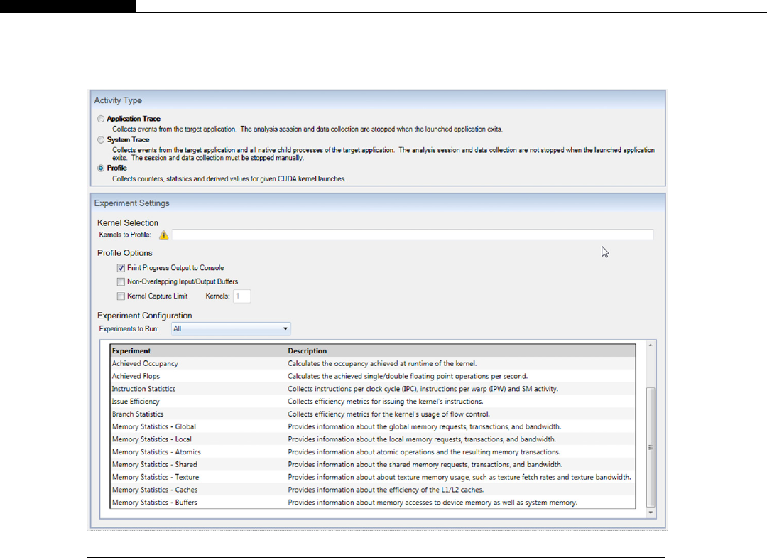
The other important experiment is occupancy rates (see Figure 9.5). In this experiment, notice the
Achieved occupancy column and in particular the number of Active Warps. As this is a compute 2.0
device, we can have up to 48 warps resident on a single SM. The achieved occupancy, as opposed to the
theoretical occupancy, is the measured value of what was actually achieved. This will usually be
significantly less than the theoretical maximum. Notice also that any limiting factor is highlighted in
red, in this case the number of blocks per SM at six. The “occupancy” graphs tab allows you to
understand this in somewhat more detail. It’s an extract from the occupancy calculation spreadsheet
provided with the CUDA SDK.
The cause of this limit is actually the number of threads. Dropping this from 256 to 192 would
allow the hardware to schedule eight blocks. As this kernel has synchronization points, having more
blocks available may introduce a better instruction mix. There will also be fewer warps that are unable
to run due to the synchronization point.
In practice, making this change helps quite significantly. It improves occupancy from 98.17% to
98.22%, which is marginal at best. However, the execution time drops from 14 ms to just 10 ms. The
FIGURE 9.3
Parallel Nsight experiments.
316 CHAPTER 9 Optimizing Your Application
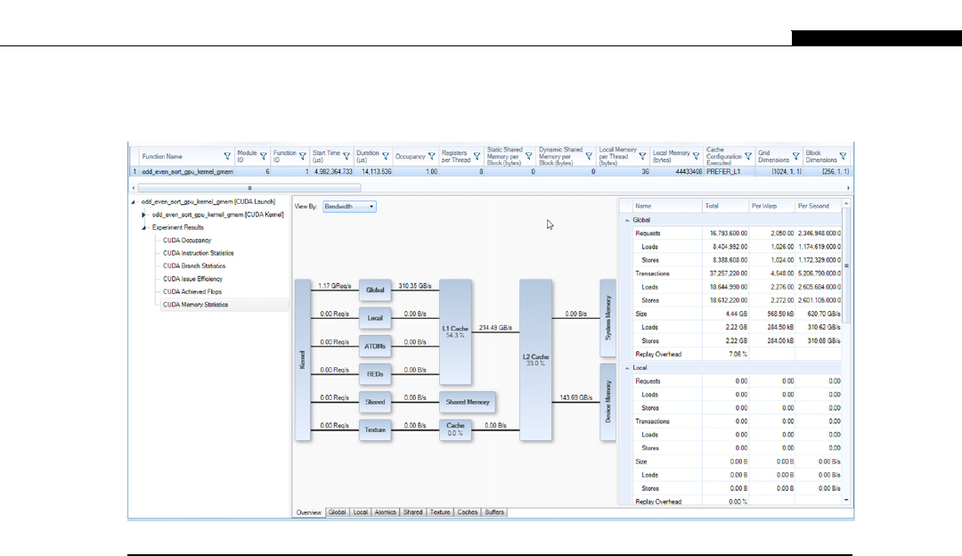
answer to this is in the memory usage. With 192 threads per block, we’re accessing a smaller range of
addresses which increases the locality of the accesses and consequently improves cache utilization.
The total number of memory transactions needed by each SM drops by about one-quarter. Conse-
quently, we see a proportional drop in execution time.
Grouping the tasks for CPU and GPU
Dr. M. Fatica from NVIDIA gave a great talk at GTC2010 concerning how Linpack had been optimized for
GPUs. Linpack is a benchmark based on linear algebra. It is used in the Top500 supercomputer benchmark
(www.top500.org) to benchmark the various supercomputers around the world. One interesting fact from
this talk was the GPU used at that time, a Fermi Tesla C2050 card, produced around 350 gigaflops of
DGEMM (double-precision matrix multiply) performance. The CPU used produced around 80 gigaflops.
The contribution of 80 gigaflops is a little under one-quarter of the GPU contribution, so not something that
can be ignored. A quarter or so extra performance goes a long way to reducing execution time.
In fact, the best applications tend to be those that play to the strengths of both the CPU and the GPU
and split the data accordingly. The CPU must be considered in any GPU-based optimization, because
it’s the total application time that is important. If you have a four-, six-, or eight-core CPU and one core
is busy handling a GPU application, why not use the other cores to also work on the problem? The
more cores you have available, the higher the potential gain is by offloading some work to the CPU.
If we say the CPU can handle work at one-tenth the rate of the GPU, then with just three CPU cores,
you’re gaining a 30% additional throughput. If you had an eight-core device, potentially this is a 70%
gain in performance, which is almost the same as having two GPUs working in tandem. In practice,
FIGURE 9.4
Parallel Nsight memory overview.
Strategy 1: Parallel/Serial GPU/CPU Problem Breakdown 317

however, often other constraints might limit the overall speed, such as memory, network, or I/O
bandwidth. However, even so, you’re likely to see a significant speedup where the application is not
already bound by one of these constraints on the host side.
Of these constraints, I/O is an interesting one, because introducing more CPU threads or processes
can often significantly improve the overall I/O throughput. This may seem a strange statement, as
surely the physical limits to and from an I/O device dictate the speed? On modern machines with large
amounts of memory, most I/O is in fact cached. Therefore, I/O can be more about moving data in
memory than it is about moving to or from devices. A decent RAID controller has its own processor to
do the I/O operations. Multiple CPU cores allow for multiple independent memory transfers, which
often provide a higher overall bandwidth than a single CPU core.
Separate CPU process or threads can create a separate GPU context and launch their own kernel onto
theGPU. These additional kernels are then queued within the GPU for execution. When availableresources
become free the kernel is executed. If you look at the typical GPU usage you see that shown in Figure 9.6.
Notice there is significant idle time on both the GPU and the CPU. Idle time on the GPU is more
expensive, as it’s typically 10 times more useful than the CPU time. Tools such as Parallel Nsight allow
you to display just such a timeline and you’ll be amazed to see just how much idle time certain kernels
can create.
FIGURE 9.5
Parallel Nsight occupancy data.
318 CHAPTER 9 Optimizing Your Application
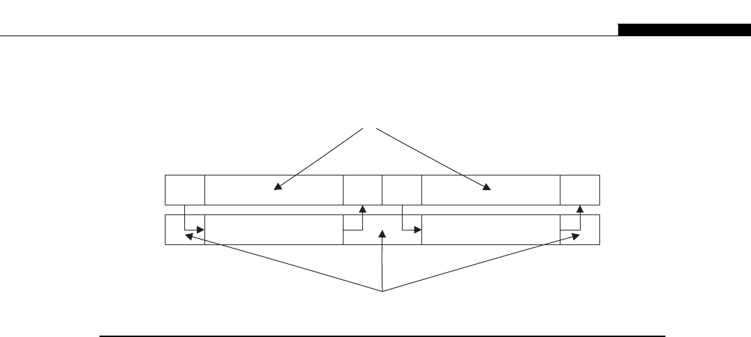
By placing multiple kernels onto a single GPU, these kernels then slot into the empty slots. This
increases, marginally, the latency of the first set of kernels but greatly improves the overall throughput
of the application. In a lot of applications, there can be as much as 30% idle time. Just consider what
a typical application will do. First, fetch data from somewhere, typically a slow I/O device like a hard
drive. Then transfer the data to the GPU and then sit and wait until the GPU kernel is complete. When
it’s complete, the host transfers the data off the GPU. It then saves it somewhere, usually to slow I/O
storage, fetches the next data block, and so on.
While the GPU is executing the kernel, why not fetch the next data block from the slow I/O device,
so it’s ready when the GPU kernel has completed? This is, in effect, what happens when you execute
multiple processes. The I/O device blocks the second process, while fetching data for the first. When
the first process is transferring data and invoking the kernel, the second process is accessing the I/O
hardware. It then does a transfer, while process one is computing and the kernel invocation of the
second process is queued. When the transfer back to the host for process one starts, the kernel from
process two also starts executing. Thus, with the introduction of just a couple of processes, you have
neatly overlapped the I/O, CPU, GPU, and transfer times, gaining a significant improvement in overall
throughput. See the stream example in Chapter 8 for a detailed explanation of this.
Note that you can achieve the same results using threads or processes. Threads allow the appli-
cation data to share a common data area and provide faster synchronization primitives. Processes allow
for processor affinity, where you lock a process to a given CPU core, which can often improve
performance because it allows for better core-specific cache reuse. The choice depends largely on how
much, if any, synchronization is needed between the CPU tasks.
The other aspect ofthe CPU/GPU decision is knowing how best to splitthe task. CPUs are great at serial
problems, where the data is sparsely distributed, or where the dataset is small. However, with a typical
10:1 ratio of performance on the GPU to the CPU, you have to be careful that you will not be holding up the
GPU. For this reason, many applications simply use the CPU to load and store data. This can sometimes
fully load a single core on the CPU, depending on how much computation time is required on the GPU.
One usage you sometimes see a CPU being used for is the final stages of a reduction. A reduction
operation typically reduces itself by a factor of two on every iteration of the reduction. If you start out
CPU
In
GPU
CPU
Out
CPU
In
GPU
CPU
Out
CPU Idle Time
GPU Idle Time
FIGURE 9.6
CPU and GPU idle time.
Strategy 1: Parallel/Serial GPU/CPU Problem Breakdown 319

with a million elements, within six iterations you are starting to hit the maximum number of sched-
ulable threads on a GPU. Within a few more iterations, several of the SMs are idle. With the GT200
and prior generation of hardware, kernels were not overlapped, so the kernel had to continue to iterate
down to the final elements before it freed up the idle SMs to do more work.
Thus, one optimization when a certain threshold is reached, is to forward the remaining part of the
computation to the CPU to complete. If the CPU was in fact idle anyway, and the remaining data being
transferred is not huge, this strategy can show significant gains over waiting for the GPU to complete the
entire reduction. With Fermi, NVIDIA addressed this issue, allowing those idle SMs to start work on the next
queued kernel. However, for the SM to become idle, it’s necessary for all the thread blocks to have completed.
Some nonoptimal kernels will have one or more active threads, even at the final levels of the reduction, which
pins the kernel to the SM until the complete reduction is done. With algorithms like reduction, be sure you are
reducing the number of active warps per iteration, not just the number of active threads.
Section summary
• Understand the problem and define your speedup goal in the context of the programming time and
skills available to you.
• Identify the parallelism in the problem and think about how to best to allocate this between the CPU
and one or more GPUs.
• Consider what is more important, a lower execution time or processing the data to a higher
resolution.
• Understand the implication of any serial code sections and think about how these might best be handled.
• Profile your application to ensure your understanding reflects the actual reality. Repeat your earlier
analysis if appropriate with your enhanced understanding.
STRATEGY 2: MEMORY CONSIDERATIONS
Memory bandwidth
Memory bandwidth and latency are key considerations in almost all applications, but especially so for
GPU applications. Bandwidth refers to the amount of data that can be moved to or from a given
destination. In the GPU case we’re concerned primarily about the global memory bandwidth. Latency
refers to the time the operation takes to complete.
Memory latency is designed to be hidden on GPUs by running threads from other warps. When
a warp accesses a memory location that is not available, the hardware issues a read or write request to
the memory. This request will be automatically combined or coalesced with requests from other
threads in the same warp, provided the threads access adjacent memory locations and the start of the
memory area is suitably aligned.
The size of memory transactions varies significantly between Fermi and the older versions. In
compute 1.x devices (G80, GT200), the coalesced memory transaction size would start off at 128 bytes
per memory access. This would then be reduced to 64 or 32 bytes if the total region being accessed by
the coalesced threads was small enough and within the same 32-byte aligned block. This memory was
not cached, so if threads did not access consecutive memory addresses, it led to a rapid drop off in
memory bandwidth. Thus, if thread 0 reads addresses 0, 1, 2, 3, 4, ., 31 and thread 1 reads addresses
320 CHAPTER 9 Optimizing Your Application

32, 32, 34, ., 63, they will not be coalesced. In fact, the hardware will issue one read request of at least
32 bytes for each thread. The bytes not used will be fetched from memory and simply be discarded.
Thus, without careful consideration of how memory is used, you can easily receive a tiny fraction of
the actual bandwidth available on the device.
The situation in Fermi and Kepler is much improved from this perspective. Fermi, unlike compute 1.x
devices, fetches memory in transactions of either 32 or 128 bytes. A 64-byte fetch is not supported. By
default every memory transaction is a 128-byte cache line fetch. Thus, one crucial difference is that access by
a stride other than one, but within 128 bytes, now results in cached access instead of another memory fetch.
This makes the GPU model from Fermi onwards considerably easier to program than previous generations.
One of the key areas to consider is in the number of memory transactions in flight. Each memory
transaction feeds into a queue and is individually executed by the memory subsystem. There is
a certain amount of overhead with this. It’s less expensive for a thread to issue a read of four floats or
four integers in one pass than to issue four individual reads. In fact, if you look at some of the graphs
NVIDIA has produced, you see that to get anywhere near the peak bandwidth on Fermi and Kepler you
need to adopt one of two approaches. First, fully load the processor with warps and achieve near 100%
occupancy. Second, use the 64-/128-bit reads via the float2/int2 or float4/int4 vector types and
your occupancy can be much less but still allow near 100% of peak memory bandwidth. In effect, by
using the vector types you are issuing a smaller number of larger transactions that the hardware can
more efficiently process. You also introduce a certain amount of instruction-level parallelism through
processing more than one element per thread.
However, be aware that the vector types (int2,int4, etc.) introduce an implicit alignment of 8 and
16 bytes, respectively. The data must support this, so for example, you cannot cast a pointer to int
from array element int[5] to int2* and expect it to work correctly. In such cases you’re better off
performing back-to-back 32-bit reads or adding some padding to the data structure to allow aligned
access. As we saw when optimizing the sample sort example, a value of four elements per thread often
provides the optimal balance between additional register usage, providing increased memory
throughput and opportunity for the processor to exploit instruction-level parallelism.
Source of limit
Kernels are typically limited by two key factors, memory latency/bandwidth and instruction latency/
bandwidth. Optimizing for one when the other is the key limiter will result in a lot of effort and very
little return on that effort. Therefore, being able to understand which of these two key factors is
limiting performance is critical to knowing where to direct your efforts.
The simplest way in which you can see where the balance of the code lies is to simply comment out
all the arithmetic instructions and replace them with a straight assignment to the result. Arithmetic
instructions include any calculations, branches, loops, etc. If you have a one-to-one mapping of input
values to calculated outputs, this is very simple and a one-to-one assignment works well. Where you
have a reduction operation of one form or another, simply replace it with a sum operation. Be sure to
include all the parameters read from memory into the final output or the compiler will remove the
apparently redundant memory reads/writes. Retime the execution of the kernel and you will see the
approximate percentage of time that was spent on the arithmetic or algorithmic part. If this percentage
is very high, you are arithmetically bound. Conversely, if very little changed on the overall timing, you
are memory bound.
Strategy 2: Memory Considerations 321
With the arithmetic code still commented out, run the kernel using Parallel Nsight, using the Analysis
function and the Profile setting. Examine the instruction statistics it produces (Figure 9.7). If the bar
graph contains a significant amount of blue, then the kernel memory pattern is displaying poor coa-
lescing and the GPU has to serialize the instruction stream to support scattered memory reads or writes.
FIGURE 9.7
High instruction reissue rate.
322 CHAPTER 9 Optimizing Your Application

If this is the case, is it possible to rearrange the memory pattern so the GPU can coalesce the
memory access pattern by thread? Remember, to do this, thread 0 has to access address 0, thread
1 address 1, thread 2 address 2, and so on. Ideally, your data pattern should generate a column-based
access pattern by thread, not a row-based access. If you can’t easily rearrange the data pattern, can you
rearrange the thread pattern such that you can use them to load the data into shared memory before
accessing the data? If so, you don’t have to worry about coalescing the reads when accessing them
from shared memory.
Is it possible to expand the number of elements of the output dataset that are processed by a single
thread? This will often help both memory- and arithmetic-bound kernels. If you do this, do it without
introducing a loop into the thread, but by duplicating the code. If the code is nontrivial, this can also be
done as a device function or a macro. Be sure to hoist the read operations up to the start of the kernel, so
that the read operations have finished fetching data before they are needed. This will increase register
usage, so be sure to monitor the number of warps being scheduled to see it does not suddenly drop off.
With arithmetic-bound kernels, look at the source code and think about how this would be
translated into assembly (PTX) code. Don’t be afraid to have a look at the actual PTX code being
generated. Array indexes can often be replaced with pointer-based code, replacing slow multiplies with
much faster additions. Divide or multiply instructions that use a power of 2 can be replaced with much
faster right and left shift operations, respectively. Anything that is constant within a loop body, an
invariant, should be moved outside the loop body. If the thread contains a loop, does unrolling the loop
speed up things (it usually does)? What loop unrolling factor works best? We look at these optimi-
zation strategies in detail a little later in this chapter.
Are you using single- or double-precision floats in reality, and what did you want to use? Look
out for floating-point constants without an Fpostfix, which the compiler will treat as double
precision. Do you really need 32 bits of precision in all of the calculations? Try the -use_fast_math
compiler switch and see if the results are still accurate enough for your needs. This switch enables
24-bit floating-point arithmetic, which can be significantly quicker than the standard IEEE 32-bit
floating-point math logic.
Finally, are you testing speed with the “release” version of the code? As we saw in some of the
examples earlier, this alone can increase performance by 15% or more.
Memory organization
Getting the memory pattern correct for a GPU is often the key consideration in many applications.
CPU programs typically arrange the data in rows within memory. While Fermi and Kepler will tolerate
noncoalesced reads and writes, as we mentioned earlier, compute 1.x devices will not. You have to try
and arrange the memory pattern such that access to it by consecutive threads will be in columns. This is
true of both global memory and shared memory. This means for a given warp (32 threads) thread
0 should access address offset 0, thread 1 address offset 1, thread 2 address offset 2, etc. Think about
the fetch to global memory.
However, assuming you have an aligned access, 128 bytes of data will come in from global
memory at a time. With a single float or integer per thread, all 32 threads in the warp will be given
exactly one element of data each.
Note the cudaMalloc function will allocate memory in 128-byte aligned blocks, so for the most part
alignment is not an issue. However, if using a structure that would straddle such a boundary, then there
Strategy 2: Memory Considerations 323
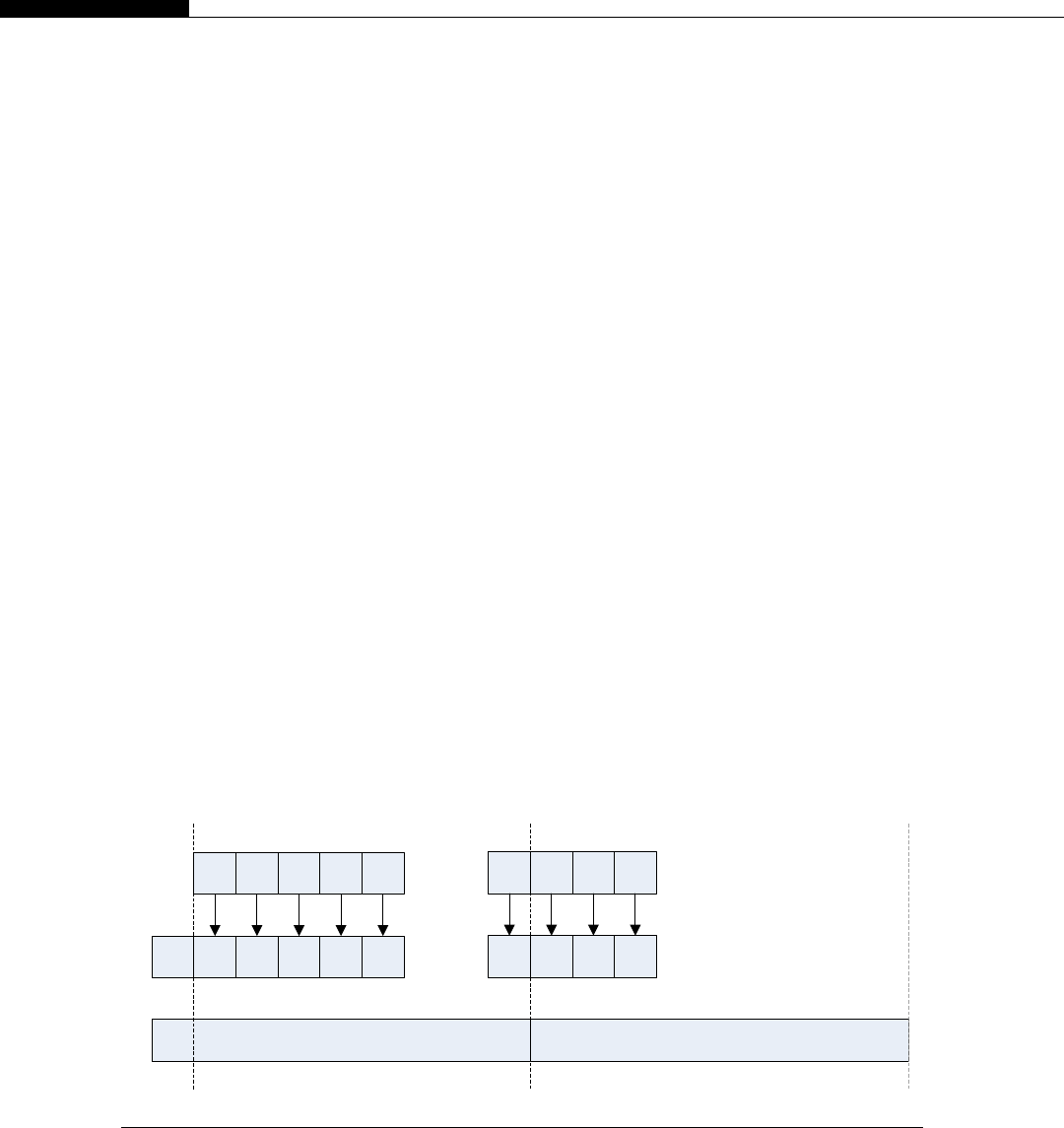
are two approaches. First, you can either add padding bytes/words explicitly to the structure. Alter-
natively, you can use the cudaMallocPitch function we covered in Chapter 6.
Notice that alignment is a key criteria as to whether one or two memory transactions, or cache lines,
need to be fetched. Suppose thread 0 accesses address offset 2 instead of 0. Perhaps you’re accessing
some data structure that has a header at the start, such as:
#define MSG_SIZE 4096
typedef struct
{
u16 header;
u32 msg_data[MSG_SIZE];
} MY_STRUCT_T;
If the kernel processes msg_data, then threads 30 and 31 of the warp cannot be served by the single
memory fetch. In fact, they generate an additional 128-byte memory transaction as shown in
Figure 9.8. Any subsequent warps suffer from the same issue. You are halving your memory band-
width, just by having a 2-byte header at the start of the data structure.
You’ll see this most acutely on compute 1.x devices where the additional fetch generated for
threads 30/31 isn’t even used to prefill the cache, but just discarded. Loading the header into a separate
chunk of memory somewhere else allows for aligned access to the data block. If you are unable to do
this, then manually insert padding bytes into the structure definition to ensure that msg_data is aligned
to a 128-byte boundary. Note that simply reordering the structure elements to move ‘header’ after
msg_data will also work, providing the structure is not subsequently used to create an array of
structures. All of a sudden your threads match the memory organization and your memory throughput
when working with the msg_data part of the structure will double.
Consider also the case where prefix sum is used. Prefix sum allows for multiple independent
processes or threads to read or write to independent areas of memory without interfering with one
another. Multiple reads from the same address are actually hugely beneficial, in that the GPU will
simply forward the value to whatever additional threads within the warp need it without additional
memory fetches. Multiple writes are of course an issue, in that they need to be sequenced.
0 1 2 3 4 29
0 1 2 29
30 31
30 31
T
N
Threads
header msg_data
Cache Line 0 Cache Line 1
3 4 Data
FIGURE 9.8
Cache line/memory transaction usage within structures.
324 CHAPTER 9 Optimizing Your Application

If we assume integers or floats for now, the size of each entry in the data array is 4 bytes. If the
distribution of the prefix array is exactly equal then we don’t need prefix arrays to access the data
anyway, as you could simply use a fixed offset per thread. Therefore, if you’re using a prefix sum to
calculate an offset into the dataset, it’s highly likely there are a variable number of elements per bin. If
you know the upper bounds of the number of elements per bin and you have a sufficient memory
available, then just pad each bin to the alignment boundary. Use an additional array that holds the
number of elements in the bin or calculate this value from the prefix sum index. In this way we can
achieve aligned access to memory at the expense of unused cells at the end of most bins.
One very simple solution to the alignment problem is to use a padding value that has no effect on
the calculated result. For example, if you’re performing a sum over the values in each bin, padding with
zero will mean no change to the end result, but will give a uniform memory pattern and execution path
for all elements in the warp. For a min operation, you can use a padding value of 0xFFFFFFFF, and
conversely 0 for a max operation. It is usually not hard to come up with a padding value that can be
processed, yet contributes nothing to the result.
Once you move to fixed-sized bins, it’s also relatively simple to ensure the dataset is generated and
accessed in columns, rather than rows. It’s often desirable to use shared memory as a staging buffer
because of the lack of coalescing requirements. This can then be used to allow coalesced reads/writes
to global memory.
Memory accesses to computation ratio
One question that you should often ask is what is the ratio of memory operations to arithmetic
operations? You ideally want a ratio of at least 10:1. That is, for every memory fetch the kernel makes
from global memory it does 10 or more other instructions. These can be array index calculations, loop
calculations, branches, or conditional evaluations. Every instruction should contribute to useful output.
Loops, in particular, especially when not unrolled, often simply contribute toward instruction overhead
and not to any useful work.
If we look inside an SM, architecturally, we see that warps are dispatched to sets of CUDA cores
based on even and odd instruction dispatchers. Compute 1.x devices have a single warp dispatcher and
compute 2.x devices have two. In the GF100/GF110 chipset (Fermi GTX480/GTX580) there are 32
CUDA cores and four SFUs (special-function units) per SM (Figure 9.9). In the GF104/GF114-based
devices (GTX460/GTX560) there are 48 CUDA cores and eight SFUs per SM (Figure 9.10). Each SM
for both compute 2.0 and compute 2.1 devices has a single set of 16 LSUs (load store units) that are
used to load values to and from memory (global, constant, shared, local, and cache).
Thus, in a single cycle, the warp dispatchers issue (or dispatch) a total of two (compute 2.0) or four
(compute 2.1) instructions, one set from each dispatcher. As these come from different warps, the
instructions are entirely independent of one another. These are then pushed into the pipeline of the
execution units (CUDA cores, SFUs, and LSUs).
There are a few implications to this design. First, the absolute minimum number of warps that must
be present is two for the GF100 series (compute 2.0) hardware and four for the GF104 series (compute
2.1) hardware. This in turn implies an absolute minimum of 64 or 128 threads per SM, respectively.
Having less than this means that one or more of the instruction dispatch units will remain idle,
effectively halving (GF100) the instruction dispatch speed. Using a number of threads other than
a multiple of 32 will mean some elements of the CUDA cores will idle, again undesirable.
Strategy 2: Memory Considerations 325
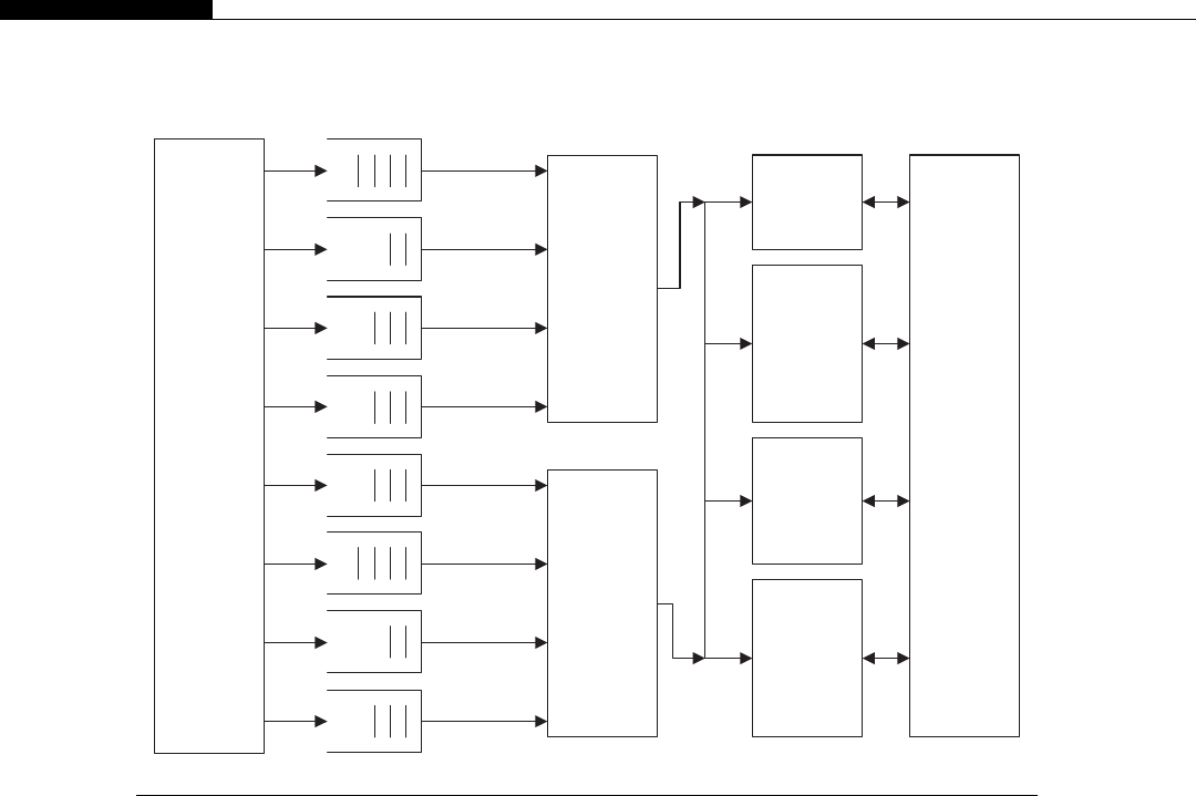
Having this minimum number of resident warps provides absolutely no hiding of latency, either memory
or instruction, based on the ability to switch to another warp. A stall in the instruction stream will actually
stall the CUDA cores, which is highly undesirable. In practice, multiple blocks are allocated to an SM to try
to ensure this problem never occurs and, more importantly, a variable mix of instructions is generated.
The second implication is the shared resources limit the ability to continuously perform the same
operation. Both the CUDA cores and the LSUs are pipelined, but are only 16 units wide. Thus, to
dispatch an entire warp to either unit takes two cycles. On compute 2.0 hardware, only one instruction
per dispatcher can be dispatched. Thus, to push an operation into the LSUs, one slot in the pipeline of
one of the CUDA cores must be left empty. There are four possible receivers for the dispatch (CUDA,
CUDA, SFUs and LSUs), yet only two suppliers per cycle.
The situation is drastically improved in compute 2.1 hardware, in that the two dispatchers dispatch
two instructions each, for a total of four per clock. With three sets of CUDA cores it would be possible to
supply three arithmetic instructions plus a load/save instruction without creating holes in the pipeline.
However, if all warps want to issue an instruction to the same execution unit, for example the LSU or
SFU, there is a problem. Only a single warp can use the LSU per two clock cycles. As the SFU has
just eight units, four on compute 2.0 hardware, a warp can take up to eight cycles to be fully consumed
by the SFUs.
Instruction
Fetch /
Decode
Warp 0
Warp 2
Warp 4
Warp 1
Warp 3
Warp 5
Warp N (Even)
Warp N (Odd)
Dispatcher
1
Dispatcher
0
16 x CUDA
Cores
16 x CUDA
Cores
SM
Shared
Resources
48KB
Shared
Memory
16KB L1
Cache
32K x 32 bit
Registers
16
Load /
Store Units
4 Special
Function
Units
FIGURE 9.9
Dispatching of CUDA warps (GF100/GF110, compute 2.0).
326 CHAPTER 9 Optimizing Your Application
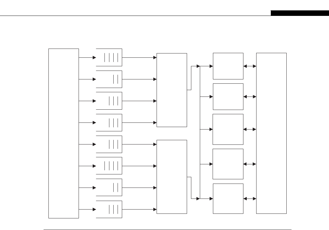
Thus, the bandwidth available to and from the LSUs on a compute 2.1 device is 50% less than
a compute 2.0 device with the same number of CUDA cores. Consequently, the LSUs or SFUs can become
a bottleneck. There need to be other instructions in the stream such that the CUDA cores can do some
useful work while the memory and transcendental instructions progress through the LSU or SFU pipeline.
The Kepler GK104 device (GTX680/Tesla K10) further extends the GF104/114 (GTX460/560)
design by extending the number of CUDA cores from 48 to 96, and then putting two of these within an
SM. Thus there are four warp schedulers, eight dispatch units, two LSUs and two SFUs per SM.
Let’s expand a little on the example we looked at earlier. Consider the case of a typical kernel. At
the start of the kernel, all threads in all warps fetch a 32-bit value from memory. The addresses are such
that they can be coalesced. For example:
int tid ¼(blockIdx.x * blockDim.x) þthreadIdx.x;
data[tid] ¼a[tid] * b[tid];
This would break down into a multiply and add (MADD) integer instruction, to calculate the value
to put into the register for the variable tid. Variables data,b, and care arrays somewhere in global
memory. The variables data,a, and bare indexed by tid so the address to write to needs to be
Instruction
Fetch /
Decode
Warp 0
Warp 2
Warp 4
Warp 1
Warp 3
Warp 5
Warp N (Even)
Warp N (Odd)
Dispatcher
1
Dispatcher
0
8 Special
Function
Units
16 x CUDA
Cores
SM
Shared
Resources
48KB
Shared
Memory
16KB L1
Cache
32K x 32 bit
Registers
16
Load /
Store Units
16 x CUDA
Cores
16 x CUDA
Cores
FIGURE 9.10
Dispatching of CUDA warps (GF104/GF114).
Strategy 2: Memory Considerations 327
calculated by multiplying tid by the size of the elements making up the array. Let’s assume they all are
integer arrays, so the size is 4 bytes per entry.
We very quickly hit the first dependency in the calculation of tid (Figure 9.11). The warp
dispatches the multiply of blockIdx.x and blockDim.x to the integer MADD units in the CUDA cores.
Until the multiply and add instruction to calculate tid has completed we can continue no further, so the
warp is marked as blocked and suspended.
At this point, the next warp is selected, which does the same operation and is again suspended at the
calculation of tid. After all warps have progressed to this point, enough clocks have passed such that the
value of tid in warp 0 is now known and can be fed into the multiply for the destination address calcu-
lations. Thus, three additional MADD instructions are dispatched to the CUDA cores, to calculate the
address offsets. The next instruction would be a couple of loads, but for this we need the address of aand
bfrom the multiply instructions. At this point we again suspend the warp and the other warps execute.
Once the address calculation of ais available, the load instruction can be dispatched. It’s likely, due
to the address calculation of bbeing issued back to back with that of a, that the address calculation of
bwill be retired by the time the load for ahas been dispatched. Thus, we immediately issue the load for
the ‘b’. The next instruction in the stream would be a multiply of ‘a’ and ‘b’, neither of which will be
available for some time yet as they have to be fetched from main memory to the SM. Thus, the warp is
suspended and the subsequent warps execute to the same point.
As memory fetches take a long time, all warps dispatch the necessary load instructions to the LSU
and are suspended. If there is no other work to do from other blocks, the SM will idle pending the
memory transactions completing.
Int MADD
(tid)
Load
(a[tid])
Load
(b[tid])
Int MUL
(address for
data)
Int MUL
(a[tid]*b[tid])
Store
(data[tid] =
a[tid] * b[tid])
Int MUL
(address for a)
Int MUL
(address for b)
FIGURE 9.11
Data flow dependency.
328 CHAPTER 9 Optimizing Your Application

Sometime later afinally arrives from the memory subsystem as a coalesced read of 128 bytes,
a single cache line, or a memory transaction. The 16 LSUs distributes 64 of the 128 bytes to the
registers used by the first half-warp of warp 0. In the next cycle, the 16 LSUs distribute the remaining
64 bytes to the register used by the other half-warp. However, warp 0 still can not progress as it has
only one of the two operands it needs for the multiply. It thus does not execute and the subsequent bytes
arriving from the coalesced read of afor the other warps are distributed to the relevant registers for
those warps.
By the time all of the data from the coalesced read for ahas been distributed to the registers of
all the other warps, the data for bwill likely have arrived in the L1 cache. Again, the 16 LSUs dis-
tribute the first 64 bytes to the registers of the first half-warp of warp 0. In the subsequent cycle they
distribute the second 64 bytes to the second half-warp.
At the start of this second cycle, the first half-warp is able to progress the multiply instruction for a
[tid] * b[tid]. In the third cycle the LSUs start providing data to the first half-warp of warp 0.
Meanwhile, the second half-warp of warp 0 starts the execution of the multiply. As the next instruction
in warp 0 would be a store and is dependent on the multiply, warp 0 is suspended.
Providing there are on the order of 18–22 warps resident, by the time the last warp has dispatched
the final multiply, the multiply will have completed for warp 0. It can then dispatch the store
instructions to the 16 LSUs and complete its execution. The other warps then do exactly the same and
the kernel is complete.
Now consider the case of (see Figure 9.12).
int tid ¼(blockIdx.x * blockDim.x) þthreadIdx.x;
data[tid] ¼a[tid] * b[tid];
data[tidþ1] ¼a[tidþ1] * b[tidþ1];
By halving the number of blocks, we can process two elements per thread. Notice this introduces an
independent execution stream into each thread of the warp. Thus, the arithmetic operations start to
overlap with the load operations.
However, as the example C code is written, this will not help. This is because the code contains
dependencies that are not immediately obvious. The write operation to the first element of data could
affect the value in either the aor the barray. That is, the address space of data may overlap with aor b.
Where you have a write in the data flow to global memory, you need to lift out the reads to the start of
the kernel. Use the following code instead:
int tid ¼(blockIdx.x * blockDim.x) þthreadIdx.x;
int a_0 ¼a[tid];
int b_0 ¼b[tid];
int a_1 ¼a[tidþ1];
int b_1 ¼b[tidþ1];
data[tid] ¼a_0 * b_0;
data[tidþ1] ¼a_1 * b_1;
or
int tid ¼(blockIdx.x * blockDim.x) þthreadIdx.x;
int2 a_vect ¼a[tid];
int2 b_vect ¼b[tid];
data[tid] ¼a_vect * b_vect;
Strategy 2: Memory Considerations 329
We have two choices, a scalar approach or a vector approach. The GPU supports only vector
loads and saves, not vector operations, in hardware. Thus, the multiplication is actually done as an
overloaded operator in Cþþ and simply multiplies the two integers independently of one another.
However, the vector loads and saves two 64-bit loads and a single 64-bit save, respectively, instead
of the four separate 32-bit loads and a single 32-bit save with the nonvector version. Thus, 40% of
the memory transactions are eliminated. The memory bandwidth usage is the same, but less
memory transactions mean less memory latency, and therefore any stall time waiting for memory is
reduced.
To use the vector types, simply declare all arrays as type int2, which is an in-built vector type of
two integers. Supported types are int2,int3,int4,float2,float3, and float4. You can of course
create your own types, such as uchar4, and define your own operators. Each vector type is actually just
an aligned structure with Nnamed member elements of the base type.
Thus, I hope you can actually see that a balance is therefore required between the different types of
instructions. This becomes somewhat more critical with the compute 2.1 devices (GF104 series) where
there are three sets of CUDA cores sharing the same resources within the SM. The change in compute
2.0 to compute 2.1 devices added significantly more arithmetic capacity within the SM without
providing additional data transport capacity. The compute 2.0 devices have up to 512 CUDA cores on
a bus of up to 384 bits wide, giving a ratio of 1:3 of cores to memory bandwidth. The compute 2.1
devices have up to 384 CUDA cores on a bus of up to 256 bits, giving a ratio of 1:5 cores to memory
bandwidth. Thus, compute 2.0 devices are more suited to applications that are memory bound, whereas
compute 2.1 devices are more suited to applications that are compute bound.
Int MADD
(tid)
Load
(a[tid])
Load
(b[tid])
Int MUL
(address for
data)
Int MUL
(a[tid]*b[tid])
Store
(data[tid] =
a[tid] * b[tid])
Int MUL
(address for
a[tid])
Int MUL
(address for
b[tid])
Int MADD
(address for
a[tid+1])
Int MADD
(address for
b[tid+1])
Load
(a[tid+1])
Load
(b[tid+1])
Int MUL
(a[tid+1]*b[tid+1])
Store
(data[tid] =
a[tid+1] * b[tid+])
FIGURE 9.12
Dual data flow dependency.
330 CHAPTER 9 Optimizing Your Application

In practice, this is balanced in the compute 2.0 devices by having up to 33% more CUDA cores.
The compute 2.1 devices, however, typically also run at somewhat higher clock rates, both in terms of
the internal clock speed and also the external memory bus speed. This helps significantly in reba-
lancing the smaller memory bus width but is generally not sufficient to allow compute 2.1 devices to
outperform their 2.0 counterparts.
What is important to realize, especially with compute 2.1 devices, is that there needs to be
sufficient arithmetic density to the instruction stream to make good use of the CUDA cores present
on the SMs. A kernel that simply does loads or stores and little else will not achieve anything like the
peak performance available from these devices. Expand such kernels to also include independent
instruction flow via processing two, four, or eight elements per thread. Use vector operations where
possible.
Loop and kernel fusion
Another area where we can significantly save on memory bandwidth is a technique based on loop
fusion we looked at in the last section. Loop fusion is where two apparently independent loops run over
an intersecting range. For example, loop 1 runs from 0 to 100 and loop 2 from 0 to 200. The code for
loop 2 can be fused with the code for loop 1, for at least the first 100 iterations. This increases the level
of instruction-level parallelism, but also decreases the overall number of iterations by a third.
Kernel fusion is a variation on loop fusion. If you have a number of kernels that are run in sequence,
one after the other, are there elements of these kernels that can be fused? Be careful doing this with
kernels you did not write or do not fully understand. Invoking two kernels in series generates an
implicit synchronization between them. This may have been intended by design and, as it’s implicit,
probably only the original designer is aware of it.
In developing kernels it’s quite common to break down the operation into a number of phases or
passes. For example, in the first pass you might calculate the results over the whole dataset. On the
second pass you may filter data for certain criteria and perform some further processing on certain
points. If the second pass can be localized to a block, the first and second pass can usually be combined
into a single kernel. This eliminates the write to main memory of the first kernel and the subsequent
read of the second, as well as the overhead of invoking an additional kernel. If the first kernel is able to
write the results to shared memory, and you only need those results for the second pass, you eliminate
the read/write to global memory entirely. Reduction operations often fall into this category and can
benefit significantly from such an optimization, as the output of the second phase is usually many times
smaller than the first phase, so it saves considerably on memory bandwidth.
Part of the reason why kernel fusion works so well is because of the data reuse it allows. Fetching
data from global memory is slow, on the order of 400–600 clock cycles. Think of memory access like
reading something from disk. If you’ve ever done any disk I/O, you’ll know that reading a file by
fetching one character at time is very slow and using fread to read large blocks is far more efficient
than repeatedly calling read character functions like fgetch. Having read the data in, you keep it in
memory. Apply the same approach to accessing global memory. Fetch data in chunks of up to 16 bytes
per thread (float4,int4), not in single bytes or words. Once you have each thread successfully
processing a single element, switch to int2 or float2 and process two. Moving to four may or may not
help, but moving from one to two often does. Once you have the data, store it in shared memory, or
keep it in the register set and reuse it as much as possible.
Strategy 2: Memory Considerations 331

Use of shared memory and cache
Using shared memory can provide a 10:1 increase in speed over global memory, but is limited in
sized48 K on Fermi/Kepler devices and 16 K on all the previous devices. This may not sound like
a great deal of space, especially with multigigabyte memory systems found on the host, but this is
actually per SM. Thus, a GTX580 or Tesla M2090 has 16 SMs active per GPU, each of which provides
48 K of shared memory, a total of 768 K. This is memory that runs at L1 cache speed. In addition, you
have 768 K of L2 cache memory (on 16 SM devices) that is shared between all the SMs. This allows
for an order of magnitude faster, global memory, atomic operations than in previous generation GPUs.
When you consider that a GTX580 comes with 1.5 GB of memory, 768 K means just a tiny fraction
of that memory space can be held in cache at any one point in time. The equivalent Tesla card comes
with 6 GB of memory. Thus, kernels that iterate over datasets need to be aware that they may be using
either the cache or shared memory in an ineffective manner, if they are not reusing data.
Rather than a number of passes over a large dataset, techniques such as kernel fusion can be used to move
through the data as opposed to passing over it multiple times. Think of the problem in terms of the output
data and not the input data. Construct the problem such that you assign threads to output data items, not input
data items. Create a fan in and not a fan out in terms of data flow. Have a preference for gather (collecting
data) primitives, rather than scatter (distributing data) primitives. The GPU will broadcast data, both from
global memory and the L2 cache, directly to each SM. This supports high-speed gather-type operations.
On Fermi and Kepler we have a very interesting choice, to configure the shared memory to either
prefer L1 cache (48 K L1 cache, 16 K shared) or to prefer shared (48 K shared, 16 K cache). By default the
device will prefer shared memory, and thus you’ll have 48 Kof shared memory available. This decision is
not fixed, but set at runtime, and thus can be set per kernel call. Kernels that do not make use of shared
memory, or keep to the 16 K limit to ensure compatibility with earlier GPUs, usually benefit significantly
(10% to 20% performance gain) by enabling the additional 32 K of cache, disabled by default:
cudaFuncSetCacheConfig(cache_prefer, kernel_name);
where the cache_prefer parameter is cudaFuncCachePreferShared for 48 K of shared memory and 16
K of L1 cache, or cudaFuncCachePreferL1 for 48 K of cache memory and 16 K of shared memory.
Note, Kepler also allows a 32 K/32 K split.
There are, however, some areas where the cache causes Fermi and Kepler to operate slower than
previous generation GPUs. On compute 1.x devices, memory transactions would be progressively
reduced in size to as little as 32 bytes per access if the data item was small. Thus, a kernel that accesses
one data element from a widely dispersed area in memory will perform poorly on any cache-based
architecture, CPU, or GPU. The reason for this is that a single-element read will drag in 128 bytes of data.
For most programs, the data brought into the cache will then allow a cache hit on the next loop iteration.
This is because programs typically access data close in memory to where they previously accessed data.
Thus, for most programs this is a significant benefit. However, for programs that only need one data
element, the other 124 bytes are wasted. For such kernels, you have to configure the memory subsystem
to fetch only the memory transactions it needs, not one that is cache line sized. You can do this only at
compile time via the -Xptxas –dlcm¼cg flag. This reduces all access to 32 bytes per transaction and
disables the L1 cache. For read only data consider also using either texture or constant memory.
With G80/GT200, compute 1.x hardware, it’s essential that you make use of shared memory as an
integral part of the kernel design. Without cached accessed to data, be it explicitly via shared memory
332 CHAPTER 9 Optimizing Your Application

or implicitly via a hardware-managed cache, memory latency times are just huge. The arrival of cache
on GPUs via the Fermi architecture has made it much, much easier to write at a program, or kernel, that
performs at least reasonably well on the GPU.
Let’s look at some of the obstacles to using shared memory. The first is the size availabled16 K on
compute 1.x hardware and up to 48 K on compute 2.x hardware. It can be allocated statically at
compile time via the __shared__ prefix for variables. It is also one of the optional parameters in
a kernel call, that is,
kernel<<<num_blocks, num_threads, smem_size>>>(a,b,c);
With runtime allocation, you additionally need a pointer to the start of the memory. For example,
extern volatile __shared__ int s_data[];
__global__ my_kernel(const int * a,
const int * b,
const int num_elem_a,
const int num_elem_b)
{
const int tid ¼(blockIdx.x * blockDim.x) þthreadIdx.x;
// Copy arrays ‘a’and ‘b’to shared memory
s_data[tid] ¼a[tid];
s_data[num_elem_a þtid] ¼b[tid];
// Wait for all threads
__syncthreads();
// Process s_data[0] to s_data[(num_elem_a-1)] –a
// Process s_data[num_elem_a] to s_data[num_elem_a þ(num_elem_b-1)] –array ‘b’
}
Note that L2 cache size in Fermi is not always 768 K as stated in the CUDA C programmer guide.
In fact, the L2 cache is based on the type of device being used and the number of SMs present.
Compute 2.1 devices may have less L2 cache than compute 2.0 devices. Even compute 2.0 devices
without all the SMs enabled (GTX470, GTX480, GTX570) have less than 768 K of L2 cache. The
GTX460 device we’re using for testing has 512 K of L2 cache and the GTX470 device has 640 K.
The size of the L2 cache is returned from a call to cudaGetDeviceProperties API as l2CacheSize
member.
Section summary
• Think carefully about the data your kernel processes and how best to arrange this in memory.
• Optimize memory access patterns for coalesced 128-byte access, aligning with the 128-byte
memory fetch and L1 cache line size.
• Consider the single-/double-precision tradeoff and how this impacts memory usage.
• Fuse multiple kernels to single kernels where appropriate.
Strategy 2: Memory Considerations 333

• Make optimal use of shared memory and cache, ensuring you’re making full use of the expanded
size on later compute levels.
STRATEGY 3: TRANSFERS
Pinned memory
To work on a dataset you need to transfer the data from the host to the device, work on the dataset,
and transfer the results back to the host. Performed in a purely serial manner, this causes periods
where both the host and GPU are inactive, both in terms of unused transfer capacity and compute
capacity.
We looked in detail in the chapter on multi-GPU usage at how to use streams to ensure the GPU
always has some work to do. With a simple double-buffering technique, while the GPU is transferring
back the results and acquiring a new work packet, the other buffer is being used by the compute engine
to process the next data block.
The host processor supports a virtual memory system where a physical memory page can be marked
as swapped out. It can then be paged to disk. Upon an access by the host processor to that page, the
processor loads the page back in from disk. It allows the programmer to use a much larger virtual address
space than is actually present on the hardware. Given that the programs typically exhibit quite good
locality, this allows the total memory space to be much larger than the physical limits allow. However, if
the program really does need 8 GB and the host only has 4 GB, the performance will typically be poor.
Arguably the use of virtual memory is a hangover from a time when memory capacities were very
limited. Today you can purchase 16 GB of memory for a little over 100 euros/dollars/pounds, meaning
the host’s need to use virtual memory is almost eliminated for most applications.
Most programs, except for big data problems, will generally fit within the host memory space. If
not, then there are special server solutions that can hold up to 128 GB of memory per node. Such
solutions are often preferable, as they allow you to keep the data within one node rather than add the
complexity of a multinode solution. Of course, loading the dataset in chunks is perfectly feasible, but
then you are ultimately limited by the throughput of the I/O hardware.
You should always be using page-locked memory on a system that has a reasonable amount of host
memory. Page-locked memory allows the DMA (direct memory access) controller on the GPU to
request a transfer to and from host memory without the involvement of the CPU host processor. Thus,
no load is placed onto the host processor in terms of managing a transfer or having to bring back from
disk any pages that have been swapped out.
The PCI-E transfers in practice can only be performed using DMA-based transfer. The driver does
this in the background when you don’t use page-locked memory directly. Thus, the driver has to
allocate (or malloc) a block of paged-locked memory, do a host copy from the regular memory to the
page-locked memory, initiate the transfer, wait for the transfer to complete, and then free the page-
locked memory. All of this takes time and consumes precious CPU cycles that could be used more
productively.
Memory allocated on the GPU is by default allocated as page locked simply because the GPU does
not support swapping memory to disk. It’s the memory allocated on the host processor we’re con-
cerned with. To allocate page-locked memory we need to either allocate it using the special
334 CHAPTER 9 Optimizing Your Application

cudaHostMalloc function or allocate it with the regular malloc function and register it as page-locked
memory.
Registering memory simply sets some internal flags to ensure the memory is never swapped out and
also tells the CUDA driver that this memory is page-locked memory so it is able to use it directly rather
than using a staging buffer.
As with malloc, if you use cudaHostAlloc you need to use the cudaFreeHost function to free this
memory. Do not call the regular C free function with pointers allocated from cudaHostAlloc or you
will likely get a crash, some undefined behavior, or a strange error later in your program.
The prototype for cudaHostAlloc is
cudaError_t cudaHostAlloc (void ** host_pointer, size_t size, unsigned int flags)
The flags consist of the following:
cudaHostAllocDefaultdUse for most cases. Simply specifies the default behavior.
cudaHostAllocWriteCombineddUse for memory regions that will be transferred to the device only.
Do not use this flag when the host will read from this memory area. This turns off the caching of the
memory region on the host processor, which means it completely ignores the memory region during
transfers. This speeds up transfer to the device with certain hardware configurations.
cudaHostAllocPortabledThe page-locked memory becomes page locked and visible in all
CUDA contexts. By default the allocation belongs to the context creating it. You must use this
flag if you plan to pass the pointer between CUDA contexts or threads on the host processor.
cudaHostAllocMappeddWe’ll look at this shortly. It allocates host memory into device memory
space, allowing the GPU kernel to directly read and write with all transfers being implicitly
handled.
To demonstrate the effect of paged memory versus nonpaged memory, we wrote a short program. This
simply does a number of transfers, varied by size to and from a device, and invokes a dummy kernel to
ensure the transfers actually take place. The results are shown in Figure 9.13.
On the Y axis we have MB/second to or from the device and the transfer size in bytes along the X
axis. What we can see from the chart is that there is a considerable difference between using paged
memory and nonpaged memory, the page-locked (pinned) memory being 1.4faster for writes and
1.8faster for reads. It took 194 ms to send out 512 MB of data to the card using page-locked memory,
as opposed to 278 ms to do this with nonpaged memory. Timings to transfer data from the device, for
comparison, were 295 ms for paged memory versus 159 ms for pinned memory.
On the input side, we see a strange issue: With page-locked memory, the bandwidth from the device
is 20% higher than to the device. Given that PCI-E provides for a full duplex connection of the same
speed to and from the device, you’d expect to see a similar transfer speed for both reads and writes.
This variation, as you will see in subsequent tests, is very hardware dependent. All the systems tested
except the Intel Nehalem I7 system exhibiting it to varying degrees.
Transfer rates to and from the four devices were almost identical, which is to be expected given the
bandwidth of global memory on all of the cards is at least an order of magnitude greater than the PCI-E
bandwidth.
What is also very noticable is that to get near-peak bandwidth, even with pinned memory, the
transfer size needs to be on the order of 2 MB of data. In fact, we don’t achieve the absolute peak until
the transfer size is 16 MB or beyond.
Strategy 3: Transfers 335
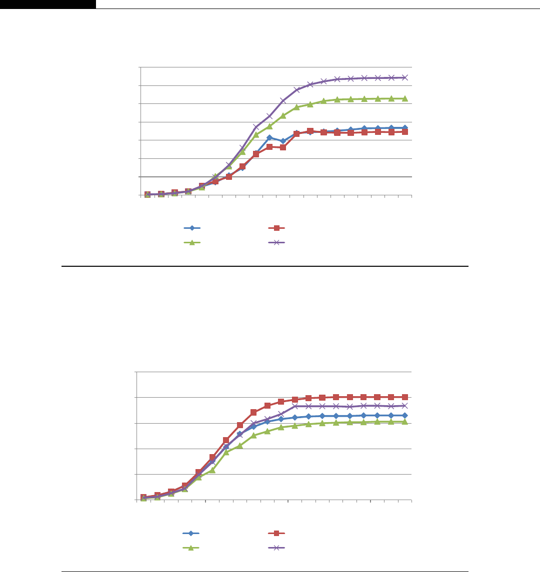
For comparison, the results are also shown in Figures 9.14,9.15 and 9.16 for a number of systems
we tested.
Figure 9.14 shows a small netbook based on Intel’s low-power ATOM device, equipped with
a dedicated GT218 NVIDIA ION graphics card. The peak PCI-E bandwidth you can typically see is up
0
500
1000
1500
2000
2500
3000
3500
1K
2K
4K
8K
16K
32K
64K
128K
256K
512K
1M
2M
4M
8M
16M
32M
64M
128M
256M
512M
Paged To Device Paged From Device
Pinned To Device Pinned From Device
FIGURE 9.13
Transfer speed to and from the device (AMD Phenom II X4 905e, PCI-E 2.0 X8 link).
0
50
100
150
200
250
1K
2K
4K
8K
16K
32K
64K
128K
256K
512K
1M
2M
4M
8M
16M
32M
64M
128M
256M
512M
Pinned To Device Pinned From Device
Paged To Device Pagged From Device
FIGURE 9.14
Transfer speed to and from the device (Intel Atom D525, PCI-E 2.0 X1 link).
336 CHAPTER 9 Optimizing Your Application
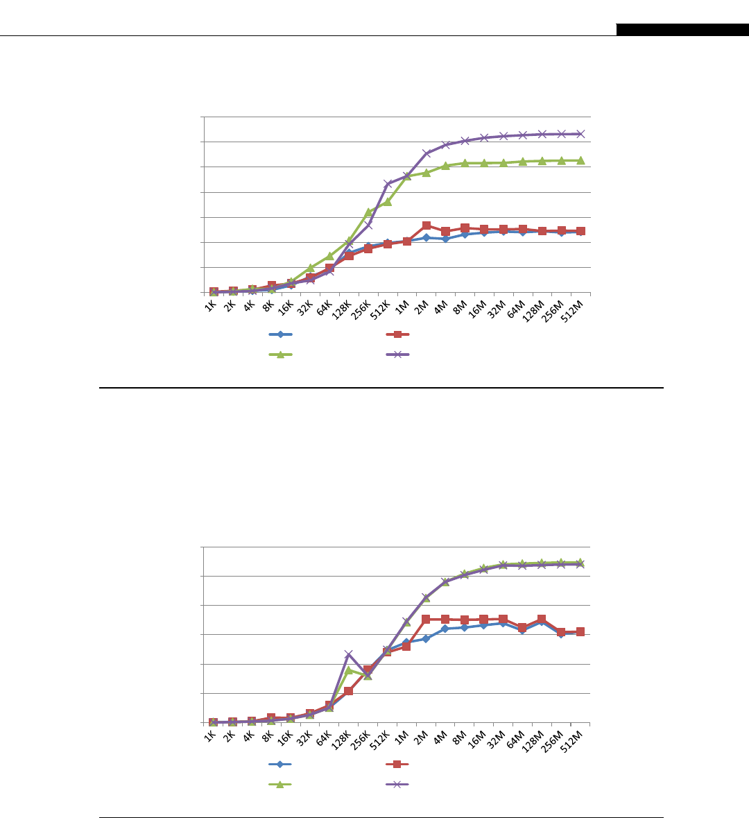
to 5 GB/s when using a 2.0 X16 link. As this netbook uses an X1 link, we could expect a maximum of
320 MB/s and we see in the order of 200 MB/s.
However, we see a very similar pattern to the AMD system, in that we need around 2 MB plus
transfer sizes before we start to achieve anything like the peak transfer rate. The only difference we see
is there is a noticable difference between transfers to the device and transfers from the device.
0
1000
2000
3000
4000
5000
6000
7000
Paged To Device Paged From Device
Pinned To Device Pinned From Device
FIGURE 9.15
Transfer speed to and from the device (Intel I3 540, PCI-E X16 link).
0
1000
2000
3000
4000
5000
6000
Paged To Device Paged From Device
Pinned To Device Pinned From Device
FIGURE 9.16
Transfer speed to and from the device (Intel I7 920, PCI-E X16 link).
Strategy 3: Transfers 337

A midrange system quite common in the consumer enviroment is the i3/i5 system from Intel. This
particular one is the i3 540 running with a H55 chipset. As this device has a single GPU only, it’s
running at X16 the peak speed PCI-E 2.0 (Figure 9.15).
Again we can see the very large difference between pinned and nonpinned transfers, in excess of
2. However, notice the absolute speed difference, approximately a 2increase over the AMD
system. This is largely due to the AMD system using an X8 PCI-E link, whereas the Intel system here
uses an X16 PCI-E link.
The Intel I3 is a typical consumer processor. Anyone writing consumer-based applications should
be very much aware by now that they need to be using pinned memory transfers, as we can see the huge
difference it makes.
Finally, we look at one further system, this time from the server arena, using the Intel I7 920
Nehalem processor and the ASUS supercomputer socket 1366 motherboard. This is a common
motherboard for very high-end GPUs, as it allows up to four PCI-E slots. This particular one is
equipped with 3GTX290 GPUs each using an PCI-E 2.0 X16 connection.
What we see from the diagram is again interesting. Pinned and paged memory transfers are equal
until transfer sizes larger than 512 KB, after which the pinned memory transfers lead by up to 1.8
over the paged memory–based transfers. Unlike the Nehalem I3 system, notice the Nehalem I7 system
is more consistent and there is not a huge variation between inbound and outbound transfer speeds.
However, also note the peak transfer speed, despite both devices being on a X16 PCI-E 2.0 link, is only
5400 MB/s as opposed to the I3, which achieved a peak of 6300 MB/s (Figure 9.16).
So in summary, we can say that across a selection of today’s computing hardware, pinned
memory transfers are approximately twice as fast as nonpinned transfers. Also we see there can be
a considerable variance in performance between read and write speeds from and to the various devices.
We can also see that we need to use larger, rather than smaller, block sizes, perhaps combining multiple
transfers to increase the overall bandwidth utilization of the bus.
Zero-copy memory
Zero-copy memory is a special form of memory mapping that allows you to map host memory into the
memory space of the GPU directly. Thus, when you dereference memory on the GPU, ifit’s GPU based, then
you get high-speed (180 GB/s) bandwidth to global memory. If the GPU code reads a host-mapped variable it
issues a PCI-E read transaction, and a (very) long time later the host will return the data over the PCI-E bus.
After looking at the PCI-E bus bandwidth in the previous section, this doesn’t, at first glance, make
a lot of sense. Big transfers are efficient and small transfers inefficient. If we rerun the test program we
used for the previous examples, we see that the median transfer time is 0.06 ms on our sample AMD
Phenom X4 platform. However, these are explicit, individual transfers, so it’s possible the zero-copy
implementation may be more efficient.
If you think about what happens with access to global memory, an entire cache line is brought in
from memory on compute 2.x hardware. Even on compute 1.x hardware the same 128 bytes, poten-
tially reduced to 64 or 32, is fetched from global memory.
NVIDIA does not publish the size of the PCI-E transfers it uses, or details on how zero copy is
actually implemented. However, the coalescing approach used for global memory could be used with
PCI-E transfer. The warp memory latency hiding model can equally be applied to PCI-E transfers,
providing there is enough arithmetic density to hide the latency of the PCI-E transfers. This is, in fact,
338 CHAPTER 9 Optimizing Your Application

the key to getting this to work. If you do very little for each global memory fetch and your application
is already memory bound, this approach is unlikely to help you.
However, if your application is arithmetically bound, zero-copy memory can be a very useful
technique. It saves you the explicit transfer time to and from the device. In effect, you are overlapping
computation with data transfers without having to do explicit stream management. The catch, of
course, is that you have to be efficient with your data usage. If you fetch or write the same data point
more than once, this will create multiple PCI-E transactions. As each and every one of these is
expensive in terms of latency, the fewer there are the better.
This can also be used very effectively on systems where the host and GPU share the same
memory space, such as on the low-end NVIDIA ION-based netbooks. Here a malloc of global
memory on the GPU actually results in a malloc of memory on the host. Clearly it doesn’t make
sense to copy from one memory area on the host to another memory area on the host. Zero-copy
memory can eliminate the need to perform these copies in such systems, without the impact of
a PCI-E bus transfer.
Zero-copy memory also has one very useful use case. This is during the phase where you are
initially porting a CPU application to a GPU. During this development phase there will often be
sections of code that exist on the host that have not yet been ported over to the GPU. By declaring such
data references as zero-copy memory regions, it allows the code to be ported in sections and still have
it work. The performance will be generally poor until all the intended parts are present on the GPU. It
simply allows this to be done in smaller steps so it’s not an “everything or nothing” problem.
Let’s start by taking the existing memcpy program and expanding the kernel so it does the read of the
data instead of relying on an explicit copy. For this we absolutely must coalesce accesses to memory,
which when reading a simple one-dimensional array is easy. Thus, our kernel becomes
__global__ void kernel_copy(u32 * const gpu_data,
const u32 * const host_data,
const u32 num_elements)
{
const u32 idx ¼(blockIdx.x * blockDim.x) þthreadIdx.x;
const u32 idy ¼(blockIdx.y * blockDim.y) þthreadIdx.y;
const u32 tid ¼((gridDim.x * blockDim.x) * idy) þidx;
if (tid < num_elements)
gpu_data[tid] ¼host_data[tid];
}
In the kernel we simply make the xand ygrid dimensions into a single linear array and assign one
element from the source dataset to the destination dataset. Next we have to do three critical things to
use zero-copy or host-mapped memorydthat is, first to enable it, second to allocate memory using it,
and finally to convert the regular host pointer to the device memory space.
Prior to any creation of a CUDA context, we need to make the following call:
// Enable host mapping to device memory
CUDA_CALL(cudaSetDeviceFlags(cudaDeviceMapHost));
When the CUDA context is created the driver will know it also has to support host-mapped
memory. Without this the host-mapped (zero-copy) memory will not work. This will not work if it’s
Strategy 3: Transfers 339

done after the CUDA context has been created. Be aware that calls to functions like cudaHostAlloc,
despite operating on host memory, still create a GPU context.
Although most devices support zero-copy memory, some earlier devices do not. It’s not part of the
compute level, so it has to be checked for explicitly as follows:
struct cudaDeviceProp device_prop;
CUDA_CALL(cudaGetDeviceProperties(&device_prop, device_num));
zero_copy_supported ¼device_prop.canMapHostMemory;
The next stage is to allocate memory on the host such that it can be mapped into device memory.
This is done with an additional flag cudaHostAllocMapped to the cudaHostAlloc function.
// Allocate zero copy pinned memory
CUDA_CALL(cudaHostAlloc((void **) &host_data_to_device, size_in_bytes,
cudaHostAllocWriteCombined jcudaHostAllocMapped));
Finally, we need to convert the host pointer to a device pointer, which is done with the
cudaHostGetDevicePointer function as follows:
// Convert to a GPU host pointer
CUDA_CALL(cudaHostGetDevicePointer( &dev_host_data_to_device, host_data_to_device, 0));
In this call we convert the host_data_to_device previously allocated in the host memory space
to an equvalent pointer, but within the GPU memory space. Do not confuse the pointers. Use the
converted pointer only with GPU kernels and the original pointer only in code that executes on the host.
Thus, for example, to free the memory later, an operation performed on the host, the existing call remains
the same:
// Free pinned memory
CUDA_CALL(cudaFreeHost(host_data_to_device));
As we’re using memory blocks up to 512 MB in size, to access one element per thread no matter
how many threads we allocate per block means the number of blocks will exceed 64 K. This is the hard
limit on the number of blocks in any single dimension. Thus, we have to introduce another dimension.
This introduces grids, which we covered in Chapter 5. We can do this relatively simply by fixing the
number of grids at some value that will be large enough to allow sufficient flexibility in selecting the
number of threads per block.
const int num_elements ¼(size_in_bytes / sizeof(u32));
const int num_threads ¼256;
const int num_grid ¼64;
const int num_blocks ¼(num_elements þ(num_threads-1)) / num_threads;
int num_blocks_per_grid;
// Split blocks into grid
if (num_blocks > num_grid)
num_blocks_per_grid ¼num_blocks / num_grid;
else
num_blocks_per_grid ¼1;
dim3 blocks(num_grid, num_blocks_per_grid);
340 CHAPTER 9 Optimizing Your Application
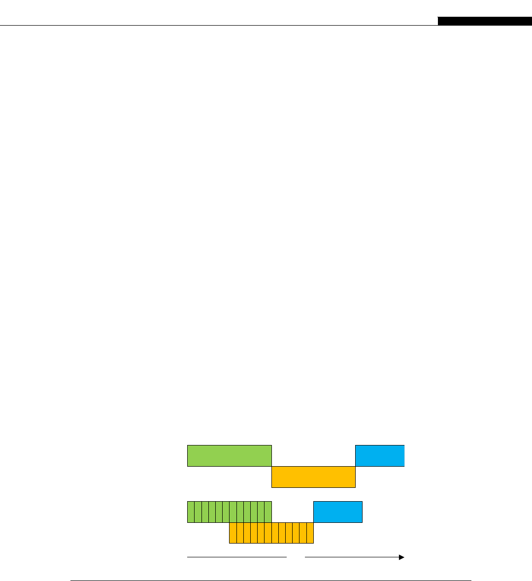
The dim3 operation simply assigns the regular scalar values we calculated to a structure type
holding a triplet that can be used as a single parameter in the kernel launch. It causes the kernel to
launch 64 grids of Nblocks. This simply ensures that for a given block index we do not exceed the 64 K
limit. Thus, on the kernel launch, we replace num blocks, a scalar type, with blocks,adim3 type:
// Run the kernel
kernel_copy<<<blocks, num_threads>>>(gpu_data, dev_host_data_to_device, num_elements);
What we see for transfers to the device is that the overall figures are identical to the transfers using
explicit memory copies. This has significant implications. Most applications that do not already use the
stream API simply copy memory to the GPU at the start and copy back once the kernel is complete. We
can shrink that time drastically using pinned memory copies, but the time is still cumulative because
it’s a serial operation.
In effect, what happens with the zero-copy memory is we break both the transfer and the kernel
operation into much smaller blocks, which execute them in a pipeline (Figure 9.17). The overall time is
reduced quite significantly.
Notice we did not perform the same optimization with the copy from device. The reason for this is
because consumer GPUs have only one copy engine enabled. Thus, they support only a single memory
stream. When you do a read-kernel-write operation, if the write is pushed into the stream ahead of
subsequent reads, it will block the read operations until the pending write has completed. Note this is not
the case for Tesla devices, as both copy engines are enabled and thus Tesla cards are able to support
independent to and from streams. Prior to Fermi, there was only ever one copy engine on any card.
However, with zero-copy memory the transfers are actually quite small. The PCI-E bus has the
same bandwidth in both directions. Due to the high latency of the PCI-E-based memory reads, actually
most of the reads should have been pushed into the read queue ahead of any writes. We may be able to
achieve significant execution time savings over the explicit memory copy version.
Note the diagram in Figure 9.18 is simplified in that it lists a single “Pinned To & From Device”
line, yet we show the zero device copy times explicitly for the devices. The pinned memory time was
effectively the same for all devices, so it was not shown per device.
We have listed the entire execution time of a single memory copy to device, kernel execution, and
memory copy from device. Thus, there is some overhead that is not present when purely measuring the
Memcpy To
Kernel
Memcpy
From
Memcpy
From
Serial
Version
Overlapped
Version
Time
FIGURE 9.17
Serial versus overlapped transfer/kernel execution.
Strategy 3: Transfers 341
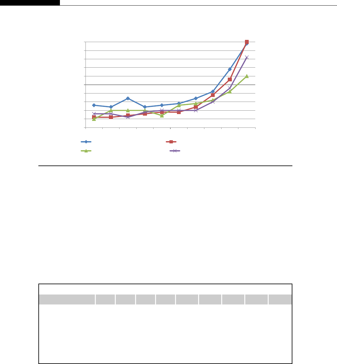
transfer to/from the device. As we’re using zero copy, the memory transactions and the kernel time
cannot be pulled apart. However, as the kernel is doing very little, the overall execution time represents
a fair comparison between the zero copy and explicit copy versions.
There is a considerable amount of variability. What we can see, however, is that for small transfer
amounts, less than 512 KB, zero copy is faster than using explicit copies. Let’s now look at sizes larger
than 512 KB in Table 9.1 and Figure 9.19.
What is very interesting to see here is a considerable drop in execution time. On the Fermi
hardware the overlapping of the kernel operation with the memory copies drops the execution time
from 182 ms to 104 ms, a 1.75speedup. The results are less impressive in the earlier devices, but still
represent a significant speedup.
0
0.05
0.1
0.15
0.2
0.25
0.3
0.35
0.4
0.45
0.5
1K 2K 4K 8K 16K 32K 64K 128K 256K 512K
Pinned To & From Device GTX470/460 Zero To & From Device
GTX9800 Zero To & From Device GTX260 Zero To & From Device
FIGURE 9.18
Zero-copy time versus explicit pinned copy time over different GPU generations.
Table 9.1 Zero-Copy Results (execution time in ms)
Device 1M 2M 4M 8M 16M 32M 64M 128M 256M
Pinned to and from
device
0.96 1.62 3 5.85 11.52 22.97 45.68 91.14 182.04
GTX470/460 zero to
and from device
0.5 0.9 1.72 3.34 6.61 13.11 26.15 52.12 103.99
GT9800 zero to and
from device
0.56 1.09 2 3.94 7.92 15.63 31.6 61.89 123.81
GTX260 zero to and
from device
0.68 1.38 2.52 4.48 8.74 18.84 38.96 74.35 160.33
342 CHAPTER 9 Optimizing Your Application
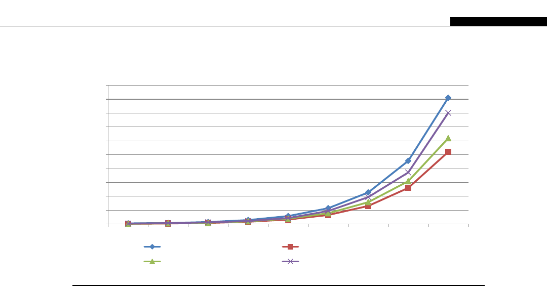
You can of course achieve this using streams and asynchronous memory copies, as demonstrated in
Chapter 8. Zero copy simply presents an alternative, and somewhat simpler, interface you can work
with.
However, there are some caveats. Beware of exactly how many times the data is being fetched from
memory. Re-reading data from global memory will usually exclude the use of zero-copy memory.
If we modify the program to read the value from host memory twice instead of once, then the
performance drops by half on the 9800 GT and GTX260 platforms, the compute 1.x devices. This is
because each and every fetch from global memory on these platforms is not cached. Thus, the number
of PCI-E transactions issued is doubled, as we double the amount of times the GPU accesses the zero-
copy memory area.
On Fermi the situation is somewhat different. It has an L1 and L2 cache and it’s highly likely the data
fetched earlier in the kernel will still be in the cache when the latter access hits the same memory address.
To be sure, you have to explicitly copy the data you plan to reuse to the shared memory. So in Fermi,
depending on the data pattern, you typically do not see the device issuing multiple PCI-E transactions, as
many of these hit the internal caches and therefore never create a global memory transaction.
Thus, zero-copy memory presents a relatively easy way to speed up your existing serial code
without having to explicitly learn the stream API, providing you are careful about data reuse and have
a reasonable amount of work to do with each data item.
However, be aware that the bandwidth of the PCI-E bus is nowhere near the bandwidth available on
a CPU. The latest Sandybridge I7 processor (Socket 2011) achieves some 37 GB/s of memory
bandwidth, from a theoretical peak of 51 GB/s. We’re achieving 5–6 GB/s from a theoretical peak of
8 GB/s on the PCI-E 2.0 bus. You must have enough work in your application to justify the cost of
moving the data over the PCI-E bus. Consider that the CPU can be a better alternative in situations
where very little work is being done per element.
0
20
40
60
80
100
120
140
160
180
200
1M 2M 4M 8M 16M 32M 64M 128M 256M
Pinned To & From Device GTX470/460 Zero To & From Device
9800GT Zero To & From Device GTX260 Zero To & From Device
FIGURE 9.19
Zero-copy graph (time in ms versus transfer size).
Strategy 3: Transfers 343

The program used for these measurements is shown here for reference.
void memcpy_test_zero_to_from(const int device_num,
const size_t size_in_bytes,
TIMER_T * const kernel_time,
const u32 num_runs,
const bool pinned)
{
char device_prefix[256];
int major, minor;
int zero_copy_supported;
// Init
// Enable host mapping to device memory
CUDA_CALL(cudaSetDeviceFlags(cudaDeviceMapHost));
// Get the device properties
get_device_props(device_prefix, device_num, &major,
&minor, &zero_copy_supported);
// Exit if zero copy not supported and is requested
if (zero_copy_supported ¼¼ 0)
{
printf("%s Error Zero Copy not supported", device_prefix);
wait_exit(1);
}
// Select the specified device
CUDA_CALL(cudaSetDevice(device_num));
printf("%s Running Memcpy Test to device using",
device_prefix);
if (pinned)
printf(" locked memory");
else
printf(" unlocked memory");
printf(" %lu K", size_in_bytes / 1024);
(*kernel_time) ¼0;
init_device_timer();
// Allocate data space on GPU
u32 * gpu_data;
CUDA_CALL(cudaMalloc((void**)&gpu_data,
size_in_bytes));
344 CHAPTER 9 Optimizing Your Application

u32 * dev_host_data_to_device;
u32 * dev_host_data_from_device;
// Allocate data space on host
u32 * host_data_to_device;
u32 * host_data_from_device;
if (pinned)
{
// Allocate zero copy pinned memory
CUDA_CALL(cudaHostAlloc((void **) &host_data_to_device, size_in_bytes,
cudaHostAllocWriteCombined jcudaHostAllocMapped));
CUDA_CALL(cudaHostAlloc((void **) &host_data_from_device, size_in_bytes,
cudaHostAllocDefault jcudaHostAllocMapped));
}
else
{
host_data_to_device ¼(u32 *) malloc(size_in_bytes);
host_data_from_device ¼(u32 *) malloc(size_in_bytes);
}
// Convert to a GPU host pointer
CUDA_CALL(cudaHostGetDevicePointer(&dev_host_data_to_device, host_data_to_device, 0));
CUDA_CALL(cudaHostGetDevicePointer(&dev_host_data_from_device, host_data_from_device,
0));
// If the host allocation did not result in
// an out of memory error
if ( (host_data_to_device !¼NULL) &&
(host_data_from_device !¼NULL) )
{
const int num_elements ¼(size_in_bytes / sizeof(u32));
const int num_threads ¼256;
const int num_grid ¼64;
const int num_blocks ¼(num_elements þ(num_threads-1)) / num_threads;
int num_blocks_per_grid;
// Split blocks into grid
if (num_blocks > num_grid)
num_blocks_per_grid ¼num_blocks / num_grid;
else
num_blocks_per_grid ¼1;
dim3 blocks(num_grid, num_blocks_per_grid);
for (u32 test¼0; test < num_runsþ1; testþþ)
{
Strategy 3: Transfers 345

// Add in all but first test run
if (test !¼0)
start_device_timer();
// Run the kernel
kernel_copy<<<blocks, num_threads>>>(dev_host_data_to_device,
dev_host_data_to_device, num_elements);
// Wait for device to complete all work
CUDA_CALL(cudaDeviceSynchronize());
// Check for kernel errors
cuda_error_check(device_prefix, " calling kernel kernel_copy");
// Add in all but first test run
if (test !¼0)
(*kernel_time) þ¼ stop_device_timer();
}
// Average over number of test runs
(*kernel_time) /¼num_runs;
if (pinned)
{
// Free pinned memory
CUDA_CALL(cudaFreeHost(host_data_to_device));
CUDA_CALL(cudaFreeHost(host_data_from_device));
}
else
{
// Free regular paged memory
free(host_data_to_device);
free(host_data_from_device);
}
}
CUDA_CALL(cudaFree(gpu_data));
destroy_device_timer();
// Free up the device
CUDA_CALL(cudaDeviceReset());
printf(" KERNEL:%.2f ms", (*kernel_time));
const float one_mb ¼(1024 * 1024);
const float kernel_time_for_one_mb ¼(*kernel_time) * (one_mb / size_in_bytes);
// Adjust for doing a copy to and back
346 CHAPTER 9 Optimizing Your Application
const float MB_per_sec ¼((1000.0F / kernel_time_for_one_mb) * 2.0F);
printf(" KERNEL:%.0f MB/s", MB_per_sec );
}
Bandwidth limitations
The ultimate bandwidth limitation of a significant number of applications is the I/O speed of
whatever devices the input and output data have to be acquired from and written to. This is often the
limitation on the speedup of any application. If your application takes 20 minutes to run on a serial
CPU implementation and can express enough parallelism, it’s quite feasible for that application to
run on a GPU in less time than it takes to load and save the data from the storage device you are
using.
The first problem we have in terms of bandwidth is simply getting the data in and out of the
machine. If you are using network-attached storage, the limit to this will be the speed of the
network link. The best solution to this problem is a high-speed SATA3 RAID controller using
many high-speed SSD drives. However, this will not solve your bandwidth issues unless you
are using the drive efficiently. Each drive will have a peak transfer rate into host memory,
which is actually a function of the transfer rate of the drive, the controller, and the route to host
memory.
Running a benchmark on a drive, such as the commonly used ATTO benchmark, can show you the
effect of using different size blocks (see Figure 9.20). This benchmark simulates access to drives based
on a certain size of reads and writes. Thus, it reads and writes a 2 GB file in blocks of 1 K, 2 K, 4 K, etc.
to see the effect of changing the block size.
We can see from the results that only when we read data in 64 K chunks or more do we achieve the
peak bandwidth from the single SSD drive. For the RAID 0 hard drive system we need at least 1 MB
blocks to make use of the multiple disks. Thus, you need to make sure you’re using the fread function
0
50
100
150
200
250
300
350
400
0.512481632641282565121024
Single SSD 5xRAID 0 Hard Disk
FIGURE 9.20
Bandwidth (MB/s) for a single SSD versus five hard disks in RAID 0.
Strategy 3: Transfers 347

in C to read suitable sized blocks of data from the disk subsystem. If we fetch data in 1 K chunks, we
get just 24 MB/s from the drive, less than 10% of its peak read bandwidth. The more drives you add to
a RAID system, the larger the minimum block size becomes. If you are processing compressed music
or image files, the size of a single file may only be a few megabytes.
Note also that whether the data is compressible or not has a big impact on drive performance.
The server level drives, such as the OCZ Vertex 3, provide both higher peak values and sustained
bandwidth with uncompressible data. Thus, if your dataset is in an already compressed format
(MP3, MP4, WMV, H.264, JPG, etc.), then you need to make sure you use server drives. The
bandwidth on many consumer-level SSD drives can fall to half of quoted peak when using
uncompressible data streams.
The reason for this is the use of synchronous NAND memory in the high-end server SSDs
versus the cheaper and much lower-performing asynchronous NAND memory used in consumer SSDs.
Even with noncompressed data, synchronous NAND-based drives still outperform their asynchronous
cousins, especially once the drive starts to contain some data. OCZ also provides the RevoDrive R4
PCI-E-based product, which claims speeds in the order of 2 GB/s plus at the expense of a PCI-E slot.
The next bandwidth limit you hit is that of host memory speed. This is typically not an issue until
you introduce multiple GPUs per node, if you consider that you can fetch data at 6 GB/s off the PCI-E
bus from a very high-speed SSD RAID system. We then have to send out data at 6 GB/s to and from the
host memory to the GPU. Potentially you could also write data again at 6 GB/s to the RAID controller.
That’s a potential 24 GB/s of pure data movement without the CPU actually doing anything useful
except moving data. We’re already hitting the bandwidth limits of most modern processor designs and
have already surpassed that available from the older-generation CPUs. In fact, only the latest quad
channel I7 Sandybridge-E CPU has anything like the bandwidth we could start moving around, if we
were to solve the slow I/O device issue.
CUDA 4.0 SDK introduced Peer2Peer GPU communication. The CUDA 4.1 SDK also introduced
Peer2Peer communication with non-NVIDIA hardware. Thus, with the correct hardware, GPUs can
talk to any supported device. This is mostly limited to a small number of InfiniBand and other
highspeed network cards. However, in principle, any PCI-E device can talk with the GPU. Thus,
a RAID controller could send data directly to and from a GPU. There is a huge potential for such
devices, as no host memory bandwidth, PCI-E, or memory is consumed. As data is not having to flow
to a CPU and then back out again, latency is dropped considerably.
Once the data has been moved to the GPU, there is a bandwidth limit of up to 190 GB/s on GeForce
cards and 177 GB for Tesla, to and from the global memory on the device. To achieve this you need to
ensure coalescing of the data reads from the threads and ensure your application makes use of 100% of
the data moved from memory to the GPU.
Finally, we have shared memory. Even if you partition data into tiles, move it into shared memory,
and access it in a bank conflict–free manner, the bandwidth limit is on the order of 1.3 TB/s. For
comparison the AMD Phenom II and Nehalem I7 CPUs for a 64 KB L1 cache block, the same capacity
as the GPU L1 cache and shared memory, has around 330 GB/s bandwidth, some 25% of that of the
GPU.
If we take a typical float or integer parameter, it’s 4 bytes wide. Thus, the bandwidth to global
memory is a maximum of 47.5 giga-elements per second (190 GB/s O4). Assuming you read and
write just one value, we can halve this figure to 23.75 giga-elements per second. Thus, with no data
reuse, this is the maximum upper throughput of your application.
348 CHAPTER 9 Optimizing Your Application

The Fermi device is rated in excess of 1 teraflop, that is, it can process on the order of 1000 giga
floating-point operations per second. Kepler is rated at in excess of 3 teraflops. The actual available flops
depend on how you measure flops. The fastest measure is the FMADD instruction (floating-point
multiply and add) instruction. This multiplies two floating-point numbers together and adds another
number to it. As such, this counts as two flops, not one. Real instruction streams intermix memory loads,
integer calculations, loops, branches, etc. Thus, in practice, kernels never get near to this peak figure.
We can measure the real speed achievable by simply using the program we previously developed to
visualize the PCI-E bandwidth. Simply performing a memory copy from global memory to global
memory will show us the maximum possible read and write speed a kernel can achieve.
GTX 470: 8 bytes x 1 K (1x4x32) 0.060 ms, 489 MB/s
GTX 470: 8 bytes x 2 K (1x8x32) 0.059 ms, 988 MB/s
GTX 470: 8 bytes x 4 K (1x16x32) 0.060 ms, 1969 MB/s
GTX 470: 8 bytes x 8 K (1x32x32) 0.059 ms, 3948 MB/s
GTX 470: 8 bytes x 16 K (1x32x64) 0.059 ms, 7927 MB/s
GTX 470: 8 bytes x 32 K (1x64x64) 0.061 ms, 15444 MB/s
GTX 470: 8 bytes x 64 K (1x64x128) 0.065 ms, 28779 MB/s
GTX 470: 8 bytes x 128 K (1x64x256) 0.074 ms, 50468 MB/s
GTX 470: 8 bytes x 256 K (1x128x256) 0.090 ms, 83053 MB/s
GTX 470: 8 bytes x 512 K (1x256x256) 0.153 ms, 98147 MB/s
GTX 470: 8 bytes x 1 M (1x512x256) 0.30 ms, 98508 MB/s
GTX 470: 8 bytes x 2 M (1x1024x256) 0.56 ms, 105950 MB/s
GTX 470: 8 bytes x 4 M (1x2048x256) 1.10 ms, 108888 MB/s
GTX 470: 8 bytes x 8 M (1x4096x256) 2.19 ms, 112215 MB/s
GTX 470: 8 bytes x 16 M (1x8192x256) 4.26 ms, 112655 MB/s
GTX 470: 8 bytes x 32 M (1x16384x256) 8.48 ms, 113085 MB/s
GTX 470: 8 bytes x 64 M (1x32768x256) 16.9 ms, 113001 MB/s
GTX 470: 8 bytes x 128 M (2x32768x256) 33.9 ms, 112978 MB/s
GTX 470: 8 bytes x 256 M (4x32768x256) 67.7 ms, 113279 MB/s
Note the values in the parentheses shows grids blocks threads. The above figures are plotted in
Figure 9.21.
These results are created by pushing 16 kernels into an asynchronous stream, with each call sur-
rounded by a stop and start event. Each kernel performs a single-element copy from the source to the
destination for every memory location. The execution time of the first kernel in each batch is ignored.
The remaining kernels contribute to the total time, which is then averaged over the kernels. The quoted
bandwidth for the GTX470 is 134 GB/s, so we’re falling short of this, despite having a simple kernel
and obviously hitting the peak at the larger transfer sizes.
What we see from this chart is that to achieve anywhere near the peak memory performance you
need to have enough threads. We start off by using 32 threads per block until we launch a total of
64 blocks. This ensures that all the SMs are given work, rather than one SM getting a large number of
threads and therefore most of the work. We then increase the thread count per block up to 256 threads
once there is a reasonable distribution of blocks to the SMs.
Changing the element type from uint1 to uint2,uint3, and uint4 produces some interesting
results. As you increase the size of a single element, the total number of transactions issued to the
memory subsystem is reduced. On the GTX470, going from the 4-byte read (single-element integer or
float) to an 8-byte read (dual-element integer, float, or single-element double) resulted in up to a peak
Strategy 3: Transfers 349
23% increase in measured bandwidth to and from global memory (Figure 9.22). The average
improvement was somewhat lower at just 7%, but this still represents a reasonable improvement in
execution time by simply switching from int1/float1 to int2/float2 vector types. The GTX460
presents a similar, but more pronounced pattern (Figure 9.23).
0
20000
40000
60000
80000
100000
120000
GTX470 GT9800 GTX260 GTX460
FIGURE 9.21
Global memory bandwidth across devices.
0
20000
40000
60000
80000
100000
120000
GTX470 - 4 GTX470 - 8 GTX470 - 12 GTX470 - 16
FIGURE 9.22
Global memory bandwidth GTX470/compute 2.0 (transaction size in bytes).
350 CHAPTER 9 Optimizing Your Application
To achieve optimum bandwidth, the CUDA code was compiled specifically for compute 2.1
devices. We also found that thread blocks that were a multiple of 48 threads worked best. This is not
surprising given that there are three sets of 16 cores per SM instead of the usual two. When moving
from 4 bytes per element to 8 or 16 bytes per element, the bandwidth was increased by an average of
19%, but a best case of 38%.
A single warp transaction for 8 bytes per thread would result in a total of 256 bytes moving over the
memory bus. The GTX460 we are using has a 256-bit-wide bus to the global memory. This would clearly
indicate that, regardless of any occupancy considerations, on such devices you should always be pro-
cessing either 8 or 16 bytes (two or four elements) per thread. This is most likely due to the higher ratio of
CUDA codes within the SM causing some contention for the single set of LSUs (load/store units).
The GTX260 for comparison, a compute 1.3 device similar to the Tesla C2050 device, gained, on
average, 5% by moving from 4 to 8 bytes per element. However, its performance was drastically
reduced when moving beyond this. The 9800 GT did not show any significant improvement, sug-
gesting this device is already achieving the peak when using 4 bytes per element.
Finally, note that Fermi-based Tesla devices implement an ECC (error checking and correction)
based memory protocol. Disabling this can boost transfer speeds by around 10% at the expense of the
error detection and correction ability. In a single machine versus a server room, this may be an
acceptable tradeoff.
GPU timing
Single GPU timing
Timing data on the GPU is not particularly straightforward. Using a timer that is CPU based is not
a good solution, as the best way to use the GPU and CPU is to operate asynchronously. That is, both the
0
20000
40000
60000
80000
100000
120000
GTX470 - 4 GTX470 - 8 GTX470 - 12 GTX470 - 16
FIGURE 9.23
Global memory bandwidth GTX460/compute 2.1 (transaction size in bytes).
Strategy 3: Transfers 351
GPU and CPU are running at the same time. CPU timing is only semi-accurate when you force
sequential operation of the GPU and CPU. As this is not what we want in practice, it’s a poor solution.
The GPU, by default, operates in a synchronous mode in that the memcpy operations implicitly
synchronize. The programmer expects to copy to the device, run the kernel, copy back from the device,
and have the results in CPU memory to save to disk or for further processing. While this is an easy
model to understand, it’s also a slow model. It’s one aimed at getting kernels to work, but not one
aimed at performance.
We examined the use of streams, in detail, in Chapter 8. A stream is effectively a work queue. Stream
0 is used as the default work queue when you do not specify a stream to the CUDA API. However, stream
0 has many operations that implicitly synchronize with the host. You might be expecting an asyn-
chronous operation, but in practice certain API calls have implicit synchronization when using stream 0.
To use asynchronous operations, we need to first create a stream such as
// Create a new stream on the device
cudaStream_t stream;
CUDA_CALL(cudaStreamCreate(&stream));
For the bandwidth test, we created an array of events.
#define MAX_NUM_TESTS 16
cudaEvent_t kernel_start[MAX_NUM_TESTS];
cudaEvent_t kernel_stop[MAX_NUM_TESTS];
The GPU provides events that can be time-stamped by the GPU hardware (Figure 9.24). Thus, to
time a particular action on the GPU, you need to push a start event into the queue, then the action you
wish to time, and finally a stop event. Streams are simply a FIFO (first in, first out) queue of operations
for the GPU to perform. Each stream represents an independent queue of operations.
Having created a stream, you need to create one or more events.
for (u32 test¼0; test < MAX_NUM_TESTS; testþþ)
{
CUDA_CALL(cudaEventCreate(&kernel_start[test]));
CUDA_CALL(cudaEventCreate(&kernel_stop[test]));
}
Here we have a simple loop creating MAX_NUM_TESTS eventsda start event and a stop event. We
then need to push the events into the stream on either side of the action to measure.
// Start event
CUDA_CALL(cudaEventRecord(kernel_start[test],stream));
// Run the kernel
Start
Event
Action to be
timed
Stop
Event
Time
FIGURE 9.24
Timing an action on the GPU.
352 CHAPTER 9 Optimizing Your Application

kernel_copy_single<data_T><<<num_blocks, num_threads, dynamic_shared_memory_usage,
stream>>>(s_data_in, s_data_out, num_elements);
// Stop event
CUDA_CALL(cudaEventRecord(kernel_stop[test],stream));
To calculate the time, either per CUDA call or in total, call the CUDA function
cudaEventElapsedTime to get the time difference between two time-stamped events.
// Extract the total time
for (u32 test¼0; test < MAX_NUM_TESTS; testþþ)
{
float delta;
// Wait for the event to complete
CUDA_CALL(cudaEventSynchronize(kernel_stop[test]));
// Get the time difference
CUDA_CALL(cudaEventElapsedTime(&delta, kernel_start[test], kernel_stop[test]));
kernel_time þ¼ delta;
}
You should realize that in performing such a timed event, there is no guarantee of ordering of events
between streams. The CUDA runtime could execute your start event in stream 0 and then switch to
a previously suspended kernel execution in stream 5, sometime later come back to stream 0, kick off the
kernel, jump to another stream to process a number of other start events, and finally come back to stream
0 and timestamp the stop event. The delta time is the time from the start period to the end period.
In this example, notice we have created only a single stream. We have multiple events, but they all
execute from the same stream. With only a single stream the runtime can only execute events in order,
so we guarantee achieving the correct timing.
Notice the call to the cudaEventSynchronize API. This call causes the CPU thread to block should
it be called when the event has not completed. As we’re doing nothing useful on the CPU, this is
perfectly fine for our purposes.
At the end of the host program we must ensure that with any resources we allocated are freed up.
// Free up all events
for (u32 test¼0; test < MAX_NUM_TESTS; testþþ)
{
CUDA_CALL(cudaEventDestroy(kernel_start[test]));
CUDA_CALL(cudaEventDestroy(kernel_stop[test]));
}
Destroying an event before it’s actually been used will result in undefined runtime errors when
executing the kernels.
Finally, you should be aware that events are not free. It takes some resources to handle the events at
runtime. In this example we specifically wanted to time each kernel to ensure there was not significant
variability. In most cases a single start and stop event at the start and end of the work queue will be
entirely sufficient for the overall timing.
Strategy 3: Transfers 353
Multi GPU timing
Multi GPU timing is a little more complex, but based on the same principles. Again, we create
a number of streams and push events into the streams.
Unfortunately, there is no function provided in the API to obtain the absolute timestamp from an
event. You can only obtain the delta between two events. However, by pushing an event into the start of
the stream, you can use this as time point zero and thus obtain the time relative to the start of the
stream. However, asking for the delta time between events on different GPUs causes the API to return
an error. This complicates creating a timeline when using multiple GPUs, as you may need to adjust the
time based on when the start events actually happened. We can see in Figure 9.29 a copy to the device,
a kernel execution, a copy from the device, a copy to the device, a second kernel invocation, and finally
a copy from the device.
Notice that with different devices, the copy times are largely similar but the kernels’ time will
vary considerably. In the second-to-last copy from device operation for the GTX470 device (CFD 2),
notice the bar is somewhat smaller (258 ms versus 290 ms). This is because the GTX470 starts its
transfer first and only toward the tail end of the transfer do the other devices also initiate a transfer.
The GT9800, being a much slower device, still has its kernel being executed while GTX470 has in
fact completed its transfer. With different device generations, you will get such a pattern. The
transfer rates are largely similar, but the kernel times cause shifts in the points where the transfers are
initiated.
Figure 9.25 was generated using timers, but tools such as Parallel Nsight and the Visual Profiler
will draw the timeline for you automatically, along with the CPU timeline so you can clearly see what
has happened and when.
Note that it’s possible with cudaEventQuery API to simply query if the event has completed
without causing a blocking call as with cudaEventSynchronize. Thus, the CPU can continue to do
useful work, or simply move onto the next stream to see if it has completed yet.
0 200 400 600 800 1000 1200 1400
GTX470
9800GT
GTX260
GTX460
CTD 1 Kernel 1 CFD 1 CTD 2 Kernel 2 CFD 2
FIGURE 9.25
Multi-GPU timeline.
354 CHAPTER 9 Optimizing Your Application

if ( cudaEventQuery( memcpy_to_stop[device_num][complete_count_in_stop[device_num]] )
¼¼ cudaSuccess)
{
TIMER_T delta ¼0.0F;
CUDA_CALL( cudaEventElapsedTime( &delta, memcpy_to_start[device_num][0],
memcpy_to_stop[device_num][complete_count_in_stop[device_num]] ));
printf("%sMemcpy to device test %d completed %.2f ms", device_prefix[device_num],
complete_count_in_stop[device_num], delta);
complete_count_in_stop[device_num]þþ;
event_completed ¼true;
}
In this particular example, taken from another program, we have an array of events,
memcpy_to_stop, indexed by device number and test number. We check if the event has completed by
a call to cudaEventQuery, which returns cudaSuccess if the event has already completed. If so, we get
the delta time between this event and the start event memcpy_to_start from the same device, but for
test 0, we get the start event for the whole kernel stream on that GPU. To obtain the delta time we
simply call the cudaEventElapsedTime function.
Note as this will generate an error if the event has not yet completed, it is guarded by the check with
cudaEventQuery. We could equally call cudaEventSynchronize if we simply wanted a blocking call
that would wait for the event to complete.
If we’re particularly interested in the absolute time, the GPU does provide access to the low-level
timers with the help of some embedded PTX code:
// Fetch the lower 32 bits of the clock (pre compute 2.x)
unsigned int clock;
asm("mov.u32 %0, %%clock ;" : "¼r"(clock));
// Fetch the clock (req. compute 2.x)
unsigned long int clock64;
asm("mov.u64 %0, %%clock64 ;" : "¼r"(clock64));
This section of code loads the raw clock value into a C variable that can then later be stored in
a history buffer and transferred back to the host. The special %clock value is simply a 32-bit counter
that wraps at max(u32). Compute 2.x hardware provides a 64-bit clock, thus allowing a wider time
range over which values can be timed. Note, the CUDA API provides functions to access these register
values through the use of the clock and clock64 functions.
You can use this to measure the times of device functions within kernel calls or sections of code.
Such measurements are not shown with either the Visual Profiler or Parallel Nsight, as their resolution
onto the timing stops at the global-level kernel functions. You can also use this to store the times warps
arrive at a barrier point. Simply create a store on a per-warp basis prior to a call to a barrier primitive
such as syncthreads. You can then see the distribution of the warps to the synchronization point.
However, one very important caveat here is you must understand that a given warp in a kernel will
not be running all the time. Thus, as with timing multiple streams, a warp may store a start time, get
Strategy 3: Transfers 355

suspended, sometime later get resumed, and meet the next timer store event. The delta is only the
overall real time difference, not the time the SM spent executing code from the given warp.
You should also realize that instrumenting code in this way may well affect its timing and execution
order relative to other warps. You will be making global memory stores to later transfer this data back
to the host where it can be analyzed. Consequently, your instrumentation impacts not only execution
flow, but memory accesses. The effect of this can be minimized by running a single block of 32 threads,
that is, a single warp. However, this entirely discounts the quite necessary effects of running with other
warps present on the SM and across multiple SMs within the GPU.
Overlapping GPU transfers
There are two strategies for trying to overlap transfer; first, to overlap transfer times with the compute
time. We’ve look at this in detail in the last section, explicitly with the use of streams and implicitly
with the use of zero-copy memory.
Streams are a very useful feature of GPU computing. By building independent work queues we can
drive the GPU device in an asynchronous manner. That is, the CPU can push a number of work
elements into a queue and then go off and do something else before having to service the GPU again.
To some extent, operating the GPU synchronously with stream 0 is like polling a serial device with
a single character buffer. Such devices were used in the original serial port implementations for devices
like modems that operated over the RS232 interface. These are now obsolete and have been replaced
with USB1, USB2, and USB3 interfaces. The original serial controller, a UART, would raise an interrupt
request to the processor to say it had received enough bits to decode one character and its single character
buffer was full. Only once the CPU serviced the interrupt could the communications continue. One
character at a time communication was never very fast, and highly CPU intensive. Such devices were
rapidly replaced with UARTs that had a 16-character buffer in them. Thus, the frequency of the device
raising an interrupt to the CPU was reduced by a factor of 16. It could process the incoming characters
and accumulate them to create a reasonably sized transfer to the CPU’s memory.
By creating a stream of work for the GPU we’re effectively doing something similar. Instead of the
GPU working in a synchronous manner with the CPU, and the CPU having to poll the GPU all the time
to find out if it’s ready, we just give it a chunk of work to be getting on with. We then only periodically
have to check if it’s now out of work, and if so, push some more work into the stream or work queue.
Through the CUDA stream interface we can also drive multiple GPU devices, providing you
remember to switch the desired device before trying to access it. For asynchronous operation, pinned
or page-locked memory is required for any transfers to and from the GPU.
On a single-processor system, all the GPUs will be connected to a single PCI-E switch. The
purpose of a PCI-E switch is to connect the various high-speed components to the PCI-E bus. It also
functions as a means for PCI-E cards to talk to one another without having to go to host memory.
Although we may have multiple PCI-E devices, in the case of our test machine, four GPUs on four
separate X8 PCI-E 2.0 links, they are still connected to a single PCI-E controller. In addition,
depending on the implementation, this controller may actually be on the CPU itself. Thus, if we
perform a set of transfers to multiple GPUs at any one point in time, although the individual bandwidth
to each device may be in the order of 5 GB/s in each direction, can the PCI-E switch, the CPU, the
memory, and other components work at that speed if all devices become active?
With four GPUs present on a system, what scaling can be expected? With our I7 920 Nehalem
system, we measured around 5 GB/s to a single card using a PCI-E 2.0 X16 link. With the AMD
356 CHAPTER 9 Optimizing Your Application
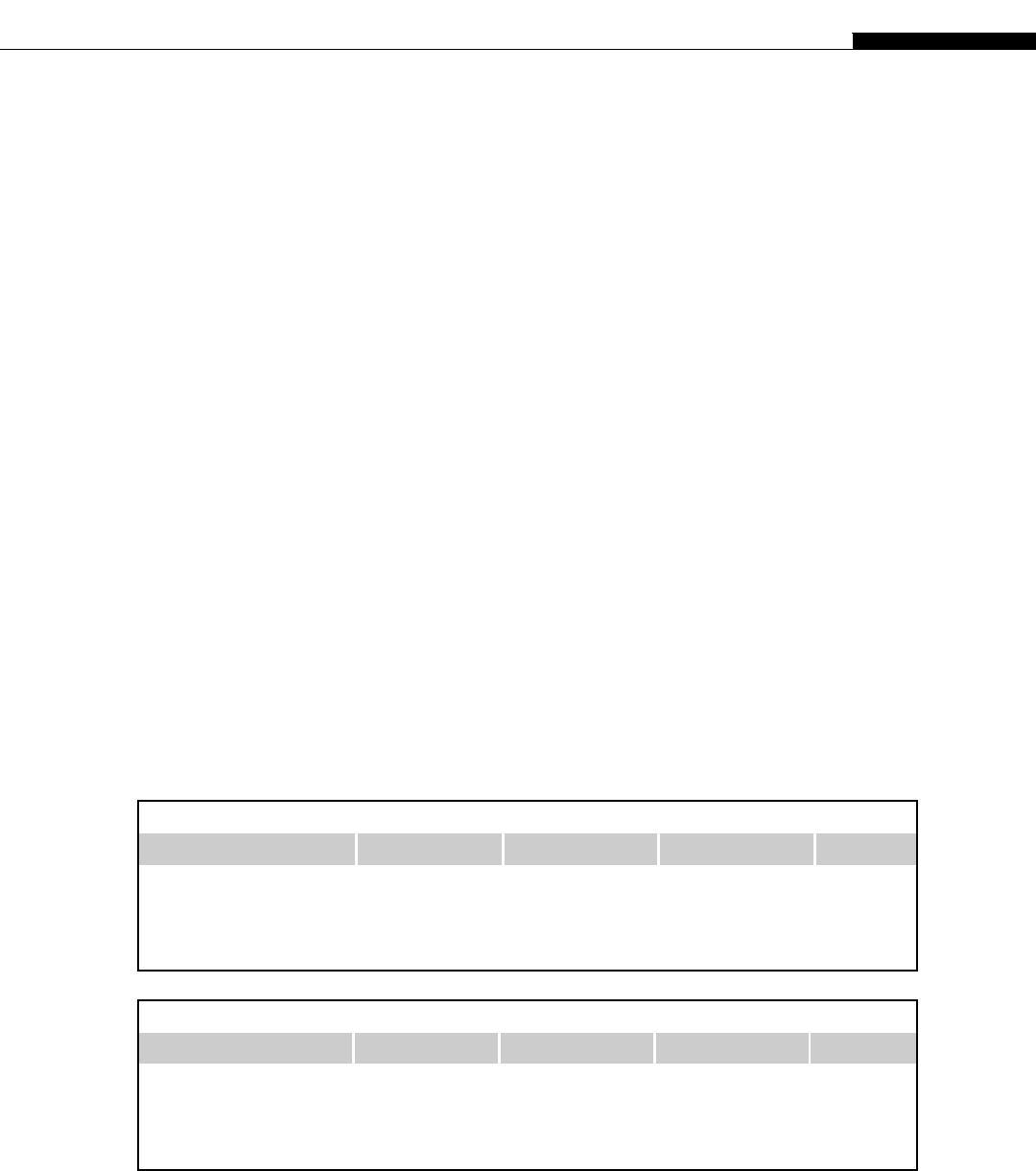
system, we have around 2.5–3 GB/s on the PCI-E 2.0 X8 link. As the number of PCI-E lanes are half
that of the I7 system, these sorts of numbers are around what you might expect to achieve.
We modified the bandwidth test program we used earlier for measuring the PCI-E bandwidth
to measure the bandwidth as we introduce more cards and more concurrent transfers. Any
number of things can affect the transfers once we start introducing concurrent transfers to
different GPUs. Anyone familiar with the multi-GPU scaling within the games industry will
appreciate that simply inserting a second GPU does not guarantee twice the performance. Many
benchmarks show that most commercial games benefit significantly from two GPU cards. Adding
a third card often introduces some noticeable benefit, but nothing like the almost times two
scaling that is often seen with a second card. Adding a fourth card will often cause the
performance to drop.
Now this may not seem very intuitive, adding more hardware equals lower speed. However, it’s the
same issue we see on CPUs when the core count becomes too high for the surrounding components. A
typical high-end motherboard/CPU solution will dedicate at most 32 PCI-E lands to the PCI-E bus.
This means only two cards can run at full X16 PCI-E 2.0 speed. Anything more than this is achieved by
the use of PCI-E switch chips, which multiplex the PCI-E lines. This works well until the two cards on
the PCI-E multiplexer both need to do a transfer at the same time.
The AMD system we’ve run most of these tests in this book on does not use a multiplexer, but drops
the speed of each connected GPU to an X8 link when four GPUs are present. Thus, at 2.5–3 GB/s per
device, we could achieve a theoretical maximum of 10–12.5 GB/s. In addition, being an AMD
solution, the PCI-E controller is built into the processor, which also sits between the PCI-E system and
main memory. The bandwidth to main memory is approximately 12.5 GB/s. Therefore, you can see
this system would be unlikely to achieve the full potential of four GPUs. See Tables 9.2 and 9.3 and
Figures 9.26 and 9.27.
What you can see from Tables 9.2 and 9.3 is that transfers scale quite nicely to three GPUs. We’re
seeing approximately linear scaling. However, when the four GPUs compete for the available
resources (CPU, memory bandwidth, and PCI-E switch bandwidth) the overall rate is slower.
Table 9.2 Bandwidth Effects of Multiple PCI-E Transfers to the Device
1 Device 2 Devices 3 Devices 4 Devices
470 to device 3151 3082 2495 1689
GT9800GT to device 0 3069 2490 1694
GTX260 to device 0 0 2930 1792
GTX460 to device 0 0 0 1822
Table 9.3 Bandwidth Effects of Multiple PCI-E Transfers from the Device
1 Device 2 Devices 3 Devices 4 Devices
470 from device 2615 2617 2245 1599
GT9800 from device 0 2616 2230 1596
GTX260 from device 0 0 2595 1522
GTX460 from device 0 0 0 1493
Strategy 3: Transfers 357
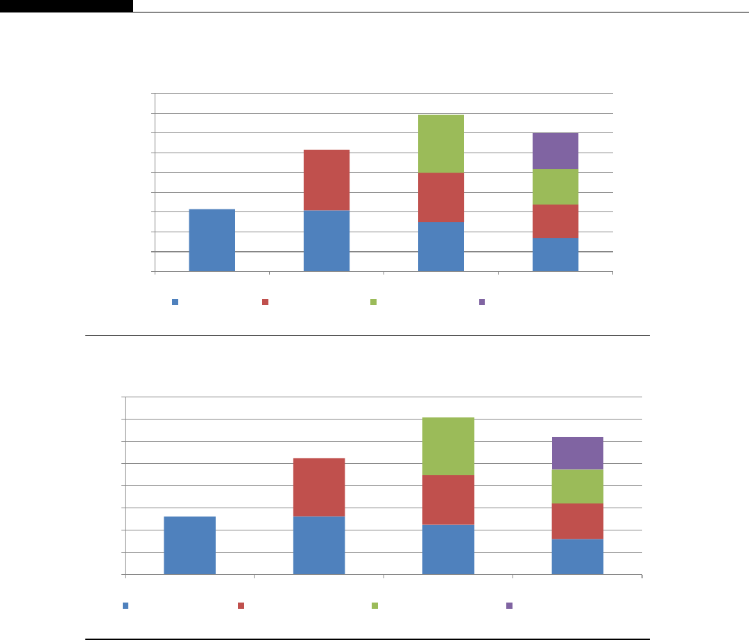
The other multi-GPU platform we have to work with is a six-GPU system based on the
Nehalem I7 platform and the ASUS supercomputer motherboard (P6T7WS) with 3 GTX295 Dual
GPU cards. This uses dual NF200 PCI-E switch chips allowing each PCI-E card to work with a full
X16 link. While this might be useful for inter-GPU communication, the P2P (peer-to-peer) model
supported in CUDA 4.x, it does not extend the bandwidth available to and from the host if both
cards are simultaneously using the bus. We are using GTX290 cards, which are a dual-GPU device.
Internally, each GPU has to share the X16 PCI-E 2.0 link. Table 9.4 and Figure 9.28 show what
effect this has.
0
1000
2000
3000
4000
5000
6000
7000
8000
9000
1 Device 2 Devices 3 Devices 4 Devices
470 To Device 9800GT To Device 260GTX To Device 460 GTX To Device
FIGURE 9.26
Multi-GPU PCI-E bandwidth to device AMD 905e Phenom II.
0
1000
2000
3000
4000
5000
6000
7000
8000
1 Device 2 Devices 3 Devices 4 Devices
470 From Device 9800GT From Device 260GTX From Device 460 GTX From Device
FIGURE 9.27
Multi-GPU PCI-E bandwidth from device AMD 905e Phenom II.
358 CHAPTER 9 Optimizing Your Application

As you can see from Table 9.4, we see an approximate linear increase in total bandwidth to the
device. We achieve a peak of just over 10 GB/s, 20% or so higher than our AMD-based system.
We can see the bandwidth from the device is a different story (Table 9.5 and Figure 9.29).
Bandwidth peaks with two devices, and is not significantly higher than our AMD system. This is not
altogether unexpected if you consider the design in most GPU systems is based around gaming. In
a game, most of the data is being sent to the GPU with very little if any coming back to the CPU host.
Thus, we see a near linear scaling of up to three cards, which coincides with the top-end triple SLI
(scalable link interface) gaming platforms. Vendors have little incentive to provide PCI-E bandwidth
beyond this setup. As the GTX290 is actually a dual-GPU card, we may also be seeing that the internal
Table 9.4 I7 Bandwidth to Device
1 Device 2 Devices 3 Devices 4 Devices 5 Devices 6 Devices
To device 0 5026 3120 2846 2459 2136 2248
To device 1 0 3117 3328 2123 1876 1660
To device 2 0 0 2773 2277 2065 2021
To device 3 0 0 0 2095 1844 1588
To device 4 0 0 0 0 1803 1607
To device 5 0 0 0 0 0 1579
Overall 5026 6237 8947 8954 9724 10,703
0
2000
4000
6000
8000
10000
12000
1 Device 2 Devices 3 Devices 4 Devices 5 Devices 6 Devices
To Device 0 To Device 1 To Device 2 To Device 3 To Device 4 To Device 5
FIGURE 9.28
I7 bandwidth to device.
Strategy 3: Transfers 359
SLI interface is not really able to push the limits of the card. We’re clearly seeing some resource
contention.
Section summary
• Understand and plan for the fact you will have limited PCI-E bandwidth capability.
• Always use pinned memory where possible.
• Use transfer sizes of at least 2 MB.
• Understand the use of zero-copy memory as an alternative to the stream API.
• Think about how to overlap transfer time with kernel execution time.
• Do not expect a linear scaling of bandwidth when using multiple GPUs.
Table 9.5 I7 Bandwidth from Device
1 Device 2 Devices 3 Devices 4 Devices 5 Devices 6 Devices
From device 0 4608 3997 2065 1582 1485 1546
From device 1 0 3976 3677 1704 1261 1024
From device 2 0 0 2085 1645 1498 1536
From device 3 0 0 0 1739 1410 1051
From device 4 0 0 0 0 1287 1035
From device 5 0 0 0 0 0 1049
Overall 4608 7973 7827 6670 6941 7241
0
1000
2000
3000
4000
5000
6000
7000
8000
9000
1 Device 2 Devices 3 Devices 4 Devices 5 Devices 6 Devices
From Device 0 From Device 1 From Device 2 From Device 3 From Device 4 From Device 5
FIGURE 9.29
I7 bandwidth from device.
360 CHAPTER 9 Optimizing Your Application
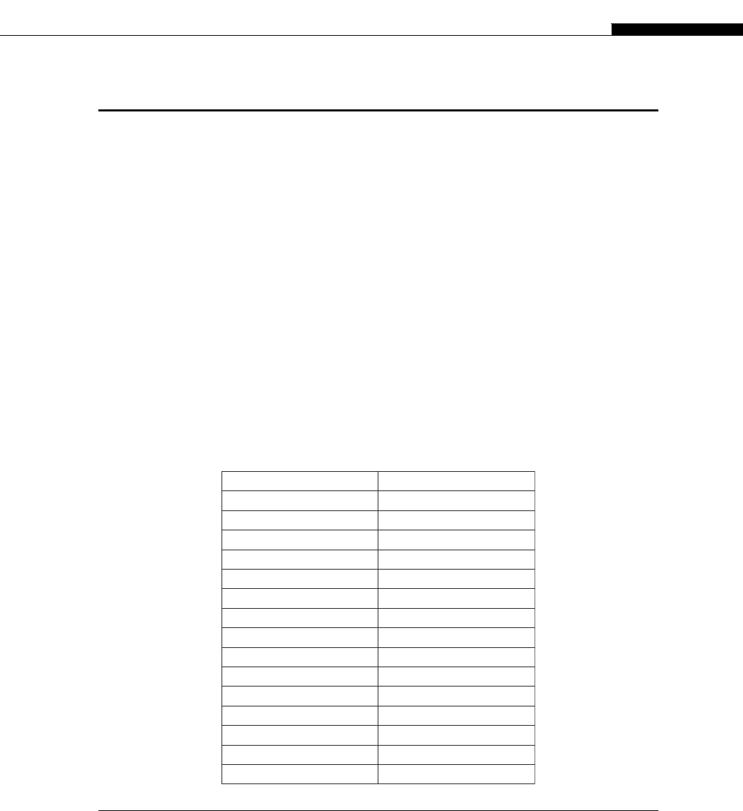
STRATEGY 4: THREAD USAGE, CALCULATIONS, AND DIVERGENCE
Thread memory patterns
Breaking down the application into suitably sized grids, blocks, and threads is often one of the key
aspects of performance of CUDA kernels. Memory is the bottleneck in almost any computer design,
the GPU included. A bad choice of thread layout typically also leads to a bad memory pattern, which
will significantly harm performance.
Consider the first example, a 2 32 layout of threads (Figure 9.30) versus a 32 2 layout of
threads. Think about how they would typically overlay memory if they were processing floating-point
values. In the 2 32 example, thread 0 cannot be coalesced with any other thread than thread 1. In this
case the hardware issues a total of 16 memory fetches. The warp cannot progress until at least the first
half-warp has acquired all the data it needs. Therefore, at least eight of these very long memory
transactions need to complete prior to any compute activity on the SM. As most warps will be
following the same pattern, the SM will be swamped with issuing memory requests while the compute
part of the SM is almost idle.
We saw from the bandwidth analysis in the previous section that there is a limit to the number of
memory requests the SM can push out from the warps. The SM services the data request for any single
warp over two clock cycles. In our example, the request has to be broken into 16 8 byte memory
transactions.
Thread 0 Thread 1
Thread 2 Thread 3
Thread 4 Thread 5
Thread 6 Thread 7
Thread 8 Thread 9
Thread 10 Thread 11
Thread 12 Thread 13
Thread 14 Thread 15
Thread 16 Thread 17
Thread 18 Thread 19
Thread 20 Thread 21
Thread 22 Thread 23
Thread 24 Thread 25
Thread 26 Thread 27
Thread 28 Thread 29
Thread 30 Thread 31
FIGURE 9.30
232 thread grid layout.
Strategy 4: Thread Usage, Calculations, and Divergence 361

On Fermi, the first of these would cause a read miss in the L1 cache. The L1 cache would request
the minimum size of data possible, 128 bytes from the L2 cache, and some 16 times more data than the
thread needs. Thus, when data is moved from the L2 cache to the L1 cache, just 3.125% of the data
moved is consumed by thread 0. As thread 1 also wants the adjacent address, we can increase this to
6.25%, which is still terrible.
On the first run through the code the L2 cache is unlikely to contain the data. It issues a 128-byte
fetch also to slow global memory. This latency-expensive operation is finally performed and 128 bytes
arrive at the L2 cache.
The L2 cache is 768 K in size on a 16 SM device. Assuming we’re using a GTX580, we have 16 SMs.
That is just 48 KB per SM, the maximum size of the L1 cache. Using 128-byte cache lines we have just
384 entries in the cache per SM. If we assume the SM is fully loaded with 48 warps (Kepler supports 64),
each warp will issue 16 separate reads, which is 768 reads in total. This means we’d need 768 cache
lines, not the 384 we have, just to cache the data needed so each warp can hold a single block in memory.
The cache is effectively far too small to be used for temporal locality in this example. By temporal
locality we mean we expect the data to remain in the cache from one read to the next. Halfway through
processing the warps in each SM, the cache is full and the hardware starts filling it with new data.
Consequently, there is absolutely no data reuse with the L2 cache, but a significant overhead in having
to fetch entire cache lines. In fact, the only saving grace is that Fermi, unlike previous generations, will
now forward the data it fetched to the other thread in our example.
The cache model is one that can cause problems in that it allows people to think the hardware will
save them from poor programming. Let’s assume for a moment we have to use this thread pattern and we
would have processed the element we fetched from memory a number of times. The thread pattern for
fetching data does not have to be the same thread pattern for using the data. We can fetch data into shared
memory in a 32 2 pattern, synchronize the threads, and then switch to a 2 32 usage pattern if we
wish. Despite the shared memory bank conflicts this would then incur, it would still be an order of
magnitude faster than doing the global memory fetches. We can also simply add a padding element to the
shared memory by declaring it as 33 2 to ensure when we access it, these bank conflicts are removed.
Consider for a moment the difference in handling of the memory system. We issue 1 coalesced read
for 128 bytes instead of 16 separate reads. There’s a factor of 16:1 improvement in both the number of
memory transactions in flight and also bandwidth usage. Data can be moved from the L2 to the L1
cache in just one transaction, not 16.
The LSUs in the SM have to issue only a single fetch transaction instead of 16 separate
fetches, taking just 2 clock cycles instead of 32 and freeing up the LSUs for other tasks from other warps.
Each warp consumes a single cache line, 48 maximum per SM. Thus, of the 384 cache lines we
have per SM in the L2 cache, we’re using only 100, just 12.5% of the L2 cache instead of 200%. Thus,
it’s absolutely critical that to get anywhere near the full performance, even in Fermi with its multilevel
caches, you have to fetch data in coalesced blocks of 128 bytes across a warp.
Now we could configure the L2 cache to fetch only 32 bytes instead of 128 bytes using the -Xptxas
-dlcm¼cg compiler flag. However, this also disables global memory storage in the L1 cache. It’s an
easy fix but a poor solution to the fact that you are not fetching data in large enough blocks from global
memory. To get the best performance from a given device, you need to understand what’s going on
down inside or use libraries that are coded by someone who does.
We can see this quite clearly with the effects on memory bandwidth with Parallel Nsight if you
select “Custom” experiment and then add in the L1 and L2 cache counters. The particular counters we
362 CHAPTER 9 Optimizing Your Application
are interested in are shown in Table 9.6. These can be set up in Parallel Nsight using the “Custom”
experiment, shown in Figure 9.31.
From these counters we can manually work out the L1 and L2 cache hit ratio. The hit ratio is the
percentage of reads (or writes) that we cached. Every cached access saves us several hundreds of
cycles of global memory latency.
Table 9.6 Parallel Nsight Cache Counters
Nsight Counter Usage
L1 global load hits The number of global
memory load requests
met by the L1 cache.
L1 global load misses The number of global
memory load requests not
met by the L1 cache.
L2 subpartition 0 read
section misses
Half the number of L2
misses.
L2 subpartition 1 read
section misses
The other half of the
number of L2 misses.
L2 subpartition 0 read
section queries
Half the number of L2
access attempts.
L2 subpartition 1 read
section queries
The other half of the
number of L2 access
attempts.
FIGURE 9.31
Setting up Parallel Nsight to capture cache statistics.
Strategy 4: Thread Usage, Calculations, and Divergence 363
When we look at the results for the sample sort algorithm in Table 9.7, we can instantly see the L2 cache
hit ratio drops off sharply as soon as the kernel exceeds 64 threads. Occupancy increases, but performance
drops off. This is not at all surprising given the usage of the L2 cache a prefix sum array will generate. If
each thread is processing one bin, as we extend the number of threads, the size of the memory area being
cached increases. As soon as it exceeds the L2 cache size the hit ratio rapidly drops off.
The solution to the problem is to replace the existing algorithm that uses one thread per bin with
one where the threads all work on a single bin at a time. This way we’d achieve coalesced memory
accesses on each iteration and significantly better locality of memory access. An alternative solution
would be to use shared memory to handle the transition between noncoalesced access by the threads
and the necessary coalesced access when reading or writing to global memory.
Inactive threads
Threads, despite there being many thousands of them, are not free, even if they are inactive. The problem
with inactive threads is twofold. First, a warp will remain active, scheduled, and using resources if just one of
its threads is active. There are a limited number of warps that can be dispatched in a dispatch period (two
clock cycles). This is two on compute 2.0 hardware, four on compute 2.1 hardware and eight in compute 3.x
hardware. There is no point in the hardware dispatching a warp with a single thread to a set of CUDA cores
and having it use just a single CUDA core while the other 15 idle. However, this is exactly what the hardware
has to do if there is divergence of execution flow within a warp down to just one thread being active.
You sometimes see a parallel reduction–type operation that has been written by a programmer who
does not understand the hardware well. They will perform the reduction operation within every warp,
going from 32 to 16, to 8, to 4, to 2, and finally to 1 active thread. Regardless of whether you use 32 threads
or 1 thread the hardware still allocates 32 and simply masks out the inactive ones. Because the warps are
still active, even if they have only one thread active, they still need to be scheduled onto the hardware.
A much better approach to this is to have all 32 threads in every block compute a set of partial
results. Let’s use the sum operation, as it’s easy to understand. With 32 threads per warp, you can
compute 64 additions in one cycle. Now have each thread store its value into shared memory. Thus, the
first warp stores to element 0..31, the second to 32..63, etc. Now divide N, the number of elements of
the reduction, by 2. Repeat the reduction using the threshold if (threadIdx.x < (N/2)) until such
time as Nequals 2.
Table 9.7 Cache Hit Ratio for Sample Sort
Function Time Occupancy
Active
Warps Blocks Threads
L1
Hit
%
L2
Hit
%
sort_bins_gpu_kernel 28.8
ms
0.17 8 512 32 87 69
sort_bins_gpu_kernel 33.5
ms
0.33 16 256 64 86 60
sort_bins_gpu_kernel 44.4
ms
0.67 32 128 128 80 36
sort_bins_gpu_kernel 47
ms
0.83 40 64 256 78 32
364 CHAPTER 9 Optimizing Your Application

Threads 0..255 read values 0..511 (eight active warps).
Threads 0..127 read values 0..256 (four active warps).
Threads 0..63 read values 0..127 (two active warps).
Threads 0..31 read values 0..63 (one active warp).
Threads 0..15 read values 0..31 (half an active warp).
Etc.
Warps with thread numbers greater than the threshold simply no longer get scheduled. The warps with
values less than Nare fully populated with work, until such time as Nequals some value less than 32. At this
point we can simply do an addition or all remaining elements, or continue to iterate toward the final addition.
Inactive warps are not in themselves free either. Although the SM internally cares about warps, not
blocks, the external scheduler can only schedule blocks into an SM, not warps. Thus, if each block contains
only one active warp, we can have as little as 6 to 8 warps for the SM to select from for scheduling. Usually
we’d have up to 64 warps active in an SM, depending on the compute version and resource usage. This is
a problem because the thread-level parallelism (TLP) model relies on having lots of threads to hide
memory and instruction latency. As the number of active warps drops, the ability of the SM to hide latency
using TLP also dramatically drops. As some point this will hurt the performance, especially if the warp is
still making global memory accesses.
Therefore, at the last levels of such a reduction-type operation, or any operation where progres-
sively larger numbers of warps will drop out, we need to introduce some instruction level parallelism
(ILP). We want to terminate the last warp as soon as possible so the entire block can be retired and
replaced with another block that will likely have a fresh set of active warps.
We look at reduction in detail later in this chapter.
Arithmetic density
Arithmetic density is a term that measures the relative number of calculations per memory fetch. Thus,
a kernel that fetches two values from memory, multiplies them, and stores the result back to memory
has very low arithmetic density.
C[z] ¼A[y] * B[x];
The fetch and store operations may well involve some index calculations. The real work being done
is the multiplication. However, with only one operation being performed per three memory trans-
actions (two reads and one write), the kernel is very much memory bound.
The total execution time is
T¼read timeðAÞþreads timeðBÞþarithmetic timeðMÞþstore timeðCÞ
or
T¼AþBþMþC
Notice we use here AþBas opposed to multiplying A, the single memory fetch time, by 2. The indi-
vidual read times are not easy to predict. In fact neither A,B,orCare constant, as they are affected by the
loads other SMs are making on the memory subsystem. Fetching of Amay also bring into the cache B,
so the access time for Bis considerably less than A. Writing Cmay evict from the cache Aor B.
Strategy 4: Thread Usage, Calculations, and Divergence 365

Changes to the resident lines in the L2 cache may be the result of the activity of an entirely different SM.
Thus, we can see caching makes timing very unpredictable.
When looking at the arithmetic density, our goal is to increase the ratio of useful work done
relative to memory fetches and other overhead operations. However, we have to consider what we
define as a memory fetch. Clearly, a fetch from global memory would qualify for this, but what
about a shared memory, or cache fetch? As the processor must physically move data from shared
memory to a register to operate on it, we must consider this also as a memory operation. If the data
comes from the L1, L2, or constant cache, it too has to be moved to a register before we can
operate on it.
However, in the case of a shared memory or L1 cache access, the cost of such operations is reduced
by an order of magnitude compared to global memory accesses. Thus, a global memory fetch should
be weighted at 10if a shared memory fetch equates to 1.
So how do we increase the arithmetic density of such instruction flows? First, we have to under-
stand the underlying instruction set. The maximum operand size of an instruction is 128 bytes, a four-
element vector load/store operation. This tells us the ideal chunk size for our data is four elements,
assuming we’re using floats or integers, two if we’re using doubles. Thus, our operation should be in
the first instance:
C[idx_C].x ¼A[idx_A].x * B[idx_b].x;
C[idx_C].y ¼A[idx_A].y * B[idx_b].y;
C[idx_C].z ¼A[idx_A].z * B[idx_b].z;
C[idx_C].w ¼A[idx_A].w * B[idx_b].w;
I’ve written this in long-hand form to make the operations clear. If you extend the vector-type
class yourself and provide a multiplication operator that performs this expanded code, you can
simply write
C[idx_C] ¼A[idx_A] * B[idx_b];
Unfortunately, the GPU hardware currently doesn’t support such vector manipulations, only loads,
stores, moves, and pack/unpack from scalar types.
With such vector-based operations, we amortize the cost of the associated operations (load A, load
B, write C, calculate idx_A, calculate idx_B, calculate idx_C) over four multiplies instead of one. The
load and store operations take marginally longer as we have to introduce a pack and unpack operation
that was not needed when accessing scalar parameters. We reduce the loop iterations by a factor of four
with a consequential drop in the number of memory requests, issuing a much smaller number of larger
requests to the memory system. This vastly improves performance (~20%), as we have seen with some
examples in this book.
Transcendental operations
The GPU hardware is aimed at speeding up gaming environments. Often these require the manipu-
lation of hundreds of thousands of polygons, modeling the real world in some way. There are certain
accelerators built into the GPU hardware. These are dedicated sections of hardware designed for
a single purpose. GPUs have the following such accelerators:
• Division
• Square root
366 CHAPTER 9 Optimizing Your Application

• Reciprocal square root
• Sine
• Cosine
• Log
2
• Base 2 exponent Ex
2
These various instructions perform operations to 24-bit accuracy, in line with the typical 24-bit
RGB setup used in many game environments. None of these operations are enabled by default.
Compute 1.x devices take various shortcuts that make single-precision math not IEEE 754
compliant. These will not be relevant to many applications, but be aware they are there. Fermi
(compute 2.x) hardware brings IEEE compliance with regard to floating-point operations by
default.
If you’d like the faster but less precise operation, you have to enable them using either the compile
switch (-use_fast_math) or explicitly using intrinsic operations. The first step is simply to enable the
option in the compiler and check the outcome of your existing application. The answer will be
different, but by how much and how important this is, are the key questions. In the gaming industry it
doesn’t matter if the flying globe projectile is one pixel off to the left or right of the targetdno one will
notice. In compute applications it can make a very real difference.
Individual operations can also be selectively enabled in 24-bit math using an explicit compiler
intrinsic such as __logf(x), etc. For a complete list of these and an explanation of the drawbacks of
using them, see Appendix C.2 of the CUDA C programming guide. They can considerably speed up
your kernels so it’s worth investigating if this is an option for your particular code.
Approximation
Approximation is a useful technique in problems that explore a certain search space. Double-precision
math is particularly expensive, in the order of at least twice as slow as floating-point math. Single-
precision math uses 24 bits for the mantissa and 8 bits for the exponent. Thus, in the compute 1.x
devices a fast 24-bit integer approximation could be used to provide an additional computation path to
the single- and double-precision math. Note in Fermi, the 24-bit native integer support was replaced
with 32-bit integer support, so an integer approximation in 24-bit math is actually slower than if the
same approximation was made in 32-bit math.
In all compute hardware versions that natively support double precision (compute onwards),
approximation in single precision is at least twice the speed of double-precision math. Sometimes
a much higher speedup can be achieved because the single-precision calculations require less registers
and thus potentially more blocks can be loaded into the hardware. Memory fetches are also half the
size, doubling the effective per-element memory bandwidth. Consumer-based GPUs also have less
double-precision units enabled in the hardware than their Tesla counterparts, making single-precision
approximation a far more attractive proposition for such hardware.
Clearly, with approximating you are performing a tradeoff between speed and accuracy and
introducing additional complexity into the program. Often this is a tradeoff worth exploring, for it can
bring a significant speedup.
Once we have done the approximation, the kernel can test the result to see if it is within a certain
range or meets some criteria by which further analysis is warranted. For this subset of the dataset, the
single- or double-precision calculation is performed as necessary.
Strategy 4: Thread Usage, Calculations, and Divergence 367

The initial pass simply acts as a filter on the data. For every data point that falls outside the criteria
of interest, you have saved the expensive double-precision calculations. For every point that falls into
it, you have added an additional 24- or 32-bit filtering calculation. Thus, the benefit of this approach
depends on the relative cost of the additional filtering calculation versus the cost of double-precision
math required for the full calculation. If the filters remove 90% of the double-precision calculations,
you have a huge speedup. However, if 90% of the calculations require a further double-precision
calculation, then this strategy is not useful.
NVIDIA claims Tesla Fermi has in the order of 8faster double-precision math over the previous
compute 1.3 implementations (GT200 series). However, consumer-level Fermi cards are artificially
restricted to one-quarter the double-precision performance of Tesla cards. Therefore, if double
precision is key to your application, clearly a Tesla is the easy-fix solution to the problem. However,
some may prefer the alternative of using multiple consumer GPUs. Two 3 GB 580 GTXs would likely
provide a faster solution than a single Fermi Tesla for considerably less money.
If double precision is secondary or you simply wish to prototype a solution on commonly
available hardware, then single precision of 24-bit filtered may be an attractive solution to this
issue. Alternatively, if you have a mixture of GPUs, with an older card that is still good for single-
precision usage, you can use the older card to scan the problem space for interesting sections, and
the second card to investigate problem space in detail based on the likely candidates from the first
card’s quick evaluation. Of course with a suitable Tesla card, you can perform both passes with just
asinglecard.
Lookup tables
One common optimization technique used for complex algorithms is a lookup table. On CPUs where
computation is quite expensive, these generally work reasonably well. The principle is that you
calculate a number of representative points in the data space. You then apply an interpolation method
between points based on the proportional distance to either edge point. This is typically used in
modeling of the real world in that a linear interpolation method with a sufficient number of key sample
points provides a good approximation of the actual signal.
A variation on this technique is used in brute-force attacks on ciphers. Passwords on most systems
are stored as hashes, an apparently unintelligible series of digits. Hashes are designed so that it’s
difficult to calculate the password from the hash by reversing the calculation. Otherwise, it would be
trivial to calculate the original password based on a compromised hash table.
One method of attack on this type of system involves a CPU spending a considerable time
generating all possible permutations based on the use of common and/or short passwords. The
attacker then simply matches the precomputer hash against the target hash until such time as a match
is made.
In both cases, the lookup table method trades memory space for compute time. By simply storing
the result, you have instant access to the answer. Many people will have learned multiplication tables in
their heads as children. It’s the same principle; instead of tediously calculating ab, for the most
common set of values, we simply memorize the result.
This optimization technique works well on CPUs, especially older ones, where the compute time
may be significant. However, as the compute resources have become faster and faster, it can be cheaper
to calculate the results than to look them up from memory.
368 CHAPTER 9 Optimizing Your Application

If you consider the average arithmetic instruction latency will be between 18 to 24 cycles and the
average memory fetch in the order of 400 to 600 cycles, you can clearly see we can do a lot of
calculation work in the time it takes for the memory fetch to come back from global memory. This,
however, assumes we have to go out to global memory for the result and that it’s not stored in shared
memory or the cache. It also does not consider that the GPU, unlike the CPU, will not idle during this
memory fetch time. In fact, the GPU will likely have switched to another thread and be performing
some other operation. This, of course, depends on the number of available warps you have scheduled
onto the device.
In many cases the lookup may win over the calculation, especially where you are achieving a high
level of GPU utilization. Where you have low utilization, the calculation method often wins out,
depending of course on how complex the calculation really is. Let’s assume we have 20-cycle
instruction latency for arithmetic operations and 600-cycle latency for memory operations. Clearly, if
the calculation takes less than 30 operations it would be much faster than lookup in memory when we
have low GPU utilization. In this case the SM is behaving like a serial processor, in that it has to wait
for the memory fetch. With a reasonable utilization the memory fetch effectively becomes free, as the
SM is simply executing other warps.
It’s often a case of trying this and seeing how well it works. Also be prepared to take it back out
again should you suddenly manage to increase utilization of the GPU through other means.
Note, in the case of linear interpolation, a low-precision floating point–based linear interpo-
lation is available in the GPU hardware. This is a feature of the texture memory hardware,
something we do not cover in this text. Texture memory was useful for its cache features (24 K per
SM) in compute 1.x hardware, but this use has largely been made redundant by the L1/L2 cache
introduced in Fermi. However, the linear interpolation in hardware may still be useful for some
problems. See the “Texture and Surface Memory” chapter of the CUDA programming guide if this
is of interest to you.
Some common compiler optimizations
We’ll take a quick look at some compiler optimizations and how they affect GPUs. We cover these
here to highlight cases where the optimizer may struggle and also to give you some understanding
of how optimizations may be applied at the source code level where the automatic optimizations
fail.
Some compilers are well known for producing efficient code on certain targets. Not surprisingly,
the Intel ICC compiler produces extremely efficient code for the Intel platform. New features of the
processor are incorporated rapidly to showcase the technology. Mainstream compilers often come
from a code base that supports many targets. This allows for more efficient development, but means the
compiler may not be so easy to customize for a single target.
As of the 4.1 SDK CUDA moved from using an Open64-based compiler to a more modern
LLVM-based compiler. The most significant benefit from the user perspective is significantly faster
compile times. NVIDIA also claims a 10% improvement in code speed. We saw noticeable
improvements in code generation with this move. However, as with any new technology, there is room
for improvement and I’m sure this will happen over time.
The optimizations compilers apply are well documented. What we present here is a broad
overview of some common ones. For most programmers, simply setting the optimization level is
Strategy 4: Thread Usage, Calculations, and Divergence 369

entirely sufficient. Others prefer to know what exactly is going on and check the output. This is of
course a tradeoff of your programming time versus the potential gain and the relative costs of
these.
Strength reduction
When accessing an array index, typically nonoptimized compiler code will use
array_element_address ¼index * element size
This can be more efficiently replaced by one of two techniques. First, we must load the array base
address (element 0) into a base register. Then we have the option of accessing an index as base þ
offset. We can also simply add a fixed offset, the size of an array element in bytes, to the base register
after each loop iteration.
In terms of C this is the same as writing
{
int i;
int a[4];
for (i¼0;i<4;iþþ)
a[i]¼i;
}
vs.
{
int i;
int a[4];
int *_ptr ¼a;
for (i¼0; i<4; iþþ)
*_ptrþþ ¼ i;
}
In terms of GPU usage, this optimization relies on the fact that certain instructions (multiply,
divide) are computationally expensive and others (addition) are cheaper. It tries to replace the
expensive operations with cheaper (or faster) ones. This technique works well on CPUs as well as on
GPUs. This is especially the case with compute 2.1 devices where integer addition has three times the
throughput of integer multiplication.
Notice also that the pointer version of the code creates a dependency between loop iterations.
The value of ptr must be known to execute the assignment. The first example is much easier to
parallelize because there is no dependency on the loop iteration and the address of a[i] can
easily be statically calculated. In fact, simply adding the #pragma unroll directive would have
caused the compiler to unroll the entire loop, as the boundaries in this simple example are
literals.
It’s a typical example of a CPU-based optimization that may have been applied and to parallelize
the loop you need to reverse-engineer back to the original code. It’s shown here because it helps you
370 CHAPTER 9 Optimizing Your Application

understand how C code may have been changed in the past to provide faster execution time for a given
target. Like most optimizations at the C source code level, it can lead to the purpose of the source code
being obscured.
Loop invariant analysis
Loop invariant analysis looks for expressions that are constant within the loop body and moves them
outside the loop body. Thus, for example,
for (int j¼0;j<100;jþþ)
{
for (int i¼0; i<100; iþþ)
{
const int b ¼j * 200;
q[i]¼b;
}
}
In this example, the parameter jis constant within the loop body for parameter i. Thus, the
compiler can easily detect this and will move the calculation of boutside the inner loop and generate
the following code:
for (int j¼0;j<100;jþþ)
{
const int b ¼j * 200;
for (int i¼0; i<100; iþþ)
{
q[i]¼b;
}
}
This optimized code removes thousands of unnecessary calculations of b, where j, and thus b, are
constant in the inner loop. However, consider the case where bis an external to the function, a global
variable, instead of a local variable. For example:
int b;
void some_func(void)
{
for (int j¼0;j<100;jþþ)
{
for (int i¼0; i<100; iþþ)
{
b¼j * 200;
q[i]¼b;
}
}
}
Strategy 4: Thread Usage, Calculations, and Divergence 371

The compiler cannot safely make this optimization because the write to qmay affect b. That is,
the memory space of qand bmay intersect. It cannot even safely reuse the result of j * 200 in the
assignment to q, but must reload it from memory, as the contents of bmay have changed since the
assignment in the prior line.
If you consider each line individually, then the issue becomes somewhat clearer. Any memory
transaction, a read or write, will likely cause a switch to another warp, if that transaction involves
accessing anything that is not immediately available. That area of global memory is accessible to any
thread in any warp, on any active block in any SM. From one instruction to the next you get the very
real possibility that any writable non register data could have changed.
You might say, well I’ve split up the application into Ntiles and the tiles do not intersect, so this is
not necessary. As the programmer you may know this, but it is very difficult for the compiler to figure
that out. Consequently, it opts for the safe route and does not perform such optimizations. Many
programmers do not understand what the optimization stage of a compiler does, and thus when it does
something that breaks the code, they blame the compiler. Consequently, compilers tend to be rather
conservative in how they optimize code.
As the programmer, understanding this allows you to make such optimization at the source level.
Remember to think of global memory as you might a slow I/O device. Read from it once and reuse the data.
Loop unrolling
Loop unrolling is a technique that seeks to ensure you do a reasonable number of data operations for
the overhead of running through a loop. Take the following code:
{
for (i¼0;i<100;iþþ)
q[i]¼i;
}
In terms of assembly code, this will generate:
• A load of a register with 0 for parameter i.
• A test of the register with 100.
• A branch to either exit or execute the loop.
• An increment of the register holding the loop counter.
• An address calculation of array qindexed by i.
• A store of ito the calculated address.
Only the last of these instructions actually does some real work. The rest of the instructions are
overhead.
We can rewrite this C code as
{
for (i¼0;i<25;iþ¼4)
q[i]¼i;
q[iþ1]¼iþ1;
q[iþ2]¼iþ2;
q[iþ3]¼iþ3;
}
372 CHAPTER 9 Optimizing Your Application

Thus, the ratio of useful work to overhead of using the loop is much increased. However, the size of
the C source code is somewhat increased and it’s now less obvious what exactly it was doing compared
to the first loop.
In terms of PTX code, we see each C statement translated into PTX. For every branch test, there are
now four memory copy operations. Thus, the GPU is executing more instructions than before, but
a higher percentage of the memory copy operations are doing useful work.
In the CPU domain often there are limited registers, so the same registers will be reused in each
step. This reduces register overhead, but means q[iþ1] cannot start processing until q[i] has
completed. We’d see the same overhead on the GPU with this approach. Each instruction has 20 cycles
of latency. Therefore, the GPU assigns each address calculation to a separate register, so we have a set
of four parallel instructions, rather than four sequential instructions executing. Each set is pushed into
the pipelines and thus comes out one after another almost back to back.
With this approach the limit is the number of registers. As the GPU has 64 (compute 2.x,3.0) and
128 (compute 1.x) maximum, there is considerable scope for unrolling small loop bodies and
achieving a good speedup.
The NVCC compiler supports the #pragma unroll directive, which will automatically unroll fully
such loops when the iteration count is constant or silently do nothing when it’s not. The latter is less
than helpful, if the programmer has specified the loop should be unrolled. If the compiler is not able to,
it should complain about this until the code is amended or the pragma removed.
You can also specify #pragma unroll 4 where four is replaced by any number the programmer
wishes. Typically four or eight will work well, but beyond that too many registers will be used and this
will result in register spilling. On compute 1.x hardware, this will cause a huge performance drop as
registers are spilled to global memory. From compute 2.x hardware onwards, registers are spilled to the
L1 cache and then to global memory if necessary. The best solution is to try it and see which value
works best for each loop.
Loop peeling
Loop peeling is an enhancement to the loop unrolling, when the number of iterations is not an exact
multiple of the loop unrolling size. Here the last few iterations are peeled away and done separately,
and then the main body of the loop is unrolled.
For example, if we have 101 loop iterations and plan to use four levels of loop unrolling, the first
100 iterations of the loop are unrolled and the final iteration is peeled away to allow the bulk of the
code to operate on the unrolled code. The final few iterations are then handled as either a loop or
explicitly.
Loop peeling can be equally applied to the start of a loop as to the end. It can be used in such cases
to allow a nonaligned structure to be accessed as an aligned structure. For example, copying a byte-
aligned memory section to another byte-aligned memory is slow because it has to be done one byte at
a time. The first few iterations can be peeled away such that a 32-, 64-, or 128-byte alignment is
achieved. Then the loop can switch to much faster word, double-, or quad-word based copies. At the
end of the loop the byte-based copies can be used again.
When using the #pragma loop unroll N directive, the compiler will unroll the loop such that the
number of iterations does not exceed the loop boundaries and insert the end of loop peeling code
automatically.
Strategy 4: Thread Usage, Calculations, and Divergence 373

Peephole optimization
This optimization simple searches for combinations of instructions that can be replaced by more
complex instructions with the same functionality. The classic example of this is multiply followed by
an add instruction, as you might see in a gain and offset type calculation. This type of construct can be
replaced with the more complex madd (multiply and add) instruction, reducing the number of
instructions from two to one.
Other types of peephole optimizations include simplification of flow of control, algebraic
simplifications, and removal of unreachable code.
Common subexpressions and folding
Many programmers write code that repeats some operation, for example,
const int a ¼b[base þi] * c[base þi];
or
const int a ¼b[NUM_ELEMENTS-1] * c[NUM_ELEMENTS-1];
In the first example, arrays band care indexed by the base and iparameters. Providing these
parameters are within local scope, the compiler can simply calculate the index (base þi), and add this
value to the start address of arrays band cand to the work address for each parameter. However, if
either of the index parameters are global variables, then the calculation must be repeated, since either
could have changed once multiple threads are used. With a single thread it would be safe to eliminate
the second calculation. With multiple threads it may also be safe to do so, but the compiler doesn’t
know for sure, so will typically perform two calculations.
In the second example, the term NUM_ELEMENTS-1 is repeated. If we assume that NUM_ELEMENTS is
a define, then the preprocessor will substitute the actual value, so we get b[1024-1] * c[1024-1].
Clearly, 1024 1 can in both instances be replaced by 1023. However, if NUM_ELEMENTS was actually
a formal parameter, as it is in many kernel calls, this type of optimization is not available. In this case
we have to drop back to common subexpression optimization.
Therefore, be aware that in making such constants parameters of a function, or by having
such parameters in global memory, you may be limiting the compiler’s ability to optimize the code.
You then have to ensure such common subexpressions are not present in the source code. Often
eliminating the common subexpressions makes the code simpler to understand and improves the
performance.
Divergence
GPUs execute code in blocks, or warps. A single instruction is decoded once and dispatched to a warp
scheduler. There it remains in a queue until the warp dispatcher dispatches it to a set of 32 execution
units, which execute that instruction.
This approach amortizes the instruction fetch and decoding time over Nexecution units. This in
itself is very similar to the old vector machines. However, the main difference is that CUDA does not
require that every instruction execute in this way. If there is a branch in the code and only some
instructions follow this branch, those instructions diverge while the others wait at the point of
divergence.
374 CHAPTER 9 Optimizing Your Application

The single fetch/decode logic then fetches the instruction stream for the divergent threads and the
other threads simply ignore it. In effect, each thread within the warp has a mask that enables its
execution or not. Those threads not following the divergence have the mask cleared. Conversely, those
following the branch have the bit set.
This type of arrangement is called predication. A predicate is created, which results in a single bit
being set for those threads within a warp that follow the branch. Most PTX op-codes support an
optional predicate allowing selective threads to execute an instruction.
Thus, for example, consider the following code:
if (threadIdx.x < 32)
{
if (threadIdx.x < 16)
{
if (threadIdx.x < 8)
func_a1();
else
func_a2();
}
else
{
func_b();
}
}
In the first line of code the program eliminates all other warps in the current block except the first
warp, the first 32 threads. This does not result in any divergence within the warp. The other warps in the
block are simply not scheduled for this section of the code. They do not stall, but fall through the code
and continue the execution of subsequent code.
The first warp then meets a test for threadIdx.x < 16, which splits the warp exactly in half. This is
a special scenario where the warp does not actually diverge. Although the warp size is 32, the
divergence criteria are actually a half-warp. If you noticed earlier, the CUDA cores are arranged in
banks of 16 cores, not 32 cores. The scheduler issues instructions to two or more sets of 16 cores per
cycle. Thus both the true and false path of the conditional are executed.
In the subsequent step, threads 16 to 31 call the function func_b. However, threads 0..15 hit another
conditional. This time it’s not half-warp based, but quarter-warp based. The minimum scheduling
quantity is 16 threads. Thus, the first set of eight threads jump off to call function func_a1 while the
second set of eight threads (8..15) stall.
Functions func_b and func_a1 will continue to independently fetch instructions and dispatch them
to the two half-warps. This is somewhat less efficient than a single instruction fetch, but nonetheless
better than sequential execution. Eventually func_a1 will complete and func_a2 will start, stalling the
threads 0..7. In the meantime func_b may have also completed. We can write a short test program to
demonstrate this.
// All threads follow the same path
__global__ void cuda_test_kernel(
u32 * const a,
const u32 * const b,
Strategy 4: Thread Usage, Calculations, and Divergence 375

const u32 * const c,
const u32 num_elements)
{
const u32 tid ¼(blockIdx.x * blockDim.x) þthreadIdx.x;
if (tid < num_elements)
{
for (u32 iter¼0; iter<MAX_ITER; iterþþ)
{
a[tid] þ¼ b[tid] * c[tid];
}
}
}
// Thread diverge by half warps
__global__ void cuda_test_kernel_branched_half(
u32 * const a,
const u32 * const b,
const u32 * const c,
const u32 num_elements)
{
const u32 tid ¼(blockIdx.x * blockDim.x) þthreadIdx.x;
if (tid < num_elements)
{
for (u32 iter¼0; iter<MAX_ITER; iterþþ)
{
if (threadIdx.x < 16)
a[tid] þ¼ b[tid] * c[tid];
else
a[tid] -¼b[tid] * c[tid];
}
}
}
// Thread diverge into one quarter group
__global__ void cuda_test_kernel_branched_quarter(
u32 * const a,
const u32 * const b,
const u32 * const c,
const u32 num_elements)
{
const u32 tid ¼(blockIdx.x * blockDim.x) þthreadIdx.x;
if (tid < num_elements)
{
for (u32 iter¼0; iter<MAX_ITER; iterþþ)
{
376 CHAPTER 9 Optimizing Your Application

if (threadIdx.x < 16)
{
if (threadIdx.x < 8)
{
a[tid] þ¼ b[tid] * c[tid];
}
else
{
a[tid] -¼b[tid] * c[tid];
}
}
else
{
a[tid] þ¼ b[tid] * c[tid];
}
}
}
}
// Thread diverge into one eighth group
__global__ void cuda_test_kernel_branched_eighth(
u32 * const a,
const u32 * const b,
const u32 * const c,
const u32 num_elements)
{
const u32 tid ¼(blockIdx.x * blockDim.x) þthreadIdx.x;
if (tid < num_elements)
{
for (u32 iter¼0; iter<MAX_ITER; iterþþ)
{
if (threadIdx.x < 16)
{
if (threadIdx.x < 8)
{
if (threadIdx.x < 4)
a[tid] þ¼ b[tid] * c[tid];
else
a[tid] -¼b[tid] * c[tid];
}
else
{
if (threadIdx.x >¼8)
a[tid] þ¼ b[tid] * c[tid];
else
a[tid] -¼b[tid] * c[tid];
}
Strategy 4: Thread Usage, Calculations, and Divergence 377

}
else
{
a[tid] þ¼ b[tid] * c[tid];
}
}
}
}
Here we have set up a number of kernels, each of which exhibit different levels of divergence. The
first is the optimal with no divergence. The second diverges based on half-warps. These half-warps
should execute in parallel. We then further subdivide the first half-warp into two groups. These should
execute in series. We then subdivide again the first group into a total of four serial execution paths. The
results we see are as follows:
ID:0 GeForce GTX 470:Running 32768 blocks of 32 threads to calculate 1048576 elements
ID:0 GeForce GTX 470:All threads : 27.05 ms (100%)
ID:0 GeForce GTX 470:Half warps : 32.59 ms (121%)
ID:0 GeForce GTX 470:Quarter warps: 72.14 ms (267%)
ID:0 GeForce GTX 470:Eighth warps : 108.06 ms (400%)
ID:1 GeForce 9800 GT:Running 32768 blocks of 32 threads to calculate 1048576 elements
ID:1 GeForce 9800 GT:All threads : 240.67 ms (100%)
ID:1 GeForce 9800 GT:Half warps : 241.33 ms (100%)
ID:1 GeForce 9800 GT:Quarter warps: 252.77 ms (105%)
ID:1 GeForce 9800 GT:Eighth warps : 285.49 ms (119%)
ID:2 GeForce GTX 260:Running 32768 blocks of 32 threads to calculate 1048576 elements
ID:2 GeForce GTX 260:All threads : 120.36 ms (100%)
ID:2 GeForce GTX 260:Half warps : 122.44 ms (102%)
ID:2 GeForce GTX 260:Quarter warps: 149.60 ms (124%)
ID:2 GeForce GTX 260:Eighth warps : 174.50 ms (145%)
ID:3 GeForce GTX 460:Running 32768 blocks of 32 threads to calculate 1048576 elements
ID:3 GeForce GTX 460:All threads : 43.16 ms (100%)
ID:3 GeForce GTX 460:Half warps : 57.49 ms (133%)
ID:3 GeForce GTX 460:Quarter warps: 127.68 ms (296%)
ID:3 GeForce GTX 460:Eighth warps : 190.85 ms (442%)
We can see this somewhat better in a graphical format in Figure 9.32.
Notice how the thread divergence is not such a significant problem on the compute 1.x devices (the
9800 GT and GTX260). It has an effect, but takes the maximum time to just 145% of the optimal time.
By comparison, the Fermi compute 2.x cards (GTX460, GTX470) suffer over a 4slowdown when
diverging significantly within a warp. The GTX460 seems especially sensitive to warp divergence.
Notice the GTX470 is almost 10faster in absolute terms than the 9800 GT when there is no
divergence, which is a massive improvement for just two generations of cards.
If you are curious to know how much a 32-way divergence costs, it leads to a 27slowdown on the
compute 1.x cards and a massive 125to 134slowdown on the compute 2.x cards. Note that the
378 CHAPTER 9 Optimizing Your Application

code for this test was a simple switch statement based on the thread index, so it is not directly
comparable to the code we’re using here. However, clearly such divergence needs to be avoided at
all costs.
The easiest method of avoiding divergence within a warp is to simply mask out the sections of the
warp you don’t wish to contribute to the result. How can you do this? Just perform the same calculation
on every thread in the warp, but select a value that does not contribute for the threads you wish to
mask out.
For example, for a min operation on 32-bit integers, select 0xFFFFFFFF as the value for threads that
should not contribute. Conversely for max,sum, and many other arithmetic-type operations, just use 0 in
the threads you do not wish to contribute. This will usually be much quicker than branching within
a warp.
Understanding the low-level assembly code
The GPU compiles code into a virtual assembly system called PTX (Parallel Thread eXecution
Instruction Set Architecture). This is a lot like Java byte-code in that it is a virtual assembly language.
This can either be translated at compile time or runtime into the real code, which executes on the
device. The compile time translation simply inserts a number of real binaries into the application,
depending on which architectures you specify on the command line (the –arch switch).
To look at the virtual assembly generated, you simply add the –keep flag to the compiler command
line. For Visual Studio users, the default NVIDIA projects contain an option to keep the PTX files
(–keep)(Figure 9.33). You can also specify the place to store them if you prefer they do not clutter up
the project directory using the –keep-dir <directory> option.
However, PTX is not what is really executed on the hardware, so it’s useful only to a certain degree.
You can also see the actual binary post translation using the cuobjdump utility as follows:
cuobjdump –sass global_mem_sample_sort.sm_20.cubin > out.txt
0
50
100
150
200
250
300
All Half Quarter Eighth
GTX470 9800GT GTX260 GTX460
FIGURE 9.32
How thread divergence affects execution time.
Strategy 4: Thread Usage, Calculations, and Divergence 379
If we look at a small device function, this is what we see at the various levels:
__global__ void add_prefix_sum_total_kernel(
u32 * const prefix_idx,
const u32 * const total_count)
{
const u32 tid ¼(blockIdx.x * blockDim.x) þthreadIdx.x;
prefix_idx[tid] þ¼ total_count[blockIdx.x];
}
In PTX:
.entry _Z27add_prefix_sum_total_kernelPjPKj(
.param .u64 _Z27add_prefix_sum_total_kernelPjPKj_param_0,
.param .u64 _Z27add_prefix_sum_total_kernelPjPKj_param_1
)
{
FIGURE 9.33
Visual C optionsdhow to keep PTX files.
380 CHAPTER 9 Optimizing Your Application

.reg .s32 %r<10>;
.reg .s64 %rl<9>;
ld.param.u64 %rl1, [_Z27add_prefix_sum_total_kernelPjPKj_param_0];
ld.param.u64 %rl2, [_Z27add_prefix_sum_total_kernelPjPKj_param_1];
cvta.to.global.u64 %rl3, %rl1;
.loc 2 923 1
mov.u32 %r1, %ntid.x;
mov.u32 %r2, %ctaid.x;
mov.u32 %r3, %tid.x;
mad.lo.s32 %r4, %r1, %r2, %r3;
cvta.to.global.u64 %rl4, %rl2;
.loc 2 925 1
mul.wide.u32 %rl5, %r2, 4;
add.s64 %rl6, %rl4, %rl5;
ldu.global.u32 %r5, [%rl6];
.loc 2 925 1
mul.wide.u32 %rl7, %r4, 4;
add.s64 %rl8, %rl3, %rl7;
ld.global.u32 %r6, [%rl8];
add.s32 %r8, %r6, %r5;
st.global.u32 [%rl8], %r8;
.loc 2 926 2
ret;
}
And the actual generated code for a compute 2.0 device:
Function : _Z27add_prefix_sum_total_kernelPjPKj
/*0000*/ MOV R1, c [0x1] [0x100];
/*0008*/ S2R R0, SR_CTAid_X;
/*0010*/ S2R R2, SR_Tid_X;
/*0018*/ MOV32I R6, 0x4;
/*0020*/ IMAD R2, R0, c [0x0] [0x8], R2;
/*0028*/ IMUL.U32.U32.HI R3, R2, 0x4;
/*0030*/ IMAD.U32.U32 R4.CC, R2, R6, c [0x0] [0x20];
/*0038*/ IADD.X R5, R3, c [0x0] [0x24];
/*0040*/ IMAD.U32.U32 R6.CC, R0, R6, c [0x0] [0x28];
/*0048*/ IMUL.U32.U32.HI R0, R0, 0x4;
/*0050*/ IADD.X R7, R0, c [0x0] [0x2c];
/*0058*/ LD_LDU.E.E.32.32 R2, R0, [R4], [R6þ0x0];
/*0060*/ IADD R0, R2, R0;
/*0068*/ ST.E [R4], R0;
/*0070*/ EXIT;
I’ve removed from the final generated code the actual raw hex codes, as they are not useful. Both
PTX and the target assembler code use the format
Strategy 4: Thread Usage, Calculations, and Divergence 381

<instruction> <target_reg> <source_reg1> <source_reg2>
The PTX code is extensively documented in the PTX ISA found in the “doc” directory of the
NVIDIA GPU Computing Toolkit as the “ptx_isa_3.0.pdf” file for the CUDA 4.1 SDK release. The
binary instruction set is listed for GT200 and Fermi in the “cuobjdump.pdf” file found in the same
directory. There is no detailed explanation of the actual instruction set as yet, as with the PTX, but it’s
fairly easy to see which instructions map back to the PTX ISA.
While NVIDIA supports forward compatibility with the PTX ISA between revisions of hardware,
that is, PTX for compute 1.x will run on compute 2.x, the binaries are not compatible. This support of
older versions of PTX will usually involve the CUDA driver recompiling the code for the actual target
hardware on-the-fly.
You should read the PTX ISA document and understand it well. It refers to CTAs a lot, which are
cooperative thread arrays. This is what is termed a “block” (of threads) at the CUDA runtime layer.
Changes in the C code will drastically affect the final assembly code generated. It’s always good
practice to look at the code being generated and ensure it is doing what is expected. If the compiler is
reloading something from memory or doing something you would not expect, there is usually a good
reason. You can usually then identify the cause in the C source code and eliminate the problem. In
certain instances, you can also create inline PTX to get the exact functionality you require, although
a lot of the very low-level instructions have equivalent compiler intrinsic functions that can be used.
One of the easiest ways to look at and understand the low-level assembly functions is to view the
interleaved source and assembly listing via the “View Disassembly” option from within Parallel
Nsight. Simply set a breakpoint within the CUDA code, run the code from the Nsight menu (“Start
CUDA Debugging”), and wait for the breakpoint to be hit. Then right-click near the breakpoint and the
context menu will show “View Disassembly.” This brings up a new window showing the interleaved C,
PTX, and SASS code. For example:
// 0..127 (warps 0..3)
if (threadIdx.x < 128)
0x0002caa0 [3393] mov.u32 %r30, %tid.x;
0x0002caa0 S2R R0, SR_Tid_X;
0x0002caa8 MOV R0, R0;
0x0002cab0 [3395] setp.lt.u32 %p7, %r30, 128;
0x0002cab0 ISETP.LT.U32.AND P0, pt, R0, 0x80, pt;
0x0002cab8 [3397] not.pred %p8, %p7;
0x0002cab8 PSETP.AND.AND P0, pt, pt, pt, !P0;
0x0002cac0 [3399] @%p8 bra BB16_13;
0x0002cac0 NOP CC.T;
0x0002cac8 SSY 0x858;
0x0002cad0 @P0 BRA 0x850; # Target¼0x0002cb50
{
// Accumulate into a register and then write out
local_result þ¼ *(smem_ptrþ128);
0x0002cad8 [3403] ld.u64 %rl28, [%rl7þ1024];
0x0002cad8 IADD R8.CC, R2, 0x400;
0x0002cae0 IADD.X R9, R3, RZ;
0x0002cae8 MOV R10, R8;
0x0002caf0 MOV R11, R9;
382 CHAPTER 9 Optimizing Your Application

0x0002caf8 LD.E.64 R8, [R10];
0x0002cb00 [3405] add.s64 %rl42, %rl42, %rl28;
0x0002cb00 IADD R6.CC, R6, R8;
0x0002cb08 IADD.X R7, R7, R9;
Here you can easily see how the C source code, a test for threadIdx.x < 128, is translated into
PTX and how each PTX instruction is itself translated into one or more SASS instructions.
Register usage
Registers are the fastest storage mechanism on the GPU. They are the only way of achieving anything
like the peak performance of the device. However, they are limited in their availability.
To launch a block onto an SM, the CUDA runtime will look at the block’s usage of registers and
shared memory. If there are sufficient resources, the block will be launched. If not, the block will not.
The number of blocks that are resident in an SM will vary, but typically you can achieve up to six
blocks with reasonably complex kernels, and up to eight with simple ones (up to 16 on Kepler). The
number of blocks is not really the main concern. It’s the overall number of threads as a percentage of
the maximum number supported, which is the key factor.
We listed a number of tables in Chapter 5 that gave an overview of how the number of registers per
block affects the number of blocks that can be scheduled onto an SM, and consequentially the number
of threads that the device will select from.
The compiler provides a –voption, which provides some more detailed output of what is currently
allocated. An example of a typical kernel is:
ptxas info : Compiling entry function ’_Z14functionTest’for ’sm_20’
ptxas info : Function properties for _Z14functionTest
40 bytes stack frame, 0 bytes spill stores, 0 bytes spill loads
ptxas info : Used 26 registers, 8þ0 bytes lmem, 80 bytes cmem[0], 144 bytes cmem[2], 52
bytes cmem[16]
The output is useful, but only if you understand what the compiler is telling you. The first item of
interest is the for sm_20 message, which tells you the code being created here is for the compute 2.x
architecture (Fermi). If you’re using exclusively Fermi devices for your target deployment, then make sure
your target is set correctly. By default you will generate compute 1.0 code unless you specify otherwise,
which will restrict the available operations and generate code that is not as efficient as it could be for Fermi.
The next interesting point is 40 bytes of stack frame, which generally means you have local
variables you are taking the address of, or that you declared a local array. The term “local” in C refers
to the scope of a variable, and in Cþþ was replaced with the keyword “private,” which more accu-
rately reflects what is meant.
In CUDA the term “local” refers to the scope of a variable for a given thread. Thus, the CUDA
documentation also uses the term “local memory,” meaning thread private data. Unfortunately, “local”
implies near or close, which in memory terms might imply the data is held close to the processor. In fact,
“local data” is stored in either global memory for compute 1.x devices or in the L1 cache on Fermi
devices. Thus, only on Fermi is it really “local” to the processor, and even in this case, its size is limited.
The stack frame is something you typically see with compute 2.x device code, especially if using
atomic operations. The stack frame will also exist in the L1 cache unless it becomes too large. Where
Strategy 4: Thread Usage, Calculations, and Divergence 383

possible the CUDA compiler will simply inline calls to device functions, thereby removing the need to
pass formal parameters to the called functions. If the stack frame is being created simply to pass values
by reference (i.e., pointers) to the device function, it is often better to remove the call and manually
inline the functions into the caller. This will eliminate the stack frame and generate a significant
improvement in speed.
The next section lists 8þ0 bytes lmem. By “lmem” the compiler is referring to local memory. Thus,
for 8 bytes, probably a couple of floats or integers have been placed into local memory. Again this is
typically not a good indication as, especially in compute 1.x devices, there will be implicit memory
fetches/writes to and from slow global memory. It’s an indication you need to think about how you
might rewrite the kernel, perhaps placing these values into shared memory or constant memory if
possible.
Note the aþbnotation used here denotes the total amount of variables declared in those sections
(the first number), and then the amount used by the system (the second number). Also smem (shared
memory) usages will be listed in addition to lmem if shared memory is used by the kernel.
Next we see 80 bytes cmem[0]. This says the compiler has used 80 bytes of constant memory.
Constant memory is typically used for parameter passing, as most formal parameters do not change
across calls. The value in the square brackets is the constant memory bank used and is not relevant.
Simply add all the cmem figures to obtain the total constant memory usage.
Register usage can also be controlled, or forced, using the –maxrregcount n option in the
compiler. You can use this to instruct the compiler to use more or less registers than it currently is.
You may wish to have fewer registers to squeeze another block onto the SM. You may already be
limited by some other criteria such as shared memory usage, so you may wish to allow the compiler
to use more registers. By using more registers the compiler may be able to reuse more values in
registers, rather than store/fetch them again. Conversely, asking for less registers usage will usually
cause more memory accesses.
Asking for less registers to get an additional block is a tradeoff exercise. The lower register count
and the additional block may bring higher occupancy, but this does not necessarily make the code
run faster. This is a concept most programmers starting with CUDA struggle with. The various
analyzer tools try to get you to achieve higher occupancy rates. For the most part this is a good thing,
as it allows the hardware scheduler to have a wider choice of warps to run. However, only if the
scheduler actually runs out of warps at some point, and thus the SM stalls, does adding more
available warps actually help. Fermi, due to its dual warp dispatcher and higher number of CUDA
cores per SM, executes warps with a higher frequency than earlier models. The effect varies between
applications, but generally asking for less register usage usually results in slower code. Try it for
your particular application and see. We look at how you can see if the SMs are stalling in the later
section on analysis tools.
A better approach to asking for less registers is to understand the register usage and allocation of
variables. To do this, you need to look into the PTX code, using the –keep compiler flag. PTX, the
virtual assembly language used by CUDA, defines a number of state spaces. A variable exists in one of
these state spaces. These are shown in Table 9.8. Thus, you can always look into the PTX code to see
where a variable has been placed.
Reducing register usage from say 26 to 25 per kernel will have little effect. However, tran-
sitioning over a register boundary (16, 20, 24, and 32) will usually allow for more blocks to be
scheduled. This will bring a greater selection of warps and will usually improve performance. This is
384 CHAPTER 9 Optimizing Your Application

not always the case. More blocks can mean more contention for shared resources (shared memory,
L1/L2 caches).
Register usage can often be reduced simply be rearranging the C source code. By bringing the
assignment and usage of a variable closer together you enable the compiler to reuse registers. Thus, at
the start of the kernel you might assign a,b, and c. If in fact they are used only later in the kernel, you’ll
often find reduced register usage by moving the creation and assignment close to the usage. The
compiler may then be able to use a single register for all three variables, as they exist in distinct and
disjoint phases of the kernel.
Section summary
• Understand how thread layout impacts memory and cache access patterns.
• Use only multiples of 32 when specifying the thread count for kernel launch.
• Think about how to increase the amount of work performed per memory fetch.
• Understand at least a little of how compilers work when optimizing code and adapt your source
code to aid the compiler.
• Consider how branching within a warp can be avoided.
• Look at the PTX and final target code to ensure the compiler is not generating inefficient code. If it
is, understand why and make changes at the source level to address it.
• Be aware and understand where data is being placed and what the compiler is telling you.
Table 9.8 PTX State Space
Name Description Speed
Kernel
Access
Host
Access Visibility
.reg Registers (fastest) Fastest Read/write None Per
thread
.const Constant memory Fast for uniform
access
Read only Read/
write
Per
context
.global Global memory Slow (coalesced) to
very slow
(noncoalesced)
Read/write Read/
write
Per
context
.local Private memory Slow on compute
1.x devices; much
faster on compute
2.x devices
Read/write None Per
thread
.param (kernel
call)
Formal parameters
used in kernel call
from host
As per constant
memory
Read only Read/
write
Per grid
.param (device
call)
Formal parameters
used in calls from
global to device
functions
As per registers;
generally device
functions are in-lined
Read/write None Per
thread
.shared Shared memory Fast for bank
conflictefree access
Read/write None Per
block
Strategy 4: Thread Usage, Calculations, and Divergence 385

STRATEGY 5: ALGORITHMS
Selecting an efficient algorithm on the GPU can be challenging. The best algorithm in the CPU domain
is not necessarily the best for the GPU. The GPU has its own unique challenges. To get the best
performance you need to understand the hardware. Thus, when considering algorithms, we need to
think about:
• How to decompose the problem into blocks or tiles and then how to decompose those blocks into
threads.
• How the threads will access the data and what sort of memory pattern this will generate.
• What data reuse opportunities are present and how these can be realized.
• How much work the algorithm will be performing in total and whether there is a significantly
difference from a serial implementation.
There is an 800-plus-page book published by Morgan Kaufman entitled GPU Computing Gems that
covers in detail implementation of various algorithms for the following areas:
• Scientific simulation
• Life sciences
• Statistical modeling
• Data-intensive applications
• Electronic design and automation
• Ray tracing and rendering
• Computer vision
• Video and image processing
• Medical imaging
The purpose of this section is not to look at algorithms that are specific to certain fields, as they are of
limited general interest. Here we look at a few common algorithms that can be implemented, which in
turn may form building blocks for more complex algorithms. This book is not about providing sets of
examples you can copy and paste, but providing examples where you can learn the concepts of what
makes good CUDA programs.
Sorting
There are many, many sorting algorithms available, some of which can easily and efficiently be
implemented on the GPU and many of which are not well suited. We’ve looked already in
previous chapters at merge sort, radix sort, and the more exotic sample sort. We’ll look here at one
more parallel sort that is useful in terms of looking at how algorithms are implemented in GPUs.
Odd/even sort
An odd/even sort works by selecting every even array index and comparing it with the higher adjacent
odd array index (Figure 9.34). If the number at the even element is larger than the element at the odd
index, the elements are swapped. The process is then repeated, starting with the odd indexes and
386 CHAPTER 9 Optimizing Your Application
comparing them with the higher adjacent even index. This is repeated until we make no swaps, at
which point the list is sorted.
An odd/even sort is a variation of a bubble sort. A bubble sort works by selecting the number at the
first index and comparing and swapping it with the index to the right until such time as it’s no longer
larger than the number to its right. The odd/even sort simply extends this to use Pindependent threads
to do this, where Pis half the number of elements in the list.
If we define the number of elements in an array as N, then the ability to deploy half of Nthreads
may be appealing. The sort is also quite easy to conceptualize, but raises some interesting problems
when trying to implement on the GPU, so it is a good example to look at.
The first issue is that odd/even sort is designed for parallel systems where individual processor
elements can exchange data with their immediate neighbor. It requires a connection to the left and right
neighbor only. A connection for our purposes will be via shared memory.
Having thread 0 access array elements zero and one and thread 1 access elements two and three
causes a sequence issue for the coalescing hardware. It needs each thread to access a contiguous
pattern for a coalesced access. Thus, on compute 1.x hardware this access pattern is terrible, resulting
in multiple 32-byte fetches. However, on compute 2.x hardware, the accesses fetch at most two cache
lines. The additional data fetched from the even cycle will likely be available for the odd cycle and vice
versa. There is also a significant amount of data reuse with a high degree of locality, suggesting cache
and/or shared memory would be a good choice. Shared memory would likely be the only choice for
compute 1.x devices due to the poor coalescing.
34 3 42 47 1 7 15 36
3 34 42 47 1 7 15 36
3 34 42 1 47 7 15 36
3 34 1 42 7 47 15 36
31 34 7 42 15 47 36
1 3 7 34 15 42 36 47
1 3 7 15 34 36 42 47
FIGURE 9.34
Odd/even sort.
Strategy 5: Algorithms 387

If we consider shared memory, we need to think about bank conflicts. Thread 0 would need to read
banks 0 and 1, plus write to bank 0. Thread 1 would need to reads banks 2 and 3 and write to bank 2. In
a compute 1.x system with 16 banks, thread 8 would wrap around and start accessing banks 0 and 1. On
compute 2.0 hardware, we’d see the same effect at thread 16. Thus, we’d have four bank conflicts per
thread on compute 1.x hardware and two bank conflicts per thread on compute 2.x hardware with
a shared memory implementation.
The CPU code for odd/even sort is quite simple:
void odd_even_sort_cpu(u32 * const data,
const u32 num_elem)
{
u32 offset ¼0; // Start off with even, then odd
u32 num_swaps; // Keep track of the number of swaps
u32 run ¼0; // Keep track of the number of iterations
printf("\nSorting %u elements using odd/even sort on cpu\n", num_elem);
print_array(run, data, num_elem);
do
{
runþþ;
num_swaps ¼0; // Reset number of swaps each iteration
// Iterate over 0..num_elements OR
// 1..(num_elements-1) in steps of two
for (u32 i¼offset; i<(num_elem-offset); iþ¼2)
{
// Read values into registers
const u32 d0 ¼data[i];
const u32 d1 ¼data[iþ1];
// Compare registers
if ( d0 > d1 )
{
// Swap values if needed
data[i] ¼d1;
data[iþ1] ¼d0;
// Keep track that we did a swap
num_swapsþþ;
}
}
// Switch from even to odd, or odd to even
if (offset ¼¼ 0)
offset ¼1;
else
388 CHAPTER 9 Optimizing Your Application

offset ¼0;
// If something swapped then print the array
if (num_swaps > 0)
print_array(run, data, num_elem);
// While elements are still being swapped
} while (num_swaps !¼0);
}
The code iterates over the dataset from array element 0 to num_elem-1 and then from element 1 to
num_elem-2. The two data elements are read into local variables and compared. They are swapped if
necessary and a counter num_swaps is used to keep track of the number of swaps done. When no swaps
are necessary, the list is sorted.
For a mostly sorted list, such algorithms work well. The reverse sorted list is the worst case, where
we have to move elements all through the list to the end. The output of a reverse sorted list is shown
here. We can see in each stage how the values move between the cells.
Run 000: 15 14 13 12 11 10 09 08 07 06 05 04 03 02 01 00
Run 001: 14 15 12 13 10 11 08 09 06 07 04 05 02 03 00 01
Run 002: 14 12 15 10 13 08 11 06 09 04 07 02 05 00 03 01
Run 003: 12 14 10 15 08 13 06 11 04 09 02 07 00 05 01 03
Run 004: 12 10 14 08 15 06 13 04 11 02 09 00 07 01 05 03
Run 005: 10 12 08 14 06 15 04 13 02 11 00 09 01 07 03 05
Run 006: 10 08 12 06 14 04 15 02 13 00 11 01 09 03 07 05
Run 007: 08 10 06 12 04 14 02 15 00 13 01 11 03 09 05 07
Run 008: 08 06 10 04 12 02 14 00 15 01 13 03 11 05 09 07
Run 009: 06 08 04 10 02 12 00 14 01 15 03 13 05 11 07 09
Run 010: 06 04 08 02 10 00 12 01 14 03 15 05 13 07 11 09
Run 011: 04 06 02 08 00 10 01 12 03 14 05 15 07 13 09 11
Run 012: 04 02 06 00 08 01 10 03 12 05 14 07 15 09 13 11
Run 013: 02 04 00 06 01 08 03 10 05 12 07 14 09 15 11 13
Run 014: 02 00 04 01 06 03 08 05 10 07 12 09 14 11 15 13
Run 015: 00 02 01 04 03 06 05 08 07 10 09 12 11 14 13 15
Run 016: 00 01 02 03 04 05 06 07 08 09 10 11 12 13 14 15
For the GPU implementation, we’ll use global memory on a compute 2.x device. The GPU
implementation is:
__global__ void odd_even_sort_gpu_kernel_gmem(
u32 * const data,
const u32 num_elem)
{
const u32 tid ¼(blockIdx.x * blockDim.x) þthreadIdx.x;
u32 tid_idx;
u32 offset ¼0; // Start off with even, then odd
u32 num_swaps;
Strategy 5: Algorithms 389

// Calculation maximum index for a given block
// Last block it is number of elements minus one
// Other blocks to end of block minus one
const u32 tid_idx_max ¼min( (((blockIdx.xþ1) * (blockDim.x*2))-1), (num_elem-1) );
do
{
// Reset number of swaps
num_swaps ¼0;
// Work out index of data
tid_idx ¼(tid * 2) þoffset;
// If no array or block overrun
if (tid_idx < tid_idx_max)
{
// Read values into registers
const u32 d0 ¼data[tid_idx];
const u32 d1 ¼data[tid_idxþ1];
// Compare registers
if ( d0 > d1 )
{
// Swap values if needed
data[tid_idx] ¼d1;
data[tid_idxþ1] ¼d0;
// Keep track that we did a swap
num_swapsþþ;
}
}
// Switch from even to off, or odd to even
if (offset ¼¼ 0)
offset ¼1;
else
offset ¼0;
} while (__syncthreads_count(num_swaps) !¼0);
}
Instead of the traditional for loop construct, the CPU code uses a do..while construct. The
obvious choice for parallelism from the algorithm is the compare and swap operation, meaning we
need N/2 threads where Nis the number of elements in the array. Given that most lists we’d bother
sorting on the GPU will be large, this gives us potential to make use of the maximum number of threads
on a given device (24,576 threads on GTX580).
390 CHAPTER 9 Optimizing Your Application

As each thread processes two elements we cannot simply use tid as the array index, so create a new local
parameter tid_idx, which is used to index into the array. We also create a parameter tid_idx_max,whichis
set to the last value in the array, or the last value in the current block where there is more than one block.
// Calculation maximum index for a given block
// Last block it is number of elements minus one
// Other blocks to end of block minus one
const u32 tid_idx_max ¼min( (((blockIdx.xþ1) * (blockDim.x*2))-1), (num_elem-1) );
The end condition is somewhat problematic. The parameter num_swaps in the serial version is
written to only once per iteration. In the parallel version we need to know if any thread did a swap. We
could therefore use an atomic add,increment,AND,orOR operation for this, but this would represent
a serial bottleneck, as every thread that did a write would have to be serialized.
We could mitigate the cost of the atomic operations somewhat by using a shared memory atomic
operation. Note that shared memory atomics are supported only on compute 1.2 hardware or later
(the GT200 series). For the older compute 1.1 hardware (the 9000 series) we’d need to use global
memory atomics. The definition of the num_swaps variable would need to be changed accordingly.
For compute 2.x hardware, there is a much faster solution that we will use here. As we have to wait
at the end of each round anyway, we can make use of the newly provided primitive,
__syncthreads_count, to which we pass a predicate. If the predicate is nonzero in any of the threads,
then the result to all threads is also nonzero. Thus, if just one thread does a swap, all threads again
iterate around the loop.
} while (__syncthreads_count(num_swaps) !¼0);
The host function to call the kernel is also shown here for completeness.
// Host function - copy to / from and invoke kernel
__host__ void odd_even_sort_gpu_gmem(
u32 * const data_cpu,
const u32 num_elem)
{
const u32 size_in_bytes ¼(num_elem * sizeof(u32));
u32 * data_gpu;
// Allocate memory on the device
CUDA_CALL(cudaMalloc((void **) &data_gpu,
size_in_bytes));
// Copy data to GPU
CUDA_CALL(cudaMemcpy(data_gpu, data_cpu, size_in_bytes, cudaMemcpyHostToDevice));
// Use blocks of 256 threads
const u32 num_threads ¼256;
const u32 num_blocks ¼(((num_elem/2) þ(num_threads-1)) / num_threads);
printf("\nInvoking Odd Even sort with %d blocks of
%d threads (%u active)", num_blocks,
Strategy 5: Algorithms 391

num_threads, (num_elem / 2));
// Invoke the kernel
odd_even_sort_gpu_kernel_gmem<<<num_blocks, num_threads>>>(data_gpu, num_elem);
cuda_error_check( "Error Invoking kernel",
"odd_even_sort_gpu_kernel_gmem");
// Copy back to CPU memory space
CUDA_CALL(cudaMemcpy(data_cpu, data_gpu, size_in_bytes, cudaMemcpyDeviceToHost));
// Free memory on the device
CUDA_CALL(cudaFree(data_gpu));
print_array(0, data_cpu, num_elem);
}
One question that should be in your mind about this code is what happens at the block boundaries.
Let’s look at the results with one and two blocks with a dataset small enough to print here:
Invoking Odd Even sort with 1 blocks of 8 threads (8 active)
Run 000: 00 01 02 03 04 05 06 07 08 09 10 11 12 13 14 15
Test passed
and
Invoking Odd Even sort with 2 blocks of 4 threads (8 active)
Run 000: 08 09 10 11 12 13 14 15 00 01 02 03 04 05 06 07
Test failed
Notice in the second output the sort occurred only within the block. The values on the right needed
to propagate to the left and vice versa. However, as the blocks do not overlap, they are not able to do
this. The obvious solution would be to overlap the blocks, but this would not be an ideal solution.
CUDA was designed to allow blocks to run in any order, without a means for cross-block synchro-
nization within a single kernel run. It’s possible by issuing multiple kernels to synchronize between
blocks, but this mechanism works well only where you have a small number of synchronization steps. In
this kernel we’d need to overlap the blocks on every iteration. This would lose all locality, as now two SMs
need to share the same dataset. We also need a global memory atomic or a reduction operation to keep
track of whether any blocks performed a swap and have to continue issuing kernels until no swaps had
taken place in any blockda lot of host interaction. That would not be a good route to go down.
So we’re left with the two choices found in most sorts that decompose into blocks. Either presort
the input lists so the values in list N
1
are less than N
0
, which are larger than N
1
, the solution we used
with the sample sort, or merge Nseparate lists, the merge sort problem we also looked at earlier.
Reduction
Reduction is used significantly in parallel programming. We’ll look at some of the many ways we can
perform a reduction to see which method produces the best results on the various compute platforms
and to understand why.
392 CHAPTER 9 Optimizing Your Application

We’ll look first at computing the sum of N32-bit integers, some 48 million to give a reasonable
sized dataset. With such a large number of values one of the first issues we need to consider is overflow.
If we add 0xFFFFFFFF and 0x00000001 then we have an overflow condition with a 32-bit number.
Therefore, we need to accumulate into a 64-bit number. This presents some issues.
First, any atomic-based accumulation would require an atomic 64-bit integer add. Unfortunately,
this is supported in shared memory only with compute 2.x hardware and in global memory only in
compute 1.2 hardware onward.
Global atomic add
Let’s look first at the simplest form of reduction:
// Every thread does atomic add to the same
// address in GMEM
__global__ void reduce_gmem(const u32 * const data,
u64 * const result,
const u32 num_elements)
{
const u32 tid ¼(blockIdx.x * blockDim.x) þthreadIdx.x;
if (tid < num_elements)
atomicAdd(result, (u64) data[tid]);
}
In this first example, each thread reads a single element from memory and adds it to a single result
in global memory. This, although very simple, is probably one of the worst forms of a reduce oper-
ation. The interblock atomic operation means the value needs to be shared across all of the SMs.
In the older hardware this means physically writing to global memory. In the compute 2.x hardware
this means maintaining an L2 cache entry, shared among all the SMs, and eventually writing this to
global memory. The results we see are as follows:
Processing 48 MB of data, 12M elements
ID:0 GeForce GTX 470:GMEM passed Time 197.84 ms
ID:3 GeForce GTX 460:GMEM passed Time 164.28 ms
We’ll look here at the compute 2.x devices, as these support 64-bit integer atomics.
The issue with the atomic writes, even to L2 cache, is they force a serialization of the threads. We
have six blocks in each SM, 256 threads per block, generating 1536 threads per SM. On the GTX470
we have 14 SMs, so a total of 21, 504 active threads. On the GTX460 we have 7 SMs, so a total of
10,752 active threads. Performing an atomic operation on a single global memory cell means we create
a lineup, or serialization, of 10 K to 21 K threads. Every thread has to queue, once for every single
element it processes. Clearly a poor solution, even if it is a somewhat simple one.
Reduction within the threads
We can improve this situation by performing some of the reduction within the thread. We can do this
very simply by changing the data type and adjusting the kernel to ensure we don’t go out of bounds.
// Every thread does atomic add to the same
// address in GMEM
Strategy 5: Algorithms 393

__global__ void reduce_gmem_ILP2(const uint2 * const data,
u64 * const result,
const u32 num_elements)
{
const u32 tid ¼(blockIdx.x * blockDim.x) þthreadIdx.x;
if (tid < (num_elements>>1))
{
uint2 element ¼data[tid];
const u64 add_value ¼((u64)element.x) þ
((u64)element.y);
atomicAdd(result, add_value);
}
}
// Every thread does atomic add to the same
// address in GMEM
__global__ void reduce_gmem_ILP4(const uint4 * const data,
u64 * const result,
const u32 num_elements)
{
const u32 tid ¼(blockIdx.x * blockDim.x) þthreadIdx.x;
if (tid < (num_elements>>2))
{
uint4 element ¼data[tid];
const u64 add_value ¼((u64)element.x) þ
((u64)element.y) þ
((u64)element.z) þ
((u64)element.w);
atomicAdd(result, add_value);
}
}
In the first example we process two elements per thread and four in the second using the built-in
vector types uint2 and uint4. This produces the following timings:
ID:0 GeForce GTX 470:GMEM ILP2 passed Time 98.96 ms
ID:3 GeForce GTX 460:GMEM ILP2 passed Time 82.37 ms
ID:0 GeForce GTX 470:GMEM ILP4 passed Time 49.53 ms
ID:3 GeForce GTX 460:GMEM ILP4 passed Time 41.47 ms
Although, a dramatic reduction, we’ve not really solved the problem. All we have done is to half or
quarter the number of times each thread has to queue by performing a local reduction. This drops the
394 CHAPTER 9 Optimizing Your Application

overall time to approximately one-half and one-quarter of the original. However, there is still a 5 K
thread lineup trying to write to the global memory.
Note in performing the addition locally, we reduce the number of global writes by a factor equal to
the level of ILP. However, we have to be careful about how the addition is performed. You could write:
const u64 add_value ¼((u64)element.x) þelement.y þelement.z þelement.w;
In C, an expression is typically evaluated from left to right. A promotion of the left operator
generates an implicit promotion of the right operator. Thus, you might expect element.x to be
promoted to an unsigned 64-bit type, and as element.y is to be added to it, it will also be promoted. As
element.z and element.w will subsequently be added, you might also expect these to be promoted.
You are, however, thinking like a serial programmer. The zand welements can be calculated inde-
pendently of xand y. This is exactly what the PTX code does. As neither znor whas been promoted to
a 64-bit value, the addition is done as a 32-bit addition, which may result in an overflow.
The problem lies in that C permits any order of evaluation where the operator is commutative.
However, as you typically see a left to right evaluation, people assume this is how all compilers work.
This is one of the portability issues between C compilers. When we move to a superscalar processor
such as a GPU, it performs the two sets of additions independently to make the maximum use of the
pipeline. We don’t want it to wait 18–22 plus cycles for the first addition to complete then make the
subsequent additions in series.
Thus, the correct way to write such additions is:
const u64 add_value ¼((u64)element.x) þ((u64)element.y) þ((u64)element.z) þ((u64)
element.w);
Here every value is converted to a 64-bit number before the addition takes place. Then any ordering
of the addition is fine for integer values. Note for floating-point values simply converting to doubles is
not enough. Due to the way floating-point numbers work adding a very tiny number to a very large
number will result in the small number being discarded, as the floating-point notation does not have the
required resolution to hold such values. The best approach to this type of problem is to first sort the
floating-point values and work from the smallest number to the largest.
We can take the ILP technique a little further by using multiple elements of uint4 and adjusting the
kernel accordingly.
// Every thread does atomic add to the same
// address in GMEM
__global__ void reduce_gmem_ILP8(const uint4 * const data,
u64 * const result,
const u32 num_elements)
{
const u32 tid ¼(blockIdx.x * blockDim.x) þthreadIdx.x;
if (tid < (num_elements>>3))
{
const u32 idx ¼(tid * 2);
uint4 element ¼data[idx];
u64 value ¼((u64)element.x) þ
Strategy 5: Algorithms 395

((u64)element.y) þ
((u64)element.z) þ
((u64)element.w);
element ¼data[idxþ1];
value þ¼ ((u64)element.x) þ
((u64)element.y) þ
((u64)element.z) þ
((u64)element.w);
atomicAdd(result, value);
}
}
// Every thread does atomic add to the same
// address in GMEM
__global__ void reduce_gmem_ILP16(const uint4 * const data,
u64 * const result,
const u32 num_elements)
{
const u32 tid ¼(blockIdx.x * blockDim.x) þthreadIdx.x;
if (tid < (num_elements>>4))
{
const u32 idx ¼(tid * 4);
uint4 element ¼data[idx];
u64 value ¼((u64)element.x) þ
((u64)element.y) þ
((u64)element.z) þ
((u64)element.w);
element ¼data[idxþ1];
value þ¼ ((u64)element.x) þ
((u64)element.y) þ
((u64)element.z) þ
((u64)element.w);
element ¼data[idxþ2];
value þ¼ ((u64)element.x) þ
((u64)element.y) þ
((u64)element.z) þ
((u64)element.w);
element ¼data[idxþ3];
value þ¼ ((u64)element.x) þ
((u64)element.y) þ
396 CHAPTER 9 Optimizing Your Application

((u64)element.z) þ
((u64)element.w);
atomicAdd(result, value);
}
}
// Every thread does atomic add to the same
// address in GMEM
__global__ void reduce_gmem_ILP32(const uint4 * const data,
u64 * const result,
const u32 num_elements)
{
const u32 tid ¼(blockIdx.x * blockDim.x) þthreadIdx.x;
if (tid < (num_elements>>5))
{
const u32 idx ¼(tid * 8);
uint4 element ¼data[idx];
u64 value ¼((u64)element.x) þ
((u64)element.y) þ
((u64)element.z) þ
((u64)element.w);
element ¼data[idxþ1];
value þ¼ ((u64)element.x) þ
((u64)element.y) þ
((u64)element.z) þ
((u64)element.w);
element ¼data[idxþ2];
value þ¼ ((u64)element.x) þ
((u64)element.y) þ
((u64)element.z) þ
((u64)element.w);
element ¼data[idxþ3];
value þ¼ ((u64)element.x) þ
((u64)element.y) þ
((u64)element.z) þ
((u64)element.w);
element ¼data[idxþ4];
value þ¼ ((u64)element.x) þ
((u64)element.y) þ
((u64)element.z) þ
((u64)element.w);
Strategy 5: Algorithms 397

element ¼data[idxþ5];
value þ¼ ((u64)element.x) þ
((u64)element.y) þ
((u64)element.z) þ
((u64)element.w);
element ¼data[idxþ6];
value þ¼ ((u64)element.x) þ
((u64)element.y) þ
((u64)element.z) þ
((u64)element.w);
element ¼data[idxþ7];
value þ¼ ((u64)element.x) þ
((u64)element.y) þ
((u64)element.z) þ
((u64)element.w);
atomicAdd(result, value);
}
}
Notice that we’re mixing the loading of data with the addition. We could move all the loads to the
start of the function. However, consider that each uint4 type requires four registers. Thus, the ILP32
example would require 32 registers just to hold the values from a single read iteration. In addition,
some are needed for the addition and final write. If we use too many registers, the number of blocks
that can be scheduled is reduced or the kernel spills registers to “local” memory. Such local memory is
the L1 cache for compute 2.x devices and global memory for the compute 1.x devices. The results for
these ILP kernels are shown here:
ID:0 GeForce GTX 470:GMEM ILP8 passed Time 24.83 ms
ID:3 GeForce GTX 460:GMEM ILP8 passed Time 20.97 ms
ID:0 GeForce GTX 470:GMEM ILP16 passed Time 12.49 ms
ID:3 GeForce GTX 460:GMEM ILP16 passed Time 10.75 ms
ID:0 GeForce GTX 470:GMEM ILP32 passed Time 13.18 ms
ID:3 GeForce GTX 460:GMEM ILP32 passed Time 15.94 ms
We can see that ILP significantly decreases the execution time, providing it’s not taken too far. Note
the ILP32 solution actually takes longer. Despite achieving a 20speedup over the simplest version, we
have still not solved the atomic write queuing problem, just reduced the overall number of elements.
There are still too many active threads (10–21 K) all trying to write to the single accumulator.
Reduction of the number of blocks
Currently, we’re invoking Nblocks where Nis the problem size, 12 million elements
(48 MB) divided by the number of threads per block multiplied by the number of elements
398 CHAPTER 9 Optimizing Your Application

processed per block. We finally get Natomic writes, all of which are serialized and cause
a bottleneck.
We can reduce the number of contentions if we create far, far less blocks and greatly increase the
amount of work each block performs. However, we have to do this without increasing the register usage,
something the ILP32 example did. This, in turn, caused a slowdown due to local memory reads and writes.
Currently, we launch 48 K blocks, but could reduce this to 16, 32, 64, 128, or 256 blocks. We can
then have each thread march through memory, accumulating the result to a register, and only when the
block is complete, write out the result. Depending on the number of blocks, this should generate quite
good locality of memory references between the SMs, thus making good use of the memory bandwidth
and L2 cache if present.
// Every thread does atomic add to the same
// address in GMEM after internal accumulation
__global__ void reduce_gmem_loop(const u32 * const data,
u64 * const result,
const u32 num_elements)
{
// Divide the num. elements by the number of blocks launched
// ( 4096 elements / 256 threads) / 16 blocks ¼1 iter
// ( 8192 elements / 256 threads) / 16 blocks ¼2 iter
// (16384 elements / 256 threads) / 16 blocks ¼4 iter
// (32768 elements / 256 threads) / 16 blocks ¼8 iter
const u32 num_elements_per_block ¼((num_elements / blockDim.x) / gridDim.x);
const u32 increment ¼(blockDim.x * gridDim.x);
// Work out the initial index
u32 idx ¼(blockIdx.x * blockDim.x) þthreadIdx.x;
// Accumulate into this register parameter
u64 local_result ¼0;
// Loop N times depending on the number of
// blocks launched
for (u32 i¼0; i<num_elements_per_block; iþþ)
{
// If still within bounds, add into result
if (idx < num_elements)
local_result þ¼ (data[idx]);
// Move to the next element in the list
idx þ¼ increment;
}
// Add the final result to the GMEM accumulator
atomicAdd(result, local_result);
}
Strategy 5: Algorithms 399

The first task is to work out how many iterations over the data each thread needs to make. The
parameter gridDim.x holds the number of blocks launched. Each block consists of blockDim.x
threads. Thus, we can work out how many elements of data each thread must accumulate. We
then accumulate these in local_result, and only when the block is complete, do a single write to
global memory.
This reduces the contention from a thread-level contention to a block-level contention. As we’re
only launching a few hundred blocks, the probability of them all requiring the write at the same time is
reasonably low. Clearly as we increase the number of blocks, the potential contention increases. Once
we have loaded all the SMs with the maximum number of permitted blocks, there is little reason to
increase the number of blocks further, other than for work balancing.
The GTX460 is perhaps the worst example, as with only 7 SMs, each with 6 blocks, we should
saturate the device at only 42 blocks. The GTX470 would need 90 blocks. We, therefore, try all
number of blocks (49,152) down to 16 in powers of two, fewer blocks than would be necessary to fully
populate the SMs. This generates the following results:
ID:0 GeForce GTX 470:GMEM loop1 49152 passed Time 197.82 ms
ID:0 GeForce GTX 470:GMEM loop1 24576 passed Time 98.96 ms
ID:0 GeForce GTX 470:GMEM loop1 12288 passed Time 49.56 ms
ID:0 GeForce GTX 470:GMEM loop1 6144 passed Time 24.83 ms
ID:0 GeForce GTX 470:GMEM loop1 3072 passed Time 12.48 ms
ID:0 GeForce GTX 470:GMEM loop1 1536 passed Time 6.33 ms
ID:0 GeForce GTX 470:GMEM loop1 768 passed Time 3.35 ms
ID:0 GeForce GTX 470:GMEM loop1 384 passed Time 2.26 ms
ID:0 GeForce GTX 470:GMEM loop1 192 passed Time 1.92 ms
ID:0 GeForce GTX 470:GMEM loop1 96 passed Time 1.87 ms
ID:0 GeForce GTX 470:GMEM loop1 64 passed Time 1.48 ms
ID:0 GeForce GTX 470:GMEM loop1 48 passed Time 1.50 ms
ID:0 GeForce GTX 470:GMEM loop1 32 passed Time 1.75 ms
ID:0 GeForce GTX 470:GMEM loop1 16 passed Time 2.98 ms
ID:3 GeForce GTX 460:GMEM loop1 49152 passed Time 164.25 ms
ID:3 GeForce GTX 460:GMEM loop1 24576 passed Time 82.45 ms
ID:3 GeForce GTX 460:GMEM loop1 12288 passed Time 41.52 ms
ID:3 GeForce GTX 460:GMEM loop1 6144 passed Time 21.01 ms
ID:3 GeForce GTX 460:GMEM loop1 3072 passed Time 10.77 ms
ID:3 GeForce GTX 460:GMEM loop1 1536 passed Time 5.60 ms
ID:3 GeForce GTX 460:GMEM loop1 768 passed Time 3.16 ms
ID:3 GeForce GTX 460:GMEM loop1 384 passed Time 2.51 ms
ID:3 GeForce GTX 460:GMEM loop1 192 passed Time 2.19 ms
ID:3 GeForce GTX 460:GMEM loop1 96 passed Time 2.12 ms
ID:3 GeForce GTX 460:GMEM loop1 64 passed Time 2.05 ms
ID:3 GeForce GTX 460:GMEM loop1 48 passed Time 2.41 ms
ID:3 GeForce GTX 460:GMEM loop1 32 passed Time 1.96 ms
ID:3 GeForce GTX 460:GMEM loop1 16 passed Time 2.70 ms
If we look at this first on the very large number of blocks we see a fairly linear drop as we halve the
number of blocks for each run, for both the GTX470 and GTX460 cards. We’re halving the number of
400 CHAPTER 9 Optimizing Your Application
blocks each cycle by increasing the amount of work done per thread, but without increasing the ILP
(indicated here with loop1).
Notice that the GTX460 has consistently outperformed the GTX470 in the previous examples. It
does this until such time as we get down to a very small number of blocks (Figure 9.35). At 384 blocks
we see the GTX470 outperform the GTX460. The GTX470’s larger number of smaller SMs (32 CUDA
cores versus 48 CUDA cores each) and larger cache starts to impact performance.
If you then look at the timing with a very small number of blocks, you can see that around 64 blocks
is the minimum needed before the number of SM scheduling/occupancy issues come into play
(Figure 9.36). In the figure, we’ve split the graphs into one with a large number of blocks and one with
a smaller number, so we can see the time at small block numbers.
0
50
100
150
200
250
48K 24K 12K 6K 3K 1.5K
GTX470 GTX460
FIGURE 9.35
Time (ms) versus number of blocks (large number of blocks).
0
0.5
1
1.5
2
2.5
3
3.5
4
768 384 192 96 64 48 32 16
GTX470 GTX460
FIGURE 9.36
Time (ms) versus number of blocks (small number of blocks).
Strategy 5: Algorithms 401

Note so far we’ve used no ILP (instruction-level parallelism). However, we know that introducing
ILP allows us to achieve better timing. This is especially the case when we have a small number of
blocks. The optimal timing is for 64 blocks. The GTX470 would have just over 4 blocks, 32 warps per
SM. With 32-bit memory fetches we need a fully loaded SM, 48 warps, to achieve peak bandwidth
from the global memory. We can achieve this only with ILP while maintaining this number of warps.
// Every thread does atomic add to the same
// address in GMEM after internal accumulation
__launch_bounds__(256)
__global__ void reduce_gmem_loop_ILP2(
const uint2 * const data,
u64 * const result,
const u32 num_elements)
{
const u32 num_elements_per_block ¼(( (num_elements / 2) / blockDim.x) / gridDim.x);
const u32 increment ¼(blockDim.x * gridDim.x);
// Work out the initial index
u32 idx ¼(blockIdx.x * blockDim.x) þthreadIdx.x;
// Accumulate into this register parameter
u64 local_result ¼0;
// Loop N times depending on the number
// of blocks launched
for (u32 i¼0; i<num_elements_per_block; iþþ)
{
// If still within bounds, add into result
if (idx < (num_elements>>1))
{
const uint2 elem ¼data[idx];
local_result þ¼ ((u64)elem.x) þ((u64)elem.y);
// Move to the next element in the list
idx þ¼ increment;
}
}
// Add the final result to the GMEM accumulator
atomicAdd(result, local_result);
}
// Every thread does atomic add to the same
// address in GMEM after internal accumulation
__launch_bounds__(256)
__global__ void reduce_gmem_loop_ILP4(
const uint4 * const data,
402 CHAPTER 9 Optimizing Your Application

u64 * const result,
const u32 num_elements)
{
const u32 num_elements_per_block ¼(( (num_elements/4) / blockDim.x) / gridDim.x);
const u32 increment ¼(blockDim.x * gridDim.x);
// Work out the initial index
u32 idx ¼(blockIdx.x * blockDim.x) þthreadIdx.x;
// Accumulate into this register parameter
u64 local_result ¼0;
// Loop N times depending on the number
// of blocks launched
for (u32 i¼0; i<num_elements_per_block; iþþ)
{
// If still within bounds, add into result
if (idx < (num_elements>>2))
{
const uint4 elem ¼data[idx];
local_result þ¼ ((u64)elem.x) þ((u64)elem.y);
local_result þ¼ ((u64)elem.z) þ((u64)elem.w);
// Move to the next element in the list
idx þ¼ increment;
}
}
// Add the final result to the GMEM accumulator
atomicAdd(result, local_result);
}
The effect on introducing ILP has one additional benefit: The time spent performing the loop
(overhead) is amortized over more useful instructions (memory fetch, add). We therefore see the
following results:
ID:0 GeForce GTX 470:GMEM loop1 64 passed Time 1.48 ms
ID:3 GeForce GTX 460:GMEM loop1 64 passed Time 2.05 ms
ID:0 GeForce GTX 470:GMEM loop2 64 passed Time 1.16 ms
ID:3 GeForce GTX 460:GMEM loop2 64 passed Time 1.49 ms
ID:0 GeForce GTX 470:GMEM loop4 64 passed Time 1.14 ms
ID:3 GeForce GTX 460:GMEM loop4 64 passed Time 1.38 ms
In loop1 we use a single 32-bit element, in loop2 we use two elements (uint2), and in loop4 we use
four elements (uint4). In each case we use 64 blocks, the best result from the previous test. You can
see that moving from 32-bit elements per thread to 64-bit elements per thread we gain on the order of
20–25%. Moving from 64-bit reads to 128-bit reads gains us almost nothing on the GTX470, but on the
order of an 8% gain on the GTX460. This is entirely consistent with the bandwidth results we looked at
Strategy 5: Algorithms 403

earlier where the GTX460 (compute 2.1) device achieved a significantly higher bandwidth when using
128-bit reads instead of 64-bit reads.
Reduction using shared memory
If we look at the last instruction of the kernel to date, we still have one issue, using an atomic add to
write out the result. With 256 threads per block and 64 blocks resident, we have 16 K threads all
trying to write to this final accumulated value. What we actually need is a reduction across the
threads within the block. This would drop the number of writes from 16 K to just 64, the number of
blocks. This should reduce the overall timing considerably, as we’re removing the serialization
bottleneck.
However, going back to the first section in this chapter, know when fast is fast enough and
appreciate the additional effort required to squeeze that last few percent out of the problem. Notice as
the speed has improved, the kernels become more and more complex.
Shared memory is a bank-switched set of 32 banks (16 in compute 1.x). Providing each thread uses
a unique bank index (0..31) the shared memory can process one element per clock, per thread. This is
its peak performance, for a single warp. As we introduce more warps, if they too want to access shared
memory, the ability of one warp to use the full bandwidth of shared memory is reduced as it must share
the LSUs with other competing warps. Once the LSUs are running at 100% capacity, we’re limited by
the bandwidth from the combined 64 K of L1 cache/shared memory on the SM.
We could simply perform a block-level reduction into a single shared memory value for each SM.
Thus, with 256 threads we’d have a 256:1 reduction ratio. However, this proves not to be particularly
effective, as each of the 256 threads is serialized.
The execution units within an SM can execute a half-warp, a group of 16 threads. Therefore,
it makes sense to perform a reduction across half-warps. We could then either perform an
additional reduction across the set of 16 half-warps, or we could simply write out the set of
values to shared memory. It turns out there is almost no difference in execution time between the
two approaches.
The problem, however, with a subsequent intrablock reduction in shared memory is where to
locate the shared memory parameter to perform the reduction. If you place it after the set of 64 bytes
occupied by the intrawarp reduction parameters, it causes the next block of intrawarp not to be
64-byte aligned. The different blocks interact with one another to cause bank conflicts in the shared
memory.
We opted for the direct write to global memory, as this was the simpler solution and shows marginal
if any difference in performance. Thus, instead of reducing the 16 K conflicting writes to 64 potentially
conflicting writes, we have 512 potentially conflicting writes, which is a factor of 32 reduction.
__global__ void reduce_gmem_loop_block(
const uint4 * const data,
u64 * const result,
const u32 num_elements)
{
const u32 num_elements_per_block ¼(( (num_elements/4) / blockDim.x) / gridDim.x);
const u32 increment ¼(blockDim.x * gridDim.x);
const u32 num_u4_elements ¼(num_elements>>2);
404 CHAPTER 9 Optimizing Your Application

// Work out the initial index
u32 idx ¼(blockIdx.x * blockDim.x) þthreadIdx.x;
// Accumulate into this register parameter
u64 local_result ¼0;
// Loop N times depending on the
// number of blocks launched
for (u32 i¼0; i<num_elements_per_block; iþþ)
{
// If still within bounds, add into result
if (idx < num_u4_elements)
{
const uint4 elem ¼data[idx];
local_result þ¼ ((u64)elem.x) þ((u64)elem.y);
local_result þ¼ ((u64)elem.z) þ((u64)elem.w);
// Move to the next element in the list
idx þ¼ increment;
}
}
const u32 num_half_warps ¼blockDim.x >> 4;
const u32 half_warp ¼threadIdx.x >> 4;
// Have first N threads clear the half warps
if (threadIdx.x < num_half_warps)
intra_half_warp_reduce[threadIdx.x] ¼0;
// Wait for threads to zero SMEM
__syncthreads();
// Reduce first by half warp into SMEM
// 256 -> 16 (32 banks)
atomicAdd( &intra_half_warp_reduce[half_warp],
local_result );
// Wait for all threads to complete
__syncthreads();
// Write up to 16 values out to GMEM
if (threadIdx.x < num_half_warps)
atomicAdd(result,
intra_half_warp_reduce[threadIdx.x]);
}
Strategy 5: Algorithms 405

This results in the following:
ID:0 GeForce GTX 470:GMEM loopB 64 passed Time 0.93 ms
ID:0 GeForce GTX 470:GMEM loopC 64 passed Time 0.93 ms
ID:3 GeForce GTX 460:GMEM loopB 64 passed Time 1.34 ms
ID:3 GeForce GTX 460:GMEM loopC 64 passed Time 1.33 ms
In this example, loopB has 512 atomic writes to global memory. The second kernel, loopC,
performs an additional intrablock reduction before making 64 atomic writes to global memory. As you
can see, there is little if any difference in performance, demonstrating the additional reduction step
gains us nothing and therefore was removed from the final solution. This is not really too surprising, as
if the latency of the 512 memory writes is already hidden by the considerable computation workload,
reducing this to just 64 writes would bring us nothing.
If we compare the best result from the previous section, using an accumulation into registers
and then writing out the 16 K values we see on the GTX470 (compute 2.0), this took 1.14 ms. By
adding this further reduction step in shared memory we’ve reduced this to just 0.93 ms, a 19%
saving in execution time. As the GTX470 has 14 SMs, this intra-SM reduction step significantly
reduces the number of final atomic global memory writes that must be coordinated between these
SMs.
By contrast, the GTX460 device (compute 2.1) reduced from 1.38 ms to 1.33 ms, just 4%. The
absolute difference is of course clear in that the GTX470 has a 320-bit memory bus compared with the
256-bit memory bus on the GTX460. It’s the relative speedup difference that is interesting.
Such a small speedup would indicate that the multiple global memory atomic operations were not in
fact the bottleneck as they were on the GTX470. It could also indicate that perhaps we were already
using the LSUs to their full capacity. The ratio of LSUs to CUDA cores is much less on the compute 2.1
devices than on the compute 2.0 devices. Both global memory and shared memory accesses require the
LSUs.
Thus, the shared memory–based reduction, based on half-warps, gains us a significant reduction
over the purely atomic/global memory–based solution in the previous section.
An alternative approach
As with any implementation, you should always look to what previous work has been done and how
this could be used to improve existing designs. Mark Harris wrote an excellent study of parallel
reduction
3
back in the early GPU days based on the G80 device. Instead of performing a 512:16
reduction, it writes the entire set of values to shared memory and then uses shared memory to perform
a series of partial reductions, always accumulating the result to shared memory.
The results are impressive. He used unsigned integer elements and achieved a total time of 0.268
ms on 4 million elements. Scaling this to the 12 million elements (48 MB data) we used in the example
works out to 1.14 ms, a comparable number to the 0.93 ms we achieved on the GTX470.
However, the GTX470 has 448 CUDA cores, compared to the 128 CUDA cores of the G80, a factor
of 3.5improvement in arithmetic capacity. Memory bandwidth has increased from 86 GB/s to 134
GB/s, a factor of 1.5. However, Mark’s kernel accumulates into 32-bit integers, whereas we
3
Mark Harris, NVIDIA Developer Technology, “Optimizing Parallel Reduction in CUDA,” 2007.
406 CHAPTER 9 Optimizing Your Application

accumulate into 64-bit integers to avoid the overflow problem. Therefore, the kernels are not directly
comparable.
Nonetheless the method proposed may produce good results. Accumulation into a register will
clearly be faster than accumulation into shared memory. As the hardware does not support operations
that directly operate on shared memory, to perform any operation we need to move the data to and
from shared memory. One of the reasons for selecting register-based accumulation was the elimi-
nation of this overhead. However, that is not to say we have an optimum set of code for this part of
reduction yet.
Some time has passed since this chapter was originally written and this late addition comes after
a transition from CUDA 4.0 to CUDA 4.1 SDK, which moved us from the Open64 compiler to an
LLVM-based compiler. This should bring a performance boost, and indeed we find the more efficient
compiler generates an execution time of 0.74 ms instead of our previous 0.93 ms, a huge improvement
just from changing compilers.
However, of this time, how much is actually due to the reduction at the end of the code? We can find
out simply by commenting out the final reduction. When we do this, the time drops to 0.58 ms, a drop
of 0.16 ms or some 21%. Further investigation reveals that actually all but 0.1 ms of this time can be
attributed to the atomic add operation.
Using the 2.1 version of Parallel Nsight we can extract a number of useful facts from the data:
• Of the 48 scheduled warps, on average we get only 32 active warps.
• The workload is unevenly distributed between the SMs.
• Most issue dependencies are the short class.
• There is very little divergent branching.
• Around 8% of the time the SMs stalled. This was due mostly to either instruction fetch or
instruction dependencies.
This occupancy issue is a somewhat misleading one, in that it is caused by the uneven distribution
rather than some runtime issue. The problem is the number of blocks launched. With 14 SMs, we can
have 84 blocks resident with 6 blocks per SM. Unfortunately we only launch 64, so in fact some of the
SMs are not fully loaded with blocks. This drops the average executed warps per SM and means some
SMs idle at the end of the workload.
We ended up with a value of 64 due to it being identified as an ideal number from the earlier
experiments. However, these were based on 16 K competing atomic writes to global memory. We’ve
since reduced this to just 512 writes with most of the atomic writes being within the SM. Once we
remove this global bottleneck, it would appear that 64 blocks in total is not the ideal number. Running
a sample we see:
ID:0 GeForce GTX 470:GMEM loopC 6144 passed Time 2.42 ms
ID:0 GeForce GTX 470:GMEM loopC 3072 passed Time 1.54 ms
ID:0 GeForce GTX 470:GMEM loopC 1536 passed Time 1.11 ms
ID:0 GeForce GTX 470:GMEM loopC 768 passed Time 0.89 ms
ID:0 GeForce GTX 470:GMEM loopC 384 passed Time 0.80 ms
ID:0 GeForce GTX 470:GMEM loopC 192 passed Time 0.82 ms
ID:0 GeForce GTX 470:GMEM loopC 96 passed Time 0.83 ms
ID:0 GeForce GTX 470:GMEM loopC 64 passed Time 0.77 ms
ID:0 GeForce GTX 470:GMEM loopC 48 passed Time 0.82 ms
Strategy 5: Algorithms 407

ID:0 GeForce GTX 470:GMEM loopC 32 passed Time 0.95 ms
ID:0 GeForce GTX 470:GMEM loopC 16 passed Time 1.40 ms
ID:3 GeForce GTX 460:GMEM loopC 6144 passed Time 3.53 ms
ID:3 GeForce GTX 460:GMEM loopC 3072 passed Time 2.04 ms
ID:3 GeForce GTX 460:GMEM loopC 1536 passed Time 1.41 ms
ID:3 GeForce GTX 460:GMEM loopC 768 passed Time 1.11 ms
ID:3 GeForce GTX 460:GMEM loopC 384 passed Time 0.97 ms
ID:3 GeForce GTX 460:GMEM loopC 192 passed Time 0.92 ms
ID:3 GeForce GTX 460:GMEM loopC 96 passed Time 0.91 ms
ID:3 GeForce GTX 460:GMEM loopC 64 passed Time 0.95 ms
ID:3 GeForce GTX 460:GMEM loopC 48 passed Time 1.00 ms
ID:3 GeForce GTX 460:GMEM loopC 32 passed Time 1.02 ms
ID:3 GeForce GTX 460:GMEM loopC 16 passed Time 1.29 ms
Notice the best number of blocks on the GTX470 is 384, while on the GTX460 it is 96. A value of
192 works well on both devices. Clearly, however, a value of 64 blocks does not work well.
However, what about the last issue we noticed, that 8% of the time the SMs were idle? Well this
improves to 7% when there are additional blocks, so this is helping. However, what is the cause of the
problem? Looking to the kernel output gives us a clue to the issue:
1>ptxas info : Used 18 registers, 1032þ0 bytes smem, 52 bytes cmem[0]
1>ptxas info : Compiling entry function ’_Z27reduce_gmem_loop_block_256tPK5uint4Pyj’
for ’sm_20’
1>ptxas info : Function properties for _Z27reduce_gmem_loop_block_256tPK5uint4Pyj
1> 16 bytes stack frame, 0 bytes spill stores, 0 bytes spill loads
Notice, unlike the CUDA 4.0 SDK compiler, the 4.1 compiler places uint4 types into local
memory. This local memory on Fermi is the L1 cache, so should you care? We can rewrite the uint4
access to use a uint4 pointer. As the uint4 types are 128-bit aligned (4 32 bit words), they are
guaranteed to sit on a cache line and memory transaction boundary. Thus, an access to the first element
of the uint4 by any thread will pull the remaining three elements into the L1 cache. Consequently, we
have L1 local memory access versus L1 direct cache access. There should be no difference, in theory.
Let’s see:
ID:0 GeForce GTX 470:GMEM loopD 384 passed Time 0.68 ms
ID:0 GeForce GTX 470:GMEM loopD 192 passed Time 0.72 ms
ID:0 GeForce GTX 470:GMEM loopD 96 passed Time 0.73 ms
ID:3 GeForce GTX 460:GMEM loopD 384 passed Time 0.85 ms
ID:3 GeForce GTX 460:GMEM loopD 192 passed Time 0.81 ms
ID:3 GeForce GTX 460:GMEM loopD 96 passed Time 0.80 ms
Both the GTX470 and GTX460 devices show a significant drop in the execution time. Looking to
the cache utilization statistics, we can see the L1 cache hit rate has jumped from 61.1% to 74.5% as we
have moved from the local memory version (loopC) to the pointer version (loopD). We also see the
percentage of stalls in the SMs drops to 5%. Actually for this statistic, the difference on the GTX460 is
quite pronounced, as it started off at 9%, slightly higher than the GTX470. This is likely to be because
we’re now able to share the L1 cache data between threads as the data is no longer “thread private.”
408 CHAPTER 9 Optimizing Your Application

You may be wondering why we simply do not just use 84 blocks as we calculated earlier. The issue
is one of rounding. The 12 million element dataset does not equally divide into 84 blocks. Thus, some
blocks would need to process more than others. This means the logic would need to be more complex,
but more complex for every block executed. Just running 84 blocks without solving this issue shows
a time of 0.62 ms, a gain of 0.06 ms over the 384-block version. This demonstrates that the 384-block
version introduces small enough blocks that the existing load-balancing mechanism handles it quite
well. The value of making the code more complex significantly outweighs the benefits and is only
necessary if we in fact do not know the size of the input dataset.
Coming back to the question of shared memory versus atomics, which is faster? We can replace the
atomic-based reduction with the following code:
// Write initial result to smem –256 threads
smem_data[threadIdx.x] ¼local_result;
__syncthreads();
// 0..127
if (threadIdx.x < 128)
smem_data[threadIdx.x] þ¼ smem_data[(threadIdx.x)þ128];
__syncthreads();
// 0..63
if (threadIdx.x < 64)
smem_data[threadIdx.x] þ¼ smem_data[(threadIdx.x)þ64];
__syncthreads();
// 0..31 - A single warp
if (threadIdx.x < 32)
{
smem_data[threadIdx.x] þ¼ smem_data[(threadIdx.x)þ32]; // 0..31
smem_data[threadIdx.x] þ¼ smem_data[(threadIdx.x)þ16]; // 0..15
smem_data[threadIdx.x] þ¼ smem_data[(threadIdx.x)þ8]; // 0..7
smem_data[threadIdx.x] þ¼ smem_data[(threadIdx.x)þ4]; // 0..3
smem_data[threadIdx.x] þ¼ smem_data[(threadIdx.x)þ2]; // 0..1
// Have thread zero write out the result to GMEM
if (threadIdx.x ¼¼ 0)
atomicAdd(result, smem_data[0] þsmem_data[1]);
}
Notice how the code works. First, all 256 threads (warps 0..6) write out their current local_result
to an array of 256 64-bit values in shared memory. Then those threads numbered 0 to 127 (warps 0..3)
add to their result, the result from the upper set of warps. As the warps within a block are cooperating
with one another, we need to ensure each warp runs to completion, so add the necessary
__syncthreads()call.
We continue this reduction until the point at which we reach 32 threads, the size of a single warp. At
this point all threads within the warp are synchronous. Thus, we no longer need to synchronize the
threads, as the thread sync operation is really a warp sync operation within a single block.
Strategy 5: Algorithms 409

We now have a couple of choices. We could continue the if threadIdx.x < threshold
operation or we can simply ignore the fact that the redundant threads within the warp perform
a useless operation. The additional test actually generates a considerable number of additional
instructions, so we simply calculated all values within the warp. Note that this is different than
running multiple warps, as in the case where we have the 128 and 64 test. Within a single warp,
reducing the number of threads gains us nothing. By comparison, the prior tests eliminate entire
warps.
So does this gain us anything compared to the atomic reduction?
ID:0 GeForce GTX 470:GMEM loopE 384 passed Time 0.64 ms
ID:3 GeForce GTX 460:GMEM loopE 192 passed Time 0.79 ms
Compared with the last version, we moved from 0.68 ms to 0.64 ms on the GTX470 and 0.8 ms to
0.79 ms on the GTX460. Not a significant gain, but nonetheless a gain in execution speed. We can
provide one last optimization to this code before we move on.
Compilers typically generate less than optimal code for array indexing where the value of the array
index is not a constant. The CUDA compiler is no exception. We can replace the array code with
pointer code, which runs somewhat faster. We can also reduce the number of reads/writes to the shared
memory area. However, as with most optimized solutions the code becomes more complex to
understand and less easy to maintain and debug.
// Create a pointer to the smem data area
u64 * const smem_ptr ¼&smem_data[(threadIdx.x)];
// Store results - 128..255 (warps 4..7)
if (threadIdx.x >¼128)
{
*(smem_ptr) ¼local_result;
}
__syncthreads();
// 0..127 (warps 0..3)
if (threadIdx.x < 128)
{
// Accumulate into a register and then write out
local_result þ¼ *(smem_ptrþ128);
if (threadIdx.x >¼64) // Warps 2 and 3
*smem_ptr ¼local_result;
}
__syncthreads();
// 0..63 (warps 0 and 1)
if (threadIdx.x < 64)
{
// Accumulate into a register and then write out
local_result þ¼ *(smem_ptrþ64);
410 CHAPTER 9 Optimizing Your Application

*smem_ptr ¼local_result;
if (threadIdx.x >¼32) // Warp 1
*smem_ptr ¼local_result;
}
__syncthreads();
// 0..31 - A single warp
if (threadIdx.x < 32)
{
local_result þ¼ *(smem_ptrþ32);
*(smem_ptr) ¼local_result;
local_result þ¼ *(smem_ptrþ16);
*(smem_ptr) ¼local_result;
local_result þ¼ *(smem_ptrþ8);
*(smem_ptr) ¼local_result;
local_result þ¼ *(smem_ptrþ4);
*(smem_ptr) ¼local_result;
local_result þ¼ *(smem_ptrþ2);
*(smem_ptr) ¼local_result;
local_result þ¼ *(smem_ptrþ1);
// Have thread zero write out the result to GMEM
if (threadIdx.x ¼¼ 0)
atomicAdd(result, local_result );
}
The approach taken here is that, as we already have the current threads result stored in
local_result, there is little point in accumulating into the shared memory. The only shared memory
stores needed are those from the upper set of threads sending their data to the lower set. Thus, in each
reduction step only the top set of threads write to shared memory. Once we get to a single warp, the
code for this test takes longer than the reads/writes it saves from the shared memory, so we drop the test
and write anyway. Also to avoid any address calculations, other than simple pointer addition, the
address of the shared memory area is taken as a pointer at the start of the code section. The revised
timings are:
ID:0 GeForce GTX 470:GMEM loopE 384 passed Time 0.62 ms
ID:3 GeForce GTX 460:GMEM loopE 192 passed Time 0.77 ms
Thus, we gained 0.02 ms on both the GTX470 and GTX460. We have also largely eliminated the
shared memory based atomic reduction operations, which in turn allows for implementation on older
hardware. To remove the final reduction to global memory, you’d need to write to an array indexed by
blockIdx.x and then run a further kernel to add up the individual results.
Strategy 5: Algorithms 411
An alternative CPU version
For reference, the CPU serial and parallel implementations are provided so we can see the same
reduction on the CPU side.
u64 reduce_cpu_serial(const u32 * data,
const u32 num_elements)
{
u64 result ¼0;
for (u32 i¼0; i< num_elements; iþþ)
result þ¼ data[i];
return result;
}
u64 reduce_cpu_parallel(const u32 * data,
const int num_elements)
{
u64 result ¼0;
int i¼0;
#pragma omp paralle l for reduction(þ:result)
for (i¼0; i< num_elements; iþþ)
result þ¼ data[i];
return result;
}
On an AMD Phenom II X4 processor (four cores) running at 2.5 MHz, this resulted in a timing of 10.65
ms for the serial version and 5.25 ms for the parallel version. The parallel version was created using OpenMP
and the “reduction” primitive. To enable these quite useful pragma in the NVCC compiler simply use the
-Xcompiler –openmp flag and you can use any of the OpenMP directives for CPU-level thread parallelism.
0
2
4
6
8
10
12
1234
Time vs. Number of Cores
Time
FIGURE 9.37
OpenMP scaling on four cores.
412 CHAPTER 9 Optimizing Your Application

This code spawns Nthreads where Nis the number of cores. The threads are then free to run on any
available core. The work is split into Nchunks and finally the results are combined.
As can often be the case with parallel programming on CPUs, we see sublinear scaling as the
number of cores increases. We can see that the scaling works well from one core to two cores,
with a 35% drop in time when using two cores and a 50% drop when using three. However, the
addition of the fourth core drops the execution time by just an additional 2% so is effectively
noncontributing (Figure 9.37). You typically see a U shape as the number of cores is further
increased.
The reason for this is, while the compute performance is being scaled by the introduction of more
cores, the memory bandwidth to the socket is shared between all cores. Taking our test system as an
example, the AMD 905e processor has a typical memory bandwidth of 12.5 MB/s. Just to read the 48
MB of data from memory without any compute operations would therefore take 3.8 seconds,
a considerable chunk of the 5.25 ms execution time. Thus, the issue here is not OpenMP versus CUDA
but one of memory bandwidth available per core on a CPU versus that of a GPU.
Parallel reduction summary
The original, very simplistic GPU implementation took 197 ms and 164 ms (GTX470 and GTX460).
Compared with the CPU parallel four-core result of 5.25 ms this is really terrible and an example of
how an apparently fast device can be brought to its knees by poor programming practices.
The final GPU version uses atomic operations as little as possible outside of the SM. It achieves, in
pure compute terms, a 6.8(GTX460) or 8.4(GTX470) speedup over a four-core CPU. However,
0.62 ms is very little compute time to hide any transfer time. At 5 GB/s to the device the PCI-E
2.0 bandwidth is around 40% of the bandwidth to main memory on our test platform (12 GB/s). A 5
GB per second transfer rate gives us around 5 MB per millisecond. Thus the transfer time of the 48 MB
of data would be 9.6 ms alone. We’d be able to overlap less than 10% of compute time with this, which
limits the overall execution to no faster than the PCI-E 2.0 transfer speed.
This is actually all too often a problem with GPUs in general. They need to have a sufficiently
complex problem that the benefit of their huge compute power can be applied. In such cases, they can
drastically outperform a CPU. A simple problem like performing a sum,min,max, or other simplistic
task just doesn’t provide enough of a problem to justify the time for the PCI-E transfer, unless we can
discount the transfer time by ensuring the data is already resident on the device and stays there. This is
one of the reasons why the 6 GB Teslas are more attractive than the much cheaper consumer cards that
have a maximum capacity of 4 GB.
To increase the overall amount of data held in the GPU memory space, you can simply install
multiple cards in a system, typically up to four per node, or more if you use exotic cooling methods.
Thus, up to 24 GB in total data can be held on four Tesla class cards within a single node. The host
memory space can be directly augmented with the GPU memory space using the UVA (universal
virtual addressing) feature if this is available to you (requires a compute 2.x device onwards, a 64-bit
OS, Linux or the TCC driver under Windows, CUDA 4.x runtime). Inter-GPU communication (peer-
to-peer, P2P) can also be performed without routing the data through the CPU, saving hugely on
PCI-E bandwidth.
As we move from PCI-E 2.0 (5 GB/s) to PCI-E 3.0 the bandwidth per PCI-E slot should
effectively double, significantly alleviating this problem for GPU devices supporting the new PCI-E
3.0 standard. As of the start of 2012 we saw motherboards start to support PCI-E 3.0 standard with the
Strategy 5: Algorithms 413

Ivybridge/Ivybridge-E processor. PCI-E graphics cards will start to appear through 2012 and beyond.
In addition to increased PCI-E bandwidth came increased host memory bandwidth.
This also highlights another point that we’ve made throughout this book. The CPU can be a useful
partner in dealing with all the simple problems in conjunction with a GPU. For example, where tiles of
data need to communicate, it can process the halo cases where they need to share data while the GPU is
processing the bulk of the data. Often such cases present a lot of branching, which is not efficient on the
GPU and therefore can be better suited to a cooperative approach.
Section summary
• There are now well-documented sources that detail algorithms for specific fields. Many are
available in the form of plug-in libraries.
• Be aware that not all parallel algorithms have obvious implementations on GPUs. Consider factors
such as coalescing and communications when thinking about how to implement such algorithms.
• New functions such as __syncthreads_count may have been introduced to address certain types of
problems as the API develops. Study carefully the various additions to the API and understand
possible usage.
• Use multiple elements per thread wherever possible. However, using too many elements per thread
may adversely affect performance.
• As our reduction example shows, the simplest kernel is often the slowest. To achieve the absolute
best performance often takes significant programming time and a good understanding of the
underlying hardware.
• A multicore CPU is more than a capable partner in calculating workloads, but will often be memory
bandwidth constrained, which in turn may limit your ability to make effective use of all the cores.
• OpenMP can provide an easy-to-use multithreaded interface for threads on the CPU side and is
included as part of the standard CUDA compiler SDK.
STRATEGY 6: RESOURCE CONTENTIONS
Identifying bottlenecks
It’s often not clear to a programmer what, if anything, is wrong with a program. Most GPU programs, if
they contain a reasonable amount of work for the GPU to do, show significant performance gains over
their CPU counterparts. The question is how much is significant? The problem this question raises is
that GPUs can be very good at some tasks, adequate at other tasks, and terrible with certain tasks.
Anything that has a lot of arithmetic work and can be split into many independent problems works
well.
Algorithms that have significant branching or are mostly sequential are not suited to GPU, or most
parallel architectures for that matter. In going down the parallel route, you almost always see a tradeoff
of single-thread performance versus multiple-thread performance. The GPUs are typically clocked at
up to 1000 MHz, one-third or less than that of a typical CPU. They contain none of the fancy branch
prediction logic that is necessary for large pipelines.
The CPU has had decades of development and we’re pretty much at the end game of any significant
single-thread performance gains. Consequently, largely serial code performs terribly on a GPU
414 CHAPTER 9 Optimizing Your Application

compared to a CPU. This may change with future hybrid architectures, especially if we see them
include the dedicated CPU as it is proposed with NVIDIA’s “Project Denver.” This aims to embed an
ARM-based CPU core into the GPU fabric. We already see the inclusion of GPU elements onto
common CPU platforms, so it’s fairly certain the future for both the CPU and GPU world is likely to be
a hybrid, taking the most useful parts of each.
However, restricting ourselves to the data parallel problems that run well on current GPUs, what is
a good baseline for your kernel? What should you compare it against? What is a realistic target?
There are many fields now where CUDA is used to accelerate problems. One of the best resources
to provide both some idea of what you can achieve and to see if there is already a solution that you can
just buy in is http://www.nvidia.com/object/cuda_app_tesla.html. Here they list the following types of
applications:
• Government and Defense
• Molecular Dynamic, Computation Chemistry
• Life Sciences, Bio-Informatics
• Electrodynamics and Electromagnetic
• Medical Imagining, CR, MRI
• Oil and Gas
• Financial Computing and Options Pricing
• Matlab, Labview, Mathematica
• Electronic Design Automation
• Weather and Ocean Modeling
• Video, Imaging, and Vision Applications
Thus, if your field is options pricing, you can go to the relevant section, browse through a few of the
sites, and see that the Monte Carlo pricing model is somewhere from a 30to 50speedup over
a single-core CPU according to the particular vendor’s analysis. Of course, you have to ask what
CPU, what clock speed, how many cores were used, etc. to get a reasonable comparison. You also
have to remember that any vendor-provided figures are trying to sell their product. Thus, any figures
will be the best case and may well ignore certain difficult aspects of the problem to present a more
compelling reason to purchase their product over their competitor’s product. However, a few hours of
research can tell you what would be a reasonable target figure for your particular field. You will also
get an appreciation of what other people have done and more importantly what still needs to be
developed.
However, don’t be disappointed with your initial GPU results in comparison with many of these
applications. Often these arise from years of effort, which can be a great advantage, but can also mean
they have to carry a lot of legacy code. A new approach to the problem, or a long forgotten approach
used in the time of vector machines, may be the best approach today.
Also remember that many of these projects are from startup companies, although as CUDA has
become more mainstream, there are now more and more corporate offerings. Often startups come from
talented PhD students who want to continue their field of research or thesis into the commercial world.
Thus, they often contain a small number of individuals who understand a particular problem domain
well, but who may not come from a computing background. Thus, as someone with a detailed
understanding of CUDA and a detailed understanding of the application field, you may well be able to
do much better than the existing commercial or research offerings.
Strategy 6: Resource Contentions 415

Analysis tools
Visual profiler
One of the first places to start, at least with existing code, is the analysis tools provided with the SDK.
The first of these is the NVIDIAVisual Profiler tool. This is a multiplatform tool. It has the very useful
feature of pointing out what it thinks is wrong with your kernel, at least pointing you toward what you
need to do.
To use this tool, you simply compile your CUDA kernel and then select File/New Session,
selecting the executable you just created. You can also input any working directory and command
line arguments if applicable. Finally, you have to tell the profiler how long the application run is,
so it knows when the kernel has simply crashed and does not wait forever to start processing the
results. Note with Windows, you need to disable the default Aero desktop and select the standard
desktop theme.
You are probably unlikely to be able to see the detail on the timeline in Figure 9.38, but should be
able to make out the major sections. The first thing that is striking about the timeline is how little
compute is being performed (the green bar in the middle of the figure). This is a series of kernels using
the default stream in sequence on a number of GPUs. We see that using the default stream causes
implicit synchronization and the huge impact this has on overall timing.
Switchingtoastreamingexamplenow,wegetadifferentview.Herewecanseeakernelpushed
into a stream with a memcpy to and memcpy from device around it. Although we can see the two
GPUs are being used together this time, the tool warns us that there is little kernel memory transfer
overlap.Thisisentirelycorrect.It’scausedbythefact that a typical kernel will have some input data
and some output data. Although on all Fermi devices there are two memcpy engines in the physical
hardware, only one is enabled in consumer devices such as the GTX470 and GTX460 used here.
Thus, all transfers must go into the same memcpy stream and be executed in order. As the kernel does
a “copy to” followed by a “copy from” on the first stream, the subsequent stream’s “copy to” gets
held up.
Thus, on Tesla devices where both copy engines are present, we do not see such an issue. For
consumer-level hardware, we need to adopt a different approach. We simply do not issue any copy
back transfers into the streams, until such time as all the memcpy to and kernel invocations have been
issued. At this point we then push a set of “copy back” commands into the streams and do the
transfers. There may be some kernel overlap with the last kernel and transfer back, but this will be
minimal.
The other issue the analysis presents is the bandwidth to and from the device is being
underutilized (the “Low Memcpy/Compute Overlap” message). In this example, we’re using 32
MB chunks of data. If you look back to earlier sections of this chapter, you’ll see this is plenty
enough to achieve the peak bandwidth of the PCI-E bus. However, this issue here is the compute
part is taking up most of the time. Even if we were to overlap the transfer and kernel execution,
the benefit would be marginal. Therefore, it’s important to understand theimplicationsofwhat
exactly the tools are telling you and if the associated effort will actually be worth the saving in
execution time.
Overall it’s a very useful tool and quite easy to set up and use. It produces reasonable results quite
quickly and is supported on multiple platforms (Figure 9.39).
416 CHAPTER 9 Optimizing Your Application
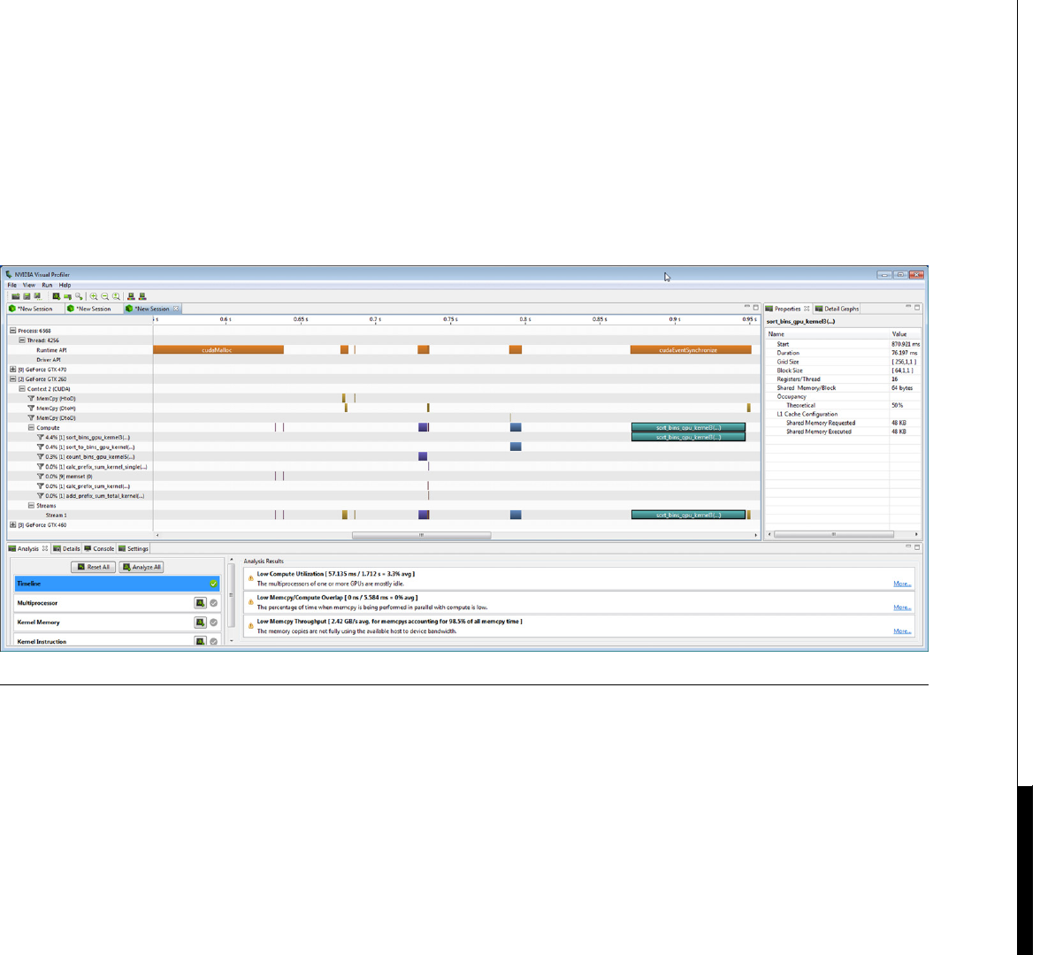
FIGURE 9.38
Visual Profiler timeline.
Strategy 6: Resource Contentions 417

FIGURE 9.39
Visual Profiler, multi-GPU.
418 CHAPTER 9 Optimizing Your Application

Parallel Nsight
Visual Profiler can, unfortunately, only tell you so much. A much better level of detail can be found
with the Parallel Nsight tool, which is a Windows-only visual analyzer and debugger. Even if Windows
is not your primary development environment, it’s worth dedicating a spare PC to this tool for its
analysis features alone.
Parallel Nsight is a far more in-depth tool than Visual Profiler. It will tell you a lot more about the
kernels and what they are doing. However, as with any more complex tool, it takes a little time to
learn how to use it well. The Visual Profiler tool is far simpler to set up and use. It’s a beginner’s
tool, whereas Parallel Nsight is more of an intermediate to advanced tool.
Parallel Nsight is best set up with a single PC using one or more compute 2.x (Fermi) graphics
cards. Parallel Nsight will also run remotely using two PCs, each of which has a NVIDIA
graphics card. However, you’ll find it much easier to have one PC, rather than wait whilst data
is copied to/from a remote machine.
Parallel Nsight presents a number of options for debugging and profiling. The two main
choices are “Application Trace” and “Profile.” The “Application Trace” feature allows you
to generate a timeline as with Visual Profiler. This is particularly useful for seeing how the
CPU interacts with the GPU and shows the times taken for host/device interaction. You
should also use the timeline to verify correct operation of streams and overlapping kernel/
memory copy operations.
Multiple concurrent GPU timelines are also supported. For example, the timeline in Figure 9.40 shows
we’re failing to provide enough work to keep all GPUs busy. Only the computation parts are shown.
The Fermi GPUs are shown in red as the first and last context, while the older GPUs are shown in green
as the middle two bars. Each red square represents one kernel invocation on a given stream. You can
see the first set of kernels end prior to the next set running. We have a huge time period where the first
GPU is idle. It’s only through using tools such as Parallel Nsight you can see issues such as this. It’s
difficult to see this using host/GPU timers alone.
The next useful feature is the “Profile” option under the Activity Type menu (Figure 9.41). This
allows us to profile the CUDA kernels. However, as many of the experiments require multiple runs of
the kernel, no timeline can be produced when selecting this option.
Selecting Experiments to Run as “All” from the dropdown box is the simplest option. As you can
see from the list of experiments in Figure 9.42, they are quite extensive. To start acquiring data, simply
press the “Launch” button in the application control panel (Figure 9.43). Note the green Connection
Status circle. This tells you the Parallel Nsight monitor has successfully connected with the target
devices. This needs to be green before any other options work. See the help options for details about
setting up the monitor.
Once you press the “Launch” button your application will run until such time as it exits. You
then will have a number of options in a dropdown box on the top of the screen, the last of which is
“GPU Devices” (Figure 9.44). Select this and you will see an overview of the GPU devices in the
system.
This is a useful dialog if you are not sure exactly what the properties of a particular device in your
system are. Next, change the dropdown menu from “GPU Devices” to “CUDA Launches.” You’ll then
see a list of kernels that were executed and various statistics. You’ll also find “Experimental Results” in
the panel below the expandable list.
Strategy 6: Resource Contentions 419

FIGURE 9.40
Parallel Nsight, multi-GPU timeline.
420 CHAPTER 9 Optimizing Your Application
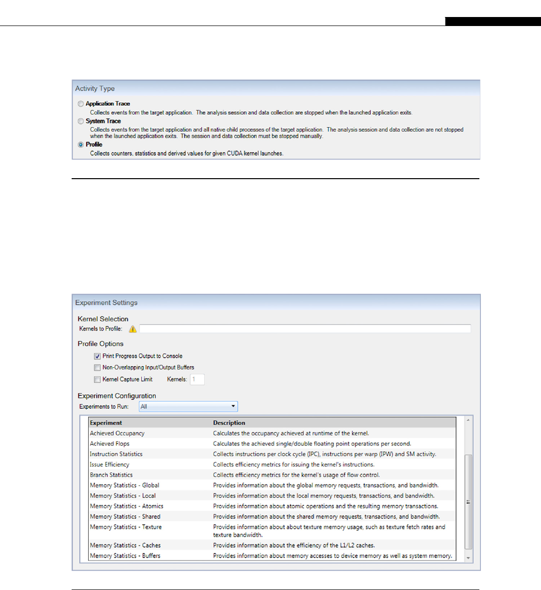
In this particular example, we have six kernels. We can see from the results a number of issues.
First, none of the kernels achieve a theoretical occupancy above 33% (Figure 9.45). In the case of
the first kernel, this is caused by the block limit (8) being hit before we’ve achieved the maximum
of 48 warps that can be resident on the device. Also note that the first kernel does not set the
FIGURE 9.41
Parallel Nsight Activity Type selection.
FIGURE 9.42
Parallel Nsight Experiments.
Strategy 6: Resource Contentions 421
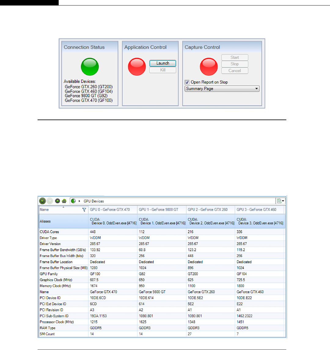
cache configuration and the CUDA runtime uses the PREFER_SHARED option, allocating 48 K to
shared memory instead of the cache. As the kernel does not use shared memory, this is pointless.
We’re missing a call in the host code to set to cache configuration to PREFER_L1 prior to the first
kernel call.
FIGURE 9.43
Parallel Nsight application Launch control.
FIGURE 9.44
Parallel Nsight, GPU devices present.
422 CHAPTER 9 Optimizing Your Application
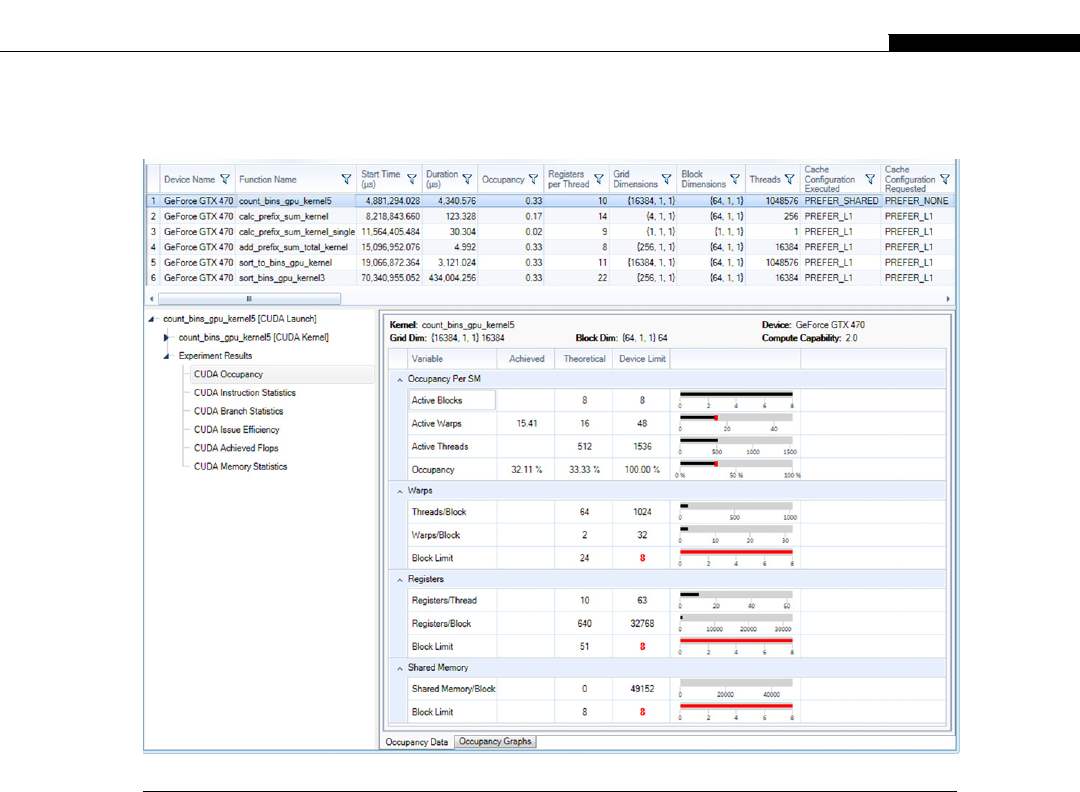
The next experiment to look at is the “Instruction Statistics” (Figure 9.46). Here we see a few
issues. There is a very high level of instructions that are being issued but not executed. This is
indicative of the SM having to serialize and thus reissue the same instructions. We also see a huge
spike of activity on SM 2. This is in fact very bad, as it means one of the blocks that were allocated to
this SM performed a huge amount of additional work compared with the other blocks. This indicates
the blocks are not equally distributed in terms of work per block, and this is something we need to
solve at the algorithm level. Some balancing of the work per block is needed.
The next experiment is the “Branch Statistics,” which tells us how much the execution within
a warp diverges (Figure 9.47). We ideally want a very small if not zero value for branch divergence.
Here we see 16% of the branches diverge, which contributes to the reissuing of instructions we saw in
the “Instruction Statistics” experiment. This too originates from the algorithm in that the amount of
work per thread varies. It points to the need to balance the workload between the work blocks.
The next experiment looks at the ability of the SM to issue and execute instructions. We’d expect to
see a roughly equal distribute in terms of the “Active Warps per Cycle” chart. It shows that despite SM
FIGURE 9.45
Parallel Nsight occupancy.
Strategy 6: Resource Contentions 423
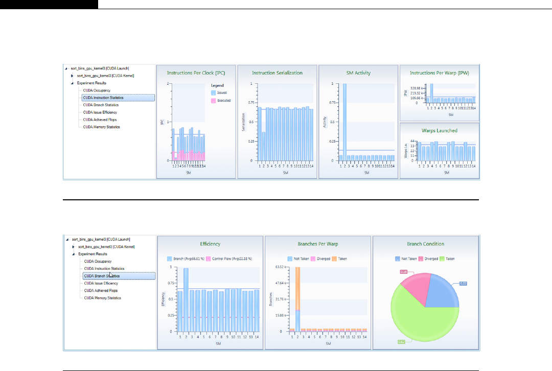
2 taking a very long time to execute, it was actually only given a small number of warps to execute.
This confirms that it was likely that one of the blocks given to it contained much more work than the
other blocks. We also have a very low level of “Eligible Warps per Active Cycle,” which may in turn
suggest the SMs are stalling at some point (Figure 9.48).
Looking at the next tab we see the distribution of instruction dependencies (Figure 9.49).
Instruction dependencies are caused by the output of one operation feeding into the input of the next.
As the GPU uses a lazy evaluation model, the GPU operates best with long instruction dependencies.
The graph in Figure 9.49 shows there are too many immediate dependencies. The easiest method to
solve this is by introducing some ILP on the thread level. As we in fact have very few blocks, we have
a significant number of unused registers that could be used to introduce ILP. We could do this via the
vector types or by expanding the loop to process Nelements per iteration. We could also use one or
more registers to prefetch the values from the next loop iteration.
The next tab confirms what we saw in the “Eligible Warps” tab, that the SMs are in fact hitting a stall
condition. The first pie chart in Figure 9.50 shows that in 69% of the time, the SM has no eligible warp to
execute, meaning it will stall or idle, which is of course not good. The second pie chart in Figure 9.50
shows the reason for the stall, which we can see is 85% of the time related to execution dependencies.
FIGURE 9.47
Parallel Nsight “Branch Statistics.”
FIGURE 9.46
Parallel Nsight “Instruction Statistics.”
424 CHAPTER 9 Optimizing Your Application
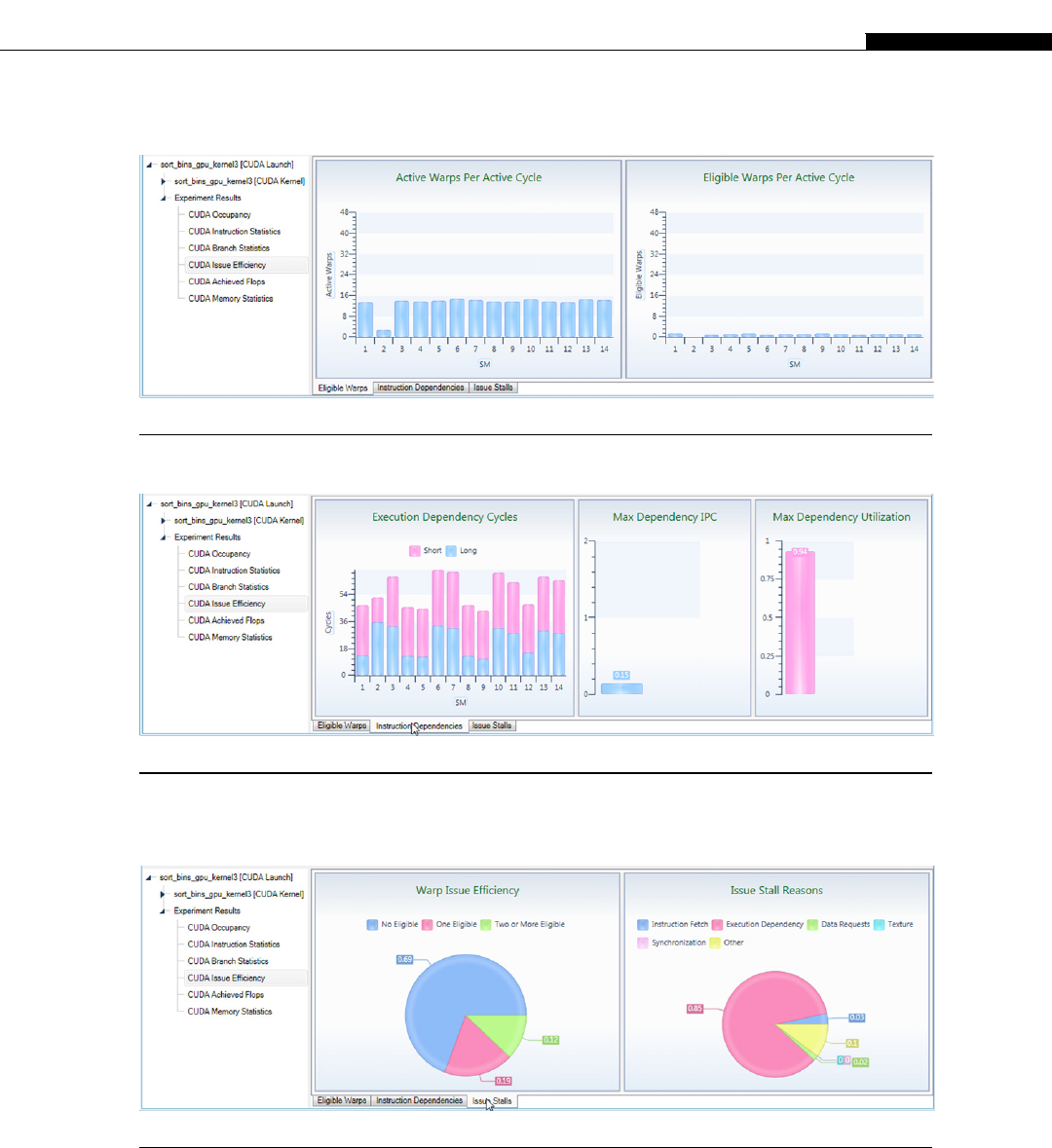
FIGURE 9.48
Parallel Nsight issue efficiency, eligible warps.
FIGURE 9.49
Parallel Nsight issue efficiency, instruction dependencies.
FIGURE 9.50
Parallel Nsight issue efficiency, issue stalls.
Strategy 6: Resource Contentions 425

This can be solved in one of two ways. Currently, we have only 64 threads per block, meaning we
get too few warps that are resident (16 out of a possible 48). Increasing the number of threads per block
will increase the number of resident warps. From this perspective only, we’d need to move from 64 to
192 threads per block. This in itself may well resolve the issue. However, the effect of this issue on the
overall timing is significantly less than issues concerning memory. Increasing the number of resident
blocks will affect cache usage, which may have a bigger impact on the overall timing.
We can see this in practice by looking at the total amount of data fetched from global memory by
creating two versions, one that uses 128 threads per block and another that uses 64 threads per block.
As we have registers to spare, we’ll also fetch 16 elements in the 64-register version and 12 elements in
the 128-register version. This maximizes the register usage while still maintaining eight blocks per SM.
Sure enough the “Warp Issue Efficiency” improves, reducing the “No Eligible” warps from 75% down
to just 25%. The number of theoretical warps per SM also increases from 16 to 32 (13.25 versus 26.96
actual). The occupancy increases from 27% to 56%. These are all improvements, but they are secondary
effects. The kernel is performing a sort, so is likely, as with almost all sorts, to be memory bound.
In fact, when we compare the two kernels with the “CUDA Memory Statistics” experiment, there is
a difference. The increased number of blocks per SM means that the ratio of L1 cache to each block is
reduced. This in turn results in a doubling of the number of global memory fetch operations that are not
cached in the L1 or L2 cache.
In the first kernel, using 64 threads per block, we achieve a 93.7% cache hit rate, which is very good
(Figure 9.51). Of the 6.3% of the transactions the L1 cache misses, the L2 cache picks up 30%, or
around one-third. Thus, very few read transactions actually make it to global memory and we stay
mostly on chip.
When we extend this to 128 threads per block, the overall number of blocks halves to 128 blocks in
total (Figure 9.52). However, this is not an issue, as with 14 SMs on the device and a maximum of eight
resident blocks, we can only accommodate a maximum of 112 blocks at any given time anyway. Thus,
we can increase the number of resident warps without any SMs running out of blocks.
FIGURE 9.51
Memory statistics, memory overview (256 blocks 64 threads).
426 CHAPTER 9 Optimizing Your Application
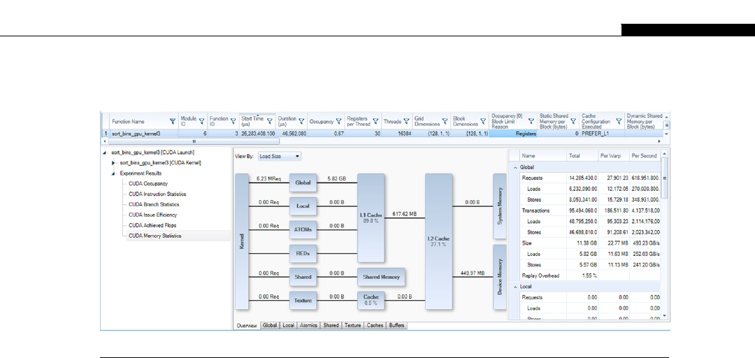
Notice the problem with the cache hit ratio. Both the L1 and L2 caches achieve a lower hit ratio
than before. The amount of memory fetched from global memory approximately doubles from 272
MB to 449 MB. This takes the execution time from 35 ms to 46 ms, despite the apparent improvements
in utilization of the SMs. Note that due to the allocation of one thread to each sample block, these
memory fetches are all uncoalesced, so they are in fact very expensive.
Note that a design in which the threads from a thread block cooperated on sorting a single sample
block would be far less sensitive to this effect. This analysis shows us this dependency. Through using
a different mapping of threads to work in the sort stage, or by balancing or adjusting the bin
boundaries, we may well be able to significantly improve the throughput.
Resolving bottlenecks
It’s all very well knowing what the code you are running is doing, but it’s often another matter to
both understand and fix the issue. The three types of bottlenecks you typically see, in order of impor-
tance, are:
• PCI-E transfer bottlenecks
• Memory bandwidth bottlenecks
• Compute bottlenecks
PCI-E transfer bottlenecks
PCI-E transfer bottlenecks are often a key consideration. As we saw from the earlier sections, PCI-E
bus bandwidth is limited and you can expect to achieve a peak of around 5 GB/s on PCI-E 2.0
depending on the host hardware. However, to achieve this peak you need to be using pinned memory
and an appropriately sized transfer. Adding more GPUs to a node typically reduces the overall
bandwidth, but allows the overall amount of GPU to be increased. If you can keep everything in the
FIGURE 9.52
Memory statistics, memory overview (128 blocks 128 threads).
Strategy 6: Resource Contentions 427

GPU memory space, be that a single Tesla GPU or multiple GPUs, then the transfer cost can be
eliminated from the equation. The extent of the reduction in bandwidth by adding more cards is very
much dependent on the host hardware. You therefore need to be aware of how much data you are
transferring and its usage.
Compression techniques are one way to increase this apparently hard limit on PCI-E transfer rates.
Do you really need to transfer all the data you are sending? For example, image data often contains an
alpha channel that is used for transparency. If you are not using this on the GPU, then you can discard it
and transfer from the host only the RGB (red, green, and blue) components, eliminating 25% of the
data to be transferred. Although this may then mean you have 24 bits per pixel, the transfer time saving
may significantly outweigh the nonaligned access pattern this might cause.
The other question is can you infer some data from others? This is very much problem dependent,
but you may be able to compress the data using a simple algorithm such as run-length encoding. A long
series of the same numbers can be replaced with a value, count pair and reconstructed at the GPU end
in very little time. You may have lots of activity from a sensor and then no “interesting” activity for
quite a period of time. Clearly, you can transfer the “interesting” data in full and either throw away the
“uninteresting” data at the host end, or transfer it in some compressed form.
Interleaving transfer with computation using streams or zero-copy memory is another essential
technique we have already covered. In the situation where your PCI-E transfer time is in excess of your
kernel time, you effectively have the computation time for free. Without overlapping, the two times
must be added and you end up with large gaps where no computation is taking place. See Chapter 8 for
more information on using streams.
PCI-E is not the only transfer bottleneck you need to consider. The host will have a limit on
the amount of memory bandwidth there is. Hosts such as the Intel Sandybridge-E processors use
quad-banked memory, meaning they can achieve much higher host memory bandwidth than other
solutions. Host memory bandwidth can also be saved by using P2P (Peer to Peer) transfers if
your problem allows for this. Unfortunately, at the time of writing, to use the P2P function you
need to use an OS other than Windows 7. With the exception of those using Tesla cards and thus
the TCC (Tesla Compute Cluster) driver, Windows 7 is the only major OS not currently sup-
ported for this feature.
The speed at which the node can load and save data to storage devices, be they local devices or
network devices, will also be a limiting factor. High-speed SSD drives connected in RAID 0 mode will
help with this. These are all considerations for selecting host hardware. We look at a number of these in
detail in Chapter 11.
Memory bottlenecks
Assuming you can get the data on and off the GPU, the next issue is memory bandwidth to or from
global memory. Moving data is expensive in terms of time and power usage. Therefore, being able to
efficiently fetch/store and reuse data are essential criteria for selecting an appropriate algorithm. The
GPU has huge amounts of compute resources, so an inefficient algorithm with a memory pattern
favorable to a GPU (coalesced, tiled, high locality) may outperform a more computationally intensive
algorithm that exhibits less GPU-friendly memory pattern.
When considering memory, think also about thread cooperation and appreciate the cooperation is
best limited to a single block of threads. Generic algorithms that assume any thread can talk to any
other thread are less useful than those that value locality of threads to one another. Algorithms
428 CHAPTER 9 Optimizing Your Application

designed for use on older vector machines are often far more efficient than those designed around
distributing work over Nindependent processing nodes, as commonly found in today’s cluster
machines.
On modern GPUs, the L1 and L2 caches can significantly affect the execution time of kernels in
sometimes rather unpredictable ways. Shared memory should be used where you have data reuse, want
a more predictable outcome, or are developing for compute 1.x hardware. Even with the full 48 K
allocation to the L1 cache, there is still 16 K of local shared memory storage available on each SM.
A fully populated Fermi GPU has 16 SMs, so this amounts to a total of 256 K of high-speed
memory in addition to the 768 K of L1 cache. This can be swapped, giving 768 K of programmer-
managed shared memory and 256 K of L1 cache. Data reuse through either or both mechanisms is
critical to achieving high throughput. This is typically achieved by ensuring locality of the calculation.
Instead of multiple passes over large datasets, break the data into tiny tiles, use multiple passes over
individual tiles, and then repeat for the other tiles. This allows the data to remain on chip throughout
whatever transformation is being made on it, without multiple read/writes to and from global memory.
Memory coalescing is key to achieving high memory throughput, although a sufficiently high number
of memory transactions is also required. On Fermi and Kepler devices, to achieve anything like the full
bandwidth when using 32-bit values per thread (i.e., floats or integers), you need to have the GPU almost
fully populated with threads (48 to 64 resident warps, 1536 to 2048 threads per SM). Increased transaction
sizes through the use of the various vector types help improve both ILP and memory bandwidth. Having
each thread process four values instead of one tends to work well for many applications.
Compute bottlenecks
Complexity
Surprisingly, despite the immense computing throughput of the GPU, there are still problems that are
compute bound. These are usually problems where the overall amount of data is very large, such as the
various forms of medical image scanning or data processing from devices that generate large amounts
of sample data. These types of problems were previously processed on clusters. However, now due to
the huge processing power available from a multi-GPU computer, many problems can be processed on
a single standalone PC.
Algorithms that contain a lot of computations work really well on GPUs compared to their CPU
counterparts. However, algorithms that also include a lot of control complexity do not. Take the example
of boundary cells in a typical tiled algorithm. If the cells collect data from their immediate neighbors,
then a cell at the corner of a tile needs to collect data from the corner points of three other tiles.
In Figure 9.53 you can see there is a large block of green cells in the centre that have no boundary
condition. They can safely calculate some value from the surrounding cells within the current block.
Unfortunately, some programmers write programs that deal with the problem cases first. Thus, their
kernel goes along the lines
if (top left corner cell)
else if (top right corner cell)
else if (bottom right corner cell)
else if (bottom left corner cell)
else if (top row)
else if (right row)
Strategy 6: Resource Contentions 429
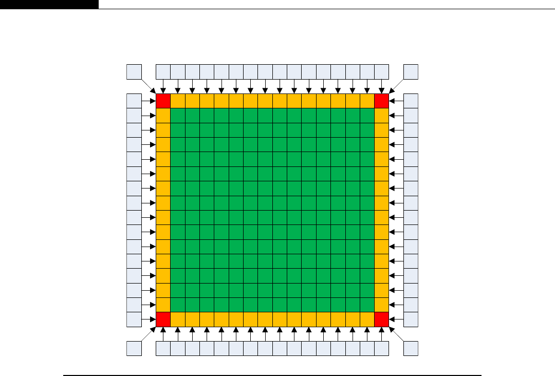
else if (bottom row)
else if (left row)
else (must be centre element)
Particularly, control complex algorithms are not well suited to GPUs. If each thread runs the same
kernel, the center elements have nine conditions to test before the thread does any work on them.
Reversing the order of the tests, so the center elements are tested first, means we need four boundary
tests. This would be an improvement, but is still far from optimal. The solution is to write customized
kernels for each special case or let the CPU handle these complex conditionals.
The type of problem here is a stencil one, where cells Nlevels from the center contribute in some
way to the result. In this simple example, Nis 1, as the immediate neighbors are used. As Nis
increased, typically some factor is applied, as values that are a long way from the center often do not
contribute as much to the result.
As each cell will need values from the surrounding cells, each cell value will be read multiple
times. Thus, a common approach to such problems is to use many threads to read a tile of data into
shared memory. This allows for high-performance coalesced access to global memory, both when
FIGURE 9.53
Halo cells needed.
430 CHAPTER 9 Optimizing Your Application

reading the data and also when writing it back. However, shared memory is not visible between blocks
and there is no mechanism to pass shared data directly between blocks. This is due to the design of
CUDAwhere there is only ever a subset of the total number of blocks executing. Thus, shared memory
is reused as old blocks are retired and new blocks scheduled.
Thus, to load the halo cells, the cells outside the boundary of our particular tile, you can either read
them from global memory or also load these into shared memory. Reading the rows from global
memory gives a nice coalesced memory pattern. However, the columns generate a number of separate
memory transactions, one for each cell we load. As these cells may be read a number of times, reading
the columns can be a memory-intensive operation that will limit performance. Thus, at least the
columns are usually placed into shared memory.
Thus, writing multiple kernels is usually a good solution to the problem of eliminating the control
flow complexity. We can have one kernel that handles corner elements, another for rows, another for
columns, and another for the center elements. If appropriate, each of these can call a common routine
that processes the data as a series of values, and now the complexity of where the data came from has
been removed.
Note that for compute 1.x and compute 2.x different solutions are applicable. As compute 1.x
hardware has no cache for global memory, each memory transaction would generate a considerable
amount of latency. Thus, for these devices it can make sense to manually cache the necessary data from
the surrounding tiles in shared memory or give the calculation to the CPU.
However, compute 2.x devices have both an L1 and L2 cache. As each tile will have to process its
own elements, it’s likely that the tiles above, above left, and left will have already been loaded into the
cache by previous activity of other blocks. The tiles to the right, right bottom, and bottom will usually
not be present unless there are multiple passes over quite a small dataset. Accessing these from global
memory will bring them into the cache for the subsequent block. You can also explicitly request cache
lines be brought into the cache using the prefetch PTX instruction (see PTX ISA).
As a consequence of the caching, we can eliminate a large amount of the control complexity
necessary to manage shared memory by simply selecting a 48 K L1 cache and not using shared
memory at all. Elimination of complexity is often useful in speeding up compute bound kernels.
Instruction throughput
As with many processors, not all instructions take the same amount of time to execute on every device.
Selecting the correct instruction mix for a given processor is something the compiler should be able to
perform quite well, but it’s also something the programmer needs to be aware of.
First of all, you need to ensure you are targeting the correct binaries for your hardware. Ideally, you
should have one compute level specification for each target hardware platform. In Visual Studio this is
done in the project options and is something we’ve already covered. For those people using command
line it’s the -arch flag that specifies this.
In terms of single-precision floating-point operations, all compute levels achieve a throughput of
one instruction per clock, per thread. Remember, however, as this is per thread. In absolute terms we
need to consider this is warp wide times the number of simultaneous warps per SM times the number
of SMs on the GPU. Thus on Kepler GTX680 we have a 32 wide warp x 8 warp dispatch x 8 SMs =
2048 instructions per clock. Now throughput is not the same as instruction latency. It may take up to
the order of 20 clock cycles for the result to become available to feed into a subsequent operation.
A series of floating-point operations fed into the instruction pipeline would therefore appear 20 cycles
Strategy 6: Resource Contentions 431

later, one each cycle. The throughput would be one instruction per cycle, per thread but the latency
would be 20 cycles.
Double-precision floating-point hardware, however, does not achieve this. For compute 2.0
hardware, it’s half the speed of single precision. For compute 2.1 hardware, it’s actually only one-third
of the speed. Compute 2.1 hardware (GTX460/560) and compute 3.0 hardware (GTX680) was aimed
more toward the gaming market, so it lacks the same level of double-precision floating-point
performance.
We see a similar issue with 32-bit integer values. Add and logical instructions only run at full speed.
All other integer instructions (multiply, multiply-add, shift, compare, etc.) run at half speed on
compute 2.0 hardware and one-third speed on compute 2.1 hardware. As usual, division and modulus
operations are the exception. These are expensive on all compute levels, taking “tens of instructions”
on compute 1.x hardware and “below 20 instructions” on compute 2.x hardware [NVIDIA CUDA C
Programming Guide, v4.1, chapter 5].
Type conversion instructions operate at half speed on compute 2.0 devices and one-third speed
on compute 2.1 devices. These are necessary when 8- or 16-bit integer types are used, as the
hardware supports only native integer types (32-bit on compute 2.x, 24-bit on compute 1.x). Thus,
the addition of two byte values results in promotion of these values to two integer values. The
subsequent result then again needs to be demotedtoabytevalue.Similarly,conversionstoand
from single-/double-precision floating-point values cause additional type conversion instructions to
be inserted.
In C all whole numbers are by default signed integers. All numbers containing a decimal place are
treated as double-precision floating-point values unless an Fpostfix is placed immediately after the
number. Thus,
#define PI (3.14)
creates a double-precision definition and
#define PI (3.14F)
creates a single-precision definition.
Using a non-postfixed constant in a floating-point expression causes an implicit conversion to
double precision during the calculation. An implicit conversion to single precision is also performing
when the result is assigned to a single-precision variable. Thus, forgetting to use the Fpostfix is
a common cause of creating unnecessary conversion instructions.
Synchronization and atomics
Synchronization points are often necessary in many algorithms. Synchronization within a thread block
is not costly, but does potentially impact performance. The CUDA scheduler will try to schedule up to
sixteen blocks per SM, which it can do unless you start using larger numbers of threads (see Chapter 5).
As the number of threads increases, the number of blocks that can be scheduled decreases. This in itself
is not too bad, but when combined with synchronization points it can lead to the SM stalling.
When a block performs a synchronization, a number of warps out of the available set (24 on
compute 1.x, 48 on compute 2.x, 64 on compute 3.x) effectively drop out of the scheduling availability,
as all but the last warp hits the synchronization point. In the extreme case of 1024 threads per block
(two blocks per SM), up to half of the resident warps would be at the synchronization barrier. Without
432 CHAPTER 9 Optimizing Your Application

any ILP, the ability of the SM to hide memory latency through running multiple threads then becomes
insufficient. The SM stops running at peak efficiency. Clearly, we want maximum throughput from all
the SMs for as much time as possible.
The solution to the synchronization issue is not to use large thread blocks. You should aim to fully
populate the SM where possible, so 192 threads is an ideal number, which results in eight blocks per
SM on compute 2.x hardware, 256 being better for compute 3.x hardware.
Unfortunately, if we’re using interthread synchronization it is likely we’ll also need interblock
synchronization. It’s more efficient to synchronize data between threads than between blocks. For
block-based synchronization we need to use global memory, whereas interthread synchronization can
be performed with shared memory. Thus, it’s a tradeoff between the two scenarios best resolved by
simply running both and seeing which is the fastest.
Atomic operations act very much like synchronization points in that all the threads in a warp have
to line up one after another to perform the operation. It takes time for all the threads in a block to line
up in groups of 32 to move through the atomic operation. However, unlike synchronization points, they
are free to continue at full speed afterward. This helps in terms of increasing the availability of warps
that can be run, but doesn’t help the overall execution time of the block. The block cannot be retired
from the SM until all the threads have completed. Thus, a single atomic operation effectively serializes
and spreads out, in terms of execution time, the warps in a given block. The block can’t finish until all
the stragglers have completed.
The effect of synchronization and atomics on your kernel can be seen using the “CUDA Issue
Efficiency” experiment within Parallel Nsight.
Control flow
As we saw earlier, branch divergence can have a serious impact on execution time as both paths have to
be executed separately. The compiler is aware of this and thus uses something called predication.
Most of the PTX instructions can be predicated using the .p notation of the PTX ISA. For example,
setp.eq.s32 %p16, %r295, 1;
@%p16 bra BB9_31;
Herewesetupapredicateregisterineachthread, testing virtual register 295 for the value 1 and
setting predicate register 16 accordingly. In the next instruction the predicate register 16 is used to
predicate the bra (branch to) instruction. Thus, only those threads meeting the test condition of the
earlier setp.eq.s32 instruction follow the branch. We could replace the branch with a mov or
similar instruction. Typically, you see the compiler generate this for small if-else constructs. For
example,
if (local_idx >¼12)
local_idx ¼0;
will be translated to
setp.gt.u32 %p18, %r136, 11;
selp.b32 %r295, 0, %r136, %p18;
This works well in avoiding branches, as in fact all threads in the warp execute the predicate
instruction, but those threads without the predicate bit set simply ignore it. The compiler has a strong
Strategy 6: Resource Contentions 433

preference for predication, even when other approaches would be better. The criteria is simply based
on the size of the body of the if statement. Consider the following example:
// Fetch the test data element
switch(local_idx)
{
case 0: elem ¼local_elem_00; break;
case 1: elem ¼local_elem_01; break;
case 2: elem ¼local_elem_02; break;
case 3: elem ¼local_elem_03; break;
case 4: elem ¼local_elem_04; break;
case 5: elem ¼local_elem_05; break;
case 6: elem ¼local_elem_06; break;
case 7: elem ¼local_elem_07; break;
case 8: elem ¼local_elem_08; break;
case 9: elem ¼local_elem_09; break;
case 10: elem ¼local_elem_10; break;
case 11: elem ¼local_elem_11; break;
case 12: elem ¼local_elem_12; break;
case 13: elem ¼local_elem_13; break;
case 14: elem ¼local_elem_14; break;
case 15: elem ¼local_elem_15; break;
}
This code simply selects one of Nlocal variables (registers) based on an index. The local variables
are individually named, as creating an array causes the compiler to place this into local memory.
Unfortunately, the compiler implements a series of if-else-if type statements, which means at
element 16 we have to perform 15 prior tests. I’d have expected it to implement a jump table, creating
an assignment at the target of each jump. This would be two instructions, load local_idx into
a register and then an indirect jump to some base address plus the value in the register. The jump table
itself is set up at compile time.
Thus, you need to ensure the control flow you expect is the control flow the compiler generates. You
can do this relatively easily by inspecting the PTX code and/or the actual target code if you are still
unsure. Predication works well in many but not all instances.
Section summary
• Use profiling tools to really see into what is happening as opposed to what you think is
happening.
• Avoid overly complex kernels by generating a general case and exception case kernel, or by using
the caching features to eliminate the complex kernel altogether.
• Understand how predication works in control flow.
• Don’t assume the compiler will provide the same scope of optimizations found with more mature
compilers. CUDA is still quite new and things will take time.
434 CHAPTER 9 Optimizing Your Application

STRATEGY 7: SELF-TUNING APPLICATIONS
GPU optimization is not like CPU optimization. Many techniques overlap, while others have unde-
sirable effects. I’ve tried to cover the major areas of optimization in the preceding sections. However,
optimization is never an exact science, not when practiced by human programmers anyway. There are
lots of factors that need to be considered when designing code for the GPU. Getting an optimal solution
is not easy and it takes considerable time to become familiar with what works, try different solutions,
and understand why one works when another doesn’t.
Consider some of the major factors:
• Transfer to and from the host.
• Memory coalescing.
• Launch configuration.
• Theoretical and achieved occupancy.
• Cache utilization.
• Shared memory usage/conflicts.
• Branch divergence.
• Instruction-level parallelism.
• Device compute level.
For someone starting out with CUDA, there is a lot to think about and it will take time to become
proficient with each of these areas. However, the most challenging aspect of this is that what works
on one device many not work on another. Throughout this book we’ve used the whole range of
available devices and a number of different host platforms where necessary to highlight
differences.
In the same way as different CPUs provide different levels of performance and functionality, so do
GPUs. The CPU world is largely stuck with an x86 architecture, which reflects design goals of
a system designed to run serial programs. There have been many extensions to provide additional
functionality, such as MMX, SSE, AVX, etc. The x86 instruction set is today translated within the
hardware to micro-instructions, which can be really for any target hardware. Sandybridge is perhaps
the best example of this, where the micro-instructions themselves are actually cached instead of the
x86 assembly code instructions.
GPU hardware is also not fixed and has changed significantly since the first CUDA-enabled devices
were released back in the GTX8800 times. CUDA compiles to PTX, a virtual assembly code, aimed at
a parallel processor–like architecture. PTX can itself be compiled to many targets, including CPUs, as
the cooperative thread array concept lends itself to implementation in most parallel hardware.
However, as far as we’re concerned, it’s compiled to a specified compute level for various NVIDIA
GPUs. Therefore, you need to be familiar with what a given compute level provides, that is you need to
understand for what hardware you are writing code. This has always been the basis of good optimi-
zation. Trends toward abstraction, layering, and hiding the architecture are all aimed at programmer
productivity, but often at the expense of performance.
Not every programmer is interested in the intricate workings of the hardware. Even with
the previous list of issues to consider you’re unlikely to get an optimal solution the first time, the
second time, or the Nth time without considerable thought and a lot of trial and error. Thus, one
Strategy 7: Self-Tuning Applications 435

approach to this issue that works well is simply to ask the program to work out the best use of the
hardware for a given problem. This can either be done on a small set of the problem or the real
problem itself.
Identifying the hardware
The first step in any optimization process is to know what hardware is available and what it is. To find
out how many GPUs we have, you simply call
cudaError_t cudaGetDeviceCount(int * count);
This sets whatever parameter you pass as count to the number of devices available. If there is no
CUDA hardware available the function returns cudaErrorNoDevice.
Then for each device found we need to know what its capabilities are. For this we call
cudaError_t cudaGetDeviceProperties (struct cudaDeviceProp * prop, int device);
We covered in detail the properties of a device in Chapter 8 so will not repeat this here. You should,
however, be interested in at least the following:
• Members major and minor that, when combined, provide the compute level of the device.
•The
integrated flag, especially when combined with the canMapHostMemory flag. This allows you
to use zero-copy memory (covered in Strategy 3) and avoid memory copies to and from the device
for devices of which the GPU memory is actually on the host.
•The
totalGlobalMem value so you can maximize the use of GPU memory and ensure you don’t try
to allocate too much memory space on the GPU.
•The
sharedMemPerBlock value so you know how much shared memory is available per SM.
•The
multiProcessorCount, which is the number of SMs present in the device. Multiply this number
by the number of blocks you are able to run on an SM. The occupancy calculator, the Visual Profiler,
and Parallel Nsight will all tell you the number of blocks you can run for a given kernel. It’s
typically up to eight but can be as many as 16 on Kepler. This is the minimum number of blocks
you need to schedule to this GPU.
This information gives us some bounds with which we can define the problem space. We then have two
choices: either analyze offline the best solution or try to work it out at runtime. The offline approach
generally leads to better results and can greatly increase your understanding of the issues involved and
may cause you to redesign certain aspects of the program. The runtime approach is necessary for
optimal performance, even after significant analysis has taken place.
Thus, the first part of the optimization takes place offline, during the development phase. If you are
targeting multiple compute levels, you’ll need a suitable card to test your application on. For consumer
cards as a whole the most popular NVIDIA cards have always been the 9800 (compute 1.1), 8800
(compute 1.0), GTX260 (compute 1.3), and GTX460 (compute 2.1). For more modern DirectX 11 cards,
the 460/560 cards dominate, with a smaller number of power users opting for the more expensive 470/
570 cards. Our choice of hardware for this book pretty much reflects the market trends to make the
figures presented as useful as possible for people developing mass-market applications.
As we’ve been working with CUDA since it release on the 8800 series of cards, we have a number
of consumer cards at hand. Clearly, many of these are no longer available for sale but can easily be
purchased on eBay or elsewhere. All you need is a motherboard with four dual-spaced PCI-E
connectors all running at the same speed when fully populated. The primary board used in the
436 CHAPTER 9 Optimizing Your Application

development of this book was the (AMD) MSI 790FX-GD70, although this has now been replaced
with the MSI 890FXX-G70. Note the newest 990FX board in the series no longer provides four
double-spaced connectors.
Device utilization
Having identified what hardware we have, we then have to make use of it. If there are multiple GPUs in
the system, as is often the case, then be sure to make use of them. Multi-GPU programming, as of the
CUDA 4.x SDK, is now much easier than before, so be sure you are not leaving a 100% performance
gain on the table because you’re only using a single GPU. See Chapter 8 for more information on this.
All applications are different, so the same primary performance factors may not always be the same.
However, many will be. Primary among these is the launch configuration. The first part of this is ensuring
you have multiple targets set up in the build process, one target for each compute level you plan on
supporting. The target code will automatically be selected based on which GPU you are running the
kernel on. Make sure also before running any performance tests you have the “Release” version selected
as the build target, something in itself that can provide up to a 2performance improvement. You’re not
going to release the debug version, so don’t select this as your build target, other than for testing.
Next we need some sort of check to ensure correctness. I suggest you run the GPU code back to
back with the CPU code and then do a memory compare (memcmp) on the output of the two identical
tests. Note this will detect any error, even if the error is not significant. This is especially the case with
floating point, as the order in which the operations are combined will cause small rounding/precision
errors. In such cases your check needs to iterate through both results and see if the answers differ by
whatever you consider to be significant (0.01, 0.001, 0.0001, etc.) for your particular problem.
In terms of launch configuration we’re trying to optimize for the following:
• Number of threads per block.
• Overall number of blocks.
• Work performed per thread (ILP).
The answer for each of these will vary between compute levels. A simple for loop is all that is needed
to iterate through all possible combinations and record the timings for each. Then at the end simply
print a summary of the results.
In terms of threads per block, start at 1 and increase in powers of two until you reach 16. Then
increase the thread count in 16-step intervals until you reach 512 threads per block. Depending on the
kernel resource usage (registers, shared memory) you may not be able to reach 512 threads on the
earlier compute devices, so scale this back as necessary for these devices only.
Note that we chose 16 here as the increment value, rather than 32, the warp size. This is because
warp divergence is half-warp based. Certain devices such as the GTX460s are actually based on three
sets of 16 CUDA cores, rather than two as found in other compute levels. Thus, a number of threads
that is a multiple of 48 may work better on such devices.
As a general rule, you’ll find well-written kernels work best with 128, 192, or 256 threads per block.
You should use a consistent scaling from one thread per block up to a peak point where the performance
will level off and then fall away. The plateau is usually hit when you achieve the maximum number of
resident warps per SM and thus the instruction and memory latency hiding is working at its peak.
Using a slightly smaller number of threads (e.g., 192 instead of 256) is often desirable if this
increases the number of resident blocks per SM. This usually provides for a better instruction mix,
Strategy 7: Self-Tuning Applications 437

as more blocks increases the chance they will not all hit the same resource contention at the
same time.
If you are hitting the maximum performance at 16, 32, or 64 threads then this usually indicates
there is a contention issue, or that your kernel is highly geared toward ILP and you are using a lot of
registers per thread.
Once you have a baseline figure for the ideal number of threads per block, try increasing the
amount of work done by each thread to two or four elements using the various vector_N types (e.g.,
int2,int4,float2,float4, etc.). You’ll typically see this will improve performance further. The
easiest way of doing this is to create additional functions with the same name and simply overload the
kernel function. CUDA will call the appropriate kernel depending on the type passed to it at runtime.
Using the vector types will increase register usage, which in turn may decrease the number of
resident blocks per SM. This in turn may improve cache utilization. Memory throughput will also
likely be increased as the overall number of memory transactions falls. However, kernels with
synchronization points may suffer as the number of resident blocks drops and the SM has less choice of
which warps are available to execute.
As with many optimizations, the outcome is difficult to predict with any degree of certainty, as
some factors play in your favor while others don’t. The best solution is to try it and see. Then work
backwards, to understand what factor(s) are the primary ones and which are secondary. Don’t waste
your time worrying about secondary factors unless the primary ones are already addressed.
Sampling performance
The final part of a self-tuning application is sampling. Although you can build a good performance
model around compute level and number of SMs, there are many other factors. The same card model
may be produced using GDD3 and GDD5 memory, the latter having significantly more global memory
bandwidth. The same card may be clocked internally at 600 MHz yet also appear as a 900 MHz model.
An optimization strategy that works well for a card with 16 SMs may not work well on one with half
that number and vice versa. A mobile processor in a laptop may have been put on a PCI-E X1 link and
may have dedicated or shared memory with the host.
It’s impossible to collect every card and address every variation that your product might have to
address. Even if you could do this, next week NVIDIA will release another card. This is of course mostly
a problem for those people writing consumer applications, rather than the somewhat less diverse Tesla
population of cards. Nonetheless, when a new card is released people first expect their existing appli-
cations to run on it, and second, if they have upgraded, to see a suitable performance boost.
Sampling is the answer to this issue. Each card will have a peak value in terms of a launch
configuration that works best for its particular setup. As we’ve seen in some of the tests run throughout
this book, different cards prefer different setups. The Fermi cards work well with 192 or 256 threads
per block, yet the prior GPUs work well with 128 and 192 threads per block. The compute 2.1 cards
perform best with 64- or 128-byte memory fetches, mixed with ILP, instead of 32-byte memory fetches
and a single element per thread. The earlier cards are hugely sensitive to thread/memory ordering when
coalescing. Global memory bandwidth on these cards is a fraction of the newer models, yet they can
perform to a similar level with some problems if shared memory is used well. The cache in Fermi can
play a big part to the extent that very low thread numbers (32 or 64) can outperform higher occupancy
rates if the data is then entirely contained in the cache.
438 CHAPTER 9 Optimizing Your Application

When the program is installed, run a short test suite as part of the installation procedure. Run a loop
through all feasible numbers of threads. Try ILP values from one to four elements per thread. Enable
and disable shared memory usage. Run a number of experiments, repeating each a number of times,
and average the result. Store in a data file or program configuration file the ideal values and for which
GPU these relate. If the user later upgrades the CPU or GPU, then rerun the experiments and update the
configuration. As long as you don’t do this on every startup, the user will be happy you are tuning the
application to make the best possible use of their hardware.
Section summary
• There are too many factors to say with certainty the effect of a change without actually trying it.
• Some experimentation is often required during development to get the optimal solution.
• The optimal solution will be different on different hardware platforms.
• Write your applications to be aware of the different hardware out there and what works best on each
platform, either statically or dynamically.
CONCLUSION
We’ve looked in detail at a number of strategies for trying to improve the throughput of your kernels with
various examples throughout this chapter. You should be aware of the factors that affect performance and
their relative importance (primary ones are transfers, memory/data patterns, and finally SM utilization).
Correctness is a key issue in optimizing code. You cannot reliably optimize code without automatic
regression testing. This doesn’t have to be hugely complex. A back-to-back run against a known
working version with several known datasets is entirely sufficient. You should aim to spot 95% plus of
the errors before any program leaves your desk. Testing is not the job of some test group, but your
responsibility as a professional to produce reliable and working code. Optimization often breaks code
and breaks it many times. The wrong answer in one minute instead of the correct answer in one hour is
no use to anyone. Always test for correctness after every change and you’ll see the errors there and
then, as and when they are introduced.
You should also be aware that optimization is a time-consuming and iterative process that will grow
your understanding of your code and how the hardware functions. This in turn will lead you to design
and write better code from the outset as you become more familiar with what does and what does not
work well on GPUs.
Questions on Optimization
1. Take an existing program that has one or more GPU kernels. Run the Visual Profiler and Parallel
Nsight to analyze the kernels. What are the key indicators you need to look for? How would you
optimize this program?
2. A colleague brings a printout of a GPU kernel to you and asks your advice about how to make it run
faster. What would be your advice?
3. Another colleague proposes to implement a web server using CUDA. Do you think this is a good
idea? What issues, if any, would you expect with such a program?
4. Implement a shared memory version of the odd–even sort, which produces a single sorted list.
What issues might you expect to deal with?
Conclusion 439

Answers
1. You should be looking first to the execution time of each kernel. If one or more kernels dominate
the timing, then, until these are optimized, trying to optimize the others is a waste of your time.
Second, you should be looking to the timeline, specifically concerning transfers. Are they overlapped
with kernel operations and are they using pinned memory or not? Is the GPU busy all the time or
only periodically given work by the host?
Of the two longest executing kernels, what is causing them to take this time? Is there a sufficient
number of threads overall? Are there enough blocks to populate all the SMs? Are there any
peaks on one SM, and if so, why? What is the thread to memory pattern and can this be
coalesced by the hardware? Are there any serialization points, for example, shared memory
bank conflicts, atomics, synchronization points?
2. First, you need to understand the problem before looking at specifics. The “look at the code”
optimization strategy can be hit or miss. Sure you can probably optimize the code on the paper
in some way, but you need much more information to provide a good answer to the question the
person is really asking.
Probably the best answer would be to tell your colleague to profile the application, including the host
timeline, and then come back with the results. In doing this they will likely see what the problems
are and these may well not even be related to the original kernel printout.
3. Applications that are highly data parallel are well suited to GPUs. Applications that are highly task
parallel with lots of divergence threads are not. The typical implementation of a web server on
a CPU is to spawn one thread per Nconnections and to distribute connections dynamically over
a cluster of servers to prevent overloading any single node.
GPUs execute code in groups of 32 warps, effectively a vector processor with the ability to follow
single-thread control flow when necessary, but at a large performance penalty. Constructing
in real time a dynamic web page is very expensive in terms of control flow, a significant
amount of which will diverge on a per-user basis. PCI-E transfers would be small and not
efficient.
A GPU would not be a good choice, with the CPU host being a much better choice. However, the GPU
may be able to be used in the back-end operations of the server, performing some analytical work,
churning through the user-generated data to make sense of it, etc.
4. This is a useful exercise to think about how to solve some open-ended problems. First, the question
does not specify how to combine the output of Nblocks.
The quickest solution for largest datasets should be the sample sort method as it completely eliminates
the merge sort step. The framework for sample sort is provided in the text, but is nonetheless quite
a complex sort. However, it suffers from a variable number of elements per bin. A prefix sum that
padded the bins to 128-byte boundaries would help significantly.
Merge sort is much easier to implement, allows for fixed block sizes, and is what I’d expect most
implementations to opt for.
In terms of the odd/even sort, the coalescing problems with global memory are largely hidden by the
cache in Fermi due to the locality being extremely high. A compute 1.x implementation would
need to use shared memory/registers for the sort. It would need to access the global memory in
a coalesced manner in terms of loading and writing back.
440 CHAPTER 9 Optimizing Your Application

Libraries and SDK 10
INTRODUCTION
Writing programs directly in CUDA is not the only option available to people wishing to speed up their
work by making use of GPUs. There are three broad ways of developing applications for CUDA:
• Using libraries
• Directive-based programming
• Writing CUDA kernels directly
We’ll look at each of these in turn and when you should apply them.
LIBRARIES
Libraries are useful components that can save you weeks or months of development effort. It makes
perfect sense to use libraries where possible because, generally, they are developed by experts in their
particular field and thus are both reliable and fast. Some of the more common, and free, libraries are as
follows:
• ThrustdAn implementation of the Cþþ STL (Standard Template Interface).
• NVPPdNVIDIA performance primitives (similar to Intel’s MKK).
• CuBLASdGPU version of BLAS (basic linear algebra) library.
• cuFFTdGPU-accelerated fast Fourier transformation library.
• cuSparsedLinear algebra and matrix manipulation for sparse matrix data.
• MagmadLAPACK and BLAS library.
• GPU AIdGPU-based path planning and collision avoidance.
• CUDA Math LibdC99 standard math support and optimized functions.
There are also a number of commercial offerings, including the following, many of which offer either
a limited functionality free or trial version:
• JacketdAn alternative GPU-based Matlab engine for M-code.
• ArrayFiredMatrix, signal, and image processing similar to IPP, MKL, and Eigen.
• CULA toolsdLinear algebra.
• IMSLdImplementation of the Fortran IMSL numerical library.
CHAPTER
CUDA Programming. http://dx.doi.org/10.1016/B978-0-12-415933-4.00010-7
Copyright Ó2013 Elsevier Inc. All rights reserved.
441

There are, of course, many others that are not shown here. We maintain a list of CUDA libraries at
www.cudalibs.com, including a number of our own libraries, provided free for personal or academic
use, or licensed and supported for commercial use.
General library conventions
The NVIDIA-provided libraries, as a general principle, do no memory management for the caller.
They instead expect the caller to provide pointers to the area of allocated memory on the device. This
allows for a number of functions on the device to be run one after another without unnecessary device/
host transfer operations between calls.
As they perform no memory operations, it is the caller’s responsibility to both allocate and free
memory after usage. This extends even to providing memory for any scratch space or buffer areas used
by the library calls.
Although this may seem an overhead to place onto the programmer, it’s actually a very good design
principle and one you should follow when designing libraries. Memory allocation is a costly operation.
Resources are limited. Having a library continuously allocating and freeing memory in the background
is far less efficient than you performing these operations once at startup and then again at program exit.
NPP (Nvidia Performance Primitives)
The NPP library provides a set of functions for image and general signal processing. It supports all
CUDA platforms. To include NPP into your project, simply include the relevant header files and link to
the precompiled library.
For signal processing functions, the library expects one or more source pointers (pSrc1,pSrc2,etc.),
one or more destination pointers (pDst1,pDst2, etc.), or one or more mixed pointers for in-place opera-
tions (pSrcDst1,pSrcDst2, etc). The library names the functions according to the data type processed.
Cþþ function name overloadingdthat is, using a single name for a common functiondis not supported.
The supported data types for signal processing are Npp8u,Npp8s,Npp16u,Npp16s,Npp32u,Npp32s,
Npp64u,Npp64s,Npp32f, and Npp64f. These equate to unsigned and signed versions of 8, 16, 32, and 64
types plus the 32- and 64-bit single-precision and double-precision floating-point types.
The image part of the library follows a similar naming convention, in that the function names
reflect intended usage and data type. Image data can be organized in a number of ways, so there are
a few key letters that allow you to see the functionality and data type from the name. These are:
•AdUsed where the image contains an alpha channel that should not be processed.
•CndUsed where the data is laid out in a packed or interleaved format of nchannels, for example
{R, G, B}, {R, G, B}, {R, G, B}, etc. would be C3.
•PndUsed where the color data is split into planes, such as all the data from one color is contiguous,
so {R, R, R}, {G, G, G}, {B, B,.B}, etc. would be P3.
In addition to how the data is organized, the naming also tells you how the function will manipulate
the data.
•IdUsed where the image data is manipulated in-place. That is, the source image data will be
overwritten by the operation being performed on it.
442 CHAPTER 10 Libraries and SDK

•MdIndicates that a nonzero mask will be used to determine which pixels meet the criteria.
Only those pixels will be processed. Useful, for example, in overlaying one image onto
another.
•RdIndicates that the function operates on a subsection of the image, via the caller specifying an
ROI (region of interest).
• SfsdIndicates the function performs a fixed scaling and saturation on the output data as part of the
operation.
The use of such short function naming postfixes leads to function names that may appear somewhat
obscure to the casual reader. However, once you memorize the meaning of each attribute of the
function name and work with NPP a little bit, you’ll quickly recognize what operation a given function
is performing.
The image data functions take also an additional parameter of pSrcStep or pDstStep, which are
pointers to the size of a given image line/row in bytes, including any padding bytes that are added
to the line width to ensure alignment. Many image processing functions will add padding bytes
to the end of a line to ensure the following lines starts on a suitable boundary. Thus, an image
460 pixels wide may be padded to 512 bytes per line. A line width value that is a multiple of
128 is a good choice, as this will allow entire cache lines to be brought in from the memory
subsystem.
Let’s look at a simple example from the signal manipulation library. We’ll take two sets of
random data and XOR them together. We’ll do this both on the host and the device and then compare
the result.
#include <stdlib.h>
#include <stdio.h>
#include <iostream>
#include "cuda.h"
#include "cuda_helper.h"
#include "common_types.h"
#include "timer.h"
// NPP Library
#include "npp.h"
#include "nppcore.h"
#include "nppdefs.h"
#include "nppi.h"
#include "npps.h"
#include "nppversion.h"
#define NPP_CALL(x) {const NppStatus a ¼(x); if (a !¼NPP_SUCCESS) { printf("\nNPP
Error: (err_num¼%d) \n", a); cudaDeviceReset(); ASSERT(0);} }
int main(int argc, char *argv[])
{
const int num_bytes ¼(1024u * 255u) * sizeof(Npp8u);
Libraries 443

// Declare and allocate memory on the host
Npp8u * host_src_ptr1 ¼(u8 *) malloc(num_bytes);
Npp8u * host_src_ptr2 ¼(u8 *) malloc(num_bytes);
Npp8u * host_dst_ptr1 ¼(u8 *) malloc(num_bytes);
Npp8u * host_dst_ptr2 ¼(u8 *) malloc(num_bytes);
// Check memory allocation worked
if ( (host_src_ptr1 ¼¼ NULL) k(host_src_ptr2 ¼¼ NULL) k
(host_dst_ptr1 ¼¼ NULL) k(host_dst_ptr2 ¼¼ NULL) )
{
printf("\nError Allocating host memory");
exit(0);
}
// Declare and allocate memory on the device
Npp8u * device_src_ptr1;
Npp8u * device_src_ptr2;
Npp8u * device_dst_ptr1;
Npp8u * device_dst_ptr2;
CUDA_CALL(cudaMalloc((void **) &device_src_ptr1, num_bytes));
CUDA_CALL(cudaMalloc((void **) &device_src_ptr2, num_bytes));
CUDA_CALL(cudaMalloc((void **) &device_dst_ptr1, num_bytes));
CUDA_CALL(cudaMalloc((void **) &device_dst_ptr2, num_bytes));
// Fill host src memory with random data
for (u32 i¼0; i< num_bytes; iþþ)
{
host_src_ptr1[i] ¼(rand() % 255);
host_src_ptr2[i] ¼(rand() % 255);
}
// Copy the random data to the device
CUDA_CALL(cudaMemcpy(device_src_ptr1, host_src_ptr1, num_bytes,
cudaMemcpyHostToDevice));
CUDA_CALL(cudaMemcpy(device_src_ptr2, host_src_ptr2, num_bytes,
cudaMemcpyHostToDevice));
// Call NPP library to perform the XOR operation on the device
TIMER_T start_time_device ¼get_time();
NPP_CALL(nppsXor_8u(device_src_ptr1, device_src_ptr2, device_dst_ptr1, num_bytes));
NPP_CALL(nppsAnd_8u(device_src_ptr1, device_dst_ptr1, device_dst_ptr2, num_bytes));
TIMER_T delta_time_device ¼get_time() - start_time_device;
// Copy the XOR’d data on the device back to the host
CUDA_CALL(cudaMemcpy(host_dst_ptr1, device_dst_ptr2, num_bytes,
cudaMemcpyDeviceToHost));
444 CHAPTER 10 Libraries and SDK

// Perform the same XOR followed by AND on the host
TIMER_T start_time_cpu ¼get_time();
for (u32 i¼0; i< num_bytes; iþþ)
{
host_dst_ptr2[i] ¼host_src_ptr1[i] ^ host_src_ptr2[i];
host_dst_ptr2[i] &¼host_src_ptr1[i];
}
TIMER_T delta_time_cpu ¼get_time() - start_time_cpu;
// Compare the device data with the host calculated version
printf("\nComparison between CPU and GPU processing: ");
if (memcmp(host_dst_ptr1, host_dst_ptr2, num_bytes) ¼¼ 0)
{
printf("Passed");
}
else
{
printf("**** FAILED ****");
}
printf("\nCPU Time: %f, GPU Time: %f", delta_time_cpu, delta_time_device);
// Free host and device memory
CUDA_CALL(cudaFree(device_src_ptr1));
CUDA_CALL(cudaFree(device_src_ptr2));
CUDA_CALL(cudaFree(device_dst_ptr1));
CUDA_CALL(cudaFree(device_dst_ptr2));
free(host_src_ptr1);
free(host_src_ptr2);
free(host_dst_ptr1);
free(host_dst_ptr2);
// Reset the device so it’s clear for next time
CUDA_CALL(cudaDeviceReset());
}
Notice in the code we have used an NPP_CALL macro around the call to the NPP library. This is
similar to the CUDA_CALL macro we’ve used throughout this text. It checks that the return value from the
caller is always equal to NPP_SUCESS (zero) and otherwise prints the error code associated with the
returned value. Negative values are associated with errors and positive values with warnings.
Unfortunately, there is no function to convert the error code to an error message, so you have to look up
the error value in the NPP documentation (Section 7.2, “NPP Type Definitions and Constants,” as of
v4.1 of the library).
NPP_CALL(nppsXor_8u(device_src_ptr1, device_src_ptr2, device_dst_ptr1, num_bytes));
NPP_CALL(nppsAnd_8u(device_src_ptr1, device_dst_ptr1, device_dst_ptr2, num_bytes));
Each of the NPP calls is invoking a kernel on the device. By default, NPP operates in a synchronous
mode using the default stream 0. However, often you will want to perform a number of operations one
Libraries 445

after another. You may then want to do some other work on the CPU, so you will come back later to
check the progress of the GPU task.
To specify that NPP will use a given, already defined stream, use the following API call:
void nppSetStream (cudaStream_t hStream);
As we saw from some other examples in this text, if you have a number of sequential kernel calls,
you can achieve much better overall performance by pushing them into the nondefault stream. This is
largely because this permits asynchronous memory transfers and thus overlapping compute and
transfer work. However, to achieve this, we need to change the program somewhat, as follows.
// Max for compute 2.x devices is 16
#define NUM_STREAMS 4
int main(int argc, char *argv[])
{
// 64MB
const int num_bytes ¼(1024u * 255u * 256) * sizeof(Npp8u);
// Select the GTX470 in our test setup
CUDA_CALL(cudaSetDevice(0));
printf("\nXOR’ing with %d MB", (num_bytes / 1024) / 1024);
// Declare and allocate pinned memory on the host
Npp8u * host_src_ptr1;
Npp8u * host_src_ptr2;
Npp8u * host_dst_ptr1[NUM_STREAMS];
Npp8u * host_dst_ptr2;
CUDA_CALL(cudaMallocHost((void **) &host_src_ptr1, num_bytes));
CUDA_CALL(cudaMallocHost((void **) &host_src_ptr2, num_bytes));
CUDA_CALL(cudaMallocHost((void **) &host_dst_ptr2, num_bytes));
for (u32 i¼0; i< NUM_STREAMS; iþþ)
{
CUDA_CALL(cudaMallocHost((void **) &(host_dst_ptr1[i]), num_bytes));
}
// Declare and allocate memory on the device
Npp8u * device_src_ptr1[NUM_STREAMS];
Npp8u * device_src_ptr2[NUM_STREAMS];
Npp8u * device_dst_ptr1[NUM_STREAMS];
Npp8u * device_dst_ptr2[NUM_STREAMS];
for (u32 i¼0; i< NUM_STREAMS; iþþ)
{
CUDA_CALL(cudaMalloc((void **) &(device_src_ptr1[i]), num_bytes));
CUDA_CALL(cudaMalloc((void **) &(device_src_ptr2[i]), num_bytes));
CUDA_CALL(cudaMalloc((void **) &(device_dst_ptr1[i]), num_bytes));
446 CHAPTER 10 Libraries and SDK

CUDA_CALL(cudaMalloc((void **) &(device_dst_ptr2[i]), num_bytes));
}
// Fill host src memory with random data
for (u32 i¼0; i< num_bytes; iþþ)
{
host_src_ptr1[i] ¼(rand() % 255);
host_src_ptr2[i] ¼(rand() % 255);
}
TIMER_T start_time_device ¼get_time();
printf("\nRunning Device Synchronous version");
for (u32 i¼0; i< NUM_STREAMS; iþþ)
{
// Copy the random data to the device
CUDA_CALL(cudaMemcpy(device_src_ptr1[i], host_src_ptr1,
num_bytes, cudaMemcpyHostToDevice));
CUDA_CALL(cudaMemcpy(device_src_ptr2[i], host_src_ptr2,
num_bytes, cudaMemcpyHostToDevice));
// Call NPP library to perform the XOR operation on the device
NPP_CALL(nppsXor_8u(device_src_ptr1[i], device_src_ptr2[i],
device_dst_ptr1[i], num_bytes));
// Copy the XOR’d data on the device back to the host
CUDA_CALL(cudaMemcpy(host_dst_ptr1[i], device_dst_ptr1[i],
num_bytes, cudaMemcpyDeviceToHost));
}
// Grab the end time
// Last memcpy is synchronous, so CPU time is fine
TIMER_T delta_time_device ¼get_time() - start_time_device;
printf("\nRunning Host version");
// Perform the same XOR on the host
TIMER_T start_time_cpu ¼get_time();
for (u32 i¼0; i< NUM_STREAMS; iþþ)
{
for (u32 i¼0; i< num_bytes; iþþ)
{
host_dst_ptr2[i] ¼host_src_ptr1[i] ^ host_src_ptr2[i];
}
}
Libraries 447

TIMER_T delta_time_cpu ¼get_time() - start_time_cpu;
// Compare the device data with the host calculated version
for (u32 i¼0; i< NUM_STREAMS; iþþ)
{
compare_results(host_dst_ptr1[i], host_dst_ptr2, num_bytes,
"\nSingle Stream Comparison between CPU and GPU processing: ");
}
printf("\nRunning Device Asynchronous version");
// Now run and alternate streamed version
// Create a stream to work in
cudaStream_t async_stream[NUM_STREAMS];
for (u32 i¼0; i< NUM_STREAMS; iþþ)
{
CUDA_CALL(cudaStreamCreate(&async_stream[i]));
}
// Grab the CPU time again
start_time_device ¼get_time();
for (u32 i¼0; i< NUM_STREAMS; iþþ)
{
// Tell NPP to use the correct stream
NPP_CALL(nppSetStream(async_stream[i]));
// Copy the random data to the device using async transfers
CUDA_CALL(cudaMemcpyAsync(device_src_ptr1[i], host_src_ptr1, num_bytes,
cudaMemcpyHostToDevice, async_stream[i]));
CUDA_CALL(cudaMemcpyAsync(device_src_ptr2[i], host_src_ptr2, num_bytes,
cudaMemcpyHostToDevice, async_stream[i]));
// Call NPP library to perform the XOR operation on the device
NPP_CALL(nppsXor_8u(device_src_ptr1[i], device_src_ptr2[i],
device_dst_ptr1[i], num_bytes));
}
for (u32 i¼0; i< NUM_STREAMS; iþþ)
{
// Tell NPP to use the correct stream
NPP_CALL(nppSetStream(async_stream[i]));
// Copy the XOR’d data on the device back to the host using async mode
CUDA_CALL(cudaMemcpyAsync(host_dst_ptr1[i], device_dst_ptr1[i], num_bytes,
cudaMemcpyDeviceToHost, async_stream[i]));
}
448 CHAPTER 10 Libraries and SDK

// Wait for everything to complete
for (u32 i¼0; i< NUM_STREAMS; iþþ)
{
CUDA_CALL(cudaStreamSynchronize(async_stream[i]));
}
// Grab the end time
TIMER_T delta_time_device_async ¼get_time() - start_time_device;
// Compare the device data with the host calculated version
for (u32 i¼0; i< NUM_STREAMS; iþþ)
{
compare_results(host_dst_ptr1[i], host_dst_ptr2, num_bytes, "\nMulti Stream
Comparison between CPU and GPU processing: ");
}
printf("\nCPU Time: %.1f, GPU Sync Time: %.1f, GPU Async Time: %.1f", delta_time_cpu,
delta_time_device, delta_time_device_async);
// Free host and device memory
for (u32 i¼0; i< NUM_STREAMS; iþþ)
{
CUDA_CALL(cudaFree(device_src_ptr1[i]));
CUDA_CALL(cudaFree(device_src_ptr2[i]));
CUDA_CALL(cudaFree(device_dst_ptr1[i]));
CUDA_CALL(cudaFree(device_dst_ptr2[i]));
CUDA_CALL(cudaFreeHost(host_dst_ptr1[i]));
CUDA_CALL(cudaStreamDestroy(async_stream[i]));
}
CUDA_CALL(cudaFreeHost(host_src_ptr1));
CUDA_CALL(cudaFreeHost(host_src_ptr2));
CUDA_CALL(cudaFreeHost(host_dst_ptr2));
// Reset the device so it’s clear for next time
CUDA_CALL(cudaDeviceReset());
}
The major difference we see with the streamed version is that we now need multiple output data
blocks on the host as well as multiple copies on the device. Thus, all the device arrays are now indexed by
[NUM_STREAMS], allowing the streams to operate entirely separately and independently of one another.
To use the asynchronous model we need to allocate host memory as pinned, so we have to use
cudaHostMalloc instead of malloc,pairedwithcudaFreeHost instead of free.Wealsoneedto
wait on the completion of the stream prior to processing its data. In this example we wait on all
fourstreams,butinrealityasonestreamcompletes,itwouldbeprovidedwithmorework.See
Chapters 8 and 9 regarding multi-GPU programming and optimization, respectively, to see how
this works.
Libraries 449

If we look at a plot from Parallel Nsight we can actually see this happening with our new streamed
version of the code (Figure 10.1). Notice on the output two large transfers to the device followed by
a small series of kernel operations. Notice also that the transfer in stream 3 starts while the kernels in
stream 2 are still running (Memory and Compute rows). Finally, notice all the transfers back to the host
come one after another.
In this example the transfers, as can often be the case, dominate the overall timeframe. It depends
largely on the amount of processing you are doing on the GPU and if, in fact, you need to transfer the
data all the time. Leaving the data on the GPU is a good solution, especially if you later intend to
visualize it or just simply do not need a host copy.
In this particular example, because the series of kernels is small in comparison to the transfer, the
synchronous time was 300 ms whereas the asynchronous time was 280 ms. We have a very small
kernel/transfer overlap, so we save only this time from the overall timeframe. To benefit significantly
from parallel independent workloads we actually need multiple GPUs where the transfers and kernels
can operate in parallel across NGPUs.
Depending on the mix of events, memory copies, and kernels, you can achieve a significant
improvement by using the asynchronous mode. This is because the CUDA device can simply get on
with the work set, rather than idle while the CPU organizes more work for it. By using multiple streams
for independent work units you can define task level parallelism in addition to the regular data level
parallelism. This is exploitable on Fermi-class GPUs (compute 2.x), to some extent, in that it’s used to
fill the GPU via back-to-back and concurrent kernels. As the SM devices within the GPUs become
larger, as is the case for Kepler, this becomes more and more important.
Note that the setup here is for a single DMA transfer engine, as found on consumer cards. The Telsa
devices have both DMA engines enabled, allowing transfer to and from the device to also be
FIGURE 10.1
NPP streamed calls.
450 CHAPTER 10 Libraries and SDK

overlapped. In the previous timeline this would cause, with some program changes, the copy-back-to-
host transfers to occur while the copy-to-device transfers were occurring. In effect, we’d eliminate the
time of the copy-back-to-host transfers, a significant savings. Due to both DMA engines being enabled
on Tesla devices, enabling streams can bring significant benefits for this platform.
Note also that for this test we are using a PCI-E 2.0 X8 link. Using a PCI-E 3.0 X16 link would
reduce the transfer time to around a quarter of what is shown here, making transfers less of an issue.
Once you have your kernel working, and only once you have it working, switch to an asynchronous
mode of operation. An Asynchronous operation, however, can make debugging somewhat more
complex so this is best done only once everything works correctly.
SDK Samples: Grabcut, Histogram Equalization, BoxFilter, Image Segmentation, Interoperability
with the FreeImage library.
Thrust
Those familiar with Cþþ may have used the Cþþ STL and specifically the BOOST library. For those
not familiar with templates, they are actually a very useful feature of Cþþ. In traditional C if you have
a simple function that you wish to perform an operation, sum for example, you have to specify the
operand type explicitly. Thus, you might have something like the following:
int sum(const int x, const int y)
{
return xþy;
}
If I wish to call the function and pass a float then I need a new function. As C does not allow the
same name for two functions, I need something like sum_i32,sum_u8,sum_u32,sum_f32, etc. It’s
somewhat tedious to provide and use a library that is type specific.
Cþþ tried to address this in the form of function overloading. This allows the same name to be
used for many functions. Depending on the type of the parameters passed, the appropriate function is
called. However, the library provider still needs to write one function body to handle int8,int16,f32,
etc. even if he or she can now use a common name for the function.
The Cþþ template system addresses this. We have a generic function that changes only in terms of
the type of its parameters. Thus, why does the programmer have to copy and paste the code a dozen
times to support all the possible permutations he or she might imagine? Templates, as the name
suggests, mean supplying a template of what you’d like to do in a type agnostic manner. The compiler
then generates a version of the function at compile time if, and only if, it is actually called.
Thus, the STL was born, a type agnostic definition of some very common functions in Cþþ. If you
happen to use the int32 version, but not the f32 version, only the int32 version results in actual code
within your application. The downside of templates, as opposed to libraries, is that they are compiled
during every compilation run, so they can increase compile times.
The NVCC compiler is actually a Cþþ front end, rather than a C front end. The standard
development package on Windows, Microsoft Visual Studio, also supports Cþþ language, as do the
primary Linux and Mac development environments.
The Thrust library supports many of the STL containers for which it makes sense to support on
a massively parallel processor. The simplest structures are often the best and thus arrays (or vectors as
Libraries 451

the STL calls them) are well supported in Thrust. Not all containers make sense, such as lists which
have unknown access times and are of variable length.
One other Cþþ concept we need to cover before we look at Thrust is Cþþ namespaces. In C if you
declare two functions with the same name you get an error at the link stage if it is not detected during
compilation. In Cþþ this is perfectly valid providing the two functions belong to a different name-
space. A namespace is a little like specifying a library prefix to differentiate which library the compiler
should search for the function. The Cþþ namespace is actually a class selector. Classes in Cþþ,at
a very high level, are simply a way of grouping related functions and data together in one definition.
Thus, we can have two calls to the same function, providing the namespace used is different. For
example:
ClassNameA::my_func();
ClassNameB::my_func();
Because of the namespace prefix the compiler can identify which function is intended to be called.
The :: (double colon) is equivalent to the -> operator if you think of the class definition as a structure
definition that has a number of function pointers as well as data.
Finally, to use the Thrust library we need one more Cþþ concept, that of a functor. A functor can
be thought of as a function pointer that can also store state or data. It is actually a pointer to an instance
of an object that is based on a given class definition.
If you have ever used any functions like qsort (Quicksort) from the standard C libraries, you’ll be
familiar with the concept of a user-provided function. In the case of qsort you provide the comparison
function to say whether one opaque data object is greater than or less than another opaque data object.
You may have specific or multiple criteria to rank records by. The provider of the qsort library cannot
hope to cover a significant number of these possibilities, so they provide a formal parameter where you
must provide your own comparison function.
The Thrust library provides you with two vector containers. Vectors in the STL are simply resizable
arrays that can hold elements of any type. Thrust provides both host and device vector classes that,
reside in the global memory of the host and device, respectively.
Vectors can be read or modified using the array subscript notation (the [and ]symbols). However,
be aware that Thrust is in the background performing individual transfers over the PCI-E bus for each
such access, if the vector is on the device. Therefore, putting such a construct within a loop is a really
bad idea.
The first aspect of using Thrust is simply how to get the data you need into and out of thrust vectors.
Thus, we first need to include the necessary include files. Thrust provides the following broad set of
function types:
• Transformation
• Reduction
• Prefix sum
• Reordering
• Sorting
Thrust is not a library in the traditional sense, as all of its contents are contained within the header files
you include into your source. Thus, you wish to avoid simply including everything and should include
only the header files you need.
452 CHAPTER 10 Libraries and SDK

Thrust provides two vector objects, host_vector and device_vector, which are used with Cþþ
terminology to create an instance of these objects. For example,
thrust::host_vector <float> my_host_float_vector(200);
thrust::device_vector <int> my_device_int_vector(500);
In this code we declare two objects, one that physically resides on the host and one that will
physically reside on the device.
The thrust:: part specifies a class namespace that you can largely think of as a library specifier in
C. The host_vector and device_vector are functions (constructors) provided by the object. The
<int> and <float> specifiers are passed to the constructor (the initialization function) for the object.
The constructor then uses them along with the value passed into the function to allocate 200 elements
of sizeof(float) and 500 elements of sizeof(int), respectively. Internally there may be other data
structures, but at a high level this is effectively what you are doing when using such a Cþþ
constructor.
Objects in Cþþ also have a destructor, a function that is called when the object goes out of
scope. This function is responsible for deallocating any resources allocated by the constructor or
during the runtime of the object. Thus, unlike C, it’s not necessary to call free or cudaFree for
Thrust vectors.
Having defined a vector you now need to get data into and out of the vector. A Thrust vector is
conceptually simply a resizable array. Thus, a vector object provides a size() function that returns the
number of elements in the vector. This allows you to use standard loop constructs, for example,
for (int i¼0; i < my_device_int_vector.size(); iþþ)
{
int x ¼my_device_int_vector[i];
.
}
In this example the array [] operator is being supplied by the class definition. Thus, in every
iteration, a function is being called to transform iinto a physical piece of data. Because of this, if the
data happens to be on the device, Thrust will generate a transfer from the device to the host, in the
background, which is completely hidden from the programmer. The size() function means
the number of iterations is only known at runtime. As this can change within the loop body, it must be
called on each loop iteration. This in turn prevents the compiler from statically unrolling the loop.
Depending on your view of such things, you’ll either love it or hate it. The love it camp loves
abstractions because they make programming easier and you don’t have to care about the hardware.
This camp is primarily made up of inexperienced programmers and people who simply want to get
a calculation done. The hate it camp wants to know what is happening and is very keen to maximize
performance from the hardware it has. They don’t want to have a “simple” array dereference initiate
a hugely inefficient 4-byte PCI-E transfer. They’d much prefer a far more efficient several-megabyte
transfer to or from the device/host when they schedule it.
Thrust actually makes both camps happy. Large transfers are simply done by initiating a host vector
with a device vector or vice versa. For example:
thrust::host_vector <float> my_host_float_out_vector
(my_device_float_results_vector.begin(), my_device_float_results_vector.end() );
Libraries 453

or
thrust::copy(my_host_float_out_vector.begin(), my_host_float_out_vector.end(),
my_device_float_results_vector.begin(), my_device_float_results_vector.begin() );
In the first example we are creating a new vector on the host side and initializing the host vector
with the device vector. Notice we did not specify only one value for the constructor as we did
previously when creating a host vector, but two. In such cases Thrust does a subtraction to work out the
number of elements that need to be copied and allocates storage on the host accordingly.
In the second example we use the explicit copy method. This method (function) takes three
parameters, the start and end of the destination region, plus the start of the source region. Because
Thrust knows what type of vector you are using, the copy method works for both host and device
vectors. There is no need to specify additional parameters such as cudaMemcpyDeviceToHost or
cudaMemcpyHostToDevice, or to call different functions depending on the type passed. Thrust is simply
using Cþþ templates to overload the namespace to invoke a number of functions depending on the
parameters passed. As this is done at compile time, you have the benefit of strong type checking and no
runtime overhead. Templates are one of the major benefits of Cþþ over C.
Using the functions provided by Thrust
Once the data is within a Thrust device vector or host vector container, there are a number of standard
functions Thrust provides. Thrust provides a simple sort function that requires only the start and end of
the vector. It distributes the work over the different blocks and performs any reduction and interblock
communications for you. This is often code that people new to CUDA get wrong. Having something
such as a sort function makes using the GPU as easy as using the common C qsort library routine.
thrust::sort(device_array.begin(), device_array.end());
We can see this in action with a short program.
#include <thrust/host_vector.h>
#include <thrust/device_vector.h>
#include <thrust/generate.h>
#include <thrust/sort.h>
#include <thrust/copy.h>
#include <cstdlib>
// 1M Elements ¼4MB Data
#define NUM_ELEM (1024*1024)
int main(void)
{
// Declare an array on the host
printf("\nAllocating memory on host");
thrust::host_vector<int>host_array(NUM_ELEM);
// Populate this array with random numbers
printf("\nGenerating random numbers on host");
thrust::generate(host_array.begin(), host_array.end(), rand);
454 CHAPTER 10 Libraries and SDK

// Create a device array and populate it with the host values
// A PCI-E transfer to device happens here
printf("\nTransferring to device");
thrust::device_vector<int>device_array [host_array;
// Sort the array on the device
printf("\nSorting on device");
thrust::sort(device_array.begin(), device_array.end());
// Sort the array on the host
printf("\nSorting on host");
thrust::sort(host_array.begin(), host_array.end());
// Create a host array and populate it with the sorted device values
// A PCI-E transfer from the device happens here
printf("\nTransfering back to host");
thrust::host_vector<int>host_array_sorted [device_array;
printf("\nSorting Complete");
return 0;
}
Problems with Thrust
What is interesting to note here is that the GPU- and CPU-based sorts may or may not be performed at
the same time, depending on how you arrange the transfers. Unfortunately, Thrust always uses the
default stream and you cannot change this as with NPP library. There is no stream parameter to pass, or
function to set the currently selected stream.
Using the default stream has some serious implications. The sort operation is actually just a
series of kernels run in stream 0. Kernels, like regular kernels, launch asynchronously. However,
memory transfers, unless explicitly done asynchronously, operate synchronously. Thus,
any function you call from Thrust that returns a value, reduce for example, and any copy back
to the host causes an implicit synchronization. In the example code, placing the sort host
array call after the copy back from the device code would have serialized the GPU and CPU
sorts.
Multi-CPU/GPU considerations
On the CPU side, Thrust automatically spawns Nthreads where Nis the number of physical processor
cores. Thrust is actually using OpenMP for the CPU side, and by default OpenMP will use the number
of physical cores on the CPU.
It would be nice if the GPU version did this also, splitting the task over NGPUs. The host side
implements a NUMA (nonuniform memory access)-based memory system. This means all memory
addresses are accessible to any CPU socket and any CPU core. Thus, even on a dual-CPU system,
8, 12, or 16 CPU cores can work in parallel on a problem.
Libraries 455

Multiple GPUs are more like a cluster of distributed memory machines all attached to the PCI-E
bus. The GPUs can talk over the bus directly to one another using the peer-to-peer (P2P) functionality
if you have the correct hardware and operating system (OS). To have multiple GPUs work together on
a sort is a little more complicated.
However, just like regular multi-GPU programming, Thrust supports the single-thread/multiple-
GPU and multiple-threads/multiple-GPU model. It does not implicitly make use of multiple GPUs. It’s
left to the programmer to either spawn multiple threads or use cudaSetDevice calls where appropriate
to select the correct device to work on.
When sorting on multiple processors there are two basic approaches. The first is used by merge
sort. Here the data is split into equal-size blocks with each block independently sorted and a final
merge operation applied. The second, used by algorithms like the sample sort we looked at earlier, is to
partially sort, or presort, the blocks. The resultant blocks can then be independently sorted, or can also
simply be concatenated together to form the sorted output.
As memory access time is much slower than comparison time, algorithms that have the fewest
passes over the data, both in terms of reading and writing, tend to be the fastest. Operations that create
contention, such as merging, ultimately limit scaling compared with those algorithms that can
maintain wide parallelism throughout the entire process.
For basic types (u8,u16,u32,s8,s16,s32,f32,f64) Thrust uses a very fast radix sort, something
we looked at earlier with sample sort. For other types and user-defined types it uses a merge sort.
Thrust automatically adjusts the number of bits used for the radix sort depending on the type and the
range of the data. Thus, a 32-bit sort where the maximum range of the data is only 256 is significantly
faster than one where the entire range is used.
Timing sort
To see some timings, let’s add some timers to the Thrust example code and see what values we get.
#include <thrust/host_vector.h>
#include <thrust/device_vector.h>
#include <thrust/generate.h>
#include <thrust/sort.h>
#include <thrust/copy.h>
#include <cstdlib>
#include "cuda_helper.h"
#include "timer.h"
void display_gpu_name(void)
{
int device_num;
struct cudaDeviceProp prop;
CUDA_CALL(cudaGetDevice(&device_num));
// Get the device name
CUDA_CALL( cudaGetDeviceProperties( &prop, device_num ) );
456 CHAPTER 10 Libraries and SDK

// Print device name and logical to physical mapping
printf("\n\nUsing CUDA Device %u. Device ID: %s on PCI-E %d",
device_num, prop.name, prop.pciBusID);
}
// 4M Elements ¼16MB Data
#define NUM_ELEM (1024*1024*4)
int main(void)
{
int num_devices;
CUDA_CALL(cudaGetDeviceCount(&num_devices));
for (int device_num ¼0; device_num < num_devices; device_numþþ)
{
CUDA_CALL(cudaSetDevice(device_num));
display_gpu_name();
const size_t size_in_bytes ¼NUM_ELEM * sizeof(int);
printf("\nSorting %lu data items (%lu MB)", NUM_ELEM, (size_in_bytes/1024/1024));
// Allocate timer events to track time
float c2d_t, sort_d_t, sort_h_t, c2h_t;
cudaEvent_t c2d_start, c2d_stop;
cudaEvent_t sort_d_start, sort_d_stop;
cudaEvent_t c2h_start, c2h_stop;
CUDA_CALL(cudaEventCreate(&c2d_start));
CUDA_CALL(cudaEventCreate(&c2d_stop));
CUDA_CALL(cudaEventCreate(&sort_d_start));
CUDA_CALL(cudaEventCreate(&sort_d_stop));
CUDA_CALL(cudaEventCreate(&c2h_start));
CUDA_CALL(cudaEventCreate(&c2h_stop));
// Declare an array on the host
printf("\nAllocating memory on host");
thrust::host_vector<int>host_array(NUM_ELEM);
// Populate this array with random numbers
printf("\nGenerating random numbers on host");
thrust::generate(host_array.begin(), host_array.end(), rand);
// Create a device array and populate it with the host values
// A PCI-E transfer to device happens here
printf("\nTransferring to device");
CUDA_CALL(cudaEventRecord(c2d_start, 0));
thrust::device_vector<int>device_array [host_array;
Libraries 457

CUDA_CALL(cudaEventRecord(c2d_stop, 0));
// Sort the array on the device
printf("\nSorting on device");
CUDA_CALL(cudaEventRecord(sort_d_start, 0));
thrust::sort(device_array.begin(), device_array.end());
CUDA_CALL(cudaEventRecord(sort_d_stop, 0));
CUDA_CALL(cudaEventSynchronize(sort_d_stop));
// Sort the array on the host
printf("\nSorting on host");
sort_h_t ¼get_time();
thrust::sort(host_array.begin(), host_array.end());
sort_h_t ¼(get_time() - sort_h_t);
// Create a host array and populate it with the sorted device values
// A PCI-E transfer from the device happens here
printf("\nTransfering back to host");
CUDA_CALL(cudaEventRecord(c2h_start, 0));
thrust::host_vector<int>host_array_sorted [device_array;
CUDA_CALL(cudaEventRecord(c2h_stop, 0));
// Wait for last event to be recorded
CUDA_CALL(cudaEventSynchronize(c2h_stop));
printf("\nSorting Complete");
// Calculate time for each aspect
CUDA_CALL(cudaEventElapsedTime(&c2d_t, c2d_start, c2d_stop));
CUDA_CALL(cudaEventElapsedTime(&sort_d_t, sort_d_start, sort_d_stop));
CUDA_CALL(cudaEventElapsedTime(&c2h_t, c2h_start, c2h_stop));
printf("\nCopy To Device : %.2fms", c2d_t);
printf("\nSort On Device : %.2fms", sort_d_t);
printf("\nCopy From Device : %.2fms", c2h_t);
printf("\nTotal Device Time: %.2fms", c2d_t þsort_d_t þc2h_t);
printf("\n\nSort On Host : %.2fms", sort_h_t);
CUDA_CALL(cudaEventDestroy(c2d_start));
CUDA_CALL(cudaEventDestroy(c2d_stop));
CUDA_CALL(cudaEventDestroy(sort_d_start));
CUDA_CALL(cudaEventDestroy(sort_d_stop));
CUDA_CALL(cudaEventDestroy(c2h_start));
CUDA_CALL(cudaEventDestroy(c2h_stop));
}
return 0;
}
458 CHAPTER 10 Libraries and SDK

As Thrust uses the default stream for all calls, to time device code we simply insert a number
of events and then get the delta time between the various events. Notice, however, that we need to
synchronize the stream after the sort and after the final event. The cudaEventRecord function,
even if the device is not currently doing anything, returns immediately, without setting the event.
Thus, leaving out the synchronize call after the device sort significantly extends the actual time
reported.
The timings we see across our four devices are shown in Table 10.1 and Figure 10.2 for sorting 16
MB of random data. As you can see from the table there is a fairly linear decline of speed as we move
back the various GPU generations. As we hit the compute 1.1 9800 GT device we see a significant
jump in execution time. The 9800 GT has less than half of the memory bandwidth and around two-
thirds, at best, of the processing power of the GTX260.
Host times by comparison are pretty poor on our 2.5 Ghz AMD Phenom II X4. Sort time averages
around 2400 ms, some 10slower than even the 9800 GT. However, is this really a fair comparison? It
depends on how efficiently Thrust implements the sort on the CPU, and on the particular CPU used and
the host memory bandwidth. Both Parallel Nsight and the task manager indicate Thrust does not
load the CPU on our test system by more than 25%. This would indicate it’s far from making the best
use of the CPU resources. Thus, to use it as a comparison is unfair to the CPU and artificially inflates
the GPU performance figures.
Table 10.1 Thrust Sort Timings on Various Devices
Device Time
GTX470 67.45
GTX460 85.18
GTX260 109.02
9800 GT 234.83
0
50
100
150
200
250
GTX470 GTX460 GTX260 GT9800
Time
FIGURE 10.2
Thrust sort time by device (16 MB data).
Libraries 459

Using CUDA Device 0. Device ID: GeForce GTX 470 on PCI-E 8
Sorting 4194304 data items (16 MB)
Allocating memory on host
Generating random numbers on host
Transferring to device
Sorting on device
Sorting on host
Transfering back to host
Extracting data from Thrust vector
Sorted arrays Match
Running single core qsort comparison
Sorting Complete
Copy To Device : 10.00ms
Sort On Device : 58.55ms
Copy From Device : 12.17ms
Total Device Time : 80.73ms
Thrust Sort On Host: 2398.00ms
QSort On Host : 949.00ms
As you can see a single-core qsort easily outperforms Thrust sorting on the CPU side and uses near
100% of a single core. If we assume a similar speedup for a parallel version as we saw on the OpenMP
reduce we looked at earlier, a typical CPU figure would be half that shown here, let’s say 475 ms. Even
so, a GPU-based Thrust sort is outperforming the CPU by a factor of almost six times, even accounting
for transfers to and from the PCI-E bus.
Thrust also has a number of other useful functions:
• Binary search
• Reductions
• Merging
• Reordering
• Prefix sum
• Set operations
• Transformations
Documentation on each of these is provided in the Thrust user guide. The usage of each is similar to the
sort example we’ve used here.
We could obviously write a great deal on Thrust, but this chapter is about libraries in general, so
we’ll look at just one more example, that of reduction.
#include <thrust/host_vector.h>
#include <thrust/device_vector.h>
#include <thrust/sequence.h>
#include <thrust/sort.h>
#include <thrust/copy.h>
#include <cstdlib>
460 CHAPTER 10 Libraries and SDK

#include "cuda_helper.h"
#include "timer.h"
void display_gpu_name(void)
{
int device_num;
struct cudaDeviceProp prop;
CUDA_CALL(cudaGetDevice(&device_num));
// Get the device name
CUDA_CALL( cudaGetDeviceProperties( &prop, device_num ) );
// Print device name and logical to physical mapping
printf("\n\nUsing CUDA Device %u. Device ID: %s on PCI-E %d",
device_num, prop.name, prop.pciBusID);
}
long int reduce_serial(const int * __restrict__ const host_raw_ptr,
const int num_elements)
{
long int sum ¼0;
for (int i¼0; i < num_elements; iþþ)
sum þ¼ host_raw_ptr[i];
return sum;
}
long int reduce_openmp(const int * __restrict__ const host_raw_ptr,
const int num_elements)
{
long int sum ¼0;
#pragma omp parallel for reduction(þ:sum) num_threads(4)
for (int i¼0; i < num_elements; iþþ)
sum þ¼ host_raw_ptr[i];
return sum;
}
// 1M Elements ¼4MB Data
#define NUM_ELEM_START (1024*1024)
#define NUM_ELEM_END (1024*1024*256)
Libraries 461

int main(void)
{
int num_devices;
CUDA_CALL(cudaGetDeviceCount(&num_devices));
for (unsigned long num_elem ¼NUM_ELEM_START; num_elem < NUM_ELEM_END; num_elem *¼2)
{
const size_t size_in_bytes ¼num_elem * sizeof(int);
for (int device_num ¼0; device_num < num_devices; device_numþþ)
{
CUDA_CALL(cudaSetDevice(device_num));
display_gpu_name();
printf("\nReducing %lu data items (%lu MB)", num_elem, (size_in_bytes/1024/1024));
// Allocate timer events to track time
float c2d_t, reduce_d_t, reduce_h_t, reduce_h_mp_t, reduce_h_serial_t;
cudaEvent_t c2d_start, c2d_stop;
cudaEvent_t sort_d_start, sort_d_stop;
CUDA_CALL(cudaEventCreate(&c2d_start));
CUDA_CALL(cudaEventCreate(&c2d_stop));
CUDA_CALL(cudaEventCreate(&sort_d_start));
CUDA_CALL(cudaEventCreate(&sort_d_stop));
// Declare an array on the host
thrust::host_vector<int>host_array(num_elem);
// Populate this array with random numbers
thrust::sequence(host_array.begin(), host_array.end());
// Create a device array and populate it with the host values
// A PCI-E transfer to device happens here
CUDA_CALL(cudaEventRecord(c2d_start, 0));
thrust::device_vector<int>device_array [host_array;
CUDA_CALL(cudaEventRecord(c2d_stop, 0));
// Sort the array on the device
CUDA_CALL(cudaEventRecord(sort_d_start, 0));
const long int sum_device [thrust::reduce(device_array.begin(),
device_array.end());
CUDA_CALL(cudaEventRecord(sort_d_stop, 0));
CUDA_CALL(cudaEventSynchronize(sort_d_stop));
// Sort the array on the host
reduce_h_t ¼get_time();
const long int sum_host [thrust::reduce(host_array.begin(), host_array.end());
reduce_h_t ¼(get_time() - reduce_h_t);
462 CHAPTER 10 Libraries and SDK

// Allocate host memory
int * const host_raw_ptr_2 ¼(int *) malloc(size_in_bytes);
int *p2 ¼host_raw_ptr_2;
if ( (host_raw_ptr_2 ¼¼ NULL) )
{
printf("\nError allocating host memory for extraction of thrust data");
exit(0);
}
// Extract data from Thrust vector to normal memory block
for (int i¼0; i<num_elem; iþþ)
{
*p2þþ ¼ host_array[i];
}
reduce_h_mp_t ¼get_time();
const long int sum_host_openmp ¼reduce_openmp(host_raw_ptr_2, num_elem);
reduce_h_mp_t ¼(get_time() - reduce_h_mp_t);
reduce_h_serial_t ¼get_time();
const long int sum_host_serial ¼reduce_serial(host_raw_ptr_2, num_elem);
reduce_h_serial_t ¼(get_time() - reduce_h_serial_t);
// Free memory
free(host_raw_ptr_2);
if ( (sum_host ¼¼ sum_device) && (sum_host ¼¼ sum_host_openmp) )
printf("\nReduction Matched");
else
printf("\n**** FAILED ****");
// Calculate time for each aspect
CUDA_CALL(cudaEventElapsedTime(&c2d_t, c2d_start, c2d_stop));
CUDA_CALL(cudaEventElapsedTime(&reduce_d_t, sort_d_start, sort_d_stop));
printf("\nCopy To Device : %.2fms", c2d_t);
printf("\nReduce On Device : %.2fms", reduce_d_t);
printf("\nTotal Device Time : %.2fms", c2d_t þreduce_d_t);
printf("\n\nThrust Reduce On Host: %.2fms", reduce_h_t);
printf("\nSerial Reduce On Host: %.2fms", reduce_h_serial_t);
printf("\nOpenMP Reduce On Host: %.2fms", reduce_h_mp_t);
CUDA_CALL(cudaEventDestroy(c2d_start));
CUDA_CALL(cudaEventDestroy(c2d_stop));
CUDA_CALL(cudaEventDestroy(sort_d_start));
CUDA_CALL(cudaEventDestroy(sort_d_stop));
}
}
return 0;
Libraries 463
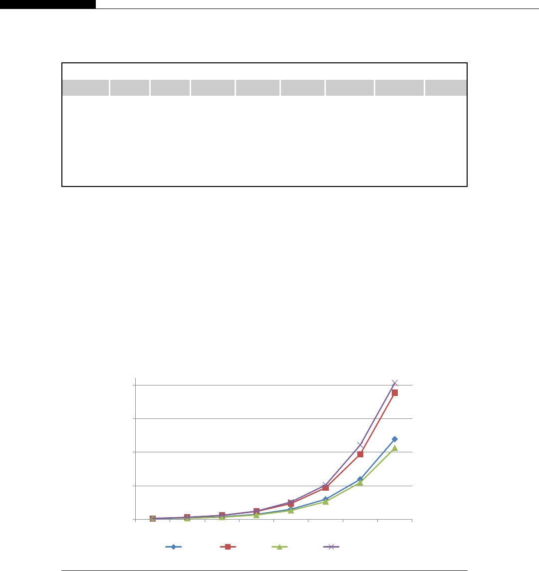
}
Reduction is an interesting problem in that, as we saw earlier, it’s difficult to write a reduction that
is faster than an OpenMP version given the transfer time of the data to the GPU. We win considerably
because there is only one significant transfer to the device, but this dominates the overall time.
However, if the data is already on the GPU, then of course this transfer is not associated with the
reduction step.
We will time a Thrust-based reduction, both on the host and device, against a standard single-core
serial reduction, an OpenMP quad-core reduction, and the four GPU test devices with a range of data
sizes. See Table 10.2 and Figure 10.3. The one item missing from the table is the Thrust reduce time on
the CPU. It was excluded because it was significantly larger than any of the other figures. With
consistency across all the block sizes, the CPU Thrust sort took approximately 10 times the execution
time of the single-core serial version.
Table 10.2 Reduce Timing for Multiple Sizes and GPUs (in ms)
Device 4 MB 8 MB 16 MB 32 MB 64 MB 128 MB 256 MB 512 MB
GTX470 1.21 2.14 4.12 7.71 15.29 30.17 59.87 119.56
GTX460 1.7 3.34 6.26 12.13 23.9 47.33 97.09 188.39
GTX260 2.38 1.85 3.53 6.8 13.46 26.64 55.02 106.28
9800 GT 1.75 3.24 6.4 12.59 26.18 51.39 110.82 202.98
Copy 2.97 6.51 9.34 17.69 38.15 68.55 134.96 278.63
Serial 6 11 22 43 91 174 348 696
OpenMP 1 4 5 9 33 37 91 164
0
50
100
150
200
4MB 8MB 16MB 32MB 64MB 128MB 256MB 512MB
GTX470 GTX460 GTX260 GT9800
FIGURE 10.3
GPU reduce time (in ms) by size.
464 CHAPTER 10 Libraries and SDK
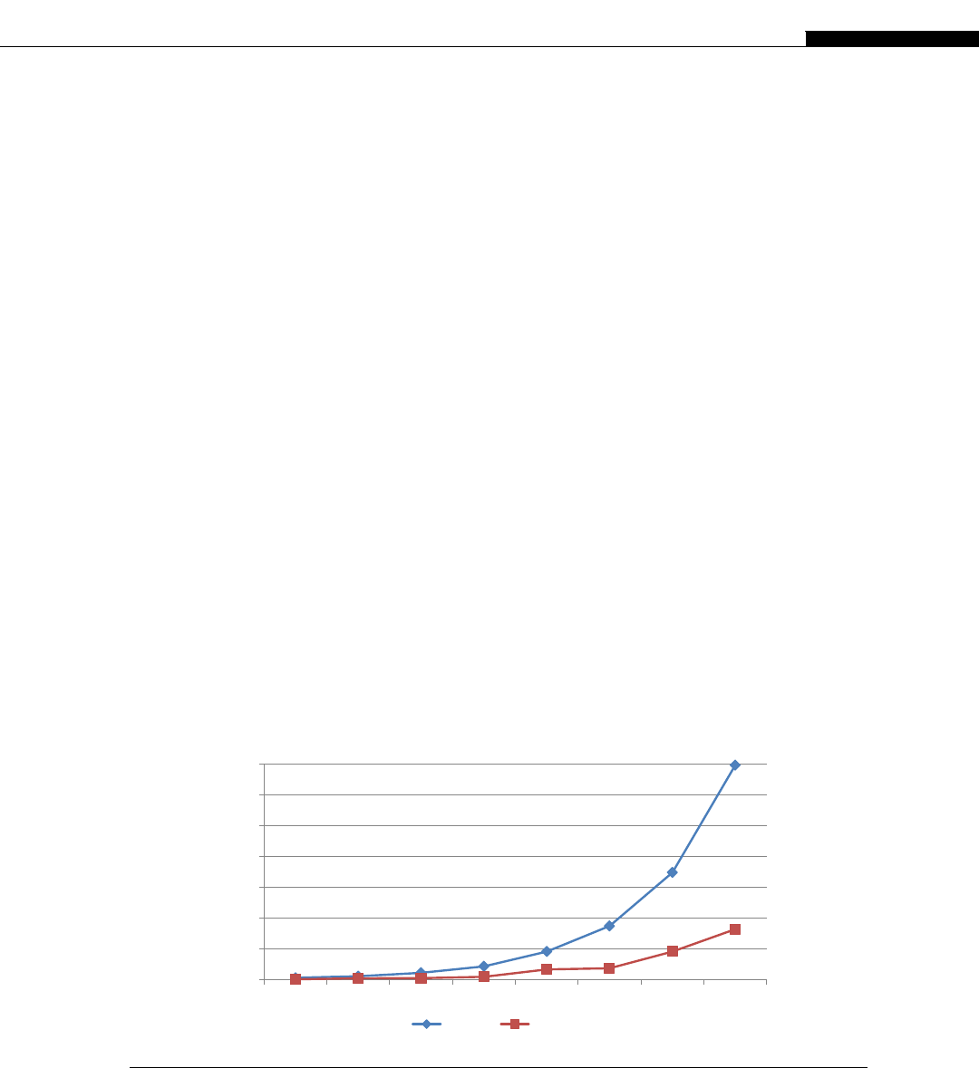
Notice in Figure 10.3, and also in Table 10.2, the yaxis is time in milliseconds. Thus, a lower value
is better. The GTX260, surprisingly, comes out with the best reduction times, marginally out-
performing the later-generation GTX470.
This is all very well, but how does it compare with the CPU versions? All the cards are faster than
the single-core serial implementation, by 3.5to 7. The GTX470 and GTX260 cards fare very well
against the OpenMP version, coming in at around two-thirds of the time of the parallel CPU version.
The GTX460 is about the same time as the CPU, with the 9800 GT being slower. However, if we take
into account the (PCI-E 2.0 x8) transfer time, 278 ms for 512 MB of data, even the GTX260 at 106 ms
(plus 278 ms) is slower than the OpenMP version at 164 ms.
With a CUDA-implemented reduction, or a Thrust asynchronous version that supported streams,
we could have subtracted the kernel time as we overlapped successive transfers and kernels. This is, of
course, assuming we have more than one reduction to perform or we broke the single reduction down
into a series of reductions. Even with this, we’re looking at a best case of 178 ms, which is still slower
than the OpenMP version. The clear message here is make use of OpenMP and the CPU when
appropriate. If the data is already on the GPU, then perform the reduction on the GPU. Otherwise, use
the CPU for some useful purpose. See Figure 10.4.
Using Thrust and CUDA
Thus, we’d like to be able to use these features of the Thrust library with regular CUDA code. It
may well be that you can write your application entirely using the provided Thrust operations.
However, libraries never cover everything and always end up doing certain things well and others
not so well. Therefore, we don’t want to be forced into a particular way of thinking just to make use
of a library.
Thrust does not provide a mechanism to copy data out of its host_vector structure in an easy
manner. It provides only a read single element method. Thus, a copy can only be performed one
element at a time, which is laboriously slow. However, with device_vectors we have an alternative
method.
0
100
200
300
400
500
600
700
4MB 8MB 16MB 32MB 64MB 128MB 256MB 512MB
Serial OpenMP
FIGURE 10.4
OpenMP and serial reduction timing (in ms).
Libraries 465

First, you need to allocate the storage space on the device yourself, thus obtaining a pointer to the
data and not a Thrust iterator. Then you need to cast the regular device pointer to a Thrust device
pointer. This is done using the device_ptr constructor. You may then pass this Thrust device pointer to
the various Thrust functions. Now Thrust works on the underlying data you have supplied and thus it is
visible to you, rather than being hidden within the Thrust library.
We can adapt the sort example to make use of this.
#include <thrust/host_vector.h>
#include <thrust/device_vector.h>
#include <thrust/sort.h>
#include <cstdlib>
#include "cuda_helper.h"
#include "timer.h"
#include "common_types.h"
void display_gpu_name(void)
{
int device_num;
struct cudaDeviceProp prop;
CUDA_CALL(cudaGetDevice(&device_num));
// Get the device name
CUDA_CALL( cudaGetDeviceProperties( &prop, device_num ) );
// Print device name and logical to physical mapping
printf("\n\nUsing CUDA Device %u. Device ID: %s on PCI-E %d",
device_num, prop.name, prop.pciBusID);
}
__global__ void fill_memory(int * const __restrict__ data,
const int num_elements)
{
const int tid ¼(blockIdx.x * blockDim.x) þthreadIdx.x;
if (tid < num_elements)
data[tid] ¼(num_elements - tid);
}
// 4M Elements ¼16MB Data
#define NUM_ELEM (1024*1024*4)
int main(void)
{
const size_t size_in_bytes ¼NUM_ELEM * sizeof(int);
display_gpu_name();
printf("\nSorting %lu data items (%lu MB)", NUM_ELEM, (size_in_bytes/1024/1024));
466 CHAPTER 10 Libraries and SDK

// Declare an array on the device
printf("\nAllocating memory on device");
int * device_mem_ptr;
CUDA_CALL(cudaMalloc((void **) &device_mem_ptr, size_in_bytes));
const u32 num_threads ¼256;
const u32 num_blocks ¼(NUM_ELEM þ(num_threads-1)) / num_threads;
printf("\nFilling memory with pattern");
fill_memory<<<num_threads, num_blocks>>>(device_mem_ptr, NUM_ELEM);
// Convert the array to
printf("\nConverting regular device pointer to thrust device pointer");
thrust::device_ptr<int>thrust_dev_ptr(device_mem_ptr);
// Sort the array on the device
printf("\nSorting on device");
thrust::sort(thrust_dev_ptr, thrust_dev_ptr DNUM_ELEM);
printf("\nFreeing memory on device");
CUDA_CALL(cudaFree(device_mem_ptr));
return 0;
}
Notice the constructor thrust::device_ptr, which creates the object thrust_dev_ptr that can
then be passed into the thrust::sort function. Unlike the conventional iteration a Thrust device
pointer does not have “begin” and “end” functions, so we simply use base plus length to obtain the last
element for the sort.
This allows host-initiated Thrust calls to be implemented alongside simple device kernels.
However, be aware there is (as of 4.2 SDK) no device level interface for Thrust, so you cannot call
Thrust functions from within a device or global function. Functions like sort, for example, spawn
multiple kernels themselves. As the GPU cannot, at least until Kepler K20 is released, spawn addi-
tional work itself, we’re limited to host-based control.
SDK Samples: Line of Sight, Radix Sort, Particles, Marching Cubes, Smoke Particles.
CuRAND
The CuRAND library provides various types of random number generation on the GPU. In C you are
probably used to calling the standard library function rand() on the host. Like many standard library
functions rand() is not available to be called in device code. Thus, your only option is to create a block
of random numbers on the host and copy this over to the device. This causes a number of problems:
• Increased startup time on the host.
• Increased PCI-E bandwidth.
• In practice, usually a poorly distributed random number set.
Libraries 467

The standard library rand() function is not designed for true randomness. It works, like many random
number generation algorithms, by creating a list of pseudo-random numbers and simply selecting the
next element from the list. Thus, anyone who knows the seed used can use this knowledge to accurately
predict the next random number in the given sequence.
This has some implications, not least of which is from the security field. Many algorithms use
randomness, in one way or another, to make it difficult to impersonate a peer. Suppose two peers
exchange a seed of a random number generator. Peer A encodes a random number into the message
frame. Peer B using the same seed and same random number generator knows what data identifier it
should expect from peer A. Given a captured sequence of identifiers from peers A and B, it’s possible
for an attacker, C, to work out the next number and spoof (pretend to be) either peer A or B.
This is possible because the random numbers are usually just a small, repeating sequence of
pseudo-random numbers. If the set of random numbers is small, then an attack is easy. The seed is
either never set by the programmer, set to some “secret” number, or set based on the current time.
Startup times are not really very random and thus time-based seeds are actually within a very small
window. Secrets rarely remain secrets.
Another example is password generation. If you have a few hundred users to set up on a system,
they will usually be issued “random” passwords that are changed on first login. These passwords may
be long character strings, leading to the belief that they are secure. However, if they are actually chosen
from a random number generator with a small pseudo-random set of numbers, the actual search space
for a brute-force attack is quite small.
Thus, for anything where predictability of the sequence is a problem, we need much better random
numbers than most standard library implementations of rand() provide.
To use the CuRAND library, you need to include the following header file:
#include <curand_kernel.h>
Additionally, you need to ensure you link to the following library:
C:\Program Files\NVIDIA GPU Computing Toolkit\CUDA\v4.1\lib\x64\curand.lib
Obviously, replace the path with the current version of the CUDA toolkit you are using. Let’s
therefore look at an example of generating some random numbers:
#include <stdio.h>
#include <stdlib.h>
#include <curand_kernel.h>
#include "cuda_helper.h"
#include "cuda.h"
#define CURAND_CALL(x) {const curandStatus_t a ¼(x); if (a !¼CURAND_STATUS_SUCCESS) {
printf("\nCuRand Error: (err_num¼%d) \n", a); cudaDeviceReset(); ASSERT(0);} }
__host__ void print_array(const float * __restrict__ const data, const int num_elem)
{
for (int i¼0; i<num_elem; iþþ)
{
if ( i% 4 ¼¼ 0)
printf("\n");
468 CHAPTER 10 Libraries and SDK

printf("%2d: %f ", i, data[i]);
}
}
__host__ int main(int argc, char *argv[])
{
const int num_elem ¼32;
const size_t size_in_bytes ¼(num_elem * sizeof(float));
curandGenerator_t rand_generator_device, rand_generator_host;
const unsigned long int seed ¼987654321;
const curandRngType_t generator_type [CURAND_RNG_PSEUDO_DEFAULT;
// Allocate memory on the device
float * device_ptr;
CUDA_CALL( cudaMalloc( (void **) &device_ptr, size_in_bytes ));
// Allocate memory on the host for the device copy
float * host_ptr;
CUDA_CALL( cudaMallocHost( (void **) &host_ptr, size_in_bytes ));
// Allocate memory on the host for the host version
float * host_gen_ptr ¼(float *) malloc(size_in_bytes);
if (host_gen_ptr ¼¼ NULL)
{
printf("\nFailed to allocation memory on host");
exit(0);
}
// Print library version number
int version;
CURAND_CALL(curandGetVersion(&version));
printf("\nUsing CuRand Version: %d and generator: CURAND_RNG_PSEUDO_DEFAULT",
version);
// Register the generator - note the different function calls
CURAND_CALL(curandCreateGenerator(&rand_generator_device, generator_type));
CURAND_CALL(curandCreateGeneratorHost(&rand_generator_host, generator_type));
// Set the seed for the random number generators
CURAND_CALL(curandSetPseudoRandomGeneratorSeed(rand_generator_device, seed));
CURAND_CALL(curandSetPseudoRandomGeneratorSeed(rand_generator_host, seed));
// Create a set of random numbers on the device and host
CURAND_CALL(curandGenerateUniform(rand_generator_device, device_ptr, num_elem));
CURAND_CALL(curandGenerateUniform(rand_generator_host, host_gen_ptr, num_elem));
// Copy the set of device generated data to the host
CUDA_CALL(cudaMemcpy(host_ptr, device_ptr, size_in_bytes, cudaMemcpyDeviceToHost));
Libraries 469

printf("\n\nRandom numbers from GPU");
print_array(host_ptr, num_elem);
printf("\n\nRandom numbers from Host");
print_array(host_gen_ptr, num_elem);
printf("\n");
// Free device resources
CURAND_CALL(curandDestroyGenerator(rand_generator_device));
CUDA_CALL(cudaFree(device_ptr));
CUDA_CALL(cudaFreeHost(host_ptr));
CUDA_CALL(cudaDeviceReset());
// Free host resources
CURAND_CALL(curandDestroyGenerator(rand_generator_host));
free(host_gen_ptr);
}
This program generates num_elem number of random numbers on the device and the host using the
CuRand API. It then prints both sets of random numbers. The output is shown here:
Using CuRand Version: 4010 and generator: CURAND_RNG_PSEUDO_DEFAULT
Random numbers from GPU
0: 0.468090 1: 0.660579 2: 0.351722 3: 0.891716
4: 0.624544 5: 0.861485 6: 0.662096 7: 0.007847
8: 0.179364 9: 0.260115 10: 0.453508 11: 0.711956
12: 0.973453 13: 0.152303 14: 0.784318 15: 0.948965
16: 0.214159 17: 0.236516 18: 0.020540 19: 0.175973
20: 0.085989 21: 0.863053 22: 0.908001 23: 0.539129
24: 0.849580 25: 0.496193 26: 0.588651 27: 0.361609
28: 0.025815 29: 0.778294 30: 0.194206 31: 0.478006
Random numbers from Host
0: 0.468090 1: 0.660579 2: 0.351722 3: 0.891716
4: 0.624544 5: 0.861485 6: 0.662096 7: 0.007847
8: 0.179364 9: 0.260115 10: 0.453508 11: 0.711956
12: 0.973453 13: 0.152303 14: 0.784318 15: 0.948965
16: 0.214159 17: 0.236516 18: 0.020540 19: 0.175973
20: 0.085989 21: 0.863053 22: 0.908001 23: 0.539129
24: 0.849580 25: 0.496193 26: 0.588651 27: 0.361609
28: 0.025815 29: 0.778294 30: 0.194206 31: 0.478006
One important issue to note from the example program is the API calls are the same for device and
host functions, except for registering the generator. The device version must be used with
curandCreateGenerator and the host version with curandCreateGeneratorHost. Additionally, note that
the curandGenerateUniform function must be called with the associated host or device-based pointer.
470 CHAPTER 10 Libraries and SDK

Getting either of these mixed up will likely result in a CUDA “unknown error” issue or the program
simply crashing. Unfortunately, as both host-side and device-side memory allocations are just regular C
pointers, it’s not possible for the library to tell if this pointer passed to it, is a host-side pointer, or device-
side pointer.
Also be aware that CuRand, as with NPP, supports streams. Thus, a call to curandSet
Stream(generator, stream) will switch the library to an asynchronous operation in that stream. By
default the library will use stream 0, the default stream.
There are many types of generators you can use with the CuRand library, including one based on
the Mersenne Twister algorithm used for Monte Carlo simulations.
SDK Samples: Monte Carlo, Random Fog, Mersenne Twister, Sobol.
CuBLAS (CUDA basic linear algebra) library
The last library we’ll mention is the CuBLAS. The CuBLAS library aims to replicate the functionality
of the Fortran BLAS library commonly used in Fortran scientific applications. To allow easy porting of
existing Fortran BLAS code, the CuBLAS library maintains the Fortran column-major layout, the
opposite of the standard C row-major layout. It also uses the 1..N as opposed to the C standard 0..(N-1)
notation when accessing array elements.
Thus, for porting legacy Fortran code to CUDA, the CuBLAS library is ideal. There are many large
codebases written over the past decades in Fortran. Allowing this existing legacy code to run on
modern GPU-accelerated hardware without significant code changes is one of the great strengths of
this library. However, it’s also one of its weaknesses, as it will not appeal to anyone who learned to
program in a modern computing language.
The CuBLAS library documentation provides some sample macros to convert the old-style Fortran
array indexes into what most programmers would consider “regular” array indexing. However, even if
implemented as macros or as an inline function, this adds execution time overhead to anyone
attempting to work with non-Fortran indexing. This makes using the library rather a pain for C
programmers. C programmers may have preferred to see a separate C style CuBLAS implementation
that natively supported C array indexing.
As of version four of the library, it deprecated the older API. It now requires all callers to first create
a handle via a call to the cublasCreate function call before any other calls are made. The handle is
used in subsequent calls and allows CuBLAS to be both re-entrant and to support multiple GPUs using
multiple asynchronous streams for maximum performance. Note although these features are provided,
it’s the programmers responsibility to handle multiple devices. Like so many of the other libraries
provided, the CuBLAS library does not automatically distribute its load across multi-GPU devices.
The current API can be used by including the cublas_v2.h file instead of the older cublas.h
include file. Any current usage of the older API should be replaced with the newer API. As with
the NPP library, operations are expected to be performed on data already present on the GPU and the
caller is therefore responsible for transferring the data to and from the device. A number of “helper”
functions are provided for such purposes.
The new CuBLAS interface is entirely asynchronous in nature, meaning even functions that return
values do it in such a way as the value may not be available unless the programmer specifically waits
for the asynchronous GPU operation to complete. This is part of the move to asynchronous streams
that will become important when the Kepler K20 is released.
Libraries 471

We’ll look at a simple example here, declaring a matrix on the host side, copying it to the device,
performing some operations, copying the data back to the host, and printing the matrix.
#include <stdio.h>
#include <stdlib.h>
#include <cublas_v2.h>
#include "cuda_helper.h"
#include "cuda.h"
#define CUBLAS_CALL(x) {const cublasStatus_t a ¼(x); if (a !¼CUBLAS_STATUS_SUCCESS) {
printf("\nCUBLAS Error: (err_num¼%d) \n", a); cudaDeviceReset(); ASSERT(0);} }
__host__ void print_array(const float * __restrict__ const data1,
const float * __restrict__ const data2,
const float * __restrict__ const data3,
const int num_elem,
const char * const prefix)
{
printf("\n%s", prefix);
for (int i¼0; i<num_elem; iþþ)
{
printf("\n%2d: %2.4f %2.4f %2.4f ", iþ1, data1[i], data2[i], data3[i]);
}
}
__host__ int main(int argc, char *argv[])
{
const int num_elem ¼8;
const size_t size_in_bytes ¼(num_elem * sizeof(float));
// Allocate memory on the device
float * device_src_ptr_A;
CUDA_CALL( cudaMalloc( (void **) &device_src_ptr_A, size_in_bytes ));
float * device_src_ptr_B;
CUDA_CALL( cudaMalloc( (void **) &device_src_ptr_B, size_in_bytes ));
float * device_dest_ptr;
CUDA_CALL( cudaMalloc( (void **) &device_dest_ptr, size_in_bytes ));
// Allocate memory on the host for the device copy
float * host_src_ptr_A;
CUDA_CALL( cudaMallocHost( (void **) &host_src_ptr_A, size_in_bytes ));
float * host_dest_ptr;
CUDA_CALL( cudaMallocHost( (void **) &host_dest_ptr, size_in_bytes ));
float * host_dest_ptr_A;
CUDA_CALL( cudaMallocHost( (void **) &host_dest_ptr_A, size_in_bytes ));
float * host_dest_ptr_B;
CUDA_CALL( cudaMallocHost( (void **) &host_dest_ptr_B, size_in_bytes ));
472 CHAPTER 10 Libraries and SDK

// Clear destination memory
memset(host_dest_ptr_A, 0, size_in_bytes);
memset(host_dest_ptr_B, 0, size_in_bytes);
memset(host_dest_ptr, 0, size_in_bytes);
// Init the CUBLAS library
cublasHandle_t cublas_handle;
CUBLAS_CALL(cublasCreate(&cublas_handle));
// Print library version number
int version;
CUBLAS_CALL(cublasGetVersion(cublas_handle, &version));
printf("\nUsing CUBLAS Version: %d", version);
// Fill the first host array with known values
for (int i¼0; i < num_elem; iþþ)
{
host_src_ptr_A[i] ¼(float) i;
}
print_array(host_src_ptr_A, host_dest_ptr_B, host_dest_ptr, num_elem, "Before Set");
const int num_rows ¼num_elem;
const int num_cols ¼1;
const size_t elem_size ¼sizeof(float);
// Copy a matrix one cell wide by num_elem rows from the CPU to the device
CUBLAS_CALL(cublasSetMatrix(num_rows, num_cols, elem_size, host_src_ptr_A,
num_rows, device_src_ptr_A, num_rows));
// Clear the memory in the other two
CUDA_CALL(cudaMemset(device_src_ptr_B, 0, size_in_bytes));
CUDA_CALL(cudaMemset(device_dest_ptr, 0, size_in_bytes));
// SAXPY on device based on copied matrix and alpha
const int stride ¼1;
float alpha ¼2.0F;
CUBLAS_CALL(cublasSaxpy(cublas_handle, num_elem, &alpha, device_src_ptr_A,
stride, device_src_ptr_B, stride));
alpha ¼3.0F;
CUBLAS_CALL(cublasSaxpy(cublas_handle, num_elem, &alpha, device_src_ptr_A,
stride, device_dest_ptr, stride));
// Calculate the index of the max of each maxtrix, writing the result
// directly to host memory
int host_max_idx_A, host_max_idx_B, host_max_idx_dest;
Libraries 473

CUBLAS_CALL(cublasIsamax(cublas_handle, num_elem, device_src_ptr_A,
stride, &host_max_idx_A));
CUBLAS_CALL(cublasIsamax(cublas_handle, num_elem, device_src_ptr_B,
stride, &host_max_idx_B));
CUBLAS_CALL(cublasIsamax(cublas_handle, num_elem, device_dest_ptr,
stride, &host_max_idx_dest));
// Calculate the sum of each maxtrix, writing the result directly to host memory
float host_sum_A, host_sum_B, host_sum_dest;
CUBLAS_CALL(cublasSasum(cublas_handle, num_elem, device_src_ptr_A,
stride, &host_sum_A));
CUBLAS_CALL(cublasSasum(cublas_handle, num_elem, device_src_ptr_B,
stride, &host_sum_B));
CUBLAS_CALL(cublasSasum(cublas_handle, num_elem, device_dest_ptr,
stride, &host_sum_dest));
// Copy device versions back to host to print out
CUBLAS_CALL(cublasGetMatrix(num_rows, num_cols, elem_size, device_src_ptr_A,
num_rows, host_dest_ptr_A, num_rows));
CUBLAS_CALL(cublasGetMatrix(num_rows, num_cols, elem_size, device_src_ptr_B,
num_rows, host_dest_ptr_B, num_rows));
CUBLAS_CALL(cublasGetMatrix(num_rows, num_cols, elem_size, device_dest_ptr,
num_rows, host_dest_ptr, num_rows));
// Make sure any async calls above are complete before we use the host data
const int default_stream ¼0;
CUDA_CALL(cudaStreamSynchronize(default_stream));
// Print out the arrays
print_array(host_dest_ptr_A, host_dest_ptr_B, host_dest_ptr, num_elem, "After Set");
// Print some stats from the arrays
printf("\nIDX of max values : %d, %d, %d", host_max_idx_A,
host_max_idx_B, host_max_idx_dest);
printf("\nSUM of values : %2.2f, %2.2f, %2.2f", host_sum_A,
host_sum_B, host_sum_dest);
// Free device resources
CUBLAS_CALL(cublasDestroy(cublas_handle));
CUDA_CALL(cudaFree(device_src_ptr_A));
CUDA_CALL(cudaFree(device_src_ptr_B));
CUDA_CALL(cudaFree(device_dest_ptr));
// Free host resources
CUDA_CALL(cudaFreeHost(host_src_ptr_A));
CUDA_CALL(cudaFreeHost(host_dest_ptr_A));
CUDA_CALL(cudaFreeHost(host_dest_ptr_B));
474 CHAPTER 10 Libraries and SDK

CUDA_CALL(cudaFreeHost(host_dest_ptr));
// Reset ready for next GPU program
CUDA_CALL(cudaDeviceReset());
}
The basic steps of the program are as follows:
• Create a CuBLAS handle using the cublasCreate function.
• Allocate resources on the device and host.
• Set a matrix on the device directly from a matrix on the host.
• Run Saxpy on the device.
• Run max and sum functions on the device.
• Copy the resultant matrix back to the host and display it.
• Free any allocated resources.
In practice, real programs will be significantly more complex. We’ve attempted to show here the basic
template necessary to get some simple CuBLAS functions working on the GPU.
SDK Samples: Matrix Multiplication.
CUDA COMPUTING SDK
The CUDA SDK is a separate download from regular toolkits and drivers, although it is now bundled
with the CUDA 5 release candidate for Windows users, so it may become a single download in the
future. It contains lots of sample code and a nice interface to find all the provided CUDA
documentation.
There are almost 200 samples, so we’ll select a few sample applications to look at in detail. We’ll
look at some general-purpose applications since these are easier to understand for the wider audience
this text is aimed at than some of the more domain-specific examples in the toolkit.
The computing samples are incredibly useful for someone starting out with GPU programming, as
well as more advanced programmers who want examples of how something should be done. Unfor-
tunately, a lot of the underlying CUDA API is hidden from you. When you are learning a new API the
last thing you need is yet another API layer on top of the one you wish to learn, so this rather
complicates understanding.
Many of the SDK examples use the cutil or other packages that are not part of the standard CUDA
release. Thus, when you see the line
cutilSafeCall(cudaGetDeviceProperties(&deviceProps, devID));
you might expect it to work in your own code. However, to do this it’s also necessary to include the
relevant cutil source headers from the SDK. NVIDIA makes no guarantee about the version-to-
version compatibility of these libraries. They are not part of the official CUDA release and therefore
are not supported.
The CUDA APIs always start cuda.. Therefore, if you see anything other than this, you should
realize that you will need to bring in additional code from the SDK samples, should you wish to use
such calls.
CUDA Computing SDK 475

So what does cutilSafeCall do? Fairly much the same as the CUDA_CALL macro we’ve used
throughout this text. If there is an error returned from the caller, it prints the file and line number and
then exits. So why not use the cutil package directly? Largely because there are many functions in
this library and you only need a small number of them in reality.
There are, however, many useful functions within this package, for example, the
gpuGetMaxGflopsDeviceId function that identifies the fastest GPU device in the system. You should
browse through the libraries provided with the SDK to help you understand some of the samples before
jumping into the samples themselves.
Device Query
Device query is an interesting application in that it’s quite simple and allows you to see what your GPU
is capable of. It is run from the command line rather than the Windows interface and can be found in
“C:\ProgramData\NVIDIA Corporation\NVIDIA GPU Computing SDK 4.1\C\bin\win64\Release.”
Obviously it is the Windows 64-bit version we’re using here from the 4.1 toolkit, which may be
different on your system. The output is shown here:
Found 4 CUDA Capable device(s)
Device 0: "GeForce GTX 470"
CUDA Driver Version / Runtime Version 4.1 / 4.1
CUDA Capability Major/Minor version number: 2.0
Total amount of global memory: 1280 MBytes (1342177280 bytes)
(14) Multiprocessors x (32) CUDA Cores/MP: 448 CUDA Cores
GPU Clock Speed: 1.22 GHz
Memory Clock rate: 1674.00 Mhz
Memory Bus Width: 320-bit
L2 Cache Size: 655360 bytes
Max Texture Dimension Size (x,y,z) 1D¼(65536), 2D¼(65536,65535),
3D¼(2048,2048,2048)
Max Layered Texture Size (dim) x layers 1D¼(16384) x 2048, 2D¼(16384,16384) x
2048
Total amount of constant memory: 65536 bytes
Total amount of shared memory per block: 49152 bytes
Total number of registers available per block: 32768
Warp size: 32
Maximum number of threads per block: 1024
Maximum sizes of each dimension of a block: 1024 x 1024 x 64
Maximum sizes of each dimension of a grid: 65535 x 65535 x 65535
Maximum memory pitch: 2147483647 bytes
Texture alignment: 512 bytes
Concurrent copy and execution: Yes with 1 copy engine(s)
Run time limit on kernels: No
Integrated GPU sharing Host Memory: No
Support host page-locked memory mapping: Yes
Concurrent kernel execution: Yes
Alignment requirement for Surfaces: Yes
Device has ECC support enabled: No
476 CHAPTER 10 Libraries and SDK

Device is using TCC driver mode: No
Device supports Unified Addressing (UVA): No
Device PCI Bus ID / PCI location ID: 8 / 0
Compute Mode:
< Default (multiple host threads can use ::cudaSetDevice() with device simultaneously) >
Device 1: "GeForce 9800 GT"
CUDA Capability Major/Minor version number: 1.1
Total amount of global memory: 1024 MBytes (1073741824 bytes)
(14) Multiprocessors x ( 8) CUDA Cores/MP: 112 CUDA Cores
GPU Clock Speed: 1.63 GHz
Memory Clock rate: 950.00 Mhz
Memory Bus Width: 256-bit
Total amount of shared memory per block: 16384 bytes
Total number of registers available per block: 8192
Maximum number of threads per block: 512
Device PCI Bus ID / PCI location ID: 7 / 0
Device 2: "GeForce GTX 260"
CUDA Capability Major/Minor version number: 1.3
Total amount of global memory: 896 MBytes (939524096 bytes)
(27) Multiprocessors x ( 8) CUDA Cores/MP: 216 CUDA Cores
GPU Clock Speed: 1.35 GHz
Memory Clock rate: 1100.00 Mhz
Memory Bus Width: 448-bit
Total amount of shared memory per block: 16384 bytes
Total number of registers available per block: 16384
Maximum number of threads per block: 512
Device PCI Bus ID / PCI location ID: 1 / 0
Device 3: "GeForce GTX 460"
CUDA Capability Major/Minor version number: 2.1
Total amount of global memory: 1024 MBytes (1073741824 bytes)
( 7) Multiprocessors x (48) CUDA Cores/MP: 336 CUDA Cores
GPU Clock Speed: 1.45 GHz
Memory Clock rate: 1800.00 Mhz
Memory Bus Width: 256-bit
L2 Cache Size: 524288 bytes
Total amount of shared memory per block: 49152 bytes
Total number of registers available per block: 32768
Maximum number of threads per block: 1024
Device PCI Bus ID / PCI location ID: 2 / 0
The program will iterate through all GPUs to find and list the various details of each device. For
brevity, we have listed only one of the four devices completely and extracted the interesting parts from
the other devices. For those interested in Kepler GK104, the relevant details are as follows:
Device 0: "GeForce GTX 680"
CUDA Capability Major/Minor version number: 3.0
CUDA Computing SDK 477

Total amount of global memory: 2048 MBytes (2146762752 bytes)
( 8) Multiprocessors x (192) CUDA Cores/MP: 1536 CUDA Cores
GPU Clock Speed: 1006 MHz
Memory Clock rate: 3004.00 Mhz
Memory Bus Width: 256-bit
L2 Cache Size: 524288 bytes
Total amount of shared memory per block: 49152 bytes
Total number of registers available per block: 65536
Warp size: 32
Maximum number of threads per block: 1024
Concurrent copy and execution: Yes with 1 copy engine(s)
Items reported of note are the current driver and runtime version, which should be the same.
Compute capability defines what type of device we have for a given device number. Also detailed is the
number of cores/SMs per device, speed of the device, along with memory speed and width. Thus, it’s
possible to calculate the peak bandwidth on a given device. Talking of bandwidth, this brings us to the
next useful application in the SDK.
Bandwidth test
The bandwidth example provided by the SDK provides the following useful statistics about your
particular device/host setup:
• Host-to-device bandwidth (paged and pinned memory)
• Device-to-host bandwidth (paged and pinned memory)
• Device-to-device bandwidth
The actual output is shown here for a GTX470 on an x8 PCI-E 2.0 link:
>> bandwidthtest --device[0 --memory[pageable
Device 0: GeForce GTX 470
Quick Mode
Host to Device Bandwidth, 1 Device(s), Paged memory
Transfer Size (Bytes) Bandwidth(MB/s)
33554432 1833.6
Device to Host Bandwidth, 1 Device(s), Paged memory
Transfer Size (Bytes) Bandwidth(MB/s)
33554432 1700.5
Device to Device Bandwidth, 1 Device(s)
Transfer Size (Bytes) Bandwidth(MB/s)
33554432 113259.3
>> bandwidthtest --device[0 --memory[pinned
Host to Device Bandwidth, 1 Device(s), Pinned memory
Transfer Size (Bytes) Bandwidth(MB/s)
478 CHAPTER 10 Libraries and SDK

33554432 2663.6
Device to Host Bandwidth, 1 Device(s), Pinned memory
Transfer Size (Bytes) Bandwidth(MB/s)
33554432 3225.8
Device to Device Bandwidth, 1 Device(s)
Transfer Size (Bytes) Bandwidth(MB/s)
33554432 113232.3
One of the things you’ll see when using this example program is just how much benefit using
pinned memory on your system brings. We looked at this in Chapter 9, but there is nothing like seeing
it on your own system to drive home the point that pinned memory can be much faster for memory
transfers. Even a modern Sandybridge-E processor achieves 3 GB/s versus 2.3 GB/s when using
pinned versus paged memory on a similar PCI-E 2.0 x8 link.
Typical memory on a consumer GPU card is anything from 512 MB (88/9800 series) to 2 GB
(GTX680). There is really no reason why you should not pin system memory to do the transfers to or
from the GPU. Even in a 32-bit system with a 4 GB memory limit, CUDA will still be using pinned
transfers in the background. Therefore, you may just as well pin the memory yourself and avoid the
implicit pageable to pinned memory copy within the driver.
As memory is now very cheap there is no reason why you should not fully load the machine. This is
especially the case if you have more than one GPU card or are using Tesla cards. You can purchase
16 GB of host memory for less than 100 euros/dollars/pounds.
If we take the memory clock from the GTX470, there is 1674 MHz with a bus width of 320 bits.
Thus, we take the bus width and divide by 8 to get bytes (40 bytes). Next we multiply this by the clock
rate (66,960 MB/s). Then we multiply by 2 for GDDR5 (133,920 MB/s). Then we divide by 1000 to
get listed memory bandwidth (133.9 GB/s) or 1024 (130.8 GB/s) to get actual bandwidth.
So why do we get device-to-device bandwidth of 113,232 MB/s instead of 133,920 MB/s? Where
did the missing 20 MB/s or 15% of the memory bandwidth go? The GPU never achieves this theo-
retical peak bandwidth. This is why it’s useful to run the bandwidth test as opposed to calculating the
theoretical peak. You then have a very good idea of what bandwidth you will get in your system, with
your PCI-E arrangement, your host CPU, your CPU chipset, your host memory, etc. By knowing this
you know what your application should be able to achieve on a given target and can therefore see how
much potential you have yet to exploit.
Note with Tesla-based Fermi devices you can gain a significant boost in bandwidth by disabling the
ECC memory option using the nvidia-smi tool. Error checking and correction (ECC) distributes the bit
patterns using Hamming codes. This, in effect, means you need a larger memory space to store the
same data block. This additional storage requirement means you trade both space and speed for the
extra redundancy ECC brings. NVIDA claims to have addressed this issue in Kepler K20 (GK110),
where the impact of using ECC is claimed to be around one-third of that of Fermi.
SimpleP2P
The SimpleP2P example shows how to use the P2P memory transfer capabilities introduced in
compute 2.x devices (Fermi). The principle of P2P transfers to avoid having to go through host
CUDA Computing SDK 479
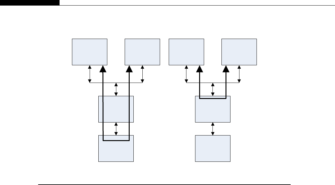
memory (see Figure 10.5). Host memory may be directly accessible to the PCI-E I/O hub
(Northbridge), as is often the case with Intel’s QPI-based system. It may also be to the other side of the
processor, as with Intel’s DMI and AMD’s hypertransport-based systems.
Depending on the number of GPUs in the system, the host memory may represent a bottleneck for the
transfer in terms of its own speed. The maximum PCI-E transfer speed approaches 6 GB/s on a PCI-E 2.0
link. With PCI-E 3.0 (GTX680, GTX690, Tesla K10) the actual bandwidth almost doubles to just under
12 GB/s in each direction. To maximize bandwidth, you typically define two pinned memory areas and
use a double buffer scheme to transfer into one block and out of the other. Especially with the older
processors, you can rapidly consume the entire host memory bandwidth simply by performing transfers
between GPUs through host memory. This will severely hamper any attempt to use the CPU for additional
processing capabilities, as it will be competing for host memory bandwidth with the GPU transfers.
The idea of P2P is to keep the data out of the host memory space and to do a transfer directly
between the GPUs. While this is an extremely useful feature, support for this in the mainstream
Windows 7 systems has been noticeably lacking. Thus it is not something we’ve looked at yet in this
text, so we will cover it here as there are a number of uses for this technology. Requirements to use the
P2P functionality are:
• A 64-bit OS, and thus UVA (unified virtual addressing) enabled, a requirement for P2P to be
available.
• Two or more compute 2.x devices that support this feature.
• GPU Devices that are on the same PCI-E I/O hub.
• Appropriate driver level support.
GPU0 GPU1
PCI-E I/O
Hub
Host
Memory
(DDR3)
GPU0 GPU1
PCI-E I/O
Hub
Host
Memory
(DDR3)
GPU to Host to GPU-Copy Peer to Peer-Copy
FIGURE 10.5
P2P transfers.
480 CHAPTER 10 Libraries and SDK

To use this feature under Windows 7 you need the 64-bit OS plus the TCC (Tesla compute cluster)
drivers active. As the TCC driver will only activate with Tesla cards, effectively there is no mainstream
consumer support for this in Windows 7. Thus, this should be considered as a feature suitable for
clusters, high-performance computing (HPC), and other compute-centered applications. It’s not
something you can exploit with, say, a video transcoding application for consumer PCs.
To support P2P first you should check UVA is enabled:
struct cudaDevice device_prop;
CUDA_CALL(cudaGetDeviceProperties(&device_prop));
if (device_prop.unifiedAddressing ¼¼ 1) // If unified addressing is enabled
UVA will only be enabled under a 64-bit OS, or Windows 7 using the TCC driver.
Next you need to check if device A can talk to device B. Note, just because this test passes, it does
not imply that device B can talk to device A. Resources are consumed in enabling P2P access in a given
direction. This test can be performed with the following code:
int peer_access_avail;
int src_device ¼0;
int peer_device ¼1;
CUDA_CALL(cudaDeviceCanAccessPeer( &peer_access_avail, src_device, peer_device));
if (peer_access_avail ¼¼ 1) // If peer access from device 0 to device 1 is available
{
int flags ¼0;
CUDA_CALL(cudaSetDevice(peer_device));
CUDA_CALL(cudaEnablePeerAccess(peer_device, flags);
}
Once peer access has been enabled, memory can be accessed, in the direction of the peer access,
either in device kernels or as host-initiated memory copies. Thus, device 0 can enable peer access to
device 1, as in the previous example. You can then call a kernel on device 1, passing it a pointer to the
global memory space from device 0. The kernel will then dereference this pointer in the same way as it
would a zero-copy device pointer to host memory. Every time there is an access through that pointer
device 1 will initiate a fetch over the PCI-E bus from device 0. Of course, the same caveats apply as
with zero-copy memory usage, specifically that you should avoid re-reading such memory and try to
achieve coalesced access patterns for performance reasons.
You can of course use such features for device-initiated memory copies. To do this from the
device, have a device kernel fetch the data via a device pointer, and simply store it to the local
device’s global memory. Equally you can push as well as pull data from one device to another.
However, if you want bidirectional access, you will need to remember to enable P2P access in both
directions.
The second approach is an explicit memory copy, something we must initiate from the host.
There are the two standard forms of this, the synchronous version and the asynchronous streamed
version:
cudaMemcpyPeer(dest_device_ptr, dst_device_num, src_device_ptr,
src_device_num,num_bytes);
CUDA Computing SDK 481

and
cudaMemcpyPeerAsync( dest_device_ptr, dst_device_num, src_device_ptr, src_device_num,
num_bytes, stream );
Finally, once we’re done, we need to disable the provisioning of the resources for the P2P access by
calling
cudaDeviceDisablePeerAccess(device_num);
Performance wise the SimpleP2P application reports 2.4 GB/s, which is quite close to the peak 3
GB/s available on this particular (PCI-E 2.0 x8) test system.
The SimpleP2P example program in the SDK provides some simple template code as to how to do
this in practice. It does a series of GPU transfers between two GPUs and then computes the transfer
speed. With the background we’ve covered here you should be able to read and follow the example
code.
asyncAPI and cudaOpenMP
The asyncAPI SDK sample provides an example of using the asynchronous API, but is not
actually very simple for someone new to CUDA to understand. We’ve covered streams and
asynchronous operation already in the text. These are important for getting multi-GPU setups
to work alongside CPU usage. Therefore, we’ll look at this example and see what exactly it
does.
The basic premise of the asyncAPI example is that it creates an asynchronous stream, into which it
puts a memory copy to the device, a kernel, and finally a memory copy back to the host. During this
time it runs some code on the CPU that simply counts up while the GPU is running the asynchronous
kernel.
The cudaOpenMP example shows how to use OpenMP with CUDA. It identifies the number of CPU
threads, and the number and name of each attached CUDA device. It then tries to spawn one thread per
GPU device and work-share the different devices.
We’ll provide a similar example here that fuses the two SDK examples, but simplifies them
somewhat and is potentially more useful as template code for your own work.
#include <stdio.h>
#include <omp.h>
#include "cuda_helper.h"
#include "cuda.h"
__global__ void increment_kernel(int * __restrict__ const data,
const int inc_value,
const int num_elem)
{
const int idx ¼blockIdx.x * blockDim.x þthreadIdx.x;
// Check array index does not overflow the array
if (idx < num_elem)
482 CHAPTER 10 Libraries and SDK

{
// Repeat N times - just to make the kernel take some time
const int repeat ¼512;
for (int i¼0; i < repeat; iþþ)
data[idx] þ¼ inc_value;
}
}
// Max number of devices on any single node is, usually at most, eight
#define MAX_NUM_DEVICES 8
__host__ int main(int argc, char *argv[])
{
const int num_elem ¼1024 * 1024 * 16;
const int size_in_bytes ¼num_elem * sizeof(int);
const int increment_value ¼1;
const int loop_iteration_check ¼1000000;
const int shared_mem ¼0;
// Define the number of threads/blocks needed
const int num_threads ¼512;
const int num_blocks ¼((num_elem þ(num_threads-1)) / num_threads);
// One array element per CPU thread
int host_counter[MAX_NUM_DEVICES];
float delta_device_time[MAX_NUM_DEVICES];
cudaDeviceProp device_prop[MAX_NUM_DEVICES];
int num_devices;
CUDA_CALL(cudaGetDeviceCount(&num_devices));
printf("\nIdentified %d devices. Spawning %d threads to calculate %d MB using (%dx%d)",
num_devices, num_devices, ((size_in_bytes/1024)/1024), num_blocks, num_threads );
// Declare thread private, per thread variables
int * device_ptr[MAX_NUM_DEVICES];
int * host_ptr[MAX_NUM_DEVICES];
cudaEvent_t start_event[MAX_NUM_DEVICES], stop_event[MAX_NUM_DEVICES];
cudaStream_t async_stream[MAX_NUM_DEVICES];
// Create all allocations outside of OpenMP in series
for (int device_num¼0; device_num < num_devices; device_numþþ)
{
// Set the device to a unique device per CPU thread
CUDA_CALL(cudaSetDevice(device_num));
// Get the current device properties
CUDA_CALL(cudaGetDeviceProperties(&device_prop[device_num], device_num));
CUDA Computing SDK 483

// Allocate the resources necessary
CUDA_CALL(cudaMalloc((void **) &device_ptr[device_num], size_in_bytes));
CUDA_CALL(cudaMallocHost((void **) &host_ptr[device_num], size_in_bytes));
CUDA_CALL(cudaEventCreate(&start_event[device_num]));
CUDA_CALL(cudaEventCreate(&stop_event[device_num]));
CUDA_CALL(cudaStreamCreate(&async_stream[device_num]));
}
// Spawn one CPU thread for each device
#pragma omp parallel num_threads(num_devices)
{
// Variables declared within the OpenMP block are thread private and per thread
// Variables outside OpenMP block exist once in memory and are shared between
// threads.
// Get our current thread number and use this as the device number
const int device_num ¼omp_get_thread_num();
// Set the device to a unique device per CPU thread
CUDA_CALL(cudaSetDevice(device_num));
// Push start timer, memset, kernel, copy back and stop timer into device queue
CUDA_CALL(cudaEventRecord(start_event[device_num], async_stream[device_num]));
// Copy the data to the device
CUDA_CALL(cudaMemsetAsync(device_ptr[device_num], 0, size_in_bytes,
async_stream[device_num]));
// Invoke the kernel
increment_kernel<<<num_blocks, num_threads, shared_mem, async_stream[device_num]
>>>(device_ptr[device_num], increment_value, num_elem);
// Copy data back from the device
CUDA_CALL(cudaMemcpyAsync(host_ptr[device_num], device_ptr[device_num],
size_in_bytes, cudaMemcpyDeviceToHost,
async_stream[device_num]));
// Record the end of the GPU work
CUDA_CALL(cudaEventRecord(stop_event[device_num], async_stream[device_num]));
// Device work has now been sent to the GPU, so do some CPU work
// whilst we’re waiting for the device to complete its work queue
// Reset host counter
int host_counter_local ¼0;
int complete ¼0;
484 CHAPTER 10 Libraries and SDK

// Do some work on the CPU until all the device kernels complete
do
{
// Insert useful CPU work here
host_counter_localþþ;
// Check device completion status every loop_iteration_check iterations
if ( (host_counter_local % loop_iteration_check) ¼¼ 0)
{
// Assume everything is now complete
complete ¼1;
// Check if all GPU streams have completed. Continue to do more CPU
// work if one of more devices have pending work.
for ( int device_check_num¼0; device_check_num < num_devices;
device_check_numþþ)
{
if ( cudaEventQuery(stop_event[device_check_num]) ¼¼ cudaErrorNotReady )
complete ¼0;
}
}
} while( complete ¼¼ 0);
// Write out final result
host_counter[device_num] ¼host_counter_local;
// Calculate elapsed GPU time
CUDA_CALL(cudaEventElapsedTime(&delta_device_time[device_num],
start_event[device_num],
stop_event[device_num]));
} // End parallel region
// Now running as a single CPU thread again
// Free allocated resources
// Create all allocations outside of OpenMP in series
for (int device_num¼0; device_num < num_devices; device_numþþ)
{
// Set the device to a unique device per CPU thread
CUDA_CALL(cudaSetDevice(device_num));
CUDA_CALL(cudaStreamDestroy(async_stream[device_num]));
CUDA_CALL(cudaEventDestroy(stop_event[device_num]));
CUDA_CALL(cudaEventDestroy(start_event[device_num]));
CUDA_CALL(cudaFreeHost(host_ptr[device_num]));
CUDA Computing SDK 485

CUDA_CALL(cudaFree(device_ptr[device_num]));
// Reset the device for later use
CUDA_CALL(cudaDeviceReset());
}
// Print a summary of the results
for (int device¼0; device < num_devices; deviceþþ)
{
printf("\n\nKernel Time for device %s id:%d: %.2fms",
device_prop[device].name, device, delta_device_time[device]);
printf("\nCPU count for thread %d: %d", device, host_counter[device]);
}
}
There are a few points in the SDK examples that need further discussion. First, with the asyncAPI
example, stream 0, the default stream, is used. Unfortunately, there are many instances where the
default stream causes implicit synchronization between streams. You will almost certainly end up
using a double- or triple-buffered method and this implicit synchronization will catch you out. When
using asynchronous operations, always create your own streams.
cudaStream_t async_stream[MAX_NUM_DEVICES];
CUDA_CALL(cudaSetDevice(device_num));
CUDA_CALL(cudaStreamCreate(&async_stream[device_num]));
The second point from the asyncAPI stream example that you may not have noticed is that it
takes the number of elements, N, and divides it directly by the number of threads to get the number
of blocks for the grid. As it happens Nis a multiple of the number of threads, but what if it is not?
What happens is, the last elements in the arrayarenotprocessedbytheGPUkernel.Thismay
not be at all obvious for anyone starting out with CUDA. Always use the following formula for
generating the number of blocks if you plan on allowing Nnot to be a multiple of the number of
threads:
const int num_elem ¼1024 * 1024 * 16;
const int num_threads ¼512;
const int num_blocks ¼((num_elem þ(num_threads-1)) / num_threads);
And in the kernel, add a check for array overrun:
// Check array index does not overflow the array
if (idx < num_elem)
Now this creates the overhead of passing num_elem to the kernel and checking it within the kernel.
If you can guarantee you will always use a multiple of the number of threads, then you can avoid the
need for this code and stick with the much simpler num_blocks ¼num_elem / num_threads approach.
Most of the time we can say as programmers this holds true, as we often control the data block sizes.
If we look at the cudaOpenMP example now, how are multiple CPU threads launched? It uses a call
to omp_set_num_threads:
486 CHAPTER 10 Libraries and SDK

omp_set_num_threads(num_gpus);
//omp_set_num_threads(2*num_gpus);
#pragma omp parallel
{
}
There are two approaches here: to set one thread per GPU or multiple threads per GPU (Figure 10.6).
The later approach is more useful where you have many more CPU cores than GPUs. A simpler form of
this OpenMP directive that often works more reliably is the one we’ve used in the sample program:
// Spawn one CPU thread for each device
#pragma omp parallel num_threads(num_devices)
{
}
With this approach it does not matter how OpenMP may or may not have been configured, what
environment variables are set or not; it spawns the specified number of threads. Note that the current
thread is one of the threads used to execute work.
Identified 4 devices. Spawning 4 threads to calculate 64 MB using (32768x512)
Kernel Time for device GeForce GTX 470 id:0: 427.74ms
CPU count for thread 0: 1239000000
Kernel Time for device GeForce 9800 GT id:1: 3300.55ms
CPU count for thread 1: 1180000000
Kernel Time for device GeForce GTX 285 id:2: 1693.63ms
CPU count for thread 2: 1229000000
Kernel Time for device GeForce GTX 460 id:3: 662.61ms
CPU count for thread 3: 1254000000
You can see from the program output that, by using different GPUs, the threads finish at different
times. You can see from Figure 10.6 that there are four threads running, including the originating thread.
If viewed on screen you would see dark green bars along the top showing the threads are mostly running
(~95%) with occasional stalls that would be shown in light green. Below are the four GPU tasks each of
which is performing a memset, a kernel launch, and then a copy back to host. The bottom row of bars
shows the CPU utilization for this timeframe. You can see the CPU is busy almost the entire time.
As the four GPUs finish, the CPU threads continue to work until all GPUs in the set have completed.
We could of course, and you would in practice, allocate more GPU work to these GPUs if we really had
such different performance characteristics with our GPUs. However, most GPU systems will have all of
the same GPUs present and thus we’d not have to care about reissuing work until they had all completed.
As they are all the same, given a similar job, they would all complete around the same time.
The next issue we should address with using OpenMP is where to put resource allocations and
deallocations. Allocation of memory and creation of resources on a given device is a time-consuming
process. Often there needs to be a common understanding of the allocation across threads and thus
common data structures. To share common data structures across threads requires locking and this in
CUDA Computing SDK 487
FIGURE 10.6
Multiple GPUs with OpenMP.
488 CHAPTER 10 Libraries and SDK

turn often causes serialization. We see exactly this when we place the resource allocation/deallocation
within the OpenMP parallel region. Therefore, allocation/deallocation prior to and after the OpenMP
parallel region achieves the best CPU utilization within that region.
In connection with this is the use of calls into the CUDA API, in particular the cudaEventQuery call,
to check if the device has completed. Such calls should in no way be considered as low overhead. If we
change the value of loop_iteration_check constant from one million to just one, we see the CPU
count drop from 1,239,000,000 to just 16,136. In effect, every thread is then asking, in every loop
iteration, for the status of the device. Thus, the CPU spends more time in the driver than doing anything
else. Unfortunately, this is exactly how the asyncAPI is coded and one of the reasons for highlighting it
here. Be sensible about any API call you make within a loop. It will take time, so don’t just have the
CPU poll the device every cycle. Do something useful with the CPU between device queries.
Aligned types
The aligned types example seeks to show the effect of using the __align__(n) directive. For example:
typedef struct __align__(8)
{
unsigned int l, a;
} LA32;
Here the 8part is the number of bytes the start of any element shall be aligned to. The example
explains, in the associated text, that the align directive allows the compiler to use larger reads per thread
than it would otherwise use. In the preceding LA32 case, the compiler can use a 64-bit read instead of two
32-bit reads. As we saw in Chapter 9, less memory transactions equate to more bandwidth. We used
the vector types in the examples there, which also used the align directive within their definitions.
One of the things we saw in the earlier examples was that to achieve anything like peak bandwidth
you had to generate a sufficient number of memory transactions in flight. Unfortunately, this SDK
sample is not written with this in mind. It uses 64 blocks of 256 threads, a total of 32 warps. To load
a compute 2.x device fully we need 48 warps, (64 for Kepler) so the example uses too few blocks. We
therefore extended this to 1024 blocks and chose a figure of 192 threads, a figure that works well across
the entire set of compute levels.
We also added the basic type output to the test so we can see baseline figures. Additionally each run
was compiled specifically generating code for that device compute level. Note that this SDK example,
even with the changes, only reaches about 50% of the peak memory transfer capacity. However, the
relative memory bandwidth is actually the figure we’re interested in here.
Initially we see the baseline figures shown in Table 10.3 and Figure 10.7 from the various devices. We
can use this baseline performance table to assess how well aligned and nonaligned types perform.
As you can see from Figure 10.7, they all hit the maximum coalesced memory size at u32, or four
bytes. This would equate to 32 threads, multiplied by 4 bytes, or 128 bytes in total. On Fermi, this is the
size of a single cache line, so we flatline at this point on compute 2.x devices.
The GTX285 device (compute 1.3) is executing 16-thread coalesced memory reads instead of 32 as
in compute 2.x devices. Thus, it benefits from back-to-back reads and can make use of the 64-bit (8-
byte) reads per thread. Additionally, with twice the number of SMs than the Fermi generation cards, and
a wider memory bus than the GTX470, in this particular kernel it’s able to outperform the GTX470.
CUDA Computing SDK 489

In the 9800 GT (compute 1.1) we see a similar pattern to the GTX285. However, the major
difference here is the physical memory bandwidth is only around half of that of the GTX285. Thus, we
see a minor gain between 32- to 64-bit accesses per thread, much less than we see with the GTX285.
See Table 10.4. We can see from running the example the percentage change in the aligned versus the
nonaligned access. In Table 10.5, 100% would represent no change.
Thus, we can see that as we move back through the compute levels, especially for the early
compute levels, aligned access gains greatly. In the best case we see a 31speed improvement when
adding such a directive to the data structure. Even moving to the modern GPUs we can see
a2performance gain. Clearly, adding such a directive is very beneficial in all cases except where it
causes more memory to be moved from main memory to the GPU.
Note the RGB32 case. This is actually a 96-bit structure (three u32s), effectively an int3 for float3
type. Adding the align directive inserts 4 bytes of padding at the end of the structure. Although this
allows coalesced accesses, 25% of the data being transferred from the memory system is being
0
10
20
30
40
50
60
70
U8 U16 U32 U64
GT9800 GTX285 GTX460 GTX470
FIGURE 10.7
Graph of baseline performance across the devices (MB/s vs. transfer size).
Table 10.3 Table of Baseline Performance across Devices
Type GT9800 GTX285 GTX460 GTX470 Size in Bytes
u8 0.6 18 20 32 1
u16 13622482
u32 19 48 42 49 4
u64 23 59 43 51 8
490 CHAPTER 10 Libraries and SDK

discarded. In the nonaligned case, the overfetch from the previous cache line on Fermi devices saves
33% of the subsequent memory fetch.
The conclusion we can draw from this example is that, if you are using structures, you need to think
about the coalescing impact of this and, at a minimum, use the align directive. A better solution
entirely is to create structures of arrays, rather than arrays of structures. For example, have separate
red, green, and blue (RGB) color planes instead of interleaved RGB values.
DIRECTIVE-BASED PROGRAMMING
This book has largely focused on writing CUDA directly. This is good if you enjoy writing programs
and are maybe from a CS (computer science) background like myself. However, very many people
who find themselves writing CUDA today are not in this category. Many people’s primary concern is
their own problem space, not CUDA or elegant solutions from a CS perspective.
One of the great successes of OpenMP is that it’s relatively easy to learn and pick up. It involves
decorating the C source code with directives that tell the compiler various things about the parallel
nature of the code it’s currently compiling. Thus, it requires the programmer to explicitly identify
parallelism within the code. The compiler takes care of the somewhat harder task of exploiting that
parallelism. On the whole, it does this reasonably well.
Thus, the obvious solution to making GPU programming easier is to extend the OpenMP model to
GPUs. There are, unfortunately, two standards that have/will come about for this: the OpenMP4ACC
and OpenACC standards. We’ll concentrate here on the OpenACC standard, as this is the one NVIDIA
Table 10.4 MB/s Aligned/Nonaligned for Various Devices
Type
GT9800
Nonaligned
9800
Aligned
GTX285
Nonaligned
GTX285
Aligned
GTX460
Nonaligned
GTX460
Aligned
GTX470
Nonaligned
GTX470
Aligned
RBGA8 0.6 18.7 11 48 21 41 40 49
LA32 2.4 23.3 30 59 42 42 47 51
RGB32 2.6 2 20 9 33 30 32 29
RGBA32 2.7 23.6 15 51 25 43 24 51
RGBA32_2 10.7 10.6 25 25 34 34 32 32
Table 10.5 Percentage Change for Aligned versus Nonaligned Access Patterns
Type GTX470 GTX460 GTX285 GT9800
RBGA8 123 195 436 3117
LA32 109 100 197 971
RGB32 91 91 45 77
RGBA32 213 172 340 874
RGBA32_2 100 100 100 99
Directive-Based Programming 491

is clearly supporting. Generally, you find the size of a backer and the take up among programmers will
largely dictate the success or failure of a given software programming initiative. Most standards,
regardless of who develops them, largely cover the same space, so in most cases learning one makes it
much easier to learn another.
If you are interested in writing GPU code using directives, you will likely already have a reasonable
understanding of the OpenMP directives for CPUs. The major difference we find with standards such
as OpenACC is that they, and thus the programmer, also have to deal with the location of data. In an
OpenMP system where there is more than a single physical socket for the CPU we have what is called
a NUMA (nonuniform memory access) system.
As we can see from Figure 10.8, memory in a system with more than one CPU is attached
directly to a given CPU. Thus, a process that resides on CPU
0
takes considerably longer to access
memory that resides on CPU
1
than if that memory was local to CPU
0
. Let’s assume we have eight
processes running over two CPU sockets, each CPU with four cores. To perform an exchange of
data that requires many-to-many communications means we’re limited to the throughput of the
slowest communication link. This will be the QPI/hypertransport link between processors
over which the memory traffic to the other processor’s memory bus must go. The OpenMP
model simply ignores this effect and lacks many of the data concepts accelerator-based solutions
require.
OpenACC
OpenACC is a move toward directive programming and very much follows in the footsteps of
OpenMP, which has been very successful within standalone, single machines.
OpenACC is aimed at:
• Independent loop-based parallelism.
• Programmers who have not yet been exposed to CUDA or found it too complex.
Memory Memory
GPU0GPU1
CPU0
GPU2GPU3
CPU1
FIGURE 10.8
Multi-GPU data pathways.
492 CHAPTER 10 Libraries and SDK

• Programmers who have no wish to learn CUDA and are happy to abstract the details of the
particular target architecture to the compiler.
• Programmers who would like rapidly to prototype an existing serial application on the GPU.
OpenACC, as with OpenMP, tries to abstract the hardware and let the programmer write standard serial
code that the compiler then transforms into code that runs on the accelerator. As with OpenMP it
involves adding a series of pragma statements around loops to instruct the compiler to run particular
loops in parallel.
Advantages:
• Looks similar to OpenMP so it is easy to learn for anyone who has used OpenMP.
• Existing serial source code remains unchanged and is simply decorated with directives.
• Single set of source for both CPU and GPU accelerated versions.
• Accelerator vendor agnostic. The potential, as with OpenCL, to target multiple hardware platforms
including CPU-based AVX acceleration.
• Takes care of many of the “details”, such as moving data to and from shared memory for data the
user specifies shall be cached.
• Vendor-cited studies show easy learning curve for non-CUDA programmers.
• Supports Fortran in addition to C. Allows many existing Fortran programs to benefit from
acceleration without a massive rewrite.
Disadvantages:
• Not currently supported under Visual Studio, so is effectively a Linux-only solution.
• Commercial product currently supported by PGI, CAPS, and Cray, so it is not part of the free CUDA
SDK product suite.
• To achieve a comparable or better level of performance to OpenMP with nontrivial programs, the
user must additionally specify various simple data clauses to minimize PCI-E-based transfers.
• Is targeted at single-CPU/single-GPU solutions. Does not autoscale when additional GPUs are
added. Multiple GPU usage requires the use of multiple CPU threads/processes. This may
change in the future.
• New features of the CUDA toolkit or the hardware may require explicit support from the compiler
vendor. Currently OpenACC compiler support can take several months to switch over to a CUDA
SDK release or to support a new hardware release.
The main issue with regard to OpenACC versus OpenMP is that OpenMP has no concept of various
levels of memory or various locations of memory because these concepts do not exist in the traditional
CPU programming models. In OpenMP data is either thread private or global (shared).
By contrast the GPU system is much more complex. You have:
• Host memory
• GPU global memory
• GPU constant memory
• GPU block private memory (shared memory in CUDA)
• GPU thread private memory (local memory in CUDA)
The OpenACC model, for simplicity, works on the basis that the data resides on the host and is shipped
to the accelerator memory space at the start of the parallel region and shipped back at the end of the
Directive-Based Programming 493

parallel region. Thus, every parallel region is, by default, bounded by these implicit memory copies
over the PCI-E bus.
Although a simplistic way to think of this, conceptually it’s an easy way to ensure correctness at the
potential expense of performance. If you had only one calculation and would not reuse the data, then
this is effectively what you’d do in CUDA anyway. If, however, you plan to make a number of
transformations on the data, then you need to explicitly specify what data is to remain on the device by
adding data qualifiers to the directives.
So let’s look at a simple program to give some idea of how it might be converted to OpenMP/
OpenACC. If we take the classic reduction, you typically see the following:
long int reduce_serial(const int * __restrict__ const host_ptr,
const int num_elements)
{
long int sum ¼0;
for (int i¼0; i < num_elements; iþþ)
sum þ¼ host_ptr[i];
return sum;
}
long int reduce_openmp(const int * __restrict__ const host_ptr,
const int num_elements)
{
long int sum ¼0;
#pragma omp parallel for reduction(D:sum)
for (int i¼0; i < num_elements; iþþ)
{
sum þ¼ host_ptr[i];
}
return sum;
}
long int reduce_openacc(const int * __restrict__ const host_ptr,
const int num_elements)
{
long int sum ¼0;
#pragma acc kernels
for (int i¼0; i < num_elements; iþþ)
{
sum þ¼ host_ptr[i];
}
return sum;
}
494 CHAPTER 10 Libraries and SDK

As you can see all we do is replace the OpenMP directive with an OpenACC directive. We then
compile with the vendor-supplied OpenACC compiler. This may generate anything from high-level
CUDA code to raw PTX code. It will then usually invoke the NVCC compiler to generate the target
GPU code. Some vendors support additional targets other than simply NVIDIA GPUs.
During the compilation stage most vendors’ compilers provide statistics about how they are
transforming the serial code to device code. However, this is a little like the -v option in NCC, in that
you need to be able to understand what the compiler is telling you. We look here at an example of the
PGI compiler output.
Accelerator kernel generated
60, #pragma acc loop gang, vector /* blockIdx.x threadIdx.x */
CC 1.3 : 21 registers; 1024 shared, 20 constant, 0 local memory bytes; 100% occupancy
CC 2.0 : 23 registers; 1048 shared, 40 constant, 0 local memory bytes; 100% occupancy
To understand this output, you need to understand how the OpenACC terminology maps onto
CUDA terminology (Table 10.6).
The first line states that the kernel occupied 60 gangs (blocks in CUDA terminology). It then states
it generated output for “CC 1.3 and CC 2.0,” compute capacity 1.3 and 2.0 devices, respectively. It also
tells you the number of registers used, the number of shared memory per block used, the number of
bytes of constant memory per block, and any registers spilled to local memory.
Finally, it calculates the ideal number of threads (OpenACC calls these vectors) to achieve near
100% occupancy as possible based on the number of registers and shared memory the kernel is using.
It may, however, not always select the best values for a given kernel/data pattern. Specifying this
allows us to override or partially override such choices.
It will look at your data and decide on the best launch parameters (number of threads, number of
blocks, number of grids, etc.). It will also automatically try to allocate data to constant and/or global
memory. You are free to override these selections if you wish.
To override the default behavior of mirroring global data on the host (automatic background update
commands), you need to specify how the data must be managed. This can be done as follows:
#pragma acc data <directives>
where <directives> can be one of the following plus some additional more complex ones not shown
here:
copy (data1, data2, .)dMaintain an identical CPU version by copying in at the start of the kernel
and out at the end (the default behavior).
copyin (data1, data2, .)dOnly copy data to the GPU and do not copy it back, that is, discard the
GPU data. This is useful for read-only data the GPU will process.
Table 10.6 OpenACC and CUDA Terminology
OpenACC CUDA
Gangs Blocks
Workers Warps
Vectors Threads
Directive-Based Programming 495

copyout (data1, data2, .)dOnly copy data from the GPU back to the CPU. Useful for declaring
output data on the GPU.
create (data1, data2, .)dAllocates temporary storage on the GPU with no copy operation in
either direction.
present (data1, data2, .)dData is already present on the GPU so does not need to be copied or
allocated anew.
Be aware that the OpenACC model expects you to use the C99 standard and in particular the
__restrict__ keyword in C to specify that any pointers used do not alias with one another. Failure to
do this will likely result in your code failing to vectorize.
You can tell if adding data directives helps (it almost always will) by using the PGI_ACC_TIME¼1
(vendor-specific) option. This, in the case of the PGI compiler, will enable profiling. It will then
tell you how often the kernel was called, the block dimensions of the kernel and how long it took, and
finally how much time was spent transferring data. It’s this later part that is often the most critical and
where the data clauses help out. You can also use the standard profiling tools available in Linux, such
as the Visual Profiler, to see into what the OpenACC compiler is doing in reality. In doing so you may
spot issues you would otherwise be unaware of.
In being able to see the block size chosen you can also then perform certain optimizations to it. For
example, you can specify less blocks and threads than you have data elements. By default, OpenACC
compilers tend to select one thread per element, although there is nothing in the standard to say they
have to. Thus, if you’d like to process four elements per thread, something we have seen tends to work
well, you can do it by specifying a smaller number of blocks and threads:
#define NUM_ELEM 32768
#pragma acc kernels loop gang(64), vector(128)
for( int i ¼0; i < NUM_ELEM; iþþ )
{
x[i] þ¼ y[i];
}
Here we’ve specified the loop should use 64 blocks (gangs) of 128 threads (vectors) each. Thus, we
have 8192 active threads on the device. Assuming a 16 SM device such as the GTX580, this would be
four blocks per SM, each of 128 threads. This equates to 16 warps per SM, which is too few for ideal
occupancy on the GTX580. To solve the issue, we’d need to increase the block (gang) or thread
(vector) count.
Depending on the particular algorithm, you may wish to process more than one element per thread,
rather than increase the block or thread count. As long as the number of elements is known to the
compiler, as in the previous example, it will process multiple elements per thread, in this case four.
Remember also, as with regular CUDA, threads in reality run as warps, groups of 32
threads. Allocating 33 threads allocates 64 threads in the hardware, 31 of which do nothing but
consume space resources on the device. Always allocate thread blocks (vectors in OpenACC) in
blocks of 32.
Also as with CUDA, if you specify gangs or vectors (blocks or threads), which you don’t have to,
then the usual kernel launch rules apply. Thus, there is a limit on the number of threads a block can
support, which will change depending on the compute level of the hardware you are targeting.
Generally, you’ll find 64, 128, 192, and 256 vales work well with compute 1.x devices. Values of 128,
496 CHAPTER 10 Libraries and SDK

192, 256, 384, and 512 work well with compute 2.x devices. The 256 value is usually the best for the
compute 3.x platform.
However, when considering adding any specifiers here, consider the likely impact of future
hardware and how this might limit the use of other accelerator targets. By specifying nothing you are
letting the compiler select what it thinks is the best value. When a new GPU comes out with more
threads per block and more blocks per SM, once the vendors update the compiler to accommodate it,
all works. If you do specify these parameters, you should be specifying some multiple of the current
maximum to allow for your code to run on future devices without running out of blocks.
By default the OpenACC model uses synchronous kernel calls. That is, the host processor will wait
for the GPU to complete and then continue execution once the GPU kernel call returns. This is akin to
making a function call in C as opposed to spawning a worker thread and later converging.
You should be aware by now that this approach, although nice to develop the initial application on,
should be replaced with an asynchronous model as soon as the application is running well. You
probably have a reasonable multicore CPU in the machine and could make good use of it while the
GPU is off calculating something. On the top of the list of things to allocate to the CPU should be those
operations requiring few compute actions compared to loads and stores to and from memory.
One of the reasons why we see the reduction operation perform better, or at least the at same speed
as the GPU, is the amount of work done per memory read/write. To calculate data on the GPU we need
to either generate it there or send it over the PCI-E bus. If you are shipping two data items over the bus
just to perform a simple operation such as addition, forget it and do it on the CPU instead. The cost of
the PCI-E transfer greatly outweighs any other consideration in such a scenario. The best candidates
for the GPU are those computationally intensive areas, or where the additional memory bandwidth on
the GPU can make a difference.
Thus, OpenACC provides the async clause for kernels and data to allow them to run asynchro-
nously to the host and perform asynchronous transfers with the host.
#pragma acc kernels loop async
for (i¼0; i< num_elem; iþþ)
{
.
}
Asynchronous transfers require the use of pinned memory, that is, memory that cannot be swapped to
disk. You do not need to explicitly care about this in OpenACC as you do with CUDA. Specifying the
async clause will cause the OpenACC compiler to use pinned memory under the hood for transfers. Of
course, one thing to remember when using an asynchronous operation is that you cannot change the data
that is being transferred or operated on by the kernel until the asynchronous operation has completed.
Once people have mastered asynchronous communication and achieved the best performance they
are able to on a single-core/GPU pair, the obvious question is: Can I speed up my application by using
multiple GPUs? The answer is of course yes, and very often you’ll see near linear scaling if you can
stay within a single node.
The OpenACC standard supports only a “one CPU thread per GPU” view of multiple GPUs on
a single node. If you plan on performing some work on the CPU, this makes perfect sense, as it allows
you to exploit the full potential of a multicore CPU. Thus, with OpenMP you simply launch a number
of threads using the OpenMP directive
Directive-Based Programming 497

#pragma omp parallel num_thread(4)
Assuming you have a quad-core CPU and four GPU cards attached, then you would specify to
OpenACC that you wish the current thread to use a given GPU.
#pragma omp parallel num_thread(4)
{
const int cpu_thread_id ¼omp_get_thread_num();
acc_set_device_num( cpu_thread_id, acc_device_nvidia );
}
If you have only two GPUs in the system then you might be better off specifying two threads for
OpenMP. If you wished to make use of four threads, but only have two for GPU usage, you could do
the following:
const int num_gpus ¼acc_get_num_devices( acc_device_nvidia );
#pragma omp parallel num_thread(4)
{
const int cpu_thread_id ¼omp_get_thread_num();
if (cpu_thread_id < num_gpus)
{
// Do CPU and GPU work
acc_set_device_num( cpu_thread_id, acc_device_nvidia );
}
else
{
// Do CPU only work
}
}
We can do the same in MPI by using
const int num_gpus ¼acc_get_num_devices( acc_device_nvidia );
// Get my MPI virtual process id (rank)
int my_rank;
MPI_Comm_rank( MPI_COMM_WORLD, &my_rank );
if ( my_rank < num_gpus)
{
// Do CPU and GPU work e.g. workers
acc_set_device_num( my_rank, acc_device_nvidia );
}
else
{
// Do CPU only work, e.g. master
}
498 CHAPTER 10 Libraries and SDK

One issue to be careful of here is that the acc_set_device_num API call is a one-time event only per
host thread. This is very much the way the cudaSetDevice call used to work prior to the CUDA
4.x SDK. You cannot select a context from a single host thread and thus control multiple GPUs from
that single thread. The only model supported is one where there is a single host thread per GPU
context.
Note that a dedicated 1:1 ratio of CPU cores to GPUs is the ideal for heavily used systems.
However, oversubscribing GPUs to CPU cores can be useful, as rarely will GPU programs actually
saturate the GPU. Thus, there may be points where the GPUs are underutilized, typically at
synchronization points or between kernel invocations. In cases where you have a master/worker
arrangement, which is typical in MPI, it can be beneficial to dedicate a non-GPU, CPU core to be the
master.
One aspect I should touch on here is memory patterns. OpenACC, when implemented on an
accelerator that does coalescing of global memory, will be just as badly affected by a poor memory layout
as a CUDA program will. There is no automatic transpose. You need to think about your memory layout
and create one that is optimal for a GPU (data in columns of 32 elements, rather than sequential rows).
Overall OpenACC represents a very interesting development in GPU programming and potentially
opens up the GPU programming arena to many non-GPU programmers. Many of these people will
progress to use learn CUDA, as it’s perfectly possible to mix OpenACC and CUDA. Thus, you can
start with OpenACC, and if you find specific areas where you need that extra control, switch over to
CUDA, while leaving most of the application untouched.
WRITING YOUR OWN KERNELS
We’ve presented a number of other options in this chapter that range from specifying the parallelism
at a high level and having the compiler do the heavy lifting, to using libraries developed by those far
better at exploiting the hardware than you are. You will never, and in fact probably should not try to,
be the best in everything. Tools such as compiler directives and libraries allow you to leverage the
effort of others to achieve your goals. Your knowledge resides primarily within your own field of
interest.
As a professional developer, or even as a student, you should be conscious of the time you take to
develop a solution. It may be technically challenging to develop the most efficient parallel quick sort,
but probably some bright computer science graduate has already written a paper on it. If you are hiring,
then the obvious thing to do is bring this person on board. Buying in knowledge, in terms of people or
software, is something that can give you a huge head start on whomever your competition may be.
It also makes a lot of sense to select libraries where they cover something that is not your area of
expertise. If you are developing an image blur algorithm, for example, loading/saving the images from
the disk is not really what you are interested in. There are a number of open-source, or commercial,
libraries that may cover this aspect of your development.
One common problem you may encounter using libraries is memory allocation. Most CPU-based
solutions, if they allocate memory, do not allocate pinned memory. Thus, an image library that returns
a pointer to the loaded image will cause a slowdown in your application when you transfer that image
data to the GPU. Therefore, look for libraries that allow the user to control the memory management,
or are GPU aware and support pinned memory.
Writing Your Own Kernels 499

The next issue we hit with the directive and library approach is they are, generally, not multi-GPU
aware unless written as such. As you can usually get up to four GPU cards into a workstation, this
approach is a bit like using only one of the cores in a standard quad-core CPU. The programming
required to support multi-GPU configurations is not trivial, but neither is it rocket science. The
libraries we use internally at CudaDeveloper support multiple GPU setups. It complicates the handling
of the data and requires a lot more thought, but is certainly doable.
The issue of how much you need to write yourself often is a question of performance. In using
directives you trade a certain percentage of performance for quicker program development. Libraries,
by comparison, may bring a significant speedup along with a reduction in development effort, but at
the potential cost of flexibility and license issues. Many are restricted in terms of commercial usage,
which simply reflects that if you intend to avoid your own development costs by using libraries, you
should be prepared to pay for that privilege. For academic usage, simply acknowledging the contri-
bution is usually sufficient.
Thus, there are a number of reasons why you might chose to develop your own kernels in CUDA.
This text provides good insight to the issues of developing kernels using CUDA. The basic principles
(coalesced memory access, fully utilizing the hardware, avoiding contention of resources, under-
standing the hardware limitations, data locality) apply regardless of whether you write the kernels
yourself or abstract them to someone else’s problem.
We’ve covered in this section some of the NVIDIA-provided libraries. If you are working in a field that
these cover, why would you not chose to use such libraries? They are developed by the manufacturer to
run well on their hardware. They are designed to be used as the basic building blocks of more complex
algorithms. NVIDIA’s licensing terms are very generous in that they want people to use the libraries and to
build CUDA applications. This is hardly surprising when you consider wider acceptance of CUDA means
more GPUs get sold, and of course the more valuable your knowledge of CUDA becomes.
The question is really does this bring you sufficient level of performance? Most people program in
a high-level language because it’s much more productive than something like Assembler. The better
programmers out there understand both C and Assembler in great detail. They know when they should
use C for the productivity gains and know when a small number of functions need to be hand-coded in
Assembler. The question of using libraries/directives is largely a similar one. You could write
everything yourself, but unless you have to, why make your life so hard?
When developing applications for GPUs, a good approach is to first get a prototype working on the
CPU side. Consider how you’d like to make that CPU version multicore aware and if it would benefit
the application. What will be the CPU/GPU work balance? How will you create threads on the CPU
side if you need them? However, at least initially, stick with a single CPU thread and a single GPU, but
think at the start about what you want to achieve in the end.
Now think about the host/device transfers. The transfer-compute-transfer model will usually
(depending on the ratios) underutilize the GPU. To some extent we can overlap transfer/compute
depending on the hardware you have to support.
Next think about the memory hierarchy within the GPU. What locality (registers, shared, cache,
constant, texture) are you going to exploit on the GPU? What data layout do you need for these various
types of data stores?
Now think about the kernel design. The decomposition into threads and blocks has implications in
terms of the amount of interthread/interblock communication and resource usage. What serialization
or contention issues are you likely to have?
500 CHAPTER 10 Libraries and SDK

Once you have a working CPU/GPU application, profile it and get it working as efficiently as you
can. At this stage keep a very close eye on correctness, preferably through some back-to-back auto-
mated tests.
This brings us then to the issue of efficiency of the kernel implementation and where you need to
consider the CUDA/libraries/directives choice. Given the plan of how you’d like to use the GPU, how
does your choice here affect your ability to do that? Is your choice to use our CUDA/libraries/
directives positively or negatively impacting performance, and by what percentage?
Consider shared memory as an example. OpenACC has a cache qualifier that instructs the compiler
to place and hold this data in shared memory, a resource it may otherwise ignore or use depending on
the compiler vendor. Libraries rarely expose shared memory, but often use it very efficiently internally
and will usually document this fact. Newer hardware may have different implementations. For
example, Kepler can configure shared memory as 32- or 64-bit wide, meaning many financial and
other applications could benefit significantly from this optimization.
Can you make use of such significant optimizations? If you are reliant on the directive vendor or
library developer to do this, what level of support will they provide and how long might this take? If the
library was written by a student as part of his or her thesis work, unless you or someone else is willing
to maintain it or you pay someone to do so, it won’t get updated. If you require a feature the directive
vendor doesn’t think there is a widespread need for, it’s unlikely they will develop it just for your
application.
When you have an efficient single-CPU/single-GPU implementation, move it to a multicore/
multi-GPU solution as appropriate for your workload. For GPU-dominated workflow where the CPU
is underutilized, the simple single-CPU core controls and all-GPU asynchronous model works fine.
Where the CPU core is also loaded, how might using multiple threads and thus one GPU per thread
help? With the underutilized CPU load case, is there not something useful the multicore CPU can be
doing? Optimal design is about using the resources you have most effectively to solve a given
problem.
Moving to a multithread/multi-GPU approach may be a painless or very painful experience. Your
GPU global memory data is now split over multiple GPUs’ memory spaces. What inter-GPU
communication is now needed? The P2P model, if supported, is usually the best method for such
communication. Alternatively, the coordination or transfers need to be done by the host. Having
a single CPU coordinate NGPUs may be simpler that having multiple CPU threads coordinate those
same GPUs.
How well do your directives or libraries support a multi-GPU approach? Are they thread safe, or do
they maintain an internal state assuming there will only be one instance or CPU thread? What support
is there for exchanging data and concurrent operations? Are you forced to serially send or receive data
to or from each GPU in turn, or can you perform Nsimultaneous transfers?
When selecting tools or libraries, consider how mature they are and for what purpose they were
written. How do you debug the code when it goes wrong, as it inevitably will? Are you left on your own
to figure out the issue or is there support provided for bug fixes, feature requests, etc.? When were they
written and for which GPU do they work best? Are they optimized for, or aware of, different GPU
generations?
By thinking about your design in advance and realizing where you’d like to end up, you can decide
what sort of software/tools you will need at the outset. You may be able to prototype a solution with
one approach, but may ultimately have to use CUDA to get the performance and efficiency you’d like.
Writing Your Own Kernels 501

There is no mystical “silver bullet” in software development. You have to think about the design, plan
how you will achieve it, and understand how far certain approaches can take you.
CONCLUSION
We have looked at a number of approaches to development of code for the GPU in this chapter. What
appeals to you will largely depend on your background and how comfortable and experienced you
currently are with CUDA. I specifically encourage you to look at the NVIDA-provided libraries as they
provide very large coverage of many common problems.
We have looked at a number of the nondomain-specific examples in the SDK, specifically because
everyone can follow and benefit from looking at these. There are many domain-specific examples in
the SDK. I encourage you to explore these as, with now a good understanding of CUDA, you will be
able to get a lot more out of looking at these examples.
I hope you have seen from this chapter that writing everything yourself in CUDA is not the only
option. Significant productivity gains can be made by the use of libraries. Directives also allow a much
higher level of programming that many people may prefer to the more low-level CUDA approach.
People make different choices for various reasons. Understand what the key criteria are for you, and
select accordingly.
502 CHAPTER 10 Libraries and SDK

Designing GPU-Based Systems 11
INTRODUCTION
Server environments are typically large, specially air conditioned rooms, often sealed against the
excessive noise they generate. They consume hundreds of kilowatts to many megawatts of power.
Typically, the computers are arranged by 1U, 2U, or 4U nodes, which slot into a large rack unit. These
racks are often interconnected using a high-speed interconnect, such as InfiniBand, as shown in
Figure 11.1.
Each node is connected to every other node within a given server by a high-speed switch. This can
be something as simple as gigabit Ethernet. Most motherboards ship with two gigabit Ethernet ports,
allowing one internal and one external connection per node. All the external connections go to
a common switch, which itself sits on a high-speed backbone network such as InfiniBand.
This arrangement has one very interesting property: Communication from one node to another
within the server rack may be considerably faster than communication with a node in another server
rack. This type of arrangement leads to a nonuniform memory access (NUMA) architecture. As
a programmer, you have to deal with this transition. You can simply choose to ignore the problem, but
this leads to poor performance. You need to think about where the data resides and what data sharing is
needed between nodes.
If you look at a multi-GPU system, you will see it’s actually quite similar to a single-server box
shown in Figure 11.1. Instead of a gigabit Ethernet connection between nodes, each node is a GPU card
that is connected to a central PCI-E bus. Each group of GPU cards make up a much more powerful
node, which is connected via a high-speed link to other such nodes, as shown in Figure 11.2.
Notice in the figure a total of seven GPUs within a single node. In practice, this is only possible
using specialist racks or liquid-cooled GPU systems. One such example we built at CudaDeveloper is
shown in Figure 11.3.
Most GPU cards are dual-slot cards, with the exception of some of the older G80-based systems.
Most motherboards support only up to a maximum of four PCI-E slots, meaning for any air-cooled
system you are limited to four GPUs per node if you have a desktop form factor. Given that each
Kepler series card is on the order of 3 teraflops of processing power, that’s 12 teraflops on the desktop,
not in a remote server room.
One of the main issues limiting the use of high-speed computing these days is power and heat. As
the clock rate increases, so does the heat generated. As the heat goes up, the power consumed for the
same clock rate also rises. The thermal envelope is exceeded at just over 212F (100C) for Fermi
devices. A system with more than two GPUs next to one another can easily start to rapidly climb
toward this threshold if there is poor airflow.
CHAPTER
CUDA Programming. http://dx.doi.org/10.1016/B978-0-12-415933-4.00011-9
Copyright Ó2013 Elsevier Inc. All rights reserved.
503
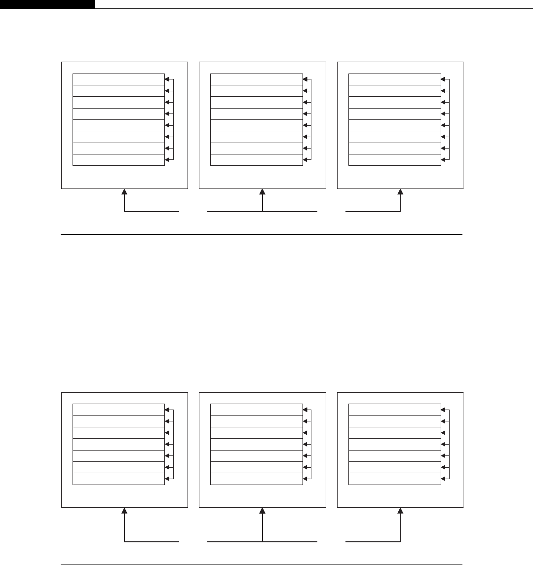
Hold your hand behind the exhaust of a modern GPU and it’s somewhat like putting your hand
near a hair dryer. Multiply this four times and very rapidly most small offices find they have a nice
heating system included with their teraflop workstation free of charge.
The 580 series Fermi cards (GF110) introduced a much better vapor chamber cooling system later
dropped on the GTX680 due to the lower heat output. With this, hollow copper pipes contain a liquid that
quickly takes the heat away to the cooling fins and fans. This is very similar to liquid-cooled systems,
except the heat still has to be dissipated from the fins using fans inside the small area of the GPU card.
Keeping the GPUs cooler means less power consumption and less heat generation. However, there are
limits to how far you can go with air-based cooling and ultimately this will limit the ability of GPUs to
Server A
Node 1
Node 2
Node 3
Node 4
Node 5
Node 6
Node 7
Node 8
Server B
Node 1
Node 2
Node 3
Node 4
Node 5
Node 6
Node 7
Node 8
Infiniband
Server C
Node 1
Node 2
Node 3
Node 4
Node 5
Node 6
Node 7
Node 8
Infiniband
G
i
g
-
E
G
i
g
-
E
G
i
g
-
E
FIGURE 11.1
Typical high-performance computing (HPC) setup.
Node A
GPU 1
GPU 2
GPU 3
GPU 4
GPU 5
GPU 6
GPU 7
Node B
GPU 1
GPU 2
GPU 3
GPU 4
GPU 5
GPU 6
GPU 7
Infiniband
Node C
GPU 1
GPU 2
GPU 3
GPU 4
GPU 5
GPU 6
GPU 7
Infiniband
P
C
I
-
E
P
C
I
-
E
P
C
I
-
E
FIGURE 11.2
GPU HPC setup.
504 CHAPTER 11 Designing GPU-Based Systems
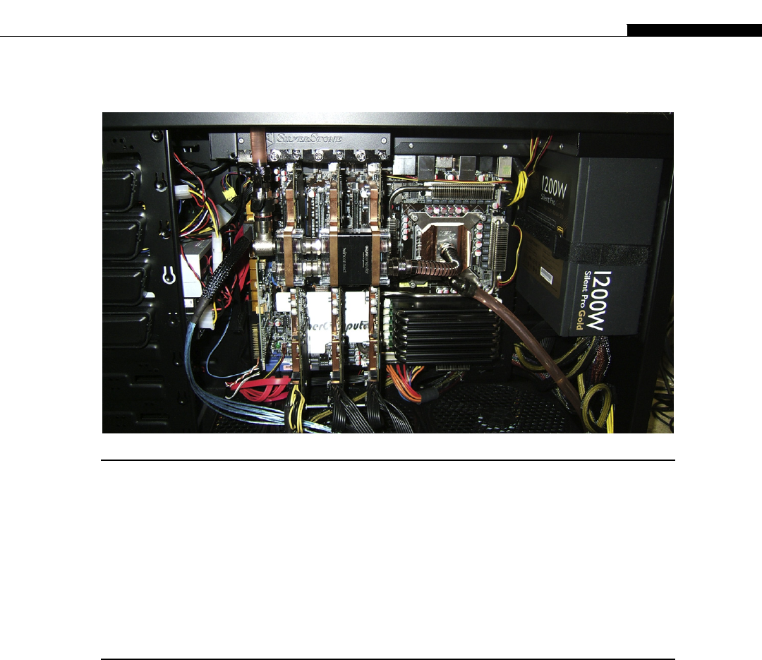
grow significantly from where they currently are. A typical 480/580 series card can draw up to 250 W per
card. Thus, a four-card system is easily exceeding 1 kW per node. The Kepler GTX680 comes in at just
under 200 W per card with the dual GTX690 managing to come in at under 300 W.
However, the GPU is not the only component in a typical high-speed workstation or server. We’ll
look at each one of these in turn and see how they impact the system design. The key aspect to
remember in designing any system is the slowest component will limit the overall throughput no
matter what speed GPUs you have.
CPU PROCESSOR
The choice of processor is primarily one between Intel and AMD. Ignoring obsolete processors, you
have a choice today of the Intel I7 series or the AMD Phenom series. Note, the Sandybride socket
1156/1155 designs are not considered here due to the limited PCI-E lanes provided. Looking at these
options, we have:
Intel I7 Nehalem (Socket 1366; Figure 11.4):
•4 to 6 Cores
•QPI-based DDR-3 triple-bank memory interface
•125 W thermal design
•36 PCI-E 2.0 Lanes
FIGURE 11.3
3x GTX290 (6 GPUs) liquid-cooled machine built at CudaDeveloper.
CPU Processor 505
Intel I7 Sandybridge-E (Socket 2011)
•4 to 6 Cores (up to 8 on the Xeon variant)
•QPI-based DDR-3 quad-bank memory interface
•130 W thermal design
•40 PCI-E 2.0 Lanes
AMD Phenom II / FX
•Hypertransport-based DDR-2/DDR-3 memory interface
•125 W thermal design
•42 PCI-E 2.0 Lanes
Performance wise, the Intel parts are typically faster than the AMD parts for a similar number of cores
and clock speed. Price wise, the AMD part is significantly cheaper Low Power versions are also
available and are certainly attractive for machines in constant operation. However, the choice of
motherboards supporting four or more PCI-E slots is limited, meaning you might have to settle for less
GPUs per node, which may be an issue. The Sandybridge-E platform is significantly faster than either
of the other solutions, but brings a significant price premium both in terms of processor and
motherboard.
You typically allocate one thread core per GPU in applications that require significant CPU
involvement. This gives the opportunity to fix a thread or process to a physical core. Unless you have
more than four GPUs, or you have significant extra workload for a CPU core, the additional two cores
in the hex core device may well be wasted. The I7 in this instance is a clear winner on the performance
side. However, with six GPUs, slotting in a six-core device may well prove advantageous.
GPU 1
GPU 2
GPU 3
GPU 4
CPU
Core 1
CPU
Core 2
CPU
Core 3
CPU
Core 4
Northbridge
PCI-E
(4 x 8GB/s)
Memory
QPI
(25 to 30GB/S)
QPI
(25 to 30GB/S)
Southbridge
Disk 1
Disk 2
Disk 3
Disk 4
Disk 5
Disk 6
SATA II
(6 x 300MB/s)
FIGURE 11.4
Typical I7 Nehalem layout.
506 CHAPTER 11 Designing GPU-Based Systems

One other alternative is the recently released IvyBridge based Intel processor line. This
supports PCI-E 3.0 standard. With the socket 2011 Ivybridge-E scheduled for release late
2012 this will finally bring a PCI-E 3.0 solution with enough PCI-E lanes for GPU based
computing.
GPU DEVICE
TheGPUinaGPUmachineisobviouslythemostimportant consideration in any design. GPUs
change generations about every 12–24 months, a slightly faster rate than the CPU side. So far
we’ve seen an approximate doubling of GPU performance every 18–24 months, exactly following
Moore’s law, for now anyway. The CPUs did this for many years, but there are limits to just how
fast you can make a single core go. As long as there is sufficient parallelism in the problem
domain, GPUs should continue this scaling for quite a few years to come, mirroring the multicore
growthseeninCPUs.
So what are the major considerations of a GPU? First, there is no point in having the last
generation of hardware. With a doubling of performance in every major hardware generation for
approximately the same power budget, there is little point in keeping old hardware around unless you
already have acceptable performance. Going from 2 minutes to 1 minute is no big deal, but from 10
hours to 5 hours, or 10 days to 5 days can make a huge difference, both in terms of usability and
power and space budget.
The GPU market is driven by the gamersdthank them, for they have brought parallel hardware to
the masses at commodity prices. GPU hardware is split into two major areas, the gaming GPUs and the
server GPUs. NVIDIA provides the Tesla range of GPUs for the server and workstation market with
a number of key advantages over their desktop cousins:
• Large memory support
• ECC memory support (Fermi onward)
• Tesla compute cluster driver
• Higher double-precision math
• Large memory bus width
• SMI (system management interrupt)
• Status LEDs
Let’s look at what these are and why they are important for the server market.
Large memory support
Shipping data onto and off of a GPU is slow. You have, at best, a 5 GB/s bidirectional PCI-E bus
(10 GB/s total) bandwidth to the main CPU memory. The larger the memory on the GPU, the more
data you can leave on the GPU. This avoids the need to transfer data to or from the GPU. Tesla cards
typically come with 4 GB to 6 GB of memory. With the introduction of Fermi, we finally moved away
from the 32-bit limit on memory space, allowing GPUs to have up to 6 GB of memory. Given
a maximum 4 GPUs per CPU, that is a total of 24 GB of RAM, easily within the limit on memory size
you’ll find on most server boards.
GPU Device 507

ECC memory support
ECC memory is a special type of memory used in server environments, or where the memory may be
subject to corruption. With large amounts of electromagnetic interference, it’s possible that memory
cells may be changed to some random value with regular memory. The higher the density of electronics
around the device, the more electromagnetic radiation is generated and the higher the error rate. Placing
lots of GPUs into a rack and then placing that rack next to several other racks generates a significant
amount of electronic noise. For years now, servers on the CPU side have used ECC. ECC can both detect
and correct errors found within the memory, making it ideal for this type of environment.
Memory corruption of the data on the GPU doesn’t generally matter for gamers and would usually
go entirely unnoticed. It may result in an odd pixel, or a strangely appearing object. However, as the
frame buffer is typically redrawn 50 to 60 times a second, completely from scratch, it’s very hard to see
any single pixel getting corrupted.
When you shift this to the compute world, however, corruption of the data memory means the
wrong answer for one or more elements in the output dataset, which is clearly not acceptable. You can
tackle this in a number of ways, either using ECC or running every calculation twice to check the
result. The latter choice requires you to double up on the hardware, which effectively means twice the
initial investment and twice the operating costsda less-than-optimal solution.
Tesla compute cluster driver (TCC)
This is a Tesla-only supported driver. The Tesla cards have no graphics output and are designed for
compute only. There is a considerable overhead and latency on the kernel calls due to the need to
support the graphics interface. By removing this, the TCC drivers produce a significant increase in
performance over the standard GeForce driver. There are also certain parts of the hardware that are
enabled only on Tesla devices, such as ECC and dual PCI-E copy engines.
The TCC driver is included in the standard NVIDIA driver download package, but can only be
enabled on Tesla-based hardware.
Higher double-precision math
As most games have very little, if any, double-precision math present, the Fermi range of cards comes
with one of the two double-precision units within each SM disabled. Thus, the standard GeForce Fermi
cards have around half of the double-precision performance of the equivalent Tesla cards. Single-float
performance is comparable, and in many cases faster on the GeForce cards due to the higher clock
rates. However, if double precision is important in your application, as it is in many financial appli-
cations, it makes sense to install only Telsa-based GPUs.
Larger memory bus width
The Tesla cards, being the top-end cards, are usually the ones with all the SMs enabled. NVIDIA
charges much more for the server-level cards, so they can afford to “bin” the GPUs according to how
many SMs are functional. Those with nonfunctional SMs can be sold as cheaper GeForce cards where
having one or two SM units disabled make little difference to overall game performance.
Having all the SMs enabled usually also means the full bus width is available for transfers to or
from the global memory on the card. As memory bandwidth is often the single limiting factor in a lot of
508 CHAPTER 11 Designing GPU-Based Systems

algorithms, having 512 bits as opposed to 448 bits can make a significant difference. In the older G200
series cards, you often saw a reasonable performance increase at a considerable cost increase, by using
a 285 card over a 275 card, due to this additional bus bandwidth. The GeForce 480 and 580 cards have
the same issue, with 320 bits versus 384 bits, a 20% improvement on memory bus bandwidth alone, not
to mention the additional SM unit. The Kepler targeted for compute, the Tesla K20 model, will also
have a 384 bit bus as compared with the 256 bit bus found on the GTX680.
SMI
SMI is a useful feature for remotely querying devices over a network. In a large data center you may have
thousands of GPUs installed. There are already existing centrally managed solutions for CPU nodes and
adding SMI support simply extends this to GPUs as well. Thus, the GPU has the capability to respond to
a request and report a number of useful pieces of information to the central management system.
Status LEDs
The Tesla cards have a number of LEDs on the back of the card that show the card’s status. With the
exception of the GeForce 295 cards, these LEDs are not present on any standard GeForce card. They
allow a technician to walk around an installation of GPUs and identify the GPU that is failing. In a data
center with a thousand GPUs, being able to quickly see if any node has a problem is a huge benefit to
the IT people looking at the system.
PCI-E BUS
The Intel system uses the Northbridge/Southbridge chipset design. The Northbridge is basically a fast
switch, connecting all the high-speed peripherals. The slower Southbridge handles all the mundane requests,
like USB, mouse, keyboards, etc. On AMD-based systems, and also the later Intel designs, some aspects of
the PCI-E bus controller are integrated into the CPU, rather than being a completely separate device.
On the Intel I7 Nehalem systems, you get a total of 36 (40 on Sandybridge-E) lines of PCI-E bus
bandwidth available. These are combined into groups of 16 lines to form a single PCI-E 2.0 X16 link.
This is what the GPU will utilize, giving a total of 4 GB/s in either direction. A single I7 or AMD
processor supports up to two GPUs in full X16 mode. As you add more GPUs, the number of lanes, and
thus the bandwidth allocated to each GPU, is reduced. With four GPUs, you’re running an X8 link, or 2
GB/s in either direction.
Most motherboards do not support more than 4 PCI-E slots. However, some do, using a special
NVIDIA multiplexer device (NF200) to multiplex up the number of lanes. Motherboards such as the
ASUS supercomputer are an example. This board supports seven PCI-E slots.
When designing a system, remember that other devices may also need to sit on the PCI-E bus. The
six GPU workstations shown in Figure 11.3 also has a 24-channel PCI-E raid card in the last PCI-E
slot. Other systems may use InfiniBand or gigabit Ethernet network cards in the spare PCI-E slots, so
it’s not just GPUs that need to be considered.
PCI-E 3.0 is also now available on many motherboards. This will significantly boost the current bus
bandwidth available to each GPU because the same number of lanes on PCI-E 3.0 equates to double
that of PCI-E 2.0. However, PCI-E 3.0 is only supported on the Kepler line of graphics cards.
PCI-E Bus 509

GEFORCE CARDS
An alternative to the Tesla cards are the GeForce cards. The Tesla cards are aimed at the server and
corporate market. If you are a student or an engineer learning CUDA on your own and do not have access to
these cards through your company or university, a GeForce card is entirely suitable for developing CUDA
code. If you are developing for the consumer market, clearly these are what you need to develop on.
The consumer cards vary primarily in terms of compute level. Currently, almost any card you
purchase from the 400 or 500 series will contain a Fermi-class GPU. The 600 series cards are mostly
Kepler based designs. If you specifically want an older card, the previous generations (compute 1.3)
are numbered in the 200 series. The compute 1.1/1.2 cards are typically numbered in the 9000 series.
Finally, the 8000 series are usually compute 1.0 cards, which are actually pretty difficult to program
well compared with the more modern designs.
Within a generation of the cards, the cards vary by the number of SMs and the global memory present.
You should purchase a card with at least 1 GB of memory. Currently, the largest memory capacity of
a GeForce card is 4 GB. Be aware that most GPU cards are noisy compared with a typically quiet PC. If
this is an issue for you, select one of the less powerful cards, or opt for a card with a customized cooler
such as the MSI Frozr series. Note the later 500 series cards are typically quieter than the 400 series cards
as they are based on a revision of the silicon that reduced both power consumption and heat. The Kepler
based cards tend to be marginally quieter than the 500 series cards due to generating less heat. However,
as with anything, you get what you pay for. Thus, a card near the top end of the price scale for a given
series (560, 570, 580, etc.) will typically be quieter than one at the very low end.
In terms of card design, almost all the cards produced are based on the standard NVIDIA layout.
Thus, they are largely identical and vary in terms of brand, accessories, and software provided. The
exceptions to this are the very high-end cards where the manufacturers have actually innovated. The
Gigabyte SOC (Super OverClock) brand is perhaps the best example of this. The typical stock single-
fan cooler is replaced by a three-fan cooler. The GPUs have been speed-binned to select those that
work reliably at a higher speed, typically a 10% overclock. Power circuitry has been redesigned to
provide additional power to reliably drive the GPU to this specification.
In terms of a low-end card, the GTX520/GTX610 is one of the cheapest cards at less than $50 USD,
or around £30 or 35 Euros. It doesn’t require any special power connectors and will fit in just about any
PC. It’s an ideal low-budget card to do some CUDA development on.
On the liquid cooling side, the Zoltac Infinity Edition card is perhaps the most useful in that it comes
with a sealed and self-contained liquid cooling system, similar to some systems available for the CPU. As
such, all you need to do is replace the existing exhaust fan with the provided radiator and fan. It is ideal for
a single-card solution, but not a good choice for a multi-GPU system. The Point of View (POV) TGT Beast
GTX580 Liquid cooled edition comes with 3 GB of RAM and a prefitted water block that can be easily
connected to additional blocks. Pre-fitted liquid cooled cards are also available from EVGA, MSI and PNY.
CPU MEMORY
CPU memory may not seem like such a consideration. However, any transfer of data must come from
somewhere and eventually return to the sender. At the maximum 4 GB/s of PCI-E 2.0 bandwidth in
both directions, each GPU card can use up to 8 GB/s of memory bandwidth.
510 CHAPTER 11 Designing GPU-Based Systems

The amount of bandwidth you need depends a lot on your data structures and how much you
can keep on the GPU cards. You may have a large input dataset but a tiny output dataset, or vice
versa.
Assuming a balanced dataset, having three GPU cards (total 24 GB/s peak bandwidth) can saturate
the CPU memory bandwidth without the CPU itself actually doing any work. Four or more cards
means you may need the server edition of the I7 Nehalem or the Sandybridge-E processor with the 6
GT/s QPI bus connector just to keep the cards supplied with data if your application has large input and
output bandwidth requirements.
Standard 1066/1333 MHz memory clocks will be a bottleneck on multi-GPU systems if there is
a lot of data needing to be transferred. For applications that are primarily compute bound, it will make
little difference. DDR-3 memory can be safely clocked up to 2 GHz on the I7 platform, but rarely this
high on the AMD platform. Officially neither device supports memory clocks beyond 1333 MHz.
Memory also comes with certain timing information, sometimes abbreviated to CL7, CL8, or CL9.
This broadly measures the response time to requests for data. Thus, the same CL7 memory at 1066
MHz may also be sold as CL9 memory at 1333 MHz. As with most computer hardware, the higher the
clock rate and the lower the response time, the more expensive the memory becomes.
Special memory DIMMs containing embedded information (Intel XMP) are available. With the
appropriate motherboard support, they can automatically be used to safely clock the memory to an
optimum rate. Of course, this certified memory, due to the licensing costs associated with such a brand,
is more expensive than the noncertified memory that may in all other respects be identical.
Be aware, however, the higher the clock rate, the more heat and power is consumed. Memory
devices are the same in this respect. Typically, you should budget for around 1 W of power per gigabyte
of DDR-3 present on the motherboard.
As well as the speed of the memory, you need to consider the total capacity of memory you will
likely need. The fastest transfers are achieved using page-locked memory, which is where
a dedicated block of memory is allocated to each card in the system. Using the Tesla cards, you
maywishtotransferupto6GBtothecard,thefull memory capacity of the card. As Tesla cards
are headless (have no monitor) a typical desktop configuration will use three Tesla cards and one
dedicated graphics card. Thus, in terms of page-locked memory alone, you could need up to 18 GB
of memory.
The OS also needs around 1–2 gigabytes of memory for its own purposes. Around another 2 GB or
so should be allocated to a disk cache. Thus, for a three-card Tesla system, you can see we need around
20 GB of memory.
However, the DDR3 memory system is typically a triple or quad bank on the Intel system and dual
bank on the AMD system. Most Intel systems have between four and eight DIMMs, and most AMD
systems have four DIMM sockets. You generally have to use the same size memory in each slot: 4 GB
DIMMs are fairly standard now, with 8 GB DIMMS also being available at around twice the cost per
gigabyte of the 4 GB DIMMs. Thus, with four slots you typically find up to 16 GB/32 GB AMD
systems and up to 16 GB/24 GB/32 GB/64 GB Intel systems. Note that 4 GB 32-bit systems are still the
most common consumer-level platform.
With non-Tesla cards, we typically have up to 2 GB memory capacity on the card, meaning the total
footprint of memory we need to allocate to page-locked memory is much less. With four cards, we
need just 8 GB. With the maximum of seven cards, we need 14 GB, well within the capacity you’d find
on a typical high-end motherboard.
CPU Memory 511
AIR COOLING
Heat and power are the bane of any system designer. As you increase the clock speed, the power
needed increases, which in turn generates more heat. The hotter the device, the more power is required
to drive the gates. The higher the clock speed, the more of a problem it becomes.
CPU designers gave up pushing the 4 GHz limit some time ago and went down the parallel core
route. Hardened overclockers will tell you they can run systems reliably at 4 GHz and beyond.
However, the amount of heat generated and the power consumption is huge compared to the standard
clock and power footprint of the device.
GPUs have always drawn a lot of power and generated a lot of heat. This is not because they are
inefficient, but because they contain so many cores on one device. A CPU has four cores typically, but
up to 16 in some high-end server devices. When you start to consider that the top-end GPUs have 512
CUDA cores to keep cool, you start to understand the problem. It’s arguable whether a fair comparison
with CPU cores is at the SM level or at the CUDA core level. Whichever measure is used, the GPU
devices end up with many times more cores than a CPU.
A retail CPU typically comes with a fairly basic heat sink and fan unit. They are low-cost, mass-
produced units. Replace the standard heat sink and fan with an advanced one and the CPU temperature
can easily drop by 20 degrees or more.
GPUs come typically as a dual-height board (two PCI-E slots) with the top part being an air cooler.
When taken apart, you can usually see quite a substantial cooler (Figure 11.5).
The GeForce 580 design even features vapor chamber cooler, where the copper surface next to the
GPU is filled with a liquid to aid transfer of heat from the GPU to the set of cooling fins. This is highly
advanced technology just to cool a GPU. However, one of the problems you find is the GPUs’ coolers
work well only when surrounded by cool air, but if you put one next to another and you will suffocate
their air supply.
Put four GPU cards in a standard PC case and it sounds like a hovercraft and does a good job
replacing a storage heater. Unfortunately, it will most likely start to overheat after as little as
FIGURE 11.5
Heat sink from a GTX295 (dual-GPU) board.
512 CHAPTER 11 Designing GPU-Based Systems
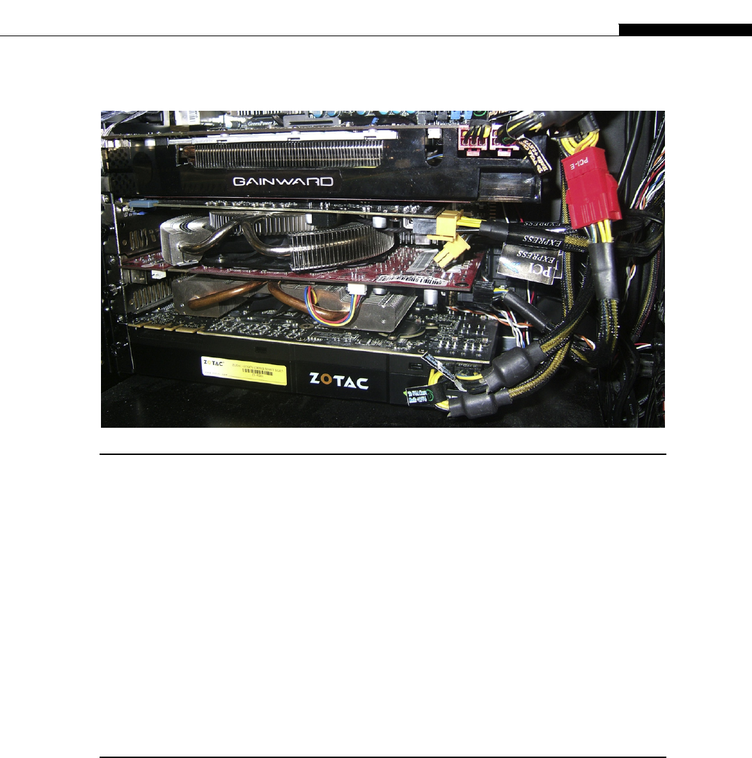
10 minutes once you start loading the GPUs. Overheating will eventually translate into errors in the
calculations and operators who have to come to work in t-shirts and shorts.
The only way to run four GPUs with air cooling is either to feed in air conditioned air (costly) or to
purchase special cards with custom coolers (Figure 11.6). Most server environments do the former and
the servers are kept in specially air conditioned server rooms. The custom cooler solution is more
suitable for office workstation usage. This, however, means you can’t use the Tesla cards, or can use at
most two of them with a gap between them if you’d like a machine next to your desk and expect the
machine to be silent. With larger cases, motherboards such as the ASRock X58 Extreme6 work well due
to the three-slot spacing of the PCI-E sockets, making a three-card air-cooled system a real possibility.
There are many review sites on the Internet that review the GeForce cards and almost all of them
will measure the noise output of the cards. MSI, Gigabyte, and Gainward produce some very inter-
esting cooling solutions for air-cooled GPUs. The regular stock cooler that comes with most solutions
(GPU or CPU) should generally be avoided at all costs, as they are often far too noisy for usage next to
a desk. Spending $20 USD more on a custom cooling solution will often make your life far quieter and
keep the GPU far cooler, saving on running costs.
LIQUID COOLING
Liquid has two interesting properties over air when considered for cooling. It is both thermally more
conductive and has a higher thermal mass. This means it both more easily absorbs heat and can carry
more of it away.
FIGURE 11.6
Four GPU air-cooled system (various consumer GPU cards).
Liquid Cooling 513
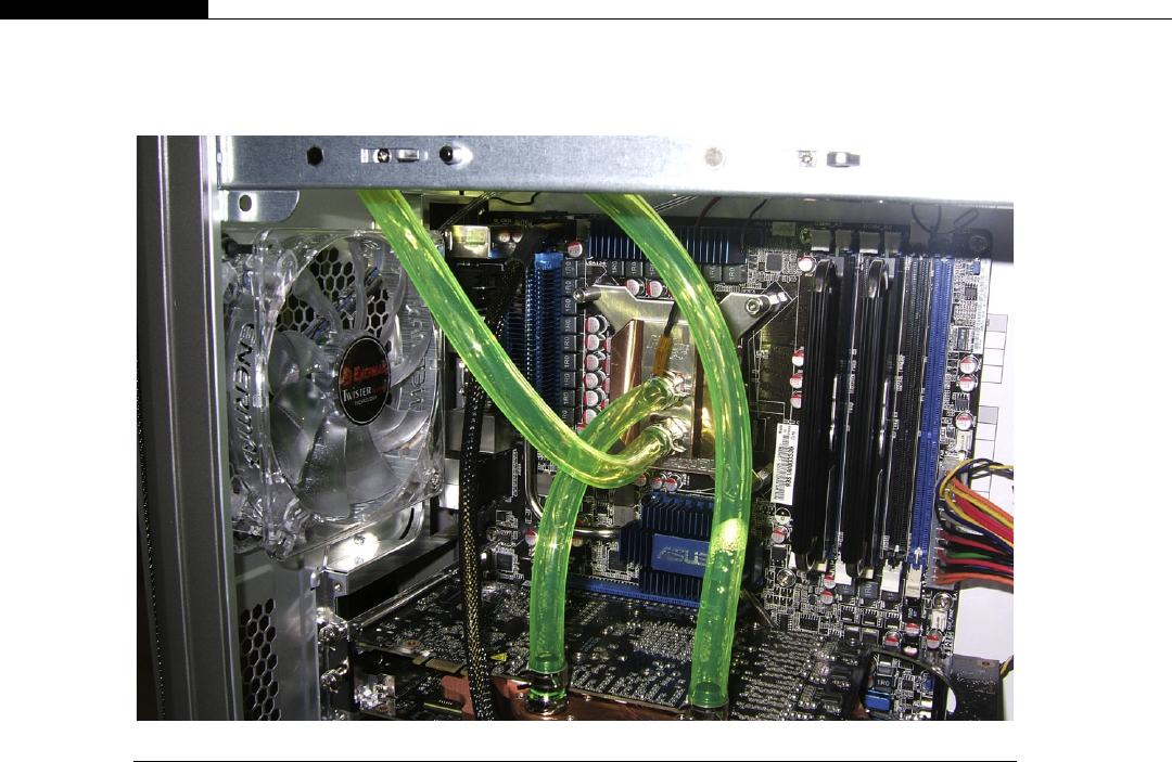
Liquid cooling may sound like an exotic solution to the heat problem, but it’s actually quite
a practical one. One of the major breakthroughs in cooling in the early days of supercomputers was the
use of nonconductive liquids. The Cray-II, for example, used a special nonconductive liquid made by
3M called Fluorinert into which the entire circuit boards were immersed. The liquid was pumped
through the system and then to an external cooling unit where the heat was dispersed.
For GPU computing, we’ve moved on a little. Although immersing an entire motherboard and GPU
in a nonconductive liquid such as commonly available oils works, it’s not a good solution. The liquid
can eventually penetrate sensitive components, which ultimately results in system failure.
Liquid cooling enthusiasts came up with the idea of liquid cooling blocks. These are hollow blocks
of copper through which liquid runs and never makes physical contact with anything electrical
(Figure 11.7). You can buy nonconductive liquids, which we use in our liquid-cooled systems,
minimizing the risk of any damage to components should some spillage occur.
A modern liquid-cooled system consists of a number of heat collectors, a CPU block, one or more
GPU blocks, and, optionally, memory and chipset blocks. The hollow copper blocks have liquid
pumped through them, which is fed from a reservoir. The output of the heated liquid is then fed into
a cooling system, usually one or more radiators or a heat exchanger. The typical layout is shown in
Figure 11.8.
FIGURE 11.7
Single CPU and GPU water cooling loop.
514 CHAPTER 11 Designing GPU-Based Systems

There are many variations on this type of layout. The more units there are in a serial run like the one
shown in Figure 11.8, the higher the resistance to the flow of the liquid. There are parallel flow
solutions that overcome this, but it’s actually quite hard to ensure exactly the same flow goes through
each parallel route, as the liquid will always pick the route of least resistance.
The main issue with liquid cooling is that it doesn’t really solve the heat generation issue. It only
allows you to move the heat to somewhere it can be dispersed more easily. Thus, the radiator may be
a large external one, or even mounted internally within the workstation if only a small amount of
cooling is required.
The key aspect of any water cooling system is actually the radiator and more importantly the size
and the amount and temperature of the airflow. One of the best radiators is the external Watercool
MO-RA3, available in a 9 120 mm or 4 180 mm form factor. Internal radiators should be the
largest size (height, width, depth) that can fit within the case and should exhaust the air out of the
case. Always try to ensure you consider the laws of physics, specifically that heat rises. A top-mount
radiator is often the best solution, but will require some method to purge the residual air when
initially filling the system. Place the pump as low as possible and the reservoir as high as possible to
ensure the pump is always pumping liquid and never air. Think about how you will fill and empty
such a system and where any air may accumulate. Often included are a drain point and an air purge
point.
Liquid cooling connectors come in many sizes. Most liquid cooling systems use G1/4-threaded
connectors. These have a 10 mm intertube diameter (ID). Thus, 13 mm/10 mm (3/8 inch ID) tubing is
commonly used. The first size is the outertube diameter (OD) followed by the ID. The connectors may
be a barb, push fit, or compression-type fitting. Compression and barb fittings use a system that
requires a reasonable force to remove the connector even if it is not sealed. The compression seal slides
over the barb and screws into place, ensuring it’s pretty much impossible to remove without
unscrewing the top. The barb fitting instead uses a hose clip that is not so tight, but is often easier to
maneuver into place in smaller cases. Compression fittings are the least likely to leak or work free of
the connector and are highly recommended. See Figure 11.9.
Reservoir
Pump CPU Block GPU Block Radiator
FIGURE 11.8
Typical liquid-cooled loop.
Liquid Cooling 515
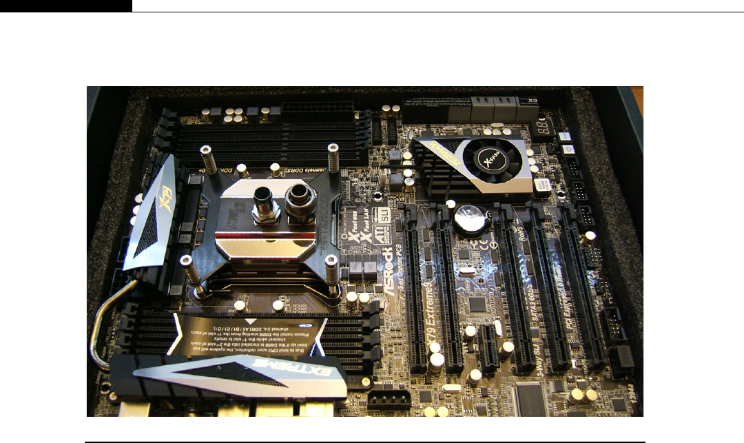
As for liquids, many people use various premixed fluids. These often contain the necessary anti-
bacterial agents to prevent algae growth. Some are nonconductive, although most are at least somewhat
electrically conductive. Alternatively, distilled or deionized water may be used, but never tap water as
it contains all sorts of things you’d not want in a liquid cooling loop.
Multiple GPUs in the system have to be connected together. This is done with a dedicated
connector block, such as the AquaComputer twin connect and other similar systems. These consist of
a solid plastic connector to which all the cards sit at a 90-degree angle. These are far preferable to the
metal bar–type SLI connectors as they provide a nice grip for the cards and ensure the correct spacing.
See Figure 11.10.
The main advantage of liquid cooling is that it allows you to create an almost silent workstation, but
also to cool components far better than an air-cooled system. This in turn means lower power
consumption. It also allows the increase in the clock speed beyond the original clock specification,
so-called overclocking. Such overclocked GeForce cards can, on single-precision tasks, easily
outperform Tesla cards found in workstations and server environments by around 20% or more. You
can even purchase liquid-cooled versions of many cards out of the box, either as components or self-
contained sealed systems.
The downside is twofold. First, there is the additional cost and effort required to plumb in all
the components. Second, there is a risk of a leak of coolant, which is generally only a major issue when
the system is first put together. Maintenance is also higher in that most liquids must be replaced on an
annual basis.
FIGURE 11.9
CPU liquid cooling block with barb and compression fitting side by side.
516 CHAPTER 11 Designing GPU-Based Systems
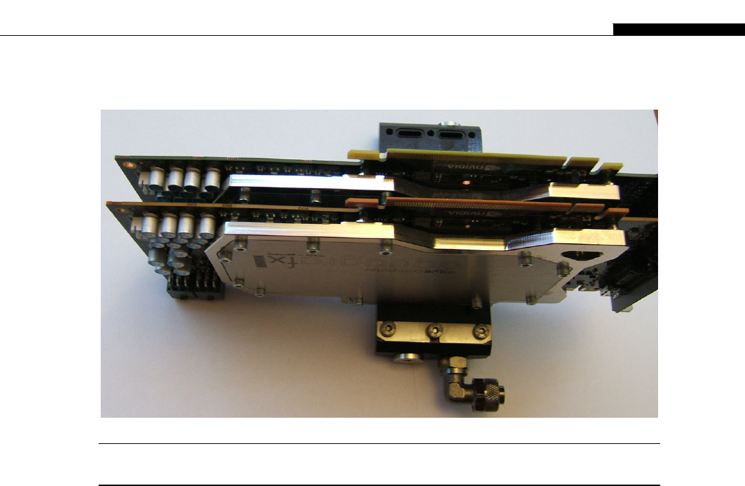
DESKTOP CASES AND MOTHERBOARDS
People interested in building their own GPU system will need to house it in a case of some description. A
case has to be something that is a suitable size. The main criteria will be how many GPUs you wish to fit
into the case and also the form factor of the motherboard. Most motherboards are ATX or E-ATX
designs, meaning they will fit most desktop cases. Some smaller cases, however, do not support E-ATX.
A number of motherboards that support four PCI-E or more connectors are larger than the E-ATX
specification, EVGA being a typical example. EVGA sells the only dual-X58 motherboard, the EVGA
Classified SR-2, which accepts two Xeon-based Nehalem I7 processors and up to 48 GB of RAM.
However, selecting such a motherboard limits the case choice to just a few models (see EVGA’s
website at http://www.evga.com for an up-to-date list).
ASUS was among the first to produce a dedicated compute platform motherboard aimed at CUDA
with its P6T7 WS supercomputer motherboard. This is an X58 platform (Nehalem I7) supporting four
double-spaced PCI-E 2.0 sockets at full x16 PCI-E 2.0 speed. Note this board is a CEB form factor,
which generally means it will fit most E-ATX cases. It’s one of the few boards that supports the x16
speed on all four slots.
The ASUS Rampage III Extreme is also a good E-ATX design, although it only supports x8 PCI-E
speeds with four cards. The ASUS Extreme V board is one of the few Ivybridge compatible PCI-E 3.0
boards supporting 4 PCI-E connectors.
MSI produce the BigBang series of motherboards aimed at power users, sporting seven physical
PCI-E sockets. However, when populated with four cards, as is the case for most motherboards, only
FIGURE 11.10
Twin liquid-cooled GPU cards fitted in solid connector block.
Desktop Cases and Motherboards 517

X8 PCI-E bus speed is supported. MSI is one of the few vendors supporting four double-spaced PCI-E
sockets on the AMD platform, for example, the MSI 890FXA-GD70.
The ASRock X58 supercomputer design provides for four PCI-E 2.0 sockets running at x8 speed
with up to 24 GB of RAM. Its designs since this have improved tremendously, especially with its
latest socket 2011 (Sandybridge-E) design. The ASRock X79 Extreme9 is one of the best designs for
the Sandybridge-E platform we’ve seen to date (see Figure 11.9). It supports five PCI-E x8 sockets,
eight SATA-3 ports, the PCI-E 3.0 standard, and up to 64 GB of RAM while still being an ATX form
factor design. ASROCK recently released the socket 2011, Extreme 11 board which boasts 7 PCI-E
3.0 x16 slots.
Gigabyte is also a well-respected manufacturer. Its UD9-X58 platform, as with the ASUS super-
computer, has dual NF200 chips, meaning it supports four full-speed x16 PCI-E 2.0 slots. Its
GA-990FXA-UD7 AMD platform supports the latest 990 chipset, providing SATA-3 support and four
PCI-E 2.0 sockets up to x8 speed.
Having decided on the motherboard, you need a case that supports the form factor, but also the
number of PCI-E slots you plan to use. Standard PC cases only come with seven PCI-E slots, which
causes an issue if you in fact have four double-height PCI-E cards.
Heat and airflow should be big considerations in selecting a case, especially with multiple GPUs
present. Silverstone produces a number of cases that rotate the motherboard 90 degrees and thus vent
the hot air from the CPU and GPUs directly up and out of the case. Figure 11.3 shows a design used
with Raven’s RV02 case. We’ve found this design to be the most effective in terms of cooling. The
upward-flowing air design drops the internal case temperature by several degrees. Raven’s Fortress
FT02 and Temjin TJ11 cases follow similar designs. The Raven cases have an aesthetic you either love
or hate. The Fortress and Temjin designs are much more traditional, although all three cases are
quite large. Note, the newer edition Raven (the RV02-evolution) and Fortress cases support only seven
PCI-E slots, whereas the Temjin supports nine slots.
As an alternative, the Coolermaster HAF and Antec 1200 series cases also have very good airflow.
However, both support only seven PCI-E slots. The Raven RV03 is a much more compact version of
Raven RV02. It supports a full set of eight PCI-E slots and is one of the cheapest cases on the market.
In terms of liquid-cooled cases, most are aimed at single CPU–based cooling, so there is a lack of
necessary space for a multi-GPU liquid-cooled configuration. With four GPUs and an I7 CPU you are
burning in excess of 1 kWof power, a significant amount of which is heat. Such systems are best cooled
externally. As an approximate guide, you’ll need one 120 mm radiator capacity to cool each device
(CPU or GPU). The Silverstone Temjin TJ11 allows you to remove the internal hard drive section at
the bottom of the case and replace it with a 4 140 mm radiator and pump assembly. This is perhaps
one of the best, but most expensive, cases currently on the market.
MASS STORAGE
Motherboard-based I/O
The mass storage subsystem is something that is quite important. You need to be able to easily import
and export data from a system. If you consider that each GPU has a maximum of 5 GB/s input
bandwidth and 5 GB/s output bandwidth, you will have a problem supplying such a large amount of
data from a mass storage device.
518 CHAPTER 11 Designing GPU-Based Systems

A typical hard disk has a transfer rate of around 160 MB/s maximum. Due to the construction of
hard disks, the density of the data is diminished as you approach the center of the disk. As such, the
data rate drops off to around half of the maximum rate at the outside of the disk as it becomes full and
starts to use the inner part of the drive.
Most Intel I7 motherboards come with an built-in controller that supports up to six SATA-based
hard disks. This is part of the Southbridge chipset, which controls the slow devices such as keyboards
and mice. It also handles the SATA hard disks and network interfaces.
The SATA-2 standard defines a speed of up to 300 MB/s per SATA channel. The new SATA-3
standard supports twice this. The built-in controller supports up to six hard drives, meaning you could
theoretically achieve a transfer capability of 1.8 GB/s from the SATA ports to the main memory. With
SATA-2 SSD disks exceeding 300 MB/s read speeds, you might expect to be able to simply connect up
to six disks and get a reasonable input data rate, but even this is only half the bandwidth of a single
PCI-E X16 graphics card.
However, life is never that easy. In practice, Southbridge-based built-in controllers will peak out at
about 600 MB/s to 700 MB/s, which is nowhere near close to the 1.8 GB/s you’d need to support all hard
drives at the full data rate. For 160 MB/s physical hard disks, this may work, but for SSD drives that can
match or exceed the SATA-2 interface speeds, the standard motherboard SATA controller will not be of
much use. With just four SSD drives present, the controller is already a bottleneck in the system.
The more modern boards have now entirely moved to SATA-3 on the AMD platforms and
a mixture of SATA-2 and SATA-3 on the Intel platforms. SATA-3 doubles the SATA-2 speed, meaning
an SSD drive can peak at up to 550 MB/s (SATA-3 speed is 600 MB/s). With six of these, peak speeds
are rapidly approaching the speeds we need for a single GPU. However, as with the SATA-2
controllers, most on-board SATA3 controllers peak at around 1GB/s transfer rates and thus cannot
support large numbers of SSDs.
Dedicated RAID controllers
For faster input of data you need to turn to a dedicated hard disk controller, which sits on the PCI-E
bus. However, this approach conflicts with our need to have the graphics compute cards on exactly this
same bus. With air based cooling, all the GPUs are double-slot cards. You may have to remove a GPU
card to be able to insert a dedicated hard disk controller card and/or a high-speed network card.
With liquid-cooled systems it’s a little easier, because each card is single slot. However, you are
still limited by the overall power consumption of a PC, typically up to 1.5 kW. This in effect means, at
least with the high-end cards, there will be spare PCI-E slots.
Assuming you have a 550 MB/s SATA-3 SSD drive subsystem, to achieve the 5 GB/s input
capacity for a single GPU card, you need 10 SSD drives. If the RAID card you are using supports
simultaneous transfers to and from the PCI-E bus, then you’d need a total of 20 SATA-3 SSD drives to
support the full bandwidth of a single PCI-E X16 RAID controller.
So to be able to supply and store in real time the full bandwidth of a single GPU card, even using
SSDs, it will take 20 SSDs. Even with four 6 SSDs per drive bay, you’d need 4 drive bays to support
this.
If you look at a high-end GPU setup, the solution is a four GPU liquid-cooled solution based on
a motherboard that supports seven PCI-E bus connectors. With no additional cards, all GPUs run at the
X8 speed (2.5 GB/s in, 2.5 GB/s out) with four GPU cards and X16 with two GPU cards.
Mass Storage 519

With a liquid-cooled system, you have spare slots between the cards, as most liquid-cooled
solutions are single slot. As soon as you add a RAID controller card, the associated slot drops to X8 or
X4 for both the GPU and RAID card. This is unless you dedicate an X16 slot to the RAID controller,
something we’d recommend.
There is a physical limit on the number of drive bays that can be included in a workstation format.
Even a motherboard with seven PCI-E slots, often dubbed supercomputer motherboards, have only
three slots left available once four liquid-cooled GPUs are present. This allows for two RAID
controllers and a single high-speed network card to be squeezed into such systems.
RAID, however, is not simply about speed, although the RAID-0 mode is used for this. RAID-1
supports mirroring, where the data is completely duplicated onto another disk. Failure of one disk then
means the system falls back to the remaining disk without significant impact on the operation of the
system. Clearly, however, the faulty disk needs to be replaced as soon as possible. It saves you the case
where several weeks of compute time could be lost due to a faulty hard drive.
With a small cluster, hard drives fail rarely enough that it’s not that much of a problem. However, in
a larger setup, with thousands of active drives, you will be changing drives regularly.
RAID-5 is a system that balances storage usage with redundancy, allowing data to be split over
multiple drives in a safe manner. One of the drives in a set is a dedicated parity drive that, if one
drive fails, can be used to recover the RAID array. RAID is something you definitely need to
consider if restarting your job on another machine and losing the computations to date is not
acceptable.
Check pointing is a system that is often used to avoid the effects of failure. After a certain period,
the entire results to data are check-pointed or dumped to permanent storage. Thus, the job can be
moved to another node by simply moving the check-pointed data and the associated program code. In
designing applications that run for some period of time, you should always consider building a check
pointing system into the application.
HDSL
HDSL is a standard from a company called OCZ that has developed a number of innovative products in
the SSD market. Most notable of these is the RevoDrive range, a product that is basically a number of
SSD drives on a PCI-E card with a built-in hard disk controller. This original card achieved on the
order of 500 MB/s, which is quite reasonable; the high-end cards (the R4 C series) claim 2800 MB/s.
You would need a SATA-3 controller and at least five top-end SSDs to achieve the same sort of
bandwidth.
The HDSL drive offered by OCZ is also an interesting product and an insight into where storage is
likely to go. It embeds four older-style SSD drives into a standard 3.5 inch hard disk, with an embedded
RAID-0 controller. A special controller card is used that basically extends four lanes of the PCI-E bus
through a cable directly to the drive interface. Four PCI-E 2.0 lanes equates to around 1 GB/s in both
directions, vastly superior to the unidirectional SATA-3 interface.
Being a new technology, it has some way to go before the drives themselves match this bandwidth.
Currently, the drive peaks at around 750 MB/s, which is somewhat shy of the 1000 MB/s capacity of
the link. The drive ships with a single-port X4 HDSL controller, but dual- and quad-port X8 and X16
controllers are planned. Assuming the drive picks up a little in speed to the full bandwidth of the
interface, which is almost certain given the march of technology, this will be a very interesting
technology to see evolve.
520 CHAPTER 11 Designing GPU-Based Systems

As the drives themselves are a 3.5 inch format, this means more drives can be put in the same
physical space. Allocating two X8 slots would support four HDSL drives, giving a read/write capacity
of around 3 GB/s.
Mass storage requirements
As well as speed of input from the mass storage devices, we have the total storage capacity. Take one of
the largest users of data in the world, Google. In 2008 they were processing 20 petabytes of data per
day. A petabyte is 1000 terabytes, which is itself 1000 gigabytes. Given that the largest single mass
storage drive available today is around 4 terabytes, just to store that amount of data would require
(20 1000) O4¼5000 hard disk drives!
So clearly one consideration in designing any node is mass storage needs. In practice, most large
installations use dedicated storage nodes that do not have any compute functionality. Thus, the
compute nodes need only the storage capacity necessary for a single compute run. They can download
data over a high-speed interconnect from a central data cluster, meaning you can design them with
high-speed, small-capacity SSD drives, which we’ve done with some of our test machines at
CudaDeveloper.
Networking
Networking is one of the key issues when you consider a system that contains more than a single node.
Clusters of nodes have become very common in universities and commercial organizations as the
availability of cheap commodity hardware has become commonplace. It is relatively straightforward
to configure a small network of machines and have them work together on a problem.
You typically see two types of networks: those based on gigabit Ethernet and those using
somewhat faster, but considerably more expensive, InfiniBand networks. Gigabit Ethernet is
cheap, usually comes as free on the motherboard, and can be connected to a 16-, 24-, or 32-port
switch with relative ease. Some motherboards offer dual-gigabit Ethernet connections, which
often include a feature called Link Aggregation. This, when supported by the switch, allows for
the two physical links to be used as one, doubling the amount of bandwidth available to and from
that node.
How critical networking is to your problem depends greatly on the amount of data that needs to be
shared. If you can stay within a single node and go down the multiple-GPU route, this will be far, far
more effective than going down the multiple-node route in most cases.
Systems like Google’s MapReduce is one example where, due to the huge amount of data being
used, you are forced to split the data between multiple nodes. MapReduce works on the principle of
a shared and distributed file system, making the file system appear as one very large disk. The data
itself is located in chunks on the local storage of each node. Instead of bringing the data to the program,
MapReduce sends the program to where the data is physically located. Hadoop is an open-source
implementation of MapReduce, allowing you to set up a very similar framework for distributing and
scheduling such jobs. Typically the dataset is very large and the program very small, so this type of
approach works really well in greatly reducing network traffic.
Dedicated communication with something like MPI is also typically how such a system is set up.
However, as soon as network communication becomes the dominant feature of the program, in terms
of time, you need to move to a faster network architecture such as InfiniBand. This obviously incurs
Mass Storage 521
cost, which you may be able to avoid through clever programming, such as asynchronous commu-
nication, compressing data packets, etc.
Peer-to-peer communication within a node between the GPUs is now supported with the CUDA 4.0
SDK. In addition, the GPUs can talk directly to certain InfiniBand cards in the same way, without the
interaction of the host CPU. Thus, for larger-scale GPU installations, InfiniBand and other higher-
speed interconnects can become a necessity if network traffic plays a significant role.
POWER CONSIDERATIONS
Power usage is a big consideration when designing machines that constantly run. Often the operating
costs of running a supercomputer over just a few years can equate to the cost of installing it in the first
place. Certainly, the cost of running such a machine over its lifetime will easily exceed the original
installation costs.
Power usage comes from the components themselves, but also from the cooling necessary to allow
such computers to operate. Even one high-end workstation with four GPUs requires some planning on
how to keep it cool. Unless you live in a cold climate and can banish the computer to somewhere cold,
it will do a nice job of heating up the office for you. Put a number of such machines into one room, and
very rapidly the air temperature in that room will start to rise to quite unacceptable levels.
A significant amount of power is therefore expended on installing air conditioning systems to ensure
computers remain cool and can operate without producing errors. This is especially so where summer
temperatures can reach 85F/ 30C or higher. Air conditioning is expensive to run. Significant thought
should be given to how best to cool such a system and if the heat energy can in some way be reused.
Liquid-cooled systems are very efficient in this way in that the liquid can be circulated through a heat
exchanger and into a conventional heating system without any chance of the two liquids ever mixing. I’m
always amazed by the lack of thought that goes into how to reuse waste heat in computer installations.
With the ever-increasing costs of natural resources, and the increasing pressures on companies to be seen
as green, simply pumping the heat out the window is no longer economically or socially acceptable.
If you look at the top-end GPU cards, they typically come in around the 250 W mark in terms of
power consumption. A typical CPU is around 125 W by comparison. A typical power budget for
a four-GPU system might therefore be as shown in Table 11.1.
Table 11.1 Typical Power Usage
Component Number Power per Unit Total Power
GPU 4 250 1000
CPU 1 125 125
Memory 16 1 16
Motherboard 1 50 50
Boot drive 2 5 10
Data drive 8 5 40
Peripherals 1 10 10
Total 1251
522 CHAPTER 11 Designing GPU-Based Systems

As you can see from the table, you can be drawing up 1250 W (1.3 kW) of power per node with
such a configuration. Off-the-shelf power supplies top out at around the 1.5 kW mark, after which
you’re looking at a very expensive, custom solution.
Selection of the GPU can makea hugedifference to overall power consumption.If you look atwatts per
core and gigaflops per core we see something interesting (Table 11.2). Notice how the architectural
improvements in the 500 series Fermi cards produce much better performance, both in terms of watts and
gigaflops. Fermi devices also automatically clock down much lower than the older G80 or G200 series
cards, using a lot less power when idle. In fact, one of the best performing cards in terms of gigaflops per
watt is the GF114-based 560 Ti range. The 560 Ti is aimed squarely at the game market and comes with
a high internal clock speed, producing some 1.2 gigaflops versus the almost 1.6 gigaflops of the 580.
However, it does this at just 170 W compared with the 240 W of the 580, giving it by far the best
performance per watt. Note the 560 Ti was relaunched at the end of 2011 as a 448-core device based on the
570 design. The GTX680 is based on the 560 design. The dual GPU 690 contains two of these devices,
specially binned and clocked to achieve 300 W, giving this card the best overall GFlops per watt ratio.
One important consideration when selecting a power supply is to realize that not all power supplies
are made equal. A lot of the cheaper power supplies claim a certain power rating, but fail to provide this
on the 12v rails, which is where the primary power draw is in such a system (from the graphics cards).
Also, others do not provide enough PCI-E connectors to support more than a small number of cards.
However, one of the most important issues to be concerned about is the efficiency of a power
supply. This can be as low as 80% or as high as 96%. That difference of 16% is effectively a cost of
$0.16 cents on every dollar (Euro/pound/franc) spent on electricity.
Power supplies are rated according to an efficiency rating. Those meeting the 80-plus standard
guarantee a minimum of 80% efficiency across the entire power range. More efficient models are rated
bronze (82%), silver (85%), gold (87%), platinum (89%), and titanium (91%) in terms of efficiency at
100% usage. Efficiency is typically a few percent higher at 50% load and slightly higher with the
European 240v power supplies than the U.S. 115v standard. See the website http://www.80plus.org for
a list of certified power supplies.
Table 11.2 Gigaflops per Core
Card
CUDA
Cores
Clock
(MHz)
Power
Usage (W) Gigaflops
Gigaflops
per Core
Gigaflops
per Watt
430 96 700 49 269 2.8 5.5
450 192 790 106 455 2.37 4.3
460 336 675 160 907 2.7 5.7
470 448 607 215 1089 2.43 5.1
480 480 700 250 1345 2.8 5.4
560 Ti (GF114) 384 822 170 1260 3.28 7.4
560 (GF110) 448 732 210 1312 2.93 6.2
570 480 732 219 1405 2.93 6.4
580 512 772 244 1581 3.09 6.5
590 1024 607 365 2488 2.43 6.8
680 1536 1006 195 3090 2.01 15.8
690 3072 915 300 5620 1.83 18.7
Power Considerations 523

If you take the typical European cost of electricity at, say, 0.20 Euros per kilowatt hour, a 1.3 kW
machine costs 0.20 1.3 ¼0.26 per hour to run. That is 6.24 Euros per day, 43.48 Euros a week, or
2271 Euros a year to constantly run in terms of electricity cost alone. This assumes you have a 100%
efficient power supply, something that just doesn’t exist. See Table 11.3.
With an 80% efficient power supply, for 1.3 kW output, you’d need to put in 1.625 kW of power, an
additional 325 W, which is wasted. This increases the annual bill from 2271 Euros to 2847 Euros, some
216 Euros. With a 92% efficient power supply, you’d need just 1.413 kW (212 W less), which costs you
2475 Euros per year. This is a savings of around 400 Euros a year, which easily covers the additional
costs of a high-efficiency power supply.
In terms of the U.S. market, electricity is somewhat cheaper at around $0.12 cents per kW. Thus,
a 1.3 kW machine with an 80% efficient power supply (1.625 kW input power) would cost around
$0.19 per hour to run. With a 92% efficient supply (1.413 kW input power) it would cost $0.17 per
hour. That little $0.02 cents per hour translates into $175 per year when the machine is constantly run.
Multiply that by Nnodes and you can soon see why efficiency is a key criterion for many companies
purchasing computer systems.
Certainly in our own machines we always use the most efficient power supply available at the time
any development machine is built. Companies such as Google follow similar policies, using highly
efficient power supplies, targeting 90% plus efficiency. Energy prices are unlikely to do anything other
than increase over time, so this makes perfect sense.
Liquid-cooled systems provide an interesting option in terms of recycling the waste heat energy.
While an air-cooled system can only be used to heat the immediate area it is located in, heat from
Table 11.3 Typical Costs per Year by Power Consumption
Power
Usage
(Hours/
Day)
Unit Cost
(Euros/
kW)
Per
Day
(kW)
Per
Week
(kW)
Per
Year
(kW)
Per
Day
(Euro)
Per
Week
(Euro)
Per
Year
(Euro)
CPU
65 24 0.2 1.56 10.92 568 0.31 2.18 114
95 24 0.2 2.28 15.96 830 0.46 3.19 166
125 24 0.2 3 21 1092 0.6 4.2 218
GPU
50 24 0.2 1.2 8.4 437 0.24 1.68 87
100 24 0.2 2.4 16.8 874 0.48 3.36 175
150 24 0.2 3.6 25.2 1310 0.72 5.04 262
200 24 0.2 4.8 33.6 1747 0.96 6.72 349
250 24 0.2 6 42 2184 1.2 8.4 437
300 24 0.2 7.2 50.4 2621 1.44 10.08 524
600 24 0.2 14.4 100.8 5242 2.88 20.16 1048
900 24 0.2 21.6 151.2 7862 4.32 30.24 1572
1200 24 0.2 28.8 201.6 10,483 5.76 40.32 2097
1500 24 0.2 36 252 13,104 7.2 50.4 2621
524 CHAPTER 11 Designing GPU-Based Systems

liquid-based coolants can be pumped elsewhere. By using a heat exchanger, the coolant can be cooled
using conventional water. This can then be pumped into a heating system or even used to heat an
outdoor swimming pool or other large body of water. Where a number of such systems are installed,
such as in a company or university computer center, it can really make sense to use this waste heat
energy to reduce the heating bill elsewhere in the organization.
Many supercomputer installations site themselves next to a major river precisely because they need
a ready supply of cold water. Others use large cooling towers to dissipate the waste heat energy.
Neither solution is particularly green. Having paid for the energy already it makes little sense to simply
throw it away when it could so easily be used for heating.
When considering power usage, we must also remember that program design actually plays a very
big role in power consumption. The most expensive operation, power wise, is moving data on and off
chip. Thus, simply making efficient use of the registers and shared memory within the device vastly
reduces power usage. If you also consider that the total execution time for well-written programs is
much smaller than for poorly written ones, you can see that rewriting old programs to make use of new
features such as larger shared memory can even reduce operating costs in a large data center.
OPERATING SYSTEMS
Windows
The CUDA development environment is officially supported by Windows XP, Windows Vista, and
Windows 7 in both the 32- and 64-bit variants. It is also supported by the Windows HPC (high-
performance computing) Server edition.
Support for certain features related to rendering on DirectX versions later than version 9 are not
supported on XP due to the lack of support for DirectX 10 and 11. Support for more than four GPUs
can be problematic, both from an OS (Operating Systems) perspective and also from the BIOS (Basic
Input Output System) of the motherboard. Support may vary from one CUDA driver release to another,
but for the most part it now works.
GPU support when using Windows remote desktop is nonexistent, as the exported desktop does not
contain any CUDA devices. There are other packages that provide SSH (Secure Shell) type connec-
tions that do support this, UltraVNC being a very common one.
Ease of installation of the drivers on the Windows platform and the availability of debugging tools,
notably Parallel NSight, is excellent. For multi-GPU solutions, a 64-bit version is essential, as the CPU
memory space is otherwise limited to a total of 4 GB.
Linux
CUDA is supported for most major Linux distributions. However, one of the key differences between
the Linux distribution and the Windows distribution is the expected level of the installer’s knowledge.
The CUDA drivers need to be explicitly installed for most distributions. This varies by distribution.
Refer to Chapter 4 where we covered installation procedures for each of the major distributions.
Support for multiple GPUs is much better in Linux than under Windows. It’s also possible with
a custom BIOS to get around some of the BIOS issues found when booting a system containing more than
four GPUs. The problem encountered is that most older BIOS designs are 32 bit and thus cannot map
Operating Systems 525

such a large amount of memory into the memory space that is presented by very large numbers of GPUs.
If you’d like to try this approach, then have a look at the Fastra II project (http://fastra2.ua.ac.be/), where
they used a BIOS with 13 GPUs in a single desktop.
The primary Linux-supported debugger is the GDB package from GNU. This is not as compre-
hensive as the Parallel NSight package that is now also available on Linux, but is steadily improving.
Other common parallel debuggers for the most part already support or are in the process of having
support added for CUDA.
As with the Windows versions, for multi-GPU solutions a 64-bit version is essential because the
CPU memory space is otherwise limited to a total of 4 GB. However, unlike Windows, the OS footprint
is significantly smaller, so more memory is made available to the application.
CONCLUSION
In this chapter we looked at some of the aspects of building GPU-based machines, both from the
perspective of using GPUs in a data center and considerations for building your own GPU machines. If
you’re a researcher and you want a superfast machine, building one yourself is a very useful experience
in setting everything up. For those wishing for an out-of-the-box solution, NVIDIA provides prebuilt
desktop and server systems, tested and certified to work reliably. Whether you decide to build your own
or buy, by reading this chapter you will be far more informed about the key decisions and issues you
need to consider before committing to the purchase of any hardware.
526 CHAPTER 11 Designing GPU-Based Systems

Common Problems, Causes,
and Solutions 12
INTRODUCTION
In this chapter we look at some of the issues that plague CUDA developers and how you can avoid or at
least mitigate these issues with some relatively simple practices. Issues with CUDA programs often
fall into one the following categories:
• Errors of usage of various CUDA directives.
• General parallel programming errors.
• Algorithmic errors.
Finally, we finish this last chapter with a discussion of where to continue your learning. There are many
other texts on the subject of CUDA and GPU programming in general, as well as a lot of online
material. We provide some pointers for what to read and where to find it. We also briefly discuss
NVIDIA’s professional certification program for CUDA developers.
ERRORS WITH CUDA DIRECTIVES
Errors using the CUDA API are by far the most common issue we see with people learning CUDA. It is
a new API for many, and therefore mistakes in its usage should be expected and planned for.
CUDA error handling
In Chapter 4, we introduced the CUDA_CALL macro. All of the CUDA API functions return an error
code. Anything other than cudaSuccess generally indicates you did something wrong in calling the
API. There are, however, a few exceptions, such as cudaEventQuery, which returns the event status as
opposed to an error status.
The CUDA API is by nature asynchronous, meaning the error code returned at the point of
the query, may have happened at some distant point in the past. In practice, it will usually be as
a result of the call immediately prior to the error being detected. You can, of course, force this by
synchronizing (i.e., calling the cudaDeviceSynchronize function) after every API call. While this
strategy might be a good one for debugging, it’s not something that should be in any release version
of the code.
CHAPTER
CUDA Programming. http://dx.doi.org/10.1016/B978-0-12-415933-4.00012-0
Copyright Ó2013 Elsevier Inc. All rights reserved.
527

Each error code can be turned into a semi-useful error string, rather than a number you have to look
up in the API documentation. The error string is a somewhat helpful first attempt to identify the
potential cause of the problem. However, it relies on the programmer explicitly checking the return
code in the host program. It would be better if the CUDA runtime could trap such exceptions and
perform some error indication, as we do explicitly with the CUDA_CALL macro, when running the debug
version. This would help tremendously in pointing out errors in the user’s program, as and when they
are introduced. We see some move toward this in the CUDA v4.1 SDK.
The CUDA error handling can be somewhat rudimentary. Most of the time, you’ll get a useful error
message. However, often you will get a not-so-useful message such as unknown error, usually after
a kernel invocation. This basically means your kernel did something it should not have, for example,
writing over the end of the array in global or shared memory. There are debugging tools and methods
we cover later in this chapter that help identify this type of problem.
Kernel launching and bounds checking
One of the most common failings in CUDA is an array overrun. You should ensure all your kernel
invocations start with a check to ensure the data they will access, both for read and write purposes, is
guarded by a conditional. For example,
if (tid < num_elements)
{
.array[tid] ¼..
}
This conditional takes a marginal amount of time, but will save you a lot of debugging effort. You
typically see such a problem where you have a number of data elements that are not multiples of the
thread block size.
Suppose we have 256 threads per block and 1024 data elements. This would invoke four blocks of 256
threads. Each thread would contribute to the result. Now suppose we had 1025 data elements. You would
typically have two types of errors here. The first is to not invoke a sufficient number of threads, due to
using an integer division. This will usually truncate the number of blocks needed. Typically people write
const int num_blocks ¼num_elements / num_threads;
This will work, but only where the number of elements is an exact multiple of the number of
threads. In the 1025 elements case we launch 4 256 threads, some 1024 threads in total. The last
element remains unprocessed. I’ve also seen, as well as other variations, attempts to “get around” this
issue. For example,
const int num_blocks ¼((float) num_elements / num_threads);
This does not solve the problem. You cannot have 4.1 blocks. The assignment to integer truncates
the number to four blocks. The solution is a simple one. You write the following instead:
const int num_blocks ¼(num_elements þ(num_threads-1)) / num_threads;
This will ensure you always allocate enough blocks.
The second issue we commonly see then follows. We now invoke five blocks for a total of 1280
threads. Without such guarded access to the array within the kernel, all but the first thread in block 5
528 CHAPTER 12 Common Problems, Causes, and Solutions

would be accessing an out-of-bounds memory location. The CUDA runtime performs little if any
runtime checks, such as array bounds. You will never see it halt the kernel and display a message such
as array overrun in line 252 file kernel.cu. However, rather than silently fail, which is the
worst case, it does at least trap the error in some way and then returns a message such as unknown
error.
Invalid device handles
The other type of errors you typically see are incorrect mixing of handles, most often pointers. When
you allocate memory on the device or on the host, you receive a pointer to that memory. However, that
pointer comes with an implicit requirement that only the host may access host pointers and only the
device may access device pointers. There are a few exceptions, such as zero-copy memory, where
a host pointer can be converted to a device pointer to host memory, but even in this case you have
a separation.
As the pointers are not interchangeable, one might have hoped that device pointers would be
declared using a different type. This would allow for type-based checks on calls to the API to flag such
issues at compile time. Unfortunately, a device pointer and a host pointer are the same basic type,
which means there is no static-type checking performed by the compiler.
There is, of course, no reason why you could not define such a type. You could then develop your
own wrapper functions around the API functions that performed type checking. Certainly for those
who are starting out writing CUDA, this would be a tremendous help and perhaps something we’ll see
as CUDA develops. The Thrust library we looked at in Chapter 10 has the concept of a host vector and
a device vector. It uses Cþþ function overloading to ensure that the correct function is always called
for the given data type.
The standard CUDA runtime checks for this type of incorrect mixing of device and host pointers, in
terms of passing a host pointer to a device function are reasonable. The CUDA API checks the
pointer’s origin and will generate a runtime error if you pass a host pointer to a kernel function without
first converting it to a device pointer to host memory. However, the same cannot be said for the
standard C/Cþþ system libraries. If you call the standard free function as opposed to the cudaFree
function with a device pointer, the system libraries will try to free that memory on the host, and then
will likely crash. The host libraries have no concept of a memory space they can’t access.
The other type of invalid handle comes from the usage of a type before it’s been initialized. This is
akin to using a variable before assigning it a value. For example,
cudaStream_t my_stream;
my_kernel<<<num_blocks, num_threads, dynamic_shared, my_stream>>>(a, b, c);
In this example we’re missing the call to cudaStreamCreate and subsequent cudaStreamDestroy
functions. The create call performs some initialization to register the event in the CUDA API. The
destroy call releases those resources. The correct code is as follows:
cudaStream_t my_stream;
cudaStreamCreate(&my_stream);
my_kernel<<<num_blocks, num_threads, dynamic_shared, my_stream>>>(a, b, c);
cudaStreamSynchronize(my_stream);
cudaStreamDestroy(my_stream);
Errors With CUDA Directives 529

Unfortunately, the CUDA multiple-device model is based on selecting a device context prior to
performing an operation. A somewhat cleaner interface would have been to specify an optional
device_num parameter in each call, which would default to device 0 if not specified. This would then
allow the following:
{
cudaStream_t my_stream(device_num); // constructor for stream
my_kernel<<<num_blocks, num_threads, dynamic_shared, my_stream, device_num>>>(a, b, c);
cudaStreamSynchronize(my_stream);
} // destructor for stream
Although this is moving from C to Cþþ, it provides a somewhat cleaner interface, as resources
would be automatically created with a constructor and destroyed with a destructor. You can, of course,
easily write such a Cþþ class.
Invalid device handles, however, are not simply caused by forgetting to create them. They can
also be caused by destroying them prior to the device finishing usage of them. Try deleting the
cudaStreamSynchronize call from the original code. This will cause the stream in use by the asyn-
chronous kernel to be destroyed while the kernel is potentially still running on the device.
Due to the asynchronous nature of streams, the cudaStreamDestroy function will not fail. It
will return cudaSuccess, so it will not even be detected by the CUDA_CALL macro. In fact, you will
not get an error until sometime later, from an entirely unrelated call into the CUDA API. One
solution to this is to embed the cudaSynchronizeDevice call into the CUDA_CALL macro. This can
help in identifying the exact cause of the problem. However, be careful not to leave this in production
code.
Volatile qualifiers
The C “volatile” keyword specifies to the compiler that all references to this variable, read or write,
must result in a memory reference, and those references must be in the order specified in the program.
Consider the following code segment:
static unsigned int a ¼0;
void some_func(void)
{
unsigned int i;
for (i¼0; i<¼1000; iþþ)
{
aþ¼ i;
}
}
Here we declare a global variable astarting at 0. Every time we call the function it iterates ifrom
0 to 1000 and adds each value to the variable a. In the nonoptimized version of this code, it’s likely
each write of awill result in a physical memory write. However, this is highly unlikely in the optimized
code version.
The optimizer can apply two approaches here. First, and the most common, would be to load the
value of ainto a register at the start of the loop, run the loop to the end, and then write the resulting
530 CHAPTER 12 Common Problems, Causes, and Solutions

register back to memory as a single store operation. This is simply an example of the programmer
being unaware, or not caring, about the cost of memory access. The C code could have been written as
follows:
static unsigned int a ¼0;
void some_func(void)
{
unsigned int register reg_a ¼a;
unsigned int i;
for (i¼0; i<1000; iþþ)
{
reg_a þ¼ i;
}
a¼reg_a;
}
This is effectively what the compiler will likely replace it with. A somewhat more advanced
optimizer may be able to unroll the loop, as if it had constant boundaries, to a single expression. As that
expression would contain aplus a series of constants, the constants could be reduced to a single
constant at compile time, eliminating the loop altogether. For example,
static unsigned int a ¼0;
void some_func(void)
{
aþ¼ (1 þ2þ3þ4þ5þ6þ7 .......);
}
or
static unsigned int a ¼0;
void some_func(void)
{
aþ¼ 500500;
}
While many compilers will unroll loops, I’d not expect many, if any, compilers to produce the later,
simplified code. However, in theory there is no reason why this could not be the case.
Either approach potentially causes problems if some other thread needs to share the value of
parameter aduring any intermediate loop iteration. On the GPU this shared parameter can be either in
shared or global memory. For the most part these types of problems are largely hidden from the GPU
programmer in that the call to __syncthreads() causes an implicit flush of any writes to memory in
both shared and global memory for the current block. As most shared memory code typically does
some action, writes the result, and then synchronizes, the synchronization operation also serves to
automatically distribute the data between threads.
Problems occur when the programmer takes account of the fact that threads within a warp operate
in a synchronous manner and thus omits the synchronization primitive. You typically see such opti-
mizations when a reduction operation is in use and the last 32 values don’t need a synchronization
primitive. This is true only in the case in which the shared memory is additionally declared as volatile.
Otherwise, the compiler does not have to write any values at all to shared memory.
Errors With CUDA Directives 531

Shared memory has two purposes: first, to act as a block of local, high-speed, per-thread memory,
and second, to facilitate interthread communication within a block. Only in the latter case does shared
memory need to be declared as volatile. Thus, the __shared__ directive does not implicitly declare the
parameter as volatile since the programmer may not always wish to enforce reads and writes when the
compiler is able to use a register to optimize out some of these. It is perfectly valid practice not to use
asyncthread call when the threads are cooperating within a warp, but you must realize that the shared
memory has no longer been made coherent to every thread in the warp.
When you have interblock communication via global memory, the view each block sees of global
memory is again not consistent between blocks without explicit synchronization. We have the same
issue as with shared memory, in that the compiler may optimize away intermediate global writes and
write only the last one out to memory. This can be overcome by using the volatile keyword for access
within a block. However, CUDA does not specify block execution order, so this does not deal with
interblock-based dependencies. These are handled in two ways. First, and the most common, is the
termination and invocation of another kernel. Implicit in this is a completion of all pending global
memory transactions and a flush of all caches. The second method is used where you wish to perform
some operation within the same kernel invocation. In this instance you need to call the __threadfence
primitive, which simply causes, and waits for, any writes from the calling thread to be visible to all
affected threads. For shared memory, this equates to the threads within the same block, as only these
threads can see the shared memory allocated to a given block. For global memory, this equates to all
threads within the device.
Compute level–dependent functions
The compute 2.x hardware supports many additional functions not present in the earlier hardware. The
same is true of compute 1.3 devices. If you search through the CUDA programming guide it will list
various functions as available only on certain compute levels. For example, __syncthreads_count is
a compute 2.0 function.
Unfortunately, the default CUDA projects (e.g., the New Project wizard in Visual Studio) use
CUDA 1.0 support. Thus, when you have a Fermi card installed (a compute 2.x device) and compile
the project using a compute 2.0 directive, the compiler rather unhelpfully states the following:
Error 1 error: identifier "__syncthreads_count" is undefined j:\CUDA\Chapter-009-
OddEvenSort\OddEven\kernel.cu 145 OddEven
It doesn’t say this function is supported only under the compute 2.0 architecture. This would be at
least helpful in helping you identify the problem. It just says it’s undefined, which makes most
programmers assume they have missed an include statement or have done something wrong. Thus,
they are sent off in the wrong direction searching for a solution.
The issue is simply resolved by setting the GPU architecture level by changing the properties of the
GPU option of the CUDA runtime, as shown in Figure 12.1. This results in the following command
line option being added to the compiler invocation command:
-gencode¼arch¼compute_20,code¼\"sm_20,compute_20\"
Note that you can set, by default, up to three architectures in the standard project created by Visual
Studio for CUDA projects. Code can be written for various compute levels using the compiler
preprocessor. In fact, this is what is being used to make higher compute level functions visible.
532 CHAPTER 12 Common Problems, Causes, and Solutions
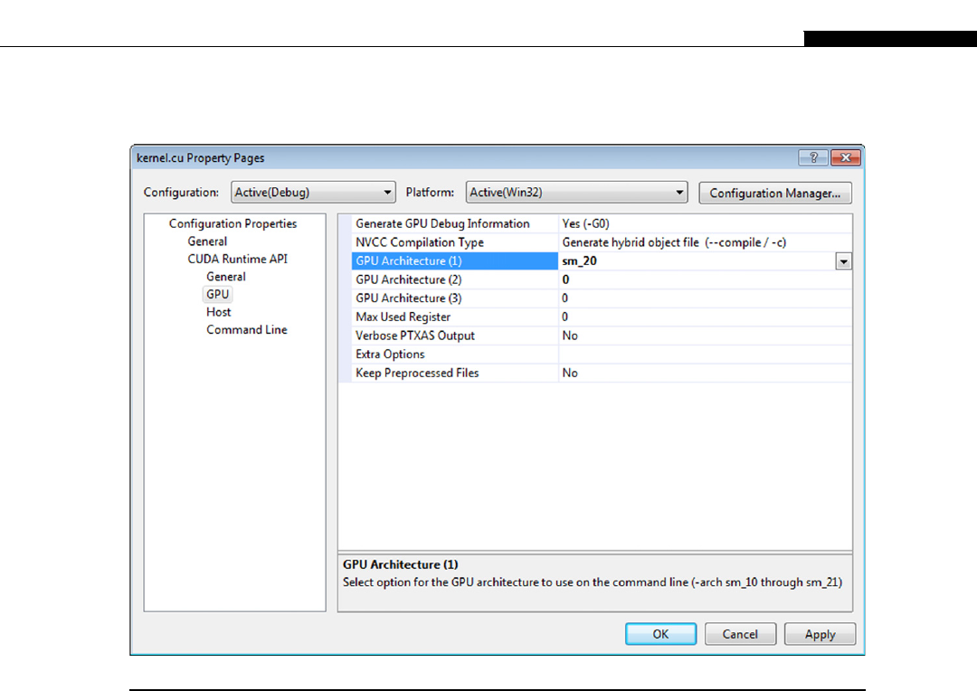
CUDA defines a preprocessor symbol __CUDA_ARCH__, which currently holds the value 100, 110,
120, 130, 200, 210, or 300. Clearly, as future architectures are defined these will increase. Thus, you
can write
#if (__CUDA_ARCH__ >¼200)
my_compute_2x_function();
#else
my_compute_1x_function();
#endif
Alternatively, you can write a single function that uses conditional compilation only where
necessary to either make use of the later compute level functions or provide an alternative solution for
lower compute level devices.
Many of the compute 2.x functions simplify the programming necessary and therefore make
development easier. However, most of these later functions can also be implemented by lower compute
level devices in a slower manner or with slightly more programming. By not providing any imple-
mentation to provide for backward compatibility, CUDA forces programmers to make a choice of
FIGURE 12.1
Setting the correct architecture.
Errors With CUDA Directives 533

either not using the new features, using them and excluding those customers with older hardware, or
using them and writing their own implementation for older hardware.
Most consumers will expect your software to work on their hardware. They will not be impressed
with a message telling them to swap out their 9800 GT or GTX260 for a 400/500/600 series Fermi/
Kepler card. Most consumers will have no clue what the compute level is anyway and will have
purchased the card to play the latest version of a particular game.
If you work in the research or commercial fields, then your hardware is largely defined for you by
the institution or company. If you have an input into this, absolutely choose at least compute 2.x
hardware or later, as it is much easier to program. You can then largely forget about the evolution of
GPUs to date and work with a cache-based system far more familiar to most CPU programmers. If you
have a mix of hardware, as do many of our clients, then you need to think about how to achieve the best
performance on each generation of hardware and write your program accordingly.
Device, global, and host functions
In CUDA you have to specify if a function or data item exists on the host (the CPU side) or the device
(the GPU side) of the PCI-E data bus. Thus, there are three specifiers that can be used, as shown in
Table 12.1. If you omit the specifier, then the CUDA compiler will assume the function exists on the
host and will only allow you to call it from there. This is an error detected at compile time and thus
easy to correct. It is possible to specify that a function exists both on the host (CPU) and also on the
device (GPU) by using both the __device__ and __host__ specifiers. However, it’s not possible to
mix __global__ and __host__ specifiers.
This dual specification is useful in that it allows you to write common code on both the GPU
and the CPU. You can abstract what data gets processed by what thread to the global function.
The global function then calls the device function, passing it a pointer to the data it should perform
the task on. The host function can simply call the device function in a loop to achieve the same
functionality.
In terms of how device and global functions get translated, device functions are similar to static
functions in C. That is, the CUDA compiler expects to be able to see the entire scope of a device
function at compile time, not link time. This is because device functions, by default, get in-lined into
the global function.
In-lining is a process where the formal parameters and the call overhead are eliminated and every
call to the function is expanded as if the body of the called function was included at the point of the
call. This might lead you to think the compiler is wasting code space, as you will have potentially two
copies of the same device function in the program memory space. However, usually the context of the
Table 12.1 GPU and Host Functions
Specifier Code Is Located on May Be Called by
__device__ GPU A global or device function
__global__ GPU A host function using
a kernel invocation
__host__ Host A regular C function call
534 CHAPTER 12 Common Problems, Causes, and Solutions

call will allow additional optimization strategies to be used, so although the device function is largely
duplicated, it may be slightly different in each usage.
The problem this causes for you, the programmer, is that the compiler expects one source file. If
you want to have two kernel source files (.cu files) that share a common device function, then you need
to #include the .cu source file into each caller instead of declaring the usual header file approach and
having the linker resolve the call. Note that in the CUDA 5.0 release of the SDK, its new GPU Library
Object Linking feature allows for standard object code generation of the device code kernel and even
placing this code into static linkable libraries. This allows for much better reuse of existing code and
somewhat quicker compile times.
Kernels within streams
Getting an asynchronous operation to work as you intend is actually quite tricky since the stream
model is not reflected in the actual hardware, at least up to compute 2.1 devices. Thus, you might create
two streams and fill stream A with a number of memory copies and then stream B with a number of
memory copies. You might expect that as streams A and B are different, the hardware would interleave
copies from each stream. What happens in practice is the hardware has only a single queue and
executes commands based on the order in which they were issued. Thus, two streams that implement
acopy to device, execute kernel, and copy from device operation will be run in sequence rather than
being overlapped with one another.
In consumer hardware up to and including compute 3.0 devices there are just two queuesdone for
the memory copies and one for the kernels. In the memory queue, any preceding operation must
complete prior to a new operation being issued. This makes perfect sense, as a single DMA (direct-
memory access) engine can do a single transfer at a time. However, this means filling the queues, depth
first by stream has the effect of serializing the stream operations, which defeats the object of using
streams, to achieve an enhanced level of concurrent kernel/memory transfers.
The solution is still to fill the queue depth first, but to exclude the copy back memory operations
from the queue. Thus, the copy to and kernel operations will overlap execution with one another. In
a situation where the input data is larger than the output data, this works quite well. Once the last kernel
in the batch has been pushed into the queue, all of the copy back operations are then pushed into the
transfer queue.
In Fermi devices based on the GF100/GF110 devices (i.e., GTX470, GTX480, GTX570,
GTX580, Tesla C2050, C2070, C2075, Tesla M2050/2070) there are two DMA engines. However,
only the Tesla devices enable this second transfer engine, known as “async engine count,” in the
driver. Thus, on Fermi Tesla devices, the depth-first approach mentioned previously can be improved
upon. As we no longer have a single transfer queue, we in fact should issue commands to the stream
breadth first. This vastly simplifies stream handling, as we can effectively forget about the hardware
handling internally and expect it to work as the logical stream model predicts.
However, do be aware of one optimization in the hardware that can cause issues. The hardware will
tie successive transfers together in terms of when they complete. Thus, launching two memory copies
followed by two kernel calls results in both the memory copies having to complete before either kernel
gets launched. You can break this behavior by inserting an event into the stream in between the
memory copies. Then each copy is handled independently of the ones after it.
Errors With CUDA Directives 535

PARALLEL PROGRAMMING ISSUES
Having gotten over the usage of the API issues, the next pitfalls most CUDA developers fall into are
some of the more general problems that plague all parallel software development. We look in this
section at some of these issues and how they affect GPU development.
Race hazards
In a single-thread application, the problem of producer/consumer is quite easy to handle. It’s simply
a case of looking at the data flow and seeing if a variable was read before anything wrote to it. Many of
the better compilers highlight such issues. However, even with this assistance, complex code can suffer
from this issue.
As soon as you introduce threads into the equation, producer/consumer problems become a
real headache if not thought about carefully in advance. The threading mechanism in most operat-
ing systemsdand CUDA is no exceptiondtries to operate to achieve the best overall throughput.
This usually means threads can run in any order and the program must not be sensitive to this
ordering.
Consider a loop where iteration idepends on loop iteration i-1. If we simply assign a thread to
each element of the array and do nothing else, the program will work only when the processor executes
one thread at a time according to the thread ID from low to high thread numbers. Reverse this order or
execute more than one thread in parallel and the program breaks. However, this is a rather simple
example and not all programs break. Many run and produce the answer correctly sometimes. If you
ever find you have a correct answer on some runs, but the wrong answer on others, it is likely you have
a producer/consumer or race hazard issue.
A race hazard, as its name implies, occurs when sections of the program “race” toward a critical
point, such as a memory read/write. Sometimes warp 0 may win the race and the result is correct. Other
times warp 1 might get delayed and warp 3 hits the critical section first, producing the wrong answer.
The major problem with race hazards is they do not always occur. This makes debugging them and
trying to place a breakpoint on the error difficult. The second feature of race hazards is they are
extremely sensitive to timing disturbances. Thus, adding a breakpoint and single-stepping the code
always delays the thread being observed. This delay often changes the scheduling pattern of other
warps, meaning the particular conditions of the wrong answer may never occur.
The first question in such a situation is not where in the code is this happening, but requires you to
take a step backward and look at the larger picture. Consider under what circumstances the answer can
change. If there is some assumption about the ordering of thread or block execution in the design, then
we already have the cause of the problem. As CUDA does not provide any guarantee of block ordering
or warp execution ordering, any such assumption means the design is flawed. For instance, take
a simple sum-based reduction to add all the numbers in a large array. If each run produces a different
answer, then this is likely because the blocks are running in a different order, which is to be expected.
The order should not and must not affect the outcome of the result.
In such an example we can fix the ordering issues by sorting the array and combining values from
low to high in a defined order. We can and should define an order for such problems. However, the
actual execution order in the hardware should be considered as undefined with known synchronization
points.
536 CHAPTER 12 Common Problems, Causes, and Solutions

Synchronization
Synchronization in CUDA is the term used for sharing of information between threads within a block,
or between blocks within a grid. A thread can access register space or local memory space, both of
which are private to the thread. For threads to work together on a problem they will often use the on-
chip shared memory. We saw some examples of this in the reduction problem we looked at earlier.
Threads are grouped into warps of 32 threads. Each warp is an independent schedulable unit for
the hardware. The SMs themselves have 8, 16, 32, 48, or more CUDA cores within them. Thus, they
can schedule at any single point in time a number of warps and will switch warps to maintain the
throughput of the device. This causes us some issues in terms of synchronization. Suppose we have 256
threads in a single block. This equates to eight warps. On a compute 2.0 device, with 32 CUDA cores,
two warps will be running at any single time. There are two warps running and not one warp because
the hardware actually runs two independent halfwarps per shader clock (two full warps per GPU
clock). Thus, two warps may make some progress in the program while others remain idle.
Let’s assume warps 0 and 1 are the ones that are initially selected by the hardware to run. The SMs
do not use a conventional time-slicing method, but run until the warp is blocked or hits a maximum run
period. In principle this is all that is needed of the scheduler. As soon as warp 0 issues an operation,
arithmetic or memory, it will stall and the warp will switch. If all warps follow the same path this has
the effect of pipelining the operations within a block, one warp at a time. This in turn allows for
extremely efficient execution of the instruction stream across Nwarps.
However, this arrangement rarely remains for long, as one or more external dependencies will
cause one warp to get delayed. For example, let’s assume every warp in the block reads from global
memory. All but the last warp hit the L1 cache. The last warp was unlucky and its data is now being
fetched from global memory. If we assume a 20-clock-cycle instruction latency and a 600-cycle
memory latency, the other warps will have progressed 30 instructions by the time the memory request
is satisfied. If the kernel has a loop, then warps 0..6 could be several iterations ahead of warp 7.
Let’s look at an example of this from Chapter 9, adding a dataset. To do this we add the following
sections of code to the start of the loop:
#define MAX_WARPS_PER_SM 8
__shared__ u64 smem_start_clock_times[MAX_WARPS_PER_SM];
__shared__ u64 smem_sync_clock_times[MAX_WARPS_PER_SM];
__global__ void reduce_gmem_loop_block_256t_smem(const uint4 * const data,
u64 * const result,
const u32 num_elements)
{
// Calculate the current warp id
const u32 log_warp_id [threadIdx.x >> 5;
// For the first SM only, store the start clock times
if (blockIdx.x [[ 0)
smem_start_clock_times[log_warp_id] [clock64();
// Shared memory per block
// Divide the number of elements by the number of blocks launched
// ( 4096 elements / 256 threads) / 16 blocks ¼1 iteration
// ( 8192 elements / 256 threads) / 16 blocks ¼2 iterations
Parallel Programming Issues 537

// (16384 elements / 256 threads) / 16 blocks ¼4 iterations
// (32768 elements / 256 threads) / 16 blocks ¼8 iterations
const u32 num_elements_per_block ¼(( (num_elements/4) / 256) / gridDim.x);
const u32 increment ¼(gridDim.x * 256);
const u32 num_elem_per_iter ¼(num_elements>>2);
// Work out the initial index
u32 idx ¼(blockIdx.x * 256) þthreadIdx.x;
// Accumulate into this register parameter
u64 local_result ¼0;
// Loop N times depending on the number of blocks launched
for (u32 i¼0; i<num_elements_per_block; iþþ)
{
// If still within bounds, add into result
if (idx < num_elem_per_iter)
{
const uint4 * const elem ¼&data[idx];
local_result þ¼ ((u64)(elem->x)) þ((u64)(elem->y)) þ((u64)(elem->z)) þ
((u64)(elem->w));
// Move to the next element in the list
idx þ¼ increment;
}
}
// Create a pointer to the smem data area
u64 * const smem_ptr ¼&smem_data[(threadIdx.x)];
// Store results - 128..255 (warps 4..7)
if (threadIdx.x >¼128)
{
*(smem_ptr) ¼local_result;
}
// For the first SM only, store the clock times before the sync
if (blockIdx.x [[ 0)
smem_sync_clock_times[log_warp_id] [clock64();
__syncthreads();
.
}
What we’ve done here is to store into shared memory the internal GPU clock at the start of the
accumulation, and then again just prior to the synchronization operation. The raw data results are
shown in Table 12.2. Notice a few things from this data. First, the first run through the data takes more
538 CHAPTER 12 Common Problems, Causes, and Solutions

Table 12.2 Clock Data from Reduction Example
Parallel Programming Issues 539
time. This is because the data is being fetched from memory rather than the cache. Second, notice the
actual start time varies between the warps. We can see the even and odd warps being scheduled within
a few clocks of one another, as you might expect.
However, even so, there is still quite some variation in the start time at this very early stage.
Figure 12.2 shows a scatter plot of start times for a normalized version. Warps are shown along the X
axis and cycles on the Yaxis. Notice how we see the alternate warp schedulers issue warps into the SM.
As we might expect, given the warps are executed out of order, the timing variation by the time we
hit the synchronization operation is on the order of 4000 clocks. Even though warp 1 started after warp
0, it hits the synchronization point just over 3000 cycles later (Figure 12.3).
Clearly, we can see that it is impossible to rely on any execution order to achieve correct operation.
Synchronization points are needed at any point where the threads within different warps need to
exchange data.
0
2
4
6
8
10
12
14
16
18
20
01234567
Normalized Start Time
FIGURE 12.2
Normalized warp start time distribution.
0
500
1000
1500
2000
2500
3000
3500
4000
4500
01234567
Normalized Sync Time
FIGURE 12.3
Normalized warp sync time distribution.
540 CHAPTER 12 Common Problems, Causes, and Solutions

We see the same issue when we try to exchange data from different blocks:
Block Id: 16 SM: 0 Start: 10420984500 End: 10421078132 Delta: 93632
Block Id: 22 SM: 0 Start: 10420984504 End: 10421079614 Delta: 95110
Block Id: 36 SM: 0 Start: 10420984508 End: 10421086198 Delta: 101690
Block Id: 50 SM: 0 Start: 10420984512 End: 10421105046 Delta: 120534
Block Id: 64 SM: 0 Start: 10420984592 End: 10421137178 Delta: 152586
Block Id: 171 SM: 0 Start: 10421223384 End: 10421308772 Delta: 85388
Block Id: 172 SM: 0 Start: 10421223406 End: 10421311256 Delta: 87850
Block Id: 176 SM: 0 Start: 10421223424 End: 10421322372 Delta: 98948
Block Id: 177 SM: 0 Start: 10421223518 End: 10421350178 Delta: 126660
Block Id: 178 SM: 0 Start: 10421233178 End: 10421381276 Delta: 148098
Block Id: 303 SM: 0 Start: 10421449580 End: 10421535186 Delta: 85606
Block Id: 304 SM: 0 Start: 10421449618 End: 10421538246 Delta: 88628
Block Id: 305 SM: 0 Start: 10421449800 End: 10421546884 Delta: 97084
Block Id: 306 SM: 0 Start: 10421449822 End: 10421577204 Delta: 127382
Block Id: 313 SM: 0 Start: 10421469888 End: 10421606770 Delta: 136882
Here we have dumped the start time and completion time from thread 0 for those blocks running on
SM 0. You can see that initially SM 0 gets wide distribution of block IDs as the blocks are distributed to
many SMs in turn. We’d expect to see that pattern continue, as individual blocks are retired from the
SM and new blocks introduced.
In practice, we see the scheduler add large sets of near linear block IDs to each SM. This would
suggest the block scheduler is allocating new blocks only once a certain threshold of free block slots is
reached with a given SM. This would be beneficial in terms of localizing the cache accesses, which
may in turn improve the L1 cache hit rate. However, it comes at the cost of potentially reducing the
number of available warps for scheduling. Thus, we can see that both warps and blocks are distributed
in time, and therefore it is essential that any thread- or block-based cooperation allows for all elements
of the calculation to complete.
For thread synchronization you need to use the __syncthreads primitive and can make use of on-
chip shared memory. For block-based synchronization you write the data to global memory and launch
a further kernel.
One final point that often trips up people with synchronization is that you need to remember that all
threads in a thread block must reach any barrier synchronization primitive such as __syncthreads or
else your kernel will hang. Therefore, be careful of using such primitives within an if statement or
looping construct, as such usage may cause the GPU to hang.
Atomic operations
As you can see in the previous section, you cannot rely on, or make any assumption about, ordering to
ensure an output is correct. However, neither can you assume a read/modify/write operation will be
completed synchronously with the other SMs within the device. Consider the scenario of SM 0 and SM
1 both performing a read/modify/write. They must perform it in series to ensure the correct answer is
reached. If SM 0 and SM 1 both read 10 from a memory address, add 1 to it, and both write 11 back,
one of the increments to the counter has been lost. As the L1 cache is not coherent, this is a very real
possibility if more than one block writes to the same output address within a single kernel call.
Parallel Programming Issues 541
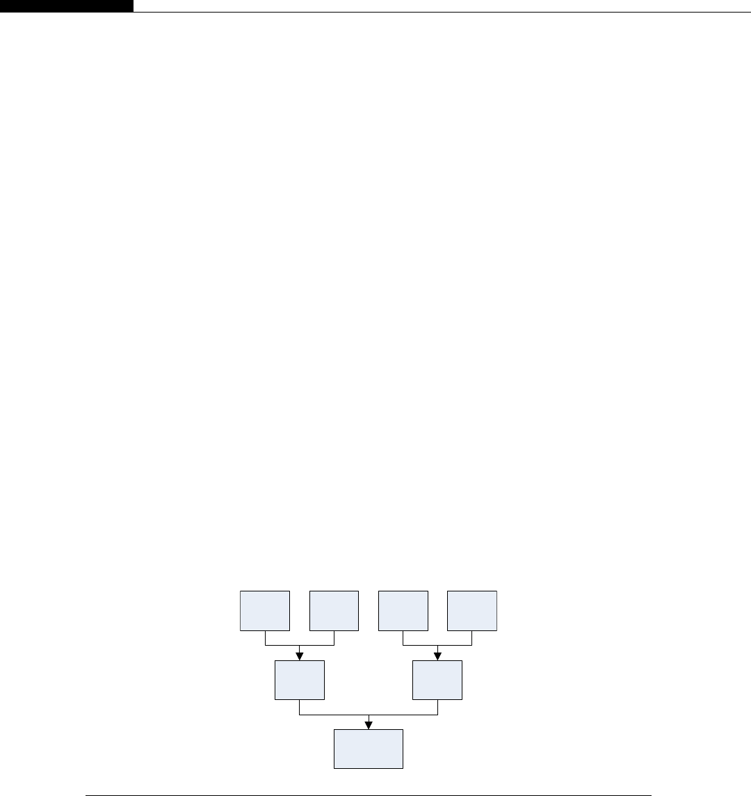
Atomic operations are used where we have many threads that need to write to a common output.
They guarantee that the read/write/modify operation will be performed as an entire serial operation.
They, however, do not guarantee any ordering of the read/write/modify operation. Thus, if both SM
0 and SM 1 ask to perform an atomic operation on the same address, which SM goes first is not defined.
Let’s consider the classic parallel reduction algorithm. It can be viewed as a simple tree as shown in
Figure 12.4. We have a number of ways to view this operation. We could allocate A, B, C, and D to
a single thread and have those threads do an atomic add to an output storing (A,B) and (C,D). We then
drop down to two threads, each of which would add the partial result to the final result.
Alternatively, we could start with the second line and use two threads. Thread 0 would read
the contents of A and B and write it as the designated output address. Thread 1 would handle the
inputs from C and D. Thread 1 would then drop out, leaving thread 0 to add the two partial results.
Equally, we could reduce the problem to a single thread by simply having thread 0 calculate A þ
BþCþD.
The first approach works by considering the destination data writing to a common output, a scatter
operation. The other approaches work by considering the source data and gathering it for use in the
next stage. The scatter operation, because more than one contributor is writing to the output, requires
the use of atomic operations. The gather approach completely eliminates the use of atomic operations
and is therefore usually the preferable solution.
Atomic operations introduce serialization if, in fact, there is more than a single thread trying to
perform a write at exactly the same time. If the writes are distributed in time such that there is no
conflicting write, then an atomic operation has no significant cost. However, you cannot say with any
certainty in a complex system that there will be absolutely no two writes happening at any single point
in time. Therefore, even if the writes are expected to be sparsely distributed in time, we need to use
atomics to ensure this is always the case.
Given we can replace an atomic write with a gather operation, which does not need any form of
data locking, does it makes sense to use atomics at all? The answer in most cases is the gather approach
will be quicker. However, this comes at a cost.
In our reduction example the addition of two numbers is trivial. Given just four numbers, we could
easily eliminate all threads and have a single thread add the four numbers sequentially. This clearly
A B
A+B
A+B+C+D
C D
C+D
FIGURE 12.4
Classic reduction.
542 CHAPTER 12 Common Problems, Causes, and Solutions
works for trivial amounts of values, but what if we have 32 million values that we have to process in
some form of reduction?
We saw in the reduction example from Chapter 9 that using a single thread on a CPU was slower
than two threads, which itself was slower than three. There is a clear tradeoff here between the amount
of work done by a given thread and the overall number of threads running. In the CPU case the
maximum throughput on our AMD Phenom II 905e system was effectively limited to three threads due
to memory bandwidth issues on the host.
A more modern processor, such as the Sandybridge-E, has higher host memory bandwidth, but
at the same time, two additional processor cores (six instead of four). Running the same OpenMP
reduction on a Sandybridge-E I7 3930 K system produces the results shown in Table 12.3 and
Figure 12.5. Thus, even if we hugely increase the memory bandwidth and increase the core count, we
see the same issue as before. Using more threads on CPU-based architecture produces progressively
lower returns as we add more and more cores.
Running only two threads would not make use of the hardware. Running 16 million threads and
killing half of them every reduction round would also not be a good approach on a CPU. On a GPU we
could adopt this approach since the GPU creates a thread pool that gradually moves through the 32
million threads the programmer requested. We can, of course, manually create a similar thread pool on
the CPU, although we have far fewer cores with which we can run threads.
Table 12.3 OpenMP Scaling on Sandybridge-E
Number of Threads Execution Time % Time Expected % Overhead %
1 5.78 100 100 0
2 3.05 53 50 3
3 2.12 37 33 4
4 1.71 30 25 5
5 1.52 26 20 6
6 1.46 25 17 8
0
1
2
3
4
5
6
7
123456
Execution Time
FIGURE 12.5
OpenMP scaling on Sandybridge-E.
Parallel Programming Issues 543

Our approach with the reduction example from Chapter 9 is a gather operation mixed with the
scatter operation. We schedule a number of blocks based on a multiple of the number of SMs phys-
ically present on the device. We then divide the data set into Nblocks and have each thread gather the
necessary data from memory to perform a local, on-chip accumulation.
Each thread is doing a significant amount of work. We can see from the previous timing example
that the wider data bus and double the number of SMs on the GTX470 allow it to complete this
operation much quicker than the GTX460. We want to ensure we’re using the parallelism present in the
device, be it a GPU or CPU, to the maximum.
Having calculated the partial sums on a per-thread basis, the issue then is how to combine the
partial sums. This is where atomic operations become necessary because the accumulated data is
private to the thread. Thus, it’s not possible to gather this data from another thread without the source
thread writing its data somewhere.
A typical compute 2.0 GPU has up to 16 SMs, each of which can run up to 48 warps of 32 threads
each. Thus, we have up to 24.5 K threads active at any point in time. Atomic operations can be
performed in shared memory (from compute 1.1 devices and later) or in global memory. Shared
memory atomics are, not surprisingly, significantly faster than having to go all the way out of the
SM to global memory for global memory–based atomics. As we have up to 16 SMs, the shared
memory–based atomics are 16 times wider than a write to global memory. Therefore, we want to use
shared memory atomics wherever possible.
Atomic functions as a whole are only available on compute 1.1 devices, which is basically any
device except the early GTX8800 series cards. 32-bit integer atomic operations on shared memory
became available in compute 1.2 (the 9800 series and later). 64-bit integer atomic operations became
available in global memory from compute 1.2 devices and in shared memory from compute 2.0 devices
(the GTX400 series).
Single-precision, floating point–based atomic operations are available only in compute 2.0 and
later. Double-precision atomics are not natively supported in any current hardware. However, you can
implement them via software. The CUDA programming guide provides an example of how to do this
using the atomic CAS (compare and swap) operation.
Understanding when to use gather operations and when to use scatter operations are often key to
achieving both correctness and performance. Think about how best to structure the design to minimize
the use of atomics (scatters) and maximize the use of gather operations instead.
ALGORITHMIC ISSUES
The final type of problem programmers hit is a tricky one. The program runs and doesn’t produce any
errors, but the answer is wrong.
Back-to-back testing
Testing is something that is key to a programmer being perceived as either someone who writes “good
code” or someone who throws together something that occasionally works. As a professional
programmer you should strive to deliver the best-quality software you are able to in the timeframe
available. How can you achieve this?
544 CHAPTER 12 Common Problems, Causes, and Solutions

Back-to-back testing is a technique that acknowledges that it is much harder to write code that
executes in parallel than a functionally equivalent set of code for a serial processor. With this in mind
you always develop, in parallel to or prior to the CUDA application, a serial implementation of the
problem. You then run the identical dataset through both sets of code and compare the output. Any
difference tells you that you may have an issue.
Now why do I only say “may” have an issue? The answer is largely down to if you are using
floating-point (single- or double-precision) numbers or not. The issue with floating-point numbers is
rounding and precision. Adding a large series of random floating-point numbers on a serial CPU from
the lowest array value to the highest array value will result in a different value than if you were to add
the same numbers from the highest array index to the lowest array index. Try it and see.
Now why is this? Single-precision, floating-point numbers use 24 bits to hold the mantissa value and
8 bits to hold the exponent. If we add 1.1eþ38 to 0.1e38 what do you think the result will be? The
answer is 1.1eþ38. The tiny value represented by 0.1e38 is too small to be represented in the mantissa
part. Over a large set of numbers there will be many of these types of issues. Therefore, the order in
which the numbers are processed becomes important. To preserve accuracy often the best way to solve
this issue is to sort the set of numbers and add from the lowest number to the largest. However, this
introduces potentially a significant amount of work, in the terms of the sort, for this enhanced precision.
There are also other issues concerning the handling of floating-point values in compute 1.x devices,
especially with very small numbers around 0, which may cause them to handle floating-point numbers
in different ways than the same code running on the CPU. Thus, it’s often best to compromise and
allow a certain threshold of error when dealing with floating-point equivalence tests.
If you have an existing CPU solution, then it is relatively simple to compare the results. With
integer-based problems the standard C library function memcmp (memory compare) is quite sufficient to
see if there is a difference between two sets of outputs. Usually when there is a programming error on
the GPU side, the results are not just a little different, but greatly different, so it’s easy to say this code
does or does not work and at which point in the output the difference occurs.
More difficult are aspects where the results match up until a certain point. Typically this might be
the first 256 values. As 256 is often used as a thread count, this points to an error in the block index
calculation. Only the first 32 values being correct points to an error in the thread index calculation.
Without an already existing CPU implementation, you’ll need to write one or use someone else’s
implementation that you know works. However, actually writing your own serial implementation
allows you to formulate the problem and understand it much better before attempting a parallel
implementation. You have to, of course, ensure the serial version produces the expected answer before
you start the parallel work.
It also provides a useful benchmark to see if using the GPU is providing a good speedup. In this
evaluation always consider any transfer times for the PCI-E bus. As with the reduction example, we
could write a reduction algorithm on the GPU that runs much faster than its CPU OpenMP equiv-
alent. However, just sending the data to the GPU swamped any execution time saving. Be aware the
GPU is not always the best solution. Having a CPU counterpart can let you evaluate this decision
easily. The solution should be about maximizing the use of whatever resources are available, CPU
and GPU.
Once the back-to-back test is set up, and there are many such examples where we do this in the
various examples in this book, you can instantly see if you introduce an error. As you see this at the
point you introduce it, it makes finding and identifying the error far easier. Combining this with
Algorithmic Issues 545

a version control system, or simply always making a new backup after every major step, allows you to
eliminate a lot of hard debugging effort later in the development cycle.
Memory leaks
Memory leaks are a common problem and something that is not just restricted to the CPU domain. A
memory leak, as its name suggests, is available memory space simply leaking away as the program
runs. The most common cause of this is where a program allocates, or mallocs, memory space but does
not free that space later.
If you have ever left a computer on for weeks at a time, sooner or later it will start to slow down.
Sometime afterwards it will start to display out of memory warnings. This is caused by badly written
programs that don’t clean up after themselves.
Explicit memory management is something you are responsible for within CUDA. If you allocate
memory, you are responsible for deallocating that memory when the program completes its task. You
are also responsible for not using a device handle or pointer that you previously released back to the
CUDA runtime.
Several of the CUDA operations, in particular streams and events, require you to create an instance
of that stream. During that initial creation the CUDA runtime may allocate memory internally. Failing
to call cudaStreamDestroy or cudaEventDestory means that memory, which may be both on the host
and on the GPU, stays allocated. Your program may exit, but without the explicit release of this data by
the programmer, the runtime does not know it should be released.
A nice catchall for this type of problem is the cudaResetDevice call, which completely clears all
allocations on the device. This should be the last call you make before exiting the host program. Even
if you have released all the resources you think you have allocated, with a program of a reasonable size,
you or a colleague on the team may have forgotten one or more allocations. It’s a simple and easy way
to ensure everything is cleaned up.
Finally, a very useful tool available for developers, supported on Linux, Windows, and Mac, is the
cuda-memcheck tool. This can be integrated into cuda-gdb for Linux and Mac users. For Windows
users it’s simply run from the command line
cuda-memcheck my_cuda_program
The program will execute your kernel and print appropriate error messages should your kernel
contain any of the following issues:
• Unspecified launch failures.
• Out-of-bounds global memory access.
• Misaligned global memory access.
• Certain hardware-detected exceptions on compute 2.x GPUs.
• Errors detected by the cudaGetLastError API call.
It will run on both debug and release versions of the kernels. In the debug mode, due to the additional
information present in the executable, the source line causing the issue in the source can also be identified.
Long kernels
Kernels that take a long time to execute can cause a number of problems. One of the most noticeable is
slow screen updates when the kernel is executing in the background on a device also used to display the
546 CHAPTER 12 Common Problems, Causes, and Solutions

screen. To run a CUDA kernel and at the same time support a display, the GPU must context switch
between the display updates and the kernel. When the kernels take a short time, the user has little
perception of this. However, when they become longer, it can become quite annoying to the point of
the user not using the program.
Fermi attempted to address this issue, and users with compute 2.x hardware or better suffer far less
from this than those with earlier hardware. However, it is still noticeable. Thus, if your application is
something like BOINC, which uses “spare” GPU cycles, then it will likely get switched off by the
userdclearly not good.
The solution to this issue is to ensure you have small kernels in the first instance. If you consider the
display needs to be updated every 60 ms, this means each screen update takes place at approximately
16 ms intervals. You could break up your kernel into sections that would fit within this time period.
However, that would likely mean your overall problem execution time would increase considerably, as
the GPU would need to continuously switch between the graphics context and the CUDA context.
There is no easy solution to this particular issue. Lower-powered machines and older (compute 1.x)
cards suffer badly from trying to execute CUDA and graphics workloads if the CUDA workload
becomes significant. Just be aware of this and test your program on older hardware to ensure it behaves
well. Users often prefer slightly slower programs if it means they can still use the machine for other
tasks.
FINDING AND AVOIDING ERRORS
How many errors does your GPU program have?
One of the most beneficial development changes we ever made at CudaDeveloper was to move to
encapsulating all CUDA API calls in the CUDA_CALL macro. We looked at this in Chapter 4 on setting
up CUDA. This is an incredibly useful way to free yourself of laboriously checking return values, yet
see the point in a CUDA program where you introduced an error.
If you are not using such a detection mechanism, the number of errors your kernels generates is
shown in tools such as Parallel Nsight. Unfortunately, they do not pinpoint the error for you. They
simply tell you the number of errors returned from the execution run. Obviously any value other than
zero is not good. Trying to track down those errors is then troublesome. It’s usually a case of you not
checking a return value, which is of course bad programming practice. Either the function should
handle all errors internally or, if it does not, the caller must handle them.
The errors detected by the runtime are the easy issues to fix. Simply using the CUDA_CALL macro in
every CUDA API, along with cudaGetLastError() after the kernel has completed, will pick up most
problems. The back-to-back testing against the CPU code will pick up the vast majority of the
functional/algorithmic errors in any kernel.
Tools such as Memcheck and the Memory Checker tool within Parallel Nsight are also extremely
useful (Figure 12.6). One of the most common mistakes that often leads to “Unknown Error” being
returned after a kernel call is out-of-bounds memory access. The Memcheck utility we have already
covered. However, the Parallel Nsight Debugger can also check for out-of-bounds memory access.
Selecting the Nsight/Options menu allows you to enable the memory checker during sessions
where Nsight is running as a debugger. If your kernel then writes out of bounds, be it in global memory
or shared memory, the debugger will break on the out-of-bounds access.
Finding and Avoiding Errors 547
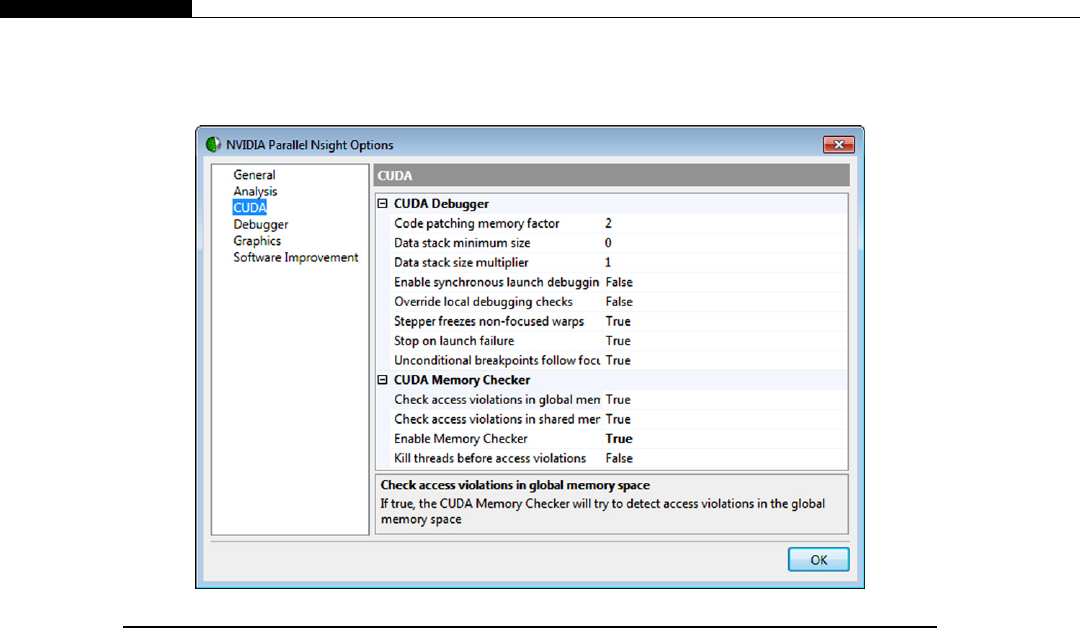
Note, however, this does not work where the out-of-bounds memory access occurs on thread local
variables, and enabling this feature slows down the overall execution time of the kernel. As it’s only
enabled when debugging with Parallel Nsight, this is usually not an issue.
Enabling this option will also provide some useful information about misaligned accesses to
memory. Misaligned accesses are not errors in the strictest sense, but simply point where, if you could
make the access aligned, you may considerably improve the kernel’s speed. These messages are
written to the Nsight Output window, which is one of the many output windows selectable by
a dropdown box in Microsoft Visual Studio. This is the same output window that the compile error
messages are written to, usually the bottom pane of the three standard windows that open in a Visual
Studio project.
Divide and conquer
The divide-and-conquer approach is a common approach for debugging and is not GPU specific.
However, it’s quite effective, which is why we mention it here. It is useful where your kernel is causing
some exception that is not handled by the runtime. This usually means you get an error message and
the program stops running or, in the worst case, the machine simply hangs.
The first approach in this sort of problem should be to run through with the debugger, stepping over
each line at a high level. Sooner or later you will hit the call that triggers the crash. Start with the host
debugger, ensuring you are using the CUDA_CALL macro, and see at which point the error occurs. It’s
FIGURE 12.6
Enabling CUDA Memory Checker tool by default.
548 CHAPTER 12 Common Problems, Causes, and Solutions

most likely it will be the kernel invocation or the first call into the CUDA API after the kernel
invocation.
If you identify the issue as within the kernel, switch to a GPU debugger such as Parallel Nsight
or CUDA-GDB. Then simply repeat the process following a single thread through the kernel
execution process. This should allow you to see the top-level call that triggers the fault. If not, the
cause may be a thread other than the one you are tracking. Typically the “interesting” threads are
threads 0 and 32 within any given block. Most CUDA kernel errors that are not otherwise detected
are either to do with interwarp or interblock behavior not working as the programmer imagined
they would work.
Single step through the code and check that the answer for every calculation is what it is expected
to be. As soon as you have one wrong answer, you simply have to understand why it’s wrong and often
the solution is then clear. What you are attempting to do is a very high level binary search. By stepping
over the code until you hit the failure point, you are eliminating a single level of functionality. You can
then very quickly identify the problem function/code line.
You can also use this approach without a debugger if for whatever reason you have no access to
such a debugger within your environment or the debugger is in some way interfering with the visibility
of the problem. Simply place #if 0 and #endif preprocessor directives around the code you wish to
remove for this run. Compile and run the kernel and check the results. When the code runs error free,
the error is likely to be somewhere within the section that is removed. Gradually reduce the size
of this section until it breaks again. The point it breaks is a clear indicator of the likely source of the
issue.
You may also wish to try the approach of seeing if the program runs with the following:
• One block of 1 thread.
• One block of 32 threads.
• One block of 64 threads.
• Two blocks of 1 thread.
• Two blocks of 32 threads.
• Two blocks of 64 threads.
• Sixteen blocks of 1 thread.
• Sixteen blocks of 32 threads.
• Sixteen blocks of 64 threads.
If one or more of these tests fail, it tells you there is some interaction of either the threads within
a warp, threads within a block, or blocks within a kernel launch that is causing the issue. It provides
a pointer as to what to look for in the code.
Assertions and defensive programming
Defensive programming is programming that assumes the caller will do something wrong. For
example, what is wrong with the following code?
char * ptr ¼malloc(1024);
free(ptr);
The code assumes that malloc will return a valid pointer to 1024 bytes of memory. Given the small
amount of memory we’re requesting, it’s unlikely in reality to fail. If it fails, malloc returns a null
Finding and Avoiding Errors 549

pointer. For the code to work correctly, the free() function also needs to handle null pointers. Thus,
the start of the free function might be
if (ptr !¼NULL)
{
.search list of allocated memory areas for ptr and de-allocate memory.
}
The free() function needs to consider both receiving a null pointer and also an apparently valid
pointer. The NULL pointer, however, doesn’t point to a valid area of allocated memory. Typically, if you
call free() with a null or an invalid pointer, a function that is written defensively will not corrupt the
heap storage, but will instead do nothing. Defensive programming is about doing nothing erroneous in
the case of bad inputs to a function.
However, this has a rather nasty side effect. While the user no longer sees the program crash,
neither does the test or quality assurance department, or the author for that matter. In fact, the program
now silently fails, despite the programming errors in the caller. If a function has implicit requirements
on the bounds or range of an input, this should be checked. For example, if a parameter is an index into
an array, you should absolutely check this value to ensure the array access does not generate an out-of-
bounds access. This is a question that is often addressed incorrectly.
C provides a very useful construct that is rarely used, except by those programmers familiar with
good software engineering practicesdthe assert directive. When a program fails, to have it fail silently
is bad practice. It allows bugs to remain in the code and go undetected. The idea behind assert is the
opposite. If there is an error with the parameters passed by the caller, there is a programming error. The
called function should scream about the issue until it’s fixed. Thus, if a null pointer is not allowed as one
of the input parameters to the function, then replace the if ptr ¼! NULL check with the following:
// Null pointers not supported
assert(ptr_param !¼NULL);
This means we no longer require an additional indent, plus we document in the code the
precondition for entry into the function. Always make sure you place a comment above the assertion
explaining why the assertion is necessary. It will likely fail at some point in the future and you want the
caller of that function to understand as quickly as possible why their call to the function is invalid. That
caller may very often be yourself, so it’s in your own best interests to ensure it is commented.
Six months from now you’ll have forgotten why this precondition was necessary. You will
then have to search around trying to remember why it was needed. It also helps prevent future
programmers from removing the “incorrect” assertion and therefore making the problem “go away”
before the upcoming release. Never do this without entirely understanding why the assertion was put
there in the first place. In almost all cases, removing the assert check will simply mask an error later
in the program.
When using assertions, be careful not to mix handling of programming errors with valid failure
conditions. For example, this following code is incorrect:
char * ptr ¼malloc(1024);
assert(ptr !¼NULL);
It is a valid condition for malloc to return a NULL pointer. It does so when the heap space is
exhausted. This is something the programmer should have a valid error handling case for, as it’s
550 CHAPTER 12 Common Problems, Causes, and Solutions

something that will always happen eventually. Assertions should be reserved for handling an invalid
condition, such as index out of bounds, default switch case when processing enumerations, etc.
One of the concerns with using defensive programming and assertions is that the processor
spends time checking conditions that for the most part will always be valid. It can do this on
each and every function call, loop iteration, etc., depending on how widespread the use of asser-
tions are. The solution to this issue is a simple onedto generate two sets of software, a debug
version and a release version. If you’re already using a package such as Visual Studio this is
inherent in the default project setup. Older systems, especially non-IDE-based systems, may need
this to be set up.
Once done, you can simply generate a version of the assert macro, ASSERT.
#ifdef DEBUG
#define ASSERT(x) (assert(x))
#else
#define ASSERT(x)
#endif
This simple macro will include the assertion checks only into the debug code, the version you and
the quality assurance people test alongside the release version.
As of the CUDA 4.1 release, it’s now also possible to place assertions into device code for compute
2.x devices. This was not something that was previously possible due to the inability of the GPU to
raise such an exception.
Debug level and printing
As well as having a single release and debug version, it’s often useful to have a debug level that is
easily changeable, for example, by setting the value of a global variable, #define, or other constant.
You may also wish to allow for setting such a parameter via the command line, for example -debug¼5
to set debug level five, etc.
During development, you can add useful information messages to the code, for example:
#ifdef DEBUG
#ifndef DEBUG_MSG
// Set to 0..4 to print errors
// 0 ¼Critical (program abort)
// 1 ¼Serious
// 2 ¼Problem
// 3 ¼Warning
// 4 ¼Information
#define DEBUG_ERR_LVL_CRITICAL (0u)
#define DEBUG_ERR_LVL_SERIOUS (1u)
#define DEBUG_ERR_LVL_PROBLEM (2u)
#define DEBUG_ERR_LVL_WARNING (3u)
#define DEBUG_ERR_LVL_INFO (4u)
// Define the global used to set the error indication level
extern unsigned int GLOBAL_ERROR_LEVEL;
Finding and Avoiding Errors 551

void debug_msg(char * str, const unsigned int error_level)
{
if (error_level <¼GLOBAL_ERROR_LEVEL)
{
if (error_level ¼¼ 0)
printf("\n***********%s%s", str, "**************\n");
else
printf("\n%s", str);
fflush(stdout);
if (error_level ¼¼ 0)
exit(0);
}
}
#define DEBUG_MSG(x, level) debug_msg(x, level)
#else
#define DEBUG_MSG(x, level)
#endif
#endif
In this example, we’ve created five levels of debug messages. Where the debug version of the
software is not used, these messages are stripped from the executable in a way that does not cause
compilation errors.
#define DEBUG
#include "debug_msg.h"
unsigned int GLOBAL_ERROR_LEVEL ¼DEBUG_ERR_LVL_WARNING;
int main(int argc, char *argv[])
{
DEBUG_MSG("Error from level four", DEBUG_ERR_LVL_INFO);
DEBUG_MSG("Error from level three", DEBUG_ERR_LVL_WARNING);
DEBUG_MSG("Error from level two", DEBUG_ERR_LVL_PROBLEM);
DEBUG_MSG("Error from level one", DEBUG_ERR_LVL_SERIOUS);
DEBUG_MSG("Error from level zero", DEBUG_ERR_LVL_CRITICAL);
return 0;
}
To call the function, you simply place the macro into the code as shown in the previous
example. This will work fine in host code, but will not work on device code without some minor
modifications.
First, you have to be aware of some issues when printing a message within a kernel. Kernel level
printf is only supported for compute 2.x capability. If you try to use printf in a kernel that is being
compiled for compute 1.x devices, you will get an error saying you cannot call printf from a global or
552 CHAPTER 12 Common Problems, Causes, and Solutions

device function. This is not strictly truedit’s simply that it’s not supported for compute 1.x devices and
the target architecture must be compute 2.x.
Let’s assume you have a Fermi-level device so the printf call is supported. Unless you take care
not to, the message will be printed from every thread in groups of 32, the warp size. Clearly, as you
should be launching tens of thousands of threads, simply printing a single message may result in
10,000 plus lines scrolling off the top of the terminal window. As the printf buffer is of a fixed size,
and wraps, you will lose the earlier output.
As the lines can also be printed in any order, we cannot take the order of printing to represent the
order of execution without also some reference to the time to confirm exactly when the message
originated. Consequently, we need to identify the source of each message and timestamp it.
The first issue is easily handled, by having one thread in a block or warp print the message.
By convention this is usually thread 0. We might also wish to print a message from every warp,
so again we select only the first thread from each warp to print the message. You may also have
some other criteria, such as the threads that calculate halo regions, etc. A sample set of code is
shown here.
if ( (blockIdx.x ¼¼ some_block_id) && ((threadIdx.x %32) ¼¼ 0) )
{
// Fetch raw clock value
unsigned int clock32 ¼0;
asm("mov.u32 %0, %%clock ;" : "¼r"(clock32));
// Fetch the SM id
unsigned int sm ¼0;
asm("mov.u32 %0, %%smid ;" : "¼r"(sm));
printf("\nB:%05d, W:%02d, SM:%02u, CLK:%u", blockIdx.x, (threadIdx.x>>5), sm,
clock32);
}
This simply looks for a specified block ID and prints the block ID, warp number, SM we’re
executing on, and the raw clock value.
B:00007, W:05, SM:13, CLK:1844396538
B:00001, W:04, SM:05, CLK:1844387468
B:00002, W:09, SM:09, CLK:1844387438
B:00007, W:10, SM:13, CLK:1844396668
B:00002, W:06, SM:09, CLK:1844387312
B:00007, W:00, SM:13, CLK:1844396520
B:00005, W:12, SM:06, CLK:1844396640
B:00005, W:13, SM:02, CLK:24073638
B:00006, W:03, SM:04, CLK:24073536
B:00005, W:15, SM:02, CLK:24073642
B:00002, W:03, SM:05, CLK:24076530
B:00006, W:00, SM:04, CLK:24073572
B:00002, W:00, SM:05, CLK:24076570
Finding and Avoiding Errors 553
Here we’re printing the block index, warp ID, SM the warp is executing on, and the raw clock
value. You can simply redirect this output to a file and then plot a scatter graph. As we chose to place
the device printf at the start of the kernel, it shows when each kernel is invoked.
In Figure 12.7, the SMs are shown on the vertical axis with absolute clock time on the horizontal
axis. We can see all the SMs start at around the same time, except a few SMs that start a little later,
again all together. We then see a mostly random distribution of timestamps as each block prints its
details at the start of its execution. The distribution depends entirely on the program you execute and
the time for external resources to become available, global memory being the primary example.
With multiple GPUs or multiple streams, we also have the issue of identification of where the
message originated. This again can be simply handled by prefixing the message with a unique iden-
tifier. In several examples we have used a string created from the device ID string, device_prefix,to
do exactly this when using multiple GPUs. However, the API for extracting this information is a host-
side call, not a device-side call. This makes sense as we wouldn’t want 30,000 threads each getting the
device ID string, as it would be the same for all of them. Therefore, what we can do is provide this host-
side information via global or constant memory. If we have one GPU, one stream, this is not necessary,
but any nontrivial programs will be using both streams and multiple GPUs where available.
In the case of multiple GPUs, you will see a noticeable change in the clock values. Thus, it’s quite easy
to see the output streams are from different devices, but which came from device 0, 1, 2, or 3? For identical
devices, we can’t say. What if these messages originate from different streams on the same device?
Using the absolute TID (thread ID) value is sufficient to identify messages for single GPU kernels.
However, a combination of device number, TID, and stream number is required where either multiple
streams and/or devices are used.
The ordering issue is a problem in terms of viewing the output only. You should create a prefix in
the following form:
GPU ID : Stream ID : TID : Message
With this prefix, it’s possible to redirect the output to a file and simple sort using a sort that preserves
the relative ordering. We then end up with all the messages, in order, for each GPU and stream.
FIGURE 12.7
Warp execution by the 14 SMs (GTX470).
554 CHAPTER 12 Common Problems, Causes, and Solutions

Note that although printf is an easy way to display information at the host end, be aware that
it’s creating a 1 MB buffer in GPU memory and transferring that buffer back to the host upon certain
events.
Thus, the printf output will be seen only under the following conditions:
1. At the start of a subsequent kernel launch.
2. At the end of a kernel execution if the environment variable CUDA_LAUNCH_BLOCKING is set (not
recommended if using multiple GPUs or streams).
3. As the result of a host side–initiated synchronization point such as synchronizing the device,
stream, or an event.
4. Blocking versions of cudaMemcpy.
5. Programmer-initiated device reset (cudaDeviceReset or driver cuCtxDestroy API calls).
Thus, in most cases you will see the output printed. If you do not, simply call cudaDeviceReset prior to
exiting the host program or cudaStreamSynchronize at the end of the set of work from a stream and the
missing output should appear.
Should you need a larger buffer, this can be set using the cudaDeviceSetLimit
(cudaLimitPrintFifoSize, new_size_in_bytes) API call.
Version control
Version control is a key aspect of any professional software development. It does not necessitate using
very expensive tools or huge processes that cover who can update what. In large projects version
control is absolutely essential. However, even for single-developer projects, something that may apply
to many readers, it is important.
Consider for a moment that debugging a 30,000-thread program is easy. If you laugh at this
statement then you realize just how hard a task you are setting yourself up for by not versioning your
program, either regularly or whenever a major point is reached. Programmers are generally a fairly
overconfident bunch of people and can be sure at the outset that a “simple” change will work without
problems. However, when it doesn’t quite work to plan, remembering exactly the set of changes you
made can be difficult. Without a working backup of the program it can be difficult if nearly impossible
to get back to exactly the working version before the changes.
Most programs in the professional world are developed in teams. A colleague can be extremely
helpful in providing a fresh pair of eyes with which to see a problem. If you have a versioned or
baselined copy of the working code it makes it relatively easy to look simply at the differences and see
what is now breaking the previously working solution. Without these periodic baselines it’s not easy to
identify the place where the error might be, and thus instead of a few hundred lines of code, you may
have to look at a few thousand.
DEVELOPING FOR FUTURE GPUs
Kepler
The roadmap that NVIDIA has presented from Fermi and later versions is the Kepler GK104 (K10),
the Kepler GK110 (K20), and the Maxwell. As of March 2012 the first of the Kepler releases was
made, the GK104. This product was aimed squarely at the consumer market and lacked some of the
Developing for Future GPUs 555

features that some aspects of the HPC (high-performance computing) market would have liked to see,
specifically significant dual-precision math support. Kepler GK110 will almost certainly be a far more
HPC-focused product that will likely end up in some form or another as a consumer card. The GK110
is scheduled for release at the end of 2012, but the design is already in use internally at NVIDIA for
development of the CUDA 5 release that will accompany it.
Let’s look briefly at the changes Kepler brings to the table. First and foremost, it brings energy
efficiency. The Kepler GTX680 has a TDP rating of 195 watts as compared with GTX580 at 244 watts.
This is just over a 20% reduction in absolute power usage of the top-end single-consumer GPU.
Looking more closely at the GTX680 it is actually closer to the GTX560 (GF114) in architecture than
the GTX580 (GF110), being somewhat like an internally doubled-up version of the GTX560.
If, however, we look at power usage in terms of watts per gigaflop, then you see the Kepler GK104
outperforming Fermi GF110 by a factor of up to two. NVIDIA’s own studies on common consumer
games (NVIDIA, May 18, 2012) show an average of 1.5better performance per watt. Many of
today’s games are highly complex, and thus it’s reasonable to expect a comparable power usage profile
on compute-based applications.
By being highly selective in terms of binning components, the GTX690 (a dual-GPU version of the
GTX680) significantly outperforms even the GTX680 in terms of gigaflops per watt. A doubling or
more in terms of performance per watt is a huge achievement on the part of the team at NVIDIA. The
GTX690 is the basis of the Tesla K10 range. This is the first time a Tesla product will be a dual-GPU
solution.
Although peak global memory bandwidth has remained the same from the GTX580 to the
GTX680, we have now transitioned from PCI-E 2.0 to the PCI-E 3.0 specification. Thus, transfers to
and from the card under a PCI-E 3.0 motherboard with a PCI-E 3.0–enabled CPU are double the speed
of the PCI-E 2.0 400/500 series cards. This doubling of bandwidth should see significant speedups for
certain PCI-E-limited kernels.
The Kepler GTX680/GTX690 moves us from the compute 2.1 level to the compute 3.0 level, with
the Kepler GK110 being targeted as a compute 3.5 device. A summary of the new compute levels is
shown in Table 12.4.
One of the major changes in Kepler was the elimination of the shader clock. Prior to Kepler, the
GPU ran at a given GPU clock frequency and the shader clock was multiplied internally by a factor of
2. In previous generations, it was the shader clock and not the GPU clock that drove the execution of
the CUDA cores within the device.
Clock rate is a significant driver of power consumption in any processor design. In eliminating the
shader clocker, NVIDIA has to lay out double the number of CUDA cores per SM to achieve the same
throughput. This tradeoff significantly reduced overall power consumption and allowed NVIDIA to
push the core clock from 772 MHz all the way up to just over 1 GHz.
The Kepler GK104 design actually increases the number of CUDA cores by four. It doubles the
number load/store units (LSUs), special functional units (SFUs), instruction dispatchers, and the size
of the register file. The shared memory/L1 cache remains unchanged at 64 KB, but can now be split in
a 32 K/32 K in addition to the usual 16 K/48 K split.
This choice is interesting in that a large amount of additional compute power has been added. If we
look to previous generations, we see the move from the GT200 (compute 1.3) to the GF110 (compute
2.0) devices from 24 warps per SM to 48 warps per SM. The Kepler GK104 design increases the total
warp count per SM to 64 and the total thread count per SM to 2048.
556 CHAPTER 12 Common Problems, Causes, and Solutions

The GTX680 claims a peak performance of 3 teraflops compared with the claimed 1.5 teraflops of
the GTX580. This peak performance is based on executing floating-point multiply and add (FMAD)
operations. Of course, in any real usage there is a huge variation in instruction makeup and memory
access patterns, which ultimately determine real performance levels.
In addition, the Kepler GK104 now features dynamic clock adjustment where it will ramp
down and up the clock according to the current GPU loading. We’ve seen this feature for years on
the CPU side, which helps significantly in saving power, especially when the device itself is not in
use.
In terms of instruction evolution, the major benefit we see is a shuffle instruction that allows
communication between threads within a single warp. This is a huge benefit in that threads within
a warp can now cooperate without the need to share data via shared memory. The final stages of
reduction operations and prefix sum can be easily accelerated with such operations. Additional
compiler intrinsics have become available for hardware-level shift, rotate, and access to the texture
memory as a simple additional 48 K read-only cache without the overhead of having to write texture
Table 12.4 New Compute Levels in Kepler
Description/
Device
G80
(GTX8800)/
G92
(GTX9800)
G200
(GTX280)
Fermi
GF110
(GTX580)
Fermi
GF114
(GTX560)
Kepler
GK104/K10
(GTX680)
Kepler
GK110/K20
(TBD)
Compute
level
1.0/1.1 1.3 2.0 2.1 3.0 3.5
Max warps
per SM
24 32 48 48 64 64
Max total
threads
per SM
768 1024 1536 1536 2048 2048
Total register
size per SM
in bytes
32 K 64 K 128 K 128 K 256 K 256 K
Max registers
per thread
63 127 63 63 63 255
Max threads
per block
512 512 1024 1024 1024 1024
CUDA cores
per SM
8 16 32 48 192 192*
Max SMs
per device
8 32168 8 15
Max shared
memory/L1
cache per SM
16 K 16 K 48 K 48 K 48 K 48 K
Max L2 cache
per device
N/A N/A 768 K 512 K 512 K 1536 K
*
Plus an additional 64 dual-precision units per SM.
Developing for Future GPUs 557

memory code. Four byte, packed vector instructions (add, subtract, average, abs, min, max) are
also introduced.
The Kepler GK110 (K20) has some very attractive features from the compute perspectivedthe
technologies NVIDIA refer to as dynamic parallelism, Hyper-Q, and RDMA. It also almost doubles
the number of SMs per device and adds the missing double-precision floating-point units necessary for
significant numbers of HPC applications. Initial (NVIDIA) figures indicate in excess of 1 teraflop of
double-precision performance. The memory bus has been increased from 256 bits to 384 bits, which if
we see similar clocks to the GK104, should result in a memory bandwidth in excess of 250 GB/s.
The first of these technologies, dynamic parallelism, allows us for the first time to easily launch
additional work from a GPU kernel. Previously, this was implemented by either oversubscribing the
thread blocks and leaving some idle or by running multiple kernels. The former is wasteful of
resources and works poorly, especially for large problems. The latter means there are periods where the
GPU is underutilized and prevents kernels from maintaining data in the high-speed shared memory/
cache as this memory is not persistent between kernel launches.
The second of these technologies is Hyper-Q, which addresses the difference between the
programmer exposed stream model and how it’s actually implemented in the hardware. All streams up
to and including Kepler GK104 are implemented in the hardware as a single pipe. Thus, a stream of
kernels from stream 0 will not be intermixed with a stream of kernels from stream 1, despite the
programmer explicitly specifying, via putting these kernels into separate streams, that they are
independent work units.
Hyper-Q breaks this single hardware stream into 32 separate hardware queues. Thus, up to 32
streams from perhaps a set of a few hundred programmer-defined streams are available to be inde-
pendently run on the hardware. The main benefit of this is in terms of loading the device. With 192 plus
cores per SM, the granularity of an SM has increased considerably. The resources within an SM can
therefore be wasted if small kernels are run that only partially load an SM.
Finally, RDMA (remote direct memory access) is also an interesting technology. NVIDIA has been
working with certain vendors, noticeably on the Infiniband side, to improve the latency of GPU-to-
GPU communications between nodes. Currently, the peer-to-peer function supports communication
between GPUs within the node directly over the PCI-E bus. For cards and OSs supporting this, it
avoids the need to go indirectly via the CPU memory space.
However, to send or receive data from a non-GPU device (e.g., an I/O device such as a network
card), the best case is a shared area of pinned memory on the host. The RDMA feature changes
that in that it allows the GPU to talk over the PCI-E bus directly to other PCI-E cards, not just
NVIDIA GPUs. Currently, this is only supported for some Infiniband cards, but it opens up the
potential for the use of other cards, such as direct data acquisition, FPGAs, RAID controllers, and
the like, to be able to talk directly to a GPU. This will be an interesting technology to watch
develop.
What to think about
Developing code that will run many years into the future, or at least be able to be run in the future, is
always a difficult issue. The more something is tuned to be fast on one particular set of hardware, the
less portable code will be in terms of future development. Thus, one strategy is to ensure any code you
develop is parameterized so it can easily be adapted for future GPUs.
558 CHAPTER 12 Common Problems, Causes, and Solutions

Often an application will be tailored to a particular architecture. Thus, you might have a code
section such as the following:
if ( (major ¼¼ 2) && (minor ¼¼ 0) ) // Compute 2.0
num_blocks ¼(96*4);
else if ( (major ¼¼ 2) && (minor ¼¼ 1) ) // Compute 2.1
num_blocks ¼(96*2);
else
num_blocks ¼64; // Assume compute 1.x
Now what happens if a compute 2.2 or compute 3.0 architecture is released? In the sample
program we’ll drop through to the compute 1.x path (the G80/G92/G200 series). The users of
your program don’t want to replace their Fermi-class GPU with a new Kepler card and find
your program runs slower or not at all on their brand-new graphics card. When writing
such code, assume you may also come across an unknown computer level and cater for it
accordingly.
With the move from G200 to Fermi there was a transition period, where authors had to reissue
programs because the number of blocks executed per SM remained the same between generations,
only the number of threads per block increased. If a kernel was already using the maximum number of
blocks per SM, which allowed for the best instruction mix and thus good performance, no additional
blocks got scheduled onto the SMs. Thus, the new hardware went unused and the existing software did
not run any faster on the new hardware.
The major transition between G200 and Fermi was the need to increase the number of threads per
block. The maximum number of threads per block, a property that can be queried, went from
a maximum of 512 to 1024. At the same time the number of resident warps has increased from 24
(compute 1.0/1.1) to 32 (compute 1.2/1.3) to 48 (compute 2.0/2.1). Thus, it’s likely in the future we’ll
continue to see such a trend, with blocks containing larger and larger thread numbers. Kepler was the
first GPU architecture to also increase the block count per SM, doubling it from 8 to 16 blocks.
Thus, the optimal number of threads, to schedule the maximum number of blocks, shifts back to 2048
threads O16 blocks ¼128 threads per block.
We can work out the number of warps available from simply querying the number of threads
and the warp size. The cudaDeviceProp structure returns warpSize and maxThreadsPerBlock.
Thus, we can call cudaGetDeviceProperties(&device_props) API and then divide the number
of threads per block by the number of warps to work out the maximum number of warps on a
given GPU.
This approach would work well for Kepler GK104 and also the upcoming Kepler GK110.
However, it does not take account of the changes in the programming model that the GK110 will bring.
The dynamic parallelism aspect of the GK110, now that it’s public, can clearly be planned for.
NVIDIA showed some work at GTC (GPU Technology Conference), where it claimed this feature
alone, primarily the elimination of the CPU control overhead, would leads to quite significant
speedups on many codes. It also leads to greatly simpler forms of recursion, where the recursive part
can increase the amount of parallelism as the number of nodes expands and contracts depending on the
data that is encountered.
One important aspect that you can implement into programs today to run on Kepler hardware is
the use of the dedicated 48 K read-only texture cache without the need to do texture memory
Developing for Future GPUs 559

programming. This will require only that you declare read-only pointers with the C99 standard
___restrict__ keyword, so for example:
void my_func(float * __restrict__ out_ptr, const float * __restrict__ in_ptr)
In this example by adding this keyword we’re saying that any writes to the parameter out_ptr
will have no effect on the memory region pointed to by in_ptr. In effect, we’re saying that
the two pointers do not alias one another. This will cause the reads via in_ptr to be cached in
the texture cache, giving an additional 48 K of read-only cache memory. Potentially this could
significantly reduce off-chip access to global memory and thus significantly improve memory
throughput.
The Hyper-Q logic is also something you should think about in terms of what elements of existing
kernels can be performed in parallel. For the first time task-level parallelism will be truly possible on
the GPU. To prepare for this, if you currently run a series of kernels, split these into independent
streams, one stream for every independent task. This will not adversely affect code performance when
running on your current platform, but will prepare those kernels to execute better on Kepler once this
feature becomes available.
Finally, the new K10 Tesla product is a dual GPU, based on the currently available GTX690
consumer card. As with CPUs, if you’re using only a single core you’re wasting 50% plus of the
available compute capability. Thus, anyone planning to install the K10 product will need to move their
existing code to support multiple GPUs. We covered this in Chapter 8. You’ll need to think about
where the data resides and if any communication between the GPUs will be necessary. Moving to
a multi-GPU solution today will make the transition much easier and provide almost linear scaling for
many applications.
FURTHER RESOURCES
Introduction
There are many CUDA resources available on the Internet and through a large number of universities
worldwide. We run sessions for professionals wishing to learn CUDA on an individual or group basis.
As such, I try to attend, in person or online, as many courses about CUDA as possible each year. As
CUDA is a great passion of mine, I’ve read every book published to date on this subject. I’d, therefore,
like to provide some information here about the various CUDA resources for anyone wishing to learn
more about CUDA. This information is also available from our website www.learncuda.com, a portal
for the various CUDA resources available worldwide.
Online courses
One of the great successes of CUDA is the commitment from NVIDIA to bring CUDA to a wider
audience. If we look back in time, there have been many attempts to bring parallel programming to the
mainstream and many languages designed to enable the use of parallel constructs. With the exception of
perhaps OpenMP, and to a lesser extent MPI, all have failed. This is largely because they never escaped
the niche group they were created for, did not have a major backer willing to invest in training, and were
often restricted to a small number of machines owned by universities, governments, or corporations.
560 CHAPTER 12 Common Problems, Causes, and Solutions

Thus, we start with one of the best resources for CUDA, NVIDIA’s own page on training: http://
developer.nvidia.com/cuda-training. Here you can access a number of recorded lectures from various
universities, including:
ECE-498AL, http://courses.engr.illinois.edu/ece498al/ da course taught by Professor Wen-mei
W. Hwu, author of the first major textbook on CUDA. Available from the 2010 course are
lecture audio recording and slides.
Stanford CS193G, http://code.google.com/p/stanford-cs193g-sp2010/ da course run by Stanford
University based on the ECE-498 course. Includes recorded lecture videos available via iTunes.
Taught by Jared Hoberock and David Tarjan.
Winsconsin ME964, http://sbel.wisc.edu/Courses/ME964/ da course on high-performance
computing applications in engineering, with links to lecture videos and a number of interesting
guest lectures. Taught by Dan Negrut.
EE171 Parallel Computer Architecture, http://www.nvidia.com/object/cudau_ucdavis dan
excellent course covering data-level parallelism, instruction-level parallelism, and thread-
level parallelism from the architecture perspective. Taught by John Owens, University of
CaliforniadDavis.
The next major source of online information is the recorded GPU conference archives. Usually every year
NVIDIA holds a conference in San Jose, California, where they are based, called the GPU Technology
Conference. These are actually held worldwide in various locations. About a month after the conference,
the various sessions are uploaded to NVIDIA’s GPU technology portal at http://www
.gputechconf.com/gtcnew/on-demand-gtc.php. There are far too many sessions to attend since, like
many conferences, sessions overlap with one another. You canview almost all of the sessions online going
back a number of years. Also available are other conferences where NVIDIA has recorded sessions.
The keynotes, especially those by Jen-Hsun Huang, are always very interesting to listen to and
give a great insight into the future of GPU technology. The keynote on the DARPA challenge by
Sebastian Thrun shows just how wide the range of CUDA applications is, for example, with GPUs
being used to autonomously control a car. Various talks by Paulius Micikevicius are available focusing
on CUDA optimization, as well as one talk by Vasily Volkov on occupancy, which is also interesting to
watch.
The next major source of online information is the archived webinars provided by NVIDIA that can be
found at http://developer.nvidia.com/gpu-computing-webinars. The webinar series is aimed at registered
CUDA developers. Registration is free and allows you access to the webinars live. Live attendance allows
you to ask questions and provide feedback on a particular subject of interest. Sometime after the webinar
is over, the archived versions usually become available. The webinar series tends to focus on new
innovations in CUDA, the API, and may also have sessions on vendor-specific tools.
There are also many other resources available on CUDA and parallel computing. Visit www
.learncuda.com for a complete list.
Taught courses
Many universities teach CUDA as part of parallel programming courses. Often it is taught alongside
OpenMP and MPI, which are the dominant intercore and intranode programming models used today.
NVIDIA provides a very useful tool to identify where CUDA is being taught around the world, so you
Further Resources 561

can find a course near you: http://research.nvidia.com/content/cuda-courses-map. As of mid-2012,
NVIDIA was listing 500 plus universities around the world teaching CUDA.
Books
There are a number of books written that cover CUDA. No single book will cover every aspect of
CUDA and/or parallel programming. You may wish to read the following additional texts:
•CUDA by Example by Jason Sanders
•CUDA Application Design and Development by Rob Farber
•Programming Massively Parallel Processors by D. Kirk and Wen-mei W. Hwu
•GPU Computing Gems, Emerald and Jade Editions, by various authors
I’ve ordered these books in terms of how I’d rate them for accessibility to new CUDA/GPU
programmers. All of these books are highly rated on consumer sites such as Amazon, so they are well
worth the investment.
NVIDIA CUDA certification
The CUDA certification program is a program run by NVIDIA to allow you to demonstrate to a
potential employer that you have achieved a certain level of competence in CUDA. It consists of
a number of multiple-choice questions and a number of programming assignments that have to be
completed within a given timeframe. The syllabus for the exam is covered at NVIDIA’s website
at http://developer.nvidia.com/nvidia-cuda-professional-developer-program-study-guide and http://
developer.nvidia.com/cuda-certification.
The material you need to cover largely overlaps with the Programming Massively Parallel
Processors textbook. The questions are highly programming focused. You are expected to have a good
knowledge of CUDA, both in terms of being able to write a number of CUDA kernels from scratch and
understanding what makes for efficient and high-performance code. This text you are reading covers
many significant aspects of the certification exam, but not everything you might be asked. In many
areas this text goes far beyond what is necessary for the certification. Throughout the text there are
question and answer sections that require you to think and understand the examples provided in the
various chapters. It is through working with such questions and adapting the examples so that you will
gain the most understanding.
You will also be expected to keep abreast of new developments in CUDA that may not necessarily be
listed in the syllabus but are covered by other aspects like webinars and training provided by NVIDIA.
CONCLUSION
You have finally reached the end of a book that attempts to cover CUDA from a practitioner’s
perspective. I hope you have learned a significant amount about CUDA, GPUs, CPUs, and how to write
efficient programs.
I hope too that your view on GPUs and the use of CUDA is one of excitement. The older serial
model of programming is dead. Parallel architectures, be it on a GPU or a CPU, are the future of
562 CHAPTER 12 Common Problems, Causes, and Solutions

computing. You are at a tipping point in history where parallel computing is finally gathering enough
practitioners and is being driven from the computing industry as the only answer to increasing
computational throughput.
Having to think as programmers in a parallel manner is becoming ever more the norm. Our
everyday smart phones now have or are moving to dual-core processors. Most tablet-based PCs are
dual core. Of those PCs used for gaming, the vast majority of the home PC market, some 92%, are now
multicore machines. Just fewer than 50% of those machines are running NVIDIA GPUs (Steam, April
14, 2012).
CUDA has a huge potential to revolutionize parallel processing, both in the consumer arena and the
business market. You can purchase a top-end consumer Kepler graphics card (GeForce GTX680) for
around $500 USD. The GPU industry is still riding the curve of doubling performance every couple of
years and looks set to continue this for at least the near future. It’s an exciting time to be someone
learning to program GPUs.
References
NVIDIA, “NVIDIA’s Next Generation Compute Architecture: Kepler GK110.” Available at http://www.nvidia
.com/content/PDF/kepler/NVIDIA-Kepler-GK110-Architecture-Whitepaper.pdf, accessed May 18, 2012.
Steam, “Consumer Hardware Survey.” Available at http://store.steampowered.com/hwsurvey, accessed April 14,
2012.
Conclusion 563
This page intentionally left blank
Index
Note: Page numbers with “f” denote figures; “t” tables.
A
Advanced Encryption Standard (AES), 264–266
cipher, 232
vs. CPU
AES-NI code, 251
AES-NI sample library, 250
decode kernel, 252
__forceinline__ directive function, 258
global memory bandwidth, 259
gmul tables, 256
GTX470 GPUs, 251
memory bandwidth, 255–256, 256f
num_cipher_blocks, 251
PTX instructions, 257
Sandybridge-E system, 252
s_box function, 255
shared memory, 257, 258f
stack elimination, memory usage, 259, 259f
uint4 type, 257, 266
cudaMemcpyToSymbol function, 262
decryption, 233, 260
ECB, 232, 233f
EXTRACT macro, 239
GT9800 card, 262, 265–266
GTX260 card, 261, 265–266
GTX460 card, 260
__host__ and __device__ qualifiers, 239
initial kernel, 239
ITEF, 232
kernel performance
address calculation, 246
cipher_key pointer, 246
compiler strategies, 245
global function, 245
numbers of threads, 247–248, 247t
num_rounds parameter, 247
s_box substitution operation, 244
u32 definition, 244
MIX_COL macro, 243
mix columns with column 0, 235, 236f
multiple streams, 263–264
OpenSSL, 231–232
output of, 262
plain text, 232
Rijndael mix column, 234, 234f
round key
addition, 235
generation, 236, 237f, 238f
row rotate left, 234, 234f
Sandybridge-E device, 263
s_box array, 241
serial implementations
access size, 236–237
hardware acceleration, 238
memory vs. operations tradeoff, 237
single streaming version, 249–250
substitution, 233–234
transfer performance, 248–249
uint4 vector, 239
XOR operation, 240, 243
Advanced Vector Extensions instruction set (AVX), 39
Amdahl’s law, 28
AMD Phenom II 905e system, 543
ASRock X58 supercomputer design, 518
ASSERT macro, 551
asyncAPI and cudaOpenMP
blocks generation, 486
cudaEventQuery call, 489
double-/triple-buffered method, 486
multiple CPU threads launch, 486
multiple GPUs, 487, 488f
resource allocation and deallocation, 487–489
template code, 482
atomicAdd function, 193
Atomic operations, 265–266
ATX/E-ATX design motherboard, 517
B
Blocks
kernel program output, 82
mapping, 79, 79f
memory allocation, 80
num_blocks parameter, 78
parallelism limit, 79
printf statement, 80
scheduling, 95–97
thread_idx parameter, 78
C
Cache-coherent system, 29–30
Coarse-grained parallelism, 28
Column-row order method, 104
Constant memory, 166
broadcast mechanism
#define statement, 152
565

Constant memory (Continued)
__device__ specifier, 158
GPU kernels, 156
indexed address, 161
literal kernel replacement, 157
memory subsystem, 152
PTX code, 158, 160–161
warm-up call execution, 156
caching
compute 1.x devices, 150–151
compute 2.x devices, 151–152
__constant__ keyword, 150
cudaCopyToSymbol function, 150
properties, 150
read-only memory, 150
updates at runtime, 162–166
const_test_gpu_const function, 156
const_test_gpu_literal function, 156
cublasCreate function, 471
CUDA
AES, see Advanced Encryption Standard (AES)
algorithmic issues
back-to-back testing, 544–546
long kernels, 546–547
memory leaks, 546
algorithm types, 386
applications
directive-based programming, see Directive-based
programming
image blur algorithm, 499
libraries, see Libraries
memory allocation, 499
multi-GPU approach, 501
OpenACC, 501
single-CPU/single-GPU implementation, 501
transfer-compute-transfer model, 500
arithmetic density
approximation, 367–368
definition, 365
global memory fetch, 366
lookup tables, 368–369
multiplication operator, 366
total execution time, 365–366
transcendental operations, 366–367
arithmetic instructions, 321
bandwidth limitations
ATTO benchmark, 347
ECC, 351
FMADD instruction, 349
fread function, 347–348
GTX460/compute 2.1, global memory bandwidth,
349–350, 351f
GTX470/compute 2.0, global memory bandwidth,
349–350, 350f
high-speed SSD drives, 347, 347f
memory copy, 349
network-attached storage, 347
OCZ Vertex 3, 348
Peer2Peer communication, 348
shared memory, 348
synchronous vs. asynchronous NAND memory, 348
bottleneck computing
complexity, 429–431, 430f
control flow, 433–434
instruction throughput, 431–432
synchronization and atomics, 432–433
bottleneck identification
application types, 415
Parallel Nsight tool, see Parallel Nsight tool
single-thread vs. multiple-thread performance, 414
visual profiler, 416, 417f, 418f, 439–440
bottleneck types, 427
compiler optimizations
Intel ICC compiler, 369
LLVM-based compiler, 369
loop invariant analysis, 371–372
loop peeling, 373
loop unrolling, 372–373
peephole optimization, 374
programming time vs. potential gain, 369–370
strength reduction, 370–371
subexpressions and folding, 374
compute level–dependent functions
cache-based system, 534
__CUDA_ARCH__, preprocessor symbol, 533
GPU architecture, 532, 533f
__syncthreads_count, 532
CUDA_DEVCODE_CACHE variable, 67
dataset processes, see Dataset processes
divergence
func_b function, 375
half-warps level, 378
min operation, 379
predication, 375
thread divergence, 378, 379f
warp dispatcher, 374
error finding and avoidance
assertions, 550–551
cudaGetLastError() function, 547
debug level code, 551
defensive programming, 549, 550
divide-and-conquer approach, 548–549
halo region calculation, 553
Memory Checker tool, 547, 548f
566 Index566 Index

printf function, 552–553, 555
unknown error, 281
version control, 555
warp execution, 554, 554f
error handling, 67–68, 527–528
Fermi Tesla devices, 535
file extensions, 66, 66t
global function, 534
GPU and host functions, 534, 534t
GPU Library Object Linking feature, 535
hardware overview, see Hardware overview
high instruction reissue rate, 322, 322f
inactive threads, 364–365
instruction latency/bandwidth factor, 321
invalid device handle, 529–530
Kepler cards
clock rate, 556
compute levels, 556, 557t
cudaDeviceProp structure, 559
cudaGetDeviceProperties(&device_props) API, 559
dynamic parallelism technology, 558
Fermi-class GPU, 559
FMAD operations, 557
GK104 card, 555–556
GTX690 card, 556
GTX680 vs. GTX580 card, 556
Hyper-Q technology, 558
K10 Tesla product, 560
PCI-E 3.0 motherboard, 556
RDMA technology, 558
___restrict__ keyword, 559–560
Kernel launching and bounds checking, 528–529
Linux
CentOS, Ubuntu 10.4, see Kernel base driver installation
OpenGL development environment, 59
sudo command, 58
yum command, 58
loop and kernel fusion, 331
low-level assembly code, see Parallel thread execution
(PTX) instruction set architecture
MAC, 62
memory- and arithmetic-bound kernels, 323
memory bandwidth, 320–321
memory bottlenecks, 428–429
memory computation ratio
arithmetic and load/save instruction, 326
compute 2.0 device, 330–331
compute 2.1 device, 331
data flow dependency, 328, 328f
dual data flow dependency, 330f
GF104/GF114-based device, 325, 327f
GF100/GF110 chipset, 325, 326f
MADD integer instruction, 327–328
vector types, 330
warp dispatchers, 325
write operation, 329
memory handling model, see Memory handling model
memory latency/bandwidth factor, 321
memory organization
cache line/memory transaction usage, 324f
cudaMalloc function, 323–324
cudaMallocPitch function, 323–324
data structure, 324
msg_data, 324
uniform memory pattern and execution path, 325
memory queue, 535
multi GPU timing, 354–356, 354f
odd/even sort, 386, 387f, 439–440
bubble sort, 387
coalescing hardware, 387
CPU code, 388
do..while construct, 390
global memory atomic/reduction operation, 392
GPU implementation, 389
num_swaps, 389, 391
reverse sorted list, 389
__syncthreads_count, 391
tid_idx and tid_idx_max parameter, 391
overlap GPU transfer
AMD 905e Phenom II, bandwidth effects, 357, 357t,
358f
bandwidth from device, 359, 360f, 360t
bandwidth to device, 358, 359f, 359t
I7 920 Nehalem system, 356–357
PCI-E switch, 356
UART, 356
Parallel Nsight
see also Parallel Nsight tool
“Application Control” panel, 65
connection status, 65, 65f
dual-monitor setup, 62–63, 63f
MSVC, 62–63, 63f
remote connection, 64f, 65, 65f
TDR mechanism, 63, 64f
Visual Profiler, 66
parallel programming, see Parallel programming
parallel/serial GPU/CPU problem breakdown, see Parallel/
serial GPU/CPU problem breakdown
PCI-E transfer bottlenecks, 427–428
pinned memory
AMD Phenom II X4 905e, PCI-E X8 link, 335, 336f
bandwidth utilization, 338
cudaHostAlloc function, 335
host processor, 334
Index 567Index 567

CUDA (Continued)
Intel Atom D525, PCI-E X1 link, 336, 336f
Intel I3 540, PCI-E X16 link, 337f, 338
Intel I7 920, PCI-E X16 link, 337f, 338
multi-GPU usage, 334
Nehalem I7 system, 338
page-locked memory, 334
profiling, see Sample sort
PTX image and code, 66–67, 323
reduction algorithm, 392
see also Reduction algorithm
register usage
constant memory, 384
C source code rearrangement, 385
–maxrregcount n option, 384
“private” keyword, 383
PTX state space, 384, 385t
stack frame, 383–384
resources
books, 562
NVIDIA CUDA certification, 562
online courses, 560–561
taught courses, 561–562
SDK, 68
see also SDK
installation, Windows, 53–54, 54f
self-tuning applications
device utilization, 437–438
factors, 435
hardware identification, 436–437
sampling performance, 438–439
X86 instruction set, 435
serial and parallel code, see Serial and parallel code
shared memory and cache, 332–333
single GPU timing, 351–352, 352f
cudaEventElapsedTime function, 353
cudaEventSynchronize API call, 353
MAX_NUM_TESTS events, 352
memcpy operations, 352
work queue, 352
stream model, 535
thread memory patterns, 361
cache hit ratio, sample sort, 364, 364t
coalesced memory access, 364
232 vs. 322 layout, 361–362, 361f
L1 cache, 362
L2 cache, 362
Parallel Nsight cache counters, 362–363, 363f, 363t
Visual Studio, see Visual Studio
volatile qualifiers
code segment, 530–531
global memory, 532
loop elimination, 531
shared memory, 532
__syncthreads() function, 531
web server, 439
zero-copy memory
cudaHostGetDevicePointer function, 340
device memory space, 339
dim3 operation, 341
vs. explicit pinned copy time, 341, 342f
host-mapped memory, 339–340
memcpy program, 339
memory allocation, 340
PCI-E transfer, 338–339
results and graph, 342, 342t, 343f
Sandybridge I7 processor, 343–344
serial vs. overlapped transfer/kernel execution, 341, 341f
CUDA basic linear algebra (CuBLAS) library, 471–475
CUDA_CALL macro, 271
CudaDeveloper, 503, 505f
cudaDeviceProp structure, 559
cudaErrorNotReady function, 283
cudaError_t error type, 67–68
cudaEventElapsedTime function, 355
cudaEventQuery API call, 354
cudaEventRecord function, 459
cudaEventSynchronize function, 354
cudaGetDeviceCount call, 278
cudaGetLastError API call, 546
cudaGetLastError() function, 547
cudaHostAllocDefault function, 335
cudaHostAllocMapped function, 335
cudaHostAllocPortable function, 335
cudaHostAllocWriteCombined function, 335
cudaHostMalloc function, 449
cuda-memcheck tool, 546
cudaMemcpyToSymbol function, 152, 262
cudaPeekAtLastError call, 68
cudaResetDevice call, 546
cudaStreamDestroy function, 530
CuRAND library
curandCreateGenerator function, 470–471
curandCreateGeneratorHost function, 470–471
curandSet Stream(generator, stream) function, 471
header file, 468
password generation, 468
rand() function, 467–468
D
Dataset processes
ballot and intrinsic operations
absolute thread ID, 215
atomicAdd function, 212, 218
568 Index568 Index

atomic operation, 211
atomicOr, 211
__ballot function, 211
block-based shared memory accumulator, 217
block-based sum, 212
execution time, 219
GTX260, 218
__popc function, 212
predicate function and wrapper, 213
predicate_gt function, 216
__syncthreads operation, 216
thread 0, 217
high-value transactions, 210
sample data and threshold level, 209, 210f
split operation, 210
Tesla M2090, 211
DDR-3 memory, 511
dest_bin_idx array, 192, 194
device_num paramater, 271
deviceOverlap property, 47
device_ptr constructor, 466
deviceQuery tool, 62
Directive-based programming
multi-GPU data pathways, 492, 492f
OpenACC standard, see OpenACC standard
OpenMP model, 491–492
Divide-and-conquer algorithm, 121–123
Double buffering method, 289
Dynamic parallelism technology, 558
E
Electronic Cook Book (ECB), 232
Error checking and correction (ECC), 351, 479
Explicit copy method, 454
F
Floating-point multiply and add (FMADD) instruction, 349,
557
free() function, 549–550
Flynn’s taxonomy, 30–31
G
G80 design, 104
GeForce cards, 510
General purpose graphical processor unit (GPGPU)
programming, 2t, 11–12
Global memory
address access, thread ID, 168f, 169
array elements, 170, 170f
array of structures, 171
CPU code, 172
cudaMallocPitch function, 169, 169f
GPU code, 173–174
interleaved memory access pattern, 175
latency, 168–169
overlapping kernel and memory transfer, 168, 168f
PCI-E bus, 167–168
score boarding, 176
sorting
binary search, 184–185
bins sorting, 193–195
dataset sizes, 198, 200
GMEM sort by size, 177, 178f, 178t
GTX470 device, 181
kernel function, 186
loop elimination method, 182
memory access, per-thread basis, 179
memory coalescing, 176
merge phase, 176
merge sort, 179–180
prefix sum array, see Prefix sum array
processors, 180, 180f, 181f
qsort routine, 183
result analysis, 196–198, 197t, 198f, 198t,
199f, 199t
sample bin, 183
sample_interval elements, 181
sequential search, 184
single SM GMEM sort, 177, 177f, 177t
sorting into bins, 191–193
structure of arrays, 171
words access, 170, 170f
Grids
block allocation, rows, 83, 83f
Fermi hardware, 83
stride and offset, 84–85, 84f
X and Y thread indexes, 85
absolute thread index, 87
alternative thread block layouts, 85, 86f
cudaMalloc, cudaFree and cudaMemcpy
function, 88
dim3 type, 86
noncoalesced memory access, 85
thread ID, 86, 87f
GPGPU, see General purpose graphical processor unit
(GPGPU) programming
gpuGetMaxGflopsDeviceId function, 476
GPU kernel function, 73
GPU Library Object Linking feature, 535
GPU-based system design
air cooling, 504–505
consumer GPU cards, 513, 513f
heat sink, GTX295 board, 512, 512f
CPU memory, 510–511
Index 569Index 569

GPU-based system design (Continued)
CPU processor, 505–506
AMD, advantages, 506
hex core device, 506
I7 Nehalem layout, 505, 506f
CudaDeveloper, 503, 505f
desktop cases and motherboards, 517–518
device
advantages, 507
ECC memory support, 508
higher double-precision math, 508
large memory support, 507
LEDs, 509
memory bus width, 508–509
Moore’s law, 507
SMI, 509
TCC, 508
HPC setup, 503, 504f
Linux, 525–526
liquid cooling, 513
advantage, 516
with barb and compression fitting, 515, 516f
Cray-II, 514
G1/4-threaded connectors, 515
liquid-cooled loop, 514, 515f
metal bar–type SLI connectors, 516, 517f
and single CPU, 514, 514f
mass storage
HDSL, 520–521
motherboard-based I/O, 518–519
networking, 521–522
RAID controllers, 519–520
requirements, 521
NUMA architecture, 503
parallelism, see Parallel programming
PCI-bus, 509
power usage
electricity cost, 524, 524t
four-GPU system, 522, 522t
gigaflops per core, 523, 523t
register usage and shared memory, 525
waste heat energy, 524–525
Windows, 525
GPU uint4 type, 237
H
Hadoop concept, 18
Hardware overview
Compute 1.0, 47
Compute 1.1, 47–49, 48f
Compute 1.2, 49
Compute 1.3, 49
Compute 2.0
Fermi hardware, 49
L1 cache, 50
shared memory banks, 51
stream pipelining, 50, 50f
Compute 2.1, 51–52
CPUS AND GPUS, 46
GPU hardware
dual- to quad-core CPUs transitions, 42
multi-GPU system, 42, 44f
SMs array, 42, 45f
texture memory, 42–45
G80 series graphics cards, 46–47
Pentium 4 architecture
AMD, 42, 43f
layout of, 37, 38f
MPI, 39
PCI-E bus, 37
Sandybridge design, 39, 41f
X58 subsystem, 39, 40f
HDSL, 520–521
High-performance computing (HPC) setup, 503, 504f
Histogram algorithm, 104
atomic write operation, 100
256-bin histogram creation, 100–101
execution time, 98
memory bandwidth, 99, 103
results of, 102, 102t
serial implementation, 97
task decomposition model, 98
word-to-byte mapping, 99f
HPC setup, see High-performance computing (HPC) setup
Hyper-Q technology, 558
I
I7 Nehalem processor
bandwidth on, 2, 2t
layout of, 4, 4f
Instruction-level parallelism (ILP), 29, 112
Internet Engineering Task Force (ITEF), 232
J
JPEG-type algorithm, 269
K
Kernel base driver installation
downloads and driver versions, 59, 60f
PATH and LD_LIBRARY_PATH environment variables,
61
sh sdk_version.run command, 61
system reboot, graphics mode, 59–61
toolkit installation, 59
570 Index570 Index

L
Libraries
commercial uses, 441
components, 441
conventions, 442
CuBLAS, 471–475
CuRAND, see CuRAND library
NPP, see Nvidia Performance Primitives (NPP)
thrust
array [] operator, 453
C++, 451–452
cudaEventRecord function, 459
default stream, 455
explicit copy method, 454
function types, 452, 460
functor, 452
host_vector and device_vector, 453, 465
int32 version, 451
multi-CPU/GPU considerations, 455–456
multiple sizes and GPUs time reduction, 464, 464f, 464t
NVCC compiler, 451
OpenMP and serial reduction time, 465, 465f
parallel Nsight and task manager, 459
qsort library, 452, 454
reduction function, 460
size() function, 453
sort time, 459, 459f, 459t
storage space allocation, 466
thrust::device_ptr constructor, 467
timers addition, 456
Linear interpolation method, 368
Linux
CentOS, Ubuntu 10.4, see Kernel base driver installation
OpenGL development environment, 59
sudo command, 58
yum command, 58
M
Mass storage subsystem
HDSL, 520–521
motherboard-based I/O, 518–519
networking, 521–522
RAID controllers, 519–520
requirements, 521
memcpy_to_start function, 355
memcpy_to_stop function, 355
Memory Checker tool, 547, 548f
Memory handling model
abstraction, 107
caches
data storage types, 110, 110t
G80 and GT200 series GPUs, 109
Intel Xeon chips, 108
nonprogrammer-managed data cache, 109
SM L1/L2 data path, 109f
software performance, 110
constant memory, see Constant memory
DDR-3 DRAM, 107
global memory, see Global memory
latency, 107–108
memory bandwidth, 107–108
register usage
bit packing, global memory, 114
Boolean variable, 113
CPU vs. GPU architectures, 111
d_tmp function, 115
Fermi-level hardware, 112
ILP, 112
for loop (place in F alpha), 118
loop indexes and iterations, 114
loop unrolling effects, 120, 120t
optimizer phase, 113–114
packed_array function, 118–120
packed_result parameter, 113
speedups, 115–116, 115t, 116t
SPs, 111
thread usage, 112, 112t
virtual assembly code, 116
shared memory, see Shared memory
temporal locality principle, 107
texture memory, see Texture memory
transaction overhead concept, 108
Message Passing Interface (MPI), 18, 22, 302–303,
521–522
Multi-CPU systems
double buffering method, 289
dual-socket machines, 267
locality, 267
memory access time, 268
memory coherency, 268
multiple-node systems, 290, 292
request/reply pattern, 292
ZeroMQ, 291–292, 291f
single-node systems
memory allocation, 274
third-party interprocess communications library, 275
UNIX, 274
single-socket, multicore desktop, 267
single-stream vs. multiple-stream kernel, 290
SMP, 268
Multi-GPU systems
BOINC, 269
CUDA_CALL macro, 271
device_num paramater, 271
Index 571Index 571

Multi-GPU systems (Continued)
device selection, 270
JPEG-type algorithm, 269
locality, 267
low-powered ION desktop, 268–269
MPI, 302–303
multiple-node systems, 290, 294
client and server problem, 301
collect result function, 298
processed_results array, 295, 300
push_work_into_stream function, 297
request/reply pattern, 292
scheduling, 294
ZeroMQ, 291–292, 291f, 301
peer-to-peer communication model, 270
stream
creation, 276
cudaErrorNotReady function, 283
cudaGetDeviceCount call, 278
cudaMallocHost function, 279
double buffering, 289
event queue query, 283
kernel function, 277
kernel redefinition, 282
MAX_NUM_DEVICES, 289
PCI link speed, 282
push work abstract, 286
start and stop event, 280
UNIX, 283
while loop, 285
work block allocation, 288, 288f
structure properties, 271, 272t
synchronous network communications, 302
threads vs. processes, advantages and disadvantages, 302
Multiple instructions, multiple data (MIMD) model, 30–31
Multiple instructions, single data (MISD) model, 30
Multiply and add (MADD) integer instruction, 327–328
N
Noncache-coherent system, 30
Nonuniform memory access (NUMA) architecture, 503
Northbridge/Southbridge chipset design, 509
NULL pointer, 550
num_blocks parameter, 77
num_threads parameter, 77–78
Nvidia Performance Primitives (NPP)
CUDA_CALL macro, 445
cudaHostMalloc function, 449
DMA engines, 450–451
Fermi-class GPUs, 450
image data, 442–443
nondefault stream, asynchronous memory transfer, 446
NPP_CALL macro, 445
PCI-E 2.0 X8 link, 451
signal manipulation library, 443
source and destination pointers, 442
streamed calls, 450, 450f
O
Oak Ridge National Laboratory, 6
OpenACC standard
acc_set_device_num API call, 499
advantages, 493
async clause, 497
blocks and threads, 496
classic reduction method, 494
CUDA terminology, 495, 495t
data management, 495
disadvantages, 493
focus at, 492–493
GPU system, 493
MPI, 498
“one CPU thread per GPU” view, 497
PGI compiler output, 495
__restrict__ keyword, 496
OpenMP system, 18, 22
Open Secure Socket Layer (OpenSSL), 231–232
P
Parallel Nsight tool, 439–440
“ActiveWarps per Cycle” chart, 423–424, 425f
Activity Type menu, 419, 421f
Branch Statistics, 423, 424f
“CUDA Memory Statistics” experiment, 426
efficiency and instruction dependencies, 424, 425f
“EligibleWarps per Active Cycle,”, 423–424, 425f
“EligibleWarps” tab, 424, 425f
Experiment selection, 419, 421f
features, 419
GPU devices, 419, 422f
Instruction Statistics, 423, 424f
Launch control, 419, 422f
memory statistics and overview, 308, 426, 426f, 427f
multi-GPU timeline, 419, 420f
occupancy, 421–422, 423f
Windows-only visual analyzer and debugger, 419
Parallel programming
atomic operations
AMD Phenom II 905e system, 543
compute 2.0 GPU, 544
OpenMP scaling, Sandybridge-E, 543, 543f,
543t
parallel reduction algorithm, 542, 542f
read/modify/write operation, 541–542
572 Index572 Index

concurrency
“embarrassingly parallel,” problems, 24
explicit local memory, 27
Fermi GPUs, 25
hard drive/SSD, 26
military analogy, 24, 25f
multilevel caches, 25
programmer-controlled on-chip memory, 27
spatial/temporal locality, 25
data-based parallelism, 28–30
divide-and-conquer pattern, 35–36
Flynn’s taxonomy, 30–31
fork/join pattern, 33–34, 33f
locking system, 23
loop-based patterns, 31–33
OpenMP and MPI, 24
race hazards, 536
shared memory, 23
synchronization
20-clock-cycle instruction latency and 600-cycle
memory latency, 537
data exchange, 541
raw data results, 538–540, 539t
start time distribution, normalized version, 540, 540f
__syncthreads, 541
sync time distribution, 540, 540f
threads work, 537
task-based parallelism, 27–28
thread issues, 23
tiling/grids pattern, 35
traditional serial code, 21–22
Parallel/serial GPU/CPU problem breakdown
Amdahl’s law
data flow bottlenecks, 313, 314f
histogram algorithm, 315
program execution time, 313
dataset size, 311–312
dependencies
arithmetic operation latency, 309
array index calculation, 308
loop fusion, 309, 311
multiple independent pipelines, 309
sequential kernel calls, 311
I/O device, 318–319
Linpack, 317
nonoptimal kernels, 320
problem decomposition, 307–308
profiling
CUDA Memcheck tool, 315
memory transactions, 316–317
occupancy rates, 316, 317f
Parallel Nsight experiments, 315, 316f
reduction operation, 319–320
resolution, 312–313
significant idle time, 318, 319f
time
acceptable time, 306
“buy new hardware” approach, 307
vs. speedup, 305, 306f
Parallel thread execution (PTX) instruction set architecture
cuobjdump utility, 379
Java byte-code, 379
PTX ISA, 382
SASS instruction, 383
and target assembler code format, 381
“View Disassembly” option, 382
Visual C options, 379, 380f
Peer-to-peer (P2P) mechanism, 28
Pipeline parallelism, 27
Prefix sum array
array element 0, 186
bin_count array, 187
CPU code, 186
GPU code, 188
host function, 189
num_threads_per_block and num_blocks function, 191
parallel prefix sum, 187, 188f
serial vs. blocked, 188
thread process, 187
tid number and tid_offset, 189
processed_results array, 295, 300
Pthreads library, 18
push_work_into_stream function, 297
R
Radix sort
compiler optimizations, 130–131
GPU kernel, 128
invariant analysis, 130
least significant bit, 125–126
num_lists threads, 129
optimized radix sort results, 131, 131t
parallel radix sort graph, 129, 129f, 129t
serial code, 126
Thrust library, 127, 127f
radix_sort kernel, 195
RAID controllers, 519–520
Reduction algorithm, 398
advantages, 403
alternative CPU version, 412–413, 412f
atomic-based accumulation, 393
data type change and kernal adjustment, 393
floating-point values, 395
global atomic add, 393
Index 573Index 573

Reduction algorithm (Continued)
GTX460 card, 403–404
GTX470 card, 400
ILP, 402
memory bandwidth and L2 cache, 399
shared memory
see also Shared memory
address calculations, revised time, 411
array index, 410
vs. atomics, 409
block-level reduction, 404
GTX460 vs. GTX470 device, 406
intrablock reduction, 404, 406
load-balancing mechanism, 409
Parallel Nsight, 2.1 version, 407
parallel reduction, 406, 413–414
problem cause, 408
register-based accumulation, 407
__syncthreads() call function, 409
uint4 types, 408
time (ms) vs. number of blocks, 401, 401f
uint2 vector type, 394
uint4 vector type, 394–395, 398
Remote direct memory access (RDMA) technology, 558
Row-column order method, 104
S
Sample sort
array indexing, 226
cache utilization, 231
debug vs. release version timing, 229, 230f, 230t
end loop condition, 228
instruction stats, 221, 224f
local storage, 225
loop unrolling and tail reduction, 227
occupancy view, 221, 223f
parallel Nsight launch options, 220, 222f
parameters, 219
pointer increament, 227
PTX code, 226, 228
QSort, 230
rand() function, 227
register usage, 225
thread level parallelism, 231
time distribution, 220, 220f, 221f
unroll level vs. time and register usage, 228, 229f, 229t
SDK
aligned types
__align__(n) directive, 489
baseline performance, 489, 490f, 490t
GTX285 device, 490, 491t
vs. nonaligned access patterns, 490, 491t
asyncAPI and cudaOpenMP
blocks generation, 486
cudaEventQuery call, 489
double-/triple-buffered method, 486
multiple CPU threads launch, 486
multiple GPUs, 487, 488f
resource allocation and deallocation, 487–489
template code, 482
bandwidth test, 478–479
CUDA_CALL macro, 476
cutil source headers, 475
device query, 478
Kepler GK104, 477
Windows 64-bit version, output, 476
gpuGetMaxGflopsDeviceId function, 476
SimpleP2P
explicit memory copy, 481
GPU transfer, 482
principle of, 479–480, 480f
requirements, 480
TCC driver, 481
zero-copy device pointer, 481
Serial and parallel code
CPUs and GPUs design goals
abstraction, 204
branch prediction, 203–204
independent sum values, 205–206
instruction level parallelism, 203
instruction and memory latency, 205
on-chip memory space, 204
SIMT implementation, 205
speculative execution technique, 203
src_array[i] calculation, 205
superscalar processors, 206
CPU vs. GPU
__device__ functions, 208
dynamic parallelism, 208
interthread communication, 207
memcpy function, 208–209
MPI and OpenMP, 207
prefix sum, 206–207
recursive algorithm, 208, 208f
segmented scan operation, 209
single-thread block kernels, 209
Shared memory, 148–149
Fermi and non-Fermi level hardware, 120
GPUs, 148
load-store model, 121
merging lists
device clock rate and bandwidth, 137, 137t
find_min function, 132f, 136
global memory, 134
574 Index574 Index

“local” memory, 135
merge_array function, 132f, 136
merge routine, function cal avoidance, 135
num_lists values, 133
serial code, 131
single-thread merge sort results, 136f, 136t
stack frame, 134
top-level function, 133
parallel merging
atomicMin function, 139–140, 139t, 140f
merge stage, 137
parallel reduction
and atomicMin method, 143
GPU stages, 140, 141f
hybrid approach, 147f
hybrid atomic results and graph, 147f, 147t, 148
merge sort, 144
min_val, 146
num_list datasets, 143
REDUCTION_SIZE value, 146–148
results and graph, 143, 143t, 144f
patterns, 121, 122f
radix sort, 149–150
see also Radix sort
runtime evaluation, 149
sorting algorithm, 149
bank conflict–free access, 124, 125f
decomposition, 124, 125f
merge sort, 123, 123f
merge stages, 124, 124f
quicksort algorithm, 121–123
single warp per SM, 125
synchronization, 149
Single instruction, multiple data (SIMD) instructions, 6, 31,
104–105
Single instruction, single data (SISD) model, 30
Solid-state drive (SSD), 26
sort_to_bins_gpu_kernel function, 193
Standard template libraries (STLs), 17
Streaming processors (SPs), 111
Stream processing elements (SPEs), 8
Supercomputing
cell processor
IBM cell processor die layout, 7–8, 7f
Opteron processors, 9
routing stream processor, 8, 8f
SPEs, 8
computing speed measurement, 6
Connection Machine, 6–7
CPU alternatives, 17–18
Cray-2 supercomputer, 5, 5f
CUDA compilation model, 16
DirectCompute, 17
directives and libraries, 18–19
GPGPU coding, 2t, 11–12
heterogeneous route, 1
IBM ASCI Red, 1
instruction-level parallelism, 15
multinode computing, 9
cluster computing, 9
cluster layout, 10, 10f
distributed applications, 10–11, 11f
streaming multiprocessors, 10
NVIDIA
CPU and GPU performance, 13, 14f
CUDA-enabled applications, 14
GPU cards, 15, 16t
Oak Ridge National Laboratory, 6
OpenCL, 16–17
single-core solution, 12–13
Von Neumann architecture, 2, 2t, 4, 4f
cache and burst memory access, 2
cache hit, definition, 4
CPU cache organization, 3, 3f
DDR-3 memory, 2
I7 Nehalem processor, 2, 2t, 4, 4f
Symmetrical multiprocessor (SMP) system, 268
syncthreads() function, 104–105, 531
T
Task execution model, 72, 72f
Tesla compute cluster (TCC), 481, 508
Texture memory, 200
caching, 200
hardware manipulation, 200–201, 201f
restrictions using, 201–202
Thread level parallelism (TLP), 112, 265–266
Threads
CUDA kernels, 77–78
cycle 8, 76f
cycle 9, 77f
cycle 0 and cycle 1, 75, 75f, 76f
GPUs
CPUs and, 71–72
threading on, 73–74
lock-step basis, 72, 72f
memory fetch request, 74–75
problem decomposition
alternate frames, 70, 70f
coarse-grained parallelism, 70, 70f
data parallelism model, 69–70
image correction function, 71
macro and micro economics, 70–71
single-thread programs, 69
Index 575Index 575

V
Visual Studio
64-bit users
error message, 55
library directory addition, 56, 57f
library path addition, 56, 56f
Visual C platform selection, 55, 55f
“.cu” extension, source code, 55
express and professional versions, 54
project creation, 57, 58f
Von Neumann architecture
cache and burst memory access, 2
cache hit, definition, 4
CPU cache organization, 3, 3f
DDR-3 memory, 2
I7 Nehalem processor, 2, 2t, 4, 4f
W
wait_exit function, 68
Warps
branching
action_a() function, 93
some_condition function, 92
thread/branch selection, 92, 92f
GNU gcc compiler, 91
GPU utilization
blocks per SM, 94, 95t
synchronization points, 94
threads per block, 93, 94t
threads per SM, 94, 95t
task-level parallelism, 91
warpSize variable, 92
Westmere-based I7 Xeon processors, 238
X
X86 processor instruction set, 238
Z
Zero-copy memory
cudaHostGetDevicePointer function, 340
device memory space, 339
dim3 operation, 341
vs. explicit pinned copy time, 341, 342f
host-mapped memory, 339–340
memcpy program, 339
memory allocation, 340
PCI-E transfer, 338–339
results and graph, 342, 342t, 343f
Sandybridge I7 processor, 343–344
serial vs. overlapped transfer/kernel execution, 341, 341f
ZeroMQ (0MQ), 18, 291–292, 291f, 301
576 Index576 Index
