SIM800C_Hardware_Design_V1.02 150427 SIM800C Hardware Design V1.02
SIM800C_Hardware_Design_V1.02
2017-11-06
: Pdf Sim800C Hardware Design V1.02 SIM800C_Hardware_Design_V1.02 3570-121-5668 aftab
Open the PDF directly: View PDF ![]() .
.
Page Count: 52
SIM800C_Hardware_Design_V1.02
Smart Machine Smart Decision
SIM800C_Hardware_Design_V1.02 2 2015-4-27
Document Title SIM800C Hardware Design
Version V1.02
Date 2015-04-27
Status Release
Document Control ID SIM800C_Hardware_Design_V1.02
General Notes
SIMCom offers this information as a service to its customers, to support application and engineering efforts that
use the products designed by SIMCom. The information provided is based upon requirements specifically
provided to SIMCom by the customers. SIMCom has not undertaken any independent search for additional
relevant information, including any information that may be in the customer’s possession. Furthermore, system
validation of this product designed by SIMCom within a larger electronic system remains the responsibility of the
customer or the customer’s system integrator. All specifications supplied herein are subject to change.
Copyright
This document contains proprietary technical information which is the property of SIMCom Limited, copying of
this document and giving it to others and the using or communication of the contents thereof, are forbidden
without express authority. Offenders are liable to the payment of damages. All rights reserved in the event of grant
of a patent or the registration of a utility model or design. All specification supplied herein are subject to change
without notice at any time.
Copyright © Shanghai SIMCom Wireless Solutions Ltd. 2015

Smart Machine Smart Decision
SIM800C_Hardware_Design_V1.02 3 2015-4-27
Contents
Version History............................................................................................................8
1. Introduction..........................................................................................................9
2. SIM800C Overview .............................................................................................9
2.1. SIM800C...............................................................................................................................9
2.2. SIM800C Key Features.........................................................................................................9
2.3. Operating Mode ..................................................................................................................11
2.4. Functional Diagram.............................................................................................................12
3. Package Information.........................................................................................13
3.1. Pin Out Diagram .................................................................................................................13
3.2. Pin Description....................................................................................................................13
3.3. Package Dimensions ...........................................................................................................15
4. Application Interface.........................................................................................17
4.1. Power Supply ......................................................................................................................17
4.1.1. Power Supply Pin................................................................................................................................ 18
4.1.2. Monitoring Power Supply ................................................................................................................... 19
4.2. Power on/off SIM800C.......................................................................................................19
4.2.1. Power on SIM800C............................................................................................................................. 19
4.2.2. Power off SIM800C ............................................................................................................................ 20
4.3. Power Saving Mode............................................................................................................22
4.3.1. Minimum Functionality Mode ............................................................................................................ 22
4.3.2. Sleep Mode 1 (AT+CSCLK=1) .......................................................................................................... 22
4.3.3. Wake Up SIM800C from Sleep Mode 1............................................................................................. 23
4.3.4. Sleep Mode 2 (AT+CSCLK=2) .......................................................................................................... 23
4.3.5. Wake Up SIM800C from Sleep Mode 2............................................................................................. 23
4.4. Power Saving Mode............................................................................................................23
4.5. Serial Port and USB Interface.............................................................................................24
4.5.1 Function of Serial Port ........................................................................................................................ 25
4.5.2 Serial Interfaces................................................................................................................................... 25
4.5.3 Debug Interface................................................................................................................................... 27
4.5.4 Software Upgrade................................................................................................................................ 28
4.6. UART1_RI Behaviors.........................................................................................................28
4.7. Audio Interfaces..................................................................................................................29
4.7.1. Speaker Interfaces Configuration........................................................................................................ 30
4.7.2. Microphone Interfaces Configuration ................................................................................................. 30
4.7.3. Audio Electronic Characteristic .......................................................................................................... 30
4.7.4. TDD .................................................................................................................................................... 31
4.8. SIM Card Interface..............................................................................................................31
4.8.1. SIM Card Application ......................................................................................................................... 31

Smart Machine Smart Decision
SIM800C_Hardware_Design_V1.02 4 2015-4-27
4.8.2. SIM Card Design Guide...................................................................................................................... 32
4.8.3. Design Considerations for SIM Card Holder...................................................................................... 32
4.9. ADC ....................................................................................................................................34
4.10. Network Status Indication...................................................................................................35
4.10.1. NETLIGHT Multiplexing Function................................................................................................. 35
4.11. Operating Status Indication................................................................................................. 36
4.11.1. STATUS Multiplexing Function...................................................................................................... 36
4.12. RF Synchronization Signal .................................................................................................36
4.12.1. RF_SYNC Multiplexing Function................................................................................................... 36
4.13. Antenna Interface................................................................................................................37
4.13.1 GSM Antenna Interface ................................................................................................................... 37
4.13.2 Bluetooth Antenna Interface ............................................................................................................ 38
5. PCB Layout........................................................................................................39
5.1 Pin Assignment ...................................................................................................................39
5.2 Principle of PCB Layout.....................................................................................................39
5.2.1 Antenna Interface................................................................................................................................ 40
5.2.2 Power Supply ...................................................................................................................................... 40
5.2.3 SIM Card Interface.............................................................................................................................. 40
5.2.4 Audio Interface.................................................................................................................................... 40
5.2.5 Others.................................................................................................................................................. 40
6. Electrical, Reliability and Radio Characteristics...........................................41
6.1 Absolute Maximum Ratings ...............................................................................................41
6.2 Recommended Operating Conditions .................................................................................41
6.3 Digital Interface Characteristics..........................................................................................41
6.4 SIM Card Interface Characteristics..................................................................................... 41
6.5 SIM_VDD Characteristics ..................................................................................................42
6.6 VDD_EXT Characteristics .................................................................................................42
6.7 VRTC Characteristics .........................................................................................................42
6.8 Current Consumption (VBAT=4.0V) ................................................................................. 42
6.9 Electro-Static Discharge .....................................................................................................43
6.10 Radio Characteristics ..........................................................................................................44
6.10.1 Module RF Output Power................................................................................................................ 44
6.10.2 Module RF Receive Sensitivity ....................................................................................................... 45
6.10.3 Module Operating Frequencies........................................................................................................ 45
7. Manufacturing ...................................................................................................46
7.1. Top and Bottom View of SIM800C....................................................................................46
7.2. Typical Solder Reflow Profile ............................................................................................46
7.3. The Moisture Sensitivity Level...........................................................................................47
7.4. Baking Requirements.......................................................................................................... 47
8. Appendix.............................................................................................................48
I. Related Documents .............................................................................................................48
II. Multiplexing Function.........................................................................................................49

Smart Machine Smart Decision
SIM800C_Hardware_Design_V1.02 5 2015-4-27
III. Terms and Abbreviations ....................................................................................................49
IV. Safety Caution.....................................................................................................................51

Smart Machine Smart Decision
SIM800C_Hardware_Design_V1.02 6 2015-4-27
Table Index
TABLE 1: MODULE INFORMATION ............................................................................................................................. 9
TABLE 2: SIM800C KEY FEATURES ............................................................................................................................. 9
TABLE 3: CODING SCHEMES AND MAXIMUM NET DATA RATES OVER AIR INTERFACE ............................ 11
TABLE 4: OVERVIEW OF OPERATING MODES........................................................................................................ 11
TABLE 5: PIN DESCRIPTION ....................................................................................................................................... 13
TABLE 6: RECOMMENDED ZENER DIODE .............................................................................................................. 17
TABLE 7: THE CURRENT CONSUMPTION OF FUNCTION MODE........................................................................ 22
TABLE 8: SERIAL PORT AND USB PIN DEFINITION............................................................................................... 24
TABLE 9: SERIAL PORT CHARACTERISTICS........................................................................................................... 25
TABLE 10: USB_VBUS OPERATION VOLTAGE ........................................................................................................ 27
TABLE 11: RI BEHAVIORS ........................................................................................................................................... 28
TABLE 12: AUDIO INTERFACE DEFINITION............................................................................................................ 29
TABLE 13: MICROPHONE INPUT CHARACTERISTICS........................................................................................... 30
TABLE 14: AUDIO OUTPUT CHARACTERISTICS.................................................................................................... 31
TABLE 15: SIM PIN DEFINITION................................................................................................................................. 31
TABLE 16: PIN DESCRIPTION (MOLEX SIM CARD HOLDER) .............................................................................. 33
TABLE 17: PIN DESCRIPTION (AMPHENOL SIM CARD HOLDER)....................................................................... 34
TABLE 18: PIN DEFINITION OF THE ADC................................................................................................................. 34
TABLE 19: ADC SPECIFICATION ................................................................................................................................ 35
TABLE 20: PIN DEFINITION OF THE NETLIGHT ..................................................................................................... 35
TABLE 21: STATUS OF THE NETLIGHT PIN.............................................................................................................. 35
TABLE 22: NETLIGHT MULTIPLEXING FUNCTION................................................................................................ 35
TABLE 23: PIN DEFINITION OF THE STATUS........................................................................................................... 36
TABLE 24: STATUS MULTIPLEXING FUNCTION ..................................................................................................... 36
TABLE 25: DEFINITION OF THE RF_SYNC PIN........................................................................................................ 36
TABLE 26: RF_SYNC MULTIPLEXING FUNCTION.................................................................................................. 36
TABLE 27: ABSOLUTE MAXIMUM RATINGS........................................................................................................... 41
TABLE 28: RECOMMENDED OPERATING CONDITIONS ....................................................................................... 41
TABLE 29: DIGITAL INTERFACE CHARACTERISTICS ........................................................................................... 41
TABLE 30: SIM CARD INTERFACE CHARACTERISTICS........................................................................................ 41
TABLE 31: SIM_VDD CHARACTERISTICS................................................................................................................ 42
TABLE 32: VDD_EXT CHARACTERISTICS ............................................................................................................... 42
TABLE 33: VRTC CHARACTERISTICS ....................................................................................................................... 42
TABLE 34: CURRENT CONSUMPTION ...................................................................................................................... 42
TABLE 35: THE ESD CHARACTERISTICS (TEMPERATURE: 25℃, HUMIDITY: 45 %) ....................................... 43
TABLE 36: GSM850 AND EGSM900 CONDUCTED RF OUTPUT POWER.............................................................. 44
TABLE 37: DCS1800 AND PCS1900 CONDUCTED RF OUTPUT POWER............................................................... 44
TABLE 38: CONDUCTED RF RECEIVE SENSITIVITY ............................................................................................. 45
TABLE 39: OPERATING FREQUENCIES..................................................................................................................... 45
TABLE 40: MOISTURE SENSITIVITY LEVEL AND FLOOR LIFE........................................................................... 47
TABLE 41: BAKING REQUIREMENTS ....................................................................................................................... 47
TABLE 42: RELATED DOCUMENTS ........................................................................................................................... 48
TABLE 43: MULTIPLEXING FUNCTION .................................................................................................................... 49
TABLE 44: TERMS AND ABBREVIATIONS................................................................................................................ 49
TABLE 45: SAFETY CAUTION..................................................................................................................................... 51

Smart Machine Smart Decision
SIM800C_Hardware_Design_V1.02 7 2015-4-27
Figure Index
FIGURE 1: SIM800C FUNCTIONAL DIAGRAM......................................................................................................... 12
FIGURE 2: PIN OUT DIAGRAM (TOP VIEW)............................................................................................................. 13
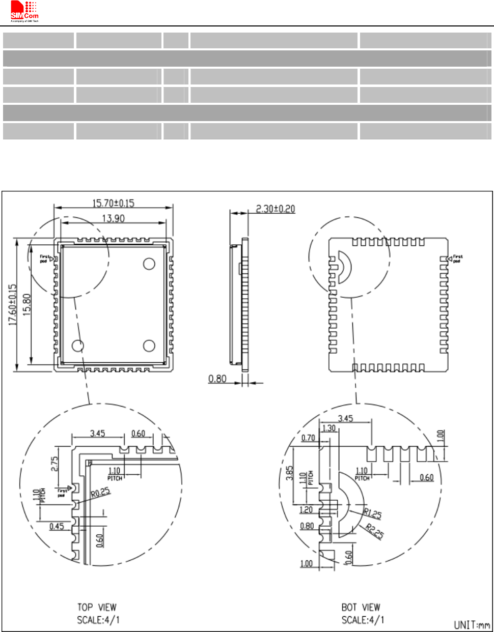
FIGURE 3: DIMENSIONS OF SIM800C (UNIT: MM) ................................................................................................. 15
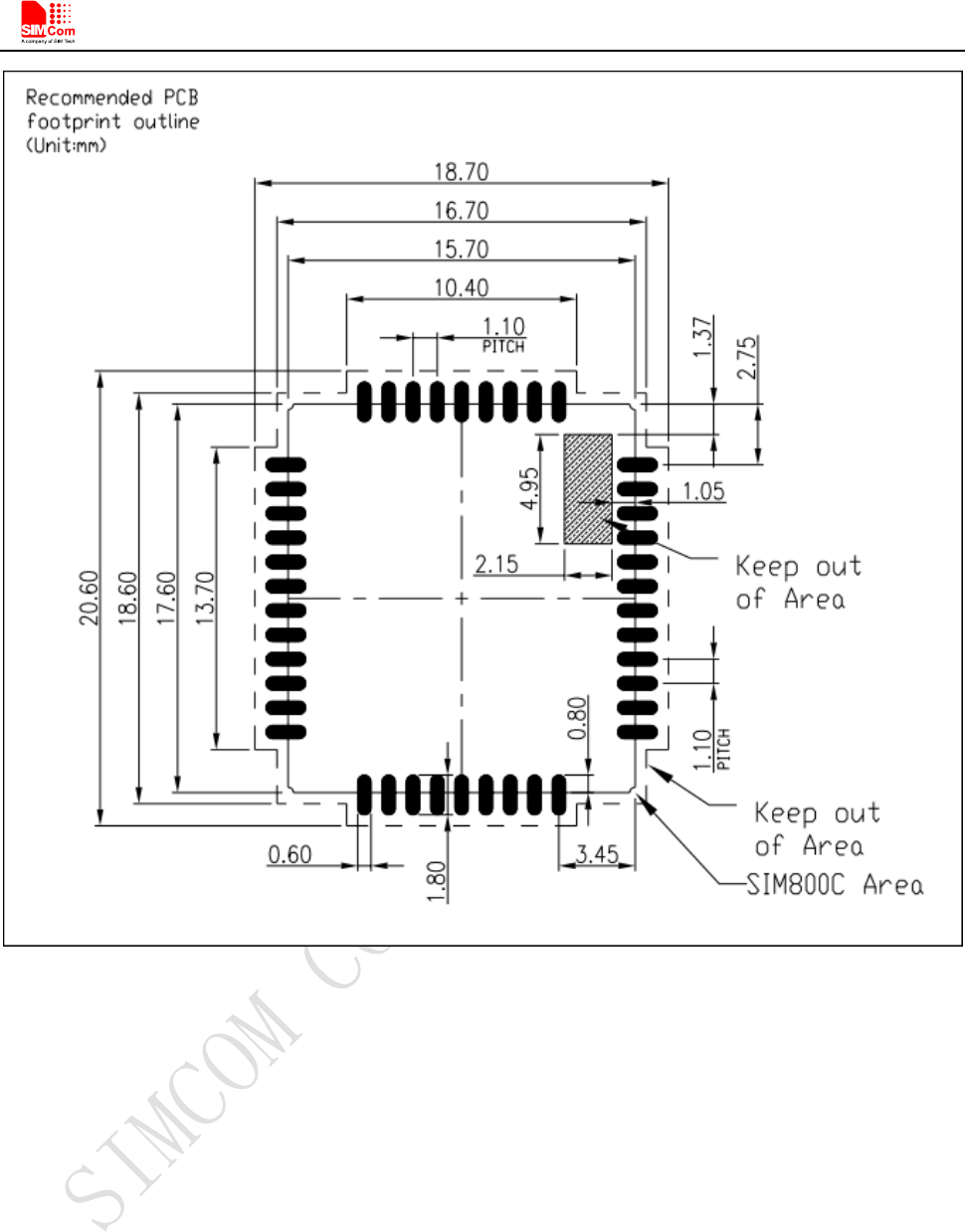
FIGURE 4: RECOMMENDED PCB FOOTPRINT OUTLINE (UNIT: MM) ................................................................ 16
FIGURE 5: REFERENCE CIRCUIT OF THE VBAT INPUT......................................................................................... 17
FIGURE 6: REFERENCE CIRCUIT OF THE LDO POWER SUPPLY ......................................................................... 17
FIGURE 7: REFERENCE CIRCUIT OF THE DC-DC POWER SUPPLY..................................................................... 18
FIGURE 8: VBAT VOLTAGE DROP DURING TRANSMIT BURST........................................................................... 18
FIGURE 9: THE MINIMAL VBAT VOLTAGE REQUIREMENT AT VBAT DROP .................................................... 18
FIGURE 10: POWERED ON/DOWN MODULE USING TRANSISTOR..................................................................... 19
FIGURE 11: POWERED ON/DOWN MODULE USING BUTTON ............................................................................. 19
FIGURE 12: TIMING OF POWER ON MODULE......................................................................................................... 19
FIGURE 13: TIMING OF POWER OFF SIM800C BY PWRKEY ................................................................................20
FIGURE 14: TIMING OF RESTART SIM800C.............................................................................................................. 22
FIGURE 15: RTC SUPPLY FROM CAPACITOR........................................................................................................... 23
FIGURE 16: RTC SUPPLY FROM NON-CHARGEABLE BATTERY ......................................................................... 24
FIGURE 17: RTC SUPPLY FROM RECHARGEABLE BATTERY .............................................................................. 24
FIGURE 18: CONNECTION OF THE SERIAL INTERFACES..................................................................................... 26
FIGURE 19: RESISTOR MATCHING CIRCUIT ........................................................................................................... 26
FIGURE 20 : DIODE ISOLATION CIRCUIT................................................................................................................. 26
FIGURE 21: TX LEVEL MATCHING CIRCUIT ........................................................................................................... 27
FIGURE 22: RX LEVEL MATCHING CIRCUIT........................................................................................................... 27
FIGURE 23: USB REFERENCE CIRCUIT .................................................................................................................... 27
FIGURE 24: CONNECTION FOR SOFTWARE UPGRADING AND DEBUGGING.................................................. 28
FIGURE 25: UART1_RI BEHAVIOUR OF VOICE CALLING AS A RECEIVER ....................................................... 29
FIGURE 26: UART1_RI BEHAVIOUR OF URC OR RECEIVE SMS.......................................................................... 29
FIGURE 27: UART1_RI BEHAVIOUR AS A CALLER................................................................................................. 29
FIGURE 28: SPEAKER REFERENCE CIRCUIT .......................................................................................................... 30
FIGURE 29: MICROPHONE REFERENCE CIRCUIT.................................................................................................. 30
FIGURE 30: REFERENCE CIRCUIT OF THE 8-PIN SIM CARD HOLDER............................................................... 32
FIGURE 31: REFERENCE CIRCUIT OF THE 6-PIN SIM CARD HOLDER............................................................... 32
FIGURE 32: MOLEX 91228 SIM CARD HOLDER ...................................................................................................... 33
FIGURE 33: AMPHENOL C707 10M006 512 SIM CARD HOLDER........................................................................... 34
FIGURE 34: REFERENCE CIRCUIT OF NETLIGHT .................................................................................................. 35
FIGURE 35: RF_SYNC SIGNAL DURING TRANSMIT BURST ................................................................................ 36
FIGURE 36: GSM ANTENNA MATCHING CIRCUIT ................................................................................................. 37
FIGURE 37: GSM ANTENNA MATCHING CIRCUIT WITHOUT RF CONNECTOR ............................................... 37
FIGURE 38: BLUETOOTH ANTENNA MATCHING CIRCUIT .................................................................................. 38
FIGURE 39: PIN ASSIGNMENT.................................................................................................................................... 39
FIGURE 40: TOP AND BOTTOM VIEW OF SIM800C ................................................................................................ 46
FIGURE 41: TYPICAL SOLDER REFLOW PROFILE OF LEAD-FREE PROCESSES.............................................. 46
Smart Machine Smart Decision
SIM800C_Hardware_Design_V1.02 8 2015-4-27
Version History
Date Version Description of change Author
2014-11-06 1.00 Origin Yanwu.wang;
Xiaobo.bai
2015-01-06 1.01
Update figure1,figure12,figure40
Delete figure26
Add VRTC segment to table5
Update table11,table34,table35,table36
Yanwu.wang;
Xiaobo.bai
2015-04-27 1.02
Update figure7,figure10,figure11,figure10,figure12,figure13,
figure14,figure23,figure37,figure38
Update table1,table2
Yanwu.wang;
Xiaobo.bai
Smart Machine Smart Decision
SIM800C_Hardware_Design_V1.02 9 2015-4-27
1. Introduction
This document describes SIM800C hardware interface in great detail. The document can help customer to
quickly understand SIM800C interface specifications, electrical and mechanical details. With the help of this
document and other SIM800C application notes, customer guide, customers can use SIM800C to design various
applications quickly.
2. SIM800C Overview
SIM800C is a quad-band GSM/GPRS module that works on frequencies GSM850MHz, EGSM900MHz,
DCS1800MHz and PCS1900MHz. SIM800C features GPRS multi-slot class10/class12 (optional) and supports
the GPRS coding schemes CS-1, CS-2, CS-3 and CS-4.
With a tiny configuration of 17.6*15.7*2.3mm, SIM800C can meet almost all the space requirements in
customers’ applications, such as smart phone, PDA and other mobile devices.
SIM800C is a SMT package with 42 pads, and provides all hardware interfaces between the module and
customers’ boards.
- One 3 lines serial port and one full modem serial port;
- One USB, the USB interface can debug, download software;
- One audio channel which include a microphone input and a speaker output;
- Programmable general purpose input and output;
- One SIM card interface;
- Support Bluetooth (need software support).
SIM800C is designed with power saving technique so that the current consumption is as low as 0.6mA in sleep
mode.
2.1. SIM800C
Table 1: Module information
SIM800C
GSM 850,900,1800 and 1900MHz
BT (need software support)
FLASH SIM800C (24Mbit)
SIM800C32 (32Mbit)
RAM 32Mbit
2.2. SIM800C Key Features
Table 2: SIM800C key features
Feature Implementation
Power supply 3.4V ~4.4V
Power saving Typical power consumption in sleep mode is 0.88mA (BS-PA-MFRMS=9 )
Frequency bands - Quad-band: GSM 850, EGSM 900, DCS 1800, PCS 1900. SIM800C can

Smart Machine Smart Decision
SIM800C_Hardware_Design_V1.02 10 2015-4-27
search the 4 frequency bands automatically. The frequency bands can also be
set by AT command “AT+CBAND”. For details, please refer to document [1].
- Compliant to GSM Phase 2/2+
Transmitting power
- Class 4 (2W) at GSM 850 and EGSM 900
- Class 1 (1W) at DCS 1800 and PCS 1900
GPRS connectivity
- GPRS multi-slot class 12(default)
- GPRS multi-slot class 1~12 (option)
Temperature range
- Normal operation: -40°C ~ +85°C
- Storage temperature -45°C ~ +90°C
Data GPRS
- GPRS data downlink transfer: max. 85.6 kbps
- GPRS data uplink transfer: max. 85.6 kbps
- Coding scheme: CS-1, CS-2, CS-3 and CS-4
- PAP protocol for PPP connect
- Integrate the TCP/IP protocol.
- Support Packet Broadcast Control Channel (PBCCH)
USSD - Unstructured Supplementary Services Data (USSD) support
SMS
- MT, MO, CB, Text and PDU mode
- SMS storage: SIM card
SIM interface Support SIM card: 1.8V, 3V
External antenna Antenna pad
Audio features
Speech codec modes:
- Half Rate (ETS 06.20)
- Full Rate (ETS 06.10)
- Enhanced Full Rate (ETS 06.50 / 06.60 / 06.80)
- Adaptive multi rate (AMR)
- Echo Cancellation
- Noise Suppression
Serial port and
USB port
Serial port:
- Default one Full modem serial port
- Can be used for AT commands or data stream
- Support RTS/CTS hardware handshake and software ON/OFF flow control
- Multiplex ability according to GSM 07.10 Multiplexer Protocol
- Autobauding supports baud rate from 1200 bps to 115200bps
- upgrading firmware
USB port:
- USB_DN and USB_DP
- Can be used for debugging and upgrading firmware
Phonebook management Support phonebook types: SM, FD, LD, RC, ON, MC
SIM application toolkit GSM 11.14 Release 99
Physical characteristics Size:17.6*15.7*2.3mm
Weight:1.3g
Firmware upgrade Full modern serial port or USB port(recommend to use USB port)
Smart Machine Smart Decision
SIM800C_Hardware_Design_V1.02 11 2015-4-27
Table 3: Coding schemes and maximum net data rates over air interface
Coding scheme 1 timeslot 2 timeslot 4 timeslot
CS-1 9.05kbps 18.1kbps 36.2kbps
CS-2 13.4kbps 26.8kbps 53.6kbps
CS-3 15.6kbps 31.2kbps 62.4kbps
CS-4 21.4kbps 42.8kbps 85.6kbps
2.3. Operating Mode
The table below summarizes the various operating modes of SIM800C.
Table 4: Overview of operating modes
Mode Function
GSM/GPRS
SLEEP
Module will automatically go into sleep mode if the conditions of sleep
mode are enabling and there aren’t on air and hardware interrupt (such as
GPIO interrupt or data on serial port).
In this case, the current consumption of module will reduce to the minimal
level.
In sleep mode, the module can still receive paging message and SMS.
GSM
IDLE
Software is active. Module is registered to the GSM network, and the
module is ready to communicate.
GSM
TALK
Connection between two subscribers is in progress. In this case, the power
consumption depends on network settings such as DTX off/on,
FR/EFR/HR, hopping sequences, antenna.
GPRS
STANDBY
Module is ready for GPRS data transfer, but no data is currently sent or
received. In this case, power consumption depends on network settings and
GPRS configuration.
Normal
operation
GPRS
DATA
There is GPRS data transfer (PPP or TCP or UDP) in progress. In this case,
power consumption is related with network settings (e.g. power control
level); uplink/downlink data rates and GPRS configuration (e.g. used
multi-slot settings).
Power off
Normal power off by sending AT command “AT+CPOWD=1” or using the PWRKEY. The
power management unit shuts down the power supply for the baseband part of the module.
Software is not active. The serial port is not accessible. Power supply (connected to VBAT)
remains applied.
Minimum
functionality
mode
AT command “AT+CFUN” can be used to set the module to a minimum functionality mode
without removing the power supply. In this mode, the RF part of the module will not work
or the SIM card will not be accessible, or both RF part and SIM card will be closed, and the
serial port is still accessible. The power consumption in this mode is lower than normal
mode.
Smart Machine Smart Decision
SIM800C_Hardware_Design_V1.02 12 2015-4-27
2.4. Functional Diagram
The following figure shows a functional diagram of SIM800C:
- GSM baseband
- GSM RF
- Antenna interface
- Other interface
Analog base
band
Digita l base
band
Pow er m anagem ent unit
Radio
Frequency
Power
Supply
Analog Interface Digita l In te rfa c e
UART
SIM
Audio
ADC
GSM
USB
GPIO
BT
RTC
Figure 1: SIM800C functional diagram
Smart Machine Smart Decision
SIM800C_Hardware_Design_V1.02 13 2015-4-27
3. Package Information
3.1. Pin Out Diagram
Figure 2: Pin out Diagram (Top view)
3.2. Pin Description
Table 5: Pin description
Pin name Pin number I/O Description Comment
Power supply
VBAT 34,35 I Power supply
Smart Machine Smart Decision
SIM800C_Hardware_Design_V1.02 14 2015-4-27
VRTC 28 I/O Power supply for RTC
It is recommended to
connect with a battery or a
capacitor (e.g. 4.7uF).
VDD_EXT 40 O 2.8V power output If these pins are unused,
keep open.
GND 8,13,19,21,27,30,
31,33,36,37 Ground GND for VBAT recommend
to use 36,37pin
Power on/down
PWRKEY 39 I
PWRKEY should be pulled low at
least 1 second and then released to
power on/down the module.
Internally pulled up to
VBAT.
Audio interfaces
MICP 9
MICN 10
I Differential audio input
SPKP 11
SPKN 12
O Differential audio output
If these pins are unused,
keep open.
GPIO
NETLIGHT 41 O Network status
STATUS 42 O Power on status
Serial port
UART1_DTR 6 I Data terminal ready
UART1_RI 7 O Ring indicator
UART1_DCD 5 O Data carrier detect
UART1_CTS 4 O Clear to send
UART1_RTS 3 I Request to send
UART1_TXD 1 O Transmit data
UART1_RXD 2 I Receive data
UART2_TXD 22 O Transmit data
UART2_RXD 23 I Receive data
If these pins are unused,
keep open.
Debug interface
USB_VBUS 24 I
USB_DP 25 I/O
USB_DN 26 I/O
Debug and download If these pins are unused,
keep open.
ADC
ADC 38 I 10bit general analog to digital
converter
If these pins are unused,
keep open.
SIM card interface
SIM_VDD 18 O Voltage supply for SIM card.
Support 1.8V or 3V SIM card
SIM_DATA 15 I/O SIM data input/output
SIM_CLK 16 O SIM clock
SIM_RST 17 O SIM reset
All signals of SIM interface
should be protected against
ESD with a TVS diode
array.
SIM_DET 14 I SIM card detection If these pins are unused,
Smart Machine Smart Decision
SIM800C_Hardware_Design_V1.02 15 2015-4-27
keep open.
Antenna interface
GSM_ANT 32 I/O Connect GSM antenna
BT_ANT 20 I/O Connect Bluetooth antenna
Synchronizing signal of RF
RF_SYNC 29 O Synchronizing signal of RF
3.3. Package Dimensions
Figure 3: Dimensions of SIM800C (Unit: mm)
Smart Machine Smart Decision
SIM800C_Hardware_Design_V1.02 16 2015-4-27
Figure 4: Recommended PCB footprint outline (Unit: mm)
Smart Machine Smart Decision
SIM800C_Hardware_Design_V1.02 17 2015-4-27
4. Application Interface
4.1. Power Supply
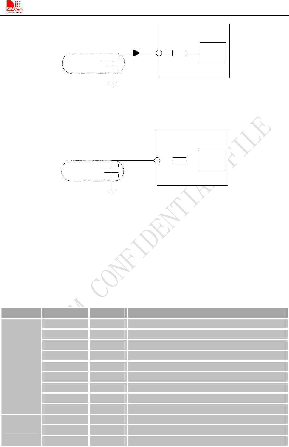
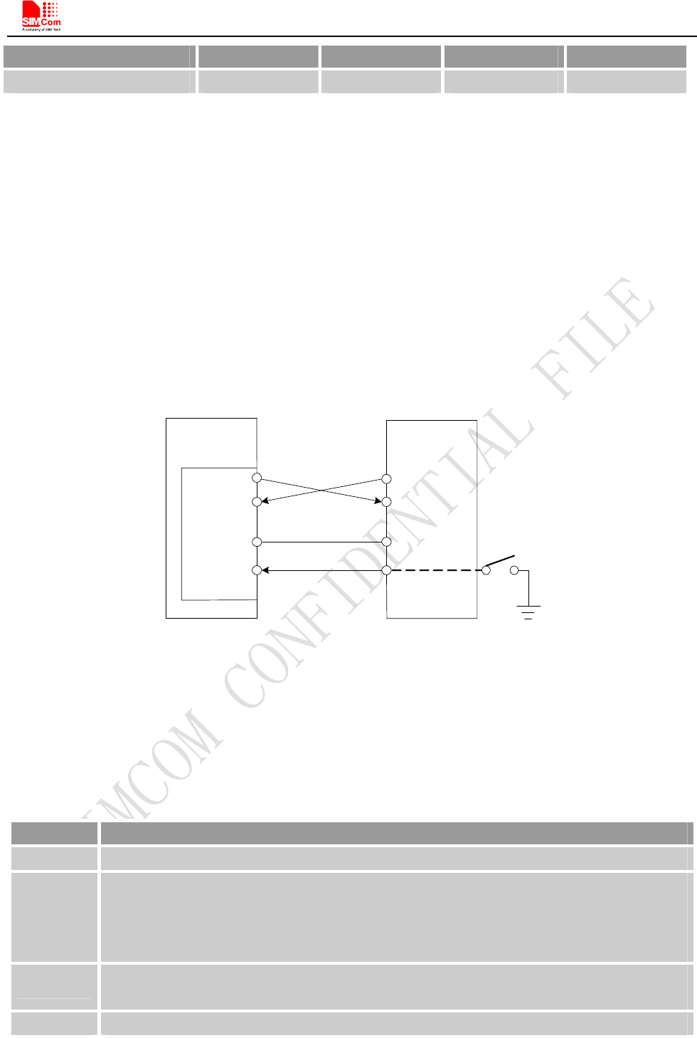
The power supply range of SIM800C is from 3.4V to 4.4V. Recommended voltage is 4.0V. The transmitting
burst will cause voltage drop and the power supply must be able to provide sufficient current up to 2A. For the
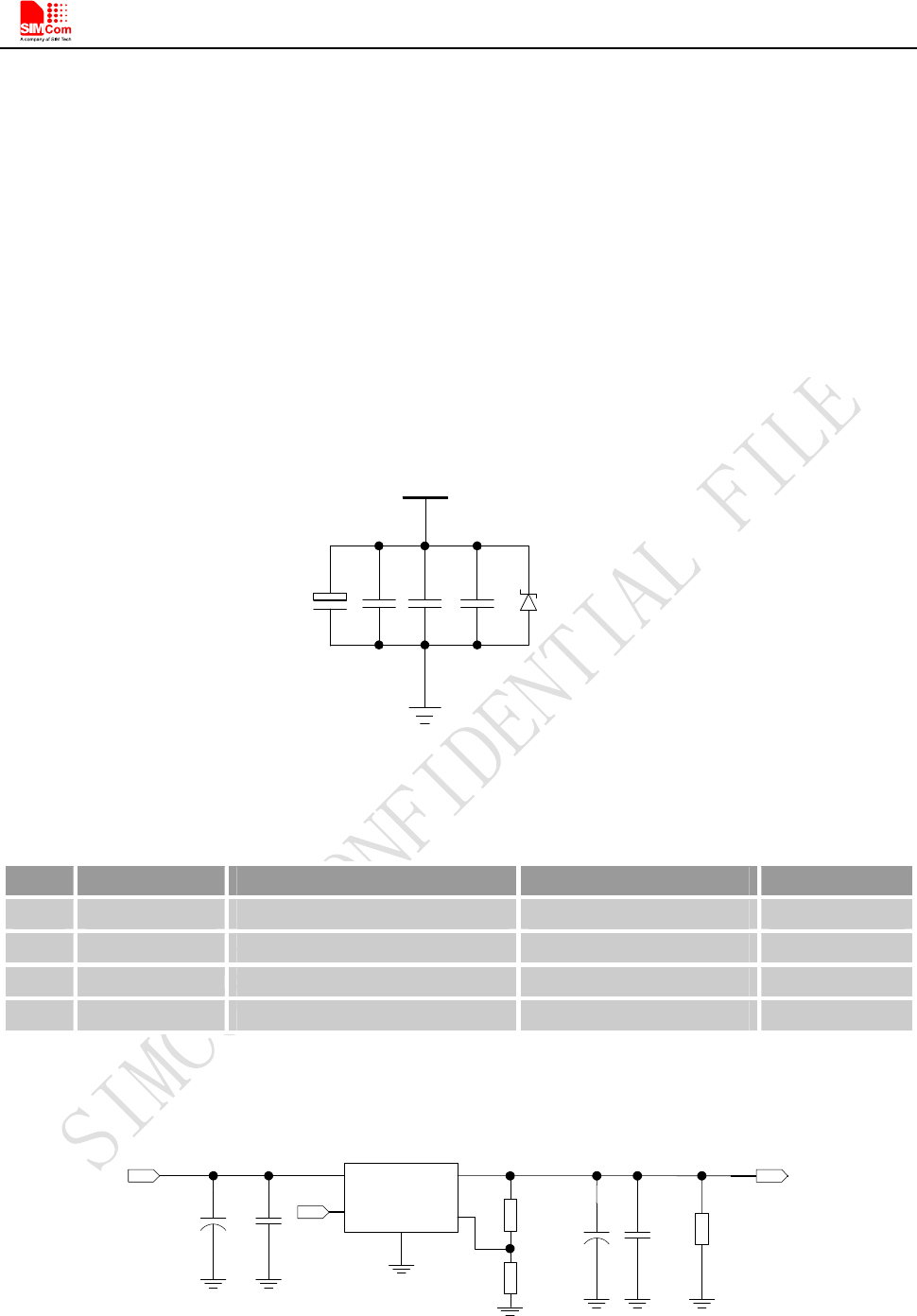
VBAT input, a bypass capacitor (low ESR) such as a 100 µF is strongly recommended.
For the VBAT input, a 100uF Tantalum capacitor (CA low ESR) and a 1uF~10uF Ceramics capacitor CB are
strongly recommended. Increase the 33pF and 10pF capacitors can effectively eliminate the high frequency
interference. A 5.1V/500mW Zener diode is strongly recommended, the diode can prevent chip from damaging
by the voltage surge. These capacitors and Zener diode should be placed as close as possible to SIM800C
VBAT pins.
VBAT
5.1V
500m W
CACB33pF 10pF
Figure 5: Reference circuit of the VBAT input
Table 6: Recommended zener diode
Vendor Part number Power(watts) Packages
1 On semi MMSZ5231BT1G 500mW SOD123
2 Prisemi PZ3D4V2H 500mW SOD323
3 Vishay MMSZ4689-V 500mW SOD123
4 Crownpo CDZ55C5V1SM 500mW 0805
The following figure is the reference design of +5V input power supply. The output power supply is 4.1V, thus a
linear regulator can be used.
VinVout
GND
FB
3
+
PW R_CTRL
R 102
R 101
VBAT
100K
43K
+C103
330uF
C104
100nF
U101 M IC 29302
5
4
1
2
C101 C102
100uF 1uF
DC INPUT
R103
470Ω
O n /O ff
Figure 6: Reference circuit of the LDO power supply
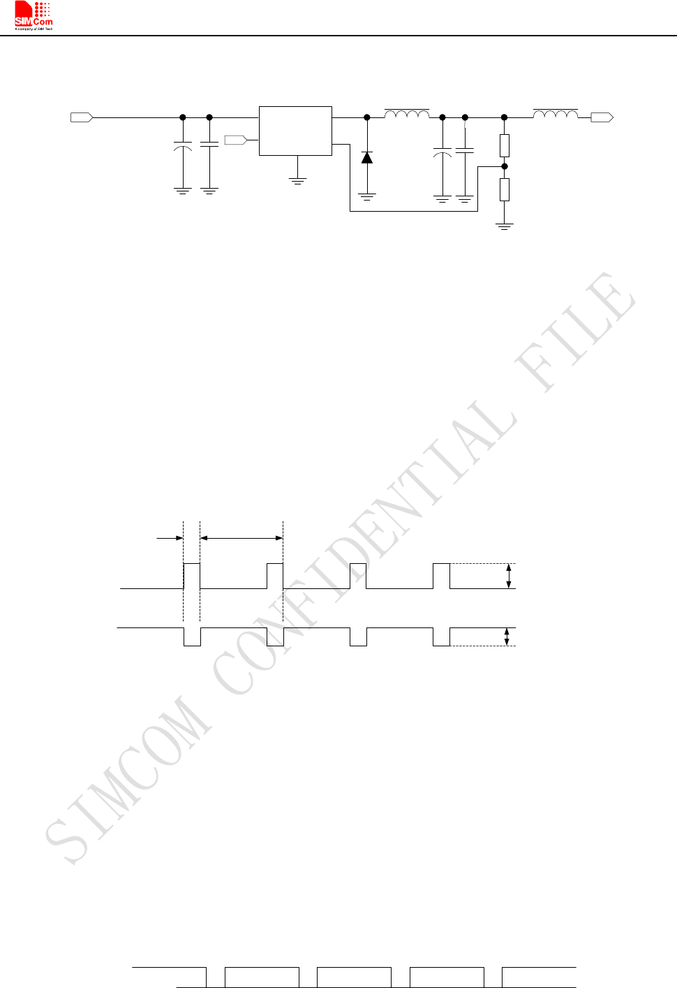
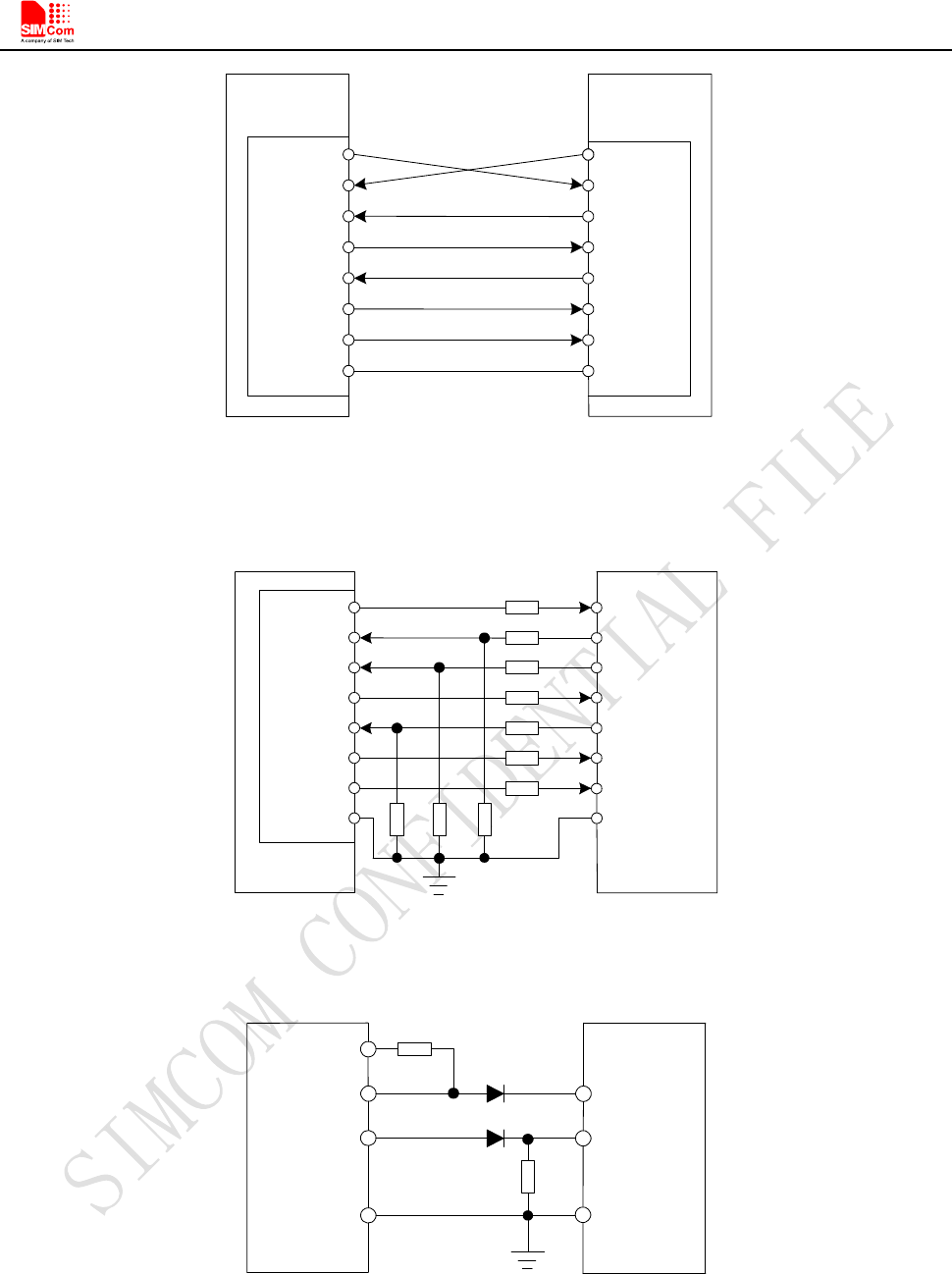
If there is a high drop-out between the input and the desired output (VBAT), a DC-DC power supply will be
preferable because of its better efficiency especially with the 2A peak current in burst mode of the module. The
Smart Machine Smart Decision
SIM800C_Hardware_Design_V1.02 18 2015-4-27
following figure is the reference circuit.
VinVout
FB
U101
12
3
4
5
LM 2596-A D J
+
100uH
MBR360
L101
C 101 +C 102
D 102 C 103
R 102
R 101
FB 101
330uF
VBAT
2.2K
1K
100uF 1uF
C 104
100nF
270
DC input
PW R_CTRL
GND
Ω
O n /O ff
Figure 7: Reference circuit of the DC-DC power supply
The single 3.7V Li-ion cell battery can be connected to SIM800C VBAT pins directly. But the Ni-Cd or Ni-MH
battery must be used carefully, since their maximum voltage can rise over the absolute maximum voltage of the
module and damage it.
When battery is used, the total impedance between battery and VBAT pins should be less than 150m.
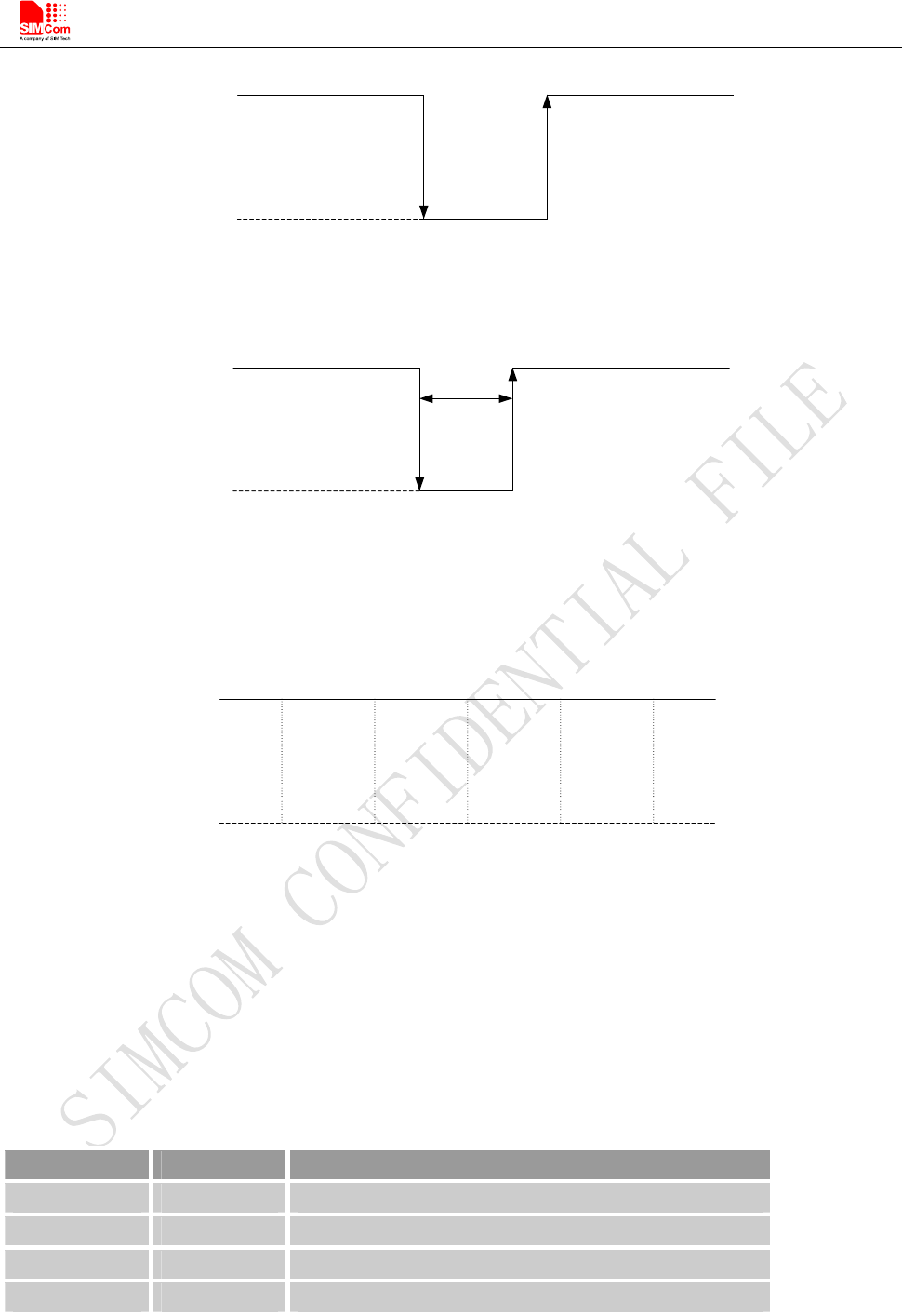
The following figure shows the VBAT voltage drop at the maximum power transmit phase, and the test condition
is as following:
VBAT=4.0V,
A VBAT bypass capacitor CA=100µF tantalum capacitor (ESR=0.7),
Another VBAT bypass capacitor CB=1uF~10uF.
577us 4.615m s
B u rs t:2 A
I
VBAT
VBAT
M ax:350m V
Figure 8: VBAT voltage drop during transmit burst
4.1.1. Power Supply Pin
Pin34 and Pin35 are VBAT input, Pin36 and Pin37 are GND of power supply, and VRTC pin is power supply of
the RTC circuit in the module. VDD_EXT output 2.8V when module is in normal operation mode.
When designing the power supply in customers’ application, pay special attention to power losses. Ensure that
the input voltage never drops below 3.0V even when current consumption rises to 2A in the transmit burst. If the
power voltage drops below 3.0V, the module may be shut down automatically. The PCB traces from the VBAT
pins to the power supply must be wide enough (at least 60mil) to decrease voltage drops in the transmit burst.
The power IC and the bypass capacitor should be placed to the module as close as possible.
VBAT
MIN:3.0V
Figure 9: The minimal VBAT voltage requirement at VBAT drop
Note: Hardware power off voltage is 3.0V.
Smart Machine Smart Decision
SIM800C_Hardware_Design_V1.02 19 2015-4-27
4.1.2. Monitoring Power Supply
AT command “AT+CBC” can be used to monitor the VBAT voltage. For detail, please refer to document [1].
4.2. Power on/off SIM800C
4.2.1. Power on SIM800C
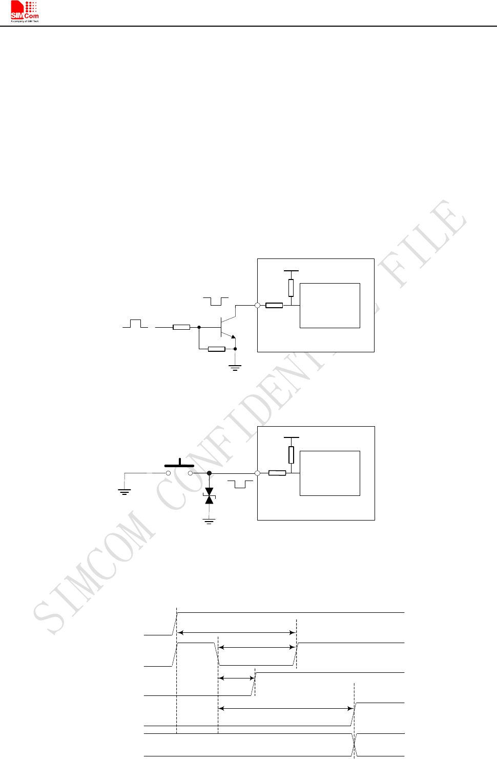
Customer can power on SIM800C by pulling down the PWRKEY pin for at least 1 second and release. This pin
is already pulled up to VBAT in the module internal, so external pull up is not necessary. Reference circuits are
shown as below.
4.7K
47K
T u rn o n /o ff
impulse
PW RKEY Power
o n /o ff logic
100K
3V
Module
1K
Figure 10: Powered on/down module using transistor
PW RKEY Power
on/off logic
100K
3V
M odule
1K
Figure 11: Powered on/down module using button
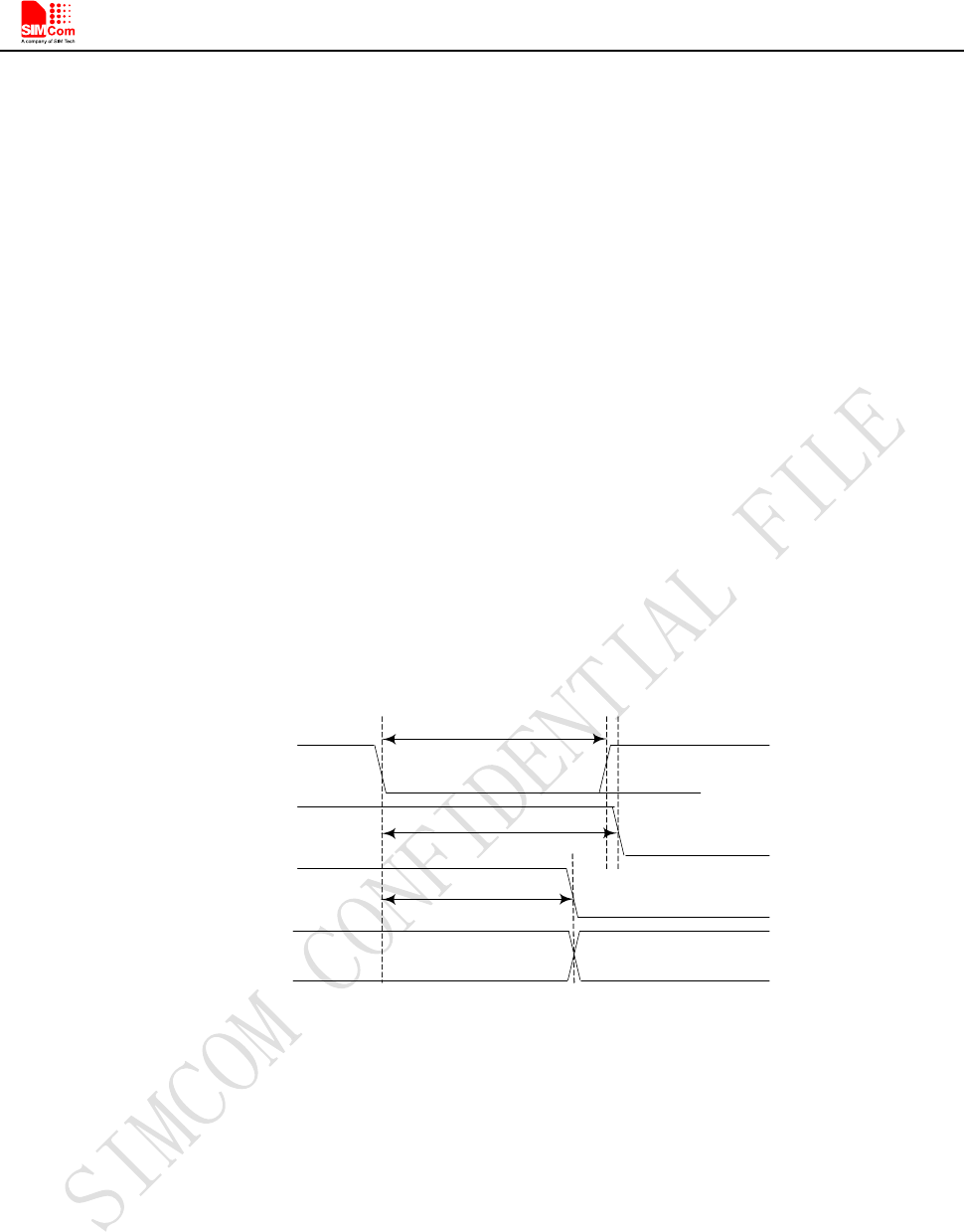
The power on timing is illustrated as in the following figure.
VIL <0.7V
U ndefind Active
VBAT
PW RKEY
(INPUT)
t> 3 s
VDD_EXT
STATUS
t> 1 s
Serial P o rt
T>1.5s
T>55m s
Figure 12: Timing of power on module
Smart Machine Smart Decision
SIM800C_Hardware_Design_V1.02 20 2015-4-27
When power on procedure is completed, SIM800C will send following URC to indicate that the module is ready
to operate at fixed baud rate.
RDY
This URC does not appear when autobauding function is active.
Note: Customer can use AT command “AT+IPR=x” to set a fixed baud rate and save the configuration to
non-volatile flash memory. After the configuration is saved as fixed baud rate, the Code “RDY” should be
received from the serial port every time when SIM800C is powered on. For details, please refer to the chapter
“AT+IPR” in document [1].
4.2.2. Power off SIM800C
SIM800C will be powered off in the following situations:
- Normal power off procedure: power off SIM800C by the PWRKEY pin.
- Normal power off procedure: power off SIM800C by AT command “AT+CPOWD=1”.
- Abnormal power off: over-voltage or under-voltage automatic power off.
- Abnormal power off: over-temperature or under-temperature automatic power off.
4.2.2.1. Power off SIM800C by the PWRKEY Pin
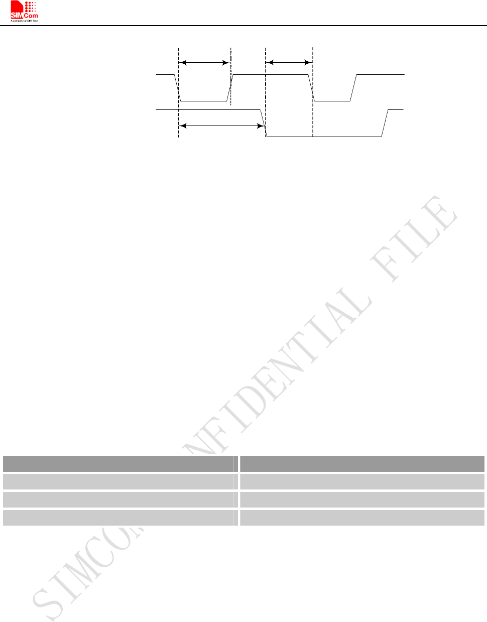
Customer can power off SIM800C by pulling down the PWRKEY pin for at least 1 second and release. Please
refer to the power on circuit. The power off timing is illustrated in the following figure.
PW RKEY
VDD_EXT
STATUS
VIL <0.7V
Serial port UndifinedActive
(input)
T3=2s
1s<T1<33s
T2≥2s
Figure 13: Timing of power off SIM800C by PWRKEY
Note:
1. the module will restart after pull down the pwrkey over 33 seconds.
2. VDD_EXT will power off after STATUS change into low level and the PWRKEY release 55ms..
If 1s<T1<2s
,
T2>2s
;
If 2s
≤
T1<33s
,
T2>T1+55ms
This procedure makes the module log off from the network and allows the software to enter into a secure state to
save data before completely shut down.
Before the completion of the power off procedure, the module will send URC:
NORMAL POWER OFF
At this moment, AT commands can not be executed any more. Power off mode can also be indicated by STATUS
pin, which is at low level at this time.
4.2.2.2. Power off SIM800C by AT Command

Smart Machine Smart Decision
SIM800C_Hardware_Design_V1.02 21 2015-4-27
SIM800C can be powered off by AT command “AT+CPOWD=1”. This procedure makes the module log off from
the network and allows the software to enter into a secure state to save data before completely shut down.
Before the completion of the power off procedure, the module will send URC:
NORMAL POWER OFF
At this moment, AT commands can not be executed any more. Power off mode can also be indicated by STATUS
pin, which is at low level at this time.
For detail about AT command “AT+CPOWD”, please refer to document [1].
4.2.2.3. Over-Voltage or Under-Voltage Power off
The module software monitors the VBAT voltage constantly.
If the voltage 3.5V, the following URC will be reported:
UNDER-VOLTAGE WARNNING
If the voltage 4.3V, the following URC will be reported:
OVER-VOLTAGE WARNNING
If the voltage < 3.4V, the following URC will be reported, and the module will be automatically powered off.
UNDER-VOLTAGE POWER OFF
If the voltage > 4.4V, the following URC will be reported, and the module will be automatically powered off.
OVER-VOLTAGE POWER OFF
At this moment, AT commands can not be executed any more. Power off mode can also be indicated by STATUS
pin, which is at low level at this time.
4.2.2.4. Over-Temperature or Under-Temperature Power off
The module will constantly monitor the temperature of the module,
If the temperature +80℃, the following URC will be reported:
+CMTE: 1
If the temperature -30℃, the following URC will be reported:
+CMTE:-1
If the temperature > +85℃, the following URC will be reported, and the module will be automatically powered
off.
+CMTE: 2
If the temperature < -40℃, the following URC will be reported, and the module will be automatically powered
off.
+CMTE:-2
At this moment, AT commands can not be executed any more. Power off mode can also be indicated by STATUS
pin, which is at low level at this time.
Note
:
The default temperature detect is disable, AT command “AT+CMTE” could be used to read the
temperature when the module is running.For details please refer to document [1].
4.2.2.5. Restart SIM800C by PWRKEY Pin:
When the module works normally, if the customer wants to restart the module, follow the procedure below:
1) Power off the module.
2) Wait for at least 800ms after STATUS pin changed to low level.
Smart Machine Smart Decision
SIM800C_Hardware_Design_V1.02 22 2015-4-27
3) Power on the module.
PW RKEY
T2≥2s
STATUS
T3>800m s
1s<T1<2s
Figure 14: Timing of restart SIM800C
4.3. Power Saving Mode
SIM800C has two power saving modes: Minimum functionality mode and sleep mode. AT command
“AT+CSCLK=1”can be used to set SIM800C into sleep mode. AT command “AT+CFUN=<fun>“can be used to
set SIM800C into minimum functionality. When SIM800C is in sleep mode and minimum functionality mode,
the current of module is lowest.
4.3.1. Minimum Functionality Mode
There are three functionality modes, which could be set by AT command “AT+CFUN=<fun>“. The command
provides the choice of the functionality levels <fun>=0, 1, 4.
- AT+CFUN=0: Minimum functionality.
- AT+CFUN=1: Full functionality (default).
- AT+CFUN=4: Flight mode (disable RF function).
Table 7: The current consumption of Function Mode
<fun> Current consumption(mA) (sleep mode)
0 0.6
1 0.88
4 0.65
Minimum functionality mode minimizes the current consumption to the lowest level. If SIM800C is set to
minimum functionality by “AT+CFUN=0”, the RF function and SIM card function will be disabled. In this
case, the serial port is still accessible, but partial AT commands and correlative to RF function and SIM card
function will not be accessible.
For detailed information about AT command “AT+CFUN=<fun>“, please refer to document [1].
4.3.2. Sleep Mode 1 (AT+CSCLK=1)
Customer can control SIM800C module to enter or exit the sleep mode (AT+CSCLK=1) by DTR signal. When
DTR is in high level and without interrupt (on air and hardware such as GPIO interrupt or data in serial port),
SIM800C will enter sleep mode automatically. In this mode, SIM800C can still receive paging or SMS from
network but the serial port is not accessible.
Smart Machine Smart Decision
SIM800C_Hardware_Design_V1.02 23 2015-4-27
4.3.3. Wake Up SIM800C from Sleep Mode 1
When SIM800C is in sleep mode 1(AT+CSCLK=1), the following methods can wake up the module:
- Pull down DTR pin.
The serial port will be active after DTR pin is pulled to low level for about 50ms.
- Receive a voice or data call from network.
- Receive a SMS from network.
- Receive external interrupt.
Note: After module has received incoming call or new SMS, serial port can report URC, but the serial port can
not input AT command. Only after the DTR pin is pulled to low level for 50ms, the serial port can input AT
command.
4.3.4. Sleep Mode 2 (AT+CSCLK=2)
In this mode, SIM800C will continuously monitor the serial port data signal. When there is no data transfer over 5
seconds on the RXD signal and there is no on air and hardware interrupts (such as GPIO interrupt), SIM800C will
enter sleep mode 2 automatically. In this mode, SIM800C can still receive paging or SMS from network.
4.3.5. Wake Up SIM800C from Sleep Mode 2
When SIM800C is in sleep mode 2 (AT+CSCLK=2), the following methods can wake up the module:
- Send data to SIM800C via main serial port (the first character will lose).
- Receive a voice or data call from network.
- Receive a SMS from network.
Note: Autobauding is default. It cannot enter sleep mode in the absence of synchronous serial port baud rate
after module power on.
4.4. Power Saving Mode
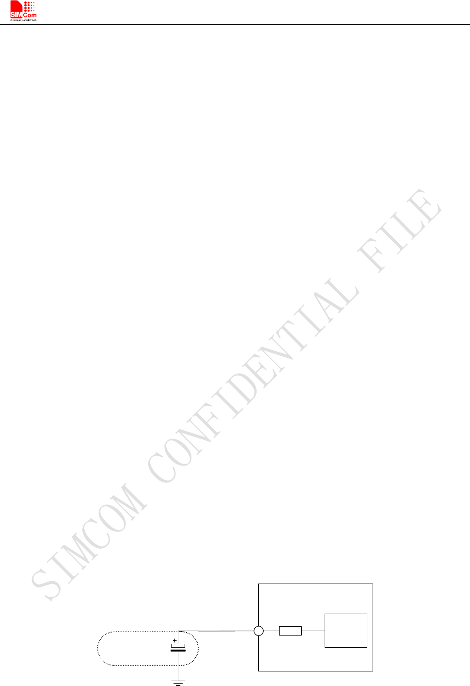
Current input for RTC when the VBAT is not supplied for the system. Current output for backup battery when
the VBAT power supply is in present and the backup battery is in low voltage state. The RTC power supply of
module can be provided by an external capacitor or a battery (non-chargeable or rechargeable) through the VRTC.
The following figures show various reference circuits for RTC back up.
- External capacitor backup
RTC
Core
1.5K
M odule
VRTC
Large-capacita n c e
C apacito r
Figure 15: RTC supply from capacitor
- Non-chargeable battery backup
Smart Machine Smart Decision
SIM800C_Hardware_Design_V1.02 24 2015-4-27
RTC
Core
1.5K
M odule
VRTC
N on-chargeable
B a c k u p B a tte ry
Figure 16: RTC supply from non-chargeable battery
- Rechargeable battery backup
RTC
Core
1.5K
Module
VRTC
R echargeable
B a c k u p B a tte ry
Figure 17: RTC supply from rechargeable battery
Note: When shut off VBAT and power on VRTC only, the clock error becomes larger.
4.5. Serial Port and USB Interface
SIM800C default provides one unbalanced asynchronous serial ports. The module is designed as a DCE (Data
Communication Equipment). The following figure shows the connection between module and client (DTE).
Table 8: Serial port and USB pin definition
Note: Hardware flow control is disabled by default. AT command “AT+IFC=2, 2”can enable hardware flow
Pin name Pin number Function
UART1_DTR 6 Data terminal ready
UART1_RI 7 Ring indicator
UART1_DCD 5 Data carrier detect
UART1_CTS 4 Clear to send
UART1_RTS 3 Request to send
UART1_TXD 1 Transmit data
UART1_RXD 2 Receive data
UART2_TXD 22 Transmit data
Serial port
UART2_RXD 23 Receive data
USB_VBUS 24 USB power supply
USB_DP 25 D+ data input/output
Debug port
USB_DN 26 D- data input/output
Smart Machine Smart Decision
SIM800C_Hardware_Design_V1.02 25 2015-4-27
control. AT command “AT+IFC=0,0”can disable hardware flow control. For more details please refer to
document [1].
Table 9: Serial port characteristics
Symbol Min Max Unit
VIL -0.3 0.7 V
VIH 2.1 3.1 V
VOL - 0.4 V
VOH 2.4 - V
4.5.1 Function of Serial Port
Serial port:
- Full mode device.
- Contain data lines UART1_TXD/UART1_RXD, hardware flow control lines UART1_RTS/UART1_CTS,
status lines UART1_DTR、UART1_DCD and UART1_RI.
- Serial port can be used for GPRS service and AT communication. It can also be used for multiplexing
function. For details about multiplexing function, please refer to table 11.
- Autobauding supports the following baud rates:
1200, 2400, 4800, 9600, 19200, 38400, 57600 and 115200bps
Autobauding allows SIM800C to automatically detect the baud rate of the host device. Pay more attention to the
following requirements:
- Synchronization between DTE and DCE:
When DCE powers on with autobauding enabled, it is recommended to send "AT" or "at" or "aT" or "At"
to synchronize the baud rate, until DTE receives the "OK" response, which means DTE and DCE are
correctly synchronized. For more information please refer to AT command "AT+IPR".
- Restrictions of autobauding operation:
The DTE serial port must be set at 8 data bits, no parity and 1 stop bit.
The URC such as "RDY", "+CFUN: 1" and "+CPIN: READY” will not be reported.
Note: Customer can use AT command “AT+IPR=x” to set a fixed baud rate and the setting will be saved to
non-volatile flash memory automatically. After the configuration is set as fixed baud rate, the URC such as
"RDY", "+CFUN: 1" and "+CPIN: READY” will be reported when SIM800C is powered on.
4.5.2 Serial Interfaces
The following figure shows the connection between module and client (DTE).
Smart Machine Smart Decision
SIM800C_Hardware_Design_V1.02 26 2015-4-27
UART1_TXD
UART1_RXD
UART1_RTS
UART1_CTS
UART1_DTR
UART1_DCD
UART1_RI
TXD
RXD
RTS
CTS
DTR
DCD
RING
Serial P o rt Serial P o rt
Module(D C E ) C ustom er(D TE)
GND GND
Figure 18: Connection of the serial interfaces
If the voltage of UART is 3.3V, the following reference circuits are recommended. If the voltage is 3.0V, please
change the resistors in the following figure from 5.6K to 14K.
1K
5.6K
RXD
TXD
RTS
CTS
GPIO
GPIO
EINT
DTE
(3 .3 V )
5.6K
5.6K
1K
1K
1K
1K
1K
1K
Module
UART1_TXD
UART1_RXD
UART1_RTS
UART1_CTS
UART1_DTR
UART1_DCD
UART1_RI
GND GND
Figure 19: Resistor matching circuit
If the voltage of UART is 3V or3.3V, the following reference circuits are recommended:
UART1_TXD RXD
M oduleDTE
TXDUART1_RXD
VDD_EXT
10K
10K
GND GND
Figure 20 : Diode isolation circuit
Note: please make sure the minimum of client high limit should be less than 2.8V minus the diode drop.
If the voltage of UART is 5V, the following reference circuits are recommended:
Smart Machine Smart Decision
SIM800C_Hardware_Design_V1.02 27 2015-4-27
VDD_EXT
4.7K
47K
UART1_TXD
4.7K
Module
VDD_EXT
RXD
VDD
DTE
Figure 21: TX level matching circuit
VDD_EXT
4.7K
47K
4.7K
DTE
UART1_RXD
M odule
VDD_EXT
TXD
VDD
Figure 22: RX level matching circuit
4.5.3 Debug Interface
SIM800C could achieve software debug function through USB interface. When powering on the module,
connect USB_VBUS, USB_DP, USB_DN, and GND to PC, then install the driver following the prompts, a
UART port could be recognized by PC, customer could achieve the software Debug with this UART port.
SIMCom recommended the following connected diagram:
MODULE USB
USB_DP
USB _ DN USB _ DN
GND
GND
22R
USB _ DP
USB_VBUS VBUS
22 R
1uF
Figure 23: USB reference circuit
The TVS on USB data line should be less than 5pF, and traced by differential forms.
Note: please reserve the USB interface or test point for the further debugging
Table 10: USB_VBUS operation voltage
Smart Machine Smart Decision
SIM800C_Hardware_Design_V1.02 28 2015-4-27
Pin Min Typ Max Unit
USB_VBUS 4.3 5.0 7.0 V
4.5.4 Software Upgrade
Customer could upgrade module’s firmware through USB or UART interface.
If upgrading through USB interface, it is necessary to power on SIM800C first, and then connect USB_VBUS,
USB_DP, USB_DN, and GND to PC. There is no need to operate PWRKEY pin in the whole procedure, when
SIM800C detects USB_VBUS and could communicate normally with USB_DP and USB_DN, it will enter USB
download mode automatically.
If customer upgrades the software through UART interface, it is strongly recommended to lead the UART1_TXD,
UART1_RXD, GND and PWRKEY pin to IO connector for the upgrading, and PWRKEY pin should connect to
GND while upgrading. Refer to the following figure for debugging and upgrading software.
UART1_TXD
M odule(D C E)
UART1_RXD
GND
PW RKEY
TXD
RXD
GND
Serial P o rt
PW RKEY
I/O C onnector
Figure 24: Connection for software upgrading and debugging
The UART interface supports the CMOS level. If customer connects the module to the computer, the level shifter
should be added between the DCE and DTE.
4.6. UART1_RI Behaviors
Table 11: RI behaviors
State RI response
Standby High
Voice call
The pin is changed to low. When any of the following events occur, the pin will be changed to
high:
(1)Establish the call
(2)Hang up the call
SMS The pin is changed to low, and kept low for 120ms when a SMS is received. Then it is changed
to high.
Others For more details, please refer to document [2].
The behavior of the RI pin is shown in the following figure when the module is used as a receiver.
Smart Machine Smart Decision
SIM800C_Hardware_Design_V1.02 29 2015-4-27
HIGH
LO W
Id leRing
H ang up the call
Establish the call
RI
Figure 25: UART1_RI behaviour of voice calling as a receiver
HIGH
LO W
Id le
RI
120m s
Receive S M S
URC
Figure 26: UART1_RI behaviour of URC or receive SMS
However, if the module is used as caller, the UART1_RI will remain high. Please refer to the following figure.
HIGH
LO W
Id leRing Establish
th e c a ll
H ang up
th e c a ll
Id le
RI
Figure 27: UART1_RI behaviour as a caller
4.7. Audio Interfaces
SIM800C provides an analog input (MICP; MICN), which could be used for electret microphone. The module
also provides an analog output (SPKP; SPKN).
Table 12: Audio interface definition
SPKP/SPKN output can directly drive 32 receiver.
AT command “AT+CMIC” is used to adjust the input gain level of microphone. AT command “AT+SIDET”
is used to set the side-tone level. In addition, AT command “AT+CLVL” is used to adjust the output gain level.
For more details, please refer to document [1].
Pin name Pin number Function
MICP 9 Audio input positive
MICN 10 Audio input negative
SPKP 11 Audio output positive
SPKN 12 Audio output negative
Smart Machine Smart Decision
SIM800C_Hardware_Design_V1.02 30 2015-4-27
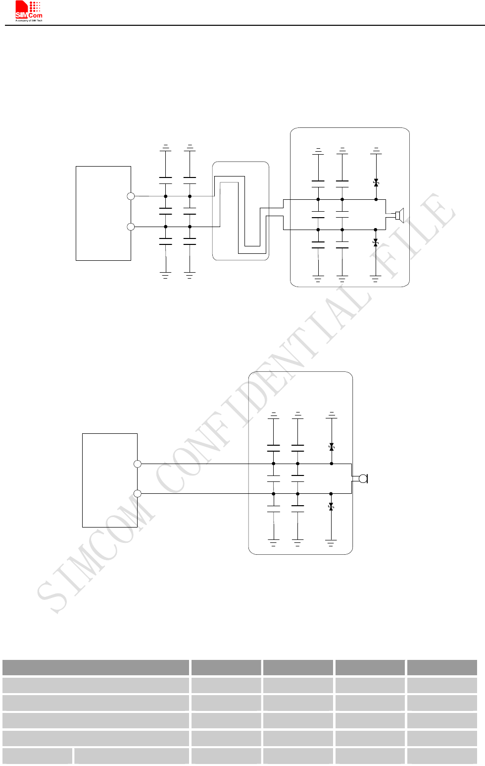
In order to improve audio performance, the following reference circuits are recommended. The audio signals
have to be layout according to differential signal layout rules as shown in following figures.
4.7.1. Speaker Interfaces Configuration
SPKP
Close to speaker
ESD
ESD
10pF
33pF
33pF
33pF
M odule
SPKN
10pF
10pF
10pF
33pF
33pF
33pF
10pF
10pF
Figure 28: Speaker reference circuit
4.7.2. Microphone Interfaces Configuration
Electret
Microphone
The lines in bold type should
be accorded to differential
signal layout rules
These components should
be placed to microphone
as close as possible
MICP
M odule
MICN
ESD
ESD
10pF
33pF
33pF
33pF
10pF
10pF
Figure 29: Microphone reference circuit
4.7.3. Audio Electronic Characteristic
Table 13: Microphone input characteristics
Parameter Min Typ Max Unit
Microphone biasing voltage - 1.9 2.2 V
Working current - - 2.0 mA
Input impedance(differential) 13 20 27 K
Idle channel noise - - -67 dBm0
SINAD Input level:-40dBm0 29 - - dB
Smart Machine Smart Decision
SIM800C_Hardware_Design_V1.02 31 2015-4-27
Input level:0dBm0 - 69 - dB
Table 14: Audio output characteristics
Parameter Conditions Min Typ Max Unit
Normal output RL=32 receiver - 15 90 mW
4.7.4. TDD
Audio signal could be interferenced by RF signal. Coupling noise could be filtered by adding 33pF and 10pF
capacitor to audio lines. 33pF capacitor could eliminate noise from GSM850/EGSM900MHz, while 10pF
capacitor could eliminate noise from DCS1800/PCS1900Mhz frequency. Customer should develop this filter
solution according to field test result.
GSM antenna is the key coupling interfering source of TDD noise. Thereat, pay attention to the layout of audio
lines which should be far away from RF cable, antenna and VBAT pin. The bypass capacitor for filtering should
be placed near module and another group needs to be placed near to connector.
Conducting noise is mainly caused by the VBAT drop. If audio PA was powered by VBAT directly, then there
will be some cheep noise from speaker output easily. So it is better to put big capacitors and ferrite beads near
audio PA input.
TDD noise has something to do with GND signal. If GND plane is not good, lots of high-frequency noises will
interference microphone and speaker over bypass capacitor. So a good GND during PCB layout could avoid
TDD noise.
4.8. SIM Card Interface
The SIM interface complies with the GSM Phase 1 specification and the new GSM Phase 2+ specification for
FAST 64kbps SIM card. Both 1.8V and 3.0V SIM card are supported. The SIM interface is powered from an
internal regulator in the module.
4.8.1. SIM Card Application
Table 15: SIM pin definition
Pin name Pin number Function
SIM_VDD 18 Voltage supply for SIM card. Support 1.8V or 3V SIM card
SIM_DATA 15 SIM data input/output
SIM_CLK 16 SIM clock
SIM_RST 17 SIM reset
SIM_DET 14 SIM card detection
It is recommended to use an ESD protection component such as ST (www.st.com ) ESDA6V1-5W6 or ON
SEMI (www.onsemi.com ) SMF05C. The SIM card peripheral components should be placed close to the SIM
card holder. The reference circuit of the 8-pin SIM card holder is illustrated in the following figure.
Smart Machine Smart Decision
SIM800C_Hardware_Design_V1.02 32 2015-4-27
M odule
PRESENCE
100nF
M O LEX -91228
SIM Card
22pF
VCC GND
RST VPP
CLK I/O
GND
VDD_EXT
SIM _VDD
SIM _RST
SIM _CLK
SIM _DATA
4.7K
ESDA6V1
SIM _DET
51Ω
51Ω
51Ω
Figure 30: Reference circuit of the 8-pin SIM card holder
The SIM_DET pin is used for detection of the SIM card hot plug in. Customer can select the 8-pin SIM card
holder to implement SIM card detection function. AT command “AT+CSDT” is used to enable or disable SIM
card detection function. For details of this AT command, please refer to document [1].
If the SIM card detection function is not used, customer can keep the SIM_DET pin open. The reference circuit
of 6-pin SIM card holder is illustrated in the following figure.
Module
SIM Card
VCC GND
RST VPP
CLK I/O
C 707 10M 006 512 2
22pF 100nF
SIM _VDD
SIM _RST
SIM _CLK
SIM _DATA
SIM _DET
ESDA6V1
51Ω
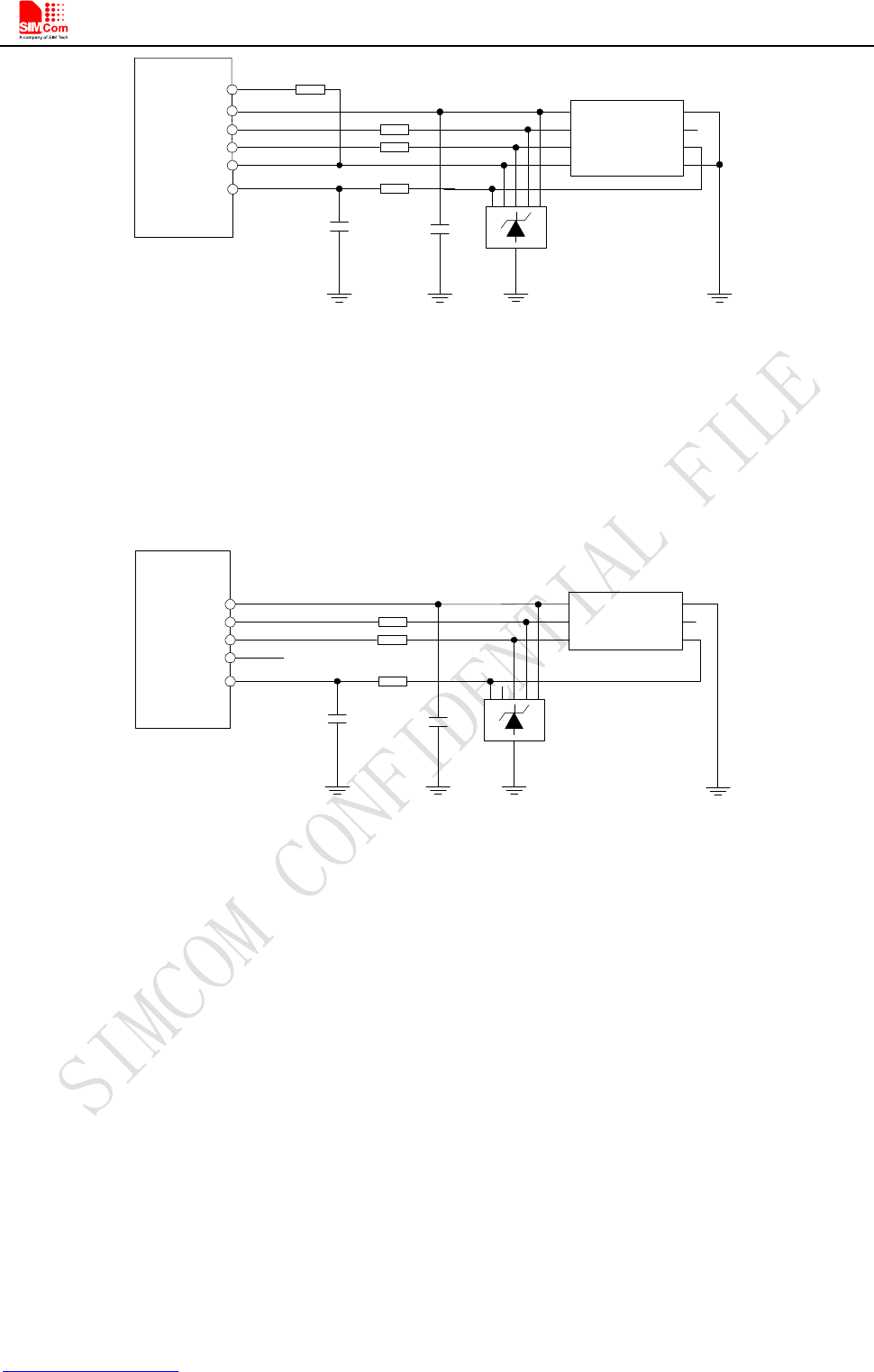
51Ω
51Ω
Figure 31: Reference circuit of the 6-pin SIM card holder
4.8.2. SIM Card Design Guide
SIM card signal could be interferenced by some high frequency signal, it is strongly recommended to follow
these guidelines while designing:
- SIM card holder should be far away from GSM antenna
- SIM traces should keep away from RF lines, VBAT and high-speed signal lines
- The traces should be as short as possible
- Keep SIM card holder’s GND connect to main ground directly
- Shielding the SIM card signal by ground well
- Recommended to place a 100nF capacitor on SIM_VDD line and keep close to the SIM card holder
- Add some TVS which parasitic capacitance should not exceed 50pF
- Add 51 resistor to (SIM_RST/SIM_CLK/SIM_DATA) signal could enhance ESD protection
4.8.3. Design Considerations for SIM Card Holder
For 8 pins SIM card holder, SIMCom recommends to use Molex 91228.Customer can visit
http://www.molex.com for more information about the holder.
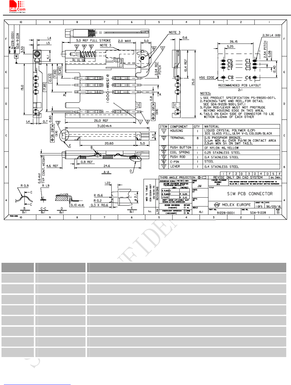
Smart Machine Smart Decision
SIM800C_Hardware_Design_V1.02 33 2015-4-27
Figure 32: Molex 91228 SIM card holder
Table 16: Pin description (Molex SIM card holder)
Pin name Signal Description
C1 SIM_VDD SIM card power supply
C2 SIM_RST SIM card reset
C3 SIM_CLK SIM card clock
C4 GND Connect to GND
C5 GND Connect to GND
C6 VPP Not connect
C7 SIM_DATA SIM card data I/O
C8 SIM_DET Detect SIM card presence
For 6-pin SIM card holder, SIMCom recommends to use Amphenol C707 10M006 512 .Customer can visit
http://www.amphenol.com for more information about the holder.
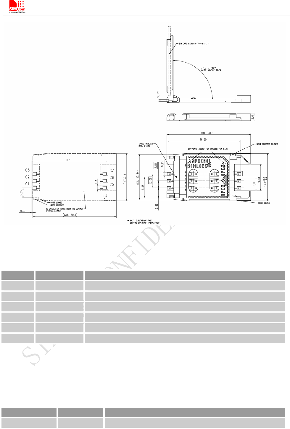
Smart Machine Smart Decision
SIM800C_Hardware_Design_V1.02 34 2015-4-27
Figure 33: Amphenol C707 10M006 512 SIM card holder
Table 17: Pin description (Amphenol SIM card holder)
Pin name Signal Description
C1 SIM_VDD SIM card power supply
C2 SIM_RST SIM card reset
C3 SIM_CLK SIM card clock
C5 GND Connect to GND
C6 VPP Not connect
C7 SIM_DATA SIM card data I/O
Note: Every time plug SIM card interval advice is greater than 2s. Otherwise may not be able to correct
detection.
4.9. ADC
Table 18: Pin definition of the ADC
SIM800C provides an auxiliary ADC, which can be used to measure the voltage. Customer can use AT command
“AT+CADC” to read the voltage value. For details of this AT command, please refer to document [1].
Pin name Pin number Description
ADC 38 Analog voltage input
Smart Machine Smart Decision
SIM800C_Hardware_Design_V1.02 35 2015-4-27
Table 19: ADC specification
Parameter Min Typ Max Unit
Voltage range 0 - 2.8 V
ADC Resolution - 10 - bits
Sampling rate - - 1.0833 MHz
ADC precision 10 30 mV
4.10. Network Status Indication
Table 20: Pin definition of the NETLIGHT
The NETLIGHT pin can be used to drive a network status indication LED. The status of this pin is listed in
following table:
Table 21: Status of the NETLIGHT pin
Status SIM800C behavior
Off Powered off
64ms On/ 800ms Off Not registered the network
64ms On/ 3000ms Off Registered to the network
64ms On/ 300ms Off GPRS communication is established
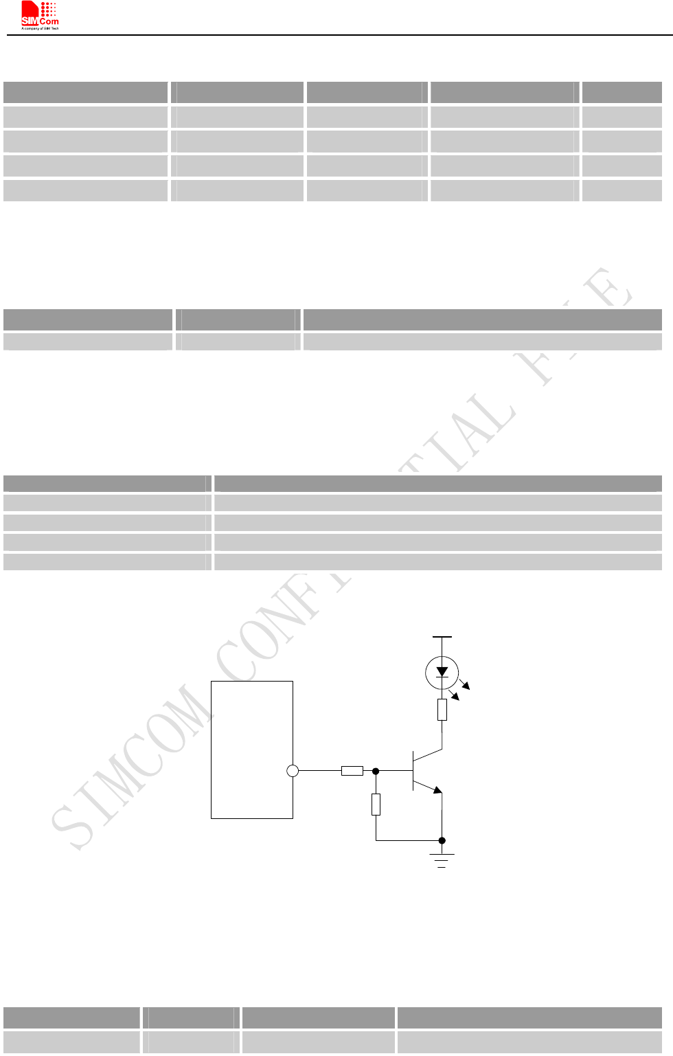
Reference circuit is recommended in the following figure:
M odule
NETLIGHT
VBAT
4.7K
47K
R
Figure 34: Reference circuit of NETLIGHT
4.10.1. NETLIGHT Multiplexing Function
Table 22: NETLIGHT multiplexing function
Pin name Pin number Mode 0(default) Mode 1
NETLIGHT 41 NETLIGHT GPIO
Note: Multiplexing function need different software supply.
Pin name Pin number Description
NETLIGHT 41 Network Status Indication
Smart Machine Smart Decision
SIM800C_Hardware_Design_V1.02 36 2015-4-27
4.11. Operating Status Indication
The pin42 is for operating status indication of the module. The pin output is high when module is powered on,
and output is low when module is powered off.
Table 23: Pin definition of the STATUS
Pin name Pin number Description
STATUS 42 Operating status indication
Note: For timing about STATUS, please reference to the chapter “4.2 power on/down scenarios”
4.11.1. STATUS Multiplexing Function
Table 24: STATUS multiplexing function
Pin name Pin number Mode 0(default) Mode 1
STATUS 42 STATUS GPIO
Note: Multiplexing function need different software supply.
4.12. RF Synchronization Signal
The synchronization signal is used to indicate incoming GSM burst.
Table 25: Definition of the RF_SYNC pin
The timing of the synchronization signal is shown below.
Transm it burst
RF_SYNC
577us
220us
Figure 35: RF_SYNC signal during transmit burst
4.12.1. RF_SYNC Multiplexing Function
RF_SYNC can also be used as GPIO to indicate the RF Jamming. The RF_SYNC function and RF Jamming
Detection function can be switched by AT+SJDR command.
Table 26: RF_SYNC Multiplexing function
Pin name Pin number Description
RF_SYNC 29 Transmit synchronization signal
Smart Machine Smart Decision
SIM800C_Hardware_Design_V1.02 37 2015-4-27
Pin name Pin number Mode 0(default) Mode 1
RF_SYNC 29 RF Synchronization Signal JD(RF jamming detection)
Note: About AT+SJDR, please refer to document [1].
4.13. Antenna Interface
There are two antenna interfaces, GSM_ANT and BT_ANT.
- The input impendence of the antenna should be 50, and the VSWR should be less than 2.
- It is recommended that the GSM antenna and the BT antenna should be placed as far as possible.
- The isolations of the two antenna should be bigger than 30dB
NOTE
:
About the RF trace layout please refer to“AN_SMT Module_RF_Reference Design_Guide”.
4.13.1 GSM Antenna Interface
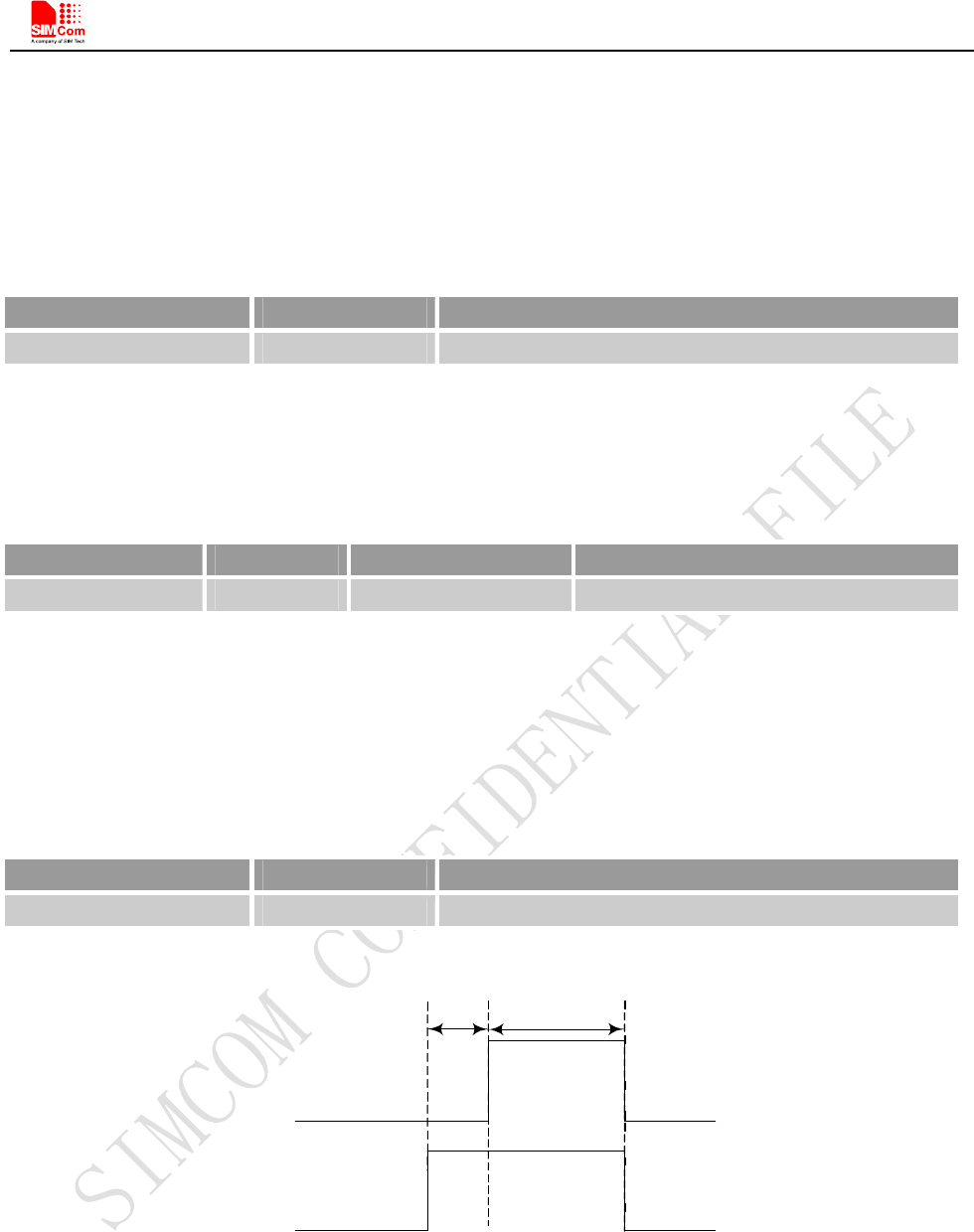
SIM800C provides a GSM antenna named GSM_ANT, customer could use 50 microstrip line or stripline
antenna connect to the module.
It is recommended to reserve the matching circuit as following:
Module
GND
(P in33)
R F connector
R101
GSM_ANT
C101 C102
GND
(P in31)
GSM
Antenna
(P in33)
Figure 36: GSM antenna matching circuit
R101,C101,C102 are the matching circuit, the value should be defined by the antenna design. Normally R101 is
0, C101 and C102 are not mounted.
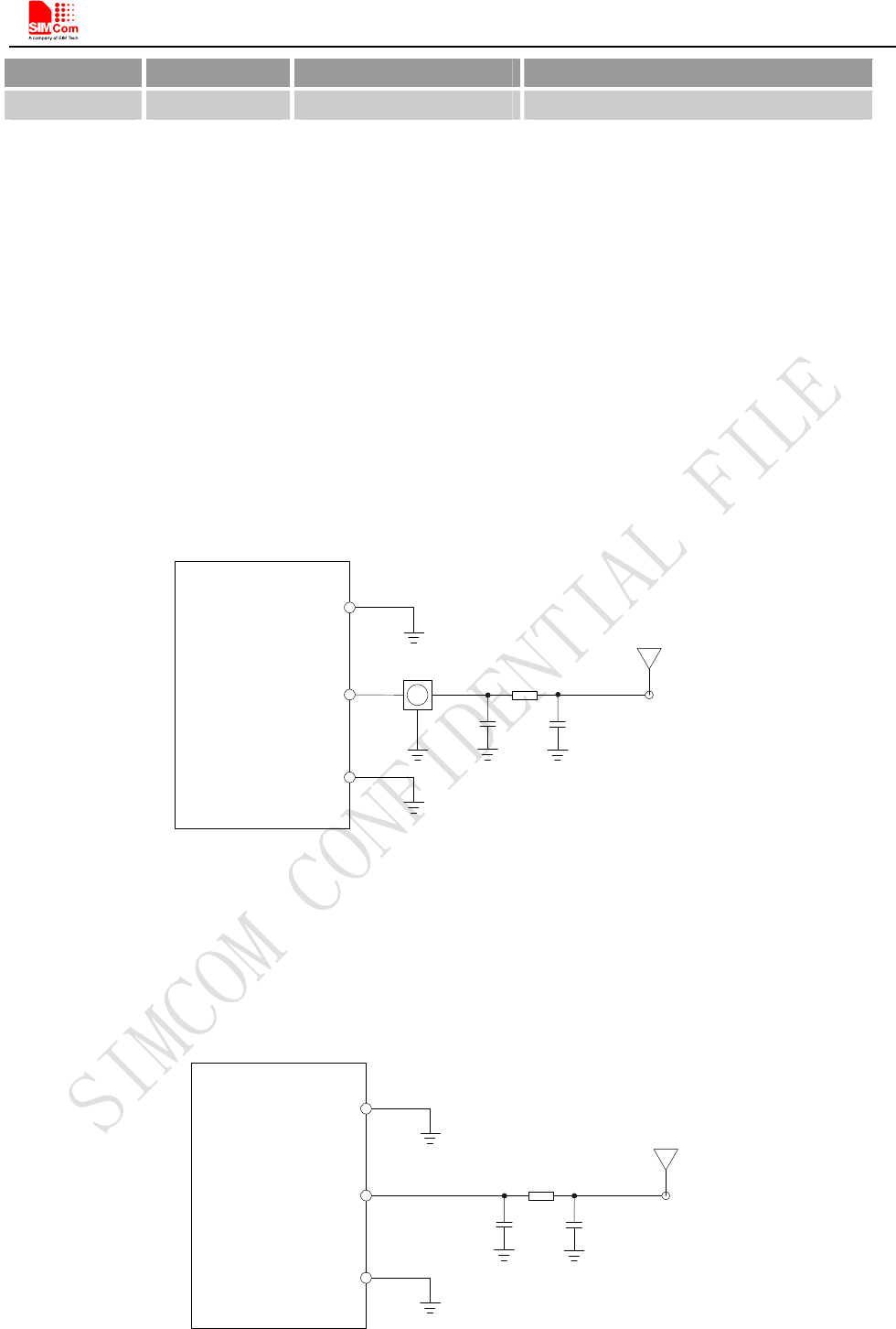
The RF connector is used for conduction test. If the space between RF pin and antenna is not enough, the
matching circuit should be designed as in the following figure:
M odule
R101
GSM_ANT
C101 C102
GND
(P in33)
GND
(P in31)
GSM
Antenna
(P in33)
Figure 37: GSM antenna matching circuit without RF connector
Smart Machine Smart Decision
SIM800C_Hardware_Design_V1.02 38 2015-4-27
Normally R101 is 0, C101 and C102 are not mounted.
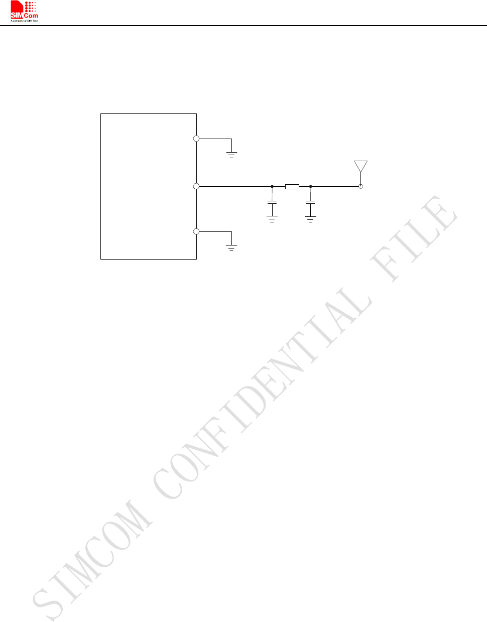
4.13.2 Bluetooth Antenna Interface
It is recommended to reserve the matching circuit as following:
M oduleR201
BT_ANT
C201 C 202
GND
(P in21)
GND
(P in19)
BT
Antenna
(P in20)
Figure 38: Bluetooth antenna matching circuit
R201, C201, C202 are the matching circuit, the value should be defined by the antenna design. Normally R201 is
0R, C202 and C201 are not mounted.
There are some suggestions for placing components and RF trace for GSM_ANT/BT_ANT:
- The RF connector is used for conducted test, so keep it as close to pin GSM_ANT as possible;
- Antenna matching circuit should be close to the antenna;
- Keep the RF traces impedance as 50;
- The RF traces should be kept far away from the high frequency signals and strong interference
source.
Smart Machine Smart Decision
SIM800C_Hardware_Design_V1.02 39 2015-4-27
5. PCB Layout
This section will give some guidelines on PCB layout, in order to eliminate interfere or noise.
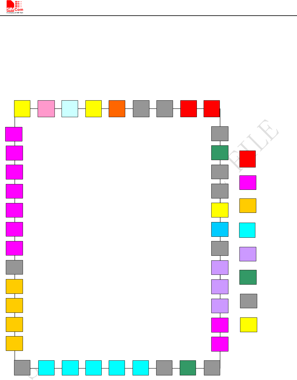
5.1 Pin Assignment
Before PCB layout, we should learn about pin assignment in order to get reasonable layout with so many
external components. Following figure is the overview of pin assignment of the module.
UART1_DTR
USB_DP
VBAT
VBAT
ADC
UART1_RXD
PWRKEY
UART1_CTS
UART1_TXD
UART1_RTS
UART1_DCD
NETLIGHT
SIM_RSTSIM_CLK
SIM_DET SIM_DATA BT_ANT
UART2_TXD
SPKP
VRTC
MICP
MICN USB_VBUS
USB_DM
GSM_ANT
STATUS
SIM_VDD
UART2_RXD
GND
13
SPKN
UART1_RI
14 15 16 21
17 18 19 20
22
23
24
25
26
27
28
29
30
31
32
33
37 36 35 34
1
42 41 40 39 38
5
4
2
3
6
11
10
9
8
7
12
VDD_EXT
GND
GND
GND
GND
GND
GND
GND
UART1_DTR
RF_SYNC
GND
GND
SIM800C
TOP VIEW
VBAT
UART
AUDIO
SIM CART
USB
ANTANA
GND
OTHERS
Figure 39: Pin assignment
5.2 Principle of PCB Layout
During layout, attention should be paid to the following interfaces, like Antenna, power supply, SIM card
interface, audio interface, and so on.

Smart Machine Smart Decision
SIM800C_Hardware_Design_V1.02 40 2015-4-27
5.2.1 Antenna Interface
- The length of trace between pin output and connector should be as short as possible;
- Do not trace RF signal over across the board;
- The RF signal should be far away from SIM card, power ICs.
5.2.2 Power Supply
- Not only VBAT but also return GND are very important in layout;
- The positive line of VBAT should be as short and wide as possible;
- The correct flow from source to VBAT pin should go though Zener diode then huge capacitor;
- Pin 36 and Pin37 are GND signals, and shortest layout to GND of power source should be designed;
- There are 10 GND pads in the module; these pads could enhance the GND performances. On the
upper layer of these pads, do not trace any signal if possible.
5.2.3 SIM Card Interface
- SIM card holder has no anti-EMI component inside. Thus SIM card interface maybe interfered,
please pay more attention on this interface during layout;
- Ensure SIM card holder is far way from antenna or RF cable inside;
- Put SIM card holder near the module, as nearer as possible;
- Add ESD component to protect SIM_CLK, SIM_DATA, SIM_RST and SIM_VDD signals which
should be far away from power and high-speed-frequency signal.
5.2.4 Audio Interface
- The signal trace of audio should far away from antenna and power;
- The audio signal should avoid to parallel with VBAT trace.
5.2.5 Others
- It is better to trace signal lines of UART bunched, as well as signals of USB.
Smart Machine Smart Decision
SIM800C_Hardware_Design_V1.02 41 2015-4-27
6. Electrical, Reliability and Radio Characteristics
6.1 Absolute Maximum Ratings
The absolute maximum ratings stated in following table are stress ratings under non-operating conditions.
Stresses beyond any of these limits will cause permanent damage to SIM800C.
Table 27: Absolute maximum ratings
Symbol Min Typ Max Unit
VBAT - - 4.5 V
Current 0 - 2.0 A
USB_VBUS - - 12 V
II* - 4 16 mA
IO* - 4 16 mA
*These parameters are for digital interface pins, GPIO, and UART.
6.2 Recommended Operating Conditions
Table 28: Recommended operating conditions
Symbol Parameter Min Typ Max Unit
VBAT Power supply voltage 3.4 4.0 4.4 V
TOPER Operating temperature -40 +25 +85 ℃
TSTG Storage temperature -45 +90 ℃
6.3 Digital Interface Characteristics
Table 29: Digital interface characteristics
Symbol Parameter Min Typ Max Unit
VIH High-level input current 2.1 - 3.1 V
VIL Low-level input current -0.3 - 0.7 V
VOH High-level output voltage 2.4 - - V
VOL Low-level output voltage - - 0.4 V
Note: These parameters are for digital interface pins, such as keypad, GPIO and UART.
6.4 SIM Card Interface Characteristics
Table 30: SIM card interface characteristics
Symbol Parameter Min Typ Max Unit
IIH High-level input current -1.0 - 1.0 uA
IIL Low-level input current -1.0 - 1.0 uA
Smart Machine Smart Decision
SIM800C_Hardware_Design_V1.02 42 2015-4-27
1.4 - - V
VIH High-level input voltage
2.4 - - V
- - 0.27 V
VIL Low-level input voltage
0.4 V
1.62 - - V
VOH High-level output voltage
2.7 - - V
- - 0.36 V
VOL Low-level output voltage
- - 0.4 V
6.5 SIM_VDD Characteristics
Table 31: SIM_VDD characteristics
Symbol Parameter Min Typ Max Unit
- 3.0 -
VO Output voltage
- 1.8 -
V
IO Output current - - 10 mA
6.6 VDD_EXT Characteristics
Table 32: VDD_EXT characteristics
Symbol Parameter Min Typ Max Unit
VO Output voltage 2.7 2.8 2.9 V
IO Output current - - 50 mA
6.7 VRTC Characteristics
Table 33: VRTC characteristics
Symbol Description Min Typ Max Unit
VRTC-IN VRTC input voltage 1.2 2.8 3.0 V
IRTC-IN VRTC input current - 3.0 5.0 uA
VRTC-OUT VRTC output voltage - 2.8 - V
IRTC-OUT VRTC output current - 2.0 mA
6.8 Current Consumption (VBAT=4.0V)
Table 34: Current consumption
Symbol Parameter Conditions Min Typ Max Unit
Voltage 4.0 V
Power drop PCL=5 350 mV
VBAT
Voltage ripple
PCL=5
@ f<200kHz
50
mV

Smart Machine Smart Decision
SIM800C_Hardware_Design_V1.02 43 2015-4-27
@ f>200kHzss 2.0 mV
Power off mode 130 150 uA
Sleep mode (AT+CFUN=1):
( BS-PA-MFRMS=9 )
( BS-PA-MFRMS=5)
( BS-PA-MFRMS=2)
0.88
1
1.5
mA
mA
mA
Idle mode (AT+CFUN=1):
GSM850
EGSM900
DCS1800
PCS1900
13.8
13.8
13.8
13.8
mA
mA
mA
mA
Voice call (PCL=5):
GSM850
EGSM900
Voice call (PCL=0):
DCS1800
PCS1900
209
211
126
413
mA
mA
mA
mA
Data mode GPRS (1Rx,4Tx):
GSM850
EGSM900
DCS1800
PCS1900
394
416
271
285
mA
mA
mA
mA
Data mode GPRS (3Rx,2Tx):
GSM850
EGSM900
DCS1800
PCS1900
323
330
212
227
mA
mA
mA
mA
IVBAT Average currnet
Data mode GPRS (4Rx,1Tx):
GSM850
EGSM900
DCS1800
PCS1900
213
210
150
162
mA
mA
mA
mA
IMAX Peak current During Tx burst 2.0 A
Note: In above table the current consumption value is the typical one of the module tested in laboratory. In the
mass production stage, there may be differences among each individual.
6.9 Electro-Static Discharge
SIM800C is an ESD sensitive component, so attention should be paid to the procedure of handling and
packaging. The ESD test results are shown in the following table.
Table 35: The ESD characteristics (Temperature: 25℃, Humidity: 45 %)
Pin name Contact discharge Air discharge
VBAT ±5KV ±12KV
Smart Machine Smart Decision
SIM800C_Hardware_Design_V1.02 44 2015-4-27
GND ±6KV ±12KV
UART1_TXD /UART1_RXD ±4KV ±8KV
Antenna port ±5KV ±10KV
SPKP/SPKN/MICP/MICN ±4KV ±8KV
PWRKEY ±4KV ±8KV
6.10 Radio Characteristics
6.10.1 Module RF Output Power
The following table shows the module conducted output power, it is followed by the 3GPP TS 05.05 technical
specification requirement.
Table 36: GSM850 and EGSM900 conducted RF output power
GSM850,EGSM900
Tolerance (dB) for conditions
PCL Nominal output power (dBm) Normal Extreme
5 33 ±2 ±2.5
6 31 ±3 ±4
7 29 ±3 ±4
8 27 ±3 ±4
9 25 ±3 ±4
10 23 ±3 ±4
11 21 ±3 ±4
12 19 ±3 ±4
13 17 ±3 ±4
14 15 ±3 ±4
15 13 ±3 ±4
16 11 ±5 ±6
17 9 ±5 ±6
18 7 ±5 ±6
19-31 5 ±5 ±6
Table 37: DCS1800 and PCS1900 conducted RF output power
DCS1800,PCS1900
Tolerance (dB) for conditions
PCL Nominal output power (dBm) Normal Extreme
0 30 ±2 ±2.5
1 28 ±3 ±4
2 26 ±3 ±4
3 24 ±3 ±4
Smart Machine Smart Decision
SIM800C_Hardware_Design_V1.02 45 2015-4-27
4 22 ±3 ±4
5 20 ±3 ±4
6 18 ±3 ±4
7 16 ±3 ±4
8 14 ±3 ±4
9 12 ±4 ±5
10 10 ±4 ±5
11 8 ±4 ±5
12 6 ±4 ±5
13 4 ±4 ±5
14 2 ±5 ±6
15 0 ±5 ±6
6.10.2 Module RF Receive Sensitivity
The following table shows the module’s conducted receiving sensitivity, it is tested under static condition.
Table 38: Conducted RF receive sensitivity
Frequency Receive sensitivity(Typical) Receive sensitivity(Max)
GSM850,EGSM900 < -109dBm < -107dBm
DCS1800,PCS1900 < -109dBm < -107dBm
6.10.3 Module Operating Frequencies
The following table shows the module’s operating frequency range; it is followed by the 3GPP TS 05.05
technical specification requirement.
Table 39: Operating frequencies
Frequency Receive Transmit
GSM850 869 ~ 894MHz 824 ~ 849MHz
EGSM900 925 ~ 960MHz 880 ~ 915MHz
DCS1800 1805 ~ 1880MHz 1710 ~ 1785MHz
PCS1900 1930 ~ 1990MHz 1850 ~ 1910MHz
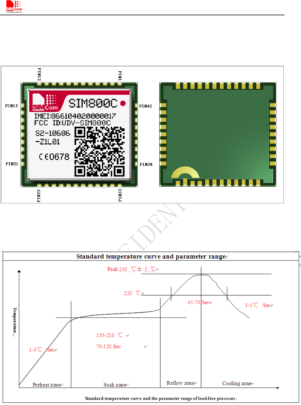
Smart Machine Smart Decision
SIM800C_Hardware_Design_V1.02 46 2015-4-27
7. Manufacturing
7.1. Top and Bottom View of SIM800C
Figure 40: Top and bottom view of SIM800C
7.2. Typical Solder Reflow Profile
Figure 41: Typical solder reflow profile of lead-free processes
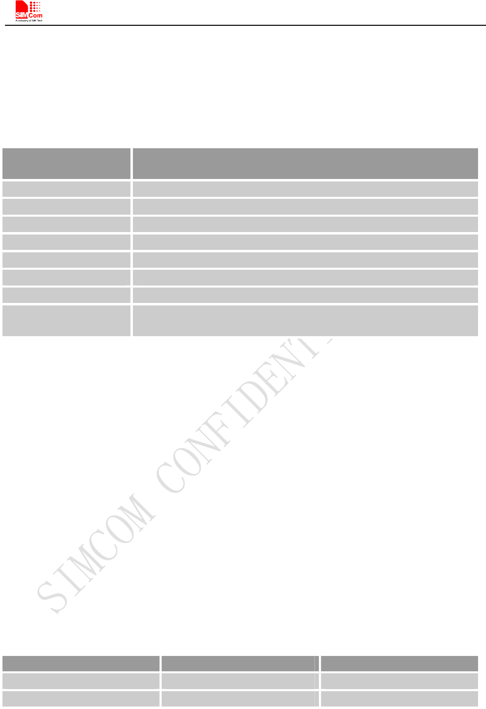
Smart Machine Smart Decision
SIM800C_Hardware_Design_V1.02 47 2015-4-27
7.3. The Moisture Sensitivity Level
The moisture sensitivity level of SIM800C module is 3. The modules should be mounted within 168 hours after
unpacking in the environmental conditions of temperature <30℃ and relative humidity of <60% (RH). It is
necessary to bake the module if the above conditions are not met:
Table 40: Moisture sensitivity level and floor life
Moisture Sensitivity Level
(MSL)
Floor Life (out of bag) at factory ambient≤30°C/60% RH or as stated
1 Unlimited at ≦30℃/85% RH
2 1 year
2a 4 weeks
3 168 hours
4 72 hours
5 48 hours
5a 24 hours
6 Mandatory bake before use. After bake, it must be reflowed within the time limit
specified on the label.
NOTES:
For product handling, storage, processing, IPC / JEDEC J-STD-033 must be followed.
7.4. Baking Requirements
SIM800C modules are vacuum packaged, and guaranteed for 6 months storage without opening or leakage under
the following conditions: the environment temperature is lower than 40℃, and the air humidity is less than 90%.
If the condition meets one of the following ones shown below, the modules should be baked sufficiently before
re-flow soldering, and the baking condition is shown in below table; otherwise the module will be at the risk of
permanent damage during re-flow soldering.
- If the vacuum package is broken or leakage;
- If the vacuum package is opened after 6 months since it’s been packed;
- If the vacuum package is opened within 6 months but out of its Floor Life at factory ambient≦30℃
/60%RH or as stated.
Table 41: Baking requirements
Baking temperature Moisture Time
40 ±5℃℃ <5% 192 hours
120 ±5℃℃ <5% 6 hours
Note: Care should be taken if that plastic tray is not heat-resistant, the modules should be taken out for
preheating, otherwise the tray may be damaged by high-temperature heating.
Smart Machine Smart Decision
SIM800C_Hardware_Design_V1.02 48 2015-4-27
8. Appendix
I. Related Documents
Table 42: Related documents
SN Document name Remark
[1] SIM800 Series AT Command
Manual
[2] SIM800 Series UART Port
Application Note_V1 02.doc
[3] ITU-T Draft new
recommendation V.25ter: Serial asynchronous automatic dialing and control
[4] GSM 07.07: Digital cellular telecommunications (Phase 2+); AT command set for
GSM Mobile Equipment (ME)
[5] GSM 07.10: Support GSM 07.10 multiplexing protocol
[6] GSM 07.05:
Digital cellular telecommunications (Phase 2+); Use of Data
Terminal Equipment – Data Circuit terminating Equipment (DTE –
DCE) interface for Short Message Service (SMS) and Cell
Broadcast Service (CBS)
[7] GSM 11.14:
Digital cellular telecommunications system (Phase 2+);
Specification of the SIM Application Toolkit for the Subscriber
Identity Module – Mobile Equipment (SIM – ME) interface
[8] GSM 11.11:
Digital cellular telecommunications system (Phase 2+);
Specification of the Subscriber Identity Module – Mobile
Equipment (SIM – ME) interface
[9] GSM 03.38: Digital cellular telecommunications system (Phase 2+); Alphabets
and language-specific information
[10] GSM 11.10
Digital cellular telecommunications system (Phase 2); Mobile
Station (MS) conformance specification; Part 1: Conformance
specification
[11] AN_Serial Port AN_Serial Port
Smart Machine Smart Decision
SIM800C_Hardware_Design_V1.02 49 2015-4-27
II. Multiplexing Function
Table 43: Multiplexing function
Pin name Reset Pin number Mode 0(default) Mode 1 Mode 2 Mode 3
STATUS I/PD 42 STATUS GPIO19 -
SIM_DET I/PD 14 SIM_DET GPIO20 EINT14
NETLIGHT I/PD 41 NETLIGHT GPIO17 UTXD3
UART1_DTR I/PD 6 UART1_DTR GPIO18 EINT13
UART1_RI I/PD 7 UART1_RI GPIO13 EINT11
UART1_DCD I/PD 5 UART1_DCD GPIO12 URXD3
UART1_CTS I/PD 4 UART1_CTS GPIO14 EINT12
UART1_RTS I/PD 3 UART1_RTS GPIO15
UART1_TXD HO 1 UART1_TXD GPIO11
UART1_RXD I/PD 2 UART1_RXD GPIO10
UART2_TXD HO 22 UART3_TXD GPIO0
UART2_RXD I/PD 23 UART3_RXD GPIO1
Note: Multiplexing function need different software supply.
III. Terms and Abbreviations
Table 44: Terms and abbreviations
Abbreviation Description
ADC Analog-to-Digital Converter
AMR Adaptive Multi-Rate
CS Coding Scheme
CTS Clear to Send
DTE Data Terminal Equipment (typically computer, terminal, printer)
DTR Data Terminal Ready
DTX Discontinuous Transmission
EFR Enhanced Full Rate
EGSM Enhanced GSM
ESD Electrostatic Discharge
ETS European Telecommunication Standard
FR Full Rate
GPRS General Packet Radio Service
GSM Global Standard for Mobile Communications
HR Half Rate
MO Mobile Originated
MS Mobile Station (GSM engine), also referred to as TE
MT Mobile Terminated
PAP Password Authentication Protocol
Smart Machine Smart Decision
SIM800C_Hardware_Design_V1.02 50 2015-4-27
PBCCH Packet Broadcast Control Channel
PCB Printed Circuit Board
PCL Power Control Level
PCS Personal Communication System, also referred to as GSM 1900
PDU Protocol Data Unit
PPP Point-to-point protocol
RF Radio Frequency
RMS Root Mean Square (value)
RX Receive Direction
SIM Subscriber Identification Module
SMS Short Message Service
TE Terminal Equipment, also referred to as DTE
TX Transmit Direction
SINAD Signal to Noise and Distortion Ratio
UART Universal Asynchronous Receiver & Transmitter
URC Unsolicited Result Code
USSD Unstructured Supplementary Service Data
Phonebook abbreviations
FD SIM fix dialing phonebook
LD SIM last dialing phonebook (list of numbers most recently dialed)
MC Mobile Equipment list of unanswered MT calls (missed calls)
ON SIM (or ME) own numbers (MSISDNs) list
RC Mobile Equipment list of received calls
SM SIM phonebook
NC Not connect
Smart Machine Smart Decision
SIM800C_Hardware_Design_V1.02 51 2015-4-27
IV. Safety Caution
Table 45: Safety caution
Marks Requirements
When in a hospital or other health care facility, observe the restrictions about the use of mobiles.
Switch the cellular terminal or mobile off, medical equipment may be sensitive to not operate
normally for RF energy interference.
Switch off the cellular terminal or mobile before boarding an aircraft. Make sure it is switched off.
The operation of wireless appliances in an aircraft is forbidden to prevent interference with
communication systems. Forget to think much of these instructions may lead to the flight safety or
offend against local legal action, or both.
Do not operate the cellular terminal or mobile in the presence of flammable gases or fumes. Switch
off the cellular terminal when you are near petrol stations, fuel depots, chemical plants or where
blasting operations are in progress. Operation of any electrical equipment in potentially explosive
atmospheres can constitute a safety hazard.
Your cellular terminal or mobile receives and transmits radio frequency energy while switched on.
RF interference can occur if it is used close to TV sets, radios, computers or other electric
equipment.
Road safety comes first! Do not use a hand-held cellular terminal or mobile when driving a
vehicle, unless it is securely mounted in a holder for hands free operation. Before making a call
with a hand-held terminal or mobile, park the vehicle.
GSM cellular terminals or mobiles operate over radio frequency signals and cellular networks and
cannot be guaranteed to connect in all conditions, for example no mobile fee or a invalid SIM card.
While you are in this condition and need emergent help, please remember using emergency calls.
In order to make or receive calls, the cellular terminal or mobile must be switched on and in a
service area with adequate cellular signal strength.
Some networks do not allow for emergency call if certain network services or phone features are in
use (e.g. lock functions, fixed dialing etc.). You may have to deactivate those features before you
can make an emergency call.
Also, some networks require that a valid SIM card be properly inserted in the cellular terminal or
mobile.

Smart Machine Smart Decision
SIM800C_Hardware_Design_V1.02 52 2015-4-27
Contact us:
Shanghai SIMCom Wireless Solutions Co.,Ltd.
Address: Building A, SIM Technology Building, No. 633, Jinzhong Road, Shanghai, P. R. China
200335
Tel: +86 21 3252 3300
Fax: +86 21 3252 3020
URL: www.sim.com/wm
