SoC FPGA Design Guide [DE1 Edition] So C
User Manual: Pdf
Open the PDF directly: View PDF ![]() .
.
Page Count: 106 [warning: Documents this large are best viewed by clicking the View PDF Link!]
- 2 List of Figures
- 3 Table of Tables
- 4 Prerequisites
- 5 Introduction
- 6 Terasic DE1-SoC Board
- 7 Cyclone V Overview
- 8 Using the Cyclone V – General Information
- 9 Using the Cyclone V – Hardware
- 10 Using the Cyclone V – FPGA – Nios II – Bare-metal
- 11 Using the Cylone V – HPS – ARM – General
- 12 Using the Cyclone V – HPS – ARM – Bare-metal
- 12.1 Preloader
- 12.2 ARM DS-5
- 13 Using the Cyclone V – HPS – ARM – Linux
- 13.1 Preloader
- 13.2 Bootloader
- 13.3 Linux Kernel
- 13.4 Ubuntu Core Root Filesystem
- 13.5 Writing Everything to the sdcard
- 13.6 Scripting the Complete Procedure
- 13.7 Testing the Setup
- 13.8 ARM DS-5
- 13.8.1 Setting Up a New C Project
- 13.8.2 Creating a Remote Debug Connection to the Linux Distribution
- 13.8.3 Linux Programming
- 14 TODO
- 15 References


SoC-FPGA Design Guide [DE1-SoC Edition]
21/04/2018 P a g e | 1
2 List of Figures ................................................................................................................................................. 6
3 Table of Tables ................................................................................................................................................ 9
4 Prerequisites ................................................................................................................................................ 10
4.1 Hardware .............................................................................................................................................. 10
4.2 Software ............................................................................................................................................... 10
4.2.1 Software Versions Used in this Guide .......................................................................................... 10
4.2.2 Licenses ........................................................................................................................................ 10
5 Introducon ................................................................................................................................................. 12
6 Terasic DE1-SoC Board ................................................................................................................................. 13
6.1 Specicaons ....................................................................................................................................... 13
6.1.1 FPGA Device ................................................................................................................................. 13
6.1.2 Conguraon and Debug ............................................................................................................. 13
6.1.3 Memory Device ............................................................................................................................ 13
6.1.4 Communicaon ............................................................................................................................ 13
6.1.5 Connectors ................................................................................................................................... 14
6.1.6 Display .......................................................................................................................................... 14
6.1.7 Audio ............................................................................................................................................ 14
6.1.8 Video Input ................................................................................................................................... 14
6.1.9 ADC ............................................................................................................................................... 14
6.1.10 Switches, Buons and Indicators ................................................................................................. 14
6.1.11 Sensors ......................................................................................................................................... 14
6.1.12 Power ........................................................................................................................................... 14
6.1.13 Block Diagram .............................................................................................................................. 15
6.2 Layout ................................................................................................................................................... 15
7 Cyclone V Overview ..................................................................................................................................... 17
7.1 Introducon to the Cyclone V Hard Processor System ........................................................................ 17
7.2 Features of the HPS .............................................................................................................................. 19
7.3 System Integraon Overview ............................................................................................................... 20
7.3.1 MPU Subsystem ........................................................................................................................... 20
7.3.2 SDRAM Controller Subsystem ...................................................................................................... 20
7.3.3 Support Peripherals ...................................................................................................................... 20

SoC-FPGA Design Guide [DE1-SoC Edition]
21/04/2018 P a g e | 2
7.3.3.1 System Manager ....................................................................................................................... 20
7.3.3.2 FPGA Manager ......................................................................................................................... 20
7.3.4 Interface Peripherals .................................................................................................................... 21
7.3.4.1 GPIO Interfaces ......................................................................................................................... 21
7.3.5 On-Chip Memory .......................................................................................................................... 21
7.3.5.1 On-Chip RAM ............................................................................................................................ 21
7.3.5.2 Boot ROM ................................................................................................................................. 21
7.4 HPS-FPGA Interfaces ............................................................................................................................ 21
7.5 HPS Address Map ................................................................................................................................. 21
7.5.1 HPS Address Spaces ..................................................................................................................... 21
7.5.2 HPS Peripheral Region Address Map ............................................................................................ 23
7.6 HPS Boong and FPGA Conguraon .................................................................................................. 25
7.6.1 HPS Boot and FPGA Conguraon Ordering ................................................................................ 25
7.6.2 Zooming In On the HPS Boot Process ........................................................................................... 27
7.6.2.1 Preloader .................................................................................................................................. 28
8 Using the Cyclone V – General Information ................................................................................................. 29
8.1 Introduction ......................................................................................................................................... 29
8.2 FPGA-only ............................................................................................................................................. 29
8.3 HPS & FPGA .......................................................................................................................................... 29
8.3.1 Bare-metal Application ................................................................................................................ 29
8.3.2 Application Over an Operating System (Linux) ............................................................................ 30
8.4 Goals ..................................................................................................................................................... 30
8.5 Project Structure .................................................................................................................................. 30
9 Using the Cyclone V – Hardware .................................................................................................................. 32
9.1 General Quartus Prime Setup .............................................................................................................. 32
9.2 System Design with Qsys – Nios II ........................................................................................................ 32
9.3 System Design with Qsys – HPS ........................................................................................................... 35
9.3.1 Instantiating the HPS Component ................................................................................................ 35
9.3.1.1 FPGA Interfaces Tab ................................................................................................................. 35
9.3.1.2 Peripheral Pins Tab ................................................................................................................... 35
9.3.1.2.1 Theory ................................................................................................................................ 35
9.3.1.2.2 Configuration ..................................................................................................................... 37
9.3.1.3 HPS Clocks Tab ......................................................................................................................... 38
9.3.1.4 SDRAM Tab ............................................................................................................................... 38

SoC-FPGA Design Guide [DE1-SoC Edition]
21/04/2018 P a g e | 3
9.3.2 Interfacing with FPGA Peripherals ............................................................................................... 41
9.4 Generating the Qsys System ................................................................................................................ 41
9.5 Instantiating the Qsys System .............................................................................................................. 42
9.6 HPS DDR3 Pin Assignments .................................................................................................................. 45
9.7 Wiring the DE1-SoC .............................................................................................................................. 46
9.8 Programming the FPGA ........................................................................................................................ 47
9.9 Creating Target sdcard Artifacts .......................................................................................................... 49
10 Using the Cyclone V – FPGA – Nios II – Bare-metal ................................................................................. 50
10.1 Project Setup ........................................................................................................................................ 50
10.2 Nios II Programming Theory – Accessing Peripherals .......................................................................... 50
10.3 Nios II Programming Practice ............................................................................................................... 51
11 Using the Cylone V – HPS – ARM – General ............................................................................................. 53
11.1 Partitioning the sdcard ......................................................................................................................... 53
11.2 Generating a Header File for HPS Peripherals ..................................................................................... 53
11.3 HPS Programming Theory .................................................................................................................... 54
12 Using the Cyclone V – HPS – ARM – Bare-metal ...................................................................................... 56
12.1 Preloader .............................................................................................................................................. 56
12.1.1 Preloader Generation ................................................................................................................... 56
12.1.2 Creating Target sdcard Artifacts .................................................................................................. 57
12.2 ARM DS-5 ............................................................................................................................................. 57
12.2.1 Setting Up a New C Project .......................................................................................................... 58
12.2.2 Writing a DS-5 Debug Script ......................................................................................................... 59
12.2.3 Setting Up the Debug Configuration ............................................................................................ 60
12.2.4 Bare-metal Programming ............................................................................................................. 61
12.2.4.1 Accessing FPGA Peripherals ................................................................................................. 62
12.2.4.2 Accessing HPS Peripherals.................................................................................................... 62
12.2.4.2.1 Using Altera’s HWLIB - Prerequisites ............................................................................... 62
12.2.4.2.2 Global Timer & Clock Manager ........................................................................................ 63
12.2.4.2.3 GPIO ................................................................................................................................. 63
12.2.4.3 Launching the Bare-metal Code in the Debugger ................................................................ 64
12.2.4.4 DS-5 Bare-metal Debugger Tour .......................................................................................... 65
12.2.4.4.1 “Registers” View [UNAVAILABLE IN SoC EDS 16.0] .......................................................... 65
12.2.4.4.2 App Console ..................................................................................................................... 67
13 Using the Cyclone V – HPS – ARM – Linux ............................................................................................... 68

SoC-FPGA Design Guide [DE1-SoC Edition]
21/04/2018 P a g e | 4
13.1 Preloader .............................................................................................................................................. 68
13.1.1 Preloader Generation ................................................................................................................... 68
13.1.2 Creating Target sdcard Artifacts .................................................................................................. 69
13.2 Bootloader............................................................................................................................................ 69
13.2.1 Getting & Compiling U-Boot ........................................................................................................ 69
13.2.2 Scripting U-Boot ........................................................................................................................... 71
13.2.3 Creating Target sdcard Artifacts .................................................................................................. 72
13.3 Linux Kernel .......................................................................................................................................... 72
13.3.1 Getting & Compiling Linux ........................................................................................................... 72
13.3.2 Creating Target sdcard Artifacts .................................................................................................. 73
13.4 Ubuntu Core Root Filesystem .............................................................................................................. 74
13.4.1 Obtaining Ubuntu Core ................................................................................................................ 74
13.4.2 Customizing Ubuntu Core ............................................................................................................ 74
13.4.2.1 System configuration on first boot ...................................................................................... 74
13.4.2.2 Post-install configuration script ........................................................................................... 76
13.4.3 Creating Target sdcard Artifacts .................................................................................................. 77
13.5 Writing Everything to the sdcard ......................................................................................................... 77
13.6 Scripting the Complete Procedure ....................................................................................................... 78
13.7 Testing the Setup ................................................................................................................................. 79
13.8 ARM DS-5 ............................................................................................................................................. 89
13.8.1 Setting Up a New C Project .......................................................................................................... 89
13.8.2 Creating a Remote Debug Connection to the Linux Distribution ................................................. 91
13.8.2.1 Find the Linux Distribution’s IP Address .............................................................................. 91
13.8.2.2 Create an SSH Remote Connection ...................................................................................... 93
13.8.2.3 Setting Up the Debug Configuration .................................................................................... 94
13.8.3 Linux Programming ...................................................................................................................... 95
13.8.3.1 Using Altera’s HWLIB - Prerequisites ................................................................................... 97
13.8.3.2 Accessing Hardware Peripherals from User Space .............................................................. 97
13.8.3.2.1 Opening the Physical Memory File Descriptor ................................................................ 97
13.8.3.2.2 Accessing HPS Peripherals ............................................................................................... 98
13.8.3.2.3 Accessing FPGA Peripherals ............................................................................................. 99
13.8.3.2.4 Cleaning Up Before Application Exit .............................................................................. 100
13.8.3.3 Launching the Linux code in the Debugger ........................................................................ 100
13.8.3.4 App Console ....................................................................................................................... 101

SoC-FPGA Design Guide [DE1-SoC Edition]
21/04/2018 P a g e | 5
13.8.3.5 DS-5 Linux Debugger Restrictions ...................................................................................... 102
14 TODO ...................................................................................................................................................... 103
15 References .............................................................................................................................................. 104

SoC-FPGA Design Guide [DE1-SoC Edition]
21/04/2018 P a g e | 6
Figure 6-1. Terasic DE1-SoC Board [1] .................................................................................................................. 13
Figure 6-2. Block Diagram of the DE1-SoC Board [1] ........................................................................................... 15
Figure 6-3. Back [1] .............................................................................................................................................. 15
Figure 6-4. Front [1] ............................................................................................................................................. 16
Figure 7-1. Altera SoC FPGA Device Block Diagram [2, pp. 1-1] ........................................................................... 17
Figure 7-2. HPS Block Diagram [2, pp. 1-3] .......................................................................................................... 19
Figure 7-3. HPS Address Space Relaons [2, pp. 1-14] ........................................................................................ 22
Figure 7-4. Simplied HPS Boot Flow [2, pp. A-3] ................................................................................................ 25
Figure 7-5. Independent FPGA Conguraon and HPS Boong [2, pp. A-2] ........................................................ 26
Figure 7-6. FPGA Conguraon before HPS Boong (HPS boots from FPGA) [2, pp. A-2] ................................... 26
Figure 7-7. HPS Boots and Performs FPGA Conguraon [2, pp. A-3] ................................................................. 27
Figure 7-8. HPS Boot Flows [2, pp. A-3] ............................................................................................................... 27
Figure 8-1. Project Folder Structure ..................................................................................................................... 31
Figure 9-1. Exporting the pll_0.outclk2 Signal ..................................................................................................... 33
Figure 9-2. Basic Nios II System with SDRAM and JTAG UART ............................................................................. 34
Figure 9-3. Adding LEDs to the System ................................................................................................................ 34
Figure 9-4. HPS Component Parameters ............................................................................................................. 35
Figure 9-5. HPS_KEY_N & HPS_LED on DE1-SoC Schematic. Note that the schematic uses “HPS_KEY” instead of
“HPS_KEY_N” as the name of the signal. This is a mistake, as the button is active-low, so the “_N” in the name
is warranted for clarity. ........................................................................................................................................ 36
Figure 9-6. HPS_KEY_N & HPS_LED on Qsys Peripheral Pins Tab ........................................................................ 36
Figure 9-7. Using Pin G21 for SPI .......................................................................................................................... 36
Figure 9-8. Ethernet MAC configuration .............................................................................................................. 37
Figure 9-9. SD/MMC configuration ...................................................................................................................... 37
Figure 9-10. UART configuration .......................................................................................................................... 37
Figure 9-11. Exported peripheral pins ................................................................................................................. 38
Figure 9-12. Quad SPI Flash, USB, SPI, and I2C peripheral pin configurations ..................................................... 38
Figure 9-13. Adding the "Standalone" HPS to the System ................................................................................... 40
Figure 9-14. Adding Buttons and 7-segment Displays to the Lightweight HPS-to-FPGA Bridge ......................... 41
Figure 9-15. Generate Qsys System ..................................................................................................................... 42
Figure 9-16. Qsys Component Instantiation ........................................................................................................ 43
Figure 9-17. Final Top-level Entity........................................................................................................................ 45

SoC-FPGA Design Guide [DE1-SoC Edition]
21/04/2018 P a g e | 7
Figure 9-18. Correct HPS DDR3 Pin Assignment TCL Script Selection .................................................................. 46
Figure 9-19. DE1-SoC Wiring ................................................................................................................................ 47
Figure 9-20. Quartus Prime Programmer............................................................................................................. 47
Figure 9-21. FPGA Selection ................................................................................................................................. 48
Figure 9-22. JTAG Scan Chain ............................................................................................................................... 48
Figure 9-23. Programming the FPGA ................................................................................................................... 48
Figure 10-1. Incorrect Nios II Peripheral Access in C ........................................................................................... 50
Figure 10-2. Correct Nios II Peripheral Access in C .............................................................................................. 51
Figure 10-3. nios.c ................................................................................................................................................ 52
Figure 10-4. Nios II Target Connection Dialog ..................................................................................................... 52
Figure 11-1. Partitioning the sdcard .................................................................................................................... 53
Figure 11-2. hps_soc_system.h ............................................................................................................................ 54
Figure 12-1. New BSP Dialog ................................................................................................................................ 56
Figure 12-2. Preloader Settings Dialog ................................................................................................................. 57
Figure 12-3. New C Project Dialog ....................................................................................................................... 58
Figure 12-4. debug_setup.ds................................................................................................................................ 60
Figure 12-5. Debug Configuraton “Connection” Tab ........................................................................................... 60
Figure 12-6. Debug Configuration "Files" Tab ...................................................................................................... 61
Figure 12-7. Debug Configuration "Debugger" Tab ............................................................................................. 61
Figure 12-8. hps_baremetal.c main() function .................................................................................................... 62
Figure 12-9. Accessing FPGA Buttons from the HPS ............................................................................................ 62
Figure 12-10. Programming the HPS Global Timer .............................................................................................. 63
Figure 12-11. Programming the HPS GPIO Peripheral ......................................................................................... 64
Figure 12-12. Switching to the DS-5 Debug Perspective ...................................................................................... 65
Figure 12-13. Debug Control View ....................................................................................................................... 65
Figure 12-14. DS-5 Debugger Controls ................................................................................................................. 65
Figure 12-15. DS-5 Debugger Registers View ....................................................................................................... 66
Figure 12-16. DS-5 App Console View .................................................................................................................. 67
Figure 13-1. New BSP Dialog ................................................................................................................................ 68
Figure 13-2. Preloader Settings Dialog ................................................................................................................. 69
Figure 13-3. U-Boot Script .................................................................................................................................... 72
Figure 13-4. Rootfs system configuration script to be used on first boot ("config_system.sh") ......................... 76
Figure 13-5. Rootfs /etc/rc.local file. ................................................................................................................... 76

SoC-FPGA Design Guide [DE1-SoC Edition]
21/04/2018 P a g e | 8
Figure 13-6. Rootfs post-install configuration script to be used AFTER the first boot (“config_post_install.sh”).
.............................................................................................................................................................................. 77
Figure 13-7. Target sdcard directory .................................................................................................................... 77
Figure 13-8. Incorrect DE1-SoC Boot Messages (from U-Boot) ........................................................................... 80
Figure 13-9. DE1-SoC Boot Messages (first boot) ................................................................................................ 85
Figure 13-10. DE1-SoC Boot Messages (second boot) ......................................................................................... 89
Figure 13-11. New C Project Dialog ..................................................................................................................... 90
Figure 13-12. hps_linux.c with an empty main() function. .................................................................................. 91
Figure 13-13. ARM DS-5 Serial Terminal .............................................................................................................. 91
Figure 13-14. ARM DS-5 Serial Terminal Settings ................................................................................................ 92
Figure 13-15. ARM DS-5 Serial Terminal Linux Prompt ....................................................................................... 92
Figure 13-16. Obtaining the DE1-SoC's IP Address through ARM DS-5’s Serial Terminal .................................... 93
Figure 13-17. New SSH Only Connection ............................................................................................................. 93
Figure 13-18. New SSH Connection In "Remote Systems" View .......................................................................... 94
Figure 13-19. Debug Configuraton “Connection” Tab ......................................................................................... 94
Figure 13-20. Debug Configuration "Files" Tab .................................................................................................... 95
Figure 13-21. Debug Configuration "Debugger" Tab ........................................................................................... 95
Figure 13-22. hps_linux.c main() function. .......................................................................................................... 96
Figure 13-23. Prototype of the mmap() function. ............................................................................................... 97
Figure 13-24. open_physical_memory_device() function. .................................................................................. 97
Figure 13-25. mmap_hps_peripherals() function. ............................................................................................... 98
Figure 13-26. setup_hps_gpio() function. ............................................................................................................ 98
Figure 13-27. handle_hps_led() function. ............................................................................................................ 99
Figure 13-28. mmap_fpga_peripherals() function. .............................................................................................. 99
Figure 13-29. setup_fpga_leds() function. ......................................................................................................... 100
Figure 13-30. handle_fpga_leds() function. ....................................................................................................... 100
Figure 13-31. munmap_peripherals() family of functions. ................................................................................ 100
Figure 13-32. close_physical_memory_device() function. ................................................................................ 100
Figure 13-33. Switching to the DS-5 Debug Perspective .................................................................................... 101
Figure 13-34. Debug Control View ..................................................................................................................... 101
Figure 13-35. DS-5 Debugger Controls ............................................................................................................... 101
Figure 13-36. DS-5 App Console View ................................................................................................................ 102

SoC-FPGA Design Guide [DE1-SoC Edition]
21/04/2018 P a g e | 9
3
Table 7-1. Possible HPS and FPGA Power Configurations .................................................................................... 18
Table 7-2. HPS Address Spaces [2, pp. 1-13] ........................................................................................................ 22
Table 7-3. Common Address Space Regions [2, pp. 1-15] .................................................................................... 22
Table 7-4. HPS Peripheral Region Address Map [2, pp. 1-16] .............................................................................. 24
Table 11-1. Predefined Data Sizes in socal.h ....................................................................................................... 54

SoC-FPGA Design Guide [DE1-SoC Edition]
21/04/2018 P a g e | 10
4.1 HARDWARE
We use the Terasic DE1-SoC board in this guide, but the guide can easily be adapted to be used with any other
Cyclone V SoC device.
4.2 SOFTWARE
This guide assumes users are running a version of the UBUNTU operating system on their host machines.
Furthermore, it is assumed you have ROOT PERMISSIONS on the machine and have installed the following
programs:
Quartus Prime
Nios II Software Build Tools (Nios II SBT)
ModelSim-Altera
SoC Embedded Design Suite (SoC EDS)
Additionally, we require that you install the following packages from the Ubuntu package manager:
git
minicom
Finally, we insist that ALL command-line instructions provided in this guide MUST be executed in an ALTERA
EMBEDDED COMMAND SHELL. The executable for the Altera Embedded Command Shell can be found at
“<altera_install_directory>/<version>/embedded/embedded_command_shell.sh”
4.2.1 Software Versions Used in this Guide
All HARDWARE examples in this guide were made with Quartus Prime, SoC EDS and Nios II SBT version
16.0.
All SOFTWARE examples in this guide were made with Quartus Prime, SoC EDS and Nios II SBT version
16.0.
Some FIGURES in this guide were made with Quartus Prime, SoC EDS and Nios II SBT version 14.0.
The HOST OPERATING SYSTEM used is UBUNTU 16.04, but all instructions in the guide have also been
successfully tested on all versions of Ubuntu from 14.04 to 16.04.
4.2.2 Licenses
Chapter 12: “Using the Cyclone V – HPS – ARM – Bare-metal” shows how to perform bare-metal
debugging for demonstration purposes in order to see what the systems described in this tutorial can
do. However, I highly recommend using linux on the HPS instead or bare-metal debugging.
Indeed, BARE-METAL debugging in ARM DS-5 REQUIRES a PAID LICENSE (not the free community
license). If you do not have a paid license, then you should use linux on the HPS instead of bare-metal
debugging as debugging a LINUX application in ARM DS-5 does NOT REQUIRE a PAID LICENSE, and is
FULLY SUPPORTED with the FREE COMMUNITY LICENSE.
Additionally, using linux on such a system is much easier and supperior to bare-metal programming.
Using a Nios II processor as described in this tutorial REQUIRES a PAID LICENSE in order to convert the
FPGA programming file that Quartus Prime generates (*.sof) into a RAW Binary File (*.rbf) to be
used to program the FPGA automatically at boot time.
If you do not have a paid license for the Nios II processor, then you should avoid using it and just use
the HPS instead. No license is required for using the HPS.

SoC-FPGA Design Guide [DE1-SoC Edition]
21/04/2018 P a g e | 11

SoC-FPGA Design Guide [DE1-SoC Edition]
21/04/2018 P a g e | 12
The development of embedded systems based on chips containing one or more microprocessors and hardcore
peripherals, as well as an FPGA part is becoming more and more important. This technology gives the designer
a lot of freedom and powerful abilies. Classical design ows with microcontrollers are emphasized with the
full power of FPGAs.
Mixed designs are becoming a reality. One can now design specic accelerators to greatly improve algorithms,
or create specic programmable interfaces with the external world.
Two main HDL (Hardware Design Language) languages are available for the design of the FPGA part: VHDL and
Verilog. There also exist other tools that perform automac translaons from C to HDL. New emerging
technologies like OpenCL allow compability between high-level soware design, and low-level hardware
implementaons such as:
Compilaon for single or mulcore processors
Compilaon for GPUs (Graphical Processing Unit)
Translaon and compilaon for FPGAs. The latest models use a PCIe interface or some other way of
parameters passing between the main processor and the FPGA
We will introduce and use the Terasic DE1-SoC board, as well as the ARM DS-5 IDE.

SoC-FPGA Design Guide [DE1-SoC Edition]
21/04/2018 P a g e | 13
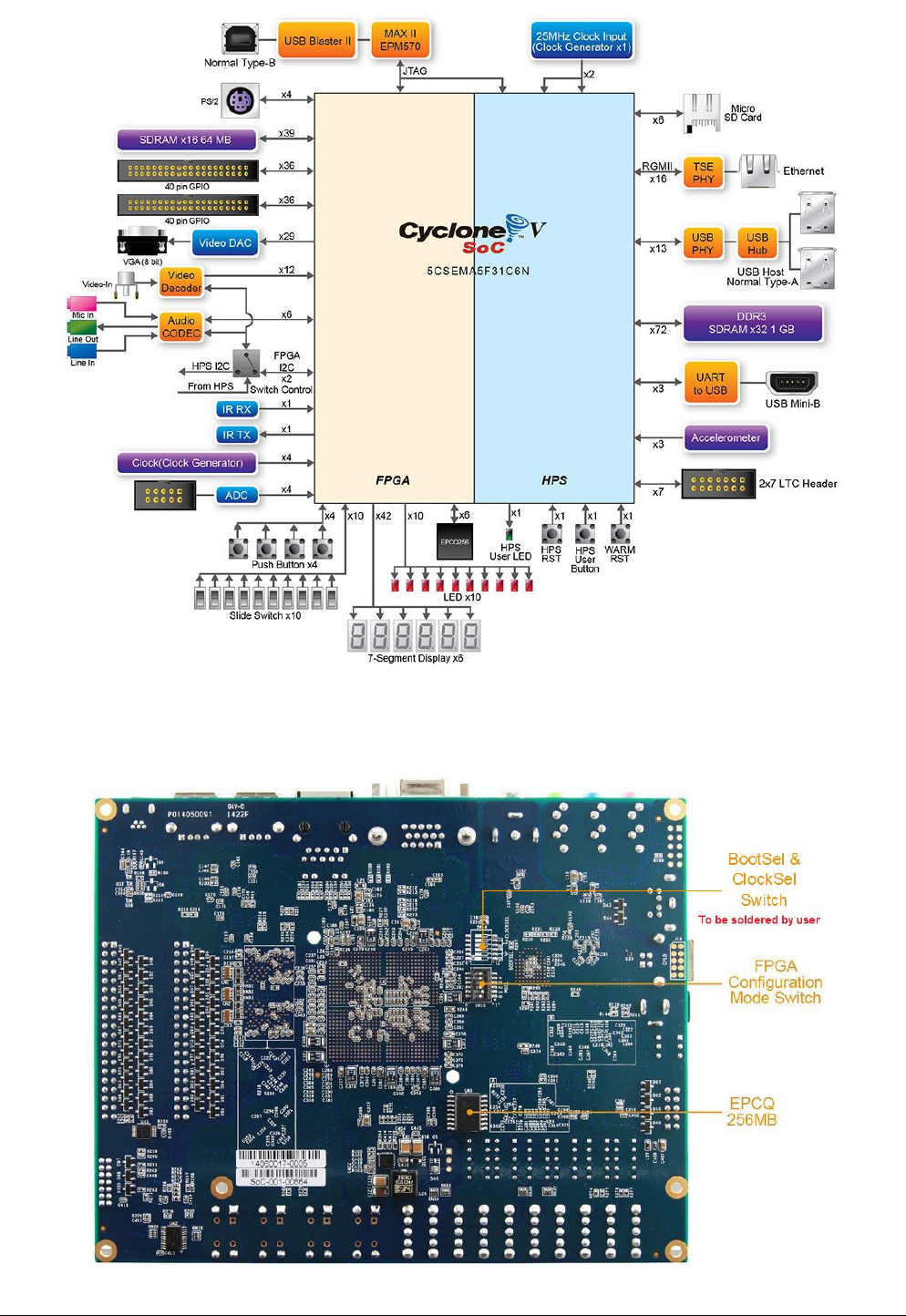
Figure 6-1. Terasic DE1-SoC Board [1]
The DE1-SoC board has many features that allow users to implement a wide range of designed circuits. We will
discuss some noteworthy features in this guide.
Cyclone V SoC 5CSEMA5F31C6 Device
Dual-core ARM CORTEX-A9 (HPS)
85K Programmable Logic Elements
4’450 Kbits embedded memory
6 Fraconal PLLs
2 Hard Memory Controllers (only seems to be used for the HPS DDR3 SDRAM, not the FPGA SDRAM)
Serial Conguraon device – EPCS128 on FPGA
On-Board USB BLASTER II (Normal type B USB connector)
64 MB (32Mx16) SDRAM on FPGA
1 GB (2x256Mx16) DDR3 SDRAM on HPS
MICRO SD Card Socket on HPS
Two Port USB 2.0 Host (ULPI interface with USB type A connector)
USB to UART (micro USB type B connector)
10/100/1000 Ethernet
PS/2 mouse/keyboard
IR Emier/Receiver

SoC-FPGA Design Guide [DE1-SoC Edition]
21/04/2018 P a g e | 14
Two 40-pin Expansion Headers
One 10-pin ADC Input Header
One LTC connector (One Serial Peripheral Interface (SPI) Master, one I2C and one GPIO interface)
24-bit VGA DAC
24-bit CODEC, line-in, line-out, and microphone-in jacks
TV Decoder (NTSC/PAL/SECAM) and TV-in connector
Sample rate: 500 KSPS
Channel number: 8
Resoluon: 12 bits
Analog input range : 0 ~ 2.5 V or 0 ~ 5V as selected via the RANGE bit in the control register
5 User Keys (FPGA x4; HPS x1)
10 User switches (FPGA x10)
11 User LEDs (FPGA x10; HPS x1)
2 HPS Reset Buons (HPS_RST_n and HPS_WARM_RST_n)
Six 7-segment displays
G-Sensor on HPS
12V DC input
SoC-FPGA Design Guide [DE1-SoC Edition]
21/04/2018 P a g e | 15
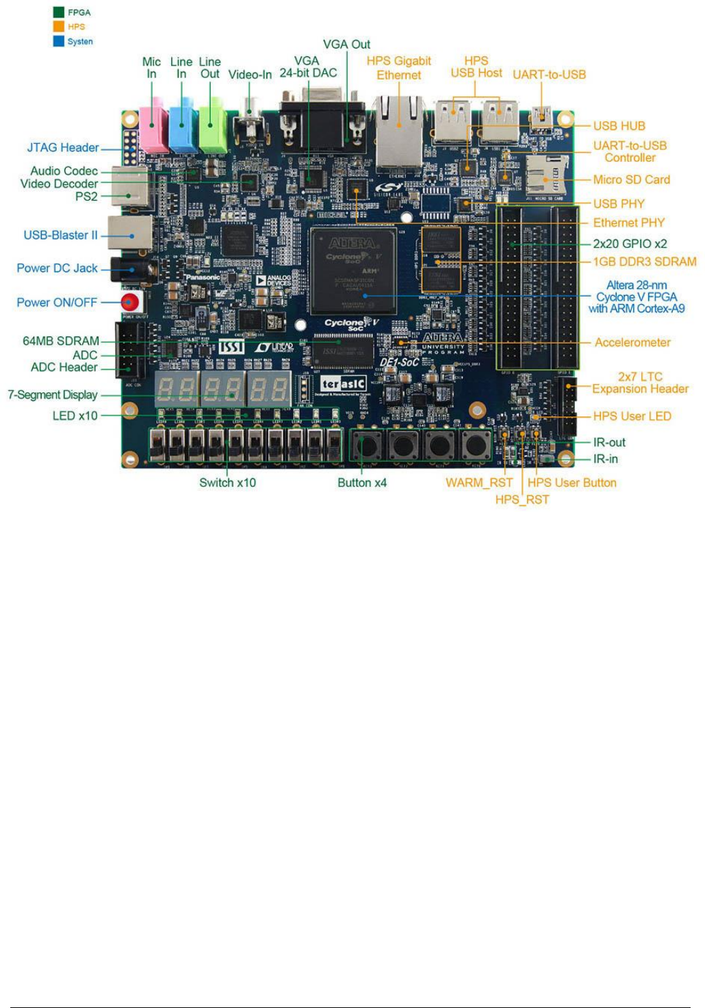
Figure 6-2. Block Diagram of the DE1-SoC Board [1]
Figure 6-3. Back [1]
SoC-FPGA Design Guide [DE1-SoC Edition]
21/04/2018 P a g e | 16
Figure 6-4. Front [1]
Green for peripherals directly connected to the FPGA
Orange for peripherals directly connected to the HPS
Blue for board control
SoC-FPGA Design Guide [DE1-SoC Edition]
21/04/2018 P a g e | 17
This secon describes some features of the Cyclone V family of devices. We do not list all features, but only
the ones most important to us. All informaon below, along with the most complete documentaon regarding
this family can be found in the Cyclone V Device Handbook [2].
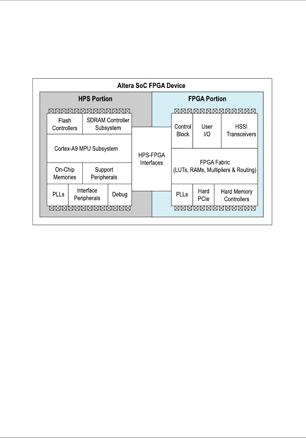
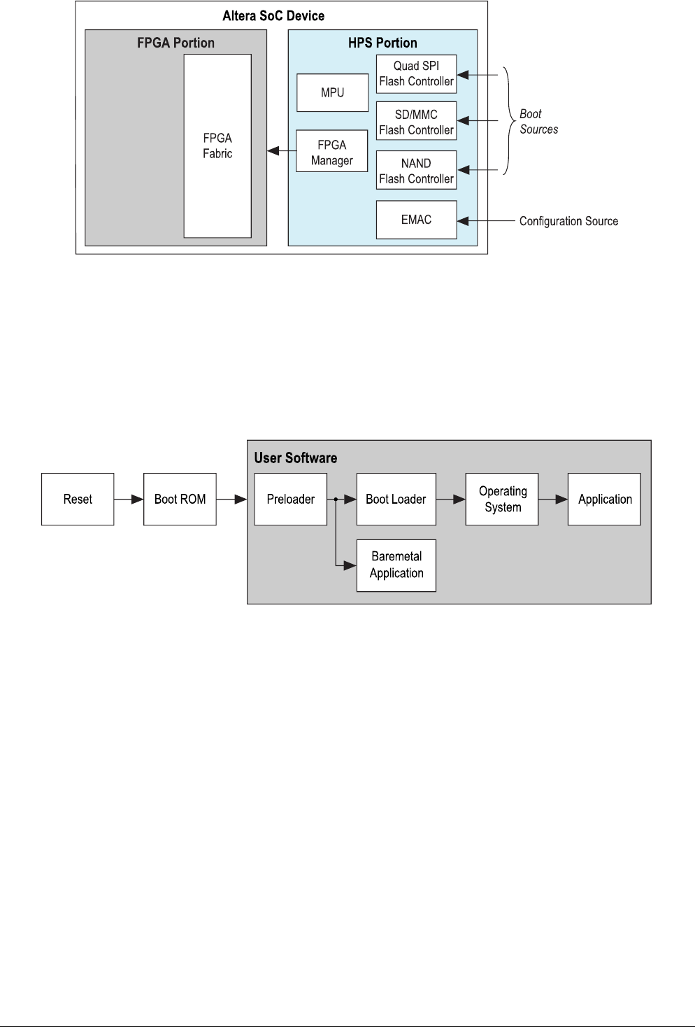
The Cyclone V device is a single-die system on a chip (SoC) that consists of two disnct parts – a hard
processor system (HPS) poron and an FPGA poron.
Figure 7-1. Altera SoC FPGA Device Block Diagram [2, pp. 1-1]
The HPS contains a microprocessor unit (MPU) subsystem with single or dual ARM Cortex-A9 MPCore
processors, ash memory controllers, SDRAM L3 Interconnect, on-chip memories, support peripherals,
interface peripherals, debug capabilies, and phase-locked loops (PLLs). The dual-processor HPS supports
symmetric (SMP) and asymmetric (AMP) mulprocessing.
The DE1-SoC has a DUAL-processor HPS.
The FPGA poron of the device contains the FPGA fabric, a control block (CB), phase-locked loops (PLLs), and
depending on the device variant, high-speed serial interface (HSSI) transceivers, hard PCI Express (PCIe)
controllers, and hard memory controllers.
The DE1-SoC does not contain any HSSI transceivers, or hard PCIe controllers.
The HPS and FPGA porons of the device are disnctly dierent. The HPS can boot from
the FPGA fabric,
external ash, or
JTAG
In contrast, the FPGA must be congured either through
the HPS, or
an externally supported device such as the Quartus Prime programmer.

SoC-FPGA Design Guide [DE1-SoC Edition]
21/04/2018 P a g e | 18
The MPU subsystem can boot from
ash devices connected to the HPS pins, or
from memory available on the FPGA poron of the device (when the FPGA poron is previously
congured by an external source).
The HPS and FPGA porons of the device each have their own pins. Pins are not freely shared between the
HPS and the FPGA fabric. The FPGA I/O PINS are congured by an FPGA CONFIGURATION IMAGE through the
HPS or any external source supported by the device. The HPS I/O PINS are congured by SOFTWARE execung
in the HPS. Soware execung on the HPS accesses control registers in the Cyclone V system manager to
assign HPS I/O pins to the available HPS modules.
The SOFTWARE that congures the HPS I/O PINS is called the PRELOADER.
The HPS and FPGA porons of the device have separate external power supplies and independently power on.
You can power on the HPS without powering on the FPGA poron of the device. However, to power on the
FPGA poron, the HPS must already be on or powered on at the same me as the FPGA poron. Table 7-1
summarizes the possible conguraons.
HPS Power
FPGA Power
On
On
On
O
O
O
Table 7-1. Possible HPS and FPGA Power Configurations
SoC-FPGA Design Guide [DE1-SoC Edition]
21/04/2018 P a g e | 19
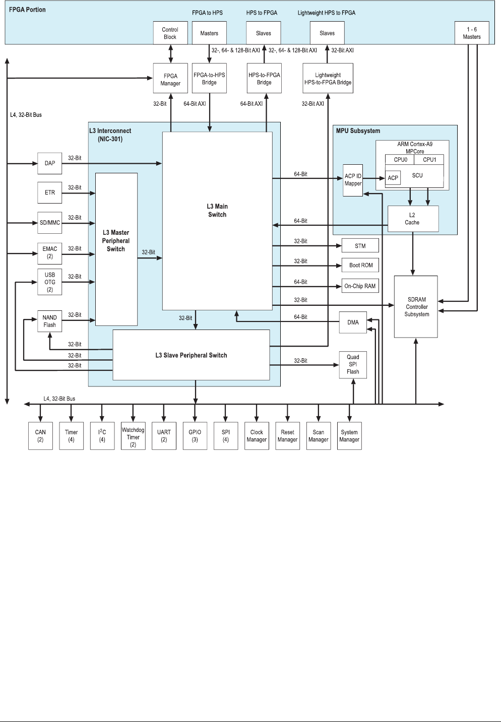
Figure 7-2. HPS Block Diagram [2, pp. 1-3]
The following list contains the main modules of the HPS:
Masters
o MPU subsystem featuring dual ARM Cortex-A9 MPCore processors
o General-purpose Direct Memory Access (DMA) controller
o Two Ethernet media access controllers (EMACs)
o Two USB 2.0 On-The-Go (OTG) controllers
o NAND ash controller
o Secure Digital (SD) / MulMediaCard (MMC) controller
o Two serial peripheral interface (SPI) master controllers
o ARM CoreSight debug components
Slaves
o Quad SPI ash controller
o Two SPI slave controllers
o Four inter-integrated circuit (I2C) controllers
o 64 KB on-chip RAM

SoC-FPGA Design Guide [DE1-SoC Edition]
21/04/2018 P a g e | 20
o 64 KB on-chip boot ROM
o Two UARTs
o Four mers
o Two watchdog mers
o Three general-purpose I/O (GPIO) interfaces
o Two controller area network (CAN) controllers
o System manager
o Clock manager
o Reset manager
o Scan manager
o FPGA manager
In this part, we briey go through some features provided by the most important HPS components.
Here are a few important features of the MPU subsystem:
Interrupt controller
One general-purpose mer and one watchdog mer per processor
One Memory management unit (MMU) per processor
The HPS masters the L3 interconnect and the SDRAM controller subsystem.
The SDRAM controller subsystem is MASTERED by HPS MASTERS and FPGA FABRIC MASTERS. It supports
DDR2, DDR3, and LPDDR2 devices. It is composed of 2 parts:
SDRAM controller
DDR PHY (interfaces the single port memory controller to the HPS I/O)
The DE1-SoC contains DDR3 SDRAM
7.3.3.1 System Manager
This is one of the most essenal HPS components. It oers a few important features:
PIN MULTIPLEXING (term used for the SOFTWARE conguraon of the HPS I/O PINS by the
PRELOADER)
Freeze controller that places I/O elements into a safe state for conguraon
Low-level control of peripheral features not accessible through the control and status registers (CSRs)
The low-level control of some peripheral features that are not accessible through the CSRs is NOT externally
documented. You will see this type of code when you generate your custom preloader, but must NOT use the
constructs in your own code.
7.3.3.2 FPGA Manager
The FPGA manager oers the following features:
Manages the conguraon of the FPGA poron of the device
Monitors conguraon-related signals in the FPGA
Provides 32 general-purpose inputs and 32 general-purpose outputs to the FPGA fabric

SoC-FPGA Design Guide [DE1-SoC Edition]
21/04/2018 P a g e | 21
7.3.4.1 GPIO Interfaces
The HPS provides three GPIO interfaces and oer the following features:
Supports digital de-bounce
Congurable interrupt mode
Supports up to 71 I/O pins and 14 input-only pins, based on device variant
Supports up to 67 I/O pins and 14 input-only pins
The DE1-SoC has 67 I/O pins and 14 input-only pins
The following on-chip memories are DIFFERENT from any on-chip memories located in the FPGA fabric.
7.3.5.1 On-Chip RAM
The on-chip RAM oers the following features:
64 KB size
High performance for all burst lengths
7.3.5.2 Boot ROM
The boot ROM oers the following features:
64 KB size
Contains the code required to support HPS boot from cold or warm reset
Used EXCLUSIVELY for boong the HPS
The code in the boot ROM CANNOT be changed.
The HPS-FPGA interfaces provide a variety of communicaon channels between the HPS and the FPGA fabric.
The HPS-FPGA interfaces include:
FPGA-to-HPS bridge – a high performance bus with a congurable data width of 32, 64, or 128 bits. It
allows the FPGA fabric to master transacons to slaves in the HPS. This interface allows the FPGA
fabric to have full visibility into the HPS address space.
HPS-to-FPGA bridge – a high performance bus with a congurable data width of 32, 64, or 128 bits. It
allows the HPS to master transacons to slaves in the FPGA fabric. I will somemes call this the
“heavyweight” HPS-to-FPGA bridge to disnguish its “lightweight” counterpart (see below).
Lightweight HPS-to-FPGA bridge – a bus with a 32-bit xed data width. It allows the HPS to master
transacons to slaves in the FPGA fabric.
FPGA manager interface – signals that communicate with the FPGA fabric for boot and conguraon.
Interrupts – allows so IPs to supply interrupts directly to the MPU interrupt controller.
HPS debug interface – an interface that allows the HPS debug control domain to extend into the FPGA.
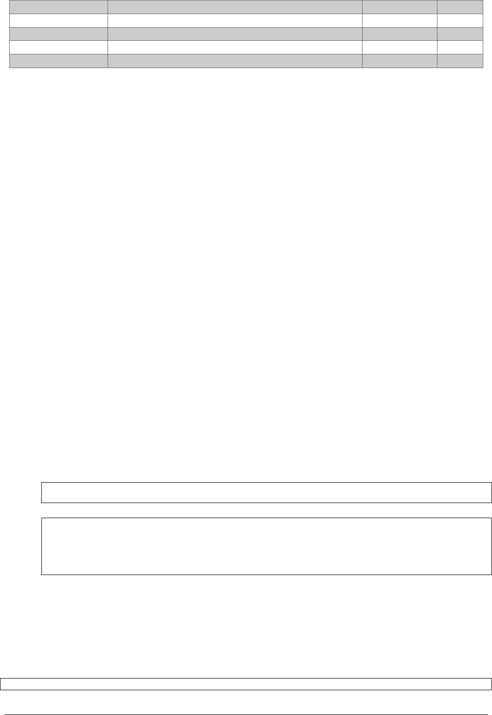
The HPS address map species the address of slaves, such as memory and peripherals, as viewed by the HPS
masters. The HPS has 3 address spaces:
SoC-FPGA Design Guide [DE1-SoC Edition]
21/04/2018 P a g e | 22
Name
Descripon
Size
MPU
MPU subsystem
4 GB
L3
L3 interconnect
4 GB
SDRAM
SDRAM controller subsystem
4 GB
Table 7-2. HPS Address Spaces [2, pp. 1-13]
The following gure shows the relaonships between the dierent HPS address spaces. The gure is NOT to
scale.
Figure 7-3. HPS Address Space Relaons [2, pp. 1-14]
The window regions provide access to other address spaces. The thin black arrows indicate which address
space is accessed by a window region (arrows point to accessed address space).
The SDRAM window in the MPU can grow and shrink at the top and boom (short blue vercal arrows) at the
expense of the FPGA slaves and boot regions. The ACP window can be mapped to any 1 GB region in the MPU
address space (blue vercal bidireconal arrow), on gigabyte-aligned boundaries.
The following table shows the base address and size of each region that is common to the L3 and MPU address
spaces.
Region Name
Descripon
Base Address
Size
FPGA slaves
FPGA slaves connected to the heavyweight HPS-to-
FPGA bridge
0xC0000000
960 MB
HPS peripherals
Slaves directly connected to the HPS (corresponds
to all orange colored elements on Figure 6-4 and
Figure 6-3)
0xFC000000
64 MB
Lightweight FPGA slaves
FPGA slaves connected to the lightweight HPS-to-
FPGA bridge
0xFF200000
2 MB
Table 7-3. Common Address Space Regions [2, pp. 1-15]

SoC-FPGA Design Guide [DE1-SoC Edition]
21/04/2018 P a g e | 23
The following table lists the slave idener, slave tle, base address, and size of each slave in the HPS
peripheral region. The Slave Idener column lists the names used in the HPS register map le provided by
Altera (more on this later).
Slave Idener
Slave Title
Base Address
Size
STM
STM
0xFC000000
48 MB
DAP
DAP
0xFF000000
2 MB
LWFPGASLAVES
FPGA slaves accessed with lightweight HPS-to-FPGA
bridge
0xFF200000
2 MB
LWHPS2FPGAREGS
Lightweight HPS-to-FPGA bridge GPV
0xFF400000
1 MB
HPS2FPGAREGS
HPS-to-FPGA bridge GPV
0xFF500000
1 MB
FPGA2HPSREGS
FPGA-to-HPS bridge GPV
0xFF600000
1 MB
EMAC0
EMAC0
0xFF700000
8 KB
EMAC1
EMAC1
0xFF702000
8 KB
SDMMC
SD/MMC
0xFF704000
4 KB
QSPIREGS
Quad SPI ash controller registers
0xFF705000
4 KB
FPGAMGRREGS
FPGA manager registers
0xFF706000
4 KB
ACPIDMAP
ACP ID mapper registers
0xFF707000
4 KB
GPIO0
GPIO0
0xFF708000
4 KB
GPIO1
GPIO1
0xFF709000
4 KB
GPIO2
GPIO2
0xFF70A000
4 KB
L3REGS
L3 interconnect GPV
0xFF800000
1 MB
NANDDATA
NAND controller data
0xFF900000
1 MB
QSPIDATA
Quad SPI ash data
0xFFA00000
1 MB
USB0
USB0 OTG controller registers
0xFFB00000
256 KB
USB1
USB1 OTG controller registers
0xFFB40000
256 KB
NANDREGS
NAND controller registers
0xFFB80000
64 KB
FPGAMGRDATA
FPGA manager conguraon data
0xFFB90000
4 KB
CAN0
CAN0 controller registers
0xFFC00000
4 KB
CAN1
CAN1 controller registers
0xFFC01000
4 KB
UART0
UART0
0xFFC02000
4 KB
UART1
UART1
0xFFC03000
4 KB
I2C0
I2C0
0xFFC04000
4 KB
I2C1
I2C1
0xFFC05000
4 KB
I2C2
I2C2
0xFFC06000
4 KB
I2C3
I2C3
0xFFC07000
4 KB
SPTIMER0
SP Timer0
0xFFC08000
4 KB
SPTIMER1
SP Timer1
0xFFC09000
4 KB
SDRREGS
SDRAM controller subsystem registers
0xFFC20000
128 KB
OSC1TIMER0
OSC1 Timer0
0xFFD00000
4 KB
OSC1TIMER1
OSC1 Timer1
0xFFD01000
4 KB
L4WD0
Watchdog0
0xFFD02000
4 KB
L4WD1
Watchdog1
0xFFD03000
4 KB
CLKMGR
Clock manager
0xFFD04000
4 KB
RSTMGR
Reset manager
0xFFD05000
4 KB
SYSMGR
System manager
0xFFD08000
16 KB
DMANONSECURE
DMA nonsecure registers
0xFFE00000
4 KB
DMASECURE
DMA secure registers
0xFFE01000
4 KB
SPIS0
SPI slave0
0xFFE02000
4 KB
SPIS1
SPI slave1
0xFFE03000
4 KB
SPIM0
SPI master0
0xFFF00000
4 KB
SPIM1
SPI master1
0xFFF01000
4 KB
SoC-FPGA Design Guide [DE1-SoC Edition]
21/04/2018 P a g e | 24
SCANMGR
Scan manager registers
0xFFF02000
4 KB
ROM
Boot ROM
0xFFFD0000
64 KB
MPUSCU
MPU SCU registers
0xFFFEC000
8 KB
MPUL2
MPU L2 cache controller registers
0xFFFEF000
4 KB
OCRAM
On-chip RAM
0xFFFF0000
64 KB
Table 7-4. HPS Peripheral Region Address Map [2, pp. 1-16]
The programming model for accessing the HPS peripherals in Table 7-4 is the same as for peripherals created
on the FPGA fabric. That is, every peripheral has a base address at which a certain number of registers can be
found. You can then read and write to a certain set of these registers in order to modify the peripheral’s
behavior.
When using a HPS peripheral in Table 7-4, you do not need to hard-code any base address or peripheral
register map in your programs, as Altera provides a header le for each one.
Three directories contain all HPS-related HEADER FILES:
1. “<altera_install_directory>/<version>/embedded/ip/altera/hps/altera_hps/hwlib/inclu
de”
Contains HIGH-LEVEL header les that typically contain a few FUNCTIONS which facilitate control over
the HPS components. These funcons are all part of Altera’s HWLIB, which was created to make
programming the HPS easier. This directory contains code that is common to the Cyclone V, Arria V,
and Arria 10 devices.
2. “<altera_install_directory>/<version>/embedded/ip/altera/hps/altera_hps/hwlib/inclu
de/soc_cv_av”
Same as above, but more specifically for the Cyclone V and Arria V FPGA families.
3. “<altera_install_directory>/<version>/embedded/ip/altera/hps/altera_hps/hwlib/inclu
de/soc_cv_av/socal”
Contains LOW-LEVEL header les that provide a peripheral’s BIT-LEVEL REGISTER DETAILS. For
example, any bits in a peripheral’s register that correspond to undened behavior will be specied in
these header les.
To illustrate the dierences among the high and low-level header les, we can compare the ones related to the
FPGA manager peripheral:
1. “…/hwlib/include/soc_cv_av/alt_fpga_manager.h”
ALT_STATUS_CODE alt_fpga_reset_assert(void);
ALT_STATUS_CODE alt_fpga_configure(const void* cfg_buf, size_t cfg_buf_len);
2. “…/hwlib/include/soc_cv_av/socal/alt_fpgamgr.h”
/* The width in bits of the ALT_FPGAMGR_CTL_EN register field. */
#define ALT_FPGAMGR_CTL_EN_WIDTH 1
/* The mask used to set the ALT_FPGAMGR_CTL_EN register field value. */
#define ALT_FPGAMGR_CTL_EN_SET_MSK 0x00000001
/* The mask used to clear the ALT_FPGAMGR_CTL_EN register field value. */
#define ALT_FPGAMGR_CTL_EN_CLR_MSK 0xfffffffe
An important header le is “…/hwlib/include/soc_cv_av/socal/hps.h”. It contains the HPS component’s
full REGISTER MAP, as provided in Table 7-4.
Note however, that there exists NO HEADER FILE for the “heavyweight” HPS-to-FPGA bridge, as it is not
located in the “HPS peripherals” region in Figure 7-3. Indeed, the “heavyweight” HPS-to-FPGA bridge is not
considered a HPS peripheral, whereas the “lightweight” HPS-to-FPGA bridge is. Therefore, in order to use the
“heavyweight” HPS-to-FPGA bridge, you will have to dene a macro in your code, as follows:
#define ALT_HWFPGASLVS_OFST 0xc0000000
SoC-FPGA Design Guide [DE1-SoC Edition]
21/04/2018 P a g e | 25
Note that HWLIB can only be directly used in a BARE-METAL APPLICATION, as it directly references physical
addresses. The library can unfortunately NOT be used directly in a LINUX DEVICE DRIVER, because it uses
standard header files that are not available in the kernel. Needless to say that a userspace linux program
cannot use the library either, as the linux kernel would terminate a user process that tries to access any of
these physical addresses directly.
Before being able to use the Cyclone V SoC, one needs to understand how the HPS boots and how the FPGA is
congured. We’ll rst take a look at the ordering between the HPS and FPGA.
The HPS BOOT starts when the processor is released from reset (for example, on power up) and executes code
in the internal boot ROM at the reset excepon address. The boot process ends when the code in the boot
ROM jumps to the next stage of the boot soware. This next stage of the boot soware is referred to as the
preloader. Figure 7-4 illustrates this inial incomplete HPS boot ow.
Figure 7-4. Simplied HPS Boot Flow [2, pp. A-3]
The processor can boot from the following sources:
NAND ash memory through the NAND ash controller
SD/MMC ash memory through the SD/MMC ash controller
SPI and QSPI ash memory through the QSPI ash controller using Slave Select 0
FPGA fabric on-chip memory
The choice of the boot source is done by modifying the BOOTSEL and CLKSEL values BEFORE THE DEVICE IS
POWERED UP. Therefore, the Cyclone V device normally uses a PHYSICAL DIP SWITCH to congure the
BOOTSEL and CLKSEL.
The DE1-SoC can ONLY BOOT from SD/MMC ash memory, as its BOOTSEL and CLKSEL values are hard-wired
on the board. Although its HPS contains all necessary controllers, the board doesn’t have a physical DIP switch
to modify the BOOTSEL and CLKSEL values. The actual locaon of the DIP switch is present underneath the
board, as can be seen in Figure 6-3, but a switch isn’t soldered.
CONFIGURATION OF THE FPGA poron of the device starts when the FPGA poron is released from reset state
(for example, on power up). The control block (CB) in the FPGA poron of the device is responsible for
obtaining an FPGA conguraon image and conguring the FPGA. The FPGA conguraon ends when the
conguraon image has been fully loaded and the FPGA enters user mode. The FPGA conguraon image is
provided by users and is typically stored in non-volale ash-based memory. The FPGA CB can obtain a
conguraon image from the HPS through the FPGA manager, or from another external source, such as the
Quartus Prime Programmer.
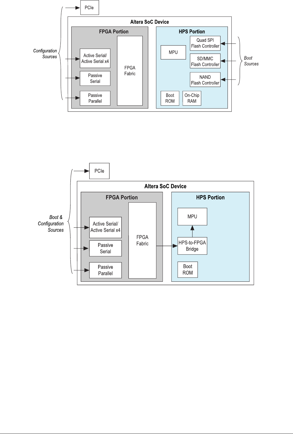
The following three gures illustrate the possible HPS boot and FPGA conguraon schemes. Note that
Cyclone V devices can also be fully congured through a JTAG connecon.
SoC-FPGA Design Guide [DE1-SoC Edition]
21/04/2018 P a g e | 26
Figure 7-5. Independent FPGA Conguraon and HPS Boong [2, pp. A-2]
Figure 7-5 shows the scheme where the FPGA conguraon and the HPS boot occur independently. The FPGA
conguraon obtains its image from a non-HPS source (Quartus Prime Programmer), while the HPS boot
obtains its conguraon image from a non-FPGA fabric source.
Figure 7-6. FPGA Conguraon before HPS Boong (HPS boots from FPGA) [2, pp. A-2]
Figure 7-6 shows the scheme where the FPGA is rst congured through the Quartus Prime Programmer, then
the HPS boots from the FPGA fabric. The HPS boot waits for the FPGA fabric to be powered on and in user
mode before execung. The HPS boot ROM code executes the preloader from the FPGA fabric over the HPS-
to-FPGA bridge. The preloader can be obtained from the FPGA on-chip memory, or by accessing an external
interface (such as a larger external SDRAM).
SoC-FPGA Design Guide [DE1-SoC Edition]
21/04/2018 P a g e | 27
Figure 7-7. HPS Boots and Performs FPGA Conguraon [2, pp. A-3]
Figure 7-7 shows the scheme under which the HPS rst boots from one of its non-FPGA fabric boot sources,
then soware running on the HPS congures the FPGA fabric through the FPGA manager. The soware on the
HPS obtains the FPGA conguraon image from any of its ash memory devices or communicaon interfaces,
such as the SD/MMC memory, or the Ethernet port. The soware is provided by users and the boot ROM is
not involved in conguring the FPGA fabric.
Figure 7-8. HPS Boot Flows [2, pp. A-3]
Boong soware on the HPS is a mul-stage process. Each stage is responsible for loading the next stage. The
rst soware stage is the boot ROM. The boot ROM code locates and executes the second soware stage,
called the preloader. The preloader locates, and IF PRESENT, executes the next soware stage. The preloader
and subsequent soware stages are collecvely referred to as user soware.
The reset, boot ROM, and preloader stages are always present in the HPS boot ow. What comes aer the
preloader then depends on the type of applicaon you want to run. The HPS can execute 2 types of
applicaons:
Bare-metal applicaons (no operang system)
Applicaons on top of an operang system (linux)
Figure 7-8 shows the HPS’ available boot ows. The Reset and Boot ROM stages are the only xed parts of the
boot process. Everything in the user soware stages can be customized.
Although the DE1-SoC has a DUAL-processor HPS (CPU0 and CPU1), the boot ow only executes on CPU0 and
CPU1 is under reset. If you want to use both processors of the DE1-SoC, then USER SOFTWARE execung on
CPU0 is responsible for releasing CPU1 from reset.

SoC-FPGA Design Guide [DE1-SoC Edition]
21/04/2018 P a g e | 28
7.6.2.1 Preloader
The preloader is one of the most important boot stages. It is actually what one would call the boot “source”, as
all stages before it are unmodiable. The preloader can be stored on external ash-based memory, or in the
FPGA fabric.
The preloader typically performs the following acons:
Inialize the SDRAM interface
Congure the HPS I/O through the scan manager
Congure pin mulplexing through the system manager
Congure HPS clocks through the clock manager
Inialize the ash controller (NAND, SD/MMC, QSPI) that contains the next stage boot soware
Load the next boot soware into the SDRAM and pass control to it
The preloader does NOT release CPU1 from reset. The subsequent stages of the boot process are responsible
for it if they want to use the extra processor.

SoC-FPGA Design Guide [DE1-SoC Edition]
21/04/2018 P a g e | 29
GENERAL INFORMATION
8.1 INTRODUCTION
The HPS component is a SOFT component, but it does NOT mean that the HPS is a socore processor. In fact,
the HPS exclusively contains HARD LOGIC. The reason it is considered a socore component originates from
the fact that it enables other so components to interface with the HPS hard logic. As such, the HPS
component has a small footprint in the FPGA fabric, as its only purpose is to connect the so and hard logic
together.
Therefore, it is possible to use the Cyclone V SoC in 3 dierent conguraons:
FPGA-only
HPS-only
HPS & FPGA
We will look at the FPGA-only and HPS & FPGA conguraons below. We will not cover the HPS-only
conguraon as it is idencal to the HPS & FPGA one where you simply don’t load any design on the FPGA
fabric. The conguraons using the HPS are more dicult to set up than the FPGA-only one.
8.2 FPGA-ONLY
Exclusively using the FPGA part of the Cyclone V is easy, as the design process is idencal to any other Altera
FPGA. You can build a complete design in Quartus Prime & Qsys, simulate it in ModelSim-Altera, then program
the FPGA through the Quartus Prime Programmer. If you instanated a Nios II processor in Qsys, you can use
the Nios II SBT IDE to develop soware for the processor.
The DE1-SoC has a lot of pins, which makes it tedious to start an FPGA design. It is recommended to use the
ENTITY in [3] for your TOP-LEVEL VHDL FILE, as it contains all the board’s FPGA and HPS pins.
Aer having dened a top-level module, it is necessary to map your design’s pins to the ones available on the
DE1-SoC. The TCL SCRIPT in [4] can be executed in Quartus Prime to specify the board’s device ID and all its
PIN ASSIGNMENTS. In order to execute the TCL script, place it in your quartus working directory, then run it
through the “Tools > Tcl Scripts…” menu item in Quartus Prime.
8.3 HPS & FPGA
8.3.1 Bare-metal Application
On one hand, bare-metal soware enjoys the advantage of having no OS overhead. This has many
consequences, the most visible of which are that code executes at nave speed as no context switching is ever
performed, and addionally, that code can directly address the HPS peripherals using their PHYSICAL memory-
mapped addresses, as no virtual memory system is being used. This is very useful when trying to use the HPS
as a high-speed microcontroller. Such a programming environment is very similar to the one used by other
microcontrollers, like the TI MSP430.
On the other hand, bare-metal code has one great disadvantage, as the programmer must connue to
congure the Cyclone V to use all its resources. For example, we saw in 7.6.2.1 that the preloader does not
release CPU1 from reset, and that it is up to the user software to perform this, which is the bare-metal
application itself in this case. Furthermore, supposing CPU1 is available for use, it is still difficult to run multi-
threaded code, as an OS generally handles program scheduling and CPU affinity for the programmer. The
programmer must now manually assign code fragments to each CPU.

SoC-FPGA Design Guide [DE1-SoC Edition]
21/04/2018 P a g e | 30
8.3.2 Application Over an Operating System (Linux)
Running code over a linux operating system has several advantages. First of all, the kernel releases CPU1 from
reset upon boot, so all processors are available. Furthermore, the kernel initializes and makes most, if not all
HPS peripherals available for use by the programmer. This is possible since the linux kernel has access to a
huge amount of device drivers. Multi-threaded code is also much easier to write, as the programmer has
access to the familiar OS facilities for threading. Finally, the linux kernel is not restricted to running compiled C
programs. Indeed, you can always run code written in another programming language providing you first
install the runtime environment required (which must be available for ARM processors).
However, running an “EMBEDDED” application on top of an operating system also has disadvantages. Due to
the virtual memory system put in place by the OS, a program cannot directly access the HPS peripherals
through their physical memory-mapped addresses. Instead, one first needs to map the physical addresses of
interest into the running program’s virtual address space. Only then will it be possible to access a peripheral’s
registers. Ideally, the programmer should write a device driver for each specific component that is designed in
order to have a clean interface between user code and device accesses.
At the end of the day, bare-metal applications and applications running code on top of linux can do the same
things. Generally speaking, programming on top of linux is superior and much easier compared to bare-metal
code, as its advantages greatly outweigh its drawbacks.
8.4 GOALS
Let’s start by defining what we want to achieve in this tutorial. We want to create a system in which both the
HPS and FPGA can do some computation simultaneously. More specifically, we want the following
capabilities:
1. A NIOS II processor on the FPGA must be able to access the LEDs connected to the FPGA PORTION of
the device and will be responsible for creating a strobing light effect on the lower 5 LEDs.
2. The Nios II processor will use the DE1-SoC’s SDRAM instead of any form of on-chip memory.
3. The HPS must be able to use the LED and button that are directly connected to the HPS PORTION of
the device. Pressing the button should toggle the LED.
4. The HPS must be able to access the LEDs connected to the FPGA PORTION of the device and will be
responsible for creating a strobing light effect on the upper 5 LEDs.
5. The HPS must be able to use the ethernet port on the board.
6. The HPS must be able to use the microSD card port on the board to which we will write anything we
want.
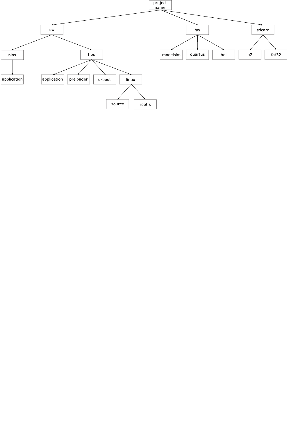
8.5 PROJECT STRUCTURE
The development process creates a lot more files compared to an FPGA-only design. We will use the folder
structure shown in Figure 8-1 to organize our project. In this demo, we will use “DE1_SoC_demo” as the
project name.
The “hw” directory contains all hardware-related files.
The “sw” directory contains all software-related files.
The “sdcard” directory contains all final targets needed to create a valid sdcard from which the DE1-
SoC can boot.
SoC-FPGA Design Guide [DE1-SoC Edition]
21/04/2018 P a g e | 31
Figure 8-1. Project Folder Structure
Many steps have to be performed in order to configure the Cyclone V before you can use the HPS.
The HARDWARE design is IDENTICAL whether you want to write bare-metal applications, or linux HPS
applications.
The SOFTWARE design is DIFFERENT for bare-metal and linux HPS applications.
The complete design for this tutorial can be found in DE1_SoC_demo.zip [5].

SoC-FPGA Design Guide [DE1-SoC Edition]
21/04/2018 P a g e | 32
9 USING THE CYCLONE V HARDWARE
The details below give step-by-step instructions to create a full system from scratch.
9.1 GENERAL QUARTUS PRIME SETUP
1. Create a new Quartus Prime project. You only need to specify the project name and destination, as all
other settings will be set at a later stage by a TCL script. For this demo, we will call our project
“DE1_SoC_demo” and will store it in “DE1_SoC_demo/hw/quartus”.
2. Download DE1_SoC_top_level.vhd [3] and save it in “DE1_SoC_demo/hw/hdl”. We will use this file
as the project’s top-level VHDL file, as it contains a complete list of pin names available on the DE1-
SoC for use in your designs. Add the file to the Quartus Prime project by using “Project >
Add/Remove Files in Project…” and set it as your design’s top-level entity.
3. Download pin_assignment_DE1_SoC.tcl [4] and save it in “DE1_SoC_demo/hw/quartus”. This
script assigns pin locations and I/O standards to all pins names in “DE1_SoC_top_level.vhd”.
Execute the TCL script by using “Tools > Tcl Scripts…” in Quartus Prime.
At this stage, all general Quartus Prime settings have been performed, and we can start creating our
design. We want to use the HPS, as well as a Nios II processor in our design, so we will use the Qsys tool to
create the system.
4. Launch the Qsys tool and create a new system. Save it under the name “soc_system.qsys”.
9.2 SYSTEM DESIGN WITH QSYS NIOS II
In this section, we assemble all system components needed to allow the Nios II processor to create a strobing
light effect on the lower 5 LEDs.
We want to use a Nios II processor with an SDRAM. To use an SDRAM, we need 2 things:
An SDRAM controller.
A PLL to generate a clock for the softcore SDRAM controller and a phase-shifted clock for the off-chip
SDRAM component. The reference clocks and timings needed for the SDRAM can be found on its
datasheet [6].
5. Add an “Altera PLL” to the system.
Reference Clock Frequency: 50 MHz
Operation Mode: normal
Uncheck “Enable locked output port”
We need to generate 3 clocks:
50 MHz clock for the Nios II processor and all its peripherals.
100 MHz clock for the SDRAM controller.
100 MHz, -3758 ps phase-shifted clock for the off-chip SDRAM component.
In Qsys’ “System Contents” tab:
Export “pll_0.outclk2” under the name “pll_0_sdram”, as shown in Figure 9-1. This clock
will be used for the off-chip SDRAM component.

SoC-FPGA Design Guide [DE1-SoC Edition]
21/04/2018 P a g e | 33
Figure 9-1. Exporting the pll_0.outclk2 Signal
6. Add a softcore SDRAM controller to the system. Use the following settings (taken from the SDRAM’s
datasheet):
Memory Profile
Data Width
Bits: 16
Architecture
Chip select: 1
Banks: 4
Address Width
Row: 13
Column: 10
Timing
CAS latency cycles: 3
Initialization refresh cycles: 2
Issue one refresh command every: 7.8125 us
Delay after powerup, before initialization: 100.0 us
Duration of refresh command (t_rfc): 70.0 ns
Duration of precharge command (t_rp): 15.0 ns
ACTIVE to READ or WRITE delay (t_rcd): 15.0 ns
Access time (t_ac): 5.4 ns
Write recovery time (t_wr, no auto precharge): 14.0 ns
In Qsys’ “System Contents” tab:
Rename “new_sdram_controller_0” to “sdram_controller_0”.
Export “sdram_controller_0.wire” under the name “sdram_controller_0_wire”.
7. Add a Nios II processor to the system. You can choose any variant. In this demo, we use the “non-
classic” Nios II processor, with configuration “Nios II/f”.
8. Add a System ID Peripheral to the system. In Qsys’ “System Contents” tab:
Rename the component to “sysid”
9. Add a JTAG UART to the system. This serial console will be used to be able to see the output
generated by the printf() function when programming the Nios II processor.
10. Connect the system as shown in Figure 9-2 below:
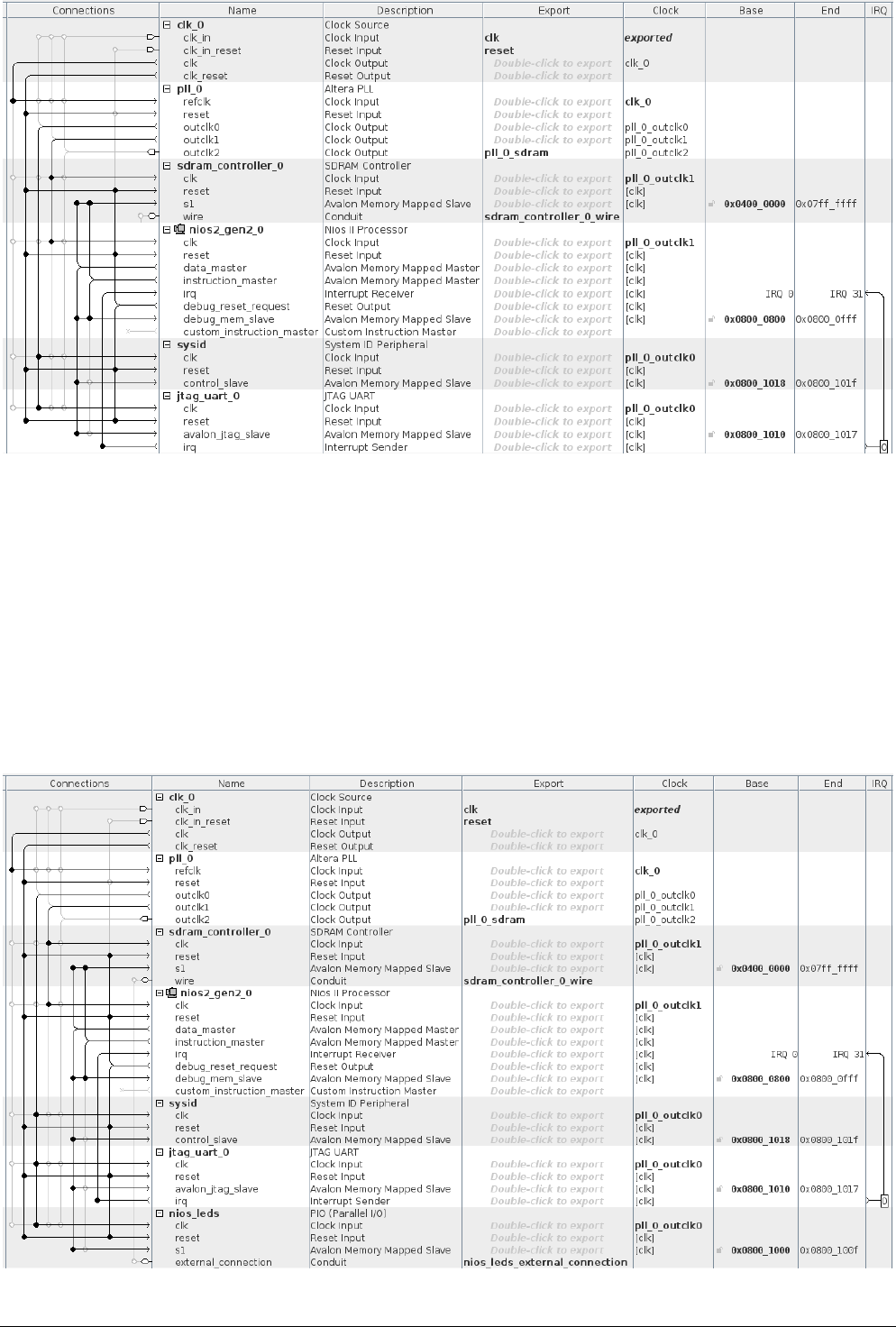
SoC-FPGA Design Guide [DE1-SoC Edition]
21/04/2018 P a g e | 34
Figure 9-2. Basic Nios II System with SDRAM and JTAG UART
11. Edit the Nios II processor and set “sdram_controller_0.s1” as its Reset and Exception vectors.
12. Add a PIO component to the system for the LEDs. The DE1-SoC has 10 LEDs, but we will only use the 5
lower ones with the Nios II processor, so we will use a 5-bit PIO component.
Width: 5 bits
Direction: Output
Output Port Reset Value: 0x00
In Qsys’ “System Contents” tab:
Rename the component to “nios_leds”
Export “nios_leds.external_connection”
13. Connect the system as shown in Figure 9-3 below:
Figure 9-3. Adding LEDs to the System
SoC-FPGA Design Guide [DE1-SoC Edition]
21/04/2018 P a g e | 35
9.3 SYSTEM DESIGN WITH QSYS HPS
In this section, we assemble all system components needed to allow the HPS to access a button and LED
connected directly to itself, as well as the 5 upper LEDs connected to the FPGA portion of the device.
Note: When using Qsys to manipulate any signal or menu item related to the HPS, the GUI will seem as though
it is not responding, but this is not the case. The GUI is just checking all parameters in the background, which
makes the interface hang momentarily. It is working correctly behind the scenes.
9.3.1 Instantiating the HPS Component
14. To use the HPS, add an “Arria V/Cyclone V Hard Processor System” to the system.
15. Open the HPS’ parameters and have a look around. There are 4 tabs that control various aspects of
the HPS’ behaviour, as shown on Figure 9-4.
Figure 9-4. HPS Component Parameters
9.3.1.1 FPGA Interfaces Tab
This tab configures everything related to the interfaces between the HPS and the FPGA. You can configure
which bridges to use, interrupts, …
16. We want to use the HPS to access FPGA peripherals, so we need to enable one of the following buses:
HPS-to-FPGA AXI bridge
Lightweight HPS-to-FPGA AXI bridge
Since we are not going to be using any high performance FPGA peripherals in this demo, we’ll choose
to enable the Lightweight HPS-to-FPGA AXI bridge.
Set the FPGA-to-HPS interface width to “Unused”.
Set the HPS-to-FPGA interface width to “Unused”.
By default, Qsys checks “Enable MPU standby and event signals”, but we are not going to use
this feature, so
Uncheck “Enable MPU standby and event signals”.
Qsys also adds an FPGA-to-HPS SDRAM port by default, which we are not going to use either, so
Remove the port listed under “FPGA-to-HPS SDRAM Interface”.
9.3.1.2 Peripheral Pins Tab
This tab configures the physical pins that are available on the device. Most device pins have various sources,
and are multiplexed. The pins can be configured to be sourced by the FPGA, or by various HPS peripherals.
9.3.1.2.1 Theory
We want to use the HPS to access the button and LED that are directly connected to it. These HPS peripherals
correspond to pins “HPS_KEY_N” and “HPS_LED” on the device’s top-level entity. We need to know how
these 2 pins are connected to the HPS to access them. To find out this information, we have to look at the
board’s schematics. You can find the schematics in [7].
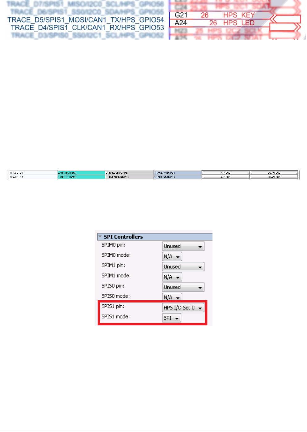
SoC-FPGA Design Guide [DE1-SoC Edition]
21/04/2018 P a g e | 36
The right side of Figure 9-5 shows the area of interest on the DE1-SoC’s schematics. We see that “HPS_KEY_N”
and “HPS_LED” are respectively connected to pins G21 and A24.
Figure 9-5. HPS_KEY_N & HPS_LED on DE1-SoC Schematic. Note that the schematic uses “HPS_KEY” instead of “HPS_KEY_N” as the
name of the signal. This is a mistake, as the button is active-low, so the “_N” in the name is warranted for clarity.
Figure 9-5 allows us to explain what Qsys’ Peripheral Pins tab does. The Qsys GUI doesn’t make any reference
to pins G21 and A24, as they depend on the device being used, and cannot be generalized to other Cyclone V
devices. However, the GUI does have references to what is displayed on the left side of Figure 9-5. We will
examine the details of pin G21, to which “HPS_KEY_N” is connected. The schematic shows that pin G21 is
connected to 4 sources:
TRACE_D5
SPIS1_MOSI
CAN1_TX
HPS_GPIO54
This can be seen in Qsys, as shown in Figure 9-6.
Figure 9-6. HPS_KEY_N & HPS_LED on Qsys Peripheral Pins Tab
Depending on how you configure the Peripheral Pins tab, you can configure pin G21 to use any of the sources
above. For example, if you want to use this pin as an SPI slave control signal, you would use the configuration
shown in Figure 9-7.
Figure 9-7. Using Pin G21 for SPI
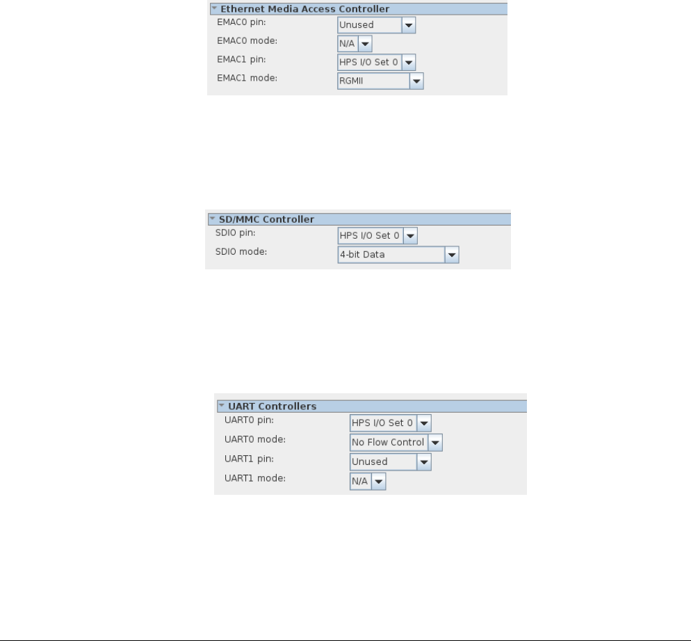
SoC-FPGA Design Guide [DE1-SoC Edition]
21/04/2018 P a g e | 37
However, if you don’t want to use any of the peripherals available at the top of the Peripheral Pins tab, then
you can always use one of the 2 buttons on the right side of Figure 9-6:
GPIOXY: Configures the pin to be connected to the HPS’ GPIO peripheral.
LOANIOXY: Configures the pin to be connected to the FPGA fabric. This pin can be exported from
Qsys to be used by the FPGA.
9.3.1.2.2 Configuration
17. We want the HPS to directly control the “HPS_KEY_N” and “HPS_LED” pins. To do this, we will connect
pins G21 and A24 to the HPS’ GPIO peripheral.
Click on the “GPIO53” button. This corresponds to pin A24, which is connected to “HPS_LED”.
Click on the “GPIO54” button. This corresponds to pin G21, which is connected to
“HPS_KEY_N”.
18. We want to connect to our DE1-SoC with an SSH connection later in the tutorial, so we need to enable
the Ethernet MAC interface.
Configure “EMAC1 pin” to “HPS I/O Set 0” and the “EMAC 1 mode” to “RGMII”, as shown
in Figure 9-8.
Click on the “GPIO35” button. This corresponds to pin C19, which is connected to
“HPS_ENET_INT_N”.
Figure 9-8. Ethernet MAC configuration
19. Our system will boot from the microSD card slot, so we need to enable the SD/MMC controller.
Configure “SDIO pin” to “HPS I/O Set 0” and “SDIO mode” to “4-bit Data”, as shown in
Figure 9-9.
Figure 9-9. SD/MMC configuration
20. When initially configuring our system, we will need to connect a keyboard to our system. We will do
this through a serial UART connection, so we need to enable the UART controller.
Configure “UART0 pin” to “HPS I/O Set 0” and “UART0 mode” to “No Flow Control”, as
shown in Figure 9-10.
Figure 9-10. UART configuration
At this stage, you should have the same configuration shown in Figure 9-11.
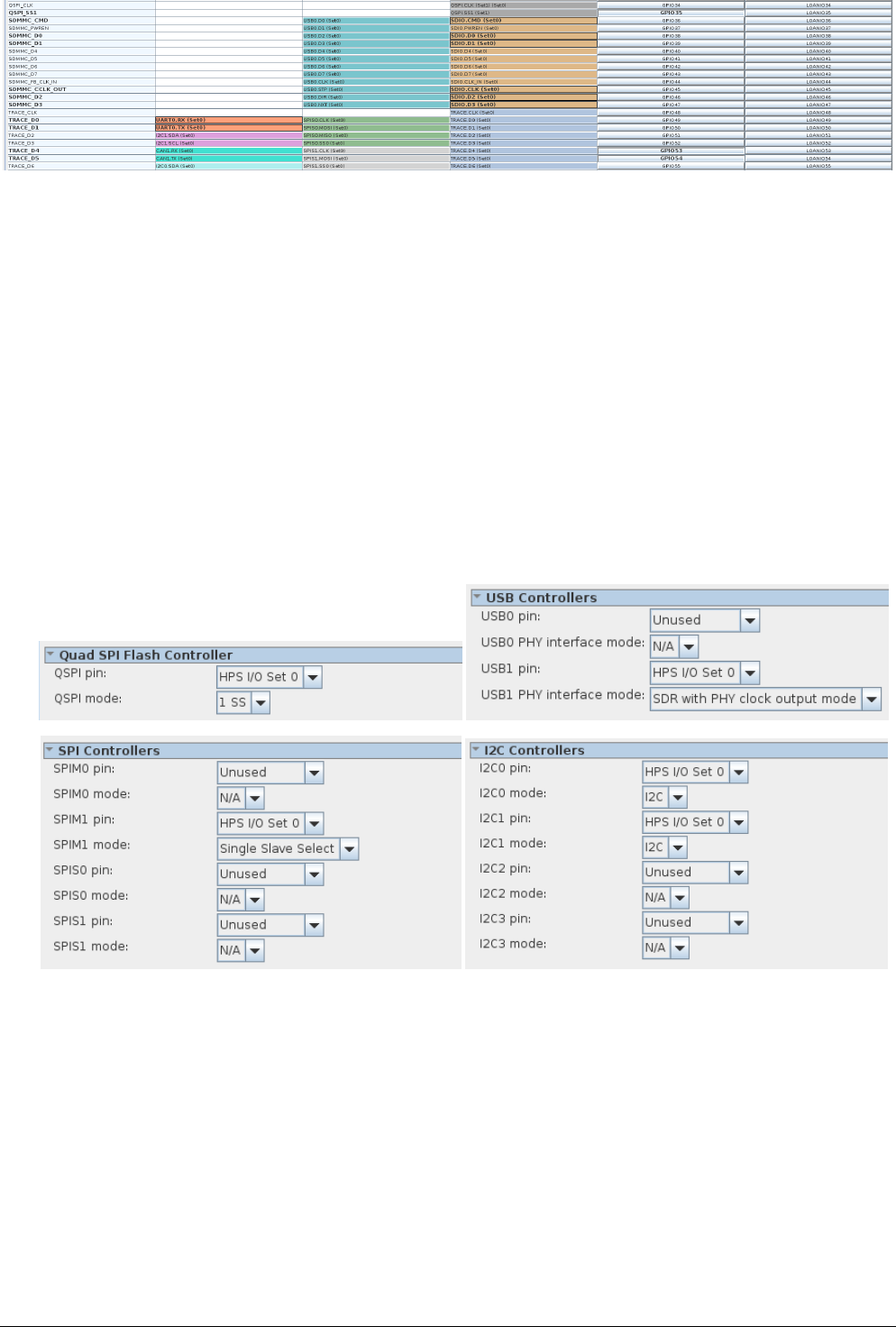
SoC-FPGA Design Guide [DE1-SoC Edition]
21/04/2018 P a g e | 38
Figure 9-11. Exported peripheral pins
21. Although not needed to satisfy the design goals defined in 8.4, we enable all the remaining HPS
peripherals so future designs can use any of them if needed. Adding these peripherals does not
increase FPGA resource usage as they are all hard peripherals connected directly to the HPS.
Configure the Quad SPI Flash controller, USB controllers, SPI controllers, and the I2C
controllers as shown in Figure 9-12.
Click on the “GPIO09” button. This corresponds to pin B15, which is connected to
“HPS_CONV_USB_N”.
Click on the “GPIO40” button. This corresponds to pin H17, which is connected to
“HPS_LTC_GPIO”.
Click on the “GPIO48” button. This corresponds to pin B26, which is connected to
“HPS_I2C_CONTROL”.
Click on the “GPIO61” button. This corresponds to pin B22, which is connected to
“HPS_GSENSOR_INT”.
Figure 9-12. Quad SPI Flash, USB, SPI, and I2C peripheral pin configurations
22. In Qsys’ “System Contents” tab:
Export “hps_0.hps_io” under the name “hps_0_io”. This is a conduit that contains all the
pins configured in the Peripheral Pins tab. We will connect these to our top-level entity later.
9.3.1.3 HPS Clocks Tab
This tab configures the clocking system of the HPS. We will generally use the default settings here, so no need
to change anything.
9.3.1.4 SDRAM Tab
This tab configures the memory subsystem of the HPS.

SoC-FPGA Design Guide [DE1-SoC Edition]
21/04/2018 P a g e | 39
23. We need to configure all clocks and timings related to the memory used on our system. The DE1-SoC
uses DDR3 memory, so we need to consult its datasheet to find all the settings. The datasheet is
available at [8] . Based on the memory’s datasheet, we can fill in the following memory settings (you
will soon see that it is quite tedious to enter these values):
SDRAM Protocol: DDR3
PHY Settings:
Clocks:
Memory clock frequency: 400.0 MHz
PLL reference clock frequency: 25.0 MHz
Advanced PHY Settings:
Supply Voltage: 1.5V DDR3
Memory Parameters:
Memory vendor: Other
Memory device speed grade: 800.0 MHz
Total interface width: 32
Number of chip select/depth expansion: 1
Number of clocks: 1
Row address width: 15
Column address width: 10
Bank-address width: 3
Enable DM pins
DQS# Enable
Memory Initialization Options:
Mirror Addressing: 1 per chip select: 0
Mode Register 0:
o Burst Length: Burst chop 4 or 8 (on the fly)
o Read Burst Type: Sequential
o DLL precharge power down: DLL off
o Memory CAS latency setting: 11
Mode Register 1:
o Output drive strength setting: RZQ/7
o ODT Rtt nominal value: RZQ/4
Mode Register 2:
o Auto selfrefresh method: Manual
o Selfrefresh temperature: Normal
o Memory write CAS latency setting: 8
o Dynamic ODT (Rtt_WR) value: RZQ/4
Memory Timing:
tIS (base): 180 ps
tIH (base): 140 ps
tDS (base): 30 ps
tDH (base): 65 ps
tDQSQ: 125 ps
tQH: 0.38 cycles
tDQSCK: 255 ps
tDQSS: 0.25 cycles
tQSH: 0.4 cycles
tDSH: 0.2 cycles
tDSS: 0.2 cycles
tINIT: 500 us
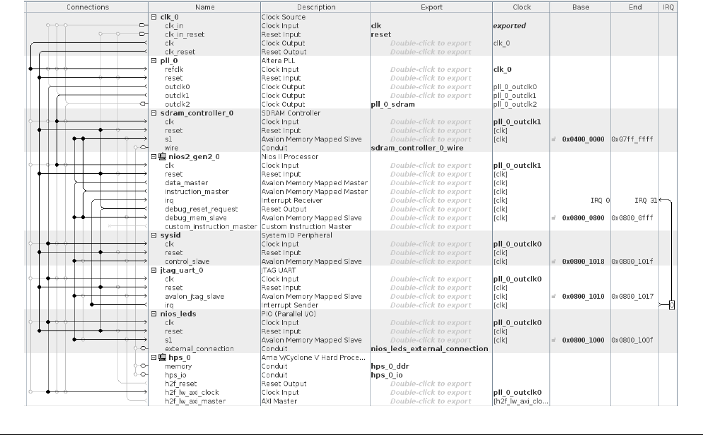
SoC-FPGA Design Guide [DE1-SoC Edition]
21/04/2018 P a g e | 40
tMRD: 4 cycles
tRAS: 35.0 ns
tRCD: 13.75 ns
tRP: 13.75 ns
tREFI: 7.8 us
tRFC: 260.0 ns
tWR: 15.0 ns
tWTR: 4 cycles
tFAW: 30.0 ns
tRRD: 7.5 ns
tRTP: 7.5 ns
Board Settings:
Setup and Hold Derating:
Use Altera's default settings
Channel Signal Integrity:
Use Altera's default settings
Board Skews:
Maximum CK delay to DIMM/device: 0.03 ns
Maximum DQS delay to DIMM/device: 0.02 ns
Minimum delay difference between CK and DQS: 0.06 ns
Maximum delay difference between CK and DQS: 0.12 ns
Maximum skew within DQS group: 0.01 ns
Maximum skew between DQS groups: 0.06 ns
Average delay difference between DQ and DQS: 0.05 ns
Maximum skew within address and command bus: 0.02 ns
Average delay difference between address and command and CK: 0.01 ns
24. In Qsys’ “System Contents” tab:
Export “hps_0.memory” under the name “hps_0_ddr”.
25. Connect the system as shown in Figure 9-13 below:
Figure 9-13. Adding the "Standalone" HPS to the System
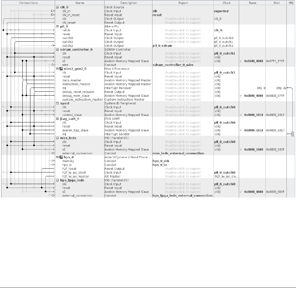
SoC-FPGA Design Guide [DE1-SoC Edition]
21/04/2018 P a g e | 41
The HPS is now ready and can be used in our system, however, the HPS can only be used “standalone” and
cannot access any FPGA peripherals. We will handle this issue in the next section.
9.3.2 Interfacing with FPGA Peripherals
The next step is to connect the HPS to FPGA peripherals through one of its interface bridges. The setup we
have uses the Lightweight HPS-to-FPGA bridge to communicate with the FPGA.
26. Add a PIO component to the system for the LEDs. The DE1-SoC has 10 LEDs, but we will only use the 5
upper ones with the HPS, so we will use a 5-bit PIO component.
Width: 5 bits
Direction: Output
Output Port Reset Value: 0x00
In Qsys’ “System Contents” tab:
Rename the component to “hps_fpga_leds”
Export “hps_fpga_leds.external_connection”
27. Connect the system as shown in Figure 9-14 below. Notice that we use “hps_0.h2f_reset” as the
reset signal for the components connected to the HPS. This is a design choice so we can separately
reset FPGA-only peripherals, and FPGA peripherals connected to the HPS.
Figure 9-14. Adding Buttons and 7-segment Displays to the Lightweight HPS-to-FPGA Bridge
28. In the main Qsys window, select “System > Assign Base Addresses” to get rid of any error
messages regarding memory space overlaps among the different components in the system.
At this stage, we finally have a system that satisfies all goals defined in 8.4. Our design work with Qsys is now
done.
9.4 GENERATING THE QSYS SYSTEM
29. Click on the “Generate HDL” button.
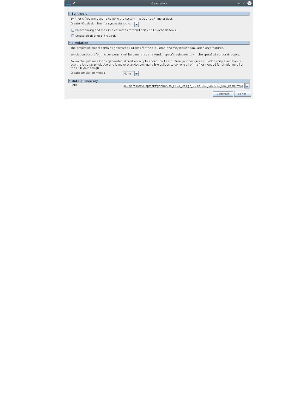
SoC-FPGA Design Guide [DE1-SoC Edition]
21/04/2018 P a g e | 42
30. Select “VHDL” for “Create HDL design files for synthesis”.
31. Uncheck the “Create block symbol file (.bsf)” checkbox.
Figure 9-15. Generate Qsys System
32. Click on the “Generate” button to generate the system.
33. Save the design and exit Qsys. When asked if you want to generate the design, select “No”, as we
have already done it in the previous step.
9.5 INSTANTIATING THE QSYS SYSTEM
You now have a complete Qsys system. The system will be available as an instantiable component in your
design files. However, in order for Quartus Prime to see the Qsys system, you will have to add the
system’s files to your Quartus Prime project.
34. Add “DE1_SoC_demo/hw/quartus/soc_system/synthesis/soc_system.qip” to the Quartus Prime
project by using “Project > Add/Remove Files in Project…”.
35. To use the Qsys system in your design, you have to declare its component, and then instantiate it.
Qsys already provides you with a component declaration. You can find it among the numerous files
that were generated. The one we are looking for is
“DE1_SoC_demo/hw/quartus/soc_system/soc_system.cmp”.
36. Copy the component declaration code in “DE1_SoC_demo/hw/hdl/DE1_SoC_top_level.vhd”. Be
sure to instantiate the component and assign all the correct pins of the DE1-SoC board. For our demo
project, we would use the instantiation shown in Figure 9-16.
soc_system_inst : component soc_system
port map(
clk_clk => CLOCK_50,
hps_0_ddr_mem_a => HPS_DDR3_ADDR,
hps_0_ddr_mem_ba => HPS_DDR3_BA,
hps_0_ddr_mem_ck => HPS_DDR3_CK_P,
hps_0_ddr_mem_ck_n => HPS_DDR3_CK_N,
hps_0_ddr_mem_cke => HPS_DDR3_CKE,
hps_0_ddr_mem_cs_n => HPS_DDR3_CS_N,
hps_0_ddr_mem_ras_n => HPS_DDR3_RAS_N,
hps_0_ddr_mem_cas_n => HPS_DDR3_CAS_N,
hps_0_ddr_mem_we_n => HPS_DDR3_WE_N,
hps_0_ddr_mem_reset_n => HPS_DDR3_RESET_N,
hps_0_ddr_mem_dq => HPS_DDR3_DQ,
hps_0_ddr_mem_dqs => HPS_DDR3_DQS_P,
hps_0_ddr_mem_dqs_n => HPS_DDR3_DQS_N,
hps_0_ddr_mem_odt => HPS_DDR3_ODT,
hps_0_ddr_mem_dm => HPS_DDR3_DM,
hps_0_ddr_oct_rzqin => HPS_DDR3_RZQ,
hps_0_io_hps_io_emac1_inst_TX_CLK => HPS_ENET_GTX_CLK,
hps_0_io_hps_io_emac1_inst_TX_CTL => HPS_ENET_TX_EN,
hps_0_io_hps_io_emac1_inst_TXD0 => HPS_ENET_TX_DATA(0),
hps_0_io_hps_io_emac1_inst_TXD1 => HPS_ENET_TX_DATA(1),
hps_0_io_hps_io_emac1_inst_TXD2 => HPS_ENET_TX_DATA(2),

SoC-FPGA Design Guide [DE1-SoC Edition]
21/04/2018 P a g e | 43
hps_0_io_hps_io_emac1_inst_TXD3 => HPS_ENET_TX_DATA(3),
hps_0_io_hps_io_emac1_inst_RX_CLK => HPS_ENET_RX_CLK,
hps_0_io_hps_io_emac1_inst_RX_CTL => HPS_ENET_RX_DV,
hps_0_io_hps_io_emac1_inst_RXD0 => HPS_ENET_RX_DATA(0),
hps_0_io_hps_io_emac1_inst_RXD1 => HPS_ENET_RX_DATA(1),
hps_0_io_hps_io_emac1_inst_RXD2 => HPS_ENET_RX_DATA(2),
hps_0_io_hps_io_emac1_inst_RXD3 => HPS_ENET_RX_DATA(3),
hps_0_io_hps_io_emac1_inst_MDIO => HPS_ENET_MDIO,
hps_0_io_hps_io_emac1_inst_MDC => HPS_ENET_MDC,
hps_0_io_hps_io_qspi_inst_CLK => HPS_FLASH_DCLK,
hps_0_io_hps_io_qspi_inst_SS0 => HPS_FLASH_NCSO,
hps_0_io_hps_io_qspi_inst_IO0 => HPS_FLASH_DATA(0),
hps_0_io_hps_io_qspi_inst_IO1 => HPS_FLASH_DATA(1),
hps_0_io_hps_io_qspi_inst_IO2 => HPS_FLASH_DATA(2),
hps_0_io_hps_io_qspi_inst_IO3 => HPS_FLASH_DATA(3),
hps_0_io_hps_io_sdio_inst_CLK => HPS_SD_CLK,
hps_0_io_hps_io_sdio_inst_CMD => HPS_SD_CMD,
hps_0_io_hps_io_sdio_inst_D0 => HPS_SD_DATA(0),
hps_0_io_hps_io_sdio_inst_D1 => HPS_SD_DATA(1),
hps_0_io_hps_io_sdio_inst_D2 => HPS_SD_DATA(2),
hps_0_io_hps_io_sdio_inst_D3 => HPS_SD_DATA(3),
hps_0_io_hps_io_usb1_inst_CLK => HPS_USB_CLKOUT,
hps_0_io_hps_io_usb1_inst_STP => HPS_USB_STP,
hps_0_io_hps_io_usb1_inst_DIR => HPS_USB_DIR,
hps_0_io_hps_io_usb1_inst_NXT => HPS_USB_NXT,
hps_0_io_hps_io_usb1_inst_D0 => HPS_USB_DATA(0),
hps_0_io_hps_io_usb1_inst_D1 => HPS_USB_DATA(1),
hps_0_io_hps_io_usb1_inst_D2 => HPS_USB_DATA(2),
hps_0_io_hps_io_usb1_inst_D3 => HPS_USB_DATA(3),
hps_0_io_hps_io_usb1_inst_D4 => HPS_USB_DATA(4),
hps_0_io_hps_io_usb1_inst_D5 => HPS_USB_DATA(5),
hps_0_io_hps_io_usb1_inst_D6 => HPS_USB_DATA(6),
hps_0_io_hps_io_usb1_inst_D7 => HPS_USB_DATA(7),
hps_0_io_hps_io_spim1_inst_CLK => HPS_SPIM_CLK,
hps_0_io_hps_io_spim1_inst_MOSI => HPS_SPIM_MOSI,
hps_0_io_hps_io_spim1_inst_MISO => HPS_SPIM_MISO,
hps_0_io_hps_io_spim1_inst_SS0 => HPS_SPIM_SS,
hps_0_io_hps_io_uart0_inst_RX => HPS_UART_RX,
hps_0_io_hps_io_uart0_inst_TX => HPS_UART_TX,
hps_0_io_hps_io_i2c0_inst_SDA => HPS_I2C1_SDAT,
hps_0_io_hps_io_i2c0_inst_SCL => HPS_I2C1_SCLK,
hps_0_io_hps_io_i2c1_inst_SDA => HPS_I2C2_SDAT,
hps_0_io_hps_io_i2c1_inst_SCL => HPS_I2C2_SCLK,
hps_0_io_hps_io_gpio_inst_GPIO09 => HPS_CONV_USB_N,
hps_0_io_hps_io_gpio_inst_GPIO35 => HPS_ENET_INT_N,
hps_0_io_hps_io_gpio_inst_GPIO40 => HPS_LTC_GPIO,
hps_0_io_hps_io_gpio_inst_GPIO48 => HPS_I2C_CONTROL,
hps_0_io_hps_io_gpio_inst_GPIO53 => HPS_LED,
hps_0_io_hps_io_gpio_inst_GPIO54 => HPS_KEY_N,
hps_0_io_hps_io_gpio_inst_GPIO61 => HPS_GSENSOR_INT,
pll_0_sdram_clk => DRAM_CLK,
reset_reset_n => KEY_N(0),
sdram_controller_0_wire_addr => DRAM_ADDR,
sdram_controller_0_wire_ba => DRAM_BA,
sdram_controller_0_wire_cas_n => DRAM_CAS_N,
sdram_controller_0_wire_cke => DRAM_CKE,
sdram_controller_0_wire_cs_n => DRAM_CS_N,
sdram_controller_0_wire_dq => DRAM_DQ,
sdram_controller_0_wire_dqm(1) => DRAM_UDQM,
sdram_controller_0_wire_dqm(0) => DRAM_LDQM,
sdram_controller_0_wire_ras_n => DRAM_RAS_N,
sdram_controller_0_wire_we_n => DRAM_WE_N,
nios_leds_external_connection_export => LEDR(4 downto 0),
hps_fpga_leds_external_connection_export => LEDR(9 downto 5)
);
Figure 9-16. Qsys Component Instantiation
37. After finishing the design, REMOVE/COMMENT OUT all unused pins from the top-level VHDL file. Your
top-level entity should look like the one shown in Figure 9-17.
entity DE1_SoC_top_level is
port(
-- ADC
-- ADC_CS_n : out std_logic;
-- ADC_DIN : out std_logic;
-- ADC_DOUT : in std_logic;

SoC-FPGA Design Guide [DE1-SoC Edition]
21/04/2018 P a g e | 44
-- ADC_SCLK : out std_logic;
-- Audio
-- AUD_ADCDAT : in std_logic;
-- AUD_ADCLRCK : inout std_logic;
-- AUD_BCLK : inout std_logic;
-- AUD_DACDAT : out std_logic;
-- AUD_DACLRCK : inout std_logic;
-- AUD_XCK : out std_logic;
-- CLOCK
CLOCK_50 : in std_logic;
-- CLOCK2_50 : in std_logic;
-- CLOCK3_50 : in std_logic;
-- CLOCK4_50 : in std_logic;
-- SDRAM
DRAM_ADDR : out std_logic_vector(12 downto 0);
DRAM_BA : out std_logic_vector(1 downto 0);
DRAM_CAS_N : out std_logic;
DRAM_CKE : out std_logic;
DRAM_CLK : out std_logic;
DRAM_CS_N : out std_logic;
DRAM_DQ : inout std_logic_vector(15 downto 0);
DRAM_LDQM : out std_logic;
DRAM_RAS_N : out std_logic;
DRAM_UDQM : out std_logic;
DRAM_WE_N : out std_logic;
-- I2C for Audio and Video-In
-- FPGA_I2C_SCLK : out std_logic;
-- FPGA_I2C_SDAT : inout std_logic;
-- SEG7
-- HEX0_N : out std_logic_vector(6 downto 0);
-- HEX1_N : out std_logic_vector(6 downto 0);
-- HEX2_N : out std_logic_vector(6 downto 0);
-- HEX3_N : out std_logic_vector(6 downto 0);
-- HEX4_N : out std_logic_vector(6 downto 0);
-- HEX5_N : out std_logic_vector(6 downto 0);
-- IR
-- IRDA_RXD : in std_logic;
-- IRDA_TXD : out std_logic;
-- KEY_N
KEY_N : in std_logic_vector(3 downto 0);
-- LED
LEDR : out std_logic_vector(9 downto 0);
-- PS2
-- PS2_CLK : inout std_logic;
-- PS2_CLK2 : inout std_logic;
-- PS2_DAT : inout std_logic;
-- PS2_DAT2 : inout std_logic;
-- SW
-- SW : in std_logic_vector(9 downto 0);
-- Video-In
-- TD_CLK27 : inout std_logic;
-- TD_DATA : out std_logic_vector(7 downto 0);
-- TD_HS : out std_logic;
-- TD_RESET_N : out std_logic;
-- TD_VS : out std_logic;
-- VGA
-- VGA_B : out std_logic_vector(7 downto 0);
-- VGA_BLANK_N : out std_logic;
-- VGA_CLK : out std_logic;
-- VGA_G : out std_logic_vector(7 downto 0);
-- VGA_HS : out std_logic;
-- VGA_R : out std_logic_vector(7 downto 0);
-- VGA_SYNC_N : out std_logic;
-- VGA_VS : out std_logic;
-- GPIO_0

SoC-FPGA Design Guide [DE1-SoC Edition]
21/04/2018 P a g e | 45
-- GPIO_0 : inout std_logic_vector(35 downto 0);
-- GPIO_1
-- GPIO_1 : inout std_logic_vector(35 downto 0);
-- HPS
HPS_CONV_USB_N : inout std_logic;
HPS_DDR3_ADDR : out std_logic_vector(14 downto 0);
HPS_DDR3_BA : out std_logic_vector(2 downto 0);
HPS_DDR3_CAS_N : out std_logic;
HPS_DDR3_CK_N : out std_logic;
HPS_DDR3_CK_P : out std_logic;
HPS_DDR3_CKE : out std_logic;
HPS_DDR3_CS_N : out std_logic;
HPS_DDR3_DM : out std_logic_vector(3 downto 0);
HPS_DDR3_DQ : inout std_logic_vector(31 downto 0);
HPS_DDR3_DQS_N : inout std_logic_vector(3 downto 0);
HPS_DDR3_DQS_P : inout std_logic_vector(3 downto 0);
HPS_DDR3_ODT : out std_logic;
HPS_DDR3_RAS_N : out std_logic;
HPS_DDR3_RESET_N : out std_logic;
HPS_DDR3_RZQ : in std_logic;
HPS_DDR3_WE_N : out std_logic;
HPS_ENET_GTX_CLK : out std_logic;
HPS_ENET_INT_N : inout std_logic;
HPS_ENET_MDC : out std_logic;
HPS_ENET_MDIO : inout std_logic;
HPS_ENET_RX_CLK : in std_logic;
HPS_ENET_RX_DATA : in std_logic_vector(3 downto 0);
HPS_ENET_RX_DV : in std_logic;
HPS_ENET_TX_DATA : out std_logic_vector(3 downto 0);
HPS_ENET_TX_EN : out std_logic;
HPS_FLASH_DATA : inout std_logic_vector(3 downto 0);
HPS_FLASH_DCLK : out std_logic;
HPS_FLASH_NCSO : out std_logic;
HPS_GSENSOR_INT : inout std_logic;
HPS_I2C_CONTROL : inout std_logic;
HPS_I2C1_SCLK : inout std_logic;
HPS_I2C1_SDAT : inout std_logic;
HPS_I2C2_SCLK : inout std_logic;
HPS_I2C2_SDAT : inout std_logic;
HPS_KEY_N : inout std_logic;
HPS_LED : inout std_logic;
HPS_LTC_GPIO : inout std_logic;
HPS_SD_CLK : out std_logic;
HPS_SD_CMD : inout std_logic;
HPS_SD_DATA : inout std_logic_vector(3 downto 0);
HPS_SPIM_CLK : out std_logic;
HPS_SPIM_MISO : in std_logic;
HPS_SPIM_MOSI : out std_logic;
HPS_SPIM_SS : inout std_logic;
HPS_UART_RX : in std_logic;
HPS_UART_TX : out std_logic;
HPS_USB_CLKOUT : in std_logic;
HPS_USB_DATA : inout std_logic_vector(7 downto 0);
HPS_USB_DIR : in std_logic;
HPS_USB_NXT : in std_logic;
HPS_USB_STP : out std_logic
);
end entity DE1_SoC_top_level;
Figure 9-17. Final Top-level Entity
9.6 HPS DDR3 PIN ASSIGNMENTS
In a normal FPGA design flow, you would be able to compile your design at this stage. However, this isn’t
possible at the moment in our design. The reason is that some of the compilation settings required HPS’
DDR3 pin assignments have not been performed yet.
The HPS’ DDR3 SDRAM is an external memory with requires specific input/output termination resistance
and and drive strengths. Fortunately, Qsys can derive all these parameters from the various settings we
provided in the HPS’ memory configuration tab and it generates a custom TCL script for the HPS DDR3 pin
assignments.
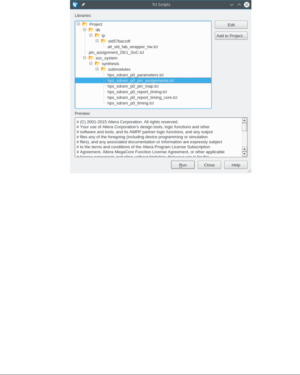
SoC-FPGA Design Guide [DE1-SoC Edition]
21/04/2018 P a g e | 46
38. Start the “Analysis and Synthesis” flow to perform a preliminary analysis of the system.
39. Go to “Tools > Tcl Scripts…” in Quartus Prime.
IF AT THIS POINT YOU DO NOT SEE THE SAME THING AS ON Figure 9-18, THEN CLOSE AND
RELAUNCH QUARTUS PRIME AGAIN. SOME VERSIONS OF QUARTUS PRIME SUFFER FROM A BUG,
WHERE THE PROGRAM DOESN’T CORRECTLY DETECT TCL FILES GENERATED BY QSYS. YOU SHOULD
SEE THE SAME THING AS ON Figure 9-18.
Figure 9-18. Correct HPS DDR3 Pin Assignment TCL Script Selection
40. Execute “hps_sdram_p0_pin_assignments.tcl”.
41. You can now start the full compilation of your design with the “Start Compilation” flow.
At this point, we have finished the hardware design process and can proceed to programming the FPGA.
9.7 WIRING THE DE1-SOC
Connect the DE1-SoC as shown in Figure 9-19. We connect the
Power cable
USB-Blaster cable
Ethernet cable
UART cable
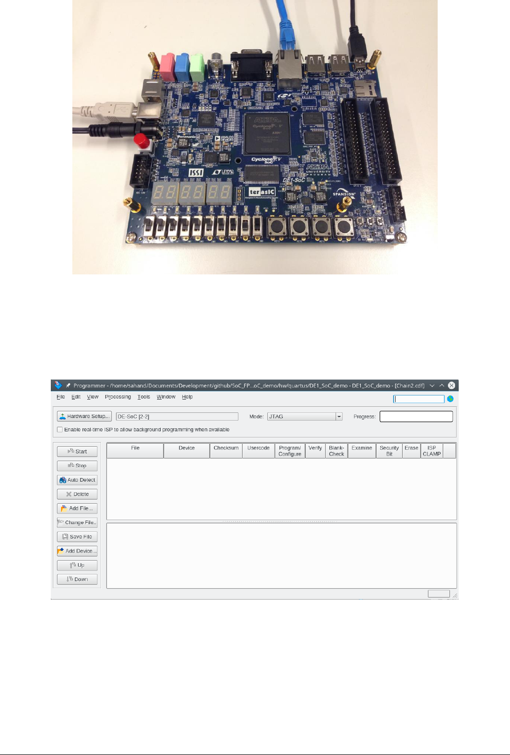
SoC-FPGA Design Guide [DE1-SoC Edition]
21/04/2018 P a g e | 47
Figure 9-19. DE1-SoC Wiring
Note that the microSD card is NOT plugged in at this point.
9.8 PROGRAMMING THE FPGA
42. Open the Quartus Prime Programmer.
Figure 9-20. Quartus Prime Programmer
43. Choose the “Auto Detect” button on the left of Figure 9-20, then choose “5CSEMA5”, as shown in
Figure 9-21.
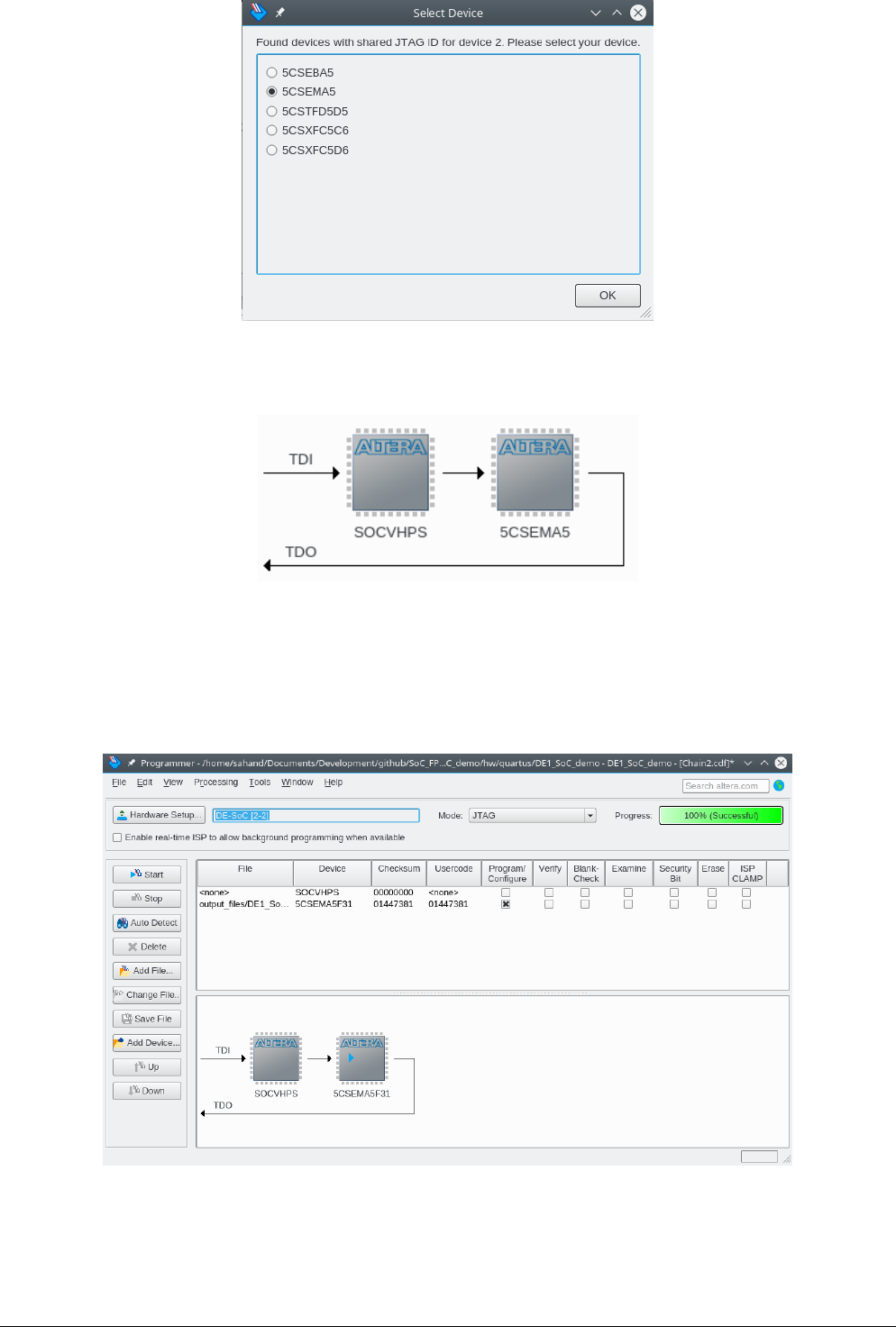
SoC-FPGA Design Guide [DE1-SoC Edition]
21/04/2018 P a g e | 48
Figure 9-21. FPGA Selection
You should now see 2 devices on the JTAG scan chain, as shown in Figure 9-22.
Figure 9-22. JTAG Scan Chain
44. Right-click on the “5CSEMA5” device shown in Figure 9-22 and choose “Edit > Change File”. Then,
select “DE1_SoC_demo/hw/quartus/output_files/DE1_SoC_demo.sof” through the file browser.
45. Enable the “Program/Configure” checkbox for device “5CSEMA5F31”, then press the “Start”
button, as shown in Figure 9-23.
Figure 9-23. Programming the FPGA
We are now done with the Quartus Prime program, and will no longer need it for the rest of this tutorial.

SoC-FPGA Design Guide [DE1-SoC Edition]
21/04/2018 P a g e | 49
9.9 CREATING TARGET SDCARD ARTIFACTS
Later in this tutorial, we will sometimes want to avoid having to manually program the FPGA through the
Quartus Prime programmer, and would instead like the HPS to take care of this programmatically.
Quartus Prime generates an SRAM Object File (.sof) as its default FPGA target image. However, the HPS can
only program the FPGA by using a Raw Binary File (.rbf). Therefore, we must convert our .sof file to a .rbf
to later satisfy this requirement.
46. Execute the following command to convert the .sof file to a .rbf file.
$ quartus_cpf –c \
DE1_SoC_demo/hw/quartus/output_files/DE1_SoC_demo.sof \
DE1_SoC_demo/sdcard/fat32/socfpga.rbf

SoC-FPGA Design Guide [DE1-SoC Edition]
21/04/2018 P a g e | 50
10 USING THE CYCLONE V FPGA NIOS II BARE-METAL
10.1 PROJECT SETUP
1. Launch the Nios II SBT IDE by executing the following command.
$ eclipse-nios2
2. Choose “File > New > Nios II Application and BSP from Template”.
a. All the information needed to program a Nios II processor is contained within the
“.sopcinfo” file created by Qsys. For the “SOPC Information File name” use
“DE1_SoC_demo/hw/quartus/soc_system.sopcinfo”.
b. Use “DE1_SoC_demo_nios” as the project name.
c. Disable the “Use default location” checkbox
d. Use “DE1_SoC_demo/sw/nios/application/DE1_SoC_demo_nios” as the project location.
e. Choose the “Blank Project” template.
f. Click on the “Finish” button to create the project.
3. Right-click on the “DE1_SoC_demo_nios” project folder and select “New > Source file”. Use the
default C source template, and set “nios.c” as the file name.
4. Right-click on the “DE1_SoC_demo_nios_bsp” project, and select “Build Project”. Once the build is
completed, a number of files will be generated, the most useful of which is the “system.h” file. This
file contains all the details related to the Nios II processor’s various peripherals, as defined in Qsys in
9.2.
10.2 NIOS II PROGRAMMING THEORY ACCESSING PERIPHERALS
The Nios II processor can be programmed in C similarly to any other microcontroller. However, care must be
taken when accessing any of the processor’s peripherals. Depending on which version of the Nios II you
instantiated in Qsys, you may not be able to correctly read data at a peripheral’s address space using pointers.
The issue arises when your Nios II processor has a data cache.
Our current system is composed of a Nios processor connected to a PIO set in output mode, which is in turn
connected to a series of LEDs. Suppose now that instead of a PIO in output mode, we use a PIO in input mode
connected to a series of switches. We use the code in Figure 10-1 to read data from the switches.
#include <stdbool.h>
#include <inttypes.h>
#include "system.h"
int main() {
uint32_t *p_switches = SWITCHES_0_BASE;
while (true) {
uint32_t switches_value = *p_switches;
printf("switches_value = %" PRIx32 "\n", switches_value);
}
return 0;
}
Figure 10-1. Incorrect Nios II Peripheral Access in C
When this code is run, the initial value of the “switches_value” variable, as obtained from the first iteration
of the while loop, will be the correct representation of the switches’ state. However, at each iteration of the
while loop, the “switches_value” variable will NEVER change again, even if the switches are flipped
between each iteration. The issue is that each successive access is being served by the data cache, which
doesn’t see that the switches have been modified.
The solution to this issue is to use special instructions that bypass the data cache when reading or writing to
peripherals. These instructions are part of the IO family of load and store instructions and bypass all caches.

SoC-FPGA Design Guide [DE1-SoC Edition]
21/04/2018 P a g e | 51
The available instructions are listed below, and an example of how to correctly access Nios II peripherals is
shown in Figure 10-2.
Reading
IORD_8DIRECT(BASE, OFFSET)
IORD_16DIRECT(BASE, OFFSET)
IORD_32DIRECT(BASE, OFFSET)
Writing
IOWR_8DIRECT(BASE, OFFSET, DATA)
IOWR_16DIRECT(BASE, OFFSET, DATA)
IOWR_32DIRECT(BASE, OFFSET, DATA)
#include <stdbool.h>
#include <inttypes.h>
#include "system.h"
#include “io.h”
int main() {
while (true) {
uint32_t switches_value = IORD_32DIRECT(SWITCHES_0_BASE, 0);
printf("switches_value = %" PRIx32 "\n", switches_value); }
return 0;
}
Figure 10-2. Correct Nios II Peripheral Access in C
10.3 NIOS II PROGRAMMING PRACTICE
5. Write the code provided in Figure 10-3 in “nios.c”. The code instructs the Nios II processor to create
a strobing light effect on its 5 peripheral LEDs.
#include <stdio.h>
#include <stdbool.h>
#include <stdint.h>
#include <unistd.h>
#include "io.h"
#include "altera_avalon_pio_regs.h"
#include "system.h"
#define SLEEP_DELAY_US (100 * 1000)
void setup_leds() {
// Switch on first LED only
IOWR_ALTERA_AVALON_PIO_DATA(NIOS_LEDS_BASE, 0x1);
}
void handle_leds() {
uint32_t leds_mask = IORD_ALTERA_AVALON_PIO_DATA(NIOS_LEDS_BASE);
if (leds_mask != (0x01 << (NIOS_LEDS_DATA_WIDTH - 1))) {
// rotate leds
leds_mask <<= 1;
} else {
// reset leds
leds_mask = 0x1;
}
IOWR_ALTERA_AVALON_PIO_DATA(NIOS_LEDS_BASE, leds_mask);
}
int main() {
printf("DE1-SoC nios demo\n");
setup_leds();
while (true) {
handle_leds();
usleep(SLEEP_DELAY_US);
}
return 0;
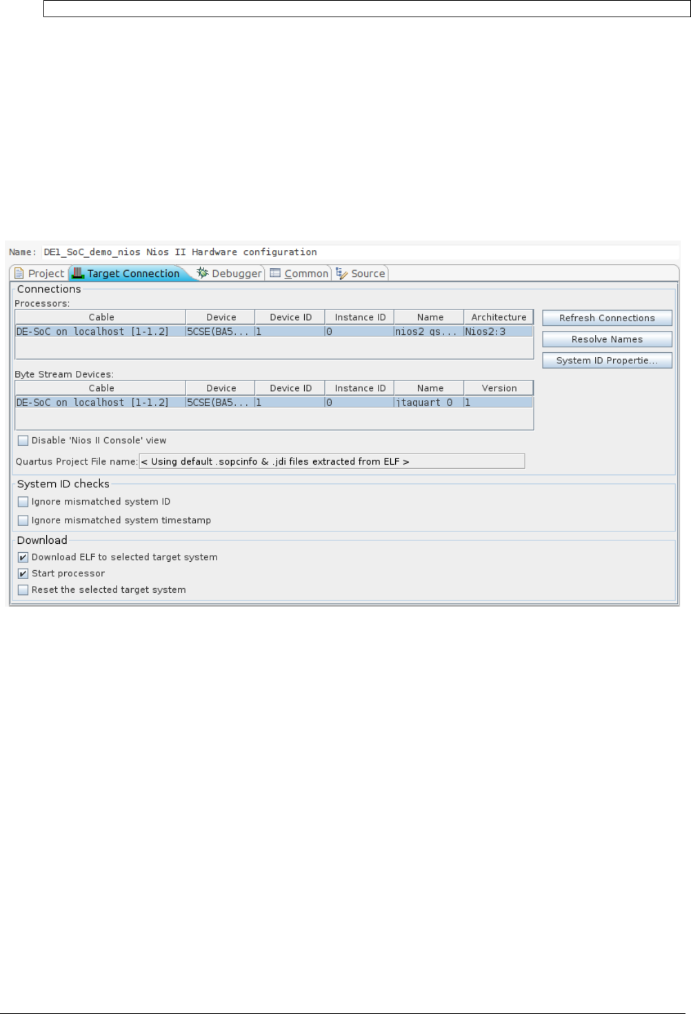
SoC-FPGA Design Guide [DE1-SoC Edition]
21/04/2018 P a g e | 52
}
Figure 10-3. nios.c
6. Right-click on the “DE1_SoC_demo_nios” project, and select “Build Project”.
7. The code is now ready to be run on the FPGA. Right-click on the “DE1_SoC_demo_nios” project, and
select “Run As > Nios II Hardware”. You should be able to see a strobing light effect on the 5
lower FPGA LEDs.
8. In some cases, it is possible that the program will not immediately run on the Nios II processor, and
you will be prompted with a “Target Connection” dialog, as shown in Figure 10-4. If your Nios II
CPU doesn’t appear in the list of available processors, then
a. Click on the “Refresh Connections” button on the right of Figure 10-4.
b. Click on the “Run” button to finish.
Figure 10-4. Nios II Target Connection Dialog
We now have a programmed Nios II processor on the FPGA. Of course, the design we had specified didn’t
require the power of a Nios II processor, and could have easily been done in pure VHDL. Nevertheless, the
idea was to show that one can have a secondary programmable processor functioning on the FPGA parallely
to the HPS. We are now done with the Nios II SBT IDE, and will no longer need it for the rest of this tutorial.

SoC-FPGA Design Guide [DE1-SoC Edition]
21/04/2018 P a g e | 53
11 USING THE CYLONE V HPS ARM GENERAL
11.1 PARTITIONING THE SDCARD
The DE1-SoC needs to boot off of a microSD card, so we need to partition it appropriately before we can write
to it.
1. Plug your sdcard into your computer.
2. Find out the device’s identifier. When writing this tutorial, the sdcard was recognized as entry
“/dev/sdb” on my computer.
Please be careful and choose the correct /dev/sdX or /dev/mmcblkX entry for your sdcard. Failure to do so will
ensure that the following commands will WIPE THE WRONG PARTITION OFF OF YOUR MACHINE, which will
be a most unfortunate outcome!
3. Wipe the partition table of the sdcard by executing the following command.
$ sudo dd if=/dev/zero of=/dev/sdb bs=512 count=1
4. Manually partition the device by using the “fdisk” command. “fdisk” is an interactive program, so
you have to interactively provide the configuration of your device. You can do this by using the
following sequence of commands whenever “fdisk” prompts you for what to do.
The fdisk commands shown below were executed on version 2.27.1 of the fdisk utility. Other versions
of fdisk have different interfaces, and you will have to adapt the commands accordingly.
$ sudo fdisk /dev/sdx
# use the following commands
# n p 3 <default> 4095 t a2 (2048 is default first sector)
# n p 1 <default> +32M t 1 b (4096 is default first sector)
# n p 2 <default> +512M t 2 83 (69632 is default first sector)
# w
Figure 11-1. Partitioning the sdcard
5. Create the required filesystems on the device. We need a FAT32 partition for various boot-time files
(FPGA raw binary file, linux kernel zImage file, U-Boot configuration script …), and an EXT3 partition
for the linux root filesystem.
$ sudo mkfs.vfat /dev/sdb1
$ sudo mkfs.ext3 -F /dev/sdb2
11.2 GENERATING A HEADER FILE FOR HPS PERIPHERALS
We need the HPS to be able to programmatically access peripherals that are part of the FPGA fabric. In order
to do this, we must generate a header file.
1. Execute the following command.
$ sopc-create-header-files \
DE1_SoC_demo/hw/quartus/soc_system.sopcinfo \
--single DE1_SoC_demo/sw/hps/application/hps_soc_system.h \
--module hps_0
Figure 11-2 shows a short extract of the generated “hps_soc_system.h” header file. At the top of the file, it
says that macros for devices connected to master port “h2f_lw_axi_master” of module “hps_0” have been
generated.
/*
* This file contains macros for module 'hps_0' and devices
* connected to the following master:

SoC-FPGA Design Guide [DE1-SoC Edition]
21/04/2018 P a g e | 54
* h2f_lw_axi_master
*
* Do not include this header file and another header file created for a
* different module or master group at the same time.
* Doing so may result in duplicate macro names.
* Instead, use the system header file which has macros with unique names.
*/
/*
* Macros for device 'hps_fpga_leds', class 'altera_avalon_pio'
* The macros are prefixed with 'HPS_FPGA_LEDS_'.
* The prefix is the slave descriptor.
*/
#define HPS_FPGA_LEDS_COMPONENT_TYPE altera_avalon_pio
#define HPS_FPGA_LEDS_COMPONENT_NAME hps_fpga_leds
#define HPS_FPGA_LEDS_BASE 0x0
#define HPS_FPGA_LEDS_SPAN 16
#define HPS_FPGA_LEDS_END 0xf
#define HPS_FPGA_LEDS_BIT_CLEARING_EDGE_REGISTER 0
#define HPS_FPGA_LEDS_BIT_MODIFYING_OUTPUT_REGISTER 0
#define HPS_FPGA_LEDS_CAPTURE 0
#define HPS_FPGA_LEDS_DATA_WIDTH 5
#define HPS_FPGA_LEDS_DO_TEST_BENCH_WIRING 0
#define HPS_FPGA_LEDS_DRIVEN_SIM_VALUE 0
#define HPS_FPGA_LEDS_EDGE_TYPE NONE
#define HPS_FPGA_LEDS_FREQ 50000000
#define HPS_FPGA_LEDS_HAS_IN 0
#define HPS_FPGA_LEDS_HAS_OUT 1
#define HPS_FPGA_LEDS_HAS_TRI 0
#define HPS_FPGA_LEDS_IRQ_TYPE NONE
#define HPS_FPGA_LEDS_RESET_VALUE 0
Figure 11-2. hps_soc_system.h
11.3 HPS PROGRAMMING THEORY
The HPS works just like any other “microcontroller”.
If you want to access a peripheral, you have to read/write at its address.
If a peripheral is connected to a bus, its address is obtained by adding its offset in the bus to the bus’
address.
Altera provides useful utility functions in
“<altera_install_directory>/<version>/embedded/ip/altera/hps/altera_hps/hwlib/include/soc
_cv_av/socal/socal.h”, a few of which are listed below. Most functions exist for multiple sizes. These sizes
are summarized in Table 11-1. Note that “socal” means “SoC Abstraction Layer”.
alt_write_byte(dest_addr, byte_data)
alt_read_byte(src_addr)
alt_setbits_byte(dest_addr, byte_data)
alt_clrbits_byte(dest_addr, byte_data)
alt_xorbits_byte(dest_addr, byte_data)
alt_replbits_byte(dest_addr, msk, byte_data)
Name
Size (bits)
byte
8
hword
16
word
32
dword
64
Table 11-1. Predefined Data Sizes in socal.h
Up until this point, the hardware and software design process has been IDENTICAL for both BARE-METAL and
LINUX HPS applications. This is where the design process DIVERGES between bare-metal and linux HPS

SoC-FPGA Design Guide [DE1-SoC Edition]
21/04/2018 P a g e | 55
applications. If you want to write a bare-metal application for the HPS, then read section 12. If instead you
want to write a linux application for the HPS, then read section 13.
Note: In addition to the example used in this tutorial, you can find many more in
“<altera_install_directory>/<version>/embedded/examples/software/”
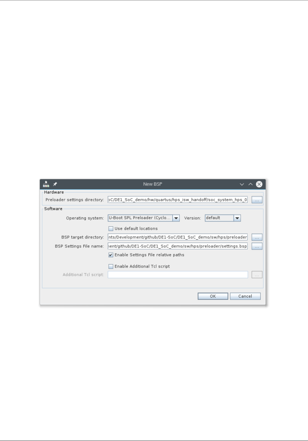
SoC-FPGA Design Guide [DE1-SoC Edition]
21/04/2018 P a g e | 56
12 USING THE CYCLONE V HPS ARM BARE-METAL
12.1 PRELOADER
In Figure 7-8, we saw that a bare-metal application can only be launched after the preloader has setup the
HPS. So, the first thing that needs to be done for bare-metal applications is to generate and compile a
preloader for the HPS.
12.1.1 Preloader Generation
1. Execute the following command to launch the preloader generator.
$ bsp-editor
2. Choose “File > New BSP…”.
a. The preloader will need to know which of the HPS’ peripherals were enabled so it can
appropriately initialize them in the boot process. Under “Preloader settings directory”,
select the “DE1_SoC_demo/hw/quartus/hps_isw_handoff/soc_system_hps_0” directory.
This directory contains settings relative to the HPS’ HARD peripherals, as configured in the
“Arria V/Cyclone V Hard Processor System” component in Qsys.
b. Disable the “Use default locations” checkbox and under the “BSP target directory”,
select the “DE1_SoC_demo/sw/hps/preloader” directory. You should have something similar
to Figure 12-1.
Figure 12-1. New BSP Dialog
c. Press the “OK” button. You should then arrive on a page with many settings, as shown on
Figure 12-2. Take some time to read through them to see what the preloader has the ability to
do.
SoC-FPGA Design Guide [DE1-SoC Edition]
21/04/2018 P a g e | 57
Figure 12-2. Preloader Settings Dialog
3. On the main settings page of Figure 12-2, we will only need to modify 2 parameters for our design.
a. Under “spl.boot”, disable the “WATCHDOG_ENABLE” checkbox. This is necessary to prevent
the system from being automatically reset after a certain time has elapsed. Note that we only
disable this option since we intend on writing a bare-metal program and want to simplify the
code. Any operating system would periodically write to the watchdog timer to avoid it from
resetting the system, and this is a good thing.
b. Under “spl.boot”, enabled the “FAT_SUPPORT” checkbox. This option configures the
preloader to load the image of the next boot stage from the FAT32 partition of the sdcard
(instead of from a binary partition located immediately after the preloader on the sdcard).
The image of the next boot stage is named “u-boot.img” by default, but can be modified by
editing “spl.boot.FAT_LOAD_PAYLOAD_NAME”. We will leave the default name for this
tutorial.
c. Press the “Generate” button to finish. You can then exit the bsp-editor.
4. Execute the following command to build the preloader.
$ cd DE1_SoC_demo/sw/hps/preloader
$ make
IF YOU EVER DECIDE TO MOVE THE “DE1_SoC_demo” PROJECT DIRECTORY DEFINED IN FIGURE 8-1, YOU
WILL HAVE TO REGENERATE THE PRELOADER. UNFORTUNATELY, THE SCRIPT PROVIDED BY ALTERA WHICH
GENERATES THE PRELOADER HARD-CODES MULTIPLE ABSOLUTE PATHS DIRECTLY IN THE RESULTING FILES,
RENDERING THEM USELESS ONCE MOVED.
12.1.2 Creating Target sdcard Artifacts
5. Copy the preloader binary to the sdcard target directory. Execute the following command.
$ cp \
DE1_SoC_demo/sw/hps/preloader/preloader-mkpimage.bin \
DE1_SoC_demo/sdcard/a2/preloader-mkpimage.bin
12.2 ARM DS-5
6. Launch the ARM DS-5 IDE by executing the following command.
$ eclipse
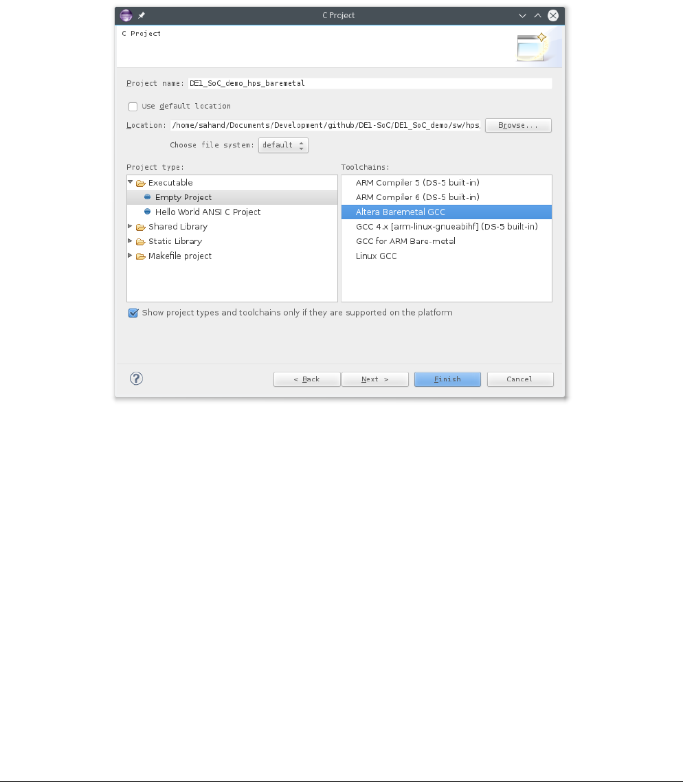
SoC-FPGA Design Guide [DE1-SoC Edition]
21/04/2018 P a g e | 58
12.2.1 Setting Up a New C Project
7. Create a new C project by going to “File > New > Project > C/C++ > C Project”.
a. Use “DE1_SoC_demo_hps_baremetal” as the project name.
b. Disable the “Use default location” checkbox.
c. Set “DE1_SoC_demo/sw/hps/application/DE1_SoC_demo_hps_baremetal” as the target
location for the project.
d. We want to create a single output executable for our project, so choose “Executable >
Empty Project” as the project type.
e. Choose “Altera Baremetal GCC” as the Toolchain.
f. You should have something similar to Figure 12-3. Then, press the “Finish” button to create
the project.
Figure 12-3. New C Project Dialog
8. When programming the HPS, we will need access to a few standard header and linker files provided
by Altera. We need to add these files to the ARM DS-5 project.
a. Right-click on the “DE1_SoC_demo_hps_baremetal” project, and go to “Properties”.
b. We are going to use Altera’s HWLIB to develop our bare-metal application, so we need to
define a macro that is needed by the library to know which board is being targetted.
Under “C/C++ Build > Settings > GCC C Compiler > Symbols”, add “soc_cv_av” to
the “Defined symbols (-D)” list.
c. Under “C/C++ Build > Settings > GCC C Compiler > Includes”, add
“<altera_install_directory>/<version>/embedded/ip/altera/hps/altera_hps/hwli
b/include” to the “Include paths (-I)” list.
d. Under “C/C++ Build > Settings > GCC C Compiler > Includes”, add
“<altera_install_directory>/<version>/embedded/ip/altera/hps/altera_hps/hwli
b/include/soc_cv_av” to the “Include paths (-I)” list.
e. Since we are not going to be running any operating system, we will need to use a linker script
in order to correctly layout our bare-metal program in memory. Altera provides linker scripts
for the HPS’ on-chip memory, as well as for it’s DDR3 memory. We want our code to be
loaded in the HPS’ DDR3 memory and will not use any on-chip memory in our design, so we

SoC-FPGA Design Guide [DE1-SoC Edition]
21/04/2018 P a g e | 59
will use the DDR3 linker script.
Under “C/C++ Build > Settings > GCC C Linker > Image”, set the linker script to
“<altera_install_directory>/<version>/embedded/host_tools/mentor/gnu/arm/bar
emetal/arm-altera-eabi/lib/cycloneV-dk-ram-HOSTED.ld”. The “hosted” script
allows the bare-metal application to use some of the host’s functionality. In this case, we use
the “hosted” script to be able to see the output of the printf() function on the host’s
console.
f. Click on the “Apply” button, then on the “Ok” button to close the project properties dialog.
12.2.2 Writing a DS-5 Debug Script
In Figure 7-8, we saw that a bare-metal application cannot run immediately upon boot, and that the HPS must
first go through the preloader. The preloader executes, and, before terminating, it jumps to the next stage of
the user software. In the case of a bare-metal application, the preloader jumps to the start of the bare-metal
code.
Jumping directly to the bare-metal code is useful for production environments, but it would be great if we
could use a debugger when testing our bare-metal code. To do this, we will use a DS-5 DEBUG SCRIPT to
instruct the DS-5 debugger exactly how to load our application in the HPS’ memory. This debugger script will
load and execute the preloader, then jump to our bare-metal code.
9. Create a new file for our DS-5 debug script and save it under
“DE1_SoC_demo/sw/hps/application/DE1_SoC_demo_hps_baremetal/debug_setup.ds”.
10. Populate the file with the code shown in Figure 12-4. This script tells the debugger to load the
prealoder, then to load our bare-metal application. This is performed by placing a breakpoint at the
very last function executed by the preloader prior to handing control of the cpu to the next boot
stage. This function is “spl_boot_device()”, which is responsible for choosing the next boot
medium on the DE1-SoC and jumping to it’s address. For bare-metal applications, we don’t want the
boot process to continue on towards another device. Instead, we want to load our bare-metal code
and jump to it’s address. This is exactly what the debug script in Figure 12-4 does.
# Reset and stop the system.
stop
wait 5s
reset system
wait 5s
# Delete all breakpoints.
delete breakpoints
# Disable semihosting
set semihosting enabled false
# Load the preloader.
loadfile "$sdir/../../preloader/uboot-socfpga/spl/u-boot-spl" 0x0
# Enable semihosting to allow printing even if you don't have a uart module
# available.
set semihosting enabled true
# Set a breakpoint at the "spl_boot_device()" function. This function is the
# last step of the preloader. It looks for a boot device (qspi flash, sdcard,
# fpga), and jumps to that address. For our bare-metal programs, we don't want
# to use any boot device, but want to run our own program, so we want the
# processor to stop here. Then, we will modify its execution to make it run our
# program.
tbreak spl_boot_device
# Set the PC register to the entry point address previously recorded by the
# "load" or "loadfile" command and start running the target.
run
# Instruct the debugger to wait until either the application completes or a
# breakpoint is hit. In our case, it will hit the breakpoint.
wait
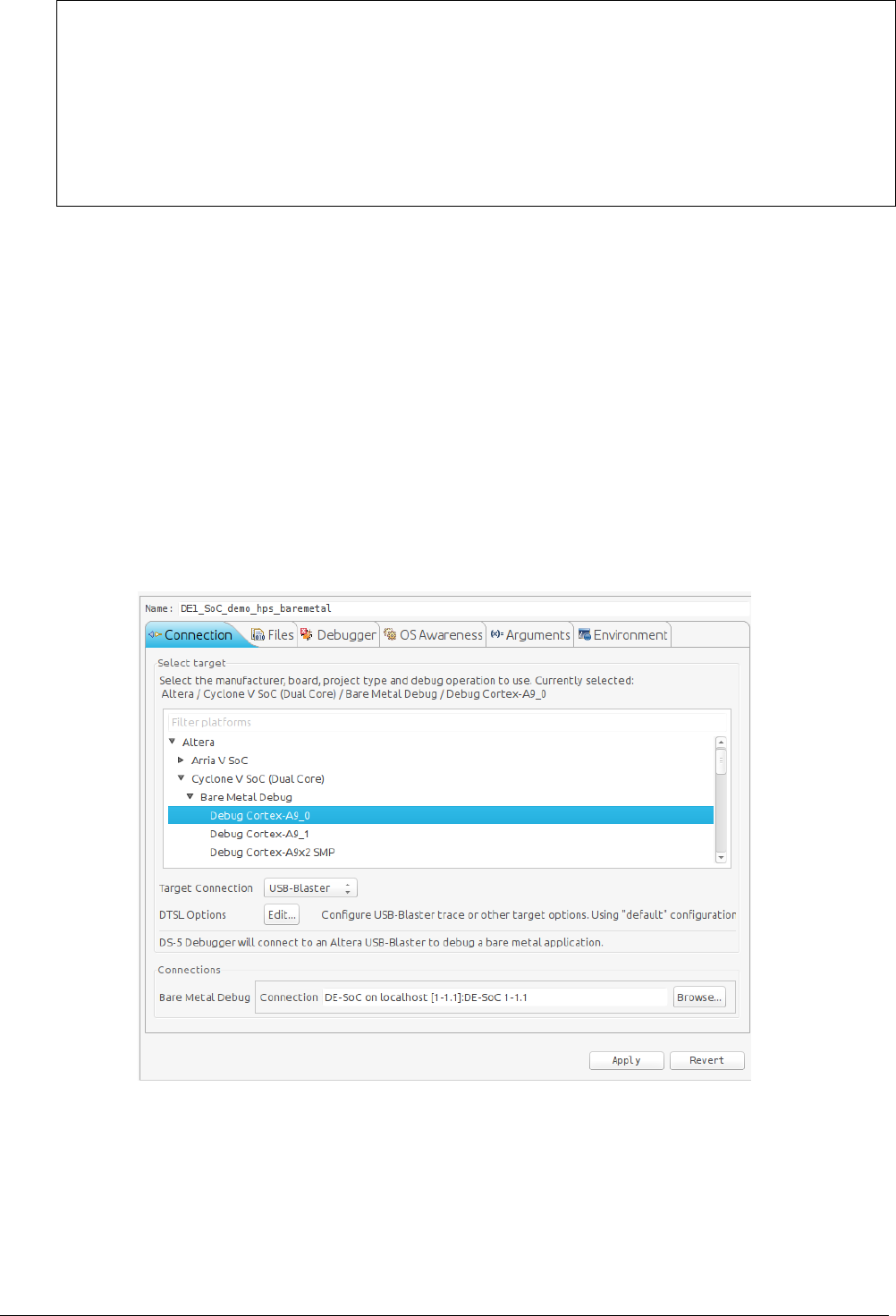
SoC-FPGA Design Guide [DE1-SoC Edition]
21/04/2018 P a g e | 60
# Load our bare-metal program.
loadfile "$sdir/Debug/DE1_SoC_demo_hps_baremetal.axf"
# Set a breakpoint at our program's "main()" function.
tbreak main
# Start running the target.
run
# wait at main().
Wait
Figure 12-4. debug_setup.ds
For a comprehensive list of commands supported by the DS-5 debugger, please refer to [9].
12.2.3 Setting Up the Debug Configuration
11. Right-click on the “DE1_SoC_demo_hps_baremetal” project, and go to “Debug As > Debug
Configurations…”.
12. Choose to create a new debugger configuration by right-clicking on “DS-5 Debugger” on the left and
selecting “New”. Use “DE1_SoC_demo_hps_baremetal” as the name of the new debug configuration.
13. Under the “Connection” tab:
a. Use “Altera > Cyclone V SoC (Dual Core) > Bare Metal Debug > Debug Cortex-
A9_0” as the target platform.
b. Set the “Target Connection” to “USB-Blaster”.
c. Use the “Browse” button to select the DE1-SoC that is connected to your machine.
d. You should have something similar to Figure 12-5.
Figure 12-5. Debug Configuraton “Connection” Tab
14. Under the “Files” tab:
a. Leave the “Application on host to download” empty. We do this since we are using a
debug script to instruct the debugger how to load our application.
b. [UNAVAILABLE IN SoC EDS 16.0] In 9.3.2, we configured our HPS to use some FPGA
peripherals. We can instruct the debugger about this so it can show more detailed
information when debugging. To do this, set the combobox to “Add peripheral
description files from directory” and set it to the
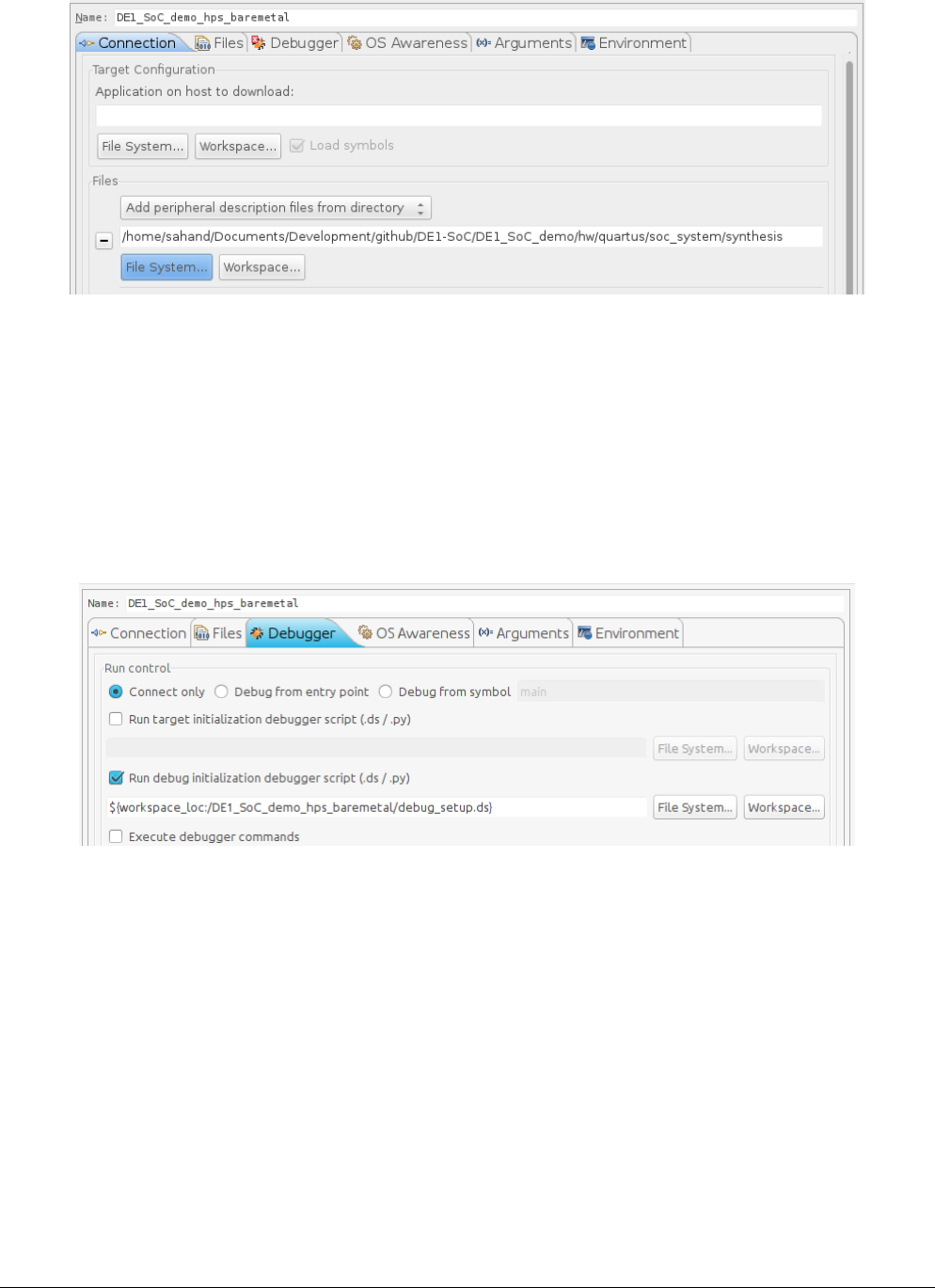
SoC-FPGA Design Guide [DE1-SoC Edition]
21/04/2018 P a g e | 61
“DE1_SoC_demo/hw/quartus/soc_system/synthesis” directory, as shown in Figure 12-6.
This directory contains a file called “soc_system_hps_0_hps.svd” which has information on
all of the HPS’ peripherals which are in the FPGA fabric.
Figure 12-6. Debug Configuration "Files" Tab
15. Under the “Debugger” tab:
a. Since we are going to use a debug script to launch the application, we don’t need to specify
any function to be loaded by the debugger. So, choose “Connect only” under “Run
control”.
b. Enable the “Run DEBUG initialization debugger script (.ds / .py)” checkbox. Set
the debug script to the one we defined for the project in 12.2.2. You should have something
similar to Figure 12-7.
16. Click on the “Apply” button, then on the “Close” button to save the debug configuration.
Figure 12-7. Debug Configuration "Debugger" Tab
12.2.4 Bare-metal Programming
We can now start writing bare-metal code for the HPS.
17. Right-click on the “DE1_SoC_demo_hps_baremetal” project, and go to “New > Source File”. Use
“hps_baremetal.c” as the file name, and click on the “Finish” button to create the new source file.
18. Right-click on the “DE1_SoC_demo_hps_baremetal” project, and go to “New > Header File”. Use
“hps_baremetal.h” as the file name, and click on the “Finish” button to create the new header file.
The code for this part of the application is quite large to be inserted in this document. Therefore, we will just
go over a few practical aspects of the code which are worth paying attention to. The full source can be found
in DE1_SoC_demo.zip [5].
We are not going to implement any interrupts for the various buttons on the board at this time. Therefore, in
order to satisfy the HPS-related goals specified in 8.4, we will need to use an infinite loop and do some polling.

SoC-FPGA Design Guide [DE1-SoC Edition]
21/04/2018 P a g e | 62
This can be seen in our application’s “main()” function, which is shown in Figure 12-8.
#include "hwlib.h"
int main() {
printf("DE1-SoC bare-metal demo\n");
setup_hps_timer();
setup_hps_gpio();
setup_fpga_leds();
while (true) {
handle_hps_led();
handle_fpga_leds();
delay_us(ALT_MICROSECS_IN_A_SEC / 10);
}
return 0;
}
Figure 12-8. hps_baremetal.c main() function
12.2.4.1 Accessing FPGA Peripherals
Accessing the FPGA peripherals connected to the HPS’ lightweight HPS-to-FPGA bridge is quite simple, as no
libraries are needed. One can simply use the low-level functions listed in 11.3 to address the peripherals at an
offset from the lightweight HPS-to-FPGA bridge’s base address.
Figure 12-9 shows an example where the HPS accesses the LEDs on the FPGA.
#include "socal/hps.h"
#include "socal/socal.h"
// fpga LEDs can be found at an offset from the base of the lightweight HPS-to-FPGA bridge
void *fpga_leds = ALT_LWFPGASLVS_ADDR + HPS_FPGA_LEDS_BASE;
void setup_fpga_leds() {
// Switch on first LED only
alt_write_word(fpga_leds, 0x1);
}
void handle_fpga_leds() {
uint32_t leds_mask = alt_read_word(fpga_leds);
if (leds_mask != (0x01 << (HPS_FPGA_LEDS_DATA_WIDTH - 1))) {
// rotate leds
leds_mask <<= 1;
} else {
// reset leds
leds_mask = 0x1;
}
alt_write_word(fpga_leds, leds_mask);
}
Figure 12-9. Accessing FPGA Buttons from the HPS
12.2.4.2 Accessing HPS Peripherals
It is possible to do everything with the low-level functions listed in 11.3. However, a better way would be to
use Altera’s HWLIB, as discussed In 7.5.2. You can easily use HWLIB to access all the HPS’ HARD peripherals.
Note that some things may not be available in HWLIB, and you will then have to resort to using the low-level
functions. One example of this scenario which we have already seen is when accessing any FPGA peripherals
through the lightweight or heavyweight HPS-to-FPGA bus (as there is no standard header file for any FPGA
peripherals).
Since we already demonstrated how to use low-level functions to access peripherals in 12.2.4.1, we will
instead use Altera’s HWLIB to access the HPS’ hard peripherals.
12.2.4.2.1 Using Altera’s HWLIB - Prerequisites
In order to be able to use HWLIB to configure a peripheral, 2 steps need to be performed:

SoC-FPGA Design Guide [DE1-SoC Edition]
21/04/2018 P a g e | 63
You need to INCLUDE the HPS peripheral’s HWLIB HEADER FILE to your code.
You must COPY the HPS peripheral’s HWLIB SOURCE FILE in your DS-5 project directory. The HWLIB
source files can be found in directory
“<altera_install_directory>/<version>/embedded/ip/altera/hps/altera_hps/hwlib/src”,
and must be copied to “DE1_SoC_demo/sw/hps/application/DE1_SoC_demo_hps_baremetal”.
12.2.4.2.2 Global Timer & Clock Manager
If you look closely at the code in Figure 12-8, you’ll see that we used a “delay_us()” function to slow the
counter down. It turns out that among all the code available for the HPS, Altera does not provide any
“sleep()” function (unlike for the Nios II processor). Therefore, we will have to write the “delay_us()”
function ourselves.
The easiest way to create a delay in the HPS is to use one of it’s timers. There are numerous timers on Cyclone
V SoCs:
One such timer is the GLOBAL TIMER. This timer is actually shared by both HPS cores, as well as by the
FPGA.
In addition to the unique global timer, each HPS core also has 7 other timers which it can use
exclusively, if needed.
For simplicity, we will use the global timer to implement the “delay_us()” function.
As described in 12.2.4.2.1, we need to add the required HWLIB sources to our project, and their headers to
our code. To program the global timer, we will need information regarding the clock frequency, as well as any
timer-specific functions. We can access this information by using the following source and header files:
alt_clock_manager.c
alt_clock_manager.h
alt_globaltmr.c
alt_globaltmr.h
Figure 12-10 shows how we implement the “delay_us()” function using the global timer.
#include "alt_clock_manager.h"
#include "alt_globaltmr.h"
void setup_hps_timer() {
assert(ALT_E_SUCCESS == alt_globaltmr_init());
}
/* The HPS doesn't have a sleep() function like the Nios II, so we can make one
* by using the global timer. */
void delay_us(uint32_t us) {
uint64_t start_time = alt_globaltmr_get64();
uint32_t timer_prescaler = alt_globaltmr_prescaler_get() + 1;
uint64_t end_time;
alt_freq_t timer_clock;
assert(ALT_E_SUCCESS == alt_clk_freq_get(ALT_CLK_MPU_PERIPH, &timer_clock));
end_time = start_time + us * ((timer_clock / timer_prescaler) / ALT_MICROSECS_IN_A_SEC);
// polling wait
while(alt_globaltmr_get64() < end_time);
}
Figure 12-10. Programming the HPS Global Timer
12.2.4.2.3 GPIO
Figure 12-11 shows how we implement the “handle_hps_led()” function. This function uses the HPS_KEY_N
button to toggle HPS_LED.
Once again, we need to add the HWLIB source file for the GPIO peripheral to our DS-5 project directory. The
files we will use are listed below:

SoC-FPGA Design Guide [DE1-SoC Edition]
21/04/2018 P a g e | 64
alt_generalpurpose_io.c
alt_generalpurpose_io.h
As stated in 12.2.4.2 previously, HWLIB is quite a broad library, but it sometimes lacks certain “obvious”
things. In such cases, you have to fall back on using lower-level functions to implement whatever you are
missing.
In our case, we see that HWLIB has functions that allow us to write to the GPIO peripheral’s “data” register,
but it doesn’t have any function to read the it back. We get around this issue by directly reading the register
with “alt_read_word(ALT_GPIO1_SWPORTA_DR_ADDR)”.
Note that we also need to include the “socal/alt_gpio.h” header file to have access to the lower-level
ALT_GPIO1_SWPORTA_DR_ADDR macro.
#include "alt_generalpurpose_io.h"
#include "socal/alt_gpio.h"
// | Signal Name | HPS GPIO | Register/bit | Function |
// |=============|==========|==============|==========|
// | HPS_LED | GPIO53 | GPIO1[24] | I/O |
// |=============|==========|==============|==========|
#define HPS_LED_IDX (ALT_GPIO_1BIT_53) // GPIO53
#define HPS_LED_PORT (alt_gpio_bit_to_pid(HPS_LED_IDX)) // ALT_GPIO_PORTB
#define HPS_LED_PORT_BIT (alt_gpio_bit_to_port_pin(HPS_LED_IDX)) // 24 (from GPIO1[24])
#define HPS_LED_MASK (1 << HPS_LED_PORT_BIT)
// |=============|==========|==============|==========|
// | Signal Name | HPS GPIO | Register/bit | Function |
// |=============|==========|==============|==========|
// | HPS_KEY_N | GPIO54 | GPIO1[25] | I/O |
// |=============|==========|==============|==========|
#define HPS_KEY_N_IDX (ALT_GPIO_1BIT_54) // GPIO54
#define HPS_KEY_N_PORT (alt_gpio_bit_to_pid(HPS_KEY_N_IDX)) // ALT_GPIO_PORTB
#define HPS_KEY_N_PORT_BIT (alt_gpio_bit_to_port_pin(HPS_KEY_N_IDX)) // 25 (from GPIO1[25])
#define HPS_KEY_N_MASK (1 << HPS_KEY_N_PORT_BIT)
void setup_hps_gpio() {
uint32_t hps_gpio_config_len = 2;
ALT_GPIO_CONFIG_RECORD_t hps_gpio_config[] = {
{HPS_LED_IDX , ALT_GPIO_PIN_OUTPUT, 0, 0, ALT_GPIO_PIN_DEBOUNCE, ALT_GPIO_PIN_DATAZERO},
{HPS_KEY_N_IDX, ALT_GPIO_PIN_INPUT , 0, 0, ALT_GPIO_PIN_DEBOUNCE, ALT_GPIO_PIN_DATAZERO}
};
assert(ALT_E_SUCCESS == alt_gpio_init());
assert(ALT_E_SUCCESS == alt_gpio_group_config(hps_gpio_config, hps_gpio_config_len));
}
void handle_hps_led() {
uint32_t hps_gpio_input = alt_gpio_port_data_read(HPS_KEY_N_PORT, HPS_KEY_N_MASK);
// HPS_KEY_N is active-low
bool toggle_hps_led = (~hps_gpio_input & HPS_KEY_N_MASK);
if (toggle_hps_led) {
uint32_t hps_led_value = alt_read_word(ALT_GPIO1_SWPORTA_DR_ADDR);
hps_led_value >>= HPS_LED_PORT_BIT;
hps_led_value = !hps_led_value;
hps_led_value <<= HPS_LED_PORT_BIT;
assert(ALT_E_SUCCESS == alt_gpio_port_data_write(HPS_LED_PORT, HPS_LED_MASK, hps_led_value));
}
}
Figure 12-11. Programming the HPS GPIO Peripheral
12.2.4.3 Launching the Bare-metal Code in the Debugger
19. Once you have finished writing all the application’s code, right-click on the
“DE1_SoC_demo_hps_baremetal” project, and select “Build Project”.
20. Switch to the DS-5 Debug perspective, as shown in Figure 12-12.
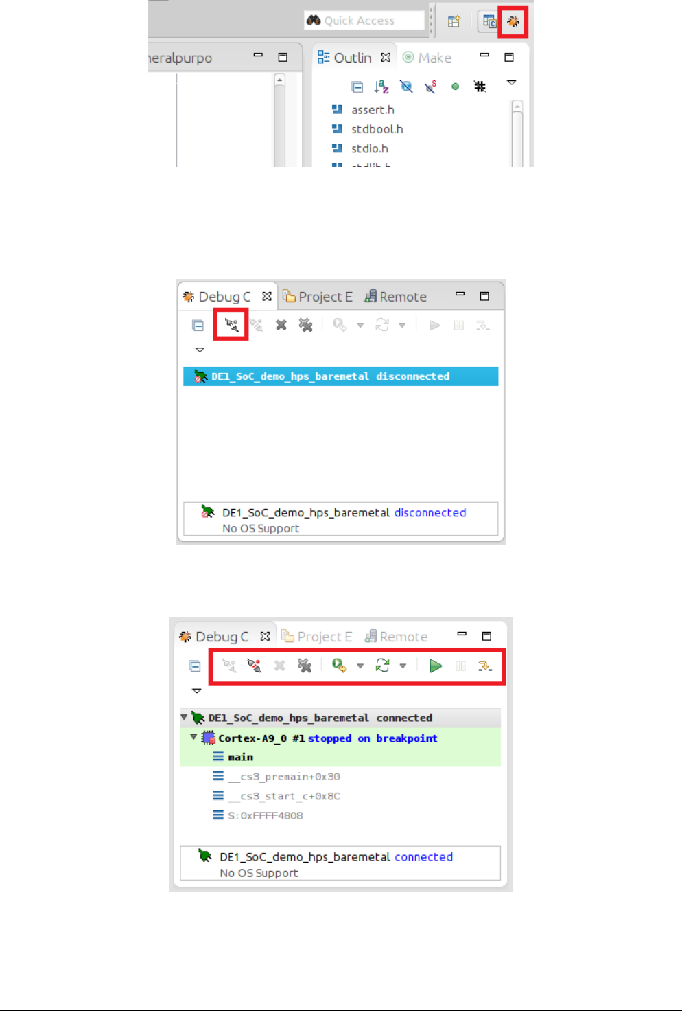
SoC-FPGA Design Guide [DE1-SoC Edition]
21/04/2018 P a g e | 65
Figure 12-12. Switching to the DS-5 Debug Perspective
21. In the “Debug Control” view, click on the “DE1_SoC_demo_hps_baremetal” entry, then click on the
“Connect to Target” button, as shown on Figure 12-13. Our debug script will load and execute the
preloader, then it will load and wait at our application’s “main()” function.
Figure 12-13. Debug Control View
22. You can the use the buttons in the “Debug Control” view to control the application’s execution.
Figure 12-14. DS-5 Debugger Controls
12.2.4.4 DS-5 Bare-metal Debugger Tour
12.2.4.4.1 “Registers” View [UNAVAILABLE IN SoC EDS 16.0]
DS-5’s greatest feature is its “Registers” view.
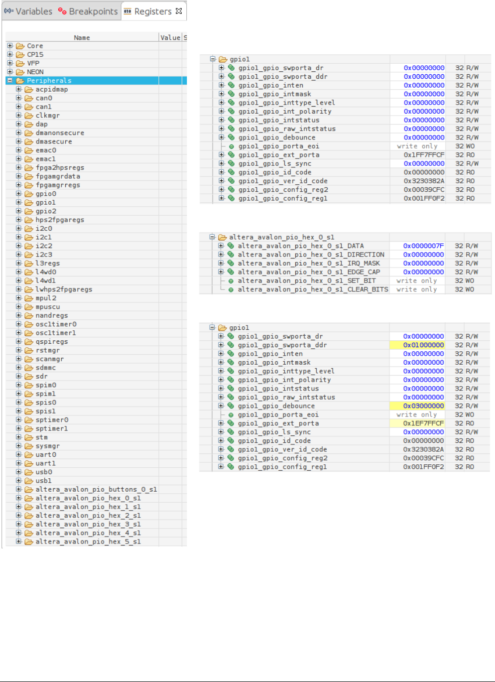
SoC-FPGA Design Guide [DE1-SoC Edition]
21/04/2018 P a g e | 66
Recall that we provided the debugger with a PERIPHERAL DESCRIPTION FILE in 12.2.3. This file allows the
debugger’s “Registers” view to display information about all the HPS’ internal and FPGA peripherals, as
shown in Figure 12-15.
Figure 12-15. DS-5 Debugger Registers View
You can MODIFY any value in this view, and they will automatically be applied to the corresponding
peripheral. For example, you can manually switch on one of the LEDs, or manually trigger a button press of
HPS_KEY_N (assuming you write the correct bit in the correct place).
The view also highlights the values that changed when stepping through the code while debugging, which
helps you track down invalid peripheral writes, side-effects, …
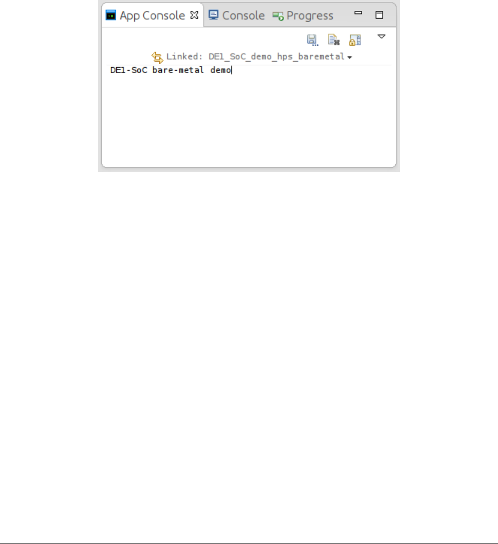
SoC-FPGA Design Guide [DE1-SoC Edition]
21/04/2018 P a g e | 67
However, there is one downside with the “Registers” view. With so many details in this view, one would
normally start browsing through each peripheral’s registers (much easier than reading the Cyclone V manual,
isn’t it?).
The problem occurs when you expand a peripheral that has not been enabled in the preloader, or that has
side-effects when some of its registers are accessed.
Indeed, DS-5 will try to access an invalid address, and it will crash the debugging session, therefore leaving the
software on the board in an unrecoverable state. You will have to SWITCH OFF THE BOARD and reprogram it
to relaunch the application. Don’t forget to REPROGRAM THE FPGA FABRIC with your design as well.
12.2.4.4.2 App Console
Data sent to standard output is shown in the “App Console” view. Figure 12-16 shows the result of a
“printf()” call in our demo code shown in Figure 12-8.
Figure 12-16. DS-5 App Console View
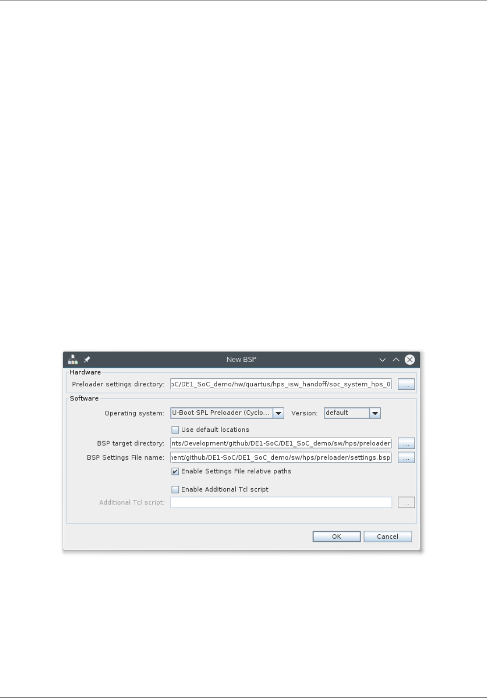
SoC-FPGA Design Guide [DE1-SoC Edition]
21/04/2018 P a g e | 68
13 USING THE CYCLONE V HPS ARM LINUX
In Figure 7-8, we saw that there are 3 stages before a linux application can be launched:
Preloader
Bootloader
Operating System
In this section, we detail each step needed to create such a linux system from scratch.
13.1 PRELOADER
The first step is to generate and compile the preloader which sets up the HPS.
13.1.1 Preloader Generation
1. Execute the following command to launch the preloader generator.
$ bsp-editor
2. Choose “File > New BSP…”.
a. The preloader will need to know which of the HPS’ peripherals were enabled so it can
appropriately initialize them in the boot process. Under “Preloader settings directory”,
select the “DE1_SoC_demo/hw/quartus/hps_isw_handoff/soc_system_hps_0” directory.
This directory contains settings relative to the HPS’ HARD peripherals, as configured in the
“Arria V/Cyclone V Hard Processor System” component in Qsys.
b. Disable the “Use default locations” checkbox and under the “BSP target directory”,
select the “DE1_SoC_demo/sw/hps/preloader” directory. You should have something similar
to Figure 13-1.
Figure 13-1. New BSP Dialog
c. Press the “OK” button. You should then arrive on a page with many settings, as shown on
Figure 13-2. Take some time to read through them to see what the preloader has the ability to
do.

SoC-FPGA Design Guide [DE1-SoC Edition]
21/04/2018 P a g e | 69
Figure 13-2. Preloader Settings Dialog
3. On the main settings page of Figure 13-2, we will only need to modify 1 parameter for our design.
a. Under “spl.boot”, enabled the “FAT_SUPPORT” checkbox. This option configures the
preloader to load the image of the next boot stage from the FAT32 partition of the sdcard
(instead of from a binary partition located immediately after the preloader on the sdcard).
The image of the next boot stage is named “u-boot.img” by default, but can be modified by
editing “spl.boot.FAT_LOAD_PAYLOAD_NAME”. We will leave the default name for this
tutorial.
b. Press the “Generate” button to finish. You can then exit the bsp-editor.
4. Execute the following command to build the preloader.
$ cd DE1_SoC_demo/sw/hps/preloader
$ make
IF YOU EVER DECIDE TO MOVE THE “DE1_SoC_demo” PROJECT DIRECTORY DEFINED IN FIGURE 8-1, YOU
WILL HAVE TO REGENERATE THE PRELOADER. UNFORTUNATELY, THE SCRIPT PROVIDED BY ALTERA WHICH
GENERATES THE PRELOADER HARD-CODES MULTIPLE ABSOLUTE PATHS DIRECTLY IN THE RESULTING FILES,
RENDERING THEM USELESS ONCE MOVED.
13.1.2 Creating Target sdcard Artifacts
5. Copy the preloader binary to the sdcard target directory. Execute the following command.
$ cp \
DE1_SoC_demo/sw/hps/preloader/preloader-mkpimage.bin \
DE1_SoC_demo/sdcard/a2/preloader-mkpimage.bin
13.2 BOOTLOADER
The second step is to obtain a bootloader that is capable of loading the linux kernel. Altera provides a copy of
the U-Boot bootloader alongside the preloader. However, this copy is quite old as it dates back to 2013.
Instead, we will download the official U-Boot sources online and use a more recent version.
13.2.1 Getting & Compiling U-Boot
6. Download the latest version of the U-Boot bootloader by executing the following command. This
command downloads the latest U-Boot sources and saves it to the “DE1_SoC_demo/sw/hps/u-boot”
directory.

SoC-FPGA Design Guide [DE1-SoC Edition]
21/04/2018 P a g e | 70
$ git clone \
git://git.denx.de/u-boot.git \
DE1_SoC_demo/sw/hps/u-boot
7. Change your current working directory to the U-Boot directory.
$ cd DE1_SoC_demo/sw/hps/u-boot
8. We need to compile U-Boot for an ARM machine, but are compiling on an x86-64 machine, so we
must cross-compile the bootloader. To cross-compile U-Boot, define the following environment
variable:
$ export CROSS_COMPILE=arm-linux-gnueabihf-
9. Clean up the source tree to be sure it is in a clean state before we compile it.
$ make distclean
10. Checkout the following U-Boot commit. This corresponds to the last commit against which the
instructions in this guide were tested. You can skip this step if you want to use a more recent version
of U-Boot, but keep in mind that there may be regressions that make some things not work.
# commit b104b3dc1dd90cdbf67ccf3c51b06e4f1592fe91
# Author: Tom Rini trini@konsulko.com
# Date: Mon Jun 6 17:43:54 2016 -0400
#
# Prepare v2016.07-rc1
#
# Signed-off-by: Tom Rini trini@konsulko.com
$ git checkout b104b3dc1dd90cdbf67ccf3c51b06e4f1592fe91
11. Configure U-Boot for the Cyclone V SoC architecture.
$ make socfpga_cyclone5_config
By default, U-Boot loads some environment variables from a specific flash sector on the sdcard, then
continues executing the commands specified in the macro called “CONFIG_BOOTCOMMAND” (defined in the U-
Boot source code). If this flash sector is empty, then U-Boot emits the following error message.
*** Warning - bad CRC, using default environment
To get around this issue, we are going to patch U-Boot’s source code to ignore the empty flash sector (if it
exists), and instruct it to always load and execute the contents of a user-defined script that we will provide. As
we will see in 13.2.2, U-Boot can be scripted to perform steps of your choosing.
12. Open “DE1_SoC_demo/sw/hps/u-boot/include/configs/socfpga_cyclone5_socdk.h" with a text
editor.
13. Replace the value of the “CONFIG_BOOTCOMMAND” macro with the following definition. This macro
contains the first instruction that will be executed by U-Boot when it boots. In our case, we are telling
U-Boot to execute the contents of the environment variable called “callscript”.
#define CONFIG_BOOTCOMMAND "run callscript"
The “callscript” environment variable does not yet exist in U-Boot, so we are going to set it in the source
code as an extra environment variable.

SoC-FPGA Design Guide [DE1-SoC Edition]
21/04/2018 P a g e | 71
14. Replace the value of the “CONFIG_EXTRA_ENV_SETTINGS” macro with the following definition. We
define the environment variables needed to load a user-defined script called “u-boot.scr” from
sdcard 0, partition 1 (FAT32 partition) into memory, and to execute it.
#define CONFIG_EXTRA_ENV_SETTINGS \
"scriptfile=u-boot.scr" "\0" \
"fpgadata=0x2000000" "\0" \
"callscript=fatload mmc 0:1 $fpgadata $scriptfile;" \
"source $fpgadata" "\0"
15. At this point, we have finished modifying U-Boot’s source code, and we can compile the bootloader.
$ make
13.2.2 Scripting U-Boot
U-Boot can be scripted to perform steps of your choosing. We will use this ability to automate a few steps
before booting into linux.
16. Create a new file for our U-Boot script and save it under “DE1_SoC_demo/sw/hps/u-boot/u-
boot.script”.
17. Populate the file with the code shown in Figure 13-3. This script instructs U-Boot to
a. Define some environment variables.
b. Load the FPGA .rbf file from the FAT32 partition into memory.
c. Program the FPGA.
d. Enable the FPGA2HPS and HPS2FPGA bridges.
e. Load linux kernel image and devicee tree into memory.
f. Boot linux.
In our case, we use such a script to ensure that the FPGA is programmed BEFORE linux boots.
################################################################################
echo --- Resetting Env variables ---
# reset environment variables to default
env default -a
echo --- Setting Env variables ---
# Set the kernel image
setenv bootimage zImage;
# address to which the device tree will be loaded
setenv fdtaddr 0x00000100
# Set the devicetree image
setenv fdtimage socfpga.dtb;
# set kernel boot arguments, then boot the kernel
setenv mmcboot 'setenv bootargs mem=1024M console=ttyS0,115200 root=${mmcroot} rw rootwait; bootz
${loadaddr} - ${fdtaddr}';
# load linux kernel image and device tree to memory
setenv mmcload 'mmc rescan; ${mmcloadcmd} mmc 0:${mmcloadpart} ${loadaddr} ${bootimage}; ${mmcloadcmd}
mmc 0:${mmcloadpart} ${fdtaddr} ${fdtimage}'
# command to be executed to read from sdcard
setenv mmcloadcmd fatload
# sdcard fat32 partition number
setenv mmcloadpart 1
# sdcard ext3 identifier
setenv mmcroot /dev/mmcblk0p2
# standard input/output
setenv stderr serial
setenv stdin serial
setenv stdout serial

SoC-FPGA Design Guide [DE1-SoC Edition]
21/04/2018 P a g e | 72
# save environment to sdcard (not needed, but useful to avoid CRC errors on a new sdcard)
saveenv
################################################################################
echo --- Programming FPGA ---
# load rbf from FAT partition into memory
fatload mmc 0:1 ${fpgadata} socfpga.rbf;
# program FPGA
fpga load 0 ${fpgadata} ${filesize};
# enable HPS-to-FPGA, FPGA-to-HPS, LWHPS-to-FPGA bridges
bridge enable;
################################################################################
echo --- Booting Linux ---
# load linux kernel image and device tree to memory
run mmcload;
# set kernel boot arguments, then boot the kernel
run mmcboot;
Figure 13-3. U-Boot Script
18. Convert the U-Boot script to binary form.
$ mkimage \
-A arm \
-O linux \
-T script \
-C none \
-a 0 \
-e 0 \
-n DE1_SoC_demo \
-d DE1_SoC_demo/sw/hps/u-boot/u-boot.script \
DE1_SoC_demo/sw/hps/u-boot/u-boot.scr
13.2.3 Creating Target sdcard Artifacts
19. Copy the U-Boot image to the sdcard target directory.
$ cp \
DE1_SoC_demo/sw/hps/u-boot/u-boot.img \
DE1_SoC_demo/sdcard/fat32/u-boot.img
20. Copy the binary U-Boot script to the sdcard target directory.
$ cp \
DE1_SoC_demo/sw/hps/u-boot/u-boot.scr \
DE1_SoC_demo/sdcard/fat32/u-boot.scr
13.3 LINUX KERNEL
The third step is to obtain and compile the linux kernel.
13.3.1 Getting & Compiling Linux
21. Download the latest version of the linux kernel by executing the following command. This command
downloads the latest linux sources and saves it to the “DE1_SoC-demo/sw/hps/linux/source”
directory.
Note that we are not going to use the sources directly from the mainline kernel branch, as it is
generally behind the various development branches maintained by Altera (which contain drivers for
most of the FPGA-related components specific to the socfpga architecture). Once Altera’s branches
are merged back into the mainline kernel, we can switch to that source tree, but for the moment, we
will continue to use Altera’s branch.

SoC-FPGA Design Guide [DE1-SoC Edition]
21/04/2018 P a g e | 73
$ git clone \
https://github.com/altera-opensource/linux-socfpga.git \
DE1_SoC_demo/sw/hps/linux/source
22. Change your current working directory to the linux directory.
$ cd DE1_SoC_demo/sw/hps/linux/source
23. We need to compile linux for an ARM machine, but are compiling on an x86-64 machine, so we must
cross-compile the kernel. To cross-compile linux, define the following environment variables:
$ export ARCH=arm
$ export CROSS_COMPILE=arm-linux-gnueabihf-
24. Clean up the source tree to be sure it is in a clean state before we compile it.
$ make distclean
25. Checkout the following linux commit. This corresponds to the last commit against which the
instructions in this guide were tested. You can skip this step if you want to use a more recent version
of linux, but remember that there may be regressions that make some things not work.
# commit 9735a22799b9214d17d3c231fe377fc852f042e9
# Author: Linus Torvalds <torvalds@linux-foundation.org>
# Date: Sun Apr 3 09:09:40 2016 -0500
#
# Linux 4.6-rc2
$ git checkout 9735a22799b9214d17d3c231fe377fc852f042e9
26. Configure linux for the Cyclone V SoC architecture.
$ make socfpga_defconfig
27. Compile the linux kernel “zImage” binary, which corresponds to a self-extracting compressed version
of the linux kernel image.
$ make zImage
28. Compile the device tree blob for the Cyclone V Development Kit. This device tree does not exactly
correspond to the device tree needed for the DE1-SoC, but given that there are no predefined device
trees available for the DE1-SoC, we will use the one provided for the (more feature-rich) Cyclone V
Development Kit.
$ make socfpga_cyclone5_socdk.dtb
13.3.2 Creating Target sdcard Artifacts
29. Copy the linux zImage binary to the sdcard target directory
$ cp \
DE1_SoC_demo/sw/hps/linux/source/arch/arm/boot/zImage
DE1_SoC_demo/sdcard/fat32/zImage
30. Copy the linux device tree blob to the sdcard target directory.
$ cp \
DE1_SoC_demo/sw/hps/linux/source/arch/arm/boot/dts/socfpga_cyclone5_socdk.dtb \
DE1_SoC_demo/sdcard/fat32/socfpga.dtb

SoC-FPGA Design Guide [DE1-SoC Edition]
21/04/2018 P a g e | 74
13.4 UBUNTU CORE ROOT FILESYSTEM
At this stage, we technically have everything needed to have a fully-working linux machine. The machine,
however, is quite minimal. This is normal, as we merely have the linux KERNEL available at this point. We will
now install a linux DISTRIBUTION in order to have more tools and functionality.
In this guide, we will install Ubuntu Core on our DE1-SoC. Ubuntu Core is the minimal root filesystem (rootfs)
needed to run Ubuntu. It consists of a very basic command-line version of the distribution, and can be
customized to eventually ressemble the desktop version of Ubuntu most people are familiar with. Most
importantly, it comes with a package manager.
13.4.1 Obtaining Ubuntu Core
31. Download the Ubuntu Core 14.04.4 rootfs for the armhf architecture from Canonical’s servers.
$ wget \
http://cdimage.ubuntu.com/ubuntu-base/releases/14.04.5/release/ubuntu-base-
14.04.5-base-armhf.tar.gz \
-O DE1_SoC_demo/sw/hps/linux/rootfs/ubuntu-base-14.04.5-base-armhf.tar.gz
32. Create a directory where we will extract the root filesystem.
$ mkdir –p DE1_SoC_demo/sw/hps/linux/rootfs/ubuntu-core-rootfs
33. Change your working directory to the previously created directory and extract the root filesystem.
Note that you need to extract the archive with root permissions to allow the “mknod” commands to
work.
$ cd DE1_SoC_demo/sw/hps/linux/rootfs/ubuntu-core-rootfs
$ sudo tar –xzpf ../ubuntu-base-14.04.5-core-armhf.tar.gz
13.4.2 Customizing Ubuntu Core
The Ubuntu Core rootfs is not very useful in its current state, as it is completely unconfigured. By
unconfigured, we mean that there is no user installed, no DNS configuration, no network interfaces …
We must therefore configure the rootfs before we can use it. Normally, root filesystems are configured by
means of the “chroot” command, which allows you to obtain an interactive shell in a root directory different
from the one used on your host machine. After “chroot”ing in a directory, one essentially executes the
binaries from the chrooted directory as if they were in a different computer. This is very practical for
configuring a rootfs, as we can issue commands to configure it as we want, then “exit” the chroot to return
back to our host operating system and package the configured rootfs for deployment to another machine.
Unfortunately, we will not be able to use this technique in our case. The reason is that our host machine has
an x86-64 architecture, but the Cyclone V SoC has an armhf architecture. It is not possible to chroot into a
directory with binaries targetting a different architecture, because your host machine’s CPU will not recognize
the instructions. If you attempted this, your operating system would return “Exec format error” and abort the
chroot. One could use an emulator such as QEMU to emulate the binaries in the chroot directory so your host
CPU can correctly execute them, but such emulators are difficult to set up, and do not work on all machines.
What we will instead do is configure the rootfs directly on the target machine (DE1-SoC) when it boots the
operating system for the first time. For this, we will write a shell script “config_system.sh” on our host
macine and place it in the extracted rootfs. We will then configure the rootfs to launch our script when it
boots for the first time.
13.4.2.1 System configuration on first boot
34. Create a new file for our rootfs system configuration script and save it under
“DE1_SoC_demo/sw/hps/linux/rootfs/config_system.sh”.

SoC-FPGA Design Guide [DE1-SoC Edition]
21/04/2018 P a g e | 75
35. Populate the file with the code shown in Figure 13-4. The script takes care of setting up the overall
system. This includes language support, timezone information, machine names, network connectivity,
support for users, …
#!/bin/bash -x
# Configure the locale to have proper language support.
localedef -i en_US -c -f UTF-8 en_US.UTF-8
dpkg-reconfigure locales
# Configure the timezone.
echo "Europe/Zurich" > "/etc/timezone"
dpkg-reconfigure -f noninteractive tzdata
# Set the machine’s hostname.
echo "DE1-SoC" > "/etc/hostname"
tee "/etc/hosts" >"/dev/null" <<EOF
127.0.0.1 localhost
127.0.1.1 DE1-SoC
EOF
# Create the “/etc/network/interfaces” file that describes the network
# interfaces available on the board.
tee "/etc/network/interfaces" > "/dev/null" <<EOF
# interfaces(5) file used by ifup(8) and ifdown(8)
# The loopback network interface
auto lo
iface lo inet loopback
# The primary network interface
auto eth0
iface eth0 inet dhcp
EOF
# DNS configuration for name resolution. We use google's public DNS server here.
sudo tee "/etc/resolv.conf" > "/dev/null" <<EOF
nameserver 8.8.8.8
EOF
# Configure Ubuntu Core to display a login shell on the serial console once the
# kernel boots. We had previously configured U-Boot to supply the command-line
# argument "console=ttyS0,115200" to the linux kernel. This argument instructs
# the kernel to use serial console “ttyS0” as the boot shell, so here we choose
# to use the same serial console for the login shell-
tee "/etc/init/ttyS0.conf" > "/dev/null" <<EOF
# ttyS0 - getty
#
# This service maintains a getty on ttyS0
description "Get a getty on ttyS0"
start on runlevel [2345]
stop on runlevel [016]
respawn
exec /sbin/getty -L 115200 ttyS0 vt102
EOF
# Create a user and a password. In this example, we create a user called
# “sahand” with password "1234". Note that we compute an encrypted version of
# the password, because useradd does not allow plain text passwords to be used
# in non-interactive mode.
username="sahand"
password="1234"
encrypted_password="$(perl -e 'printf("%s\n", crypt($ARGV[0], "password"))' "${password}")"
useradd -m -p "${encrypted_password}" -s "/bin/bash" "${username}"
# Ubuntu requires the admin to be part of the "adm" and "sudo" groups, so add
# the previously-created user to the 2 groups.
addgroup ${username} adm
addgroup ${username} sudo
# Set root password to "1234" (same as previously-created user).
echo -e "${password}\n${password}\n" | passwd root

SoC-FPGA Design Guide [DE1-SoC Edition]
21/04/2018 P a g e | 76
# Remove "/rootfs_config.sh" from /etc/rc.local to avoid reconfiguring system on
# next boot
tee "/etc/rc.local" > "/dev/null" <<EOF
#!/bin/sh -e
#
# rc.local
#
# This script is executed at the end of each multiuser runlevel.
# Make sure that the script will "exit 0" on success or any other
# value on error.
#
# In order to enable or disable this script just change the execution
# bits.
#
# By default this script does nothing.
exit 0
EOF
Figure 13-4. Rootfs system configuration script to be used on first boot ("config_system.sh")
36. Copy the system configuration script to the extracted rootfs directory.
$ cp \
DE1_SoC_demo/sw/hps/linux/rootfs/config_system.sh \
DE1_SoC_demo/sw/hps/linux/rootfs/ubuntu-core-rootfs
37. Edit “DE1_SoC_demo/sw/hps/linux/rootfs/ubuntu-core-rootfs/etc/rc.local” such that
“config_system.sh” is run when the operating system boots. Populate the file with the code shown
in Figure 13-5.
#!/bin/sh -e
#
# rc.local
#
# This script is executed at the end of each multiuser runlevel.
# Make sure that the script will "exit 0" on success or any other
# value on error.
#
# In order to enable or disable this script just change the execution
# bits.
#
# By default this script does nothing.
/config_system.sh
exit 0
Figure 13-5. Rootfs /etc/rc.local file.
13.4.2.2 Post-install configuration script
In Section 13.8 we see how to use the remote debugging feature of our IDE to debug our linux applications.
Remote debugging uses SSH to connect to the target device, then uses a GDB server to debug the application
on the target while coordinating back with a GDB client running in our IDE. Ubuntu core does not come pre-
installed with the ssh and gdbserver packages, so we would need to install them from the Ubuntu package
manager.
We could be tempted to call the package manger in our previous “config_system.sh” script so all required
packages can also be installed when the operating system boots for the first time. However, if you look closely
at what the script does, you see that it configures the system’s network interfaces, which means that the
system does NOT have any network connectivity while the previous script is running. Because of this reason,
we cannot call the package manager in “config_system.sh”, and must instead do this once the system has
finished booting and is running. We create a second configuration script for this purpose and also place it on
the rootfs.

SoC-FPGA Design Guide [DE1-SoC Edition]
21/04/2018 P a g e | 77
38. Create a new file for our rootfs post-install configuration script and save it under
“DE1_SoC_demo/sw/hps/linux/rootfs/config_post_install.sh”.
39. Populate the file with the code shown in.
#!/bin/bash -x
# apt sources
# uncomment the "deb" lines (no need to uncomment "deb src" lines)
# Edit the “/etc/apt/sources.list” file to configure the package manager. This
# file contains a list of mirrors that the package manager queries. By default,
# this file has all fields commented out, so the package manager will not have
# access to any mirrors. The following command uncomments all commented out
# lines starting with "deb". These contain the mirrors we are interested in.
sudo perl -pi -e 's/^#+\s+(deb\s+http)/$1/g' "/etc/apt/sources.list"
# When writing our linux applications, we want to use ARM DS-5’s remote
# debugging feature to automatically transfer our binaries to the target device
# and to start a debugging session. The remote debugging feature requires an SSH
# server and a remote gdb server to be available on the target. These are easy
# to install as we have a package manager available
sudo apt update
sudo apt -y install ssh gdbserver
# Allow root SSH login with password (needed so we can use ARM DS-5 for remote
# debugging)
sudo perl -pi -e 's/^(PermitRootLogin) without-password$/$1 yes/g' "/etc/ssh/sshd_config"
Figure 13-6. Rootfs post-install configuration script to be used AFTER the first boot (“config_post_install.sh”).
40. Copy the post-install configuration script to the extracted rootfs directory.
$ cp \
DE1_SoC_demo/sw/hps/linux/rootfs/config_post_install.sh \
DE1_SoC_demo/sw/hps/linux/rootfs/ubuntu-core-rootfs
At this stage we are done configuring the rootfs.
13.4.3 Creating Target sdcard Artifacts
41. Copy the customized root filesystem to the sdcard target directory. For the previous artifacts, we used
to simply copy files with the “cp” command. However, we will create an archive for the rootfs, as
there are many special files in some directories that the standard “cp” command does not copy
correctly.
$ cd DE1_SoC_demo/sw/hps/linux/rootfs/ubuntu-core-rootfs
# Note: there is a “.” at the end of the next command
$ sudo tar -czpf DE1_SoC_demo/sdcard/ext3_rootfs.tar.gz .
13.5 WRITING EVERYTHING TO THE SDCARD
If you have followed all the steps in sections 9 and 13 until this point, then you should have the file structure
shown in Figure 13-7 as your “DE1_SoC_demo/sdcard” directory.
sdcard/
├── a2
│ └── preloader-mkpimage.bin
├── ext3_rootfs.tar.gz
└── fat32
├── socfpga.dtb
├── socfpga.rbf
├── u-boot.img
├── u-boot.scr
└── zImage
Figure 13-7. Target sdcard directory
We now have all the files needed to create our final sdcard.

SoC-FPGA Design Guide [DE1-SoC Edition]
21/04/2018 P a g e | 78
42. Create 2 directories where you will mount the FAT32 and EXT3 partitions of the sdcard.
$ mkdir –p DE1_SoC_demo/sdcard/mount_point_fat32
$ mkdir –p DE1_SoC_demo/sdcard/mount_point_ext3
43. Mount the sdcard partitions.
$ sudo mount /dev/sdb1 DE1_SoC_demo/sdcard/mount_point_fat32
$ sudo mount /dev/sdb2 DE1_SoC_demo/sdcard/mount_point_ext3
44. Write the preloader to the custom “a2” partition.
$ sudo dd \
if=DE1_SoC_demo/sdcard/a2/preloader-mkpimage.bin \
of=/dev/sdb3 \
bs=64K \
seek=0
45. Write the FPGA .rbf file, U-Boot .img file, U-Boot .scr file, linux zImage file, and linux .dtb file to
the FAT32 partition.
$ sudo cp \
DE1_SoC_demo/sdcard/fat32/* \
DE1_SoC_demo/sdcard/mount_point_fat32
46. Write the customized Ubuntu Core root filesystem to the EXT3 partition.
$ cd DE1_SoC_demo/sdcard/mount_point_ext3
$ sudo tar -xzf ../ext3_rootfs.tar.gz
47. Flush all write buffers to target.
$ sudo sync
48. Unmount sdcard partitions.
$ sudo umount DE1_SoC_demo/sdcard/mount_point_fat32
$ sudo umount DE1_SoC_demo/sdcard/mount_point_ext3
49. Delete sdcard mount points.
$ rm –rf DE1_SoC_demo/sdcard/mount_point_fat32
$ rm –rf DE1_SoC_demo/sdcard/mount_point_ext3
The sdcard is now finally ready.
13.6 SCRIPTING THE COMPLETE PROCEDURE
It is important to perform all steps above by hand once to see how one creates a linux system for a new
device from scratch. As previously stated, the full design used in this tutorial is available in DE1_SoC_demo.zip
[5].
However, due to the very large number of steps required to build the current linux system from scratch, we
provide a “create_linux_system.sh” script that performs all steps described until now automatically. The
script performs the following tasks:
Compile the Quartus Prime hardware project.
Generate, configure, and compile the preloader.
Download, configure, and compile U-Boot.
Download, configure, and compile Linux.
Download and configure the Ubuntu Core root filesystem.
Partition the sdcard.

SoC-FPGA Design Guide [DE1-SoC Edition]
21/04/2018 P a g e | 79
Write the sdcard.
The script has a large number of constants at the beginning that you can modify to tailor the process to your
needs. The default linux user account created is “sahand” and the password is “1234”. The root password is
also set to “1234”.
===================================================================================
usage: create_linux_system.sh [sdcard_device]
positional arguments:
sdcard_device path to sdcard device file [ex: "/dev/sdb", "/dev/mmcblk0"]
===================================================================================
IT IS RECOMMENDED TO USE THE SCRIPT TO AUTOMATE THE FULL SYSTEM CREATION PIPELINE, AND TO GO
GET A SNACK WHILE YOU WAIT FOR IT TO FINISH
13.7 TESTING THE SETUP
50. Wire up the DE1-SoC as described in Figure 9-19.
51. Plug in the microSD card.
BE SURE YOU ARE PART OF THE “dialout” GROUP BEFORE YOU CONTINUE, OTHERWISE YOU WON’T BE
ABLE TO ACCESS THE SERIAL CONSOLE ON YOUR MACHINE IN ORDER TO CONNECT TO THE DE1-SOC.
52. Launch a serial console on your host machine by executing the following command.
$ minicom --device /dev/ttyUSB0
53. Configure the serial console as shown below.
+------------------------------------------+
| A - Serial Device : /dev/ttyUSB0 |
| B - Lockfile Location : /var/lock |
| C - Callin Program : |
| D - Callout Program : |
| E - Bps/Par/Bits : 115200 8N1 |
| F - Hardware Flow Control : No |
| G - Software Flow Control : No |
| |
| Change which setting? |
+------------------------------------------+
BE SURE TO SET THE MSEL SWITCH ON THE BOTTOM SIDE OF THE DE1-SOC TO “00000” BEFORE
CONTINUING.
54. Power-on the DE1-SoC.
If SOMETHING GOES WRONG and you end up with an error message similar to the one shown in Figure 13-8,
then perform the following steps to help fix the problem.
fatload - load binary file from a dos filesystem
Usage:
fatload <interface> [<dev[:part]> [<addr> [<filename> [bytes [pos]]]]]
- Load binary file 'filename' from 'dev' on 'interface'
to address 'addr' from dos filesystem.
'pos' gives the file position to start loading from.
If 'pos' is omitted, 0 is used. 'pos' requires 'bytes'.
'bytes' gives the size to load. If 'bytes' is 0 or omitted,
the load stops on end of file.
If either 'pos' or 'bytes' are not aligned to
ARCH_DMA_MINALIGN then a misaligned buffer warning will
be printed and performance will suffer for the load.

SoC-FPGA Design Guide [DE1-SoC Edition]
21/04/2018 P a g e | 80
Kernel image @ 0x1000000 [ 0x000000 - 0x363908 ]
FDT and ATAGS support not compiled in - hanging
### ERROR ### Please RESET the board ###
Figure 13-8. Incorrect DE1-SoC Boot Messages (from U-Boot)
55. Reset the board and interrupt U-Boot’s boot process by pressing any button on the serial console
when you see the following message.
Hit any key to stop autoboot:
56. Overwrite the environment variables stored on the sdcard by executing the following commands on
the U-Boot command prompt.
$ env default –a
$ saveenv
57. Reset the board. The system should now run correctly at this point.
If you DID EVERYTHING CORRECTLY until now, you should see the messages shown in Figure 13-9. The
sequence is as follows:
The preloader starts (“U-Boot SPL 2013.01.01”), followed by
U-Boot (“U-Boot 2016.07-rc1-dirty”), and finally
The linux kernel (“Starting Kernel ...”).
The output you obtain when the linux kernel is loading may be slightly different as some interleaving may
occur when all system services boot. Note that all lines starting with a “+” are those executed in our system
configuration script, “config_system.sh”.
U-Boot SPL 2013.01.01 (Feb 08 2017 - 10:24:55)
BOARD : Altera SOCFPGA Cyclone V Board
CLOCK: EOSC1 clock 25000 KHz
CLOCK: EOSC2 clock 25000 KHz
CLOCK: F2S_SDR_REF clock 0 KHz
CLOCK: F2S_PER_REF clock 0 KHz
CLOCK: MPU clock 925 MHz
CLOCK: DDR clock 400 MHz
CLOCK: UART clock 100000 KHz
CLOCK: MMC clock 50000 KHz
CLOCK: QSPI clock 370000 KHz
RESET: COLD
INFO : Watchdog enabled
SDRAM: Initializing MMR registers
SDRAM: Calibrating PHY
SEQ.C: Preparing to start memory calibration
SEQ.C: CALIBRATION PASSED
SDRAM: 1024 MiB
ALTERA DWMMC: 0
reading u-boot.img
reading u-boot.img
U-Boot 2016.07-rc1-dirty (Feb 08 2017 - 10:25:37 +0100)
CPU: Altera SoCFPGA Platform
FPGA: Altera Cyclone V, SE/A5 or SX/C5 or ST/D5, version 0x0
BOOT: SD/MMC Internal Transceiver (3.0V)
Watchdog enabled
I2C: ready
DRAM: 1 GiB
MMC: dwmmc0@ff704000: 0
In: serial
Out: serial
Err: serial
Model: Altera SOCFPGA Cyclone V SoC Development Kit
Net:
Error: ethernet@ff702000 address not set.
No ethernet found.
Hit any key to stop autoboot: 0

SoC-FPGA Design Guide [DE1-SoC Edition]
21/04/2018 P a g e | 81
reading u-boot.scr
1772 bytes read in 5 ms (345.7 KiB/s)
## Executing script at 02000000
--- Resetting Env variables ---
## Resetting to default environment
--- Setting Env variables ---
Saving Environment to MMC...
Writing to MMC(0)... done
--- Programming FPGA ---
reading socfpga.rbf
7007204 bytes read in 372 ms (18 MiB/s)
--- Booting Linux ---
reading zImage
4018912 bytes read in 214 ms (17.9 MiB/s)
reading socfpga.dtb
31348 bytes read in 7 ms (4.3 MiB/s)
Kernel image @ 0x1000000 [ 0x000000 - 0x3d52e0 ]
## Flattened Device Tree blob at 00000100
Booting using the fdt blob at 0x000100
reserving fdt memory region: addr=0 size=1000
Loading Device Tree to 03ff5000, end 03fffa73 ... OK
Starting kernel ...
[ 0.000000] Booting Linux on physical CPU 0x0
[ 0.000000] Linux version 4.5.0-00160-gffea805 (sahand@thinkpad) (gcc version 4.8.3 20140401
(prerelease) (crosstool-NG linaro-1.13.1-4.8-2014.04 - Linaro GCC 4.8-2014.04) ) #1 SMP Wed Feb 8
10:34:50 CET 2017
[ 0.000000] CPU: ARMv7 Processor [413fc090] revision 0 (ARMv7), cr=10c5387d
[ 0.000000] CPU: PIPT / VIPT nonaliasing data cache, VIPT aliasing instruction cache
[ 0.000000] Machine model: Altera SOCFPGA Cyclone V SoC Development Kit
[ 0.000000] Truncating RAM at 0x00000000-0x40000000 to -0x30000000
[ 0.000000] Consider using a HIGHMEM enabled kernel.
[ 0.000000] Memory policy: Data cache writealloc
[ 0.000000] PERCPU: Embedded 13 pages/cpu @ef9c3000 s21824 r8192 d23232 u53248
[ 0.000000] Built 1 zonelists in Zone order, mobility grouping on. Total pages: 195072
[ 0.000000] Kernel command line: mem=1024M console=ttyS0,115200 root=/dev/mmcblk0p2 rw rootwait
[ 0.000000] PID hash table entries: 4096 (order: 2, 16384 bytes)
[ 0.000000] Dentry cache hash table entries: 131072 (order: 7, 524288 bytes)
[ 0.000000] Inode-cache hash table entries: 65536 (order: 6, 262144 bytes)
[ 0.000000] Memory: 770528K/786432K available (6131K kernel code, 423K rwdata, 1532K rodata, 452K
init, 140K bss, 15904K reserved, 0K cma-reserved)
[ 0.000000] Virtual kernel memory layout:
[ 0.000000] vector : 0xffff0000 - 0xffff1000 ( 4 kB)
[ 0.000000] fixmap : 0xffc00000 - 0xfff00000 (3072 kB)
[ 0.000000] vmalloc : 0xf0800000 - 0xff800000 ( 240 MB)
[ 0.000000] lowmem : 0xc0000000 - 0xf0000000 ( 768 MB)
[ 0.000000] modules : 0xbf000000 - 0xc0000000 ( 16 MB)
[ 0.000000] .text : 0xc0008000 - 0xc078423c (7665 kB)
[ 0.000000] .init : 0xc0785000 - 0xc07f6000 ( 452 kB)
[ 0.000000] .data : 0xc07f6000 - 0xc085fe3c ( 424 kB)
[ 0.000000] .bss : 0xc085fe3c - 0xc0882eb4 ( 141 kB)
[ 0.000000] SLUB: HWalign=64, Order=0-3, MinObjects=0, CPUs=2, Nodes=1
[ 0.000000] Hierarchical RCU implementation.
[ 0.000000] Build-time adjustment of leaf fanout to 32.
[ 0.000000] NR_IRQS:16 nr_irqs:16 16
[ 0.000000] L2C: platform provided aux values permit register corruption.
[ 0.000000] L2C-310 erratum 769419 enabled
[ 0.000000] L2C-310 enabling early BRESP for Cortex-A9
[ 0.000000] L2C-310 full line of zeros enabled for Cortex-A9
[ 0.000000] L2C-310 ID prefetch enabled, offset 1 lines
[ 0.000000] L2C-310 dynamic clock gating enabled, standby mode enabled
[ 0.000000] L2C-310 cache controller enabled, 8 ways, 512 kB
[ 0.000000] L2C-310: CACHE_ID 0x410030c9, AUX_CTRL 0x76460001
[ 0.000000] clocksource: timer1: mask: 0xffffffff max_cycles: 0xffffffff, max_idle_ns: 19112604467 ns
[ 0.000005] sched_clock: 32 bits at 100MHz, resolution 10ns, wraps every 21474836475ns
[ 0.000017] Switching to timer-based delay loop, resolution 10ns
[ 0.000364] Console: colour dummy device 80x30
[ 0.000383] Calibrating delay loop (skipped), value calculated using timer frequency.. 200.00
BogoMIPS (lpj=1000000)
[ 0.000396] pid_max: default: 32768 minimum: 301
[ 0.000483] Mount-cache hash table entries: 2048 (order: 1, 8192 bytes)
[ 0.000494] Mountpoint-cache hash table entries: 2048 (order: 1, 8192 bytes)
[ 0.001010] CPU: Testing write buffer coherency: ok
[ 0.001038] ftrace: allocating 20284 entries in 60 pages
[ 0.031704] CPU0: thread -1, cpu 0, socket 0, mpidr 80000000
[ 0.031931] Setting up static identity map for 0x8280 - 0x82d8
[ 0.033305] CPU1: thread -1, cpu 1, socket 0, mpidr 80000001

SoC-FPGA Design Guide [DE1-SoC Edition]
21/04/2018 P a g e | 82
[ 0.033369] Brought up 2 CPUs
[ 0.033384] SMP: Total of 2 processors activated (400.00 BogoMIPS).
[ 0.033389] CPU: All CPU(s) started in SVC mode.
[ 0.034058] devtmpfs: initialized
[ 0.040815] VFP support v0.3: implementor 41 architecture 3 part 30 variant 9 rev 4
[ 0.041095] clocksource: jiffies: mask: 0xffffffff max_cycles: 0xffffffff, max_idle_ns:
19112604462750000 ns
[ 0.042040] NET: Registered protocol family 16
[ 0.042759] DMA: preallocated 256 KiB pool for atomic coherent allocations
[ 0.049053] hw-breakpoint: found 5 (+1 reserved) breakpoint and 1 watchpoint registers.
[ 0.049065] hw-breakpoint: maximum watchpoint size is 4 bytes.
[ 0.082040] SCSI subsystem initialized
[ 0.082312] usbcore: registered new interface driver usbfs
[ 0.082374] usbcore: registered new interface driver hub
[ 0.082433] usbcore: registered new device driver usb
[ 0.082579] soc:usbphy@0 supply vcc not found, using dummy regulator
[ 0.083712] lcd_load_custom_fonts: i2c_master_send returns -121
[ 0.083963] lcd_cmd_no_params: i2c_master_send returns -121
[ 0.090029] lcd_cmd_one_param: i2c_master_send returns -121
[ 0.099763] lcd_cmd_no_params: i2c_master_send returns -121
[ 0.099789] lcd-comm 0-0028: LCD driver initialized
[ 0.100165] pps_core: LinuxPPS API ver. 1 registered
[ 0.100174] pps_core: Software ver. 5.3.6 - Copyright 2005-2007 Rodolfo Giometti <giometti@linux.it>
[ 0.100207] PTP clock support registered
[ 0.100366] FPGA manager framework
[ 0.101138] clocksource: Switched to clocksource timer1
[ 0.128973] NET: Registered protocol family 2
[ 0.129469] TCP established hash table entries: 8192 (order: 3, 32768 bytes)
[ 0.129546] TCP bind hash table entries: 8192 (order: 4, 65536 bytes)
[ 0.129652] TCP: Hash tables configured (established 8192 bind 8192)
[ 0.129738] UDP hash table entries: 512 (order: 2, 16384 bytes)
[ 0.129783] UDP-Lite hash table entries: 512 (order: 2, 16384 bytes)
[ 0.129957] NET: Registered protocol family 1
[ 0.130237] RPC: Registered named UNIX socket transport module.
[ 0.130247] RPC: Registered udp transport module.
[ 0.130253] RPC: Registered tcp transport module.
[ 0.130259] RPC: Registered tcp NFSv4.1 backchannel transport module.
[ 0.131503] futex hash table entries: 512 (order: 3, 32768 bytes)
[ 0.140599] NFS: Registering the id_resolver key type
[ 0.140641] Key type id_resolver registered
[ 0.140648] Key type id_legacy registered
[ 0.140704] ntfs: driver 2.1.32 [Flags: R/W].
[ 0.141035] jffs2: version 2.2. (NAND) �© 2001-2006 Red Hat, Inc.
[ 0.142204] io scheduler noop registered (default)
[ 0.147681] Serial: 8250/16550 driver, 2 ports, IRQ sharing disabled
[ 0.148750] console [ttyS0] disabled
[ 0.148788] ffc02000.serial0: ttyS0 at MMIO 0xffc02000 (irq = 45, base_baud = 6250000) is a 16550A
[ 0.723743] console [ttyS0] enabled
[ 0.727835] ffc03000.serial1: ttyS1 at MMIO 0xffc03000 (irq = 46, base_baud = 6250000) is a 16550A
[ 0.738404] brd: module loaded
[ 0.741560] at24 0-0051: 4096 byte 24c32 EEPROM, writable, 32 bytes/write
[ 0.749127] cadence-qspi ff705000.spi: Read data capture delay for 100000000 baud calibrated to 8 (0
- 15)
[ 0.758785] cadence-qspi ff705000.spi: unrecognized JEDEC id bytes: ff, ff, ff
[ 0.765990] cadence-qspi ff705000.spi: Cadence QSPI NOR probe failed -2
[ 0.772621] cadence-qspi: probe of ff705000.spi failed with error -2
[ 0.780850] CAN device driver interface
[ 0.785353] c_can_platform ffc00000.can: c_can_platform device registered (regs=f08ee000, irq=26)
[ 0.794674] stmmac - user ID: 0x10, Synopsys ID: 0x37
[ 0.799706] Ring mode enabled
[ 0.802767] DMA HW capability register supported
[ 0.807276] Enhanced/Alternate descriptors
[ 0.811633] Enabled extended descriptors
[ 0.815625] RX Checksum Offload Engine supported (type 2)
[ 0.821082] TX Checksum insertion supported
[ 0.825341] Enable RX Mitigation via HW Watchdog Timer
[ 0.831007] socfpga-dwmac ff702000.ethernet eth0: No MDIO subnode found
[ 0.843117] libphy: stmmac: probed
[ 0.846512] eth0: PHY ID 00221611 at 1 IRQ POLL (stmmac-0:01) active
[ 0.853302] ffb40000.usb supply vusb_d not found, using dummy regulator
[ 0.859931] ffb40000.usb supply vusb_a not found, using dummy regulator
[ 1.141149] dwc2 ffb40000.usb: EPs: 16, dedicated fifos, 8064 entries in SPRAM
[ 1.241227] dwc2 ffb40000.usb: DWC OTG Controller
[ 1.245936] dwc2 ffb40000.usb: new USB bus registered, assigned bus number 1
[ 1.252997] dwc2 ffb40000.usb: irq 47, io mem 0x00000000
[ 1.258526] usb usb1: New USB device found, idVendor=1d6b, idProduct=0002
[ 1.265304] usb usb1: New USB device strings: Mfr=3, Product=2, SerialNumber=1
[ 1.272506] usb usb1: Product: DWC OTG Controller

SoC-FPGA Design Guide [DE1-SoC Edition]
21/04/2018 P a g e | 83
[ 1.277191] usb usb1: Manufacturer: Linux 4.5.0-00160-gffea805 dwc2_hsotg
[ 1.283959] usb usb1: SerialNumber: ffb40000.usb
[ 1.289079] hub 1-0:1.0: USB hub found
[ 1.292869] hub 1-0:1.0: 1 port detected
[ 1.297411] usbcore: registered new interface driver usb-storage
[ 1.303774] mousedev: PS/2 mouse device common for all mice
[ 1.310107] rtc-ds1307: probe of 0-0068 failed with error -5
[ 1.315818] i2c /dev entries driver
[ 1.320089] Synopsys Designware Multimedia Card Interface Driver
[ 1.326365] dw_mmc ff704000.dwmmc0: IDMAC supports 32-bit address mode.
[ 1.333009] dw_mmc ff704000.dwmmc0: Using internal DMA controller.
[ 1.339168] dw_mmc ff704000.dwmmc0: Version ID is 240a
[ 1.344334] dw_mmc ff704000.dwmmc0: DW MMC controller at irq 34,32 bit host data width,1024 deep fifo
[ 1.353676] dw_mmc ff704000.dwmmc0: Got CD GPIO
[ 1.391226] dw_mmc ff704000.dwmmc0: 1 slots initialized
[ 1.397129] ledtrig-cpu: registered to indicate activity on CPUs
[ 1.403334] usbcore: registered new interface driver usbhid
[ 1.408884] usbhid: USB HID core driver
[ 1.412949] fpga_manager fpga0: Altera SOCFPGA FPGA Manager registered
[ 1.419844] altera_hps2fpga_bridge ff400000.fpga_bridge: fpga bridge [lwhps2fpga] registered
[ 1.428490] altera_hps2fpga_bridge ff500000.fpga_bridge: fpga bridge [hps2fpga] registered
[ 1.437103] fpga-region soc:base_fpga_region: FPGA Region probed
[ 1.443356] oprofile: no performance counters
[ 1.447791] oprofile: using timer interrupt.
[ 1.453158] NET: Registered protocol family 10
[ 1.458355] sit: IPv6 over IPv4 tunneling driver
[ 1.463634] NET: Registered protocol family 17
[ 1.468085] NET: Registered protocol family 15
[ 1.472537] can: controller area network core (rev 20120528 abi 9)
[ 1.478752] NET: Registered protocol family 29
[ 1.483211] can: raw protocol (rev 20120528)
[ 1.487469] can: broadcast manager protocol (rev 20120528 t)
[ 1.493128] can: netlink gateway (rev 20130117) max_hops=1
[ 1.498796] 8021q: 802.1Q VLAN Support v1.8
[ 1.503038] Key type dns_resolver registered
[ 1.507366] ThumbEE CPU extension supported.
[ 1.511645] Registering SWP/SWPB emulation handler
[ 1.517291] of_cfs_init
[ 1.519813] of_cfs_init: OK
[ 1.525687] ttyS0 - failed to request DMA
[ 1.529758] Waiting for root device /dev/mmcblk0p2...
[ 1.569829] mmc_host mmc0: Bus speed (slot 0) = 50000000Hz (slot req 50000000Hz, actual 50000000HZ
div = 0)
[ 1.579595] mmc0: new high speed SDHC card at address 59b4
[ 1.585477] mmcblk0: mmc0:59b4 3.73 GiB
[ 1.590820] mmcblk0: p1 p2 p3
[ 1.642095] EXT4-fs (mmcblk0p2): mounting ext3 file system using the ext4 subsystem
[ 1.669361] EXT4-fs (mmcblk0p2): mounted filesystem with ordered data mode. Opts: (null)
[ 1.677470] VFS: Mounted root (ext3 filesystem) on device 179:2.
[ 1.685018] devtmpfs: mounted
[ 1.688304] Freeing unused kernel memory: 452K (c0785000 - c07f6000)
[ 1.741174] usb 1-1: new high-speed USB device number 2 using dwc2
Mount failed for selinuxfs on /sys/fs/selinux: No such file or directory
[ 1.951361] usb 1-1: New USB device found, idVendor=0424, idProduct=2512
[ 1.958061] usb 1-1: New USB device strings: Mfr=0, Product=0, SerialNumber=0
[ 1.965781] hub 1-1:1.0: USB hub found
[ 1.969624] hub 1-1:1.0: 2 ports detected
[ 1.974513] random: init urandom read with 18 bits of entropy available
[ 2.106056] init: plymouth-upstart-bridge main process (638) terminated with status 1
[ 2.114098] init: plymouth-upstart-bridge main process ended, respawning
[ 2.167825] init: hwclock main process (640) terminated with status 1
[ 2.177919] init: plymouth-upstart-bridge main process (648) terminated with status 1
[ 2.188180] init: plymouth-upstart-bridge main process ended, respawning
[ 2.221887] init: plymouth-upstart-bridge main process (654) terminated with status 1
[ 2.229812] init: plymouth-upstart-bridge main process ended, respawning
[ 2.252610] init: ureadahead main process (641) terminated with status 5
* Starting Mount filesystems on boot[ OK ]
* Stopping Send an event to indicate plymouth is up[ OK ]
* Starting Signal sysvinit that the rootfs is mounted[ OK ]
* Starting Populate /dev filesystem[ OK ]
* Stopping Populate /dev filesystem[ OK ]
* Starting Clean /tmp directory[ OK ]
* Starting Populate and link to /run filesystem[ OK ]
* Stopping Clean /tmp directory[ OK ]
* Stopping Populate and link to /run filesystem[ OK ]
* Stopping Track if upstart is running in a container[ OK ]
* Starting Initialize or finalize resolvconf[ OK ]
* Starting set console keymap[ OK ]

SoC-FPGA Design Guide [DE1-SoC Edition]
21/04/2018 P a g e | 84
* Starting Signal sysvinit that virtual filesystems are mounted[ OK ]
* Starting Signal sysvinit that virtual filesystems are mounted[ OK ]
* Starting Bridge udev events into upstart[ OK ]
* Starting Signal sysvinit that local filesystems are mounted[ OK ]
* Starting device node and kernel event manager[ OK ]
* Starting Signal sysvinit that remote filesystems are mounted[ OK ]
* Stopping set console keymap[ OK ]
* Starting load modules from /etc/modules[ OK ]
* Starting cold plug devices[ OK ]
* Starting log initial device creation[ OK ]
* Stopping load modules from /etc/modules[ OK ]
* Starting flush early job output to logs[ OK ]
* Stopping Mount filesystems on boot[ OK ]
* Stopping cold plug devices[ OK ]
* Stopping flush early job output to logs[ OK ]
* Stopping log initial device creation[ OK ]
* Starting load fallback graphics devices[ OK ]
* Starting configure network device security[ OK ]
* Stopping load fallback graphics devices[ OK ]
* Starting save udev log and update rules[ OK ]
* Stopping save udev log and update rules[ OK ]
* Starting set console font[ OK ]
* Stopping set console font[ OK ]
* Starting userspace bootsplash[ OK ]
* Starting configure network device security[ OK ]
* Starting configure network device security[ OK ]
* Starting configure network device[ OK ]
* Stopping userspace bootsplash[ OK ]
* Starting Send an event to indicate plymouth is up[ OK ]
* Starting configure network device[ OK ]
* Stopping Send an event to indicate plymouth is up[ OK ]
* Starting system logging daemon[ OK ]
* Starting System V initialisation compatibility[ OK ]
* Starting configure virtual network devices[ OK ]
* Starting configure network device security[ OK ]
* Starting configure network device security[ OK ]
* Starting configure network device[ OK ]
* Starting configure network device[ OK ]
* Starting Mount network filesystems[ OK ]
* Starting Failsafe Boot Delay[ OK ]
* Stopping System V initialisation compatibility[ OK ]
* Stopping Mount network filesystems[ OK ]
* Starting System V runlevel compatibility[ OK ]
* Starting regular background program processing daemon[ OK ]
* Starting save kernel messages[ OK ]
* Stopping save kernel messages[ OK ]
+ localedef -i en_US -c -f UTF-8 en_US.UTF-8
* Starting Bridge socket events into upstart[ OK ]
* Starting Bridge file events into upstart[ OK ]
+ dpkg-reconfigure locales
+ echo Europe/Zurich
+ dpkg-reconfigure -f noninteractive tzdata
Current default time zone: 'Europe/Zurich'
Local time is now: Thu Jan 1 01:00:11 CET 1970.
Universal Time is now: Thu Jan 1 00:00:11 UTC 1970.
+ echo DE1-SoC
+ tee /etc/hosts
+ tee /etc/network/interfaces
+ sudo tee /etc/resolv.conf
sudo: unable to resolve host localhost.localdomain
+ tee /etc/init/ttyS0.conf
+ username=sahand
+ password=1234
++ perl -e 'printf("%s\n", crypt($ARGV[0], "password"))' 1234
+ encrypted_password=pa4.HHSXL55NA
+ useradd -m -p pa4.HHSXL55NA -s /bin/bash sahand
+ addgroup sahand adm
Adding user `sahand' to group `adm' ...
Adding user sahand to group adm
Done.
+ addgroup sahand sudo
Adding user `sahand' to group `sudo' ...
Adding user sahand to group sudo
Done.
+ echo -e '1234\n1234\n'
+ passwd root

SoC-FPGA Design Guide [DE1-SoC Edition]
21/04/2018 P a g e | 85
Enter new UNIX password: Retype new UNIX password: passwd: password updated successfully
+ tee /etc/rc.local
* Stopping System V runlevel compatibility[ OK ]
Figure 13-9. DE1-SoC Boot Messages (first boot)
58. At this stage, the system has booted and has been configured. You must now restart the board for all
changes to take effect. Once you restart the board, you should get the output shown in Figure 13-10.
Note the absence of lines starting with “+”, indicating that our system configuration script is not re-
run on subsequent boots. You will be greeted by the linux login prompt and can login with user
“sahand” or “root”, and with password “1234”, which we set in Section 13.4.2.1.
U-Boot SPL 2013.01.01 (Feb 08 2017 - 10:24:55)
BOARD : Altera SOCFPGA Cyclone V Board
CLOCK: EOSC1 clock 25000 KHz
CLOCK: EOSC2 clock 25000 KHz
CLOCK: F2S_SDR_REF clock 0 KHz
CLOCK: F2S_PER_REF clock 0 KHz
CLOCK: MPU clock 925 MHz
CLOCK: DDR clock 400 MHz
CLOCK: UART clock 100000 KHz
CLOCK: MMC clock 50000 KHz
CLOCK: QSPI clock 370000 KHz
RESET: COLD
INFO : Watchdog enabled
SDRAM: Initializing MMR registers
SDRAM: Calibrating PHY
SEQ.C: Preparing to start memory calibration
SEQ.C: CALIBRATION PASSED
SDRAM: 1024 MiB
ALTERA DWMMC: 0
reading u-boot.img
reading u-boot.img
U-Boot 2016.07-rc1-dirty (Feb 08 2017 - 10:25:37 +0100)
CPU: Altera SoCFPGA Platform
FPGA: Altera Cyclone V, SE/A5 or SX/C5 or ST/D5, version 0x0
BOOT: SD/MMC Internal Transceiver (3.0V)
Watchdog enabled
I2C: ready
DRAM: 1 GiB
MMC: dwmmc0@ff704000: 0
In: serial
Out: serial
Err: serial
Model: Altera SOCFPGA Cyclone V SoC Development Kit
Net:
Error: ethernet@ff702000 address not set.
No ethernet found.
Hit any key to stop autoboot: 0
reading u-boot.scr
1772 bytes read in 4 ms (432.6 KiB/s)
## Executing script at 02000000
--- Resetting Env variables ---
## Resetting to default environment
--- Setting Env variables ---
Saving Environment to MMC...
Writing to MMC(0)... done
--- Programming FPGA ---
reading socfpga.rbf
7007204 bytes read in 372 ms (18 MiB/s)
--- Booting Linux ---
reading zImage
4018912 bytes read in 213 ms (18 MiB/s)
reading socfpga.dtb
31348 bytes read in 7 ms (4.3 MiB/s)
Kernel image @ 0x1000000 [ 0x000000 - 0x3d52e0 ]
## Flattened Device Tree blob at 00000100
Booting using the fdt blob at 0x000100
reserving fdt memory region: addr=0 size=1000
Loading Device Tree to 03ff5000, end 03fffa73 ... OK

SoC-FPGA Design Guide [DE1-SoC Edition]
21/04/2018 P a g e | 86
Starting kernel ...
[ 0.000000] Booting Linux on physical CPU 0x0
[ 0.000000] Linux version 4.5.0-00160-gffea805 (sahand@thinkpad) (gcc version 4.8.3 20140401
(prerelease) (crosstool-NG linaro-1.13.1-4.8-2014.04 - Linaro GCC 4.8-2014.04) ) #1 SMP Wed Feb 8
10:34:50 CET 2017
[ 0.000000] CPU: ARMv7 Processor [413fc090] revision 0 (ARMv7), cr=10c5387d
[ 0.000000] CPU: PIPT / VIPT nonaliasing data cache, VIPT aliasing instruction cache
[ 0.000000] Machine model: Altera SOCFPGA Cyclone V SoC Development Kit
[ 0.000000] Truncating RAM at 0x00000000-0x40000000 to -0x30000000
[ 0.000000] Consider using a HIGHMEM enabled kernel.
[ 0.000000] Memory policy: Data cache writealloc
[ 0.000000] PERCPU: Embedded 13 pages/cpu @ef9c3000 s21824 r8192 d23232 u53248
[ 0.000000] Built 1 zonelists in Zone order, mobility grouping on. Total pages: 195072
[ 0.000000] Kernel command line: mem=1024M console=ttyS0,115200 root=/dev/mmcblk0p2 rw rootwait
[ 0.000000] PID hash table entries: 4096 (order: 2, 16384 bytes)
[ 0.000000] Dentry cache hash table entries: 131072 (order: 7, 524288 bytes)
[ 0.000000] Inode-cache hash table entries: 65536 (order: 6, 262144 bytes)
[ 0.000000] Memory: 770528K/786432K available (6131K kernel code, 423K rwdata, 1532K rodata, 452K
init, 140K bss, 15904K reserved, 0K cma-reserved)
[ 0.000000] Virtual kernel memory layout:
[ 0.000000] vector : 0xffff0000 - 0xffff1000 ( 4 kB)
[ 0.000000] fixmap : 0xffc00000 - 0xfff00000 (3072 kB)
[ 0.000000] vmalloc : 0xf0800000 - 0xff800000 ( 240 MB)
[ 0.000000] lowmem : 0xc0000000 - 0xf0000000 ( 768 MB)
[ 0.000000] modules : 0xbf000000 - 0xc0000000 ( 16 MB)
[ 0.000000] .text : 0xc0008000 - 0xc078423c (7665 kB)
[ 0.000000] .init : 0xc0785000 - 0xc07f6000 ( 452 kB)
[ 0.000000] .data : 0xc07f6000 - 0xc085fe3c ( 424 kB)
[ 0.000000] .bss : 0xc085fe3c - 0xc0882eb4 ( 141 kB)
[ 0.000000] SLUB: HWalign=64, Order=0-3, MinObjects=0, CPUs=2, Nodes=1
[ 0.000000] Hierarchical RCU implementation.
[ 0.000000] Build-time adjustment of leaf fanout to 32.
[ 0.000000] NR_IRQS:16 nr_irqs:16 16
[ 0.000000] L2C: platform provided aux values permit register corruption.
[ 0.000000] L2C-310 erratum 769419 enabled
[ 0.000000] L2C-310 enabling early BRESP for Cortex-A9
[ 0.000000] L2C-310 full line of zeros enabled for Cortex-A9
[ 0.000000] L2C-310 ID prefetch enabled, offset 1 lines
[ 0.000000] L2C-310 dynamic clock gating enabled, standby mode enabled
[ 0.000000] L2C-310 cache controller enabled, 8 ways, 512 kB
[ 0.000000] L2C-310: CACHE_ID 0x410030c9, AUX_CTRL 0x76460001
[ 0.000000] clocksource: timer1: mask: 0xffffffff max_cycles: 0xffffffff, max_idle_ns: 19112604467 ns
[ 0.000006] sched_clock: 32 bits at 100MHz, resolution 10ns, wraps every 21474836475ns
[ 0.000016] Switching to timer-based delay loop, resolution 10ns
[ 0.000362] Console: colour dummy device 80x30
[ 0.000380] Calibrating delay loop (skipped), value calculated using timer frequency.. 200.00
BogoMIPS (lpj=1000000)
[ 0.000393] pid_max: default: 32768 minimum: 301
[ 0.000480] Mount-cache hash table entries: 2048 (order: 1, 8192 bytes)
[ 0.000491] Mountpoint-cache hash table entries: 2048 (order: 1, 8192 bytes)
[ 0.001008] CPU: Testing write buffer coherency: ok
[ 0.001036] ftrace: allocating 20284 entries in 60 pages
[ 0.031679] CPU0: thread -1, cpu 0, socket 0, mpidr 80000000
[ 0.031903] Setting up static identity map for 0x8280 - 0x82d8
[ 0.033280] CPU1: thread -1, cpu 1, socket 0, mpidr 80000001
[ 0.033342] Brought up 2 CPUs
[ 0.033356] SMP: Total of 2 processors activated (400.00 BogoMIPS).
[ 0.033362] CPU: All CPU(s) started in SVC mode.
[ 0.034030] devtmpfs: initialized
[ 0.040781] VFP support v0.3: implementor 41 architecture 3 part 30 variant 9 rev 4
[ 0.041062] clocksource: jiffies: mask: 0xffffffff max_cycles: 0xffffffff, max_idle_ns:
19112604462750000 ns
[ 0.042004] NET: Registered protocol family 16
[ 0.042726] DMA: preallocated 256 KiB pool for atomic coherent allocations
[ 0.049020] hw-breakpoint: found 5 (+1 reserved) breakpoint and 1 watchpoint registers.
[ 0.049033] hw-breakpoint: maximum watchpoint size is 4 bytes.
[ 0.082067] SCSI subsystem initialized
[ 0.082343] usbcore: registered new interface driver usbfs
[ 0.082410] usbcore: registered new interface driver hub
[ 0.082470] usbcore: registered new device driver usb
[ 0.082612] soc:usbphy@0 supply vcc not found, using dummy regulator
[ 0.083751] lcd_load_custom_fonts: i2c_master_send returns -121
[ 0.090039] lcd_cmd_no_params: i2c_master_send returns -121
[ 0.099763] lcd_cmd_one_param: i2c_master_send returns -121
[ 0.109773] lcd_cmd_no_params: i2c_master_send returns -121
[ 0.109799] lcd-comm 0-0028: LCD driver initialized
[ 0.110171] pps_core: LinuxPPS API ver. 1 registered

SoC-FPGA Design Guide [DE1-SoC Edition]
21/04/2018 P a g e | 87
[ 0.110179] pps_core: Software ver. 5.3.6 - Copyright 2005-2007 Rodolfo Giometti <giometti@linux.it>
[ 0.110212] PTP clock support registered
[ 0.110363] FPGA manager framework
[ 0.111162] clocksource: Switched to clocksource timer1
[ 0.140399] NET: Registered protocol family 2
[ 0.140912] TCP established hash table entries: 8192 (order: 3, 32768 bytes)
[ 0.140991] TCP bind hash table entries: 8192 (order: 4, 65536 bytes)
[ 0.141097] TCP: Hash tables configured (established 8192 bind 8192)
[ 0.141246] UDP hash table entries: 512 (order: 2, 16384 bytes)
[ 0.141330] UDP-Lite hash table entries: 512 (order: 2, 16384 bytes)
[ 0.141517] NET: Registered protocol family 1
[ 0.141848] RPC: Registered named UNIX socket transport module.
[ 0.141857] RPC: Registered udp transport module.
[ 0.141863] RPC: Registered tcp transport module.
[ 0.141868] RPC: Registered tcp NFSv4.1 backchannel transport module.
[ 0.142987] futex hash table entries: 512 (order: 3, 32768 bytes)
[ 0.154155] NFS: Registering the id_resolver key type
[ 0.154200] Key type id_resolver registered
[ 0.154207] Key type id_legacy registered
[ 0.154275] ntfs: driver 2.1.32 [Flags: R/W].
[ 0.154570] jffs2: version 2.2. (NAND) �© 2001-2006 Red Hat, Inc.
[ 0.155860] io scheduler noop registered (default)
[ 0.160651] Serial: 8250/16550 driver, 2 ports, IRQ sharing disabled
[ 0.161786] console [ttyS0] disabled
[ 0.161830] ffc02000.serial0: ttyS0 at MMIO 0xffc02000 (irq = 45, base_baud = 6250000) is a 16550A
[ 0.736522] console [ttyS0] enabled
[ 0.740600] ffc03000.serial1: ttyS1 at MMIO 0xffc03000 (irq = 46, base_baud = 6250000) is a 16550A
[ 0.751226] brd: module loaded
[ 0.754352] at24 0-0051: 4096 byte 24c32 EEPROM, writable, 32 bytes/write
[ 0.761974] cadence-qspi ff705000.spi: Read data capture delay for 100000000 baud calibrated to 8 (0
- 15)
[ 0.771635] cadence-qspi ff705000.spi: unrecognized JEDEC id bytes: ff, ff, ff
[ 0.778828] cadence-qspi ff705000.spi: Cadence QSPI NOR probe failed -2
[ 0.785466] cadence-qspi: probe of ff705000.spi failed with error -2
[ 0.793686] CAN device driver interface
[ 0.798158] c_can_platform ffc00000.can: c_can_platform device registered (regs=f08ee000, irq=26)
[ 0.807463] stmmac - user ID: 0x10, Synopsys ID: 0x37
[ 0.812512] Ring mode enabled
[ 0.815555] DMA HW capability register supported
[ 0.820064] Enhanced/Alternate descriptors
[ 0.824418] Enabled extended descriptors
[ 0.828410] RX Checksum Offload Engine supported (type 2)
[ 0.833875] TX Checksum insertion supported
[ 0.838124] Enable RX Mitigation via HW Watchdog Timer
[ 0.843805] socfpga-dwmac ff702000.ethernet eth0: No MDIO subnode found
[ 0.855905] libphy: stmmac: probed
[ 0.859298] eth0: PHY ID 00221611 at 1 IRQ POLL (stmmac-0:01) active
[ 0.866097] ffb40000.usb supply vusb_d not found, using dummy regulator
[ 0.872742] ffb40000.usb supply vusb_a not found, using dummy regulator
[ 1.151169] dwc2 ffb40000.usb: EPs: 16, dedicated fifos, 8064 entries in SPRAM
[ 1.251256] dwc2 ffb40000.usb: DWC OTG Controller
[ 1.255965] dwc2 ffb40000.usb: new USB bus registered, assigned bus number 1
[ 1.263020] dwc2 ffb40000.usb: irq 47, io mem 0x00000000
[ 1.268544] usb usb1: New USB device found, idVendor=1d6b, idProduct=0002
[ 1.275319] usb usb1: New USB device strings: Mfr=3, Product=2, SerialNumber=1
[ 1.282519] usb usb1: Product: DWC OTG Controller
[ 1.287205] usb usb1: Manufacturer: Linux 4.5.0-00160-gffea805 dwc2_hsotg
[ 1.293970] usb usb1: SerialNumber: ffb40000.usb
[ 1.299094] hub 1-0:1.0: USB hub found
[ 1.302879] hub 1-0:1.0: 1 port detected
[ 1.307412] usbcore: registered new interface driver usb-storage
[ 1.313753] mousedev: PS/2 mouse device common for all mice
[ 1.320094] rtc-ds1307: probe of 0-0068 failed with error -5
[ 1.325798] i2c /dev entries driver
[ 1.330063] Synopsys Designware Multimedia Card Interface Driver
[ 1.336332] dw_mmc ff704000.dwmmc0: IDMAC supports 32-bit address mode.
[ 1.342973] dw_mmc ff704000.dwmmc0: Using internal DMA controller.
[ 1.349133] dw_mmc ff704000.dwmmc0: Version ID is 240a
[ 1.354295] dw_mmc ff704000.dwmmc0: DW MMC controller at irq 34,32 bit host data width,1024 deep fifo
[ 1.363637] dw_mmc ff704000.dwmmc0: Got CD GPIO
[ 1.401221] dw_mmc ff704000.dwmmc0: 1 slots initialized
[ 1.407065] ledtrig-cpu: registered to indicate activity on CPUs
[ 1.413274] usbcore: registered new interface driver usbhid
[ 1.418823] usbhid: USB HID core driver
[ 1.422873] fpga_manager fpga0: Altera SOCFPGA FPGA Manager registered
[ 1.429749] altera_hps2fpga_bridge ff400000.fpga_bridge: fpga bridge [lwhps2fpga] registered
[ 1.438373] altera_hps2fpga_bridge ff500000.fpga_bridge: fpga bridge [hps2fpga] registered
[ 1.447031] fpga-region soc:base_fpga_region: FPGA Region probed

SoC-FPGA Design Guide [DE1-SoC Edition]
21/04/2018 P a g e | 88
[ 1.453303] oprofile: no performance counters
[ 1.457742] oprofile: using timer interrupt.
[ 1.463111] NET: Registered protocol family 10
[ 1.468225] sit: IPv6 over IPv4 tunneling driver
[ 1.473487] NET: Registered protocol family 17
[ 1.477938] NET: Registered protocol family 15
[ 1.482389] can: controller area network core (rev 20120528 abi 9)
[ 1.488593] NET: Registered protocol family 29
[ 1.493051] can: raw protocol (rev 20120528)
[ 1.497309] can: broadcast manager protocol (rev 20120528 t)
[ 1.502966] can: netlink gateway (rev 20130117) max_hops=1
[ 1.508633] 8021q: 802.1Q VLAN Support v1.8
[ 1.512875] Key type dns_resolver registered
[ 1.517205] ThumbEE CPU extension supported.
[ 1.521483] Registering SWP/SWPB emulation handler
[ 1.527230] of_cfs_init
[ 1.529731] of_cfs_init: OK
[ 1.534552] ttyS0 - failed to request DMA
[ 1.538600] Waiting for root device /dev/mmcblk0p2...
[ 1.579850] mmc_host mmc0: Bus speed (slot 0) = 50000000Hz (slot req 50000000Hz, actual 50000000HZ
div = 0)
[ 1.589631] mmc0: new high speed SDHC card at address 59b4
[ 1.595529] mmcblk0: mmc0:59b4 3.73 GiB
[ 1.600861] mmcblk0: p1 p2 p3
[ 1.652114] EXT4-fs (mmcblk0p2): mounting ext3 file system using the ext4 subsystem
[ 1.691159] usb 1-1: new high-speed USB device number 2 using dwc2
[ 1.901348] usb 1-1: New USB device found, idVendor=0424, idProduct=2512
[ 1.908031] usb 1-1: New USB device strings: Mfr=0, Product=0, SerialNumber=0
[ 1.915790] hub 1-1:1.0: USB hub found
[ 1.919620] hub 1-1:1.0: 2 ports detected
[ 2.037962] random: nonblocking pool is initialized
[ 2.633724] EXT4-fs (mmcblk0p2): recovery complete
[ 2.651781] EXT4-fs (mmcblk0p2): mounted filesystem with ordered data mode. Opts: (null)
[ 2.659865] VFS: Mounted root (ext3 filesystem) on device 179:2.
[ 2.668181] devtmpfs: mounted
[ 2.671487] Freeing unused kernel memory: 452K (c0785000 - c07f6000)
Mount failed for selinuxfs on /sys/fs/selinux: No such file or directory
[ 3.031579] init: plymouth-upstart-bridge main process (641) terminated with status 1
[ 3.039559] init: plymouth-upstart-bridge main process ended, respawning
[ 3.073301] init: plymouth-upstart-bridge main process (649) terminated with status 1
[ 3.081399] init: plymouth-upstart-bridge main process ended, respawning
[ 3.111731] init: hwclock main process (643) terminated with status 1
[ 3.120597] init: plymouth-upstart-bridge main process (654) terminated with status 1
[ 3.128562] init: plymouth-upstart-bridge main process ended, respawning
[ 3.158626] init: plymouth-upstart-bridge main process (656) terminated with status 1
[ 3.166701] init: plymouth-upstart-bridge main process ended, respawning
[ 3.223595] init: ureadahead main process (644) terminated with status 5
* Stopping Send an event to indicate plymouth is up[ OK ]
* Starting Mount filesystems on boot[ OK ]
* Starting Signal sysvinit that the rootfs is mounted[ OK ]
* Starting Populate /dev filesystem[ OK ]
* Stopping Populate /dev filesystem[ OK ]
* Starting Clean /tmp directory[ OK ]
* Starting Populate and link to /run filesystem[ OK ]
* Stopping Populate and link to /run filesystem[ OK ]
* Stopping Clean /tmp directory[ OK ]
* Stopping Track if upstart is running in a container[ OK ]
* Starting Initialize or finalize resolvconf[ OK ]
* Starting set console keymap[ OK ]
* Starting Signal sysvinit that virtual filesystems are mounted[ OK ]
* Starting Signal sysvinit that virtual filesystems are mounted[ OK ]
* Starting Bridge udev events into upstart[ OK ]
* Starting Signal sysvinit that local filesystems are mounted[ OK ]
* Starting device node and kernel event manager[ OK ]
* Stopping set console keymap[ OK ]
* Starting Signal sysvinit that remote filesystems are mounted[ OK ]
* Starting load modules from /etc/modules[ OK ]
* Starting cold plug devices[ OK ]
* Starting log initial device creation[ OK ]
* Stopping load modules from /etc/modules[ OK ]
* Starting flush early job output to logs[ OK ]
* Stopping Mount filesystems on boot[ OK ]
* Stopping flush early job output to logs[ OK ]
* Stopping cold plug devices[ OK ]
* Stopping log initial device creation[ OK ]
* Starting load fallback graphics devices[ OK ]
* Starting configure network device security[ OK ]
* Stopping load fallback graphics devices[ OK ]

SoC-FPGA Design Guide [DE1-SoC Edition]
21/04/2018 P a g e | 89
* Starting save udev log and update rules[ OK ]
* Stopping save udev log and update rules[ OK ]
* Starting configure network device security[ OK ]
* Starting set console font[ OK ]
* Starting configure network device security[ OK ]
* Stopping set console font[ OK ]
* Starting userspace bootsplash[ OK ]
* Starting configure network device[ OK ]
* Stopping userspace bootsplash[ OK ]
* Starting Send an event to indicate plymouth is up[ OK ]
* Starting system logging daemon[ OK ]
* Stopping Send an event to indicate plymouth is up[ OK ]
* Starting configure network device security[ OK ]
* Starting configure network device security[ OK ]
* Starting configure network device[ OK ]
* Starting configure network device[ OK ]
* Starting Mount network filesystems[ OK ]
* Starting Failsafe Boot Delay[ OK ]
* Starting configure network device[ OK ]
* Stopping Failsafe Boot Delay[ OK ]
* Stopping Mount network filesystems[ OK ]
* Starting System V initialisation compatibility[ OK ]
* Starting configure virtual network devices[ OK ]
* Starting Bridge socket events into upstart[ OK ]
* Stopping System V initialisation compatibility[ OK ]
* Starting System V runlevel compatibility[ OK ]
* Starting save kernel messages[ OK ]
* Starting Get a getty on ttyS0[ OK ]
* Starting regular background program processing daemon[ OK ]
* Starting Bridge file events into upstart[ OK ]
* Stopping save kernel messages[ OK ]
* Stopping System V runlevel compatibility[ OK ]
Ubuntu 14.04.5 LTS DE1-SoC ttyS0
DE1-SoC login: sahand
Password:
Welcome to Ubuntu 14.04.5 LTS (GNU/Linux 4.5.0-00160-gffea805 armv7l)
* Documentation: https://help.ubuntu.com/
The programs included with the Ubuntu system are free software;
the exact distribution terms for each program are described in the
individual files in /usr/share/doc/*/copyright.
Ubuntu comes with ABSOLUTELY NO WARRANTY, to the extent permitted by
applicable law.
sahand@DE1-SoC:~$
Figure 13-10. DE1-SoC Boot Messages (second boot)
59. Finally, once you are logged in, we can call our post-installation configuration script to install the
required tools from the package manager.
sahand@DE1-SoC:~$ sudo /config_post_install.sh
Now that full system is booted and fully configured, we can move on towards building a linux application
13.8 ARM DS-5
60. Launch the ARM DS-5 IDE by executing the following command.
$ eclipse
13.8.1 Setting Up a New C Project
61. Create a new C project by going to “File > New > C Project”.
a. Use “DE1_SoC_demo_hps_linux” as the project name.
b. Disable the “Use default location” checkbox.
c. Set “DE1_SoC_demo/sw/hps/application/DE1_SoC_demo_hps_linux” as the target
location for the project.
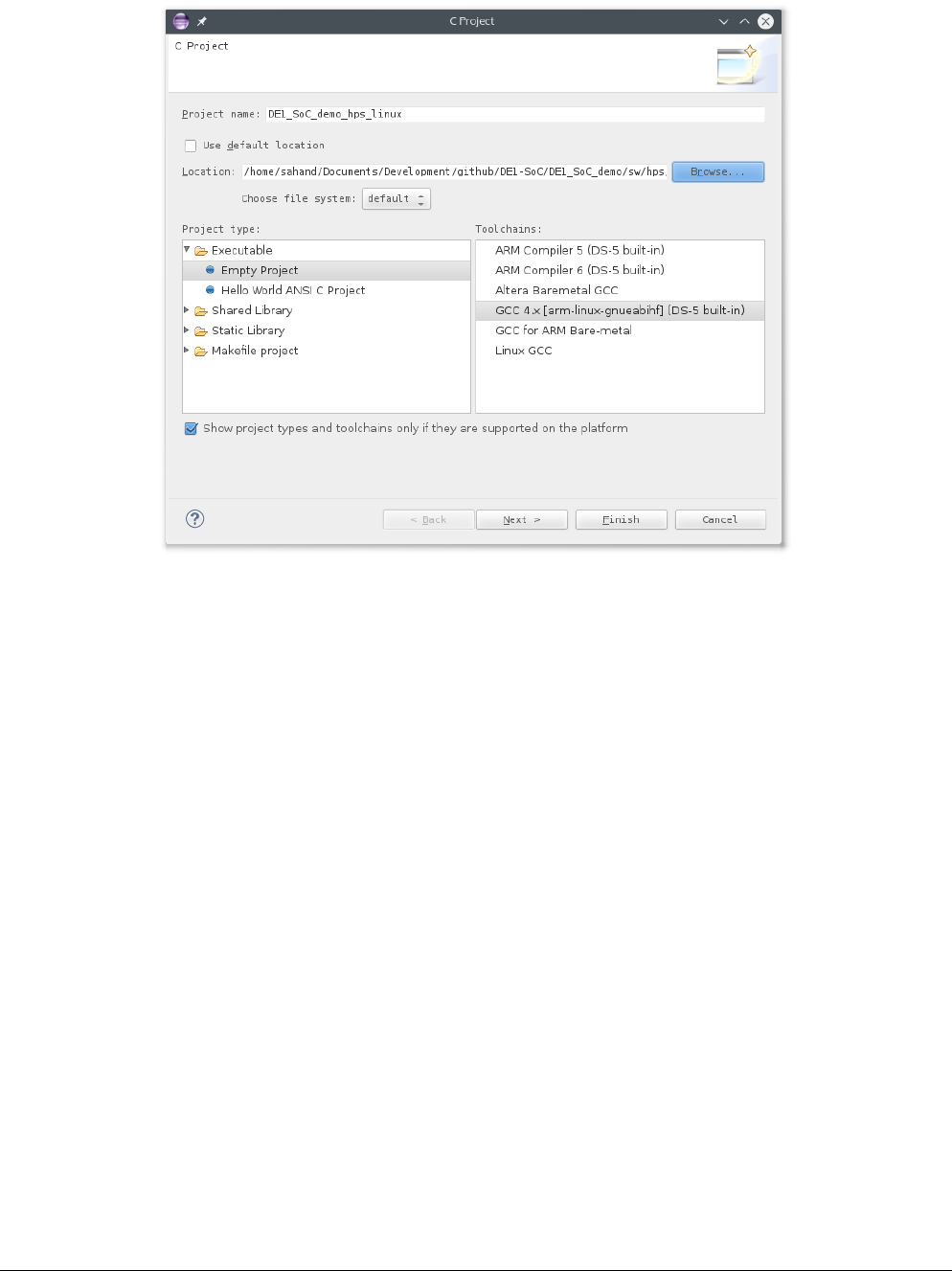
SoC-FPGA Design Guide [DE1-SoC Edition]
21/04/2018 P a g e | 90
d. We want to create a single output executable for our project, so choose “Executable >
Empty Project” as the project type.
e. Choose “GCC 4.x [arm-linux-gnueabihf] (DS-5 built-in)” as the Toolchain.
f. You should have something similar to Figure 13-11. Then, press the “Finish” button to
create the project.
Figure 13-11. New C Project Dialog
62. When programming the HPS, we will need access to a few standard header and linker files provided
by Altera. We need to add these files to the ARM DS-5 project.
a. Right-click on the “DE1_SoC_demo_hps_linux” project, and go to “Properties”.
b. We are going to use a RESTRICTED SUBSET of Altera’s HWLIB to develop our linux application,
so we need to define a macro that is needed by the library to know which board is being
targetted. The reason we use a restricted subset of the library is due to the fact that the
library is not fully usable in a user application, as many physical peripheral addresses are
employed. We will only use the library to compute offsets and to use the non-intrusive
functions it has available.
Under “C/C++ Build > Settings > GCC C Compiler > Symbols”, add “soc_cv_av” to
the “Defined symbols (-D)” list.
c. Under “C/C++ Build > Settings > GCC C Compiler > Includes”, add
“<altera_install_directory>/<version>/embedded/ip/altera/hps/altera_hps/hwli
b/include” to the “Include paths (-I)” list.
d. Under “C/C++ Build > Settings > GCC C Compiler > Includes”, add
“<altera_install_directory>/<version>/embedded/ip/altera/hps/altera_hps/hwli
b/include/soc_cv_av” to the “Include paths (-I)” list.
e. Click on the “Apply” button, then on the “Ok” button to close the project properties dialog.
63. In order to unlock a few settings later in this tutorial, we will create a C file that simply contains an
empty “main()” function for the moment.
a. Right-click on the “DE1_SoC_demo_linux” project, and go to “New > Source File”. Use
“hps_linux.c” as the file name, and click on the “Finish” button to create the new source
file.

SoC-FPGA Design Guide [DE1-SoC Edition]
21/04/2018 P a g e | 91
b. Right-click on the “DE1_SoC_demo_linux” project, and go to “New > Header File”. Use
“hps_linux.h” as the file name, and click on the “Finish” button to create the new header
file.
c. Fill “hps_linux.c” with the code shown in Figure 13-12.
int main(void) {
return 0;
}
Figure 13-12. hps_linux.c with an empty main() function.
d. Right-click on the “DE1_SoC_demo_linux” project and select “Build Project”.
13.8.2 Creating a Remote Debug Connection to the Linux Distribution
13.8.2.1 Find the Linux Distribution’s IP Address
Later in this tutorial, we will need to know the IP address assigned to the DE1-SoC so ARM DS-5 can
automatically use an SSH connection to transfer linux binaries and launch gdb debug sessions for us. In this
step, we will use a serial terminal to manually connect to the linux distribution running on the board and find
out its IP address.
64. Although we can continue to use the “minicom” program as we previously did in Figure 13-9, we will
use the built-in serial terminal available in ARM DS-5 to have all development windows in one area.
Go to “Window > Show View > Other… > Terminal > Terminal” to open ARM DS-5’s the built-in
serial terminal. You should see the terminal shown in Figure 13-13.
Figure 13-13. ARM DS-5 Serial Terminal
65. Modify the serial terminal’s settings to match those shown in Figure 13-14, then press “OK” to start
the connection.
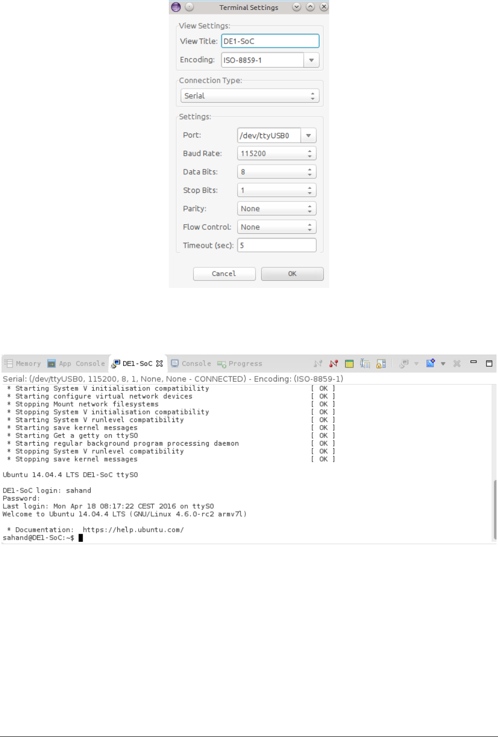
SoC-FPGA Design Guide [DE1-SoC Edition]
21/04/2018 P a g e | 92
Figure 13-14. ARM DS-5 Serial Terminal Settings
66. You should see the linux login prompt. Login with the same username and password we defined
earlier. You should see something similar as Figure 13-15.
Figure 13-15. ARM DS-5 Serial Terminal Linux Prompt
67. Type “ifconfig eth0 | grep inet” to obtain the IP address attributed to the device. You should
get something similar to Figure 13-16. If you don’t see an IP address listed, then run the following
command to try to get one automatically through DHCP.
$ sudo dhclient eth0
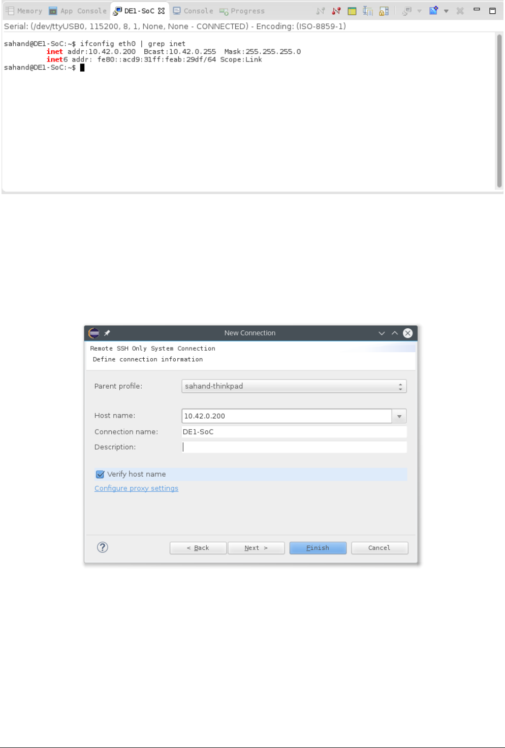
SoC-FPGA Design Guide [DE1-SoC Edition]
21/04/2018 P a g e | 93
Figure 13-16. Obtaining the DE1-SoC's IP Address through ARM DS-5’s Serial Terminal
13.8.2.2 Create an SSH Remote Connection
68. Go to “File > New > Other… > Remote System Explorer > Connection”.
69. Choose to create an “SSH Only” connection.
70. Enter the IP address you found in 13.8.2.1 as the “Host name”.
71. Enter “DE1-SoC” as the “Connection name”. You should have something similar to Figure 13-17.
72. Click on “Finish” to create the connection.
Figure 13-17. New SSH Only Connection
73. You should be able to see the remote system in ARM DS-5’s “Remote Systems” view, as shown in
Figure 13-18.

SoC-FPGA Design Guide [DE1-SoC Edition]
21/04/2018 P a g e | 94
Figure 13-18. New SSH Connection In "Remote Systems" View
13.8.2.3 Setting Up the Debug Configuration
74. Right-click on the “DE1_SoC_demo_linux” project, and go to “Debug As > Debug
Configurations…”.
75. Choose to create a new debugger configuration by right-clicking on “DS-5 Debugger” on the left and
selecting “New”. Use “DE1_SoC_demo_hps_linux” as the name of the new debug configuration.
76. Under the “Connection” tab:
a. Use “Altera > Cyclone V SoC (Dual Core) > Linux Application Debug > Download
and debug application” as the target platform.
b. Set the “RSE connection” to “DE1-SoC”. This is the remote system connection we created
earlier. You should have something similar to Figure 13-19.
Figure 13-19. Debug Configuraton “Connection” Tab
77. Under the “Files” tab:
a. Set “Application on host to download” to the built binary of our project. Use the
“Workspace” button to choose the binary. You should have something similar to
“${workspace_loc:/DE1_SoC_demo_hps_linux/Debug/DE1_SoC_demo_hps_linux}”.
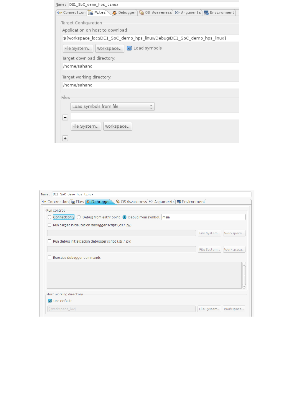
SoC-FPGA Design Guide [DE1-SoC Edition]
21/04/2018 P a g e | 95
b. Set the “Target download directory” to your user directory. In my case it is
“/home/sahand”.
c. Set the “Target working directory” to your user directory. In my case it is
“/home/sahand”. You should have something similar to Figure 13-20.
Figure 13-20. Debug Configuration "Files" Tab
78. Under the “Debugger” tab, make sure that “Debug from symbol” is selected and that “main” is the
name of the symbol, as shown in Figure 13-21.
79. Click on the “Apply” button, then on the “Close” button to save the debug configuration.
Figure 13-21. Debug Configuration "Debugger" Tab
13.8.3 Linux Programming
The interrupt-driven nature of operating systems requires that error-prone processes be unable to harm the
correct operation of the computer. Modern processors provide a hardware solution to this issue by means of
a DUAL-MODE operating state. CPUs define two modes which operating systems can then use to implement
protection mechanisms among processes they are handling.

SoC-FPGA Design Guide [DE1-SoC Edition]
21/04/2018 P a g e | 96
The linux operating system calls these modes USER MODE and KERNEL MODE. Processors remain in user
mode when executing harmless code in user applications, whereas they transition to kernel mode when
executing potentially dangerous code in the system kernel. Examples of dangerous code are handling an
interrupt from a peripheral, copying data from a peripheral’s registers to main memory, …
User code cannot be executed in kernel mode. When a user process needs to perform an action that is only
allowed in kernel mode, it performs a system call and asks the operating system to take care of the task in its
place. What this boils down to is that USER CODE CANNOT ACCESS THE HARDWARE DIRECTLY, as there is too
much of a risk for the code to have an error and cause the system to crash. User code must always ask the
operating system to perform dangerous operations in its place.
The main advantage of Cyclone V SoCs is the ability to have the HPS and FPGA communicate with each other
easily. This is simple to accomplish in a standard bare-metal application as there are absolutely no protection
mechanisms implemented. However, this is not possible while the HPS is running linux, as user code doesn’t
have the right to access hardware directly.
There are 2 solutions to this problem:
If developers are knowledgeable enough, they can write a device driver for the target peripheral they
want to access in their user code, and package this in a loadable linux kernel module. This is the
correct way to access hardware in linux, but it requires that the developer know how to write a device
driver. Administrative users can load the kernel module, then any standard user code can interact
with the peripheral.
A simpler technique often used in embedded linux environments is to leverage the virtual memory
system in order to access any MEMORY-MAPPED peripherals (peripherals and operations that are
only accessible through priviledged machine instructions cannot be accessed with this method).
Unfortunately, this method requires code to be run with root privileges. However, it does not require
any kernel code to be written.
Writing a linux device driver is outside the scope of this tutorial, so we will use the memory mapping
technique here.
The code for this part of the application is quite large to be inserted in this document. Therefore, we will just
go over a few practical aspects of the code which are worth paying attention to. The full source can be found
in DE1_SoC_demo.zip [5].
Recall that we cannot handle interrupts in linux user mode. Therefore, in order to satisfy the HPS-related goals
specified in 8.4, we will need to use an infinite loop and do some polling. This can be seen in our application’s
“main()” function, which is shown in Figure 13-22.
int main() {
printf("DE1-SoC linux demo\n");
open_physical_memory_device();
mmap_peripherals();
setup_hps_gpio();
setup_fpga_leds();
while (true) {
handle_hps_led();
handle_fpga_leds();
usleep(ALT_MICROSECS_IN_A_SEC / 10);
}
munmap_peripherals();
close_physical_memory_device();
return 0;
}
Figure 13-22. hps_linux.c main() function.

SoC-FPGA Design Guide [DE1-SoC Edition]
21/04/2018 P a g e | 97
13.8.3.1 Using Altera’s HWLIB - Prerequisites
We will use a SUBSET of Altera’s HWLIB in this tutorial. In order to be able to use HWLIB to configure a
peripheral, 2 steps need to be performed:
You need to INCLUDE the HPS peripheral’s HWLIB HEADER FILE to your code.
You must COPY the HPS peripheral’s HWLIB SOURCE FILE in your DS-5 project directory. The HWLIB
source files can be found in directory
“<altera_install_directory>/<version>/embedded/ip/altera/hps/altera_hps/hwlib/src”,
and must be copied to “DE1_SoC_demo/sw/hps/application/DE1_SoC_demo_hps_linux”.
In the example used in this linux programming tutorial, we use some HWLIB functions related to the HPS’
GPIO peripheral, so you must copy “alt_generalpurpose_io.c” to your DS-5 project directory.
13.8.3.2 Accessing Hardware Peripherals from User Space
13.8.3.2.1 Opening the Physical Memory File Descriptor
In Figure 7-3 we saw that the FPGA slaves and HPS peripherals are visible to the MPU unit and are therefore
subject to memory-mapped IO. We need to be able to access these peripherals’ addresses in order to interact
with them.
Unfortunately, a process can only interact with the virtual address space it is assigned by the linux kernel. Any
attempt to access memory outside this region will cause the process to be terminated. Nevertheless, it is
possible for a process to gain access to another virtual memory region by using the “mmap()” function. The
mmap() function maps another memory region into the running process’ virtual address space. Therefore, all
we need to do is to mmap() the FPGA slaves and HPS peripherals’ memory regions into our address space.
The mmap() function’s prototype is shown in Figure 13-23. Note that it memory maps a FILE into the running
process’ address space, so we need to find a file that “represents” our peripherals.
void *mmap(void *addr, size_t length, int prot, int flags, int fd, off_t offset)
Figure 13-23. Prototype of the mmap() function.
By design, linux represents everything as a file, including all devices. In particular, the special “/dev/mem” file
represents the content of the system’s physical memory. This is the file we will mmap() in order to access the
memory regions we are interested in.
Since we are memory-mapping a file, the first step is to open this file. Figure 13-24 shows how to open the
/dev/mem file. Remember that /dev/mem grants access to physical memory, so a user requires elevates rights
in order to open it. Therefore, don’t forget to launch this code as the root user in order to have enough
privileges.
// physical memory file descriptor
int fd_dev_mem = 0;
void open_physical_memory_device() {
// We need to access the system's physical memory so we can map it to user
// space. We will use the /dev/mem file to do this. /dev/mem is a character
// device file that is an image of the main memory of the computer. Byte
// addresses in /dev/mem are interpreted as physical memory addresses.
// Remember that you need to execute this program as ROOT in order to have
// access to /dev/mem.
fd_dev_mem = open("/dev/mem", O_RDWR | O_SYNC);
if(fd_dev_mem == -1) {
printf("ERROR: could not open \"/dev/mem\".\n");
printf(" errno = %s\n", strerror(errno));
exit(EXIT_FAILURE);
}
}
Figure 13-24. open_physical_memory_device() function.

SoC-FPGA Design Guide [DE1-SoC Edition]
21/04/2018 P a g e | 98
13.8.3.2.2 Accessing HPS Peripherals
Now that we have opened the physical memory file, we can memory-map a subset of it into our process’
virtual address space. Figure 13-25 shows how this is done for memory-mapping the HPS’ GPIO peripheral.
Note that you must know the offset of your peripheral within the physical memory file, as well as the amount
of memory you want to be memory-mapped from that offset. In our case, we will start memory-mapping
from the GPIO1 peripheral’s offset, and we choose to map the size of the full peripheral.
#include "socal/hps.h"
void *hps_gpio = NULL;
size_t hps_gpio_span = ALT_GPIO1_UB_ADDR - ALT_GPIO1_LB_ADDR + 1;
size_t hps_gpio_ofst = ALT_GPIO1_OFST;
void mmap_hps_peripherals() {
hps_gpio = mmap(NULL, hps_gpio_span, PROT_READ | PROT_WRITE, MAP_SHARED, fd_dev_mem, hps_gpio_ofst);
if (hps_gpio == MAP_FAILED) {
printf("Error: hps_gpio mmap() failed.\n");
printf(" errno = %s\n", strerror(errno));
close(fd_dev_mem);
exit(EXIT_FAILURE);
}
}
Figure 13-25. mmap_hps_peripherals() function.
Finally, after having memory-mapped the HPS’ GPIO peripheral, we can access any of its internal registers
with the low-level functions we saw in 11.3. Figure 13-26 shows how we configure the HPS’ GPIO peripheral,
and Figure 13-27 shows how we can toggle HPS_LED on the DE1-SoC by using the HPS_KEY_N button.
// |=============|==========|==============|==========|
// | Signal Name | HPS GPIO | Register/bit | Function |
// |=============|==========|==============|==========|
// | HPS_LED | GPIO53 | GPIO1[24] | I/O |
// |=============|==========|==============|==========|
#define HPS_LED_IDX (ALT_GPIO_1BIT_53) // GPIO53
#define HPS_LED_PORT (alt_gpio_bit_to_pid(HPS_LED_IDX)) // ALT_GPIO_PORTB
#define HPS_LED_PORT_BIT (alt_gpio_bit_to_port_pin(HPS_LED_IDX)) // 24 (from GPIO1[24])
#define HPS_LED_MASK (1 << HPS_LED_PORT_BIT)
// |=============|==========|==============|==========|
// | Signal Name | HPS GPIO | Register/bit | Function |
// |=============|==========|==============|==========|
// | HPS_KEY_N | GPIO54 | GPIO1[25] | I/O |
// |=============|==========|==============|==========|
#define HPS_KEY_N_IDX (ALT_GPIO_1BIT_54) // GPIO54
#define HPS_KEY_N_PORT (alt_gpio_bit_to_pid(HPS_KEY_N_IDX)) // ALT_GPIO_PORTB
#define HPS_KEY_N_PORT_BIT (alt_gpio_bit_to_port_pin(HPS_KEY_N_IDX)) // 25 (from GPIO1[25])
#define HPS_KEY_N_MASK (1 << HPS_KEY_N_PORT_BIT)
void setup_hps_gpio() {
// Initialize the HPS PIO controller:
// Set the direction of the HPS_LED GPIO bit to "output"
// Set the direction of the HPS_KEY_N GPIO bit to "input"
void *hps_gpio_direction = ALT_GPIO_SWPORTA_DDR_ADDR(hps_gpio);
alt_setbits_word(hps_gpio_direction, ALT_GPIO_PIN_OUTPUT << HPS_LED_PORT_BIT);
alt_setbits_word(hps_gpio_direction, ALT_GPIO_PIN_INPUT << HPS_KEY_N_PORT_BIT);
}
Figure 13-26. setup_hps_gpio() function.
void handle_hps_led() {
void *hps_gpio_data = ALT_GPIO_SWPORTA_DR_ADDR(hps_gpio);
void *hps_gpio_port = ALT_GPIO_EXT_PORTA_ADDR(hps_gpio);
uint32_t hps_gpio_input = alt_read_word(hps_gpio_port) & HPS_KEY_N_MASK;
// HPS_KEY_N is active-low
bool toggle_hps_led = (~hps_gpio_input & HPS_KEY_N_MASK);
if (toggle_hps_led) {
uint32_t hps_led_value = alt_read_word(hps_gpio_data);
hps_led_value >>= HPS_LED_PORT_BIT;
hps_led_value = !hps_led_value;

SoC-FPGA Design Guide [DE1-SoC Edition]
21/04/2018 P a g e | 99
hps_led_value <<= HPS_LED_PORT_BIT;
alt_replbits_word(hps_gpio_data, HPS_LED_MASK, hps_led_value);
}
}
Figure 13-27. handle_hps_led() function.
The key to doing memory-mapped IO in linux is to use HWLIB’s OFFSET-based macros with the virtual address
returned by mmap() as the base address. Note that HWLIB also has macros with ABSOLUTE addresses for
every device, but those can only be used in bare-metal or linux device driver code as they directly access
certain physical addresses.
In Figure 13-26 and Figure 13-27, we used three such offset-based macros to access the HPS GPIO peripheral’s
“Port A Data Register”, “Port A Data Direction Register”, and “External Port A Register”.
These macros were the following:
ALT_GPIO_SWPORTA_DR_ADDR(base)
ALT_GPIO_SWPORTA_DDR_ADDR(base)
ALT_GPIO_EXT_PORTA_ADDR(base)
13.8.3.2.3 Accessing FPGA Peripherals
Memory-mapping FPGA peripherals is identical to the process used for HPS peripherals. However, there is one
subtlety that must be taken care of. When using mmap() you must specify an offset within the file that is to be
mapped, as well as the amount of memory to be mapped. The mmap() manual page states that the offset
provided MUST BE A MULTIPLE OF THE SYSTEM’S PAGE SIZE, which is 0x1000 bytes in our case.
Figure 13-28 shows how we memory-map the FPGA peripherals in our design from the Lightweight HPS-to-
FPGA bridge, and Figure 13-30 shows how we can write to the FPGA leds.
void *h2f_lw_axi_master = NULL;
size_t h2f_lw_axi_master_span = ALT_LWFPGASLVS_UB_ADDR - ALT_LWFPGASLVS_LB_ADDR + 1;
size_t h2f_lw_axi_master_ofst = ALT_LWFPGASLVS_OFST;
void *fpga_leds = NULL;
void mmap_fpga_peripherals() {
// Use mmap() to map the address space related to the fpga leds into user
// space so we can interact with them.
// The fpga leds are connected to the h2f_lw_axi_master, so its base
// address is calculated from that of the h2f_lw_axi_master.
// IMPORTANT: If you try to only mmap the fpga leds, it is possible for the
// operation to fail, and you will get "Invalid argument" as errno. The
// mmap() manual page says that you can only map a file from an offset which
// is a multiple of the system's page size.
// In our specific case, our fpga leds are located at address 0xFF200000,
// which is a multiple of the page size, however this is due to luck because
// the fpga leds are the only peripheral connected to the h2f_lw_axi_master.
// The typical page size in Linux is 0x1000 bytes.
// So, generally speaking, you will have to mmap() the closest address which
// is a multiple of your page size and access your peripheral by a specific
// offset from the mapped address.
h2f_lw_axi_master = mmap(NULL, h2f_lw_axi_master_span, PROT_READ | PROT_WRITE, MAP_SHARED,
fd_dev_mem, h2f_lw_axi_master_ofst);
if (h2f_lw_axi_master == MAP_FAILED) {
printf("Error: h2f_lw_axi_master mmap() failed.\n");
printf(" errno = %s\n", strerror(errno));
close(fd_dev_mem);
exit(EXIT_FAILURE);
}
fpga_leds = h2f_lw_axi_master + HPS_FPGA_LEDS_BASE;
}
Figure 13-28. mmap_fpga_peripherals() function.

SoC-FPGA Design Guide [DE1-SoC Edition]
21/04/2018 P a g e | 100
void setup_fpga_leds() {
// Switch on first LED only
alt_write_word(fpga_leds, 0x1);
}
Figure 13-29. setup_fpga_leds() function.
void handle_fpga_leds() {
uint32_t leds_mask = alt_read_word(fpga_leds);
if (leds_mask != (0x01 << (HPS_FPGA_LEDS_DATA_WIDTH - 1))) {
// rotate leds
leds_mask <<= 1;
} else {
// reset leds
leds_mask = 0x1;
}
alt_write_word(fpga_leds, leds_mask);
}
Figure 13-30. handle_fpga_leds() function.
13.8.3.2.4 Cleaning Up Before Application Exit
Although the operating system should take care of this for you, it is always a good practice to remove any
unneeded memory mappings and to close the physical memory file descriptor before your application
terminates.
Figure 13-31 shows how to unmap the GPIO peripheral’s memory-mapping, and Figure 13-32 shows how to
close the physical memory file descriptor.
void munmap_peripherals() {
munmap_hps_peripherals();
munmap_fpga_peripherals();
}
void munmap_hps_peripherals() {
if (munmap(hps_gpio, hps_gpio_span) != 0) {
printf("Error: hps_gpio munmap() failed\n");
printf(" errno = %s\n", strerror(errno));
close(fd_dev_mem);
exit(EXIT_FAILURE);
}
hps_gpio = NULL;
}
void munmap_fpga_peripherals() {
if (munmap(h2f_lw_axi_master, h2f_lw_axi_master_span) != 0) {
printf("Error: h2f_lw_axi_master munmap() failed\n");
printf(" errno = %s\n", strerror(errno));
close(fd_dev_mem);
exit(EXIT_FAILURE);
}
h2f_lw_axi_master = NULL;
fpga_leds = NULL;
}
Figure 13-31. munmap_peripherals() family of functions.
void close_physical_memory_device() {
close(fd_dev_mem);
}
Figure 13-32. close_physical_memory_device() function.
13.8.3.3 Launching the Linux code in the Debugger
80. Once you have finished writing all the application’s code, right-click on the
“DE1_SoC_demo_hps_linux” project, and select “Build Project”.
81. Switch to the DS-5 Debug perspective, as shown in Figure 12-12.
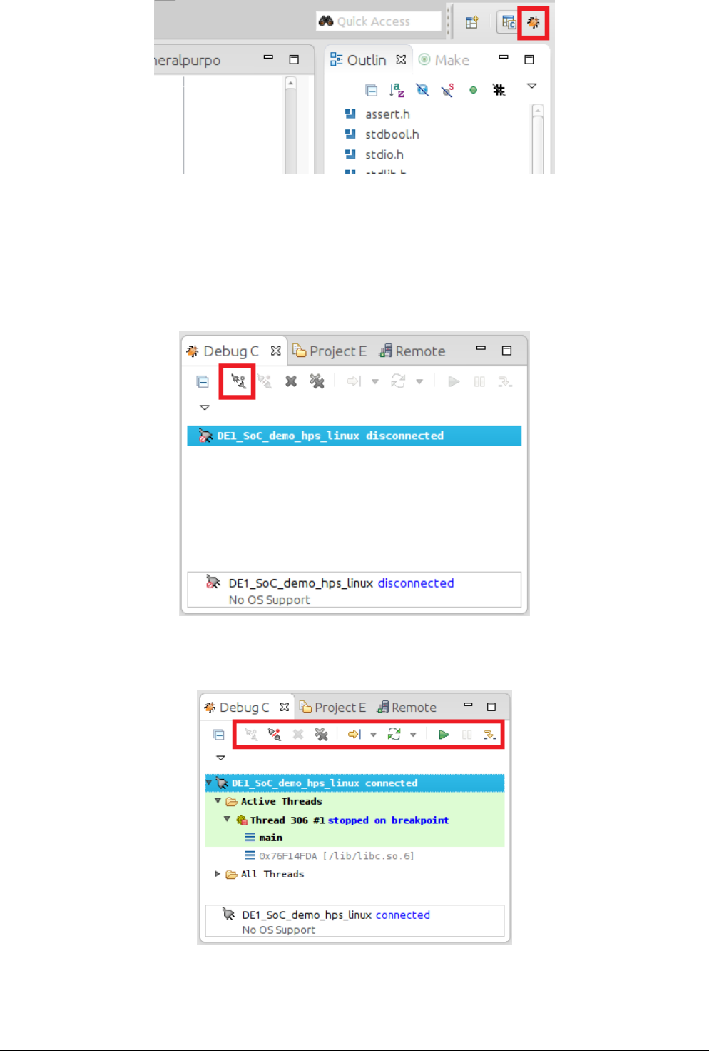
SoC-FPGA Design Guide [DE1-SoC Edition]
21/04/2018 P a g e | 101
Figure 13-33. Switching to the DS-5 Debug Perspective
82. In the “Debug Control” view, click on the “DE1_SoC_demo_hps_linux” entry, then click on the
“Connect to Target” button, as shown on Figure 13-34. The debugger will start an SSH conection to
the linux distribution running on the DE1-SoC and will automatically transfer our binary file and wait
at our application’s “main()” function. If you are prompted to log in, then log in with the ROOT user
and password.
Figure 13-34. Debug Control View
83. You can the use the buttons in the “Debug Control” view to control the application’s execution.
Figure 13-35. DS-5 Debugger Controls
13.8.3.4 App Console
Data sent to standard output is shown in the “App Console” view. Figure 13-36 shows the result of a
“printf()” call in our demo code shown in Figure 13-22.
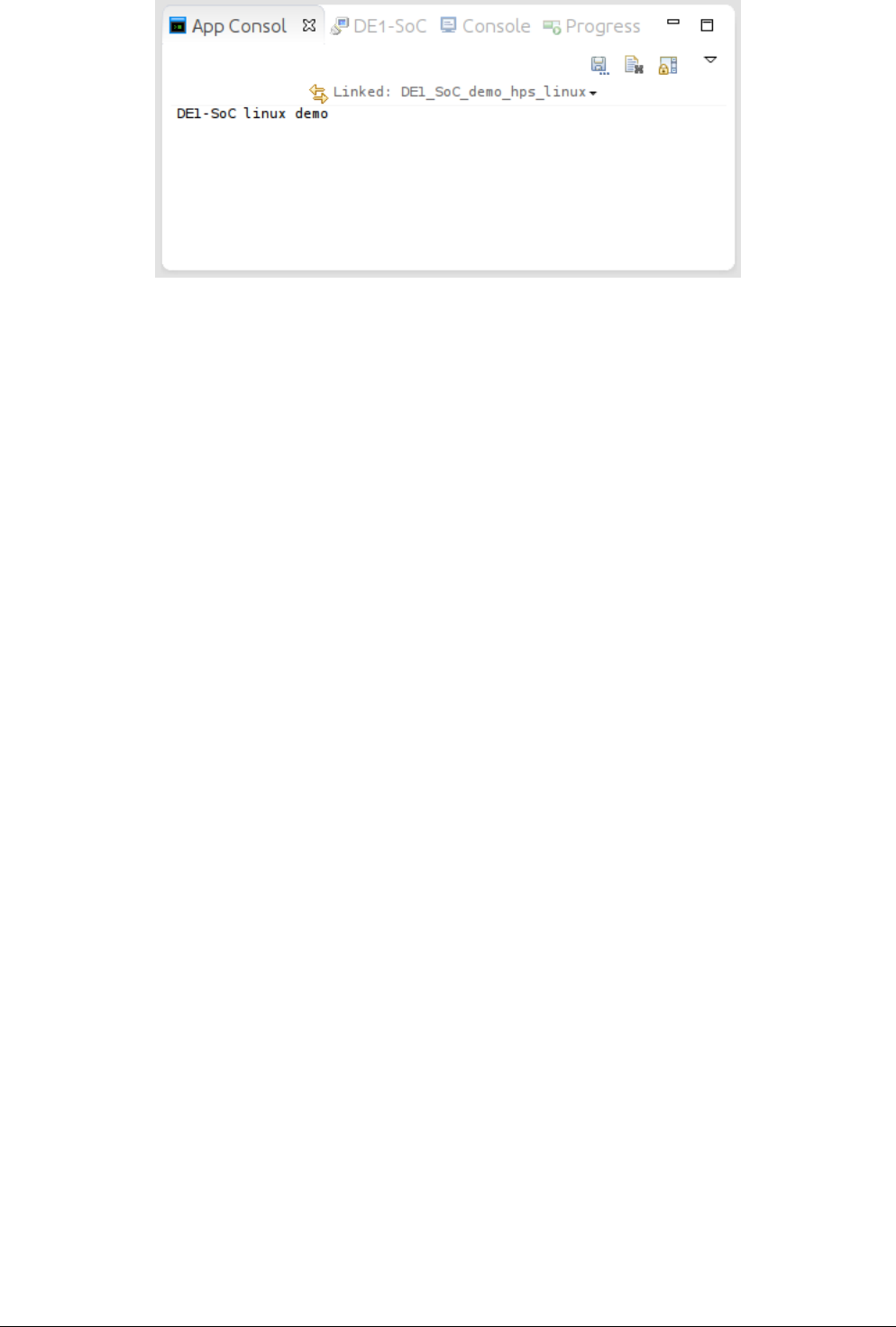
SoC-FPGA Design Guide [DE1-SoC Edition]
21/04/2018 P a g e | 102
Figure 13-36. DS-5 App Console View
13.8.3.5 DS-5 Linux Debugger Restrictions
In 12.2.4.4.1, we saw that the DS-5 BARE-METAL debugger had a “Registers” view which could show the
registers of all HPS and FPGA peripherals. This was a very handy tool, as it made it easy to verify if registers
were accessed and updated correctly.
Unfortunately, when it comes to debugging LINUX binaries, the DS-5 debugger is subject to the same
constraints our linux applications are. Namely, it cannot directly access physical hardware addresses directly.
As such, there is no “Registers” view when debugging linux applications, and you must resort to manually
memory-mapping and verifying peripheral accesses yourself.

SoC-FPGA Design Guide [DE1-SoC Edition]
21/04/2018 P a g e | 103
Explain MSEL when reprogramming the FPGA from the HPS.
Talk about what the JTAG to Avalon masters are.
Find out how to automatically program the FPGA when writing a bare-metal HPS application. Use
“tftp” command?

SoC-FPGA Design Guide [DE1-SoC Edition]
21/04/2018 P a g e | 104
[1]
Terasic Technologies, "Terasic - DE Main Boards - Cyclone - DE1-SoC Board," [Online]. Available:
http://de1-soc.terasic.com.
[2]
Altera Corporation, "Cyclone V Device Handbook, Volume 3: Hard Processor System Technical Reference
Manual," 31 July 2014. [Online]. Available: http://www.altera.com/literature/hb/cyclone-v/cv_5v4.pdf.
[3]
S. Kashani-Akhavan, "DE1_SoC_top_level.vhd," [Online]. Available:
https://github.com/sahandKashani/Altera-FPGA-top-level-files/blob/master/DE1-
SoC/DE1_SoC_top_level.vhd.
[4]
S. Kashani-Akhavan, "pin_assignment_DE1_SoC.tcl," [Online]. Available:
https://github.com/sahandKashani/Altera-FPGA-top-level-files/blob/master/DE1-
SoC/pin_assignment_DE1_SoC.tcl.
[5]
S. Kashani-Akhavan, "DE1_SoC_demo.zip," [Online]. Available: https://github.com/sahandKashani/SoC-
FPGA-Design-Guide/blob/master/DE1_SoC/DE1_SoC_demo.zip.
[6]
ISSI. [Online]. Available: https://github.com/sahandKashani/SoC-FPGA-Design-
Guide/blob/master/DE1_SoC/Documentation/SDRAM%20Datasheet.pdf.
[7]
Terasic Technologies, [Online]. Available: https://github.com/sahandKashani/SoC-FPGA-Design-
Guide/blob/master/DE1_SoC/Documentation/DE1-SoC%20Schematic.pdf.
[8]
ISSI. [Online]. Available: https://github.com/sahandKashani/SoC-FPGA-Design-
Guide/blob/master/DE1_SoC/Documentation/DDR3%20SDRAM%20Datasheet.pdf.
[9]
ARM, "DS-5 Debugger Commands," [Online]. Available:
http://infocenter.arm.com/help/index.jsp?topic=/com.arm.doc.dui0452c/CIHJIBIH.html.
[10]
Altera Corporation, "Documentation: Cyclone V Devices," [Online]. Available:
http://www.altera.com/literature/lit-cyclone-v.jsp?ln=devices_fpga&l3=Low-Cost%20FPGAs-
Cyclone%20V%20%28E,%20GX,%20GT,%20SE,%20SX,%20ST%29&l4=Documentation.
[11]
Altera Corporation, "Address Map for HPS," [Online]. Available:
http://www.altera.com/literature/hb/cyclone-v/hps.html.
[12]
Altera Corporation, "A Look Inside: SoC FPGAs Embedded Development Tools (Part 5 of 5)," 25
November 2013. [Online]. Available: http://www.youtube.com/watch?v=NxZznvf5EKc.
[13]
Altera Corporation, "A Look Inside: SoC FPGAs Introduction (Part 1 of 5)," 25 November 2013. [Online].
Available: http://www.youtube.com/watch?v=RVM-ESUMOMU.
[14]
Altera Corporation, "A Look Inside: SoC FPGAs Reliability and Flexibility (Part 3 of 5)," 25 November
2013. [Online]. Available: http://www.youtube.com/watch?v=cWIaqt2RU84.
[15]
Altera Corporation, "A Look Inside: SoC FPGAs System Cost and Power (Part 4 of 5)," 25 November 2013.
[Online]. Available: http://www.youtube.com/watch?v=gUE669XKhUY.

SoC-FPGA Design Guide [DE1-SoC Edition]
21/04/2018 P a g e | 105
[16]
Altera Corporation, "A Look Inside: SoC FPGAs System Performance (Part 2 of 5)," 25 November 2013.
[Online]. Available: http://www.youtube.com/watch?v=Ssxf8ggmQk4.
[17]
Altera Corporation, "Cyclone V Device Datasheet," July 2014. [Online]. Available:
http://www.altera.com/literature/hb/cyclone-v/cv_51002.pdf.
[18]
Altera Corporation, "Cyclone V Device Handbook, Volume 1: Device Interfaces and Integration," 22 July
2014. [Online]. Available: http://www.altera.com/literature/hb/cyclone-v/cv_5v2.pdf.
[19]
ARM, "DS-5 Altera Edition: Bare-metal Debug and Trace," 21 October 2013. [Online]. Available:
http://www.youtube.com/watch?v=u_xKybPhcHI.
[20]
ARM, "FPGA-adaptive debug on the Altera SoC using ARM DS-5," 16 December 2013. [Online]. Available:
http://www.youtube.com/watch?v=2NBcUv2TxbI.
[21]
EE Journal, "OpenCL on FPGAs Accelerating Performance and Design Productivity -- Altera," 28
November 2013. [Online]. Available: http://www.youtube.com/watch?v=M6vpq6s1h_A.
[22]
Altera Corporation, "Bare-Metal Debugging using ARM DS-5 Altera Edition," 3 December 2013. [Online].
Available: http://www.youtube.com/watch?v=CJ0EHJ9oQ7Y.
[23]
Altera Corporation, "Cyclone V Device Overview," 7 July 2014. [Online]. Available:
http://www.altera.com/literature/hb/cyclone-v/cv_51001.pdf.
[24]
Altera Corporation, "Linux Kernel Debug using ARM DS-5 Altera Edition," 3 December 2013. [Online].
Available: http://www.youtube.com/watch?v=QcA39O6ofGw.
[25]
Altera Corporation, "Architecting FPGAs beyond 1M LEs," Altera Corporation, 3 September 2014.
[Online]. Available: http://www.fpl2014.org/fileadmin/w00bpo/www/hutton.pdf.
[26]
S. Kashani-Akhavan and R. Beuchat. [Online]. Available: https://github.com/sahandKashani/SoC-FPGA-
Design-Guide.
