Xilinx UG524 SP601 Reference Design, User Guide Spartan6evm Manual
User Manual: Pdf
Open the PDF directly: View PDF ![]() .
.
Page Count: 15

[Guide Subtitle]
[optional]
UG524 (v1.1) September 16, 2009 [optional]
SP601 Reference
Design User Guide
UG524 (v1.1) September 16, 2009
SP601 Reference Design User Guide www.xilinx.com UG524 (v1.1) September 16, 2009
Xilinx is disclosing this user guide, manual, release note, and/or specification (the "Documentation") to you solely for use in the development
of designs to operate with Xilinx hardware devices. You may not reproduce, distribute, republish, download, display, post, or transmit the
Documentation in any form or by any means including, but not limited to, electronic, mechanical, photocopying, recording, or otherwise,
without the prior written consent of Xilinx. Xilinx expressly disclaims any liability arising out of your use of the Documentation. Xilinx reserves
the right, at its sole discretion, to change the Documentation without notice at any time. Xilinx assumes no obligation to correct any errors
contained in the Documentation, or to advise you of any corrections or updates. Xilinx expressly disclaims any liability in connection with
technical support or assistance that may be provided to you in connection with the Information.
THE DOCUMENTATION IS DISCLOSED TO YOU “AS-IS” WITH NO WARRANTY OF ANY KIND. XILINX MAKES NO OTHER
WARRANTIES, WHETHER EXPRESS, IMPLIED, OR STATUTORY, REGARDING THE DOCUMENTATION, INCLUDING ANY
WARRANTIES OF MERCHANTABILITY, FITNESS FOR A PARTICULAR PURPOSE, OR NONINFRINGEMENT OF THIRD-PARTY
RIGHTS. IN NO EVENT WILL XILINX BE LIABLE FOR ANY CONSEQUENTIAL, INDIRECT, EXEMPLARY, SPECIAL, OR INCIDENTAL
DAMAGES, INCLUDING ANY LOSS OF DATA OR LOST PROFITS, ARISING FROM YOUR USE OF THE DOCUMENTATION.
© 2009 Xilinx, Inc. XILINX, the Xilinx logo, Virtex, Spartan, ISE, and other designated brands included herein are trademarks of Xilinx in the
United States and other countries. All other trademarks are the property of their respective owners.
Revision History
The following table shows the revision history for this document.
Date Version Revision
08/18/2009 1.0 Initial Xilinx release.
09/16/2009 1.1 Minor updates for 11.3.

SP601 Reference Design User Guide www.xilinx.com 3
UG524 (v1.1) September 16, 2009
Preface: About This Guide
Guide Contents . . . . . . . . . . . . . . . . . . . . . . . . . . . . . . . . . . . . . . . . . . . . . . . . . . . . . . . . . . . . . . 5
Additional Documentation . . . . . . . . . . . . . . . . . . . . . . . . . . . . . . . . . . . . . . . . . . . . . . . . . . . 5
Additional Support Resources. . . . . . . . . . . . . . . . . . . . . . . . . . . . . . . . . . . . . . . . . . . . . . . . 6
Chapter 1: SP601 Evaluation Board
Introduction . . . . . . . . . . . . . . . . . . . . . . . . . . . . . . . . . . . . . . . . . . . . . . . . . . . . . . . . . . . . . . . . . 7
SP601 Features . . . . . . . . . . . . . . . . . . . . . . . . . . . . . . . . . . . . . . . . . . . . . . . . . . . . . . . . . . . . 8
Reference Designs . . . . . . . . . . . . . . . . . . . . . . . . . . . . . . . . . . . . . . . . . . . . . . . . . . . . . . . . . . . 9
Built-In Self Test (BIST) . . . . . . . . . . . . . . . . . . . . . . . . . . . . . . . . . . . . . . . . . . . . . . . . . . . . . 9
Memory Interface Generator (MIG) DDR2 Design . . . . . . . . . . . . . . . . . . . . . . . . . . . . . 10
MultiBoot Design . . . . . . . . . . . . . . . . . . . . . . . . . . . . . . . . . . . . . . . . . . . . . . . . . . . . . . . . . 12
Base System Reference Design (BSRD) . . . . . . . . . . . . . . . . . . . . . . . . . . . . . . . . . . . . . . . 12
Stand-Alone Applications. . . . . . . . . . . . . . . . . . . . . . . . . . . . . . . . . . . . . . . . . . . . . . . . . . 13
Restoring Flash Contents . . . . . . . . . . . . . . . . . . . . . . . . . . . . . . . . . . . . . . . . . . . . . . . . . . . . 13
Appendix A: References
Table of Contents

SP601 Reference Design User Guide www.xilinx.com 5
UG524 (v1.1) September 16, 2009
Preface
About This Guide
This user guide introduces several designs that demonstrate Spartan®-6 FPGA features
using the SP601 evaluation board. The provided designs include processing systems based
on the MultiBoot and the Xilinx Memory Interface Generator (MIG) for the
Spartan-6 FPGA.
Guide Contents
This manual contains the following chapters:
•Chapter 1, “SP601 Evaluation Board,” provides an overview of the Spartan-6 FPGA,
components and features of the SP601 board, and supporting reference designs.
•Appendix A, “References.”
Additional Documentation
The following documents are available for download at
http://www.xilinx.com/products/spartan6/
•Spartan®-6 Datasheet: Family Overview
The features and products of the Spartan®-6 family are outlined in this overview.
•Spartan®-6 FPGA Data Sheet: DC and Switching Characteristics
This data sheet contains the DC and Switching Characteristic specifications for the
Spartan®-6 family.
•Spartan®-6 FPGA Packaging and Pinouts User Guide
This specification includes the tables for device/package combinations and maximum
I/Os, pin definitions, pinout tables, pinout diagrams, mechanical drawings, and
thermal specifications.
•Spartan®-6 FPGA Configuration User Guide
This all-encompassing configuration guide includes chapters on configuration
interfaces (Serial, SelectMAP, and Master BPI), bitstream encryption, Boundary-Scan
and JTAG configuration, reconfiguration techniques, and readback through the
SelectMAP and JTAG interfaces.
•Spartan®-6 FPGA Select I/O Resources User Guide
This user guide details input/output characteristics and SelectIO™ logic resources
available in Spartan®-6 FPGAs.
•Spartan®-6 FPGA Clocking Resources User Guide
This document describes Spartan®-6 FPGA clocking.

6www.xilinx.com SP601 Reference Design User Guide
UG524 (v1.1) September 16, 2009
Preface: About This Guide
•Spartan®-6 FPGA Block RAM Resources User Guide
This guide describes the Spartan®-6 FPGA block RAMs. Block RAMs are used for
efficient data storage or buffering, for high-performance state machines or FIFO buffer,
for large shift registers, large look-up tables, or ROMs.
•Spartan®-6 FPGA Configurable Logic Block User Guide
This guide describes the Spartan®-6 FPGA configurable logic blocks (CLBs). Including
the varying capabilities of the look-up tables (LUTs), the physical direction of the carry
propagation, the number and distribution of the available flip-flops, and the
availability of the very efficient shift registers.
•Spartan®-6 FPGA GTP Transceivers User Guide
This document shows how to use the GTP transceivers in Spartan®-6 FPGAs.
•Spartan®-6 FPGA Memory Controller User Guide
This document describes the Spartan®-6 FPGA memory controller.
•Spartan®-6 FPGA DSP48A1 Slice User Guide
This user guide is a detailed functional description of the DSP48A1 slice in Spartan®-
6 FPGAs. The Spartan®-6 family offers a high ratio of DSP48A1 slices to logic, making
it ideal for math-intensive applications. Refer to the Spartan®-6 Family Overview for
the number of DSP48A1 slices for each Spartan®-6 device.
•Spartan®-6 FPGA Hardware User Guide
Chapters in this manual cover the following topics:
-Clocking Resources
-Clock Management Technology (CMT)
-Phase-Locked Loops (PLLs)
-Block RAM
-Configurable Logic Blocks (CLBs)
-SelectIO™ Resources
-SelectIO Logic Resources
-Advanced SelectIO Logic Resources
•LogiCORE Datasheet: Multi-port Memory Controller (MPMC)
This datasheet details the use of the MPMC compatible with the Spartan®-6 FPGAs.
Additional Support Resources
To search the database of silicon and software questions and answers, or to create a
technical support case in WebCase, see the Xilinx website at:
http://www.xilinx.com/support.

SP601 Reference Design User Guide www.xilinx.com 7
UG524 (v1.1) September 16, 2009
Chapter 1
SP601 Evaluation Board
Introduction
The Spartan®-6 family [Ref 1] provides leading system integration capabilities with the
lowest total cost for high-volume applications. The thirteen-member family delivers
expanded densities ranging from 3,400 to 148,000 logic cells, with half the power
consumption of previous Spartan families and faster, more comprehensive connectivity.
Built on a mature 45 nm low-power copper process technology that delivers the optimal
balance of cost, power, and performance, the Spartan®-6 family offers a new, more
efficient, dual-register 6-input look-up table (LUT) logic and a rich selection of built-in
system-level blocks. These include 18 Kb block RAMs, second generation DSP48A1 slices,
SDRAM memory controllers, enhanced mixed-mode clock management blocks,
SelectIO™ technology, power-optimized high-speed serial transceiver blocks, PCI
Express™ compatible Endpoint blocks, advanced system-level power management
modes, autodetect configuration options, and enhanced IP security with AES and Device
DNA protection. These features provide a low-cost programmable alternative to custom
ASIC products with unprecedented ease-of-use. Spartan®-6 FPGAs are the programmable
silicon foundation for Targeted Design Platforms that deliver integrated software and
hardware components to enable designers to focus on innovation as soon as their
development cycle begins.
The SP601 Evaluation Kit is based on the XC6SLX16-2CSG324 Spartan-6 FPGA. This FPGA
contains 14,579 logic cells, a rating that reflects the increased logic capacity offered by the
new six-input LUT architecture. For additional information, see the Spartan-6 Family
FPGAs Product Table at
http://www.xilinx.com/publications/prod_mktg/Spartan6_Product_Table.pdf.
The Built-In Self Test (BIST), feature demonstrations, and reference design files are
provided with the SP601 Evaluation Kit. The onboard Linear BPI Flash is pre-programmed
with a BIST application. The BIST provides a convenient way to test many of the board's
features on power-up and upon reconfiguration using BPI-UP mode. After running
through the tutorial provided in Getting Started with the Xilinx Spartan-6 FPGA SP601
Evaluation Kit [Ref 2], the tutorials and reference designs available on the SP601 Web page
can be used to further explore the capabilities of the SP601 and the Spartan-6 FPGA.
For the most up-to-date information on the tutorial content provided with the SP601
Evaluation Kit, see the SP601 Reference Design Web page at
http://www.xilinx.com/products/boards/sp601/reference_designs.htm.

8www.xilinx.com SP601 Reference Design User Guide
UG524 (v1.1) September 16, 2009
Chapter 1: SP601 Evaluation Board
SP601 Features
The SP601 designs demonstrate Spartan-6 FPGA features using the SP601 evaluation
board. These features include:
•DDR2 component
•SPI x4 Flash and headers
•Linear BPI Flash
•10/100/1000 Ethernet PHY
•RS232 UART (USB Bridge)
•IIC
•200 MHz differential clock, 27 MHz socketed oscillator, clock SMA connectors
•VITA 57.1 FMC-LPC connector
•LEDs
•DIP switch
•Pushbuttons
•12-pin (8 I/O) header
•USB JTAG
•Onboard power
For detailed information on the features of the SP601 board, see the SP601 Hardware User
Guide. [Ref 3]
SP601 Reference Design User Guide www.xilinx.com 9
UG524 (v1.1) September 16, 2009
Reference Designs
Reference Designs
•Built-In Self Test (BIST)
•Memory Interface Generator (MIG) DDR2 Design
•MultiBoot Design
•Base System Reference Design (BSRD)
•Stand-Alone Applications
Built-In Self Test (BIST)
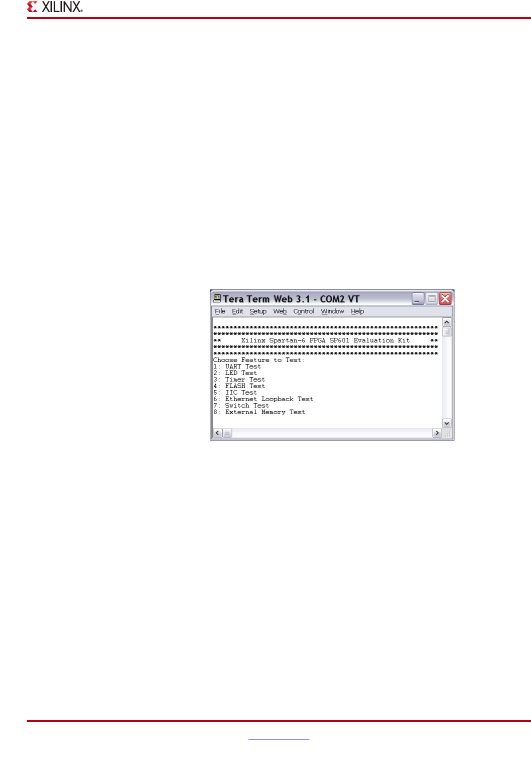
The BIST tests the operation of many of the SP601 Evaluation Kit features. When
configured to boot from the linear flash, the BIST menu appears upon power-up. After
FPGA configuration, the text shown in Figure 1-1 appears in a terminal program window,
such as Tera Term. Type the number associated with one of the listed tests to run the test
application. For example, typing a "5" runs the IIC Test application.
See the SP601 Built-In Self Test Flash Application tutorial for more information on the BIST
software and its operation. [Ref 18]
The default location of the BIST program is the in the Numonyx 28F128J3D Linear BPI
Flash device on the SP601 board. The SP601 Restoring Flash Contents tutorial provides
instructions for restoring the image to its factory default content. [Ref 22]
X-Ref Target - Figure 1-1
Figure 1-1: BIST Initial Screen
10 www.xilinx.com SP601 Reference Design User Guide
UG524 (v1.1) September 16, 2009
Chapter 1: SP601 Evaluation Board
Memory Interface Generator (MIG) DDR2 Design
The Spartan-6 FPGA contains dedicated Memory Controller Blocks (MCB) for simplified
DRAM interfaces, including up to four MCB cores in a single Spartan-6 device. The FPGA
also contains an embedded controller and physical (PHY) interface, 4-bit, 8-bit, or 16-bit
single component memory support, and memory densities up to 4 Gb. Additionally, the
Spartan-6 FPGA is capable of performance up to 800 Mb/s (400 MHz double data rate).
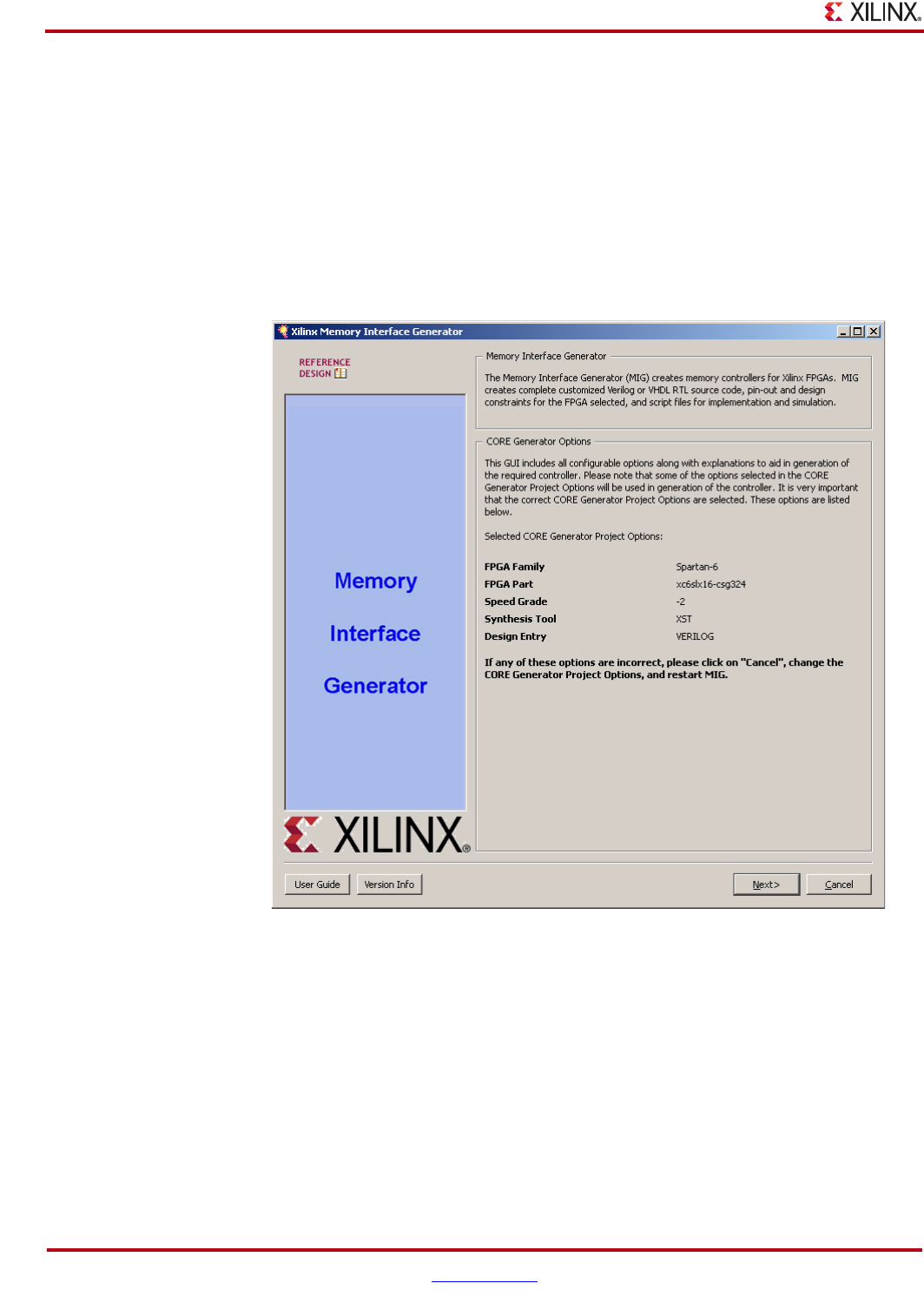
For the logic designer, the MIG tool (Figure 1-2) can be use to create a simple user interface
that abstracts away the complexity of memory transactions. The integrated memory
controller block's assembly and signal connectivity is made transparent to the user.
X-Ref Target - Figure 1-2
Figure 1-2: MIG Graphical User Interface
SP601 Reference Design User Guide www.xilinx.com 11
UG524 (v1.1) September 16, 2009
Reference Designs
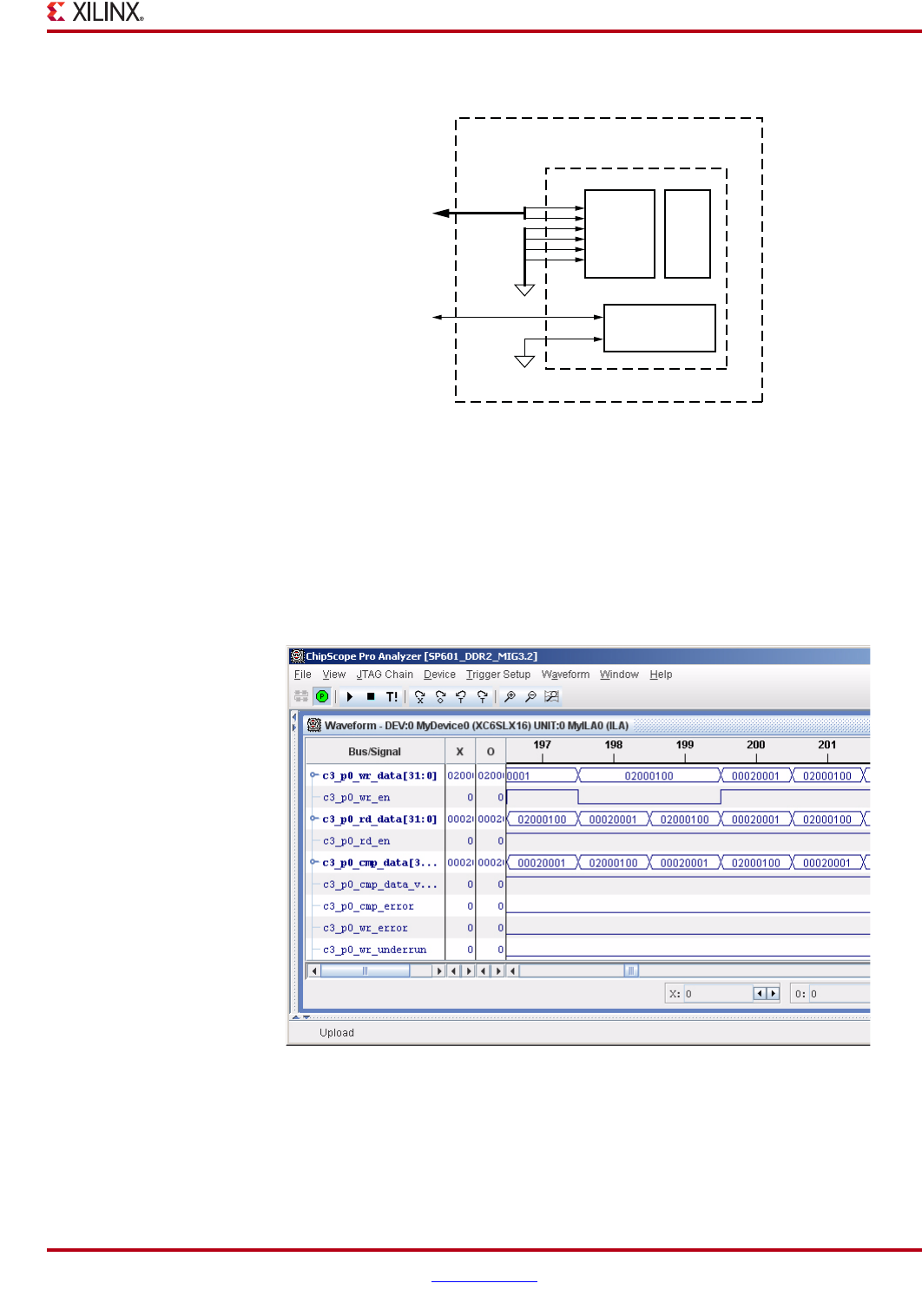
The LogiCORE™ MIG example debug design tests the DDR2 memory interface through a
series of writes and reads with pattern verification. The example design was generated
using the option to include the debug interface. The results can be viewed in the
ChipScope Pro Analyzer tool as shown in Figure 1-4, page 11. [Ref 19]
For more information on the MCB, see the Spartan-6 FPGA Memory Controller User Guide
[Ref 12]. For information about the ChipScope Pro Analyzer tool, refer to the ChipScope Pro
Software and Cores User Guide [Ref 14].
X-Ref Target - Figure 1-3
Figure 1-3: MIG Wrapper for Non-embedded Design
X-Ref Target - Figure 1-4
Figure 1-4: ChipScope Pro Analyzer Tool
Top-level
User
Interface
UG524_03_091409
Top-level Wrapper (MIG)
Lower-level Wrapper
Non-embedded Design
(MIG/CORE Generator Tool)
Ports
MCB
Port
Grouping
Signal
Tie Off
Soft Calibration
Module
I/O
12 www.xilinx.com SP601 Reference Design User Guide
UG524 (v1.1) September 16, 2009
Chapter 1: SP601 Evaluation Board
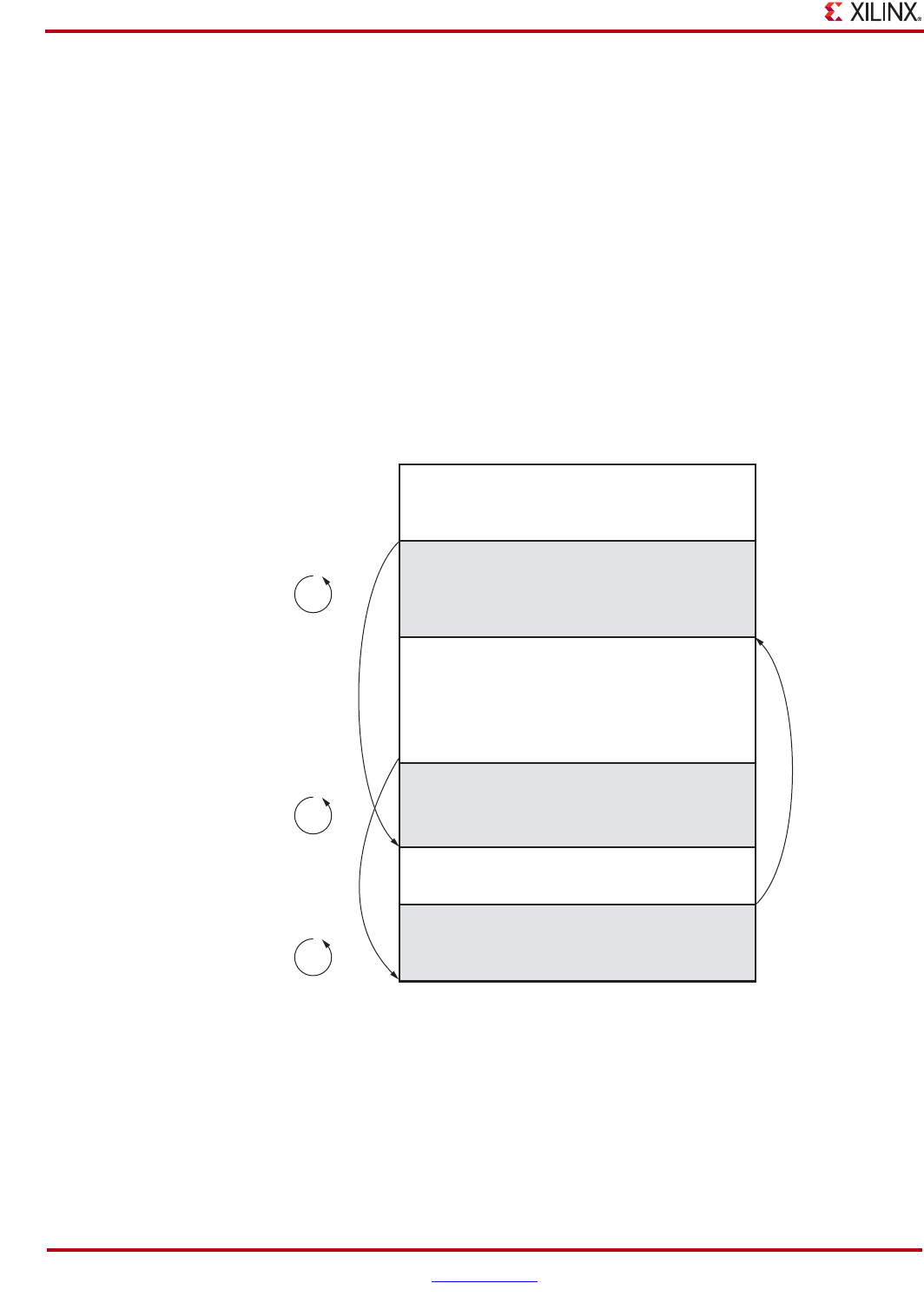
MultiBoot Design
Figure 1-5, page 12 illustrates the MultiBoot operation. MultiBoot is the process by which
the FPGA selectively reprograms and reloads its bitstream from an attached external
memory. This feature allows field updating of a stored bitstream with a new bitstream
while guarding against system upsets due to an update failure. A general update process
is accomplished in a five step procedure:
1. New MultiBoot image is created
2. System setup to receive the new image
3. User application erases section of Flash
4. The new image is delivered into the system's Flash
5. User application resets system
For additional information on the Spartan-6 MultiBoot feature, see the Spartan-6 FPGA
Configuration User Guide [Ref 5]. For a demonstration of this operation on the Spartan-6
FPGA, see the SP601 MultiBoot Demonstration [Ref 20].
Base System Reference Design (BSRD)
An image processing and networking application is shown through the BSRD design
programmed into the SPI Flash. The getting started guide [Ref 2] describes the
components of the BSRD application and how to run the reference design.
X-Ref Target - Figure 1-5
Figure 1-5: MultiBoot Operation
UG524_02_073009
Strike 0..2
0xFFFFFF
0x000000
MultiBoot
Bitstream
Golden
Header 1st Image
2nd Image
3rd Image
Strike 3..5
Strike 6..8

SP601 Reference Design User Guide www.xilinx.com 13
UG524 (v1.1) September 16, 2009
Restoring Flash Contents
Stand-Alone Applications
Each feature on the board can be tested for functionality by using the on-board BIST
application [Ref 18] or by using the stand-alone applications [Ref 21] offered on the SP601
reference designs Web page.
Restoring Flash Contents
The SP601 Evaluation Kit contains several non-volatile memories (Linear BPI Flash, SPI
Flash) that can be overwritten by user created designs. The Restoring Flash Contents tutorial
[Ref 22] provides a means to re-establish the original functionality programmed into the
Linear BPI Flash and the SPI Flash.
Table 1-1: Stand-Alone Applications
Feature Feature Test Capability
Spartan-6 FPGA BIST
DDR2 Component BIST
SPI x4 Flash SPI Configuration Mode
Linear BPI Flash BIST, BPI-UP Configuration Mode
10/100/1000 Ethernet PHY BIST, SPI Base System Reference Design (BSRD)
Demonstration
RS232 UART (USB Bridge) BIST
IIC BIST
Clock, socket, SMA 200 MHz system clock, 27MHz populated socket, User
SMA
VITA 57.1 FMC-LPC connector Factory Test
LEDs (Ethernet PHY) BIST
Suspend Header/Awake LED Web Tutorial
LEDs (INIT/DONE) BIST
User LED BIST
User DIP Switch BIST
User Pushbutton BIST
User 12-pin (8 I/O) Header Web Tutorial
Pushbutton (PROG) BIST
USB JTAG Configuration
Onboard Power BIST
SP601 Reference Design User Guide www.xilinx.com 15
UG524 (v1.1) September 16, 2009
Appendix A
References
This section provides references to documentation supporting Spartan-6 FPGAs, tools,
and IP. For additional information, see
www.xilinx.com/support/documentation/index.htm.
Documents supporting the SP601 Evaluation Board:
1. DS160, Spartan-6 Family Overview
2. UG523, Getting Started with the Xilinx Spartan-6 FPGA SP601 Evaluation Kit
3. UG518, SP601 Hardware User Guide
4. DS162, Spartan-6 FPGA Data Sheet: DC and Switching Characteristics
5. UG380, Spartan-6 FPGA Configuration User Guide
6. UG381, Spartan-6 FPGA SelectIO Resources User Guide
7. UG382, Spartan-6 FPGA User Guide: Clocking Resources
8. UG383, Spartan-6 FPGA Block RAM Resources User Guide
9. UG384, Spartan-6 FPGA Configurable Logic Block User Guide
10. UG385, Spartan-6 FPGA Packaging and Pinouts
11. UG386, Spartan-6 FPGA GTP Transceivers User Guide
12. UG388, Spartan-6 FPGA Memory Controller User Guide
13. UG389, Spartan-6 FPGA DSP48A1 Slice User Guide
14. UG029, ChipScope Pro Software and Cores User Guide
15. DS614, Clock Generator (v3.01a) Data Sheet
16. DS643, Multi-Port Memory Controller (MPMC) (v5.02a) Data Sheet
17. UG138, LogiCORE™ IP Tri-Mode Ethernet MAC v4.2 User Guide
The following SP601 tutorials, demonstration, and design files are located at
http://www.xilinx.com/products/boards/sp601/reference_designs.htm:
18. XTP041, SP601 Built-In Self Test Flash Application (rdf0045.zip)
19. XTP039, SP601 MIG Design Creation (rdf0005.zip)
20. XTP038, SP601 MultiBoot Design (rdf0006.zip)
21. XTP053, SP601 Stand-Alone Applications (rdf0015.zip)
22. XTP040, SP601 Restoring Flash Contents (rdf0004.zip)

