Tn5445 TECHNOTE/TN 544 TN
TECHNOTE/TN-544 TN-544
TECHNOTE/TN-544 TN-544
TECHNOTE/TN-544 TN-544
User Manual: Pdf TECHNOTE/TN-544
Open the PDF directly: View PDF ![]() .
.
Page Count: 4

Tait Electronics Ltd Page 1 of 4
558 Wairakei Rd, P.O. Box 1645, Christchurch, New Zealand
Phone: (64) (3) 358 3399 Fax: (64) (3) 358 3903
Technical Note TN-544
Improving The Noise Mute
Performance In Series II
T855 Receivers
14 December 1998
For Internal Use Only: This Technical Note must not be distributed beyond Tait
Customer Service Organisations without prior approval
from Radio Systems Division Customer Support.
Applicability
This Technical Note (TN) applies to all T855 Series II receivers manufactured with PCB
IPN 220-01396-02.
Introduction
T855 Series II receivers manufactured with PCB IPN 220-01396-02 have a potential prob-
lem with noise mute hysteresis. This problem may cause the noise mute to open and
stay open, particularly when the receiver is operating in high temperatures and/or
noisy RF environments.
The modifications described in this TN will prevent this problem from happening and
ensure that the specified receiver performance is maintained.
If you have any questions about this TN or the procedures it describes, please contact
your nearest Tait Dealer or Customer Service Organisation. If necessary, you can get
additional technical help from Customer Support, Radio Systems Division, Tait Elec-
tronics Ltd, Christchurch, New Zealand.
Parts Required
1 x 10n 0805 chip capacitor
Tools Required
hot air gun tweezers or narrow-nosed pliers
solder paste No. 2 Pozidriv screwdriver

Page 2 of 4 14 December 1998
TN-544
Method
Caution:
Observe appropriate static precautions while working on the radio
equipment. This procedure should be carried out by a person experi-
enced in SMD soldering techniques.
1. Remove the top and bottom covers.
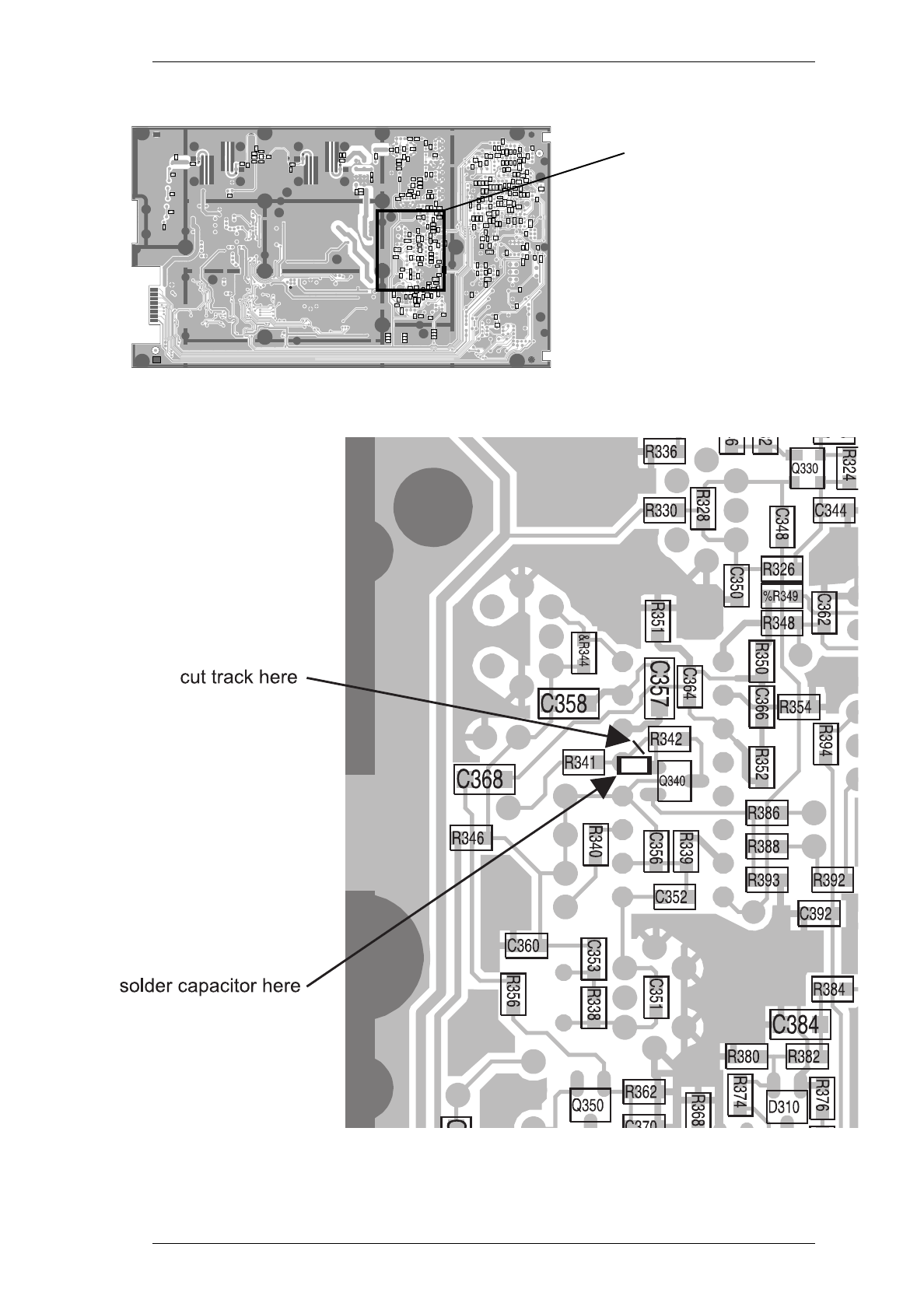
2. Cut the track between R342 and pin 5 of IC310 as shown in Figure 1.
3. Solder a 10n 0805 chip capacitor between pin 5 of IC310 and the base of Q340 as
shown in Figure 1.
4. Check that all the solder joints are of a good standard and that there are no short
circuits.
Noise Mute Adjustment
Note:
In this section deviation settings are given first for wide bandwidth sets, fol-
lowed by settings in brackets for mid bandwidth sets ( ) and narrow band-
width sets [ ].
1. Set up the test equipment as shown in Section 3.3 of the T850 Series II service man-
ual.
2. Connect pins 1 & 2 of PL250 to enable the noise mute.
3. Set the RF level to -105dBm with ±3kHz deviation (±2.4kHz) [±1.5kHz] at 1kHz.
4. Set RV230 (front panel gating sensitivity) fully anticlockwise.
5. Adjust RV310 (noise mute gain) to close the mute (if necessary turn off the RF sig-
nal and then turn it on again).
6. Rotate RV310 anticlockwise until the mute just opens.
Once the mute has been set up as described above, adjust RV230 for the required open-
ing sinad.
Noise Mute Hysteresis Check
1. Reduce the RF level until the mute closes and note this RF level.
2. Check that the difference between this RF level and level at which the mute opens
is 1.5 to 6dB.
TN-544
14 December 1998 Page 3 of 4
Figure 1 T855 PCB Modifications - Bottom Side
NP D
2
3
4
7
5
6
M
1
QHGK CLJ EF AB
8
%C460
%R223
%R349
&C203
&C205
C211
C213 C215
C217
C221
&C318
&C320
&C322
&C324
&C326
&C334
&C336
&C338
&C340
&R202
&R209R210
R211
&R219
R221
R222
&R344
B85510
B85513
B85515
B85520
B85523
B85525
B855S1
B855S2
B855S3
BOTFIDA
BOTFIDB
BOTHOLE
BOTSLOT
C210
C219
C223
C225
C227
C235
C237
C238
C240A
C240B
C251
C255 C257
C259
C260A
C260B
C264
C270
C272
C274
C276
C278
C280
C286
C302
C304
C306
C308
C310
C314
C316
C328
C330
C332
C342
C344
C346
C348
C350
C351
C352
C353
C356
C357
C358
C360
C362
C364
C366
C368
C370
C372
C374
C376
C378
C380
C384
C386
C388
C392
C394
C410
C420
C430
C450
C470
C480
C910
C920
C930
C940
C950
D220
D230
D240
D260
D270
D310
L410
L430
Q210
Q220 Q230
Q240
Q245
Q250
Q255
Q260
Q270
Q280
Q290
Q320
Q330
Q340
Q350
Q360
Q410
R201
R204R205
R207
R213
R215
R218
R224
R225
R227
R229
R230
R232
R233 R234
R236
R238
R239
R241
R242
R244
R245
R247 R249
R251
R252
R254
R255
R256
R258
R260
R261
R262
R264
R265
R266
R267 R269
R271
R272
R273
R275 R277
R278
R280
R281
R282
R284
R285
R287
R288
R289
R290
R292
R293
R294
R295
R296
R298
R299
R302
R304 R306
R308
R310
R312
R314
R316
R318
R320
R322
R323
R324
R326
R328
R330
R332
R336
R338
R339
R340
R341
R342
R346
R348
R350
R351
R352
R354
R356
R358
R360
R362
R364
R366
R368 R370
R372
R374
R376 R378
R380 R382
R384
R386
R388
R392R393
R394
R395
R396 R397
R398
R405 R410
R415
R420
R425
R430
R435
R440
R445
R450
R455
R460
R465
R470
R475
SL210SL220
TP408
TP409
TP410
TP411
area shown enlarged below

Page 4 of 4 14 December 1998
TN-544
Reassembly
1. Refit the top and bottom covers and torque down to 1.36Nm/12in.lbf. Tighten the
centre screws first, then work your way out evenly to those at the ends.
Issuing Authority
This TN was issued by: Andreas Becker
RSD Customer Support Manager
