TCA9538 Low Voltage 8 Bit I2C And SMBus Power I/O Expander (Rev. D)
2017-07-11
: Pdf Tca9538 tca9538 3155-147-5062 aftab
Open the PDF directly: View PDF ![]() .
.
Page Count: 37
- 1 Features
- 2 Applications
- 3 Description
- Table of Contents
- 4 Revision History
- 5 Pin Configuration and Functions
- 6 Specifications
- 7 Parameter Measurement Information
- 8 Detailed Description
- 9 Application and Implementation
- 10 Power Supply Recommendations
- 11 Layout
- 12 Device and Documentation Support
- 13 Mechanical, Packaging, and Orderable Information
TCA9538
Peripheral
Devices
I2C or SMBus
Master
(e.g. Processor)
SDA
SCL
INT P0
P1
RESET
P2
P3
P4
P5
P6
P7
VCC
A1
GND
A0
• ,
ENABLE, or
control
inputs
• or
status
outputs
• LEDs
RESET
INT
Product
Folder
Sample &
Buy
Technical
Documents
Tools &
Software
Support &
Community
An IMPORTANT NOTICE at the end of this data sheet addresses availability, warranty, changes, use in safety-critical applications,
intellectual property matters and other important disclaimers. PRODUCTION DATA.
TCA9538
SCPS199D –AUGUST 2014–REVISED OCTOBER 2016
TCA9538 Low Voltage 8-Bit I
2
C and SMBus Low-Power I/O Expander with Interrupt
Output, Reset, and Configuration Registers
1
1 Features
1• Low Standby Current Consumption
• I2C to Parallel Port Expander
• Open-Drain Active-Low Interrupt Output
• Active-Low Reset Input
• Operating Power-Supply Voltage Range of 1.65 V
to 5.5 V
• 5-V Tolerant I/O Ports
• 400-kHz Fast I2C Bus
• Two Hardware Address Pins Allow up to Four
Devices on the I2C/SMBus
• Input and Output Configuration Register
• Polarity Inversion Register
• Power-Up With All Channels Configured as Inputs
• No Glitch on Power Up
• Noise Filter on SCL/SDA Inputs
• Latched Outputs With High-Current Drive
Maximum Capability for Directly Driving LEDs
• Latch-Up Performance Exceeds 100 mA Per
JESD 78, Class II
• ESD Protection Exceeds JESD 22
– 2000-V Human-Body Model (A114-A)
– 1000-V Charged-Device Model (C101)
2 Applications
• Servers
• Routers (Telecom Switching Equipment)
• Personal Computers
• Personal Electronics (example: Gaming Consoles)
• Industrial Automation
• Products With GPIO-Limited Processors
3 Description
The TCA9538 is a 16-pin device that provides 8 bits
of general purpose parallel input and output (I/O)
expansion for the two-line bidirectional I2C bus (or
SMBus) protocol. The device can operate with a
power supply voltage ranging from 1.65 V to 5.5 V.
The device supports both 100-kHz (Standard-mode)
and 400-kHz (Fast-mode) clock frequencies. I/O
expanders such as the TCA9538 provide a simple
solution when additional I/Os are needed for
switches, sensors, push-buttons, LEDs, fans, etc.
The features of the TCA9538 include an interrupt that
is generated on the INT pin whenever an input port
changes state. The A0 and A1 hardware selectable
address pins allow up to four TCA9538 devices on
the same I2C bus. The device can also be reset to its
default sate by using the RESET feature or by cycling
the power supply and causing a power-on reset.
Device Information(1)
PART NUMBER PACKAGE BODY SIZE (NOM)
TCA9538 TSSOP (16) 5.00 mm × 4.40 mm
SSOP (16) 6.20 mm × 5.30 mm
(1) For all available packages, see the orderable addendum at
the end of the datasheet.
Simplified Block Diagram
2
TCA9538
SCPS199D –AUGUST 2014–REVISED OCTOBER 2016
www.ti.com
Product Folder Links: TCA9538
Submit Documentation Feedback Copyright © 2014–2016, Texas Instruments Incorporated
Table of Contents
1 Features.................................................................. 1
2 Applications ........................................................... 1
3 Description ............................................................. 1
4 Revision History..................................................... 2
5 Pin Configuration and Functions......................... 3
6 Specifications......................................................... 4
6.1 Absolute Maximum Ratings ..................................... 4
6.2 ESD Ratings ............................................................ 4
6.3 Recommended Operating Conditions....................... 4
6.4 Thermal Information.................................................. 5
6.5 Electrical Characteristics........................................... 5
6.6 I2C Interface Timing Requirements........................... 6
6.7 RESET Timing Requirements................................... 7
6.8 Switching Characteristics.......................................... 7
6.9 Typical Characteristics.............................................. 8
7 Parameter Measurement Information ................ 10
8 Detailed Description ............................................ 14
8.1 Overview ................................................................. 14
8.2 Functional Block Diagram ....................................... 15
8.3 Feature Description................................................. 16
8.4 Device Functional Modes........................................ 17
8.5 Programming........................................................... 17
8.6 Register Map........................................................... 19
9 Application and Implementation ........................ 23
9.1 Application Information............................................ 23
9.2 Typical Application ................................................. 23
10 Power Supply Recommendations ..................... 26
10.1 Power-On Reset Requirements ........................... 26
11 Layout................................................................... 28
11.1 Layout Guidelines ................................................. 28
11.2 Layout Example .................................................... 28
12 Device and Documentation Support ................. 29
12.1 Documentation Support ........................................ 29
12.2 Receiving Notification of Documentation Updates 29
12.3 Community Resources.......................................... 29
12.4 Trademarks........................................................... 29
12.5 Electrostatic Discharge Caution............................ 29
12.6 Glossary................................................................ 29
13 Mechanical, Packaging, and Orderable
Information ........................................................... 29
4 Revision History
NOTE: Page numbers for previous revisions may differ from page numbers in the current version.
Changes from Revision C (October 2015) to Revision D Page
• Updated Figure 18 ............................................................................................................................................................... 19
Changes from Revision B (September 2015) to Revision C Page
• Added "Time to reset; VCC = 1.65 V-2.3 V" parameter to RESET Timing Requirements table. ............................................ 7
• Added "Output data valid; VCC = 1.65 V-2.3 V" to Switching Characteristics table................................................................ 7
• Updated VCC_GW parameter. ................................................................................................................................................ 26
Changes from Revision A (September 2014) to Revision B Page
• Added DB package to datasheet. .......................................................................................................................................... 1
Changes from Original (August 2014) to Revision A Page
• Updated document to full version. ......................................................................................................................................... 1
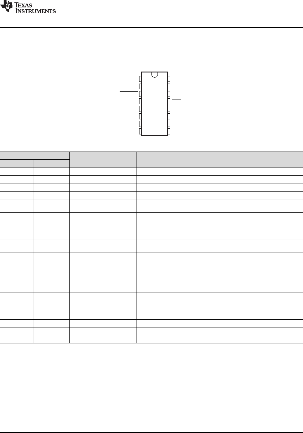
RESET
1
2
3
4
5
6
7
8
16
15
14
13
12
11
10
9
A0
A1
P0
P1
P2
P3
GND
VCC
SDA
SCL
INT
P7
P6
P5
P4
3
TCA9538
www.ti.com
SCPS199D –AUGUST 2014–REVISED OCTOBER 2016
Product Folder Links: TCA9538
Submit Documentation FeedbackCopyright © 2014–2016, Texas Instruments Incorporated
5 Pin Configuration and Functions
PW, DB Package
16-Pin TSSOP, SSOP
Top View
Pin Functions
PIN I/O DESCRIPTION
NAME NO.
A0 1 I Address input. Connect directly to VCC or ground
A1 2 I Address input. Connect directly to VCC or ground
GND 8 — Ground
INT 13 O Interrupt output. Connect to VCC through a pull-up resistor
P0 4 I/O P-port input-output. Push-pull design structure. At power on, P0 is
configured as an input
P1 5 I/O P-port input-output. Push-pull design structure. At power on, P1 is
configured as an input
P2 6 I/O P-port input-output. Push-pull design structure. At power on, P2 is
configured as an input
P3 7 I/O P-port input-output. Push-pull design structure. At power on, P3 is
configured as an input
P4 9 I/O P-port input-output. Push-pull design structure. At power on, P4 is
configured as an input
P5 10 I/O P-port input-output. Push-pull design structure. At power on, P5 is
configured as an input
P6 11 I/O P-port input-output. Push-pull design structure. At power on, P6 is
configured as an input
P7 12 I/O P-port input-output. Push-pull design structure. At power on, P7 is
configured as an input
RESET 3 I Active-low reset input. Connect to VCC through a pull-up resistor if no active
connection is used
SCL 14 I Serial clock bus. Connect to VCC through a pull-up resistor
SDA 15 I/O Serial data bus. Connect to VCC through a pull-up resistor
VCC 16 — Supply voltage
4
TCA9538
SCPS199D –AUGUST 2014–REVISED OCTOBER 2016
www.ti.com
Product Folder Links: TCA9538
Submit Documentation Feedback Copyright © 2014–2016, Texas Instruments Incorporated
(1) Stresses beyond those listed under Absolute Maximum Ratings may cause permanent damage to the device. These are stress ratings
only, which do not imply functional operation of the device at these or any other conditions beyond those indicated under Recommended
Operating Conditions. Exposure to absolute-maximum-rated conditions for extended periods may affect device reliability.
(2) The input negative-voltage and output voltage ratings may be exceeded if the input and output current ratings are observed.
6 Specifications
6.1 Absolute Maximum Ratings(1)
over operating free-air temperature range (unless otherwise noted)
MIN MAX UNIT
VCC Supply voltage –0.5 6 V
VIInput voltage (2) –0.5 6 V
VOOutput voltage(2) –0.5 6 V
IIK Input clamp current VI< 0 –20 mA
IOK Output clamp current VO< 0 –20 mA
IIOK Input-output clamp current VO< 0 or VO> VCC ±20 mA
IOL Continuous output low current through a single P-port VO= 0 to VCC 50 mA
IOH Continuous output high current through a single P-port VO= 0 to VCC –50 mA
ICC
Continuous current through GND by all P-ports, INT, and SDA 250 mA
Continuous current through VCC by all P-ports –160
Tstg Storage temperature –65 150 °C
(1) JEDEC document JEP155 states that 500-V HBM allows safe manufacturing with a standard ESD control process. Manufacturing with
less than 500-V HBM is possible with the necessary precautions.
(2) JEDEC document JEP157 states that 250-V CDM allows safe manufacturing with a standard ESD control process. Manufacturing with
less than 250-V CDM is possible with the necessary precautions.
6.2 ESD Ratings
VALUE UNIT
V(ESD) Electrostatic discharge Human-body model (HBM), per ANSI/ESDA/JEDEC JS-001(1) 2000 V
Charged-device model (CDM), per JEDEC specification JESD22-C101(2) 1000
(1) The SCL and SDA pins shall not be at a higher potential than the supply voltage VCC in the application, or an increase in supply current,
ICC, will result.
6.3 Recommended Operating Conditions
MIN MAX UNIT
VCC Supply voltage 1.65 5.5 V
VIH High-level input voltage
SCL, SDA VCC = 1.65 V to 5.5 V 0.7 × VCC VCC(1)
V
A0, A1, RESET, P7–P0 VCC = 1.65 V to 2.7 V 0.7 × VCC 5.5
VCC = 3 V to 5.5 V 0.8 × VCC 5.5
VIL Low-level input voltage
SCL, SDA VCC = 1.65 V to 5.5 V –0.5 0.3 × VCC
V
A0, A1, RESET, P7–P0 VCC = 1.65 V to 2.7 V –0.5 0.3 × VCC
VCC = 3 V to 5.5 V –0.5 0.2 × VCC
IOL Low-level output current Any P-port, P7–P0 25 mA
IOH High-level output current Any P-port, P7–P0 –10 mA
ICC
Continuous current through
GND All P-ports P7-P0, INT, and SDA 200 mA
Continuous current through VCC All P-ports P7-P0 –80
TAOperating free-air temperature –40 85 °C
5
TCA9538
www.ti.com
SCPS199D –AUGUST 2014–REVISED OCTOBER 2016
Product Folder Links: TCA9538
Submit Documentation FeedbackCopyright © 2014–2016, Texas Instruments Incorporated
(1) For more information about traditional and new thermal metrics, see the Semiconductor and IC Package Thermal Metrics application
report.
6.4 Thermal Information
THERMAL METRIC(1)
TCA9538
UNITPW (TSSOP) DB (SSOP)
16 PINS 16 PINS
RθJA Junction-to-ambient thermal resistance 122 113.2 °C/W
RθJC(top) Junction-to-case (top) thermal resistance 56.4 63.6 °C/W
RθJB Junction-to-board thermal resistance 67.1 64 °C/W
ψJT Junction-to-top characterization parameter 10.8 21.2 °C/W
ψJB Junction-to-board characterization parameter 66.5 63.4 °C/W
(1) All typical values are at nominal supply voltage (1.8-, 2.5-, 3.3-, or 5-V VCC) and TA= 25°C.
(2) Each P-port I/O configured as a high output must be externally limited to a maximum of 10 mA, and the total current sourced by all I/Os
(P-ports P7-P0) through VCC must be limited to a maximum current of 80 mA.
(3) The SDA pin must be externally limited to a maximum of 12 mA, and the total current sunk by all I/Os (P-ports P7-P0, INT, and SDA)
through GND must be limited to a maximum current of 200 mA.
(4) Each P-port I/O configured as a low output must be externally limited to a maximum of 25 mA, and the total current sunk by all I/Os (P-
ports P7-P0, INT, and SDA) through GND must be limited to a maximum current of 200 mA.
(5) The INT pin must be externally limited to a maximum of 7 mA, and the total current sunk by all I/Os (P-ports P7-P0, INT, and SDA)
through GND must be limited to a maximum current of 200 mA.
6.5 Electrical Characteristics
over operating free-air temperature range (unless otherwise noted)
PARAMETER TEST CONDITIONS VCC MIN TYP(1) MAX UNIT
VIK Input diode clamp voltage II= –18 mA 1.65 V to 5.5 V –1.2 V
VPORR Power-on reset voltage, VCC rising VI= VCC or GND, IO= 0 1.2 1.5 V
VPORF Power-on reset voltage, VCC
falling VI= VCC or GND, IO= 0 0.75 1 V
VOH P-port high-level output voltage(2)
IOH = –8 mA
1.65 V 1.2
V
2.3 V 1.8
3 V 2.6
4.5 V 4.1
IOH = –10 mA
1.65 V 1.1
2.3 V 1.7
3 V 2.5
4.5 V 4
IOL
SDA (3) VOL = 0.4 V 1.65 V to 5.5 V 3 11
mAP port(4)
VOL = 0.5 V
1.65 V 8 10
2.3 V 8 13
3 V 8 15
4.5 V 8 17
VOL = 0.7 V
1.65 V 10 14
2.3 V 10 17
3 V 10 20
4.5 V 10 24
INT (5) VOL = 0.4 V 1.65 V to 5.5 V 3 7
II
SCL, SDA VI= VCC or GND 1.65 V to 5.5 V ±1 μA
A0, A1, RESET ±1
IIH P port VI= VCC 1.65 V to 5.5 V 1 μA
IIL P port VI= GND 1.65 V to 5.5 V –1 μA
6
TCA9538
SCPS199D –AUGUST 2014–REVISED OCTOBER 2016
www.ti.com
Product Folder Links: TCA9538
Submit Documentation Feedback Copyright © 2014–2016, Texas Instruments Incorporated
Electrical Characteristics (continued)
over operating free-air temperature range (unless otherwise noted)
PARAMETER TEST CONDITIONS VCC MIN TYP(1) MAX UNIT
ICC
Operating mode
VI= VCC or GND, IO= 0,
I/O = inputs, fscl = 400 kHz, No load
tr= 3 ns 5.5 V 18 30
μA
VI= VCC or GND, IO= 0,
I/O = inputs, fscl = 400 kHz, No load
tr,max = 300 ns
5.5 V 34
3.6 V 15
2.7 V 9
1.65 V 5
VI= VCC or GND, IO= 0,
I/O = inputs, fscl = 100 kHz, No load
tr,max = 1 µs
5.5 V 20
3.6 V 8
2.7 V 5
1.65 V 3
Standby mode VI= VCC or GND, IO= 0,
I/O = inputs, fscl = 0 kHz, No load
5.5 V 1.9 3.5
μA
3.6 V 1.1 1.8
2.7 V 1 1.6
1.65 V 0.4 1
ΔICC Additional current in standby
mode One P-port input at VCC – 0.6 V,
Other P-port inputs at VCC or GND 1.65 V to 5.5 V 70 µA
CiSCL VI= VCC or GND 1.65 V to 5.5 V 4 5 pF
Cio
SDA VIO = VCC or GND 1.65 V to 5.5 V 5.5 6.5 pF
P port 8 9.5
6.6 I2C Interface Timing Requirements
over operating free-air temperature range (unless otherwise noted) (see Figure 9)
MIN MAX UNIT
STANDARD MODE
fscl I2C clock frequency 0 100 kHz
tsch I2C clock high time 4μs
tscl I2C clock low time 4.7 μs
tsp I2C spike time 50 ns
tsds I2C serial-data setup time 250 ns
tsdh I2C serial-data hold time 0 ns
ticr I2C input rise time 1000 ns
ticf I2C input fall time 300 ns
tocf I2C output fall time 10-pF to 400-pF bus 300 ns
tbuf I2C bus free time between Stop and Start 4.7 μs
tsts I2C Start or repeated Start condition setup 4.7 μs
tsth I2C Start or repeated Start condition hold 4μs
tsps I2C Stop condition setup 4μs
tvd(data) Valid data time SCL low to SDA output valid 3.45 μs
tvd(ack) Valid data time of ACK condition ACK signal from SCL low to
SDA (out) low 3.45 μs
CbI2C bus capacitive load 400 ns
FAST MODE
fscl I2C clock frequency 0 400 kHz
tsch I2C clock high time 0.6 μs
tscl I2C clock low time 1.3 μs
tsp I2C spike time 50 ns
tsds I2C serial-data setup time 100 ns
7
TCA9538
www.ti.com
SCPS199D –AUGUST 2014–REVISED OCTOBER 2016
Product Folder Links: TCA9538
Submit Documentation FeedbackCopyright © 2014–2016, Texas Instruments Incorporated
I2C Interface Timing Requirements (continued)
over operating free-air temperature range (unless otherwise noted) (see Figure 9)
MIN MAX UNIT
tsdh I2C serial-data hold time 0 ns
ticr I2C input rise time 20 300 ns
ticf I2C input fall time 20 × (VDD /
5.5 V) 300 ns
tocf I2C output fall time 10-pF to 400-pF bus 20 × (VDD /
5.5 V) 300 ns
tbuf I2C bus free time between Stop and Start 1.3 μs
tsts I2C Start or repeated Start condition setup 0.6 μs
tsth I2C Start or repeated Start condition hold 0.6 μs
tsps I2C Stop condition setup 0.6 μs
tvd(data) Valid data time SCL low to SDA output valid 0.9 μs
tvd(ack) Valid data time of ACK condition ACK signal from SCL low to
SDA (out) low 0.9 μs
CbI2C bus capacitive load 400 ns
6.7 RESET Timing Requirements
over operating free-air temperature range (unless otherwise noted)
PARAMETER MIN MAX UNIT
STANDARD and FAST MODE
twReset pulse duration 4 ns
tREC Reset recovery time 0 ns
tRESET
Time to reset; VCC = 2.3 V-5.5 V 400 ns
Time to reset; VCC = 1.65 V-2.3 V 550
6.8 Switching Characteristics
over operating free-air temperature range (unless otherwise noted) (see Figure 10 and Figure 11)
PARAMETER FROM
(INPUT) TO
(OUTPUT) MIN MAX UNIT
STANDARD and FAST MODE
tiv Interrupt valid time P port INT 4 μs
tir Interrupt reset delay time SCL INT 4 μs
tpv
Output data valid; VCC = 2.3 V-5.5 V SCL P7–P0 200 ns
Output data valid; VCC = 1.65 V-2.3 V 300
tps Input data setup time P port SCL 100 ns
tph Input data hold time P port SCL 1 μs
VOL - Output Low Voltage - (V)
IOL - Output Sink Current (mA)
0 0.1 0.2 0.3 0.4 0.5 0.6 0.7 0.8
0
10
20
30
40
50
60
70
80
D005
1.8 V
2.5 V
3.3 V
5 V
TA - Free-Air Temperature (°C)
(VCC - VOH) - Output High Voltage (mV)
-40 -15 10 35 60 85
0
50
100
150
200
250
300
350
400
450
500
D006
VCC = 1.8 V, IOH = 8 mA
VCC = 5 V, IOH = 8 mA
VCC = 1.65 V, IOH = 10 mA
VCC = 5 V, IOH = 10 mA
VCC - Supply Voltage (V)
ICC - Supply Current (µA)
0 0.5 1 1.5 2 2.5 3 3.5 4 4.5 5 5.5
0
5
10
15
20
25
D003
TA - Free-Air Temperature (°C)
VOL - Output Low Voltage (mV)
-40 -15 10 35 60 85
0
50
100
150
200
250
D004
VCC = 1.8 V, IOL = 8 mA
VCC = 5 V, IOL = 8 mA
VCC = 1.8 V, IOL = 10 mA
VCC = 5 V, IOL = 10 mA
TA - Free-Air Temperature (°C)
ICC - Supply Current (µA)
-40 -15 10 35 60 85
0
2
4
6
8
10
12
14
16
18
20
22
D001
1.8 V
2.5 V
3.3 V
5 V
TA - Free-Air Temperature (°C)
ICC - Supply Current (µA)
-40 -15 10 35 60 85
0
0.2
0.4
0.6
0.8
1
1.2
1.4
1.6
1.8
D002
1.8 V
2.5 V
3.3 V
5 V
8
TCA9538
SCPS199D –AUGUST 2014–REVISED OCTOBER 2016
www.ti.com
Product Folder Links: TCA9538
Submit Documentation Feedback Copyright © 2014–2016, Texas Instruments Incorporated
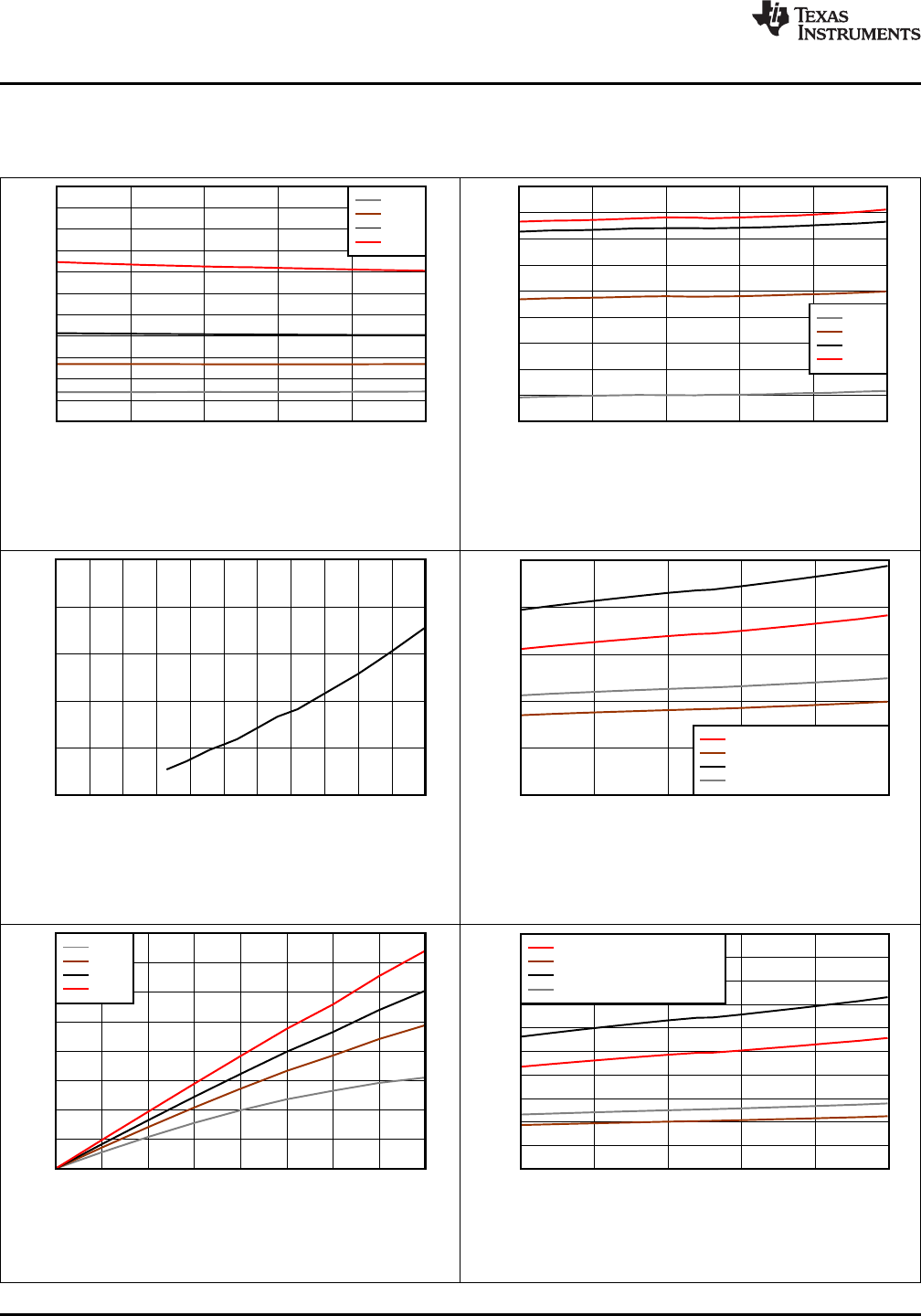
6.9 Typical Characteristics
TA= 25°C (unless otherwise noted)
fSCL = 400 kHz I/Os = High or Low
Inputs
Figure 1. Supply Current (ICC, Operating Mode) vs
Temperature (TA) at Four Supply Voltages
fSCL = 0 kHz I/Os = High or Low
Inputs
Figure 2. Supply Current (ICC, Standby Mode) vs
Temperature (TA) at Four Supply Voltages
fSCL = 400 kHz I/Os = High or Low
Inputs TA= 25°C
Figure 3. Supply Current (ICC, Operating Mode) vs Supply
Voltage (VCC)
I/Os = High or Low
Inputs
Figure 4. Output Low Voltage (VOL) vs Temperature (TA) for
P-Port I/Os
TA= 25°C
Figure 5. Sink Current (IOL) vs Output Low Voltage (VOL) for
P-Ports at Four Supply Voltages Figure 6. Output High Voltage (VCC – VOH) vs Temperature
(TA) for P-Ports
(VCC - VOH) - Output High Voltage (V)
IOH - Output Source Current (mA)
0 0.1 0.2 0.3 0.4 0.5 0.6 0.7 0.8
0
10
20
30
40
50
60
70
D007
1.8 V
2.5 V
3.3 V
5 V
VCC - Supply Voltage (V)
VOH - Output High Voltage (V)
0 1 2 3 4 5 6
0
1
2
3
4
5
6
D008
IOH = -8 mA
IOH = -10 mA
9
TCA9538
www.ti.com
SCPS199D –AUGUST 2014–REVISED OCTOBER 2016
Product Folder Links: TCA9538
Submit Documentation FeedbackCopyright © 2014–2016, Texas Instruments Incorporated
Typical Characteristics (continued)
TA= 25°C (unless otherwise noted)
TA= 25°C
Figure 7. Source Current (IOH) vs Output High Voltage (VOH)
for P-Ports at Four Supply Voltages
TA= 25°C
Figure 8. Output High Voltage (VOH) vs Supply Voltage (VCC)
for P-Ports
RL= 1 kΩ
VCC
CL= 50 pF
(see Note A)
tbuf
ticr
tsth tsds
tsdh
ticf
ticr
tscl tsch
tsts
tPHL
tPLH
0.3 ×VCC
Stop
Condition
tsps
Repeat
Start
Condition
Start or
Repeat
Start
Condition
SCL
SDA
Start
Condition
(S)
Address
Bit 7
(MSB)
Data
Bit 10
(LSB)
Stop
Condition
(P)
Three Bytes for Complete
Device Programming
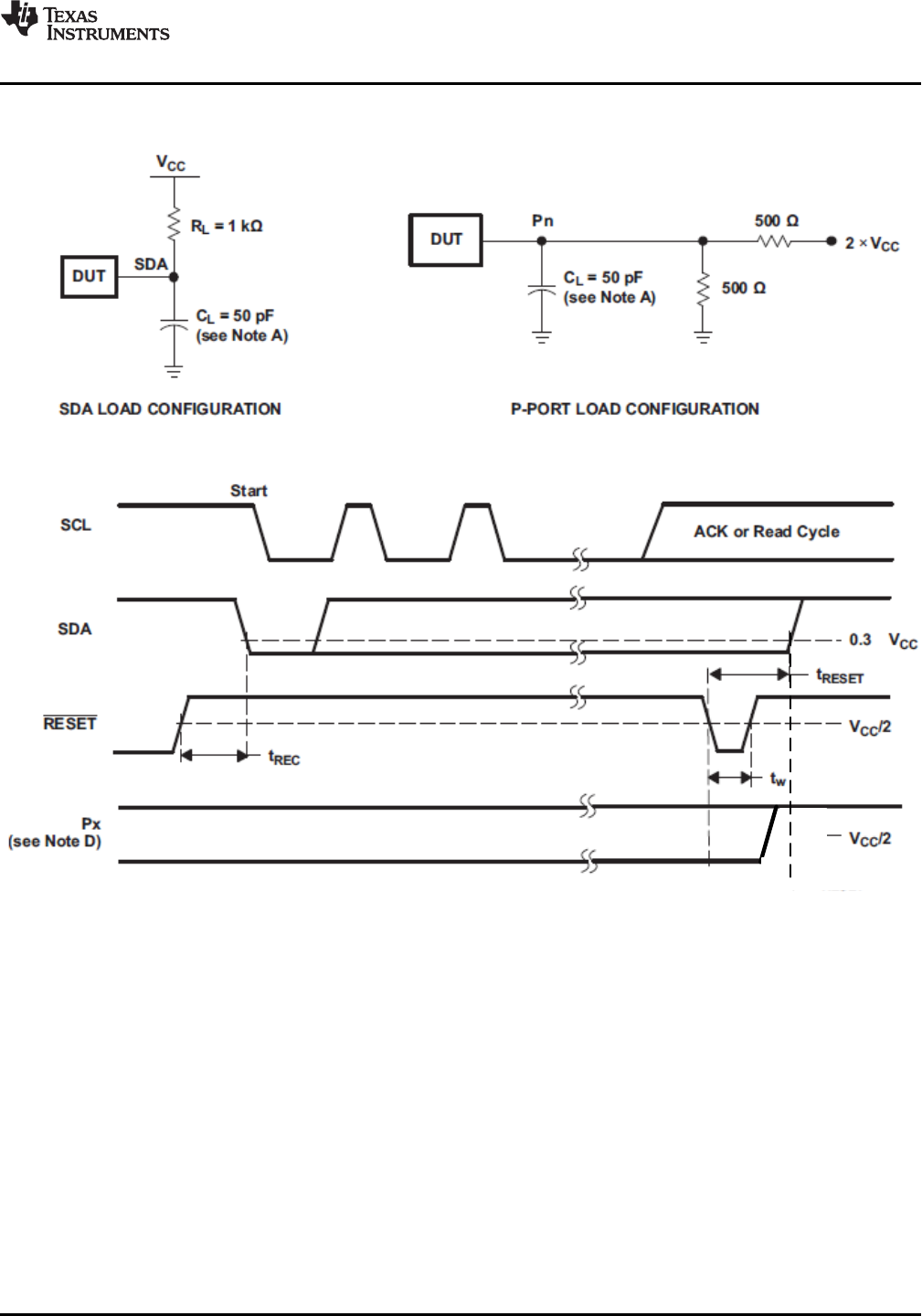
SDA LOAD CONFIGURATION
VOLTAGE WAVEFORMS
ticf
Stop
Condition
(P)
tsp
DUT SDA
0.7 ×VCC
0.3 ×VCC
0.7 ×VCC
R/W
Bit 0
(LSB)
ACK
(A)
Data
Bit 07
(MSB)
Address
Bit 1
Address
Bit 6
BYTE DESCRIPTION
1 I2C address
2, 3 P-port data
10
TCA9538
SCPS199D –AUGUST 2014–REVISED OCTOBER 2016
www.ti.com
Product Folder Links: TCA9538
Submit Documentation Feedback Copyright © 2014–2016, Texas Instruments Incorporated
7 Parameter Measurement Information
A. CLincludes probe and jig capacitance.
B. All inputs are supplied by generators having the following characteristics: PRR ≤10 MHz, ZO= 50 Ω, tr/tf≤30 ns.
C. All parameters and waveforms are not applicable to all devices.
Figure 9. I2C Interface Load Circuit and Voltage Waveforms
A
A
A
A
S 1 1 1 0 A10 A0 1 Data 1 1 PData 2
Start
Condition 8 Bits
(One Data Byte)
From Port Data From PortSlave Address
R/W
87654321
tir
tir
tsps
tiv
Address Data 1 Data 2
INT
Data
Into
Port
B
B
A
A
PnINT
R/W A
tir
0.7 ×VCC
0.3 ×VCC
0.7 ×VCC
0.3 ×VCC
0.7 ×VCC
0.3 ×VCC
0.7 ×VCC
0.3 ×VCC
INT SCL
View B−BView A−A
tiv
RL= 4.7 kΩ
VCC
CL= 100 pF
(see Note A)
INTERRUPT LOAD CONFIGURATION
DUT INT
ACK
From Slave ACK
From Slave
11
TCA9538
www.ti.com
SCPS199D –AUGUST 2014–REVISED OCTOBER 2016
Product Folder Links: TCA9538
Submit Documentation FeedbackCopyright © 2014–2016, Texas Instruments Incorporated
Parameter Measurement Information (continued)
A. CLincludes probe and jig capacitance.
B. All inputs are supplied by generators having the following characteristics: PRR ≤10 MHz, ZO= 50 Ω, tr/tf≤30 ns.
C. All parameters and waveforms are not applicable to all devices.
Figure 10. Interrupt Load Circuit and Voltage Waveforms
P0 A
0.7 ×VCC
0.3 ×VCC
SCL P3
tpv
(see Note B)
Slave
ACK
Unstable
Data
Last Stable Bit
SDA
Pn
Pn
WRITE MODE (R/W = 0)
P0 A
0.7 ×VCC
0.3 ×VCC
SCL P3
0.7 ×VCC
0.3 ×VCC
tps
tph
READ MODE (R/W = 1)
DUT
CL= 50 pF
(see Note A)
P-PORT LOAD CONFIGURATION
Pn
2×VCC
500 Ω
500 Ω
12
TCA9538
SCPS199D –AUGUST 2014–REVISED OCTOBER 2016
www.ti.com
Product Folder Links: TCA9538
Submit Documentation Feedback Copyright © 2014–2016, Texas Instruments Incorporated
Parameter Measurement Information (continued)
A. CLincludes probe and jig capacitance.
B. All inputs are supplied by generators having the following characteristics: PRR ≤10 MHz, ZO= 50 Ω, tr/tf≤30 ns.
C. The outputs are measured one at a time, with one transition per measurement.
D. All parameters and waveforms are not applicable to all devices.
Figure 11. P-Port Load Circuit and Voltage Waveforms
13
TCA9538
www.ti.com
SCPS199D –AUGUST 2014–REVISED OCTOBER 2016
Product Folder Links: TCA9538
Submit Documentation FeedbackCopyright © 2014–2016, Texas Instruments Incorporated
Parameter Measurement Information (continued)
A. CLincludes probe and jig capacitance.
B. All inputs are supplied by generators having the following characteristics: PRR ≤10 MHz, ZO= 50 Ω, tr/tf≤30 ns.
C. The outputs are measured one at a time, with one transition per measurement.
D. I/Os are configured as inputs.
E. All parameters and waveforms are not applicable to all devices.
Figure 12. Reset Load Circuits and Voltage Waveforms

14
TCA9538
SCPS199D –AUGUST 2014–REVISED OCTOBER 2016
www.ti.com
Product Folder Links: TCA9538
Submit Documentation Feedback Copyright © 2014–2016, Texas Instruments Incorporated
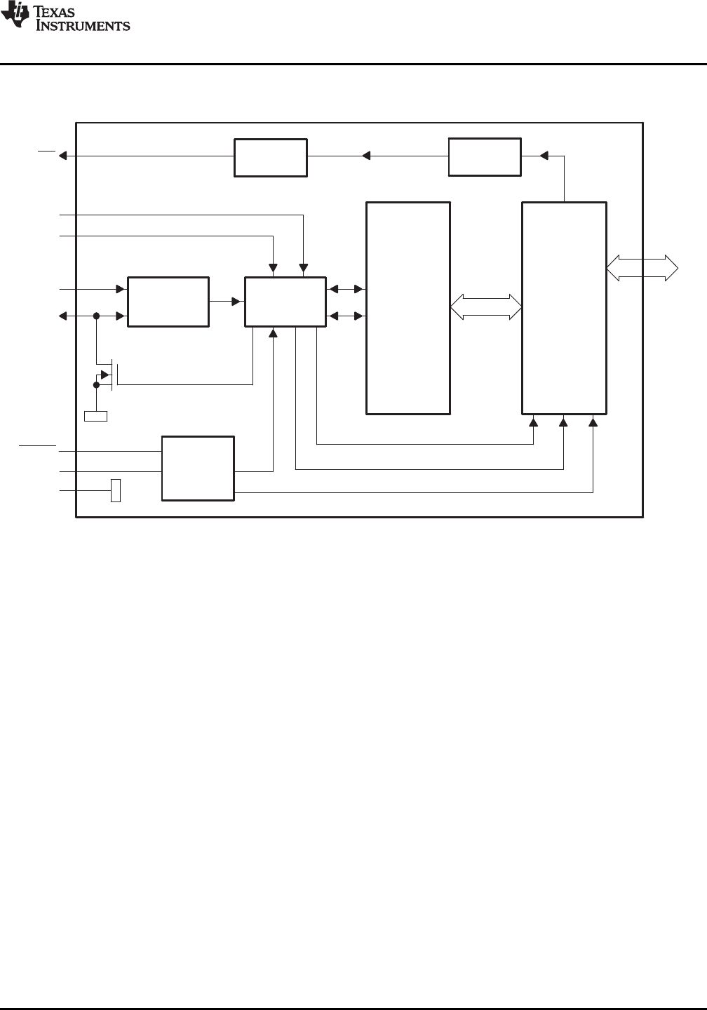
8 Detailed Description
8.1 Overview
The TCA9538 is an 8-bit I/O expander for the two-line bidirectional bus (I2C) is designed for 1.65-V to 5.5-V
VCC operation. It provides general-purpose remote I/O expansion for most micro-controller families via the
I2C interface (serial clock, SCL, and serial data, SDA, pins).
The TCA9538 open-drain interrupt (INT) output is activated when any input state differs from its
corresponding Input Port register state and is used to indicate to the system master that an input state has
changed. The INT pin can be connected to the interrupt input of a micro-controller. By sending an interrupt
signal on this line, the remote I/O can inform the micro-controller if there is incoming data on its ports without
having to communicate via the I2C bus. Thus, the TCA9538 can remain a simple slave device. The device
outputs (latched) have high-current drive capability for directly driving LEDs.
Two hardware pins (A0 and A1) are used to program and vary the fixed I2C slave address and allow up to
four devices to share the same I2C bus or SMBus.
The system master can reset the TCA9538 in the event of a timeout or other improper operation by asserting
a low on the RESET input pin or by cycling the power supply and causing a power-on reset (POR). A reset
puts the registers in their default state and initializes the I2C /SMBus state machine. The RESET feature and
a POR cause the same reset/initialization to occur, but the RESET feature does so without powering down
the part.
The TCA9538 consists of one 8-bit Configuration (input or output selection), Input Port, Output Port, and
Polarity Inversion (active high or active low) registers. At power on, the I/Os are configured as inputs.
However, the system master can enable the I/Os as either inputs or outputs by writing to the I/O
configuration bits. The data for each input or output is kept in the corresponding Input Port or Output Port
register. The polarity of the Input Port register can be inverted with the Polarity Inversion register. All
registers can be read by the system master.
The TCA9538 is identical to the TCA9554 except for the removal of the internal I/O pull-up resistors, which
greatly reduces power consumption when the I/Os are held LOW, the replacement of A2 with RESET, and
different slave address range.
14
I/O
Port
Shift
Register 8 Bits
LP Filter Interrupt
Logic
Input
Filter
15
Power-On
Reset
Read Pulse
Write Pulse
2
1
13
16
8
GND
VCC
SDA
SCL
A1
A0
INT
I2C Bus
Control
P7−P0
RESET 3
15
TCA9538
www.ti.com
SCPS199D –AUGUST 2014–REVISED OCTOBER 2016
Product Folder Links: TCA9538
Submit Documentation FeedbackCopyright © 2014–2016, Texas Instruments Incorporated
8.2 Functional Block Diagram
Pin numbers shown are for the PW package.
Figure 13. Functional Block Diagram
Data From
Shift Register
Data From
Shift Register
Write Configuration
Pulse
Write Pulse
Read Pulse
Write Polarity
Pulse
Data From
Shift Register
Output Port
Register
Configuration
Register
Input Port
Register
Polarity
Inversion
Register
Polarity
Register Data
Input Port
Register Data
GND
ESD Protection
Diode
P0 to P7
VCC
Output Port
Register Data
Q1
Q2
D
CK
FF
Q
Q
D
CK
FF
Q
Q
D
CK
FF
Q
Q
D
CK
FF
Q
Q
To INT
16
TCA9538
SCPS199D –AUGUST 2014–REVISED OCTOBER 2016
www.ti.com
Product Folder Links: TCA9538
Submit Documentation Feedback Copyright © 2014–2016, Texas Instruments Incorporated
Functional Block Diagram (continued)
At power-on reset, all registers return to default values.
Figure 14. Simplified Schematic of P0 to P7
8.3 Feature Description
8.3.1 I/O Port
When an I/O is configured as an input, FETs Q1 and Q2 are off, creating a high-impedance input. The input
voltage may be raised above VCC to a maximum of 5.5 V.
If the I/O is configured as an output, Q1 or Q2 is enabled depending on the state of the output port register. In
this case, there are low impedance paths between the I/O pin and either VCC or GND. The external voltage
applied to this I/O pin must not exceed the recommended levels for proper operation.
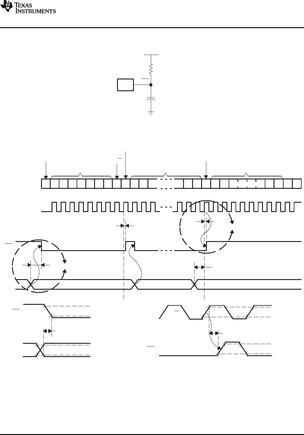
8.3.2 Interrupt Output (INT)
An interrupt is generated by any rising or falling edge of any P-port I/O configured as an input. After time tiv, the
signal INT is valid. Resetting the interrupt circuit is achieved when data on the ports is changed back to the
original state or when data is read from the Input Port register. Resetting occurs in the read mode at the
acknowledge (ACK) bit after the rising edge of the SCL signal. Interrupts that occur during the ACK clock pulse
can be lost (or be very short) due to the resetting of the interrupt during this pulse. Each change of the I/Os after
resetting is detected and is transmitted as an interrupt on the INT pin.
Reading from or writing to another device does not affect the interrupt circuit, and a pin configured as an output
cannot cause an interrupt. Changing an I/O from an output to an input may cause a false interrupt to occur if the
state of the pin does not match the contents of the Input Port register.
The INT output has an open-drain structure and requires pull-up resistor to VCC.
SDA
SCL
Start Condition
S
Stop Condition
P
17
TCA9538
www.ti.com
SCPS199D –AUGUST 2014–REVISED OCTOBER 2016
Product Folder Links: TCA9538
Submit Documentation FeedbackCopyright © 2014–2016, Texas Instruments Incorporated
Feature Description (continued)
8.3.3 RESET Input
The RESET input can be asserted to reset the system while keeping the VCC at its operating level. A reset can
be accomplished by holding the RESET pin low for a minimum of tW. The TCA9538 registers and I2C/SMBus
state machine are changed to their default states once RESET is low (0). Once RESET is high (1), the I/O levels
at the P port can be changed externally or through the master. This input requires a pull-up resistor to VCC if no
active connection is used.
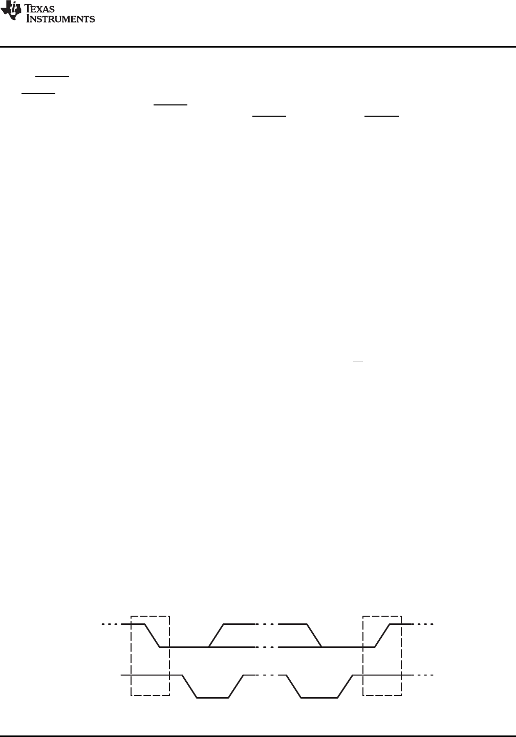
8.4 Device Functional Modes
8.4.1 Power-On Reset
When power (from 0 V) is applied to VCC, an internal power-on reset holds the TCA9538 in a reset condition
until VCC has reached VPORR. At that point, the reset condition is released and the TCA9538 registers and
SMBus/I2C state machine initialize to their default states. After that, VCC must be lowered to below VPORF and
then back up to the operating voltage for a power-on reset cycle.
8.5 Programming
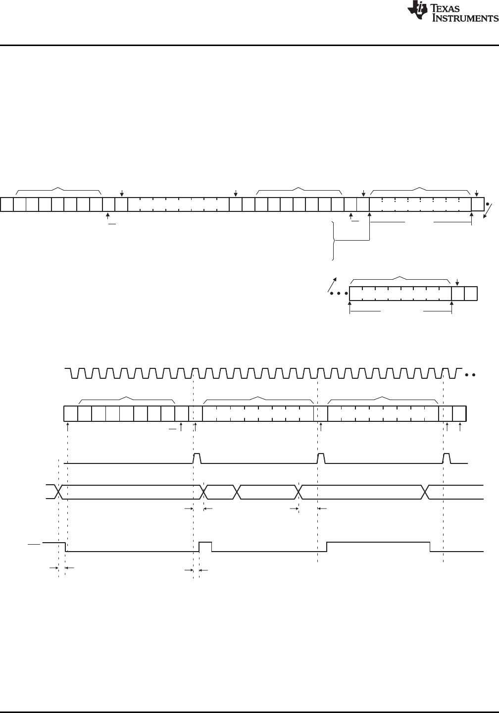
8.5.1 I2C Interface
The bidirectional I2C bus consists of the serial clock (SCL) and serial data (SDA) lines. Both lines must be
connected to a positive supply through a pull-up resistor when connected to the output stages of a device. Data
transfer may be initiated only when the bus is not busy.
I2C communication with this device is initiated by a master sending a Start condition, a high-to-low transition on
the SDA input/output while the SCL input is high (see Figure 15). After the Start condition, the device address
byte is sent, most significant bit (MSB) first, including the data direction bit (R/W).
After receiving the valid address byte, this device responds with an acknowledge (ACK), a low on the SDA
input/output during the high of the ACK-related clock pulse. The address inputs (A0–A1) of the slave device must
not be changed between the Start and the Stop conditions.
On the I2C bus, only one data bit is transferred during each clock pulse. The data on the SDA line must remain
stable during the high pulse of the clock period, as changes in the data line at this time are interpreted as control
commands (Start or Stop) (see Figure 16).
A Stop condition, a low-to-high transition on the SDA input/output while the SCL input is high, is sent by the
master (see Figure 15).
Any number of data bytes can be transferred from the transmitter to receiver between the Start and the Stop
conditions. Each byte of eight bits is followed by one ACK bit. The transmitter must release the SDA line before
the receiver can send an ACK bit. The device that acknowledges must pull down the SDA line during the ACK
clock pulse so that the SDA line is stable low during the high pulse of the ACK-related clock period (see
Figure 17). When a slave receiver is addressed, it must generate an ACK after each byte is received. Similarly,
the master must generate an ACK after each byte that it receives from the slave transmitter. Setup and hold
times must be met to ensure proper operation.
A master receiver signals an end of data to the slave transmitter by not generating an acknowledge (NACK) after
the last byte has been clocked out of the slave. This is done by the master receiver by holding the SDA line high.
In this event, the transmitter must release the data line to enable the master to generate a Stop condition.
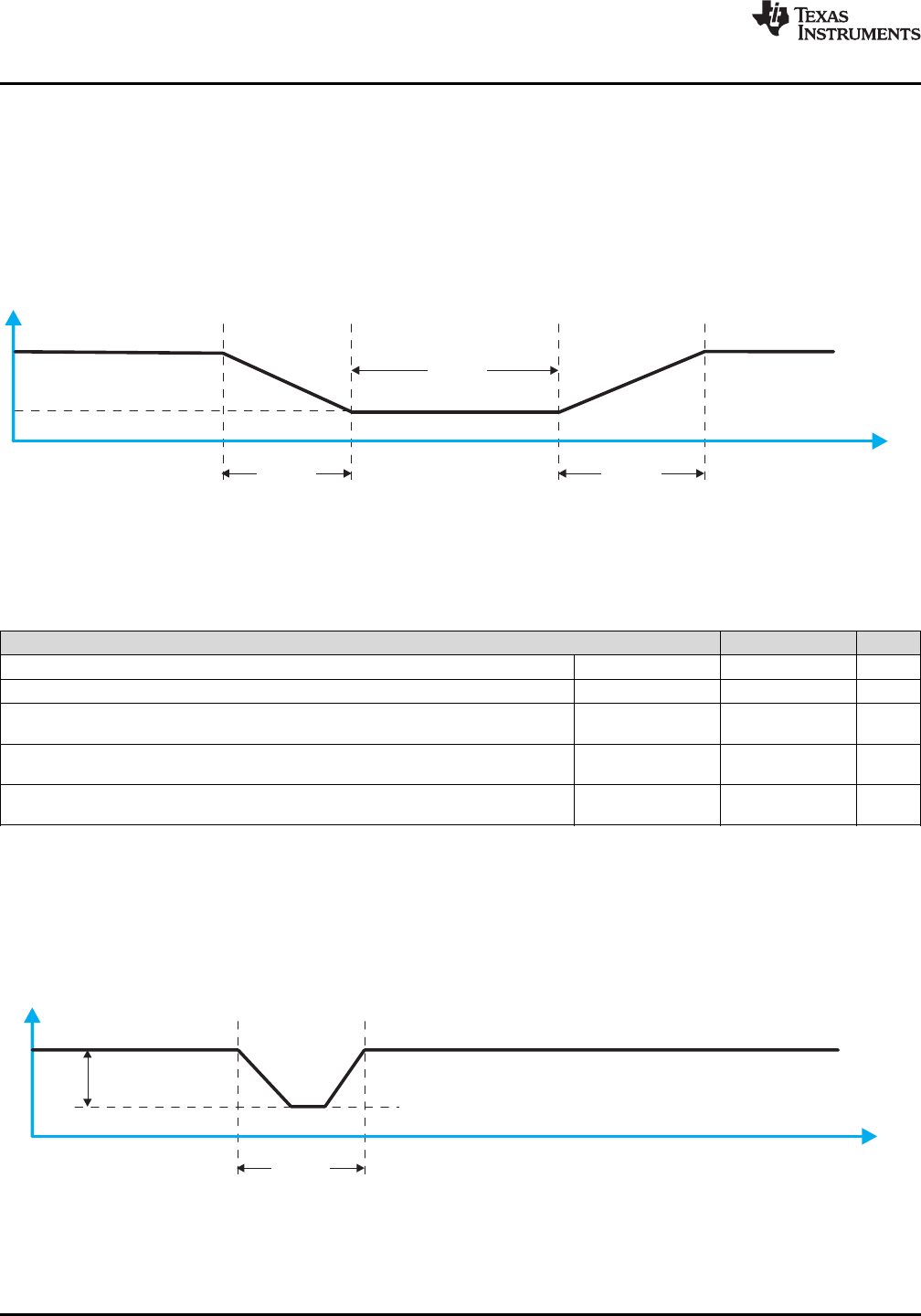
Figure 15. Definition of Start and Stop Conditions
Data Output
by Transmitter
SCL From
Master
Start
Condition
S
1 2 8 9
Data Output
by Receiver
Clock Pulse for
Acknowledgment
NACK
ACK
SDA
SCL
Data Line
Stable;
Data Valid
Change
of Data
Allowed
18
TCA9538
SCPS199D –AUGUST 2014–REVISED OCTOBER 2016
www.ti.com
Product Folder Links: TCA9538
Submit Documentation Feedback Copyright © 2014–2016, Texas Instruments Incorporated
Programming (continued)
Figure 16. Bit Transfer
Figure 17. Acknowledgment on I2C Bus
Table 1 shows the TCA9538 interface definition.
Table 1. Interface Definition Table
BYTE BIT
7 (MSB) 6 5 4 3 2 1 0 (LSB)
I2C slave address H H H L L A1 A0 R/W
Px I/O data bus P7 P6 P5 P4 P3 P2 P1 P0
0 0 0 B2 B1 B000
1 1 1 0 A1 A0
Slave Address R/W
Fixed Programmable
0
19
TCA9538
www.ti.com
SCPS199D –AUGUST 2014–REVISED OCTOBER 2016
Product Folder Links: TCA9538
Submit Documentation FeedbackCopyright © 2014–2016, Texas Instruments Incorporated
8.6 Register Map
8.6.1 Device Address
Figure 18 shows the address byte of the TCA9538.
Figure 18. TCA9538 Address
Table 2 shows the Address Reference of the TCA9538.
Table 2. Address Reference Table
INPUTS I2C BUS SLAVE ADDRESS
A1 A0
L L 112 (decimal), 70 (hexadecimal)
L H 113 (decimal), 71 (hexadecimal)
H L 114 (decimal), 72 (hexadecimal)
H H 115 (decimal), 73 (hexadecimal)
The last bit of the slave address defines the operation (read or write) to be performed. When it is high (1), a read
is selected while a low (0) selects a write operation.
8.6.2 Control Register and Command Byte
Following the successful Acknowledgment of the address byte, the bus master sends a command byte that is
stored in the control register in the TCA9538 (see Figure 19). Two bits of this command byte state the operation
(read or write) and the internal register (input, output, polarity inversion or configuration) that is affected. This
register can be written or read through the I2C bus. The command byte is sent only during a write transmission.
Once a command byte has been sent, the register that was addressed continues to be accessed by reads until a
new command byte has been sent.
Figure 19. Control Register Bits
Table 3 shows the TCA9538 Command byte.
Table 3. Command Byte Table
CONTROL REGISTER BITS COMMAND BYTE
(HEX) REGISTER PROTOCOL POWER-UP DEFAULT
B1 B0
0 0 0x00 Input Port Read byte XXXX XXXX
0 1 0x01 Output Port Read/write byte 1111 1111
1 0 0x02 Polarity Inversion Read/write byte 0000 0000
1 1 0x03 Configuration Read/write byte 1111 1111
20
TCA9538
SCPS199D –AUGUST 2014–REVISED OCTOBER 2016
www.ti.com
Product Folder Links: TCA9538
Submit Documentation Feedback Copyright © 2014–2016, Texas Instruments Incorporated
8.6.3 Register Descriptions
The Input Port register (register 0) reflects the incoming logic levels of the pins, regardless of whether the pin is
defined as an input or an output by the Configuration register. It only acts on read operation. Writes to these
registers have no effect. The default value, X, is determined by the externally applied logic level.
Before a read operation, a write transmission is sent with the command byte to indicate to the I2C device that the
Input Port register is accessed next. See Table 4.
Table 4. Register 0 (Input Port Register) Table
BIT I7 I6 I5 I4 I3 I2 I1 I0
DEFAULT XXXXXXXX
The Output Port register (register 1) shows the outgoing logic levels of the pins defined as outputs by the
Configuration register. Bit values in this register have no effect on pins defined as inputs. In turn, reads from this
register reflect the value that is in the flip-flop controlling the output selection, not the actual pin value. See
Table 5.
Table 5. Register 1 (Output Port Register) Table
BIT O7 O6 O5 O4 O3 O2 O1 O0
DEFAULT 11111111
The Polarity Inversion register (register 2) allows polarity inversion of pins defined as inputs by the Configuration
register. If a bit in this register is set (written with 1), the corresponding port pin polarity is inverted. If a bit in this
register is cleared (written with a 0), the corresponding port pin original polarity is retained. See Table 6.
Table 6. Register 2 (Polarity Inversion Register) Table
BIT N7 N6 N5 N4 N3 N2 N1 N0
DEFAULT 00000000
The Configuration register (register 3) configures the directions of the I/O pins. If a bit in this register is set to 1,
the corresponding port pin is enabled as an input with a high-impedance output driver. If a bit in this register is
cleared to 0, the corresponding port pin is enabled as an output. See Table 7.
Table 7. Register 3 (Configuration Register) Table
BIT C7 C6 C5 C4 C3 C2 C1 C0
DEFAULT 11111111
SCL
SDA
Data to
Register
Start Condition R/W ACK From Slave ACK From Slave ACK From Slave
1 98765432
Data1/001 1S 01 A1 A0 0 A 1000000 A A P
Data to RegisterCommand ByteSlave Address
SCL
Start Condition
Data 1 Valid
SDA
Write to Port
Data Out
From Port
R/W ACK From Slave ACK From Slave ACK From Slave
1 98765432
Data 1
101 1S 01 A1 A0 0 A 0000000 A A P
tpv
Data to PortCommand ByteSlave Address
21
TCA9538
www.ti.com
SCPS199D –AUGUST 2014–REVISED OCTOBER 2016
Product Folder Links: TCA9538
Submit Documentation FeedbackCopyright © 2014–2016, Texas Instruments Incorporated
8.6.3.1 Bus Transactions
Data is exchanged between the master and the TCA9538 through write and read commands.
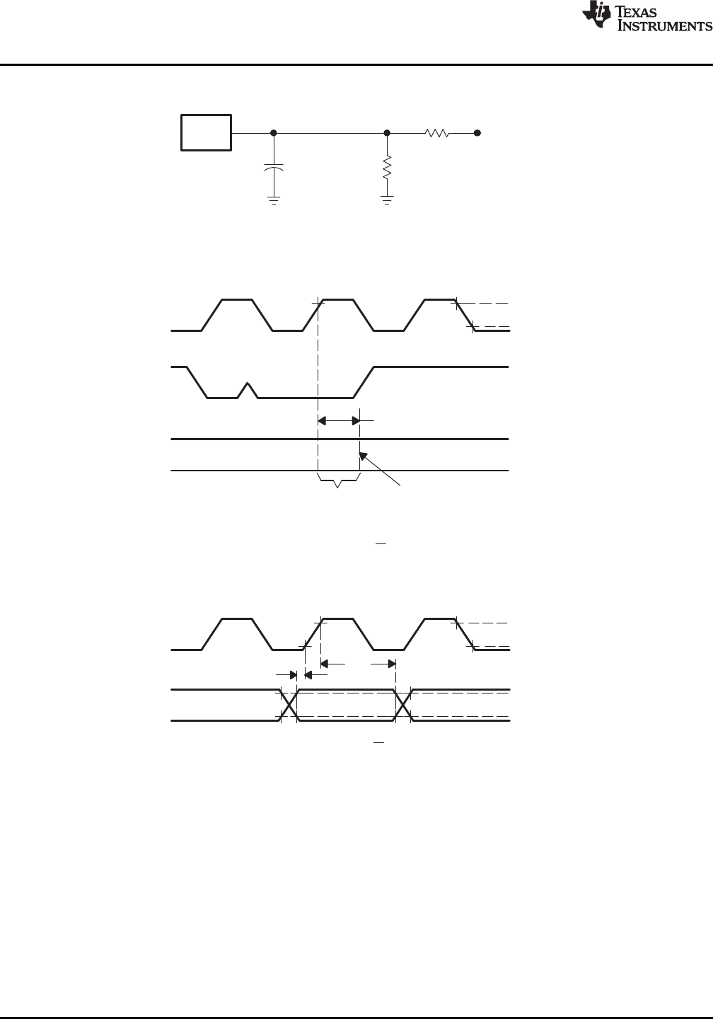
8.6.3.1.1 Writes
Data is transmitted to the TCA9538 by sending the device address and setting the least-significant bit (LSB) to a
logic 0 (see Figure 18 for device address). The command byte is sent after the address and determines which
register receives the data that follows the command byte (see Figure 20 and Figure 21). There is no limitation on
the number of data bytes sent in one write transmission.
Figure 20. Write to Output Port Register
<br/>
Figure 21. Write to Configuration or Polarity Inversion Registers
SCL
SDA
INT
Start
Condition
R/W
Read From
Port
Data Into
Port
Stop
Condition
ACK From
Master
NACK From
Master
ACK From
Slave
Data From Port
Slave Address Data From Port
1 98765432
01 1S 01 A1 A0 1AData 1 Data 4
A NA P
Data 2 Data 3 Data 4
tiv
tph tps
tir
Data 5
01 1S 01 A1 A0 0 A A
Data from Register
Slave Address
Slave Address
R/W
ACK From
Slave
Command Byte
ACK From
Slave
S 01 1 01 A1 A0
R/W
1 A Data A
ACK From
Master
Data
Data from Register
NACK From
Master
NA P
Last Byte
ACK From
Slave
22
TCA9538
SCPS199D –AUGUST 2014–REVISED OCTOBER 2016
www.ti.com
Product Folder Links: TCA9538
Submit Documentation Feedback Copyright © 2014–2016, Texas Instruments Incorporated
8.6.3.1.2 Reads
The bus master first must send the TCA9538 address with the LSB set to a logic 0 (see Figure 18 for device
address). The command byte is sent after the address and determines which register is accessed. After a restart,
the device address is sent again but, this time, the LSB is set to a logic 1. Data from the register defined by the
command byte then is sent by the TCA9538 (see Figure 22 and Figure 23). After a restart, the value of the
register defined by the command byte matches the register being accessed when the restart occurred. Data is
clocked into the register on the rising edge of the ACK clock pulse. There is no limitation on the number of data
bytes received in one read transmission, but when the final byte is received, the bus master must not
acknowledge the data.
Figure 22. Read From Register
<br/>
A. This figure assumes the command byte has previously been programmed with 00h.
B. Transfer of data can be stopped at any moment by a Stop condition.
C. This figure eliminates the command byte transfer, a restart, and slave address call between the initial slave address
call and actual data transfer from the P port. See Figure 22 for these details.
Figure 23. Read From Input Port Register
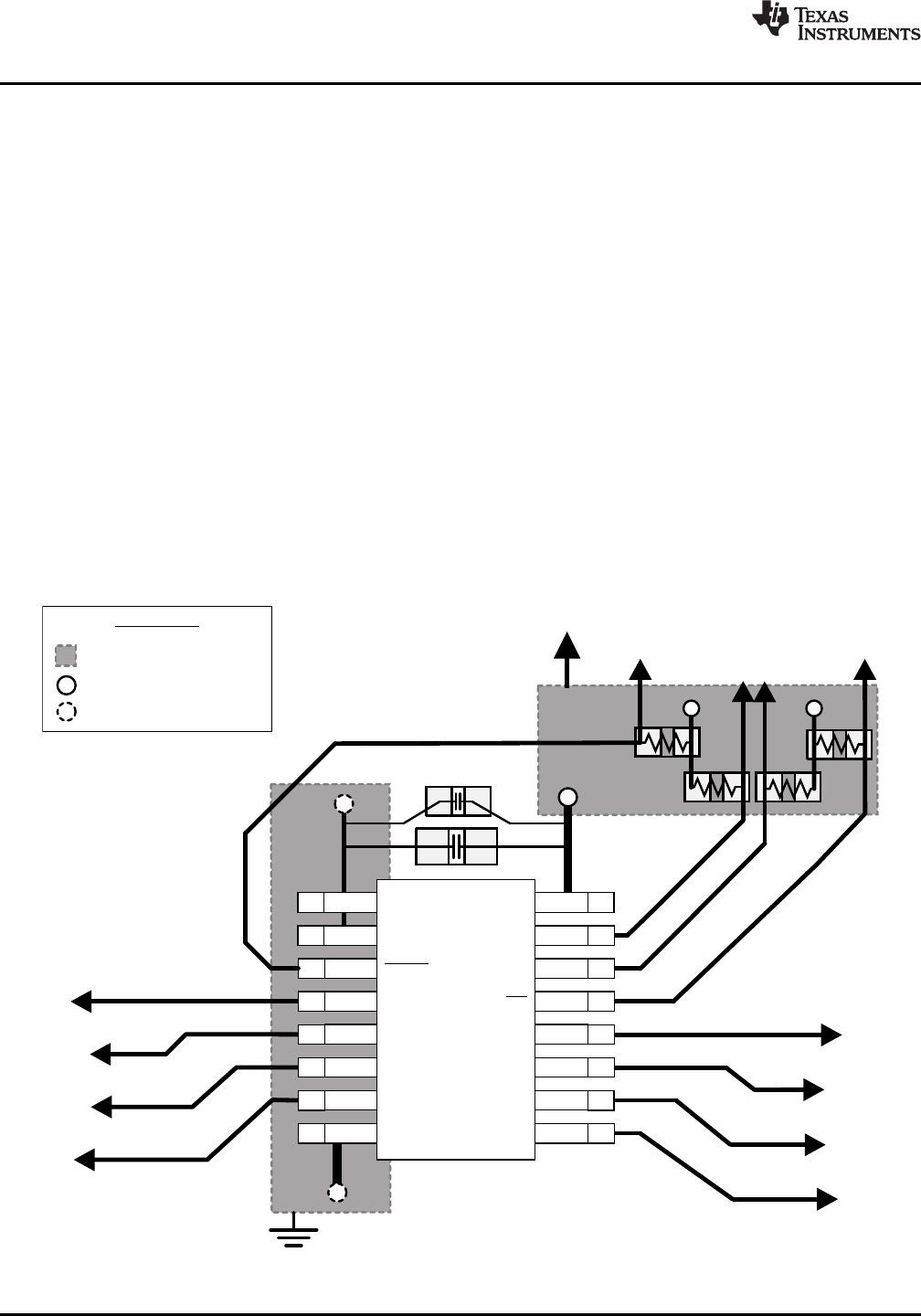
A1
A0
SDA
SCL
INT
GND
P6
P0
P1
P2
P3
P4
P5
P7
INT
GND
VCC
VCC
VCC 10 k (1)
Ω10 k (1)
Ω10 kΩ10 kΩ2 kΩ100 kΩ
(x3)
Master
Controller
TCA9538
INT
RESET
Subsystem 2
(e.g., counter)
Subsystem 3
(e.g., alarm system)
ALARM
Controlled Device
(e.g., CBT device)
ENABLE
A
B
VCC
RESET RESET
Subsystem 1
(e.g., temperature sensor)
SDA
SCL
15
14
16
13
3
2
1
8
12
11
10
9
7
6
5
4
23
TCA9538
www.ti.com
SCPS199D –AUGUST 2014–REVISED OCTOBER 2016
Product Folder Links: TCA9538
Submit Documentation FeedbackCopyright © 2014–2016, Texas Instruments Incorporated
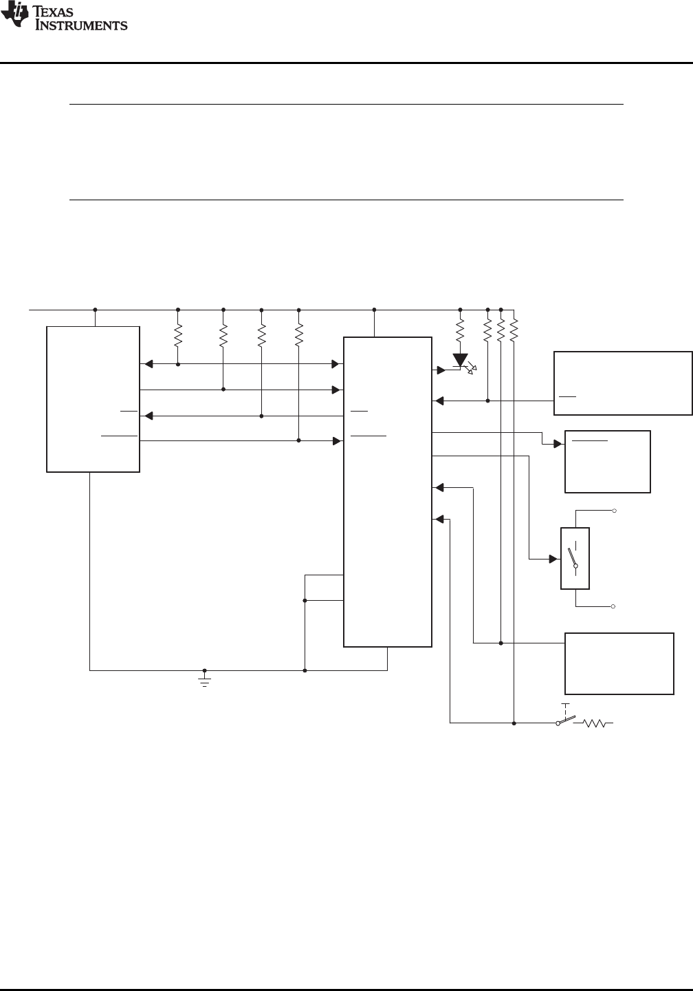
9 Application and Implementation
NOTE
Information in the following applications sections is not part of the TI component
specification, and TI does not warrant its accuracy or completeness. TI’s customers are
responsible for determining suitability of components for their purposes. Customers should
validate and test their design implementation to confirm system functionality.
9.1 Application Information
Figure 24 shows an application in which the TCA9538 can be used.
9.2 Typical Application
(1) The SCL and SDA pins must be tied directly to VCC because if SCL and SDA are tied to an auxiliary power supply
that could be powered on while VCC is powered off, then the supply current, ICC, increases as a result.
A. Device address is configured as 1110000 for this example.
B. P0, P2, and P3 are configured as outputs.
C. P1, P4, and P5 are configured as inputs.
D. P6 and P7 are not used and must be configured as outputs.
Figure 24. Application Schematic
r
p(max)
b
t
R0.8473 C
=
´
CC OL(max)
p(min)
OL
V V
RI
-
=
LED
3.3 V 5 V
LEDx
VCC
LED
LEDx
VCC
100 k
VCC
24
TCA9538
SCPS199D –AUGUST 2014–REVISED OCTOBER 2016
www.ti.com
Product Folder Links: TCA9538
Submit Documentation Feedback Copyright © 2014–2016, Texas Instruments Incorporated
Typical Application (continued)
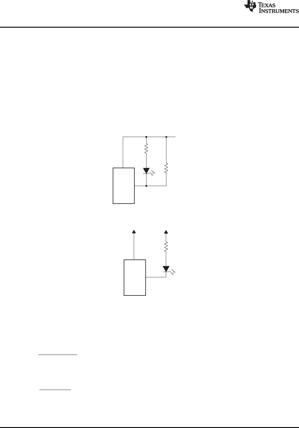
9.2.1 Design Requirements
9.2.1.1 Minimizing ICC When I/Os Control LEDs
When the I/Os are used to control LEDs, normally they are connected to VCC through a resistor as shown in
Figure 24. For a P-port configured as an input, ICC increases as VIbecomes lower than VCC. The LED is a diode,
with threshold voltage VT, and when a P-port is configured as an input the LED is off but VIis a VTdrop below
VCC.
For battery-powered applications, it is essential that the voltage of P-ports controlling LEDs is greater than or
equal to VCC when the P-ports are configured as input to minimize current consumption. Figure 25 shows a high-
value resistor in parallel with the LED. Figure 26 shows VCC less than the LED supply voltage by at least VT.
Both of these methods maintain the I/O VIat or above VCC and prevents additional supply current consumption
when the P-port is configured as an input and the LED is off.
Figure 25. High-Value Resistor in Parallel with LED
Figure 26. Device Supplied by a Lower Voltage
9.2.2 Detailed Design Procedure
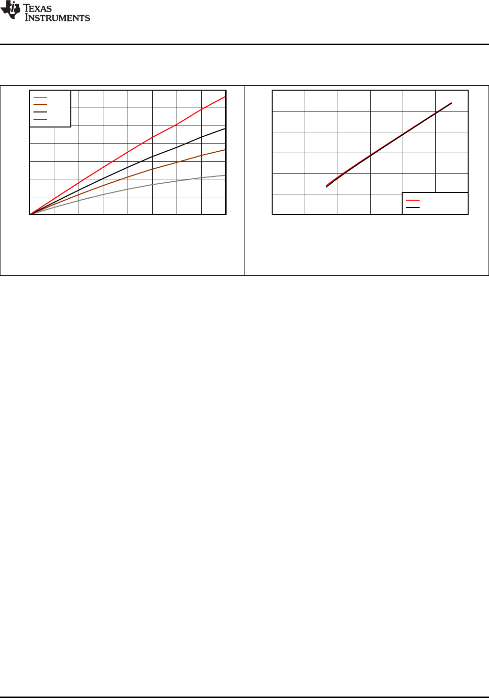
The pull-up resistors, RP, for the SCL and SDA lines need to be selected appropriately and take into
consideration the total capacitance of all slaves on the I2C bus. The minimum pull-up resistance is a function of
VCC, VOL,(max), and IOL as shown in Equation 1:
(1)
The maximum pull-up resistance is a function of the maximum rise time, tr(300 ns for fast-mode operation, fSCL =
400 kHz) and bus capacitance, Cbas shown in Equation 2:
(2)
The maximum bus capacitance for an I2C bus must not exceed 400 pF for standard-mode or fast-mode
operation. The bus capacitance can be approximated by adding the capacitance of the TCA9538, Cifor SCL or
Cio for SDA, the capacitance of wires/connections/traces, and the capacitance of additional slaves on the bus.
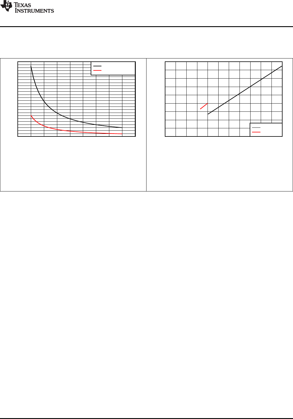
Cb (pF)
Rp(max) (kOhm)
0 50 100 150 200 250 300 350 400 450
0
5
10
15
20
25
D008
Standard-mode
Fast-mode
VCC (V)
Rp(min) (kOhm)
0 0.5 1 1.5 2 2.5 3 3.5 4 4.5 5 5.5
0
0.2
0.4
0.6
0.8
1
1.2
1.4
1.6
1.8
D009
VCC > 2V
VCC <= 2
25
TCA9538
www.ti.com
SCPS199D –AUGUST 2014–REVISED OCTOBER 2016
Product Folder Links: TCA9538
Submit Documentation FeedbackCopyright © 2014–2016, Texas Instruments Incorporated
Typical Application (continued)
9.2.3 Application Curves
Standard-mode
(fSCL = 100 kHz, tr= 1 µs) Fast-mode
(fSCL = 400 kHz, tr= 300 ns)
Figure 27. Maximum Pull-Up Resistance (Rp(max)) vs Bus
Capacitance (Cb)
VOL = 0.2*VCC, IOL = 2 mA
when VCC ≤2 V
VOL = 0.4 V, IOL = 3 mA
when VCC > 2 V
Figure 28. Minimum Pull-Up Resistance (Rp(min)) vs Pull-Up
Reference Voltage (VCC)
VCC
Time
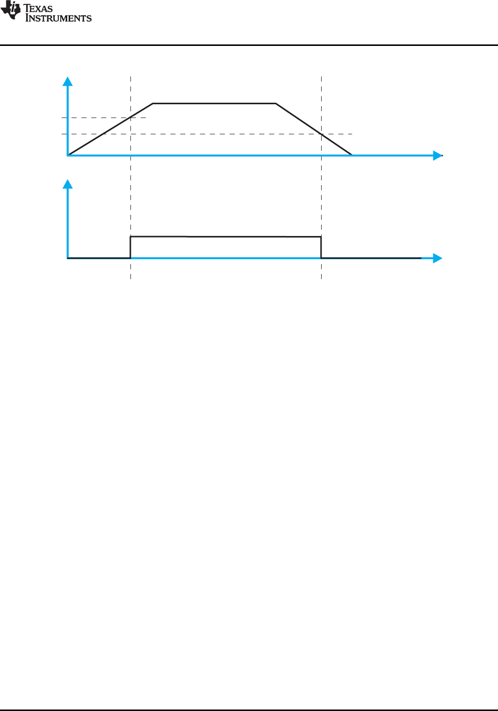
VCC_GH
VCC_GW
VCC
Ramp-Up
Time to Re-Ramp
Time
Ramp-Down
VCC drops below V 50 mV
PORF –
VCC_RT
VCC_FT
VCC_TRR
26
TCA9538
SCPS199D –AUGUST 2014–REVISED OCTOBER 2016
www.ti.com
Product Folder Links: TCA9538
Submit Documentation Feedback Copyright © 2014–2016, Texas Instruments Incorporated
(1) All supply sequencing and ramp rate values are measured at TA= 25°C
10 Power Supply Recommendations
10.1 Power-On Reset Requirements
In the event of a glitch or data corruption, the TCA9538 can be reset to its default conditions by using the power-
on reset feature. Power-on reset requires that the device go through a power cycle to be completely reset. This
reset also happens when the device is powered on for the first time in an application.
The two types of power-on reset are shown in and Figure 29.
Figure 29. VCC is Lowered Below the POR Threshold, Then Ramped Back Up to VCC
Table 8 specifies the performance of the power-on reset feature for the TCA9538 for both types of power-on
reset.
Table 8. Recommended Supply Sequencing And Ramp Rates(1)
PARAMETER MIN MAX UNIT
VCC_FT Fall rate See Figure 29 1 ms
VCC_RT Rise rate See Figure 29 0.1 ms
VCC_TRR Time to re-ramp (when VCC drops to VPOR_MIN – 50 mV or when
VCC drops to GND) See Figure 29 2μs
VCC_GH Level that VCC can glitch down to, but not cause a functional
disruption when VCC_GW = 1 µs See Figure 30 1.2 V
VCC_GW Glitch width that does not cause a functional disruption when
VCC_GH = 0.5 × VCC (For VCC > 3 V) See Figure 30 10 μs
Glitches in the power supply can also affect the power-on reset performance of this device. The glitch width
(VCC_GW) and height (VCC_GH) are dependent on each other. The bypass capacitance, source impedance, and
device impedance are factors that affect power-on reset performance. Figure 30 and Table 8 provide more
information on how to measure these specifications.
Figure 30. Glitch Width and Glitch Height
VPOR is critical to the power-on reset. VPOR is the voltage level at which the reset condition is released and all the
registers and the I2C/SMBus state machine are initialized to their default states. The value of VPOR differs based
on the VCC being lowered to or from 0. Figure 31 and Table 8 provide more details on this specification.
GND
By-pass/De-coupling
capacitors
TCA9538
1A0
2 A1
3
4P0
5P1
6P2
7P3
8GND 9
P4
10
P5
11
P6
12
P7
13
14
SCL
15
SDA
16
VCC
RESET
INT
VIA to Power Plane
Power or GND Plane
VIA to GND Plane
LEGEND
To I/Os
VCC
To I2C Master
To I/Os
28
TCA9538
SCPS199D –AUGUST 2014–REVISED OCTOBER 2016
www.ti.com
Product Folder Links: TCA9538
Submit Documentation Feedback Copyright © 2014–2016, Texas Instruments Incorporated
11 Layout
11.1 Layout Guidelines
For printed circuit board (PCB) layout of the TCA9538, common PCB layout practices must be followed but
additional concerns related to high-speed data transfer such as matched impedances and differential pairs are
not a concern for I2C signal speeds.
In all PCB layouts, it is a best practice to avoid right angles in signal traces, to fan out signal traces away from
each other upon leaving the vicinity of an integrated circuit (IC), and to use thicker trace widths to carry higher
amounts of current that commonly pass through power and ground traces. By-pass and de-coupling capacitors
are commonly used to control the voltage on the VCC pin, using a larger capacitor to provide additional power in
the event of a short power supply glitch and a smaller capacitor to filter out high-frequency ripple. These
capacitors must be placed as close to the TCA9538 as possible. These best practices are shown in Figure 32.
For the layout example provided in Figure 32, it would be possible to fabricate a PCB with only 2 layers by using
the top layer for signal routing and the bottom layer as a split plane for power (VCC) and ground (GND). However,
a 4 layer board is preferable for boards with higher density signal routing. On a 4 layer PCB, it is common to
route signals on the top and bottom layer, dedicate one internal layer to a ground plane, and dedicate the other
internal layer to a power plane. In a board layout using planes or split planes for power and ground, vias are
placed directly next to the surface mount component pad which needs to attach to VCC or GND and the via is
connected electrically to the internal layer or the other side of the board. Vias are also used when a signal trace
needs to be routed to the opposite side of the board, but this technique is not demonstrated in Figure 32.
11.2 Layout Example
Figure 32. TCA9538 Layout

29
TCA9538
www.ti.com
SCPS199D –AUGUST 2014–REVISED OCTOBER 2016
Product Folder Links: TCA9538
Submit Documentation FeedbackCopyright © 2014–2016, Texas Instruments Incorporated
12 Device and Documentation Support
12.1 Documentation Support
12.1.1 Related Documentation
For related documentation see the following:
•I2C Bus Pull-Up Resistor Calculation
•Maximum Clock Frequency of I2C Bus Using Repeaters
•Introduction to Logic
•Understanding the I2C Bus
•Choosing the Correct I2C Device for New Designs
•I/O Expander EVM User's Guide
12.2 Receiving Notification of Documentation Updates
To receive notification of documentation updates, navigate to the device product folder on ti.com. In the upper
right corner, click on Alert me to register and receive a weekly digest of any product information that has
changed. For change details, review the revision history included in any revised document.
12.3 Community Resources
The following links connect to TI community resources. Linked contents are provided "AS IS" by the respective
contributors. They do not constitute TI specifications and do not necessarily reflect TI's views; see TI's Terms of
Use.
TI E2E™ Online Community TI's Engineer-to-Engineer (E2E) Community. Created to foster collaboration
among engineers. At e2e.ti.com, you can ask questions, share knowledge, explore ideas and help
solve problems with fellow engineers.
Design Support TI's Design Support Quickly find helpful E2E forums along with design support tools and
contact information for technical support.
12.4 Trademarks
E2E is a trademark of Texas Instruments.
All other trademarks are the property of their respective owners.
12.5 Electrostatic Discharge Caution
This integrated circuit can be damaged by ESD. Texas Instruments recommends that all integrated circuits be handled with
appropriate precautions. Failure to observe proper handling and installation procedures can cause damage.
ESD damage can range from subtle performance degradation to complete device failure. Precision integrated circuits may be more
susceptible to damage because very small parametric changes could cause the device not to meet its published specifications.
12.6 Glossary
SLYZ022 —TI Glossary.
This glossary lists and explains terms, acronyms, and definitions.
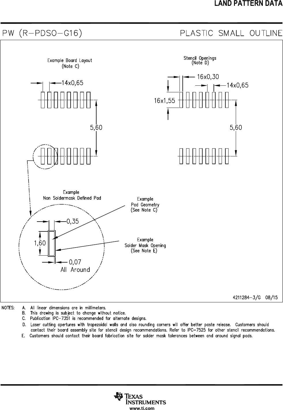
13 Mechanical, Packaging, and Orderable Information
The following pages include mechanical, packaging, and orderable information. This information is the most
current data available for the designated devices. This data is subject to change without notice and revision of
this document. For browser-based versions of this data sheet, refer to the left-hand navigation.
PACKAGE OPTION ADDENDUM
www.ti.com 10-Oct-2016
Addendum-Page 1
PACKAGING INFORMATION
Orderable Device Status
(1)
Package Type Package
Drawing Pins Package
Qty Eco Plan
(2)
Lead/Ball Finish
(6)
MSL Peak Temp
(3)
Op Temp (°C) Device Marking
(4/5)
Samples
TCA9538DBR ACTIVE SSOP DB 16 2000 Green (RoHS
& no Sb/Br)
CU NIPDAU Level-1-260C-UNLIM -40 to 85 TD538
TCA9538PWR ACTIVE TSSOP PW 16 2000 Green (RoHS
& no Sb/Br)
CU NIPDAU Level-1-260C-UNLIM -40 to 85 PW538
(1) The marketing status values are defined as follows:
ACTIVE: Product device recommended for new designs.
LIFEBUY: TI has announced that the device will be discontinued, and a lifetime-buy period is in effect.
NRND: Not recommended for new designs. Device is in production to support existing customers, but TI does not recommend using this part in a new design.
PREVIEW: Device has been announced but is not in production. Samples may or may not be available.
OBSOLETE: TI has discontinued the production of the device.
(2) Eco Plan - The planned eco-friendly classification: Pb-Free (RoHS), Pb-Free (RoHS Exempt), or Green (RoHS & no Sb/Br) - please check http://www.ti.com/productcontent for the latest availability
information and additional product content details.
TBD: The Pb-Free/Green conversion plan has not been defined.
Pb-Free (RoHS): TI's terms "Lead-Free" or "Pb-Free" mean semiconductor products that are compatible with the current RoHS requirements for all 6 substances, including the requirement that
lead not exceed 0.1% by weight in homogeneous materials. Where designed to be soldered at high temperatures, TI Pb-Free products are suitable for use in specified lead-free processes.
Pb-Free (RoHS Exempt): This component has a RoHS exemption for either 1) lead-based flip-chip solder bumps used between the die and package, or 2) lead-based die adhesive used between
the die and leadframe. The component is otherwise considered Pb-Free (RoHS compatible) as defined above.
Green (RoHS & no Sb/Br): TI defines "Green" to mean Pb-Free (RoHS compatible), and free of Bromine (Br) and Antimony (Sb) based flame retardants (Br or Sb do not exceed 0.1% by weight
in homogeneous material)
(3) MSL, Peak Temp. - The Moisture Sensitivity Level rating according to the JEDEC industry standard classifications, and peak solder temperature.
(4) There may be additional marking, which relates to the logo, the lot trace code information, or the environmental category on the device.
(5) Multiple Device Markings will be inside parentheses. Only one Device Marking contained in parentheses and separated by a "~" will appear on a device. If a line is indented then it is a continuation
of the previous line and the two combined represent the entire Device Marking for that device.
(6) Lead/Ball Finish - Orderable Devices may have multiple material finish options. Finish options are separated by a vertical ruled line. Lead/Ball Finish values may wrap to two lines if the finish
value exceeds the maximum column width.
Important Information and Disclaimer:The information provided on this page represents TI's knowledge and belief as of the date that it is provided. TI bases its knowledge and belief on information
provided by third parties, and makes no representation or warranty as to the accuracy of such information. Efforts are underway to better integrate information from third parties. TI has taken and
continues to take reasonable steps to provide representative and accurate information but may not have conducted destructive testing or chemical analysis on incoming materials and chemicals.
TI and TI suppliers consider certain information to be proprietary, and thus CAS numbers and other limited information may not be available for release.
PACKAGE OPTION ADDENDUM
www.ti.com 10-Oct-2016
Addendum-Page 2
In no event shall TI's liability arising out of such information exceed the total purchase price of the TI part(s) at issue in this document sold by TI to Customer on an annual basis.
TAPE AND REEL INFORMATION
*All dimensions are nominal
Device Package
Type Package
Drawing Pins SPQ Reel
Diameter
(mm)
Reel
Width
W1 (mm)
A0
(mm) B0
(mm) K0
(mm) P1
(mm) W
(mm) Pin1
Quadrant
TCA9538DBR SSOP DB 16 2000 330.0 16.4 8.2 6.6 2.5 12.0 16.0 Q1
TCA9538PWR TSSOP PW 16 2000 330.0 12.4 6.9 5.6 1.6 8.0 12.0 Q1
PACKAGE MATERIALS INFORMATION
www.ti.com 10-Oct-2016
Pack Materials-Page 1
*All dimensions are nominal
Device Package Type Package Drawing Pins SPQ Length (mm) Width (mm) Height (mm)
TCA9538DBR SSOP DB 16 2000 367.0 367.0 38.0
TCA9538PWR TSSOP PW 16 2000 367.0 367.0 35.0
PACKAGE MATERIALS INFORMATION
www.ti.com 10-Oct-2016
Pack Materials-Page 2
MECHANICAL DATA
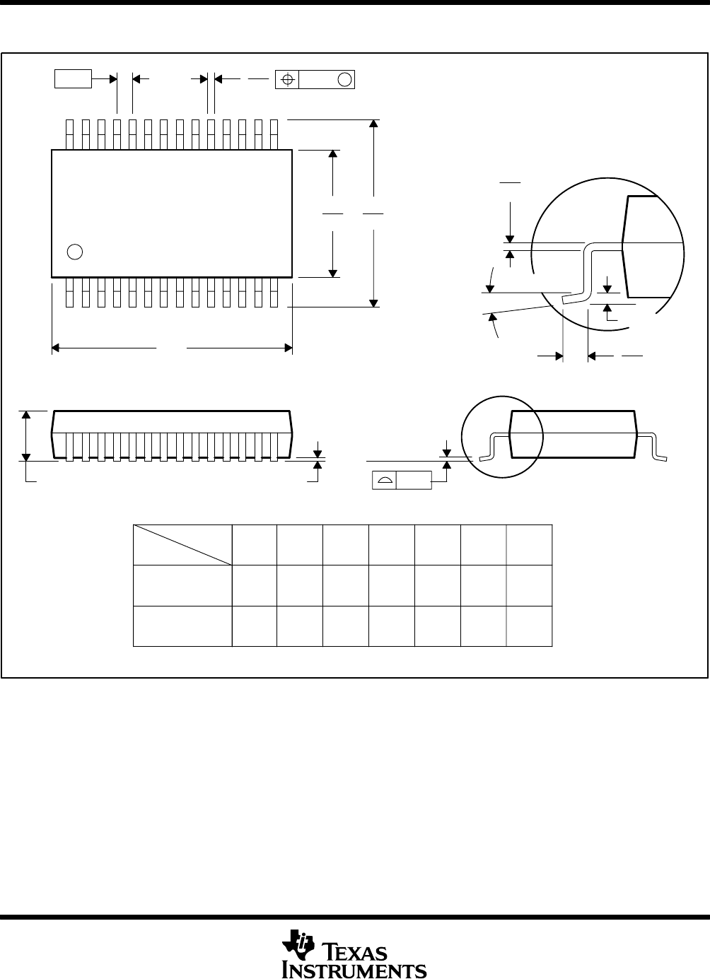
MSSO002E – JANUARY 1995 – REVISED DECEMBER 2001
POST OFFICE BOX 655303 • DALLAS, TEXAS 75265
DB (R-PDSO-G**) PLASTIC SMALL-OUTLINE
4040065 /E 12/01
28 PINS SHOWN
Gage Plane
8,20
7,40
0,55
0,95
0,25
38
12,90
12,30
28
10,50
24
8,50
Seating Plane
9,907,90
30
10,50
9,90
0,38
5,60
5,00
15
0,22
14
A
28
1
2016
6,50
6,50
14
0,05 MIN
5,905,90
DIM
A MAX
A MIN
PINS **
2,00 MAX
6,90
7,50
0,65 M
0,15
0°–ā8°
0,10
0,09
0,25
NOTES: A. All linear dimensions are in millimeters.
B. This drawing is subject to change without notice.
C. Body dimensions do not include mold flash or protrusion not to exceed 0,15.
D. Falls within JEDEC MO-150

IMPORTANT NOTICE
Texas Instruments Incorporated and its subsidiaries (TI) reserve the right to make corrections, enhancements, improvements and other
changes to its semiconductor products and services per JESD46, latest issue, and to discontinue any product or service per JESD48, latest
issue. Buyers should obtain the latest relevant information before placing orders and should verify that such information is current and
complete. All semiconductor products (also referred to herein as “components”) are sold subject to TI’s terms and conditions of sale
supplied at the time of order acknowledgment.
TI warrants performance of its components to the specifications applicable at the time of sale, in accordance with the warranty in TI’s terms
and conditions of sale of semiconductor products. Testing and other quality control techniques are used to the extent TI deems necessary
to support this warranty. Except where mandated by applicable law, testing of all parameters of each component is not necessarily
performed.
TI assumes no liability for applications assistance or the design of Buyers’ products. Buyers are responsible for their products and
applications using TI components. To minimize the risks associated with Buyers’ products and applications, Buyers should provide
adequate design and operating safeguards.
TI does not warrant or represent that any license, either express or implied, is granted under any patent right, copyright, mask work right, or
other intellectual property right relating to any combination, machine, or process in which TI components or services are used. Information
published by TI regarding third-party products or services does not constitute a license to use such products or services or a warranty or
endorsement thereof. Use of such information may require a license from a third party under the patents or other intellectual property of the
third party, or a license from TI under the patents or other intellectual property of TI.
Reproduction of significant portions of TI information in TI data books or data sheets is permissible only if reproduction is without alteration
and is accompanied by all associated warranties, conditions, limitations, and notices. TI is not responsible or liable for such altered
documentation. Information of third parties may be subject to additional restrictions.
Resale of TI components or services with statements different from or beyond the parameters stated by TI for that component or service
voids all express and any implied warranties for the associated TI component or service and is an unfair and deceptive business practice.
TI is not responsible or liable for any such statements.
Buyer acknowledges and agrees that it is solely responsible for compliance with all legal, regulatory and safety-related requirements
concerning its products, and any use of TI components in its applications, notwithstanding any applications-related information or support
that may be provided by TI. Buyer represents and agrees that it has all the necessary expertise to create and implement safeguards which
anticipate dangerous consequences of failures, monitor failures and their consequences, lessen the likelihood of failures that might cause
harm and take appropriate remedial actions. Buyer will fully indemnify TI and its representatives against any damages arising out of the use
of any TI components in safety-critical applications.
In some cases, TI components may be promoted specifically to facilitate safety-related applications. With such components, TI’s goal is to
help enable customers to design and create their own end-product solutions that meet applicable functional safety standards and
requirements. Nonetheless, such components are subject to these terms.
No TI components are authorized for use in FDA Class III (or similar life-critical medical equipment) unless authorized officers of the parties
have executed a special agreement specifically governing such use.
Only those TI components which TI has specifically designated as military grade or “enhanced plastic” are designed and intended for use in
military/aerospace applications or environments. Buyer acknowledges and agrees that any military or aerospace use of TI components
which have not been so designated is solely at the Buyer's risk, and that Buyer is solely responsible for compliance with all legal and
regulatory requirements in connection with such use.
TI has specifically designated certain components as meeting ISO/TS16949 requirements, mainly for automotive use. In any case of use of
non-designated products, TI will not be responsible for any failure to meet ISO/TS16949.
Products Applications
Audio www.ti.com/audio Automotive and Transportation www.ti.com/automotive
Amplifiers amplifier.ti.com Communications and Telecom www.ti.com/communications
Data Converters dataconverter.ti.com Computers and Peripherals www.ti.com/computers
DLP® Products www.dlp.com Consumer Electronics www.ti.com/consumer-apps
DSP dsp.ti.com Energy and Lighting www.ti.com/energy
Clocks and Timers www.ti.com/clocks Industrial www.ti.com/industrial
Interface interface.ti.com Medical www.ti.com/medical
Logic logic.ti.com Security www.ti.com/security
Power Mgmt power.ti.com Space, Avionics and Defense www.ti.com/space-avionics-defense
Microcontrollers microcontroller.ti.com Video and Imaging www.ti.com/video
RFID www.ti-rfid.com
OMAP Applications Processors www.ti.com/omap TI E2E Community e2e.ti.com
Wireless Connectivity www.ti.com/wirelessconnectivity
Mailing Address: Texas Instruments, Post Office Box 655303, Dallas, Texas 75265
Copyright © 2016, Texas Instruments Incorporated
