Application Note AN387 Arm Cortex M0 Designstart Eval Fpga User Guide
arm_cortex_m0_designstart_eval_fpga_user_guide
arm_cortex_m0_designstart_eval_fpga_user_guide
User Manual: Pdf
Open the PDF directly: View PDF ![]() .
.
Page Count: 29
- Preface
- 1. Introduction
- 2. FPGA platform overview
- 2.1 System overview
- 2.2 Memory map
- 2.3 Block RAM for booting up
- 2.4 External ZBT Synchronous SRAM (SSRAM1)
- 2.5 External ZBT Synchronous SRAM (SSRAM2 & SSRAM3)
- 2.6 External PSRAM
- 2.7 CMSDK APB subsystem
- 2.8 AHB GPIO
- 2.9 Serial Peripheral Interface (SPI)
- 2.10 Color LCD parallel interface
- 2.11 Shield I2C interfaces
- 2.12 Shield UARTS
- 2.13 Ethernet
- 2.14 VGA
- 2.15 Audio I2S
- 2.16 Audio Configuration
- 2.17 FPGA system control and I/O
- 3. Clocks
- 4. Interrupt assignments
- 5. Serial Communication Controller (SCC)
- 6. FPGA Build Guide
- 7. Utilization of default system
- Appendix A. Revisions

Copyright 2017 Arm. All rights reserved.
Non-Confidential
101125_0200_00_en
i
Arm® Cortex®-M0 DesignStart™ Eval
FPGA
Revision: r2p0
User Guide

Copyright 2017 Arm. All rights reserved.
Non-Confidential
101125_0200_00_en
ii
Arm® Cortex®-M0 DesignStart™ Eval FPGA User Guide
Copyright © 2017 Arm. All rights reserved.
Release Information
The following changes have been made to this book.
Change History
Date
Issue
Confidentiality
Change
25 September 2017
A
Non-Confidential
First release for r2p0
Non-Confidential Proprietary Notice
This document is protected by copyright and other related rights and the practice or implementation of the information
contained in this document may be protected by one or more patents or pending patent applications. No part of this
document may be reproduced in any form by any means without the express prior written permission of Arm. No license,
express or implied, by estoppel or otherwise to any intellectual property rights is granted by this document
unless specifically stated.
Your access to the information in this document is conditional upon your acceptance that you will not use or permit others to
use the information for the purposes of determining whether implementations infringe any third party patents.
THIS DOCUMENT IS PROVIDED “AS IS”. ARM PROVIDES NO REPRESENTATIONS AND NO WARRANTIES,
EXPRESS, IMPLIED OR STATUTORY, INCLUDING, WITHOUT LIMITATION, THE IMPLIED WARRANTIES OF
MERCHANTABILITY, SATISFACTORY QUALITY, NON-INFRINGEMENT OR FITNESS FOR A PARTICULAR
PURPOSE
WITH RESPECT TO THE DOCUMENT. For the avoidance of doubt, ARM makes no representation with respect to, and
has undertaken no analysis to identify or understand the scope and content of, third party patents, copyrights, trade
secrets, or other rights.
This document may include technical inaccuracies or typographical errors.
TO THE EXTENT NOT PROHIBITED BY LAW, IN NO EVENT WILL ARM BE LIABLE FOR ANY DAMAGES,
INCLUDING WITHOUT LIMITATION ANY DIRECT, INDIRECT, SPECIAL, INCIDENTAL, PUNITIVE, OR
CONSEQUENTIAL DAMAGES, HOWEVER CAUSED AND REGARDLESS OF THE THEORY OF LIABILITY, ARISING
OUT OF ANY USE OF THIS DOCUMENT, EVEN IF ARM HAS BEEN ADVISED OF THE POSSIBILITY OF SUCH
DAMAGES.
This document consists solely of commercial items. You shall be responsible for ensuring that any use, duplication or
disclosure of this document complies fully with any relevant export laws and regulations to assure that this document or any
portion thereof is not exported, directly or indirectly, in violation of such export laws. Use of the word “partner” in reference to
Arm’s customers is not intended to create or refer to any partnership relationship with any other company. Arm may make
changes to this document at any time and without notice.
If any of the provisions contained in these terms conflict with any of the provisions of any signed written agreement covering
this document with Arm, then the signed written agreement prevails over and supersedes the conflicting provisions of these
terms. This document may be translated into other languages for convenience, and you agree that if there is any conflict
between the English version of this document and any translation, the terms of the English version of the Agreement shall
prevail.
Words and logos marked with ® or ™ are registered trademarks or trademarks of Arm Limited or its affiliates in the EU
and/or elsewhere. All rights reserved. Other brands and names mentioned in this document may be the trademarks of
their respective owners. Please follow Arm’s trademark usage guidelines at http://www.arm.com/about/trademark-usage-
guidelines.php
Copyright © [2017], Arm Limited or its affiliates. All rights reserved.
Arm Limited. Company 02557590 registered in England.
110 Fulbourn Road, Cambridge, England CB1 9NJ.
LES-PRE-20349

Copyright 2017 Arm. All rights reserved.
Non-Confidential
101125_0200_00_en
iii
Confidentiality Status
This document is Non-Confidential. The right to use, copy and disclose this document may be subject to license
restrictions in accordance with the terms of the agreement entered into by Arm and the party that Arm delivered this
document to.
Product Status
The information in this document is Final, which is for a developed product.
Web Address
http://www.arm.com

Copyright 2017 Arm. All rights reserved.
Non-Confidential
101125_0200_00_en
iv
Contents
Arm® Cortex®-M0 DesignStart™ Eval FPGA User Guide
PREFACE.......................................................................................................................................... 1
1. INTRODUCTION ................................................................................................................... 1-1
1.1 CORTEX-M0 DESIGNSTART EVAL ............................................................................................. 1-1
1.2 DECRYPTION KEY ................................................................................................................... 1-2
1.3 PREREQUISITES ..................................................................................................................... 1-2
2. FPGA PLATFORM OVERVIEW ............................................................................................... 2-1
2.1 SYSTEM OVERVIEW ................................................................................................................ 2-2
2.2 MEMORY MAP ...................................................................................................................... 2-1
2.3 BLOCK RAM FOR BOOTING UP ................................................................................................. 2-2
2.4 EXTERNAL ZBT SYNCHRONOUS SRAM (SSRAM1) ..................................................................... 2-2
2.5 EXTERNAL ZBT SYNCHRONOUS SRAM (SSRAM2 & SSRAM3).................................................... 2-3
2.6 EXTERNAL PSRAM ................................................................................................................ 2-3
2.7 CMSDK APB SUBSYSTEM ....................................................................................................... 2-3
2.8 AHB GPIO .......................................................................................................................... 2-4
2.9 SERIAL PERIPHERAL INTERFACE (SPI) ......................................................................................... 2-4
2.10 COLOR LCD PARALLEL INTERFACE ............................................................................................. 2-4
2.11 SHIELD I2C INTERFACES ........................................................................................................... 2-4
2.12 SHIELD UARTS ..................................................................................................................... 2-5
2.13 ETHERNET ............................................................................................................................ 2-5
2.14 VGA ................................................................................................................................... 2-5
2.15 AUDIO I2S ............................................................................................................................ 2-5
2.16 AUDIO CONFIGURATION ......................................................................................................... 2-7
2.17 FPGA SYSTEM CONTROL AND I/O ............................................................................................ 2-7
3. CLOCKS ................................................................................................................................ 3-8
4. INTERRUPT ASSIGNMENTS .................................................................................................. 4-1
5. SERIAL COMMUNICATION CONTROLLER (SCC) .................................................................... 5-1
6. FPGA BUILD GUIDE .............................................................................................................. 6-1
6.1 BUILD FLOW ......................................................................................................................... 6-1
6.2 CREATING A USER BIT FILE ....................................................................................................... 6-1
6.3 LOADING A NEW BIT FILE ONTO THE MPS2+ PLATFORM ................................................................ 6-2
7. UTILIZATION OF DEFAULT SYSTEM ...................................................................................... 7-1
APPENDIX A. REVISIONS........................................................................................................... A-1

Copyright 2017 Arm. All rights reserved.
Non-Confidential
1
101125_0200_00_en
Preface
About this book
This book describes how to use the FPGA platform in the Arm Versatile™ Express Cortex®-M
Prototyping System to evaluate a design developed using Cortex-M0 DesignStart Eval.
Product revision status
The rnpn identifier indicates the revision status of the product described in this book, where:
rn Identifies the major revision of the product.
pn Identifies the minor revision or modification status of the product.
Intended audience
This book is written for hardware engineers, software engineers, system integrators, and system
designers, who might not have previous experience of Arm products, but want to run a complete
example of a working system.
Using this book
This book is organized into the following chapters:
Chapter 1 Introduction
This chapter introduces Cortex-M0 DesignStart Eval and gives an overview of the FPGA
Evaluation Flow, its directory structure, and prerequisites.
Chapter 2 Overview
This chapter describes the design and layout of the FPGA and its peripherals
Chapter 3 Clocks
This chapter describes the FPGA clocks.
Chapter 4 Interrupt assignments
This chapter describes the Cortex-M0 interrupts.
Chapter 5 Serial Communications Controller
This chapter describes the Serial Communications Controller (SCC) operation.
Chapter 6 FPGA build flow
This chapter describes how to run synthesis and build the FPGA.
Chapter 7 Utilization of default system
This chapter gives details of the resource utilization of the FPGA.

Copyright 2017 Arm. All rights reserved.
Non-Confidential
2
101125_0200_00_en
Glossary
The Arm Glossary is a list of terms used in Arm documentation, together with definitions for
those terms. The Arm Glossary does not contain terms that are industry standard unless the Arm
meaning differs from the generally accepted meaning.
See Arm Glossary.
Conventions
The following typographical conventions are used:
monospace Denotes text that you can enter at the keyboard, such as commands, file and
program names, and source code.
monospace Denotes a permitted abbreviation for a command or option. You can enter the
underlined text instead of the full command or option name.
monospace italic
Denotes arguments to commands and functions where the argument is to be
replaced by a specific value.
monospace bold
Denotes language keywords when used outside example code.
italic Highlights important notes, introduces special terminology, denotes internal
cross-references, and citations.
bold highlights interface elements, such as menu names. Denotes signal names. Also
used for emphasis in descriptive lists, where appropriate.
<and> Encloses replaceable terms for assembler syntax where they appear in code or
code fragments. For example:
MRC p15, 0 <Rd>, <CRn>, <CRm>, <Opcode_2>.
SMALL CAPITALS
Used in body text for a few terms that have specific technical meanings, that are
defined in the Arm glossary. For example, IMPLEMENTATION DEFINED,
IMPLEMENTATION SPECIFIC, UNKNOWN, and UNPREDICTABLE.
Copyright 2017 Arm. All rights reserved.
Non-Confidential
3
101125_0200_00_en
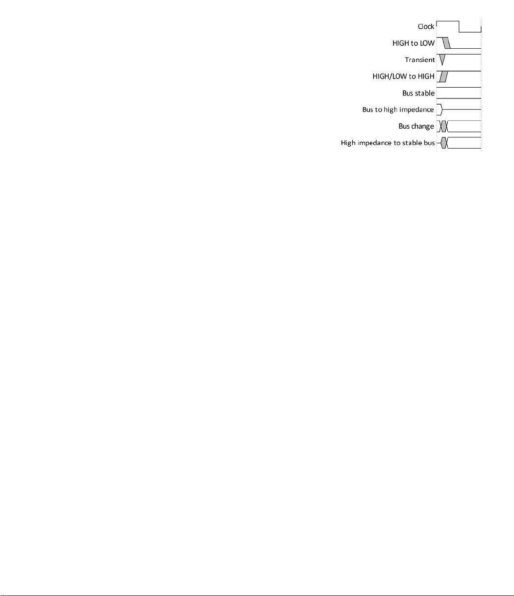
Timing diagrams
The figure named Key to timing diagram conventions explains the components used in timing
diagrams. Variations, when they occur, have clear labels. You must not assume any timing
information that is not explicit in the diagrams.
Shaded bus and signal areas are undefined, so the bus or signal can assume any value within the
shaded area at that time. The actual level is unimportant and does not affect normal operation.
Key to timing diagram conventions
Timing diagrams sometimes show single-bit signals as HIGH and LOW at the same time and
they look similar to the bus change shown in Key to timing diagram conventions. If a timing
diagram shows a single-bit signal in this way then its value does not affect the accompanying
description.
Signals
The signal conventions are:
Signal level
The level of an asserted signal depends on whether the signal is
active-HIGH or active-LOW. Asserted means:
•
HIGH for active-HIGH signals.
•
LOW for active-LOW signals.
Lower-case n
At the start or end of a signal name denotes an active-LOW signal.
Additional reading
This section lists publications by Arm and third parties.
See Infocentre http://infocenter.arm.com for access to Arm documentation.

Copyright 2017 Arm. All rights reserved.
Non-Confidential
4
101125_0200_00_en
Arm publications
This book contains information that is specific to this product. See the following documents for
other relevant information:
•
Arm® Cortex®-M0 DesignStart™ Eval User Guide (DUI 0926).
•
Arm® Armv6-M Architecture Reference Manual (DDI 0419).
•
Arm® Cortex®-M0 Devices Generic User Guide (DUI 0479)
•
Arm® Cortex®-M0 System Design Kit Technical Reference Manual (DDI 0479).
•
Arm® PrimeCell Synchronous Serial Port (PL022) Technical Reference Manual (DDI0194).
•
Keil® MCBSTM32C Evaluation Board Display Board Schematic.
•
Arm® Versatile™ Express Cortex®-M Prototyping System (V2M-MPS2and V2M-MPS2+)
Technical Reference Manual (100112).
•
Application Note AN502 Adapter for Arduino for the Cortex®-M Prototyping System (MPS2 and
MPS2+) (DAI 0502).
•
Arm® AMBA®3 AHB-Lite Protocol (v1.0) Specification (IHI 0033).
Terms and abbreviations
Volatile (storage class qualifier)
In C and C++ this is the volatile storage class qualifier. In other languages the
syntax and semantics might vary slightly if the concept is supported at all. The
intent is to cover all storage locations that might be used for inter-processor
communication variables that can be used for lock-free programming.
CMSDK Cortex®-M System Design Kit.
SMM Soft Macro Model. An SMM is an FPGA implementation of an Arm processor,
which is built with Arm development tools
ZBT Zero Bus Turnaround. A ZBT RAM is an implementation of a DDR RAM,
which
supports back to back read and write cycles, or zero turnaround.
PSRAM Pseudo-SRAM. An implementation of a DDR RAM, which has an SRAM
interface, with all refresh and similar operations kept internal to the device.
AMBA Advanced Microcontroller Bus Architectures

Copyright 2017 Arm. All rights reserved.
Non-Confidential
5
101125_0200_00_en
Feedback on this product
If you have any comments and suggestions about this product, contact your supplier and give:
•
Your name and company.
•
The serial number of the product.
•
Details of the release you are using.
•
Details of the platform you are using, such as the hardware platform, operating system type and
version.
•
A small standalone sample of code that reproduces the problem.
•
A clear explanation of what you expected to happen, and what actually happened.
•
The commands you used, including any command-line options.
•
Sample output illustrating the problem.
•
The version string of the tools, including the version number and build numbers.
Feedback on documentation
If you have comments on the documentation, e-mail errata@arm.com. Give:
•
The title.
•
The number, 101125_0200_00_en.
•
If viewing online, the topic names to which your comments apply.
•
If viewing a PDF version of a document, the page numbers to which your comments apply.
•
A concise explanation of your comments.
Arm also welcomes general suggestions for additions and improvements.
Arm periodically provides updates and corrections to its documentation on the Arm Information
Center, together with knowledge articles and Frequently Asked Questions (FAQs).

Copyright 2017 Arm. All rights reserved.
Non-Confidential
101125_0200_00_en
1-1
1. Introduction
This chapter introduces Cortex-M0 DesignStart Eval and gives an overview of the FPGA
Evaluation Flow, its directory structure, and prerequisites. It explains the simulation views available
and any prerequisites that are required to build an FPGA bitfile.
This chapter includes the following topics:
•
Cortex-M0 DesignStart Eval.
•
Decryption key.
•
Prerequisites.
1.1 Cortex-M0 DesignStart Eval
The Cortex-M0 DesignStart Eval package is aimed at developers who are new to Arm or have
limited soft IP system design experience. It provides developers an easy way to simulate SoC
designs based on the Cortex-M0 processor. It allows a system designer to design and test on a
simulator and then proceed with hardware prototyping using an FPGA.
The package includes the following:
•
An Arm Cortex-M0 processor from DesignStart.
•
An example system-level design for the Arm Cortex-M0 processor.
•
An FPGA system design for the Arm Cortex-M0 processor, suitable for the Arm Cortex-M
Prototyping System (MPS2+).
•
Reusable AMBA components for system-level development.
•
Peripheral support for the Arm Adaptor for Arduino Shield.
The Cortex-M0 processor from DesignStart:
•
Is a fixed configuration of the Cortex-M0 processor, enabling low-cost easy access to Cortex-M0
processor technology by offering a subset of the full product.
•
Is delivered as a preconfigured and obfuscated, but synthesizable, Verilog version of the full
Cortex-M0 processor.
In addition to the simulation views of the Cortex-M DesignStart Eval systems, you can purchase the
Arm® Versatile™ Express Cortex®-M Prototyping System, MPS2+. The MPS2+ platform is a small
FPGA development board that allows you to prototype on hardware where software debug tools can
be used. Combining these approaches allows for rapid development and verification. To purchase
the prototyping system, go to the Arm website http://www.arm.com/mps.
Cortex-M0 DesignStart Eval is built using the Cortex-M System Design Kit (CMSDK). This a
product to help silicon and FPGA designers to create Cortex-M-based systems. It contains ready-to-
use example systems for Cortex-M processors and a range of AMBA® bus fabric components for
Cortex-M system development.
This document describes the usage and operation of Cortex-M0 DesignStart Eval on the MPS2+
FPGA prototyping system. For details regarding the Cortex-M0 DesignStart Eval RTL, and the
fixed processor configuration, see the Arm® Cortex®-M0 DesignStart™ Eval User Guide.
You can download Cortex-M0 DesignStart Eval by registering at http://designstart.arm.com.
If your design requires more processing capability, or a more complicated system design, you can
also use Cortex-M3 DesignStart Eval. This is based on the SSE-050 subsystem, and also supports
the MPS2+ FPGA prototyping system. It is possible, for example to combine the deliverables from

Copyright 2017 Arm. All rights reserved.
Non-Confidential
101125_0200_00_en
1-2
both evaluation platforms to use the Cortex-M0 processor with the more advanced SSE-050
subsystem to develop a system which includes an additional AHB bus master.
1.2 Decryption key
Arm supplies the MPS2+ platform with a decryption key programmed into the FPGA. This key is
required to enable loading of the prebuilt images, which are encrypted.
Note
A battery supplies power to the key storage area of the FPGA. Any keys stored in the FPGA are
lost when battery power is lost. If battery power is lost, you must return the board to Arm for
reprogramming of the key.
The encryption key is not required for any images you build yourself using Cortex-M0 DesignStart
Eval. You must not redistribute any bitfiles which you generate.
1.3 Prerequisites
Rebuilding the FPGA requires the Intel Quartus Prime tool. Any edition, including the free Lite
Edition can be used.

Copyright 2017 Arm. All rights reserved.
Non-Confidential
101125_0200_00_en
2-1
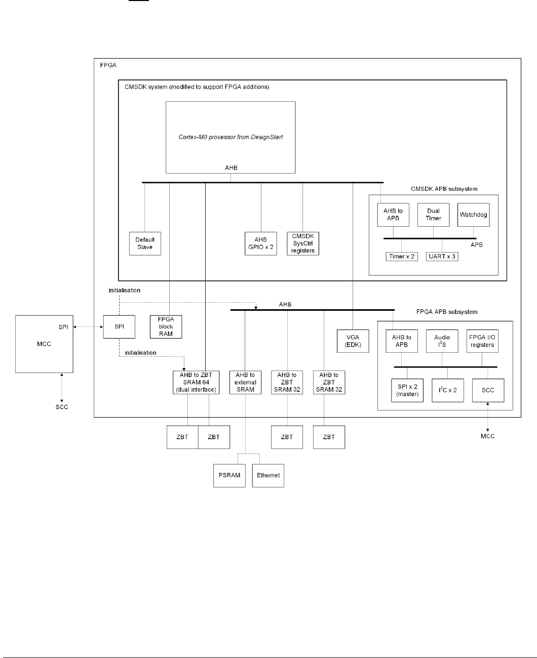
2. FPGA platform overview
The Soft Macro Model (SMM) is based on the Cortex-M System Design Kit (CMSDK). Extra
peripherals required by the FPGA are placed to extend the memory map. This results in the FPGA
SMM sharing some common structure with the basic CMSDK system which is also included in the
Cortex-M0 DesignStart Eval package. The FPGA SMM for Cortex-M0 DesignStart Eval is similar
to the other Cortex-M SMM designs which are available for the MPS2+ system.
Compared with the Cortex-M3 DesignStart Eval SMM, there are some changes to the memory map
because Cortex-M3 DesignStart Eval uses a different base subsystem designed for expansion.
The following topics describe the components that are connected to this SMM.
•
Memory map.
•
Block RAM for booting up.
•
External ZBT Synchronous SRAM (SSRAM1).
•
External ZBT Synchronous SRAM (SSRAM2 & SSRAM3).
•
External PSRAM.
•
CMSDK APB subsystem.
•
AHB GPIO.
•
Serial Peripheral Interface (SPI).
•
Color LCD parallel interface.
•
Shield I2C interfaces.
•
Shield UARTS.
•
Ethernet.
•
VGA.
•
Audio I2S.
•
Audio Configuration.
•
FPGA system control and I/O.
Copyright 2017 Arm. All rights reserved.
Non-Confidential
101125_0200_00_en
2-2
2.1 System overview
The following figure shows the block diagram of the FPGA, indicating the Cortex-M0 processor
from DesignStart, the CMSDK system, and the interfaces to the MPS2+ platform peripherals.
Note
This block diagram shows the functional hierarchy of the FPGA. The physical hierarchy is
shown in the Arm® Cortex®-M0 DesignStart™ Eval User Guide.
Figure 2-1 System overview

Copyright 2017 Arm. All rights reserved.
Non-Confidential
101125_0200_00_en
2-1
2.2 Memory map
The following table shows the memory map:
Start Address
End Address
Description
Comment
0x41100000
0x4110FFFF
VGA Image (512x128) (AHB)
Not present in cortex_m0_mcu
0x41000000
0x4100FFFF
VGA Console (AHB)
Not present in cortex_m0_mcu
0x40200000 0x402FFFFF Ethernet (Through ahb_to_extmem16.
Offset 0x0 to 0x0FE for Control
and Status Registers (CSRs), 0x100
to 0x1FE for FIFO)
Not present in cortex_m0_mcu
0x40030000
0x401FFFFF
RESERVED
-
0x4002F000 0x4002FFFF SCC register (see Serial
Communication Controller (SCC)
chapter)
Not present in cortex_m0_mcu
0x40029000
0x4002EFFF
RESERVED
-
0x40028000
0x40028FFF
FPGA System Control & I/O, APB
Not present in cortex_m0_mcu
0x40025000
0x40027FFF
RESERVED
-
0x40024000 0x40024FFF
Audio I
2
S, APB
Not present in cortex_m0_mcu
0x40023000
0x40023FFF
SBCon (Audio Configuration), APB
Not present in cortex_m0_mcu
0x40022000 0x40022FFF SBCon (Touch for LCD module),
APB
Not present in cortex_m0_mcu
0x40021000
0x40021FFF
PL022 (SPI for LCD module), APB
Not present in cortex_m0_mcu
0x40020000
0x40020FFF
PL022 (SPI), APB
Not present in cortex_m0_mcu
0x4001F000 0x4001FFFF CMSDK system controller Identical to cortex_m0_mcu
0x40014000 0x4001EFFF
Reserved for extra GPIO / other AHB
peripherals
Unused
0x40013000
0x40013FFF
CMSDK AHB GPIO #3
Not present in cortex_m0_mcu
0x40012000
0x40012FFF
CMSDK AHB GPIO #2
Not present in cortex_m0_mcu
0x40011000
0x40011FFF
CMSDK AHB GPIO #1
Identical to cortex_m0_mcu
0x40010000
0x40010FFF
CMSDK AHB GPIO #0
Identical to cortex_m0_mcu
0x40000000
0x4000FFFF
CMSDK APB subsystem
Identical to cortex_m0_mcu
0x21000000
0x21FFFFFF
PSRAM (16MB)
Not present in cortex_m0_mcu
0x20800000
0x20FFFFFF
RESERVED
-
0x20000000 0x207FFFFF ZBTSRAM 2 & 3 (2x 32-bit).
Reserved 8MB, 4MB available. The
two SRAM blocks are interleaved.
Only 64KB SRAM in
cortex_m0_mcu
0x01010000
0x1FFFFFFF
RESERVED
-
0x01000000 0x0100FFFF Block RAM (boot time) – reserved
64KB, 16K implemented. Memory
wrapped through region.
-

Copyright 2017 Arm. All rights reserved.
Non-Confidential
101125_0200_00_en
2-2
Start Address
End Address
Description
Comment
0x00800000
0x00FFFFFF
RESERVED
-
0x00400000 0x007FFFFF ZBTSRAM 1 (64-
bit). Wrapped (only
4MB ZBTSRAM fitted)
Not present in cortex_m0_mcu
0x00004000 0x003FFFFF ZBTSRAM 1 (64-bit) Flash memory in cortex_m0_mcu
example system is 64KB. This is
increased to 4MB in this SMM.
0x00000000 0x00003FFF CODE region.
When zbt_boot_ctrl = 0,
ZBTSRAM 1 is mapped to this
region, otherwise,
Remap_ctrl = 0 maps Block RAM
and
Remap_ctrl = 1 maps ZBTSRAM 1.
Block RAM or ZBTSRAM remap1
Table 2-1 Detailed system memory map
Many parts of the memory map have the same programmer’s view as a standard CMSDK system
(cortex_m0_mcu).
2.3 Block RAM for booting up
The SMM implements 16KB of FPGA internal block RAM as 32-bit AHB SRAM with a boot-code
to enable the system to start in a defined state. You can then add extra functions.
By default, the microcontroller using a zbt_boot_ctrl signal overrides the boot option.
2.4 External ZBT Synchronous SRAM (SSRAM1)
This section describes the Zero Bus Turnaround (ZBT) SRAM in the CODE region.
This interface consists of two external 32-bit ZBT SSRAMs in parallel, forming a 64-bit ZBT
SSRAM. 8MB of memory space is allocated, but only 4MB is available (each ZBT SSRAM is
2MB).
By default, the first 64KB is aliased to the FPGA internal block RAM. You can turn off the aliasing
by clearing the REMAP register in the CMSDK system controller.
CMSDK_SYSCON->REMAP = 0;
By default, the SMM design overwrites this alias with an extra boot control so that it boots from
ZBT SRAM.
You can also turn off the default ZBT SRAM boot control by changing the TOTALSYSCONS
variable in the board.txt file to 0.
TOTALSYSCONS: 1 -> TOTALSYSCONS: 0
This memory space connects through AHB.
1 The microcontroller on the MPS2+ platform controls the zbt_boot_ctrl signal. The zbt_boot_ctrl signal overrides the boot option
to enable the ZBT RAM to be used.

Copyright 2017 Arm. All rights reserved.
Non-Confidential
101125_0200_00_en
2-3
2.5 External ZBT Synchronous SRAM (SSRAM2 & SSRAM3)
The ZBT SSRAM in SRAM region is set up as two external ZBT SSRAMs, connected to two
independent ZBT interfaces. In the 8MB memory region, 4MB of ZBT are available.
The address of the ZBT SSRAM is interleaved as shown in the following table.
Upper 32-bit ZBT SSRAM3
Lower 32-bit ZBT SSRAM2
0x207FFFFC (wrap round to 0x203FFFFC)
0x207FFFF8 (alias to 0x203FFFF8)
…
…
0x20400004 (wrap round to 0x20000004)
0x20200000 (alias to 0x20000000)
0x203FFFFC
0x203FFFF8
…
…
0x2000000C
0x20000008
0x20000004
0x20000000
Table 2-2 32-bit ZBT Memory Map
This memory space connects through AHB
2.6 External PSRAM
A 16MB 16-bit PSRAM area is available and the memory map allocates the address range
0x21000000 - 0x21FFFFFF. This PSRAM space enables large test programs to be used in the
SRAM region of the Cortex-M0 memory space.
Note
Running code from SRAM region is slower than from CODE region because the internal bus
structure is not optimized for running programs from this region.
2.7 CMSDK APB subsystem
The SMM uses APB subsystem in CMSDK.
Address
Item
Notes
0x4000F000-0x4000FFFF APB expansion port 15 Not used. Reserved for micro
DMA controller configuration
port
0x4000E000-0x4000EFFF
APB expansion port 14
Not used
0x4000D000-0x4000DFFF
APB expansion port 13
Not used
0x4000C000-0x4000CFFF
APB expansion port 12
Not used
0x4000B000-0x4000BFFF
APB test slave
For validation of AHB to APB
bridge
0x4000A000-0x4000AFFF
APB expansion port 10
Not used

Copyright 2017 Arm. All rights reserved.
Non-Confidential
101125_0200_00_en
2-4
Address
Item
Notes
0x40009000-0x40009FFF
UART4
-
0x40008000-0x40008FFF
Watchdog
-
0x40007000-0x40007FFF
UART3
-
0x40006000-0x40006FFF
UART2
-
0x40005000-0x40005FFF
UART1
-
0x40004000-0x40004FFF
UART0
Used for Stdout redirect
0x40003000-0x40003FFF
APB expansion port 3
Not used
0x40002000-0x40002FFF
Dual timer
-
0x40001000-0x40001FFF
Timer1
-
0x40000000-0x40000FFF
Timer0
-
Table 2-3 APB Memory Map
2.8 AHB GPIO
The SMM uses CMSDK AHB GPIO #0 and #1, and also adds GPIO #2 and #3. See the Arm®
Cortex®-M0 System Design Kit Technical Reference Manual for details. Where the GPIO pin is
shared with a peripheral I/O, the default state at reset has the pin defined as a GPIO, the alternate
function registers in the GPIO are used to enable the peripheral connections.
2.9 Serial Peripheral Interface (SPI)
The SMM implements five PL022 SPI modules:
•
General-purpose SPI module that connects to the general-purpose SPI connector, J21. An adaptor is
available from Arm which allows you to use this interface to connect a micro-SD card.
•
Color LCD module control.
•
SPI ports for each shield connector on the Adaptor for Arduino Shield.
•
SPI port to interface to the ADC on the Adaptor for Arduino Shield.
2.10 Color LCD parallel interface
The color LCD module has two interfaces:
•
SPI for LCD module that is used for sending image data to the LCD.
•
I2C to transfer data input from the touch screen.
These interfaces are connected to a STMicroelectronics STMPE811QTR Port Expander with
Advanced Touch Screen Controller on the KEIL MCBSTM32C display board. This display board
contains an Ampire AM-240320LG 2.4” Touch Panel. See the Keil® MCBSTM32C Evaluation
Board Display Board Schematic for more details.
Self-test that is provided with the MPS2 includes example code for both of these interfaces.
2.11 Shield I2C interfaces
There are two additional I2C interfaces for the Adaptor for Arduino Shield. These use the SBCon
peripheral.

Copyright 2017 Arm. All rights reserved.
Non-Confidential
101125_0200_00_en
2-5
2.12 Shield UARTS
There are three additional UART interfaces for the Adaptor for Arduino Shield. These use the
CMSDK UART.
2.13 Ethernet
The SMM design connects SMSC LAN9220 through AHB to external memory block. The SMM
self-test code includes example code for a simple loopback operation.
2.14 VGA
The following table shows the memory map for controlling a screen using the VGA interface
Address
Description
0x41000000 - 0x4100FFFF
Writes to the current location of the cursor.
0x41100000 - 0x4110FFFF 512x128 image area at the top right of the screen.
0x41100000 is the top left of the area and
0x4110FFFF is the bottom right.
HADDR[16:2] = YYYYYYYXXXXXXXX,
where X and Y are the horizontal and vertical pixel
offset respectively
Table 2-4 VGA Memory Map
For the image data, each pixel requires one 32-bit word, therefore, a total of 256KB are needed. The
values in the data buffer are packed as 4 bits per-channel in the format 0x00000RGB.
The pixel in the top left-hand corner of the display occupies address 0x41100000 with each
successive row using an offset of 0x00000400 from the previous row. For example: the Left
Most Pixel (LMP) of the second row is at 0x41100400 and the LMP of the third row is at
0x41100800.
2.15 Audio I2S
A simple FIFO interface generates and receives I2S audio.
Address
Name
Information
0x40024000 CONTROL
Control Register
[31:18]: Reserved
[17]: Audio codec reset control (output pin)
[16]: FIFO reset
[15]: Reserved
[14:12]: RX Buffer IRQ Water Level - Default 2
(IRQ triggers when more less two word space available)
[11]: Reserved
[10: 8]: TX Buffer IRQ Water Level - Default 2
(IRQ triggers when more than two word space available)
[7: 4]: Reserved
[3]: RX Interrupt Enable

Copyright 2017 Arm. All rights reserved.
Non-Confidential
101125_0200_00_en
2-6
Address
Name
Information
[2]: RX Enable
[1]: TX Interrupt Enable
[0]: TX Enable
0x40024004 STATUS
Status register
[31:6]: Reserved
[5]: RX Buffer Full
[4]: RX Buffer Empty
[3]: TX Buffer Full
[2]: TX Buffer Empty
[1]: RX Buffer Alert (Depends on Water level)
[0]: TX Buffer Alert (Depends on Water level)
0x40024008 ERROR
Error status register
[31:2]: Reserved
[1]: RX overrun - write 1 to clear
[0]: TX overrun or underrun - write 1 to clear
0x4002400C DIVIDE
Divide ratio register (for Left or Right clock)
[31:10]: Reserved
[9:0] LRDIV (Left/Right) Default = 0x80
12.288MHz / 48KHz / 2 (L+R) = 128
0x40024010 TXBUF
Transmit Buffer FIFO Data Register (WO)
[31:16]: Left Channel
[15:0]: Right Channel
0x40024014 RXBUF
Receive Buffer FIFO Data Register (RO)
[31:16] Left Channel
[15: 0] Right Channel
0x40024018
-
0x400242FC
RESERVED -
0x40024300 ITCR
Integration Test Control Register
[31:1]: Reserved
[0]: ITCR
0x40024304 ITIP1
Integration Test Input Register 1
[31:1]: Reserved
[0]: SDIN
0x40024308 ITOP1
Integration Test Output Register 1
[31:4]: Reserved
[3]: IRQOUT

Copyright 2017 Arm. All rights reserved.
Non-Confidential
101125_0200_00_en
2-7
Address
Name
Information
[2]: LRCK
[1]: SCLK
[0]: SDOUT
Table 2-5 Audio I2S Memory Map
2.16 Audio Configuration
The SMM implements a simple SBCon interface that is based on I2C.
2.17 FPGA system control and I/O
The SMM implements an FPGA system control block.
Address
Name
Information
0x40028000 LED0
LED connections
[31:2]: Reserved
[1:0]: LED
0x40028004
RESERVED
-
0x40028008 BUTTON
Buttons
[31:2]: Reserved
[1:0]: Buttons
0x4002800C
RESERVED
-
0x40028010
CLK1HZ
1Hz up counter
0x40028014
CLK100HZ
100Hz up counter
0x40028018 COUNTER Cycle Up Counter
Increments when 32-bit prescale counter reach zero.
0x4002801C
PRESCALE
Bit [31:0] – reload value for prescale counter.
0x40028020 PSCNTR 32-bit prescale counter – current value of the pre-scaler
counter. The Cycle Up Counter increment when the
prescale down counter reach 0. The pre-
scaler counter is
reloaded with PRESCALE after reaching 0.
0x40028024
RESERVED
-
0x4002804C MISC
Miscellaneous control
[31:7]: Reserved
[6]: CLCD_BL_CTRL
[5]: CLCD_RD
[4]: CLCD_RS
[3]: CLCD_RESET
[2]: RESERVED
[1]: SPI_nSS
[0]: CLCD_CS
Table 2-6 System Control and I/O Memory Map

Copyright 2017 Arm. All rights reserved.
Non-Confidential
101125_0200_00_en
3-8
3. Clocks
The following table shows the Source Clocks for the system.
Name
Frequency
OSCCLK[0]
50MHz
OSCCLK[1]
24.576MHz
OSCCLK[2]
25MHz
CFGCLK
0.5MHz
CS_TCK
Determined by debugger
SPICFGCLK
7.5MHz
Table 3-1 Source Clocks
The following table shows the Derived Clocks for the system.
Name Frequency Division
Factor
Multiplication
Factor
Derived From
SYSCLK
25MHz
2
1
OSCCLK[0]
DBGCLK
25MHz
2
1
OSCCLK[0]
SPICLCD
25MHz
2
1
OSCCLK[0]
SPICON
25MHz
2
1
OSCCLK[0]
I2CCLCD
25MHz
2
1
OSCCLK[0]
I2CAUD
25MHz
2
1
OSCCLK[0]
AUDMCLK
12.29MHz
2
1
OSCCLK[1]
AUDSCLK
3.07MHz
8
1
OSCCLK[1]
Table 3-2 Derived Clocks

Copyright 2017 Arm. All rights reserved.
Non-Confidential
101125_0200_00_en
4-1
4. Interrupt assignments
The SMM uses the following interrupt assignments. These interrupt assignments are different from
the default CMSDK assignments due to the increased number of peripherals:
Number
Interrupt source
NMI
Watchdog
0
UART 0 receive interrupt
1
UART 0 transmit interrupt
2
UART 1 receive interrupt
3
UART 1 transmit interrupt
4
UART 2 receive interrupt
5
UART 2 transmit interrupt
6
UART 3 Rx, GPIO 0, GPIO 2 combined interrupt
7
UART 3 Tx, GPIO 0, GPIO 2 combined interrupt
8
Timer 0
9
Timer 1
10
Dual Timer
11
SPI combined interrupt
12
UART overflow (0, 1, 2, 3 & 4)
13
Ethernet
14
Audio I
2
S
15
Touch Screen
16
UART 4 Rx, GPIO0 bit0 combined
17
UART 4 Tx, GPIO0 bit1 combined
18-31
GPIO0 bit 2 to bit 15 individual interrupts
Table 4-1 Interrupt Assignments
Copyright 2017 Arm. All rights reserved.
Non-Confidential
101125_0200_00_en
5-1
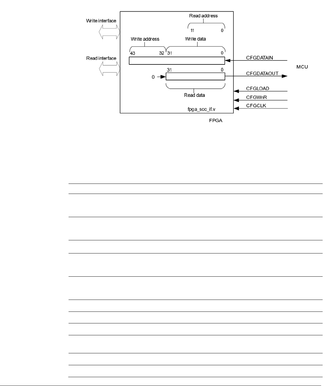
5. Serial Communication Controller (SCC)
The SMM implements communication between the microcontroller and the FPGA system through
an SCC interface.
Figure 5-1 Diagram of the SCC Interface
The read-addresses and write-addresses of the SCC interface do not use bits [1:0]. All address
words are word-aligned.
Address
Name
Information
0x000 CFG_REG0
[31:1]: Reserved
[0]: 1 = REMAP Block RAM to ZBT
0x004 CFG_REG1
[31:8]: Reserved
[7:0]: MCC LEDs: 0 = OFF, 1 = ON
0x008
CFG_REG2 Reserved
0x00C CFG_REG3
[31:8]: Reserved
[7:0]: MCC switches: 0 = OFF, 1 = ON
0x010 CFG_REG4
[31:4]: Reserved
[3:0]: Board Revision
0x014
CFG_REG5
Reserved
0x018
CFG_REG6
Reserved
0x01C
CFG_REG7
Reserved
0x020 –
0x09C
RESERVED -
0x0A0
SYS_CFGDATA_RTN
32-bit data [R/W]
0x0A4
SYS_CFGDATA_OUT
32-bit data [R/W]

Copyright 2017 Arm. All rights reserved.
Non-Confidential
101125_0200_00_en
5-2
Address
Name
Information
0x0A8 SYS_CFGCTRL
[31]: Start (generates interrupt on write to this bit)
[30]: R/W access
[29:26]: Reserved
[25:20]: Function value
[19:12]: Reserved
[11:0]: Device (value of 0/1/2 for supported clocks)
0x0AC
SYS_CFGSTAT
[31:2]: Reserved
[1]: Error
[0]: Complete
0x0AD –
0x0FC
RESERVED -
0x100 SCC_DLL
DLL lock register
[31:24]: DLL LOCK MASK[7:0] - These bits
indicate that the DLL lock is masked.
[23:16]: DLL LOCK MASK[7:0] - These bits
indicate whether the DLLs are locked or
unlocked.
[15:1]: Reserved
[0]: This bit indicates whether all enabled DLLs are
locked.
0x104 –
0xFF4
RESERVED -
0xFF8 SCC_AID
SCC AID register is read only
[31:24]: FPGA build number
[23:20]: MPS2+ target board revision
(C = 2)
[19:8]: Reserved
[7:0]: number of SCC configuration registers
0xFFC SCC_ID
SCC ID register is read only
[31:24]: Implementer ID: 0x41 = Arm
[23:20]: Application note IP variant number
2
[19:16]: IP Architecture: 0x4 =AHB
[11:4]: Primary part number: 387 = AN387
[3:0]: Application note IP revision number
2
Table 5-1 SCC Register memory map
2 The variant and revision numbers relate to the rXpY number. For example, for r1p0 processors the 1 would be the variant number and the 0
would be the revision number.

Copyright 2017 Arm. All rights reserved.
Non-Confidential
101125_0200_00_en
6-1
6. FPGA Build Guide
This section describes the steps that are required to build an FPGA bitfile from the supplied source
code.
This section contains the following subsections:
• Build Flow.
• Creating a user bit file.
• Loading a new bit file onto the MPS2+ platform.
6.1 Build Flow
Cortex-M0 DesignStart Eval includes a prebuilt FPGA image file that is based on an example
system. However, if your design is different from the example system, then you are able to build
your own FPGA image file.
To run the build flow, use the Intel Quartus software, version 16.1 onwards.
You can use the Lite Edition of Quartus Prime, which does not require a license.
The build flow involves two stages, which are creating a new user bit file, and loading the bit file
onto the MPS2+ platform.
6.2 Creating a user bit file
To create a user bit file, follow these steps:
1. Open the Intel Quartus software.
a. Select File > Open Project and navigate to the project file:
RevC/SMM_M0DS/synthesis/SMM_M0DS_AN387.qpf
b. Select Processing > Start Compilation to compile the design.
This compiles the standard design and creates various report files in the
output_files folder.
After the compilation is completed, an SOF file, titled SMM_M0DS_AN387.sof,
is created in the output_files folder.
2. Open a terminal window (Linux) or a command prompt (Microsoft Windows).
3. Navigate to the following directory:
RevC/SMM_M0DS/synthesis/
4. Execute the following command:
make convert
This converts the SOF file to an RBF file, titled an387_v5.rbf, in the current directory.
Note
To allow for a degree of traceability between different user bit files, the final digit can be used as a
version number. The Motherboard Configuration Controller (MCC) for the MPS2+ platform only
supports a format of 8:3 characters for the filename, so only one digit is possible as the suffix. To
change this digit when generating the RBF file, modify the REV variable in the header of the
makefile with any text editor. If you provide an RBF file that uses a long file name, the MPS2+
platform will not boot.

Copyright 2017 Arm. All rights reserved.
Non-Confidential
101125_0200_00_en
6-2
6.3 Loading a new bit file onto the MPS2+ platform
To load a new user bitfile onto the MPS2+ platform, execute the following instructions:
1. Power the board with the supplied power supply.
2. Connect a USB lead to your computer and the USB-B port (labeled USB) on the board.
The computer recognizes a new USB device called V2M_MPS2.
3. Access the V2M_MPS2 device and copy the an387_v5.rbf file to the folder:
MB\HBI0263C\AN387
4. Check which image is programmed into the FPGA. In the USB device, the board.txt
file allows you to select which hardware image is programmed into the FPGA. This affects
which project to run. The board file is located in the directory:
MB\HBI0263C\board.txt
• The image to be loaded is selected with the line starting with APPFILE:. A
selection of images has been preloaded onto the USB device. All but one has been
commented out with a ';' character:
• To select an image, remove the comment ';' in front of the appropriate line and ensure
that all other APPFILE: references are preceded by the comment character. For the
default Cortex-M0 DesignStart Eval FPGA image, you should use:
APPFILE: AN387\an387_v5.txt ; - Cortex-M0 DesignStart
5. Specify the bitfile to use in the APPFILE referenced in step (4):
• Modify the an387_v5.txt file located in the MB\HBI0263C\AN387. Use
the following line to specify which bitfile to load:
F0FILE: an387_v5.rbf ;FPGA0 Filename
Note
Arm supplies an encrypted prebuilt bit file (.rbe) with the MPS2+ platform. If you are
rebuilding the bit file, the file produced is not encrypted (.rbf). Therefore, if you are not
using the prebuilt FPGA image and you are modifying an387_v5.txt, it is necessary to
change the file extension from .rbe to .rbf as shown above.
6. When these steps have been completed, save and close both files. Eject the V2M_MPS2
volume using Windows Explorer.

Copyright 2017 Arm. All rights reserved.
Non-Confidential
101125_0200_00_en
6-3
7. Press the Power ON button on the MPS2+ board, the bitfile loads and the board is ready
to use.
Note
To confirm the files loaded correctly, check the log.txt file in the root directory of
V2M_MPS2. This details which files were loaded at boot- up. After the bitfile name,
you should see the following:
FPGA config: PASSED
OSCCLK config: PASSED
Writing SCC 0x00000010 with board revision C
Writing SCC 0x00000000 with 0x00000001
The software image which is loaded is also controlled by the an387_v5.txt file.

Copyright 2017 Arm. All rights reserved.
Non-Confidential
101125_0200_00_en
7-1
7. Utilization of default system
The FPGA on the MPS2+ platform is an Altera Cyclone V 5CEBA9F31C8.
The following table shows the resources of the FPGA:
Resources
Value
LUTs
113 560
DFFs
454 240
Memory
3.9Mbit
DSP
342
PLLs
7
Table 7-1 FPGA resources
The following table shows the Cortex-M0 DesignStart Eval code utilization of FPGA resources:
Resources
Value
LUTs
10%
DFFs
2%
Memory
8%
DSP
<1%
PLLs
29%
Table 7-2 Code utilization FPGA resources

Copyright 2017 Arm. All rights reserved.
Non-Confidential
101125_0200_00_en
A-1
Revisions
This appendix describes the technical changes between released issues of this book.
Table A-1 Issue A
Change
Location
Affects
First release for r2p0
-
-
