Xilinx PG034 LogiCORE IP AXI Central Direct Memory Access Product Guide, V3.03.a Cdma Guide
User Manual: Pdf
Open the PDF directly: View PDF ![]() .
.
Page Count: 70

LogiCORE IP AXI Central
Direct Memory Access
v3.03a
Product Guide
PG034 October 16, 2012

LogiCORE IP AXI CDMA v3.03a www.xilinx.com 2
PG034 October 16, 2012
Table of Contents
SECTION I: SUMMARY
IP Facts
Chapter 1: Overview
Registers . . . . . . . . . . . . . . . . . . . . . . . . . . . . . . . . . . . . . . . . . . . . . . . . . . . . . . . . . . . . . . . . . . . . . . . . . 7
Scatter Gather . . . . . . . . . . . . . . . . . . . . . . . . . . . . . . . . . . . . . . . . . . . . . . . . . . . . . . . . . . . . . . . . . . . . 7
Cntl/Sts Logic . . . . . . . . . . . . . . . . . . . . . . . . . . . . . . . . . . . . . . . . . . . . . . . . . . . . . . . . . . . . . . . . . . . . . 7
DataMover . . . . . . . . . . . . . . . . . . . . . . . . . . . . . . . . . . . . . . . . . . . . . . . . . . . . . . . . . . . . . . . . . . . . . . . 7
Feature Summary. . . . . . . . . . . . . . . . . . . . . . . . . . . . . . . . . . . . . . . . . . . . . . . . . . . . . . . . . . . . . . . . . . 8
Applications . . . . . . . . . . . . . . . . . . . . . . . . . . . . . . . . . . . . . . . . . . . . . . . . . . . . . . . . . . . . . . . . . . . . . . 8
Licensing and Ordering Information . . . . . . . . . . . . . . . . . . . . . . . . . . . . . . . . . . . . . . . . . . . . . . . . . . . 8
Chapter 2: Product Specification
Performance. . . . . . . . . . . . . . . . . . . . . . . . . . . . . . . . . . . . . . . . . . . . . . . . . . . . . . . . . . . . . . . . . . . . . . 9
Standards . . . . . . . . . . . . . . . . . . . . . . . . . . . . . . . . . . . . . . . . . . . . . . . . . . . . . . . . . . . . . . . . . . . . . . . 10
Resource Utilization. . . . . . . . . . . . . . . . . . . . . . . . . . . . . . . . . . . . . . . . . . . . . . . . . . . . . . . . . . . . . . . 11
Port Descriptions . . . . . . . . . . . . . . . . . . . . . . . . . . . . . . . . . . . . . . . . . . . . . . . . . . . . . . . . . . . . . . . . . 13
Register Space . . . . . . . . . . . . . . . . . . . . . . . . . . . . . . . . . . . . . . . . . . . . . . . . . . . . . . . . . . . . . . . . . . . 21
Chapter 3: Designing with the Core
General Design Guidelines . . . . . . . . . . . . . . . . . . . . . . . . . . . . . . . . . . . . . . . . . . . . . . . . . . . . . . . . . 34
Clocking. . . . . . . . . . . . . . . . . . . . . . . . . . . . . . . . . . . . . . . . . . . . . . . . . . . . . . . . . . . . . . . . . . . . . . . . . 35
Resets . . . . . . . . . . . . . . . . . . . . . . . . . . . . . . . . . . . . . . . . . . . . . . . . . . . . . . . . . . . . . . . . . . . . . . . . . . 35
Design Parameters. . . . . . . . . . . . . . . . . . . . . . . . . . . . . . . . . . . . . . . . . . . . . . . . . . . . . . . . . . . . . . . . 36
AXI CDMA Operation . . . . . . . . . . . . . . . . . . . . . . . . . . . . . . . . . . . . . . . . . . . . . . . . . . . . . . . . . . . . . . 43

LogiCORE IP AXI CDMA v3.03a www.xilinx.com 3
PG034 October 16, 2012
SECTION II: VIVADO DESIGN SUITE
Chapter 4: Customizing and Generating the Core
GUI . . . . . . . . . . . . . . . . . . . . . . . . . . . . . . . . . . . . . . . . . . . . . . . . . . . . . . . . . . . . . . . . . . . . . . . . . . . . 54
Output Generation. . . . . . . . . . . . . . . . . . . . . . . . . . . . . . . . . . . . . . . . . . . . . . . . . . . . . . . . . . . . . . . . 57
Chapter 5: Constraining the Core
SECTION III: ISE DESIGN SUITE
Chapter 6: Customizing and Generating the Core
GUI . . . . . . . . . . . . . . . . . . . . . . . . . . . . . . . . . . . . . . . . . . . . . . . . . . . . . . . . . . . . . . . . . . . . . . . . . . . . 61
Output Generation. . . . . . . . . . . . . . . . . . . . . . . . . . . . . . . . . . . . . . . . . . . . . . . . . . . . . . . . . . . . . . . . 63
Chapter 7: Constraining the Core
Automatic Constraint Generation. . . . . . . . . . . . . . . . . . . . . . . . . . . . . . . . . . . . . . . . . . . . . . . . . . . . 65
SECTION IV: APPENDICES
Appendix A: Migrating
Appendix B: Debugging
Appendix C: Additional Resources
Xilinx Resources . . . . . . . . . . . . . . . . . . . . . . . . . . . . . . . . . . . . . . . . . . . . . . . . . . . . . . . . . . . . . . . . . . 69
References . . . . . . . . . . . . . . . . . . . . . . . . . . . . . . . . . . . . . . . . . . . . . . . . . . . . . . . . . . . . . . . . . . . . . . 69
Technical Support . . . . . . . . . . . . . . . . . . . . . . . . . . . . . . . . . . . . . . . . . . . . . . . . . . . . . . . . . . . . . . . . 69
Revision History . . . . . . . . . . . . . . . . . . . . . . . . . . . . . . . . . . . . . . . . . . . . . . . . . . . . . . . . . . . . . . . . . . 70
Notice of Disclaimer. . . . . . . . . . . . . . . . . . . . . . . . . . . . . . . . . . . . . . . . . . . . . . . . . . . . . . . . . . . . . . . 70


LogiCORE IP AXI CDMA v3.03a www.xilinx.com 5
PG034 October 16, 2012 Product Specification
Introduction
The Advanced eXtensible Interface (AXI) Central
Direct Memory Access (CDMA) core is a soft
Xilinx Intellectual Property (IP) core for use with
the Xilinx Embedded Development Kit (EDK).
The AXI CDMA provides high-bandwidth Direct
Memory Access (DMA) between a
memory-mapped source address and a
memory-mapped destination address using the
AXI4 protocol. An optional Scatter Gather (SG)
feature can be used to off-load control and
sequencing tasks from the System Central
Processing Unit (CPU). Initialization, status, and
control registers are accessed through an
AXI4-Lite slave interface, suitable for the Xilinx
MicroBlaze™ microprocessor.
Features
• AXI4 Memory Map interface for data
transfer
• Independent AXI4-Lite Slave interface for
register access
• Independent AXI4 Master interface for
optional Scatter/Gather function.
• Optional Data Realignment Engine
•Register Direct Mode.
Optional Scatter Gather DMA support
• Optional Store and Forward support
• Parameterized Read and Write Address
Pipeline depths
• Fixed-address and Incrementing-address
burst support
IP Facts
LogiCORE IP Facts Table
Core Specifics
Supported
Device
Family(1)
Zynq™-7000(2), Virtex®-7, Kintex™-7, Artix™-7,
Virtex-6, Spartan®-6
Supported
User Interfaces AXI4, AXI4-Lite
Resources See Tabl e 2-3, Ta b l e 2 - 4 , and Ta b l e 2-5.
Provided with Core
Design Files ISE®: VHDL
Vivado™: RTL
Example
Design Not Provided
Test Bench Not Provided
Constraints
File Not Provided
Simulation
Model Not Provided
Supported
S/W Driver(3) Standalone and Linux
Tested Design Flows(4)
Design Entry Xilinx Platform Studio 14.3
Vivado Design Suite(5) 2012.3
Simulation Mentor Graphics ModelSim
ISim, Vivado simulator
Synthesis Xilinx Synthesis Technology (XST)
Vivado Synthesis
Support
Provided by Xilinx @ www.xilinx.com/support
Notes:
1. For a complete list of supported derivative devices, see the
Embedded Edition Derivative Device Support.
2. Supported in ISE Design Suite implementations only.
3. Standalone driver details can be found in the EDK or SDK
directory (<install_directory>/doc/usenglish/
xilinx_drivers.htm). Linux OS and driver support information is
available from //wiki.xilinx.com.
4. For the supported versions of the tools, see the Xilinx Design
Tools: Release Notes Guide.
5. Supports only 7 series devices.
LogiCORE IP AXI CDMA v3.03a www.xilinx.com 6
PG034 October 16, 2012
Chapter 1
Overview
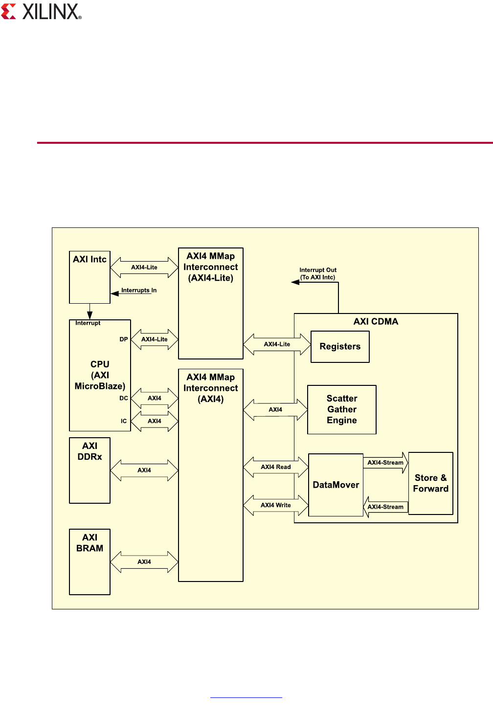
The AXI CDMA is designed to provide a centralized DMA function for use in an embedded
processing system employing the AXI4 system interfaces. The core supports both a simple
CDMA operation mode and an optional Scatter Gather mode.
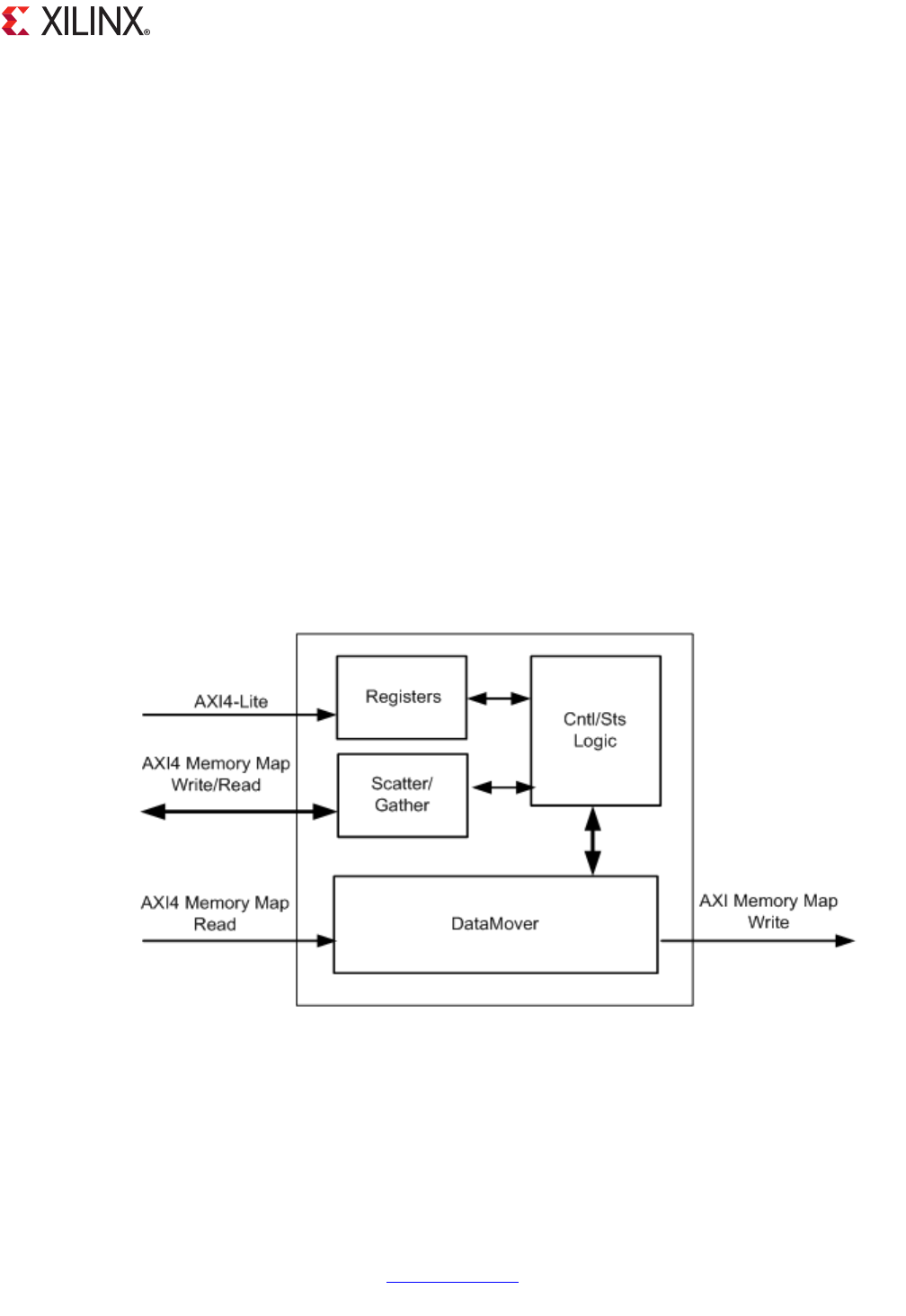
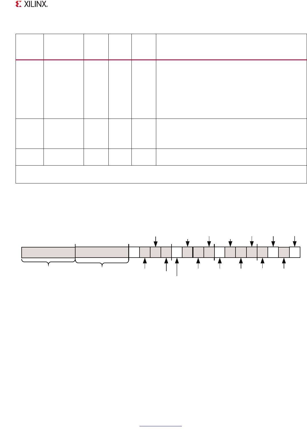
Figure 1-1 shows the functional composition of the AXI CDMA. It contains the following
major functional blocks:
•Registers
•Scatter Gather
•Cntl/Sts Logic
•DataMover
X-Ref Target - Figure 1-1
Figure 1-1: AXI CDMA Block Diagram

LogiCORE IP AXI CDMA v3.03a www.xilinx.com 7
PG034 October 16, 2012
Chapter 1: Overview
Registers
This block contains control and status registers that allows you to configure AXI CDMA
through the AXI4-Lite slave interface. See Register Space in Chapter 2.
Scatter Gather
The AXI CDMA can also optionally include Scatter/Gather (SG) functionality for off-loading
CPU management tasks to hardware automation. The Scatter/Gather Engine fetches and
updates CDMA control transfer descriptors from system memory through dedicated the
AXI4 Scatter Gather Master interface. The SG engine provides internal descriptor queuing
which allows descriptor prefetch and processing in parallel with ongoing CDMA data
transfer operations.
Cntl/Sts Logic
This block manages overall CDMA operation. It coordinates DataMover command loading
and status retrieval and updates it back to Registers block.
DataMover
The DataMover is used for high-throughput transfer of data. The DataMover provides
CDMA operations with 4 KB address boundary protection, automatic burst partitioning, and
can queue multiple transfer requests. Furthermore, the DataMover provides byte-level data
realignment (for 32-bit and 64-bit data widths) allowing the CDMA to read from and write
to any byte offset combination.

LogiCORE IP AXI CDMA v3.03a www.xilinx.com 8
PG034 October 16, 2012
Chapter 1: Overview
Feature Summary
• Independent AXI4-Lite Slave interface for register access
°Fixed 32-bit data width
°Optional asynchronous operation mode
• Independent AXI4 Master interface for primary CDMA datapath. Parameterizable width
of 32, 64, 128, 256, 512, and 1024 bits with fixed-address burst (key hole) support.
• Independent AXI4 Master interface for optional Scatter/Gather function. Fixed 32-bit
data width.
• Optional Data Realignment Engine for the primary CDMA datapath. Available with 32
and 64-bit datapath widths.
• Provides Simple DMA only mode and an optional hybrid mode supporting both Simple
DMA and Scatter Gather automation.
• Optional Store and Forward operation mode.
• Parameterized Read and Write Address Pipeline depths.
Applications
The AXI CDMA provides a high performance CDMA function for Embedded Systems.
Licensing and Ordering Information
This Xilinx LogiCORE™ IP module is provided at no additional cost with the Xilinx Vivado™
Design Suite and ISE® Design Suite Embedded Edition tools under the terms of the Xilinx
End User License.
Information about this and other Xilinx LogiCORE IP modules is available at the Xilinx
Intellectual Property page. For information on pricing and availability of other Xilinx
LogiCORE IP modules and tools, contact your local Xilinx sales representative.
LogiCORE IP AXI CDMA v3.03a www.xilinx.com 9
PG034 October 16, 2012
Chapter 2
Product Specification
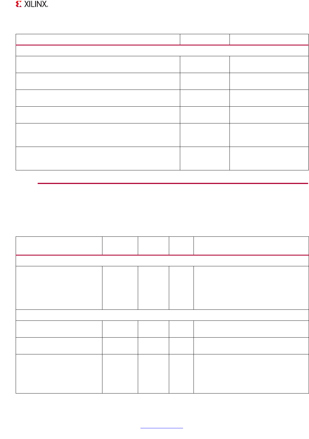
Performance
This section details the performance information for various core configurations.
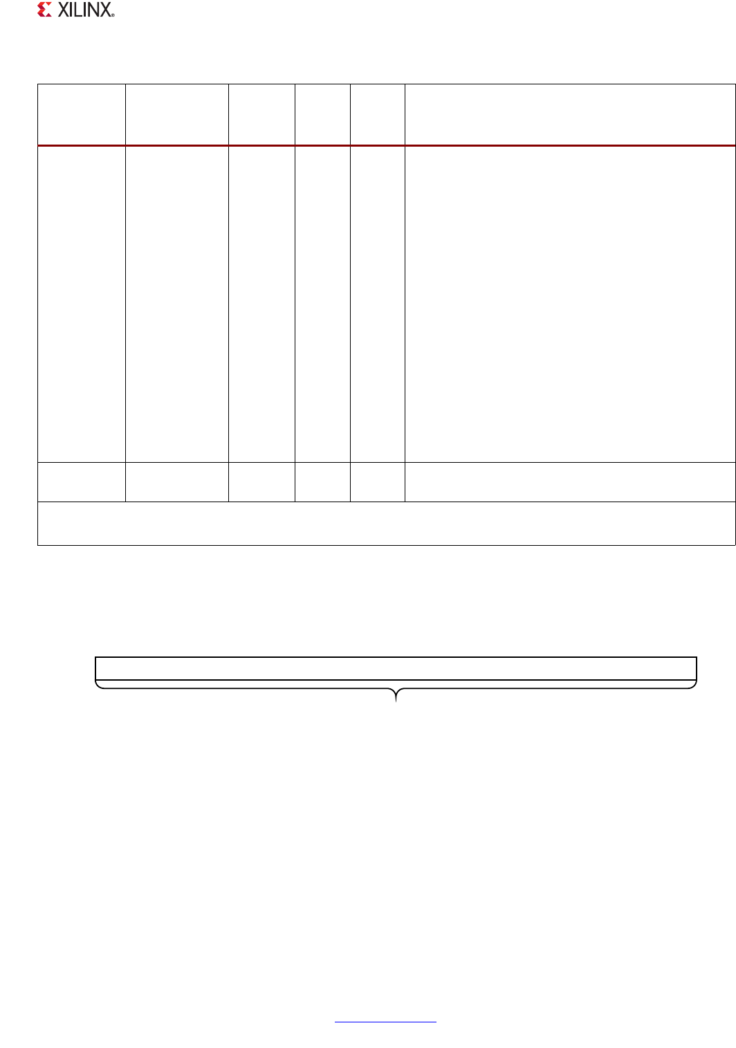
X-Ref Target - Figure 2-1
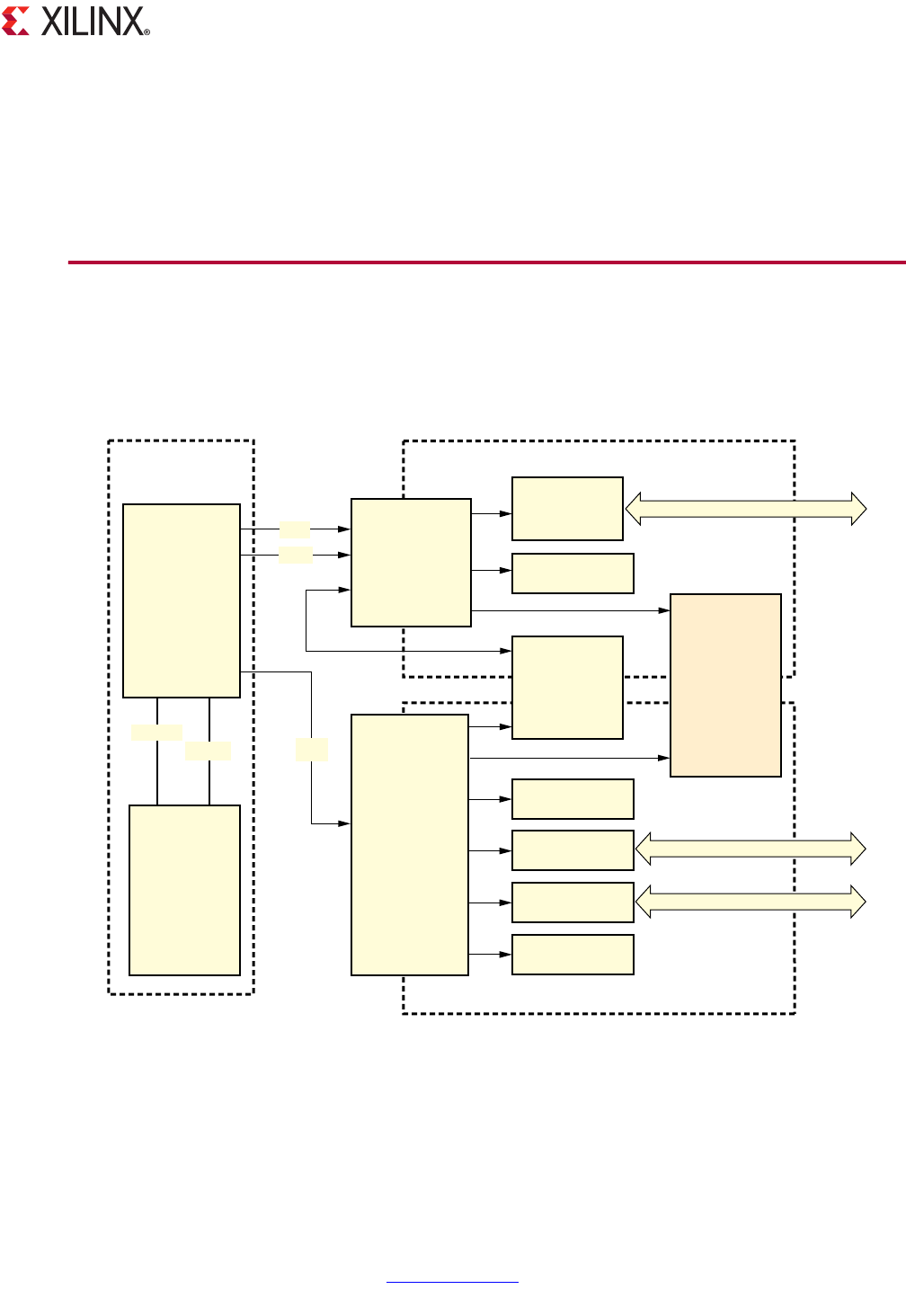
Figure 2-1: Virtex-6 and Spartan-6 FPGA System Configuration Diagram
!8),ITE
-ICRO"LAZE
#ONTROLLER
!8)).4#
!8)'0)/
!8)5!24,ITE
!8)
-EMORY
#ONTROLLER
-$-
-ICRO"LAZE
$OMAIN
!8)
"LOCK2!-
#ONTROLLER
$?,-"
)?,-"
)#
!8)"LOCK2!-
$#
!8)#$-!
-EMORY
$0
,%$S
23
!8)#$-!
-EMORY-AP
)NTERCONNECT
!8)
#ONTROL
)NTERFACE
3UBSET
)NTERCONNECT
!8),ITE

LogiCORE IP AXI CDMA v3.03a www.xilinx.com 10
PG034 October 16, 2012
Chapter 2: Product Specification
Maximum Frequencies
The maximum frequencies are calculated based on a benchmarking design which is filled
with dummy logic to get 70% Look-up Table (LUT) utilization. The resulting target FMax are
shown in Tab le 2- 1.
Throughput
Due to the parameterizable nature of the AXI CDMA, throughput is best measured as a
percentage of the AXI4 bus bandwidth available to the AXI CDMA (Table 2- 2). This available
bus bandwidth is a function of the clock frequency of the AXI4 bus and the parameterized
data width of the AXI CDMA. The other parameter affecting throughput is the value
assigned to the C_M_AXI_BURST_LEN parameter of the AXI CDMA. In general, the bigger
value assigned increases the realized throughput of the AXI CDMA. However, larger burst
lengths can be detrimental to other components of a user’s system design (causing lower
system performance) so this is a trade-off that you must evaluate.
.
Standards
The AXI CDMA core is AXI4 and AXI4-Lite compliant.
Table 2-1: System Performance
Family Device Target FMax (MHz)
AXI4 AXI4-Lite MicroBlaze
Spartan-6 xc6slx45t (1) 90 120 80
Virtex-6 xc6vlx240t (2) 135 180 135
Notes:
1. Spartan-6 FPGA LUT utilization: 70%; Block RAM utilization: 70%; I/O utilization: 80%; MicroBlaze™ processor not
AXI4 interconnect; AXI4 interconnect configured with a single clock of 120 MHz.
2. Virtex-6 FPGA LUT utilization: 70%; Block RAM utilization: 70%; I/O utilization: 80%.
Table 2-2: AXI CDMA Throughput
C_M_AXI_BURST_LEN Test Packet Size
AXI4 Frequency
(m_axi_aclk input in
Virtex-6 FPGA)
Observed Bus Bandwidth
Utilization by AXI CDMA
16 9000 bytes 150 MHz 70%
64 9000 bytes 150 MHz up to 99%
LogiCORE IP AXI CDMA v3.03a www.xilinx.com 11
PG034 October 16, 2012
Chapter 2: Product Specification
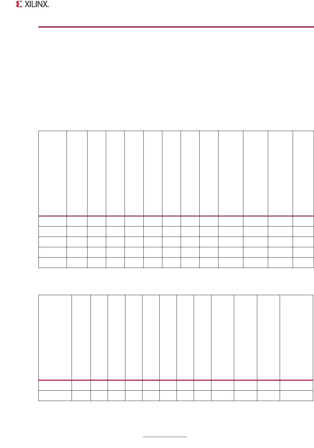
Resource Utilization
Resource utilization numbers for the AXI CDMA core are shown for the 7 series and
Zynq™-7000 devices in Ta ble 2-3, for the Virtex®-6 FPGA family in Table 2-4 , and for the
Spartan®-6 FPGA family in Table 2- 5. These values have been generated using the Xilinx
EDK and ISE® tools. They are derived from ISE tool Map reports from actual hardware
validation systems. Parameter combinations shown are not all that are possible but are
chosen to represent a range of minimum utilization (low performance) to high utilization
(high performance).
Table 2-3: 7 Series FPGA and Zynq-7000 Device Resource Estimates
C_M_AXI_DATA_WIDTH
C_MAX_BURST_LEN
C_INCLUDE_DRE
C_INCLUDE_SG
C_USE_DATAMOVER_LITE
C_INCLUDE_SF
C_AXI_LITE_IS_ASYNC
C_READ_ADDR_PIPE_DEPTH
C_WRITE_ADDR_PIPE_DEPTH
Slices
Slice Reg
Slice LUTs
Block RAM
32 32 0 0 1 1 0 11 26 398 1125 819 1
128 256 0 0 0 0 1 17 27 721 2676 1765 0
32 64 1 1 0 0 0 29 10 799 2933 2411 1
512 16 0 1 0 1 0 24 15 1965 7963 5012 10
512 128 0 1 0 0 0 21 7 1903 7887 4801 1
Table 2-4: Virtex-6 FPGA Resource Estimates
C_M_AXI_DATA_WIDTH
C_MAX_BURST_LEN
C_INCLUDE_DRE
C_INCLUDE_SG
C_USE_DATAMOVER_LITE
C_INCLUDE_SF
C_AXI_LITE_IS_ASYNC
C_READ_ADDR_PIPE_DEPTH
C_WRITE_ADDR_PIPE_DEPTH
Slices
Slice Reg
Slice LUTs
Block RAM
32 32 0 0 1 1 0 11 26 478 1125 846 1
128 256 0 0 0 0 1 17 27 631 2679 1904 0

LogiCORE IP AXI CDMA v3.03a www.xilinx.com 12
PG034 October 16, 2012
Chapter 2: Product Specification
32 64 1 1 0 0 0 29 10 1006 2934 2361 1
512 16 0 1 0 1 0 24 15 2224 7963 4688 10
512 128 0 1 0 0 0 21 7 1799 7887 4929 1
Table 2-5: Spartan-6 FPGA Resource Estimates
C_M_AXI_DATA_WIDTH
C_MAX_BURST_LEN
C_INCLUDE_DRE
C_INCLUDE_SG
C_USE_DATAMOVER_LITE
C_INCLUDE_SF
C_AXI_LITE_IS_ASYNC
C_READ_ADDR_PIPE_DEPTH
C_WRITE_ADDR_PIPE_DEPTH
Slices
Slice Reg
Slice LUTs
Block RAM
32 320011011263871126 845 3
128 2560000117277722682 2034 0
32 641100029109932943 2394 1
512 160101024151961 7986 4924 18
512 128010002171962 7895 4577 1
Table 2-4: Virtex-6 FPGA Resource Estimates (Cont’d)
C_M_AXI_DATA_WIDTH
C_MAX_BURST_LEN
C_INCLUDE_DRE
C_INCLUDE_SG
C_USE_DATAMOVER_LITE
C_INCLUDE_SF
C_AXI_LITE_IS_ASYNC
C_READ_ADDR_PIPE_DEPTH
C_WRITE_ADDR_PIPE_DEPTH
Slices
Slice Reg
Slice LUTs
Block RAM

LogiCORE IP AXI CDMA v3.03a www.xilinx.com 13
PG034 October 16, 2012
Chapter 2: Product Specification
Port Descriptions
The AXI CDMA signals are described in Table 2 -6.
Table 2-6: AXI CDMA I/O Signal Description
Signal Name Interface Signal
Type
Init
Status Description
System Signals
m_axi_aclk Clock I – AXI CDMA Synchronization Clock
m_axi_aresetn Reset I –
AXI CDMA Reset. When asserted Low, the AXI CDMA
core is put into hard reset. This signal must be
synchronous to m_axi_aclk. Assertion requirements
are specified in Ta bl e 3 -1 .
cdma_introut Interrupt O 0 Interrupt output for the AXI CDMA core
AXI4-Lite Slave Interface Signals
s_axi_lite_aclk S_AXI_LITE I –
Synchronization Clock for the AXI4-Lite interface. This
clock can be the same as m_axi_aclk (synchronous
mode) or different (asynchronous mode).
Note: If it is asynchronous, the frequency of this
clock must be less than or equal to the frequency
of the m_axi_aclk.
s_axi_lite_aresetn S_AXI_LITE I –
Active-Low AXI4-Lite Reset. When asserted Low, the
AXI4-Lite Register interface and the entire CDMA core
logic is put into hard reset. This signal must be
synchronous to s_axi_lite_aclk. Assertion
requirements are specified in Ta ble 3-1.
s_axi_lite_awvalid S_AXI_LITE I –
AXI4-Lite Write Address Channel Write Address Valid
0 = Write address is not valid
1 = Write address is valid
s_axi_lite_awready S_AXI_LITE O 0
AXI4-Lite Write Address Channel Write Address
Ready. Indicates CDMA ready to accept the write
address.
0 = Not ready to accept address
1 = Ready to accept address
s_axi_lite_awaddr(31:0) S_AXI_LITE I – AXI4-Lite Write Address Bus
s_axi_lite_wvalid S_AXI_LITE I –
AXI4-Lite Write Data Channel Write Data Valid.
0 = Write data is not valid
1 = Write data is valid
s_axi_lite_wready S_AXI_LITE O 0
AXI4-Lite Write Data Channel Write Data Ready.
Indicates CDMA ready to accept the write data.
0 = Not ready to accept data
1 = Ready to accept data
s_axi_lite_wdata(31:0) S_AXI_LITE I – AXI4-Lite Write Data Bus

LogiCORE IP AXI CDMA v3.03a www.xilinx.com 14
PG034 October 16, 2012
Chapter 2: Product Specification
s_axi_lite_bresp(1:0) S_AXI_LITE O 0
AXI4-Lite Write Response Channel. Indicates results of
the write transfer. The AXI CDMA Lite interface always
responds with OKAY.
00 = OKAY – Normal access has been successful
01 = EXOKAY – Not supported
10 = SLVERR – Not supported
11 = DECERR – Not supported
s_axi_lite_bvalid S_AXI_LITE O 0
AXI4-Lite Write Response Channel Response Valid.
Indicates response is valid.
0 = Response is not valid
1 = Response is valid
s_axi_lite_bready S_AXI_LITE I –
AXI4-Lite Write Response Channel Ready. Indicates
target is ready to receive response.
0 = Not ready to receive response
1 = Ready to receive response
s_axi_lite_arvalid S_AXI_LITE I –
AXI4-Lite Read Address Channel Read Address Valid
0 = Read address is not valid
1 = Read address is valid
s_axi_lite_arready S_AXI_LITE O 0
AXI4-Lite Read Address Channel Read Address Ready.
Indicates CDMA ready to accept the read address.
0 = Not ready to accept address
1 = Ready to accept address
s_axi_lite_araddr(31:0) S_AXI_LITE I – AXI4-Lite Read Address Bus
s_axi_lite_rvalid S_AXI_LITE O 0
AXI4-Lite Read Data Channel Read Data Valid
0 = Read data is not valid
1 = Read data is valid
s_axi_lite_rready S_AXI_LITE I –
AXI4-Lite Read Data Channel Read Data Ready.
Indicates target ready to accept the read data.
0 = Not ready to accept data
1 = Ready to accept data
s_axi_lite_rdata(31:0) S_AXI_LITE O 0 AXI4-Lite Read Data Bus
s_axi_lite_rresp(1:0) S_AXI_LITE O 0
AXI4-Lite Read Response Channel Response. Indicates
results of the read transfer. The AXI CDMA Lite
interface always responds with OKAY.
00 = OKAY – Normal access has been successful
01 = EXOKAY – Not supported
10 = SLVERR – Not supported
11 = DECERR – Not supported
CDMA Data AXI4 Read Master Interface Signals
m_axi_araddr
(C_M_AXI_ADDR_
WIDTH-1: 0)
M_AXI O 0 Read Address Channel Address Bus.
Table 2-6: AXI CDMA I/O Signal Description (Cont’d)
Signal Name Interface Signal
Type
Init
Status Description

LogiCORE IP AXI CDMA v3.03a www.xilinx.com 15
PG034 October 16, 2012
Chapter 2: Product Specification
m_axi_arlen(7:0) M_AXI O 0 Read Address Channel Burst Length. In data beats - 1.
m_axi_arsize(2:0) M_AXI O 0
Read Address Channel Burst Size. Indicates with of
burst transfer.
000 = Not Supported by AXI CDMA
001 = Not Supported by AXI CDMA
010 = 4 bytes (32-bit wide burst)
011 = 8 bytes (64-bit wide burst)
100 = 16 bytes (128-bit wide burst)
101 = 32 bytes (256-bit wide burst)
110 = Not Supported by AXI CDMA
111 = Not Supported by AXI CDMA
m_axi_arburst(1:0) M_AXI O 0
Read Address Channel Burst Type. Indicates type
burst.
00 = FIXED – Key Hole Operation
01 = INCR – Incrementing address
10 = WRAP – Not supported
11 = Reserved
m_axi_arprot(2:0) M_AXI O 000 Read Address Channel Protection. Always driven with
a constant output of 000.
m_axi_arcache(3:0) M_AXI O 0011 Read Address Channel Cache. This is always driven
with a constant output of 0011.
m_axi_arvalid M_AXI O 0
Read Address Channel Read Address Valid. Indicates
when the Read Address Channel qualifiers are valid.
0 = Read address is not valid
1 = Read address is valid
m_axi_arready M_AXI I –
Read Address Channel Read Address Ready. Indicates
target is ready to accept the read address.
0 = Target not ready to accept address
1 = Target read to accept address
m_axi_rdata
(C_M_AXI_DATA_
WIDTH-1: 0)
M_AXI I – Read Data Channel Read Data
m_axi_rresp(1:0) M_AXI I –
Read Data Channel Response. Indicates results of the
read transfer.
00 = OKAY – Normal access has been successful
01 = EXOKAY – Not supported
10 = SLVERR – Slave returned error on transfer
11 = DECERR – Decode error, transfer targeted
unmapped address
m_axi_rlast M_AXI I –
Read Data Channel Last. Indicates the last data beat of
a burst transfer.
0 = Not last data beat
1 = Last data beat
Table 2-6: AXI CDMA I/O Signal Description (Cont’d)
Signal Name Interface Signal
Type
Init
Status Description

LogiCORE IP AXI CDMA v3.03a www.xilinx.com 16
PG034 October 16, 2012
Chapter 2: Product Specification
m_axi_rvalid M_AXI I –
Read Data Channel Data Valid. Indicates m_axi_rdata
is valid.
0 = Not valid read data
1 = Valid read data
m_axi_rready M_AXI O 0
Read Data Channel Ready. Indicates the read channel
is ready to accept read data.
0 = Not ready
1 = Ready
CDMA Data AXI4 Write Master Interface Signals
m_axi_awaddr
(C_M_AXI_ADDR_
WIDTH-1: 0)
M_AXI O 0 Write Address Channel Address Bus
m_axi_awlen(7: 0) M_AXI O 0 Write Address Channel Burst Length. In data beats - 1.
m_axi_awsize(2: 0) M_AXI O 0
Write Address Channel Burst Size. Indicates width of
burst transfer.
000 = Not Supported by AXI CDMA
001 = Not Supported by AXI CDMA
010 = 4 bytes (32-bit wide burst
011 = 8 bytes (64-bit wide burst)
100 = 16 bytes (128-bit wide burst)
101 = 32 bytes (256-bit wide burst)
110 = Not Supported by AXI CDMA
111 = Not Supported by AXI CDMA
m_axi_awburst(1:0) M_AXI O 0
Write Address Channel Burst Type. Indicates type
burst.
00 = Fixed address (key hole).
01 = INCR – Incrementing address
10 = WRAP – Not supported
11 = Reserved
m_axi_awprot(2:0) M_AXI O 000 Write Address Channel Protection. This is always
driven with a constant output of 000.
m_axi_awcache(3:0) M_AXI O 0011 Write Address Channel Cache. This is always driven
with a constant output of 0011.
m_axi_awvalid M_AXI O 0
Write Address Channel Write Address Valid. Indicates
when the Write Address Channel qualifiers are valid.
0 = Write Address is not valid
1 = Write Address is valid
m_axi_awready M_AXI I –
Write Address Channel Write Address Ready. Indicates
target is ready to accept the write address.
0 = Target not ready to accept address
1 = Target read to accept address
Table 2-6: AXI CDMA I/O Signal Description (Cont’d)
Signal Name Interface Signal
Type
Init
Status Description

LogiCORE IP AXI CDMA v3.03a www.xilinx.com 17
PG034 October 16, 2012
Chapter 2: Product Specification
m_axi_wdata
(C_M_AXI_DATA_
WIDTH-1: 0)
M_AXI O 0 Write Data Channel Write Data Bus
m_axi_wstrb
(C_M_AXI_DATA_
WIDTH/8 - 1: 0)
M_AXI O 0
Write Data Channel Write Strobe Bus. Indicates which
bytes are valid in the write data bus. This value is
passed from the stream side strobe bus.
m_axi_wlast M_AXI O 0
Write Data Channel Last. Indicates the last data beat
of a burst transfer.
0 = Not last data beat
1 = Last data beat
m_axi_wvalid M_AXI O 0
Write Data Channel Data Valid. Indicates m_axi_wdata
is valid.
0 = Not valid write data
1 = Valid write data
m_axi_wready M_AXI I –
Write Data Channel Ready. Indicates the write channel
target is ready to accept write data.
0 = Target is not ready
1 = Target is ready
m_axi_bresp(1:0) M_AXI I –
Write Response Channel Response. Indicates results
of the write transfer.
00 = OKAY – Normal access has been successful
01 = EXOKAY – Not supported
10 = SLVERR – Slave returned error on transfer
11 = DECERR – Decode error, transfer targeted
unmapped address
m_axi_bvalid M_AXI I –
Write Response Channel Response Valid. Indicates
response, m_axi_bresp, is valid.
0 = Response is not valid
1 = Response is valid
m_axi_bready M_AXI O 0
Write Response Channel Ready. Indicates the write
channel is ready to receive the AXI write response.
0 = Not ready to receive response
1 = Ready to receive response
Scatter Gather AXI4 Read Master Interface Signals
m_axi_sg_araddr
(C_M_AXI_SG_ADDR_
WIDTH-1: 0)
M_AXI_SG O 0 Scatter Gather Read Address Channel Address Bus
m_axi_sg_arlen(7: 0) M_AXI_SG O 0 Scatter Gather Read Address Channel Burst Length.
Length in data beats - 1.
m_axi_sg_arsize(2: 0) M_AXI_SG O 0
Scatter Gather Read Address Channel Burst Size.
Indicates width of burst transfer.
010 = 4 bytes (32-bit wide burst). Other values are not
supported.
Table 2-6: AXI CDMA I/O Signal Description (Cont’d)
Signal Name Interface Signal
Type
Init
Status Description

LogiCORE IP AXI CDMA v3.03a www.xilinx.com 18
PG034 October 16, 2012
Chapter 2: Product Specification
m_axi_sg_arburst(1:0) M_AXI_SG O 0
Scatter Gather Read Address Channel Burst Type.
Indicates type burst.
01 = INCR – Incrementing address. Other values are
not supported.
m_axi_sg_arprot(2:0) M_AXI_SG O 000 Scatter Gather Read Address Channel Protection. This
is always driven with a constant output of 000.
m_axi_sg_arcache(3:0) M_AXI_SG O 0011 Scatter Gather Read Address Channel Cache. This is
always driven with a constant output of 0011.
m_axi_sg_arvalid M_AXI_SG O 0
Scatter Gather Read Address Channel Read Address
Valid. Indicates if m_axi_sg_araddr is valid.
0 = Read Address is not valid
1 = Read Address is valid
m_axi_sg_arready M_AXI_SG I –
Scatter Gather Read Address Channel Read Address
Ready. Indicates target is ready to accept the read
address.
0 = Target not ready to accept address
1 = Target read to accept address
m_axi_sg_rdata
(C_M_AXI_SG_DATA_
WIDTH-1: 0)
M_AXI_SG I – Scatter Gather Read Data Channel Read Data
m_axi_sg_rresp(1:0) M_AXI_SG I –
Scatter Gather Read Data Channel Response. Indicates
results of the read transfer.
00 = OKAY – Normal access has been successful
01 = EXOKAY – Not supported
10 = SLVERR – Slave returned error on transfer
11 = DECERR – Decode error, transfer targeted
unmapped address
m_axi_sg_rlast M_AXI_SG I –
Scatter Gather Read Data Channel Last. Indicates the
last data beat of a burst transfer.
0 = Not last data beat
1 = Last data beat
m_axi_sg_rdata M_AXI_SG I –
Scatter Gather Read Data Channel Data Valid.
Indicates m_sg_aximry_rdata is valid.
0 = Not valid read data
1 = Valid read data
m_axi_sg_rready M_AXI_SG O 0
Scatter Gather Read Data Channel Ready. Indicates the
read channel is ready to accept read data.
0 = Not ready
1 = Ready
Table 2-6: AXI CDMA I/O Signal Description (Cont’d)
Signal Name Interface Signal
Type
Init
Status Description

LogiCORE IP AXI CDMA v3.03a www.xilinx.com 19
PG034 October 16, 2012
Chapter 2: Product Specification
Scatter Gather AXI4 Write Master Interface Signals
m_axi_sg_awaddr
(C_M_AXI_SG_ADDR_
WIDTH-1: 0)
M_AXI_SG O 0 Scatter Gather Write Address Channel Address Bus
m_axi_sg_awlen(7: 0) M_AXI_SG O 0 Scatter Gather Write Address Channel Burst Length.
Length in data beats - 1.
m_axi_sg_awsize(2: 0) M_AXI_SG O 0
Scatter Gather Write Address Channel Burst Size.
Indicates with of burst transfer.
010 = 4 bytes (32-bit wide burst). Other values are not
supported.
m_axi_sg_awburst(1:0) M_AXI_SG O 0
Scatter Gather Write Address Channel Burst Type.
Indicates type burst.
01 = INCR – Incrementing address. Other values are
not supported.
m_axi_sg_awprot(2:0) M_AXI_SG O 000 Scatter Gather Write Address Channel Protection. This
is always driven with a constant output of 000.
m_axi_sg_awcache(3:0) M_AXI_SG O 0011 Scatter Gather Write Address Channel Cache. This is
always driven with a constant output of 0011.
m_axi_sg_awvalid M_AXI_SG O 0
Scatter Gather Write Address Channel Write Address
Valid. Indicates if m_axi_sg_awaddr is valid.
0 = Write Address is not valid
1 = Write Address is valid
m_axi_sg_awready M_AXI_SG I –
Scatter Gather Write Address Channel Write Address
Ready. Indicates target is ready to accept the write
address.
0 = Target not ready to accept address
1 = Target ready to accept address
m_axi_sg_wdata
(C_M_AXI_SG_DATA_
WIDTH-1: 0)
M_AXI_SG O 0 Scatter Gather Write Data Channel Write Data Bus
m_axi_sg_wstrb
(C_M_AXI_SG_DATA_
WIDTH/8 - 1: 0)
M_AXI_SG O 1111
Scatter Gather Write Data Channel Write Strobe Bus.
All strobe bytes asserted for SG write address channel
transfer requests.
m_axi_sg_wlast M_AXI_SG O 0
Scatter Gather Write Data Channel Last. Indicates the
last data beat of a burst transfer.
0 = Not last data beat
1 = Last data beat
m_axi_sg_wvalid M_AXI_SG O 0
Scatter Gather Write Data Channel Data Valid.
Indicates the Write Data Channel has a valid data beat
on the bus.
0 = Not valid write data
1 = Valid write data
Table 2-6: AXI CDMA I/O Signal Description (Cont’d)
Signal Name Interface Signal
Type
Init
Status Description

LogiCORE IP AXI CDMA v3.03a www.xilinx.com 20
PG034 October 16, 2012
Chapter 2: Product Specification
m_axi_sg_wready M_AXI_SG I –
Scatter Gather Write Data Channel Ready. Indicates
the SG Write Data Channel target slave is ready to
accept
write data.
0 = Target slave is not ready
1 = Target slave is ready
m_axi_sg_bresp(1:0) M_AXI_SG I –
Scatter Gather Write Response Channel Response.
Indicates results of the write transfer.
00 = OKAY – Normal access has been successful
01 = EXOKAY – Not supported
10 = SLVERR – Slave returned error on transfer
11 = DECERR – Decode error, transfer targeted
unmapped address
m_axi_sg_bvalid M_AXI_SG I –
Scatter Gather Write Response Channel Response
Valid. Indicates response, m_axi_sg_bresp, is valid.
0 = Response is not valid
1 = Response is valid
m_axi_sg_bready M_AXI_SG O 0
Scatter Gather Write Response Channel Ready.
Indicates source is ready to receive response.
0 = Not ready to receive response
1 = Ready to receive response
Table 2-6: AXI CDMA I/O Signal Description (Cont’d)
Signal Name Interface Signal
Type
Init
Status Description
LogiCORE IP AXI CDMA v3.03a www.xilinx.com 21
PG034 October 16, 2012
Chapter 2: Product Specification
Register Space
The AXI CDMA core register space is summarized in Tab le 2-7. The AXI CDMA Registers are
memory-mapped into non-cacheable memory space. The registers are 32 bits wide and the
register memory space must be aligned on 128-byte (80h) boundaries.
Register Address Mapping
Endianess
All registers are in Little Endian format, as shown in Figure 2-2.
Table 2-7: AXI CDMA Register Summary
Address Space
Offseta
a. Address Space Offset is relative to C_BASEADDR assignment. C_BASEADDR is defined in AXI CDMA MPD file and
set by XPS.
Name Description
00h CDMACR CDMA Control
04h CDMASR CDMA Status
08h CURDESC_PNTR Current Descriptor Pointer
0Ch Reserved N/A
10h TAILDESC_PNTR Tail Descriptor Pointer
14h Reserved N/A
18h SA Source Address
1Ch Reserved N/A
20h DA Destination Address
24h Reserved N/A
28h BTT Bytes to Transfer
X-Ref Target - Figure 2-2
Figure 2-2: 32-bit Little Endian Example
BYTE3 BYTE2 BYTE 1 BYTE 0
31 24 23 16 15 87 0
MSB LSB
Addr Offset 0x00Addr Offset 0x01Addr Offset 0x02Addr Offset 0x03

LogiCORE IP AXI CDMA v3.03a www.xilinx.com 22
PG034 October 16, 2012
Chapter 2: Product Specification
Register Detail
CDMACR (CDMA Control – Offset 00h)
This register provides software application control of the AXI CDMA.
X-Ref Target - Figure 2-3
Figure 2-3: CDMACR Register
SGMode
ERR_IrqEn
IOC_IrqEn
IRQThreshold
0
654
9
TailPtrEn
Rsvd
Reset
7
810
1115
Rsvd Rsvd
IRQDelay
Dly_IrqEn
Key Hole
Write
Key Hole
Read
2
3 11213
14
23 16
31 24
Table 2-8: CDMACR Register Details
Bits Field Name Default
Value
Access
Type
CDMA
Mode
Used
Description
31 to 24 IRQDelay 00h R/W SG
Interrupt Delay Time Out. This value is used for setting
the interrupt delay time out value. The interrupt time out
is a mechanism for causing the CDMA engine to generate
an interrupt after the delay time period has expired.
Timer begins counting at the end of a packet and resets
with receipt of a new packet or a time out event occurs.
Note: Setting this value to zero disables the delay
timer interrupt.
Note: This field is ignored when AXI CDMA is
configured for simple CDMA mode (C_INCLUDE_SG =
0)
23 to 16 IRQThreshold 01h R/W SG
Interrupt Threshold. This value is used for setting the
interrupt threshold. When IOC interrupt events occur, an
internal counter counts down from the Interrupt
Threshold setting. When the count reaches zero, an
interrupt out is generated by the DMA engine.
Note: The minimum setting for the threshold is 0x01.
A write of 0x00 to this register has no effect.
Note: This field is ignored when AXI DMA is
configured for Simple DMA Mode (C_INCLUDE_SG =
0)
15 Reserved 0 RO N/A Writing to this bit has no effect and it is always read as
zeroes.
14 Err_IrqEn 0 R/W Simple
and SG
Error Interrupt Enable. When set to 1, it allows the
CDMASR.Err_Irq to generate an interrupt out.
0 = Error Interrupt disabled
1 = Error Interrupt enabled

LogiCORE IP AXI CDMA v3.03a www.xilinx.com 23
PG034 October 16, 2012
Chapter 2: Product Specification
13 Dly_IrqEn 0 R/W SG
Delay Timer Interrupt Enable. When set to 1, it allows
CDMASR.Dly_Irq to generate an interrupt out. This is only
used with Scatter Gather assisted transfers.
0 = Delay Interrupt disabled
1 = Delay Interrupt enabled
12 IOC_IrqEn 0 R/W Simple
and SG
Complete Interrupt Enable. When set to 1, it allows
CDMASR.IOC_Irq to generate an interrupt out for
completed DMA transfers.
0 = IOC Interrupt disabled
1 = IOC Interrupt enabled
11 to 6 Reserved 0 RO N/A Writing to these bits has no effect and they are always
read as zeroes.
5Key Hole
Write 0R/W
Simple
and SG
Writing 1 to this enables the keyhole write (FIXED address
AXI transaction). This value should not be changed when
a transfer is in progress. This value should remain
constant until all the descriptors are processed (for SG =
1). CDMA shows unexpected behavior if this value is
changed in the middle of a transfer. It is the responsibility
of the slave device to enforce the functionality. When
enabling Key Hole operation, the MAX BURST LENGTH
should be set to 16.
4Key Hole
Read 0R/W
Simple
and SG
Writing 1 to this enables the keyhole read (FIXED address
AXI transaction). This value should not be changed when
a transfer is in progress. This value should remain
constant until all the descriptors are processed (for SG =
1). CDMA shows unexpected behavior if this value is
changed in the middle of a transfer. It is the responsibility
of the slave device to enforce the functionality. When
enabling Key Hole operation, the MAX BURST LENGTH
should be set to 16.
3SGMode0R/W
Simple
and SG
This bit controls the transfer mode of the CDMA. Setting
this bit to a 1 causes the AXI CDMA to operate in a Scatter
Gather mode if the Scatter Gather engine is included
(C_INCLUDE_SG = 1).
0 = Simple DMA Mode
1 = Scatter Gather Mode (Only valid if C_INCLUDE_SG = 1)
This bit must only be changed when the CDMA engine is
idle (CDMASR.IDLE = 1). Changing the state of this bit at
any other time has undefined results.
This bit must be set to a 0 then back to 1 by the software
application to force the CDMA SG engine to use a new
value written to the CURDESC_PNTR register.
This bit must be set prior to setting the
CDMACR.Dly_IrqEn bit. Otherwise, the
CDMACR.Dly_IrqEn bit does not get set.
Table 2-8: CDMACR Register Details (Cont’d)
Bits Field Name Default
Value
Access
Type
CDMA
Mode
Used
Description
LogiCORE IP AXI CDMA v3.03a www.xilinx.com 24
PG034 October 16, 2012
Chapter 2: Product Specification
CDMASR (CDMA Status – Offset 04h)
This register provides status for the AXI CDMA.
2 Reset 0 R/W Simple
and SG
Soft reset control for the AXI CDMA core. Setting this bit
to a 1 causes the AXI CDMA to be reset. Reset is
accomplished gracefully. Committed AXI4 transfers are
then completed. Other queued transfers are flushed.
After completion of a soft reset, all registers and bits are
in the Reset State.
0 = Reset NOT in progress – Normal operation
1 = Reset in progress
1TailPntrEn1ROSG
Indicates tail pointer mode is enabled to the SG Engine.
This bit is fixed to 1 and always read as 1 when SG is
included. If the CDMA is built with SG disabled (Simple
Mode Only), the default value of the port is 0.
0 Reserved 0 RO N/A Writing to these bits has no effect, and they are always
read as zeroes.
RO = Read Only. Writing has no effect.
R/W = Read/Write.
Table 2-8: CDMACR Register Details (Cont’d)
Bits Field Name Default
Value
Access
Type
CDMA
Mode
Used
Description
X-Ref Target - Figure 2-4
Figure 2-4: CDMASR Register
310 613 1214 11
IRQThresholdSts
5
Rsvd
4 1 027
IdleDMASlvErr
DMAIntErr
IOC_IrqErr_Irq
15
31 24 23 16
IRQDlySts
Dly_Irq DMADecErr
Rsvd
Rsvd
Rsvd
SGSlvErr
SGIntErr
SGDecErr
SGIncld
89

LogiCORE IP AXI CDMA v3.03a www.xilinx.com 25
PG034 October 16, 2012
Chapter 2: Product Specification
Table 2-9: CDMASR Register Details
Bits Field Name Default
Value
Access
Type
CDMA
Mode
Used
Description
31 to 24 IRQDelaySts 00h RO SG
Interrupt Delay Time Status. This field reflects
the current interrupt delay timer value in the SG
Engine.
23 to 16 IRQThresholdSts 01h RO SG
Interrupt Threshold Status. This field reflects
the current interrupt threshold value in the SG
Engine.
15 Reserved 0 RO N/A Always read as zero.
14 Err_Irq 0 R/WC Simple
and SG
Interrupt on Error. When set to 1, this bit
indicates an interrupt event has been generated
due to an error condition. If the corresponding
enable bit is set (CDMACR.Err_IrqEn = 1), an
interrupt out is generated from the AXI CDMA.
0 = No error Interrupt
1 = Error interrupt active
13 Dly_Irq 0 R/WC SG
Interrupt on Delay. When set to 1, this bit
indicates an interrupt event has been generated
on a delay timer time out. If the corresponding
enable bit is set (CDMACR.Dly_IrqEn = 1), an
interrupt out is generated from the AXI CDMA.
0 = No Delay Interrupt
1 = Delay Interrupt active
This bit is cleared whenever CDMACR.SGMode
is set to 0.
12 IOC_Irq 0 R/WC Simple
and SG
Interrupt on Complete. When set to 1, this bit
indicates an interrupt event has been generated
on completion of a DMA transfer (either a
Simple or SG). If the corresponding enable bit is
set (CDMACR.IOC_IrqEn = 1), an interrupt out is
generated from the AXI CDMA.
0 = No IOC Interrupt
1 = IOC Interrupt active
When operating in SG mode, the criteria
specified by the interrupt threshold must also
be met.
11 Reserved 0 RO N/A Writing to this bit has no effect and it is always
read as zeroes.

LogiCORE IP AXI CDMA v3.03a www.xilinx.com 26
PG034 October 16, 2012
Chapter 2: Product Specification
10 SGDecErr 0 RO SG
Scatter Gather Decode Error. This bit indicates
that a AXI decode error has been received by the
SG Engine during a AXI transfer (transfer
descriptor read or write). This error occurs if the
SG Engine issues an address request to an
invalid location. This error condition causes the
AXI CDMA to gracefully halt. The CDMASR.IDLE
bit is set to 1 when the CDMA has completed
shut down. CURDESC_PNTR register is updated
with the descriptor pointer value when this error
is detected.
0 = No SG Decode Errors
1 = SG Decode Error detected. CDMA Engine
halts.
A reset (soft or hard) must be issued to clear the
error condition.
9SGSlvErr0 ROSG
Scatter Gather Slave Error. This bit indicates
that a AXI slave error response has been
received by the SG Engine during a AXI transfer
(transfer descriptor read or write). This error
condition causes the AXI CDMA to gracefully
halt. The CDMASR.IDLE bit is set to 1 when the
CDMA has completed shut down.
CURDESC_PNTR register is updated with the
descriptor pointer value when this error is
detected.
0 = No SG Slave Errors
1 = SG Slave Error detected. CDMA Engine halts.
A reset (soft or hard) must be issued to clear the
error condition.
8 SGIntErr 0 RO SG
Scatter Gather Internal Error. This bit indicates
that a internal error has been encountered by
the SG Engine. This error condition causes the
AXI CDMA to gracefully halt. The CDMASR.IDLE
bit is set to 1 when the CDMA has completed
shutdown. CURDESC_PNTR register is updated
with the descriptor pointer value when this error
is detected.
0 = No SG Internal Errors
1 = SG Internal Error detected. CDMA Engine
halts.
A reset (soft or hard) must be issued to clear the
error condition.
7Reserved0 RON/A
Writing to this bit has no effect and it is always
read as zeroes.
Table 2-9: CDMASR Register Details (Cont’d)
Bits Field Name Default
Value
Access
Type
CDMA
Mode
Used
Description

LogiCORE IP AXI CDMA v3.03a www.xilinx.com 27
PG034 October 16, 2012
Chapter 2: Product Specification
6DMADecErr0 RO
Simple
and SG
DMA Decode Error. This bit indicates that an
AXI decode error has been received by the AXI
DataMover. This error occurs if the DataMover
issues an address request to an invalid location.
This error condition causes the AXI CDMA to
halt gracefully. The CDMASR.IDLE bit is set to 1
when the CDMA has completed shut down.
CURDESC_PNTR register is updated with the
descriptor pointer value when this error is
detected.
0 = No CDMA Decode Errors.
1 = CDMA Decode Error detected. CDMA Engine
halts.
A reset (soft or hard) must be issued to clear the
error condition.
5 DMASlvErr 0 RO Simple
and SG
DMA Slave Error. This bit indicates that a AXI
slave error response has been received by the
AXI DataMover during a AXI transfer (read or
write). This error condition causes the AXI
CDMA to gracefully halt. The CDMASR.IDLE bit
is set to 1 when the CDMA has completed shut
down. CURDESC_PNTR register is updated with
the descriptor pointer value when this error is
detected.
0 = No CDMA Slave Errors.
1 = CDMA Slave Error detected. CDMA Engine
halts.
A reset (soft or hard) must be issued to clear the
error condition.
Table 2-9: CDMASR Register Details (Cont’d)
Bits Field Name Default
Value
Access
Type
CDMA
Mode
Used
Description

LogiCORE IP AXI CDMA v3.03a www.xilinx.com 28
PG034 October 16, 2012
Chapter 2: Product Specification
4 DMAIntErr 0 RO Simple
and SG
DMA Internal Error. This bit indicates that a
internal error has been encountered by the
DataMover on the data transport channel. This
error can occur if a 0 value BTT (bytes to
transfer) is fed to the AXI DataMover or
DataMover has an internal processing error. A
BTT of 0 only happens if the BTT register is
written with zeroes (in Simple DMA mode) or a
BTT specified in the Control word of a fetched
descriptor is set to 0 (SG Mode). This error
condition causes the AXI CDMA to gracefully
halt. The CDMASR.IDLE bit is set to 1 when the
CDMA has completed shut down.
CURDESC_PNTR register is updated with the
descriptor pointer value when this error is
detected.
0 = No CDMA Internal Errors.
1 = CDMA Internal Error detected. CDMA Engine
halts.
A reset (soft or hard) must be issued to clear the
error condition.
3SGIncld See
Description RO Simple
and SG
SG Included. This bit indicates if the AXI CDMA
has been implemented with Scatter Gather
support included (C_SG_ENABLE = 1). This is
used by application software (drivers) to
determine if SG Mode can be utilized.
0 = Scatter Gather not included. Only Simple
DMA operations are supported.
1 = Scatter Gather is included. Both Simple DMA
and Scatter Gather operations are supported.
2Reserved0 RON/A
Writing to these bits has no effect and they are
always read as zeroes.
Table 2-9: CDMASR Register Details (Cont’d)
Bits Field Name Default
Value
Access
Type
CDMA
Mode
Used
Description

LogiCORE IP AXI CDMA v3.03a www.xilinx.com 29
PG034 October 16, 2012
Chapter 2: Product Specification
CURDESC_PNTR (CDMA Current Descriptor Pointer – Offset 08h)
This register provides the Current Descriptor Pointer for the AXI CDMA Scatter Gather
Descriptor Management.
1 Idle 0 RO Simple
and SG
CDMA Idle. Indicates the state of AXI CDMA
operations.
When set and in Simple DMA mode, the bit
indicates the programmed transfer has
completed and the CDMA is waiting for a new
transfer to be programmed. Writing to the BTT
register in Simple DMA mode causes the CDMA
to start (not Idle).
When set and in SG mode, the bit indicates the
SG Engine has reached the tail pointer for the
associated channel and all queued descriptors
have been processed. Writing to the tail pointer
register automatically restarts CDMA SG
operations.
0 = Not Idle – Simple or SG DMA operations are
in progress.
1 = Idle – Simple or SG operations completed or
not started.
0Reserved0 ROSG
Writing to these bits has no effect and they are
always read as zeroes.
RO = Read Only. Writing has no effect.
R/WC = Read/Write to Clear. A CPU write of 1 clears the associated bit to 0.
Table 2-9: CDMASR Register Details (Cont’d)
Bits Field Name Default
Value
Access
Type
CDMA
Mode
Used
Description
X-Ref Target - Figure 2-5
Figure 2-5: CURDESC_PNTR Register
Current Descriptor Pointer[31:6]
031 54
RSVD
6312

LogiCORE IP AXI CDMA v3.03a www.xilinx.com 30
PG034 October 16, 2012
Chapter 2: Product Specification
TAILDESC_PNTR (CDMA Tail Descriptor Pointer – Offset 10h)
This register provides Tail Descriptor Pointer for the AXI CDMA Scatter Gather Descriptor
Management.
Table 2-10: CURDESC_PNTR Register Details
Bits Field Name Default
Value
Access
Type
CDMA
Mode
Used
Description
31 to 6
Current
Descriptor
Pointer
0R/W
(RO) SG
Current Descriptor Pointer. Indicates the pointer of
current descriptor being worked on. This register must
contain a pointer to a valid descriptor prior to writing the
TAILDESC_PTR register. Failure to do so results in an
undefined operation by the CDMA.
When the CDMA SG Engine is running (CDMASR.IDLE =
0), the CURDESC_PNTR register is updated by the SG
Engine to reflect the starting address of the current
descriptor being executed.
On error detection, the CURDESC_PNTR register is
updated to reflect the descriptor associated with the
detected error.
The register should only be written by the software
application when the AXI CDMA is idle (CDMASR.IDLE =
1). Descriptor addresses written to this field must be
aligned to 64-byte boundaries (sixteen 32-bit words).
Examples are 0x00, 0x40, 0x80. Any other alignment has
undefined results.
This register is cleared when CDMACR.SGMode = 0.
5 to 0 Reserved 0 RO N/A Writing to these bits has no effect and they are always
read as zeroes.
RO = Read Only. Writing has no effect.
R/WC = Read/Write to Clear. A write of 1 clears the associated bit to 0.
X-Ref Target - Figure 2-6
Figure 2-6: TAILDESC_PNTR Register
Tail Descriptor Pointer [31:6]
1
031 54
RSVD
6312
LogiCORE IP AXI CDMA v3.03a www.xilinx.com 31
PG034 October 16, 2012
Chapter 2: Product Specification
SA (CDMA Source Address – Offset 18h)
This register provides the source address for Simple DMA transfers by AXI CDMA.
Table 2-11: TAILDESC_PNTR Register Details
Bits Field Name Default
Value
Access
Type
CDMA
Mode
Used
Description
31 to 6 Tail Descriptor
Pointer 0R/W
(RO) SG
Tail Descriptor Pointer. Indicates pause pointer for
descriptor chain execution. The AXI CDMA SG
Engine pauses descriptor fetching after completing
operations on the descriptor whose current
descriptor pointer matches the tail descriptor
pointer.
When the AXI CDMA is in SG Mode
(CDMACR.SGMode = 1), a write by the software
application to the TAILDESC_PNTR register causes
the AXI CDMA SG Engine to start fetching
descriptors starting from the CURDESC_PNTR
register value. If the SG engine is paused at a
tailpointer pause point, the SG engine restarts
descriptor execution at the next sequential transfer
descriptor. If the AXI CDMA is not idle
(CDMASR.IDLE = 0), writing to the TAILDESC_PNTR
has no effect except to reposition the SG pause
point.
This register is cleared when CDMACR.SGMode = 0.
5 to 0 Reserved 0 RO N/A Writing to these bits has no effect and they are
always read as zeroes.
RO = Read Only. Writing has no effect.
R/WC = Read/Write to Clear - A CPU write of 1 clears the associated bit to 0.
X-Ref Target - Figure 2-7
Figure 2-7: SA Register
31 0
Source Address[31:0]
LogiCORE IP AXI CDMA v3.03a www.xilinx.com 32
PG034 October 16, 2012
Chapter 2: Product Specification
DA (CDMA Destination Address – Offset 20h)
This register provides the Destination Address for Simple DMA transfers by AXI CDMA.
Table 2-12: SA Register Details
Bits Field Name Default
Value
Access
Type
CDMA
Mode
Used
Description
31 to 0 SA 0 R/W Simple
Source Address Register. This register is used by Simple
DMA operations (CDMACR.SGMode = 0) as the starting read
address for DMA data transfers. The address value written
can be at any byte offset.
The software application should only write to this register
when the AXI CDMA is idle (CDMASR.IDLE = 1).
RO = Read Only. Writing has no effect.
R/W = Read/Write.
X-Ref Target - Figure 2-8
Figure 2-8: DA Register
31 0
Destination Address[31:0]
Table 2-13: DA Register Details
Bits Field Name Default
Value
Access
Type
CDMA
Mode
Used
Description
0DA 0 ROSimple
Destination Address Register. This register is used by
Simple DMA operations as the starting write address for
DMA data transfers. The address value written has
restrictions relative to the Source Address and Data
Realignment Engine (DRE) inclusion as follows.
If DRE is not included in the AXI CDMA (C_INCLUDE_DRE =
0) or the DMA data width is 128 or 256 bits
(C_M_AXI_DATA_WIDTH = 128 or 256), then the address
offset of the Destination address must match that of the
Source Address Register value. Offset is defined as that
portion of a system address that is used to designate a byte
position within a single data beat width. For example, a
32-bit data bus has four addressable byte positions within a
single data beat (0, 1, 2, and 3). The portion of the address
that designates these positions is the offset. The number of
address bits used for the offset varies with the transfer bus
data width.
The software application should only write to this register
when the AXI CDMA is idle (CDMASR.IDLE = 1).
RO = Read Only. Writing has no effect.
R/WC = Read / Write to Clear. A CPU write of 1 clears the associated bit to 0.
LogiCORE IP AXI CDMA v3.03a www.xilinx.com 33
PG034 October 16, 2012
Chapter 2: Product Specification
BTT (CDMA Bytes to Transfer – Offset 28h)
This register provides the value for the bytes to transfer for Simple DMA transfers by the AXI
CDMA.
X-Ref Target - Figure 2-9
Figure 2-9: BTT Register
Table 2-14: BTT Register Details
Bits Field
Name
Default
Value
Access
Type Description
31 to 23 Reserved 0 RO Writing to these bits has no effect, and they are always
read as zeroes.
22 to 0 BTT 0 R/W
(RO)
Bytes to Transfer. This register field is used for Simple
DMA transfers and indicates the desired number of bytes
to DMA from the Source Address to the Destination
Address. A maximum of 8,388,607 bytes of data can be
specified by this field for the associated transfer.
Writing to the BTT Register also initiates the Simple DMA
transfer.
Note: A value of zero (0) is not allowed and causes a
DMA internal error to be set by AXI CDMA. The
software application should only write to this register
when the AXI CDMA is idle (CDMASR.IDLE = 1).
RO = Read Only. Writing has no effect.
R/W = Read/Write.
BTT[22:0]
222331
RSVD
LogiCORE IP AXI CDMA v3.03a www.xilinx.com 34
PG034 October 16, 2012
Chapter 3
Designing with the Core
General Design Guidelines
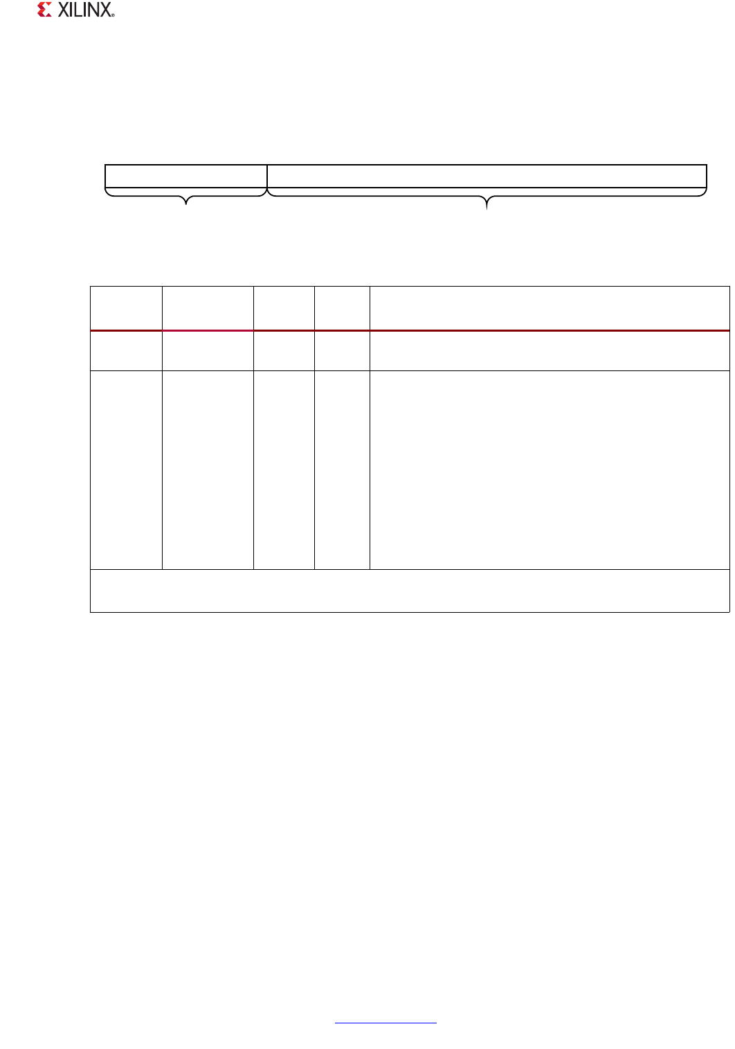
A typical MicroBlaze™ processor based system is shown in Figure 3-1.
X-Ref Target - Figure 3-1
Figure 3-1: Typical MicroBlaze Processor System Configuration Using AXI CDMA
8

LogiCORE IP AXI CDMA v3.03a www.xilinx.com 35
PG034 October 16, 2012
Chapter 3: Designing with the Core
Clocking
AXI CDMA provides two clocking modes of operation: asynchronous and synchronous. In
asynchronous mode, AXI4-Lite interface is asynchronous to AXI4-MMap interface. This is
achieved by setting C_AXI_LITE_IS_ASYNC = 1. In this case, s_axi_lite_aclk can be less
than or equal to m_axi_aclk. In synchronous mode, C_AXI_LITE_IS_ASYNC = 0, both
s_axi_lite_aclk and m_axi_aclk run at same frequency.
Resets
The AXI CDMA utilizes two hardware resets for logic initialization. An active-Low reset
assertion on the CDMA m_axi_aresetn input or the s_axi_lite_aresetn input results
in a reset of the entire AXI CDMA core logic. This is considered a hardware reset and there
are no graceful completions of AXI4 transfers in progress. A hardware reset initializes all AXI
CDMA registers to the default state, all internal queues are flushed, and all internal logic is
returned to power on conditions. It is required that the m_axi_aresetn input is
synchronous to the m_axi_aclk master clock input and the s_axi_lite_aresetn input
be synchronous to the s_axi_lite_aclk input.
The required reset assertion times are stated in Table 3-1. The table also indicates the
stabilization time for AXI CDMA outputs reacting to a reset conditions.
Table 3-1: Reset Assertion/Deassertion Stabilization Times
Description Value Applicable Signal
C_AXI_LITE_IS_ASYNC = 0
Minimum assertion time 8 clocks
(m_axi_aclk) m_axi_aresetn input
Minimum assertion time 8 clocks
(m_axi_lite_aclk) m_axi_lite_resetn input
m_axi_aresetn assertion to output signals in reset state
(maximum)
3 clocks
(m_axi_aclk) All output signals
Reset deassertion to normal operation state (maximum) 3 clocks
(m_axi_aclk) All output signals
m_axi_lite_resetn assertion to output signals in reset state
(maximum)
3 clocks
(m_axi_aclk =
m_axi_lite_aclk)
All output signals
m_axi_lite_resetn deassertion to normal operation state
(maximum)
3 clocks
(m_axi_aclk =
m_axi_lite_aclk)
All output signals
LogiCORE IP AXI CDMA v3.03a www.xilinx.com 36
PG034 October 16, 2012
Chapter 3: Designing with the Core
Design Parameters
The AXI CDMA design parameters are listed and described in Table 3-2 .
C_AXI_LITE_IS_ASYNC = 1
Minimum assertion time 8 clocks
(m_axi_aclk) m_axi_aresetn input
Minimum assertion time 8 clocks
(m_axi_lite_aclk) m_axi_lite_resetn input
m_axi_aresetn assertion to output signals in reset state
(maximum)
3 clocks
(m_axi_aclk) All output signals
Reset deassertion to normal operation state (maximum) 3 clocks
(m_axi_aclk) All output signals
m_axi_lite_resetn assertion to output signals in reset state
(maximum)
1 m_axi_lite_aclk
plus 5 m_axi_aclk
clocks
All output signals
m_axi_lite_resetn deassertion to normal operation state
(maximum)
1 m_axi_lite_aclk
plus 5 m_axi_aclk
clocks
All output signals
Table 3-1: Reset Assertion/Deassertion Stabilization Times (Cont’d)
Description Value Applicable Signal
Table 3-2: AXI CDMA Design Parameter Description
Parameter Name Allowable
Values
Default
Values
VHDL
Type Feature/Description
AXI CDMA General Parameters
C_FAMILY
virtex6,
spartan6,
Virtex7,
Kintex7,
Artix7,
Zynq
virtex6 String Specifies the target FPGA family
AXI CDMA AXI4-Lite Parameters
C_S_AXI_LITE_ADDR_WIDTH 6 6 integer Address width (in bits) of AXI4-Lite
Interface. This is currently fixed at 6 bits.
C_S_AXI_LITE_DATA_WIDTH 32 32 integer Data width (in bits) of AXI4-Lite Interface.
This is currently fixed at 32 bits.
C_AXI_LITE_IS_ASYNC 0,1 0 integer
Specifies if the s_axi_lite_aclk is different
than the m_axi_aclk
0 = s_axi_lite_aclk is the same as m_axi_aclk
1 = s_axi_lite_aclk is different than the
m_axi_aclk

LogiCORE IP AXI CDMA v3.03a www.xilinx.com 37
PG034 October 16, 2012
Chapter 3: Designing with the Core
AXI CDMA Data AXI4 Master Parameters
C_M_AXI_ADDR_WIDTH 32 32 integer Address width of the AXI4 master interface
for the Data transfer path.
C_M_AXI_DATA_WIDTH
32, 64, 128,
256, 512,
1024
32 integer Data width of the AXI4 master interface for
the Data transfer path.
C_M_AXI_MAX_BURST_LEN 16, 32, 64,
128, 256 16 integer
Specifies the maximum burst length to be
requested by the Data AXI4 master for
both read and writes.
Note: When enabling Key Hole read or
write, the max burst length should be set
to 16.
C_INCLUDE_DRE 0, 1 0 integer
Specifies the inclusion or omission of the
Data Realignment Engine (DRE) in the
DataMover (can only be included for 32-bit
and 64-bit data widths).
0 = Exclude DRE
1 = Include DRE
C_USE_DATAMOVER_LITE 0, 1 0 integer
Specifies the use of a reduced resource
version of the DataMover (can only be used
for 32-bit and 64-bit data widths, no DRE,
and burst lengths limited to 16, 32, and 64).
This parameter is ignored if Scatter Gather
is enabled (C_INCLUDE_SG = 1).
0 = Normal DataMover (full version)
1 = Reduced resource DataMover
C_READ_ADDR_PIPE_DEPTH 1 to 30 4 integer
This parameter specifies the depth of the
DataMover read address pipelining queues
for the Main data transport channels. The
effective address pipelining on the AXI4
Read Address Channel is the value
assigned plus 2. If the value assigned is 1,
the effective address pipelining on the
AXI4 Read Address Channel is the value
assigned plus 1.
C_WRITE_ADDR_PIPE_DEPTH 1 to 30 4 integer
This parameter specifies the depth of the
DataMover write address pipelining
queues for the Main data transport
channels. The effective address pipelining
on the AXI4 Write Address Channel is the
value assigned plus 2. However, if the value
assigned is 1, the effective address
pipelining on the AXI4 Read Address
Channel is 2.
Table 3-2: AXI CDMA Design Parameter Description (Cont’d)
Parameter Name Allowable
Values
Default
Values
VHDL
Type Feature/Description

LogiCORE IP AXI CDMA v3.03a www.xilinx.com 38
PG034 October 16, 2012
Chapter 3: Designing with the Core
Parameter Descriptions
C_FAMILY
•Type: string
•Allowed Values: Zynq™-7000, 7 series, Virtex®-6, and Spartan®-6 devices
•Definition: Indicates the target device for the design
•Description: Specifies the target FPGA
C_S_AXI_LITE_ADDR_WIDTH
•Type: Integer
•Allowed Values: 6 (default = 6)
•Definition: Address bus width of the AXI4-Lite interface
•Description: This integer parameter is used by the AXI4-Lite interface to size the read
and write address channel related components.
Store and Forward Parameters
C_INCLUDE_SF 0, 1 1 integer
Specifies the inclusion or omission of the
Store and Forward feature
0 = Exclude Store and Forward
1 = Include Store and Forward
Scatter Gather Related Parameters
C_INCLUDE_SG 0, 1 0 integer
Specifies the inclusion or omission of the
Scatter Gather feature
0 = Exclude Scatter Gather
1 = Include Scatter Gather
C_M_AXI_SG_ADDR_WIDTH 32 32 integer Address width (in bits) of AXI Scatter
Gather AXI4 Master interface
C_M_AXI_SG_DATA_WIDTH 32 32 integer Data width (in bits) of AXI Scatter Gather
AXI4 Master interface
C_DLYTMR_RESOLUTION 1 to
1000000 125 integer
Specifies the resolution of one tick of the
SG interrupt delay timer in m_axi_aclk
cycles
Table 3-2: AXI CDMA Design Parameter Description (Cont’d)
Parameter Name Allowable
Values
Default
Values
VHDL
Type Feature/Description

LogiCORE IP AXI CDMA v3.03a www.xilinx.com 39
PG034 October 16, 2012
Chapter 3: Designing with the Core
C_S_AXI_LITE_DATA_WIDTH
•Type: Integer
•Allowed Values: 32 (default = 32)
•Definition: Data bus width of the AXI4-Lite interface
•Description: This integer parameter is used by the AXI4-Lite interface to size the read
and write data channel related components within the Lite interface.
C_AXI_LITE_IS_ASYNC
•Type: Integer
•Allowed Values: 0, 1 (default = 0)
•Definition: 0 = s_axi_lite_aclk is the same (synchronous) to m_axi_aclk, 1 =
s_axi_lite_aclk is different (asynchronous) to m_axi_aclk
•Description: This integer parameter indicates to the AXI CDMA logic that the clock
supplied to the s_axi_lite_aclk input is the same or different than that supplied to
the m_axi_aclk input. If the s_axi_lite_aclk is different, it must have a frequency
that is less than or equal to the frequency of the m_axi_aclk.
Note: The AXI CDMA v3_03_a incorporates a Tool Command Language (TCL) script that
automatically sets the appropriate value for this parameter based on a compare of the signal
names attached to the m_axi_aclk and s_axi_lite_aclk inputs in the XPS MHS file.
C_INCLUDE_DRE
•Type: Integer
•Allowed Values: 0, 1 (default = 1)
•Definition: 0 = Exclude Data Realignment Engine; 1 = Include Data Realignment Engine
•Description: Include or exclude the Data Realignment Engine. For use cases where all
transfers are C_M_AXI_DATA_WIDTH aligned, this parameter can be set to 0 to exclude
DRE, saving FPGA resources. Setting this parameter to 1 allows data realignment to the
byte (8 bits) address resolution on the data transport AXI4 interface. DRE is only
supported for C_M_AXI_DATA_WIDTH = 32 and C_M_AXI_DATA_WIDTH = 64.
When DRE is included, CDMA data reads can start from any address byte offset (the
transfer source address). DRE realigns the read data to match the starting offset of the
programmed destination address.

LogiCORE IP AXI CDMA v3.03a www.xilinx.com 40
PG034 October 16, 2012
Chapter 3: Designing with the Core
Note: If DRE is disabled (C_INCLUDE_DRE = 0) or DRE does not support the specified data width
(C_M_AXI_DATA_WIDTH = 128 or 256), the offset of the transfer source address must match the
offset of the transfer destination address. Offset is defined as that portion of a system address
that is used to designate a byte position within a single data beat width. For example, a 32-bit
data bus has four addressable byte positions within a single data beat (0, 1, 2, and 3). The portion
of the address that designates these positions is the offset. The number of address bits used for
the offset varies with the transfer bus data width.
C_M_AXI_ADDR_WIDTH
•Type: Integer
•Allowed Values: 32 (default = 32)
•Definition: Address bus width of the data transport AXI4 master interface
•Description: This integer parameter is used to size the address bus for the data
transport AXI4 master interface. The EDK tool suite assigns this parameter a fixed value
of 32.
C_M_AXI_ADDR_WIDTH
•Type: Integer
•Allowed Values: 32 (default = 32)
•Definition: Address Channel width of the AXI CDMA AXI4 data transport interface
•Description: This integer parameter is used to size the AXI CDMA AXI4 data transport
address channel related qualifiers. The EDK tool suite assigns this parameter a fixed
value of 32.
C_M_AXI_DATA_WIDTH
•Type: Integer
•Allowed Values: 32, 64, 128, 256, 512, 1024 (default = 32)
•Definition: Data Channel width of the AXI CDMA AXI4 data transport interface
•Description: This integer parameter is used to size the AXI CDMA AXI4 data transport
Data Channel related qualifiers.
C_M_AXI_MAX_BURST_LEN
•Type: Integer
•Allowed Values: 16, 32, 64, 128, 256 (default = 16)
•Definition: Maximum burst length used (in data beats) by AXI CDMA for data transfers

LogiCORE IP AXI CDMA v3.03a www.xilinx.com 41
PG034 October 16, 2012
Chapter 3: Designing with the Core
•Description: This parameter limits the burst length requested by CDMA on the AXI4
data transport interface. A value of 256 is not allowed if the C_M_AXI_DATA_WIDTH
parameter is assigned a value of 256. An AXI 4K address boundary crossing violation
could occur otherwise.
•Type: Integer
•Allowed Values: 0, 1 (default = 0)
•Definition: 0 = Use Full DataMover; 1 = Use DataMover Lite
•Description: This parameter allows the DataMover used in the main CDMA data
transport path to be implemented in a “lite” mode. DataMover Lite is useful for
resource limited designs that requires a smaller resource utilization traded off for high
performance data transfer. This parameter is ignored if Scatter Gather is enabled
(C_INCLUDE_SG = 1).
C_USE_DATAMOVER_LITE
•Type: Integer
•Allowed Values: 1 to 30 (default = 4)
•Definition: Sets the Read Address Pipeline depth for the DataMover MM2S function
•Description: This parameter specifies the depth of the DataMover read address
pipelining queues for the Main data transport channel. The effective address pipelining
on the AXI4 Read Address Channel is the value assigned plus 2. If the value assigned is
1, the effective address pipelining on the AXI4 Read Address Channel is the value
assigned plus 1.
C_READ_ADDR_PIPE_DEPTH
•Allowed Values: 1 to 30 (default = 4)
•Definition: Sets the Write Address Pipeline depth for the DataMover S2MM function
•Description: This parameter specifies the depth of the DataMover write address
pipelining queues for the Main data transport channel. The effective address pipelining
on the AXI4 Write Address Channel is the value assigned plus 2. If the value assigned is
1, the effective address pipelining is 2.
C_INCLUDE_SF
•Type: Integer
•Allowed Values: 0, 1 (default = 1)
•Definition: 0 = Exclude Store and Forward; 1 = Include Store and Forward
•Description: This parameter specifies the inclusion or omission of the Store and
Forward function.

LogiCORE IP AXI CDMA v3.03a www.xilinx.com 42
PG034 October 16, 2012
Chapter 3: Designing with the Core
C_INCLUDE_SG
•Type: Integer
•Allowed Values: 0, 1 (default = 0)
•Definition: 0 = Exclude Scatter Gather; 1 = Include Scatter Gather
•Description: Include or exclude the Scatter Gather support feature. When set to 0, only
Simple Mode DMA operations are supported by AXI CDMA. When set to 1, both Simple
and Scatter Gather assisted transfers are supported.
C_M_AXI_SG_ADDR_WIDTH
•Type: Integer
•Allowed Values: 32 (default = 32)
•Definition: Address bus width of attached AXI on the AXI Scatter Gather interface
•Description: This integer parameter is used to size the Read Address and Write
Address Channels of the AXI4 Scatter Gather interface. The EDK tool suite assigns this
parameter a fixed value of 32.
C_M_AXI_SG_DATA_WIDTH
•Type: Integer
•Allowed Values: 32 (default = 32)
•Definition: Data bus width of attached AXI on the AXI Scatter/Gather interface
•Description: This integer parameter is used to size the Read Data and Write Data
Channels of the AXI4 Scatter Gather interface. The EDK tool suite assigns this parameter
a fixed value of 32.
C_DLYTMR_RESOLUTION
•Type: Integer
•Allowed Values: 1 to 100,000 (default = 256)
•Definition: Interrupt Delay Timer Resolution in axi_aclk cycles
•Description: This integer parameter is used to set the resolution of the Interrupt Delay
Timer. The value assigned specifies the number of the input axi_aclk clock cycles
between each tick of the delay timer. The Delay Timer is only used during Scatter
Gather operations. For additional information, see the section SG Delay Interrupt.

LogiCORE IP AXI CDMA v3.03a www.xilinx.com 43
PG034 October 16, 2012
Chapter 3: Designing with the Core
AXI CDMA Operation
DataMover Lite Mode Restrictions
The AXI DataMover that is internally used by the AXI CDMA can be optionally programmed
to a reduced feature set to provide a reduced resource utilization footprint in the target
FPGA (see CDMA resource utilizations in Table 2 -4 and Table 2-5). Using the DataMover Lite
operation mode puts restrictions on the available CDMA features. The following is a list of
feature restrictions (compared to the Full mode).
• AXI CDMA data transport width is restricted to 32 and 64 bits.
C_M_AXI_DATA_WIDTH = 32 or 64 only
• Maximum Burst Length is restricted to 16, 32, and 64 data beats.
C_M_AXI_MAX_BURST_LEN = 16, 32, or 64 only
• Maximum allowed bytes to transfer (BTT) value that is programmed per transfer request
is limited to the specified maximum burst length times the specified CDMA data width
divided by 8.
C_M_AXI_MAX_BURST_LEN × (C_M_AXI_DATA_WIDTH/8)
• The DRE function is not supported with Data Mover Lite.
C_INCLUDE_DRE must be set to 0
Note: In case the CDMA is configured in Lite Mode, the 4K address crossing guard must be done by
the software application when specifying the Source Address, the Destination Address, and the BTT
values programmed into the CDMA registers.

LogiCORE IP AXI CDMA v3.03a www.xilinx.com 44
PG034 October 16, 2012
Chapter 3: Designing with the Core
Sequence of Operation
Simple DMA Mode
The basic mode of operation for the CDMA is Simple DMA. In this mode, the CDMA
executes one programmed DMA command and then stops. This requires the CDMA
registers to be set up by an external AXI4 Master for each DMA operation required.
These basic steps describe how to set up and initiate a CDMA transfer in simple operation
mode.
1. Verify CDMASR.IDLE = 1.
2. Program the CDMACR.IOC_IrqEn bit to the desired state for interrupt generation on
transfer completion. Also set the error interrupt enable (CDMACR.ERR_IrqEn), if so
desired.
3. Write the desired transfer source address to the Source Address (SA) Register. The
transfer data at the source address must be valid and ready for transfer.
4. Write the desired transfer destination address to the Destination Address (DA) Register.
5. Write the number of bytes to transfer to the CDMA Bytes to Transfer (BTT) Register. Up
to 8,388,607 bytes can be specified for a single transfer (unless DataMover Lite is being
used). Writing to the BTT register also starts the transfer.
6. Either poll the CDMASR.IDLE bit for assertion (CDMASR.IDLE = 1) or wait for the CDMA
to generate an output interrupt (assumes CDMACR.IOC_IrqEn = 1).
7. If interrupt based, determine the interrupt source (transfer completed or an error has
occurred).
8. Clear the CDMASR.IOC_Irq bit by writing a 1 to the DMASR.IOC_Irq bit position.
9. Ready for another transfer. Go back to step 1.
Scatter Gather Mode
Scatter Gather is a mechanism that allows for automated DMA transfer scheduling through
a pre-programmed instruction list of transfer descriptors (Scatter Gather Transfer Descriptor
Definition). This instruction list is programmed by the user software application into a
memory-resident data structure that must be accessible by the AXI CDMA SG interface. This
list of instructions is organized into what is referred to as a transfer descriptor chain. Each
descriptor has an address pointer to the next sequential descriptor to be processed. The last
descriptor in the chain generally points back to the first descriptor in the chain but it is not
required.

LogiCORE IP AXI CDMA v3.03a www.xilinx.com 45
PG034 October 16, 2012
Chapter 3: Designing with the Core
CDMA operations began with the setup of the descriptor pointer registers and the CDMA
control registers. The following lists minimum steps, in order, required for AXI CDMA
operations:
1. Write a valid pointer to channel CURDESC_PNTR register (Offset 0x08).
2. Write control information to channel CDMACR register (Offset 0x00) to set interrupt
enables and key hole feature if desired.
3. Write a valid pointer to the channel’s TAILDESC_PNTR register (Offset 0x10). This starts
the channel fetching and processing descriptors.
4. CDMA scatter gather operations continue until the descriptor at TAILDESC_PNTR is
processed, and then the engine idles as indicated by CDMASR.Idle = 1.
Transfer Descriptor Management
Prior to starting CDMA Scatter Gather operations, the software application must set up a
transfer descriptor chain. After the AXI CDMA begins SG operations, it fetches, processes,
and then update the descriptors. By analyzing the descriptors, the software application can
track the status of the associated CDMA data transfer and determine the completion status
of the transfer. With this information, the software application can manage the transfer
descriptors and DMA data buffers.
The software applications should process each DMA data buffer associated with completed
descriptor and reallocate the descriptor for AXI CDMA use. To prevent software and
hardware from modifying the same descriptor, a Tail Pointer Mode was created. The tail
pointer is initialized by software to point to the end of the descriptor chain.
This becomes the pause point for hardware. When hardware begins running, it fetches and
processes each descriptor in the chain until it reaches the tail pointer. The AXI CDMA then
pauses descriptor processing.
The software typically then processes and re-allocates any descriptor with the Complete bit
set to 1. While the software is processing descriptors, AXI CDMA hardware is prevented
from modifying the descriptors being processed by software by the tail pointer. When the
software finishes re-allocating a set of descriptors, it then moves the tail pointer location to
the end of the re-allocated descriptors by writing to the AXI CDMA TAILDESC register. The
act of writing to the TAILDESC register causes the AXI CDMA hardware, if it is paused at the
tail pointer, to begin processing descriptors again.
If the AXI CDMA hardware is not paused at the TAILDESC pointer, writing to the TAILDESC
register has no effect on the hardware. In this situation, the AXI CDMA continues to process
descriptors until reaching the new tail descriptor pointer location.

LogiCORE IP AXI CDMA v3.03a www.xilinx.com 46
PG034 October 16, 2012
Chapter 3: Designing with the Core
Scatter Gather Transfer Descriptor Definition
This defines the format and contents of the AXI CDMA Scatter Gather Transfer Descriptors.
These are used only by the SG function if it is enabled in the CDMA by assigning the
parameter C_INCLUDE_SG a value of 1 and the CDMACR.SGMode bit is set to 1. A transfer
descriptor consists of eight 32-bit words. The descriptor represents the control and status
information needed for a single CDMA transfer plus address linkage to the next sequential
descriptor. Each descriptor can define a single CDMA transfer of up to 8,388,607 Bytes of
data. A descriptor chain is defined as a series of descriptors that are sequentially linked
through the address linkage built into the descriptor format.
The AXI CDMA SG Engine traverses the descriptor chain following the linkage until the last
descriptor of the chain has been completed. The relationship and identification of the AXI
CDMA transfer descriptor words is shown in Table 3 -3.
Note: Transfer Descriptors must be aligned on 16 32-bit word alignment. Example valid offsets are
0x00, 0x40, 0x80, and 0xC0.
Table 3-3: Transfer Descriptor Word Summary
Address Space
Offseta
a. Address Space Offset is relative to the address of the first word of the Transfer Descriptor in system memory.
Name Description
00h NXTDESC_PNTR Next Descriptor Pointer
04h RESERVED N/A
08h SA Source Address
0Ch RESERVED N/A
10h DA Destination Address
14h RESERVED N/A
18h CONTROL Transfer Control
1Ch STATUS Transfer Status
LogiCORE IP AXI CDMA v3.03a www.xilinx.com 47
PG034 October 16, 2012
Chapter 3: Designing with the Core
Transfer Descriptor NXTDESC_PNTR (Next Descriptor Pointer – Offset 00h)
This word provides the address pointer to the first word of the next transfer descriptor in
the descriptor chain.
Transfer Descriptor SA Word (Source Address – Offset 08h)
This word provides the starting address for the data read operations for the associated
DMA transfer.
X-Ref Target - Figure 3-2
Figure 3-2: Transfer Descriptor NXTDESC_PNTR Word
031 54
Reserved
3216
NxtDescPntr
Table 3-4: Transfer Descriptor NXTDESC_PNTR Word Details
Bits Field Name Description
31 to 6 NxtDescPntr
Next Descriptor Pointer. This field is an address pointer (most significant 26 bits) to
the first word of the next transfer descriptor to be executed by the CDMA SG Engine.
The least-significant 6 bits of this register are appended to this value when used by the
SG Engine forcing transfer descriptors to be loaded in memory at 128-byte address
alignment.
5 to 0 Reserved These bits are reserved and fixed to zeroes. This forces the address value programmed
in this register to be aligned to 128-byte aligned addresses.
X-Ref Target - Figure 3-3
Figure 3-3: Transfer Descriptor SA Word
BTT[22:0]
0
2223
31
RSVD
Table 3-5: Transfer Descriptor SA Word Details
Bits Field Name Description
31 to 0 DA Source Address. This value specifies the starting address for data read operations for
the associated DMA transfer. The address value can be at any byte offset.
LogiCORE IP AXI CDMA v3.03a www.xilinx.com 48
PG034 October 16, 2012
Chapter 3: Designing with the Core
Transfer Descriptor DA Word (Destination Address – Offset 10h)
This word provides the starting address for the data write operations for the associated
DMA transfer.
Transfer Descriptor CONTROL Word (Control – Offset 18h)
This value provides control for the AXI CDMA transfer.
X-Ref Target - Figure 3-4
Figure 3-4: Transfer Descriptor DA Word
31 0
Destination Address [31:0]
Table 3-6: Transfer Descriptor DA Word Details
Bits Field Name Description
31 to 0 DA
Destination Address. This value specifies the starting write address for DMA data
transfers. The address value has restrictions relative to the Source Address and AXI
CDMA DRE inclusion.
If DRE is not included in the AXI CDMA (C_INCLUDE_DRE = 0) or the specified CDMA
data width is not supported by DRE (C_M_AXI_DATA_WIDTH = 128 or more), then the
address offset of the Destination Address must match that of the Source Address value.
X-Ref Target - Figure 3-5
Figure 3-5: Transfer Descriptor CONTROL Word
BTT[22:0]
0
2223
31
RSVD
Table 3-7: Transfer Descriptor CONTROL Word Details
Bits Field Name Description
31 to 23 Reserved These bits are reserved and should be set to zero.
22 to 0 BTT
Bytes to Transfer. This field in the Control word specifies the desired number of
bytes to DMA from the Source Address to the Destination Address. A maximum of
8,388,607 bytes of data can be specified by this field for the associated transfer.
A value of zero (0) is not allowed and causes a DMA internal error to be set by AXI
CDMA.
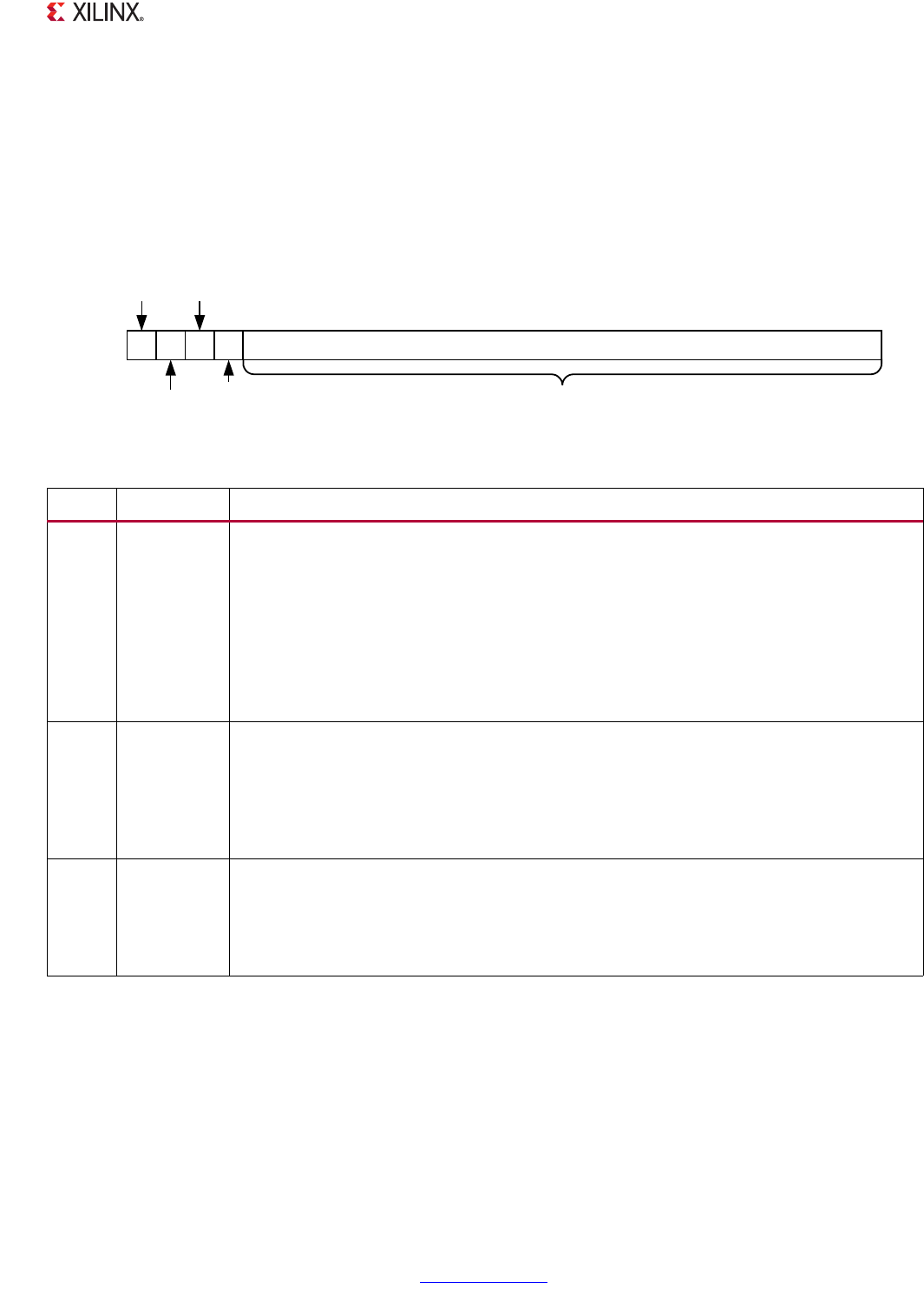
LogiCORE IP AXI CDMA v3.03a www.xilinx.com 49
PG034 October 16, 2012
Chapter 3: Designing with the Core
Transfer Descriptor Status Word (Status – Offset 1Ch)
This value provides status to the software application regarding the execution of the
Transfer Descriptor by the AXI CDMA. This status word should be zeroed when the transfer
descriptor is programmed by the software application. When the AXI CDMA SG Engine has
completed execution of the transfer descriptor, the status word is updated and written back
to the original status word location in memory by the SG Engine.
X-Ref Target - Figure 3-6
Figure 3-6: Transfer Descriptor Status Word
Cmplt
031
RSVD
30 29 28
DMADecErr
DMASlvErr
DMAIntErr
27
Table 3-8: Transfer Descriptor Status Word Details
Bits Field Name Description
31 Cmplt
Transfer Completed. This indicates to the software application that the CDMA Engine
has completed the transfer as described by the associated descriptor. The software
application can manipulate any descriptor with the Completed bit set to 1 when in Tail
Pointer Mode (currently the only supported mode).
0 = Descriptor not completed
1 = Descriptor completed
If the CDMA SG Engine fetches a descriptor is with this bit set to 1, the descriptor is
considered a stale descriptor. An SGIntErr is flagged in the AXI CDMA Status Register and
the AXI CDMA engine halts with no update to the descriptor.
30 DMADecErr
DMA Decode Error. This bit indicates that an AXI decode error was received by the AXI
CDMA DataMover. This error occurs if the DataMover issues an address that does not
have a mapping assignment to a slave device. This error condition causes the AXI CDMA
to gracefully halt.
0 = No CDMA Decode Errors
1 = CDMA Decode Error received. CDMA Engine halts at this descriptor
29 DMASlvErr
DMA Slave Error. This bit indicates that a AXI slave error response was received by the
AXI CDMA DataMover during the AXI transfer (read or write) associated with this
descriptor. This error condition causes the AXI CDMA to gracefully halt.
0 = No CDMA Slave Errors
1 = CDMA Slave Error received. CDMA Engine halts at this descriptor

LogiCORE IP AXI CDMA v3.03a www.xilinx.com 50
PG034 October 16, 2012
Chapter 3: Designing with the Core
t
CDMA Scatter Gather Restart and Pause Behavior
The CDMA Scatter Gather engine has two ways to continue SG operation after it has paused
at a tail pointer descriptor. The first is to re-allocate transfer descriptors in the chain that is
currently active. The software application merely writes the address of the last re-allocated
transfer descriptor to the CDMA TAILDESC_PNTR register. This causes the CDMA SG engine
to continue sequencing through the re-allocated descriptor chain until the next tail pointer
location is hit.
However, it is sometimes advantageous for a software application to have a different
descriptor chain set up somewhere else in memory that needs to be executed after the
CDMA has hit the initial tail descriptor. The second method is to have the CDMA SG restart
after the CDMA SG has paused and the CDMASR.IDLE bit is set. At that point, the
application must set the CDMACR.SGMode bit to 0. Then initialization should be followed
again.
Interrupt Generation
An interrupt output is provided by the AXI CDMA. This output drives high when an internal
interrupt event is logged in the CDMA Status Register (CDMASR) and the associated
interrupt enable bit is set in the CDMA Control Register (CDMACR).
IMPORTANT: This interrupt output is synchronized to the s_axi_lite_aclk clock input.
Internal interrupt events are different depending on whether the AXI CDMA is operating in
Simple DMA mode or SG Mode. Simple DMA mode generates an IOC interrupt whenever a
programmed transfer is completed. In addition, three error conditions reported by the
DataMover (internal error, slave error, and decode error) can also generate an interrupt
assertion. For Scatter Gather mode, the delay interrupt and the three SG engine error
interrupt events are added to the interrupt event mix.
28 DMAIntErr
DMA Internal Error. This bit indicates that an internal error was encountered by the AXI
CDMA DataMover on the data transport channel during the execution of this descriptor.
This error can occur if a 0 value BTT (bytes to transfer) is fed to the AXI DataMover or
DataMover has an internal processing error. A BTT of 0 only happens if the BTT field in
the transfer descriptor CONTROL word is programmed with a value of zero. This error
condition causes the AXI CDMA to gracefully halt. The CDMASR.IDLE bit is set to 1 when
the CDMA has completed shutdown.
0 = No CDMA Internal Errors
1 = CDMA Internal Error detected. CDMA Engine halts at this descriptor
27 to 0 Reserved These bits are reserved and should be set to zero.
Table 3-8: Transfer Descriptor Status Word Details (Cont’d)
Bits Field Name Description

LogiCORE IP AXI CDMA v3.03a www.xilinx.com 51
PG034 October 16, 2012
Chapter 3: Designing with the Core
SG Interrupt Threshold and Interrupt Coalescing
The AXI CDMA interrupt coalescing feature is enabled by setting the
CDMACR.IRQThreshold field to a value greater than the default value of 1. When a SG
session is started in the CDMA, the CDMACR.IRQThreshold field is loaded into the SG
Engine threshold counter. With each Interrupt On Complete event generated by the SG
Engine (occurs whenever the AXI CDMA completes a transfer descriptor), the threshold
count is decremented. When the count reaches zero, an IOC_Irq is generated by the SG
Engine. If the CDMACR.IOC_IrqEn = 1, an interrupt is generated on the AXI CDMA
cdma_introut signal.
If the delay interrupt feature is enabled (CDMACR.IRQDelay not equal to 0), a delay
interrupt event causes a reload of the SG Engine interrupt threshold counter. In addition, a
write by the software application to the threshold value (CDMACR.Threshold), the internal
threshold counter is reloaded.
SG Delay Interrupt
The delay interrupt feature is used in conjunction with the interrupt coalescing filter. Using
the delay interrupt feature allows the software application to guarantee it receives an
interrupt from the AXI CDMA, when the interrupt threshold is not met but the programmed
descriptor chain has been completely processed by the AXI CDMA. The delay interrupt
timer feature is enabled by setting the CDMACR.IRQDelay value to a non-zero value. The
delay time is loaded into an internal counter in the SG Engine when a SG session is started.
The internal timer begins counting up whenever the AXI CDMA is idle (CDMASR.IDLE = 1).
The delay timer is reset and halted whenever the AXI CDMA is not idle (CDMASR.IDLE = 0).
Error Interrupts
Any detected error results in the AXI CDMA gracefully halting. Per AXI4 protocol, all AXI
transfers that have been committed with accepted address channel transfers must
complete the associated data transfer. Therefore, the AXI CDMA completes all committed
AXI4 transfers before setting the CDMASR.IDLE bit. When the CDMASR.IDLE bit is set to 1,
the AXI CDMA engine is truly halted.
The pointer to the descriptor associated with the errored transfer is updated to the
CURDESC_PNTR register. On the rare occurrence that more than one error is detected, only
the CURDESC_PNTR register for one of the errors are logged. To resume operations, a reset
must be issued to the AXI CDMA either by a hardware reset (m_axi_aresetn = 0) or by
writing a 1 to the CDMACR.Reset bit.

LogiCORE IP AXI CDMA v3.03a www.xilinx.com 52
PG034 October 16, 2012
Chapter 3: Designing with the Core
The following is a list of possible errors:
•DMAIntErr – CDMA Internal Error indicates that an internal error in the AXI DataMover
was detected. This can occur under two conditions. First, for the DataMover MM2S and
S2MM channels, it can occur when a BTT = 0 is written to the primary AXI DataMover
command input. This would happen if a transfer descriptor is fetched and executed
with the CONTROL word having the BTT field = 0.
•DMASlvErr – CDMA Slave Error occurs when the slave to or from which data is
transferred responds with a SLVERR.
•DMADecErr – CDMA Decode Error occurs when the address request is targeted to an
address that does not exist.
•SGIntErr – Scatter Gather Internal Error occurs when a BTT = 0. This error only occurs if
a fetched descriptor already has the Complete bit set. This condition indicates to the
AXI CDMA that the descriptor has not been processed by the CPU, and therefore is
considered stale.
•SGSlvErr – Scatter Gather Slave Error occurs when the slave to or from which
descriptors are fetched and updated responds with a SLVERR.
•SGDecErr – Scatter Gather Decode Error occurs when the address request is targeted to
an address that does not exist.
Note: Scatter Gather error bits are unable to be updated to the descriptor in remote memory. They
are only captured in the associated channel CDMASR where the error occurred.


LogiCORE IP AXI CDMA v3.03a www.xilinx.com 54
PG034 October 16, 2012
Chapter 4
Customizing and Generating the Core
This chapter includes information about using Xilinx tools to customize and generate the
core in the Vivado™ Design Suite environment.
GUI
The AXI CDMA can be found in \AXI_Infrastructure and also in
Embedded_Processing\AXI_Infrastructure\DMA in the Vivado IP catalog.
To access the AXI CDMA, perform the following:
1. Open a project by selecting File then Open Project or create a new project by selecting
File then New Project in Vivado design environment.
2. Open the IP catalog and navigate to any of the taxonomies.
3. Double-click on AXI Central Direct Memory Access to bring up the AXI CDMA GUI.
Vivado System Parameter Screen
The AXI CDMA GUI contains one screen with two tabs (Figure 4-1 and Figure 4-2) that
provides information about the core, allow configuration of the core, and provides the
ability to generate the core.
In most cases the CDMA can be configured with the option specified on the “Basic Options”
tab. All the options available in this GUI are essentially the same as the CORE Generator™
GUI. The GUI has been split into two tabs for sake of simplicity and enhanced for
ease-of-use.

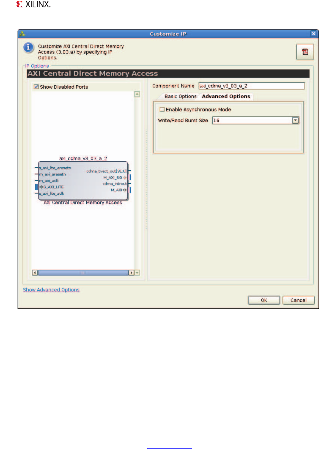
LogiCORE IP AXI CDMA v3.03a www.xilinx.com 56
PG034 October 16, 2012
Chapter 4: Customizing and Generating the Core
• Component Name – The base name of the output files generated for the core. Names
must begin with a letter and can be composed of any of the following characters: a to z,
0 to 9, and "_".
X-Ref Target - Figure 4-2
Figure 4-2: AXI CDMA GUI – Advanced Options Tab

LogiCORE IP AXI CDMA v3.03a www.xilinx.com 57
PG034 October 16, 2012
Chapter 4: Customizing and Generating the Core
Basic Options
The following describe the fundamental options that affect both channels of the AXI CDMA
core.
•Enable Scatter Gather Engine – Checking this option enables Scatter Gather Mode
operation and includes the Scatter Gather Engine in AXI CDMA. Unchecking this option
enables Simple CDMA Mode operation, excluding the Scatter Gather Engine. Disabling
the Scatter Gather Engine causes all output ports for the Scatter/Gather engine to be
tied to zero, and all of the input ports to be left open.
•Disable 4K Boundary Checks – Checking this option puts the CDMA in low resource
utilization mode. This considerably reduces the performance and features of the CDMA.
This option is available only when Scatter Gather is disabled.
•Allow Unaligned Transfer – Enabling this allows the CDMA to do unaligned memory
access for Read and Write. This option is available only when Scatter Gather is enabled.
Enabling this feature restricts the allowed values of data width to 32 and 64 only.
•Read/Write Data Width – Data width of the AXI Memory Mapped Read and Write data
bus. Valid values are 32, 64, 128, 256, 512, and 1024.
Advanced Options
•Enable Asynchronous Mode – Select this box if the clocks used in AXI CDMA are
asynchronous.
•Write/Read Burst Size – Maximum Burst size of the AXI4 read/write operation. When
using the Keyhole feature of CDMA, this needs to be set to 16.
Output Generation
The output files generated from the Xilinx Vivado IP catalog are placed in the project
directory. The file output list can include some or all of the following files.
The component name of the IP generated is axi_cdma_v3_03_a_0.
<project directory>/ip
Top-level project directory; name is user-defined
<project directory>/ip/axi_cdma_v3_03_a_0
AXI CDMA folders and files
proc_common_v3_00_a
Helper cores
sim
Simulation wrapper
LogiCORE IP AXI CDMA v3.03a www.xilinx.com 58
PG034 October 16, 2012
Chapter 4: Customizing and Generating the Core
synth
Synthesis wrapper
axi_datamover.veo/.vho/.xdc
Instantiation template files
<axi_cdma_v3_03_a_0>/axi_cdma_v3_03_a/hdl/src/vhdl
AXI DMA RTL files
<project directory>
The project directory contains the axi_cdma core RTL files as well as all its helper cores.
The proc_common_v3_00_a directory contains the helper cores used by the axi_cdma.
<project directory>/ip/axi_cdma_v3_03_a_0
The axi_cdma_v3_03_a_0 name directory contains the following folders and files.
<axi_cdma_v3_03_a_0>/axi_cdma_v3_03_a/hdl/src/vhdl
The axi_dma RTL files are delivered under /ip/axi_cdma_v3_03_a/hdl/src/vhdl
directory.
Table 4-1: axi_cdma_v3_03_a_0 Directory
Name Description
<project_dir>/ip/axi_cdma_v3_03_a_0
proc_common_v3_00_a Helper cores folder
sim Simulation wrapper folder
synth Synthesis wrapper folder
axi_datamover.veo/.vho/.xdc Instantiation template files
Back to Top


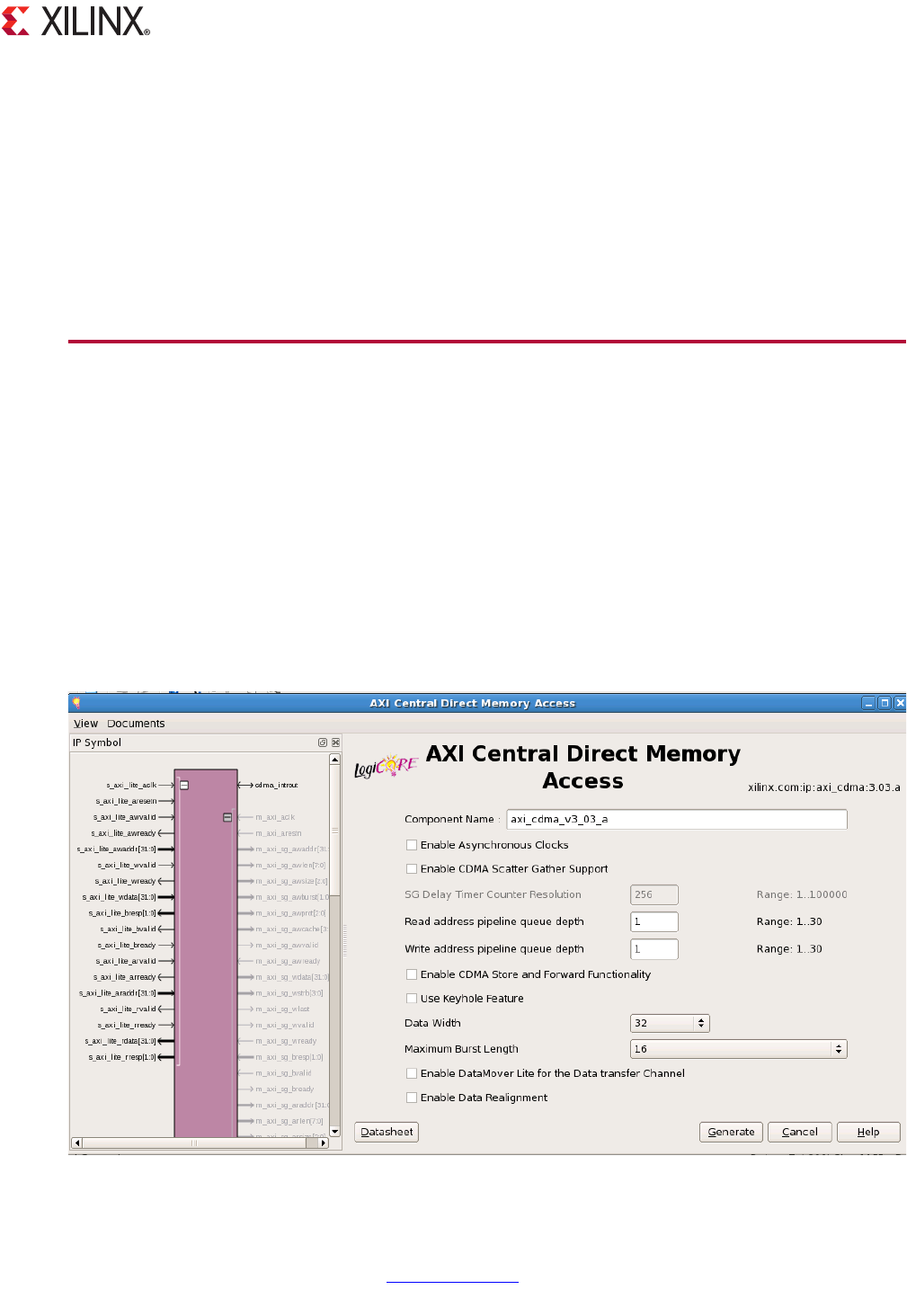
LogiCORE IP AXI CDMA v3.03a www.xilinx.com 61
PG034 October 16, 2012
Chapter 6
Customizing and Generating the Core
This chapter includes information about using Xilinx tools to customize and generate the
core in the ISE® Design Suite environment.
GUI
This section describes the GUI of the CORE Generator™ tool and follows the same flow
required to set up the clocking network requirements. Tool tips are available in the GUI for
most features; place your mouse over the relevant text, and additional information is
provided in a pop-up dialog
Configuring AXI CDMA Parameters
On the first page of the GUI you identify the required features of the clocking network and
configure the input clocks.
X-Ref Target - Figure 6-1
Figure 6-1: CORE Generator GUI

LogiCORE IP AXI CDMA v3.03a www.xilinx.com 62
PG034 October 16, 2012
Chapter 6: Customizing and Generating the Core
•Enable Asynchronous Clocks – AXI CDMA can be configured in an asynchronous
mode by selecting the Enable Asynchronous Clocks check box. This enables the
necessary logic that is required to synchronize the clock domain crossing paths.
•Enable CDMA Scatter Gather Support – Enable/Disable the Scatter Gather support.
This can be enabled by selecting the check box. When set to 1, Scatter Gather support
is enabled.
•SG Delay Timer Counter Resolution – This integer parameter is used to set the
resolution of the Interrupt Delay Timer. The value assigned specifies the number of the
input axi_aclk clock cycles between each tick of the delay timer. The Delay Timer is only
used during Scatter Gather operations. For additional information, see SG Delay
Interrupt.
•Read Address Pipeline Queue Depth – This check box sets the Read Address Pipeline
depth for the Data read function. The effective address pipelining on the AXI4 Read
Address Channel is the value assigned plus 2. If the value assigned is 1, the effective
address pipelining on the AXI4 Read Address Channel is the value assigned plus 1.
•Write Address Pipeline Queue Depth – This check box sets the Write Address Pipeline
depth for the Data write function. The effective address pipelining on the AXI4 Write
Address Channel is the value assigned plus 2. If the value assigned is 1, the effective
address pipelining on the AXI4 Write Address Channel is the value assigned plus 1.
•Enable CDMA Store and Forward Functionality – This check box enables/disables the
CDMA store and forward feature.
•Use Keyhole Feature – Checking this box sets the Max burst length to 16. For Keyhole
operation, the Maximum Burst Length should not exceed 16.
•Data Width – This integer parameter is used to size the AXI CDMA AXI4 data transport
Data Channel related qualifiers. Allowed values are 32, 64, 128, 256, 512, and 1024.
•Maximum Burst Length – This parameter limits the burst length requested by CDMA
on the AXI4 data transport interface.
A value of 256 is not allowed if the C_M_AXI_DATA_WIDTH parameter is assigned a
value of 256. An AXI 4K address boundary crossing violation could occur otherwise.
•Enable Datamover Lite for the Data Transfer Channel – This parameter allows the
CDMA data transport path to be implemented in a "lite" mode. Lite mode is useful for
resource limited designs that requires smaller resource utilization traded off for high
performance data transfer. This parameter is ignored if Scatter Gather support is
enabled.
•Enable Data Realignment – Include or exclude the Data Realignment Engine. For use
cases where all transfers are C_M_AXI_DATA_WIDTH aligned, this parameter can be set
to 0 to exclude DRE, saving FPGA resources.
Setting this parameter to 1 allows data realignment to the byte (8 bits) address
resolution on the data transport AXI4 interface. The DRE is only supported for Data
Width 32 and 64.
LogiCORE IP AXI CDMA v3.03a www.xilinx.com 63
PG034 October 16, 2012
Chapter 6: Customizing and Generating the Core
When the DRE is included, CDMA data reads can start from any address byte offset (the
transfer source address). DRE realigns the read data to match the starting offset of the
programmed destination address.
Note: If the DRE is disabled (C_INCLUDE_DRE = 0) or DRE does not support the specified data
width (C_M_AXI_DATA_WIDTH = 128 or 256), the offset of the transfer source address must match
the offset of the transfer destination address. Offset is defined as that portion of a system
address that is used to designate a byte position within a single data beat width. For example, a
32-bit data bus has four addressable byte positions within a single data beat (0, 1, 2, and 3). The
portion of the address that designates these positions is the offset. The number of address bits
used for the offset varies with the transfer bus data width.
Output Generation
<project directory>
Top-level project directory; name is user-defined
<project directory>/doc
Core release notes readme file
<component name>/hdl/src/vhdl
Core release notes readme file
<project directory>
The project directory contains all the CORE Generator tool project files.
Table 6-1: Project Directory
Name Description
<project_dir>
<component_name>.xco CORE Generator tool project-specific option file; can be
used as an input to the CORE Generator tool.
<component_name>_xmdf.tcl Xilinx standard IP Core information file used by Xilinx
design tools.
Back to Top

LogiCORE IP AXI CDMA v3.03a www.xilinx.com 64
PG034 October 16, 2012
Chapter 6: Customizing and Generating the Core
<project directory>/doc
The doc directory contains the Product Guide and the release notes in the readme file
provided with the core, which can include tool requirements, updates, and issue resolution.
<component name>/hdl/src/vhdl
The hdl/src/vhdl directory contains the core implementation source files.
Table 6-2: Doc Directory
Name Description
<project_dir>/doc
axi_cdma_readme.txt Release notes file.
pg034_axi_cdma.pdf PG034 LogiCORE IP AXI CDMA Product Guide
Back to Top
Table 6-3: Implement Directory
Name Description
<project_dir>/hdl/src/vhdl
RTL files to implement the core.
Back to Top

LogiCORE IP AXI CDMA v3.03a www.xilinx.com 65
PG034 October 16, 2012
Chapter 7
Constraining the Core
This chapter contains information about constraining the core in the ISE® Design Suite
environment.
Automatic Constraint Generation
The AXI CDMA v3_03_a incorporates a TCL file that automatically generates DATAPATHONLY
constraints between the m_axi_aclk and the s_axi_lite_aclk domains. This only
occurs when the parameter C_AXI_LITE_IS_ASYNC is assigned a value of 1 indicating the
m_axi_aclk and s_axi_lite_aclk input ports are being driven with different clocks.


LogiCORE IP AXI CDMA v3.03a www.xilinx.com 68
PG034 October 16, 2012
Appendix B
Debugging
Some of the common problems encountered and possible solutions follow.
• You have programmed your BD ring but nothing seems to work.
Register programming sequence has to be followed to start the CDMA. See Sequence of
Operation in Chapter 3.
• Internal Error/Error bits set in the Status register
Internal error could be set when BTT specified in the descriptor is 0. SG internal error
would be set if the fetched BD is a completed BD. Other error bits like Decode Error or
Slave Error could also be set based on the response from Interconnect or Slave.
• You are reading data from a location, but the data does not seem to be in order.
Verify if the start address location is aligned or un-aligned. If it is un-aligned, ensure
that the DRE is enabled while configuring CDMA.

LogiCORE IP AXI CDMA v3.03a www.xilinx.com 69
PG034 October 16, 2012
Appendix C
Additional Resources
Xilinx Resources
For support resources such as Answers, Documentation, Downloads, and Forums, see the
Xilinx Support website at:
www.xilinx.com/support.
For a glossary of technical terms used in Xilinx documentation, see:
www.xilinx.com/company/terms.htm.
References
To search for Xilinx documentation, go to www.xilinx.com/support
The following document provides supplemental material useful with this product guide:
1. LogiCORE IP AXI Interconnect Product Guide (PG059)
2. Vivado Design Suite Migration Methodology Guide (UG911)
3. Vivado Design Suite documentation:
www.xilinx.com/cgi-bin/docs/rdoc?v=2012.3;t=vivado+userguides
4. AMBA® AXI4-Stream Protocol Specification
Technical Support
Xilinx provides technical support at www.xilinx.com/support for this LogiCORE™ IP product
when used as described in the product documentation. Xilinx cannot guarantee timing,
functionality, or support of product if implemented in devices that are not defined in the
documentation, if customized beyond that allowed in the product documentation, or if
changes are made to any section of the design labeled DO NOT MODIFY.

LogiCORE IP AXI CDMA v3.03a www.xilinx.com 70
PG034 October 16, 2012
Appendix C: Additional Resources
See the IDS Embedded Edition Derivative Device Support web page
(www.xilinx.com/ise/embedded/ddsupport.htm) for a complete list of supported derivative
devices for this core.
See the IP Release Notes Guide (XTP025) for more information on this core. For each core,
there is a master Answer Record that contains the Release Notes and Known Issues list for
the core being used. The following information is listed for each version of the core:
• New Features
• Resolved Issues
• Known Issues
Revision History
The following table shows the revision history for this document.
Notice of Disclaimer
The information disclosed to you hereunder (the “Materials”) is provided solely for the selection and use of Xilinx products. To the
maximum extent permitted by applicable law: (1) Materials are made available “AS IS” and with all faults, Xilinx hereby DISCLAIMS
ALL WARRANTIES AND CONDITIONS, EXPRESS, IMPLIED, OR STATUTORY, INCLUDING BUT NOT LIMITED TO WARRANTIES OF
MERCHANTABILITY, NON-INFRINGEMENT, OR FITNESS FOR ANY PARTICULAR PURPOSE; and (2) Xilinx shall not be liable (whether
in contract or tort, including negligence, or under any other theory of liability) for any loss or damage of any kind or nature related
to, arising under, or in connection with, the Materials (including your use of the Materials), including for any direct, indirect,
special, incidental, or consequential loss or damage (including loss of data, profits, goodwill, or any type of loss or damage
suffered as a result of any action brought by a third party) even if such damage or loss was reasonably foreseeable or Xilinx had
been advised of the possibility of the same. Xilinx assumes no obligation to correct any errors contained in the Materials or to
notify you of updates to the Materials or to product specifications. You may not reproduce, modify, distribute, or publicly display
the Materials without prior written consent. Certain products are subject to the terms and conditions of the Limited Warranties
which can be viewed at http://www.xilinx.com/warranty.htm; IP cores may be subject to warranty and support terms contained in
a license issued to you by Xilinx. Xilinx products are not designed or intended to be fail-safe or for use in any application requiring
fail-safe performance; you assume sole risk and liability for use of Xilinx products in Critical Applications:
http://www.xilinx.com/warranty.htm#critapps.
© Copyright 2012 Xilinx, Inc. Xilinx, the Xilinx logo, Artix, ISE, Kintex, Spartan, Virtex, Vivado, Zynq, and other designated brands
included herein are trademarks of Xilinx in the United States and other countries. All other trademarks are the property of their
respective owners.
Date Version Description of Revisions
04/24/12 1.0 Initial Xilinx Release
This new document is based on the LogiCORE IP AXI CDMA Product
Specification (DS792)
07/11/12 1.1 Template update.
07/25/12 2.0 • Updated for Vivado 2012.2, Zynq features, and ISE v14.2
• Added Vivado content in Customizing and Generating the Core
10/16/12 2.5 • Updated for Vivado 2012.3 and ISE v14.3 design tools.
• Document clean up.
