Cortex M3 Devices Generic User Guide
cortex-m3%20guide
User Manual: Pdf
Open the PDF directly: View PDF ![]() .
.
Page Count: 180 [warning: Documents this large are best viewed by clicking the View PDF Link!]
- Cortex-M3 Devices Generic User Guide
- Contents
- Preface
- Introduction
- The Cortex-M3 Processor
- 2.1 Programmers model
- 2.2 Memory model
- 2.2.1 Memory regions, types and attributes
- 2.2.2 Memory system ordering of memory accesses
- 2.2.3 Behavior of memory accesses
- 2.2.4 Software ordering of memory accesses
- 2.2.5 Optional bit-banding
- 2.2.6 Memory endianness
- 2.2.7 Synchronization primitives
- 2.2.8 Programming hints for the synchronization primitives
- 2.3 Exception model
- 2.4 Fault handling
- 2.5 Power management
- The Cortex-M3 Instruction Set
- 3.1 Instruction set summary
- 3.2 CMSIS functions
- 3.3 About the instruction descriptions
- 3.4 Memory access instructions
- 3.5 General data processing instructions
- 3.6 Multiply and divide instructions
- 3.7 Saturating instructions
- 3.8 Bitfield instructions
- 3.9 Branch and control instructions
- 3.10 Miscellaneous instructions
- Cortex-M3 Peripherals
- 4.1 About the Cortex-M3 peripherals
- 4.2 Nested Vectored Interrupt Controller
- 4.2.1 Accessing the Cortex-M3 NVIC registers using CMSIS
- 4.2.2 Interrupt Set-enable Registers
- 4.2.3 Interrupt Clear-enable Registers
- 4.2.4 Interrupt Set-pending Registers
- 4.2.5 Interrupt Clear-pending Registers
- 4.2.6 Interrupt Active Bit Registers
- 4.2.7 Interrupt Priority Registers
- 4.2.8 Software Trigger Interrupt Register
- 4.2.9 Level-sensitive and pulse interrupts
- 4.2.10 NVIC usage hints and tips
- 4.3 System control block
- 4.3.1 Auxiliary Control Register
- 4.3.2 CPUID Base Register
- 4.3.3 Interrupt Control and State Register
- 4.3.4 Vector Table Offset Register
- 4.3.5 Application Interrupt and Reset Control Register
- 4.3.6 System Control Register
- 4.3.7 Configuration and Control Register
- 4.3.8 System Handler Priority Registers
- 4.3.9 System Handler Control and State Register
- 4.3.10 Configurable Fault Status Register
- 4.3.11 HardFault Status Register
- 4.3.12 MemManage Fault Address Register
- 4.3.13 BusFault Address Register
- 4.3.14 Auxiliary Fault Status Register
- 4.3.15 System control block usage hints and tips
- 4.4 System timer, SysTick
- 4.5 Optional Memory Protection Unit
- Cortex-M3 Options
- Glossary

Copyright © 2010 ARM. All rights reserved.
ARM DUI 0552A (ID121610)
Cortex™-M3 Devices
Generic User Guide

ARM DUI 0552A Copyright © 2010 ARM. All rights reserved. ii
ID121610 Non-Confidential
Cortex-M3 Devices
Generic User Guide
Copyright © 2010 ARM. All rights reserved.
Release Information
The following changes have been made to this book.
Proprietary Notice
Words and logos marked with ® or ™ are registered trademarks or trademarks of ARM® in the EU and other countries,
except as otherwise stated below in this proprietary notice. Other brands and names mentioned herein may be the
trademarks of their respective owners.
Neither the whole nor any part of the information contained in, or the product described in, this document may be
adapted or reproduced in any material form except with the prior written permission of the copyright holder.
The product described in this document is subject to continuous developments and improvements. All particulars of the
product and its use contained in this document are given by ARM in good faith. However, all warranties implied or
expressed, including but not limited to implied warranties of merchantability, or fitness for purpose, are excluded.
This document is intended only to assist the reader in the use of the product. ARM shall not be liable for any loss or
damage arising from the use of any information in this document, or any error or omission in such information, or any
incorrect use of the product.
Where the term ARM is used it means “ARM or any of its subsidiaries as appropriate”.
Confidentiality Status
This document is Non-Confidential. The right to use, copy and disclose this document may be subject to license
restrictions in accordance with the terms of the agreement entered into by ARM and the party that ARM delivered this
document to.
Product Status
The information in this document is final, that is for a developed product.
Web Address
http://www.arm.com
Change history
Date Issue Confidentiality Change
16 December 2010 A Non-Confidential First release

ARM DUI 0552A Copyright © 2010 ARM. All rights reserved. iii
ID121610 Non-Confidential
Contents
Cortex-M3 Devices Generic User Guide
Preface
About this book ........................................................................................................... vi
Feedback .................................................................................................................... ix
Chapter 1 Introduction
1.1 About the Cortex-M3 processor and core peripherals ............................................. 1-2
Chapter 2 The Cortex-M3 Processor
2.1 Programmers model ................................................................................................ 2-2
2.2 Memory model ....................................................................................................... 2-12
2.3 Exception model .................................................................................................... 2-21
2.4 Fault handling ........................................................................................................ 2-28
2.5 Power management ............................................................................................... 2-31
Chapter 3 The Cortex-M3 Instruction Set
3.1 Instruction set summary ........................................................................................... 3-2
3.2 CMSIS functions ...................................................................................................... 3-6
3.3 About the instruction descriptions ............................................................................ 3-8
3.4 Memory access instructions .................................................................................. 3-17
3.5 General data processing instructions .................................................................... 3-34
3.6 Multiply and divide instructions .............................................................................. 3-49
3.7 Saturating instructions ........................................................................................... 3-54
3.8 Bitfield instructions ................................................................................................. 3-56
3.9 Branch and control instructions ............................................................................. 3-60
3.10 Miscellaneous instructions ..................................................................................... 3-68
Chapter 4 Cortex-M3 Peripherals
4.1 About the Cortex-M3 peripherals ............................................................................. 4-2

ARM DUI 0552A Copyright © 2010 ARM. All rights reserved. iv
ID121610 Non-Confidential
4.2 Nested Vectored Interrupt Controller ....................................................................... 4-3
4.3 System control block .............................................................................................. 4-11
4.4 System timer, SysTick ........................................................................................... 4-33
4.5 Optional Memory Protection Unit ........................................................................... 4-37
Appendix A Cortex-M3 Options
A.1 Cortex-M3 implementation options .......................................................................... A-2
Glossary


Preface
ARM DUI 0552A Copyright © 2010 ARM. All rights reserved. vi
ID121610 Non-Confidential
About this book
This book is a generic user guide for devices that implement the ARM Cortex-M3 processor.
Implementers of Cortex-M3 designs make a number of implementation choices, that can affect
the functionality of the device. This means that, in this book:
• some information is described as implementation-defined
• some features are described as optional.
In this book, unless the context indicates otherwise:
Processor Refers to the Cortex-M3 processor, as supplied by ARM.
Device Refers to an implemented device, supplied by an ARM partner, that incorporates
a Cortex-M3 processor. In particular, your device refers to the particular
implementation of the Cortex-M3 that you are using. Some features of your
device depend on the implementation choices made by the ARM partner that
made the device.
Product revision status
The rnpn identifier indicates the revision status of the product described in this book, where:
rn Identifies the major revision of the product.
pn Identifies the minor revision or modification status of the product.
Intended audience
This book is written for application and system-level software developers, familiar with
programming, who want to program a device that includes the Cortex-M3 processor.
Using this book
This book is organized into the following chapters:
Chapter 1 Introduction
Read this for an introduction to the Cortex-M3 processor and its features.
Chapter 2 The Cortex-M3 Processor
Read this for information about how to program the processor, the processor
memory model, exception and fault handling, and power management.
Chapter 3 The Cortex-M3 Instruction Set
Read this for information about the processor instruction set.
Chapter 4 Cortex-M3 Peripherals
Read this for information about Cortex-M3 peripherals.
Appendix A Cortex-M3 Options
Read this for information about the processor implementation and configuration
options.
Glossary Read this for definitions of terms used in this book.

Preface
ARM DUI 0552A Copyright © 2010 ARM. All rights reserved. vii
ID121610 Non-Confidential
Typographical conventions
The typographical conventions are:
italic Highlights important notes, introduces special terminology, denotes
internal cross-references, and citations.
bold Highlights interface elements, such as menu names. Denotes signal
names. Also used for terms in descriptive lists, where appropriate.
monospace
Denotes text that you can enter at the keyboard, such as commands, file
and program names, and source code.
monospace
Denotes a permitted abbreviation for a command or option. You can enter
the underlined text instead of the full command or option name.
monospace
italic
Denotes arguments to monospace text where the argument is to be
replaced by a specific value.
< and > Enclose replaceable terms for assembler syntax where they appear in code
or code fragments. For example:
CMP Rn, <Rm|#imm>

Preface
ARM DUI 0552A Copyright © 2010 ARM. All rights reserved. viii
ID121610 Non-Confidential
Additional reading
This section lists publications by ARM and by third parties.
See Infocenter, http://infocenter.arm.com, for access to ARM documentation.
See onARM, http://onarm.com, for embedded software development resources including the
Cortex Microcontroller Software Interface Standard (CMSIS).
ARM publications
This book contains information that is specific to this product. See the following documents for
other relevant information:
•Cortex-M3 Technical Reference Manual (ARM DDI 0439)
•ARMv7-M Architecture Reference Manual (ARM DDI 0403).
Other publications
This guide only provides generic information for devices that implement the ARM Cortex-M3
processor. For information about your device see the documentation published by the device
manufacturer.

Preface
ARM DUI 0552A Copyright © 2010 ARM. All rights reserved. ix
ID121610 Non-Confidential
Feedback
ARM welcomes feedback on this product and its documentation.
Feedback on content
If you have comments on content then send an e-mail to
errata@arm.com
. Give:
• the title
• the number, ARM DUI 0552A
• the page numbers to which your comments apply
• a concise explanation of your comments.
ARM also welcomes general suggestions for additions and improvements.

Introduction
ARM DUI 0552A Copyright © 2010 ARM. All rights reserved. 1-2
ID121610 Non-Confidential
1.1 About the Cortex-M3 processor and core peripherals
The Cortex-M3 processor is a high performance 32-bit processor designed for the
microcontroller market. It offers significant benefits to developers, including:
• outstanding processing performance combined with fast interrupt handling
• enhanced system debug with extensive breakpoint and trace capabilities
• efficient processor core, system and memories
• ultra-low power consumption with integrated sleep mode and an optional deep sleep
mode
• platform security robustness, with an optional integrated Memory Protection Unit (MPU).
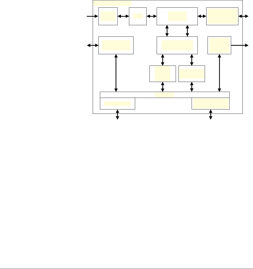
Figure 1-1 Cortex-M3 implementation
The Cortex-M3 processor is built on a high-performance processor core, with a 3-stage pipeline
Harvard architecture, making it ideal for demanding embedded applications. The processor
delivers exceptional power efficiency through an efficient instruction set and extensively
optimized design, providing high-end processing hardware including optional
IEEE754-compliant single-precision floating-point computation, a range of single-cycle and
SIMD multiplication and multiply-with-accumulate capabilities, saturating arithmetic and
dedicated hardware division.
To facilitate the design of cost-sensitive devices, the Cortex-M3 processor implements
tightly-coupled system components that reduce processor area while significantly improving
interrupt handling and system debug capabilities. The Cortex-M3 processor implements a
version of the Thumb® instruction set based on Thumb-2 technology, ensuring high code density
and reduced program memory requirements. The Cortex-M3 instruction set provides the
exceptional performance expected of a modern 32-bit architecture, with the high code density
of 8-bit and 16-bit microcontrollers.
The Cortex-M3 processor closely integrates a configurable NVIC, to deliver industry-leading
interrupt performance. The NVIC includes a Non-Maskable Interrupt (NMI) that can provide
up to 256 interrupt priority levels. The tight integration of the processor core and NVIC provides
fast execution of Interrupt Service Routines (ISRs), dramatically reducing the interrupt latency.
Optional
Embedded
Trace Macrocell
NVIC
Optional Debug
Access Port
Optional
WIC
Optional
Serial Wire
viewer
Bus matrix
Code interface SRAM and
peripheral interface
Optional Data
watchpoints
Optional
Flash
patch
Cortex-M3 processor
Processor
core
Optional Memory
protection unit

Introduction
ARM DUI 0552A Copyright © 2010 ARM. All rights reserved. 1-3
ID121610 Non-Confidential
This is achieved through the hardware stacking of registers, and the ability to suspend
load-multiple and store-multiple operations. Interrupt handlers do not require wrapping in
assembler code, removing any code overhead from the ISRs. A tail-chain optimization also
significantly reduces the overhead when switching from one ISR to another.
To optimize low-power designs, the NVIC integrates with the sleep modes, which can include
an optional deep sleep function. This enables the entire device to be rapidly powered down
while still retaining program state.
1.1.1 System-level interface
The Cortex-M3 processor provides multiple interfaces using AMBA® technology to provide
high speed, low latency memory accesses. It supports unaligned data accesses and implements
atomic bit manipulation that enables faster peripheral controls, system spinlocks and thread-safe
Boolean data handling.
The Cortex-M3 processor has an optional Memory Protection Unit (MPU) that permits control
of individual regions in memory, enabling applications to utilize multiple privilege levels,
separating and protecting code, data and stack on a task-by-task basis. Such requirements are
becoming critical in many embedded applications such as automotive.
1.1.2 Optional integrated configurable debug
The Cortex-M3 processor can implement a complete hardware debug solution. This provides
high system visibility of the processor and memory through either a traditional JTAG port or a
2-pin Serial Wire Debug (SWD) port that is ideal for microcontrollers and other small package
devices.
For system trace the processor integrates an Instrumentation Trace Macrocell (ITM) alongside
data watchpoints and a profiling unit. To enable simple and cost-effective profiling of the system
events these generate, a Serial Wire Viewer (SWV) can export a stream of software-generated
messages, data trace, and profiling information through a single pin.
The optional Embedded Trace Macrocell™ (ETM) delivers unrivalled instruction trace capture
in an area far smaller than traditional trace units, enabling many low cost MCUs to implement
full instruction trace for the first time.
The optional Flash Patch and Breakpoint Unit (FPB) provides up to eight hardware breakpoint
comparators that debuggers can use. The comparators in the FPB also provide remap functions
of up to eight words in the program code in the CODE memory region. This enables applications
stored on a non-erasable, ROM-based microcontroller to be patched if a small programmable
memory, for example flash, is available in the device. During initialization, the application in
ROM detects, from the programmable memory, whether a patch is required. If a patch is
required, the application programs the FPB to remap a number of addresses. When those
addresses are accessed, the accesses are redirected to a remap table specified in the FPB
configuration, which means the program in the non-modifiable ROM can be patched.
1.1.3 Cortex-M3 processor features and benefits summary
• tight integration of system peripherals reduces area and development costs
• Thumb instruction set combines high code density with 32-bit performance
• code-patch ability for ROM system updates
• power control optimization of system components
• integrated sleep modes for low power consumption
• fast code execution permits slower processor clock or increases sleep mode time
• hardware division and fast digital-signal-processing orientated multiply accumulate

Introduction
ARM DUI 0552A Copyright © 2010 ARM. All rights reserved. 1-4
ID121610 Non-Confidential
• deterministic, high-performance interrupt handling for time-critical applications
• optional MPU for safety-critical applications
• extensive implementation-defined debug and trace capabilities:
— Serial Wire Debug and Serial Wire Trace reduce the number of pins required for
debugging, tracing, and code profiling.
1.1.4 Cortex-M3 core peripherals
These are:
Nested Vectored Interrupt Controller
The NVIC is an embedded interrupt controller that supports low latency interrupt
processing.
System Control Block
The System Control Block (SCB) is the programmers model interface to the
processor. It provides system implementation information and system control,
including configuration, control, and reporting of system exceptions.
System timer
The system timer, SysTick, is a 24-bit count-down timer. Use this as a Real Time
Operating System (RTOS) tick timer or as a simple counter.
Memory Protection Unit
The MPU improves system reliability by defining the memory attributes for
different memory regions. It provides up to eight different regions, and an
optional predefined background region.

ARM DUI 0552A Copyright © 2010 ARM. All rights reserved. 2-1
ID121610 Non-Confidential
Chapter 2
The Cortex-M3 Processor
This Chapter describes the Cortex-M3 processor. It contains the following sections:
•Programmers model on page 2-2
•Memory model on page 2-12
•Exception model on page 2-21
•Fault handling on page 2-28
•Power management on page 2-31.

The Cortex-M3 Processor
ARM DUI 0552A Copyright © 2010 ARM. All rights reserved. 2-2
ID121610 Non-Confidential
2.1 Programmers model
This section describes the Cortex-M3 programmers model. In addition to the individual core
register descriptions, it contains information about the processor modes and privilege levels for
software execution and stacks.
2.1.1 Processor mode and privilege levels for software execution
The processor modes are:
Thread mode Used to execute application software. The processor enters Thread mode
when it comes out of reset.
Handler mode Used to handle exceptions. The processor returns to Thread mode when it
has finished all exception processing.
The privilege levels for software execution are:
Unprivileged The software:
• has limited access to the
MSR
and
MRS
instructions, and cannot use the
CPS
instruction
• cannot access the system timer, NVIC, or system control block
• might have restricted access to memory or peripherals.
Unprivileged software executes at the unprivileged level.
Privileged The software can use all the instructions and has access to all resources.
Privileged software executes at the privileged level.
In Thread mode, the CONTROL register controls whether software execution is privileged or
unprivileged, see CONTROL register on page 2-9. In Handler mode, software execution is
always privileged.
Only privileged software can write to the CONTROL register to change the privilege level for
software execution in Thread mode. Unprivileged software can use the
SVC
instruction to make
a supervisor call to transfer control to privileged software.
2.1.2 Stacks
The processor uses a full descending stack. This means the stack pointer holds the address of
the last stacked item in memory. When the processor pushes a new item onto the stack, it
decrements the stack pointer and then writes the item to the new memory location. The
processor implements two stacks, the main stack and the process stack, with a pointer for each
held in independent registers, see Stack Pointer on page 2-4.
In Thread mode, the CONTROL register controls whether the processor uses the main stack or
the process stack, see CONTROL register on page 2-9. In Handler mode, the processor always
uses the main stack. The options for processor operations are:
Table 2-1 Summary of processor mode, execution privilege level, and stack use options
Processor
mode Used to execute Privilege level for
software execution Stack used
Thread Applications Privileged or unprivilegeda
a. See CONTROL register on page 2-9.
Main stack or process stacka
Handler Exception handlers Always privileged Main stack
The Cortex-M3 Processor
ARM DUI 0552A Copyright © 2010 ARM. All rights reserved. 2-3
ID121610 Non-Confidential
2.1.3 Core registers
The processor core registers are:
SP (R13)
LR (R14)
PC (R15)
R5
R6
R7
R0
R1
R3
R4
R2
R10
R11
R12
R8
R9
Low registers
High registers
MSP
‡
PSP
‡
PSR
PRIMASK
FAULTMASK
BASEPRI
CONTROL
General-purpose registers
Stack Pointer
Link Register
Program Counter
Program status register
Exception mask registers
CONTROL register
Special registers
‡
Banked version of SP
Table 2-2 Core register set summary
Name Type aRequired privilegebReset value Description
R0-R12 RW Either Unknown General-purpose registers on page 2-4
MSP RW Privileged See description Stack Pointer on page 2-4
PSP RW Either Unknown Stack Pointer on page 2-4
LR RW Either
0xFFFFFFFF
Link Register on page 2-4
PC RW Either See description Program Counter on page 2-4
PSR RW Privileged
0x01000000
Program Status Register on page 2-4
ASPR RW Either Unknown Application Program Status Register on page 2-5
IPSR RO Privileged
0x00000000
Interrupt Program Status Register on page 2-6
EPSR RO Privileged
0x01000000
Execution Program Status Register on page 2-6
PRIMASK RW Privileged
0x00000000
Priority Mask Register on page 2-8
FAULTMASK RW Privileged
0x00000000
Fault Mask Register on page 2-8
BASEPRI RW Privileged
0x00000000
Base Priority Mask Register on page 2-9
CONTROL RW Privileged
0x00000000
CONTROL register on page 2-9
a. Describes access type during program execution in thread mode and Handler mode. Debug access can differ.
b. An entry of Either means privileged and unprivileged software can access the register.
The Cortex-M3 Processor
ARM DUI 0552A Copyright © 2010 ARM. All rights reserved. 2-4
ID121610 Non-Confidential
General-purpose registers
R0-R12 are 32-bit general-purpose registers for data operations.
Stack Pointer
The Stack Pointer (SP) is register R13. In Thread mode, bit[1] of the CONTROL register
indicates the stack pointer to use:
•0 = Main Stack Pointer (MSP). This is the reset value.
•1 = Process Stack Pointer (PSP).
On reset, the processor loads the MSP with the value from address
0x00000000
.
Link Register
The Link Register (LR) is register R14. It stores the return information for subroutines, function
calls, and exceptions. On reset, the processor sets the LR value to
0xFFFFFFFF.
Program Counter
The Program Counter (PC) is register R15. It contains the current program address. On reset,
the processor loads the PC with the value of the reset vector, which is at address
0x00000004
.
Bit[0] of the value is loaded into the EPSR T-bit at reset and must be 1.
Program Status Register
The Program Status Register (PSR) combines:
•Application Program Status Register (APSR)
•Interrupt Program Status Register (IPSR)
•Execution Program Status Register (EPSR).
These registers are mutually exclusive bitfields in the 32-bit PSR. The bit assignments are:
Access these registers individually or as a combination of any two or all three registers, using
the register name as an argument to the
MSR
or
MRS
instructions. For example:
• read all of the registers using
PSR
with the
MRS
instruction
• write to the APSR N, Z, C, V, and Q bits using
APSR_nzcvq
with the
MSR
instruction.
25 24 23
Reserved ISR_NUMBER
31 30 29 28 27
NZCV
0
Reserved
APSR
IPSR
EPSR Reserved Reserved
26 16 15 10 9
ReservedICI/IT ICI/ITT
Q
8

The Cortex-M3 Processor
ARM DUI 0552A Copyright © 2010 ARM. All rights reserved. 2-5
ID121610 Non-Confidential
The PSR combinations and attributes are:
See the instruction descriptions MRS on page 3-74 and MSR on page 3-75 for more information
about how to access the program status registers.
Application Program Status Register
The APSR contains the current state of the condition flags from previous instruction executions.
See the register summary in Table 2-2 on page 2-3 for its attributes. The bit assignments are:
Table 2-3 PSR register combinations
Register Type Combination
PSR RWa, b
a. The processor ignores writes to the IPSR
bits.
b. Reads of the EPSR bits return zero, and the
processor ignores writes to the these bits
APSR, EPSR, and IPSR
IEPSR RO EPSR and IPSR
IAPSR RWaAPSR and IPSR
EAPSR RWbAPSR and EPSR
Table 2-4 APSR bit assignments
Bits Name Function
[31] N Negative flag
[30] Z Zero flag
[29] C Carry or borrow flag
[28] V Overflow flag
[27] Q Saturation flag
[26:0] - Reserved

The Cortex-M3 Processor
ARM DUI 0552A Copyright © 2010 ARM. All rights reserved. 2-6
ID121610 Non-Confidential
Interrupt Program Status Register
The IPSR contains the exception type number of the current Interrupt Service Routine (ISR).
See the register summary in Table 2-2 on page 2-3 for its attributes. The bit assignments are:
Execution Program Status Register
The EPSR contains the Thumb state bit, and the execution state bits for either the:
•If-Then (IT) instruction
•Interruptible-Continuable Instruction (ICI) field for an interrupted load multiple or store
multiple instruction.
See the register summary in Table 2-2 on page 2-3 for the EPSR attributes. The bit assignments
are:
Table 2-5 IPSR bit assignments
Bits Name Function
[31:9] - Reserved.
[8:0] ISR_NUMBER This is the number of the current exception:
0 = Thread mode
1 = Reserved
2 = NMI
3 = HardFault
4 = MemManage
5 = BusFault
6 = UsageFault
7-10 = Reserved
11 = SVCall
12 = Reserved for Debug
13 = Reserved
14 = PendSV
15 = SysTick
16 = IRQ0
.
.
.
n+15 = IRQ(n-1)a.
See Exception types on page 2-21 for more information.
a. The number of interrupts, n, is implementation-defined, in the range 1-240.
Table 2-6 EPSR bit assignments
Bits Name Function
[31:27] - Reserved.
[26:25], [15:10] ICI/IT Indicates the interrupted position of a continuable instruction, see
Interruptible-continuable instructions on page 2-7, or the execution state of an
IT
instruction, see IT on page 3-64.

The Cortex-M3 Processor
ARM DUI 0552A Copyright © 2010 ARM. All rights reserved. 2-7
ID121610 Non-Confidential
Attempts to read the EPSR directly through application software using the
MSR
instruction
always return zero. Attempts to write the EPSR using the
MSR
instruction in application software
are ignored.
Interruptible-continuable instructions
When an interrupt occurs during the execution of an
LDM
,
STM
,
PUSH
, or
POP
instruction, the
processor:
• stops the load multiple or store multiple instruction operation temporarily
• stores the next register operand in the multiple operation to EPSR bits[15:12].
After servicing the interrupt, the processor:
• returns to the register pointed to by bits[15:12]
• resumes execution of the multiple load or store instruction.
When the EPSR holds ICI execution state, bits[26:25,11:10] are zero.
If-Then block
The If-Then block contains up to four instructions following an
IT
instruction. Each instruction
in the block is conditional. The conditions for the instructions are either all the same, or some
can be the inverse of others. See IT on page 3-64 for more information.
Thumb state
The Cortex-M3 processor only supports execution of instructions in Thumb state. The following
can clear the T bit to 0:
• instructions
BLX
,
BX
and
POP{PC
}
• restoration from the stacked xPSR value on an exception return
• bit[0] of the vector value on an exception entry or reset.
Attempting to execute instructions when the T bit is 0 results in a fault or lockup. See Lockup
on page 2-30 for more information.
Exception mask registers
The exception mask registers disable the handling of exceptions by the processor. Disable
exceptions where they might impact on timing critical tasks.
To access the exception mask registers use the
MSR
and
MRS
instructions, or the
CPS
instruction to
change the value of PRIMASK or FAULTMASK. See MRS on page 3-74, MSR on page 3-75,
and CPS on page 3-70 for more information.
[24] T Thumb state bit, see Thumb state.
[23:16] - Reserved.
[9:0] - Reserved.
Table 2-6 EPSR bit assignments (continued)
Bits Name Function

The Cortex-M3 Processor
ARM DUI 0552A Copyright © 2010 ARM. All rights reserved. 2-8
ID121610 Non-Confidential
Priority Mask Register
The PRIMASK register prevents activation of all exceptions with configurable priority. See the
register summary in Table 2-2 on page 2-3 for its attributes. The bit assignments are:
Fault Mask Register
The FAULTMASK register prevents activation of all exceptions except for Non-Maskable
Interrupt (NMI). See the register summary in Table 2-2 on page 2-3 for its attributes. The bit
assignments are:
The processor clears the FAULTMASK bit to 0 on exit from any exception handler except the
NMI handler.
Table 2-7 PRIMASK register bit assignments
Bits Name Function
[31:1] - Reserved
[0] PRIMASK 0 = no effect
1 = prevents the activation of all exceptions with configurable priority.
Table 2-8 FAULTMASK register bit assignments
Bits Name Function
[31:1] - Reserved
[0] FAULTMASK 0 = no effect
1 = prevents the activation of all exceptions except for NMI.
31
Reserved
10
PRIMASK
31 10
Reserved
FAULTMASK
The Cortex-M3 Processor
ARM DUI 0552A Copyright © 2010 ARM. All rights reserved. 2-9
ID121610 Non-Confidential
Base Priority Mask Register
The BASEPRI register defines the minimum priority for exception processing. When BASEPRI
is set to a nonzero value, it prevents the activation of all exceptions with the same or lower
priority level as the BASEPRI value. See the register summary in Table 2-2 on page 2-3 for its
attributes. The bit assignments are:
CONTROL register
The CONTROL register controls the stack used and the privilege level for software execution
when the processor is in Thread mode. See the register summary in Table 2-2 on page 2-3 for
its attributes. The bit assignments are:
Handler mode always uses the MSP, so the processor ignores explicit writes to the active stack
pointer bit of the CONTROL register when in Handler mode. The exception entry and return
mechanisms automatically update the CONTROL register based on the EXC_RETURN value,
see Table 2-17 on page 2-27.
BASEPRIReserved
31 078
Table 2-9 BASEPRI register bit assignments
Bits Name Function
[31:8] - Reserved
[7:0] BASEPRIaPriority mask bits:
0x00
= no effect
Nonzero = defines the base priority for exception processing.
The processor does not process any exception with a priority value greater than or equal to BASEPRI.
a. This field is similar to the priority fields in the interrupt priority registers. Register priority value fields are 8 bits wide, and
non-implemented low-order bits read as zero and ignore writes. See Interrupt Priority Registers on page 4-7 for more information.
Higher priority field values correspond to lower exception priorities.
31 210
Reserved
SPSEL
3
nPRIV
Table 2-10 CONTROL register bit assignments
Bits Name Function
[31:2] - Reserved.
[1] SPSEL Defines the currently active stack pointer: In Handler mode this bit reads as zero and ignores writes. The
Cortex-M3 updates this bit automatically on exception return.
0 = MSP is the current stack pointer
1 = PSP is the current stack pointer.
[0] nPRIV Defines the Thread mode privilege level:
0 = Privileged
1 = Unprivileged.

The Cortex-M3 Processor
ARM DUI 0552A Copyright © 2010 ARM. All rights reserved. 2-10
ID121610 Non-Confidential
In an OS environment, ARM recommends that threads running in Thread mode use the process
stack and the kernel and exception handlers use the main stack.
By default, Thread mode uses the MSP. To switch the stack pointer used in Thread mode to the
PSP, either:
•use the
MSR
instruction to set the Active stack pointer bit to 1, see MSR on page 3-75.
• perform an exception return to Thread mode with the appropriate EXC_RETURN value,
see Table 2-17 on page 2-27.
Note
When changing the stack pointer, software must use an
ISB
instruction immediately after the
MSR
instruction. This ensures that instructions after the
ISB
instruction execute using the new stack
pointer. See ISB on page 3-73
2.1.4 Exceptions and interrupts
The Cortex-M3 processor supports interrupts and system exceptions. The processor and the
NVIC prioritize and handle all exceptions. An exception changes the normal flow of software
control. The processor uses Handler mode to handle all exceptions except for reset. See
Exception entry on page 2-26 and Exception return on page 2-27 for more information.
The NVIC registers control interrupt handling. See Nested Vectored Interrupt Controller on
page 4-3 for more information.
2.1.5 Data types
The processor:
• supports the following data types:
— 32-bit words
— 16-bit halfwords
— 8-bit bytes.
• manages all data memory accesses as little-endian or big-endian. Instruction memory and
PPB accesses are always performed as little-endian. See Memory regions, types and
attributes on page 2-12 for more information.
2.1.6 The Cortex Microcontroller Software Interface Standard
For a Cortex-M3 microcontroller system, the Cortex Microcontroller Software Interface
Standard (CMSIS) defines:
• a common way to:
— access peripheral registers
— define exception vectors
• the names of:
— the registers of the core peripherals
— the core exception vectors
• a device-independent interface for RTOS kernels, including a debug channel.
The CMSIS includes address definitions and data structures for the core peripherals in the
Cortex-M3 processor.

The Cortex-M3 Processor
ARM DUI 0552A Copyright © 2010 ARM. All rights reserved. 2-11
ID121610 Non-Confidential
CMSIS simplifies software development by enabling the reuse of template code and the
combination of CMSIS-compliant software components from various middleware vendors.
Software vendors can expand the CMSIS to include their peripheral definitions and access
functions for those peripherals.
This document includes the register names defined by the CMSIS, and gives short descriptions
of the CMSIS functions that address the processor core and the core peripherals.
Note
This document uses the register short names defined by the CMSIS. In a few cases these differ
from the architectural short names that might be used in other documents.
The following sections give more information about the CMSIS:
•Power management programming hints on page 2-33
•CMSIS functions on page 3-6
•Accessing the Cortex-M3 NVIC registers using CMSIS on page 4-4
•NVIC programming hints on page 4-9.
The Cortex-M3 Processor
ARM DUI 0552A Copyright © 2010 ARM. All rights reserved. 2-12
ID121610 Non-Confidential
2.2 Memory model
This section describes the processor memory map, the behavior of memory accesses, and the
optional bit-banding features. The processor has a fixed default memory map that provides up
to 4GB of addressable memory. The memory map is:
The regions for SRAM and peripherals include optional bit-band regions. Bit-banding provides
atomic operations to bit data, see Optional bit-banding on page 2-16.
The processor reserves regions of the PPB address range for core peripheral registers, see About
the Cortex-M3 peripherals on page 4-2.
2.2.1 Memory regions, types and attributes
The memory map and the programming of the optional MPU splits the memory map into
regions. Each region has a defined memory type, and some regions have additional memory
attributes. The memory type and attributes determine the behavior of accesses to the region.
The memory types are:
Normal The processor can re-order transactions for efficiency, or perform
speculative reads.
Vendor-specific
memory
External device
External RAM
Peripheral
SRAM
Code
0xFFFFFFFF
Private peripheral
bus
0xE0100000
0xE00FFFFF
0x9FFFFFFF
0xA0000000
0x5FFFFFFF
0x60000000
0x3FFFFFFF
0x40000000
0x1FFFFFFF
0x20000000
0x00000000
0x40000000 Bit band region
Bit band alias
32MB
1MB
0x400FFFFF
0x42000000
0x43FFFFFF
Bit band region
Bit band alias
32MB
1MB
0x20000000
0x200FFFFF
0x22000000
0x23FFFFFF
1.0GB
1.0GB
0.5GB
0.5GB
0.5GB
0xDFFFFFFF
0xE0000000
1.0MB
511MB

The Cortex-M3 Processor
ARM DUI 0552A Copyright © 2010 ARM. All rights reserved. 2-13
ID121610 Non-Confidential
Device The processor preserves transaction order relative to other transactions to
Device or Strongly-ordered memory.
Strongly-ordered The processor preserves transaction order relative to all other transactions.
The different ordering requirements for Device and Strongly-ordered memory mean that the
memory system can buffer a write to Device memory, but must not buffer a write to
Strongly-ordered memory.
The additional memory attributes include:
Shareable For a shareable memory region that is implemented, the memory system
provides data synchronization between bus masters in a system with
multiple bus masters, for example, a processor with a DMA controller.
Strongly-ordered memory is always shareable.
If multiple bus masters can access a non-shareable memory region,
software must ensure data coherency between the bus masters.
Note
This attribute is relevant only if the device is likely to be used in systems
where memory is shared between multiple processors.
Execute Never (XN) Means the processor prevents instruction accesses. A fault exception is
generated only on execution of an instruction executed from an XN
region.
2.2.2 Memory system ordering of memory accesses
For most memory accesses caused by explicit memory access instructions, the memory system
does not guarantee that the order in which the accesses complete matches the program order of
the instructions, providing this does not affect the behavior of the instruction sequence.
Normally, if correct program execution depends on two memory accesses completing in
program order, software must insert a memory barrier instruction between the memory access
instructions, see Software ordering of memory accesses on page 2-15.
However, the memory system does guarantee some ordering of accesses to Device and
Strongly-ordered memory. For two memory access instructions A1 and A2, if A1 occurs before
A2 in program order, the ordering of the memory accesses caused by two instructions is:
Where:
- Means that the memory system does not guarantee the ordering of the accesses.
< Means that accesses are observed in program order, that is, A1 is always observed
before A2.
Normal access
Device access, non-shareable
Device access, shareable
Strongly-ordered access
Normal
access Non-shareable Shareable
Strongly-
ordered
access
Device access
A1
A2
-
-
-
-
-
<
-
<
-
-
<
<
-
<
<
<

The Cortex-M3 Processor
ARM DUI 0552A Copyright © 2010 ARM. All rights reserved. 2-14
ID121610 Non-Confidential
2.2.3 Behavior of memory accesses
Table 2-11 lists the behavior of accesses to each region in the memory map.
The Code, SRAM, and external RAM regions can hold programs. However, ARM recommends
that programs always use the Code region. This is because the processor has separate buses that
enable instruction fetches and data accesses to occur simultaneously.
The optional MPU can override the default memory access behavior described in this section.
For more information, see Optional Memory Protection Unit on page 4-37.
Additional memory access constraints for caches and shared memory
When a system includes caches or shared memory, some memory regions might have additional
access constraints, and some regions are subdivided, as Table 2-12 shows:
Table 2-11 Memory access behavior
Address
range Memory region Memory
typeaXNaDescription
0x00000000
-
0x1FFFFFFF
Code Normal - Executable region for program code. You can also put data here.
0x20000000
-
0x3FFFFFFF
SRAM Normal - Executable region for data. You can also put code here.This region
includes bit band and bit band alias areas, see Table 2-13 on
page 2-16.
0x40000000
-
0x5FFFFFFF
Peripheral Device XN This region includes bit band and bit band alias areas, see
Table 2-14 on page 2-16.
0x60000000
-
0x9FFFFFFF
External RAM Normal - Executable region for data.
0xA0000000
-
0xDFFFFFFF
External device Device XN External Device memory.
0xE0000000
-
0xE00FFFFF
Private Peripheral Bus Strongly-
ordered
XN This region includes the NVIC, System timer, and system control
block.
0xE0100000
-
0xFFFFFFFF
Device Device XN Implementation-specific.
a. See Memory regions, types and attributes on page 2-12 for more information.
Table 2-12 Memory region shareability and cache policies
Address range Memory region Memory typeaShareability Cache policyb
0x00000000
-
0x1FFFFFFF
Code Normal - WT
0x20000000
-
0x3FFFFFFF
SRAM Normal - WBWA
0x40000000
-
0x5FFFFFFF
Peripheral Device - -
0x60000000
-
0x7FFFFFFF
External RAM Normal - WBWA
0x80000000
-
0x9FFFFFFF
WT

The Cortex-M3 Processor
ARM DUI 0552A Copyright © 2010 ARM. All rights reserved. 2-15
ID121610 Non-Confidential
Instruction prefetch and branch prediction
The Cortex-M3 processor:
• prefetches instructions ahead of execution
• speculatively prefetches from branch target addresses.
2.2.4 Software ordering of memory accesses
The order of instructions in the program flow does not always guarantee the order of the
corresponding memory transactions. This is because:
• the processor can reorder some memory accesses to improve efficiency, providing this
does not affect the behavior of the instruction sequence.
• the processor has multiple bus interfaces
• memory or devices in the memory map have different wait states
• some memory accesses are buffered or speculative.
Memory system ordering of memory accesses on page 2-13 describes the cases where the
memory system guarantees the order of memory accesses. Otherwise, if the order of memory
accesses is critical, software must include memory barrier instructions to force that ordering.
The processor provides the following memory barrier instructions:
DMB
The Data Memory Barrier (DMB) instruction ensures that outstanding
memory transactions complete before subsequent memory transactions.
See DMB on page 3-71.
DSB
The Data Synchronization Barrier (DSB) instruction ensures that
outstanding memory transactions complete before subsequent instructions
execute. See DSB on page 3-72.
ISB
The Instruction Synchronization Barrier (ISB) ensures that the effect of all
completed memory transactions is recognizable by subsequent
instructions. See ISB on page 3-73.
MPU programming
Use a
DSB
followed by an
ISB
instruction or exception return to ensure that the new MPU
configuration is used by subsequent instructions.
0xA0000000
-
0xBFFFFFFF
External device Device Shareable -
0xC0000000
-
0xDFFFFFFF
Non-shareable
0xE0000000
-
0xE00FFFFF
Private Peripheral Bus Strongly- ordered Shareable -
0xE0100000
-
0xFFFFFFFF
Device Device - -
a. See Memory regions, types and attributes on page 2-12 for more information.
b. WT = Write through, no write allocate. WBWA = Write back, write allocate. See the Glossary for more
information.
Table 2-12 Memory region shareability and cache policies (continued)
Address range Memory region Memory typeaShareability Cache policyb

The Cortex-M3 Processor
ARM DUI 0552A Copyright © 2010 ARM. All rights reserved. 2-16
ID121610 Non-Confidential
2.2.5 Optional bit-banding
A bit-band region maps each word in a bit-band alias region to a single bit in the bit-band
region. The bit-band regions occupy the lowest 1MB of the SRAM and peripheral memory
regions.
The memory map has two 32MB alias regions that map to two 1MB bit-band regions:
• accesses to the 32MB SRAM alias region map to the 1MB SRAM bit-band region, as
shown in Table 2-13
• accesses to the 32MB peripheral alias region map to the 1MB peripheral bit-band region,
as shown in Table 2-14.
Note
• A word access to the SRAM or peripheral bit-band alias regions maps to a single bit in the
SRAM or peripheral bit-band region
• Bit band accesses can use byte, halfword, or word transfers. The bit band transfer size
matches the transfer size of the instruction making the bit band access.
The following formula shows how the alias region maps onto the bit-band region:
bit_word_offset = (byte_offset x 32) + (bit_number x 4)
bit_word_addr = bit_band_base + bit_word_offset
where:
•
Bit_word_offset
is the position of the target bit in the bit-band memory region.
•
Bit_word_addr
is the address of the word in the alias memory region that maps to the
targeted bit.
•
Bit_band_base
is the starting address of the alias region.
•
Byte_offset
is the number of the byte in the bit-band region that contains the targeted bit.
Table 2-13 SRAM memory bit-banding regions
Address
range Memory region Instruction and data accesses
0x20000000
-
0x200FFFFF
SRAM bit-band region Direct accesses to this memory range behave as SRAM memory accesses, but
this region is also bit addressable through bit-band alias.
0x22000000
-
0x23FFFFFF
SRAM bit-band alias Data accesses to this region are remapped to bit band region. A write operation
is performed as read-modify-write. Instruction accesses are not remapped.
Table 2-14 Peripheral memory bit-banding regions
Address
range Memory region Instruction and data accesses
0x40000000-
0x400FFFFF
Peripheral bit-band alias Direct accesses to this memory range behave as peripheral memory
accesses, but this region is also bit addressable through bit-band alias.
0x42000000-
0x43FFFFFF
Peripheral bit-band region Data accesses to this region are remapped to bit band region. A write
operation is performed as read-modify-write. Instruction accesses are not
permitted.
The Cortex-M3 Processor
ARM DUI 0552A Copyright © 2010 ARM. All rights reserved. 2-17
ID121610 Non-Confidential
•
Bit_number
is the bit position, 0-7, of the targeted bit.
Figure 2-1 shows examples of bit-band mapping between the SRAM bit-band alias region and
the SRAM bit-band region:
• The alias word at
0x23FFFFE0
maps to bit[0] of the bit-band byte at
0x200FFFFF
:
0x23FFFFE0
=
0x22000000
+ (
0xFFFFF
*32) + (0*4).
• The alias word at
0x23FFFFFC
maps to bit[7] of the bit-band byte at
0x200FFFFF
:
0x23FFFFFC
=
0x22000000
+ (
0xFFFFF
*32) + (7*4).
• The alias word at
0x22000000
maps to bit[0] of the bit-band byte at
0x20000000
:
0x22000000
=
0x22000000
+ (0*32) + (0 *4).
• The alias word at
0x2200001C
maps to bit[7] of the bit-band byte at
0x20000000
:
0x2200001C
=
0x22000000
+ (0*32) + (7*4).
Figure 2-1 Bit-band mapping
Directly accessing an alias region
Writing to a word in the alias region updates a single bit in the bit-band region.
Bit[0] of the value written to a word in the alias region determines the value written to the
targeted bit in the bit-band region. Writing a value with bit[0] set to 1 writes a 1 to the bit-band
bit, and writing a value with bit[0] set to 0 writes a 0 to the bit-band bit.
Bits[31:1] of the alias word have no effect on the bit-band bit. Writing
0x01
has the same effect
as writing
0xFF
. Writing
0x00
has the same effect as writing
0x0E
.
Reading a word in the alias region:
•
0x00000000
indicates that the targeted bit in the bit-band region is set to zero
•
0x00000001
indicates that the targeted bit in the bit-band region is set to 1
Directly accessing a bit-band region
Behavior of memory accesses on page 2-14 describes the behavior of direct byte, halfword, or
word accesses to the bit-band regions.
0x23FFFFE4
0x22000004
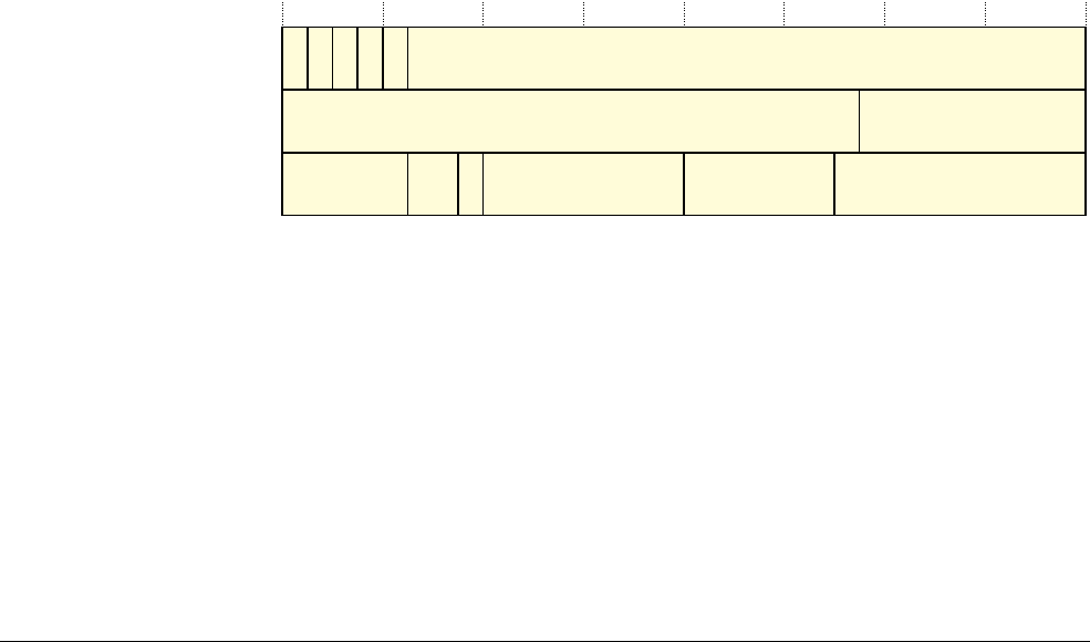
0x23FFFFE00x23FFFFE80x23FFFFEC0x23FFFFF00x23FFFFF40x23FFFFF80x23FFFFFC
0x220000000x220000140x220000180x2200001C 0x220000080x22000010 0x2200000C
32MB alias region
0
7 0
07
0x200000000x200000010x200000020x20000003
6 5 4 3 2 1 07 6 5 4 3 2 1 7 6 5 4 3 2 1 07 6 5 4 3 2 1
07 6 5 4 3 2 1 6 5 4 3 2 107 6 5 4 3 2 1 07 6 5 4 3 2 1
0x200FFFFC0x200FFFFD0x200FFFFE0x200FFFFF
1MB SRAM bit-band region
The Cortex-M3 Processor
ARM DUI 0552A Copyright © 2010 ARM. All rights reserved. 2-18
ID121610 Non-Confidential
2.2.6 Memory endianness
The processor views memory as a linear collection of bytes numbered in ascending order from
zero. For example, bytes 0-3 hold the first stored word, and bytes 4-7 hold the second stored
word. The memory endianness used is implementation-defined, and the following subsections
describe the possible implementations:
•Byte-invariant big-endian format
•Little-endian format.
Read the AIRCR.ENDIANNESS field to find the implemented endianness, see Application
Interrupt and Reset Control Register on page 4-16.
Byte-invariant big-endian format
In byte-invariant big-endian format, the processor stores the most significant byte of a word at
the lowest-numbered byte, and the least significant byte at the highest-numbered byte. For
example:
Little-endian format
In little-endian format, the processor stores the least significant byte of a word at the
lowest-numbered byte, and the most significant byte at the highest-numbered byte. For
example:
2.2.7 Synchronization primitives
The Cortex-M3 instruction set includes pairs of synchronization primitives. These provide a
non-blocking mechanism that a thread or process can use to obtain exclusive access to a memory
location. Software can use them to perform a guaranteed read-modify-write memory update
sequence, or for a semaphore mechanism.
Memory Register
Address A
A+1
msbyte
lsbyte
A+2
A+3
07
B3B2B0 B1
31 24 23 16 15 8 7 0
B0
B1
B2
B3
Memory Register
Address A
A+1
lsbyte
msbyte
A+2
A+3
07
B0B1B3 B2
31 24 23 16 15 8 7 0
B0
B1
B2
B3

The Cortex-M3 Processor
ARM DUI 0552A Copyright © 2010 ARM. All rights reserved. 2-19
ID121610 Non-Confidential
A pair of synchronization primitives comprises:
A Load-Exclusive instruction
Used to read the value of a memory location, requesting exclusive access to that
location.
A Store-Exclusive instruction
Used to attempt to write to the same memory location, returning a status bit to a
register. If this bit is:
0 it indicates that the thread or process gained exclusive access to the
memory, and the write succeeds,
1 it indicates that the thread or process did not gain exclusive access to
the memory, and no write was performed.
The pairs of Load-Exclusive and Store-Exclusive instructions are:
• the word instructions
LDREX
and
STREX
• the halfword instructions
LDREXH
and
STREXH
• the byte instructions
LDREXB
and
STREXB
.
Software must use a Load-Exclusive instruction with the corresponding Store-Exclusive
instruction.
To perform an exclusive read-modify-write of a memory location, software must:
1. Use a Load-Exclusive instruction to read the value of the location.
2. Modify the value, as required.
3. Use a Store-Exclusive instruction to attempt to write the new value back to the memory
location.
4. Test the returned status bit. If this bit is:
0 The read-modify-write completed successfully.
1 No write was performed. This indicates that the value returned at step 1 might
be out of date. The software must retry the entire read-modify-write sequence.
Software can use the synchronization primitives to implement a semaphores as follows:
1. Use a Load-Exclusive instruction to read from the semaphore address to check whether
the semaphore is free.
2. If the semaphore is free, use a Store-Exclusive to write the claim value to the semaphore
address.
3. If the returned status bit from step 2 indicates that the Store-Exclusive succeeded then the
software has claimed the semaphore. However, if the Store-Exclusive failed, another
process might have claimed the semaphore after the software performed step 1.
The Cortex-M3 includes an exclusive access monitor, that tags the fact that the processor has
executed a Load-Exclusive instruction. If the processor is part of a multiprocessor system, the
system also globally tags the memory locations addressed by exclusive accesses by each
processor.
The processor removes its exclusive access tag if:
• It executes a
CLREX
instruction.
• It executes a Store-Exclusive instruction, regardless of whether the write succeeds.

The Cortex-M3 Processor
ARM DUI 0552A Copyright © 2010 ARM. All rights reserved. 2-20
ID121610 Non-Confidential
• An exception occurs. This means the processor can resolve semaphore conflicts between
different threads.
In a multiprocessor implementation:
• executing a
CLREX
instruction removes only the local exclusive access tag for the processor
• executing a Store-Exclusive instruction, or an exception. removes the local exclusive
access tags, and global exclusive access tags for the processor.
For more information about the synchronization primitive instructions, see LDREX and STREX
on page 3-31 and CLREX on page 3-33.
2.2.8 Programming hints for the synchronization primitives
ISO/IEC C cannot directly generate the exclusive access instructions. CMSIS provides
functions for generation of these instructions:
Table 2-15 CMSIS functions for exclusive access instructions
Instruction CMSIS function
LDREX uint32_t __LDREXW (uint32_t *addr)
LDREXH uint16_t __LDREXH (uint16_t *addr)
LDREXB uint8_t __LDREXB (uint8_t *addr)
STREX uint32_t __STREXW (uint32_t value, uint32_t *addr)
STREXH uint32_t __STREXH (uint16_t value, uint16_t *addr)
STREXB uint32_t __STREXB (uint8_t value, uint8_t *addr)
CLREX void __CLREX (void)

The Cortex-M3 Processor
ARM DUI 0552A Copyright © 2010 ARM. All rights reserved. 2-21
ID121610 Non-Confidential
2.3 Exception model
This section describes the exception model in:
•Exception states
•Exception types
•Exception handlers on page 2-23
•Vector table on page 2-23
•Exception priorities on page 2-24
•Interrupt priority grouping on page 2-25
•Exception entry and return on page 2-25.
2.3.1 Exception states
Each exception is in one of the following states:
Inactive The exception is not active and not pending.
Pending The exception is waiting to be serviced by the processor.
An interrupt request from a peripheral or from software can change the
state of the corresponding interrupt to pending.
Active An exception that is being serviced by the processor but has not
completed.
Note
An exception handler can interrupt the execution of another exception
handler. In this case both exceptions are in the active state.
Active and pending
The exception is being serviced by the processor and there is a pending
exception from the same source.
2.3.2 Exception types
The exception types are:
Reset Reset is invoked on power up or a warm reset. The exception model treats
reset as a special form of exception. When reset is asserted, the operation
of the processor stops, potentially at any point in an instruction. When
reset is deasserted, execution restarts from the address provided by the
reset entry in the vector table. Execution restarts as privileged execution
in Thread mode.
NMI A NonMaskable Interrupt (NMI) can be signalled by a peripheral or
triggered by software. This is the highest priority exception other than
reset. It is permanently enabled and has a fixed priority of -2. NMIs cannot
be:
• masked or prevented from activation by any other exception
• preempted by any exception other than Reset.
HardFault A HardFault is an exception that occurs because of an error during
exception processing, or because an exception cannot be managed by any
other exception mechanism. HardFaults have a fixed priority of -1,
meaning they have higher priority than any exception with configurable
priority.

The Cortex-M3 Processor
ARM DUI 0552A Copyright © 2010 ARM. All rights reserved. 2-22
ID121610 Non-Confidential
MemManage
A MemManage fault is an exception that occurs because of a memory
protection related fault. The MPU or the fixed memory protection
constraints determines this fault, for both instruction and data memory
transactions. This fault is always used to abort instruction accesses to
Execute Never (XN) memory regions.
BusFault A BusFault is an exception that occurs because of a memory related fault
for an instruction or data memory transaction. This might be from an error
detected on a bus in the memory system.
UsageFault A UsageFault is an exception that occurs because of a fault related to
instruction execution. This includes:
• an undefined instruction
• an illegal unaligned access
• invalid state on instruction execution
• an error on exception return.
The following can cause a UsageFault when the core is configured to
report them:
• an unaligned address on word and halfword memory access
• division by zero.
SVCall A supervisor call (SVC) is an exception that is triggered by the
SVC
instruction. In an OS environment, applications can use
SVC
instructions to
access OS kernel functions and device drivers.
PendSV PendSV is an interrupt-driven request for system-level service. In an OS
environment, use PendSV for context switching when no other exception
is active.
SysTick A SysTick exception is an exception the system timer generates when it
reaches zero. Software can also generate a SysTick exception. In an OS
environment, the processor can use this exception as system tick.
Interrupt (IRQ) A interrupt, or IRQ, is an exception signalled by a peripheral, or generated
by a software request. All interrupts are asynchronous to instruction
execution. In the system, peripherals use interrupts to communicate with
the processor.
Table 2-16 Properties of the different exception types
Exception
numbera
IRQ
numberaException type Priority Vector address
or offsetbActivation
1 - Reset -3, the highest
0x00000004
Asynchronous
2 -14 NMI -2
0x00000008
Asynchronous
3 -13 HardFault -1
0x0000000C
-
4 -12 MemManage Configurablec
0x00000010
Synchronous
5-11BusFault
Configurablec
0x00000014
Synchronous when precise,
asynchronous when imprecise
6 -10 UsageFault Configurablec
0x00000018
Synchronous
7-10 - Reserved - - -

The Cortex-M3 Processor
ARM DUI 0552A Copyright © 2010 ARM. All rights reserved. 2-23
ID121610 Non-Confidential
For an asynchronous exception, other than reset, the processor can execute another instruction
between when the exception is triggered and when the processor enters the exception handler.
Privileged software can disable the exceptions that Table 2-16 on page 2-22 shows as having
configurable priority, see:
•System Handler Control and State Register on page 4-23
•Interrupt Clear-enable Registers on page 4-5.
For more information about HardFaults, MemManage faults, BusFaults, and UsageFaults, see
Fault handling on page 2-28.
2.3.3 Exception handlers
The processor handles exceptions using:
Interrupt Service Routines (ISRs)
The IRQ interrupts are the exceptions handled by ISRs.
Fault handlers HardFault, MemManage fault, UsageFault, and BusFault are fault
exceptions handled by the fault handlers.
System handlers NMI, PendSV, SVCall SysTick, and the fault exceptions are all system
exceptions that are handled by system handlers.
2.3.4 Vector table
The vector table contains the reset value of the stack pointer, and the start addresses, also called
exception vectors, for all exception handlers. Figure 2-2 on page 2-24 shows the order of the
exception vectors in the vector table. The least-significant bit of each vector must be 1,
indicating that the exception handler is Thumb code, see Thumb state on page 2-7.
11 -5 SVCall Configurablec
0x0000002C
Synchronous
12-13 - Reserved - - -
14 -2 PendSV Configurablec
0x00000038
Asynchronous
15 -1 SysTick Configurablec
0x0000003C
Asynchronous
16 0 Interrupt (IRQ) Configurabled
0x00000040
eAsynchronous
a. To simplify the software layer, the CMSIS only uses IRQ numbers and therefore uses negative values for exceptions other than
interrupts. The IPSR returns the Exception number, see Interrupt Program Status Register on page 2-6.
b. See Vector table for more information.
c. See System Handler Priority Registers on page 4-21.
d. See Interrupt Priority Registers on page 4-7.
e. Increasing in steps of 4.
Table 2-16 Properties of the different exception types (continued)
Exception
numbera
IRQ
numberaException type Priority Vector address
or offsetbActivation

The Cortex-M3 Processor
ARM DUI 0552A Copyright © 2010 ARM. All rights reserved. 2-24
ID121610 Non-Confidential
Figure 2-2 Vector table
On system reset, the vector table is fixed at address
0x00000000
. Privileged software can write to
the VTOR to relocate the vector table start address to a different memory location, in the range
0x00000080
to
0x3FFFFF80
, see Vector Table Offset Register on page 4-16.
2.3.5 Exception priorities
Table 2-16 on page 2-22 shows that all exceptions have an associated priority, with:
• a lower priority value indicating a higher priority
• configurable priorities for all exceptions except Reset, HardFault, and NMI.
If software does not configure any priorities, then all exceptions with a configurable priority
have a priority of 0. For information about configuring exception priorities, see:
•System Handler Priority Registers on page 4-21
•Interrupt Priority Registers on page 4-7.
Note
Configurable priority values are in the range 0-255. This means that the Reset, HardFault, and
NMI exceptions, with fixed negative priority values, always have higher priority than any other
exception.
Initial SP value
Reset
Hard fault
NMI
Memory management fault
Usage fault
Bus fault
0x0000
0x0004
0x0008
0x000C
0x0010
0x0014
0x0018
Reserved
SVCall
PendSV
Reserved for Debug
Systick
IRQ0
Reserved
0x002C
0x0038
0x003C
0x0040
OffsetException number
2
3
4
5
6
11
12
14
15
16
18
13
7
10
1
Vector
.
.
.
8
9
IRQ1
IRQ2
0x0044
IRQn
17
0x0048
0x004C
16+n
.
.
.
.
.
.
0x0040+4n
IRQ number
-14
-13
-12
-11
-10
-5
-2
-1
0
2
1
n

The Cortex-M3 Processor
ARM DUI 0552A Copyright © 2010 ARM. All rights reserved. 2-25
ID121610 Non-Confidential
For example, assigning a higher priority value to IRQ[0] and a lower priority value to IRQ[1]
means that IRQ[1] has higher priority than IRQ[0]. If both IRQ[1] and IRQ[0] are asserted,
IRQ[1] is processed before IRQ[0].
If multiple pending exceptions have the same priority, the pending exception with the lowest
exception number takes precedence. For example, if both IRQ[0] and IRQ[1] are pending and
have the same priority, then IRQ[0] is processed before IRQ[1].
When the processor is executing an exception handler, the exception handler is preempted if a
higher priority exception occurs. If an exception occurs with the same priority as the exception
being handled, the handler is not preempted, irrespective of the exception number. However, the
status of the new interrupt changes to pending.
2.3.6 Interrupt priority grouping
To increase priority control in systems with interrupts, the NVIC supports priority grouping.
This divides each interrupt priority register entry into two fields:
• an upper field that defines the group priority
• a lower field that defines a subpriority within the group.
Only the group priority determines preemption of interrupt exceptions. When the processor is
executing an interrupt exception handler, another interrupt with the same group priority as the
interrupt being handled does not preempt the handler,
If multiple pending interrupts have the same group priority, the subpriority field determines the
order in which they are processed. If multiple pending interrupts have the same group priority
and subpriority, the interrupt with the lowest IRQ number is processed first.
For information about splitting the interrupt priority fields into group priority and subpriority,
see Application Interrupt and Reset Control Register on page 4-16.
2.3.7 Exception entry and return
Descriptions of exception handling use the following terms:
Preemption When the processor is executing an exception handler, an exception can
preempt the exception handler if its priority is higher than the priority of
the exception being handled. See Interrupt priority grouping for more
information about preemption by an interrupt.
When one exception preempts another, the exceptions are called nested
exceptions. See Exception entry on page 2-26 more information.
Return This occurs when the exception handler is completed, and:
• there is no pending exception with sufficient priority to be serviced
• the completed exception handler was not handling a late-arriving
exception.
The processor pops the stack and restores the processor state to the state it
had before the interrupt occurred. See Exception return on page 2-27 for
more information.
Tail-chaining This mechanism speeds up exception servicing. On completion of an
exception handler, if there is a pending exception that meets the
requirements for exception entry, the stack pop is skipped and control
transfers to the new exception handler.

The Cortex-M3 Processor
ARM DUI 0552A Copyright © 2010 ARM. All rights reserved. 2-26
ID121610 Non-Confidential
Late-arriving This mechanism speeds up preemption. If a higher priority exception
occurs during state saving for a previous exception, the processor switches
to handle the higher priority exception and initiates the vector fetch for
that exception. State saving is not affected by late arrival because the state
saved is the same for both exceptions. Therefore the state saving continues
uninterrupted. The processor can accept a late arriving exception until the
first instruction of the exception handler of the original exception enters
the execute stage of the processor. On return from the exception handler
of the late-arriving exception, the normal tail-chaining rules apply.
Exception entry
Exception entry occurs when there is a pending exception with sufficient priority and either:
• the processor is in Thread mode
• the new exception is of higher priority than the exception being handled, in which case
the new exception preempts the exception being handled.
When one exception preempts another, the exceptions are nested.
Sufficient priority means the exception has has greater priority than any limits set by the mask
registers, see Exception mask registers on page 2-7. An exception with less priority than this is
pending but is not handled by the processor.
When the processor takes an exception, unless the exception is a tail-chained or a late-arriving
exception, the processor pushes information onto the current stack. This operation is referred to
as stacking and the structure of eight data words is referred as the stack frame. The stack frame
contains the following information:
Immediately after stacking, the stack pointer indicates the lowest address in the stack frame. The
alignment of the stack frame is controlled via the STKALIGN bit of the Configuration Control
Register (CCR).
The stack frame includes the return address. This is the address of the next instruction in the
interrupted program. This value is restored to the PC at exception return so that the interrupted
program resumes.
The processor performs a vector fetch that reads the exception handler start address from the
vector table. When stacking is complete, the processor starts executing the exception handler.
At the same time, the processor writes an EXC_RETURN value to the LR. This indicates which
stack pointer corresponds to the stack frame and what operation mode the processor was in
before the entry occurred.
If no higher priority exception occurs during exception entry, the processor starts executing the
exception handler and automatically changes the status of the corresponding pending interrupt
to active.
SP points here before interrupt
xPSR
PC
LR
R12
R3
R2
R1
R0
<previous>
SP points here after interrupt
SP + 0x1C
SP + 0x18
SP + 0x14
SP + 0x10
SP + 0x0C
SP + 0x08
SP + 0x04
SP + 0x00
Decreasing
memory
address

The Cortex-M3 Processor
ARM DUI 0552A Copyright © 2010 ARM. All rights reserved. 2-27
ID121610 Non-Confidential
If another higher priority exception occurs during exception entry, the processor starts executing
the exception handler for this exception and does not change the pending status of the earlier
exception. This is the late arrival case.
Exception return
Exception return occurs when the processor is in Handler mode and executes one of the
following instructions attempts to set the PC to an EXC_RETURN value:
•an
LDM
or
POP
instruction that loads the PC
•an
LDR
instruction with PC as the destination
•a
BX
instruction using any register.
The processor saves an EXC_RETURN value to the LR on exception entry. The exception
mechanism relies on this value to detect when the processor has completed an exception
handler. Bits[31:4] of an EXC_RETURN value are
0xFFFFFFF
. When the processor loads a value
matching this pattern to the PC it detects that the operation is a not a normal branch operation
and, instead, that the exception is complete. Therefore, it starts the exception return sequence.
Bits[3:0] of the EXC_RETURN value indicate the required return stack and processor mode, as
Table 2-17 shows.
Table 2-17 Exception return behavior
EXC_RETURN Description
0xFFFFFFF1
Return to Handler mode.
Exception return gets state from the main stack.
Execution uses MSP after return.
0xFFFFFFF9
Return to Thread mode.
Exception Return get state from the main stack.
Execution uses MSP after return.
0xFFFFFFFD
Return to Thread mode.
Exception return gets state from the process stack.
Execution uses PSP after return.
All other values Reserved.

The Cortex-M3 Processor
ARM DUI 0552A Copyright © 2010 ARM. All rights reserved. 2-28
ID121610 Non-Confidential
2.4 Fault handling
Faults are a subset of the exceptions, see Exception model on page 2-21. Faults are generated by:
• a bus error on:
— an instruction fetch or vector table load
— a data access.
• an internally-detected error such as an Undefined instruction.
• attempting to execute an instruction from a memory region marked as Non-Executable
(XN).
• attempting to execute an instruction while the EPSR T-bit is clear. For example, as the
result of an erroneous
BX
instruction, or a vector fetch from a vector table entry with bit[0]
clear.
• If your device contains an MPU, a privilege violation or an attempt to access an
unmanaged region causing an MPU fault.
2.4.1 Fault types
Table 2-18 shows the types of fault, the handler used for the fault, the corresponding fault status
register, and the register bit that indicates that the fault has occurred. See Configurable Fault
Status Register on page 4-24 for more information about the fault status registers.
Table 2-18 Faults
Fault Handler Bit name Fault status register
Bus error on a vector read HardFault VECTTBL HardFault Status Register on page 4-30
Fault escalated to a hard fault FORCED
MPU or default memory map mismatch: MemManage - -
on instruction access IACCVIOLaMemManage Fault Address Register on page 4-30
on data access DACCVIOL
during exception stacking MSTKERR
during exception unstacking MUNSKERR
Bus error: BusFault - -
during exception stacking STKERR BusFault Status Register on page 4-26
during exception unstacking UNSTKERR
during instruction prefetch IBUSERR
Precise data bus error PRECISERR
Imprecise data bus error IMPRECISERR
Attempt to access a coprocessor UsageFault NOCP UsageFault Status Register on page 4-28
Undefined instruction UNDEFINSTR
Attempt to enter an invalid instruction
set stateb
INVSTATE

The Cortex-M3 Processor
ARM DUI 0552A Copyright © 2010 ARM. All rights reserved. 2-29
ID121610 Non-Confidential
2.4.2 Fault escalation and hard faults
All faults exceptions except for HardFault have configurable exception priority, see System
Handler Priority Registers on page 4-21. Software can disable execution of the handlers for
these faults, see System Handler Control and State Register on page 4-23.
Usually, the exception priority, together with the values of the exception mask registers,
determines whether the processor enters the fault handler, and whether a fault handler can
preempt another fault handler. as described in Exception model on page 2-21.
In some situations, a fault with configurable priority is treated as a HardFault. This is called
priority escalation, and the fault is described as escalated to HardFault. Escalation to HardFault
occurs when:
• A fault handler causes the same kind of fault as the one it is servicing. This escalation to
HardFault occurs because a fault handler cannot preempt itself because it must have the
same priority as the current priority level.
• A fault handler causes a fault with the same or lower priority as the fault it is servicing.
This is because the handler for the new fault cannot preempt the currently executing fault
handler.
• An exception handler causes a fault for which the priority is the same as or lower than the
currently executing exception.
• A fault occurs and the handler for that fault is not enabled.
If a BusFault occurs during a stack push when entering a BusFault handler, the BusFault does
not escalate to a HardFault. This means that if a corrupted stack causes a fault, the fault handler
executes even though the stack push for the handler failed. The fault handler operates but the
stack contents are corrupted.
Note
Only Reset and NMI can preempt the fixed priority HardFault. A HardFault can preempt any
exception other than Reset, NMI, or another HardFault.
Invalid EXC_RETURN value UsageFault INVPC UsageFault Status Register on page 4-28
Illegal unaligned load or store UNALIGNED
Divide By 0 DIVBYZERO
a. Occurs on an access to an XN region even if the processor does not include an MPU or if the MPU is disabled.
b. Attempting to use an instruction set other than the Thumb instruction set or returns to a non load/store-multiple instruction with ICI
continuation.
Table 2-18 Faults (continued)
Fault Handler Bit name Fault status register

The Cortex-M3 Processor
ARM DUI 0552A Copyright © 2010 ARM. All rights reserved. 2-30
ID121610 Non-Confidential
2.4.3 Fault status registers and fault address registers
The fault status registers indicate the cause of a fault. For BusFaults and MemManage faults,
the fault address register indicates the address accessed by the operation that caused the fault,
as shown in Table 2-19.
2.4.4 Lockup
The processor enters a lockup state if a fault occurs when executing the NMI or HardFault
handlers. When the processor is in lockup state it does not execute any instructions. The
processor remains in lockup state until either:
• it is reset
• an NMI occurs
• it is halted by a debugger.
Note
If lockup state occurs from the NMI handler a subsequent NMI does not cause the processor to
leave lockup state.
Table 2-19 Fault status and fault address registers
Handler Status register
name
Address register
name Register description
HardFault HFSR - HardFault Status Register on page 4-30
MemManage MMFSR MMFAR MemManage Fault Status Register on page 4-25
MemManage Fault Address Register on page 4-30
BusFault BFSR BFAR BusFault Status Register on page 4-26
BusFault Address Register on page 4-31
UsageFault UFSR - UsageFault Status Register on page 4-28

The Cortex-M3 Processor
ARM DUI 0552A Copyright © 2010 ARM. All rights reserved. 2-31
ID121610 Non-Confidential
2.5 Power management
The Cortex-M3 processor sleep modes reduce power consumption. The sleep modes your
device implements are implementation-defined, but they might be one or all of the following:
• sleep mode stops the processor clock
• deep sleep mode stops the system clock and switches off the PLL and flash memory.
If your device implements two sleep modes providing different levels of power saving, the
SLEEPDEEP bit of the SCR selects which sleep mode is used, see System Control Register on
page 4-19. For more information about the behavior of the sleep modes see the documentation
supplied by your device vendor.
This section describes the mechanisms for entering sleep mode, and the conditions for waking
up from sleep mode.
2.5.1 Entering sleep mode
This section describes the mechanisms software can use to put the processor into sleep mode.
The system can generate spurious wakeup events, for example a debug operation wakes up the
processor. Therefore software must be able to put the processor back into sleep mode after such
an event. A program might have an idle loop to put the processor back to sleep mode.
Wait For Interrupt
The Wait For Interrupt instruction,
WFI
, causes immediate entry to sleep mode unless the
wake-up condition is true, see Wakeup from WFI or sleep-on-exit on page 2-32. When the
processor executes a
WFI
instruction it stops executing instructions and enters sleep mode. See
WFI on page 3-80 for more information.
Wait For Event
The Wait For Event instruction,
WFE
, causes entry to sleep mode depending on the value of a
one-bit event register. When the processor executes a
WFE
instruction, it checks the value of the
event register:
0 The processor stops executing instructions and enters sleep mode.
1 The processor clears the register to 0 and continues executing instructions without
entering sleep mode.
See WFE on page 3-79 for more information.
If the event register is 1, this indicates that the processor must not enter sleep mode on execution
of a
WFE
instruction. Typically, this is because an external event signal is asserted, or a processor
in the system has executed an
SEV
instruction, see SEV on page 3-77. Software cannot access this
register directly.
Sleep-on-exit
If the SLEEPONEXIT bit of the SCR is set to 1, when the processor completes the execution of
all exception handlers it returns to Thread mode and immediately enters sleep mode. Use this
mechanism in applications that only require the processor to run when an exception occurs.

The Cortex-M3 Processor
ARM DUI 0552A Copyright © 2010 ARM. All rights reserved. 2-32
ID121610 Non-Confidential
2.5.2 Wakeup from sleep mode
The conditions for the processor to wakeup depend on the mechanism that cause it to enter sleep
mode.
Wakeup from WFI or sleep-on-exit
Normally, the processor wakes up only when it detects an exception with sufficient priority to
cause exception entry. Some embedded systems might have to execute system restore tasks after
the processor wakes up, and before it executes an interrupt handler. To achieve this set the
PRIMASK bit to 1 and the FAULTMASK bit to 0. If an interrupt arrives that is enabled and has
a higher priority than current exception priority, the processor wakes up but does not execute the
interrupt handler until the processor sets PRIMASK to zero. For more information about
PRIMASK and FAULTMASK see Exception mask registers on page 2-7.
Wakeup from WFE
The processor wakes up if:
• it detects an exception with sufficient priority to cause exception entry
• it detects an external event signal, see The external event input
• in a multiprocessor system, another processor in the system executes an
SEV
instruction.
In addition, if the SEVONPEND bit in the SCR is set to 1, any new pending interrupt triggers
an event and wakes up the processor, even if the interrupt is disabled or has insufficient priority
to cause exception entry. For more information about the SCR see System Control Register on
page 4-19.
2.5.3 The optional Wakeup Interrupt Controller
Your device might include a Wakeup Interrupt Controller (WIC), an optional peripheral that can
detect an interrupt and wake the processor from deep sleep mode. The WIC is enabled only
when the DEEPSLEEP bit in the SCR is set to 1, see System Control Register on page 4-19.
The WIC is not programmable, and does not have any registers or user interface. It operates
entirely from hardware signals.
When the WIC is enabled and the processor enters deep sleep mode, the power management unit
in the system can power down most of the Cortex-M3 processor. This has the side effect of
stopping the SysTick timer. When the WIC receives an interrupt, it takes a number of clock
cycles to wakeup the processor and restore its state, before it can process the interrupt. This
means interrupt latency is increased in deep sleep mode.
Note
If the processor detects a connection to a debugger it disables the WIC.
2.5.4 The external event input
Your device might include an external event input signal, so that device peripherals can signal
the processor, to either:
• wake the processor from WFE
• set the internal WFE event register to one to indicate that the processor must not enter
sleep mode on a later
WFE
instruction.

The Cortex-M3 Processor
ARM DUI 0552A Copyright © 2010 ARM. All rights reserved. 2-33
ID121610 Non-Confidential
See Wait For Event on page 2-31 and the documentation supplied by your device vendor for
more information about this signal.
2.5.5 Power management programming hints
ISO/IEC C cannot directly generate the
WFI
and
WFE
instructions. The CMSIS provides the
following functions for these instructions:
void __WFE(void) // Wait For Event
void __WFI(void) // Wait For Interrupt

ARM DUI 0552A Copyright © 2010 ARM. All rights reserved. 3-1
ID121610 Non-Confidential
Chapter 3
The Cortex-M3 Instruction Set
This chapter is the reference material for the Cortex-M3 instruction set description in a User Guide.
The following sections give general information:
•Instruction set summary on page 3-2
•CMSIS functions on page 3-6
•About the instruction descriptions on page 3-8.
Each of the following sections describes a functional group of Cortex-M3 instructions. Together
they describe all the instructions supported by the Cortex-M3 processor:
•Memory access instructions on page 3-17
•General data processing instructions on page 3-34
•Multiply and divide instructions on page 3-49
•Saturating instructions on page 3-54
•Bitfield instructions on page 3-56
•Branch and control instructions on page 3-60
•Miscellaneous instructions on page 3-68.

The Cortex-M3 Instruction Set
ARM DUI 0552A Copyright © 2010 ARM. All rights reserved. 3-2
ID121610 Non-Confidential
3.1 Instruction set summary
The processor implements a version of the Thumb instruction set. Table 3-1 lists the supported
instructions.
Note
In Table 3-1:
• angle brackets, <>, enclose alternative forms of the operand
• braces, {}, enclose optional operands
• the Operands column is not exhaustive
•
Op2
is a flexible second operand that can be either a register or a constant
• most instructions can use an optional condition code suffix.
For more information on the instructions and operands, see the instruction descriptions.
Table 3-1 Cortex-M3 instructions
Mnemonic Operands Brief description Flags See
ADC, ADCS {Rd,}
Rn,
Op2
Add with Carry N,Z,C,V page 3-35
ADD, ADDS {Rd,}
Rn, Op2
Add N,Z,C,V page 3-35
ADD, ADDW {Rd,}
Rn, #imm12
Add N,Z,C,V page 3-35
ADR Rd, label
Load PC-relative Address - page 3-18
AND, ANDS {Rd,} Rn, Op2
Logical AND N,Z,C page 3-38
ASR, ASRS Rd, Rm, <Rs|#n>
Arithmetic Shift Right N,Z,C page 3-40
B label
Branch - page 3-61
BFC Rd, #lsb, #width
Bit Field Clear - page 3-57
BFI Rd, Rn, #lsb, #width
Bit Field Insert - page 3-57
BIC, BICS {Rd,}
Rn, Op2
Bit Clear N,Z,C page 3-38
BKPT #imm
Breakpoint - page 3-69
BL label
Branch with Link - page 3-61
BLX Rm
Branch indirect with Link - page 3-61
BX Rm
Branch indirect - page 3-61
CBNZ Rn, label
Compare and Branch if Non Zero - page 3-63
CBZ Rn, label
Compare and Branch if Zero - page 3-63
CLREX
-Clear Exclusive -page 3-33
CLZ Rd, Rm
Count Leading Zeros - page 3-42
CMN Rn, Op2
Compare Negative N,Z,C,V page 3-43
CMP Rn, Op2
Compare N,Z,C,V page 3-43
CPSID i
Change Processor State, Disable Interrupts - page 3-70

The Cortex-M3 Instruction Set
ARM DUI 0552A Copyright © 2010 ARM. All rights reserved. 3-3
ID121610 Non-Confidential
CPSIE i
Change Processor State, Enable Interrupts - page 3-70
DMB -
Data Memory Barrier - page 3-71
DSB -
Data Synchronization Barrier - page 3-72
EOR, EORS {Rd,} Rn, Op2
Exclusive OR N,Z,C page 3-38
ISB -
Instruction Synchronization Barrier - page 3-73
IT
- If-Then condition block - page 3-64
LDM Rn{!}, reglist
Load Multiple registers, increment after - page 3-27
LDMDB, LDMEA Rn{!}, reglist
Load Multiple registers, decrement before - page 3-27
LDMFD, LDMIA Rn{!}, reglist
Load Multiple registers, increment after - page 3-27
LDR Rt, [Rn, #offset]
Load Register with word - page 3-17
LDRB, LDRBT Rt, [Rn, #offset]
Load Register with byte - page 3-17
LDRD Rt, Rt2, [Rn, #offset]
Load Register with two bytes - page 3-19
LDREX Rt, [Rn, #offset]
Load Register Exclusive - page 3-31
LDREXB Rt, [Rn]
Load Register Exclusive with Byte - page 3-31
LDREXH Rt, [Rn]
Load Register Exclusive with Halfword - page 3-31
LDRH, LDRHT Rt, [Rn, #offset]
Load Register with Halfword - page 3-17
LDRSB, LDRSBT Rt, [Rn, #offset]
Load Register with Signed Byte - page 3-17
LDRSH, LDRSHT Rt, [Rn, #offset]
Load Register with Signed Halfword - page 3-17
LDRT Rt, [Rn, #offset]
Load Register with word - page 3-17
LSL, LSLS Rd, Rm, <Rs|#n>
Logical Shift Left N,Z,C page 3-40
LSR, LSRS Rd, Rm, <Rs|#n>
Logical Shift Right N,Z,C page 3-40
MLA Rd, Rn, Rm, Ra
Multiply with Accumulate, 32-bit result - page 3-50
MLS Rd, Rn, Rm, Ra
Multiply and Subtract, 32-bit result - page 3-50
MOV, MOVS Rd, Op2
Move N,Z,C page 3-44
MOVT Rd, #imm16
Move Top - page 3-46
MOVW, MOV Rd, #imm16
Move 16-bit constant N,Z,C page 3-44
MRS Rd, spec_reg
Move from Special Register to general register - page 3-74
MSR spec_reg, Rm
Move from general register to Special Register N,Z,C,V page 3-75
MUL, MULS {Rd,}
Rn, Rm
Multiply, 32-bit result N,Z page 3-50
MVN, MVNS Rd, Op2
Move NOT N,Z,C page 3-44
NOP
-No Operation -page 3-76
ORN, ORNS {Rd,} Rn, Op2
Logical OR NOT N,Z,C page 3-38
ORR, ORRS {Rd,} Rn, Op2
Logical OR N,Z,C page 3-38
Table 3-1 Cortex-M3 instructions (continued)
Mnemonic Operands Brief description Flags See

The Cortex-M3 Instruction Set
ARM DUI 0552A Copyright © 2010 ARM. All rights reserved. 3-4
ID121610 Non-Confidential
POP reglist
Pop registers from stack - page 3-29
PUSH reglist
Push registers onto stack - page 3-29
RBIT Rd, Rn
Reverse Bits - page 3-47
REV Rd, Rn
Reverse byte order in a word - page 3-47
REV16 Rd, Rn
Reverse byte order in each halfword - page 3-47
REVSH Rd, Rn
Reverse byte order in bottom halfword and sign
extend
-page 3-47
ROR, RORS Rd, Rm, <Rs|#n>
Rotate Right N,Z,C page 3-40
RRX, RRXS Rd, Rm
Rotate Right with Extend N,Z,C page 3-40
RSB, RSBS {Rd,} Rn, Op2
Reverse Subtract N,Z,C,V page 3-35
SBC, SBCS {Rd,} Rn, Op2
Subtract with Carry N,Z,C,V page 3-35
SBFX Rd, Rn, #lsb, #width
Signed Bit Field Extract - page 3-58
SDIV {Rd,} Rn, Rm
Signed Divide - page 3-53
SEV
- Send Event - page 3-77
SMLAL RdLo, RdHi, Rn, Rm
Signed Multiply with Accumulate (32 x 32 + 64),
64-bit result
-page 3-52
SMULL RdLo, RdHi, Rn, Rm
Signed Multiply (32 x 32), 64-bit result - page 3-52
SSAT Rd, #n, Rm {,shift #s}
Signed Saturate Q page 3-54
STM Rn{!}, reglist
Store Multiple registers, increment after - page 3-27
STMDB, STMEA Rn{!}, reglist
Store Multiple registers, decrement before - page 3-27
STMFD, STMIA Rn{!}, reglist
Store Multiple registers, increment after - page 3-27
STR Rt, [Rn, #offset]
Store Register word - page 3-17
STRB, STRBT Rt, [Rn, #offset]
Store Register byte - page 3-17
STRD Rt, Rt2, [Rn, #offset]
Store Register two words - page 3-19
STREX Rd, Rt, [Rn, #offset]
Store Register Exclusive - page 3-31
STREXB Rd, Rt, [Rn]
Store Register Exclusive Byte - page 3-31
STREXH Rd, Rt, [Rn]
Store Register Exclusive Halfword - page 3-31
STRH, STRHT Rt, [Rn, #offset]
Store Register Halfword - page 3-17
STRT Rt, [Rn, #offset]
Store Register word - page 3-17
SUB, SUBS {Rd,} Rn, Op2
Subtract N,Z,C,V page 3-35
SUB, SUBW {Rd,} Rn, #imm12
Subtract N,Z,C,V page 3-35
SVC #imm
Supervisor Call - page 3-78
SXTB {Rd,} Rm {,ROR #n}
Sign extend a byte - page 3-59
Table 3-1 Cortex-M3 instructions (continued)
Mnemonic Operands Brief description Flags See

The Cortex-M3 Instruction Set
ARM DUI 0552A Copyright © 2010 ARM. All rights reserved. 3-5
ID121610 Non-Confidential
SXTH {Rd,} Rm {,ROR #n}
Sign extend a halfword - page 3-59
TBB [Rn, Rm]
Table Branch Byte - page 3-66
TBH [Rn, Rm, LSL #1]
Table Branch Halfword - page 3-66
TEQ Rn, Op2
Test Equivalence N,Z,C page 3-48
TST Rn, Op2
Test N,Z,C page 3-48
UBFX Rd, Rn, #lsb, #width
Unsigned Bit Field Extract - page 3-58
UDIV {Rd,} Rn, Rm
Unsigned Divide - page 3-53
UMLAL RdLo, RdHi, Rn, Rm
Unsigned Multiply with Accumulate (32 x 32 +
64), 64-bit result
-page 3-52
UMULL RdLo, RdHi, Rn, Rm
Unsigned Multiply (32 x 32), 64-bit result - page 3-52
USAT Rd, #n, Rm {,shift #s}
Unsigned Saturate Q page 3-54
UXTB {Rd,} Rm {,ROR #n}
Zero extend a Byte - page 3-59
UXTH {Rd,} Rm {,ROR #n}
Zero extend a Halfword - page 3-59
WFE
- Wait For Event - page 3-79
WFI
- Wait For Interrupt - page 3-80
Table 3-1 Cortex-M3 instructions (continued)
Mnemonic Operands Brief description Flags See

The Cortex-M3 Instruction Set
ARM DUI 0552A Copyright © 2010 ARM. All rights reserved. 3-6
ID121610 Non-Confidential
3.2 CMSIS functions
ISO/IEC C code cannot directly access some Cortex-M3 instructions. This section describes
intrinsic functions that can generate these instructions, provided by the CMSIS and that might
be provided by a C compiler. If a C compiler does not support an appropriate intrinsic function,
you might have to use inline assembler to access some instructions.
The CMSIS provides the following intrinsic functions to generate instructions that ISO/IEC C
code cannot directly access:
The CMSIS also provides a number of functions for accessing the special registers using
MRS
and
MSR
instructions:
Table 3-2 CMSIS functions to generate some Cortex-M3 instructions
Instruction CMSIS function
CPSIE I void __enable_irq(void)
CPSID I void __disable_irq(void)
CPSIE F void __enable_fault_irq(void)
CPSID F void __disable_fault_irq(void)
ISB void __ISB(void)
DSB void __DSB(void)
DMB void __DMB(void)
REV uint32_t __REV(uint32_t int value)
REV16 uint32_t __REV16(uint32_t int value)
REVSH uint32_t __REVSH(uint32_t int value)
RBIT uint32_t __RBIT(uint32_t int value)
SEV void __SEV(void)
WFE void __WFE(void)
WFI void __WFI(void)
Table 3-3 CMSIS functions to access the special registers
Special register Access CMSIS function
PRIMASK Read
uint32_t __get_PRIMASK (void)
Write
void __set_PRIMASK (uint32_t value)
FAULTMASK Read
uint32_t __get_FAULTMASK (void)
Write
void __set_FAULTMASK (uint32_t value)
BASEPRI Read
uint32_t __get_BASEPRI (void)
Write
void __set_BASEPRI (uint32_t value)
CONTROL Read
uint32_t __get_CONTROL (void)
Write
void __set_CONTROL (uint32_t value)

The Cortex-M3 Instruction Set
ARM DUI 0552A Copyright © 2010 ARM. All rights reserved. 3-7
ID121610 Non-Confidential
MSP Read
uint32_t __get_MSP (void)
Write
void __set_MSP (uint32_t TopOfMainStack)
PSP Read
uint32_t __get_PSP (void)
Write
void __set_PSP (uint32_t TopOfProcStack)
Table 3-3 CMSIS functions to access the special registers (continued)
Special register Access CMSIS function

The Cortex-M3 Instruction Set
ARM DUI 0552A Copyright © 2010 ARM. All rights reserved. 3-8
ID121610 Non-Confidential
3.3 About the instruction descriptions
The following sections give more information about using the instructions:
•Operands on page 3-9
•Restrictions when using PC or SP on page 3-9
•Flexible second operand on page 3-9
•Shift Operations on page 3-10
•Address alignment on page 3-13
•PC-relative expressions on page 3-13
•Conditional execution on page 3-14
•Instruction width selection on page 3-16.

The Cortex-M3 Instruction Set
ARM DUI 0552A Copyright © 2010 ARM. All rights reserved. 3-9
ID121610 Non-Confidential
3.3.1 Operands
An instruction operand can be an ARM register, a constant, or another instruction-specific
parameter. Instructions act on the operands and often store the result in a destination register.
When there is a destination register in the instruction, it is usually specified before the operands.
Operands in some instructions are flexible in that they can either be a register or a constant. See
Flexible second operand.
3.3.2 Restrictions when using PC or SP
Many instructions have restrictions on whether you can use the Program Counter (PC) or Stack
Pointer (SP) for the operands or destination register. See instruction descriptions for more
information.
Note
Bit[0] of any address you write to the PC with a
BX
,
BLX
,
LDM
,
LDR
, or
POP
instruction must be 1
for correct execution, because this bit indicates the required instruction set, and the Cortex-M3
processor only supports Thumb instructions.
3.3.3 Flexible second operand
Many general data processing instructions have a flexible second operand. This is shown as
Operand2
in the descriptions of the syntax of each instruction.
Operand2
can be a:
•Constant
•Register with optional shift on page 3-10.
Constant
You specify an
Operand2
constant in the form:
#constant
where
constant
can be:
• any constant that can be produced by shifting an 8-bit value left by any number of bits
within a 32-bit word
• any constant of the form
0x00XY00XY
• any constant of the form
0xXY00XY00
• any constant of the form
0xXYXYXYXY
.
Note
In the constants shown above,
X
and
Y
are hexadecimal digits.
In addition, in a small number of instructions,
constant
can take a wider range of values. These
are described in the individual instruction descriptions.
When an
Operand2
constant is used with the instructions
MOVS
,
MVNS
,
ANDS
,
ORRS
,
ORNS
,
EORS
,
BICS
,
TEQ
or
TST
, the carry flag is updated to bit[31] of the constant, if the constant is greater than 255
and can be produced by shifting an 8-bit value. These instructions do not affect the carry flag if
Operand2
is any other constant.

The Cortex-M3 Instruction Set
ARM DUI 0552A Copyright © 2010 ARM. All rights reserved. 3-10
ID121610 Non-Confidential
Instruction substitution
Your assembler might be able to produce an equivalent instruction in cases where you specify a
constant that is not permitted. For example, an assembler might assemble the instruction
CMP
Rd
,
#0xFFFFFFFE
as the equivalent instruction
CMN
Rd
,
#0x2
.
Register with optional shift
You specify an
Operand2
register in the form:
Rm {, shift}
where:
Rm
Specifies the register holding the data for the second operand.
shift
Is an optional shift to be applied to
Rm
. It can be one of:
ASR #n
Arithmetic shift right
n
bits, 1 ≤
n
≤ 32.
LSL #n
Logical shift left
n
bits, 1 ≤
n
≤ 31.
LSR #n
Logical shift right
n
bits, 1 ≤
n
≤ 32.
ROR #n
Rotate right
n
bits, 1 ≤
n
≤ 31.
RRX
Rotate right one bit, with extend.
- If omitted, no shift occurs, equivalent to
LSL #0
.
If you omit the shift, or specify
LSL #0
, the instruction uses the value in
Rm
.
If you specify a shift, the shift is applied to the value in
Rm
, and the resulting 32-bit value is used
by the instruction. However, the contents in the register
Rm
remains unchanged. Specifying a
register with shift also updates the carry flag when used with certain instructions. For Is an
optional condition the carry flag, see Shift Operations.
3.3.4 Shift Operations
Register shift operations move the bits in a register left or right by a specified number of bits,
the shift length. Register shift can be performed:
• directly by the instructions
ASR
,
LSR
,
LSL
,
ROR
, and
RRX
, and the result is written to a
destination register
• during the calculation of
Operand2
by the instructions that specify the second operand as a
register with shift, see Flexible second operand on page 3-9. The result is used by the
instruction.
The permitted shift lengths depend on the shift type and the instruction, see the individual
instruction description or Flexible second operand on page 3-9. If the shift length is 0, no shift
occurs. Register shift operations update the carry flag except when the specified shift length is
0. The following sub-sections describe the various shift operations and how they affect the carry
flag. In these descriptions,
Rm
is the register containing the value to be shifted, and
n
is the shift
length.
ASR
Arithmetic shift right by
n
bits moves the left-hand
32
-
n
bits of the register
Rm
, to the right by
n
places, into the right-hand
32
-
n
bits of the result. It also copies the original bit[31] of the register
into the left-hand
n
bits of the result. See Figure 3-1 on page 3-11.
The Cortex-M3 Instruction Set
ARM DUI 0552A Copyright © 2010 ARM. All rights reserved. 3-11
ID121610 Non-Confidential
You can use the
ASR #n
operation to divide the value in the register
Rm
by 2n, with the result being
rounded towards negative-infinity.
When the instruction is
ASRS
or when
ASR #n
is used in
Operand2
with the instructions
MOVS
,
MVNS
,
ANDS
,
ORRS
,
ORNS
,
EORS
,
BICS
,
TEQ
or
TST
, the carry flag is updated to the last bit shifted out, bit[
n
-1],
of the register
Rm
.
Note
• If
n
is 32 or more, then all the bits in the result are set to the value of bit[31] of
Rm
.
• If
n
is 32 or more and the carry flag is updated, it is updated to the value of bit[31] of
Rm
.
Figure 3-1 ASR #3
LSR
Logical shift right by
n
bits moves the left-hand
32
-
n
bits of the register
Rm
, to the right by
n
places, into the right-hand
32
-
n
bits of the result. It also sets the left-hand
n
bits of the result to
0. See Figure 3-2.
You can use the
LSR #n
operation to divide the value in the register
Rm
by 2n, if the value is
regarded as an unsigned integer.
When the instruction is
LSRS
or when
LSR #n
is used in
Operand2
with the instructions
MOVS
,
MVNS
,
ANDS
,
ORRS
,
ORNS
,
EORS
,
BICS
,
TEQ
or
TST
, the carry flag is updated to the last bit shifted out, bit[
n
-1],
of the register
Rm
.
Note
• If
n
is 32 or more, then all the bits in the result are cleared to 0.
• If
n
is 33 or more and the carry flag is updated, it is updated to 0.
Figure 3-2 LSR #3
LSL
Logical shift left by
n
bits moves the right-hand
32
-
n
bits of the register
Rm
, to the left by
n
places,
into the left-hand
32
-
n
bits of the result. And it sets the right-hand
n
bits of the result to 0. See
Figure 3-3 on page 3-12.
Carry
Flag
031 5 4 3 2 1
Carry
Flag
031 5 4 3 2 1
00
0
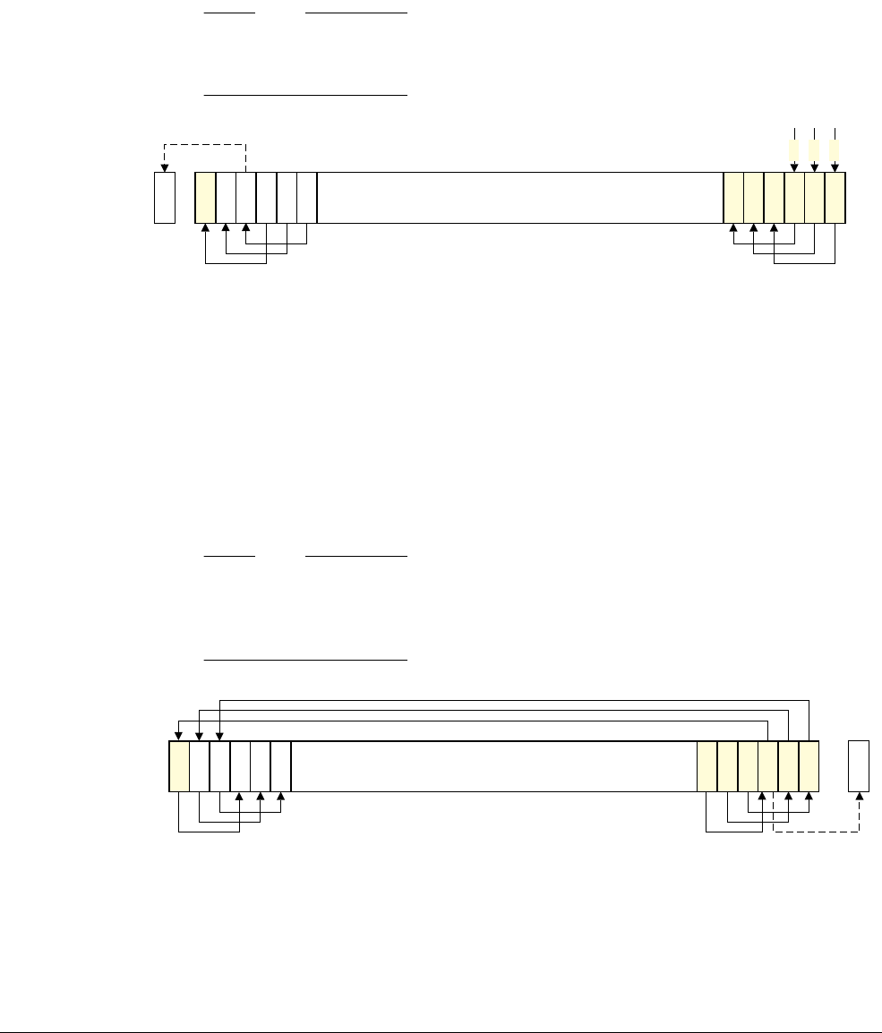
The Cortex-M3 Instruction Set
ARM DUI 0552A Copyright © 2010 ARM. All rights reserved. 3-12
ID121610 Non-Confidential
You can use he
LSL #n
operation to multiply the value in the register
Rm
by 2n, if the value is
regarded as an unsigned integer or a two’s complement signed integer. Overflow can occur
without warning.
When the instruction is
LSLS
or when
LSL #n
, with non-zero
n
, is used in
Operand2
with the
instructions
MOVS
,
MVNS
,
ANDS
,
ORRS
,
ORNS
,
EORS
,
BICS
,
TEQ
or
TST
, the carry flag is updated to the
last bit shifted out, bit[
32
-
n
], of the register
Rm
. These instructions do not affect the carry flag
when used with
LSL #0
.
Note
• If
n
is 32 or more, then all the bits in the result are cleared to 0.
• If
n
is 33 or more and the carry flag is updated, it is updated to 0.
Figure 3-3 LSL #3
ROR
Rotate right by
n
bits moves the left-hand
32
-
n
bits of the register
Rm
, to the right by
n
places, into
the right-hand
32
-
n
bits of the result. And it moves the right-hand
n
bits of the register into the
left-hand
n
bits of the result. See Figure 3-4.
When the instruction is
RORS
or when
ROR #n
is used in
Operand2
with the instructions
MOVS
,
MVNS
,
ANDS
,
ORRS
,
ORNS
,
EORS
,
BICS
,
TEQ
or
TST
, the carry flag is updated to the last bit rotation, bit[
n
-1],
of the register
Rm
.
Note
• If
n
is 32, then the value of the result is same as the value in
Rm
, and if the carry flag is
updated, it is updated to bit[31] of
Rm
.
•
ROR
with shift length,
n
, more than 32 is the same as
ROR
with shift length
n
-32.
Figure 3-4 ROR #3
RRX
Rotate right with extend moves the bits of the register
Rm
to the right by one bit. And it copies
the carry flag into bit[31] of the result. See Figure 3-5 on page 3-13.
031 5 4 3 2 1
Carry
Flag
00
0
Carry
Flag
031 5 4 3 2 1

The Cortex-M3 Instruction Set
ARM DUI 0552A Copyright © 2010 ARM. All rights reserved. 3-13
ID121610 Non-Confidential
When the instruction is
RRXS
or when
RRX
is used in
Operand2
with the instructions
MOVS
,
MVNS
,
ANDS
,
ORRS
,
ORNS
,
EORS
,
BICS
,
TEQ
or
TST
, the carry flag is updated to bit[0] of the register
Rm
.
Figure 3-5 RRX
3.3.5 Address alignment
An aligned access is an operation where a word-aligned address is used for a word, dual word,
or multiple word access, or where a halfword-aligned address is used for a halfword access. Byte
accesses are always aligned.
The Cortex-M3 processor supports unaligned access only for the following instructions:
•
LDR
,
LDRT
•
LDRH
,
LDRHT
•
LDRSH
,
LDRSHT
•
STR
,
STRT
•
STRH
,
STRHT
.
All other load and store instructions generate a UsageFault exception if they perform an
unaligned access, and therefore their accesses must be address aligned. For more information
about UsageFaults see Fault handling on page 2-28.
Unaligned accesses are usually slower than aligned accesses. In addition, some memory regions
might not support unaligned accesses. Therefore, ARM recommends that programmers ensure
that accesses are aligned. To trap accidental generation of unaligned accesses, use the
UNALIGN_TRP bit in the Configuration and Control Register, see Configuration and Control
Register on page 4-19.
3.3.6 PC-relative expressions
A PC-relative expression or label is a symbol that represents the address of an instruction or
literal data. It is represented in the instruction as the PC value plus or minus a numeric offset.
The assembler calculates the required offset from the label and the address of the current
instruction. If the offset is too big, the assembler produces an error.
Note
• For
B
,
BL
,
CBNZ
, and
CBZ
instructions, the value of the PC is the address of the current
instruction plus 4 bytes.
• For most other instructions that use labels, the value of the PC is the address of the current
instruction plus 4 bytes, with bit[1] of the result cleared to 0 to make it word-aligned.
• Your assembler might permit other syntaxes for PC-relative expressions, such as a label
plus or minus a number, or an expression of the form
[PC, #number]
.
30
Carry
Flag
031 1
...

The Cortex-M3 Instruction Set
ARM DUI 0552A Copyright © 2010 ARM. All rights reserved. 3-14
ID121610 Non-Confidential
3.3.7 Conditional execution
Most data processing instructions can optionally update the condition flags in the Application
Program Status Register (APSR) according to the result of the operation, see Application
Program Status Register on page 2-5. Some instructions update all flags, and some only update
a subset. If a flag is not updated, the original value is preserved. See the instruction descriptions
for the flags they affect.
You can execute an instruction conditionally, based on the condition flags set in another
instruction, either:
• immediately after the instruction that updated the flags
• after any number of intervening instructions that have not updated the flags.
Conditional execution is available by using conditional branches or by adding condition code
suffixes to instructions. See Table 3-4 on page 3-15 for a list of the suffixes to add to instructions
to make them conditional instructions. The condition code suffix enables the processor to test a
condition based on the flags. If the condition test of a conditional instruction fails, the
instruction:
• does not execute
• does not write any value to its destination register
• does not affect any of the flags
• does not generate any exception.
Conditional instructions, except for conditional branches, must be inside an If-Then instruction
block. See IT on page 3-64 for more information and restrictions when using the
IT
instruction.
Depending on the vendor, the assembler might automatically insert an
IT
instruction if you have
conditional instructions outside the IT block.
Use the
CBZ
and
CBNZ
instructions to compare the value of a register against zero and branch on
the result.
This section describes:
•The condition flags
•Condition code suffixes on page 3-15.
The condition flags
The APSR contains the following condition flags:
N Set to 1 when the result of the operation was negative, cleared to 0 otherwise.
Z Set to 1 when the result of the operation was zero, cleared to 0 otherwise.
C Set to 1 when the operation resulted in a carry, cleared to 0 otherwise.
V Set to 1 when the operation caused overflow, cleared to 0 otherwise.
For more information about the APSR see Program Status Register on page 2-4.
A carry occurs:
• if the result of an addition is greater than or equal to 232
• if the result of a subtraction is positive or zero
• as the result of an inline barrel shifter operation in a move or logical instruction.
Overflow occurs when the sign of the result, in bit[31], does not match the sign of the result had
the operation been performed at infinite precision, for example:
• if adding two negative values results in a positive value

The Cortex-M3 Instruction Set
ARM DUI 0552A Copyright © 2010 ARM. All rights reserved. 3-15
ID121610 Non-Confidential
• if adding two positive values results in a negative value
• if subtracting a positive value from a negative value generates a positive value
• if subtracting a negative value from a positive value generates a negative value.
The Compare operations are identical to subtracting, for
CMP
, or adding, for
CMN
, except that the
result is discarded. See the instruction descriptions for more information.
Note
Most instructions update the status flags only if the
S
suffix is specified. See the instruction
descriptions for more information.
Condition code suffixes
The instructions that can be conditional have an optional condition code, shown in syntax
descriptions as
{cond}
. Conditional execution requires a preceding
IT
instruction. An instruction
with a condition code is only executed if the condition code flags in the APSR meet the specified
condition. Table 3-4 shows the condition codes to use.
You can use conditional execution with the
IT
instruction to reduce the number of branch
instructions in code.
Table 3-4 also shows the relationship between condition code suffixes and the N, Z, C, and V
flags.
Example 3-1 on page 3-16 shows the use of a conditional instruction to find the absolute value
of a number.
R0
=
abs
(
R1
).
Table 3-4 Condition code suffixes
Suffix Flags Meaning
EQ
Z = 1 Equal
NE
Z = 0 Not equal
CS or HS
C = 1 Higher or same, unsigned
CC or LO
C = 0 Lower, unsigned
MI
N = 1 Negative
PL
N = 0 Positive or zero
VS
V = 1 Overflow
VC
V = 0 No overflow
HI
C = 1 and Z = 0 Higher, unsigned
LS
C = 0 or Z = 1 Lower or same, unsigned
GE
N = V Greater than or equal, signed
LT
N != V Less than, signed
GT
Z = 0 and N = V Greater than, signed
LE
Z = 1 and N != V Less than or equal, signed
AL
Can have any value Always. This is the default when no suffix is specified.

The Cortex-M3 Instruction Set
ARM DUI 0552A Copyright © 2010 ARM. All rights reserved. 3-16
ID121610 Non-Confidential
Example 3-1 Absolute value
MOVS R0, R1 ; R0 = R1, setting flags
IT MI ; skipping next instruction if value 0 or positive
RSBMI R0, R0, #0 ; If negative, R0 = -R0
Example 3-2 shows the use of conditional instructions to update the value of
R4
if the signed
values
R0
is greater than
R1
and
R2
is greater than
R3
.
Example 3-2 Compare and update value
CMP R0, R1 ; Compare R0 and R1, setting flags
ITT GT ; Skip next two instructions unless GT condition holds
CMPGT R2, R3 ; If 'greater than', compare R2 and R3, setting flags
MOVGT R4, R5 ; If still 'greater than', do R4 = R5
3.3.8 Instruction width selection
There are many instructions that can generate either a 16-bit encoding or a 32-bit encoding
depending on the operands and destination register specified. For some of these instructions,
you can force a specific instruction size by using an instruction width suffix. The
.W
suffix forces
a 32-bit instruction encoding. The
.N
suffix forces a 16-bit instruction encoding.
If you specify an instruction width suffix and the assembler cannot generate an instruction
encoding of the requested width, it generates an error.
Note
In some cases it might be necessary to specify the
.W
suffix, for example if the operand is the
label of an instruction or literal data, as in the case of branch instructions. This is because the
assembler might not automatically generate the right size encoding.
To use an instruction width suffix, place it immediately after the instruction mnemonic and
condition code, if any. Example 3-3 shows instructions with the instruction width suffix.
Example 3-3 Instruction width selection
BCS.W label ; creates a 32-bit instruction even for a short branch
ADDS.W R0, R0, R1 ; creates a 32-bit instruction even though the same
; operation can be done by a 16-bit instruction

The Cortex-M3 Instruction Set
ARM DUI 0552A Copyright © 2010 ARM. All rights reserved. 3-17
ID121610 Non-Confidential
3.4 Memory access instructions
Table 3-5 shows the memory access instructions.
Table 3-5 Memory access instructions
Mnemonic Brief description See
ADR
Generate PC-relative address ADR on page 3-18
CLREX
Clear Exclusive CLREX on page 3-33
LDM{mode}
Load Multiple registers LDM and STM on page 3-27
LDR{type}
Load Register using immediate offset LDR and STR, immediate offset on page 3-19
LDR{type}
Load Register using register offset LDR and STR, register offset on page 3-22
LDR{type}T
Load Register with unprivileged access LDR and STR, unprivileged on page 3-24
LDR
Load Register using PC-relative address LDR, PC-relative on page 3-25
LDREX{type}
Load Register Exclusive LDREX and STREX on page 3-31
POP
Pop registers from stack PUSH and POP on page 3-29
PUSH
Push registers onto stack PUSH and POP on page 3-29
STM{mode}
Store Multiple registers LDM and STM on page 3-27
STR{type}
Store Register using immediate offset LDR and STR, immediate offset on page 3-19
STR{type}
Store Register using register offset LDR and STR, register offset on page 3-22
STR{type}T
Store Register with unprivileged access LDR and STR, unprivileged on page 3-24
STREX{type}
Store Register Exclusive LDREX and STREX on page 3-31

The Cortex-M3 Instruction Set
ARM DUI 0552A Copyright © 2010 ARM. All rights reserved. 3-18
ID121610 Non-Confidential
3.4.1 ADR
Generate PC-relative address.
Syntax
ADR{cond} Rd, label
where:
cond
Is an condition code, see Conditional execution on page 3-14.
Rd
Specifies the destination register.
label
is a PC-relative expression. See PC-relative expressions on page 3-13.
Operation
ADR
generates an address by adding an immediate value to the PC, and writes the result to the
destination register.
ADR
provides the means by which position-independent code can be generated, because the
address is PC-relative.
If you use
ADR
to generate a target address for a
BX
or
BLX
instruction, you must ensure that bit[0]
of the address you generate is set to 1 for correct execution.
Values of
label
must be within the range of −4095 to +4095 from the address in the PC.
Note
You might have to use the
.W
suffix to get the maximum offset range or to generate addresses
that are not word-aligned. See Instruction width selection on page 3-16.
Restrictions
Rd
must not be SP and must not be PC.
Condition flags
This instruction does not change the flags.
Examples
ADR R1, TextMessage ; Write address value of a location labelled as
; TextMessage to R1

The Cortex-M3 Instruction Set
ARM DUI 0552A Copyright © 2010 ARM. All rights reserved. 3-19
ID121610 Non-Confidential
3.4.2 LDR and STR, immediate offset
Load and Store with immediate offset, pre-indexed immediate offset, or post-indexed
immediate offset.
Syntax
op{type}{cond} Rt, [Rn {, #offset}] ; immediate offset
op{type}{cond} Rt, [Rn, #offset]! ; pre-indexed
op{type}{cond} Rt, [Rn], #offset ; post-indexed
opD{cond} Rt, Rt2, [Rn {, #offset}] ; immediate offset, two words
opD{cond} Rt, Rt2, [Rn, #offset]! ; pre-indexed, two words
opD{cond} Rt, Rt2, [Rn], #offset ; post-indexed, two words
where:
op
Is one of:
LDR
Load Register.
STR
Store Register.
type
Is one of:
B
unsigned byte, zero extend to 32 bits on loads.
SB
signed byte, sign extend to 32 bits (
LDR
only).
H
unsigned halfword, zero extend to 32 bits on loads.
SH
signed halfword, sign extend to 32 bits (
LDR
only).
-
omit, for word.
cond
Is an optional condition code, see Conditional execution on page 3-14.
Rt
Specifies the register to load or store.
Rn
Specifies the register on which the memory address is based.
offset
Specifies an offset from
Rn
. If
offset
is omitted, the address is the contents of
Rn
.
Rt2
Specifies the additional register to load or store for two-word operations.

The Cortex-M3 Instruction Set
ARM DUI 0552A Copyright © 2010 ARM. All rights reserved. 3-20
ID121610 Non-Confidential
Operation
LDR
instructions load one or two registers with a value from memory.
STR
instructions store one or two register values to memory.
Load and store instructions with immediate offset can use the following addressing modes:
Offset addressing
The offset value is added to or subtracted from the address obtained from the
register
Rn
. The result is used as the address for the memory access. The register
Rn
is unaltered. The assembly language syntax for this mode is:
[Rn, #offset]
Pre-indexed addressing
The offset value is added to or subtracted from the address obtained from the
register
Rn
. The result is used as the address for the memory access and written
back into the register
Rn
. The assembly language syntax for this mode is:
[Rn, #offset]!
Post-indexed addressing
The address obtained from the register
Rn
is used as the address for the memory
access. The offset value is added to or subtracted from the address, and written
back into the register
Rn
. The assembly language syntax for this mode is:
[Rn], #offset
The value to load or store can be a byte, halfword, word, or two words. Bytes and halfwords can
either be signed or unsigned. See Address alignment on page 3-13.
Table 3-6 shows the ranges of offset for immediate, pre-indexed and post-indexed forms.
Table 3-6 Offset ranges
Instruction type Immediate offset Pre-indexed Post-indexed
Word, halfword, signed
halfword, byte, or signed byte
−255 to 4095 −255 to 255 −255 to 255
Two words multiple of 4 in the
range −1020 to 1020
multiple of 4 in the
range −1020 to 1020
multiple of 4 in the
range −1020 to 1020

The Cortex-M3 Instruction Set
ARM DUI 0552A Copyright © 2010 ARM. All rights reserved. 3-21
ID121610 Non-Confidential
Restrictions
For load instructions:
•
Rt
can be SP or PC for word loads only
•
Rt
must be different from
Rt2
for two-word loads
•
Rn
must be different from
Rt
and
Rt2
in the pre-indexed or post-indexed forms.
When
Rt
is PC in a word load instruction:
• bit[0] of the loaded value must be 1 for correct execution
• a branch occurs to the address created by changing bit[0] of the loaded value to 0
• if the instruction is conditional, it must be the last instruction in the IT block.
For store instructions:
•
Rt
can be SP for word stores only
•
Rt
must not be PC
•
Rn
must not be PC
•
Rn
must be different from
Rt
and
Rt2
in the pre-indexed or post-indexed forms.
Condition flags
These instructions do not change the flags.
Examples
LDR R8, [R10] ; Loads R8 from the address in R10.
LDRNE R2, [R5, #960]! ; Loads (conditionally) R2 from a word
; 960 bytes above the address in R5, and
; increments R5 by 960
STR R2, [R9,#const-struc] ; const-struc is an expression evaluating
; to a constant in the range 0-4095.
STRH R3, [R4], #4 ; Store R3 as halfword data into address in
; R4, then increment R4 by 4
LDRD R8, R9, [R3, #0x20] ; Load R8 from a word 8 bytes above the
; address in R3, and load R9 from a word 9
; bytes above the address in R3
STRD R0, R1, [R8], #-16 ; Store R0 to address in R8, and store R1 to
; a word 4 bytes above the address in R8,
; and then decrement R8 by 16.

The Cortex-M3 Instruction Set
ARM DUI 0552A Copyright © 2010 ARM. All rights reserved. 3-22
ID121610 Non-Confidential
3.4.3 LDR and STR, register offset
Load and Store with register offset.
Syntax
op{type}{cond} Rt, [Rn, Rm {, LSL #n}]
where:
op
Is one of:
LDR
Load Register.
STR
Store Register.
type
Is one of:
B
unsigned byte, zero extend to 32 bits on loads.
SB
signed byte, sign extend to 32 bits (
LDR
only).
H
unsigned halfword, zero extend to 32 bits on loads.
SH
signed halfword, sign extend to 32 bits (
LDR
only).
-
omit, for word.
cond
Is an optional condition code, see Conditional execution on page 3-14.
Rt
Specifies the register to load or store.
Rn
Specifies the register on which the memory address is based.
Rm
Specifies the register containing a value to be used as the offset.
LSL #n
Is an optional shift, with n in the range 0 to 3.
Operation
LDR
instructions load a register with a value from memory.
STR
instructions store a register value into memory.
The memory address to load from or store to is at an offset from the register
Rn
. The offset is
specified by the register
Rm
and can be shifted left by up to 3 bits using
LSL
.
The value to load or store can be a byte, halfword, or word. For load instructions, bytes and
halfwords can either be signed or unsigned. See Address alignment on page 3-13.
Restrictions
In these instructions:
•
Rn
must not be PC
•
Rm
must not be SP and must not be PC
•
Rt
can be SP only for word loads and word stores
•
Rt
can be PC only for word loads.
When
Rt
is PC in a word load instruction:
• bit[0] of the loaded value must be 1 for correct execution, and a branch occurs to this
halfword-aligned address
• if the instruction is conditional, it must be the last instruction in the IT block.

The Cortex-M3 Instruction Set
ARM DUI 0552A Copyright © 2010 ARM. All rights reserved. 3-23
ID121610 Non-Confidential
Condition flags
These instructions do not change the flags.
Examples
STR R0, [R5, R1] ; Store value of R0 into an address equal to
; sum of R5 and R1
LDRSB R0, [R5, R1, LSL #1] ; Read byte value from an address equal to
; sum of R5 and two times R1, sign extended it
; to a word value and put it in R0
STR R0, [R1, R2, LSL #2] ; Stores R0 to an address equal to sum of R1
; and four times R2.

The Cortex-M3 Instruction Set
ARM DUI 0552A Copyright © 2010 ARM. All rights reserved. 3-24
ID121610 Non-Confidential
3.4.4 LDR and STR, unprivileged
Load and Store with unprivileged access.
Syntax
op{type}T{cond} Rt, [Rn {, #offset}] ; immediate offset
where:
op
Is one of:
LDR
Load Register.
STR
Store Register.
type
Is one of:
B
unsigned byte, zero extend to 32 bits on loads.
SB
signed byte, sign extend to 32 bits (
LDR
only).
H
unsigned halfword, zero extend to 32 bits on loads.
SH
signed halfword, sign extend to 32 bits (
LDR
only).
-
omit, for word.
cond
Is an optional condition code, see Conditional execution on page 3-14.
Rt
Specifies the register to load or store.
Rn
Specifies the register on which the memory address is based.
offset
Is an offset from
Rn
and can be 0 to 255. If
offset
is omitted, the address is the
value in
Rn
.
Operation
These load and store instructions perform the same function as the memory access instructions
with immediate offset, see LDR and STR, immediate offset on page 3-19. The difference is that
these instructions have only unprivileged access even when used in privileged software.
When used in unprivileged software, these instructions behave in exactly the same way as
normal memory access instructions with immediate offset.
Restrictions
In these instructions:
•
Rn
must not be PC
•
Rt
must not be SP and must not be PC.
Condition flags
These instructions do not change the flags.
Examples
STRBTEQ R4, [R7] ; Conditionally store least significant byte in
; R4 to an address in R7, with unprivileged access
LDRHT R2, [R2, #8] ; Load halfword value from an address equal to
; sum of R2 and 8 into R2, with unprivileged access.

The Cortex-M3 Instruction Set
ARM DUI 0552A Copyright © 2010 ARM. All rights reserved. 3-25
ID121610 Non-Confidential
3.4.5 LDR, PC-relative
Load register from memory.
Syntax
LDR{type}{cond} Rt, label
LDRD{cond} Rt, Rt2, label ; Load two words
where:
type
Is one of:
B
unsigned byte, zero extend to 32 bits.
SB
signed byte, sign extend to 32 bits.
H
unsigned halfword, zero extend to 32 bits.
SH
signed halfword, sign extend to 32 bits.
-
omit, for word.
cond
Is an optional condition code, see Conditional execution on page 3-14.
Rt
Specifies the register to load or store.
Rt2
Specifies the second register to load or store.
label
Is a PC-relative expression. See PC-relative expressions on page 3-13.
Operation
LDR
loads a register with a value from a PC-relative memory address. The memory address is
specified by a label or by an offset from the PC.
The value to load or store can be a byte, halfword, or word. For load instructions, bytes and
halfwords can either be signed or unsigned. See Address alignment on page 3-13.
label
must be within a limited range of the current instruction. Table 3-7 shows the possible
offsets between
label
and the PC.
Note
You might have to use the
.W
suffix to get the maximum offset range. See Instruction width
selection on page 3-16.
Restrictions
In these instructions:
•
Rt
can be SP or PC only for word loads
•
Rt2
must not be SP and must not be PC
•
Rt
must be different from
Rt2.
Table 3-7 Offset ranges
Instruction type Offset range
Word, halfword, signed halfword, byte, signed byte −4095 to 4095
Two words −1020 to 1020

The Cortex-M3 Instruction Set
ARM DUI 0552A Copyright © 2010 ARM. All rights reserved. 3-26
ID121610 Non-Confidential
When
Rt
is PC in a word load instruction:
• bit[0] of the loaded value must be 1 for correct execution, and a branch occurs to this
halfword-aligned address
• if the instruction is conditional, it must be the last instruction in the IT block.
Condition flags
These instructions do not change the flags.
Examples
LDR R0, LookUpTable ; Load R0 with a word of data from an address
; labelled as LookUpTable
LDRSB R7, localdata ; Load a byte value from an address labelled
; as localdata, sign extend it to a word
; value, and put it in R7.

The Cortex-M3 Instruction Set
ARM DUI 0552A Copyright © 2010 ARM. All rights reserved. 3-27
ID121610 Non-Confidential
3.4.6 LDM and STM
Load and Store Multiple registers.
Syntax
op{addr_mode}{cond} Rn{!}, reglist
where:
op
Is one of:
LDM
Load Multiple registers.
STM
Store Multiple registers.
addr_mode
This is any one of the following:
IA
Increment address After each access. This is the default.
DB
Decrement address Before each access.
cond
Is an optional condition code, see Conditional execution on page 3-14.
Rn
Specifies the register on which the memory addresses are based.
!
Is an optional writeback suffix. If
!
is present the final address, that is loaded from
or stored to, is written back into
Rn
.
reglist
Is a list of one or more registers to be loaded or stored, enclosed in braces. It can
contain register ranges. It must be comma separated if it contains more than one
register or register range, see Examples on page 3-28.
LDM
and
LDMFD
are synonyms for
LDMIA
.
LDMFD
refers to its use for popping data from Full
Descending stacks.
LDMEA
is a synonym for
LDMDB
, and refers to its use for popping data from Empty Ascending
stacks.
STM
and
STMEA
are synonyms for
STMIA
.
STMEA
refers to its use for pushing data onto Empty
Ascending stacks.
STMFD
is s synonym for
STMDB
, and refers to its use for pushing data onto Full Descending stacks.
Operation
LDM
instructions load the registers in
reglist
with word values from memory addresses based on
Rn
.
STM
instructions store the word values in the registers in
reglist
to memory addresses based on
Rn
.
For
LDM
,
LDMIA
,
LDMFD
,
STM
,
STMIA
, and
STMEA
the memory addresses used for the accesses are at
4-byte intervals ranging from
Rn
to
Rn
+ 4 * (
n
-1), where
n
is the number of registers in
reglist
.
The accesses happens in order of increasing register numbers, with the lowest numbered register
using the lowest memory address and the highest number register using the highest memory
address. If the writeback suffix is specified, the value of
Rn
+ 4 * (
n
-1) is written back to
Rn
.
For
LDMDB
,
LDMEA
,
STMDB
, and
STMFD
the memory addresses used for the accesses are at 4-byte
intervals ranging from
Rn
to
Rn
- 4 * (
n
-1), where
n
is the number of registers in
reglist
. The
accesses happen in order of decreasing register numbers, with the highest numbered register
using the highest memory address and the lowest number register using the lowest memory
address. If the writeback suffix is specified, the value of
Rn
- 4 * (
n
-1) is written back to
Rn
.

The Cortex-M3 Instruction Set
ARM DUI 0552A Copyright © 2010 ARM. All rights reserved. 3-28
ID121610 Non-Confidential
The
PUSH
and
POP
instructions can be expressed in this form. See PUSH and POP on page 3-29
for details.
Restrictions
In these instructions:
•
Rn
must not be PC
•
reglist
must not contain SP
• in any
STM
instruction,
reglist
must not contain PC
• in any
LDM
instruction,
reglist
must not contain PC if it contains LR
•
reglist
must not contain
Rn
if you specify the writeback suffix.
When PC is in
reglist
in an
LDM
instruction:
• bit[0] of the value loaded to the PC must be 1 for correct execution, and a branch occurs
to this halfword-aligned address
• if the instruction is conditional, it must be the last instruction in the IT block.
Condition flags
These instructions do not change the flags.
Examples
LDM R8,{R0,R2,R9} ; LDMIA is a synonym for LDM
STMDB R1!,{R3-R6,R11,R12}
Incorrect examples
STM R5!,{R5,R4,R9} ; Value stored for R5 is unpredictable
LDM R2, {} ; There must be at least one register in the list.

The Cortex-M3 Instruction Set
ARM DUI 0552A Copyright © 2010 ARM. All rights reserved. 3-29
ID121610 Non-Confidential
3.4.7 PUSH and POP
Push registers onto, and pop registers off a full-descending stack.
Syntax
PUSH{cond} reglist
POP{cond} reglist
where:
cond
Is an optional condition code, see Conditional execution on page 3-14.
reglist
Is a non-empty list of registers, enclosed in braces. It can contain register ranges.
It must be comma separated if it contains more than one register or register range.
PUSH
and
POP
are synonyms for
STMDB
and
LDM
(or
LDMIA
) with the memory addresses for the access
based on SP, and with the final address for the access written back to the SP.
PUSH
and
POP
are
the preferred mnemonics in these cases.
Operation
PUSH
stores registers on the stack, with the lowest numbered register using the lowest memory
address and the highest numbered register using the highest memory address.
POP
loads registers from the stack, with the lowest numbered register using the lowest memory
address and the highest numbered register using the highest memory address.
PUSH
uses the value in the SP register minus four as the highest memory address,
POP
uses the
value in the SP register as the lowest memory address, implementing a full-descending stack.
On completion,
PUSH
updates the SP register to point to the location of the lowest stored value,
POP
updates the SP register to point to the location immediately above the highest location
loaded.
If a
POP
instruction includes PC in its reglist, a branch to this location is performed when the POP
instruction has completed. Bit[0] of the value read for the PC is used to update the APSR T-bit.
This bit must be 1 to ensure correct operation.
See LDM and STM on page 3-27 for more information.
Restrictions
In these instructions:
•
reglist
must not contain SP
•for the
PUSH
instruction,
reglist
must not contain PC
•for the
POP
instruction,
reglist
must not contain PC if it contains LR.
When PC is in
reglist
in a
POP
instruction:
• bit[0] of the value loaded for PC must be 1 for correct execution
• if the instruction is conditional, it must be the last instruction in the IT block.
Condition flags
These instructions do not change the flags.

The Cortex-M3 Instruction Set
ARM DUI 0552A Copyright © 2010 ARM. All rights reserved. 3-30
ID121610 Non-Confidential
Examples
PUSH {R0,R4-R7} ; Push R0,R4,R5,R6,R7 onto the stack
PUSH {R2,LR} ; Push R2 and the link-register onto the stack
POP {R0,R6,PC} ; Pop r0,r6 and PC from the stack, then branch to the new PC.

The Cortex-M3 Instruction Set
ARM DUI 0552A Copyright © 2010 ARM. All rights reserved. 3-31
ID121610 Non-Confidential
3.4.8 LDREX and STREX
Load and Store Register Exclusive.
Syntax
LDREX{cond} Rt, [Rn {, #offset}]
STREX{cond} Rd, Rt, [Rn {, #offset}]
LDREXB{cond} Rt, [Rn]
STREXB{cond} Rd, Rt, [Rn]
LDREXH{cond} Rt, [Rn]
STREXH{cond} Rd, Rt, [Rn]
where:
cond
Is an optional condition code, see Conditional execution on page 3-14.
Rd
Specifies the destination register for the returned status.
Rt
Specifies the register to load or store.
Rn
Specifies the register on which the memory address is based.
offset
Is an optional offset applied to the value in
Rn
. If
offset
is omitted, the address is
the value in
Rn
.
Operation
LDREX
,
LDREXB
, and
LDREXH
load a word, byte, and halfword respectively from a memory address.
STREX
,
STREXB
, and
STREXH
attempt to store a word, byte, and halfword respectively to a memory
address. The address used in any Store-Exclusive instruction must be the same as the address in
the most recently executed Load-exclusive instruction. The value stored by the Store-Exclusive
instruction must also have the same data size as the value loaded by the preceding
Load-exclusive instruction. This means software must always use a Load-exclusive instruction
and a matching Store-Exclusive instruction to perform a synchronization operation, see
Synchronization primitives on page 2-18.
If an Store-Exclusive instruction performs the store, it writes 0 to its destination register. If it
does not perform the store, it writes 1 to its destination register. If the Store-Exclusive
instruction writes 0 to the destination register, it is guaranteed that no other process in the system
has accessed the memory location between the Load-exclusive and Store-Exclusive
instructions.
For reasons of performance, keep the number of instructions between corresponding
Load-Exclusive and Store-Exclusive instruction to a minimum.
Note
The result of executing a Store-Exclusive instruction to an address that is different from that
used in the preceding Load-Exclusive instruction is unpredictable.

The Cortex-M3 Instruction Set
ARM DUI 0552A Copyright © 2010 ARM. All rights reserved. 3-32
ID121610 Non-Confidential
Restrictions
In these instructions:
• do not use PC
• do not use SP for
Rd
and
Rt
• for
STREX
,
Rd
must be different from both
Rt
and
Rn
• the value of
offset
must be a multiple of four in the range 0-1020.
Condition flags
These instructions do not change the flags.
Examples
MOV R1, #0x1 ; Initialize the ‘lock taken’ value
try
LDREX R0, [LockAddr] ; Load the lock value
CMP R0, #0 ; Is the lock free?
ITT EQ ; IT instruction for STREXEQ and CMPEQ
STREXEQ R0, R1, [LockAddr] ; Try and claim the lock
CMPEQ R0, #0 ; Did this succeed?
BNE try ; No – try again
.... ; Yes – we have the lock.

The Cortex-M3 Instruction Set
ARM DUI 0552A Copyright © 2010 ARM. All rights reserved. 3-33
ID121610 Non-Confidential
3.4.9 CLREX
Clear Exclusive.
Syntax
CLREX{cond}
where:
cond
Is an optional condition code, see Conditional execution on page 3-14.
Operation
Use
CLREX
to make the next
STREX
,
STREXB
, or
STREXH
instruction write 1 to its destination register
and fail to perform the store. It is useful in exception handler code to force the failure of the store
exclusive if the exception occurs between a load exclusive instruction and the matching store
exclusive instruction in a synchronization operation.
See Synchronization primitives on page 2-18 for more information.
Condition flags
These instructions do not change the flags.
Examples
CLREX

The Cortex-M3 Instruction Set
ARM DUI 0552A Copyright © 2010 ARM. All rights reserved. 3-34
ID121610 Non-Confidential
3.5 General data processing instructions
Table 3-8 shows the data processing instructions.
Table 3-8 Data processing instructions
Mnemonic Brief description See
ADC
Add with Carry ADD, ADC, SUB, SBC, and RSB on page 3-35
ADD
Add ADD, ADC, SUB, SBC, and RSB on page 3-35
ADDW
Add ADD, ADC, SUB, SBC, and RSB on page 3-35
AND
Logical AND AND, ORR, EOR, BIC, and ORN on page 3-38
ASR
Arithmetic Shift Right ASR, LSL, LSR, ROR, and RRX on page 3-40
BIC
Bit Clear AND, ORR, EOR, BIC, and ORN on page 3-38
CLZ
Count leading zeros CLZ on page 3-42
CMN
Compare Negative CMP and CMN on page 3-43
CMP
Compare CMP and CMN on page 3-43
EOR
Exclusive OR AND, ORR, EOR, BIC, and ORN on page 3-38
LSL
Logical Shift Left ASR, LSL, LSR, ROR, and RRX on page 3-40
LSR
Logical Shift Right ASR, LSL, LSR, ROR, and RRX on page 3-40
MOV
Move MOV and MVN on page 3-44
MOVT
Move Top MOVT on page 3-46
MOVW
Move 16-bit constant MOV and MVN on page 3-44
MVN
Move NOT MOV and MVN on page 3-44
ORN
Logical OR NOT AND, ORR, EOR, BIC, and ORN on page 3-38
ORR
Logical OR AND, ORR, EOR, BIC, and ORN on page 3-38
RBIT
Reverse Bits REV, REV16, REVSH, and RBIT on page 3-47
REV
Reverse byte order in a word REV, REV16, REVSH, and RBIT on page 3-47
REV16
Reverse byte order in each halfword REV, REV16, REVSH, and RBIT on page 3-47
REVSH
Reverse byte order in bottom halfword and sign extend REV, REV16, REVSH, and RBIT on page 3-47
ROR
Rotate Right ASR, LSL, LSR, ROR, and RRX on page 3-40
RRX
Rotate Right with Extend ASR, LSL, LSR, ROR, and RRX on page 3-40
RSB
Reverse Subtract ADD, ADC, SUB, SBC, and RSB on page 3-35
SBC
Subtract with Carry ADD, ADC, SUB, SBC, and RSB on page 3-35
SUB
Subtract ADD, ADC, SUB, SBC, and RSB on page 3-35
SUBW
Subtract ADD, ADC, SUB, SBC, and RSB on page 3-35
TEQ
Test Equivalence TST and TEQ on page 3-48
TST
Test TST and TEQ on page 3-48

The Cortex-M3 Instruction Set
ARM DUI 0552A Copyright © 2010 ARM. All rights reserved. 3-35
ID121610 Non-Confidential
3.5.1 ADD, ADC, SUB, SBC, and RSB
Add, Add with carry, Subtract, Subtract with carry, and Reverse Subtract.
Syntax
op{S}{cond} {Rd,} Rn, Operand2
op{cond} {Rd,} Rn, #imm12 ; ADD and SUB only
where:
op
Is one of:
ADD
Add.
ADC
Add with Carry.
SUB
Subtract.
SBC
Subtract with Carry.
RSB
Reverse Subtract.
S
Is an optional suffix. If
S
is specified, the condition code flags are updated on the
result of the operation, see Conditional execution on page 3-14.
cond
Is an optional condition code, see Conditional execution on page 3-14.
Rd
Specifies the destination register. If
Rd
is omitted, the destination register is
Rn
.
Rn
Specifies the register holding the first operand.
Operand2
Is a flexible second operand. See Flexible second operand on page 3-9 for details
of the options.
imm12
This is any value in the range 0-4095.
Operation
The
ADD
instruction adds the value of
Operand2
or
imm12
to the value in
Rn
.
The
ADC
instruction adds the values in
Rn
and
Operand2
, together with the carry flag.
The
SUB
instruction subtracts the value of
Operand2
or
imm12
from the value in
Rn
.
The
SBC
instruction subtracts the value of
Operand2
from the value in
Rn
. If the carry flag is clear,
the result is reduced by one.
The
RSB
instruction subtracts the value in
Rn
from the value of
Operand2
. This is useful because
of the wide range of options for
Operand2
.
Use
ADC
and
SBC
to synthesize multiword arithmetic, see Multiword arithmetic examples on
page 3-36.
See also ADR on page 3-18.
Note
ADDW
is equivalent to the
ADD
syntax that uses the
imm12
operand.
SUBW
is equivalent to the
SUB
syntax that uses the
imm12
operand.

The Cortex-M3 Instruction Set
ARM DUI 0552A Copyright © 2010 ARM. All rights reserved. 3-36
ID121610 Non-Confidential
Restrictions
In these instructions:
•
Operand2
must not be SP and must not be PC
•
Rd
can be SP only in
ADD
and
SUB
, and only with the additional restrictions:
—
Rn
must also be SP
— any shift in
Operand2
must be limited to a maximum of 3 bits using
LSL
•
Rn
can be SP only in
ADD
and
SUB
•
Rd
can be PC only in the
ADD{cond} PC, PC, Rm
instruction where:
— you must not specify the S suffix
—
Rm
must not be PC and must not be SP
— if the instruction is conditional, it must be the last instruction in the IT block
• with the exception of the
ADD{cond} PC, PC, Rm
instruction,
Rn
can be PC only in
ADD
and
SUB
, and only with the additional restrictions:
— you must not specify the S suffix
— the second operand must be a constant in the range 0 to 4095.
Note
— When using the PC for an addition or a subtraction, bits[1:0] of the PC are rounded
to b00 before performing the calculation, making the base address for the
calculation word-aligned.
— If you want to generate the address of an instruction, you have to adjust the constant
based on the value of the PC. ARM recommends that you use the
ADR
instruction
instead of
ADD
or
SUB
with
Rn
equal to the PC, because your assembler automatically
calculates the correct constant for the
ADR
instruction.
When
Rd
is PC in the
ADD{cond} PC, PC, Rm
instruction:
• bit[0] of the value written to the PC is ignored
• a branch occurs to the address created by forcing bit[0] of that value to 0.
Condition flags
If
S
is specified, these instructions update the N, Z, C and V flags according to the result.
Examples
ADD R2, R1, R3
SUBS R8, R6, #240 ; Sets the flags on the result
RSB R4, R4, #1280 ; Subtracts contents of R4 from 1280
ADCHI R11, R0, R3 ; Only executed if C flag set and Z
; flag clear.
Multiword arithmetic examples
Example 3-4 on page 3-37 shows two instructions that add a 64-bit integer contained in
R2
and
R3
to another 64-bit integer contained in
R0
and
R1
, and place the result in
R4
and
R5
.

The Cortex-M3 Instruction Set
ARM DUI 0552A Copyright © 2010 ARM. All rights reserved. 3-37
ID121610 Non-Confidential
Example 3-4 64-bit addition
ADDS R4, R0, R2 ; add the least significant words
ADC R5, R1, R3 ; add the most significant words with carry
Multiword values do not have to use consecutive registers. Example 3-5 shows instructions that
subtract a 96-bit integer contained in R9, R1, and R11 from another contained in R6, R2, and
R8. The example stores the result in R6, R9, and R2.
Example 3-5 96-bit subtraction
SUBS R6, R6, R9 ; subtract the least significant words
SBCS R9, R2, R1 ; subtract the middle words with carry
SBC R2, R8, R11 ; subtract the most significant words with carry

The Cortex-M3 Instruction Set
ARM DUI 0552A Copyright © 2010 ARM. All rights reserved. 3-38
ID121610 Non-Confidential
3.5.2 AND, ORR, EOR, BIC, and ORN
Logical AND, OR, Exclusive OR, Bit Clear, and OR NOT.
Syntax
op{S}{cond} {Rd,} Rn, Operand2
where:
op
Is one of:
AND
logical AND.
ORR
logical OR, or bit set.
EOR
logical Exclusive OR.
BIC
logical AND NOT, or bit clear.
ORN
logical OR NOT.
S
Is an optional suffix. If
S
is specified, the condition code flags are updated on the
result of the operation, see Conditional execution on page 3-14.
cond
Is an optional condition code, see Conditional execution on page 3-14.
Rd
Specifies the destination register.
Rn
Specifies the register holding the first operand.
Operand2
Is a flexible second operand. See Flexible second operand on page 3-9 for details
of the options.
Operation
The
AND
,
EOR
, and
ORR
instructions perform bitwise AND, Exclusive OR, and OR operations on
the values in
Rn
and
Operand2
.
The
BIC
instruction performs an AND operation on the bits in
Rn
with the complements of the
corresponding bits in the value of
Operand2
.
The
ORN
instruction performs an OR operation on the bits in
Rn
with the complements of the
corresponding bits in the value of
Operand2
.
Restrictions
Do not use SP and do not use PC.
Condition flags
If
S
is specified, these instructions:
• update the N and Z flags according to the result
• can update the C flag during the calculation of
Operand2
, see Flexible second operand on
page 3-9
• do not affect the V flag.

The Cortex-M3 Instruction Set
ARM DUI 0552A Copyright © 2010 ARM. All rights reserved. 3-39
ID121610 Non-Confidential
Examples
AND R9, R2, #0xFF00
ORREQ R2, R0, R5
ANDS R9, R8, #0x19
EORS R7, R11, #0x18181818
BIC R0, R1, #0xab
ORN R7, R11, R14, ROR #4
ORNS R7, R11, R14, ASR #32

The Cortex-M3 Instruction Set
ARM DUI 0552A Copyright © 2010 ARM. All rights reserved. 3-40
ID121610 Non-Confidential
3.5.3 ASR, LSL, LSR, ROR, and RRX
Arithmetic Shift Right, Logical Shift Left, Logical Shift Right, Rotate Right, and Rotate Right
with Extend.
Syntax
op{S}{cond} Rd, Rm, Rs
op{S}{cond} Rd, Rm, #n
RRX{S}{cond} Rd, Rm
where:
op
Is one of:
ASR
Arithmetic Shift Right.
LSL
Logical Shift Left.
LSR
Logical Shift Right.
ROR
Rotate Right.
S
Is an optional suffix. If
S
is specified, the condition code flags are updated on the
result of the operation, see Conditional execution on page 3-14.
Rd
Specifies the destination register.
Rm
Specifies the register holding the value to be shifted.
Rs
Specifies the register holding the shift length to apply to the value in
Rm
. Only the
least significant byte is used and can be in the range 0 to 255.
n
Specifies the shift length. The range of shift length depends on the instruction:
ASR
shift length from 1 to 32
LSL
shift length from 0 to 31
LSR
shift length from 1 to 32
ROR
shift length from 1 to 31.
Note
MOVS Rd, Rm
is the preferred syntax for
LSLS Rd, Rm, #0
.
Operation
ASR
,
LSL
,
LSR
, and
ROR
move the bits in the register
Rm
to the left or right by the number of places
specified by constant
n
or register
Rs
.
RRX
moves the bits in register
Rm
to the right by 1.
In all these instructions, the result is written to
Rd
, but the value in register
Rm
remains
unchanged. For details on what result is generated by the different instructions, see Shift
Operations on page 3-10.
Restrictions
Do not use SP and do not use PC.

The Cortex-M3 Instruction Set
ARM DUI 0552A Copyright © 2010 ARM. All rights reserved. 3-41
ID121610 Non-Confidential
Condition flags
If
S
is specified:
• these instructions update the N and Z flags according to the result
• the C flag is updated to the last bit shifted out, except when the shift length is 0, see Shift
Operations on page 3-10.
Examples
ASR R7, R8, #9 ; Arithmetic shift right by 9 bits
LSLS R1, R2, #3 ; Logical shift left by 3 bits with flag update
LSR R4, R5, #6 ; Logical shift right by 6 bits
ROR R4, R5, R6 ; Rotate right by the value in the bottom byte of R6
RRX R4, R5 ; Rotate right with extend.

The Cortex-M3 Instruction Set
ARM DUI 0552A Copyright © 2010 ARM. All rights reserved. 3-42
ID121610 Non-Confidential
3.5.4 CLZ
Count Leading Zeros.
Syntax
CLZ{cond} Rd, Rm
where:
cond
Is an optional condition code, see Conditional execution on page 3-14.
Rd
Specifies the destination register.
Rm
Specifies the operand register.
Operation
The
CLZ
instruction counts the number of leading zeros in the value in
Rm
and returns the result
in
Rd
. The result value is 32 if no bits are set and zero if bit[31] is set.
Restrictions
Do not use SP and do not use PC.
Condition flags
This instruction does not change the flags.
Examples
CLZ R4,R9
CLZNE R2,R3

The Cortex-M3 Instruction Set
ARM DUI 0552A Copyright © 2010 ARM. All rights reserved. 3-43
ID121610 Non-Confidential
3.5.5 CMP and CMN
Compare and Compare Negative.
Syntax
CMP{cond} Rn, Operand2
CMN{cond} Rn, Operand2
where:
cond
Is an optional condition code, see Conditional execution on page 3-14.
Rn
Specifies the register holding the first operand.
Operand2
Is a flexible second operand. See Flexible second operand on page 3-9 for details
of the options.
Operation
These instructions compare the value in a register with
Operand2
. They update the condition
flags on the result, but do not write the result to a register.
The
CMP
instruction subtracts the value of
Operand2
from the value in
Rn
. This is the same as a
SUBS
instruction, except that the result is discarded.
The
CMN
instruction adds the value of
Operand2
to the value in
Rn
. This is the same as an
ADDS
instruction, except that the result is discarded.
Restrictions
In these instructions:
• do not use PC
•
Operand2
must not be SP.
Condition flags
These instructions update the N, Z, C and V flags according to the result.
Examples
CMP R2, R9
CMN R0, #6400
CMPGT SP, R7, LSL #2

The Cortex-M3 Instruction Set
ARM DUI 0552A Copyright © 2010 ARM. All rights reserved. 3-44
ID121610 Non-Confidential
3.5.6 MOV and MVN
Move and Move NOT.
Syntax
MOV{S}{cond} Rd, Operand2
MOV{cond} Rd, #imm16
MVN{S}{cond} Rd, Operand2
where:
S
Is an optional suffix. If
S
is specified, the condition code flags are updated on the
result of the operation, see Conditional execution on page 3-14.
cond
Is an optional condition code, see Conditional execution on page 3-14.
Rd
Specifies the destination register.
Operand2
Is a flexible second operand. See Flexible second operand on page 3-9 for details
of the options.
imm16
This is any value in the range 0-65535.
Operation
The
MOV
instruction copies the value of
Operand2
into
Rd
.
When
Operand2
in a
MOV
instruction is a register with a shift other than
LSL #0
, the preferred
syntax is the corresponding shift instruction:
•
ASR{S}{cond} Rd, Rm, #n
is the preferred syntax for
MOV{S}{cond} Rd, Rm, ASR #n
•
LSL{S}{cond} Rd, Rm, #n
is the preferred syntax for
MOV{S}{cond} Rd, Rm, LSL #n
if
n
!= 0
•
LSR{S}{cond} Rd, Rm, #n
is the preferred syntax for
MOV{S}{cond} Rd, Rm, LSR #n
•
ROR{S}{cond} Rd, Rm, #n
is the preferred syntax for
MOV{S}{cond} Rd, Rm, ROR #n
•
RRX{S}{cond} Rd, Rm
is the preferred syntax for
MOV{S}{cond} Rd, Rm, RRX
.
Also, the
MOV
instruction permits additional forms of
Operand2
as synonyms for shift instructions:
•
MOV{S}{cond} Rd, Rm, ASR Rs
is a synonym for
ASR{S}{cond} Rd, Rm, Rs
•
MOV{S}{cond} Rd, Rm, LSL Rs
is a synonym for
LSL{S}{cond} Rd, Rm, Rs
•
MOV{S}{cond} Rd, Rm, LSR Rs
is a synonym for
LSR{S}{cond} Rd, Rm, Rs
•
MOV{S}{cond} Rd, Rm, ROR Rs
is a synonym for
ROR{S}{cond} Rd, Rm, Rs
See ASR, LSL, LSR, ROR, and RRX on page 3-40.
The
MVN
instruction takes the value of
Operand2
, performs a bitwise logical NOT operation on the
value, and places the result into
Rd
.
Note
The
MOVW
instruction provides the same function as
MOV
, but is restricted to using the
imm16
operand.

The Cortex-M3 Instruction Set
ARM DUI 0552A Copyright © 2010 ARM. All rights reserved. 3-45
ID121610 Non-Confidential
Restrictions
You can use SP and PC only in the
MOV
instruction, with the following restrictions:
• the second operand must be a register without shift
• you must not specify the
S
suffix.
When
Rd
is PC in a
MOV
instruction:
• bit[0] of the value written to the PC is ignored
• a branch occurs to the address created by forcing bit[0] of that value to 0.
Note
Though it is possible to use
MOV
as a branch instruction, ARM strongly recommends the use of
a
BX
or
BLX
instruction to branch for software portability to the ARM instruction set.
Condition flags
If
S
is specified, these instructions:
• update the N and Z flags according to the result
• can update the C flag during the calculation of
Operand2
, see Flexible second operand on
page 3-9
• do not affect the V flag.
Example
MOVS R11, #0x000B ; Write value of 0x000B to R11, flags get updated
MOV R1, #0xFA05 ; Write value of 0xFA05 to R1, flags are not updated
MOVS R10, R12 ; Write value in R12 to R10, flags get updated
MOV R3, #23 ; Write value of 23 to R3
MOV R8, SP ; Write value of stack pointer to R8
MVNS R2, #0xF ; Write value of 0xFFFFFFF0 (bitwise inverse of 0xF)
; to the R2 and update flags.

The Cortex-M3 Instruction Set
ARM DUI 0552A Copyright © 2010 ARM. All rights reserved. 3-46
ID121610 Non-Confidential
3.5.7 MOVT
Move Top.
Syntax
MOVT{cond} Rd, #imm16
where:
cond
Is an optional condition code, see Conditional execution on page 3-14.
Rd
Specifies the destination register.
imm16
Is a 16-bit immediate constant.
Operation
MOVT
writes a 16-bit immediate value,
imm16
, to the top halfword,
Rd
[31:16], of its destination
register. The write does not affect
Rd
[15:0].
The
MOV
,
MOVT
instruction pair enables you to generate any 32-bit constant.
Restrictions
Rd
must not be SP and must not be PC.
Condition flags
This instruction does not change the flags.
Examples
MOVT R3, #0xF123 ; Write 0xF123 to upper halfword of R3, lower halfword
; and APSR are unchanged.

The Cortex-M3 Instruction Set
ARM DUI 0552A Copyright © 2010 ARM. All rights reserved. 3-47
ID121610 Non-Confidential
3.5.8 REV, REV16, REVSH, and RBIT
Reverse bytes and Reverse bits.
Syntax
op{cond} Rd, Rn
where:
op
Is any of:
REV
Reverse byte order in a word.
REV16
Reverse byte order in each halfword independently.
REVSH
Reverse byte order in the bottom halfword, and sign extend to 32 bits.
RBIT
Reverse the bit order in a 32-bit word.
cond
Is an optional condition code, see Conditional execution on page 3-14.
Rd
Specifies the destination register.
Rn
Specifies the register holding the operand.
Operation
Use these instructions to change endianness of data:
REV
Converts 32-bit big-endian data into little-endian data or 32-bit little-endian data
into big-endian data.
REV16
Converts 16-bit big-endian data into little-endian data or 16-bit little-endian data
into big-endian data.
REVSH
Converts either:
• 16-bit signed big-endian data into 32-bit signed little-endian data
• 16-bit signed little-endian data into 32-bit signed big-endian data.
Restrictions
Do not use SP and do not use PC
.
Condition flags
These instructions do not change the flags.
Examples
REV R3, R7 ; Reverse byte order of value in R7 and write it to R3
REV16 R0, R0 ; Reverse byte order of each 16-bit halfword in R0
REVSH R0, R5 ; Reverse Signed Halfword
REVHS R3, R7 ; Reverse with Higher or Same condition
RBIT R7, R8 ; Reverse bit order of value in R8 and write the result to R7.

The Cortex-M3 Instruction Set
ARM DUI 0552A Copyright © 2010 ARM. All rights reserved. 3-48
ID121610 Non-Confidential
3.5.9 TST and TEQ
Test bits and Test Equivalence.
Syntax
TST{cond} Rn, Operand2
TEQ{cond} Rn, Operand2
where:
cond
Is an optional condition code, see Conditional execution on page 3-14.
Rn
Specifies the register holding the first operand.
Operand2
Is a flexible second operand. See Flexible second operand on page 3-9 for details
of the options.
Operation
These instructions test the value in a register against
Operand2
. They update the condition flags
based on the result, but do not write the result to a register.
The
TST
instruction performs a bitwise AND operation on the value in
Rn
and the value of
Operand2
. This is the same as the
ANDS
instruction, except that it discards the result.
To test whether a bit of
Rn
is 0 or 1, use the
TST
instruction with an
Operand2
constant that has
that bit set to 1 and all other bits cleared to 0.
The
TEQ
instruction performs a bitwise Exclusive OR operation on the value in
Rn
and the value
of
Operand2
. This is the same as the
EORS
instruction, except that it discards the result.
Use the
TEQ
instruction to test if two values are equal without affecting the V or C flags.
TEQ
is also useful for testing the sign of a value. After the comparison, the N flag is the logical
Exclusive OR of the sign bits of the two operands.
Restrictions
Do not use SP and do not use PC
.
Condition flags
These instructions:
• update the N and Z flags according to the result
• can update the C flag during the calculation of
Operand2
, see Flexible second operand on
page 3-9
• do not affect the V flag.
Examples
TST R0, #0x3F8 ; Perform bitwise AND of R0 value to 0x3F8,
; APSR is updated but result is discarded
TEQEQ R10, R9 ; Conditionally test if value in R10 is equal to
; value in R9, APSR is updated but result is discarded.

The Cortex-M3 Instruction Set
ARM DUI 0552A Copyright © 2010 ARM. All rights reserved. 3-49
ID121610 Non-Confidential
3.6 Multiply and divide instructions
Table 3-9 shows the multiply and divide instructions.
Table 3-9 Multiply and divide instructions
Mnemonic Brief description See
MLA
Multiply with Accumulate, 32-bit result MUL, MLA, and MLS on page 3-50
MLS
Multiply and Subtract, 32-bit result MUL, MLA, and MLS on page 3-50
MUL
Multiply, 32-bit result MUL, MLA, and MLS on page 3-50
SDIV
Signed Divide SDIV and UDIV on page 3-53
SMLAL
Signed Multiply with Accumulate
(32x32+64), 64-bit result
UMULL, UMLAL, SMULL, and SMLAL on page 3-52
SMULL
Signed Multiply (32x32), 64-bit result UMULL, UMLAL, SMULL, and SMLAL on page 3-52
UDIV
Unsigned Divide SDIV and UDIV on page 3-53
UMLAL
Unsigned Multiply with Accumulate
(32x32+64), 64-bit result
UMULL, UMLAL, SMULL, and SMLAL on page 3-52
UMULL
Unsigned Multiply (32x32), 64-bit result UMULL, UMLAL, SMULL, and SMLAL on page 3-52

The Cortex-M3 Instruction Set
ARM DUI 0552A Copyright © 2010 ARM. All rights reserved. 3-50
ID121610 Non-Confidential
3.6.1 MUL, MLA, and MLS
Multiply, Multiply with Accumulate, and Multiply with Subtract, using 32-bit operands, and
producing a 32-bit result.
Syntax
MUL{S}{cond} {Rd,} Rn, Rm ; Multiply
MLA{cond} Rd, Rn, Rm, Ra ; Multiply with accumulate
MLS{cond} Rd, Rn, Rm, Ra ; Multiply with subtract
where:
cond
Is an optional condition code, see Conditional execution on page 3-14.
S
Is an optional suffix. If
S
is specified, the condition code flags are updated on the
result of the operation, see Conditional execution on page 3-14.
Rd
Specifies the destination register. If
Rd
is omitted, the destination register is
Rn
.
Rn, Rm
Are registers holding the values to be multiplied.
Ra
Is a register holding the value to be added or subtracted from.
Operation
The
MUL
instruction multiplies the values from
Rn
and
Rm
, and places the least significant 32 bits
of the result in
Rd
.
The
MLA
instruction multiplies the values from
Rn
and
Rm
, adds the value from
Ra
, and places the
least significant 32 bits of the result in
Rd
.
The
MLS
instruction multiplies the values from
Rn
and
Rm
, subtracts the product from the value
from
Ra
, and places the least significant 32 bits of the result in
Rd
.
The results of these instructions do not depend on whether the operands are signed or unsigned.
Restrictions
In these instructions, do not use SP and do not use PC.
If you use the
S
suffix with the
MUL
instruction:
•
Rd
,
Rn
, and
Rm
must all be in the range
R0
to
R7
•
Rd
must be the same as
Rm
• you must not use the
cond
suffix.
Condition flags
If
S
is specified, the
MUL
instruction:
• updates the N and Z flags according to the result
• does not affect the C and V flags.

The Cortex-M3 Instruction Set
ARM DUI 0552A Copyright © 2010 ARM. All rights reserved. 3-51
ID121610 Non-Confidential
Examples
MUL R10, R2, R5 ; Multiply, R10 = R2 x R5
MLA R10, R2, R1, R5 ; Multiply with accumulate, R10 = (R2 x R1) + R5
MULS R0, R2, R2 ; Multiply with flag update, R0 = R2 x R2
MULLT R2, R3, R2 ; Conditionally multiply, R2 = R3 x R2
MLS R4, R5, R6, R7 ; Multiply with subtract, R4 = R7 - (R5 x R6).

The Cortex-M3 Instruction Set
ARM DUI 0552A Copyright © 2010 ARM. All rights reserved. 3-52
ID121610 Non-Confidential
3.6.2 UMULL, UMLAL, SMULL, and SMLAL
Signed and Unsigned Long Multiply, with optional Accumulate, using 32-bit operands and
producing a 64-bit result.
Syntax
op{cond} RdLo, RdHi, Rn, Rm
where:
op
Is one of:
UMULL
Unsigned Long Multiply.
UMLAL
Unsigned Long Multiply, with Accumulate.
SMULL
Signed Long Multiply.
SMLAL
Signed Long Multiply, with Accumulate.
cond
Is an optional condition code, see Conditional execution on page 3-14.
RdHi, RdLo
Are the destination registers. For
UMLAL
and
SMLAL
they also hold the accumulating
value.
Rn, Rm
Are registers holding the operands.
Operation
The
UMULL
instruction interprets the values from
Rn
and
Rm
as unsigned integers. It multiplies
these integers and places the least significant 32 bits of the result in
RdLo
, and the most
significant 32 bits of the result in
RdHi
.
The
UMLAL
instruction interprets the values from
Rn
and
Rm
as unsigned integers. It multiplies
these integers, adds the 64-bit result to the 64-bit unsigned integer contained in
RdHi
and
RdLo
,
and writes the result back to
RdHi
and
RdLo
.
The
SMULL
instruction interprets the values from
Rn
and
Rm
as two’s complement signed integers.
It multiplies these integers and places the least significant 32 bits of the result in
RdLo
, and the
most significant 32 bits of the result in
RdHi
.
The
SMLAL
instruction interprets the values from
Rn
and
Rm
as two’s complement signed integers.
It multiplies these integers, adds the 64-bit result to the 64-bit signed integer contained in
RdHi
and
RdLo
, and writes the result back to
RdHi
and
RdLo
.
Restrictions
In these instructions:
• do not use SP and do not use PC
•
RdHi
and
RdLo
must be different registers.
Condition flags
These instructions do not affect the condition code flags.
Examples
UMULL R0, R4, R5, R6 ; Unsigned (R4,R0) = R5 x R6
SMLAL R4, R5, R3, R8 ; Signed (R5,R4) = (R5,R4) + R3 x R8

The Cortex-M3 Instruction Set
ARM DUI 0552A Copyright © 2010 ARM. All rights reserved. 3-53
ID121610 Non-Confidential
3.6.3 SDIV and UDIV
Signed Divide and Unsigned Divide.
Syntax
SDIV{cond} {Rd,} Rn, Rm
UDIV{cond} {Rd,} Rn, Rm
where:
cond
Is an optional condition code, see Conditional execution on page 3-14.
Rd
Specifies the destination register. If
Rd
is omitted, the destination register is
Rn
.
Rn
Specifies the register holding the value to be divided.
Rm
Is a register holding the divisor.
Operation
SDIV
performs a signed integer division of the value in
Rn
by the value in
Rm
.
UDIV
performs an unsigned integer division of the value in
Rn
by the value in
Rm
.
For both instructions, if the value in
Rn
is not divisible by the value in
Rm
, the result is rounded
towards zero.
Restrictions
Do not use SP and do not use PC
.
Condition flags
These instructions do not change the flags.
Examples
SDIV R0, R2, R4 ; Signed divide, R0 = R2/R4
UDIV R8, R8, R1 ; Unsigned divide, R8 = R8/R1.

The Cortex-M3 Instruction Set
ARM DUI 0552A Copyright © 2010 ARM. All rights reserved. 3-54
ID121610 Non-Confidential
3.7 Saturating instructions
This section describes the saturating instructions,
SSAT
and
USAT
.
3.7.1 SSAT and USAT
Signed Saturate and Unsigned Saturate to any bit position, with optional shift before saturating.
Syntax
op{cond} Rd, #n, Rm {, shift #s}
where:
op
Is one of:
SSAT
Saturates a signed value to a signed range.
USAT
Saturates a signed value to an unsigned range.
cond
Is an optional condition code, see Conditional execution on page 3-14.
Rd
Specifies the destination register.
n
specifies the bit position to saturate to:
•
n
ranges from 1 to 32 for
SSAT
•
n
ranges from 0 to 31 for
USAT
.
Rm
Specifies the register containing the value to saturate.
shift #s
Is an optional shift applied to
Rm
before saturating. It must be one of the following:
ASR #s
where
s
is in the range 1 to 31
LSL #s
where
s
is in the range 0 to 31.
Operation
These instructions saturate to a signed or unsigned
n
-bit value.
The
SSAT
instruction applies the specified shift, then saturates to the signed range
−2n–1 ≤x≤2n–1−1.
The
USAT
instruction applies the specified shift, then saturates to the unsigned range
0≤x≤2n−1.
For signed n-bit saturation using
SSAT
, this means that:
• if the value to be saturated is less than −2n−1, the result returned is −2n-1
• if the value to be saturated is greater than 2n−1−1, the result returned is 2n-1−1
• otherwise, the result returned is the same as the value to be saturated.
For unsigned n-bit saturation using
USAT
, this means that:
• if the value to be saturated is less than 0, the result returned is 0
• if the value to be saturated is greater than 2n−1, the result returned is 2n−1
• otherwise, the result returned is the same as the value to be saturated.
If the returned result is different from the value to be saturated, it is called saturation. If
saturation occurs, the instruction sets the Q flag to 1 in the APSR. Otherwise, it leaves the Q flag
unchanged. To clear the Q flag to 0, you must use the
MSR
instruction, see MSR on page 3-75.
To read the state of the Q flag, use the
MRS
instruction, see MRS on page 3-74.

The Cortex-M3 Instruction Set
ARM DUI 0552A Copyright © 2010 ARM. All rights reserved. 3-55
ID121610 Non-Confidential
Restrictions
Do not use SP and do not use PC
.
Condition flags
These instructions do not affect the condition code flags.
If saturation occurs, these instructions set the Q flag to 1.
Examples
SSAT R7, #16, R7, LSL #4 ; Logical shift left value in R7 by 4, then
; saturate it as a signed 16-bit value and
; write it back to R7
USATNE R0, #7, R5 ; Conditionally saturate value in R5 as an
; unsigned 7 bit value and write it to R0.

The Cortex-M3 Instruction Set
ARM DUI 0552A Copyright © 2010 ARM. All rights reserved. 3-56
ID121610 Non-Confidential
3.8 Bitfield instructions
Table 3-10 shows the instructions that operate on adjacent sets of bits in registers or bitfields.
Table 3-10 Packing and unpacking instructions
Mnemonic Brief description See
BFC
Bit Field Clear BFC and BFI on page 3-57
BFI
Bit Field Insert BFC and BFI on page 3-57
SBFX
Signed Bit Field Extract SBFX and UBFX on page 3-58
SXTB
Sign extend a byte SXT and UXT on page 3-59
SXTH
Sign extend a halfword SXT and UXT on page 3-59
UBFX
Unsigned Bit Field Extract SBFX and UBFX on page 3-58
UXTB
Zero extend a byte SXT and UXT on page 3-59
UXTH
Zero extend a halfword SXT and UXT on page 3-59

The Cortex-M3 Instruction Set
ARM DUI 0552A Copyright © 2010 ARM. All rights reserved. 3-57
ID121610 Non-Confidential
3.8.1 BFC and BFI
Bit Field Clear and Bit Field Insert.
Syntax
BFC{cond} Rd, #lsb, #width
BFI{cond} Rd, Rn, #lsb, #width
where:
cond
Is an optional condition code, see Conditional execution on page 3-14.
Rd
Specifies the destination register.
Rn
Specifies the source register.
lsb
Specifies the position of the least significant bit of the bitfield.
lsb
must be in the
range 0 to 31.
width
Specifies the width of the bitfield and must be in the range 1 to 32−
lsb
.
Operation
BFC
clears a bitfield in a register. It clears
width
bits in
Rd
, starting at the low bit position
lsb
.
Other bits in
Rd
are unchanged.
BFI
copies a bitfield into one register from another register. It replaces
width
bits in
Rd
starting
at the low bit position
lsb
, with
width
bits from
Rn
starting at bit[0]. Other bits in
Rd
are
unchanged.
Restrictions
Do not use SP and do not use PC.
Condition flags
These instructions do not affect the flags.
Examples
BFC R4, #8, #12 ; Clear bit 8 to bit 19 (12 bits) of R4 to 0
BFI R9, R2, #8, #12 ; Replace bit 8 to bit 19 (12 bits) of R9 with
; bit 0 to bit 11 from R2.

The Cortex-M3 Instruction Set
ARM DUI 0552A Copyright © 2010 ARM. All rights reserved. 3-58
ID121610 Non-Confidential
3.8.2 SBFX and UBFX
Signed Bit Field Extract and Unsigned Bit Field Extract.
Syntax
SBFX{cond} Rd, Rn, #lsb, #width
UBFX{cond} Rd, Rn, #lsb, #width
where:
cond
Is an optional condition code, see Conditional execution on page 3-14.
Rd
Specifies the destination register.
Rn
Specifies the source register.
lsb
Specifies the position of the least significant bit of the bitfield.
lsb
must be in the
range 0 to 31.
width
Specifies the width of the bitfield and must be in the range 1 to 32−
lsb
.
Operation
SBFX
extracts a bitfield from one register, sign extends it to 32 bits, and writes the result to the
destination register.
UBFX
extracts a bitfield from one register, zero extends it to 32 bits, and writes the result to the
destination register.
Restrictions
Do not use SP and do not use PC
.
Condition flags
These instructions do not affect the flags.
Examples
SBFX R0, R1, #20, #4 ; Extract bit 20 to bit 23 (4 bits) from R1 and sign
; extend to 32 bits and then write the result to R0.
UBFX R8, R11, #9, #10 ; Extract bit 9 to bit 18 (10 bits) from R11 and zero
; extend to 32 bits and then write the result to R8.

The Cortex-M3 Instruction Set
ARM DUI 0552A Copyright © 2010 ARM. All rights reserved. 3-59
ID121610 Non-Confidential
3.8.3 SXT and UXT
Sign extend and Zero extend.
Syntax
SXTextend{cond} {Rd,} Rm {, ROR #n}
UXTextend{cond} {Rd}, Rm {, ROR #n}
where:
extend
Is one of:
B
Extends an 8-bit value to a 32-bit value.
H
Extends a 16-bit value to a 32-bit value.
cond
Is an optional condition code, see Conditional execution on page 3-14.
Rd
Specifies the destination register.
Rm
Specifies the register holding the value to extend.
ROR #n
Is one of:
ROR #8
Value from
Rm
is rotated right 8 bits.
ROR #16
Value from
Rm
is rotated right 16 bits.
ROR #24
Value from
Rm
is rotated right 24 bits.
If
ROR #n
is omitted, no rotation is performed.
Operation
These instructions do the following:
1. Rotate the value from
Rm
right by 0, 8, 16 or 24 bits.
2. Extract bits from the resulting value:
•
SXTB
extracts bits[7:0] and sign extends to 32 bits.
•
UXTB
extracts bits[7:0] and zero extends to 32 bits.
•
SXTH
extracts bits[15:0] and sign extends to 32 bits.
•
UXTH
extracts bits[15:0] and zero extends to 32 bits.
Restrictions
Do not use SP and do not use PC.
Condition flags
These instructions do not affect the flags.
Examples
SXTH R4, R6, ROR #16 ; Rotate R6 right by 16 bits, then obtain the lower
; halfword of the result and then sign extend to
; 32 bits and write the result to R4.
UXTB R3, R10 ; Extract lowest byte of the value in R10 and zero
; extend it, and write the result to R3.

The Cortex-M3 Instruction Set
ARM DUI 0552A Copyright © 2010 ARM. All rights reserved. 3-60
ID121610 Non-Confidential
3.9 Branch and control instructions
Table 3-11 shows the branch and control instructions.
Table 3-11 Branch and control instructions
Mnemonic Brief description See
B
Branch B, BL, BX, and BLX on page 3-61
BL
Branch with Link B, BL, BX, and BLX on page 3-61
BLX
Branch indirect with Link B, BL, BX, and BLX on page 3-61
BX
Branch indirect B, BL, BX, and BLX on page 3-61
CBNZ
Compare and Branch if Non Zero CBZ and CBNZ on page 3-63
CBZ
Compare and Branch if Zero CBZ and CBNZ on page 3-63
IT
If-Then IT on page 3-64
TBB
Table Branch Byte TBB and TBH on page 3-66
TBH
Table Branch Halfword TBB and TBH on page 3-66

The Cortex-M3 Instruction Set
ARM DUI 0552A Copyright © 2010 ARM. All rights reserved. 3-61
ID121610 Non-Confidential
3.9.1 B, BL, BX, and BLX
Branch instructions.
Syntax
B{cond} label
BL{cond} label
BX{cond} Rm
BLX{cond} Rm
where:
B
Is a branch (immediate).
BL
Is a branch with link (immediate).
BX
Is a branch indirect (register).
BLX
Is a branch indirect with link (register).
cond
Is an optional condition code, see Conditional execution on page 3-14.
label
Is a PC-relative expression. See PC-relative expressions on page 3-13.
Rm
Is a register that indicates an address to branch to. Bit[0] of the value in
Rm
must
be 1, but the address to branch to is created by changing bit[0] to 0.
Operation
All these instructions cause a branch to
label
, or to the address indicated in
Rm
. In addition:
•The
BL
and
BLX
instructions write the address of the next instruction to LR (the link
register, R14).
•The
BX
and
BLX
instructions result in a UsageFault exception if bit[0] of
Rm
is 0.
Bcond label
is the only conditional instruction that can be either inside or outside an IT block.
All other branch instructions can only be conditional inside an IT block, and are always
unconditional otherwise, see IT on page 3-64.
Table 3-12 shows the ranges for the various branch instructions.
Table 3-12 Branch ranges
Instruction Branch range
B label
−16 MB to +16 MB
Bcond label
(outside IT block) −1 MB to +1 MB
Bcond label
(inside IT block) −16 MB to +16 MB
BL{cond} label
−16 MB to +16 MB
BX{cond} Rm
Any value in register
BLX{cond} Rm
Any value in register

The Cortex-M3 Instruction Set
ARM DUI 0552A Copyright © 2010 ARM. All rights reserved. 3-62
ID121610 Non-Confidential
Note
You might have to use the
.W
suffix to get the maximum branch range. See Instruction width
selection on page 3-16.
Restrictions
The restrictions are:
• do not use PC in the
BLX
instruction
• for
BX
and
BLX
, bit[0] of
Rm
must be 1 for correct execution but a branch occurs to the target
address created by changing bit[0] to 0
• when any of these instructions is inside an IT block, it must be the last instruction of the
IT block.
Note
Bcond
is the only conditional instruction that is not required to be inside an IT block. However,
it has a longer branch range when it is inside an IT block.
Condition flags
These instructions do not change the flags.
Examples
B loopA ; Branch to loopA
BLE ng ; Conditionally branch to label ng
B.W target ; Branch to target within 16MB range
BEQ target ; Conditionally branch to target
BEQ.W target ; Conditionally branch to target within 1MB
BL funC ; Branch with link (Call) to function funC, return address
; stored in LR
BX LR ; Return from function call
BXNE R0 ; Conditionally branch to address stored in R0
BLX R0 ; Branch with link and exchange (Call) to a address stored
; in R0.

The Cortex-M3 Instruction Set
ARM DUI 0552A Copyright © 2010 ARM. All rights reserved. 3-63
ID121610 Non-Confidential
3.9.2 CBZ and CBNZ
Compare and Branch on Zero, Compare and Branch on Non-Zero.
Syntax
CBZ Rn, label
CBNZ Rn, label
where:
Rn
Specifies the register holding the operand.
label
Specifies the branch destination.
Operation
Use the
CBZ
or
CBNZ
instructions to avoid changing the condition code flags and to reduce the
number of instructions.
CBZ Rn, label
does not change condition flags but is otherwise equivalent to:
CMP Rn, #0
BEQ label
CBNZ Rn, label
does not change condition flags but is otherwise equivalent to:
CMP Rn, #0
BNE label
Restrictions
The restrictions are:
•
Rn
must be in the range of
R0
to
R7
• the branch destination must be within 4 to 130 bytes after the instruction
• these instructions must not be used inside an IT block.
Condition flags
These instructions do not change the flags.
Examples
CBZ R5, target ; Forward branch if R5 is zero
CBNZ R0, target ; Forward branch if R0 is not zero.

The Cortex-M3 Instruction Set
ARM DUI 0552A Copyright © 2010 ARM. All rights reserved. 3-64
ID121610 Non-Confidential
3.9.3 IT
If-Then condition instruction.
Syntax
IT{x{y{z}}} cond
where:
x
specifies the condition switch for the second instruction in the IT block.
y
specifies the condition switch for the third instruction in the IT block.
z
specifies the condition switch for the fourth instruction in the IT block.
cond
specifies the condition for the first instruction in the IT block.
The condition switch for the second, third and fourth instruction in the IT block can be either:
T
Then. Applies the condition
cond
to the instruction.
E
Else. Applies the inverse condition of
cond
to the instruction.
Note
It is possible to use
AL
(the always condition) for
cond
in an
IT
instruction. If this is done, all of
the instructions in the IT block must be unconditional, and each of x, y, and z must be
T
or
omitted but not
E
.
Operation
The
IT
instruction makes up to four following instructions conditional. The conditions can be
all the same, or some of them can be the logical inverse of the others. The conditional
instructions following the
IT
instruction form the IT block.
The instructions in the IT block, including any branches, must specify the condition in the
{cond}
part of their syntax.
Note
Your assembler might be able to generate the required
IT
instructions for conditional
instructions automatically, so that you do not need to write them yourself. See your assembler
documentation for details.
A
BKPT
instruction in an IT block is always executed, even if its condition fails.
Exceptions can be taken between an
IT
instruction and the corresponding IT block, or within an
IT block. Such an exception results in entry to the appropriate exception handler, with suitable
return information in LR and stacked PSR.
Instructions designed for use for exception returns can be used as normal to return from the
exception, and execution of the IT block resumes correctly. This is the only way that a
PC-modifying instruction is permitted to branch to an instruction in an IT block.
Restrictions
The following instructions are not permitted in an IT block:
•
IT
•
CBZ
and
CBNZ
•
CPSID
and
CPSIE
•
MOVS.N Rd,Rm
.

The Cortex-M3 Instruction Set
ARM DUI 0552A Copyright © 2010 ARM. All rights reserved. 3-65
ID121610 Non-Confidential
Other restrictions when using an IT block are:
• a branch or any instruction that modifies the PC must either be outside an IT block or must
be the last instruction inside the IT block. These are:
—
ADD PC, PC, Rm
—
MOV PC, Rm
—
B
,
BL
,
BX
,
BLX
—any
LDM
,
LDR
, or
POP
instruction that writes to the PC
—
TBB
and
TBH
• do not branch to any instruction inside an IT block, except when returning from an
exception handler
• all conditional instructions except
Bcond
must be inside an IT block.
Bcond
can be either
outside or inside an IT block but has a larger branch range if it is inside one
• each instruction inside the IT block must specify a condition code suffix that is either the
same or logical inverse as for the other instructions in the block.
Note
Your assembler might place extra restrictions on the use of IT blocks, such as prohibiting the
use of assembler directives within them.
Condition flags
This instruction does not change the flags.
Example
ITTE NE ; Next 3 instructions are conditional
ANDNE R0, R0, R1 ; ANDNE does not update condition flags
ADDSNE R2, R2, #1 ; ADDSNE updates condition flags
MOVEQ R2, R3 ; Conditional move
CMP R0, #9 ; Convert R0 hex value (0 to 15) into ASCII
; ('0'-'9', 'A'-'F')
ITE GT ; Next 2 instructions are conditional
ADDGT R1, R0, #55 ; Convert 0xA -> 'A'
ADDLE R1, R0, #48 ; Convert 0x0 -> '0'
IT GT ; IT block with only one conditional instruction
ADDGT R1, R1, #1 ; Increment R1 conditionally
ITTEE EQ ; Next 4 instructions are conditional
MOVEQ R0, R1 ; Conditional move
ADDEQ R2, R2, #10 ; Conditional add
ANDNE R3, R3, #1 ; Conditional AND
BNE.W dloop ; Branch instruction can only be used in the last
; instruction of an IT block
IT NE ; Next instruction is conditional
ADD R0, R0, R1 ; Syntax error: no condition code used in IT block.

The Cortex-M3 Instruction Set
ARM DUI 0552A Copyright © 2010 ARM. All rights reserved. 3-66
ID121610 Non-Confidential
3.9.4 TBB and TBH
Table Branch Byte and Table Branch Halfword.
Syntax
TBB [Rn, Rm]
TBH [Rn, Rm, LSL #1]
where:
Rn
Specifies the register containing the address of the table of branch lengths.
If
Rn
is PC, then the address of the table is the address of the byte immediately
following the
TBB
or
TBH
instruction.
Rm
Specifies the index register. This contains an index into the table. For halfword
tables,
LSL #1
doubles the value in
Rm
to form the right offset into the table.
Operation
These instructions cause a PC-relative forward branch using a table of single byte offsets for
TBB
,
or halfword offsets for
TBH
.
Rn
provides a pointer to the table, and
Rm
supplies an index into the
table. For
TBB
the branch offset is twice the unsigned value of the byte returned from the table.
and for
TBH
the branch offset is twice the unsigned value of the halfword returned from the table.
The branch occurs to the address at that offset from the address of the byte immediately after
the
TBB
or
TBH
instruction.
Restrictions
The restrictions are:
•
Rn
must not be SP
•
Rm
must not be SP and must not be PC
• when any of these instructions is used inside an IT block, it must be the last instruction of
the IT block.
Condition flags
These instructions do not change the flags.

The Cortex-M3 Instruction Set
ARM DUI 0552A Copyright © 2010 ARM. All rights reserved. 3-67
ID121610 Non-Confidential
Examples
ADR.W R0, BranchTable_Byte
TBB [R0, R1] ; R1 is the index, R0 is the base address of the
; branch table
Case1
; an instruction sequence follows
Case2
; an instruction sequence follows
Case3
; an instruction sequence follows
BranchTable_Byte
DCB 0 ; Case1 offset calculation
DCB ((Case2-Case1)/2) ; Case2 offset calculation
DCB ((Case3-Case1)/2) ; Case3 offset calculation
TBH [PC, R1, LSL #1] ; R1 is the index, PC is used as base of the
; branch table
BranchTable_H
DCI ((CaseA - BranchTable_H)/2) ; CaseA offset calculation
DCI ((CaseB - BranchTable_H)/2) ; CaseB offset calculation
DCI ((CaseC - BranchTable_H)/2) ; CaseC offset calculation
CaseA
; an instruction sequence follows
CaseB
; an instruction sequence follows
CaseC
; an instruction sequence follows

The Cortex-M3 Instruction Set
ARM DUI 0552A Copyright © 2010 ARM. All rights reserved. 3-68
ID121610 Non-Confidential
3.10 Miscellaneous instructions
Table 3-13 shows the remaining Cortex-M3 instructions.
Table 3-13 Miscellaneous instructions
Mnemonic Brief description See
BKPT
Breakpoint BKPT on page 3-69
CPSID
Change Processor State, Disable Interrupts CPS on page 3-70
CPSIE
Change Processor State, Enable Interrupts CPS on page 3-70
DMB
Data Memory Barrier DMB on page 3-71
DSB
Data Synchronization Barrier DSB on page 3-72
ISB
Instruction Synchronization Barrier ISB on page 3-73
MRS
Move from special register to register MRS on page 3-74
MSR
Move from register to special register MSR on page 3-75
NOP
No Operation NOP on page 3-76
SEV
Send Event SEV on page 3-77
SVC
Supervisor Call SVC on page 3-78
WFE
Wait For Event WFE on page 3-79
WFI
Wait For Interrupt WFI on page 3-80

The Cortex-M3 Instruction Set
ARM DUI 0552A Copyright © 2010 ARM. All rights reserved. 3-69
ID121610 Non-Confidential
3.10.1 BKPT
Breakpoint.
Syntax
BKPT #imm
where:
imm
is an expression evaluating to an integer in the range 0-255 (8-bit value).
Operation
The
BKPT
instruction causes the processor to enter Debug state. Debug tools can use this to
investigate system state when the instruction at a particular address is reached.
imm
is ignored by the processor. If required, a debugger can use it to store additional information
about the breakpoint.
The
BKPT
instruction can be placed inside an IT block, but it executes unconditionally, unaffected
by the condition specified by the
IT
instruction.
Condition flags
This instruction does not change the flags.
Examples
BKPT #0x3 ; Breakpoint with immediate value set to 0x3 (debugger can
; extract the immediate value by locating it using the PC)
Note
ARM does not recommend the use of the
BKPT
instruction with an immediate value set to 0xAB
for any purpose other than Semi-hosting.

The Cortex-M3 Instruction Set
ARM DUI 0552A Copyright © 2010 ARM. All rights reserved. 3-70
ID121610 Non-Confidential
3.10.2 CPS
Change Processor State.
Syntax
CPSeffect iflags
where:
effect
Is one of:
IE
Clears the special purpose register.
ID
Sets the special purpose register.
iflags
Is a sequence of one or more flags:
i
Set or clear PRIMASK.
f
Set or clear FAULTMASK.
Operation
CPS
changes the PRIMASK and FAULTMASK special register values. See Exception mask
registers on page 2-7 for more information about these registers.
Restrictions
The restrictions are:
•use
CPS
only from privileged software, it has no effect if used in unprivileged software
•
CPS
cannot be conditional and so must not be used inside an IT block.
Condition flags
This instruction does not change the condition flags.
Examples
CPSID i ; Disable interrupts and configurable fault handlers (set PRIMASK)
CPSID f ; Disable interrupts and all fault handlers (set FAULTMASK)
CPSIE i ; Enable interrupts and configurable fault handlers (clear PRIMASK)
CPSIE f ; Enable interrupts and fault handlers (clear FAULTMASK).

The Cortex-M3 Instruction Set
ARM DUI 0552A Copyright © 2010 ARM. All rights reserved. 3-71
ID121610 Non-Confidential
3.10.3 DMB
Data Memory Barrier.
Syntax
DMB{cond}
where:
cond
Is an optional condition code, see Conditional execution on page 3-14.
Operation
DMB
acts as a data memory barrier. It ensures that all explicit memory accesses that appear, in
program order, before the
DMB
instruction are completed before any explicit memory accesses
that appear, in program order, after the
DMB
instruction.
DMB
does not affect the ordering or
execution of instructions that do not access memory.
Condition flags
This instruction does not change the flags.
Examples
DMB ; Data Memory Barrier

The Cortex-M3 Instruction Set
ARM DUI 0552A Copyright © 2010 ARM. All rights reserved. 3-72
ID121610 Non-Confidential
3.10.4 DSB
Data Synchronization Barrier.
Syntax
DSB{cond}
where:
cond
Is an optional condition code, see Conditional execution on page 3-14.
Operation
DSB
acts as a special data synchronization memory barrier. Instructions that come after the
DSB
,
in program order, do not execute until the
DSB
instruction completes. The
DSB
instruction
completes when all explicit memory accesses before it complete.
Condition flags
This instruction does not change the flags.
Examples
DSB ; Data Synchronisation Barrier

The Cortex-M3 Instruction Set
ARM DUI 0552A Copyright © 2010 ARM. All rights reserved. 3-73
ID121610 Non-Confidential
3.10.5 ISB
Instruction Synchronization Barrier.
Syntax
ISB{cond}
where:
cond
Is an optional condition code, see Conditional execution on page 3-14.
Operation
ISB
acts as an instruction synchronization barrier. It flushes the pipeline of the processor, so that
all instructions following the
ISB
are fetched from cache or memory again, after the
ISB
instruction has been completed.
Condition flags
This instruction does not change the flags.
Examples
ISB ; Instruction Synchronisation Barrier

The Cortex-M3 Instruction Set
ARM DUI 0552A Copyright © 2010 ARM. All rights reserved. 3-74
ID121610 Non-Confidential
3.10.6 MRS
Move the contents of a special register to a general-purpose register.
Syntax
MRS{cond} Rd, spec_reg
where:
cond
Is an optional condition code, see Conditional execution on page 3-14.
Rd
Specifies the destination register.
spec_reg
can be any of:
APSR
,
IPSR
,
EPSR
,
IEPSR
,
IAPSR
,
EAPSR
,
PSR
,
MSP
,
PSP
,
PRIMASK
,
BASEPRI
,
BASEPRI_MAX
,
FAULTMASK
, or
CONTROL
.
Note
All the
EPSR
and
IPSR
fields are zero when read by the
MRS
instruction.
Operation
Use
MRS
in combination with
MSR
as part of a read-modify-write sequence for updating a PSR,
for example to clear the Q flag.
Note
BASEPRI_MAX
is an alias of
BASEPRI
when used with the
MRS
instruction.
See MSR on page 3-75.
Restrictions
Rd
must not be SP and must not be PC.
Condition flags
This instruction does not change the flags.
Examples
MRS R0, PRIMASK ; Read PRIMASK value and write it to R0.

The Cortex-M3 Instruction Set
ARM DUI 0552A Copyright © 2010 ARM. All rights reserved. 3-75
ID121610 Non-Confidential
3.10.7 MSR
Move the contents of a general-purpose register into the specified special register.
Syntax
MSR{cond} spec_reg, Rn
where:
cond
Is an optional condition code, see Conditional execution on page 3-14.
Rn
Specifies the source register.
spec_reg
can be any of:
APSR
,
IPSR
,
EPSR
,
IEPSR
,
IAPSR
,
EAPSR
,
PSR
,
MSP
,
PSP
,
PRIMASK
,
BASEPRI
,
BASEPRI_MAX
,
FAULTMASK
, or
CONTROL
.
Note
The processor ignores
MSR
writes to the
EPSR
and
IPSR
fields.
Operation
The register access operation in
MSR
depends on the privilege level. Unprivileged software can
only access the
APSR
, see Table 2-4 on page 2-5. Privileged software can access all special
registers.
In unprivileged software writes to unallocated or execution state bits in the
PSR
are ignored.
Note
When you write to
BASEPRI_MAX
, the instruction writes to
BASEPRI
only if either:
•
Rn
is non-zero and the current
BASEPRI
value is 0
•
Rn
is non-zero and less than the current
BASEPRI
value.
See MRS on page 3-74.
Restrictions
Rn
must not be SP and must not be PC.
Condition flags
This instruction updates the flags explicitly based on the value in Rn.
Examples
MSR CONTROL, R1 ; Read R1 value and write it to the CONTROL register.

The Cortex-M3 Instruction Set
ARM DUI 0552A Copyright © 2010 ARM. All rights reserved. 3-76
ID121610 Non-Confidential
3.10.8 NOP
No Operation.
Syntax
NOP{cond}
where:
cond
Is an optional condition code, see Conditional execution on page 3-14.
Operation
NOP
does nothing.
NOP
is not necessarily a time-consuming
NOP
. The processor might remove it
from the pipeline before it reaches the execution stage.
Use
NOP
for padding, for example to adjust the alignment of a following instruction.
Condition flags
This instruction does not change the flags.
Examples
NOP ; No operation

The Cortex-M3 Instruction Set
ARM DUI 0552A Copyright © 2010 ARM. All rights reserved. 3-77
ID121610 Non-Confidential
3.10.9 SEV
Send Event.
Syntax
SEV{cond}
where:
cond
Is an optional condition code, see Conditional execution on page 3-14.
Operation
SEV
is a hint instruction that causes an event to be signaled to all processors within a
multiprocessor system. It also sets the local event register to 1, see Power management on
page 2-31.
Condition flags
This instruction does not change the flags.
Examples
SEV ; Send Event

The Cortex-M3 Instruction Set
ARM DUI 0552A Copyright © 2010 ARM. All rights reserved. 3-78
ID121610 Non-Confidential
3.10.10 SVC
Supervisor Call.
Syntax
SVC{cond} #imm
where:
cond
Is an optional condition code, see Conditional execution on page 3-14.
imm
Is an expression evaluating to an integer in the range 0-255 (8-bit value).
Operation
The
SVC
instruction causes the
SVC
exception.
imm
is ignored by the processor. If required, it can be retrieved by the exception handler to
determine what service is being requested.
Condition flags
This instruction does not change the flags.
Examples
SVC #0x32 ; Supervisor Call (SVCall handler can extract the immediate value
; by locating it via the stacked PC)

The Cortex-M3 Instruction Set
ARM DUI 0552A Copyright © 2010 ARM. All rights reserved. 3-79
ID121610 Non-Confidential
3.10.11 WFE
Wait For Event.
Syntax
WFE{cond}
where:
cond
Is an optional condition code, see Conditional execution on page 3-14.
Operation
WFE
is a hint instruction.
If the event register is 0,
WFE
suspends execution until one of the following events occurs:
• an exception, unless masked by the exception mask registers or the current priority level
• an exception enters the Pending state, if
SEVONPEND
in the System Control Register is set
• a Debug Entry request, if Debug is enabled
• an event signaled by a peripheral or another processor in a multiprocessor system using
the
SEV
instruction.
If the event register is 1,
WFE
clears it to 0 and returns immediately.
For more information see Power management on page 2-31.
Condition flags
This instruction does not change the flags.
Examples
WFE ; Wait For Event

The Cortex-M3 Instruction Set
ARM DUI 0552A Copyright © 2010 ARM. All rights reserved. 3-80
ID121610 Non-Confidential
3.10.12 WFI
Wait For Interrupt.
Syntax
WFI{cond}
where:
cond
Is an optional condition code, see Conditional execution on page 3-14.
Operation
WFI
is a hint instruction that suspends execution until one of the following events occurs:
• a non-masked interrupt occurs and is taken
• an interrupt masked by PRIMASK becomes pending
• a Debug Entry request.
Condition flags
This instruction does not change the flags.
Examples
WFI ; Wait For Interrupt

ARM DUI 0552A Copyright © 2010 ARM. All rights reserved. 4-1
ID121610 Non-Confidential
Chapter 4
Cortex-M3 Peripherals
This chapter describes the ARM Cortex-M3 core peripherals. It contains the following sections:
•About the Cortex-M3 peripherals on page 4-2
•Nested Vectored Interrupt Controller on page 4-3
•System control block on page 4-11
•System timer, SysTick on page 4-33.
•Optional Memory Protection Unit on page 4-37.

Cortex-M3 Peripherals
ARM DUI 0552A Copyright © 2010 ARM. All rights reserved. 4-2
ID121610 Non-Confidential
4.1 About the Cortex-M3 peripherals
Table 4-1 shows the address map of the Private Peripheral Bus (PPB).
In register descriptions:
• the register type is described as follows:
RW Read and write.
RO Read-only.
WO Write-only.
• the required privilege gives the privilege level required to access the register, as follows:
Privileged
Only privileged software can access the register.
Unprivileged
Both unprivileged and privileged software can access the register.
Table 4-1 Core peripheral register regions
Address Core peripheral Description
0xE000E008
-
0xE000E00F
System control block Table 4-12 on page 4-11
0xE000E010
-
0xE000E01F
System timer Table 4-32 on page 4-33
0xE000E100
-
0xE000E4EF
Nested Vectored Interrupt Controller Table 4-2 on page 4-3
0xE000ED00
-
0xE000ED3F
System control block Table 4-12 on page 4-11
0xE000ED90
-
0xE000ED93
MPU Type Register Reads as zero, indicating MPU is not implementeda
0xE000ED90
-
0xE000EDB8
Memory Protection Unit Table 4-38 on page 4-38
0xE000EF00
-
0xE000EF03
Nested Vectored Interrupt Controller Table 4-2 on page 4-3
a. Software can read the MPU Type Register at
0xE000ED90
to test for the presence of a Memory Protection Unit (MPU)

Cortex-M3 Peripherals
ARM DUI 0552A Copyright © 2010 ARM. All rights reserved. 4-3
ID121610 Non-Confidential
4.2 Nested Vectored Interrupt Controller
This section describes the NVIC and the registers it uses. The NVIC supports:
• An implementation-defined number of interrupts, in the range 1-240 interrupts.
• A programmable priority level of 0-255 for each interrupt. A higher level corresponds to
a lower priority, so level 0 is the highest interrupt priority.
• Level and pulse detection of interrupt signals.
• Dynamic reprioritization of interrupts.
• Grouping of priority values into group priority and subpriority fields.
• Interrupt tail-chaining.
• An external Non-Maskable Interrupt (NMI)
• Optional WIC, providing ultra-low power sleep mode support.
The processor automatically stacks its state on exception entry and unstacks this state on
exception exit, with no instruction overhead. This provides low latency exception handling.
Table 4-2 shows the hardware implementation of the NVIC registers.
Table 4-2 NVIC register summary
Address Name Type Required
privilege Reset value Description
0xE000E100
-
0xE000E11C
NVIC_ISER0-
NVIC_ISER7
RW Privileged
0x00000000
Interrupt Set-enable Registers on page 4-4
0XE000E180
-
0xE000E19C
NVIC_ICER0-
NVIC_ICER7
RW Privileged
0x00000000
Interrupt Clear-enable Registers on page 4-5
0XE000E200
-
0xE000E21C
NVIC_ISPR0-
NVIC_ISPR7
RW Privileged
0x00000000
Interrupt Set-pending Registers on page 4-5
0XE000E280
-
0xE000E29C
NVIC_ICPR0-
NVIC_ICPR7
RW Privileged
0x00000000
Interrupt Clear-pending Registers on page 4-6
0xE000E300
-
0xE000E31C
NVIC_IABR0-
NVIC_IABR7
RW Privileged
0x00000000
Interrupt Active Bit Registers on page 4-7
0xE000E400
-
0xE000E4EF
NVIC_IPR0-
NVIC_IPR59
RW Privileged
0x00000000
Interrupt Priority Registers on page 4-7
0xE000EF00
STIR WO Configurablea
0x00000000
Software Trigger Interrupt Register on page 4-8
a. See the register description for more information.

Cortex-M3 Peripherals
ARM DUI 0552A Copyright © 2010 ARM. All rights reserved. 4-4
ID121610 Non-Confidential
4.2.1 Accessing the Cortex-M3 NVIC registers using CMSIS
CMSIS functions enable software portability between different Cortex-M profile processors. To
access the NVIC registers when using CMSIS, use the following functions:
4.2.2 Interrupt Set-enable Registers
The NVIC_ISER0-NVIC_ISER7 registers enable interrupts, and show which interrupts are
enabled. See the register summary in Table 4-2 on page 4-3 for the register attributes.
The bit assignments are:
If a pending interrupt is enabled, the NVIC activates the interrupt based on its priority. If an
interrupt is not enabled, asserting its interrupt signal changes the interrupt state to pending, but
the NVIC never activates the interrupt, regardless of its priority.
Table 4-3 CMSIS access NVIC functions
CMSIS function Description
void NVIC_EnableIRQ(IRQn_Type IRQn)
aEnables an interrupt or exception.
void NVIC_DisableIRQ(IRQn_Type IRQn)
aDisables an interrupt or exception.
void NVIC_SetPendingIRQ(IRQn_Type IRQn)
aSets the pending status of interrupt or exception to 1.
void NVIC_ClearPendingIRQ(IRQn_Type IRQn)
aClears the pending status of interrupt or exception to 0.
uint32_t NVIC_GetPendingIRQ(IRQn_Type IRQn)
aReads the pending status of interrupt or exception. This
function returns non-zero value if the pending status is
set to 1.
void NVIC_SetPriority(IRQn_Type IRQn, uint32_t priority)
aSets the priority of an interrupt or exception with
configurable priority level to 1.
uint32_t NVIC_GetPriority(IRQn_Type IRQn)
aReads the priority of an interrupt or exception with
configurable priority level. This function return the
current priority level.
a. The input parameter
IRQn
is the IRQ number, see Table 2-16 on page 2-22 for more information.
Table 4-4 ISER bit assignments
Bits Name Function
[31:0] SETENA Interrupt set-enable bits.
Write:
0 = no effect
1 = enable interrupt.
Read:
0 = interrupt disabled
1 = interrupt enabled.
SETENA bits
31 0

Cortex-M3 Peripherals
ARM DUI 0552A Copyright © 2010 ARM. All rights reserved. 4-5
ID121610 Non-Confidential
4.2.3 Interrupt Clear-enable Registers
The NVIC_ICER0-NVIC_ICER7 registers disable interrupts, and show which interrupts are
enabled. See the register summary in Table 4-2 on page 4-3 for the register attributes.
The bit assignments are:
4.2.4 Interrupt Set-pending Registers
The NVIC_ISPR0-NVIC_ISPR7 registers force interrupts into the pending state, and show
which interrupts are pending. See the register summary in Table 4-2 on page 4-3 for the register
attributes.
The bit assignments are:
Note
Writing 1 to the ISPR bit corresponding to:
• an interrupt that is pending has no effect
• a disabled interrupt sets the state of that interrupt to pending.
Table 4-5 ICER bit assignments
Bits Name Function
[31:0] CLRENA Interrupt clear-enable bits.
Write:
0 = no effect
1 = disable interrupt.
Read:
0 = interrupt disabled
1 = interrupt enabled.
CLRENA bits
31 0
Table 4-6 ISPR bit assignments
Bits Name Function
[31:0] SETPEND Interrupt set-pending bits.
Write:
0 = no effect
1 = changes interrupt state to pending.
Read:
0 = interrupt is not pending
1 = interrupt is pending.
SETPEND bits
31 0

Cortex-M3 Peripherals
ARM DUI 0552A Copyright © 2010 ARM. All rights reserved. 4-6
ID121610 Non-Confidential
4.2.5 Interrupt Clear-pending Registers
The NVIC_ICPR0-NCVIC_ICPR7 registers remove the pending state from interrupts, and
show which interrupts are pending. See the register summary in Table 4-2 on page 4-3 for the
register attributes.
The bit assignments are:
Note
Writing 1 to an ICPR bit does not affect the active state of the corresponding interrupt.
Table 4-7 ICPR bit assignments
Bits Name Function
[31:0] CLRPEND Interrupt clear-pending bits.
Write:
0 = no effect
1 = removes pending state an interrupt.
Read:
0 = interrupt is not pending
1 = interrupt is pending.
CLRPEND bits
31 0
Cortex-M3 Peripherals
ARM DUI 0552A Copyright © 2010 ARM. All rights reserved. 4-7
ID121610 Non-Confidential
4.2.6 Interrupt Active Bit Registers
The NVIC_IABR0-NVIC_IABR7 registers indicate which interrupts are active. See the register
summary in Table 4-2 on page 4-3 for the register attributes.
The bit assignments are:
A bit reads as one if the status of the corresponding interrupt is active or active and pending.
4.2.7 Interrupt Priority Registers
The NVIC_IPR0-NVIC_IPR59 registers provide an 8-bit priority field for each interrupt and
each register holds four priority fields. These registers are byte-accessible. See the register
summary in Table 4-2 on page 4-3 for their attributes. Each register holds four priority fields as
shown:
See Accessing the Cortex-M3 NVIC registers using CMSIS on page 4-4 for more information
about the access to the interrupt priority array, which provides the software view of the interrupt
priorities.
Table 4-8 IABR bit assignments
Bits Name Function
[31:0] ACTIVE Interrupt active flags:
0 = interrupt not active
1 = interrupt active.
ACTIVE bits
31 0
Table 4-9 IPR bit assignments
Bits Name Function
[31:24] Priority, byte offset 3 Each implementation-defined priority field can hold a priority value, 0-255. The
lower the value, the greater the priority of the corresponding interrupt. Register
priority value fields are 8 bits wide, and un-implemented low-order bits read as zero
and ignore writes.
[23:16] Priority, byte offset 2
[15:8] Priority, byte offset 1
[7:0] Priority, byte offset 0
PRI_239
31 24 23 16 15 8 7 0
PRI_238 PRI_237 PRI_236
IPR59
PRI_4n+3 PRI_4n+2 PRI_4n+1 PRI_4n
IPRn
PRI_3 PRI_2 PRI_1 PRI_0
IPR0
. . . . . .
. . . . . .

Cortex-M3 Peripherals
ARM DUI 0552A Copyright © 2010 ARM. All rights reserved. 4-8
ID121610 Non-Confidential
Find the IPR number and byte offset for interrupt m as follows:
• the corresponding IPR number, see Table 4-8 on page 4-7 n is given by n = m DIV 4
• the byte offset of the required Priority field in this register is m MOD 4, where:
— byte offset 0 refers to register bits[7:0]
— byte offset 1 refers to register bits[15:8]
— byte offset 2 refers to register bits[23:16]
— byte offset 3 refers to register bits[31:24].
4.2.8 Software Trigger Interrupt Register
Write to the STIR to generate an interrupt from software. See the register summary in Table 4-2
on page 4-3 for the STIR attributes.
When the USERSETMPEND bit in the SCR is set to 1, unprivileged software can access the
STIR, see System Control Register on page 4-19.
Note
Only privileged software can enable unprivileged access to the STIR.
The bit assignments are:
4.2.9 Level-sensitive and pulse interrupts
A Cortex-M3 device can support both level-sensitive and pulse interrupts. Pulse interrupts are
also described as edge-triggered interrupts.
A level-sensitive interrupt is held asserted until the peripheral deasserts the interrupt signal.
Typically this happens because the ISR accesses the peripheral, causing it to clear the interrupt
request. A pulse interrupt is an interrupt signal sampled synchronously on the rising edge of the
processor clock. To ensure the NVIC detects the interrupt, the peripheral must assert the
interrupt signal for at least one clock cycle, during which the NVIC detects the pulse and latches
the interrupt.
When the processor enters the ISR, it automatically removes the pending state from the
interrupt, see Hardware and software control of interrupts on page 4-9. For a level-sensitive
interrupt, if the signal is not deasserted before the processor returns from the ISR, the interrupt
becomes pending again, and the processor must execute its ISR again. This means that the
peripheral can hold the interrupt signal asserted until it no longer requires servicing.
See the documentation supplied by your device vendor for details of which interrupts are
level-based and which are pulsed.
Table 4-10 STIR bit assignments
Bits Field Function
[31:9] - Reserved.
[8:0] INTID Interrupt ID of the interrupt to trigger, in
the range 0-239. For example, a value of
0x03
specifies interrupt IRQ3.
931 0
Reserved INTID
8

Cortex-M3 Peripherals
ARM DUI 0552A Copyright © 2010 ARM. All rights reserved. 4-9
ID121610 Non-Confidential
Hardware and software control of interrupts
The Cortex-M3 latches all interrupts. A peripheral interrupt becomes pending for one of the
following reasons:
• the NVIC detects that the interrupt signal is HIGH and the interrupt is not active
• the NVIC detects a rising edge on the interrupt signal
• software writes to the corresponding interrupt set-pending register bit, see Interrupt
Set-pending Registers on page 4-5, or to the STIR to make an interrupt pending, see
Software Trigger Interrupt Register on page 4-8.
A pending interrupt remains pending until one of the following:
• The processor enters the ISR for the interrupt. This changes the state of the interrupt from
pending to active. Then:
— For a level-sensitive interrupt, when the processor returns from the ISR, the NVIC
samples the interrupt signal. If the signal is asserted, the state of the interrupt
changes to pending, which might cause the processor to immediately re-enter the
ISR. Otherwise, the state of the interrupt changes to inactive.
— For a pulse interrupt, the NVIC continues to monitor the interrupt signal, and if this
is pulsed the state of the interrupt changes to pending and active. In this case, when
the processor returns from the ISR the state of the interrupt changes to pending,
which might cause the processor to immediately re-enter the ISR.
If the interrupt signal is not pulsed while the processor is in the ISR, when the
processor returns from the ISR the state of the interrupt changes to inactive.
• Software writes to the corresponding interrupt clear-pending register bit.
For a level-sensitive interrupt, if the interrupt signal is still asserted, the state of the
interrupt does not change. Otherwise, the state of the interrupt changes to inactive.
For a pulse interrupt, state of the interrupt changes to:
— inactive, if the state was pending
— active, if the state was active and pending.
4.2.10 NVIC usage hints and tips
Ensure software uses correctly aligned register accesses. The processor does not support
unaligned accesses to NVIC registers. See the individual register descriptions for the supported
access sizes.
A interrupt can enter pending state even if it is disabled. Disabling an interrupt only prevents the
processor from taking that interrupt.
Before programming VTOR to relocate the vector table, ensure the vector table entries of the
new vector table are setup for fault handlers, NMI and all enabled exception like interrupts. For
more information see Vector Table Offset Register on page 4-16.
NVIC programming hints
Software uses the CPSIE I and CPSID I instructions to enable and disable interrupts. The
CMSIS provides the following intrinsic functions for these instructions:
void __disable_irq(void) // Disable Interrupts
void __enable_irq(void) // Enable Interrupts

Cortex-M3 Peripherals
ARM DUI 0552A Copyright © 2010 ARM. All rights reserved. 4-10
ID121610 Non-Confidential
In addition, the CMSIS provides a number of functions for NVIC control, including:
The input parameter IRQn is the IRQ number, see Table 2-16 on page 2-22. For more
information about these functions see the CMSIS documentation.
Table 4-11 CMSIS functions for NVIC control
CMSIS interrupt control function Description
void NVIC_SetPriorityGrouping(uint32_t priority_grouping)
Set the priority grouping
void NVIC_EnableIRQ(IRQn_t IRQn)
Enable IRQn
void NVIC_DisableIRQ(IRQn_t IRQn)
Disable IRQn
uint32_t NVIC_GetPendingIRQ (IRQn_t IRQn)
Return true (IRQ-Number) if IRQn is pending
void NVIC_SetPendingIRQ (IRQn_t IRQn)
Set IRQn pending
void NVIC_ClearPendingIRQ (IRQn_t IRQn)
Clear IRQn pending status
uint32_t NVIC_GetActive (IRQn_t IRQn)
Return the IRQ number of the active interrupt
void NVIC_SetPriority (IRQn_t IRQn, uint32_t priority)
Set priority for IRQn
uint32_t NVIC_GetPriority (IRQn_t IRQn)
Read priority of IRQn
void NVIC_SystemReset (void)
Reset the system

Cortex-M3 Peripherals
ARM DUI 0552A Copyright © 2010 ARM. All rights reserved. 4-11
ID121610 Non-Confidential
4.3 System control block
The System control block (SCB) provides system implementation information, and system
control. This includes configuration, control, and reporting of the system exceptions. The
system control block registers are:
4.3.1 Auxiliary Control Register
The ACTLR provides disable bits for the following processor functions:
• IT folding
• write buffer use for accesses to the default memory map
• interruption of multi-cycle instructions.
By default this register is set to provide optimum performance from the Cortex-M3 processor,
and does not normally require modification.
Table 4-12 Summary of the system control block registers
Address Name Type Required
privilege Reset value Description
0xE000E008
ACTLR RW Privileged
0x00000000
Auxiliary Control Register
0xE000ED00
CPUID RO Privileged
0x412FC230
CPUID Base Register on page 4-12
0xE000ED04
ICSR RWaPrivileged
0x00000000
Interrupt Control and State Register on page 4-13
0xE000ED08
VTOR RW Privileged
0x00000000
Vector Table Offset Register on page 4-16
0xE000ED0C
AIRCR RW aPrivileged
0xFA050000
Application Interrupt and Reset Control Register on page 4-16
0xE000ED10
SCR RW Privileged
0x00000000
System Control Register on page 4-19
0xE000ED14
CCR RW Privileged
0x00000200
Configuration and Control Register on page 4-19
0xE000ED18
SHPR1 RW Privileged
0x00000000
System Handler Priority Register 1 on page 4-21
0xE000ED1C
SHPR2 RW Privileged
0x00000000
System Handler Priority Register 2 on page 4-22
0xE000ED20
SHPR3 RW Privileged
0x00000000
System Handler Priority Register 3 on page 4-22
0xE000ED24
SHCRS RW Privileged
0x00000000
System Handler Control and State Register on page 4-23
0xE000ED28
CFSR RW Privileged
0x00000000
Configurable Fault Status Register on page 4-24
0xE000ED28
MMSRbRW Privileged
0x00
MemManage Fault Status Register on page 4-25
0xE000ED29
BFSRbRW Privileged
0x00
BusFault Status Register on page 4-26
0xE000ED2A
UFSRbRW Privileged
0x0000
UsageFault Status Register on page 4-28
0xE000ED2C
HFSR RW Privileged
0x00000000
HardFault Status Register on page 4-30
0xE000ED34
MMAR RW Privileged Unknown MemManage Fault Address Register on page 4-30
0xE000ED38
BFAR RW Privileged Unknown BusFault Address Register on page 4-31
0xE000ED3C
AFSR RW Privileged
0x00000000
Auxiliary Fault Status Register on page 4-31
a. See the register description for more information.
b. A subregister of the CFSR.

Cortex-M3 Peripherals
ARM DUI 0552A Copyright © 2010 ARM. All rights reserved. 4-12
ID121610 Non-Confidential
See the register summary in Table 4-12 on page 4-11 for the ACTLR attributes. The bit
assignments are:
About IT folding
In some situations, the processor can start executing the first instruction in an IT block while it
is still executing the
IT
instruction. This behavior is called IT folding, and improves
performance, However, IT folding can cause jitter in looping. If a task must avoid jitter, set the
DISFOLD bit to 1 before executing the task, to disable IT folding.
4.3.2 CPUID Base Register
The CPUID register contains the processor part number, version, and implementation
information. See the register summary in Table 4-12 on page 4-11 for its attributes. The bit
assignments are:
DISFOLD
DISDEFWBUF
DISMCYCINT
31 3210
Reserved
Table 4-13 ACTLR bit assignments
Bits Name Function
[31:3] - Reserved
[2] DISFOLD When set to 1, disables IT folding. see About IT folding for more information.
[1] DISDEFWBUF When set to 1, disables write buffer use during default memory map accesses. This causes all
BusFaults to be precise BusFaults but decreases performance because any store to memory must
complete before the processor can execute the next instruction.
Note
This bit only affects write buffers implemented in the Cortex-M3 processor.
[0] DISMCYCINT When set to 1, disables interruption of load multiple and store multiple instructions. This increases
the interrupt latency of the processor because any LDM or STM must complete before the
processor can stack the current state and enter the interrupt handler.
Table 4-14 CPUID register bit assignments
Bits Name Function
[31:24] Implementer Implementer code:
0x41
= ARM
[23:20] Variant Variant number, the r value in the rnpn product revision identifier:
0x2
= Revision 2
31 16 15 4 3 0
Implementer RevisionPartNo
24 23 20 19
Variant Constant

Cortex-M3 Peripherals
ARM DUI 0552A Copyright © 2010 ARM. All rights reserved. 4-13
ID121610 Non-Confidential
4.3.3 Interrupt Control and State Register
The ICSR:
• provides:
— a set-pending bit for the Non-Maskable Interrupt (NMI) exception
— set-pending and clear-pending bits for the PendSV and SysTick exceptions
• indicates:
— the exception number of the exception being processed
— whether there are preempted active exceptions
— the exception number of the highest priority pending exception
— whether any interrupts are pending.
[19:16] Constant Reads as
0xF
[15:4] PartNo Part number of the processor:
0xC23
= Cortex-M3
[3:0] Revision Revision number, the p value in the rnpn product revision identifier:
0x0
= Patch 0
Table 4-14 CPUID register bit assignments (continued)
Bits Name Function
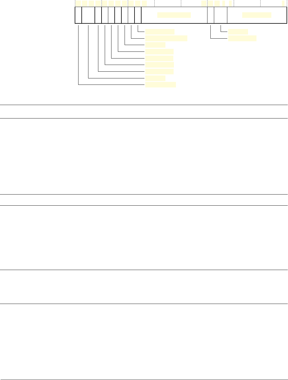
Cortex-M3 Peripherals
ARM DUI 0552A Copyright © 2010 ARM. All rights reserved. 4-14
ID121610 Non-Confidential
See the register summary in Table 4-12 on page 4-11, and the Type descriptions in Table 4-15,
for the ICSR attributes. The bit assignments are:
31 28 22 21 910 0
VECTACTIVE
30 29 27 26 2324 12 11
VECTPENDING
NMIPENDSET
PENDSVSET
PENDSVCLR
Reserved for Debug
ISRPENDING Reserved
RETTOBASE
25
PENDSTSET
PENDSTCLR
8
Reserved
Reserved
Table 4-15 ICSR bit assignments
Bits Name Type Function
[31] NMIPENDSET RW NMI set-pending bit.
Write:
0 = no effect1 = changes NMI exception state to pending.
Read:
0 = NMI exception is not pending
1 = NMI exception is pending.
Because NMI is the highest-priority exception, normally the processor enter the NMI
exception handler as soon as it registers a write of 1 to this bit, and entering the handler clears
this bit to 0. A read of this bit by the NMI exception handler returns 1 only if the NMI signal
is reasserted while the processor is executing that handler.
[30:29] - - Reserved.
[28] PENDSVSET RW PendSV set-pending bit.
Write:
0 = no effect
1 = changes PendSV exception state to pending.
Read:
0 = PendSV exception is not pending
1 = PendSV exception is pending.
Writing 1 to this bit is the only way to set the PendSV exception state to pending.
[27] PENDSVCLR WO PendSV clear-pending bit.
Write:
0 = no effect
1 = removes the pending state from the PendSV exception.
[26] PENDSTSET RW SysTick exception set-pending bit.
Write:
0 = no effect
1 = changes SysTick exception state to pending.
Read:
0 = SysTick exception is not pending
1 = SysTick exception is pending.

Cortex-M3 Peripherals
ARM DUI 0552A Copyright © 2010 ARM. All rights reserved. 4-15
ID121610 Non-Confidential
When you write to the ICSR, the effect is Unpredictable if you:
• write 1 to the PENDSVSET bit and write 1 to the PENDSVCLR bit
• write 1 to the PENDSTSET bit and write 1 to the PENDSTCLR bit.
[25] PENDSTCLR WO SysTick exception clear-pending bit.
Write:
0 = no effect
1 = removes the pending state from the SysTick exception.
This bit is WO. On a register read its value is
Unknown
.
[24] - - Reserved.
[23] Reserved for
Debug use
RO This bit is reserved for Debug use and reads-as-zero when the processor is not in Debug.
[22] ISRPENDING RO Interrupt pending flag, excluding NMI and Faults:
0 = interrupt not pending
1 = interrupt pending.
[21:18] - - Reserved.
[17:12] VECTPENDING RO Indicates the exception number of the highest priority pending enabled exception:
0 = no pending exceptions
Nonzero = the exception number of the highest priority pending enabled exception.
The value indicated by this field includes the effect of the BASEPRI and FAULTMASK
registers, but not any effect of the PRIMASK register.
[11] RETTOBASE RO Indicates whether there are preempted active exceptions:
0 = there are preempted active exceptions to execute
1 = there are no active exceptions, or the currently-executing exception is the only active
exception.
[10:9] - - Reserved.
[8:0] VECTACTIVEaRO Contains the active exception number:
0 = Thread mode
Nonzero = The exception numbera of the currently active exception.
Note
Subtract 16 from this value to obtain the CMSIS IRQ number required to index into the
Interrupt Clear-Enable, Set-Enable, Clear-Pending, Set-Pending, or Priority Registers, see
Table 2-5 on page 2-6.
a. This is the same value as IPSR bits[8:0], see Interrupt Program Status Register on page 2-6.
Table 4-15 ICSR bit assignments (continued)
Bits Name Type Function

Cortex-M3 Peripherals
ARM DUI 0552A Copyright © 2010 ARM. All rights reserved. 4-16
ID121610 Non-Confidential
4.3.4 Vector Table Offset Register
The VTOR indicates the offset of the vector table base address from memory address
0x00000000
. See the register summary in Table 4-12 on page 4-11 for its attributes. The bit
assignments are:
When setting TBLOFF, you must align the offset to the number of exception entries in the vector
table. The minimum alignment is 32 words, enough for up to 16 interrupts. For more interrupts,
adjust the alignment by rounding up to the next power of two. For example, if you require 21
interrupts, the alignment must be on a 64-word boundary because the required table size is 37
words, and the next power of two is 64. See your vendor documentation for the alignment details
for your device.
Note
Table alignment requirements mean that bits[6:0] of the table offset are always zero.
4.3.5 Application Interrupt and Reset Control Register
The AIRCR provides priority grouping control for the exception model, endian status for data
accesses, and reset control of the system. See the register summary in Table 4-12 on page 4-11
and Table 4-17 on page 4-17 for its attributes.
To write to this register, you must write
0x5FA
to the VECTKEY field, otherwise the processor
ignores the write.
31 60
TBLOFF Reserved
7
Table 4-16 VTOR bit assignments
Bits Name Function
[31:7] TBLOFF Vector table base offset field. It contains bits[29:7] of the offset of the table base from the bottom
of the memory map.
Note
Bit[29] determines whether the vector table is in the code or SRAM memory region:
• 0 = code
•1 = SRAM.
In implementations bit[29] is sometimes called the TBLBASE bit.
[6:0] - Reserved.

Cortex-M3 Peripherals
ARM DUI 0552A Copyright © 2010 ARM. All rights reserved. 4-17
ID121610 Non-Confidential
The bit assignments are:
On read: VECTKEYSTAT
On write: VECTKEY
31 16 15 14 11 10 8 7 3 2 1 0
Reserved Reserved
ENDIANNESS PRIGROUP SYSRESETREQ
VECTCLRACTIVE
VECTRESET
Reserved for Debug use
Table 4-17 AIRCR bit assignments
Bits Name Type Function
[31:16] Write: VECTKEYSTAT
Read: VECTKEY
RW Register key:
Reads as
0xFA05
On writes, write
0x5FA
to VECTKEY, otherwise the write is ignored.
[15] ENDIANNESS RO Data endianness bit is implementation defined:
0 = Little-endian
1 = Big-endian.
[14:11] - - Reserved
[10:8] PRIGROUP R/W Interrupt priority grouping field is implementation defined. This field
determines the split of group priority from subpriority, see Binary point on
page 4-18.
[7:3] - - Reserved.
[2] SYSRESETREQ WO System reset request bit is implementation defined:
0 = no system reset request
1 = asserts a signal to the outer system that requests a reset.
This is intended to force a large system reset of all major components
except for debug.
This bit reads as 0.
See you vendor documentation for more information about the use of this
signal in your implementation.
[1] VECTCLRACTIVE WO Reserved for Debug use. This bit reads as 0. When writing to the register
you must write 0 to this bit, otherwise behavior is Unpredictable.
[0] VECTRESET WO Reserved for Debug use. This bit reads as 0. When writing to the register
you must write 0 to this bit, otherwise behavior is Unpredictable.

Cortex-M3 Peripherals
ARM DUI 0552A Copyright © 2010 ARM. All rights reserved. 4-18
ID121610 Non-Confidential
Binary point
The PRIGROUP field indicates the position of the binary point that splits the PRI_n fields in
the Interrupt Priority Registers into separate group priority and subpriority fields. Table 4-18
shows how the PRIGROUP value controls this split. Implementations having fewer than 8-bits
of interrupt priority treat the least significant bits as zero.
Note
Determining preemption of an exception uses only the group priority field, see Interrupt priority
grouping on page 2-25.
Table 4-18 Priority grouping
Interrupt priority level value, PRI_N[7:0] Number of
PRIGROUP Binary pointaGroup priority bits Subpriority bits Group priorities Subpriorities
0b000
bxxxxxxx.y [7:1] [0] 128 2
0b001
bxxxxxx.yy [7:2] [1:0] 64 4
0b010
bxxxxx.yyy [7:3] [2:0] 32 8
0b011
bxxxx.yyyy [7:4] [3:0] 16 16
0b100
bxxx.yyyyy [7:5] [4:0] 8 32
0b101
bxx.yyyyyy [7:6] [5:0] 4 64
0b110
bx.yyyyyyy [7] [6:0] 2 128
0b111
b.yyyyyyyy None [7:0] 1 256
a. PRI_n[7:0] field showing the binary point. x denotes a group priority field bit, and y denotes a subpriority field bit.

Cortex-M3 Peripherals
ARM DUI 0552A Copyright © 2010 ARM. All rights reserved. 4-19
ID121610 Non-Confidential
4.3.6 System Control Register
The SCR controls features of entry to and exit from low power state. See the register summary
in Table 4-12 on page 4-11 for its attributes. The bit assignments are:
4.3.7 Configuration and Control Register
The CCR controls entry to Thread mode and enables:
• the handlers for NMI, hard fault and faults escalated by FAULTMASK to ignore
BusFaults
• trapping of divide by zero and unaligned accesses
• access to the STIR by unprivileged software, see Software Trigger Interrupt Register on
page 4-8.
See the register summary in Table 4-12 on page 4-11 for the CCR attributes.
31 4 3 2 1 0
Reserved
Reserved
SLEEPDEEP
SLEEPONEXIT
Reserved
5
SEVONPEND
Table 4-19 SCR bit assignments
Bits Name Function
[31:5] - Reserved.
[4] SEVONPEND Send Event on Pending bit:
0 = only enabled interrupts or events can wakeup the processor, disabled interrupts are
excluded
1 = enabled events and all interrupts, including disabled interrupts, can wakeup the
processor.
When an event or interrupt enters pending state, the event signal wakes up the processor
from WFE. If the processor is not waiting for an event, the event is registered and affects the
next WFE.
The processor also wakes up on execution of an
SEV
instruction or an external event.
[3] - Reserved.
[2] SLEEPDEEP Controls whether the processor uses sleep or deep sleep as its low power mode:
0 = sleep
1 = deep sleep.
[1] SLEEPONEXIT Indicates sleep-on-exit when returning from Handler mode to Thread mode:
0 = do not sleep when returning to Thread mode
1 = enter sleep, or deep sleep, on return from an ISR.
Setting this bit to 1 enables an interrupt driven application to avoid returning to an empty
main application.
[0] - Reserved.

Cortex-M3 Peripherals
ARM DUI 0552A Copyright © 2010 ARM. All rights reserved. 4-20
ID121610 Non-Confidential
The bit assignments are:
DIV_0_TRP
Reserved
UNALIGN_TRP
NONBASETHRDENA
USERSETMPEND
BFHFNMIGN
STKALIGN
Reserved
31 10 9 8 7 5 4 3 2 1 0
Reserved
Table 4-20 CCR bit assignments
Bits Name Function
[31:10] - Reserved.
[9] STKALIGN Indicates stack alignment on exception entry:
0 = 4-byte aligned
1 = 8-byte aligned.
On exception entry, the processor uses bit[9] of the stacked PSR to indicate the
stack alignment. On return from the exception it uses this stacked bit to restore
the correct stack alignment.
[8] BFHFNMIGN Enables handlers with priority -1 or -2 to ignore data BusFaults caused by load
and store instructions. This applies to the hard fault, NMI, and FAULTMASK
escalated handlers:
0 = data bus faults caused by load and store instructions cause a lock-up
1 = handlers running at priority -1 and -2 ignore data bus faults caused by load
and store instructions.
Set this bit to 1 only when the handler and its data are in absolutely safe memory.
The normal use of this bit is to probe system devices and bridges to detect control
path problems and fix them.
[7:5] - Reserved.
[4] DIV_0_TRP Enables faulting or halting when the processor executes an
SDIV
or
UDIV
instruction with a divisor of 0:
0 = do not trap divide by 0
1 = trap divide by 0.
When this bit is set to 0, a divide by zero returns a quotient of 0.
[3] UNALIGN_TRP Enables unaligned access traps:
0 = do not trap unaligned halfword and word accesses
1 = trap unaligned halfword and word accesses.
If this bit is set to 1, an unaligned access generates a UsageFault.
Unaligned
LDM
,
STM
,
LDRD
, and
STRD
instructions always fault irrespective of
whether UNALIGN_TRP is set to 1.

Cortex-M3 Peripherals
ARM DUI 0552A Copyright © 2010 ARM. All rights reserved. 4-21
ID121610 Non-Confidential
4.3.8 System Handler Priority Registers
The SHPR1-SHPR3 registers set the priority level, 0 to 255, of the exception handlers that have
configurable priority.
SHPR1-SHPR3 are byte accessible. See the register summary in Table 4-12 on page 4-11 for
their attributes.
To access to the system exception priority level using CMSIS, use the following CMSIS
functions:
•
uint32_t NVIC_GetPriority(IRQn_Type IRQn)
•
void NVIC_SetPriority(IRQn_Type IRQn, uint32_t priority)
The input parameter IRQn is the IRQ number, see Table 2-16 on page 2-22 for more
information.
System Handler Priority Register 1
The bit assignments are:
[2] - Reserved.
[1] USERSETMPEND Enables unprivileged software access to the STIR, see Software Trigger Interrupt
Register on page 4-8:
0 = disable
1 = enable.
[0] NONBASETHRDENA Indicates how the processor enters Thread mode:
0 = processor can enter Thread mode only when no exception is active
1 = processor can enter Thread mode from any level under the control of an
EXC_RETURN value, see Exception return on page 2-27.
Table 4-20 CCR bit assignments (continued)
Bits Name Function
Table 4-21 SHPR1 register bit assignments
Bits Name Function
[31:24] PRI_7 Reserved
[23:16] PRI_6 Priority of system handler 6, UsageFault
[15:8] PRI_5 Priority of system handler 5, BusFault
[7:0] PRI_4 Priority of system handler 4, MemManage
31 24 23 0
Reserved PRI_6 PRI_5 PRI_4
16 15 8 7
Cortex-M3 Peripherals
ARM DUI 0552A Copyright © 2010 ARM. All rights reserved. 4-22
ID121610 Non-Confidential
System Handler Priority Register 2
The bit assignments are:
System Handler Priority Register 3
The bit assignments are:
Table 4-22 SHPR2 register bit assignments
Bits Name Function
[31:24] PRI_11 Priority of system handler 11, SVCall
[23:0] - Reserved
Table 4-23 SHPR3 register bit assignments
Bits Name Function
[31:24] PRI_15 Priority of system handler 15, SysTick exception
[23:16] PRI_14 Priority of system handler 14, PendSV
[15:0] - Reserved
31 24 23 0
PRI_11 Reserved
PRI_15
31 15 01624 23
PRI_14 Reserved
Cortex-M3 Peripherals
ARM DUI 0552A Copyright © 2010 ARM. All rights reserved. 4-23
ID121610 Non-Confidential
4.3.9 System Handler Control and State Register
The SHCSR enables the system handlers, and indicates:
• the pending status of the BusFault, MemManage fault, and SVC exceptions
• the active status of the system handlers.
See the register summary in Table 4-12 on page 4-11 for the SHCSR attributes. The bit
assignments are:
Table 4-24 SHCSR bit assignments
Bits Name Function
[31:19] - Reserved
[18] USGFAULTENA UsageFault enable bit, set to 1 to enablea
[17] BUSFAULTENA BusFault enable bit, set to 1 to enablea
[16] MEMFAULTENA MemManage enable bit, set to 1 to enablea
[15] SVCALLPENDED SVCall pending bit, reads as 1 if exception is pendingb
[14] BUSFAULTPENDED BusFault exception pending bit, reads as 1 if exception is pendingb
[13] MEMFAULTPENDED MemManage exception pending bit, reads as 1 if exception is pendingb
[12] USGFAULTPENDED UsageFault exception pending bit, reads as 1 if exception is pendingb
[11] SYSTICKACT SysTick exception active bit, reads as 1 if exception is activec
[10] PENDSVACT PendSV exception active bit, reads as 1 if exception is active
[9] - Reserved
[8] MONITORACT Debug monitor active bit, reads as 1 if Debug monitor is active
[7] SVCALLACT SVCall active bit, reads as 1 if SVC call is active
[6:4] - Reserved
[3] USGFAULTACT UsageFault exception active bit, reads as 1 if exception is active
USGFAULTENA
SVCALLPENDED
BUSFAULTENA
MEMFAULTENA
BUSFAULTPENDED
SYSTICKACT
PENDSVACT
MONITORACT
SVCALLACT
USGFAULTACT
BUSFAULTACT
MEMFAULTACT
MEMFAULTPENDED
USGFAULTPENDED
Reserved
Reserved
Reserved
Reserved
31 19 18 17 16 15 14 13 12 11 10 9 8 7 6 4 3 2 1 0
Cortex-M3 Peripherals
ARM DUI 0552A Copyright © 2010 ARM. All rights reserved. 4-24
ID121610 Non-Confidential
If you disable a system handler and the corresponding fault occurs, the processor treats the fault
as a hard fault.
You can write to this register to change the pending or active status of system exceptions. An
OS kernel can write to the active bits to perform a context switch that changes the current
exception type.
Caution
• Software that changes the value of an active bit in this register without correct adjustment
to the stacked content can cause the processor to generate a fault exception. Ensure
software that writes to this register retains and subsequently restores the current active
status.
• After you have enabled the system handlers, if you have to change the value of a bit in this
register you must use a read-modify-write procedure to ensure that you change only the
required bit.
4.3.10 Configurable Fault Status Register
The CFSR indicates the cause of a MemManage fault, BusFault, or UsageFault. See the register
summary in Table 4-12 on page 4-11 for its attributes. The bit assignments are:
The following subsections describe the subregisters that make up the CFSR:
•MemManage Fault Status Register on page 4-25
•BusFault Status Register on page 4-26
•UsageFault Status Register on page 4-28.
The CFSR is byte accessible. You can access the CFSR or its subregisters as follows:
• access the complete CFSR with a word access to
0xE000ED28
• access the MMFSR with a byte access to
0xE000ED28
• access the MMFSR and BFSR with a halfword access to
0xE000ED28
• access the BFSR with a byte access to
0xE000ED29
• access the UFSR with a halfword access to
0xE000ED2A
.
[2] - Reserved
[1] BUSFAULTACT BusFault exception active bit, reads as 1 if exception is active
[0] MEMFAULTACT MemManage exception active bit, reads as 1 if exception is active
a. Enable bits, set to 1 to enable the exception, or set to 0 to disable the exception.
b. Pending bits, read as 1 if the exception is pending, or as 0 if it is not pending. You can write to these bits to change the pending
status of the exceptions.
c. Active bits, read as 1 if the exception is active, or as 0 if it is not active. You can write to these bits to change the active status
of the exceptions, but see the Caution in this section.
Table 4-24 SHCSR bit assignments (continued)
Bits Name Function
Memory Management
Fault Status Register
31 16 15 8 7 0
Usage Fault Status Register Bus Fault Status
Register
UFSR BFSR MMFSR

Cortex-M3 Peripherals
ARM DUI 0552A Copyright © 2010 ARM. All rights reserved. 4-25
ID121610 Non-Confidential
MemManage Fault Status Register
The flags in the MMFSR indicate the cause of memory access faults. The bit assignments are:
MMARVALID
Reserved
MSTKERR MUNSTKERR
76543210
IACCVIOL
DACCVIOL
Reserved
Table 4-25 MMFSR bit assignments
Bits Name Function
[7] MMARVALID MemManage Fault Address Register (MMFAR) valid flag:
0 = value in MMAR is not a valid fault address
1 = MMAR holds a valid fault address.
If a MemManage fault occurs and is escalated to a HardFault because of priority, the HardFault
handler must set this bit to 0. This prevents problems on return to a stacked active MemManage
fault handler whose MMAR value has been overwritten.
[6:5] - Reserved.
[4] MSTKERR MemManage fault on stacking for exception entry:
0 = no stacking fault
1 = stacking for an exception entry has caused one or more access violations.
When this bit is 1, the SP is still adjusted but the values in the context area on the stack might
be incorrect. The processor has not written a fault address to the MMAR.
[3] MUNSTKERR MemManage fault on unstacking for a return from exception:
0 = no unstacking fault
1 = unstack for an exception return has caused one or more access violations.
This fault is chained to the handler. This means that when this bit is 1, the original return stack
is still present. The processor has not adjusted the SP from the failing return, and has not
performed a new save. The processor has not written a fault address to the MMAR.
[2] - Reserved
[1] DACCVIOL Data access violation flag:
0 = no data access violation fault
1 = the processor attempted a load or store at a location that does not permit the operation.
When this bit is 1, the PC value stacked for the exception return points to the faulting
instruction. The processor has loaded the MMAR with the address of the attempted access.
[0] IACCVIOL Instruction access violation flag:
0 = no instruction access violation fault
1 = the processor attempted an instruction fetch from a location that does not permit execution.
This fault occurs on any access to an XN region, even when the MPU is disabled or not present.
When this bit is 1, the PC value stacked for the exception return points to the faulting
instruction. The processor has not written a fault address to the MMAR.
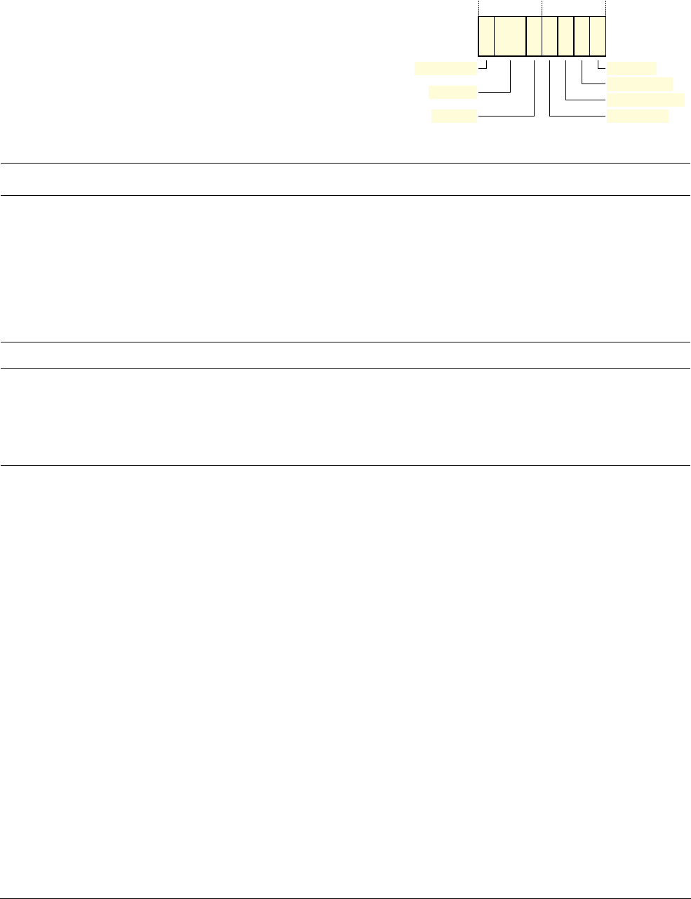
Cortex-M3 Peripherals
ARM DUI 0552A Copyright © 2010 ARM. All rights reserved. 4-26
ID121610 Non-Confidential
BusFault Status Register
The flags in the BFSR indicate the cause of a bus access fault. The bit assignments are:
BFARVALID
STKERR UNSTKERR
76543210
IBUSERR
PRECISERR
IMPRECISERR
Reserved
Table 4-26 BFSR bit assignments
Bits Name Function
[7] BFARVALID BusFault Address Register (BFAR) valid flag:
0 = value in BFAR is not a valid fault address
1 = BFAR holds a valid fault address.
The processor sets this bit to 1 after a BusFault where the address is known. Other faults can set this bit to
0, such as a MemManage fault occurring later.
If a BusFault occurs and is escalated to a hard fault because of priority, the hard fault handler must set this
bit to 0. This prevents problems if returning to a stacked active BusFault handler whose BFAR value has
been overwritten.
[6:5] - Reserved.
[4] STKERR BusFault on stacking for exception entry:
0 = no stacking fault
1 = stacking for an exception entry has caused one or more BusFaults.
When the processor sets this bit to 1, the SP is still adjusted but the values in the context area on the stack
might be incorrect. The processor does not write a fault address to the BFAR.
[3] UNSTKERR BusFault on unstacking for a return from exception:
0 = no unstacking fault
1 = unstack for an exception return has caused one or more BusFaults.
This fault is chained to the handler. This means that when the processor sets this bit to 1, the original return
stack is still present. The processor does not adjust the SP from the failing return, does not performed a
new save, and does not write a fault address to the BFAR.

Cortex-M3 Peripherals
ARM DUI 0552A Copyright © 2010 ARM. All rights reserved. 4-27
ID121610 Non-Confidential
[2] IMPRECISERR Imprecise data bus error:
0 = no imprecise data bus error
1 = a data bus error has occurred, but the return address in the stack frame is not related to the instruction
that caused the error.
When the processor sets this bit to 1, it does not write a fault address to the BFAR.
This is an asynchronous fault. Therefore, if it is detected when the priority of the current process is higher
than the BusFault priority, the BusFault becomes pending and becomes active only when the processor
returns from all higher priority processes. If a precise fault occurs before the processor enters the handler
for the imprecise BusFault, the handler detects both IMPRECISERR set to 1 and one of the precise fault
status bits set to 1.
[1] PRECISERR Precise data bus error:
0 = no precise data bus error
1 = a data bus error has occurred, and the PC value stacked for the exception return points to the instruction
that caused the fault.
When the processor sets this bit is 1, it writes the faulting address to the BFAR.
[0] IBUSERR Instruction bus error:
0 = no instruction bus error
1 = instruction bus error.
The processor detects the instruction bus error on prefetching an instruction, but it sets the IBUSERR flag
to 1 only if it attempts to issue the faulting instruction.
When the processor sets this bit is 1, it does not write a fault address to the BFAR.
Table 4-26 BFSR bit assignments (continued)
Bits Name Function
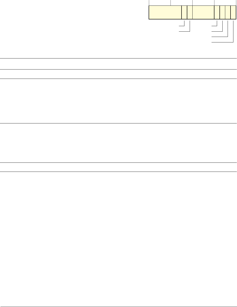
Cortex-M3 Peripherals
ARM DUI 0552A Copyright © 2010 ARM. All rights reserved. 4-28
ID121610 Non-Confidential
UsageFault Status Register
The UFSR indicates the cause of a UsageFault. The bit assignments are:
NOCP
INVPC
INVSTATE
UNDEFINSTR
DIVBYZERO
UNALIGNED
15 10987 43210
Reserved Reserved
Table 4-27 UFSR bit assignments
Bits Name Function
[15:10] - Reserved.
[9] DIVBYZERO Divide by zero UsageFault:
0 = no divide by zero fault, or divide by zero trapping not enabled
1 = the processor has executed an
SDIV
or
UDIV
instruction with a divisor of 0.
When the processor sets this bit to 1, the PC value stacked for the exception return points to the instruction
that performed the divide by zero.
Enable trapping of divide by zero by setting the DIV_0_TRP bit in the CCR to 1, see Configuration and
Control Register on page 4-19.
[8] UNALIGNED Unaligned access UsageFault:
0 = no unaligned access fault, or unaligned access trapping not enabled
1 = the processor has made an unaligned memory access.
Enable trapping of unaligned accesses by setting the UNALIGN_TRP bit in the CCR to 1, see
Configuration and Control Register on page 4-19.
Unaligned
LDM
,
STM
,
LDRD
, and
STRD
instructions always fault irrespective of the setting of UNALIGN_TRP.
[7:4] - Reserved.
[3] NOCP No coprocessor UsageFault. The processor does not support coprocessor instructions:
0 = no UsageFault caused by attempting to access a coprocessor
1 = the processor has attempted to access a coprocessor.

Cortex-M3 Peripherals
ARM DUI 0552A Copyright © 2010 ARM. All rights reserved. 4-29
ID121610 Non-Confidential
Note
The UFSR bits are sticky. This means as one or more fault occurs, the associated bits are set to
1. A bit that is set to 1 is cleared to 0 only by writing 1 to that bit, or by a reset.
[2] INVPC Invalid PC load UsageFault, caused by an invalid PC load by EXC_RETURN:
0 = no invalid PC load UsageFault
1 = the processor has attempted an illegal load of EXC_RETURN to the PC, as a result of an invalid
context, or an invalid EXC_RETURN value.
When this bit is set to 1, the PC value stacked for the exception return points to the instruction that tried
to perform the illegal load of the PC.
[1] INVSTATE Invalid state UsageFault:
0 = no invalid state UsageFault
1 = the processor has attempted to execute an instruction that makes illegal use of the EPSR.
When this bit is set to 1, the PC value stacked for the exception return points to the instruction that
attempted the illegal use of the EPSR.
This bit is not set to 1 if an undefined instruction uses the EPSR.
[0] UNDEFINSTR Undefined instruction UsageFault:
0 = no undefined instruction UsageFault
1 = the processor has attempted to execute an undefined instruction.
When this bit is set to 1, the PC value stacked for the exception return points to the undefined instruction.
An undefined instruction is an instruction that the processor cannot decode.
Table 4-27 UFSR bit assignments (continued)
Bits Name Function

Cortex-M3 Peripherals
ARM DUI 0552A Copyright © 2010 ARM. All rights reserved. 4-30
ID121610 Non-Confidential
4.3.11 HardFault Status Register
The HFSR gives information about events that activate the HardFault handler. See the register
summary in Table 4-12 on page 4-11 for its attributes.
This register is read, write to clear. This means that bits in the register read normally, but writing
1 to any bit clears that bit to 0. The bit assignments are:
Note
The HFSR bits are sticky. This means as one or more fault occurs, the associated bits are set to
1. A bit that is set to 1 is cleared to 0 only by writing 1 to that bit, or by a reset.
4.3.12 MemManage Fault Address Register
The MMFAR contains the address of the location that generated a MemManage fault. See the
register summary in Table 4-12 on page 4-11 for its attributes. The bit assignments are:
31 30 210
Reserved
29
DEBUGEVT
FORCED VECTTBL
Reserved
Table 4-28 HFSR bit assignments
Bits Name Function
[31] DEBUGEVT Reserved for Debug use. When writing to the register you must write 0 to this bit, otherwise
behavior is Unpredictable.
[30] FORCED Indicates a forced hard fault, generated by escalation of a fault with configurable priority that
cannot be handles, either because of priority or because it is disabled:
0 = no forced HardFault
1 = forced HardFault.
When this bit is set to 1, the HardFault handler must read the other fault status registers to find
the cause of the fault.
[29:2] - Reserved.
[1] VECTTBL Indicates a BusFault on a vector table read during exception processing:
0 = no BusFault on vector table read
1 = BusFault on vector table read.
This error is always handled by the hard fault handler.
When this bit is set to 1, the PC value stacked for the exception return points to the instruction
that was preempted by the exception.
[0] - Reserved.
Table 4-29 MMFAR bit assignments
Bits Name Function
[31:0] ADDRESS When the MMARVALID bit of the MMFSR is set to 1, this field holds the address of the location
that generated the MemManage fault

Cortex-M3 Peripherals
ARM DUI 0552A Copyright © 2010 ARM. All rights reserved. 4-31
ID121610 Non-Confidential
When an unaligned access faults, the address is the actual address that faulted. Because a single
read or write instruction can be split into multiple aligned accesses, the fault address can be any
address in the range of the requested access size.
Flags in the MMFSR indicate the cause of the fault, and whether the value in the MMFAR is
valid. See MemManage Fault Status Register on page 4-25.
4.3.13 BusFault Address Register
The BFAR contains the address of the location that generated a BusFault. See the register
summary in Table 4-12 on page 4-11 for its attributes. The bit assignments are:
When an unaligned access faults the address in the BFAR is the one requested by the instruction,
even if it is not the address of the fault.
Flags in the BFSR indicate the cause of the fault, and whether the value in the BFAR is valid.
See BusFault Status Register on page 4-26.
4.3.14 Auxiliary Fault Status Register
The AFSR contains additional system fault information. See the register summary in Table 4-12
on page 4-11 for its attributes.
This register is read, write to clear. This means that bits in the register read normally, but writing
1 to any bit clears that bit to 0.
The bit assignments are:
Each AFSR bit maps directly to an AUXFAULT input of the processor, and a single-cycle
HIGH signal on the input sets the corresponding AFSR bit to one. It remains set to 1 until you
write 1 to the bit to clear it to zero. See your vendor documentation for more information.
When an AFSR bit is latched as one, an exception does not occur. Use an interrupt if an
exception is required.
4.3.15 System control block usage hints and tips
Ensure software uses aligned accesses of the correct size to access the system control block
registers:
• except for the CFSR and SHPR1-SHPR3, it must use aligned word accesses
• for the CFSR and SHPR1-SHPR3 it can use byte or aligned halfword or word accesses.
The processor does not support unaligned accesses to system control block registers.
Table 4-30 BFAR bit assignments
Bits Name Function
[31:0] ADDRESS When the BFARVALID bit of the BFSR is set to 1, this field holds the address of the location that
generated the BusFault
Table 4-31 AFSR bit assignments
Bits Name Function
[31:0] IMPDEF Implementation defined. The bits map to the AUXFAULT input signals.

Cortex-M3 Peripherals
ARM DUI 0552A Copyright © 2010 ARM. All rights reserved. 4-32
ID121610 Non-Confidential
In a fault handler. to determine the true faulting address:
1. Read and save the MMFAR or BFAR value.
2. Read the MMARVALID bit in the MMFSR, or the BFARVALID bit in the BFSR. The
MMFAR or BFAR address is valid only if this bit is 1.
Software must follow this sequence because another higher priority exception might change the
MMFAR or BFAR value. For example, if a higher priority handler preempts the current fault
handler, the other fault might change the MMFAR or BFAR value.
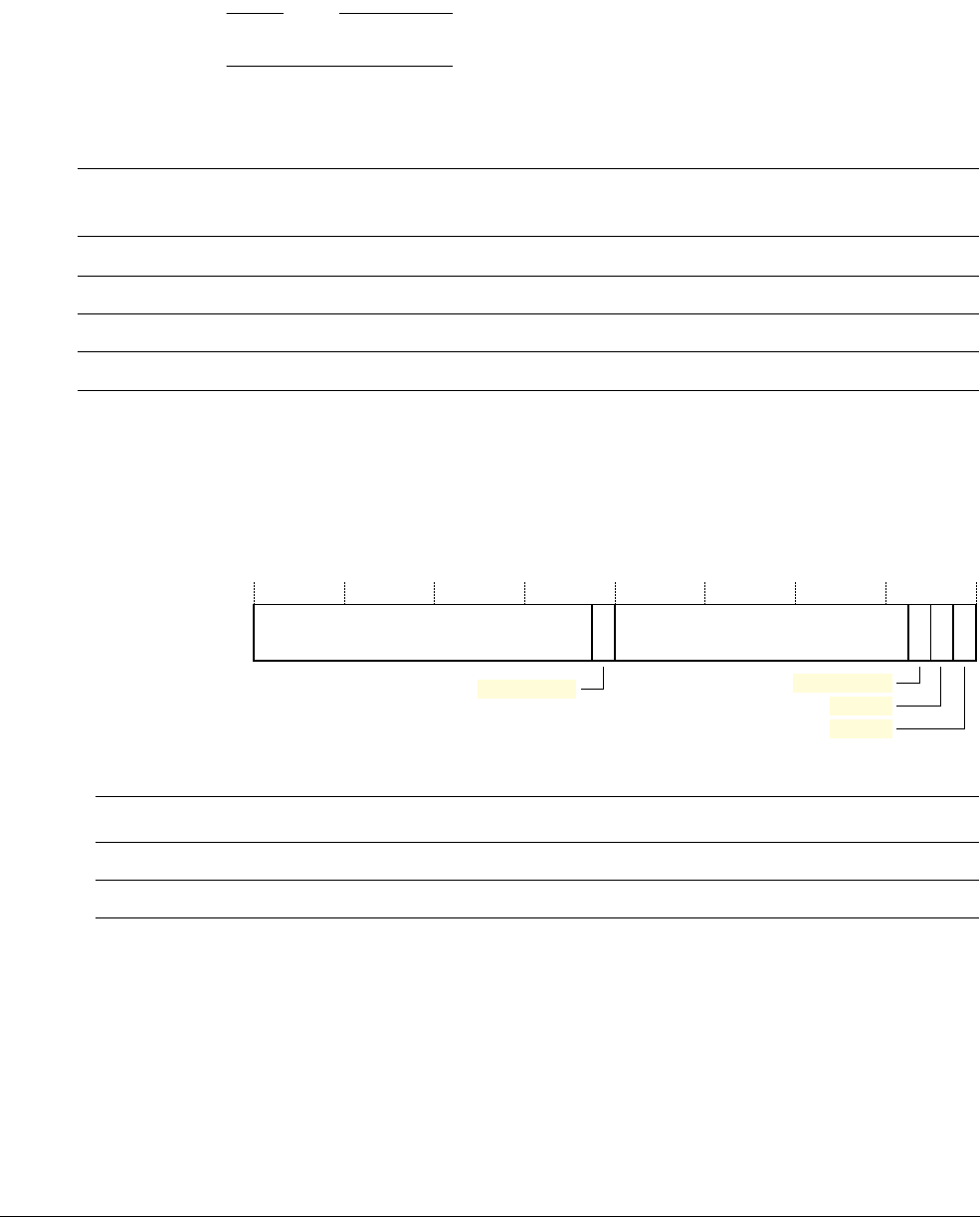
Cortex-M3 Peripherals
ARM DUI 0552A Copyright © 2010 ARM. All rights reserved. 4-33
ID121610 Non-Confidential
4.4 System timer, SysTick
The processor has a 24-bit system timer, SysTick, that counts down from the reload value to
zero, reloads, that is wraps to, the value in the SYST_RVR register on the next clock edge, then
counts down on subsequent clocks.
Note
When the processor is halted for debugging the counter does not decrement.
The system timer registers are:
4.4.1 SysTick Control and Status Register
The SysTick SYST_CSR register enables the SysTick features. The register resets to
0x00000000
, or to
0x00000004
if your device does not implement a reference clock. See the
register summary in Table 4-32 for its attributes. The bit assignments are:
Table 4-32 System timer registers summary
Address Name Type Required
privilege Reset value Description
0xE000E010
SYST_CSR RW Privileged aSysTick Control and Status Register
0xE000E014
SYST_RVR RW Privileged UNKNOWN SysTick Reload Value Register on page 4-34
0xE000E018
SYST_CVR RW Privileged UNKNOWN SysTick Current Value Register on page 4-35
0xE000E01C
SYST_CALIB RO Privileged
-
aSysTick Calibration Value Register on page 4-35
a. See the register description for more information.
0Reserved
31 17 16 15 3 2 1 0
Reserved 0 0
COUNTFLAG CLKSOURCE
TICKINT
ENABLE
Table 4-33 SysTick SYST_CSR register bit assignments
Bits Name Function
[31:17] - Reserved.
[16] COUNTFLAG Returns 1 if timer counted to 0 since last time this was read.
[15:3] - Reserved.

Cortex-M3 Peripherals
ARM DUI 0552A Copyright © 2010 ARM. All rights reserved. 4-34
ID121610 Non-Confidential
When ENABLE is set to 1, the counter loads the RELOAD value from the SYST_RVR register
and then counts down. On reaching 0, it sets the COUNTFLAG to 1 and optionally asserts the
SysTick depending on the value of TICKINT. It then loads the RELOAD value again, and
begins counting.
4.4.2 SysTick Reload Value Register
The SYST_RVR register specifies the start value to load into the SYST_CVR register. See the
register summary in Table 4-32 on page 4-33 for its attributes. The bit assignments are:
Calculating the RELOAD value
The RELOAD value can be any value in the range
0x00000001
-
0x00FFFFFF
. A start value of 0 is
possible, but has no effect because the SysTick exception request and COUNTFLAG are
activated when counting from 1 to 0.
The RELOAD value is calculated according to its use. For example, to generate a multi-shot
timer with a period of N processor clock cycles, use a RELOAD value of N-1. If the SysTick
interrupt is required every 100 clock pulses, set RELOAD to 99.
[2] CLKSOURCE Indicates the clock source:
0 = external clock
1 - processor clock.
[1] TICKINT Enables SysTick exception request:
0 = counting down to zero does not assert the SysTick exception request
1 = counting down to zero asserts the SysTick exception request.
Software can use COUNTFLAG to determine if SysTick has ever counted to zero.
[0] ENABLE Enables the counter:
0 = counter disabled
1 = counter enabled.
Table 4-33 SysTick SYST_CSR register bit assignments (continued)
Bits Name Function
31 0
RELOADReserved
2324
Table 4-34 SYST_RVR register bit assignments
Bits Name Function
[31:24] - Reserved.
[23:0] RELOAD Value to load into the SYST_CVR register when the counter is enabled and when it reaches 0, see
Calculating the RELOAD value.
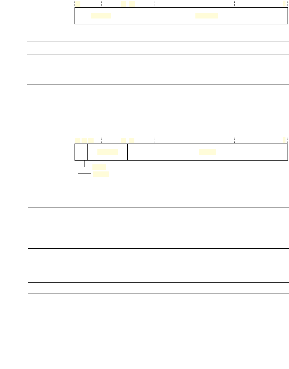
Cortex-M3 Peripherals
ARM DUI 0552A Copyright © 2010 ARM. All rights reserved. 4-35
ID121610 Non-Confidential
4.4.3 SysTick Current Value Register
The SYST_CVR register contains the current value of the SysTick counter. See the register
summary in Table 4-32 on page 4-33 for its attributes. The bit assignments are:
4.4.4 SysTick Calibration Value Register
The SYST_CALIB register indicates the SysTick calibration properties. See the register
summary in Table 4-32 on page 4-33 for its attributes. The reset value of this register is
implementation-defined. See the documentation supplied by your device vendor for more
information about the meaning of the SYST_CALIB field values. The bit assignments are:
If calibration information is not known, calculate the calibration value required from the
frequency of the processor clock or external clock.
31 0
CURRENTReserved
2324
Table 4-35 SYST_CVR register bit assignments
Bits Name Function
[31:24] - Reserved.
[23:0] CURRENT Reads return the current value of the SysTick counter.
A write of any value clears the field to 0, and also clears the SYST_CSR COUNTFLAG bit to 0.
31 0
TENMSReserved
2324
30
SKEW
NOREF
29
Table 4-36 SYST_CALIB register bit assignments
Bits Name Function
[31] NOREF Indicates whether the device provides a reference clock to the processor:
0 = reference clock provided
1 = no reference clock provided
If your device does not provide a reference clock, the SYST_CSR.CLKSOURCE bit reads-as-one
and ignores writes.
[30] SKEW Indicates whether the TENMS value is exact:
0 = TENMS value is exact
1 = TENMS value is inexact, or not given.
An inexact TENMS value can affect the suitability of SysTick as a software real time clock.
[29:24] - Reserved.
[23:0] TENMS Reload value for 10ms (100Hz) timing, subject to system clock skew errors. If the value reads as
zero, the calibration value is not known.

Cortex-M3 Peripherals
ARM DUI 0552A Copyright © 2010 ARM. All rights reserved. 4-36
ID121610 Non-Confidential
4.4.5 SysTick usage hints and tips
Some implementations stop all the processor clock signals during deep sleep mode. If this
happens, the SysTick counter stops.
Ensure software uses aligned word accesses to access the SysTick registers.
The SysTick counter reload and current value are not initialized by hardware. This means the
correct initialization sequence for the SysTick counter is:
1. Program reload value.
2. Clear current value.
3. Program Control and Status register.

Cortex-M3 Peripherals
ARM DUI 0552A Copyright © 2010 ARM. All rights reserved. 4-37
ID121610 Non-Confidential
4.5 Optional Memory Protection Unit
This section describes the optional Memory Protection Unit (MPU).
The MPU divides the memory map into a number of regions, and defines the location, size,
access permissions, and memory attributes of each region. It supports:
• independent attribute settings for each region
• overlapping regions
• export of memory attributes to the system.
The memory attributes affect the behavior of memory accesses to the region. The Cortex-M3
MPU defines:
• eight separate memory regions, 0-7
• a background region.
When memory regions overlap, a memory access is affected by the attributes of the region with
the highest number. For example, the attributes for region 7 take precedence over the attributes
of any region that overlaps region 7.
The background region has the same memory access attributes as the default memory map, but
is accessible from privileged software only.
The Cortex-M3 MPU memory map is unified. This means instruction accesses and data
accesses have same region settings.
If a program accesses a memory location that is prohibited by the MPU, the processor generates
a MemManage fault. This causes a fault exception, and might cause termination of the process
in an OS environment. In an OS environment, the kernel can update the MPU region setting
dynamically based on the process to be executed. Typically, an embedded OS uses the MPU for
memory protection.
Configuration of MPU regions is based on memory types, see Memory regions, types and
attributes on page 2-12.
Table 4-37 shows the possible MPU region attributes. These include Shareability and cache
behavior attributes are not relevant to most microcontroller implementations. See MPU
configuration for a microcontroller on page 4-47 and your vendor documentation for
programming guidelines if implemented.
Table 4-37 Memory attributes summary
Memory type Shareability Other attributes Description
Strongly- ordered - - All accesses to Strongly-ordered memory occur in program
order. All Strongly-ordered regions are assumed to be shared.
Device Shared - Memory-mapped peripherals that several processors share.
Non-shared - Memory-mapped peripherals that only a single processor uses.
Normal Shared Non-cacheable
Write-through Cacheable
Write-back Cacheable
Normal memory that is shared between several processors.
Non-shared Non-cacheable
Write-through Cacheable
Write-back Cacheable
Normal memory that only a single processor uses.

Cortex-M3 Peripherals
ARM DUI 0552A Copyright © 2010 ARM. All rights reserved. 4-38
ID121610 Non-Confidential
Use the MPU registers to define the MPU regions and their attributes. The MPU registers are:
4.5.1 MPU Type Register
The MPU_TYPE register indicates whether the MPU is present, and if so, how many regions it
supports. See the register summary in Table 4-38 for its attributes. The bit assignments are:
Table 4-38 MPU registers summary
Address Name Type Required
privilege
Reset
value Description
0xE000ED90
MPU_TYPE RO Privileged
0x00000800
MPU Type Register
0xE000ED94
MPU_CTRL RW Privileged
0x00000000
MPU Control Register on page 4-39
0xE000ED98
MPU_RNR RW Privileged
0x00000000
MPU Region Number Register on page 4-40
0xE000ED9C
MPU_RBAR RW Privileged
0x00000000
MPU Region Base Address Register on page 4-40
0xE000EDA0
MPU_RASR RW Privileged
0x00000000
MPU Region Attribute and Size Register on page 4-41
0xE000EDA4
MPU_RBAR_A1 RW Privileged
0x00000000
Alias of RBAR, see MPU Region Base Address Register on
page 4-40
0xE000EDA8
MPU_RASR_A1 RW Privileged
0x00000000
Alias of RASR, see MPU Region Attribute and Size Register
on page 4-41
0xE000EDAC
MPU_RBAR_A2 RW Privileged
0x00000000
Alias of RBAR, see MPU Region Base Address Register on
page 4-40
0xE000EDB0
MPU_RASR_A2 RW Privileged
0x00000000
Alias of RASR, see MPU Region Attribute and Size Register
on page 4-41
0xE000EDB4
MPU_RBAR_A3 RW Privileged
0x00000000
Alias of RBAR, see MPU Region Base Address Register on
page 4-40
0xE000EDB8
MPU_RASR_A3 RW Privileged
0x00000000
Alias of RASR, see MPU Region Attribute and Size Register
on page 4-41
Reserved
31 24 23 16 15 8 7 1 0
IREGION DREGION Reserved
SEPARATE
Table 4-39 TYPE register bit assignments
Bits Name Function
[31:24] - Reserved.
[23:16] IREGION Indicates the number of supported MPU instruction regions.
Always contains
0x00
. The MPU memory map is unified and is described by the DREGION field.
[15:8] DREGION Indicates the number of supported MPU data regions:
0x08
= eight MPU regions.
[7:1] - Reserved.
[0] SEPARATE Indicates support for unified or separate instruction and date memory maps:
0 = unified.

Cortex-M3 Peripherals
ARM DUI 0552A Copyright © 2010 ARM. All rights reserved. 4-39
ID121610 Non-Confidential
4.5.2 MPU Control Register
The MPU_CTRL register enables:
• the MPU
• the default memory map background region
• the use of the MPU when in the hard fault, Non-maskable Interrupt (NMI), and
FAULTMASK escalated handlers.
See the register summary in Table 4-38 on page 4-38 for the MPU_CTRL attributes. The bit
assignments are:
When ENABLE and PRIVDEFENA are both set to 1:
• For privileged accesses, the default memory map is as described in Memory model on
page 2-12. Any access by privileged software that does not address an enabled memory
region behaves as defined by the default memory map.
• Any access by unprivileged software that does not address an enabled memory region
causes a MemManage fault.
XN and Strongly-ordered rules always apply to the System Control Space regardless of the
value of the ENABLE bit.
31 10
Reserved
HFNMIENA
ENABLE
2
PRIVDEFENA
3
Table 4-40 MPU_CTRL register bit assignments
Bits Name Function
[31:3] - Reserved.
[2] PRIVDEFENA Enables privileged software access to the default memory map:
0 = If the MPU is enabled, disables use of the default memory map. Any memory access to a
location not covered by any enabled region causes a fault.
1 = If the MPU is enabled, enables use of the default memory map as a background region for
privileged software accesses.
When enabled, the background region acts as if it is region number -1. Any region that is
defined and enabled has priority over this default map.
If the MPU is disabled, the processor ignores this bit.
[1] HFNMIENA Enables the operation of MPU during hard fault, NMI, and FAULTMASK handlers.
When the MPU is enabled:
0 = MPU is disabled during hard fault, NMI, and FAULTMASK handlers, regardless of the
value of the ENABLE bit
1 = the MPU is enabled during hard fault, NMI, and FAULTMASK handlers.
When the MPU is disabled, if this bit is set to 1 the behavior is Unpredictable.
[0] ENABLE Enables the MPU:
0 = MPU disabled
1 = MPU enabled.

Cortex-M3 Peripherals
ARM DUI 0552A Copyright © 2010 ARM. All rights reserved. 4-40
ID121610 Non-Confidential
When the ENABLE bit is set to 1, at least one region of the memory map must be enabled for
the system to function unless the PRIVDEFENA bit is set to 1. If the PRIVDEFENA bit is set
to 1 and no regions are enabled, then only privileged software can operate.
When the ENABLE bit is set to 0, the system uses the default memory map. This has the same
memory attributes as if the MPU is not implemented, see Table 2-11 on page 2-14. The default
memory map applies to accesses from both privileged and unprivileged software.
When the MPU is enabled, accesses to the System Control Space and vector table are always
permitted. Other areas are accessible based on regions and whether PRIVDEFENA is set to 1.
Unless HFNMIENA is set to 1, the MPU is not enabled when the processor is executing the
handler for an exception with priority –1 or –2. These priorities are only possible when handling
a hard fault or NMI exception, or when FAULTMASK is enabled. Setting the HFNMIENA bit
to 1 enables the MPU when operating with these two priorities.
4.5.3 MPU Region Number Register
The MPU_RNR selects which memory region is referenced by the MPU_RBAR and
MPU_RASR registers. See the register summary in Table 4-38 on page 4-38 for its attributes.
The bit assignments are:
Normally, you write the required region number to this register before accessing the
MPU_RBAR or MPU_RASR. However you can change the region number by writing to the
MPU RBAR with the VALID bit set to 1, see MPU Region Base Address Register. This write
updates the value of the REGION field.
4.5.4 MPU Region Base Address Register
The MPU_RBAR defines the base address of the MPU region selected by the MPU_RNR, and
can update the value of the MPU_RNR. See the register summary in Table 4-38 on page 4-38
for its attributes.
Reserved
31 8 7 0
REGION
Table 4-41 MPU_RNR bit assignments
Bits Name Function
[31:8] - Reserved.
[7:0] REGION Indicates the MPU region referenced by the MPU_RBAR and MPU_RASR registers.
The MPU supports 8 memory regions, so the permitted values of this field are 0-7.

Cortex-M3 Peripherals
ARM DUI 0552A Copyright © 2010 ARM. All rights reserved. 4-41
ID121610 Non-Confidential
Write MPU_RBAR with the VALID bit set to 1 to change the current region number and update
the MPU_RNR. The bit assignments are:
The ADDR field
The ADDR field is bits[31:N] of the MPU_RBAR. The region size, as specified by the SIZE
field in the MPU_RASR, defines the value of N:
N = Log2(Region size in bytes),
If the region size is configured to 4GB, in the MPU_RASR, there is no valid ADDR field. In
this case, the region occupies the complete memory map, and the base address is
0x00000000
.
The base address is aligned to the size of the region. For example, a 64KB region must be
aligned on a multiple of 64KB, for example, at
0x00010000
or
0x00020000
.
4.5.5 MPU Region Attribute and Size Register
The MPU_RASR defines the region size and memory attributes of the MPU region specified by
the MPU_RNR, and enables that region and any subregions. See the register summary in
Table 4-38 on page 4-38 for its attributes.
MPU_RASR is accessible using word or halfword accesses:
• the most significant halfword holds the region attributes
• the least significant halfword holds the region size and the region and subregion enable
bits.
VALID
ADDR
31 N N-1 5 4 3 0
Reserved REGION
If the region size is 32B, the ADDR field is bits [31:5] and there is no Reserved field
Table 4-42 MPU_RBAR bit assignments
Bits Name Function
[31:N] ADDR Region base address field. The value of N depends on the region size. For more information see
The ADDR field.
[(N-1):5] - Reserved.
[4] VALID MPU Region Number valid bit:
Write:
0 = MPU_RNR not changed, and the processor:
• updates the base address for the region specified in the MPU_RNR
• ignores the value of the REGION field
1 = the processor:
• updates the value of the MPU_RNR to the value of the REGION field
• updates the base address for the region specified in the REGION field.
Always reads as zero.
[3:0] REGION MPU region field:
For the behavior on writes, see the description of the VALID field.
On reads, returns the current region number, as specified by the RNR.

Cortex-M3 Peripherals
ARM DUI 0552A Copyright © 2010 ARM. All rights reserved. 4-42
ID121610 Non-Confidential
The bit assignments are:
For information about access permission, see MPU access permission attributes on page 4-43.
SIZE field values
The SIZE field defines the size of the MPU memory region specified by the RNR. as follows:
(Region size in bytes) = 2(SIZE+1)
XN
Reserved
31 29 28 27 26 24 23 22 21 19 18 17 16 15 8 7 6 5 1 0
AP TEX S C B SRD SIZE
ENABLE
Reserved
Reserved
Reserved
Table 4-43 MPU_RASR bit assignments
Bits Name Function
[31:29] - Reserved.
[28] XN Instruction access disable bit:
0 = instruction fetches enabled
1 = instruction fetches disabled.
[27] - Reserved.
[26:24] AP Access permission field, see Table 4-47 on page 4-44.
[23:22] - Reserved.
[21:19, 17, 16] TEX, C, B Memory access attributes, see Table 4-45 on page 4-43.
[18] S Shareable bit, see Table 4-45 on page 4-43.
[15:8] SRD Subregion disable bits. For each bit in this field:
0 = corresponding sub-region is enabled
1 = corresponding sub-region is disabled.
See Subregions on page 4-46 for more information.
Region sizes of 128 bytes and less do not support subregions. When writing the attributes
for such a region, write the SRD field as
0x00
.
[7:6] - Reserved.
[5:1] SIZE Specifies the size of the MPU protection region. The minimum permitted value is 3
(
0b00010
), see See SIZE field values for more information.
[0] ENABLE Region enable bit.

Cortex-M3 Peripherals
ARM DUI 0552A Copyright © 2010 ARM. All rights reserved. 4-43
ID121610 Non-Confidential
The smallest permitted region size is 32B, corresponding to a SIZE value of 4. Table 4-44 gives
example SIZE values, with the corresponding region size and value of N in the MPU_RBAR.
4.5.6 MPU access permission attributes
This section describes the MPU access permission attributes. The access permission bits, TEX,
C, B, S, AP, and XN, of the RASR, control access to the corresponding memory region. If an
access is made to an area of memory without the required permissions, then the MPU generates
a permission fault. Table 4-45 shows encodings for the TEX, C, B, and S access permission bits.
Table 4-44 Example SIZE field values
SIZE value Region size Value of Na
a. In the MPU_RBAR, see MPU Region Base Address Register on page 4-40.
Note
0b00100
(4) 32B 5 Minimum permitted size
0b01001
(9) 1KB 10 -
0b10011
(19) 1MB 20 -
0b11101
(29) 1GB 30 -
0b11111
(31) 4GB 32 Maximum possible size
Table 4-45 TEX, C, B, and S encoding
TEX C B S Memory type Shareability Other attributes
0b000 0
0
xaStrongly-ordered Shareable -
1 xaDevice Shareable -
1 0
0
Normal Not shareable Outer and inner write-through. No write allocate.
1
Shareable
1
0
Normal Not shareable Outer and inner write-back. No write allocate.
1Shareable
0b001 0
0
0
Normal Not shareable Outer and inner noncacheable.
1Shareable
1 xaReserved encoding -
1
0
xaImplementation defined attributes. -
1 0
Normal Not shareable Outer and inner write-back. Write and read allocate.
1Shareable
0b010 0 0
xaDevice Not shareable Nonshared Device.
1
xaReserved encoding -
1
xaxaReserved encoding -
0b1BB
AA
0
Normal Not shareable Cached memory, BB = outer policy, AA = inner policy.
See Table 4-46 on page 4-44 for the encoding of the AA
and BB bits.
1
Shareable
a. The MPU ignores the value of this bit.

Cortex-M3 Peripherals
ARM DUI 0552A Copyright © 2010 ARM. All rights reserved. 4-44
ID121610 Non-Confidential
Table 4-46 shows the cache policy for memory attribute encodings with a TEX value is in the
range 4-7.
Table 4-47 shows the AP encodings that define the access permissions for privileged and
unprivileged software.
4.5.7 MPU mismatch
When an access violates the MPU permissions, the processor generates a MemManage fault, see
Exceptions and interrupts on page 2-10. The MMFSR indicates the cause of the fault. See
MemManage Fault Status Register on page 4-25 for more information.
4.5.8 Updating an MPU region
To update the attributes for an MPU region, update the MPU_RNR, MPU_RBAR and
MPU_RASR registers. You can program each register separately, or use a multiple-word write
to program all of these registers. You can use the MPU_RBAR and MPU_RASR aliases to
program up to four regions simultaneously using an
STM
instruction.
Updating an MPU region using separate words
Simple code to configure one region:
; R1 = region number
; R2 = size/enable
; R3 = attributes
; R4 = address
LDR R0,=MPU_RNR ; 0xE000ED98, MPU region number register
Table 4-46 Cache policy for memory attribute encoding
Encoding, AA or BB Corresponding cache policy
0b00
Non-cacheable
0b01
Write back, write and read allocate
0b10
Write through, no write allocate
0b11
Write back, no write allocate
Table 4-47 AP encoding
AP[2:0] Privileged
permissions
Unprivileged
permissions Description
000 No access No access All accesses generate a permission fault
001 RW No access Access from privileged software only
010 RW RO Writes by unprivileged software generate a permission fault
011 RW RW Full access
100 Unpredictable Unpredictable Reserved
101 RO No access Reads by privileged software only
110 RO RO Read only, by privileged or unprivileged software
111 RO RO Read only, by privileged or unprivileged software

Cortex-M3 Peripherals
ARM DUI 0552A Copyright © 2010 ARM. All rights reserved. 4-45
ID121610 Non-Confidential
STR R1, [R0, #0x0] ; Region Number
STR R4, [R0, #0x4] ; Region Base Address
STRH R2, [R0, #0x8] ; Region Size and Enable
STRH R3, [R0, #0xA] ; Region Attribute
Disable a region before writing new region settings to the MPU if you have previously enabled
the region being changed. For example:
; R1 = region number
; R2 = size/enable
; R3 = attributes
; R4 = address
LDR R0,=MPU_RNR ; 0xE000ED98, MPU region number register
STR R1, [R0, #0x0] ; Region Number
BIC R2, R2, #1 ; Disable
STRH R2, [R0, #0x8] ; Region Size and Enable
STR R4, [R0, #0x4] ; Region Base Address
STRH R3, [R0, #0xA] ; Region Attribute
ORR R2, #1 ; Enable
STRH R2, [R0, #0x8] ; Region Size and Enable
Software must use memory barrier instructions:
• before MPU setup if there might be outstanding memory transfers, such as buffered
writes, that might be affected by the change in MPU settings
• after MPU setup if it includes memory transfers that must use the new MPU settings.
However, memory barrier instructions are not required if the MPU setup process starts by
entering an exception handler, or is followed by an exception return, because the exception entry
and exception return mechanism cause memory barrier behavior.
Software does not require any memory barrier instructions during MPU setup, because it
accesses the MPU through the PPB, which is a Strongly-Ordered memory region.
For example, if you want all of the memory access behavior to take effect immediately after the
programming sequence, use a
DSB
instruction and an
ISB
instruction. A
DSB
is required after
changing MPU settings, such as at the end of context switch. An
ISB
is required if the code that
programs the MPU region or regions is entered using a branch or call. If the programming
sequence is entered using a return from exception, or by taking an exception, then you do not
require an
ISB
.
Updating an MPU region using multi-word writes
You can program directly using multi-word writes, depending on how the information is
divided. Consider the following reprogramming:
; R1 = region number
; R2 = address
; R3 = size, attributes in one
LDR R0, =MPU_RNR ; 0xE000ED98, MPU region number register
STR R1, [R0, #0x0] ; Region Number
STR R2, [R0, #0x4] ; Region Base Address
STR R3, [R0, #0x8] ; Region Attribute, Size and Enable
Use an
STM
instruction to optimize this:
; R1 = region number
; R2 = address
; R3 = size, attributes in one
LDR R0, =MPU_RNR ; 0xE000ED98, MPU region number register
STM R0, {R1-R3} ; Region Number, address, attribute, size and enable

Cortex-M3 Peripherals
ARM DUI 0552A Copyright © 2010 ARM. All rights reserved. 4-46
ID121610 Non-Confidential
You can do this in two words for pre-packed information. This means that the MPU_RBAR
contains the required region number and had the VALID bit set to 1, see MPU Region Base
Address Register on page 4-40. Use this when the data is statically packed, for example in a boot
loader:
; R1 = address and region number in one
; R2 = size and attributes in one
LDR R0, =MPU_RBAR ; 0xE000ED9C, MPU Region Base register
STR R1, [R0, #0x0] ; Region base address and
; region number combined with VALID (bit 4) set to 1
STR R2, [R0, #0x4] ; Region Attribute, Size and Enable
Subregions
Regions of 256 bytes or more are divided into eight equal-sized subregions. Set the
corresponding bit in the SRD field of the MPU_RASR to disable a subregion, see MPU Region
Attribute and Size Register on page 4-41. The least significant bit of SRD controls the first
subregion, and the most significant bit controls the last subregion. Disabling a subregion means
another region overlapping the disabled range matches instead. If no other enabled region
overlaps the disabled subregion the MPU issues a fault.
Regions of 32, 64, and 128 bytes do not support subregions, With regions of these sizes, you
must set the SRD field to
0x00
, otherwise the MPU behavior is Unpredictable.
Example of SRD use
Two regions with the same base address overlap. Region one is 128KB, and region two is
512KB. To ensure the attributes from region one apply to the first 128KB region, set the SRD
field for region two to
0b00000011
to disable the first two subregions, as the figure shows.
4.5.9 MPU usage hints and tips
To avoid unexpected behavior, disable the interrupts before updating the attributes of a region
that the interrupt handlers might access.
Ensure software uses aligned accesses of the correct size to access MPU registers:
• except for the MPU_RASR, it must use aligned word accesses
• for the MPU_RASR it can use byte or aligned halfword or word accesses.
The processor does not support unaligned accesses to MPU registers.
When setting up the MPU, and if the MPU has previously been programmed, disable unused
regions to prevent any previous region settings from affecting the new MPU setup.
Region 1
Disabled subregion
Disabled subregion
Region 2, with
subregions
Base address of both regions
Offset from
base address
0
64KB
128KB
192KB
256KB
320KB
384KB
448KB
512KB

Cortex-M3 Peripherals
ARM DUI 0552A Copyright © 2010 ARM. All rights reserved. 4-47
ID121610 Non-Confidential
MPU configuration for a microcontroller
Usually, a microcontroller system has only a single processor and no caches. In such a system,
program the MPU as follows:
In most microcontroller implementations, the shareability and cache policy attributes do not
affect the system behavior. However, using these settings for the MPU regions can make the
application code more portable. The values given are for typical situations. In special systems,
such as multiprocessor designs or designs with a separate DMA engine, the shareability attribute
might be important. In these cases see the recommendations of the memory device
manufacturer.
Table 4-48 Memory region attributes for a microcontroller
Memory region TEX C B S Memory type and attributes
Flash memory
0b000 1 0 0
Normal memory, Non-shareable, write-through
Internal SRAM
0b000 1 0 1
Normal memory, Shareable, write-through
External SRAM
0b000 1 1 1
Normal memory, Shareable, write-back, write-allocate
Peripherals
0b000 0 1 1
Device memory, Shareable

ARM DUI 0552A Copyright © 2010 ARM. All rights reserved. A-1
ID121610 Non-Confidential
Appendix A
Cortex-M3 Options
The configuration options for a Cortex-M3 processor implementation are determined by the device
manufacturer. This appendix describes what the configuration options are and the affect these have
on this book. It contains the following section:
•Cortex-M3 implementation options on page A-2.

Cortex-M3 Options
ARM DUI 0552A Copyright © 2010 ARM. All rights reserved. A-2
ID121610 Non-Confidential
A.1 Cortex-M3 implementation options
Table A-1 shows the Cortex-M3 implementation options.
Table A-1 Effects of the Cortex-M3 implementation options
Option Description, and affected documentation
Inclusion of
MPU
The implementer decides whether to include the MPU. See the Optional Memory Protection Unit on
page 4-37.
Number of
interrupts
The implementer decides how many interrupts the Cortex-M3 implementation supports Cortex-M3
implementation supports, in the range 1-240. This affects:
The range of IRQ values in Table 2-5 on page 2-6.
Entries in the last row of Table 2-16 on page 2-22, particularly if only one interrupt is implemented.
The maximum interrupt number, and associated information where appropriate, in:
•Exception handlers on page 2-23
•Figure 2-2 on page 2-24
•Nested Vectored Interrupt Controller on page 4-3.
The number of implemented Nested Vectored Interrupt Controller (NVIC) registers in:
•Table 4-2 on page 4-3
• The appropriate register descriptions in sections Interrupt Set-enable Registers on page 4-4
to Interrupt Priority Registers on page 4-7.
Vector Table Offset Register on page 4-16, including the figure and Table 4-16 on page 4-16. See the
configuration information in the section for guidance on the required configuration.
Number of
priority bits
The implementer decides how many priority bits are implemented in priority value fields, in the range
3-8. This affects The maximum priority level value in Nested Vectored Interrupt Controller on
page 4-3.
Inclusion of the
WIC
The implementer decides whether to include the Wakeup interrupt Controller (WIC), see The optional
Wakeup Interrupt Controller on page 2-32.
Sleep mode
power-saving
The implementer decides what sleep modes to implement, and the power-saving measures associated
with any implemented mode, See Power management on page 2-31.
Sleep mode power saving might also affect the SysTick behavior, see SysTick usage hints and tips on
page 4-36.
Register reset
values
The implementer decides whether all registers in the register bank can be reset. This affects the reset
values, see Table 2-2 on page 2-3.
Endianness The implementer decides whether the memory system is little-endian or big-endian, see Data types on
page 2-10 and Memory endianness on page 2-18.
Memory features Some features of the memory system are implementation-specific. This means that the Memory model
on page 2-12 cannot completely describe the memory map for a specific Cortex-M3 implementation.
Bit-banding The implementer decides whether bit-banding is implemented., see Optional bit-banding on
page 2-16 and Memory model on page 2-12.
SysTick timer The SYST_CALIB register is implementation- defined. This can affect:
•SysTick Calibration Value Register on page 4-35
• The entry for SYST_CALIB in Table 4-44 on page 4-43.

ARM DUI 0552A Copyright © 2010 ARM. All rights reserved. Glossary-1
ID121610 Non-Confidential
Glossary
This glossary describes some of the terms used in technical documents from ARM.
Abort A mechanism that indicates to a processor that the value associated with a memory access is
invalid. An abort can be caused by the external or internal memory system as a result of attempting
to access invalid instruction or data memory.
Aligned A data item stored at an address that is divisible by the number of bytes that defines the data size
is said to be aligned. Aligned words and halfwords have addresses that are divisible by four and
two respectively. The terms word-aligned and halfword-aligned therefore stipulate addresses that
are divisible by four and two respectively.
Banked register A register that has multiple physical copies, where the state of the processor determines which copy
is used. The Stack Pointer, SP (R13) is a banked register.
Base register In instruction descriptions, a register specified by a load or store instruction that is used to hold the
base value for the address calculation for the instruction. Depending on the instruction and its
addressing mode, an offset can be added to or subtracted from the base register value to form the
address that is sent to memory.
See also Index register.
Big-endian (BE) Byte ordering scheme in which bytes of decreasing significance in a data word are stored at
increasing addresses in memory.
See also Byte-invariant, Endianness, Little-endian (LE).
Big-endian memory Memory in which:
• a byte or halfword at a word-aligned address is the most significant byte or halfword within
the word at that address

Glossary
ARM DUI 0552A Copyright © 2010 ARM. All rights reserved. Glossary-2
ID121610 Non-Confidential
• a byte at a halfword-aligned address is the most significant byte within the halfword at
that address.
See also Little-endian memory.
Breakpoint A breakpoint is a mechanism provided by debuggers to identify an instruction at which program
execution is to be halted. Breakpoints are inserted by the programmer to enable inspection of
register contents, memory locations, variable values at fixed points in the program execution to
test that the program is operating correctly. Breakpoints are removed after the program is
successfully tested.
Byte-invariant In a byte-invariant system, the address of each byte of memory remains unchanged when
switching between little-endian and big-endian operation. When a data item larger than a byte
is loaded from or stored to memory, the bytes making up that data item are arranged into the
correct order depending on the endianness of the memory access. An ARM byte-invariant
implementation also supports unaligned halfword and word memory accesses. It expects
multi-word accesses to be word-aligned.
Cache A block of on-chip or off-chip fast access memory locations, situated between the processor and
main memory, used for storing and retrieving copies of often used instructions, data, or
instructions and data. This is done to greatly increase the average speed of memory accesses and
so improve processor performance.
Condition field A four-bit field in an instruction that specifies a condition under which the instruction can
execute.
Conditional execution
If the condition code flags indicate that the corresponding condition is true when the instruction
starts executing, it executes normally. Otherwise, the instruction does nothing.
Context The environment that each process operates in for a multitasking operating system. In ARM
processors, this is limited to mean the physical address range that it can access in memory and
the associated memory access permissions.
Coprocessor A processor that supplements the main processor. The Cortex-M4 processor does not support
any coprocessors.
Debugger A debugging system that includes a program, used to detect, locate, and correct software faults,
together with custom hardware that supports software debugging.
Direct Memory Access (DMA)
An operation that accesses main memory directly, without the processor performing any
accesses to the data concerned.
Doubleword A 64-bit data item. The contents are taken as being an unsigned integer unless otherwise stated.
Doubleword-aligned
A data item having a memory address that is divisible by eight.
Endianness Byte ordering. The scheme that determines the order that successive bytes of a data word are
stored in memory. An aspect of the systems memory mapping.
See also Little-endian and Big-endian
Exception An event that interrupts program execution. When an exception occurs, the processor suspends
the normal program flow and starts execution at the address indicated by the corresponding
exception vector. The indicated address contains the first instruction of the handler for the
exception.

Glossary
ARM DUI 0552A Copyright © 2010 ARM. All rights reserved. Glossary-3
ID121610 Non-Confidential
An exception can be an interrupt request, a fault, or a software-generated system exception.
Faults include attempting an invalid memory access, attempting to execute an instruction in an
invalid processor state, and attempting to execute an undefined instruction.
Exception service routine
See Interrupt handler.
Exception vector See Interrupt vector.
Flat address mapping
A system of organizing memory in which each physical address in the memory space is the same
as the corresponding virtual address.
Halfword A 16-bit data item.
Illegal instruction An instruction that is architecturally Undefined.
Implementation-defined
The behavior is not architecturally defined, but is defined and documented by individual
implementations.
Implementation-specific
The behavior is not architecturally defined, and does not have to be documented by individual
implementations. Used when there are a number of implementation options available and the
option chosen does not affect software compatibility.
Index register In some load and store instruction descriptions, the value of this register is used as an offset to
be added to or subtracted from the base register value to form the address that is sent to memory.
Some addressing modes optionally enable the index register value to be shifted prior to the
addition or subtraction.
See also Base register.
Instruction cycle count
The number of cycles that an instruction occupies the Execute stage of the pipeline.
Interrupt handler A program that control of the processor is passed to when an interrupt occurs.
Interrupt vector One of a number of fixed addresses in low memory, or in high memory if high vectors are
configured, that contains the first instruction of the corresponding interrupt handler.
Little-endian (LE) Byte ordering scheme in which bytes of increasing significance in a data word are stored at
increasing addresses in memory.
See also Big-endian (BE), Byte-invariant, Endianness.
Little-endian memory
Memory in which:
• a byte or halfword at a word-aligned address is the least significant byte or halfword
within the word at that address
• a byte at a halfword-aligned address is the least significant byte within the halfword at that
address.
See also Big-endian memory.
Load/store architecture
A processor architecture where data-processing operations only operate on register contents, not
directly on memory contents.

Glossary
ARM DUI 0552A Copyright © 2010 ARM. All rights reserved. Glossary-4
ID121610 Non-Confidential
Memory Protection Unit (MPU)
Hardware that controls access permissions to blocks of memory. An MPU does not perform any
address translation.
Prefetching In pipelined processors, the process of fetching instructions from memory to fill up the pipeline
before the preceding instructions have finished executing. Prefetching an instruction does not
mean that the instruction has to be executed.
Read Reads are defined as memory operations that have the semantics of a load. Reads include the
Thumb instructions
LDM
,
LDR
,
LDRSH
,
LDRH
,
LDRSB
,
LDRB
, and
POP
.
Region A partition of memory space.
Reserved A field in a control register or instruction format is reserved if the field is to be defined by the
implementation, or produces Unpredictable results if the contents of the field are not zero. These
fields are reserved for use in future extensions of the architecture or are
implementation-specific. All reserved bits not used by the implementation must be written as 0
and read as 0.
Should Be One (SBO)
Write as 1, or all 1s for bit fields, by software. Writing as 0 produces Unpredictable results.
Should Be Zero (SBZ)
Write as 0, or all 0s for bit fields, by software. Writing as 1 produces Unpredictable results.
Should Be Zero or Preserved (SBZP)
Write as 0, or all 0s for bit fields, by software, or preserved by writing the same value back that
has been previously read from the same field on the same processor.
Thread-safe In a multi-tasking environment, thread-safe functions use safeguard mechanisms when
accessing shared resources, to ensure correct operation without the risk of shared access
conflicts.
Thumb instruction One or two halfwords that specify an operation for a processor to perform. Thumb instructions
must be halfword-aligned.
Unaligned A data item stored at an address that is not divisible by the number of bytes that defines the data
size is said to be unaligned. For example, a word stored at an address that is not divisible by four.
Undefined Indicates an instruction that generates an Undefined instruction exception.
Unpredictable (UNP)
You cannot rely on the behavior. Unpredictable behavior must not represent security holes.
Unpredictable behavior must not halt or hang the processor, or any parts of the system.
Warm reset Also known as a core reset. Initializes the majority of the processor excluding the debug
controller and debug logic. This type of reset is useful if you are using the debugging features
of a processor.
WA See Write-allocate (WA).
WB See Write-back (WB).
Word A 32-bit data item.
Write Writes are defined as operations that have the semantics of a store. Writes include the Thumb
instructions
STM
,
STR
,
STRH
,
STRB
, and
PUSH
.
Write-allocate (WA) In a write-allocate cache, a cache miss on storing data causes a cache line to be allocated into
the cache.

Glossary
ARM DUI 0552A Copyright © 2010 ARM. All rights reserved. Glossary-5
ID121610 Non-Confidential
Write-back (WB) In a write-back cache, data is only written to main memory when it is forced out of the cache on
line replacement following a cache miss. Otherwise, writes by the processor only update the
cache. This is also known as copyback.
Write buffer A block of high-speed memory, arranged as a FIFO buffer, between the data cache and main
memory, whose purpose is to optimize stores to main memory.
Write-through (WT) In a write-through cache, data is written to main memory at the same time as the cache is
updated.
