Easypic V7 Manual V104d
easypic-v7-manual-v104d
User Manual: Pdf
Open the PDF directly: View PDF ![]() .
.
Page Count: 36
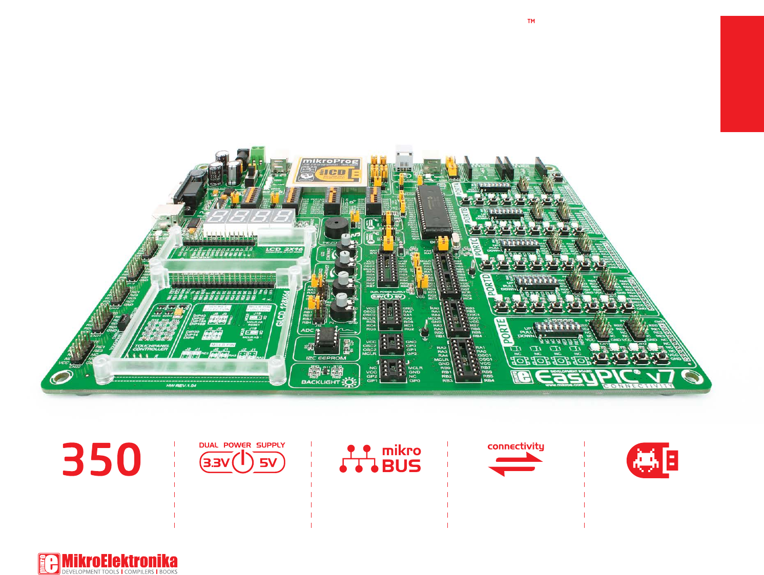
USER'S GUIDE
EasyPIC
connectivity
v7
Supports 3.3V and 5V devices
Dual Power Supply
Easy-add extra boards
mikroBUS™ sockets
Four connectors for each port
Amazing Connectivity
microcontrollers supported
The ultimate PIC® board
Fast USB 2.0 programmer and
In-Circuit Debugger

From the day one, we in MikroElektronika gave ourselves the highest possible goals in pursuit of excellence.
That same day, the idea of EasyPIC™ development board was born. And we all grew together with EasyPIC™.
In its each and tiniest piece we had put all of our energy, creativity and sense of what’s best for an engineer.
I’ve personally assembled hundreds of early EasyPIC™ boards myself with my home soldering iron.
Today, we present you the 7th generation of the board, which brings us some exciting new features. We hope
that you will like it as much as we do.
Use it wisely and have fun!
To our valued customers
Nebojsa Matic,
Owner and General Manager
of MikroElektronika
Table of contents
page 3
DS1820 - Digital Temperature Sensor . . . . . . . . . . . . . .
LCD 2x16 characters . . . . . . . . . . . . . . . . . . . . . . . . . . . . . .
Introduction . . . . . . . . . . . . . . . . . . . . . . . . . . . . . . . . . . . . . . .
What’s Next? . . . . . . . . . . . . . . . . . . . . . . . . . . . . . . . . . . . . . .
I2C EEPROM . . . . . . . . . . . . . . . . . . . . . . . . . . . . . . . . . . . . . .
mikroBUS™ sockets . . . . . . . . . . . . . . . . . . . . . . . . . . . . . . . .
Installing programmer drivers . . . . . . . . . . . . . . . . . . . . . .
4 digit 7-seg display . . . . . . . . . . . . . . . . . . . . . . . . . . . . . .
LM35 - Analog Temperature Sensor . . . . . . . . . . . . . . . .
GLCD 128x64. . . . . . . . . . . . . . . . . . . . . . . . . . . . . . . . . . . . .
It's good to know . . . . . . . . . . . . . . . . . . . . . . . . . . . . . . . . . .
Piezo Buzzer . . . . . . . . . . . . . . . . . . . . . . . . . . . . . . . . . . . . . .
Input/Output Group . . . . . . . . . . . . . . . . . . . . . . . . . . . . . . .
Programming software . . . . . . . . . . . . . . . . . . . . . . . . . . . . ADC inputs . . . . . . . . . . . . . . . . . . . . . . . . . . . . . . . . . . . . . . . .
On-board programmer . . . . . . . . . . . . . . . . . . . . . . . . . . . . .
Dual power supply . . . . . . . . . . . . . . . . . . . . . . . . . . . . . . . .
Supported microcontrollers . . . . . . . . . . . . . . . . . . . . . . . .
Touch panel controller . . . . . . . . . . . . . . . . . . . . . . . . . . . . .
Additional GNDs . . . . . . . . . . . . . . . . . . . . . . . . . . . . . . . . . . .
Introduction
Power Supply
Supported MCUs
Programming
Displays
Modules
What’s Next
Connectivity
28
24
04
34
31
19
12
27
29
25
05
32
22
13
mikroICD™ - In Circuit Debugger . . . . . . . . . . . . . . . . . . . . 14
30
10
06
08
26
33
UART via RS-232 . . . . . . . . . . . . . . . . . . . . . . . . . . . . . . . . .
UART via USB . . . . . . . . . . . . . . . . . . . . . . . . . . . . . . . . . . . . .
USB connection . . . . . . . . . . . . . . . . . . . . . . . . . . . . . . . . . . .
Communication
16
17
18
Introduction
introduction
page 4
EasyPIC™ is an old friend. It has been with us for six generations. Many of
us made our rst steps in embedded world with EasyPIC™. Today it has
thousands of users: students, hobbyists, enthusiasts and professionals.
It’s used in many schools and other educational institutions across the
globe. We may say that it’s the most famous PIC development system
in the world. We asked ourselves what we can do to make such a great
board even greater. And we made some brilliant changes. We focused
all of our creativity and knowledge into making a revolutionary new
design, unlike any previous version of the board. We now present
you with the new version 7 that brings so much more, and we
hope that you will be thrilled with your new board, just as we are.
EasyPIC™ development Team
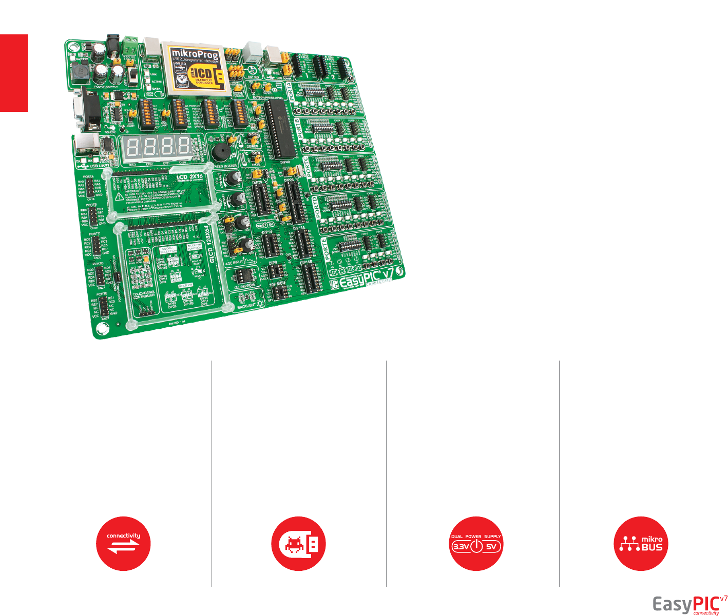
EasyPIC™ v7 is all about
connectivity. Having four
dierent connectors for
each port, you can connect
accessory boards, sensors and
your custom electronics easier
then ever before.
Powerful on-board mikroProg™
programmer and In-Circuit
debugger can program
and debug over 350
microcontrollers. You will
need it, whether you are a
professional or a beginner.
Four connectors for each port Everything is already here
Amazing connectivity mikroProg™ on board
EasyPIC™ v7 is among few
development boards which
support both 3.3V and 5V
microcontrollers. This feature
greatly increases the number of
supported MCUs. It’s like having
two boards instead of one!
3.3V and 5V power supply
Dual Power Supply
Just plug in your Click™ board,
and it’s ready to work. We
picked up a set of the most
useful pins you need for
development and made a
pinout standard you will
enjoy using.
For easier connections
mikroBUS™ support
It's good to know
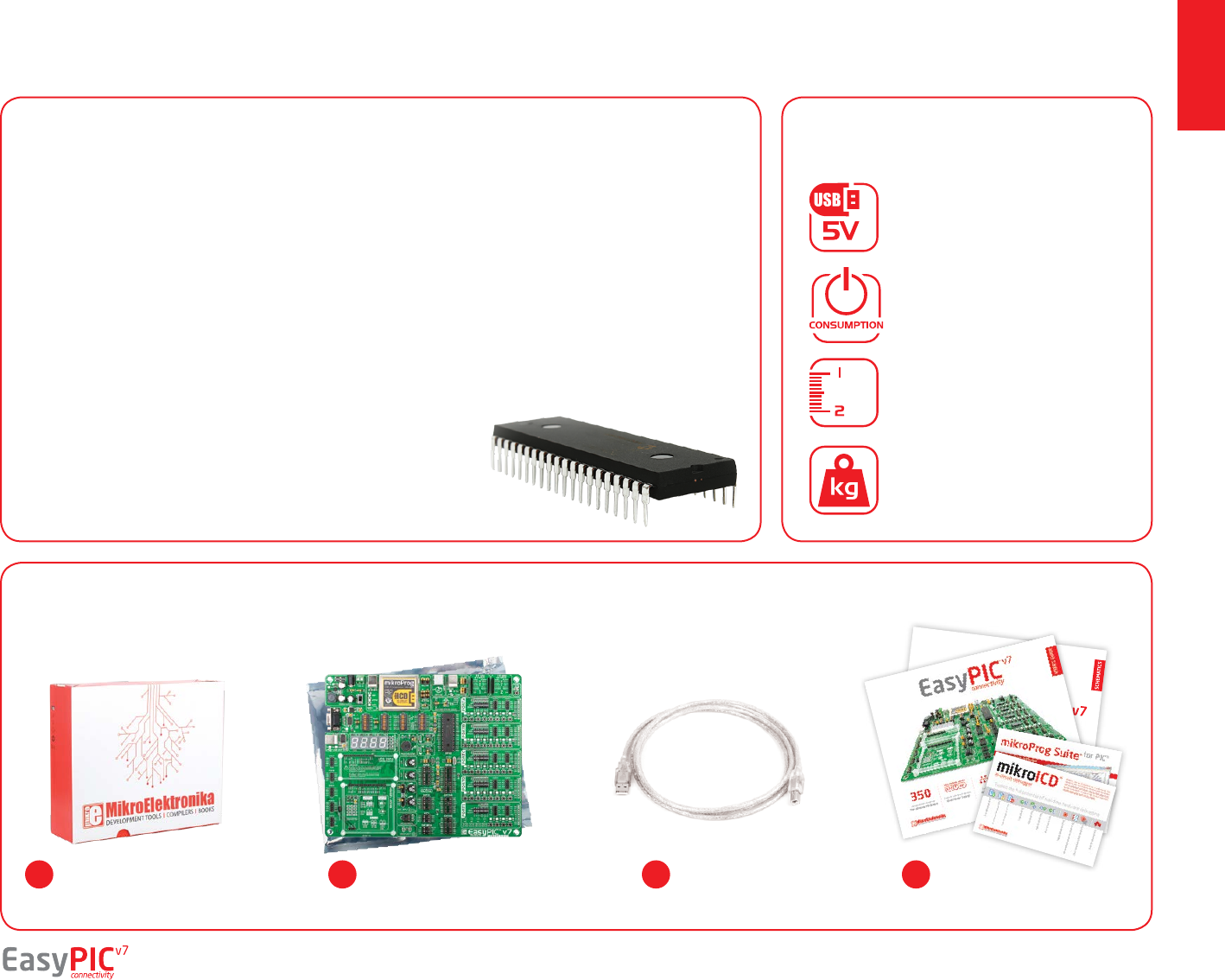
Package contains
introduction
page 5
System Specication
PIC18F45K22 is the new default microcontroller!
power supply
7–23V AC or 9–32V DC
or via USB cable (5V DC)
board dimensions
266 x 220mm (10.47 x 8.66 inch)
weight
~445g (0.981 lbs)
power consumption
~85mA when all peripheral
modules are disconnected
Damage resistant
protective box
EasyPIC™ v7 board in
antistatic bag
USB cable User Manuals and
Board schematic
1 2 3 4
Until now, EasyPIC™ development boards were equipped
with PIC16® as the default chip. Now we are giving you more
power than ever before. PIC18F45K22 is the new default
chip of EasyPIC™ v7! It has 16 MIPS operation, 32K bytes of
linear program memory, 1536 bytes of linear data memory,
and support for a wide range of power supply from 1.8V to
5V. It’s loaded with great modules: 36 General purpose I/O
pins, 30 Analog Input pins (AD), Digital-To-Analog Converter
(DAC), support for Capacitive Touch Sensing using Charge
Time Measurement Unit (CTMU), three 8-bit timers and four
16-bit timers. It also has pair of CCP, Comparators and
MSSP modules (which can be either SPI or I2C).
- More power than ever before
- Great choice for both beginners
and professionals
- Rich with modules
- Enough RAM and Flash
- Comes with examples for
mikroC, mikroBasic and
mikroPascal compilers
We present you with a complete color schematics for EasyPIC ™ v7 development board. We wanted
to make electronics more understandable, even for absolute beginners, so we provided photos of
most used SMD components, and made additional comments and drawings so you can get to know
what your board is consisted of, and how it actually works.
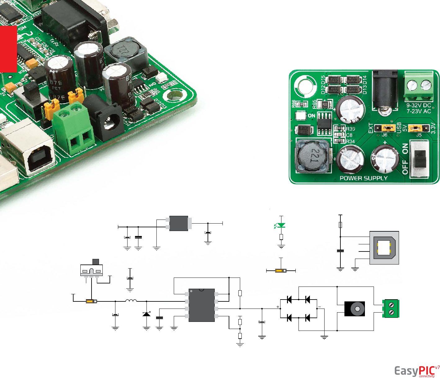
Dual power supply
Board contains switching power supply
that creates stable voltage and
current levels necessary for
powering each part of the
board. Power supply section
contains two power regulators:
MC34063A, which generates
VCC-5V, and MC33269DT3.3 which
creates VCC-3.3V power supply. The board
can be powered in three dierent ways: with USB
power supply (CN2), using external adapters via adapter
connector (CN31) or additional screw terminals (CN30). External
adapter voltage levels must be in range of 9-32V DC or 7-23V AC. Use
jumper J6 to specify which power source you are using and jumper J5 to specify
whether you are using 5V or 3.3V power supply. Upon providing the power using
either external adapter or USB power source you can turn on power supply by using SWITCH 1
(Figure 3-1). Power LED (Green ON) will indicate the presence of power supply.
Figure 3-2: Dual power supply unit schematic
Figure 3-1: Dual power supply unit of EasyPIC™ v7
1
2
3
4
8
7
6
5
SWC
SWE
CT
GND
DRVC
IPK
VIN
CMPR
U3
MC34063A
R65
0.22
R34
3K
VCC-SW
C8
220pF
D1
MBRS140T3
L2 220uH
E1
220uF/35V LESR
VCC-EXT
R35
1K
VCC-5V
J6
2
1
3
SWITCH1
VCC-USB
VCC-SW
D12
1N4007
D13
1N4007
D15
1N4007
D14
1N4007
J5
VCC-5V
VCC-BRD
VCC-3.3
C14
100nF
VCC-5V
2
1
3
GND
Vout
Vin
REG1
MC33269DT3.3E7
10uF
VCC-3.3
CN31 CN30
VCC-5V
R66
2K2
LD37
E2
220uF/35V LESR
E4
10uF
VCC-USB
L4
FERRITE
C19
100nF
1
2
3
4
VCC
GND
CN2
USB
3.3V VOLTAGE REGULATOR
5V SWITCHING POWER SUPPLY
E6
220uF/35V LESR
VCC-5V
power supply
page 6
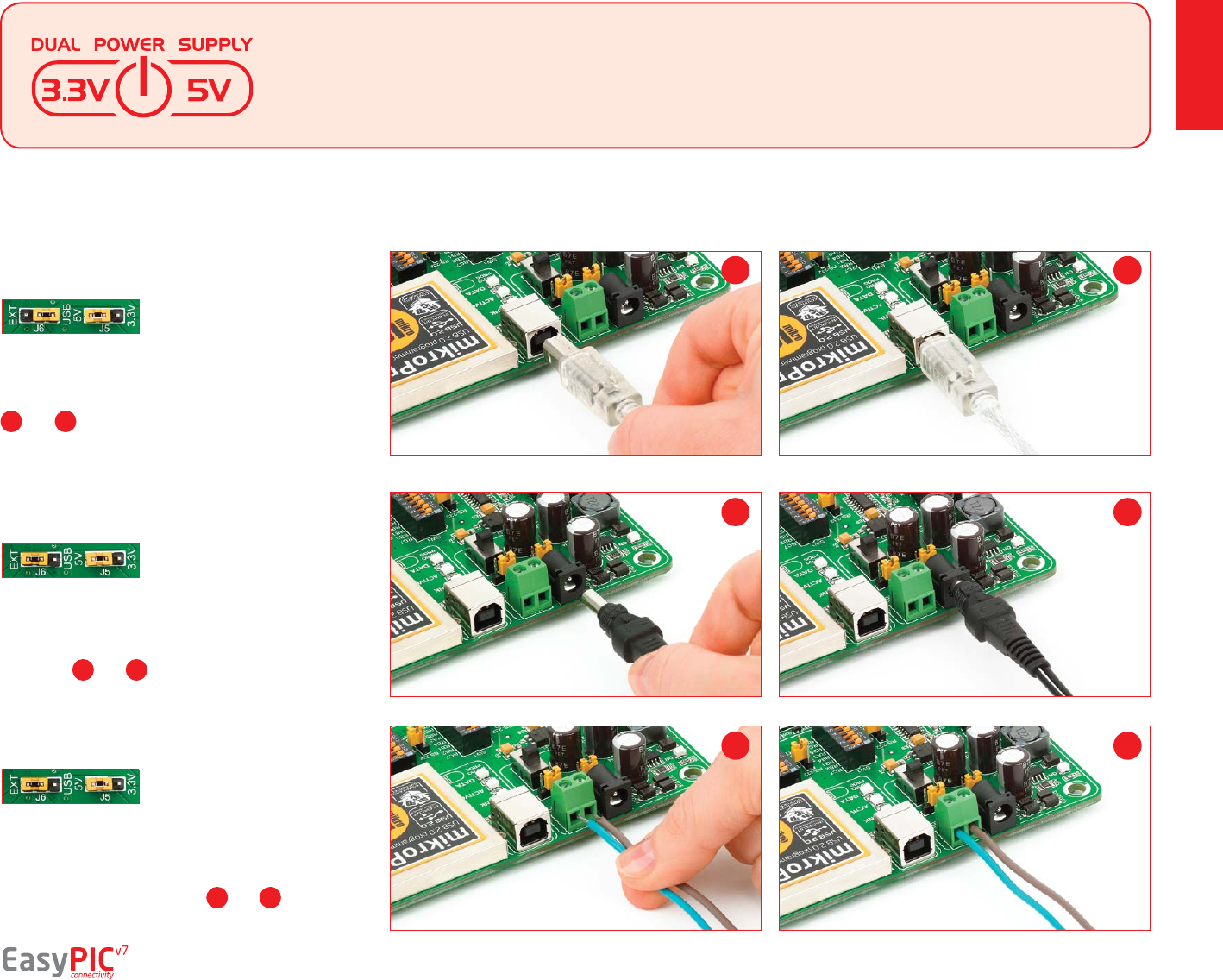
How to power the board?
power supply
To power the board with USB cable, place jumper J6 in
USB position and place jumper J5 in 5V or 3.3V position.
You can then plug in the USB cable as shown on images
1 and 2, and turn the power switch ON.
To power the board via adapter connector, place jumper
J6 in EXT position, and place jumper J5 in 5V or 3.3V
position. You can then plug in the adapter cable as shown
on images 3 and 4, and turn the power switch ON.
To power the board using screw terminals, place jumper
J6 in EXT position, and place jumper J5 in 5V or 3.3V
position. You can then screw-on the cables in the screw
terminals as shown on images 5 and 6, and turn the
power switch ON.
EasyPIC™ v7 development board supports both
3.3V and 5V power supply on a single board.
This feature enables you to use wide range of
peripheral boards.
Set J6 jumper to
USB position
Set J6 jumper to
EXT position
1. With USB cable
3. With laboratory power supply
Set J6 jumper to
EXT position
2. Using adapter
1
3
5
2
4
6
page 7
Power supply: via DC connector or screw terminals
(7V to 23V AC or 9V to 32V DC),
or via USB cable (5V DC)
Power capacity: up to 500mA with USB, and up to 600mA
with external power supply
supported MCUs
Supported
microcontrollers
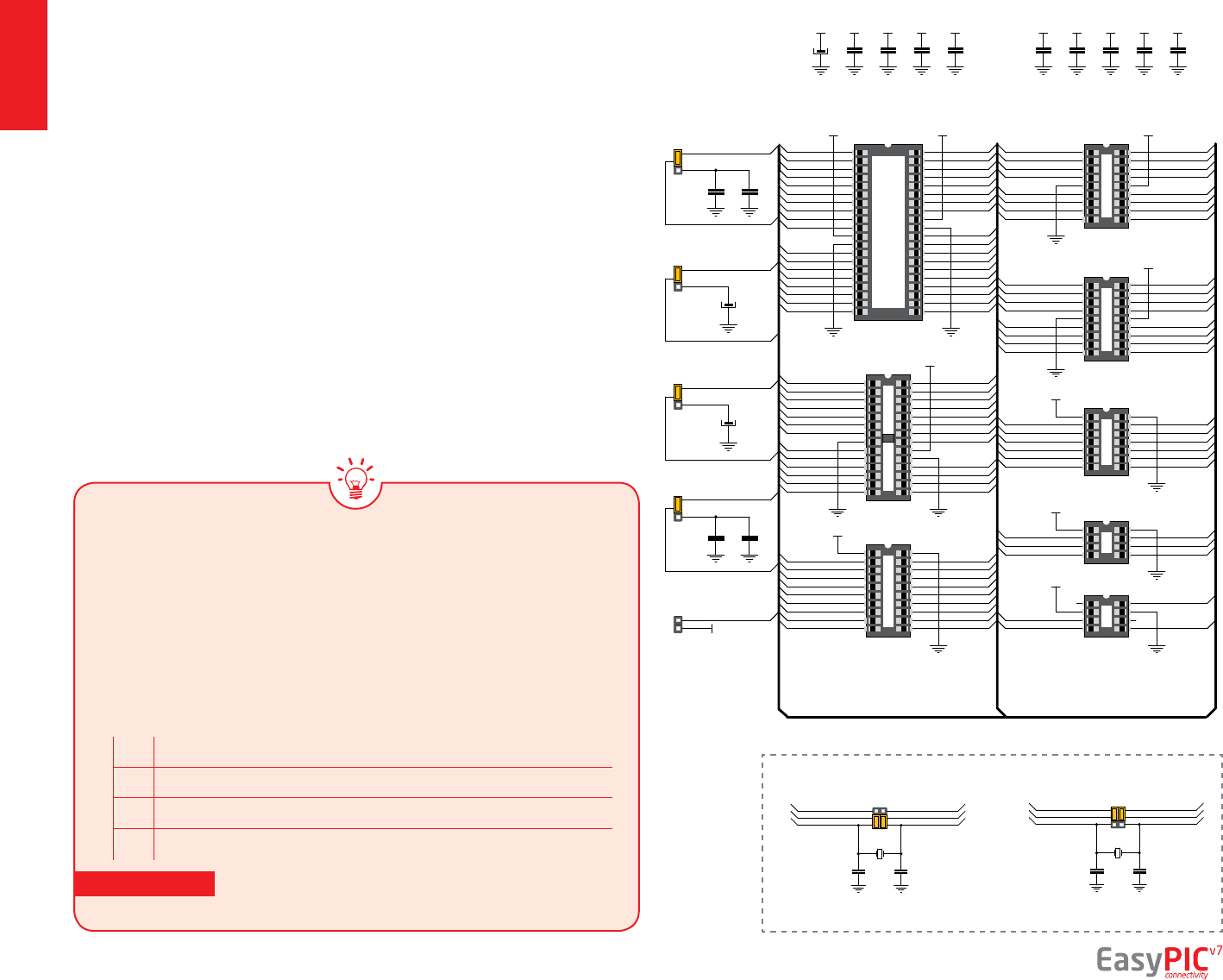
The board contains eight DIP sockets: DIP40, DIP28, DIP20, DIP18A, DIP18B, DIP14,
DIP8 and support for PIC10F MCUs. With dual power supply and smart on-board
mikroProg, board is capable of programming over 350 microcontrollers from PIC10F,
PIC12F, PIC16F, PIC16Enh, PIC18F, PIC18FJ and PIC18FK families.
There are two DIP18 sockets for PIC microcontrollers provided on the board - DIP18A
and DIP18B. Which of these sockets you will use depends solely on the pinout of
the microcontroller in use. The EasyPIC™ v7 development system comes with the
PIC18F45K22 microcontroller in a DIP40 package.
DIP40 DIP18A
DIP28
C33
100nF
VCC-MCU
C9
100nF
VCC-MCU
C12
100nF
VCC-MCU
C13
100nF
VCC-MCU
C10
100nF
VCC-MCU
E14
10uF
VCC-MCU
VCC-MCU VCC-MCU
VCC-MCU
1
2
3
4
5
6
7
8
9
10
11
12
13
14
15
16
17
18
19
20 21
22
23
24
25
26
27
28
29
30
31
32
33
34
35
36
37
38
39
40
DIP SKT 40
1
2
3
4
5
6
7
8
9 10
11
12
13
14
15
16
17
18
DIP SKT 18
1
2
3
4
5
6
7
8
9
10
11
12
13
14 15
16
17
18
19
20
21
22
23
24
25
26
27
28
DIP SKT 28
J20
M1X2
C36
100nF
C35
100nF
C38
100nF
C37
100nF
E11
10uF
E13
10uF
RA5
RA4
RA4
RA5
RA5-DIP28
RA5-DIP40
RA4-DIP40
RA4-DIP28
RA5-DIP28
VCC-MCU
for PIC16F724/727
for PIC18F44J10, PIC18F45J10
for PIC18F24J10, PIC18F25J10
PIC18F2XJ50, PIC18F2XJ11
for PIC16F722/723/726
for PIC18F2331/24311
2
3
4 5
6
7
8
DIP SKT 8
1
2
3
4 5
6
7
8
DIP SKT 8
1
2
3
4
5
6
7 8
9
10
11
12
13
14
DIP SKT 14
1
2
3
4
5
6
7
8
9 10
11
12
13
14
15
16
17
18
DIP SKT 18
1
2
3
4
5
6
7
8
9
10 11
12
13
14
15
16
17
18
19
20
DIP SKT 20
DIP20
RA0
RA1
RA2
RA3
RE0
RE1
RE2
RC0
RC1
RC2
RC3-MCU
RD0
RD1
RB7-MCU
RB6-MCU
RB5
RB4
RB3
RB2
RB1
RB0
RD7
RD6
RD5
RD4
RC7
RC6
RC5-MCU
RC4-MCU
RD3
RD2
MCLR-RE3
RA7-MCU
RA6-MCU
RA5-DIP40
RA4-DIP40
RB7-MCU
RB6-MCU
RB2
RB1
RB0
RC7
RC6
RC5-MCU
RC4-MCU
RA0
RA1
RA2
RA3
RC0
RC1
RC2
RC3-MCU
RB5
RB4
RB3
MCLR-RE3
RA7-MCU
RA6-MCU
RA5-DIP28
RA4-DIP28
RA5-MCU
RA4-MCU RA1-MCU
RA0-MCU
RA2-MCU
RC0
RC1
RC2RC3
RC4
RC5
MCLR-RA3
RB4
RB5
RB6RB7
RC7
RC6
VCC-MCU
VCC-MCU
RA0
RA1
RB7-MCU
RB6-MCU
RA3
RA4
RA2
RB2
RB1
RB0
RB5
RB4RB3
MCLR-RA5
RA7-MCU
RA6-MCU
VCC-MCU
DIP18B
RB2
RB3
RB7-MCU
RB6-MCU
RA1
RA4
RA0
RB0
RA3
RA2
RB5
RB4RB1
MCLR-RA5
RA7-MCU
RA6-MCU
RA5-MCU
RA4-MCU RA1-MCU
RA0-MCU
RA2
RC0
RC1
RC2RC3
RC4
RC5
MCLR-RA3
VCC-MCU
RA0-MCU
RA1-MCU
RA5-MCU
RA4-MCU
RA2MCLR-RA3
VCC-MCU
VCC-MCU
RA1-MCU
RA2
RA0-MCU
MCLR-RA3
DIP14
DIP8
10F MCU
C11
100nF
VCC-MCU
C42
100nF
VCC-MCU
C40
100nF
VCC-MCU
C39
100nF
VCC-MCU
J22
J7
J10
J23
X1
8MHz SYS
C6
22pF
C7
22pF
RA7-MCU RA6-MCU
RA7 RA6
J13
RA7-OSC1 RA6-OSC2
X2
8MHz SEC
C22
22pF
C21
22pF
J14
RA4-MCURA5-MCU
RA4RA5
RA4-OSC1RA5-OSC2
X1
8MHz SYS
C6
22pF
C7
22pF
RA7-MCU RA6-MCU
RA7 RA6
J13
RA7-OSC1 RA6-OSC2
X2
8MHz SEC
C22
22pF
C21
22pF
J14
RA4-MCURA5-MCU
RA4RA5
RA4-OSC1RA5-OSC2
VCAP jumpers explained
Some PIC16F, PIC18FK and all PIC18FJ microcontrollers have cores that work
on 1.8V-2.5V voltage range, and peripherals that work with 3.3V and 5V
voltages. Internally, those microcontrollers have power regulators, which adjust
the core voltage levels. In order for those devices to have a stable operation of
the core, manufacturer recommends that decoupling capacitive lters should
be provided, and connected between specic microcontroller pins designated
with VCAP and GND. EasyPIC v7 board provides jumpers which are used for this
purpose. Here is list of devices that require jumpers placed in VCAP position:
VCAP position when using PIC16F724/16F727
VCAP position for PIC18F44J10 and PIC18F45J10
VCAP for PIC18F24J10, PIC18F25J10 PIC18F2XJ50, PIC18F2XJ11
VCAP for PIC16F722, PIC16F723, PIC16F726
IMPORTANT: If you do not place VCAP jumper for the MCUs that need it,
you might experience some instabilities in program execution.
IMPORTANT: When using PIC18F2331 or PIC18F2431 microcontrollers it is necessary
to place J20 jumper, in order to route VCC power line to RA5 pin (Figure 4-1)
page 8
J7
J22
(see gure 4-1)
J10
J23
Figure 4-2:
crystal
oscillators
Figure 4-1: Schematic of on-board DIP sockets and VCAP jumpers
supported MCUs
Using crystal oscillators
If you want to use microcontrollers in DIP8, DIP14 and DIP20 packages, it is
necessary to put quartz crystal into socket X2 (OSC2). The value of the quartz-
crystal depends on the maximum clock frequency allowed and your application.
You can always exchange the default 8MHz crystal with another one.
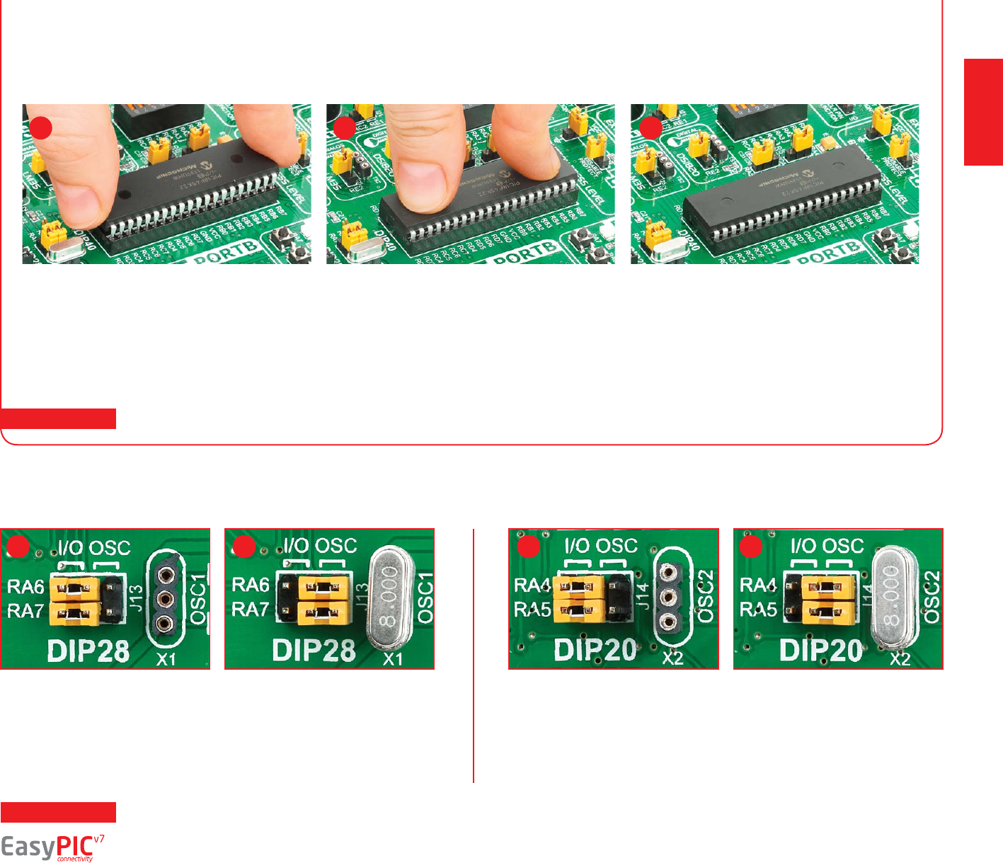
Only one microcontroller may be plugged into the development board at the same time.
Before you plug the microcontroller into the
appropriate socket, make sure that the power
supply is turned o. Images above show how to
correctly plug a microcontroller. First make sure that
a half circular cut in the microcontroller DIP packaging
matches the cut in the DIP socket. Place both ends of
the microcontroller into the socket as shown in Figure
4-3. Then put the microcontroller slowly down until
all the pins match the socket as shown in Figure 4-4.
Check again if everything is placed correctly and press
the microcontroller until it is completely plugged into
the socket as shown in Figure 4-5.
Figure 4-6: RA6 and RA7 as I/O pins
(when using internal oscillator)
Figure 4-3: Place both ends of microcontroller on
the socket so the pins are aligned correctly
Figure 4-4: with both ngers, evenly distribute
the force and press the chip into the socket.
Figure 4-5: Properly placed microcontroller will
have equally leveled pins.
Figure 4-7: RA6 and RA7 connected
to X1 quartz-crystal
Figure 4-8: RA4 and RA5 as I/O pins
(when using internal oscillator)
Figure 4-9: RA4 and RA5 connected
to X2 quartz-crystal
How to properly place your microcontroller into the DIP socket?
1
1
2
2
3
3
4
IMPORTANT:
IMPORTANT: Microcontrollers which are plugged into socket 10F use their own internal oscillator and are not connected to any of the mentioned quartz-crystal sockets.
PIC microcontrollers normally use a quartz crystal for the purpose of providing
clock frequency. The EasyPIC™ v7 provides two sockets for quartz-crystal.
Microcontrollers in DIP18A, DIP18B, DIP28 and DIP40 packages use socket
X1 (OSC1) for quartz-crystal.
page 9
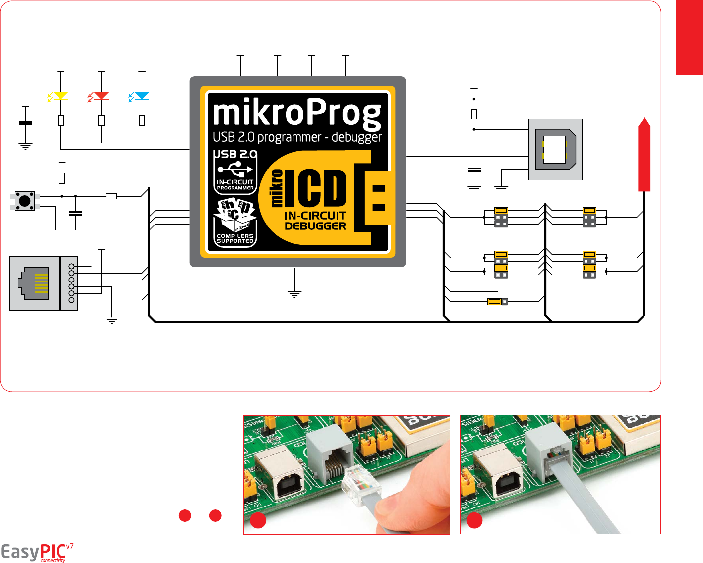
On-board programmer
What is mikroProg™?
How do I start?
programming
mikroProg™ is a fast USB 2.0 programmer with mikroICD™ hardware
In-Circuit Debugger. Smart engineering allows mikroProg™ to support
all PIC10, PIC12, PIC16, PIC18, devices in a single programmer! It
supports over 350 microcontrollers from Microchip®. Outstanding
performance and easy operation are among it's top features.
In order to start using mikroProg™ and program your microcontroller,
you just have to follow two simple steps:
1. Install the necessary software
- Install USB drivers
- Install mikroProg Suite™ for PIC® software
2. Power up the board, and you are ready to go.
- Plug in the programmer USB cable
- LINK LED should light up. MCLR pin
selection
Programing
lines selection
MCLR pin
function
Before using the programmer,
make sure to set MCLR pin jumpers
J1 and J2, so that MCLR line is
routed to the correct socket for
your microcontroller. If you are
using the default PIC18F45K22,
jumpers are supposed to be set for
DIP40, as shown below.
Jumpers J8 and J9 are
used to select PGC and
PGD programming lines
for your microcontroller.
Make sure to place
jumpers in the proper
position for your socket.
Using jumper J19 you can
specify whether MCLR
pin of your microcontroller
is connected to the on-
board reset circuit, or
acts just as I/O pin.
DIP40,
DIP28,
DIP18A,
DIP18B
MCLR
as
MCLR
DIP20,
DIP14,
DIP8
MCLR
as I/O
DIP40,
DIP28
DIP18A,
DIP18B
DIP20
DIP14
DIP8
Why so many LEDs?
Three LEDs indicate specic programmer
operation. Link LED lights up when USB
link is established with your PC, Active
LED lights up when programmer is active.
Data is on when data is being transferred
between the programmer and PC software
(compiler or mikroProg Suite™ for PIC®).
page 10
NOTE: If you use other than the default PIC18F45K22 MCU,
make sure that programmer jumpers are placed in proper
positions for your microcontroller socket.
programming
C18
100nF
VCC-BRD
T65
VCC-BRD
R7
10K
R6
1K
C41
100nF
VCC-5VVCC-3.3
LED-DATA
LED-USB
VCC-3.3
LED-ACT
LINK ACTIVE DATA
R67
2K2
R68
4K7
R69
6K8
LD38 LD39 LD40
VCC-USB
L4
FERRITE
C19
100nF
1
2
3
4
VCC
GND
D-
D+
CN2
USB
VCC-BRD
MCU-PGC
MCU-PGD
MCU-VPP
3
4
5
6
1
2
CN28
ICD
MCU-VPP
MCU-PGC
MCU-PGD
BRD-PGC
BRD-PGD
BRD-VPP
VCC-3.3V VCC-5VVCC-BRDVCC-MCU
#RST
USBPROG_P
USBPROG_N
J2 J1
J8 J9
I/O
RE3
RA5
RA3
MCLR-RE3
MCLR-RA5
MCLR-RA3
MCU-VPP
RB6-MCU
RA1-MUX
RB6
RA1
MCU-PGC
BRD-PGC
MCU-PGD
BRD-PGD
RB7-MCU
RA0-MUX
RB7
RA0
J19
BRD-VPP
I/ORST#
DATA BUS
Figure 5-1: mikroProg™ block schematic
EasyPIC™ v7 is equipped with RJ-12 connector compatible with
Microchip® ICD2® and ICD3® external programmers. You can
either use the on-board mikroProg™ programmer or external
programming tools as long as you use only one of them in the
same time. But you still have to set the appropriate jumpers,
as described in the previous page. Insert your ICD programmer
cable into connector CN28, as shown in images 1 and 2.1 2
Programming with ICD2/ICD3
page 11
programming
Step 1 - Start Installation
Step 3 - Installing drivers Step 4 - Finish installation
Step 2 - Accept EULA
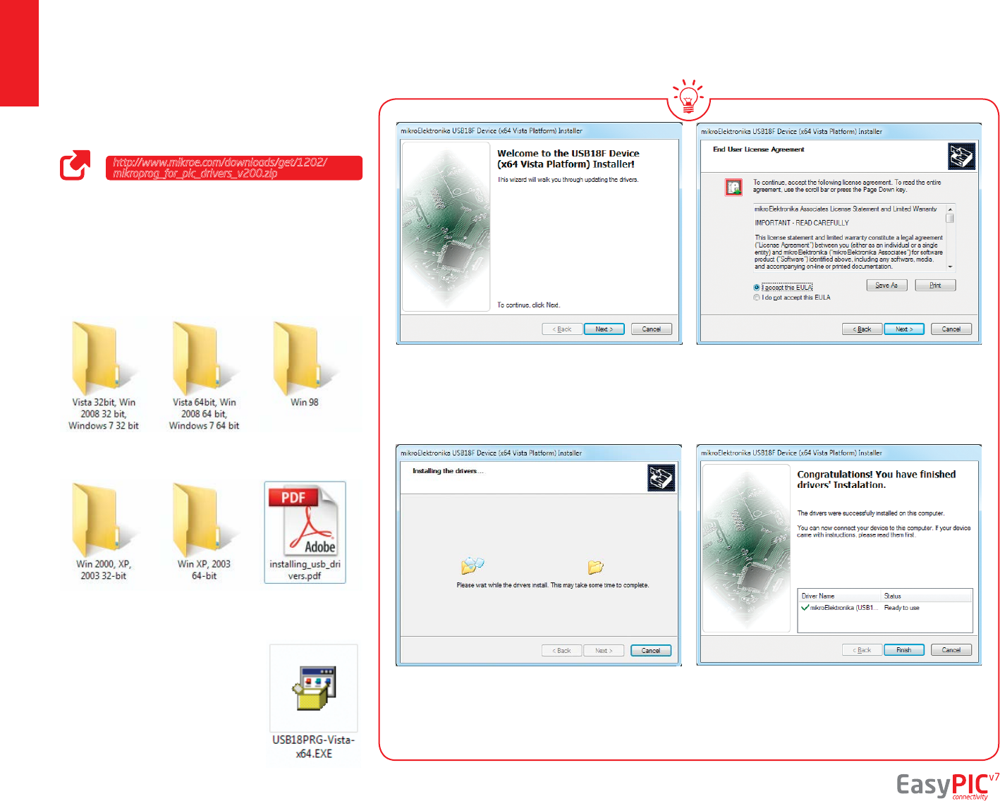
Installing programmer drivers
In the opened folder you should
be able to locate the driver
setup le. Double click on setup
le to begin installation of the
programmer drivers.
Welcome screen of the installation. Just click on Next
button to proceed.
Drivers are installed automatically in a matter of
seconds.
You will be informed if the drivers are installed correctly.
Click on Finish button to end installation process.
Carefully read End User License Agreement. If you
agree with it, click Next to proceed.
page 12
On-board mikroProg™ requires drivers in order to work.
Drivers can be found on the link below:
When you locate the drivers, please extract les from
the ZIP archive. Folder with extracted les contains sub
folders with drivers for dierent operating systems.
Depending on which operating system you use, choose
adequate folder and open it.
http://www.mikroe.com/downloads/get/1202/
mikroprog_for_pic_drivers_v200.zip
programming
Step 1 - Start Installation
Step 3 - Install for All users or
current user
Step 5 - Installation in progress
Step 2 - Accept EULA and continue
Step 4 - Choose destination folder
Step 6 - Finish Installation
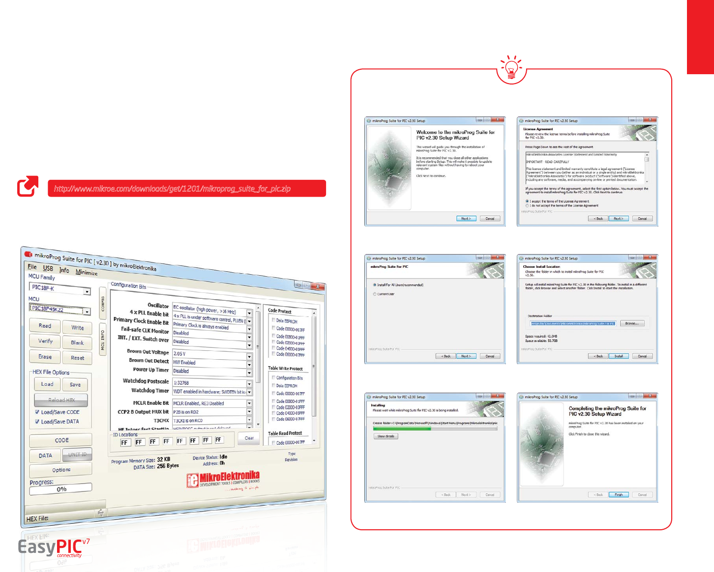
Programming software
Installation wizard - 6 simple steps
page 13
mikroProg Suite™ for PIC®
On-board mikroProg™ programmer requires special programming software called
mikroProg Suite™ for PIC®. This software is used for programming all of Microchip®
microcontroller families, including PIC10, PIC12, PIC16, PIC18, dsPIC30/33, PIC24 and
PIC32. Software has intuitive interface and SingleClick™ programming technology.
To begin, rst locate the installation archive on our website:
After downloading, extract the package and double click the executable setup
le, to start installation.
http://www.mikroe.com/downloads/get/1201/mikroprog_suite_for_pic.zip
programming
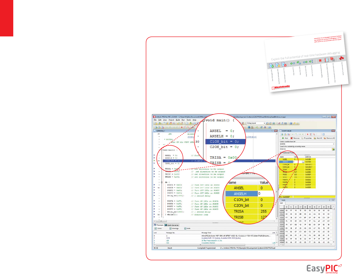
mikroICD™ - In Circuit Debugger
page 14
What is Debugging?
Every developer comes to a point where he has to monitor the
code execution in order to nd errors in the code, or simply
to see if everything is going as planed. This hunt for bugs, or
errors in the code is called debugging. There are two ways
to do this: one is the software simulation, which enables
you to simulate what is supposed to be happening on the
microcontroller as your code lines are executed, and the other,
most reliable one, is monitoring the code execution on the
MCU itself. And this latter one is called In-Circuit debugging.
"In-Circuit" means that it is the real deal - code executes right
on the target device.
What is mikroICD™?
The on-board mikroProg™ programmer supports mikroICD™ - a
highly eective tool for a Real-Time debugging on hardware
level. The mikroICD™ debugger enables you to execute your
program on the host PIC microcontroller and view variable
values, Special Function Registers (SFR), RAM, CODE and
EEPROM memory along with the mikroICD™ code execution
on hardware. Whether you are a beginner, or a professional,
this powerful tool, with intuitive interface and convenient
set of commands will enable you to track down bugs quickly.
mikroICD™ is one of the fastest, and most reliable debugging
tools on the market.
Supported Compilers
All MikroElektronika compilers, mikroC™, mikroBasic™ and
mikroPascal™ for PIC®, dsPIC® and PIC32® natively support
mikroICD™. Specialized mikroICD™ DLL module allows compilers
to exploit the full potential of fast hardware debugging.
Along with compilers, make sure to install the appropriate
programmer drivers and mikroProg Suite™ for PIC®
programming software, as described on pages 12 and 13.
When you build your project for debugging, and program
the microcontroller with this HEX le, you can start the
debugger using [F9] command. Compiler will change layout
to debugging view, and a blue line will mark where code
execution is currently paused. Use debugging toolbar in
the Watch Window to guide the program execution and
stop anytime. Add the desired variables to Watch Window and
monitor their values. Complete guide to using mikroICD™ with
your compiler is provided within the EasyPIC™ v7 package.
How do I use the debugger?
Figure 5-2: mikroICD™ manual
explains debugging thoroughly
mikroICD
™
in-circuit debugger
Figure 5-3: mikroC PRO for PIC® compiler in debugging view, with SFR registers in Watch Window
programming
page 15
Here is a short overview of which debugging commands are supported in MikroElektronika compilers. You can see what each command does,
and what are their shortcuts when you are in debugging mode. It will give you some general picture of what your debugger can do.
Toolbar
Icon Command Name Shortcut Description
Start Debugger [F9] Starts Debugger.
Run/Pause Debugger [F6] Run/Pause Debugger.
Stop Debugger [Ctrl + F2] Stops Debugger.
Step Into [F7]
Executes the current program line, then halts. If the executed
program line calls another routine, the debugger steps into the
routine and halts after executing the rst instruction within it.
Step Over [F8]
Executes the current program line, then halts. If the executed program
line calls another routine, the debugger will not step into it. The whole
routine will be executed and the debugger halts at the rst instruction
following the call.
Step Out [Ctrl + F8] Executes all remaining program lines within the subroutine. The
debugger halts immediately upon exiting the subroutine.
Run To Cursor [F4] Executes the program until reaching the cursor position.
Toggle Breakpoint [F5] Toggle breakpoints option sets new breakpoints or removes those
already set at the current cursor position.
Show/Hide breakpoints [Shift+F4] Shows/Hides window with all breakpoints
Clears breakpoints [Shift+Ctrl+F5] Delete selected breakpoints
Jump to interrupt [F2] Opens window with available interrupts (doesn't work in mikroICD™
mode)
mikroICD™ commands
UART via RS-232
communication
The UART (universal asynchronous
receiver/transmitter) is one of the most
common ways of exchanging data between
the MCU and peripheral components. It is
a serial protocol with separate transmit and
receive lines, and can be used for full-duplex
communication. Both sides must be initialized with
the same baud rate, otherwise the data will not be
received correctly.
RS-232 serial communication is performed through a
9-pin SUB-D connector and the microcontroller UART
module. In order to enable this communication, it
is necessary to establish a connection between
RX and TX lines on SUB-D connector and the
same pins on the target microcontroller using
DIP switches. Since RS-232 communication
voltage levels are dierent than
microcontroller logic levels, it is
necessary to use a RS-232
Transceiver circuit, such as
MAX3232 as shown
on Figure 6-1.
1
2
3
4
5
6
7
8 9
10
11
12
13
14
15
16
C1+
V+
C1-
C2+
C2-
V-
T2OUT
R2IN
T1IN
T2IN
VCC
GND
T1OUT
R1IN
R1OUT
R2OUT
U4
MAX3232
5
9
4
8
3
7
2
6
1
1
5
96
CN37
RS232
C28
100nF
C30
100nF
C29
100nF
C31
100nF
E8
10uF
VCC-MCU
RX-232
TX-232
12345678
O
N
SW1
R32
100K
RS232
CONNECTOR
RX-FTDI
RX-232
RX
12345678
O
N
SW2
TX-FTDI
TX-232
TX
RB1
RB4
RB2
RC7
RA3
RB5
RC5
RD7
RB2
RB1
RB5
RC6
RA2
RB7
RC4
RD6
VCC-MCU
VCC-MCU
J3
J4
DATA BUS
Figure 6-1: RS-232 connection schematic
Enabling RS-232
In order to enable RS-232
communication, you must set J3
and J4 jumpers in the RS-232
position, and enable desired RX
and TX lines via SW1 and SW2
DIP switches. For example, if you
want to enable RS-232 connection
on UART1 module of the default
PIC18F45K22 chip, you should
enable SW1.1 (RC7) and SW2.1
(RC6) lines.
page 16
UART via USB
Modern PC computers, laptops and notebooks are
no longer equpped with RS-232 connectors and
UART controllers. They are nowdays replaced with USB
connectors and USB controllers. Still, certain technology
enables UART communication to be done over USB connection.
Controllers such as FT232RL from FTDI® convert UART signals
to the appropriate USB standard. In order to use USB-UART module
on EasyPIC™ v7, you must rst install FTDI drivers on your computer.
Drivers can be found on link bellow:
USB-UART communication is being done through a FT232RL
controller, USB connector (CN32), and microcontroller UART
module. To establish this connection, you must put J3 and
J4 jumpers in the USB-UART position, and connect
RX and TX lines to the appropriate pins of the
microcontroller. This connection is done
using DIP switches SW1 and SW2.
1
2
3
4
5
6
7
8
9
10
11
12
13
14 15
16
17
18
19
20
21
22
23
24
25
26
27
28
TXD
DTR#
RTS#
VCCIO
RXD
RI#
GND
NC
DSR#
DCD#
CTS#
CBUS4
CBUS2
CBUS3
CBUS0
CBUS1
OSCO
OSCI
TEST
AGND
NC
GND
GND
VCC
RESET#
3V3OUT
USBDM
USBDP
FT232RL
U2
FT232RL
VCC-5V
C32
100nF
RX-LED
TX-LED
R9
4K7
R8
2K2
R78
4K7
R79
10K
1
2
3
4
VCC
GND
D-
D+
CN32
USB B
C34
100nF
C50
100nF
E12
10uF
VCC-5VVCC-5V
TX-FTDI
RX-FTDI
USB UA RT
CONNECTOR
TXRX
VCC-MCU VCC-MCU VCC-MCU
VCC-MCU
12345678
O
N
SW1
RX-FTDI
RX-232
RX
12345678
O
N
SW2
TX-FTDI
TX-232
TX
RB1
RB4
RB2
RC7
RA3
RB5
RC5
RD7
RB2
RB1
RB5
RC6
RA2
RB7
RC4
RD6
J3
J4
DATA BUS
Figure 7-1: USB-UART connection schematic
Enabling USB-UART
In order to enable USB-UART
communication, you must set J3
and J4 jumpers in the USB-UART
position, and enable desired RX
and TX lines via SW1 and SW2 DIP
switches. For example, if you want
to enable USB-UART connection
on UART1 module of the default
PIC18F45K22 chip, you should
enable SW1.1 (RC7) and SW2.1
(RC6) lines.
page 17
communication
http://www.ftdichip.com/Drivers/VCP.htm
USB is the acronym for Universal Serial
Bus. This is a very popular industry
standard that denes cables, connectors
and protocols used for communication
and power supply between computers
and other devices. EasyPIC™ v7 contains
USB connector (CN4) which enables
microcontrollers that support USB
communication to establish a connection
with the target host (eg. PC, Laptop, etc).
Selection of communication lines is done
using jumpers J12 or J18, depending on
the target microcontroller.
When communication lines are
routed from the microcontroller to the
USB connector using mentioned jumpers,
they are cut o from the rest of the
board, and cannot be accessed via PORT
headers.
Dedicated USB ON LED
signalizes the presence of USB connection,
when the USB cable is inserted into the
USB connector.
communication
Figure 8-1:
USB function disabled
Figure 8-2:
USB enabled on PORTC
Figure 8-3:
USB enabled on PORTA
1
2
3
4
VCC
GND
D-
D+
CN4
USB B
USB
CONNECTOR
L44
USB ON
R11
4K7
VCC-3.3
RC3-MCU
RC4-MCU
RC5-MCU
RC3
RC4
RC5
RA2
RA2-MCU
RA1-MUX
RA1-MCU
RA0-MUX
RA0-MCU
PIC18F4550
PIC18F2XJ50
PIC18F1XK50
PIC18LF1XK50
J12
J18
DATA BUS
Depending on your target microcontroller, USB communication can be enabled on
PORTA or PORTC. For PIC18(L)F1XK50 you should put J18 jumpers in the USB
position (Figure 8-3). For PIC18Fxx(J)50, PIC18Fxx(J)53, PIC18Fxx(J)55
and PIC18Fxx58 place J12 jumpers in the USB position (Figure 8-2).
Enabling USB connection
page 18
Figure 8-4: USB connection schematic
(jumpers are in USB disabled position)
USB connection
connectivity
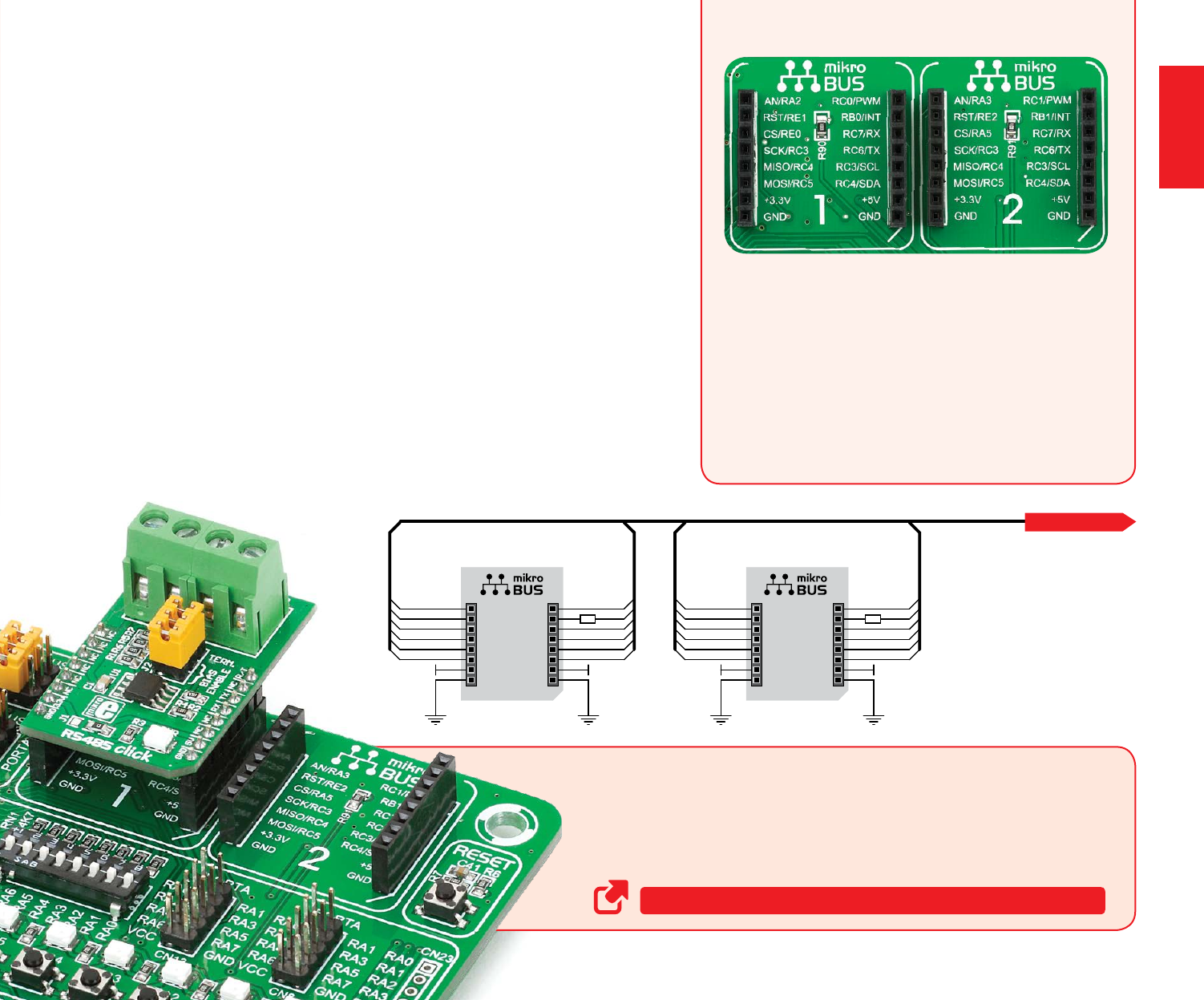
mikroBUS™ sockets
mikroBUS™ pinout explained
Easier connectivity and simple conguration are
imperative in modern electronic devices. Success
of the USB standard comes from it’s simplicity of
usage and high and reliable data transfer rates.
As we in MikroElektronika see it, Plug-and-Play
devices with minimum settings are the future in
embedded world too. This is why our engineers
have come up with a simple, but brilliant pinout
with lines that most of today’s accessory boards
require, which almost completely eliminates the
need of additional hardware settings. We called
this new standard the mikroBUS™. EasyPIC™ v7
is the rst development board in the world to
support mikroBUS™ with two on-board sockets.
As you can see, there are no additional DIP
switches, or jumper selections. Everything is
already routed to the most appropriate pins of
the microcontroller sockets.
mikroBUS™ host connector
Each mikroBUS™ host connector consists of
two 1x8 female headers containing pins
that are most likely to be used in the target
accessory board. There are three groups
of communication pins: SPI, UART and I2C
communication. There are also single pins
for PWM, Interrupt, Analog input, Reset
and Chip Select. Pinout contains two power
groups: +5V and GND on one header and
+3.3V and GND on the other 1x8 header.
AN - Analog pin
RST - Reset pin
CS - SPI Chip Select line
SCK - SPI Clock line
MISO - SPI Slave Output line
MOSI - SPI Slave Input line
+3.3V - VCC-3.3V power line
GND - Reference Ground
PWM - PWM output line
INT - Hardware Interrupt line
RX - UART Receive line
TX - UART Transmit line
SCL - I2C Clock line
SDA - I2C Data line
+5V - VCC-5V power line
GND - Reference Ground
R90 1K
VCC-3.3V VCC-5V
AN
RST
CS
SCK
MISO
MOSI
3.3V
GND
PWM
INT
RX
TX
SCL
SDA
5V
GND
1
R91 1K
VCC-3.3V VCC-5V
AN
RST
CS
SCK
MISO
MOSI
3.3V
GND
PWM
INT
RX
TX
SCL
SDA
5V
GND
2
RC5
RC4
RC3
RE1
RE0
RA2
RC6
RC7
RC3
RC4
RC0
RB0
RC5
RC4
RC3
RE2
RA5
RA3
RC6
RC7
RC3
RC4
RC1
RB1
DATA BUS
Figure 9-1:
mikroBUS™
connection
schematic
http://www.mikroe.com/mikrobus/
mikroBUS™ is not made to be only a part of our development boards. You can freely
place mikroBUS™ host connectors in your nal PCB designs, as long as you clearly mark
them with mikroBUS™ logo and footprint specications. For more information, logo
artwork and PCB les visit our website:
Integrate mikroBUS™ in your design
page 19
connectivity
page 20
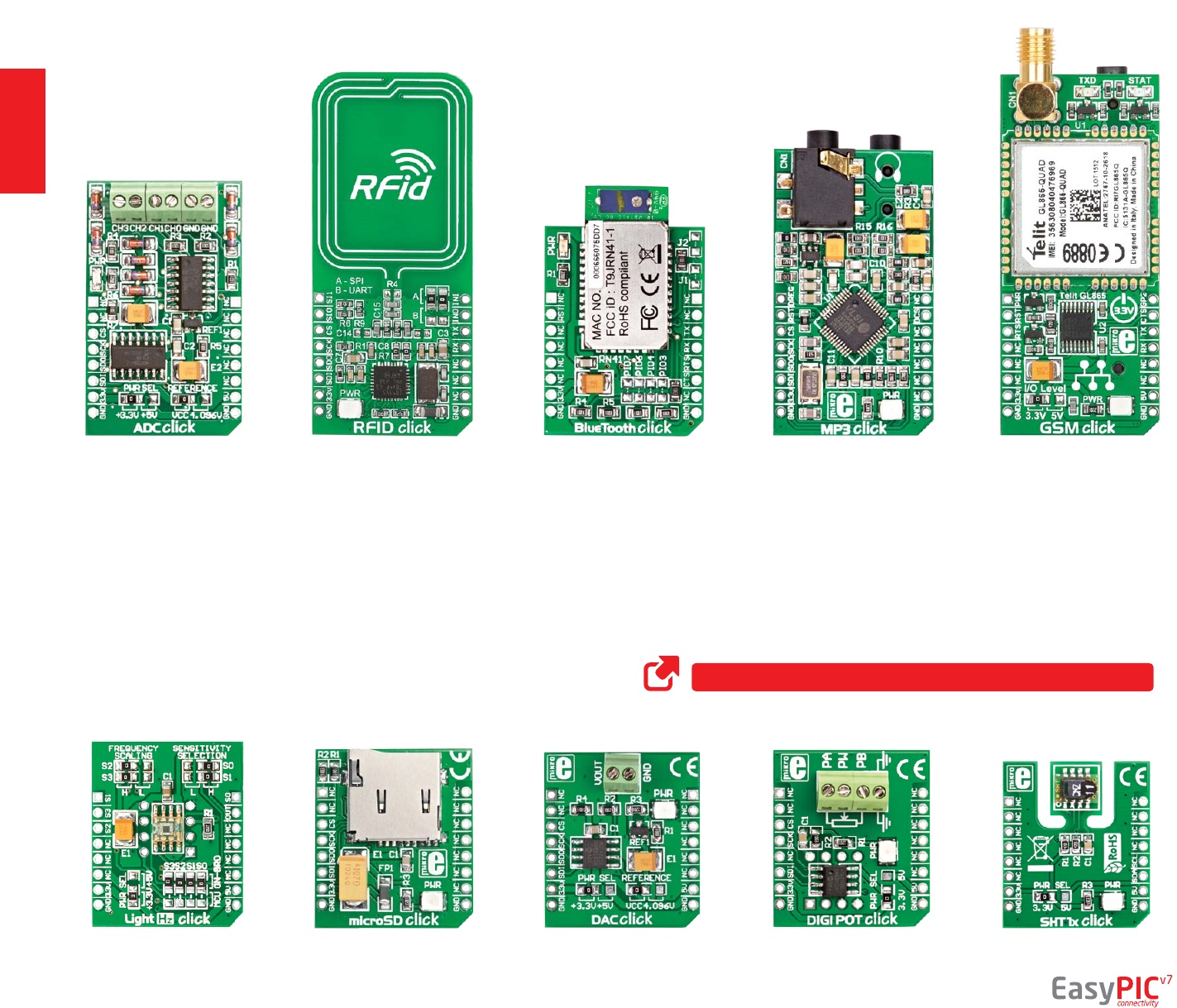
Click Boards™ are plug-n-play!
ADC click™
LightHz click™microSD click™DAC click™DIGIPOT click™SHT1x click™
MP3 click™GSM click™
RFiD click™BlueTooth click™
MikroElektronika portfolio of over 200 accessory boards is now enriched
by an additional set of mikroBUS™ compatible Click Boards™. Almost each
month several new Click boards™ are released. It is our intention to provide
the community with as much of these boards as possible, so you will be able
to expand your EasyPIC™ v7 with additional functionality with literally zero
hardware conguration. Just plug and play. Visit the Click boards™ webpage
for the complete list of available boards:
http://www.mikroe.com/click/
connectivity
page 21
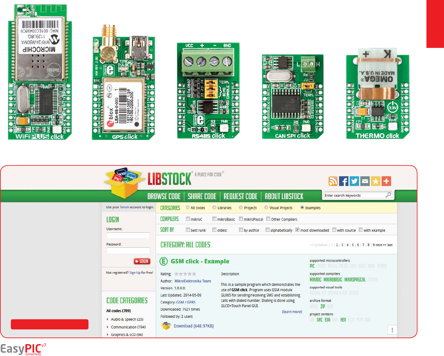
CAN SPI click™THERMO click™
RS485 click™
WiFi PLUS click™GPS click™
Code Examples
It easy to get your Click™ board
up and running. We provided
the examples for mikroC™,
mikroBasic™ and mikroPascal™
compilers on our Libstock
community website. Just
download them and you are
ready to start:
http://www.libstock.com
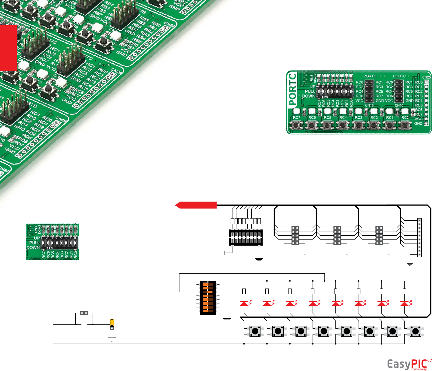
One of the most distinctive features of
EasyPIC™ v7 are it’s Input/Output PORT groups.
They add so much to the connectivity potential of
the board.
Everything is grouped together
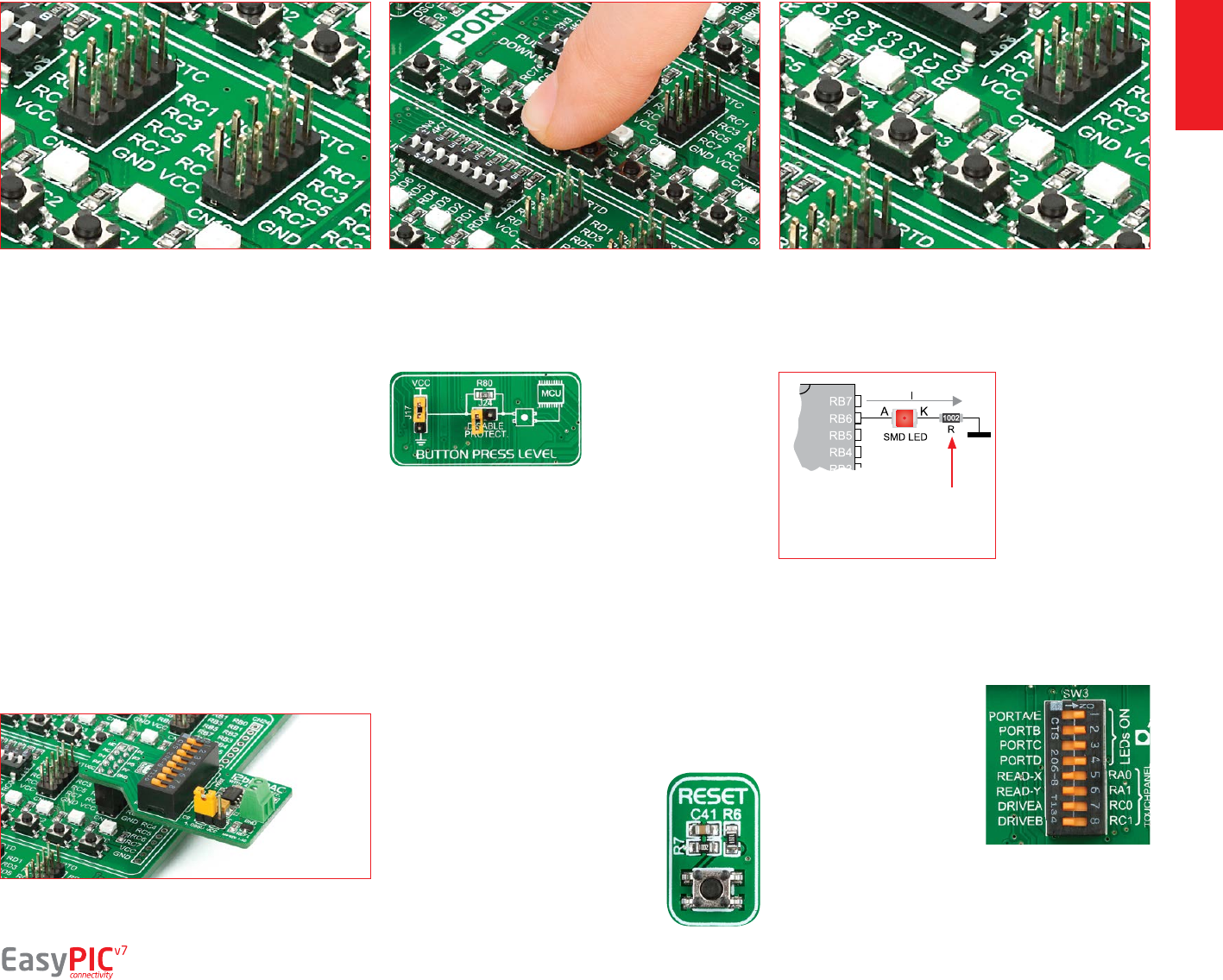
PORT headers, PORT buttons and PORT LEDs are next to each other, and
grouped together. It makes development easier, and the entire EasyPIC™ v7
cleaner and well organized. We have also provided an additional PORT headers
on the left side of the board, so you can access any pin you want from both sides of
the board. Some PORT pins are directly connected to the microcontroller, and some that are connected to other on-board modules are enabled via jumpers (for
example USB jumpers, J12 and J18).
Tri-state pull-up/down DIP switches
Tri-state DIP switches, like SW7 on Figure 10-2, are used to
enable 4K7 pull-up or pull-down resistor on any desired port
pin. Each of these switches has three states:
1. middle position disables both
pull-up and pull-down feature from
the PORT pin
2. up position connects the resistor
in pull-up state to the selected pin
3. down position connects the
resistor in pull-down state to the
selected PORT pin.
Figure 10-1: I/O group contains PORT headers, tri-state pull
up/down DIP switch, buttons and LEDs all in one place
LD17LD18LD19LD20LD21LD22LD23LD24
RN8-1
10K
RN8-2
10K
RN8-3
10K
RN8-4
10K
RN8-5
10K
RN8-6
10K
RN8-7
10K
RN8-8
10K
T17T18T19T20T21T22T23T24
RC0
RC1
RC2
RC3
RC4
RC5
RC6
RC7
RC0
RC1
RC2
RC3
RC4
RC5
RC6
RC7
12345678
O
N
SW3
PC_LED
R80
220
J24
PRESS_LEVEL
DISABLE
PROTECTION
J17
VCC-MCU
1 2 3 4 5 6 7 8
+
_
SW7
VCC-BRD VCC-BRD
VCC-MCU
RC0
RC1
RC2
RC3
RC4
RC5
RC6
RC7
UP
DOWN
PULL
CN15 CN10
1
2
3
4
5
6
7
8
9
10
CN25
VCC-BRD
RC0 RC1
RC2 RC3
RC4 RC5
RC6 RC7
RC0 RC1
RC2 RC3
RC4 RC5
RC6 RC7
RC0
RC1
RC2
RC3
RC4
RC5
RC6
RC7
VCC-BRD
CN20
RC0 RC1
RC2 RC3
RC4 RC5
RC6 RC7
4k7
DATA BUS
connectivity
Figure 10-3: Schematic of the single I/O group connected to microcontroller PORTC
Input/Output Group
Figure 10-2: Tri-state
DIP switch on PORTC
page 22
The logic state of all
microcontroller digital
inputs may be changed
using push buttons.
Jumper J17 is available
for selecting which logic
state will be applied
to corresponding MCU pin when button is pressed
in any I/O port group. If you, for example, place J17
in VCC position, then pressing of any push button in
PORT I/O group will apply logic one to the appropriate
microcontroller pin. The same goes for GND. If the
jumper is taken out, then neither of two logic states
will be applied to the appropriate microcontroller pin. You
can disable pin protection 220ohm resistors by placing
jumper J24, which will connect your push buttons
directly to VCC or GND. Be aware that doing so you may
accidentally damage MCU in case of wrong usage.
Reset Button
In the far upper right section of the
board, there is a RESET button, which
can be used to manually reset the
microcontroller. This button is directly
connected to the MCLR pin.
Headers Buttons LEDs
connectivity
Figure 10-4: IDC10 male headers enable easy
connection with MikroElektronika accessory boards
With enhanced connectivity as one of the key features of
EasyPIC v7, we have provided four connection headers
for each PORT. I/O PORT group contains two male IDC10
headers (like CN10 and CN15 on Figure 10-3). These
headers are all compatible with over 70 MikroElektronika
accessory boards, and enable simple connection. There is
one more IDC10 header available on the left side of the
board, next to the section with displays.
I/O PORT group also contains 1x10 connection pad (like
CN25 on Figure 10-3) which can be used for connecting
MikroElektronika PROTO boards, or custom user boards.
LED (Light-Emitting
Diode) is a highly
ecient electronic
light source. When
connecting LEDs, it
is necessary to place
a current limiting
resistor in series
so that LEDs are
provided with the
current value specied by the manufacturer. The current
varies from 0.2mA to 20mA, depending on the type of the
LED and the manufacturer.. The EasyPIC™ v7 board uses
low-current LEDs with typical current consumption of
0.2mA or 0.3mA, depending of VCC voltage selection.
Board contains 36 LEDs
which can be used for visual
indication of the logic state
on PORT pins. An active LED
indicates that a logic high
(1) is present on the pin. In
order to enable PORT LEDs,
it is necessary to enable the
corresponding DIP switches
on SW3 (Figure 10-6). Figure 10-6: SW3.1
through SW3.4
switches are used to
enable PORT LEDs
Microcontroller
page 23
Figure 10-5: Button press
level jumper (J17) SMD resistor
limiting current
through the LED
NOTE: Because of it's orientation, header on the left side
of the board is not meant for placing accessory boards
directly. Instead, use wire jumpers or other ways to
establish connection and utilize these pins.
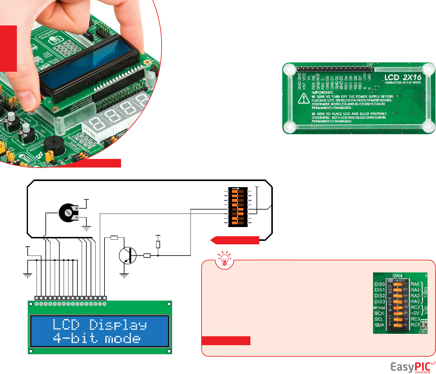
Liquid Crystal Displays or LCDs are cheap and
popular way of representing information to the
end user of some electronic device. Character
LCDs can be used to represent standard and
custom characters in the predened number of
elds. EasyPIC™ v7 provides the connector and the
necessary interface for supporting 2x16 character
LCDs in 4-bit mode. This type of display has two rows
consisted of 16 character elds. Each eld is a 7x5 pixel
matrix. Communication with the display module is done
through CN7 display connector. Board is tted with uniquely
designed plastic display distancer, which allows the LCD module
to perfectly and rmly t into place.
GND and VCC - Display power supply lines
Vo - LCD contrast level from potentiometer P4
RS - Register Select Signal line
E - Display Enable line
R/W - Determines whether display is in Read or Write mode. It’s
always connected to GND, leaving the display in Write mode all
the time.
D0–D3 - Display is supported in 4-bit data mode, so lower half of
the data byte interface is connected to GND.
D4–D7 - Upper half of the data byte
LED+ - Connection with the back-light LED anode
LED- - Connection with the back-light LED cathode
We have allowed LCD back-light to be enabled in two dierent
ways:
1. It can be turned on with full brightness using SW4.6 switch.
2. Brightness level can be determined with PWM signal from the
microcontroller, allowing you to write custom back-light controlling
software. This back-light mode is enabled with SW4.5 switch.
LCD 2x16 characters
Vss
Vdd
Vee
RS
R/W
E
D0
D1
D2
D3
D4
D5
D6
D7
A
K
CN7
LCD SOCKET
VCC-5
V
P4
10K
VCC-5V
Q11
BC846
R93
56
R89
4K7
R10
1K
VCC-MCU
Vee
GND
GND
GND
GND
GND
GND
RB3
RB2
RB1
RB0
RB5
RB4
K-LCD
LCD-GLCD BPWM
LCD-GLCD BCK
12345678
O
N
SW4
LCD-GLCD BPWM RC2
VCC-5V
DATA BUS
Figure 11-1: On-board LCD 2x16 display connector
Figure 11-2: 2x16 LCD
connection schematic Standard and PWM-driven back-light
Connector pinout explained
Make sure to turn o the power supply before placing LCD onto
the board. Otherwise your display can be permanently damaged.
In order to use PWM back-light both SW4.5 and SW4.6 switches must
be enabled at the same time.
IMPORTANT:
IMPORTANT:
page 24
displays
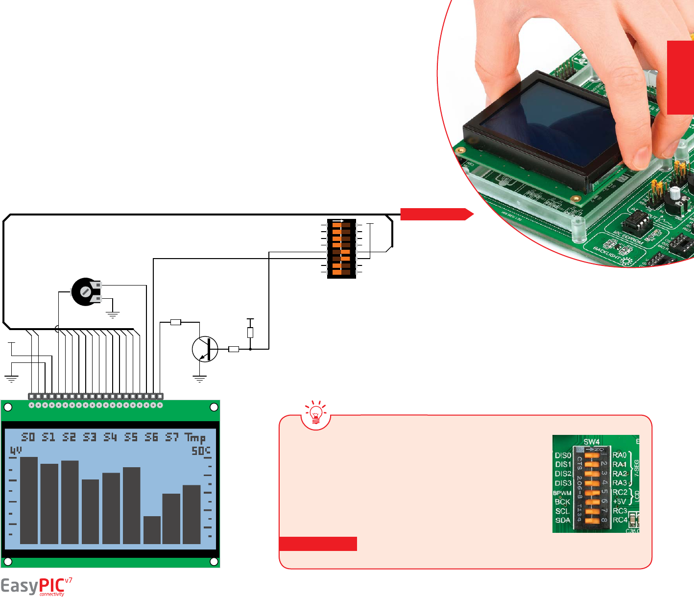
As for LCD, we have allowed GLCD back-light to be enabled in two
dierent ways:
1. It can be turned on with full brightness using SW4.6 switch.
2. Brightness level can be determined with PWM signal from the
microcontroller, allowing you to write custom back-light controlling
software. This back-light mode is enabled with SW4.5 switch.
Graphical Liquid Crystal Displays, or GLCDs are used to
display monochromatic graphical content, such as text, images,
human-machine interfaces and other content. EasyPIC™ v7
provides the connector and necessary interface for supporting
GLCD with resolution of 128x64 pixels, driven by the KS108 or
compatible display controller. Communication with the display
module is done through CN6 display connector. Board is tted
with uniquely designed plastic display distancer, which allows
the GLCD module to perfectly and rmly t into place.
Display connector is routed to PORTB
(control lines) and PORTD (data lines) of the
microcontroller sockets. Since the same ports are
used by 2x16 character LCD display, you cannot
use both displays simultaneously. You can control
the display contrast using dedicated potentiometer
P3. Full brightness display back light can be enabled
with SW4.6 switch, and PWM-driven back light
with SW4.5 switch.
GLCD 128x64
VCC-5V
P3
10K
Q11
BC846
R92
20
R89
4K7
R10
1K
VCC-MCU
CS1
CS2
GND
Vcc
Vo
RS
R/W
D1
D2
D3
D4
D5
D6
D7
E
D0
RST
Vee
LED+
LED-
1 20
CN6
GLCD SOCKET2
RD0
RD1
RD2
RD3
RD4
RD5
RD6
RD7
RB4
RB2
RB5
RB3
RB1
RB0
Vo
LCD-GLCD BCK
K-GLCD
LCD-GLCD BCK
12345678
O
N
SW4
LCD-GLCD BPWM RC2
VCC-5VDATA BUS
displays
Figure 12-1: GLCD 128x64
connection schematic
Standard and PWM-driven back-light
Connector pinout explained
In order to use PWM back-light both SW4.5 and SW4.6 switches must
be enabled at the same time.
IMPORTANT:
CS1 and CS2 - Controller Chip Select lines
VCC - +5V display power supply
GND - Reference ground
Vo - GLCD contrast level from potentiometer P3
RS - Data (High), Instruction (Low) selection line
R/W - Determines whether display is in Read or
Write mode.
E - Display Enable line
D0–D7 - Data lines
RST - Display reset line
Vee - Reference voltage for GLCD contrast
potentiometer P3
LED+ - Connection with the back-light LED anode
LED- - Connection with the back-light LED cathode
page 25
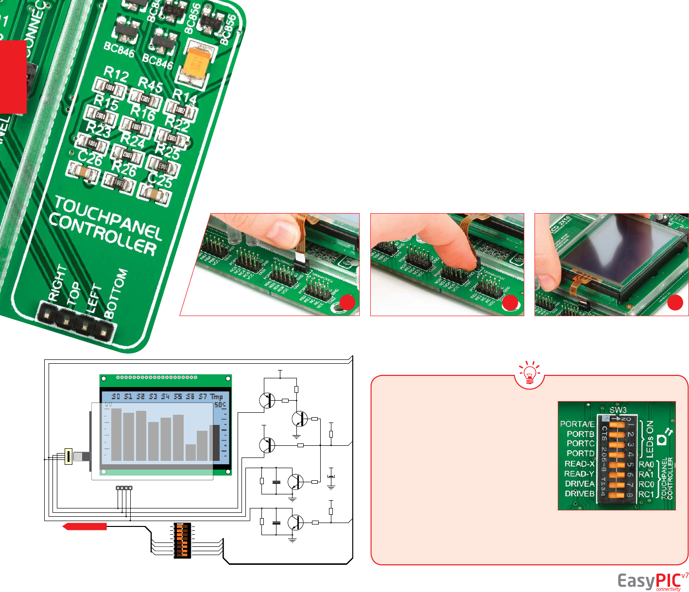
Touch panel controller
Enabling Touch panel
Correctly placing the touch panel cable into the connector
Touch panel is a glass panel whose surface is
covered with two layers of resistive material. When
the screen is pressed, the outer layer is pushed
onto the inner layer and appropriate controllers can
measure that pressure and pinpoint its location. This
is how touch panels can be used as an input devices.
EasyPIC™ v7 is equipped with touch panel controller
and connector for 4-wire resistive touch panels. It
can very accurately register pressure at a specific point,
representing the touch coordinates in the form of analog
voltages, which can then be easily converted to X and Y
values. Touch panel comes as a part of display.
Figure 13-1: Put Touch panel at cable in
the connector
Figure 13-2: Use a tip of your nger
to push it inside
Figure 13-3: Now place GLCD with
Touch panel into GLCD socket
1 2 3
Figure 13-5: Turn on switches
5 through 8 on SW3 to enable
Touch panel controller
Touch panel is enabled using SW3.5,
SW3.6, SW3.7 and SW3.8 switches.
They connect READ-X and READ-Y lines
of the touch panel with RA0 and RA1
analog inputs, and DRIVEA and DRIVEB
with RC0 and RC1 digital outputs on
microcontroller sockets. Make sure to
disconnect other peripherals, LEDs and
additional pull-up or pull-down resistors
from the interface lines in order not to
interfere with signal/data integrity.
page 26
Q15
BC856
Q13
BC846
R22
10K
R16
1K
R15
10K
R12
1K
VCC-MCU
Q14
BC856
R14
10K
Q12
BC846
R45
10K
C25
100nF
R25
100K
Q16
BC846
R24
10K
C26
100nF
R26
100K
R23
1K
RIGHT
TOP
LEFT
BOTTOM
DRIVEA
DRIVEB
BOTTOM
LEFT
E3
10uF
CS1
CS2
GND
Vcc
Vo
RS
R/W
D1
D2
D3
D4
D5
D6
D7
E
D0
RST
Vee
LED+
LED-
1 20
21
22
23
24
CN6
GLCD SOCKET2
CN29
RIGHT
TOP
LEFT
BOTTOM
VCC-MCU
VCC-MCU
VCC-MCU
VCC-MCU
12345678
O
N
SW3
RA0
RA1
RC0
RC1
DRIVEA
DRIVEB
LEFT
BOTTOM
DATA BUS
Figure 13-4: Touch Panel
controller and connection
schematic
displays
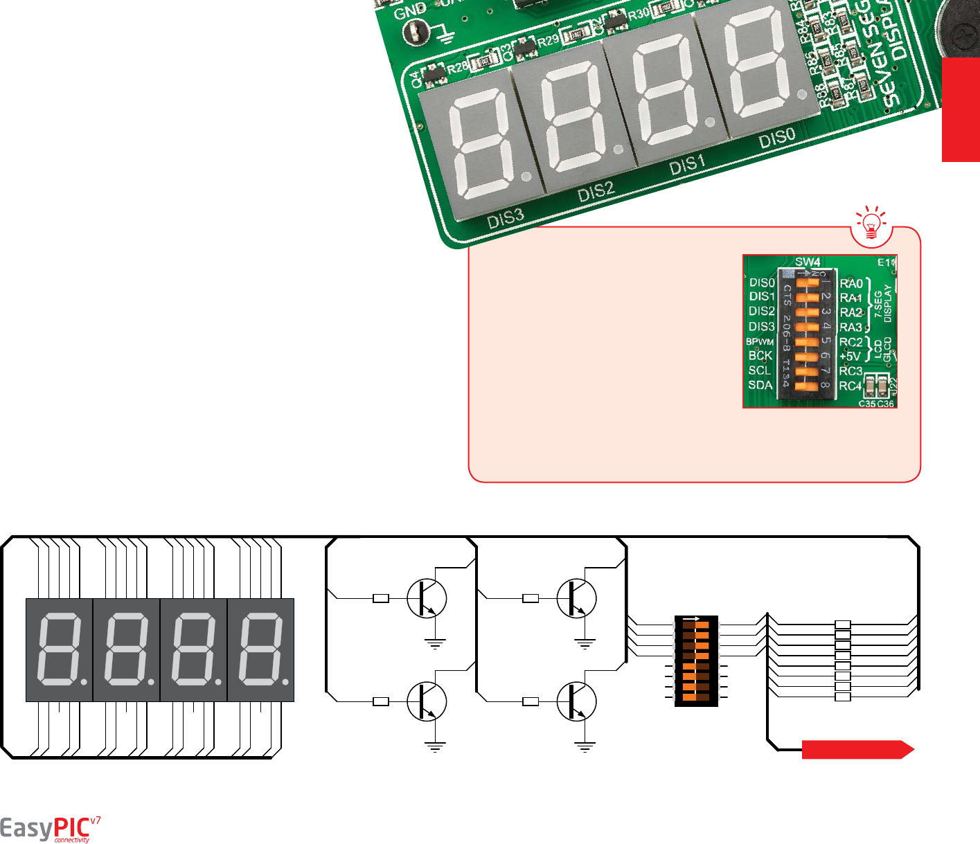
One seven segment digit consist of 7+1
LEDs which are arranged in a specic
formation which can be used to represent
digits from 0 to 9 and even some letters.
One additional LED is used for marking
the decimal dot, in case you want to write
a decimal point in the desired segment.
EasyPIC™ v7 contains four of these digits
put together to form 4-digit 7-segment
display. Driving such a display is done
using multiplexing techniques. Data
lines are shared between segments, and
therefore the same segment LEDs in
each digit are connected in parallel. Each
digit has it’s unique digit select line,
which is used to enable the digit
to which the data is currently being
sent. By multiplexing data through all
four segments fast enough, you create
an illusion that all four segments are in
operation simultaneously.
This is possible because human eye has
a slower reaction time than the mention
changes. This way you can represent
numbers in decimal or hexadecimal
form. Eight data lines that are common
for all the digits are connected to PORTD,
and digit select lines are connected to
RA0–RA3 lines on the microcontroller
sockets.
To enable digit select lines for the 4-digit
7-segment display you have to turn
on SW4.1, SW4.2, SW4.3 and SW4.4
switches. Digit select lines are connected
to RA0 – RA3 pins on the microcontroller
sockets, while data lines are connected to
RD0 – RD7 pins. Make sure to disconnect
other peripherals from the interface lines
in order not to interfere with signal/data
integrity.
12345678
O
N
SW4
1
2
4
5 6
7
9
8
10
3
b
ac
d
e
f
g
dp
cc
1
2
4
56
7
9
8
10
3
b
ac
d
e
f
g
dp
cc
1
2
4
56
7
9
8
10
3
b
ac
d
e
f
g
dp
cc
1
2
4
56
7
9
8
10
3
b
ac
d
e
f
g
dp
cc
COM0
COM1
COM2
COM3
R81 470
R82 470
R83 470
R84 470
R85 470
R86 470
R87 470
R88 470
Q1
BC846
Q2
BC846
Q3
BC846
Q4
BC846
R28
10K
R29
10K
R30
10K
R31
10K
COM3
COM0
COM1
COM2
DIS0
DIS1
DIS2
DIS3
RA1
RA3
RA2
RA0
DIS3
DIS0
DIS1
DIS2
seg e
seg d
seg c
seg dp
seg b
seg a
seg f
seg g
RD7
RD6
RD4
RD3
RD2
RD1
RD0
RD5
seg a
seg b
seg f
seg g
seg dp
seg c
seg d
seg e
seg a
seg b
seg f
seg g
seg dp
seg c
seg d
seg e
seg a
seg b
seg f
seg g
seg dp
seg c
seg d
seg e
seg a
seg b
seg f
seg g
seg dp
seg c
seg d
seg e
DATA BUS
Figure 14-2: 4-digit 7-segment display schematic
Figure 14-1: Turn on switches
1 through 4 on SW4 to enable
4-digit 7-seg display
Enabling the display
4 digit
7-seg display
page 27
displays
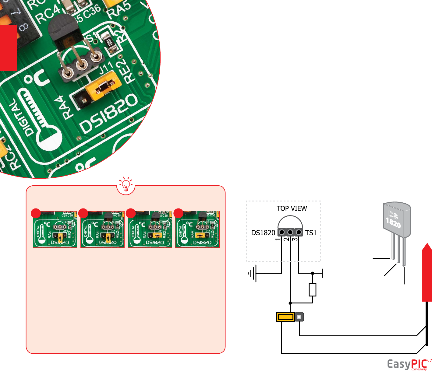
DQ
RA4
RE2
VCC-MCU
J11
R2
1K VCC
DQ
GND
DATA BUS
DS1820 - Digital
Temperature Sensor
DS1820 is a digital temperature
sensor that uses 1-wire®
interface for it’s operation. It is
capable of measuring temperatures
within the range of -55 to 128°C,
and provides ±0.5°C accuracy for
temperatures within the range of -10 to
85°C. It requires 3V to 5.5V power supply
for stable operation. It takes maximum
of 750ms for the DS1820 to calculate
temperature with 9-bit resolution.
1-wire® serial communication enables
data to be transferred over a single
communication line, while the process
itself is under the control of the master
microcontroller. The advantage of
such communication is that only one
microcontroller pin is used. Multiple
sensors can be connected on the same
line. All slave devices by default have
a unique ID code, which enables the
master device to easily identify all
devices sharing the same interface.
EasyPIC™ v7 provides a separate socket
(TS1) for the DS1820. Communication
line with the microcontroller is connected
via jumper J11.
EasyPIC™ v7 enables you to establish 1-wire® communication between DS1820 and
the microcontroller via RA4 or RE2 microcontroller pins. The selection of either of
those two lines is done using J11 jumper. When placing the sensor in the socket
make sure that half-circle on the board’s silkscreen markings matches the rounded
part of the DS1820 sensor. If you accidentally connect the sensor the other way, it
may be permanently damaged. Make sure to disconnect other peripherals (except
1-wire), LEDs and additional pull-up or pull-down resistors from the interface lines
in order not to interfere with signal/data integrity.
Figure 15-1:
DS1820 not
connected
Figure 15-2:
DS1820
placed in
socket
Figure 15-3:
DS1820
connected
to RE2 pin
Figure 15-4:
DS1820
connected
to RA4 pin
Figure 15-5:
DS1820
connected
to RE2 pin
Enabling DS1820 Sensor
1 2 3 4
page 28
modules
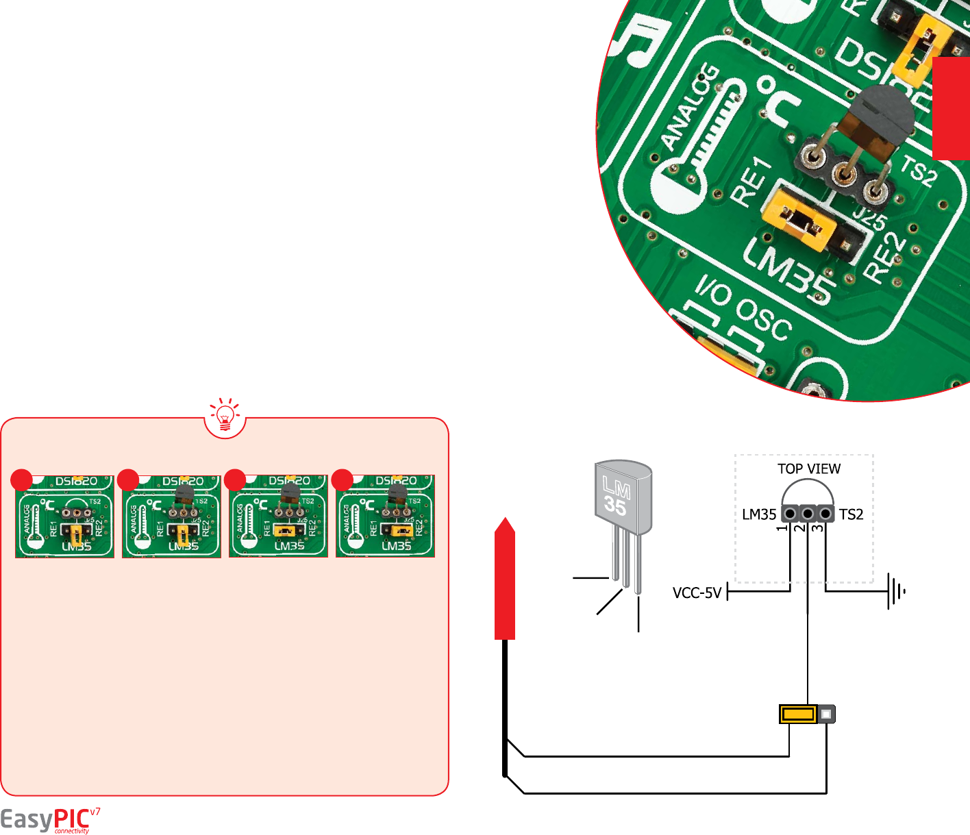
VOUT
RE1
RE2
J25
DATA BUS
VOUT
GND
VCC
Figure 16-5:
LM35
connected
to RE1 pin
The LM35 is a low-cost precision
integrated-circuit temperature sensor,
whose output voltage is linearly
proportional to the Celsius (Centigrade)
temperature. The LM35 thus has an
advantage over linear temperature
sensors calibrated in ° Kelvin, as the
user is not required to subtract a large
constant voltage from its output to
obtain convenient Centigrade scaling.
It has a linear +10.0 mV/°C scale factor
and less than 60 μA current drain. As it
draws only 60 μA from its supply, it has
very low self-heating, less than 0.1°C
in still air. EasyPIC™ v7 enables you to
get analog readings from the LM35
sensor in restricted temperature range
from +2ºC to +150ºC. Board provides a
separate socket (TS2) for
the LM35 sensor in TO-92
plastic packaging. Readings
are done with microcontroller
using single analog input line,
which is selected with jumper J25.
Jumper connects the sensor with
either RE2 or RE1 microcontroller pins.
EasyPIC™ v7 enables you to get analog readings from the LM35 sensor using
RE1 or RE2 microcontroller pins. The selection of either of those two lines
is done using J25 jumper. When placing the sensor in the socket make sure
that half-circle on the board’s silkscreen markings matches the rounded part of
the LM35 sensor. If you accidentally connect the sensor the other way, it can
be permanently damaged and you might need to replace it with another one.
During the readings of the sensor, make sure that no other device uses the
selected analog line, because it may interfere with the readings.
Figure 16-1:
LM35 not
connected
Figure 16-2:
LM35 placed
in socket
Figure 16-3:
LM35
connected
to RE1 pin
Figure 16-4:
LM35
connected
to RE2 pin
Enabling LM35 Sensor
LM35 - Analog
Temperature Sensor
page 29
1 2 3 4
modules
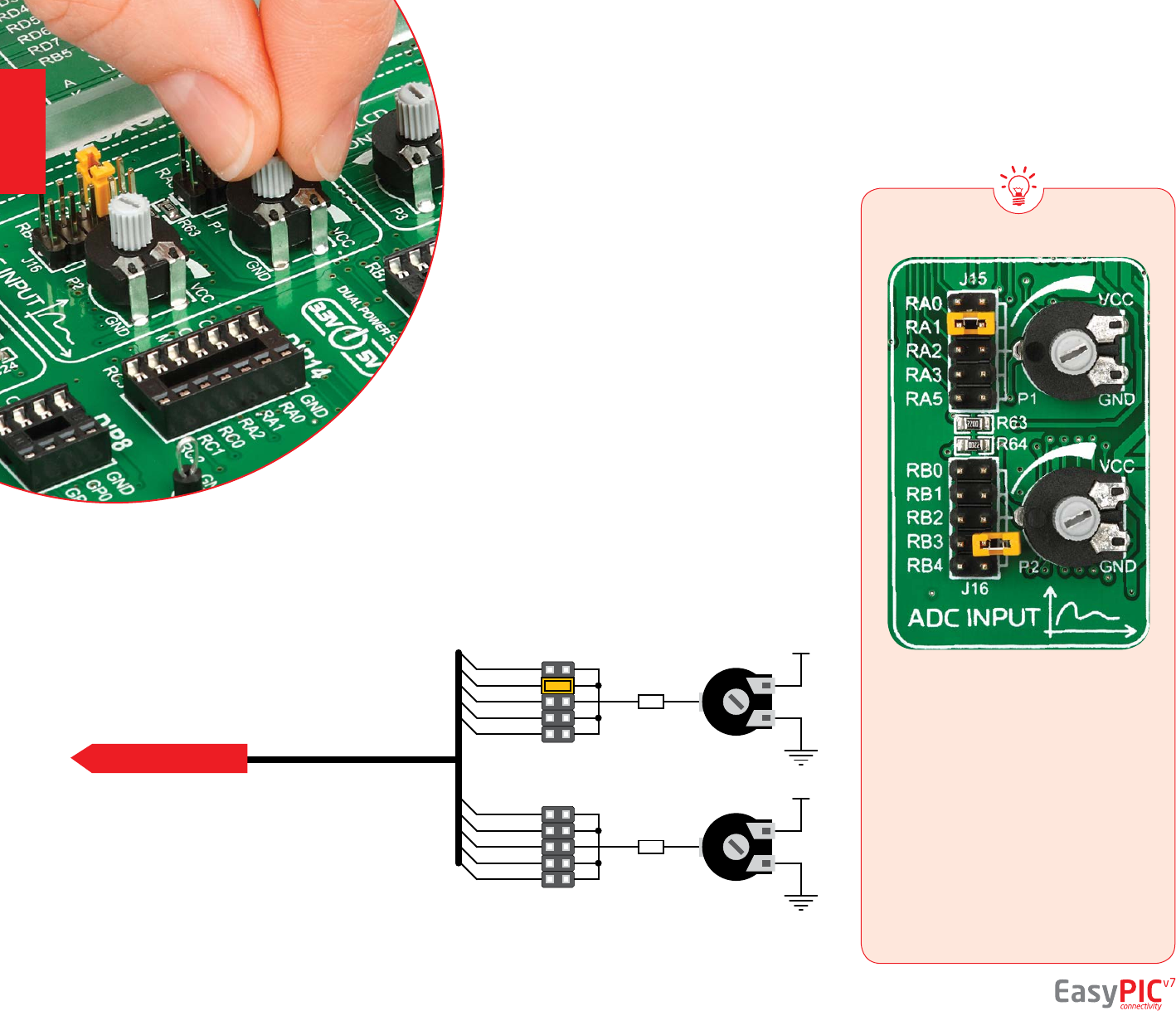
Digital signals have two discrete states, which are decoded
as high and low, and interpreted as logic 1 and logic 0.
Analog signals, on the other hand, are continuous, and can
have any value within dened range. A/D converters are
specialized circuits which can convert analog signals (voltages)
into a digital representation, usually in form of an integer
number. The value of this number is linearly dependent on
the input voltage value. Most microcontrollers nowadays internally
have A/D converters connected to one or more input pins. Some of
the most important parameters of A/D converters are conversion
time and resolution. Conversion time determines how fast can an
analog voltage be represented in form of a digital number. This is an
important parameter if you need fast data acquisition. The other parameter
is resolution. Resolution represents the number of discrete steps that supported
voltage range can be divided into. It determines the sensitivity of the A/D converter.
Resolution is represented in maximum number of bits that resulting number occupies. Most
PIC® microcontrollers have 10-bit resolution, meaning that maximum value of conversion can be
represented with 10 bits, which converted to integer is 210=1024. This means that supported voltage range, for
example from 0-5V, can be divided into 1024 discrete steps of about 4.88mV.
EasyPIC™ v7 provides an interface in form of two potentiometers for simulating analog input voltages that can be routed to
any of the 10 supported analog input pins.
ADC inputs
P2
10K
R64
220
P1
10K
R63
220
J15
J16
VCC-MCU
VCC-MCU
RA2
RA1
RA0
RA3
RA5
RB2
RB1
RB0
RB3
RB4
DATA BUS
Enabling ADC inputs
In order to connect the output of the
potentiometer P1 to RA0, RA1, RA2,
RA3 or RA5 analog microcontroller inputs,
you have to place the jumper J15 in the
desired position. If you want to connect
potentiometer P2 to any of the RB0 – RB4
analog microcontroller inputs, place jumper
J16 in the desired position. By moving
the potentiometer knob, you can create
voltages in range from GND to VCC.
Figure 17-1: use J15 and J16 jumpers
to connect analog input lines with
potentiometers P1 and P2
page 30
Figure 17-2:
Schematic of ADC
input
modules
EEPROM is short for Electrically Erasable
Programmable Read Only Memory. It is usually
a secondary storage memory in devices containing
data that is retained even if the device looses power
supply. Because of the ability to alter single bytes
of data, EEPROM devices are used to store personal
preference and conguration data in a wide spectrum
of consumer, automotive, telecommunication, medical,
industrial, and PC applications.
EasyPIC™ v7 supports serial EEPROM which uses I2C
communication interface and has 1024 bytes of available
memory. Board contains socket for serial EEPROMs in DIP8
packaging, so you can easily exchange it with dierent memory
size EEPROM IC. EEPROM itself supports single byte or 16-byte (page)
write and read operations. Data rate is 400 kHz for both 3.3V and 5V
power supply.
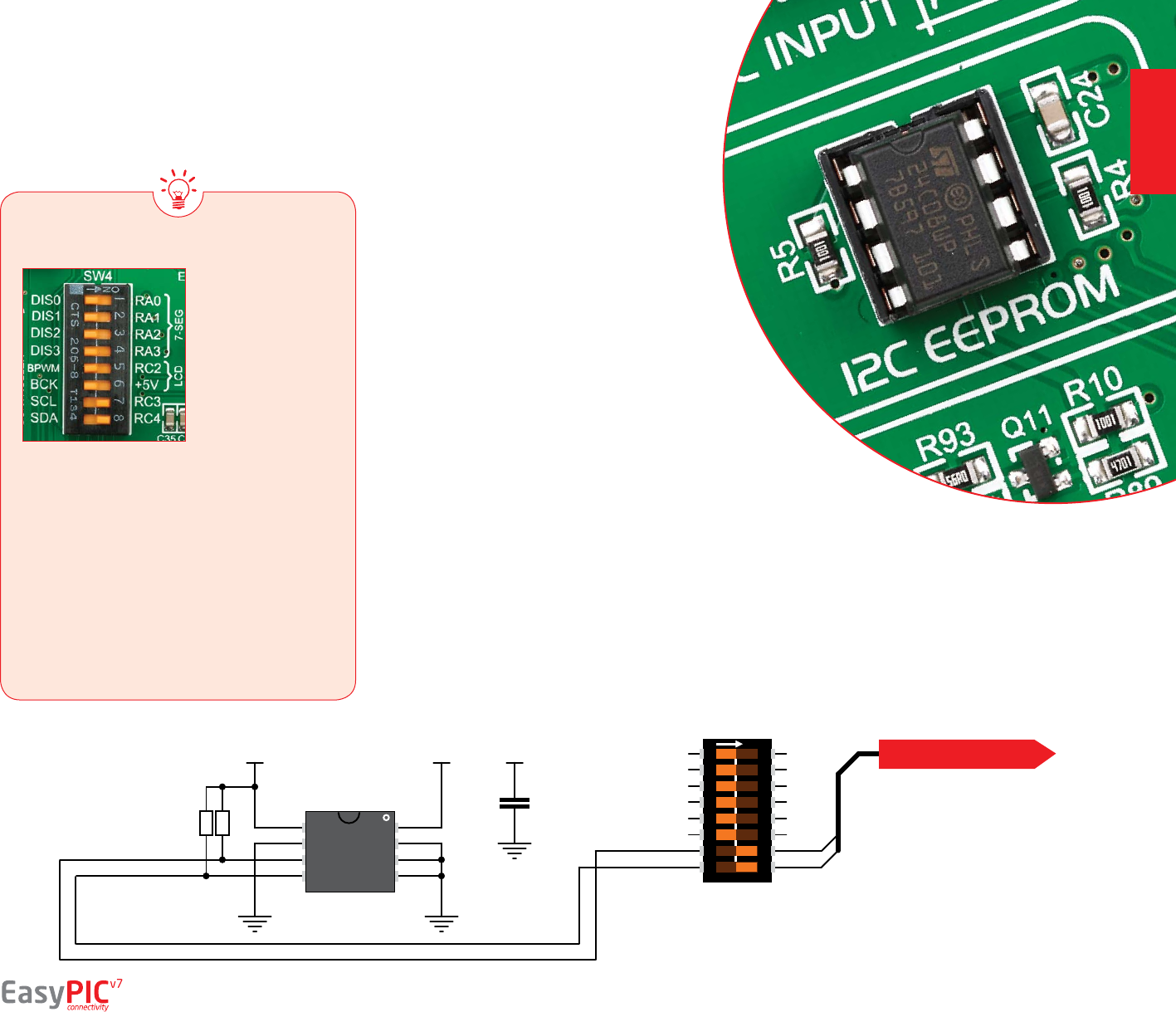
In order to connect I2C EEPROM to the
microcontroller you must enable SW4.7 and
SW4.8 switches, as shown on Figure 18-1. 1kΩ
pull-up resistors necessary for I2C communication
are already provided on SDA and SCL lines once
switches are turned on. Prior to using EEPROM in
your application, make sure to disconnect other
peripherals, LEDs and additional pull-up or pull-
down resistors from the interface lines in order
not to interfere with signal/data integrity.
I2C is a multi-master serial single-ended bus that is used to attach low-speed peripherals to computer or embedded
systems. I²C uses only two open-drain lines, Serial Data Line (SDA) and Serial Clock (SCL), pulled up with
resistors. SCL line is driven by a master, while SDA is used as bidirectional line either by master or slave device.
Up to 112 slave devices can be connected to the same bus. Each slave must have a unique address.
I2C EEPROM
C24
100nF
R4
1K
R5
1K
EEPROM-SCL
EEPROM-SDA
12345678
O
N
SW4
A0
A1
A2
VSSSDA
SCL
WP
VCC1
2
3
45
6
7
8
U8
24C08
EEPROM-SCL
EEPROM-SDA
RC3
RC4
VCC-MCU VCC-MCU VCC-MCU DATA BUS
Enabling I2C EEPROM
What is I2C?
Figure 18-1:
Activate SW4.7 and
SW4.8 switches
to connect
microcontroller
I2C lines to Serial
EEPROM.
page 31
Figure 18-1:
Schematic of
I2C EEPROM
module
modules
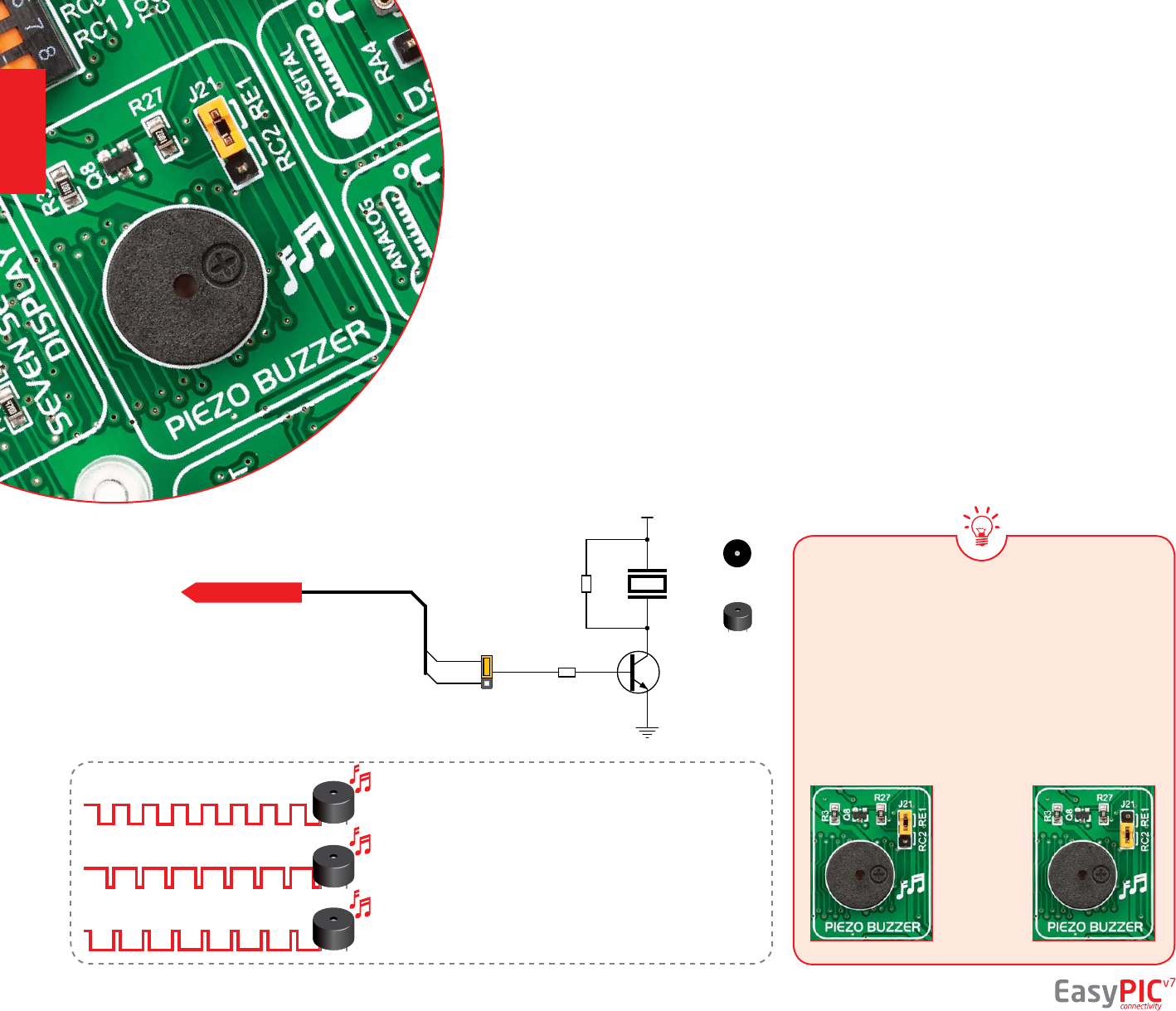
Figure 19-2:
Use jumper
J12 to
connect
Piezo buzzer
on RE1 or
RC2 pin
Piezo electricity is the charge which
accumulates in certain solid materials in response
to mechanical pressure, but also providing the
charge to the piezoelectric material causes it to
physically deform. One of the most widely used
applications of piezo electricity is the production of
sound generators, called piezo buzzers. Piezo buzzer
is an electric component that comes in dierent shapes
and sizes, which can be used to create sound waves
when provided with analog electrical signal. EasyPIC™ v7
comes with piezo buzzer which can be connected either to
RC2 or RE1 microcontroller pins, which is determined by the
position of J21 jumper. Buzzer is driven by transistor Q8 (Figure
19-1). Microcontrollers can create sound by generating a PWM (Pulse
Width Modulated) signal – a square wave signal, which is nothing more
R27
10K
Q8
BC846
R3
1K
VCC-5V
BUZZER
RE1
RC2
PZ1
BUZZER
J21
PERSPECTIVE
VIEW
TOP
VIEW
DATA BUS
In order to use the on-board Piezo Buzzer in
your application, you rst have to connect the
transistor driver of piezo buzzer to the appropriate
microcontroller pin. This is done using jumper J21.
You can place the jumper in two positions, thus
connecting the buzzer driver to either RE1 or RC2
microcontroller pin.
Buzzer starts "singing" when you provide
PWM signal from the microcontroller
to the buzzer driver. The pitch of the
sound is determined by the frequency,
and amplitude is determined by the
duty cycle of the PWM signal.
Enabling Piezo Buzzer
How to make it sing?
page 32
Figure 19-1: Piezo
buzzer connected to RE1
microcontroller pin
Piezo Buzzer
than a sequence of logic zeros and ones. Frequency of the
square signal determines the pitch of the generated sound,
and duty cycle of the signal can be used to increase or decrease
the volume in the range from 0% to 100% of the duty cycle.
You can generate PWM signal using hardware capture-compare
module, which is usually available in most microcontrollers, or
by writing a custom software which emulates the desired
signal waveform.
Supported sound frequencies
Piezo buzzer’s resonant frequency (where you can expect it's
best performance) is 3.8kHz, but you can also use it to create
sound in the range between 2kHz and 4kHz.
Freq = 3kHz, Duty Cycle = 50%Freq = 3kHz,
Volume = 50%
Freq = 3kHz,
Volume = 80%
Freq = 3kHz,
Volume = 20%
Freq = 3kHz, Duty Cycle = 80%
Freq = 3kHz, Duty Cycle = 20%
TO SOCKETS
VCC-5V
R3
1K
PZ1
Q8
BC846
10K
R27
PERSPECTIVE
VIEW
TOP
VIEW
RE1
RC2
J21
BUZZER
TO SOCKETS
VCC-5V
R3
1K
PZ1
Q8
BC846
10K
R27
PERSPECTIVE
VIEW
TOP
VIEW
RE1
RC2
J21
BUZZER
TO SOCKETS
VCC-5V
R3
1K
PZ1
Q8
BC846
10K
R27
PERSPECTIVE
VIEW
TOP
VIEW
RE1
RC2
J21
BUZZER
modules
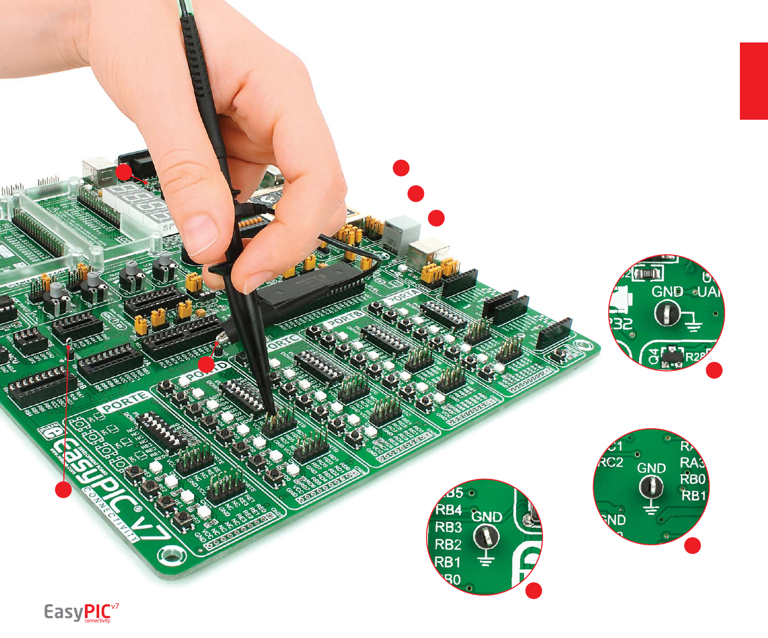
EasyPIC™ v7 contains three GND pins located in three dierent sections of the board,
which allow you to easily connect oscilloscope GND reference when you monitor
signals on microcontroller pins, or signals of on-board modules.
GND is located between UART module and 4-digit 7-seg display.
GND is located in the cross section between DIP18 and DIP14 sockets
GND is located between PORTD I/O group and DIP28 socket.
Additional GNDs
1
1
1
2
3
2
2
3
3
Figure 20-1:
3 oscilloscope
GND pins are
conveniently
positioned so each
part of the board
can be reached with
an oscilloscope probe
page 33
modules
what’s next?
page 34
What’s Next?
Once you have chosen your compiler,
and since you already got the board,
you are ready to start writing your
rst projects. We have equipped our
compilers with dozens of examples
that demonstrate the use of each and
every feature of the EasyPIC™ board,
and all of our accessory boards as well.
This makes an excellent starting point
for your future projects. Just load the
example, read well commented code,
and see how it works on hardware.
Browse through the compiler
Examples available on this link:
You have now completed the journey through each and every feature of EasyPIC™ v7 board. You got to know it’s modules, organization, supported microcontrollers,
programmer and debugger. Now you are ready to start using your new board. We are suggesting several steps which are probably the best way to begin. We invite
you to join thousands of users of EasyPIC™ brand. You will find very useful projects and tutorials and can get help from a large ecosystem of users. Welcome!
Projects
If you want to nd answers to your
questions on many interesting topics
we invite you to visit our forum at
http://www.mikroe.com/forum
and browse through more than 150
thousand posts. You are likely to nd
just the right information for you.
On the other hand, if you want to
download free projects and libraries,
or share your own code, please visit
the Libstock™ website. With user
proles, you can get to know other
programmers, and subscribe to receive
notications on their code.
Community
We all know how important it is that
we can rely on someone in moments
when we are stuck with our projects,
facing a deadline, or when we just
want to ask a simple, basic question,
that’s pulling us back for a while.
We do understand how important
this is to people and therefore our
Support Department is one of the
pillars upon which our company is
based. MikroElektronika oers Free
Tech Support to the end of product
lifetime, so if something goes wrong,
we are ready and willing to help!
Support
www.mikroe.com/easypic/ www.libstock.com/ www.mikroe.com/support/
Compiler
You still don’t have an appropriate compiler? Locate PIC® compiler
that suits you best on our website:
Choose between mikroC™, mikroBasic™ and mikroPascal™, and
download fully functional demo version, so you can begin building
your PIC® applications.
www.mikroe.com/pic/compilers/

DISCLAIMER
All the products owned by MikroElektronika are protected by copyright law and international copyright treaty. Therefore, this manual is to be treated as any other copyright
material. No part of this manual, including product and software described herein, must be reproduced, stored in a retrieval system, translated or transmitted in any form or by
any means, without the prior written permission of MikroElektronika. The manual PDF edition can be printed for private or local use, but not for distribution. Any modication
of this manual is prohibited.
MikroElektronika provides this manual ‘as is’ without warranty of any kind, either expressed or implied, including, but not limited to, the implied warranties or conditions of
merchantability or tness for a particular purpose.
MikroElektronika shall assume no responsibility or liability for any errors, omissions and inaccuracies that may appear in this manual. In no event shall MikroElektronika, its
directors, ocers, employees or distributors be liable for any indirect, specic, incidental or consequential damages (including damages for loss of business prots and business
information, business interruption or any other pecuniary loss) arising out of the use of this manual or product, even if MikroElektronika has been advised of the possibility of
such damages. MikroElektronika reserves the right to change information contained in this manual at any time without prior notice, if necessary.
TRADEMARKS
The MikroElektronika name and logo, the MikroElektronika logo, mikroC™, mikroBasic™, mikroPascal™, mikroProg™, EasyPIC™, EasyPIC PRO™, mikroBUS™, mikromedia™, MINI™ and
Click boards™ are trademarks of MikroElektronika. All other trademarks mentioned herein are property of their respective companies.
All other product and corporate names appearing in this manual may or may not be registered trademarks or copyrights of their respective companies, and are only used for
identication or explanation and to the owners’ benet, with no intent to infringe.
Copyright © MikroElektronika™, 2014, All Rights Reserved.
HIGH RISK ACTIVITIES
The products of MikroElektronika are not fault – tolerant nor designed, manufactured or intended for use or resale as on – line control equipment in hazardous environments
requiring fail – safe performance, such as in the operation of nuclear facilities, aircraft navigation or communication systems, air trac control, direct life support
machines or weapons systems in which the failure of Software could lead directly to death, personal injury or severe physical or environmental damage (‘High Risk
Activities’). MikroElektronika and its suppliers specically disclaim any expressed or implied warranty of tness for High Risk Activities.

If you want to learn more about our products, please visit our website at www.mikroe.com
If you are experiencing some problems with any of our products or just need additional
information, please place your ticket at www.mikroe.com/support/
If you have any questions, comments or business proposals,
do not hesitate to contact us at oce@mikroe.com
