Implementing The Design I CEcube201708User Guide
User Manual: Pdf
Open the PDF directly: View PDF ![]() .
.
Page Count: 207 [warning: Documents this large are best viewed by clicking the View PDF Link!]

iCEcube2 User Guide
August 2017

iCEcube2 User Guide www.latticesemi.com 2
Copyright
Copyright © 2017 Lattice Semiconductor Corporation. All rights reserved. This document may
not, in whole or part, be reproduced, modified, distributed, or publicly displayed without prior
written consent from Lattice Semiconductor Corporation (“Lattice”).
Trademarks
All Lattice trademarks are as listed at www.latticesemi.com/legal. Synopsys and Synplify Pro are
trademarks of Synopsys, Inc. Aldec and Active-HDL are trademarks of Aldec, Inc. All other
trademarks are the property of their respective owners.
Disclaimers
NO WARRANTIES: THE INFORMATION PROVIDED IN THIS DOCUMENT IS “AS IS”
WITHOUT ANY EXPRESS OR IMPLIED WARRANTY OF ANY KIND INCLUDING
WARRANTIES OF ACCURACY, COMPLETENESS, MERCHANTABILITY,
NONINFRINGEMENT OF INTELLECTUAL PROPERTY, OR FITNESS FOR ANY PARTICULAR
PURPOSE. IN NO EVENT WILL LATTICE OR ITS SUPPLIERS BE LIABLE FOR ANY
DAMAGES WHATSOEVER (WHETHER DIRECT, INDIRECT, SPECIAL, INCIDENTAL, OR
CONSEQUENTIAL, INCLUDING, WITHOUT LIMITATION, DAMAGES FOR LOSS OF PROFITS,
BUSINESS INTERRUPTION, OR LOSS OF INFORMATION) ARISING OUT OF THE USE OF
OR INABILITY TO USE THE INFORMATION PROVIDED IN THIS DOCUMENT, EVEN IF
LATTICE HAS BEEN ADVISED OF THE POSSIBILITY OF SUCH DAMAGES. BECAUSE SOME
JURISDICTIONS PROHIBIT THE EXCLUSION OR LIMITATION OF CERTAIN LIABILITY,
SOME OF THE ABOVE LIMITATIONS MAY NOT APPLY TO YOU.
Lattice may make changes to these materials, specifications, or information, or to the products
described herein, at any time without notice. Lattice makes no commitment to update this
documentation. Lattice reserves the right to discontinue any product or service without notice and
assumes no obligation to correct any errors contained herein or to advise any user of this
document of any correction if such be made. Lattice recommends its customers obtain the latest
version of the relevant information to establish that the information being relied upon is current
and before ordering any products.
Contact Information
Lattice Semiconductor Corporation
5555 N.E. Moore Court
Hillsboro, Oregon 97124-6421
United States of America
Tel: +1 503 268 8000
Fax: +1 503 268 8347
http://www.latticesemi.com.

iCEcube2 User Guide www.latticesemi.com 3
TABLE OF CONTENTS
Preface ............................................................................................. 7
About this Document ................................................................................................................... 7
Software Version ......................................................................................................................... 7
Platform Requirements................................................................................................................ 7
Programming Hardware .............................................................................................................. 7
Programming Software................................................................................................................ 8
Chapter 1 Overview ......................................................................... 9
iCEcube2 Tool Suite.................................................................................................................... 9
Design Flow ............................................................................................................................... 10
Chapter 2 Quick Start Guide ......................................................... 11
Creating a Project ...................................................................................................................... 11
Synthesizing the Design ............................................................................................................ 15
Programming the Device ........................................................................................................... 25
Addendum: ................................................................................................................................ 29
Importing Physical Constraints from iCEcube to iCEcube2 .................................................. 29
Chapter 3 iCEcube2 Project Setup and Navigation .................... 34
Introduction ................................................................................................................................ 34
Project Manager GUI................................................................................................................. 34
Adding/Deleting Design and Constraint Files ........................................................................... 34
Selecting Synthesis Tool and Setting synthesis Options .......................................................... 36
Selecting the Target Device and Operating Conditions ............................................................ 39
Output Window .......................................................................................................................... 40
Simulation Wizard ..................................................................................................................... 40
PLL Module Generator .............................................................................................................. 41
PLL Dynamic Reconfiguration ................................................................................................... 50
SPI/I2C Module Generator ........................................................................................................ 52
Chapter 4 Lattice Synthesis Engine ............................................. 60
Changing the LSE Tool Options ................................................................................................ 60
BRAM Utilization ................................................................................................................... 60
Carry Chain Length ............................................................................................................... 60
Command Line Options ........................................................................................................ 60
Fix Gated Clocks ................................................................................................................... 60
FSM Encoding Style ............................................................................................................. 61
Intermediate File Dump ......................................................................................................... 61
Max Fanout Limit .................................................................................................................. 61
Memory Initial Value File Search Path .................................................................................. 61
Number of Critical Paths ....................................................................................................... 61
Optimization Goal ................................................................................................................. 61
Propagate Constants ............................................................................................................ 61
RAM Style ............................................................................................................................. 61
Remove Duplicate Registers ................................................................................................ 62
Resolve Mixed Drivers .......................................................................................................... 62
Resource Sharing ................................................................................................................. 62
ROM Style ............................................................................................................................. 62
RW Check on RAM ............................................................................................................... 62
Target Frequency .................................................................................................................. 63
Top-Level Unit ....................................................................................................................... 63
Use Carry Chain ................................................................................................................... 63

iCEcube2 User Guide www.latticesemi.com 4
Use IO Insertion .................................................................................................................... 63
Use IO Registers ................................................................................................................... 63
Optimizing LSE for Area and Speed ......................................................................................... 63
FSM Encoding Style ............................................................................................................. 64
Max Fanout Limit .................................................................................................................. 64
Optimization Goal ................................................................................................................. 64
Remove Duplicate Registers ................................................................................................ 64
Resource Sharing ................................................................................................................. 65
Target Frequency .................................................................................................................. 65
LSE Options versus Synplify Pro .............................................................................................. 65
Coding Tips for LSE .................................................................................................................. 66
LSE Differences with Synplify Pro ........................................................................................ 66
About Inferring Memory ........................................................................................................ 67
Inferring RAM ...................................................................................................................... 68
Inferring RAM with Synchronous Read .............................................................................. 69
Inferring Pseudo Dual-Port RAM ........................................................................................ 71
Initializing Inferred RAM ..................................................................................................... 73
Inferring ROM ..................................................................................................................... 74
About Verilog Blocking Assignments .................................................................................... 75
Inferring DSP Multipliers ....................................................................................................... 76
Verilog Examples ................................................................................................................ 76
VHDL Examples ................................................................................................................. 78
Inferring I/O ........................................................................................................................... 80
Event Inside an Event ........................................................................................................... 81
HDL Attributes and Directives ................................................................................................... 82
black_box_pad_pin ............................................................................................................... 82
syn_black_box ...................................................................................................................... 83
syn_encoding ........................................................................................................................ 83
syn_hier................................................................................................................................. 84
syn_keep ............................................................................................................................... 85
syn_maxfan ........................................................................................................................... 86
syn_multstyle ........................................................................................................................ 87
syn_noprune ......................................................................................................................... 88
syn_pipeline .......................................................................................................................... 89
syn_preserve ........................................................................................................................ 90
syn_ramstyle ......................................................................................................................... 91
syn_romstyle ......................................................................................................................... 92
syn_use_carry_chain ............................................................................................................ 93
syn_useioff ............................................................................................................................ 94
Synthesis Macro ................................................................................................................... 95
translate_off/translate_on ..................................................................................................... 95
Synopsys Design Constraints (SDC) ........................................................................................ 96
create_clock .......................................................................................................................... 96
set_false_path ....................................................................................................................... 97
set_input_delay ..................................................................................................................... 98
set_max_delay ...................................................................................................................... 98
set_multicycle_path .............................................................................................................. 99
set_output_delay ................................................................................................................... 99
Chapter 5 iCEcube2 Physical Implementation Tools ............... 100
Overview ................................................................................................................................. 100
Tools for Physical Implementation .......................................................................................... 100
Placing and Routing the Design .............................................................................................. 101
Floor Planner ........................................................................................................................... 102

iCEcube2 User Guide www.latticesemi.com 5
Package View .......................................................................................................................... 109
Pin Constraints Editor.............................................................................................................. 111
Power Estimator ...................................................................................................................... 112
Generating a Bitmap ............................................................................................................... 114
Programming the Device ......................................................................................................... 116
Diamond Programmer ......................................................................................................... 116
Memory Initializer .................................................................................................................... 118
Memory initialization file Format (.mem) : ........................................................................... 120
Simulating the Routed Design ................................................................................................. 121
Chapter 6 Timing Constraints and Static Timing Analysis ...... 122
Overview ................................................................................................................................. 122
Specifying Constraints Using the Timing Constraints Editor (TCE) ........................................ 122
SDC Constraints in TCE ..................................................................................................... 124
Clock Constraints ................................................................................................................ 124
Generated Clock Constraints .............................................................................................. 124
Source Clock Latency Constraints ...................................................................................... 125
Input Delay Constraints ....................................................................................................... 125
Output Delay Constraints .................................................................................................... 126
Max Delay Constraints ........................................................................................................ 126
False Path Exceptions ........................................................................................................ 127
Multi Cycle Path Exceptions ............................................................................................... 128
Analyzing Reports Generated by the Static Timing Analyzer (STA) ....................................... 129
Clock Summary Pane ......................................................................................................... 129
Clock Relationship Summary .............................................................................................. 133
Data Sheet .......................................................................................................................... 133
Analyzing Constrained Paths .............................................................................................. 135
By Slack ............................................................................................................................ 135
By Paths ........................................................................................................................... 137
Point to Point .................................................................................................................... 139
Other Features .................................................................................................................... 140
Detailed Timing Report............................................................................................................ 142
Chapter 7 Physical Constraints in iCEcube2 ............................ 146
Specifying Physical Constraints after Design Import and Before Placement ......................... 147
Absolute Placement ............................................................................................................ 147
Constraining Logic or RAMs ............................................................................................. 147
Constraining IOs ............................................................................................................... 147
Constraining SPI Configuration IOs .................................................................................. 148
Relative Placement ............................................................................................................. 148
Region Constraints ............................................................................................................. 152
IO/FF Merge ........................................................................................................................ 153
Global Buffer Promotion/Demotion ..................................................................................... 155
Modifying the Device Floor Plan after Placement ................................................................... 157
Chapter 8 Generating/Integrating Fixed Placement IP Blocks . 160
IP Generation Flow .................................................................................................................. 160
System Design Flow................................................................................................................ 164
Chapter 9 Hierarchical Project Flow .......................................... 169
Create Top Level Project ........................................................................................................ 169
Create Sub-Projects for IP blocks ........................................................................................... 173
Synthesize Top Level Project .................................................................................................. 175

iCEcube2 User Guide www.latticesemi.com 6
Chapter 10 Simulating Design with ALDEC Active-HDL .......... 178
ALDEC Active-HDL ................................................................................................................. 178
Pre-Compiled iCE Simulation Libraries ................................................................................... 178
VHDL ................................................................................................................................ 179
VERILOG .......................................................................................................................... 179
Design ..................................................................................................................................... 180
Pre-Synthesis Simulation ........................................................................................................ 181
Post Place-n-Route Functional Simulation (Verilog/VHDL) .................................................... 188
Post Place-n-Route Timing Simulation (Verilog/VHDL) .......................................................... 190
Chapter 11 iCEcube2 Command Line Interface ........................ 196
Overview ................................................................................................................................. 196
Running LSE in batch mode ................................................................................................... 196
Running Synplify-pro in batch mode ....................................................................................... 197
Running iCEcube2 Backend tools in batch mode ................................................................... 199
Backend tool Options .......................................................................................................... 200
Edif Parser ........................................................................................................................ 200
Placer ................................................................................................................................ 200
Router ............................................................................................................................... 201
Bitmap ............................................................................................................................... 201
Command Line Execution ....................................................................................................... 201
Chapter 12 High Drive IO with configurable drive strengths ... 204
Chapter 13 Open Drain LED IO ................................................... 206
Appendix A: PCF Syntax ............................................................ 207

iCEcube2 User Guide www.latticesemi.com 7
Preface
About this Document
The iCEcube2 User Guide provides iCE FPGA designers with an overview of the software tools
and the design process using iCEcube2. This document covers the iCEcube2 tools for Project
Setup, Navigation, Synthesis and Physical Implementation on the iCE FGPA device.
For information on the Synopsys Synplify Pro software, please refer to the Synplify Pro
documentation provided in the synpbase/doc directory in the iCEcube2 software installation
(<icecube2_install_dir>/synpbase/doc), and on the Lattice website.
For information on the Aldec Active-HDL design tool, please refer to the Active-HDL
documentations available at <icecube2_install_dir>/Aldec/Active-HDL/BOOKS.
Software Version
This User Guide documents the features of iCEcube2 Software Version 2017.08.
For more information about acquiring the iCEcube2 software, please visit the Lattice
Semiconductor website: http://www.latticesemi.com.
Platform Requirements
The iCEcube2 software can be installed on a platform satisfying the following minimum
requirements.
A Pentium 4 computer (500 MHz) with 256 MB of RAM, 256MB of Virtual Memory, and running
one of the following Operating Systems :
Windows 10 OS, 32-bit / 64-bit
Windows 8/8.1 OS, 32-bit / 64-bit
Windows 7 OS, 32-bit / 64-bit
Windows XP Professional
Red Hat Enterprise Linux WS v4, 5, and 6
Programming Hardware
Here are the following ways to program iCE FPGA devices:
A third party programmer or a processor, using the programming files generated by the
iCEcube2 Physical Implementation Tools. Consult the third party programmer user
manual for instructions.
The iCEblink and iCEman evaluation Board, which not only serves as a vehicle to
evaluate iCE FPGAs, but also includes an integrated device programmer. This
programmer can be used to program devices on the evaluation board, or it can be used
to program devices in a target system. Please visit Lattice Semiconductor website:
http://www.latticesemi.com for additional information on the Evaluation Boards.
Digilent USB cables to program the external SPI Flash.

iCEcube2 User Guide www.latticesemi.com 8
The iCE Programming hardware: iCEcable, iCEprog (Programmer base module) and
iCEsab (socket adaptor). Refer to lattice website: http://www.latticesemi.com for more
details on programming hardware.
Programming Software
Standalone Lattice Diamond Programmer software is required to program iCE40 FPGA devices
or SPI flash. Download and install the latest standalone programmer from
http://www.latticesemi.com/ispvm.
For more information about Diamond Programmer, refer “Diamond Programmer” on page 116.
iCEcube2 User Guide www.latticesemi.com 9
Chapter 1 Overview
iCEcube2 Tool Suite
The iCEcube2 Tool Suite is comprised of several integrated components, running under either
the Microsoft Windows or the Red Hat Linux environments. Please refer to Platform
Requirements for additional information on supported operating systems.
The Figure 1-1 below depicts the design flow using the iCEcube2 Tool Suite. The components in
blue signify functionality supported by Lattice Semiconductor’s proprietary Synthesis Engine
(LSE) and iCEcube2 place and route software, and the components in purple indicate the
functionality supported by Synopsys’ Synplify Pro synthesis tools and the Aldec Active-HDL
simulation tool. The iCEcube2 software, Synopsys Synplify Pro and the Aldec Active-HDL
software constitutes the iCEcube2 Tool Suite.
Note: The Aldec Active-HDL tool is available only in Windows environments.
Figure 1-1: The iCEcube2 Design Flow

iCEcube2 User Guide www.latticesemi.com 10
Design Flow
The following steps provide an overview of the design flow using the iCEcube2 Tool Suite.
1. Create a new project in the iCEcube2 Project Navigator and specify a target device and its
operating conditions. Add your HDL (Verilog or VHDL) design files and your Constraint files
to the project.
2. iCEcube2 software supports Synplify-Pro Synthesis tool and Lattice Synthesis (LSE) tool.
Synplify-pro is the default synthesis tool in iCEcube2. Synthesis your design using the
selected synthesis tool.
3. Perform Placement and Routing using the iCEcube2 place and route tools. iCEcube2 also
supports physical implementation tools such as floor planning, allowing users to manually
place logic cells and IOs.
4. Perform timing simulation of your design using the Aldec Active-HDL simulation tool or any
industry-standard HDL simulation tool. The files necessary for simulation are automatically
generated by the iCEcube2 Physical Implementation tools, after the routing phase.
5. Perform Static Timing Analysis using the iCEcube2 static timing analyzer.
6. Generate the device programming and configuration files from the iCEcube2 Physical
Implementation tools.
7. Program your device using the device programming hardware provided by Lattice.
iCEcube2 User Guide www.latticesemi.com 11
Chapter 2 Quick Start Guide
This chapter provides a brief introduction to the iCEcube2 design flow. The goal of this chapter is
to familiarize the user with the fundamental steps needed to create a design project, synthesize
and implement the design, generate the necessary device configuration files, and program the
target device.
Detailed information on tool features and usage is provided in subsequent chapters.
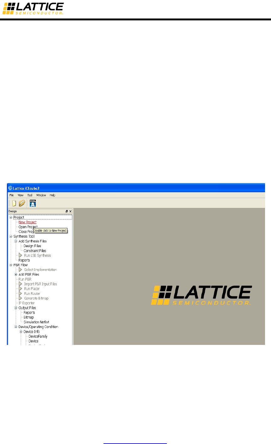
Creating a Project
Starting the iCEcube2 software for the first time, you will see the following interface shown in
Figure 2-1.
Figure 2-1 : Create a New Project
The first step is to create a new design project and add the appropriate design files to your
project. You can create a new project by either selecting File > New Project from the iCEcube2
menu, or by clicking the Create a New Project icon as seen in Figure 2-1. The New Project
Wizard GUI is displayed in Figure 2-2.
iCEcube2 User Guide www.latticesemi.com 12
Figure 2-2: New Project Setup Wizard for iCE40 Family
This example is targeted for iCE40 family device. Follow the following steps to setup the project
properties.
1. Project Name Field: Specify a project name (quick_start) in the Project Name field.
2. Project Directory Field: Specify any directory where you want to place the project directory
in the Project Directory field.
3. Device Family Fields: This section allows you to specify the Lattice iCE device family you
are targeting. For this example, change the Device Family to iCE40.
4. Device Fields: This section allows you to specify the Lattice device and package you are
targeting. For this example, change the Device to HX1K and change the device package to
the VQ100.
5. Operating Condition Fields: This section allows you to specify the operating conditions of
the device which will be used for timing and power analysis.
iCEcube2 User Guide www.latticesemi.com 13
6. Start From Synthesis: This option allows you to start the flow from Synthesis. For current
example, select this option.
7. Start From BackEnd: This option allows you to start from Post Synthesis flow.
After the above selections the New Project GUI Wizard has the following settings as shown in
Figure 2-3.
`
Figure 2-3: Tutorial Project Settings
8. Click Next to go to the Add Files dialog box shown in Figure 2-4. You will be prompted to
create a new project directory. Click Yes.
9. In the Add Files dialog box, navigate to: <iCEcube2 installation directory>/examples/blinky
Highlight the following files:
blinky.vhd
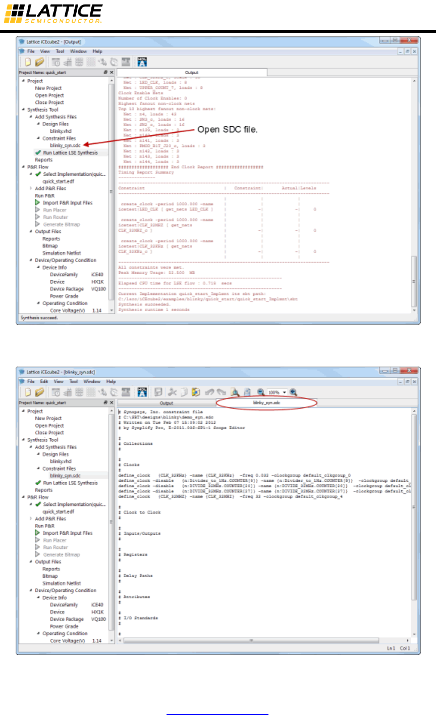
blinky_syn.sdc*

iCEcube2 User Guide www.latticesemi.com 14
Select each file and click >> to add the selected file, or click >>> to add all the files in the
open directory (files can be removed using << and <<<) to your project. Click Finish to create
the project.
* The SDC file is a Synopsys constraint file, which contains timing constraint information.
Figure 2-4: Add Files Dialog Box
After successfully setting up your project, you will return to the iCEcube2 Project Navigator
screen shown in Figure 2-5.
iCEcube2 User Guide www.latticesemi.com 15
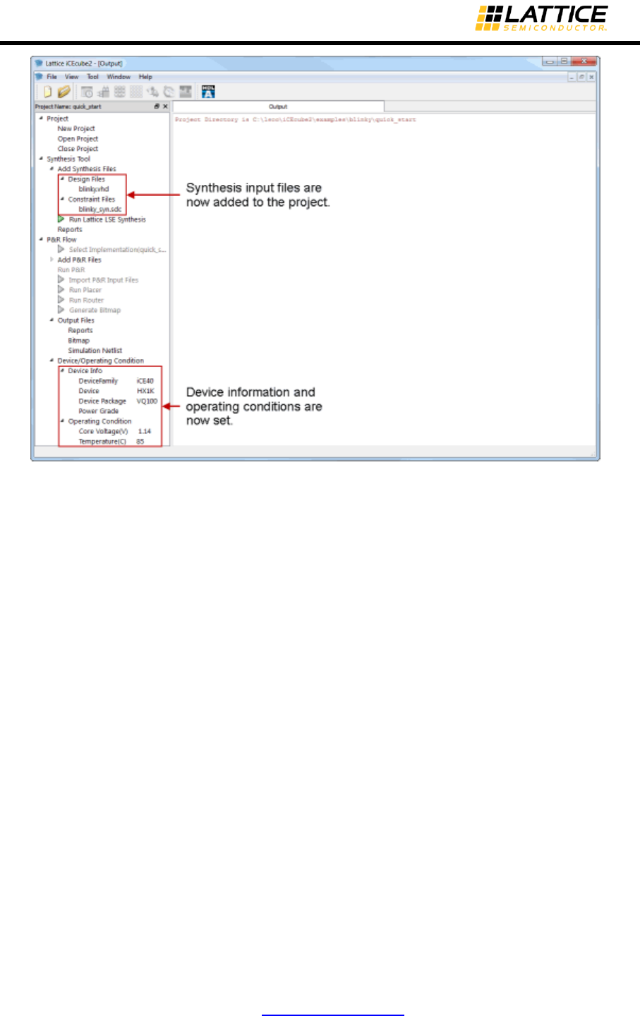
Figure 2-5: iCECube2 Project Navigator View after Completing Project Setup
Synthesizing the Design
After a successful project setup, select a synthesis tool:
1. In the iCEcube2 window, right-click Synthesis Tool and choose Select Synthesis Tools.
The Select Synthesis Tool dialog box opens.
2. Select a tool: Synplify Pro or Lattice LSE.
3. Click OK.
The Run <Tool> Synthesis command changes to show the selected tool.
For this tutorial, select Lattice LSE.
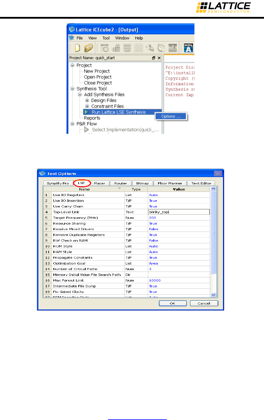
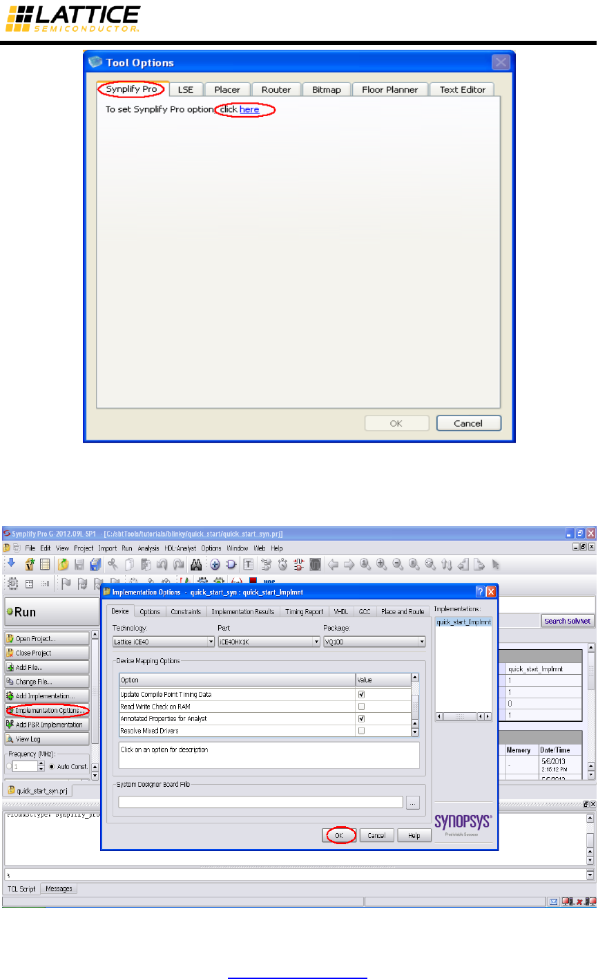
Next, set options for the synthesis tool. Select Tool > Tool Options. In the Tool Options dialog
box, click the tab of the tool. To change the value of an option, either click in its Value cell and
start typing to replace the value or double-click to edit the value or to see a menu of values. In the
Synplify Pro tab, click on the word “here” to open Synplify Pro. Then, in the Synplify Pro window,
click Implementation Options.
For now, do not change any option settings. Click Cancel.
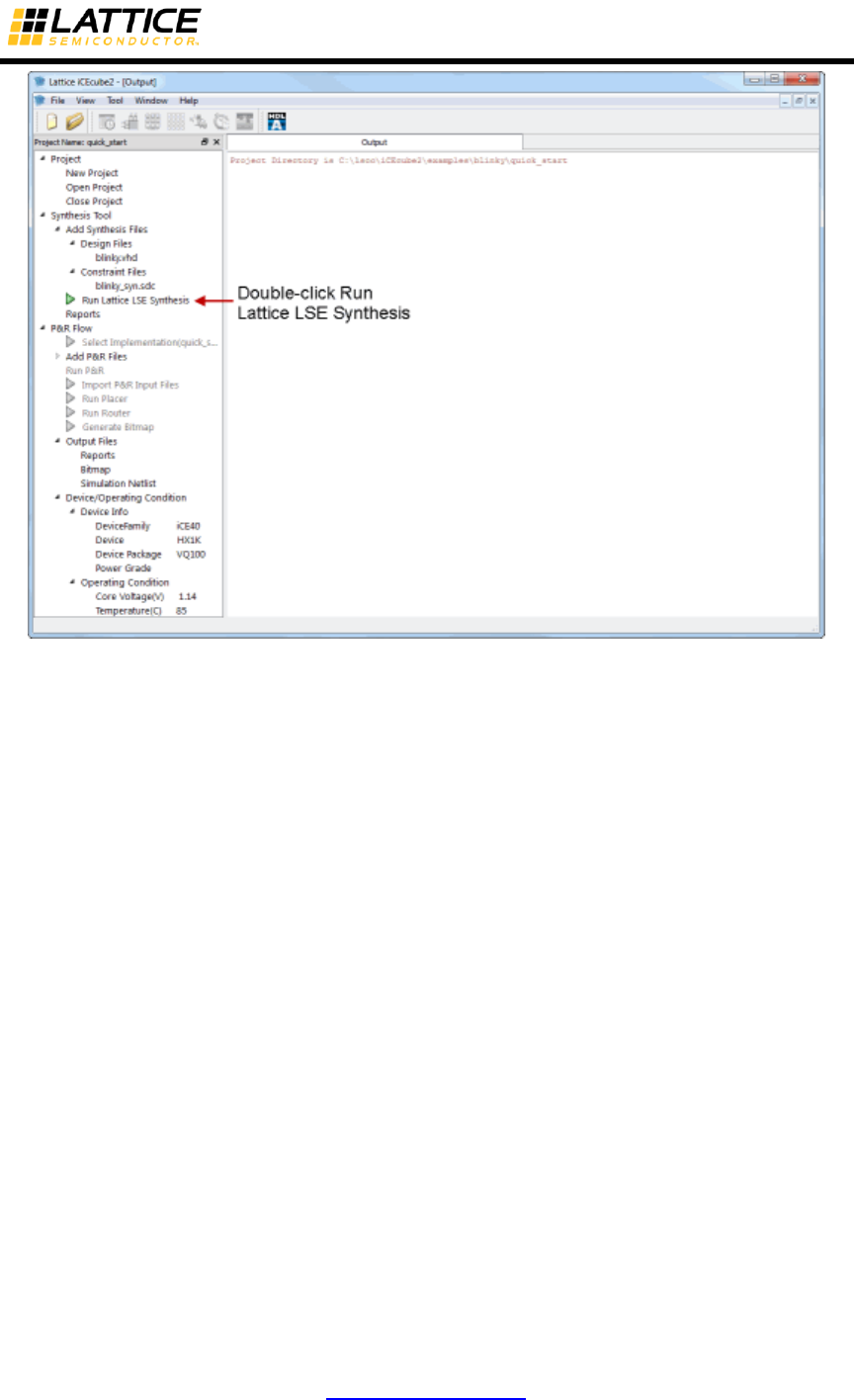
Double-click Run Lattice LSE Synthesis in the project navigator window. See Figure 2-6. This
starts the Lattice Synthesis Engine running. See Figure 2-7.
iCEcube2 User Guide www.latticesemi.com 16
Figure 2-6: Launch Synthesis Tool
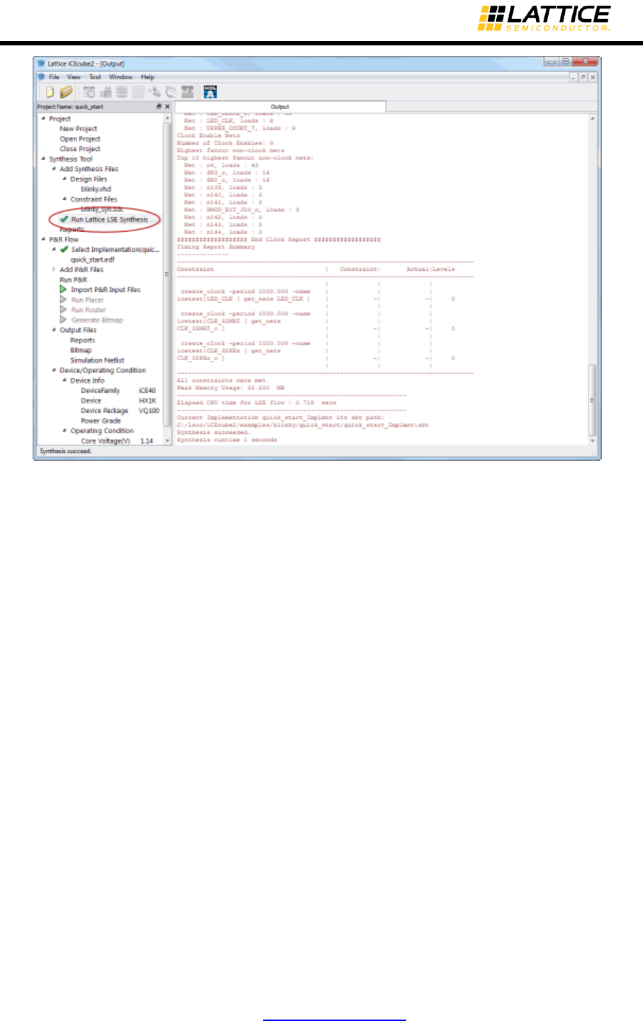
Once synthesis is complete, you will see a green checkmark next to the Run Lattice LSE
Synthesis command. The Output tab shows the actions taken along with any warning or error
messages. Scroll down toward the bottom to see the area, clock, and timing reports. See Figure
2-7.
iCEcube2 User Guide www.latticesemi.com 19
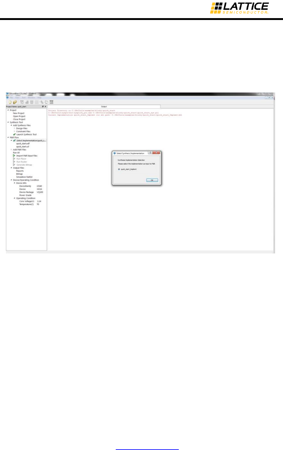
Select Implementation
Double-click on Select Implementation. See Figure 2-10. This will tell iCEcube2 which
synthesis implementation to process for place and route. If you have different synthesis
implementations, you will be able to select the synthesis implementation you wish to place and
route. Since we only have one implementation, select OK when the Select Synthesis
Implementation dialog box appears.
Figure 2-10: Select Synthesis Implementation
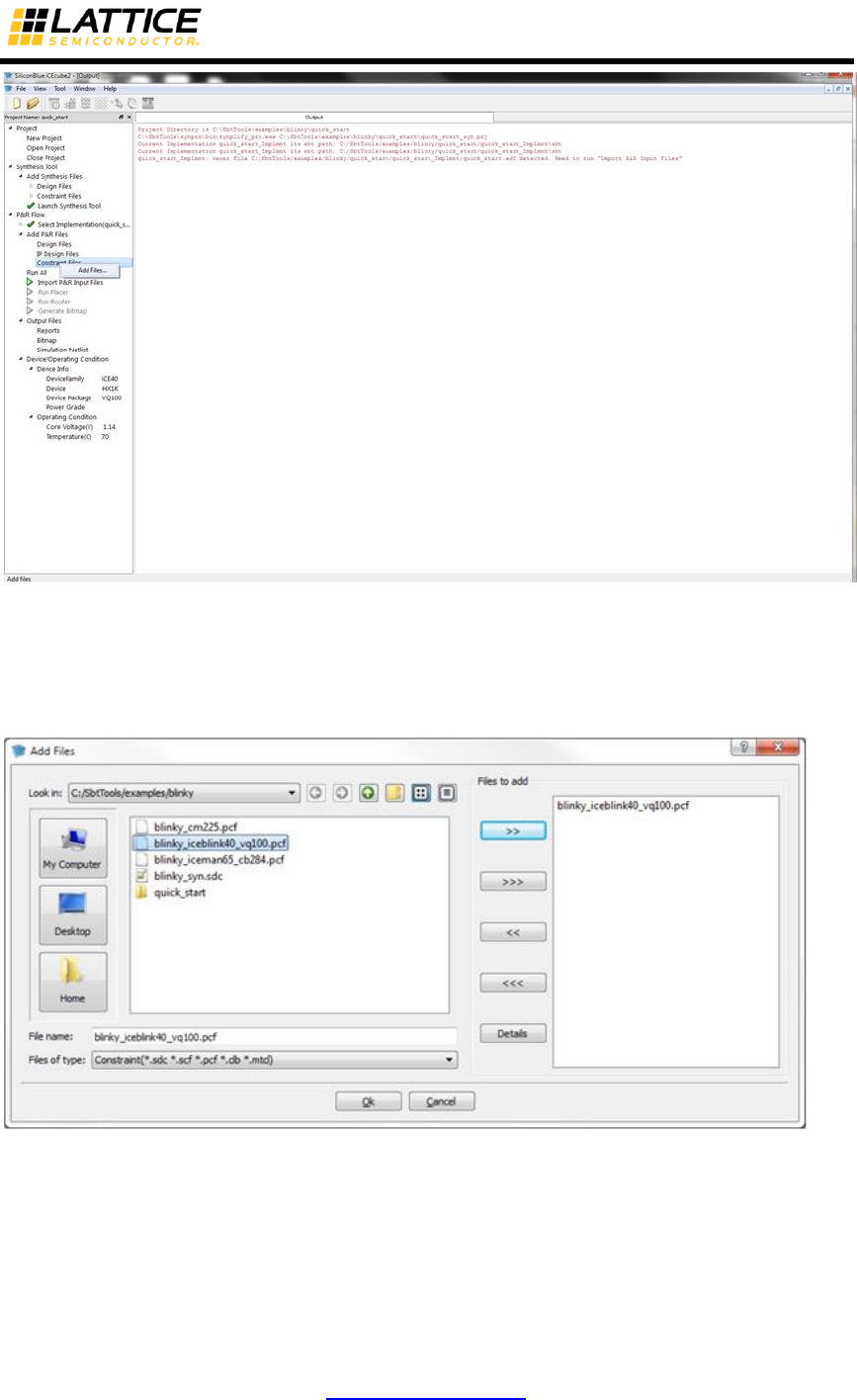
Importing Physical Constraints
Physical constraints such as pin assignments are stored in a .PCF file (Physical Constraint File).
Add the .PCF file to your project.
In the iCEcube2 Project Navigator, Right Click on Constraint Files. Select Add Files… See
Figure 2-11.
Note: For information on importing physical constraints from iCEcube to iCEcube2, please refer
to the Importing Physical Constraints from iCEcube to iCEcube2 section at the end of this
quick start guide.
iCEcube2 User Guide www.latticesemi.com 21
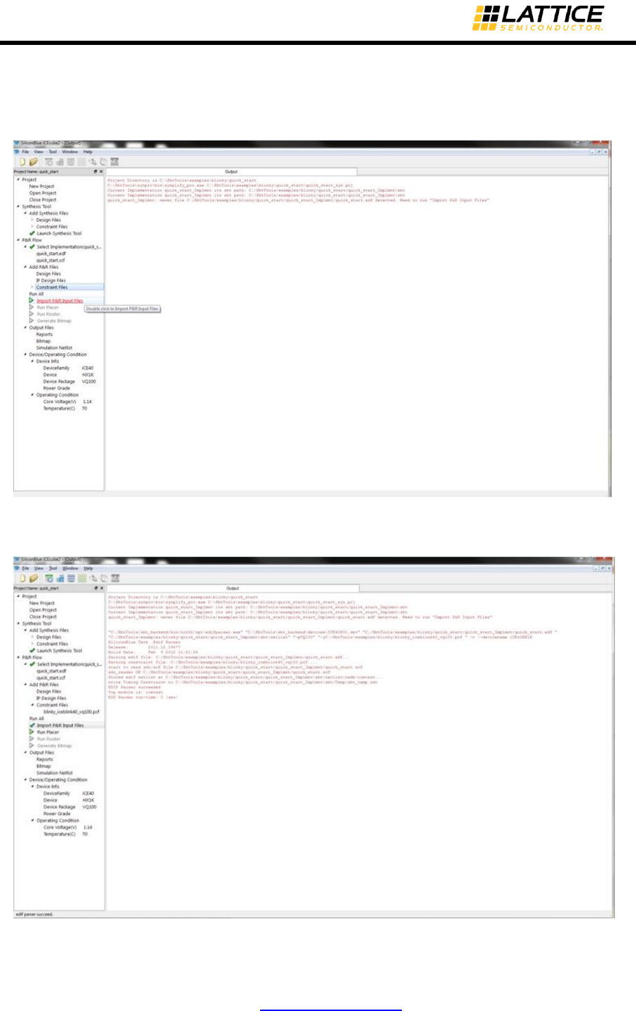
Import Place & Route Input Files
The next step is to import the files for Place and Route. Double-click on Import P&R Input
Files in the Project Navigator. See Figure 2-13. Once completed you will see a green check
next to Import P&R Input Files. See Figure 2-14.
Figure 2-13: Import P&R Input Files
Figure 2-14: Successful Import of P&R Input Files
iCEcube2 User Guide www.latticesemi.com 22
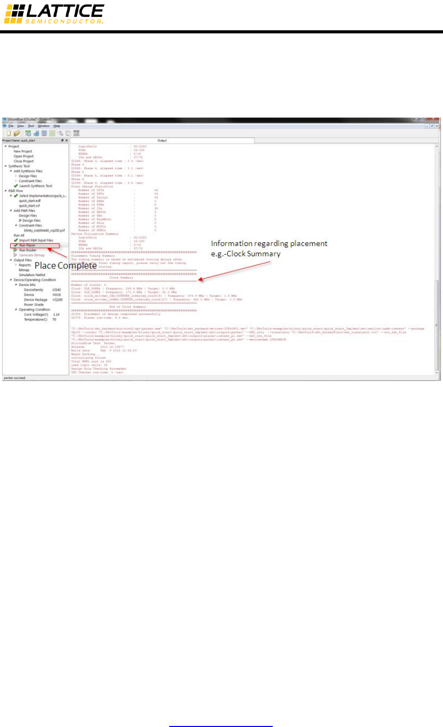
Place the Design
Double-click on Run Placer.
Once placement is complete, a green check will appear and the Output window will show
information about the placement of the design. See Figure 2-15.
Figure 2-15: Placer Run Status Display
View Floor Planner
At this point, since placement has been completed, you can view the placement of the design by
opening the Floor Planner. You can open the Floor Planner by going to the menu and selecting
Tool > Floor Planner or you can also select the Floor Planner Icon. See Figure 2-16.
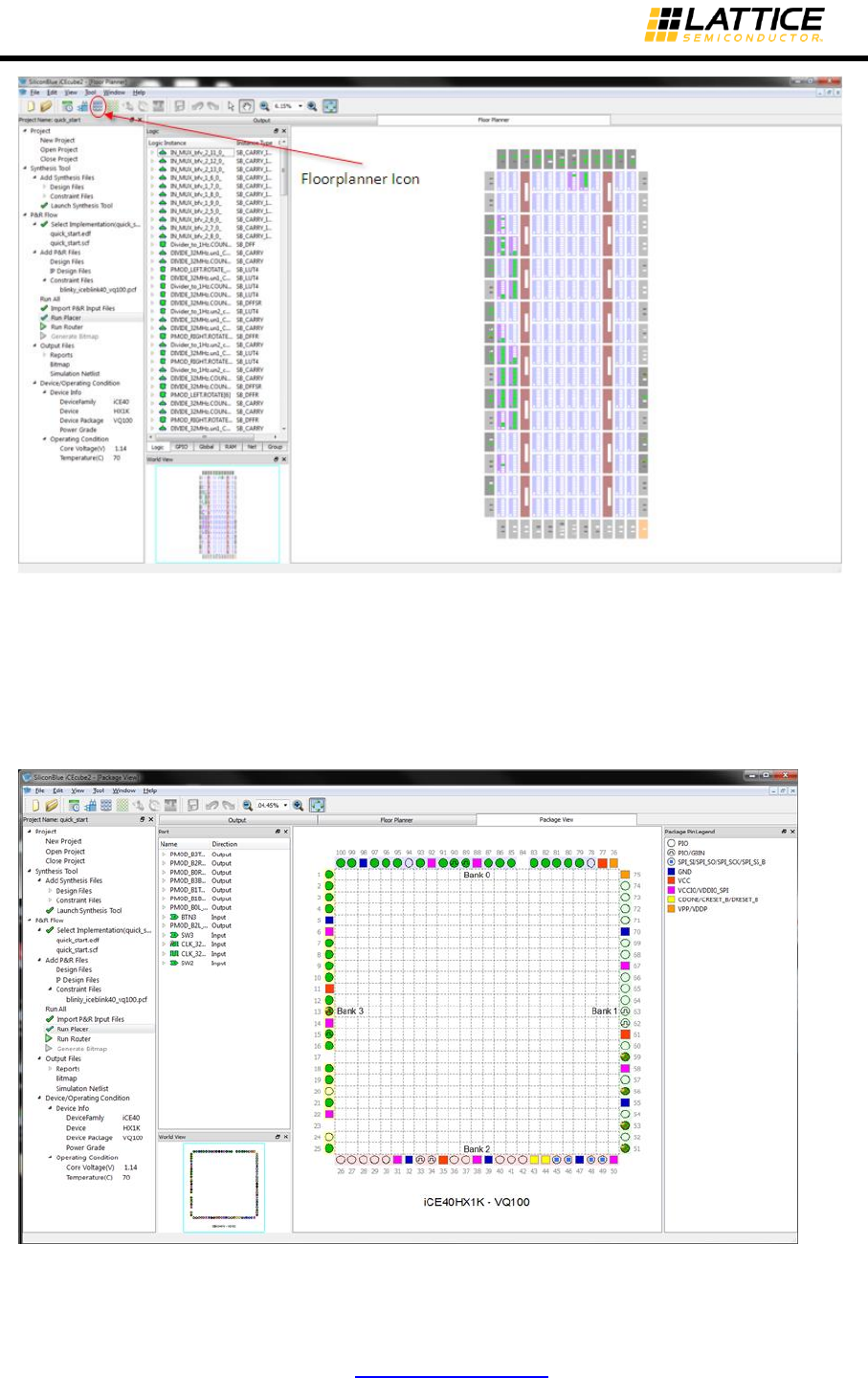
iCEcube2 User Guide www.latticesemi.com 23
Figure 2-16: Floorplanner View
View the Package View
You can also see how pins were placed for your design by selecting the Package View. You can
select the package viewer by going to the menu and selecting Tool > Package View or you can
also select the Package View Icon. See Figure 2-17.
Figure 2-17: Package View

iCEcube2 User Guide www.latticesemi.com 24
Route the Design
Double-click on Run Router in the project navigation window. Place and Route have been
separated into different steps as to allow you to re-route the design after making placement
modifications in the floor planner without having to re-run the placer.
Perform Static Timing Analysis
Now that you have routed the design, you can perform timing analysis to check to see if the
design meets your timing requirements. To launch the timing analyzer, go to the menu and
select Tool > Timing Analysis. You can also select the Timing Analysis Icon. See Figure 2-18.
Figure 2-18: Timing Analysis Summary
You can see from the timing analysis that our 32-kHz design is running at over 395 MHz and our
32-MHz clock is running at over 222 MHz (worst case timing). If we were not meeting timing, the
timing analyzer would allow you to see your failing paths and do a more in-depth analysis. For
this tutorial, we won’t go into details on timing slack analysis.
Perform Power Analysis
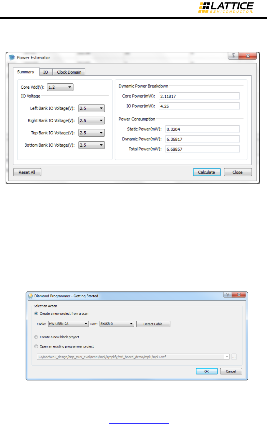
iCEcube2 also comes with power estimator tool. To launch the power estimator, go to the menu
and select Tool > Power Estimator. You can alternatively select the power estimator icon.
There are multiple tabs in the Power Estimator tool including Summary, IO, and Clock Domain as
shown in Figure 2-19. On the Summary tab, change the Core Vdd to 1.2V and make sure all IO
voltages are at 2.5V. Then hit Calculate. The estimator will update with power information for
iCEcube2 User Guide www.latticesemi.com 25
both static and dynamic power. For more information on using the IO and Clock Domain tabs,
please refer to the detailed section on the Power Estimator tool.
Figure 2-19: Power Estimator
Programming the Device
In order to program a device, you will need to generate a programming file. In the project
navigator, double click on Generate Bitmap.
You are now ready to program an iCE40 device with the generated bitmap.
Start the stand-alone Diamond Programmer. In Windows, from the Start menu, choose Lattice
Diamond Programmer <version_number> > Diamond Programmer.
The Diamond Programmer Getting Started dialog box appears, as shown in Figure 2-20.
Figure 2-20 : Getting Started Dialog Box

iCEcube2 User Guide www.latticesemi.com 26
Choose Create a New Project from a Scan button and click OK. The Diamond Programmer
main window appears. In the Cable Settings box in the upper right, click Detect Cable.
Diamond Programmer will indicate in the bottom output tab that the Lattice HW-USBN-2A USB
programming cable was detected, as shown in
Figure
2-21.
Figure 2-21 : Diamond Programmer Main Window
In the Device Family field, click the Generic JTAG Device box and choose iCE40 from the drop-
down menu, as shown in Figure 2-22 .
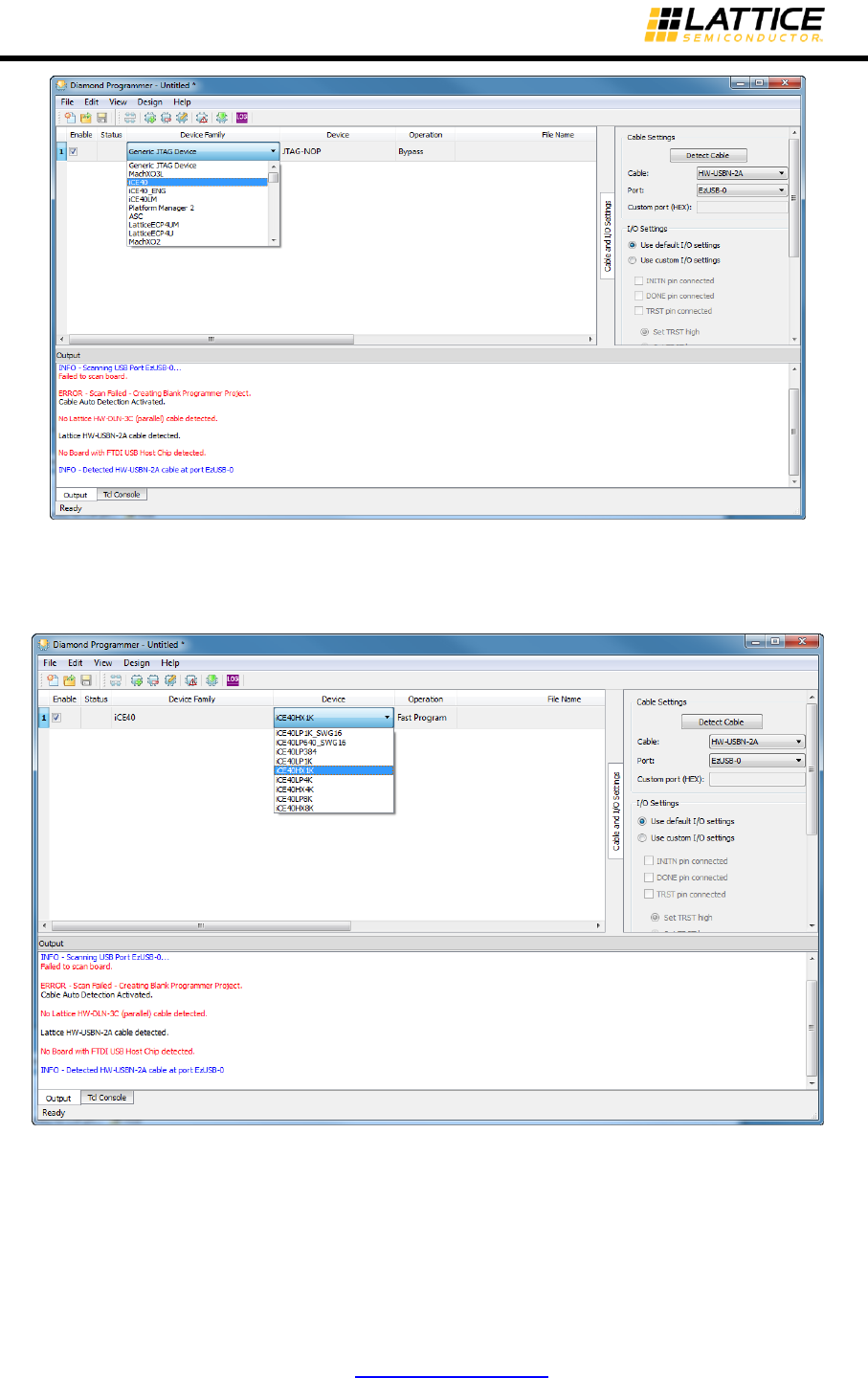
iCEcube2 User Guide www.latticesemi.com 27
Figure 2-22: Choosing iCE40 Device Family
In the Device column, choose iCE40HX1K from the drop-down menu, as shown in Figure 2-23.
Figure 2-23 : Choosing iCE40HX1K Device
There are three basic programming flows for configuring the iCE40 device. This section explains
programming iCE40 device using an external SPI Flash device available in iCEblink40-HX1K
evaluation board.
iCEcube2 User Guide www.latticesemi.com 28
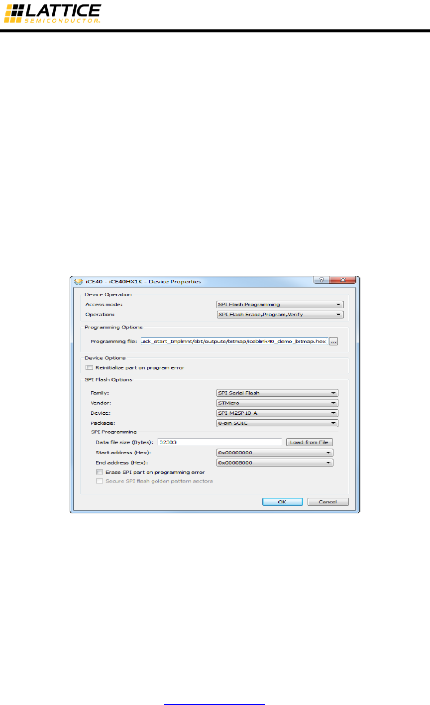
Choose Edit > Device Properties, or double-click the Operation box to display the Device
Properties dialog box, as shown in Figure 2-24.
In the Device Properties dialog box, set options as follows:
Access Mode: SPI Flash Programming
Operation: SPI Flash Erease,Program,Verify
In the Programming File box, browse to the .hex file you generated with iCEcube2.
In the SPI Flash Options box, choose the following options:
Family : SPI Serial Flash
Vendor : STMicro
Device : SPI-M25P 10-A
Package : 8-pin SOIC
The Device Properties dialog box should be configured as shown in Figure 2-24. In the Device
Properties dialog box, click OK.
Figure 2-24 : Device Properties Dialog Box
In the Diamond Programmer main window, choose Design > Program, or click the Program icon
in the toolbar, as shown in Figure 2-25. Once the SPI Flash is programmed, the output tab in the
lower left portion of Diamond Programmer indicates Operation successful.
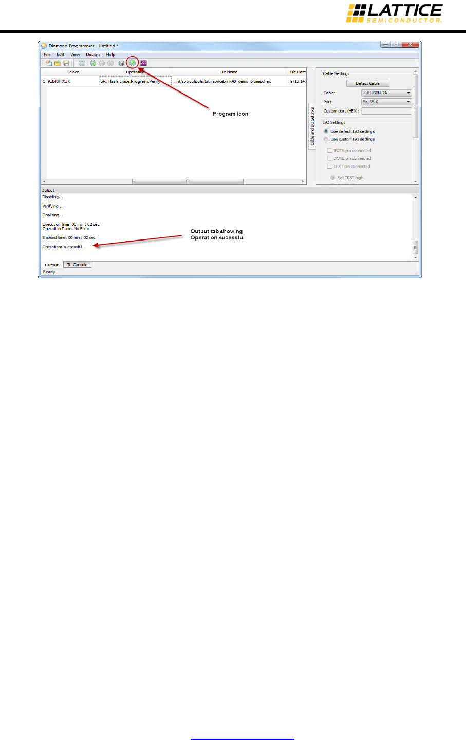
iCEcube2 User Guide www.latticesemi.com 29
Figure 2-25 : Program the device.
The external SPI Flash on the Lattice iCEblink40-HX1K evaluation board has been programmed,
and the iCE40 is configured from the SPI flash.
Addendum:
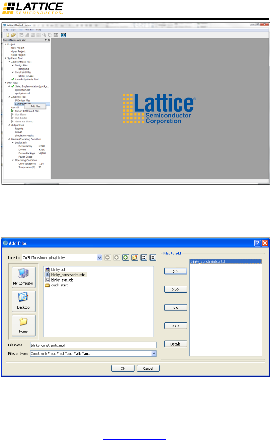
Importing Physical Constraints from iCEcube to iCEcube2
For users who have created physical constraints using iCEcube, this section describes how to
import and convert those constraints for use in iCEcube2. This section will demonstrate how to
import a .MTCL file from iCEcube and save it into .PCF format used in iCEcube2.
In the iCEcube2 project navigator, Right-click on Constraint Files and select Add Files. See
Figure 2-26.
iCEcube2 User Guide www.latticesemi.com 31
Import Place & Route Input Files
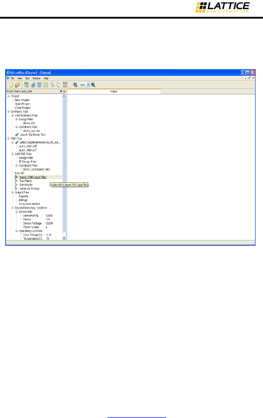
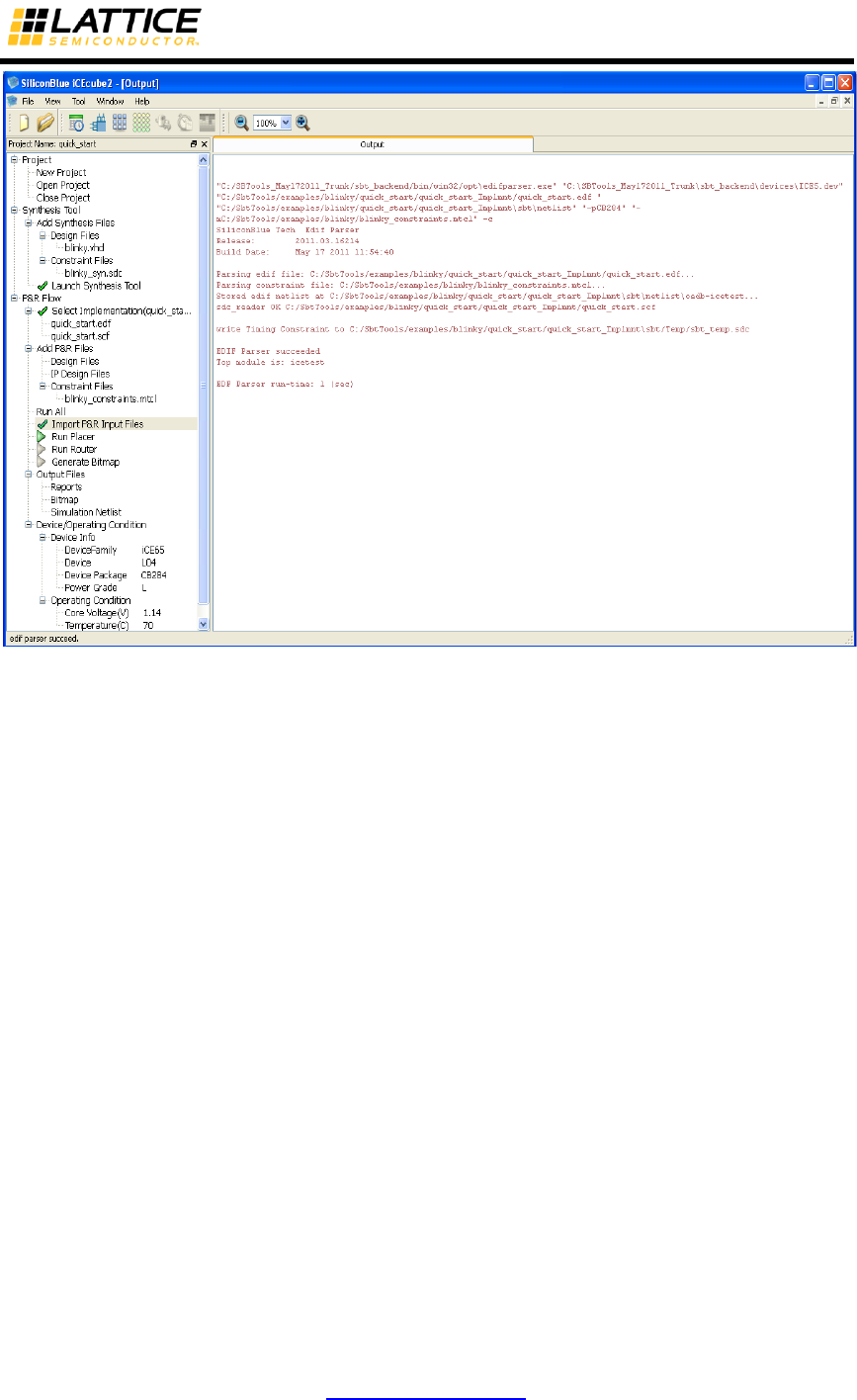
The next step is to import the files for Place and Route. Double-click on Import P&R Input
Files in the Project Navigator. See Figure 2-28. Once importing of files completed you will see a
green check next to Import P&R Input Files. See Figure 2-29.
Figure 2-28: Double-Clock on Import P&R Input Files
iCEcube2 User Guide www.latticesemi.com 32
Figure 2-29: Successful Import of P & R Input Files
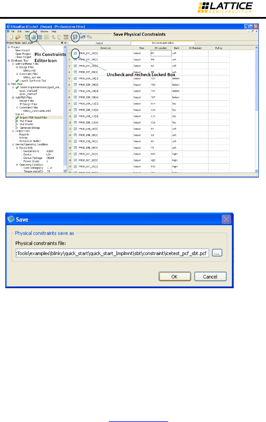
Saving Physical Constraints into .pcf Format
Open the Pin Constraints Editor by going to the menu and selecting Tool > Pin Constraints
Editor or you can also select the Pin Constraints Editor Icon. See Figure 2-30. You will see a list
of pin assignments that are locked under the locked column. Uncheck and Recheck one of the
pins under the locked column. The save icon will now become an active icon. Click on the
Save physical constraints icon. This will bring up a dialog box where you can save the PCF
file. Hit OK. See Figure 2-31. The .PCF file contains physical constraints in the design used for
place and route.
iCEcube2 User Guide www.latticesemi.com 34
Chapter 3 iCEcube2 Project Setup and Navigation
Introduction
This chapter describes the features of the iCEcube2 Project Manager and how to set up a design
Project. The primary functions of the Project Manager include project setup, launching the Lattice
Synthesis Engine (LSE) or Synplify pro for synthesis, placing and routing the design, launching
the Aldec Active-HDL for simulation and launching the software required to Program the target
device.
This chapter assumes that the reader is familiar with the New Project creation process as
described in Chapter 2 Quick Start.
Project Manager GUI
Figure 3-1 below displays the Project Manager GUI. A new project can be opened by clicking on
the New Project icon or the File > New Project menu item. Similarly, an existing project can be
opened or closed using the Open Project and Close Project icons.
Figure 3-1 : iCEcube2 Project Flow Manager
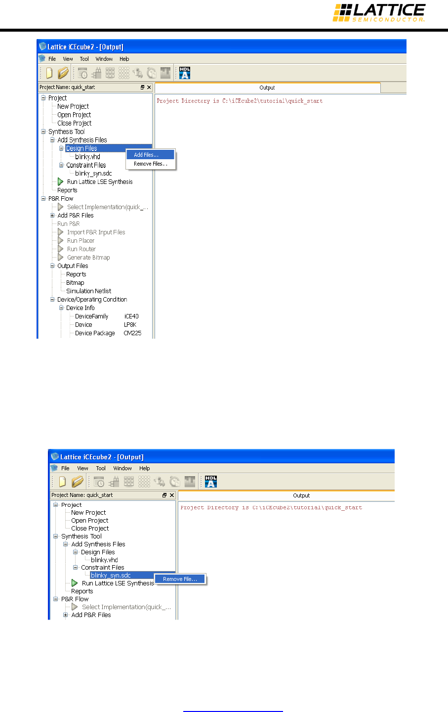
Adding/Deleting Design and Constraint Files
Design and Constraint files can be added or removed from the project by selecting Design Files
or Constraint Files respectively as displayed in Figure 3-2.
iCEcube2 User Guide www.latticesemi.com 35
Figure 3-2 : Adding/Removing Design Files to the design project
Deleting a specific file can be accomplished by selecting the file name and clicking the right-
button on the mouse. Figure 3-3 below displays the state of the GUI upon clicking the mouse
button.
Figure 3-3 : Removing Files from the design project
iCEcube2 User Guide www.latticesemi.com 36
Selecting Synthesis Tool and Setting synthesis Options
The iCEcube2 software supports Synplify-pro synthesis tool and Lattice Synthesis tool (LSE) to
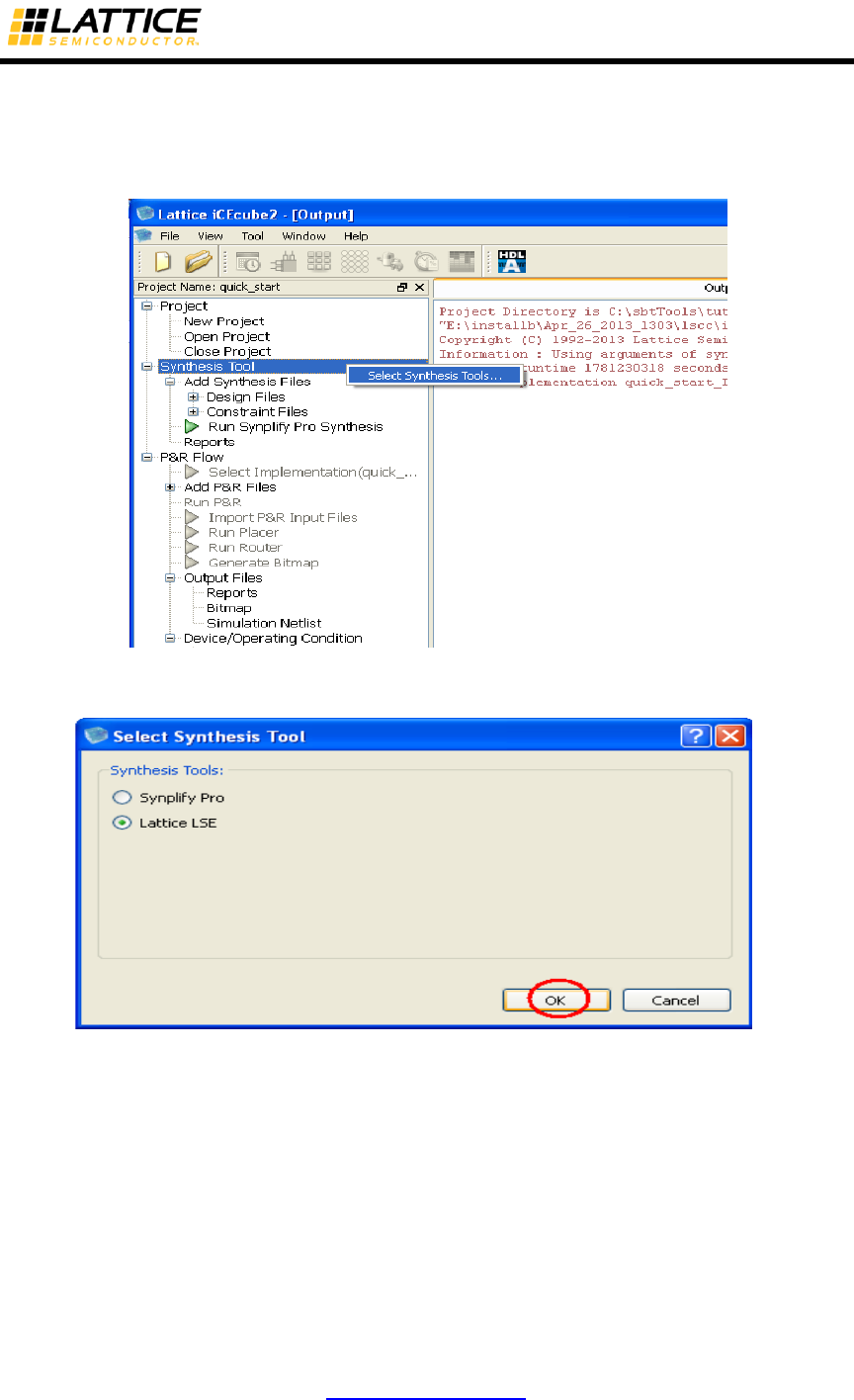
synthesis the design. In order to change the synthesis tool, click right-mouse button on
“Synthesis Tool” item and select the synthesis tool as shown in Figure 3-5.
Figure 3-4 : Select Synthesis Tool
Figure 3-5 : Synthesis Tool Selection Wizard
To set the LSE synthesis tool options, click “right- mouse” button on the “Run LSE Synthesis” as
shown in Figure 3-6.
iCEcube2 User Guide www.latticesemi.com 37
Figure 3-6 : Open LSE Tool Options Wizard
Set the LSE tool options and click on “OK” button to save the changes. Rerun the LSE synthesis.
Figure 3-7 : LSE tool options wizard
To set the Synplify-Pro synthesis tool options, click “right-mouse” button on the “Run Synplify-
Pro Synthesis” item. This will pop up the “Tool Options” wizard. In the “Synplify Pro” tab select
the word “here” to open the Synplify-Pro GUI.
iCEcube2 User Guide www.latticesemi.com 39
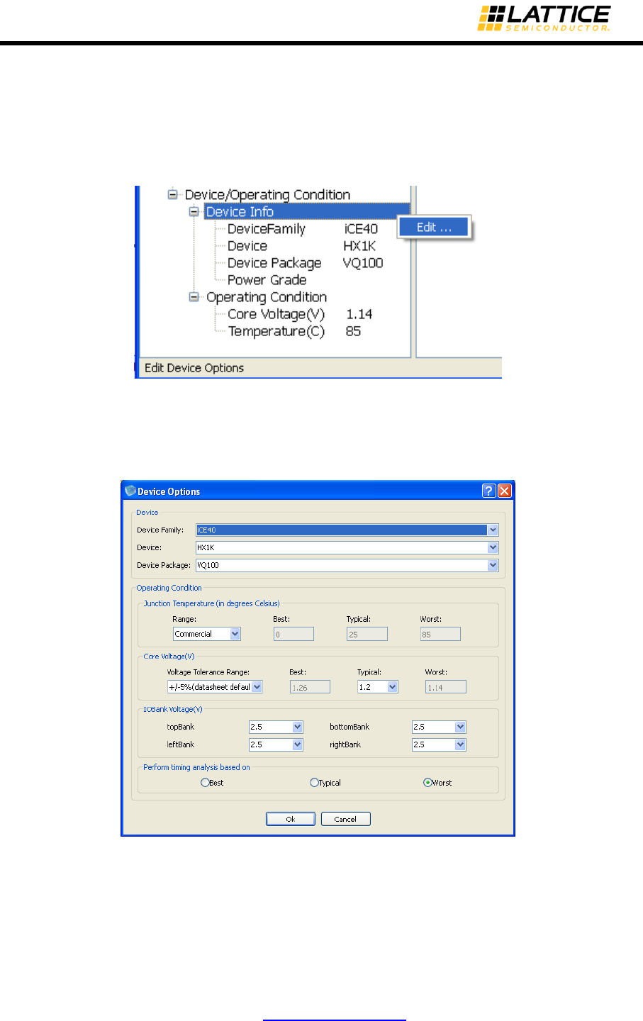
Selecting the Target Device and Operating Conditions
The iCEcube2 software provides the ability to specify the operating conditions for the target
device. In order to change the Target Family, Device and/or the Operating Conditions, click the
right-button on the mouse, in the Device/Operating Condition window to display the Edit
action. This is shown in Figure 3-10.
Figure 3-10 : Modifying the Device Selection/Operating Conditions
Device options wizard is shown in Figure 3-11.
Figure 3-11: Device Options for iCE40 Family

iCEcube2 User Guide www.latticesemi.com 40
In order to specify a suitable target Device, the following steps need to be performed:
1. Specify a Device Family
2. Specify a Device using the drop-down menu
3. Select a suitable Device Package for the device selected in the previous step
Specifying the Operating Conditions for the target device involves the following steps:
1. Junction Temperature
a. Select an appropriate Junction Temperature Range from the options available.
Depending on the Power Grade selected for the target device, the software provides
built-in options such as Commercial and Industrial temperature ranges.
b. If the device’s operating conditions do not fall into either the Commercial or the
Industrial temperature ranges, the software also permits the user to specify a
customized junction temperature. This is accomplished by selecting the Custom option,
and manually specifying the Best, Typical and Worst Case junction temperatures.
2. Core Voltage: Select a Voltage Tolerance Range from the provided options.
3. IO Bank Voltage: This option is available only for iCE40 family as shown in Figure 3-11.
Select a bank voltage from the provided options for the top, bottom, left, right banks. The
specified IO Voltage values are used by Power Estimator and Static Timing Analysis tools.
In order for Static Timing Analysis to be performed at the desired Operating Conditions, the
software provides the ability to select the Best Case, Typical Case or Worst Case conditions.
Output Window
The iCEcube2 Project Flow Manager software provides an Output Window to display messages,
warnings and errors.
Simulation Wizard
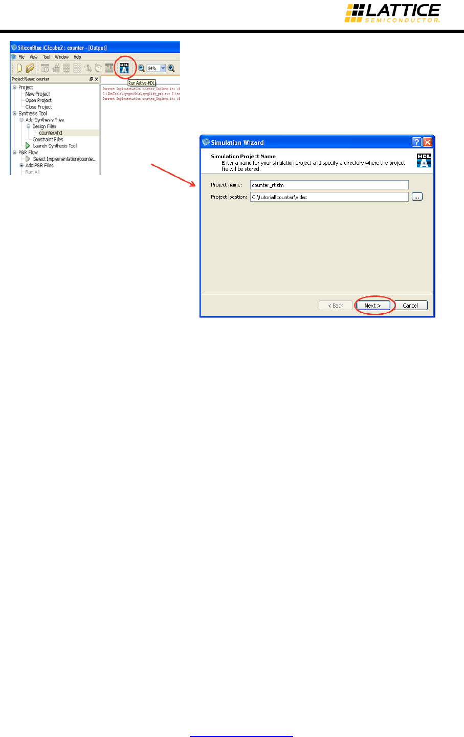
The iCEcube2 windows software installs Aldec Active-HDL, a windows based simulator tool to
perform functional and timing verification of the implemented designs. The “Simulation Wizard” in
the project navigator allows the user to create a simulation project for Aldec Active-HDL, select
the simulation netlist, simulation language and invokes the Aldec Active-HDL interface.
Select Active-HDL icon to invoke the “Simulation Wizard” as shown in Figure 3-12. Refer to
chapter “Simulating Design with ALDEC Active-HDL” for more details about simulation wizard and
simulation steps with Aldec Active-HDL.
iCEcube2 User Guide www.latticesemi.com 41
Figure 3-12 : Invoking Simulation Wizard.
PLL Module Generator
Certain devices of the iCE40 family include a Phase Lock Loop (PLL) function. The PLL function
requires configuration before it can be used in a design. To help configure the PLL, the iCEcube2
Project Flow Manager includes a PLL Module Generator, which can be launched from the Tool >
Configure > Configure PLL Module menu item, as displayed in Figure 3-13.

iCEcube2 User Guide www.latticesemi.com 42
Figure 3-13: Launching the PLL Module Generator
The PLL Module Generator allows the user to create a new PLL configuration, or edit an existing
one as shown in Figure 3-14.
The output of the PLL Module Generator is a PLL module file (Verilog), that instantiates a PLL, as
configured by the user. A secondary file (wrapper), that includes an instance of the PLL module,
is generated in order to help instantiate the PLL module in the user’s design. Note that the PLL
module file should be included in the list of design files.
Once a PLL module file has been generated, it can be edited, by selecting the “Modify an existing
PLL configuration” option (Figure 3-14).

iCEcube2 User Guide www.latticesemi.com 43
Figure 3-14: Create/Modify a PLL configuration
Configuring the iCE65 PLL
In the PLL Module Generator wizard, select Device Family as iCE65 and provide the PLL
Module Name. Click on the OK button. The PLL Module Generator launches a wizard to help the
user configure the PLL as per the design requirements. This section describes the features of
iCE65 family PLL modules.
PLL Type
The connectivity of the PLL to its surrounding logic determines the PLL Type. The iCEcube2
software supports the following PLL types. These PLL type options can be selected on the first
page of the wizard, as displayed in Figure 3-15.
1. General Purpose IO Pad or Core Logic: In this scenario, the PLL input (source clock) is
driven by a signal from the FPGA fabric. This signal can either be generated on the FPGA
core, or it can be an external signal that was brought onto the FPGA using a General
Purpose IO pad. The PLL output (generated clock) is available on the FPGA to drive a global
clock network, as well as regular routing.
2. Clock Pad: The PLL input clock (source) is driven by a dedicated clock pad located in IO
Bank 2
a. The PLL output (generated clock) is available to drive a global clock network, as well
as regular routing. The PLL source clock is not available on the FPGA.
b. The PLL output (generated clock) is available to drive a global clock network, as well
a regular routing. The PLL source clock is also available on the FPGA, and can drive
a global clock network, as well as regular routing.
iCEcube2 User Guide www.latticesemi.com 44
Figure 3-15: Selecting the PLL Type and Operation Mode
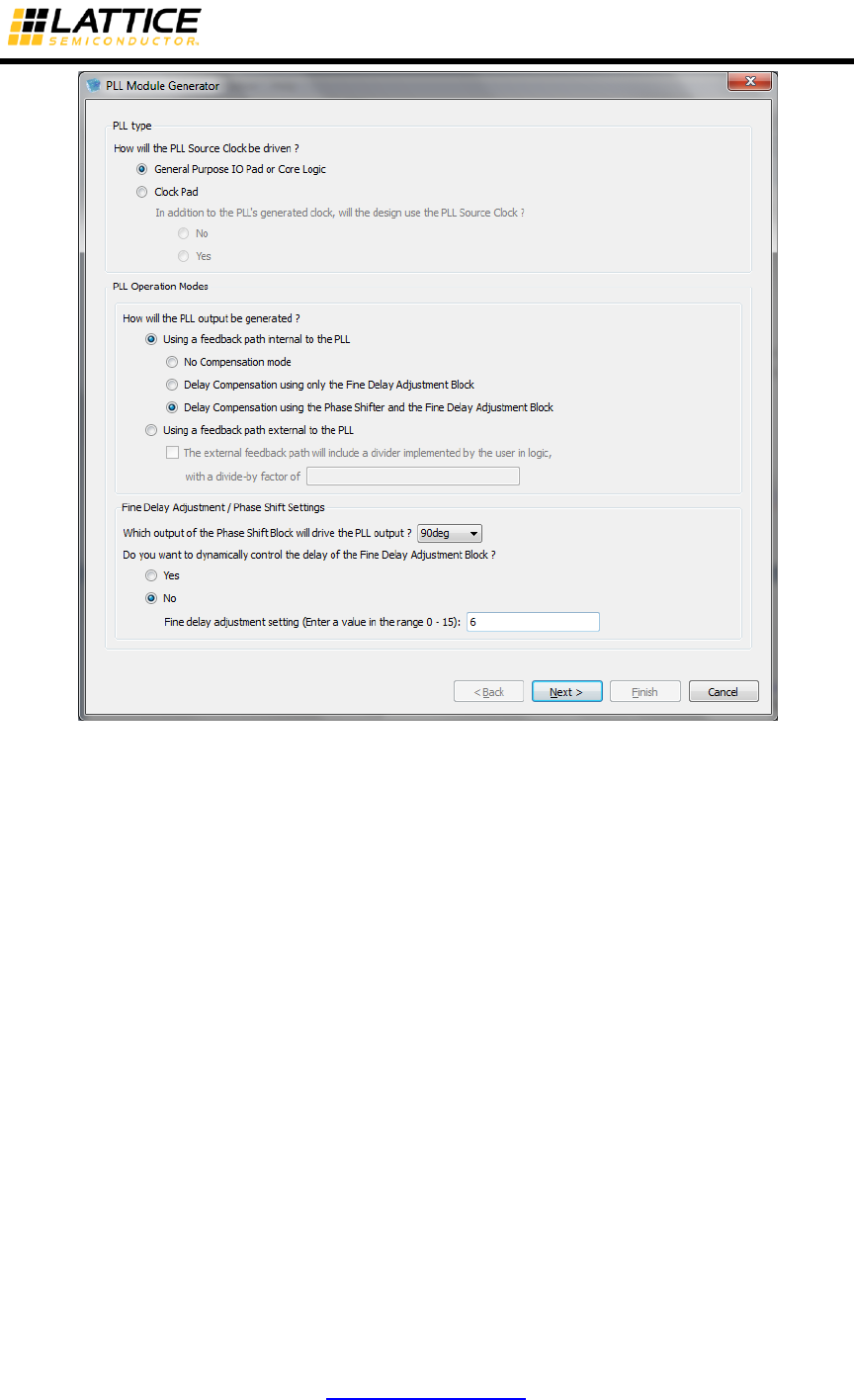
PLL Operation Modes
The PLL can be configured to operate in one of multiple modes. An Operation Mode determines
the feedback path of the PLL and enables phase alignment of the generated clock with respect to
the source clock.
The iCEcube2 software supports the following PLL Operation modes:
1. No Compensation mode: The PLL can be used for generating the desired output frequency,
without the ability to control the phase of the generated clock.
2. Delay Compensation using only the Fine Delay Adjustment (FDA) Block: In this mode, the
feedback path is internal to the PLL but traverses through a fine delay adjustment circuit that
permits user control of the feedback path delay in 16 steps of 0.15 ns each. The delay
adjustment can be controlled dynamically through signals connected to the PLL, or it can be
fixed i.e. once configured, the delay contributed by the delay block can only be changed upon
re-programming the FPGA with a different bit configuration.
3. Delay Compensation using the Phase Shifter and the Fine Delay Adjustment (FDA) Block:
The Phase Shifter provides four outputs corresponding to a phase shift of 0 degrees, 90
degrees, 180 degrees or 270 degrees. In addition, this feedback path provides additional
delay adjustment through the FDA block.
4. Delay Compensation using a feedback path external to the PLL: The feedback path traverses
through FPGA routing (external to the PLL) followed by the Fine Delay Adjustment (FDA)
iCEcube2 User Guide www.latticesemi.com 45
Block. Hence, in effect, two delay controls are available – the external path for coarse
adjustment and the FDA block for fine delay adjustment.
Figure 3-16 : PLL Module Generator – Frequency Specification
Fine Delay Adjustment: The delay contributed by the FDA block can be Fixed or controlled
dynamically during FPGA operation. If Fixed, it is necessary to provide a number (n) in the range
0-15 to specify the delay contributed to the feedback path. The delay for a setting “n” is calculated
as follows
FDA delay = (n+1)*0.15 ps, where “n” is the value specified by the user, and 0 ≤ n ≤ 15
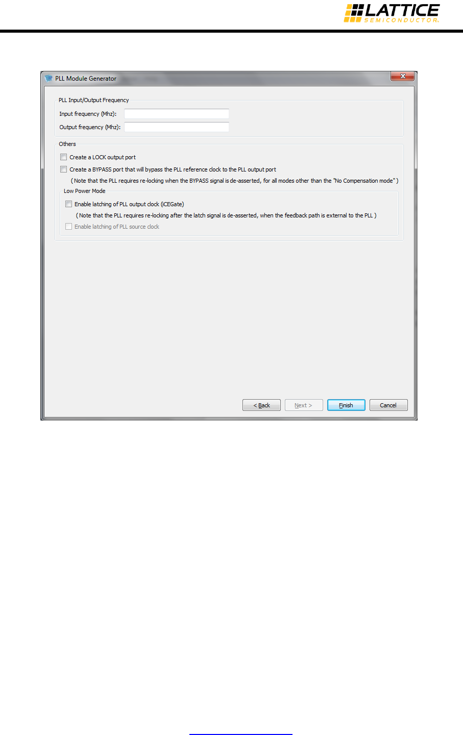
Frequency Specification: The input and output frequency of the PLL should be specified in MHz
as shown in Figure 3-16. Depending on the values provided by the user, the PLL is internally
configured to generate the specified output frequency.
In case the frequency specified is not in the range permitted by the Operation Mode, the software
provides appropriate feedback, as displayed in Figure 3-17.

iCEcube2 User Guide www.latticesemi.com 46
Figure 3-17: Frequency Validation by PLL Configurator
Other options:
LOCK: A Lock signal is provided to indicate that the PLL has locked on to the incoming signal.
Lock asserts High to indicate that the PLL has achieved frequency lock with a good phase lock.
BYPASS: A BYPASS signal is provided which both powers-down the PLL core and bypasses it
such that the PLL output tracks the input reference frequency.
Low Power Mode: A control is provided to dynamically put the PLL into a Lower Power Mode
through the iCEGate feature. The iCEGate feature latches the PLL Output signal, and prevents
unnecessary toggling.
The RESET (Active Low) port is always generated, and an explicit PLL reset operation is required
to initialize the PLL functionality.
Configuring the iCE40 PLL
Most devices in the iCE40 family provide two PLL functions, each of which can be configured
independently.
In the PLL Module Generator wizard, select Device Family as iCE40 and provide the PLL
Module Name. Click on the OK button. The PLL Module Generator launches a wizard to help the
user configure the PLL as per the design requirements.
PLL Type
The connectivity of the PLL to its surrounding logic determines the PLL Type. The iCEcube2
software supports the following PLL types. These PLL type options can be selected on the first
page of the wizard, as displayed in Figure 3-18.
1. Select the number of global networks to be driven by the PLL output. Setting the value to “1”
generates a PLL which drives a single global clock network, as well as regular routing.
Setting the value to “2” generates a PLL which drives two global clock networks as well as
two regular routing resources.
2. Specify the input to the PLL:
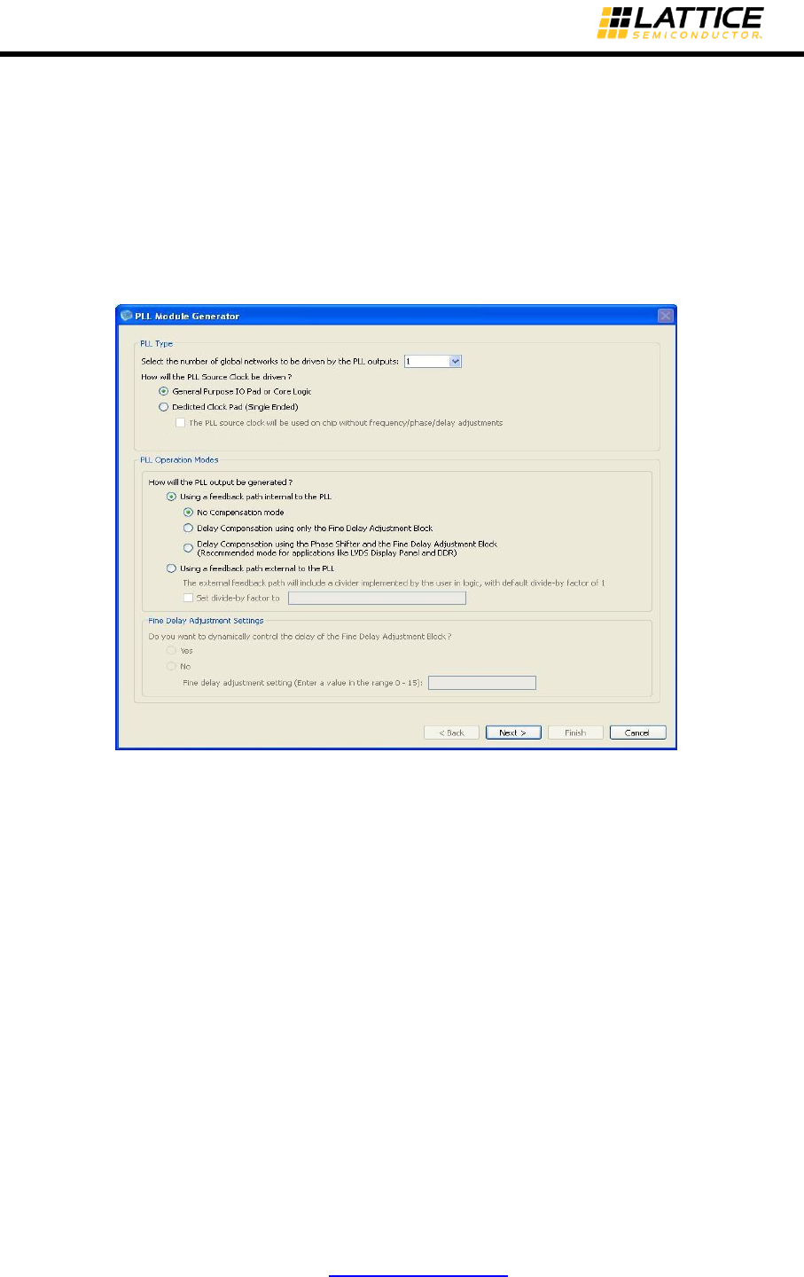
iCEcube2 User Guide www.latticesemi.com 47
General Purpose IO Pad or Core Logic: In this scenario, the PLL input (source clock) is
driven by a signal from the FPGA fabric. This signal can either be generated on the FPGA
core, or it can be an external signal that was brought onto the FPGA using a General
Purpose IO pad.
Dedicated Clock Pad (Single Ended): The PLL input clock (source) is driven by a dedicated
single ended clock pad located in IO Bank 2 (Bottom bank) or IO Bank 0 (Top bank). (In case
two global networks were selected in the previous step, the input signal can be used as-is on
the logic fabric, i.e. it can bypass the PLL. In the rare situation that this is required, select the
check-box, “The PLL source clock will be used on chip without frequency/phase/delay
adjustments”.)
Figure 3-18: iCE40 PLL - Selecting PLL Type and Operation Modes
PLL Operation Modes
The PLL can be configured to operate in one of multiple modes. An Operation Mode determines
the feedback path of the PLL, and enables phase alignment of the generated clock with respect
to the source clock.
The iCEcube2 software supports the following PLL Operation modes:
1. No Compensation mode: The PLL can be used for generating the desired output frequency,
without the ability to control the phase of the generated clock.
2. Delay Compensation using only the Fine Delay Adjustment (FDA) Block: In this mode, the
feedback path is internal to the PLL but traverses through a fine delay adjustment circuit that
permits user control of the feedback path delay in 16 steps of 0.15 ns each. The delay
adjustment can be controlled dynamically through signals connected to the PLL, or it can be
fixed i.e. once configured, the delay contributed by the delay block can only be changed upon
re-programming the FPGA with a different bit configuration.
3. Delay Compensation using the Phase Shifter and the Fine Delay Adjustment (FDA) Block.
For single port PLL types the Phase Shifter provides two outputs corresponding to a phase
shift of 0 degrees and 90 degrees. For two port PLL types, the Phase Shifter has two modes:

iCEcube2 User Guide www.latticesemi.com 48
Divide-by-4 mode and Divide-by-7. In Divide-by-4 mode, the output of B port can be shifted
either 0 degrees or 90 degrees w.r.t to A port outputs. In Divide-by-7 mode, the B port output
frequency can be set to have a frequency ratio of 3.5:1 or 7:1 w.r.t the port A output
frequency. In addition to the delay compensation provided by the phase shifter, this feedback
path provides additional delay adjustment through the FDA block.
4. Delay Compensation using a feedback path external to the PLL: The feedback path traverses
through FPGA routing (external to the PLL) followed by the Fine Delay Adjustment (FDA)
Block. Hence, in effect, two delay controls are available – the external path for coarse
adjustment and the FDA block for fine delay adjustment.
Fine Delay Adjustment: The delay contributed by the FDA block can be Fixed or controlled
dynamically during FPGA operation. If Fixed, it is necessary to provide a number (n) in the range
0-15 to specify the delay contributed to the feedback path. The delay for a setting “n” is calculated
as follows
FDA delay = (n+1)*0.15 ps, where “n” is the value specified by the user, and 0 ≤ n ≤ 15.
Additional Delay Adjustment: In addition to Fine Delay Adjustment in the feedback path, the user
can specify additional delay on the PLL output ports as shown in Figure 3-19. The delay
contributed by the delay block can be Fixed or controlled dynamically during FPGA operation. If
Fixed, it is necessary to provide a number (n) in the range 0-15 to specify the delay contributed to
the feedback path. The delay for a setting “n” is calculated as follows
FDA delay = (n+1)*0.15 ps, where “n” is the value specified by the user, and 0 ≤ n ≤ 15.
This additional delay is applied on the output of single port PLL and port A of two port PLL types.
Phase Shift Specification: Phase Shift specification allows the user to specify 0 degrees or 90
degrees phase shift.
Figure 3-19: iCE40 PLL - Additional Delay and Phase Shift Options
iCEcube2 User Guide www.latticesemi.com 49
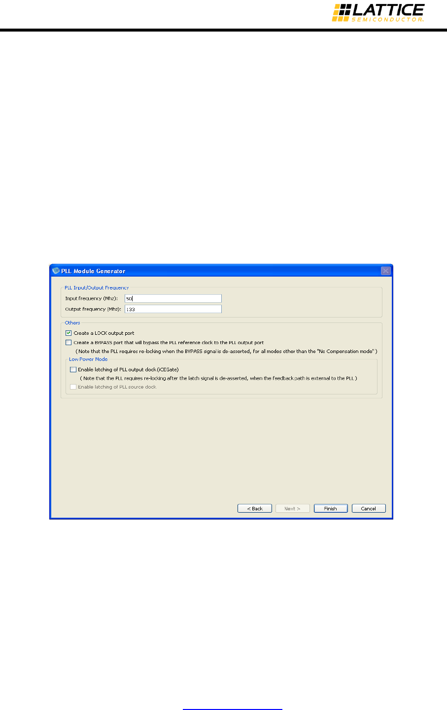
Frequency Specification: The input and output frequency of the PLL should be specified in MHz
as shown in Figure 3-20. Depending on the values provided by the user, the PLL is internally
configured to generate the specified output frequency.
Frequency Specification window also checks for the input and output frequencies given by the
user. If the specified frequencies are at a range that cannot be generated by the PLL, then a
popup dialog box is displayed as shown in Figure 3-17 asking the user to enter the frequencies in
valid range.
LOCK: A Lock signal is provided to indicate that the PLL has locked on to the incoming signal.
Lock asserts High to indicate that the PLL has achieved frequency lock with a good phase lock.
BYPASS: A BYPASS signal is provided which both powers-down the PLL core and bypasses it
such that the PLL output tracks the input reference frequency.
Low Power Mode: A control is provided to dynamically put the PLL into a Lower Power Mode
through the iCEGate feature. The iCEGate feature latches the PLL Output signal, and prevents
unnecessary toggling.
The RESET (Active Low) port is always generated, and an explicit PLL reset operation is required
to initialize the PLL functionality.
Figure 3-20: iCE40 PLL - Frequency Specification
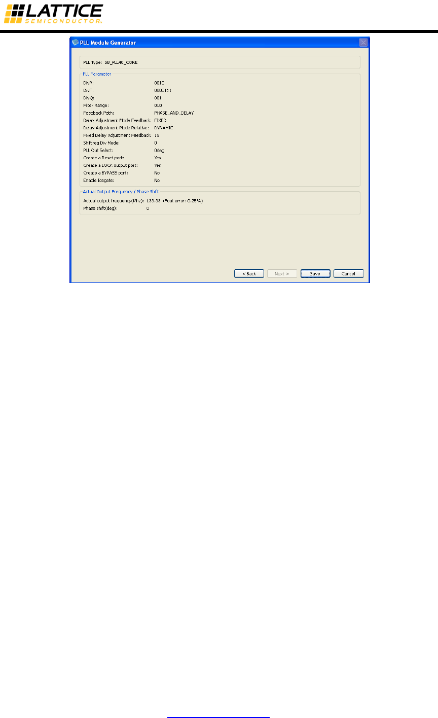
PLL Summary: The PLL Configuration summary is shown in Figure 3-21. Click on “Save” to
save the PLL configuration file.
iCEcube2 User Guide www.latticesemi.com 50
Figure 3-21 : PLL Summary
PLL Dynamic Reconfiguration
iCE5LP devices supports dynamic reconfiguration of PLL to change the output frequency, phase
shift and clock delays at runtime. Reconfiguration of PLL directly accesses the configuration bits
and changes the configuration on the fly while the design is running. This allows the user to run
the design at different frequencies.
To enable dynamic PLL reconfiguration, user needs to set the TEST_MODE parameter of the
PLL instance. Reconfiguration of PLL is done using the serial data input pin SDI. The
configuration bits are latched in a 27 bit shift register (PLLCFGREG) in the PLL block by
configuration clock SCLK.
The user can reconfigure the PLL either by using a build in configuration load module or by using
external control signals connected to the device.
PLL Reconfiguration Process
1. Assert the PLL RESET (Active low) signal.
2. Load the serial configuration bits via SDI pin. The data should be available at positive
edge of SCLK and the data is latched at negative edge of SCLK. The shift out bit is
available in SDO pin.
3. After 27 clock cycles stop the configuration clock signal. The recommended configuration
clock frequency range is 2 MHz to 12 MHz.
4. At the end of 27 clock cycles, the PLLCFGREG is loaded with 27 bit configuration bit.
The first data shifted in is available at PLLCFGREG [26].
5. De-assert the RESET signal after 10ns.
6. Wait for the PLL to lock.

iCEcube2 User Guide www.latticesemi.com 51
Dynamic configuration PLL instance model is given below. If the TEST_MODE is set, the PLL
output frequency is based on the PLLCFGREG settings.
Verilog:
SB_PLL40_PAD instSBPLL (
.PACKAGEPIN (REFCLK),
.EXTFEEDBACK (),
.DYNAMICDELAY (),
.BYPASS (BYPASS),
.RESETB (RESETB),
.LATCHINPUTVALUE (LATCHINPUTVALUE),
.LOCK (LOCK),
.SDI(SDI), // serial data in
.SDO(SDO), // serial data out
.SCLK(SCLK), // Configuration clock
.PLLOUTCORE (PLLOUTCORE_net),
.PLLOUTGLOBAL (PLLOUTGLOBAL_net)
);
// INPUT Fin=20MHz, Fout=200MHz
defparam instSBPLL.DIVR = 4'b0001;
defparam instSBPLL.DIVF = 7'b1001111;
defparam instSBPLL.DIVQ = 3'b010;
defparam instSBPLL.FILTER_RANGE = 3'b001;
defparam instSBPLL.FEEDBACK_PATH = "SIMPLE";
defparam instSBPLL.DELAY_ADJUSTMENT_MODE_FEEDBACK= "FIXED";
defparam instSBPLL.FDA_RELATIVE = 4'b0000;
defparam instSBPLL.PLLOUT_SELECT = "GENCLK";
defparam instSBPLL.SHIFTREG_DIV_MODE = 2'b00;
defparam instSBPLL.ENABLE_ICEGATE = 1;
// Enable Dynamic PLL configuration
defparam instSBPLL.TEST_MODE = 1;
PLL Configuration Register Mapping
The following table maps the PLL configuration register bits to PLL parameter settings.
Configuration
Register
PLL Parameter Map
Range/Values
Description
PLLCFGREG[3:0]
DIVR
0,1,2,…15
REFERENCECLK
divider value
PLLCFGREG[10:4]
DIVF
0,1,..,63
Feedback divider value
PLLCFGREG[13:11]
DIVQ
1,2,…,6
VCO Divider
PLLCFGREG[16:14]
FILTER_RANGE
0,1,…,7
PLL Filter Range

iCEcube2 User Guide www.latticesemi.com 52
PLLCFGREG[25,18,17]
FEEDBACK_PATH
1xx
SIMPLE Feedback
(Internal )
000
DELAY
010/001
PHASE_AND_DELAY
011
EXTERNAL
PLLCFGREG[26,21]
SHIFTREG_DIV_MODE
00
Divide by 4
01
Divide by 7
10
Invalid setting
11
Divide by 5
PLLCFGREG[20:19],
PLLCFGREG[24:23]
PLLOUT_SELECT_PORTB,
PLLOUT_SELECT_PORTA
00
GENCLK
01
GENCLK_HALF
10
SHIFTREG_90deg
11
SHIFTREG_0deg
PLLCFGREG[22]
Set PLL Primitive type.
0
CORE PLL
1
PAD PLL
The sample configuration register setting for a PAD PLL with 20 MHz reference clock and 200
MHz output frequency is
PLLCFGREG [26:0] =27'b0_1_00_00_00_00_001_010_1001111_0001;
SPI/I2C Module Generator
iCE40LM, iCE5LP (iCE40 Ultra) device families contains hardened I2C and SPI IP blocks. These
devices do not pre-load the hard IP registers during configuration. A soft IP is required to
configure the I2C/SPI hard IP blocks in the design.
The iCEcube2 Project Flow Manager includes an I2C/SPI Module Generator to generate soft IP
modules. Launch the module generator from Tool > Configure > Configure SPI/I2C Module
menu item, as shown in Figure 3-22.
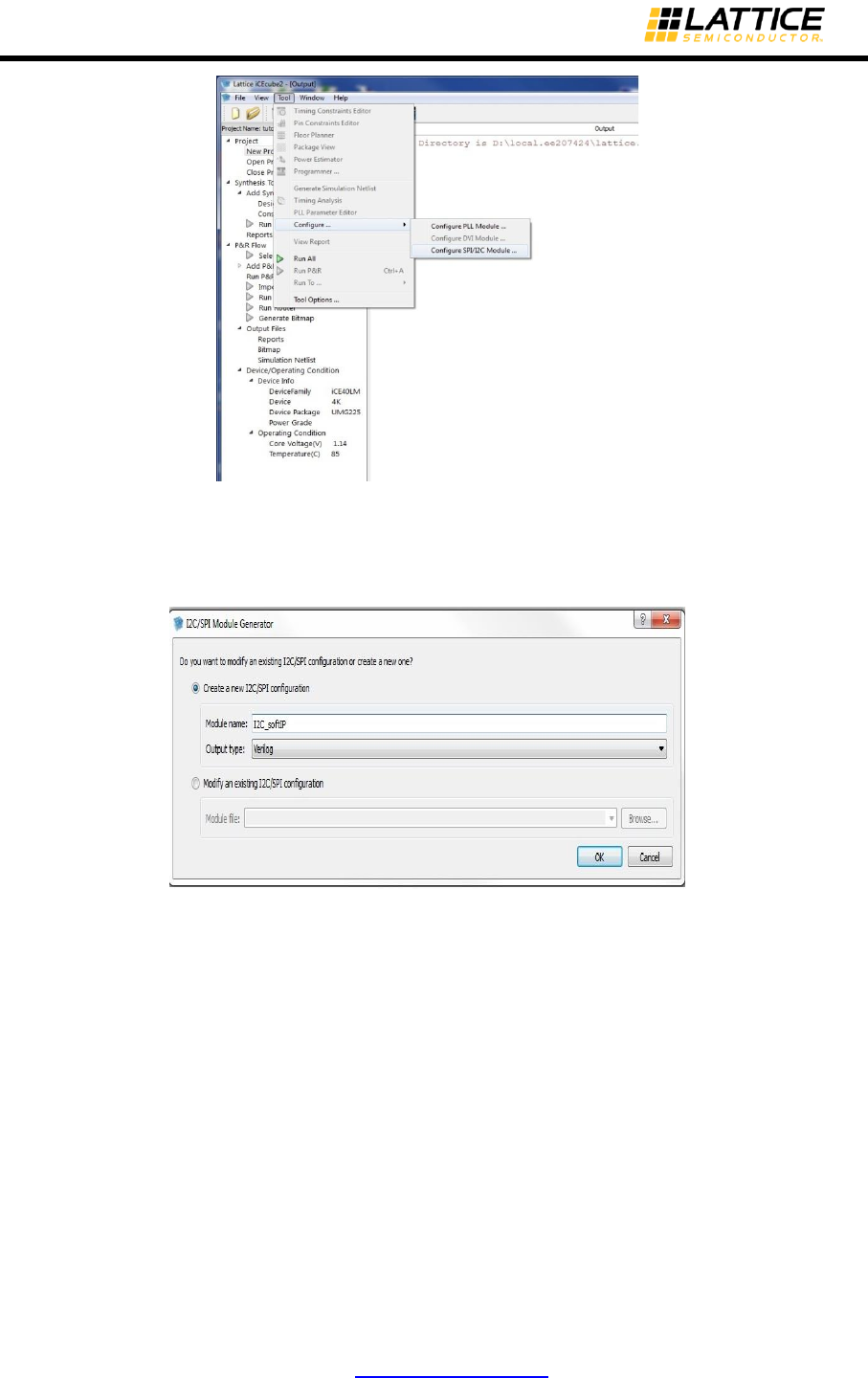
iCEcube2 User Guide www.latticesemi.com 53
Figure 3-22 : Launch I2C/SPI Module Generator.
The I2C/SPI Module Generator allows the user to create a new configuration, or edit an existing
one as shown in Figure 3-23.
Figure 3-23: Create New I2C/SPI Module
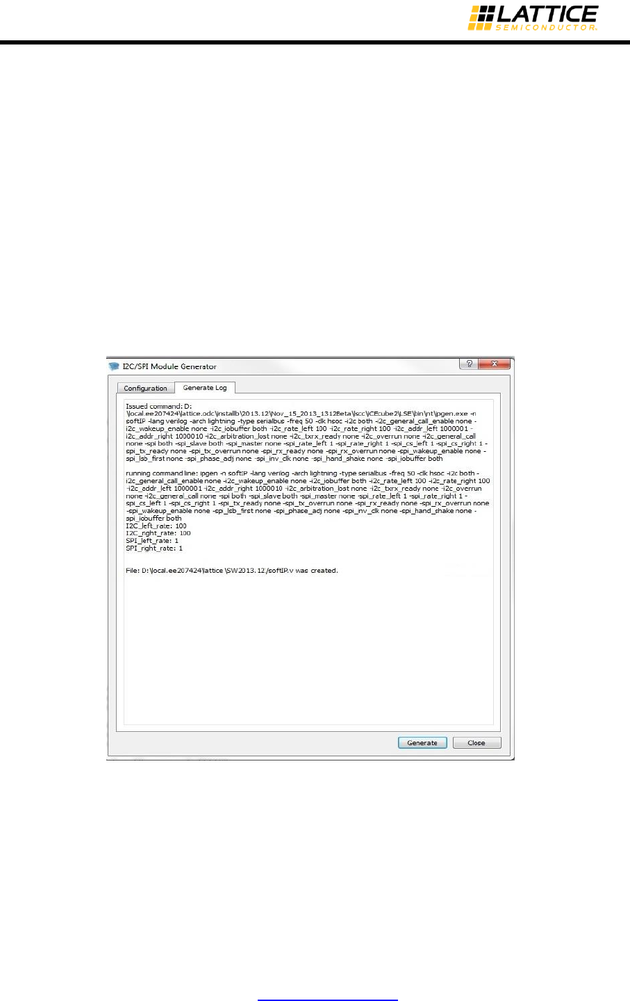
The output of the Module Generator is a module file (Verilog), that instantiates a SPI/I2C, as
configured by the user. Note that the I2C/SPI module file should be included in the list of design
files.
Once an I2C/SPI module file has been generated, it can be edited, by selecting the “Modify an
existing PLL configuration” option (Figure 3-24).
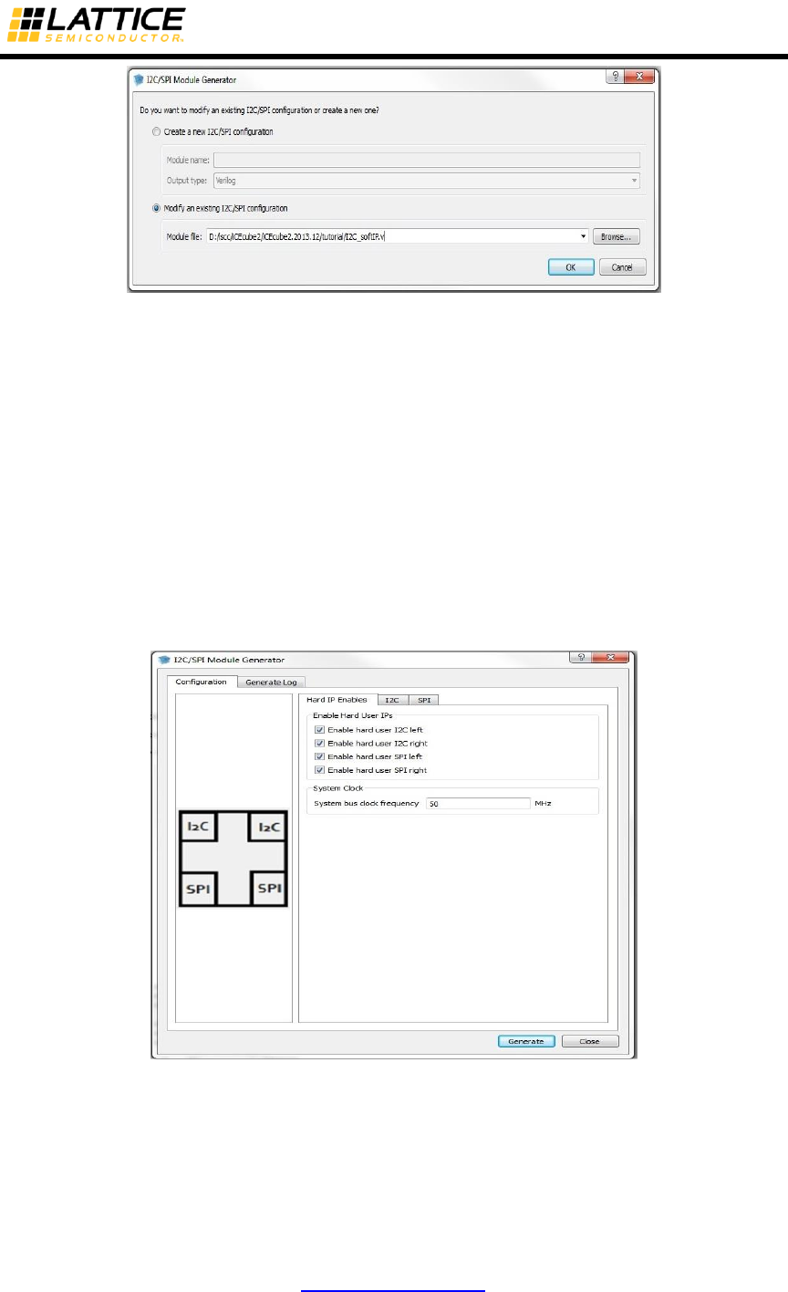
iCEcube2 User Guide www.latticesemi.com 54
Figure 3-24: Modify Existing I2C/SPI configuration
Configuring I2C/SPI Hard IP
iCE40LM, iCE5LP (iCE40 Ultra) device contains two I2C and SPI hard IP blocks, each of which
can be configured independently.
In the I2C/SPI Module Generator wizard, select “Create a new I2C/SPI configuration” and provide
the module Name. Click on the OK button. The Module generator launches a wizard to help the
user configure the I2C/SPI as per the design requirements. This section explains the options in
the wizard to enable and configure the I2C/SPI soft IP wrappers.
Enable Hard IP
The ‘Hard IP Enables’ tab allows the user to enable the required left/right I2C, left/right SPI
instances in the wrapper and specify the system bus clock frequency. Selecting the hard IP type
enables the I2C and SPI Tabs in the wizard as shown in Figure 3-25.
Figure 3-25 : Enable Hard IP
Enable hard user I2C left: This option allows the user to enable left I2C on the I2C Tab.
Enable hard user I2C Right: This option allows the user to enable right I2C on the I2C Tab.
Enable hard user SPI Left: This option allows the user to enable left SPI on the SPI Tab.
Enable hard user SPI Right: This option allows the user to enable right SPI on the SPI Tab.
iCEcube2 User Guide www.latticesemi.com 55
System Clock: Specify the system clock frequency in Mhz. This value is used to derive the
divider settings of the I2C and SPI hard IP master clocks. “Generate” button is enabled once the
value is set in this field.
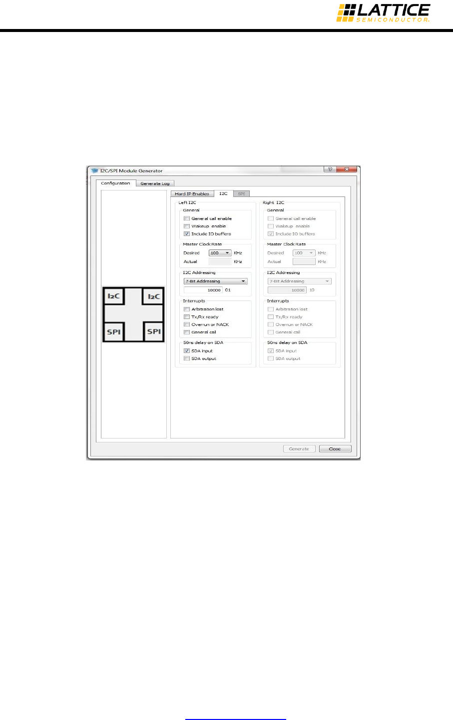
Configure I2C
I2C Tab allows the user to configure the left and right I2C blocks independently as shown in
Figure 3-26. I2C Tab is enabled only when I2C hard IP is selected in the Hard IP Enables Tab.
Figure 3-26: Configure Left/Right I2C hard IP.
I2C Controller General Options:
General Call Enable: This setting enables the I2C General Call response (addresses all devices
on the bus using the I2C address 0) in Slave mode. This setting can be modified dynamically by
enabling the GCEN bit in the I2C Control Register I2CCR1.
Wakeup Enable: Turns on the I2C wakeup on address match. The WKUPEN bit in the I2CCR1
can be modified dynamically allowing the Wake Up function to be enabled or disabled.
Include IO Buffers: Include buffers to the I2C_SCL, I2C_SDA pins.
Master Clock (Desired): Specify the desired I2C master clock frequency. A calculation is then
made to determine a divider value to generate a clock close to this value from the input clock.
The frequency of the input System Bus clock is specified on the main/general tab. The divider
value is rounded to the nearest integer after dividing the input System Bus clock by the value
entered in this field.

iCEcube2 User Guide www.latticesemi.com 56
Master Clock (Actual): Since it is not always possible to divide the input System Bus clock to
the exact value requested by the user, the actual value will be returned in this read-only field.
I2C Addressing: This option allows the user to set 7-bit or 10-bit addressing and define the Hard
I2C address.
iCEcube2 User Guide www.latticesemi.com 57
I2C Controller Interrupts:
Arbitration Lost Interrupts: An interrupt which indicates I2C lost arbitration. This interrupt is bit
IRQARBL of the register I2CIRQ. When enabled, it indicates that ARBL is asserted. Writing a ‘1’
to this bit clears the interrupt. This option can be changed dynamically by modifying the bit
IRQARBLEN in the register I2CIRQEN.
TX/RX Ready: An interrupt which indicates that the I2C transmit data register (I2CTXDR) is
empty or that the receive data register (I2CRXDR) is full. The interrupt bit is IRQTRRDY of the
register I2CIRQ. When enabled, it indicates that TRRDY is asserted. Writing a ‘1’ to this bit clears
the interrupt. This option can be changed dynamically by modifying the bit IRQTRRDYEN in the
register I2CIRQEN.
Overrun or NACK: An interrupt which indicates that the I2CRXDR received new data before the
previous data. The interrupt is bit IRQROE of the register I2CIRQ. When enabled, it indicates that
ROE is asserted. Writing a ‘1’ to this bit clears the interrupt. This option can be changed
dynamically by modifying the bit IRQROEEN in the register I2CIRQEN.
General Call Interrupts: An interrupt which indicates that a general call has occurred. The
interrupt is bit IRQHGC of the register I2CIRQ. When enabled, it indicates that ROE is asserted.
Writing a ‘1’ to this bit clears the interrupt. This option can be changed dynamically by modifying
the bit IRQHGCEN in the register I2CIRQEN.
I2C SDA delays
This option is available only for iCE5LP (iCE40 Ultra) devices. Using these options, the user can
add 50ns delay to the SDA input, output signals.
SDA input: By default 50ns is added to the SDA input. Turn off this option if delay is not required.
SDA output: Turn on this setting to add 50ns delay to the SDA output.
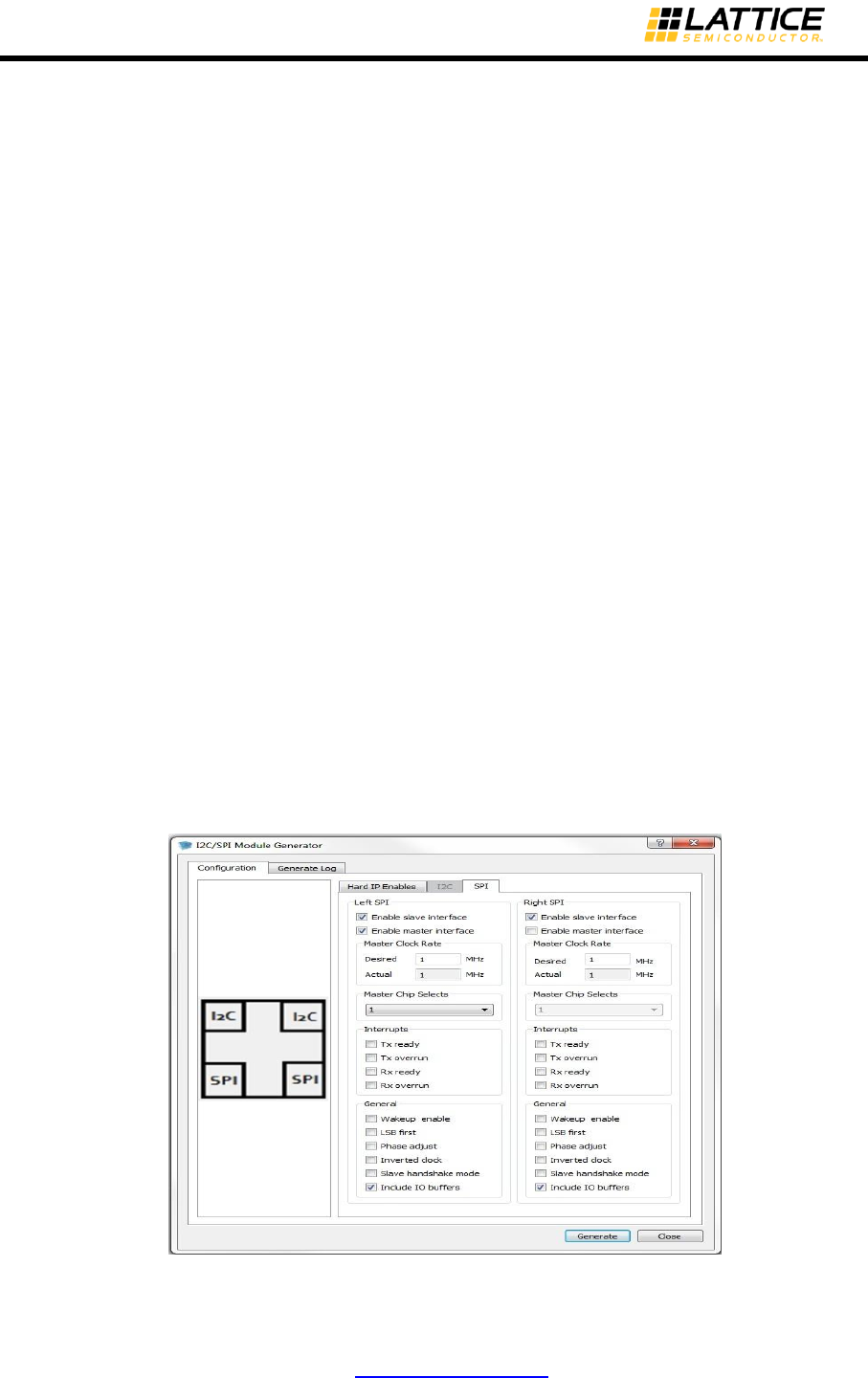
Configure SPI
SPI Tab allows the user to configure the left and right SPI blocks independently as shown in
Figure 3-27. SPI Tab is enabled only when SPI hard IP is selected in the Hard IP Enables Tab.
Figure 3-27: Configure Left/Right SPI hard IP.

iCEcube2 User Guide www.latticesemi.com 58
Enable Slave Interface: This option allows the user to enable Slave Mode interface for the initial
state of the SPI block. By default, Slave Mode interface is enabled.
Enable Master Interface: This option allows the user to enable Master Mode interface for the
initial state of the SPI block. This option can be updated dynamically by modifying the MSTR bit
of the register SPICR2.
Master Clock Rate (Desired): Specify the desired SPI master clock frequency. A calculation is
then made to determine a divider value to generate a clock close to this value from the input
System Bus clock frequency. The divider value is rounded to the nearest integer after dividing the
input System Bus clock by the value entered in this field.
Master Clock Rate (Actual): Since it is not always possible to divide the input System Bus clock
exactly to that requested by the user, the actual value will be returned in this read-only field.
When both the desired SPI clock and System Bus clock fields have valid data and either is
updated, this field returns the value (System Bus Frequency / SPI_CLK_DIVIDER), rounded to
two decimal places.
Master Chip Selects: The core has the ability to provide up to 4 individual chip select outputs for
master operation. This field allows the user to prevent extra chip selects from being brought out of
the core. This option can be updated dynamically by modifying the register SPICSR.
SPI Controller Interrupts
TX Ready: An interrupt which indicates the SPI transmit data register (SPITXDR) is empty. The
interrupt bit is IRQTRDY of the register SPIIRQ. When enabled, indicates TRDY was asserted.
Write “1” to this bit to clear the interrupt. This option can be change dynamically by modifying the
bit IRQTRDYEN in the register SPIIRQEN.
TX Overrun: An interrupt which indicates the Slave SPI chip select (SPI_SCSN) was driven low
while a SPI Master. The interrupt is bit IRQMDF of the register SPIIRQ. When enabled, indicates
MDF (Mode Fault) was asserted. Write “1” to this bit to clear the interrupt. This option can be
change dynamically by modifying the bit IRQMDFEN in the register SPIIRQEN.
RX Ready: An interrupt which indicates the receive data register (SPIRXDR) contains valid
receive data. The interrupt is bit IRQRRDY of the register SPIIRQ. When enabled, indicates
RRDY was asserted. Write “1” to this bit to clear the interrupt. This option can be change
dynamically by modifying the bit IRQRRDYEN in the register SPICSR.
RX Overrun: An interrupt which indicates SPIRXDR received new data before the previous data.
The interrupt is bit IRQROE of the register SPIIRQ. When enabled, indicates ROE was asserted.
Write a “1” to this bit to clear the interrupt. This option can be change dynamically by modifying
the bit IRQROEEN in the register SPIIRQEN.
SPI Controller General Options:
Wakeup Enable: The core can optionally provide a wakeup signal to the device to resume from
low power mode. This option can be updated dynamically by modifying the bit WKUPEN_USER
in the register SPICR1.
LSB First: This setting specifies the order of the serial shift of a byte of data. The data order
(MSB or LSB first) is programmable within the SPI core. This option can be updated dynamically
by modifying the LSBF bit in the register SPICR2.
Inverted Clock: Select this option to invert the clock polarity used to sample input and output
data. When selected the edge changes from the rising to the falling clock edge. This option can
be updated dynamically by accessing the CPOL bit of register SPICR2.
iCEcube2 User Guide www.latticesemi.com 59
Phase Adjust: An alternate clock-data relationship is available for SPI devices with particular
requirements. This option allows the user to specify a phase change to match the application.
This option can be updated dynamically by accessing the CPHA bit in the register SPICR2.
Slave Handshake Mode: Enables Lattice proprietary extension to the SPI protocol. For use
when the internal sup-port circuit (e.g. WISHBONE host) cannot respond with initial data within
the time required, and to make the Slave read out data predictably available at high SPI clock
rates. This option can be updated dynamically by accessing the SDBRE bit in the register
SPICR2.
Include IO Buffers: Include buffers to the SPI_MISO, SPI_MOSI, SPI_SCK, SPI_MCSNO [0]
pins.
Generate Module
Once the settings are done generate the soft IP module by selecting “Generate” button. The
wizard displays the status and the generated file details in the “Generate Log” tab as shown in
Figure 3-28.
Figure 3-28: I2C/SPI soft IP module generation.

iCEcube2 User Guide www.latticesemi.com 60
Chapter 4 Lattice Synthesis Engine
Lattice Synthesis Engine (LSE) is the integrated synthesis tool that comes with iCEcube2.
This chapter describes:
LSE tool options
HDL coding tips
Attributes and directives supported by LSE
Synopsys design constraints (SDC) supported by LSE
LSE is a synthesis tool custom-built for Lattice products and fully integrated with iCEcube2.
Depending on the design, LSE may lead to a more compact or faster placement of the design
than another synthesis tool would do.
Also, LSE offers the following advantages:
More granular control through the tool options
Enhanced RAM and ROM inference and mapping, including:
o Dual-port RAM in write-through, normal, and read-before-write modes mapped to
BRAM
o Clock enable and read enable packing
o Mapping for the minimal number of BRAM blocks
o BRAM mapping for minimal timing
Post-synthesis Verilog netlist suitable for simulation
Changing the LSE Tool Options
The LSE options can be changed by selecting Tool > Tool Options > LSE. This section lists all
the tool options associated with LSE. The following sections describe how to set the options to
optimize synthesis for either area or speed and some of the differences between LSE and
Synplify Pro options.
BRAM Utilization
Specifies BRAM utilization target setting in percent of total vacant sites. LSE will honor the setting
and do the resource computation accordingly. Default is 100 (in percentage).
Carry Chain Length
Specifies the maximum number of output bits that get mapped to a single carry chain. Default is
0, which is interpreted as infinite length.
Command Line Options
Enables additional command line options for the LSE synthesis process. Type in the option and
its value (if any) in the Value column.
Fix Gated Clocks
Turns on (True) or off (False) converting all gated clocks to data enables for best performance.
Turn off to save power. Default is True.

iCEcube2 User Guide www.latticesemi.com 61
FSM Encoding Style
Specifies the encoding style to use for finite state machines: Binary, Gray, or One-Hot. Default is
Auto, meaning that LSE chooses a style for each finite state machine.
Intermediate File Dump
If you set this to True, LSE will dump about 20 intermediate encrypted Verilog files. If you supply
Lattice with these files, they can be decrypted and analyzed for problems. This option is good for
analyzing simulation issues.
Max Fanout Limit
Specifies the maximum fanout setting. LSE will make sure that any net in the design does not
exceed this limit. Default is 10000 fanouts.
Memory Initial Value File Search Path
Allows you to specify a path to locate memory initialization files (.mem) used in the design. The
software will add the specified paths to the list of directories to search when resolving file
references.
To specify a search path, double-click the Value box, and directly enter the path.
Number of Critical Paths
Specifies the number of critical timing paths to be reported in the timing report.
Optimization Goal
Enables LSE to optimize the design for area, speed, or both. Valid options are:
Area (default) – Optimizes the design for area by reducing the total amount of logic used
for design implementation.
When Optimization Goal is set to Area, LSE ignores the Target Frequency setting and
uses 1 MHz instead.
Timing – Optimizes the design for speed by reducing the levels of logic.
When Optimization Goal is set to Timing and a create_clock constraint is available in an
.ldc file, LSE ignores the Target Frequency setting and uses the value from the
create_clock constraint instead.
Balanced – Optimizes the design for both area and timing.
Propagate Constants
When set to True (default), enables constant propagation to reduce area, where possible. LSE
will then eliminate the logic used when constant inputs to logic cause their outputs to be constant.
You can turn off the operation by setting this option to False.
RAM Style
Sets the type of random access memory globally to BRAM or registers.
The default is Auto which attempts to determine the best implementation. That is, LSE will map to
RAM resources based on the resource availability.
This option will apply a syn_ramstyle attribute globally in the source to a module or to a RAM
instance. To turn off RAM inference, set its value to Registers.

iCEcube2 User Guide www.latticesemi.com 62
Other options are:
Registers – Causes an inferred RAM to be mapped to registers (flip-flops and logic)
rather than the technology-specific RAM resources.
BRAM – Causes the RAM to be implemented using the dedicated RAM resources. If your
RAM resources are limited, for whatever reason, you can map additional RAMs to
registers instead of the dedicated BRAM resources using this attribute.
Remove Duplicate Registers
Specifies the removal of duplicate registers. When set to True (default), LSE removes a register if
it is identical to another register. If two registers generate the same logic, the second one will be
deleted and the first one will be made to fan out to the second one's destinations. LSE will not
remove duplicate registers if this option is set to False.
Resolve Mixed Drivers
If a net is driven by a VCC or GND and active drivers, setting this option to True connects the net
to the VCC or GND driver.
Resource Sharing
When this is set to True (default), the synthesis tool uses resource sharing techniques to optimize
for area. With resource sharing, synthesis uses the same arithmetic operators for mutually
exclusive statements; for example, with the branches of a case statement. Conversely, you can
improve timing by disabling resource sharing, but at the expense of increased area.
ROM Style
Allows you to globally implement ROM architectures using dedicated, distributed ROM, or a
combination of the two (Auto).
This applies the syn_romstyle attribute globally to the design by adding the attribute to the
module or entity. You can also specify this attribute on a single module or ROM instance.
This option specifies a syn_romstyle attribute globally or on a module or ROM instance with a
value of:
Auto (default) – Allows the synthesis tool to choose the best implementation to meet the
design requirements for speed, size, and so on.
BRAM – Causes the ROM to be mapped to dedicated BRAM resources. ROM address or
data should be registered to map it to an BRAM block. If your ROM resources are limited,
for whatever reason, you can map additional ROM to registers instead of the dedicated or
distributed RAM resources using this attribute.
Logic – Causes the ROM to be implemented using the normal logic.
Infer ROM architectures using a CASE statement in your code. For the synthesis tool to
implement a ROM, at least half of the available addresses in the CASE statement must be
assigned a value. For example, consider a ROM with six address bits (64 unique addresses). The
CASE statement for this ROM must specify values for at least 32 of the available addresses.
RW Check on RAM
Adds (True) or does not add (False) the glue logic to resolve read/write conflicts wherever
needed. Default is False.

iCEcube2 User Guide www.latticesemi.com 63
Target Frequency
Specifies the target frequency setting. This frequency applies to all the clocks in the design. If
there are some clocks defined in an .sdc file, the remaining clocks will get this frequency setting.
When Optimization Goal is set to Area, LSE ignores the Target Frequency setting and uses
1 MHz instead.
When Optimization Goal is set to Timing and a create_clock constraint is available in an .sdc file,
LSE ignores the Target Frequency setting and uses the value from the create_clock constraint
instead.
Top-Level Unit
It is a good practice to specify the top-level unit (or module) of the design. If you don’t, LSE will try
to determine the top-level unit. While usually accurate, there is no guarantee that LSE will get the
correct unit.
You may also want to change the top-level unit when experimenting with different designs or
switching between simulation and synthesis.
If the design is mix of EDIF and Verilog or VHDL, you cannot set an EDIF module as the top-level
unit.
Use Carry Chain
Turns on (True) or off (False) carry chain implementation for adders. Default is True. This option
is equivalent to the “-use_carry_chain” command in LSE.
Use IO Insertion
Turns on (True) or off (False) the use of I/O insertion. Default is True.
Use IO Registers
Enables (True) or disables (False) register packing. True forces the synthesis tool to pack all
input, output, and I/O registers into I/O pad cells based on timing requirements. Default is Auto,
which selects True or False based on how Optimization Goal is set.
You can place the syn_useioff attribute on an individual register or port. When applied to a
register, the synthesis tool packs the register into the pad cell, and when applied to a port, packs
all registers attached to the port into the pad cell. The syn_useioff attribute can be set on a:
Top-level port
Register driving the top-level port
Lower-level port if the register is specified as part of the port declaration
Optimizing LSE for Area and Speed
The following strategy settings for LSE can help reduce the amount of FPGA resources that your
design requires or increase the speed with which it runs. (For other synthesis tools, see those
tools’ documentation.) Use these methods along with other, generic coding methods to optimize
your design.
Minimizing area often produces larger delays, making it more difficult to meet timing
requirements. Maximizing frequency often produces larger designs, making it more difficult to

iCEcube2 User Guide www.latticesemi.com 64
meet area requirements. Either goal, pushed to an extreme, may cause the place and route
process to run longer or not complete routing.
To control the global performance of LSE, modify the tool options. Choose Tool > Tool Options.
In the Tool Options dialog box, set the following options, which are found in the LSE tab. See the
following text for explanations and more details.
LSE Tool Options for Area and Speed
Option
Area
Speed
FSM Encoding Style
Binary or Gray
One-Hot
Max Fanout Limit
<maximum>
<minimum>
Optimization Goal
Area
Timing
Remove Duplicate Registers
True
False
Resource Sharing
True
False
Target Frequency
<minimum>
FSM Encoding Style
If your design includes large finite state machines, the Binary or Gray style may use fewer
resources than One-Hot. Which one is best depends on the design. One-Hot is usually the fastest
style. However, if the finite state machine is followed by a large output decoder, the Gray style
may be faster.
Max Fanout Limit
A larger fanout limit means less duplicated logic and fewer buffers. A lower fanout limit may
reduce delays. The default is 10000, which is essentially unlimited fanout. To minimize area, don’t
lower this value any more than needed to meet other requirements. To maximize speed, try much
lower values, such as 50.
You can change the fanout limit for portions of the design by using the syn_maxfan attribute. See
“syn_maxfan” on page 86. Set Max Fanout Limit to meet your most demanding requirement.
Then add syn_maxfan to help other requirements.
Optimization Goal
If set to Area, LSE will choose smaller design forms over faster whenever possible. LSE will also
ignore the Target Frequency option, using a low 1 MHz target instead. If set to Timing, LSE will
choose faster design forms over smaller whenever possible. LSE will also use the timing
constraints in the design’s .sdc file to guide the optimization. If you are having trouble meeting
one requirement (area or speed) while optimizing for the other, try setting this option to
Balanced.
Remove Duplicate Registers
Removing duplicate registers reduces area, but keeping duplicate registers may reduce delays.

iCEcube2 User Guide www.latticesemi.com 65
Resource Sharing
If set to True, LSE will share arithmetic components such as adders, multipliers, and counters
whenever possible.
If the critical path includes such resources, turning this option off may reduce delays. However, it
may also increase delays elsewhere, possibly reducing the overall frequency.
Target Frequency
A lower frequency target means LSE can focus more on area. A higher frequency target may
force LSE to increase area. Try setting this value to about 10% higher than your minimum
requirement. However, if Optimization Goal is set to Area, LSE will ignore the Target Frequency
value, using a low 1 MHz target instead. If Optimization Goal is set to Timing and a create_clock
constraint is available in an .sdc file, LSE will use the value from the create_clock constraint
instead.
LSE Options versus Synplify Pro
If you are moving from using Synplify Pro to LSE, there are many differences in the options to
consider. Many of the Synplify Pro options have similar LSE options. But many also do not. See
the following table. And there are many LSE options that have no Synplify Pro equivalents. See
the lists following the table. For more information about the options, see “Changing the LSE Tool
Options” on page 60.
Synplify Pro Tool Options and LSE Equivalents
Synplify Pro Option
LSE Equivalent
Synplify Pro
Default
LSE
Default
Allow Duplicate Modules
None
False
Area
Optimization Goal
False
Balanced
Arrange VHDL Files
None
True
Clock Conversion
None
True
Command Line Options
Command Line Options
Default Enum Encoding
FSM Encoding Style
Default
Auto
Disable IO Insertion
Use IO Insertion
False
True
Export Diamond Settings to Synplify Pro GUI
None
No
Fanout Guide
Max Fanout Limit
10000
1000
Force GSR
None
False
Frequency
Target Frequency
200
FSM Encoding
None
True
Number of Critical Paths
Number of Critical Paths
3

iCEcube2 User Guide www.latticesemi.com 66
Number of Start/End Points
None
Output Netlist Format
None
None
Output Preference File
None
True
Pipelining and Retiming
None
Pipelining Only
Push Tristates
None
True
Resolved Mixed Drivers
Resolve Mixed Drivers
False
False
Resource Sharing
Resource Sharing
True
True
Update Compile Point Timing Data
None
False
Use Clock Period for Unconstrained I/O
None
False
Verilog Input
None
Verilog 2001
VHDL 2008
None
False
LSE has additional options that provide more granular control than Synplify Pro. These options
include:
Carry Chain Length
BRAM Utilization
RAM Style
ROM Style
Other LSE options without Synplify Pro equivalents:
Intermediate File Dump
Memory Initial Value Search Path
Use Carry Chain
Use IO Registers
Propagate Constants
Remove Duplicate Registers
Coding Tips for LSE
If you are going to use LSE to synthesize the design, the following coding tips may help. Mostly
the tips are about writing code so that blocks of memory are “inferred”: that is, automatically
implemented using logic cells or block RAM (BRAM) instead of registers. There are also tips
about inferring types of I/O ports and about style differences with Synplify Pro.
LSE Differences with Synplify Pro
LSE tends to apply the Verilog and VHDL specifications strictly, sometimes more strictly than
other synthesis tools including Synplify Pro. Following are some coding practices that can cause
problems with LSE:

iCEcube2 User Guide www.latticesemi.com 67
Semicolons (;) to separate ports in a Verilog module statement. For example:
module COUNTER (
input CLK ,
input RESET ; // LSE error on semicolon.
output TIMEOUT
);
Spaces in the location path.
Duplicate instantiation names (due to names in generate statements).
Module instances without instance names.
Multiple files with the same module names. Synplify Pro will error out but LSE will not.
This could cause designs in LSE to use the incorrect module.
Global VHDL signals.
Modules that have a port mismatch between instance and definition.
Both ieee.std_logic_signed and unsigned packages in VHDL. When preparing VHDL
code for LSE, you can include either:
USE ieee.std_logic_signed.ALL;
or:
USE ieee.std_logic_unsigned.ALL;
Code with both signed and unsigned packages could fail to synthesize because
operators would have multiple definitions.
Mismatched variable types in VHDL. A std_logic_vector signal cannot be assigned to a
std_logic signal and an unsigned type cannot be assigned to a std_logic_vector signal.
For example:
din : in unsigned (data_width - 1 downto 0);
dout : out std_logic_vector (data_width - 1 downto 0));
...
dout <= din; // Illegal, mismatched assignment.
Such mismatched assignments generate errors that stop synthesis.
About Inferring Memory
Inferring memory means that LSE, based on aspects of the code, implements a block of memory
using logic cells or block RAM (BRAM)—logic cells for small memories, BRAM for large—instead
of registers. LSE can infer synchronous RAM that is:
single-port or pseudo dual-port
with or without asynchronous reset of the output
with or without write enables
with or without clock enables
LSE can also infer synchronous ROM.
In some old VHDL coding styles, one-dimensional memories and CASE statements were used to
create two-dimensional memories. This coding style does not translate to memories properly in
LSE.

iCEcube2 User Guide www.latticesemi.com 68
The following sections describe how to write code to infer different kinds of memory with LSE.
Inferring RAM
The basic inferred RAM is synchronous. It can have synchronous or asynchronous reads and can
be either single- or dual-port. You can also set initial values. Other features, such as resets and
clock enables, can be added as desired. The following text lists the rules for coding inferred RAM.
Following that, Figure 4-1 (Verilog) and Figure 4-2 (VHDL) show the code for a simple, single-port
RAM with asynchronous read.
To code RAM to be inferred, do the following:
Define the RAM as an indexed array of registers.
To control how the RAM is implemented (with block RAM), consider adding the
syn_ramstyle attribute. See “syn_ramstyle” on page 86.
Control the RAM with a clock edge and a write enable signal.
For synchronous reads, see “Inferring RAM with Synchronous Read” on page 69.
For single-port RAM, use the same address bus for reading and writing.
For pseudo dual-port RAM, see “Inferring Pseudo Dual-Port RAM on page 71.
If desired, assign initial values to the RAM as described in “Initializing Inferred RAM” on
page 73.
module ram (din, addr, write_en, clk, dout);
parameter addr_width = 8;
parameter data_width = 8;
input [addr_width-1:0] addr;
input [data_width-1:0] din;
input write_en, clk;
reg [data_width-1:0] mem [(1<<addr_width)-1:0];
// Define RAM as an indexed memory array.
always @(posedge clk) // Control with a clock edge.
begin
if (write_en) // And control with a write enable.
mem[(addr)] <= din;
end
assign dout = mem[addr];
endmodule
Figure 4-1: Simple, Single-Port RAM in Verilog
library IEEE;
use IEEE.std_logic_1164.all;
use IEEE.std_logic_unsigned.all;
entity ram is
generic (
addr_width : natural := 8;
data_width : natural := 8);

iCEcube2 User Guide www.latticesemi.com 69
port (
addr : in std_logic_vector (addr_width - 1 downto 0);
write_en : in std_logic;
clk : in std_logic;
din : in std_logic_vector (data_width - 1 downto 0);
dout : out std_logic_vector (data_width - 1 downto 0));
end ram;
architecture rtl of ram is
type mem_type is array ((2** addr_width) - 1 downto 0) of
std_logic_vector(data_width - 1 downto 0);
signal mem : mem_type;
-- Define RAM as an indexed memory array.
begin
process (clk)
begin
if (clk'event and clk = '1') then -- Control with clock
edge
if (write_en = '1') then -- Control with a write
enable.
mem(conv_integer(addr)) <= din;
end if;
end if;
end process;
dout <= mem(conv_integer(addr));
end rtl;
Figure 4-2: Simple, Single-Port RAM in VHDL
Inferring RAM with Synchronous Read
For synchronous reads, add a register for the read address or for the data output. Load the
register inside the procedure or process that is controlled by the clock. See the following
examples. They show the simple RAM of “Inferring RAM” on page 68 modified for synchronous
reads. Changes are in bold text.
Verilog Examples
module ram (din, addr, write_en, clk, dout);
parameter addr_width = 8;
parameter data_width = 8;
input [addr_width-1:0] addr;
input [data_width-1:0] din;
input write_en, clk;
output [data_width-1:0] dout;
reg [data_width-1:0] dout; // Register for output.
reg [data_width-1:0] mem [(1<<addr_width)-1:0];
always @(posedge clk)
begin
if (write_en)
mem[(addr)] <= din;
dout = mem[addr]; // Output register controlled by
clock.
end

iCEcube2 User Guide www.latticesemi.com 70
endmodule
Figure 4-3: RAM with Registered Output in Verilog
module ram (din, addr, write_en, clk, dout);
parameter addr_width = 8;
parameter data_width = 8;
input [addr_width-1:0] addr;
input [data_width-1:0] din;
input write_en, clk;
output [data_width-1:0] dout;
reg [data_width-1:0] raddr; // Register for read address.
reg [data_width-1:0] mem [(1<<addr_width)-1:0];
always @(posedge clk)
begin
if (write_en)
begin
mem[(addr)] <= din;
end
raddr <= addr; // Read addr. register controlled by
clock.
end
assign dout = mem[raddr];
endmodule
Figure 4-4: RAM with Registered Read Address in Verilog
VHDL Examples
library IEEE;
use IEEE.std_logic_1164.all;
use IEEE.std_logic_unsigned.all;
entity ram is
generic (
addr_width : natural := 8;
data_width : natural := 8);
port (
addr : in std_logic_vector (addr_width - 1 downto 0);
write_en : in std_logic;
clk : in std_logic;
din : in std_logic_vector (data_width - 1 downto 0);
dout : out std_logic_vector (data_width - 1 downto 0));
end ram;
architecture rtl of ram is
type mem_type is array ((2** addr_width) - 1 downto 0) of
std_logic_vector(data_width - 1 downto 0);
signal mem : mem_type;
begin
process (clk)
begin

iCEcube2 User Guide www.latticesemi.com 71
if (clk'event and clk = '1') then
if (write_en = '1') then
mem(conv_integer(addr)) <= din;
end if;
end if;
dout <= mem(conv_integer(addr));
-- Output register controlled by clock.
Figure 4-5: RAM with Registered Output in VHDL
library IEEE;
use IEEE.std_logic_1164.all;
use IEEE.std_logic_unsigned.all;
entity ram is
generic (
addr_width : natural := 8;
data_width : natural := 8);
port (
addr : in std_logic_vector (addr_width - 1 downto 0);
write_en : in std_logic;
clk : in std_logic;
din : in std_logic_vector (data_width - 1 downto 0);
dout : out std_logic_vector (data_width - 1 downto 0));
end ram;
architecture rtl of ram is
type mem_type is array ((2** addr_width) - 1 downto 0) of
std_logic_vector(data_width - 1 downto 0);
signal mem : mem_type;
begin
process (clk)
begin
if (clk'event and clk = '1') then
if (write_en = '1') then
mem(conv_integer(addr)) <= din;
end if;
raddr <= addr;
-- Read address register controlled by clock.
end if;
end process;
dout <= mem(conv_integer(raddr));
end rtl;
Figure 4-6: RAM with Registered Read Address in VHDL
Inferring Pseudo Dual-Port RAM
For pseudo dual-port RAM:
Use two address buses.

iCEcube2 User Guide www.latticesemi.com 72
If the design does not simultaneously read and write the same address, add the
syn_ramstyle attribute with the no_rw_check value to minimize overhead logic.
If writing in Verilog, use non-blocking assignments as described in “About Verilog
Blocking Assignments” on page 75.
The following examples are based on the simple RAM of “Inferring RAM” on page 68.
Verilog Examples
module ram (din, write_en, waddr, wclk, raddr, rclk, dout);
parameter addr_width = 8;
parameter data_width = 8;
input [addr_width-1:0] waddr, raddr;
input [data_width-1:0] din;
input write_en, wclk, rclk;
reg [data_width-1:0] dout;
reg [data_width-1:0] mem [(1<<addr_width)-1:0]
/* synthesis syn_ramstyle = "no_rw_check" */ ;
always @(posedge wclk) // Write memory.
begin
if (write_en)
mem[waddr] <= din; // Using write address bus.
end
always @(posedge rclk) // Read memory.
begin
dout <= mem[raddr]; // Using read address bus.
end
endmodule
Figure 4-7: Pseudo Dual-Port RAM in Verilog
VHDL Examples
library IEEE;
use IEEE.std_logic_1164.all;
use IEEE.std_logic_unsigned.all;
entity ram is
generic (
addr_width : natural := 8;
data_width : natural := 8);
port (
write_en : in std_logic;
waddr : in std_logic_vector (addr_width - 1 downto 0);
wclk : in std_logic;
raddr : in std_logic_vector (addr_width - 1 downto 0);
rclk : in std_logic;
din : in std_logic_vector (data_width - 1 downto 0);
dout : out std_logic_vector (data_width - 1 downto 0));
end ram;
architecture rtl of ram is
type mem_type is array ((2** addr_width) - 1 downto 0) of
std_logic_vector(data_width - 1 downto 0);

iCEcube2 User Guide www.latticesemi.com 73
signal mem : mem_type;
attribute syn_ramstyle: string;
attribute syn_ramstyle of mem: signal is "no_rw_check";
begin
process (wclk) -- Write memory.
begin
if (wclk'event and wclk = '1') then
if (write_en = '1') then
mem(conv_integer(waddr)) <= din;
-- Using write address bus.
end if;
end if;
end process;
process (rclk) -- Read memory.
begin
if (rclk'event and rclk = '1') then
dout <= mem(conv_integer(raddr));
-- Using read address bus.
end if;
end process;
end rtl;
Figure 4-8: Pseudo Dual-Port RAM in VHDL
Initializing Inferred RAM
Create initial values for inferred RAM in the usual ways for initializing memory.
Verilog
In Verilog, initialize RAM with the standard $readmemb or $readmemh tasks in an initial block.
Create a separate file with the initial values in either binary or hexadecimal form. For example, to
initialize a RAM block named “ram”:
reg [7:0] ram [0:255];
initial
begin
$readmemh ("ram.ini", ram);
end
The data file has one word of data on each line. The data needs to be in the same order in which
the array was defined. That is, for “ram [0:255]” the data starts with address 0; for “ram [255:0]”
the data starts with address 255. The ram.ini file might start like this:
0A /* Address 0 */
23
5C
...
VHDL
In VHDL, initialize RAM with either signal declarations or variable declarations. Define an entity
with the same ports and architecture as the memory. Use this entity in either a signal or variable
statement with the initial values as shown below.

iCEcube2 User Guide www.latticesemi.com 74
For example, to initialize a RAM block named “ram,” define an entity such as:
entity ram_init is
port (
clk : in std_logic;
addr : in std_logic_vector(7 downto 0);
din : in std_logic_vector(7 downto 0);
we : in std_logic;
dout : out std_logic_vector(7 downto 0));
end;
architecture arch of ram_init is
type ram_init_arch is array(0 to 255)
of std_logic_vector (7 downto 0);
Then use the entity in a signal statement:
signal ram : ram_init_arch := (
"00001010",
"00100011",
"01011100",
...
others => (others => '0'));
Or use the entity in a variable statement:
variable ram : ram_init_arch := (
1 => "00001010",
...
others => (1=>'1', others => '0'));
Inferring ROM
To code ROM to be inferred, do the following:
Define the ROM with a case statement or equivalent if statements.
Assign constant values, all of the same width.
Assign values for at least 16 addresses or half of the address space, whichever is
greater. For example, if the address has 6 bits, the address space is 64 words, and at
least 32 of them must be assigned values.
To control how the ROM is implemented (with distributed or block ROM), consider adding
the syn_romstyle attribute. See “syn_romstyle” on page 92.
module rom(data, addr);
output [3:0] data;
input [4:0] addr;
always @(addr) begin
case (addr)
0 : data = 'h4;
1 : data = 'h9;
2 : data = 'h1;
...
15 : data = 'h8;
16 : data = 'h1;
17 : data = 'h0;

iCEcube2 User Guide www.latticesemi.com 75
default : data = 'h0;
endcase
end
endmodule
Figure 4-9: ROM Inferred with Case Statement in Verilog
entity rom is
port (addr : in std_logic_vector(4 downto 0);
data : out std_logic_vector(3 downto 0) );
end rom;
architecture behave of rom is
begin
process(addr)
begin
if addr = 0 then data <= "0100";
elsif addr = 1 then data <= "1001";
elsif addr = 2 then data <= "0001";
...
elsif addr = 15 then data <= "1000";
elsif addr = 16 then data <= "0001";
elsif addr = 17 then data <= "0000";
else data <= "0000";
end if;
end process;
end behave;
Figure 4-10: ROM Inferred with If Statement in VHDL
About Verilog Blocking Assignments
LSE support for Verilog blocking assignments to inferred RAM and ROM, such as
“ram[(addr)] = data;,” is limited to a single such assignment. Multiple blocking assignments, such
as you might use for dual-port RAM (see Figure 4-11), or a mix of blocking and non-blocking
assignments are not supported. Instead, use non-blocking assignments (<=). See Figure 4-12.
always @(posedge clka)
begin
if (write_ena)
ram[addra] = dina; // Blocking assignment A
douta = ram[addra];
end
always @(posedge clkb)
begin
if (write_enb)
ram[addrb] = dinb; // Blocking assignment B
doutb = ram[addrb];
end
Figure 4-11: Example of RAM with Multiple Blocking Assignments (Wrong)

iCEcube2 User Guide www.latticesemi.com 76
always @(posedge clka)
begin
if (write_ena)
ram[addra] <= dina;
douta <= ram[addra];
end
always @(posedge clkb)
begin
if (write_enb)
ram[addrb] <= dinb;
doutb <= ram[addrb];
end
Figure 4-12: Example Rewritten with Non-blocking Assignments (Right)
Inferring DSP Multipliers
LSE can infer the following types of multipliers and map them to MAC16+ blocks:
Multiplier
Multiply/Add (multiplier followed by an addition)
Multiply/Sub (multiplier followed by a subtraction)
Multiply/Accumulate (multiplier followed by an accumulator)
Inferring works with multipliers with 3 to 16-bit inputs.
All multiplier types can have any combination of input, output, and pipeline registers.
Control signals (clock, enable, and reset) for any registers in a multiplier must be shared by all the
registers. That is, there can only be one clock, one enable, and one reset signal in a given
multiplier.
To control how the multiplier is implemented (with logic or DSP), consider adding the
syn_multstyle attribute. See syn_multstyle on page 87.
The following sections show code written to infer different kinds of DSP multipliers with LSE.
Verilog Examples
module mult_unsign_7_6(a,b,c);
parameter A_WIDTH = 7;
parameter B_WIDTH = 6;
input unsigned [(A_WIDTH - 1):0] a;
input unsigned [(B_WIDTH - 1):0] b;
output unsigned [(A_WIDTH + B_WIDTH - 1):0] c;
assign c = a * b;
endmodule
Figure 4-13 : Basic Multiplier without Registers
module multaddsub_add_unsign_7_6(a,b,c,din);
parameter A_WIDTH = 7;
parameter B_WIDTH = 6;
input unsigned [(A_WIDTH - 1):0] a;
input unsigned [(B_WIDTH - 1):0] b;

iCEcube2 User Guide www.latticesemi.com 77
input unsigned [(A_WIDTH + B_WIDTH - 1):0] din;
output unsigned [(A_WIDTH + B_WIDTH - 1):0] c;
assign c = a * b + din;
endmodule
Figure 4-14: Multiply/Add without Registers
module multaddsub_sub_sign_ir_7_6(clk,a,b,din,c,rst,set);
parameter A_WIDTH = 7;
parameter B_WIDTH = 6;
input rst;
input set;
input clk;
input signed [(A_WIDTH - 1):0] a;
input signed [(B_WIDTH - 1):0] b;
input signed [(A_WIDTH + B_WIDTH - 1):0] din;
output signed [(A_WIDTH + B_WIDTH - 1):0] c;
reg signed [(A_WIDTH - 1):0] reg_a;
reg signed [(B_WIDTH - 1):0] reg_b;
reg signed [(A_WIDTH + B_WIDTH - 1):0] reg_din;
assign c = reg_a * reg_b - reg_din;
always @(posedge clk)
begin
if(rst)
begin
reg_a <= 0;
reg_b <= 0;
reg_din <= 0;
end
else if(set)
begin
reg_a <= -1;
reg_b <= -1;
reg_din <= -1;
end
else
begin
reg_a <= a;
reg_b <= b;
reg_din <= din;
end
end
endmodule
Figure 4-15: Multiplier/Sub with Input Registers
module multacc_unsign_7_6(clk,a,b,c,set);
parameter A_WIDTH = 7;

iCEcube2 User Guide www.latticesemi.com 78
parameter B_WIDTH = 6;
input set;
input clk;
input unsigned [(A_WIDTH - 1):0] a;
input unsigned [(B_WIDTH - 1):0] b;
output unsigned [(A_WIDTH + B_WIDTH - 1):0] c;
reg [(A_WIDTH + B_WIDTH - 1):0] reg_tmp_c;
assign c = reg_tmp_c;
always @(posedge clk)
begin
if(set)
begin
reg_tmp_c <= 0;
end
else
begin
reg_tmp_c <= a * b + c;
end
end
endmodule
Figure 4-16 : Multiplier/Accumulator without Registers
VHDL Examples
entity m_07x06 is
generic (widtha : natural := 7;
widthb : natural := 6);
port (
ina : in std_logic_vector (0 to widtha - 1);
inb : in std_logic_vector (0 to widthb - 1);
mout : out std_logic_vector (0 to widtha+widthb - 1));
end m_07x06;
architecture rtl of m_07x06 is
begin
mout <= ina * inb ;
end rtl;
Figure 4-17 : Basic Multiplier without Registers
entity mult_add_07x06 is
generic (widtha : natural := 7;
widthb : natural := 6);
port (
ina : in std_logic_vector (widtha - 1 downto 0);
inb : in std_logic_vector (widthb - 1 downto 0);
mout : out std_logic_vector (widtha+widthb - 1 downto 0);
inc : in std_logic_vector (widtha+widthb - 1 downto 0)
);

iCEcube2 User Guide www.latticesemi.com 79
end mult_add_07x06;
architecture rtl of mult_add_07x06 is
begin
mout <= ina * inb + inc ;
end rtl;
Figure 4-18 : Multiply/Add without Registers
entity mult_sub_07x06_ir_r is
generic (widtha : natural := 7;
widthb : natural := 6);
port (
ina : in std_logic_vector (widtha - 1 downto 0);
inb : in std_logic_vector (widthb - 1 downto 0);
clk : in std_logic;
reset: in std_logic;
mout : out std_logic_vector (widtha+widthb - 1 downto 0);
inc : in std_logic_vector (widtha+widthb - 1 downto 0)
);
end mult_sub_07x06_ir_r;
architecture rtl of mult_sub_07x06_ir_r is
signal reg1_ina : std_logic_vector(widtha - 1 downto 0);
signal reg1_inb : std_logic_vector(widthb - 1 downto 0);
begin
mout <= reg1_ina * reg1_inb-inc;
process (clk,reset) begin
if(reset ='1') then
reg1_ina <= (others => '0');
reg1_inb <= (others => '0');
elsif rising_edge (clk) then
reg1_ina <= ina;
reg1_inb <= inb;
end if;
end process;
end rtl;
Figure 4-19 : Multiplier/Sub with Input Registers
entity multacc_07x06_up is
generic (widtha : natural := 7;
widthb : natural := 6);
port (
ina : in std_logic_vector (widtha - 1 downto 0);
inb : in std_logic_vector (widthb - 1 downto 0);
clk : in std_logic;
reset : in std_logic;
mout : out std_logic_vector (widtha+widthb - 1 downto 0)
);

iCEcube2 User Guide www.latticesemi.com 80
end multacc_07x06_up;
architecture rtl of multacc_07x06_up is
signal reg_mout:std_logic_vector(widtha+widthb-1 downto 0);
signal mout_s :std_logic_vector(widtha+widthb-1 downto 0);
begin
mout <= mout_s ;
mout_s <= reg_mout;
process (clk,reset) begin
if(reset ='1') then
reg_mout <= (others => '0');
elsif rising_edge (clk) then
reg_mout <= ina * inb + mout_s ;
end if;
end process;
end rtl;
Figure 4-20: Multiplier/Accumulator without Registers
Inferring I/O
To specify types of I/O ports, follow these models.
Verilog
Open Drain:
output <
port
>;
wire <
output_enable
>;
assign <
port
> = <
output_enable
> ? 1'b0 : 1'bz;
Bidirectional:
inout <
port
>;
wire <
output_enable
>;
wire <
output_driver
>;
wire <
input_signal
>;
assign <
port
> = <
output_enable
> ? <
output_driver
> : 1'bz;
assign <
input_signal
> = <
port
>;
VHDL
Tristate:
library ieee;
use ieee.std_logic_1164.all;
entity <tbuf> is
port (
<enable> : std_logic;
<input_sig> : in std_logic_vector (1 downto 0);
<output_sig> : out std_logic_vector (1 downto 0));
end tbuf2;
architecture <port> of <tbuf> is
begin
<output_sig> <= <input_sig> when <enable> = '1' else "ZZ";

iCEcube2 User Guide www.latticesemi.com 81
end;
Open Drain:
library ieee;
use ieee.std_logic_1164.all;
entity <
od
> is
port (
<
enable
> : std_logic;
<
output_sig
> : out std_logic_vector (1 downto 0));
end od2;
architecture <
port
> of <
od
> is
begin
<
output_sig
> <= "00" when <
enable
> = '1' else "ZZ";
end;
Bidirectional:
library ieee;
use ieee.std_logic_1164.all;
entity <
bidir
> is
port (
<
direction
> : std_logic;
<
input_sig
> : in std_logic_vector (1 downto 0);
<
output_sig
> : out std_logic_vector (1 downto 0);
<
bidir_sig
> : inout std_logic_vector (1 downto 0));
end bidir2;
architecture <
port
> of <
bidir
> is
begin
<
bidir_sig
> <= <
input_sig
> when <
direction
> = '0' else
"ZZ";
<
output_sig
> <= <
bidir_sig
>;
end;
Event Inside an Event
Do not code an event within another event such as shown below:
always begin :main
guess = 0;
@(posedge clk or posedge rst);
if (rst) disable main;
while(1) begin
while(!result ) begin
guess = 0;
while(!result ) begin
@(posedge clk or posedge rst);
if (rst) disable main;
end
@(posedge clk or posedge rst);
if (rst) disable main;
end
while(result) begin
guess = 1;
while(result) begin
@(posedge clk or posedge rst);

iCEcube2 User Guide www.latticesemi.com 82
if (rst) disable main;
end
@(posedge clk or posedge rst);
if (rst) disable main;
end
end
end
Figure 4-21: Event within an Event (Wrong)
HDL Attributes and Directives
This section describes the Synplify Lattice attributes and directives that are supported by LSE.
These attributes and directives are directly interpreted by the engine and influence the
optimization or structure of the output netlist. Traditional HDL attributes, such as UGROUP, are
also compatible with LSE and are passed into the netlist to direct place and route.
black_box_pad_pin
Directive. Specifies pins on a user-defined black-box component as I/O pads that are visible to
the environment outside of the black box. If there is more than one port that is an I/O pad, list the
ports inside double-quotes ("), separated by commas (,), and without enclosed spaces.
Verilog Syntaxobject /* synthesis syn_black_box black_box_pad_pin = "portList" */ ;
where portList is a spaceless, comma-separated list of the names of the ports on black boxes that
are I/O pads.
module BBDLHS(D,E,GIN,GOUT,PAD,Q)
/* synthesis syn_black_box black_box_pad_pin="GIN[2:0],Q"
*/;
Figure 4-22: Verilog Example
VHDL Syntax
attribute black_box_pad_pin of object : objectType is "portList" ;
where object is an architecture or component declaration of a black box. Data type is string;
portList is a spaceless, comma-separated list of the black-box port names that are I/O pads.
library ieee;
use ieee.std_logic_1164.all;
package my_components is
component BBDLHS
port (D: in std_logic;
E: in std_logic;
GIN : in std_logic_vector(2 downto 0);
Q : out std_logic );
end component;
attribute syn_black_box : boolean;
attribute syn_black_box of BBDLHS : component is true;
attribute black_box_pad_pin : string;

iCEcube2 User Guide www.latticesemi.com 83
attribute black_box_pad_pin of BBDLHS : component is
"GIN(2:0),Q";
end package my_components;
Figure 4-23: VHDL Example
syn_black_box
Directive. Specifies that a module or component is a black box with only its interface defined for
synthesis. The contents of a black box cannot be optimized during synthesis. A module can be a
black box whether it is empty or not. This directive has an implicit Boolean value of 1 or true.
Verilog Syntax
object /* synthesis syn_black_box */ ;
where object is a module declaration.
module bl_box(out,data,clk) /* synthesis syn_black_box */;
Figure 4-24: Verilog Example
VHDL Syntax
attribute syn_black_box of object : objectType is true ;
where object is a component declaration, label of an instantiated component to define as a black
box, architecture, or component. Data type is Boolean.
architecture top of top-entity is
component ram4
port (myclk : in bit;
opcode : in bit_vector(2 downto 0);
a, b : in bit_vector(7 downto 0);
rambus : out bit_vector(7 downto 0) );
end component;
attribute syn_black_box : boolean;
attribute syn_black_box of ram4: component is true;
Figure 4-25: VHDL Example
syn_encoding
Directive for VHDL designs. Defines how enumerated data types are implemented. The type of
implementation affects the performance and device utilization.
VHDL Syntax
attribute syn_encoding of object : objectType is "value" ;
Where object is an enumerated type and value is one of the following: default, sequential, onehot,
or gray.
package testpkg is
type mytype is (red, yellow, blue, green, white,
violet, indigo, orange);

iCEcube2 User Guide www.latticesemi.com 84
attribute syn_encoding : string;
attribute syn_encoding of mytype : type is "sequential";
end package testpkg;
library IEEE;
use IEEE.std_logic_1164.all;
use work.testpkg.all;
entity decoder is
port (sel : in std_logic_vector(2 downto 0);
color : out mytype );
end decoder;
architecture rtl of decoder is
begin
process(sel)
begin
case sel is
when "000" => color <= red;
when "001" => color <= yellow;
when "010" => color <= blue;
when "011" => color <= green;
when "100" => color <= white;
when "101" => color <= violet;
when "110" => color <= indigo;
when others => color <= orange;
end case;
end process;
end rtl;
Figure 4-26: VHDL Example
syn_hier
Attribute. Allows you to control the amount of hierarchical transformation that occurs across
boundaries on module or component instances during optimization.
syn_hier Values
The following value can be used for syn_hier:
hard – Preserves the interface of the design unit with no exceptions. This attribute affects only the
specified design units.
object /* synthesis syn_hier = "value" */ ;
where object can be a module declaration and value can be any of the values described in
syn_hier Values. Check the attribute values to determine where to attach the attribute.
module top1 (Q, CLK, RST, LD, CE, D)
/* synthesis syn_hier = "hard" */;
Figure 4-27: Verilog Example
VHDL Syntax
attribute syn_hier of object : architecture is "value" ;

iCEcube2 User Guide www.latticesemi.com 85
where object is an architecture name and value can be any of the values described in syn_hier
Values. Check the attribute values to determine the level at which to attach the attribute.
architecture struct of cpu is
attribute syn_hier : string;
attribute syn_hier of struct: architecture is "hard";
Figure 4-28: VHDL Example
syn_keep
Directive. Keeps the specified net intact during optimization and synthesis.
Verilog Syntax
object /* synthesis syn_keep = 1 */ ;
where object is a wire or reg declaration. Make sure that there is a space between the object
name and the beginning of the comment slash (/).
module example2(out1, out2, clk, in1, in2);
output out1, out2;
input clk;
input in1, in2;
wire and_out;
wire keep1 /* synthesis syn_keep=1 */;
wire keep2 /* synthesis syn_keep=1 */;
reg out1, out2;
assign and_out=in1&in2;
assign keep1=and_out;
assign keep2=and_out;
always @(posedge clk)begin;
out1<=keep1;
out2<=keep2;
end
endmodule
Figure 4-29: Verilog Example
VHDL Syntax
attribute syn_keep of object : objectType is true ;
where object is a single or multiple-bit signal.
entity example2 is
port (in1, in2 : in bit;
clk : in bit;
out1, out2 : out bit );
end example2;
architecture rt1 of example2 is
attribute syn_keep : boolean;

iCEcube2 User Guide www.latticesemi.com 86
signal and_out, keep1, keep2: bit;
attribute syn_keep of keep1, keep2 : signal is true;
begin
and_out <= in1 and in2;
keep1 <= and_out;
keep2 <= and_out;
process(clk)
begin
if (clk'event and clk = '1') then
out1 <= keep1;
out2 <= keep2;
end if;
end process;
end rt1;
Figure 4-30: VHDL Example
syn_maxfan
Attribute. Overrides the default (global) fan-out guide for an individual input port, net, or register
output.
Verilog Syntax
object /* synthesis syn_maxfan = "value" */ ;
module test (registered_data_out, clock, data_in);
output [31:0] registered_data_out;
input clock;
input [31:0] data_in /* synthesis syn_maxfan=1000 */;
reg [31:0] registered_data_out /* synthesis syn_maxfan=1000
*/;
Figure 4-31: Verilog Example
VHDL Syntax
attribute syn_maxfan of object : objectType is "value" ;
entity test is
port (clock : in bit;
data_in : in bit_vector(31 downto 0);
registered_data_out: out bit_vector(31 downto 0)
);
attribute syn_maxfan : integer;
attribute syn_maxfan of data_in : signal is 1000;
Figure 4-32: VHDL Example

iCEcube2 User Guide www.latticesemi.com 87
syn_multstyle
Attribute. Specifies whether to use logic or DSP blocks. Multiply, multiply/add, and
multiply/accumulate blocks are automatically implemented as MAC16+ blocks when available
unless the syn_multstyle attribute is used.
The following values can be specified globally or on a module:
Logic – Causes multiply, multiply/add, and multiply/accumulate blocks to be mapped
to logic.
DSP – Causes multiply, multiply/add, and multiply/accumulate blocks to be mapped
to DSP blocks.
Verilog Syntax
object /* synthesis syn_multstyle = "string" */ ;
Where object is a multiply, multiply/add, and multiply/accumulate definition. The data type is
string.
module mult(a,b,c,r,en);
input [7:0] a,b;
output [15:0] r;
input [15:0] c;
input en;
wire [15:0] temp /* synthesis syn_multstyle="logic" */;
assign temp = a*b;
assign r = en ? temp: c;
endmodule
Figure 4-33: Verilog Example
VHDL Syntax
attribute syn_multstyle of object : objectType is "string" ;
Where object is a signal that defines a multiply, multiply/add, and multiply/accumulate block. The
data type is string.
library ieee ;
use ieee.std_logic_1164.all ;
USE ieee.numeric_std.all;
entity mult is
port (clk : in std_logic ;
a : in std_logic_vector(7 downto 0) ;
b : in std_logic_vector(7 downto 0) ;
c : out std_logic_vector(15 downto 0))
end mult ;
architecture rtl of mult is
signal mult_i : std_logic_vector(15 downto 0) ;
attribute syn_multstyle : string ;
attribute syn_multstyle of mult_i : signal is "logic" ;
begin
mult_i <= std_logic_vector(unsigned(a)*unsigned(b)) ;

iCEcube2 User Guide www.latticesemi.com 88
process(clk)
begin
if (clk'event and clk = '1') then
c <= mult_i ;
end if ;
end process
Figure 4-34 : VHDL Example
syn_noprune
Directive. Prevents instance optimization for black-box modules (including technology-specific
primitives) with unused output ports.
Verilog Syntax
object /* synthesis syn_noprune = 1 */ ;
where object is a module declaration or an instance. The data type is Boolean.
module top(a1,b1,c1,d1,y1,clk);
output y1;
input a1,b1,c1,d1;
input clk;
wire x2,y2;
reg y1;
syn_noprune u1(a1,b1,c1,d1,x2,y2) /* synthesis
syn_noprune=1 */;
always @(posedge clk)
y1<= a1;
endmodule
Figure 4-35: Verilog Example
VHDL Syntax
attribute syn_noprune of object : objectType is true ;
where the data type is boolean, and object is an architecture, a component, or a label of an
instantiated component.
library ieee;
use ieee.std_logic_1164.all;
entity top is
port (a1, b1 : in std_logic;
c1,d1,clk : in std_logic;
y1 :out std_logic );
end ;
architecture behave of top is
component noprune
port (a, b, c, d : in std_logic;
x,y : out std_logic );

iCEcube2 User Guide www.latticesemi.com 89
end component;
signal x2,y2 : std_logic;
attribute syn_noprune : boolean;
attribute syn_noprune of u1 : label is true;
begin
u1: noprune port map(a1, b1, c1, d1, x2, y2);
process begin
wait until (clk = '1') and clk'event;
y1 <= a1;
end process;
end;
Figure 4-36: VHDL Example
syn_pipeline
This attribute permits registers to be moved to improve timing. Depending on the criticality of the
path, the tool move the suitable output registers to the input side to improve timing. If there is no
candidate register identified for pipelining, this attribute will not be honored.
syn_pipeline attribute is applicable only for Timing and Balance mode optimization. The tool
ignores the attribute in Area mode optimization.
Verilog Syntax
object /* synthesis syn_pipeline = {1|0} */ ;
where object is a register declaration.
module pipeline (a, b, clk,r);
input [3:0] a,b;
input clk;
output [7:0] r;
reg [3:0] a_reg,b_reg;
reg [7:0] temp2/* synthesis syn_pipeline = 1 */;
reg [7:0] temp3;
wire [7:0] temp1;
assign temp1 = a_reg * b_reg;
always @(posedge clk)
begin
a_reg <= a;
b_reg <= b;
temp2 <= temp1;
temp3 <= temp2;
end
assign r = temp3;
endmodule
Figure 4-37 : Verilog Example
VHDL Syntax
attribute syn_pipeline of object : objectType is {true|false} ;

iCEcube2 User Guide www.latticesemi.com 90
library ieee ;
use ieee.std_logic_1164.all ;
USE ieee.numeric_std.all;
use ieee.std_logic_unsigned.all;
entity pipeline is
port (clk : in std_logic ;
a : in std_logic_vector(3 downto 0) ;
b : in std_logic_vector(3 downto 0) ;
r : out std_logic_vector(7 downto 0) );
end pipeline ;
architecture rtl of pipeline is
signal a_reg : std_logic_vector(3 downto 0) ;
signal b_reg : std_logic_vector(3 downto 0) ;
signal temp1 : std_logic_vector(7 downto 0) ;
signal temp2 : std_logic_vector(7 downto 0) ;
signal temp3 : std_logic_vector(7 downto 0) ;
attribute syn_pipeline : string ;
attribute syn_pipeline of temp2 : signal is "true" ;
begin
process(clk)
begin
if (clk'event and clk = '1') then
temp1 <= a_reg * b_reg;
a_reg <= a;
b_reg <= b;
temp2 <= temp1;
temp3 <= temp2;
r <= temp3;
end if ;
end process ;
end rtl ;
Figure 4-38 : VHDL Example
syn_preserve
Directive. Prevents sequential optimization such as constant propagation, inverter push-through,
and FSM extraction.
Verilog Syntax
object /* synthesis syn_preserve = 1 */ ;
where object is a register definition signal or a module.
module syn_preserve (out1,out2,clk,in1,in2)/* synthesis
syn_preserve=1 */;
output out1, out2;
input clk;
input in1, in2;
reg out1;
reg out2;
reg reg1;
reg reg2;
always@ (posedge clk)begin

iCEcube2 User Guide www.latticesemi.com 91
reg1 <= in1 &in2;
reg2 <= in1&in2;
out1 <= !reg1;
out2 <= !reg1 & reg2;
end
endmodule
Figure 4-39: Verilog Example
VHDL Syntax
attribute syn_preserve of object : objectType is true ;
where object is an output port or an internal signal that holds the value of a state register or
architecture.
library ieee;
use ieee.std_logic_1164.all;
entity simpledff is
port (q : out std_logic_vector(7 downto 0);
d : in std_logic_vector(7 downto 0);
clk : in std_logic );
-- Turn on flip-flop preservation for the q output
attribute syn_preserve : boolean;
attribute syn_preserve of q : signal is true;
end simpledff;
architecture behavior of simpledff is
begin
process(clk)
begin
if rising_edge(clk) then
-- Notice the continual assignment of "11111111" to q.
q <= (others => '1');
end if;
end process;
end behavior;
Figure 4-40: VHDL Example
syn_ramstyle
Attribute. The syn_ramstyle attribute specifies the implementation to use for an inferred RAM.
You apply syn_ramstyle globally to a module or to a RAM instance. To turn off RAM inference,
set its value to registers.
The following values can be specified globally or on a module or RAM instance:
registers – Causes an inferred RAM to be mapped to registers (flip-flops and logic) rather
than the technology-specific RAM resources.
block_ram – Causes the RAM to be implemented using the dedicated RAM resources. If
your RAM resources are limited, you can use this attribute to map additional RAMs to
registers instead of the dedicated or distributed RAM resources.

iCEcube2 User Guide www.latticesemi.com 92
no_rw_check (some modes, but all technologies). – You cannot specify this value alone.
Without no_rw_check, the synthesis tool inserts bypass logic around the RAM to prevent
the mismatch. If you know your design does not read and write to the same address
simultaneously, use no_rw_check to eliminate bypass logic. Use this value only when
you cannot simultaneously read and write to the same RAM location and you want to
minimize overhead logic.
Verilog Syntax
object /* synthesis syn_ramstyle = "string" */ ;
where object is a register definition (reg) signal. The data type is string.
module ram4 (datain,dataout,clk);
output [31:0] dataout;
input clk;
input [31:0] datain;
reg [7:0] dataout[31:0] /* synthesis
syn_ramstyle="block_ram" */;
Figure 4-41: Verilog Example
VHDL Syntax
attribute syn_ramstyle of object : objectType is "string" ;
where object is a signal that defines a RAM or a label of a component instance. Data type is
string.
library ieee;
use ieee.std_logic_1164.all;
entity ram4 is
port (d : in std_logic_vector(7 downto 0);
addr : in std_logic_vector(2 downto 0);
we : in std_logic;
clk : in std_logic;
ram_out : out std_logic_vector(7 downto 0) );
end ram4;
library synplify;
architecture rtl of ram4 is
type mem_type is array (127 downto 0) of std_logic_vector
(7 downto 0);
signal mem : mem_type; -- mem is the signal that defines
the RAM
attribute syn_ramstyle : string;
attribute syn_ramstyle of mem : signal is "block_ram";
Figure 4-42: VHDL Example
syn_romstyle
Attribute. Allows you to implement ROM architectures using dedicated or distributed ROM. Infer
ROM architectures using a CASE statement in your code.

iCEcube2 User Guide www.latticesemi.com 93
For the synthesis tool to implement a ROM, at least half of the available addresses in the CASE
statement must be assigned a value. For example, consider a ROM with six address bits (64
unique addresses). The case statement for this ROM must specify values for at least 32 of the
available addresses. You can apply the syn_romstyle attribute globally to the design by adding
the attribute to the module or entity.
The following values can be specified globally on a module or ROM instance:
auto – (default) Allows the synthesis tool to chose the best implementation to meet the
design requirements for speed, size, and so on.
logic – Causes the ROM to be implemented using logic cells.
BRAM – Causes the ROM to be implemented using the dedicated ROM resources. If
your ROM resources are limited, you can use this attribute to map additional ROM to
registers instead of the dedicated or distributed RAM resources.
Verilog Syntax
object /* syn_romstyle = "auto | logic | BRAM" */ ;
reg [8:0] z /* synthesis syn_romstyle = "BRAM" */;
Figure 4-43: Verilog Example
VHDL Syntax
attribute syn_romstyle of object : object_type is "block_rom | logic" ;
signal z : std_logic_vector(8 downto 0);
attribute syn_romstyle : string;
attribute syn_romstyle of z : signal is "logic";
Figure 4-44: VHDL Example
syn_use_carry_chain
Attribute. Used to turn on or off the carry chain implementation for adders.
Verilog Syntax
object synthesis syn_use_carry_chain = {1 | 0} */ ;
Verilog Example
To use this attribute globally, apply it to the module.
module test (a, b, clk, rst, d) /* synthesis
syn_use_carry_chain = 1 */;
VHDL Syntax
attribute syn_use_carry_chain of object : objectType is true | false ;

iCEcube2 User Guide www.latticesemi.com 94
architecture archtest of test is
signal temp : std_logic;
signal temp1 : std_logic;
signal temp2 : std_logic;
signal temp3 : std_logic;
attribute syn_use_carry_chain : boolean;
attribute syn_use_carry_chain of archtest : architecture is
true;
Figure 4-45: VHDL Example
syn_useioff
Attribute. Overrides the default behavior to pack registers into I/O pad cells based on timing
requirements for the target Lattice families. Attribute syn_useioff is Boolean-valued: 1 enables
(default) and 0 disables register packing. You can place this attribute on an individual register or
port or apply it globally. When applied globally, the synthesis tool packs all input, output, and I/O
registers into I/O pad cells. When applied to a register, the synthesis tool packs the register into
the pad cell; and when applied to a port, it packs all registers attached to the port into the pad
cell.
The syn_useioff attribute can be set on the following ports:
top-level port
register driving the top-level port
lower-level port, if the register is specified as part of the port declaration
Verilog Syntax
object synthesis syn_useioff = {1 | 0} */ ;
Verilog Example
To use this attribute globally, apply it to the module. To use this attribute on individual ports, apply
it to individual port declarations.
module test (a, b, clk, rst, d) /* synthesis syn_useioff =
1 */;
Figure 4-46: Verilog Example Applied Globally
module test (a, b, clk, rst, d);
input a;
input b /* synthesis syn_useioff = 1 */;
Figure 4-47: Verilog Example Applied to a Port
VHDL Syntax
attribute syn_useioff of object : objectType is true | false ;
architecture archtest of test is

iCEcube2 User Guide www.latticesemi.com 95
signal temp : std_logic;
signal temp1 : std_logic;
signal temp2 : std_logic;
signal temp3 : std_logic;
attribute syn_useioff : boolean;
attribute syn_useioff of archtest : architecture is true;
Figure 4-48: VHDL Example
Synthesis Macro
Use this text macro along with the Verilog `ifdef compiler directive to conditionally exclude part of
your Verilog code from being synthesized. The most common use of the synthesis macro is to
avoid synthesizing stimulus that only has meaning for logic simulation. The synthesis macro is
defined so that the statement `ifdef synthesis is true. The statements in the `ifdef branch are
compiled; the stimulus statements in the `else branch are ignored. Because Verilog simulators do
not recognize a synthesis macro, the compiler for your simulator will use the stimulus in the `else
branch.
module top (a,b,c);
input a,b;
output c;
`ifdef synthesis
assign c = a & b;
`else
assign c = a | b;
`endif
Endmodule
Figure 4-49: Verilog Example
translate_off/translate_on
Directive. Allows you to synthesize designs originally written for use with other synthesis tools
without needing to modify source code. All source code that is between these two directives is
ignored during synthesis.
Verilog Syntax
/* pragma translate_off */
/* pragma translate_on */
module real_time (ina, inb, out);
input ina, inb;
output out;
/* pragma translate_off */
realtime cur_time;
/* pragma translate_on */
assign out = ina & inb;
endmodule
Figure 4-50: Verilog Example

iCEcube2 User Guide www.latticesemi.com 96
VHDL Syntax
pragma translate_off
pragma translate_on
library ieee;
use ieee.std_logic_1164.all;
entity adder is
port (a, b, cin:in std_logic;
sum, cout:out std_logic );
end adder;
architecture behave of adder is
signal a1:std_logic;
--pragma translate_off
constant a1:std_logic:='0';
--pragma translate_on
begin
sum <= (a xor b xor cin);
cout <= (a and b) or (a and cin) or (b and cin); end
behave;
Figure 4-51: VHDL Example
Synopsys Design Constraints (SDC)
This section describes the Synopsys Design Constraint (SDC) language elements for timing-
driven synthesis that are supported by the Lattice Synthesis Engine (LSE). The SDC constraints
will drive optimization of the design if LSE’s Optimization Goal is set for either timing or Balanced
in the active strategy file. Furthermore, in Timing or Balanced Optimization Goal, the SDC
constraints are forward annotated to post P&R’s Static Timing Analysis (STA) software, thus
saving the need for users to create another set of timing constraints.
In the case of LSE’s optimization Goal is set to Area, SDC constraints will be ignored and not
forward annotated to STA. To enter timing constraints for STA, refer to “Timing Constraints and
Static Timing Analysis”.
To add SDC constraints to LSE, create the .sdc file using a text editor and add the file to
Synthesis Tool > Synthesis Input Files > Constraint Files. Do not use Timing Constraints Editor
as it used to enter timing constraints for STA for use with backend processes.
The current LSE timing does not take the PLL/DLL frequency or phase shift properties into
account. It also does not model the different IO_TYPE in the PIO. Therefore, it is necessary to
adjust the timing constraint. For example, you can explicitly include a timing constraint on the PLL
outputs with the phase-shift property.
create_clock
Creates a clock and defines its characteristics.
Note
In LSE timing, interclock domain paths are always blocked for create_clock. However, the interclock domain

iCEcube2 User Guide www.latticesemi.com 97
path is still valid for constraints such as set_false_path and set_multicycle_path.
Syntax
create_clock -name name -period period_value source
Arguments
-name name
Specifies the name of the clock constraint, which can be referenced by other constraints.
-period period_value
Specifies the clock period in nanoseconds. The value you specify is the minimum time over which
the clock waveform repeats. The period_value must be greater than zero.
source
Specifies the source of the clock constraint. The source can be ports or nets (signals) in the
design. If you specify a clock constraint on a port or net that already has a clock, the new clock
will replace the existing one. Only one source is accepted. Wildcards are accepted as long as the
resolution shows one port or net.
Example
The following example creates two clocks on ports CK1 and CK2 with a period of 6:
create_clock -name my_user_clock -period 6 [ get_ports CK1
]
create_clock -name my_other_user_clock –period 6 [get_nets
CK2]
set_false_path
Identifies paths that are considered false and excluded from timing analysis.
Syntax
set_false_path [-from port or cell] [-to port or cell]
or
set_false_path [-through through_net]
Arguments
-from port or cell
Specifies the timing path start point. A valid timing starting point is a clock, a primary input, a
combinational logic cell, or a sequential cell (clock-pin).
-to port or cell
Specifies the timing path end point. A valid timing end point is a primary output, a combinational
logic cell, or a sequential cell (data-pin).
-through through_net
Specifies a net through which the paths should be blocked.
Examples
The following example specifies all paths from clock pins of the registers in clock domain clk1 to
data pins of a specific register in clock domain clk2 as false paths:

iCEcube2 User Guide www.latticesemi.com 98
set_false_path –from [get_ports clk1] –to [get_cells reg_2]
The following example specifies all paths through the net UO/sigA as false:
set_false_path –through [get_nets UO/sigA]
set_input_delay
Defines the arrival time of an input relative to a clock.
Syntax
set_input_delay delay_value -clock clock_ref input_port
Arguments
delay_value
Specifies the arrival time in nanoseconds that represents the amount of time for which the signal
is available at the specified input after a clock edge.
-clock clock_ref
Specifies the clock reference to which the specified input delay is related. This is a mandatory
argument.
input_port
Provides one or more input ports in the current design to which delay_value is assigned. You can
also use the keyword “all_inputs” to include all input ports.
Example
The following example sets an input delay of 1.2 ns for port data1 relative to the rising edge of
CLK1:
set_input_delay 1.2 -clock [get_clocks CLK1] [get_ports
data1]
set_max_delay
Specifies the maximum delay for the timing paths.
Syntax
set_max_delay delay_value [-from port or cell] [-to port or cell]
Arguments
delay_value
Specifies a floating point number in nanoseconds that represents the required maximum delay
value for specified paths.
If the path ending point is on a sequential device, the tool includes library setup time in the
computed delay.
-from port or cell
Specifies the timing path start point. A valid timing start point is a clock, a primary input, a
combinational logic cell, or a sequential cell (clock pin).
-to port or cell
Specifies the timing path end point. A valid timing end point is a primary output, a combinational
logic cell, or a sequential cell (data pin).

iCEcube2 User Guide www.latticesemi.com 99
Examples
The following example sets a maximum delay by constraining all paths from ff1a:CLK to ff2e:D
with a delay less than 5 ns:
set_max_delay 5 -from [get_cells ff1a] -to [get_cells ff2e]
set_multicycle_path
Defines a path that takes multiple clock cycles.
Syntax
set_multicycle_path ncycles [-from net or cell] [-to net or cell]
Arguments
ncycles
Specifies a value that represents the number of cycles the data path must have for setup check.
The value is relative to the ending point clock and is defined as the delay required for arrival at
the ending point.
-from net or cell
Specifies the timing path start point. A valid timing start point is a sequential cell (clock pin) or a
clock net (signal). You can also use the keyword “all_registers” to include all registers’ clock
inputs.
-to net or cell
Specifies the timing path end point. A valid timing end point is a sequential cell (data-pin) or a
clock-net (signal). You can also use the keyword “all_registers” to include all registers’ data
inputs.
Example
The following example sets all paths between reg1 and reg2 to 3 cycles for setup check. Hold
check is measured at the previous edge of the clock at reg2.
set_multicycle_path 3 –from [get_cells reg1] –to [get_cells
reg2]
set_output_delay
Defines the output delay of an output relative to a clock.
Syntax
set_output_delay delay_value -clock clock_ref output_port
Arguments
delay_value
Specifies the amount of time from a “clock_ref” to a primary “output_port.”
-clock clock_ref
Specifies the clock reference to which the specified output delay is related. This is a mandatory
argument.
output_port
Provides one or more (by wildcard) output ports in the current design to which delay_value is
assigned. You can also use the keyword “all_outputs” to include all output ports.

iCEcube2 User Guide www.latticesemi.com 100
Example
The following example sets an output delay of 1.2 ns for all outputs relative to clki_c:
set_output_delay 1.2 -clock [get_clocks CLK1] [get_ports
OUT1]
set_output_delay 1.2 -clock [get_clocks CLK1] [all_outputs]
Chapter 5 iCEcube2 Physical Implementation Tools
Overview
The iCEcube2 Physical Implementation software constitutes the second half of the iCE design
flow, and is used to implement the design on the iCE FPGA devices. The inputs to Physical
Implementation Tools are an EDIF netlist and SDC constraint files.
In addition, the software supports additional Timing Constraints in SDC format, as well as
Physical Constraints in PCF format, that can be passed directly to the Physical Implementation
tools.
The outputs are the device configuration files used to program the device, and Verilog/VHDL and
SDF files for timing simulation in an industry standard simulator.
In addition, the software also provides several powerful and useful back-end tools such as a
Timing Constraints Editor (SDC), a Floor Planner, a Pin Constraints Editor, a device Package
Viewer, a Power Estimator, and a Static Timing Analyzer.
Tools for Physical Implementation
In addition to the Placer and the Router, iCEcube2 provides the following tools to appropriately
constrain, analyze/verify the design and program the target device.
1. Timing Constraint Editor (TCE): This tool allows the user to specify timing constraints in the
SDC format, which can be used to constrain the Placer and Router. Additional details on
using TCE are provided in a subsequent chapter.
2. Timing Analysis: The Static Timing Analysis tool provides design performance analysis, to
help identify critical paths in the design. The usage of this tool is explained in subsequent
chapters.
3. Physical Constraints Editor / Floor Plan Viewer: This tool has a dual function: It allows the
user to create physical constraints after importing the design, which are honored by the
Placer. After the Placer has run, this tool allows the user to view the logic and pin placement
before final bitmap generation. At this stage of the design flow, it allows the user to modify the
placement of logic cells, IO cells and RAM cells, before final routing.
4. Package View: This utility allows the user to view the pin assignments before final bitmap
generation. It also allows the user to modify the pin placement.
5. Pin Attributes Editor: This tool allows the user to view and configure pin properties, such as
pin location, the IO standard and the optional pin Pull Up resistor.
6. Power Estimator: This utility assists users in estimating device power for a given design via
a spreadsheet listing the various utilized resources of the device, the estimated maximum
operating frequency, the core voltage etc.
iCEcube2 User Guide www.latticesemi.com 101
7. Bitmap Generator: To support device programming, the iCEcube2 Physical Implementation
Tools include a utility for generating device configuration data, referred to as a bitmap.
8. Device Programmer: The iCEcube2 Physical Implementation Tools also include a utility for
programming the iCE FPGA device
Placing and Routing the Design
Once the synthesized design is loaded into the iCEcube2 Physical Implementation software, the
next step is to place and route the design. The placement and routing process is started by
clicking on the Run Placer and Run Router icons respectively. Note that if the placer/router is yet
to be run, there is a green arrow next to the appropriate icon. Upon successful completion of the
operation, the green arrow changes into a green check mark.
Changing the Placer Options
The placer options can be changed by selecting Tool > Tool Options > Placer. The options are
shown in Figure 5-1.
1. Effort Level: Placer supports three effort levels for placement Optimization. Standard,
Medium and high.
2. Auto Lut Cascade: This option is “ON” by default and the placer cascades four input LUTs
via dedicated LUT output routing to implement larger logic functions in iCE40 Devices.
3. Auto Ram Cascade: This option is “ON” by default and the placer cascades the 4K RAM
Blocks to implement larger Block RAM in iCE40 Devices.
4. Power Driven: Enable this option to run the placer in power driven optimization mode.
5. Area Driven: Enable this option to pack for dense area. Default is for timing.
Figure 5-1: Placer Tool Options
Changing the Router Options
iCEcube2 User Guide www.latticesemi.com 102
The router options can be changed by selecting Tool > Tool Options > Router. Note that all
changes to the options as shown in Figure 5-2 require the router to be rerun. The options are as
follows:
1. Timing Driven: The router algorithms try to honor the timing constraints specified by the
user.
2. Pin Permutation: This option is ON by default, and aids the router in making intelligent
decisions when routing signals to the inputs of the Look-Up table Logic cell.
Figure 5-2 : Router Options
Floor Planner
The device Floor Plan (Figure 5-3) can be viewed by selecting Tool > Floor Planner from the
Tool menu, by or clicking the Floor Planner icon in the Tools tree in the Project Name pane.
The subsequent details in this section pertain to the viewing capabilities of the Floor Planner.
The Floor Planner also allows the user to manually modify the placement of logic (Logic Cells and
RAM blocks) as well as IO pins. Additional details on the creation/application of Physical
Constraints are provided in 0
Physical Constraints in iCEcube2.
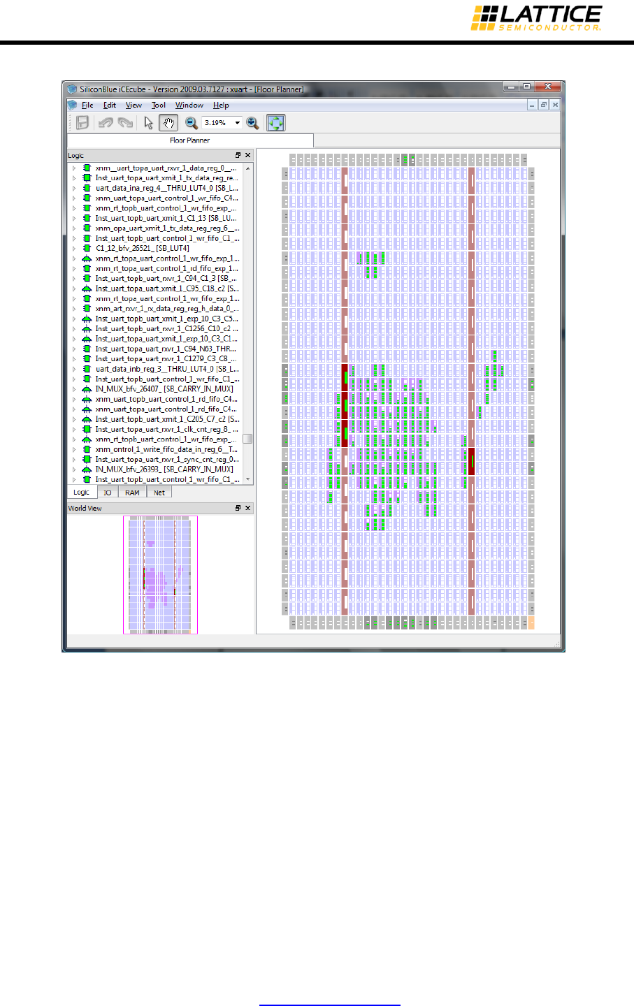
iCEcube2 User Guide www.latticesemi.com 103
Figure 5-3 : The Floor Planner
Viewing the Device Floor Plan
The Floor Planner displays the placement of the netlist on the selected device, as shown in
Figure 5-4 with utilized resources depicted in green.
The IO Tiles are depicted in grey, and are located along the periphery of the chip. Each IO Tile
has two or three IO Pin locations. Non-bonded IOs i.e. an IO cell that does not bond out to a pin
on the device package is unusable. Such non-bonded IOs are depicted in a dark shade of grey.
The RAM block locations are depicted by the two brown columns, running vertically through the
Floor Plan. Utilized RAM blocks are depicted in green, and the corresponding RAM Tile in a dark
brown.
The Logic Tiles are depicted by the blue tiles, and contain eight rectangular blocks, each
signifying a Logic Cell (4-input LUT, a flip-flop, and Carry logic), and a small square in the bottom-
left corner of each tile, signifying the Carry-In from the Logic Tile directly below it.

iCEcube2 User Guide www.latticesemi.com 104
The layout of the cells follows an (X, Y, Z) co-ordinate numbering scheme, with the origin at the
bottom-left corner of the device. Mousing over the logic and IO tiles displays the location co-
ordinates of the tile as a two dimensional (X, Y) co-ordinate location. Since each IO and Logic tile
has multiple IO and logic cells respectively, the IO and Logic cells within a tile are identified by the
Z co-ordinate, resulting in a (X, Y, Z) triplet that uniquely identifies each cell.
As mentioned above, the Logic Cell has multiple resources (LUT, flip-flop, Carry logic). It is
possible to view the utilized portions by performing a right-mouse-click > Show Content on a
selected Logic Cell, as displayed in Figure 5-4. This brings up a window that shows the portions
that have logic placed within. An example of a Logic Cell which contains a used LUT and flip-flop
but an unused Carry-In is displayed in Figure 5-5 below.
Figure 5-4: Viewing the utilized portions of a Logic Cell
Figure 5-5: Example of the utilized portions of a Logic Cell
The View > Zoom In and View > Zoom Out menu items zoom in and out of the Floor Plan
respectively. Mousing over a cell or net also displays instance information for that cell or net.
A World View pane provides a view of the entire Floor Plan, and can be used to navigate the
floor plan when the Zoom In factor is high.
The placed Logic tiles in the Floor Planner have the following Color conventions. White color
represents an empty cell; Green color represents a placed cell. When you select a particular cell
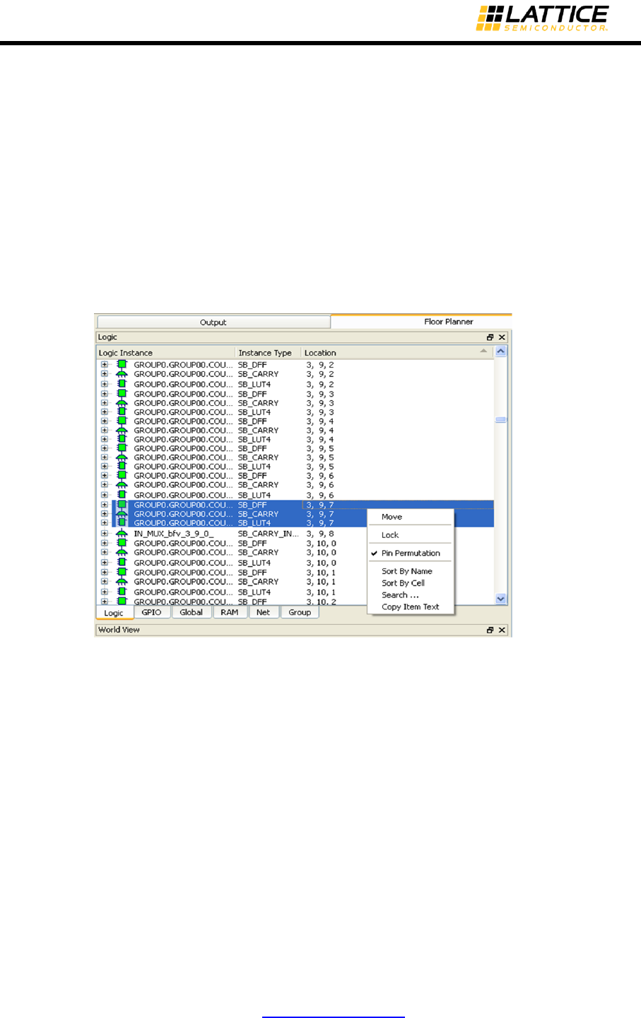
iCEcube2 User Guide www.latticesemi.com 105
it would be highlighted in Yellow. A cell which was locked at a location would be highlighted in
green color with red checks. Also, a Lock symbol would be shown on the cell.
Navigating the Design Placement
Through the Floor Plan View, the user can trace the connectivity of an implemented design. This
can be achieved via a combination of the Logic/IO/RAM/Net pane and the Fan-in/Fan-out
functionality available for each used resource.
The Logic/IO/RAM/Net pane displays the used resources on the device. Selection of a node
within this pane highlights the corresponding cell/net in the Floor Plan view.
The right-button of the mouse brings up a context sensitive menu specific to the particular type of
resource selected. This menu allows the user to Search for specific nodes, or to Sort the listed
nodes. As an example, the menu for Logic Cells is displayed in Figure 5-6.
Figure 5-6: Invoking the Sort and Search functionality in the Logic/IO/RAM/Net pane
Selecting the Sort by Name option sorts the Logic instances based on instance names as shown
below

iCEcube2 User Guide www.latticesemi.com 106
Figure 5-7: Sort by Name Option
Selecting Sort by Cell option sorts the panel display based on logic cell grouping as shown in
Figure 5-8.
Figure 5-8: Sort by Cell Option
Select Lock option to fix the instance location in the floor planner view.
Selecting the Search menu item brings up the user interface displayed in Figure 5-9. Note that
the same dialog box can also be invoked from the Edit > Search menu item.
The type of design node (Logic, Net, IO, RAM, Port) should be specified, in order to filter the
search process. In addition, a search pattern with wildcards (*,?) to match the required node
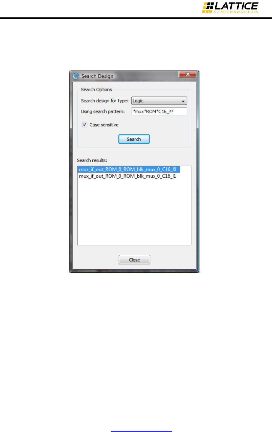
iCEcube2 User Guide www.latticesemi.com 107
names, can be specified. Clicking on the Search Button identifies and lists the nodes whose
names match the search pattern, for the specified node type.
When a node from the Search Results window is selected, it is highlighted in the corresponding
tab of the Logic/IO/RAM/Net pane, as well as in the Floor Plan view.
Figure 5-9: Search Functionality in the Floor Planner
A Right-Mouse-Click on the selected node in the Floor Plan View invokes a menu that allows
the user to display the nets connected to the node. This menu can be invoked for Logic Cells,
Block RAM and IO Cells. The resulting menu for a Block RAM cell is displayed in Figure 5-10.
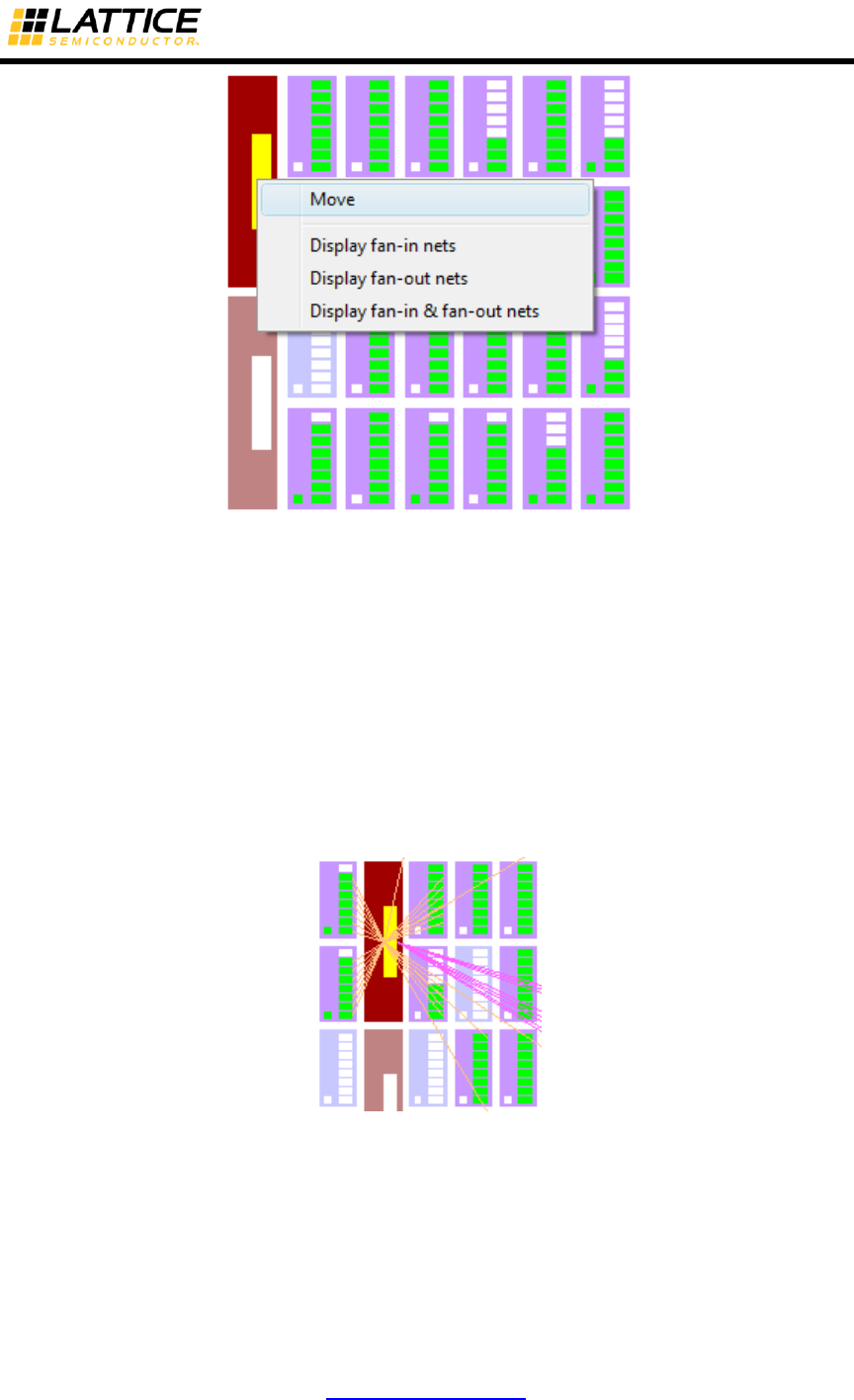
iCEcube2 User Guide www.latticesemi.com 108
Figure 5-10: Invoking the Move and Net Tracing Capability in the Floor Planner
The user now has the option to selectively display the nets connected to a cell. For example,
selecting the Display fan-in nets menu item displays only the nets that drive the node, i.e. the
fan-in nets. Similarly, if the user wishes to display only the nets that are driven by the selected
node, the Display fan-out nets menu item should be selected. Both, fan-in and fan-out nets, can
be displayed simultaneously, by selecting the Display fan-in & fan-out nets menu item.
As an example, both fan-in and fan-out nets of a Block RAM cell are shown in Figure 5-11. It
should be noted that the fan-in nets connect to the left side of the driven cell, and are depicted in
light yellow. Fan-out nets connect to the right side of the driver cell, and are depicted in dark pink.
Using fan-in and fan-out nets, the user can traverse the design from cell to cell, and make
appropriate decisions about modifying the placement manually.
Figure 5-11: Fan-in and Fan-out Nets displayed in Floor Plan
Note that by default, the fan-in and fan-out nets are displayed whenever a cell is selected. This
setting can be changed by disabling it in the Tool > Tool Options > Floor Planner tab, as
displayed in Figure 5-12 below.
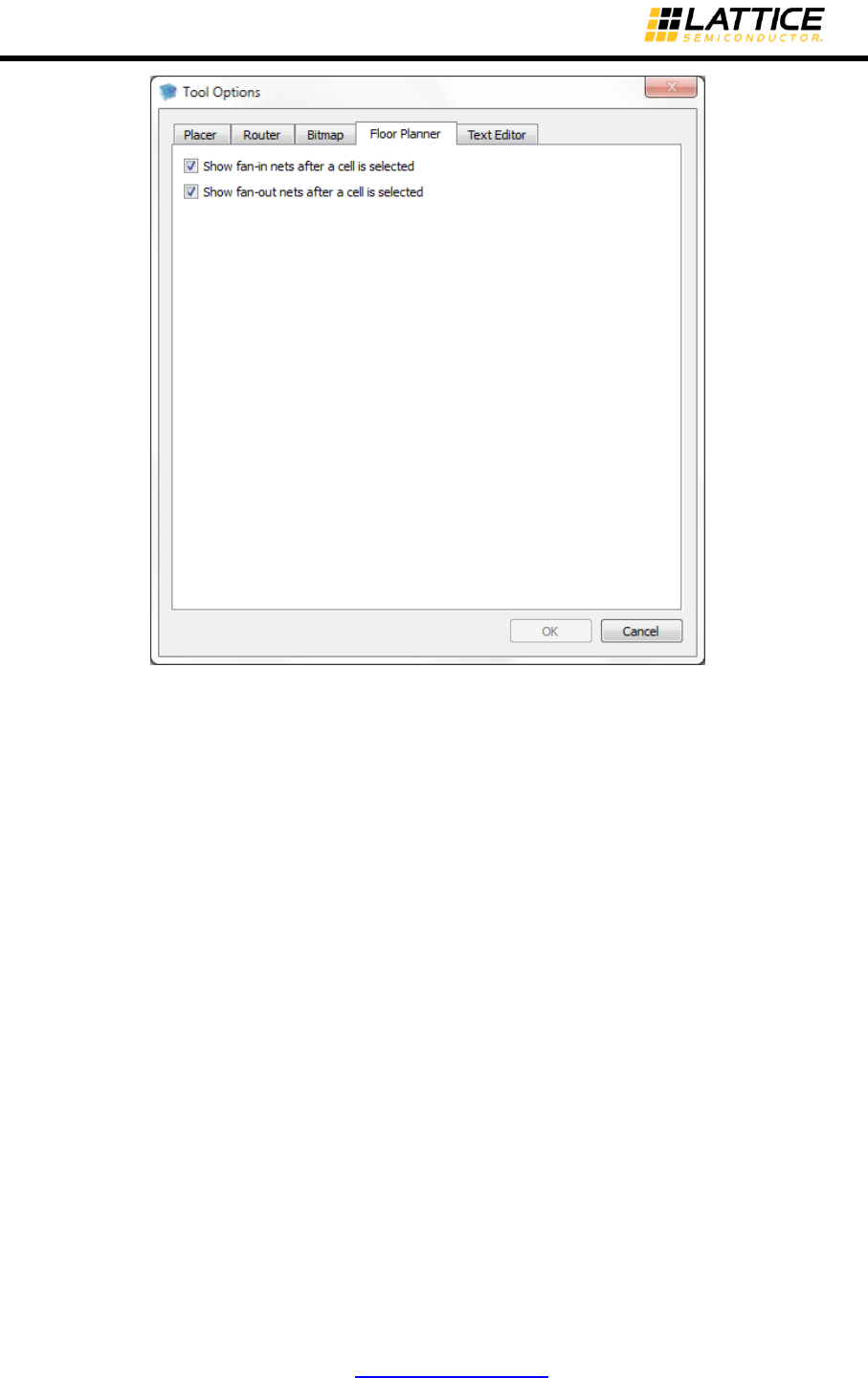
iCEcube2 User Guide www.latticesemi.com 109
Figure 5-12: Floor Planner Options
Package View
The Package View tool (Figure 5-13) displays a pin map of the implemented design in the
targeted package, and allows the user to change Pin properties such as Location and IO
Standard. Note that these properties can also be modified from the Floor Planner and the Pin
Constraints Editor.
A Port pane is available and it permits the user to select a design pin, and highlight it in the
package view.
A World View pane provides a view of the entire package, and can be used to navigate the
package view when the Zoom In factor is high.
Mousing over a pin in the package view provides information on its usage, whether the pin is
available, the pin number and the pin name.
The package pins assigned to the user’s design ports are depicted in green, and in general can
be re-assigned to different locations.
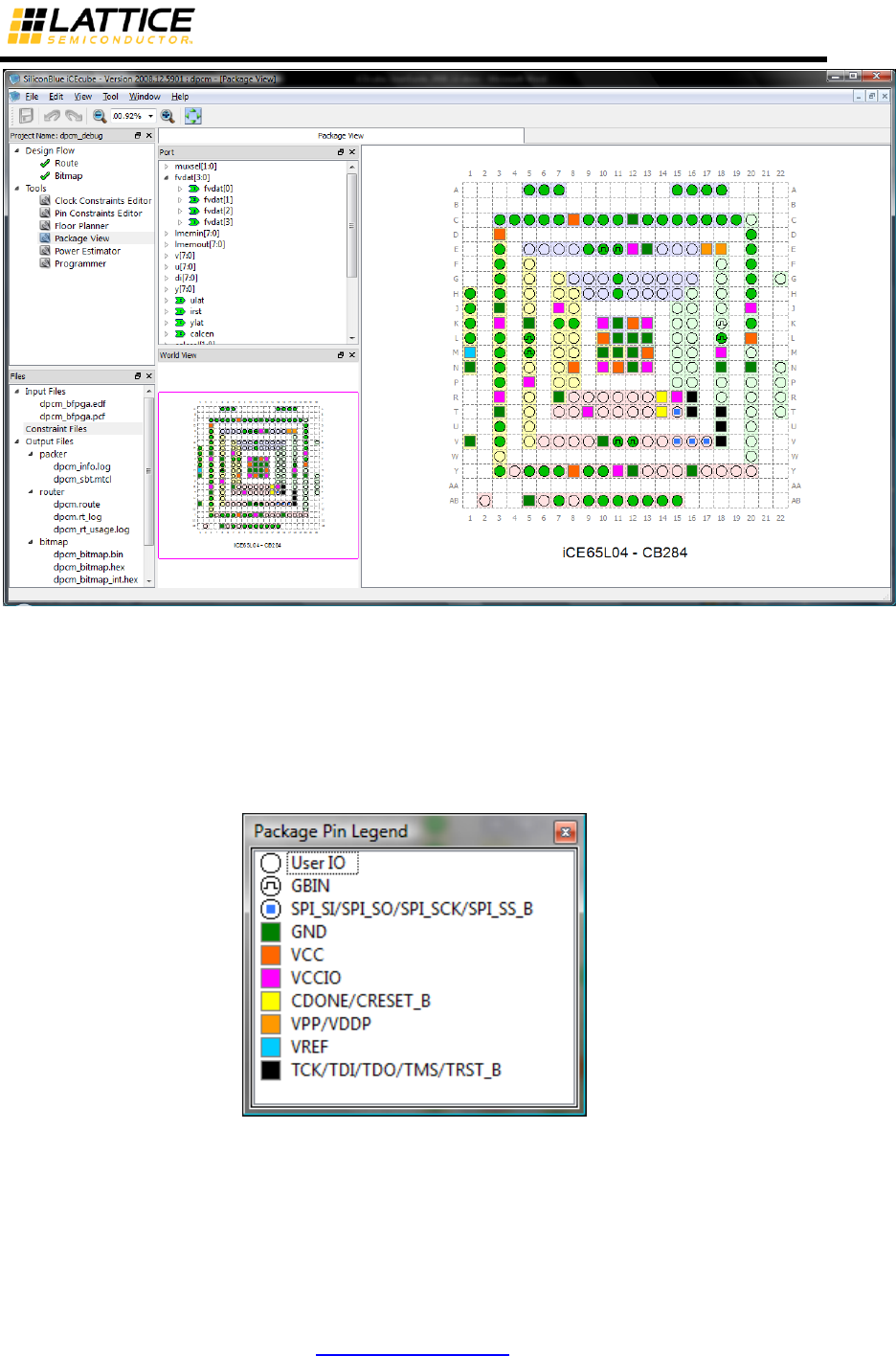
iCEcube2 User Guide www.latticesemi.com 110
Figure 5-13 : Package View
The Package Pin Legend (Figure 5-14) shows the color coding of the various pins available on
the selected package, identifying the functions of the pins. For example: power (VCC, VCCIO,
GND, VPP/VDDP, VREF), user IO, and other special purpose pins which provide access to the
low-skew global network (GBIN).
Figure 5-14: Package Pin Legend
Editing Pin Properties
Modifying a pin’s placement is accomplished either by clicking the pin and dragging it to a desired
empty location, or by invoking the Pin Constraints dialog box (Figure 5-15) using the Right-
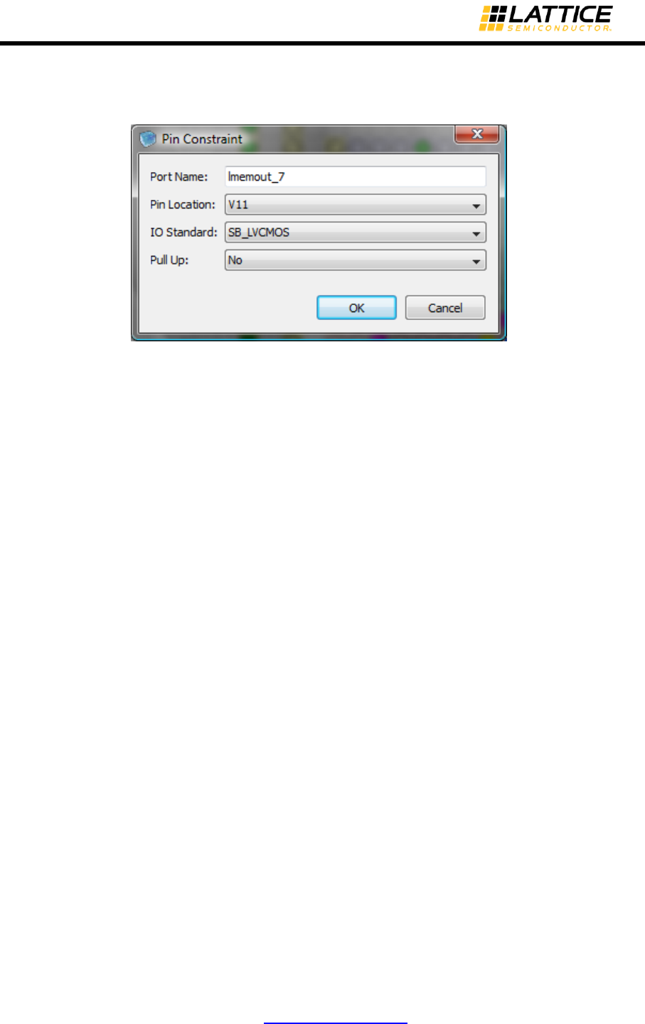
iCEcube2 User Guide www.latticesemi.com 111
Mouse-Click>Edit Pin Constraint. In addition to its location, the pin’s IO standard and Pull Up
resistor can also be configured from this dialog.
Figure 5-15: The Pin Constraints dialog box invoked from the Package View
Undesired pin location changes can be reverted back to their initial state using the Edit > Undo
menu.
Once all changes are complete, the new pinout can be saved by clicking File > Save Package
View from the main menu.
Note: Any changes to the package pin assignment will require the router to be rerun.
Pin Constraints Editor
The Pin Constraints Editor (Figure 5-16) provides a table of all the pins in the design and their
attributes. The Editor allows the user to modify the location of the pin, assign an IO Standard,
specify Load Capacitance on output pads, and set a Pull Up resistor.
In order to modify a cell value, click on the cell and select a value from the drop down box. The
drop-down selection for each cell presents only the relevant pin properties i.e. only those
destination pins that match the properties of the selected pin. Similarly, in the IO Standards
column, only the IO standards that are valid for the pin are available for selection. The same is
true for the Pull Up resistor column.
Once all changes are complete, the new pin-out can be saved by clicking File > Save Pin
Constraints Editor from the main menu.
Load Capacitance Entry: Pin Constraints Editor also allows specifying the output load
capacitance for output pads. The default value for load capacitance is 10pf (not displayed
explicitly in the cells) and the new desired value can be entered in the corresponding cells. The
capacitance values are used by Power Estimator and Static Timing Analysis tool to calculate
the power consumptions and paths delays based on output loads.
Once the router is run, a report file for the IO pins is generated. This file is named
<project>_pin_table.CSV (Comma delimited text file), is located in the
<project_directory>/<project>_Impl/sbt/outputs/packer directory.
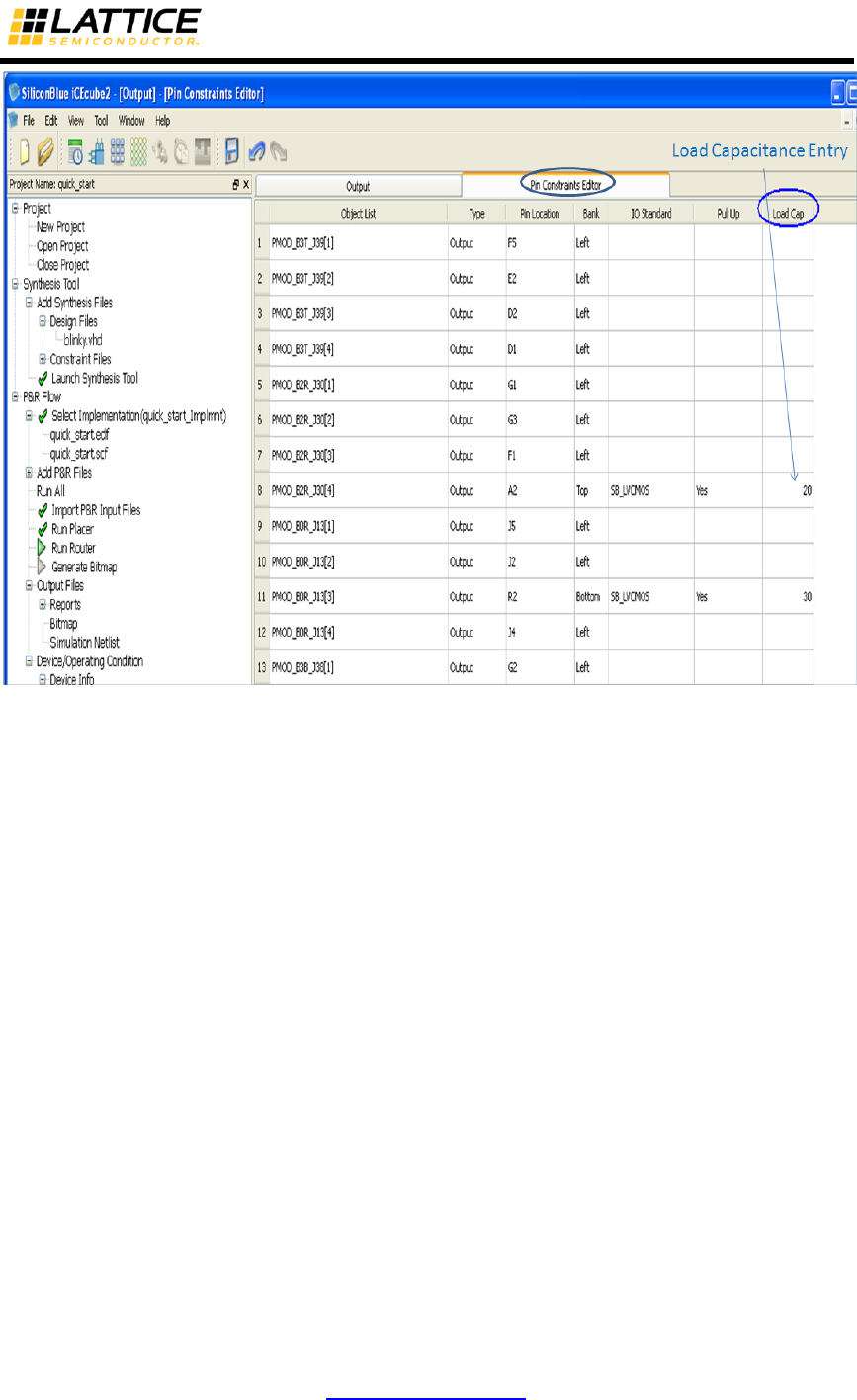
iCEcube2 User Guide www.latticesemi.com 112
Figure 5-16: Pin Constraints Editor
Power Estimator
The iCEcube2 Tool Suite includes a utility for estimating device power consumption for a given
design. The Power Estimator (Figure 5-17) can be invoked by selecting Tools > Power Estimator
from the main menu.
The utility includes a listing of utilized device resources and power dissipated at the estimated
maximum operating frequency. The user can modify several design parameters to analyze their
impact on power consumption. These parameters can be modified on the various tabs of the
Power Estimator GUI.
The Summary tab displayed in Figure 5-17 below allows the specification of the following
operational parameters for the purpose of power calculation only. Note that the operating
conditions specified earlier for Timing Analysis are not impacted by changes to the Power
Estimation parameters.
Core Vdd: The voltage at which the core of the chip operates, in Volts.
IO Voltage: The voltage at which the IO cells operate, in Volts. This can be specified
individually per bank.
Process: The process corner selection for power calculations.
Temperature: The temperature at which the chip operates, in degree Celsius. The
operating temperature can vary from -40°C to 100°C.
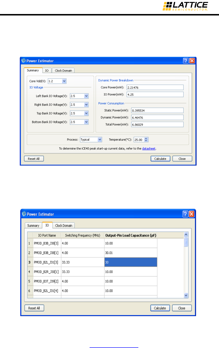
iCEcube2 User Guide www.latticesemi.com 113
Clicking on Calculate computes the estimated power dissipation and displays the results under
Dynamic Power Breakdown and Power Consumption.
Clicking Reset resets the values to the initial power estimates, and also resets all the changes
back to their default values.
Figure 5-17 : Power Estimator - Summary Tab
The IO tab displayed in Figure 5-18 permits the user to specify the toggle rate for the design’s
input and output ports, as well as loading capacitance for output pins.
Figure 5-18: Power Estimator – IO Tab
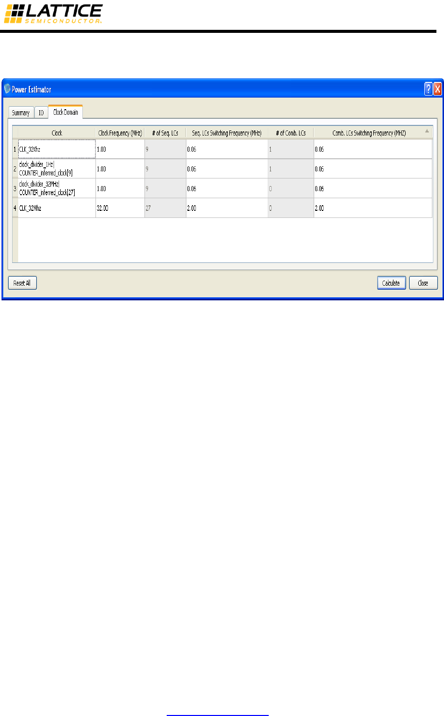
iCEcube2 User Guide www.latticesemi.com 114
Figure 5-19: Power Estimator – Clock Domain Frequency Specification
The Clock Domain tab allows the user to specify the clock frequency in MHz as shown in Figure
5-19. Note that changing this frequency adjusts the operating frequency of the individual logic
resources like the IO Cells, LUTs, Flip-Flops and Block RAMs (BRAM), as per the built-in toggle
rate estimates. In addition, the switching frequencies of the Sequential Logic Cells (Logic cell in
which the flip-flop is utilized), as well as the Combinational Logic Cells (Logic cell in which only
the LUT is utilized), can be specified, on a per domain basis.
The user can save the current session’s input data while closing the Power Estimator. Next time
when the Power Estimator is open, the previous session’s input data are populated automatically.
Generating a Bitmap
After routing is complete, the last step in the flow is to generate the configuration files (bitmap) for
programming the target device. Clicking the Bitmap icon in the Flow tab generates the bitmap.
Changing the Bitmap Options
The user can change the Bitmap options by selecting Tool > Tool Options > Bitmap. See Figure
5-20.
1. SPI Flash Mode Options: Checking the option will place the PROM in low power mode after
configuration. (Note: This option is applicable only when the iCE FPGA is used as SPI
master mode for configuration)
2. RAM4K Initialization Option: The device configuration files will not include RAM4K
initialization pattern when this option is unchecked.
3. Internal Oscillator Frequency Range: Depending on the speed of the external PROM, this
option adjusts the frequency of the internal oscillator used by the iCE FPGA during
configuration (Note: This is only applicable when the iCE FPGA is used in SPI master mode
for configuration)
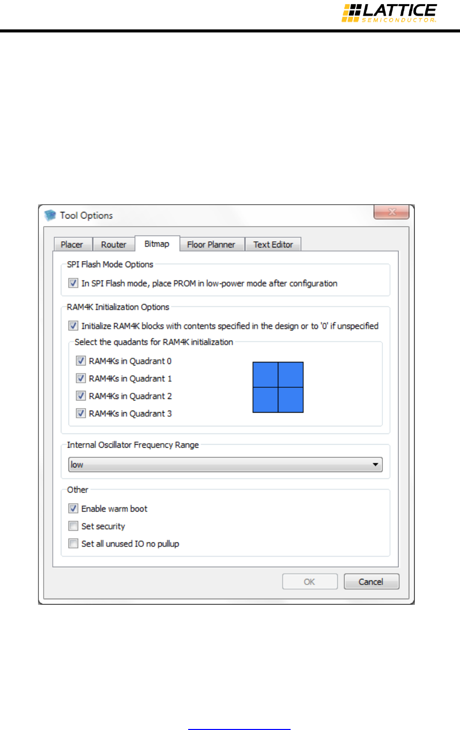
iCEcube2 User Guide www.latticesemi.com 115
4. Other
a. Enable Warm Boot: This option enables the Warm Boot functionality, provided
the design contains an instance of the SB_WARMBOOT primitive, and the
Multiple Image Files are specified as explained in the section Programming the
Device.
b. Set security: Selecting this option ensures that the contents of the Non Volatile
Configuration Memory (NVCM) are secure and the configuration data cannot be
read out of the device.
c. Set all unused IO no pullup: Selecting this option removes the pullup on the
unused IOs (except Bank 3 IOs which do not have pullup)
Figure 5-20 : Bitmap Options
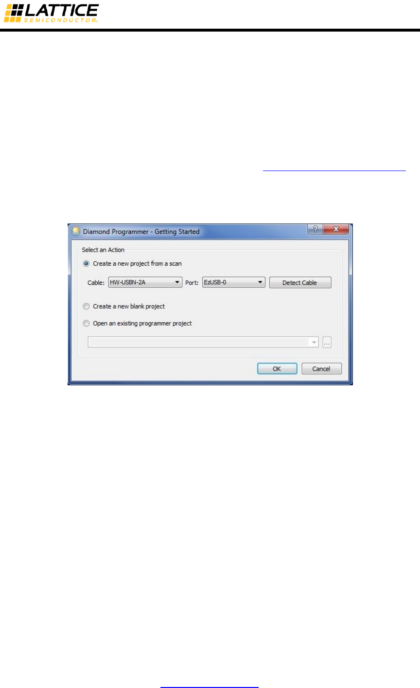
iCEcube2 User Guide www.latticesemi.com 116
Programming the Device
Standalone Lattice Diamond programmer is the device programmer required to program iCE
devices.
Diamond Programmer
Diamond programmer is fully integrated into Lattice Diamond software and also available as a
standalone application. When Diamond programmer is run within the Diamond GUI, it can be only
used to program devices supported by Diamond Software. When Diamond Programmer is run
standalone it can be used to program iCE devices.
Download and install the latest standalone programmer from http://www.latticesemi.com/ispvm.
Launch the standalone programmer to program iCE devices. The following options are available
in the getting started Dialog box as shown in Figure 5-21.
Figure 5-21: Diamond Programmer – Getting started Window.
Create a new project from a scan: Use this option to create a project based on
scanning of the attached programming cable. Select the cable type, port and click on
detect cable button to create a new configuration project.
Create a new blank project: Create a new blank project.
Open an existing programmer project: Open an existing configuration project (.xcf)
file.
The following figure shows the programmer main windows. Main window shows the cable
settings, selected device and the programming mode options.
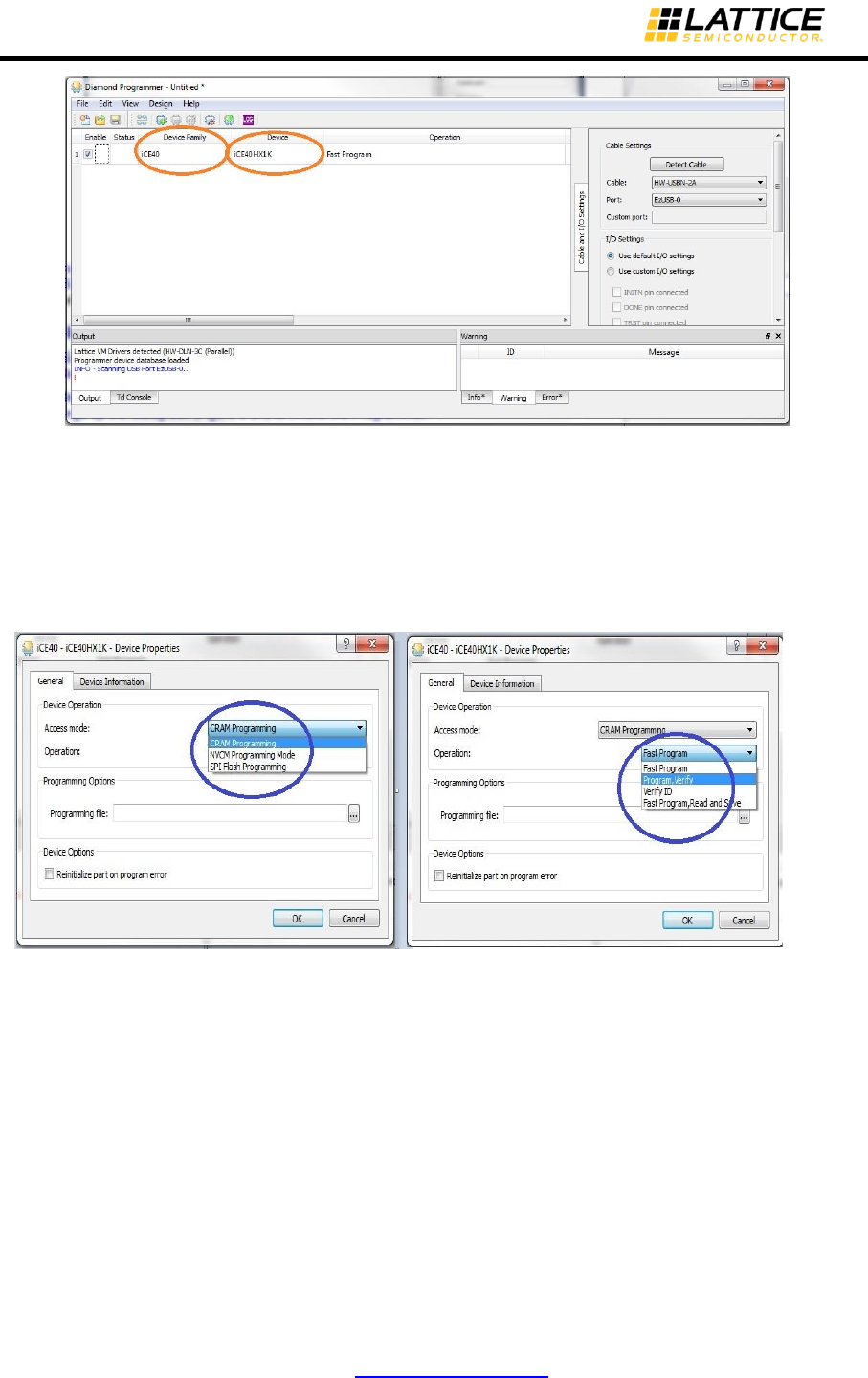
iCEcube2 User Guide www.latticesemi.com 117
Figure 5-22 : Programmer Main Window
Click on Device Family tab and select the device family. Similarly select the target device.
There are three programming modes available to configure iCE40 devices. Click on Operation tab
in the main window or select Edit -> Device Properties to select the configuration mode.
Figure 5-23 : Device Programming Modes
Access Mode:
CRAM Programming: Configuration Random Access Memory (CRAM) configuration is
accomplished by directly loading the iCE40 CRAM over the SPI bus. This flow use the iCEcube2
generated .hex, .bin files for programming the device.
NVCM Programming Mode: NCVM programming involves transmitting programming data over
the SPI bus to the NVCM array internal to the iCE40 device. The NVCM is one-time
programmable (OTP). This flow uses the .nvcm file.
SPI Flash Programming: iCE40 device is configured using an external SPI Flash device. In this
flow, the iCE40 device acts as the SPI bus master and will therefore control the data flow from the
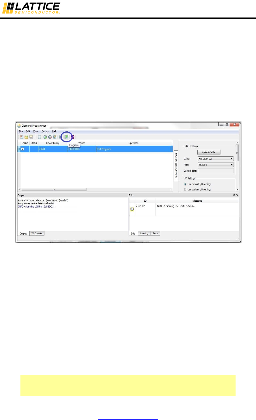
iCEcube2 User Guide www.latticesemi.com 118
configuration device. This flow use the iCEcube2 generated .hex, .bin files for programming the
device.
Operation:
Each programming mode has various operation modes to erase, program and verify. Refer Help
-> Programming the FPGA -> Programmer Options -> Device Properties Dialog Box for the
supported operation modes.
Click on the program icon or select Design->Program to start program the device. The output
window displays the status of programming.
Figure 5-24 : Program the device.
For more information on iCE40 Programming, refer Standalone Diamond programmer Help ->
Programming the FPGA > Programming and Configuring iCE40 Devices with Programmer.
Memory Initializer
iCEcube2 provides a command line utility to initialize the block memory primitives (BRAM) in the
design after placement and routing. The memory initialize utility directly updates the memory
contents in the post route OA database. This feature allows the user to initialize a single or
multiple memory contents without re-implementing the design. The post route simulation netlist
can be regenerated through Tools ->Generate Simulation Netlist menu item for functional
verifications.
Dos Command
<<icecube2_install_dir>>\sbt_backend\bin\win32\opt\mem
initializer.exe --des-lib <design_OA_database> --mem-
list-file <mem-list-file-name>

iCEcube2 User Guide www.latticesemi.com 119
Bash Command
export LD_LIBRARY_PATH =
<<icecube2_install_dir>>/sbt_backend/lib/linux/opt/:
$LD_LIBRARY_PATH
<<icecube2_install_dir>>/sbt_backend/bin/linux/opt/mem
initializer --des-lib <design_OA_database> --mem-list-
file <mem-list-file-name>
Options:
--des-lib <design_OA_database> : Specify the design OA database (oadb-XXXX ).
--mem-list-file <mem-list-file-name> : File specifying the post-synthesis logical BRAM name or
the post-routed physical BRAM instance name and the
associated memory initialization file.
Memory list file Format: Memory list file is a text file which specifies the post-synthesis logical
BRAM instance name or the post-routed physical BRAM instance name as in the post route
simulation netlist and the associated memory initialization file. The format of the file is shown
below
Format: < BRAM logical/physical Instance name> <mem init file>
Example: sample_mem.list
memory0 ram1.mem
memory1 ram2.mem
memory2_physical ram3.mem
The floor planner view shows the post synthesis BRAM logical instance names.
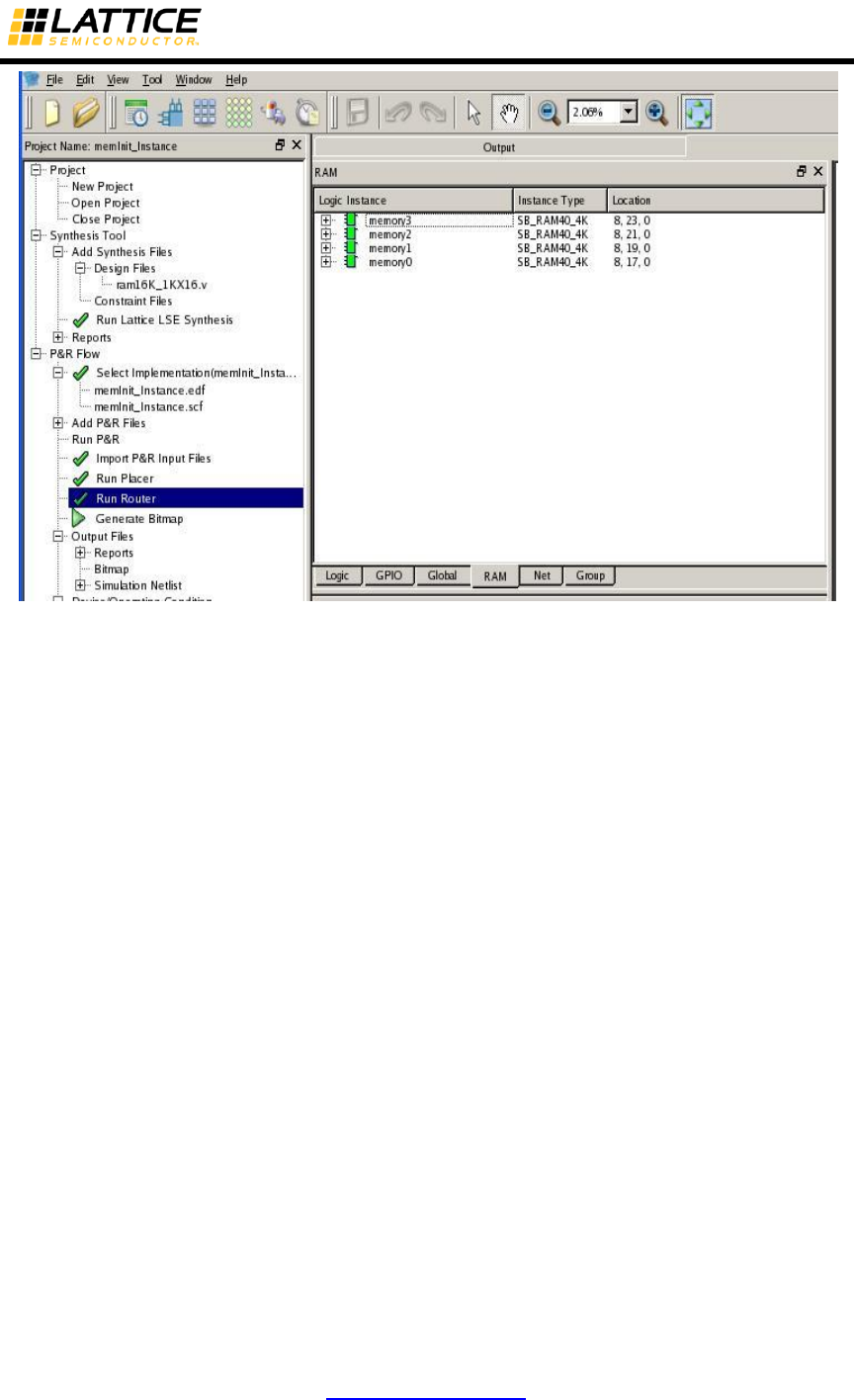
iCEcube2 User Guide www.latticesemi.com 120
Figure 5-25 : Floorplanner view – BRAM logical instances
Memory initialization file Format (.mem) :
A memory initialization file (.mem) is an ASCII text file that contains memory initialization data in
hex format.
Data
The address and data must be in Hex (hexadecimal) Format. Each line consists of an address
followed by a colon and then any number of data words, separated by spaces. If the specified
address contains multiple data words, the data initialization starts at specified <address> and the
initialization continue for the next immediate sequential addresses till the last data word. If the
data has fewer bits than the expected data width then the most significant bits are filled with 0.
Any address not specified in the .mem file will be filled with 0. Use pound sign (#) in the .mem file
to add comments or block an address for memory initialization.
Format : <address> :< data> <data> <data>...
Example: memory256x16.mem
A0:0003 00F3 003E 004F
B2:3B 9F
#Set address B3 to “0”.
#B3:FF
This initialize the address A0 with 0003, A1 with 00F3, A2 with 003E, A3 with 004F, B2 with
003B, and B3 with 009F. Address B3 is not parsed and initialized to 0. The other addresses not
specified in the .mem file are initialized to 0.

iCEcube2 User Guide www.latticesemi.com 121
Simulating the Routed Design
Once the design is routed successfully, the iCEcube2 Physical Implementation Software
generates Post route Verilog and VHDL models and SDF files in the
<project_dir>/<project_name>_Impl/sbt/outputs/simulation_netlist directory.
Verilog Simulation
The post-route files used for Verilog timing simulation are as follows:
Post-Route Verilog netlist : <top_level_design_name>_sbt.v
Verilog SDF Timing file : <top_level_design_name>_sbt.sdf
The iCEcube2 software provides Verilog simulation libraries at the following location:
<iCEcube2_installation_directory>/Verilog
Using the above files, the design can be simulated in Aldec Active-HDL simulator or simulated in
an industry standard Verilog simulator, and verified for functionality and timing.
VHDL Simulation
The post-route files used for VHDL timing simulation are as follows:
Post-Route VHDL netlist: <top_level_design_name>_sbt.vhd
VHDL SDF Timing file : <top_level_design_name>_sbt_vital.sdf
The iCEcube2 software provides VHDL simulation libraries at the following location:
<iCEcube2_installation_directory>/VHDL
Using the above files, the design can be simulated in Aldec Active-HDL simulator or simulated in
an industry standard VHDL simulator, and verified for functionality and timing. The details of
simulating a design with Aldec Active-HDL are described in Simulating Design with ALDEC
Active-HDLChapter 10.
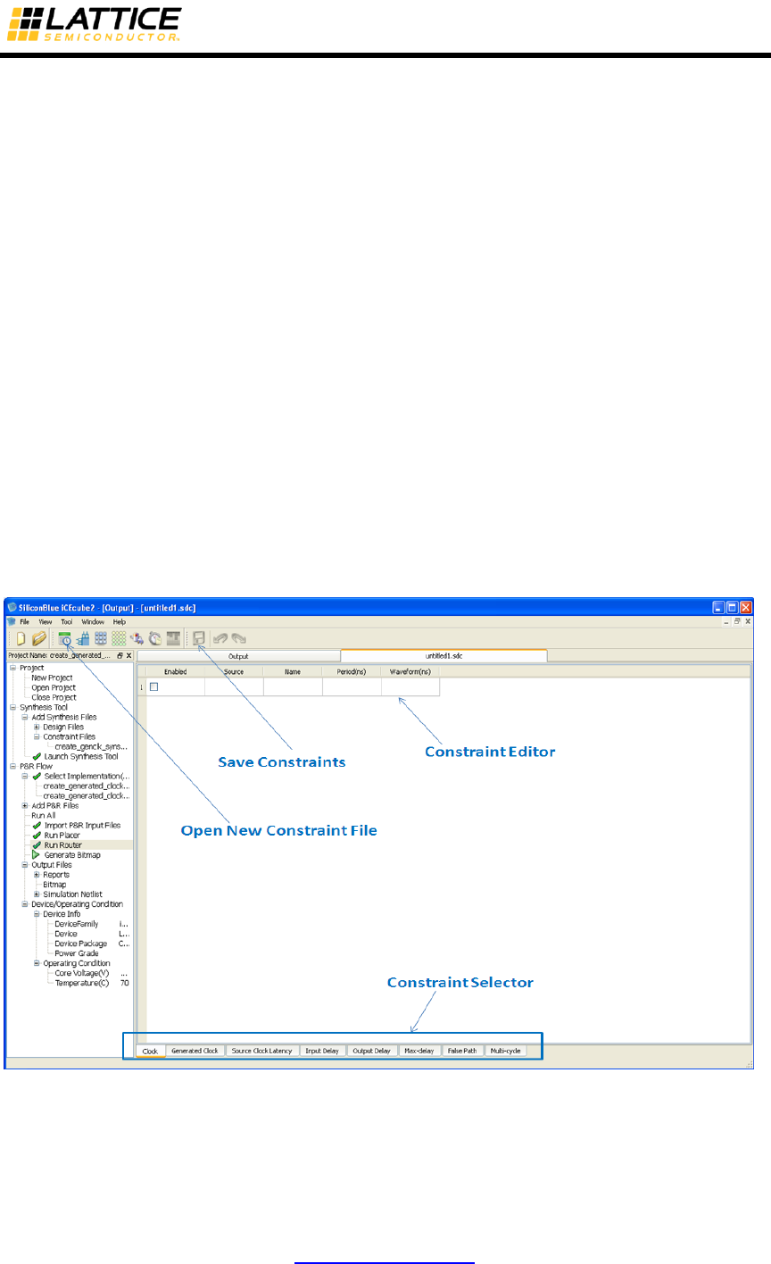
iCEcube2 User Guide www.latticesemi.com 122
Chapter 6 Timing Constraints and Static Timing Analysis
Overview
The iCEcube2 Static Timing Analysis (STA) software is useful for analyzing, verifying and
debugging the timing performances of your design. Static Timing analysis along with functional
verification allows you to verify the overall design operation.
The STA tool accepts timing constraints in Synopsys Design Constraints (SDC) format. The SDC
constraints can be forward annotated by Synplify Pro or LSE. In LSE, SDC constraints are
forward annotated in all Optimization Goal settings except for “Area”. SDC constraints can also
be specified separately by the user through the Timing Constraints Editor (TCE).
This chapter focuses on the following aspects:
Specifying Timing Constraints using the Timing Constraints Editor (TCE)
Analyzing Reports generated by STA
Specifying Constraints Using the Timing Constraints Editor (TCE)
The Timing Constraints Editor can be invoked by clicking Tool > Timing Constraints Editor.
This launches a spread sheet type editor for specifying timing constraints in the SDC format.
Figure 6-1: Timing Constraints Editor
The user can select the type of constraint in Constraint Selector tab as displayed in Figure 6-1.
When invalid constraints are specified, the TCE editor displays them in RED color and does not
forward annotate the constraints to the Placer/Router/STA tools.
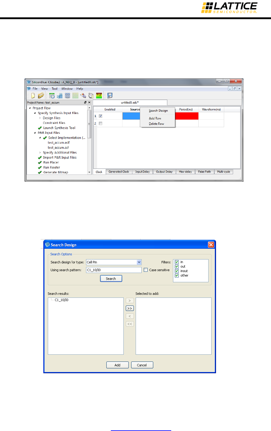
iCEcube2 User Guide www.latticesemi.com 123
Searching for Pins/Ports in the design
The Timing Constraints Editor provides the ability to specify the design object patterns using
wildcards or to search for design objects to which constraints are be applied.
Right-click on the appropriate field in TCE displays the option to ‘Search Design’, as displayed in
Figure 6-2
Figure 6-2: Searching for objects in the design
Selecting this option opens a new window where the user can search pin/clock/cell pin names as
shown in Figure 6-3. The user can also use the “*” and “?” wildcards in the search pattern fields to
search for a specific pin/clock/cell pins.
Figure 6-3: Searching for object names to constrain
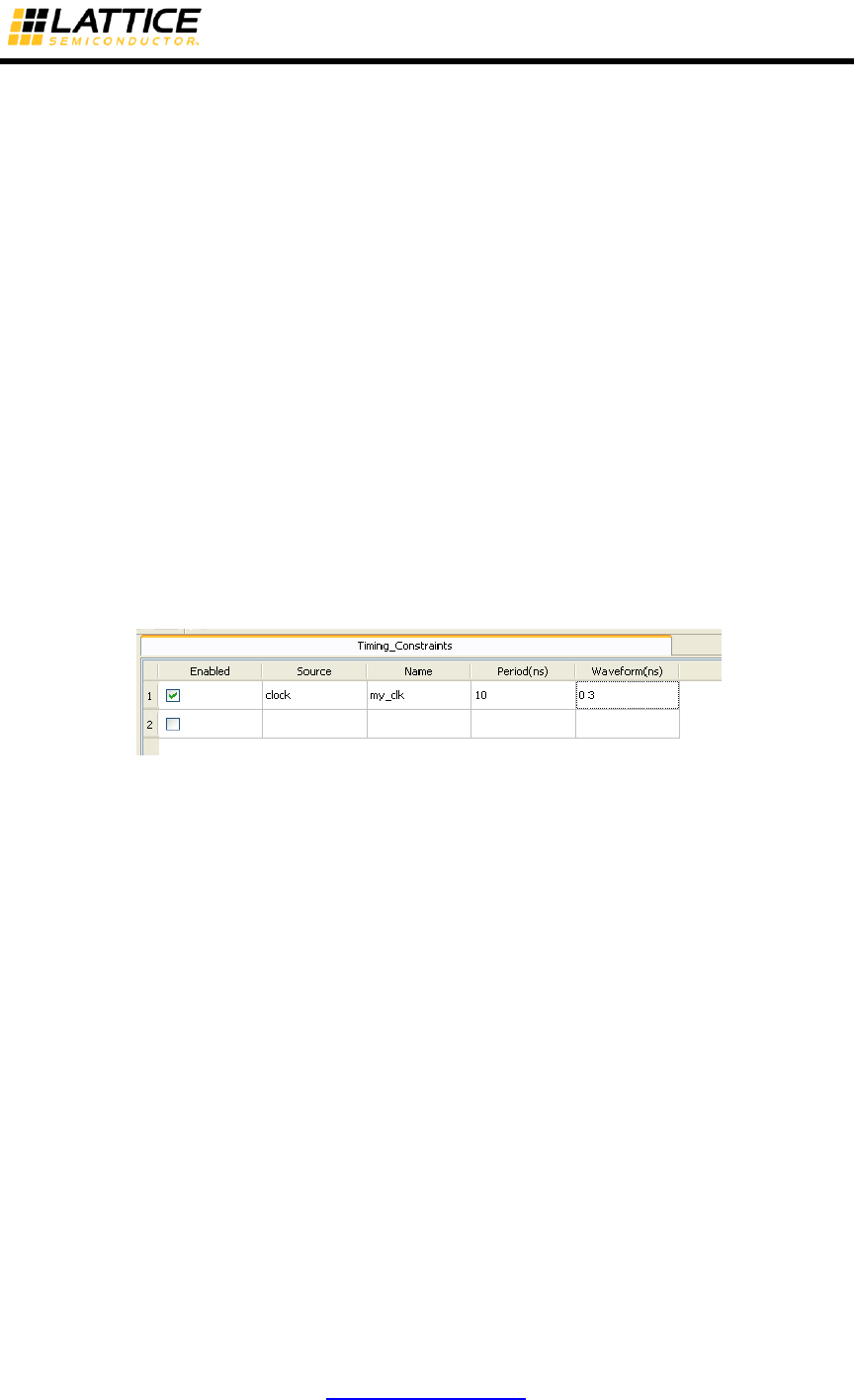
iCEcube2 User Guide www.latticesemi.com 124
SDC Constraints in TCE
Clock Constraints
To enter clock constraints, select the Clock tab in the Timing Constraints Editor GUI. The
following fields are displayed under the Clock tab.
Enabled: Use the Enable tab to enable or disable the constraint.
Source: Enter the pin name or the port name for the clock in the Source field. The port or pin
name can be selected from the drop-down box. Alternately, the user can search for
ports/cell pins by using the search option. Right clicking in source field gives the option of
searching ports/cell pins, as shown in Figure 6-2.
Name: Enter the name for the clock in the Name field. This is an optional field.
Period: Enter the period in ns, for the clock in Period field.
Waveform: Duty cycle for the clock can be specified in the Waveform field, with rising and falling
time edges of the clock.
For example, when a clock is specified as displayed in Figure 6-4, the following SDC command is
generated:
Figure 6-4: Specifying a Clock Constraint
create_clock –name my_clk –period 10.00 –waveform {0 3} [get_ports {clock}]
Generated Clock Constraints
To enter generated clock constraints, select the Generated Clock tab in the Timing Constraints
Editor GUI. The following fields are displayed under the Generated Clock tab.
Enabled: Use the Enable tab to enable or disable the constraint.
Source: Specify the port or pin name from which the clock is derived
Ref Clock Pin: Specify the generated clock pin name
Name: Enter the name of the generated clock in Name tab which is optional.
Select the option Divide by or multiply by or invert options and duty cycle according to constraint.
For example, when a generated clock is specified as displayed in Figure 6-5, the following SDC
command is generated:
create_generated_clock [get_pins {divby2clk_inst.SB_DFFSR_inst/Q}] –name divbyclk –source [get_ports
{clk_i} ] -divide_by 2
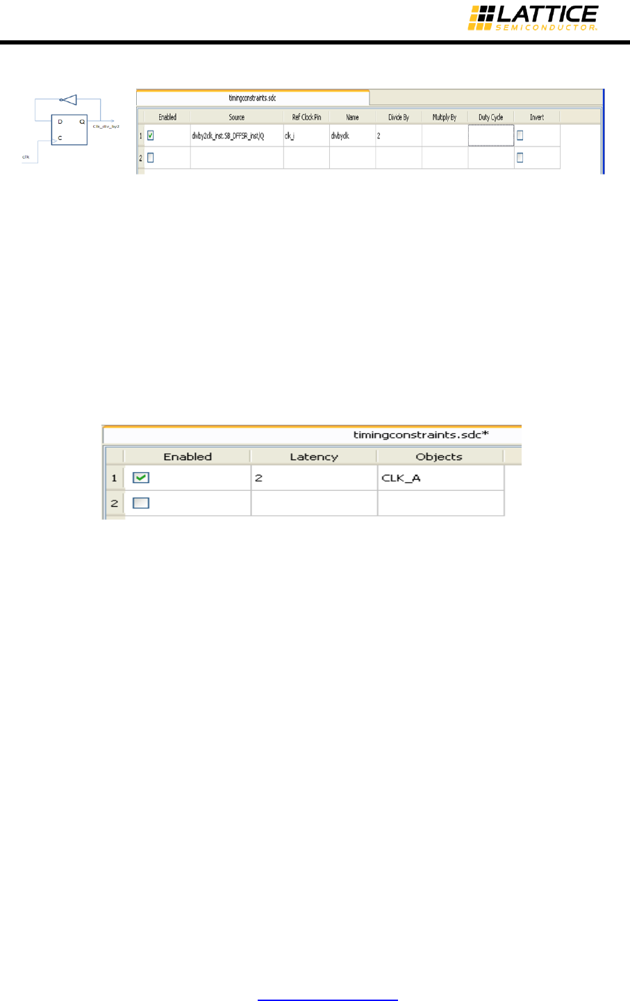
iCEcube2 User Guide www.latticesemi.com 125
Figure 6-5: Generated Clock Constraint
Source Clock Latency Constraints
To create source clock latency constraints, select the Source Clock latency tab of the TCE GUI.
The following fields are displayed:
Enabled: Use the enable tab to enable or disable the constraint.
Latency: Enter the source clock latency value.
Objects: Specify the clock source or the clock name.
For example, when source clock latency is specified as displayed Figure 6-6, the following SDC
command is generated:
Figure 6-6: Clock Latency Constraints
set_clock_latency -source 2.00 [get_clocks {CLK_A}].
Input Delay Constraints
To enter Input Delay constraints, select the Input Delay tab in the Timing Constraints Editor GUI.
The following fields are displayed:
Enabled: Use the enable tab to enable or disable the constraint.
Input List: Enter the Input pin name in the Input List.
Clock: This is the reference clock w.r.t to which the input signal is delayed.
Delay Value: Enter the Delay value in Delay Value field.
Clock Fall: Enable this field only if the input is delayed w.r.t. the negative edge of the reference
clock.
Add Delay: Enable this field if multiple clocks or edges reach the same port.
For example, when an input delay is specified as displayed in Figure 6-7, the following SDC
command is generated:
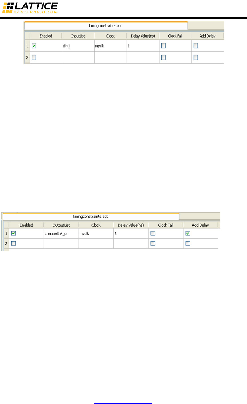
iCEcube2 User Guide www.latticesemi.com 126
Figure 6-7: Input Delay Constraint
set_input_delay -clock [get_clocks {myclk}] 1.00 [get_ports {dins_i}]
Output Delay Constraints
To create output delay constraints, select the output delay tab of the TCE GUI. The following
fields are displayed:
Enabled: Use the enable tab to enable or disable the constraint.
Output List: Enter the Output pin name.
Clock: Specify the Reference clock edge with respect to which the output delay is specified.
Delay Value: Enter the Delay value in Delay Value field.
Clock Fall: Enable this field only if the output delay is specified w.r.t. the negative edge of the
reference clock.
Add Delay: Enable this field if multiple clocks or edges reach the same port.
For example, when an output delay is specified as displayed in Figure 6-8, the following SDC
command is generated:
Figure 6-8: Output Delay Constraints
set_output_delay -clock [get_clocks {myclk}] -add_delay 2.00 [get_ports {channel1A_o}]
Max Delay Constraints
To create Max Delay constraints, select the Max Delay tab. The following fields are displayed:
Enabled: Use the Enabled field to enable or disable the constraint.
Delay Value: Enter the delay value (non-negative number) in the Delay value field.
From: Enter the source pin or port of the constrained path. The constraint is applied for the data
paths launched on both rising and falling transitions.
Rise From: Enter the source pin or port of the constrained path. The constraint is applied only for
the paths launched on rising transitions.
Fall From: Enter the source pin or port of the constrained path. The constraint is applied only for
the paths launched on falling transitions.
To: Enter destination pin or port, up to which the path is defined. The constraint is applied for the
paths captured on both rising and falling transitions.
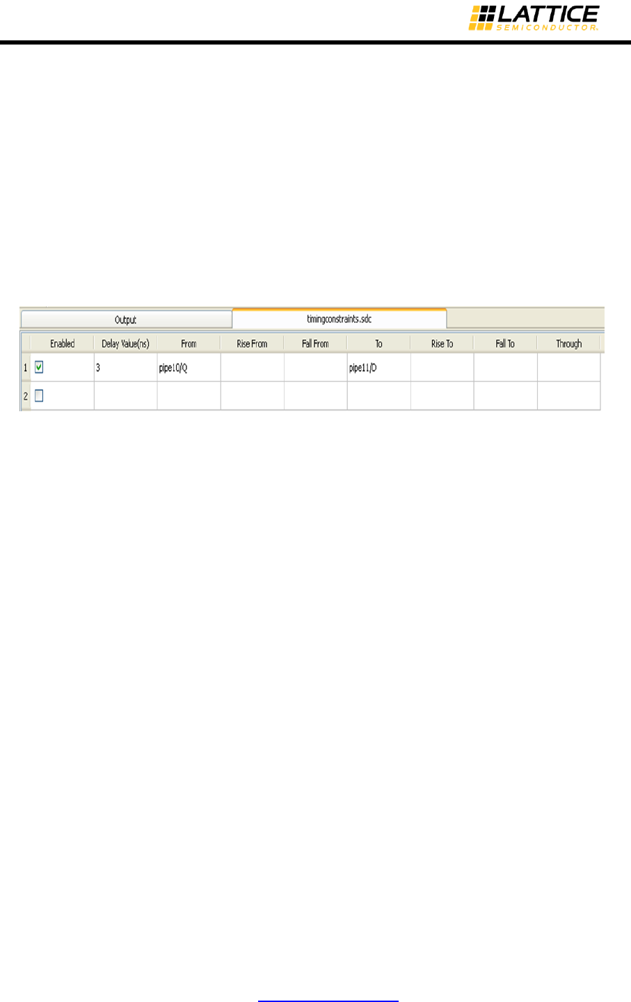
iCEcube2 User Guide www.latticesemi.com 127
Rise To: Enter destination pin or port, up to which the path is defined. The constraint is applied
only for the paths captured on rising transitions.
Fall To: Enter destination pin or port, up to which the path is defined. The constraint is applied
only for the paths captured on falling transitions. Through: Specify a pin to ensure that the
constrained path passes through this pin. This field is optional.
Note: The fields From, Rise From, Fall From are mutually exclusive. Similarly the fields To, Rise
To, Fall To are mutually exclusive.
For example, when a Max Delay constraint is specified as displayed in Figure 6-9, the following
SDC command is generated:
set_max_delay -from [get_pins {pipe10/Q}] -to [get_pins {pipe11/D}] 3.00
Figure 6-9: Max Delay Constraints
False Path Exceptions
To create False Path exceptions, select the False Path tab. The following fields are displayed:
Enabled: Use the Enable field to enable or disable the constraint.
From: Enter the port or pin from which the false path is defined. The exception is applied for the
data paths launched on both rising and falling transitions.
Rise From: Enter the port or pin from which the false path is defined. The exception is applied
only for the paths launched on rising transitions.
Fall From: Enter the port or pin from which the false path is defined. The exception is applied
only for the paths launched on falling transitions.
To: Enter the Port or pin up to which the false path is defined. The exception is applied for the
data paths captured on both rising and falling transitions.
Rise To: Enter the Port or pin up to which the false path is defined. The exception is applied only
for the paths captured on rising transitions.
Fall To: Enter the Port or pin up to which the false path is defined. The exception is applied only
for the paths captured on falling transitions.
Through: Specify a pin to ensure that the constrained path passes through this pin. This field is
optional.
Note: The fields From, Rise From, Fall From are mutually exclusive. Similarly the fields To, Rise
To, Fall To are mutually exclusive.
For example, when a False Path exception is specified as displayed in Figure 6-10, the following
SDC command is generated:
set_false_path -rise_from [get_clocks {CLK_A}] -to [get_clocks {CLK_B}]
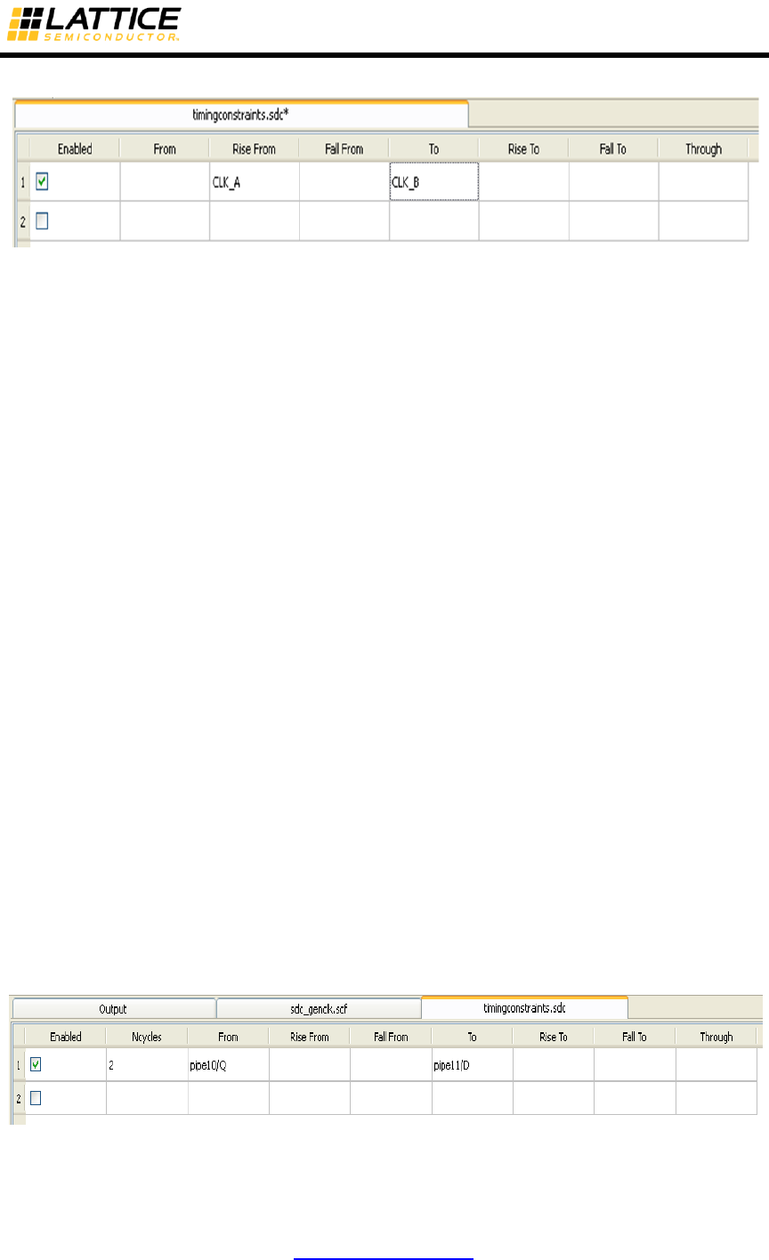
iCEcube2 User Guide www.latticesemi.com 128
Figure 6-10: False Path Exceptions
Multi Cycle Path Exceptions
To create Multi Cycle path exceptions, select the Multi-Cycle tab. The following fields are
displayed:
Enabled: Use the Enable field to enable or disable the exception.
Ncycles: Enter the number of clock cycles (non negative number) of the capture clock.
From: Enter the port or pin from which the exception is defined. The exception is applied for the
data paths launched on both rising and falling transitions.
Rise From: Enter the port or pin from which the exception is defined. The const exception rained
is applied only for the paths launched on rising transitions.
Fall From: Enter the port or pin from which the exception is defined. The exception is applied
only for the paths launched on falling transitions.
To: Enter the port or pin up to which the multi-cycle exception is defined. The exception is applied
for the data paths captured on both rising and falling transitions.
Rise To: Enter the port or pin up to which the multi-cycle exception is defined. The exception is
applied only for the paths captured on rising transitions.
Fall To: Enter the port or pin up to which the multi-cycle exception is defined. The exception is
applied only for the paths captured on falling transitions.
Through: Specify a pin to ensure that the constrained path passes through this pin. This field is
optional.
Note: The fields From, Rise From, Fall From are mutually exclusive. Similarly the fields To, Rise
To, Fall To are mutually exclusive.
For example, when a Multi Cycle exception is specified as displayed in Figure 6-11, the following
SDC command is generated:
set_multicycle_path -from [get_pins {pipe10/Q}] -to [get_pins {pipe11/D}] 2
Figure 6-11: Multi Cycle Path Exception
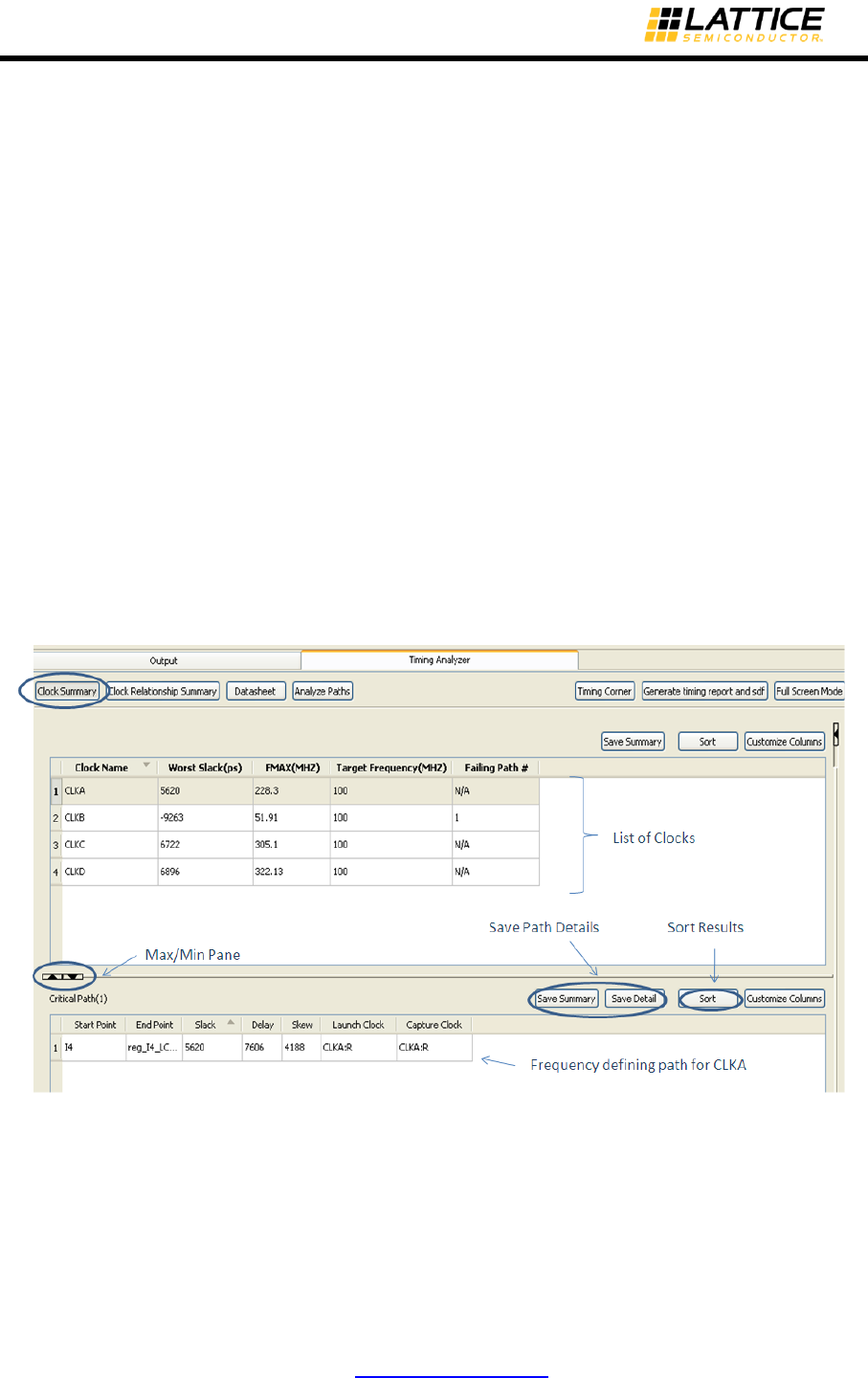
iCEcube2 User Guide www.latticesemi.com 129
Analyzing Reports Generated by the Static Timing Analyzer (STA)
The output of STA is a path report giving the details of each path in the design along with delays
along the paths. This section explains the timing reports generated by STA in the Timing Analyzer
window for a design targeted for iCE40 family and also provides directions on performing queries
on specific paths of interest.
The Timing Analyzer window can be opened by selecting the Timing Analysis tab on the top left
corner or through the Tools > Timing Analysis menu item.
The Timing Analyzer window provides the following features, each of which is explained below:
Clock Summary
Clock Relationship Summary
Data Sheet
Analyze Paths
Clock Summary Pane
The first window shown after opening the Timing Analyzer is the Clock Summary pane, as shown
in Figure 6-12. This section gives the details of computed frequency summaries and the
frequency defining paths for all clocks in the design. When a particular clock is selected, the
paths corresponding to that clock, and the path used for frequency computation, are displayed in
the path summary pane.
Figure 6-12: Clock Summary Report
For every frequency defining path (one per clock), the following fields are displayed in the Critical
Path Summary section:
Start Point: This indicates the pin at which the data path initiates. It can be a top-level design
port (input package pin), the output of a flip-flop or the RDATA output of a RAM block.
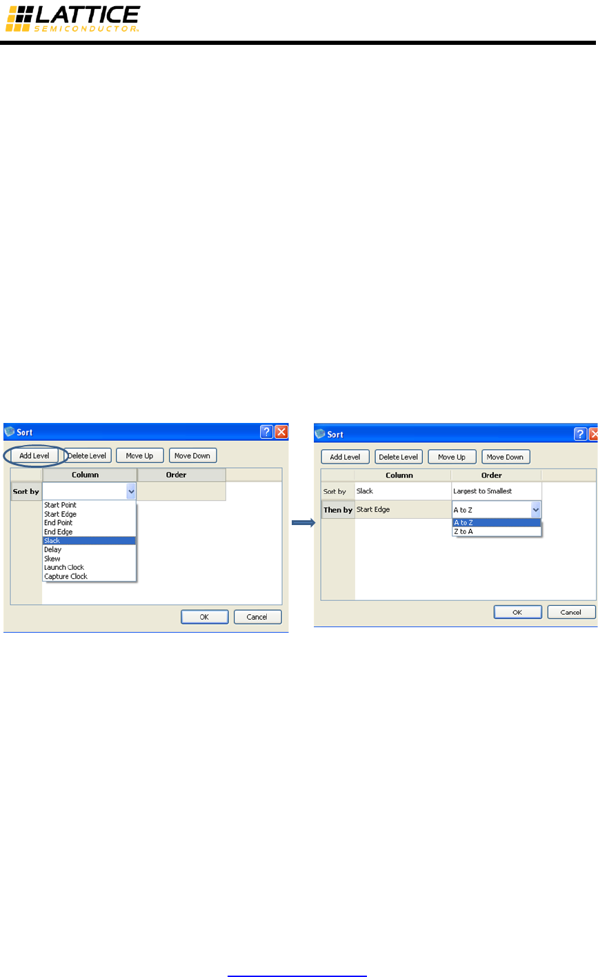
iCEcube2 User Guide www.latticesemi.com 130
End Point: This indicates the pin at which the data path ends. It can be a top-level design port
(output package pin), the input of a flip-flop or an input of a RAM block.
Launch Clock: The clock and its polarity at which the data is launched.
Capture Clock: The clock and its polarity at which the data is captured.
Slack: The slack value computed for the path. The critical path has the lowest slack.
Delay: The delay of the path as computed by the sum of the logic and routing elements between
the Start and End Points. This includes the Clock-to-Out delay of the starting FF or RAM block.
Skew: The clock skew between the edges of the launch clock and the latch clock.
Save Summary and Save Detail sections are useful in saving the reported path details in a text
format. Save Summary option writes out the simple delay computation details used in computing
the path delay. Save Detail option writes out detailed path delay computation details.
Sort Option in the clock summary section helps the user to sort the generated path results.
By clicking on the sort option, a window would popup asking for the feature to be used for sorting.
User can sort the results hierarchically based on every filed displayed in the summary section.
So, the sort option in critical path report section would sort according to Start Point, End Point,
Slack, Delay, Skew, Start Edge and End Edge. Using the ‘Add Level’ feature user can add these
fields in priority basis and select their order in which the results need to be sorted.
Figure 6-13 Sorting Reported Paths
For example, in Figure 6-13 “Slack” was added first in ascending order. Then “Start Edge” was
added next in ascending order. So, the results are displayed with ascending order of slack first
and then, the results with same slack are sorted in ascending order of Start Edge.
It should be noted that:
1. Frequency computations are performed only on paths starting from input pads and flip-
flop/RAM outputs, and ending at output pads and flip-flop/RAM inputs.
2. If the paths triggered by a clock are not constrained (timing start point and timing end points),
then the columns Worst Slack, FMAX and Failing Paths are shown as “N/A”. Appropriate
constraints are required in order for clock frequencies to be reported.
3. In the clock summary pane, only the most critical path for each constrained clock is displayed
irrespective of constraints met or not.
4. If the constraints are not met, the “Failing Path #” column shows the no of paths failed
including the most critical path displayed in the summary pane. All the other failing paths can
be viewed through query path options as described in Analyzing Constrained Paths.
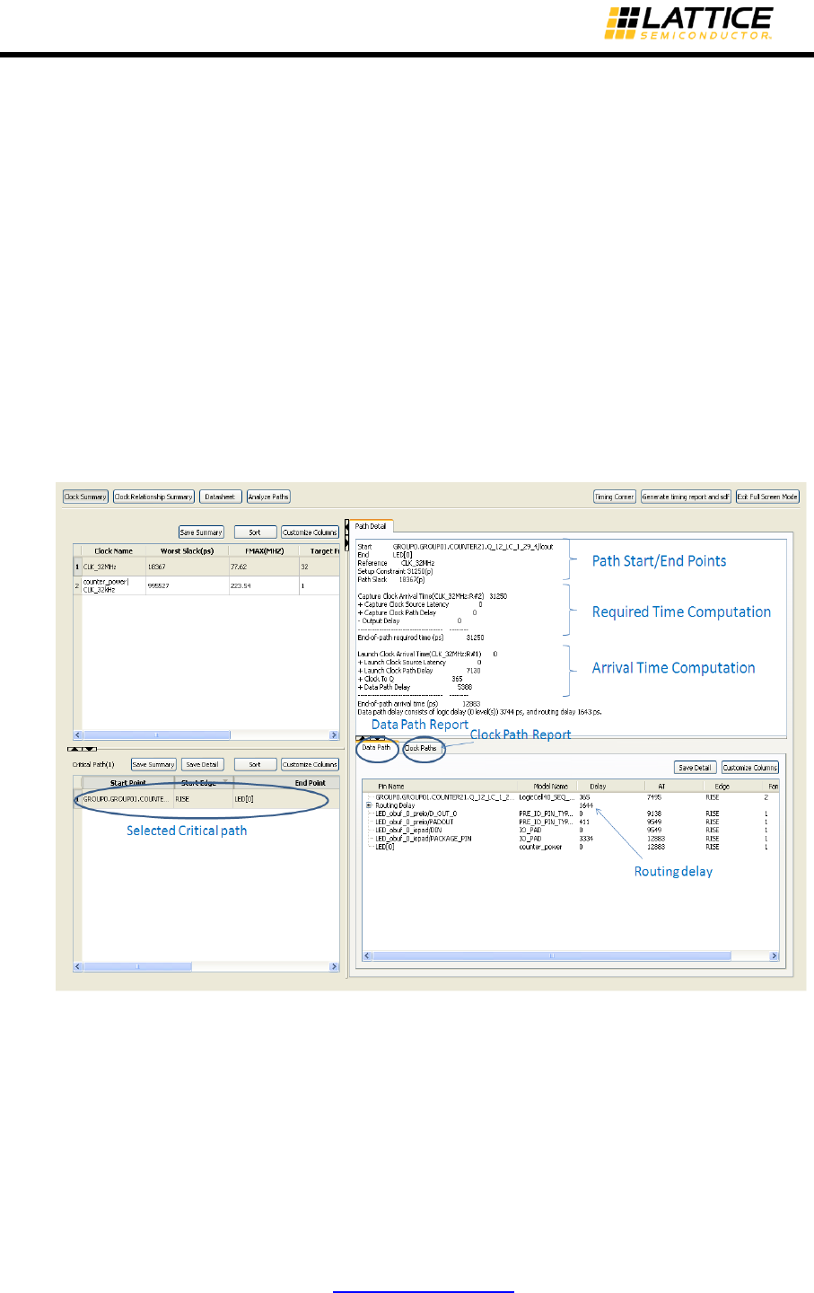
iCEcube2 User Guide www.latticesemi.com 131
5. Frequency calculations do not include paths involving IO’s unless the IO’s are constrained
with Input and Output Delays.
6. Cross-clock domain paths are not reported in this pane.
Detailed Path Report
When a path in the Critical Path pane is selected, detailed path section for the path is displayed.
The detailed path report provides the following details as shown in Figure 6-14.
Path Detail: Gives the Timing Start Point, Timing End Point, reference clock used for slack
computation and the slack value. If the Timing Start Point or End Point is a register within an IO
pad, the summary panel displays either the default IO register name or the name of the user FF
that was originally in the logic fabric, but was merged into the IO pad as shown in Figure 6-15 .
Data Required Time: Detailed path report for computing the data required time, at the capture
clock edge.
Data Arrival Time: Detailed path report for computing the data arrival time, starting from the
launch clock edge.
Figure 6-14: Example of Detailed Path Summary for Frequency Computation
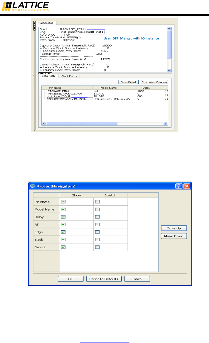
iCEcube2 User Guide www.latticesemi.com 132
Figure 6-15 : Path Summary Displaying user DFF merged with IO
Detailed Path Report Pane gives the routing delays and delay of each cell involved in the path
and the slack values. For detailed analysis of Timing Path Reports, refer to “Detailed Timing
Path” section.
The detailed timing path report can be saved in text format by using “Save Detail” Option.
Figure 6-16: Customize Report Options
Customize Columns option enables the user to choose the parameters that need to be used while
displaying the timing report. A sample customization option menu is shown in Figure 6-16. It also
enables the user to adjust the width of each column. By using “Move Up” and “Move Down”, the
user can sort out the Columns.
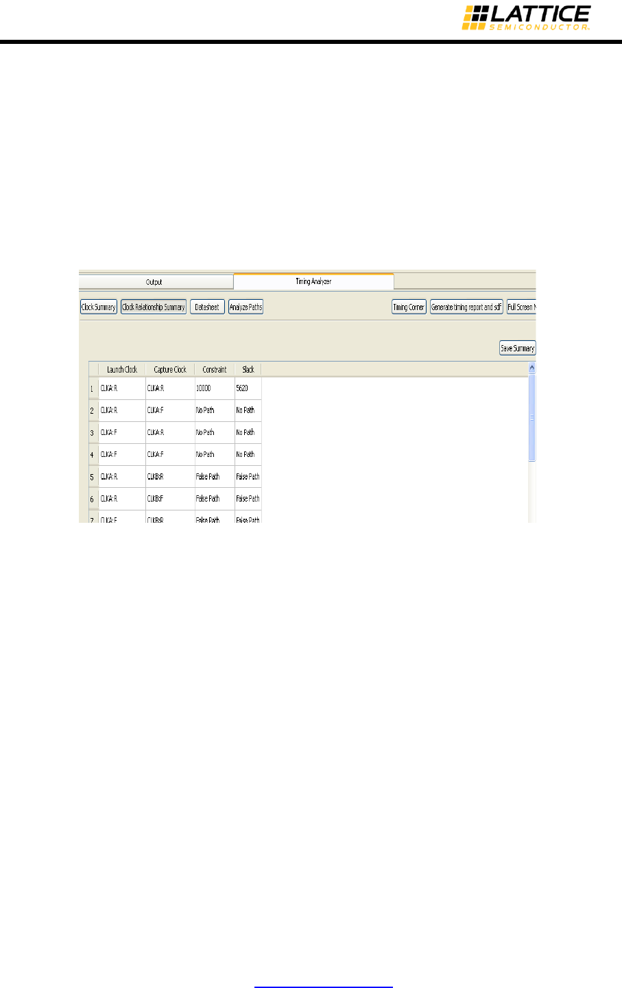
iCEcube2 User Guide www.latticesemi.com 133
Clock Relationship Summary
The Clock Relationship Summary in the Timing Analyzer Window displays the constraints and
slack details for the critical clocked paths, which are in the same clock domain as well as cross-
clock domains. Clicking on “Clock Relationship Summary” in the timing analyzer pane generates
a report as shown in Figure 6-17.
“No Path” in the Slack Column indicates that there exists no Clock Path between mentioned
Launch Clock and Capture Clock. “False Path” in the Slack Column indicates that the path
between the mentioned Launch Clock and Capture Clock was constrained as False Path.
The Save Summary option saves the clock relationship summary in a text format.
Figure 6-17 Clock Relationship Summary
Data Sheet
The Data Sheet report summarizes the timing characteristics of the chip interface. It reports the
‘setup time’ and ‘hold time’ for the input pad to FF paths in the design, maximum and minimum
‘clock to out delays’ for the FF to output pad paths and maximum and minimum ‘path delay’ for
the pad to pad paths.
A sample Data Sheet report by the iCEcube2 software is shown in Figure 6-18.
Select “Input Pad to FF” tab and “Setup Time” sub tab to view the paths and the associated setup
delays. Similarly select the “FF to Output Pad” tab to view the maximum and minimum clock to
out delays and “Pad to Pad” tab to view the maximum and minimum path delays.
Setup Time: Reports the input setup time for each combination of input data port and clock port.
Setup time for an Input port wrt a clock is given by
Setup Time = (Maximum Data delay from Input Pad to FF) + (FF setup delay) - (Minimum Clock Path Delay)
Hold Time: Reports the hold times for design inputs, for each combination of input data port and
clock port. Hold time for the signal on an Input port wrt a clock is given by
Hold Time =(Maximum Clock Path Delay) + (FF hold delay) - (Minimum Data delay from Input
Pad to FF)

iCEcube2 User Guide www.latticesemi.com 134
Max Clock to out Delay: Reports the maximum clock_-to-out delays each combination of output
data port and clock port. Max Clock to out delay for an output port wrt a clock is given by
Max Clock to out delay = (Maximum Clock Path Delay) + (FF clock-to-out delay) + (Maximum
Data delay from FF to Output Pad)
Min Clock to out Delay Reports the maximum clock_-to-out delays each combination of output
data port and clock port. Min Clock to out delay for an output port wrt a clock is given by
Clock to out delay for an output port wrt a clock is given by
Min Clock to out delay = (Minimum Clock Path Delay) + (FF clock-to-out delay) + (Minimum Data
delay from FF to Output Pad)
Max Pad to Pad Delay: Reports the maximum Pad to Pad delay for a signal traversing a purely
combinational path from input pad (PI) to output pad (PO)
Max Pad to Pad delay = (Maximum Combinational Delay from PI to PO)
Min Pad to Pad Delay: Reports the minimum Pad to Pad delay for a signal traversing a purely
combinational path from input pad (PI) to output pad (PO)
Min Pad to Pad delay = (Minimum Combinational Delay from PI to PO)
Figure 6-18 Data Sheet Report
Select the path shown in “Setup Time” sub tab to display the detailed path report as shown in
Figure 6-19.
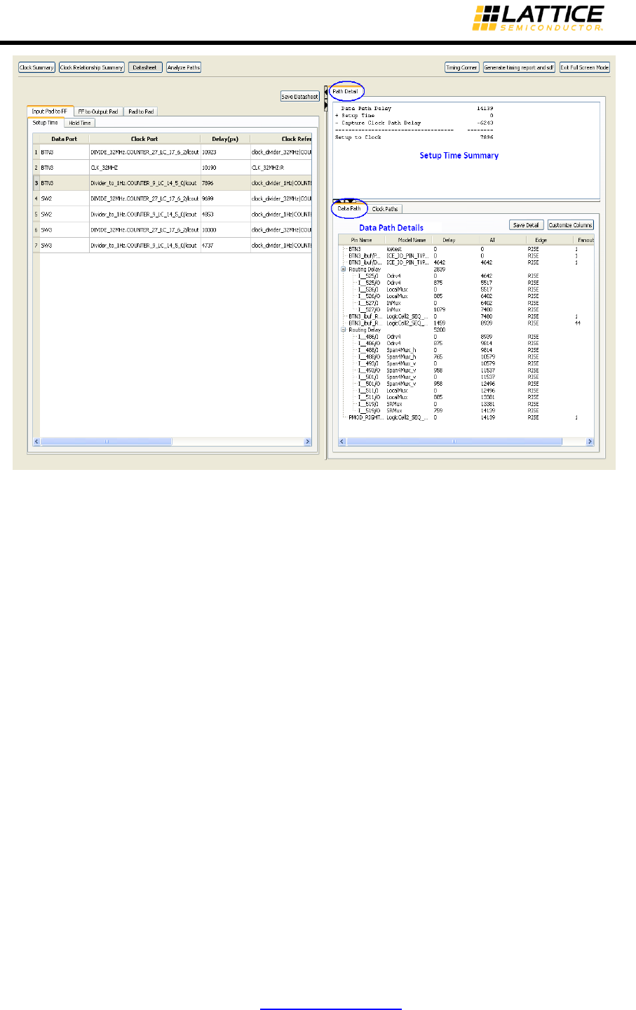
iCEcube2 User Guide www.latticesemi.com 135
Figure 6-19: Setup to Clock Path Summary
Analyzing Constrained Paths
Clicking on the Analyze Paths button allows the user to query paths in the following ways:
1. Querying for the paths based on the “Slack” value.
2. Querying for the paths based on the “Paths Start/End” Points.
3. Querying for the combinational paths based on the “Start/End” Terminals.
By Slack
The By Slack option in the “Analyze Paths” window allows the user to list out all the paths in the
design with increasing slack values.
User can customize the number of paths reported by modifying the value in “Limit Report to n
Paths” option as shown in Figure 6-20.
The Advanced Options section helps the user to customize the paths reported.
The first option in this section is useful to limit the paths reports based on Launch Clock, Capture
Clock and their phases.
The second option helps in limiting the results reported based on the number of paths per start
point and number of paths per end point.
Using the third option the results can be restricted based on the maximum slack value.
The Save Summary and Save Detail provide the ability to save the report in a text format, for all
paths, or the details of the selected path, respectively.
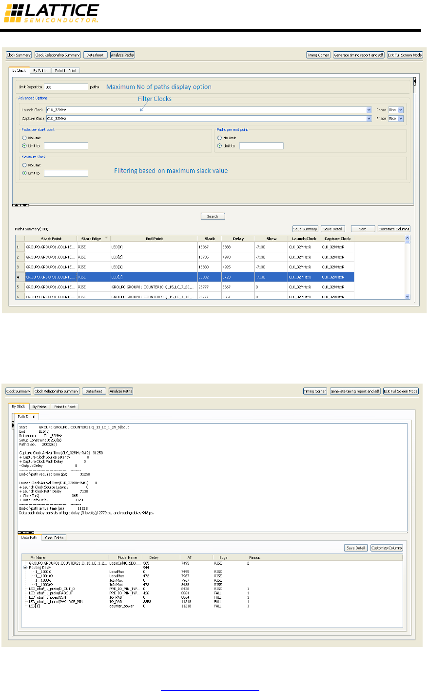
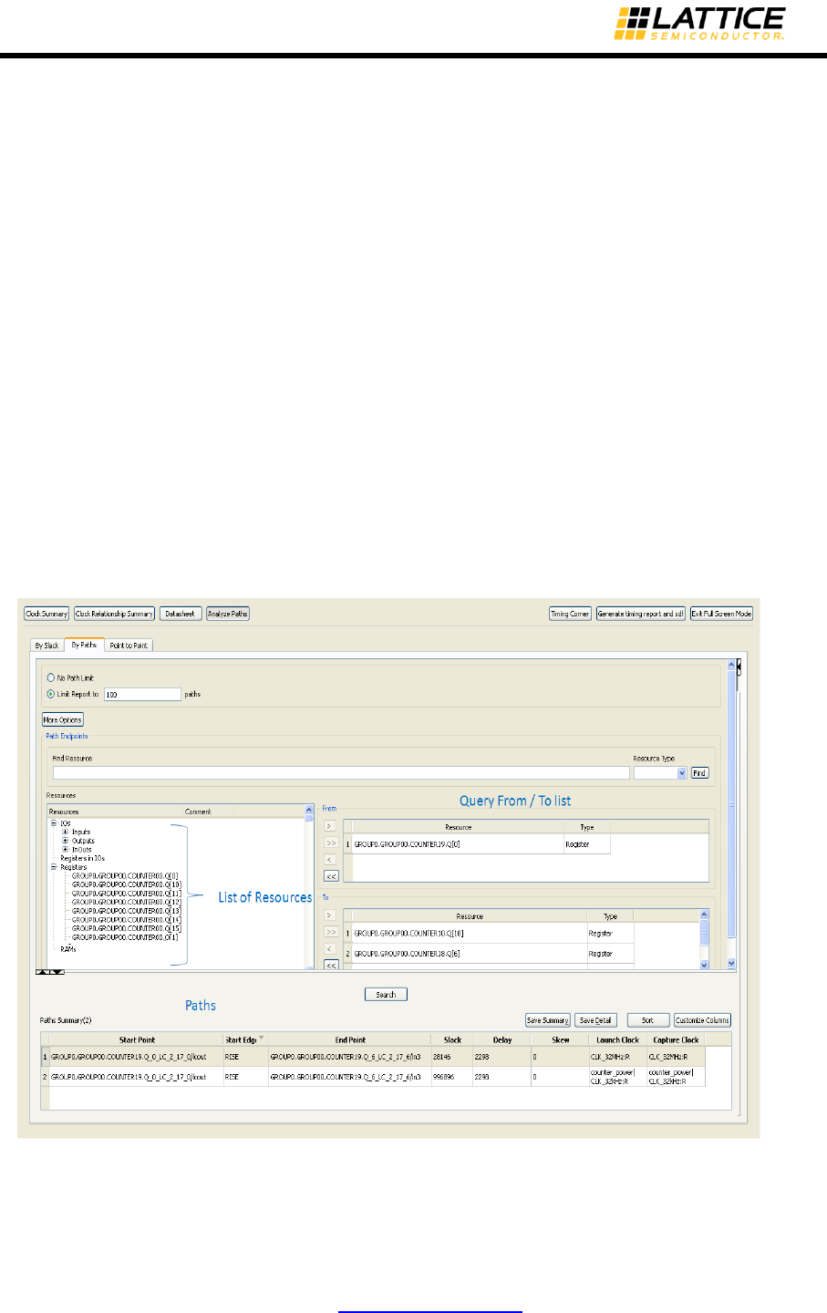
iCEcube2 User Guide www.latticesemi.com 137
By Paths
The By Paths page in “Analyze Paths” window allows the user to limit the timing report to specific
Start (Source) and End (Destination) Points. See Figure 6-22.
Start points are limited to primary design inputs, flip-flop outputs and RAM outputs. End Points
are limited to primary outputs, flip-flop inputs and RAM inputs.
All the instances of the design are shown in “Resources” pane. User can search for specific set of
resources by using the “Find Resource” option. User can select the Start and End points from
“Resource” pane and can move them to “From” to “To” options pane as shown in Figure 6-22.
The Resources which are used in “From” or “To” options can be a Register, Register in IO, IO, or
RAM. Timing report will be generated for the set of paths beginning with nodes in the “From”
category and ending with nodes in the “To” category.
User can customize the number of paths reported by using “No Path Limit” and “Limit Report to
100 Paths” options.
“More Options” button gives user different filters to limit the timing reports. Various filters include,
filtering the reported paths based on Launch Clock, Latch (Capture) clock and their phases,
filtering the paths based on number of paths per start point and number of paths per end point,
and filtering paths based on maximum slack value.
“Full Screen Mode” allows the user to view all the paths and customize window lengths in Full
Screen.
Figure 6-22: Analyzing User Specific Paths
Please note that when the user searches from/to an IO, STA reports the paths as follows:
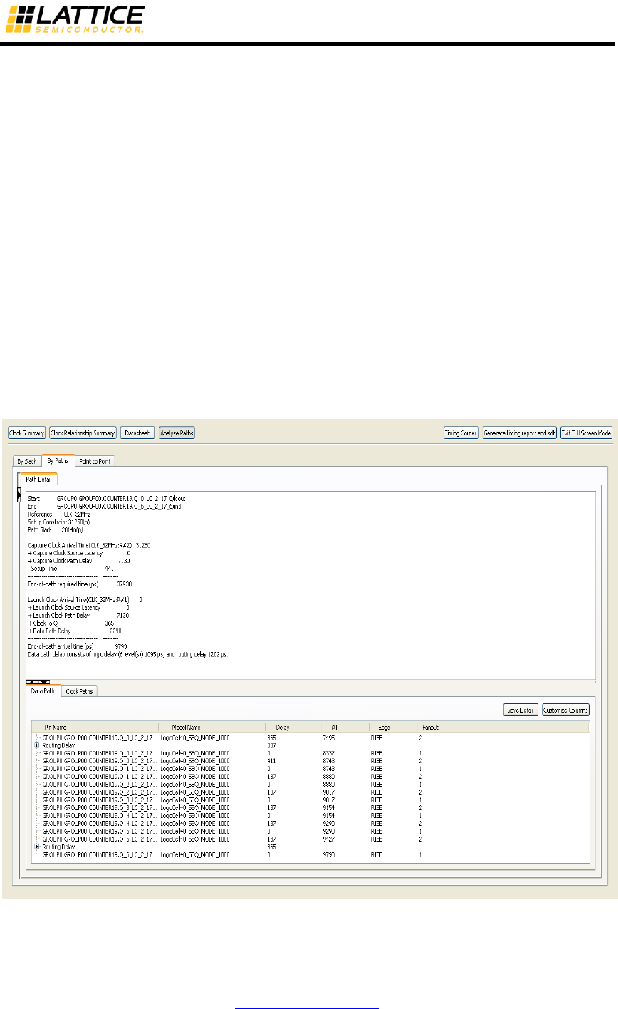
iCEcube2 User Guide www.latticesemi.com 138
1. From a combinational INPUT/INOUT IO: STA reports the path originating from that top
module port.
2. To a combinational INPUT/INOUT IO: STA reports the path ending to that top module output
port.
3. From a Registered INPUT/INOUT IO: STA reports the path originating from the DIN0/DIN1
pin of the corresponding IO.
4. To a Registered OUTPUT/INOUT IO: STA reports the path ending onto DOUT0/DOUT1 pin
of the corresponding IO.
5. To a Registered INPUT/INOUT IO: STA reports the path from the top module port to the
PACKAGE PIN of the IO.
6. From a Registered OUTPUT/INOUT IO: STA reports the path from the package pin of the IO
to the top module port of the IO.
7. If only the ‘From’ list is empty, then the STA returns all the paths from all possible ‘From’
source to given ‘To’ list.
8. If only the ‘To’ list is empty, then STA returns all the paths from the given ‘From’ list to all the
possible ‘To’ destinations.
9. If both ‘From’ and ‘To’ lists are empty then no paths are returned.
Figure 6-23: Detailed path Summary
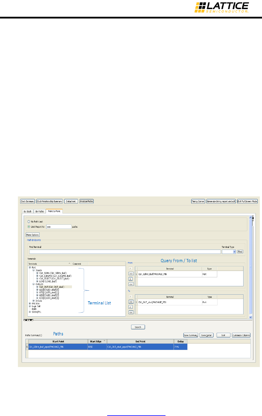
iCEcube2 User Guide www.latticesemi.com 139
Point to Point
The Point to Point in “Analyze Paths” window allows the user to analyze the routed timing delays
of the combinational paths that exists between the specific Start (Source) and End (Destination)
Terminals. No timing constraints are necessary to report these combinational path delays. See
Figure 6-24.
All the terminals of the design are shown in “Terminals” pane. User can search for specific type of
terminal by using the “Find Terminal” option. User can select the Start and End points from
“Terminals” pane and can move them to “From” and “To” options pane as shown in Figure 5-22.
The terminals which are used in “From” or “To” options can be a terminal of a Port, LogicCell,
RAM or PLL. Point to Point delay report will be generated for the set of paths beginning with
terminals in the “From” category and ending with terminals in the “To” category.
In the Path Summary pane, the user can select a path and double click on it. A detailed delay
report of the path is displayed as shown in Figure 6-25.
User can customize the number of paths reported by using “No Path Limit” and “Limit Report to
100 Paths” options.
“More Options” button gives user different filters to limit the point to point delay reports. The
reports can be filtered based on number of paths per start point, number of paths per end point,
and minimum delay value settings.
“Full Screen Mode” allows the user to view all the paths and customize window lengths in Full
Screen.
Figure 6-24: Analyzing Point to Point Delays

iCEcube2 User Guide www.latticesemi.com 140
Figure 6-25: Detailed Delay Report of the Selected Path
Other Features
Various other features in Timing Analyzer include:
Timing Corner: The Timing Corner option in the “Timing Analyzer” allows the user to analyze the
timing performance of a routed design under different Power Grade/Operating Conditions, without
having to recompile the design. The Timing Corner window (Figure 6-26) is used to change the
power grade of the device, operating conditions like junction temperature, core voltage and IO
bank voltage. Along with these, user can also select the best, typical, worst cases corners at
which timing analysis should be performed.
Whenever the Operating Conditions/Power Grade are different from the settings used for design
compilation, the changes are highlighted in red. For example, in Figure 6-26, the timing analysis
condition is red, since the design was compiled for ‘Worst’ case timing analysis.
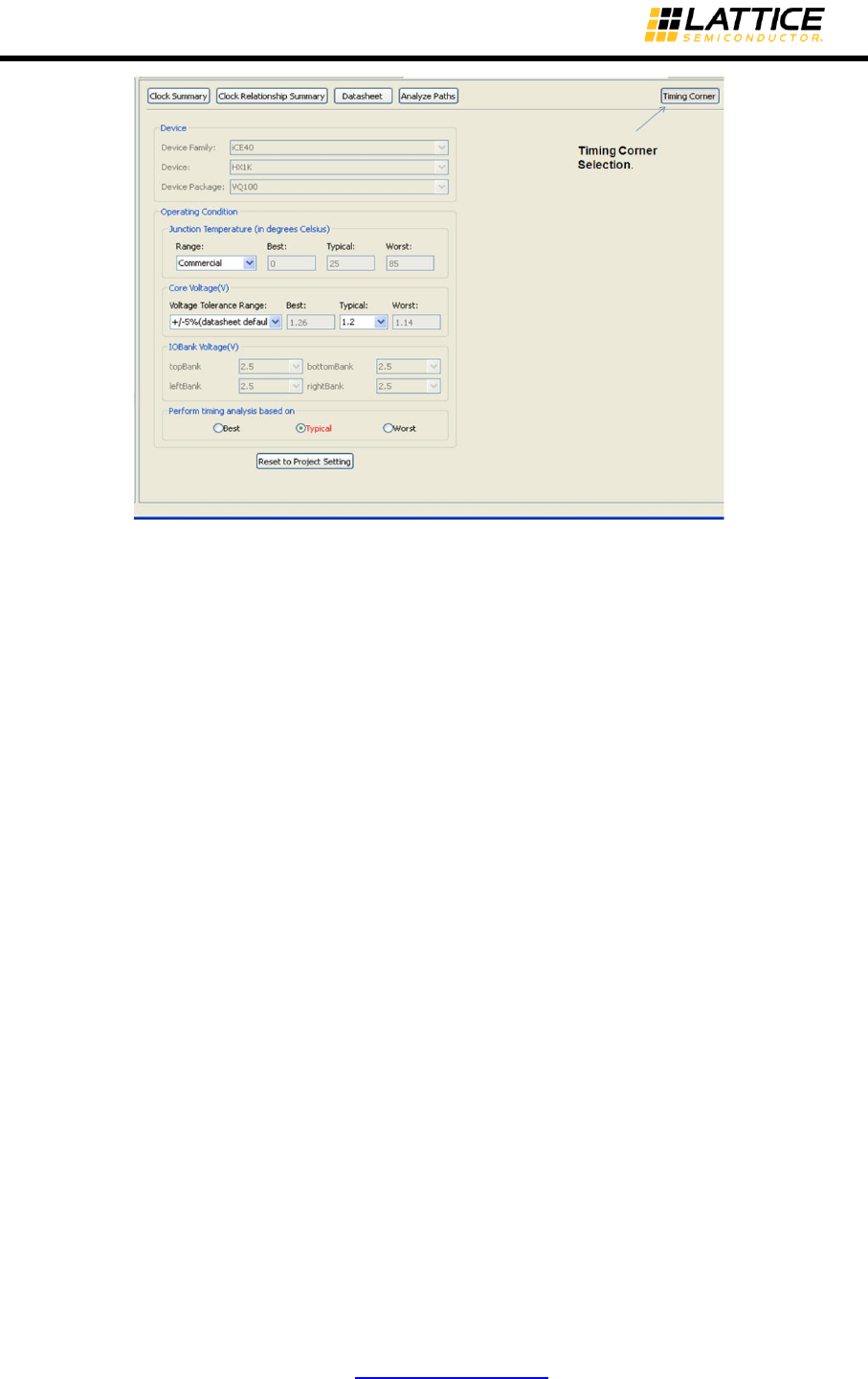
iCEcube2 User Guide www.latticesemi.com 141
Figure 6-26: Changing the Timing Corner in the Timing Viewer
Generate Timing Report and SDF: This option allows the user to save the generated timing
reports and SDF file for the Timing Corner selected in the Timing Viewer.
Cross Probing between the Timing Viewer and Floor Planner: A right click on a pin name in
the detailed timing path report gives options to highlight the pin and the full path in floor planner.
When “Highlight in Floor-Planner” is selected, the selected pin and its connections would be
highlighted in the Floor Planner as shown in the Figure 6-27. When “Highlight Path in Floor-
Panner” option is selected the entire reported path is highlighted in the Floor Planner as shown in
the Figure 6-28. The delay of each instance in the path and the cumulative path delay are also
displayed for the selected path. “Zoom in” for a particular instance to see the delays. The number
displayed inside the instance is the absolute delay and the number on the path is the
accumulated total path delay. This feature helps the user to analyze the reported paths easily.
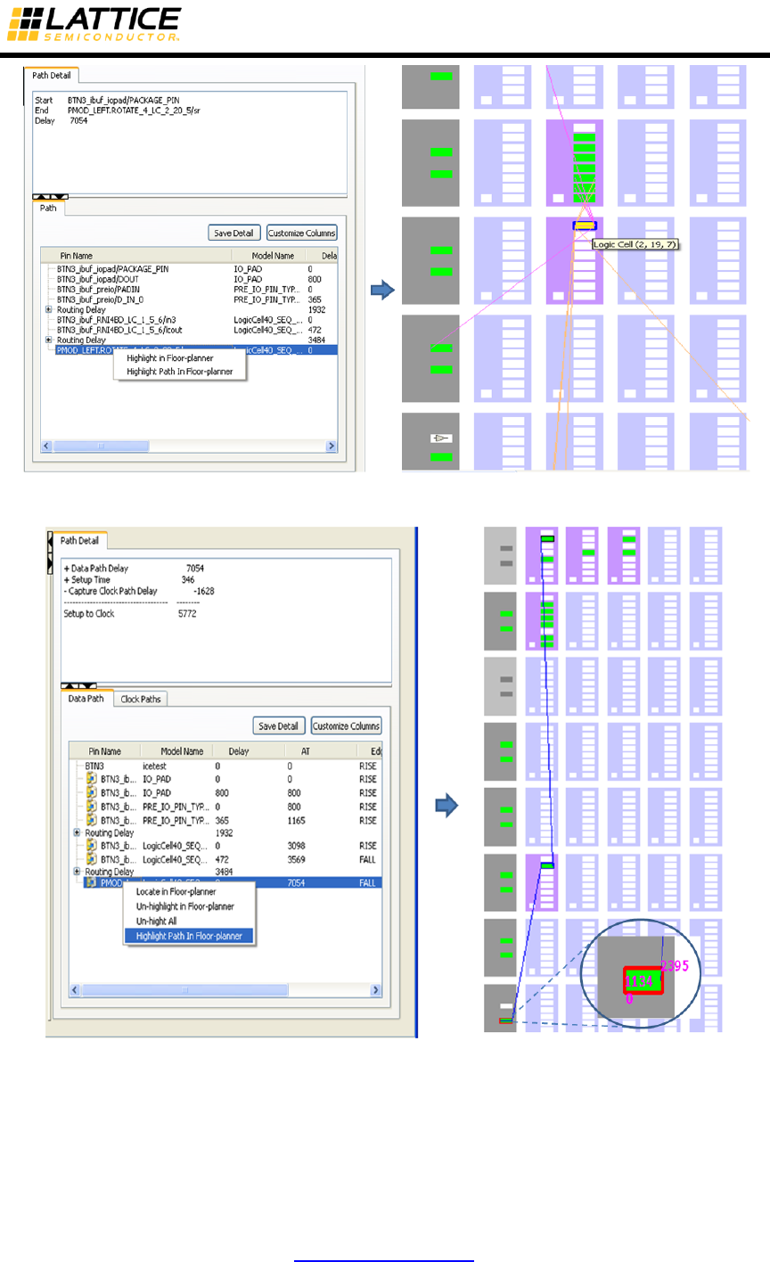
iCEcube2 User Guide www.latticesemi.com 142
Figure 6-27: Pin Corss Probing between the Timer and Floor Planner
Figure 6-28: Path Cross Probing between the Timer and Floor Planner
Detailed Timing Report
A detailed timing report in text format is generated after running the Timing Analyzer. This section
explains about the timing report file generated by iCEcube2 STA tool and how to interpret them.
iCEcube2 STA can report timing paths at three corner cases: Best, Typical and Worst.
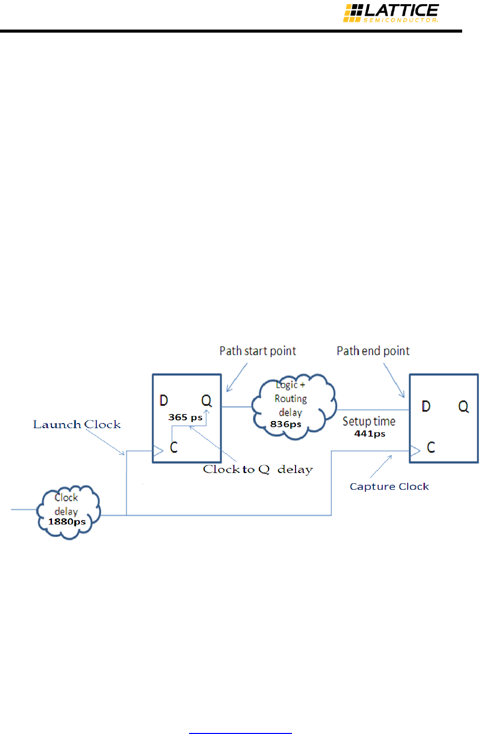
iCEcube2 User Guide www.latticesemi.com 143
Various Kinds of Summary Reports generated by iCEcube2 STA tool are:
Clock Summary
Clock Relationship Summary
Data Sheet Report
Detailed Report of All Timing Paths
The Clock Summary, Clock Relationship Summary and Data Sheet Report are visible in the
Timing Viewer GUI, and explained in earlier sections. The All Timing Paths report is described
below.
Detailed Report of All Timing Paths
The “Detailed Report” section gives detailed slack report for all the constrained paths in the
design. Following section shows slack calculation for a Register to Register timing path by
iCEcube2 STA.
A detailed Timing Report contains three sections:
1. Reference Points
2. Slack computation
3. Detailed Clock path and Data path delays
Figure 6-29: Flop to Flop Path
Reference Points:
Reference point section gives details about the start point; end point and reference launch clock
and the slack of the timing path. Typical Reference Points report is as shown below:
Path Begin : reg_0_LC_1_4_0/lcout
Path End : reg_1_LC_1_4_1/in3
Capture Clock : reg_1_LC_1_4_1/clk
Setup Constraint : 10000p
Path slack : 8357p

iCEcube2 User Guide www.latticesemi.com 144
In this example, the starting point is the flop output (lcout) which is in the BLE reg_0_LC_1_4_0.
The end point is the flop input (in3 input pin of BLE which drives the flop) which is in the BLE
reg_1_LC_1_4_1. Capture Clock is the capture clock of the timing path and it is the clock pin
BLE reg_1_LC_1_4_1 . The Setup Constraint between the launch and capture clock is 10000ps.
Slack computed for the path is 8357ps.
Slack Computation:
Slack is the difference between the signal required time and signal arrival time and is computed
using the below formula:
slack = End-of-path required time - End-of-path arrival time
= (Capture Clock Arrival Time + Clock Source latency +Clock Path Delay - Setup Time) -
(Launch clock Arrival Time + Clock Source latency + Clock Path delay + Clock to Q + Data Path
Delay)
Typical Slack Computation Report is as shown below:
Capture Clock Arrival Time (clk:R#2) 10000
+ Capture Clock Source Latency 0
+ Capture Clock Path Delay 1880
- Setup Time -441
------------------------------------ ---------------------------
End-of-path required time (ps) 11439
Launch Clock Arrival Time (clk:R#1) 0
+ Launch Clock Source Latency 0
+ Launch Clock Path Delay 1880
+ Clock To Q 365
+ Data Path Delay 836
----------------------------------- ---------------------------
End-of-path arrival time (ps) 3082
So, from the timing report Slack = ( 10000+1880 -441) - (1880 + 365 +836) = 8357ps.
Detailed Clock Path and Data Path delays:
The Launch and Capture clock path delays, Data path delays shown in “Slack Computation”
section are reported in detail here.
The detailed report is shown below. The “model name” indicates the type of cell involved in the
path. For example, the cells with PRE_IO_GBUF are the IO global buffers and the cells with
LOGIC_CELL* are the LUTs. Also the report gives the details of the LUT configuration mode.
Cells used for routing are defined using I__*. The “delay” column gives the amount of time
consumed by each cell unit. 'AT' gives the incremental time delay for the path upto the mentioned
cell. “Edge” column gives the “RISE/FALL” delay edge of the cell. The number in “Fanout” column
gives the Fanout for the mentioned cell.
The path delays reporting order is Launch Clock Delay, Data Path Delay and Capture Clock
Delay.
Clock network delay is the delay from the clock port to the registered clock pin.

iCEcube2 User Guide www.latticesemi.com 145
In this section, first path reported is detailed clock path report for the launch clock.
Launch Clock Path
pin name model name delay cumulative edge Fanout
delay
-------------------------------------------------------------------------------------------------------- ----- ---------------- ---- ------
clk i2c_top 0 0 RISE 1
clk_ibuf_iopad/PACKAGEPIN:in IO_PAD 0 0 RISE 1
clk_ibuf_iopad/DOUT IO_PAD 800 800 RISE 1
clk_ibuf_preiogbuf/
PADSIGNALTOGLOBALBUFFER PRE_IO_GBUF 0 800 RISE 1
clk_ibuf_preiogbuf/
GLOBALBUFFEROUTPUT PRE_IO_GBUF 502 1302 RISE 1
I__8/I gio2CtrlBuf 0 1302 RISE 1
I__8/O gio2CtrlBuf 0 1302 RISE 1
I__9/I GlobalMux 0 1302 RISE 1
I__9/O GlobalMux 335 1637 RISE 1
I__10/I ClkMux 0 1637 RISE 1
I__10/O ClkMux 243 1880 RISE 1
reg_0_LC_1_4_0/clk LogicCell40_SEQ_MODE_1000 0 1880 RISE 1
Here clk is the launch clock. The delay from port clk to Launch Flop clock pin
(reg_0_LC_1_4_0/clk) is shown here. The clock starts from clock port, traverse through global
buffer and reaches Launch Flop Clock Pin at 1880ps.
Second section is the Data Path Delay. Data delay is the delay from Flop output pin
(reg_0_LC_1_4_0/lcout) to Flop input pin ( reg_1_LC_1_4_1/in3). From the report, the data path
delay is (3082-2246)=836ps.
Data path
Pin name model name delay cumulative slack edge Fanout
delay
-------------------- ------------------------- ----- ---------------- ----- ---- ------ ------------------ ------------------------- ------------
reg_0_LC_1_4_0/lcout LogicCell40_SEQ_MODE_1000 365 2246 8357 RISE 1
I__15/I LocalMux 0 2246 8357 RISE 1
I__15/O LocalMux 472 2717 8357 RISE 1
I__16/I InMux 0 2717 8357 RISE 1
I__16/O InMux 365 3082 8357 RISE 1
reg_1_LC_1_4_1/in3 LogicCell40_SEQ_MODE_1000 0 3082 8357 RISE 1
Third section is the Clock path delay of Capture clock. The clock delay is the delay from clock
port to registered latch flop clock pin. From the report, this delay is 1880ps.
Capture Clock Path
pin name model name delay cumulative edge Fanout
------------------------------------------ ---------------------------------------------- ---------------- ---------------- -------- --------
-
clk i2c_top 0 0 RISE 1
clk_ibuf_iopad/PACKAGEPIN:in IO_PAD 0 0 RISE 1
clk_ibuf_iopad/DOUT IO_PAD 800 800 RISE 1
clk_ibuf_preiogbuf/

iCEcube2 User Guide www.latticesemi.com 146
PADSIGNALTOGLOBALBUFFER PRE_IO_GBUF 0 800 RISE 1
clk_ibuf_preiogbuf/
GLOBALBUFFEROUTPUT PRE_IO_GBUF 502 1302 RISE 1
I__8/I gio2CtrlBuf 0 1302 RISE 1
I__8/O gio2CtrlBuf 0 1302 RISE 1
I__9/I GlobalMux 0 1302 RISE 1
I__9/O GlobalMux 335 1637 RISE 1
I__10/I ClkMux 0 1637 RISE 1
I__10/O ClkMux 243 1880 RISE 1
reg_1_LC_1_4_1/clk LogicCell40_SEQ_MODE_1000 0 1880 RISE 1
Chapter 7 Physical Constraints in iCEcube2
Physical constraints in iCEcube2 can be provided at 2 different stages of the design flow: before
Placement and after Placement. Details on both approaches are provided below.
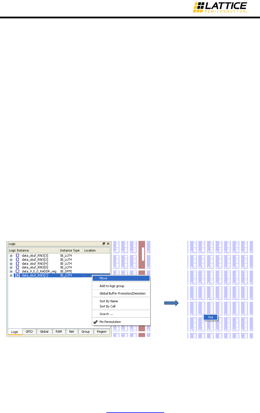
iCEcube2 User Guide www.latticesemi.com 147
Specifying Physical Constraints after Design Import and Before Placement
After importing the design into iCEcube2, the user can constrain the placement of the design to
desired locations on the physical device. This can be specified through the following physical
constraints:
Absolute Placement
Relative Placement
SPI Configuration IO Placement.
IO/FF Merge
Global Promotion/Demotion
Absolute Placement
After importing the design into iCEcube2 using “Import P&R Files”, the user can set a placement
location for all the instances like LUTs, DFFs, RAMs, IOs and Carry etc. These constraints can be
applied in Floor Planner, which can be invoked through Tools > FloorPlanner.
Constraining Logic or RAMs
In the Floor Planner, the logic or RAM instances can be placed by dragging the instances from
the instance menu to Floor Planner. The user can also perform the same action by the following
steps:
1. Select a logic/RAM instance from the instance menu and right click on it.
2. Select the Move Option
3. Go to the desired location in the Floor Plan, right click and select the option PUT.
The above steps are shown in Figure 7-1. Once constraining of all instances is done, you can
save these constraints in a PCF file by selecting the “Save” button on the top panel. Rerun the
placer to get the constraints honored.
Figure 7-1 Absolute placement of Logic Cells/ RAMs
Constraining IOs
IOs can be constrained at desired locations by invoking the pin constraint editor box. This can be
invoked by a right click on the IO and selecting “move” option. In the pop up “Pin Constraint
editor” box user can set the Pin location, IO standard and pull up type for the IO as shown in the
iCEcube2 User Guide www.latticesemi.com 148
Figure 7-2. Also, user can constrain all the IOs in the “Pin Constraint Editor” or by selecting them
and dragging them to IO locations in the Floor Plan View or the Package Viewer.
Detailed descriptions of the “Pin Constraints Editor” and “Package View” can be found in 0.
Figure 7-2 Absolute Placement of IOs
Constraining SPI Configuration IOs
Each device contains 4 SPI Configuration IO pins for programming the device. At the end of
device configuration, configuration controller will release the 4 configuration SPI pins, which will
become user IO. User can constrain IOs in SPI pin locations in the “Pin Constraint Editor” or by
selecting them and dragging them to IO locations in the Floor Plan View or in the Package
Viewer.
Note: Placement of IOs into SPI locations are supported only through constraints.
Relative Placement
Relative Placement Constraints helps the user to group logic, and to fix the placement of the
grouped logic cells relative to each other.
Group Constraints
iCEcube2 User Guide www.latticesemi.com 149
User can create groups with different logic elements like LUT, FF, Carry Chain, RAM and IO.
The logic elements are placed relative each other based on the location constraint (x, y, z) given
to each element in the group.
The location constraint of every element can be a fixed value like (1, 2, 3) or a floating value (-1, -
1, -1). (x, y) gives the location of the instance on the device. In case of LUT/FF/Carry Chain, ‘z’
value gives the location of a BLE in CLB. Since a CLB contains eight BLE’s, the valid values of Z
are 0 to 7. In case of IO, ‘z’ value gives the location of an IO in a tile. Since an IO tile contains two
values, the valid values of Z are 0 and 1. RAM instance contains only (x, y) location.
User can place the elements in a group relative to an origin location by constraining the group
elements to an origin.
When a group is set to an origin point, then the location constraint of an element in the group is
the sum of origin value and its location constraint value given in the group. For example, when a
LUT location constraint in a group is (1, 2, 3) and the group is set to origin (3, 4) then the location
constraint on the LUT becomes (4, 6, 3). By default, the origin point of any group is (0, 0).
In case of RAM/IO, the constraints are absolute. So, they will be placed at the location mentioned
in the group, origin constraint will be ignored.
Group creation and setting their origin point can be done from GUI. The following section explains
how to create the constraints from GUI.
Figure 7-3 Creating a Logic Group
Once the Synthesis is done and after importing the P&R files, user can create the relative
placement location constraints. User has to invoke the floor planner from Tools > Floor Planner
or by clicking the Floor Planner symbol on the left top corner tools pane.
Creating a Group from Floor Planner is shown in Figure 7-3. In order to create a group, go to the
Group tab in the Floor Planner window. Right clicking on the empty space provides an option to
iCEcube2 User Guide www.latticesemi.com 150
“Create Logic Group”. On selecting this option, a popup comes out asking the user to give the
details of the Logic Group such as its name and its origin location.
Logic/RAM/IO tabs in the Floor Planner gives the list of all logical elements in the design. User
can add elements to a created logic group by right clicking on any element and selecting the
option “Add to Logic Group” as shown in Figure 7-4. A popup will come out, asking the user to
select the group into which the element needs to be added.
Figure 7-4 Adding Logic Elements to a Group
User can also delete the elements from logic elements from a group. Right-clicking on any logic
element in the ‘Group’ tab, gives the user the option to delete element from the logic group as
shown in Figure 7-5.
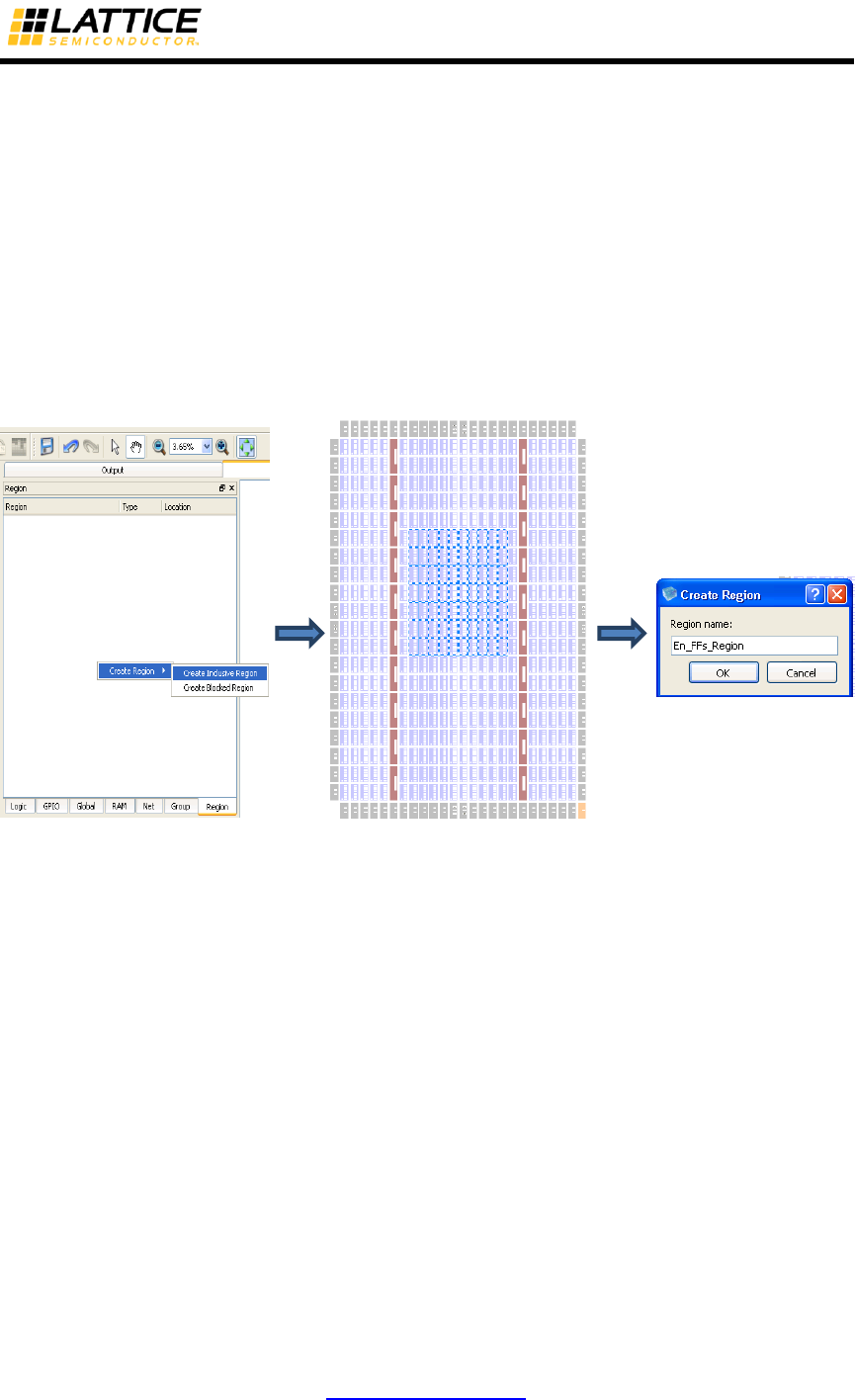
iCEcube2 User Guide www.latticesemi.com 152
Region Constraints
The Region Constraints enable the user to constrain a Group to a physical region on the device.
Region Constraints can be specified in the GUI. Going to ‘Region’ tab in Floor Planner and right
clicking on it gives an option to create a Region as shown in the Figure 7-6. The coordinates of
the region can be selected by dragging the mouse on the Floor Planner view. A pop up dialog box
comes up asking the name of the region. By entering the name, a Region would be created.
User can change the co-ordinates of a created region by changing the properties of the region,
which are available by a right click on the region name. The properties of the region gives user
the options to change region co-ordinates, type of region (inclusive/blocked), groups assigned to.
If the Region is of type Inclusive, the logic in the Group assigned to the Region, is placed inside
the boundary of the Region. If the Region type is Blocked, no logic is placed inside the Region.
Figure 7-6 Creating an Inclusive Region
Once a region is created, user can assign a Group to a Region by going to Group tab and
changing its properties. Figure 7-7 shows how to set group to an origin. Multiple groups can be
assigned to the same region.
Once creating the constraint is done, user can save the created constraints in PCF file by clicking
the ‘save’ button on the top panel. Then the created PCF file will be automatically added to the
current project. The legality check of the created constraints can be performed by running the
‘Import P&R files’. The adherence of the constraints can be checked out by invoking the Floor
Planner again after running the Placer.
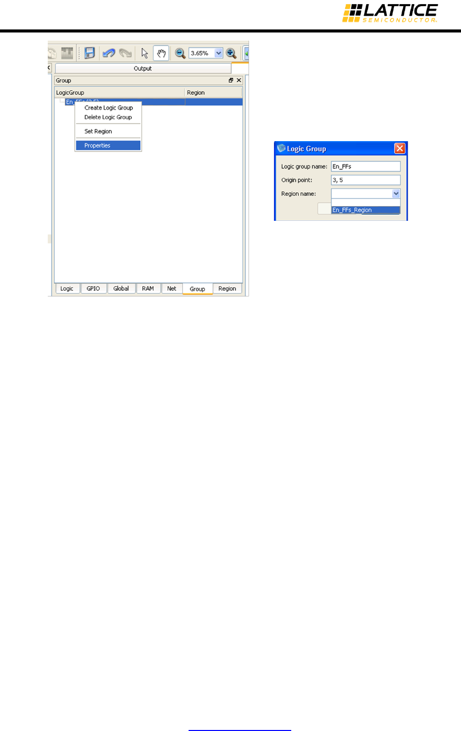
iCEcube2 User Guide www.latticesemi.com 153
Figure 7-7 Set group to a region
IO/FF Merge
The device IO pads include registers which can be used through explicit instantiation of the
SB_IO primitive, or by merging logic registers into the IO. Similarly, you can separate the IO
registers from the IO pads; this process is called Unmerging.
Creating the merging and unmerging constraints from GUI is shown in Figure 7-8.
After successful “Import P&R Input Files”, open the “Floor planner” and select “GPIO” tab.
Right Clicking on any IO shown in Floor Planner, gives the option to merge/unmerge FF. On
selecting this option, a pop up comes out asking the user to merge/unmerge FF from the IO.
The pop up gives the user the options to merge FF into IO and to separate FF from IO. The
options “Merge FF into Input/Merge FF into Output/Merge FF into Output Enable” specifies where
the Flip Flop should be merged into. Similarly, the options “Unmerge FF from Input/Unmerge FF
from Output/Unmerge FF from Output Enable” specifies from where the Flip Flop should be
separated.
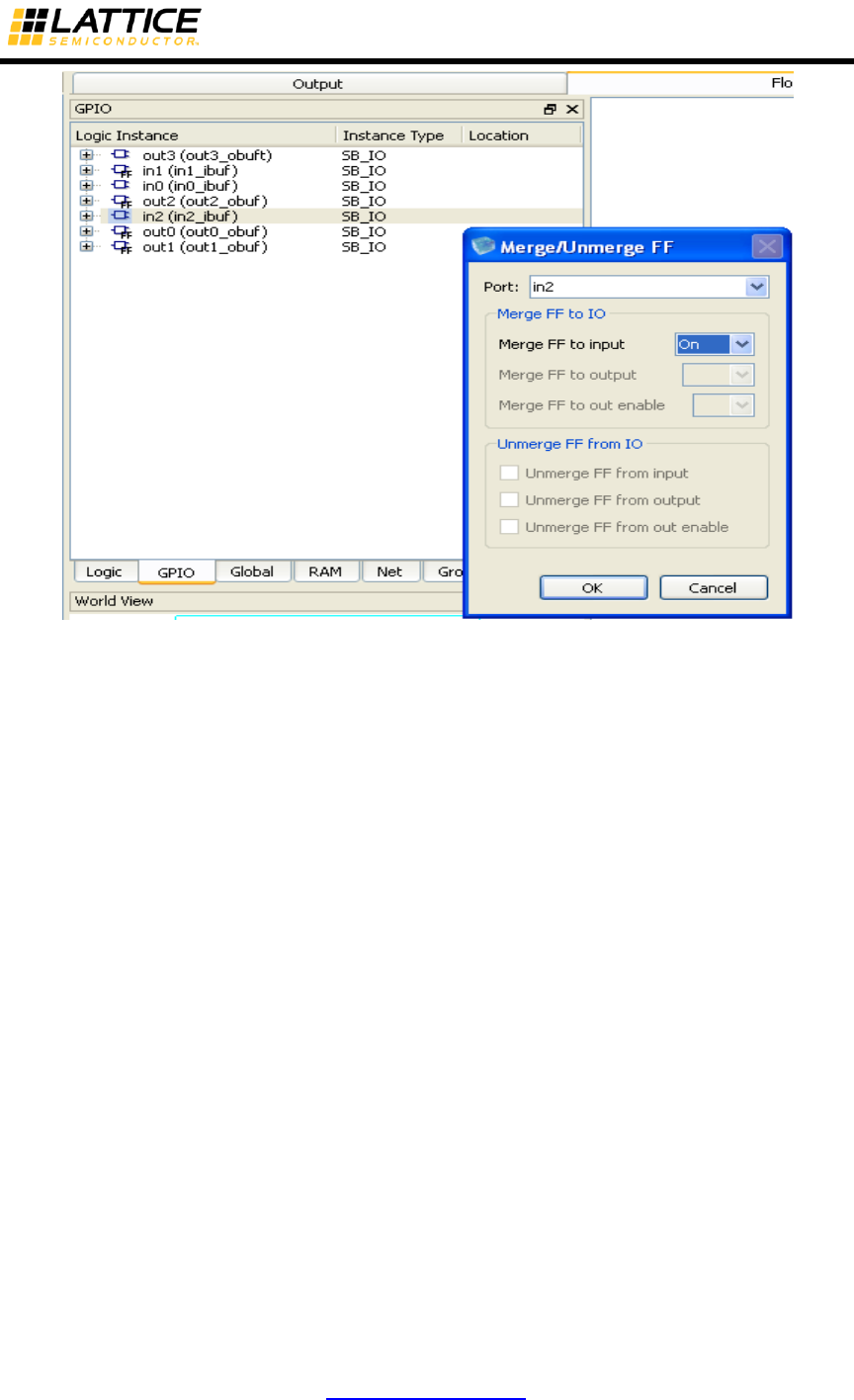
iCEcube2 User Guide www.latticesemi.com 154
Figure 7-8: IO/FF Merge and Unmerge Option
Only the options that are feasible to merge/separate are displayed in the GUI. The options will be
grayed out, whenever merging/unmerging a FF is not possible.
The synthesis tool by default identifies the flops that can be merged into the IO and generates
appropriate directives to the P&R tool. The auto FF merge directive can be controlled by the user
by setting the Merge FF option to “off”. This is shown in Figure 7-9.
Once creating the constraint is done, user can save the created constraints in PCF file by clicking
the ‘save’ button on the top panel. The created PCF file will be automatically added to the current
project. The legality check of the created constraints can be performed by running the ‘Import
P&R files’. The adherence of the constraints can be checked out by invoking the floor planner
again after running the placer.
The merged FF to IO is displayed in timing reports as shown in Figure 6-15.
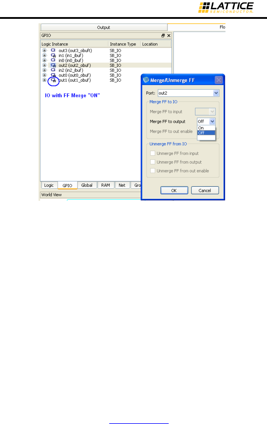
iCEcube2 User Guide www.latticesemi.com 155
Figure 7-9: Disable the Auto FF Merge Synthesis Directive
Global Buffer Promotion/Demotion
This feature allows the designer to specify usage of global routing network for a net. The GUI
enables this in terms of promotion / demotion constraints.
Global Buffer Promotion
For critical signals and high fan-out nets such as clock, designer would want to have it routed
through the global routing network. Also, if a high routing congestion is observed in a specific
area on the device, this can be reduced by promoting a high fanout net in this area.
Global Buffer Promotion feature allows the user to explicitly assign a net to the global routing
network on the device as shown in Figure 7-10. Right clicking on the logic instance gives the
option “Global Buffer Promotion/Demotion”. Selecting the option will gives a pop up with Global
Buffer Promotion Option.
Once creating the constraint is done, user can save the created constraints in pcf file by clicking
the ‘save’ button on the top panel. Then the created pcf file will be automatically added to the
current project. The legality check of the created constraints can be performed by running the
‘Import P&R files’.
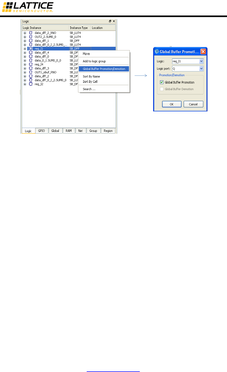
iCEcube2 User Guide www.latticesemi.com 156
Figure 7-10: Global Buffer Promotion.
Global Buffer Demotion
Non-critical signals in a design need not use the global routing network. This can be ensured by
the designer by specifying “Global buffer demotion” constraints in GUI. If designer finds that delay
from source of the net to SB_GB is causing degradation of performance, such instance of SB_GB
could be demoted.
Global Buffer Demotion feature allows the user to demote an SB_GB/SB_GB_IO. In case of
SB_GB, the instance will be removed and for SB_GB_IO, it will be converted into SB_IO.
Figure 7-11 shows how to demote a Global Buffer. Right clicking on the instance SB_GB gives
the option “Global Buffer Promotion/Demotion”. Selecting the option will gives a pop up with
Global Buffer Demotion Option.
Once creating the constraint is done, user can save the created constraints in pcf file by clicking
the ‘save’ button on the top panel. Then the created pcf file will be automatically added to the
current project. The legality check of the created constraints can be performed by running the
‘Import P&R files’. The adherence of the constraints can be checked out by invoking the floor
planner again after running the placer.
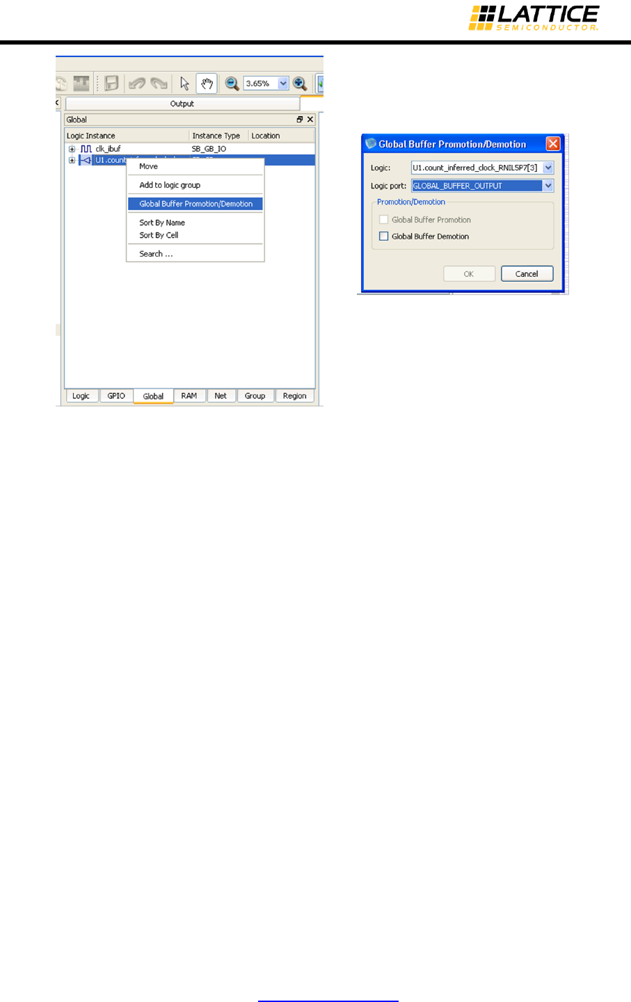
iCEcube2 User Guide www.latticesemi.com 157
Figure 7-11: Global Buffer Demotion
Modifying the Device Floor Plan after Placement
This section explains the steps used to change an existing floor plan.
Modifying Placement of Individual Cells
Placement of individual Logic, Block RAM and IO cells can be changed by clicking on the cell to
be moved and dragging it to the desired location. Optionally, the following three-step process is
recommended:
1. Select the cell to be moved by Right-Mouse-Click > Move. It may be the case that, for
certain IO cells, the Move menu is not available. This is intentional, since it prevents
incorrect placement of special pins (like global buffers) that can only be placed at certain
fixed locations.
2. Move the cursor to the desired location.
3. Place the cell at the target location by Right-Mouse-Click > Put.
Note: A set of logic cells contained in the same carry-chain, can be moved as a group. In order to
move the entire set of logic cells, select the carry-in cell i.e. the square green cell at the
bottom-left corner of the Logic Tile. Drop this cell at the desired carry-in cell location.
Pin locations can also be changed through the Pin Constraint dialog box (Figure 7-12). This
dialog can be invoked for each pin using Right-Click > Edit Pin Constraint. In addition to its
location, the pin’s IO standard and Pull Up resistor can also be configured from this dialog.
Note: Differential IO pins are supported only on Bank #3.
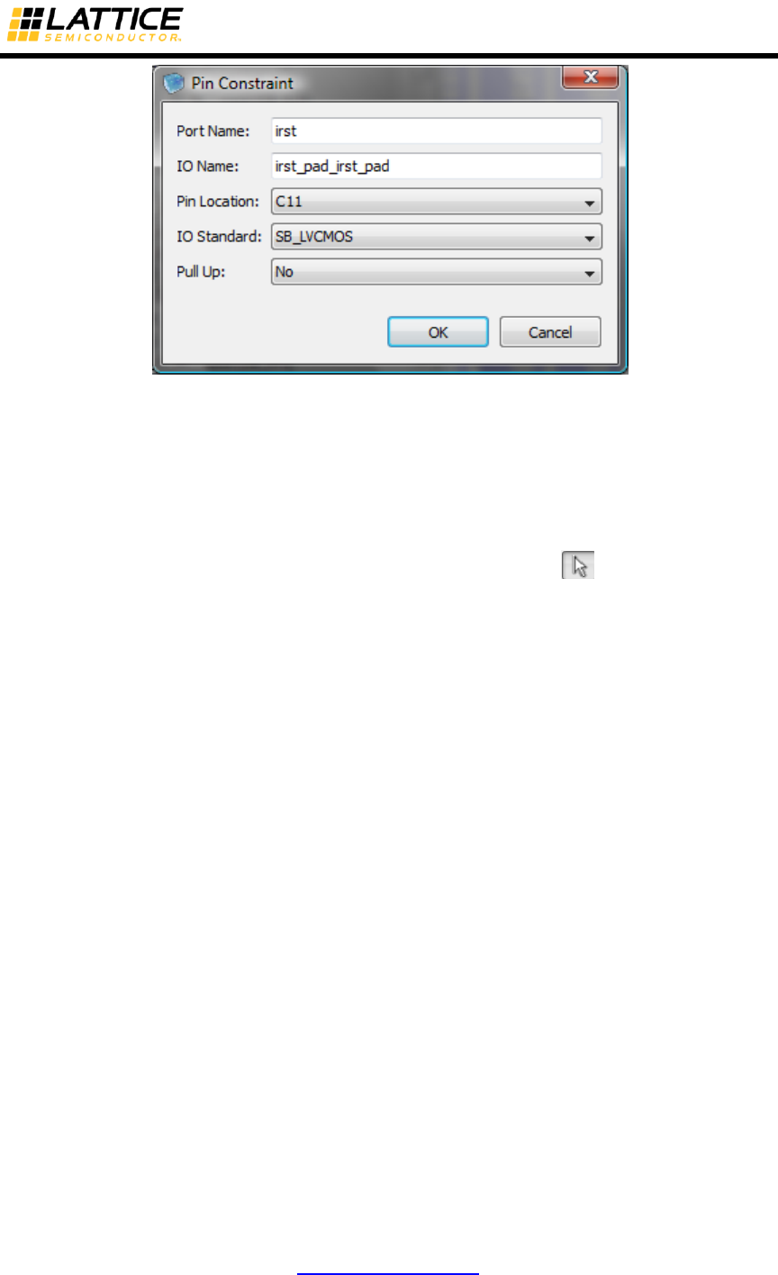
iCEcube2 User Guide www.latticesemi.com 158
Figure 7-12: The Edit Pin Constraints dialog box
Modifying Placement of a Group of Cells
A group of cells (RAM, IO, Logic) can be moved as a unit to a new placement location (Figure
7-13). In order to accomplish such an operation, the Floor Planner software permits the user to
select the cells using a Left-mouse-click and drag operation. This operation is permitted only
when the Floor Planner is in the Select Mode i.e. the arrow button is clicked. The Select
Mode can be toggled ON and OFF, simply by clicking this arrow icon.
Once the cells are grouped together (it is recommended that the options shown in Figure 5-12 be
switched OFF for easier selection and movement), the following three-step process is
recommended:
1. Invoke the Move operation through Right-Mouse-Click > Move.
2. Move the cursor to the desired location. Make sure that there are sufficient unused
resources available at the target location. Since the selected group of cells cannot be
placed over any cell this is already utilized, it is necessary that the unused portion of the
device be large enough to accommodate the same relative layout as the selected group
of cells.
3. Place the group of cells at the target location by Right-Mouse-Click > Lock. A lock
symbol would be shown on the moved cells in the Floor Planner.
Note: A set of logic cells contained in the same carry-chain, can be moved as a group. In order to
move the entire set of logic cells, select the carry-in cell i.e. the square green cell at the
bottom-left corner of the Logic Tile. Drop this cell at the desired carry-in cell location.
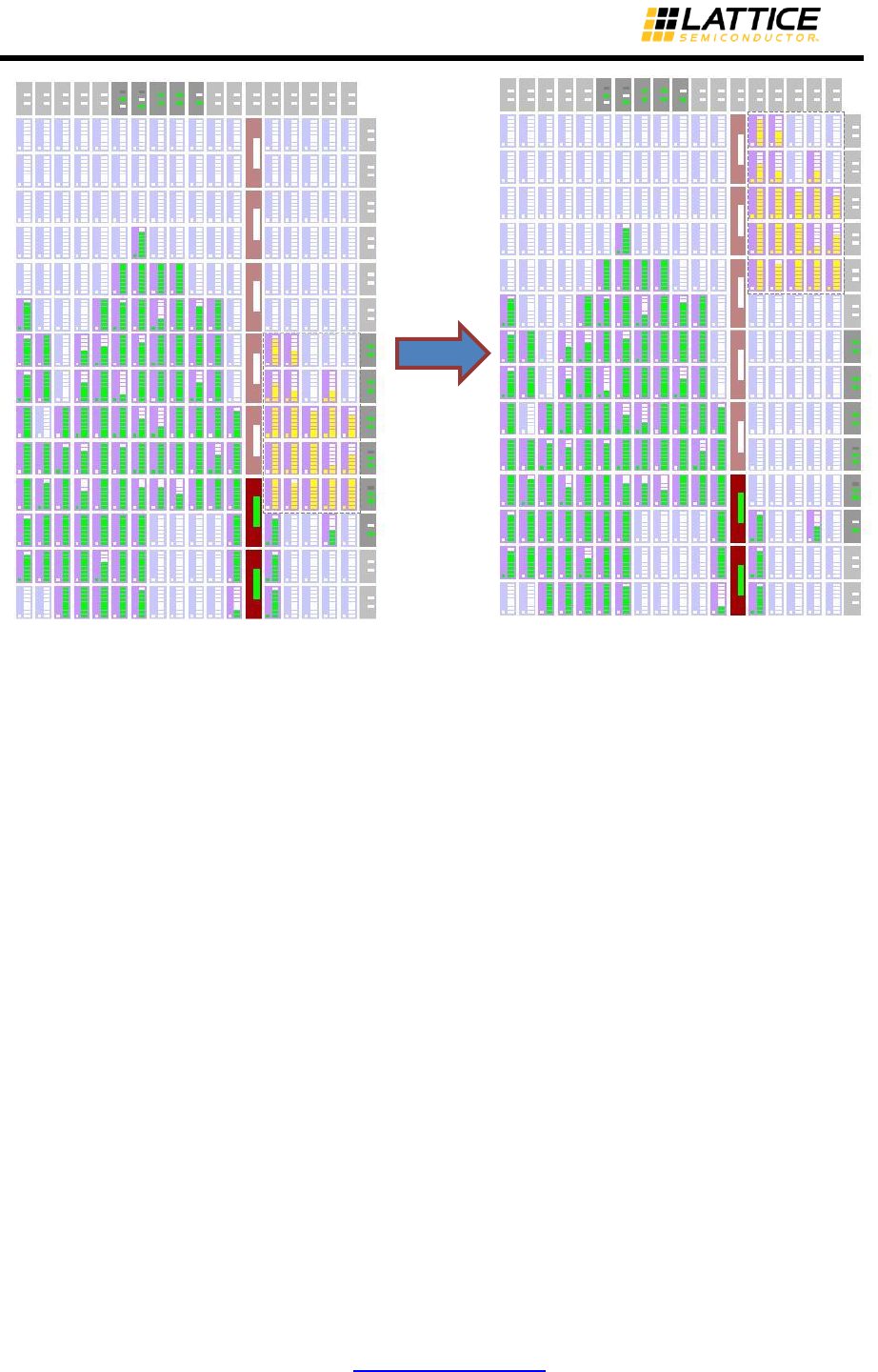
iCEcube2 User Guide www.latticesemi.com 159
Figure 7-13: Moving a group of Logic Cells
Floor Plan changes can be reverted back to their initial state using the Edit > Undo menu.
Once all changes are complete, the new floor plan should be saved my clicking File > Save Floor
Planner from the main menu.
Note: Any changes to the device Floor Plan will require the router to be rerun.

iCEcube2 User Guide www.latticesemi.com 160
Chapter 8 Generating/Integrating Fixed Placement IP Blocks
This chapter talks about the “IP Generation/Integration Flow” feature in iCEcube2 tools. This
chapter consists of the following two sections:
1. IP Generation Flow: This section explains the steps required to create an IP with fixed
locations, which can later be used in a design as a sub-module, thereby guaranteeing the
performance of this IP sub-module.
2. System Design Flow: This section explains the steps for instantiating the IP as a black box in
the synthesis flow, and including the placed IP (EDIF) as a sub-module in the iCEcube2
Physical Implementation tools.
IP Generation Flow
The sample design used in this document as an IP is an up counter. The RTL for the up counter
is presented below.
module ip (
clock,
enable,
reset,
out
);
input clock;
input reset;
input enable;
output [7:0] out;
reg [7:0] out;
always @(posedge clock)
begin
if(reset == 1)
out <= 0;
else
if(enable == 1)
out <= out+1;
end
endmodule
The steps involved in exporting this IP into EDF format are:
1. Launch the iCEcube2 tool and create a new project from File > New Project. In the New
Project Window, enter the project name, set device and operation conditions. Make sure
that the Start from Synthesis and IP Generation options are selected. Click Next. See
Figure 8-1.

iCEcube2 User Guide www.latticesemi.com 161
Figure 8-1 New Project Creation
2. Browse to the RTL location and add the up counter file “ip.v” into the project. Add timing
constraint files if any. Click Finish to go back to the iCEcube2 main window.
Figure 8-2 Add Files to Project
3. Run synthesis. If using:

iCEcube2 User Guide www.latticesemi.com 162
LSE, double-click Run Lattice LSE Synthesis.
The Use IO Insertion option should be False if you selected IP Generation in the New
Project dialog box. You can check by selecting Tool > Tool Options and looking in the
LSE tab.
Synplify Pro, double-click Run Synplify Pro Synthesis.
The Disable IO Insertion option should be selected if you selected IP Generation in
the New Project dialog box. You can check by selecting Tool > Tool Options and click
the word "here" in the Synplify Pro tab. In the Synplify Pro window, click
Implementation Options and look in the Device tab.
Figure 8-3 Run Synthesis
4. After Synthesis, close the Synplify Pro tool. This will bring you back to iCEcube2 tool. The
Synthesis output files “PRJNAME.edf” and “PRJNAME.scf” would be automatically added
to the project. Double Click on “Run All” to run placement, router, and bitmap generation.
Figure 8-4 Run Complete Flow
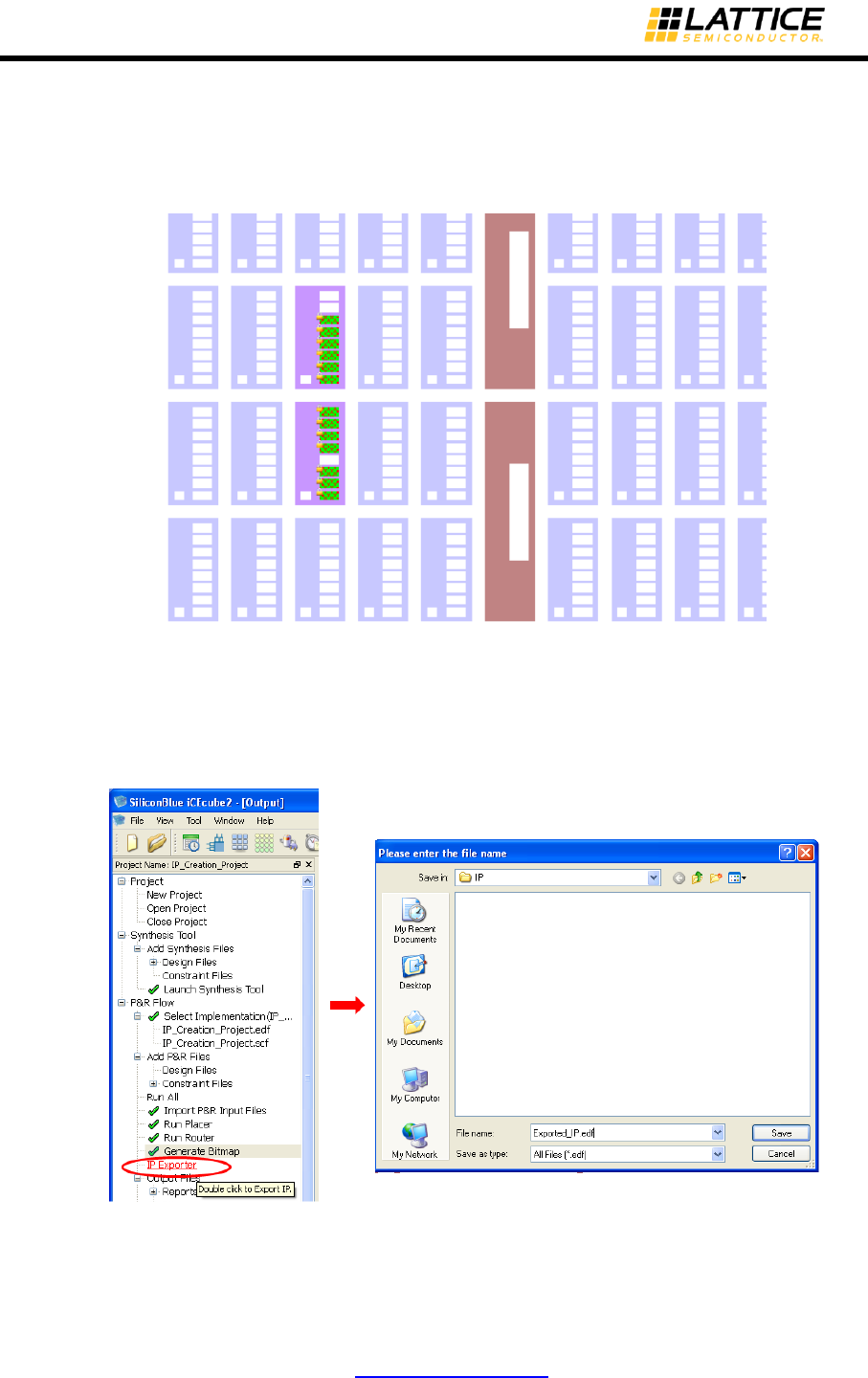
iCEcube2 User Guide www.latticesemi.com 163
5. Launch the Floor Planner from Tool > Floor Planner and can view the placed IP on the
FPGA. If the user wants to do any modification to the placement he can do the same by
dragging the placed instances into required location. Lock the instance using the option
showed after a right click on the instance. Save the placement using File > Save Floor
Planner and rerun “Run All”.
Figure 8-5 Placed IP Instances
6. Double click on “IP Exporter” to save the IP in EDF format. Browse to a location on the
pop window and save the EDF file. By default, the EDIF file is saved in
<PrjName>/<PrjName_Implmnt>/sbt/IP/ location. The saved IP EDF file contains the
locations of all the instances.
Figure 8-6 Exporting the IP into EDF Format

iCEcube2 User Guide www.latticesemi.com 164
System Design Flow
This section explains the process to integrate the placed IP into the top level designs.
First, the user needs to instantiate the IP as a black box in his RTL. For example, the system Top
instantiates the IP. So, the customer needs to add a black box attribute IP as shown below.
module top(
clock,
reset,
enable,
up_count_out,
down_count_out
);
input clock;
input reset;
input enable;
output [7:0] up_count_out;
output [7:0] down_count_out;
reg [7:0] down_count_out;
always @(posedge clock)
begin
if(reset == 1)
down_count_out <= 0;
else
begin
if(enable == 1)
down_count_out <= down_count_out - 1;
end
end
ip up_count_inst ( //// IP Instantiation
.clock(clock),
.reset(reset),
.enable(enable),
.out(up_count_out)
);
endmodule
///// BLACK BOX DECLARATION /////
module ip (
clock,
reset,
enable,
out
) /* synthesis syn_blackbox = 1 */ ;
input clock;
input reset;
input enable;
output [7:0] out;
endmodule

iCEcube2 User Guide www.latticesemi.com 165
The IP can be declared as black box by using the attribute “syn_blackbox” during the IP
declaration.
The steps involved in running the System Design Flow are:
1. Launch iCEcube2 tool and create a new project from File > New Project. In the New
Project Window, browse to location where project need to be created, enter the project
name, set device and operation conditions. Select option “Start from Synthesis” and click
on Next.
Figure 8-7 Create New Project
2. Browse to the RTL location and add the Verilog file “system.v” into the project as shown.
Click on Finish to get back to iCEcube2 tool.
iCEcube2 User Guide www.latticesemi.com 166
Figure 8-8 Add RTL Files to Project
3. Run synthesis. If using:
LSE, double-click Run Lattice LSE Synthesis.
The Use IO Insertion option should be True. You can check by selecting Tool > Tool
Options and looking in the LSE tab.
Synplify Pro, double-click Run Synplify Pro Synthesis.
The Disable IO Insertion option should be off. You can check by selecting Tool > Tool
Options and click the word "here" in the Synplify Pro tab. In the Synplify Pro window,
click Implementation Options and look in the Device tab.
The synthesis would be performed treating the IP as a black box.
Figure 8-9 Run Synthesis
4. After successfully running synthesis, close the Synplify Pro Tool. This will bring you back
to iCEcube2 tool. The Synthesis outputs “PRJNAME.edf” and “PRJNAME.scf” would be
automatically added to the project. Now, right click on the “IP Design Files” in “Add P&R
iCEcube2 User Guide www.latticesemi.com 167
Files” select “Add Files”. On the popup window browse to the Vendor provided IP location
and add the EDF file.
Figure 8-10 Add IP File for performing P&R
5. Click on “Run All”. This would perform Placement, Routing and Bitmap Generation.
6. Once the Flow is completely run, the placed instances can be viewed again by launching
Floor Planner through Tools > Floor Planner. You can observe that the IP would be
placed according to the locations mentioned in IP EDF.
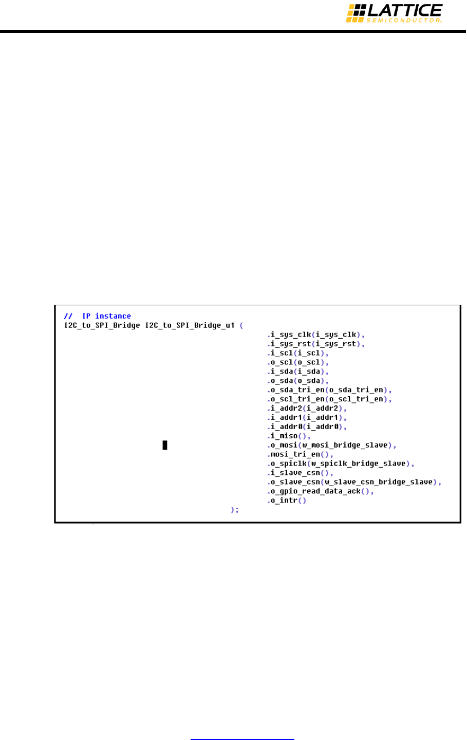
iCEcube2 User Guide www.latticesemi.com 169
Chapter 9 Hierarchical Project Flow
The iCEcube2 software supports hierarchical project management flow for larger team based
designs. The iCEcube2 installation contains various IP Modules in encrypted format. These IP
modules can be easily integrated as building blocks in the larger designs, resulting in significant
time and cost savings though design-reuse.
This chapter explains how to integrate IP building blocks provided with the iCEcube2 software
into a larger design using the Synplify Pro software.
For additional information please refer to the section on Hierarchical Project Management Flows
of the Synplify Pro for SiliconBlue User Guide located at <iCEcube2_install_dir>/synpro/doc/
user_guide.pdf.
Create Top Level Project
This section explains the steps to create a top level design file with an IP block instantiation.
1. In your top level design file, instantiate the required IP as shown in Figure 9-1.
Figure 9-1: IP Block Instantiation in the top level module
2. In the same top level design file, provide a black box definition of the IP building block, as
displayed in Figure 9-2.
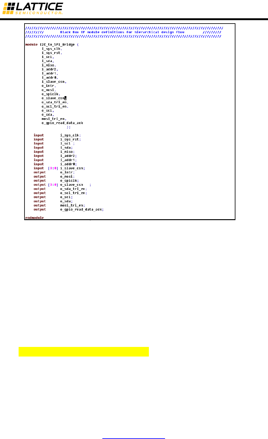
iCEcube2 User Guide www.latticesemi.com 170
Figure 9-2 : Black Box Definition of IP block in the top level module
Note: For iCE40 UltraLite, Ultra and UltraPlus devices, if connecting VPP_25V supply to voltages
of 2.3V or below, and any one or more of these functions: SB_HFOC, SB_LFOSC,
SB_RGBA_DRV, SB_IR400_DRV, SB_IR500_DRV, or SB_BARCODE_DRV is needed in
the design, then you should add the VPP_2V5_TO_1P8V attribute to your top-level to
override the limitation specified in the datasheet’s Recommended Operating Conditions.
This workaround is allowed only when Slave SPI Configuration mode is used. For attribute
usage, see the following examples:
Verilog Syntax Example
module top
(
clkhf_en,
clkhf_pu,
clkhf
)
/* synthesis VPP_2V5_TO_1P8V = 1 */
;
/* VPP_2V5_TO_1P8V = 1 or 0 */
input clkhf_en;
input clkhf_pu;
output clkhf;
SB_HFOSC OSCInst0 (
.CLKHFEN(clkhf_en),
.CLKHFPU(clkhf_pu),

iCEcube2 User Guide www.latticesemi.com 171
.CLKHF(clkhf)
) /* synthesis ROUTE_THROUGH_FABRIC= 0 */;
defparam OSCInst0.CLKHF_DIV = "0b00";
endmodule
VHDL Syntax Example:
library ieee;
use ieee.std_logic_1164.all;
entity top is
port (
clkhf_pu : in std_logic;
clkhf_en : in std_logic;
clkhf : out std_logic
);
attribute VPP_2V5_TO_1P8V :boolean;
attribute VPP_2V5_TO_1P8V of top : entity is true; --true or false
end top;
architecture behavior of top is
component SB_HFOSC is
port(CLKHFEN, CLKHFPU : in std_logic;
CLKHF: out std_logic);
end component;
begin
HFOSCinst0 : SB_HFOSC
port map
(
CLKHFEN => clkhf_en,
CLKHFPU => clkhf_pu,
CLKHF => clkhf
);
end behavior;
3. Launch iCEcube2 and create a new project from File > New Project. In the New Project
Window, browse to location where project need to be created, enter the project name, set
device and operation conditions. Select option “Start from Synthesis” and click on Next.
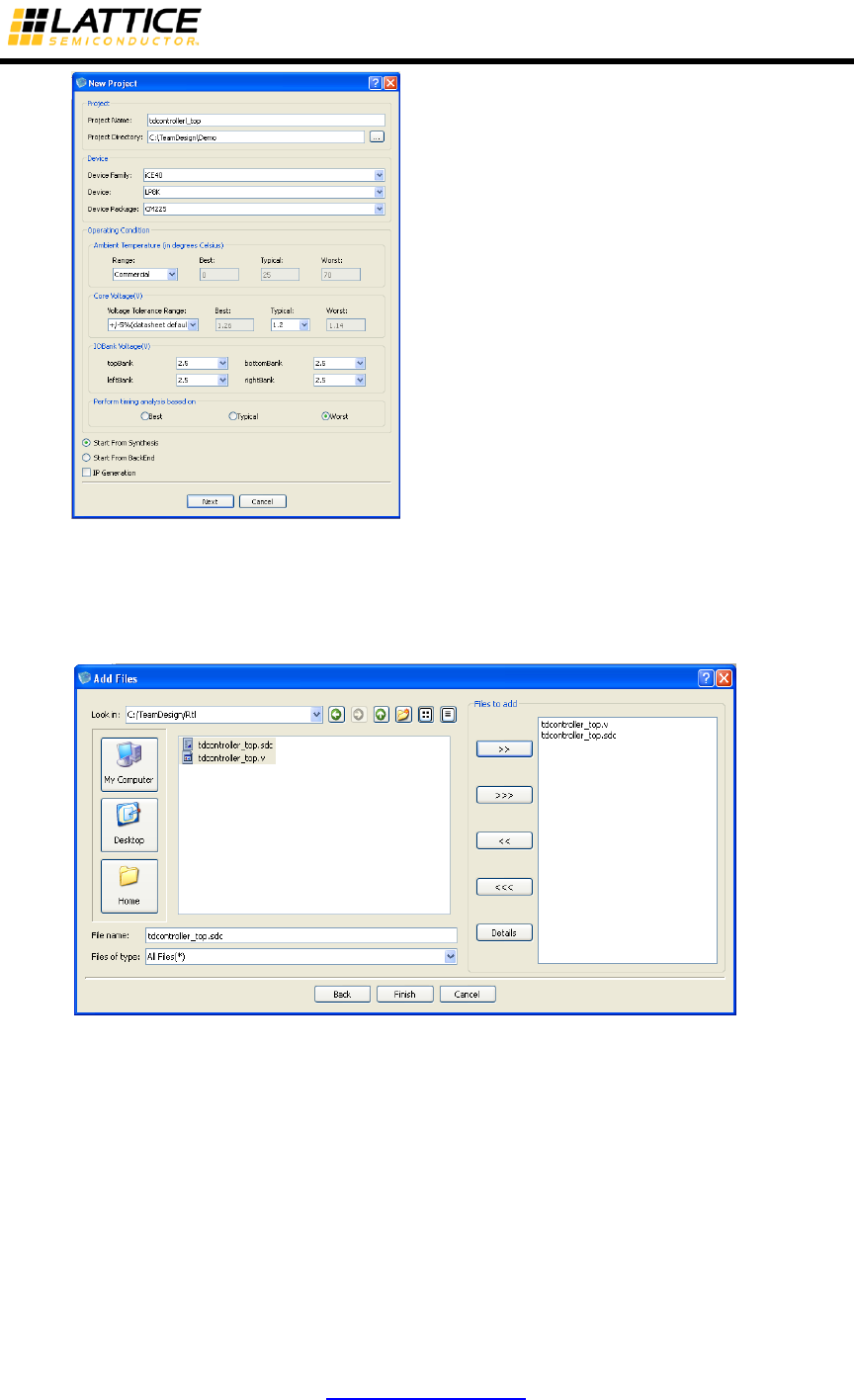
iCEcube2 User Guide www.latticesemi.com 172
Figure 9-3: Create Top Level Project
4. Add the top level design file into the project as shown in Figure 9-4. Click on Finish to get
back to the iCEcube2 tool.
Figure 9-4 : Add RTL Files to top Project
4. Right-click Synthesis Tool and choose Select Synthesis Tools.
The Select Synthesis Tool dialog box opens.
5. Select Synplify Pro.
6. Click OK.
The command under Synthesis Tool changes to Run Synplify Pro Synthesis.
The top level project is created with the specified input design files as shown in Figure 9-5.
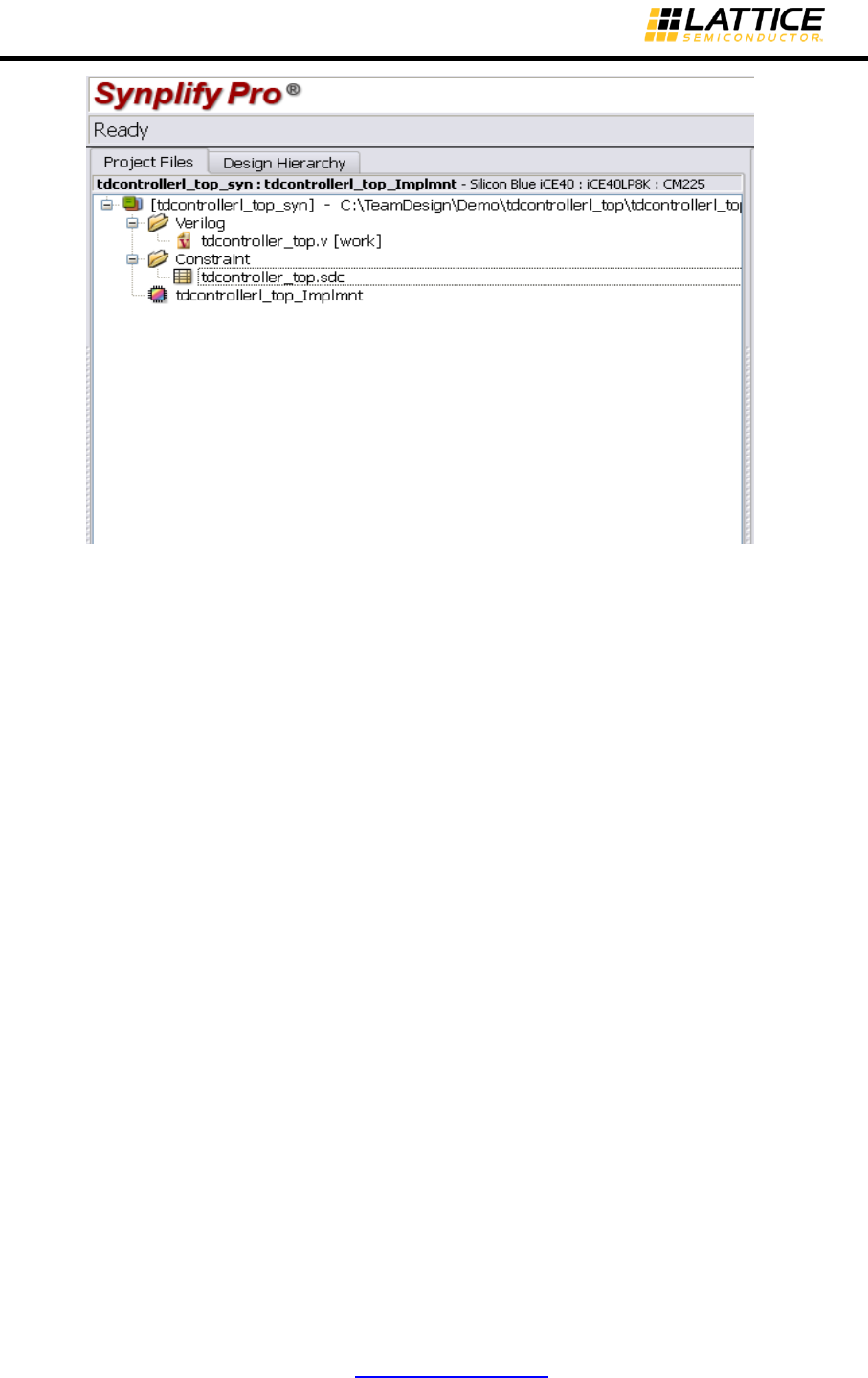
iCEcube2 User Guide www.latticesemi.com 173
Figure 9-5: Top Level Design Project.
Create Sub-Projects for IP blocks
This section explains the steps for integrating the IP blocks into your top level design, and
converting the IP projects into sub-projects of the top level project.
It is strongly recommended that the IP library be copied to a user specified location as it enables
better design management.
The IP blocks provided with the iCEcube2 software include a Synplify Project file with the
required design source files (RTL), the top module name and other settings required to import the
IP into your top level design. This Project file is located at <iCEcube2_install_dir>/IP/<IP
Name>/V1.x/source/<IP Name>.prj.
1. Copy the <iCEcube2_install_dir>/IP/<IP Name> directory into a user specified directory.
For example, copy <iCEcube2_install_dir>/IP/I2C_to_SPI_Bridge to <user_IP_dir>/IP/
I2C_to_SPI_Bridge.
2. In Synplify Pro, click on the “Open Project” icon. Select “Existing Project” in the “Open
Projects” dialog box. Browse to the “<user_IP_dir>/IP/I2C_to_SPI_Bridge/V1.1/source”
location and add the existing “I2C_to_SPI_Bridge.prj” file as shown in Figure 9-6. This
opens the “I2C_to_SPI_Bridge” project in Synplify Pro and automatically imports the
required source files. See Figure 9-7.
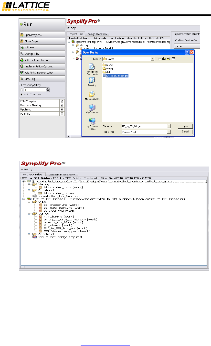
iCEcube2 User Guide www.latticesemi.com 174
Figure 9-6: Select the I2C_to_SPI_Bridge.prj file
Figure 9-7 : Created IP Block Project
3. Drag and Drop the IP Project into the top level project as shown in Figure 9-8. This
converts the IP Projects into a “Sub-Project” of the top level project as shown in Figure
9-9.
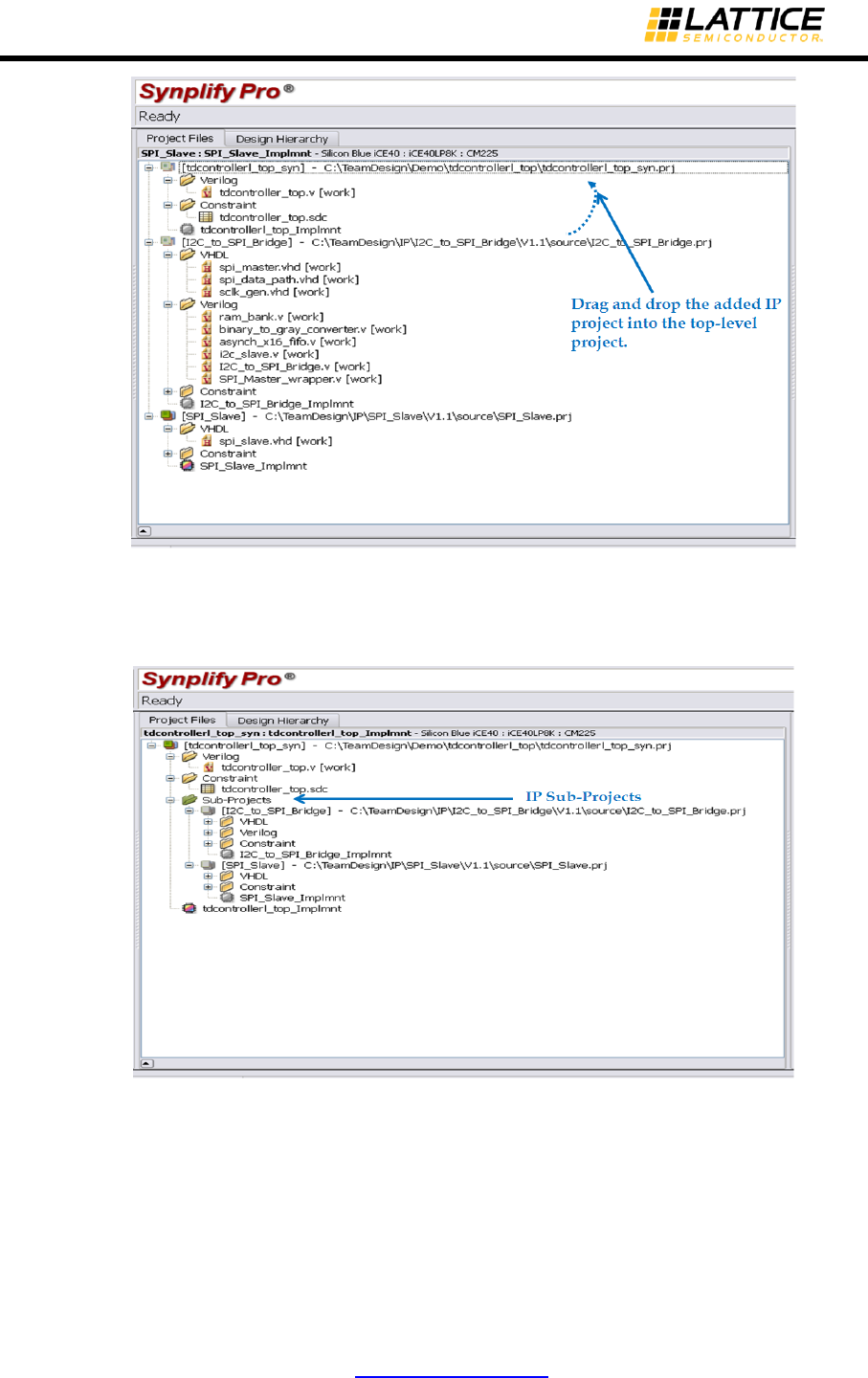
iCEcube2 User Guide www.latticesemi.com 175
Figure 9-8 : Drag and drop the IP Project into Top-Level Project
Figure 9-9: Top Level Project Hierarchy with IP Sub-Projects
Synthesize Top Level Project
1. In the Synplify Pro tool, select the top level project and right click on it. Select
“Hierarchical Project Options” as shown in Figure 9-10.

iCEcube2 User Guide www.latticesemi.com 176
Figure 9-10 : Select Hierarchical Project Options Menu
2. In the “Hierarchical Project Options”, specify the Sub-Project Implementation and set run
type as “top_down” as shown in Figure 9-11. Click on the “Synchronize All Options with
Top Level” icon to synchronize Sub-Project options with top-level project options.
Figure 9-11: Set Hierarchical Project Options
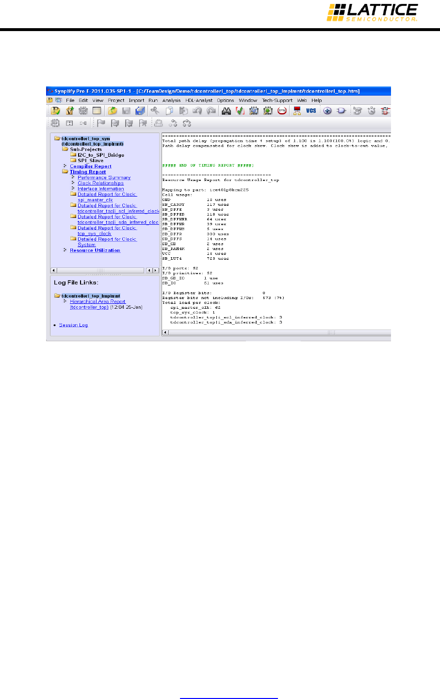
iCEcube2 User Guide www.latticesemi.com 177
3. Click on “Run” to synthesize the top level design. Click on the “View Log” menu item and
select the “Resource Utilization” link. The resource usage report shows that all the
design units are elaborated and synthesized into primitive cells, as shown in Figure 9-12.
Figure 9-12: Resource Utilization Report for Top Level Project
4. Exit the Synplify Pro software. This will bring you back to the iCEcube2 environment. The
synthesized netlist is automatically added to the iCEcube2 project. Click on “Run All” to
Place, Route and generate bitmap.

iCEcube2 User Guide www.latticesemi.com 178
Chapter 10 Simulating Design with ALDEC Active-HDL
The iCEcube2 windows software installs windows based ALDEC Active-HDL simulator to
simulate and verify the functionality of the implemented design at various stages. The simulation
wizard in the Project Navigator allows the user to easily create simulation project, simulation
language and add the required files to the simulator.
This chapter explains the steps to perform simulation in ALDEC Active-HDL simulator.
ALDEC Active-HDL
Active-HDL is a windows based RTL/gate-level mixed language simulator from ALDEC. Active-
HDL simulator is fully integrated into iCECube2 windows design environment and launched
directly from the iCECube2 project Navigator. The iCEcube2 simulation wizard helps the user to
perform the following simulation scenarios.
1. Pre-Synthesis Simulation.
2. Post Place-n-Route Functional Simulation (Verilog/VHDL)
3. Post Place-n-Route Timing Simulation (Verilog/VHDL)
Pre-Compiled iCE Simulation Libraries
iCEcube2 contains the following precompiled iCE simulation libraries for ALDEC simulator to
reference the iCE device primitives and hard IP core models.
ovi_ice : Precompiled iCE library for Verilog functional simulations.
ovi_ice_timing : Precompiled iCE library for Verilog timing simulations.
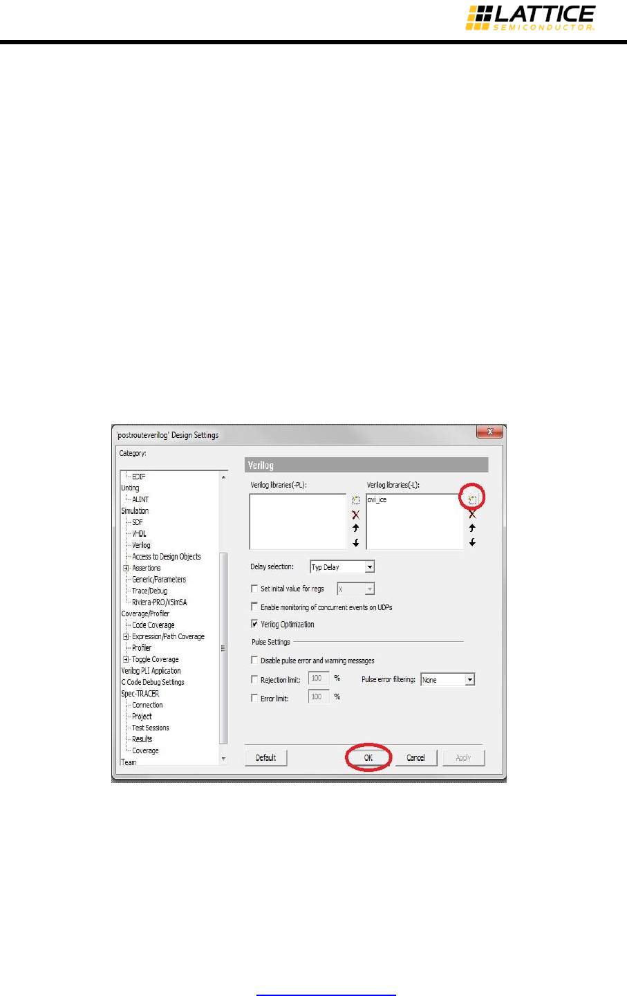
iCEcube2 User Guide www.latticesemi.com 179
ice : Precompiled iCE library for VHDL functional and timing simulations.
VHDL
Add the following library declaration in the HDL file. This library contains all the iCE primitive
VHDL functional and timing models.
library ice;
use ice.vcomponent_vital.all;
VERILOG
When you invoke the Aldec simulator through Simulation Wizard, the appropriate precompiled
libraries are automatically included for the simulation.
If you are running Aldec simulator outside of Simulation Wizard, appropriate precompiled libraries
must be referenced to the simulator.
To add a reference library in a standalone Aldec simulator, click on Design > Settings >
Simulation > Verilog. Browse the available precompiled library list and add the required Verilog
library. Click on Apply and then OK.
Figure 10-1 : Adding reference library to standalone Aldec Simulator.
For script or bash mode, use the –L switch of the asim command to specify the precompiled
library. asim -O5 -L ovi_ice +access tb

iCEcube2 User Guide www.latticesemi.com 180
Design
The sample design used in this chapter is a simple 4-bit binary up-counter with an associated
testbench.
The counter design, counter.vhd is presented first:
library ieee;
use ieee.std_logic_1164.all;
use ieee.std_logic_arith.all;
use ieee.std_logic_unsigned.all;
library ice;
use ice.vcomponent_vital.all;
entity counter is port (
clk : in std_logic;
reset : in std_logic;
count : out std_logic_vector (3 downto 0));
end counter;
architecture behavioral of counter is
signal q : std_logic_vector (3 downto 0);
begin
process(clk, reset)
begin
if(reset = '1') then
q <= (others=>'0');
elsif(clk'event and clk = '1') then
q <= q + 1;
end if;
end process;
count <= q;
end behavioral;
The testbench design, count_tb.vhd, is presented next:
library ieee;
use ieee.std_logic_1164.all;
use ieee.std_logic_arith.all;
use ieee.std_logic_unsigned.all;
entity count_tb is
end count_tb;
architecture testbench_arch of count_tb is

iCEcube2 User Guide www.latticesemi.com 181
component counter
port (
clk : in std_logic;
reset : in std_logic;
count : out std_logic_vector (3 downto 0));
end component;
signal clk : std_logic := '0';
signal reset : std_logic := '0';
signal count : std_logic_vector (3 downto 0) := "0000";
constant period : time := 100 ns;
constant duty_cycle : real := 0.5;
constant offset : time := 100 ns;
begin
uut : counter
port map (
clk => clk,
reset => reset,
count => count);
process -- clock generation
begin
wait for offset;
clock_loop : loop
clk <= '0';
wait for (period - (period * duty_cycle));
clk <= '1';
wait for (period * duty_cycle);
end loop clock_loop;
end process;
process -- reset generation
begin
reset <= '0';
-- ------------- Current Time: 0ns
wait for 100 ns;
reset <= '1';
-- ------------- Current Time: 100ns
wait for 35 ns;
reset <= '0';
-- ------------- Current Time: 135ns
wait for 1865 ns;
-- ------------- Current Time: 2000ns
end process;
end testbench_arch;
Figure 10-2 : Sample Design and testbench.
Pre-Synthesis Simulation
This section details the steps required for pre-synthesis simulation.
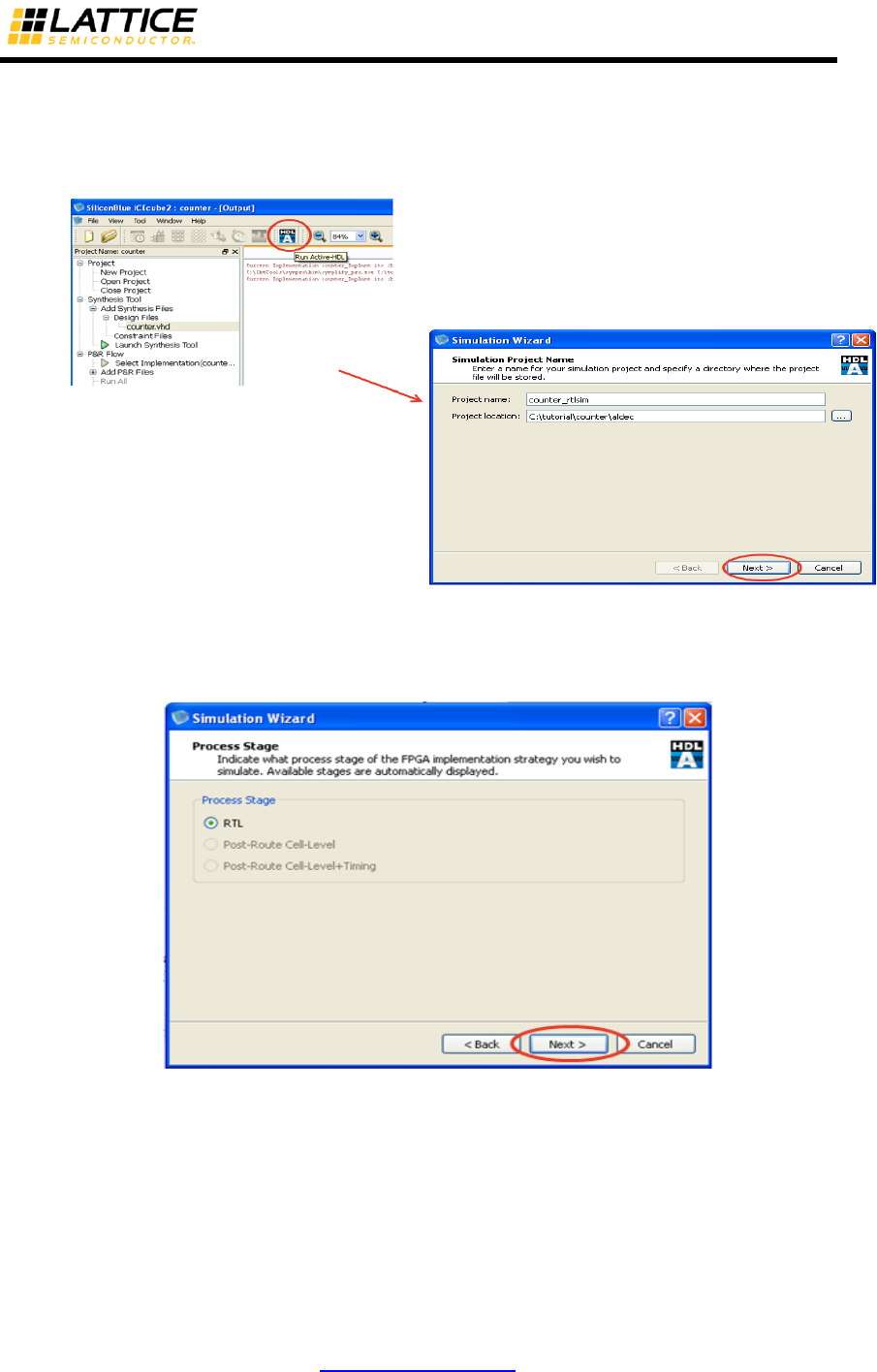
iCEcube2 User Guide www.latticesemi.com 182
1. After creating iCECube2 project and added the RTL design files, launch simulation
wizard by selecting the “AHDL” icon menu as shown in Figure 10-3. In the Simulation
Wizard specify the simulation project name and simulation project location. The default
project location is “Current iCEcube2 project directory\aldec”. Click on “Next” icon.
Figure 10-3: Launch Simulation Wizard and Specify Simulation Project name.
2. Select “RTL” Simulation and click on “Next” button.
Figure 10-4: Select RTL Simulation.
3. All the RTL design files in the iCECube2 project would be automatically added under the
source files section as shown in Figure 10-5. Select “+” icon to add “count_tb.vhd” test
bench file.
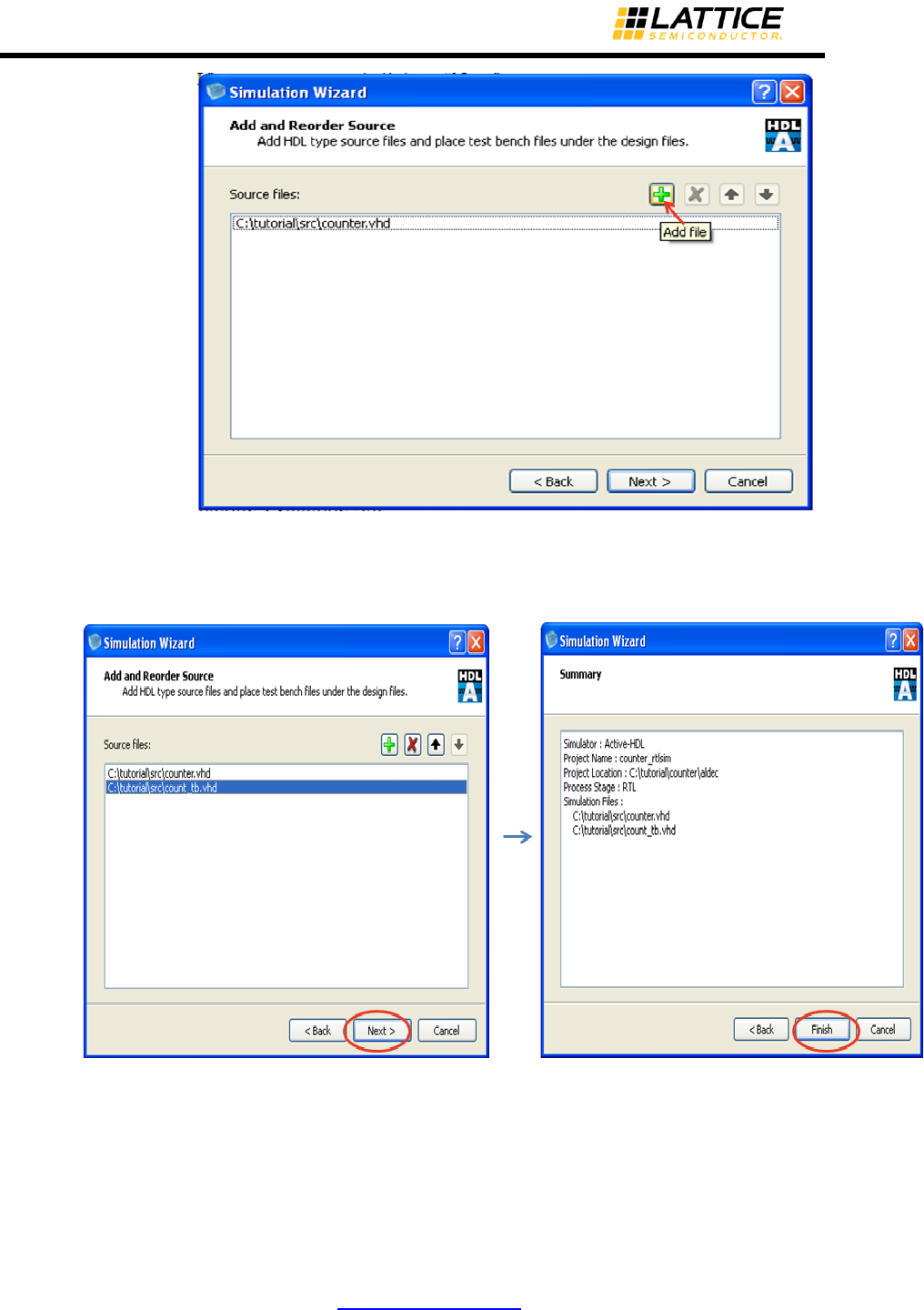
iCEcube2 User Guide www.latticesemi.com 183
Figure 10-5 : Auto added RTL design Files
4. Add “count_tb.vhd” test bench file and click on “Next”. Click on “Finish” in the summary
page as shown in Figure 10-6.
Figure 10-6: Add test bench and Complete Simulation Wizard.
5. The Active-HDL simulator is launched now and the workspace, simulation project, work
library are automatically created as per the simulation wizard inputs. The simulation
source files also added under simulation project. See Figure 10-7.
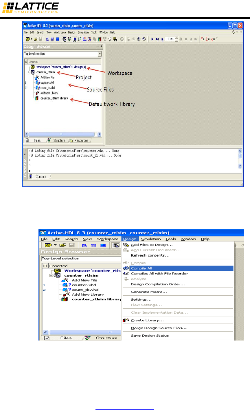
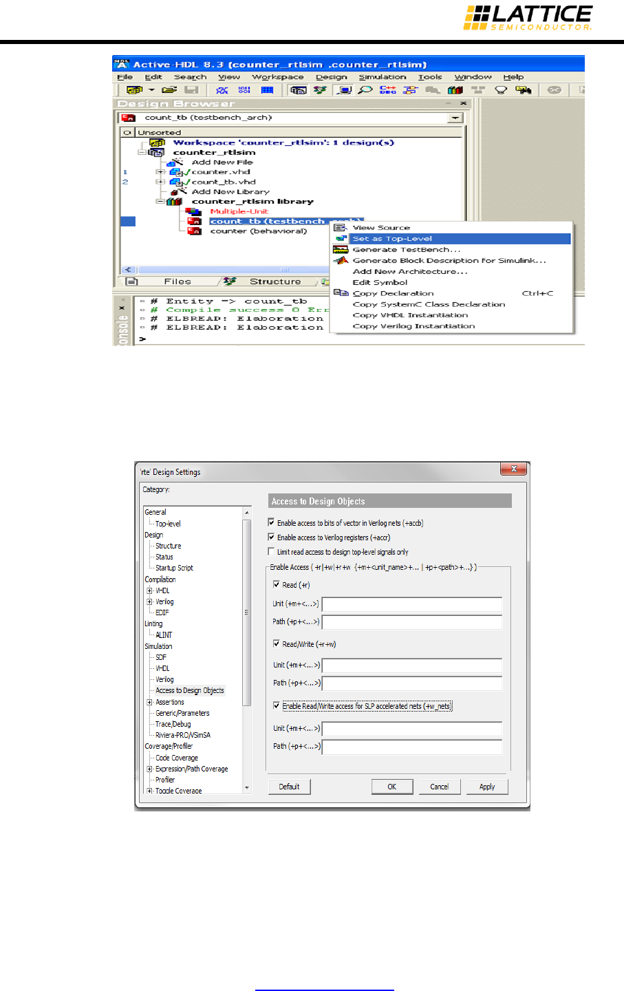
iCEcube2 User Guide www.latticesemi.com 185
Figure 10-9 : Set Top-Level Entity.
8. To get internal signal visibility, set the read access to internal signals. To set the access
click on Design > Settings > Simulation > Access to design Objects. Set the signal
access as shown below. Click on Apply and then OK.
Figure 10-10 : Set Signal Access
For script or bash mode runs, add +access +r +w_nets switch to the asim command.
9. Click on Simulation > Initialize Simulation. After Initialization, the “Design Browser” view
will be changed from “file” view to “Structure” view as shown in Figure 10-11.
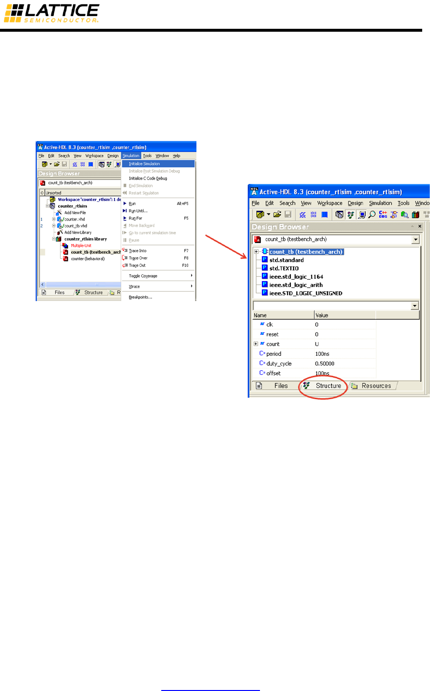
iCEcube2 User Guide www.latticesemi.com 186
For batch mode run, use the “asim” command.
Verilog:
asim -O5 -L ovi_ice +access +r +w_nets tb
VHDL:
asim -O5 +access +r +w_nets tb
Figure 10-11 : Initialize Simulation.
10. Right Click on “count_tb” and select “Add to waveform”. A new waveform window will
show up and all the I/O signals in the design are added to the waveform viewer.
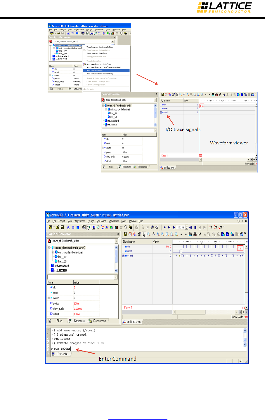
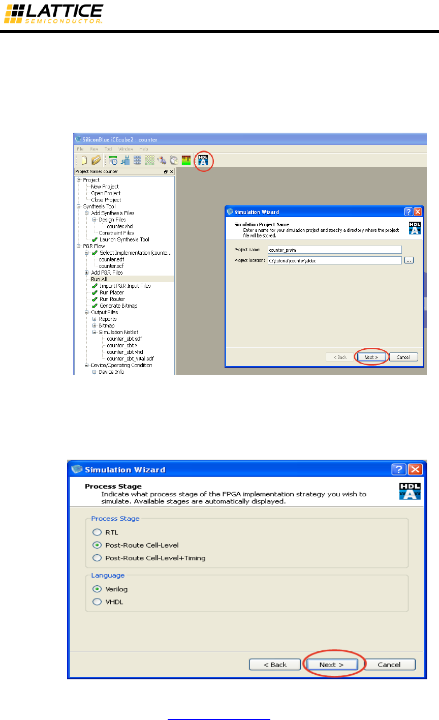
iCEcube2 User Guide www.latticesemi.com 188
Post Place-n-Route Functional Simulation (Verilog/VHDL)
1. Generate the files that are required for Post-Route Functional simulation model as listed
in the section “Simulating the Routed Design”.
2. Launch simulation wizard by selecting the “AHDL” icon menu in the Project Navigator. In
the Simulation Wizard specify the simulation project name and simulation project
location. Click on “Next”.
Figure 10-14 : Launch Simulation Wizard and Specify Simulation Project name.
3. Select “Post-Route Cell-Level” as Process Stage and Select “Verilog” Simulation. Click
on “Next”.
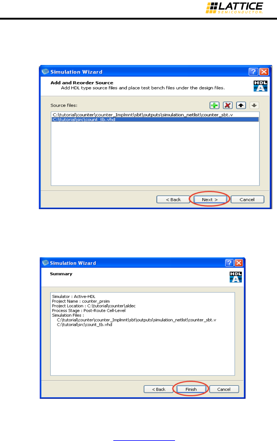
iCEcube2 User Guide www.latticesemi.com 189
Figure 10-15 : Select Post Route Functional Simulation.
4. The Verilog post routed simulation netlist “counter_sbt.v” would be automatically added
to the source files panel. Click on the “+” icon to add “count_tb.vhd” test bench file. Click
on “Next”.
Figure 10-16 : Add Test Bench File for Simulation.
5. In the Simulation wizard summary page click on “Finish” to launch the Active-HDL
Simulator.
Figure 10-17 : Complete Simulation Wizard
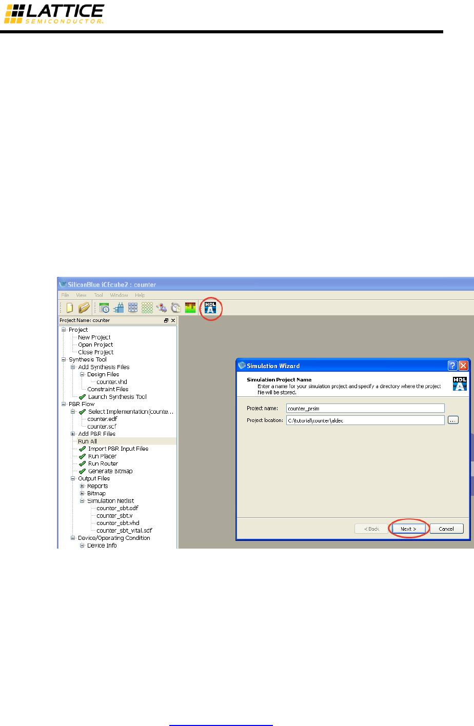
iCEcube2 User Guide www.latticesemi.com 190
6. The Active-HDL simulator is launched now and the workspace, simulation projects, work
library are automatically created as per the simulation wizard inputs. The simulation
source files are also added under the simulation project. Perform simulation as explained
in section “Pre-Synthesis Simulation” from point 6 onwards.
7. To perform post-route VHDL simulation, select language as “VHDL” in the simulation
wizard instead of “Verilog” at step 3. This would automatically add “counter_sbt.vhd”
netlist to source file panel. Follow the remaining steps as explained in this section.
Post Place-n-Route Timing Simulation (Verilog/VHDL)
1. Generate the files that are required for Post-Route Timing simulation model using the
steps described in the section “Simulating the Routed Design”.
2. Launch simulation wizard by selecting the “AHDL” icon menu in the Project Navigator. In
the Simulation Wizard specify the simulation project name and simulation project
location. Click on “Next”.
Figure 10-18: Create Simulation Project for Post-route Timing Simulation.
3. Select “Post-Route Cell-Level+Timing” as Process Stage and Select “Verilog” Simulation.
Click on “Next”.
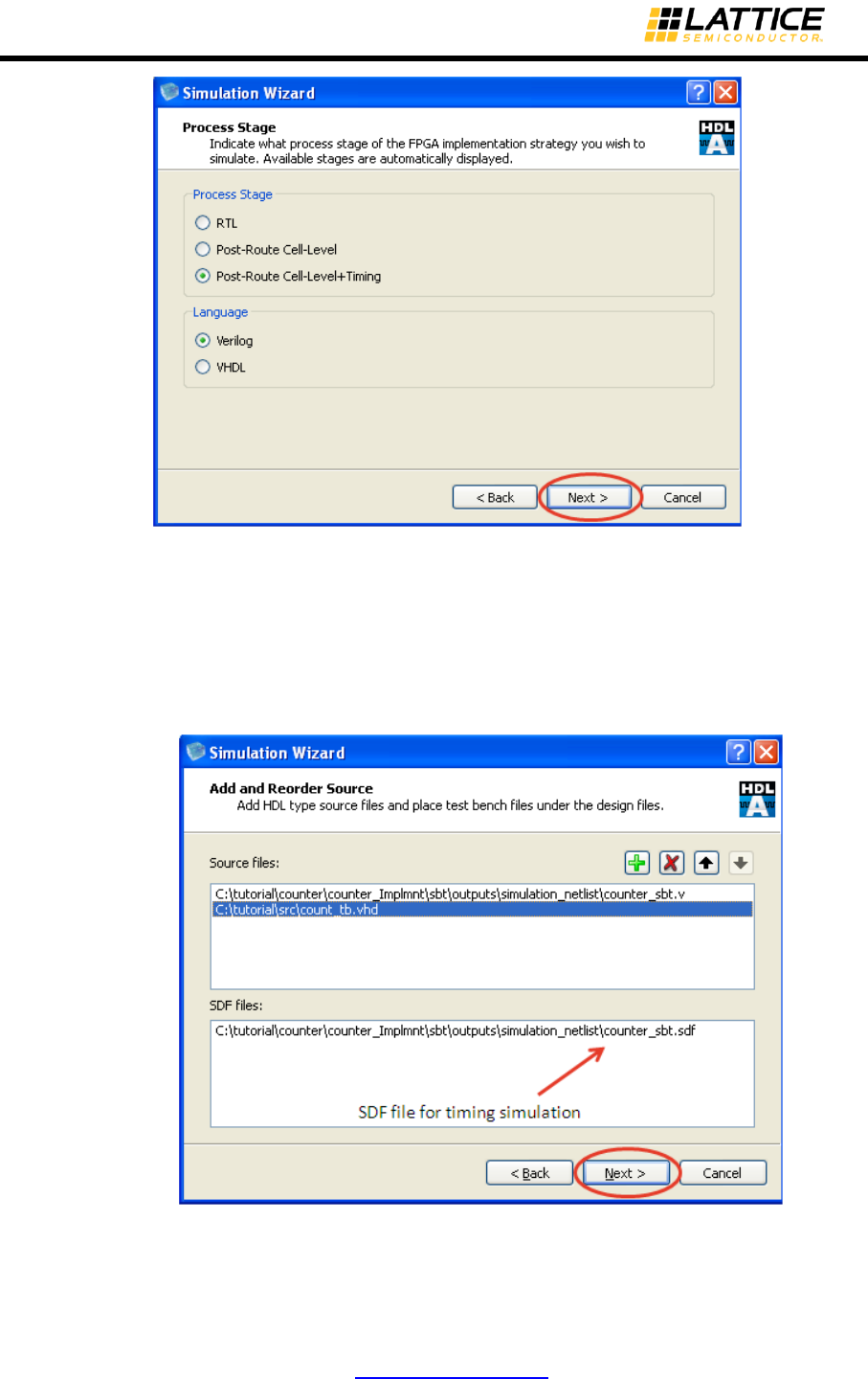
iCEcube2 User Guide www.latticesemi.com 191
Figure 10-19 : Select Verilog Timing Simulation option.
4. The simulation wizard automatically adds the post routed netlist “counter_sbt.v” in
“Source files” panel and the verilog delay format file “counter_sbt.sdf” under “SDF files”
panel as shown in Figure 10-20. Click on “+” icon to add the “count_tb.vhd” test bench
to the “Source files” panel. Click on “Next”.
Figure 10-20 : Add Test bench File.
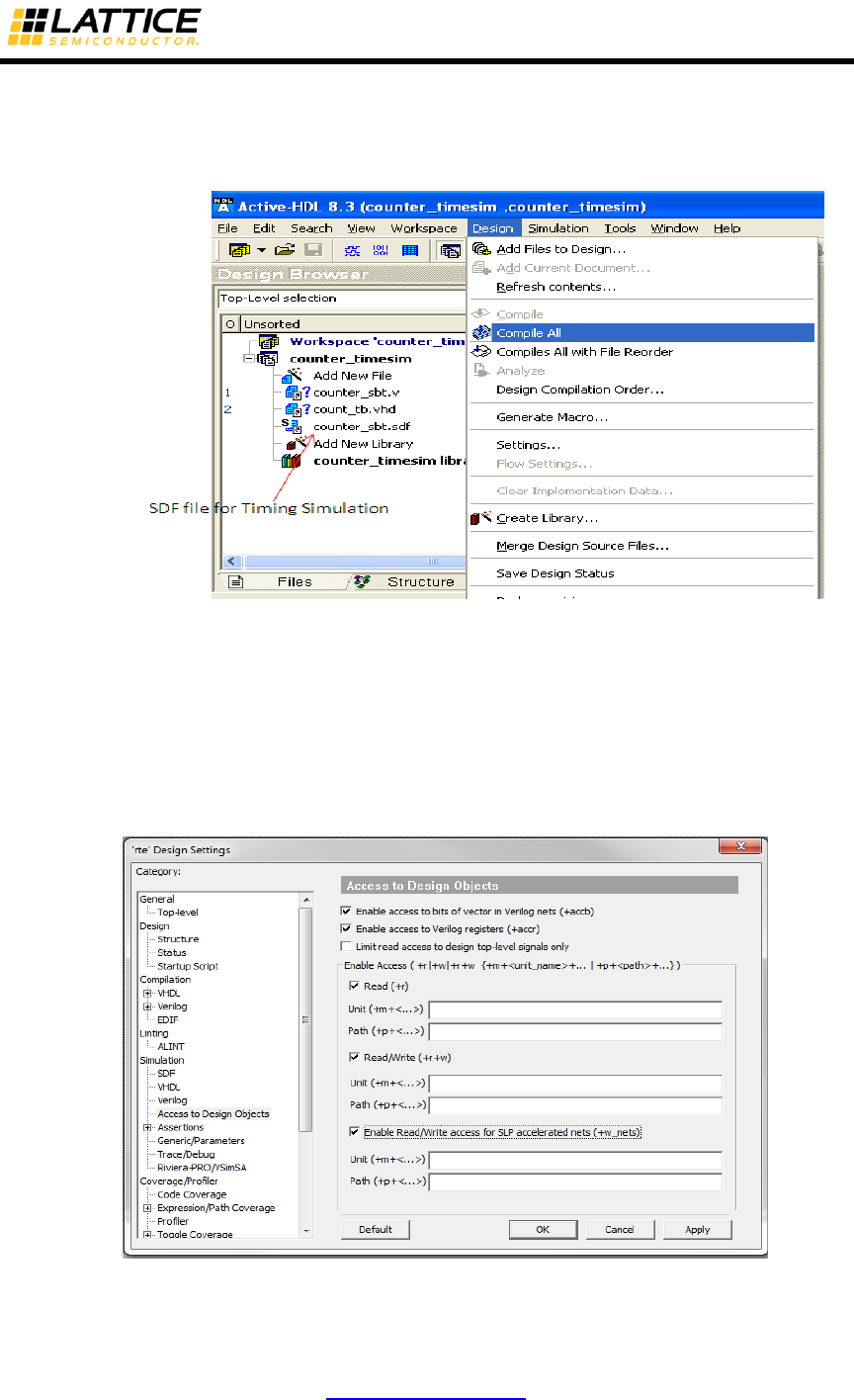
iCEcube2 User Guide www.latticesemi.com 192
5. In the simulation wizard summary page click on “Finish” icon to close the simulation
wizard and launch the Active-HDL Simulator.
6. Select Design > Compile All.
Figure 10-21 : Compile the Source Files
7. Expand the default work library in the “Design Browser” panel and set “count_tb” as Top-
Level entity.
8. To get internal signal visibility, set the read access to internal signals. To set the access,
click on Design > Settings > Simulation > Access to design Objects. Set the signal access as
shown below. Click on Apply and then OK.
Figure 10-22 : Set Signal Access
For script or bash mode runs, add +access +r +w_nets switch to the asim command.
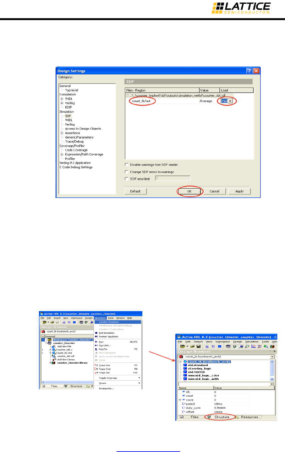
iCEcube2 User Guide www.latticesemi.com 193
9. Select DesignSettings to l open up the “Design Settings” Wizard. Select SDF in the
category panel. Set the Region to “count_tb/uut” and change the Load option to “Yes” as
shown in Figure 10-23. The SDF value selection can be set to “Minimal”, “Average” and
“Maximal”. The value is set to “Average” by default. Click on “OK” icon to close the wizard.
Figure 10-23 : Set SDF Options.
10. Select Simulation > Initialize Simulation. After Initialization, the “Design Browser” view will
be changed from “file” view to “Structure” view as shown in Figure 10-24.
For batch mode run, use the “asim” command.
Verilog:
asim -O5 -L ovi_ice +access +r +w_nets tb
VHDL:
asim -O5 +access +r +w_nets tb
Figure 10-24 : Initialize Simulation
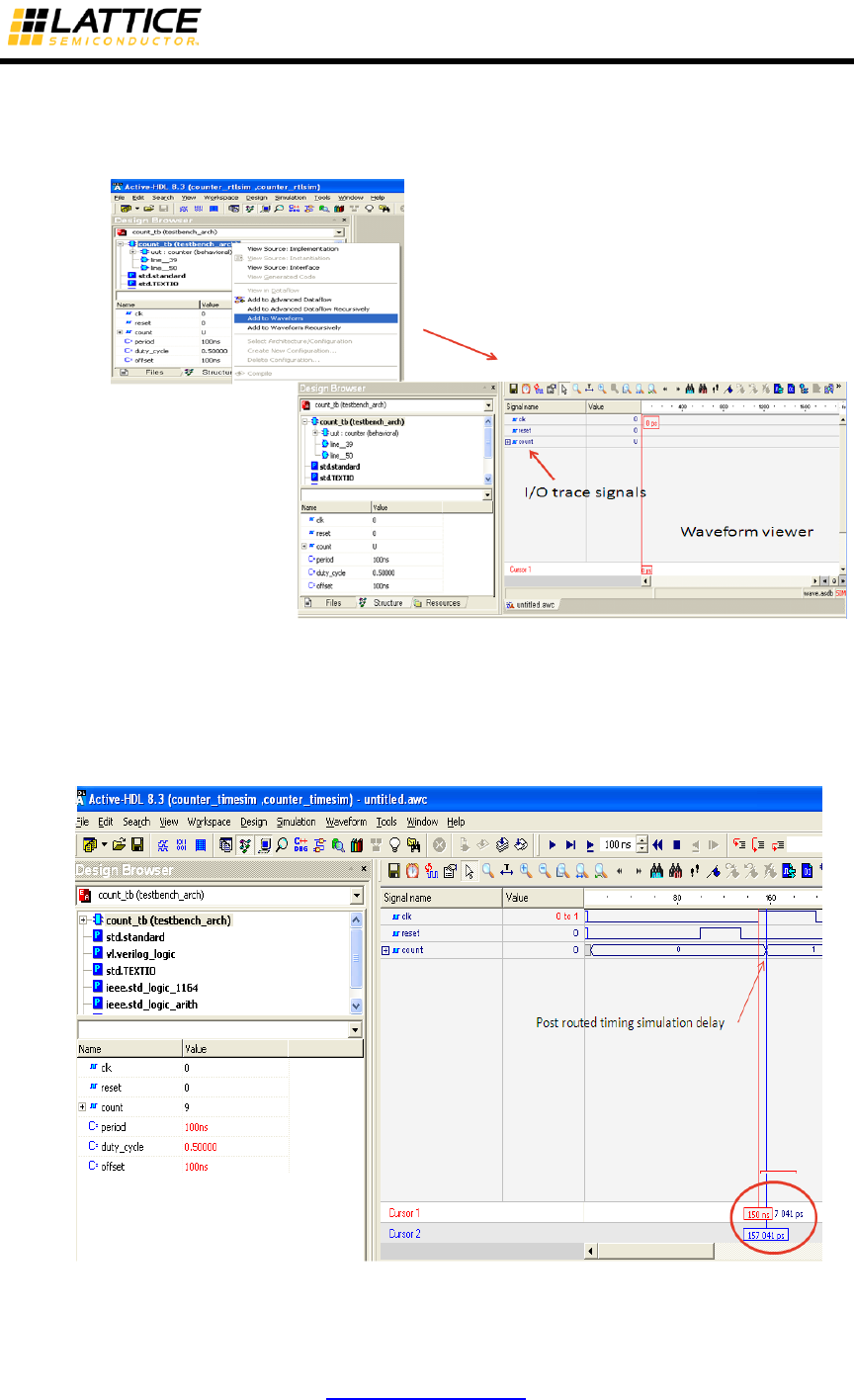
iCEcube2 User Guide www.latticesemi.com 194
11. Right Click on “count_tb” and select “Add to waveform”. A new waveform window will
show up and all the I/O signals in the design are added to the waveform viewer.
Figure 10-25 : Add Waveform Viewer
12. Type the command “run 1000ns” in the console and press enter. The 1-µs simulation
waveform will show up in the waveform window. The counter output timing delays with
respect to clock positive edge is shown in Figure 10-26.
Figure 10-26: Timing Simulation Waveform

iCEcube2 User Guide www.latticesemi.com 195
13. To perform post-route VHDL timing simulation, select language as “VHDL” in the
simulation wizard instead of “Verilog” at step 3. This would automatically add
“counter_sbt.vhd” netlist to source file panel and “counter_sbt_vital.sdf” SDF file.
Follow the remaining steps as explained in this section.

iCEcube2 User Guide www.latticesemi.com 196
Chapter 11 iCEcube2 Command Line Interface
The iCEcube2 software tools can be executed in a command line shell such as DOS or bash. The
iCEcube2 installation contains a set of TCL scripts, which helps the user to run the designs in
batch mode. This chapter describes the iCEcube2 TCL scripts and the default flow options for
command-line operations.
Overview
The iCEcube2 software provides command line executables at each stage of the flow. The
iCEcube2 installation contains a set of TCL wrapper scripts to set the project and tool options and
execute the individual tools. It also contains top level TCL script to run the default backend flow
starting with edifparser tool to bitmap generation. The environment variables to be set for the
batch mode run are listed at Command Line Execution.
Running LSE in batch mode
Lattice Synthesis Engine (LSE) is the integrated synthesis tool that comes with iCEcube2. LSE is
a synthesis tool custom-built for Lattice products and depending on the design, LSE may lead to
a more compact or faster placement of the design than another synthesis tool would do. LSE
generates EDIF netlist and forward annotated timing constraint file for the backend tools.
The command to execute LSE in batch mode is shown below
<<iCEcube2_install>>\LSE\bin\nt\synthesis.exe -f <project_name.prj>
Arguments:
-f <project_name.prj> : Specify LSE project file.
Sample project file “top_design_lse.prj” is shown below. Refer iCEcube2 user guide for LSE
project setting options.
###########################
## top_design_lse.prj ##
###########################
#-- Lattice, Inc.
#-- Project file
#device
-a SBTiCE40
-d iCE40LP8K
-t CM225
#constraint file
-sdc "../src/top_design.sdc"
#options
-frequency 200
-optimization_goal Area
-twr_paths 3

iCEcube2 User Guide www.latticesemi.com 197
-bram_utilization 100.00
-ramstyle Auto
-romstyle Auto
-use_carry_chain 1
-carry_chain_length 0
-resource_sharing 1
-propagate_constants 1
-remove_duplicate_regs 1
-max_fanout 10000
-fsm_encoding_style Auto
-use_io_insertion 1
-use_io_reg auto
-ifd
-resolve_mixed_drivers 0
-RWCheckOnRam 0
-fix_gated_clocks 1
-ver "../src/top_design.v"
-p "C:/examples/sbtProject/top_design"
#set result format/file last
-output_edif rev_1/top_design.edf
#set log file
-logfile rev_1/top_design.log
Running Synplify-pro in batch mode
Synplify-pro synthesis tool integrated with the iCEcube2 IDE supports the comprehensive verilog
HDL, VHDL, timing constraint design entry files. After successful run, Synplify generates EDIF
netlist and forward annotated timing constraint file for the backend tools. Synplify-pro synthesis
tool is executed through a wrapper (synpwrap) executable available in the build.
The command to execute Synplify-pro in batch mode is shown below
<<iCEcube2_install>>\sbt_backend\bin\win32\opt\synpwrap\synpwrap.exe
-prj <project_name.prj> -log <logfile_name>
Arguments:
-prj <project_name.prj> : Specify Synplify pro project file
-log <logfile_name> : Specify log file name.
Sample project file “top_design_syn.prj” is shown below. Refer to Synplify-pro user guide for
more project setting options.
###########################
## top_design_syn.prj ##
###########################
#project files
add_file -verilog -lib work "../src/top_design.v"
add_file -constraint -lib work "../src/top_design.sdc"

iCEcube2 User Guide www.latticesemi.com 198
#implementation: "rev_1"
impl -add rev_1 -type fpga
#implementation attributes
set_option -vlog_std v2001
set_option -project_relative_includes 1
#device options
set_option -technology SBTiCE40
set_option -part iCE40LP8K
set_option -package CM225
set_option -speed_grade
set_option -part_companion ""
#compilation/mapping options
# mapper_options
set_option -frequency auto
set_option -write_verilog 0
set_option -write_vhdl 0
# Silicon Blue iCE40
set_option -maxfan 10000
set_option -disable_io_insertion 0
set_option -pipe 1
set_option -retiming 0
set_option -update_models_cp 0
set_option -fixgatedclocks 2
set_option -fixgeneratedclocks 0
# NFilter
set_option -popfeed 0
set_option -constprop 0
set_option -createhierarchy 0
# sequential_optimization_options
set_option -symbolic_fsm_compiler 1
# Compiler Options
set_option -compiler_compatible 0
set_option -resource_sharing 1
#automatic place and route (vendor) options
set_option -write_apr_constraint 1
#set result format/file last
project -result_format "edif"
project -result_file ./rev_1/top_design.edf
impl -active rev_1

iCEcube2 User Guide www.latticesemi.com 199
Running iCEcube2 Backend tools in batch mode
“run_sbt_backend_auto” is the top level TCL wrapper which accepts tools specific options and
executes the default flow. The TCL source files are available in the installation area at
<<iCEcube2_install>>\lscc\iCEcube2\sbt_backend\tcl.
Command:
run_sbt_backend_auto <device_package> <design_topmodule> <project_dir>
<output_dir> <tool_options> <edif_netlist>
Arguments:
<device-package> : Specify the selected device –package name.
Ex: iCE40LP8K-CM225.
<design_topmodule : Specify the design top module name.
<project_dir> : Specify the path to synthesis project dir.
<output_dir> : Specify the synthesis implementation dir.
Backend results will be kept in the same directory.
<tool_options> : Specify tool options. Refer Backend tool Options for
complete list of tool options.
<edif_netlist> : Specify input edif netlist name.
Sample “iCEcube2_flow.tcl” file is shown below
#!usr/bin/tclsh8.4
# Sample flow script for iCEcube2
#############################################
# User Configurable section
#############################################
set device iCE40LP8K-CM225
set top_module top_design
set proj_dir [pwd]
set output_dir "rev_1"
set edif_file "top_design"
set tool_options ":edifparser -y top_design.pcf"
###########################################
# Tool Interface
############################################
set sbt_root $::env(SBT_DIR)
append sbt_tcl $sbt_root "/tcl/sbt_backend_synpl.tcl"
source $sbt_tcl
run_sbt_backend_auto $device $top_module $proj_dir
$output_dir $tool_options $edif_file
exit

iCEcube2 User Guide www.latticesemi.com 200
Backend tool Options
Each tool in the backend flow accepts parameter values to optimize the design. The
“
run_sbt_backend_auto”
wrapper accepts the individual tool options as a single argument
as given below
“:edifparser <edif_parser_options> :placer <placer_options> :router
<router_options> :bitmap <bitmap_options>”
This section covers the tools in the iCEcube2 backend flow and the tool options.
Edif Parser
“Import P&R Input Files” stage in GUI invokes edif parser tool to parse the input edif netlist,
forward annotated timing constraints (scf) and the physical constraints file (pcf). This generates a
design database for placer and route tool. The edif parser tool options are specified with
“:edifparser” keyword in the argument.
:edifparser [-y | --physicalconstraint <phy_constraints.pcf>] [-s | --sdcfiles <sdc_constraints.sdc> ]
Options
[-y | --physicalconstraint <phy_constraints.pcf>]
Specify the design physical constraints file.
[-s | --sdcfile <sdc_constraints.sdc>]
Specify the SDC timing constraint files. If default SCF file exits along with specified SDC
file, both files will be parsed.
Placer
iCEcube2 Placer tool optimally places the design objects into the device layout based on the
given physical and timing constraints to meet the performance requirements. The placer tool
options are specified with “:placer” keyword in the argument.
:placer [ -e | --effort_level <std|mid|high>] [ -k | --no_autolutcascade] [-r | --no_autoramcascade]
[ -t | --power_driven] [ -p | --pack_area]
Options
[ -e | --effort_level <std|mid|high>]
Option to specify the placement effort level. Default is std.
[ -k | --no_autolutcascade]
Disable automatic LUT cascading in placer. By default LUT cascading is enabled.
[ -r | --no_autoramcascade]
Disable automatic RAM cascading in placer. By default RAM cascading is enabled in
placer.
[ -t | --power_driven]
Enable power driven placement mode. By default power driven placement option is
disabled in placer.
[ -p | --pack_area]
Pack for dense area. Default is for timing.

iCEcube2 User Guide www.latticesemi.com 201
Router
Router tool route the placer design with timing driven optimization. The router tool options are
specified with “:router” keyword in the argument.
:router [ --no_timing_driven ] [--no_pin_permutation]
Options
[ --no_timing_driven ]
Option to disable timing driven router optimization. By default timing driven option is
enabled.
[ --no_pin_permutation]
Option to disable LUT pin permutation. By default pin permutation is enabled.
Bitmap
Bitmap generates the bit stream to program the device. The bitmap tool options are specified
with “:bitmap” keyword in the argument.
:bitmap [--no_low_power] [--no_init_ram] [--init_ram_bank <specify_quadrants>] [--frequency
<low|medium|high>] [--no warmboot] [ -- set_security] [--set_unused_io_nopullup]
Options
[--no_low_power]
Change setting of SPI PROM from low power mode after configuration. Default is low
power mode if not specified.
[--no_init_ram]
Do not initialize Block Rams in the design with contents specified in the design or ‘0’.
Default is on.
[--init_ram_bank <specify_quadrants >]
Select the quadrants for Block RAM initialization. Quadrant 0 to quadrant 3 can be
specified as 1111.
[--frequency <low|medium|high>]
Select frequency value
[--no_warmboot]
Set warm boot to off. Default is on.
[-- set_security]
Set security mode.
[--set_unused_io_nopullup]
Set all unused IO in the design to no-pullup mode.
Command Line Execution
Certain environment variables need to be set in Dos or bash shell to execute the tools in
command line. To execute the tools in command line, the LM_LICENSE_FILE environment
variable should point to the license server, which contains license for iCEcube2 GUI. The user


iCEcube2 User Guide www.latticesemi.com 203
DOS scripts
Dos script for LSE-iCEcube2 flow:
SET FOUNDRY=C:\lscc\iCEcube2\LSE
SET SBT_DIR=C:\lscc\iCEcube2\sbt_backend
C:\lscc\iCEcube2\LSE\bin\nt\synthesis.exe –f
top_design_lse.prj
tclsh iCEcube2_flow.tcl
Dos script for Synplify–iCEcube2 flow:
SET SYNPLIFY_PATH=C:\lscc\iCEcube2\synpbase
SET SBT_DIR=C:\lscc\iCEcube2\sbt_backend
C:\lscc\iCEcube2\sbt_backend\bin\win32\opt\synpwrap\sy
npwrap.exe -prj top_design_syn.prj -log icelog.log
tclsh iCEcube2_flow.tcl
Bash scripts
Bash script for LSE–iCEcube2 flow:
export LD_LIBRARY_PATH=/home/user1/lscc/iCEcube2/LSE
:$LD_LIBRARY_PATH
export FOUNDRY=/home/user1/lscc/iCEcube2/LSE
export SBT_DIR=/home/user1/lscc/iCEcube2/sbt_backend/
/home/user1/lscc/iCEcube2/LSE/bin/lin/synthesis.exe –f
top_design_lse.prj
tclsh iCEcube2_flow.tcl
Bash script for Synplify-iCEcube2 flow:
export
LD_LIBRARY_PATH=/home/user1/lscc/iCEcube2/sbt_backend/
bin/linux/opt/synpwrap:$LD_LIBRARY_PATH
export
SYNPLIFY_PATH=/home/user1/lscc/iCEcube2/synpbase
export SBT_DIR=/home/user1/lscc/iCEcube2/sbt_backend/
/home/user1/lscc/iCEcube2/sbt_backend/bin/linux/opt/sy
npwrap/synpwrap -prj top_design_syn.prj -log
icelog.log
tclsh iCEcube2_flow.tcl
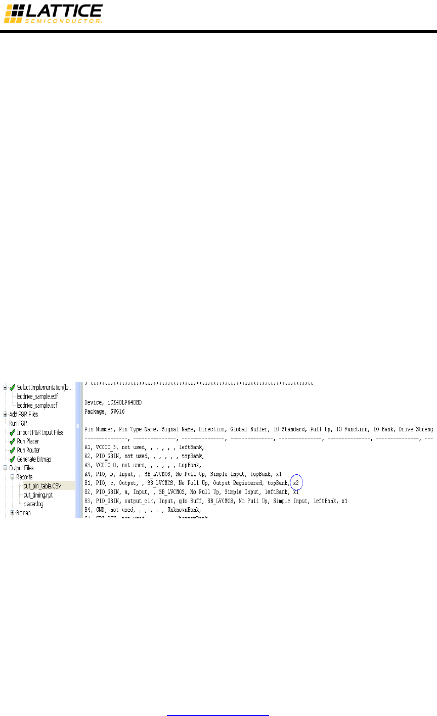
iCEcube2 User Guide www.latticesemi.com 204
Chapter 12 High Drive IO with configurable drive strengths
IO’s in iCE40/iCE40LM device can be configured with different drive strengths to increase the IO
output current. This special IO’s are available only in selected iCE device packages and only
three IO’s with configurable drive strength is allowed in a device.
To configure an IO with specific drive value, the user needs specify the “DRIVE_STRENGTH”
synthesis attribute on the IO instance. The design can have maximum of three IO instances with
configured drive strengths and the IO needs to be configured as output-only registered IO.
The iCEcube2 SW replicates the IO instance once or twice based on the specified drive strength
value. The original and the replicate IO instances share the following signal and properties.
Signals
o DOUT0
o DOUT1
o OUTPUT_CLK
o OUTPUT ENABLE
Properties
o PIN_TYPE
o PULL_UP
o IO_STANDARD
The placer auto places the IO in one of the 3 predefined IO group locations. The users can also
constraint the IO group location by using pcf constraints. The drive strengths are reported under
drive strength column in the pin table csv report as shown in Figure 12-1.
Figure 12-1 : Drive Strength Display in Pin Table CSV file.
High Drive IO Supported Device–Packages
Following iCE40, ICE40LM device packages supports the high drive IO pins.
iCE40LP1K-SWG16TR
iCE40LP640-SWG16TR
iCE40LM4K-SWG25TR,CM36,CM49
iCE40LM2K-SWG25TR,CM36,CM49
iCE40LM1K-SWG25TR,CM36,CM49

iCEcube2 User Guide www.latticesemi.com 205
High Drive IO Pin Locations
Following table shows the package pin locations of high drive IO groups.
Device
Package
High drive IO
Group
Package Pin
iCE40LP1K
iCE40LP640
SWG16TR
Group 0
B1
Group 1
A2
Group 2
A4
iCE40LM4K
iCE40LM2K
iCE40LM1K
SWG25TR
Group 0
A3
Group 1
A4
Group 2
B5
CM36
Group 0
A5
Group 1
A4
Group 2
A3
CM49
Group 0
A4
Group 1
A3
Group 2
A2
Synthesis Attribute Syntax:
/* synthesis DRIVE_STRENGTH = <Drive value> */
Drive Value:
Drive Strength
Value
Description.
x1
Default drive strength. No replication of SB_IO.
x2
Increase default drive strength by 2. SB_IO
replicated once.
x3
Increase default drive strength by 3. SB_IO
replicated twice.
Example:
module highdriveio (a, b, output_clk, c );
input a, b, output_clk;
output c;
assign x = a & b;
SB_IO #(.PIN_TYPE("010101") )
x_inst
(.PACKAGE_PIN(c),
.OUTPUT_CLK(output_clk),
.D_OUT_0(x)
) /* synthesis DRIVE_STRENGTH= x2 */;
endmodule
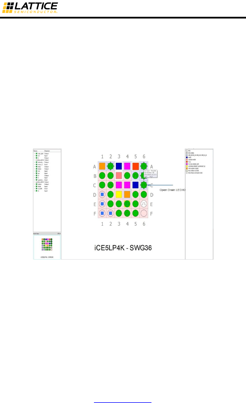
iCEcube2 User Guide www.latticesemi.com 206
Chapter 13 Open Drain LED IO
iCE5LP (iCE40 Ultra) device contains dedicated open drain LED IO for the LED drive primitives
(SB_RGB_DRV, SB_IR_DRV). These IOs can be either configured as high current sink for the
LED drive or as an Open Drain GPIO.
The RGB LED IO can sink between 0 to 24mA current in steps of 4mA per device pin when
configured as high drive sink. Similarly IR LED IO can sink between 0 to 500mA current in steps
of 50mA. The sink current value is set via the primitive parameters. Refer Technology Guide for
the details of parameter settings.
The Open Drain GPIO primitive (SB_IO_OD) instantiated in the design can be used to drive the
LED IO pins, when the LED drive parameters are set to zero. Open Drain IO cannot be placed at
normal IO pin locations and vice versa.
Package view display of LED IO is shown in Figure 13-1
Figure 13-1 : Open Drain LED IO pins

iCEcube2 User Guide www.latticesemi.com 207
Appendix A: PCF Syntax
Relative Placement
1. Group Creation
create_group $group_name Ex: create_group En_FFs
begin begin
inst0 [x0, y0, z0] EFF_A_Ins [1, 2, 3]
inst1[x1, y1, z1] EFF_B_Inst[1, 2, 4]
end end
2. Set Group Origin Point
set_group_origin $group_name x0 y0
Ex: set_group_origin En_FFs 2 3
3. Region Constraints
create_region –name $region_name –type $type $x_left $y_bottom $x_right $y_top
$type can be blocked (no cells are placed in the region) or
inclusive (holds the cells placed in the region)
set_group_to_region $group_name $region_ name
Ex: create_region –name EnFFs_Region –type inclusive 3 3 7 10
set_group_to_region En_FFs EnFFs_Region
IO/FF Merge
1. Merge FF to IO
set_io_ff $port_name [-in/-out/-oe]
The options specify where the Flip Flops need to be merged.
Three Options can coexist at same time.
Ex: set_io_ff A1 -in -oe
2. Unmerge FF from IO
seperate_io_ff $port_name [-in/-out/-oe]
Ex: separate_io_ff A1 –in –oe
Global Buffer Promotion/Demotion
1. Promote Signal to be Global Buffered
promote_signal_gbuffered $signal_name
Ex: promote_signal_gbuffered A1
2. Demote Global buffered Signal
demote_signal_unbuffered $signal_name
Ex: demote_signal_unbuffered A1
