Lab+manual+communication
User Manual: Pdf
Open the PDF directly: View PDF ![]() .
.
Page Count: 60
- CoverPage
- Experiment #1 AM and DSBsc Modulation and Demodulation_V1
- Experiment #2 Single Sideband AM (SSB) and Ring Modulator_V1
- Experiment #3 Angle Modulation - Part 1_V1
- Experiment #4 Angle Modulation - Part 2_V1
- Experiment #5 Pulse Amplitude Modulation (PAM)_V1
- Experiment #6 Pulse Code Modulation (PCM) - Part 1_V1
- Experiment #7 Pulse Code Modulation (PCM) - Part 2_V1
- Experiment #8 Delta Modulation - Part 1_V1
- Experiment #9 Delta Modulation - Part 2_V1
- Experiment #10 Noise in Amplitude Modulation_V1

FACULTY OF ENGINEERING AND TECHNOLOGY
DEPARTMENT OF ELECTRICAL AND COMPUTER
ENGINEERING
COMMUNICATIONS LABORATORY MANUAL
ENEE4103
Updated: May, 2016
ECE Department ENEE4103 – Communications Lab Page 1 of 8
Experiment #1
AM and DSBsc Modulation and Demodulation
Prelab:
• Theoretical Review
Review the AM and DSBsc modulation techniques from the text book of the courses
ENEE3303 and ENEE339.
• Matlab Simulation
Use MATLAB command and M files to draw the demodulated signal after the envelope
detector given that:
)
tcos()]
tcos(
1[A)t(
S
c
mcM
ωω
µ
+
=
1. Write the mathematical expression for the demodulated signal.
2. Use MATLAB command and M files to draw the demodulated signal for the following
three cases:
a. Ac=16v, modulation index=0.22, modulating signal frequency=800Hz
b. Ac=16v, modulation index=1, modulating signal frequency=800Hz
c. Ac=16v, modulation index=1.85, modulating signal frequency=800Hz
3. Discuss your result in each part .you must write the commands which are used in the
Pre-lab.
Experiment #1: AM and DSBsc Modulation and Demodulation
Page 2 of 8
Part One: AM Modulation
Experiment set-up: Assemble the components as shown below. Set the function generator
to: sine, AM = 2 V and fM = 2 kHz.
• Set toggle switch to CARRIER ON setting.
• Load the CASSY Lab 2 example Diagram 3.1-1.labx.
• Start the measurement by pressing F9.
• Display the output signal of the modulator M2 on CASSY lab 2 (this signal is called
the modulation product SAM(t)) and the modulating signal SM(t) of the function
generator (Modulation product on channel B, modulating signal on channel A of
Sensor - CASSY 2 Starter). Shift the AF signal (modulating signal) to the upper or
lower envelope curve of the AM signal. For this purpose see the CASSY lab 2 settings.
• Vary the frequency fM and the amplitude AM of the modulating signal of the
frequency generator. What do you observe?
Experiment #1: AM and DSBsc Modulation and Demodulation
Page 3 of 8
• Trigger to the modulating signal SM(t). Reduce the AM signal of function generator
to approx. 1 V. Determine the modulation depth m. The following applies for the
modulation depth m:
Where
o D: Peak-to-peak value of the maximum of the AM signal
o d: Peak-to-peak value of the minimum of the AM signal
• Distortion can only be detected with difficulty when determining the modulation
depth directly from the modulated signal. A better approach is to determine m from
the modulation trapezoid. For this Sensor - CASSY 2 is operated in XY modus and
the message signal SM(t) is used for horizontal deflection. The result obtained on the
screen is a trapezoid which opens to the left. Set the function generator to: sine, AM =
2 V and fM = 2 kHz. Load the CASSY Lab 2 example Diagram 3.1-2.labx.
Experiment #1: AM and DSBsc Modulation and Demodulation
Page 4 of 8
Part Two: DSBSC Modulation
• Keep the experiment setup as in part one but set the toggle switch to CARRIER OFF.
• Set the function generator to: sine, AM = 2 V and fM = 2 kHz.
• Load the CASSY Lab 2 example Diagram 3.1-3.labx.
• Start the measurement by pressing F9.
• Proceed as described in the paragraph to “DSB”. What is this kind of signal called?
What characteristics does it have?
• Display the modulation trapezoid in Diagram below, assess the modulation
distortion. Repeat the experiment. This time feed the modulating signal SM(t) via the
low pass (LP) filter in modulator M2. Set the function generator to: sine, AM = 2 V
and fM = 2 kHz. Vary fM. What do you observe?
Experiment #1: AM and DSBsc Modulation and Demodulation
Page 5 of 8
Part Three: Spectrum of AM Modulation
• Keep the experiment setup as in part one, make sure that the toggle switch is set to
the CARRIER ON position.
• Use a sinusoidal signal with AM = 2 V and fM = 2 kHz of the function generator as the
modulating signal SM(t).
o Feed the modulating signal into the input LP filter of the CF transmitter.
o Measure the AM spectrum in the range from approx. 15 kHz up to 25 kHz.
• For this Sensor - CASSY 2 - Starter is operated in FFT modus. For this purpose see
the CASSY lab 2 settings.
• Load the CASSY Lab 2 example Diagram 3.2-1.labx.
• Start the measurement by pressing F9
• Repeat the experiment for SM(t): Sinusoidal, AM = 1 V and fM = 3 kHz.
o Feed the modulating signal SM(t) directly (without the Low Pass (LP) filter)
into the modulator M2 (why?).
o Keep the Sensor - CASSY 2 -Starter settings unchanged. Load the CASSY Lab 2
example Diagram 3.2-2.labx.
o Compare the results.
o How does the Upper Side Line (USL) respond as a function of the signal
frequency fM?
o What about the Lower Side Line (LSL)?
o What is the frequency response of the LSL and USL?
o Determine the transmission bandwidth of the AM signal based on the
measurements. Generalize your results for a randomly taken modulating
signal.
o Determine the modulation depth m from the various spectra.
Experiment #1: AM and DSBsc Modulation and Demodulation
Page 6 of 8
Part Four: Spectrum of DSBSC Modulation
• Set the toggle switch to CARRIER OFF.
• Use a sinusoidal signal with AM = 2 V and fM = 2 kHz of the function generator as a
modulating signal.
• Measure the spectrum as described in paragraph “DSB”.
• Load the CASSY Lab 2 example Diagram 3.2-3.labx.
• Start the measurement by pressing F9.
• Repeat the recording of the spectrum for a modulating square-wave signal with AM
= 2 V and fM = 2 kHz. Feed the square-wave signal directly of the frequency
generator and the CARRIER into the modulator M2 . Explain your findings.
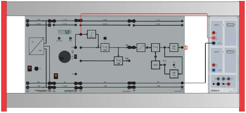
Part Five: DSBSC synchronous demodulation
Experiment set-up: Assemble the components as shown below. Set the function generator
to: sine, AM = 2 V and fM = 2 kHz
• Set the phase controller on the CF transmitter to far left limit. Feed the DSB signal
from the output of the modulator M2 directly into the demodulator D2 (do not use
channel filter CH2!). Using a connecting lead feed the carrier signal (fC = 20 kHz) of
Experiment #1: AM and DSBsc Modulation and Demodulation
Page 7 of 8
the CF transmitter into the auxiliary carrier input of the demodulator D2. What have
you achieved by this?
• Load the CASSY Lab 2 example Diagram 3.3-1.labx.
• Display the modulating signal SM(t) on CASSY lab 2 as well as the demodulated
signal SD(t) at the output of the LP filter of the CF receiver. Sketch the curve of the
modulating signal and the demodulated signal in Diagram 3.3-1. Tap the auxiliary
carrier for the demodulator D2 in front of the phase shifter of the CF transmitter.
• Start the measurement by pressing F9.
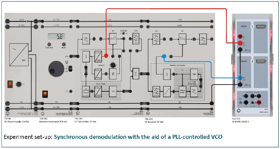
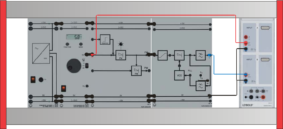
Part Six: DSBSC synchronous demodulation with the aid of a PLL-
controlled VCO
• Remove the cable connected to the auxiliary carrier input of the demodulator D2.
For this insert the bridging plug between the CARRIER RECOVERY and auxiliary
carrier input of D2. Use now for demodulation the recovered auxiliary carrier from
the PLL CARRIER RECOVERY. Assemble the experiment set-up as shown below.
• Sketch the pilot tone of the transmitter and the recovered signal in the receiver at
the output of the PLL circuit in Diagram 3.3-2.
• Load the CASSY Lab 2 example Diagram 3.3-2.labx.
Experiment #1: AM and DSBsc Modulation and Demodulation
Page 8 of 8
• Start the measurement by pressing F9.
Questions
Q.1. What is meant by modulation? Mixing?
Q.2. Name the reasons for performing modulation!
Q.3. In DSB the carrier's peak values are affected by the instantaneous value of the message
signal, but the spectrum shows that the carrier amplitude remains constant! How do
you explain the apparent contradiction?
Q.4. Define amplitude deviation and the modulation index.
Q.5. Which methods of AM demodulation are you familiar with and how do they differ?
Q.6. How high is the maximum efficiency in DSB? How can the efficiency be increased?
Experiment #2
Single Sideband AM (SSB) and Ring Modulator
Prelab:
• Theoretical Review
Review the AM and SSB modulation techniques from the text book of the courses
ENEE3303 and ENEE339.
• Matlab Simulation
Using Matlab software and Simulink, to show graphically the time domain of SSB-SC
modulated Signal. Taking the modulating signal
tt
m)1500
(
2cos
)(
π
=
and the carrier signal
ttc )100000(2
cos4)(
π
=
.
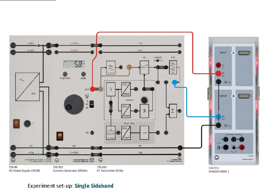
Part One: SSB with Residual Carrier (SSBRC) Modulation
Experiment set-up: Set up the experiment as specified below. Connect the output of the
function generator directly to the AF input of the modulator M2. Set the function generator
to: sinusoidal, AM = 2 V and fM = 2 kHz.
Experiment #2: Single Sideband AM (SSB) and Ring Modulator
ECE Department ENEE4103 – Communications Lab Page 2 of 8
• Set the toggle switch to CARRIER ON.
• Feed a sine signal from the function generator with f = 2 kHz, A = 1.5 V
• Display the output signal of the channel filter CH2 and the modulating signal sM(t) of
the function generator on Sensor - CASSY 2 - Starter and sketch the signals.
(Modulation product on channel B, modulating signal on channel A of Sensor -
CASSY 2 - Starter).
• Load the CASSY Lab 2 example Diagram 4.1-1.labx.
• Start the measurement by pressing F9.
• Shift the AF signal to the upper or lower envelope curve of the AM signal. Vary the
frequency fM and the amplitude AM of the modulating signal. What do you observe?
• Trigger to the modulating signal sM(t).
o Switch the modulating signal off.
o Measure the un-attenuated carrier amplitude AC at the input of the channel
filter
o Measure the amplitude ARC of the attenuated carrier at the output of the
channel filter.
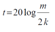
o Calculate the ratio k = ARC/AC.
o Determine the carrier suppression t in dB according to the equation
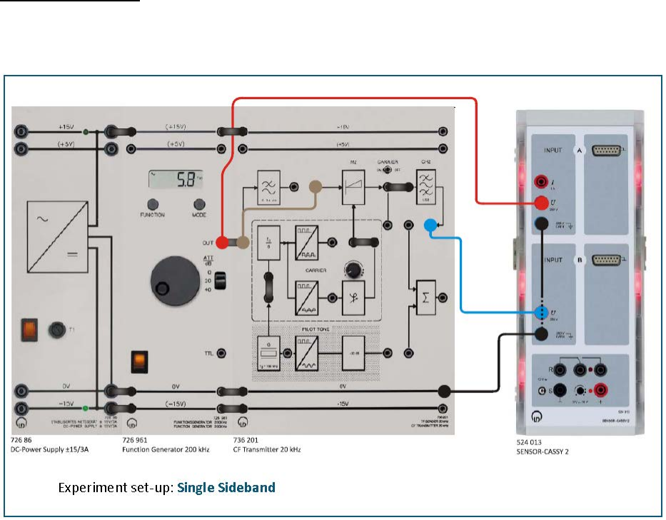
Experiment #2: Single Sideband AM (SSB) and Ring Modulator
ECE Department ENEE4103 – Communications Lab Page 3 of 8
Part Two: SSB with Suppressed Carrier (SSBSC) Modulation
Experiment set-up: Set up the experiment as specified in the next figure. Connect the
output of the function generator directly to the AF input of the modulator M2. Set the
function generator to: sinusoidal, AM = 2 V and fM = 2 kHz.
• Keep the experiment setup as in part one but set the toggle switch to CARRIER OFF.
• Load the CASSY Lab 2 example Diagram 4.1-2.labx.
• Start the measurement by pressing F9.
• What features does the SSBSC signal have?
Part Three: Spectrum of the SSBRC
• Keep the experiment setup as in part one, make sure that the toggle switch is set to
the CARRIER ON position.
• As the modulating signal use a sinusoidal signal with AM = 2 V and fM = 1 kHz. Feed
the modulating signal into the input LP filter of the CF transmitter.
Experiment #2: Single Sideband AM (SSB) and Ring Modulator
ECE Department ENEE4103 – Communications Lab Page 4 of 8
• Measure the SSB spectrum in the range of approx. 15 kHz up to 25 kHz obtained
from:
o Label the spectral lines.
o Determine the transmission bandwidth of the AM signal based on the
measurements.
o Generalize the results for the case of any modulating signals.
Part Four: Spectrum of the SSBSC
• Keep the experiment setup as in part one, make sure that the toggle switch is set to
the CARRIER OFF position.
• As the modulating signal use a sinusoidal signal with AM = 2 V and fM = 2 kHz. Feed
the modulating signal into the input LP filter of the CF transmitter.
• Measure the SSB spectrum in the range of approx. 15 kHz up to 25 kHz obtained
from:
o Label the spectral lines.
o Determine the transmission bandwidth of the AM signal based on the
measurements.
o Generalize the results for the case of any modulating signals.
Experiment #2: Single Sideband AM (SSB) and Ring Modulator
ECE Department ENEE4103 – Communications Lab Page 5 of 8
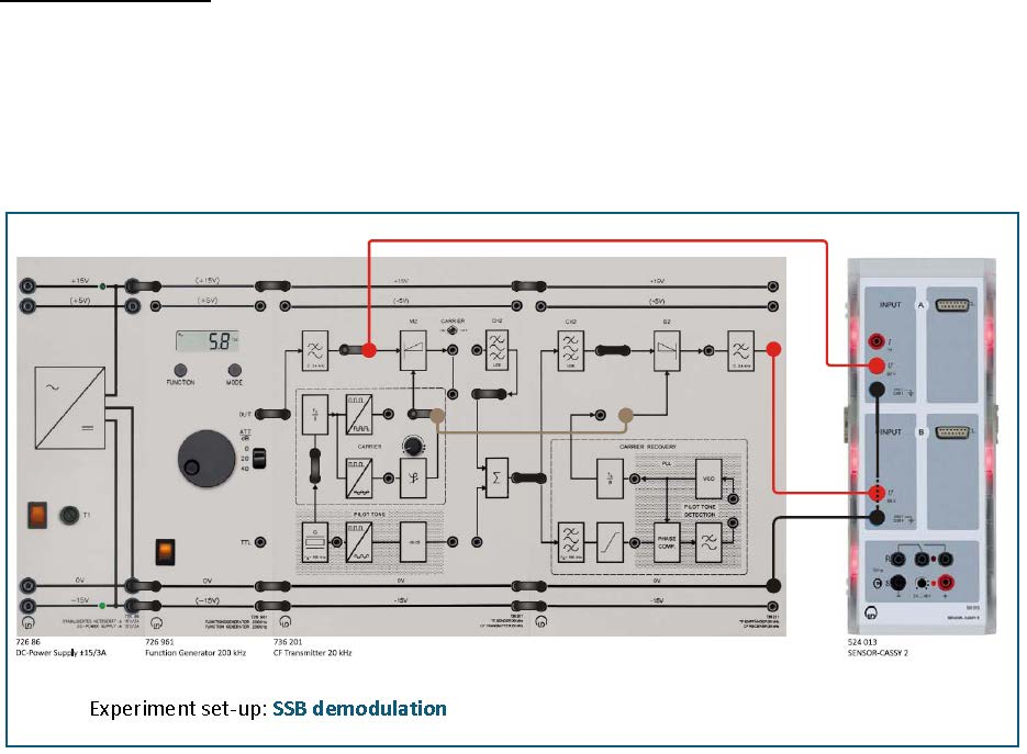
Part Five: SSBRC demodulation
Experiment set-up: Set up the experiment as specified below. Start with the settings of the
Sensor-CASSY 2. Load the CASSY Lab 2 example Diagram 4.1-1.labx. With the aid of a
connecting lead feed the carrier signal (fC = 20 kHz) of the CF transmitter directly into the
RF input of the demodulator D2. What have you achieved by this? Set the function
generator to: sinusoidal, AM = 2 V and fM = 2 kHz.
• Display the modulating signal sM(t) on Sensor-CASSY 2 - Starter as well as the
demodulated signal sD(t) at the output of the LP filter of the CF receiver.
• Load the CASSY Lab 2 example Diagram 4.3-1.labx.
• Start the measurement by pressing F9.
• Adjust the phase between the original carrier of the transmitter and the auxiliary
carrier of the receiver. What do you observe?
Experiment #2: Single Sideband AM (SSB) and Ring Modulator
ECE Department ENEE4103 – Communications Lab Page 6 of 8
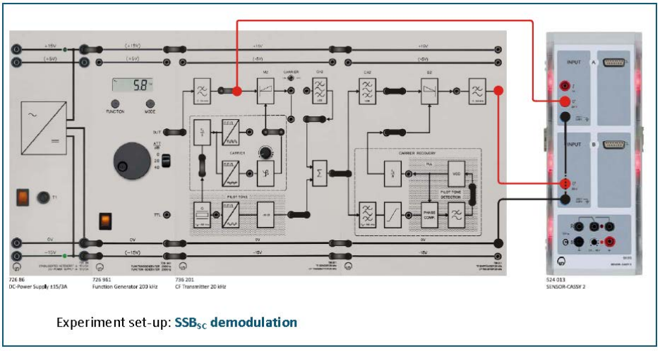
Part Six: SSBRC demodulation
• Remove the connecting lead between the CF transmitter and the demodulator.
• Now for the demodulation use the recovered auxiliary carrier from the PLL circuit
to recover the carrier.
• For this connect the bridging plug between CARRIER RECOVERY and the auxiliary
carrier input of D2.
• Discuss your findings.
• Set the toggle switch to CARRIER OFF.
• This time repeat the experiment for SSBSC.
• Load the CASSY Lab 2 example Diagram 4.3-2.labx.
• Start the measurement by pressing F9.
Experiment #2: Single Sideband AM (SSB) and Ring Modulator
ECE Department ENEE4103 – Communications Lab Page 7 of 8
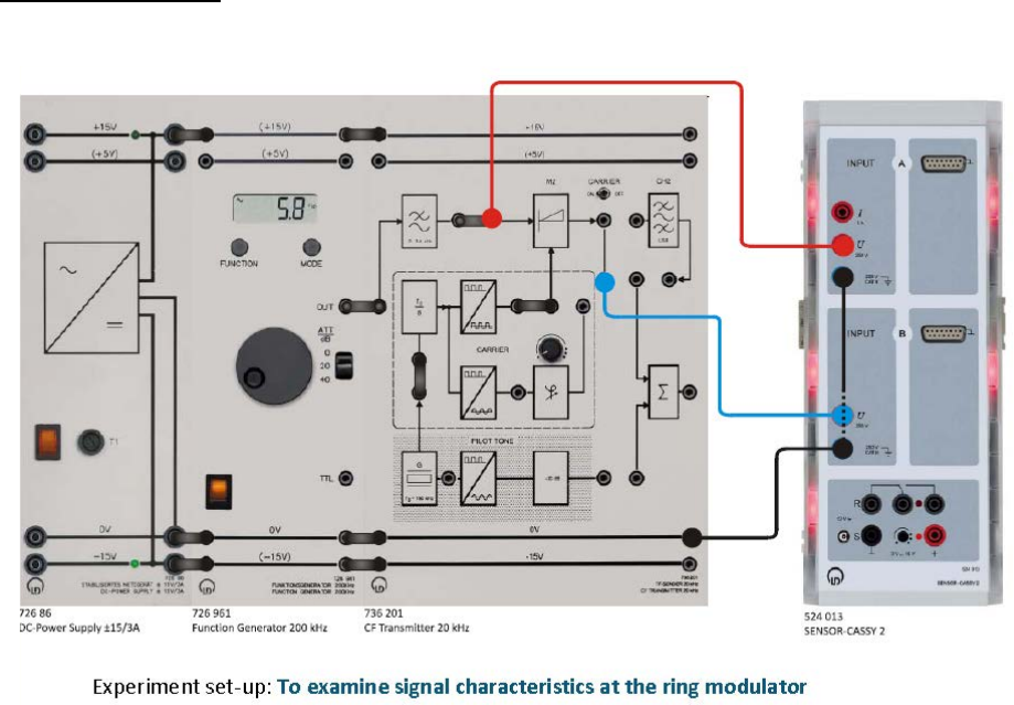
Part Seven: The Ring Modulator
Experiment set-up: Operating the CF transmitter as a ring modulator, set up the
experiment as specified in the following figure.
• Display the modulating AF signal and the output signal of the modulator on Sensor-
CASSY 2 - Starter. Sketch the signal in Diagram 5.1-1.
• Set the toggle switch to CARRIER OFF.
• Use the bridging plug to feed the square-wave carrier into the RF input of the
modulator.
• Feed a sinusoidal signal with fM = 2 kHz and AM = 2 V as the modulating signal into
the AF input of the modulator.
• Load the CASSY Lab 2 example Diagram 5.1-1.labx.
• Start the measurement by pressing F9
• Repeat the experiment with CARRIER ON.
• Load the CASSY Lab 2 example Diagram 5.1-2.labx.
• Start the measurement by pressing F9.
Experiment #2: Single Sideband AM (SSB) and Ring Modulator
ECE Department ENEE4103 – Communications Lab Page 8 of 8
Part Eight: Spectrum at the output of the ring modulator
• Set the toggle switch to CARRIER OFF! Record the spectrum of the modulation
product at the output of the modulator M2 in the range 0.5 kHz...150 kHz.
• Load the CASSY Lab 2 example Diagram 5.1-3.labx.
• Start the measurement by pressing F9.
Questions
Q.1. In radio links the carrier is normally attenuated to 5%...10%. What advantages does
this have compared to transmission with 100% carrier amplitude? Why isn't the carrier
completely suppressed?
Q.2. Which methods of carrier suppression are there?
Q.3. Which demodulation method is used for AM with suppressed carrier?
Experiment #3
Angle Modulation – Part 1
Prelab: Matlab Simulation
Consider the frequency modulated signal:
)]2sin(4)17(2cos[)( tttS
ππ
+=
a. Find the message signal m(t).
b. Plot s(t) versus t for -1 ≤ t ≤ 1.
c. Differentiate s(t) with respect to t and plot ds(t)/dt for -1 ≤ t ≤ 1. Notice how this
operation transforms an FM waveform into an AM waveform.
d. Apply ds(t)/dt to an ideal envelope detector, subtract the dc term and show that the
detector’s output is linearly proportional to m(t).
Part One: Dynamic response of FM
Experiment set-up: Assemble the components as shown below
Experiment #3: Angle Modulation – Part 1
ECE Department ENEE4103 – Communications Lab Page 2 of 5
• Set the carrier frequency to center position: fC = 20 kHz approx.
• Use a sinusoidal signal with AM = 20 Vpp and fM = 1.0 kHz of the function generator
as the modulating signal sM(t). Feed the modulating signal into the input of the FM
modulator.
• Load the CASSY Lab 2 example FM_TD.labx.
• Start the measurement by pressing F9.
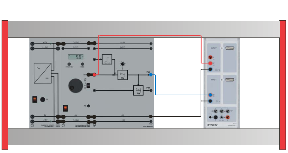
Part Two: The Characteristic of the FM Modulator
Experiment set-up: Use the same setup in Part One
• Load the CASSY Lab 2 example FM_FFT.labx.
• Start the measurement by pressing F9.
• With the potentiometer, set the frequency of the carrier line to fc = 20.0 kHz.
• Use a DC-signal with -10 V of the function generator as input signal.
• Feed the DC-signal into the input of the FM modulator.
• Determine the frequency fC of the carrier from the spectrum.
• Enhance the DC voltage in steps of 1 V and repeat each time the measurement of the
carrier frequency fc = fVCO.
• Note all frequency values in the table.
• Draw the characteristic carrier frequency versus the control voltage of the VCO for
U1=-10, -9, -8, … , -1, 0, 1, 2, … , 8, , 10
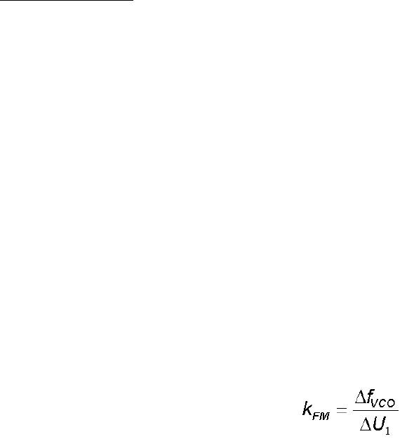
• Determine the coefficient of the FM modulator:
Experiment #3: Angle Modulation – Part 1
ECE Department ENEE4103 – Communications Lab Page 3 of 5
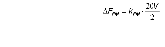
Part Three: Determination of the frequency deviation
The maximum frequency deviation depends of the coefficient of the FM modulator and the
amplitude of the modulating signal.
Part Four: Measurements in the frequency domain of FM
Experiment set-up: Use the same setup in Part One
• Remove the bridging plug from the function generator to the FM modulator.
• Load the CASSY Lab 2 example FM_FFT.labx.
• Start the measurement by pressing F9.
• Set the carrier frequency to 20.0 kHz with the potentiometer.
• Reconnect the function generator to the FM modulator with the bridging plug again.
• Use a sinusoidal signal with AM = 20 Vpp (= amplitude 10 V) and fM = 300 Hz of the
function generator as the modulating signal sM(t). Hints:
o The function generator displays peak to peak values.
o Reset the DC offset to 0 V=.
• Feed the modulating signal into the input of the FM modulator.
• Sketch the graph of the FM spectrum.
• Interpret the result.
• Repeat the measurement of the FM spectrum for a modulating signal AM = 20 Vpp and fM
= 200 Hz.
Part Five: Determining the carrier zero crossings by varying the
frequency deviation ΔFFM.
• Use a sinusoidal signal with AM = 0 Vpp and fM = 100 Hz of the function generator as the
modulating signal sM(t).
• Feed the modulating signal into the input of the FM modulator.
• Load the CASSY Lab 2 example FM_FFT.labx.
• Start the measurement by pressing F9.
• Slowly enhance the amplitude of the modulating signal AM of the function generator.
• Observe the decay of the carrier line.
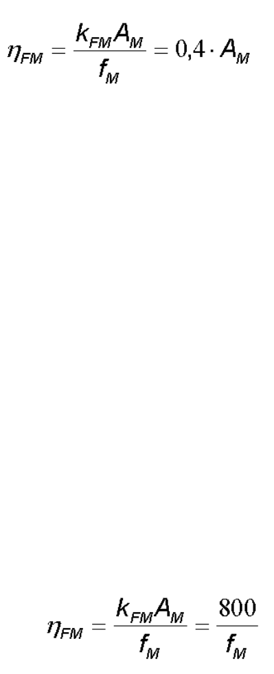
Experiment #3: Angle Modulation – Part 1
ECE Department ENEE4103 – Communications Lab Page 4 of 5
• Note the values of the amplitudes AM of the modulating signal, when the carrier line
disappears. Hint: the function generator displays peak to peak values.
• Enter your measurements into the table and calculate the modulation index η.
• Sketch the graph of the FM spectrum for the first carrier zero crossing.
With AM the amplitude of the modulating signal in V and a fix modulating frequency
fM = 100 Hz.
Part Six: Determine the carrier zero crossings by varying the modulating
frequency fM.
• Use a sinusoidal signal with AM = 20 Vpp (amplitude 10 V) and fM = 3.0 kHz of the function
generator as the modulating signal sM(t). Feed the modulating signal into the input of the
FM modulator.
• Load the CASSY Lab 2 example FM_FFT.labx.
• Start the measurement by pressing F9.
• Slowly reduce the frequency of the modulating signal fM of the function generator.
Observe the decay of the carrier line.
• Sketch the graph of the FM spectrum for the first carrier zero crossing.
• Note the values of the frequencies of the modulating signal fM when the carrier line
disappears.
Enter your measurements into the table and calculate the modulation index η.
With fM the frequency of the modulating signal in Hz and a fix amplitude AM = 20 Vpp.
Experiment #3: Angle Modulation – Part 1
ECE Department ENEE4103 – Communications Lab Page 5 of 5
Part Seven: FM spectrum for square wave modulation
• Use a square wave signal with AM = 20 Vpp (amplitude 10 V, duty cycle 50%) and fM =
200 Hz of the function generator as the modulating signal sM(t).
• Feed the modulating signal into the input of the FM modulator.
• Load the CASSY Lab 2 example FM_FFT.labx.
• Start the measurement by pressing F9.
• Sketch the graph of the FM spectrum.
• Interpret the results.
Questions
Q.1. Which carrier parameters can be used for angle modulation?
Q.2. Which angle modulation method is least affected by noise? Why?
Q.3. In FM with η = 1.0 how high are the amplitudes of the 1st sideline compared to AM for
m = 100%? Given that the amplitude of the unmodulated carrier is AC = 1 V.
Experiment #4
Angle Modulation – Part 2
Part One: FM demodulation for loop filter τ2
To carry out this experiment, assemble the components as shown below.
A) Time response of the FM modulating system
• Feed the modulating signal into the input of the FM modulator.
• Set the loop filter of the FM demodulator to τ2.
• Use a sinusoidal modulating signal sM(t) with AM = 10 Vpp and fM = 500 Hz.
• Measure at the input of the FM modulator and at the output of the FM demodulator.
• Load the CASSY Lab 2 example FM_TDem.labx.
• Start the measurement by pressing F9. Hint: If necessary, correct the frequency of the
• carrier line to fC = 20.0 kHz (without modulating signal).
• Sketch the time responses of the modulating signal sM(t) and the demodulated signal
sD(t).
Experiment #4: Angle Modulation – Part 2
ECE Department ENEE4103 – Communications Lab Page 2 of 7
B) Transfer characteristic of the FM modulating system
• Use a sinusoidal modulating signal sM(t) with AM = 2 Vpp and initially fM = 500 Hz.
• Load the CASSY Lab 2 example FM_FFT_Dem.labx.
• Start the measurement by pressing F9.
• Determine the amplitude of the demodulated signal AD with the spectrum analyser.
• Note the value into the table.
• Enhance the frequency of the modulated signal in steps of 500 Hz and repeat the
measurement (up tp 5000 Hz).
• Sketch the results in a diagram.
Part Two: FM demodulation for loop filter τ1
Repeat the experiment in Part eight while setting the loop filter of the FM demodulator to τ1.
Part Three: FM preemphasis
Experiment set-up: Assemble the components as shown.
• Set the loop filter of the FM demodulator to τ2.
• Set the function generator to a sinusoidal modulating signal sM(t) with AM = 5 Vpp and
initially fM = 500 Hz.
Experiment #4: Angle Modulation – Part 2
ECE Department ENEE4103 – Communications Lab Page 3 of 7
A) Time characteristic of the input signals
• Measure at the input of the preemphasis stage with channel A of the Sensor-CASSY2.
• Load the CASSY Lab 2 example FM_PreDem.labx.
• Start the measurement by pressing F9.
• Sketch the time response of the modulating signal sM(t).
• Set the function generator sequentially to 1000 Hz and 2000 Hz. Repeat the
measurement by pressing F9 again.
• Sketch the time response of the input signal of the preemphasis stage.
B) Time characteristic of the output signals
• Repeat the experiment above, after carrying out the following changes.
• Set the function generator to a sinusoidal modulating signal sM(t) with AM = 5 Vpp and
initially fM = 500 Hz.
• Set the loop filter of the FM demodulator to τ2.
• Measure at the output of the FM demodulator low pass filter () with channel A of the
Sensor-CASSY2.
• Load the CASSY Lab 2 example FM_PreDem.labx.
• Start the measurement by pressing F9.
• Sketch the time response of the demodulating signal sD(t).
• Set the function generator sequentially to 1000 Hz and 2000 Hz. Repeat the
measurement by pressing F9 again.
• Sketch the time response of the output signal of the FM demodulator.
• Interpret your results.
Experiment #4: Angle Modulation – Part 2
ECE Department ENEE4103 – Communications Lab Page 4 of 7
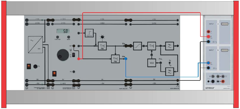
Part Four: Dynamic response of Phase Modulation (PM)
Experiment set-up: Connect the components as shown below.
• Set the carrier frequency to center position: fC = 20 kHz approx.
• Set the function generator to a sinusoidal modulating signal sM(t) with AM = 2 Vpp and fM =
1000 Hz.
• Feed the modulating signal sM(t) into the input of the PM modulator.
• Measure the modulating signal with channel A of the Sensor-CASSY2.
• Measure the PM signal at the output of the PM modulator with channel B of the Sensor
CASSY2.
• Load the CASSY Lab 2 example PM_TDscope.labx.
• Start the measurement by pressing F9.
• Interpret your results.
Part Five: Characteristic of the PM modulator
• Set the carrier frequency to center position: fC = 20 kHz approx.
• Set the function generator to DC.
• Feed a DC voltage U1 = -1.0 …+ 1.0V into the input of the PM modulator.
• Load the CASSY Lab 2 example PM_TD.labx.
• Start the measurement by pressing F9.
Experiment #4: Angle Modulation – Part 2
ECE Department ENEE4103 – Communications Lab Page 5 of 7
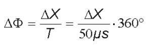
• Determine the phase shift ΔX/μs between the carrier oscillations of the FM and PM
output. Use Set Marker / Vertical Line and Measure Difference of CASSY Lab2 to
evaluate your measurements.
• Enter your results into the table and calculate the phase shift.
• Sketch the characteristic ΔX = f(U1) of the phase modulator.
• Sketch the time characteristics for -1.0 V and +1.0 V.
• Interpret your results.
Part Six: The PM Spectrum
• Measure the spectrum at the PM modulator output with channel B of the Sensor-
CASSY2.
• Load the CASSY Lab 2 example PM_FFT.labx.
• Start the measurement by pressing F9.
• Set the carrier frequency to 20.0 kHz with the potentiometer.
• Connect the function generator to the PM modulator input.
• Set the function generator to a sinusoidal modulating signal sM(t) with AM = 2 Vpp and fM =
300 Hz.
• Sketch the graph of the PM spectrum.
• Interpret the result.
• Repeat the measurement of the PM spectrum for a modulating signal AM = 2 Vpp and fM =
200 Hz.
Experiment #4: Angle Modulation – Part 2
ECE Department ENEE4103 – Communications Lab Page 6 of 7
Part Seven: PM demodulation for loop filter τ2
Experiment set-up: Connect the components as shown.
• Set the toggle switch of the PM demodulator to τ2.
• Load the CASSY Lab 2 example PM_TDem.labx
• Start the measurement by pressing F9.
• Interpret your results.
Part Eight: PM demodulation for loop filter τ1
• Set the toggle switch of the PM demodulator to τ1.
• Repeat the experiment in Part seven
Experiment #4: Angle Modulation – Part 2
ECE Department ENEE4103 – Communications Lab Page 7 of 7
Questions
Q.1. What does preemphasis mean?
Q.2. When is deemphasis used in FM demodulation? How does it function?
Q.3. Assuming in FM that the spectrum for a harmonic signal A1 = 5 V and fM1 = 1000 Hz is known.
Can conclusions be drawn regarding the spectrum, which is produced for a different harmonic
modulation signal, with, for example A1 = 3 V and fM1 = 100 Hz? Compare this with AM!
Experiment #5
Pulse Amplitude Modulation (PAM)
Part One: Time and Frequency Characteristics of pulse train
To carry out this experiment, assemble the components as shown below.
• Select a pulse train at the function generator with fp = 1 kHz, pulse amplitude AP = 5 V
(10 Vpp) and duty cycle = 1
⁄= 1 10
⁄.
• Load the CASSY Lab 2 example PulseTime.labx.
• Start the measurement by pressing F9
• Determine the time characteristic of the pulse train.
• Determine the spectrum of the pulse train. Load the CASSY Lab 2 example PulseFFT.labx.
• Where are in general the zero crossings in the envelope of the pulse spectrum?
• How many spectral lines l arise between two zero crossings of the envelope (syncfunction)?
• Repeat the measurement of the spectra and time characteristics for the same pulse
frequency fP = 1 kHz and pulse amplitude AP for different duty cycles 2
⁄= 2 10
⁄,
3
⁄= 3 10
⁄, 4
⁄= 4 10
⁄, 5
⁄= 5 10
⁄ and 6
⁄= 9 10
⁄. Proceed as described
above.
• Why do pulse trains require large transmission bandwidths?
Experiment #5: Pulse Amplitude Modulation (PAM)
ECE Department ENEE4103 – Communications Lab Page 2 of 6
• What is the structure of the spectrum of a pulse train?
• What kind of characteristic curve is the envelope curve of the pulse spectrum?
Part Two: Time Characteristics of Pulse Amplitude Modulation (PAM)
To carry out this experiment, assemble the components as shown below.
Adjusting the sampling frequency
• The sampling frequency fP is set using the FFT analyzer. For that purpose set the PAM
modulator:
o Controller for duty cycle
⁄ PCM
o Controller for sampling frequency fP - … (max)
o CASSY UB1 Clock generator G.
• Load the CASSY Lab 2 example pulse frequency5000.labx.
• Start the measurement by pressing F9
• Now slowly adjust the pulse frequency fP, until the spectral line of the fundamental mode
appears at f0 = 5000 Hz (3f0 = 15 kHz, etc). Don’t change the sampling (pulse) frequency fP
anymore.
Time characteristic of the PAM
Measure the Input and output of the channel filter CH1.
• Function generator: Sine, 500 Hz, A = 10 Vpp.
Experiment #5: Pulse Amplitude Modulation (PAM)
ECE Department ENEE4103 – Communications Lab Page 3 of 6
• CASSY UA1 Input of channel filter CH1.
• CASSY UB1 Output of channel filter CH1.
• Load the CASSY Lab 2 example PAMTimeInOut.labx.
• Start the measurement by pressing F9.
Display the time characteristic of the PAM.
• Function generator: Sine, 500 Hz, A = 10 Vpp.
• CASSY UA1 Input PAM Modulator channel CH1.
• CASSY UB1 Output PAM1.
• Load the CASSY Lab 2 example PAMTime.labx.
• Start the measurement by pressing F9.
• Repeat the measurement at the output PAM2.
Measure the modulating signal sM(t) and the demodulated signal sD(t) as a function of the
duty cycle.
• Now: Controller for the sampling frequency fP … (max)
• Adjusting the duty cycle:
o CASSY UB1 Clock generator G.
o Load the CASSY Lab 2 example DutyCycle.labx.
o Start the measurement by pressing F9.
• Slowly readjust the duty cycle
⁄, until the display of the CASSY instrument shows
⁄ = 50% Eventually correct the display, for that make a right click into the instrument
Duty Cycle and match the factor 1.1 to your special situation. For the maximum position
(PCM) is true:
⁄ = 50%
• CASSY UA1 Input of channel filter CH1 at PAM modulator.
• CASSY UB1 Output of channel filter CH1 at PAM demodulator.
• Load the CASSY Lab 2 example PAMModDem.labx.
• Start the measurement by pressing F9.
• Repeat the measurement for
⁄ = 30% and
⁄ = 10%
• Sketch your results.
Experiment #5: Pulse Amplitude Modulation (PAM)
ECE Department ENEE4103 – Communications Lab Page 4 of 6
Variants
• Measure the input- and output signal of the channel filter CH1 for different frequencies
and signal forms.
• Display the PAM signal for different duty cycles.
• Investigate the function of the hold stage at the PAM demodulator (TH). Measure the
pulse width as a function of TH.
Part Three: Spectra of Pulse amplitude modulation (PAM)
The PAM1 spectrum as a function of the frequency of the modulating signal.
• All measurement are made for fP = 5000 Hz.
• Function generator: Sine, 500 Hz, A = 10 Vpp.
• CASSY UA1 Output PAM1 at PAM modulator.
• CASSY UB1 Output of the clock generator.
• Load the CASSY Lab 2 example PAMFFT.labs.
• Start the measurement by pressing F9.
• Repeat the measurement for fM = 1 kHz and fM = 2 kHz.
• Sketch your results.
The PAM1-Spectrum as a function of the duty cycle.
• Function generator: Sine, 1000 Hz, A = 10 Vpp.
• CASSY UA1 Output PAM1 at PAM modulator.
• CASSY UB1 clock generator G.
• Setting of the duty cycle:
• Load the CASSY Lab 2 example DutyCycle.labs.
• Start the measurement by pressing F9.
• Set the duty cycle to
⁄ = 30%.
• Load the CASSY Lab 2 example PAMFFT.labs.
• Start the measurement by pressing F9.
• Sketch your results. Mark in the spectrum the position of the suppressed carrier lines.
Compare the PAM spectra with the pulse spectra. What is the behavior of the upper side
lines USL with regard to the frequency of the modulating signal fM? What is the behavior
of the lower side lines LSL?
Experiment #5: Pulse Amplitude Modulation (PAM)
ECE Department ENEE4103 – Communications Lab Page 5 of 6
The PAM2 spectrum as a function of the frequency of the modulating signal.
• All measurement are made for fP = 5000 Hz. Follow the hints Adjusting the sampling
frequency.
• Function generator: Sine, 500 Hz, A = 10 Vpp.
• CASSY UA1 Output PAM2 at PAM modulator.
• CASSY UB1 Output of the clock generator.
• Load the CASSY Lab 2 example PAMFFT.labs.
• Start the measurement by pressing F9.
• Repeat the measurement for fM = 1 kHz and fM = 2 kHz.
• Sketch your results.
Part Four: Subsampling in the Frequency Domain
• Function generator: Sine, 3000 Hz, A = 5 Vpp.
• CASSY UA1 Output PAM1 at the PAM modulator.
• CASSY UB1 Clock generator G.
• For the setting of the sampling frequency fP = 5000 Hz: Load the CASSY Lab 2 example
pulse frequency5000.labs.
• For the setting of the duty cycle
⁄ = 20 %: Load the CASSY Lab 2 example
DutyCycle.labs.
• For the spectrum: Load the CASSY Lab 2 example PAMFFT.labs.
• Start the measurement by pressing F9.
• Sketch the results.
Part Five: Subsampling in the Time Domain
• Function generator: Sine, 3000 Hz, A = 5 Vpp.
• CASSY UA1 Input of the PAM modulators
• CASSY UB1 Output PAM1 at the PAM modulator
• Load the CASSY Lab 2 example PAMTime.labs.
• Start the measurement by pressing F9.
• Display the modulating signal sM(t) and the demodulated signal sD(t) at subsampling.
Experiment #5: Pulse Amplitude Modulation (PAM)
ECE Department ENEE4103 – Communications Lab Page 6 of 6
Part Six: PAM time multiplex
To carry out this experiment, assemble the components as shown below.
Display the time characteristic of the time multiplex signal.
• Sampling frequency fP = 5000 Hz, duty cycle maximal.
• Function generator 1: Triangle, fM1 = 200 Hz, A = 5 Vpp.
• Function generator 2: Sine, fM2 = 300 Hz, A = 10 Vpp.
• CASSY UA1 Input PAM modulator channel CH1.
• CASSY UB1 Output PAM modulator PAM1.
• Load the CASSY Lab 2 example PAMTDMInput.labx.
• Start the measurement by pressing F9.
PAM demodulator time shift Δt left/middle
• CASSY UA1 Output PAM demodulator channel CH1.
• CASSY UB1 Output PAM demodulator channel CH2.
• Load the CASSY Lab 2 example PAMTDMOutput1.labx.
• Start the measurement by pressing F9.
Experiment #6
Pulse Code Modulation (PCM) – Part 1
Part One: Linear Quantization
To carry out this experiment, assemble the components as shown below.
• By pressing several times MODE set the PCM modulator and PCM demodulator to: PCM,
linear quantization (watch the allocated LEDs).
• Activate all bits. For that press the button SELECT, until all (red) LEDs in the PCM
modulator indicate ACTIVE. In the further course of the experiment: Deactivate bits from the
LSB (button SELECT and ON / OFF, see below).
• At the PCM modulator: turn slowly the potentiometer for DC voltage. In the range of small
inputs (< –10 V) overload of the A/D-Converter may occur. This means a sudden decrease
of voltage 0 V –9,5 V. It is not critical eventually start your measurement from ca. – 9,5 V.
• Turn the potentiometer completely to the left.
• Load the CASSY Lab 2 example Quant.labx.
• Start the measurement by pressing F9.
• Turn the potentiometer to the right. This produces an input voltage at the PCM-Modulators
(736 101) which is slowly rising from –10 V to +10 V. This input voltage is displays as
Experiment #6: Pulse Code Modulation (PCM) – Part 1
ECE Department ENEE4103 – Communications Lab Page 2 of 3
voltage UA1. The output voltage (after quantization) at the PCM Demodulator (736 111) is
displayed as voltage UB1.
• After recording the quantization characteristic, stop the measurement by pressing F9.
Part Two: Non-linear Quantization
• Press the MODE button of the PCM modulator and PCM demodulator one time. Now both
systems are in the mode non-linear quantization (watch the allocated LEDs in the 13
segment characteristic).
• Repeat the measurement in Part 1.
Part Three: Compressor / Expander characteristic
• For plotting the compressor/expander characteristic only one device is operated in the
nonlinear mode, while the other device runs in the linear mode.
Part Four: Resolution of Quantizer
• Reduction of the resolution from 8 to 5 bits. For this deactivate the three least significant bits
(LSB) of the PCM modulator by pressing of SELECT and ON/OFF. Repeatedly pressing
SELECT leads to the position of the desired bit. ON/OFF toggles between active/inactive.
• Turn the potentiometer back to left and repeat the recording of the quantization
characteristic.
Experiment #6: Pulse Code Modulation (PCM) – Part 1
ECE Department ENEE4103 – Communications Lab Page 3 of 3
Part Five: Encoding
To carry out this experiment, assemble the components as shown below.
• By pressing several times MODE set the PCM modulator and PCM demodulator to: PCM,
linear quantization (watch the allocated LEDs).
• Activate all bits. For that press the button SELECT, until all (red) LEDs in the PCM
modulator indicate ACTIVE.
• Load the CASSY Lab 2 example Code.labx.
• Set the potentiometer to maximum left.
• Vary the DC voltage UA1 with the potentiometer according to the values in the table. Note
the output voltage of the PCM demodulator UB1 and the corresponding bit pattern (green
LEDs).
• Demonstrate the relationship between the formation of the serial data packets and the “high
bits” display. Which of the bits is the LSB in the data packets? Which one is used for coding
the polarity?
ECE Department ENEE4103 – Communications Lab Page 1 of 4
Experiment #7
Pulse Code Modulation (PCM) – Part 2
Part One: PCM Transmission
To carry out this experiment, assemble the components as shown below.
• CASSY UA1 Input PAM Modulator CH1.
• CASSY UB1 Output PAM Demodulator CH1.
• Switch on the power supply.
• By pressing several times MODE set the PCM modulator and PCM demodulator to: PCM,
linear quantization (watch the allocated LEDs).
• Activate all bits. For that press the button SELECT, until all (red) LEDs in the PCM
modulator indicate ACTIVE.
• PAM Modulator
o Controller for the duty cycle
� PCM
o Controller for the sampling frequency fP PCM
• Function generator 1: Sine, fM1 = 300 Hz, A = 10 Vpp.
• Function generator 2: Triangle, fM2 = 200 Hz, A = 5 Vpp.
• PAM Demodulator
• Time shift ∆ links
1. Part of the experiment
• Load the CASSY Lab 2 example PCMTrans.labx.
• Start the measurement by pressing F9.
Experiment #7: Pulse Code Modulation (PCM) – Part 2
Page 2 of 4
2. Part of the experiment (change CASSY-connections)
• CASSY UA1 Input PAM Modulator CH2.
• CASSY UB1 Output PAM Demodulator CH2.
Part Two: Quantization Noise
To carry out this experiment, assemble the components as shown below.
• CASSY UA1 Input PAM Modulator CH2.
• CASSY UB1 Output PCM Demodulator.
• Connect both channels (CH1 and CH2) of the PAM Modulator (736 061) with the function
generator. This avoids time gaps at the output of the PCM demodulator.
• Function generator: Triangle, 30 Hz, 12 Vpp
• By pressing several times MODE set the PCM modulator and PCM demodulator to: PCM,
linear quantization (watch the allocated LEDs).
• Activate all bits. For that press the button SELECT, until all (red) LEDs in the PCM
modulator indicate ACTIVE.
• Load the CASSY Lab 2 example QNoise.labx.
• Start the measurement by pressing F9.
• Sketch the measurement and give an interpretation.
• Repeat the experiment for a resolution of 5 bit.
• Repeat the experiment for a resolution of 5 bit and a frequency of the triangle signal
fM=300 Hz.
Experiment #7: Pulse Code Modulation (PCM) – Part 2
Page 3 of 4
Part Three: Quantization Noise Variations
• Repeat the same procedure of Part 2 but use a sinusoidal modulating signal. This results in
a more complicated structure of the quantization noise.
• Repeat the same procedure of Part 2 but use a non-linear quantization.
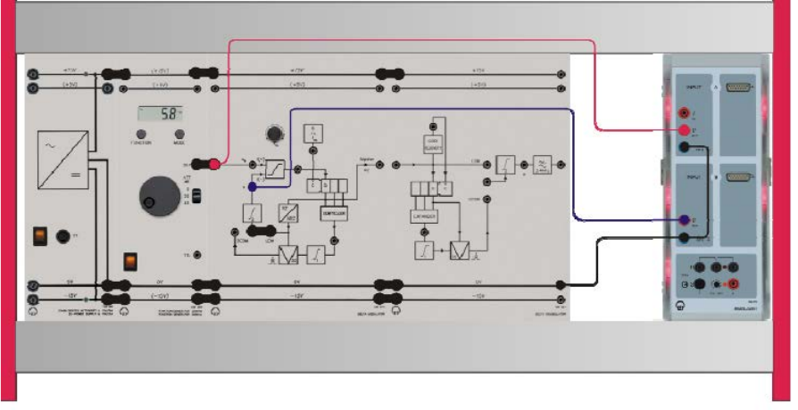
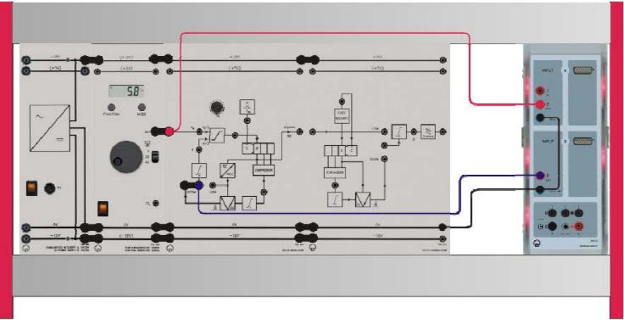
Part Four: Difference Pulse Code Modulation (DPCM)
To carry out this experiment, assemble the components as shown below.
• Switch on the power supply. Connect both channels (CH1 and CH2) of the PAM Modulator
(736 061) with the function generator. This avoids time gaps at the output of the PCM
demodulator.
• Function generator: Triangle, 30 Hz, 12 Vpp
• By pressing several times MODE set the PCM modulator and PCM demodulator to: PCM,
linear quantization (watch the allocated LEDs).
• Activate all bits. For that press the button SELECT, until all (red) LEDs in the PCM
modulator indicate ACTIVE.
• DPCM is a redundancy reducing method. In the predictor the difference to the previous
value is transmitted. At the start of the transmission it is important that the predictors in the
PCM modulator and in the PCM demodulator start from the same prediction value. During
switch-on the prediction value is initialized with 0. But since the two systems cannot be
switched on simultaneously, the following switch-on sequence has to be adhered to:
1. Connect the PAM input of the PCM modulator to 0 V.
2. Switch the PCM modulator to DPCM mode.
3. Switch the PCM demodulator to the DPCM mode.
4. Disconnect the PAM input of the PCM modulator from 0 V.
5. Drop the amplitude of the modulation signal to 0 V (on the function generator).
6. Feed the modulation signal into the PAM input of the PCM modulator and reset to the
7. desired amplitude
Experiment #7: Pulse Code Modulation (PCM) – Part 2
Page 4 of 4
• Step 5 has to be performed every time before selecting the ACTIVE BITS. Afterwards the
signal amplitude can be enhanced again.
• Load the CASSY Lab 2 example DPCM.labx.
• Start the measurement by pressing F9.
• Connect the channel UA1 of the CASSY with the input signal of the PAM modulator. With
channel UB1 of the CASSY record successively the following signals:
o PAM input
o Predictor of the DPCM modulator
o Output of the DPCM modulator
o Input of the DPCM demodulator
o Predictor of the DPCM demodulator
o PAM output of the DPCM demodulator
• Sketch your measurements and give an interpretation.
• Deactivate the following bits
• Repeat the experiment for a resolution of 4 bit.
Experiment #8
Delta Modulation – Part 1
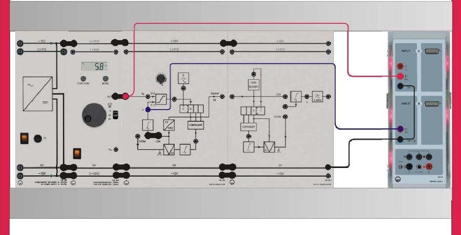
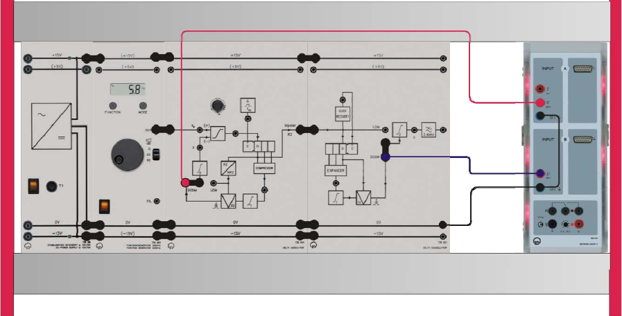
Part One: Prediction signals in Linear delta modulation (LDM)
To carry out this experiment, assemble the components as shown below.
• Settings on the DM system / function generator
o Clock frequency fCL 100 kHz (max.)
o Modulating signal sM sine, 100 Hz, 1 Vpp, ATT = 0 dB
o Delta modulator LDM, set the bridging plug
o Delta demodulator ----
• Connect the Sensor-CASSY 2 inputs:
o Input A → sM modulating signal
o Input B → X prediction signal at the output of the 2nd integrator
• Load the CASSY Lab 2 example Prediction.labs.
• Start the measurement by pressing F9.
• Jointly display on the monitor sM(t) and the prediction signal X(t).
• Reduce the clock frequency gradually to fCL = 10 kHz (min.)
• Repeat the measurement.
Experiment #8: Delta Modulation – Part 1
ECE Department ENEE4103 – Communications Lab Page 2 of 8
Part Two: Prediction signals in Digital Controlled Delta Modulation
(DCDM)
• For the same setup of part one
• Change the settings on the DM system / function generator
o Clock frequency fCL 100 kHz (max.)
o Modulating signal sM sine, 100 Hz, 1 Vpp, ATT = 0 dB
o Delta modulator DCDM, set the bridging plug
o Delta demodulator ----
• Repeat the measurements as in part one.
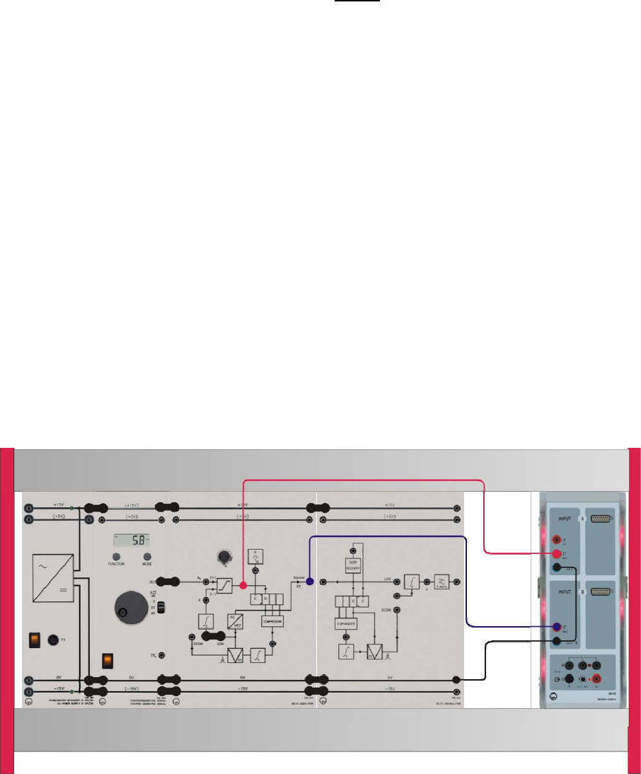
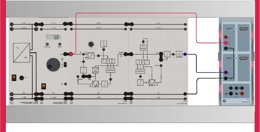
Part Three: Pulse height in LDM
To carry out this experiment, assemble the components as shown below.
• Settings on the DM system / function generator
o Clock frequency fCL 50 kHz
o Modulating signal sM(t) sine, 100 Hz, 7 Vpp, ATT = 0 dB
o Delta modulator LDM, set the bridging plug
o Delta demodulator ----
• Connect the Sensor-CASSY 2 inputs:
o Input A → sM modulating signal
o Input B → LDM signal at the output of the PAM modulator
• Load the CASSY Lab 2 example PulseAmplitude.labs.
Experiment #8: Delta Modulation – Part 1
ECE Department ENEE4103 – Communications Lab Page 3 of 8
• Start the measurement by pressing F9.
• Jointly display on the monitor sM(t) and the LDM signal.
• Set the clock frequency to approximately fCL ≈ 30…50 kHz, by setting the potentiometer into
the middle position. Then, the pulse signals show the smallest eye aperture (smallest pulse
heights in the waists).
Part Four: Pulse height in DCDM
• For the same setup of part three
• Change the settings on the DM system / function generator
o Clock frequency fCL 50 kHz
o Modulating signal sM(t) sine, 100 Hz, 7 Vpp, ATT = 0 dB
o Delta modulator DCDM, set the bridging plug
o Delta demodulator ----
• Repeat the measurements as in part three.
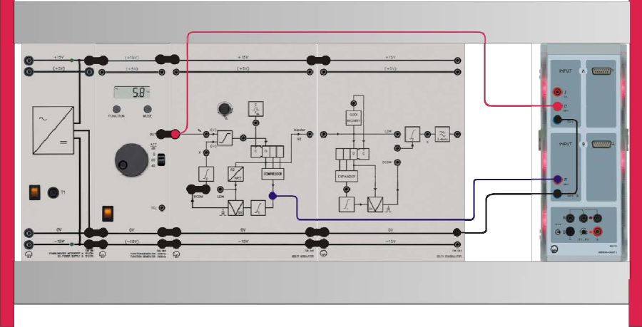
Part Five: Output signals of the LDM modulator
To carry out this experiment, assemble the components as shown below.
• Settings on the DM system / function generator
o Clock frequency fCL 30 kHz (approx.)
o Modulating signal sM(t) sine, 100 Hz, 4 Vpp, ATT = 0 dB
o Delta modulator LDM, set the bridging plug
o Delta demodulator ----
Experiment #8: Delta Modulation – Part 1
ECE Department ENEE4103 – Communications Lab Page 4 of 8
• Connect the Sensor-CASSY 2 inputs:
o Input A → sM modulating signal, function generator
o Input B → DM signal at the output of DM modulator (bipolar, RZ)
• Load the CASSY Lab 2 example DMCode.labs.
• Start the measurement by pressing F9.
• Jointly display on the monitor sM(t) and the DM signal.
• Load the CASSY Lab 2 example LDM_10kHz.labs (or DCDM_10kHz.labs)
• Start the measurement by pressing F9.
• Display sM(t) and the bipolar output signal of the delta modulator on the monitor.
Part Six: Output signals of the DCDM modulator
• For the same setup of part five
• Change the settings on the DM system / function generator
o Clock frequency fCL 30 kHz (approx.)
o Modulating signal sM(t) sine, 100 Hz, 4 Vpp, ATT = 0 dB
o Delta modulator DCDM, set the bridging plug
o Delta demodulator ----
• Repeat the measurements as in part five.
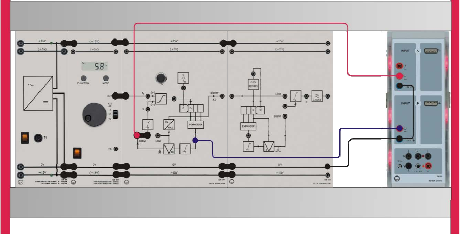
Part Seven: Clock and DM signals in RZ format
To carry out this experiment, assemble the components as shown below.
Experiment #8: Delta Modulation – Part 1
ECE Department ENEE4103 – Communications Lab Page 5 of 8
• Settings on the DM system / function generator
o Clock frequency fCL 10 kHz (min.)
o Modulating signal sM(t) sine, 200 Hz, 2 Vpp, ATT = 0 dB
o Delta modulator LDM, set the bridging plug
o Delta demodulator ----
• The type of DM signals is not important in this experiment. Thus no distinction is made
between LDM and DCDM mode. Consequently the experiments are carried out in LDM
mode only.
• Connect the Sensor-CASSY 2 inputs:
o Input A → Clock generator (G), fCL
o Input B → DM output (bipolar, RZ)
• Load the CASSY Lab 2 example Clock.labs.
• Start the measurement by pressing F9.
• Display the clock signal and the bipolar output signal of the delta modulator.
Part Eight: Clock and DM signals in NRZ format
• For the same setup of part seven
• Connect the Sensor-CASSY 2 inputs:
o Input A → Clock generator (G), fCL
o Input B → LDM output at the RZ/NRZ-converter
• Display the LDM signal in NRZ format and the bipolar output signal of the delta modulator
on the monitor.
Experiment #8: Delta Modulation – Part 1
ECE Department ENEE4103 – Communications Lab Page 6 of 8
Part Nine: Granular noise in LDM
To carry out this experiment, assemble the components as shown below.
• Settings on the DM system / function generator
o Clock frequency fCL 10 kHz (min.)
o Modulating signal sM(t) square 50%, 200 Hz, 2 Vpp, ATT = 0 dB
o Delta modulator LDM, set the bridging plug
o Delta demodulator ----
• Connect the Sensor-CASSY 2 inputs:
o Input A → modulating signal sM
o Input B → prediction signal X
• Load the CASSY Lab 2 example GranularNoise.labs.
• Start the measurement by pressing F9.
• Display the modulating signal sM(t) and the prediction signal X(t) on the monitor.
• Repeat the experiment for fCL = 30 kHz and fCL = 100 kHz.
• Remove the bridging plug between the function generator output and the input of the delta
modulator.
• Connect the input of the delta modulator to ground.
• Repeat the measurements for fCL = 10 kHz, fCL = 100 kHz.
Experiment #8: Delta Modulation – Part 1
ECE Department ENEE4103 – Communications Lab Page 7 of 8
Part Ten: Granular noise in DCDM
• For the same setup of part nine
• Settings on the DM system / function generator
o Clock frequency fCL 10 kHz (min.)
o Modulating signal sM(t) square 50%, 200 Hz, 2 Vpp, ATT = 0 dB
o Delta modulator DCDM, set the bridging plug
o Delta demodulator ----
• Repeat the measurements as in part nine.
Part Eleven: Slope overload in LDM
To carry out this experiment, assemble the components as shown below.
• Settings on the DM system / function generator
o Clock frequency fCL 100 kHz
o Modulating signal sM(t) sine, 100 Hz, 7 Vpp, ATT = 0 dB
o Delta modulator LDM, set the bridging plug
o Delta demodulator ----
• Connect the Sensor-CASSY 2 inputs:
o Input A → modulating signal sM
o Input B → prediction signal X
• Load the CASSY Lab 2 example SlopeOver.labs.
• Start the measurement by pressing F9.
• Display the modulating signal sM(t) and the prediction signal X(t) on the monitor.
Experiment #8: Delta Modulation – Part 1
ECE Department ENEE4103 – Communications Lab Page 8 of 8
• Set the function generator to: square-wave, 50%, 100 Hz, 4 Vpp.
• Repeat the measurement
• Increase the frequency of the square-wave signal to 300 Hz.
• Repeat the measurement
Part Twelve: Slope overload in DCDM
• For the same setup of part nine
• Settings on the DM system / function generator
• Clock frequency fCL 100 kHz
• Modulating signal sM(t) sine, 100 Hz, 7 Vpp, ATT = 0 dB
• Delta modulator DCDM, set the bridging plug
• Delta demodulator ----
• Repeat the measurements as in part eleven.
Experiment #9
Delta Modulation – Part 2
Part One: Dynamic of LDM and DCDM
A) Dynamic of LDM
To carry out this experiment, assemble the components as shown below.
• Settings on the DM system / function generator
o Clock frequency fCL 100 kHz (max.)
o Modulating signal sM sine, 100 Hz, ATT = 0 dB
o Delta modulator LDM, set the bridging plug
o Delta demodulator ----
• Connect the Sensor-CASSY 2 inputs:
o Input A → sM modulating signal
o Input B → X prediction signal at the output of the 2nd integrator
• Load the CASSY Lab 2 example SlopeOver.labs and start the measurement.
• Display the prediction signal X(t) on the monitor.
Experiment #9: Delta Modulation – Part 2
ECE Department ENEE4103 – Communications Lab Page 2 of 7
• Vary the amplitude AM of the modulating signal sM, until X demonstrates the beginnings of
slope overload (recognizable by the exponential distortion). This value is denoted as AMmax.
• Calculate the dynamic D.
=20
For AMmin use the value for granular noise (approx. 20 mVpp).
• Repeat the measurements for the frequency of the sM signal of 200, 300, 400, 500, 1000,
2000, 2500, 3000 Hz.
B) Dynamic of DCDM
• Repeat the measurements of part one A for DCDM.
• Compare your results with part one A.
Part Two: Coding and companding
A) LDM: Coding in the DM modulator
In delta modulation the coding of the differential values is performed by an edge triggered D-flip
flop, functioning as a sample and hold circuit. The differential values stem from the comparison
of the modulating signal and the prediction signal. With each clock pulse the bit present at the
D-input is shifted to the output and stored temporarily until the arrival of the next clock pulse.
To carry out this experiment, assemble the components as shown below.
Experiment #9: Delta Modulation – Part 2
ECE Department ENEE4103 – Communications Lab Page 3 of 7
• Settings on the DM system / function generator
o Clock frequency fCL 10 kHz (max.)
o Modulating signal sM sine, 100 Hz, 4 Vpp, ATT = 0 dB
o Delta modulator LDM, set the bridging plug
o Delta demodulator ----
• Connect the Sensor-CASSY 2 inputs:
o Input A → Comparator out (input D of the D-FF)
o Input B → DM output (bipolar/RZ)
• Load the CASSY Lab 2 example LDM_Code.labs and start the measurement.
• Display the DM signal (bipolar, RZ) and the signal at the comparator output on the monitor.
B) DCDM: Companding in the DM modulator
In the case of DCDM the companding principle is derived from the 0/1-distribution of the bits at
the shift register.
To carry out this experiment, assemble the components as shown below.
• Settings on the DM system / function generator
o Clock frequency fCL 50 kHz (approx. middle position)
o Modulating signal sM sine, 100 Hz, 15 Vpp, ATT = 0 dB
Experiment #9: Delta Modulation – Part 2
ECE Department ENEE4103 – Communications Lab Page 4 of 7
o Delta modulator DCDM, set the bridging plug
o Delta demodulator ----
• Connect the Sensor-CASSY 2 inputs:
o Input A → prediction signal X(t)
o Input B → COMPRESSOR
• Load the CASSY Lab 2 example DCDM_Compand.labs and start the measurement.
• Display the prediction signal X(t) and the signal at the output of the compressor on the
monitor.
C) DCDM: Compressor & DM signals
To carry out this experiment, assemble the components as shown below.
• Settings on the DM system / function generator
o Clock frequency fCL 50 kHz (approx. middle position)
o Modulating signal sM sine, 100 Hz, 15 Vpp, ATT = 0 dB
o Delta modulator DCDM, set the bridging plug
o Delta demodulator ----
• Connect the Sensor-CASSY 2 inputs:
o Input A → DCDM
o Input B → COMPRESSOR
• Load the CASSY Lab 2 example DCDM_Compand.labs and start the measurement.
Experiment #9: Delta Modulation – Part 2
ECE Department ENEE4103 – Communications Lab Page 5 of 7
• Display the signals at the outputs of the compressor and the PAM modulator (DCDM
output).
D) DCDM: Recovery of the predicted PAM signals in DM modulator and DM
demodulator
To carry out this experiment, assemble the components as shown below.
• Settings on the DM system / function generator
o Clock frequency fCL 50 kHz (approx. middle position)
o Modulating signal sM sine, 100 Hz, 15 Vpp, ATT = 0 dB
o Delta modulator DCDM, set the bridging plug
o Delta demodulator DCDM, set the bridging plug
• Connect the Sensor-CASSY 2 inputs:
o Input A → DCDM (DM modulator)
o Input B → DCDM (DM demodulator)
• Load the CASSY Lab 2 example DCDM_Compand.labs and start the measurement.
• Display the PAM signals (DCDM) in the delta modulator and delta demodulator on the
monitor.
Experiment #9: Delta Modulation – Part 2
ECE Department ENEE4103 – Communications Lab Page 6 of 7
Part Three: Demodulation
A) LDM demodulation
To carry out this experiment, assemble the components as shown below.
• Settings on the DM system / function generator
o Clock frequency fCL 100 kHz (max.)
o Modulating signal sM triangular, 300 Hz, 4 Vpp, ATT = 0 dB
o Delta modulator LDM, set the bridging plug
o Delta demodulator LDM, set the bridging plug
• Connect the Sensor-CASSY 2 inputs:
o Input A → modulating signal sM at the input of the DM modulator
o Input B → demodulated signal sD at the output of the DM demodulator
• Load the CASSY Lab 2 example DM_Dem.labs and start the measurement.
• Display the modulating signal sM(t) and the demodulated signal sD(t) on the monitor.
• Switch the function generator to square wave 10%, see above. Demodulation distortion can
be displayed better with this signal.
• Display sM(t) and sD(t) on the monitor again.
B) DCDM demodulation
• Settings on the DM system / function generator\
o Clock frequency fCL 100 kHz (max.)
o Modulating signal sM square 10%, 100 Hz, 4 Vpp, ATT = 0 dB
Experiment #9: Delta Modulation – Part 2
ECE Department ENEE4103 – Communications Lab Page 7 of 7
o Delta modulator LDM, set the bridging plug
o Delta demodulator LDM, set the bridging plug
• Switch the delta modulator and demodulator to DCDM operation by reconnecting the
bridging plugs at DM modulator and DM demodulator.
• Display sM(t) and sD(t) on the monitor.
Experiment #10
Noise in Amplitude Modulation
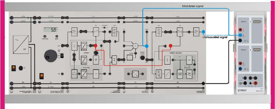
Part One: Noise in DSB-SC Modulation
a) Measurements in Amplitude Modulation
To carry out this experiment, assemble the components as shown below.
• Set the CARRIER switch to OFF. The carrier is transmitted via a separate channel. If the
pilot tone were transmitted in the transmission channel, then this would also be interfered
with by the noise. This would cause synchronization errors in the receiver. This kind of
interference should not be investigated here, as otherwise too much attention would have to
be devoted to special demodulation methods. The theoretical values most frequently
specified are also referred to in the special case dealt with here.
• Set a sinusoidal signal with 5 Vpp and f = 2 kHz on the function generator.
• Adjust the controller “NOISE LEVEL” to the far left limit.
• Connect the Sensor-CASSY 2 inputs:
o Input A → the modulated signal (tapped at the "IN" socket of the noise source).
o Input B → the demodulated signal (tapped at the output of the CF receiver).
• Display the modulated and demodulated signals on the monitor
• Determine the power P2 of the demodulated signal.
• To demonstrate the relationship of the maximum amplitudes in DSB-SC and USSB, connect
the components as shown in the next experiment set-up.
Experiment #10: Noise in Amplitude Modulation
ECE Department ENEE4103 – Communications Lab Page 2 of 3
• Connect the Sensor-CASSY 2 inputs:
o Input A → the DSB-SC modulated signal (tapped at the "IN" socket of the noise source).
o Input B → the USSB modulated signal.
• Display the DSB-SC and USSB on the monitor.
• Determine the power P1 of the DSB-SC modulated signal.
= 2 × = 2 ×
2= 2 × 1
2×()
2
b) Modulated DSB-SC signal with super-positioned interference
To carry out this experiment, assemble the components as shown below.
• Connect the Sensor-CASSY 2 inputs:
o Input A → the modulated signal (tapped at the "IN" socket of the noise source).
o Input B → the output of the PAC/VDC converter.

Experiment #10: Noise in Amplitude Modulation
ECE Department ENEE4103 – Communications Lab Page 3 of 3
• Display the modulated signal and the output of the PAC/VDC converter on the monitor
• Feed a noise power density S1 of approx. 40 ·10-9 V2/Hz into the transmission channel (this
corresponds approximately to an output DC voltage of UA1 = 1.25 V at the PAC/VDC
converter). The transfer function of the PAC/VDC converter is
=×32 ×10
Here SE is the noise power density at the input of the converter and UA is the output voltage
of the converter.
• From this calculate the noise power N1 in the transmission band occupied by the DSB-SC
signal. =×
Where BW is the occupied Bandwidth
• Calculate the Signal-to-noise (SNR1) ratio at the output of the transmission line
=
• Change the connection of the Sensor-CASSY 2 inputs to display:
o Input A → the modulated signal (tapped at the "IN" socket of the noise source).
o Input B → the demodulated signal (tapped at the output of the CF receiver).
• Display the modulated and demodulated signals on the monitor. Did you notice the noise
affect?
• In order to be able to investigate only quantitative effects, disconnect the CF transmitter
(DSB-SC output) from the noise source so that only the noise reaches the CF receiver.
• Display the tapped at the "IN" socket of the noise source (was connected to the output of the
DSB-SC modulator) and demodulated signals on the monitor.
• Apply the same procedure used to calculate the noise power N1 in the DSB-SC to calculate
the noise power N2 in the channel (in the absence of modulated signal).
• Calculate the Signal-to-noise (SNR) ratio at the output of the transmission line
=
• Compare between SNR1 and SNR2
Part Two: Noise in USSB Modulation
Repeat the same procedure applied in part one to obtain the measurements and calculations for
USSB modulation (as an example of SSB modulation technique). Compare your findings with
that of DSB-SC.
