Manual En
User Manual: Pdf
Open the PDF directly: View PDF ![]() .
.
Page Count: 348 [warning: Documents this large are best viewed by clicking the View PDF Link!]
- Chapter 1 Introduction
- 1.1 What is in this Manual?
- 1.2 Important Changes
- SPICE Simulation
- Live Design Rule Check
- WINDOW Command – Flip Board View
- Routing Direction
- SLICE Command
- User Language
- FUSIONSYNC Command
- Managed Libraries
- Board Contour Detection
- New EAGLE Internal Vector Font
- ROUTE Command
- Managed Libraries
- Design Blocks
- ROUTE command
- Copy/Paste
- Design Rule Check
- ALIGN command
- ROUTE command
- BGA Router
- New Installer Routines and Subscription Licenses
- Flexible Board size in Free and Standard Edition
- Reworked Icons
- Pin Snapping in the Schematic
- Renamed WIRE Command to LINE
- New SLICE command
- ROUTE Command Improvements
- BGA Autorouter
- Design Blocks
- 1.3 General Comments About EAGLE Component Libraries
- 1.4 Technical Terms
- Chapter 2 Installation
- Chapter 3 EAGLE Modules and Editions
- Chapter 4 A First Look at EAGLE
- 4.1 The Control Panel
- 4.2 The Schematic Editor Window
- 4.3 The Layout Editor Window
- 4.4 The Library Editor Window
- 4.5 The CAM Processor
- 4.6 The Text Editor Window
- Chapter 5 Principles for Working with EAGLE
- Chapter 6 From Schematic to Finished Board
- 6.1 Creating the Schematic Diagram
- Open the Schematic Diagram
- Set the Grid
- Place Symbols
- Wiring the Schematic Diagram
- Pinswap and Gateswap
- Power Supply
- Define Attributes
- ERC – Check and Correct Schematic
- Organize Schematic Sheets
- Points to Note for the Schematic Editor
- Duplicating a Section of the Schematic
- Merge Different Schematic Files
- Design Blocks
- 6.2 The Hierarchical Schematic
- 6.3 Considerations Prior to Creating a Board
- 6.4 Create Board
- 6.5 FUSIONSYNC – Synchronise EAGLE Board and Fusion 3D Board Model
- 6.6 DRC – Checking the Layout and Correcting Errors
- 6.7 Multilayer Boards
- 6.8 Editing and Updating Components
- 6.9 Differential Pairs And Meanders
- 6.10 Assembly Variants
- 6.11 Print Out Schematic and Layout
- 6.12 Combining Small Circuit Boards on a Common Panel
- 6.13 Consistency Lost between Schematic and Layout
- 6.1 Creating the Schematic Diagram
- Chapter 7 The Autorouter
- 7.1 Basic Features
- 7.2 What Can be Expected from the Autorouter
- 7.3 Controlling the Autorouter
- 7.4 What Has to be Defined Before Autorouting
- 7.5 The Autorouter Menu
- 7.6 How the Cost Factors Influence the Routing Process
- 7.7 Number of Ripup/Retry Attempts
- 7.8 Routing Multi-Layer Boards with Polygons
- 7.9 Backup and Interruption of Routing
- 7.10 Information for the User
- 7.11 Evaluate the Results
- 7.12 Parameters of a Control File
- 7.13 Practical Hints
- 7.14 The Follow-me Router
- 7.15 BGA Routing
- Chapter 8 Component Design Explained through Examples
- 8.1 Managed Libraries
- 8.2 Definition of a Simple Resistor
- 8.3 Defining a Complex Device
- 8.4 Supply Voltages
- 8.5 One Pin – Multiple Pads Connections
- 8.6 Supply Symbols
- 8.7 Attributes
- 8.8 External Devices without Packages
- 8.9 Labeling of Schematic Symbols
- 8.10 More about the Addlevel Parameter
- 8.11 Defining Components with Contact Cross-References
- 8.12 Drawing Frames
- 8.13 Components on the Solder Side
- 8.14 Components with Oblong Holes
- 8.15 Arbitrary Pad Shapes
- 8.16 Creating New Package Variants
- 8.17 Defining Packages in Any Rotation
- 8.18 Library and Part Management
- Chapter 9 Preparing Manufacturing Data
- 9.1 Which Data do we Need for Board Manufacture?
- 9.2 Rules that Save Time and Money
- 9.3 Quick Guide for Data Output
- 9.4 Which Files do I Need for my Board?
- 9.5 Peculiarities of Multilayer Boards
- 9.6 Set Output Parameters
- 9.7 Automating the Output with CAM Processor Jobs
- 9.8 Device Driver Definition in eagle.def
- 9.9 Gerber Files for Photoplotters with Fixed Aperture Wheels
- Chapter 10 Appendix
- 10.1 Layers and their Usage
- 10.2 EAGLE Files
- 10.3 EAGLE Options at a Glance
- 10.4 Configuration of the Text Menu
- 10.5 Text Variables
- 10.6 Options for Experts in eaglerc
- CAM Processor – Suppress Drills/Holes Warning
- Change Component Value Warning
- Consistency Check
- Delete Wire Joints
- Device Name as Value for all Components
- Disable Ctrl for Radius Mode
- Group Selection
- Load Matching File Automatically
- Name of Net, Busses, Signals and Polygons
- Open Project
- Panning Drawing Window
- Polygon Edges as Continuous Lines
- Reposition of the Mouse Cursor
- Units in Dialogs
- 10.7 Error Messages

EASILY APPLICABLE GRAPHICAL LAYOUT EDITOR
Version 8.4
Manual
71023841
Copyright © 2017 Autodesk
All Rights Reserved
This software and documentation are copyrighted by Autodesk, doing business under
the trade name EAGLE. The software and documentation are licensed, not sold, and
may be used or copied only in accordance with the EAGLE License Agreement
accompanying the software and/or reprinted in this document. This software
embodies valuable trade secrets proprietary to Autodesk.
Specifications subject to change without notice.
© Copyright 1988-2017 Autodesk. All rights reserved worldwide.
No part of this publication may be reproduced, stored in a retrieval system, or
transmitted, in any form or by any means, electronic, mechanical, photocopying,
recording, scanning, digitizing, or otherwise, without the prior consent of Autodesk.
Printing this manual for your personal use is allowed.
Windows is a registered trademark of Microsoft Corporation.
Linux is a registered trademark of Linus Torvalds.
Mac is a registered trademark of Apple Computer, Inc.

Table of Contents
Chapter 1 Introduction...................................................19
1.1 What is in this Manual?................................................................19
1.2 Important Changes......................................................................20
SPICE Simulation..........................................................................20
Live Design Rule Check.................................................................20
WINDOW Command – Flip Board View......................................20
Routing Direction..........................................................................20
SLICE Command............................................................................21
User Language................................................................................21
FUSIONSYNC Command...............................................................21
Managed Libraries..........................................................................21
Board Contour Detection...............................................................21
New EAGLE Internal Vector Font.................................................21
ROUTE Command..........................................................................21
Managed Libraries.........................................................................22
Design Blocks.................................................................................22
ROUTE command..........................................................................22
Copy/Paste.....................................................................................22
Design Rule Check.........................................................................22
ALIGN command...........................................................................22
ROUTE command..........................................................................22
BGA Router....................................................................................23
New Installer Routines and Subscription Licenses......................23
Flexible Board size in Free and Standard Edition........................23
Reworked Icons..............................................................................23
Pin Snapping in the Schematic......................................................23
Renamed WIRE Command to LINE.............................................23
New SLICE command....................................................................23
ROUTE Command Improvements................................................23
Route Start Selection...................................................................23
Undo Mouse Clicks......................................................................24
Electrical Snap Indicator.............................................................24
Loop Remove...............................................................................24
Via Placement and Change of Routing Layers............................25
BGA Autorouter..............................................................................25
Design Blocks.................................................................................25
1.3 General Comments About EAGLE Component Libraries...........26
1.4 Technical Terms...........................................................................26
Chapter 2 Installation....................................................29
2.1 System Requirements..................................................................29
2.2 Installation of the EAGLE package.............................................29
3

Table of Contents
2.3 Updating an Older Version..........................................................29
First Back up, Then Install............................................................29
Notes on Library Files....................................................................30
In Case of Changes in the File Data Structure..............................30
2.4 First Start of EAGLE...................................................................30
2.5 Language Settings........................................................................31
Windows.........................................................................................31
Linux and Mac OS X.......................................................................31
Chapter 3 EAGLE Modules and Editions.........................33
3.1 EAGLE Modules...........................................................................33
The Layout Editor..........................................................................33
Schematic Editor............................................................................33
Autorouter......................................................................................33
3.2 Different Editions........................................................................34
Premium Edition............................................................................34
General.........................................................................................34
Schematic Editor..........................................................................35
Layout Editor...............................................................................35
Autorouter Module......................................................................36
Standard Edition............................................................................36
Free Edition....................................................................................36
Chapter 4 A First Look at EAGLE...................................39
4.1 The Control Panel........................................................................39
Documentation..............................................................................40
Libraries Summary........................................................................40
Design Blocks.................................................................................42
Design Rules...................................................................................42
User Language Programs, Scripts, CAM Jobs..............................43
Projects...........................................................................................43
Menu Bar........................................................................................44
File Menu.....................................................................................44
View Menu...................................................................................45
Options Menu..............................................................................46
Window Menu..............................................................................49
Help Menu...................................................................................50
4.2 The Schematic Editor Window....................................................50
How You Obtain Detailed Information About a Command..........51
User Guidance..............................................................................51
Help Function..............................................................................51
Command Parameters...................................................................52
GRID............................................................................................53
The Action Toolbar.........................................................................53
USE..............................................................................................53
4

Table of Contents
SCRIPT........................................................................................53
RUN.............................................................................................53
WINDOW....................................................................................53
UNDO/REDO.............................................................................54
Stop Icon.....................................................................................54
Go Icon........................................................................................55
The Command Toolbar of The Schematic Editor.........................55
INFO............................................................................................55
SHOW..........................................................................................55
DISPLAY......................................................................................55
MARK..........................................................................................55
MOVE..........................................................................................56
COPY...........................................................................................56
MIRROR.....................................................................................56
ROTATE......................................................................................56
GROUP........................................................................................56
CHANGE.....................................................................................57
PASTE..........................................................................................57
DELETE.......................................................................................57
ADD.............................................................................................57
PASTE DBL.................................................................................58
PINSWAP....................................................................................58
GATESWAP................................................................................58
REPLACE....................................................................................58
NAME..........................................................................................58
VALUE........................................................................................58
SMASH........................................................................................58
MITER.........................................................................................59
SPLIT...........................................................................................59
SLICE..........................................................................................59
INVOKE......................................................................................59
LINE (was WIRE).......................................................................59
TEXT...........................................................................................60
CIRCLE.......................................................................................60
ARC.............................................................................................60
RECT...........................................................................................60
POLYGON...................................................................................60
BUS.............................................................................................60
NET.............................................................................................60
JUNCTION..................................................................................61
LABEL..........................................................................................61
ATTRIBUTE................................................................................61
DIMENSION...............................................................................61
MODULE.....................................................................................61
PORT...........................................................................................62
5

Table of Contents
ERC..............................................................................................62
Commands Not Available in the Command Toolbar....................62
ASSIGN........................................................................................62
CLASS...........................................................................................62
CLOSE..........................................................................................62
CUT..............................................................................................62
EDIT.............................................................................................62
FRAME.........................................................................................63
EXPORT.......................................................................................63
LAYER..........................................................................................63
MENU..........................................................................................63
OPEN............................................................................................63
PACKAGE.....................................................................................63
PRINT..........................................................................................64
QUIT.............................................................................................64
REMOVE......................................................................................64
SET...............................................................................................64
TECHNOLOGY............................................................................64
UPDATE.......................................................................................64
VARIANT.....................................................................................64
WRITE..........................................................................................65
Mouse Keys.....................................................................................65
Selecting Neighbouring Objects..................................................65
4.3 The Layout Editor Window.........................................................65
The Commands on the Layout Command Toolbar.......................66
INFO............................................................................................66
SHOW.........................................................................................66
DISPLAY......................................................................................67
MARK..........................................................................................68
GROUP........................................................................................68
MOVE..........................................................................................68
MIRROR.....................................................................................68
ROTATE......................................................................................69
ALIGN.........................................................................................69
COPY...........................................................................................69
PASTE.........................................................................................69
DELETE......................................................................................69
CHANGE.....................................................................................70
PASTE DBL.................................................................................70
ADD.............................................................................................70
PINSWAP....................................................................................70
REPLACE....................................................................................70
LOCK............................................................................................71
NAME..........................................................................................71
VALUE.........................................................................................71
6

Table of Contents
SMASH........................................................................................71
MITER.........................................................................................71
SPLIT...........................................................................................72
OPTIMIZE...................................................................................72
MEANDER..................................................................................72
SLICE...........................................................................................72
ROUTE........................................................................................72
RIPUP..........................................................................................73
LINE............................................................................................73
TEXT............................................................................................73
CIRCLE........................................................................................74
ARC..............................................................................................74
RECT...........................................................................................74
POLYGON...................................................................................74
VIA...............................................................................................75
SIGNAL.......................................................................................75
HOLE...........................................................................................75
ATTRIBUTE................................................................................75
DIMENSION...............................................................................75
RATSNEST..................................................................................76
AUTO...........................................................................................76
AUTO BGA..................................................................................76
ERC..............................................................................................76
DRC.............................................................................................76
ERRORS......................................................................................77
4.4 The Library Editor Window.........................................................77
Table Of Contents...........................................................................77
Important Icons in the Library Editor..........................................79
The Package Editing Mode............................................................79
Design New Package...................................................................80
PAD.............................................................................................80
SMD............................................................................................80
The Symbol Editing Mode.............................................................80
Design a New Symbol..................................................................81
PIN...............................................................................................81
The Device Editing mode...............................................................81
Create Actual Components from Symbols and Packages...........82
ADD.............................................................................................82
NAME..........................................................................................82
CHANGE.....................................................................................83
PACKAGE....................................................................................83
CONNECT....................................................................................83
PREFIX........................................................................................83
VALUE.........................................................................................83
TECHNOLOGY............................................................................83
7

Table of Contents
ATTRIBUTE................................................................................83
DESCRIPTION............................................................................83
4.5 The CAM Processor.....................................................................84
Generate Data................................................................................84
Starting the CAM Processor........................................................84
Load Job File................................................................................85
Load Board...................................................................................85
Set Output Parameters................................................................85
Start Output.................................................................................85
Define New Job............................................................................85
4.6 The Text Editor Window.............................................................86
Chapter 5 Principles for Working with EAGLE...............87
5.1 Command Input Possibilities.......................................................87
Activate Command and Select Object...........................................87
Command Line...............................................................................87
History Function............................................................................88
The Context Menu.........................................................................88
Function Keys................................................................................89
Script Files.....................................................................................90
Mixed Input....................................................................................91
5.2 The EAGLE Command Language................................................91
Typographical Conventions...........................................................91
Enter key and Semicolon.............................................................91
Bold Type or Upper Case.............................................................92
Lower Case...................................................................................92
Underscore...................................................................................92
Spaces...........................................................................................92
Alternative Parameters................................................................92
Repetition Points.........................................................................93
Mouse Click..................................................................................93
Entering Coordinates as Text........................................................93
Relative values:............................................................................94
Polar values:.................................................................................94
Right Mouse Click:.......................................................................94
Modifier:......................................................................................94
5.3 Grids and the Current Units........................................................95
5.4 Aliases for DISPLAY, GRID, and WINDOW...............................97
Example: DISPLAY Alias...............................................................97
Example: GRID Alias.....................................................................97
Example: WINDOW Alias.............................................................98
Editing, Renaming, Deleting of an Alias.......................................98
5.5 Names and Automatic Naming...................................................99
8

Table of Contents
Length.............................................................................................99
Forbidden and Special Characters................................................99
Automatic Naming.........................................................................99
5.6 Import and Export of Data..........................................................99
Script Files and Data Import.......................................................100
File Export Using the EXPORT Command.................................100
DIRECTORY..............................................................................100
NETLIST.....................................................................................101
NETSCRIPT................................................................................101
PARTLIST...................................................................................101
PINLIST......................................................................................101
SCRIPT.......................................................................................101
IMAGE........................................................................................101
LIBRARIES................................................................................102
5.7 The EAGLE User Language.......................................................103
5.8 Forward&Back Annotation........................................................104
5.9 Configuring EAGLE Individually...............................................104
Configuration Commands............................................................104
The Menu Options/Set (SET Command)....................................105
Display Certain Layers Only......................................................105
Context Menu Entries................................................................105
Contents of The Parameter Menus............................................106
ROUTE Command Settings.......................................................106
Confirm Message Dialogs Automatically..................................107
Color Settings...............................................................................107
Miscellaneous SET Options.........................................................109
The eagle.scr File...........................................................................111
The eaglerc File.............................................................................113
EAGLE Project File.......................................................................113
Chapter 6 From Schematic to Finished Board...............115
6.1 Creating the Schematic Diagram................................................115
Open the Schematic Diagram.......................................................115
Set the Grid...................................................................................116
Place Symbols................................................................................116
Load Drawing Frame..................................................................116
Place Circuit Symbols (Gates)....................................................118
Hidden Supply Gates..................................................................118
Devices with Several Gates.........................................................119
Designlink – Access to Farnell's Online Product Database......119
Wiring the Schematic Diagram...................................................120
Draw Nets (NET).......................................................................120
Defining Cross-References for Nets...........................................121
Cross-References for Contacts...................................................122
9

Table of Contents
Specifying Net Classes................................................................123
Drawing a bus (BUS).................................................................124
Pinswap and Gateswap.................................................................125
Power Supply................................................................................126
Define Attributes..........................................................................127
Global Attributes........................................................................127
Attributes for Elements..............................................................127
ERC – Check and Correct Schematic..........................................130
Organize Schematic Sheets..........................................................132
Points to Note for the Schematic Editor......................................132
Superimposed Pins....................................................................132
Open Pins when MOVEing........................................................132
Duplicating a Section of the Schematic.......................................132
With Consistent Layout.............................................................133
Merge Different Schematic Files..................................................133
With Consistent Layout.............................................................134
Multi-Channel Devices...............................................................134
Design Blocks................................................................................134
Adding Design Blocks into Your Current Design......................135
Save a Drawing as a Design Block.............................................135
Save a Selection of the Drawing as a Design Block...................136
Selection criteria.........................................................................137
6.2 The Hierarchical Schematic.......................................................137
Creating a Module........................................................................137
Define Ports..................................................................................140
Using Module Instances...............................................................141
Resulting Component Names in the Layout................................142
ModulInstanceName:PartName...............................................142
Offset..........................................................................................142
Assembly Variants for Modules...................................................142
Special Features between Schematic and Layout........................143
SHOW command.......................................................................143
Consistency.................................................................................143
6.3 Considerations Prior to Creating a Board..................................143
Checking the Component Libraries.............................................143
Agreement with the Board Manufacturer...................................144
Specifying the Design Rules.........................................................144
General Principles......................................................................145
Layers.........................................................................................146
Minimum Clearance and Distance............................................147
Sizes............................................................................................147
Restring (Pad and Via Diameter)..............................................148
Shapes........................................................................................150
Supply.........................................................................................151
10

Table of Contents
Masks..........................................................................................152
Misc.............................................................................................153
6.4 Create Board..............................................................................153
Without the Schematic.................................................................154
Specify the Board Outline............................................................154
Arrange Components....................................................................156
Attributes for Components and Global Attributes......................158
Boards with Components on Both Sides.....................................158
Exchanging Packages...................................................................159
PACKAGE Command.................................................................159
REPLACE command..................................................................160
Changing the Technology.............................................................161
Define Forbidden Areas................................................................161
Routing – Placing Tracks Manually.............................................161
Walkaround Obstacles................................................................161
Ignore Obstacles.........................................................................161
How to route...............................................................................161
Un-route traces..........................................................................163
Traces with arcs..........................................................................163
Defining a Copper Plane with POLYGON...................................164
6.5 FUSIONSYNC – Synchronise EAGLE Board and Fusion 3D
Board Model.....................................................................................167
How does this work?.....................................................................167
Synchronise with Fusion............................................................167
What if There Need to be Changes in the Board’s Geometry?. 167
How to Synchronise...................................................................167
View on Web...............................................................................170
Pull from Fusion.........................................................................170
Push to Fusion............................................................................171
6.6 DRC – Checking the Layout and Correcting Errors...................173
The DRC Errors Window.............................................................174
Error Messages and their Meaning..............................................175
6.7 Multilayer Boards.......................................................................178
Inner Layer...................................................................................178
Supply Layers with Polygons and More than One Signal.........178
Resticted Areas For Polygons....................................................179
Multilayer Boards with Through Vias..........................................179
Layer Setup.................................................................................179
Multilayer with Blind and Buried Vias........................................180
Disambiguation..........................................................................180
Displaying Vias...........................................................................181
Layer Setup.................................................................................181
Hints For Working With Blind, Buried, and Micro Vias..........186
11

Table of Contents
Micro Via − A Special Case of Blind Via......................................187
6.8 Editing and Updating Components...........................................187
Open Device/Symbol/Package....................................................187
Updating Project (Library Update).............................................188
6.9 Differential Pairs And Meanders...............................................189
Routing Differential Pairs............................................................189
Meanders......................................................................................190
Length Balance for a Differential Pair......................................190
Specifying a Certain Length.......................................................191
Symmetric and Asymmetric Meanders.....................................191
Length Tolerance Display...........................................................191
6.10 Assembly Variants....................................................................192
Creating Assembly Variants.........................................................192
Assembly Variants and CAM Processor......................................194
6.11 Print Out Schematic and Layout...............................................195
Settings of the Print Dialog..........................................................195
6.12 Combining Small Circuit Boards on a Common Panel............197
6.13 Consistency Lost between Schematic and Layout....................198
Criteria For Consistency..............................................................200
Consistency Indicator..................................................................201
Chapter 7 The Autorouter............................................203
7.1 Basic Features............................................................................203
7.2 What Can be Expected from the Autorouter.............................204
7.3 Controlling the Autorouter........................................................204
Bus Router....................................................................................205
Routing Pass................................................................................205
TopRouter....................................................................................205
Optimization................................................................................205
7.4 What Has to be Defined Before Autorouting.............................206
Design Rules................................................................................206
Track Width and Net Classes......................................................206
Grid..............................................................................................206
Placement Grid..........................................................................206
Routing Grid..............................................................................207
Memory Requirement.................................................................208
Layer............................................................................................208
Preferred Directions....................................................................209
Restricted Areas for the Autorouter............................................209
Cost Factors and Other Control Parameters...............................210
7.5 The Autorouter Menu................................................................210
Autorouter Main Setup................................................................210
Routing Variants Dialog...............................................................211
7.6 How the Cost Factors Influence the Routing Process................213
12

Table of Contents
Layer Costs....................................................................................214
cfBase.xx: 0..20..........................................................................214
Costs..............................................................................................214
cfVia: 0..99.................................................................................214
cfNonPref: 0..10.........................................................................214
cfChangeDir: 0..25.....................................................................214
cfOrthStep, cfDiagStep..............................................................215
cfExtdStep: 0..30........................................................................215
cfBonusStep, cfMalusStep: 1..3..................................................215
cfPadImpact, cfSmdImpact: 0..10.............................................215
cfBusImpact: 0..10.....................................................................215
cfHugging: 0..5...........................................................................216
cfAvoid 0..10...............................................................................216
cfPolygon 0..30...........................................................................216
Maximum......................................................................................216
mnVia 0..30................................................................................216
mnSegments 0..9999.................................................................216
mnExtdSteps 0..9999................................................................216
7.7 Number of Ripup/Retry Attempts.............................................216
7.8 Routing Multi-Layer Boards with Polygons...............................217
7.9 Backup and Interruption of Routing..........................................218
7.10 Information for the User..........................................................218
Status Display...............................................................................218
Log file..........................................................................................220
7.11 Evaluate the Results.................................................................220
7.12 Parameters of a Control File.....................................................221
7.13 Practical Hints..........................................................................222
General.........................................................................................222
Single-Sided Boards.....................................................................222
SMD Boards With Supply Layers................................................222
What can be done if not all signals are routed?..........................223
7.14 The Follow-me Router.............................................................223
Partial and Full Mode..................................................................223
Configuration...............................................................................224
Routing Parameters.....................................................................225
Notes.............................................................................................225
7.15 BGA Routing............................................................................226
Chapter 8 Component Design Explained through
Examples.......................................................................229
8.1 Managed Libraries.....................................................................229
13

Table of Contents
Migration to Managed Libraries.................................................230
Library Manager...........................................................................231
Make Your Libraries Managed....................................................233
8.2 Definition of a Simple Resistor.................................................234
Resistor Package..........................................................................234
Define a New Package...............................................................234
Set the Grid................................................................................234
Solder Pads................................................................................235
Pad Name...................................................................................236
Silkscreen and Documentation Print........................................236
Labeling......................................................................................236
Restricted area for components................................................237
Description.................................................................................237
Note............................................................................................237
Resistor Symbol...........................................................................238
Define a New Symbol................................................................238
Set the Grid................................................................................238
Place the Pins.............................................................................238
Pin Names..................................................................................240
Schematic Symbol.....................................................................240
Description.................................................................................241
Resistor Device.............................................................................241
Define a New Device..................................................................241
Selecting, Naming and Configuring Symbols............................241
Selecting the Package................................................................242
Connections Between Pins and Pads........................................242
Define Prefix..............................................................................243
Value..........................................................................................243
Description.................................................................................244
Save............................................................................................244
Library Description......................................................................245
Use Library...................................................................................245
8.3 Defining a Complex Device.......................................................245
Creating a New Library................................................................247
Drawing the Pin-Leaded Package................................................247
Set the Grid................................................................................248
Place Pads..................................................................................248
Pad Name...................................................................................249
Draw the Silk Screen Symbol....................................................249
Package Name and Package Value............................................249
Areas Forbidden to Components..............................................250
Description................................................................................250
Save.............................................................................................251
14

Table of Contents
Defining the SMD Package...........................................................251
Set the Grid................................................................................252
Placing SMD Solder Pads..........................................................253
SMD Names...............................................................................254
Draw the Silk Screen..................................................................255
Package Name and Package Value............................................255
Area Forbidden to Components................................................255
Locating Point (Origin)..............................................................255
Description.................................................................................256
Save............................................................................................256
Defining the Logic Symbol for the Schematic Diagram..............257
Check the Grid...........................................................................257
Place the Pins.............................................................................257
Pin Name...................................................................................258
Draw the Symbol.......................................................................258
Placeholders for NAME and VALUE........................................258
Description................................................................................258
Save............................................................................................258
Defining a Power Supply Symbol................................................259
Check the Grid...........................................................................259
Place the Pins.............................................................................259
Pin Name...................................................................................260
Placeholders for NAME and VALUE........................................260
Associating the Packages and Symbols to Form a Device Set....260
Select Symbols............................................................................261
Naming the Gates.......................................................................261
Specify Addlevel and Swaplevel.................................................261
Choosing the Package Variants.................................................262
The Connect Command.............................................................263
Defining Technologies...............................................................264
Specifying the Prefix..................................................................265
Value...........................................................................................265
Description.................................................................................265
Save............................................................................................266
8.4 Supply Voltages.........................................................................266
Component Power Supply Pins...................................................266
Invisible Supply Pins.................................................................266
Pins with the Same Names..........................................................268
8.5 One Pin – Multiple Pads Connections......................................268
8.6 Supply Symbols.........................................................................269
8.7 Attributes....................................................................................271
Define Attributes..........................................................................271
Display Attributes........................................................................273
Placeholders in Symbol and Package........................................273
15

Table of Contents
8.8 External Devices without Packages...........................................274
8.9 Labeling of Schematic Symbols.................................................274
8.10 More about the Addlevel Parameter........................................275
Summary......................................................................................275
Relay: Coil and First Contact must be Placed.............................276
Connector: Some Connection Pins can be Omitted....................276
Connector with Fixing Hole and Restricted Area.......................277
8.11 Defining Components with Contact Cross-References............278
Define Symbol..............................................................................278
Define Device................................................................................279
Define Package.............................................................................279
8.12 Drawing Frames.......................................................................279
8.13 Components on the Solder Side...............................................281
8.14 Components with Oblong Holes..............................................281
8.15 Arbitrary Pad Shapes...............................................................282
8.16 Creating New Package Variants...............................................283
Package from Another Library....................................................283
Defining the Package Variant...................................................283
Connect Command....................................................................285
Defining Technologies...............................................................285
Save............................................................................................285
Using a Modified Package from Another Library.......................285
Import the Package...................................................................285
Defining the Variant..................................................................286
8.17 Defining Packages in Any Rotation.........................................286
Rotating a Package as a Whole....................................................287
Packages with Radial Pad Arrangement.....................................287
8.18 Library and Part Management................................................288
Copying of Library Elements.......................................................288
Within a Library........................................................................288
From One Library into Another................................................289
Composition of Your own Libraries..........................................291
Removing and Renaming Library Elements...............................291
Update Packages in Libraries......................................................292
Chapter 9 Preparing Manufacturing Data.....................295
9.1 Which Data do we Need for Board Manufacture?.....................295
Gerber Plot Data..........................................................................296
GERBER_RS274X.....................................................................296
GERBERAUTO and GERBER...................................................296
Drill Data......................................................................................297
EXCELLON................................................................................297
EXCELLON_RACK...................................................................297
SM1000 and SM3000...............................................................298
16

Table of Contents
Further Drill Data Devices........................................................298
Prototype Manufacture With a Milling Machine.......................298
outlines.ulp................................................................................298
mill-outlines.ulp........................................................................298
Film Generation Using PostScript Files......................................298
Printing on a Film........................................................................299
Data for Pick-and-place Machines and In-circuit Testers..........299
Documentation............................................................................300
Parts List....................................................................................300
Drill Plan....................................................................................301
Drill Legend...............................................................................302
Assembly Variants.......................................................................302
9.2 Rules that Save Time and Money..............................................302
9.3 Quick Guide for Data Output....................................................303
Job gerb274x.cam........................................................................304
Job excellon.cam..........................................................................305
Job gerber.cam............................................................................306
9.4 Which Files do I Need for my Board?.......................................307
Files List.......................................................................................307
Placeholders for Output File Name Generation.......................310
Hints Concerning File Extensions:............................................310
9.5 Peculiarities of Multilayer Boards..............................................310
Inner Layers.................................................................................310
Drill Data for Multilayer Boards With Blind and Buried Vias....311
9.6 Set Output Parameters...............................................................311
9.7 Automating the Output with CAM Processor Jobs....................314
Defining a New CAM Job.............................................................314
Extending gerber.cam Job for Multilayer Boards.......................315
Error Message: Apertures Missing..............................................316
Gerber Info Files...........................................................................317
Drill Data Generation with Separate Rack File...........................317
Define a Drill Configuration (Rack) File...................................317
Define Job for Drill Data Output...............................................318
Drill Info File..............................................................................318
9.8 Device Driver Definition in eagle.def.........................................318
Creating Your Own Device Driver................................................319
Example 1: Gerber(auto) device, Millimetre.............................319
Example 2: EXCELLON Device, Output with Leading Zeros. .319
Units in the Aperture and Drill Table.........................................320
9.9 Gerber Files for Photoplotters with Fixed Aperture Wheels.....320
17

Table of Contents
Defining the Aperture Table (Wheel)..........................................321
Aperture Emulation......................................................................321
Chapter 10 Appendix....................................................323
10.1 Layers and their Usage.............................................................323
In Layout and Package Editor.....................................................323
In Schematic, Symbol, and Device Editor...................................324
10.2 EAGLE Files.............................................................................324
10.3 EAGLE Options at a Glance.....................................................325
10.4 Configuration of the Text Menu..............................................328
10.5 Text Variables..........................................................................329
10.6 Options for Experts in eaglerc.................................................329
CAM Processor – Suppress Drills/Holes Warning..................330
Change Component Value Warning.........................................330
Consistency Check.....................................................................330
Delete Wire Joints.....................................................................330
Device Name as Value for all Components...............................330
Disable Ctrl for Radius Mode....................................................330
Group Selection..........................................................................331
Load Matching File Automatically............................................331
Name of Net, Busses, Signals and Polygons..............................331
Open Project...............................................................................331
Panning Drawing Window.........................................................331
Polygon Edges as Continuous Lines..........................................331
Reposition of the Mouse Cursor................................................332
Units in Dialogs.........................................................................332
10.7 Error Messages........................................................................332
When Loading a File....................................................................332
Restring smaller than in older version......................................332
Library objects with the same names.......................................332
Pad, Via Replaced with a Hole..................................................333
Skipped unsuitable objects........................................................334
Can't Update File.......................................................................334
In a Library...................................................................................335
Package/Symbol is in use..........................................................335
In the CAM Processor..................................................................335
Polygon may cause extremely large plot data...........................335
In the Free or Standard Edition..................................................336
Can't perform the requested action..........................................336
Index............................................................................337
18

Chapter 1
Introduction
This manual describes the use of the EAGLE software and its basic
principles. The order of chapters follows the typical process from drawing a
schematic to a ready-to-use layout.
1.1 What is in this Manual?
A chapter's main heading is intended to tell you briefly what the contents of
that chapter are. Here in the first chapter we want to give a quick overview
what you can expect from this manual.
Chapter 1 – Introduction
Contains a preview of the manual and informs you about the most
important changes compared to the previous version.
Chapter 2 – Installation
Deals with the program's installation.
Chapter 3 – EAGLE Modules and Editions
Explains the various program variants.
Chapter 4 – A First Look at EAGLE
Gives a preview of the program's structure and describes the
editor windows and their commands.
Chapter 5 – Principles for Working with EAGLE
Examines the basic ways of using and configuring EAGLE.
Chapter 6 – From Schematic to Finished Layout
Follows the route from schematic to layout.
Chapter 7 – The Autorouter
Dedicated to the Autorouter module and its configuration.
Chapter 8 – Component Design Explained through Examples
Explains the definition of library components through examples and
informs about library and component management.
Chapter 9 – Preparing the Manufacturing Data
Everything you need to know about generating manufacturing data.
Chapter 10 – Appendix
Lists useful additional information and explains some error messages
EAGLE prompts in certain situations.
19

1 Introduction
1.2 Important Changes
Anybody who has already been working with a prior version of EAGLE is
advised to read the file UPDATE_en.txt. It contains a description of all the
differences from earlier versions. This file is located in the eagle/doc
directory. Please read it before you start working with the new EAGLE.
Information that was not available or that has been changed since finishing
this manual is also described in UPDATE_en.txt.
Detailed information, especially about the EAGLE command language and
the EAGLE User Language, is available on the help pages.
The most important changes are listed here:
SPICE Simulation
V8.4.0 – Integrated open-source ngspice simulator with examples.
The new ngspice-simulation library contains pre-configured parts. Spice
model cards and subcircuit models, as well as native parts are supported, and
an interface is provided to map gate pins to model inputs. Valid spice-
compatible netlists are created and can optionally be manually edited before
simulation. User interface supports making spice-compatible library parts,
and for converting existing parts.
Results are given in text form and plotted where applicable. OP analysis
results are shown in schematic and can be toggled on/off.
Simulation types supported: AC, DC, Transient, and Operating Point.
Simulation related commands in EAGLE: SIM, SIMOPTOGGLE,
SOURCESETUP, MAKESPICE, MAPTOMODEL, IPROBE, VPROBE,
VPPROBE
See help for SIM command to begin.
Live Design Rule Check
V8.4.0 – After a change in the Layout, like moving a component or while
you are routing, the Design Rule Check will be executed automatically. The
errors list will be updated and the DRC error polygons will be drawn. So you
immediately will recognize any Design Rule violations. Live DRC can be
turned on or off through the Live DRC checkbox in the Set/DRC menu or
with the command SET LIVE_DRC ON | OFF.
WINDOW Command – Flip Board View
V8.4.0 – WINDOW FLIP allows for viewing and editing the board from the
perspective of the bottom side. There is also an icon available in the Action
toolbar.
Routing Direction
V8.3.2 – While the ROUTE command is active, you can use the Arrow-right
key to change the routing direction. The starting point jumps from the one
end of the airwire to the other. This can be done at any time as often as you
want.
20

1.2 Important Changes
SLICE Command
V8.3.2 – SLICE offers options to automatically ripup traces left or right of
the slice line. These options are available through icons in the parameter
toolbar.
User Language
V8.3.2 – The User Language supports 3D Packages and URNs
(UL_PACKAGE3D).
FUSIONSYNC Command
V8.3.0 – Data exchange between the mechanical CAD system Fusion 360
and EAGLE. This command is used to have the EAGLE board represented as
a 3D object in Fusion. During the whole design process you can push the
EAGLE Layout into Fusion or pull it from there into EAGLE. See page 167
for details.
Managed Libraries
V8.3.0 – 3D Packages support: All packages in Managed Libraries will be
assigned simple 3D boxes by default. These can be replaced with 3D STEP
file models using a web-based editor. References to these 3D packages are
retained by components added to schematics and boards and can be updated
using the UPDATE command.
Added support for user creation and editing of Managed Libraries (private-
only for now).
Board Contour Detection
V8.3.0 – Added detection of board shape based on information in layer 20
(Dimension) and layer 46 (Milling). If a single, non-self-intersecting and
closed outline is detected, this will become filled depending on the user's
color profile. Holes will be shown in background color.
Since V8.3.1 it can be switched on or off in the Options/Set/User Interface
menu.
New EAGLE Internal Vector Font
V8.3.0 – EAGLE now uses a new internal vector font which is very similar
to OSIFONT, a common font implementation in the CAD industry. It covers
a bigger set of characters, in particular common Western European, Greek,
Cyrillic, other Eastern European characters and many special symbols. The
new font does not become active unless the option Keep old vector font in
this drawing in Options/User interface is unchecked.
For new designs, the new implementation is taken by default.
ROUTE Command
V8.3.0 – The new Single Layer mode greys out all layers except the one on
which you are routing. Can be enabled/disabled with the command SET
SINGLE_LAYER_MODE On | Off.
21

1 Introduction
The Avoid Obstacles mode now allows routed wires to connect to same-signal
arbitrary pad shapes.
Managed Libraries
V8.2.0 – Support for easily downloading updates to the built-in libraries and
installing new libraries from our Online Library index. When placing
components from these libraries, the ID and version of the libraries will be
stored in Schematic and Board files.
Design Blocks
V8.2.0 – Now it is possible to edit and create new Design Blocks from the
Control Panel’s tree view.
When a Design Block with a single sheet schematic is pasted into schematic
and board, it is possible to select the location where to be placed by a mouse
click in both editors, schematic and layout.
ROUTE command
V8.2.0 – Improved the ROUTE command's loop handling by making the
removal of a loop interactive when it occurs with a mouse move and not
requiring a mouse click to see the result.
Copy/Paste
V8.1.1 – The shortcuts Ctrl+C and Ctrl+V are now assigned to COPY and
PASTE by default.
Design Rule Check
V8.1.1 – The Airwires branch in the Design Rule Check’s Error window lists
remaining signal wires in the layout. Clicking on an entry in the list invokes a
pointer to the Airwire.
ALIGN command
V8.1.1 – The ALIGN command operates on a set of selected objects and
aligns them in different modes. The following are supported:
Align Top | Bottom | Left | Right edges, align Vertical | Horizontal centers,
Distribute Vertically | Horizontally and Align Components to Grid. The Align
Components to Grid mode uses the origin of the objects for alignment, all
other modes operate using axis aligned bounding boxes of objects to be
aligned.
ROUTE command
V8.1 – The ROUTE command has the capability to automatically detect
obstacles along the path of the routed wire and contouring around them.
Walkaround Obstacles mode is operational when you are routing using
straight segment wire bend styles, with no mitering!
If you switch from routing mode Walkaround Obstacles to routing mode
Ignore obstacles, you will find the routing behaviour as it was in previous
EAGLE versions.
22
1.2 Important Changes
The ROUTE command option Loop removal is now set to on by default.
BGA Router
The BGA Router now supports non-square BGA components.
New Installer Routines and Subscription Licenses
V8.0 – EAGLE uses new installer routines for Windows, Linux and Mac
versions. EAGLE offers subscription licenses now. Details can be found on
the Autodesk web sites.
Flexible Board size in Free and Standard Edition
V8.0 – The Free and Standard Edition of EAGLE are no longer limited to a
fixed board size, but to the area of 80 cm² for Free and 160 cm² for
Standard.
Reworked Icons
V8.0 – The command and action icons which were introduces in EAGLE V7
are reworked for better visibility and recognition.
This first edition of the V8 manual does not yet show all icons in the
new V8 style. This will be updated as soon as possible.
Pin Snapping in the Schematic
V8.0 – When drawing a net in the Schematic Editor, the net always jumps to
the pin connection point which is located on one end of the pin and can be
made visible if displaying layer 93, Pins.
Renamed WIRE Command to LINE
V8.0 – The WIRE command has been renamed to LINE. For compatibility
reasons WIRE is still allowed.
New SLICE command
V8.0 – The SLICE command is used to cut nets and board traces in two with
a gap specified by the current line width. Schematic wires that are sliced
become separate nets, similar to deleting a middle wire segment. Board
traces that are sliced maintain net connectivity with the new trace gap
containing an airwire (similar to ripup command).
ROUTE Command Improvements
Route Start Selection
V8.0 – The process of picking the object to start routing has changed so that
the result is more predictable and flexible. Now, you can start routing from
any copper object (pad, via, wire), in addition to airwires, without needed to
press the Ctrl key.
23

1 Introduction
When the left mouse button is pressed to start a route, a specific search order
is used to find the route start object. That search order is:
•Through-hole pads and SMDs/vias defined on current route layer
•Wires on current route layer
•Airwires
•SMDs and vias, not defined on current-layer
•Wires not defined on current layer
For example, picking a Top SMD with the current route layer as Top is
straightforward when many airwires cross over the SMD because of this
search order. Conversely, if the current route layer is Bottom, for example,
airwires and other current layer wires would have precedent over this Top
SMD when the objects are co-located.
Undo Mouse Clicks
V8.0 – Now while routing if you make a mistake with a mouse click (or you
find a better route path) and want to change it, you can press the backspace
<BS> key (DEL on Macs) to "undo" the prior mouse click. You can "Undo"
the prior mouse clicks all the way back to the route start object. When
undoing through via placements, the layer will automatically switch to the
prior routing layer.
If something is typed into the command line, the <BS> key will erase
the last typed character in the command line, as normal. In this case,
the <BS> key will have no effect on the route command. The
command line needs to be empty of characters before the <BS> key
works on the ROUTE command.
Electrical Snap Indicator
V8.0 – The ROUTE command has always had the snapping to nearby
electrical objects, but now an indicator (X) is displayed when a snap occurs to
the nearby electrical object's center point. As in the past, the Snap Length
parameter controls how close you can get to a nearby electrical object before
the mouse is snapped to it's center point.
Loop Remove
V8.0 – The Loop Remove feature, which defaults to off, allows you to re-
route any portion of a path between two pads and automatically remove the
redundant (loop) wires and possibly via.
The re-route can start at a pad, in the middle of a wire, or a via, and end in
the same fashion – on a pad, in the middle of a wire, or a via. The Loop
Remove will not work if the loop to remove goes through a pad or if a T
connection exists – for the loop to be removed it has to go between two pads
(or sub-section of those pads) and no have T connections in that path.
24

1.2 Important Changes
Via Placement and Change of Routing Layers
V8.0 – When a layer change is requested, the via is now immediately placed
at the end of the route and can be dragged around before committing it by
left-clicking.
A new keyboard shortcut has been added to change routing layers. The Space
key changes the routing layer to the next routing layer. The next routing layer
is displayed in the status line as Next Layer: Bottom for example.
You can continue to press the Space to cycle forward through the available
routing layers. If you cycle back to the current routing layer, the via at the
end of the route disappears. Pressing Shift + Space works in a similar
manner, but cycles backwards through the routing layers.
The condition holds here as with "Undo Mouse Clicks": the command
line must be empty for the Space key to work with the route
command.
To place a via and continue routing on the same (current) routing layer, press
Shift+Left button click.
If the route start object, or the object at the last mouse click, is a through-
hole pad or via, then you can press Shift + middle button click to change the
routing layer without adding a via. This could be useful, for example, if you
started routing from a through-hole pad on the top layer, but then decide it
may be better to route from this pad on the Bottom layer.
BGA Autorouter
V8.0 – The BGA router is a special kind of Autorouter which is designed to
route the connections out of Ball Grid Array (BGA) with a minimal number of
layers. The BGA router allows to route selected or all signals and supports
micro vias, if enabled. It is started with the BGA icon or with AUTO BGA in
the command line. After BGA routing you can continue with manual or
automated routing.
Design Blocks
V8.0 – A Design Block is technically spoken a combination of a Schematic
and a (consistent) Board. It is intended to represent a kind of designed
module which can be easily reused in EAGLE.
It’s possible to select objects in schematic and board which are consistent
and save them as a Design Block. The Design Block can be given a
Description and can have attributes. Once saved it can be re-used at any time
in a project.
25

1 Introduction
1.3 General Comments About EAGLE
Component Libraries
The component libraries supplied with EAGLE have been compiled with
great care as an additional service to you, our customer. However, the large
number of available components and suppliers of these components means
that the occasional discrepancy is unavoidable. Please note, therefore, that
Autodesk takes no responsibility for the complete accuracy of information
included in library files.
Please note that libraries are not necessarily identical to former libraries with
the same name. Therefore, it is advisable to back up your old libraries before
installing the new ones.
1.4 Technical Terms
In this manual, in the help function, and in EAGLE itself we frequently use
some technical terms that should be explained here in a few words.
Airwire:
Unrouted connection on a board, displayed in the unrouted layer (= rubber
band).
BGA:
Ball Grid Array – a surface mount device with round soldering pads beneath
the case.
Blind Via:
A plated-through hole for changing the layer of a track which has not been
drilled through all layers in the production process of a multilayer board.
Buried Via:
A plated-trough hole, which has been drilled through the current layer stack
in the production process like a normal (through) via, but does not connect
all layers of the whole board.
Core:
Two copper layers applied to a solid substrate.
Design Rule Check (DRC):
EAGLE can identify the violation of certain Design Rules (e.g. if two different
tracks overlap or are too close) with the DRC.
Device:
A fully defined element in a library. Consists of at least one Package and one
Symbol.
Device Set:
Consists of Devices that use the same Symbols for the Schematic but have
different Package variants or technologies.
Drill:
Plated-through drilling in the layout (in pads and vias)
Electrical Rule Check (ERC):
EAGLE can identify the violation of certain electrical rules (e.g. if two outputs
are connected) with the ERC. It also checks the consistency of the schematic
and the layout.
26

1.4 Technical Terms
Follow-me Router:
The manual ROUTE command offers an operating mode that calculates and
displays the connection of a selected signal automatically. The current
position of the mouse cursor determines the trace of the connection. Only
available with the Autorouter module.
Forward&Back Annotation:
Transforms all the actions one makes in a schematic online into the layout
(and with limitations from layout into schematic). Both files are consistent all
the time.
Gate:
The term Gate is used in this manual for a part of a component which can be
individually placed on a schematic. This can be one Gate of a TTL
component, one contact pair in a relay, or an individual resistor from a
resistor array.
Hole:
Non plated-through drilling in the layout (e.g. a mounting hole).
Layer Stack:
Current number and order of copper and isolation layers which are used to
build up a printed circuit board.
Micro via:
A plated-through hole (like Blind via) with a relatively small drill diameter
which connects an outer layer with the next reachable inner layer.
Module:
A subunit of the hierarchical schematic that contains a smaller part of the
schematic
Module instance:
A simple symbol in a superior level in the hierarchical schematic that
represents the usage of a module.
Net:
Electrical connection in a schematic.
Obstacle Avoidance:
A manual routing mode that takes care on Design Rule settings. In this mode
you can be sure that all Design Rules and Net Class settings will be taken into
consideration.
Package:
Component footprint stored in a library.
Pad:
Through-hole pad associated with a Package.
Pin:
Connection point on a Schematic Symbol.
Port:
Similar to a pin, the port connects module instances in the hierarchical
diagram with nets.
Prepreg:
Used in a compound of inner and outer layers for multilayer boards.
27

1 Introduction
Rack:
Configuration table for a drilling machine. Needed for generating drill data.
Ratsnest:
Command for calculating the shortest airwires and for hiding or displaying
certain airwires for a better overview.
Restring:
Pronunciation: rest-ring. Setting that determines the width of the copper
ring around a plated-through hole of a pad or via.
Signal:
Electrical connection in a board.
Supply Symbol:
Represents a supply signal in the schematic. Causes the ERC to run special
checks.
Symbol:
Schematic representation of a component, stored in a Library.
User Language:
Freely programmable, C-like language for data import and export.
Via:
Plated-through hole for changing the layer of a track. See also Micro via,
Blind via, and Buried via.
Wheel:
Aperture configuration file. Generated with Gerber data for board
manufacturing.
Wire:
Electrical connection in a board, or a line (since lines are drawn with the
LINE command).
28
Chapter 2
Installation
2.1 System Requirements
Detailed system requirement are mentioned on the Autodesk EAGLE product
website. EAGLE is available in 64bit versions only. Choose the appropriate
installation package according the architecture of your operating system. In
order to run EAGLE the following is required:
a minimum of 3 MB of memory,
about 700 MB free disk space,
a minimum graphics resolution of 1024 x 768 pixels,
preferably a 3-button wheel mouse.
2.2 Installation of the EAGLE package
On the Autodesk product website you will always find the newest installation
files. First download the current EAGLE package according your operating
system from the web site. EAGLE is available for Windows, Linux and Mac
OS-X in 64bit packages.
http://www.autodesk.com/products/EAGLE/Overview
For the Windows and Mac installation simply double-click the downloaded
archive. Then follow the setup routine. The Linux package has to extracted
into a folder of your choice.
2.3 Updating an Older Version
First Back up, Then Install
For reasons of safety it is good practice to create a backup of your previous
data before proceeding!
After starting EAGLE for the first time, please check the path settings in the
Control Panel's Options/Directories.. menu.
The path settings are taken from the EAGLE configuration file eaglerc(.usr),
if existing, from a previous EAGLE version installed. Modify the settings if
necessary. The variable $EAGLEDIR stands for the current EAGLE
installation directory.
29

2 Installation
Please read the file update.txt in the EAGLE/doc directory, in order to
familiarize yourself with the changes in the new version of the program.
Notes on Library Files
All files from previous versions can be used with the new EAGLE version.
Please check which library files are in use, and available for the ADD
command. To make sure that you are working with those of the new EAGLE
version you should, for example in the Schematic Editor, type the following
command in the command line
This removes all libraries from the buffer. Then type
to load all libraries of the currently given directory or other directories.
The information about libraries in use is stored in the eagle.epf file of the
currently active project.
If you have added new Devices to existing libraries, you should re-name and
copy these libraries to a separate folder to avoid over writing, muddling up
files with newer or older ones, and in the worst case loosing your work prior
to updating. This same rule holds true for ULPs and Script files as well.
In Case of Changes in the File Data Structure
In case of an update where it was necessary to change the file data structure,
it may be wise to save your own library files from the earlier version in the
new EAGLE. Expanding the tree view's library preview or showing all
libraries by the first ADD command cause additional time in screen update
viewing, depending on your computer speed. EAGLE has to update the files
temporarily to the new file format before showing the libraries' contents.
In case you have a lot of files, there is a quick and comfortable way to solve
this issue. You need two tools to achieve this:
The User Language Program run-loop-all-lbr-script.ulp and a Script file that
contains one line:
Edit one of the library files that shall be updated and start the ULP. You will
be asked for the Script file to be executed, then all libraries which are in the
same directory will be updated.
The data structure of the library files remains unchanged in the
transition from version 7 to version 8.0!
2.4 First Start of EAGLE
If you start EAGLE you are asked to sign in into your personal Autodesk
account. The account is assigned with your email address you registered and
ordered your EAGLE subscription. After logging in, EAGLE will start
according the entitlement (Standard or Premium Edition, expiration date of
subscription) you are eligible for.
30

2.4 First Start of EAGLE
You do not necessarily need an internet connection for working with EAGLE.
It’s also possible to work in OFFLINE mode for 14 days. After this period you
are asked to sign in again in order to check the validity of the entitlement. If
you do not have internet access, EAGLE will fall back into free mode until
you can log in again.
The free Edition asks for a login only once at the first start. From then on,
you don’t have to connect to the internet anymore.
2.5 Language Settings
EAGLE decides due to the operating systems' language which language to
use. If the systems' language, for example, is set to German, EAGLE will use
German language. In case you don't like the automatically selected language,
you have the following possibilities to change it.
Windows
EAGLE takes care on a variable named LANG. For changing it go to the
Windows Control Panel where you can define environment variables. Set up
a variable named LANG. For english language the value is typically set to
en_US or en_GB. For german language the value should be set to de_DE,
de_CH, or de_AT. In case you would like to use a batch file to start EAGLE, it
could look like this:
!"!#$%$%
"&&!$%
This is of use, if there are other applications that react on the LANG variable.
The batch affects EAGLE only.
Linux and Mac OS X
The same as described for the Windows EAGLE can be done for Linux and
Mac OS-X. There you have to define the variable with the systems' EXPORT
command.
You could also use a script file in order to start EAGLE:
'(')"'!#$%$%'!
31

2 Installation
This
page
has been
left free
intentionally.
32

Chapter 3
EAGLE Modules and Editions
3.1 EAGLE Modules
The Layout Editor
The Layout Editor, which allows you to design Printed Circuit Boards (PCBs)
comes with the Library Editor, the Computer Aided Manufacturing (CAM)
Processor, and the Text Editor. With the Library Editor you can already
design Packages (footprints), Symbols and Devices (for a schematic). The
CAM Processor is the program which generates the output data for the
production of the PCB (e.g. Gerber or drill files). It is also possible to use
User Language programs and Script files.
Schematic Editor
If you want to draw Schematic diagrams for electronic systems you should
have Schematic and Layout Editor. You can generate the associated circuit
board at any time with a mouse-click. EAGLE then changes to the Layout
Editor, where the packages are placed next to an empty board – connected
via airwires (rubber bands). From here you can go on designing with the
Layout Editor as usual. Schematic and layout are automatically kept
consistent by EAGLE (Forward&Back Annotation). Schematic diagrams can
consist of a maximum of 999 sheets in the Professional Edition (99 sheets in
the Standard Edition). On the left side of the Schematic Editor window the
preview of the sheets is displayed.
The Schematic Editor is also applicable for drawing simple electrical wiring
diagrams (connection scheme, contact plans...).
Autorouter
You can have airwires routed automatically if EAGLE has the Autorouter
module. You can choose single nets, groups of nets or all nets for the
automatic routing pass. The program will handle various network classes
having different track widths and minimum clearances.
The Autorouter also serves as basic engine of the Follow-me router. This is
an advanced operating mode of the ROUTE command for manual routing,
which calculates and displays the trace of a selected signal automatically.
The Autorouter has a special function to route BGA connections (AUTO
BGA).
33

3 EAGLE Modules and Editions
3.2 Different Editions
EAGLE offers various performance/price categories (editions) called Free
Standard, and Premium. The facilities mentioned in this manual always refer
to the Professional edition.
Premium Edition
General
maximum drawing area 150 x 150 inches
resolution 0.003125 µm
mm or inch grid
up to 255 drawing layers
command (Script) files
C-like User Language for data export and import and the
realization of self-defined commands
Fully documented, readable XML data structure
easy library editing
composition of self-defined libraries with already existing
elements by Drag&Drop
easy generation of new Package variants from other libraries by
Drag&Drop
free rotation of package variants (0.1-degree steps)
arbitrary pad shapes in the Package Editor
library browser and powerful component search function
technology support (e. g. 74L00, 74LS00..)
easy definition of labelled drawing frames
free definable attributes, applicable for Devices in the Library
and in Schematic or Layout
support of assembly variants
easy-to-use dimensioning tool
merging of different projects with maintaining consistency
(Design Reuse)
Design Blocks as Schematic and Layout
Save Schematic and Board (or parts of them) in a common Design
Block for design re-use in other projects
Design Blocks as templates for Schematic and Layouts
integrated PDF data export function
export function for graphic files (BMP, TIF, PNG...)
printouts via the OS's printer drivers with print preview
partlist generation with database support (bom.ulp)
Drag&Drop in the Control Panel
34

3.2 Different Editions
user-definable context menu with object-specific commands for all
objects, available through a right mouse click
properties of objects can be accessed and edited via context menu
automatic backup function
Schematic Editor
Schematics can be designed in a hierarchical structure: modules are
represented by module instances and connected through ports in the
top level of the schematic.
the hierarchy can reach any depth
up to 999 sheets per schematic
icon preview for schematic and module sheets
sorting sheets of modules and schematic with Drag&Drop
cross references for nets
automatic generation of contact cross references
simple copying of parts
replace function for parts without loss of consistency between
schematic and layout
Online-Forward&Back Annotation between schematic and board
automatic board generation
automatic generation of supply signals
Electrical Rule Check (error check in the Schematic and consistency
check between Schematic and Layout)
Layout Editor
full SMD support
support of Blind and Buried vias
rotation of objects in arbitrary angles (0.1-degree steps)
components can be locked against moving
texts can be placed in any orientation
dynamic calculation of signal lines while routing the layout
magnetic-pads function
tracks can be layed out with rounded corners in any radius
mitering to smooth wire joints
Loop remove function for re-routing any portion of a path between
two pads with automatic removal of the previous redundant trace
Design Rule Check for board layouts (checks e.g. overlaps,
measures of pads or tracks)
copper pouring (ground plains)
Package variants support
Differential Pair routing
automatic creation of meanders for length compensation of signals
35

3 EAGLE Modules and Editions
user-definable, free programmable User Language to generate data
for mounting machines, test equipments, milling machines or any
other data format
output of manufacturing data for pen plotters, photo plotters and
drilling machines with the CAM Processor
Creation of 3D data (e.g. STEP or STL) for mechanical CAD systems
via a web service
Autorouter Module
fully integrated into basic program
TopRouter with gridless routing algorithm, which can be preceded by
the Autorouter
optional automatic selection of routing grid and preferred directions
in the signal layers
Special BGA Autorouter BGA escape routing
support for multi-core processors to process multiple routing jobs
simultaneously
uses the set of Design Rules you defined for the layout
change between manual and automatic routing at any time
basic engine for the Follow-me router, a tool that supports
you in manual routing; the trace of a selected signal will be
calculated automatically
ripup&retry algorithm
user-definable strategy (by cost factors)
routing grid down to 0.8 mil (0.02 mm)
no placement restrictions
up to 16 signal layers (with user definable preferred directions)
full support of Blind and Buried vias
takes into consideration various net classes
Standard Edition
Compared to the Premium Edition the following restrictions apply to the
Standard Edition:
The layout area is restricted to 16000 mm². The board dimensions
are flexible. A typical size could be 160 x 100 mm (about 6.3 x 3.9
inches). Outside this area it is not possible to place Packages and draw
signals.
A maximum number of 4 signal layers is allowed.
A schematic can consist of a maximum of 99 sheets.
Free Edition
The following restrictions apply to the Standard (former Light) Edition:
36

3.2 Different Editions
The board area is flexible and restricted to 8000 mm². Typical board
size can be 80mm x 100mm (about 3.9 x 3.2 inches). Outside this area
it is not possible to place Packages and draw signals.
Only two signal layers can be used (no inner layers).
A schematic can consist of two sheets.
Larger layouts and schematics can be printed with the smaller editions. The
CAM processor can generate manufacturing data as well.
37

3 EAGLE Modules and Editions
This
page
has been
left free
intentionally.
38

Chapter 4
A First Look at EAGLE
4.1 The Control Panel
The Control Panel normally appears after starting EAGLE, and this is the
program's control center. All the files specific to EAGLE are managed here,
and some basic settings can be made. It is similar to the familiar file
managers used by a wide variety of applications and operating systems. Each
EAGLE file is displayed in the tree view by means of a small symbol.
A context menu is opened by clicking with the mouse on an entry in the tree
view. This allows you, depending on the object, to carry out a variety of
actions, like rename, copy, print, open, create new etc. Graphics or PDF files,
for example, will be opened with the default application.
The Control Panel supports Drag&Drop. This can also be done between
different programs. You can, for instance, copy files, move them, or create
links on the desktop. User Language programs or script files that are pulled
with the aid of the mouse out of the Control Panel and into an editor window
are started automatically. If, for instance, you pull a board file with the
mouse into the Layout Editor, the file is opened.
The tree structure provides a quick overview of the Libraries, Design Blocks,
Documentation, Design Rules, User Language programs, script files, CAM
jobs and projects. Special libraries, text, manufacturing and documentation
files can belong to a project as well as schematic diagrams and layouts.
The first time it is called, the Control Panel will appear very much as shown
in the following diagram. If an object is selected in the tree view, further
relevant information or a preview is displayed in the right hand part of the
window.
Simply click onto various folders and files in order to experiment with the
Control Panel's facilities.
39
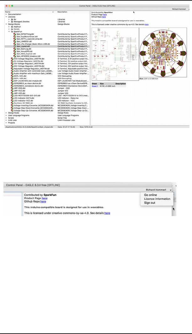
4 A First Look at EAGLE
On the top right corner the current ONLINE/OFFLINE status is shown. The
following image shows that EAGLE is currently OFFLINE. On the right, click
onto the user name and select one of the options there. Here you can Go
online again, let display the License information and Sign out from your
account.
Documentation
The Documentation branch allows direct access to the EAGLE tutorial and
manual available in different languages. Additionally, there can be found the
UPDATE.txt file and documentation files of some of the User Language
programs. Double-click opens the file with the default PDF reader or text
editor.
Libraries Summary
The possibility of displaying the contents of the libraries is particularly
interesting. It provides a very rapid overview of the available Devices.
40
➢
Control Panel: On the right, the preview of a Design Block
➢
Control Panel: License/Status Information

4.1 The Control Panel
Expand the Libraries entry, and you can see the available libraries. We
distinguish between Managed Libraries and “normal” libraries. Managed
libraries come with the EAGLE installation and are kept up-to-date and in
sync with our online EAGLE Managed Libraries repository. If there are
newer versions of Managed Libraries available, you can decide to download
and use them.
Besides the Managed Libraries folder you see a lbr folder which is supposed
to be the folder for all of your own and self-made libraries.
In the Description field you can see a brief description of the contents. If a
library is selected, you will see more extensive information about the library
in the right hand part of the Control Panel. If you then expand a library
entry, the contents will be displayed together with a short description of each
element. Devices and Packages are marked with a small icon.
Now select, for example, a Device:
The description of the Device and a graphical representation of it appear on
the right. The available Package and technology variants are listed. If you
click onto one of the Package versions, the Package preview shown above will
change.
If a Schematic Editor window is open, the entry ADD will be shown right of
the variant name. Click it and the Device is attached to the mouse cursor as
soon as it is over the Schematic Editor window. Now you can drop it in the
schematic.
If you are only working with the Layout Editor, this will of course also
operate with Packages. It is, additionally, possible to drag a Device from the
tree view into a schematic diagram and to place it there by means of
Drag&Drop. If it has more than one Package version, the ADD dialog opens
automatically, so that the desired Package can be selected.
The green marker behind the library entry indicates that this library is in use.
This means that it can be used in the current project. Devices in this library
will be examined by the search function in the ADD dialog of the schematic
diagram or of the layout. This makes them available for the project. The
library will not be examined if the marking is gray.
If starting EAGLE without a project (no eagle.epf file is read, the project has
been closed before exiting EAGLE last time) and creating a new project
(⇒ File/New/Project) all libraries will be in use automatically. However,
opening an already existing project, where only certain libraries are in use
before creating the new project, will adopt this selection.
41
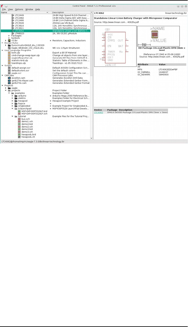
4 A First Look at EAGLE
If the Library Editor window is open, you can Drag&Drop a complete Device
set or Package definition from the Control Panel into the library window.
This way you can copy it from one library into another. If the target library
already contains an element with the same name, it will be updated
automatically.
Design Blocks
Design Blocks (dbl) ideally contain a consistent Schematic and Layout pair
that can be easily (re-)used in any project. Design Blocks can have a
Description and Attributes for getting information about the intent of the
Design Block.
A right mouse click onto a Design Block entry opens a context menu that
allows to Open, Rename, Copy, Delete a Design Block or directly Add it to a
Schematic.
Design Rules
Special Design Rules can be specified in EAGLE to govern the board design.
These can be saved as data sets in special files (*.dru).
The parameter set that is to govern the current project is specified in the
Design Rules branch of the tree view. If no data has been provided for the
Design Rules (DRC command), EAGLE will itself provide parameters. The
marking to the right of the file entry specifies the default parameter set for
the current project. The layout will be checked by the DRC in accordance
with these criteria. Further information about the DRC and the Design Rules
is found starting on page 144.
42
➢
Control Panel: Library summary with Device view

4.1 The Control Panel
User Language Programs, Scripts, CAM Jobs
These entries show the contents of the ulp, scr and cam directories. They
contain various User Language programs (*.ulp), script files (*.scr) and CAM
jobs (*.cam) for the output of data using the CAM Processor. If one of these
files is selected in the Control Panel, you will see a full description of the file.
The paths can be set by means of the Options/Directories menu. This is
discussed in more detail later in this chapter.
Projects
The various projects are managed from the Control Panel. A click onto the
Projects entry displays various folders. These are located under the path set
under Options/Directories/Projects. It is allowed to define more than one
path there.
A project usually consists of a folder which represents the project by its name
and the project's configuration file eagle.epf. The folder usually contains all
files that belong to your project, for example, schematic and board file,
special library files, script files and so on.
Project directories that contain the project file eagle.epf will be marked with
a special folder icon .
The project to be edited is selected in the Projects branch. On the right of the
project's name you will find a marker which is either gray or green. With the
help of this marker one can open or close projects. Clicking onto a gray
marker, loads the project. The marker appears green now. Clicking onto the
green marker again or clicking onto another gray marker closes the current
project respectively opens another project after closing the current one. This
way one can switch easily from one project to another.
As an alternative you can open or close a project by double-clicking onto the
entry in the tree view or by pressing the Space or Enter key.
While closing a project the settings of the currently opened Editor windows
will be stored in the corresponding project file eagle.epf, provided that the
option Automatically save project file is set in the Options/Backup menu.
If the project file was generated by another EAGLE version than currently
used, you will be asked, if it is allowed to overwrite the file.
New projects are created by clicking the right mouse button onto a folder
entry in this branch. A context menu opens which permits new files and
directories to be created and the individual projects to be managed.
Selecting the option New/Project invokes a new folder which has to be given
the project's title. The project file eagle.epf will be created automatically.
You can also use the File/Open/Project or the File/New/Project menu to
open or create a new project.
The context menu contains the Edit Description item. A description of the
project can be entered here, and this is then displayed in the Description box.
43

4 A First Look at EAGLE
It is possible to create a description for schematic and board files. It has to be
defined in the editor windows. See help function for the DESCRIPTION
command for more information.
Menu Bar
The Control Panel allows various actions to be executed and settings made
through pull-down menus that are explained below.
File Menu
The File menu contains the following items:
New
Creates a new Layout (board), Schematic, Design Block, Library, CAM job,
ULP, script or text file. The Project option creates a new project. This initially
consists simply of a new directory in which the files for a new project are
handled. These will consist as a rule of the schematic diagram and layout,
possibly of special libraries, script files, User Language programs,
documentation files etc. and of the file eagle.epf, in which project-specific
settings are stored.
The default directories for the various file types are defined in the
Options/Directories menu.
CAM jobs are definitions for generating output data with the CAM Processor.
Script and ULP files are text files containing command sequences in the
EAGLE command language or the EAGLE User Language. They can be
created and edited with the EAGLE Text Editor or with an external text
editor.
44
➢
Context menu for project management

4.1 The Control Panel
Open
Opens an existing file of the types mentioned above.
Open recent projects
Lists recently used projects.
Save all
All changed files are saved. The current settings for the project are saved in
the file eagle.epf, even if the option Automatically save project file in the
menu Options/Backup... is switched off. User-specific settings are stored in
the file eaglerc.usr (Windows) or .eaglerc (Linux/Mac).
Close project
The project will be closed. Project-specific settings are saved in the
eagle.epf file of the current project directory.
Once you have overwritten a project file from an older version (before 6.0)
the dimension values will be stored in a different format. If you then load
such a file with an old version of EAGLE, all menu entries (like wire widths or
drill diameters) will fall back to their default values.
License information
Shows the entitlements of your license.
Sign out
Here you can sign out from your Autodesk account. Now another user could
sign in and use EAGLE with his account and entitlements. When starting
EAGLE again, you will be asked for your EAGLE/Autodesk login data.
Exit
The program is terminated. When EAGLE is started again, the last program
status is restored, i.e. the windows and other working environment
parameters appear unchanged. If there was no project loaded only the
Control Panel will be opened next time.
The current status is also saved when you leave EAGLE with Alt-X from any
program part.
If you have deactivated the Pull-down menu of the Editor windows
with the Options/User interface menu, Alt+X won't work. Use the
QUIT command instead. You could even assign the QUIT command
to Alt+X with the help of the ASSIGN command.
View Menu
Extended mode
The Documentation and the Project branch of the tree view show all files by
default. Image and other binary files can be opened directly with the
appropriate default application. If this mode is switched off, only EAGLE
related files will be shown.
45
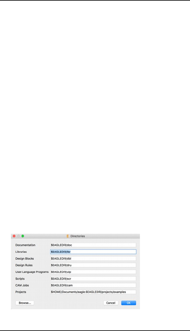
4 A First Look at EAGLE
Refresh
The contents of the tree view are updated.
Search in tree
The tree view of the Control Panel is searchable. This menu entry invokes a
Search line which is located above the Control Panel's status bar. The search
function looks exactly for the given search pattern. If you are using more
search patterns, all of them must occur in order to get a match.
The search function has access to all objects that can be displayed in the tree
view, like file names, Device and Package names in libraries, and for example
the short description shown in the Descritpion column. In order to make the
search more flexbile wildcards are allowed. ? stands for any character, * for
any number of any character.
In case you want to search for a name that contains a *, you have to escape it
with a backslash: 40\*14, for example, searches for 40*14.
Sort
The contents of the tree view will be sorted by name or by type.
Options Menu
Directories
The default directories for particular EAGLE files are entered in the
directories dialog box.
More than one path may be entered for each of these. In the Windows
version the entries are separated by semicolons, while a colon is used in the
Linux and Mac version. The Projects directory is also the default directory for
the Text Editor.
The Projects directory contains subdirectories, each of which represents a
particular project. Each of the project directories contains an EAGLE project
file (eagle.epf). A project directory and its subdirectories usually contain all
the files that are associated with one particular project, such as the schematic
diagram and the layout, text files, manufacturing data, documentation files
and so on.
Type the path directly into the corresponding box, or select the desired
directory by clicking the Browse button.
46
➢
The directories dialog in the Options menu
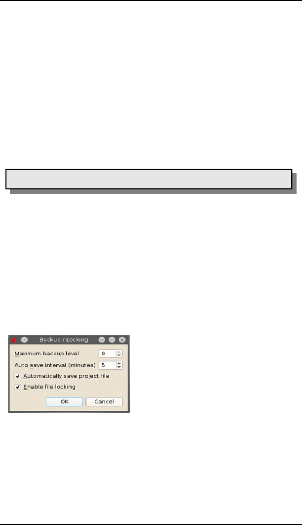
4.1 The Control Panel
The default settings can be seen in the diagram above. $EAGLEDIR stands
for the installation's EAGLE directory.
You may also use $HOME for your home directory under Linux. Under
Windows it is possible to define this environment variable in the Windows
Control Panel, System settings. If a HOME variable has not been set within
the Environment variable, then under Windows EAGLE will suggest the
directory Application Data.
This directory is defined in the Windows registry in:
HKEY_CURRENT_USER\Software\Microsoft\Windows\CurrentVers
ion\Explorer\Shell Folders\AppData
In this folder you can also find the user-specific configuration file
eaglerc.usr. Under Windows 7/8/10 this is typically
C:\Users\your_account_name\AppData\Roaming\CadSoft\EAGLE
It is of course also possible to specify paths with an absolute format.
The HOME variable must not point to the root directory of a drive!
Backup/Locking
When files are saved, EAGLE creates backup copies of the previous files. The
maximum backup level field allows you to enter the maximum number of
backup copies (default: 9). Backup files have different file extensions,
enumerated sequentially. Schematic files receive the ending s#x, board files
b#x, and library files l#x. x can run from 1 to 9. The file with x = 1 is the
newest one.
The automatic backup function also permits the backup to be scheduled. The
time-interval can be between 1 and 60 minutes (default: 5 minutes). The
backup files have the endings b##, s## and l## respectively.
All these backup files can be further processed in EAGLE if they are renamed
and given the usual file endings (brd, sch, lbr).
If the option to Automatically save project file is chosen, your project is
automatically saved when you close the current project or leave the program.
Enable file locking is set off by default. For each file edited in one of the
EAGLE editor windows, EAGLE creates a lock file name.lck. If another
EAGLE user tries to open one of the already locked files, a dialog window
that offers various options pops up.
47
➢
Backup dialog
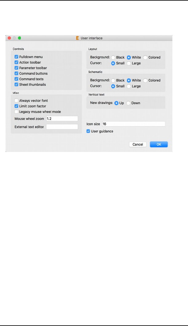
4 A First Look at EAGLE
User Interface
The User Interface dialog allows the appearance of the editor windows for
the layout, schematic diagram and library to be adjusted to your preferences.
You can also access this menu from the Editor windows.
In the Controls box you specify which objects are to be displayed in the editor
window. If you deactivate all the Controls, only the command line will
remain for entry. This maximizes the free area available for the drawing.
The option Always vector font shows and prints texts with the built-in vector
font, independently from the originally used font. Using the Vector font
guarantees that the output with a printer or the CAM Processor is exactly the
same as shown in the editor window. Fonts other than vector font depend on
the systems' settings and cannot be controlled by EAGLE. The output of non-
vector fonts may differ from the editor's view.
Opening the User Interface dialog from one of the Editor windows (for
example, the Layout Editor) the Always vector font option offers an
additional item Persistent in this drawing. Setting this option causes EAGLE
to save the Always vector font setting in the current drawing file. So you can
be quite sure that the layout will be shown with vector font at another's
person computer (for example, at a board house).
Please see the help function for details (TEXT command).
Since EAGLE 8.3.0 EAGLE comes with a new internal vector font. It is very
similar to OSIFONT which is commonly used in the CAD world. In order to
maintain all your projects with previous versions, the option Keep legacy
vector font in this drawing is selected with each project. In case you create a
new project EAGLE will automatically use the new vector font.
48
➢
Settings for the User Interface

4.1 The Control Panel
Limit zoom factor limits the maximum zoom factor in an editor window. At
maximum zoom level the width of the drawing is about one Millimetre
(approx. 40 mil). Switching off this option allows you to zoom until the
0.003125 Micron grid will become visible.
If you are working with a wheel mouse, you can zoom in and out by turning
the mouse wheel. Mouse wheel zoom determines the zoom factor. The value
0 switches this function off. The wheel is used for scrolling then.
EAGLE also supports the use of two-finger-pan gestures on track pads for
navigating and zooming. If you activate the Legacy mouse wheel mode
option, the gestures are no longer supported.
The field External text editor allows you to specify an alternative for the
built-in EAGLE text editor. Further details on this can be found in the help
function in the section Editor windows/Text editor.
The background color and the appearance of the drawing cursor can be
separately adjusted for the layout and the schematic diagram editors. The
background may be black, white or shown in any other color (Colored). The
background color definition is described on page 107.
The cursor can be displayed optionally as small cross or as large cross-hairs.
The section Vertical text lets you decide whether text should be readable
from the right hand side upwards (Up) or from the left hand side downwards
(Down) in your drawings.
Icon size can be used for scaling the icons. The value is in pixels.
Selecting the User guidance check box displays additional information about
the selected object, like the net or signal name, the net class, or the part's
name and value (with NET, MOVE, ROUTE, SHOW...), instructions about
the possible mouse actions in the status bar of the editor window.
Window Positions
Here you can store the positions and the sizes of the currently open Editor
windows. Each file that will be opened from now on appears in its Editor
window at the given position and size parameters that were stored.
If you delete the stored positions again, EAGLE determines the location of an
Editor window and uses a fixed size for it, which is the default setting.
Window Menu
From the Window menu you can choose the window (schematic, board, etc.)
to be displayed in the foreground. The number on the left is the window
number. It allows you to choose a window when combined with the Alt key
(e.g. Alt+1 selects window 1).
The combination Alt+0 can be used anywhere in the program to bring the
Control Panel into the foreground.
The functionality of Alt+window_number is supported in the
Windows and in the Linux version only.
49
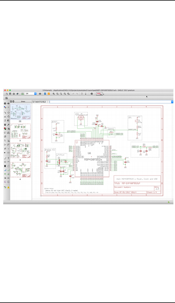
4 A First Look at EAGLE
Help Menu
The Help menu contains an item for calling the help function.
4.2 The Schematic Editor Window
The Schematic Editor window opens when you load an existing schematic or
create a new one. There are several ways of opening files in EAGLE.
You can, for instance, load a schematic diagram by means of the
File/Open/Schematic menu in the Control Panel. Alternatively double-click
onto a schematic diagram file in the tree view.
If you want to create a new schematic, select the menu File/New/Schematic.
This will open a schematic with the name untitled.sch in the current project
directory.
➢
The Schematic Editor
If you want to create a schematic diagram straight away in a new project, you
may for example click with the right mouse button onto a project in the
Projects entry of the tree view, and select the New project option from the
context menu. The new project receives a name. Then click onto this entry
with the right mouse button. Now select New/Schematic from the context
menu.
A new schematic opens in this project directory.
On top you will see the title bar, which contains the file name, and then the
menu bar, and the action toolbar.
Below the action toolbar there is the parameter toolbar, which contains
different icons, depending on the active command.
50

4.2 The Schematic Editor Window
Above the working area you will find the coordinate display on the left,
with the command line, where commands can be entered in text format, to
the right of it.
EAGLE accepts commands in different but equivalent ways: as mouse clicks,
text via keyboard, or from command (script) files.
On the left of the work space you find the command toolbar, which
contains most of the Schematic Editor's commands.
In the status line, at the bottom of the screen, instructions for the user
appear, if a command is active.
On the left you you can see the preview of the schematic sheets. You can sort
the sheets via Drag&Drop.
Each of the toolbars can be displayed or hidden using Options/User
Interface. It is also possible to rearrange the toolbars within certain limits
with the aid of the mouse. The command toolbar, for instance, can also be
placed on the right, or the action and parameter toolbars can be placed
together on one line.
How You Obtain Detailed Information About a
Command
User Guidance
If the mouse cursor remains above an icon for longer than a certain time, the
name of the EAGLE command appears. You also see a short explanation
below in the status line.
For example, move the cursor over the LINE icon. Bubble help with the word
Wire appears directly by the cursor. The short description, Draw lines,
appears in the status line.
If you select the command, a short note appears below in the status line,
indicating what would normally be expected as the next action. For instance,
if you click onto the LINE icon, the status line will display the instruction:
Left-click to start wire .
These functions can be activated or cancelled in the Control Panel by means
of the Options/User Interface menu.
Help Function
If you want to learn more about a command, e.g. the LINE command, click
its icon in the command toolbar, then click the help icon.
As an alternative you can type
*←
in the command line. The ← character symbolizes the Enter key.
The contents of the EAGLE Help is stored in a single HTML file and can be
viewed for example with a web browser, as well. It also offers a full-text
search.
After typing in a search term in the Find line, EAGLE help no longer shows
all pages but only the pages containing this expression. The keys F3 and
Shift+F3 allow you to go to the next or previous location. Each search term
51
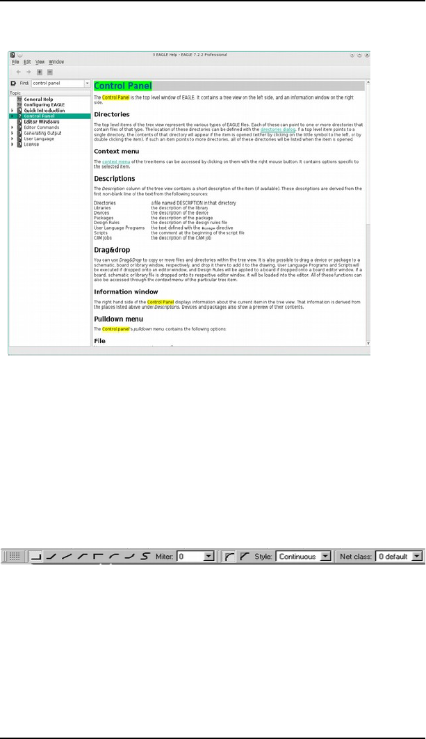
4 A First Look at EAGLE
found will be marked. Green indicating the currently found term, yellow for
all others.
➢
EAGLE Help window
Command Parameters
A number of EAGLE commands need additional parameters. Refer to the
help pages for a description of the textual entry of parameters (via command
line or script file).
Most of the parameters can be entered by clicking the appropriate icons in
the parameter toolbar, which changes according to the selected command.
These icons also show bubble help explanations.
This is how the parameter toolbar appears when the NET command is
activated.
➢
Parameter toolbar of the NET command
On the left is the GRID icon for setting the grid pitch. To the right are
buttons for the bend mode (SET WIRE_BEND) of the net line, followed by
the miter radius for smoothing line joints with the options straight or
rounded (see MITER command). Next to this is the Style menu where the
type of line is defined. On the far right is a value menu for assigning a Net
class.
52
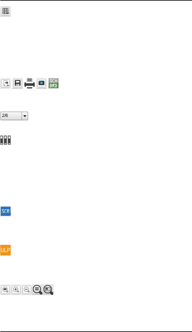
4.2 The Schematic Editor Window
GRID
This icon is available at any time. It is used to adjust the grid and to select the
current unit. In EAGLE, any value relates to the current unit.
A right-click onto the icon opens a popup menu that contains the entry Last.
So you can switch back to the previously chosen grid setting. The New...
entry allows to define so-called Aliases. More about this in chapter 5.
The Action Toolbar
This toolbar is composed of the following icons:
From the left: Open file, save file, print file, call CAM Processor, open/create
corresponding board file (BOARD command).
Load, remove, or create a new schematic sheet.
USE
Select libraries which will be taken into consideration by the ADD dialog. Can
also be done with the Library/Use menu item or by clicking the markers in
the Libraries branch of the Control Panel's tree view. The context menu of
the entry Libraries or of its subfolders contains the entries Use all and Use
none for a quick and simple selection/deselection of all libraries (of the
folder).
This command has to be used in script files in order to choose the library you
want to take parts from.
SCRIPT
Execute a script file. This enables you to execute any command sequence
with a few mouse clicks.
A right-click onto the icon shows a list of recently executed script files.
RUN
Start a User Language program (ULP).
A right-click onto the icon shows a menu that contains a list of recently used
User Language Programs.
WINDOW
These icons represent different modes of the WINDOW command:
Fit drawing into the screen (WINDOW FIT, Alt-F2), zoom in (F3), zoom out
(F4), redraw screen (WINDOW or F2), select new area.
53
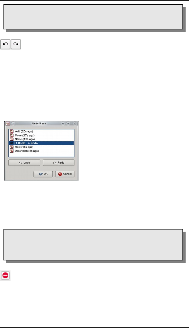
4 A First Look at EAGLE
To move the current drawing window, click the middle mouse button
and move your mouse!
WINDOW LAST returns to the previous display window.
UNDO/REDO
These commands allow you to cancel previous commands and to execute
commands which have previously been cancelled. If you are working with a
consistent pair of schematic and layout the UNDO/REDO commands now
display in the status bar which command was undone/redone and whether
the command was originally executed in the board or in the schematic editor.
Default function keys: F9 and F10.
Typing UNDO LIST into the command line opens a dialog that contains the
entire contents of the undo buffer. Alternatively you can use the
Edit/Undo/redo list... menu. Here you can undo a certain number of actions
and let them redo again.
The Undo/Redo window shows the list of recent actions. In parenthesis you
find information how long ago this was done. Use the mouse, the up/down
keys or the Undo and Redo buttons in order to place the delimiter. Click Ok
in case you are sure you want to have undone all the actions listed below the
delimiter.
Caution: This is a very powerful tool! By going all the way back in
the UNDO list (which can be done with a single mouse click) and
executing any new command, the undo buffer will be truncated at
that point, and there is no way back! So use this with care!
Stop Icon
Terminates the execution of EAGLE commands (Edit/Stop command).
54
➢
Undo/redo list
4.2 The Schematic Editor Window
Go Icon
Starts the execution of an active EAGLE command, which allows further
parameters to be entered by the user, like it is with the AUTO or the MARK
command.
The Command Toolbar of The Schematic Editor
INFO
Shows the properties of the selected object. If you know the name of the
object, you can use it as a parameter in the command line. Depending on the
selected object some of the properties can be altered in this dialog.
SHOW
Highlights the object to be selected with the mouse.
It's also possible to enter the object's or Gate's name (even several names at
once) in the command line. You may use the characters * and ? as
wildcards, as well. Ctrl + SHOW toggles the show state of the selected object.
If you are looking for very small objects, it can be useful to use the SHOW
command with the @ option, like in
*+,-.
The location of part C12 will be recognized at once, because the part is
marked with a surrounding frame.
If the searched object is not located on the current sheet, the SHOW window
opens and informs you about the sheet where it is located. In case of objects
that consist of more than one part, like elements with several gates or nets
that spread over several sheets, the window will list several entries. Clicking
on one of the entries center the selected object on the screen. If the searched
object is not found in the whole schematic, the Sheet column will be marked
with a minus sign '-'.
DISPLAY
Select and deselect the layers to be displayed. See the Appendix for the
meaning of the layers
DISPLAY LAST shows the recently used layer combination that was
previously selected for display.
For further details please see help function.
MARK
The following mouse click defines the new origin for the coordinate display.
Relative coordinates (R x-value y-value) and polar values (P radius angle)
are shown in addition to absolute coordinates in the coordinate display box.
55
4 A First Look at EAGLE
If you first click the MARK icon and then the traffic-light icon, only the
absolute coordinate values will be displayed again.
MOVE
Move any visible object. The right mouse button rotates the object while it is
attached to the mouse cursor.
If you move a net over a pin, no electrical connection will be established. If
you move the pin of a Gate over a net or another pin, an electrical connection
will be created.
To move groups of objects:
Define the group with the GROUP command, click the MOVE icon, press the
Ctrl key, then click into the drawing with the right mouse button, and move it
to the desired location.
If you don't press the Ctrl key, the context menu pops up after clicking with
the right mouse button. It contains an entry Move:Group that allows you to
move the group, too. The right mouse button rotates the group by 90 degrees
while it is attached to the mouse cursor.
If you like to move the group onto another sheet, click the sheet combo box in
the action toolbar or select it from the Sheets preview. Place the group there.
MOVE can be used in the command line with various options. See the help
function for details.
COPY
Copy parts and other objects.
When copying nets and buses the names are retained, but in all other cases a
new name is assigned.
Keep the Ctrl key pressed while clicking onto an object and the object will be
grabbed at its origin. So it will be moved into the currently chosen grid.
COPY can be used with groups. The group will be put into the clipboard of
the operating system. It is possible to copy it into another running EAGLE
program, for example.
MIRROR
Mirror objects.
ROTATE
Rotate objects by 90 degrees (also possible with MOVE).
GROUP
Define a group which can then be moved, rotated, or copied with COPY and
PASTE to another drawing or whose properties are to be changed. After the
icon has been clicked, a rectangular group can be defined by holding down
the left mouse button and dragging the cursor to the diagonal corner of the
56
4.2 The Schematic Editor Window
rectangle. If you want to define a group by a polygon, use the left mouse
button to determine the corners of the polygon. Then click the right mouse
button to close the polygon.
GROUP ALL in the command line selects all objects on the current sheet, if
the respective layers are displayed.
The following command (ROTATE, CHANGE, MOVE...) has to be applied to
the group with the right mouse button while the key is pressed.
If you like to add further groups to an already existing one, press the Shift
key and define the first corner of the selection area with a mouse click.
In case you want to add an object to or remove it from the group, press the
Ctrl key and click onto the object in question.
Press Ctrl + Shift to toggle the membership of an object and its hierarchically
superior objects: Clicking for example, on a net segment in the Schematic
inverts the group membership of the whole net.
CHANGE
Change the properties of an object, e.g. the width of a line, the Package
variant or the size of text. See help for details.
An object's properties can be checked and even changed, where applicable,
by the Properties entry of the context menu. To access the context menu,
click onto the object with the right mouse button.
PASTE
Insert objects from the paste buffer into the drawing.
It is also possible to paste from a file into schematic and layout directly. To
do so, use the PASTE command with a file name in the command line or use
the menu entry Edit/Paste from...
For further information see help function.
DELETE
Delete visible objects.
Also in combination with GROUP command. If a group has been defined, it
can be deleted with the right mouse button while the Ctrl key is pressed.
The DELETE command deletes an entire part in the Schematic when clicking
onto a Gate with the Shift key pressed. In that case, the tracks connected to
the Package in the board, if already existing, will stay unchanged.
Clicking onto a net or bus wire with the Shift key pressed deletes the entire
net or bus segment.
ADD
Add library elements to the schematic. A search function helps Devices to be
found quickly. USE specifies which libraries are available.
A right-click onto the ADD icon opens a popup menu that lists recently
fetched Devices.
57

4 A First Look at EAGLE
PASTE DBL
Add a Design Block into the drawing.
PINSWAP
Swap two nets connected to equivalent pins of a Device, provided the pins
have been defined with the same Swaplevel.
A pin that is connected to several pads can't be swapped.
GATESWAP
Swap two equivalent Gates of a Device, provided the Gates have been defined
with the same Swaplevel. In EAGLE terminology, a Gate is a part of a Device
which can be individually placed on a schematic (e.g. one transistor from a
transistor array).
Gates that come with pins connected to several pads, can't be swapped.
REPLACE
Replace a component (Device) with another one from any library. This can
only work if the new component has at least as many pins as the current one
and the pins as well as the pads have identical names or the same positions.
A right-click onto this icon opens a popup menu that shows a list of recently
replaced Devices.
NAME
Give names to components, nets, or buses.
VALUE
Provide values for components. Integrated circuits normally get the type (e.g.
74LS00N) as their value.
A right-click onto this icon opens a list of already used values. Select an entry
and apply it to one or more components by clicking onto them successively.
SMASH
Separate name, value, and, if any, attribute texts from a Device, so that they
can be placed individually. The size of detached (smashed) texts can also be
individually changed. Also in combination with GROUP. If a group is
defined, you can smash it with a right mouse click while the Ctrl key is
pressed.
Use DELETE to hide smashed texts.
Keep the Shift key pressed while using the SMASH command in order to
unsmash text. Text is not editable any more and appears at original
position(s) after a window refresh (also possible in the context menu with
58

4.2 The Schematic Editor Window
unSmash).
Alternatively you can also switch on or off the option Smashed in the context
menu's Properties entry.
MITER
Round off or bevel wire joints (also possible for nets, buses, polygon
contours). The grade of mitering is determined by the miter radius. Positive
sign results in a rounded joint, negative sign in a bevel.
The miter radius influences some wire bends, too (see help function: SET
command, Wire_Bend).
SPLIT
Insert an angle into a wire or net.
SLICE
Cuts lines in two parts. The parameter width decides about the width of the
gap.
INVOKE
Devices that consist of more than one Symbols (Gates) can be fetched Gate
by Gate, for example in certain order (Gate D before Gate C), if wanted.
INVOKE can also be used to fetch power supply Gates that do not appear
automatically in the Schematic. This is useful and required, for example,
when you are adding decoupling capacitors to your design.
This command allows you also to add a Gate from a Device which is located
on another sheet. In such a case, type the name of the Device (e.g. IC1) into
the command line after the INVOKE command has been selected.
LINE (was WIRE)
Draw line (this command was is called WIRE in previous versions). The type
of line can be changed with CHANGE STYLE. Clicking the right mouse
button changes the bend mode (SET WIRE_BEND).
LINE can also be used to draw arcs.
Please note the particularities in combination with the Ctrl and Shift key in
the help function:
If you press, for example, the Ctrl key while starting to draw a wire, the wire
begins exactly at the end of an already existing wire nearby. Even if this wire
is not in the currently set grid. Wire width, style and layer will be adopted
from the already existing wire.
59
4 A First Look at EAGLE
TEXT
Placing text.
Text size, thickness of the lines for vector font texts, the alignment and the
font can be defined in the parameter toolbar of the TEXT command. In case
the text is already placed in your drawing you can make theses changes via
the Properties entry of the context menu or via the different options of the
CHANGE command (Size, Ratio, Align, Font).
Shift + Enter inserts a line break for multi-line texts in the text window.
You can change label texts by assigning a different name to the bus or to a net
by means of the NAME command. See also LABEL command.
CIRCLE
Draw a circle. Circles with a width of 0 are drawn as filled circles.
ARC
Draw an arc (also possible with LINE).
CHANGE CAP FLAT | ROUND defines straight or rounded ends for arcs.
RECT
Draw a rectangle.
POLYGON
Draw a polygon (copper areas in any shape).
BUS
Draw a bus line. The meaning of a bus is more conceptual than physical. It is
only a means to make a schematic easier to read. Only nets define an
electrical connection. Nets, however, can be dragged out of a bus.
The name of a bus can consist of a synonym and the net names that are part
of the bus. In case there is a synonym defined, a LABEL would show the
synonym only, not the whole name of the bus.
Example:
/0$$1-23/0$$1-233+4
A LABEL shows the synonym ATBUS. The bus contains the nets A0 to A31,
B0 to B31, RESET and CLOCK.
NET
Draw a net. Nets with the same name are connected (even if located on
different sheets).
60
4.2 The Schematic Editor Window
Nets and pins which appear to the eye to be connected are not necessarily
electrically connected. Please check with the SHOW command, the ERC, or
by exporting a netlist or pinlist (EXPORT NETLIST or PARTLIST). See also
the help for MOVE.
JUNCTION
Place the symbol for a net connection. In general, junctions are placed
automatically, but nets which cross over can also be joined manually by the
JUNCTION command.
LABEL
Place the name of a bus or net as a label. Labels cannot be changed with
CHANGE TEXT but rather with the NAME command because the label
represents the net name.
If the label option XREF (in the parameter toolbar or by CHANGE XREF
ON) is set, a cross reference pointing to an further instance of the chosen net
on the next sheet is generated automatically.
The cross reference label format can be defined in the menu
Options/Set/Misc, Xref label format. See the help function of the LABEL
command for the meaning of the placeholders that can be used.
For a proper location of the object you should use a drawing frame with
classifications for columns and rows. Such frames can be defined with the
FRAME command. The library frames.lbr already contains such frames.
ATTRIBUTE
Defines an attribute for a component. Attributes are free definable and can
contain any information.
Through the menu Edit/Global attributes.. you can define attributes that are
valid for all components respectively for the whole schematic.
DIMENSION
Can be used to draw dimension lines.
It is possible to dimension objects drawn in the schematic or you can start
dimensioning at any position in the schematic with Ctrl + left mouse click.
Please look into the description of the DIMENSION command in the section
about the Layout Editor window for more details.
MODULE
The MODULE command defines modules. A module can contain parts and
nets as a part of the whole schematic. The MODULE command also inserts
module instances in the hierarchical schematic. A module instance is drawn
as a simple symbol and represents the usage of a module.
61
4 A First Look at EAGLE
PORT
The PORT command defines an interface between the nets inside a module
and the higher schematic level. Ports belong to module instances and can be
connected to nets, similar to pins of components.
ERC
Perform an Electrical Rule Check and a consistency check for schematic and
board, if already existing. A positive consistency check allows the
Forward&Back Annotation engine to run.
Commands Not Available in the Command Toolbar
Menu items already explained in the Control Panel section are not discussed
here.
The following commands can be entered into the command line as text
inputs. Some of them are available as menu items. Most of them can be used
in the Schematic and in the Layout and even in the Library Editor.
ASSIGN
Assign function keys.
The most convenient way of doing this is to use the Options/Assign menu.
CLASS
Select and define net classes (Edit/Net classes...). A net class specifies the
width of a track, the clearance from neighbouring signals, and the diameter
of vias for the Autorouter and the ROUTE command. These settings are also
used in polygons. See also page 123.
CLOSE
Text command for closing an editor window (File/Close).
CUT
Transfer the objects of a previously defined group into the paste buffer.
Activate the CUT command and click with the left mouse button into the
group to set a reference point. PASTE inserts the group into the drawing.
Since version 6 this approach has been replaced by the new functionality of
the COPY command. Further information about CUT and COPY can be
found in the help function: Editor commands/CUT.
EDIT
Text command for loading a file or a library object. You can, for instance,
load a board from the Schematic Editor (EDIT name.brd).
The EDIT command is also used to create or edit a module in a schematic
diagram.
5$
loads or creates a module in a circuit diagram.
62

4.2 The Schematic Editor Window
5$.
loads or creates page number 2 of a module.
FRAME
Define a drawing frame for the Schematic (Draw/Frame). Also possible for a
board drawing.
EXPORT
Output lists (especially netlists), directories, script files, or images
(File/Export...).
Takes care on the hierarchical structure, if existing.
LAYER
Choose or define the drawing layer. When using drawing commands the
layer can be chosen in the parameter toolbar.
To create, for example, a new layer with number 200 and layer name
Mylayer, type in the command line:
6.0078!8
In case you created a Layout, for example, with the EAGLE Light Edition and
upgraded to the Standard Edition because you would like to use two
additional inner signal layers, you have to create these layers with the LAYER
command first:
6.)&.
6-9)&-9
MENU
Specifies the contents of the text menu. Now it is located right next to the
action toolbar and can handle small images, as well. See also the example in
the appendix. The text menu can be made visible with the aid of
Options/User Interface. See help function for details.
OPEN
Text command for opening a library for editing (Library/Open). This
command is not identical to the File/Open menu item of the Schematic
Editor, which only lets you select schematics. You can use the OPEN
command as an alternative to the File menu of the Control Panel.
PACKAGE
In case there is more than one Package variant defined in the library for a
part (Device), a typical example would be a resistor from rcl.lbr, it is possible
to change the currently used Package with the PACKAGE or with the
CHANGE PACKAGE command. This can be done in the Schematic or in the
Layout Editor.
63

4 A First Look at EAGLE
PRINT
Call up the print dialog with the printer icon in the action toolbar or
from the menu item File/Print.... Usually the PRINT command is used to
print schematics or for checking the drawings needed for the PCB
production.
The actual production data are generated with the CAM Processor.
If you want to output your drawing in black and white check the Black option
(and Solid, if you don't want layers to be printed in their different fill styles).
The caption text is suppressed unless you check Caption. Set Page limit to 1,
if your drawing is to be fitted on one page. If you prefer to print the currently
visible drawing window instead of the whole drawing, select Window instead
of Full in the Area option.
QUIT
Quit EAGLE. Identical with the menu item File/Exit or Alt-X.
REMOVE
Delete files or schematic or module sheets.
7+:$1←
for instance, deletes sheet 3 of the loaded schematic.
SET
Set system parameters and modes. Best done via the Options/Set menu item.
Please note that not all of the possibilities are available through this dialog.
Presettings can be defined in the script file eagle.scr by using text
commands. Further information can be found in the help function.
TECHNOLOGY
If a part (Device) has been defined with various technologies in the library,
see typical examples in 74xx.lbr, it is possible to change the currently used
technology with the TECHNOLOGY or with the CHANGE TECHNOLOGY
command. This can be done in the Schematic or in the Layout Editor.
UPDATE
The UPDATE command checks the parts in a board or schematic against
their respective library objects and automatically updates them if they are
different. (Library/Update... or Library/Update all).
The context menu in the Control Panel's' tree view offers the Options Use all
and Use none for a quick selection of libraries.
VARIANT
This command offers the possibility to define different assembly variants of a
project. It opens a dialog that allows to decide about components to be
assembled or not, or about different values or technologies of the
components used in the different variants of the project. This function can be
reached through the Edit/Assembly variants menu or by typing the
command VARIANT into the command line of the Schematic or the Layout
64

4.2 The Schematic Editor Window
editor. Further information will be given in chapter 6.10 beginning with page
192.
WRITE
Text command for saving the currently loaded file. Please note that, in
contrast to Save as, the name of the currently edited file is never changed
when the WRITE command is used.
Mouse Keys
The middle and right mouse button have a special meaning for a number of
commands. You can use the middle mouse button only if the operating
system knows your mouse is a 3-button mouse, that is your mouse must be
installed this way.
If you are working with a wheel mouse, you can zoom into and out of the
drawing with the help of the mouse wheel. The option Mouse wheel zoom in
the Options/User Interface menu determines the zooming in/out factor per
step. The value is set to 1.2 by default.
Selecting a value of 0 allows you to use the wheel for scrolling.
Keep the mouse wheel or the middle mouse button pressed for panning.
Mouse clicks in combination with the Shift, Ctrl, and Alt key can have various
functions, for example, while selecting objects with MOVE or while drawing
lines with LINE.
The help section on Keyboard and Mouse and the help of the referring
command gives you more details.
Selecting Neighbouring Objects
If one of two objects which are very close together is to be selected, the
individual objects are highlighted one after the other. The user can select the
highlighted object with the left mouse button, or proceed to the next one with
the right mouse button. The status bar of the editor window shows
information about the pre-selected object. See also help function (SET
command, SELECT_FACTOR).
4.3 The Layout Editor Window
The Layout Editor window opens when you open an existing board file or
create a new board. If you own the Schematic Editor you will normally draw
a schematic first and then generate the board file with the BOARD
command, or by clicking the Board icon.
The Layout Editor window appears very much like the Schematic Editor
window. Even if you don't work with the Schematic Editor, you should study
the previous section, as most of the information there applies to the Layout
Editor, too.
65
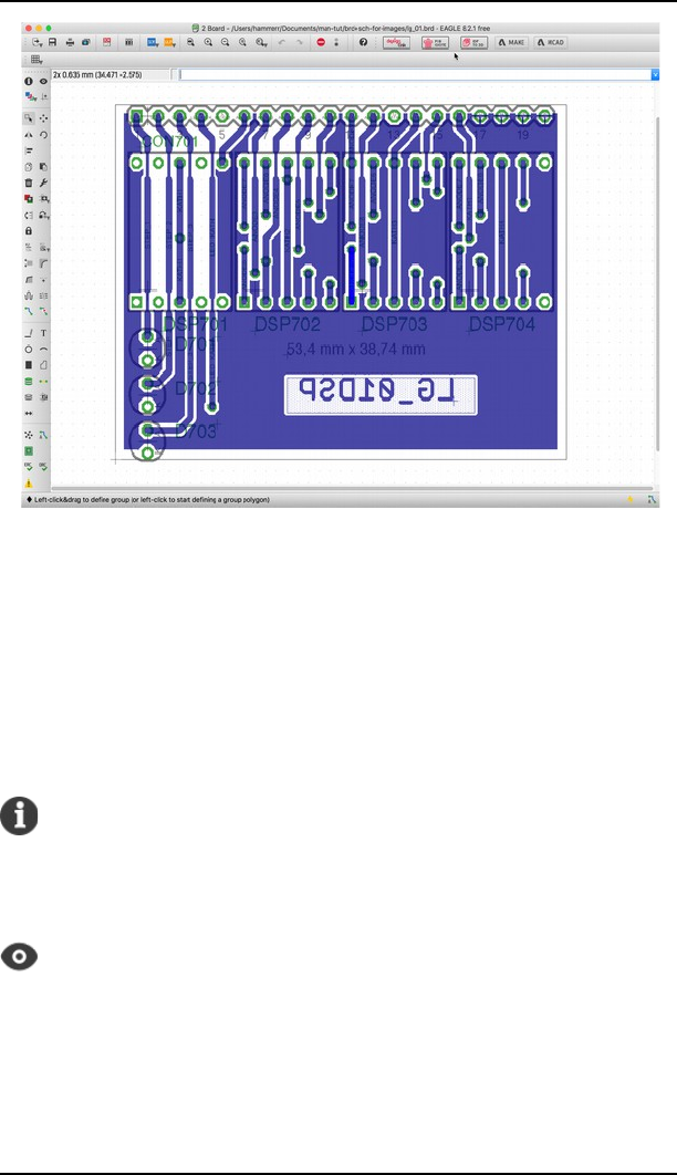
4 A First Look at EAGLE
Only the commands in the command toolbar are discussed again, as some
commands differ in their use.
Descriptions of commands that cannot be reached through the command
toolbar are also to be found in the section concerning the Schematic Editor
window. All of the commands can also be reached through the pull-down
menus in the menu bar. This also applies, of course, to the Schematic and
Layout Editor windows.
The Commands on the Layout Command Toolbar
INFO
Shows the properties of the selected object. Typing INFO IC1 in the
command line results in the properties dialog of the object named IC1.
Depending on the selected object some of the properties can be altered here.
SHOW
Highlights the object to be selected with the mouse.
It's also possible to enter the object's name (even several names at once) in
the command line. * and ? are allowed to be used as wildcards, as well.
Ctrl + SHOW toggles the show state of the selected object.
66
➢
Layout Editor window

4.3 The Layout Editor Window
DISPLAY
Select and deselect the layers to be displayed. Components on the top side of
the board can only be selected if the layer 23, tOrigins, is displayed. The
same applies to components on the bottom side of the board and layer 24,
bOrigins.
See Appendix for the meaning of the layers.
The DISPLAY command supports so-called Layer Presets (Aliases). This
allows you to name certain combinations of layers and use it as a parameter
with the LAYER command. A quick change from one view to another layer
combination is possible with this command.
Double-click one of the layer entries for changing its color or fill style.
DISPLAY LAST switches to the last displayed layer combination.
The DISPLAY menu shows only those layers defined in the Layer
Setup of the Design Rules!
Further information about DISPLAY can be found in the help function.
67
➢
The Display menu
➢
Change layer properties
4 A First Look at EAGLE
MARK
The following mouse click defines the new origin for the coordinate display.
Relative coordinates (R x-value y-value) and polar values (P radius angle)
are shown in addition to absolute coordinates in the coordinate display box.
If you first click the MARK icon and then the traffic-light icon, only the
absolute coordinate values will be displayed again.
GROUP
Define a group which can then be moved, rotated, or copied with COPY and
PASTE to another drawing or whose properties should be changed.
By default the GROUP command is always active. If you click into empty
space of a drawing and hold the mouse button you can drag a rectangle or
draw a polygon around the objects in the group. After defining the group you
can immediately move it without having to select a command icon by clicking
and holding the mouse button onto a groups’ object.
If the option GROUP command default on is not active or you want to
execute another command with the group, define the group, select for
example a command icon (for rotate, copy…..) and execute it on the group
with Ctrl + right mouse-click.
GROUP ALL in the command line selects all objects.
To be sure that all objects are selected DISPLAY ALL layers before. On the
other hand, deselecting specific layers can exclude certain objects from the
selection.
Further information about GROUP can be found in the section about the
Schematic Editor and in the help function.
MOVE
Move any visible object. The right mouse button rotates the object.
The MOVE command cannot connect signals even if a wire (trace) is
moved over another wire or a pad. Use ROUTE to route signals.
Keeping the Ctrl key pressed while selecting an object selects it in a
particular manner. Please consult the help function for details (CRICLE,
ARC, LINE, MOVE, ROUTE etc.).
For moving groups, please see MOVE in the Schematic Editor section.
MIRROR
Mirror objects. Components can be placed on the opposite side of the board
by using the MIRROR command.
68
4.3 The Layout Editor Window
ROTATE
Rotate objects (also possible with MOVE). Keep the left mouse button
pressed to rotate the selected object by moving the mouse. The parameter
toolbar shows the current angle. This can be done with groups (GROUP and
right mouse button)as well.
ROTATE can be used with groups, as well. Activate ROTATE, press the Ctrl
key and click with the right mouse button into the drawing to set the center
of rotation. The group will be rotated counterclockwise by the given angle.
Alternatively type in the angle in the Angle box or in the command line.
Details about the syntax can be found in the help function.
ALIGN
The ALIGN command can be used to align selected objects in relation to each
other or to move their origin location to the nearest grid point.
The following modes are supported:
- Align Edges Top | Bottom | Left | Right
- Align Centers Vertical | Horizontal
- Distribute Vertically | Horizontally
- Align Origin to Grid
COPY
Copy parts and other objects.
When copying objects, a new name will be assigned, but the value will be
retained. When copying a single wire, the copy will have the same name.
Keep the Ctrl key pressed while clicking onto an object and the object will be
grabbed at its origin. So it will be placed in the currently chosen grid.
COPY can be used with groups. The group will be put into the clipboard of
the operating system. It is possible to copy it into another EAGLE program,
for example.
PASTE
Insert objects from the paste buffer.
Use the menu Edit/Paste from... in order to paste a whole layout (and
schematic, if available) into your current drawing. See help for further
information.
DELETE
Delete visible objects.
If a group has been defined, it can be deleted with the right mouse button
while the Ctrl key is pressed.
69

4 A First Look at EAGLE
DELETE SIGNALS in the command line erases all tracks and signals in the
layout, provided there is no consistent schematic loaded.
The DELETE command deletes an entire polygon when clicking on a polygon
wire with the Shift key pressed.
Keeping the Ctrl key pressed while clicking with the left mouse button on a
wire bend will delete the bend. A new direct connection between the next
bends will be drawn now.
If objects cannot be deleted, the reason can lie with error polygons related to
the DRC command. They can be deleted with the ERRORS command
(ERRORS CLEAR). If layer 23, tOrigins, or 24, bOrigins, is not displayed,
components cannot be deleted.
CHANGE
Change the properties of an object, for example the width of a wire or the size
of a text. If the Esc key is pressed after changing a property, the previously
used value menu will appear again. In this way a new value can be
conveniently chosen. See also the help function.
Alternatively, object properties can be viewed and some of them even
changed with the context menu's Properties entry. The context menu opens
after a right mouse click onto the object.
PASTE DBL
Add a Design Block into the drawing. If the Design Block consists of board
and schematic the Layout part can be placed with the mouse cursor. The
Schematic part will be added automatically to the Schematic on new sheets
accordingly.
ADD
Add library elements to the drawing. It offers a convenient search function
for Packages here. USE specifies which libraries are available.
A right-click onto the ADD icon opens a popup menu that contains a list of
recently placed Devices.
PINSWAP
Swap two signals connected to equivalent pads of a component, provided the
pins have been defined with the same Swaplevel.
A pin that is connected to several pads can't be swapped.
REPLACE
Replace a component (or a Package, if there is no schematic) by another one
from any library.
If you want to change the Package variant only and not the whole Device, use
CHANGE PACKAGE or the PACKAGE command.
70

4.3 The Layout Editor Window
A right-click onto the REPLACE icon opens a popup menu that shows a list
of recently replaced components.
LOCK
Locks the position and orientation of a component on the board. If a
component is locked, you can't move it or duplicate it with CUT and PASTE.
Shift + LOCK unlocks the component. This is also possible with the unLock
entry of the context menu.
To be able to distinguish locked from unlocked components, the origin cross
of a locked component is displayed like a 'x' instead of a '+'.
The position of a locked component can be changed, however, by typing in
new coordinate values in the properties dialog.
NAME
Give names to components, signals, vias, and polygons.
With NAME it's possible to move a polygon from one signal to another.
VALUE
Provide values for components. A resistor, for example, gets 100k as its
value. A right-click onto this icon opens a list of already used values. Select an
entry and apply it to one or more components by clicking onto them
successively.
SMASH
Separate name, value, and attribute (if any) texts from a Device, so that they
can be placed individually. The size of detached (smashed) texts can also be
individually changed.
Also in combination with GROUP. If a group is defined, you can smash it
with a right mouse click while the Ctrl key is pressed.
Use the DELETE command to hide smashed texts.
Keep the Shift key pressed while using the SMASH command in order to
unsmash texts. They are not editable any more and appear at their original
positions after a window refresh (also possible with unSmash in the context
menu).
Alternatively you can switch on or off the option Smashed in the context
menu's Properties entry.
MITER
Round off or bevel wire joints (also possible for polygon contours). The grade
of mitering is determined by the miter radius. Positive sign results in a
rounded joint, negative sign in a bevel.
The miter radius influences some wire bend modes, too (see help function:
SET, Wire_Bend).
71
4 A First Look at EAGLE
SPLIT
Insert a bend into a wire.
If you want to change, for example, the layer for a section of an already
routed track, you can insert two wire bends with the SPLIT command and
change the layer of the newly created segment with the CHANGE LAYER.
EAGLE will set vias automatically at the position of the wire bends.
You can use the SPLIT command for a quick re-routing of an already existing
track. Click onto the track to insert a wire bend. Now move the mouse and
route it anew. To remove the previous track use the RIPUP command or
DELETE in combination with the Ctrl key.
OPTIMIZE
Joins wire segments in a signal layer which lie in one straight line.
MEANDER
Draw meanders in order to balance the length of signals, especially of
Differential Pairs. Can be used for measuring the length of a signal, when
pressing the Ctrl key.
SLICE
The SLICE command cut lines in two parts. If it is a routed trace the gap
contains an airwire that connects the two parts of the signal. So a signal is
actually not cut into two different parts, but it rips up the trace according to
the given width of the gap. Simply click left to start the cutting wire, a second
click ends it. All objects crossing the cutting wire will be slices. Exception is a
polygon’s contour. SLICE can be used in the command line. The cutting line
is defined by start and end coordinates, like SLICE (0.2 3) (0.5 4);
ROUTE
Route signals manually. Airwires are converted to wires.
By default the ROUTE command works in “Obstacle Avoidance” mode. So it
automatically takes care on Design Rules and avoids obstacles that are along
the path of a trace. If the routing mode is set to “Ignore Obstacle” mode by
clicking on the icon in the parameter toolbar, the user has to take care on all
the Design Rules by himself.
The ROUTE command also supports the Follow-me router mode which
automatically processes the trace of a selected signal with the Autorouter
running in the background.
ROUTE offers several options with the different mouse buttons, also in
combination with the Ctrl and Shift key.
Ctrl + Left starts routing at any given point along a wire or via
Shift + Left if the airwire begins at an already existing wire and
this wire has a different width, the new wire adopts
72

4.3 The Layout Editor Window
this width
Center selects the layer
Right changes the wire bend style
Shift +Right reverses the direction of switching bend styles
Ctrl + Right toggles between corresponding bend styles
Shift + Left places a via at the end point of the wire
Ctrl + Left defines arc radius when placing a wire's end point
More information can be found in the help function of the ROUTE
command. See also Group Default On.
RIPUP
Convert routed wires (tracks) into unrouted signals (airwires). Change the
display of filled (calculated) polygons to outline view.
Using signal names in the command line allows you to ripup only certain
signals, to exclude particular signals, or to execute the command exclusively
for polygons. More details can be found in the help function.
Wires not connected to components must be erased with DELETE.
LINE
Draw lines and arcs. If used in the layers 1 through 16, the LINE command
creates electrical connections.
The Style parameter (CHANGE) determines the line type. The DRC and the
Autorouter always treat a LINE as a continuous line, regardless of what Style
is used.
Clicking the right mouse button changes the wire bend (SET WIRE_BEND).
Please note the particularities in combination with the Ctrl and Shift key in
the help function:
If you press, for example, the Ctrl key while starting to draw a wire, the wire
begins exactly at the end of an already existing wire nearby. Even if this wire
is not in the currently set grid. Wire width, style and layer will be adopted
from the already existing wire.
TEXT
Placing text. Use CHANGE SIZE to alter the height of the text. If the text is
using a vector font, CHANGE RATIO will alter the thickness. CHANGE TEXT
is used to alter the text itself. CHANGE FONT alters the typeface. CHANGE
ALIGN defines the alignment (the location of the origin) of the text.
The option Always vector font (Options/User Interface) shows and prints all
texts in vector font, regardless of which font is actually set for a particular
text.
If you want to have inverted text in a copper layer, you have to enter the text
in the layers 41, tRestrict, or 42, bRestrict, and draw a copper plane in Top or
Bottom layer around the text with the POLYGON command. The polygon
keeps the restricted areas (which is the text) free from copper.
73
4 A First Look at EAGLE
Use Shift + Enter in order to insert a line break for multi-line texts. The line
distance can be set via the Properties window or in the parameter toolbar, as
long as the text is not yet placed and still attached to the mouse cursor.
It is strongly recommended to write texts in copper layers as vector
font! So you can be sure that the CAM Processor's output is identical
with the text shown in the Layout Editor. See also help function.
CIRCLE
Draw a circle. This command creates restricted areas for the
Autorouter/Follow-me router, if used in the layers 41, tRestrict, 42,
bRestrict, or 43, vRestrict. Circles with wire width = 0 are drawn as filled.
ARC
Draw an arc (also possible with LINE).
CHANGE CAP FLAT | ROUND defines straight or rounded ends for arcs.
If the arc is a part of a trace and both ends are connected to a wire, caps will
be round.
Arcs with flat caps are emulated when generating manufacturing data in
Gerber format with the CAM Processor. That means they will be drawn with
small short straight lines. Arcs with round caps won't be emulated.
RECT
Draw a rectangle. This command creates restricted areas for the Autorouter
or Follow-me router, if used in the layers 41, tRestrict, 42, bRestrict, or 43,
vRestrict.
POLYGON
Draw a copper areas or restricted areas in signal layers.
Polygons in the signal layers are treated as signals. They keep an adjustable
distance to objects belonging to other signals (copper pouring, flood fill). This
enables you to realize different signal areas on the same layer and make
isolated regions for your design.
The contour of a polygon in the outline mode is displayed as a dotted line.
The POLYGON command creates restricted areas for the Autorouter/Follow-
me router, if used in the layers tRestrict, bRestrict, or vRestrict. For other
possibilities of the POLYGON command see help.
Polygons with special fill style cutout can be used as restricted areas for
signal polygons in inner and outer layers. Such a polygon will be subtracted
from all other signal polygons in the same layer. The dotted contour line will
always be visible. The wire width for such a polygon may be 0 as well.
74
4.3 The Layout Editor Window
VIA
Place a plated-through hole. Vias are placed automatically if the layer is
changed during the ROUTE command. You can assign a via to a signal with
the NAME command by changing it's name to the name of the signal. Vias
can have different shapes in the outer layers (round, square, octagon) , but
are always round in inner layers.
SIGNAL
Definition of a signal. This is not possible if the Forward&Back Annotation is
active. In that case you have to define the connection with the NET command
in the Schematic Editor.
HOLE
Define a mounting hole (not plated-through).
ATTRIBUTE
Defines an attribute for a component.
Through the menu Edit/Global attributes.. you can define attributes that are
valid for the whole layout.
DIMENSION
Can be used to add dimensioning to the board. It can either be applied to an
object or you can draw arbitrary dimensions. When you select an object
EAGLE selects a suitable dimensioning type (Dtype). If it is not the one
needed, click the right mouse button to change it. If you want to start at any
location in the drawing use Ctrl key + left mouse click.
There are different dimensioning types: Parallel, Horizontal, Vertical,
Radius, Diameter, Angle, and Leader.
Configuration of dimensioning lines, text size units and so on can be done in
the objects' properties dialog or with the CHANGE command, which can be
executed for groups of objects, as well:
CHANGE Dtype changes the dimensioning type
CHANGE Dunit decides about the measurement unit,
the precision,
and about showing or hiding the unit.
CHANGE Dline determines the width of the measurement line,
the width of the extension line,
the Extension length after the dimension arrow head,
the distance from the object measured (Extension,
offset).
75
4 A First Look at EAGLE
RATSNEST
Calculate the shortest airwires possible and the real mode (filled) display of
polygons.
Use the RATSNEST command with a signal name in order to calculate and
display or hide a certain airwire. A preceding exclamation mark hides the
airwires of the given signal name. More information can be found in the help
function.
The polygon calculation can be deactivated with the SET command. Either
through the menu Options/Set/Misc or by typing in the command line:
SET POLYGON_RATSNEST ON | OFF or in short: SET POLY ON | OFF.
RATSNEST will be executed automatically for the selected signal while
drawing a wire with ROUTE.
While RATSNEST is active the status bar of the Layout Editor displays the
name of the currently calculated signal.
AUTO
Start the Autorouter.
If you type AUTO FOLLOWME in the command line, the Autorouter Setup
window opens in the follow-me mode, which allows to set the parameters for
the follow-me router only.
AUTO BGA
Start the BGA Autorouter.
If you type AUTO BGA or click this icon, EAGLEs start a special Autorouter
in order to route signals connected to BGA components out of the BGA area.
In a first step you select the BGA component(s) in the layout. Second, you
select the signals that shall be routed. You can also decide about the layer
assignment for the signals. Micro Vias are supported, if this option is
enabled.
Please verify Design Rules before starting the BGA router!
ERC
Perform a consistency check for schematic and board.
DRC
Define Design Rules and perform Design Rule Check.
Typing DRC * into the command line opens the Design Rules window where
you can check and adjust your settings and close the dialog window again
without starting the Design Rule Check.
76

4.3 The Layout Editor Window
ERRORS
Show errors found by the DRC. If you haven't already processed a Design
Rule Check for the board, it will be done automatically before showing the
error list, if there are any errors found.
There are further commands for the Layout Editor, as they are in the
Schematic, that are not available in the Command Menu. Please take
a look at the section beginning with page 62. Most of them are valid
in Schematic and Layout.
4.4 The Library Editor Window
The Library Editor window opens when you load one of your libraries for
creating or editing components. A library normally has three different
elements: Packages, Symbols, Devices, and, if assigned, a reference to a 3D
package.
A Package is a Device's housing, as will be used in the Layout Editor
(on the board).
The Symbol contains the way in which the Device will be shown in the
schematic.
The Device represents the link between one (or more) Symbol(s) and
a Package. Here we define the connection between a pin of a Symbol
and the referring pad(s) of the Package.
We call it a Device set if the component exists in more than one
Package and/or technology variant.
A 3D representation of a package can be an assigned model in STEP
file format. The 3D models are offered in our online repository or
could be your own uploaded 3D model.
All Managed Libraries have assigned simple 3D boxes by default
which can be replaced by 3D STEP file models with a web based
editor.
A library need not contain only real components. Ground or supply symbols
as well as drawing frames can also be stored as Devices in a library. These
Symbols do not normally contain any pins.
There are also libraries that only contain Packages. These libraries can only
be used in the Layout Editor.
Extensive examples of the definition of library elements are to be found in a
section entitled Component Design Explained through Examples, starting on
page 229 in this manual.
Table Of Contents
When a user library is loaded the following window appears first:
77

4 A First Look at EAGLE
➢
Library Editor: Table of Contents with four columns for
Devices, Packages, 3D Package, and Symbols
The table of contents of this library is shown. Four columns list all Devices,
Packages and Symbols available in the library file. Here no 3D packages are
assigned yet. This could be done by clicking the button Edit 3D Packages on
Web.
Double-click on of the entries to start the editing mode.
A right mouse-click opens a context menu offering a number of options, like
Edit, Remove, Rename and Edit Description.
The context menu of a Device contains also the entries Used packages and
Used symbols, of a Package or Symbol there is an entry Using DeviceSets.
This helps to understand where a Package or Symbol is used in a Device Set.
This information is already visible in the columns. In the Device column the
first entry is selected. Looking into Package and Symbol columns, you see
entries marked with underlying gray. These are the Symbols and the Package
used in the selected Device.
With clicking one of the Add…. buttons below the columns you can create a
new Device, Package or Symbol or import an object from another library.
78
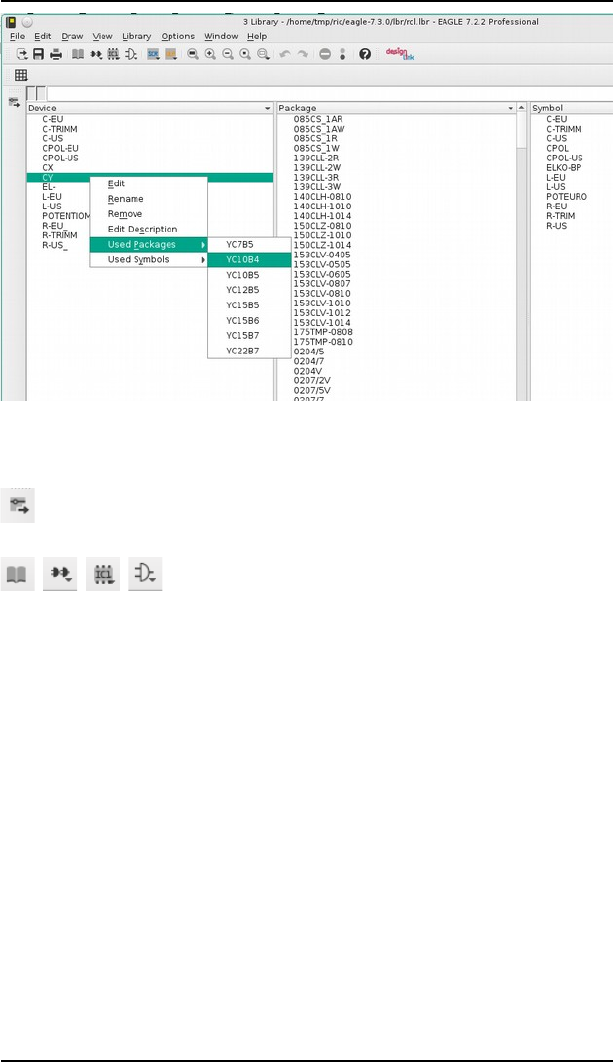
4.4 The Library Editor Window
Important Icons in the Library Editor
Load Device, Package or Symbol for editing. This icon is located in the
command icon toolbar
From the left: Show table of contents, Load Device, load Package, load
Symbol. These icons are shown in the action toolbar.
If you click on one of these icons with the right mouse button, or long-click
with the left mouse button on one of theses icons (not show table of
contents), a list with the recently edited objects will pop up.
Alternatively there are available the options Description, Table of Contents,
Manage Devices/Symbols/Packages… (EDIT command), Remove, Rename,
and Update... through the Library menu.
Please check the chapter Library and Part Management and the help
function for additional information.
The Package Editing Mode
The definition of a component is described briefly below. There is a more
extensive guide in the Component Design Explained through Examples
section.
The icons available in the command toolbar are equivalent to the identical
icons of the Schematic or Layout Editor.
79
➢
A Library's Table of Contents: Options of the context menu
4 A First Look at EAGLE
Design New Package
You change into Package editing mode through the Package icon in the
action toolbar. Type in the name of a package, and reply to the confirming
question Create new package 'packagename'? with yes.
Place pads (though-hole contacts) or SMDs (SMD contact areas) with the
following commands which are only available in the Package Editor.
PAD
Place the pad of a conventional (through-hole) component.
The pad comes with a plated-through drill that goes through all signal layers.
The pad shape can be round, square, octagon or long in the outer signal
layers. In the inner signal layers pads are always round.
SMD
Place a SMD pad.
You can change the name of the pads or SMDs with the NAME command.
Use the LINE, ARC, etc. commands to draw
the symbol for the silkscreen on layer 21, tPlace,
additional graphical information for the documentation print
into layer 51, tDocu.
Draw restricted areas for the Autorouter, if needed, in layers 41, tRestrict, 42,
bRestrict, or 43, vRestrict, or in layers 39, tKeepout, or 40, bKeepout, by
using the commands CIRCLE, RECT, or POLYGON.
Place mounting holes with the HOLE command, if needed.
Use the TEXT command to place
the string >NAME in layer 25, tNames, serving as a text variable
containing the name of the component,
the string >VALUE in layer 27, tValues, serving as a text variable
containing the value of the component.
Use the DESCRIPTION command to add a description for the Package.
HTML text format can be used for this. You will find further information in
the help pages.
The Symbol Editing Mode
Defining a Symbol means defining a part of a Device which can be placed
individually in a schematic. In the case of a 74L00 this could be one NAND
gate and the two power pins, defined as another Symbol. In the case of a
resistor, the Device contains only one Symbol which is the representation of
the resistor.
You now change into Symbol editing mode through the Symbol icon in
the action toolbar. Enter the name of the Symbol, and reply to the confirming
question Create new symbol 'symbolname'? with Yes.
80

4.4 The Library Editor Window
Design a New Symbol
Use the commands LINE, ARC, etc. to draw the schematic representation of
the Symbol into layer 94, Symbols.
Place the pins by using the following PIN command, which is only available
in the Symbol editing mode:
PIN
Place pins.
You can adjust the pin parameters (name, direction, function, length, visible,
Swaplevel) in the parameter toolbar while the PIN command is active, or
later with the CHANGE command. The pin parameters are explained starting
on page 238 and in the help pages under the keyword PIN. Pin names are
changed using the NAME command.
Use the TEXT command to place
the string >NAME in layer 25, tNames, serving as a text variable
containing the name of the component,
the string >VALUE in layer 27, tValues, serving as a text variable
containing the value of the component.
The Device Editing mode
Components are defined as Devices. In the Device editing mode you do not
draw anything, but you define the following:
which Package variant is used,
which Symbol(s) is/are used (called Gate within the Device),
which names are provided for the Gates (e.g. A, B),
which technologies are available (e.g. 74L00, 74LS00, 74HCT00),
if the Device should have additional user-definable attributes,
if there are equivalent Gates which can be interchanged (Swaplevel),
how the Gate behaves when added to a schematic (Addlevel),
the prefix for the component name, if a prefix is used,
if the value of the component can be changed or if the value should be
fixed to the Device name,
which pins relate to the pads of the Package (CONNECT command)
whether a description for this component should be stored in the
library.
The following diagram shows the fully defined 7400 Device with four NAND
gates and a supply gate in various Package and technology versions.
If you click onto one of the gates with the right mouse button, the context
menu with the executable commands pops up. Furthermore you can display
the Properties of the gate. Click on Edit Symbol to open the Symbol Editor.
81
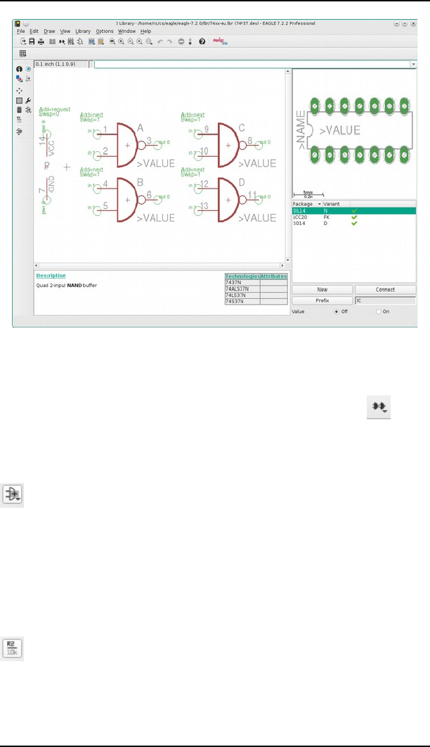
4 A First Look at EAGLE
➢
Device Editor window
Create Actual Components from Symbols and Packages
Switch to the Device editing mode by clicking the Device icon in the
action toolbar. Type in the Device name and confirm the question Create
new device 'devicename'? with Yes.
Use the following commands to create a Device.
ADD
Add a Symbol to a Device. Gate name, Swaplevel, and Addlevel can be
defined in the ADD command in the parameter toolbar, or redefined later
with the CHANGE command.
The Swaplevel specifies whether there are equivalent Gates.
The Addlevel defines, for instance, if a Gate is to be added to the schematic
only on the users request. Example: the power gate of an integrated circuit
which is normally not shown on the schematic.
NAME
Change Gate name.
82
4.4 The Library Editor Window
CHANGE
Change Swaplevel or Addlevel.
PACKAGE
Define and name Package variant(s). The PACKAGE command is started by
clicking on the New button in the Device Editor window, or by typing on the
command line. Choose the requested Package variant.
More information about this can be found on page 283.
CONNECT
Define which pins (Gate) relate to which pads (Package).
PREFIX
Provide prefix for the component name in the schematic (e.g. R for resistors).
VALUE
In the Device mode, VALUE is used to specify whether the component value
can be freely selected from within the schematic diagram or the layout, or
whether it has a fixed specification.
On: The value can be changed from within the schematic (e.g. for resistors).
The component is not fully specified until a value has been assigned.
Off: The value corresponds to the Device name, including, when present,
assignment of the technology and the Package version (e.g. 74LS00N).
Even if Value is Off, the value of a component can be changed. A query
checks if this action is intended.
The altered value of the component remains unchanged, if the Technology or
the Package version is altered later with CHANGE PACKAGE or CHANGE
TECHNOLOGY.
TECHNOLOGY
If necessary, various technologies can be defined, for example, for a logic
component. Click on Technologies therefore.
ATTRIBUTE
Click on Attributes to define any additional attribute for the Device. A
detailed description can be found in the chapter about libraries in this
manual.
DESCRIPTION
Compose a description of the Device which can also be examined by the
search function associated with the ADD dialog.
Information about Copying of Packages, Symbols and Devices can be
found from page 288 on.
83
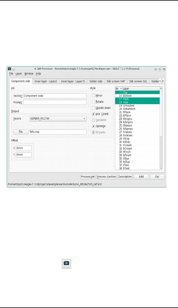
4 A First Look at EAGLE
4.5 The CAM Processor
Manufacturing data is generated by means of the CAM Processor. A number
of drivers for the data output are available. The drivers are defined in the file
eagle.def, which can be edited with any Text Editor.
Output to matrix printers, however, is not created with the CAM Processor
but with a PRINT command.
The board manufacturer may use the EAGLE Freeware for generating
manufacturing data of your board.
➢
The CAM Processor
The CAM Processor can also be started directly from the command line. A
number of command line parameters can be passed to it when it is called.
These are listed in the appendix.
Generate Data
Starting the CAM Processor
There are different ways to start the CAM Processor:
You can do this directly from the Layout or Schematic Editor window with
the CAM Processor icon in the action toolbar or through the menu
File/CAM Processor. The current schematic or board will be loaded
automatically from the Control Panel by clicking on one of the entries in the
Tree View's CAM Jobs branch. Then the selected CAM Job will be loaded
automatically. You still have to load the schematic or board from which you
want to make the CAM Processor manufacturing data from through the
84

4.5 The CAM Processor
File/Open menu by using the command prompt (Windows command
prompt, Terminal or Console window) without graphical user interface.
Particular information can be found in the appendix chapter about EAGLE
Options.
Load Job File
A job defines the sequence of several output steps in an automatic data
creation task. You can, for example, use a job to generate individual files
containing the Gerber data for several PCB layers.
A job is loaded with the File menu of the CAM Processor or with a double-
click on one of the Tree view's CAM Jobs entries in the Control Panel.
A job is not absolutely essential for output. All the data can be made step by
step manually.
Load Board
Before you can generate an output you must open the File menu and load a
board file, if not already loaded automatically while stating the CAM
Processor from an Editor window. At the bottom left in the CAM Processor
window you will see the file name the data is being generated from.
The output of data for a Schematic, for example for a certain plotter, is also
possible.
Set Output Parameters
If a job file is loaded, the output parameters are already adjusted. A job can
contain several sections with different parameter sets. The various peripheral
devices accept different parameters.
If no job is loaded, set the parameters to whatever you need (see page 311).
Start Output
If you want to execute the job which has been loaded, click the Process Job
button. If you just want to get an output using the currently visible parameter
settings, click the Process Section button.
Define New Job
Perform the following steps to define a new job:
1. Click Add, to add a new section.
2. Set parameters.
3. Repeat 1. and 2. if necessary.
4. Save job with File/Save job.
The Description button allows to describe the job file. This description will be
shown in the Control Panel.
The chapter on Preparing the Manufacturing Data contains detailed
information on this subject.
85

4 A First Look at EAGLE
4.6 The Text Editor Window
EAGLE contains a simple Text Editor.
You can use it to edit script files, User Language programs or any other text
file. The EAGLE Text Editor stores its files with UTF-8 encoding.
The menus bring you to a variety of functions, such as commands for
printing, copying and cutting, searching, replacing (with support of Regular
Expressions), changing font and size, and so on.
The keyboard shortcuts in the EAGLE Text Editor follow the platform
specific standards.
When in the Text Editor, the right mouse button calls up a context menu.
In case you prefer an external text editor, define the program call in the
Control Panel's or in one of the Editor window's Option/User interface
menu, External text editor. If you want to prevent EAGLE to start any text
editor automatically, type in a minus sign '-' in the External text editor line.
Clear the line for the built-in EAGLE text editor.
Please note further information about the usage of an external text editor in
the help function, section Editor windows/Text Editor.
86

Chapter 5
Principles for Working with EAGLE
5.1 Command Input Possibilities
Usually the commands in EAGLE are executed by clicking an icon or an item
in the menu bar and then clicking onto the object you want to edit. But there
are also alternative to execute commands.
Possibilities for command input in Schematic, Layout, and Library Editor:
clicking a command icon
typing text commands in the command line
through the context menu
via function keys
via script files
via User Language programs
In any case it is necessary to understand the syntax of the EAGLE command
language which is described in the following section.
A detailed description of the EAGLE commands can be found on the help
pages.
Activate Command and Select Object
The classical way of working with EAGLE is to activate the command first,
and then choose the object you want to have it executed on. For example,
first activate the MOVE command by clicking the icon in the command menu
or selecting the command in one of the menus, and finally click onto the
object you want to move.
Command Line
As an alternative to the previously mentioned clicking onto an icon you can
use the command line. When entering commands you may abbreviate key
words as long as they cannot be mistaken for another key word, or you may
use small or capital letters (the input is not case sensitive), for example:
*5*0$0.;
is equivalent to
(<=0$0.;
87

5 Principles for Working with EAGLE
The actual unit for the values is set in the GRID menu. It's also possible to
specify the unit directly in the command line without changing the currently
set grid:
*5*0$>77
or
(<=.;=!
Most commands can be executed whilst declaring coordinate values in the
command line.
Examples:
7+:-?:@.$90-$A9B
The value placeholder text for part IC1 moves to position 2.50 1.75 in the
layout, provided it has been released with the SMASH command before.
7+-
Part U1 will be mirrored to the bottom side of the board.
*+0$-9@9#$9B
Place a hole with drill diameter 0.15 at position 5 8.5.
:C5C0$0A0)@.$01$0B
A round shaped via with a diameter of 0.070 belonging to signal GND will be
placed at position 2.0 3.0.
History Function
You can recall the most recently entered commands by pressing Crsr-Up ( )
or Crsr-Down () and edit them. The Esc key deletes the contents of the
command line.
The Context Menu
Another way of using EAGLE is to work with the object-specific command
menu. In this case you first click with the right mouse button onto the object
and then you select the command that you want to have executed.
The context menu contains all commands that can be executed with the
selected object. Additionally you can display all the object's properties by
clicking onto the Properties entry. Some of them can be even changed
directly in the Properties window.
88
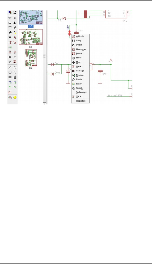
5.1 Command Input Possibilities
Function Keys
Texts may be allocated to the function keys and to combinations of those keys
with Alt, Ctrl and Shift (for Mac OS-X additionally Cmd), if not occupied by
the operating system or a Linux Window Manager (for example F1 for help).
If a function key is pressed, this corresponds to the text being typed in via the
keyboard. Since every command is capable of being entered as text, every
command, together with certain parameters, can be assigned to a function
key. Even whole sequences of commands can be assigned to a function key in
this way.
The command
ASSIGN
displays the current function key assignments. Changes to the key
assignments can be carried out in the assign window.
The New button can be used to define a new key assignment. A click onto Del
will delete a marked entry, while Change alters an existing definition. OK
closes the dialog and saves the definitions, while Cancel aborts the dialog.
These settings can also be made via the Options/Assign menu in the
Schematic or Layout Editor.
To predefine certain assignments you can also use the ASSIGN command in
the file eagle.scr (see page 111).
89
➢
The context menu for a Device in the Schematic
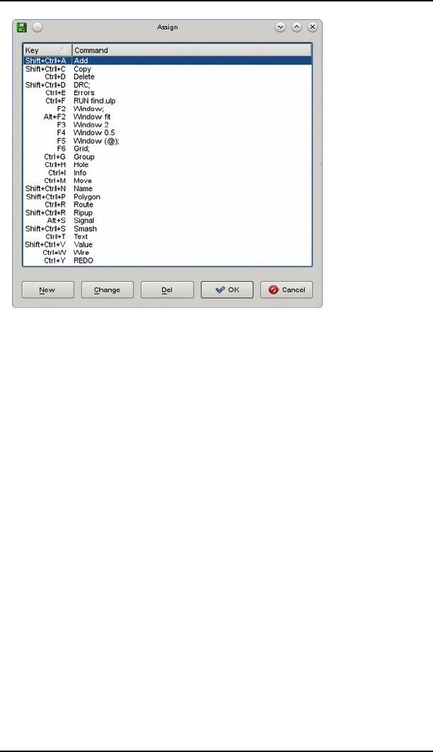
5 Principles for Working with EAGLE
➢
The dialog for the ASSIGN command
Examples:
The combination of Ctrl + Shift + G displays a grid of 0.127mm:
DC5770$-.A+C
The combination of Alt + F6 changes the layer to Top and starts the ROUTE
command:
DE>C6++C
The combination of the keys Alt + R displays only the layers Top, Pads, Vias
and Dimension first and then starts the print out with the default printer:
DC56+--A-#.0C
A, C, M, and S are the modifiers for the Alt, Ctrl, Cmd (Mac OS-X only), and
Shift key.
The combination of Alt + 0 brings the Control Panel into the foreground. The
combinations Alt + 1 up to 9 are assigned to the various editor windows,
according to the window number which is shown in the respective title bar.
Script Files
Script files are a powerful tool. They can contain long sequences of
commands, such as the specification of specific colors and fill-patterns for all
layers, as for example in defaultcolors.scr. On the other hand they might
contain netlists converted from the data of other programs.
The SCRIPT command is used to execute script files.
90

5.1 Command Input Possibilities
Many User Language programs (ULP) create script files that can be read in
order to modify a layout or a schematic.
EAGLE outputs an entire library, for instance, as a script file with the aid of
the EXPORT command (Script option). This file can be modified with a text
editor, after which it can be read in again. This allows changes to be made to
a library quite easily.
There is more information about script files and export commands later in
this chapter.
Mixed Input
The various methods of giving commands can be mixed together.
You can, for instance, click the icon for the CIRCLE command (which
corresponds to typing CIRCLE on the command line), and then type the
coordinates of the center of the circle and of a point on the circumference in
this form
@..B@.1B←
in the command line.
The values used above would, if the unit is currently set to inch, result in a
circle with a radius of one inch centered on the coordinate (2 2). It is
irrelevant whether the CIRCLE command is entered by icon or by typing on
the command line.
Some EAGLE commands are used in combination with the Shift, Alt
or Ctrl keys. In case you are working with EAGLE for Mac OS-X,
please use the Cmd key instead of Ctrl.
5.2 The EAGLE Command Language
You only need a knowledge of the EAGLE command language if you want to
make use of the alternative input methods discussed in the previous section.
The syntax of the EAGLE command language will be discussed in this
section, and typographical conventions, which are important for
understanding the descriptions, will be specified.
Typographical Conventions
Enter key and Semicolon
If EAGLE commands are entered via the command line they are finished
with the Enter key. In some cases a command must have a semicolon at the
end, so that EAGLE knows that there are no more parameters. It is a good
idea to close all commands in a script file with a semicolon.
The use of the Enter key is symbolized at many places within this handbook
with the ← sign.
However in the following examples neither the Enter key sign nor the
semicolon are shown, since all of these commands can be used both on the
command line and within script files.
91

5 Principles for Working with EAGLE
Bold Type or Upper Case
Commands and parameters shown here in UPPER CASE are entered
directly. When they are entered, there is no distinction made between upper
and lower case. For example:
Syntax:
5
Input:
5or=!="
Lower Case
Parameters shown here in lower case are to be replaced by names, numbers
or keywords. For example:
Syntax:
5="=F=)!GH!
Input:
5--0
This sets the grid to 1 mm (assuming that the current unit is set to mm).
Every tenth grid line is visible. The figures 1 and 10 are placed into the
command instead of the placeholders grid_size and grid_multiple.
Underscore
In the names of parameters and keywords the underscore sign is often used
in the interests of a clearer representation. Please do not confuse it with an
empty space. As can be seen in the example above, grid_size is a single
parameter, as is grid_multiple.
If a keyword contains an underscore sign, such as COLOR_LAYER does in
the command
++6!8!<
then the character is to be typed in just like any other. For example:
++6++7
Spaces
Wherever a space is permissible, any number of spaces can be used.
Alternative Parameters
The | character means that the parameters are alternatives. For example:
Syntax:
+I+EE
Input:
+
or
+EE
The beep, which is triggered by certain actions, is switched on or off.
92

5.2 The EAGLE Command Language
Repetition Points
The .. characters mean either that the function can be executed multiple
times, or that multiple parameters of the same type are allowed. For
example:
Syntax:
56HG!8$$
Input:
56+:
The layer number can alternatively be used:
56--A-#
More than one layer is made visible here.
If a layer (in this case Bottom) is to be hidden:
56->
Mouse Click
The following sign ● usually means that at this point in the command an
object is to be clicked with the left mouse button.
For example:
7+:●●
Input:
7+:←@!=J&(=B
7)"!=J&( "&KL&&KM
7)"!=J&("GG
7)"!=J&("KL&&KM
"$
You can also see from these examples how the repetition points are to be
understood in the context of mouse clicks.
Entering Coordinates as Text
The program sees every mouse click as a pair of coordinates. If it is desired to
enter commands in text form on the command line, then instead of clicking
with the mouse it is possible to enter the coordinates through the keyboard in
the following form:
(x y)
where x and y are numbers representing units as selected by the GRID
command. The textual input method is necessary in particular for script files.
The coordinates of the current cursor position can be fetched with (@). For
example:
5+@,B
Examples of coordinate entry in text form:
You want to enter the outline of a circuit board with precise dimensions.
93

5 Principles for Working with EAGLE
577-
657+
0@00B@->00B@->0-00B@0-00B@00B
5
The first step is to switch to a 1 mm grid. The dimension layer is then
activated. The LINE command then first sets the line width to 0 and draws a
rectangle with the aid of the four given coordinates. The last command
returns the grid to whatever had previously been selected, since circuit
boards are usually designed using inches.
Relative values:
It is possible to use relative coordinate values in the form (R x y) which refer
to a reference point set with the MARK command before. If you don't set a
reference point the absolute origin of the coordinate system will be taken.
Setting a via relative to the reference point:
5770$9
74@.0-0B
:@9-.$9B
74
First the grid is set to Millimetres, then the reference point at the position
(20 10) is placed. The via is located at a distance of 5 mm in x and 12.5 mm in
y direction from the this point. Then the reference point is removed.
Polar values:
Polar coordinates are given in the form of (P radius angle).
577
74@-.$9A$-.9B
6.-
@00B@0;0B
5@;00B
5@;0-.0B
5@;0.;0B
This examples shows how to set the reference point at position (12.5 7.125).
Then a circle with a radius of 40 mm is drawn in layer 21, tPlace. Three pads
are placed on the circumference with an angle of 120°.
Here the circle is easily drawn with the help of relative coordinates. So we do
not have to worry about absolute values of a point on the circumference for
the second coordinates pair to determine the circle.
Right Mouse Click:
The > character within parenthesis represents a right mouse click. That way
one can move a whole group, for example:
7+:@?00B@-00B
The previously selected group will be moved 10 units in x direction.
Modifier:
Within parenthesis one can use some modifiers. For combinations you don't
have to care about the order:
94

5.2 The EAGLE Command Language
Arepresents the pressed Alt key, the alternative grid
Crepresents the pressed Ctrl key, Mac OS-X: Cmd
Srepresents the pressed Shift key
Rrelative coordinates
Ppolar coordinates
>right mouse click
C and S cause miscellaneous commands to behave in different manners.
More information can be found in the help function of the respective
command.
If the commands are being read from a script file, each one must be closed
with a semicolon. In the above cases the semicolons can be omitted if the
commands are being entered via the keyboard and each is being closed with
the Enter key.
Examples:
A component is to be transposed to a specified position.
577-
7+:-@-.0.9B
Alternatively you can use the object's coordinates:
7+:@0$-.A.$9;B@-.0.9B
IC1 is located at coordinates (0.127 2.54) and is moved to position (120 25).
The current position of a Device can be obtained with the aid of the INFO
command.
E+-
When a Symbol is defined, a pin is placed at a certain position.
C5C+*+-#0@0$.0$;B
You draw a rectangular forbidden area in layer 41 tRestrict:
6
@0$90$9B@.$9;B
5.3 Grids and the Current Units
EAGLE performs its internal calculations using a basic grid size of
0,00325 µm (about 0.000123 mil).
Microns (µm), mils (1/1000 inch), inches and mm can be chosen as a unit.
The current unit as set with the GRID command applies to all values.
You should always use the pre-set 0.1 inch grid for schematic
diagrams and for drawing Symbols in the Library Editor!
95
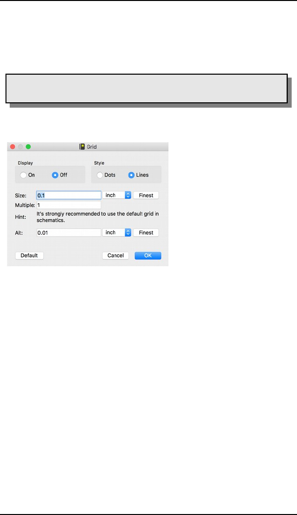
5 Principles for Working with EAGLE
When starting the design of circuit boards or libraries it pays to give prior
thought to the question of which grid size (or sizes) will be used as a basis.
For example, it is only the origin of a Package that will be pulled onto the
board's placement grid. All other objects constituting the Package (such as
pads) are placed relative to that point on the board, just as it was defined in
the library.
The basic rule for boards is: always make the grid as big as possible
and as small as necessary.
Various grid sizes can be pre-set in the eagle.scr file for different types of
editor windows (see page 104).
The current grid Size is set in the grid menu. The units chosen in the combo
box are used.
The Multiple option indicates how many grid lines are displayed. If, for
instance, the value 5 is entered at Multiple, every fifth line will be displayed.
The Alt line allows to set an alternative grid which can be activated by
pressing the Alt key (while, for example, MOVE, ROUTE, ADD, or LINE is
active). This can be very useful for placing parts in a dense layout or
arranging labels in the schematic. If you decide not to place it in the
alternative grid and release the Alt key before placing it, the object stays in its
origin grid.
Style specifies the way it is displayed: Lines or Dots. The options On and Off
under Display switch the grid display on or off. Finest sets the finest grid that
is possible. Clicking on default will select the editor's standard grid.
Beginning with a certain zooming limit, grid lines are not displayed anymore.
This limit can be set in the menu Options/Set/Misc, Min. visible grid size.
Grid lines and grid dots can have any color. Click the colored button of the
respective palette (depends on the background color) in the menu
Options/Set/Colors and select the color as requested. This can also be done
in the command line, for example:
++5
96
➢
The Grid menu

5.3 Grids and the Current Units
Instead of the color name the color number can be given, as well. It can be in
the range 0 .. 63. The shown color depends on the (self-)defined colors of the
current palette.
See also the hints concerning Color settings on page 107.
5.4 Aliases for DISPLAY, GRID, and WINDOW
For the commands DISPLAY, GRID, and WINDOW you can define so-called
aliases. This is a set of parameters which you can save with any name and
executed it with the command. To access such an alias simply click with the
right mouse button onto the command icon.
The aliases are stored in the eaglerc file for Schematic, Layout, and Library
separately. They are available for all Schematics, Layout, and Libraries then.
Example: DISPLAY Alias
Display the layers you want to see in the Layout Editor with the
DISPLAY command, for example Top, Pads, Vias, and Dimension
Right-click onto the DISPLAY icon and a popup menu appears
Select the New.. entry
Enter the name of the alias, for example Top_view
Click the OK button
From now on the popup menu of the DISPLAY icon contains the entry Top
view.
If you prefer the command line for activating this alias you have to enter:
DISPLAY TOP_VIEWordisp top_v
It does not matter if you write in upper or lower case letters hers. You may
use abbreviations as long as the name is clear.
There are no limitation to the number of aliases used.
Use DISPLAY LAST in the command line or the entry Last of the DISPLAY's
popup menu icon to return to the last layer selection.
More details can be found on the help page of the DISPLAY command.
Example: GRID Alias
The how to and the function of a grid alias is exactly the same as it is
explained for the DISPLAY command. Set the appropriate grid in one of the
Editor windows, right-click onto the GRID icon , and select the New..
entry in the popup menu to define the alias.
This can be done in the command line as well. for the grid command it could
look like this:
578==(0$009!="
The command
=8=or in short=8
97

5 Principles for Working with EAGLE
executes the alias. The command is case insensitive, the alias can be
abbreviated.
Example: WINDOW Alias
The WINDOW command allows you to define an alias for a certain part of
the drawing area. Aliases help you to navigate comfortably from one location
to another in your drawing. The definition of a WINDOW alias is similar to
the DISPLAY alias as described above:
Select the appropriate display window in the drawing
Right-click onto the Select icon of the WINDOW command to
open the popup menu
Click the New.. entry now and name your alias
Let's assume the alias name is upper_left: You can restore this display detail,
for example, in the command line with:
5+HHNor in short<=)HH!
Alternatively right-click onto the Select icon of the WINDOW command and
select the entry upper_left in the popup menu.
In a Schematic that consists of more than one sheet an alias is
executed always on the currently active sheet, independent of where
it was defined originally.
Editing, Renaming, Deleting of an Alias
In the case you want to delete an alias, you can do this in the command icon's
popup menu. First right-click onto the command icon to open the popup
menu. Then use a right mouse click onto the alias entry. This opens a context
menu. Click the Delete option there.
The same methods can be used to Rename or Edit an alias.
These actions can be executed also via the command line. Further
information can be found in the help pages about the DISPLAY, GRID, and
WINDOW commands.
98
➢
Deleting a WINDOW alias

5.5 Names and Automatic Naming
5.5 Names and Automatic Naming
Length
Names in EAGLE can have any desired length. There is no limit.
Forbidden and Special Characters
No names may contain spaces, semicolons or umlauts. Quotation marks and
other exotic characters (above 127 in the ASCII table) should be avoided as
far as possible.
Device names must not contain either question marks or asterisks, since
these characters are used as placeholders for Package variants (?) and
technologies (*).
Commas must be avoided in pad names.
Part-bus names must not contain colons, commas or square brackets.
The exclamation mark is a special character that starts and ends a bar over
the text. See the help function for the TEXT command for details. If an
exclamation mark should be visible in the text, it needs to be escaped by a
leading backslash.
In order to have a backslash displayed in a name or text, you have to type it,
for example with the NAME or TEXT command, twice.
Automatic Naming
If a name is given together with one of the commands PIN, PAD, SMD, NET,
BUS or ADD, then other names will be derived from it as long as the
command is still active.
The name is simply typed into the command line before placing the object
(while it is attached to the mouse). Note that the name must be placed within
simple quotation marks. Entry is completed with the Enter key ( ) .←
The examples illustrate how automatic naming functions:
555-;C-C←• • •
fetches three DIL14 Packages to the board and names them U1, U2 and U3
(corresponds to a mouse click).
5+C-C←• • • •
places four octagonal pads with the names 1, 2, 3, and 4.
If the name consists of only one character from A...Z, then the following
objects receive the following letters of the alphabet as names:
555CC←• • • •
fetches four NAND gates with the names A, B, C and D. If the generated
name reaches Z, then names with the default prefix will again be generated
(e.g. G$1).
5.6 Import and Export of Data
EAGLE provides a number of tools for data exchange.
99

5 Principles for Working with EAGLE
Script files for importing
The export command for exporting
EAGLE User Language programs for import and export.
The User Language is very flexible, but does call for a suitable program to be
created. You will find further details in the section on The EAGLE User
Language.
Script Files and Data Import
The SCRIPT command makes a universal tool available to the EAGLE user
for data import.
Since every EAGLE operation can be carried out with the aid of text
commands, you can import all types of data with the aid of a script file. A
script file can in turn call other script files.
Script files can be created with a simple text editor. The prerequisite for the
development of your own script files is that you understand the EAGLE
command language. You will find the precise functioning and the syntax of
the individual commands in the EAGLE help pages.
The file euro.scr in the eagle/scr directory, which draws the outline of a
eurocard with corner limits, provides a simple example.
If a netlist is to be imported into a board design which already contains the
appropriate components, then a script file of the following form is necessary:
SIGNAL GND IC1 7 IC2 7 J4 22
SIGNAL VCC IC1 14 IC2 14 J4 1
A Netscript of this sort can easily be created from the schematic diagram by
the EXPORT command (menu File/Export/Netscript) and imported into the
layout.
You will get a further impression of the power of importing, if you output a
library with the EXPORT command into a script file (File/Export/Script).
The script file that is generated provides an instructive example for the
syntax of the script language. It can be examined with any text editor. If
SCRIPT is then used to read this file into an empty library, a new library file
will be created.
Comments can be included following a #-character.
The execution of a script file can be stopped by clicking the Stop icon in the
action toolbar.
The File/Import menu offers a P-CAD/Altium/Protel import option. Files
that are saved in the ACCEL-ASCII data format can be transferred into
EAGLE. Further information is displayed when you start this function.
File Export Using the EXPORT Command
The EXPORT command and the menu File/Export... offers, depending on
the active editor window, the following modes:
DIRECTORY
Outputs a list of the contents (Devices, Symbols, and Packages) of the
currently loaded library.
100

5.6 Import and Export of Data
NETLIST
Outputs a netlist for the currently loaded schematic or board in an EAGLE-
specific format. It can be used to check the connections in a drawing.
There are also available several User Language programs that allow to export
various net list formats.
NETSCRIPT
Outputs a netlist of the currently loaded schematic in the form of a script file.
The netscript can be imported into the board file with the help of the SCRIPT
command. This could be possibly suggestive if there are differences in the
netlist between schematic and layout.
In the first step you have to delete all signals in the layout with the command
DELETE SIGNALS. Be aware that all traces are lost! Now export the
Netscript from the Schematic and import it with the SCRIPT command into
the layout. The result is a Schematic/Layout file pair with an identical netlist.
PARTLIST
Outputs a component list for the schematic or board.
PINLIST
Outputs a pin/pad list for the schematic or board, listing the connected nets.
SCRIPT
Outputs the currently loaded library in the form of a script file.
This script can be modified with a text editor in order to generate, for
example, a user defined library, or to copy parts of one library into another.
The modified script file can be imported into a new or an already existing
library with the help of the SCRIPT command.
The script file also serves as a good example for the EAGLE command syntax.
In order to avoid loss of precision the grid unit in the script file is set to
Millimetres.
IMAGE
The option Image allows you to generate files in various graphic formats.
The following formats are available:
bmp Windows Bitmap file
png Portable Network Graphics file
pbm Portable Bitmap file
pgm Portable Grayscale Bitmap file
ppm Portable Pixelmap file
tif Tag Image file
xbm X Bitmap file
xpm X Pixmap file
101

5 Principles for Working with EAGLE
Click the Browse button, select the output path, and type in the graphic file
name with its extension. The file extension determines the graphic file type.
To generate a black and white image activate the option Monochrome. To
make the image available via the system's clipboard set the Clipboard option.
The Resolution can be set in dots per inch. The resulting Image Size will be
shown in the lowest field.
The Area field allows a selection of Full or Window. Full prints the whole
drawing, whereas Window prints the currently in the Editor window visible
part of the drawing.
Further graphic formats, like HPGL, Postscript (PS), or
Encapsulated Postscript (EPS), can be generated with the help of the
CAM Processor.
The User Language Program dxf.ulp generates xf data. The PRINT
command supports PDF output.
LIBRARIES
Create library files with all the devices and packages that are used in the
current project.
Please specify the path where the library files shall be stored in the dialog
window. Be sure not to overwrtie your system libraries. This option allows to
extract all library definitions from schematic and board and make them
available, for example, for further editing or for further usage in your own
libraries. This function is realized by the User Language Program exp-
lbrs.ulp.
102
➢
Settings for graphic file output

5.6 Import and Export of Data
5.7 The EAGLE User Language
EAGLE contains an interpreter for a C-like User Language. It can be used to
access any EAGLE file. Since version 4 it has also been able to access external
data. It is possible, with very few restrictions, to export data from EAGLE,
and import a wide range of data into EAGLE.
ULPs can, for example, manipulate a layout file or a library by generating
and executing a Script file. The Script file contains all the necessary
commands for the manipulation. The User Language's integrated exit()
function allows it to execute these commands directly.
The program examples included (*.ulp) will provide some insight into the
capacity of the User Language. They are located in your installation's ULP
directory. A description of the way in which a ULP works is located in the file
header. This is also displayed in the Control Panel or in the usage box when
the program is called.
User Language programs must be written in a text editor that does not add
any control codes. It might be a good idea to use a text editor that supports
syntax highlighting for C programming language. This helps to understand
the structure of an ULP.
You can define an External text editor in the Option/User Interface menu as
your default editor.
A ULP is started with the RUN command, or by dragging a ULP from the
Control Panel into an editor window (Drag&Drop). To cancel the execution of
an ULP click the Stop icon.
EAGLE prompts a message in the status bar, Run: finished, if the User
Language program has been ended.
The language is described in detail in the EAGLE help pages, under the
keyword User Language.
Typical applications for ULPs:
Creating parts lists in various formats.
See also page 300.
Output in graphical formats.
Data output for component insertion machines, in-circuit testers etc.
Linking to an external database.
Manipulation of the silk screen print, the solder stop mask, and so on.
Import of graphic data files (for example import-bmp.ulp for logos or
the like)
A lot of valuable ULPs can be found on our web pages.
103

5 Principles for Working with EAGLE
5.8 Forward&Back Annotation
A schematic file and the associated board file are logically linked by
automatic Forward&Back Annotation. This ensures that the schematic and
the board are always consistent.
As soon as a layout is created with the BOARD command , the two files
are consistent. Every action performed on the schematic diagram is
simultaneously executed in the layout. If, for instance, you place a new
Device, the associated housing will appear on the layout at the edge of the
board. If a net is placed, the signal lines are simultaneously drawn in the
layout. Certain operations such as the placement or deletion of signals are
only allowed in the schematic. The Layout Editor does not permit these
actions, and issues an appropriate warning. Renaming Devices or changing
their values, for example, are permitted in both files.
The EAGLE help pages contain a closer description of the technical details.
It is not necessary for you, as the user, to pay any further attention to this
mechanism. You only have to ensure that you do not work on a schematic
whose associated board file has been closed, and vice versa. This means that
both files must always be loaded at the same time. Otherwise they loose
consistency, and the annotation can no longer work.
If you have, however, once edited the board or the schematic separately, the
Electrical Rule Check (ERC) will check the files for consistency when they are
loaded. If inconsistencies are found, the ERC opens an Error window with
appropriate messages about the Schematic and the Layout. Section 6.13,
starting with page 198, shows how to proceed in such a case.
5.9 Configuring EAGLE Individually
There are a number of settings that permit the program to be adjusted for
individual needs. We distinguish between program, user and project-specific
settings.
Basic program settings that will apply to every user and every new project are
made in the eagle.scr file. Under Windows, personal preferences are stored
in the file eaglerc.usr, or, under Linux, in ~/.eaglerc.
EAGLE remembers settings that only apply to one particular project in the
eagle.epf project file.
Values that, for instance, only apply to one specific board, such as the Design
Rules, special layer colors, unique newly defined layers or the grid setting are
stored directly in the layout file. This also applies, of course, to schematic
diagram and library files.
Configuration Commands
Most of the options are usually set by means of the Options menus of the
individual EAGLE editor windows.
104

5.9 Configuring EAGLE Individually
The Control Panel allows settings to be made for Directories, file Backup and
the appearance of the editor window (User interface). These options are
described in the chapter on the Control Panel under the
Options menu heading, starting on page 46.
Through the User interface settings it is possible to select the icon-based
menu or a configurable text menu.
The MENU command allows the text menu to be given a hierarchical
configuration by means of a script file. There is an example of this in the
appendix.
The Options menu in the editor windows for schematic diagrams, layouts
and libraries contains, in addition to the User interface item, two further
entries:
Assign and Set.
The ASSIGN command alters and displays the assignment of the function
keys. You will find information about this on page 89.
General system parameters are altered with the SET command.
The CHANGE command allows a variety of initial settings for object
properties.
The GRID command sets the grid size and the current unit. Further
information about this starts on page 95.
The Menu Options/Set (SET Command)
Most common options of the SET command are available in the Settings
window of the menu Options/Set. This window can be reached also by
entering on the command line:
Display Certain Layers Only
The number of available layers shown in the DISPLAY or LAYER menu can
be set with the option Used_Layers. That way it is possible to hide unused
layers for clarity reasons.
56-->-A-#-O.0.-.1.9.A.O1-;;;99-
stored in the file eagle.scr shows only the mentioned layers. After
56
all layers are available again.
Context Menu Entries
The right mouse button context menu can be extended by arbitrary entries
for different objects which are selectable with the mouse. This can be a
simple command, a sequence of commands, or maybe a script file or a User
Language Program you want to start. The syntax for the SET command looks
like this:
SET CONTEXT objecttype text commands;
105

5 Principles for Working with EAGLE
objecttype can be: attribute, circle, dimension, element, frame, gate,
hole, instance, junction, label, modinst, pad, pin, rectangle,
smd, text, via, wire
text is the menu text entry
commands is the command sequence, that is executed after clicking
onto the menu entry
Example:
SET CONTEXT wire Go_bottom 'change layer 16';
The context menu for wires (also polygons are member of object type wire)
has an additional entry named Go_bottom which changes the layer to 16
when clicking this entry.
In order to delete all self-defined entries in the context menu of a certain
objecttype, type:
+P<=
To achieve the default settings for all context menus:
+P
Contents of The Parameter Menus
The parameter menus for Width, Diameter, Dline (for dimensioning) Drill,
SMD, Size, Isolate, Spacing, and Miter, which are available, for example,
through the CHANGE command, can be configured and filled with any
values by the SET command. Simply list the values, separated by blanks, in
the command line.
Example for the Miter menu:
770$-0$.0$10$;0$90$>--$9.1;
The units of the given values are determined by the currently used GRID in
the Editor window. A maximum number of 16 entries is allowed.
Example for the SMD menu:
757-$..$00$90$O0$-=0$-;=
For each entry of the three value pairs the unit is given directly. A maximum
number of 16 value pairs is allowed.
The values in the menus are always shown in the currently selected GRID
unit.
Write the SET command in the file eagle.scr to make it default for all you
projects.
To return to the EAGLE default settings use for example for the Width menu:
5*7
ROUTE Command Settings
There are several option that can be used with the ROUTE command:
+7+54+5
is set by default. If you prefer the fully manual routing mode (as it was in
EAGLE version 7 and before) choose
+7+5+
106
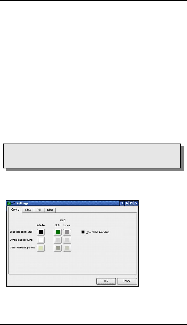
5.9 Configuring EAGLE Individually
Loop Removal can be controlled by the SET command as well:
++7+:+++7+:+EE
If you prefer better visibility while routing, activate the Single Layer mode
that displays the current routing layer colored and all other layers in a
grayish color:
67+5+
Confirm Message Dialogs Automatically
Sometimes EAGLE prompts the user with a warning or informational
message and wants to know how to proceed. This may be unwanted for
automatic processes, for example, for executing a script file. You can decide
on how such a message shall be answered.
+E76
answers the question in the positive sense (Yes or OK).
In order to use the negative option (No button, if present, or simply confirms
the dialog) type
+E7+
To switch off automatic confirmation, use
+E7+EE
Please be careful with this option! Do not use it as a general option,
for example, in the beginning of a script file. This could lead to
unexpected results! See help of the SET command for details.
Color Settings
The Colors tab contains settings for layer and background colors and colors
for grid lines or dots.
Three color palettes are available: for black, white and colored background.
Each palette allows a maximum of 64 color entries, which can be given any
value for the Alpha channel and any RGB value.
107
➢
Settings window: Color settings
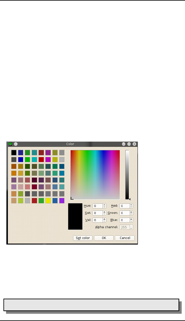
5 Principles for Working with EAGLE
If you prefer the old raster OP behaviour of previous EAGLE versions on
black background, deactivate the Use alpha blending check box. In this case
the alpha value is ignored when using a black background. Colors are mixed
now using an OR function.
By default EAGLE uses 64 values. Eight colors followed by further eight so-
called highlight colors.
The first entry of the palette determines the background color. In the white
palette, however, it is not possible to change the background color because
it's needed for print-outs, which normally are made on white paper.
The image above shows three buttons in the Palette column. Click on one of
them. For example, the button for Colored Background. The Color window
opens now.
On the left an 8 x 8 matrix is visible. There are alternating eight 'normal'
colors with their corresponding eight highlight colors. A color of the palette
at position x can be given the corresponding highlight color at position x+8.
In order to define new values select a box of the matrix and adjust the new
color with the help of the color selection area and the saturation bar on the
right. Click Set Color to apply your color. Now select a new color box in the
matrix and repeat the procedure for the next color.
You may also enter values for Red, Green, Blue or Hue, Sat, Val and Alpha
channel directly.
Alpha channel determines the transparency of the color. The value 0 means
the color is totally transparent (invisible), the maximum value 255 stands for
non-transparent. For printouts the value of the alpha channel is set to 255 for
each color.
In order to change the color palette for an editor window select the
appropriate Background in the menu Options/User Interface.
You should always define at least one pair of colors: a normal color
108
➢
Color window: Defining colors

5.9 Configuring EAGLE Individually
and its related highlight color.
Alternatively, the color definition and change of palette can be made in a
script file or in the command line.
Q=%?QαK?
defines a color for the currently used palette, where the value for the alpha
channel and the color value has to be given hexadecimal. Index stands for the
color number, αrgb for the values for alpha channel, the colors red, blue, and
green. Example:
->0%;EEEE0
sets the color number 16 to yellow, which corresponds to the decimal RGB
value 255 255 0 which is hexadecimal FF FF 00. The first byte B4
determines the value of the alpha channel (decimal 180).
Hexadecimal values are marked by a leading 0x.
To activate the black color palette type in the command line:
4
The new palette will become visible after refreshing the drawing area with
the WINDOW command.
The color assignment for layers is done with the DISPLAY command or with
SET COLOR_LAYER.
++6->;
defines, for example, the color number 4 for layer 16.
More details about the syntax can be found in the SET command's help.
If you prefer to use the default color values again, start the script file
defaultcolors.scr
Miscellaneous SET Options
The Misc tab of the Settings window contains the most common options,
which are switched on or off by check boxes. Some options allow entering
values.
sOptions overview:
109

5 Principles for Working with EAGLE
Beep:
Switches on/off the confirmation beep. Default: on.
Check connects:
Activates the package check while placing parts in the schematic.
Default: on.
Undo:
Switches on/off the undo/redo buffer of the current editor window. In case
you are working with a consistent schematic/layout pair, this setting is valid
for both editor windows. Default: on.
Optimizing:
Enables the automatic removal of bends in straight lines. Default: on.
Ratsnest processes polygons:
The contents of polygons will be calculated with the RATSNEST command.
Default: on.
Display pad names:
Pad names are displayed in the Layout or Package Editor. Default: off.
Display signal names on pads:
Signal names are displayed on pads in the Layout or Package Editor. Default:
on.
Display signal names on traces:
The traces in the layout show their signal names. Default: on.
Display via lengths:
The length of a via (start layer – end layer) will be displayed in the Layout
Editor. Default: off.
Display drills:
Pads/vias are shown with a drill hole or without it. Default: on.
110
➢
Settings at Options/Set/Misc

5.9 Configuring EAGLE Individually
Auto end net and bus:
If placing a net on a pin or a bus the net drops from the mouse cursor.
Default: on.
Auto set junction:
Ending a net on another net a junction will be set automatically.
Default: on.
Auto set route width and drill:
If this option is active, the Follow-me-Router uses the values for wire width
and via drill diameter given by the Design Rules or the net classes for the
tracks. These values will be set automatically as soon as you are clicking onto
a signal wire.
If this option is switched off, EAGLE will take the value you have set with, for
example, the previous CHANGE WIDTH command.
Group command default on:
If no command is active in the Layout editor, you can select a group as
default mouse action Default: off.
Min. visible text size:
Only texts with the given minimum size are displayed.
Default: 3 pixels.
Min. visible grid size:
Grid lines/dots which are closer than the given minimum distance are no
longer displayed on the screen. Default: 5 pixels.
Catch factor:
Within this radius a mouse click can reach objects. Set the value to 0 in order
to switch this limitation off. So you can reach even objects that are placed far
beyond the area of the currently displayed window. Default: 5% of the height
of the current display window.
Select factor:
Within this radius (given in % of the height of the current drawing window)
EAGLE offers objects for selection. Default: 2%.
Snap length:
Defines the radius of the magnetic-pads function of pads and SMDs.
If you are laying tracks with the ROUTE command and approach a pad or a
SMD beyond the given value – that is to say the dynamically calculated
airwire becomes shorter than the given radius – the wire will be snapped to
the pads/SMDs center. Default value: 20 mil.
All SET options can be used in the command line. Entering
+6++EEor, in short+6+EE
for instance, switches off polygon calculation for the RATSNEST command.
The help function offers additional instructions about the SET command.
The eagle.scr File
The script file eagle.scr is automatically executed when an editor window is
opened or when a new schematic diagram, board or library file is created,
unless a project file exists.
111

5 Principles for Working with EAGLE
It is first looked for in the current project directory. If no file of this name
exists there, it is looked for in the directory that is entered in the Script box
in the Options/Directories dialog.
This file can contain all those commands that are to be carried out whenever
an editor window (other than the Text Editor) is opened.
The SCH, BRD and LBR labels indicate those segments within the file which
are only to be executed if the Schematic, Layout or Library Editor window is
opened.
The DEV, SYM and PAC labels indicate those segments within the file which
are only to be executed if the Device, Symbol or Package editor mode is
activated.
Commands which are defined before the first label (normally BRD:) are valid
for all Editor windows.
If, because of the specifications in a project file, EAGLE opens one or more
editor windows when it starts, it is necessary to close these and to reopen
them so that the settings in eagle.scr are adopted. It is, as an alternative,
possible simply to read the file eagle.scr through the SCRIPT command.
Comments can be included in a script file by preceding them with #.
Example of an eagle.scr file:
R(=" !K)"& )&(=&<=<"$
""=DE1C=<;C
""=DE;C=<0$.9C
""=DEAC=C
""=DE#C==(C
7)C/"=!=J..$H2(S
!)"=!=J$)!H!I
(G)"=!=J$)!H
TC
BRD:
R7)(H85!&5="H!8=)H7M
RU)=&&)&=H&(<=!H!=&
R%&:!):==<CC==&=&
==(0$09
=!&=(0$0-
&"
&=&()0$00#0$0-0$0->
&5=!!)0$0.;0$01.0$0;0
&=F)0$090$0A0$-.
&"!8"-->-A-#-O.0.-...1.;.9.>
.A.#1O;0;-;.;1;;;9
(<=&(0$0-
(=!!0$0.;
("=F0$0A
SCH:
=5V)!&
(=&(0$00>
R7))"(H85!&5="H!8&"<H
R=)HMJW)GK!7M&
R="<HU)=&=H&(<H!=&:!)=<CC
R==&=&
LBR:
R7)!"%H&+H=H&=&CC=&
DEV:
=5V)!&
R7)(H8&5!&5="H!8%H&
112

5.9 Configuring EAGLE Individually
R=7MJ %U)=&=H&(<
R:!)=<CC=&=&
SYM:
5="H!8!!
=5V)!&+
(=&(0$0-0
R7)(H85!&5="H!8%H&
R=)H7M"&=U)=&=H&
R(<H!=&%&:!)=<CC==&=&
PAC:
=5V)!&+
=!&=(0$009
(=&(0$009
(=F0$090
(0$01O0$01O
R7)(H85!&5="H!8=)H
R7MU)=&=H&(<H!=&%&
R=<CC==&=&
The eaglerc File
Under Windows, user-specific data is stored in the file eaglerc.usr, or,
under Linux and Mac, in ~/.eaglerc. This file is stored in the user's home
directory. If there is no home environment variable set, the following
Windows registry entry is taken:
HKEY_CURRENT_USER\Software\Microsoft\Windows\Current-
Version\Explorer\Shell Folders\AppData
It contains information about the:
SET command (Options/Set menu)
ASSIGN command (function key assignments)
User Interface
Currently loaded project (path)
EAGLE looks for the configuration file in various locations in the given
sequence and executes them (if existing):
<prgdir>/eaglerc (Linux, Mac, Windows)
/etc/eaglerc (Linux , Mac)
$HOME/.eaglerc (Linux, Mac)
$HOME/eaglerc.usr (Windows)
These files should not be edited.
It is possible to start EAGLE with the command line option -U which can be
used to define the location of the eaglerc file. This can be useful in case you
are working with different EAGLE releases and want to keep things separate.
EAGLE Project File
If a new project is created (by clicking the right mouse button on an entry in
the Projects branch of the tree view and then selecting New/Project in the
context menu in the Control Panel), a directory is first created which has the
113

5 Principles for Working with EAGLE
name of the project. An eagle.epf configuration file is automatically created
in every project directory.
EAGLE takes note of changes to object properties that are made with the
CHANGE command during editing and the contents of the Width, Diameter,
and Size menus in the project file.
It also contains information about the libraries in use for this project.
The position and contents of the active windows at the time the program is
closed are also saved here. This assumes that the Automatically save project
file option under Options/Backup in the Control Panel is active. This state
will be recreated the next time the program starts.
114
Chapter 6
From Schematic to Finished Board
This chapter illustrates the usual route from drawing the schematic diagram
to the manually routed layout. One section explains the design of a
hierarchical schematic. Particular features of the Schematic or Layout Editor
will be explained at various points. The use of the Autorouter, the Follow-me
router, and the output of manufacturing data will be described in subsequent
chapters.
We recommend to create a project(folder) first. Details can be found
on page 43.
6.1 Creating the Schematic Diagram
The usual procedure is as follows:
Devices are taken from existing libraries and placed on the drawing area. The
connecting points (pins) on the Devices are then joined by nets (electrical
connections). Nets can have any name, and can be assigned to various
classes. Power supply voltages are generally connected automatically. In
order to document all the supply voltages in the schematic diagram it is
necessary to place at least one so-called supply symbol for each voltage.
Schematic diagrams can consist of a number of pages. Nets are connected
across all the pages if they have the same name.
It is assumed that libraries containing the required components are
available. The definition of libraries is described in its own chapter.
It is possible at any time to create a layout with the BOARD command or
with the Board icon. As soon as a layout exists, both files must always be
loaded at the same time. This is necessary for the association of the
schematic diagram and the board to function. There are further instructions
about this in the section on Forward&Back Annotation.
Open the Schematic Diagram
You first start from the Control Panel. From here you open a new or existing
schematic diagram, for instance by means of the File/Open or the File/New
menus, or with a double click on a schematic diagram file in the directory
tree. The schematic diagram editor appears.
115

6 From Schematic to Finished Board
Create more schematic sheets if needed. For that purpose, open the combo
box in the action toolbar with a mouse click, and select the New. A new sheet
will be generated (see page 53). Another way to get a second sheet is to type
in
EDIT .S2
on the command line. If, however, you do not in fact want the page, the
entire sheet is deleted with
7+:$.
A right mouse click onto the sheet preview opens a context menu. The
Description entry allows to write a descriptive text for the schematic sheet
which is displayed in the thumbnail preview and in the sheet combo box in
the action toolbar.
If you would like to have a description of the whole schematic visible in the
Control Panel's treeview use the Schematic description entry in the Edit
menu or type in the command line:
5+
Set the Grid
The grid of schematic diagrams should always be 0.1 inch, i.e. 2.54 mm.
Nets and Symbol connection points (pins) should lie on this common grid.
All symbols in the libraries are drawn in this grid.
Place Symbols
First you have to make available the libraries you want to take elements from
with the USE command. Only libraries which are in use will be recognized by
the ADD command and its search function. More information concerning the
USE command can be found on page 53.
Load Drawing Frame
It is helpful first to place a frame. The ADD command is used to select
Devices from the libraries.
When the ADD icon is clicked, the ADD dialog opens.
It shows all the libraries that are made available with the USE command,
first. You can expand the library entries for searching elements manually or
you can use the search function.
A letter format frame is to be used. Enter the search key letter in the Search
line at the lower left, and press the Enter key. The search result shows a
number of entries from frames.lbr. If you select one of the entries
(LETTER_P), a preview is shown on the right, provided the Preview option
is active. Disabling the options Pads/Smds/Description excludes parts with
Pads/Smds or the part's descriptive texts.
In the Schematic Editor you are searching for Device names and
terms of the Device description. In the Attributes line you are
searching for attribute names or values.
In the Layout Editor you can search for Package names and terms of
116
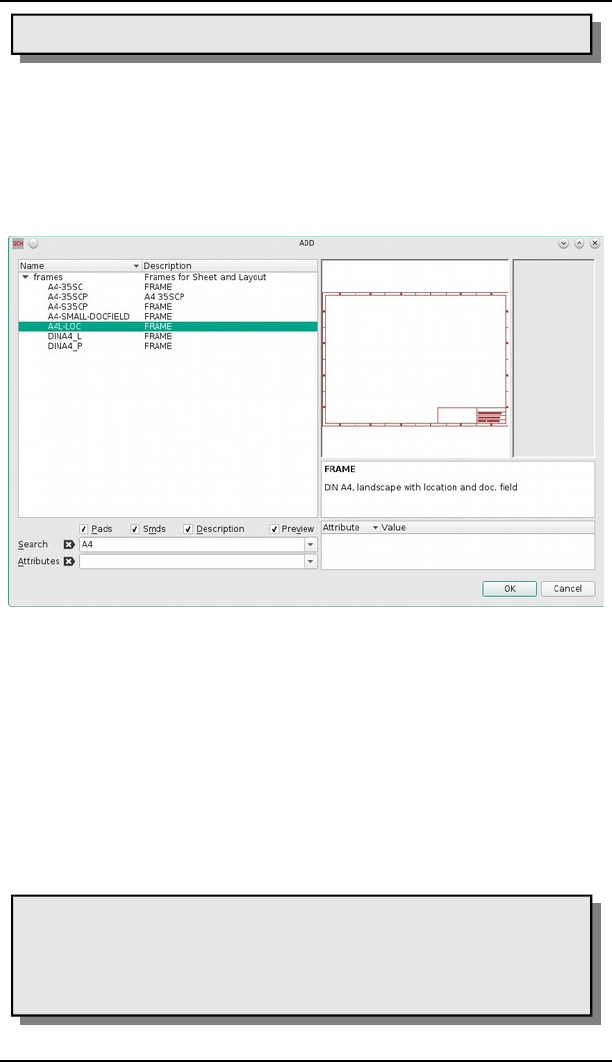
6.1 Creating the Schematic Diagram
the Package description!
Clicking OK closes the ADD window, and you return to the schematic
diagram editor. The frame is now hanging from the mouse, and it can be put
down. The bottom left hand corner of the frame is usually at the coordinate
origin (0 0).
Library names, Device names and terms from the Device description can be
used as search keys. Wildcards such as * or ? are allowed. A number of
search keys, separated by spaces, can be used.
➢ADD dialog: Results from the search key A4
The ADD command may also be entered via the command line or in script
files. The frame can also be placed using the command:
!XH,V"$!K
Wildcards like * and ? may also be used in the command line. The command
!X,V"$!K
for example opens the ADD windows and shows various frames in letter
format to select.
The search will only examine libraries that are in use. That means that the
library has been loaded by the USE command (Library/Use).
Drawing frames are defined with the FRAME command.
This can be done in a library, where the frame can be combined with
a document field. EAGLE can also use the FRAME command in the
Schematic as well as the Board Editor. Details about defining a
drawing frame can be found on page 279.
117

6 From Schematic to Finished Board
Place Circuit Symbols (Gates)
All further Devices are found and placed by means of the mechanism
described above. You decide a Package variant at this early stage. It can easily
be changed later if it should turn out that a different Package form is used in
the layout.
If you have placed a Device with ADD, and then want to return to the ADD
dialog in order to choose a new Device, press the Esc key or click the ADD
icon again.
Give the Devices names and values (NAME, VALUE).
If the text for the name or the value is located awkwardly, separate them
from the Device with SMASH, and then move them to whatever position you
prefer with MOVE. Clicking with DELETE on a text makes it invisible.
Use the Shift key with SMASH to get the texts at their original positions. The
texts are now no longer separated from the Device (unsmash). Deactivating
the Smashed option in the context menu's Properties window is the same.
MOVE relocates elements, and DELETE removes them. With INFO or
SHOW information about an element is displayed on the screen.
ROTATE turns gates by 90°. The same can be done with a right mouse click
while the MOVE command is active.
Multiple used parts may be copied with the COPY command. COPY places
always a new part even if it consists of several gates and not all of them are
already used.
A group of objects (components, nets...) can be reproduced in the schematic
diagram with the aid of the GROUP, COPY and PASTE commands. First
make sure that all the layers are made visible (DISPLAY ALL).
Hidden Supply Gates
Some Devices are defined in the libraries in such a way that the power supply
pins are not visible on the schematic diagram. Visibility is not necessary,
since all the power pins with the same name are automatically connected,
regardless of whether or not they are visible.
If you want to connect a net directly to one of the hidden pins, fetch the gate
into the schematic diagram with the aid of the INVOKE command. Click onto
the INVOKE icon, and then on the Device concerned, assuming that it is
located on the same sheet of the schematic diagram. If the gate is to be
placed on a different schematic diagram sheet, go to that sheet, activate
INVOKE, and type the name of the Device on the command line. Select the
desired Gate in the INVOKE window, then place it. Then join the supply gate
to the desired net.
118
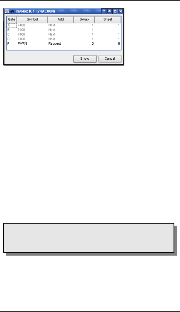
6.1 Creating the Schematic Diagram
➢
INVOKE: Gate P is to be placed
Devices with Several Gates
Some Devices consist not of one but of several Gates. These can normally be
placed onto the schematic diagram one after another with the ADD
command. To place a certain Gate you can use the Gate name directly.
Example:
The Device 74*00 from the 74xx-eu library with Package variant N and in AC
technology consists of for NAND gates named A to D and one power gate
named P. If you want to place the Gate C first, use the Gate name with the
ADD command:
55C-CCCA;00,A;%%)$!K
See also help function for the ADD command.
As soon as one Gate has been placed, the next one is attached to the mouse
(Addlevel is Next). Place one Gate after another on the diagram. When all the
Gates in one Device have been used, the next Device is brought in.
If the Gates in one Device are distributed over several sheets, place them first
with ADD, change to the other sheet of the schematic diagram, and type, for
example
:+4-
on the command line. Select the desired Gate from the INVOKE window.
If you select one of the already placed Gate entries in the INVOKE
window, the OK button changes to Show. Click the Show button, and
the selected Gate is shown in the center of the current Schematic
Editor window.
Designlink – Access to Farnell's Online Product Database
With the help of designlink-order.ulp you can do a general product search or
a search for all parts of your schematic, check price and availability and order
directly at Farnell/Newark. Found order codes can be saved as part
attributes the schematic. The order list can be exported.
119

6 From Schematic to Finished Board
Click onto the designlink icon to begin. This icon is shown next to
the action toolbar. It is part of the text menu which can be switched on or off
through the Options/User Interface menu.
The General option starts a general product search. The ULP shows a
window where you can enter a search string. You will be connected to the
Farnell/Newark-Server directly, where the ULP searches for the given search
string, and finally displays the matches.
The Schematic option starts a search for all the parts used in your schematic.
The search term is the value of each component. As a result you will get a
parts list with Farnell/Newark order codes.
Some EAGLE libraries already contain attributes with information about
Farnell/Newark order codes. In case there is no order code available in the
library, or there is no match at the Farnell/Newark web site, the list will
mark the order code as unknown. Double-click onto this entry for starting a
manual search. As soon as all the components you would like to put into the
Farnell/Newark shopping cart have got an order code, click onto Add to
shopping cart.
The ULP comes with a detailed help which explains functionality and usage.
As an alternative you can start the ULP with the RUN command.
"=!=J/!2I/"H2
For updating libraries with Farnell/Newark order codes you can use
designlink-lbr.ulp. Start it in a Library Editor window and it loops through
all Devices searching for order codes at the Farnell/Newark web site. Finally
there will be created three attributes:
>MF for manufacturer, >MPN for manufacturer part number, >OC_FARNELL
or OC_NEWARK for the order code.
Wiring the Schematic Diagram
Draw Nets (NET)
The NET command defines the connections between the pins. Nets begin and
end at the connection points of a pin. This is visible when layer 93, Pins, is
displayed (DISPLAY command).
As soon as a net approaches a pin, a marker that indicates the pin connection
point is shown; even if layer 93, Pins is not displayed. A left mouse-click
connects the net with the pin then.
Nets are always given an automatically generated name. This can be changed
by means of the NAME command. Nets with the same name are connected to
one another, regardless of whether or not they appear continuous on the
drawing. This applies even when they appear on different sheets.
If a net is taken to another net, a bus, or a pin connecting point, the net line
ends there and is connected. If no connection is made when the net is placed,
the net line continues to be attached to the mouse. This behaviour can be
changed through the Options/Set/Misc menu (using the Auto end net and
bus option). If this option is deactivated, a double click is needed to end a
net. Nets are shown on layer 91, Nets.
120

6.1 Creating the Schematic Diagram
Nets must end exactly at a pin connecting point in order to be joined.
EAGLE will inform you about the resulting net name or offer a selection of
possible names if you are connecting different nets.
The JUNCTION command is used to mark connections on nets that cross
one another. Junctions are placed by default. This option, (Auto set
junction), can also be deactivated through the Options/Set/Misc menu.
Nets must be drawn with the NET command, not with the LINE command.
Do not copy net lines with the COPY command. If you do this, the new net
lines won't get new net names. This could result in unwanted connections.
If the MOVE command is used to move a net over another net, or over a pin,
no electrical connection is created.
To check this, you can click the net with the SHOW command. All the
connected pins and nets will be highlighted. If a Gate is moved, the nets
connected to it will be dragged along.
A simple identifier (without XREF option, see next section about Cross
References) can be placed on a net with the LABEL command. Provided you
have defined a finer alternative grid, labels can be arranged comfortably in
the finer grid with the Alt key pressed.
Defining Cross-References for Nets
If you place a LABEL with active XREF option for a net, a cross-reference will
be shown automatically. It points to the next sheet where the net occurs
again. Depending on the rotation of the label the cross-reference refers to a
previous or a following schematic sheet. If the label itself goes towards the
right or bottom border of the drawing, the cross-reference shows the next
higher page number. If the label points to the left or top border, the previous
pages are taken into consideration. In the case that the net is only available
on one sheet, this cross reference is shown, independently from the rotation
of the label.
If the net is only on the current sheet, only the net name and possibly the
label's frame around it is shown. This depends on the Xref label format
definition which can be done in the menu Options/Set/Misc (can be defined
via SET, too).
The XREF option can be activated in the parameter toolbar of the LABEL
command or after placing the label with CHANGE XREF ON.
The following placeholders for defining the label format are allowed:
YEenables drawing a flag border around the label
Ythe name of the net
Ythe next sheet number
Ythe column on the next sheet
Ythe row on the next sheet
The default format string is %F%N/%S.%C%R. Apart from the defined
placeholders you can also use any other ASCII characters. If %C or %R is used
and there is no frame on that sheet, they will display a question mark '?'. See
also page 279.
121
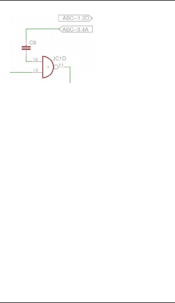
6 From Schematic to Finished Board
The lower label in the picture points to the right and refers to the net ABC on
the next page 3, field 4A, the upper XREF label points to the left (beginning
with the origin point) and refers to the previous page 1, field 2D.
If a XREF label is placed on a net line directly, it will be moved together with
the net.
More information about cross-references can be found in the help function
for the LABEL command.
Cross-References for Contacts
In case you are drawing an Electrical Schematic and using, for example,
electro-mechanical relays, EAGLE can display a contact cross-reference. In
order to do that, place the text >CONTACT_XREF inside the Schematic's
drawing frame. This text is not displayed in the drawing (excepted its origin
cross), but its position (the y coordinate) determines from where on the
contact cross-reference will be drawn on the current sheet. As soon as this
text is placed the contact cross-reference will be displayed.
The format of the contact cross-references can be defined - as for net cross-
references – in the Options/Set/Misc menu. It uses the same format
variables as described in the previous section Defining cross-references for
nets. The default setting is: /%S.%C%R, which
means /Pagenumber.ColumnRow.
The variables %C for column and %R for row can only work with a drawing
frame that was defined with the FRAME command and comes with a
column/row graduation.
For a proper display of the contact cross-references in the Schematic the
elements have to be defined in the Library Editor according to certain rules.
More information about this can be found in the help function under Contact
cross-reference and in the chapter about Libraries and Component Design
later in this manual.
122
➢
Cross-reference with a XREF
label
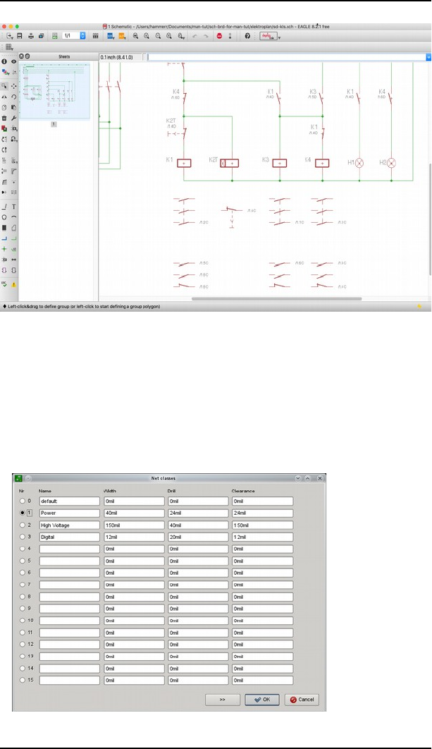
6.1 Creating the Schematic Diagram
Specifying Net Classes
The CLASS command specifies a net class (Edit/Net classes menu). The net
class specifies the minimum track width, the minimum clearance to keep
away from other signals and the minimum hole diameter for vias in the
layout. Each net primarily belongs to net class 0. By default all values are set
to 0 for this net class, which means that the values given in the Design Rules
are valid. You can use up to 16 net classes. Creating a net class can be
cancelled with the UNDO command.
➢
Net classes: Parameter settings
123
➢
Electrical Schematic with contact cross-reference
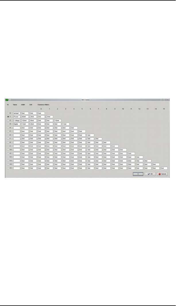
6 From Schematic to Finished Board
The image shows three additional net classes defined:
All nets that belong to class 0, default, will be checked by the settings of the
Design Rules.
Net class number 1, for example, has got the name Power and defines a
minimum track width of 40 mil.
The minimum drill diameter for vias of this class is set to 24 mil.
The clearance between tracks of net class 1 and tracks that belong to other
net classes is also set to 24 mil.
The left column Nr pre-defines the net class of the next net that is drawn
with the NET command. This selection can be made in the parameter toolbar
of the NET command, as well.
If you would like to define special clearance values between certain net
classes, click the button marked with >>. The Clearance Matrix opens. Enter
your values here.
➢
Net classes: The Clearance Matrix
To return to the simple view, click the << button. This is only possible,
however, if there are no values defined in the matrix. The net classes can be
changed later by means of the CHANGE command (the Class option) in the
Schematic and in the Layout Editor.
Net class definition can be done in the Layout Editor, as well.
A net class can be assigned to a single net/signal (left mouse click) or to a
number of nets/signals (Ctrl + right mouse click) that have been selected
with the GROUP command before.
Drawing a bus (BUS)
Buses receive names which determine which signals they include. A bus is a
drawing object. It does not create any electrical connections. These are
always created by means of the nets and their names. The associated menu
function is a special feature of a bus. A menu opens if you click onto the bus
with NET. The contents of the menu are determined by the bus name.
The bus in the diagram is named Bus1:A[0..12],D[0..7],Clock.
124
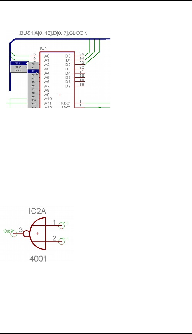
6.1 Creating the Schematic Diagram
Clicking on the bus line while the NET command is active, opens the menu as
illustrated above. The name of the net that is to be placed is selected from
here.
➢
Bus menu
The index of a partial bus name may run from 0 to 511.
The help function gives further information about the BUS command.
Pinswap and Gateswap
Pins or Gates that have the same Swaplevel can be exchanged with one
another. These properties are specified either when the Symbol is defined
(Pinswap) or when the Device is created (Gateswap).
Provided the Swaplevel of two pins is the same, they can be exchanged for
one another. Display layer 93, Pins, in order to make the Swaplevel of the
pins visible.
Pins or Gates may not be swapped if the Swaplevel = 0.
➢
Swaplevel: Pins layer is
visible
Input pins 1 and 2 have Swaplevel 1, so they can be exchanged with one
another. The output pin, 3, which has Swaplevel 0, cannot be exchanged.
You can find the Swaplevel of a Gate by means of the INFO command, for
example, type in the command line INFO IC2A. Alternatively via the context
menu, Properties entry.
125
6 From Schematic to Finished Board
Power Supply
Pins defined as having the direction Pwr are automatically wired up. This is
true, even if the associated power gate has not explicitly been fetched into the
schematic. The name of the Pwr pin determines the name of the voltage line.
This is already fixed by the definition of the Symbols in the library.
If nets are connected to a Device's Pwr pins, then these pins are not
automatically wired. They are joined instead to the connected net.
For every Pwr-pin there must be at least one pin with the same name but the
direction Sup (a supply pin). There must be one on every sheet. These Sup
pins are fetched into the schematic in the form of power supply symbols, and
are defined as Devices in a library (see supply*.lbr). These Devices do not
have a Package, since they do not represent components. They are used to
represent the supply voltages in the schematic diagram, as is required by the
Electrical Rule Check (ERC) for the purposes of its logical checks.
Various supply voltages, such as 0 V or GND, which are to have the same
potential (GND, let's say), can be connected by adding the corresponding
supply symbols and connecting them with a net. This net is then given the
name of that potential (e.g. GND).
➢
Supply symbols
If you place a supply pin (direction Sup) onto a net (with ADD or MOVE),
you will be asked for a new net name. Should it be the name of the supply pin
or should the net name remain unchanged?
Click Yes (default) for renaming the net with the name of the supply pin (in
the image above: AGND). Click No to preserve the current net name (VA1).
If the net has an automatically generated name, like N$1, you may suppress
this warning message. Use the SET command in the command line:
=$)HH!8=)&+M<=&&&-
If the last supply pin of a net is deleted, the net will get an automatically
generated name, like N$1.
126
➢
Supply pin name as new net name?

6.1 Creating the Schematic Diagram
If there is no supply pin in the supply libraries that fits to your
voltage in the schematic, you have to define a new supply pin!
Renaming an already existing supply pin is the wrong way and can
lead to unexpected results!
Define Attributes
Global Attributes
It is possible to define Global Attributes in the Schematic, for example, for
the author or a project identification number, that can be placed anywhere in
the schematic, often used in the docfield of the drawing frame.
Open the dialog through the Edit/Global Attributes... menu. Click the button
New to define a new Global Attribute. It consists of the attribute's name and
its value.
If you want to make a global attribute visible in the schematic, write a
placeholder with the TEXT command. For the AUTHOR attribute, write the
text >author.
It does not matter, if it is written in lower or upper case letters. The
> character in front of the text indicates that this is special text.
It is possible to define the placeholder text already in the Library, for
example, in a Symbol of a drawing frame. In this case the global attribute will
be shown on each schematic sheet containing this frame.
Global Attributes can be defined in the Schematic and Layout
separately.
More information on this can be found in the ATTRIBUTE command's help.
Attributes for Elements
The ATTRIBUTE command allows you to define attributes for Devices. An
attribute consists of the attribute name and its value that may provide any
information. If there already exists an attribute that has been defined in the
library, you may alter the value in the schematic.
127
➢
Global Attributes: The Author attribute is created
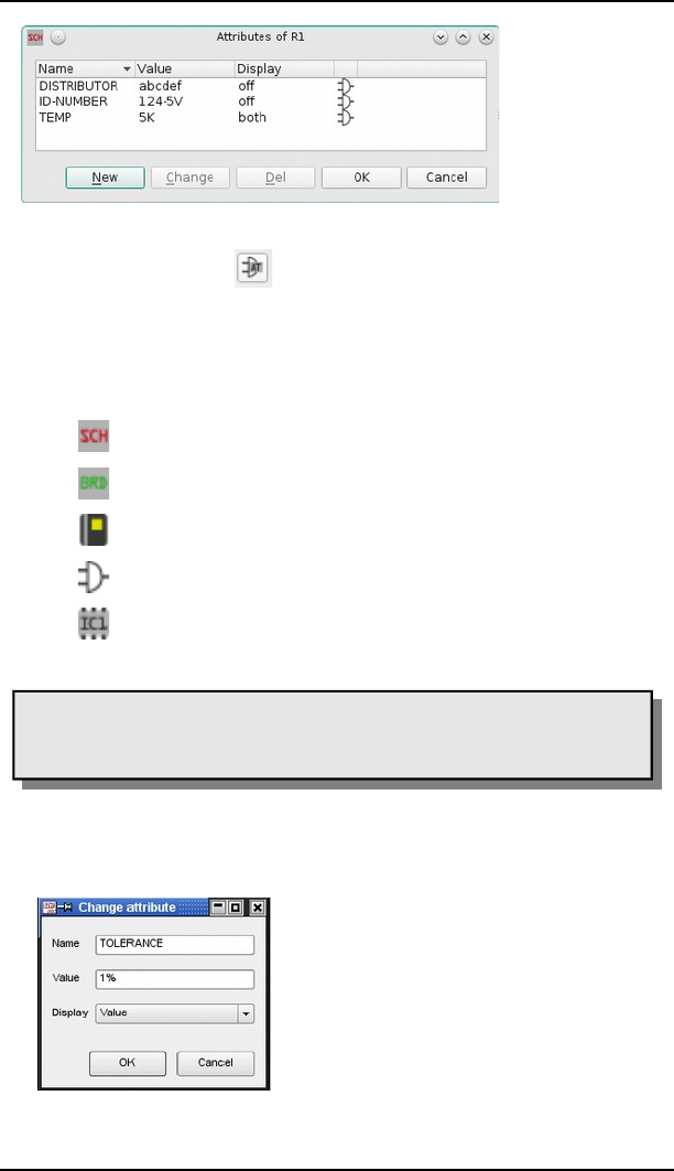
6 From Schematic to Finished Board
Clicking the ATTRIBUTE icon and then onto a Device opens a dialog
window. It lists the part's attributes already defined in the schematic or in
the library.
The image above shows the attributes DISTRIBUTOR, ID-NUMBER, and
TEMP for part R1. The icons on the right indicate where the attribute comes
form:
globally in the Schematic
globally in the Layout
in the Library's Device Editor
for the element in the Schematic
for the Package in the Layout
Attributes that are defined in the Layout Editor are not shown in the
Schematic Editor. A newly defined attribute in the Schematic adopts
the value of an already existing attribute in the Layout.
Defining a New Attribute
Click onto the New button to define a new attribute in the schematic. In the
following dialog you can define Name, Value, and the Display mode.
128
➢
Attribute dialog
➢
Create and change attributes
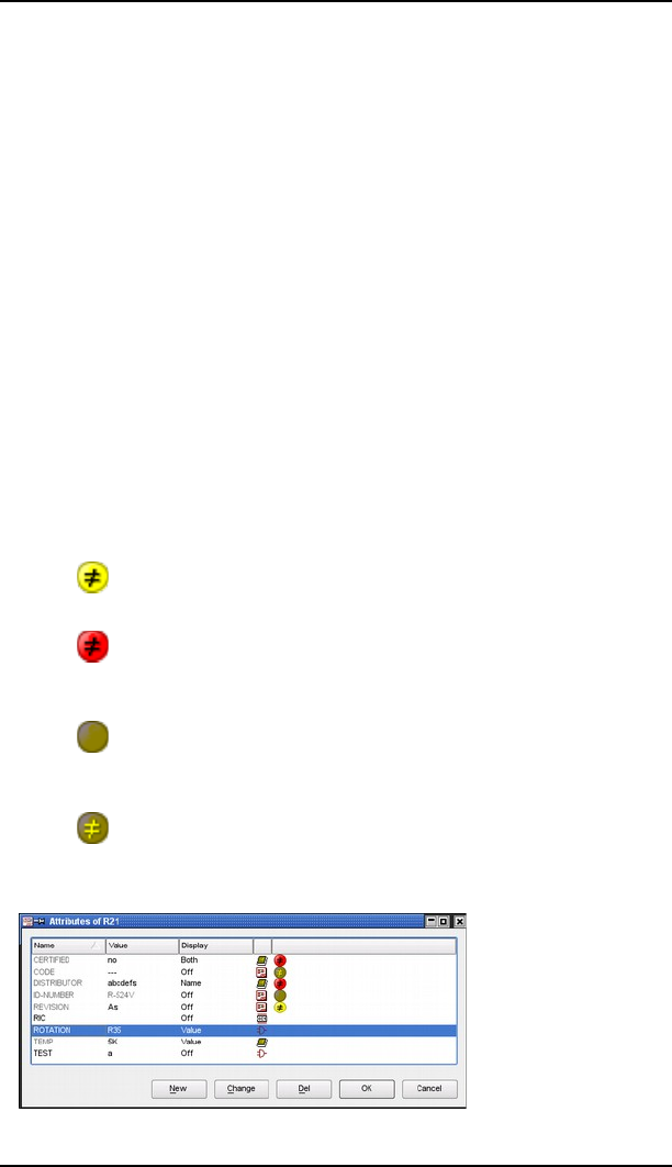
6.1 Creating the Schematic Diagram
In this image the attribute's name is TOLERANCE, its value is 1%.
With the Display option you manage the way the attribute is displayed in the
drawing. There are four options available:
Off: The attribute is not visible
Value:
Only the attribute's value is visible (1%)
Name:
Only the attribute's name is visible (TOLERANCE)
Both: Name and value are visible (TOLERANCE = 1%)
If the Display option is not set Off, the respective text will be displayed at the
Device's or Gate's origin. The layer which is preset in the Schematic, for
example with CHANGE LAYER before creating the attribute, determines the
text's layer. Location and layer can be changed any time.
If there is an already defined placeholder text for an element in the library,
the text shows up at the given location. It is possible to unfix such texts with
the SMASH command. Now you can move it, change its layer, the font, its
size and so on.
Changing an Attribute's Value
Values of attributes that are already defined in the library can be changed in
the Schematic Editor. After changing an attribute's value, the attributes
dialog displays special icons that indicate the attribute's status. The icons
have the following meaning:
the yellow icon indicates that the attribute initially was defined
with a variable value and that the value has been changed.
the red icon indicates that the value of the attribute which was
initially defined as constant has been changed after a confirmation
prompt.
the plain brown icon indicates that a global attribute was
overwritten by a part attribute. The value, however, remained
unchanged.
the brown icon with the unequal sign indicates that a global
attribute was overwritten by a part attribute and the value has
been changed.
➢
Attribute dialog with different attributes
129
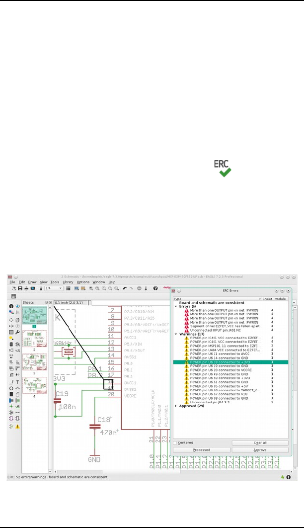
6 From Schematic to Finished Board
Grayed text in the Attributes' dialog indicates that it can't be changed or
rather the element's attribute value was defined as constant in the library.
The icons inform you about the attribute's origin and its current status. Move
the mouse cursor onto one of the icons to let EAGLE display tool tip texts to
explain its meaning, provided the Bubble help in Options/User interface is
active.
More details on defining attributes can be found in the library chapter
beginning with page 271.
ERC – Check and Correct Schematic
A schematic diagram must be checked with the aid of the Electrical Rule
Check (ERC), when the design of the schematic diagram has been completed,
if not before. It is actually a good idea to run the (ERC) many times during
your design process to catch errors immediately. To start the Electrical Rule
Check click onto the ERC icon in the command menu or the entry Erc...
in the Tools menu.
All the errors and warnings are listed in the ERC Error window. Errors are
marked with a red icon, warnings with a yellow icon.
In the case of a corresponding board file, the ERC also checks the consistency
between schematic and board. If there are no differences, ERC reports Board
and schematic are consistent. Otherwise the ERC Errors window contains a
branch with Consistency errors. For further information on this see page
198.
130
➢
The ERC Errors window

6.1 Creating the Schematic Diagram
It is possible to sort the errors and warnings, ascending or descending, by
error types or sheet numbers. click onto the column headers Type or Sheet
therefore.
If you select an entry in the Errors or Warnings branch, a line points to the
corresponding location in the schematic diagram. In case you zoomed into
the drawing, you can click the option Centered. The currently selected error
is shown in the middle of the drawing window now.
Please check each error and every warning.
In some situations it may be the case that you want to tolerate an error or a
warning. Use the Approve button for this. The error/warning entry will be
removed from the Errors or Warnings branch and appears in the Approved
branch.
If you want to have the capability of displaying an approved error/warning
occurrence in the Errors or Warnings branch, expand the Approved branch,
select the error entry and click the Disapprove button. Now it is treated as a
normal error/warning and is marked in the schematic.
An approved error/warning retains its approved status as long as you do not
disapprove it by clicking the Disapprove button. Even a new ERC won't
change this status.
If the Errors window lists approved errors or warnings only, it won't open
automatically after running the Electrical Rule Check again. The status line
of the Schematic Editor, however, will show the following hint:
ERC: 2 approved errors/warnings
Moving an entry from one branch into the other, marks the schematic file as
changed and not saved.
While correcting the error on the board, the ERC Errors window may remain
open. After correcting one error or warning you can mark the entry as
Processed in the error list by clicking onto the Processed button. The
error/warning icon turns gray now. Entries marked as processed will be
remembered as long as you don't start ERC again. Re-opening the ERC
Errors window with the ERRORS command, shows the same status as
you left it at last.
If you click onto the Clear all button, the Errors and Warnings branches will
be cleared. Approved errors and warnings, however, will remain in the
Approved branch. The message List was cleared by user is shown then.
If you did not run an ERC before, the ERRORS command will start it
automatically before opening the errors window.
The ERC checks the schematic diagram according to a rigid set of
rules. It can sometimes happen that an error message or warning
can be tolerated.
If necessary, make an output of net and pin lists with the EXPORT
command.
131
6 From Schematic to Finished Board
SHOW allows nets to be traced in the schematic diagram.
Organize Schematic Sheets
If your schematic is a bit more complex or you want to use more than one
sheet, for example, for better readability, you can add (and also remove)
sheets with the help of the sheet thumbnails' context menu. Click with the
right mouse button onto one of the thumbnails that are located on the left
side of the Schematic Editor window.
A new sheet is always added as the last one.
The schematic sheets can be sorted by dragging and dropping the
thumbnails. Therefore click with the left mouse button on a thumbnail and
drag it to its new position.
Alternatively you can sort the sheets with the EDIT command in the
command line:
5$"9$".
moves sheet number 5 at the position before sheet number 2. Further
information about this can be found in the EDIT command's help function.
Go to the Options/User interface menu in order to switch on/off the sheet
preview.
When switching between schematic sheets, the current zoom level of
each sheet will be maintained.
Points to Note for the Schematic Editor
Superimposed Pins
Pins will be connected if the connection point of an unconnected pin is placed
onto the connection point of another pin. Pins will not be connected if you
place a pin that is already connected to a net line onto another pin.
Open Pins when MOVEing
If a Gate is moved then its open pins will be connected to any nets or other
pins which may be present at its new location. Use UNDO if this has
happened unintentionally.
Duplicating a Section of the Schematic
If you want to use a certain section of your schematic several times, you can
use GROUP and COPY commands in order to put this part into the
clipboard, and then use PASTE to place the group on the same or on a
different sheet of your schematic.
The duplicated components will get new names. Nets connected to a supply
pin or marked with a LABEL will keep their original name, provided the
supply pin and the label is part of the selected group. All other nets will get
new names.
132
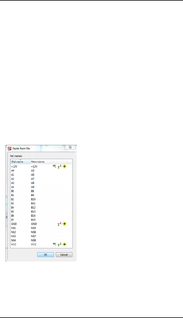
6.1 Creating the Schematic Diagram
With Consistent Layout
In case you already created a board from your schematic, the pasted
components in the layout will be placed left of the board's origin. As usual the
components have to be arranged and the airwires routed then.
Merge Different Schematic Files
It is possible to paste a whole schematic file into the current drawing. This
can be done in the menu File/Import/EAGLE drawing.... The new sheet(s)
will be appended to the current one(s), depending on the number of sheets of
the source schematic. You can re-order the sheets by drag&drop afterwards.
While inserting a group EAGLE checks the objects' names and compares
them with those already existing in the current schematic. EAGLE will show
a window where you get information about the net names. The table shows a
list with the original names of the schematic you want to paste, in the column
Old name, and the net names, in the column New name, EAGLE suggests for
this schematic after pasting it into the current drawing. By clicking onto an
entry you can influence the net names and decide about them by yourself.
Names of nets that have a label or are connected to a supply pin, will remain
unchanged by default. In the Paste... list such nets are marked with icons
that want to tell you what's the reason for leaving this net name unchanged.
Of course you are allowed to change such a net name as well.
It is not allowed to change the names of nets that are member of a bus or that
are connected to an implicit power here.
It's possible to pre-define an offset for the enumeration of the components, if
you use the PASTE command in the command line:
.00(!-$"(
133
➢
Netnames before and after pasting the
schematic

6 From Schematic to Finished Board
adds the schematic with name channel1.sch into the drawing and increments
the components' names with an offset of 200. R1 of channel1.sch will be
named R201 in the current drawing then.
This function is also available through the File/Import... menu.
With Consistent Layout
In case you are working with a consistent pair of schematic and board files,
and you want to import another consistent schematic/board pair into your
current project via the File/Import/EAGLE drawing... menu, the schematic
will be placed on a new sheet (or several sheets) and the board will be placed
left of the already existing layout. It can be moved with GROUP and MOVE
afterwards.
As an alternative to the File/Import menu and the PASTE command which
can be used in the command line, you are allowed to drag&drop a schematic
or a layout from the treeview's projects branch of the Control Panel into your
currently opened Schematic or Layout Editor window.
Multi-Channel Devices
This functionality can be used to easily create multi-channel devices:
Finish the schematic of one channel and create the board of it. Then arrange
the components and route your layout. When this is done use Paste from....
and copy the schematic/layout pair as often as needed into on common
schematic/board file pair.
If you start File/Import/EAGLE drawing... in the Layout Editor, the layout
will be attached to the mouse cursor and you can place it where you would
like to have it. The schematic part will be added on a new page in the current
schematic. If you are using the command line in the Layout Editor you can
use coordinates for an exact placement.
$5@-010B
for example, places the board from test.brd with an offset of (10 30) in grid
units compared to the original position.
In case you start the import from the Schematic Editor, the referring layout
will be placed automatically left of the already existing design in the layout
editor.
Design Blocks
A Design Block (*.dbl) may contain a schematic or a board, or ideally both. If
there is only a Schematic editor open, it will paste the schematic part of the
Design Block only, accordingly for boards. To paste both, a consistent
schematic/board pair has to be loaded.
In its tree view the Control Panel shows a branch with Design Blocks
available. Clicking onto one of these entries displays a preview of the Design
Block. Double-clicking an entry pops up the Modify Design Block window.
Here you can modify the Description, create, delete or change attributes, or
enter the Design Block editing mode by clicking the Edit.. button. Then a
Design Block Schematic or a Design Block Layout Editor window appears. It
looks the same as a Schematic or Layout Editor window, with the exception
of the text in the title bar.
134
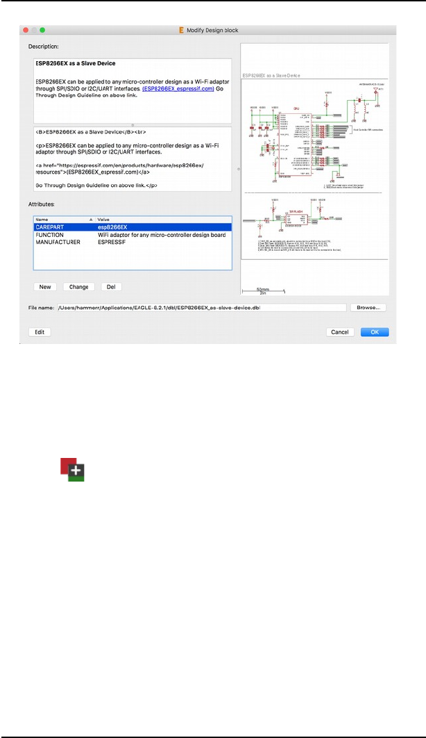
6.1 Creating the Schematic Diagram
Adding Design Blocks into Your Current Design
For inserting Design Blocks Schematic and Layout Editor have a “PASTE
DBL” icon . Alternatively you can insert it from the Control Panel. Right-
click on one of the entries in the Tree View’s Design Block branch and choose
the Add to schematic/board option.
If the PASTE DBL command is started from Layout Editor, it has the same
behaviour like pasting from a drawing file. The board can be placed by mouse
click and new sheets are added to schematic.
If the command is started from the Schematic Editor and the Design Block
has only one sheet, it can be placed by mouse click into the current sheet, as
well. No new sheet will be created in that case.
Save a Drawing as a Design Block
With File/Save as Design Block… (WRITE DBL) a Design Block is generated
from the currently loaded schematic and/or board (depending, from which
editor executed and whether schematic and board are in consistent state)
and saved under the given name.
135
➢
Modify Design Block Properties

6 From Schematic to Finished Board
If no name is given, the Design Block dialog pops up (see image above). It
allows entering an HTML description and defining Attributes. In the upper
left there is a preview of the description. The description can be written in
the text field below.
Attributes can be managed with the buttons New, Change, and Delete at the
bottom left. There also can be automatically generated Attributes which are
not editable.
The preview on the right represents the drawing(s) to be included in the
Design Block. At the bottom you can enter the file name or select where to
store it.
Save a Selection of the Drawing as a Design Block
With the pulldown menu entry File/Save selection as Design Block it is
possible to select objects of the current schematic, board or of both, if it is a
consistent pair of files, and save it as a Design Block.
The selection works in additive mode and may be adjusted several times.
Deselection with Ctrl + left click is supported. The selection in the first Editor
window has to be finished with Ctrl + right click.
Please check the hints displayed in the status bar of the editor window.
There are a couple of criteria for the selection that will be checked (see
below). If these criteria are not met, an according error message is displayed
and the user may continue and correct the selection.
If there's only one editor window opened, the Design Block dialog pops up,
presenting the current selection in the preview. The selection can now be
saved.
If both editors are open, you can continue your selection after the Ctrl +
right click in the second editor. The initially selected corresponding objects
are already selected due to the back/forward annotation (for example
element R1 in the layout, if part instance R1 in the schematic has been
selected first). In the second editor window additional objects can be added
to the selection, as long as they do not severe consistency. Selection or
deselection of any object that might severe consistency are automatically
filtered out.
For example, objects without electrical relevance like texts, dimensions etc.
are allowed to be selected. Routed traces or signal polygons can be added or
removed from the selection, if the corresponding nets were already selected
in the previous editor window. The selection process is completed with a
further Ctrl + right click. The Design Block dialog shows up now. The whole
selection is visible in the preview area and can be saved as a Design Block for
future reuse.
The combined selection is only possible, if a consistent schematic/board pair
is loaded. It works in both directions.
The selection is not yet supported within hierarchical schematics.
136

6.1 Creating the Schematic Diagram
Selection criteria
If the schematic has multiple sheets and the selection is started from a
board, only objects with counterparts on the currently active sheet are
supported.
If the selection is started from a schematic, it is checked that the user
selects net segments completely, in particular not leaving behind
some net wires or labels.
For each part all of its instances must be selected.
With a net segment being selected, all connected part instances
connected to this segment must be selected.
6.2 The Hierarchical Schematic
A hierarchical diagram differs from the schematic generated in section 6.1 in
its structure. It contains subordinate units, so-called modules, each
representing a part of the entire circuit diagram.
Modules can be edited just the same like a simple Schematic. Modules can be
drawn across multiple module pages. The sheets of the modules are
displayed in the icon preview of the Schematic Editor window; just like
normal, schematic sheets.
Modules are usually represented by module instances that are drawn as
simply symbols (boxes) at schematic main level. Module instances of one and
the same module can be used repeatedly.
For the module instances ports are defined, which serve as an interface
between the nets inside the module and a higher schematic level. Ports are
used, for example, to connect various module instances or to establish
connections between nets inside a module and nets on schematic main level.
Ports can export not only individual nets, it is also possible to export simple
buses via a port.
The hierarchical schematic can have any number of levels. This allows to use
a module instance of another module inside a module, and so on. The depth
of the hierarchy can be arbitrarily deep.
If a layout is generated from a hierarchical schematic, the result is
comparable with the layout of a schematic without hierarchy.
Creating a Module
Click onto the MODULE icon to create a module. The Module Dialog
opens. Type in the line New: the name of the module, for example FILTER.
The module will be created. Attached to the mouse cursor, you already see
the module instance of the module FILTER which can be placed on the first
page of the schematic. If you cancel the command before you place the
module instance, the module is nevertheless already created. You can see it
in the sheet preview: There is module sheet named FILTER:1 (Module
FILTER, Module sheet 1) displayed.
137

6 From Schematic to Finished Board
If you want to create multiple modules without placing a module instance,
use the command line:
7+5E
7+57
7+5+6
Each command creates after your confirmation a new module. For the
POWERSUPPLY module there is already defined the prefix PS for the
module instances. They are finally named PS1, PS2, and so on.
The hierarchical schematic may contain any number of modules.
The picture shows a newly created module with name FILTER. The module
sheet is still empty. There are no components and nets drawn.
The corresponding module instance has already been placed on the
schematic page and has the name FILTER1.
Module instances and their ports are automatically drawn in layer 90
Modules.
In the next step, you define the contents of the module. Switch to the module
sheet by clicking on the sheet preview or in the action bar on the sheet
selection box. Now draw the module as in the normal schematic, just as in
the previous section Creating the Schematic Diagram beginning with page
115 described.
A module can be drawn over several sheets. In order to create a new module
sheet, click on the module sheet preview with the right mouse button. Select
the appropriate option in the context menu.
138
➢
Module Instance for Module Filter (yet without ports and
contents)
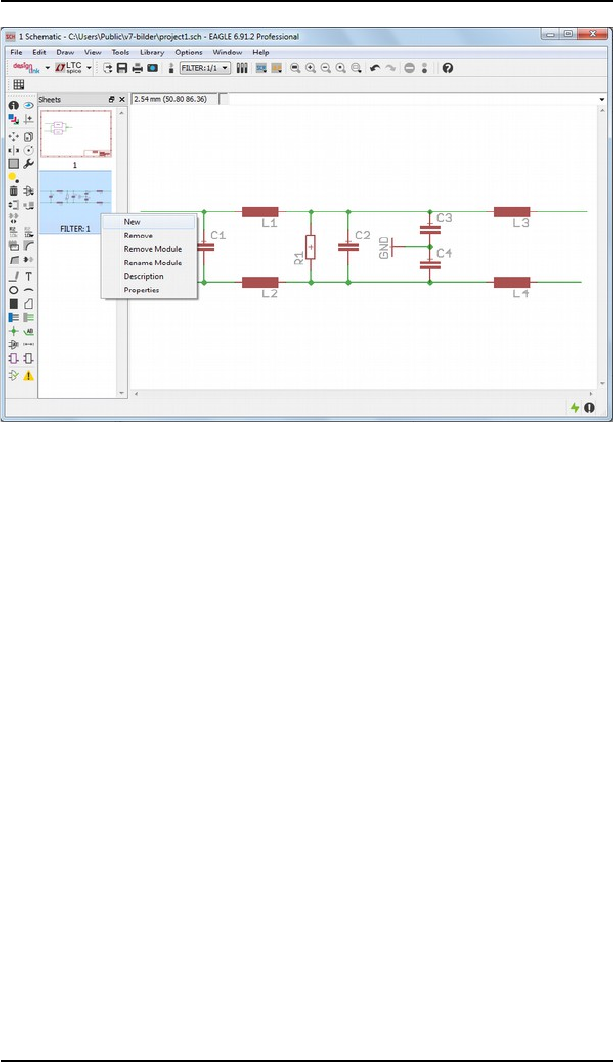
6.2 The Hierarchical Schematic
In the context menu of the module sheet you can create a new additional
module sheet, remove a module sheet, or completely remove a whole module
with all its module instances from the schematic (Remove Module).
The description of a module can be formatted with HTML tags. The first line
of the description will be displayed in addition to the module name in the
module sheet preview and in the Sheet combo box.
In Properties, you have the option to define a prefix and the size of the
symbol of the module instance that represents the module in the schematic.
Prefix defines the name of the module instances, as it is with the prefix for a
device in a library. If you choose for a module named Power_Amplifier, for
example, as a prefix PA, the name of the first module instance will be PA1,
the second PA2, and so on. If there is no prefix defined, the module name +
number will be used.
In addition, you can see the list of ports that connects the module with its
environment.
The order of the module sheets can be changed by drag&drop in the preview.
It is also possible to move a schematic sheet from main level into a module.
The result is a corresponding module sheet.
You can also move sheets out of a module into main schematic level. But
please keep in mind that this can have a significant impact on your design
under certain circumstances. If you have already started to create the layout,
such an action may have a significant impact on it.
Organizing the sheets of the module can also be done via the command line
using the EDIT command (see help).
139
➢
Context menu of module sheet Filter:1
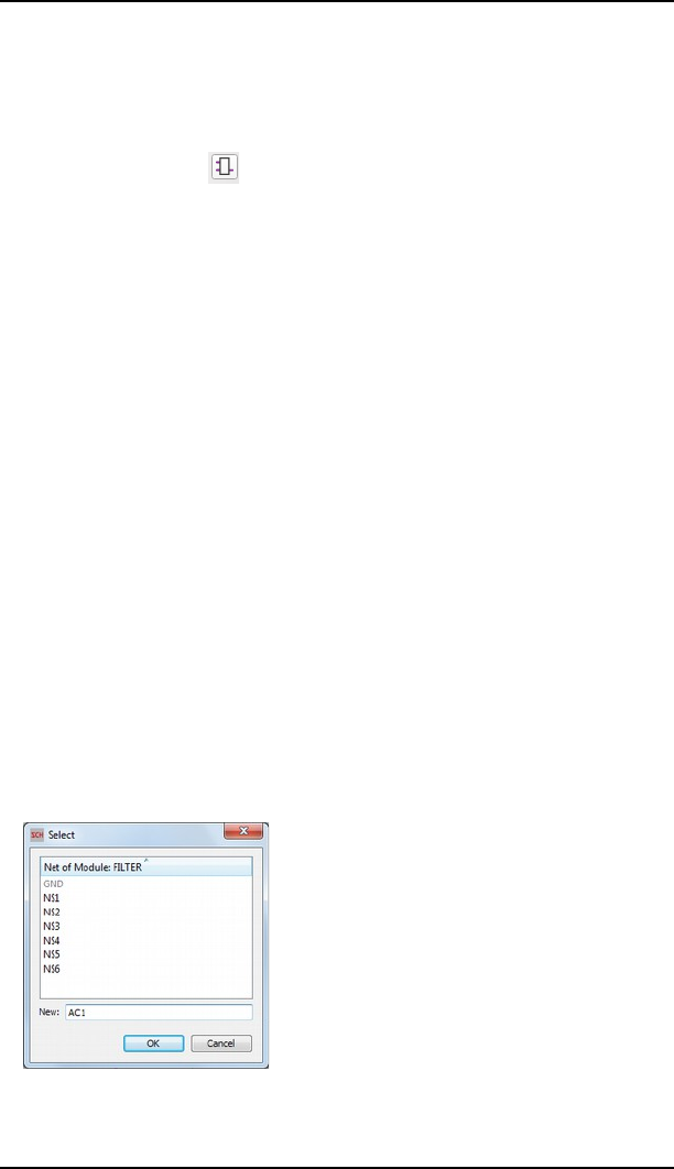
6 From Schematic to Finished Board
Define Ports
A Port serves as an interface for the nets within a module and the world
outside. In the main level schematic ports can be connected to nets that
connect different module instances or components that are not member of a
module (i.e. in the main schematic level).
Click on the PORT icon and then click the module instance for the port to
be created. The first port is attached to the mouse cursor. It can be moved
along the module instance's contour. The parameter toolbar of the PORT
command shows a combo box that offers different port directions.
The Direction describes the logical direction of signal flow. There are the
following options:
NC not connected
In input
Out output (totem-pole)
IO in/out, bidirectional (default)
OC open collector or open drain
Hiz high impedance(3-State) output
Pas passive
Pwr power pin (Vcc, Gnd, Vss ...), supply voltage input
The direction is shown at the ports by corresponding arrows.
After choosing the direction place the port with a left mouse click. This opens
a selection window from which you select the module net, which should be
connected via the port to outside the module. If there is yet no corresponding
net present in the module, you can define a New name, as well. This net has
to be created in the module then!
In the Select windows can also appear module buses. A port can even handle
simple buses, for example PA[0..7]. The nets PA0...PA7 will be exported
through this “bus port”. The bus port will be drawn with a wider line width.
Click OK to confirm the selection. The next port is attached to mouse cursor
now and can be placed as described at the contour of the module instance. If
all ports are placed, terminate the PORT command with Esc or click onto
another module instance for further placement of ports.
140
➢
Select the Module Net for the Port

6.2 The Hierarchical Schematic
The connection point of the port is displayed the same way as for pins of
components in layer 93, Pins.
Using Module Instances
Module instances are defined with the MODULE command. Click the
MODULE icon and select the module for which the module instance should
be created.
Place the module instance in the schematic.
A module instance can be moved as a whole, for example, with MOVE.
Do you want to move only one port to another location or change the
Direction or the name of the port, however, select the MOVE or INFO, hold
down the Ctrl key and click on the port.
141
➢
Module Instance with Ports; on the right: Properties Dialog
➢
Module Selection

6 From Schematic to Finished Board
A change to a module instance that is used multiple times in the hierarchical
schematic is transferred to all module instances.
If you would, for example, add a new port to the module instance Filter1 in
the image above, there would be added the same port to the module instance
Filter2 simultaneously.
A change in the size of the symbol of a module instance can be done via the
properties dialog or by Ctrl+MOVE on one of the borders of the box. The
change applies to all module instances of this module.
Resulting Component Names in the Layout
For components that are used in modules, special rules apply when
generating the component name. Each module has its own namespace.
ModulInstanceName:PartName
Supposed a component with the name C1 is used in the module FILTERS and
also used in a module named POWERSUPPLY.
If these modules are represented by two module instances in the schematic
(Filter1 and Powersupply1), the resulting component names on the board will
be composed of the module instance name followed by a ':' and the part
name. So in our example, the components will have the names Filter1:C1 and
Powersupply1:C1.
This is the default method used by EAGLE.
Offset
Optional you can specify an offset for module instances on schematic main
level. For example, the module instance Filter1 has defined an offset of 100
and the module instance Powersupply1an offset of 200, the resulting
component name on the board will be C101 instead of the previous Filter1:C1
and C201 instead Powersupply1:C1.
The offset can be defined only for module instances on main schematic level
and applies only to components. In case of components and nets in deeper
levels the module instance name is always prefixed.
The offset has to be a multiple of 100. It is specified in the properties dialog
of the module instance or directly with the MODULE command in the
command line. The syntax is described in the help of the MODULE
command.
Assembly Variants for Modules
Within modules, assembly variants can be defined. Edit a module sheet and
click onto the Assembly variants entry in the Edit menu of the Schematic
Editor. How to create assembly variants is described in section Creating
Assembly Variants beginning with page 192.
Module assembly variants are limited to the module parts. Module assembly
variants can be used via the module instance. For each module instance a
specific module assembly variant can be selected.
142

6.2 The Hierarchical Schematic
There is no direct switching between assembly variants in a module, but the
element's value, populate state and attributes in the board are set following
the chosen variant in the corresponding module instance.
If used on schematic main level, the VARIANT command works for the parts
on main level as it is in non-hierarchical schematics.
The assembly variant definitions are now kept only in the schematic.
For standalone boards, assembly variants are no longer supported, but it's
possible to set the populate option of elements with the CHANGE command
or in the properties dialog.
Special Features between Schematic and Layout
SHOW command
Show executed on a module instance displays all associated components and
signals in the layout generated by this module instance.
Click on a component in a module and EAGLE shows all components in the
board that are generated by the multiple use of a module – there are several
module instances that represent the same module in the schematic.
Consistency
To avoid inconsistencies between schematic and board regarding
components and nets and the corresponding signals in the hierarchical
design, some commands can not be executed in the Layout Editor.
This must therefore be done in the schematic and will be transferred to the
appropriate element or signal on the board then. These includes the
commands NAME and VALUE.
EAGLE prompts in such situations an appropriate message.
This restriction applies only to objects in a hierarchical structure, if there is
consistency.
6.3 Considerations Prior to Creating a Board
Checking the Component Libraries
The EAGLE component libraries are developed by practising engineers, and
correspond closely to present-day standards. The variety of components
available is, however, so wide that it is impossible to supply libraries which
are suitable for every user without modification.
There are even different Packages which are supplied by various
manufacturers using the same identification! Manufacturers recommend
very different sizes for SMD pads, and these depend again on the soldering
procedure being applied.
In short: You cannot get away without checking the components, in
particular the Package definitions, being used when laying out.
143

6 From Schematic to Finished Board
In the case of SMD components, please take particular care to ensure
that the Package from the library agrees with the specifications of
your component. Housings from different manufacturers with the
same name but different dimensions are often found.
Agreement with the Board Manufacturer
If you plan to have your PCB professionally manufactured, now is the time to
inquire at your board manufacturer whether they stipulate any particular
values for the following parameters:
track width
shape of solder lands
diameter of solder lands
dimensions of SMD pads
text size and thickness
drill hole diameters
number of signal layers
in case of multilayer boards: manufacturing directions for Blind and
Buried vias and composition of the board (see page 178)
clearance values between different potentials
parameters concerning solder stop mask and cream frame
You will save yourself time and money if you take these stipulations into
account in good time. You will find more details on this in the section on the
Preparing of Manufacturing Data (Chapter 9).
Specifying the Design Rules
All the parameters relevant to the board and its manufacture are specified in
the Design Rules.
Use the menu Edit/Design Rules.. to open the Design Rules window shown
below:
144
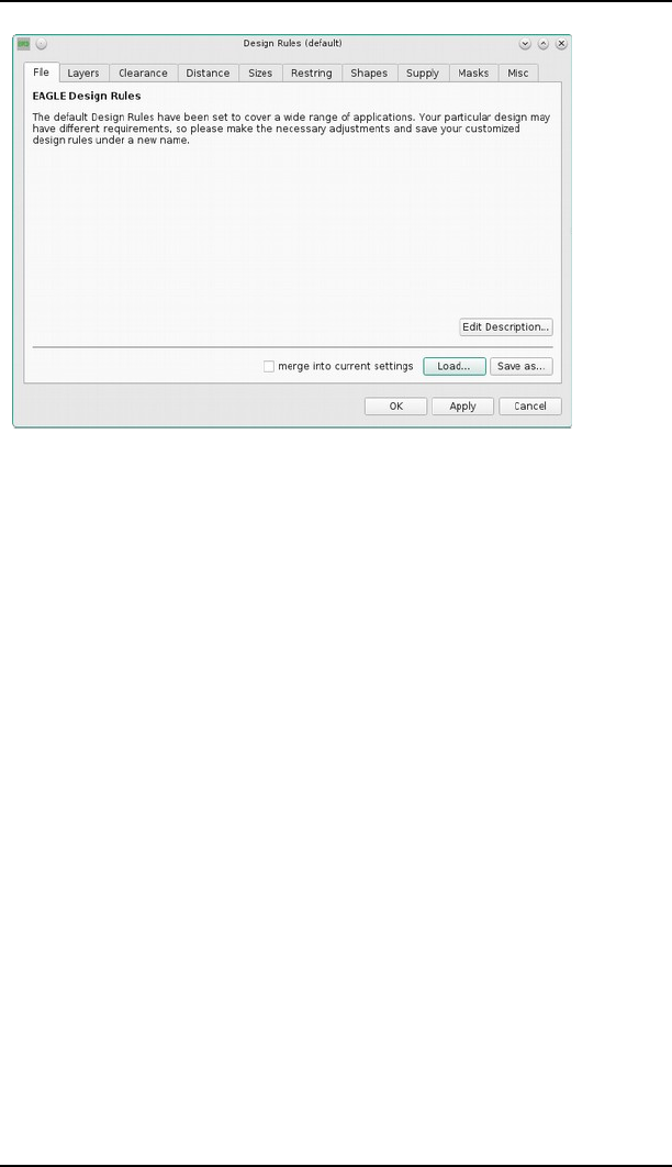
6.3 Considerations Prior to Creating a Board
➢
DRC: Adjusting the Design Rules
General Principles
The first time that you call this dialog, the Design Rules are provided by the
program. If necessary, adjust the values to suit your or your Board house's
requirements.
The Apply button stores the values that are currently set in the layout file.
Changes to various Design Rules, like the settings concerning the Restring,
are immediately displayed in the Layout Editor after clicking Apply.
The Design Rules can be saved in a special Design Rules file (*.dru) by the
use of the Save as.. button. So you can easily use this set of rules for another
board.
To apply a set of Design Rules to a board, you can drag any dru file of the
Design Rules branch of the tree view in the Control Panel into the Layout
Editor window or click the Load.. button in the File tab of the Design Rules
window.
Edit Description.. can be used to alter the descriptive text for the current
parameter set. The description usually appears in the File tab, as can be seen
in the image above. HTML text can be used. You will find notes on this in the
help system.
The Design Rules dialog offers a range of different options that can be
selected through the tabs. The options include:
File Manage the Design Rules
Layers Number of copper layers, structure of multilayer
boards, kind and length of vias, thickness of copper
and isolation layers
Clearance Distances between objects in the signal layers
representing signals that may be different or the same
145

6 From Schematic to Finished Board
Distance Distances from the board edge and between holes
Sizes Minimum track width and hole diameter, particularly
for Micro and Blind vias
Restring Width of the remaining ring at Pads and (Micro) vias
Shapes Shapes of Pads and SMDs
Supply Thermal symbols in copper plains
Mask Values for solder stop and solder cream masks
Misc Additional checks
Most parameters are explained with the help of a small image. As
soon as you click into a parameter line, the associated display
appears.
Layers
Define the number of signal layers and the kind of vias (Blind or Buried vias)
here. With the help of a mathematical expression in the Setup line the proper
structure of the board, the appropriate combination of cores and prepregs
and the resulting facilities for vias can be defined.
In most cases (for simple two or more layer boards) the vias are drilled
through all layers. The image above shows the default setup for a two layer
board. The expression (1*16) defines one core with layers 1 and 16, which
can be connected with vias. Parenthesis around the expression define
through-hole (continuous) vias.
Basic examples:
1 layer:
16 Only layer 16, no vias.
146
➢
Design Rules: Layer Setup
6.3 Considerations Prior to Creating a Board
4 layers, vias through all layers:
(1*2+15*16) Two cores are affiliated with each other.
6 layers, vias through all layers:
(1*2+3*14+15*16) Three cores are affiliated with each other.
The fields for Copper and Isolation are used to define the thickness of copper
and isolation layers. These settings are only relevant for complex multilayer
boards that use Blind or Micro vias.
The commands DISPLAY, LAYER, LINE, and ROUTE work only with those
signal layers defined in the Layer Setup.
Further information and examples about the Layer setup can be found in the
section Multilayer Boards beginning with page 178.
Loading a board file that was made with an older version causes
EAGLE to check which signal layers contain wires. These layers
appear in the layer setup. Please adjust it if necessary.
Minimum Clearance and Distance
Clearance refers to the minimum distances between tracks, pads, SMDs and
vias of different signals, and between SMDs, pads and vias of the same signal.
Setting the values for Same signal checks to 0, disables the respective check.
Distance allows settings to be made for the minimum distances between
objects in layer 20, Dimension, in which the board outline is usually drawn,
and between holes.
Setting the value for Copper/Dimension to 0 switches off the minimum
clearance check between copper and dimension.
In this case EAGLE does not recognize holes that are placed on wires.
Polygons don't keep their distance to objects in layer 20, Dimension,
either!
If a net belongs to a special net class, the values for Clearance and for the
drill diameter of vias (Drill), defined by means of the CLASS command, are
taken into consideration, provided these values are higher than those given
in the Design Rules (Clearance and Minimum Drill in the Sizes tab).
Sizes
The minimum values for track width and for hole diameter allowed in the
layout are selected here.
If additionally net classes are defined and values for clearance, width, or
minimum drill, are set, the respectively higher value is taken into
consideration.
Here you set the aspect ratio of drill depth to drill diameter for boards that
contain Blind vias. Please contact your board house for this information! If
the board house specifies, for example, an aspect ratio of 1:0.5 you have to
enter the value 0.5 in the line Min. Blind Via Ratio.
147
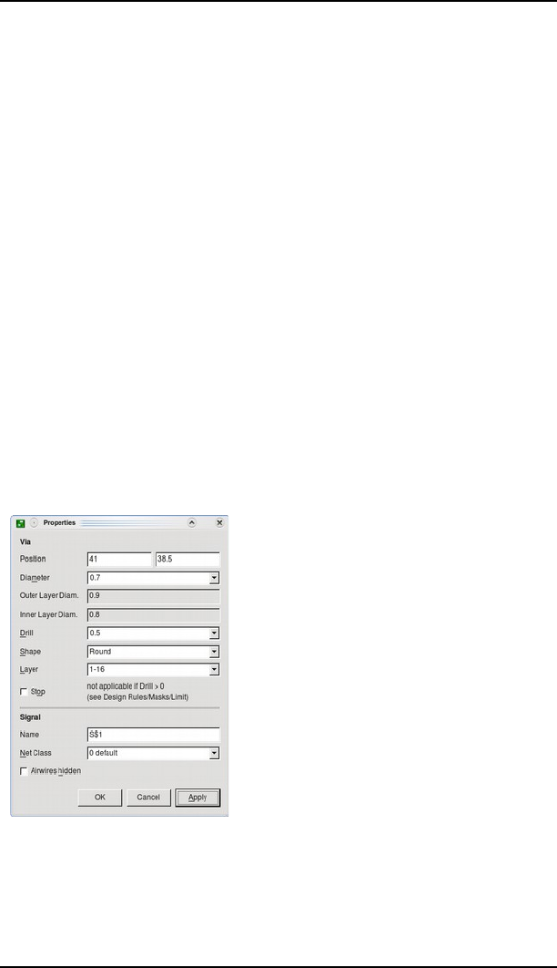
6 From Schematic to Finished Board
For micro vias you have to set the minimum drill diameter in the line Min.
MicroVia. Setting this value higher than the value in Minimum Drill means
that there are no micro vias used (default). To put this into other words: If
the drill diameter is between the value for Min. MicroVia and Minimum
Drill the via is considered a micro via.
Restring (Pad and Via Diameter)
The settings made under Restring determine the width of the ring remaining
at pads, vias, and micro vias. The remaining ring refers to the ring of copper
that remains around a hole after a pad or via has been drilled. Different
selections can be made for the width of the remaining ring in the inner and
outer layers. Pads may also differ between the Top and Bottom layers.
Usually the value is expressed as a percentage of the hole diameter.
Minimum and maximum values can additionally be specified.
As soon as you change a parameter and click the Apply button you can
directly see the effects in the layout. If you want to use different values for the
upper and lower layer (or different shapes, see Shapes tab), it is
recommended to set the layer color for layers 17, Pads, and 18, Vias, the
same as the background color (black or white). In this case you can recognize
the real size and shape of the pad/via in its respective layer.
The INFO command which has the same dialog as the context menu's
Properties entry, informs you about the via diameter in outer and inner
layers, and about the initial user-defined value. For example, in the following
image:
➢
Displaying Via properties with
INFO
Pre-defined value (by CHANGE DIAMETER): 0.7
Actual calculated diameter in the outer layers: 0.9
Actual calculated diameter in the inner layers: 0.8
148
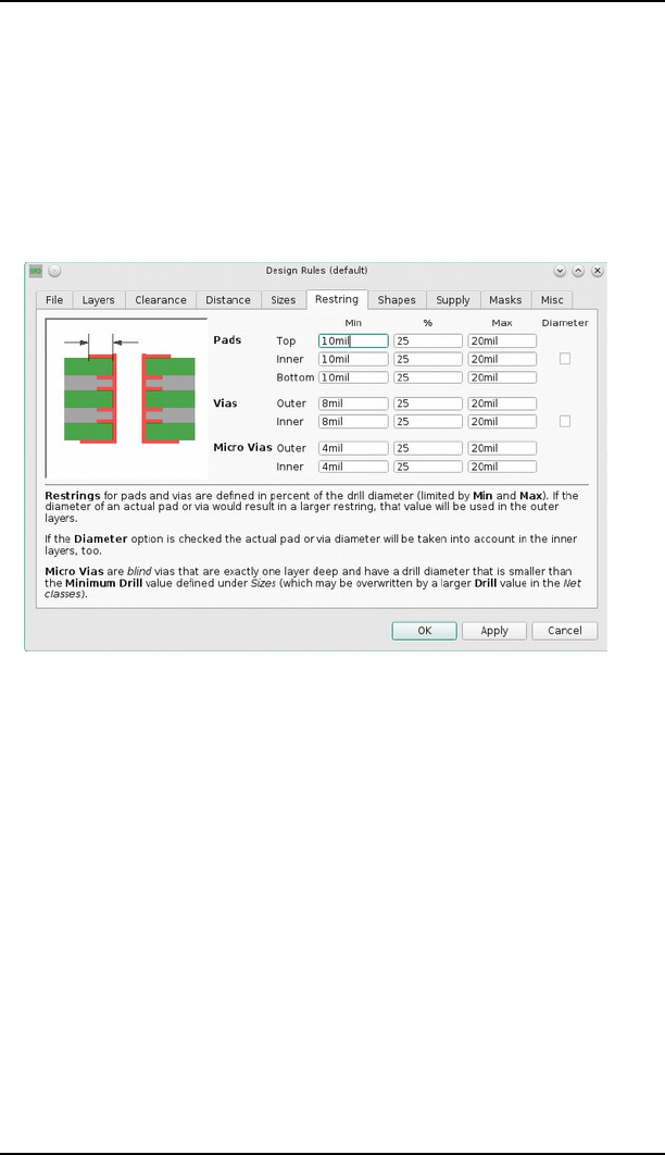
6.3 Considerations Prior to Creating a Board
Here the resulting via diameter is bigger than the pre-defined value,
according to the given minimum value in the Design Rules' Restring settings
for vias.
The following image illustrates the template for setting the width of the
residual ring. The standard value for the restring around holes is 25 % of the
hole diameter. Since the width of the ring on small holes specified this way
would soon fall below a technically feasible value, a minimum value (here: 10
mil for pads, 8 mil for vias, 4 mil for micro vias) is specified here. It is also
possible to specify a maximum value.
Example:
The ring around a hole with 40 mil diameter is 10 mil (25 %). It therefore lies
in between the maximum and minimum values.
If the hole is only 24 mil in diameter (e.g. for a via), the calculation yields a
restring value of only 6 mil. For a board made in standard technology this is
extremely fine, and cannot easily be made. It might well involve extra costs.
In this case a minimum value of 10 mil is given.
If you like to define a restring with a fixed width, use the same value for
minimum and maximum. The value in percent has no effect in this case.
Diameter check box:
In case you defined a diameter for a pad in the library or for a via in the
Layout Editor, and you want to have this given diameter taken into
consideration for the inner layers, activate the Diameter option. This can be
of interest if a pre-defined pad or via diameter exceeds the value calculated
by the Design Rules. Otherwise the pad or via in the inner layers would be
smaller than in the outer layers. If you want pads/vias to have the same
diameter in all layers, set the option Diameter.
The option is set off, by default, for new created boards, but will be set on for
149
➢
Design Rules: Restring settings
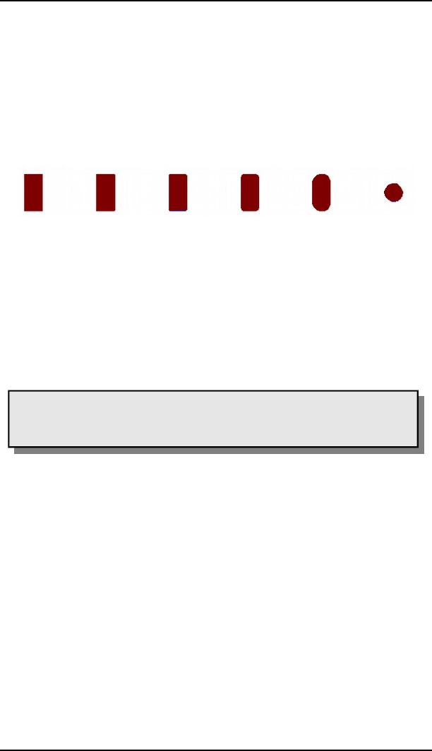
6 From Schematic to Finished Board
boards that are updated from version 3.5 or prior because in these versions
pads and vias had the same diameter in all layers. Thus the update process
does not change the original layout.
All the values can also be given in Millimetres (for example 0.2mm).
Shapes
SMDs:
A rounding factor can be specified here for SMD pads. The value can be
between 0 % (no rounding) and 100 % (maximum rounding).
A square SMD has been placed instead of an oblong one on the far right of
the diagram. After assigning the property Roundness = 100 %, the SMD
becomes round.
Pads:
This is where the form of the pads is specified. It is possible to give different
settings for the top and bottom layers.
The As in library option adopts the form defined in the Package Editor.
Clicking on Apply shows the change immediately in the Layout Editor.
Pads and Vias within inner layers are always round, no matter what
they are in Top or Bottom layer. The diameter is determined by the
restring settings.
Provided a pad was given the First flag in the library one can specify a certain
shape for all those pads in the layout.
Elongation defines the aspect ratio of length to width of Long and Offset
pads (see image). The value is given in percent. Click with the mouse into the
field Long or Offset and the image on the left shows the corresponding
calculation rule.
100 % is equivalent to an aspect ratio of 2:1. 0 % results in a normal octagon
pad with an aspect ratio of 1:1. The maximum is 200 % (ratio 4:1).
150
➢
Roundness: 0 - 10 - 25 - 50 - 100 [%]. Right: 100 %,
square
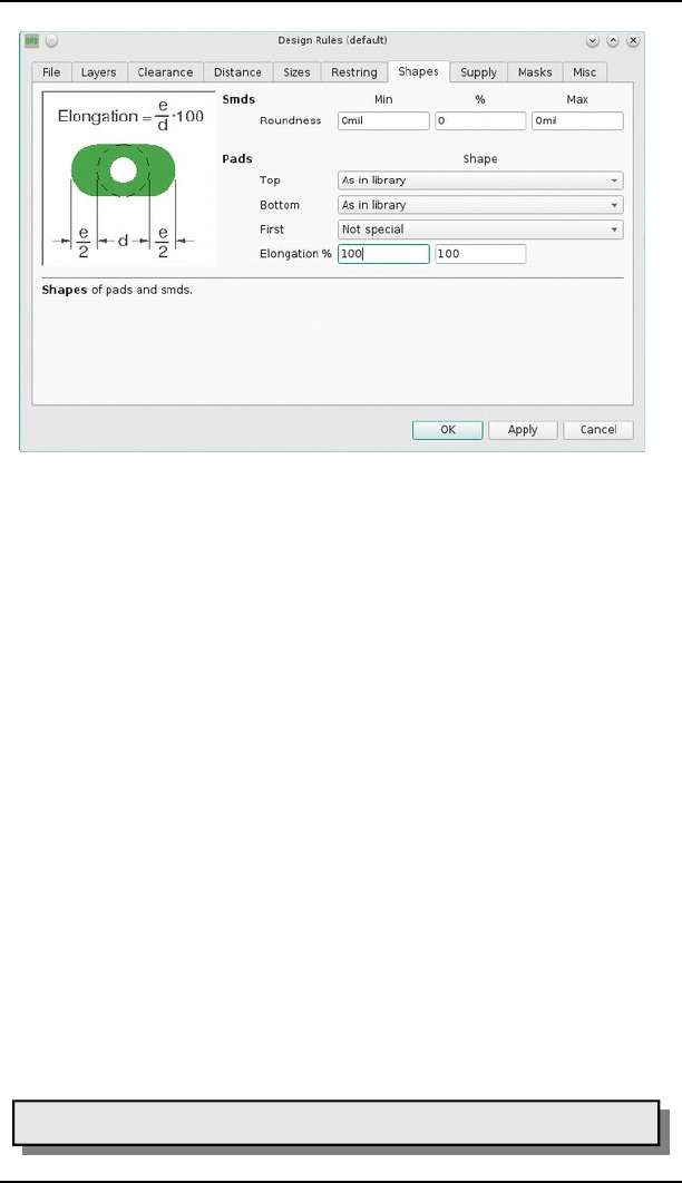
6.3 Considerations Prior to Creating a Board
➢
Design Rules: Adjusting pad shapes
Notes on the display in the Layout Editor:
If pads or vias have different shapes on different layers, the shapes of the
currently visible (activated with DISPLAY) signal layers are displayed on top
of each other.
If the color selected for layer 17, Pads, or 18, Vias, is 0 (which represents the
current background color), the pads and vias are displayed in the color and
fill style of their respective layers. If no signal layer is visible, pads and vias
are not displayed.
If the color selected for layer 17, Pads, or 18, Vias, is not the background
color and no signal layers are visible, pads and vias are displayed in the shape
of the top and bottom layer.
This also applies to printouts made with PRINT.
Supply
Specifies the settings for Thermal symbols.
The value for Thermal isolation determines the distance between a polygon
and the restring of the pad or via that is joined to the polygon through a
Thermal symbol.
The Generate thermals for vias flag permits Thermal symbols at through-
holes. Otherwise vias are fully connected to the copper plane. This applies
also for polygons. But you can disable this option for individual polygons
with CHANGE THERMALS OFF and a mouse click onto the polygon's
contour.
Inside hatched polygons EAGLE doesn't generate Thermal symbols
151
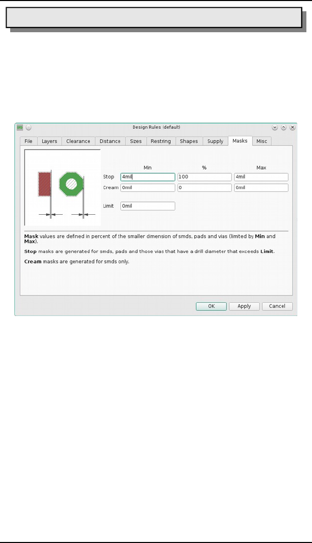
6 From Schematic to Finished Board
for vias that do not have a direct contact to one of the polygon lines.
Pads or SMDs marked with the flag NOTHERMALS (CHANGE THERMALS
OFF) in the Package Editor will be connected basically without Thermal
symbols.
Masks
Settings for the overmeasure of the solder stop mask (Stop) and the solder
cream mask (Cream) are made here.
The default value for solder stop is 4 mil, i.e. minimum value is maximum
value is 4 mil. The percent value has no effect in this case.
The value for the cream frame is set to 0, which means that it has the same
dimensions as the SMD.
If values are given in percent, in the case of SMDs and pads of the form Long
or Offset, the smaller dimension is the significant one. The values are
constrained by minimum and maximum values.
The value for Cream is given positively, as is Frame, although its effect is to
reduce the size of the solder cream mask (cream frame).
The solder cream mask is only generated for SMDs, and is displayed on layer
31, tCream, or layer 32, bCream.
The solder stop mask is drawn in layers 29, tStop, or 30, bStop.
Setting the flag STOP or CREAM (only for SMD) to OFF for a pad or SMD at
the Package definition forbids EAGLE to generate a solder stop mask or a
cream frame for it.
Limit determines, together with the hole diameter, whether or not a via is to
be covered with solder stop lacquer.
152
➢
Design Rules: Settings for Solder Stop and Cream Frame

6.3 Considerations Prior to Creating a Board
Example:
The default value for Limit is 0. This means all vias get a solder stop symbol.
They are free of solder stop lacquer.
Set the Limit = 24:
All through-plated holes with diameters up to 24 mil don't get a solder stop
symbol (they are lacquered), but vias with larger hole diameters get a solder
stop symbol.
For vias with hole diameters below the Limit the STOP flag can be set
(CHANGE STOP ON). EAGLE generates a solder stop mask then.
Misc
Here you can select/deselect various checks which are made by the Design
Rule Check:
Check grid
examines whether objects lie precisely on the grid currently set by the GRID
command. This test is not always worthwhile, since in many cases Devices
built to both metric and imperial grids are in use at the same time. No
common grid can be found in such a case.
Check angle
ensures that all tracks are laid at whole multiples of 45 degrees. This test is
normally switched off, but can be activated if required.
Check font
(de-)selects the font check.
The DRC checks if texts are written in vector font. Text which is non-vector
font is marked as an error. This check is necessary due to the fact that the
CAM Processor can't work with others than vector font for the generation of
manufacturing data.
Assumed you use proportional font text in the bottom layer, place it between
two tracks, and use the CAM Processor to generate Gerber files, it could
happen that the tracks are shorted by the text (height and length of the text
can change)!
Default: on.
Check restrict
can be set off if copper objects should not be checked against restricted areas
drawn in layers 39, tRestrict, and 40, bRestrict. Default setting: on
If restricted areas and copper objects are defined in a common Package,
EAGLE does not check them against each other. Restricted areas that are
realized by cutout polygons are not checked by DRC!
Setting the Design Rules is captured by the UNDO/REDO function.
6.4 Create Board
After you have created the schematic, click the Board icon.
An empty board is generated, next to the components that are to be placed,
joined together by airwires. Supply pins are connected by those signals which
correspond to their name, unless another net is explicitly joined to them.
153

6 From Schematic to Finished Board
The placement grid for components is set to 50 mil (1.27 mm) by default.
If you prefer a different placement grid, you are allowed to specify it
optionally with the BOARD command in the Schematic Editor's command
line.
To have the components placed, for example, in a 1 mm grid, type:
+5-
The unit has to be specified in the command line directly.
The board is linked to the schematic by the Forward&Back Annotation
engine provided that both files are always loaded. If both loaded during
editing they are guaranteed to remain consistent. Alterations made in one file
are automatically carried out in the other.
If you already generated a board from your schematic and continue placing
components in the schematic, the referring packages in the board are placed
in the current grid setting of the Layout Editor.
If, for example, the Schematic is loaded and edited without the
Layout, consistency can be lost. The Forward&Back Annotation
Engine no longer functions. Differences must then be rectified
manually with the aid of the error messages provided by the ERC
(see page 198).
If you would like to see a descriptive text for your board file in the Control
Panel's treeview Projects branch, you can define it by the Layout Editor's
Edit/Description menu. You are allowed to use HTML tags for formatting the
text.
Without the Schematic
If you work without a Schematic, you must generate a new board file, place
the Packages with the ADD command and define the connections with the
SIGNAL command.
To understand this process, please read the section on Placing Components
on page 116, and the section on Specifying Net Classes on page 123. These
two points apply to the Layout Editor as well as to the Schematic Editor.
You are also allowed to define attributes in the Layout Editor. Please read the
chapter about defining Attributes beginning with page 127.
The remaining procedures are identical for users with and without the
Schematic Editor.
Specify the Board Outline
A board that has just been generated from a schematic diagram initially
appears as in the following image. Here a few components have been already
moved into the board area.
154
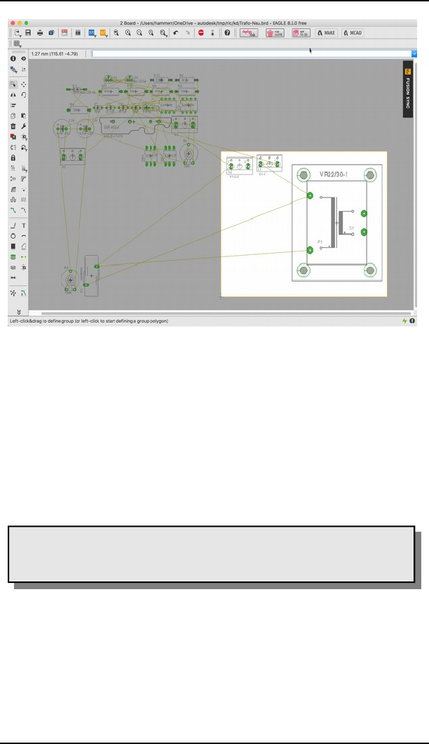
6.4 Create Board
➢
Board command: Create the layout from the schematic
The Devices are automatically placed at the left of the board.
The board outline can be drawn as a simple narrow line in layer 20,
Dimension with the LINE command.
It's easily possible to draw round outlines, too. Therefore use the CIRCLE
command with a small width near 0.
You can also place a board contour from a library (such as 19inch.lbr) with
ADD.
EAGLE detects properly drawn contours (single closed outline, non self-
intersecting) and shows the board area in a different background color
compared to the rest of the background in the Layout Editor. Mounting holes
and milling contours, drawn in layer 46, Milling, are also recognized.
Only a board with a properly drawn contour can be pushed into
Autodesk Fusion 360 with the FUSIONSYNC command in order to
get a full 3D representation of your design.
A script file can, alternatively, be read by the SCRIPT command. The
euro.scr file, for instance, can be used. Simply type
+
on the command line.
The board outline serves simultaneously as a boundary for the autorouter or
Follow-me router.
155
6 From Schematic to Finished Board
If your board has additional cut-outs, you should draw the necessary milling
contours in a separate layer, for example in 46, Milling. Use the LINE
command with wire width = 0 to define your lines.
Arrange Components
Drag the various components to the desired positions.
With the default option Group command default on set, you can move a
group of components by simply clicking into empty space in the drawing and
dragging a rectangle around the objects or by defining a group polygon
(subsequent left-clicks). Now move the selection by clicking into the selection
and holding the left mouse button and moving it.
Single components can be clicked and dragged into the board area. Release
the mouse button and the component is placed.
Devices can be clicked on directly, or addressed by name.
If you type, for example,
7+:-;
in the command line, the Device named R14 will be attached to the mouse
cursor, and can be placed.
Precise positioning results from input such as:
7+:-;@0$.9.$90B
R14's locating point is now located at these coordinates.
Keep the Ctrl key pressed while selecting a component in order to let
its origin jump at the mouse cursor and move it onto the currently
used grid.
If the above mentioned default setting is off, click onto the GROUP icon and
then draw a frame around the desired elements, click MOVE, and then click
into the group with the right mouse button in order to select it. With a click
of the left mouse button you can place the group at the desired location.
ROTATE, or a click with the right mouse button while the MOVE command
is active turns a Device through 90 degrees. This also applies to groups.
In order to place a component in any angle you may specify the rotation
directly with the ADD command or later with ROTATE or MOVE in the
parameter toolbar.
Next to the Angle box are the buttons for the Spin and Mirror flag.
The left-hand Spin icon is selected , if the spin flag is not set (default).
This means that texts are displayed always readable from the right or from
the bottom side of the drawing.
156
➢
Parameter toolbar for ROTATE, MOVE, ADD, COPY

6.4 Create Board
If the spin flag is activae – the right-hand Spinned icon is marked – the
texts can be displayed in any rotation, also upside down.
The Mirror icons used with components determine where a component is
placed: on the top side (default) or on the bottom side of the board. If a
component is placed on top, the left-hand icon is active. If you want to place
it on the bottom side, click onto the right-hand Mirrored icon.
As an alternative you can work with the command line:
+;9C-C
adds a rotation of 45° to the current position of part IC1. Assumed you tried,
for example, to rotate the component with the ROTATE command and
pressed mouse button, and you decided that it is not possible to obtain the
exact rotation angle this way (because of a too coarse grid) type in the
command line:
+;9C-C
The rotation of IC1 is now exactly 45°. The = sign stands for absolute values.
The initial position does not matter.
If, for example, a SMD should be placed on the bottom side of the board you
may add the Mirror flag, as in:
+7;9C-C
An additional Spin flag causes texts to be written upside down (by a rotation
of 180°), that means they can be read from the top view:
+7-#0C-C
The Spin flag is alternating, i. e. using it again causes the text to be displayed
'normal' again.
Check frequently whether the placement is optimal. To do this, use the
RATSNEST command. This calculates the shortest connections of the
airwires between two pints.
In boards that contain a huge number of signals it may be useful to hide
some of the airwires or display only a few of them. If you want to hide, for
example, the signals VCC and GND, type in the command line
Z:5
if want to see them all again, type:
More information about this can be found in the EAGLE help section.
The position of particular Devices can be displayed by typing the Device
name onto the command line or by clicking directly on an object while the
SHOW command is active.
INFO shows detailed information about the selected object. Depending on
the object you clicked on, some of its properties can be altered in the dialog.
The LOCK command allows you to fix components on the board. They can't
be moved any more then. Shift+LOCK releases the component again. LOCK
can be used with groups as well.
157

6 From Schematic to Finished Board
If the text for the name or the value is located awkwardly, separate them
from the Device with SMASH and move them to whatever position you prefer
with MOVE. At the same time EAGLE shows a line from the text's origin to
the belonging object. Clicking with DELETE on either of the texts makes it
invisible.
Activate the SMASH command, hold down the Shift key, and click onto the
component to have the texts displayed at their original positions again. They
are no longer editable and unsmashed, again. Another way to archive this is
to deactivate the option Smashed in the context menu's Properties entry.
Please keep in mind that the CAM Processor always uses vector font
for generating manufacturing data.
We recommend to write texts in the layout always in vector font (at
least in the signal layers). If you do so the shown text meets exactly
reality. Further information can be found on pages 48 and 177.
Attributes for Components and Global Attributes
If you want to assign any further information than name and value to a
component in the Board, you can do this with the ATTRIBUTE command.
In case a component does not have library-defined attributes you can create
attributes for a component the Schematic, as well as in the board file. If
Back&Forward Annotation is active, any attribute change in the schematic
will affect the board.
However, attribute changes made in the Layout editor won't be back-
annotated into the schematic. They are kind of independent. It is also
possible to delete them in the board. Consitency between schematic and
board remains unchanged nevertheless.
Global attributes are not valid for single components but for the whole board.
They can be defined in Board and Schematic separately.
You will find more information about this in the Creating the Schematic
chapter on page 127.
Boards with Components on Both Sides
If the board is also going to have components on the Bottom layer, the
MIRROR command is used. It causes Devices on the underside to be
inverted. SMD pads, the silk screen and the layers for the solder stop and
solder cream masks are automatically given the correct treatment here.
While ADD, COPY, MOVE, or PASTE is active it is possible to mirror an
object or a selected group with the middle mouse button.
Define components in the Package Editor always on the top side!
158
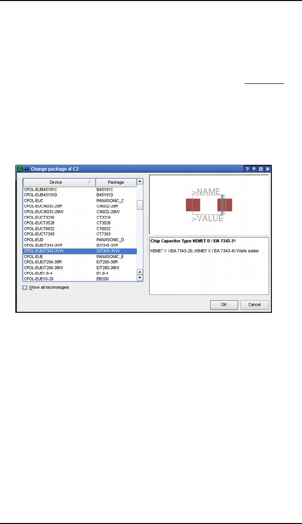
6.4 Create Board
Exchanging Packages
If, as the layout is developed, you want to replace the selected Package
variant with a different one, then you can use either the PACKAGE or the
REPLACE command, depending on the situation.
PACKAGE Command
It is assumed that the layout and the schematic diagram are consistent and
the Device has been defined with more than one Package variant.
Type in the command line PACKAGE and click onto the Package to be
replaced or alternatively click onto the Package with the right mouse button
and select the Package entry from the context menu. A third variant would
be to click onto the CHANGE icon and select the Package option.
Now you select the desired Package, and confirm it with OK, in the dialog
that then appears.
If the Show all technologies option is active, the Package versions for all the
technologies available for this Device are displayed. If this option is not active
you will only see Packages that are defined in the selected technology.
The Package can also be exchanged from within the schematic diagram.
Devices that don't have alternative Package variants defined, can be modified
in the Library Editor. Add further Package variants as needed and update
your drawing with the new library definition. See page 262 Choosing the
Package Variants for further information.
If you change the Package variant of a Device which you gave a new value
with the help of the VALUE command, although it has been defined with
VALUE Off, the value will remain unchanged. See also page 83.
If you would like to change the Package variant for several identical parts,
you can do this in the command line.
Define a GROUP with all parts that shall get a new Package variant, first.
Now type in the command line
*4C<M=C
159
➢
CHANGE package dialog
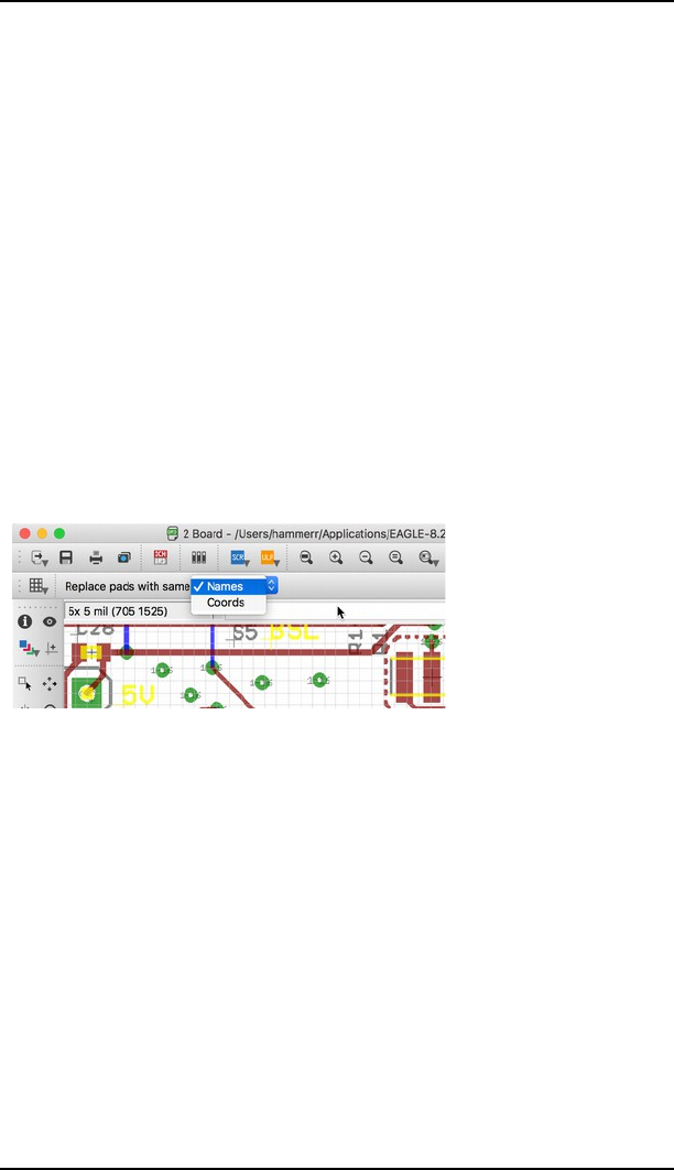
6 From Schematic to Finished Board
and click with Ctrl + right mouse button into the drawing.
The name of the new Package variant has to be enclosed in inverted commas.
REPLACE command
Consistent Schematic/Layout Pair
The REPLACE command allows you to substitute one component with
another. The well-known ADD dialog window opens where you can select the
new part. Now click onto the part you want to have replaced in the Schematic
or Layout. The old and new Device must be compatible, which means that
their used Gates and connected pins/pads must match, either by their names
or their coordinates. Otherwise the substitution is not possible.
Layout without Schematic
If you have a layout without an associated schematic diagram, you exchange
the Package with the aid of the REPLACE command. REPLACE opens the
window that is familiar from the ADD dialog, in which it is possible to search
for Devices. When the Package has been chosen you click on the part that is
to be replaced in the layout.
The REPLACE command operates in the Layout Editor in two ways, chosen
in the Parameter toolbar or with the SET command:
The first mode permits Packages whose pad or SMD names are identical to
be exchanged. The connecting areas can have any position.
In the second case (replace_same coords) the pads or SMDs in the new
Package must be located at the same coordinates (relative to the origin). The
names may differ.
The text for the name and value of a Device is only exchanged if they have not
been separated from the Device with SMASH.
The new Package can come from a different library, and can contain
additional pads and SMDs. Connections on the old Package that were
connected to signals must exist correspondingly in the new Package. The new
Package can even have fewer connections, provided that this condition is
satisfied.
160
➢
Select REPLACE mode
6.4 Create Board
Changing the Technology
It is possible to change the technology of a Device in the layout at any time ,
provided there are various technologies defined in the library. Use the
CHANGE command with the Technology option or the Technology
command of the context menu (available by clicking onto the Package with
the right mouse button). This procedure is identical to the one described
before in which Package forms are exchanged using PACKAGE.
Define Forbidden Areas
Areas in the form of rectangles, polygons or circles in layers 41, tRestrict, and
42, bRestrict, are forbidden for the Autorouter/Follow-me router. No copper
objects may be drawn in the top or bottom layers inside these areas. These
regions are tested by the Design Rule Check and taken into consideration by
the Autorouter/Follow-me router.
Layer 43, vRestrict, is for drawing restricted areas where the Autorouter or
the Follow-me router may not set vias. Manually placed vias in such a
vRestrict region are not examined by the DRC and therefore not reported as
an error.
Routing – Placing Tracks Manually
The ROUTE command allows the airwires to be converted into tracks.
ROUTE offers two different modes: Walkaround obstacles (default) and
Ignore obstacles . These modes can be selected in the parameter toolbar
of the ROUTE command.
Walkaround Obstacles
In this mode the routing engine takes care on Design Rules. If there is an
obstacle along the routing path, EAGLE will calculate a new path for your
trace.
Ignore Obstacles
This mode is the classic EAGLE routing mode. Here the user has to take care
on all the Design Rules by his own. This means taking care on clearances, net
classes, copper – dimension distances, overlaps, but you have full control
over the routing paths.
How to route
After activating the ROUTE command select the starting layer in the
parameter toolbar and click onto an airwire. Now the first segment of the
trace follows the mouse cursor. Please check the wire width! Does it fit? With
a left click you fix the segment.
In case you want to change the routing layer for the next segment, click the
middle mouse button. Depending on the layer setup a layer selection menu
will popup, or in a two-layer board the alternative layer will be chosen
automatically. Now a via is displayed the trace’s end. The following left
mouse click fixes the via and the next segment is following the mouse cursor
161
6 From Schematic to Finished Board
in the chosen layer. The layer change can also be initiated by hitting the
Space bar. This way you subsequently step through the routing layers
available.
Clicking with the right mouse button changes the way in which the track is
attached to the mouse and how it is laid (SET command, Wire_Bend
parameter). Among them are modes which allow to use a wire as 90-degree
or as free-definable arc.
In the parameter toolbar you see two additional Wire_Bend icons for the
Follow-me router. The Follow-me router can route a selected airwire
automatically. The position of the mouse cursor determines the trace of the
connection. The settings of the Design Rules and the relevant Autorouter
settings are taken into consideration. In this mode vias are set automatically.
Please check the Autorouter chapter for more information about function
and usage of the Follow-me router.
The signal's name and net class will be displayed in the status bar. When a
signal line has been completely laid, EAGLE confirms that there is a correct
connection with a short beep as it is placed.
The signal name can be used in the command line directly, for example
ROUTE VCC. EAGLE starts the trace at a signal's connection point which is
nearest to the current mouse position.
You can start routing at any point of an already laid trace, via, pad or SMD.
In case you want to re-route a part of an already routed trace, the obsolete
path of the trace will be removed. The Loop Remove options is on by default.
It can be switched off and on in the parameter toolbar of the
ROUTE command.
If there is no longer enough room for routing a signal, other tracks can be
relocated with MOVE and SPLIT, or the properties of tracks (width, layer)
can be modified in the traces’ Properties dialog or with the CHANGE
command.
SPLIT can be used to insert bends into a trace.
If a plated-through hole (a via) is to be placed at a certain point, this can be
done with the VIA command. Use the NAME command to assign the via with
the signal it should be connected to.
Airwires with length of 0 (for example, from Top to Bottom layer) are drawn
as a cross in layer 19, Unrouted.
Ending a wire at the same position where another wire of the same signal but
in another layer already exists and pressing the Shift key at the same time
causes EAGLE to place a via. Otherwise it won't.
If you intend to design a multilayer board and use Blind and Buried or Micro
vias, please note the details (also for the VIA command) in the section about
Multilayer Boards beginning at page 178.
While laying out wires EAGLE calculates the shortest connection to the
closest point of the current signal automatically. This connection is
represented by an airwire.
162
6.4 Create Board
Pads and SMDs that belong to the currently routed signal have the so-called
magnetic-pads function:
Within a certain radius around the pad the wire will be snapped to the pad's
center automatically. That is to say as soon as the length of the automatically
calculated airwire is shorter than the given value for snap length, the wire
jumps into the pad's or SMD's center point. It doesn't matter whether the
pad or SMD is exactly located at the currently used grid. The snap point is
always the center point.
As soon as you move the mouse cursor away from this pad beyond the limits,
the airwire will be shown and the wire to be routed follows the mouse again.
The snap length can be defined in the menu Options/Set/Misc. Default value
is 20 mil.
As the routing proceeds it is helpful to run the RATSNEST command
frequently, in order to recalculate all the airwires.
For more complex boards it may be useful to adjust the Snap Length in the
Options/Set/Misc menu as described on page 111.
For a better visibility of the traces in the routing layer you can enable the
Single Layer mode. All visible layers except the currently selected routing
layer are displayed in a grayish color. This mode is accessible in the ROUTE
commands parameter toolbar. Click to switch the mode off, or to
activate it.
Un-route traces
Use RIPUP if you want to convert the whole or part of a track or a via that
has been laid back to a signal line. By clicking on a track it is decomposed
between the nearest bends. If you click on this location again (on the
airwire), the whole signal branch back to the nearest pads is decomposed. If
you want to undo the whole of the signal, click RIPUP and enter the name of
the signal on the command line. More than one may be entered at the same
time.
The command
5:D9:
converts the three signals GND, VCC and +5V back to airwires.
Z5:
on the other hand converts all signals apart from GND and VCC to airwires.
converts all signals (that are visible in the editor) into airwires. To truly
include every track, all the layers in which tracks have been drawn must be
visible (DISPLAY).
Traces with arcs
If you want to use wires as arcs or try to smooth the wire bends see the hints
concerning the MITER command in the help function. The miter radius
determines how the wire joints are mitered. A positive value generates a
rounding, a negative one a straight line. The miter radius influences some
163

6 From Schematic to Finished Board
bend modi (0, 1, 3, 4; see SET command) and is shown additionally in the
parameter toolbar of the commands SPLIT, ROUTE, LINE, and POLYGON.
While LINE or ROUTE is active it is possible to click through the previously
mentioned wire bends (bend modes) with the right mouse button. EAGLE
knows ten different modes (0..9) which are shown as icons in the parameter
toolbar. Mode 8 and 9 are special modes for the Follow-me router.
Holding down the Shift key while clicking the right mouse button reverses
the direction of selection.
Holding down the Ctrl key allows to toggle between complementary wire
bends.
If you want to have only some wire bends available for the right mouse
button, you can define this, for example, in the eagle.scr file.
Supposed you want to work with wire bends number 2, 5, 6, and 7 use the
following syntax:
5,.9>A
However, if you want to use another bend mode you can always chose it from
the parameter toolbar.
It is also possible to leave the track laying to the Autorouter which
has its own chapter in this manual.
Laying tracks with the Follow-me router is explained in a subsection
of the Autorouter chapter.
Defining a Copper Plane with POLYGON
EAGLE can fill regions of a board with copper. Simply draw the borders of
the area with the POLYGON command. The polygon is displayed as a dotted
line in the outline mode. You give the polygon a signal name, using NAME
followed by a click onto the border of the polygon. Then all the objects that
carry this signal are connected to the polygon. Both pads and, optionally, vias
(as specified in the Design Rules) are joined to the copper plane through
Thermal symbols. Elements not carrying this signal are kept at a specified
distance.
RATSNEST calculates and displays the surface area of all polygons in the
layout. If you call RATSNEST with a signalname, for example
5
only the GND polygon(s) will be calculated. All other polygons in the layout
will remain unchanged in the outline mode.
RIPUP, followed by a click on the polygon border, makes the content
invisible again. If there are several polygons in your layout, and you want to
have them displayed in the outline mode again, type in the command line:
,
To have all polygons of a particular signal switched to outline mode, specify
the signal name, like
,5
More information about the syntax can be found in the help about RIPUP.
164
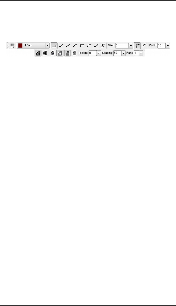
6.4 Create Board
The content of the polygon is not saved in the board file. When you first load
the file, you will only see the dotted outline of the polygon. It is only
calculated and displayed again by RATSNEST.
Various options can be changed via the parameter toolbar, either as the
polygon is being drawn or, with CHANGE, at a later stage.
Width:
Line thickness with which the polygon is drawn. Select the largest possible
width. That avoids unnecessary quantities of data when the board is sent
for manufacture. If the wire width is lower than the resolution of the
output driver in the CAM Processor, a warning is issued.
A finer line width permits the polygon to have a more complex shape.
Pour:
Specifies the filling type: the whole area (Solid) or a grid (Hatch).
The special type Cutout can be used to define polygons that get subtracted
from all other signal polygons within the same layer. Suitable for cut-outs
(restricted areas) in polygons in inner signal layers.
Rank:
Overlapping polygons must not create any short-circuits. Rank can
therefore be used to determine which polygons are to be subtracted from
others. A polygon with rank = 1 has the highest priority in the Layout
Editor, no other polygon drawn in the layout is ever subtracted from it,
while one with rank = 6 has the lowest priority. As soon as there is an
overlap with a higher rank, the appropriate area is cut out from the
polygon with rank = 6.
Polygons with the same rank are compared by the DRC. The rank property
works only for polygons with different signals. For overlapping polygons
with the same signal name it is without effect. They will be drawn one over
the other.
Polygons that are created in the Package Editor and not assigned to a
signal, will be subtracted from all other polygons. There is no rank
parameter available.
Spacing:
If the option Hatch is chosen for Pour, this value determines the spacing of
the grid lines.
Isolate:
Defines the value that the polygon must maintain with respect to all other
copper objects not part of its signal and objects in Dimension, tRestrict or
bRestrict layer. If higher values are defined for special signals in the
Design Rules or net classes, the higher values apply.
165
➢
POLYGON command: Parameter toolbar (split into two
lines)
6 From Schematic to Finished Board
In the case of polygons with different Ranks, Isolate always refers to the
drawn contour which is shown in the outline mode of the polygon, even if
the calculated polygon has got another contour, for example, due to a wire
that supersedes the polygon. The actual clearance can become greater than
the given Isolate value.
Thermals:
Determines whether pads in the polygon are connected via Thermal
symbols, or are completely connected to the copper plane. This also applies
to vias, assuming that the option has been activated in the Design Rules.
The width of the thermal connectors is calculated as the half of the pad's
drill diameter. The width has to be in the limits of a minimum of the wire
width and a maximum of twice the wire width of the polygon.
The length of the thermal connectors is defined by the Thermal isolation
value in the Design Rules' Supply tab.
Don't choose the polygon's width too fine, otherwise the thermal
connectors won't handle the current load.
This is also true for bottlenecks in the board! The polygon's wire
width determines the smallest possible width of the copper area.
Orphans:
Determines if a polygon may contain areas (islands) which are not
electrically connected to the polygon's signal.
If Orphans is set Off such un-connected areas won't be drawn.
When drawing a polygon, please take care to ensure that the outline
is not drawn more than once (overlapping) anywhere, and that the
polygon outline does not cross over itself. It is not possible for EAGLE
to compute the contents of the area in this case.
An error message 'Signalname' contains an invalid polygon! is
issued, and the RATSNEST command is aborted.
If this message appears, the outline of the polygon must be corrected.
Otherwise, manufacturing data cannot be created by the CAM
Processor.
The CAM Processor automatically computes the polygons in the
layout before generating its output.
If the polygon stays in the outline mode after calculating it with
RATSNEST, you should check the parameters for width, isolate, and
orphans and the polygon's name. Probably the polygon's filling is not
able to reach one of the objects that should be connected with its
signal.
Renaming a polygon with the NAME command, connects it with
another signal!
166

6.5 FUSIONSYNC – Synchronise EAGLE Board and Fusion 3D Board
6.5 FUSIONSYNC – Synchronise EAGLE
Board and Fusion 3D Board Model
In the Layout Editor on the right hand side you see a FUSIONSYNC flyout.
It’s displayed by default, but could also be hidden by switching off this option
in the Options/User Interface menu.
The ECAD world and the MCAD world now are unified. With FUSIONSYNC
it is possible to exchange board data between EAGLE and Autodesk Fusion
360. Synchronizing board data works in both directions. Either you push
your EAGLE board into Fusion or you pull the board object from Fusion into
EAGLE.
How does this work?
Synchronise with Fusion
Design your board as usual. At any time, when you think it’s time to
synchronise your board with Fusion, click the FUSIONSYNC flyout. By doing
so EAGLE and Fusion exchange all data needed. Now your design entered
the mechanical world.
What if There Need to be Changes in the Board’s Geometry?
In case there have to be made changes in the board’s geometry – maybe a
mounting hole has to be moved, the board size has to be amended so that it
fits exactly into the enclosure, or one of the bigger components have to be
moved some millimeters – the Fusion designer can move component objects
or amend the board contour or move a mounting hole, or add a cut-out in the
board. If this is done, you will get notice in EAGLE that your board is out of
sync.
You can pull in the new board object into EAGLE and see the new board
contour, or the hole or a component moved to another position. Now you
have to check your layout and it’s might be a good idea to run a DRC. Please
check the positioning of your components, board contour, and traces that
were already routed to a component which has been moved and so on.
Continue designing your board and as soon as you think all is okay,
synchronise and push it into Fusion again.
How to Synchronise
Click onto the FUSIONSYNC flyout and choose one of the options
presented in the dialog: Either synchronize with an already existing
project or choose a new Fusion project.
If you want to sync with an existing Fusion project, select the first
option and klick Next.
167
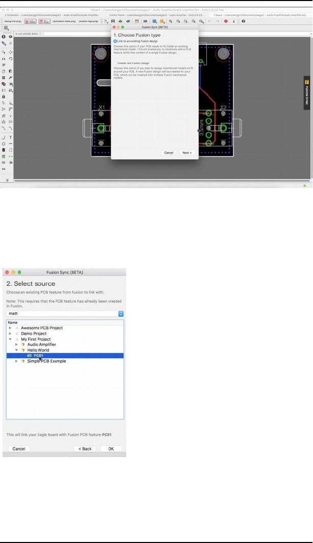
6 From Schematic to Finished Board
Choose one of your Fusion projects from the list. The Fusion project has
already to have the PCB feature created. In the image below you can see, that
the Hello World project has already a PCB1 feature which was created before
in the Fusion project. Click OK to proceed.
In the next dialog we see the current sync status.
168
➢
FUSIONSYNC: Select Fusion type
➢
FUISONSYNC: Choose the Project
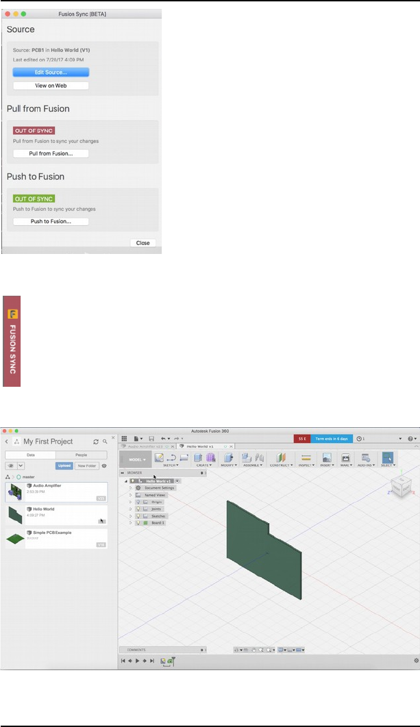
6.5 FUSIONSYNC – Synchronise EAGLE Board and Fusion 3D Board
Here the projects are out of sync. This is also indicated by the
FUSIONSYNC flyout that changed its color to red.
The Edit Source button will open the selected project in Fusion.
169
➢
FUSIONSYNC: Syncing EAGLE and Fusion
➢
FUSIONSYNC: Board shape drawn in Fusion

6 From Schematic to Finished Board
View on Web
If you click View on Web, your web browser will open and bring you to the
“bridge” between electronic and mechanical design. This is the place where
your board from EAGLE and the board object from Fusion are managed.
You could review, for example, the different versions that were synchronised
between EAGLE and Fusion. It’s also possible to view and share a 3D
representation of your project in Fusion Team. It allows to have markups,
make comments, add measures, show, for example, an exploded view, and
export in different data formats.
Pull from Fusion
Click on the Pull from Fusion button. A description that was created in
Fusion when the PCB object was defined is show in the dialog.
Click the Pull button to start syncing now. The syncing process will take some
seconds and finally you will see the new board shape in the Layout Editor.
170
➢
FUSIONSYNC: Online 3D View in Fusion Team
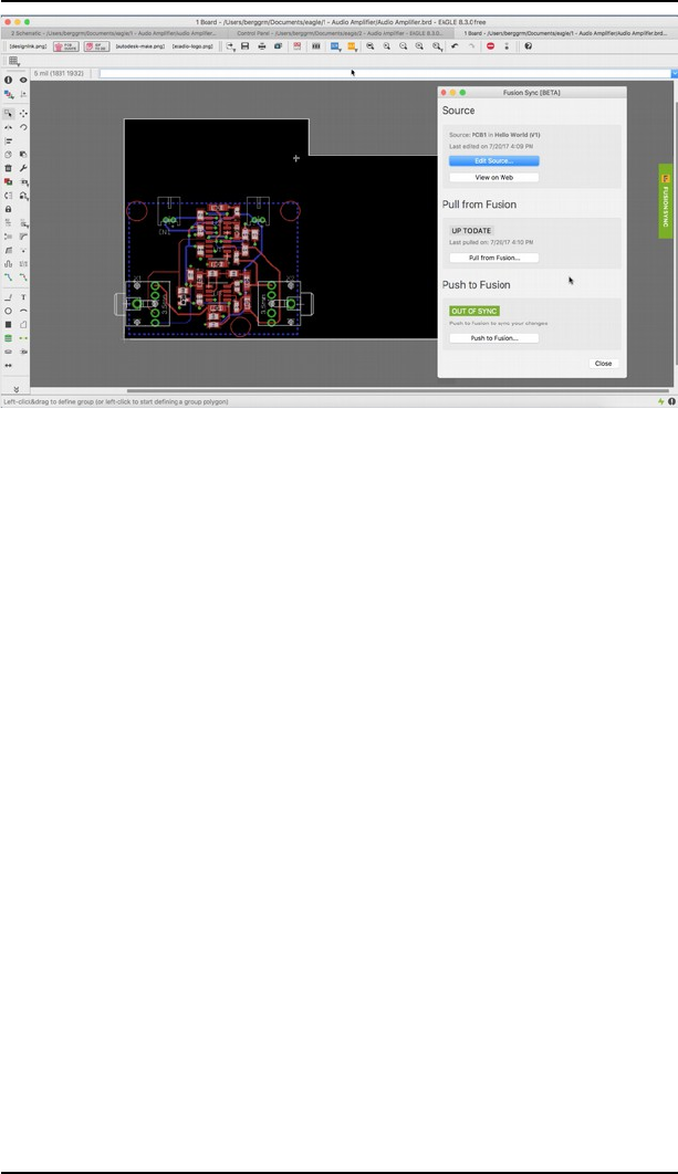
6.5 FUSIONSYNC – Synchronise EAGLE Board and Fusion 3D Board
In the Pull from Fusion section of the Fusion Sync window now it says
UP TO DATE. The FUSIONSYNC flyout is displayed in green now.
The section Push to Fusion still says OUT OF SYNC. The reason is that you as
the EAGLE designer have the last word in finalizing the project. Typically you
go on designing the board and at a final point you decide to push your design
into Fusion.
Push to Fusion
Therefore click the FUSIONSYNC flyout. In the Fusion Sync window’s
Source page click the Push to Fusion… button. What happens first now, is
showing you a list of the components on your board and the information if
there is already assigned a 3D model for it.
In case there are not all packaged assigned to a 3D model, you should change
this in the EAGLE libraries and update your design. Otherwise you do not see
the components as proper 3D representation in Fusion.
171
➢
FUSIONSYNC: New Board Shape Pulled from Fusion
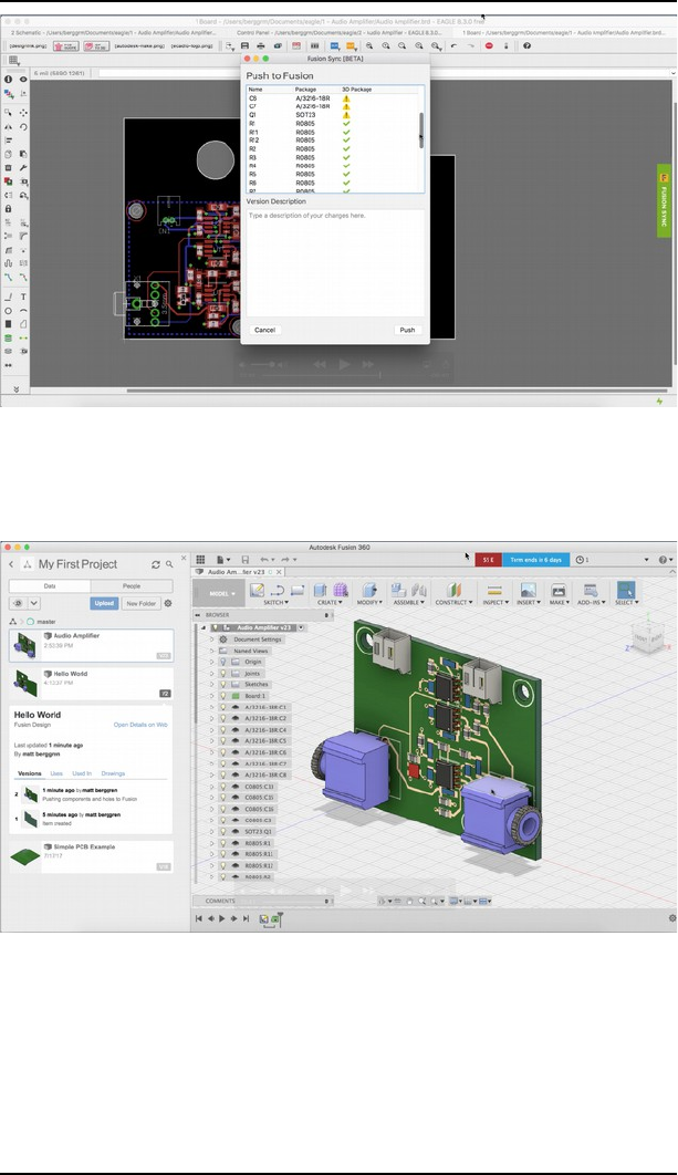
6 From Schematic to Finished Board
Enter a Version Description so that everyone knows what’s going on and
then click the Push button. The board will be transferred into Fusion.
In Fusion it is allowed to modify the board shape, moving components,
adding holes or slots in the board. If this is done, you have to pull the design
into EAGLE again and clean up your layout. Please run DRC in order to
recognize all possible problems that could be in the design now. After
cleaning up the board and finishing the design process, push it into Fusion
again.
172
➢
FUSIONSYNC: Push to Fusion - 3D Package Assignment
➢
FUSIONSYNC: EAGLE Board in Fusion
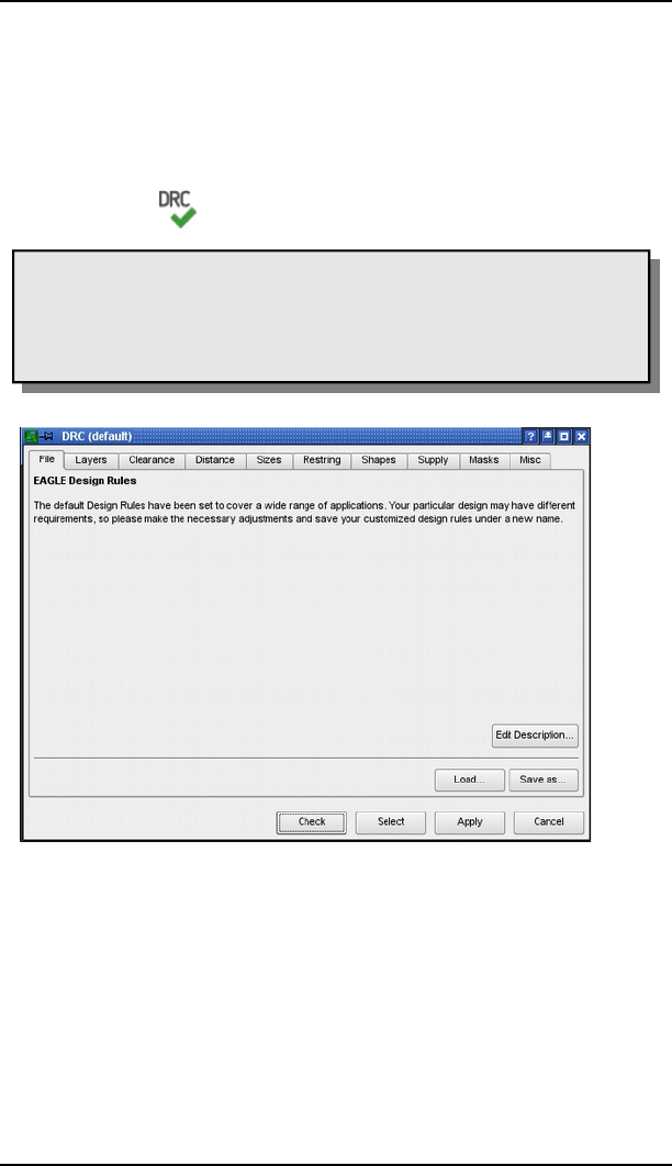
6.6 DRC – Checking the Layout and Correcting Errors
6.6 DRC – Checking the Layout and
Correcting Errors
The Design Rule Check (DRC) is carried out at the end of the board design, if
not before. If you have not yet specified any Design Rules for the layout, this
is your last opportunity. See the section on Specifying the Design Rules from
page 144. To start the Design Rule Check click onto the DRC icon in the
command toolbar or the entry DRC... in the menu Tools.
Usually one sets the common Design Rules with the Edit/Design
Rules.. menu first and starts the Design Rule Check when required
with the DRC command. But it is also possible to adjust the Design
Rules if you use the DRC command. Some settings, like those for
Restring, affect the layout directly.
➢
Starting the Design Rule Check
When you have finished the adjustments, start the error check by clicking
Check. At the same time the Design Rules are stored in the board file itself.
By clicking Select you specify the region of the layout that is to be examined.
Simply drag a rectangle over the desired region with the mouse. The error
check will then star automatically.
Clicking on Apply transfers the settings to the board file. This means that the
values that have so far been chosen are not lost if you do not immediately
start the error check and if you want to leave the DRC dialog via the Cancel
button.
173
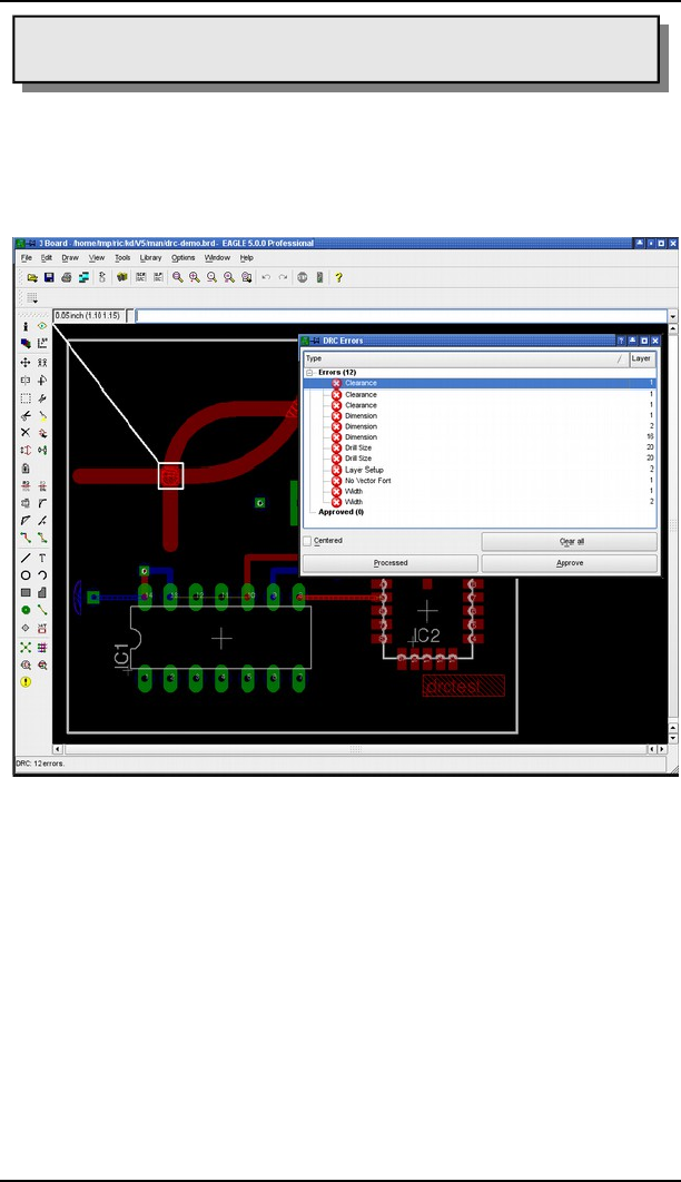
6 From Schematic to Finished Board
All signal layers and the Airwires are always examined by the
Design Rule Check, no matter if visible or not (DISPLAY command).
The DRC Errors Window
If the Design Rule Check finds errors or unrouted signal wires, an error
window opens automatically. It lists all the errors/airwires found. The
window can be opened at any time by means of the ERRORS command.
➢
DRC Errors list in the Layout Editor
Each error is marked with an error polygon. Its size tells you, for example in
the case of a clearance error, about how much the limit is exceeded. The error
polygons are visible in the Layout Editor, only. They won't be printed nor
exported with the CAM Processor. It's not possible to erase them with the
DELETE command. Click the Clear all button to delete them. Or type in the
command line:
+
Errors are marked with a red icon in the errors window. If an error in the list
is selected, a line points to the corresponding location in the board.
It is possible to have the error list sorted, ascending or descending, by error
types or layer numbers. therefore click onto the column headers Type or
Layer.
174

6.6 DRC – Checking the Layout and Correcting Errors
The errors dialog shows only errors that occur in the currently
displayed layers.
In case you zoomed into the drawing and there is only a partial view of the
board, you can click the option Centered. The currently selected error is
shown in the middle of the drawing window now. If you prefer to have the
Centered option deactivated for browsing the error list, you are nevertheless
able to center an error in the middle of the drawing area by pressing the
Enter key.
While correcting the error on the board, the DRC Errors window may remain
opened. After correcting one error you can mark it as Processed in the error
list by clicking onto the Processed button. The red error icon turns gray now.
In some situations it may be the case that you want to tolerate an error. Use
the Approve button for this. The error entry will be removed from the Errors
branch and appear in the Approved branch and the error polygon is no
longer shown in the Layout Editor.
If you want to treat an already approved error as a quite normal error, select
it in the Approved branch, and click onto the Disapprove button. Now it is a
member of the Errors branch again.
Clicking the Clear all button does not delete approved errors. They remain in
the Approved branch.
Moving an entry from one branch into the other, marks the board file as
changed and not saved.
In some cases it might be useful to approve all errors that are shown. To do
so, select the superior Errors entry in the errors list. Now the Approve
button will be named Approve all. Click it in order to have all errors moved
into the Approved list. This is also feasible the other way round for
disapproving all errors.
Error Messages and their Meaning
Airwire:
Shows a remaining signal wire that still needs to be routed. Only if there
are no Airwires left in the layout, one can be sure that all connections are
made properly.
Angle:
Tracks are not laid in an angle of 0, 45, 90 or 135°. Default: off.
Blind Via Ratio:
The limit of the ratio of via length (depth) to drill diameter is exceeded. In
this case you have to adjust the via's drill diameter (Design Rules, Sizes
tab) or the layer thickness of your board (Design Rules, Layers tab).
Clearance:
Clearance violation between copper objects. The settings of the Design
Rules' Clearance tab and the value for Clearance of a given net class are
taken into consideration. Of these two values the higher one is taken for
checking.
175

6 From Schematic to Finished Board
In addition the Isolate value will be taken into consideration for polygons
with the same rank and polygons which are defined as a part of a Package.
To deactivate the clearance check between objects that belong to the same
signal, use the value 0 for Same signals in the Clearance tab.
Micro Vias are treated like wires. The clearance value for wire to wire
applies in this case.
Dimension:
Distance violation between SMDs, pads, and connected copper objects and
a dimension line (drawn in Layer 20, Dimension), like the board's outlines.
Defined through the value for Copper/Dimension in the Design Rules'
Distance tab.
Setting the value Copper/Dimension to 0 deactivates this check.
In this case polygons do not keep a minimum distance to objects in layer
20, Dimension, and holes!
The DRC will not check if holes are placed on tracks then!
Drill Distance:
Distance violation between holes. Defined by the value Drill/Hole in the
Design Rules (Distance tab).
Drill Size:
Drill diameter violation in pads, vias, and holes. This value is defined in the
Design Rules' Sizes tab, Minimum Drill.
It is also possible to define a special drill diameter for vias in a given net
class (CLASS command, Drills). In this case the higher one is used for the
check.
Invalid Polygon:
Reason is a not properly drawn polygon contour. As soon as the contour
lines are overlapping or even crossing, the polygon can't be calculated
correctly. Change the polygon's contour in the Layout Editor or in the
Library, if it is part of a Package.
The RATSNEST command shows this error message, as well.
Keepout:
Restricted areas for components drawn in layer 39, tKeepout, or 40,
bKeepout, lie one upon another. This check is executed only if layers 39
and 40 are displayed and if the keepout areas are already defined in the
Package Editor of the library.
Layer Abuse:
Layer 17, Pads, or 18, Vias, contain objects which are not automatically
generated by EAGLE. Probably you drew something manually in these
layers, although they are reserved for pads and vias. Better move such
objects into another layer.
Layer Setup:
This error is shown if an object in a layer is found that is not defined by the
Layer setup. The same for vias that do not follow the settings of the Layer
setup, for example, if a via has an illegal length (Blind/Buried vias).
176

6.6 DRC – Checking the Layout and Correcting Errors
Micro Via Size:
The drill diameter of the micro via is smaller than the value given for Min.
Micro Via in the Sizes tab.
No Vector Font:
The font check (Design Rules, Misc tab) recognizes text in a signal layer
which is not written in EAGLE's internal vector font.
If you want to generate manufacturing data with the help of the CAM
Processor the texts, at least in the signal layers, ought to be written in
vector font. This is the only font the CAM Processor can work with.
Otherwise the board will not look the same as it is shown. Change the font
with the help of the command CHANGE FONT or use the option Always
vector font in the Layout Editor's Options/User Interface menu:
If activated, the Layout Editor shows all texts in vector font. This is the way
the manufactured board will look like.
Activating the sub-option Persistent in this drawing saves the setting in
the drawing file. If you send the layout file, for example, to the board house
you can be sure that the vector font will be displayed also at his system.
No real vector font:
The font check (Design Rules, Misc tab) recognizes text in a signal layer
which is not written in EAGLE's internal vector font although it is
displayed as vector font in the Layout Editor window. This situation arises
if the option Always vector font in the menu Options/User Interface is
active.
See error message No vector font for further details.
Off Grid:
The object does not fit onto the currently chosen grid.
This check can be switched on or off in the Design Rules' Misc tab. The
default setting is off, because as soon as trough-hole and surface-mount
parts are used together it's not easily possible to find a reasonable common
grid. The check is set off by default.
Overlap:
DRC reports this error as soon as two copper elements with different
signals touch each other.
Restrict:
A wire drawn in layer 1, Top, or 16, Bottom, or a via lies in a restricted area
which is defined in layer 41 or 42, t/bRestrict.
If restricted areas and copper objects are defined in a common Package,
the DRC does not check them!
Stop Mask:
If there are silkscreen objects drawn in layers 21, 25, 27 for components on
the Top layer, and 22, 26, and 28 for components on the Bottom layer
overlapping the area of a solder stop symbol generated in layer 29 and 30,
the DRC reports a Stopmask error.
You have to display the corresponding layers to activate this check!
Please keep in mind that this check always takes the vector font as basis for
177

6 From Schematic to Finished Board
the calculation of the required space. This is the font type the CAM
Processor uses for manufacturing data generation.
Width:
Minimum width violation of a copper object. Defined by Minimum Width
in the Design Rules (Sizes tab) or, if defined, by the track parameter Width
of a referring net class. The higher one of the given values will be taken for
this check.
Also the line width of vector font texts in signal layers will be checked.
Wire Style:
The DRC treats a line (wire) whose Style is LongDash, ShortDash or
DashDot in the same way as a continuous line. If a wire drawn with one of
these styles is laid as a signal, the DRC reports a Wire Style error.
For further investigations, net, part and pin lists can be output by
means of the EXPORT command or by various User Language
programs.
6.7 Multilayer Boards
You can develop multilayer boards with EAGLE. To do this, you use one or
more inner layers (Route2 to Route15) as well as the layers Top and Bottom
for the top and undersides. You display these layers when routing.
Before starting the routing of the layout you should be aware of the number
of signal layers to use, if vias should go through all layers, or if you have, due
to the complexity of the layout, to work with Blind, Buried or Micro vias. In
this case you really ought to contact your board manufacturer to inform you
about the possible structure of the board and the costs to be expected.
Inner Layer
Inner layers are used the same way as the outer layers Top and Bottom. They
can be filled with copper areas (polygons) as well.
Before using inner layers you must define them in the Design Rules, Layers-
Tab. More details can be found in the following sections and on page 146.
Supply Layers with Polygons and More than One Signal
Areas of the board can be filled with a particular signal (e.g. ground) using
the POLYGON command. The associated pads are then automatically
connected using Thermal symbols. The isolate value for the Thermal symbols
is specified in the Design Rules (DRC command, Supply tab). The width of
the connecting bridge depends on the line thickness with which the polygon
is drawn (see page 166). You can also specify whether or not vias are to be
connected through Thermals. The minimum clearances from objects carrying
other signals specified in the Design Rules are maintained (Clearance and
Distance tabs). Changes are shown in the layout when the polygon is next
computed (RATSNEST command).
178

6.7 Multilayer Boards
This way you can create layers in which several areas are filled with different
signals. You can assign different ranks (priorities) for the polygons. The rank
property determines which polygon is subtracted from others if they overlap.
Rank = 1 signifies the highest priority in the layout: nothing will be
subtracted from such a polygon. Rank = 6 signifies the lowest priority.
Polygons with the same rank are compared by the DRC.
Please read the notes regarding polygons in the section on Defining a Copper
Plane on page 164.
Do not choose the wire width for polygons too fine! This can lead to
huge amounts of plot data and problems for the manufacturing
process.
Resticted Areas For Polygons
For creating non-copper areas for polygons in inner layers, you can use a so-
called cutout polygon. Such a polygon, with the special fill style cutout,
defines an area which is subtracted from all other signal polygons in this
layer. A cutout polygon may be draw with any wire width, even 0. Compared
to signal polygons a cutout polygon does not cause huge data when creating
manufacturing data.
Signal polygons respect the wire width of the cutout polygon. The dotted line
of the contour is always visible, however does not occur in the manufacturing
data.
Multilayer Boards with Through Vias
This type should be preferred if possible. Vias go through all signal layers and
will be drilled at the end of the production process. The production costs are
relatively moderate.
Layer Setup
The settings concerning layer composition and number of signal layers are
made in the Design Rules, Layers tab, Setup. See page 146.
For through vias the setup is very simple. No considerations about thickness
of copper and isolation layers are necessary.
Simply join two layers by an asterisk (like 1*2 or 15*16) to one core and
combine several cores. This is symbolized by a plus character (like in
1*2+15*16). The isolation layer between two copper layers is called prepreg.
To express the possibility to have vias through all layers the whole expression
is set into parenthesis.
Examples:
4 layers: (1*2+15*16)
6 layers: (1*2+3*14+15*16)
8 layers: (1*2+3*4+13*14+15*16)
Here vias always have the length 1-16. They are reachable from all layers (see
also the help function for VIA).
179

6 From Schematic to Finished Board
Multilayer with Blind and Buried Vias
In high density boards it is often necessary to use Blind and Buried vias.
These kinds of vias don't connect all layers, but are only reachable from a
certain number of layers. How these layers are connected depends on the
manufacturing process of the board which has to be determined in the Layer
setup in the Design Rules.
Please contact your board house before starting your work! Check
which Layer Setup is suitable for your purpose and what the
manufacturing costs are.
Disambiguation
Core:
The non-flexible kernel which is coated with copper on one or on both sides.
Is represented by a * in the Layer Setup. For example 5*12: Layer 5 and 12
are the board's core.
Prepreg:
Flexible glueing or isolating layer which is used in the manufacturing process
of a multilayer board to press inner and outer layers onto each other.
Is represented by a + in the Layer Setup. 1+2 tells us that layer 1 is a prepreg
and combined with layer 2.
Layer Stack:
A pack of any number of layers consisting of cores and prepregs which are
handled together in the current step of production.
Buried Via:
The production process of this via does not differ from a through (normal)
via. The current layer stack will be drilled through completely. In the
following production steps the already drilled vias can be covered (buried) by
pressing further cores and prepregs on the current layer stack. If the via is
not visible on the completed board we call it a buried via.
This is represented by parenthesis, for example in 1+(2*15)+16 where the
Buried Via goes from layer 2 to 15.
Blind Via:
A Blind via connects an outer layer with any inner layer but doesn't go
through all copper layers. The speciality of a Blind via lies in the production
process. The current layer stack is not drilled all through. The drill hole has a
certain depth depending on the number of layers that should be allowed to be
connected with each other. Blind vias have to follow a given ratio of depth to
drill diameter. Please contact your board house to get information about this.
This ratio has to be defined in the Sizes tab as Min. Blind Via Ratio.
This is represented by brackets and the target layer marked by a colon before
or after the bracket. The example [3:1+2+3*14+15+16] allows Blind vias
from layer 1 to 3.
Blind vias may be shorter than defined. In this example you are allowed to
use vias from layer 1 to 2. The Autorouter is also allowed to use shorter Blind
vias.
180

6.7 Multilayer Boards
Micro Via:
The micro via is a special case of a Blind via. It has a maximum depth of one
layer and a very small drill diameter. See page 187.
Displaying Vias
It makes sense to set the layer color of layer 18, Vias, to the background color
(DISPLAY menu, Change, Color) if you are working with vias that have
different lengths and shapes. In doing so it is possible to recognize layer
affiliation.
Layer Setup
Combining cores and prepregs allows many variants. In the following section
some examples show the function of the Layer setup.
Please read this paragraph entirely. Even if you intend to design a four layer
board, for example, it is most advisable to read also all the other examples for
a better understanding.
4-Layer Board
Example 1:
Layers 1, 2, 15 and 16 are used.
Board structure: One core inside, outside prepregs.
Connections: 1-2 (blind vias), 2-15 (buried vias) and 1-16 (through vias)
The setup expression looks like this:
[2:(1+(2*15)+16)]
Explanation:
2*15
Layers 2 and 3 form the core.
(2*15)
Parenthesis allow buried vias from 2 to 15.
(1+(2*15)+16)
On both sides of the core copper layers are pressed on
with prepregs.
The outer parenthesis define continuous vias from 1-16.
[2:(1+(2*15)+16)]
In square brackets and separated by a colon blind vias are defined.
Here from layer 1 to 2.
The following image shows the related setup expression in the Layers tab of
the Design Rules.
Blind vias have to keep a certain ratio of via depth to drill diameter. For this
reason it is necessary to specify values for the layer thickness.
These values are given by your board house! You are supposed to contact it in
either case before starting the layout!
181
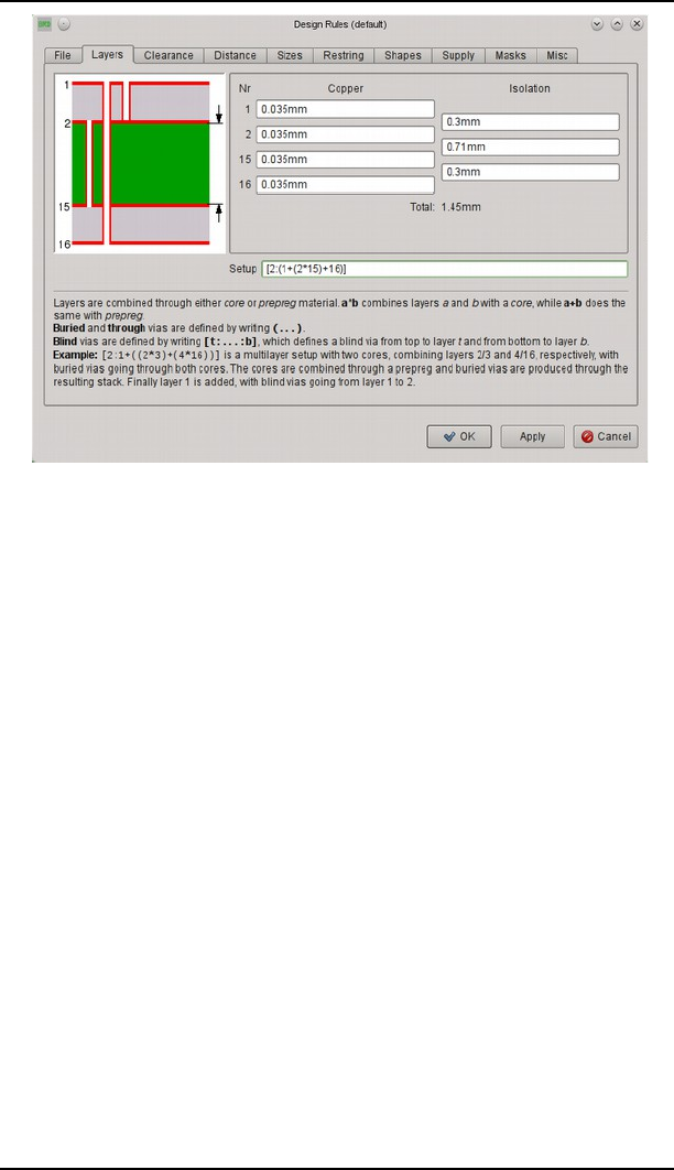
6 From Schematic to Finished Board
Type in the values in the Copper (thickness of copper layer) and Isolation
(thickness of isolation layer) fields as shown in the image. The total thickness
of the board is shown below the Copper and Isolation fields.
Example 2:
Layers 1, 2, 15, and 16 are used.
Board structure: One core inside, outside prepregs.
Connections: 1-2, 15-16 (blind vias), 1-16 (through vias)
Setup expression:
[2:(1+2*15+16):15]
Explanation:
2*15
Layers 2 and 3 form the core.
1+2*15+16
On both sides of the core copper layers are pressed on
with prepregs.
(1+2*15+16)
The outer parenthesis define through vias from 1-16.
[2:(1+2*15+16):15]
In square brackets and separated by a colon blind vias are defined.
Here from layer 1 to 2 and 16 to 15.
182
➢
Example 1: Layer Setup for a 4 layer Board
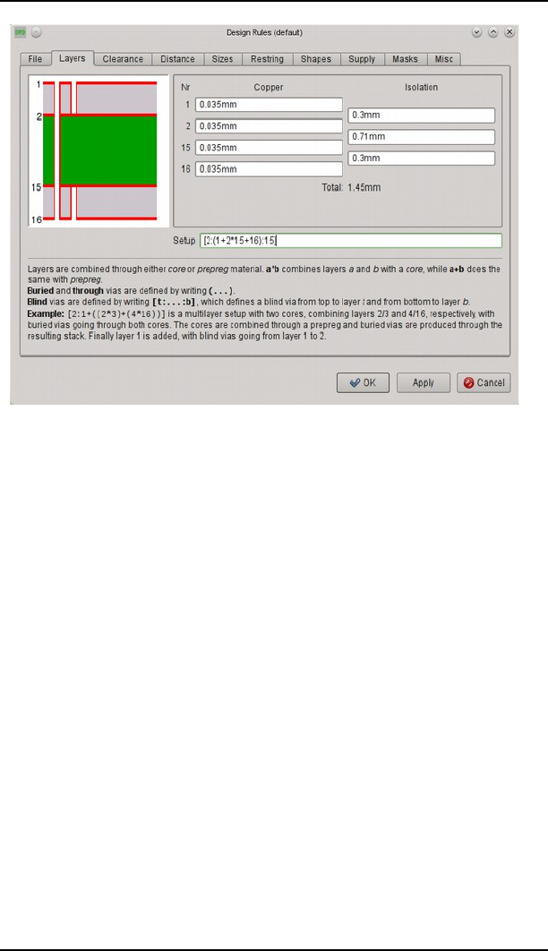
6.7 Multilayer Boards
➢
Example 2: Layer Setup for a 4 layer Board
6-Layer Board
Example 3:
Layers 1, 2, 3, 14, 15, and 16 are used.
Board structure: Two cores, prepregs outside.
Connections: 2-3, 14-15 (buried vias), 1-16 (through vias)
Setup expression:
(1+(2*3)+(14*15)+16)
Explanation:
(2*3)+(14*15)
Two cores with buried vias are pressed together.
1+(2*3)+(14*15)+16
This layer stack is covered with outer layers 1 and 16 which are
isolated with prepregs.
(1+(2*3)+(14*15)+16)
The whole expression in parenthesis defines through vias from 1-16.
183
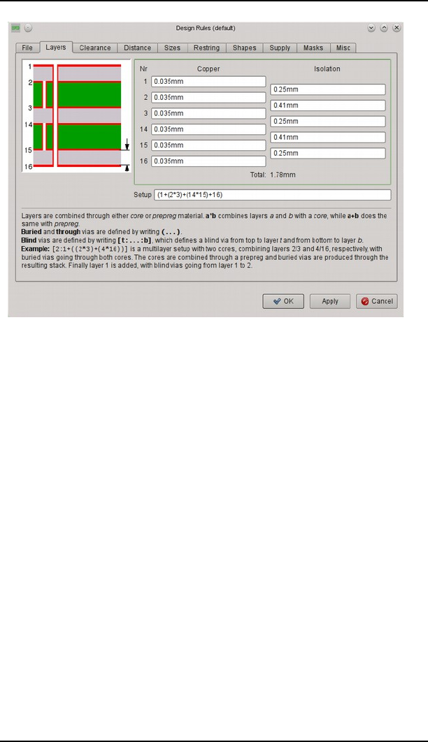
6 From Schematic to Finished Board
➢
Example 3: Layer Setup for a 6 layer Board
The values for layer thickness for copper and isolation used in these
examples are fictive. Please contact your board house to get the allowed
values.
Example 4:
Layers 1, 2, 3, 14, 15, and 16 are used.
Board structure: One core, on each side two prepregs.
Connections: 3-14 (buried vias), 2-14 (blind vias in inner layer stack),
1-16 (through vias)
Setup expression:
(1+[14:2+(3*14)+15]+16)
Explanation:
2+(3*14)+15
The core with buried vias. One prepreg on each side.
[14:2+(3*14)+15]
Blind vias from layer 2 to 4.
1+[14:2+(3*14)+15]+16
On this layer stack a prepreg on each side is pressed on.
(1+[14:2+(3*14)+15]+16)
Parenthesis allow through vias from 1 to 16.
184
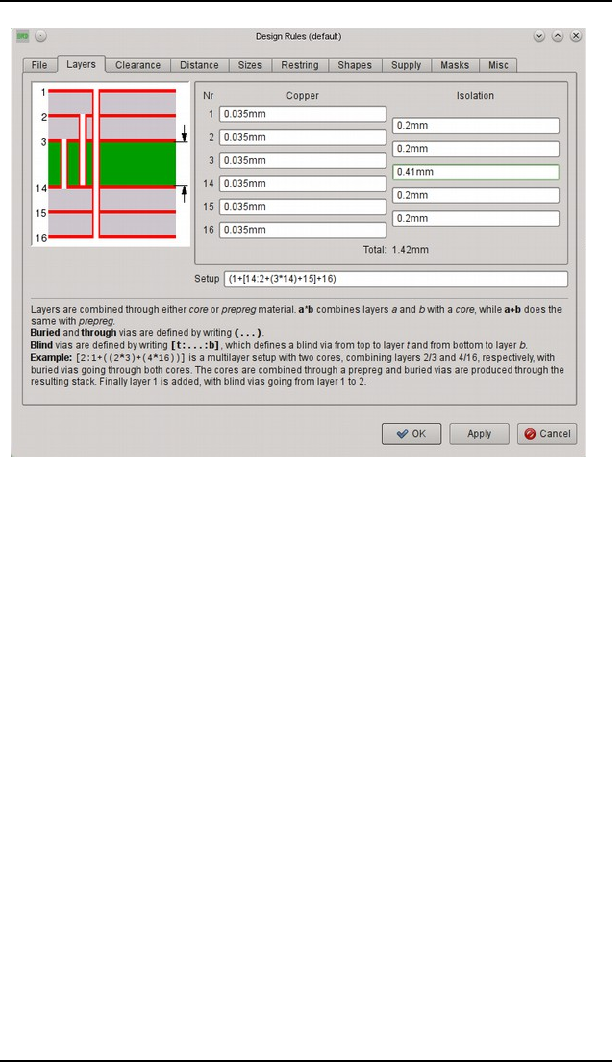
6.7 Multilayer Boards
➢
Example 4: Blind Vias in the inner layer stack
8-Layer Board
Example 5:
Layers 1, 2, 3, 4, 13, 14, 15, and 16 are used.
Board structure: Three cores, prepregs outside.
Connections: 1-3, 14-16 (blind vias), 2-3, 4-13, 14-15 (buried vias),
1-16 (through vias).
Setup expression:
[3:(1+(2*3)+(4*13)+(14*15)+16):14]
Explanation:
(2*3)+(4*13)+(14*15)
Three cores, each with buried vias, are pressed together and
isolated with prepregs.
1+(2*3)+(4*13)+(14*15)+16
Outer copper layers 1 and 16 which are isolated through prepregs
are pressed onto this layer stack.
(1+(2*3)+(4*13)+(14*15)+16)
Parenthesis allow through vias from 1-16.
[3:(1+(2*3)+(4*13)+(14*15)+16):14]
Blind vias from 1-3 and 16-14.
185
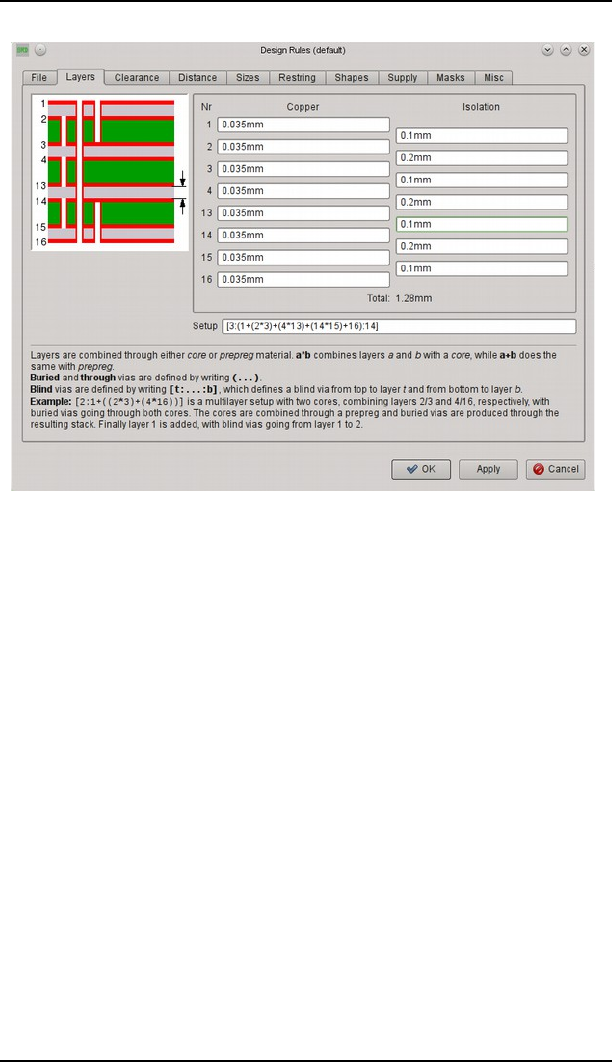
6 From Schematic to Finished Board
➢
Example 5: Layer Setup for an 8 layer board
Hints For Working With Blind, Buried, and Micro Vias
VIA command
Depending on the Layer setup vias can have different lengths. The parameter
toolbar of the VIA command shows all available lengths in the Layer box.
When routing manually (ROUTE command) EAGLE takes the shortest
possible via length in order to change layers. It is also possible that vias at the
same position are elongated.
The via length can be changed with the CHANGE VIA command. Select the
value from the according menu and click the via with the left mouse button.
Alternatively use the command line:
*:.-9
and a click onto the via changes the length from layer 2 to 15.
If the given via length is not defined in the Layer setup it will be elongated to
the next possible length or, if this is not possible, an error message will be
generated.
:C5C-;@-$09.B
places a via that belongs to the signal GND and reaches from layer 1 to 4 at
position (1.05 2).
186

6.7 Multilayer Boards
ROUTE Command
If you want to change the layer while laying-out the board, EAGLE always
takes the shortest possible via (CHANGE LAYER command; also in Follow-
me mode). It is also possible that a via at the same position is elongated
automatically.
If Micro vias are enabled in the Design Rules by setting a minimum
value for the drill diameter (Sizes tab, Min. Micro Via) and defining a
proper Layer setup, EAGLE sets a Micro via when routing from a
SMD and immediately changing to the next inner layer.
In Follow-me mode, however, EAGLE can't place Micro vias. The
Follow-me router is powered by the Autorouter engine and therefore
it has to follow its properties and restrictions.
Micro Via − A Special Case of Blind Via
In contrast to Blind vias that can reach several layers deep into the board the
Micro via connects an outer layer with the next inner layer. The drill
diameter of a micro via is relatively small. Presently the usual values are
about 0.1 to 0.05 mm.
For manufacturing reasons Micro vias, as Blind vias, have to follow a certain
Aspect ratio of depth to drill diameter. This ratio defines the maximum via
depth for a certain drill diameter.
The proper value can be learned from your board house.
Set this value in the Design Rules, Sizes tab, Min. Blind Via Ratio.
Assumed the board house demands the ratio as 1:0.5 you have to enter 0.5
for Min. Blind Via Ratio.
Additionally the Design Rule Check verifies the minimum drill diameter for
Micro vias given in Min. MicroVia. If this value is higher than the value for
Minimum Drill (default), micro vias won't be checked.
The diameter of micro vias is set in the Restring tab of the Design Rules.
If you change the layer from an outer to the next inner one while you are
routing a track out of a SMD, EAGLE automatically places a Micro via,
provided the Design Rules allow it.
The Autorouter can't set Micro vias!
6.8 Editing and Updating Components
Open Device/Symbol/Package
Depending on the Editor window you are currently working wit the context
menu of a component offers the entries Open Device/Symbol/Package. If
you select one of them, EAGLE tries to open the referring library file in the
corresponding editing mode. Now you can easily check all the objects the
187

6 From Schematic to Finished Board
Device/Symbol/Package consists of. And it is even possible to modify the
library definition.
In order to update your project with the modified library definition you have
to start a library update (menu Library/Update...)in schematic/board (see
next section)
Please be aware that changes in the libraries can affect a number of
different devices in the library file and therefore your future projects,
as well. Please act accordingly carefully!
In case EAGLE doesn't find the original library file, EAGLE prompts a
warning and cancels this action.
In this case there is a possibility of extracting the library definitions used in
your current project. File/Export/Libraries... starts the User Language
Program exp-lbrs.ulp that creates library files accordingly.
Updating Project (Library Update)
The UPDATE command allows components in a schematic diagram or a
layout to be replaced by components defined in accordance with the current
libraries. This function is of particular interest for existing projects. If, in the
course of development, the definitions of Packages, Symbols or Devices in the
libraries are changed, the existing project can be adapted to them.
The menu item Library/Update causes all the components in a project to be
compared with the definitions in the current libraries. If EAGLE finds
differences, the components are exchanged.
Those libraries on the path specified for Libraries in the Control Panel under
Options/Directories will be examined.
It is also possible to update components from one particular library. Type the
UPDATE command on the command line, stating the library, for instance as:
5!=
or
5'('8='!'!=K8'!=$!K
or select the library in the File dialog of the Library/Update... menu item.
In the case you want to replace parts from one library with parts from
another library you can use the command:
5!!K<!K$
Old-lbr-name represents the name of the library as shown by the INFO
command in the layout or schematic. New-lbr-name stands for the library
from which you want to take elements. You may add paths as well.
Please see the help function for more information.
In many cases you will be asked whether Gates, pins or pads should be
replaced according to name or according to position. This always happens if
library objects are renamed, or if their position (sequence) is changed.
188

6.8 Editing and Updating Components
If too many changes are made in the library at one time (e.g. pin names and
pin positions are changed) it is not possible to carry out an automatic
adaptation. In such a case it is possible either to carry out the modifications
to the library in two steps (e.g. first the pin names and then the pin
positions), or the library element can be given a new name, so that it is not
exchanged.
Changing a Device's prefix in the library does not update the part
names of already placed elements in your drawing.
If Forward&Back Annotation is active, the components are replaced in the
schematic diagram and in the layout at the same time.
You will find further information on the program's help pages.
After any library update, please carry out both an ERC on the
schematic and a DRC on the layout!
Individual components can, for instance, be updated with the aid of the ADD
command. If you use ADD to fetch a modified component from a library, you
will be asked whether all the older definitions of this type should be updated.
After the update you can delete the component that you just fetched. Again
here it is wise to carry out an ERC and a DRC after the update!
6.9 Differential Pairs And Meanders
Routing Differential Pairs
A Differential Pair consists of two signals that have the same name, but
different name extensions. One of the signals must have the extension _P, the
other one _N, as for example in CLOCK_P and CLOCK_N. The two signals
must belong to the same net class.
The following particularities apply:
As soon as you select an airwire of a Differential Pair with the ROUTE
command, both signals are routed in parallel. The distance between the two
signals and the wire and via sizes are always determined by the signals' net
class.
The option Auto set route width and drill in the menu Options/Set/Misc
does not affect differential pairs.
If you don't want to route both signals for the whole distance, you can drop
the second airwire with the Escape key.
The first mouse click with the active ROUTE command onto one of the
airwires of the differential pair decides about the starting point of the parallel
routing. Usually the pads or SMDs the airwires start from don't have the
necessary distance for parallel routing, so EAGLE draws traces from the
starting points to the current mouse cursor position, according to the current
wire bend style. Note that there may be cases where these wires overlap, so
189
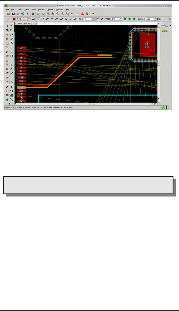
6 From Schematic to Finished Board
please make sure you choose a proper point from where to start the actual
parallel routing. It can be wise to run a Design Rule Check in this area.
The distance between the target pads/SMDs will also be probably more than
the Differential Pair is routed with, so you should start the routing from this
side as well and define the ending point of the parallel routing, as you did
before at the starting point. If you route towards the wire end points of a
Differential Pair in a different layer, and the wires are fully aligned, the
proper vias will be generated automatically.
Differential Pairs can only be routed manually. The Follow-me
router and the Autorouter treat them like regular signals.
The special functions Shift + left click that places a via at the end point and
Ctrl + left click for defining an arc radius don't work in Differential Pair
mode. When you start routing at any point of a signal (with Ctrl + left click)
you will route the selected signal only, and not the Differential Pair the signal
might be part of.
Coordinates given in the command line while routing a Differential Pair form
a center line along which the actual signal wires are placed left and right with
the proper distance.
Meanders
Length Balance for a Differential Pair
In most cases the traces of a differential pair will have different lengths
although you tried to route them in parallel. The MEANDER command can
be used to balance the lengths of signals forming a differential pair. To do
this, activate the MEANDER command, click onto one of the differential pair
wires, and move the mouse cursor away from the selection point. The
190
➢
Differential Pair follows the mouse cursor
6.9 Differential Pairs And Meanders
distance from the initial selection point and the deflection of the mouse
determines the width and the height of the meander. If there is a difference
in the length of the two signals, and the current mouse position is far enough
away from the selection point, a meander shaped sequence of wires will be
drawn. The meander increases the length of the shorter signal segment.
An indicator attached to the mouse cursor shows the target length which is
the length of the longer signal segment, as well as the deviation in percent of
both signals from the target length.
If a single meander isn't enough to balance the lengths, you can add further
meanders at different locations.
Specifying a Certain Length
In case you want to specify a certain length for the Differential Pair signals,
you can type in the value, for example 9.5in, in the command line directly.
Type in the value, press the Enter key and click onto on of the Differential
Pair wires. Again, the position of the mouse determines the way the meander
looks like.
When meandering a differential pair with a given target length, the meander
first tries to balance the length of the two signal segments that form the
differential pair, and then increases the total length of both segments.
To reset the target length you can either restart the MEANDER command or
enter a value of 0 in the command line.
It's possible to do this for a segment of any signal, not only for
Differential Pairs.
Symmetric and Asymmetric Meanders
By default a meander is generated symmetrical, which means it extends to
both sides along the selected wire. If this is not what you need (either because
there is only space on one side, or because the longer one of the wires of a
differential pair shall not be elongated you can switch to asymmetric mode by
clicking the right mouse button. The actual mouse position will decide which
side of the wire the meander extends to. Move the mouse around to find the
proper position.
The value for Gap factor for meanders in differential pairs which can be set
in the Design Rules' Misc tab, determines the size of the gap between
meander's loops. Increasing the value results in bigger gaps between the
loops. The factor may have values from 1 up to 20. Default: 2.5
Length Tolerance Display
The value defined in Design Rules, Misc tab for Max. length difference in
differential pairs is used to select the color when displaying the length
deviations while drawing a meander. If the percentage is shown in green, the
respective segment lies within the given tolerance. Otherwise the percentage
is displayed in red. The default for this parameter is 10mm.Measuring signal
lengths
191
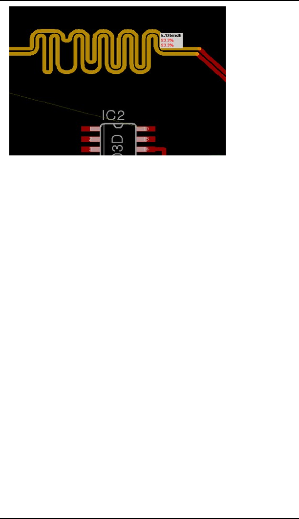
6 From Schematic to Finished Board
If you click on a signal wire with the Ctrl key pressed, the length of that signal
segment will be measured and displayed on the screen in a little indicator
near the mouse cursor. You can use this to measure the length of a given
signal segment and it as the target length for meandering an other segment.
If you do the measuring with Ctrl+Shift pressed, the maximum length of this
or any previously selected segments will be taken. This can be used to
determine the maximum length of several bus signals and then meandering
each of them to that length.
6.10 Assembly Variants
If you would like to have your project manufactured in different assembly
variants, EAGLE helps you in creating and managing them. Basically an
assembly variant offers the opportunity to have components not populated
on the board or to use components with different values or with different
technologies.
Creating Assembly Variants
As soon as you have finished your project, or at least the schematic, you can
define assembly variants. The default assembly variant (which is the
schematic/layout you just finished) should already contain all the
components which will be used in the different assembly variants. Based on
the default variant open the Assembly Variants dialog through the menu
entry Edit/Assembly variants.... This dialog shows all the components with
its name, value, technology, and the description of the device.
Click onto the New button in order to define an assembly variant. It will be
shown in the Assembly variants window then. Its name is visible in the title
bar. Below you find three columns: A check box, value, and technology.
If the check box is checked, the component will be populated. If you want it
not to be populated, uncheck it. If not populated, the component will be
crossed out in the schematic drawing. This indicates: not available in this
192
➢
Target length 5.125 inch: currently both signals have 93.3%
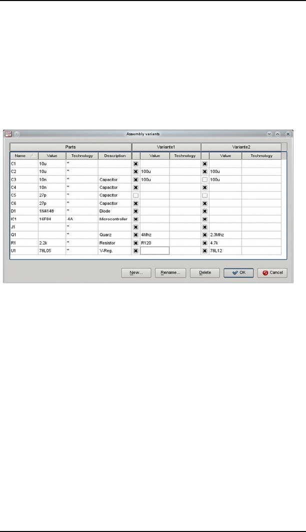
6.10 Assembly Variants
variant. Simultaneously in the Layout Editor all the objects representing the
silkscreen print for this element will be deleted.
If you would like to change the value of a component, click into the
appropriate field of the Value column, and type in the new value. By default,
all fields remain empty which means that there is no change compared to the
default assembly variant. You are allowed to alter the value of components
which have Value set on for the Device in the library. This setting is typically
used, for example, for resistors or capacitors.
If a component is defined in different technologies, you are allowed to change
it in the Technology column. If there is no technology defined, you can't
change it.
The image above shows besides the default assembly variant on the left with
its columns Name, Value, Technology, and Description two additional
variants. In Variante1 one component (C5) is not populated, some of the
components have altered values. In Variante2 two components will not be
populated. Cells without entry indicate that there are no changes compared
to the default assembly variant.
Click onto the name of the variant in the title bar of the table and it will be
shown in bold text. This indicates that this variant is currently selected. The
buttons Rename... and Delete... affect this variant now.
193
➢
Assembly variants window

6 From Schematic to Finished Board
After defining assembly variants, the action toolbar of the Schematic and
Layout Editor contain an additional selection combo box. The image above
shows Variant2 selected. Two components won't be populated. They are
crossed out in the schematic.
The commands ADD, CHANGE PACKAGE | TECHNOLOGY, REPLACE,
UPDATE and VALUE can only be used, if the default assembly variant is
active. That's the entry without name in the combo box of the action toolbar.
The EXPORT PARTLIST command creates data for the currently selected
assembly variant. If you use bom.ulp for creating the bill of materials, you
can choose the variant in the ULP's dialog. Unpopulated components will not
appear in the parts list.
Assembly Variants and CAM Processor
If you want to create manufacturing data with the CAM Processor be sure to
select the applicable assembly variant in the schematic before and save your
project. The board is also saved in this variant then and the CAM processor
can create data from this.
The information about assembly variants is available only in the
schematic. For boards without a schematic assembly variants are
not supported.
The recommended procedure is to set the variant in the schematic and save
schematic and board. Then run the CAM Processor.
194
➢
Action Toolbar with combo box for assembly variant

6.10 Assembly Variants
In boards without schematic it is possible to change the Populate option of
components via the CHANGE command or via the properties dialog.
6.11 Print Out Schematic and Layout
Schematic diagrams, boards and also library elements can be printed out
with the PRINT command.
Using DISPLAY you should first select the layers that you want to print.
The basic rule is: If you can see it in the editor, you will see it on the
print.
Exceptions to the rule above are:
Origin crosses for texts
Grid lines or grid dots
Polygons that can't be calculated by RATSNEST and therefore only
show their contours in the Layout Editor
Error polygons of the Design Rule Check
Settings of the Print Dialog
When the printer icon on the action toolbar is clicked, the PRINT dialog
opens.
195
➢
The PRINT window

6 From Schematic to Finished Board
The currently selected printer is shown at the top of the window in the
Printer line. The small button on the right, at the end of the line, can be used
to select another printer or activate one of the print-to-file options. If a
printer is selected, the button with the three dots ... leads you to the printer
properties.
In case you selected a print-to-file option the Output file line shows the path
to the output file. If you want to change it, click onto the … button.
Below these two lines you will find settings about Paper format, Orientation
and Alignment of your print. The … button in the Paper line allows you to
define a user-specific format, provided the selected printer supports this.
Alignment defines the location of the print-out on the paper. Changing this
will directly result in a modified Preview, if active.
In the Area line, you determine what to print: Window prints the drawing
window which is currently visible in the Editor window. Full on the other
hand, prints the whole drawing. In this case all drawing objects (displayed or
not) are relevant for the calculation of the resulting printing area.
Printing Options
Mirror inverts the drawing from left to right about the Y axis, Rotate turns it
90 degrees counter-clockwise, and Upside down turns it through 180
degrees. If both are activated, a rotation of 270 degrees is the result.
If the Black option is chosen, a black-and-white printout is made. Otherwise
the print will be either in color or gray scale, depending on the printer.
Solid causes each object to be entirely filled. If you want to see the different
filling patterns of the individual layers, then deactivate this option.
The Caption option switches the appearance of the title, printing date, file
name and the scale of the print on or off.
In the Scale section of the window the Scale factor specifies the scale of the
drawing. It may be in the range of 0.001 and 1000.
If Page limit is set to 0, the printer will use whatever number of pages is
needed to print the output at the selected scale. If a different value is
selected, EAGLE will adjust the scale of the drawing to fit it onto the stated
number of pages. This can mean that, under unfavourable circumstances, the
selected scale cannot be maintained.
Otherwise you have the possibility to select Page Limit 1, and a Scale factor
that would request more than one page for printing to get a maximum filling
of the page.
It is possible to select which sheets from a schematic diagram are printed
using the Sheets box. This only appears in the Schematic Editor. This
selection also determines which sheet is shown in the preview.
If you activate the option Hierarchy, all the module sheets for each module
instance used in the schematic will be printed with the corresponding part
names, net names and assembly variants.
The edges of the print can be defined with the aid of the four entry boxes
under Border. The values may be entered in mm or in inches. If you have
changed the values and want to use the printer driver's standard settings
again, simply enter a 0.
196

6.11 Print Out Schematic and Layout
Calibrate allows correction factors for the aspect ratio of the printout. This
allows linear errors in the dimensional accuracy of the print to be corrected.
The values can be specified in the range of 0.1...2.
Note concerning colored printing:
EAGLE always takes the white palette as basis for colored printouts.
If you are working with a black or colored background and using
self-defined colors, it is recommended to define these colors also for
the white palette. So the printer can use your colors, too.
If, when a layout is printed, the drill holes in the pads and vias are not to be
visible, select the No Drills option for the Display mode by way of the menu
item Options/Set/Misc.
Generating PDF files
If you want to generate a PDF file (resolution 1200dpi) from your drawing,
click onto the small selection button in the Printer line and choose the option
Print to file (PDF). Go to the Output file line then and specify path and name
of the PDF output file.
All texts that are not written in EAGLE vector font are searchable in the PDF
file by means of your PDF viewer.
Visibility and Sequence of Printed Layers
EAGLE prints its layers in a certain sequence, one over the other. If you are
using, for example, self-defined layers that are hidden by other layers in the
print-out, you can use a SET command option – SET Option.LayerSequence
– for bringing them into the foreground, or in general, for defining the layer
printing sequence. This affects printing into a PDF file, as well.
Details about this can be found in the help function of the SET command,
Help/Editor commands/SET.
The PRINT command can also be given directly on the command line, or can
be run by a script file. Information about the selection of options is available
on the help pages for PRINT.
6.12 Combining Small Circuit Boards on a
Common Panel
In order to save costs, it may be worth supplying, for example, a smaller
board to the board manufacturer in the form of a multiple board. So you can
have several boards made in one step.
You can reproduce the layout or combine different layouts to create a
multiple board with the GROUP, COPY and PASTE commands. Please note
that this will change the board's silk screen, since elements receive new
names, if a certain designator is already used in the board when pasting from
the buffer. If you don't need the silkscreen this does not matter. Otherwise a
User Language program can help. Panelize.ulp copies the texts written in the
layers 25 and 26 (t/bNames) into two new layers 125 and 126. When
combining the boards the names of the parts will change anyway, the copied
texts in those new layers however will remain unchanged.
197

6 From Schematic to Finished Board
Tell the board manufacturer that they have to take layers 125 and 126 instead
of the original layers 25 and 26 to generate the silkscreen from.
Procedure:
Load the board file.
Run panelize.ulp to copy name texts.
DISPLAY all layers.
Use GROUP to select all objects to be copied.
To select the whole layout you could also use GROUP ALL.
Click the COPY icon in order to put the group into the clipboard
Edit a new board file with File/New .
Use PASTE and place the layout as often as wanted. If necessary, it is
possible to specify an orientation for the group before fixing it.
Please make sure that the new board has the same set of Design Rules
as the original board file has. It is possible to export Design Rules into
a file (*.dru) and then import it into another board file (Edit/Design
rules menu, File tab).
Save the new board file.
Tell your board house that they have to use layers 125/126 instead of
25/26.
6.13 Consistency Lost between Schematic
and Layout
It is very important during the design that the content of the schematic and
the layout exactly correspond to allow for design congruency. Eagle uses a
Forward&Back annotation to perform this task. General information about
this can be found in the chapter about Forward&Back Annotation beginning
with page 103.
The interconnection between Schematic Editor and Layout Editor ensures
that both are in lock-step from a design standpoint automatically, provided
both files are always loaded at the same time. If you close one of them, either
the schematic or layout file, and continue your work in the remaining opened
file the consistency will be lost. EAGLE will not be able to transfer the
modifications into the other file. So differences will arise between Schematic
and Layout.
In case you close one of the two editor windows EAGLE prompts an eye-
catching yellow and black warning on top of the drawing area which tells you
that Forward&Back Annotation has been severed. Please reload the file
again.
In case you severed F&B Annotation intentionally, you can hide this warning
by clicking into the message area.
198

6.13 Consistency Lost between Schematic and Layout
EAGLE will prompt a similar warning as soon as you try to load a pair of
schematic/board files or a project which is not consistent.
Start the Electrical Rule Check (ERC) immediately. It compares both files
and reports differences in the ERC Errors window's Consistency Errors
branch. If you click onto one of these entries, EAGLE marks the affected
object in Schematic and Board, if possible.
Process each message and resolve the difference in the Schematic or in the
Layout Editor window, according to requirements. Finally you can mark the
entry in the list as done with the Processed button.
For establishing consistency again it can be helpful to use UNDO.
Launch the ERC every time a change has been made for design verification
and to get an overview of progress. All differences are cleared, if ERC reports
consistency. Now the Annotation will work again and the board and
schematic are again in lock-step with each other.
199
➢
Forward&Back Annotation severed!
➢
Consistency loss between Schematic and
Layout
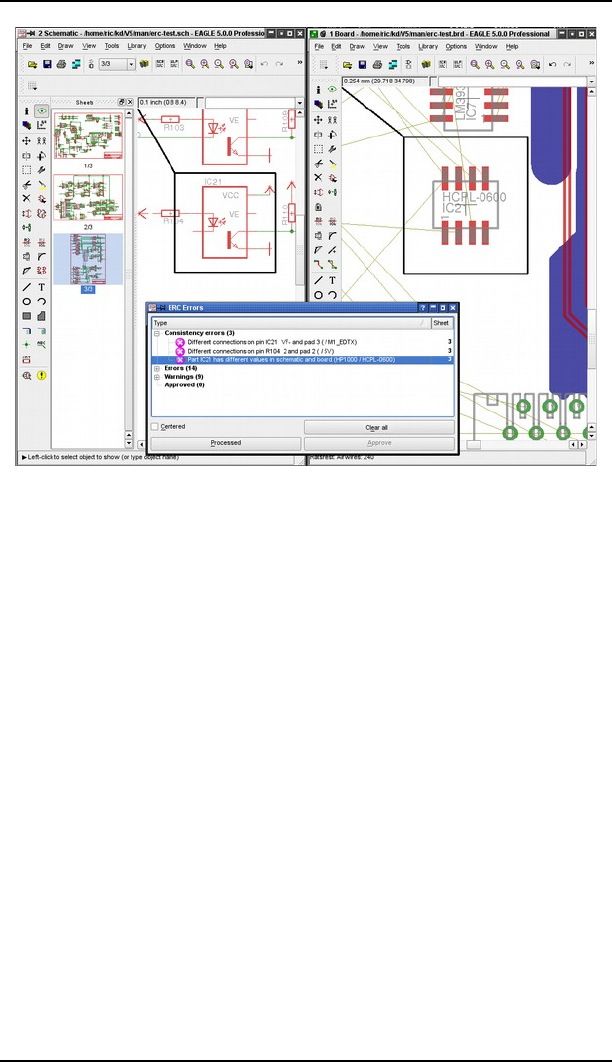
6 From Schematic to Finished Board
➢
The differences are marked in both editor windows
Don't forget to save the files now and remember to leave both files loaded
simultaneously all the time.
Criteria For Consistency
There are some rules that have to be fulfilled in order to have consistency
between schematic and layout and the Forward&Back Annotation working.
In the following list there are mentioned the most important items:
Each component in the schematic has to have a corresponding
package in the layout and vice versa. Exceptions are supply symbols,
elements without contacts, and components with an attribute with
the name _EXTERNAL_ (for example for simulation symbols).
☞ Use ADD/DELETE/NAME commands for placing/deleting/
naming components
Corresponding components have to have the same values.
☞ Use the VALUE command in order to adjust the values.
For each connection of net and pin in the schematic there has to be
a corresponding connection with the same name of signal and
referring pad in the layout.
☞ Add the missing net with the NET command, missing signals in
the layout with the SIGNAL command, if necessary use NAME
to adjust signal/net names or DELETE for deleting connections.
Nets in the schematic and signals in the layout have to belong to
identical netclasses.
200

6.13 Consistency Lost between Schematic and Layout
☞ CHANGE CLASS or use the properties dialog of the net/signal
in order to adjust the net classes and their values for width,
clearance and drill.
Assembly variants in schematic and board have to be identical;
There must be the same number of variants and identic variant
names. Additionally the population options of the components have
to be the same.
☞ Use the VARIANT command for adjusting this
If there are attributes defined for components, the attribute name
and the attribute value have to be the same in schematic and board.
It is allowed to have additional attributes defined in the layout
editor which are not available in the schematic, but not vice versa.
☞ Check the ATTRIBUTE command
If there are attributes that are defined in the library, it might be
helpful to use the REPLACE command in order to replace such
components and update the attribute information.
The definition of the package in schematic and board has to be
exactly the same. There are different options in order to eliminate
such discrepancies:
☞ Use the REPLACE command in the layout editor in order to
exchange the package with a definition that matches the
package used in the schematic.
☞ Exchange of a whole device in the schematic editor with the
REPLACE command or replacement of the components with
a package definition used in the layout editor.
Please take care on attributes, as well (see above).
☞ Change the package variant , if any, with CHANGE PACKAGE
in the schematic editor.
If the libraries that contained the components originally used in your
schematic and layout are not available, it might be helpful to export the
library definitions from your drawing files (File/Export menu). Now it is
possible to modify the libraries, if necessary, and use the REPLACE
command.
Consistency Indicator
In the bottom right corner of the editor window you can see an indicator that
gives, depending on its color, information about consistency.
Gray F&B Annotation not possible
Only one file loaded
Yellow F&B Annotation not available
SCH and BRD have different names
Pink F&B Annotation not active
SCH and BRD are not consistent
Green F&B Annotation is active
SCH and BRD are consistent
201

6 From Schematic to Finished Board
The exclamation mark right of the consistency indicator remembers you that
the drawing is currently not saved.
202
➢
Consistency indicator

Chapter 7
The Autorouter
7.1 Basic Features
Any routing grid (min. 0.02 mm)
Any placement grid
Fully integrated into basic program
TopRouter with gridless routing algorithm, which can be preceded by
the Autorouter
BGA router for fan-out routing
Optional automatic selection of routing grid and preferred directions
in the signal layers
Support for multi-core processors to process multiple routing jobs
simultaneously
SMDs are routed on both sides
The whole drawing area can be the routing area (provided enough
memory is available)
The strategy is selected via control parameters
Simultaneous routing of various signal classes with various track
widths and minimum clearances
Common data set (Design Rules) for the Design Rule Check and the
Autorouter
Multilayer capability (up to 16 layers can be routed simultaneously,
not only in pairs)
Support of Blind and Buried vias
The preferred track direction can be set independently for each layer:
horizontal and vertical, true 45/135 degrees (important for inner
layers!)
Ripup and retry for 100 % routing strategy
Optimization passes to reduce vias and smooth track paths
Prerouted tracks are not changed
Serves a basis for the Follow-me router, a special operating mode
of the ROUTE command that allows automatic routing of selected
signals
203

7 The Autorouter
7.2 What Can be Expected from the
Autorouter
The EAGLE Autorouter is a "100%" router. This means that boards which, in
theory, can be completely routed will indeed be 100% routed by the
Autorouter, provided - and this is a very important restriction - the
Autorouter has unlimited time. This restriction is valid for all 100%
Autorouters whatsoever. However, in practice, the required amount of time
is not always available, and therefore certain boards will not be completed
even by a 100% Autorouter.
The EAGLE Autorouter is based on the ripup/retry algorithm. As soon as it
cannot route a track, it removes prerouted tracks (ripup) and tries it again
(retry). The number of tracks it may remove is called ripup depth which is
decisive for the speed and the routing result. This is, in principle, the
previously mentioned restriction.
In the Autorouter main dialog it is possible to choose a TopRouter variant. It
uses a gridless algorithm with topological approach. This algorithm
calculates first the course of the signals and then uses the optimization runs
of the traditional EAGLE Autorouter to meet the Design Rules. Typically, the
TopRouter requires significantly fewer vias than the traditional EAGLE
Autorouter. The user has the option to select both methods for a project and
eventually opt for one or the other routing result.
Those who expect an Autorouter to supply a perfect board without some
manual help will be disappointed. The user must contribute his ideas and
invest some energy. If he does, the Autorouter will be a valuable tool which
will greatly reduce routine work.
Working with the EAGLE Autorouter requires that the user places the
components and sets control parameters which influence the routing
strategy. These parameters must be set carefully if the best results are to be
achieved. They are therefore described in detail in this section.
7.3 Controlling the Autorouter
The Autorouter is controlled by a number of parameters. The values in the
current Design Rules, the net classes and special Autorouter control
parameters all have an effect.
The Design Rules specify the minimum clearances (DRC commands for
setting Clearance and Distance), the via diameter (Restring setting) and the
hole diameter of the vias (Sizes setting). The minimum track width is also
specified.
The net classes - if any are defined - specify special minimum clearances,
track widths and the hole diameters for vias carrying particular signals.
There is also a range of special cost factors and control parameters that can
be changed via the Autorouter menu. They affect the route given to tracks
during automatic routing. Default values are provided by the program. The
control parameters are saved in the BRD file when the layout is saved. You
can also save these values in an Autorouter control file (*.ctl). This allows a
204

7.3 Controlling the Autorouter
particular set of parameters to be used for different layouts. Neither Design
Rules nor the data for various net classes are part of the control file.
A routing process involves a number of separate basic steps:
Bus Router
Normally the bus router starts first.
It deals with signals which can be routed in the preferred direction with only
slight deviation in x and y direction allowed. The bus router takes only those
signals into consideration that belong to net class 0.
This step may be omitted.
Buses, as understood by the Autorouter, are connections which can
be laid as straight lines in the x or y direction with only a few
deviations.
It has nothing in common with buses in the meaning of electronics,
for example, address buses or the like.
Routing Pass
The actual routing pass is then started, using parameters which make a 100%
routing as likely as possible. A large number of vias are deliberately allowed
to avoid paths becoming blocked.
TopRouter
Select a routing variant with upstream TopRouter, and the traces will be laid
out with another routing algorithm, which tends to use less vias. Finally
routing and optimization follows in order to trim all the traces to comply
with the design rules.
Optimization
After the main routing pass, any number of optimization passes can be made.
The parameters are then set to remove superfluous vias and to smooth the
track paths. In the optimization passes tracks are removed and rerouted one
at a time. This can, however, lead to a higher degree of routing, since it is
possible for new paths to be freed by the changed path of this track.
The number of optimization passes must be specified before starting the
Autorouter. It is not possible to optimize at a later stage. Once the routing job
has been completed all the tracks are considered to have been prerouted, and
may no longer be changed.
Any of the steps mentioned above may be separately activated or deactivated.
205
7 The Autorouter
7.4 What Has to be Defined Before
Autorouting
Design Rules
The Design Rules need to be specified in accordance with the complexity of
the board and of the manufacturing facilities available. You will find a
description of the procedure and of the meanings of the individual
parameters in the section on Specifying the Design Rules on page 144.
Track Width and Net Classes
If you have not already defined various net classes in the schematic diagram
you now have the opportunity, before running the Autorouter, of specifying
whether particular signals are to be laid using special track widths, particular
clearances are to be observed, or whether certain drill diameters are to be
used for vias for particular signals. Please consult the help pages (CLASS
command) or the section on Specifying Net Classes on page 123 for
information about the definition of net classes.
If no special net classes are defined, the values from the Design Rules apply.
The value Minimum width in the Sizes tab determines the track width, the
values for minimum clearances/distances are taken from the Clearance and
Distance tabs. The diameter of vias is defined by the values in the Restring
tab.
Did you set values in the Design Rules and for net classes? In this
case the Autorouter follows the higher value.
Grid
The Design Rules determine the routing and placement grid. The minimum
routing grid is 0.02 mm, which is about 0.8 mil.
Placement Grid
Although the Autorouter does permit any placement grid, it is not a good
idea to place the components on a grid that is too fine. Two good rules are:
The placement grid should not be finer than the routing grid.
If the placement grid is larger than the routing grid, it should be set to
an integral multiple of the routing grid.
These rules make sense if, for example, you consider that it might be
possible, within the Design Rules, to route two tracks between two pins of a
component, but that an inappropriate relationship between the two grids
could prevent this (see diagram).
206
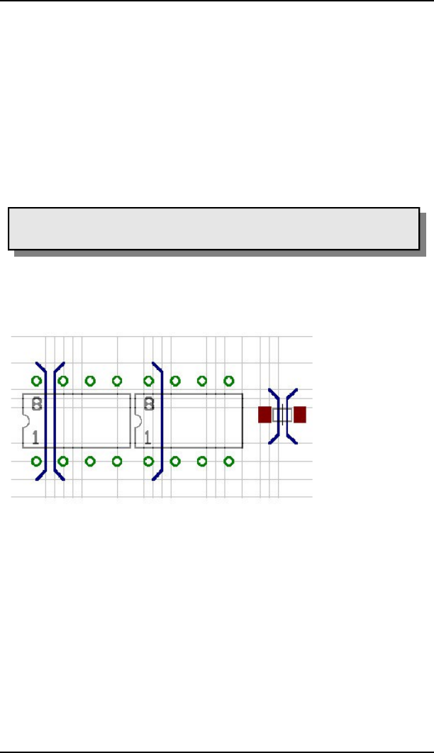
7.4 What Has to be Defined Before Autorouting
Routing Grid
Please note that the Autorouter grid has to be set in the AUTO command's
Autorouter Main Setup Window. This is not the same as the currently used
grid in the Layout Editor window that you have selected with the GRID
command.
Bear in mind that for the routing grid the time demand increases
exponentially with the resolution. Therefore select as large a grid as possible.
The main question for most boards is how many tracks are to be placed
between the pins of an IC. To answer this question, the selected Design Rules
(i.e. the minimum spacing between tracks and pads or other tracks) must of
course also be considered.
The result is:
The two grids must be selected so that component's pads are located
on the routing grid.
There are of course exceptions, such as with SMDs to which the opposite may
apply, namely that a position outside of the routing grid leads to the best
results. In any event the choice of grid should be carefully considered in the
light of the Design Rules and the pad spacing.
The example above may clarify the situation:
For the component on the left, the pads are placed on the routing grid. Two
tracks can be routed between two pads. The pads of the component in the
middle are not on the routing grid, and therefore only one track can be
routed between them.
On the right you see the exception from the rule shown for SMD pads, which
are placed between the routing grid lines so that one track can be routed
between them.
When choosing the grid, please also ensure that each pad covers at least one
grid point. Otherwise it can happen that the Autorouter is unable to route a
signal, even though there is enough space to route it. In this case the
Autorouter issues the message Unreachable SMD at x y as it starts. The
parameters x and y specify the position of the SMD pad.
207
➢
Track patterns with different placement grids
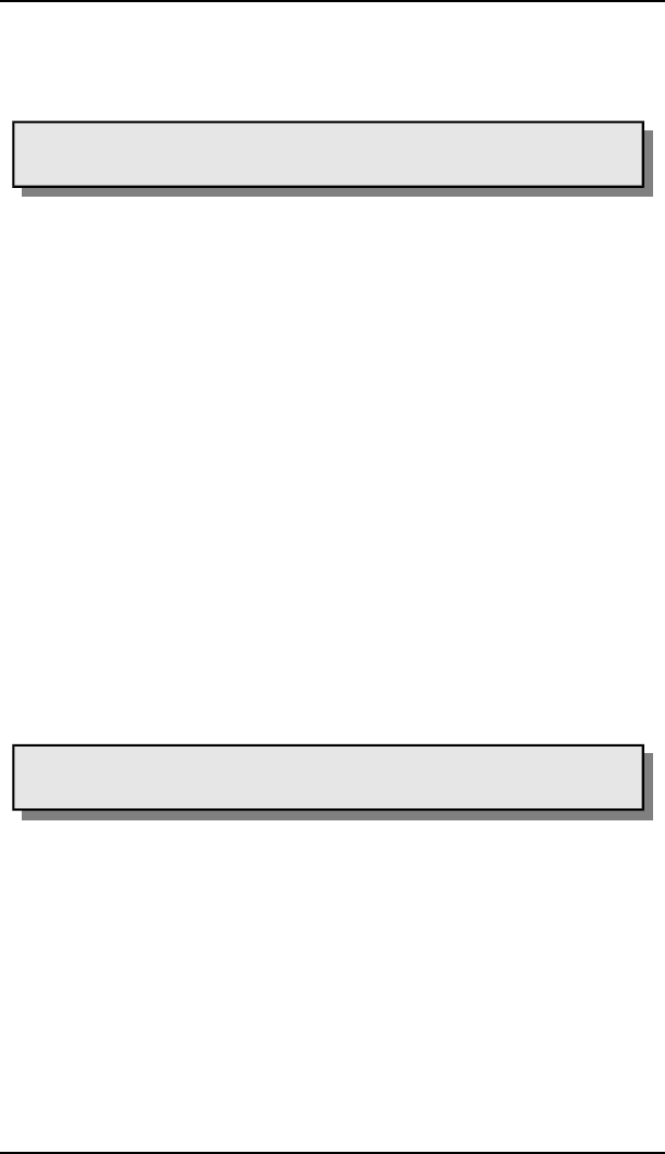
7 The Autorouter
The default value for the routing grid is 50 mil. This value is sufficient for
simple through-hole layouts. Working with SMD components demands a
finer routing grid.
Usual values are 25, 12.5, 10, or 5 mil.
Please remember that finer routing grids require significantly more
routing memory.
With the automatic grid selection option, the auto router determines at its
own heuristics suitable grid settings for each routing jobs.
Memory Requirement
The amount of routing memory required depends in the first place on the
selected routing grid, the area of the board and the number of signal layers in
which tracks are routed.
The static memory requirement (in bytes) for a board can be calculated as
follows:
)KV=H=&"x)KV"=!!8"x.
Space is also required for dynamic data, in addition to the static memory
requirement. The dynamic data require in a very rough estimate about 10%
up to 100% (in some cases even more!) of the static value. This depends
heavily on the layout.
Total memory requirement (rough approximation):
"&G8x@-$-$$.30B/K8&"2
This much RAM should be free before starting the Autorouter. If this is
insufficient, the Autorouter must store data on the hard disk. This lengthens
the routing time enormously, and should be avoided at all costs. Short
accesses to the hard disk are normal, since the job file on the hard disk is
regularly updated.
Try to choose the coarsest possible routing grid. This saves memory
space and routing time!
Layer
If you want to design a double-sided board, then select Top and Bottom as
route layers. You should only use the Bottom layer for a single-sided board.
In the case of inner layers, it is helpful to use the layers from the outside to
the inside, i.e. first 2 and 15 and so on.
In the case of boards that are so complex that it is not certain whether they
can be wired on two sides, it is helpful to define them as multilayer boards,
and to set very high costs for the inner layers. This will cause the Autorouter
to avoid the inner layers and to place as many connections as possible in the
outer layers. It can, however, make use of an inner layer when necessary.
These settings are made in the Autorouter menu (see page 210).
208

7.4 What Has to be Defined Before Autorouting
The autorouter shows the message Unreachable SMD in layer..., if a layer
that contains SMDs is not active. Clicking OK starts the autorouter
nevertheless. If you want to change the autorouter setup click Cancel.
Preferred Directions
For each routing job you can specify individually for each signal layer its own
preferred direction. With the new Auto setting the Autorouter will choose
different settings for preferred directions on its own.
If you want to set preferred directions manually, the following considerations
apply: On the two outside layers the preferred directions are normally set to
90 degrees from each other. For the inner layers it may be useful to choose
45 and 135 degrees to cover diagonal connections. Before setting the
preferred direction it is well worth examining the board (based on the
airwires) to see if one direction offers advantages for a certain side of the
board. This is particularly likely to be the case for SMD boards.
Please also follow the preferred direction when pre-placing tracks.
The defaults are vertical for the Top (red) and horizontal for the
Bottom (blue) layer.
Experience has shown that small boards containing mainly SMD components
are best routed without any preferred direction at all (set * in the Autorouter
setup). The router then reaches a usable result much faster.
Single sided boards should be routed without a preferred direction.
Restricted Areas for the Autorouter
If the Autorouter is not supposed to route tracks or place vias within certain
areas, you can define restricted areas by using the commands RECT,
CIRCLE, and POLYGON in the layers 41, tRestrict, 42, bRestrict, and 43,
vRestrict.
tRestrict: Restricted areas for Wires and Polygons in the Top layer.
bRestrict: Restricted areas for Wires and Polygons in Bottom
layer.
vRestrict: Restricted areas for Vias.
Such restricted areas can already be defined in a Device or Package (around,
for instance, the fixing holes for a connector, or for a flat-mounted transistor
under which there should not be any tracks).
Wires drawn in layer 20, Dimension, are boundary lines for the Autorouter.
Tracks cannot be laid beyond this boundary.
Typical application: board boundaries.
An area drawn in layer 20 can also be used as a restricted region for all
signals. It should, however, be noted that this area should be deleted before
sending the board for manufacture, since layer 20 is usually output during
the generation of manufacturing data.
Cutout polygons which are used, for example, in inner layers in order to keep
certain areas of signal polygons free of copper, are not recognized by the
Autorouter. It may happen that the Autorouter draws wires in such an area.
209
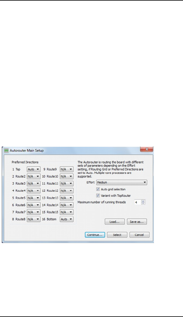
7 The Autorouter
Cost Factors and Other Control Parameters
All routing parameters are set in the Autorouter Variants dialog. They can be
modified separately for each routing variant.
The default values for the cost factors are chosen on the basis of our
experience in such a way as to give the best results.
The control parameters such as mnRipupLevel, mnRipupSteps etc. have also
been set to yield the best results according to our experience.
We want to emphasize, that we recommend working with the default values.
If you nevertheless do want to experiment with these parameters, please
consider the description of the cost factors in the following section. In the
case of many parameters even small alterations can have large effects.
7.5 The Autorouter Menu
When running the Autorouter with the AUTO command, the setup menu
appears first. All the necessary settings are made there.
Autorouter Main Setup
This is where you specify the layers that may be used for routing and which
preferred directions apply. Click in the appropriate combo box with the
mouse, and select the desired value.
Setting the preferred directions:
- horizontal
| vertical
/ diagonal at 45°
\ diagonal at 135°
* none
210
➢
Autorouter main setup: General settings

7.5 The Autorouter Menu
auto automatic setting
Setting Effort (Low, Medium or High) determines how many routing
variants can be created.
If the automatic grid selection is on, the auto router chooses its own values.
Turn off this option to choose your own suitable routing grid. There is the
opportunity to examine the (automatically) selected grid settings and modify
them later in the routing variants dialog.
Variant with TopRouter activates the new TopRouter that calculates the
layout with another routing algorithm. Typically, the computational effort is
larger, but usually provides smoother results with fewer vias.
The maximum number of running threads can be limited. The EAGLE
Autorouter supports the calculation of multiple Autorouter jobs at a time by
using multi-core processors. The indicated value depends on the number of
available processor cores. It may be useful to reduce the number of threads in
order not to occupy all processor cores with the EAGLE Autorouter.
You may use the Load... and Save as.... buttons to load a different parameter
set from an Autorouter control file (*.ctl) or to save the current settings for
further projects.
Select this by clicking the corresponding signal lines.
Clicking onto the Select button allows certain signals to be selected for
autorouting. Select these with a mouse click onto the respective airwires.
Then click on the traffic-light icon in the action toolbar in order to open the
second part of the Autorouter setup; the routing variants dialog. There you
can check the configuration of the routing jobs and change some settings
before the actual routing process begins.
It is, alternatively, possible to enter the signal names on the command line.
Examples:
:5
The signals VCC and GND will be routed.
The semicolon at the end of the line starts the Autorouter immediately. It is
alternatively possible to click on the traffic-light icon.
If you type in the command line
Z:5
all signals except VCC and GND will be routed.
You may use wildcards for the signal selection, as well. Allowed is
*which matches any number of any characters.
?which matches exactly one character.
[…] which matches any of the characters between the brackets,
for example [a-f], for all characters from a to f.
Routing Variants Dialog
Click Continue... and a number of different routing variants are calculated,
The Routing Variants Dialog opens.
211
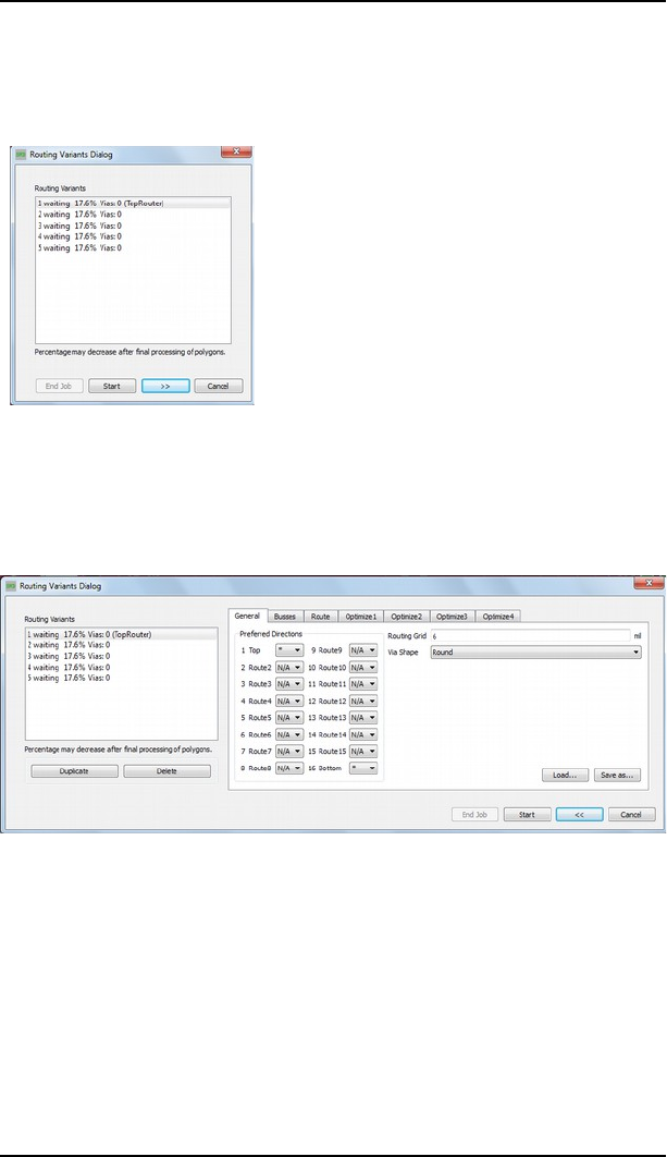
7 The Autorouter
Here you can modify the parameter set of each variant or delete or add
variants in the list. Each parameter set corresponds to the known Autorouter
parameter set from the previous versions of EAGLE.
The calculation of the individual routing variants (routing jobs) is started
from this dialog.
Depending on the settings EAGLE shows a number of routing options for the
board. Click the Start button and the Autorouter starts processing the routing
variants.
If you would like to check and maybe adjust the individual routing
parameters before, click the >> button.
In the advanced options dialog you can review and modify the routing
parameters. Click Duplicate or Delete, in order to copy or delete the selected
variant.
The parameters grouped in the sections Layer costs, Cost factors and
Maximum can be set individually for each pass (Busses, Route, Optimize 1-
4). For more information, see the following section.
You can insert additional optimization passes by clicking the Add button in
the last optimization run.
The Autorouter starts for all the signals that have not yet been laid out by
clicking on the OK button.
212
➢
Autorouter: List of Routing Variants
➢
Autorouter Variants: List and Parameter settings
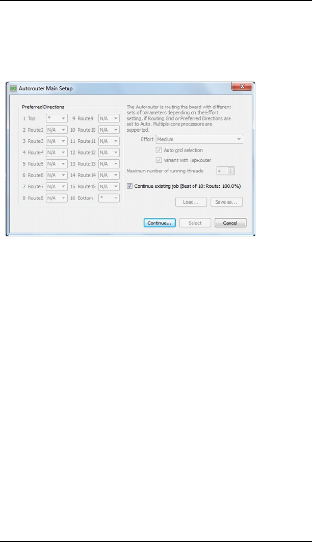
7.5 The Autorouter Menu
The Cancel menu button interrupts the AUTO command without storing any
changes.
You are not allowed to make any changes to the parameters, if you want to
restart an interrupted routing job. Use the Continue existing job check box to
decide whether you want to continue with an existing job, or whether you
want to choose new settings for the remaining unrouted signals.
➢
Autorouter Main Setup: Restarting an
interrupted job
The Autorouter's work can be undone by the UNDO command.
7.6 How the Cost Factors Influence the
Routing Process
Values between 0..99 are possible for each cost factor (cfxxx), but the full
range is not useful for all parameters. Sensible values are therefore given
with each parameter.
The control parameters (mnxxx) accept values in the range 0..9999.
Reasonable figures are also provided under each parameter.
The parameter can be set by the Autorouter Setup Menu. The settings for
Route and the Optimize passes can be configured separately. The menu is
split into three sections, Layer Costs, Costs, Maximum.
213

7 The Autorouter
➢
Autorouter: Parameter for Route
The following section shows the available parameters and their effects. The
names of the parameters are the same as they would be used in an
Autorouter control file *.ctl. Details about this can be found in Parameters of
a Control File beginning with page 221.
Layer Costs
cfBase.xx: 0..20
Base costs for one step on the corresponding layer. Recommendation:
outside layers (Top, Bottom) always 0, inside layers greater than 0.
Costs
cfVia: 0..99
Controls the use of vias. A low value produces many vias but also allows the
preferred direction to be followed. A high value tries to avoid vias and thus
violates the preferred direction. Recommendation: low value for the routing
pass, high value for the optimization.
cfNonPref: 0..10
Controls following of the preferred direction. A low value allows tracks to be
routed against the preferred direction, while a high value forces them into
the preferred direction.
If cfNonPref is set to 99, track sections can only be placed in the preferred
direction. Only select this value if you are certain that this behaviour is really
wanted.
cfChangeDir: 0..25
Controls how often the direction is changed. A low value means many bends
are allowed within a track. A high value produces virtually straight tracks.
214

7.6 How the Cost Factors Influence the Routing Process
cfOrthStep, cfDiagStep
Implements the rule that the hypotenuse of a right-angled triangle is shorter
than the sum of the other two sides. The default values are 2 and 3. That
means that the costs for the route using the two other sides are 2+2, as
against 3 for the hypotenuse. These parameters should be altered with great
care!
cfExtdStep: 0..30
Controls the avoidance of track sections which run at an angle of 45 degrees
to the preferred direction, and which would divide the board into two
sections. A low value means that such sections are allowed while a high value
tries to avoid them. In combination with the parameter mnExtdStep you can
control the length of these tracks. If mnExtdStep = 0, each grid step at 45
degrees to the preferred direction causes costs that are defined in parameter
cfExtdStep. Choosing for example mnExtdStep = 5 allows a track to run five
steps at 45 degrees without any additional costs. Each further step causes
costs defined in cfExtdStep.
In this way, 90 degree bends can be given 45 degree corners. Settings like
cfExtdStep = 99 and mnExtdStep = 0 should avoid tracks with 45 degree
angles.
This parameter is only relevant to layers which have a preferred direction.
Recommendation: use a lower value for the routing pass, and a higher value
for the optimization.
cfBonusStep, cfMalusStep: 1..3
Strengthens the differentiation between preferred (bonus) and bad (malus)
areas in the layout. With high values, the router differentiates strongly
between good and bad areas. When low values are used, the influence of this
factor is reduced. See also cfPadImpact, cfSmdImpact.
cfPadImpact, cfSmdImpact: 0..10
Pads and SMDs produce good and bad sections or areas around them in
which the Autorouter likes (or does not like) to place tracks. The good areas
are in the preferred direction (if defined), the bad ones perpendicular to it.
This means that tracks which run in the preferred direction are routed away
from the pad/SMD. With high values the track will run as far as possible in
the preferred direction, but if the value is low it may leave the preferred
direction quite soon.
It may be worth selecting a somewhat higher value for cfSmdImpact for
densely populated SMD boards.
cfBusImpact: 0..10
Controls whether the ideal line is followed for bus connections (see also
cfPadImpact). A high value ensures that the direct line between start and
end point is followed. Only important for bus routing.
215

7 The Autorouter
cfHugging: 0..5
Controls the hugging of parallel tracks. A high value allows for a strong
hugging (tracks are very close to each other), a low value allows for a more
generous distribution. Recommendation: higher value for routing, lower
value for the optimization.
cfAvoid 0..10
During the ripup, areas are avoided from which tracks were removed. A high
value means strong avoidance.
Not relevant to the optimization passes.
cfPolygon 0..30
If a polygon has been processed with the RATSNEST command and therefore
is displayed as a filled area before you start the Autorouter, every step within
the polygon is associated with this value. A low value makes it easier for the
Autorouter to route traces inside the polygon area. The probability, however,
that the polygon is broken into several pieces is higher. A higher value causes
the Autorouter to make fewer connections inside the polygon.
If a polygon is in outline mode and not processed by RATSNEST before you
start the Autorouter, it won't be taken into consideration at all. cfPolygon
does not play a role for such polygons.
Maximum
mnVia 0..30
Controls the maximum number of vias that can be used in creating a
connecting track.
mnSegments 0..9999
Determines the maximum number of wire pieces in one connecting track.
mnExtdSteps 0..9999
Specifies the number of steps that are allowed at 45 degrees to the preferred
direction without incurring the value of cfExtdStep.
See also cfExtdStep.
Additionally can be found the parameters mnRipupLevel, mnRipupSteps,
and mnRipupTotal. Those are described in the following section.
7.7 Number of Ripup/Retry Attempts
Due to the structure of the Autorouter there are some parameters which
influence the ripup/retry mechanism. They are set in such a way that they
offer a good compromise between time demand and routing result. The user
should therefore only carefully change the values for
mnRipupLevel, mnRipupSteps and mnRipupTotal when needed.
As a rule, high parameter values allow for many ripups but result in
increased computing times.
216

7.7 Number of Ripup/Retry Attempts
To understand the meaning of the parameters you need to know how the
router works.
To begin with the tracks are routed one after the other until no other path
can be found. As soon as this situation occurs, the router removes up to the
maximum number of already routed tracks (this number has been defined
with mnRipupLevel) to route the new track. If there are eight tracks in the
way, for example, it can only route the new track if mnRipupLevel is at least
eight.
After routing the new track, the router tries to reroute all the tracks which
were removed. It may happen that a new ripup sequence must be started to
reroute one of these tracks. The router is then two ripup sequences away
from the position at which, because of a track which could not be routed, it
started the whole process. Each of the removed tracks which cannot be
rerouted starts a new ripup sequence. The maximum number of such
sequences is defined with the mnRipupSteps parameter.
The parameter mnRipupTotal defines how many tracks can be removed
simultaneously. This value may be exceeded in certain cases.
If one of these values is exceeded, the router interrupts the ripup process and
re-establishes the status which was valid at the first track which could not be
routed. This track is considered as unroutable, and the router continues with
the next track.
7.8 Routing Multi-Layer Boards with
Polygons
It is possible to create supply layers with polygons that contain more than
one supply voltage, and individual wires as well. Please note the instructions
on page 178, Ground Planes and Supply Layers with Several Signals.
Define the polygons before running the Autorouter.
Give the appropriate signal names to the polygons.
Use the RATSNEST command to let EAGLE calculate the polygon.
Select the preferred directions and base costs (cfBase) for the layer in
the Autorouter setup. A higher value of cfBase for the polygon layer
causes the Autorouter to avoid these layers more strongly.
After routing, check that the polygon still connects all the signal
points. It is possible that the polygon was divided as a signal was laid.
RATSNEST recomputes polygons, and issues the message
Ratsnest: Nothing to do!, if everything is in order.
The Autorouter cannot set Micro vias!
The Autorouter is allowed to set Blind vias that are shorter than the
maximum depth defined in the Layer Setup.
217

7 The Autorouter
7.9 Backup and Interruption of Routing
As, with complex layouts, the routing process may take several hours, a
backup is carried out at intervals (approx. every 10 minutes). Depending on
the number of routing jobs, there is a corresponding number of job files. The
file name_xx.job always contains the last status of the jobs, where xx stands
for the number of the variant, always beginning with 00.
If the job is interrupted for any reason (power failure etc.) the computer time
invested so far is not lost, since you can recall the status saved in name.job.
Load your board file in the Layout Editor, and then enter:
+
Answer the prompt as to whether the Autorouter should recall (Continue
existing job?) with Yes. The Autorouter will then continue from the position
at which the job was last saved (a maximum of 10 minutes may be lost).
If the autorouting is interrupted via the stop icon, the files name_xx.job
remain intact and can be recalled. This may be useful when you have started
a complex job on a slow computer and want to continue with it on a fast
computer as soon as one is available.
Please note that changing the parameters before recalling will not influence
the job, since it will have been saved together with the parameters which
were valid at the time of the initial Autorouter start.
When the Autorouter has finished, the routed board is saved as name.b$$.
You can rename it to name.brd and use it, for instance, if a power failure
occurred after the autorouting run and you could not save the board file. This
file is deleted automatically after the board has been saved.
7.10 Information for the User
Status Display
During the routing, you are have the option to select different Variants from
the list and observe the routing progress.
The Autorouter displays information on the actual routing result of the
selected Routing variant in the status bar.
218
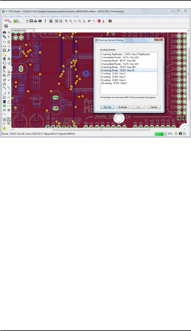
7.10 Information for the User
The displayed values have the following meaning:
Route:
Result in % (hitherto maximum, best data)
Vias:
Number of vias in the layout
Conn:
Number of Connections total/found/not routable
Connections here means 2-point connections.
Ripup:
Number of Ripups/current RipupLevel/cur. RipupTotal
Number of ripups:
This indicates the number of connections that have already been routed
during the foregoing routing procedure that have been (can be) removed in
order to be able to route new signals.
Current RipupLevel:
This indicates the number of connections that have been removed or
converted in airwires in order to lay the track for the current signal.
Current RipupTotal:
After a signal's routes have been ripped up it can be broken down into a
large number of two-point connections. These connections are then routed
again. This variable indicates the number of such two-point connections
still to be routed.
Signals:
219
➢
Autorouter: Status Bar
➢
Autorouter: Routing progress in the variants

7 The Autorouter
Signals found/handled/prepared,
if so followed by: (routing_time signalname)
In case the Autorouter needs more than about 5 seconds to lay-out a
connection, EAGLE shows in parenthesis the routing time and the name of
the currently processed signal.
Log file
For each routing pass the Autorouter generates a file called name.pro,
containing useful information. Example:
)&)&&G"G"
WK'!;'&"&"='H)$K
&&&-9$;1$-#@.;$0A$.000B
&->$-A$0#@.;$0A$.000B
!H"G00$11$;#
=!"#;)G=-0=!8";
G".1#H 0@0:="B
)&8--.-A>0
"")""")&+HG=F-+HG=F.+HG=F1+HG=F;
=HH""00$00$.-00$0#$;;00$0>$1.00$0>$-900$0>$0-00$09$99
)KV=H)H"01.0000
%$M!0-0000
%$&!01-0000
)&->.1#.1#.1#.1#.1#
:="011#-A#-;0-1;-.#
"!)G>$AY-00$0Y-00$0Y-00$0Y-00$0Y-00$0Y
E=!-00$0Y ="(
7.11 Evaluate the Results
If all routing variants are 'completed', you can select one of them and end up
with a job to complete the routing process. The selected variant is then saved
as a board file.
If you want to examine the individual routing results in more detail, select
one of the variants in the list and then click Evaluate.
You are now directly in the Layout Editor and can examine and even edit this
variant.
In the status bar of the Layout Editor there is displayed the Autorouter icon,
indicating that the routing process for the current board is not yet completed.
By clicking this icon, you obtain the following options:
Click Evaluate and you will return to Autorouter Variants dialog for
evaluating further routing results.
Click End Job and the current variant will be saved including all changes you
have made while evaluating this board. All the other routing variants and
their results will be discarded.
220
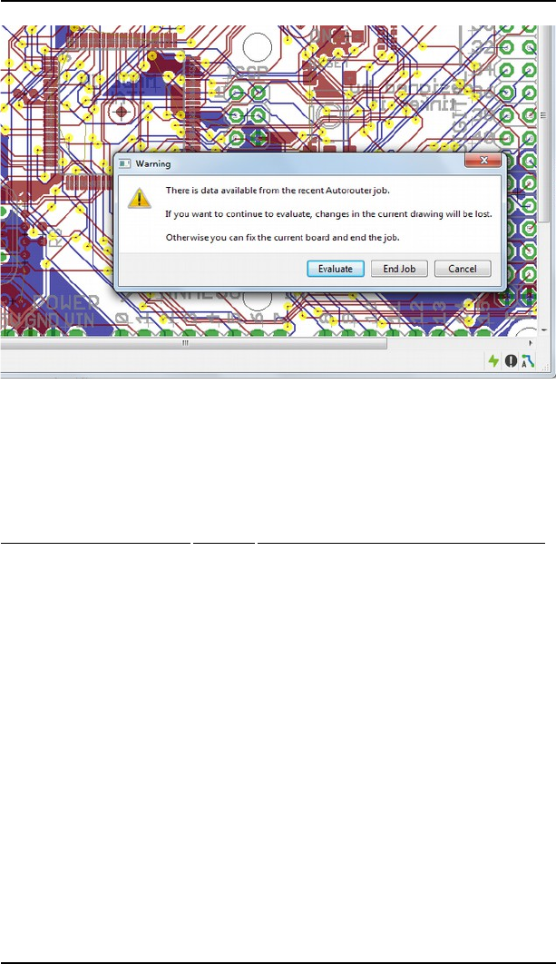
7.12 Parameters of a Control File
7.12 Parameters of a Control File
We see here how the individual parameters in an Autorouter control file
(name.ctl) are used.
Parameter Default Meaning
RoutingGrid = 50Mil Grid used by the Autorouter for tracks
and via-holes
Cost factors for...
cfVia = 8 Vias
cfNonPref = 5 Not using preferred direction
cfChangeDir = 2 Changing direction
cfOrthStep = 2 0 or 90 deg. Step
cfDiagStep = 3 45 or 135 deg. Step
cfExtdStep = 30 Deviation 45 deg. against preferred direction
cfBonusStep = 1 Step in bonus area
cfMalusStep = 1 Step in handicap area
cfPadImpact = 4 Pad influence on surrounding area
cfSmdImpact = 4 SMD influence on surrounding area
cfBusImpact = 4 Leaving ideal bus direction
cfHugging = 3 Wire hugging
cfAvoid = 4 Previously used areas during ripup
cfPolygon = 10 Avoiding polygons
cfBase.1 = 0 Basic costs for a step in the given layer
cfBase.2 = 1
...
cfBase.15 = 1
cfBase.16 = 0
Maximum number of...
mnVias = 20 Vias per connection
mnSegments = 9999 Wire segments per connection
mnExtdSteps = 9999 Steps 45 deg. against preferred direction
221
➢
Autorouter: Evaluating the routing results
7 The Autorouter
mnRipupLevel = 100 Ripups per connection
mnRipupSteps = 300 Ripup sequences per connection
mnRipupTotal = 200 Ripups at the same time
Track parameters for...
tpViaShape = Round Via shape (round or octagon)
PrefDir.1 = | Preferred direction in the given layer
PrefDir.2 = 0 Symbols: 0 - / | \ *
0 : Layer not used for routing
PrefDir.15 = 0 * : No preferred direction
PrefDir.16 = - - : X is preferred direction
| : Y is preferred direction
/ : 45 deg. is preferred direction
\ : 135 deg. is preferred direction
7.13 Practical Hints
This section presents you with some tips that have, over a period of time,
been found useful when working with the Autorouter.
Look on these examples as signposts suggesting ways in which a board can be
routed. None of these suggestions guarantee success.
General
The layer costs (cfLayer) should increase from the outer to the inner layers
or be the same for all layers. It is unfavourable to use lower values in the
inner layers than in the outer layers. This could increase the needed routing
memory enormously.
The Autorouter can't layout wires as arcs!
The Autorouter can't set micro vias!
Single-Sided Boards
There are two procedures, depending on the kind of layout:
In the simplest case, only layer 16, Bottom, is active. No preferred direction is
defined. Select a suitable grid and run the Autorouter.
If the layout is rather more complex, it may be possible to achieve a usable
result with special parameter settings. Please take a look at the project
named singlesided, which can be found in the eagle/projects/examples
directory. This example project comes with various control files (*.ctl), which
are optimized for singlesided routing.
The Autorouter may use the Top layer as well. The tracks laid there will be
realized as wire bridges on the board. In layer 41, tRestrict, you can define
restricted areas around the components and in regions where wire bridges
are not allowed.
Feel free to experiment with the parameter settings for your layout.
SMD Boards With Supply Layers
The following procedure has been found effective:
222

7.13 Practical Hints
The supply signals are routed first. In general, a short track is wanted from a
SMD component to a via that connects to the inner layer.
Before altering the parameters, save the current (default) values in an
Autorouter control file (CTL file). Click on the button Save as.. in the
General tab of the Autorouter setup window and input any name, for
example, standard.ctl.
Now switch off the bus router and all the optimization passes in the
Autorouter setup. Only the routing remains active. Alter the following cost
factors:
V:=0:="<!
:=-7%$M=HG
V"$-'->10$$OOE<&J"=H'X
&".$$#(&&J"
Start the Autorouter, using the Select button, and choose the signals to be
routed. After the routing pass it is possible, if appropriate, to optimize the
result manually.
The rest of the connections are routed after this. Use AUTO to open the
Autorouter setup menu, and load the previous stored control parameters
with the Load.. button (standard.ctl). Adjust the values to any special wishes
you may have, and start the Autorouter.
What can be done if not all signals are routed?
If this happens, check your settings.
Has a sufficiently fine routing grid been selected?
Have the track widths got appropriate dimensions?
Can the vias have smaller diameters?
Have the minimum clearances been optimally chosen?
If it is either impossible or unreasonable to optimize these values any further,
an attempt to achieve a higher level of routing may be made by increasing the
ripup level. Observe the notes in the section on the Number of Ripup/Retry
Attempts on page 216.
7.14 The Follow-me Router
To simplify the routing of airwires on the board, the ROUTE command offers
two follow-me operating modes that can route a selected signal
automatically. The position of the mouse cursor in the layout determines the
trace of the connection.
For this function your license must provide the Autorouter module.
Partial and Full Mode
To start the Follow-me router, activate the ROUTE command and select the
wire bend mode 8 or 9 from the parameter toolbar.
223
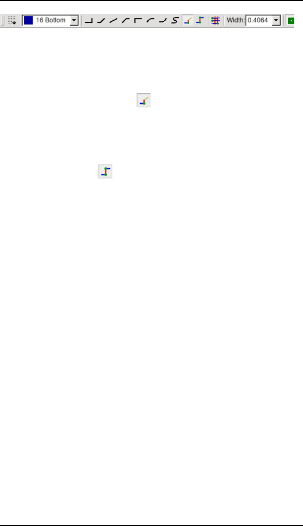
7 The Autorouter
After clicking onto an airwire, EAGLE calculates an appropriate trace and
displays the connection. Moveing the mouse cursor will change the current
trace. Trace processing depends on the complexity of the layout and may last
some moments. It is recommended not to move the mouse cursor until the
connection is displayed.
If you select wire bend mode 8 , the so-called partial mode, EAGLE
calculates the trace of the selected signal, beginning with the mouse cursor
position to the nearer end of the airwire, and display it. Fix the result with a
mouse click. The remaining part of the airwire will be calculated dynamically.
This means, that the airwire may point to another object that belongs to the
signal, depending on the current mouse cursor position.
With wire bend mode 9 , the full mode, the Follow-me router calculates
the trace in both directions simultaneously. A complete connection will be
estblished. As soon as you are clicking onto an airwire, EAGLE begins to
calculate the trace of the connection from the nearer end of the airwire to the
current mouse position. It is not mandatory that the farer end of the airwire
points always to its original position. Depending on the mouse cursor
position this end point may direct you to another (nearer) location.
If it is not possible to draw a connection from the current mouse cursor
position, the cursor turns into a small prohibition sign. Move the mouse and
try to find a possible way for the connection. Maybe it is sufficient to change
the layer at the current position. It could also be adviceable to adjust the
Design Rules. Please keep in mind that restricted areas in the layers
t/bRestrict or wires in the Dimension layer can hinder EAGLE to establish a
connection.
Configuration
The Follow-me router respects Design Rules settings:
Values for Clearance, Distance, and Size will be taken in consideration, as
well as particular values for net classes, if defined. Please be sure that the
Layer setup in the Layers tab is properly set.
The current grid setting in the Layout editor serves as routing grid. Use the
GRID command in order to change it. If there is already a signal assigned to
mouse cursor, drop it, and select it again. Otherwise the grid change does not
affect the connection.
The layer setting, which can be checked and changed in the parameter
toolbar of the ROUTE command, displays the layer which has to be used at
the mouse cursor position.
The Follow-me router reacts immediately on changes concerning wire width
or drill diameter of vias. If the option Auto set route width and drill in the
Options/Set/Misc menu is set, the Follow-me router adapts the given values
for wire width and via drill diameter from the Design Rules and from the net
classes as soon as an airwire is selected.
224
➢
Parameter toolbar of the ROUTE command
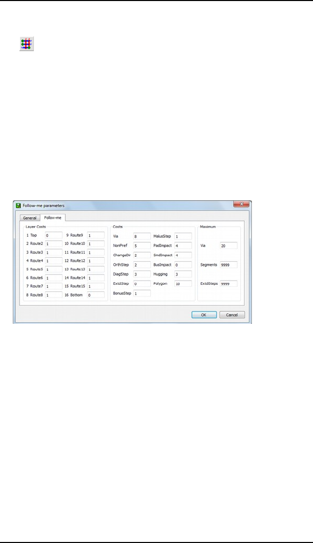
7.14 The Follow-me Router
Routing Parameters
Parameters that affect the routing strategy are set by clicking onto the AUTO
icon , which is available in the parameter toolbar after entering one of the
follow-me modes. Click this icon in order to open the known Autorouter
Setup window.
Alternatively you can open this setup window from the command line. Type:
+E++7
In the General tab you decide about preferred directions in the signal layers
(| vertical, - horizontal, / diagonal 45°, \ diagonal 135°, or * no preferred
direction). In many cases it makes sense for the Follow-me router to choose
no preferred direction in the signal layers.
Settings that influence the way how traces will be routed in the layout are
defined in the Follow-me tab.
The effects of these parameters are explained in section 7.6, beginning with
page 213.
In the Maximum section, you can define the number of Vias the router may
use for one connection. If this value is set to 0, the Follow-me router is not
allowed to set vias automatically. However, you are able to manually set a via
by changing the layer.
The value for Segments defines the maximum number of wire segments a
connection may consist of. If you choose it too small, it may happen that no
connection will be established.
Notes
The Follow-me router supports round and octagon via shapes only. Square
shaped vias are not possible.
If you are working in Full mode, the Follow-me router works in both
directions independently, beginning with the mouse cursor position. So it
could happen that the router places two vias very close to or even overlapping
225
➢
Follow-me router: Setting routing parameters
7 The Autorouter
each other near the current position of the mouse cursor. In this case move
the mouse cursor slightly, until the vias are optimized and the trace looks
good.
It's recommended to draw a Dimension line in layer 20 in order to limit the
board area and therefore required time and memory.
Depending on the complexity of your design, it may be wise to increase the
cost factor for Vias and decrease it for NonPref. This avoids frequent layer
changes.
7.15 BGA Routing
The BGA router is a special kind of Autorouter which is designed to route the
connections out of Ball Grid Array (BGA) with a minimal number of layers.
The BGA router allows to route selected or all signals and supports micro
vias, if enabled. It is started with the BGA icon or with AUTO BGA in the
command line. After BGA routing you can continue with manual or
automated routing.
Select the BGA components in the list in the left column. This list does not
contain all components of you board, but those that might have a BGA
package.
Once selected, the green dot indicates that this BGA will be routed as soon as
you click OK. If you double-click onto one of the entries in the right hand
column the marker turns orange. This indicates that the BGA is prepared for
routing (signals and layers selected), but won’t be routed now. The settings
will be saved, for example for a later BGA routing run.
226
➢
BGA router: Select BGA

7.15 BGA Routing
Clicking Edit BGA opens the Edit signals dialog. There you can choose the
signals that should be handled by the BGA router. By default the BGA router
handles all signals in all layers.
The dialog shows the list of signals connected to the BGA.
The column # lists the number of contacts of the BGA connected to this
signal. The Layers column informs about the layers the signal is allowed to
be routed in. ALL stands for all signal layers defined in the Layers Setup,
NONE excludes the signal from being routed.
Click Edit to enter layer selection of the selected signal(s). Here you can
decide about the target layer of a signal. Let’s assume the GND signal should
be connected with a GND polygon in inner layer 2. Then you would select the
target layer 2 for GND.
EAGLE can use “normal” vias and, if selected, supports Micro Vias.
Please verify the Design Rules in the area of the Ball Grid Array
components before starting BGA routing. Layer Setup, Clearance,
Net classes and Micro Via parameter must be set properly according
design specifications.
227

7 The Autorouter
This
page
has been
left free
intentionally.
228

Chapter 8
Component Design Explained
through Examples
When developing circuits with EAGLE, components are fetched from
libraries and placed into the schematic or, if the Schematic Editor is not
being used, into the layout. All the component information is then saved in
the schematic or board file. The libraries are no longer needed for continued
work with the data. So when you want to pass on your schematic to a third
party to have a layout made from it, you do not also have to supply the
libraries. An alteration in a library has no effect on a schematic or board.
The most important procedures for designing components (Devices) and
working with libraries are explained from page 79 on. Please read this
paragraph before you continue to read the current chapter!
Some practical examples follow, from which the effective application of the
relevant commands and parameters will be seen. First we will take the
example of a resistor and go through the whole process of designing a simple
component.
The second example provides a full description of the definition of a complex
component, including various Package variants and technologies. After that
we shall discuss the special features which have to be taken into account with
more complicated components.
Starting at page 288 hints concerning library and Device management can be
found. How to create my own library? How to copy elements from one library
into another?
First attempts at editing Packages, Symbols, or Devices may result in the
need to delete various library elements. To do this, use the REMOVE
command (see page 291).
8.1 Managed Libraries
The Managed libraries system allows libraries – and parts from those
libraries – to be uniquely identified within schematic and board files, even
across different users or computers. While previously schematic and board
files only retained the name of a library (which could be shared by multiple
libraries), with managed libraries the schematic and board files retain a
unique identifier for each library in addition to its name. Specifically, the
identifier is a URN assigned by our server when the managed library is
created, along with a number indicating the version of the managed library.
This URN and version allows EAGLE to unambiguously identify the managed
229

8 Component Design Explained through Examples
library from which the parts in a schematic or board came, which ensures
that the update process uses the correct library, even if there's more than one
library with a given name.
If you plan to work with 3D package references, you have to use Managed
Libraries.
The Managed Libraries that come with the EAGLE installation are not meant
to be edited by the EAGLE user. If you would like to edit, for example, a
Device from one of these libraries, you should copy it into your own library,
edit it and, if you want to add 3D packages, make it a My Managed Library.
How this works, is explained from page 233 on.
Migration to Managed Libraries
To tell whether a part in a schematic or board comes from an unmanaged or
a managed library, open the INFO/Properties dialog for that part. If the part
was from an unmanaged library, the Library field will be a simple name. For
parts from Managed libraries, the Library field will show the version and, if
you hover over the field, the URN of the Managed Library.
Of course, all existing Schematic and Board files use the old, name-based
library references. To migrate the parts in these designs to using Managed
Libraries references, you can update an existing schematic or board file using
a Managed Library with the same name as the library the parts originally
came from. This will add the URN of the Managed Library to those parts in
the Schematic or Board, allowing those parts to be unambiguously identified
going forward.
There's one catch, however. If a Schematic or Board contains parts from two
libraries with the same name – one managed and one un-managed – the
Managed Library can no longer be used to update the parts in the schematic
or board from the unmanaged library. That's because EAGLE sees those two
libraries as separate, even though they have the same name – so it will
update the parts in the Schematic or Board file that came from the Managed
Library (the closest match), not those that came from the unmanaged library.
230
➢
Properties Managed Library Part
8.1 Managed Libraries
Unfortunately, EAGLE does not yet support merging two different libraries
within a Schematic or Board file. If you do find yourself in this situation,
you'll need to individually replace the parts in the schematic or board file that
came from the unmanaged library with their equivalent parts from the
Managed Library (or vice-versa).
To avoid complications, update your designs with the managed
versions of your libraries before adding parts from them!
Library Manager
The library manager can be accessed through the menu Library/Manage
libraries... from one of the Editor windows.
The Library Manager window has two tabs: In Use and Available.
231
➢
Update Library Dialog

8 Component Design Explained through Examples
In Use shows a list of libraries currently in use for a design file and listed in
the ADD dialog.
Available shows libraries that are currently not in use, but can be included in
the list of libraries.
Columns in the libraries list:
Update / Download column
The first column is reserved for icons having to do with updating
or downloading web-based libraries.
Name The name of the library.
Author The author of the library.
Web A column with icon indicators for whether the library is web-based.
Description The headline description for the library.
There are several option in the dialog:
Remove The library is removed from the “in use” list and no longer
available for your projects.
Update In case there is a newer version of the library available, you can
start an update of the library. It will be downloaded from the
libraries server and made available in EAGLE.
Edit The library will be opened in the Library Editor.
Use Add the available library to the in use list.
Delete Delete this local library.
232
➢
The Manage Libraries dialog

8.1 Managed Libraries
Make Your Libraries Managed
In the Control Panel’s tree view in the Libraries branch you will notice the
Managed Libraries branch with a subfolder My Managed Libraries. This
folder is empty by default.
If you decide to use one of your self-made libraries, for example with 3D
packages, you have to make it a Managed Library. Right-click onto your
library in the Control Panel’s tree view and select Create managed library.
Now EAGLE connects to the Circuits website and stores this library there. It
will remain your private library. It is planned to offer an option to share your
library with others, for example with other design team members. By default
the library is stored locally on your computer and will appear now in the My
managed Libraries branch in the Control Panel.
233
➢
Create Managed Library
➢
Connected to the Web for Assigning 3D Packages

8 Component Design Explained through Examples
If you click View on Web you can start assigning 3D package references.
8.2 Definition of a Simple Resistor
First open a new library in the EAGLE Control Panel using the
File/New/Library menu.
Alternatively you can type the command
+
in the command line of the Schematic or Layout Editor windows. Then enter
a library name in the file dialog. The Library window opens.
Resistor Package
Define a New Package
Select the Package editing mode via the icon in the action toolbar, and
enter the Package name R-10 in the New field. Answer the question Create
new package 'R-10'? with Yes. Later when creating a new Symbol and a new
Device you will again have to answer the corresponding questions with Yes.
Set the Grid
Use the GRID command to set an appropriate grid size for the pad
placement. 0.05 inch (i.e. 50 mil) is usual for standard components with lead
wires.
234
➢
3D Package Assignment
8.2 Definition of a Simple Resistor
Solder Pads
For a resistor with lead-wires, select the PAD command, and set the pad
shape and the drill diameter in the parameter toolbar. The default value for
the pad diameter is auto (respectively 0). This value should be kept. The
actual diameter is specified by the Design Rules for the layout. Then place
two pads at the desired distance. The origin of the drawing will later be the
identifying point with which a component is selected. For this reason it
should be somewhere near the center of the Device.
You should not draw any objects in layer 17, Pads, or 18, Vias! They
will not be recognized, nor by the DRC, neither by polygons drawn in
the layout, and can lead to short circuits!
For a SMD resistor, select the SMD command, and set the pad
dimensions in the parameter toolbar. You can either select one of the offered
values, or directly type the length and breadth into the entry field.
All properties can be altered after placement using the CHANGE command
or by typing the command directly on the command line.
Select Top as the layer, even if the component will later be placed on the
underside of the board. SMD components are located on the other side of a
board using the MIRROR command. This moves the objects in all the t..-
layers into the corresponding b..-layers.
Place the two SMD pads (which in EAGLE are just called SMDs) at the
desired distance. It may be necessary first of all to alter the grid setting to a
suitable value. The SMD can be rotated with the right mouse button before it
is placed.
The parameter Roundness specifies whether the corners of the SMDs are to
be rounded. By default this value is set to 0 % (no rounding). This value is
usually kept, since the final roundness of SMDs is specified in the Design
Rules. The help system provides you with more information about this
parameter.
Angle determines the rotation of the SMD pad.
The INFO command or the Properties entry of the context menu
provides you with a quick summary of the current properties of a
SMD or Pad.
235
➢
SMD command: Parameter toolbar

8 Component Design Explained through Examples
Pad Name
You can now enter the names, such as 1 and 2, for the pads or SMDs
using the NAME command.
Silkscreen and Documentation Print
Now use the commands LINE, ARC, CIRCLE, RECT,
and POLYGON to draw the silkscreen Symbol in layer 21, tPlace. This layer
contains what will be printed on the board. It is up to you how much detail
you give to the Symbol. Set a finer grid size if it helps.
Take the information provided in library.txt as a guideline for the design of
components. The line thickness for the silk screen is usually 0.008 inch
(0.2032 mm), for smaller components 0.004 inch (0.1016 mm).
Layer 51, tDocu, is not used to print onto the board itself, but is a supplement
to the graphical presentation which might be used for printed
documentation. Care must be taken in layer 21, tPlace, not to cover any areas
that are to be soldered. A more realistic appearance can be given, however, in
the tDocu layer, which is not subject to this limitation. In the example of the
resistor, the Symbol can be drawn in layer 21, tPlace, but the wires, which go
over the pads, are drawn in layer 51, tDocu.
Labeling
With the TEXT command you place the texts >NAME (in layer 25,
tNames) and >VALUE (in layer 27, tValues) in those places where in the
board the actual name and the actual value are to appear. 0.07 inch for the
text height (size) and 10 % for the ratio (relationship of stroke width to text
height, which can only be set, using CHANGE, for vector fonts) are
recommended.
We recommend to write these texts in vector font. So you can be sure
that it looks exactly the same on the printed circuit board and in the
Layout Editor.
SMASH and MOVE can be used later to change the position of this text
relative to the package symbol on the board.
In the case of ICs, for instance, the value corresponds to what will later be the
Device name (e.g. 74LS00).
When working with the Layout Editor only, the value is specified in
the board.
236
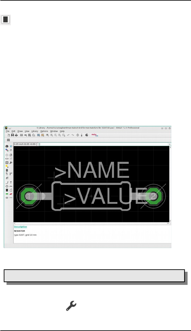
8.2 Definition of a Simple Resistor
Restricted area for components
In layer 39, tKeepout, you should create a restricted area over the whole
component (RECT command). This allows the DRC to check whether
components on your board are too close or even overlapping.
Description
Finally, you click on the Description box. Text can then be entered in the
lower part of the window which then opens. HTML text can be used, which
permits formatting of the text. You will find detailed information in the help
system under HTML Text.
Example:
QK?-0Q'K?
QH?
"="&-0=$
Keywords from this text can be searched for from the ADD dialog in the
layout.
➢
The Package Editor
Do not forget to save the library from time to time!
Note
The CHANGE command can be used at a later stage to alter object
properties such as the stroke thickness, text height, pad shape, or the layer in
which the object is located.
237

8 Component Design Explained through Examples
If you want to change the properties of several objects at one go, define a
group with the GROUP command , click the CHANGE command, select
the parameter and the value, and click on the drawing surface with the right
mouse button while the Ctrl key is pressed.
Example:
Use GROUP to define a group that contains both pads, then select CHANGE
and Shape/Square. Press the Ctrl key, and click on the drawing surface with
the right mouse button. The shape of both pads changes.
Resistor Symbol
Define a New Symbol
Select the Symbol editing mode, and enter the Symbol name R in the
New field. This name only has a meaning internal to the program, and does
not appear in the schematic.
Set the Grid
Now check that 0.1 inch is set as the grid size. The pins in the Symbol
must be placed on this grid, since this is what EAGLE expects.
Place the Pins
Select the PIN command. You can now set the properties of these pins in
the parameter toolbar, before placing them with the left mouse button. All
these properties can be changed at a later stage with the CHANGE command.
Groups can again be defined (GROUP) whose properties can then be altered
with CHANGE and the right mouse button. See also page 237.
➢
Pin command: Parameter toolbar (split into two lines)
Orientation
Set the direction of the pins (Orientation parameter) using the four left-hand
icons in the parameter toolbar or, more conveniently, by rotating with the
right mouse button.
Function
The function parameter is set with the next four icons on the parameter
toolbar. This specifies whether the Symbol is to be shown with an inversion
circle (Dot), with a clock symbol (Clk), with both (DotClk) or simply as a
stroke (None). The diagram illustrates the four representations on one
Package.
238
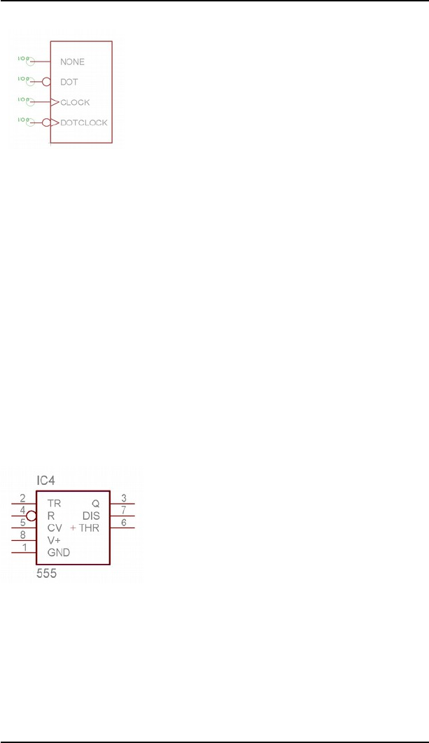
8.2 Definition of a Simple Resistor
➢
Pin functions
Length
The next four icons on the parameter toolbar permit setting of the pin length
(0, 0.1 inch, 0.2 inch, 0.3 inch). The 0 setting is used if no pin-line is to be
visible, or if, as in the resistor Symbol, a pin shorter than 0.1 inch is desired.
In that case the pin is to be drawn with the LINE command as a line in layer
94, Symbols.
The SHOW command can be used to check whether a net is connected to a
pin in the schematic diagram. The pin line and the net are displayed more
brightly if they are connected. If a pin with length 0 is used, or if it was drawn
as a line with the LINE command, it cannot be displayed brightly.
Visible
The next four icons in the parameter toolbar specify whether the pins are to
be labeled with pin names, pad names, both or neither. The diagram
illustrates an example in which pin names are shown inside and pad-names
outside. The location of the label relative to the pin is fixed. The text height is
also fixed (at 60 mil).
➢
Pin labeling
If you plan for your device to connect one pin with several pads and you
choose the Visible option Both, then there will be only one of the pad names
visible in the schematic (the pad with the lowest number). The pad name will
be followed by an asterisk (*) in order to mark the multi-pad connection.
Direction
The Direction parameter specifies the logical direction of the signal flow:
239

8 Component Design Explained through Examples
NC Not connected
In Input
Out Output
IO Input/output
OC Open Collector or Open Drain
Hiz High impedance output
Pas Passive (resistors, etc.)
Pwr Power pin (power supply input)
Sup Power supply output for ground and supply symbols
The Electrical Rule Check executes, depending on the pin direction, various
checks. It expects for the direction
NC a not connected pin
In a net connected to this pin and not only In pins
connected to this net
Out not only Out pins connected to the net, no Sup or OC
pin at the same net
OC no Out pin at the same net
Pwr a Sup pin set for this net
IO, Hiz, Pas no special checks
The Pwr and Sup directions are used for the automatic connection of supply
voltages (see page 269).
Swaplevel
Swaplevel set to 0 means that the pin cannot be exchanged for another pin in
the same Gate. Any number bigger than 0 means that pins can be exchanged
for other pins which have the same Swaplevel and are defined within the
same Symbol. The pins can be swapped in the schematic or in the board with
the PINSWAP command.
The two pins of a resistor can have the same Swaplevel (e.g. 1), since they are
interchangeable.
If the layer 93, Pins, is being displayed, the connection points on nets are
shown with green circles. The Direction and Swaplevel parameters moreover
(here Pas and 1) are displayed in this layer.
The connections of a diode, for instance, cannot be exchanged, and
are therefore given Swaplevel 0.
Pin Names
The NAME command allows you to name pins after they have been placed.
The automatic name allocation, as described on page 99 also operates.
Schematic Symbol
The schematic Symbol is drawn in the Symbols layer using LINE and the
other drawing commands. Place the texts >NAME and >VALUE in layers 95,
Names, and 96, Values (TEXT command). Place them where the name and
value of the component are to appear in the schematic.
240
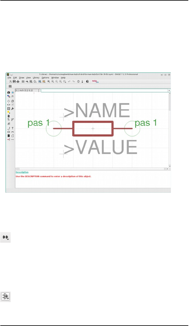
8.2 Definition of a Simple Resistor
Precise placement of the text can be achieved by setting the grid finer, which
can even be done while the TEXT command is active. Afterwards, however,
set the again grid to 0.1 inches.
Layer 97, Info, may be used for additional information and hints.
Description
Click onto the Description link in order to provide a descriptive text for the
symbol. You are allowed to use HTML tags for formatted text. More info
about this can be found in the help function, HTML text.
➢
The Symbol Editor
Resistor Device
Define a New Device
Create the new Device R-10 with this icon. When you later use the ADD
command to fetch the component into the schematic, you will select it by
using this name. It is only a coincidence that in this case the name of the
Package and the name of the Device are the same.
So enter the name R on the New line. The Device Editor opens after the
confirming question Create new device 'R'?.
Selecting, Naming and Configuring Symbols
The previously defined resistor Symbol is fetched into the Device with
the ADD command.
If a Device consists of several schematic Symbols which can be placed
independently of one another in the circuit (in EAGLE these are known as
241
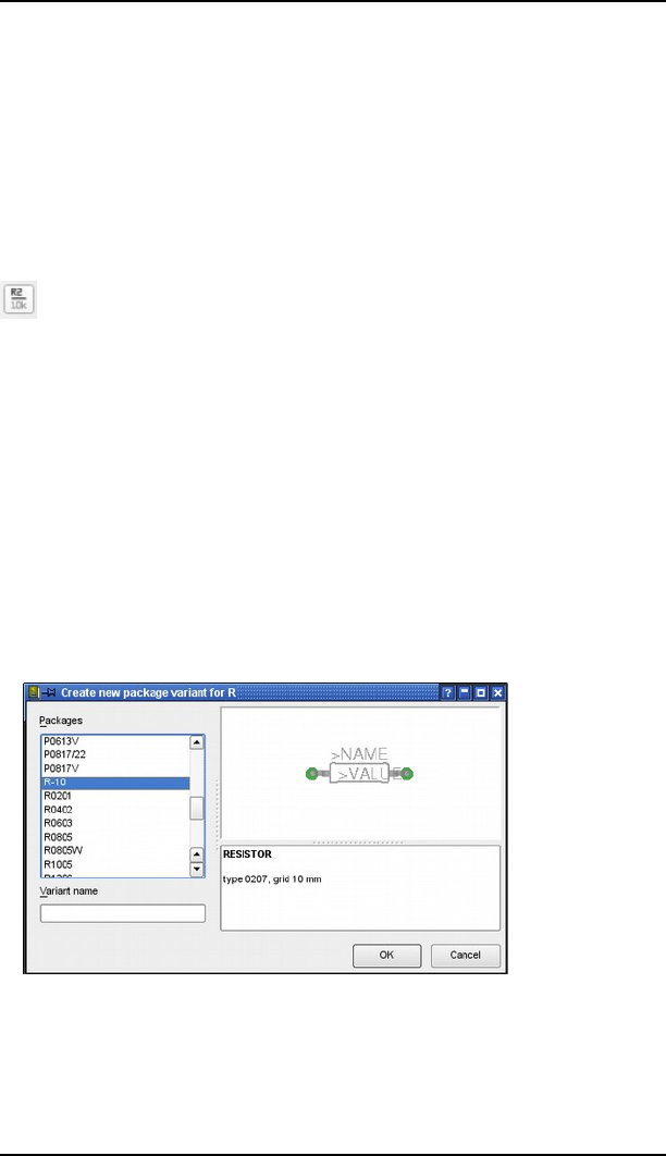
8 Component Design Explained through Examples
Gates), then each Gate is to be individually brought into the schematic with
the ADD command.
Set an Addlevel of Next and a Swaplevel of 0 in the parameter toolbar, and
then place the Gate near the origin. There are further explanations about
Addlevel from page 275 on.
The Swaplevel of a Gate behaves very much like the Swaplevel of a pin. The
value of 0 means that the Gate cannot be exchanged for another Gate in the
Device. A value greater than 0 means that the Gate can be swapped within
the schematic for another Gate in the same Device and having the same
Swaplevel. The command required for this is GATESWAP.
Only one Gate exists in this example; the Swaplevel remains 0.
You can change the name of the Gate or Gates with the NAME
command. The name is unimportant for a Device with only one Gate, since it
does not appear in the schematic.
Keep the automatically generated name!
In the case of Devices with several Gates, the name of the particular Gate is
added to the name of the Device.
Example:
The Gates are called A, B, C and D, and the name of the component in the
schematic is IC1, so the names which appear are IC1A, IC1B, IC1C and IC1D.
Selecting the Package
Now click on the New button at the lower right of the Device Editor window.
Choose the R-10 Package from the selection window, and enter a name for
the version. If only one Package version is used, it is usual to use two single
quote marks ('') for the name of the Package version. It is, however, quite
possible to assign a particular name.
Connections Between Pins and Pads
With the CONNECT command you specify which pins are taken to which
package pads.
242
➢
The Package selection

8.2 Definition of a Simple Resistor
The resistor gate in this example is automatically identified as G$1, for which
reason the pins G$1.1 and G$1.2 of this gate appear in the Pin column.
The two connections of the housing are listed in the Pad column. Mark a pin
and the associated pad, and click on Connect.
If you want to undo a connection that you have made, mark it in the
Connection column and click Disconnect.
Clicking on a column's header bar changes the sorting sequence.
Finish the CONNECT command by clicking on OK.
Define Prefix
The PREFIX command is used to specify a prefix for a name. The name itself
will initially be automatically allocated in the schematic. For a resistor this
would, naturally enough, be R. The resistors will then be identified as R1, R2,
R3 etc..
The names can be altered at any time with the NAME command
Value
On: You are allowed to change the value in the schematic (for example
for resistors). Without a value the part will not be specified exactly.
Off: The value will be generated from the Device name and includes
technology and Package variant (e. g. 74LS00N), if available.
Also recommended for supply symbols.
243
➢
The CONNECT window
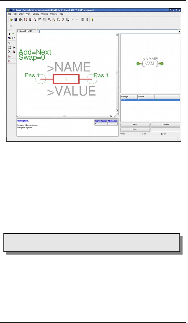
8 Component Design Explained through Examples
➢
The Device Editor: Fully defined resistor
Description
Click on Description in the description box. You can enter a description of
the component here. The search facility of the ADD command in the
schematic diagram will search through this text.
You can use HTML Text, as in the Package description. You will find notes
about this in the help system under the keyword HTML Text.
It can look like this:
QK?-0Q'K?
QH?
"="&-0HJ
Hyperlinks contained in the description of library objects are opened
with the appropriate application program.
Save
This completes definition of the resistor, and it can be fetched into the
schematic diagram. If you have not already saved the library, please do it at
this stage!
244

8.2 Definition of a Simple Resistor
Library Description
Not only Packages and Devices can have descriptions, but the Library as a
whole can have one as well. This description is shown in the Control Panel as
soon as you expand the Libraries branch of the Tree view and select a library
entry there.
No matter which editor mode (Symbol, Package, Device) is currently active,
click the Library/Description menu to edit the description. You can use
HTML text, if you like.
Use Library
The newly created library has to be made available for the schematic or
layout with the help of the USE command. This command has to be used in
the Schematic or Layout Editor. It is also possible to mark a library as in Use
in the Control Panel's tree view. See help for details.
Now the library will be recognized by the ADD command and its search
function.
8.3 Defining a Complex Device
In this section we use the example of a TTL chip (541032) to define a library
element that is to be used in two different Packages (pin-leaded and SMD). It
is a quad OR gate. The schematic diagram symbol is to be defined in such a
way that the individual OR gates can be placed one after another. The power
supply pins are not initially visible in the schematic diagram, but can be
fetched into the diagram if needed.
The definition proceeds in the following steps:
Creating a new library
Drawing the pin-leaded housing (DIL-14)
Creating the SMD housing (LCC-20)
Defining the logic symbol
Creating the power supply symbol
Associating the Packages and Symbols to form a Device set
245
8 Component Design Explained through Examples
All the data for this component has been extracted from a data
book published by Texas Instruments, whom we thank for
permission to reproduce it.
246
➢
Data sheet for the 541032
8.3 Defining a Complex Device
Creating a New Library
Click on the File/New/Library menu in the EAGLE Control Panel. The
Library Editor window appears, containing a new library, untitled.lbr.
It is, of course, also possible to expand an existing library. In that case you
would use File/Open/Library to select the library you want, or you would
click on the Libraries entry in the Control Panel's tree view, selecting the
desired library with a click of the right mouse button. This will open a context
menu, one of whose options is Open. The Library Editor is opened.
Drawing the Pin-Leaded Package
The component is manufactured in a pin-leaded Package. This is a DIL-14
housing with a pin spacing of 2.54 mm (0.1 inch) and a width of 7.62 mm
(0.3 inch).
If there is a suitable Package in another library, it can be copied into the
current library. A new definition would not be necessary.
Click onto the Edit a package icon in the action toolbar, and enter the
name of the Package in the New box of the Edit menu, which is DIL-14 in our
present example. Click OK, and confirm the question Create new package
'DIL-14'? by answering Yes.
The Package Editor window now opens.
247
➢
DIL-14 data sheet
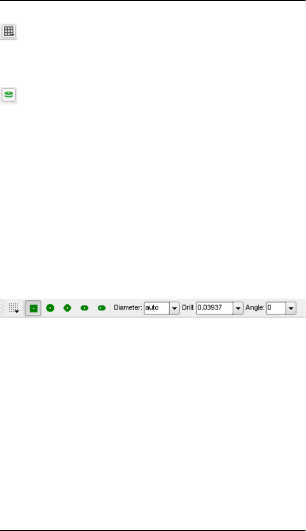
8 Component Design Explained through Examples
Set the Grid
First set the appropriate grid (50 mil in this case) using the GRID
command, and let the grid lines be visible.
The grid can easily be shown and hidden with the F6 function key.
Place Pads
Use the PAD command, and place the solder pads in accordance with
the specifications on the data sheet. The pads should be arranged in such a
way that the coordinate origin is located somewhere near the center of the
Package.
Each pad can have individual properties such as Shape, Diameter, and Drill
hole diameter. Available shapes are: Square, Round, Octagon, Long, and
Offset (Long with offset drill).
Select the desired pad shape and specify the hole diameter.
The pad diameter usually is defined with the standard value auto
(respectively 0), since the size is finally determined in the layout by means of
the Design Rules, Restring tab. The pad appears in the library with the
default value of 55 mil.
You may, however, assign an individual value. If, for instance, you specify 70
mil, the consequence is that the diameter of the pad on the board cannot be
less than 70 mil (independent of the calculated value of the Design Rules).
You select this value when the PAD command is active (i.e. the pad is
attached to the mouse cursor) using the parameter toolbar. It is also possible
to specify the drill hole diameter and the pad shape.
The properties of pads that have already been placed can be altered at a later
stage by means of the CHANGE command. Click onto the CHANGE icon and
select the property and the appropriate value. Then click onto the pads whose
properties are to be altered. CHANGE can also be applied to groups (using
the GROUP command). After the property has been selected, click inside the
group with the right mouse button.
As soon as a pad has been placed, EAGLE automatically generates solder stop
symbols in layers 29 and 30, t/bStop. The dimensions of the solder stop
symbols is specified in the Design Rules, Mask tab, Stop parameter.
Pads can be marked with special flags (First, Stop, Thermals). They can be
altered with CHANGE subsequently. Giving one pad of a Package the First
flag (CHANGE FIRST ON) allows to define a special shape for it in the
Design Rules, Shapes tab, option First, in order to mark it as the number '1'
pad of the Package.
Setting the Thermals flag off prevents generating a Thermal symbol in a
copper area.
CHANGE STOP OFF prevents automatic solder stop mask generation for a
pad.
248
➢
The parameter toolbar when the PAD command is active
8.3 Defining a Complex Device
Pad Name
EAGLE automatically assigns pad names, P$1, P$2, P$3 etc., as
placement proceeds. Assign the names in accordance with the information in
the data book.
The names can be checked easily by clicking the Options/Set/Misc menu and
choosing the Display pad names option. All pad names are displayed after
refreshing the screen (F2).
Alternatively type in the command line:
5+
To hide the pad names again:
5+EE
The following procedure is recommended for components that have a large
number of sequentially numbered pads:
Select the PAD command, type in the name of the first pad, e.g. '1', and place
the pads in sequence. The single quote marks must be typed on the command
line. See also the section on Names and Automatic Naming on page 99.
Draw the Silk Screen Symbol
A simple silk screen symbol that is to be visible on
the board is drawn in layer 21, tPlace. Use the commands LINE, ARC,
CIRCLE, RECT, and POLYGON.
Ensure that it does not cover soldered areas, since this can cause problems
when the boards come to be soldered. If necessary, use the GRID command
to set a finer grid or use the Alt key for the alternative grid (see GRID
command). The standard width (CHANGE WIDTH) for lines in the screen
print is 8 mil or 4 mil, depending on the size of the component.
It is also possible to create an additional and rather better-looking silk screen
for documentation purposes in layer 51, tDocu. This may indeed cover
soldered areas, since it is not output along with the manufacturing data.
Package Name and Package Value
The labelling now follows. Use the TEXT command and write
?7
in layer 25, tNames, for the name placeholder, and
?:
in layer 27, tValues, as the placeholder for the value, and place this at a
suitable location. We use proportional font with a text height of 70 mil as
default.
If you want to have texts upside down by a Package rotation of 180°, you
have to use the Spin flag (see help function for TEXT command).
The texts can be relocated at a later stage using SMASH and MOVE.
249
8 Component Design Explained through Examples
We recommend to write these texts in vector font. So you can be sure
that it looks exactly the same on the printed board as it is in the
Layout Editor.
Areas Forbidden to Components
In layer 39, tKeepout, you should create a restricted area over the
whole component using the RECT command or draw a frame around the
Package with LINE. This allows the DRC to check whether components on
your board are too close or even overlapping.
Description
Click on Description in the description box. A window opens in whose lower
part it is possible to enter text, while the formatted appearance of the
description is displayed in the upper part (Headline). The text can be entered
in HTML format. EAGLE works with a subset of HTML tags that allow the
text to be formatted. You will find detailed information in the help system
under HTML Text.
The descriptive text for our DIL-14 might look like this:
QK?5-;Q'K?
QH?
-;=5)!!=!"GJ3&=&(100=!
It is also possible to add, for instance, the reference data book,
the e-mail address of the source or other information here. The search facility
in the Layout Editor's ADD dialog also looks in this text for keywords.
Hyperlinks contained in the description of library objects are opened
with the appropriate application program.
250
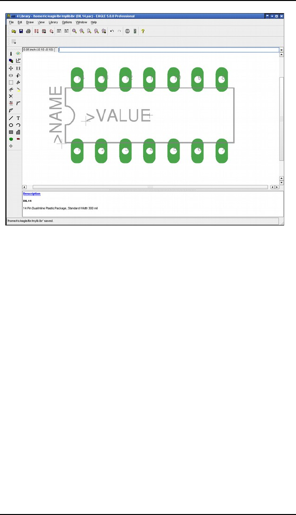
8.3 Defining a Complex Device
➢
Package Editor with DIL-14
Save
At this stage if not before the library should be saved under its own name
(e.g. my_lib.lbr).
Defining the SMD Package
The second type of housing for this component may be seen in the following
scale drawing.
251

8 Component Design Explained through Examples
The size of the soldering areas is to be 0.8 mm x 2.0 mm. The SMD 1, at 0.8
mm x 3.4 mm, is larger.
Click again onto the Edit a package icon, and enter the name of the
Package in the New box in the edit menu. The Package is to be called LCC-
20. Click OK and confirm the question Create new package 'LCC-20'? by
answering Yes.
Set the Grid
Adjust the grid to 0.635 mm (0.025 inch), and let the grid lines be
visible. It is useful to define an alternative grid of 0.05 mm for designing this
Package.
252
➢
SMD package, FK version
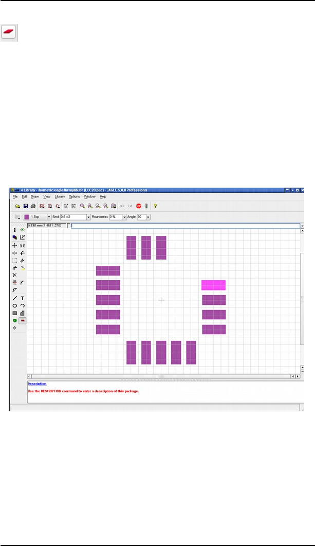
8.3 Defining a Complex Device
Placing SMD Solder Pads
SMD devices are generally defined on the top of the board; SMDs are
therefore always in layer 1, Top.
If you do want to have components on the solder side, the item is if needed
reflected on the board with the MIRROR command. See also the section on
page 281.
Begin by placing 5 SMDs at a distance of 1,27 mm from each other in two
horizontal rows close to the coordinate origin. Since the value 0.8 x 2.0 is not
contained in the SMD menu, this must be entered as 0.8 2.0, either on the
command line or in the SMD box on the parameter toolbar.
Click therefore onto the SMD icon, and type
0$#.←
in the command line. Create two vertical rows as well. The SMDs can be
rotated in 90 degree increments with the right mouse button.
The Roundness parameter (CHANGE command) specifies whether curves
should be given to the corners of the solder pads. The default value is 0 %,
which means that there is no rounding.
See also the section on page 150.
If a square SMD is selected, and if Roundness is defined as 100 %, the result
is a round SMD, as is needed when creating ball grid array housings (BGA).
Roundness is usually chosen to be 0 % when a Package is being defined. A
general value can be specified in the Design Rules if slightly rounded solder
pads are preferred.
253
➢
Placing the SMDs

8 Component Design Explained through Examples
Drag the 4 SMD rows into the correct position. Therefore use the finer
alternative grid of 0.05 mm by pressing the Alt key. The commands GROUP
and MOVE, followed by a right mouse click on the marked group while the
Ctrl key is pressed can be used to drag the marked group into the correct
position. The size of the central SMDs in the upper row can be altered with
the CHANGE SMD command. Since the value 0.8 x 3.4 is not contained in
the menu as standard, type
("0$#1$;←
onto the command line, then click the SMD. Drag it with MOVE so that it is
located at the correct position.
The INFO command is first choice for checking the positions and properties
of the solder pads and modifying them, if needed.
When a SMD is placed (in the Top layer), symbols for solder stop and solder
cream are automatically created in layer 29, tStop, and layer 31, tCream,
respectively.
If the component in the layout is mirrored onto the bottom side, these are
changed to the layers with the corresponding functions, namely 30, bStop
and 32, bCream.
SMDs can have special flags (Stop, Cream, Thermals) that can be modified
with the CHANGE command.
Setting the Thermals flag off avoids a Thermal symbol for the SMD copper
areas.
CHANGE STOP OFF or CHANGE CREAM OFF prevents EAGLE from
generating a solder stop mask or a cream frame for the SMD automatically.
See also help function about CHANGE and SMD.
SMD Names
If no names are visible in the SMD pads, click the Options/Set/Misc menu
and activate the Display pad names option.
Alternatively you can type the following onto the command line:
"&H"←
Use the NAME command to adjust the names to match the
specifications of the data sheet.
It is alternatively possible to assign names as the SMDs are being placed, if
the component has a large number of pads with sequential numbers. Select
the SMD command, type in the name of the first SMD, e.g. '1', and place the
pads in the correct sequence. The single quote marks must be entered on the
command line.
See also the section on Names and Automatic Naming on page 99.
You can also combine several statements on the command line, for example:
"0$#.C-C←
A SMD of 0.8 mm x 2.0 mm named 1 is now attached to the mouse cursor.
254
8.3 Defining a Complex Device
Draw the Silk Screen
First set the grid to a suitable value such as 0.254 mm (10 mil).
Draw the silk screen print in layer 21, tPlace.
Note that the silk screen print must not cover soldered areas, as this
will cause problems when the board comes to be soldered.
The default value for the line width is 8 mil (0.2032 mm), for smaller
components 4 mil (0.1016 mm).
It is also possible to create an additional, more detailed, silk screen for
documentation purposes in layer 51, tdocu. This may indeed cover soldered
areas, since it is not output along with the manufacturing data.
Package Name and Package Value
The labeling now follows. Use the TEXT command and write
?7
in layer 25, tNames, for the name placeholder, and
?:
in layer 27, tValues, as the placeholder for the value, and place this at a
suitable location. The texts can be separated and relocated at a later stage
using SMASH and MOVE.
We recommend to write these texts in vector font. So you can be sure
that it looks exactly the same on the printed board as it is in the
Layout Editor.
Area Forbidden to Components
In layer 39, tKeepout, you should create a forbidden area over the
whole component (RECT command) or draw a frame around the Package
with the LINE command. This allows the DRC to check whether components
on your board are too close, or even overlapping.
Locating Point (Origin)
As soon as you have finished drawing the package, please check where the
coordinate origin is located. It should be somewhere near the middle of the
Package. If necessary, use GRID to choose a suitable grid (e.g. 0.635 mm),
and shift the whole Package with GROUP and MOVE.
First make sure that all the layers are made visible (DISPLAY ALL). That is
the only way to be sure that all the objects have indeed been moved.
255
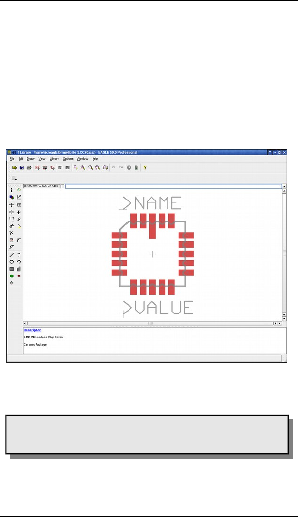
8 Component Design Explained through Examples
Description
Then click on Description in the description box. You can insert a detailed
description of this Package form here. HTML Text can be used. This format
is described in the program's help system under HTML Text .
The entry of the LCC-20 in HTML text format could look like this:
QK?.0Q'K?
QH?
E4=(=H=HJV%"
"&)&"$
The ADD dialog in the Layout Editor can search for this description or for
keywords within it.
Save
Please do not forget to save the library from time to time!
Supposed you found a Package that is exactly the one you need in
another library file, simply copy it into your current library. More
information about this on page 288.
256
➢
The fully defined LCC-20
8.3 Defining a Complex Device
Defining the Logic Symbol for the Schematic
Diagram
Our Device contains four OR gates, each having two inputs and one output.
We first create an OR symbol.
Click onto the Edit a symbol icon. Enter a name for the Symbol on the
New line, such as 2-input_positive_or, and click OK. Confirm the question
Create new symbol '2-input_positive_or'? by answering Yes. You now have
the Symbol Editor window in front of you.
Check the Grid
Check that the grid is set to the default value of 0.1 inch. Please try to
use only this grid, at least when placing the pins.
It is essential that pins and net lines are located on the same grid.
Otherwise there will not be any electrical connection between the net
and the pin!
Place the Pins
Select the PIN command, and place 3 pins. The pin properties can be
changed by means of the parameter toolbar as long as the pin is attached to
the mouse cursor and has not been placed. If a pin has already been placed,
its properties can be altered at a later stage with the CHANGE command. A
number of pins can be handled at the same time with the GROUP and
CHANGE commands followed by a click into the drawing with the right
mouse button while the Ctrl key is pressed. The parameters Orientation,
Function, Length, Visible, Direction and Swaplevel have been thoroughly
described when the example of the resistor symbol was examined (see p.
238).
257
➢
Logical appearance of the 541032
8 Component Design Explained through Examples
The coordinate origin should be somewhere near the center of the Symbol,
and, if possible, not directly under a pin connection point. This makes it easy
to select objects in the schematic diagram.
Pin Name
You assign pin names with the NAME command. In our Symbol the two
input pins are named A and B, and the output pin is named Y.
Pins carrying inverted signals (active low) can be displayed with a bar over
the name text. An exclamation mark starts and ends the bar.
!bar_above_text!-normal results in bar_above_text-normal
Further examples can be found in the help function of the TEXT command.
Draw the Symbol
Use the LINE command to draw the Symbol in layer 94, Symbols. The
standard line thickness for the Symbol Editor is 10 mil. You may also choose
any other line thickness.
Placeholders for NAME and VALUE
For the component labeling, use the TEXT command in the schematic
diagram to write
?7
in layer 95, Names and
?:
in layer 96, Values. Place the two texts at a suitable location. It is possible to
move the texts again in the schematic diagram after using SMASH to
separate it. The Symbol should now have the appearance shown in the
following diagram.
Description
Click onto the Description link in order to provide a descriptive text for the
symbol. You are allowed to use HTML tags for formatted text. More info
about this can be found in the help function, HTML text.
Save
This is a good moment to save the work that you have done so far.
Supposed you found a Symbol that is exactly the one you need use
GROUP, COPY, and PASTE to copy it into the current library. See
also page 290.
258
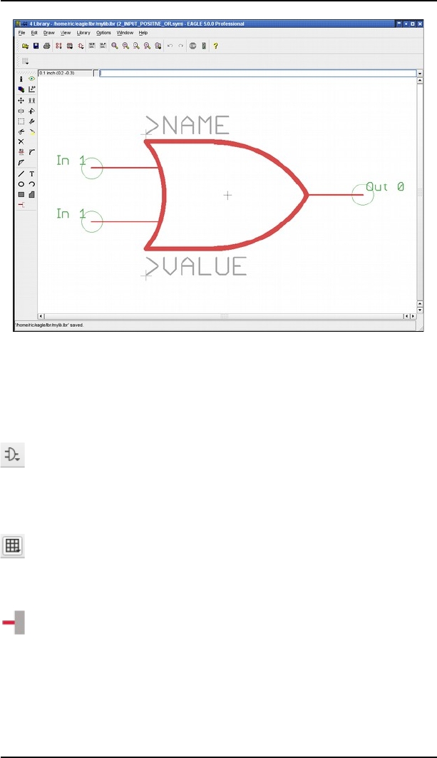
8.3 Defining a Complex Device
➢
The Symbol Editor: Logic symbol (American
representation)
Defining a Power Supply Symbol
Two pins are needed for the supply voltage. These are kept in a separate
Symbol, since they will not initially be visible in the schematic diagram.
Click onto the Edit a symbol icon. Enter a name for the Symbol on the
new line, such as VCC-GND, and click OK. Confirm the question Create new
symbol 'VCC-GND'? with Yes.
Check the Grid
First check that the grid is set to the default value of 0.1 inch. Only ever
use this grid when placing pins!
Place the Pins
Fetch and place two pins with the PIN command. The coordinate origin
should be somewhere near the center of the Symbol.
Both pins are given PWR as their direction. To do this, click with the mouse
on CHANGE, select the Direction option, and choose PWR. Now click onto
the two pins to assign this property.
The green pin label is updated, and now shows Pwr 0. It is only visible when
layer 93, Pins, is active!
259
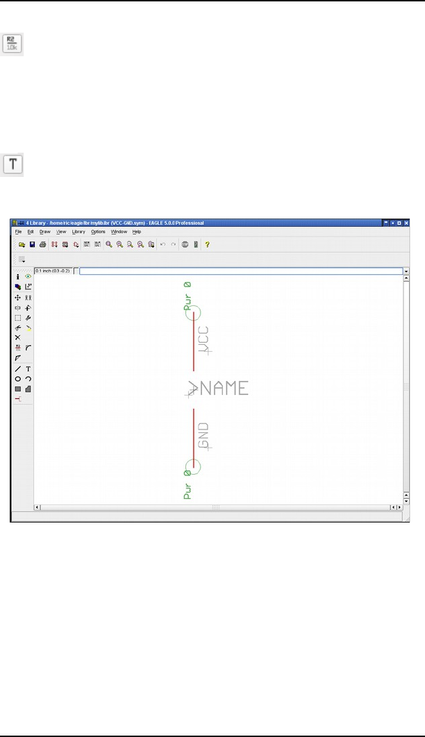
8 Component Design Explained through Examples
Pin Name
You use the NAME command to give the two pins the names of the
signals that they are to carry. In this case, these are GND and VCC.
For reasons of appearance, the pin property Visible is set to Pad in the
Symbol shown below, and the pin label has been placed on layer 95, Names,
using TEXT.
Placeholders for NAME and VALUE
For the component labelling, use the TEXT command in the schematic
diagram to write
?7
in layer 95, Names. Place the text at a suitable location. No placeholder is
necessary for value here.
Associating the Packages and Symbols to Form a
Device Set
We now come to the final step, the definition of the Device set. A Device set is
an association of Symbols and Package variants to form real components
A Device set consists of several Devices, which use the same Symbols for the
schematic but different technologies or Package variants.
Defining a Device set or a Device consists essentially of the following steps:
260
➢
The Symbol Editor: Supply symbol

8.3 Defining a Complex Device
Select Symbol(s), name them and specify properties
Assign Package(s) or specify variants
Specify the assignment of pins to pads using the CONNECT command
Define technologies (if desired/necessary)
State prefix and value
Describe the Device
Click onto the Edit a device icon. Enter the name for the Device on the
New line.
In our example this is a 541032A. This Device is to be used in two different
technologies, as the 54AS1032A and as the 54ALS1032A. The * is used as a
placeholder at a suitable location in the Device name to represent the
different technologies. Enter, therefore, the name 54*1032A, and confirm the
question Create new device '54*1032A'? with Yes.
The Device Editor window opens.
A question mark ? as part of the Device name is used as a placeholder
for the Package Variant name. If you don't use a ?, EAGLE adds the
Package Variant name at the end of the Device name automatically.
Select Symbols
First use ADD to fetch the Symbols that belong to this Device. A window
opens in which all the Symbols available in the current library are displayed.
Double-click onto the 2-input_positive_or symbol and place it four times.
Click again on the ADD icon, and select the 'VCC-GND' Symbol from the list.
Place this too onto the drawing area.
Naming the Gates
A Symbol that is used in a Device is known as a Gate. They are
automatically given generated names (G$1, G$2 etc.). This name is not
usually shown on the schematic diagram.
It is nevertheless helpful to assign individual Gate names when components
are composed of a number of Gates. To distinguish the individual OR gates,
you use the NAME command to alter the Gate names. Assign the names A, B,
C and D, and name the power supply gate P.
Specify Addlevel and Swaplevel
The Addlevel can be used to specify how the gates are placed in the schematic
diagram by the ADD command. You can see the current Addlevel for each
Gate written above left in layer 93, Pins.
261

8 Component Design Explained through Examples
Assign the Addlevel Next for Gates A to D, and the Addlevel Request to
the power supply gate. Do this by clicking onto the CHANGE icon, selecting
the Addlevel entry, and then selecting the desired value for a gate. Then click
on the Gate you want to change.
This means that as soon as the first OR gate has been placed on the
schematic diagram, the next one is attached to the mouse cursor. All 4 gates
can be placed one after another. The power gate does not automatically
appear. You can, however, fetch it into the schematic diagram if necessary,
by making use of the INVOKE command.
The parameter ADDLEVEL is described in full detail in the section entitled
More About the Addlevel Parameter on page 275.
The Swaplevel determines whether a Device's gates can be swapped within
the schematic diagram. The value that is currently set is like the Addlevel
displayed above left in layer 93, Pins, for each gate. The default value is 0,
meaning that the gates may not be exchanged. Gates with the same
Swaplevel can be exchanged with one another.
Our Device consists of four identical Gates that may be swapped. Click onto
CHANGE, select the Swaplevel entry, and enter the value 1. Click on the four
OR gates. The information text in layer 93, Pins, changes correspondingly.
Choosing the Package Variants
In the Device Editor window, click the New button at the lower right. A
window opens that displays the Packages defined in this library. Select the
DIL-14 package and give the version name J. Click OK.
Repeat this procedure, select the LCC-20, and give the version name FK.
In the list on the right you will now see the chosen Package variants, with a
simple representation of the selected Package above it.
Clicking on a Package variant entry with the right mouse button will open a
context menu. This allows variants to be deleted, renamed or newly created,
Technologies to be defined, the CONNECT command to be called, or the
Package editor to be opened.
Both entries are marked by a yellow symbol with an exclamation mark. This
means that the assignment of pins and pads has not yet been (fully) carried
out.
Supposed you don't find the appropriate Package variant in the current
library you may use Packages from another library. Use the PACKAGE
command to copy the Package into the current variant and to define a new
variant.
Example:
45-;,!!KVHJ"$!KW
This command copies the Package named DIL14 from ref-packages.lbr into
the current library. Simultaneously the variant J is generated for the Device.
See also page 283.
262
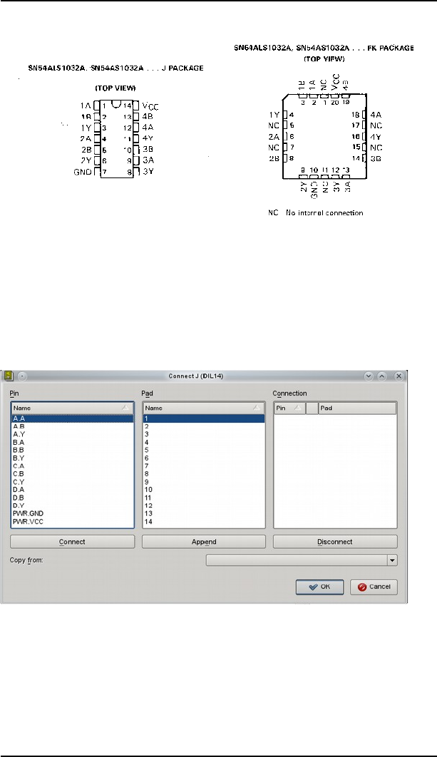
8.3 Defining a Complex Device
The Connect Command
This must be the most important step in the library definition. CONNECT
assigns each pin to one ore more pads. The way in which nets in the
schematic diagram are converted into signal lines in the layout is defined
here. Each net at a pin creates a signal line at a pad. The pin assignment for
the 541032 is specified in the data sheet. Check the connects in the library
with care. Errors that may pass unnoticed here can make the layout useless.
Select the J version from the Package list and click the CONNECT button.
The connect window opens.
➢
CONNECT dialog
The list of pins is on the left, and the pads are in the center. Click onto a pin-
entry, and select the associated pad. Both entries are now marked. You join
them with the connect button. This pair now appears on the right, in the
Connection column. Join each pin to its pad in accordance with the data
sheet. Finish the definition by clicking OK.
Please note that in our example the Gates are named A, B, C, and D while
they are named 1, 2, 3, and 4 in the data sheet.
263
➢
The pin assignment for the
packages

8 Component Design Explained through Examples
Define the connections for the second Package version, FK, in the same way.
Select the version, and click the Connect button. The usual dialog appears in
the connect window. Proceed exactly as described above.
Please note that six pads are not connected in this version. They are left over
in the Pad column. Finish the process by clicking OK.
There is now a green tick to the right of both Package variants, and this
indicates that connection is complete. This is only true when every pin is
connected to a pad.
It is not possible to connect several pins with a common pad!
A Device may contain more pads than pins, but not the other way
around!
Pins with direction NC (not connected) must be connected to a pad,
as well!
In the section 8.5 beginning with page 268 is explained how to use
the Append button of the Connect dialog in order to connect one pin
with more than one pad.
Defining Technologies
As noted above, the 541032 is to be used in two different technologies AS and
ALS. By including a * as a placeholder in the Device name we have already
taken the first step towards this. In the schematic diagram the code for the
chosen technology will appear instead of the *. The data sheet shows that
both technologies are available in both Packages.
Select the J Package from the list on the right of the Device Editor window.
Then click onto Technologies in the description box. The technologies
window opens. Define the technology in the New line, and confirm the entry
with OK. When the entry has been completed, the AS and ALS entries are
activated with a tick.
Close the window by clicking OK again.
Select the FK version from the Package list. Click onto Technologies in the
description box again. You will now see that AS and ALS are available as
selections in the technologies window. Activate both of these by clicking into
the small box to the left, so that a tick is displayed. Finish the definition by
clicking OK.
264
➢
Technologies for package
variant J

8.3 Defining a Complex Device
The technologies available for the selected Package version are now listed in
the description area of the Device Editor.
Specifying the Prefix
The prefix of the Device name is defined simply by clicking on the Prefix
button. IC is to be entered in this example.
Value
The setting of value determines whether the VALUE command can be used
to alter the value of the Device in the schematic diagram and in the layout.
On: You are allowed to change the value in the schematic (for example
for resistors). Defining the value is necessary to specify the part.
Off: The value will be generated from the Device name which can
include technology and Package variant name (e.g. 74LS00N).
Even if Value is set Off, it is possible to change the value of a component after
confirming a warning message.
If you change the initial value and decide to use another Technology or
Package variant later with CHANGE PACKAGE or CHANGE TECHNOLOGY,
the user-defined value will remain unchanged.
Independently from the Value settings mentioned above, it is allowed to
define an attribute with the name VALUE and assign any attribute value.
This attribute value will be finally used in schematic and board.
Description
Click onto Description in the description box. You can enter a description of
the Device in the window which now opens. Use typical terms that you might
apply for a keyword search. The search facility of the ADD command in the
schematic diagram will also search through this text.
You can use HTML text. The syntax is described in the help system under the
keyword HTML Text.
The description can look like this:
QK?9;-01.Q'K?
QH?
U))H!.H)&"=GM+)["'5=M"
V$
265
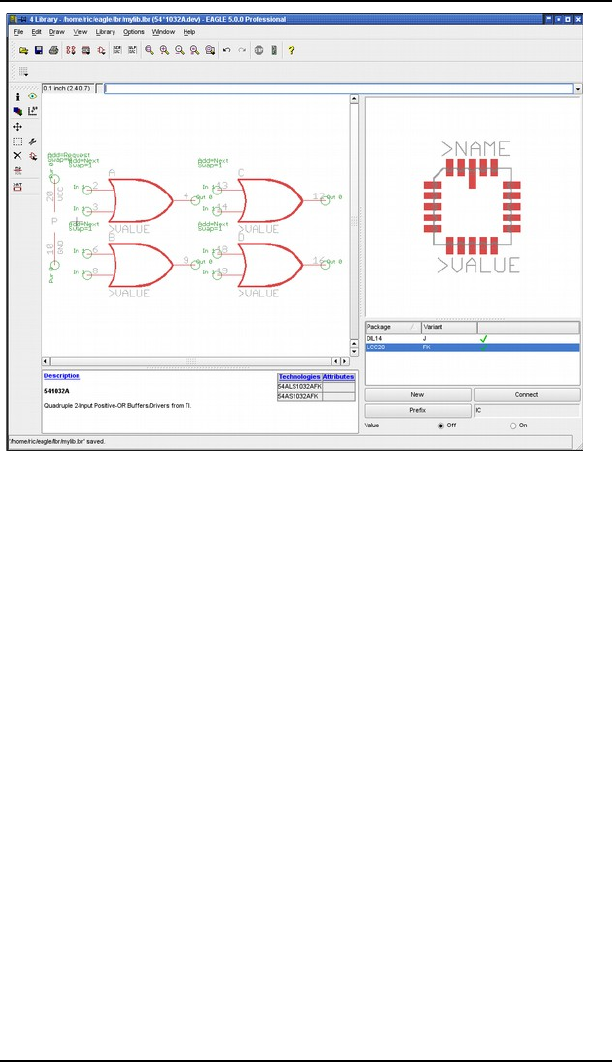
8 Component Design Explained through Examples
Save
This completes definition of the Device set. If you have not already saved the
library, please do it at this stage!
8.4 Supply Voltages
Component Power Supply Pins
The components' supply pins are to be given the direction Pwr in the Symbol
definition. The pin name determines the name of the supply signal. Pins
whose direction is Pwr and which have the same name are automatically
wired together (even when no net line is shown explicitly). Whether the pins
are visible in the schematic diagram or are fetched by means of a hidden
Symbol is also not relevant.
Invisible Supply Pins
We do not want as a rule to draw the supply connections for logic
components or operational amplifiers in the schematic. In such a case a
specific Symbol containing the supply connections is defined. This can be
demonstrated with the example of a 7400 TTL component:
You first define a NAND gate with the name 7400, and the following
properties in the Symbol Editor:
The two input pins are called I0 and I1 and are defined as having direction
In, Swaplevel 1, visible Pin and function None.
266
➢
Device Editor: 54*1032A.dev
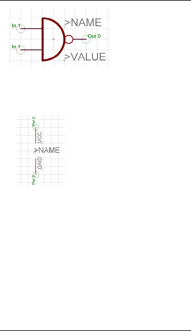
8.4 Supply Voltages
The output pin is called O and is defined with direction Out, Swaplevel 0,
visible Pin, and function Dot.
Now define the supply gate with the name PWRN, and the following
properties:
The two pins are called GND and VCC. They are defined with direction Pwr,
Swaplevel 0, function None, and visible Pad.
Now create the 7400 Device in the Device Editor:
Specify the Package with PACKAGE (which must already be present in the
library) and use PREFIX to specify the name prefix as IC.
Use the ADD command to place the 7400 Symbol four times, with Addlevel
being set to Next and Swaplevel to 1. Then label the Gates as A, B, C and D
with the NAME command.
The Addlevel of Next means that as these Gates are placed into the
schematic, they will be used in that sequence, i.e., the sequence in which they
were fetched into the Device.
Then place the PWRN Symbol once, using Addlevel Request and Swaplevel 0.
Name this Gate P.
Addlevel Request specifies two things:
267
➢
NAND Symbol 7400 (European
Representation)
➢
Power gate

8 Component Design Explained through Examples
The supply gate will only be fetched into the schematic if requested,
i.e. with the INVOKE command. The ADD command will only be able
to place NAND gates.
The supply gate will not be included when names are allocated to the
schematic. Whereas an IC with two Next Gates appears in the
schematic as something like IC1A and IC1B, an IC with one Next Gate
and one Request Gate will only be identified as IC1.
So use the CONNECT command to define the housing pads to which the
supply pins are connected.
Pins with the Same Names
If you want to define components having several power pins of the same
name, let's suppose that three pins are all to be called GND, then proceed as
follows:
set pin direction Pwr for each power pin
name these pins GND@1, GND@2, and GND@3
Only the characters in front of the "@" are visible in the schematic, and the
pins are treated as if they were all called GND. In the board the referring
pads are connected with airwires automatically.
8.5 One Pin – Multiple Pads Connections
You are allowed to connect one pin with several pads belonging to a common
signal. This can be done with the help of the Append button in the connect
dialog window.
First mark one pin and one pad in the connect dialog as usual and click onto
the Connect button. The pin/pad connection now appears in the Connection
column.
In order to add a further pad to this connection first mark the connection,
then select the pad in the Pad column, and click onto the Append button.
Repeat this for further pads, if necessary. The names of the pads appended
now are displayed in the Connection column.
EAGLE knows two different ways of creating multiple pad connections:
As soon as you establish a multiple pad connection, a special icon is
displayed in the Connections column, located between Pin and Pad list. It
informs you about the mode: All or Any. Click onto the icon to toggle.
All: All pads must be connected with traces. In the Layout editor you
will see all pads connected with airwires you have to route.
Any: Only one of the pads will be connected by an airwire and has to
be routed. In the routing process it is up to you which pad you
want to connect with a trace. In this mode internal connections
of a device can be realized.
Further information can be found in the help, Editor
Commands/CONNECT.
268

8.6 Supply Symbols
8.6 Supply Symbols
Supply symbols, such as might be used in the schematic for ground or VCC,
are defined as Devices without a Package. They are needed for the automatic
wiring of supply nets (see page 126).
The following diagram shows a GND symbol as it is defined in one of the
supplied EAGLE libraries.
Note that when defining your own supply symbols, the pin and the Device
name need to agree.
The pin is defined with direction sup and has the name GND. This specifies
that the Device containing this Symbol is responsible for the automatic
wiring of the GND signal. The text variable for the value (>VALUE) is chosen
for the labeling. The Device also receives the name GND. Thus the label GND
appears in the schematic, since by default EAGLE uses the Device name for
the value.
It is very important that the labeling reproduces the pin names, since
otherwise the user will not know which signal is automatically connected.
The pin parameter Visible is therefore set to off, since otherwise the placing,
orientation and size of the pin name would no longer be freely selectable.
Directly labeling with the text GND would also have been possible here. With
the chosen solution however, the Symbol can be used in various Devices
(such as for DGND etc.).
269
➢
Connect: One pin is connected to three pads in Any mode
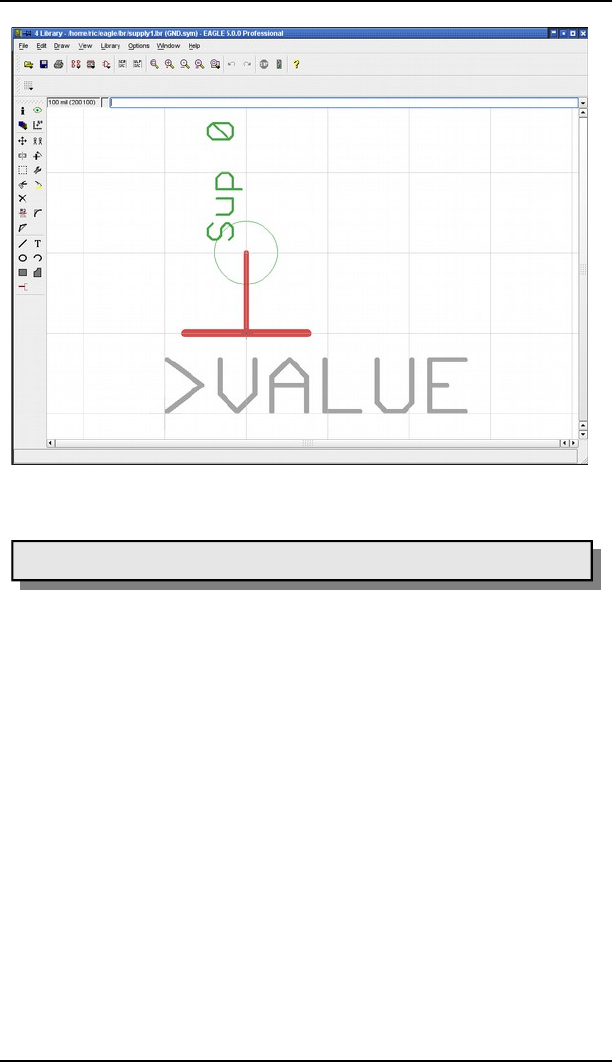
8 Component Design Explained through Examples
➢
Supply symbol for GND
The Supply symbol has no Package assigned!
As has been explained above, the Device receives the name of the pin that is
used in the Symbol. The corresponding Device is defined with Addlevel Next.
If you set Value to off you can be sure that the labeling is not accidentally
changed. On the other hand, you have more flexibility with Value set to on.
You can alter the label if, for instance, you have a second ground potential.
You must, however, then create explicit nets for the second ground.
Quick guide to define a Supply Symbol:
Create a new Symbol in the library
Place the pin, with direction Supply
Pin name corresponds to the signal name
Set Value placeholder
Create a new Device
Device name is signal name
Package assignment not necessary
270
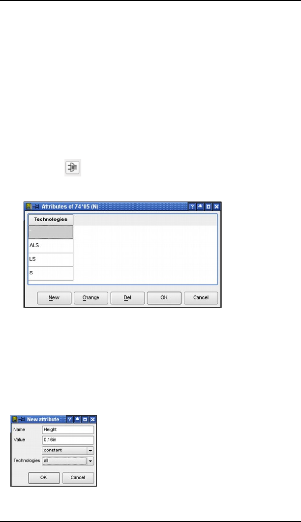
8.7 Attributes
8.7 Attributes
You are allowed to define, additionally to >name and >value, further
properties, the so-called attributes. It's possible to define attributes for each
technology and Package variant in the Device editor. This chapter will guide
you through the process of defining attributes with the help of an example.
Therefore open the library 74xx-us.lbr and save a copy of it with Save as... in
an arbitrary directory. We don't want to change the original library for this.
Edit the Device 74*05.
Define Attributes
Let's define some attributes for the Package variant N, which is the DIL14
Package. Therefore click onto entry DIL14 (Variant N) in the Package list on
the right-hand side of the Device Editor window. Now click the ATTRIBUTE
command icon in the menu bar or onto the text Attributes in the
description window below the representation of the Device. The following
Attribute window will appear.
This dialog initially shows the Technologies available for the Package variant
N. Clicking the New button opens the New Attribute window. Please enter,
for example, Height for the attribute's name and 0.16in for the attribute's
value. The line below determines whether it is allowed to modify the value of
the attribute (variable) or not (constant) in the drawing. Select constant in
our example here.
Now you have still to define for which Technologies the attribute should be
valid: for the currently selected one only (current) or for all. Select all here.
271
➢
Attributes' dialog
➢
Defining the Height Attribute
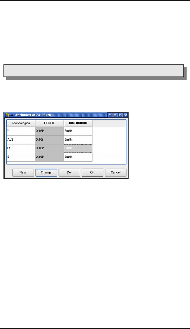
8 Component Design Explained through Examples
Click the OK button and the new attribute is shown in the list now.
Let's define a second attribute that should have different values for the
Technologies. Click the New button in the Attributes' dialog again. Enter the
following parameters:
Name: Distributor Value: Smith, variable Technologies: all
Click OK now. A further column for the Distributor attribute is shown. All
technologies have the Smith entry.
Attribute names are written in upper case letters automatically!
But in our example the LS technology has to be distributed by Miller
exclusively. Click into the field of the Distributor attribute that belongs to the
LS technology.
➢
The Distributor field for LS is selected
Click onto the Change button now. The window for changing the properties
of the attribute opens. Set the following options:
Name: Distributor Value: Miller exclusively, constant Technologies:
current
Click the OK button, and the exception for the LS technology is defined. This
value can not be altered in the Schematic/Layout.
The Change dialog allows three possibilities in the Technologies field:
current, same, all. This means that the currently changed properties will be
valid for the currently selected (current), for all the technologies with the
same attribute value as the currently selected (all with same value) , or for
all technologies.
Finally let's define a further attribute for remarks. This attribute will have no
initial value and will be variable. So we can use it in the Schematic or in the
Layout, if necessary.
Therefore click again the New button in the Attributes dialog and make the
following settings:
Name: Remarks Value: -, variable Technologies: all
272
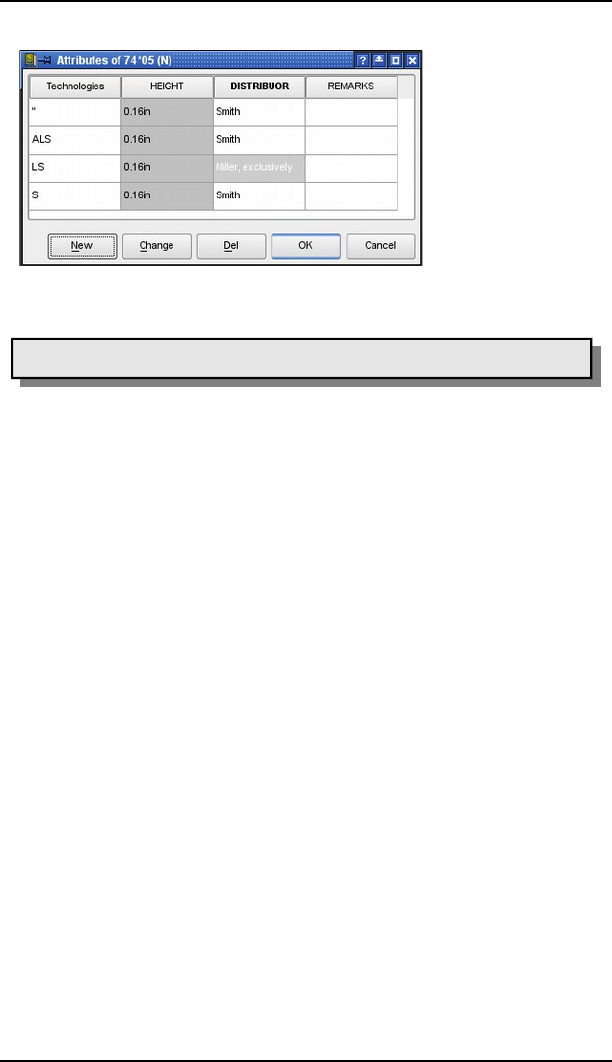
8.7 Attributes
Click OK. The attributes window looks like this now:
Attributes with a fixed value are colored gray in the table.
The definition of attributes for the Package variant N is finished now. Click
OK to close the Attributes window now. The attributes are shown in addition
to Technologies in the Device Editor window.
If you like to define attributes, for example, for the Package variant D (SO14),
click onto the entry in the Package list of the Device Editor window and
proceed as described above for variant N.
It's also possible to define attributes via the command line or with the help of
a Script file. Please take a look into the help function about the ATTRIBUTE
command for details.
Display Attributes
If you would use the Device 74*05 without further changes in the Schematic
or Layout Editor, it would bring along its attributes and their values. The
attributes are not visible in the drawing and can be check with the
ATTRIBUTES command.
Information about how to display attributes in Schematic or Layout can be
found on page 129 in this manual.
Placeholders in Symbol and Package
Already in the library you may define whether an attribute will be displayed
together with the Device in the Schematic or the Package in the Layout.
Simply write a placeholder text in the Symbol or Package with the TEXT
command. Such a placeholder text begins with the > character, as it is with
>name and >value. For our example attributes we defined above, you have to
write:
?5="&=K)&
?*=(&
?J"
273
➢
All the Attributes for 74*05, Variant N

8 Component Design Explained through Examples
Place this text at a suitable location in the Symbol or Package Editor and
select a proper layer for each text. It doesn't matter if you write it with upper
or lower case letters.
As soon as you add a part with pre-defined attribute placeholder texts and set
a value for an attribute in Schematic and Board respectively, the attribute's
value will be displayed at the placeholder text's location.
These texts can be separated from the Device/Package with the SMASH
command. From then on the Display property of the Attribute dialog takes
effect. The possible options are Off, Value, Name, or Both.
See page 129 for details about display options of attributes.
8.8 External Devices without Packages
A so-called External Device can be used to represent components or objects
that need to appear in the schematic but are not part of the board design.
There can be additional components, measurement equipment, cables,
mounting materials and so on. It could be used for testing or simulating
purposes, or for an electric schematic, as well.
An external device is created in the library the same way as any other
component. The symbol may have pins of any direction. Create the Device
and ADD the symbol(s) as usual.
For marking the device as an external device create an attribute with the
name _EXTERNAL_. This attribute has to be created in the library; creating
the attribute in the schematic won't work! The attribute's value doesn't
matter.
An external device is no longer treated as external as soon as you assign a
package. In this case you have to CONNECT all the pins with pads.
8.9 Labeling of Schematic Symbols
The two text variables >NAME and >VALUE are available for labeling
Packages and schematic Symbols. Their use has already been illustrated.
There are two further methods that can be used in the schematic: >PART
and >GATE.
The following diagram illustrates their use, in contrast to >NAME. The
Symbol definition on the left, the appearance in the schematic diagram on
the right.
In the first case all the symbols are labeled with >NAME. In the second case,
the symbol of the first gate is labeled with >PART and >GATE, the other
three with >GATE only.
274
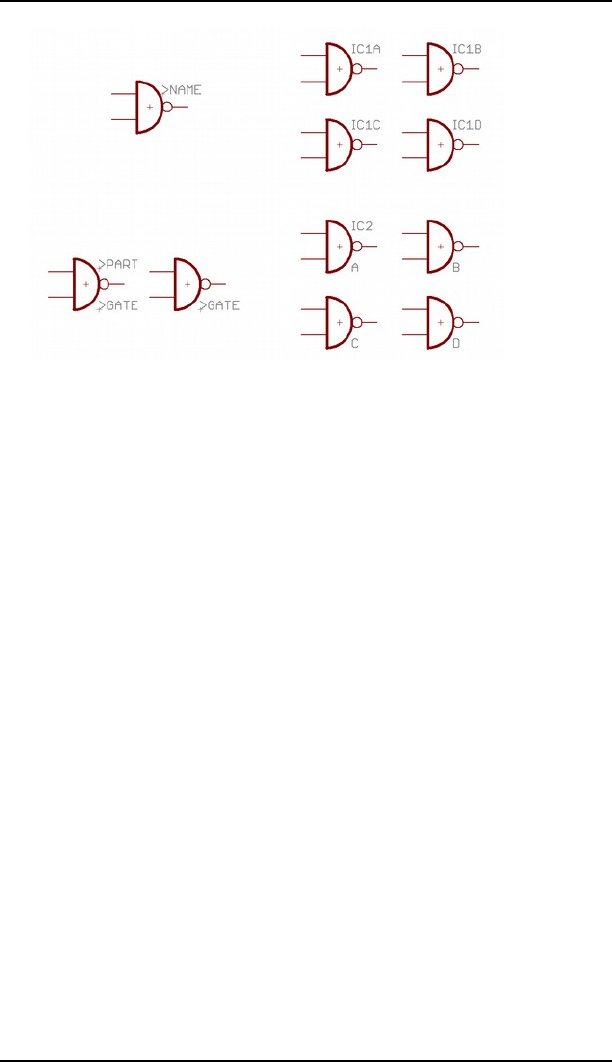
8.10 More about the Addlevel Parameter
8.10 More about the Addlevel Parameter
The Addlevel of the Gates that have been fetched determines the manner in
which these Gates are fetched into the schematic, and under what conditions
it can be deleted from the schematic.
Summary
Next: For all Gates that should be fetched in sequence (e.g. the NAND Gates
of a 7400). This is also a good option for Devices with a single Gate. The ADD
command first takes unused Next-Gates from components which exist on the
current sheet before "opening" a new component.
Must: For Gates which must be present if some other Gate from the
component is present. Typical example: the coil of a relay. Must-Gates
cannot be deleted before all the other Gates from that component have been
deleted.
Can: For Gates which are only used as required. In a relay the contacts may
be defined with Addlevel Can. In such a case the individual contacts can be
specifically fetched with INVOKE, and can later be deleted with DELETE.
Always: For Gates which as a general rule will be used in the schematic as
soon as the component is used at all. Example: contacts from a multi-contact
relay, of which a few are occasionally left unused. These contacts can be
removed with DELETE, provided that they were defined with Addlevel
Always.
Request: For supply gates of components.
The difference from Can is: A Device with exactly one Next-Gate and a
Request-Gate will be named, for example IC1. The Gate name does not
appear in the name of the part in the schematic. The Request-Gate's name,
however will consist of Prefix+Number+Gate name, for example, IC1P.
275
➢
Labeling of a schematic symbol
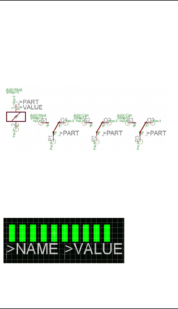
8 Component Design Explained through Examples
Relay: Coil and First Contact must be Placed
A relay with three contacts is to be designed, of which typically only the first
contact will be used.
Define the coil and one contact as their own Symbols. In the Device, give the
coil and the first contact the Addlevel Must. All the other contacts are given
the Addlevel Can.
If the relay is fetched into the schematic with the ADD command, the coil
and the first contact are placed. If another contact is to be placed, this can be
done with the INVOKE command. The coil cannot be deleted on its own. It
disappears when all the contacts have been deleted (beginning with those
defined with Addlevel Can).
➢
Relay with one coil and three contacts
Connector: Some Connection Pins can be Omitted
A PCB connector is to be designed in which normally all the contact areas are
present. In some cases it may be desirable for some of the contact areas to be
omitted.
Define a Package with 10 SMDs as contact areas, giving the SMDs the names
1 to 10.
➢
Package of a circuit board connector
Now define a symbol representing one contact area. Set visible to Pad, so
that the names 1 to 10, defined in the Package, appear in the schematic.
276
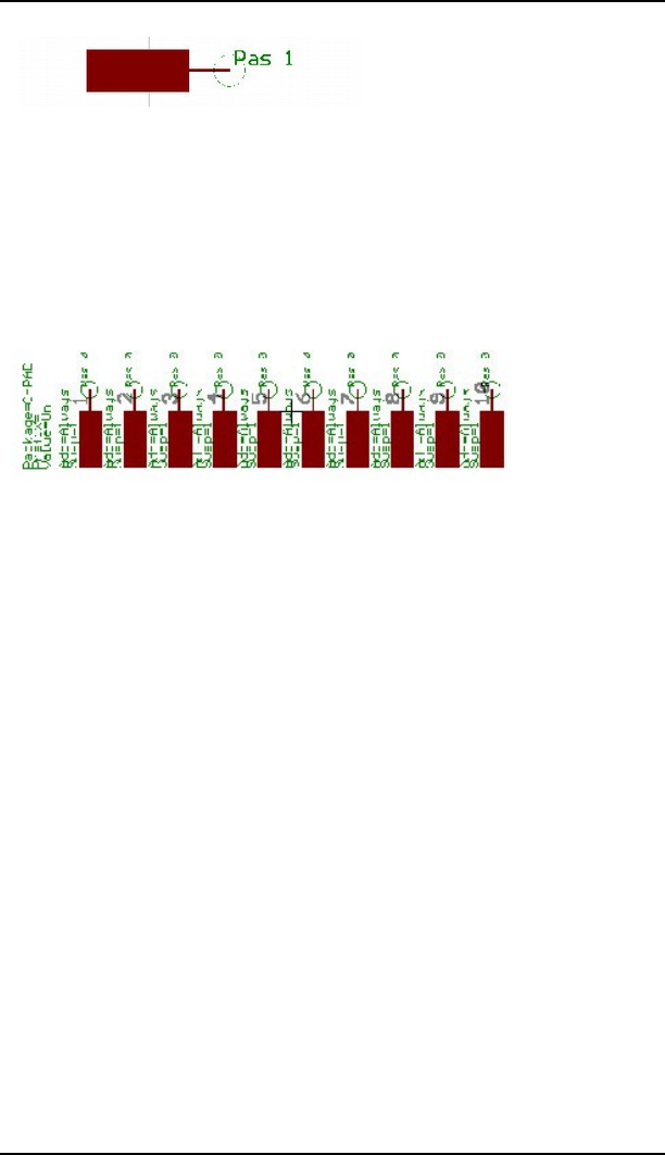
8.10 More about the Addlevel Parameter
➢
Connector symbol for the
Schematic
Then fetch the Symbol ten times into a newly created Device, setting the
Addlevel in each case to Always, and use the CONNECT command to create
the connections between the SMDs and the pins. When you now fetch this
Device into a schematic, all the connections appear as soon as it is placed.
Individual connections can be removed with DELETE.
➢
After ADD, all the connections are visible in the
schematic
Connector with Fixing Hole and Restricted Area
A connector is to be defined having fixing holes. On the solder side (bottom),
the Autorouter must avoid bringing tracks closer to the holes than a certain
distance.
277

8 Component Design Explained through Examples
The drill holes are placed, with the desired diameter, on the Package using
the HOLE command. The drilling diameter can be retrospectively changed
with CHANGE DRILL.
The forbidden area for the Autorouter/Follow-me router is defined in layer
42, bRestrict, using the CIRCLE command. For reasons of representational
clarity the circle is shown here with a non-zero width. Circles whose width is
0 are filled. In this case it has no effect on the Autorouter, since it may not
route within the circle in either case. These forbidden areas are also taken
into account by a polygon in layer 16, Bottom.
8.11 Defining Components with Contact
Cross-References
If you have to design a component that consists of a coil gate and several
contact gates for an Electrical Schematic, for example an electro-mechanical
relay, you can define the contact symbols with a placeholder text that will
generate cross-references for components. The contact overview in the
Schematic will show the cross-references then.
For a proper display of the contact cross-references in the Schematic, please
stick to the following rules for Symbol, Device, and Package definition.
Define Symbol
For defining an electro-mechanical relay you have to use one Symbol for the
coil and one or more Symbols for the contacts.
Please note the following rules for the contact symbols:
The center of the contact symbol should be located at position (0 0)
Arrange the pins in vertical direction, i.e. they are pointing up or
down
278
➢
Fixing holes with restricted areas

8.11 Defining Components with Contact Cross-References
In order to get automatically generated cross-references, use the
TEXT command to define the placeholder text >XREF and place it.
The text should be written in layer 95, Names, like >NAME and
>VALUE.
There are no special rules for the coil symbol. The placeholder text >XREF
is not needed here.
Define Device
Our electro-mechanical relay consists of multiple Gates: one Gate for the coil
and several Gates for the contacts. The placement of the Gates in the Device
Editor has to follow some rules. Otherwise the presentation of the cross-
references in the Schematic would not be optimal.
The origin of the first contact gate should be located at the
x-coordinate 0. The lower pin of the Gate should be located
completely in the positive coordinates range. The y-coordinate is
typically 0.1 inch.
Each further contact gate is placed to the right of the first one at the
same y-coordinate (the same height).
The distance between the contact gates in the Device Editor finally
determines the distance of the contacts in the graphical
representation of the contact cross-references in the Schematic. The
contact gates will be rotated by 90° and aligned vertically one by one
there.
The coil gate may be placed anywhere in the Device drawing. The
Addlevel for this Gate must be Must.
The representation of the contact cross-references shows all Gates that come
with the >XREF text. The cross-references consisting of sheet numbers and
column/row coordinates will be shown on the right of the Gates, if you placed
a drawing frame defined with the FRAME command on the Schematic's
sheets.
All other texts defined in the Symbol are not visible in the cross-reference
representation.
Define Package
Due to EAGLE's library structure and in order to avoid error messages you
have to define a Package, as well. This can be a simple dummy Package that
simply has the same number of Pads as number of Pins in the Device.
Select the Package with the New button in the Device Editor and assign Pins
with Pads with the CONNECT command.
8.12 Drawing Frames
It may be true that drawing frames are not components, but they can be
defined for schematics as Devices with neither Packages nor pins. Such
Devices in EAGLE's frames library contain a Symbol consisting merely of a
frame of the appropriate size, and a documentation field, which is also
defined as a Symbol.
279
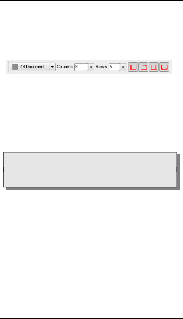
8 Component Design Explained through Examples
A drawing frame is defined with the FRAME command. This command can
be found in the Draw/Frame menu.
The parameter toolbar offers settings for the number of columns and rows
where you can define how your drawing should be fielded. A positive value
for columns labels the frame from the left to the right, beginning with 1, for
rows from top to bottom, beginning with A. Negative values inverse the
direction of the labelling. The following four icons determine on which
position the labelling of the frame shall be visible.
The position of the drawing frame is fixed by two mouse clicks or by typing
the coordinates of its corners in the command line.
Columns and Rows can be used to determine a Device's or a net's position,
for example with the help of an ULP, or to have cross-references calculated
automatically (see LABEL command).
Is the frame already defined but you want to change its properties?
Then use the CHANGE command with its options Border, Rows and
Columns to determine the frame's position of the labelling and its number of
rows or columns.
Due to the special nature of the frame object, it doesn't have a
rotation of its own!
The FRAME command is also available in Schematic or Board. But it
is common practice to define a drawing frame in the Library.
The library frames.lbr also contains documentation fields you can use
together with a frame. Of course you are allowed to draw your own.
The text variables >DRAWING_NAME, >LAST_DATE_TIME and >SHEET
are contained, as well as some fixed text. The drawing's file name, date and
time of the last change appear at these points together with the sheet number
in the schematic (e.g., 2/3 = sheet 2 of 3).
In addition, the following variables are available:
>PLOT_DATE_TIME contains the date and time of the last printout,
>SHEETS shows the total number of sheets in the schematic,
>SHEETNR shows the current sheet number.
All of these text variables can be placed on the schematic, and (with the
exception of >SHEET/S/NR) on the board.
The frame is defined in the Device with Addlevel Next, and the
documentation field with Addlevel Must. This means that the documentation
field cannot be deleted as long as the frame is present.
280
➢
Parameter toolbar of the FRAME command
8.12 Drawing Frames
There are frames defined as Packages available for the Layout Editor which
can be placed even if there is a consistent schematic/layout pair. These
frames don't have any electrical significance because they are defined
without pads or SMDs.
The variable >CONTACT_XREF has a special meaning for Electrical
Schematics. The position of this text, which is not displayed in the Schematic,
determines the reserved area for the representation of the contact cross-
references. More details about this can be found in the help function in the
section Contact cross-references.
8.13 Components on the Solder Side
SMD components (and leaded ones too) can be placed on the top or bottom
layers of a board. For this reason EAGLE makes a set of predefined layers
available which are related to the top side (Top, tPlace, tOrigins, tNames,
tValues etc.) and another set of layers related to the bottom side (Bottom,
bPlace etc.).
SMD components are always defined in the layers associated with the top.
In the board, a component of this sort is moved to the opposite side with the
MIRROR command . Therefore click onto the component with the
mouse or enter the component's name in the command line. This causes
objects in the Top layer to be reflected into the Bottom layer, while all the
objects in the t.. layers are reflected into the corresponding b.. layers.
If one of the commands ADD, COPY, MOVE, or PASTE is active the
component can be mirrored by clicking the middle mouse button.
8.14 Components with Oblong Holes
If the board manufacturer has to mill oblong holes, you have to draw the
milling contour of oblong holes in a separate layer. Usually this is layer 46,
Milling.
The milling contour for components that need oblong holes can be drawn
with LINE (and possibly ARC) with a very fine wire width near or even 0 in
the Package Editor. Take a pad that has a drill diameter which lies inside the
milling contour, or SMDs, for example in Top and Bottom layer, as basis for
the oblong hole.
281
➢
Text variables in the documentation field

8 Component Design Explained through Examples
In case of a multilayer board you should draw a LINE in the used inner layers
at the position of the oblong holes so that it covers the milling contour and
leaves a kind of restring around the opening.
Please inform your board manufacturer that they have to take care on the
milling data drawn in this layer. Also tell them whether they should be
plated-through or not.
Any other cut-outs in the board are drawn in the same way:
Use a separate layer, typically layer 46, Milling, and draw the
milling contours. Tell your board manufacturer that they have to
take care with this information and make special note.
8.15 Arbitrary Pad Shapes
If you have to define a package with solder areas that can't be achieved with
the default pad shapes, you have to draw an arbitrary pad shape. This can be
done with the help of a polygon or with additional wires. As soon as the
center of the pad or SMD is inside the polygon's area or a wire begins at the
center of a pad, it is recognized as a part of the PAD/SMD.
The typical way to draw an arbitrary pads shape is:
Place a PAD or SMD
Use POLYGON to draw the final pad shape
- For a SMD typically in Layer Top
- For a PAD you have to draw the final shape in all the layers you plan
to use (Top, Bottom, Inner layers...)
The PAD/SMDs center must be inside the polygon's area. Otherwise
that polygon is not recognized as a part to the pad. Use a reasonable
wire width for the polygon, which fulfils the Design Rules.
The alternative to POLYGON is LINE
Start the wire in the origin of the PAD/SMD. You have to draw this
area in any signal layer you plan to use. Please use a reasonable wire
width, which fits to the Design Rules.
Check the solder stop mask
Mask data will be generated for the PAD/SMD area only. Display
layers 29, tStop and 30, bStop. If you want to have the area not
covered by solder stop lacquer, draw it manually in the appropriate
layer(s).
Check the cream frame (solder paste mask)
Display layers 31, tCream and 32, bCream for this. As we agreed upon
defining packages always on the top side of a board, the layer we have
to check is 31, tCream. Mask data will be generated automatically for
the SMD area only. If this is not what you would like to have, simply
draw the mask manually. Keep in mind that it is possible to switch off
automatic generation of mask data in the SMD properties (Cream
on/off).
Further conditions for drawing arbitrary pad shapes can be found in the help
function about the PAD or SMD command.
282

8.15 Arbitrary Pad Shapes
If a pad with arbitrary shape is not connected to a signal, the DRC
will report a Clearance error, because the polygon or wires that
define the arbitrary shape can't be recognized as a part of a signal.
8.16 Creating New Package Variants
Most components are manufactured in various Package variants. Supposed
you do not find the appropriate Package for a certain Device in one of the
libraries, it is very easy to define a new Package.
To describe this procedure clearly we want to come back again to our
example Device 541032A from paragraph 8.2.
The third Package variant to be designed here only serves as an
example for practice and does not meet the specifications of the
manufacturer!
Please notify the explanations concerning this topic, in particular if the
appropriate Package already exists in the current library beginning with page
262.
Package from Another Library
In the most favourable case you can use an already existing Package from
another library. The easiest way to define the new Package variant is to use
the PACKAGE command directly in the Device Editor.
Being in the table of contents view of your library, click onto the Add
package… button at the bottom of the Packages column, then the Import...
button in the opened dialog. Now the Import Package window pops up. It’s
similar to the ADD dialog. From here search for the wanted package, or in
case you already know where to find it, select it from the libraries list. With
the Manage libraries button you can add further libraries, or in case you
want to have less libraries in the list, drop libraries from it.
In case there is already a package with the same name in your library, it will
be updated with the imported package automatically.
Open the library (here: my_lib.lbr from paragraph 8.2) that contains the
Device you want to define the new Package variant for. For example, by the
menu File/Open/Library of the Control Panel.
Click the Edit-a-Device icon and select the Device 54*1032A from the menu.
The Device Editor opens.
Defining the Package Variant
The new variant should be named Test. The Package must have a minimum
of 14 pads because both Gates together have 14 pins. As an example, we take
the SO14 Package from the smd-ipc.lbr library.
The import is done as described above from the Table of Contents of the
library with Add package… and Import.
283
8 Component Design Explained through Examples
Alternative import options:
If Control Panel and Library Editor window are arranged side by side, select
the SO14 Package and Drag&Drop it into the opened Library Editor window.
After releasing the mouse button you will be asked for the new Package
variant name. Enter it and confirm it by clicking OK. The new variant is now
shown in the Package list.
It is also possible to define the Package variant in the Device Editor directly
with the PACKAGE command.
Type in the command line:
4+-;,"=H$!K
Or include the path (if necessary):
+-;,!!K"=H$!K
If the path contains spaces include the path name in single quotes, for
example:
C+-;,=&(H""=H$!KC
Now on the lower right of the Device Editor window a new entry for the
Package SO14 and the variant name TEST appears.
On the left a black exclamation mark on yellow ground is shown which
indicates that there are no connections between pins and pads defined yet.
➢
Device Editor: List of Package
Variants
The PACKAGE command copies the complete Package definition into
the current library and makes available the new variant with the
given name for the Device.
284

8.16 Creating New Package Variants
If you decide to erase a newly defined variant, you can do this with
the UNDO function (as far as possible) or by using the context menu
of the Package entry (right mouse click, Delete entry).
Connect Command
Click the Connect button now. The Connect window opens. Connect pins with
pads by clicking on the pin and pad entries belonging together as described
in paragraph 8.2.
It is also possible to adapt the pin/pad connections from an already existing
Package variant. In our example the assignment does not differ from the
DIL14 Package. Therefore select the entry DIL14 from the Copy from: combo
box.
After clicking OK the CONNECT command is finished.
Defining Technologies
The Device 54*1032A is available in two technologies (ALS and AS). These
still have to be set up for the new Package variant.
Select the Package variant Test from the list on the lower right of the Device
Editor window. A click onto Technologies in the description field opens a
window. Click the New button and set up technology ALS with a following
click onto OK, and AS again with a following click onto OK. Both entries are
shown with a tag now. A further click onto the OK button closes the window
again.
Save
The definition of the Package variant is finished. Now it is time to save the
library.
Using a Modified Package from Another Library
If there is no appropriate but a similar Package available in another library
you should import or copy the Package into the current library first, then
modify it, and use it afterwards as new variant for the Device.
Import the Package
We want to use a Package named SOP14 from the smd-ipc.lbr library here.
This Package should get a new name, MYSOP14, in the library my_lib.lbr.
Add Package and Import
Open your library and click onto Add package… in the Table of Contents
view. Now select Import and choose the package SOP14 from smd-ipc.lbr
from the libraries list.
Copy From the Control Panel
As an alternative to the import option:
First of all open a Library Editor window with the library that should contain
the new Package (File/Open/Library). It is not necessary to
select a certain editing mode. Now switch to the Control Panel (e. g. Window
285

8 Component Design Explained through Examples
menu) and expand the Libraries branch of the tree view. Choose the library
which contains the requested Package and select it. On the right half of the
Control Panel a preview of the Package is visible now.
If the Control Panel and the Library Editor window are arranged in a way
that both windows are visible you can move the Package into the Library
window by keeping the left mouse button pressed. After releasing the mouse
button (Drag&Drop) the Library Editor will be in the Package editing mode.
The Package is shown there.
Alternatively you could use a right mouse click to open the context menu of
the Package entry in the tree view. Select Copy to Library now. The Library
Editor needs not to be visible.
Now the Package can be modified. The Package name is adopted from the
source library. To change the Package name use the RENAME command.
Using the COPY command
For the friends of command lines:
Type in the command line of the Library Editor window (it does not matter
which editor mode is active) the following:
+6+-;,"=H$!K76+-;
Or with the whole path:
+6+-;,!!K"=H$!K76+-;
If the path contains spaces use single quotes for it, for example:
+6C+-;,*"=H$!KC76+-;
The Package Editor window opens and the Package can be modified as
needed.
Don't forget to save the library.
Defining the Variant
We want to define a further variant for our example Device. Switch to the
Device editing mode, for example, by the menu Libraries/Device. The Edit
window opens. Select the entry 54*1032A. Click OK to open the editor
window.
Use the New button to define a new variant. Select the Package MYSOP14 in
the selection dialog and enter, for example, TEST2 as variant name. After
clicking OK a new entry is shown in the Package list.
To complete the definition execute the CONNECT command and define
Technologies (as described in the previous paragraph) now.
8.17 Defining Packages in Any Rotation
Components can be defined in any rotation with a resolution of 0.1 degrees in
the Package Editor. Usually the Package is defined in normal position first
and rotated afterwards as a whole. The definition of Packages has been
already explained in this chapter. Here we only want to elaborate on the
rotation of Packages.
286

8.17 Defining Packages in Any Rotation
Packages can be defined in any rotation! Schematic Symbols can be
rotated in 90-degrees steps only!
Rotating a Package as a Whole
To come back to the example of this chapter, please open the library
my_lib.lbr and edit the Package LCC-20.
Display all layers with DISPLAY ALL to make sure you have all objects
rotated. Now use GROUP ALL to select everything.
Use the ROTATE command to rotate the group:
Now click with the left mouse into the Angle box of the parameter toolbar
and type in the requested angle. Then use a right mouse click into the group
to define the rotation point.
The Package is shown now in the given angle.
Alternatively you can work with the command line:
+..$9@?00B
rotates, for example, the previously selected group 22.5° further around the
point (0 0). The > sign (right angle bracket) within the parenthesis for
coordinates causes the rotation of the whole group (as a right mouse click at
the point (0 0) would do).
Packages with Radial Pad Arrangement
It is possible to work with polar coordinates to place pads or SMDs in a radial
arrangement. Set a suitable reference point, for example, in the center of the
Package with the MARK command first. The command line shows now
additional information about the cursor position.
Values marked with an R are relative values referring to the previously set
reference point. The leading P indicates polar values referring to the
reference point.
Example:
Three pads are to be placed on the circumference of a circle with a radius of
50 mm. The center of the part is at position (0 0).
577
74@00B
5C-C@900B
5C.C@90-.0B
5C1C@90.;0B
Depending on the used pad shape it may be useful to place the pads rotated
(for example for Long pads or SMDs).
287
➢
Package Editor: Relative and Polar Coordinates Display

8 Component Design Explained through Examples
It is possible to enter the angle directly in the parameter toolbar or in the
command line while the PAD or SMD command is active.
Example:
577
74@00B
5C.C+-.0@90-.0B
8.18 Library and Part Management
Copying of Library Elements
Within a Library
The easiest way is to do this in the Table of Contents of the library.
Each object has a context menu that offers a Duplicate entry. You will
be asked for a new name for the new Device/Symbol/Package then.
Alternatives:
If you want to use a Symbol or a Package which already exists in a related
manner for a Device definition you can copy it within the library with the
commands GROUP, COPY, and PASTE. Afterwards it can be modified as
requested.
The following sections explain every single step with the help of an example
Package taken from linear.lbr.
Open Library
Use the menu File/Open/Library in the Control Panel to open the library
linear.lbr or select the entry Open from its context menu of the tree view's
expanded Libraries branch.
Edit Existing Element
Open the Edit window with Library/Package and select the Package DIL08.
After clicking OK it is shown in the Package Editor window.
Use DISPLAY to show all layers.
Draw a frame around all objects to be copied with GROUP or type
GROUP ALL in the command line.
Now click the COPY icon. The group will be copied into the clipboard.
Define New Element
Click the Edit-a-package icon in the action toolbar.
Enter the name DIL08-TEST in the New field of the Edit window and
confirm with OK.
Click the PASTE icon followed by a click at the drawing's reference point. The
Package will be placed.
Now it can be modified as requested.
288
8.18 Library and Part Management
It is possible to COPY and PASTE with coordinates in order to move a group
by a certain value in the coordinates system. This may be valuable for
elements that have been drawn in the wrong grid. Syntax:
+6@00B
@-00B
The group will be moved by a value of 10 (grid units) in x direction.
This procedure can be applied to Symbols too!
From One Library into Another
Most convenient way to import an object is in the Table of Contents view of
the library by clicking the Add Device…, Add Package…, or Add Symbol...
button and choose the Import… option in the dialog window.
There are alternative options to import Devices, Packages, and Symbols:
Devices
If there is a proper Device or Device set that you want to use in your current
library you can copy it in different ways.
In the Control Panel:
Move (with Drag&Drop) the requested Device set from the Control Panel's
tree view into the opened Library Editor window. The complete Device set
with Symbol(s) and Package(s) will be copied and newly defined.
As an alternative you could use the entry Copy to Library in the context
menu of the Device entry.
289
➢
Import Package from Table of Contents view of a Library

8 Component Design Explained through Examples
With the COPY command:
Type, for example,
+6A9-10,A9-%%$!K
or with the whole path
+6A9-10,!!KA9-%%$!K
in the command line, the Device 75130 from library 751xx.lbr is copied into
the currently opened library.
If the path contains spaces use single quotes for it, for example:
+6CA9-10,*A9-%%$!KC
If the Device should be stored in the current library under a new name
simply enter it, like here:
+6A9-10,A9-%%$!KA9-10
Symbols
Symbols can be copied similar to Devices. Either by Drag&Drop from the
Control Panel into the open Library Editor window or with the help of the
contex menu entry Copy to Library.
You can also use the COPY command, for example:
+6=$"8,H$!K=<
Packages
The procedure to copy Packages is nearly the same as to copy Devices.
Either move (with Drag&Drop) the requested Package from the Control
Panel's tree view into the opened Library Editor window. The complete
Package will be copied and newly defined in the current library. As an
alternative you could use the entry Copy to Library in the context menu of
the Package entry.
Or use the COPY command. Type, for example,
+65->,A9-%%$!K
in the command line, the Package DIL16 from library 751xx.lbr is copied into
the currently opened library. If the library is not in the current working
directory you have to enter the whole path, as for example, in:
+65->,!8!KA9-%%$!K
If the path contains spaces use single quotes for it:
+6C5->,5*8!KA9-%%$!KC
If the Package should be stored in the current library under a new name
simply enter it directly in the command line:
+65->,!8!KA9-%%$!K5->
The Package is stored with the new name DIL16NEW now.
If you want to copy a Package that already exists with the same name in the
target library the Package will be simply replaced.
290

8.18 Library and Part Management
If the Package is already used in a Device and the position or the name of one
or more pads/SMDs changes, EAGLE prompts a message in which mode the
pads/SMDs are to be replaced. This procedure can also be cancelled. The
Package remains unchanged then.
If the enumeration and position of the pads are unchanged but the order is,
EAGLE will ask you for the appropriate update mode. Depending on your
selection the pin/pad connections of the Device may change (see CONNECT
command).
➢
Requesting the Update Mode
Composition of Your own Libraries
The previously mentioned methods to copy library elements make it very
easy to compose your own libraries with selected contents.
Provided the Control Panel and the Library Editor window are arranged in a
manner that both are visible on the screen at the same time, it is very easy to
make user-defined libraries while browsing through the library contents in
the Control Panel. Simply use Drag&Drop or the context menu Copy to
Library of the current Device or Package.
Removing and Renaming Library Elements
The easiest way to remove or rename library objects is in the Table of
Contents view in the Library Editor. Simply right-click onto the
object to be removed or renamed and select the appropriate entry in
the context menu.
Devices, Symbols, and Packages can be removed from a library with the
REMOVE command. Defining a new library element can't be cancelled by
UNDO.
Example:
You would like to remove the Package named DIL16.
Open the menu Library/Remove.... A dialog window opens where you can
enter the name of the element to be deleted.
This can be done also at the command line:
7+:5->
291

8 Component Design Explained through Examples
Packages and Symbols can be removed only if they are not used in one of the
library's Devices. In this case the message Package is in use! or Symbol is in
use! appears. Remove the corresponding Device first or delete the particular
Package or Symbol in the Device (set).
Would you like to change the name of an element in your library? Then use
the RENAME command.
Switch to the Package editing mode so that the element that should be
renamed is shown first and open the menu Library/Rename. A dialog
window opens where you can enter the new name of the element.
This can also be done at the command line:
75->5->
The Package DIL16 gets the new name DIL-16.
The Device, Symbol, or Package name may also be given with its extension
(.dev, .sym, .pac), for example:
7+:5->$
In this case it is not necessary to switch to the related editing mode before.
Update Packages in Libraries
As already mentioned in the section Copying of Library Elements it is
possible to copy Packages from one library into another one. An already
existing Package is replaced in that case.
Each library contains Packages which are needed for Device definitions. In
many libraries identical types of Packages can be found. To keep them
uniform over all libraries it is possible to replace all Packages of a library with
those of another library with the help of the UPDATE command. An existing
Package with the proper name will be replaced by the current definition.
If you have, for example, special requirements for Packages you could define
them in a custom-built Package or SMD library. The UPDATE command
could transfer them to other libraries.
Therefore open the library to be updated and select Library/Update.... Now
select the library which you want to take the Packages from.
Having finished the update EAGLE reports in the status bar:
Update: finished - library modified!
If there was nothing to replace: Update: finished - nothing to do.
It is also possible to use the command line for this procedure.
If you want to update your library with Packages from, for example,
ref-packages.lbr, type:
5VHJ"$!K
To transfer Packages from different libraries, type in one after another:
5VHJ"$!K!$!K""H=!$!K
To update a single Package, type in the Package name:
5+-;,VHJ"
292


8 Component Design Explained through Examples
This
page
has been
left free
intentionally.
294

Chapter 9
Preparing Manufacturing Data
Data output for board manufacturing is made with the help of the CAM
Processor. PCB manufacturer usually work with drill data in Excellon format
and plot data in Gerber format. How to generate such data and which data
you have to pass on to your PCB manufacturer will be explained in this
chapter.
A lot of PCB manufacturers generate these data with EAGLE by themselves.
In such a case you have to pass on the board file only and you need not care
about data generation. You will find links to such firms on our Internet
pages.
With the help of pcb-service.ulp you will be directed to element14.com and
may have an offer of partners from Farnell/Newark for manufacturing your
printed circuit board. Based on your layout and the Design Rules, key
parameters for manufacturing, like board size, minimum drill size, and so on
are determined.
Your design should be complete and have passed a DRC successfully. By
clicking onto the link in the ULP dialog window you will be directed to the
quote site of element14, where these parameters will be transferred, as well
(login necessary). With a few steps you get a quote for manufacturing your
board.
If, however, your board maker is not set up to process EAGLE board files
directly, you will have to supply them with a set of files. What will be required
will be discussed in the following sections.
Additional useful User Language Programs (ULPs) are available on the web.
They can be used, for example, for the generation of glue mask data, for the
calculation of milling contours, or for data regarding automatic mounting
and testing equipment.
9.1 Which Data do we Need for Board
Manufacture?
The PCB manufacturer requires specific information pertaining to each step
in the manufacturing process of your board. This special information is
described in a file containing plot and / or drilling information.
For example, one file for each signal layer, for the silkscreen, for the solder
stop mask, the cream frame, for a gold application, for a glue mask (for SMT
devices), or for milling data regarding cut-outs in the board.
295

9 Preparing Manufacturing Data
Double-sided boards with parts on top and bottom side require a silkscreen
on both sides, or in case of SMT devices, a cream frame or a glue mask for
each side.
Additionally the board manufacturer needs drilling data in a separate file.
If you want a milled prototype board, milling contours have to be calculated
first, and generated in a specific data format for fabrication milling
machines.
If you want to have the parts automatically mounted, you need additional
files in appropriate data format that depict centroid and rotational angular
information.
A bill of materials or a legend for the drill symbols can be helpful, too.
Gerber Plot Data
All PCB manufacturers use Gerber format. There are two options of Gerber
format available, Extended Gerber format, also known as Gerber RS-274X
(in short RS-274X), which is the most commonly used today in industry.
The CAM Processor offers this device option as GERBER_RS274X.
It may be the case that the PCB manufacturer works with the second option
RS-274D. This will require the generation of data with the devices
GERBERAUTO and GERBER of the CAM Processor.
Gerber data (RS-274D) basically consist of two parts:
The so-called Aperture file or Wheel file, a special tool table, and the plot
data that contain coordinates and plotting information for the Gerber plotter.
Please inquire which format your PCB manufacturer prefers. The
more convenient to use is Extended Gerber, RS-274X.
GERBER_RS274X
This device generates files in Extended Gerber format (RS-274X) where the
aperture table is integrated in the output file. Simply generate Gerber files
with the GERBER_RS274X device and pass them on to your board
manufacturer. This is the most efficient and easiest way to generate Gerber
data.
The Extended Gerber device GERBER_RS-274X has a resolution of
1/100,000 of an Inch (data format: 2.5, inch).
Alternatives:
GERBER_RS274X_24 1/10.000 inch, data format 2.4, inch
GERBER_RS274X_26 1/1.000.000 inch, data format 2.6, inch
GERBER_RS274X_33MM 1/1000 mm, data format 3.3,
mm
GERBERAUTO and GERBER
The prior RS-274D format works with a separate aperture file which is
necessary to generate all Gerber files you will need for board manufacturing.
296

9.1 Which Data do we Need for Board Manufacture?
First you have to generate the aperture table (wheel file) with
GERBERAUTO. This file is a tool table which defines the shape and the size
of the Gerber plotter's apertures (tools). This table must contain the whole
aperture definition we need for generating all Gerber files that describe the
board.
For generating the Gerber files with the GERBER device, we refer to the
previously generated aperture file, made with GERBERAUTO.
GERBER and GERBERAUTO have a resolution of 1/10.000 of an Inch.
Exceptions are the devices GERBERAUTO_23 and GERBER_23. They have
a lower resolution of 1/1,000 of an Inch (data format 2.3, inch).
Drill Data
The generation of drill data is very similar to the generation of plot data.
Typical formats used in industry are Excellon or Sieb&Meyer 1000 or 3000.
They are supported by the CAM Processor. The most common one is
Excellon.
The simplest case is to generate one common drill data file for all drill holes.
If you have to distinguish plated from non-plated drill holes, two drill data
files must be generated. EAGLE differentiates between plated drills of Pads
and Vias in layer 44, Drills, and non-plated holes in layer 45, Holes, which
are placed by the HOLE command.
If you have to generate drill data for a multilayer board that uses Blind and
Buried vias with different via lengths that result in different drilling depths,
the CAM Processor takes care on this automatically. For each via length it
generates a separate drill data file.
Further information about this can be found in chapter 9.5 from page 310 on.
EXCELLON
Using this device the CAM Processor generates a drill file that contains the
drill table and the drill coordinates. This file format is the most common in
the industry and will be recognized by most board manufacturers.
The default resolution of the EXCELLON device is 1/100,000 of an Inch, no
leading zeros (data format: 2.5, Inch).
Alternatives:
EXCELLON_24 1/10.000 inch, data format: 2.4, inch
EXCELLON_26 1/1.000.000 inch, data format: 2.6, inch
EXCELLON_33MM 1/1.000 mm, data format: 3.3, mm
EXCELLON_RACK
This device can be used, if your board manufacturer insists on two separate
files. A drill table (rack file) and the drill data file. This was default in prior
EAGLE versions. Default data format is 2.4, Inch.
In the first step one has to generate the drill table in the Layout Editor with
the help of the User Language program drillcfg.ulp, and refers to this drill
table when generating drill data with the CAM Processor. The board
manufacturer gets two files then, drill data and drill table.
297

9 Preparing Manufacturing Data
If you have to distinguish between plated and non-plated drillings you have
to supply one drill table and two drill data files (one for layer Drills, one for
layer Holes).
SM1000 and SM3000
These devices generate drill data in Sieb&Meyer 1000 or in Sieb&Meyer
3000 format. SM1000 has a resolution of 1/100 mm, SM3000 1/1000 mm.
Data output is exactly the same as it is with EXCELLON_RACK. First you
have to generate the drill table with drillcfg.ulp, then use the CAM Processor
to generate drill data.
Further Drill Data Devices
The CAM Processor supports two further devices for drill data generation.
GERBDRL generates Gerber drill code. Here we need a separate drill table
(RUN drillcfg.ulp), as it is with EXCELLON_RACK.
SMS68 is a further drill data device that generates a HPGL code.
Prototype Manufacture With a Milling Machine
With the help of various User Language programs you can generate outline
data for milling a prototype board.
outlines.ulp
A simple example for contour data calculation is outlines.ulp. Start it with the
RUN command. Select the layer for which outline data shall be generated,
define the diameter of the milling tool (Width), and select the output file
format (Script or HPGL) in the ULP's dialog window.
The Script file containing the outline data can be imported into EAGLE with
the SCRIPT command. Thus it's possible to visualize the calculated contours
in the Layout Editor. You can even modify them, if necessary.
Finally, the milling data output is made with the CAM Processor. Select the
layer where the contours are to be drawn in and use, for example, the HPGL,
the PS (Postscript) or one of the Gerber devices for the output.
Further information can be found in the help function, Outline data.
mill-outlines.ulp
Another User Language program that calculates outline and drill data is mill-
outlines.ulp. It offers various configuration parameters. Simply start it with
the RUN command in the Layout Editor. Consult the ULPs integrated help
function for details.
This ULP exports for example CNC or HPGL formatted data or generates a
Script file which can be imported into the layout again. The milling contours
can be viewed, or even modified, if required. Generate the milling data with
the CAM Processor and one of its devices, like Gerber, HPGL or PS then.
Film Generation Using PostScript Files
A high-quality alternative to Gerber is the data generation for PostScript
raster image recorders. The exposed film serves as master for board
manufacturing.
298

9.1 Which Data do we Need for Board Manufacture?
With the PS driver, the CAM Processor generates files in PostScript format.
These files can be processed directly by appropriate service companies (most
of which operate in the print industry).
For PostScript recorders the Width and Height parameters should be set to
very high values (e.g. 100 x 100 inches), so that the drawing is not spread
over several pages.
For generating Postscript files you have to select the proper layers, the same
way it is performed for Gerber data generation. Use these files for the
generation of your artwork at your particular PCB subcontractor.
Films that relate to the bottom side are usually output in mirrored form
(Mirror option in the CAM Processor). In doing so the coating of the foil
rests directly on the copper layer of the board which is to be exposed.
The EPS driver generates Encapsulated PostScript files. They can be
processed with Desktop Publishing programs.
Printing on a Film
For boards of limited complexity, one can use a laser or ink jet printer and
print on a transparent foil with the PRINT command. This method is used,
for example, by hobbyists and results in a shorter fabrication time and a less
expensive board fabrication process.
The layers that are displayed in the Layout Editor while printing will appear
on the film. Check the options Black and Solid in the print dialog.
The drills of pads and vias are visible on the printout. This will allow an easy
visual indication of where you have to drill manually on the board.
Experience shows that the opening of a pad or a via should not be too big to
allow for a good centering of the drill bit. This issue can be solved with the
help of an User Language program, named drill-aid.ulp. Start it before
printing, and let it draw a ring inside each pad and via in a separate layer.
The inner diameter of this ring can be defined and is usually set to 0.3mm. Of
course, you have to display this additional layer for printing on the film.
Data for Pick-and-place Machines and In-circuit
Testers
EAGLE includes some ULPs which create data for various automatic
placement machines and in-circuit testers that are typically used by PCB
manufacturers.
The description of an ULP can be viewed in the User Language Programs
branch of the tree view of the Control Panel by selecting one of the ULP
entries with the mouse. The describing text appears on the right side of the
Control Panel window. It's also possible to edit the ULP file with a text editor.
The description usually is written in the file header.
ULPs for pick-and-place data (selection):
mount.ulp Generates one file with coordinates of
the centered part origins
mountsmd.ulp Centered origins for SMT devices; one file for
top and one file for bottom side
299
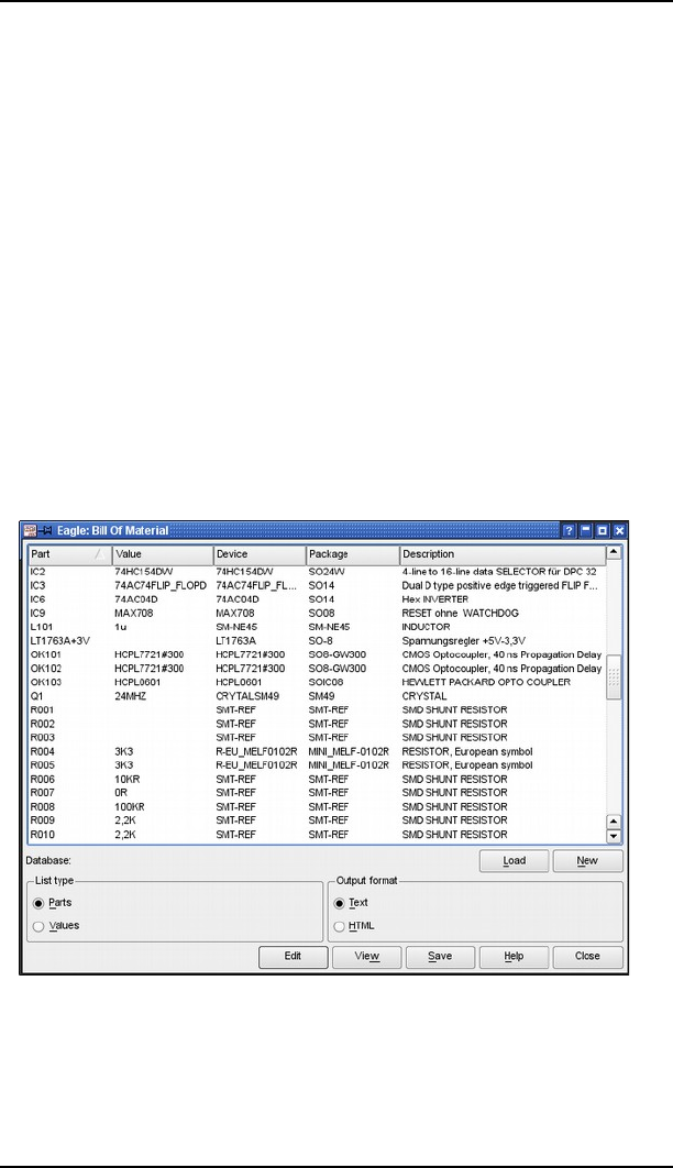
9 Preparing Manufacturing Data
ULPs for circuit tester (selection):
dif40.ulp DIF-4.0 format from Digitaltest
fabmaster.ulp Fabmaster format FATF REV 11.1
gencad.ulp GenCAD format for Teradyne/GenRad
in circuit tester
unidat.ulp UNIDAT format
Execute the RUN command in the Layout Editor window to start the
particular ULP.
Documentation
Many documentation items can be generated with the aid of User Language
programs. Note also the wide range of programs that are made available on
our web server. The bom.ulp, the program for generating a bill of materials,
has been used as a basis for lots of user-contributed ULPs.
Parts List
The parts list can be created by bom.ulp. Start it from the Schematic Editor,
using the RUN command. The Bill Of Material window with the parts
summary opens first.
➢
bom.ulp: Dialog window
It
is possible to import additional information from a database file into the
parts list (Load), or to create a new database with its own properties such as
manufacturer, stores number, material number or price (New).
You can obtain further details about the current version of the ULP by
clicking the help button.
300
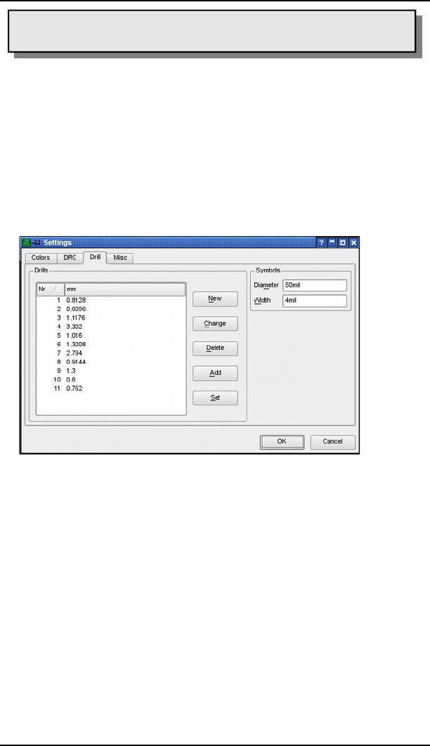
9.1 Which Data do we Need for Board Manufacture?
A simple parts list can also be created from a board or schematic by
means of the EXPORT command (Partlist option).
Drill Plan
Printing a drill plan enables you to check the drill holes and their diameters.
It shows an individual symbol for each diameter of hole, via, and pad used in
your design. EAGLE uses 19 different symbols: 18 of them are assigned to a
certain diameter; one (Æ) appears, if no symbol has been defined for the
diameter of this hole. The symbols appear in layer 44, Drills, at the positions
where pads or vias are placed, and in layer 45, Holes, at the positions where
holes are placed.
The relation between diameters and symbols is defined through the Layout
Editor's Options/Set/Drill dialog.
The buttons New, Change, Delete and Add can be used to create a new table,
to modify certain entries, delete them or to add new ones.
The Set button extracts all the hole diameters from the layout and
automatically assigns them to a drill symbol number. The values of Diameter
and Width determine the diameter and line thickness of the drill symbol on
the screen and the printout.
The image above shows that drill symbol 1 is assigned to a drill diameter of
0.01 inch. In the following image you can see how the related symbol drawn
in layer 44, Drills, or 45, Holes, looks like. The symbol number 1 looks like a
plus character (+).
The dill symbol assignment is stored in the user-specific file eaglerc.usr
(.eaglerc for Linux and Mac).
301
➢
Configuration of the drill symbols

9 Preparing Manufacturing Data
Drill Legend
Documenting the drill symbol assignment is quite simple with the help of a
handy User Language program named drill-legend.ulp.
In the first step we let EAGLE generate the drill symbol assignment for the
current layout with the Set button in the Options/Set/Drill Symbols menu.
Now we start drill-legend.ulp. It draws a table with the proper drill symbol
assignment and the drill symbols at their positions in the board in the newly
generated layer 144. For printing, it can be helpful to display layer 20,
Dimensions, additionally.
If you want to delete this all, simply use GROUP and DELETE in layer 144.
Assembly Variants
The CAM Processor basically generates data for the assembly variant, the
board is saved with. The status bar of the CAM Processors shows the
assembly variant as soon as the board file is loaded.
If you have to create data for another assembly variant, we recommend to
select this variant in the schematic editor and save schematic and board in
this variant. Now start the CAM Processor again.
If you prefer to the CAM Processor from a Command Prompt window or a
Terminal window (eagle -X) you have to specify the command line option -A
in order to select the assembly variant. Information about these options can
be found in the Appendix beginning with page 325.
9.2 Rules that Save Time and Money
Each layer should without fail be uniquely identified (e.g. CS for
Component Side, BS for Bottom Side).
302
➢
Assignment of the drill
symbols

9.2 Rules that Save Time and Money
It may be wise to use fiducial or crop marks which can be defined in
layer 49, Reference. This will allow easy alignment of PCB generated
films for both inspection and fabrication. When generating
manufacturing data, this layer has to be active additionally with all
signal layers. Please contact you board manufacturer concerning this
matter. Fiducials can be found in marks.lbr. A minimum of three
fiducials or crop marks (three corners) is required for proper film
alignment reference.
For cost reasons you should, if at all possible, avoid tracks that narrow
to below 8 mil.
Usually the contour of the board is drawn in layer 20, Dimension. But
it is also possible to draw angles at the corners to delimit the board in
each signal layer. Please contact your board manufacturer what they
prefer.
If your board has milled edges, please contact your board
manufacturer to clarify in which layer these contours have to be
drawn. See also page 309.
You should always leave at least 2 mm (about 80 mil) around the edge
of the board free of copper. This is especially important for multilayer
boards to avoid internal shorts between these layers.
In the case of supply layers on multilayer boards, which are plotted
inverse, you do this by drawing a wire around the edge of the board.
This will act as a copper keep-out in this area.
Please take care of the wire width for polygons. It should not be set
too fine or even 0. These reduced wire widths result in huge file sizes
and can lead to problems for board manufacturing, as well.
As already mentioned in the section of the TEXT command, texts in
copper layers ought to be written in vector font. So you can really be
sure that the text on your board looks the same as it does in the
Layout Editor window.
To play safe, you could activate the options Always vector font and
Persistent in this drawing in the Options/User Interface menu before
passing on your board file to the board manufacturer.
For the sake of completeness we want to point out here again that all
questions concerning layer setup, layer thickness, and drill diameter
for multilayer boards with Blind, Buried, or Micro vias have to be pre-
examined.
Supply an informational text file to your PCB manufacturer that
contains information about specific features in the board. For
example, information about used layers, milling contours, and so on.
This saves time and avoids trouble.
9.3 Quick Guide for Data Output
The CAM Processor provides an automated job mechanism aiding in the
creation of the output data for a board. It is possible to generate all data by a
single mouse click.
303
9 Preparing Manufacturing Data
The Control Panel's tree view (CAM Jobs branch) lists all jobs and shows a
brief description.
If you are not yet familiar with the use of the CAM Processor, please scroll
back to the chapter about The CAM Processor on page 84. There you will
learn about the basic operation of the CAM Processor.
The pre-defined jobs gerb274x.cam and gerber.cam are designed for
a two layer board which has components on the top side only. They
will generate files for the signal layers, the silk screen for the
component side, and the solder stop mask for top and bottom.
Job gerb274x.cam
This job can be used to generate manufacturing data in Extended Gerber
format.
Proceed as follows:
Start the CAM Processor, for example, with the CAM Processor icon
in the Layout Editor or with the File/CAM Processor menu.
Load the board into the CAM Processor (File/Open/Board) if it was
not loaded automatically during the start sequence.
Load the pre-defined job gerb274x.cam with the File/Open/Job
menu.
Now click Process Job. EAGLE generates five files, one by one,
automatically which you have to pass on to the board manufacturer.
Each Gerber file contains the aperture table and the respective plot
data.
The following files will be generated:
%N.cmp Component side
%N.sol Solder side
%N.plc Silk screen component side
%N.stc Solder stop mask component
side
%N.sts Solder stop mask solder side
%N.gpi Info file, not needed here
%N is the placeholder for the board file name without its extension.
304
9.3 Quick Guide for Data Output
If other layers are also to be generated, e.g. silkscreen for the bottom side, or
a solder cream mask, the Gerber job can be extended with modifications as
required. Extending the job is discussed later in this chapter.
Job excellon.cam
The easiest way to generate drill data is to use the pre-defined CAM job
excellon.cam, used with the CAM Processor a file that contains drill data and
the respective drill table will be generated automatically. This job does not
distinguish between the layers Drills and Holes. Both will be output into a
common file. Usually all drillings will be plated-through then.
Proceed as follows:
Start the CAM Processor (for example File/CAM Processor menu) in
the Layout Editor.
Load the board into the CAM Processor (File/Open/Board), if it has
not been loaded automatically during the start sequence.
Load the pre-defined job excellon.cam, e.g. with File/Open/Job.
Execute the job with a mouse click on Process Job. Drill data output
starts now.
Excellon.cam does not distinguish between plated-through drills and
non-plated-through holes!
The following files will be generated:
%N.drd Drill data
%N.dri Info file, for board
manufacturer,
if required
305

9 Preparing Manufacturing Data
➢
CAM Processor: Generate drill data with the excellon.cam
job
The default unit for the drill table is inch. If the drill table would be preferred
in Millimetres the device definition can be changed in the file eagle.def. More
details concerning this can be found in the section Units for aperture and
drill tables, beginning with page 320.
Excellon.cam can be used for multilayer boards, as well as for those with
Blind, Buried or Micro vias. In this case several drill data files will be
generated. See chapter 9.5 for details.
Job gerber.cam
If your board manufacturer can not handle Extended Gerber format and
expects Gerber data with a separate aperture file, use the job gerber.cam.
These files can be created with the devices GERBERAUTO and GERBER and
generates data in RS-274D format.
How to proceed:
Start the CAM Processor, for example, with the CAM Processor icon
in the Layout Editor or with the File/CAM Processor menu.
Load the board into the CAM Processor (File/Open/Board) if it was
not loaded automatically during the start sequence.
Load the pre-defined job gerber.cam with the File/Open/Job menu.
Now click Process Job. EAGLE automatically generates six files which
you have to pass on to the board manufacturer. Five Gerber plot files
and one common aperture table.
In the first step an aperture table %N.whl is generated. Two messages
appear, which you confirm with OK.
306
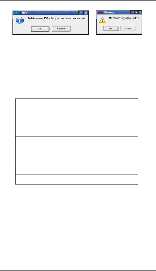
9.3 Quick Guide for Data Output
The left message is generated by the entry in the Prompt field, and
reminds you to delete the temporary file %N.$$$ created when generating
the aperture table after the job is done.
The message on the right advises you that more than one signal layer are
active at the same time. Normally only one signal layer is active while
output is generated. However, when generating the wheel, all the layers
need to be active at the same time to form a common aperture table for
the Gerber output.
The following files will be subsequently output:
%N.whl Aperture file (Wheel)
%N.cmp Component side
%N.sol Solder side
%N.plc Silk screen component side
%N.stc Solder stop mask component side
%N.sts Solder stop mask solder side
%N.$$$ Temporary file, please delete it
%N.gpi Info file, not needed here
9.4 Which Files do I Need for my Board?
The previous part of this chapter told you a lot about the basics of data
generation and how to use pre-defined job files for default two layer boards.
In this section you will find a summary of files usually generated for board
manufacturing.
Files List
The output files of the CAM jobs differ in their file extensions. You are, of
course, free to use unequivocal names of your own.
The CAM Processor allows the use of some placeholders for the generation of
output file names. Usually the output file name consists of the name of the
board file plus a special file extension. For the board file name without
extension we use the placeholder %N. Write, for example, in the Output File
307
➢
Messages in gerber.cam
9 Preparing Manufacturing Data
field: %N.cmp. This will be expanded with the name of the layout file that is
loaded plus the extension (here: boardname.cmp).
In the following table %N also stands for the name of the currently loaded
board file that is used to generate manufacturing data from.
File name Selected layers Description
Signal layers
❑%N.cmp 1 Top, 17 Pads, 18 Vias Component side
(top)
❑%N.sol 16 Bottom, 17 Pads,
18Vias Solder side (bottom)
Inner layers
❑%N.ly2 2 Route2, 17 Pads, 18
Vias
Inner layer 2
❑%N.ly3 3 Route3, 17 Pads, 18
Vias
Inner layer 3
..... ..... .....
❑%N.l15 15 Route15, 17 Pads,
18 Vias
Inner layer 15
Silk screen
❑%N.plc 21 tPlace, 25 tNames,
possibly 20
Dimension(*)
Silk screen
component side
❑%N.pls 22 bPlace, 26 bNames
possibly 20
Dimension(*)
Silk screen solder
side
Solder stop mask
❑%N.stc 29 tStop Solder stop
component side
❑%N.sts 30 bStop Solder stop solder
side
Cream frame (for SMT devices)
308
9.4 Which Files do I Need for my Board?
❑%N.crc 31 tCream Cream frame
component side
❑%N.crs 32 bCream Cream frame solder
side
Milling contours for openings, oblong holes...
❑%N.mill 46 Milling (**) Plated milling
contours
❑%N.dim 20 Dimension (**) Non-plated milling
cont.
Finishing mask (e.g. gold coating)
❑%N.fic 33 tFinish Finishing
component side
❑%N.fis 34 bFinish Finishing solder side
Glue mask (for larger SMT devices)
❑%N.glc 35 tGlue Glue mask
component side
❑%N.gls 36 bGlue Glue mask solder
side
Drill data
❑%N.drd 44 Drills, 45 Holes All drillings
Distinguishing plated from non-plated drillings
❑%N.drd 44 Drills Plated drillings
❑%N.hol 45 Holes Non-plated drillings
(*) Please check with your board manufacturer whether you have to output
the board contour in layer 20 in a separate file or you are allowed to combine
it with those layers.
(**) If there are additional milled edges in the board, you should contact
your board manufacturer and ask them which layers they prefer for milling
contours.
309

9 Preparing Manufacturing Data
Placeholders for Output File Name Generation
%D{xxx} xxx stands for a string that is inserted
only into the data file name
%E file extension of the loaded file, without
the '.'
%H home directory of the user
%I{xxx} xxx stands for a string that is inserted
only into the Info file name
%L layer range for blind&buried vias
%N name of the loaded file without path and
extension
%P directory path of the loaded Board or
Schematic file
%% the character '%'
These placeholders must be written in upper case letters!
Hints Concerning File Extensions:
cmp stands for component side, the upper side of the board, sol for the solder
(bottom) side. It makes sense to choose the first two letters according the
active layers. The third one can be c or s for belonging to component or
solder side.
Of course you are free in naming your files in any manner you wish!
Please ensure when defining a job that the extensions of the output
files are unique and therefore distinguishable.
9.5 Peculiarities of Multilayer Boards
In case of boards with inner layers one has to know how these layers are
defined in order to generate proper manufacturing data. Is it an inner layer
that contains tracks and polygons, as it is in Top or Bottom layer? Or is it a
supply layer that can be identified by the $ character in front of the layer
name?
Inner Layers
Inner layers are treated the same as the outer signal layers. Together with the
signal layer, the layers Pads and Vias have to be actived.
310

9.5 Peculiarities of Multilayer Boards
If the Layer Setup allows Blind and Buried vias, the combination of one
signal layer and the Vias layer outputs only those vias that belong to this
signal layer.
If there is only the Vias layer active (no signal layer), the CAM
Processor will output all vias of the board!
Drill Data for Multilayer Boards With Blind and Buried
Vias
The CAM Processor generates one drill data file for each via length for a
layout that uses Blind and Buried vias.
The drill data file extension .drd is expanded by the via length specification.
If there are, for example, vias from layer 1 to 2, the output file extension will
be .drd.0102.
The layer specification can be moved to another position with the help of the
wildcard %L. Writing, for example, in the File box of the CAM Processor %N.
%L.drd results in an output file named boardname.0102.drd.
Pads and trough-hole vias will be written into an output file with extension
.drd.0116. If you placed holes (HOLE command) in the layout and the Holes
layer is active for output, the CAM Processor writes this data also into the file
with extension .drd.0116.
Pass on all these files to your board manufacturer.
Provided you did not use the EXCELLON device which combines drill table
and drill coordinates in a common file, your board house additionally needs
the rack file name.drl which is generated by drillcfg.ulp.
9.6 Set Output Parameters
This section describes the setting of the parameters in the CAM Processor for
the output of a board or a schematic.
Load the schematic or board file from the CAM Processor's File/Open menu,
and set the parameters.
The CAM Processor window is divided into sections (Output, Job, Style,
Layer, Offset and so on). Some sections, like Emulate, Tolerance, Pen or
Page, are used by and therefore displayed with certain devices only.
311
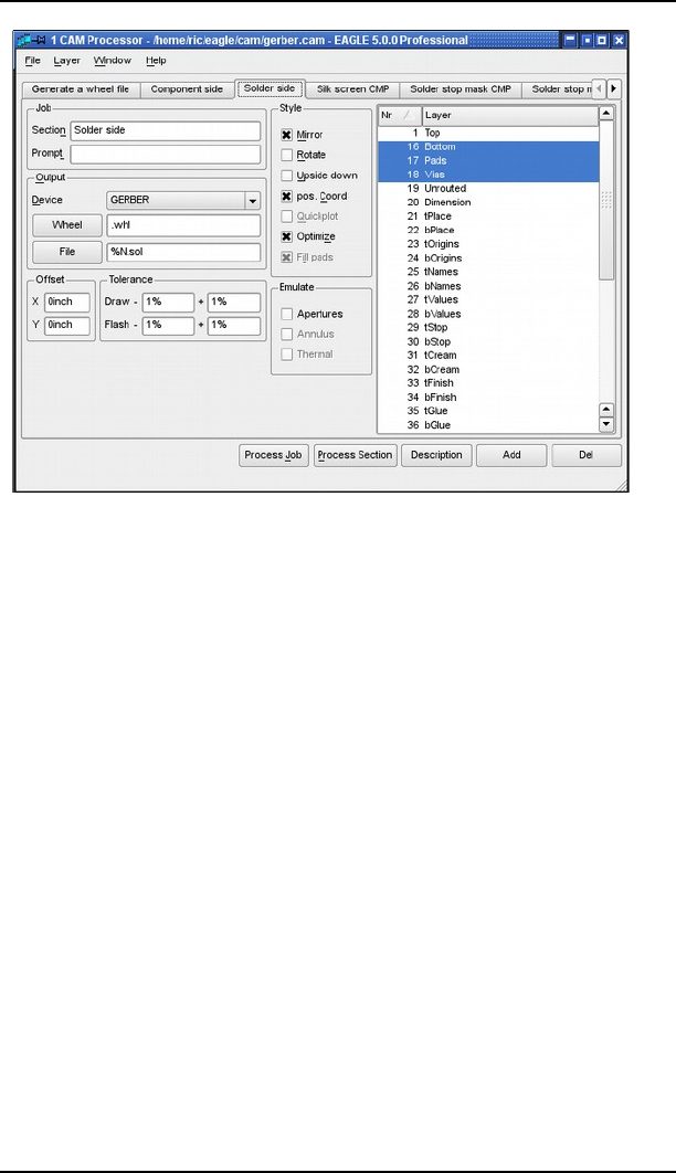
9 Preparing Manufacturing Data
➢
CAM Processor: Solder side section of the gerber.cam
job
Output:
Select the driver for the desired output device or output format in the
Device combo box.
Enter the output path and file name in the File field or simply click
onto the File button and use its dialog.
If you want to output a file on a particular drive, place the drive
identifier or, if appropriate, the path in front of the file name ending.
For instance, under Windows, d:\%N.cmp would place the file
boardname.cmp in the root directory of drive D. This also applies to
the Linux version, so that, for example, /dev/hdc2/%N.cmp, would
place the file on drive hdc2.
%H can be used as wildcard for the Home directory, %P for the loaded
file's directory path.
If output is to go directly to a plotter, enter the name of the print
queue that is connected to the corresponding computer interface in
UNC notation, e.g. \\Servername\Plottername.
Depending on the chosen device it may be asked for Wheel (aperture
table) or Rack (drill table). Select path and file by clicking the button.
Layer selection:
Select the layers that should be output into a common file by clicking
the appropriate layer number.
Click the menu Layer/Deselect all to uncheck all the layers first.
Layer/show selected displays only the currently selected layers.
Some devices (like HPGL or certain plotter devices) allow you to select
a color or pen number in an additional column.
312

9.6 Set Output Parameters
Style:
Mirror: Mirrors the output.
It can be useful to mirror all outputs that refer to the bottom
side of the board.
Rotate: Rotates the output by 90 degrees.
Upside down: Rotates the output by 180 degrees.
When combined with Rotate, the drawing is rotated
by a total of 270 degrees.
Pos. Coords.: Avoids negative coordinate values for the output.
The drawing will be moved near the coordinate's axis,
even if it is already in the positive coordinates range.
Negative values can lead to errors with a lot of devices!
This option should be set on always by default.
Switching it off, transfers the coordinate values from
the Layout Editor unchanged.
Quickplot: Draft output which shows only the outlines of objects.
This option is available for certain devices, like HPGL
and various plotters.
Optimize: Activates the optimization of the drawing sequence for
plotters. Should be set on by default.
Fill Pads: This option is always set on. Only the devices PS and
EPS allow you to switch off this option. The drill holes
for pads will be visible on the output (as it is with the
PRINT command).
Job:
If you are on the way to define a CAM job that consists of several
sections it is useful to name them. In the Section line, it is possible to
enter a section name which will be shown also in the tab above.
If, for example, you assign the section name Wheel: Generate
Aperture File, only the title Wheel is visible as a tab name. The
additional description can be read in the section line. The colon ends
the title in the tab.
In case you wish to display a message box on the screen before
executing this section, enter special message text in the Prompt field.
For example: Please insert a new sheet of paper! The output does not
continue until confirmation of this message.
Offset:
Define an offset in x and y direction.
The values can be given in Inches or Millimetres, for example, 15mm
or 0.5inch.
Tolerance:
Tolerances for Draw and Flash apertures are necessary for devices
that use an aperture file, like GERBER or GERBER_23. Usually one
allows a tolerance of 1% in all fields.
This is necessary to compensate small rounding errors that can arise
during the conversion from mm to inch values and vice versa as the
aperture table is generated.
313

9 Preparing Manufacturing Data
Devices for drill data generation that use a separate drill table (rack
file) invoke a Drill entry. A tolerance of ± 2.5% is enough to
compensate for rounding errors that possibly can arise during the
conversion from mm to inch.
Emulate:
If an aperture with the exact value is not available in the aperture file,
you can allow Aperture emulation. The CAM Processor is allowed to
use smaller drawing apertures for emulation. Plotting time and costs
will increase, and therefore you should try to avoid aperture
emulation.
Arcs with flat endings (CHANGE CAP FLAT) are always emulated for
Gerber output, which means that they are drawn with small lines.
Arcs with round endings (CHANGE CAP ROUND), however, not.
If your layout contains objects that are rotated in any angle, you
have to activate aperture emulation. Certain pad shapes must be
drawn with a smaller round aperture.
Page:
Define the Height and Width of the sheet you want to plot on. Values
are in Inches by default. Values can also be given in Millimetres, like
297mm.
Pen:
The Diameter of the plotting pen is given in here. The value has to be
in Millimetres.
For plotters that support adjustable pen Velocity you can define a
value given in cm/s (centimetres per second). No value here results in
a default value given by the plotter.
Sheet:
Select the sheet of the schematic you want to output.
9.7 Automating the Output with CAM
Processor Jobs
Defining a New CAM Job
A Job consists of one or more sections that allow you to generate a full set of
manufacturing data with only a few mouse clicks. A section is a group of
settings, as described above in the Set Output Parameters chapter, which
defines the output of one file.
Define a job as follows:
Start the CAM Processor.
No job is loaded at first, unless there is a file called eagle.cam in the
cam directory or an existing job is called up automatically by an
EAGLE project file.
314

9.7 Automating the Output with CAM Processor Jobs
If has not already been done, load the board file which you want to
define the job for (also possible for schematics).
It is best that you load an existing job, for example gerb274x.cam,
through the CAM Processor's File/Open/Job menu.
Save this job under a new name with File/Save job... So the original
job file remains unchanged.
Click the Add button.
The currently active section with all its parameter settings is copied
now.
Enter a new descriptive text in the Section line.
If you wish to get a message shown before executing this section,
enter a specific text prompt in the Prompt line.
Set all parameters now:
Device, the layers for the output, the output File, a Scale factor, if
needed, the Style options (Mirror, Rotate, Upside down...).
Define further sections in the same way using different names.
Very important: First use Add to create a new section, then set the
parameters.
Delete a section, if needed, by clicking the Del button.
Save all the sections of your new job as a job file under a name of your
choice with File/Save job...
All the sections of the job will be executed automatically one after another if
you click the Process job button. One specific (the currently shown) section
will be executed if you click the Process section button.
The Description button allows a descriptive text of the CAM job that will be
displayed in the Control Panel.
Extending gerber.cam Job for Multilayer Boards
The gerber.cam job can be used as the basis of the job for multilayer boards.
It must simply be extended for the additional inner layers.
Example:
You want to output the files for a board with SMD components on the top
and bottom sides. The board has two additional inner layers. Layer 2 and
layer 15 which is named VCC.
You need silkscreen prints for the upper and lower sides, solder stop masks,
and masks for the solder cream for both sides.
Before you start to change the CAM job you should save the job under a new
name through the File/Save job as.. menu.
Proceed as described in the previous section. The CAM job then contains the
following sections:
Ne
w
Output
file
Selected layers Description
315
9 Preparing Manufacturing Data
*%N.$$$
1, 2, 15, 16, 17, 18, 20,
21, 22, 25, 26, 29, 30,
31, 32
Generate wheel
file .whl
* modified layer
selection
%N.cmp 1 Top, 17 Pads, 18 Vias Component side
%N.ly2 2 Route2, 17 Pads, 18
Vias Inner layer 2
%N.l15 15 VCC, 17 Pads, 18
Vias Inner layer 15
%N.sol 16 Bottom, 17 Pads,
18Vias Solder side
%N.plc 21 tPlace, 25 tNames,
20 Dimension
Silkscreen
component side
%N.pls 22 bPlace, 26 bNames
20 Dimension
Silkscreen solder
side
%N.stc 29 tStop Solderstop mask
comp. side
%N.sts 30 bStop Solderstop mask
solder side
%N.crc 31 tCream Creamframe comp.
side
%N.crs 32 bCream Creamframe solder
side
Check once more whether all the necessary layers for the creation of the
aperture table are active in the first section. The output file generated in the
first section cannot be used. For this reason, the file boardname.$$$ should
be deleted.
For inner layers, you always have to activate the layers Pads and
Vias!
Error Message: Apertures Missing
If the error message APERTURES MISSING – NO PLOTFILE HAS BEEN
PRODUCED appears after starting the modified CAM Job, the Gerber info
file boardname.gpi contains information about the reason of the problem.
The error could possibly be not all apertures were defined or some could not
316

9.7 Automating the Output with CAM Processor Jobs
be found in the table due to missing tolerance settings.
Ensure all used layers were activated in the Generate a Wheel file section?
It could also be the case that there are parts placed in any angle with pads
that don't have a round shape in the layout. You have to activate the aperture
emulation then to have a successful file creation.
Gerber Info Files
The CAM Processor generates for each Gerber plot file created an additional
Gerber info file with the extension .gpi. This text file informs you about used
apertures, the data format of the Gerber device, about possible aperture
emulations or tolerances, and so on.
If you define a job for Gerber output with data files that use the extensions
proposed in the table above, the info file will be overwritten with each
succeeding section.
If your board manufacturer or your plot service wants to have these
additional information files (they are typically not necessary), use the
%I{xxx} placeholder as follows:
For Output File enter %N.xxx%I{.info}
Here %N stands for the board name, xxx stands for any characters for the file
extension, %I{.info} generates an additional extension .info for the Gerber
info files.
The output files generated will look like this:
Gerber file: boardname.xxx
Info file: boardname.xxx.info
Example:
The board myboard.brd is loaded. The File field contains %N.cmp
%I{.info}. The output file is called myboard.cmp, and the info file is
named myboard.cmp.info.
The files will be written into the same directory as the board file is.
Drill Data Generation with Separate Rack File
If you prefer drill data in another data format, for example Sieb&Meyer 1000
or 3000 (SM1000, SM3000) or the Excellon format with a separate rack file
(EXCELLON_RACK), a drill table is required first.
Define a Drill Configuration (Rack) File
This file is usually created by drillcfg.ulp (RUN command) started directly in
the Layout Editor window and will be named boardname.drl.
It is of course also possible to define a drill table with the aid of a text editor.
For data generation enter the table's path and file name in the CAM
Processor's Rack field.
Example of a drill configuration file:
0-0$0-0
0.0$0->
010$01.
0;0$0;0
090$090
0>0$0A0
317
9 Preparing Manufacturing Data
All dimensions are given here in inches. It is also possible to enter the values
with their unit, e.g. 0.010in or 0.8mm. Comments in drill configuration files
may be used and are identified by a semicolon, which may stand at the start
of a line or be preceded by a space.
Define Job for Drill Data Output
Start the CAM Processor
Load the predefined job excellon.cam, e.g. with File/Open/Job.
Change the output Device to EXCELLON_RACK, SM1000 or
SM3000 and check the parameters. Layers 44, Drills, and 45, Holes,
must be selected only. No other layers! Use the Layers/show selected
menu to get a summary of the active layers.
☞ If you want to have separate files for plated and non-plated
drillings, select here Layer 44, Drills, only and insert a further section
that outputs layer 45, Holes, in a separate file with the Add button
after the following item.
Check with your board manufacturer to see if this is the method they
prefer.
After changing the output device the CAM Processor requires a Rack
file as a tool guide. Type in .drl or click the Rack button and choose
the path to your rack file in the file dialog.
☞ In the event you wish to distinguish plated and non-plated holes:
Add a new section which outputs only layer 45, Holes, into a second
drill file with modified file name. Possibly .hol for holes.
Save the job file via File/Save job with a new name.
A tolerance of ± 2.5% should be allowed for drill diameter selection in
order to compensate rounding errors that possibly can arise during
the conversion from mm to inch and vice versa in the drill table.
Drill Info File
The file name.dri is generated with each drill data output. It contains the list
of used tools and further information about the data format.
If the error message DRILLS MISSING – NO PLOTFILE HAS BEEN
PRODUCED appears, the info file contains information which drill diameter
could not be found in the drill table. Add the missing diameter in the drill
table with a text editor or check the given values for tolerances.
The info file is written into the same directory as the output file. You may
send this file to your PCB manufacturer, if requested.
9.8 Device Driver Definition in eagle.def
Output device drivers are defined in the eagle.def text file. Here you will find
all the information that is needed for the creation of your own device driver.
The best way is to copy the block for an output device of the same general
category, and then alter the parameters where necessary.
318

9.8 Device Driver Definition in eagle.def
The file eagle.def can be found in the eagle/bin directory.
Creating Your Own Device Driver
Please use a text editor that does not introduce any control codes into the file.
Example 1: Gerber(auto) device, Millimetre
/77112
8H(&!X
\KH(&H!X\
=&\0-P000000600000050.\
"&\P000000600000050.70.\
"P.9;00
"6.9;00
(!\\
7M\PY0>6Y0>50.\@%38B
5<\PY0>6Y0>50-\@%38B
E!"(\PY0>6Y0>501\@%38B
=&"
5=!";
H&)\Y"\@H&)B
V\!]=!V\
\\
\=&E&1$1\
\=&=&"-'-000\
\5&7K"!)&\
\^)HH""=\
\+V!J\
\\
/+77112
,7711
\=&()&G<(! !G\
(!\\M="""Z
)&H&)\5Y\@H&))KB
E="&H&)-0
7%H&)=F.$0
Example 2: EXCELLON Device, Output with Leading Zeros
[EXCELLON-LZ]
Type = DrillStation
Long = "Excellon drill station"
Init = "%%\nM48\nM72\n"
Reset = "M30\n"
ResX = 10000
ResY = 10000
;Rack = ""
DrillSize = "%sC%0.4f\n" ; (Tool code, tool size)
AutoDrill = "T%02d" ; (Tool number)
FirstDrill = 1
BeginData = "%%\n"
Units = Inch
Decimals = 0
Select = "%s\n" ; (Drill code)
Drill = "X%06.0fY%06.0f\n" ; (x, y)
Info = "Drill File Info:\n"\
"\n"\
" Data Mode : Absolute\n"\
319

9 Preparing Manufacturing Data
" Units : 1/10000 Inch\n"\
"\n"
Units in the Aperture and Drill Table
When automatically generated with the GERBERAUTO driver, the aperture
table contains values in inches.
This is also the case for the drill table which is automatically written into the
drill data file with the output device EXCELLON.
If your PCB manufacturer insists on mm units for aperture sizes and drill
diameters, you can achieve this by altering the GERBER or GERBERAUTO
respectively for the EXCELLON driver.
Use a text editor that does not introduce any control codes to edit the
eagle.def file, look for the line
/2
or
/+2
and add/edit in this section the lines
=&"
5=!";
In order to change the drill table units look for the line
/P+2
and change:
=&"(
to
=&"
9.9 Gerber Files for Photoplotters with Fixed
Aperture Wheels
This section goes into more detail on the definition of the aperture table.
Some board manufacturers may perhaps still be using a Gerber plotter that
works with a fixed aperture wheel. In such a case it is necessary to adapt the
aperture table to the restricted facilities of the Gerber plotter. Files for
Gerber photoplotters with fixed aperture wheels are generated with the
GERBER driver. It is essential to confer with your photoplot service ahead of
time, so as to adjust EAGLE to the available apertures. The aperture table has
to be defined manually.
There are various types of apertures. They differ in size and shape. The most
common are circle, octagon, and square. The drawing aperture (Draw) used
for tracks is normally a round aperture.
You must specify the aperture configuration before you can generate files for
a fixed aperture wheel photoplotter. To do this, enter the configuration file
for apertures name.whl e.g. with the EAGLE Text Editor, and then load this
file into the CAM Processor by clicking the Wheel button after selecting the
GERBER device driver (see Set Output Parameters beginning with page 311).
320

9.9 Gerber Files for Photoplotters with Fixed Aperture Wheels
Defining the Aperture Table (Wheel)
The CAM Processor distinguishes Draw apertures from Flash apertures. The
first type is used to draw objects (e.g. tracks). The second type is used to
generate symbols (e.g. pads) by a light flash. Only if draw apertures are
defined can the plotter draw lines. Therefore, if the plotter doesn't
distinguish between draw and flash apertures, you must additionally define
round or octagonal apertures as draw apertures.
The following apertures are available:
Name Dimension
5< =&
) =&
_) !&(
+& =&
&! !&(P%<=&(6
+M! =&P%=&6
Use of aperture shapes in the CAM Processor:
5< <"<=")!&"H&)"
) <")H"M="
_) <""_)H"375"M="
+& <"&!H"M="<=&(
&("P6="="
&! <"&!"75"
+M! <"H"<=&(=[&P
6="="
Aperture configuration file example:
50.0)0$00;
5011)0$09O
509."_)0$09O
5-09M!0$0O0%0$010
5-0-&!0$0A9%0$0>0
5--0<0$00;
5---<0$009
The D code determines the tool number, then follows the aperture shape
after at least one blank character, then the dimensions are defined. All values
default to inches, unless a unit is added, for example 0.010in or 0.8mm.
Comments are marked with semicolons at the beginning of a line, or with a
semicolon following a blank character.
Aperture Emulation
If objects exist in a drawing which is not compatible with the available
aperture sizes, it is possible to emulate the desired dimensions by selecting
the Emulate Apertures option. The CAM Processor then selects smaller
apertures to emulate dimensions which are not matched by aperture sizes.
Emulation results in longer plot times and higher film costs, so it should be
avoided whenever possible.
The file name.gpi indicates which apertures are emulated.
321

9 Preparing Manufacturing Data
This
page
has been
left free
intentionally.
322

Chapter 10
Appendix
10.1 Layers and their Usage
In Layout and Package Editor
-H J"3&H"=
.)&. !8
1)&1 !8
;)&; !8
9)&9 !8
>)&> !8
A)&A !8
#)&# !8
O)&O !8
-0)&-0 !8
--)&-- !8
-.)&-. !8
-1)&-1 !8
-;)&-; !8
-9)&-9 !8
->X J"3KX"=
-A" "@&()((!B
-#:=" :="@&()(!!!8"B
-O)& =!="@)KKK"B
.05="= )&!="@=!"V(!"BB
.-&! =!J"3&H"=
..K! =!J"3KX"=
.1&+==" +=="3&H"=@&)&$B
.;K+==" +=="3KX"=@&)&$B
.9&" M=H=&3&H"=@H&7B
.>K" M=H=&3KX"$@H&7B
.A&:!)" H&:3&H"=
.#K:!)" H&:3KX"=
.O&&H !"&H"J3&H"=@$)&$B
10K&H !"&H"J3KX"=@$)&$B
1-& !3&H"=
1.K !3KX"=
11&E=="( E=="(3&H"=
1;KE=="( E=="(3KX"=
19&!) !)"J3&H"=
1>K!) !)"J3KX"=
1A&"& "&L)"&&=VG3&H"=
1#K"& "&L)"&&=V$3KX"=
1O&4H)& "&=&"VH&"3&H"=
;0K4H)& "&=&"VH&"3KX"$
;-&"&=& "&=&"VHH3&H"=
;.K"&=& "&=&"VHH3KX"=
;1M"&=& "&=&"VM="
;;5=!!" )G&()((!"
;9*!" )G(!"
323

10 Appendix
;>7=!!= 7=!!=
;A7")" 7")"
;#5)& 5)&G
;OV VJ"
9-&5) 5&=!&H"H=&
9.K5) 5&=!KX"H=&
In Schematic, Symbol, and Device Editor
O07)!" 7)!="&"H&"
O-&" &"
O.)""" )"""
O1=" GH=&"V"8K!"<=&(=G!=VG
O;8K!" (H"VH&"
O9" "VH&"8K!"
O>:!)" :!)"'H&&8H"
OAV =G!=VG'(=&"
O#)= )==!="V"8K!!=&
B*!"&=!"<=&(&(==&=&(="!8$
(8)"&H!"&=G"&()&)&$
Layers can be used with their names or their numbers. Names can be
changed with the LAYER command or in the DISPLAY menu. The functions
of the special layers remain.
If you want to create your own layers, please use layer numbers above 100.
Use the DISPLAY menu to create new layers (New button) or type the
LAYER command on the command line. If you want to create, for example,
layer 200, Remarks, type in:
6.00J"
To set up color and fill style of this layer use the DISPLAY command.
10.2 EAGLE Files
EAGLE uses the following file types:
Name Type of le
$K 8)&
$"( (G
$!K =K8
$K! 5"=!J !
$)!H ")
$" =H& !
$&%& %& !@!"&(")`%"B
$) 5"=)!"
$&! &!H&V&()&)&
$H )&)&H&! !
$LK )&)&LK
$Kaa J)H !VKN ="(=
&()&)&
$ 7""LK
$KR% J)H !V5@%-$$OB
$"R% J)H !V*@%-$$OB
$!R% J)H !V@%-$$OB
$KRR )&GKJ)H !V5
$"RR )&GKJ)H !V*
$!RR )&GKJ)H !V
EAGLE for Linux only creates and recognizes lower case
characters in file endings!
324

10.3 EAGLE Options at a Glance
10.3 EAGLE Options at a Glance
In order to output manufacturing data, for instance, with the CAM Processor,
EAGLE can be started directly from a terminal window under Linux and
Mac, or from a console window under MS Windows.
Since Windows programs give up their connection to the console they have
been started from, you can use the file eaglecon.exe (located in the eagle\bin
subdirectory of your installation) if you want to run the CAM Processor from
a batch file.
This version of EAGLE is exactly the same as the eagle.exe, except that it
doesn't disconnect from the console.
Type eaglecon -? for a list of CAM Processor options.
The following options are permitted:
""K!8M=&
%)&=M
5%%% 5<&!@0$--0YB
%%% 5=!!&!@0$--0YB
E%%% E!"(&!@0$--0YB
D )HH""""HH&"
+D +HG=FHM&
%%% !XH@!8HB
%%% 5=!!J !
%%% =H& !
%%% GV! !
%%% H&)<(! !
P %)&7""
D "=GM=&"
%%% 5M=@bV!="&B
)!&H&)"
VD E=!!H"
(%%% (=(&@=(B
7=)&H)&
%%% +)&H)& !'(!
H%%% =&@B
_ U)=JH!&
&&)&H)&O0"
"%%% !V&
M%%% M!=&8
) &&)&H)&-#0"
<%%% <=&(@=(B
%%%% +["&P@=(B
8%%% +["&6@=(B
Where:
xxx "&"VV)&(&3$$ !"<=&(-W=!
)K"<=&(-s$
%H!"-W'(')"'!'HL&'H&)$<(!
-s-$.9
-5V)!&VHG="[
+ 5V)!&VHG="
%H! H&))!G
D=X
H&))!G[
E!HG"@$$BK)"<=&()&HG&(CC(&
H&))!G3=)&H)&
5 =&!M!)"
V&(=""=3&(M!)HH!="&=&(=G3
+"== "H"=GM&!3
-GM&!$
325

10 Appendix
50$-0 L)"&"&(<&!&-0Y
5D0$-50$09L)"&"&(<&!&D-0Y9Y
Notes on the individual options:
-A Specify the name of an assembly variant
Start the CAM Processor (-X) with this option in order to generate
data for a special assembly variant. If you do not use -A, EAGLE
creates data for the default variant.
-C Execute a command
After loading an EAGLE file the given command will be executed in
the Editor window's command line. See also help function,
Command Line Options.
-D Draw Tolerance (0.1 = 10 %):
Default: 0
-E Drill Tolerance (0.1 = 10 %):
Default: 0
-F Flash Tolerance (0.1 = 10 %):
Default: 0
-N Suppress messages:
This option suppresses warnings or other information in the console
window (DOS box, Linux console). Thus CAM jobs run without
interruption. Default: off
-O Route-Optimizing:
With this option the route-optimizing for the plotter can be turned
on and off. Default: on
-P Plotter Pen (layer=pen):
If you use a color pen plotter, you can determine which layer is to be
drawn in which color. Example: -P1=0 -P15=1
-R Drill Rack File:
With this option you define the path to a file with the drill
configuration table.
-S Script File:
When opening the editor window, EAGLE executes the eagle.scr
file.
This option allows a different name or directory to be selected for
the script file. The script file is not read by the CAM Processor.
-U User Settings File:
This option can be used to define the location of the eaglerc file
where EAGLE stores user settings. The file can have any name.
In case you are working with EAGLE beta versions and you want to
keep things separate from the official releases, you should start
EAGLE with this option.
-W Aperture Wheel File:
This option defines the path to the wheel file which should be used.
-X Calls command line version of the CAM Processor
326

10.3 EAGLE Options at a Glance
-c Positive Coordinates:
If this option is set the CAM Processor creates data without negative
coordinates. The drawing is moved to the zero-coordinates. This
option can be turned off with the option -c-. Please be careful with
this option, especially if you use mirrored and rotated drawings,
because negative coordinates normally cause problems. Default: on
-d Device:
This option determines the output driver. eagle -d? displays a
list of the available drivers
-e Emulate Apertures:
If this option is selected, apertures that do not exist are emulated
with smaller apertures. Default: off
-f Fill Pads:
This option can only work with generic devices like Postscript.
Default: on for all devices
-h Page Height (inch):
Printable region in the y-direction (in inches). The Y direction is the
direction in which the paper is transported. See also -w.
-m Mirror Output:
Default: off.
-o Output File Name
-p Pen Diameter [mm]:
EAGLE uses the Pen-diameter measurement to calculate the
number of lines required when areas are to be filled. Default: 0
-q Quick Plot:
Generates a draft or fast output, which only prints the frames of
the objects. Default: off
-r Rotate Output:
Rotates the output by 90 degrees. Default: off
-s Scale Factor:
Those devices which cannot change their scale-factor (in the
menu of the CAM Processor), have a scale factor of 1. Default: 1
-u Rotate Output by 180 degrees:
In combination with -r+ one can rotate by 270 degrees. Default: off
-v Pen Velocity in cm/s:
This option is for pen plotters supporting different speeds. To select
a plotter's default speed, use a value of 0. Default: 0
-w Page Width (inch):
Printable area in x direction. See also -h.
-x Offset X (Inch):
This option can be used to move the origin of the drawing.
Default: 0
-y Offset Y (Inch):
Default: 0
Example for starting eaglecon.exe
327

10 Appendix
Gerber data for solder (bottom) side of a board:
!$%-X-d.A;P-o$HK$K--A-#
Gerber data for component (top) side of a board:
!$%-X-d.A;P-o$"!K$K->-A-#
Gerber data for silk screen top side:
!$%-X-d.A;P-o$H!K$K.0.-
Gerber data for solder stop mask component side:
!$%-X-d.A;P-o$"&K$K.O
Gerber data for solder stop mask solder side:
!$%-X -d.A;P-o$"&"K$K10
Gerber data for solder cream mask top:
!$%-X-d.A;P-o$K$K1-
Drill data in Excellon format:
!$%-X-dP+o$!K$K;;;9
Gerber data generated with an older Gerber device with separate aperture
file for the solder side of a board. Draw apertures may have a negative
tolerance up to 10 %.
!-X-dK-WH&)$<(!-oK$"!-D0$-
$KHM=KX
All parameters have to be written in a common line!
Paths that include space characters must be set into double quotes!
10.4 Configuration of the Text Menu
With the help of a script file (e.g. menu.scr) you can configure your own text
menu.
R7)&)H
R
R(="="%H!&(&"(<"(<&"&)HH!%
R)3=!)=")K)"!=""$
7C/"=!=J..$H2(S
!)"=!=J$)!H!I
(G)"=!=J$)!H
TC
C=S
7&=S
E==0$-I
"=-
TI
H=!S
E===(0$00-I
"==(0$-
TI
+=+I
+[=+[
TC
C5="H!8S
H5="H!8H":="5=I
X5="H!8&":="5=I
!H!S
328

10.4 Configuration of the Text Menu
H5="H!8&!5=I
X5="H!8K!5=
T
TC
C---C
CE=&=<E=&C
5!&7MCC=&U)=&
The backslash \ at the end of a line shows that a command continues in the
next line. Here the MENU command runs from the first line after the
comment to the last line.
The pipe sign | has to be used if a command within braces { } is followed by
another command.
The MENU command can handle small images as shown in the example
above with designlink22.png. The images are expected to be in the eagle/bin
folder by default. It is also possible to use a path with the image name.
10.5 Text Variables
Text variable Meaning
?7 H&@M&)!!8D&B-B
?: H&M!)'&8H-B
? H&.B
? &.B
?7+5 7)!@!8)!"(&"B
?* (&)KV=)=&==&(V
V3V%H!-'11B
?**5 ((!=V&("(&"=HG
?*+ (&)K=(=(=!"(G=&(VV
?*+'?*+
?* &!)KV"(&"1B
?*+ &!)KV"(&"=!)=&()!"(&"
?* )&"(&)K1B
?*+ )&"(&)K=!)=&()!"(&"
?76: V""K!8M=&
?57 5<=
?57 =V&(!"&= G
?+57 =V&(H!&G
-B+!8VHJ"8K!
.B+!8V"8K!
1B+!8V"8K!=)=&=
All texts starting with the character >, will be interpreted as placeholder texts
for attributes. See ATTRIBUTE command.
10.6 Options for Experts in eaglerc
The user-specific file eaglerc.usr for Windows and .eaglerc for Linux and Mac
stores various settings defined during the work with EAGLE. Among them
you find some expert settings that can be adjusted in this file directly. The
most important of them are listed here.
Since version 5.2 it is possible to change these parameters with the help of
the SET command in the command line. Please see the help function about
the SET command for details.
329
10 Appendix
CAM Processor – Suppress Drills/Holes Warning
If you want to suppress the warning that you should activate the Drills and
the Holes layer for generating Drill data, write the following line in the
eaglerc file
=$$5=!!"*!")&\0\
Change Component Value Warning
Some users don't want the warning message about a part not having a user
definable value, so this warning can be disabled by appending the line
=$&*""5 K!:!)\0\
to the file.
Consistency Check
In order to handle Board/Schematic pairs that have only minor
inconsistencies, the user can enable a dialog that allows him to force the
editor to perform Forward&Back Annotation, even if the ERC detects that
the files are inconsistent. This can be done by appending the line:
$!!<"+M="="&8(J\-\
PLEASE NOTE THAT YOU ARE DOING THIS AT YOUR OWN
RISK!!!
If the files get corrupted in the process, there may be nothing
anybody can do to recover them. After all, the ERC did state that the
files were inconsistent!
Delete Wire Joints
If you absolutely insist on having the DELETE command delete wire joints
without pressing the Ctrl key, you can append the line
$5!&$=W=&"=&()&&!\-\
to the file.
Device Name as Value for all Components
Some users always want to use the device name as part value, even if the part
needs a user supplied value. Those who want this can append the line
($$$!<8""5M=":!)\-\
to the file.
Disable Ctrl for Radius Mode
If you don't like the special mode in wire drawing commands that allows for
the definition of an arc radius by pressing the Ctrl key when placing the wire,
you can add the line
$=$&!E=)"7\-\
to the file. This will turn this feature off for all commands that draw wires.
330

10.6 Options for Experts in eaglerc
Group Selection
Since the context menu function on the right mouse button interferes with
the selection of groups, a group is now selected with Ctrl plus right mouse
button. If you want to have the old method of selecting groups back, you can
add the line
+HG$!&!E)H!G&%&7)\-\
to the file. This will allow selecting groups with the right mouse button only
and require Ctrl plus right mouse button for context menus.
Load Matching File Automatically
If you have a board and schematic editor window open and load another
board (or schematic) in one of these windows, and if that other drawing has a
matching schematic (or board), EAGLE asks whether that other drawing
shall also be loaded. By setting
+HG$)&7&(=5<=E=!\-\
this query will be suppressed.
Name of Net, Busses, Signals and Polygons
If a net consists of more than one segment, the NAME command by default
acts only upon the selected segment. In order to rename the entire net set
$$G&85V)!&\-\
This parameter also applies to busses.
If a signal contains a polygon, and the NAME command is applied to that
polygon, by default only the polygon gets renamed. Setting
$$G=!85V)!&\-\
makes the NAME command act upon the entire signal by default.
Open Project
The automatic opening of the project folder at program start (or when
activating a project by clicking onto its gray button) can be disabled by
appending the line
&!!$:=<$)&+HL&E!\0\
to the file.
Panning Drawing Window
Panning can be done with the Ctrl button (as in previous versions) by writing
&V$"&!E=\-\
into the file. Note, though, that the Ctrl key is now used for special functions
in some commands, so when using these special functions (like selecting an
object at its origin in MOVE) with this parameter enabled you may
inadvertently pan your drawing window.
Polygon Edges as Continuous Lines
If you don't like the way unprocessed polygons display their edges (as dotted
lines), you can add the line
+HG$5<H""!8"G))"\-\
The edges of polygons will be displayed as continuous lines then.
331
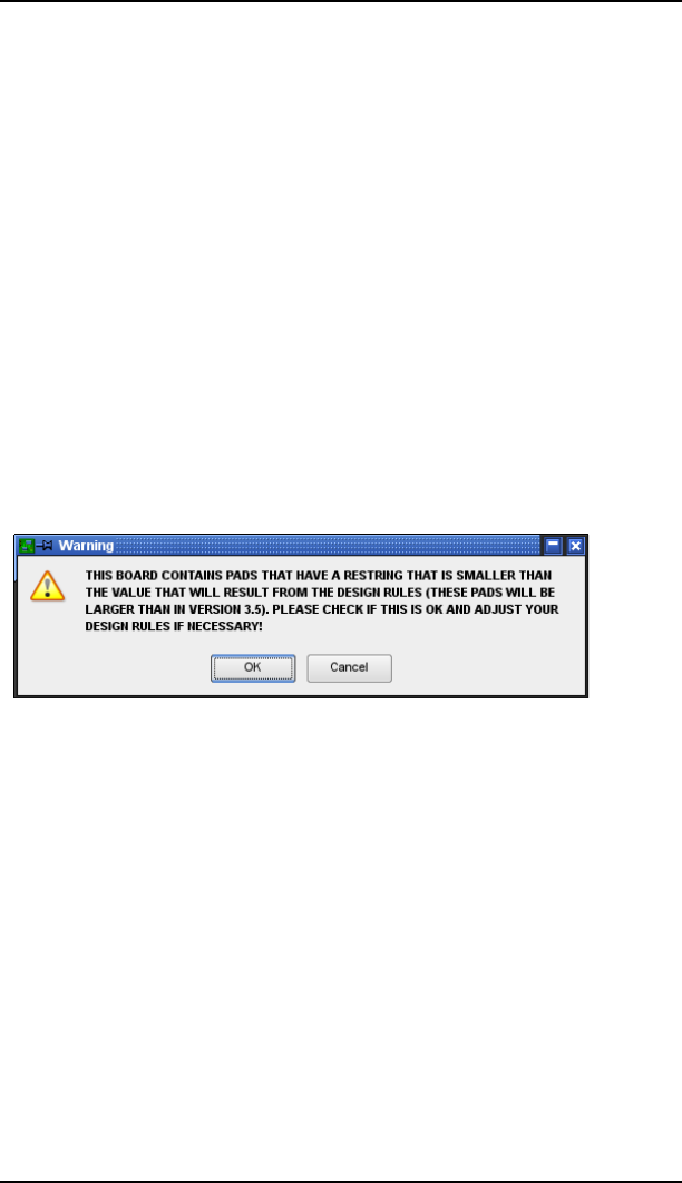
10 Appendix
Reposition of the Mouse Cursor
Normally EAGLE does not automatically position the mouse cursor.
However, if you prefer the cursor to be repositioned to the point where it has
been before a context menu in the drawing editor was opened, add the line:
+HG$H"=G7)")"N&%&7)\-\
Units in Dialogs
The automatic unit determination in dialog input fields can be controlled by
appending the line
&V$V=&\%\
to the file, where "x" can be
"0" for automatic unit determination (default)
"1" for imperial units
"2" for metric units.
10.7 Error Messages
When Loading a File
Restring smaller than in older version
In EAGLE version prior 4.0 the pad diameter has been fixed in the Package
definition. Due to the given values in the Design Rules the pad diameters
have changed.
Please check and, if required, change the Restring settings. Run the Design
Rule Check in any rate to recognize possible clearance errors.
Library objects with the same names
The Text Editor shows this message if you attempt to load an older file (BRD
or SCH) that contains different versions of a library element. In this case it
added @1, @2, @3... to the names of the Devices so that they can be
identified.
332
➢
Pad diameter changed
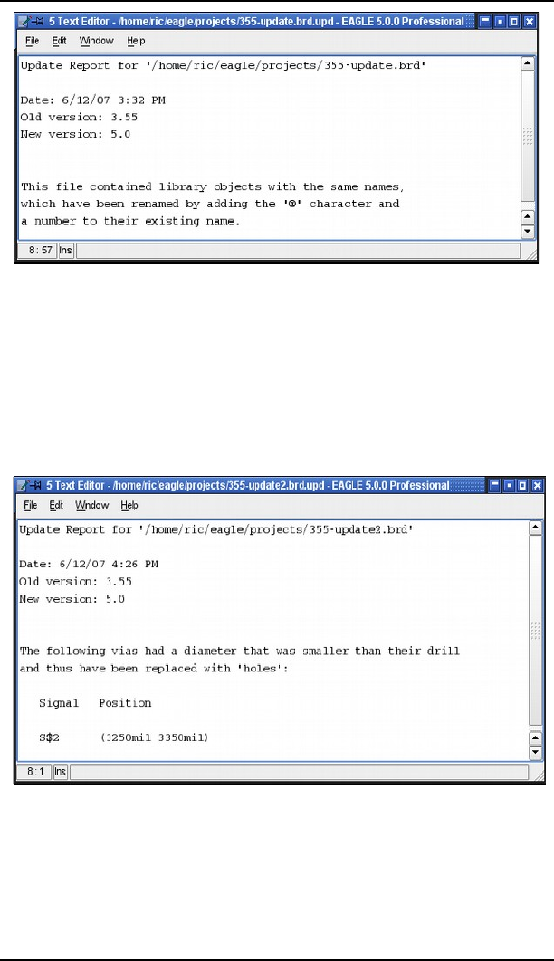
10.7 Error Messages
This message can also appear if you use COPY and PASTE commands.
Pad, Via Replaced with a Hole
In older versions of EAGLE it was possible to define pads in which the hole
diameter was larger than the pad diameter. This is no longer permitted.
If you attempt to load a library file that was created with an earlier version
and that contains such a pad, the following message appears:
The pad or via is automatically converted into a hole, provided it is not
connected by CONNECT to a pin in one of the library's Devices.
If there is pad that has a connection to a pin (it is defined in the library), the
following message appears:
333
➢
Update report: Objects with the same name
➢
Update report: Via replaced with hole

10 Appendix
In that case the Library file must be manually edited in order to correct the
pad. Then you can update the board file with the new library definition.
Skipped unsuitable objects
If this message is shown, while you are loading a file or copying objects with
COPY and PASTE from one file into another, the data structure contains
objects that do not belong to the current file type and can't be displayed. For
example, a text or rectangle that has a non-orthogonal angle and is placed in
a user-defined layer (above 100) in the Layout editor which should be pasted
into a schematic. The Schematic editor doesn't allow non-orthognal angles
and therefore can't display such an object.
This message could be prompted as well, if the file's origin is one of the first
EAGLE versions. The file can be used without problems nevertheless. The
data structure is cleaned up automatically while loading it.
Can't Update File
If this message appears when loading an EAGLE file that was made with a
version earlier than 2.60 it is necessary first to convert the file.
The program update26.exe, which is located in the eagle/bin directory, is
used for this purpose.
334
➢
Update report: Pad replaced with a hole
➢
Update error: File older than version
2.6
10.7 Error Messages
Copy the file that is to be converted into the directory containing both
update26.exe and the file layers.new. Then open a DOS window under
Windows, and change into this directory. Type the command:
)H&.>&=$%&
The file is converted, after which it can be read by the new version of EAGLE.
If the conversion is successful, the message in the DOS box is: ok...
If the message Please define replacement for layer xxx in layers.new should
appear, it means that you have defined your own layers in
layout/schematic/library.
Because of the new layer structure used since version 2.6, a new layer
number (greater than 100) must be assigned.
This requires you to edit the file layers.new using a simple text editor,
adding, for example, a new layer number as the last line of the file.
If, for instance, you have used layer 55, and want to give it number 105,
enter:
99-09
In a Library
Package/Symbol is in use
If a Package or Symbol is already used in a Device, no pads or pins which are
already referenced to a pin or pad with the help of the CONNECT comand,
may be deleted . In such a case EAGLE shows the following messages:
But it is allowed to CHANGE or NAME such pins or pads. It's also possible to
add further pins/pads with the PIN or PAD/SMD command and you are
allowed to DELETE pins/pads which are not referenced via the CONNECT
command.
This message also appears, if you try to remove the whole Package/Symbol
from the library with the REMOVE command. You have to delete the whole
Device or the Package variant or symbol in the Device before.
In the CAM Processor
Polygon may cause extremely large plot data
This message appears, if you selected a layer in the CAM Processor which
contains a signal polygon in the layout whose line thickness is less than the
resolution of the selected output driver (Device).
335
➢
Error while editing Package or
Symbol
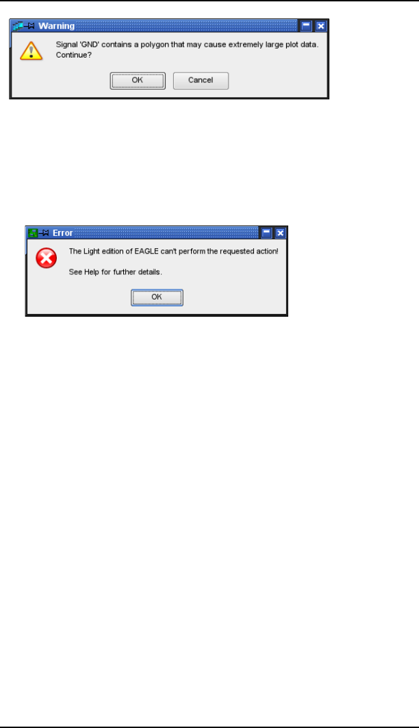
10 Appendix
In order to avoid unnecessary large plot files you should assign a higher value
to the polygon's line width (CHANGE width).
In the Free or Standard Edition
Can't perform the requested action
This message is shown if the limits of a smaller Edition are exceeded. This
can be the case, for example, if you want to place a part outside the Layout
size limits, if you want to start the Autorouter, or set parameters for the
Follow-me router, although there are parts outside the Layout limits, or you
want to define a not allowed inner layer.
336
➢
Polygons with width 0
➢
Free/Standard limits

Index
3
3
3D board 167
3D package assignment 234
A
A
Action toolbar 50, 53
Addlevel 267
Always 275, 277
Can 275
Must 275, 276
Next 275
Request 275
Airwire 26
Calculate 76
Display/hide 76
Alias 97
Deleting 98
ALIGN 22, 69
Alpha blending 108
Alt-X 45, 64
Aperture 320
Aperture File 296
Attributes
Defining 61, 127, 271
External device 274
For elements 127
Global 127
Search 116
VALUE 265
Automatic Naming 99
Autorouter 76
Backup 218
Blind vias 180
Bus router 205
Continue existing job 213
Control file, ctl 221
Control parameter 213
Controlling 204
Cost factors 213
Cutout polygon 209
Design rules 206
Effort 211
Features 203
Hints 222
Information 218
Interruption 218
Layer selection 208
Load settings 211
Log file 220
Memory requirement 208
Menu 210
Micro via 217
Min. distance, clearance 206
Min. routing grid 203
Module 33
Multilayer board 208
Net classes 206
Optimization 205
Placement grid 206
Polygon 216
Polygons as supply 217
Preferred direction 209, 210
Restarting 213
Restricted area 209
Ripup/Retry 216
Routing grid 207
Routing pass 205
Save settings 211
Select signals 211
Single-sided boards 222
Smds and supply layer 222
Status display 218
TopRouter 205
Track width 206
Unreachable Smd 207, 209
B
B
Background color 108
Backup files 47, 324
Beep 110
BGA Autorouter 76
Bill of material 300
Blind via 26
Blind via ratio 147
Blind, Buried via 180
Bmp file 101
Board
Arrange components 156
Attributes, global 158
Contour detection 155
Creating 153
Cut-out 282
337

Index
Cutouts 156
Design Rules 144
Draw outline 154
Flip View 20
Layer setup 146
Lock component 71
Multilayer 178
Multiple board 197
Placement grid 154
Prior considerations 143
Quotation 295
Routing manually 161
Board Manufacture 295
Buried via 26
Bus
End automatically 111
Naming 124, 331
C
C
CAM Job
Define drill job 318
Description 315
Excellon.cam 305
Extending gerber.cam 315
gerb274x.cam 304
gerber.cam 306
Output parameter 311
CAM Processor 84
Assembly variants 302
Choose pen number 312
Component side 308
Cream frame 309
Creating device driver 319
Drill data 297, 309
EPS output 299
Error: Apertures missing 316
Error: Drills missing 318
Extremely large plot data 335
File extensions 310
Fill Pads 313
Finish mask 309
Glue mask 309
HPGL 102
Inner layer 308
Job 314
Load job file 85
Milling contours 309
Plotter 312
Pos. Coords. 313
PostScript 298
Prompt 307
Save time and money 302
Section name 313
Silk screen 308
Solder stop 308
Start 53, 84
Start from batch 325
Tolerance 313
UNC notation 312
Vias 311
Caption 196
Circle
Filled 278
Clearance 147
Cmd key 91
Color
Background 49
Settings 107
Command
Activating 87
Language 91
Line 51, 87
Parameters 52
Text menu 328
Toolbar 51
Commands
ADD 57, 70, 82, 241
ALIGN 22, 69
ARC 60, 74
ASSIGN 62, 89, 105
ATTRIBUTE 61, 75, 83
AUTO 76
AUTO BGA 76
BOARD 53, 154
BUS 60, 124
CHANGE 57, 70, 83, 237
CIRCLE 60, 74, 91, 94
CLASS 62, 123
CLOSE 62
CONNECT 83, 242, 263
COPY 56, 69, 286
CUT 62
DELETE 57, 69
DESCRIPTION 80, 83
DIMENSION 61, 75
DISPLAY 55, 67, 97
DRC 76, 173
EDIT 62, 79, 116
ERC 62, 76, 130
ERRORS 77, 174
EXPORT 63, 91, 100
FRAME 63, 280
FUSIONSYNC 167
GATESWAP 58, 242
GRID 53
GROUP 56, 68
338

Index
HELP 51
HOLE 75, 88, 278
INFO 55, 66, 148
INVOKE 59, 118
IPROBE 20
JUNCTION 61, 121
LABEL 61, 121
LAYER 63, 324
LINE 59, 73
LOCK 71
MAKESPICE 20
MAPTOMODEL 20
MARK 55, 68, 287
MEANDER 72, 190
MENU 63, 105
MIRROR 56, 68, 88, 158, 281
MITER 59, 71
MODULE 61
MOVE 56, 68, 88
NAME 58, 71, 82
NET 60, 120
OPEN 63
OPTIMIZE 72
PACKAGE 63, 83, 284
PAD 80, 235
PASTE 57, 69, 133
PIN 95, 238
PINSWAP 58, 70
POLYGON 60, 74, 164
PORT 62
PREFIX 83, 243
PRINT 64, 195
QUIT 64
RATSNEST 76
RECT 60, 74
REDO 54
Remove 79
REMOVE 64, 116, 291
Rename 79
RENAME 292
REPLACE 58, 70, 160
RIPUP 73, 163
ROTATE 56, 69, 157, 287
ROUTE 72, 161
RUN 53
SCRIPT 53, 100
SET 64, 105, 329
SHOW 55, 66
SIGNAL 75
SIM 20
SIMOPTOGGLE 20
SLICE 59, 72
SMASH 58, 71, 118, 158
SMD 80, 235, 253
SOURCESETUP 20
SPLIT 59, 72
TECHNOLOGY 64, 83, 264
TEXT 60, 73
UNDO 54
UPDATE 64, 188, 292
USE 53, 245
VALUE 58, 71, 83, 243
VARIANT 64
VIA 75, 88, 186
VPPROBE 20
VPROBE 20
WINDOW 53
WRITE 65
Component
Add from library 57
Attribute 127
Changing Technology 161
Copying by Drag&Drop 289
Create symbol 238
Creating 82, 229
Cross-reference 278
Description 237
Editing 187
External 274
Keepout 237
Labeling 236
Lock 71
Name 236
On both sides 158
On bottom side 235, 281
Output list 101
Package editor 237
Placement grid in board 154
Prefix 243
Replace device 160
Replace package 159
Replacing 58
Rotation 156
Searching 116
Separate name/value 58, 71
Update 187
Value 58, 71, 236
Without package 274
Configuration
Commands 104
eagle.scr 111
eaglerc, eaglerc.usr 113, 329
Location of eaglerc 326
of EAGLE 104
User interface 105
Connector 276
Consistency
Check 62, 76, 104, 130
Indicator 201
Loss of c. 198
Contact cross reference
>CONTACT_XREF 122
339

Index
>XREF 278
Context menu 43, 88
Configure 105
Control Panel 39
Options menu 46
Search in tree 46
Control parameters 213
Coordinates
Display 51, 55, 68
Entering 93
Modifier 94
Polar 94, 287
Relative 94, 287
Select group 94
Copper plane 164
Copying SCH/BRD 132
Core 26, 180
Cost factors 213
Cream mask 152
Cross reference
For contacts 122, 278
For nets 61, 121
Specify format 122
Ctrl key 91
Current units 95
Cursor appearance 49
Cutout-Polygon 179
D
D
Data output 84
Date/time stamp 280
Delete
All signals 101
Wire bend 70
Design Block 42, 58
Add to drawing 58
Live DRC 20
Design Blocks 134
Design Rule Check 26, 76
Approve errors 175
Correcting errors 173
Fonts 153
Meaning of errors 175
Restricted areas 153
Show errors 77
Wire styles 178
Design Rules 42, 144
Clearance 147
Definition 76
Layer setup 146
Options 145
Restring 148
Designlink interface 119
Desktop Publishing 299
Device 26
Assign Package 242
Attributes 271
Build Device Set 260
Copying 289
Creating 241
Delete 78
Description 244
Driver 319
Editing 79, 81
External 274
Gate names 242, 261
Open/Edit 187
Placeholder in name 261
Prefix 243
Remove from LBR 291
Rename 78
Replacing 58, 160
Technologies 264
Value on/off 83, 243
Device Set 26
Differential Pair 189
Dimensioning 75
Directories 46
Distance 147
Documentation 40, 300
Export image 101
Print 236
Documentation field 280
Drag&Drop 39
Draw lines 59
Drawing area
Alias 98
Display last 54
Panning 54
Drawing frame 116, 279
Drawing name 280
DRC 26
See Design Rule Check 173
Drill 26
Diameter 278
Display 110
Legend 302
Non-plated 297
340

Index
Plan 301
Plated 297
Symbols 301
Drill data 297
Blind/buried vias 311
Configuration file 317
drillcfg.ulp 317
Error: Drills missing 318
EXCELLON 297
EXCELLON_RACK 317
Info file 318
Leading zeros 319
Multilayer boards 311
Rack 317
Separate rack file 317
SM1000 298
SM1000/SM3000 317
SM3000 298
Tolerance 318
Units 320
Dxf data export 102
E
E
eagle.def 318, 320
eagle.epf 114
eagle.scr 111
eaglecon.exe 325
eaglerc, eaglerc.usr 113, 326, 329
ECAD/MCAD
Synchronise 167
Edition
Premium 34
Standard 36
Electrical Rule Check 26, 62, 130
Approve errors 131
Electrical schematic 278
Electrical Schematic 122
Elongation 150
Encapsulated PostScript 299
Environment variable 47
ERC 26
Error messages
CAM Processor 335
Correcting 173
DRC - Meaning of 175
File prior version 2.60 334
In a library 335
Loading a file 332
excellon.cam 318
Exclamation mark 202
Exit program 45
Expert options 329
Export
Libraries 102
Export data 99
F
F
Fiducials 303
File
Backup 324
Edit 62
Import 134
Load SCH/BRD query 331
New 44
Open 45, 53
Print 53
Save 53
File Locking 47
Film Generation 298
Fixing hole 277
Follow-me Router 27, 223
Font
Checking 153, 177
No vector error 177
Persistent in drawing 48
Typeface 60, 73
Vector 48
Forbidden area 161
Forward&Back Annotation 27, 104
Consistency indicator 201
Consistency lost 198
Function keys 62, 89, 105
Fusion 167
G
G
Gate 27, 261
Hidden supply 118
Name 261
Place particular 59
Gateswap 125
Gerber
Extending gerber.cam 315
341

Index
Fixed aperture wheel 320
Units 320
Gerber device
RS-274D 296
RS274X 296
Gerber output
Aperture configuration 321
Aperture types 321
Arc 314
Draw aperture 321
Emulate aperture 314
Emulation 321
Error: Apertures missing 316
Flash aperture 321
GERBER 306
gerber.cam 306
GERBERAUTO 306
Info files 317
Messages gerber.cam 306
Resolution 296
Wheel 320
Wheel, example file 321
Gestures 49
GND symbol 269
Graphic format 101
Graphics data
Import 103
Grid 95
Alias definition 97
Alternative grid 96
Check 153
Menu 96
Min. visible size 111
Pad placement 234
Group
Default action 111
Define 56, 68
Move 56
Move to sheet 56
Rotate 287
H
H
Help function 50, 51
Hierarchical Schematic 137
Hierarchy
Part names in Layout 142
History function 88
Hole 27
Diameter 278
Min. diameter 147
HOME variable 47
Hyperlinks
In descriptions 244
I
I
Icons
Scale size 49
5.6 Import 99
ACCEL-ASCII 100
In-circuit tester 299
Inner layer 178
Installation 29
Invalid Polygon 176
J
J
Job 306, 314
Junction
Set automatically 111
K
K
Keepout 176, 237
L
L
Language setting 31
Layer
Abuse 176
Alias definition 97
Available 105
Creating 63
Display/hide 55, 67
Hide unused 105
Inner 178
Qty. of signal layers 146
Setup 146, 179, 181
Single layer mode 163
Stack 27, 180
Thickness 147, 181
Usage 323
342

Index
Layout Editor 33, 65
Layout Editor
Add Design Block 70
Description 154
Length Balance 190
Length tolerance 191
Library
3D package 77, 230
Attributes 271
Composition of your own 291
Copy elements 288
Copying by Drag&Drop 289
Create new 247
Description 245
Device creating 241
Device without package 274
Export 102
Extracting 188
Important comments 26
List contents 100
Managed libraries 41, 229
My Managed Libraries 233
Open 63
Output script file 101
Package creating 234
Package variants 262
Remove element 291
Rename element 292
Search for elements 116
Summary 40
Symbol creating 238
Table of contents 78
Update 188
Update Package 292
Updating older files 30
URN 229
Use 41, 53
Library Editor 77
License
New Installation 29
License information 40, 45
Line 28
Type 73
Logo import 103
M
M
Magnetic pads 163
Managed Libraries 229
Meander 190
Menu
Configure Text menu 328
Contents parameter menu 106
Menu bar 50
Merge SCH/BRD 132
Message
Automatic confirmation 107
Micro Via
Definition 27, 187
Restring, diameter 148
Set in SMD 187
Milling
Contour 281
Cutout in board 156
Prototype board 298
Milling machine 298
Module 27
Prefix for instance 139
Module instance 27
Port 140
Module sheets
Order 139
Modules
Assembly variants 142
Mounting hole 75, 277
Mouse click 93
Right click 94
Mouse keys 65
Mouse wheel zoom 49
Multi-channel device 134
Multilayer boards 178
4-Layer 181
6-Layer 183
8-Layer 185
Blind, Buried vias 180
Through vias 179
Via display 181
N
N
Name
Automatic naming 99
Forbidden characters 99
Length 99
Net 27
Connection point 61
Cross reference 61, 121
Naming 331
343

Index
Net classes 123
Netlist 101
Netscript 101
O
O
Object
Move 56, 68
Properties 55, 66
Show properties 49
Oblong holes 281
Obstacle Avoidance 27
Offset 142
ONLINE status 40
Output
Drawing 63, 64
Image 101
P
P
Package 27
3D 230
Arbitrary pad shape 282
Assigning 242
Changing 159
Copying 288
Creating new variant 283
Delete 78
Delete variant 285
Description 237
Editing 79
Import 285
In use 335
New 80
Open/Edit 187
Radial pad arrangement 287
Remove from LBR 291
Rename 78, 292
Rename variant 262
Replacing 70
Rotation 286
Search for P. 116
Update in LBR 291
Variants 262
Pad 27
Appearance in Editor 151
Arbitrary shapes 282
Aspect ratio 150
Automatic naming 99
Change shape 238
Diameter 235
Diameter in inner layer 149
Display name in board 110, 249
Display signal names 110
First 150, 248
Form 150
Layer color 151
Magnetic pads 163
Oblong hole 281
Offset pad 150
Radial arrangement 287
Restring, Diameter 148
Shapes 248
Solder stop mask 152
Stop flag 248
Thermals flag 152, 248
Palette 108
Panelize boards 197
Panning 54
Parameter toolbar 50, 52
Parts list 101, 300
Paste buffer 62
PASTE DBL 58, 70
Path specifications 46
Pbm file 101
PDF output 197
Pgm file 101
Photoplotters 320
Pick-and-place data 299
Pin 27
Automatic naming 99
Connection point 120, 240
Direction 239
Function 238
Inverted signal 258
Labeling 239
Length 239
Name 240
Orientation 238
Properties 238
Same names 268
Superimposed 132
Swap 58, 70
Visible 239
Pin/Pad connection 242, 263
Pin/Pad list 101
Pinswap 125
Placeholder
For attributes 273
>CONTACT_XREF 122, 281
344

Index
>DRAWING_NAME 280
>GATE 274
>LAST_DATE_TIME 280
>MODULE 329
>NAME 240, 274
>PART 274
>PLOT_DATE_TIME 280
>SHEET 280
>SHEET_HEADLINE 329
>SHEET_TOTAL 329
>SHEETNR 280
>SHEETNR_TOTAL 329
>SHEETS 280
>SHEETS_TOTAL 329
>VALUE 240, 274
Placeholder texts 329
Plated-through hole 75
Png file 101
Polar coords. 287
Polygon
Calculation on/off 110
Cutout 74
Invalid 166
Isolate 165
Naming 331
Orphans 166
Outline mode after Ratsnest 166
Pour 165
Rank 165
Restricted area 179
Spacing 165
Thermal connector width 166
Thermals 166
Width 165
Port 27
Direction 140
Eigenschaften ändern 141
Export bus 140
Port definition 140
PostScript 298
Power supply 126
Ppm graphic file 101
Prefix 83
Premium edition 34
Prepreg 27, 180
Print out
Date/time 280
Drawing 195
Options 196
Page limit 196
PDF file 197
Printing 64
Project
Close 45
Create new 43, 113
Directory 46
Edit Description 43
File, eagle.epf 113
Mangement 43
Open recent p. 45
Prototype Manufacture 298
R
R
Rack file 28, 317
Ratsnest 28
Relative coords. 287
Relay 276
Repetition points 93
Restricted area 161, 277
Cutout polygon 74
For components 237
Inner layer 165, 179
Restring 28, 148
RGB value 107
Roundness 150
Rubber band 26
S
S
Schematic
Checking 130
Create sheet 53
Creating 115
Delete sheet 64
Draw nets 120
Drawing frame 116
Duplicate section 132
Editor 33
Global attributes 127
Grid 116
Hierarchical sch. 137
Merge different 133
More than one sheet 132
New sheet 116
Points to note 132
Remove sheet 53
Sheet preview 51
Sheet preview on/off 132
Sort sheets 132
345

Index
Various supply voltages 126
Script files 100
Comments 100
defaultcolors.scr 109
Syntax 90
Search in Libraries 116
Select factor 111
Selecting objects 65
Sheet
Delete 116
Max. number of 33
New 116
Sorting 51, 132
Signal 28
Differential Pair 189
Display name 162
Length 190
Measuring length 191
Silkscreen 236
Single layer mode 163
SLICE 72
SMD
Arbitrary shapes 282
Automatic naming 99
Cream flag 254
Define size 253
Parameter 235
Placement 253
Round shape 253
Roundness 150
Solder cream mask 152
Solder stop mask 152
Stop flag 254
Thermals flag 152, 254
Snap length 111
Solder cream mask 152
Special characters 99
SPICE Simulation 20
Standard edition 34
Status line 51
Stop frame 152
Superimposed pins 132
Supply
Addlevel for gates 275
Autorouting supply layer 217
Invisible pins 266
Layer with polygons 178
Symbol 28, 126, 269
Various voltages 126
Voltages 266
Swaplevel 58, 125, 240
Symbol 28
Copying 288
Creating 238
Delete 78
Description 241
Editing 79, 80
In use 335
Labeling 274
New 81
Open/Edit 187
Power supply 259
Remove from LBR 291
Rename 78
T
T
Technologies 264
Technology
Changing 161
Termination
Of command 54
Text
Alignment 60
Bar over text 99
Change size 60, 73
Editor 86
Font 60, 73
HTML text 237
In copper layer 303
Inverted in copper layer 73
Menu 63, 105, 328
Min. visible size 111
Ratio 236
Separate from component 158
Special characters 99
Spin flag 156
Upside down 157, 249
Variables 280, 329
Vertical t. 49
Thermal symbol
In polygon 166, 178
In supply layer 151
Tif graphic file 101
Title bar 50
TopRouter 205
Trace
Display signal name 110
Track
Bend mode 164
Decompose 163
346

Index
Delete all 70
Min. width 147
Set width automatically 111
Smooth wire bends 163
Tree view
Extended mode 45
Update 46
U
U
Undo buffer 110
Undo/redo
list 54
Unsmash texts 71
Update
designlink-lbr.ulp 120
User gudance 49
User Guidance 51
User interface 48
User Language 28, 103
User Language Program
bom.ulp 300
Calculate milling contour 298
designlink-order.ulp 119
dif40.ulp 300
drill-legend.ulp 302
drillcfg.ulp. 311
dxf.ulp 102
fabmaster.ulp 300
gencad.ulp 300
List of all 43
mill-outlines.ulp 298
mount.ulp 299
mountsmd.ulp 299
outlines.ulp 298
pcb-service.ulp 295
Start ULP 53
unidat.ulp 300
V
V
Value
Placeholder text in package 249
Placeholder text in symbol 258
V. for Device 265
V. is always Device name 330
Warning 330
Variable
$EAGLEDIR 47
$HOME 47
Variant
Creating new 283
Delete 285
Using modified one 285
Vector font 48
Checking 153
Keep legacy vector font 48
New vector font 48
Via 28
Appearance in Editor 151
Blind 180
Blind via ratio 147, 187
Buried 180
Diameter display with INFO 148
Diameter in inner layer 149
Display length 110
Layer color 151
Length 186
Limit 152
Micro via 181, 187
Restricted area 161
Restring, Diameter 148
Shape in inner layer 150
Solder stop 152
Thermal symbol 151
W
W
Wheel file 28
Wheel mouse 49
Legacy wheel mode 49
Window
Fetch into foreground 90
Menu 49
Number 49
Store position 49
Wire 28
Bend mode 164
Style 73
X
X
Xbm graphic file 101
Xpm graphic file 101
XREF label 122
347

Index
Z
ZZoom factor limit 49
Zoom in/out 53
348
