Performance Designed PL051014T Afterglow Fener PS4/PS3 Wireless Dongle User Manual AV6301 Datasheet Rev 0 4x
Performance Designed Products, LLC Afterglow Fener PS4/PS3 Wireless Dongle AV6301 Datasheet Rev 0 4x
Contents
- 1. UserMan
- 2. Datasheet
Datasheet

CONTENTS SUBJECT TO CHANGE WITHOUT NOTICE 1 AVNERA PROPRIETARY & CONFIDENTIAL | PROVIDED UNDER NDA
General Description
The AV6301 / 6302 chipset is optimized for building
wireless gaming headsets and point to multi-point
audio distribution solutions such as rear speakers
and subwoofers in home theater systems..The
chipset is comprised of two ICs: AV6301 (sender)
and AV6302 (client). These devices share the VMI
RF Protocol and may be mixed and matched with
other VMI chips (AAV6200, V6201, and AV6202).
The AV6301 / 02 chipset achieves the goal of
enabling a single core design to service multiple
game platforms (PC or Console), External Digital
Signal Processing (DSP) is also easily supported
for all gaming platforms.
The chip set provides all functions necessary to
complete a bidirectional wireless audio link with
high quality voice and music performance.
Operation in the worldwide 2.4 GHz spectrum
addresses the need for global application.
System / Chipset Features
9 Stereo audio path: >93 dB SNR, 20 kHz
BW
9 Mono voice path: >70 dB SNR, 6.5 kHz
voice
9 Sophisticated audio routing and mixing
options to meet demands of multiple gaming
headset platforms
9 Over-the-air (OTA) serial interface: >2
kbps, bi-directional, full duplex
9 Works within 3 inches of WIFI Client
without impairment to Audio or WIFI throughput
9 Advanced forward error correction coding,
error detection, and audio-specific error
concealment
9 Diversity antenna support
9 Low and Fixed Latency: <16 ms,
9 Long Range: 15m (non-line-of-site)
9 Auto search/sync/standby/wake-
up/shutdown
9 All Voltage Regulators on-chip
9 Interoperability with VMI (AV6201 / 02)
Chipset
AV6301
The AV6301 is a highly integrated, single-chip,
wireless audio sender IC. It integrates the following: a
complete 2.4 GHz RF transceiver, PHY & MAC,
advanced power management hardware, audio DSP,
USB 2.0 transceiver and a full complement of
programmable digital interfaces to support a wide
range of end-product user-interface requirements,
including SPI and TWI interfaces.
The device incorporates a complete USB 2.0
transceiver and enumerates as a USB Audio device
as well as USB Human Interface Device (HID) without
the need for external drivers, enabling true plug &
play. Additionally, the device makes available 3
independent I2S interfaces, allowing independent
processing of non-USB audio sources. Simultaneous
use of the USB and I2S ports is enhanced by
additional audio processing capability, allowing for
independent control and mixing of the different audio
sources.
AV6301 Features
9 Advanced Signal Routing Capability
9 USB Port Enumerates as Audio and / or
Human interface device (HID)
9 Three available I2S ports
9 Simultaneous operation of USB and I2S
ports
9 Expansive Digital I/O Capability
9 20 General Purpose Input / Output Pins
9 Master and Slave SPI and TWI interfaces
9 Pulse Width Modulated (PWM) I/O support
9 Straightforward implementation of external
EEPROM, DSP, Audio Codec and Host uC for
advanced applications
9 On-Chip One-Time-Programmable (OTP)
Memory
Applications
PC Game Wireless Headset
Game Console Wireless Headset
I2S based Wireless Audio
Wireless Rear Speakers
Preliminary Datasheet AV6301
Wireless Audio Sender IC

CONTENTS SUBJECT TO CHANGE WITHOUT NOTICE 2 AVNERA PROPRIETARY & CONFIDENTIAL | PROVIDED UNDER NDA
Packaging
The AV6301 is packaged in a 7 x 7 mm, 48 pin
QFN and is rated for operation over the commercial
temperature range (0 to 70 degrees C)
AV6301 Datasheet (Preliminary) revision 0.2
CONTENTS SUBJECT TO CHANGE WITHOUT NOTICE 3 AVNERA PROPRIETARY & CONFIDENTIAL | PROVIDED UNDER NDA
Revision History
Revision Change Summary Release Date
0.1 Preliminary release of datasheet 10/7/11
0.2 Add AV6xxx Selection Grid, Update Audio Routing, Block Diagram, Application
Circuit, Pin Out and Pin Description. RF TX Electrical characteristics update.
10/27/11
0.3 Update Selector Grid 11/4/11
0.4 CORRECTION to I2S assignments to GPIO ports (stereo in, stereo out and mono
out have all changed).I2S assignments reflected in Applications Diagram. Update
of selection grid.
11/15/11

AV6301 Datasheet (Preliminary) revision 0.2
CONTENTS SUBJECT TO CHANGE WITHOUT NOTICE 4 AVNERA PROPRIETARY & CONFIDENTIAL | PROVIDED UNDER NDA
Table of Contents
General Description .............................................................................................................................................................. 1
System / Chipset Features ................................................................................................................................................... 1
AV6301................................................................................................................................................................................. 1
AV6301 Features.................................................................................................................................................................. 1
Applications .......................................................................................................................................................................... 1
Packaging............................................................................................................................................................................. 2
Revision History.................................................................................................................................................................... 3
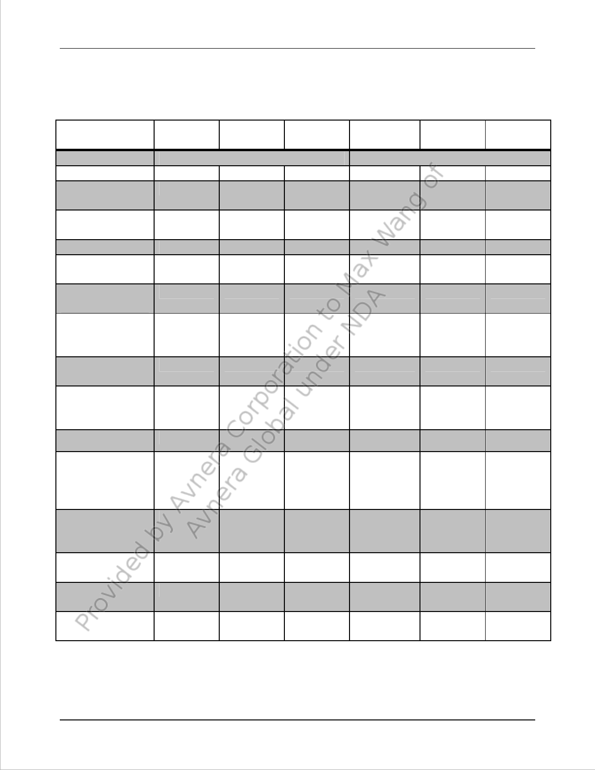
Table 0-1 AV6xxx Selection Grid .......................................................................................................................................... 6
1REFERENCE DIAGRAMS .......................................................................................................................................... 7
1.1Wireless Arbiter Solution Diagram.......................................................................................................................... 7
1.2Functional Diagram ................................................................................................................................................ 8
1.3Audio Signal Routing Diagram ............................................................................................................................... 8
1.4Application Circuit – Wireless Universal Gaming Arbiter ........................................................................................ 9
2PIN INFORMATION .................................................................................................................................................. 10
2.1Pin Diagram.......................................................................................................................................................... 10
2.2Pin Description ..................................................................................................................................................... 11
3ELECTRICAL SPECIFICATIONS ............................................................................................................................. 13
3.1Absolute Maximum Ratings.................................................................................................................................. 13
3.2DC Electrical Characteristics ................................................................................................................................ 14
3.3Electrical Characteristics – Voltage Supervisory Circuit ....................................................................................... 14
3.4Electrical Characteristics – RF Receiver .............................................................................................................. 15
3.5Electrical Characteristics – RF Transmitter .......................................................................................................... 15
3.6Electrical Characteristics – End-to-end Audio Characteristics.............................................................................. 15
4PACKAGE INFORMATION....................................................................................................................................... 16
4.1Package Outline Drawing ..................................................................................................................................... 16
4.2Package Marking.................................................................................................................................................. 17
5CONTACT INFO & LEGAL DISCLAIMER................................................................................................................. 18
List of Tables
Table 0-1 AV6xxx Selection Grid .......................................................................................................................................... 6
Table 2-2-1 AV301 pin description...................................................................................................................................... 11
Table 3-1 Absolute Maximum Ratings ................................................................................................................................ 13
Table 3-2 AV6301 DC Electrical Characteristics ................................................................................................................ 14
Table 3-3 AV6301 Electrical Characteristics - Voltage Supervisory ................................................................................... 14
Table 3-4 AV6301 Electrical Characteristics - RF Receiver................................................................................................ 15
Table 3-5 AV6301 Electrical Characteristics - RF Transmitter............................................................................................ 15
Table 3-6 AV6301 Electrical Characteristics - End-to-End Audio Characteristics............................................................... 15
List of Figures
Figure 1-1 AV6301 Wireless Arbiter Solution ....................................................................................................................... 7
Figure 1-2 AV6301 Functional Diagram................................................................................................................................ 8
Figure 1-3 AV6301 Audio Routing ........................................................................................................................................ 8
Figure 1-4 AV6301 Application Circuit .................................................................................................................................. 9
Figure 2-1 AV6301 Pin Diagram ......................................................................................................................................... 10
Figure 4-1 AV6301 48 Pin QFN Outline Drawing ............................................................................................................... 16
Figure 4-2 Package Marking Layout ................................................................................................................................... 17

AV6301 Datasheet (Preliminary) revision 0.2
CONTENTS SUBJECT TO CHANGE WITHOUT NOTICE 5 AVNERA PROPRIETARY & CONFIDENTIAL | PROVIDED UNDER NDA
AV6301 Datasheet (Preliminary) revision 0.2
CONTENTS SUBJECT TO CHANGE WITHOUT NOTICE 6 AVNERA PROPRIETARY & CONFIDENTIAL | PROVIDED UNDER NDA
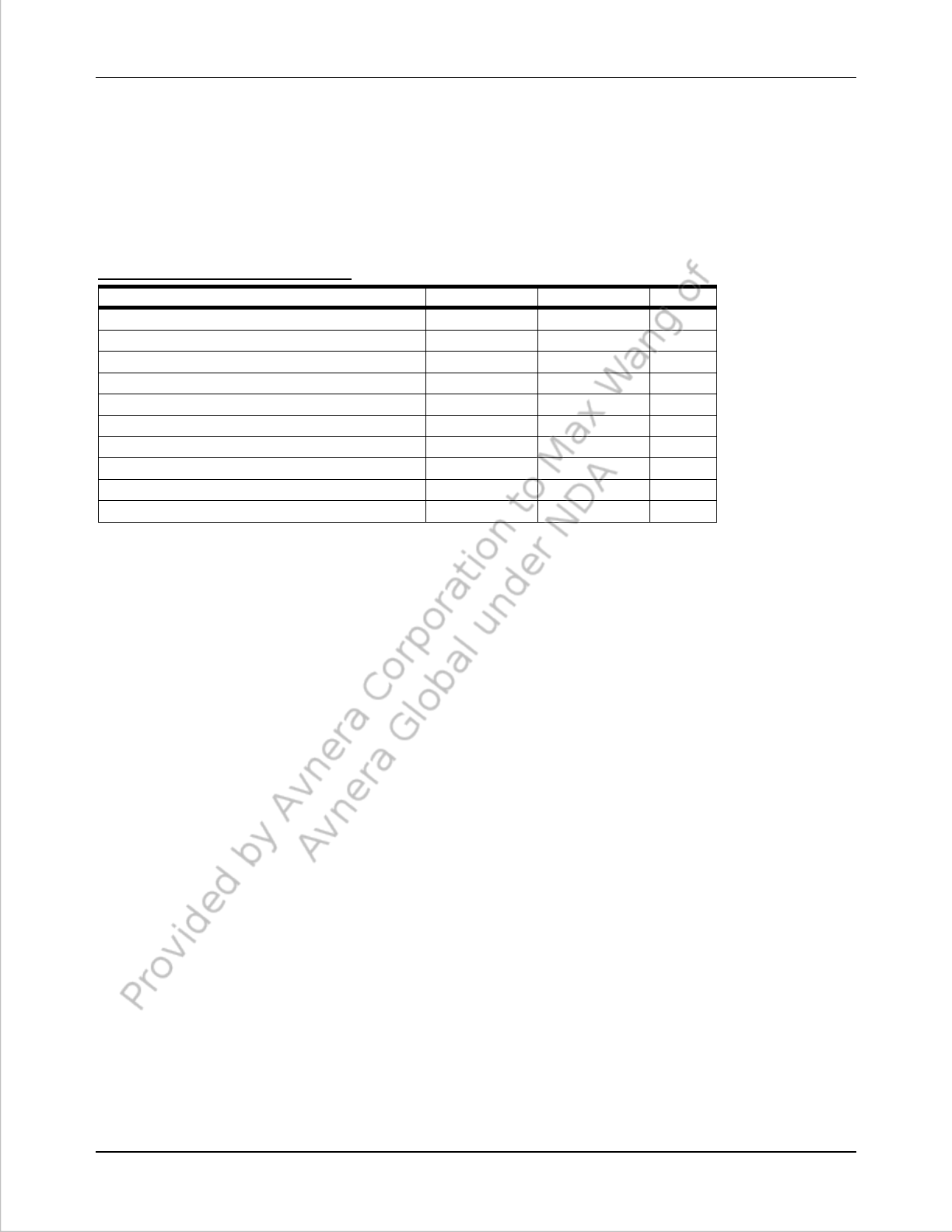
Table 0-1 AV6xxx Selection Grid
Part Number AV6200 AV6201 AV6301 AV6200 AV6202 AV6302
Role Sender Receiver
I2S IN Stereo No Stereo N/A Mono Mono
I2S Out N/A No Stereo
Mono
Stereo Stereo Stereo
Mono
USB Port No Audio /
HID
Audio /
HID
No HID HID
MIC Amp No No No No Yes Yes
Headphone
Driver Amp No No No No Yes Yes
Battery
Charger No No No No Yes Yes
General
Purpose
ADCs
0 0 0 0 0 3
Button
Support Yes Yes Yes Yes Yes Yes
Rotary
Encoder
Support
No No No No Yes Yes
LED Support Yes Yes Yes Yes Yes Yes
I2S Loop-
Back
(external
DSP)
No No Yes No No No
MIC path
input to I2S
out
N/A N/A N/A N/A No Yes
MIC Side-
tone Mix N/A N/A N/A N/A Yes Yes
Game / Chat
Mix on TX N/A No Yes N/A N/A N/A
Game / Chat
Mix at RX N/A N/A N/A No No Yes
AV6301 Datasheet (Preliminary) revision 0.2
CONTENTS SUBJECT TO CHANGE WITHOUT NOTICE 7 AVNERA PROPRIETARY & CONFIDENTIAL | PROVIDED UNDER NDA
1 REFERENCE DIAGRAMS
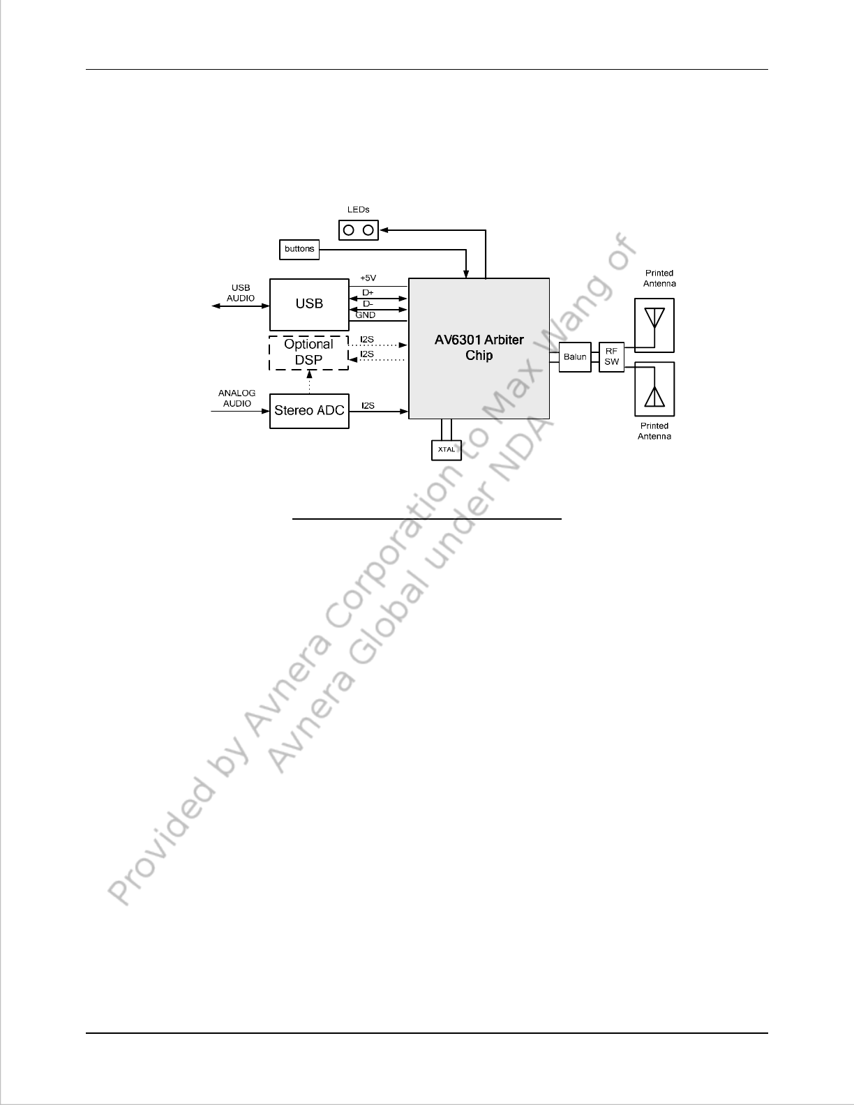
1.1 Wireless Arbiter Solution Diagram
Figure 1-1 AV6301 Wireless Arbiter Solution
AV6301 Datasheet (Preliminary) revision 0.2
CONTENTS SUBJECT TO CHANGE WITHOUT NOTICE 8 AVNERA PROPRIETARY & CONFIDENTIAL | PROVIDED UNDER NDA
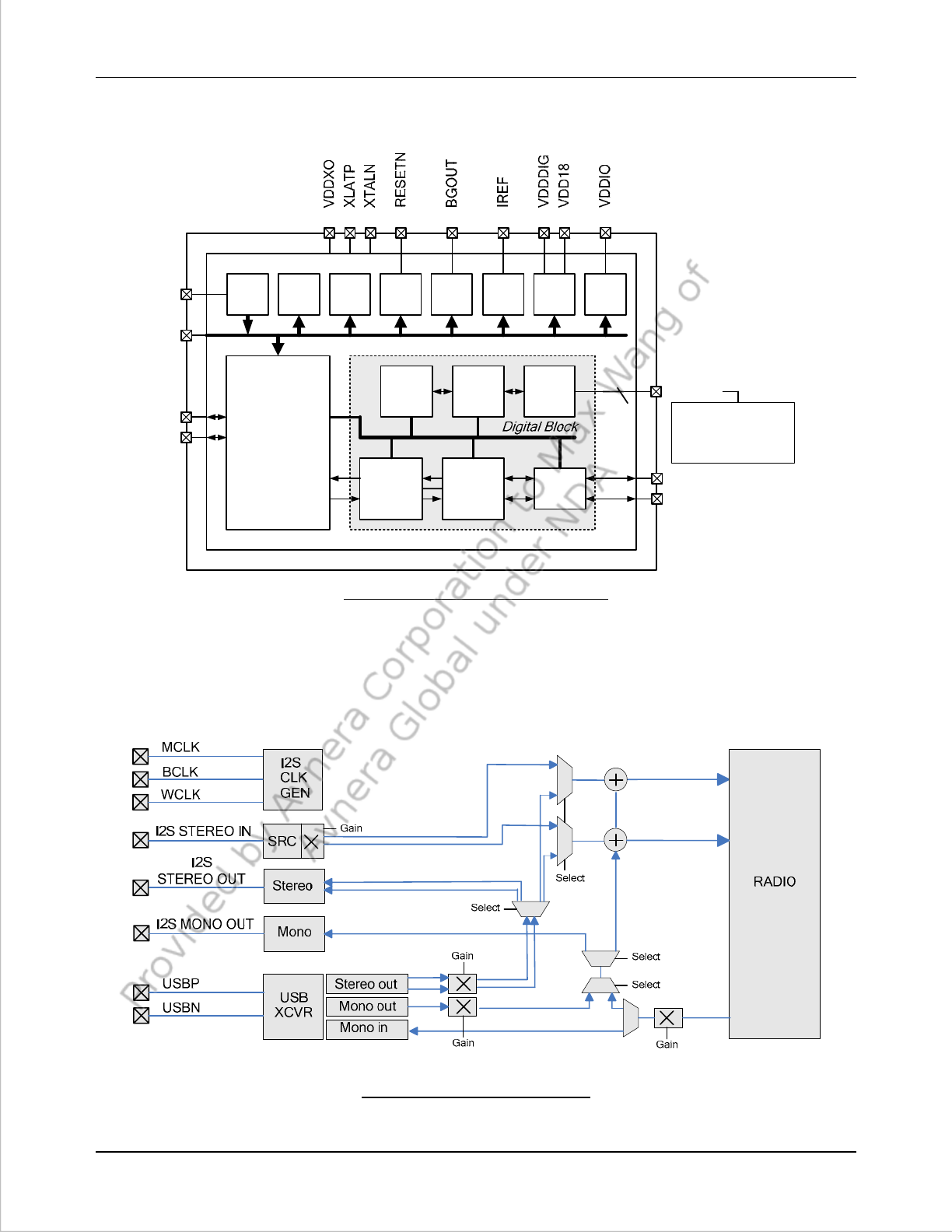
1.2 Functional Diagram
20
PHY Audio
Proc
MCU GPIO
USB DP
DM
GPIO
V3P6
VDC
DSCP,DSCN
SPI, I2C
GPIO (Buttons, LEDs)
I2S
RFP
RFN
ROM
RAM
OTP
3.6V
LDO VBGSUP REF DIG
Regs
3.3V
REG
USB
Spnd XTAL
RF/IF
Transceiver
Figure 1-2 AV6301 Functional Diagram
1.3 Audio Signal Routing Diagram
Figure 1-3 AV6301 Audio Routing
AV6301 Datasheet (Preliminary) revision 0.2
CONTENTS SUBJECT TO CHANGE WITHOUT NOTICE 9 AVNERA PROPRIETARY & CONFIDENTIAL | PROVIDED UNDER NDA
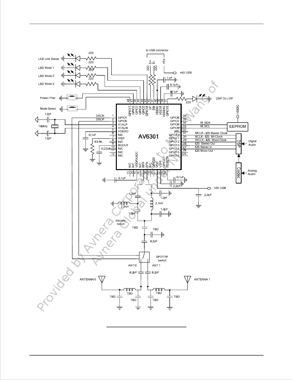
1.4 Application Circuit – Wireless Universal Gaming Arbiter
Figure 1-4 AV6301 Application Circuit
AV6301 Datasheet (Preliminary) revision 0.2
CONTENTS SUBJECT TO CHANGE WITHOUT NOTICE 10 AVNERA PROPRIETARY & CONFIDENTIAL | PROVIDED UNDER NDA
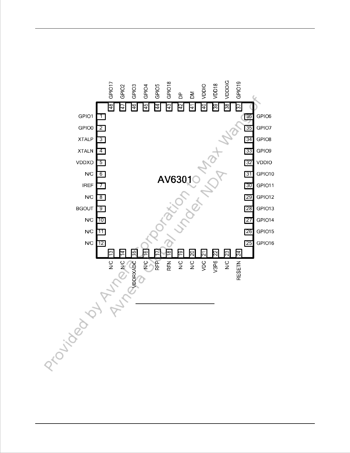
2 PIN INFORMATION
2.1 Pin Diagram
Figure 2-1 AV6301 Pin Diagram
AV6301 Datasheet (Preliminary) revision 0.2
CONTENTS SUBJECT TO CHANGE WITHOUT NOTICE 11 AVNERA PROPRIETARY & CONFIDENTIAL | PROVIDED UNDER NDA
2.2 Pin Description
Table 2-2-1 AV301 pin description
Pin No. Symbol Pin Type Description
1 GPIO1
DSCN
DPA-EN
Digital Output GPIO port 1; Usage is programmable to GPIO OR to
Antenna Diversity Switch – OR to
Power Amplifier Enable
2 GPIO0
DSCP
DSC
Digital Output GPIO port 0; Usage is programmable to GPIO OR to
Antenna Diversity Switch + OR to
Single Polarity Diversity Switch Control
3 XTALP Analog input External crystal input
4 XTALN Analog input External crystal input
5 VDDXO Analog Crystal oscillator regulator bypass pin
6,8,10-14,
16, 19, 20,
23
N/C - No connection – Leave unconnected – Do not Ground
7 IREF Analog pin Reference current setting resistor connection
9 BGOUT Analog bypass Bandgap reference bypass pin
15 VDDRXADC Bypass Bypass pin for Receiver Data Converter Supply
17 RFP RF I/O RF input/output positive
18 RFN RF I/O RF input/output negative
21 VDC Supply pin 5V input supply voltage from USB
22 V3P6 Bypass Bypass pin for 3.6V main regulator
24 RESETN Digital input RESET signal; active low
25 GPIO16
PWM2
Digital I/O GPIO port 16, usage is programmable to GPIO OR to
PWM resource #2
26 GPIO15
I2S MONO OUT
PWM1
Digital I/O GPIO port 15, usage is programmable to GPIO OR to
I2S port 2 MONO OUT Data
PWM resource #1
27 GPIO14
I2S STEREO IN
Digital I/O GPIO port 14; usage is programmable to GPIO OR to
I2S Port 1 STEREO IN Data
28 GPIO13
I2S STEREO OUT
Digital I/O GPIO port 13; usage is programmable to GPIO OR to
I2S Port 0 STEREO OUT Data
29 GPIO12
WCLK
Digital I/O GPIO port 12; usage is programmable to GPIO OR to
I2S Word Clock
30 GPIO11
BCLK
PWM1
Digital I/O GPIO port 11; usage is programmable to GPIO OR to
I2S Bit Clock OR to
PWM resource #1
32 VDDIO Supply Supply bypass capacitor pin for digital I/O
31 GPIO10
MCLK
PWM0
Digital I/O GPIO port 10; usage is programmable to GPIO OR to
I2S Master Clock OR to
PWM resource #0
33 GPIO9
M_MISO (SPI Mater)
M_SCL (TWI Master)
SCL (TWI)
Digital I/O GPIO port 9; usage is programmable to GPIO OR to
M_MISO OR to
M_SCL OR to
SCL
34 GPIO8
M_MOSI (SPI Master)
M_SDA (TWI Master)
SDA (TWI)
Digital I/O GPIO port 8; usage is programmable to GPIO OR to
M-MOSI OR to
M_SDA OR to
SDA
35 GPIO7
M_SCLK (SPI Master)
PWM1
Digital I/O GPIO port 7; usage is programmable to GPIO OR to
M_SCLK OR to
PWM resource #1
36 GPIO6
M_SSB (SPI Master)
PWM0
Digital I/O GPIO port 6; usage is programmable to GPIO OR to
M-SSB OR to
PWM resource #0
37 GPIO19 Digital I/O GPIO port 19, usage is programmable to GPIO OR to
AV6301 Datasheet (Preliminary) revision 0.2
CONTENTS SUBJECT TO CHANGE WITHOUT NOTICE 12 AVNERA PROPRIETARY & CONFIDENTIAL | PROVIDED UNDER NDA
Pin No. Symbol Pin Type Description
PWM2 PWM resource #2
38 VDDDIG Bypass Bypass capacitor pin for 1.35V digital core regulator
39 VDD18 Bypass Bypass capacitor pin for 1.8V digital regulator (LDO)
40 VDDIO Bypass Bypass capacitor pin for 3.3V digital I/O regulator
41 DM USB I/O USB negative input
42 DP USB I/O USB positive input
43 GPIO18
PWM1
GPIO port 18, usage is programmable to GPIO OR to
PWM resource #1
44 GPIO5
S_MISO (SPI Slave)
S_SCL (TWI Slave)
Digital I/O GPIO port 5; usage is programmable to GPIO OR to
S_MISO OR to
S_SCL
45 GPIO4
S_MOSI (SPI Slave)
S_SDA (TWI Slave)
Digital I/O GPIO port 4; usage is programmable to GPIO OR to
S_MOSI OR to
S_SDA
46 GPIO3
S_SCLK (SPI Slave)
UART_RX
PWM1
Digital I/O GPIO port 3; usage is programmable to GPIO OR to
S_SCLK OR to
The UART Receiver OR to
PWM resource #1
47 GPIO2
S_SSB (SPI Slave)
UART_TX
PWM0
Digital I/O GPIO port 2; usage is programmable to GPIO OR to
S_SSB OR to
The UART Transmitter OR to
PWM resource #0
48 GPIO17
PWM2
Digital I/O GPIO port 17, usage is programmable to GPIO OR to
PWM resource #2
AV6301 Datasheet (Preliminary) revision 0.2
CONTENTS SUBJECT TO CHANGE WITHOUT NOTICE 13 AVNERA PROPRIETARY & CONFIDENTIAL | PROVIDED UNDER NDA
3 ELECTRICAL SPECIFICATIONS
3.1 Absolute Maximum Ratings
The Absolute Maximum Rating (AMR) corresponds to the maximum value that can be applied without leading to
instantaneous or very short-term unrecoverable hard failure (destructive breakdown). Absolute Maximum Ratings are
stress ratings only. Permanent damage to the device may be caused by continuously operating at or beyond these limits.
Device functional operating limits and guaranteed performance specifications are given under Electrical Characteristics at
the test conditions specified.
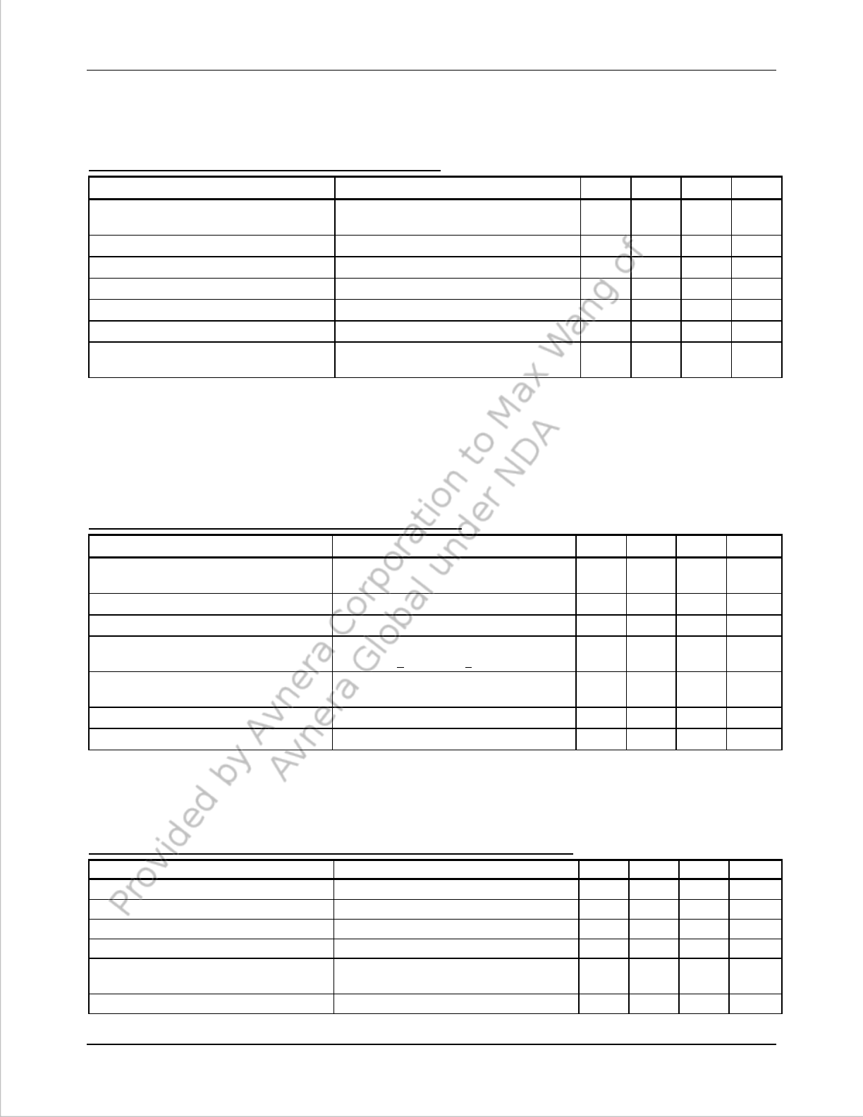
Table 3-1 Absolute Maximum Ratings
CONDITION MIN MAX Units
Supply (relative to AGND and DGND)
VDC -0.3 6.0 V
Input Voltage Range – Digital Inputs -0.3 3.6 V
Input Voltage Range – Analog Inputs -0.3 3.6 V
Short circuit to GND (any pin) -- continuous
Operating Temperature -40 +85 ºC
Storage Temperature -40 +100 ºC
Lead Temperature (10s) -- +300 ºC
Static Discharge Voltage – HBM (All pins ) 3000 V
Static Discharge Voltage – MM 300 V
Note:
1) HBM = ESD Human Body Model; C = 100pF, R = 1kΩ
2) MM = ESD Machine Model; C = 100pF; R = 300Ω
AV6301 Datasheet (Preliminary) revision 0.2
CONTENTS SUBJECT TO CHANGE WITHOUT NOTICE 14 AVNERA PROPRIETARY & CONFIDENTIAL | PROVIDED UNDER NDA
3.2 DC Electrical Characteristics
Operating Conditions: VDC = 4.4V to 5.5V, VDDIO = 3.3V, TA = 0ºC to +70 ºC; Typical specifications at TA = 25ºC, VDC = 5.0V.
Table 3-2 AV6301 DC Electrical Characteristics
PARAMETER CONDITIONS MIN TYP MAX UNIT
VDC Supply Voltage Input 4.4 5.0 5.5 V
V3P6 Internally regulated voltage 3.6 V
VDDIO (Digital 3.3V I/O) Reg. Voltage Internally regulated voltage 3.3 V
VDDDIG (Digital Core) Reg. Voltage Internally regulated voltage 1.35 V
VDD1P8 Internally regulated voltage 1.8 V
Supply Current (IVDC) – USB chip Reset TBD
USB Suspend Mode 1.0 mA
Arbiter Search Mode TBD TBD mA
Arbiter Headset Link Mode 55 TBD mA
GPIO Source Current 4 TBD mA
CMOS I/O Logic Levels – 3.3V I/O
Input Voltage Logic Low, VIL V
VDDIO = 3.3V 0.8 V
Input Voltage Logic High, VIH V
VDDIO = 3.3V 2.0 V
Output Voltage Logic Low, VOL V
VDDIO = 3.3V ; ILOAD=1mA 0.4 V
Output Voltage Logic High, VOH V
VDDIO = 3.3V; ILOAD=1mA 2.9 V
USB Interface
DP Logic Output High refer to USB spec; voltage relative to VDDIO 0.8*VDD
IO
V
DM Logic Output Low refer to USB spec; voltage relative to VDDIO 0.2*VDD
IO
V
DP Logic Input High refer to USB spec; voltage relative to VDDIO 0.7*VDD
IO
V
DM Logic Input Low refer to USB spec; voltage relative to VDDIO 0.3*VDD
IO
V
USB Differential Input Sensitivity 0.2 V
USB Differential Common Mode 0.8 2.5 V
USB Single Ended RX Threshold 0.8 2.0 V
USB IO Pin Static Output (Low) Rl=1.5k to 3.6V 0.3 V
3.3 Electrical Characteristics – Voltage Supervisory Circuit
Operating Conditions: VDC = 4.4V to 5.5V, VDDIO = 3.3V, TA = 0ºC to +70 ºC; Typical specifications at TA = 25ºC, VDC = 5.0V.
Table 3-3 AV6301 Electrical Characteristics - Voltage Supervisory
PARAMETER CONDITIONS MIN TYP MAX UNIT
Voltage Monitor Low Thres. (assert reset) Monitoring the voltage on V3P6 2.7 V
Voltage Monitor High Thres. (de-assert reset) Monitoring the voltage on V3P6 3.0 V
Brownout bandwidth Monitoring the voltage on V3P6 100 kHz
Reset Threshold (assert) 2.2 V
Reset Threshold (de-assert) 1.1 V
RESETN Minimum Time 0.1uF external capacitor 11 ms
AV6301 Datasheet (Preliminary) revision 0.2
CONTENTS SUBJECT TO CHANGE WITHOUT NOTICE 15 AVNERA PROPRIETARY & CONFIDENTIAL | PROVIDED UNDER NDA
3.4 Electrical Characteristics – RF Receiver
Operating Conditions: VDC = 4.4V to 5.5V, VDDIO = 3.3V, TA = 0ºC to +70 ºC; RF Channel Freq = 2403.35-2477.35MHz, measured at
the single-ended input of the RF balun (with external impedance matching). Typical specifications at TA = 25ºC, VDC = 5.0V.
Table 3-4 AV6301 Electrical Characteristics - RF Receiver
PARAMETER CONDITIONS MIN TYP MAX UNIT
RF Channel Frequency Range LO frequency (driving the mixers)
RF carrier frequency
2402
2403.35
2478
2479.35
MHz
MHz
Modulated Signal Offset from LO 1.35 MHz
Sensitivity (Note 1) TA=25ºC, LNA = High gain mode; max IF gain -89 dBm
Max input signal (desired signal) (Note 1) TA=25ºC, LNA = low gain mode; min IF gain -5 dBm
Input Blocker Level – High Gain mode > 2MHz offset -45 dBm
Out-of-band blocker level <2400 MHz; >2483.5 MHz TBD dBm
Spurious RF outputs <2400 MHz
>2483.5 MHz -75
-75 dBm
dBm
Note 1: Sensitivity and max signal level are defined as the onset of 0.2% Block Error Rate. )BLER)
3.5 Electrical Characteristics – RF Transmitter
Operating Conditions: VDC = 4.4V to 5.5V, VDDIO = 3.3V, TA = 0ºC to +70 ºC; RF Channel Freq = 2403.35-2477.35MHz, measured at
the single-ended input of the RF balun (with external impedance matching). Typical specifications at TA = 25ºC, VDC = 5.0V.
Table 3-5 AV6301 Electrical Characteristics - RF Transmitter
PARAMETER CONDITIONS MIN TYP MAX UNIT
RF Channel Frequency Range LO frequency (driving the mixers)
RF carrier frequency
2402
2403.35
2478
2479.35
MHz
MHz
Modulated Signal Offset from LO 1.35 MHz
Modulated Signal Bandwidth -10dB point 1.8 MHz
Output Power Pi/4 DQPSK modulated signal
ACPR: Adj < -23dBc, Alt < -30dBc
+2
dBm
Output harmonics 2nd harmonic, Pout = 0dBm
3rd harmonic, Pout = 0dBm
-52
-50
dBm
dBm
Out-of-band Spurious Output RF < 2390MHz, > 2483.5MHz, 1MHz RBW <-62 dBm
Output Noise Floor RF < 2390MHz, > 2483.5MHz, 1MHz RBW <-62 dBm
3.6 Electrical Characteristics – End-to-end Audio Characteristics
Operating Conditions: VDC = 4.4V to 5.5V or VIN = 3.2V to 4.3V, VDDIO = 3.3V, TA = 0ºC to +70 ºC; Typical specifications at TA = 25ºC,
VDC = 5.0V.
Table 3-6 AV6301 Electrical Characteristics - End-to-End Audio Characteristics
PARAMETER CONDITIONS MIN TYP MAX UNITS
SNR Forward stereo path 93 dB
Reverse mono path 68 dB
Audio/Voice Bandwidth End-to-end audio BW; 0.1dB point 20 kHz
End-to-end audio BW; 0.1dB point 6.5 kHz
Audio Latency AV6201 USB to AV6202 analog output
AV6201 I2S to AV6202 I2S output <16
<16 msec
msec
Voice Latency AV6202 analog input to AV6201 USB output <16 msec
AV6301 Datasheet (Preliminary) revision 0.2
CONTENTS SUBJECT TO CHANGE WITHOUT NOTICE 16 AVNERA PROPRIETARY & CONFIDENTIAL | PROVIDED UNDER NDA
4 PACKAGE INFORMATION
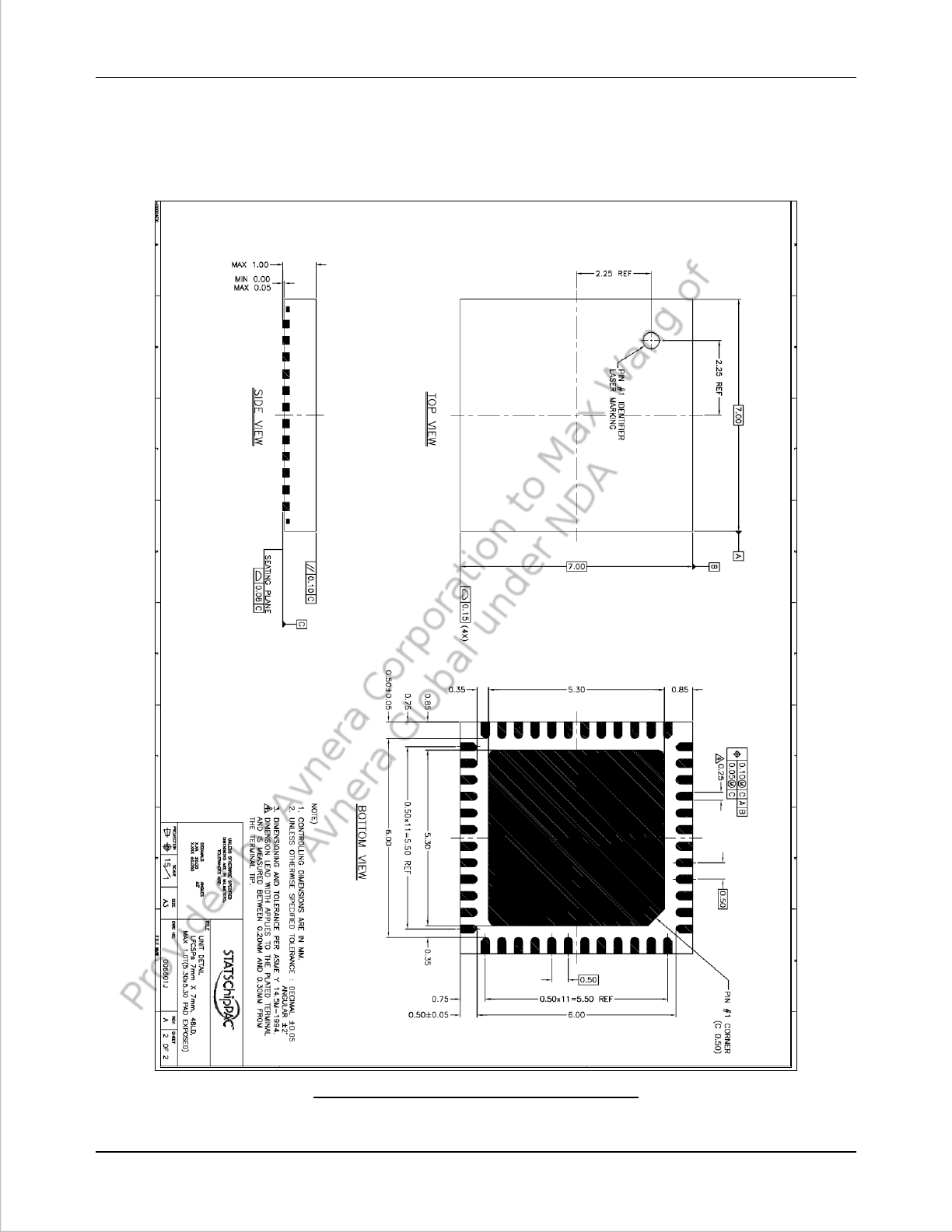
4.1 Package Outline Drawing
Figure 4-1 AV6301 48 Pin QFN Outline Drawing
AV6301 Datasheet (Preliminary) revision 0.2
CONTENTS SUBJECT TO CHANGE WITHOUT NOTICE 17 AVNERA PROPRIETARY & CONFIDENTIAL | PROVIDED UNDER NDA
4.2 Package Marking
A V D D D D
C C Y Y W W X X
L L L L L L T T A
Figure 4-2 Package Marking Layout
Abbreviations:
AVDDDD Product number (i.e. AV6301)
CC Country Code (i.e. MY for Malaysia)
YY 2 digit year code
WW 2 digit work week
XX Production revision
LLLLLL Silicon Lot number
TT Wafer split (1 by default)
A Assembly Lot

AV6301 Datasheet (Preliminary) revision 0.2
CONTENTS SUBJECT TO CHANGE WITHOUT NOTICE 18 AVNERA PROPRIETARY & CONFIDENTIAL | PROVIDED UNDER NDA
5 CONTACT INFO & LEGAL DISCLAIMER
Avnera Corporation
16505 Bethany Court, Suite 100
Beaverton, Oregon 97006
U.S.A.
Main: +1.503.718.4100
Fax: +1.503.718.4101
www.avnera.com
Avnera Corporation reserves the right to make changes without notice to the product to improve function, reliability, or
performance.
Avnera Corporation does not assume any liability arising from the application or use of the products or circuits described
herein.