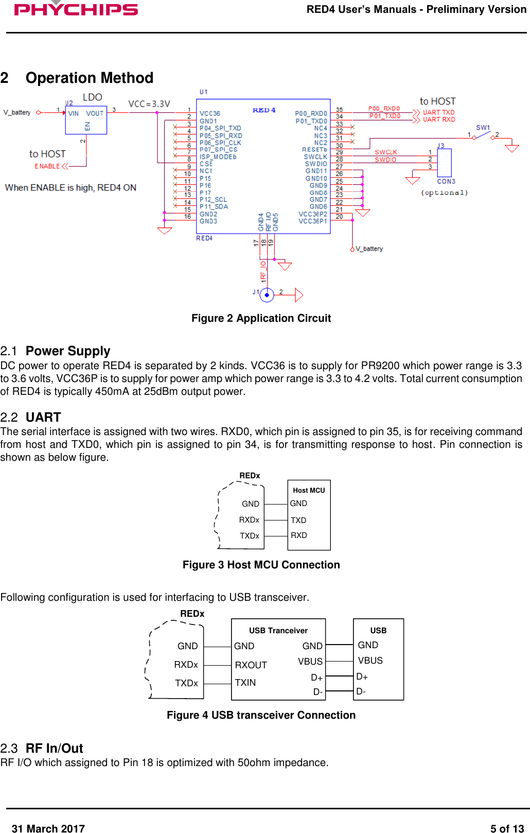
Phychips RED4 RFID Module User Manual Phychips
Phychips Inc. RFID Module Phychips
UserManual.wiki
>
Phychips
>
RED4 User Manual
User Manual
Navigation menu
Upload a User Manual
Namespaces
Wiki Guide
HTML
PDF
Info
Views
User Manual
Discussion / Help
Navigation

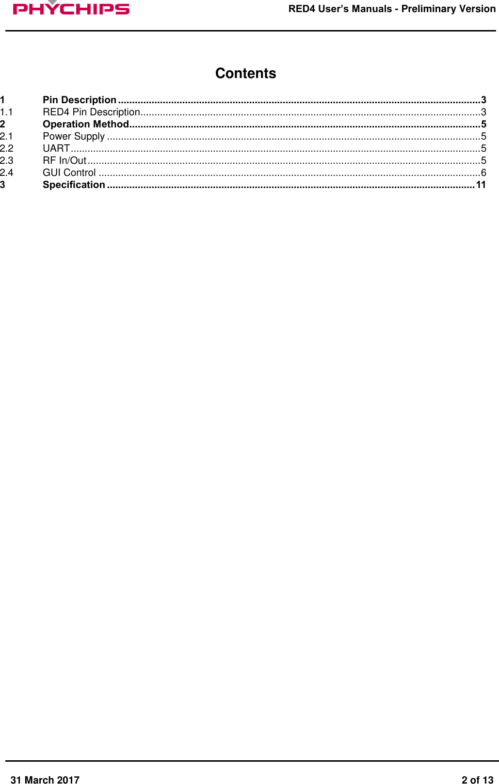
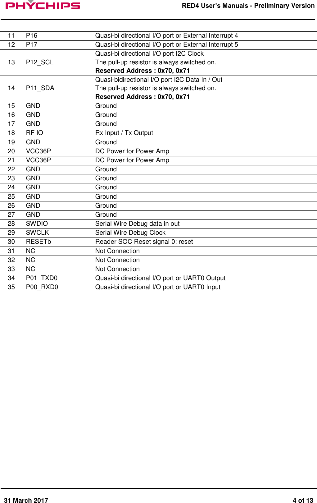
![31 March 2017 3 of 13 RED4 User’s Manuals - Preliminary Version 1 Pin Description 12345678910111213141516171819VCC36GNDNCP01_TXD0P04_SPI_TXDP05_SPI_RXDP06_SPI_CLKP07_SPI_CSISP_MODEbCSENCP15P16P17P12_SCLP11_SDAGNDGNDP00_RXD0NCNCRESETbSWCLKSWDIOGNDGNDGNDGNDGNDGNDVCC36PVCC36P2021222324252627282930313233343520212223242526272829303132333435GNDRFIOGND12345678910111213141516171819VCC36GNDNCP01_TXD0P04_SPI_TXDP05_SPI_RXDP06_SPI_CLKP07_SPI_CSISP_MODEbCSENCP15P16P17P12_SCLP11_SDAGNDGNDP00_RXD0NCNCRESETbSWCLKSWDIOGNDGNDGNDGNDGNDGNDVCC36PVCC36P20212223242526272829303132333435GNDRFIOGND Figure 1 Pin Description 1.1 RED4 Pin Description No. Pin Name Description 1 VCC36 DC Power for Reader SOC 2 GND Ground 3 P04_SPI_TXD Quasi-bi directional I/O port or SPI Output 4 P05_SPI_RXD Quasi-bi directional I/O port or SPI Input 5 P06_SPI_CLK Quasi-bi directional I/O port or SPI Clock 6 P07_SPI_CS Quasi-bi directional I/O port or SPI Chip Select 7 ISP_MODEb When ISP_MODEb is Logic ‘Low’, ISP mode is set as shown below table Pin No. 7 12 11 10 MODE ISP_MODEb P17 P16 P15 Normal 1 GPIO/INT GPIO/INT GPIO/INT UART ISP 0 0 0 0 SPI ISP 0 0 0 1 [CAUTION] Except ISP mode, ISP_MODEb should be set logic ‘High’ for robust stability for FLASH memory 8 CSE Chip Select enable / module power enable 0:Disable 1: Enable 9 NC Not Connection 10 P15 Quasi-bi directional I/O port [NOTE] This pin is already used internally. So this pin should be only for ISP mode](https://usermanual.wiki/Phychips/RED4/User-Guide-3354272-Page-3.png)