Physik Instrumente PI Ultra High Resolution Microscopy WP Pi1114
PI_Ultra-High_resolution_Microscopy_WP_pi1114 Whitepapers & Success Stories
User Manual: Physik Instrumente Whitepapers & Success Stories
Open the PDF directly: View PDF ![]() .
.
Page Count: 5
WHITEPAPER – Ultra-High-Resolution Microscopy in a Modular System
Dipl.-Phys. Gernot Hamann
Page 1 of 5
Physik Instrumente (PI) GmbH & Co. KG_Auf der Roemerstrasse 1_76228 Karlsruhe, Germany
Tel. +49 721 4846-0, Fax +49 721 4846-1019 Email info@pi.ws, www.pi.ws
Piezo-Based Scanning Stages for Precise Sample
Positioning and Measurement
Ultra-High-Resolution Microscopy in a Modular System
WHITEPAPER – Ultra-High-Resolution Microscopy in a Modular System
Dipl.-Phys. Gernot Hamann
Page 2 of 5
Physik Instrumente (PI) GmbH & Co. KG_Auf der Roemerstrasse 1_76228 Karlsruhe, Germany
Tel. +49 721 4846-0, Fax +49 721 4846-1019 Email info@pi.ws, www.pi.ws
In life sciences, chemical-pharmaceutical analyses or
modern material sciences, the optical resolution and
information content of classical microscopy methods are
no longer sufficient. In order to obtain the most
comprehensive information on a sample, modular, high-
resolution microscope systems open up interesting
opportunities, since different microscopy methods can be
used either individually or in combination. As high-
precision and dynamic sample positioning is
indispensable in most application areas, piezo-based
scanning stages are a good solution. Thanks to their
compact design, they can easily be integrated in
microscopes.
.
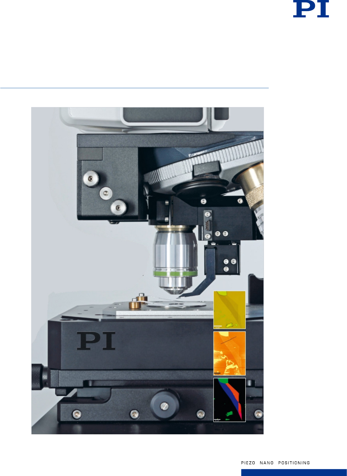
Fig. 1 The modular microscopy systems from WITec
make it possible to combine a confocal Raman
microscope with atomic force microscopy (AFM)
(Image: WITec GmbH)
The ultra-high-resolution microscopy systems from
WITec have a modular structure (fig. 1). This makes it
possible to combine a confocal Raman microscope with
atomic force microscopy (ATM), if required.
The same device can then provide and link molecular
Raman and structural AFM information from the same
sample region.
For high-resolution optical information, the microscope
can also be equipped with SNOM (scanning near field
optical microscopy). As a result, precise optical,
topographical and molecular analyses are possible, just
as required by the respective application. This opens up
opportunities for diverse of application areas. The
application spectrum of modular high-precision
microscopes ranges from pharmaceutical research and
live cell analyses, through nanophotonics, forensics up
to analyses in photovoltaic or semiconductor technology
Close-Ups Below the Diffraction
Limit
With conventional microscopy technology, the position
resolution is limited to half of its wavelength due to
diffraction effects on the objective. In contrast, scanning
near-field optical microscopy can show far smaller
structures. Here, a glass fiber couples laser light into a
hollow measuring tip. This light emerges through a tiny
opening at the tip with a diameter of less than 100 nm. If
the opening of the measuring tip is brought closely to the
sample surface, a spot far below the diffraction limit of
classical microscopy can be illuminated. Depending on
the geometry of the measuring tip and its opening, a
lateral position resolution of up to around 60 nm can be
attained, while with confocal (light) microscopy the value
would be between 200 to 300 nm.
For scanning the sample point by point, it is moved
under the measuring tip by a piezo-driven, high-
resolution scanning stage. At each position, the camera
integrated in the microscope records the incoming light
intensity and saves this value together with the position
information, which is used to create the image. The
position resolution and accuracy of the image depend on
the positioning accuracy and stability of the scanning
stage as well as the optical and mechanical components
of the microscope (fig. 2).
WHITEPAPER – Ultra-High-Resolution Microscopy in a Modular System
Dipl.-Phys. Gernot Hamann
Page 3 of 5
Physik Instrumente (PI) GmbH & Co. KG_Auf der Roemerstrasse 1_76228 Karlsruhe, Germany
Tel. +49 721 4846-0, Fax +49 721 4846-1019 Email info@pi.ws, www.pi.ws
Fig. 2 For high-resolution optical information, the
microscope can also be equipped with SNOM (scanning
near field optical microscopy). With SNOM, far smaller
structures can be shown than with conventional
microscope technology (Image: WITec GmbH)
Information on the Surface Topology
SNOM simultaneously provides information on the
surface topology: Since the distance between the
measuring tip and the surface has to be kept constant
and practically every surface has a certain roughness,
the position of the sample must be readjusted in the Z
direction. This readjustment is carried out by the
scanning stage and provides topological information
additionally to the optical SNOM image.
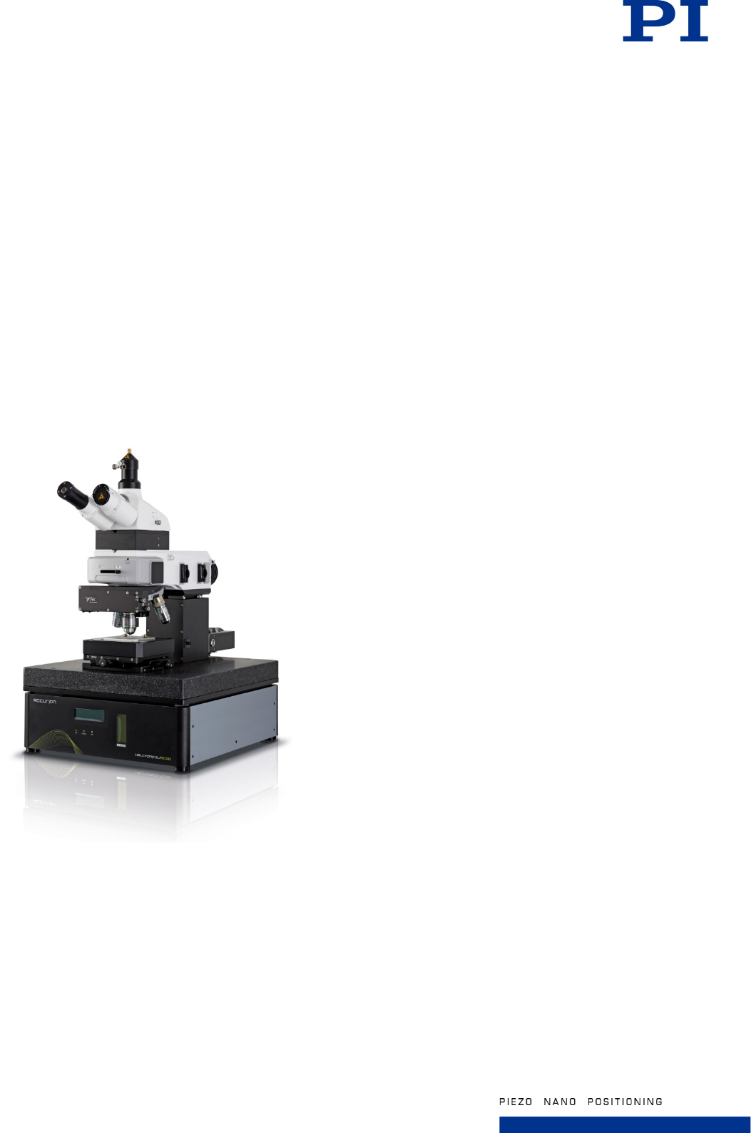
Fig. 3 Atomic force microscopy (AFM) provides precise
information on the surface topology
(Image: WITec GmbH)
In the case of the AFM method, the measuring tip is also
moved over the sample surface line by line in a defined
grid. Forces are measured between a very thin
measuring tip and the surface of the object, which then
provides information on the topology of the surface. In
addition, sample characteristics such as adhesion,
stiffness or viscosity can be determined. The lateral
resolution is 10 nm and below. The position of the
sample is readjusted in the direction of the Z axis here
as well. The variation of the Z position together with the
relevant X and Y coordinates for the spatial resolution
then provide high-precision topology information on the
samples (fig. 3).
The Chemical Fingerprint
Raman microscopy is based on a confocal, optical
microscope combined with a Raman spectrometer. In
the case of a confocal system, apertures are used to
suppress light outside of the focal plane of the
microscope. In this way, only light information from the
focal plane is transferred to the spectrometer. In the
spectrometer, this light is spectrally separated and
detected. The sample is scanned point by point and line
by line. The lateral resolution is approximately 200 nm
with green excitation light. During the measurement, a
complete Raman spectrum is recorded for each pixel.
These Raman spectra act like a specific fingerprint for
each type of molecule, so that the chemical components
of a sample can be identified for each pixel and their
distribution in the sample can be shown.
Combining Raman imaging with AFM yields
topographical information with high spatial resolution as
well as molecular information on the sample surface.
Since the corresponding images are recorded in
succession (fig. 4), the requirements for the scanning
stage are very high. Any drift would distort the correlation
between the two images. Precise positioning in all three
axes is indispensable for the accuracy of the image.
WHITEPAPER – Ultra-High-Resolution Microscopy in a Modular System
Dipl.-Phys. Gernot Hamann
Page 4 of 5
Physik Instrumente (PI) GmbH & Co. KG_Auf der Roemerstrasse 1_76228 Karlsruhe, Germany
Tel. +49 721 4846-0, Fax +49 721 4846-1019 Email info@pi.ws, www.pi.ws
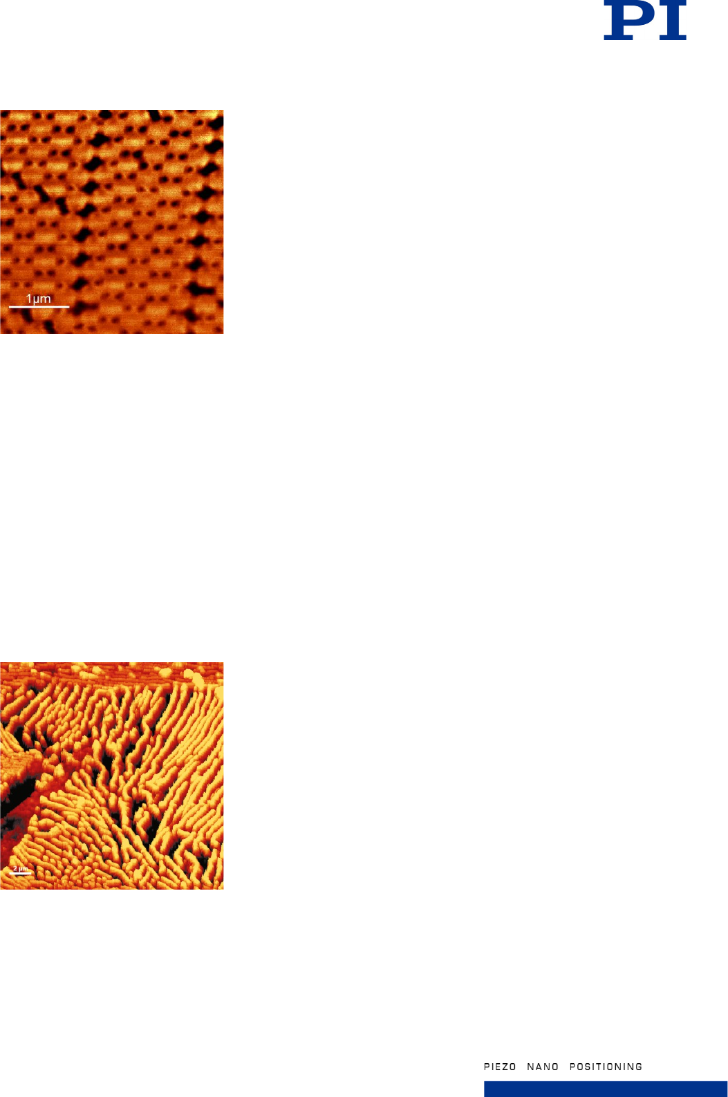
Fig. 4 Topology of a PEET-PET polymer film on a glass
substrate recorded with AFM (left), the Raman spectrum
(right) and the false color representation of the Raman
image (center). Raman spectra act like a specific
fingerprint for each type of molecule, so that chemical
components present in a sample can be identified for
each pixel and their distribution in the sample can be
shown (Image: WITec GmbH)
Positioning with a Very High
Position Resolution and Dynamics
Since the positioning system used for scanning provides
the spatial resolution, its resolution must be in the sub-
nanometer range. At the same time, the requirements for
the dynamics are high: The faster the topography
tracking in the Z direction, the faster the positioning in
the X and Y axis can be. Consequently measurement
times are shorter and temperature drift, which would
increase with time, is reduced. So the high dynamics
also benefit the accuracy.
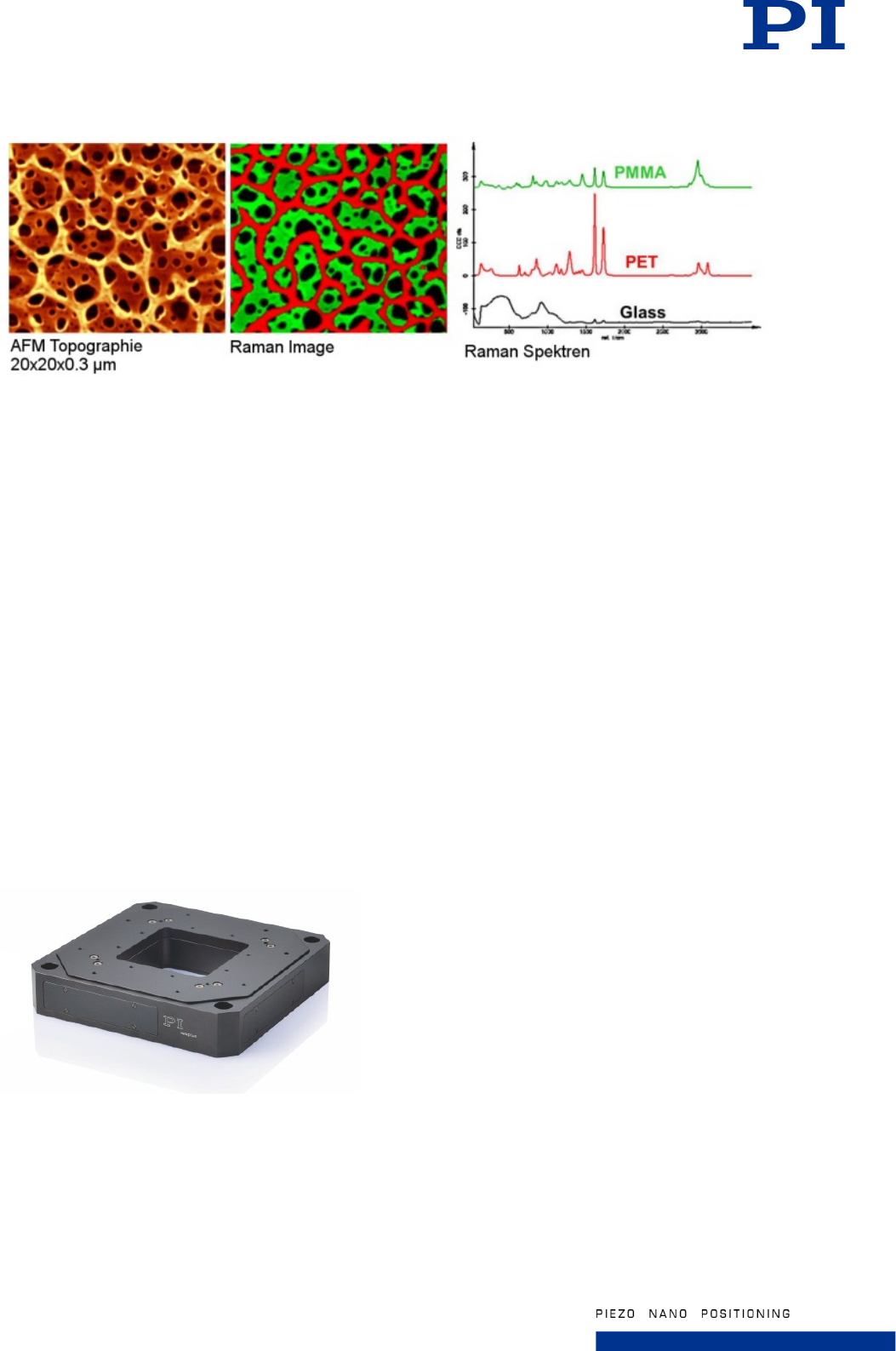
Fig. 5 The piezo-based scanning stage is essential for
sample positioning. It is designed for working distances
of 100 or 200 µm in the axes of the scanning plane and
30 µm in the Z axis. It allows a position resolution of
better than 2 nm. Capacitive sensors and digital
electronics provide maximum stability
For these reasons, WITec decided on a piezo-based
scanning stage (fig. 5) from PI (Physik Instrumente) for
positioning. It is designed for working distances of 100 or
200 µm in the axes of the scanning plane and 30 µm in
the Z axis. It allows a position resolution of better than
2 nm and provides the best conditions for use in modular
microscopes for all three methods. As there are no
classical mechanical components that could cause
friction or mechanical backlash in the drive, very high
motion resolution is possible with the piezo drives.
Capacitive Sensors and Digital
Electronics Ensure Stability
Stability and path accuracy during scanning are crucial
when combining Raman imaging with AFM, since the
measurements can take a few minutes and any drift
would distort the recordings. In addition, the active
guiding using capacitive sensors increases path
accuracy: The sensors measure any deviation in the axis
lateral to the direction of motion. Undesired crosstalk of
the motion (for example from external forces or
mechanical crosstalk) into another axis can be detected
in this way and actively compensated in real time.
A digital controller provides the necessary control. It is
specially adapted to the piezo-based scanning stage and
guarantees a good linearity, also for dynamic operation.
The digital electronics work with a high clock rate. This is
decisive for an accurate assignment of the position
values of the piezo scanner and the recording camera. If
it were too slow or inaccurate, there would be a loss of
resolution and distortions (jitter) during the assignment.
WHITEPAPER – Ultra-High-Resolution Microscopy in a Modular System
Dipl.-Phys. Gernot Hamann
Page 5 of 5
Physik Instrumente (PI) GmbH & Co. KG_Auf der Roemerstrasse 1_76228 Karlsruhe, Germany
Tel. +49 721 4846-0, Fax +49 721 4846-1019 Email info@pi.ws, www.pi.ws
The piezo-based scanning system is an essential part in
high-precision microscopes. As a result of its compact
dimensions, the scanning stage can be easily integrated
in microscopes where installation space is usually
limited.
Author
Dipl.-Physicist Gernot Hamann, Business Development
Manager for Microscopy at PI (Physik Instrumente)
WITec in Brief
Since its foundation in 1997, WITec GmbH (Ulm,
Germany) has developed into a market leader in high-
resolution microscopy systems (Raman, AFM and
SNOM) and generated average growth rates of annually
10%. With 52 employees worldwide, the company is
represented by subsidiaries in the USA and Asia, and
has regional offices in Spain and Japan. The main
application areas for the modular high-performance
microscopes, allowing the combination of different
methods, are found in nanotechnology, materials
sciences and life sciences. Europe, the USA and the
Asia/Pacific region are the most important sales markets,
with users coming from research and industry.
PI (Physik Instrumente) in Brief
In the past four decades, PI (Physik Instrumente) with
headquarters in Karlsruhe, Germany has become the
leading manufacturer of nanopositioning systems with
accuracies in the nanometer range. With four company
sites in Germany and ten sales and service offices
abroad, the privately managed company operates
globally. Over 700 highly qualified employees around the
world enable the PI Group to meet almost any
requirement in the field of innovative precision
positioning technology. All key technologies are
developed in-house. This allows the company to control
every step of the process, from design right down to
shipment: precision mechanics and electronics as well
as position sensors. The required piezoceramic
elements are manufactured by our subsidiary PI Ceramic
in Lederhose, Germany, one of the global leaders for
piezo actuator and sensor products. PI miCos GmbH in
Eschbach near Freiburg, Germany, is a specialist for
positioning systems for ultrahigh vacuum applications as
well as parallel-kinematic positioning systems with six
degrees of freedom and custom-made designs.
PI headquarters in Karlsruhe, Germany: More than 350
employees work on high-resolution drive systems and
positioning systems
