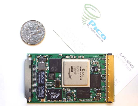
Pico Communications E 14 Users Manual E14
E-14 to the manual bfd7b1dd-2ea6-48a6-89ac-929cbc9a9987
2015-02-06
: Pico-Communications Pico-Communications-E-14-Users-Manual-518579 pico-communications-e-14-users-manual-518579 pico-communications pdf
Open the PDF directly: View PDF ![]() .
.
Page Count: 37

PicoE14HardwareReferencewww.picocomputing.com PicoComputing,Inc.
(206)283‐2178 150NickersonStreet.Suite311
Seattle,WA98109
E‐14
HardwareTechnicalReference
Release:14.1.8.12
HardwareVersion:F
E‐14HardwareReferenceManualwww.picocomputing.com PicoComputing,Inc.
2
Contents:
ProductOverview4
QuickReferenceDatasheet5
ElectricalSpecifications6
SystemArchitecture7
Features
FieldProgrammableGateArray8
Power‐PC™Processor9
CPLDTurboLoader10
Tri‐ModeEthernetInterface11
FlashMemory12
DDR2Memory13
I/OInterfaces
AnalogInterface14
RS‐232SerialInterface15
DigitalPeripheralInterface16
CardBusInterface17
DigitalBusInterface18
JTAGDebugInterface19
Appendices
A–PeripheralI/OConnectorInformation 20
B–CardBusConnectorInformation21
C–FPGAPinout22
D–CPLDPinout38
E–StandardPartNumberListing30
F–Errata32
G–FPGAPerformanceEnhancements 33
E–AnalogInterfaceSelectionGuide 34
RevisionHistory35
LegalNotices36

E‐14HardwareReferenceManualwww.picocomputing.com PicoComputing,Inc.
3
ProductOverview:
ThePicofamiliesofproductarerevolutionaryembeddedplatforms.Withperformancethatoften
exceedsmodernmicrocomputers,ashockinglysmallformfactor,andnominalpowerconsumption
thatislessthanonewatt,thePicofamilyofproductstakescomputingtoawholenewlevel.
ThePicoE‐14isbasedontherevolutionaryVirtex‐4chip.Thisdevicehastheperformanceandpower
consumptionofacustomchip(ASIC),butiscompletelyreconfigurable!ThePicoE‐14EP(Embedded
Processor)canbeconfiguredwitheithertheFX20FX40orFX60Virtex4FPGA.
Advanceduserswillenjoytheopensourcedevelopmentkitsthatallowabsolutecontroloverthe
hardware.ThosewhodesireahighlevelprogrammingenvironmentcanuseSimulink®toimplement
customalgorithmsinhardwarewithjusttheclickofabutton.ImpulseC™supportisalsoincludedfor
rapidfirmwaredevelopmentintheCprogramminglanguage.Boardsupportpackagesareavailablefor
operatingsystemssuchasLinuxorμC/OS.
E‐14HardwareReferenceManualwww.picocomputing.com PicoComputing,Inc.
4
Pico E-14 EP Quick Reference Datasheet
Core Technologies
- Virtex-4 FPGA
- PowerPC-405 450 MHz (680 DMIPS)
- 256 MB RAM
- 64 MB FPGA Image Flash
- Analog to Digital and Digital to Analog
Converters
- Gigabit Ethernet (1000/100/10 Mbps)
- 2 RS-232 Serial Ports
- JTAG Hardware / Software Debugging
- 54-bit High Speed Digital I/O Bus
- 16-bit external digital I/O port
- Standalone operation
- JTAG hardware / software debugging
- Open source
Mechanical Specification
- Cardbus Type II
- Stainless Steel Case
- Temperature Range: 0C to +85C
FPGA Performance
- DES > 16 Gbps / 250M Keys / second
- RC4 > 10 Gbps / 12M Keys / second
- > 16 Billion Multiply and Accumulates / second
Typical Applications
- Application on Card (AOC) systems. Vendors
sell their applications packaged with the
platform that they run on.
- Hybrid embedded processor / DSP applications
- Encryption / decryption
- Security algorithms and testing
- Software radio component
- Embedded control systems
- Embedded web servers / applications
- Weight and size constrained environments such
as UAVs, surveillance systems and
environmental monitoring devices.
- Complete development environment for laptop
computers. Ideal for rapid prototyping and
classroom environments.
Analog Capabilities
- 1 High Speed Analog to Digital
- 8 Bit @ 105MS/Sec
- 10 Bit @ 80MS/Sec
- 1 High Speed Digital to Analog
- 8 Bit @ 210MS/Sec
- 10 Bit @ 165MS/Sec
Features
- Complete Cardbus host interface capable of bus
speeds up to 1 Gbps
- DSP capability of the Virtex-4 FPGA
- Bus interface re-configurable to fit other bus nterface
protocols
- Works with Xilinx standard tool set (ISE, EDK, and
Platform SDK)
- Works with Starbridge Systems’ Viva, a graphical
development and modeling tool set designed for
parallel computing and IP portability
- Pico Flash utility for FPGA image and software
executable management. Runs on Windows, Linux,
and Apple Hosts
- Available plug-in for Matlab
- Pico DSP Accelerator / Xilinx System Generator plug-
in for Simulink available
- Available complete board support packages for
PowerPC embedded computing with Xilinx EDK
- Available port of RTCA DO-178B compliant UCOS-II
deterministic / pre-emptive kernel
- Available Linux port
- Available port of Green Hills Integrity RTOS
- Dynamic image swapping: unique design allows for
many FPGA images and user software images to be
stored on the PICO E-14's flash memory at one
time. FPGA and software images are associated
(paired). This allows image sets to be swapped
dynamically. Applications can store data in SDRAM.
This data can then be used by subsequent image
sets seamlessly.
E‐14HardwareReferenceManualwww.picocomputing.com PicoComputing,Inc.
5
PicoE‐14ElectricalSpecifications
Minimum NominalMaximum
DCInputVoltage3.15V3.3‐5.0V5.5V
PowerConsumption10W*
RecommendedTemperatureRange0°C10°C70°C
MaximumAllowableTemperatureRange0°C 85°C
ContinuousStorageTemperatureRange‐50°C30°C125°C
RelativeHumidity(Non‐Condensing)0% 95%
Note:Ifthecarddrawsmorethan10wattsthepowersuppliescutoffandresetthe
card
PowerConsumption
ThegraphbelowhaspowerconsumptionrunningPicoComputing’sprimaryboot.Theprimaryboot
haseverythingrunningonthecard,exceptD/A,A/D,andEthernet.Thelowercharthaspower
consumptionnumbersforprimarybootimagewith10/100andGigaBitethernetrunning.
WithGigaBitEthernet
Voltage(V)Current(A)Power(W)
FX203.31.03.3
FX603.31.34.3
NOTE:TheCardBusslotisratedto3.3W,andbecauseofthehigherpowerrequirementoftheFX60,
wedonotrecommendrunningtheFX60inthelaptop.
WithoutEthernet
Voltage(V)Current(A)Power(W)
FX203.30.72.31
FX603.30.82.64
With10/100Ethernet
Voltage(V)Current(A)Power(W)
FX203.30.82.64
FX603.31.03.3
E‐14HardwareReferenceManualwww.picocomputing.com PicoComputing,Inc.
6
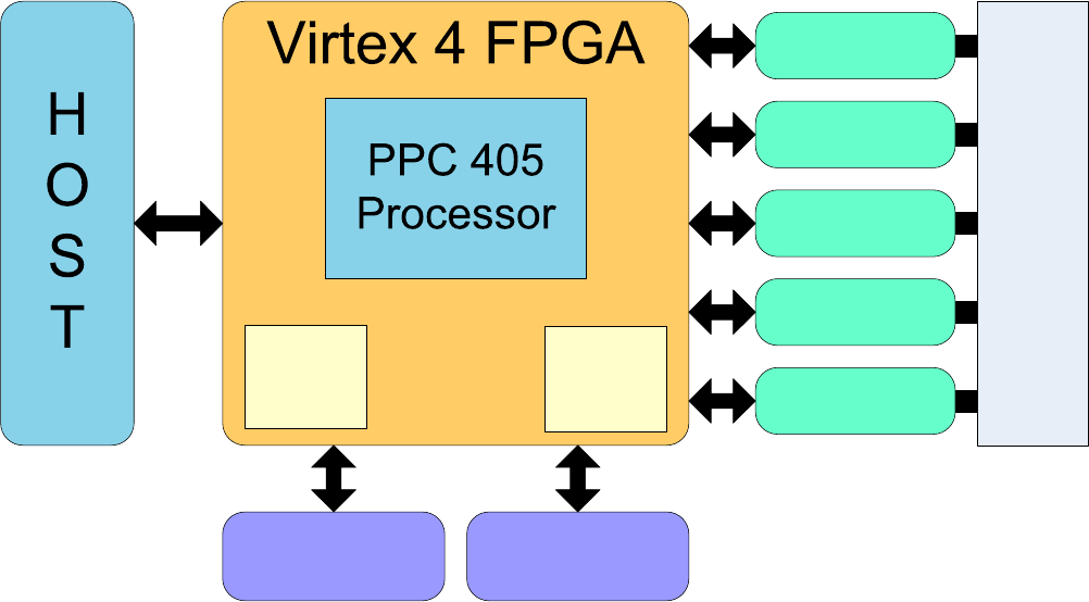
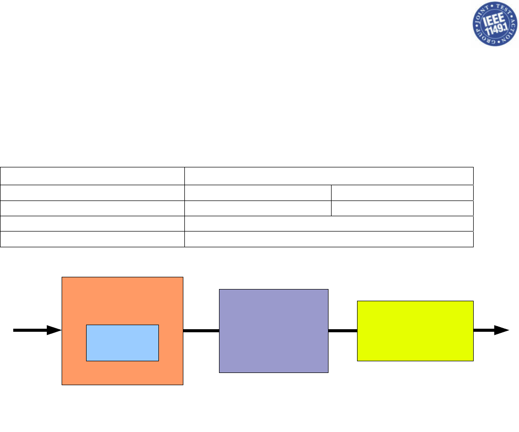
SystemArchitecture
AtthecoreofthePicoE‐14isaVirtex‐4FPGA.TheFPGAcanbedynamicallyconfiguredtoperformany
numberofspecializedtaskssuchas:protocolprocessing,encryption,orcomplexmathematical
functions.EmbeddedsystemsbenefitfromtheintegratedPower‐PC™processoravailableontheEP
seriescards.
DDR2 RAM Flash ROM
Gigabit Ethernet
Analog Converters
Serial Transceiver
JTAG
GPIO
RAM
DSP
Slices
I/O
Figure 1
E‐14HardwareReferenceManualwww.picocomputing.com PicoComputing,Inc.
7
FieldProgrammableGateArray
ThecoreofthePicoE‐14isahighperformanceVirtex‐4FPGA.IncludedintheFPGAaretheFPGA
Fabric,aPower‐PC™processor,ultrahigh‐speedDSPslicesandDDR2RAM.
FPGAFabric:
The“Fabric”ofanFPGAcomprisesanarrayoflogicelementsthatcanbeconnectedinvirtually
unlimitedpatterns.Thesepatternsoflogicelementscanbeusedtoperformbasicmathematical
functionssuchasadditionandsubtraction,orcanbegroupedtogethertoperformcomplexfunctions
likeFastFourierTransforms.Logicelementscanevenbeconnectedtocreateacustomsoftprocessor.
TheadvantageoftheFPGAisthattheinternallogiccanbeoptimizedforaspecificapplication.FPGAs
arealsoabletoexecuteoperationsinparallel,notbeinglimitedbysequentialexecutionlikea
traditionalprocessor.FPGAoperationscanbeexecutedinaparallel,pipelinedorevenan
asynchronousmanner.TheFPGAallowsincredibleapplicationspeedwithverylowpower
consumption.Yourimaginationisreallythelimit.
DSPSlice:
EmbeddedwithintheFPGAarespecialareasthataredesignedtofacilitatehighspeed“digitalsignal
processing.”TheseareasarecalledDSPslices.TheDSPslicecanbeconfiguredinavarietyofdifferent
ways.ForexampleoneDSPslicecanbeconfiguredtobeonetapofanFIRfilter.DSPslicesarefully
pipelinedandfeatureincrediblespeed.WhenconfiguredforFIRfilteringtheDSPslicehasa
guaranteedperformanceof500MHzwithalatencyofonecycle.An18x18multiplyandaccumulate
alsorunsat250MHzwithalatencyoftwocycles.Smallerdatawidthsallowhigherclockspeeds.
FPGAResources:
FreeFPGACoreswww.opencores.org
Virtex‐4Websitewww.xilinx.com/virtex4

E‐14HardwareReferenceManualwww.picocomputing.com PicoComputing,Inc.
8
PowerPC™Processor
PPC405x3ProcessorIntroduction:
FPGAsarerenownedfortheirabilitytoprocessparallellogic,buttheytypicallyhaveahardtime
emulatingahighperformanceprocessor.TogetthebestofbothworldstheVirtex‐4™featuresan
embeddedPowerPCProcessor.SincetheprocessorsharesthesamedieastheFPGAitseamlessly
interfaceswiththeFPGAfabric.
AnewfeatureoftheVitex‐4FPGAistheadditionofanauxiliaryprocessorinterface.TheAPUisthe
highestspeedinterfacebetweenthePower‐PC™processorandtheFPGAfabric.Uptofourcustom
instructionsmaybeimplementedintheFPGA,whichareaccessiblefromthePower‐PC™.
BoardsupportpackagesarecurrentlyavailableforμC/OS,LinuxandIntegrity.Boardsupportsource
codeisavailableopensourceundertheGPL.

E‐14HardwareReferenceManualwww.picocomputing.com PicoComputing,Inc.
9
CPLDTurboLoader
ACPLD(ComplexProgrammableLogicDevice)isasmallerversionofanFPGA(describedabove)with
permanentFlashstoragebuiltin.ThePicoE‐14containsoneCPLDthatloadsandreconfiguresthe
FPGA.ThePicofirmwareguidedescribeshowtoaccesstheCPLDImageManager.
CPLDResources:
XilinxCPLDWebsitewww.xilinx.com/cpld

E‐14HardwareReferenceManualwww.picocomputing.com PicoComputing,Inc.
10
Tri‐ModeEthernetInterface
ThePicoE‐14featurestheMarvellAlaskaseries88E1111tri‐modeEthernettransceiver.OnEPseries
partstheMAC(Middleaccesscontroller)isimplementedontheFPGAdie.OnLOseriespartstheMAC
mustbeimplementedinfirmware.CommunicationbetweentheMACandPHYtakesplaceoveran
industrystandardMII/GMIIinterface.
TheEthernettransceiverfeatures10/100/1000full/halfduplexoperation.Itwillautomatically
configurethephysicalinterfaceontheflyforcrossoverorstraightthroughoperation.ThePHYcan
evenautomaticallycorrectforcommonwiringmistakes.ThePHYhasabuiltinTimeDomain
Reflectometerthatcandiagnosecableproblemsandpinpointtheirdistanceawayfromthe
transceiver.
IncontrasttothePicoE‐12,theEthernetinterfaceonthePicoE‐14ismagneticallyisolatedallowing
directconnectionstoanindustrystandardhuborswitch.
TheMarvell88E1111istheonlychiponthePicoE‐14thatrequiresanNDAforaccesstothe
datasheets.Ifyouareinterestedinsomeoftheadvancedfeaturesnotsupportedbythenativedriver,
contactPicoComputingforassistanceinobtaininganNDAfromMarvell.Usersarewarnednotto
contactMarvelldirectly.
EthernetResources:
Marvell88E1111Webpagehttp://www.marvell.com/products/transceivers/singleport/88e1111.jsp
E‐14HardwareReferenceManualwww.picocomputing.com PicoComputing,Inc.
11
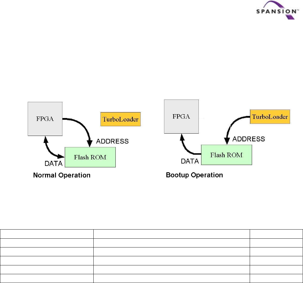
FlashMemory
ThePicoE‐14comesequippedwithatleast64megabytesofFlashROM.TheFlashROMisdividedinto
512sectorsthatcanbeerasedindependently.MostofthespaceontheROMisreservedfortheuser.
TheFlashROM’saddressbuscanbecontrolledbyeithertheTurboLoaderortheFPGA,butnotboth.
Duringpower‐uporreboot,theTurboLoaderisincontroloftheFlashROMAddressbus.Atallother
timestheFPGAisincontroloftheaddressbus.
Figure2
TypicalFlashROMAllocationTable:
ByteaddressesDescriptionFlashSectors
0x00000000‐0x0000FFFFTupleDataandconfigurationmanagement0
0x00010000‐0x0006FFFFPrimaryFPGAImage 1‐6
0x000A0000‐0x000FFFFFBackupFPGAImage7‐12
0x000D0000‐0x0012FFFFSecondaryImageincludingbootloader13‐19
0x00140000‐0x01FFFFFFOtherFPGAimages,executablesanddatafiles20‐511
TheFlashROMhasasimple,openfilesystemthatallowstheusertostoreFPGAimages,ELFbinary
files,orotherdata.TheprimaryimageisusedtoboottheFPGAinitially,andthebackupimageisonly
invokediftheprimaryimagefailstoloadcorrectly.ExecutablefilesareinELFformatandareloadedby
aloaderwithinthesecondaryimage.Theprimaryimagecaneitherloadthesecondaryimageorpause
forthePCtoaccessandmanagethefilesystem.
E‐14HardwareReferenceManualwww.picocomputing.com PicoComputing,Inc.
12
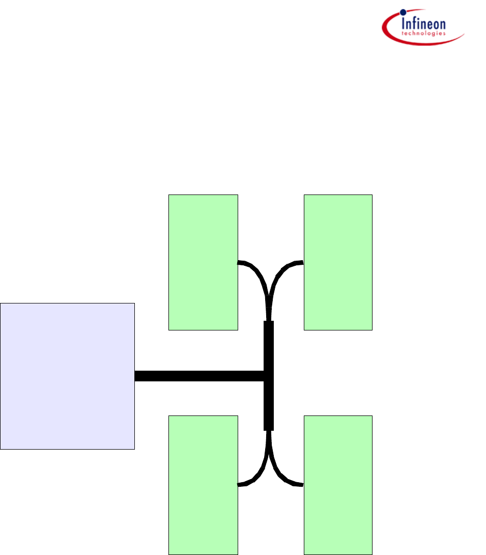
DDR2Memory
ThePicoE‐14comesequippedwith256MBofPC‐266DDR2memory.Therearefour256Mbchips
eachwith16bitdatapathsthataregroupedintotwo32bitbanks.From0°Cto+95°C,theramcanrun
at266MHz.Foroperationattemperaturesbelow0°C,specialfirmwarewithreducedramtimingsis
required.Thetemperaturecompensatedself‐refreshmodemustbedisabledbelow‐20°C.
16x16
(MSBs)
16x16
(LSBs)
FPGA
Bank 1
Bank 2
16x16
(MSBs)
16x16
(LSBs)
Figure3
E‐14HardwareReferenceManualwww.picocomputing.com PicoComputing,Inc.
13
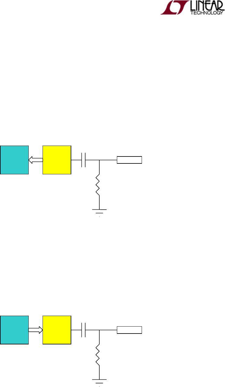
AnalogInterface(Optional)
ThePicoE‐14alsocomesequippedwithtwohigh‐speedanalogconverterseachcapableof14‐bit
resolution.Bydefault,bothanalogconvertersarepowereddownuntilthesleeplinesaredrivenlow
andtheamplifierlinesaredrivenhighbytheFPGA.Bothconvertersarecapacitivelycoupledwithpull‐
downresistorsontheoutputtofilteroutanyDCsignalcomponents.Bothamplifiersareconfigured
forminimumnoiseandunitygain.
8‐Bit,80MSPSAnalog‐to‐DigitalConverter(ADC)*
TheADCisconfiguredtoutilizetheinternal1.0Vreferencevoltageandmaximumfullscaleinput,
givingita2Vpk‐pkinput.Currently,theADCissetuptoacceptinputvoltagesbetween0Vand2V.
Clockmodesandinputdataformatissetbythesystemutilizingconfigurationpinsavailabletothe
FPGA.
8‐Bit,165MSPSDigital‐to‐AnalogConverter(DAC)*
TheDACisconfiguredtoutilizetheinternal1.2Vreferencevoltageandmaximumfull‐scaleoutput,
givingita2Vpk‐pkoutput.SincetheDACactuallyoutputscomplementarycurrents,theamplifieris
alsoutilizedasacurrenttovoltageconverterandvoltageshifter.Thisallowsthevoltagetobebuffered
withinthe0Vto3Vrailvoltages.Currently,theDACissetuptooutputbetween.5Vand2.5V.This
givesusacomfortable.5Vbetweenourmaximumoutputsandrailvoltages.Clockmodesandinput
dataformatissetbythesystemutilizingconfigurationpinsavailabletotheFPGA.
ADC AMP Input
DAC AMP Output
E‐14HardwareReferenceManualwww.picocomputing.com PicoComputing,Inc.
14
*PleaserefertotheAnalogInterfaceSelectionGuideinAppendixEforcompatible8‐12‐bitconverters
RS‐232SerialTransceiver
ThePicoE‐14containsoneasynchronousRS‐232serialtransceiverthatalsomeetsEIA/TIA‐232and
V.28/V.24specificationsatamaximumdatarateof250kBps.Becausetheserialtransceiverisdirectly
connectedtotheFPGAanybithigh‐levelprotocolcanbeimplementedinlogic.PicoComputing
supportsvariousasynchronous,synchronousandmilitaryserialprotocols.
RS‐232isthemostcommonphysicallayerprotocolforserialdata.Itisthestandardusedonserialmice
forcomputers,modems,consumerGPSreceiversandevensomemilitaryradios.Onlyonewireis
neededtosendasignalonanRS‐232link.AtotaloftwodevicesareallowedonasingleRS‐232link.
Inaddition,therearetwopossiblelogicstatesonanRS‐232line(highandlow).Thehighvoltageis
positiveandthelowvoltageisnegative.
PhysicalLayerSpecifications:
StandardNoise
Immunity
Max
Distance
Max
Speed
Max
Connections
RS‐232Satisfactory50ft 250kBps* 1Tx/1Rx
*Maximumspeeddecreaseswithincreasedcablelength.
*TheoldRS‐232,422and485standardsarenowobsoleteandhavebeenreplacedbyEIA/TIA‐232,422
and485.
SerialTransceiverSpecifications:
MaximumContinuousPositiveInputVoltage+25VDC
MaximumContinuousNegativeInputVoltage‐25VDC
ESDProtectionLimit+/‐15,000V
MaximumShortCircuitDurationonOutputInfinite
TypicalRS‐232OutputVoltage+/‐5.4V
RS‐232MaximumLowInputThreshold*1.2V
RS‐232MinimumHighInputThreshold1.5V
*RS‐232Receiverscanacceptdigitalinputs

E‐14HardwareReferenceManualwww.picocomputing.com PicoComputing,Inc.
15
DigitalPeripheralInterface
ThePicoE‐14features16GPIOlinesthatareusedforexternalperipheralsupport.PullingtheDIAG_EN
pinlowreplaces4GPIOsignalswithJTAGsignals.
AllGPIOsignalshaveuserselectablepull‐up,pull‐down,keeperorHI‐Ztermination.Drivestrengthis
alsouserselectablebetween2and24mA.AllGPIOscanbeconfiguredforinput,outputandbi‐
directionalmodeandareequippedwithESDprotection.
DIAG_ENStateJTAG GPIO
Float/HighDisabledEnabled
LowEnabledDisabled
ElectricalSpecificationsMinimum NominalMaximum
HighVoltage1.7V2.5V2.9V
LowVoltage‐0.2V0V0.7V
InputImpedance(PulldownsDisabled) HI‐Z
DriveStrength(Selectable)2mA 24mA
ESDWithstandVoltage(HumanBodyModel) 2KV
E‐14HardwareReferenceManualwww.picocomputing.com PicoComputing,Inc.
16
CardBusInterface
ThePicoE‐14canrunasastandaloneproductorbeconnectedtoahostusingtheCardBusconnector.
Bydefault,thePicoE‐14shipswithfirmwarethatisreadyforuseasaCardBusslavedevice,butitalso
supportsbusmastering.Thatsamefirmwarealsoprovidesthemeanstoswitchintostandlonemode.1
CardBusisa32‐bitinterfacewithamaximumspeedof33MHz.ThePicoE‐14hardwareisdesignedto
supportstandardPCMCIAaswellasDMAmode.TheCardBusstandardspecifiesthatallCardBushosts
bebackwardcompatiblewithPCMCIA.
SinceCardBussystemscanonlybe3.3V,nodigitaltranslatingtransceiversarerequiredtoconnectwith
ahost.ThisallowsdirectconnectiontotheVirtex‐4FPGAforreducedpowerconsumption.Withthis
design,itiseasilypossibletoreversetheCardBusinterfaceandusethePicoE‐14asahostcontroller
forotherCardBusandPCMCIAcards.
ThosewhoareinterestedinalternateinterfacesshouldcontactPicoComputing.ThePCMCIAdecoder
sourcecodeandsupportisavailable.
PCMCIAInterfaceResources:
CompactFlashAssociationwww.compactflash.org
PCMCIAWebsitewww.pcmcia.org
1 For more information on standlone, reference the Standalone documentation located in the doc directory of where Pico
Utility is installed.

E‐14HardwareReferenceManualwww.picocomputing.com PicoComputing,Inc.
17
DigitalBusInterface
WhenthePicoE‐14isnotconnectedtoaCardBushost,thedigitalbuscanbereconfiguredtoconnect
withawidevarietyofhigh‐speeddigitalbussesandperipherals.Allsignalshaveuserselectablepull‐
up,pull‐down,keeperorHI‐Ztermination.Drivestrengthisalsouserselectablebetween2and24mA.
Allpinscanbeconfiguredforinput,outputandbi‐directionalmode.
Withpropertermination,speedsofover200MHzarepossible.Theexternaldigitalbusissetto
transmitandreceiveat3.3Vonly.
ElectricalSpecifications(DC)Minimum NominalMaximum
PositiveSupplyInputVoltage(Vcc)3.15V3.3V5.5V
LowLevelInputVoltage0V0V0.7V
HighLevelInputVoltage2V3.0V3.3V
DriveStrength2mA 24mA
E‐14HardwareReferenceManualwww.picocomputing.com PicoComputing,Inc.
18
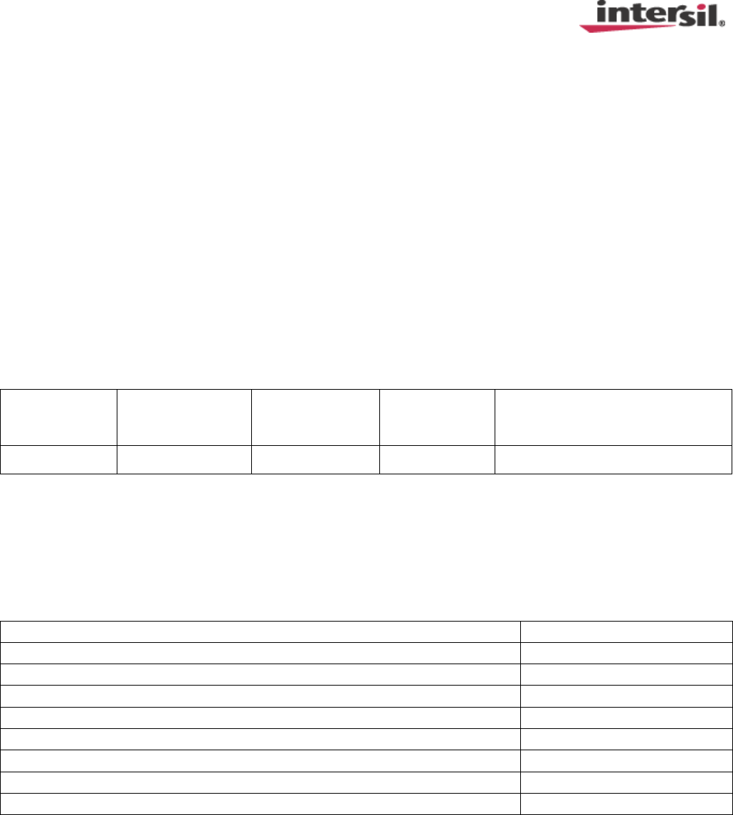
JTAGDebugInterface
ThePicoE‐14isequippedwithaJTAGdiagnosticportthatallowsreal‐timedebuggingofhardware,
firmwareandsoftware.UseoftheexternalJTAGportdisablesfourexternalGPIOpinsaswellasthe
internalJTAGloopback.
SomeJTAGprogramsrequirethelengthoftheinstructionregister(IR).TheIRlengthislistedbelowfor
alldevicesintheJTAGchain.
DeviceInstructionregisterbitlength
FX20FX60
FPGA1014
TurboLoader8
EthernetPHY8
FPGA
PowerPC
IR= 10
EthernetTurbo Loader
TDI TDO
IR= 8
IR= 8
Figure4
ThePrimaryImageintheFlashROMcontainsanembeddedJTAGdiagnosticport.Thisallowsauserin
WindowsorLinuxtodebugsoftwarewithoutanexternalJTAGcable.TheinternalJTAGdiagnosticloop
backlooksjustlikeaParallelPortIVdiagnosticcablewhenusedwiththePicoE‐14driver.
FX20: IR = 10
FX60: IR = 14

E‐14HardwareReferenceManualwww.picocomputing.com PicoComputing,Inc.
19
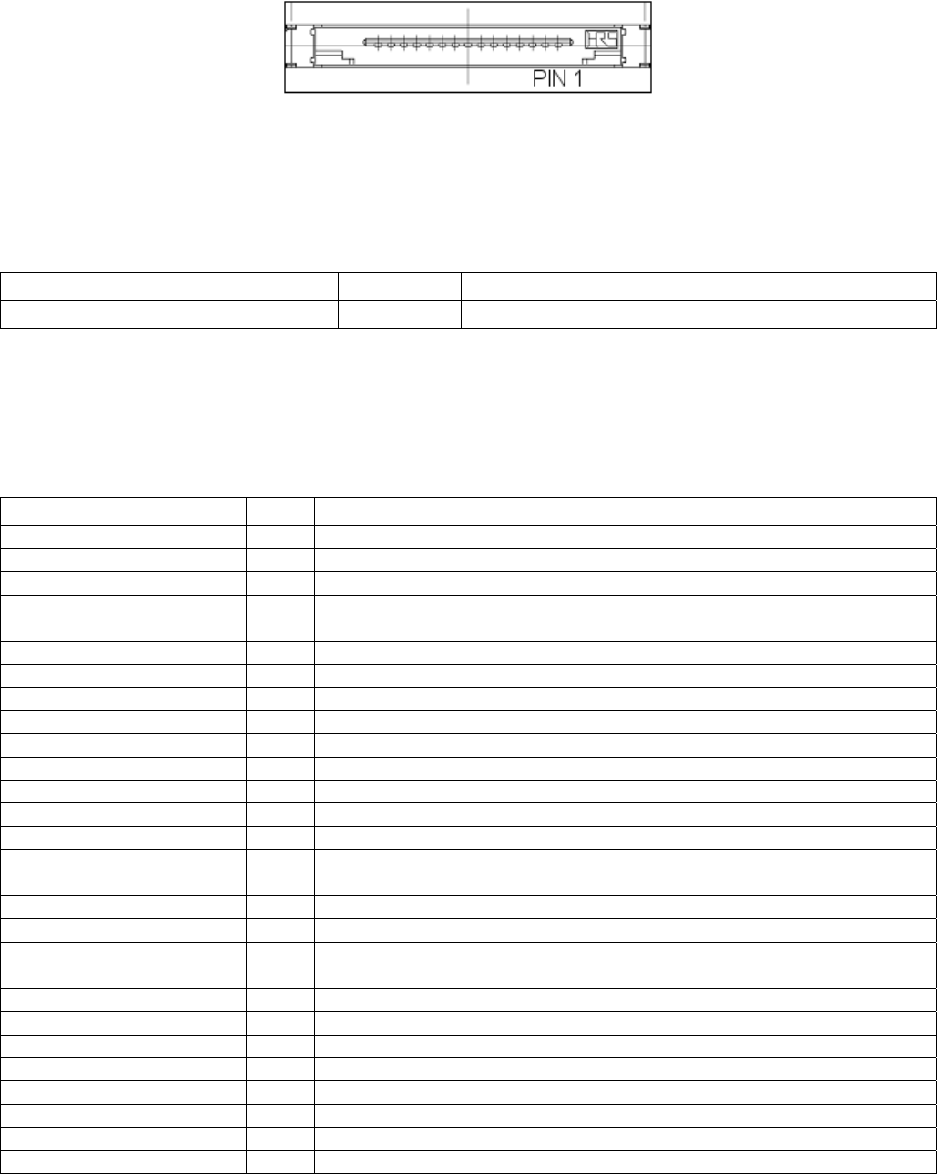
AppendixA
–
PeripheralI/OConnectorInformation
ConnectorInformation
DescriptionBrandPartNumber
MatingConnectorHiroseNX30TA‐32PAA(50)
MatingConnectorBackshellHiroseNX‐32TA‐CV1(50)
*ConnectorsarealwaysinstockatPicoComputing
PeripheralI/OConnectorPinout
1ETHER_OUT_DD‐ Ethernet(MagneticallyIsolated)
2ETHER_OUT_DD+Ethernet(MagneticallyIsolated)
3GPIO_15_FILTEREDGeneralpurposeI/O
4GPIO_14_FILTEREDGeneralpurposeI/O
5GPIO_13_FILTEREDGeneralpurposeI/O
6GPIO_12_FILTEREDGeneralpurposeI/O
7ETHER_OUT_DC‐ Ethernet(MagneticallyIsolated)
8ETHER_OUT_DC+Ethernet(MagneticallyIsolated)
9GPIO_11_FILTEREDGeneralpurposeI/O
10GPIO_10_FILTEREDGeneralpurposeI/O
11GPIO_9_FILTEREDGeneralpurposeI/O
12GPIO_8_FILTEREDGeneralpurposeI/O
13ETHER_OUT_DB‐ Ethernet(MagneticallyIsolated)
14ETHER_OUT_DB+Ethernet(MagneticallyIsolated)
15GPIO_7_FILTEREDGeneralpurposeI/O
16GPIO_6_FILTEREDGeneralpurposeI/O
17GPIO_5_FILTEREDGeneralpurposeI/O
18GPIO_4_FILTEREDGeneralpurposeI/O
19ETHER_OUT_DA‐ Ethernet(MagneticallyIsolated)
20ETHER_OUT_DA+Ethernet(MagneticallyIsolated)
21DAC_OUTPUTD/AConverteroutput
22SERIAL_RX_FILTRS‐232Serialreceiverinput
23SERIAL_TX_FILTRS‐232Serialdriveroutput
24ADC_INPUTA/DConverterinput
25PIC_TRIGGER_EXTNOTCONNECTED
262.5V_EXT2.5V0.45Aperipheralpower
27GPIO_3/TDI_FILTGeneralpurposeI/OorJTAGTDI
28GPIO_2/TDO_FILTGeneralpurposeI/OorJTAGTDO
29GPIO_1/TMS_FILTGeneralpurposeI/OorJTAGTMS
30GPIO_0/TCK_FILTGeneralpurposeI/OorJTAGTCK
31D\I\A\G\_\E\N\_\JTAGportenablewhenshortedtoground
32GND_EXTGroundreturn
NOTE:Pin1indicatorontheboardisactuallyPin32indicator
E‐14HardwareReferenceManualwww.picocomputing.com PicoComputing,Inc.
20
PeripheralConnectorPin#1Location
Figure5
AppendixB
–
CardBusConnectorInformation
ConnectorInformation
DescriptionBrandPartNumber
CardBusHeaderHiroseIC9‐68RD‐0.635SF‐(51)
ThePicoE‐14willmatewithanyType‐IICardBusHeader
ThefunctionanddirectionofthepinsontheCardBusinterfacecanbeeasilychanged.Pleaseseethe
“DigitalBusInterface”sectionformoreinformation.
CardBusConnectorPinout
NamePinDescriptionDir
GND1CardGround PWR
CAD02CardBusData/Address0IO
CAD13CardBusData/Address1IO
CAD34CardBusData/Address3IO
CAD55CardBusData/Address5IO
CAD76CardBusData/Address7IO
C\C\/\B\E
\
0
\
7CommandandByteEnable IO
CAD98CardBusData/Address9IO
CAD119CardBusData/Address11 IO
CAD1210CardBusData/Address12 IO
CAD1411CardBusData/Address14 IO
C\C\/\B\E
\
1
\
12CommandandByteEnable IO
CPAR13Parity IO
C\P
\
E\R\R
\
14ParityError IO
C\G
\
N\
T
\
15Grand I
C\I
\
N\
T
\
16CardIntertRequest O
VCC17CardPower(3.3V) PWR
VPP18CardProgrammingVoltage(NotUsed) PWR
CCLK19CardBusClock I
C\I
\
R\D\Y
\
20InitiatorReady IO
C\C\/\B\E
\
2
\
21CommandandByteEnable IO
CAD1822CardBusData/Address18 IO
CAD2023CardBusData/Address20 IO
CAD2124CardBusData/Address21 IO
CAD2225CardBusData/Address22 IO
CAD2326CardBusData/Address23 IO
CAD2427CardBusData/Address24 IO
CAD2528CardBusData/Address25 IO

E‐14HardwareReferenceManualwww.picocomputing.com PicoComputing,Inc.
21
CAD2629CardBusData/Address26 IO
CAD2730CardBusData/Address27 IO
CAD2931CardBusData/Address29 IO
RFU32ReservedForFutureUse IO
C\C\L
\
K
\
R\U
\
N
\
33ClockRequest/Status O
GND34CardGround PWR
GND35CardGround PWR
C\C\D\1
\
36CardDetect Passive
CAD237CardBusData/Address2IO
CAD438CardBusData/Address4IO
CAD639CardBusData/Address6IO
RFU40ReservedForFutureUse IO
CAD841CardBusData/Address8IO
CAD1042CardBusData/Address10 IO
C\V\S\1
\
43VoltageSelect PWR
CAD1344CardBusData/Address13 IO
CAD1545CardBusData/Address15 IO
CAD1646CardBusData/Address16 IO
RFU47ReservedForFutureUse IO
C\B\L
\
O\C
\
K
\
48CardLock IO
C\S\T
\
O\P
\
49StopTransaction IO
C\D\E
\
V
\
S
\
E\L
\
50DeviceSelect IO
VCC51CardPower(3.3V) PWR
VPP52CardProgrammingVoltage(NotUsed) PWR
C\T
\
R
\
D\Y
\
53TargetReady IO
C\F\R
\
A
\
M
\
E
\
54CycleFrame IO
CAD1755CardBusData/Address17 IO
CAD1956CardBusData/Address19 IO
C\V\S\2
\
57VoltageSelect Passive
C\R\S\T
\
58SystemReset I
C\S\E
\
R
\
R
\
59SystemError O
C\R
\
E\
Q
\
60Request O
C\C\/\B\E
\
3
\
61CommandandByteEnable IO
CAUDIO62CardAudioSignal O
CSTSCHG63CardStatusChange O
CAD2864CardBusData/Address28 IO
CAD3065CardBusData/Address30 IO
CAD3166CardBusData/Address31 IO
C\C\D\2
\
67CardDetect Passive
GND68CardGround PWR
CardBusConnectorPullUpandPullDownInformation
NamePinDescriptionValue
‐CGNT15PullUp 15K
‐CFRAME54PullUp 15K
‐CTRDY53PullUp 15K
‐CIRDY20PullUp 15K
ForadditionalinformationconsulttheCardBusStandardavailablefrom:www.pcmcia.org.
E‐14HardwareReferenceManualwww.picocomputing.com PicoComputing,Inc.
22

E‐14HardwareReferenceManualwww.picocomputing.com PicoComputing,Inc.
23
AppendixC
–
FPGAPinout
FPGAPinout
50MHZ_CLOCKAA1450MHzClockIn+/‐50ppmILV_TTL3.3V
50MHZ_CLOCKAB1250MHzClockIn+/‐50ppmILV_TTL3.3V
50MHZ_CLOCKAB1450MHzClockIn+/‐50ppmILV_TTL3.3V
50MHZ_CLOCKAC1350MHzClockIn+/‐50ppmILV_TTL3.3V
50MHZ_CLOCKAD1550MHzClockIn+/‐50ppmILV_TTL3.3V
50MHZ_CLOCKAE1350MHzClockIn+/‐50ppmILV_TTL3.3V
ADC_AMP_PWUPAD14A/DAmplifierPowerUpOLV_TTL3.3V
ADC_CLKV23ClockOLV_CMOS2.5V
ADC_D0W23Data0[LSB]ILV_CMOS2.5V
ADC_D1T24Data1ILV_CMOS2.5V
ADC_D2V21Data2ILV_CMOS2.5V
ADC_D3W18Data3ILV_CMOS2.5V
ADC_D4Y22Data4ILV_CMOS2.5V
ADC_D5W20Data5ILV_CMOS2.5V
ADC_D6AB21Data6ILV_CMOS2.5V
ADC_D7Y18Data7ILV_CMOS2.5V
ADC_D8AB20Data8ILV_CMOS2.5V
ADC_D9AC21Data9ILV_CMOS2.5V
ADC_D10T20Data10ILV_CMOS2.5V
ADC_D11R20Data11ILV_CMOS2.5V
ADC_D12R21Data12ILV_CMOS2.5V
ADC_D13V18Data13[MSB]ILV_CMOS2.5V
ADC_MODET17DataFormatSelectOLV_CMOS2.5V
ADC_OTRT18Out‐of‐RangeIndicatorOLV_CMOS2.5V
ADC_PDWNV22PowerDownA/DControllerOLV_CMOS2.5V
CB_CAD0K3CardBusData/Address0I/OLV_TTL3.3V
CB_CAD1F3CardBusData/Address1I/OLV_TTL3.3V
CB_CAD2D3CardBusData/Address2I/OLV_TTL3.3V
CB_CAD3C3CardBusData/Address3I/OLV_TTL3.3V
CB_CAD4M6CardBusData/Address4I/OLV_TTL3.3V
CB_CAD5L7CardBusData/Address5I/OLV_TTL3.3V
CB_CAD6K7CardBusData/Address6I/OLV_TTL3.3V
CB_CAD7J4CardBusData/Address7I/OLV_TTL3.3V
CB_CAD8G5CardBusData/Address8I/OLV_TTL3.3V
CB_CAD9G9CardBusData/Address9I/OLV_TTL3.3V
CB_CAD10F7CardBusData/Address10I/OLV_TTL3.3V
CB_CAD11F8CardBusData/Address11I/OLV_TTL3.3V
CB_CAD12D4CardBusData/Address12I/OLV_TTL3.3V
CB_CAD13C4CardBusData/Address13I/OLV_TTL3.3V
CB_CAD14D5CardBusData/Address14I/OLV_TTL3.3V

E‐14HardwareReferenceManualwww.picocomputing.com PicoComputing,Inc.
24
CB_CAD15D6CardBusData/Address15I/OLV_TTL3.3V
CB_CAD16C7CardBusData/Address16I/OLV_TTL3.3V
CB_CAD17J5CardBusData/Address17I/OLV_TTL3.3V
CB_CAD18K6CardBusData/Address18I/OLV_TTL3.3V
CB_CAD19E5CardBusData/Address19I/OLV_TTL3.3V
CB_CAD20E6CardBusData/Address20I/OLV_TTL3.3V
CB_CAD21E7CardBusData/Address21I/OLV_TTL3.3V
CB_CAD22D9CardBusData/Address22I/OLV_TTL3.3V
CB_CAD23C8CardBusData/Address23I/OLV_TTL3.3V
CB_CAD24F10CardBusData/Address24I/OLV_TTL3.3V
CB_CAD25G4CardBusData/Address25I/OLV_TTL3.3V
CB_CAD26J3CardBusData/Address26I/OLV_TTL3.3V
CB_CAD27L10CardBusData/Address27I/OLV_TTL3.3V
CB_CAD28K8CardBusData/Address28I/OLV_TTL3.3V
CB_CAD29F4CardBusData/Address29I/OLV_TTL3.3V
CB_CAD30K11CardBusData/Address30I/OLV_TTL3.3V
CB_CAD31H9CardBusData/Address31I/OLV_TTL3.3V
CB_CAUDIOH3CardAudioSignalOLV_TTL3.3V
CB_CBLOCKB9CardLockI/OLV_TTL3.3V
CB_CC/BE0H4CommandandByteEnablesI/OLV_TTL3.3V
CB_CC/BE1C6CommandandByteEnablesI/OLV_TTL3.3V
CB_CC/BE2H6CommandandByteEnablesI/OLV_TTL3.3V
CB_CC/BE3D10CommandandByteEnablesI/OLV_TTL3.3V
CB_CCLKD11ClockILV_TTL3.3V
CB_CCLKRUNG10ClockRequest/StatusI/OLV_TTL3.3V
CB_CDEVSELG12DeviceSelectI/OLV_TTL3.3V
CB_CFRAMEH8CycleFrameI/OLV_TTL3.3V
CB_CGNTA9GrantILV_TTL3.3V
CB_CINTB11CardInterruptRequestOLV_TTL3.3V
CB_CIRDYG7InitiatorReadyI/OLV_TTL3.3V
CB_CPARA7ParityI/OLV_TTL3.3V
CB_CPERRA8ParityErrorI/OLV_TTL3.3V
CB_CREQB10RequestOLV_TTL3.3V
CB_CRSTD8CardResetILV_TTL3.3V
CB_CSERRC9SystemErrorOLV_TTL3.3V
CB_CSTOPA10StopTransactionI/OLV_TTL3.3V
CB_CSTSCHGJ9CardStatusChangeOLV_TTL3.3V
CB_CTRDYE8TargetReadyI/OLV_TTL3.3V
CB_RFU1E3CardBus:ReservedforFutureUseI/OLV_TTL3.3V
CB_RFU2H7CardBus:ReservedforFutureUseI/OLV_TTL3.3V
CB_RFU3B7CardBus:ReservedforFutureUseI/OLV_TTL3.3V
CPLD_TDIR13CPLDJTAGTDILV_TTL3.3V
DAC_AMP_PWUPK12D/AAmplifierPowerUpOLV_TTL3.3V
DAC_CLKH11ClockOLV_TTL3.3V
DAC_CLK‐ J11ComplementaryClockOLV_TTL3.3V
DAC_CMODEB6ClockModeSelectionOLV_TTL3.3V

E‐14HardwareReferenceManualwww.picocomputing.com PicoComputing,Inc.
25
DAC_D0H16Data0[LSB]OLV_TTL3.3V
DAC_D1K13Data1OLV_TTL3.3V
DAC_D2G11Data2OLV_TTL3.3V
DAC_D3J14Data3OLV_TTL3.3V
DAC_D4E10Data4OLV_TTL3.3V
DAC_D5H12Data5OLV_TTL3.3V
DAC_D6H13Data6OLV_TTL3.3V
DAC_D7C11Data7OLV_TTL3.3V
DAC_D8H14Data8OLV_TTL3.3V
DAC_D9G15Data9OLV_TTL3.3V
DAC_D10G14Data10OLV_TTL3.3V
DAC_D11J15Data11OLV_TTL3.3V
DAC_D12J16Data12OLV_TTL3.3V
DAC_D13G16Data13[MSB]OLV_TTL3.3V
DAC_MODEK10InputDataFormatOLV_TTL3.3V
DAC_SLEEPE11PowerDownD/AControllerOLV_TTL3.3V
ETHER_25MHZAA1525MHzClockOLV_CMOS2.5V
ETHER_125MHZP24125MHzClockILV_CMOS2.5V
ETHER_COLAD19CollisionDetectILV_CMOS2.5V
ETHER_COMAAC19PowerSaveModeOLV_CMOS2.5V
ETHER_CRSAA19CarrierSenseILV_CMOS2.5V
ETHER_IRQAB15IRQILV_CMOS2.5V
ETHER_MDCAD24MediaIndependentInterfaceClockOLV_CMOS2.5V
ETHER_MDIOAC16MediaIndependentInterfaceDataI/OLV_CMOS2.5V
ETHER_RESETAC24ResetOLV_CMOS2.5V
ETHER_RX0U24MII/GMIIDataIn0ILV_CMOS2.5V
ETHER_RX1AD20MII/GMIIDataIn1ILV_CMOS2.5V
ETHER_RX2AD21MII/GMIIDataIn2ILV_CMOS2.5V
ETHER_RX3AD16MII/GMIIDataIn3ILV_CMOS2.5V
ETHER_RX4U21MII/GMIIDataIn4ILV_CMOS2.5V
ETHER_RX5T23MII/GMIIDataIn5ILV_CMOS2.5V
ETHER_RX6AD18MII/GMIIDataIn6ILV_CMOS2.5V
ETHER_RX7T22MII/GMIIDataIn7ILV_CMOS2.5V
ETHER_RX_CLKV24MII/GMIIRXClock ILV_CMOS2.5V
ETHER_RX_CTLAB16MII/GMIIRXEnableILV_CMOS2.5V
ETHER_RX_ERY23MII/GMIIRXErrorILV_CMOS2.5V
ETHER_TX0AA22MII/GMIIDataOut0OLV_CMOS2.5V
ETHER_TX1AC18MII/GMIIDataOut1OLV_CMOS2.5V
ETHER_TX2AB24MII/GMIIDataOut2OLV_CMOS2.5V
ETHER_TX3AB19MII/GMIIDataOut3OLV_CMOS2.5V
ETHER_TX4AB17MII/GMIIDataOut4OLV_CMOS2.5V
ETHER_TX5AA23MII/GMIIDataOut5OLV_CMOS2.5V
ETHER_TX6AC17MII/GMIIDataOut6OLV_CMOS2.5V
ETHER_TX7AC23MII/GMIIDataOut7OLV_CMOS2.5V
ETHER_TX_CLKW24MII/GMIITXClockOLV_CMOS2.5V
ETHER_TX_CTLAA24MII/GMIITXEnableOLV_CMOS2.5V

E‐14HardwareReferenceManualwww.picocomputing.com PicoComputing,Inc.
26
ETHER_TX_ERAA18MII/GMIITXErrorILV_CMOS2.5V
F\L\A\S\H\_\B\Y\T\E\AD3Inverted8/16BitModeSelectOLV_CMOS2.5V
F\L\A\S\H\_\O\E\AA3InvertedOutputEnableOLV_CMOS2.5V
F\L\A\S\H\_\R\E\S\E\T\T3InvertedResetOLV_CMOS2.5V
F\L\A\S\H\_\W\E\W5InvertedWriteEnableOLV_CMOS2.5V
F\L\A\S\H\_\W\P\Y16InvertedWriteProtectOLV_CMOS2.5V
F\L\A\S\H\_C\E\V3InvertedChipEnableOLV_CMOS2.5V
F\P\G\A\_\P\R\OK17InvertedFPGAProgramOLV_CMOS2.5V
FLASH_A0AD6Address0[LSB]I/OLV_CMOS2.5V
FLASH_A1AD8Address1I/OLV_CMOS2.5V
FLASH_A2AD10Address2I/OLV_CMOS2.5V
FLASH_A3AC11Address3I/OLV_CMOS2.5V
FLASH_A4AD9Address4I/OLV_CMOS2.5V
FLASH_A5Y3Address5I/OLV_CMOS2.5V
FLASH_A6AC9Address6I/OLV_CMOS2.5V
FLASH_A7V4Address7I/OLV_CMOS2.5V
FLASH_A8P3Address8I/OLV_CMOS2.5V
FLASH_A9U5Address9I/OLV_CMOS2.5V
FLASH_A10P5Address10I/OLV_CMOS2.5V
FLASH_A11AC4Address11I/OLV_CMOS2.5V
FLASH_A12N4Address12I/OLV_CMOS2.5V
FLASH_A13R5Address13I/OLV_CMOS2.5V
FLASH_A14W3Address14I/OLV_CMOS2.5V
FLASH_A15AA8Address15I/OLV_CMOS2.5V
FLASH_A16AD4Address16I/OLV_CMOS2.5V
FLASH_A17AD11Address17I/OLV_CMOS2.5V
FLASH_A18AB6Address18I/OLV_CMOS2.5V
FLASH_A19AC7Address19I/OLV_CMOS2.5V
FLASH_A20AC6Address20I/OLV_CMOS2.5V
FLASH_A21AB5Address21I/OLV_CMOS2.5V
FLASH_A22AB11Address22I/OLV_CMOS2.5V
FLASH_A23AB9Address23I/OLV_CMOS2.5V
FLASH_A24AB4Address24I/OLV_CMOS2.5V
FLASH_A25AC3Address25[MSB]I/OLV_CMOS2.5V
FLASH_D0V12Data0[LSB]I/OLV_CMOS2.5V
FLASH_D1V13Data1I/OLV_CMOS2.5V
FLASH_D2V14Data2I/OLV_CMOS2.5V
FLASH_D3U14Data3I/OLV_CMOS2.5V
FLASH_D4W13Data4I/OLV_CMOS2.5V
FLASH_D5Y13Data5I/OLV_CMOS2.5V
FLASH_D6W14Data6I/OLV_CMOS2.5V
FLASH_D7W15Data7I/OLV_CMOS2.5V
FLASH_D8V11Data8I/OLV_CMOS2.5V
FLASH_D9W11Data9I/OLV_CMOS2.5V
FLASH_D10U15Data10I/OLV_CMOS2.5V
FLASH_D11U16Data11I/OLV_CMOS2.5V

E‐14HardwareReferenceManualwww.picocomputing.com PicoComputing,Inc.
27
FLASH_D12Y11Data12I/OLV_CMOS2.5V
FLASH_D13Y12Data13I/OLV_CMOS2.5V
FLASH_D14W16Data14I/OLV_CMOS2.5V
FLASH_D15V16Data15[MSB]I/OLV_CMOS2.5V
FLASH_READYY15FlashStatusILV_CMOS2.5V
FPGA_CCLKM14FPGAClockOLV_CMOS2.5V
FPGA_DONEK15FPGADoneOLV_CMOS2.5V
FPGA_INITL15FPGAInitializeOLV_CMOS2.5V
GPIO_0AA4GPIO1I/OLV_CMOS2.5V
GPIO_1AA5GPIO2I/OLV_CMOS2.5V
GPIO_2AC22GPIO3I/OLV_CMOS2.5V
GPIO_3AB22GPIO4I/OLV_CMOS2.5V
GPIO_4Y5GPIO1I/OLV_CMOS2.5V
GPIO_5W4GPIO2I/OLV_CMOS2.5V
GPIO_6Y6GPIO3I/OLV_CMOS2.5V
GPIO_7Y7GPIO4I/OLV_CMOS2.5V
GPIO_8AB10GPIO1I/OLV_CMOS2.5V
GPIO_9Y10GPIO2I/OLV_CMOS2.5V
GPIO_10AA10GPIO3I/OLV_CMOS2.5V
GPIO_11N3GPIO4I/OLV_CMOS2.5V
GPIO_12W19GPIO1I/OLV_CMOS2.5V
GPIO_13AA20GPIO2I/OLV_CMOS2.5V
GPIO_14W21GPIO3I/OLV_CMOS2.5V
GPIO_15AD23GPIO4I/OLV_CMOS2.5V
JTAG_LOOP_TCKV8JTAGLoopbackTCKOLV_CMOS2.5V
JTAG_LOOP_TDIV6JTAGLoopbackTDIILV_CMOS2.5V
JTAG_LOOP_TDOY8JTAGLoopbackTDOOLV_CMOS2.5V
JTAG_LOOP_TMSAC8JTAGLoopbackTMSOLV_CMOS2.5V
LOADT4TurboLoaderLoadImageRequestOLV_CMOS2.5V
PEEKABOOP4TurboLoaderLoadImageRequestOLV_CMOS2.5V
PIC_CLKAF14PowerManagementControllerSleepCounterOLV_TTL3.3V
PIC_DATAAF15PowerManagementControllerSleepRequestOLV_TTL3.3V
R\A\M\_\C\A\S\F24InvertedColumnSelectOSSTL18_II_DCI
R\A\M\_\C\L\K\B14InvertedComplementaryClockOSSTL18_II_DCI
R\A\M\_\C\L\K\E15InvertedComp.ClockFeedbackISSTL18_II_DCI
R\A\M\_\C\S\0\C23InvertedChipSelectBank0OSSTL18_II_DCI
R\A\M\_\C\S\1\C24InvertedChipSelectBank1OSSTL18_II_DCI
R\A\M\_\R\A\S\F22InvertedRowSelectOSSTL18_II_DCI
R\A\M\_\W\E\B15InvertedWriteEnableOSSTL18_II_DCI
RAM_A0D20Address0[LSB]OSSTL18_II_DCI
RAM_A1F19Address1OSSTL18_II_DCI
RAM_A2A12Address2OSSTL18_II_DCI
RAM_A3D21Address3OSSTL18_II_DCI
RAM_A4E21Address4OSSTL18_II_DCI
RAM_A5G21Address5OSSTL18_II_DCI
RAM_A6A13Address6OSSTL18_II_DCI

E‐14HardwareReferenceManualwww.picocomputing.com PicoComputing,Inc.
28
RAM_A7E22Address7OSSTL18_II_DCI
RAM_A8D24Address8OSSTL18_II_DCI
RAM_A9F20Address9OSSTL18_II_DCI
RAM_A10F23Address10OSSTL18_II_DCI
RAM_A11A14Address11OSSTL18_II_DCI
RAM_A12D23Address12[MSB]OSSTL18_II_DCI
RAM_BA0E23BankAddress0OSSTL18_II_DCI
RAM_BA1K18BankAddress1OSSTL18_II_DCI
RAM_CLKC14ClockOSSTL18_II_DCI
RAM_CLKF15ClockFeedbackISSTL18_II_DCI
RAM_CLKE0A15ClockEnable0[PowerSaveMode]OSSTL18_II_DCI
RAM_CLKE1G22ClockEnable1[PowerSaveMode]OSSTL18_II_DCI
RAM_D0C19Data0(LSB)I/OSSTL18_II_DCI
RAM_D1F18Data1I/OSSTL18_II_DCI
RAM_D2G20Data2I/OSSTL18_II_DCI
RAM_D3D19Data3I/OSSTL18_II_DCI
RAM_D4C21Data4I/OSSTL18_II_DCI
RAM_D5E20Data5I/OSSTL18_II_DCI
RAM_D6F17Data6I/OSSTL18_II_DCI
RAM_D7B17Data7I/OSSTL18_II_DCI
RAM_D8D15Data8I/OSSTL18_II_DCI
RAM_D9D14Data9I/OSSTL18_II_DCI
RAM_D10C16Data10I/OSSTL18_II_DCI
RAM_D11A17Data11I/OSSTL18_II_DCI
RAM_D12G17Data12I/OSSTL18_II_DCI
RAM_D13B16Data13I/OSSTL18_II_DCI
RAM_D14C12Data14I/OSSTL18_II_DCI
RAM_D15B12Data15I/OSSTL18_II_DCI
RAM_D16H19Data16I/OSSTL18_II_DCI
RAM_D17H22Data17I/OSSTL18_II_DCI
RAM_D18G24Data18I/OSSTL18_II_DCI
RAM_D19H24Data19I/OSSTL18_II_DCI
RAM_D20J21Data20I/OSSTL18_II_DCI
RAM_D21G19Data21I/OSSTL18_II_DCI
RAM_D22K20Data22I/OSSTL18_II_DCI
RAM_D23K23Data23I/OSSTL18_II_DCI
RAM_D24M22Data24I/OSSTL18_II_DCI
RAM_D25M24Data25I/OSSTL18_II_DCI
RAM_D26K21Data26I/OSSTL18_II_DCI
RAM_D27L24Data27I/OSSTL18_II_DCI
RAM_D28N22Data28I/OSSTL18_II_DCI
RAM_D29L19Data29I/OSSTL18_II_DCI
RAM_D30N24Data30I/OSSTL18_II_DCI
RAM_D31J23Data31I/OSSTL18_II_DCI
RAM_DM0‐7E17DataMask[0‐7]OSSTL18_II_DCI
RAM_DM8‐15C13DataMask[8‐15]OSSTL18_II_DCI

E‐14HardwareReferenceManualwww.picocomputing.com PicoComputing,Inc.
29
RAM_DM16‐23L18DataMask[16‐23]OSSTL18_II_DCI
RAM_DM24‐31N23DataMask[24‐31]OSSTL18_II_DCI
RAM_LOOPBACKD13LoopbackInputISSTL18_II_DCI
RAM_LOOPBACKH17LoopbackOutputOSSTL18_II_DCI
RAM_ODT0J19On‐DieTerminationEnable0OSSTL18_II_DCI
RAM_ODT1D18On‐DieTerminationEnable1OSSTL18_II_DCI
RAM_STROBE0C18StrobeD16‐D31‐Bank0OSSTL18_II_DCI
RAM_STROBE1C17StrobeD0‐D15‐Bank0OSSTL18_II_DCI
RAM_STROBE2L23StrobeD16‐D31‐Bank1OSSTL18_II_DCI
RAM_STROBE3K22StrobeD0‐D15‐Bank1OSSTL18_II_DCI
RS232‐ENJ13SerialTransceiverEnableOLV_TTL3.3V
RS232‐RXM5SerialReceiveOLV_TTL3.3V
RS232‐TXL5SerialTransmitOLV_TTL3.3V
RS232‐VALIDL9SerialValidILV_TTL3.3V
SLEEPU4TurboLoaderSleepRequestOLV_CMOS2.5V
TCKU10JTAGTCKOLV_CMOS2.5V
TDIU11JTAGTDIILV_CMOS2.5V
TMST10JTAGTMSOLV_CMOS2.5V
VRN1F14NOTCONNECTEDI/OLV_CMOS2.5V
VRN2J24NOTCONNECTEDI/OLV_CMOS2.5V
VRP1F13NOTCONNECTEDI/OLV_CMOS2.5V
VRP2H23NOTCONNECTEDI/OLV_CMOS2.5V

E‐14HardwareReferenceManualwww.picocomputing.com PicoComputing,Inc.
30
AppendixD
–
CPLDPinout
CPLDPinout
NetPinDescriptionDirection
50MHZ_CLOCKK250MHzClockIn+/‐50ppm I
CPLD_TDIJ10CPLDJTAGTDI O
ETHER_TDIA6EthernetJTAGTDI O
F\L\A\S\H\_\B\Y\T\E\K78/16BitModeSelect O
F\L\A\S\H\_\O\E\A8OutputEnable O
F\L\A\S\H\_\R\E\S\E\T\A2FlashReset O
F\L\A\S\H\_\W\E\A3FlashWriteEnable O
F\L\A\S\H\_\W\P\A4FlashWriteProtect O
F\L\A\S\H\_C\E\A9FlashChipEnable O
F\P\G\A\_\P\R\O\G\A5FPGAAsynchronousReset O
FLASH_A0K8Address1[8BitMode] O
FLASH_A1K1Address2I/O
FLASH_A2H1Address3I/O
FLASH_A3F1Address4I/O
FLASH_A4K4Address5I/O
FLASH_A5C3Address6I/O
FLASH_A6G3Address7I/O
FLASH_A7H3Address8I/O
FLASH_A8A7Address9I/O
FLASH_A9J1Address10 I/O
FLASH_A10H10Address11 I/O
FLASH_A11G1Address12 I/O
FLASH_A12D1Address13 I/O
FLASH_A13C1Address14 I/O
FLASH_A14K5Address15 I/O
FLASH_A15E1Address16 I/O
FLASH_A16A1Address17 I/O
FLASH_A17B1Address18I/O
FLASH_A18A10Address19 I/O
FLASH_A19E3Address20 I/O
FLASH_A20F3Address21 I/O
FLASH_A21C5Address22 I/O
FLASH_A22B10Address23 I/O
FLASH_A23C4Address24 I/O
FLASH_A24D8Address25 I/O
FLASH_A25C8Address26 I/O
FLASH_D15G10Address0* I/O
FPGA_CCLKF10FPGAConfigurationClock O
FPGA_DONED10FPGADoneProgramming I
FPGA_INITE10FPGAReadytoProgram I/O
LOADK6LoadImageRequest I
PEEKABOOH5OutputLastAddressBeforeDoneRequest I

E‐14HardwareReferenceManualwww.picocomputing.com PicoComputing,Inc.
31
SLEEPC10SleepModeRequest I
*PinD15turnsintoAddress‐1whentheFlashROMisin8bitmode.

E‐14HardwareReferenceManualwww.picocomputing.com PicoComputing,Inc.
32
AppendixE
–
StandardPartNumberListing
StandardPartNumberListing
DevicePartNumberWebsite
PicoE‐14EP
FPGAXC4VFX20‐10FF672C
XC4VFX60‐10FF672C
http://www.xilinx.com/virtex4
CPLDXC2C64A‐7CP56Ihttp://www.xilinx.com/cpld
RAMHYB18T512160BF‐3.7http://www.infineon.com
ROMS29GL512N10FAI010http://www.amd.com/us‐en/FlashMemory
Ethernet88E1111‐B2‐BAB‐I000http://www.marvell.com
ADCAD9245ACPhttp://www.analog.com
DACAD9744ACPhttp://www.analog.com
RS‐232SerialISL4221EIRhttp://www.intersil.com
E‐14HardwareReferenceManualwww.picocomputing.com PicoComputing,Inc.
33
AppendixF
–
Errata
Thefollowingsectionlistsallknownerrata:
Allversions:
PermanentdamagewillresultifthePicoE‐14isleftun‐configuredandpoweredonformorethan10
minutes.ThisshouldnotbeaproblemsincethePicoE‐14automaticallyloadsanFPGAimageupon
power‐on.
E‐14HardwareReferenceManualwww.picocomputing.com PicoComputing,Inc.
34
AppendixG
–
FPGAPerformanceEnhancements
Overview:
Likemostsilicondevices,theFPGAonthePicocanbeoverclockedifpropercoolingtechniquesare
employed.Caremustbetakentoavoidthermalrunaway.
ThermalRunaway:
AsthedietemperatureoftheFPGAincreases,itdrawsmorecurrent.Thisextracurrentgetsturned
intoheat.Ifthermalequilibriumisnotreachedwithpropercooling,theFPGAwilloverheator
overstressthepowersupplies.Inalllabtests,theFPGAcorepowersupplyshutdownbeforetheFPGA
couldbedamagedbyanovertemperaturecondition(althoughthisbehaviorisnotguaranteed).The
maximumFPGAcoretemperatureis150°C.NotethatchipssurroundingtheFPGAwillbedamagedby
temperaturesabove85°C.
HeatSinkPlacement:
TheheatsinkoftheFPGAisinternallyconnectedviathermalgreasetothecaseoftheCardBuscardon
thetopside(serialnumberside).Placingalargeheatsinkontheoutsideofthecasecanallowhigher
performance.
PowerRequirements:
Caremustbetakentokeepcurrentconsumptionunderthe1Amaximumspecifiedbythe3.3V
CardBusstandard.Ifanexternalpowersupplyisavailabletheboardcanbesupplied5.0Vformaximum
power,however,thedigitalinterfaceswillstillcommunicateattheLVTTL3.3Vstandard.
SpeedRatings:
PicoComputingusesallindustrialtemperaturerangepartswhereavailable.Whena‐10industrial
temperaturespeedgradeFPGAiscreated,a‐11commercialspeedgradepartistestedto‐10
performanceratingsattheindustrialtemperaturerange.Picocomputingdoesnotguaranteethat‐10
industrialpartscanbeoperatedat‐11speedswhenkeptbelow85°C.

E‐14HardwareReferenceManualwww.picocomputing.com PicoComputing,Inc.
35
AppendixE
–
AnalogInterfaceSelectionGuide
Partsinthetablebelowareallpin‐compatiblewithfootprintsonthePicoE‐14Card.
Factorssuchascost,powerconsumption,resolution,andspeedshouldallbe
consideredfortheparticularapplicationinwhichthePicoE‐14isutilized.
PartResolution(bits)Speed(MSPS)LowPower
DACAD9748ACP8165
DACAD9740ACP10165
DACAD9742ACP12210
DACAD9744ACP14165
DACAD9704CPZ*8175X
DACAD9705CPZ*10175X
DACAD9706CPZ*12175X
DACAD9707CPZ*14175X
ADCAD9215BCP‐651065
ADCAD9215BCP‐801080
ADCAD9215BCP‐10510105
ADCAD9235BCP‐201220
ADCAD9235BCP‐401240
ADCAD9235BCP‐651265
ADCAD9236BCP‐801280
ADCAD9237BCP‐20*1220X
ADCAD9237BCP‐40*1240X
ADCAD9237BCP‐65*1265X
ADCAD9245BCP‐801480
*PartnotyetinproductionfromAnalogDevicesasof8/11/05
E‐14HardwareReferenceManualwww.picocomputing.com PicoComputing,Inc.
36
RevisionHistory
14.1.8.11
Initialpublicrelease
14.1.8.12
Updated:ElectricalSpecifications,JTAGDebuginterface,updatedpartnumbers
E‐14HardwareReferenceManualwww.picocomputing.com PicoComputing,Inc.
37
LegalNotices
“XilinxSystemGeneratorforDSP”isaregisteredtrademarkofXilinx,INC.
“Xilinx”andassociatedartworkareregisteredtrademarksofXilinx,INC.
“Virtex”andassociatedartworkareregisteredtrademarksofXilinx,INC.
“Virtex‐4”andassociatedartworkisregisteredtrademarksofXilinx,INC.
“CoolRunner‐II”andassociatedartworkareregisteredtrademarksofXilinx,INC.
“MATLAB”isaregisteredtrademarkofTheMathWorks,INC.
“Simulink”isaregisteredtrademarkofTheMathWorks,INC.
“PowerPC”andassociatedartworkareregisteredtrademarksofInternationalBusinessMachinesCorporation.
“Spansion”andassociatedartworkareregisteredtrademarksofSpansion,LLC.
“Infineon”andassociatedartworkareregisteredtrademarksofInfineonTechnologiesAG.
“Intersil”andassociatedartworkareregisteredtrademarksofIntersilCorporation.
“MirrorBit”andassociatedartworkareregisteredtrademarksofAdvancedMicrodevices,INC.
“AMD”andassociatedartworkareregisteredtrademarksofAdvancedMicroDevices,INC.
“Microchip”andassociatedartworkareregisteredtrademarksofMicrochipTechnology,INC.
“LinearTechnology”andtheLinearTechnologylogoareregisteredtrademarksofLinearTechnologyCorporation.
“ImpulseC”isaregisteredtrademarkofImpulseAcceleratedTechnologies,INC.
“ImpulseAcceleratedTechnologies”andassociatedartworkareregisteredtrademarksofImpulseAcceleratedTechnologies,INC.
“μC/OS”isaproductofMicrimm.
“PCMCIA”and“CARDBUS”governanceisprovidedunderthedirectionofthePersonalComputerMemoryCardInternationalAssociation.
Thismanualis©2005PicoComputing,Inc.
