Polycom PK4586 DECT module User Manual Produktionsflow for 1401 31XX CSLC SDX
Polycom Inc. DECT module Produktionsflow for 1401 31XX CSLC SDX
Polycom >
KT4586 UserMan
PRODUCT SPECIFICATION
POLYCOM
ED
2.0
DATE
29-06-2011
SIGN
HBR
Page 1 of 12
Model no.: KT4586
141993XX-DS
DECT application module
Model no.: KT4586

PRODUCT SPECIFICATION
POLYCOM
ED
2.0
DATE
29-06-2011
SIGN
HBR
Page 2 of 12
Model no.: KT4586
141993XX-DS
1. Preface ....................................................................................................................................... 3
2. Features ..................................................................................................................................... 3
3. Circuit description ..................................................................................................................... 4
4. Pin configuration .................................................................................................................... 5
5. Mechanical dimension............................................................................................................ 7
6. PCB integration & soldering ................................................................................................. 8
7. FCC compliance statement .................................................................................................. 11
8. Safety compliance statement .............................................................................................. 12
Proprietary and Confidential
The information contained herein is the sole intellectual property of Polycom, Inc. No distribution,
reproduction or unauthorized use of these materials is permitted without the expressed written
consent of Polycom, Inc. Information contained herein is subject to change without notice and does
not represent commitment of any type on the part of Polycom, Inc. Polycom and Accord are
registered trademarks of Polycom, Inc.
Notice
While reasonable effort was made to ensure that the information in this document was complete
and accurate at the time of printing, Polycom, Inc., cannot assume responsibility for any errors.
Changes and/or corrections to the information contained in this document may be incorporated
into future issues.

PRODUCT SPECIFICATION
POLYCOM
ED
2.0
DATE
29-06-2011
SIGN
HBR
Page 3 of 12
Model no.: KT4586
141993XX-DS
1. Preface
The KT4586, DECT application module is used to transfer messaging, data, and voice signals
by use of the radio frequency spectrum according to the DECT standard.
KT4586 is a fully approved module that complies with the following standards and certifications:
EN 301 406 V2.1.1:2009-07 (DECT radio)
EN 300 175-1 to 8 (DECT CI)
EN 301 489-1 V1.8.1:2008-04, EN 301 489-6 V1.3.1:2008-08 (EMC)
IEC 60950-1:2005 (ed. 2.0) +am1:2009, EN 60950-1:2006+A11:2009+A1:2010 (Safety)
R&TTE certificate
FCC PART 15, Subpart D
FCC part 15B
FCC SAR
RSS-213
This means that by integration on a main board no radio test is required.
2. Features
RF range: 1880 – 1930 MHz
DECT channels: 60(EU) 30(US) logical duplex channels.
Receiver sensitivity: Typ.< -93 dBm [BER,1000 ppm].
Transmit power (NTP): Typ. 23 dBm. , 20.2 dBm (US)
Power supply range: 2.0 – 3.45V
Current consumption: TBD
Temp. Range: -20ºC to +60ºC.
Size: 25.0 X 30.0 X 3.0mm.
Other features: See data sheet for SC14441

PRODUCT SPECIFICATION
POLYCOM
ED
2.0
DATE
29-06-2011
SIGN
HBR
Page 4 of 12
Model no.: KT4586
141993XX-DS
3. Circuit description
The module consists mainly of the fully integrated CMOS transceiver and baseband processor
SC14441 from SiTel semiconductor intended for DECT 6.0 handsets and base stations. RF switches
and other components are added to the design in order to perform the desired functionality
required for DECT/GAP. Figure 1 shows the block diagram of the module.
The DECT transceiver/baseband SC14441
SC14441 is a 1.8V single chip for DECT applications containing a fully integrated radio transceiver
and baseband processor. It is designed to perform the complete transmit and receiver function.
The device is designed to operate the frequency synthesizer in a close loop configuration both
during transmit and receive mode. Logic output ports are used to control the T/R switch and
antenna switch for FAD (Fast Antenna Diversity).
The CompactRISC CR 16Cplus microprocessor with a single wire debug port running from ROM
controls the protocol stack and the I/O peripherals, keyboard, UART, ACCESS bus, SPI, LED
drivers and RF switches.
The audio path comprises a 16 bit CODEC with an analog frontend including a high efficiency 4
ohm audio amplifier (class D) and a programmable Gen2DSP supporting various
telecommunication algorithms. Detailed information about the chip is available from SiTel
semiconductor.
T/R SW
29 general purpose I/O ports
Figure 1
SC14441
Integrated CMOS
transceiver and
baseband processor
Ant. SW
Serial debug interface
UART, Full duplex
SPI interface
Dual ACCESS bus
PCM interface
16-bit linear audio CODEC
Analog microphone interface.
Analog loudspeaker interface.
Charge controle
LDO & PWR SW
circuit
To supply
QSPI FLASH
EEPROM
RX Balun
TX Balun
ULP controle ports
DC-DC converter ports
Quad SPI bus

PRODUCT SPECIFICATION
POLYCOM
ED
2.0
DATE
29-06-2011
SIGN
HBR
Page 5 of 12
Model no.: KT4586
141993XX-DS
4. Pin configuration
A1
GND
B1
GND
C1
GND
D1
GND
E1
VDDPA
F1
SOCp
A2
GND
B2
GND
C2
P30
D2
P31
E2
GND
F2
P10
A3
GND
B3
CP_VOUT1
C3
GND
D3
P16
E3
CHARGE_CTRL
F3
ADC2
A4
CP_VOUT2
B4
P15
C4
P27
D4
P17
E4
SOCn
F4
DC_CTRLN
A5
VDDIO
B5
GND
C5
P14
D5
GND
E5
GND
F5
ULP_PORT
A6
P12
B6
P26
C6
P11
D6
GND
E6
GND
F6
ULP_VBAT
A7
GND
B7
P05
C7
GND
D7
GND
E7
GND
F7
ULP_MAIN_CTRL
A8
GND
B8
GND
C8
P00
D8
GND
E8
GND
F8
RFP0n
A9
VBAT
B9
P01
C9
GND
D9
P24
E9
GND
F9
P23
A10
P04
B10
VBATT
C10
JTAG
D10
VDD
E10
P07
F10
P13
A11
RSTn
B11
GND
C11
VCCRF
D11
P25
E11
GND
F11
P06
B12
TP2
G1
GND
H1
VREFm
J1
GND
K1
VREFp
L1
GND
G2
LSRn
H2
LSRp
J2
MICh
K2
MICp
L2
MICn
M2
TP1
G3
GND
H3
P37
J3
GND
K3
P32_CIDINp
L3
GND
G4
P33
H4
ONE_CELL
J4
P35
K4
P36
L4
GND
G5
GND
H5
DC_SENCE
J5
GND
K5
P34
L5
RFP0
G6
DC_CTRL
H6
DC_I
J6
RFP1
K6
WLED0
L6
GND
G7
GND
H7
P22
J7
GND
K7
WLED1
L7
GND
G8
LDORF_CTRL
H8
RFP2
J8
P21
K8
P20
L8
WLED2
G9
GND
H9
GND
J9
GND
K9
GND
L9
GND
G10
GND
H10
GND
J10
GND
K10
RF0
L10
RF1
G11
GND
H11
GND
J11
GND
K11
RF2
L11
GND
Leave K10, K11, L10, M2 and B12 (RF ports and test pin’s) unconnected to the main board without
any conducting plan underneath. Connect VREFm to local GND on the main board.

PRODUCT SPECIFICATION
POLYCOM
ED
2.0
DATE
29-06-2011
SIGN
HBR
Page 6 of 12
Model no.: KT4586
141993XX-DS
Top view of the pin’s

PRODUCT SPECIFICATION
POLYCOM
ED
2.0
DATE
29-06-2011
SIGN
HBR
Page 7 of 12
Model no.: KT4586
141993XX-DS
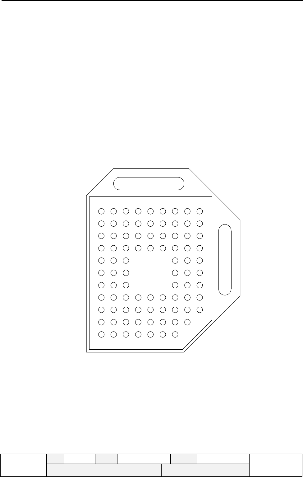
5. Mechanical dimension

PRODUCT SPECIFICATION
POLYCOM
ED
2.0
DATE
29-06-2011
SIGN
HBR
Page 8 of 12
Model no.: KT4586
141993XX-DS
6. PCB integration & soldering
Recommended integration on the main PCB
In order to ensure proper coverage and to avoid detuning of the antennas, it is very important to
place the module in a free prober way on the main board and in relation to other surrounding
materials. As a “thumb rule”, keep a distance of at least 10 mm from the antenna element to
conducting objects and at least 5 mm to non-conducting objects - depending of the size. Keep in
mind that electrical shielding objects, even partly surrounding the antennas, will normally cause a
significant degradation of the coverage. Place the module at the corner of the main-board as shown
below. If the module has to be placed away from the edge of the main-board, then avoid
conducting areas in front of the antennas and make a cut-out in the main board underneath the
antennas as shown below. Keep solid ground on layer 2 out to the edges of the main board as
shown.

PRODUCT SPECIFICATION
POLYCOM
ED
2.0
DATE
29-06-2011
SIGN
HBR
Page 9 of 12
Model no.: KT4586
141993XX-DS
Cu. pad 1.00x1.00mm
Solder mask opening 1.80x1.80mm
Substrate
Copper pads
Solder Mask
Stencil Opening in stencil 1.40 x 1,40mm
Recommended copper pad and solder mask opening (NSMD)
Recommended stencil design
(stencil thickness 0.122 mm)
Cu. pad 0,80x0,80mm
Solder mask opening 1,00x1,00mm
Opening in stencil 1,12x1,12mm

PRODUCT SPECIFICATION
POLYCOM
ED
2.0
DATE
29-06-2011
SIGN
HBR
Page 10 of 12
Model no.: KT4586
141993XX-DS
Recommended re-flow profile
t1: Max. Change in temperature
3°C/sec.
t2: Time in preheat (150°C < temp. < 190°C)
60 - 120 sec.
t3: Time in reflow zone (temp. > 220°C)
30 - 60 sec.
t4: Peak temperature
237°C±5°C
T1 Preheat zone bottom
150°C
T2 Preheat zone top
190°C
T3 Reflow zone
220°C
0°
T1 150°C
T2 190°C
T3 220°C
50°
t1
t2
Meltingpoint 217°C
150°
100°
250°
200°
Reflow profile – leadfree
Sn96.5-Ag3.0-Cu0.5
t3
t4
Temp. C°
Time
We recommend to fabricate PCB in accordance with IPC-A-600G, IPC-6012B, IPC-
6016/A and IPC-6018A, Class 2; per IPC-6011 using customer supplied data files.

PRODUCT SPECIFICATION
POLYCOM
ED
2.0
DATE
29-06-2011
SIGN
HBR
Page 11 of 12
Model no.: KT4586
141993XX-DS
7. FCC compliance statement
This device complies with Part 15 of the FCC Rules
Operation is subject to the following two conditions:
(1) this device may not cause interference, and (2) this device must accept any interference,
including interference that may cause undesired operation of the device.
Information to User:
This equipment has been tested and found to comply with the limits for a Class B digital device,
pursuant to Part 15 of the FCC Rules. These limits are designed to provide reasonable protection
against harmful interference in a residential installation. This equipment generates, uses and can
radiate radio frequency energy and, if not installed and used in accordance with the instructions,
may cause harmful interference to radio communications. However, there is no guarantee that
interference will not occur in a particular installation. If this equipment does cause harmful
interference to radio or television reception, which can be determined by turning the equipment
off and on, the user is encouraged to try to correct the interference by one or more of the following
measures:
- Reorient or relocate the receiving antenna
- Increase the separation between the equipment and receiver
- Connect the equipment into an outlet on a circuit different from that to which the receiver is
connected.
- Consult the dealer or an experienced radio/TV technician for help.
FCC / IC Canada Labeling of host device:
The modular transmitter is labeled with its own FCC and IC identification number, and, if the FCC
or IC identification numbers are not visible when the module is installed inside another device,
then the outside of the device into which the module is installed must also display a label referring
to the enclosed module. This exterior label shall use wording as the following: “Contains FCC ID:
M72-PK4586 and Contains IC: 1849C-PK4586”.
RF Exposure information:
The internal antennas used for this mobile transmitter must provide a separation distance of at
least 20 cm from all persons. OEM integrators and end users must be provided with transmitter
operating conditions for satisfying RF exposure compliance.
Antenna information:
The module has been tested and approved for use with the antenna listed below:
Type of antennas: PCB monopole antenna.
Gain of the antennas: 1.2 dBi
Frequency range: 1920-1930 MHz
The use of that module in combination with a not listed antenna must be authorized with
respective regulatory agencies.

PRODUCT SPECIFICATION
POLYCOM
ED
2.0
DATE
29-06-2011
SIGN
HBR
Page 12 of 12
Model no.: KT4586
141993XX-DS
8. Safety compliance statement
1) The specific external power supply for the DECT application module KT4585A has to fulfil
the requirements according to clause 2.5 (Limited power source) of this standard EN 60950-
1:2006.
2) Interconnection circuits shall be selected to provide continued conformance to the
requirements of clause 2.2 for SELV (Safety Extra Low Voltage) circuits according to EN
60950-1:2006 after making connections.
3) Interface type not subjected to over voltages (i.e. does not leave the building).
4) Requirements additional to those specified in this standard may be necessary for:
- Equipment intended for operation in special environments (for example, extremes of
temperature, excessive dust, moisture or vibration, flammable gases and corrosive or
explosive atmospheres).
- Equipment intended to be used in vehicles, on board ships or aircraft, in tropical
countries or at altitudes grater than 2000 m.
- Equipment intended for use where ingress of water is possible.
5) Installation by qualified personnel only!
6) The product is a component intended for installation and use in complete equipment. The
final acceptance of the component is dependent upon its installation and use in complete
equipment.