Qingdao Richmat Intelligence Technology HJBLE HJBLE User Manual
QingDao Richriver Electrics Co.,Ltd HJBLE Users Manual
Contents
User manual_Rev 1

HJ BLE Module
SPEC
V1.0

Index
1. Summary ................................................................................................................................... 3
1.1 Functions ............................................................................................................................. 3
1.2 Application .......................................................................................................................... 3
2. Electrical characters .................................................................................................................. 4
3. RF performance ......................................................................................................................... 5
4. Pin assignment .......................................................................................................................... 6
4.1 pin distribution ............................................................................................................. 6
4.2 Pin definition ................................................................................................................ 7
5. Reference Design ....................................................................................................................... 9
5.1 Reference schematic .................................................................................................... 9
5.2 Module packet............................................................................................................ 10
5.3 Warning ...................................................................................................................... 11

3
1. Summary
1.1 Functions
32-bit MCU,128KB Flash,16KB SRAM
Bluetooth 4.2.
-92dBm senstivity
Support I2C connector
Support UART connector
Support SPI connector
Support ADC connector
Support DMIC、AMIC connector
Support USB connector
PCB antenna
1.2 Application
Fitness
Wearable products
Smart home

4
2. Electrical characters
Table 1 Supply voltage
Symbol
Typical
Minimum
Maximum
Units
VDD
3.3V
2.7
3.6
V
Table 2 Digital IO specifications
Symbol
Minimum
Normal
Maximum
Units
VIH
0.7VDD
-
VDD
V
VIL
VSS
-
0.3VDD
V
VOH
VDD-0.3
-
VDD
V
VOL
VSS
-
0.3
V
Table 3 Temperature specifications
Item
Minimum
Maximum
Units
Storage
-65
+150
℃
Soldering
-
+260
℃
Table 4 DC characteristics
工作模式(Item)
典型值(typ)
单位(Units)
发射模式 Tx current (1KB/s) @0dBm
10.8
mA
接收模式 Rx current (1KB/s)
9.8
mA
睡眠(Sleep current)
150
uA
挂起(Suspend current)
10
uA
深睡眠(Deepsleep)
1
uA

5
3. RF performance
Table 5 RF section
Item
Symbol
Minimum
Normal
Maximum
Units
Sensitivity
1Mbps
-93
-92
-90
dBm
Frequency offset
tolerance
-
-300
-
+300
KHz
Co-channel
rejection
-
-
-7
-
dB
In-band blocking
rejection
±1 MHz offset
-
12
-
dB
-2 MHz offset
-
47
-
dB
-3 MHz offset
-
48
-
dB
+3 MHz offset
-
50
-
dB
>4 MHz offset
-
52
-
dB
Image rejection
-
-
44
-
dB
Table 6 BT section
Item
Symbol
Minimum
Normal
Maximum
Units
Output
-
-37
0
8
dBm
Modulation 20dB
bandwidth
-
-
1000
-
KHz

6
4. Pin assignment
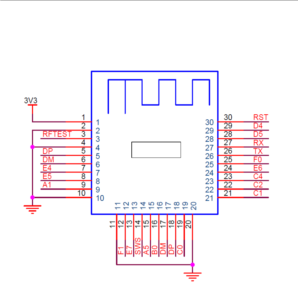
4.1 pin distribution
HJ BLE

7
4.2 Pin definition
Table 7 .HJBLE pin definition
PIN #
引脚名
类型
描述
1
3V3
POWER
3.3V power
2、4、10、11、20
GND
POWER
grond
3
RF_TEST
ANALOG
external antenna pin
5、18
DP
I/O
USB data Positive/GPIO/ANA_B<6>
6、17
DM
I/O
USB data Minus/GPIO/ANA_B<5>
7
E4
I/O
GPIO16/ANA_E<4>
8
E5
I/O
GPIO17/ANA_E<5>
9
A1
I/O
PWM3 output/GPIO/ ANA_A<1>
12
F1
I/O
SPI clock/I2C_SCK/GPIO/ ANA_F<1>
13
E7
I/O
SPI data input/I2C_SDA/GPIO/ ANA_E<7>
14
SWS
I/O
Single wire slave/GPIO/ANA_A<0>
15
A5
I/O
PWM4 output/GPIO/ ANA_A<5>
16
B0
I/O
PWM5 output/GPIO/ ANA_B<0>
19
C0
I/O
PWM0 output/GPIO/ANA_C<0>/
Analog mcrophone Bias
21
C1
I/O
GPIO/PWM1 inverting output/ANA_C<1>/
Analog microphone input
22
C2
I/O
PWM1 inverting output/GPIO/ANA_C<2>
23
C4
I/O
PWM2 output/GPIO/ ANA_C<4>
24
E6
I/O
SPI chip select. Active low/ UART_RTS
/GPIO/ANA_E<6>
25
F0
I/O
SPI data output/ UART_CTS /GPIO/
ANA_F<0>
26
TX
I/O
GPIO4/UART_TX/ ANA_C<6>
27
RX
I/O
GPIO5/UART_RX/ ANA_C<7>
28
D5
I/O
GPIO11/ ANA_D<5>/ (optional) 32KHz
crystal output

8
29
D4
I/O
GPIO10/ ANA_D<4>/(optional) 32KHz
crystal input
30
RST
I/O
Power on reset, active low

9
5. Reference Design
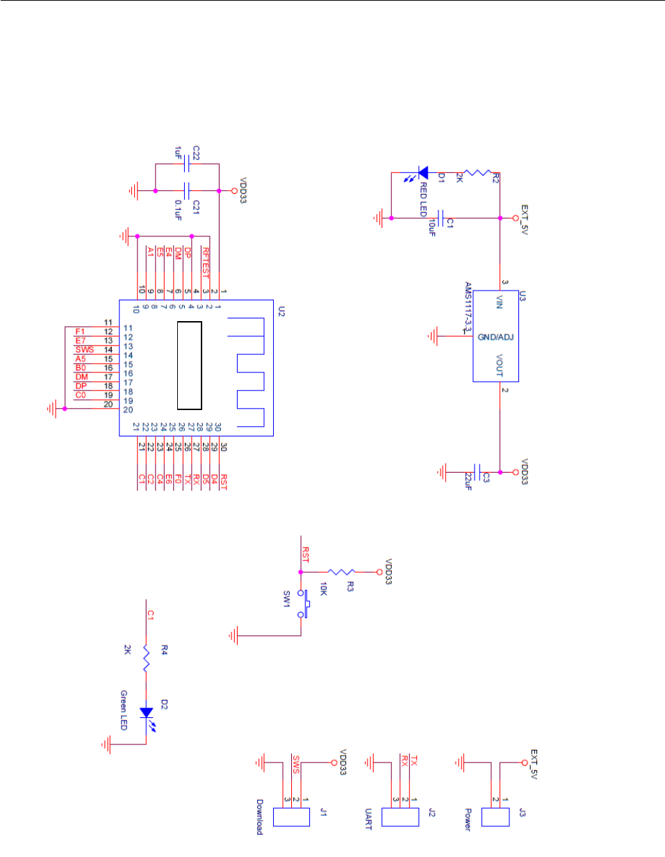
5.1 Reference schematic
HJ BLEHJ BLE

10
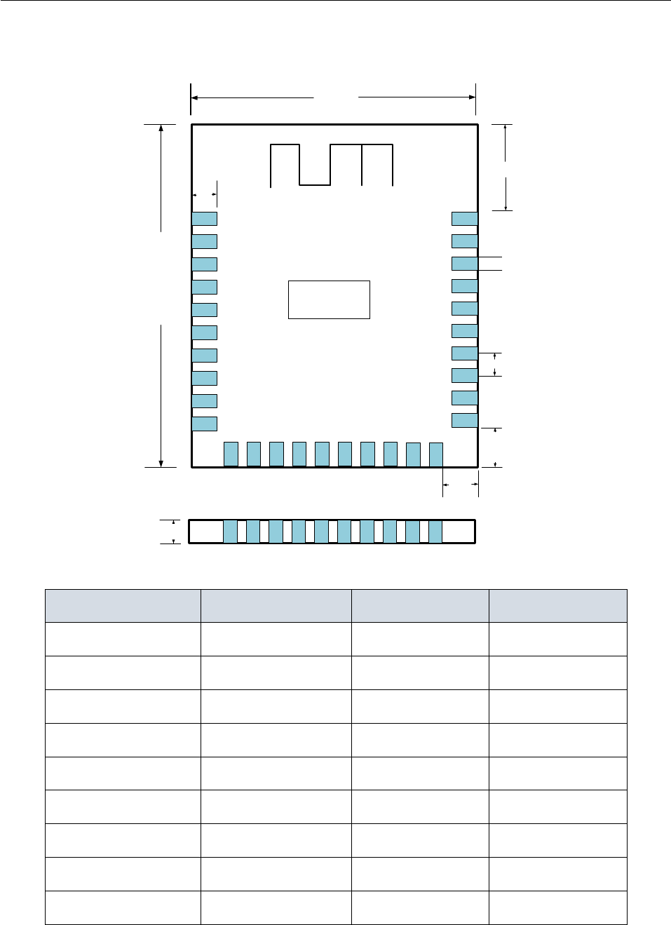
5.2 Module packet
WLT8266BM
W
L
PIN1
PIN11
PIN30
A
C
B
PIN21
D
E
T
H
Symbol
Min.
Typ.
Max.
W
14.96
15.00
15.04
L
16.96
17.00
17.04
T
0.73
0.75
0.77
A
4.55
4.60
4.65
B
-
0.80
-
C
-
1.10
-
D
2.10
2.15
2.20
E
1.65
1.7
1.75
H
1.5
1.55
1.60
HJ BLE

11
5.3 Warning
This device complies with part 15 of the FCC Rules. Operation is subject to the following two
conditions: (1) This device may not cause harmful interference, and (2) this device must accept
any interference received, including interference that may cause undesired operation.
Caution: Changes or modifications to this unit not expressly approved by the party responsible
for compliance could void the user's authority to operate the equipment.
NOTE: This equipment has been tested and found to comply with the limits for a Class B digital
device, pursuant to part 15 of the FCC Rules. These limits are designed to provide reasonable
protection against harmful interference in a residential installation. This equipment generates,
uses and can radiate radio frequency energy and, if not installed and used in accordance with the
instructions, may cause harmful interference to radio communications. However, there is no
guarantee that interference will not occur in a particular installation. If this equipment does
cause harmful interference to radio or television reception, which can be determined by turning
the equipment off and on, the user is encouraged to try to correct the interference by one or
more of the following measures:
—Reorient or relocate the receiving antenna.
—Increase the separation between the equipment and receiver.
—Connect the equipment into an outlet on a circuit different from that to which the receiver is
connected.
—Consult the dealer or an experienced radio/TV technician for help.
Information for the OEM Integrators
This device is intended for OEM integrators only. Please see the full grant of equipment
document for restrictions.
Label Information to the End User by the OEM Integrators
If this certified module is installed inside the host device, then the outside of the host must be
labeled with “Contains FCC ID: 2AJJGHJBLE”.