Quectel Wireless Solutions 16182009002 GSM/GPRS Module User Manual M10 Hardware Design
Quectel Wireless Solutions Company Limited GSM/GPRS Module M10 Hardware Design
User Manual
Quectel
M10
Quectel Cellular Engine
M10 User Guide
M10_User_Guide_V1.00 - 1 -
Quectel
Document Title M10 User Guide
Version 1.00
Date 2009-06-27
Status Release
Document Control ID M10_User_Guide_V1.00
General Notes
Quectel offers this information as a service to its customers, to support application and
engineering efforts that use the products designed by Quectel. The information provided is
based upon requirements specifically provided to Quectel by the customers. Quectel has not
undertaken any independent search for additional relevant information, including any
information that may be in the customer’s possession. Furthermore, system validation of this
product designed by Quectel within a larger electronic system remains the responsibility of the
customer or the customer’s system integrator. All specifications supplied herein are subject to
change.
Copyright
This document contains proprietary technical information which is the property of Quectel
Limited., copying of this document and giving it to others and the using or communication of
the contents thereof, are forbidden without express authority. Offenders are liable to the
payment of damages. All rights reserved in the event of grant of a patent or the registration of a
utility model or design. All specification supplied herein are subject to change without notice at
any time.
Copyright © Shanghai Quectel Wireless Solutions Co., Ltd. 2009
M10_User_Guide_V1.00 - 2 -
Quectel
1 .EVB kit introduction
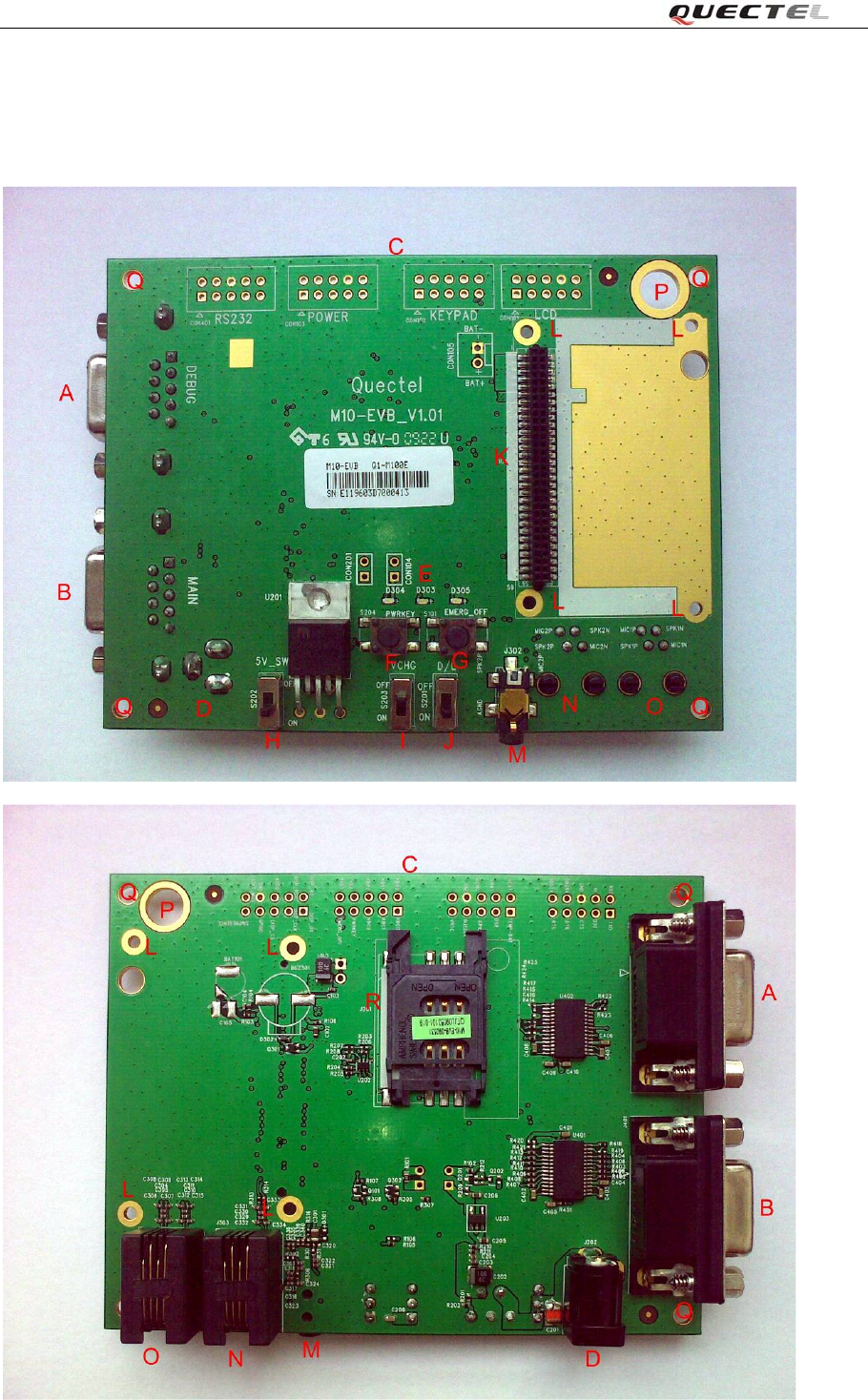
1.1 EVB top and bottom view
Figure 1: EVB top view
M10_User_Guide_V1.00 - 3 -
Quectel
Figure 2: EVB bottom view
A: Debug port
B: Main UART port
C: Test points
D: Adapter interface
E: Module operating status indication LEDs
F: PWRKEY button
G: EMERG_OFF button
H: VBAT switch
I: VCHG switch (charge function)
J: Download switch
K: Connector for M10-TE-A board
L: Screw holes for fixing the M10-TE-A
M: Headset socket
N: Handset socket of audio channel 2
O: Handset socket of audio channel 1
P: Antenna connector fixing hole
Q: Screw holes for EVB placement
R: SIM card socket
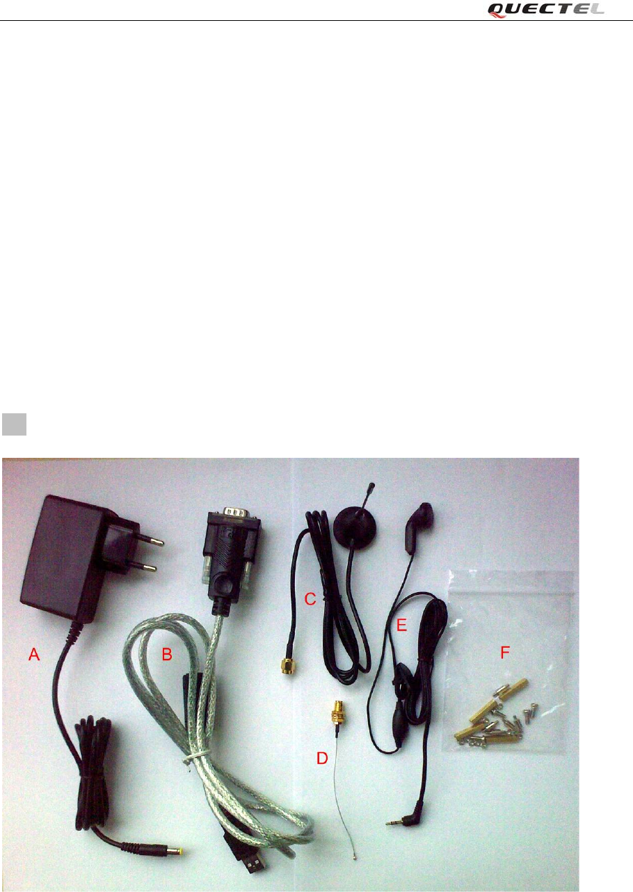
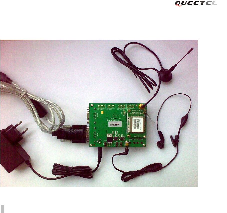
1.2 EVB accessory
Figure 3: Accessory introduction
A: 5V DC switching adapter
B: USB to UART converter cable
C: Antenna
D: RF cable
E: Headset
M10_User_Guide_V1.00 - 4 -
Quectel
F: Bolts and nuts for fixing module and EVB
Figure 4: EVB and accessories
2.Operational description
2.1 Tune up procedure
Firstly,please equip the module and accessories as the figure 4.
M10_User_Guide_V1.00 - 5 -
Quectel
Then ,switching the H switch to ON state, J switch to ON state; Press the F button PWRKEY for about
2 second, then the LED glint,and the module is tuningup successfully;( the location of All Switches and
buttons please see the Figure 1)
2. M10 features
2.2.1 General specification
M10 is a Quad-band GSM/GPRS module delivers GSM/GPRS 850/900/1800/1900MHz performance for
voice, SMS, Data, and Fax in a small form factor and with low power consumption. M10 can be used for WLL
applications/M2M application and much more.
Quad- band GSM/GPRS module with a size of 29x29x3.6mm
● Customized MMI and keypad/LCD support
● An embedded Powerful TCP/IP protocol stack
● Supply voltage range 3.4 ... 4.5 V
● Normal Operation Temperature: -35°C ~80°C
● GPRS multi-slot Class 12
● GSM R99
2.2.2 Hardware Specification
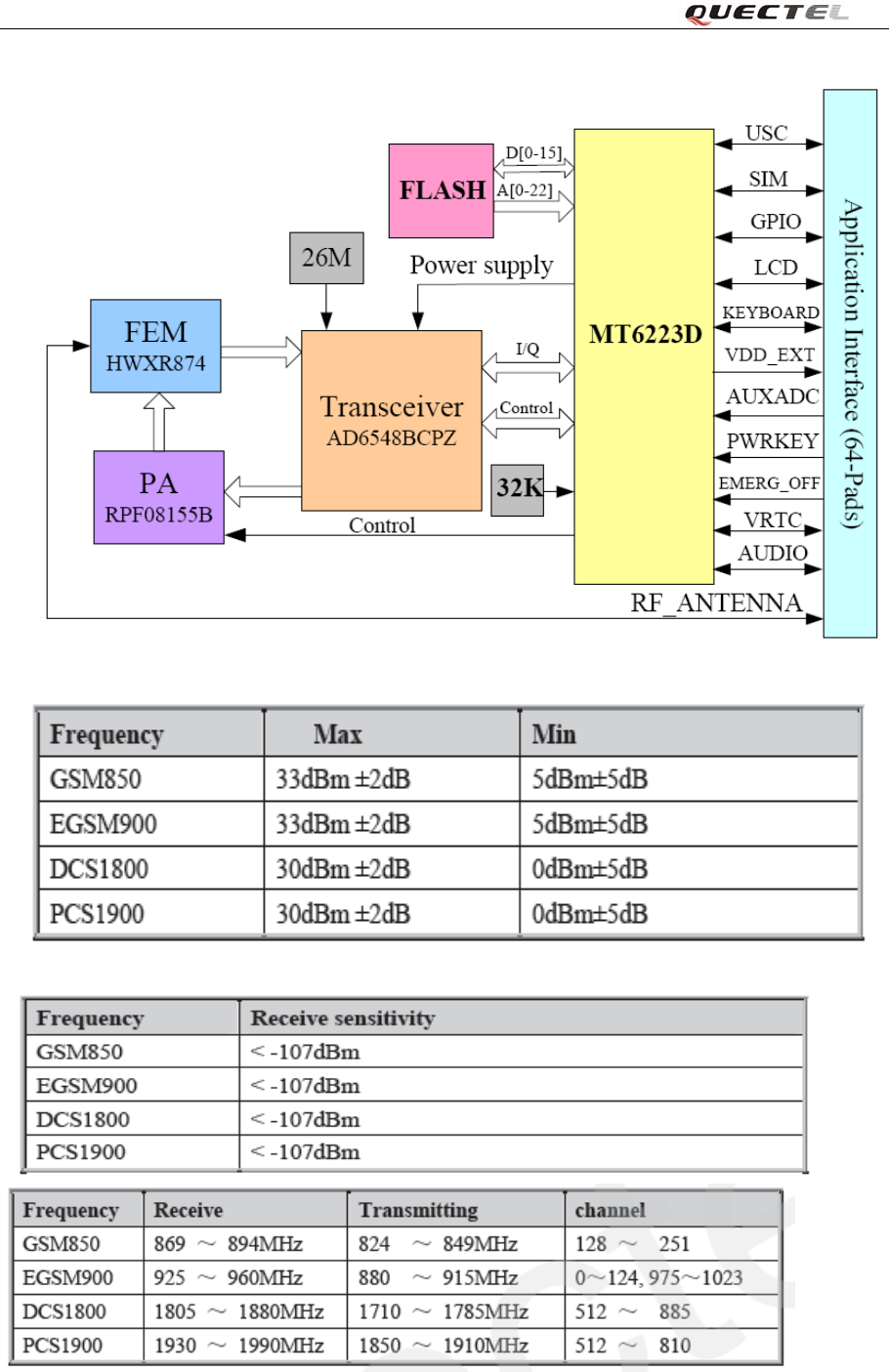
The hardware block diagram for M10 is shown as below:
M10_User_Guide_V1.00 - 6 -
Quectel
The PCB for M10 is 6 layers.
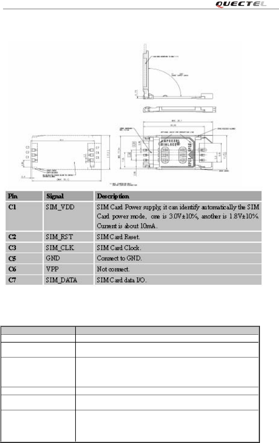
The mechanical architecture of SIM card holder and the definition of SIM card are shown below:
M10_User_Guide_V1.00 - 7 -
Quectel
2.2.3 Software Specification
Feature Implementation
Power supply Single supply voltage 3.4V – 4.5V
Power saving Typical power consumption in SLEEP mode to 1.1 mA@ DRX=5
0.7 mA@ DRX=9
Frequency bands
Quad-band: GSM850, EGSM 900, DCS1800, PCS1900.
The module can search these frequency bands automatically. The
frequency bands also can be set by AT command.
Compliant to GSM Phase 2/2+
GSM class Small MS
Transmitting power Class 4 (2W) at GSM 850 and EGSM 900
Class 1 (1W) at DCS 1800 and PCS 1900
GPRS connectivity
GPRS multi-slot class 12 (default)
GPRS multi-slot class 10 (option)
GPRS multi-slot class 8 (option)
GPRS mobile station class B
M10_User_Guide_V1.00 - 8 -
Quectel
Temperature range
Normal operation: -35°C ~ +80°C
Restricted operation: -45°C ~ -35°C and +80°C ~ +85°C ○
1
Storage temperature: -45°C ~ +90°C
DATA GPRS:
CSD:
GPRS data downlink transfer: max. 85.6 kbps
GPRS data uplink transfer: max. 85.6 kbps
Coding scheme: CS-1, CS-2, CS-3 and CS-4
Supports the protocols PAP (Password Authentication Protocol)
usually used for PPP connections.
Integrates the TCP/IP protocol.
Support Packet Switched Broadcast Control Channel (PBCCH)
CSD transmission rates: 2.4, 4.8, 9.6, 14.4 kbps, non-transparent
Unstructured Supplementary Services Data (USSD) support
SMS MT, MO, CB, Text and PDU mode
SMS storage: SIM card
FAX Group 3 Class 1
SIM interface Support SIM card: 1.8V, 3V
Antenna interface Connected via 50 Ohm antenna pad
Audio features Speech codec modes:
Half Rate (ETS 06.20)
Full Rate (ETS 06.10)
Enhanced Full Rate (ETS 06.50 / 06.60 / 06.80)
Adaptive multi rate (AMR)
Echo Cancellation
Echo Suppression
Noise Reduction
Serial port and Debug port Serial Port: Seven lines on Serial Port Interface
Serial Port can be used for CSD FAX, GPRS service and send AT
command of controlling module.
Serial Port can use multiplexing function.
Autobauding supports baud rate from 4800 bps to 115200bps.
Debug Port: Two lines on Serial Port Interface /TXD and /RXD
Debug Port only used for debugging
Phonebook management Support phonebook types: SM, FD, LD, RC, ON, MC.
SIM Application Toolkit Support SAT class 3, GSM 11.14 Release 99
Real time clock Implemented
Alarm function Programmable via AT command
Physical characteristics Size:
29±0.15 x 29±0.15 x 3.6±0.3mm
Weight: 8g
Firmware upgrade Firmware upgrade over serial port
2.2.4 Solution of M10
The hardware solution is MT6223D+AD6548+PF08155B+HWR874-2+SST34HF3284; The software
solution is MTK Release 0836.
2.2.5 Radio frequency units
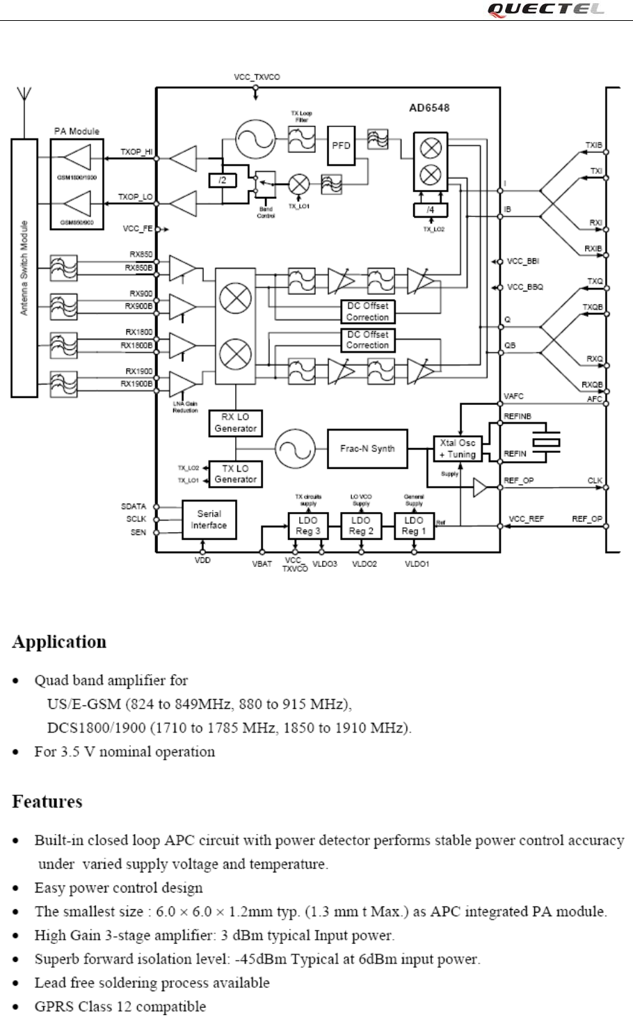
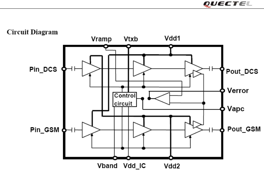
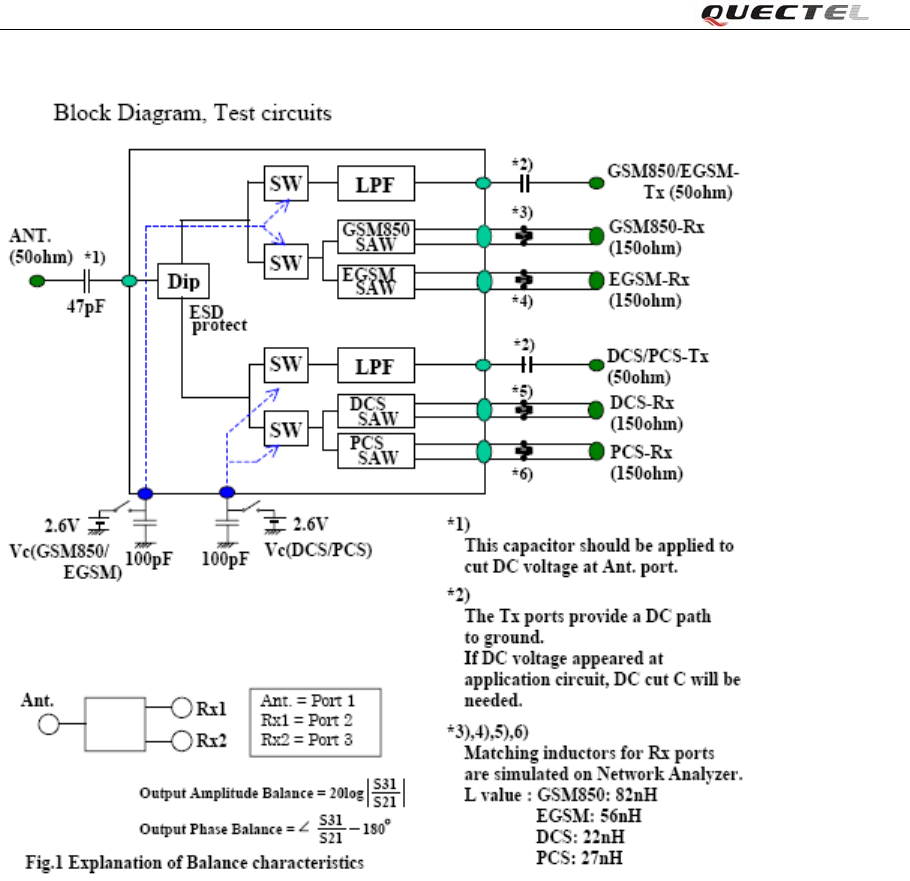
The RF units for M10 include AD6548 (transceiver), PF08155(PA), HWX874-2(FEM).
1) AD6548
M10_User_Guide_V1.00 - 9 -
Quectel
2) PF08155
M10_User_Guide_V1.00 - 10 -
Quectel
3) HWX874
M10_User_Guide_V1.00 - 11 -
Quectel
2.2.6 Baseband units
The baseband units for M10 include MT6223D and SST34HF.
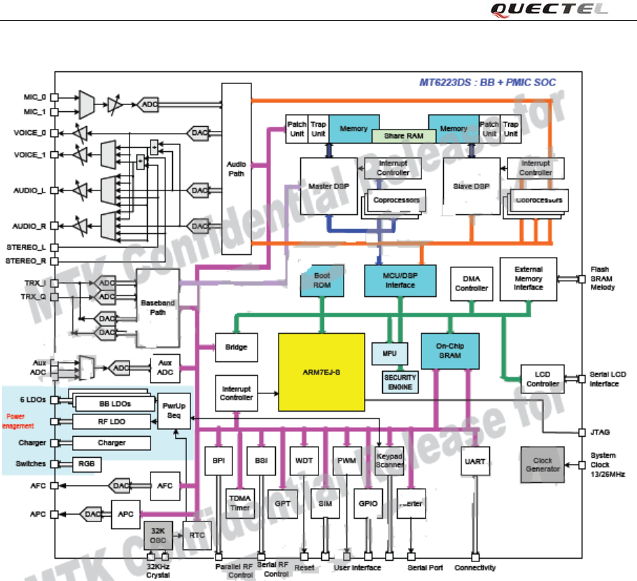
1) MT6223D (MT6223D is integrated Digital baseband and analog baseband).
M10_User_Guide_V1.00 - 12 -
Quectel
2) SST34HF
Features:
32-Mbit Flash and 8-Mbit PSRAM 2.7V~3.0V Operating voltage
Flash:32-megabit(2M*16)2.7V to 3.0V Read/Write Access Time-70ns Sector Erase Architecture
-Sixty-three 32K WordSectors With Individual Write Lockout
-Eight 4K Word Sectors with Individual Write Lockout Fast Word Program Time-15us Suspend/Resume
Feature for Erase and Program
-Supports Reading and Programming from Any Sectors by Suspending Erase of a
Different Sector -Supports Reading Any Word by Suspending Programming of Any Other Word
Low-power Operation -12mAActive -13uA Standby
PSRAM:4-megabit(256K*16)/8-megabit(512K*16) 2.7V to 3.3V Vcc 70ns Access Time
2.2.7 Mechanical architecture
M10_User_Guide_V1.00 - 13 -
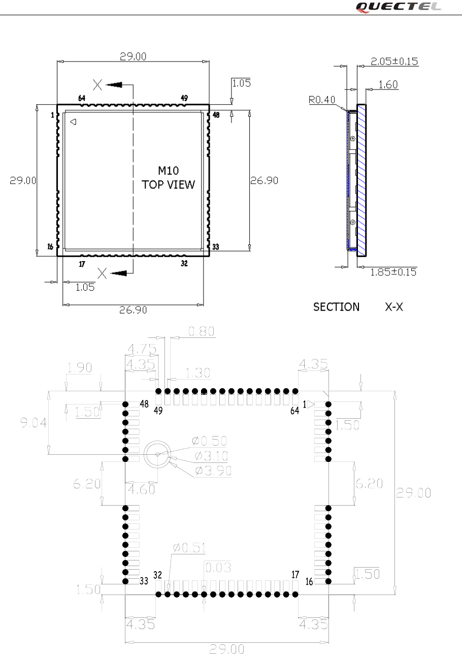
Quectel
M10
BOTTOM VIEW
test point
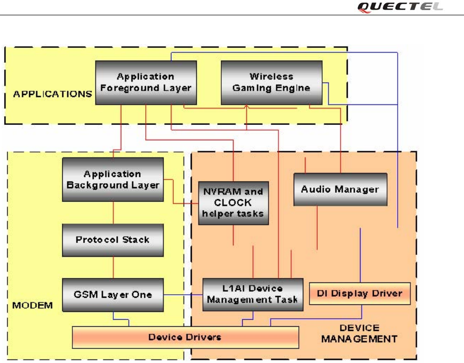
2.2.8 Software Architecture
M10_User_Guide_V1.00 - 14 -
Quectel
M10_User_Guide_V1.00 - 15 -
Quectel
3 AT command
(please see the AT command document)
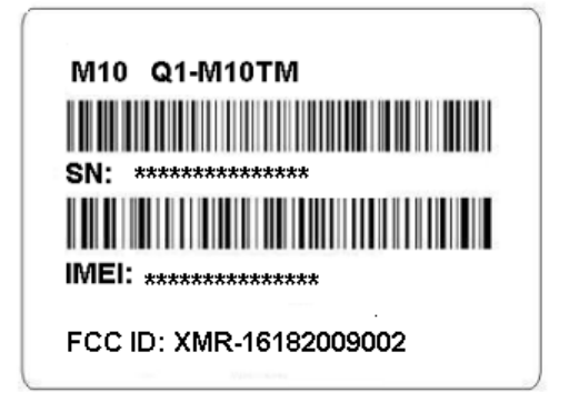
4 FCC Labeling Requirement
Please note:When the M10 is integrated into a final product, the FCC ID label must be visible through
a window on the final device or it must be visible when an access panel,door or cover is easily removed.
If not, a second label must be placed on the outside of the final device that contains the following text:
“Contains FCC ID:XMR-16182009002 ”M10 FCC label is shown as:
5 FCC RF exposure requirements
The maximum measured power output is
30dBm(1900MHz)
33dBm(850MHz),
the maximum antenna gain is
3.0dBi(1900MHz)
0.8dBi(850MHz),
The maximum permissible exposure is defined in 47 CFR 1.1310 with 1 mW/cm2.
The transmitter is using indoor antennas that operate at 20 cm or more from nearby persons.
The maximum permitted level is calculated using the general equation:
S = P′/ 4πR2
GSM850MHz: G=0.8dBi P′= 33dBm+0.8dBi=33.8dBm=2399mW
GSM1900MHz: G=3.0dBi P′= 30dBm+3.0dBi=33.0dBm=1995mw
R = 20 cm
π = 3.1416
Solving for S, the power density at 20 cm is
Quectel
GSM850: 0.4773 mW/cm2.
GSM1900: 0.3969 mW/cm2.
So The power density limit is 1 mW/cm2 is kept.