Quectel Wireless Solutions 201202M35 GSM/GPRS Module User Manual M10 Hardware Design
Quectel Wireless Solutions Company Limited GSM/GPRS Module M10 Hardware Design
UserManual.wiki
>
Quectel Wireless Solutions
>
201202M35 User Manual
Users Manual
Navigation menu
Upload a User Manual
Namespaces
Wiki Guide
HTML
PDF
Info
Views
User Manual
Discussion / Help
Navigation
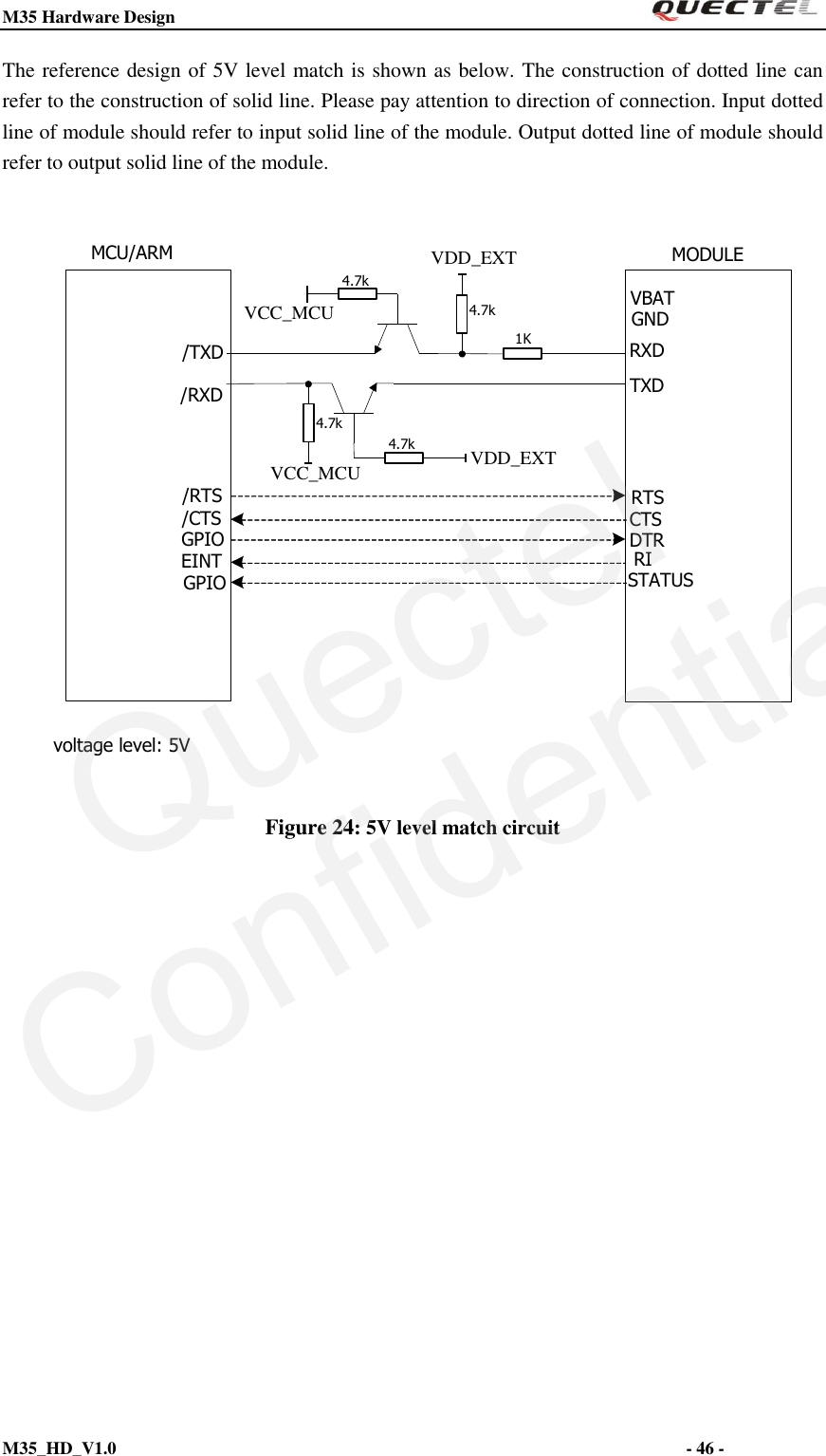
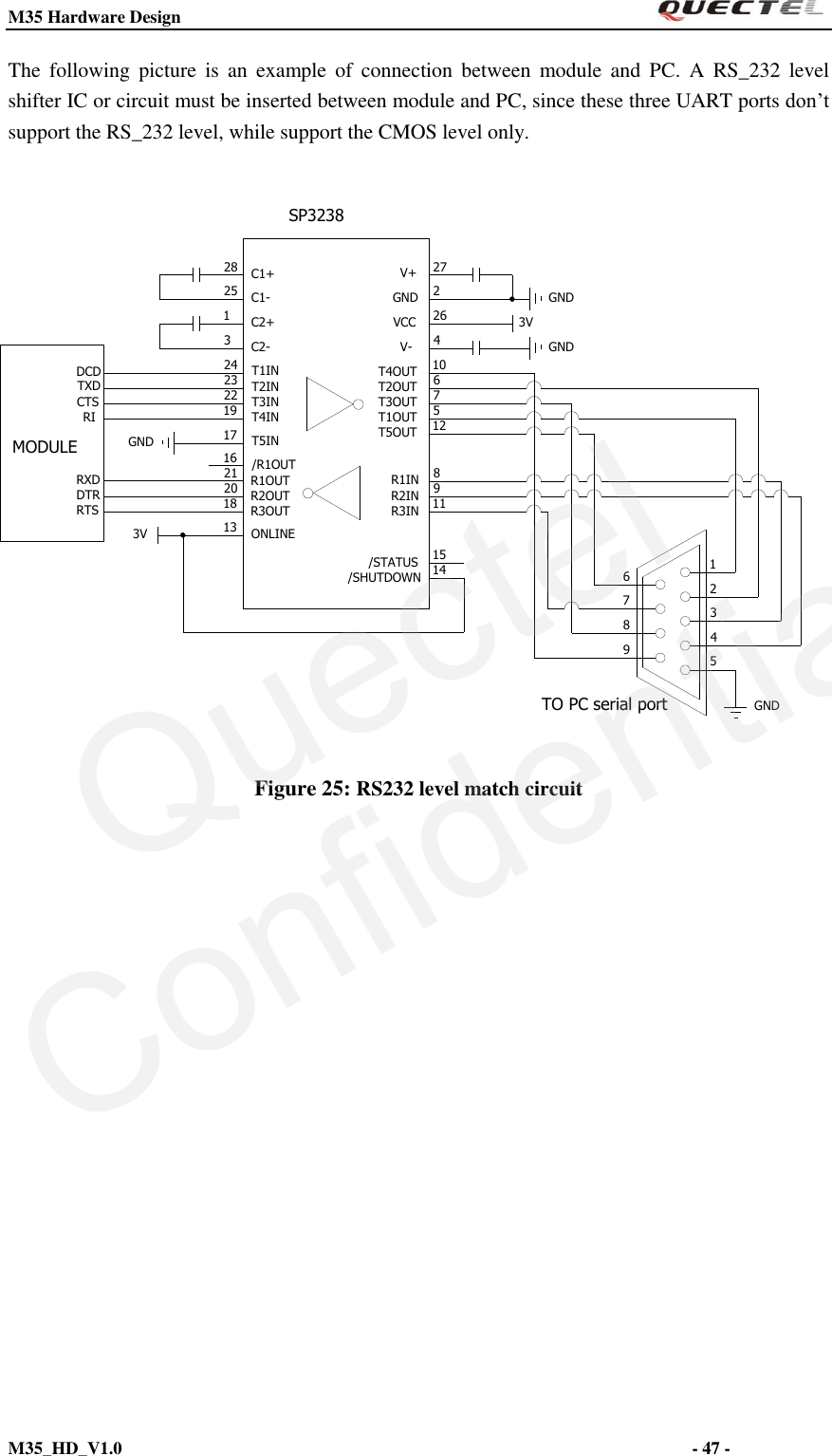
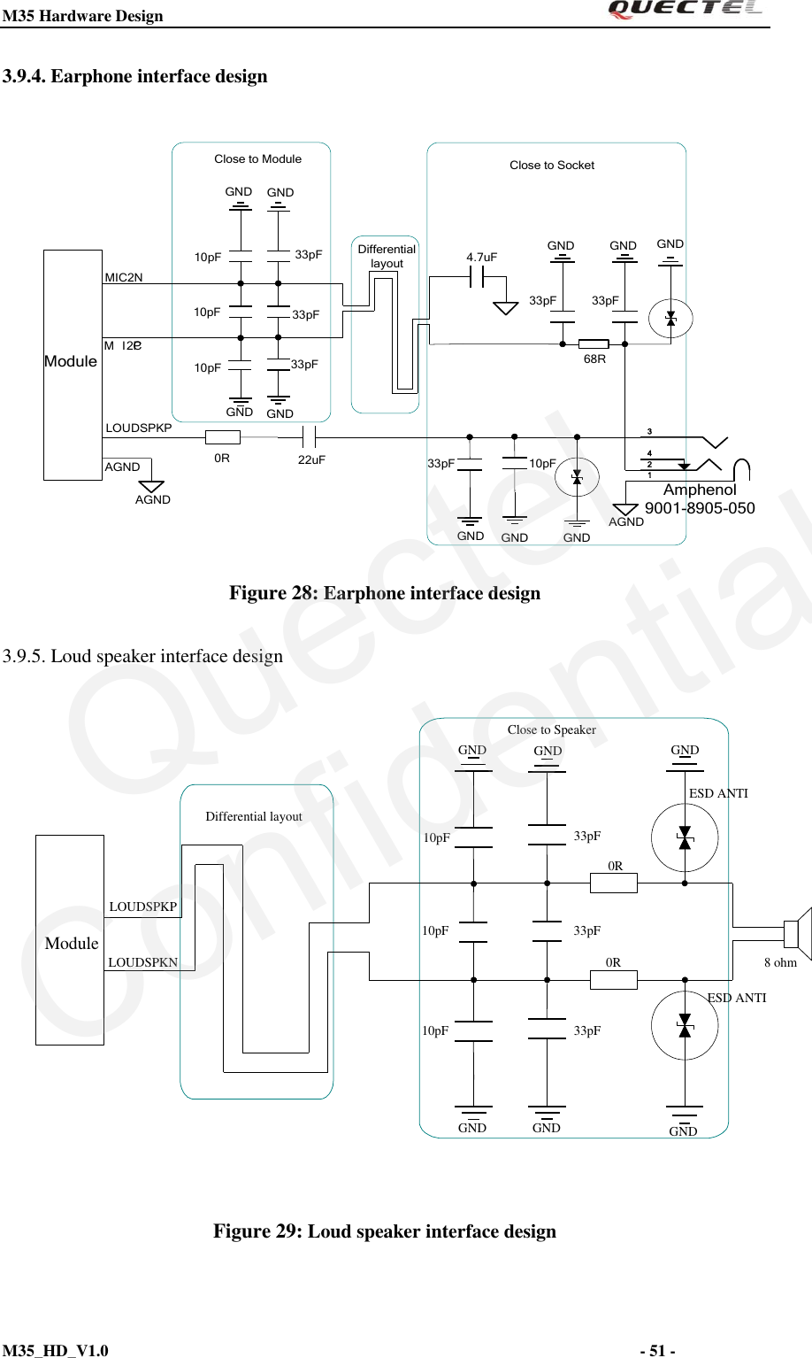
![M35 Hardware Design M35_HD_V1.0 - 9 - 1. Introduction This document defines Module M35 and describes its hardware interface which are connected with the customer application and the air interface. This document can help customers quickly understand the interface specifications, electrical and mechanical details of M35. Associated with application notes and user guide, customers can use M35 to design and set up mobile applications easily. 1.1. Related documents Table 1: Related documents SN Document name Remark [1] M35_ATC AT commands set [2] ITU-T Draft new recommendation V.25ter Serial asynchronous automatic dialing and control [3] GSM 07.07 Digital cellular telecommunications (Phase 2+); AT command set for GSM Mobile Equipment (ME) [4] GSM 07.10 Support GSM 07.10 multiplexing protocol [5] GSM 07.05 Digital cellular telecommunications (Phase 2+); Use of Data Terminal Equipment – Data Circuit terminating Equipment (DTE – DCE) interface for Short Message Service (SMS) and Cell Broadcast Service (CBS) [6] GSM 11.14 Digital cellular telecommunications (Phase 2+); Specification of the SIM Application Toolkit for the Subscriber Identity module – Mobile Equipment (SIM – ME) interface [7] GSM 11.11 Digital cellular telecommunications (Phase 2+); Specification of the Subscriber Identity module – Mobile Equipment (SIM – ME) interface [8] GSM 03.38 Digital cellular telecommunications (Phase 2+); Alphabets and language-specific information [9] GSM 11.10 Digital cellular telecommunications (Phase 2); Mobile Station (MS) conformance specification; Part 1: Conformance specification [10] GSM_UART_AN UART port application notes [11] GSM_FW_Upgrade_Tool_ Lite_GS2_UDG GSM Firmware upgrade tool lite GS2 user guide [12] M35_EVB_UGD M35 EVB user guide QuectelConfidential](https://usermanual.wiki/Quectel-Wireless-Solutions/201202M35/User-Guide-1720269-Page-9.png)
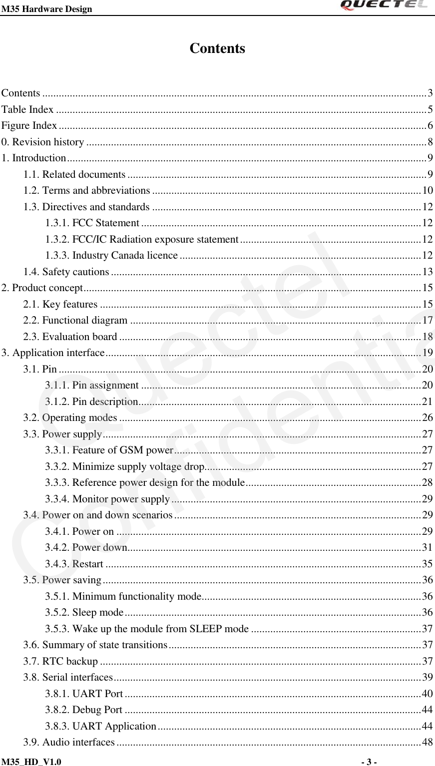
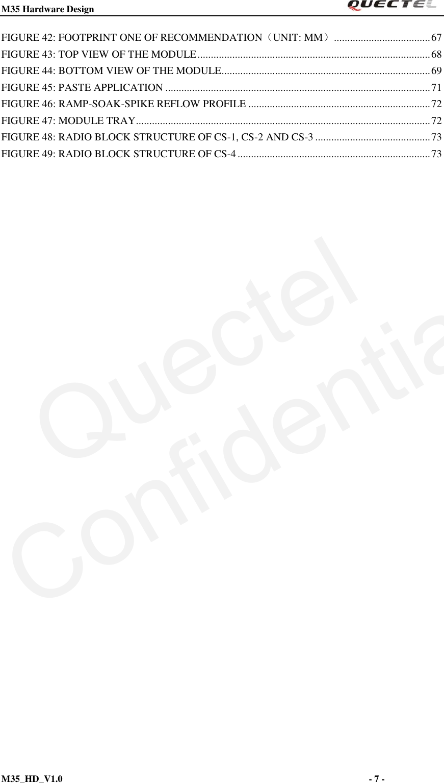
![M35 Hardware Design M35_HD_V1.0 - 18 - MT6252D32.768KControl26MPower supplyUARTSIMVDD_EXTAUDIOPWRKEYEMERG_OFFVRTCRF_ANTENNAPA TQM6M4068Application Interface (42-SMD Pads) Figure 1: Module functional diagram 2.3. Evaluation board In order to help customer to develop applications with M35, Quectel supplies an evaluation board (EVB), RS-232 to USB cable, power adapter, earphone, antenna and other peripherals to control or test the module. For details, please refer to the document [12]. QuectelConfidential](https://usermanual.wiki/Quectel-Wireless-Solutions/201202M35/User-Guide-1720269-Page-18.png)
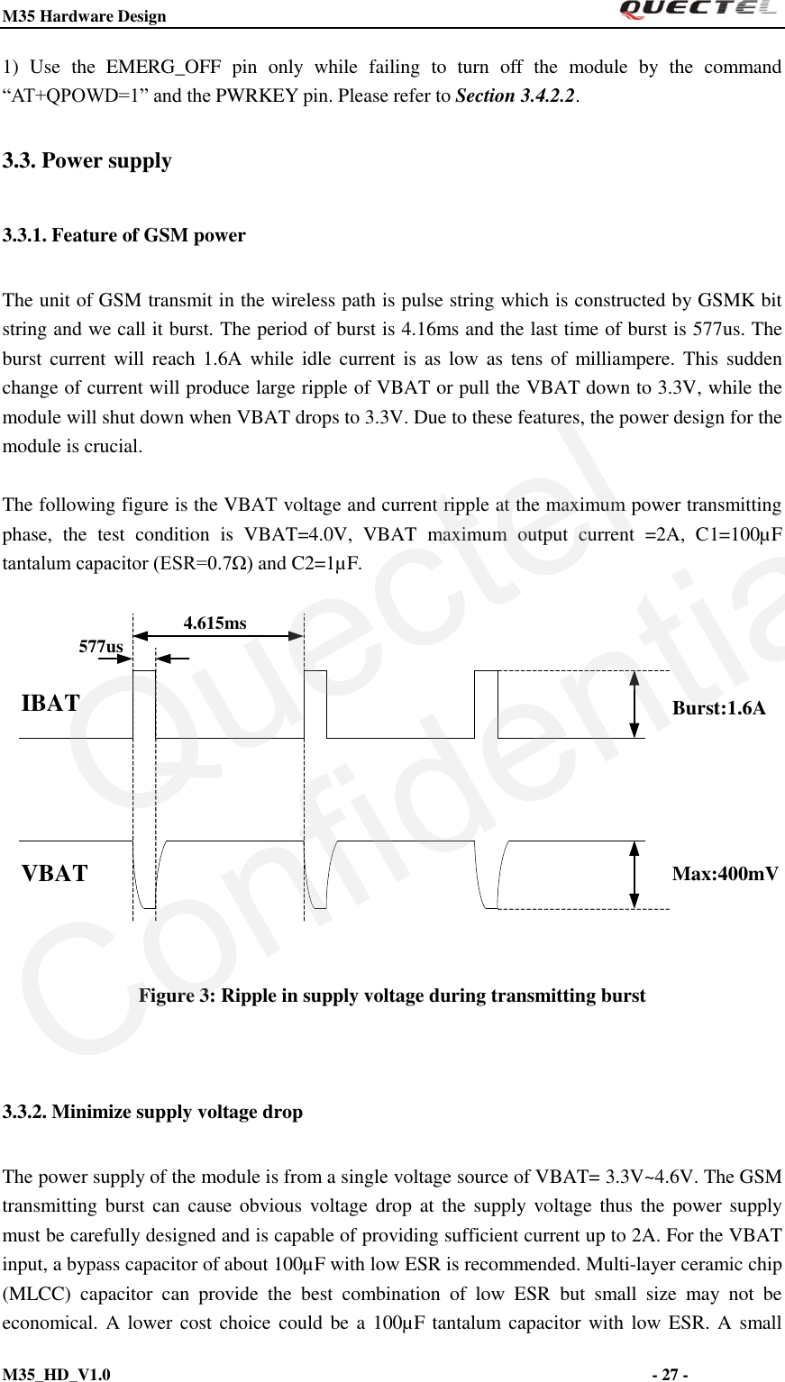
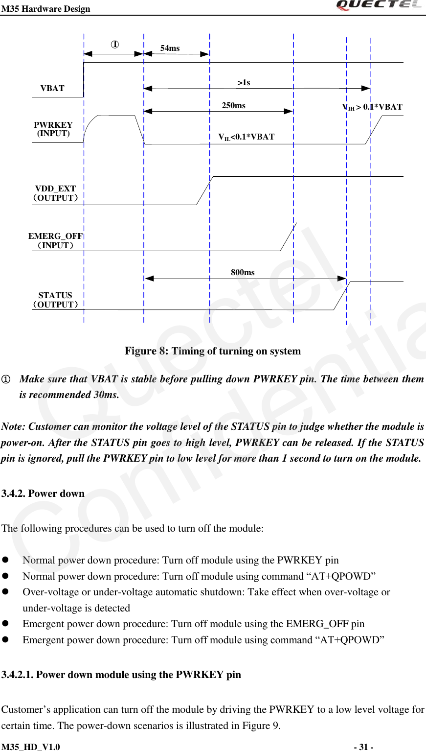
![M35 Hardware Design M35_HD_V1.0 - 29 - 3.3.4. Monitor power supply To monitor the supply voltage, the “AT+CBC” command can be used which includes three parameters: charging status, remaining battery capacity and voltage value (in mV). It returns the 0-100 percent of battery capacity and actual value measured between VBAT and GND. The voltage is automatically measured in period of 5s. The displayed voltage (in mV) is averaged over the last measuring period before the “AT+CBC” command is executed. For details, please refer to document [1]. 3.4. Power on and down scenarios 3.4.1. Power on The module can be turned on by PWRKEY pin. The module is set to autobauding mode (AT+IPR=0) in default configuration. In the autobauding mode, the URC “RDY” after powering on is not sent to host controller. When the module receives AT command, it will be powered on after a delay of 2 or 3 seconds. Host controller should firstly send an “AT” or “at” string in order that the module can detect baud rate of host controller, and it should send the second or the third “AT” or “at” string until receiving “OK” string from module. Then an “AT+IPR=x;&W” should be sent to set a fixed baud rate for module and save the configuration to flash memory of module. After these configurations, the URC “RDY” would be received from the UART Port of module every time when the module is powered on. Refer to section “AT+IPR” in document [1]. The hardware flow control is disabled in default configuration. In the simple UART port which means that only TXD, RXD, GND of the module is connected to host. CTS is pulled down internally. In this condition, the module can transmit and receive data freely. On the other side, if RTS, CTS are connected to the host together with TXD, RXD, GND, whether or not to transmit and receive data depends on the level of RTS and CTS. Then whenever hardware flow is present or not, the URC “RDY” is sent to host controller in the fixed band rate. 3.4.1.1. Power on the module using the PWRKEY pin Customer’s application can turn on the module by driving the pin PWRKEY to a low level voltage and after STATUS pin outputs a high level, PWRKEY pin can be released. Customer may monitor the level of the STATUS pin to judge whether the module is power-on or not. An open collector driver circuit is suggested to control the PWRKEY. A simple reference circuit is illustrated in Figure 6. QuectelConfidential](https://usermanual.wiki/Quectel-Wireless-Solutions/201202M35/User-Guide-1720269-Page-29.png)
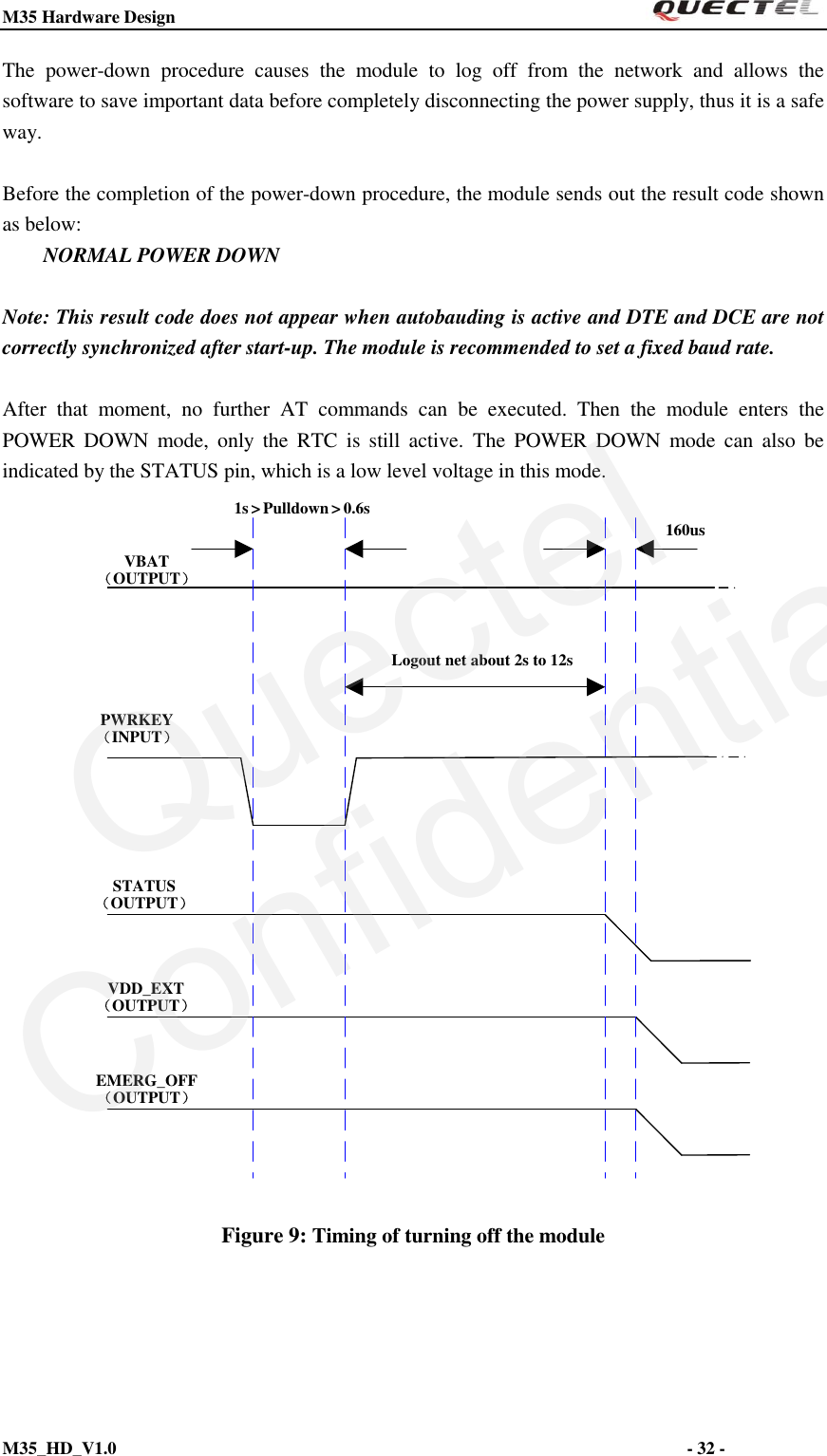
![M35 Hardware Design M35_HD_V1.0 - 33 - 3.4.2.2. Power down the module using AT command Customer’s application can turn off the module via AT command “AT+QPOWD=1”. This command will let the module to log off from the network and allow the software to save important data before completely disconnecting the power supply, thus it is a safe way. Before the completion of the power-down procedure the module sends out the result code shown as below: NORMAL POWER DOWN After that moment, no further AT commands can be executed. And then the module enters the POWER DOWN mode, only the RTC is still active. The POWER DOWN mode can also be indicated by STATUS pin, which is a low level voltage in this mode. Please refer to document [1] for details about the AT command “AT+QPOWD”. 3.4.2.3. Over-voltage or under-voltage automatic shutdown The module will constantly monitor the voltage applied on the VBAT, if the voltage is ≤ 3.5V, the following URC will be presented: UNDER_VOLTAGE WARNING If the voltage is ≥ 4.5V, the following URC will be presented: OVER_VOLTAGE WARNING The uncritical voltage range is 3.3V to 4.6V. If the voltage is > 4.6V or <3.3V, the module would automatically shutdown itself. If the voltage is <3.3V, the following URC will be presented: UNDER_VOLTAGE POWER DOWN If the voltage is >4.6V, the following URC will be presented: OVER_VOLTAGE POWER DOWN Note: These result codes don’t appear when autobauding is active and DTE and DCE are not correctly synchronized after start-up. The module is recommended to set to a fixed baud rate. After that moment, no further AT commands can be executed. The module logs off from network and enters POWER DOWN mode, and only RTC is still active. The POWER DOWN mode can also be indicated by the pin STATUS, which is a low level voltage in this mode. QuectelConfidential](https://usermanual.wiki/Quectel-Wireless-Solutions/201202M35/User-Guide-1720269-Page-33.png)
![M35 Hardware Design M35_HD_V1.0 - 35 - 3.4.3. Restart 3.4.3.1. Restart the module using the PWRKEY pin Customer’s application can restart the module by driving the PWRKEY to a low level voltage for certain time, which is similar to the way of turning on module. Before restarting the module, at least 500ms should be delayed after detecting the low level of STATUS. The restart timing is illustrated as the following figure. STATUS(OUTPUT)HPWRKEY(INPUT)Delay > 0.5sTurn offPull down the PWRKEY to turn on the moduleRestart Figure 12: Timing of restarting system The module can also be restarted by the PWRKEY after emergency shutdown. PWRKEY(INPUT)Pulldown >20ms Delay>2sEMERG_OFF(INPUT)STATUS(OUTPUT)6us Figure 13: Timing of restarting system after emergency shutdown 3.4.3.2. Restart the module using AT command Using an AT command “AT+QPOWD=2” can achieve restart of the module. Please refer to document [1] for the details. QuectelConfidential](https://usermanual.wiki/Quectel-Wireless-Solutions/201202M35/User-Guide-1720269-Page-35.png)
![M35 Hardware Design M35_HD_V1.0 - 36 - 3.5. Power saving Upon system requirement, there are several actions to drive the module to enter low current consumption status. For example, “AT+CFUN” can be used to set module into minimum functionality mode and DTR hardware interface signal can be used to lead system to SLEEP mode. 3.5.1. Minimum functionality mode Minimum functionality mode reduces the functionality of the module to minimum level, thus minimize the current consumption when the slow clocking mode is activated at the same time. This mode is set with the “AT+CFUN” command which provides the choice of the functionality levels <fun>=0,1,4. 0: minimum functionality 1: full functionality (default) 4: disable both transmitting and receiving of RF part If the module is set to minimum functionality by “AT+CFUN=0”, the RF function and SIM card function would be disabled. In this case, the UART port is still accessible, but all AT commands correlative with RF function or SIM card function will not be accessible. If the module has been set by “AT+CFUN=4”, the RF function will be disabled, but the UART port is still active. In this case, all AT commands correlative with RF function will not be accessible. After the module is set by “AT+CFUN=0” or “AT+CFUN=4”, it can return to full functionality by “AT+CFUN=1”. For detailed information about “AT+CFUN”, please refer to document [1]. 3.5.2. Sleep mode The SLEEP mode is disabled in default software configuration. Customer’s application can enable this mode by “AT+QSCLK=1”. On the other hand, the default setting is “AT+QSCLK=0” and in this mode, the module cannot enter SLEEP mode. When “AT+QSCLK=1” is sent to the module, customer’s application can control the module to enter or exit from the SLEEP mode through pin DTR. When DTR is set to high level, and there is no on-air or hardware interrupt such as GPIO interrupt or data on UART port, the module will enter SLEEP mode automatically. In this mode, the module can still receive voice, SMS or GPRS paging from network but the UART port is not accessible. QuectelConfidential](https://usermanual.wiki/Quectel-Wireless-Solutions/201202M35/User-Guide-1720269-Page-36.png)
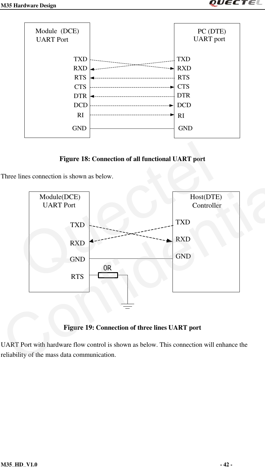
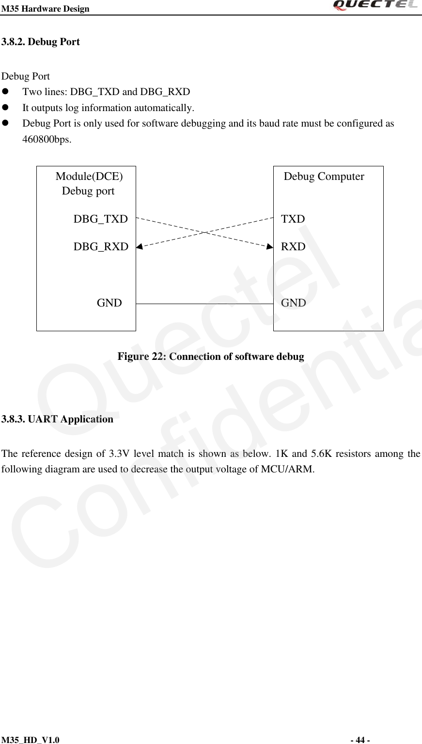
![M35 Hardware Design M35_HD_V1.0 - 39 - Figure 17: Seiko XH414H-IV01E Charge Characteristics 3.8. Serial interfaces The module provides two serial ports: UART and Debug Port. The module is designed as a DCE (Data Communication Equipment), following the traditional DCE-DTE (Data Terminal Equipment) connection. Autobauding function supports baud rate from 4800bps to 115200bps. The UART Port: TXD: Send data to RXD of DTE RXD: Receive data from TXD of DTE RTS: Requests to send CTS: Clear to send DTR: DTE is ready and inform DCE (this pin can wake the module up) RI: Ring indicator (when the call, SMS, data of the module are coming, the module will output signal to inform DTE) DCD: Data carrier detection (the valid of this pin demonstrates the communication link is set up) The module disables hardware flow control in default. When hardware flow control is required, RTS and CTS should be connected to the host. AT command “AT+IFC=2,2” is used to enable hardware flow control. AT command “AT+IFC=0,0” is used to disable the hardware flow control. For more details, please refer to document [1]. The Debug Port DBG_TXD: Send data to the COM port of a debugging computer DBG_RXD: Receive data from the COM port of a debugging computer QuectelConfidential](https://usermanual.wiki/Quectel-Wireless-Solutions/201202M35/User-Guide-1720269-Page-39.png)
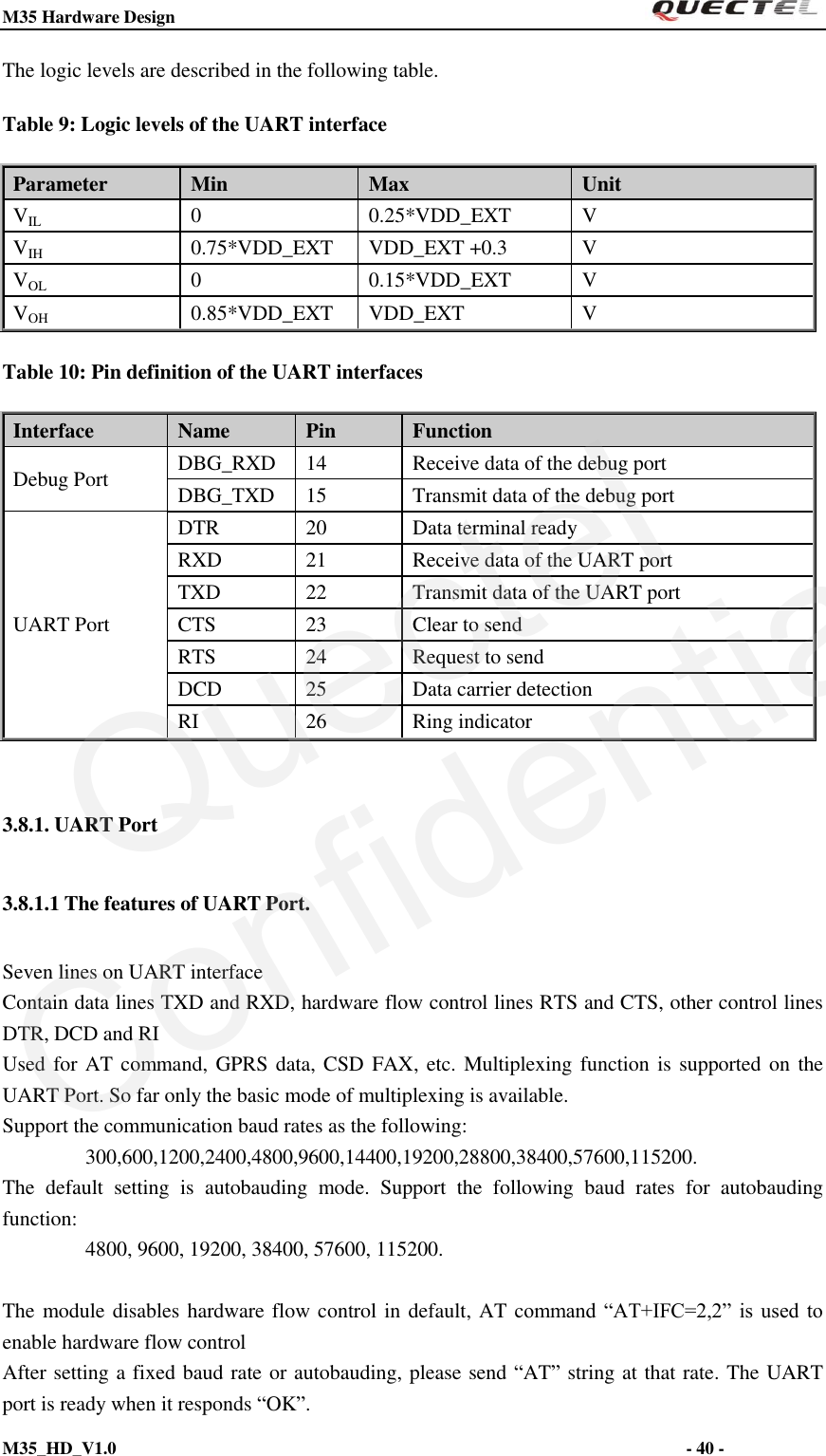
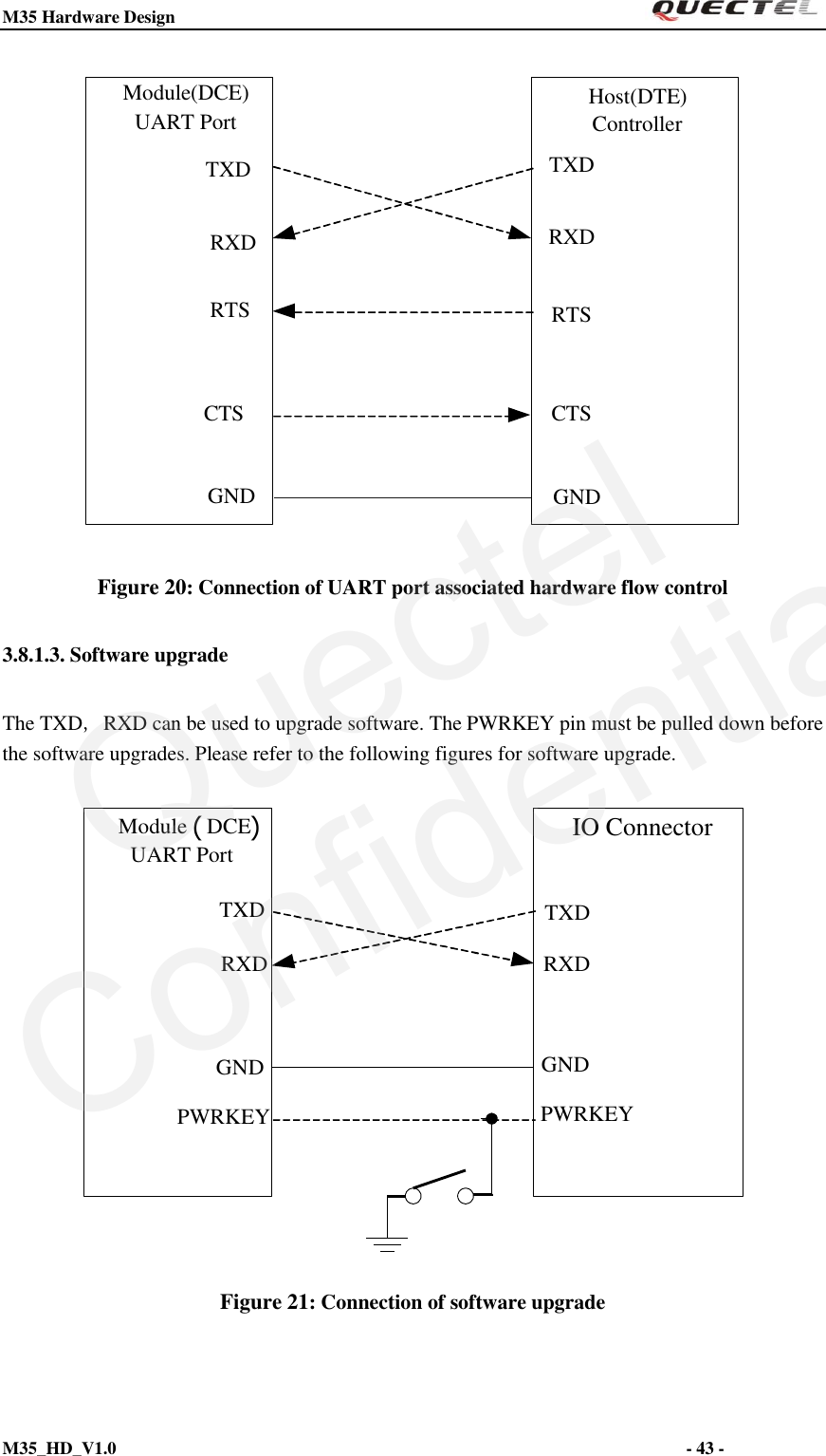
![M35 Hardware Design M35_HD_V1.0 - 41 - Autobauding allows the module to detect the baud rate by receiving the string “AT” or “at” from the host or PC automatically, which gives module flexibility without considering which baud rate is used by the host controller. Autobauding is enabled in default. To take advantage of the autobauding mode, special attention should be paid according to the following requirements: Synchronization between DTE and DCE: When DCE (the module) powers on and the autobauding is enabled, it is recommended to wait 2 to 3 seconds before sending the first AT character. After receiving the “OK” response, DTE and DCE are correctly synchronized. If the host controller needs URC in the mode of autobauding, it must be synchronized firstly. Otherwise the URC will be discarded. Restrictions on autobauding operation The UART port has to be operated at 8 data bits, no parity and 1 stop bit (factory setting). The A/ and a/ commands can’t be used. Only the strings “AT” or “at” can be detected (neither “At” nor “aT”). The Unsolicited Result Codes like "RDY", "+CFUN: 1" and "+CPIN: READY” will not be indicated when the module is turned on with autobauding enabled and not be synchronized. Any other Unsolicited Result Codes will be sent at the previous baud rate before the module detects the new baud rate by receiving the first “AT” or “at” string. The DTE may receive unknown characters after switching to new baud rate. It is not recommended to switch to autobauding from a fixed baud rate. If autobauding is active it is not recommended to switch to multiplex mode Note: To assure reliable communication and avoid any problems caused by undetermined baud rate between DCE and DTE, it is strongly recommended to configure a fixed baud rate and save it instead of using autobauding after start-up. For more details, please refer to Section “AT+IPR” in document [1]. 3.8.1.2. The connection of UART The connection between module and host via UART port is very flexible. Three connection styles are illustrated as below. UART Port connection is shown as below when it is applied in modulation-demodulation. QuectelConfidential](https://usermanual.wiki/Quectel-Wireless-Solutions/201202M35/User-Guide-1720269-Page-41.png)
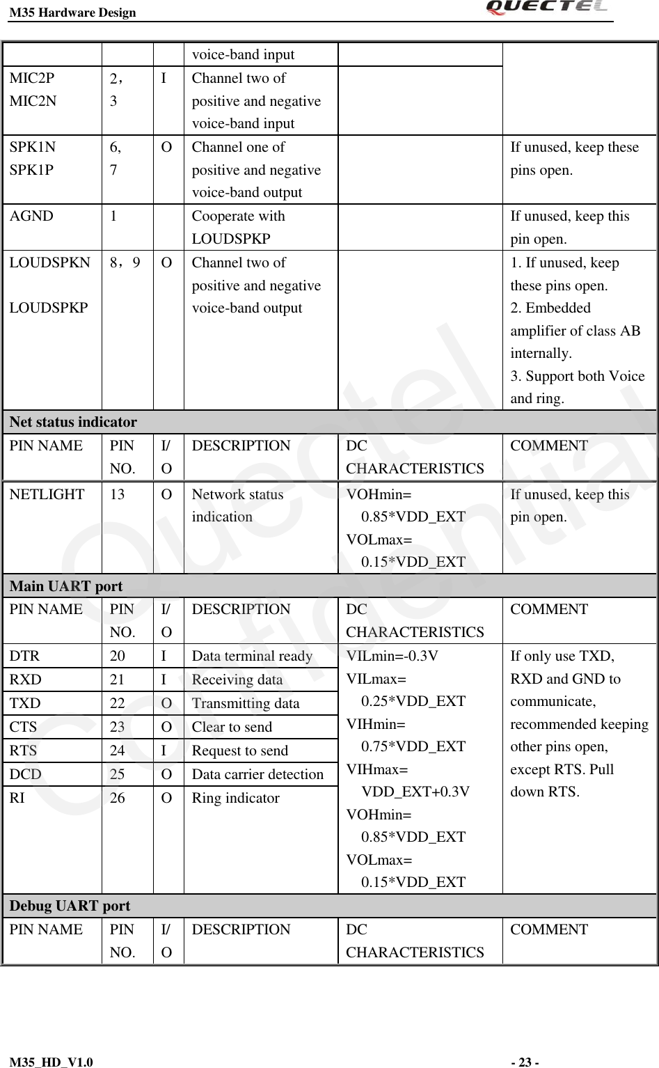
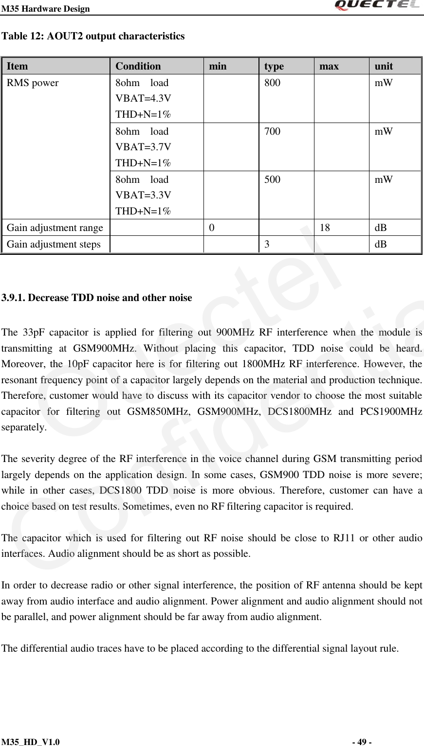
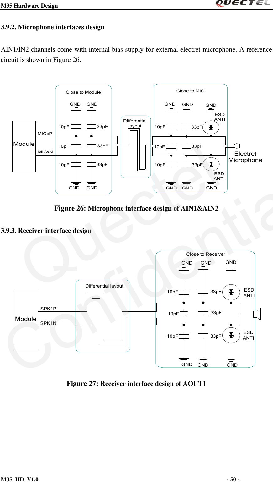
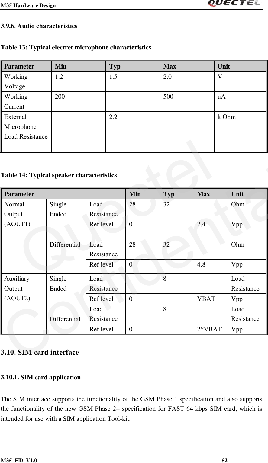
![M35 Hardware Design M35_HD_V1.0 - 48 - 3.9. Audio interfaces The module provides two analogy input channels and three analogy output channels. Table 11: Pin definition of Audio interface AIN1 and AIN2 can be used for input of microphone and line. An electret microphone is usually used. AIN1 and AIN2 are both differential input channels. AOUT1 is used for output of the receiver and speaker. This channel is typically used for a receiver built into a handset. AOUT1 channel is a differential channel. It only supports voice path. If it is used as a speaker, an amplifier should be employed. AOUT2 is used for loud speaker output as it is embedded an amplifier of class AB whose maximum drive power is 800mW. AOUT2 is a differential channel. Immediately playing Melody or Midi ring tone for incoming call is available in AOUT2. AOUT2 also can be used for output of earphone, which can be used as a single-ended channel. LOUDSPKP and AGND can establish a pseudo differential mode. These two audio channels can be swapped by “AT+QAUDCH” command. For more details, please refer to document [1]. Use AT command “AT+QAUDCH” to select audio channel: 0--AIN1/AOUT1, the default value is 0. 2--AIN2/AOUT2 For each channel, customer can use AT+QMIC to adjust the input gain level of microphone. Customer can also use “AT+CLVL” to adjust the output gain level of receiver and speaker. “AT+QECHO” is used to set the parameters for echo cancellation control. “AT+QSIDET” is used to set the side-tone gain level. For more details, please refer to document [1]. Interface Name Pin Function AIN1/AOUT1 MIC1P 4 Channel one of Microphone positive input MIC1N 5 Channel one of Microphone negative input SPK1N 6 Channel one of Audio negative output SPK1P 7 Channel one of Audio positive output AIN2/AOUT2 MIC2P 2 Channel two of Microphone positive input MIC2N 3 Channel two of Microphone negative input AGND 1 Cooperate with LOUDSPKP LOUDSPKP 9 Channel two of Audio positive output LOUDSPKN 8 Channel two of Audio negative output QuectelConfidential](https://usermanual.wiki/Quectel-Wireless-Solutions/201202M35/User-Guide-1720269-Page-48.png)
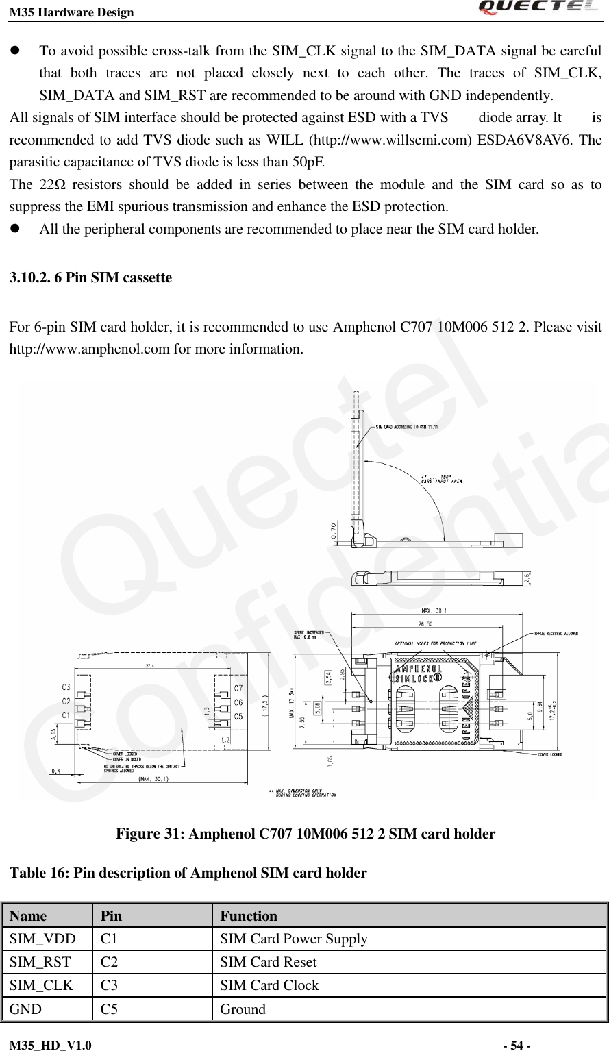
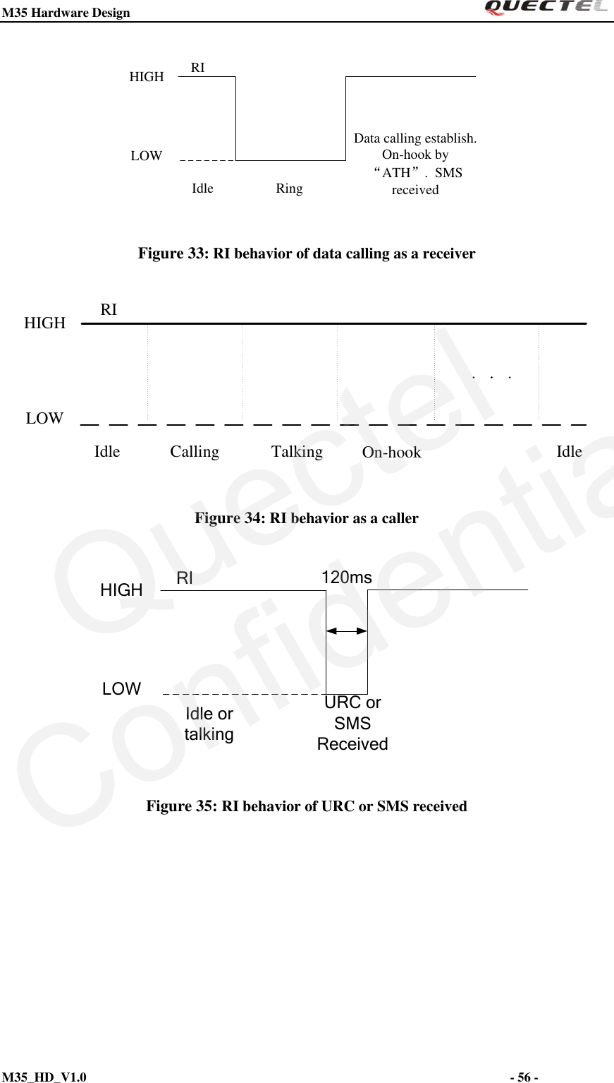
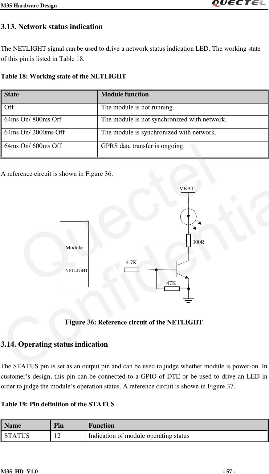
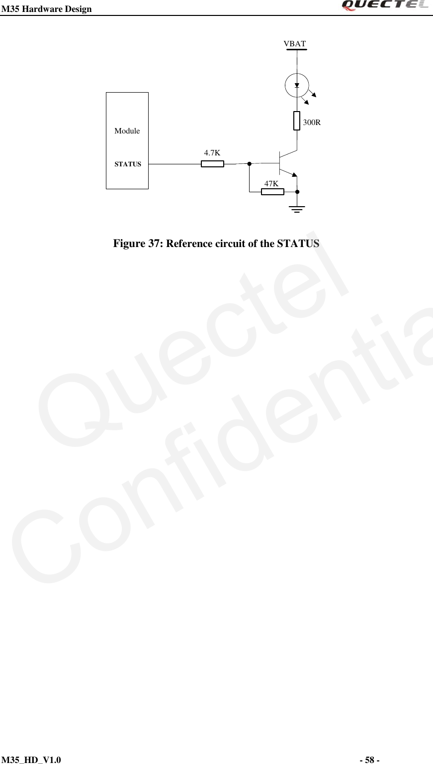
![M35 Hardware Design M35_HD_V1.0 - 55 - VPP C6 Not Connect SIM_DATA C7 SIM Card data I/O 3.12. Behaviors of the RI Table 17: Behaviors of the RI State RI respond Standby HIGH Voice calling Change to LOW, then: (1) Change to HIGH when call is established. (2) Use ATH to hang up the call, change to HIGH. (3) Calling part hangs up, change to HIGH first, and change to LOW for 120ms indicating “NO CARRIER” as an URC, then change to HIGH again. (4) Change to HIGH when SMS is received. Data calling Change to LOW, then: (1) Change to HIGH when data connection is established. (2) Use ATH to hang up the data calling, change to HIGH. (3) Calling part hangs up, change to HIGH first, and change to LOW for 120ms indicating “NO CARRIER” as an URC, then change to HIGH again. (4) Change to HIGH when SMS is received. SMS When a new SMS comes, the RI changes to LOW and holds low level for about 120 ms, then changes to HIGH. URC Certain URCs can trigger 120ms low level on RI. For more details, please refer to the document [10]. If the module is used as a caller, the RI would maintain high except the URC or SMS is received. On the other hand, when it is used as a receiver, the timing of the RI is shown below. RIIdle RingOff-hook by “ATA”. On-hook by “ATH”. SMS received. HIGHLOW Figure 32: RI behavior of voice calling as a receiver QuectelConfidential](https://usermanual.wiki/Quectel-Wireless-Solutions/201202M35/User-Guide-1720269-Page-55.png)