Quectel Wireless Solutions 201312UC20 UMTS/HSPA+ Module User Manual
Quectel Wireless Solutions Company Limited UMTS/HSPA+ Module
UserManual.wiki
>
Quectel Wireless Solutions
>
201312UC20 User Manual
User Manual
Navigation menu
Upload a User Manual
Namespaces
Wiki Guide
HTML
PDF
Info
Views
User Manual
Discussion / Help
Navigation
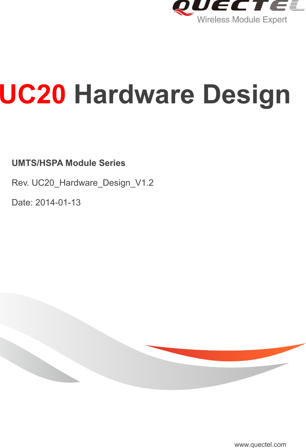
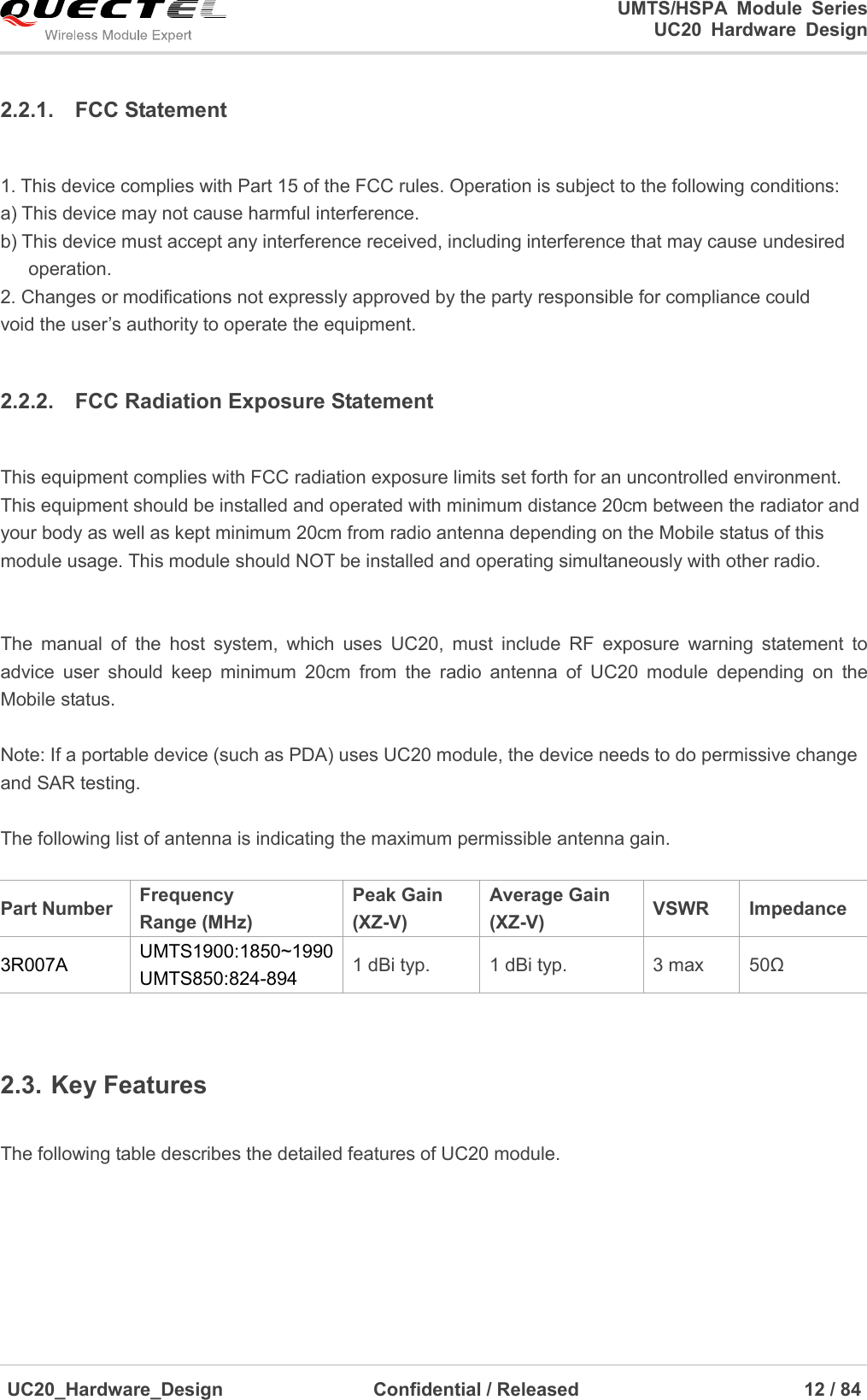
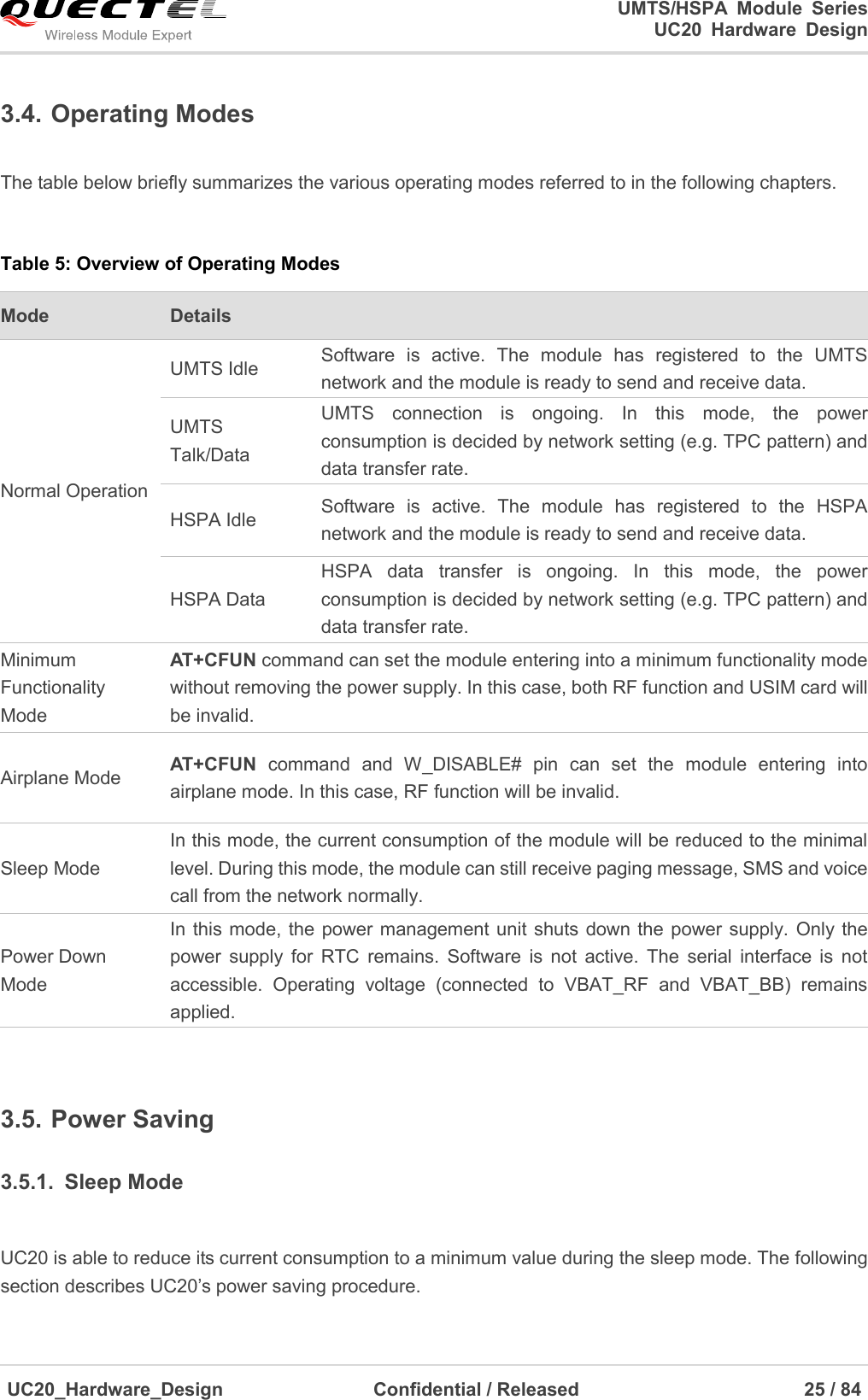
![UMTS/HSPA Module Series UC20 Hardware Design UC20_Hardware_Design Confidential / Released 16 / 84 PWRKEYRESET_N 32kHz 19.2MHzPower Management Unit BasebandRF TransceiverGNSS ReceiverANT_GNSSRF SwitchDDR RAM/ANT_MAINUSIMSTATUSADCPCMUARTVBAT_BBUSBANT_DIVVBAT_RFVDD_EXTGSM UMTSRF SwitchVDD_2V85WAKEUP_INVRTCSLEEP_INDW_DISABLE#NAND Flash Figure 1: Functional Diagram 2.5. Evaluation Board In order to help you to develop applications with UC20, Quectel supplies an evaluation board (EVB), RS-232 to USB cable, USB data cable, power adapter, earphone, antenna and other peripherals to control or test the module. For details, please refer to document [2].](https://usermanual.wiki/Quectel-Wireless-Solutions/201312UC20/User-Guide-2170092-Page-17.png)
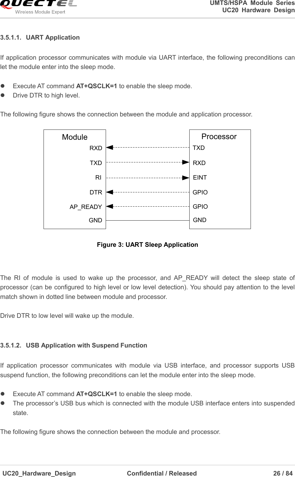
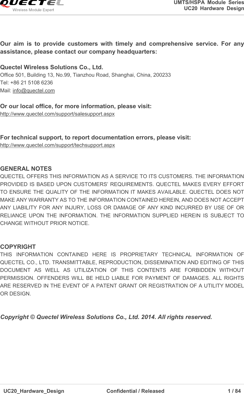
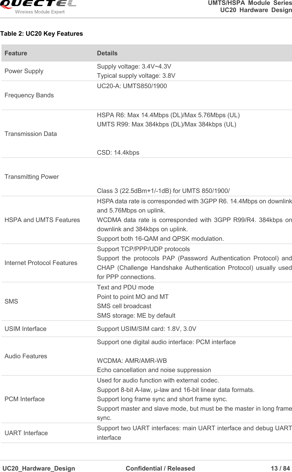
![UMTS/HSPA Module Series UC20 Hardware Design UC20_Hardware_Design Confidential / Released 28 / 84 USB_VBUSUSB_DPUSB_DMAP_READYVDDUSB_DPUSB_DMGPIOModule ProcessorRI EINTPower SwitchGPIOGND GND Figure 5: USB Sleep Application without Suspend Function Supply power to USB_VBUS will wake up the module. In sleep mode, module can still receive paging, voice call and SMS from network, but the UART port is not accessible. When the module enters into the sleep mode, the SLEEP_IND will output a high logic level. 3.5.2. Airplane Mode When module gets into the airplane mode, the RF function does not work, and all AT commands correlative with RF function will be not accessible. This mode can be set with the following way. Hardware: The W_DISABLE# pin is pulled up by default, drive it to low level will let the module get into airplane mode. Software: Command AT+CFUN provides the choice of the functionality level <fun>=0, 1, 4. AT+CFUN=0: Minimum functionality mode, both USIM and RF function are disabled. AT+CFUN=1: Full functionality mode (by default). AT+CFUN=4: Airplane mode. RF function is disabled. 1. The W_DISABLE# control function is disabled in firmware by default. It can be enabled by AT command AT+QCFG=“airplanecontrol”. Refer to document [1]. 2. When the module is in sleep mode, the W_DISABLE# control is invalid. Please be sure to wake the NOTES](https://usermanual.wiki/Quectel-Wireless-Solutions/201312UC20/User-Guide-2170092-Page-29.png)
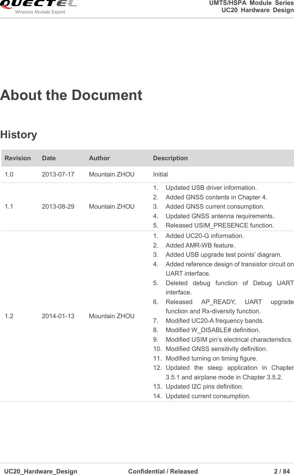
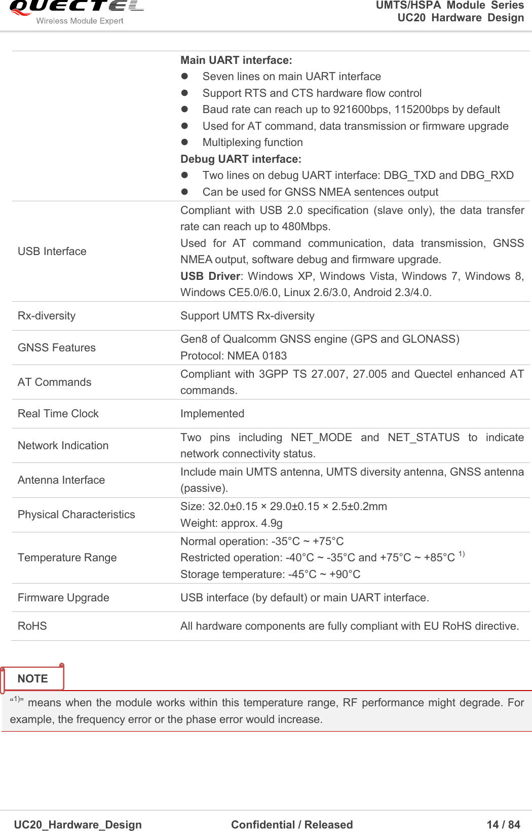
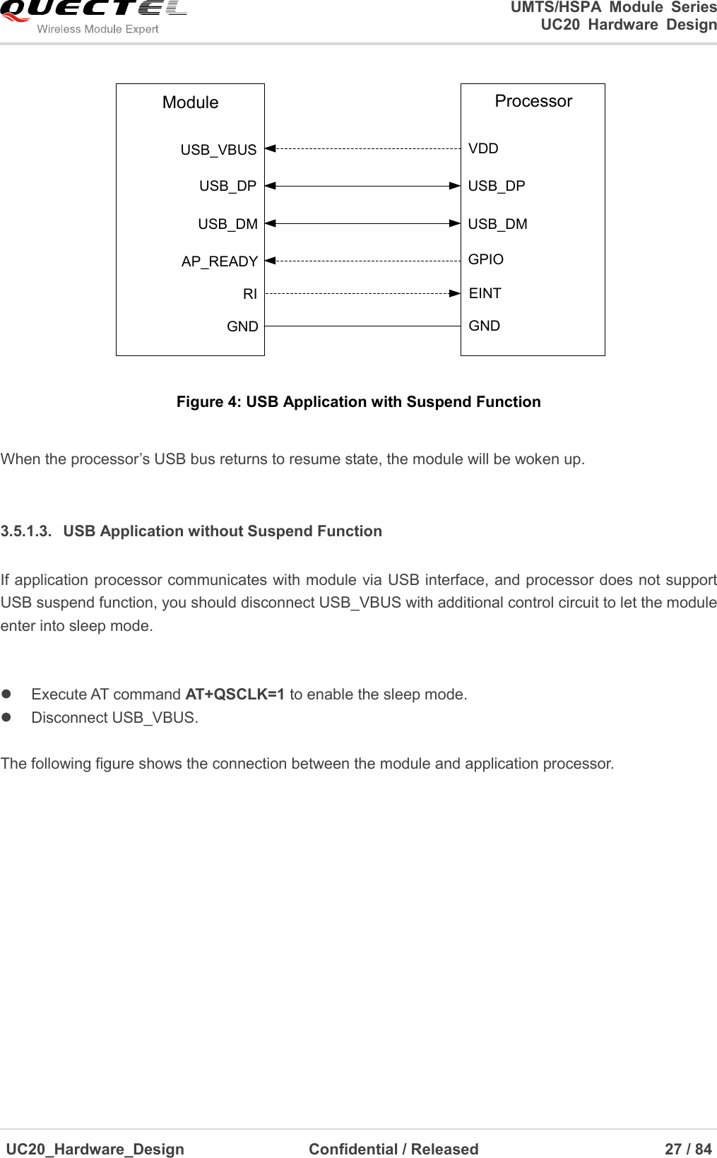
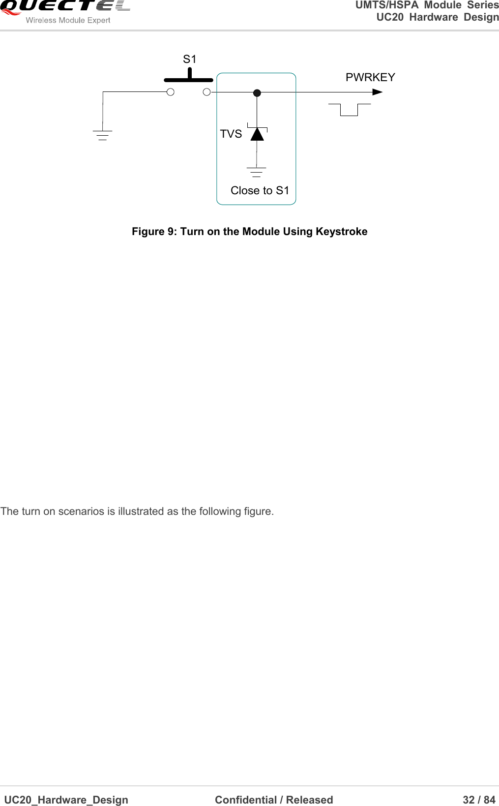
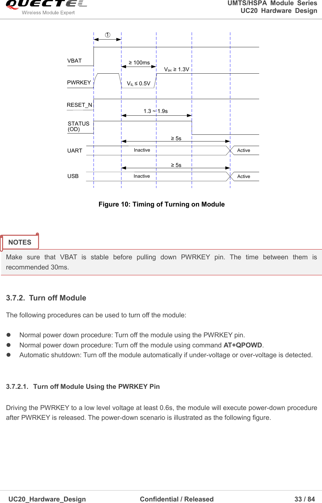
![UMTS/HSPA Module Series UC20 Hardware Design UC20_Hardware_Design Confidential / Released 31 / 84 3.6.4. Monitor the Power Supply You can use the AT+CBC command to monitor the VBAT_BB voltage value. For more details, please refer to document [1]. 3.7. Turn on and off Scenarios 3.7.1. Turn on Module Using the PWRKEY The following table shows the pin definition of PWRKEY. Table 7: PWRKEY Pin Description Pin Name Pin No. Description DC Characteristics Comment PWRKEY 21 Turn on/off the module. VIHmax = 2.1V VIHmin = 1.3V VILmax = 500mV Pull-up to 1.8V internally with 200kΩ resistor. When UC20 is in power down mode, it can be turned on to normal mode by driving the PWRKEY pin to a low level at least 100ms. It is recommended to use an open drain/collector driver to control the PWRKEY. You can monitor the level of the STATUS pin to judge whether the module is turned on or not. After STATUS pin (require external pull-up) outputting a low level, PWRKEY pin can be released. A simple reference circuit is illustrated in the following figure. Turn on pulsePWRKEY4.7K47K≥ 100ms Figure 8: Turn on the Module Using Driving Circuit The other way to control the PWRKEY is using a button directly. A TVS component is indispensable to be placed nearby the button for ESD protection. When pressing the key, electrostatic strike may generate from finger. A reference circuit is showed in the following figure.](https://usermanual.wiki/Quectel-Wireless-Solutions/201312UC20/User-Guide-2170092-Page-32.png)
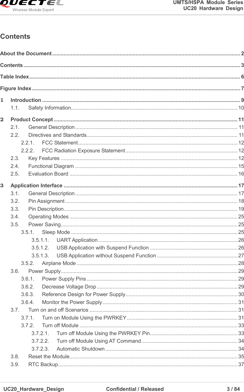
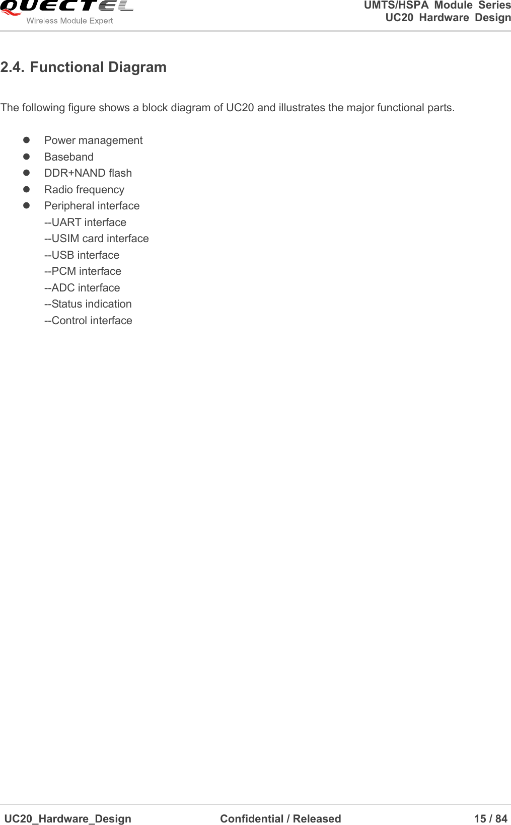
![UMTS/HSPA Module Series UC20 Hardware Design UC20_Hardware_Design Confidential / Released 34 / 84 VBATPWRKEYLog off network about 1s to 60s≥ 0.6sRUNNING Power-down procedure OFFModuleStatusSTATUS(OD) Figure 11: Timing of Turning off Module During power-down procedure, module will send out URC “NORMAL POWER DOWN” via URC port first, then log off network and save important data. After logging off, module sends out “POWERED DOWN” and shut down the internal power supply. The power on VBAT pins is not allowed to turn off before the URC “POWERED DOWN” is output to avoid data loss. If logging off is not done within 60s, module will shut down internal power supply forcibly. After that moment, the module enters the power down mode, no other AT commands can be executed and only the RTC is still active. The power down mode can also be indicated by the STATUS pin. 3.7.2.2. Turn off Module Using AT Command It is also a safe way to use AT command AT+QPOWD to turn off the module, which is similar to turning off the module via PWRKEY Pin Please refer to document [1] for details about the AT command of AT+QPOWD. 3.7.2.3. Automatic Shutdown The module will constantly monitor the voltage applied on the VBAT, if the voltage ≤ 3.5V, the following URC will be presented: +QIND: “vbatt”,-1 If the voltage ≥ 4.21V, the following URC will be presented: +QIND: “vbatt”,1](https://usermanual.wiki/Quectel-Wireless-Solutions/201312UC20/User-Guide-2170092-Page-35.png)
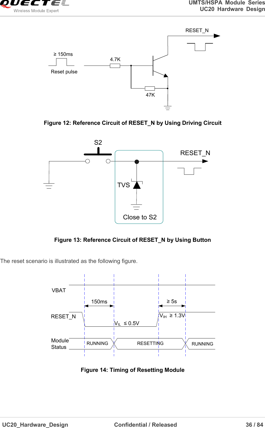
![UMTS/HSPA Module Series UC20 Hardware Design UC20_Hardware_Design Confidential / Released 35 / 84 The uncritical voltage is 3.4V to 4.3V, If the voltage > 4.3V or < 3.4V the module would automatically shut down itself. If the voltage < 3.4V, the following URC will be presented: +QIND: “vbatt”,-2 If the voltage > 4.3V, the following URC will be presented: +QIND: “vbatt”,2 The value of voltage threshold can be revised by command AT+QCFG=“vbatt”, refer to document [1] for details. 3.8. Reset the Module The RESET_N can be used to reset the module. Table 8: RESET_N Pin Description Pin Name Pin No. Description DC Characteristics Comment RESET_N 20 Reset the module. VIHmax = 2.1V VIHmin = 1.3V VILmax = 500mV Pull-up to 1.8V internally with 200kΩ resistor. Active low. You can reset the module by driving the RESET_N to a low level voltage for more than 150ms and then releasing. The recommended circuit is similar to the PWRKEY control circuit. You can use open drain/collector driver or button to control the RESET_N. NOTE](https://usermanual.wiki/Quectel-Wireless-Solutions/201312UC20/User-Guide-2170092-Page-36.png)
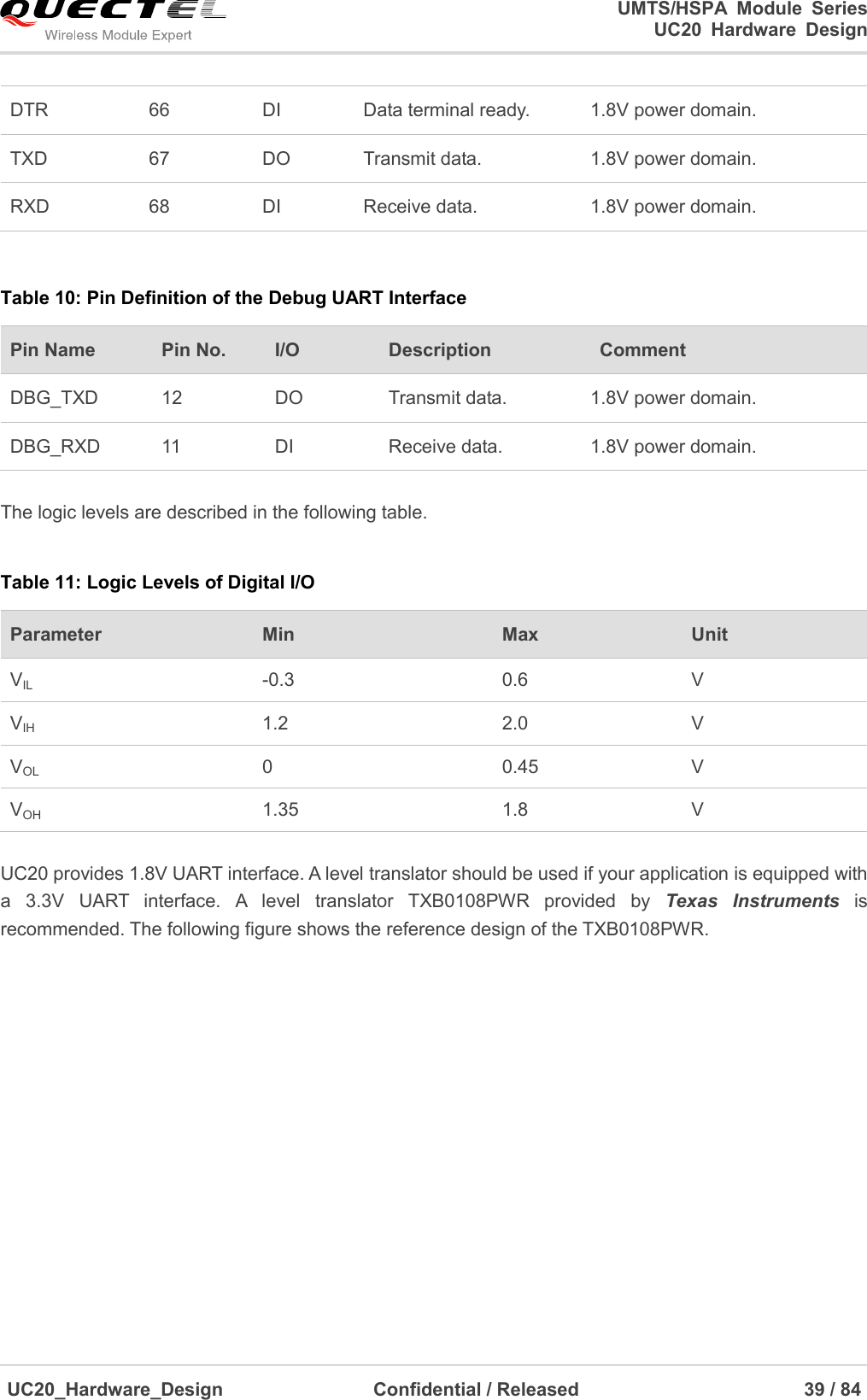
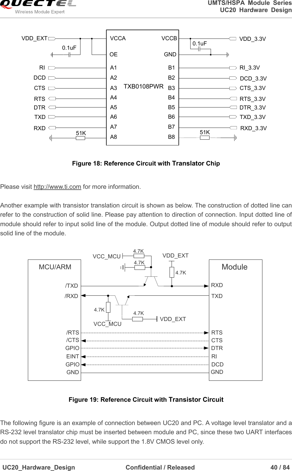
![UMTS/HSPA Module Series UC20 Hardware Design UC20_Hardware_Design Confidential / Released 41 / 84 TXB0108PWRDCD_3.3VRTS_3.3VDTR_3.3VRXD_3.3VRI_3.3VCTS_3.3VTXD_3.3VDCDRTSDTRRXDRICTSTXDDCD_1.8VRTS_1.8VDTR_1.8VRXD_1.8VRI_1.8VCTS_1.8VTXD_1.8VVCCAModuleGND GNDVDD_EXT VCCB3.3VDIN1ROUT3ROUT2ROUT1DIN4DIN3DIN2DIN5R1OUTBFORCEON/FORCEOFF /INVALID3.3VDOUT1DOUT2DOUT3DOUT4DOUT5RIN3RIN2RIN1VCC GNDOESN65C3238 DB-9Connect to PCDCDRTSDTRTXDRICTSRXDDSRGND123456789 Figure 20: RS232 Level Match Circuit The following figure shows the reference circuit of debug UART interface with logic level translator. TXB0102DCU provided by Texas Instruments is recommended. VCCA VCCBOEA1A2GNDB1B2VDD_EXTDBG_TXDDBG_RXD0.1uF 0.1uFDBG_TXD_3.3VDBG_RXD_3.3VVDD_3.3VTXB0102DCU Figure 21: Reference Circuit of Debug UART with Level Translator Please visit http://www.ti.com for more information. 1. The module disables the hardware flow control by default. When hardware flow control is required, RTS and CTS should be connected to the host. AT command AT+IFC=2,2 is used to enable hardware flow control. AT command AT+IFC=0,0 is used to disable the hardware flow control. For more details, please refer to document [1]. 2. Rising on DTR will let the module exit from the data mode by default. It can be disabled by AT commands. Refer to document [1] about the command AT&D and AT&V for details. 3. DCD is used as data mode indication. Refer to document [1] about the command AT&C and AT&V for details. NOTES](https://usermanual.wiki/Quectel-Wireless-Solutions/201312UC20/User-Guide-2170092-Page-42.png)
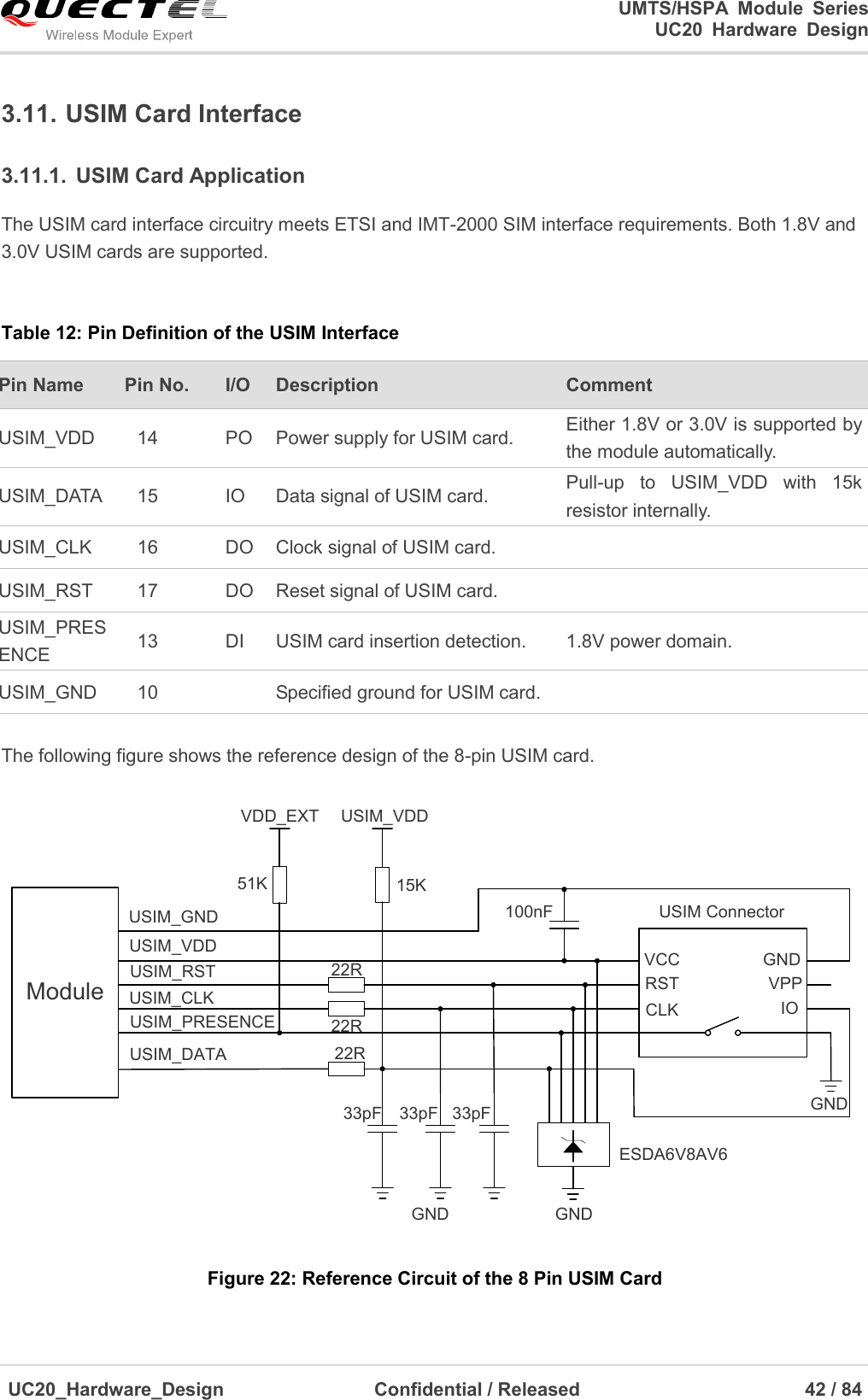
![UMTS/HSPA Module Series UC20 Hardware Design UC20_Hardware_Design Confidential / Released 43 / 84 Some AT commands are invalid when USIM card is not applied. UC20 supports USIM card hot-plugging via the USIM_PRESENCE pin. For details, refer to document [1] about the command AT+QSIMDET. If you do not need the USIM card detection function, keep USIM_PRESENCE unconnected. The reference circuit for using a 6-pin USIM card connector is illustrated as the following figure. ModuleUSIM_VDDUSIM_GNDUSIM_RSTUSIM_CLKUSIM_DATA 22R22R22R100nF USIM ConnectorGNDESDA6V8AV633pF 33pF 33pFVCCRSTCLK IOVPPGNDGND15KUSIM_VDD Figure 23: Reference Circuit of the 6 Pin USIM Card In order to enhance the reliability and availability of the USIM card in your application, please follow the following criterion in the USIM circuit design: Keep layout of USIM card as close as possible to the module. Assure the length of the trace is less than 200mm. Keep USIM card signal away from RF and VBAT alignment. Assure the ground between module and USIM connector short and wide. Keep the width of ground and USIM_VDD no less than 0.5mm to maintain the same electric potential. The decouple capacitor of USIM_VDD should be less than 1uF and must be near to USIM connector. To avoid cross-talk between USIM_DATA and USIM_CLK, keep them away with each other and shield them with surrounded ground. In order to offer good ESD protection, it is recommended to add TVS such as WILL (http://www.willsemi.com) ESDA6V8AV6. The 22Ω resistors should be added in series between the module and the USIM card so as to suppress the EMI spurious transmission and enhance the ESD protection. The pull-up resistor on USIM_DATA line can improve anti-jamming capability when long layout trace and sensitive occasion is applied. NOTE](https://usermanual.wiki/Quectel-Wireless-Solutions/201312UC20/User-Guide-2170092-Page-44.png)
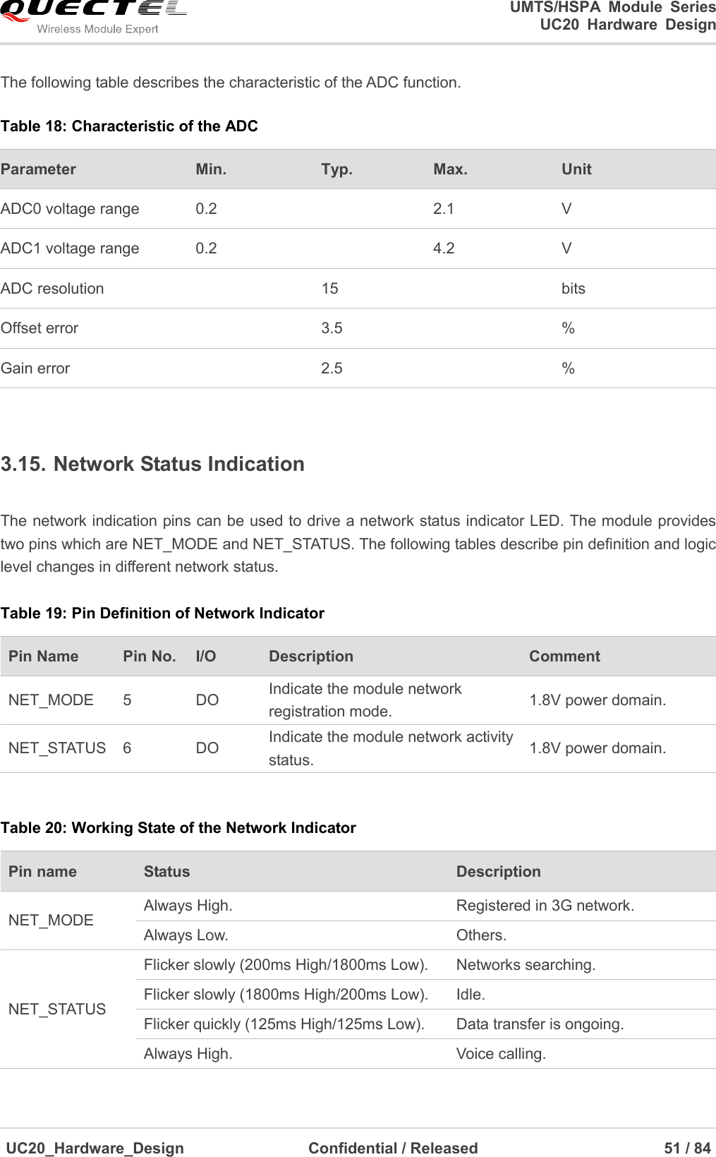
![UMTS/HSPA Module Series UC20 Hardware Design UC20_Hardware_Design Confidential / Released 49 / 84 PCM_CLKPCM_SYNCPCM_OUTMSB LSBPCM_IN125usMSB1 2 1615LSB Figure 29: Auxiliary Mode Timing The following table shows the pin definition of PCM and I2C interface which can be applied on audio codec design. Table 16: Pin Definition of PCM and I2C Interface Pin Name Pin No. I/O Description Comment PCM_IN 24 DI PCM data input. 1.8V power domain. PCM_OUT 25 DO PCM data output. 1.8V power domain. PCM_SYNC 26 IO PCM data frame sync signal. 1.8V power domain. PCM_CLK 27 IO PCM data bit clock. 1.8V power domain. I2C_SCL 41 DO I2C serial clock. Require external pull-up resistor. I2C_SDA 42 IO I2C serial data. Require external pull-up resistor. Clock and mode can be configured by AT command, and the default configuration is master mode using short sync data format with 2048kHz PCM_CLK and 8kHz PCM_SYNC. In addition, UC20’s firmware has integrated the configuration on NAU8814 application with I2C interface. Refer to document [1] about the command AT+QDAI for details.](https://usermanual.wiki/Quectel-Wireless-Solutions/201312UC20/User-Guide-2170092-Page-50.png)
![UMTS/HSPA Module Series UC20 Hardware Design UC20_Hardware_Design Confidential / Released 50 / 84 The following figure shows the reference design of PCM interface with external codec IC. PCM_INPCM_OUTPCM_SYNCPCM_CLKI2C_SCLI2C_SDANAU8814Module1.8V4.7K4.7KBCLKMCLKFSDACINADCOUTSCLKSDINBIASMIC_BIASMIC+MIC-SPKOUT+SPKOUT- Figure 30: Reference Circuit of PCM Application with Audio Codec 1. It is recommended to reserved RC (R=22Ω, C=22pF) circuit on the PCM lines, especially for PCM_CLK. 2. UC20 work as a master device pertaining to I2C interface. 3.14. ADC Function The module provides two analog-to-digital converters (ADC) to digitize the analog signal to 15-bit digital data such as battery voltage, temperature and so on. Using AT command AT+QADC=0 can read the voltage value on ADC0 pin. Using AT command AT+QADC=1 can read the voltage value on ADC1 pin. For more details of these AT commands, please refer to document [1]. In order to improve the accuracy of ADC, the trace of ADC should be surrounded by ground. Table 17: Pin Definition of the ADC Pin name Pin NO. Description ADC0 45 General purpose analog to digital converter. ADC1 44 General purpose analog to digital converter. NOTES](https://usermanual.wiki/Quectel-Wireless-Solutions/201312UC20/User-Guide-2170092-Page-51.png)
![UMTS/HSPA Module Series UC20 Hardware Design UC20_Hardware_Design Confidential / Released 54 / 84 A reference circuit is shown in the following figure. 4.7K47KVBAT2.2KModuleSLEEP_IND Figure 33: Reference Circuit of the SLEEP_IND 3.17. Behavior of the RI You can use command AT+QCFG=“risignaltype”, “physical” to configure RI behavior: No matter which port URC is presented on, URC will trigger the behavior on RI pin. URC can be output from UART port, USB AT port and USB modem port by command AT+QURCCFG. The default port is USB AT port. In additional, RI behavior can be configured flexible. The default behavior of the RI is shown as below. Table 23: Behavior of the RI State Response Idle RI keeps high level. URC RI outputs 120ms low pulse when new URC returns. The RI behavior can be changed by command AT+QCFG=“urc/ri/ring”, refer to document [1] for details. NOTE](https://usermanual.wiki/Quectel-Wireless-Solutions/201312UC20/User-Guide-2170092-Page-55.png)
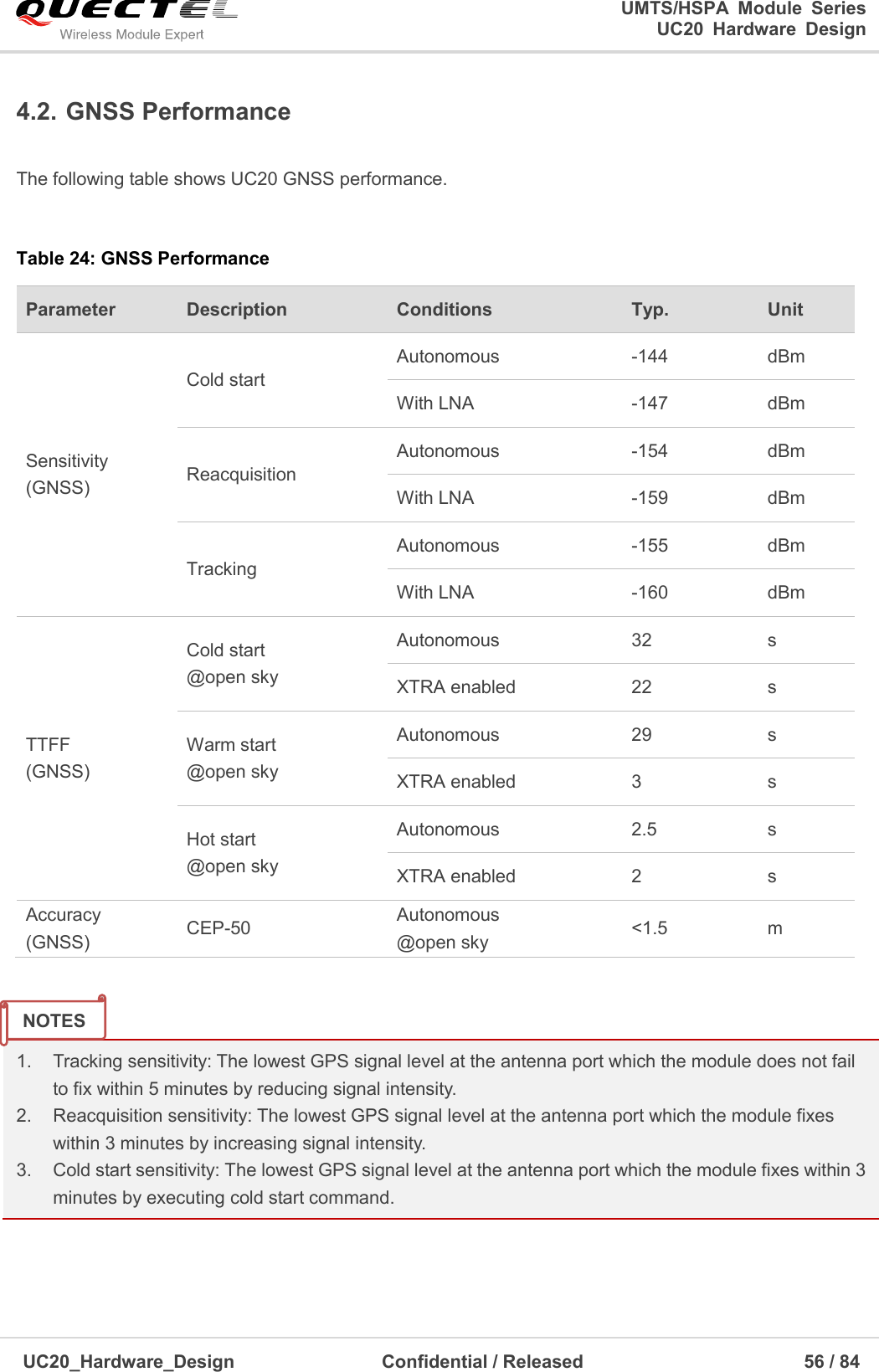
![UMTS/HSPA Module Series UC20 Hardware Design UC20_Hardware_Design Confidential / Released 55 / 84 4 GNSS Receiver 4.1. General Description UC20 includes a fully integrated global navigation satellite system solution that supports the latest generation gpsOne Gen8 of Qualcomm (GPS and GLONASS). Compared with GPS only, dual systems increase usable constellation, reduce coverage gaps and TTFF, and increase positioning accuracy, especially in rough urban environments. UC20 works in standalone mode, allows device to demodulate GNSS assistance data, calculate position without any assistance from the network, suitable for various application needing lowest-cost, accurate position determination. UC20 supports Qualcomm gpsOneXTRA technology (one kind of A-GNSS), which will download XTRA file from the internet server to enhance the TTFF. XTRA file contains predicted GPS and GLONASS satellites coordinates and clock biases valid for up to 7days. It is the best if XTRA file is downloaded once every 1-2 days. And UC20 also supports SBAS (including WAAS, EGNOS and MSAS), which will improve fix accuracy. UC20 provides power-saving solution named DPO (Dynamic Power Optimization), which attempts to turn off GNSS RF parts, reduces current consumption by 50% at most without impact on TTFF and extends battery life, maximizes talk and standby time as well. UC20 supports standard NMEA-0183 protocol, and outputs NMEA sentences with 1Hz via USB interface by default. By default, UC20 GNSS engine is switched off, it has to be switched on with AT command. For more details about GNSS engine technology and configurations, refer to document [7].](https://usermanual.wiki/Quectel-Wireless-Solutions/201312UC20/User-Guide-2170092-Page-56.png)
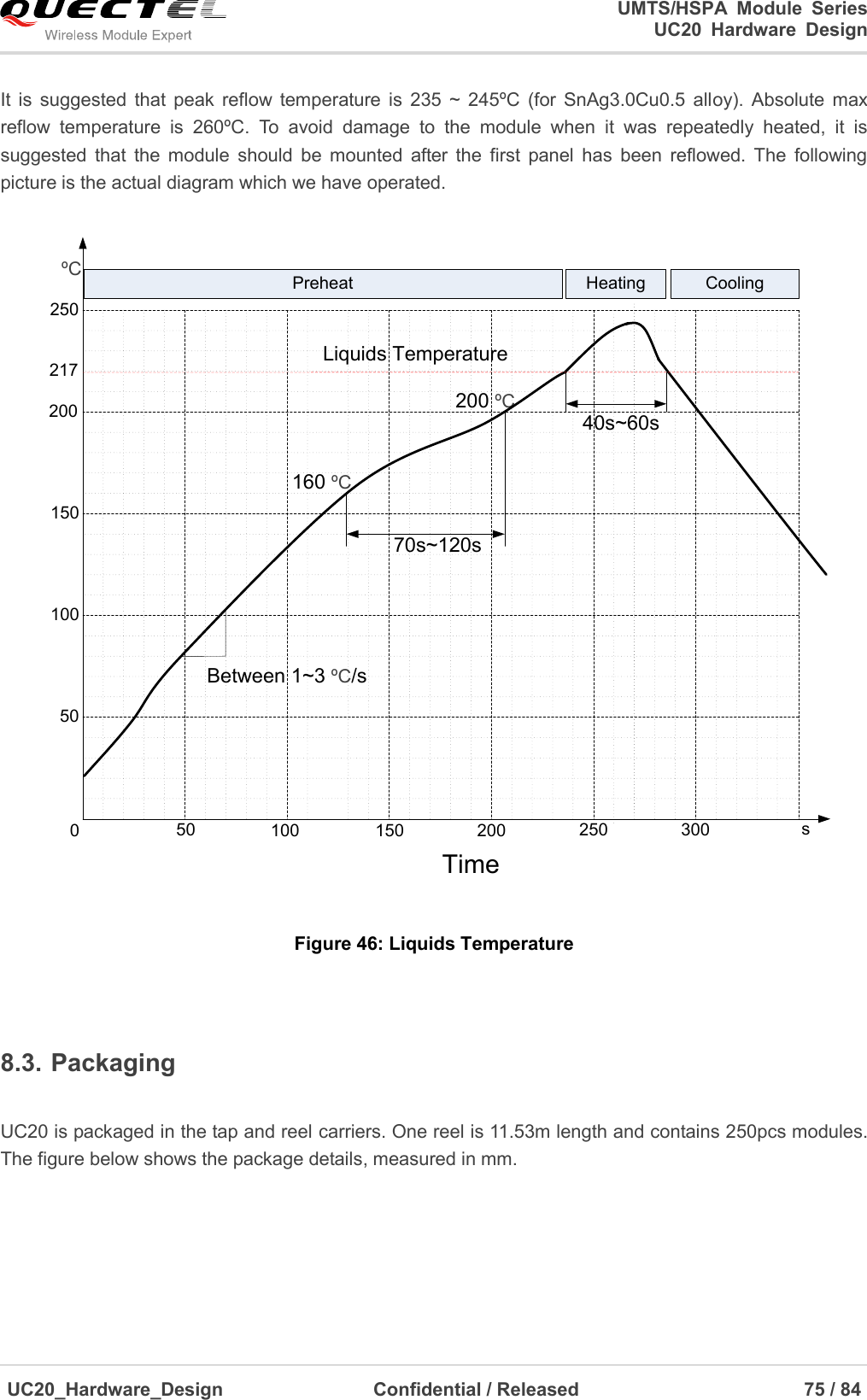
![UMTS/HSPA Module Series UC20 Hardware Design UC20_Hardware_Design Confidential / Released 74 / 84 8 Storage and Manufacturing 8.1. Storage UC20 is stored in the vacuum-sealed bag. The restriction of storage condition is shown as below. Shelf life in sealed bag is 12 months at < 40ºC / 90%RH. After this bag is opened, devices that will be subjected to reflow solder or other high temperature process must be: Mounted within 72 hours at factory conditions of ≤ 30ºC / 60%RH. Stored at <10% RH. Devices require bake, before mounting, if: Humidity indicator card is >10% when read 23ºC ± 5ºC. Mounted for more than 72 hours at factory conditions of ≤o30ºC / 60% RH. If baking is required, devices may be baked for 48 hours at 125ºC ± 5ºC. As plastic container cannot be subjected to high temperature, Module needs to be taken out from container to high temperature (125ºC) bake. If shorter bake times are desired, please refer to IPC/JEDECJ-STD-033 for bake procedure. 8.2. Manufacturing and Welding The squeegee should push the paste on the surface of the stencil that makes the paste fill the stencil openings and penetrate to the PCB. The force on the squeegee should be adjusted so as to produce a clean stencil surface on a single pass. To ensure the module soldering quality, the thickness of stencil at the hole of the module pads should be 0.18mm. For details, please refer to document [6]. NOTE](https://usermanual.wiki/Quectel-Wireless-Solutions/201312UC20/User-Guide-2170092-Page-75.png)
![UMTS/HSPA Module Series UC20 Hardware Design UC20_Hardware_Design Confidential / Released 77 / 84 9 Appendix A Reference Table 37: Related Documents SN Document Name Remark [1] UC20_AT_Commands_Manual UC20 AT Commands Manual [2] UC20_EVB_User_Guide UC20 EVB User Guide [3] UC20_Reference_Design UC20 Reference Design [4] UC20&M10_Reference_Design UC20 and M10 Compatible Reference Design [5] UC20&M10_Compatibilty_Design UC20 and M10 Compatibility Design Specification [6] Module_Secondary_SMT_User_Guide Module Secondary SMT User Guide [7] UC20_GNSS_AT_Commands_Manual UC20 GNSS AT Commands Manual Table 38: Terms and Abbreviations Abbreviation Description AMR Adaptive Multi-rate ARP Antenna Reference Point bps bits per second CHAP Challenge Handshake Authentication Protocol CMUX Customer CS Coding Scheme CSD Circuit Switched Data CTS Clear To Send DRX Discontinuous Reception](https://usermanual.wiki/Quectel-Wireless-Solutions/201312UC20/User-Guide-2170092-Page-78.png)