Quectel Wireless Solutions 201403GC65 GSM/GPRS Module User Manual Manual
Quectel Wireless Solutions Company Limited GSM/GPRS Module Manual
UserManual.wiki
>
Quectel Wireless Solutions
>
201403GC65 User Manual
Manual
Navigation menu
Upload a User Manual
Namespaces
Wiki Guide
HTML
PDF
Info
Views
User Manual
Discussion / Help
Navigation
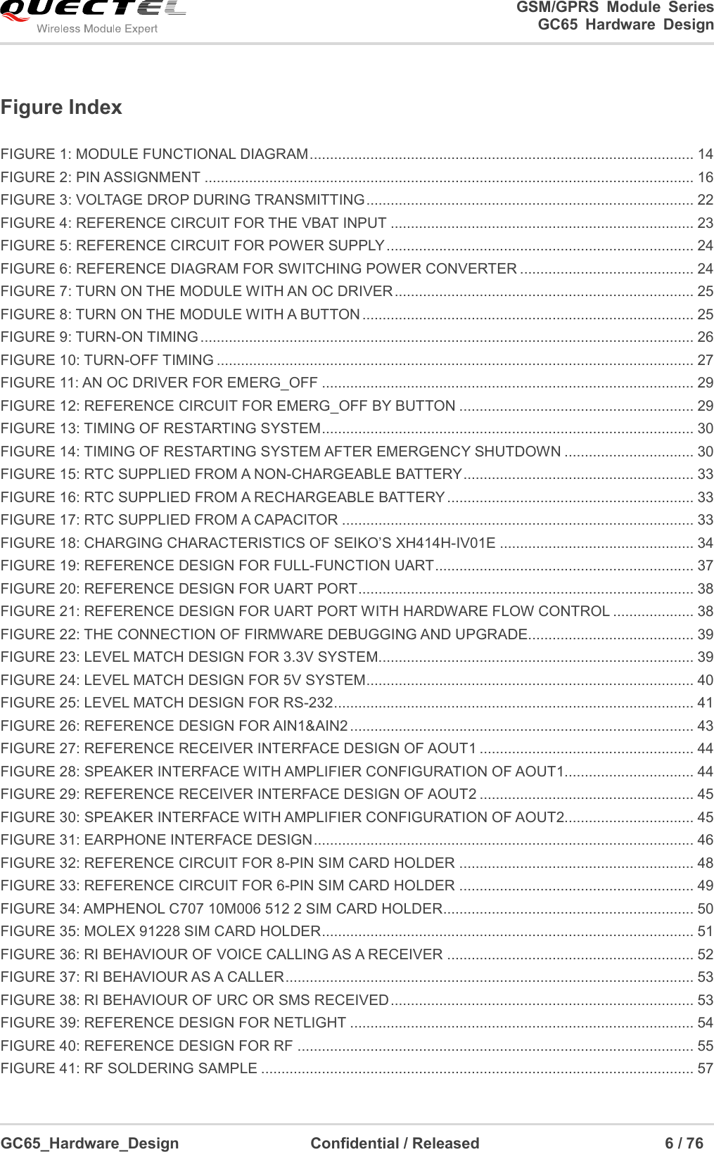
![GSM/GPRS Module Series GC65 Hardware Design GC65_Hardware_Design Confidential / Released 14 / 76 Figure 1: Module Functional Diagram 2.5. Evaluation Board In order to help you to develop applications with GC65, Quectel supplies an evaluation board (EVB) with RS-232 to USB cable, power adapter, antenna, firmware upgrade cable (UART to USB cable) and other peripherals to control or test the module. For details, please refer to the document [11].](https://usermanual.wiki/Quectel-Wireless-Solutions/201403GC65/User-Guide-2277242-Page-15.png)
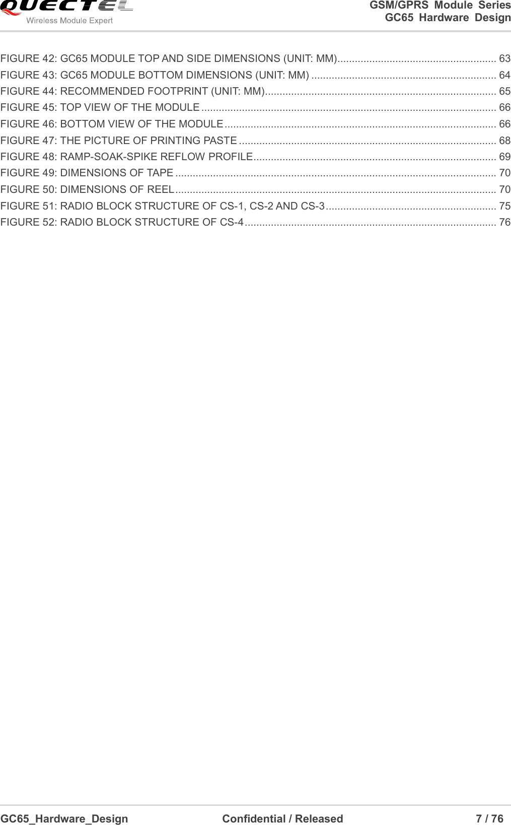
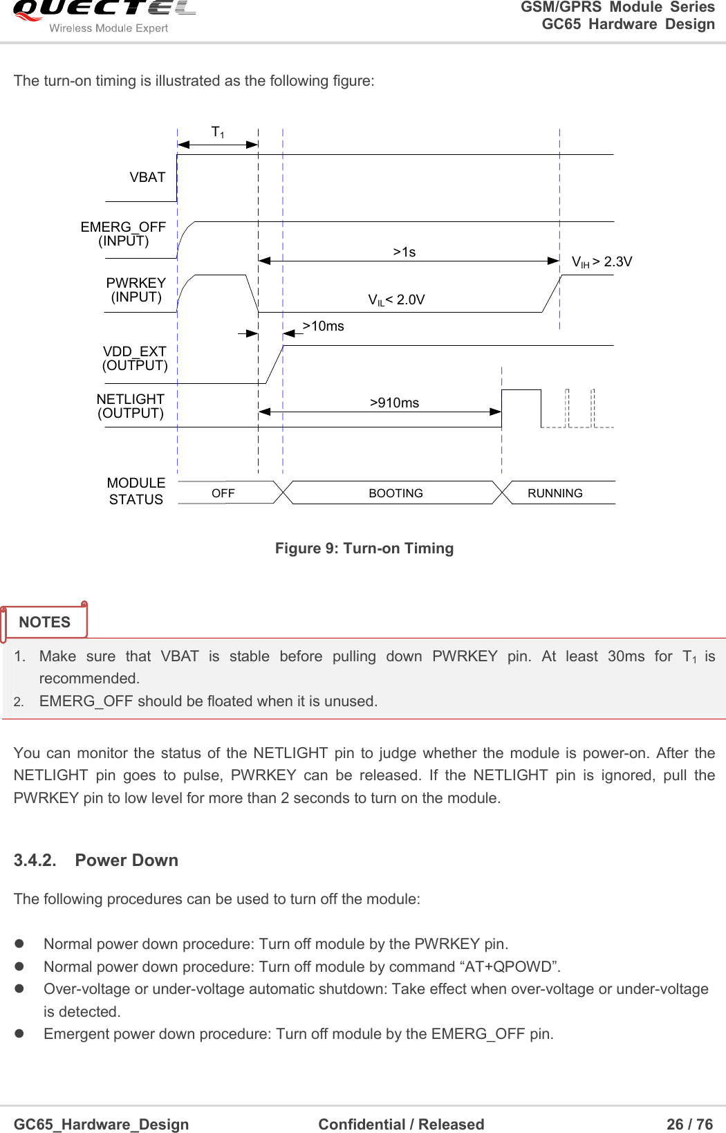
![GSM/GPRS Module Series GC65 Hardware Design GC65_Hardware_Design Confidential / Released 24 / 76 Figure 5: Reference Circuit for Power Supply If a switching power converter is used, please follow the diagram to design the circuit, it is beneficial to maintain stable power supply for the module. Figure 6: Reference Diagram for Switching Power Converter 3.3.4. Monitor Power Supply To monitor the supply voltage, you can use the “AT+CBC” command which includes three parameters: charging status, remaining battery capacity and voltage value (in mV). It returns the 0-100 percent of battery capacity and actual value measured between VBAT and GND. The voltage is automatically measured in period of 5s. The displayed voltage (in mV) is averaged over the last measuring period before the “AT+CBC” command is executed. For details, please refer to document [1]. 3.4. Power On and Down Scenarios 3.4.1. Power On The module can be turned on by driving the pin PWRKEY to a low level voltage, after booting successfully, PWRKEY pin can be released. You may monitor the status of the NETLIGHT pin to judge whether the module is power-on or not. When NETLIGHT pin outputs a signal with certain frequency, it indicates the module is turned on successfully. The NETLIGHT pin will keep in low level all the time after the module is](https://usermanual.wiki/Quectel-Wireless-Solutions/201403GC65/User-Guide-2277242-Page-25.png)
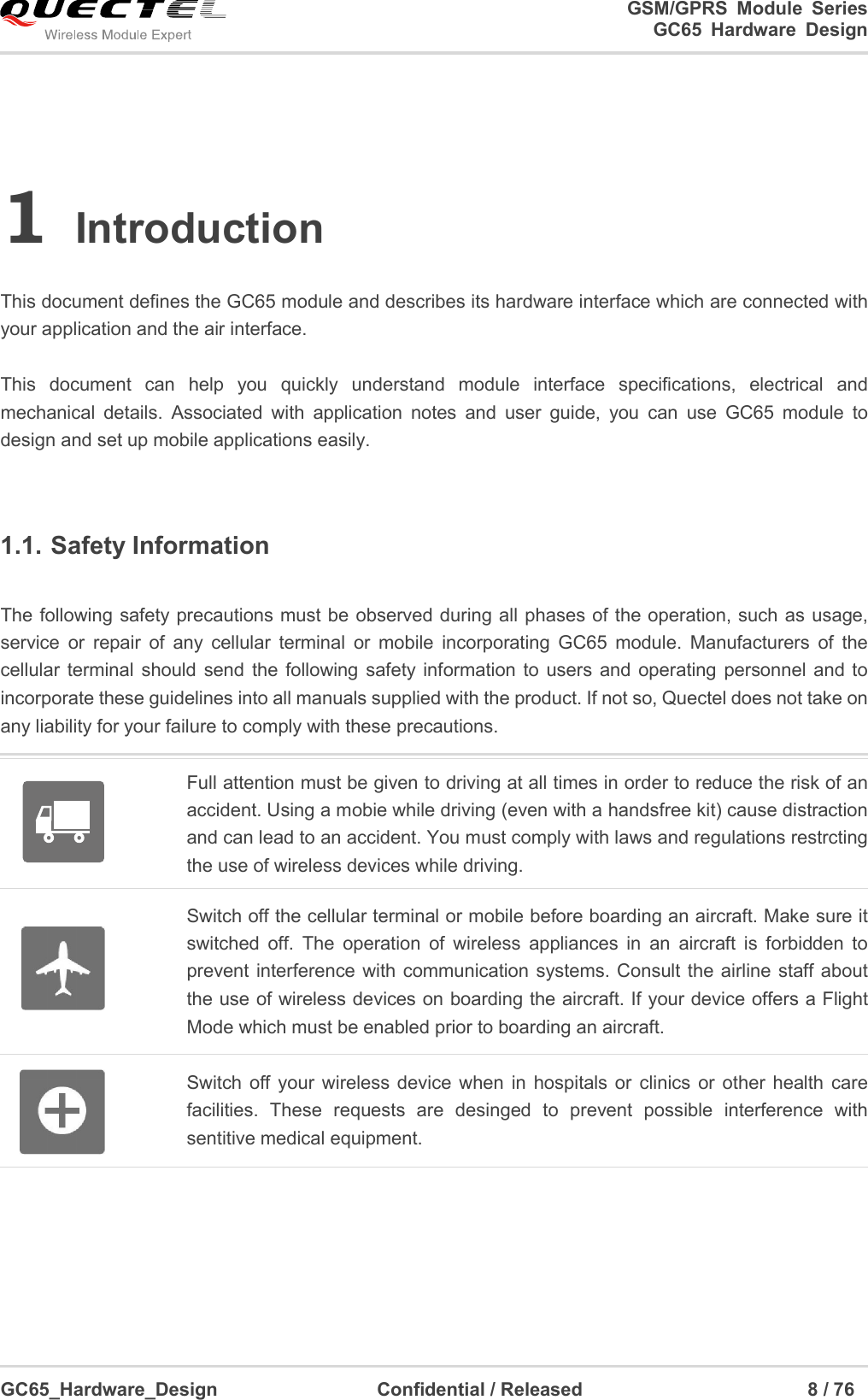
![GSM/GPRS Module Series GC65 Hardware Design GC65_Hardware_Design Confidential / Released 25 / 76 turned off. An OC driver circuit is suggested to control the PWRKEY. A simple reference circuit is illustrated as below: Figure 7: Turn On the Module with an OC Driver GC65 module is set to autobauding mode (AT+IPR=0) by default. In the autobauding mode, URC “RDY” is not reported to the host controller after module is powered on. When the module receives AT command, it will be powered on after a delay of 5~6 seconds. Host controller should first send the “AT” string in order that the module can detect baud rate of host controller, and it will continuously send 1~5 “AT” string until receiving “OK” string from the module. Then enter “AT+IPR=x;&W” to set a fixed baud rate for the module and save the configuration to flash memory of the module. After these configurations, the URC “RDY” would be received from the UART port of the module every time when the module is powered on. For more details, refer to the section “AT+IPR” in document [1]. The other way to control the PWRKEY is through a button directly. A TVS component is indispensable to be placed nearby the button for ESD protection. For the best performance, the TVS component must be placed nearby the button. When pressing the key, electrostatic strike may generate from finger. A reference circuit is shown in the following figure: Figure 8: Turn On the Module with a Button NOTE](https://usermanual.wiki/Quectel-Wireless-Solutions/201403GC65/User-Guide-2277242-Page-26.png)
![GSM/GPRS Module Series GC65 Hardware Design GC65_Hardware_Design Confidential / Released 28 / 76 3.4.2.2. Power Down Module by AT Command It is also a safe way to turn off the module via AT command “AT+QPOWD=1”. This command will let the module log off from the network and allow the firmware to save important data before completely disconnecting the power supply. Before the completion of the power down procedure, the module sends the result code, shown as below: NORMAL POWER DOWN Please refer to the document [1] for details about the AT command “AT+QPOWD”. 3.4.2.3. Over-voltage or Under-voltage Automatic Shutdown The module will constantly monitor the voltage applied on the VBAT, if the voltage is≤3.5V, the following URC will be presented: UNDER_VOLTAGE WARNING If the voltage is≥4.5V, the following URC will be presented: OVER_VOLTAGE WARNING The normal input voltage range is from 3.3V to 4.6V. If the voltage is >4.6V or <3.3V, the module would automatically shut down itself. If the voltage is <3.3V, the following URC will be presented: UNDER_VOLTAGE POWER DOWN If the voltage is >4.6V, the following URC will be presented: OVER_VOLTAGE POWER DOWN When autobauding is active and DTE&DCE are not correctly synchronized after start-up, this result code will not appear. It is recommended to set a fixed baud rate for the module. NOTE](https://usermanual.wiki/Quectel-Wireless-Solutions/201403GC65/User-Guide-2277242-Page-29.png)
![GSM/GPRS Module Series GC65 Hardware Design GC65_Hardware_Design Confidential / Released 31 / 76 3.5. Power Saving Technology Based on system requirements, there are several actions to drive the module to enter into low current consumption state. For example, “AT+CFUN” can be used to set module into minimum functionality mode and DTR hardware interface signal can be used to lead system to sleep mode. 3.5.1. Minimum Functionality Mode Minimum functionality mode reduces the functionality of the module to a minimum level. The consumption of the current can be minimized when the slow clocking mode is activated at the same time. The mode is set with the “AT+CFUN” command which provides the choice of the functionality levels <fun>=0,1,4. 0: Minimum functionality. 1: Full functionality (default). 4: Disable both transmitting and receiving of RF part. If the module is set to minimum functionality by “AT+CFUN=0”, the RF function and SIM card function would be disabled. In this case, the UART port is still accessible, but all AT commands related with RF function or SIM card function will not be available. If the module has been set by the command with “AT+CFUN=4”, the RF function will be disabled, but the UART port is still active. In this case, all AT commands related with RF function will not be available. After the module is set by “AT+CFUN=0” or “AT+CFUN=4”, it can return to full functionality by “AT+CFUN=1”. For detailed information about “AT+CFUN”, please refer to the document [1]. 3.5.2. Sleep Mode The sleep mode is disabled by default. You can enable it by “AT+QSCLK=1”. On the other hand, the default setting is “AT+QSCLK=0” and in this mode, the module cannot enter into sleep mode. When the module is set by the command “AT+QSCLK=1”, you can control the module to enter into or exit from the sleep mode through pin DTR. When DTR is set to high level, and there is no on-air or hardware interrupt such as GPIO interrupt or data on UART port, the module will enter into sleep mode automatically. In this mode, the module can still receive voice, SMS or GPRS paging from network, but the UART port does not work.](https://usermanual.wiki/Quectel-Wireless-Solutions/201403GC65/User-Guide-2277242-Page-32.png)
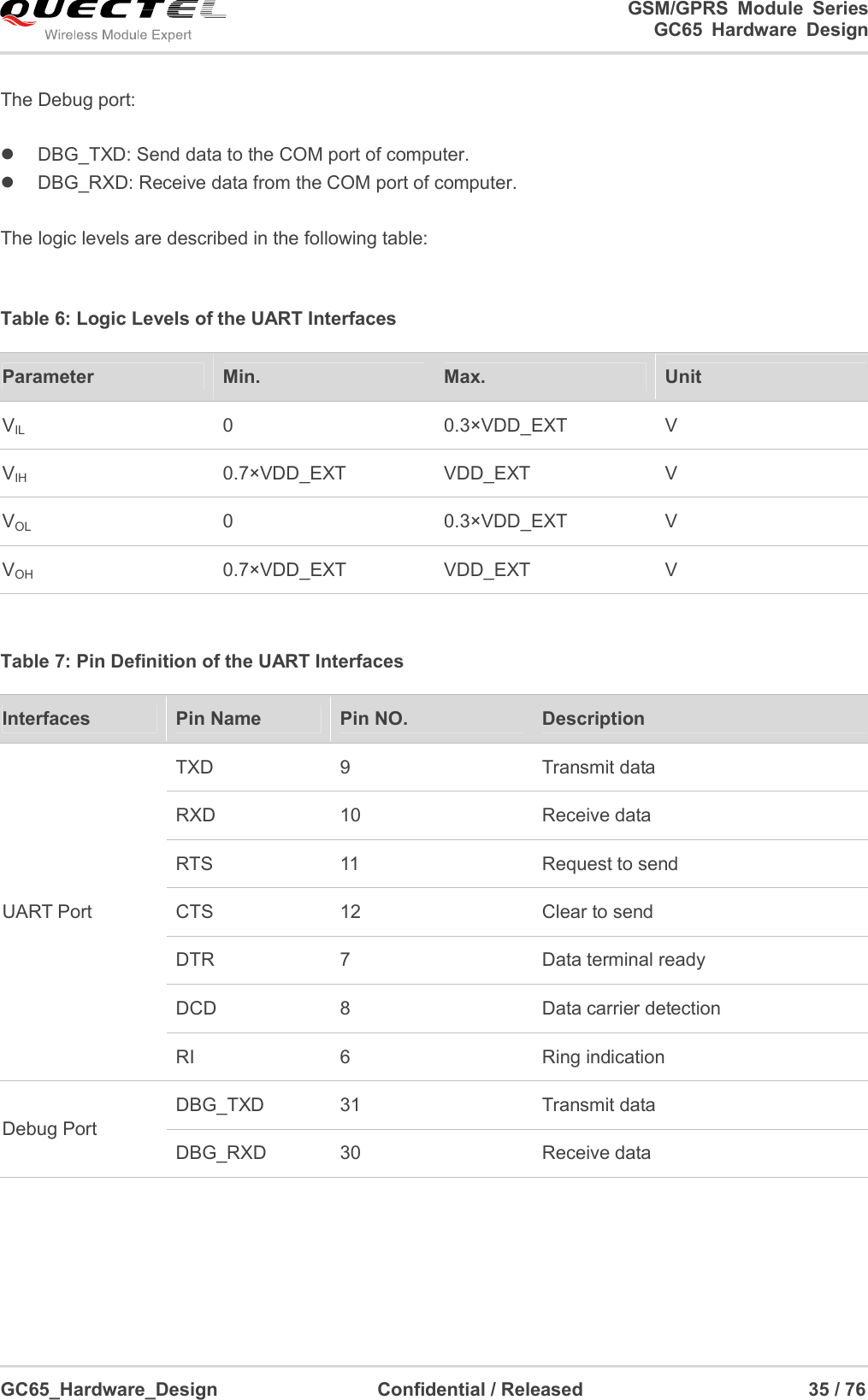
![GSM/GPRS Module Series GC65 Hardware Design GC65_Hardware_Design Confidential / Released 34 / 76 Figure 18: Charging Characteristics of Seiko’s XH414H-IV01E 3.7. Serial Interfaces The module provides two universal asynchronous serial ports: UART port and debug port. The module is designed as a DCE (Data Communication Equipment), following the traditional DCE-DTE (Data Terminal Equipment) connection. Autobauding function supports baud rate from 4800bps to 115200bps. The UART port: TXD: Send data to RXD of DTE. RXD: Receive data from TXD of DTE. RTS: Request to send. CTS: Clear to send. DTR: DTE is ready and inform DCE (this pin can wake the module up). RI: Ring indicator (when the call, SMS, data of the module are coming, the module will output signal to inform DTE). DCD: Data carrier detection (the validity of this pin demonstrates the communication link is set up). The module disables hardware flow control by default. When hardware flow control is required, RTS and CTS should be connected to the host. AT command “AT+IFC=2,2” is used to enable hardware flow control. AT command “AT+IFC=0,0” is used to disable the hardware flow control. For more details, please refer to the document [1]. NOTE](https://usermanual.wiki/Quectel-Wireless-Solutions/201403GC65/User-Guide-2277242-Page-35.png)
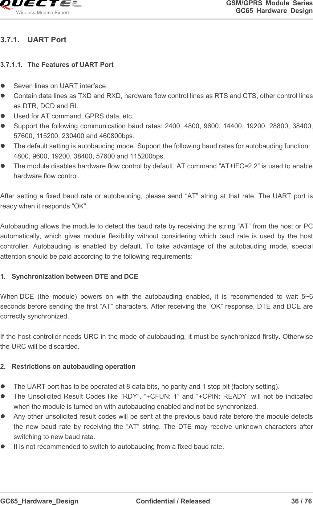
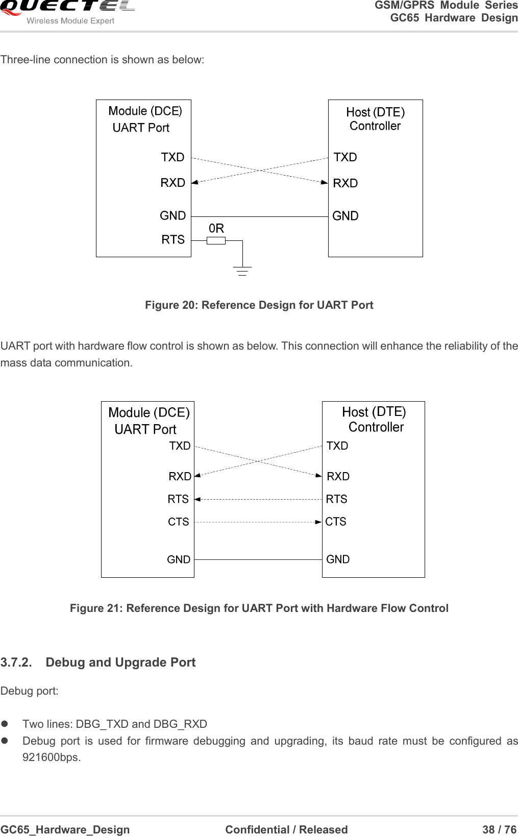
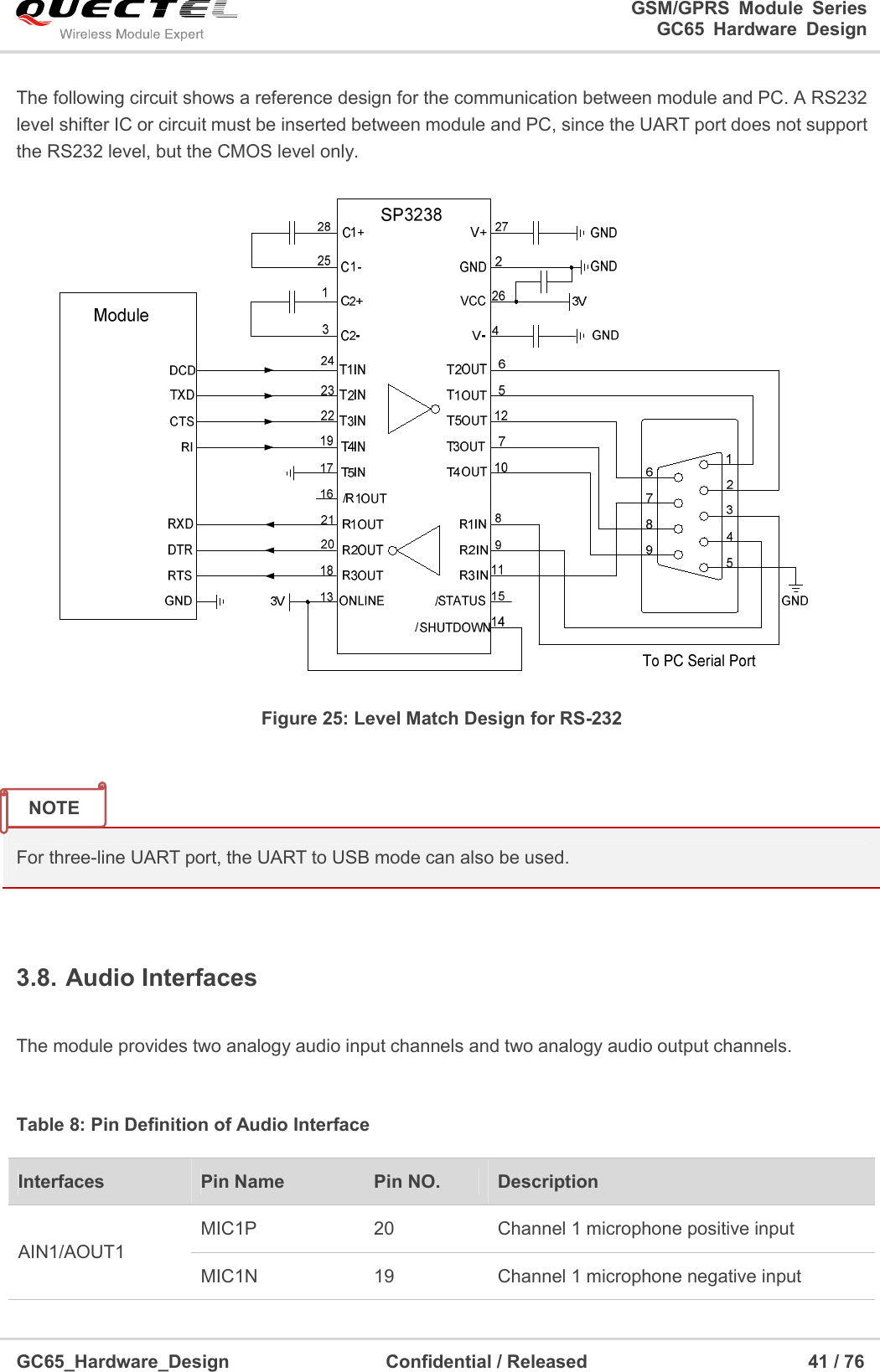
![GSM/GPRS Module Series GC65 Hardware Design GC65_Hardware_Design Confidential / Released 37 / 76 To ensure reliable communication and avoid any problems caused by undetermined baud rate between DCE and DTE, it is strongly recommended to configure a fixed baud rate and save it instead of using autobauding after start-up. For more details, please refer to the section “AT+IPR” in document [1]. 3.7.1.2. The Connection of UART The connection between module and host by UART port is very flexible. Three connection styles are illustrated as below. Reference design for Full-Function UART connection is shown as below when it is applied in modulation-demodulation. Figure 19: Reference Design for Full-Function UART NOTE](https://usermanual.wiki/Quectel-Wireless-Solutions/201403GC65/User-Guide-2277242-Page-38.png)
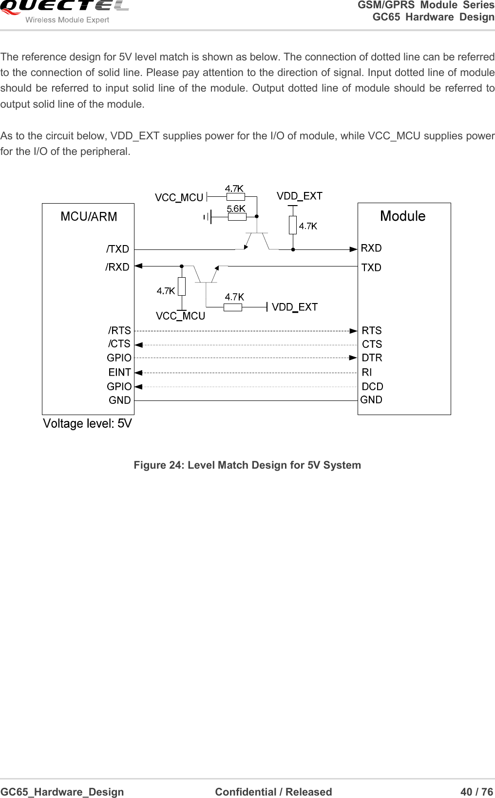
![GSM/GPRS Module Series GC65 Hardware Design GC65_Hardware_Design Confidential / Released 39 / 76 Figure 22: The Connection of Firmware Debugging and Upgrade Because the debug port uses a high baud rate 921600bps configuration, when connecting a PC for debugging and upgrading, the UART to USB mode is recommended. The test points for debug UART is recommended to be reserved, for detailed design, please refer to the document [12]. 3.7.3. UART Application VDD_EXT is the reference voltage level for UART of GC65, the 1K resistors is recommended to be added on the UART lines, the reference circuit is shown as below. This circuit is also applicable in 2.8V or 3.0V systems. Figure 23: Level Match Design for 3.3V System NOTE](https://usermanual.wiki/Quectel-Wireless-Solutions/201403GC65/User-Guide-2277242-Page-40.png)
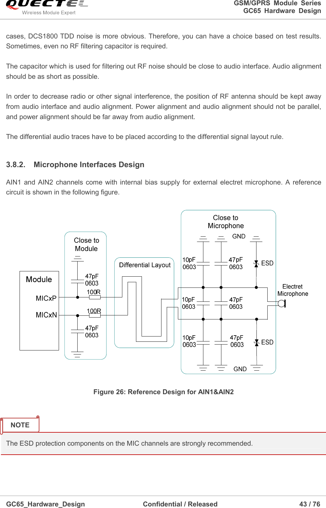
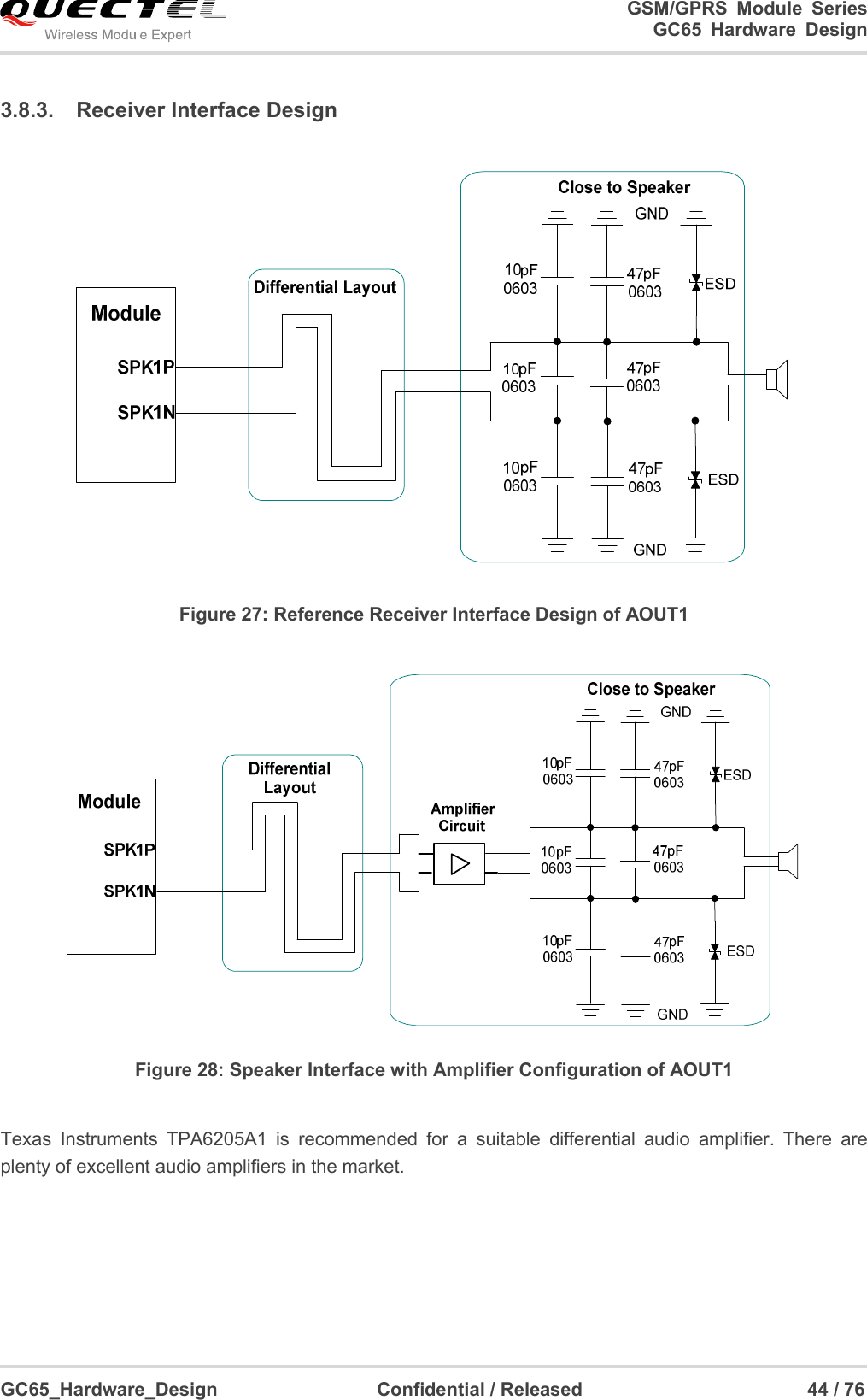
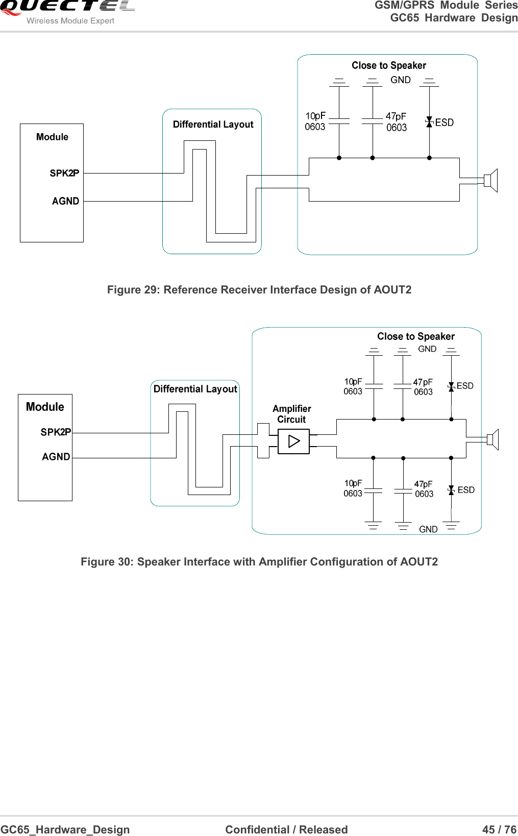
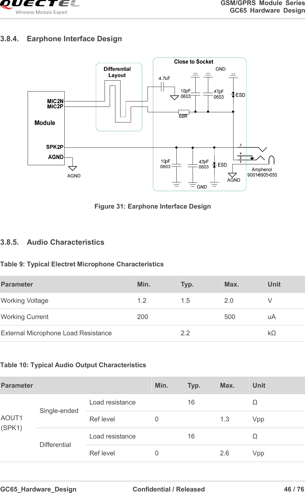
![GSM/GPRS Module Series GC65 Hardware Design GC65_Hardware_Design Confidential / Released 42 / 76 AIN1 and AIN2 can be used for input of microphone. An electret microphone is usually used. AIN1 and AIN2 are both differential input channels. AOUT1 is used for output of the receiver. This channel is typically used for a receiver built into a handset. AOUT1 channel is a differential channel. If it is used as a speaker, an amplifier should be employed. AOUT2 is used for output of earphone, which can be used as a single-ended channel. SPK2P and AGND can establish a pseudo differential mode. All of these two audio channels support voice and ringtone output, and so on, and can be switched by “AT+QAUDCH” command. For more details, please refer to the document [1]. Use AT command “AT+QAUDCH” to select audio channel: 0--AIN1/AOUT1 (main audio channel), the default value is 0. 1--AIN2/AOUT2 (auxiliary audio channel), this channel is used for earphone. For each channel, you can use AT+QMIC to adjust the input gain level of microphone. You can also use “AT+CLVL” to adjust the output gain level of receiver. “AT+QSIDET” is used to set the side-tone gain level. For more details, please refer to the document [1]. 3.8.1. Decrease TDD Noise and Other Noises The 47pF capacitor is applied for filtering out 900MHz RF interference when the module is transmitting at GSM900MHz. Without placing this capacitor, TDD noise could be heard. Moreover, the 10pF capacitor here is for filtering out 1800MHz RF interference. However, the resonant frequency point of a capacitor largely depends on the material and production technique. Therefore, you would have to discuss with its capacitor vendor to choose the most suitable capacitor for filtering out GSM850MHz, GSM900MHz, DCS1800MHz and PCS1900MHz separately. The severity degree of the RF interference in the voice channel during GSM transmitting period largely depends on the application design. In some cases, GSM900 TDD noise is more severe; while in other SPK1P 22 Channel 1 audio positive output SPK1N 21 Channel 1 audio negative output AIN2/AOUT2 MIC2P 18 Channel 2 microphone positive input MIC2N 17 Channel 2 microphone negative input SPK2P 16 Channel 2 audio single-ended output AGND 15 Form a pseudo-differential pair with SPK2P](https://usermanual.wiki/Quectel-Wireless-Solutions/201403GC65/User-Guide-2277242-Page-43.png)
![GSM/GPRS Module Series GC65 Hardware Design GC65_Hardware_Design Confidential / Released 48 / 76 please refer to document [1]. When “AT+QSIMDET=1,0” is set and the tray with SIM card is removed from SIM socket, the following URC will be presented: +CPIN: NOT INSERTED When the tray with SIM card is inserted into SIM socket again and the module finishes reinitializing SIM card, the following URC will be presented: +CPIN: READY Call Ready Figure 32: Reference Circuit for 8-pin SIM Card Holder 1. Please do not use “AT+QSIMDET=1,1” when circuit in Figure 32 is adopted, which can cause to reinitialize SIM card. 2. When SIM card detection function is used, SIM_PRESENCE pin must be pulled up by an external resistor. If unused, please keep this pin open. NOTE](https://usermanual.wiki/Quectel-Wireless-Solutions/201403GC65/User-Guide-2277242-Page-49.png)
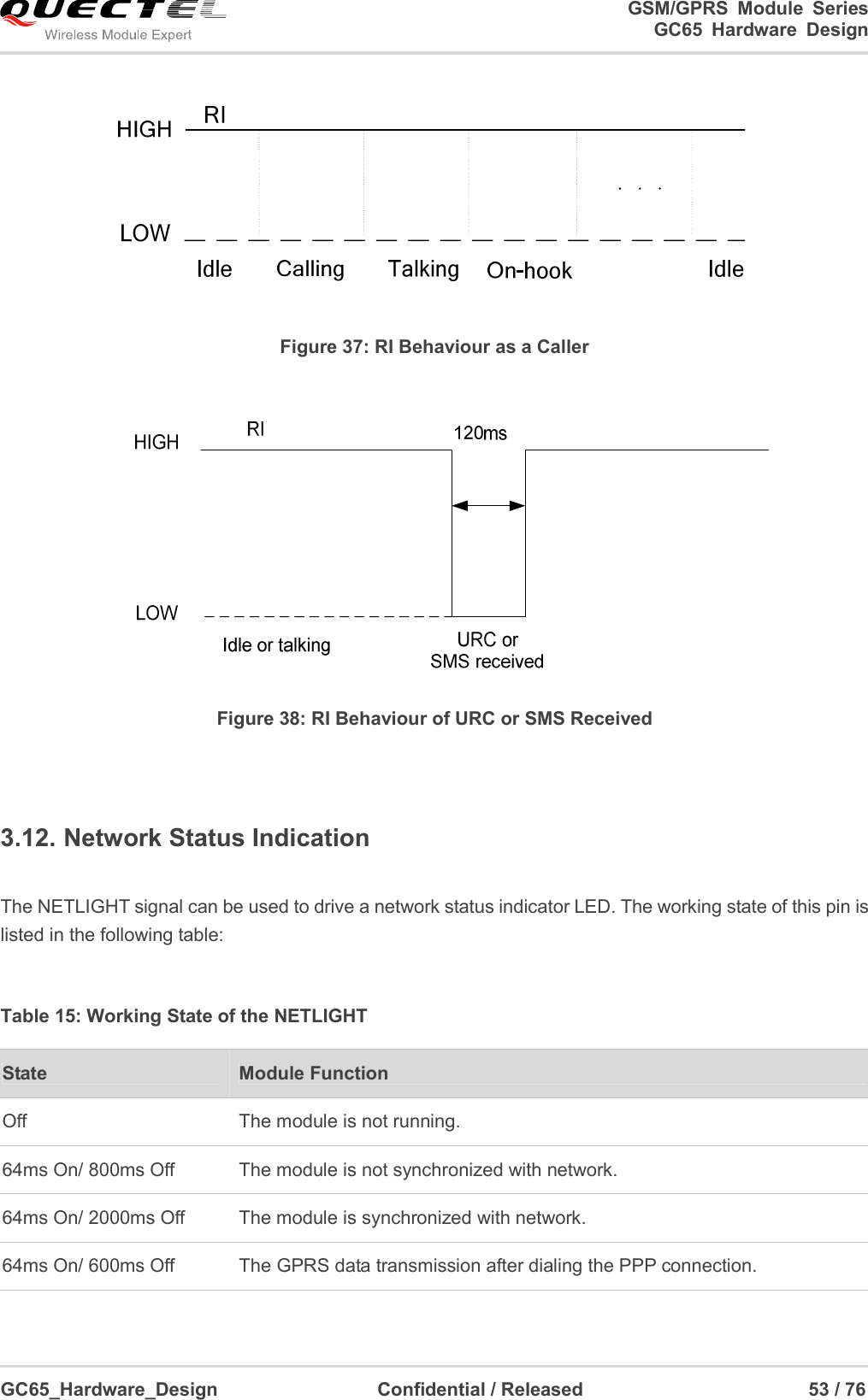
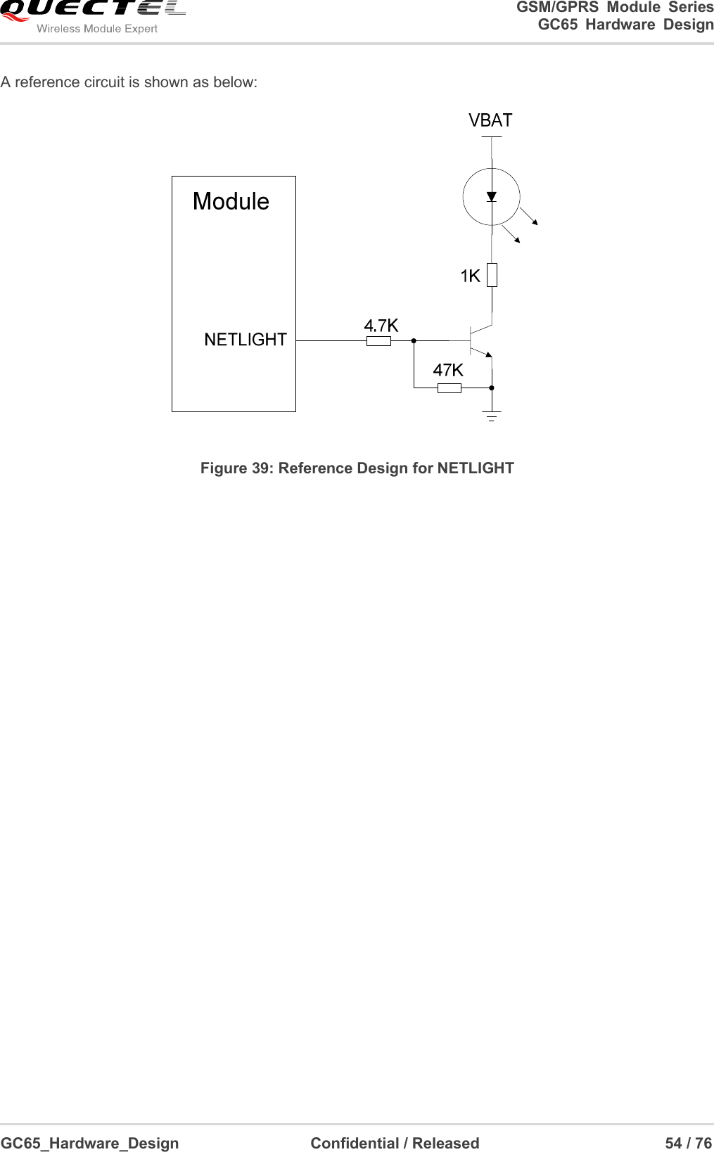
![GSM/GPRS Module Series GC65 Hardware Design GC65_Hardware_Design Confidential / Released 52 / 76 3.10. PCM Interface GC65 has reserved PCM interface, it is used as digital audio transmission between module and customer device. This interface composes PCM_CLK, PCM_SYNC, PCM_IN and PCM_OUT signal lines. PCM function is not supported at present. 3.11. Behaviors of the RI Table 14: Behaviours of the RI If the module is used as a caller, the RI would maintain high unless the URC or SMS is received. On the other hand, when it is used as a receiver, the timing of the RI is shown below: Figure 36: RI Behaviour of Voice Calling as a Receiver State RI Response Standby HIGH Voice Call Change to LOW, then: 1. Change to HIGH when call is established. 2. Use ATH to hang up the call, RI changes to HIGH. 3. Calling part hangs up, RI changes to HIGH first, and changes to LOW for 120ms indicating “NO CARRIER” as an URC, then changes to HIGH again. 4. Change to HIGH when SMS is received. SMS When a new SMS comes, the RI changes to LOW and holds low level for about 120ms, then changes to HIGH. URC Certain URCs can trigger 120ms low level on RI. For more details, please refer to the document [10].](https://usermanual.wiki/Quectel-Wireless-Solutions/201403GC65/User-Guide-2277242-Page-53.png)
![GSM/GPRS Module Series GC65 Hardware Design GC65_Hardware_Design Confidential / Released 71 / 76 8 Appendix A Reference Table 25: Related Documents SN Document Name Remark [1] GC65_AT_Commands_Manual AT commands manual [2] ITU-T Draft new recommendation V.25ter Serial asynchronous automatic dialing and control [3] GSM 07.07 Digital cellular telecommunications (Phase 2+); AT command set for GSM Mobile Equipment (ME) [4] GSM 07.10 Support GSM 07.10 multiplexing protocol [5] GSM 07.05 Digital cellular telecommunications (Phase 2+); Use of Data Terminal Equipment–Data Circuit terminating Equipment (DTE–DCE) interface for Short Message Service (SMS) and Cell Broadcast Service (CBS) [6] GSM 11.14 Digital cellular telecommunications (Phase 2+); Specification of the SIM application toolkit for the Subscriber Identity module–Mobile Equipment (SIM–ME) interface [7] GSM 11.11 Digital cellular telecommunications (Phase 2+); Specification of the Subscriber Identity module – Mobile Equipment (SIM–ME) interface [8] GSM 03.38 Digital cellular telecommunications (Phase 2+); Alphabets and language-specific information [9] GSM 11.10 Digital cellular telecommunications (Phase 2); Mobile Station (MS) conformance specification; Part 1: Conformance specification [10] GSM_UART_AN UART port application note [11] M10_EVB_UGD M10 EVB user guide [12] GSM_FW_Upgrade_AN01 GSM Firmware upgrade application note](https://usermanual.wiki/Quectel-Wireless-Solutions/201403GC65/User-Guide-2277242-Page-72.png)