Quectel Wireless Solutions 201511M85 GSM/GPRS Module User Manual
Quectel Wireless Solutions Company Limited GSM/GPRS Module
UserManual.wiki
>
Quectel Wireless Solutions
>
201511M85 User Manual
User manual
Navigation menu
Upload a User Manual
Namespaces
Wiki Guide
HTML
PDF
Info
Views
User Manual
Discussion / Help
Navigation
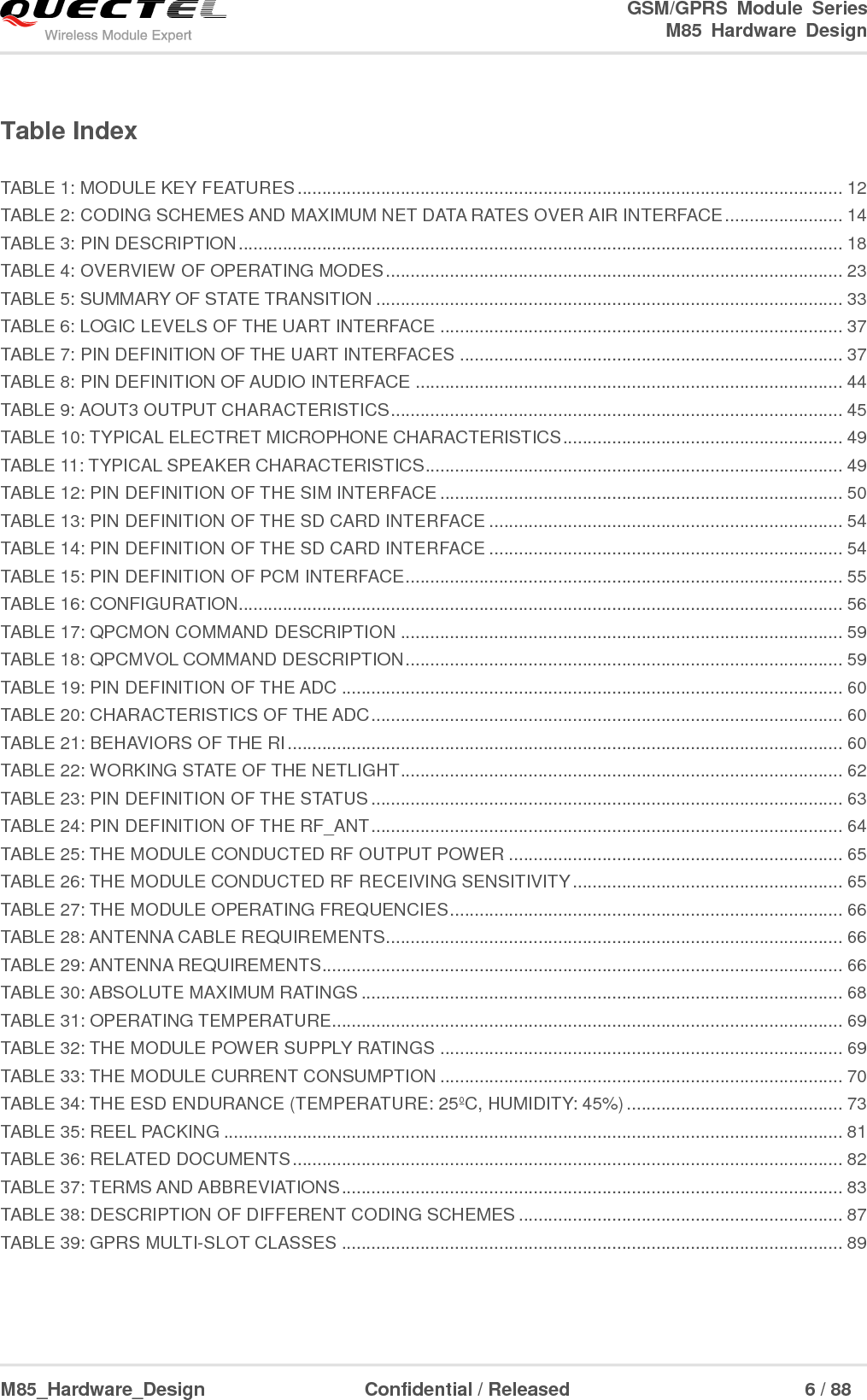
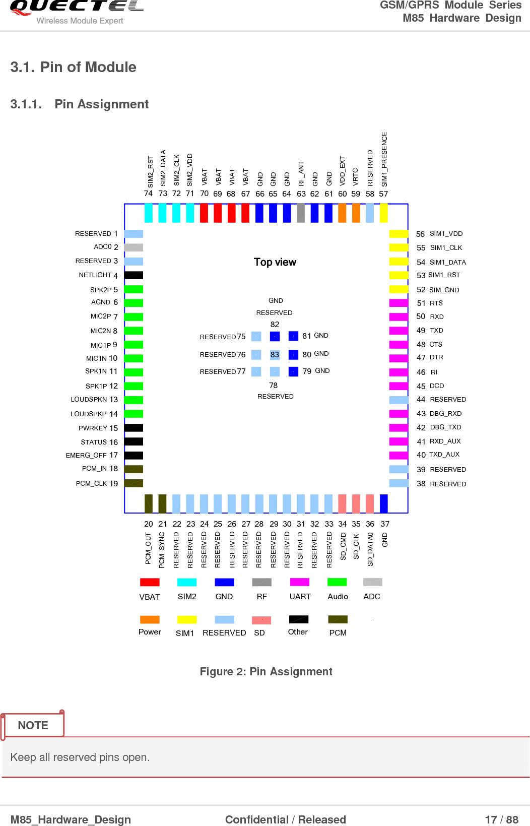
![GSM/GPRS Module Series M85 Hardware Design M85_Hardware_Design Confidential / Released 15 / 88 —RF interface BB&RFRF PAM26MHzRF TransceiverRTCGPIO&PWMSerial InterfaceSIM InterfaceRF_ANTVBATPWRKEYEMERG_OFFVRTCGPIO&Status&NetlightUARTSIM Interfaces ResetESDPMUMEMORY Audio AudioPCM Interface PCM Serial FlashSD InterfaceSDADC ADC Figure 1: Module Functional Diagram 2.5. Evaluation Board In order to help customer to develop applications with M85, Quectel supplies an evaluation board (EVB), RS-232 to USB cable, power adapter, earphone, antenna and other peripherals to control or test the module. For details, please refer to the document [12].](https://usermanual.wiki/Quectel-Wireless-Solutions/201511M85/User-Guide-2841938-Page-16.png)
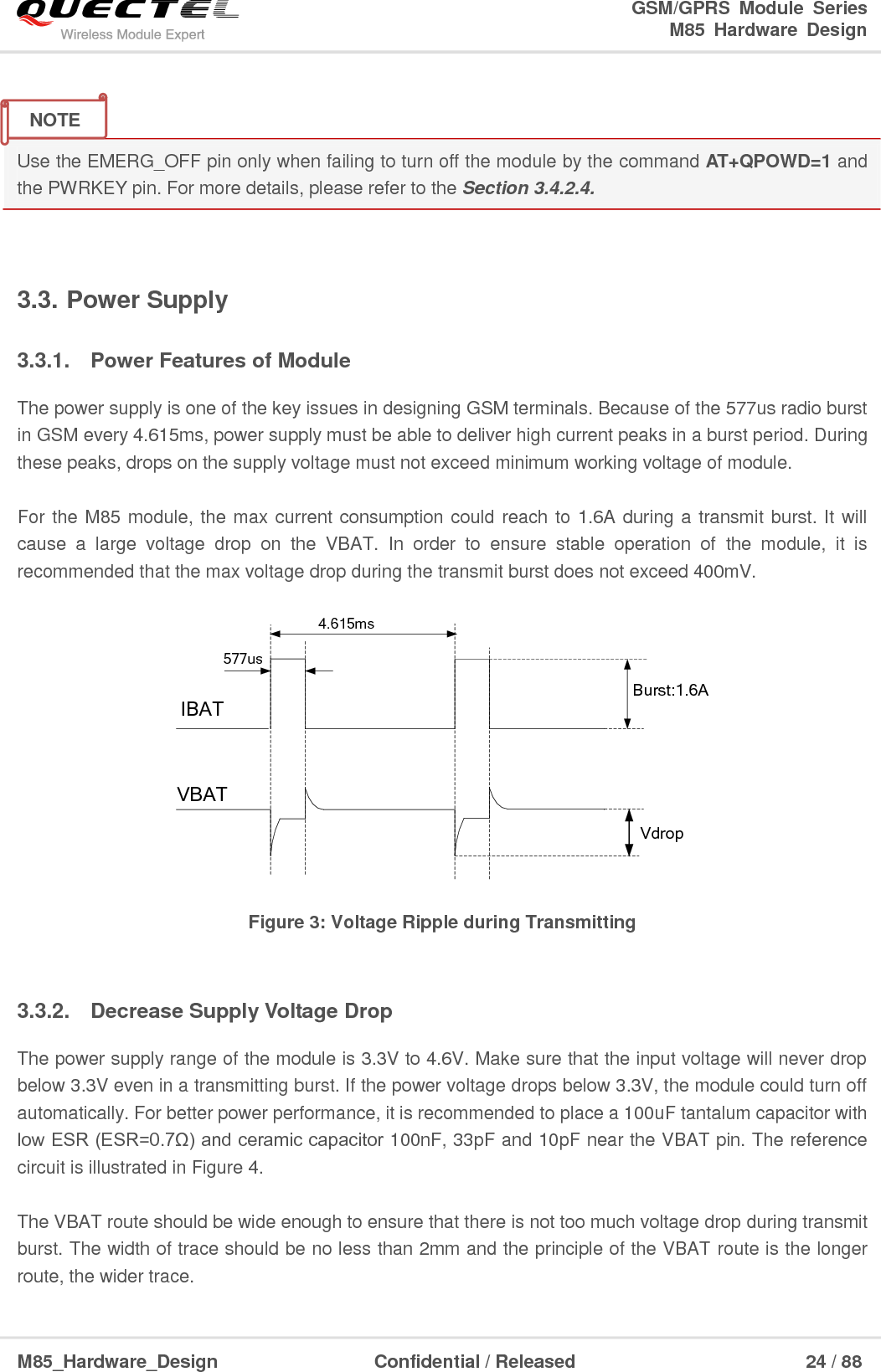
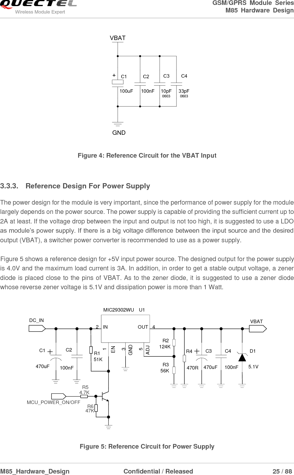
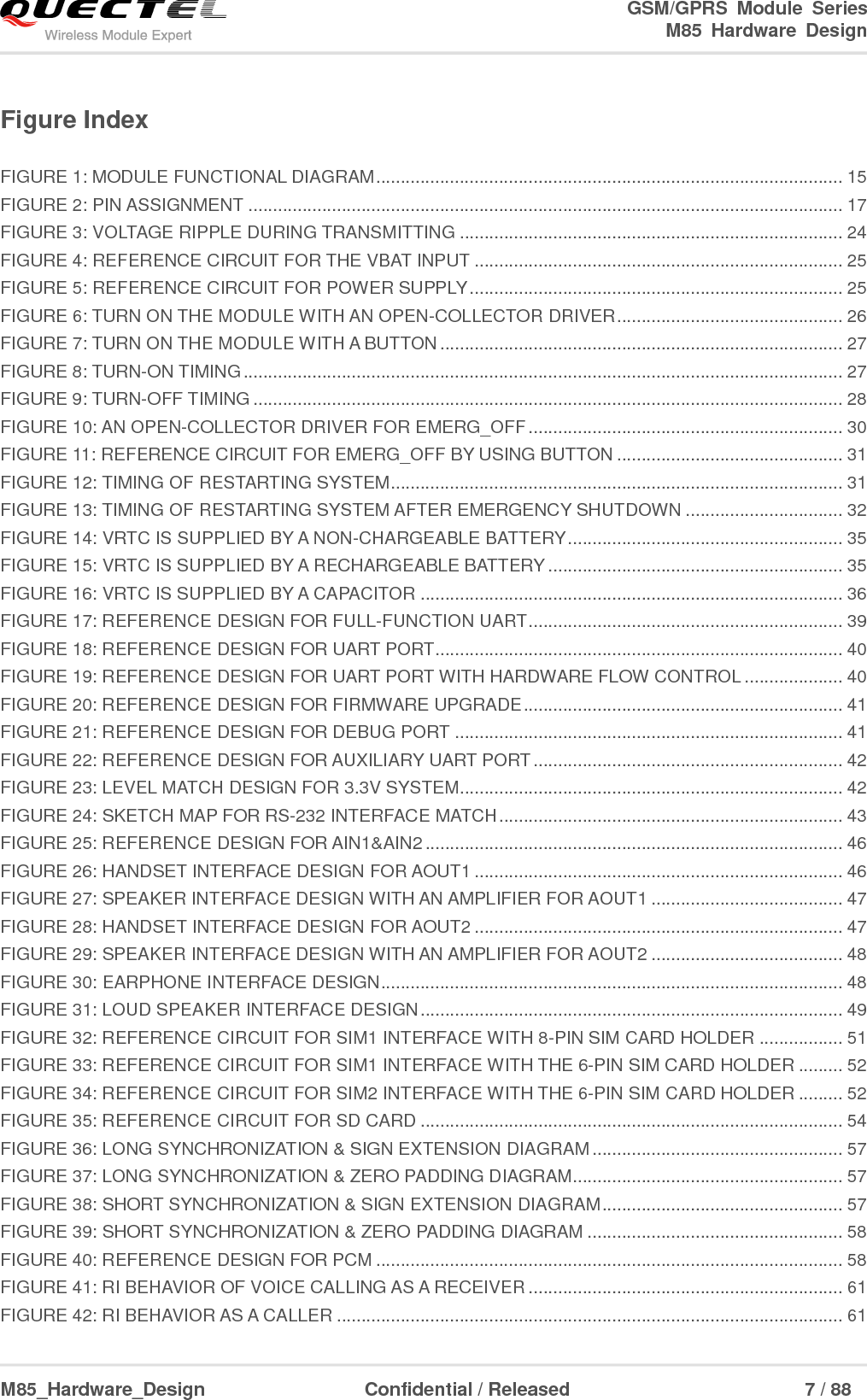
![GSM/GPRS Module Series M85 Hardware Design M85_Hardware_Design Confidential / Released 26 / 88 It is suggested to control the module’s main power supply (VBAT) via LDO enable pin to restart the module when the module has become abnormal. Power switch circuit like P-channel MOSFET switch circuit can also be used to control VBAT. 3.3.4. Monitor Power Supply The command AT+CBC can be used to monitor the supply voltage of the module. The unit of the displayed voltage is mV. For details, please refer to the document [1]. 3.4. Power On and Down Scenarios 3.4.1. Power On The module can be turned on by driving the pin PWRKEY to a low level voltage. An open collector driver circuit is suggested to control the PWRKEY. A simple reference circuit is illustrated as below. Turn on pulsePWRKEY4.7K47K Figure 6: Turn on the Module with an Open-collector Driver 1. M85 module is set to autobauding mode (AT+IPR=0) by default. In the autobauding mode, URC ―RDY‖ is not reported to the host controller after module is powered on. When the module is powered on after a delay of 4 or 5 seconds, it can receive AT command. Host controller should first send an AT string in order that the module can detect baud rate of host controller, and it should continue to send the next AT string until receiving OK string from the module. Then enter AT+IPR=x;&W to set a fixed baud rate for the module and save the configuration to flash memory of the module. After these NOTES NOTE](https://usermanual.wiki/Quectel-Wireless-Solutions/201511M85/User-Guide-2841938-Page-27.png)
![GSM/GPRS Module Series M85 Hardware Design M85_Hardware_Design Confidential / Released 27 / 88 configurations, the URC RDY would be received from the UART Port of the module every time when the module is powered on. For more details, refer to the section AT+IPR in document [1]. 2. AT command response indicates module is turned on successfully, or else the module fails to be turned on. The other way to control the PWRKEY is through a button directly. A TVS component is indispensable to be placed nearby the button for ESD protection. For the best performance, the TVS component must be placed nearby the button. When pressing the key, electrostatic strike may generate from finger. A reference circuit is shown in the following figure. PWRKEYK1Close to K1TVS Figure 7: Turn on the Module with a Button The turn-on timing is illustrated as the following figure. VDD_EXT(OUTPUT)VIL<0.1*VBATVIH > 0.6*VBATVBATPWRKEY(INPUT)EMERG_OFF(INPUT)54msSTATUS(OUTPUT)800ms>1sOFF BOOTINGMODULE STATUS RUNNINGT1 Figure 8: Turn-on Timing](https://usermanual.wiki/Quectel-Wireless-Solutions/201511M85/User-Guide-2841938-Page-28.png)
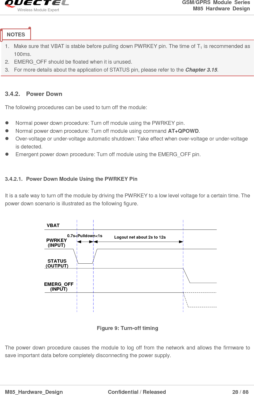
![GSM/GPRS Module Series M85 Hardware Design M85_Hardware_Design Confidential / Released 29 / 88 Before the completion of the power down procedure, module sends out the result code shown as below: NORMAL POWER DOWN After that moment, no further AT commands can be executed. Then the module enters the power down mode, only the RTC is still active. The power down mode can also be indicated by the STATUS pin, which is a low level voltage in this mode. 1. This unsolicited result codes do not appear when autobauding is active and DTE and DCE are not correctly synchronized after start-up. The module is recommended to set to a fixed baud rate. 2. As logout network time is related to the local mobile network, it is recommended to delay about 12 seconds before disconnecting the power supply or restarting the module. 3. For more details about the application of STATUS pin, please refer to the Chapter 3.15. 3.4.2.2. Power Down Module Using AT Command It is also a safe way to turn off the module via AT command AT+QPOWD=1. This command will let the module to log off from the network and allow the firmware to save important data before completely disconnecting the power supply. Before the completion of the power down procedure, module sends out the result code shown as below: NORMAL POWER DOWN After that moment, no further AT commands can be executed. And then the module enters the power down mode, only the RTC is still active. Please refer to the document [1] for details about the AT command AT+QPOWD. 3.4.2.3. Over-voltage or Under-voltage Automatic Shutdown The module will constantly monitor the voltage applied on the VBAT, if the voltage is ≤3.5V, the following URC will be presented: UNDER_VOLTAGE WARNING If the voltage is ≥4.5V, the following URC will be presented: OVER_VOLTAGE WARNING NOTES](https://usermanual.wiki/Quectel-Wireless-Solutions/201511M85/User-Guide-2841938-Page-30.png)
![GSM/GPRS Module Series M85 Hardware Design M85_Hardware_Design Confidential / Released 33 / 88 If the module has been set by the command with AT+CFUN=4, the RF function will be disabled, but the UART port is still active. In this case, all AT commands related with RF function will be not available. After the module is set by AT+CFUN=0 or AT+CFUN=4, it can return to full functionality by AT+CFUN=1. For detailed information about AT+CFUN, please refer to the document [1]. 3.5.2. SLEEP Mode The SLEEP mode is disabled by default. You can enable it by AT+QSCLK=1. On the other hand, the default setting is AT+QSCLK=0 and in this mode, the module cannot enter SLEEP mode. When the module is set by the command with AT+QSCLK=1, you can control the module to enter or exit from the SLEEP mode through pin DTR. When DTR is set to high level, and there is no on-air or hardware interrupt such as GPIO interrupt or data on UART port, the module will enter SLEEP mode automatically. In this mode, the module can still receive voice, SMS or GPRS paging from network, but the UART port does not work. 3.5.3. Wake up Module from SLEEP Mode When the module is in the SLEEP mode, the following methods can wake up the module. If the DTR Pin is set low, it would wake up the module from the SLEEP mode. The UART port will be active within 20ms after DTR is changed to low level. Receive a voice or GPRS data from network wakes up module. Receive an SMS from network wakes up module. DTR pin should be held at low level during communication between the module and DTE. 3.5.4. Summary of State Transition Table 5: Summary of State Transition Current Mode Next Mode Power Down Normal Mode Sleep Mode Power Down Use PWRKEY NOTE](https://usermanual.wiki/Quectel-Wireless-Solutions/201511M85/User-Guide-2841938-Page-34.png)
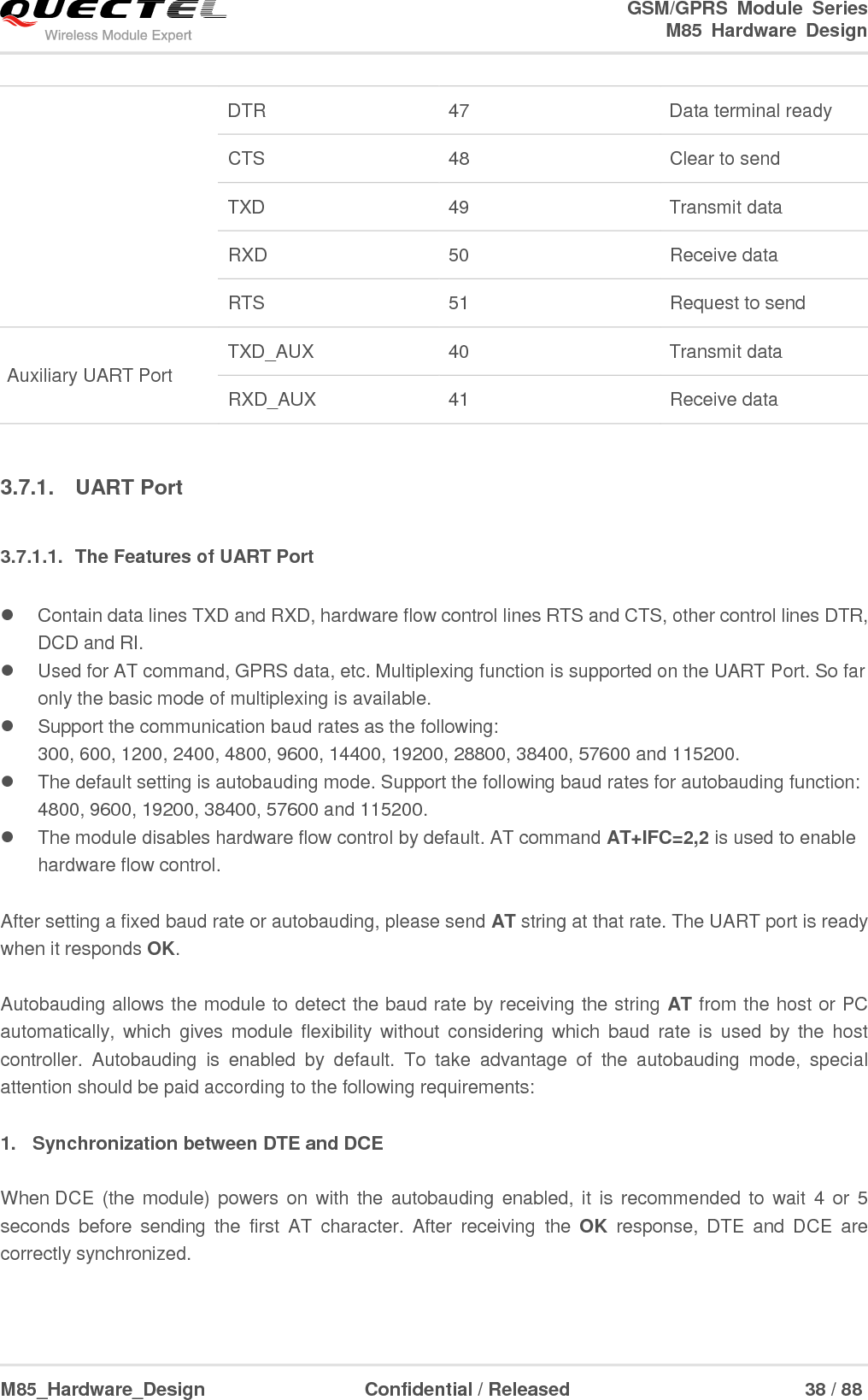
![GSM/GPRS Module Series M85 Hardware Design M85_Hardware_Design Confidential / Released 37 / 88 Hardware flow control is disabled by default. When hardware flow control is required, RTS and CTS should be connected to the host. AT command AT+IFC=2,2 is used to enable hardware flow control. AT command AT+IFC=0,0 is used to disable the hardware flow control. For more details, please refer to the document [1]. The Debug Port: DBG_TXD: Send data to the COM port of computer. DBG_RXD: Receive data from the COM port of computer. The Auxiliary UART Port: TXD_AUX: Send data to the RXD of DTE. RXD_AUX: Receive data from the TXD of DTE. The logic levels are described in the following table. Table 6: Logic Levels of the UART Interface Table 7: Pin Definition of the UART Interfaces Parameter Min. Max. Unit VIL 0 0.25×VDD_EXT V VIH 0.75×VDD_EXT VDD_EXT +0.2 V VOL 0 0.15×VDD_EXT V VOH 0.85×VDD_EXT VDD_EXT V Interface Pin Name Pin No. Description Debug Port DBG_RXD 43 Receive data DBG_TXD 42 Transmit data UART Port DCD 45 Data carrier detection RI 46 Ring indication NOTE](https://usermanual.wiki/Quectel-Wireless-Solutions/201511M85/User-Guide-2841938-Page-38.png)
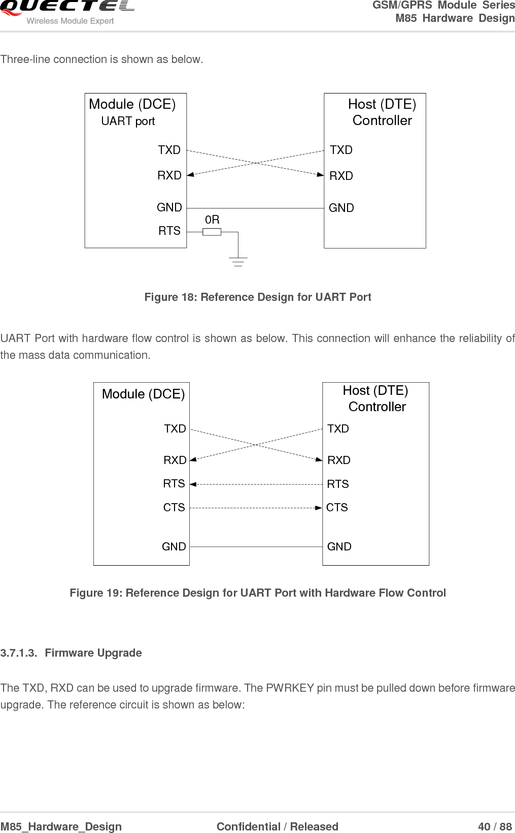
![GSM/GPRS Module Series M85 Hardware Design M85_Hardware_Design Confidential / Released 39 / 88 If the host controller needs URC in the mode of autobauding, it must be synchronized firstly. Otherwise the URC will be discarded. 2. Restrictions on autobauding operation The UART port has to be operated at 8 data bits, no parity and 1 stop bit (factory setting). Only the strings ―AT‖ or ―at‖ can be detected (neither ―At‖ nor ―aT‖). The Unsolicited Result Codes like ―RDY‖, ―+CFUN: 1‖ and ―+CPIN: READY‖ will not be indicated when the module is turned on with autobauding enabled and not be synchronized. Any other Unsolicited Result Codes will be sent at the previous baud rate before the module detects the new baud rate by receiving the first AT string. The DTE may receive unknown characters after switching to new baud rate. It is not recommended to switch to autobauding from a fixed baud rate. If autobauding is active it is not recommended to switch to multiplex mode. To assure reliable communication and avoid any problems caused by undetermined baud rate between DCE and DTE, it is strongly recommended to configure a fixed baud rate and save it instead of using autobauding after start-up. For more details, please refer to the Section AT+IPR in document [1]. 3.7.1.2. The Connection of UART Port The connection between module and host using UART Port is very flexible. Three connection styles are illustrated as below. Reference design for Full-Function UART connection is shown as below when it is applied in modulation-demodulation. TXDRXDRTSCTSDTRDCDRITXDRXDRTSCTSDTRDCDRINGModule (DCE)Serial portUART portGND GNDPC (DTE) Figure 17: Reference Design for Full-Function UART NOTE](https://usermanual.wiki/Quectel-Wireless-Solutions/201511M85/User-Guide-2841938-Page-40.png)
![GSM/GPRS Module Series M85 Hardware Design M85_Hardware_Design Confidential / Released 42 / 88 3.7.3. Auxiliary UART Port Two data lines: TXD_AUX and RXD_AUX. Auxiliary UART port is used for AT command only and does not support GPRS data, multiplexing function etc. Auxiliary UART port supports the communication baud rates as the following: 1200, 2400, 4800, 9600, 14400, 19200, 28800, 38400, 57600, 115200bps. Auxiliary UART port could be used when you send AT+QEAUART=1 string on the UART port. The default baud rate setting is 115200bps, and does not support autobauding. The baud rate can be modified by AT+QSEDCB command. For more details, please refer to the document [1]. PeripheralTXDRXDGND Module TXD_AUXRXD_AUX GND Figure 22: Reference Design for Auxiliary UART Port 3.7.4. UART Application The reference design of 3.3V level match is shown as below. If the host is a 3V system, please change the 5.6K resistor to 10K. Peripheral/TXD/RXD1KTXDRXDRTSCTSDTRRI/RTS/CTSGPIOEINTGPIO DCDModule1K1KVoltage level:3.3V5.6K5.6K5.6K1K1K1K1KGND GND Figure 23: Level Match Design for 3.3V System](https://usermanual.wiki/Quectel-Wireless-Solutions/201511M85/User-Guide-2841938-Page-43.png)
![GSM/GPRS Module Series M85 Hardware Design M85_Hardware_Design Confidential / Released 43 / 88 It is highly recommended to add the resistor divider circuit on the UART signal lines when the host’s level is 3V or 3.3V. For the higher voltage level system, a level shifter IC could be used between the host and the module. For more details about UART circuit design, please refer to document [11]. The following figure shows a sketch map between module and standard RS-232 interface. Since the electrical level of module is 2.8V, so a RS-232 level shifter must be used. Note that you should assure the IO voltage of level shifter which connects to module is 2.8V. TXDRXDRTSCTSDTRRIDCDModuleGNDC1+C1-C2+C2-V+VCCGNDV-3.3VT1INT2INT3INT4INR1INR2INR3INR1OUTR2OUTR3OUTT1OUTT2OUTT5OUTT3OUTT4OUTT5INGNDGND/R1OUT123456789GNDTo PC Serial PortGND1K1K1K1K1K5.6K5.6K1K1K5.6KRS-232 Level Shifter Figure 24: Sketch Map for RS-232 Interface Match Please visit vendor website to select the suitable RS-232 level shifter IC, such as: http://www.exar.com/ and http://www.maximintegrated.com. NOTE](https://usermanual.wiki/Quectel-Wireless-Solutions/201511M85/User-Guide-2841938-Page-44.png)
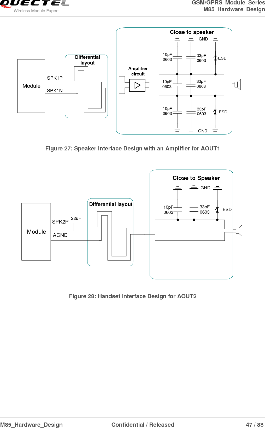
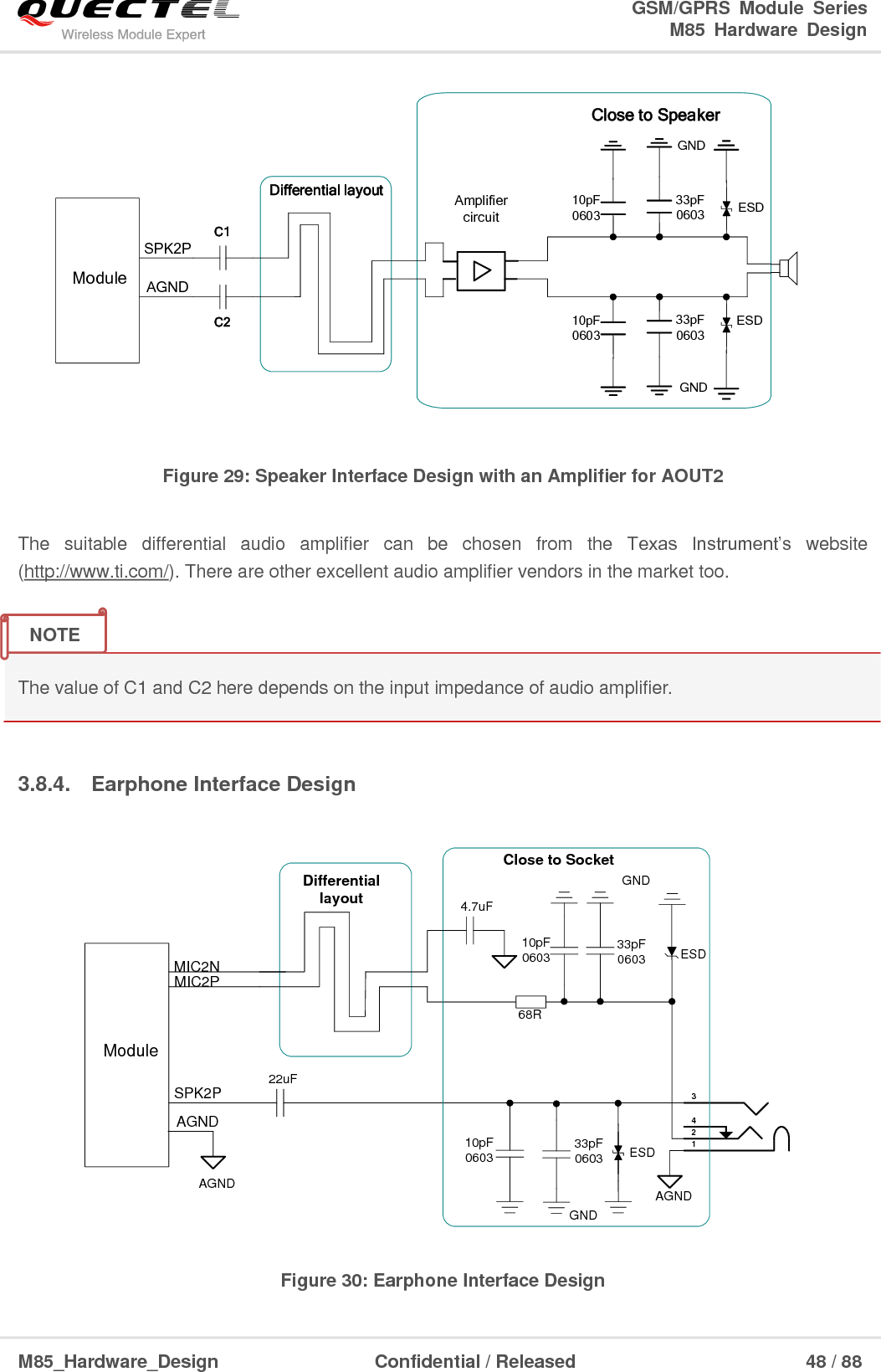
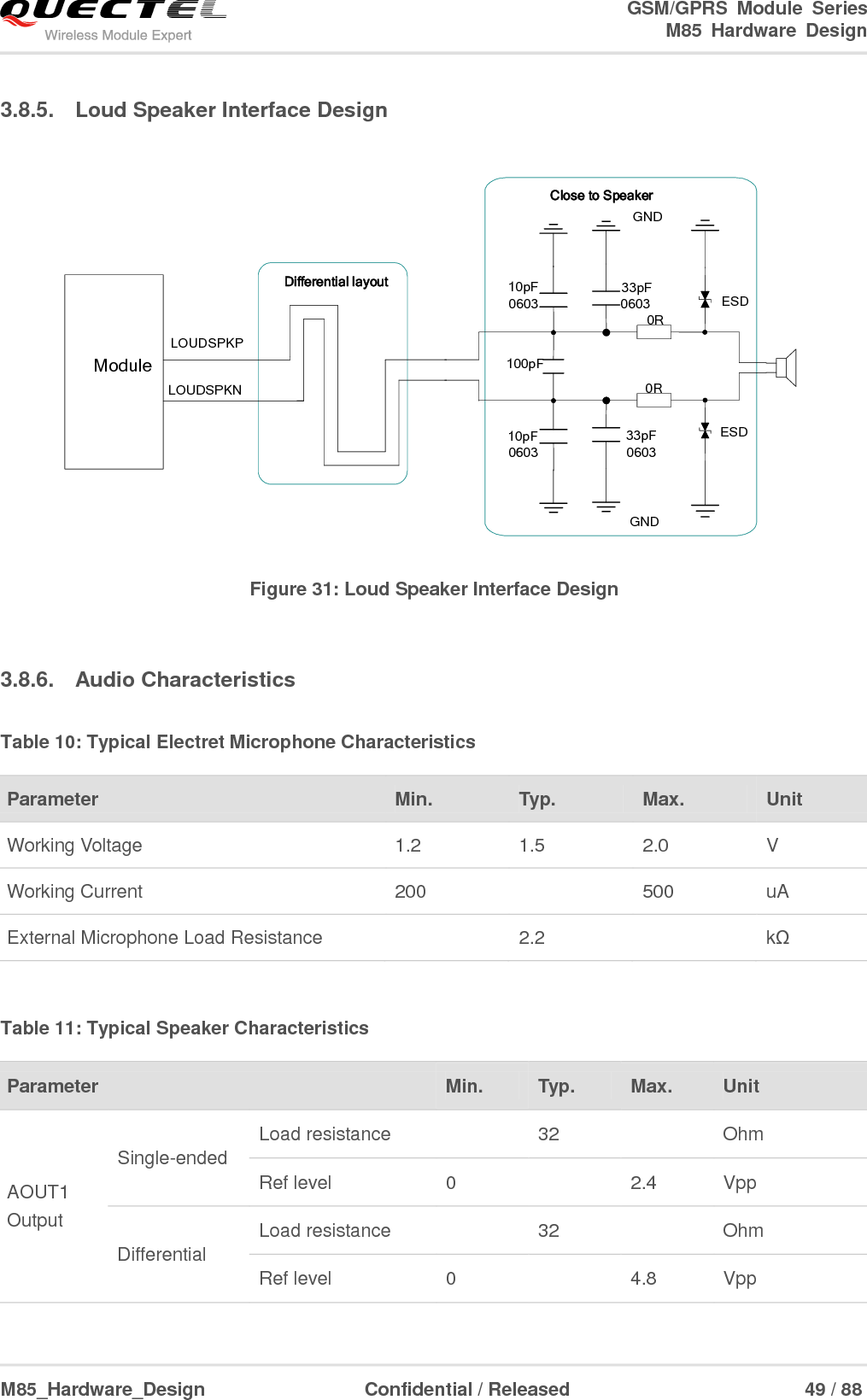
![GSM/GPRS Module Series M85 Hardware Design M85_Hardware_Design Confidential / Released 44 / 88 3.8. Audio Interfaces The module provides two analogy input channels and three analogy output channels. Table 8: Pin Definition of Audio Interface AIN1 and AIN2 can be used for input of microphone and line. An electret microphone is usually used. AIN1 and AIN2 are both differential input channels. AOUT1 is used for output of the receiver. This channel is typically used for a receiver built into a handset. AOUT1 channel is a differential channel. AOUT2 is typically used with earphone. It is a single-ended and mono channel. SPK2P and AGND can establish a pseudo differential mode. AOUT2 can also be used for output of receiver, which can be used as a single-ended channel. SPK2P and AGND can establish a pseudo differential mode. AOUT3 is used for loud speaker output as it embedded an amplifier of class AB whose maximum drive power is 870mW. All of these three audio channels support voice and ringtone output, and so on, and can be switched by AT+QAUDCH command. For more details, please refer to the document [1]. Interface Pin Name Pin No. Description AIN1/AOUT1 MIC1P 9 Channel 1 Microphone positive input MIC1N 10 Channel 1 Microphone negative input SPK1P 12 Channel 1 Audio positive output SPK1N 11 Channel 1 Audio negative output AIN2/AOUT2 MIC2P 7 Channel 2 Microphone positive input MIC2N 8 Channel 2 Microphone negative input SPK2P 5 Channel 2 Audio positive output AGND 6 Form a pseudo-differential pair with SPK2P AOUT3 LOUDSPKP 14 Channel 3 Audio positive output LOUDSPKN 13 Channel 3 Audio negative output](https://usermanual.wiki/Quectel-Wireless-Solutions/201511M85/User-Guide-2841938-Page-45.png)
![GSM/GPRS Module Series M85 Hardware Design M85_Hardware_Design Confidential / Released 45 / 88 Use AT command AT+QAUDCH to select audio channel: 0--AIN1/AOUT1, the default value is 0. 1--AIN2/AOUT2 2--AIN2/AOUT3 For each channel, you can use AT+QMIC to adjust the input gain level of microphone. Customer can also use AT+CLVL to adjust the output gain level of receiver and speaker. AT+QSIDET is used to set the side-tone gain level. For more details, please refer to the document [1]. Table 9: AOUT3 Output Characteristics 3.8.1. Decrease TDD Noise and Other Noise The 33pF capacitor is applied for filtering out 900MHz RF interference when the module is transmitting at EGSM900MHz. Without placing this capacitor, TDD noise could be heard. Moreover, the 10pF capacitor here is for filtering out 1800MHz RF interference. However, the resonant frequency point of a capacitor largely depends on the material and production technique. Therefore, you would have to discuss with its capacitor vendor to choose the most suitable capacitor for filtering out GSM850MHz, EGSM900MHz, DCS1800MHz and PCS1900MHz separately. The severity degree of the RF interference in the voice channel during GSM transmitting period largely depends on the application design. In some cases, GSM900 TDD noise is more severe; while in other cases, DCS1800 TDD noise is more obvious. Therefore, you can have a choice based on test results. Sometimes, even no RF filtering capacitor is required. The capacitor which is used for filtering out RF noise should be close to audio interface. Audio alignment should be as short as possible. In order to decrease radio or other signal interference, the position of RF antenna should be kept away from audio interface and audio alignment. Power alignment and audio alignment should not be parallel, and power alignment should be far away from audio alignment. The differential audio traces have to be placed according to the differential signal layout rule. Item Condition Min. Type Max. Unit RMS Power 8ohm load VBAT=4.2V THD+N=1% 870 mW 8ohm load VBAT=3.3V THD+N=1% 530 mW](https://usermanual.wiki/Quectel-Wireless-Solutions/201511M85/User-Guide-2841938-Page-46.png)
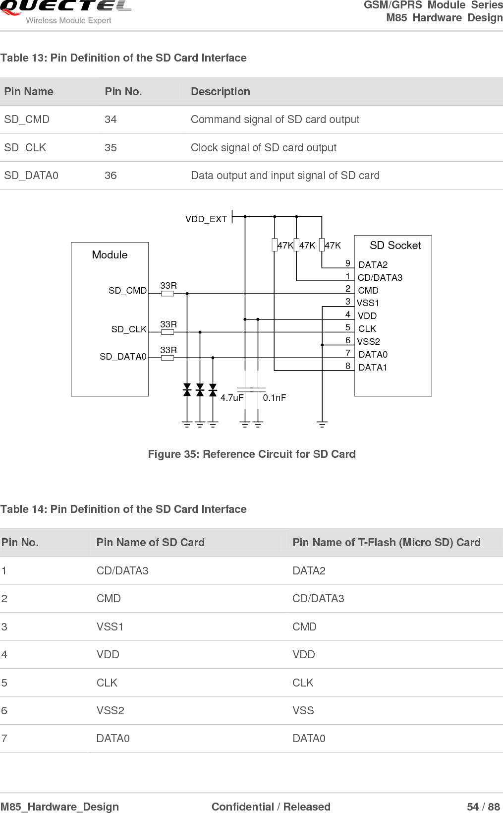
![GSM/GPRS Module Series M85 Hardware Design M85_Hardware_Design Confidential / Released 50 / 88 3.9. SIM Card Interfaces The module contains two SIM interfaces to allow module access the two SIM cards. Only one SIM card can work at a time. Both of two SIM interfaces share the ground and only first SIM interface have card insert detection. In dual SIM card mode, configure AT+QDSIM=0 to use the SIM1 interface and configure AT+QDSIM=1 to use SIM2 interface. For more details, please refer to the document [1]. The SIM interface supports the functionality of the GSM Phase 1 specification and also supports the functionality of the new GSM Phase 2+ specification for FAST 64 kbps SIM card, which is intended for use with a SIM application Tool-kit. The SIM interface is powered by an internal regulator in the module. Both 1.8V and 3.0V SIM Cards are supported. Table 12: Pin Definition of the SIM Interface AOUT2 Output Single-ended Load resistance 32 Ohm Ref level 0 2.4 Vpp AOUT3 Output Differential Load resistance 8 Ohm Ref level 0 2×VBAT Vpp Pin Name Pin No. Description SIM1_VDD 56 Supply power for SIM card. Automatic detection of SIM card voltage. 3.0V±10% and 1.8V±10%. Maximum supply current is around 10mA. SIM2_VDD 71 SIM1_CLK 55 SIM card clock SIM2_CLK 72 SIM1_DATA 54 SIM card data I/O SIM2_DATA 73 SIM1_RST 53 SIM card reset SIM2_RST 74](https://usermanual.wiki/Quectel-Wireless-Solutions/201511M85/User-Guide-2841938-Page-51.png)
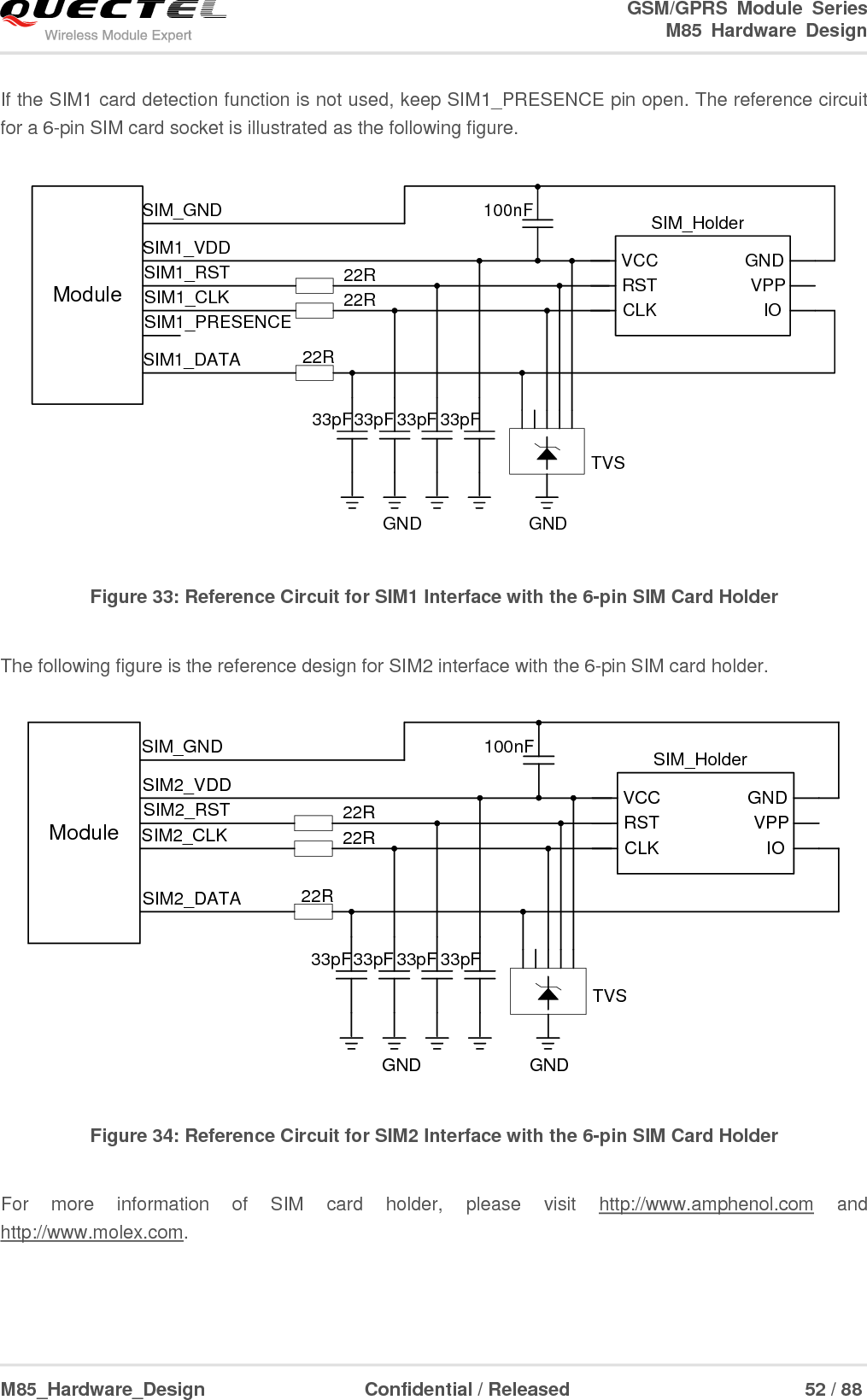
![GSM/GPRS Module Series M85 Hardware Design M85_Hardware_Design Confidential / Released 51 / 88 The following figure is the reference design for SIM interface, and here an 8-pin SIM card holder is used. The pin SIM1_PRESENCE is used to detect whether the tray of the Molex SIM socket, which is used for holding SIM card, is present in the card socket. When the tray is inserted in the socket, SIM1_PRESENCE is at low level. Regardless of the SIM card is in the tray or not, the change of SIM1_PRESENCE level from high to low level prompts the module to reinitialize SIM card. In default configuration, SIM card detection function is disabled. Your application can use AT+QSIMDET=1,0 and AT+QSIMDET=0,0 to switch on and off the SIM card detection function. For details of this AT command, please refer to document [1]. When AT+QSIMDET=1,0 is set and the tray with SIM card is removed from SIM socket, the following URC will be presented: +CPIN: NOT INSERTED When the tray with SIM card is inserted into SIM socket again and the module finishes reinitializing SIM card, the following URC will be presented: +CPIN: READY Call Ready VDD_EXTModuleSIM1_VDDSIM_GNDSIM1_RSTSIM1_CLKSIM1_DATASIM1_PRESENCE22R22R22R10K100nF SIM_HolderGNDGNDTVS33pF33pF 33pF33pFVCCRSTCLK IOVPPGNDGND Figure 32: Reference Circuit for SIM1 Interface with 8-pin SIM Card Holder SIM1_PRESENCE 57 SIM1 card detection SIM_GND 52 SIM card ground](https://usermanual.wiki/Quectel-Wireless-Solutions/201511M85/User-Guide-2841938-Page-52.png)
![GSM/GPRS Module Series M85 Hardware Design M85_Hardware_Design Confidential / Released 59 / 88 Table 17: QPCMON Command Description AT+QPCMVOL can configure the volume of input and output. AT+QPCMVOL=vol_pcm_in, vol_pcm_out Table 18: QPCMVOL Command Description 3.12. ADC The module provides an ADC channel to measure the value of voltage. Please give priority to the use of ADC0 channel. The command AT+QADC can read the voltage value applied on ADC0 pin. For details of this AT command, please refer to the document [1]. In order to improve the accuracy of ADC, the layout of ADC should be surrounded by ground. Parameter Scope Description Mode 0~2 0: Close PCM 1: Open PCM 2: Open PCM when audio talk is set up Sync_Type 0~1 0: Short synchronization 1: Long synchronization Sync_Length 1~8 Programmed from one bit to eight bit SignExtension 0~1 0: Zero padding 1: Sign extension MSBFirst 0~1 0: MSB first 1: Not supported Parameter Scope Description vol_pcm_in 0~32767 Set the input volume vol_pcm_out 0~32767 Set the output volume The voice may be distorted when this value exceeds 16384.](https://usermanual.wiki/Quectel-Wireless-Solutions/201511M85/User-Guide-2841938-Page-60.png)
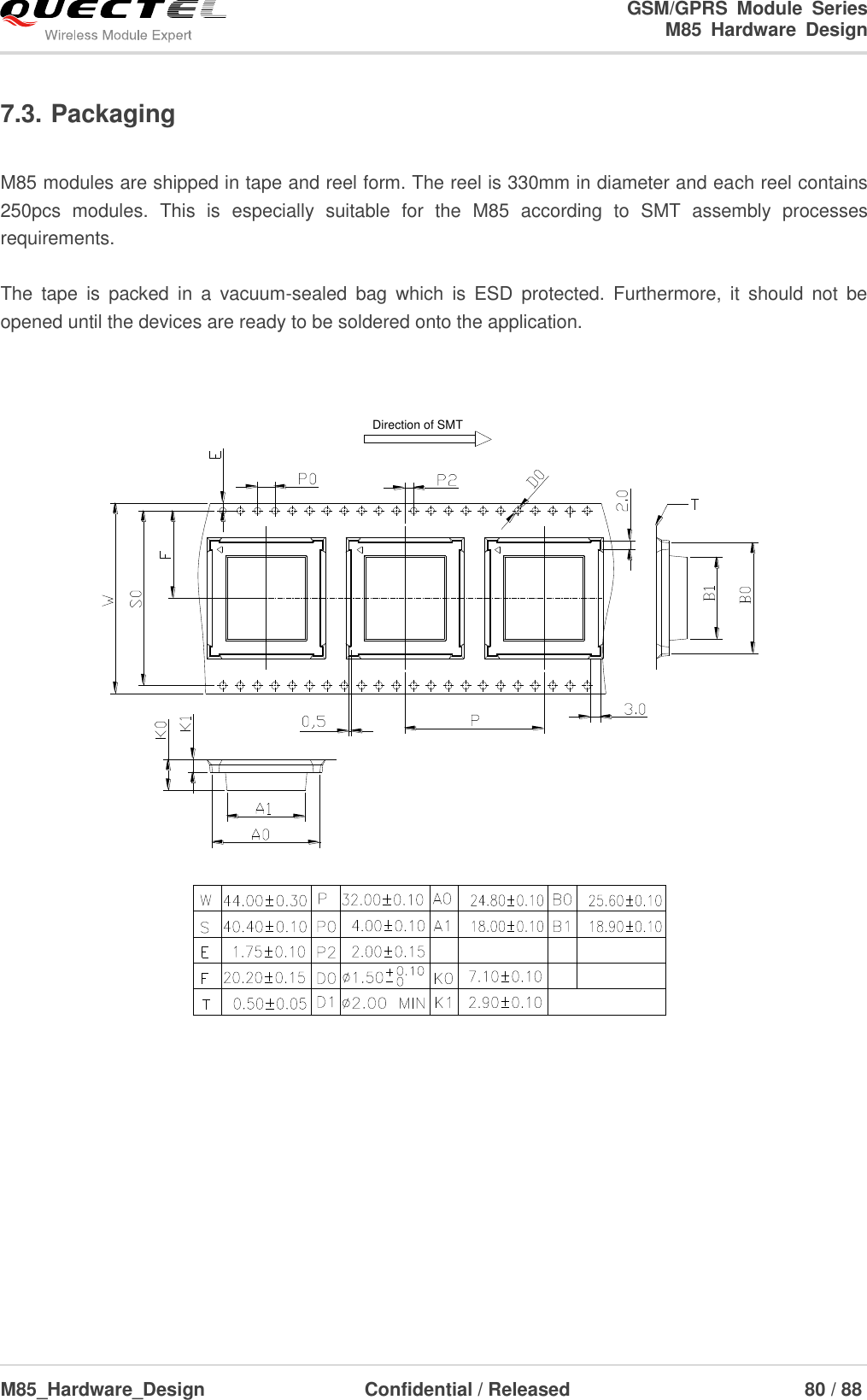
![GSM/GPRS Module Series M85 Hardware Design M85_Hardware_Design Confidential / Released 79 / 88 7.2. Soldering The squeegee should push the paste on the surface of the stencil that makes the paste fill the stencil openings and penetrate to the PCB. The force on the squeegee should be adjusted so as to produce a clean stencil surface on a single pass. To ensure the module soldering quality, the thickness of stencil at the hole of the module pads should be 0.2 mm for M85. For more details, please refer to document [13]. It is suggested that peak reflow temperature is from 235ºC to 245ºC (for SnAg3.0Cu0.5 alloy). Absolute max reflow temperature is 260ºC. To avoid damage to the module when it was repeatedly heated, it is suggested that the module should be mounted after the first panel has been reflowed. The following picture is the actual diagram which we have operated. Time(s)50 100 150 200 250 30050100150200250 160℃ 200℃217070s~120s40s~60sBetween 1~3℃/SPreheat Heating Cooling℃sLiquids Temperature Figure 54: Ramp-Soak-Spike Reflow Profile](https://usermanual.wiki/Quectel-Wireless-Solutions/201511M85/User-Guide-2841938-Page-80.png)
![GSM/GPRS Module Series M85 Hardware Design M85_Hardware_Design Confidential / Released 82 / 88 8 Appendix A Reference Table 36: Related Documents SN Document Name Remark [1] Quectel_M85_AT_Commands_Manual AT commands manual [2] ITU-T Draft new recommendation V.25ter Serial asynchronous automatic dialing and control [3] GSM 07.07 Digital cellular telecommunications (Phase 2+); AT command set for GSM Mobile Equipment (ME) [4] GSM 07.10 Support GSM 07.10 multiplexing protocol [5] GSM 07.05 Digital cellular telecommunications (Phase 2+); Use of Data Terminal Equipment – Data Circuit terminating Equipment (DTE – DCE) interface for Short Message Service (SMS) and Cell Broadcast Service (CBS) [6] GSM 11.14 Digital cellular telecommunications (Phase 2+); Specification of the SIM Application Toolkit for the Subscriber Identity module – Mobile Equipment (SIM – ME) interface [7] GSM 11.11 Digital cellular telecommunications (Phase 2+); Specification of the Subscriber Identity module – Mobile Equipment (SIM – ME) interface [8] GSM 03.38 Digital cellular telecommunications (Phase 2+); Alphabets and language-specific information [9] GSM 11.10 Digital cellular telecommunications (Phase 2); Mobile Station (MS) conformance specification; Part 1: Conformance specification [10] Quectel_GSM_UART_Application_Note UART port application note [11] Quectel_GSM_Module_Digital_IO_Application_Note GSM Module Digital IO Application Note](https://usermanual.wiki/Quectel-Wireless-Solutions/201511M85/User-Guide-2841938-Page-83.png)
![GSM/GPRS Module Series M85 Hardware Design M85_Hardware_Design Confidential / Released 83 / 88 Table 37: Terms and Abbreviations [12] Quectel_GSM_EVB_User_Guide GSM EVB user guide [13] Quectel_Module_Secondary_SMT_User_Guide Module secondary SMT user guide Abbreviation Description ADC Analog-to-Digital Converter AMR Adaptive Multi-Rate ARP Antenna Reference Point ASIC Application Specific Integrated Circuit BER Bit Error Rate BOM Bill Of Material BTS Base Transceiver Station CHAP Challenge Handshake Authentication Protocol CS Coding Scheme CSD Circuit Switched Data CTS Clear To Send DAC Digital-to-Analog Converter DRX Discontinuous Reception DSP Digital Signal Processor DCE Data Communications Equipment (typically module) DTE Data Terminal Equipment (typically computer, external controller) DTR Data Terminal Ready DTX Discontinuous Transmission EFR Enhanced Full Rate EGSM Enhanced GSM](https://usermanual.wiki/Quectel-Wireless-Solutions/201511M85/User-Guide-2841938-Page-84.png)