Quectel Wireless Solutions 201512M95 GSM/GPRS Module User Manual
Quectel Wireless Solutions Company Limited GSM/GPRS Module
UserManual.wiki
>
Quectel Wireless Solutions
>
201512M95 User Manual
User Manual
Navigation menu
Upload a User Manual
Namespaces
Wiki Guide
HTML
PDF
Info
Views
User Manual
Discussion / Help
Navigation
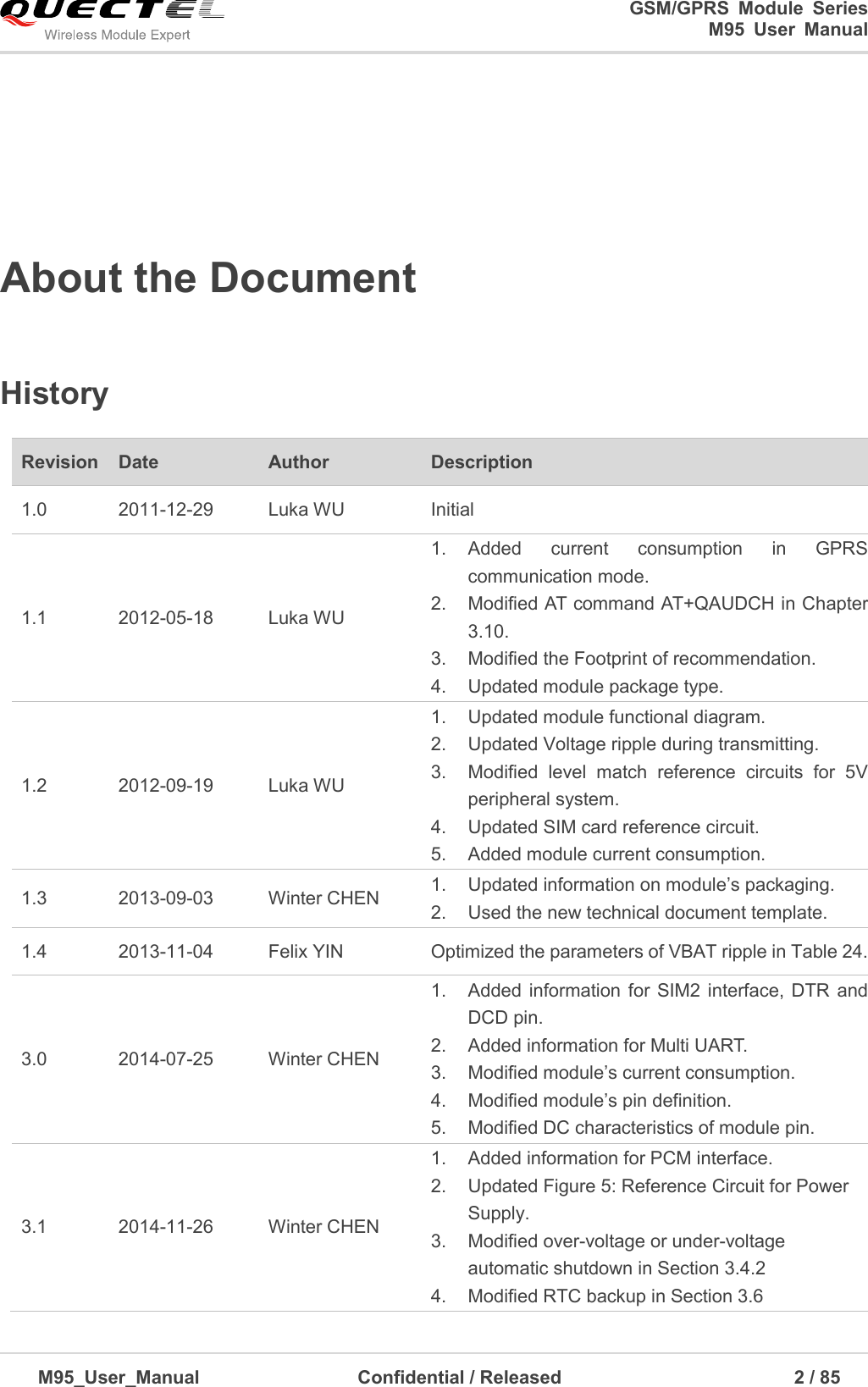
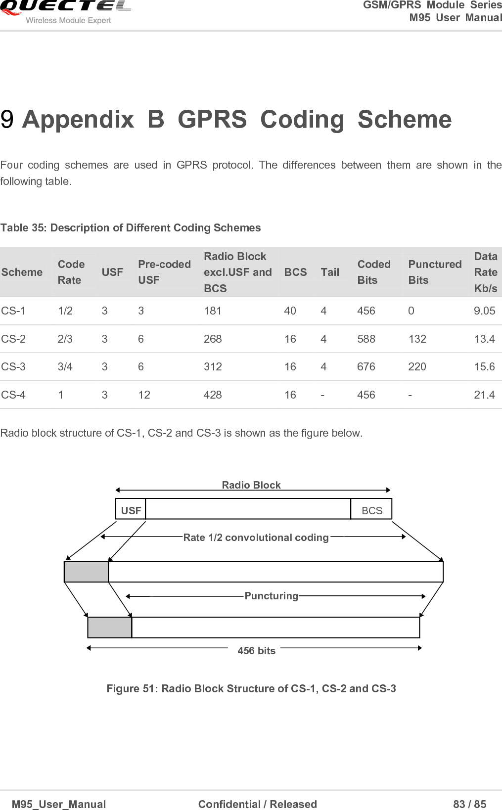
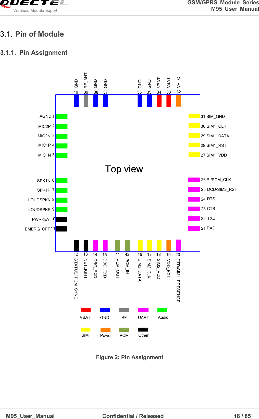
![GSM/GPRS Module Series M95 User Manual M95_User_Manual Confidential / Released 16 / 85 —Turn-on/off interface —UART interfaces —RTC interface —Audio interfaces —PCM interface —SIM interfaces —RF interface BB&RFRF PAM26MHzRF TransceiverRTCGPIO&PWMSerial InterfaceSIM InterfaceRF_ANTVBATPWRKEYEMERG_OFFVRTCStatus&NetlightUARTSIM Interfaces ResetESDPMUMEMORY Audio AudioPCM Interface PCM Figure 1: Module Functional Diagram 2.5. Evaluation Board In order to help you to develop applications with M95, Quectel supplies an evaluation board (EVB), RS-232 to USB cable, power adapter, earphone, antenna and other peripherals to control or test the module. For details, please refer to the document [4].](https://usermanual.wiki/Quectel-Wireless-Solutions/201512M95/User-Guide-2873474-Page-17.png)
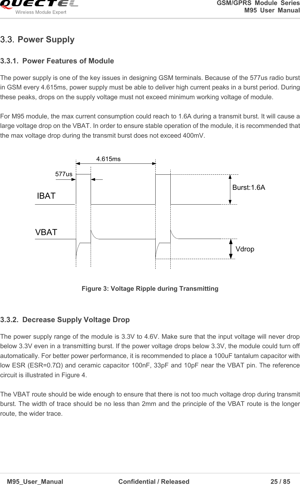
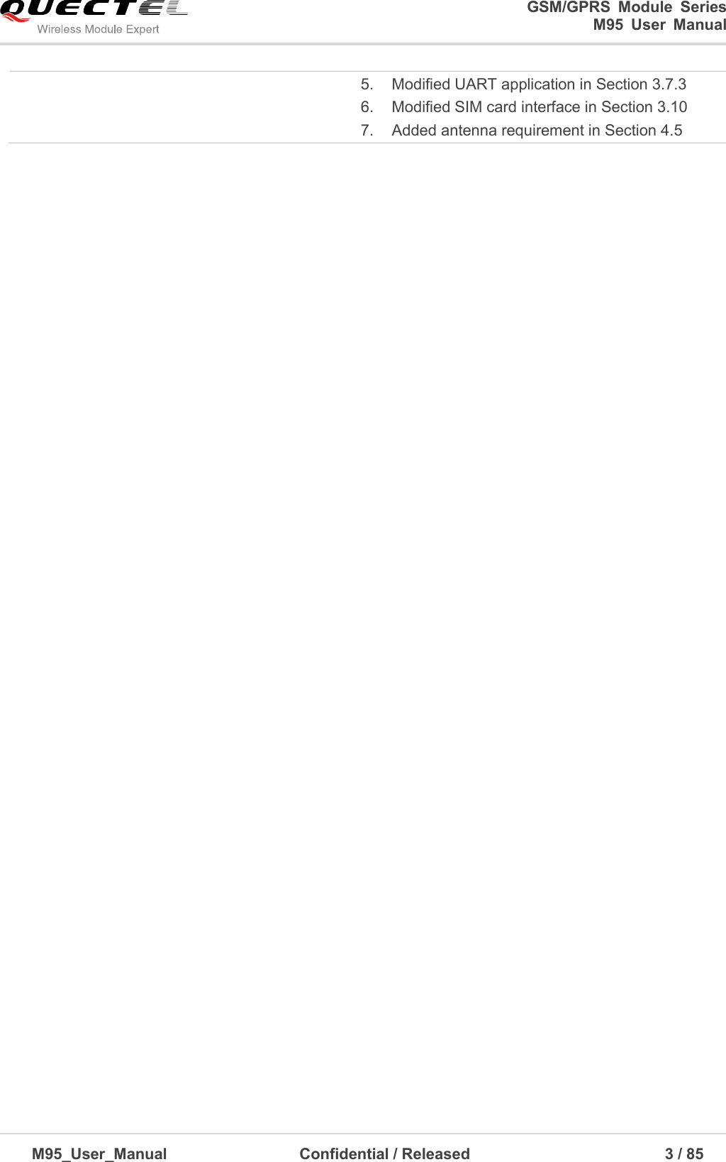
![GSM/GPRS Module Series M95 User Manual M95_User_Manual Confidential / Released 27 / 85 It is suggested to control the module’s main power supply (VBAT) via LDO enable pin to restart the module when the module has become abnormal. Power switch circuit like P-channel MOSFET switch circuit can also be used to control VBAT. 3.3.4. Monitor Power Supply The command ―AT+CBC‖ can be used to monitor the supply voltage of the module. The unit of the displayed voltage is mV. For details, please refer to the document [1]. 3.4. Power On and Down Scenarios 3.4.1. Power On The module can be turned on by driving the pin PWRKEY to a low level voltage. An open collector driver circuit is suggested to control the PWRKEY. A simple reference circuit is illustrated as below. Turn on pulsePWRKEY4.7K47K Figure 6: Turn On the Module with an Open-collector Driver 1. M95 module is set to autobauding mode (AT+IPR=0) by default. In the autobauding mode, URC ―RDY‖ is not reported to the host controller after module is powered on. When the module is powered on after a delay of 4 or 5 seconds, it can receive AT command. Host controller should first send an ―AT‖ or ―at‖ string in order that the module can detect baud rate of host controller, it should continue to send the next ‖AT‖ string until receiving ―OK‖ string from the module. Then enter ―AT+IPR=x;&W‖ to set a fixed baud rate for the module and save the configuration to flash memory of the module. After NOTE NOTE](https://usermanual.wiki/Quectel-Wireless-Solutions/201512M95/User-Guide-2873474-Page-28.png)
![GSM/GPRS Module Series M95 User Manual M95_User_Manual Confidential / Released 28 / 85 these configurations, the URC ―RDY‖ would be received from the UART Port of the module every time when the module is powered on. For more details, refer to the section ―AT+IPR‖ in document [1]. 2. AT command response indicates module is turned on successfully, or else the module fails to be turned on. The other way to control the PWRKEY is through a button directly. A TVS component is indispensable to be placed nearby the button for ESD protection. For the best performance, the TVS component must be placed nearby the button. When pressing the key, electrostatic strike may generate from finger. A reference circuit is shown in the following figure. PWRKEYS1Close to S1TVS Figure 7: Turn On the Module with a Button The turn-on timing is illustrated as the following figure. VDD_EXT(OUTPUT)VIL<0.1*VBATVIH > 0.6*VBATVBATPWRKEY(INPUT)EMERG_OFF(INPUT)54msSTATUS(OUTPUT)800ms>1sOFF BOOTINGMODULE STATUS RUNNINGT1 Figure 8: Turn-on Timing](https://usermanual.wiki/Quectel-Wireless-Solutions/201512M95/User-Guide-2873474-Page-29.png)
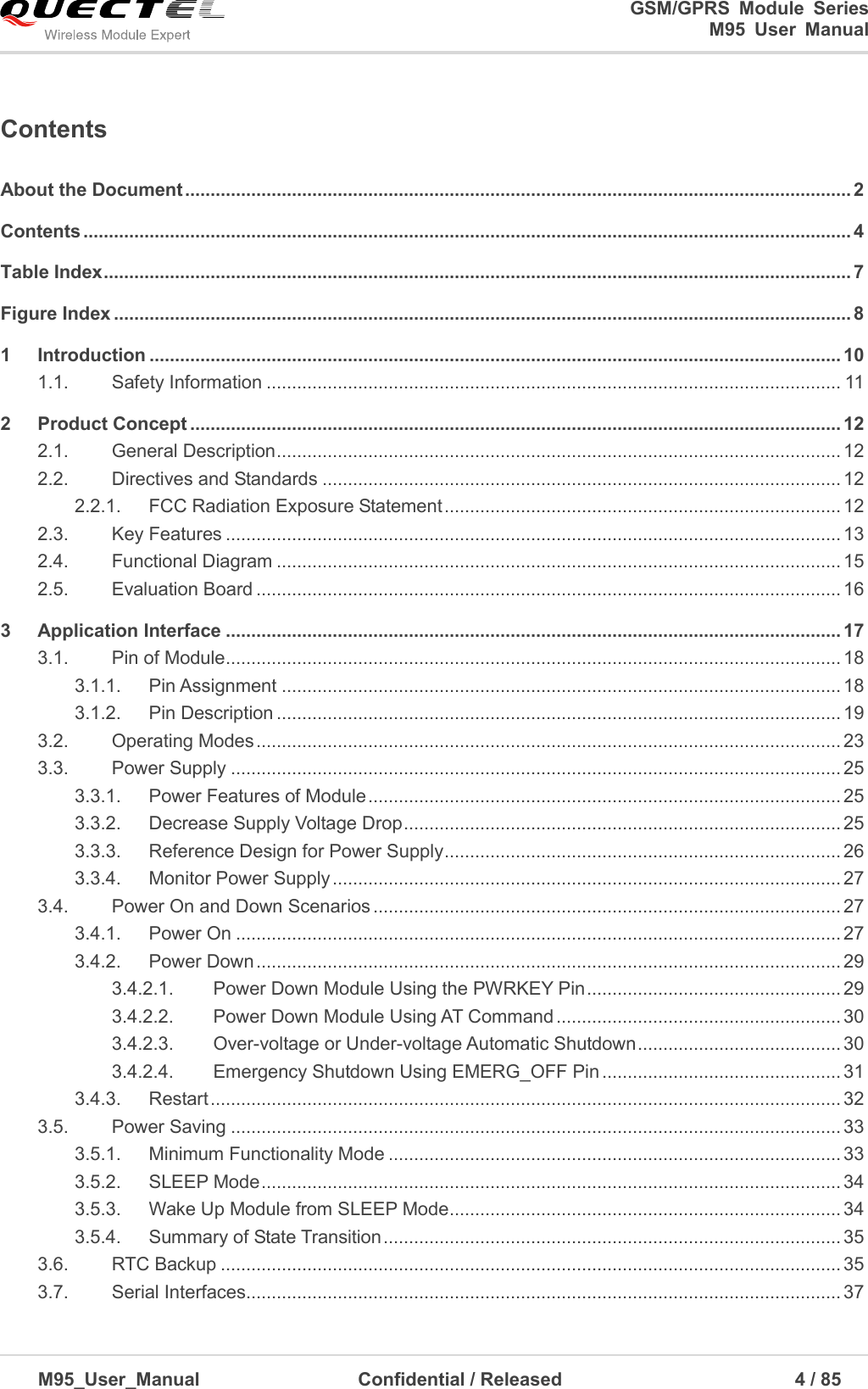
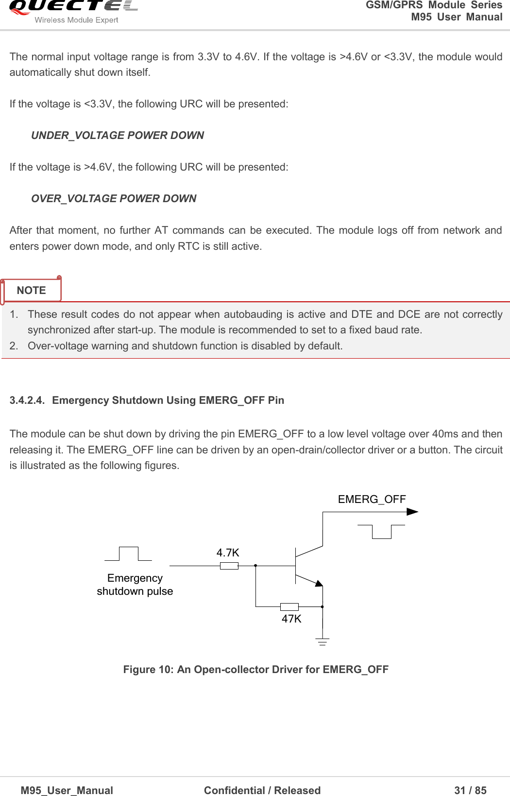
![GSM/GPRS Module Series M95 User Manual M95_User_Manual Confidential / Released 30 / 85 Before the completion of the power down procedure, the module sends out the result code shown below: NORMAL POWER DOWN 1. This result code does not appear when autobauding is active and DTE and DCE are not correctly synchronized after start-up. The module is recommended to set a fixed baud rate. 2. As logout network time is related to the local mobile network, it is recommended to delay about 12 seconds before disconnecting the power supply or restarting the module. 3. For more details about the application of STATUS pin, please refer to the Chapter 3.13. After that moment, no further AT commands can be executed. Then the module enters the power down mode, only the RTC is still active. 3.4.2.2. Power Down Module Using AT Command It is also a safe way to turn off the module via AT command ―AT+QPOWD=1‖. This command will let the module to log off from the network and allow the firmware to save important data before completely disconnecting the power supply. Before the completion of the power down procedure, the module sends the result code as shown below: NORMAL POWER DOWN After that moment, no further AT commands can be executed. And then the module enters the power down mode, only the RTC is still active. Please refer to the document [1] for details about the AT command ―AT+QPOWD‖. 3.4.2.3. Over-voltage or Under-voltage Automatic Shutdown The module will constantly monitor the voltage applied on the VBAT, if the voltage is ≤3.5V, the following URC will be presented: UNDER_VOLTAGE WARNING If the voltage is ≥4.5V, the following URC will be presented: OVER_VOLTAGE WARNING NOTE](https://usermanual.wiki/Quectel-Wireless-Solutions/201512M95/User-Guide-2873474-Page-31.png)
![GSM/GPRS Module Series M95 User Manual M95_User_Manual Confidential / Released 34 / 85 If the module is set to minimum functionality by ―AT+CFUN=0‖, the RF function and SIM card function would be disabled. In this case, the UART port is still accessible, but all AT commands related with RF function or SIM card function will be not available. If the module has been set by the command with ―AT+CFUN=4‖, the RF function will be disabled, but the UART port is still active. In this case, all AT commands related with RF function will be not available. After the module is set by ―AT+CFUN=0‖ or ―AT+CFUN=4‖, it can return to full functionality by ―AT+CFUN=1‖. For detailed information about ―AT+CFUN‖, please refer to the document [1]. 3.5.2. SLEEP Mode The SLEEP mode is disabled by default. You can enable it by ―AT+QSCLK=1‖. On the other hand, the default setting is ―AT+QSCLK=0‖ and in this mode, the module cannot enter SLEEP mode. When the module is set by the command with ―AT+QSCLK=1‖, you can control the module to enter or exit from the SLEEP mode through pin DTR. When DTR is set to high level, and there is no on-air or hardware interrupt such as GPIO interrupt or data on UART port, the module will enter SLEEP mode automatically. In this mode, the module can still receive voice, SMS or GPRS paging from network, but the UART port does not work. 3.5.3. Wake Up Module from SLEEP Mode When the module is in the SLEEP mode, the following methods can wake up the module. If the DTR Pin is set low, it would wake up the module from the SLEEP mode. The UART port will be active within 20ms after DTR is changed to low level. Receiving a voice or data call from network will wake up the module. Receiving an SMS from network will wake up the module. DTR pin should be held at low level during communication between the module and DTE. NOTE](https://usermanual.wiki/Quectel-Wireless-Solutions/201512M95/User-Guide-2873474-Page-35.png)
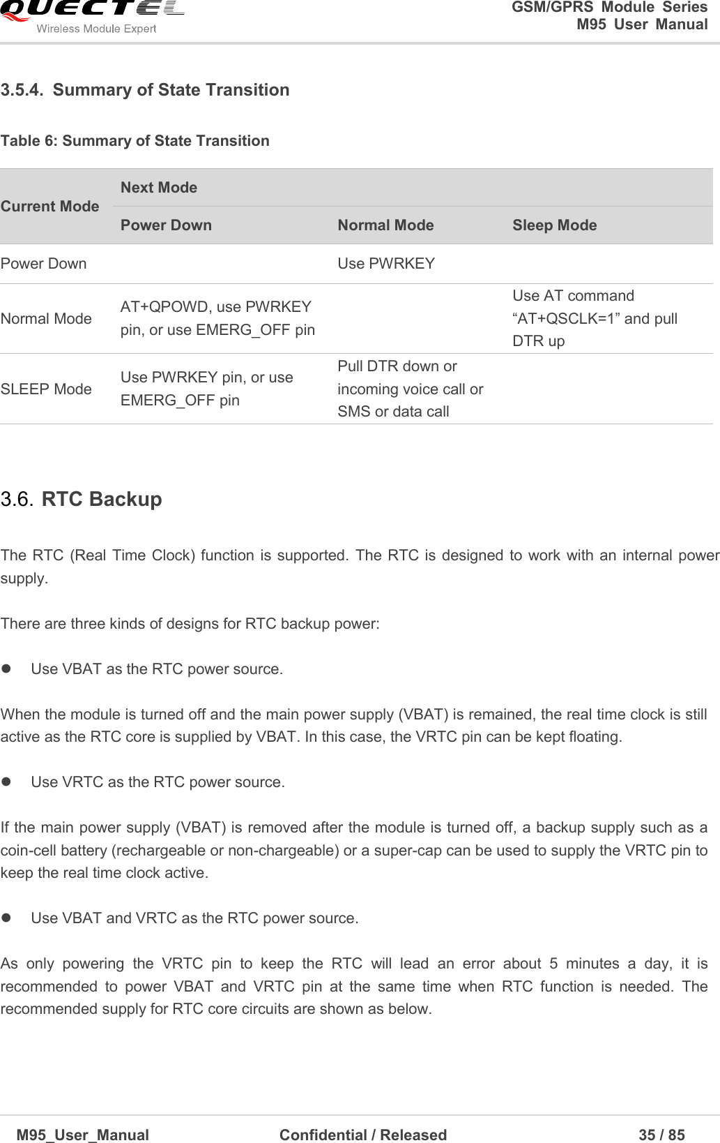
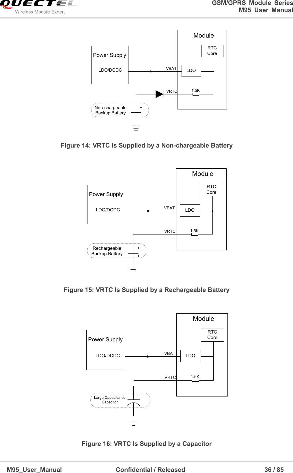
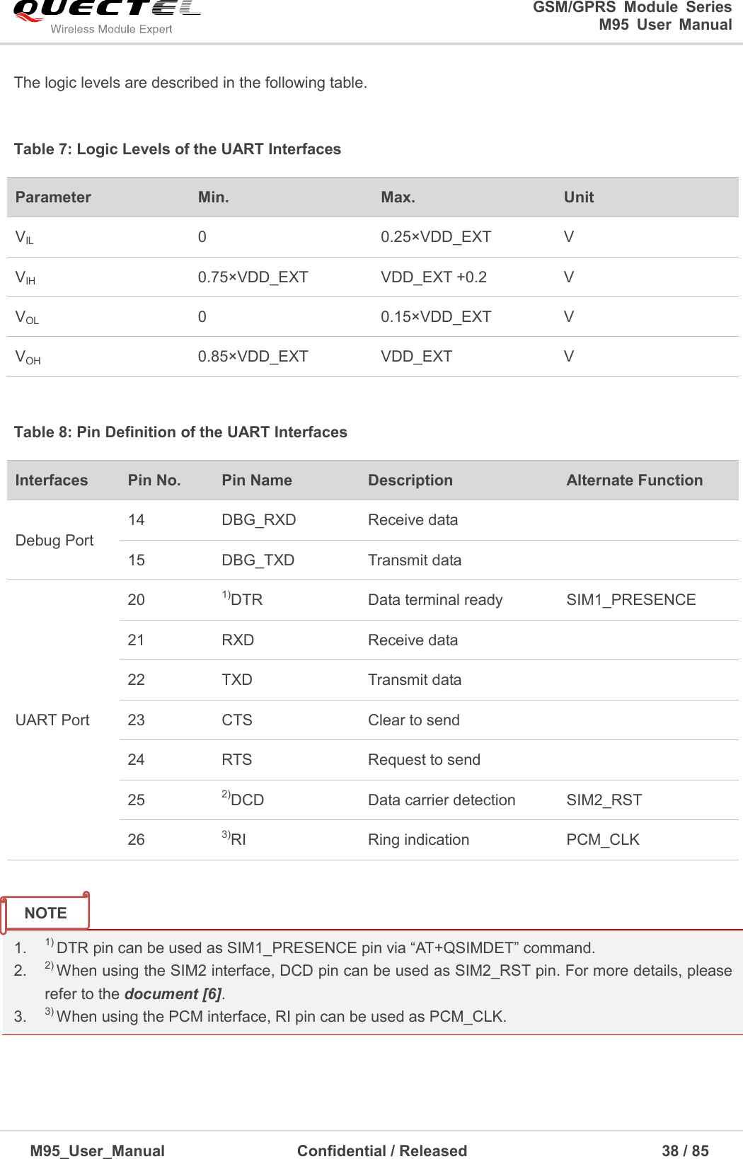
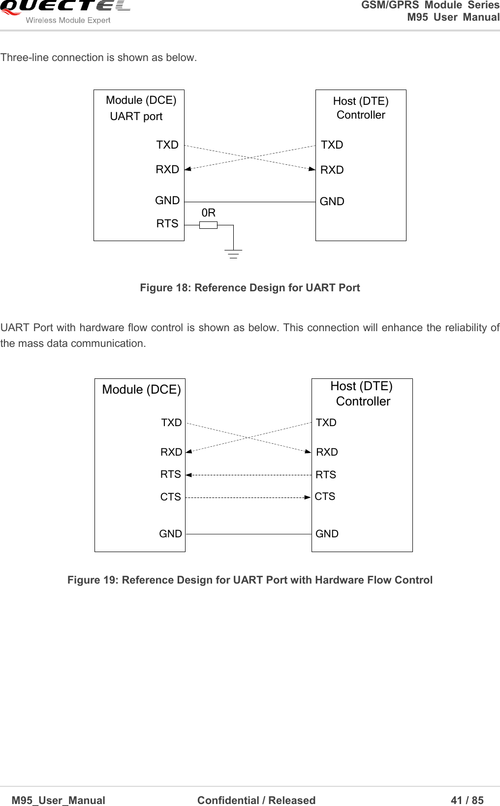
![GSM/GPRS Module Series M95 User Manual M95_User_Manual Confidential / Released 37 / 85 For the choice of a rechargeable or non-chargeable coin-cell battery, please visit http://www.sii.co.jp/en/. If the module is only powered by VRTC , the real time will have an error about 5 minutes a day. If you want to keep an accurate real time, please use VBAT to supply the RTC core. 3.7. Serial Interfaces The module provides two serial ports: UART Port and Debug Port. The module is designed as a DCE (Data Communication Equipment), following the traditional DCE-DTE (Data Terminal Equipment) connection. Autobauding function supports baud rate from 4800bps to 115200bps. The UART Port: TXD: Send data to RXD of DTE. RXD: Receive data from TXD of DTE. RTS: Request to send. CTS: Clear to send. DTR: DTE is ready and inform DCE (this pin can wake up the module). RI: Ring indicator (when the call, SMS, data of the module are coming, the module will output signal to inform DTE). DCD: Data carrier detection (the validity of this pin demonstrates the communication link is set up). Hardware flow control is disabled by default. When hardware flow control is required, RTS and CTS should be connected to the host. AT command ―AT+IFC=2,2‖ is used to enable hardware flow control. AT command ―AT+IFC=0,0‖ is used to disable the hardware flow control. For more details, please refer to the document [1]. The Debug Port: DBG_TXD: Send data to the COM port of computer. DBG_RXD: Receive data from the COM port of computer. NOTE NOTE](https://usermanual.wiki/Quectel-Wireless-Solutions/201512M95/User-Guide-2873474-Page-38.png)
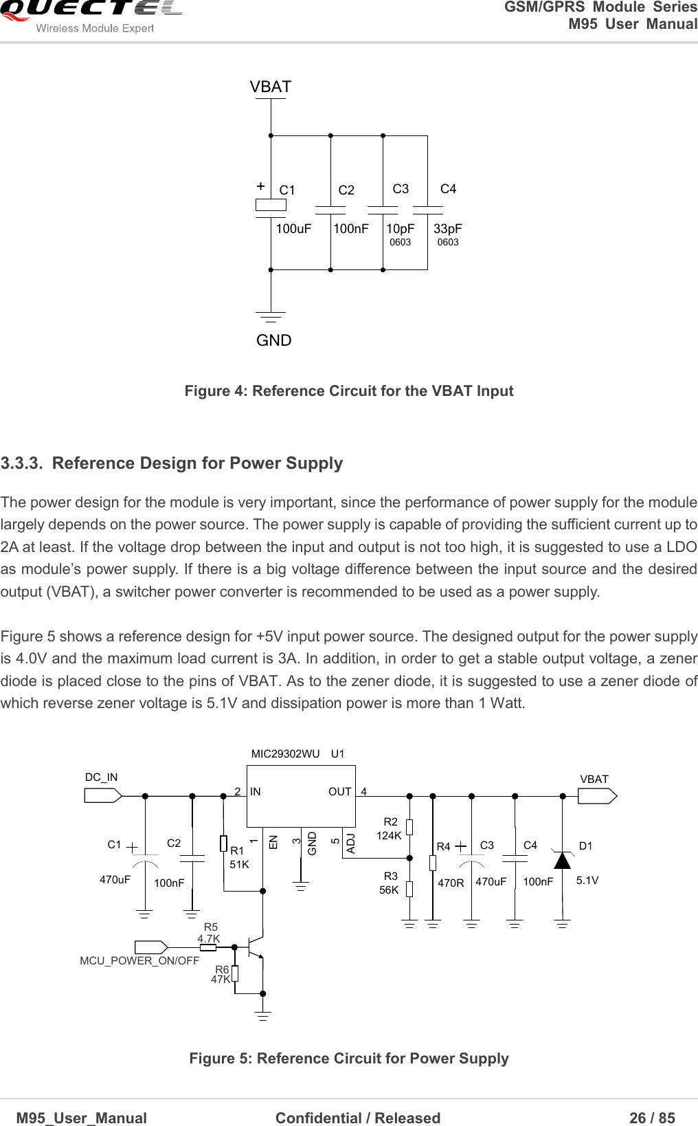
![GSM/GPRS Module Series M95 User Manual M95_User_Manual Confidential / Released 38 / 85 The logic levels are described in the following table. Table 7: Logic Levels of the UART Interfaces Table 8: Pin Definition of the UART Interfaces 1. 1) DTR pin can be used as SIM1_PRESENCE pin via ―AT+QSIMDET‖ command. 2. 2) When using the SIM2 interface, DCD pin can be used as SIM2_RST pin. For more details, please refer to the document [6]. 3. 3) When using the PCM interface, RI pin can be used as PCM_CLK. Parameter Min. Max. Unit VIL 0 0.25×VDD_EXT V VIH 0.75×VDD_EXT VDD_EXT +0.2 V VOL 0 0.15×VDD_EXT V VOH 0.85×VDD_EXT VDD_EXT V Interfaces Pin No. Pin Name Description Alternate Function Debug Port 14 DBG_RXD Receive data 15 DBG_TXD Transmit data UART Port 20 1)DTR Data terminal ready SIM1_PRESENCE 21 RXD Receive data 22 TXD Transmit data 23 CTS Clear to send 24 RTS Request to send 25 2)DCD Data carrier detection SIM2_RST 26 3)RI Ring indication PCM_CLK NOTE](https://usermanual.wiki/Quectel-Wireless-Solutions/201512M95/User-Guide-2873474-Page-39.png)
![GSM/GPRS Module Series M95 User Manual M95_User_Manual Confidential / Released 40 / 85 If autobauding is active it is not recommended to switch to multiplex mode. To assure reliable communication and avoid any problems caused by undetermined baud rate between DCE and DTE, it is strongly recommended to configure a fixed baud rate and save it instead of using autobauding after start-up. For more details, please refer to the Section ―AT+IPR‖ in document [1]. 3.7.1.2. The Connection of UART The connection between module and host using UART Port is very flexible. Three connection styles are illustrated as below. Reference design for Full-Function UART connection is shown as below when it is applied in modulation-demodulation. TXDRXDRTSCTSDTRDCDRITXDRXDRTSCTSDTRDCDRINGModule (DCE)Serial portUART portGND GNDPC (DTE) Figure 17: Reference Design for Full-Function UART NOTE](https://usermanual.wiki/Quectel-Wireless-Solutions/201512M95/User-Guide-2873474-Page-41.png)
![GSM/GPRS Module Series M95 User Manual M95_User_Manual Confidential / Released 42 / 85 3.7.1.3. Firmware Upgrade The TXD, RXD can be used to upgrade firmware. The PWRKEY pin must be pulled down before firmware upgrade. The reference circuit is shown as below: IO Connector TXDRXDGNDPWRKEY Module (DCE) UART portTXDRXDGNDPWRKEY Figure 20: Reference Design for Firmware Upgrade The firmware of module might need to be upgraded due to certain reasons. It is recommended to reserve these pins in the host board for firmware upgrade. 3.7.2. Debug Port As to Debug Port, there are two working modes, Standard Mode and Advanced Mode, which can be switched through using AT command‖ AT+QEAUART‖. For more details, please refer to the document [7]. In Standard Mode, it can be used to execute software debug and it can also connect to a peripheral device. Furthermore, its default baud rate is 115200bps. In Advanced Mode, it can only be used to execute software debug, capture the system’s log with Cather Log tool and output the log. In this mode, its baud rate is 460800bps. NOTE](https://usermanual.wiki/Quectel-Wireless-Solutions/201512M95/User-Guide-2873474-Page-43.png)
![GSM/GPRS Module Series M95 User Manual M95_User_Manual Confidential / Released 43 / 85 The reference design for Debug Port is shown as below. PeripheralTXDRXDGND Module DBG_TXDDBG_RXD GND Figure 21: Reference Design for Debug Port 3.7.3. UART Application The reference design of 3.3V level match is shown as below. If the host is a 3V system, please change the 5.6K resistor to 10K. Peripheral/TXD/RXD1KTXDRXDRTSCTSDTRRI/RTS/CTSGPIOEINTGPIO DCDModule1K1KVoltage level:3.3V5.6K5.6K5.6K1K1K1K1KGND GND Figure 22: Level Match Design for 3.3V System It is highly recommended to add the resistor divider circuit on the UART signal lines when the host’s level is 3V or 3.3V. For the higher voltage level system, a level shifter IC could be used between the host and the module. For more details about UART circuit design, please refer to document [8]. NOTE](https://usermanual.wiki/Quectel-Wireless-Solutions/201512M95/User-Guide-2873474-Page-44.png)
![GSM/GPRS Module Series M95 User Manual M95_User_Manual Confidential / Released 45 / 85 AIN1 and AIN2 can be used for input of microphone and line. An electret microphone is usually used. AIN1 and AIN2 are both differential input channels. AOUT1 is used for output of the receiver. This channel is typically used for a receiver built into a handset. AOUT1 channel is a differential channel. If it is used as a speaker, an amplifier should be employed. AOUT2 is used for loudspeaker output as it embedded an amplifier of class AB whose maximum drive power is 870mW. AOUT2 is a differential channel. AOUT2 also can be used for output of earphone, which can be used as a single-ended channel. LOUDSPKP and AGND can establish a pseudo differential mode. All of these two audio channels support voice and ringtone output, and so on, and can be switched by ―AT+QAUDCH‖ command. For more details, please refer to the document [1]. Use AT command ―AT+QAUDCH‖ to select audio channel: 0--AIN1/AOUT1, the default value is 0. 1--AIN2/AOUT2, this channel is always used for earphone. 2--AIN2/AOUT2, this channel is always used for loudspeaker. For each channel, you can use AT+QMIC to adjust the input gain level of microphone. You can also use ―AT+CLVL‖ to adjust the output gain level of receiver and speaker. ―AT+QSIDET‖ is used to set the side-tone gain level. For more details, please refer to the document [1]. Table 10: AOUT2 Output Characteristics MIC2P 2 Channel 2 Microphone positive input MIC2N 3 Channel 2 Microphone negative input LOUDSPKP 9 Channel 2 Audio positive output LOUDSPKN 8 Channel 2 Audio negative output Item Condition Min. Type Max. Unit RMS Power 8ohm load VBAT=4.2v THD+N=1% 870 mW 8ohm load VBAT=3.3v THD+N=1% 530 mW](https://usermanual.wiki/Quectel-Wireless-Solutions/201512M95/User-Guide-2873474-Page-46.png)
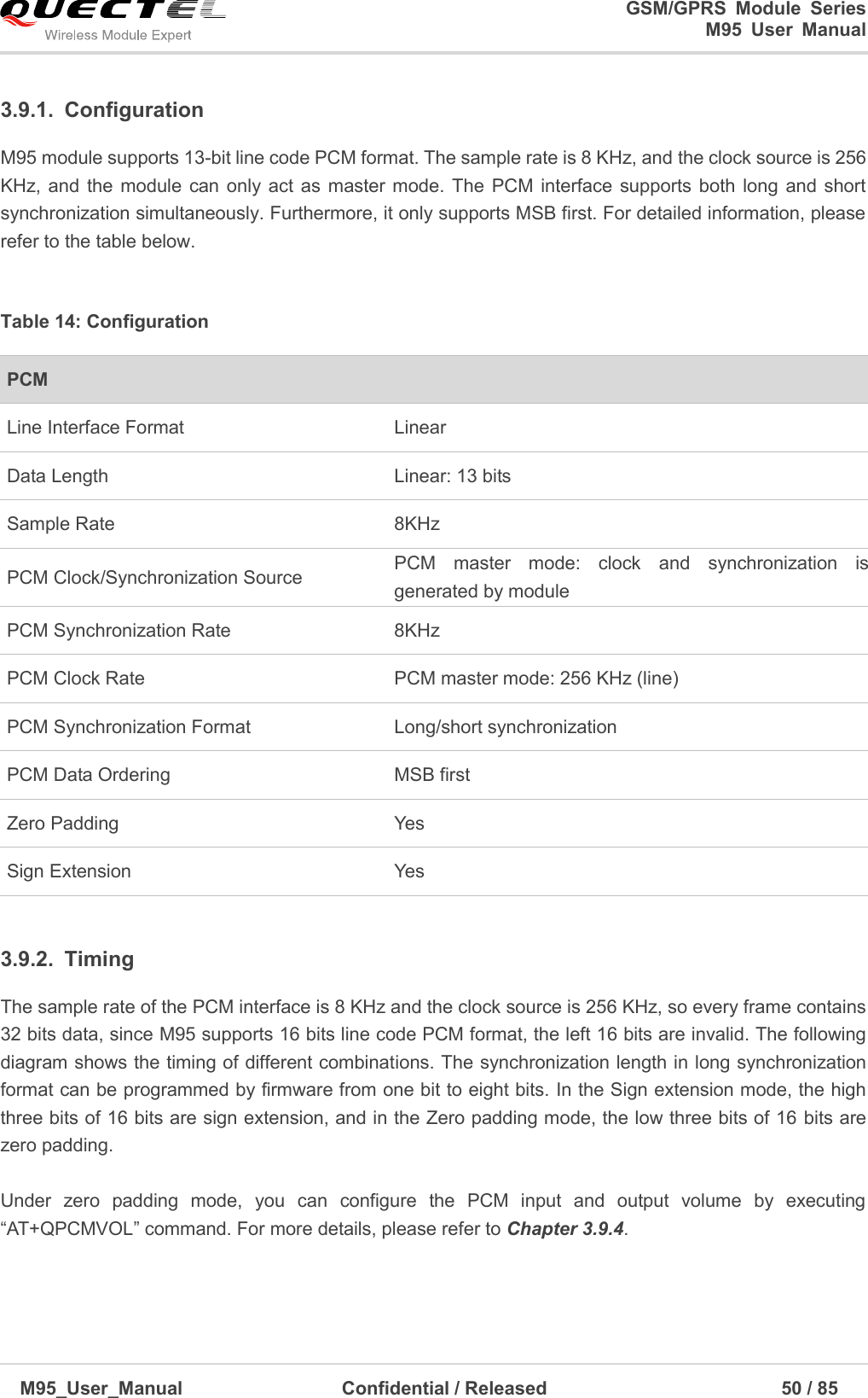
![GSM/GPRS Module Series M95 User Manual M95_User_Manual Confidential / Released 53 / 85 Table 15: QPCMON Command Description ―AT+QPCMVOL‖ can configure the volume of input and output. AT+QPCMVOL=vol_pcm_in, vol_pcm_out Table 16: QPCMVOL Command Description 3.10. SIM Card Interfaces The module contains two smart interfaces to allow module access to the two SIM cards. These two SIM interfaces share the same ground and only SIM1 interface has card inserted detection. Only one SIM card can work at a time. For more details, please refer to the document [6]. 3.10.1. SIM Card Application The SIM interfaces supports the functionality of the GSM Phase 1 specification and also supports the functionality of the new GSM Phase 2+ specification for FAST 64 kbps SIM card, which is intended for use with a SIM application Tool-kit. Parameter Scope Description Mode 0~2 0: Close PCM 1: Open PCM 2: Open PCM when audio talk is set up Sync_Type 0~1 0: Short synchronization 1: Long synchronization Sync_Length 1~8 Programmed from one bit to eight bit SignExtension 0~1 0: Zero padding 1: Sign extension MSBFirst 0~1 0: MSB first 1: Not support Parameter Scope Description vol_pcm_in 0~32767 Set the input volume vol_pcm_out 0~32767 Set the output volume The voice may be distorted when this value exceeds 16384.](https://usermanual.wiki/Quectel-Wireless-Solutions/201512M95/User-Guide-2873474-Page-54.png)
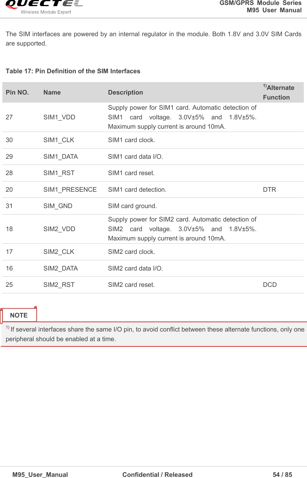
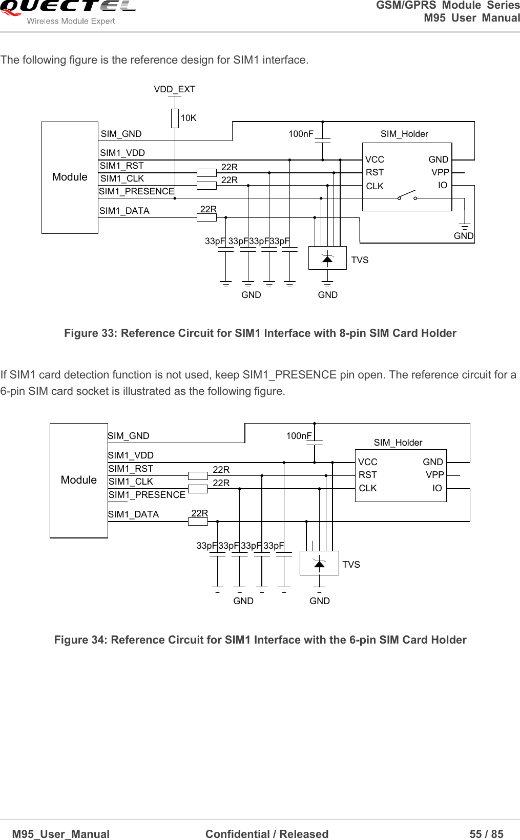
![GSM/GPRS Module Series M95 User Manual M95_User_Manual Confidential / Released 57 / 85 3.11. Behaviors of The RI When using PCM interface, RI pin can be used as PCM_CLK. Table 18: Behaviors of the RI If URC of SMS is disabled, the RI will not change. If the module is used as a caller, the RI would maintain high except the URC or SMS is received. On the other hand, when it is used as a receiver, the timing of the RI is shown as below. RIIdle RingOff-hook by“ATA”On-hook by “ATH”HIGHLOW Figure 36: RI Behavior of Voice Calling as a Receiver State RI Response Standby HIGH Voice Calling Change to LOW, then: 1. Change to HIGH when call is established. 2. Use ATH to hang up the call, RI changes to HIGH. 3. Calling part hangs up, RI changes to HIGH first, and changes to LOW for 120ms indicating ―NO CARRIER‖ as an URC, then changes to HIGH again. 4. Change to HIGH when SMS is received. SMS When a new SMS comes, the RI changes to LOW and holds low level for about 120ms, then changes to HIGH. URC Certain URCs can trigger 120ms low level on RI. For more details, please refer to the document [1]. NOTE](https://usermanual.wiki/Quectel-Wireless-Solutions/201512M95/User-Guide-2873474-Page-58.png)
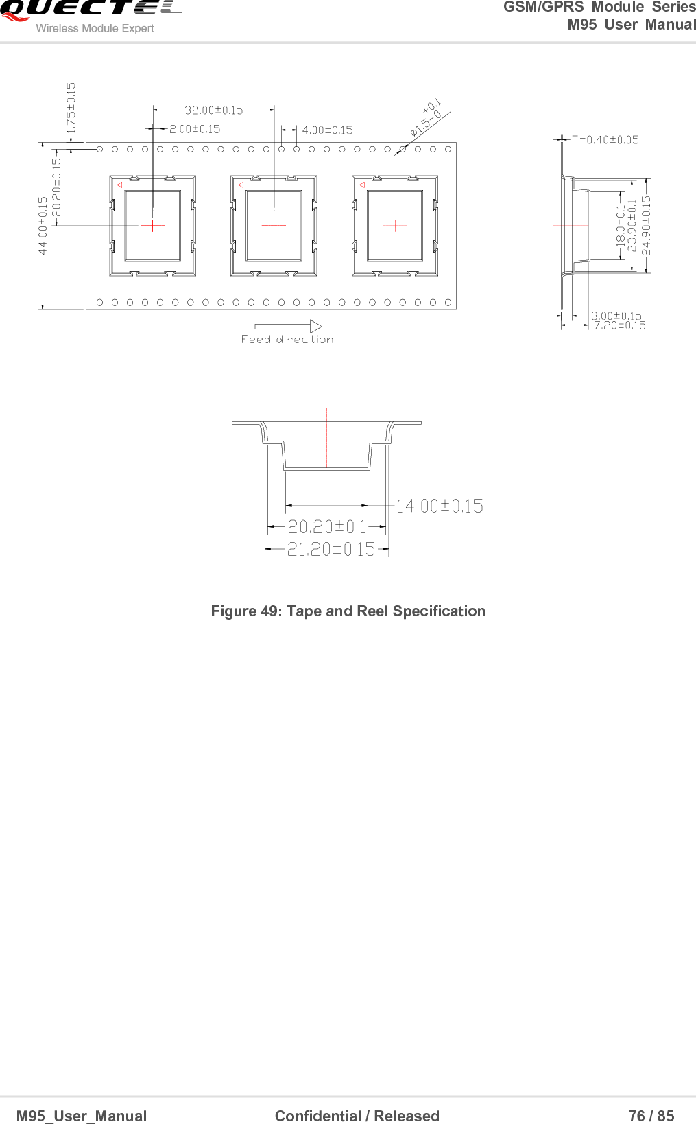
![GSM/GPRS Module Series M95 User Manual M95_User_Manual Confidential / Released 75 / 85 The squeegee should push the paste on the surface of the stencil that makes the paste fill the stencil openings and penetrate to the PCB. The force on the squeegee should be adjusted so as to produce a clean stencil surface on a single pass. To ensure the module soldering quality, the thickness of stencil at the hole of the module pads should be 0.2 mm for M95. For more details, please refer to document [5]. It is suggested that peak reflow temperature is from 235ºC to 245ºC (for SnAg3.0Cu0.5 alloy). Absolute max reflow temperature is 260ºC. To avoid damage to the module when it was repeatedly heated, it is suggested that the module should be mounted after the first panel has been reflowed. The following picture is the actual diagram which we have operated. Time(s)50 100 150 200 250 30050100150200250 160℃ 200℃217070s~120s40s~60sBetween 1~3℃/SPreheat Heating Cooling℃sLiquids Temperature Figure 48: Ramp-Soak-Spike Reflow Profile 7.3. Packaging The modules are stored inside a vacuum-sealed bag which is ESD protected. It should not be opened until the devices are ready to be soldered onto the application. 7.3.1. Tape and Reel Packaging The reel is 330mm in diameter and each reel contains 250 modules.](https://usermanual.wiki/Quectel-Wireless-Solutions/201512M95/User-Guide-2873474-Page-76.png)
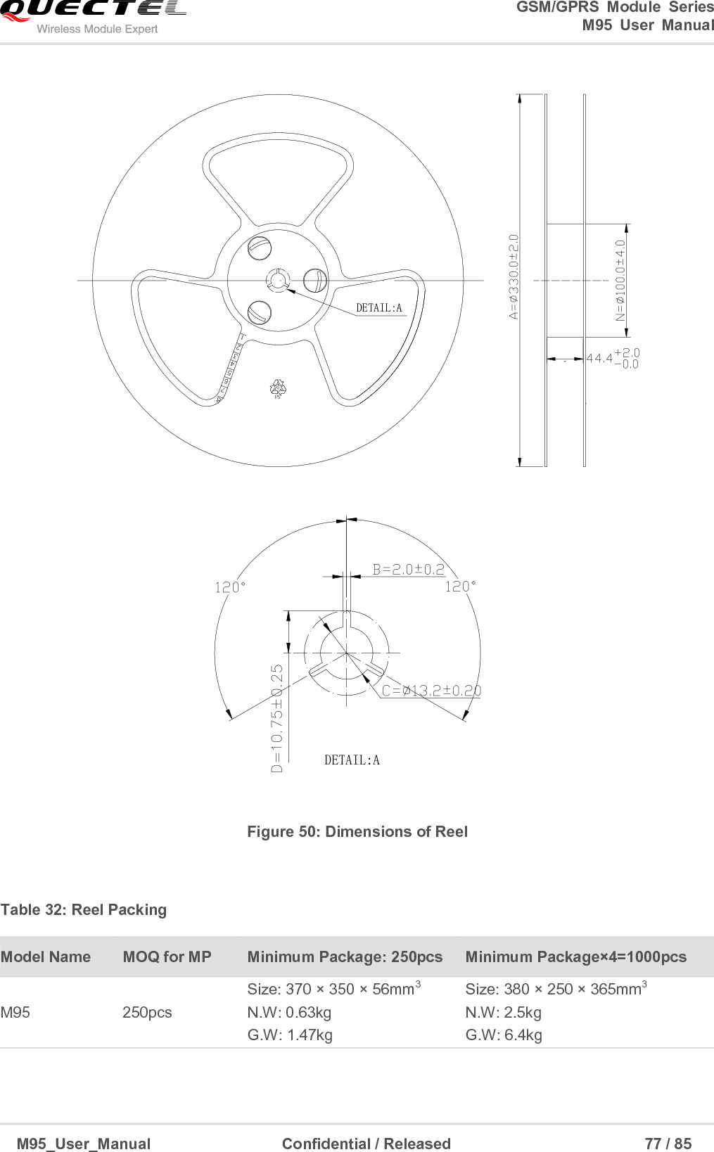
![GSM/GPRS Module Series M95 User Manual M95_User_Manual Confidential / Released 78 / 85 8 Appendix A Reference Table 33: Related Documents SN Document Name Remark [1] Quectel_M95_AT_Commands_Manual AT commands manual [2] ITU-T Draft new recommendation V.25ter Serial asynchronous automatic dialing and control [3] GSM_UART_Application_Note UART port application note [4] GSM_EVB_User_Guide GSM EVB user guide [5] Module_Secondary_SMT_User_Guide Module secondary SMT user guide [6] M95_Dual_SIM_Application_Notes_V3.0 M95 Dual SIM Application Notes [7] GSM_Multi_UART_Application_Note M95 Multi UART Application Notes [8] Quectel_GSM_Module_Digital_IO_Application_Note GSM module digital IO application note [9] GSM 07.07 Digital cellular telecommunications (Phase 2+); AT command set for GSM Mobile Equipment (ME) [10] GSM 07.10 Support GSM 07.10 multiplexing protocol [11] GSM 07.05 Digital cellular telecommunications (Phase 2+); Use of Data Terminal Equipment – Data Circuit terminating Equipment (DTE – DCE) interface for Short Message Service (SMS) and Cell Broadcast Service (CBS) [12] GSM 11.14 Digital cellular telecommunications (Phase 2+); Specification of the SIM Application Toolkit for the Subscriber Identity module – Mobile Equipment (SIM – ME) interface [13] GSM 11.11 Digital cellular telecommunications (Phase 2+); Specification of the Subscriber Identity module – Mobile Equipment (SIM – ME) interface](https://usermanual.wiki/Quectel-Wireless-Solutions/201512M95/User-Guide-2873474-Page-79.png)
![GSM/GPRS Module Series M95 User Manual M95_User_Manual Confidential / Released 79 / 85 Table 34: Terms and Abbreviations [14] GSM 03.38 Digital cellular telecommunications (Phase 2+); Alphabets and language-specific information [15] GSM 11.10 Digital cellular telecommunications (Phase 2); Mobile Station (MS) conformance specification; Part 1: Conformance specification Abbreviation Description ADC Analog-to-Digital Converter AMR Adaptive Multi-Rate ARP Antenna Reference Point ASIC Application Specific Integrated Circuit BER Bit Error Rate BOM Bill of Material BTS Base Transceiver Station CHAP Challenge Handshake Authentication Protocol CS Coding Scheme CSD Circuit Switched Data CTS Clear To Send DAC Digital-to-Analog Converter DRX Discontinuous Reception DSP Digital Signal Processor DCE Data Communications Equipment (typically module) DTE Data Terminal Equipment (typically computer, external controller) DTR Data Terminal Ready DTX Discontinuous Transmission](https://usermanual.wiki/Quectel-Wireless-Solutions/201512M95/User-Guide-2873474-Page-80.png)