Quectel Wireless Solutions 201604M26 GSM/GPRS module User Manual
Quectel Wireless Solutions Company Limited GSM/GPRS module Users Manual
UserManual.wiki
>
Quectel Wireless Solutions
>
201604M26 User Manual
Users Manual
Navigation menu
Upload a User Manual
Namespaces
Wiki Guide
HTML
PDF
Info
Views
User Manual
Discussion / Help
Navigation
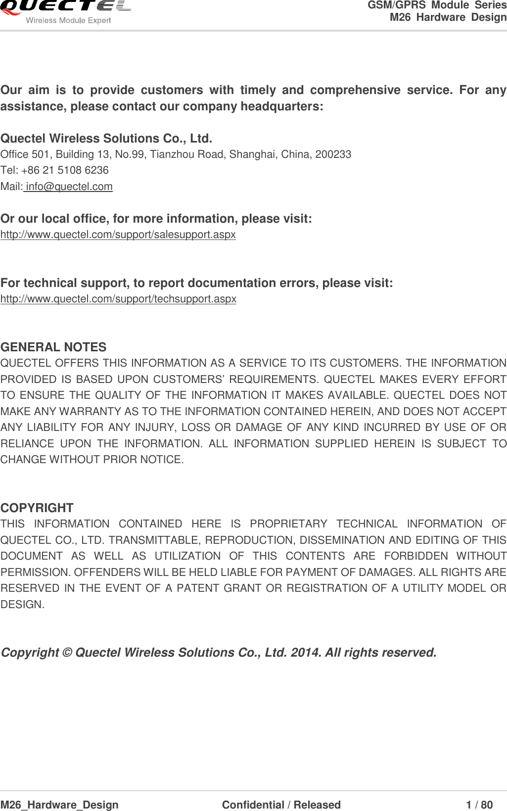
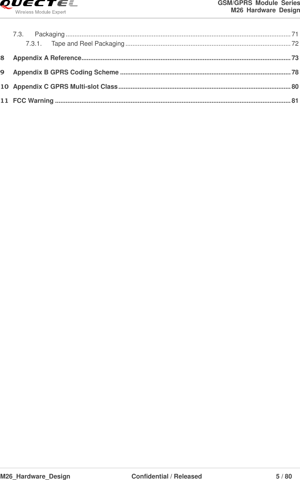
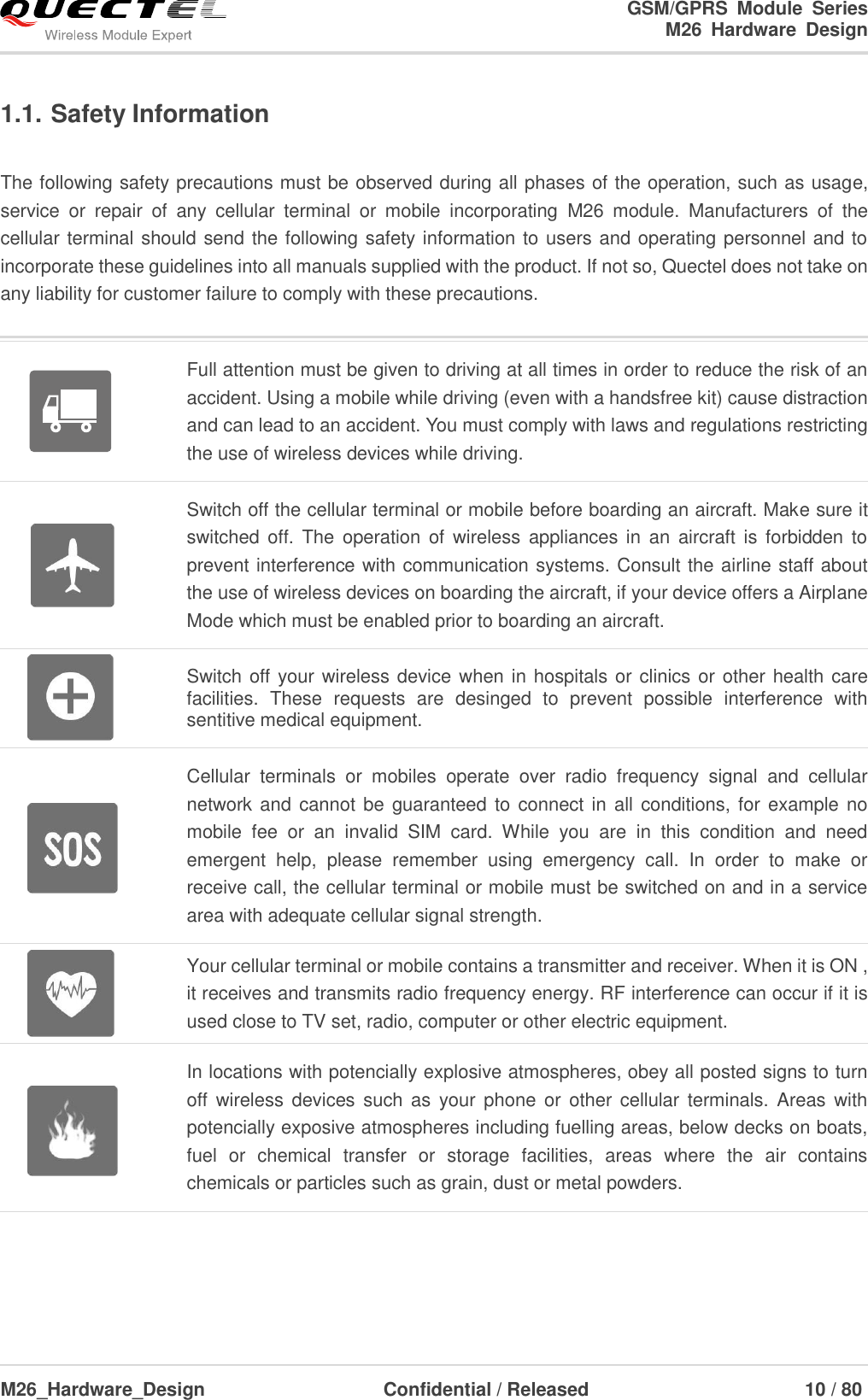
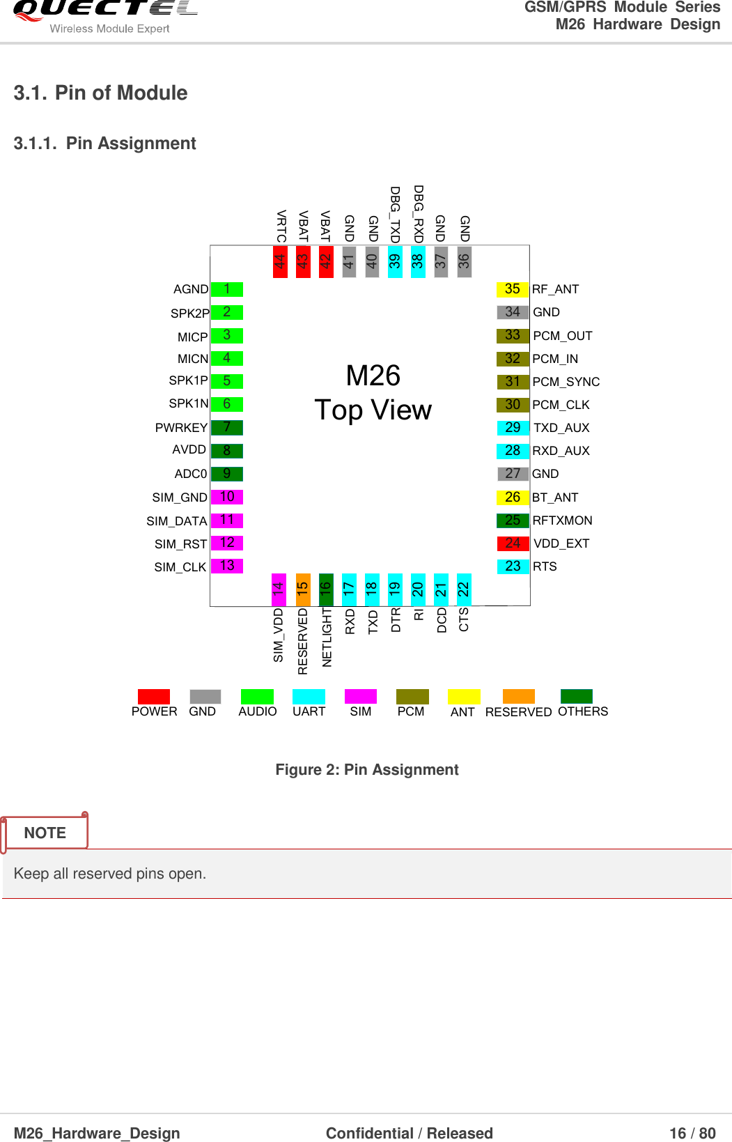
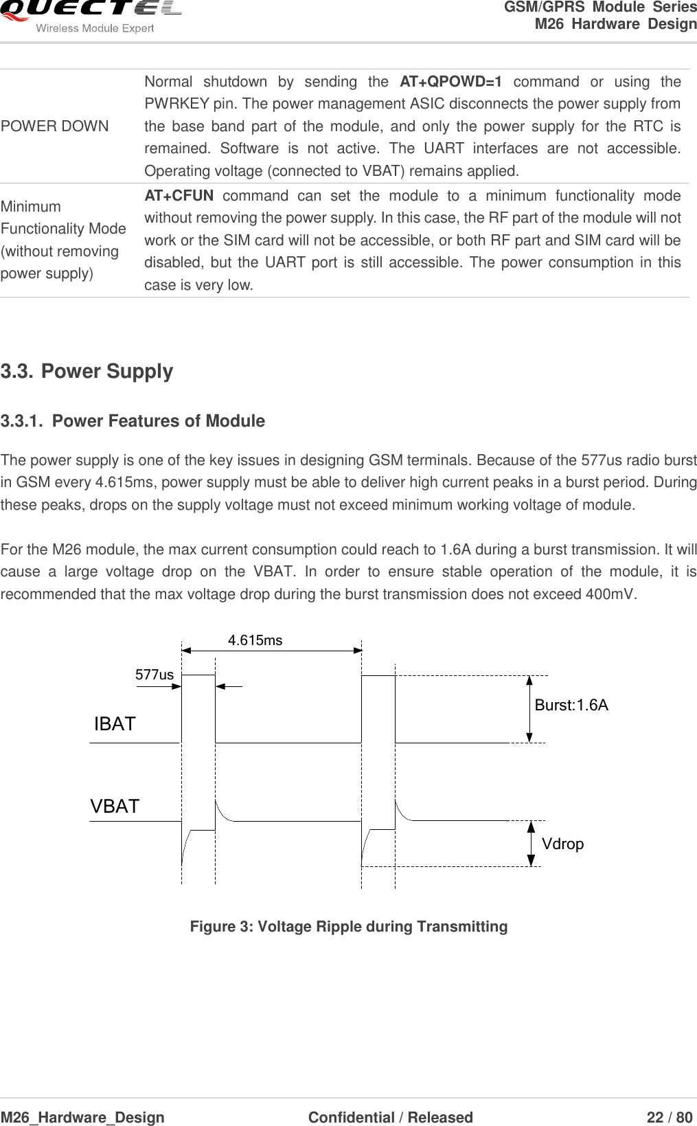
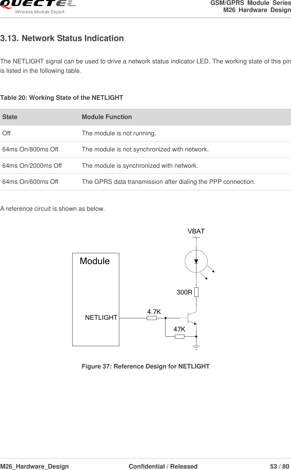
![GSM/GPRS Module Series M26 Hardware Design M26_Hardware_Design Confidential / Released 14 / 80 2.3. Functional Diagram The following figure shows a block diagram of M26 and illustrates the major functional parts. Radio frequency part Power management The peripheral interface —Power supply —Turn-on/off interface —UART interface —Audio interface —PCM interface —SIM interface —ADC interface —RF interface —BT interface BB&RFRF PAM26MHzRF TransceiverRTCAUDIOSerial InterfaceSIM InterfaceRF_ANTVBATPWRKEYVRTCNETLIGHTUARTSIM Interface ESDPMUMEMORYBT_ANTPWMAUDIOPCM PCMADC ADCBTVDD_EXTVDD_EXT Figure 1: Module Functional Diagram 2.4. Evaluation Board In order to help you to develop applications with M26, Quectel supplies an evaluation board (EVB), RS-232 to USB cable, power adapter, earphone, antenna and other peripherals to control or test the module. For details, please refer to the document [11].](https://usermanual.wiki/Quectel-Wireless-Solutions/201604M26/User-Guide-3010680-Page-15.png)
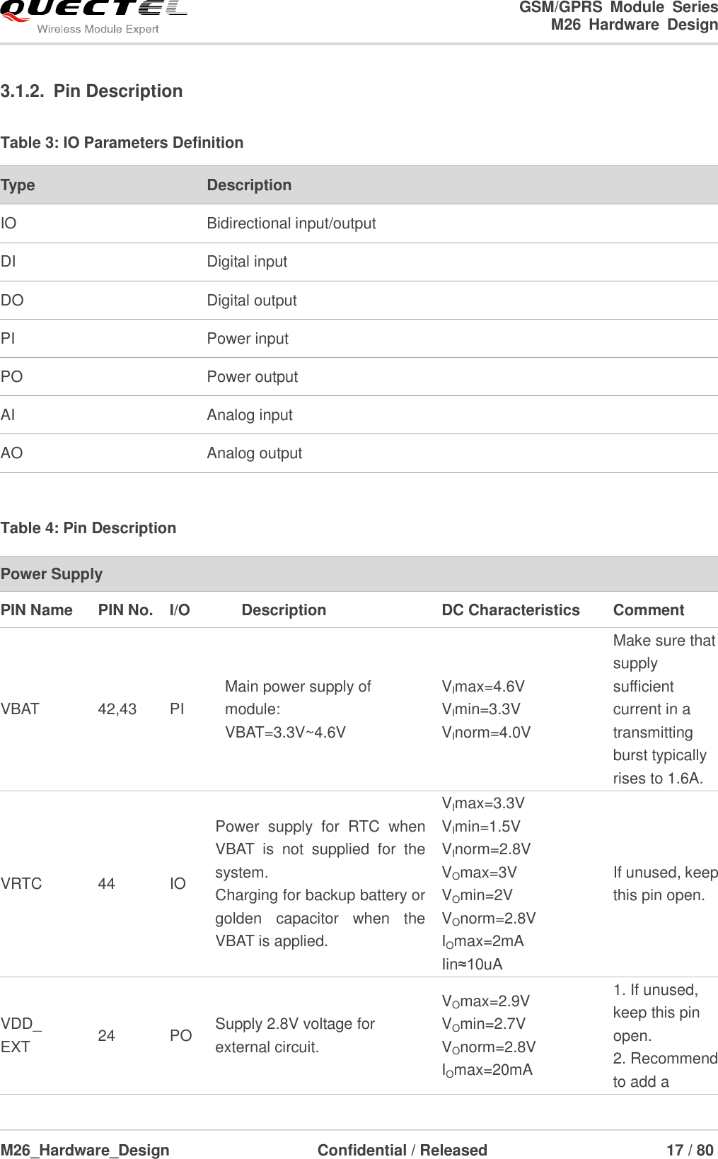
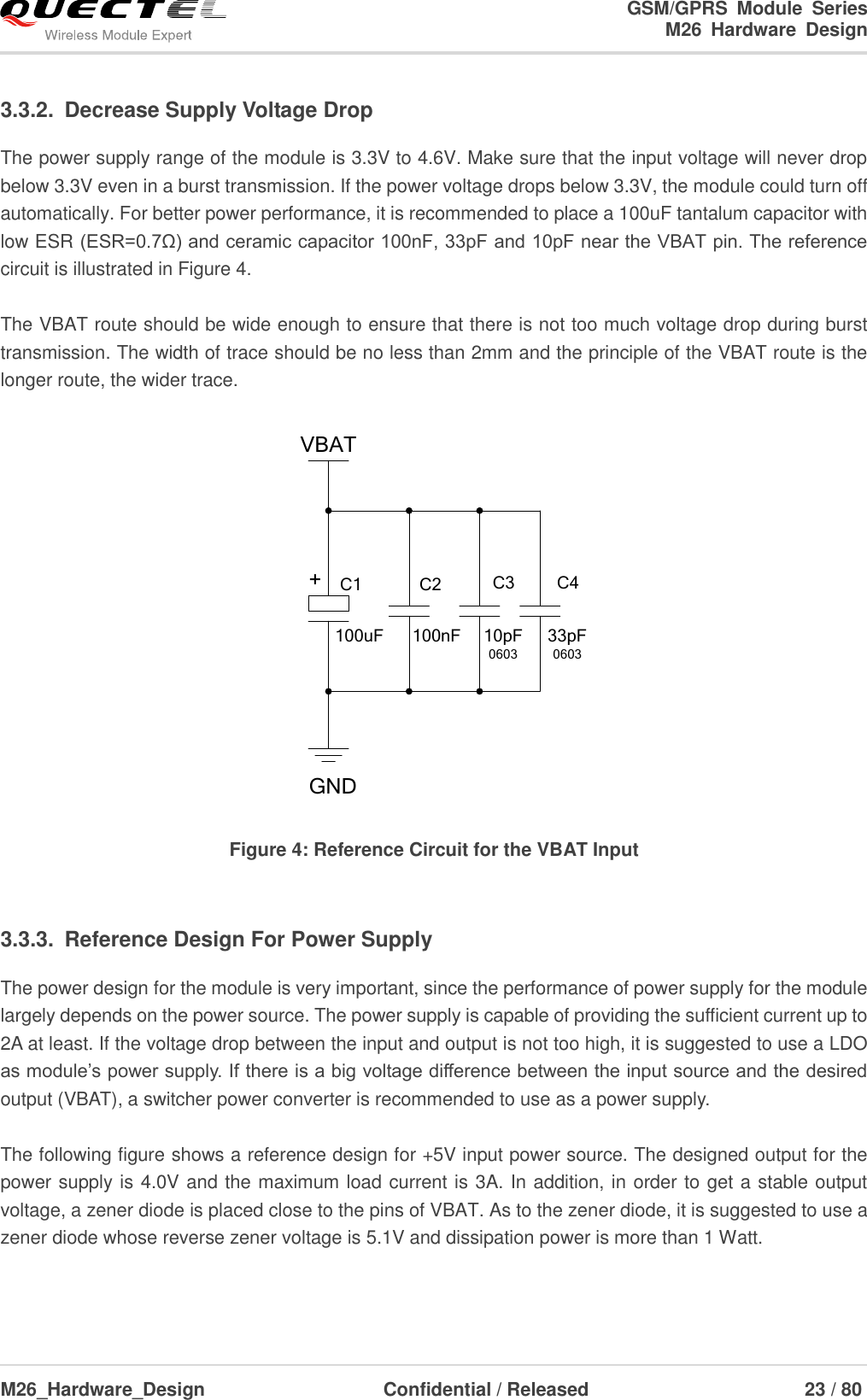
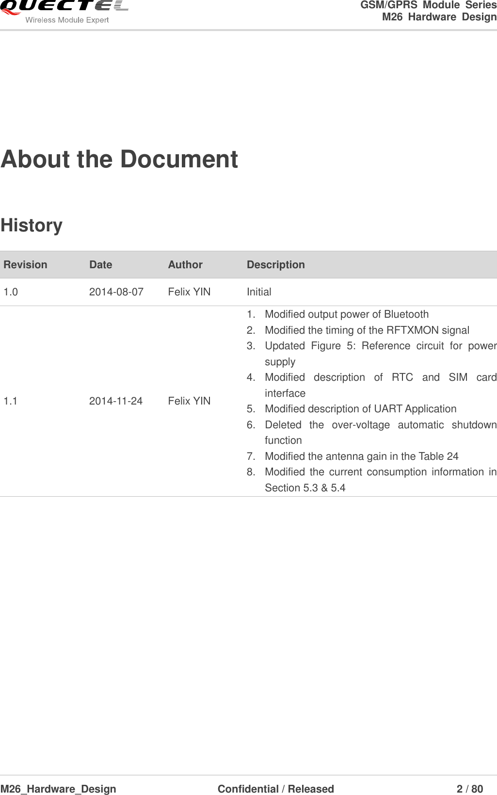
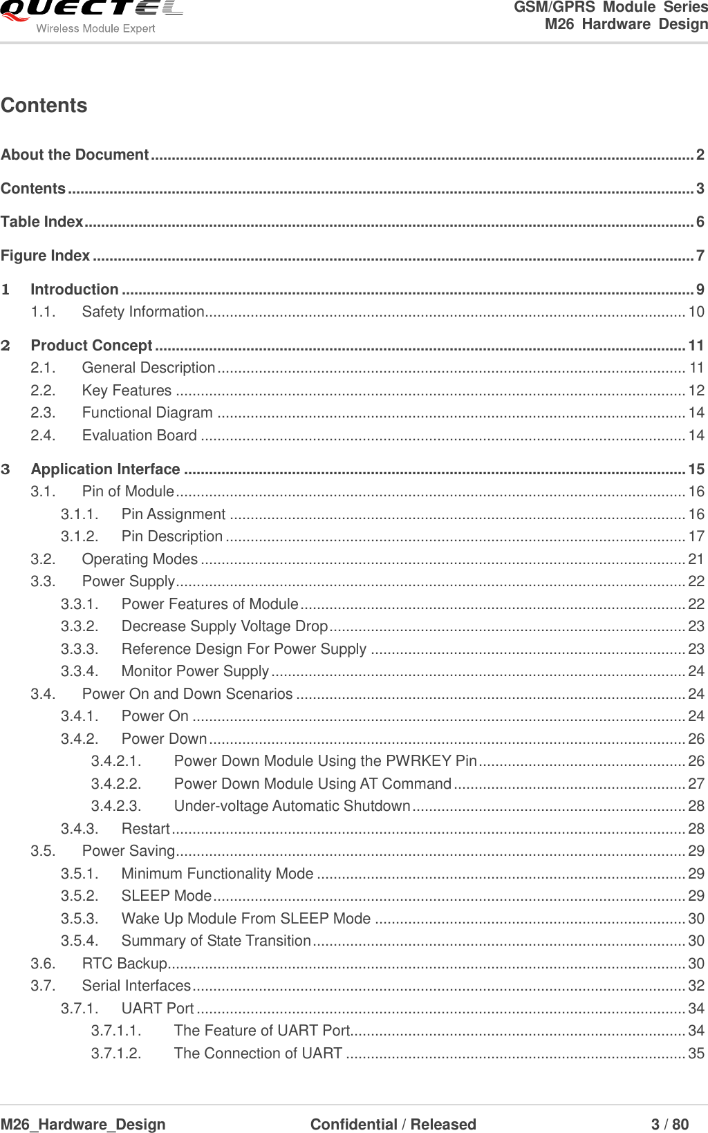
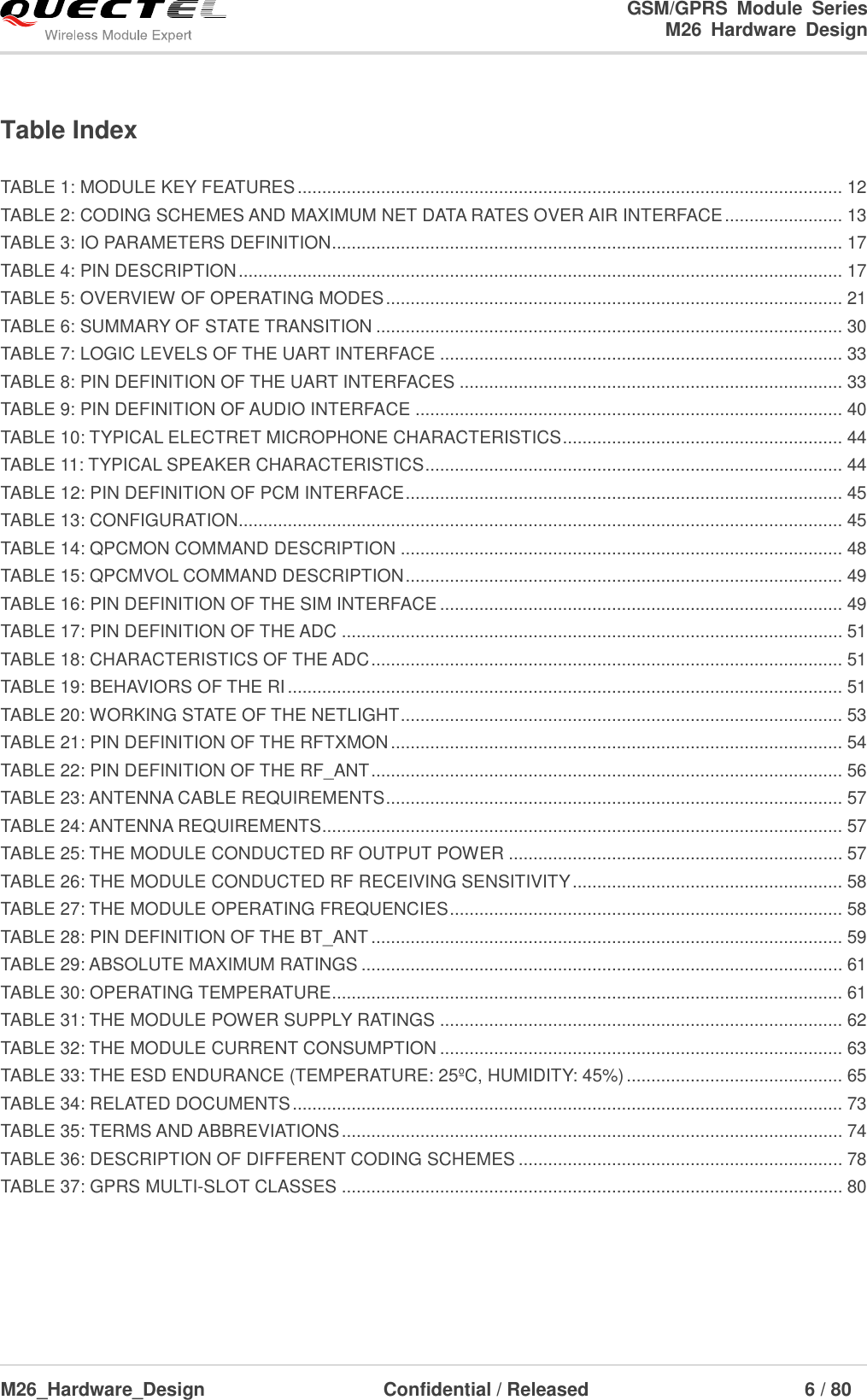
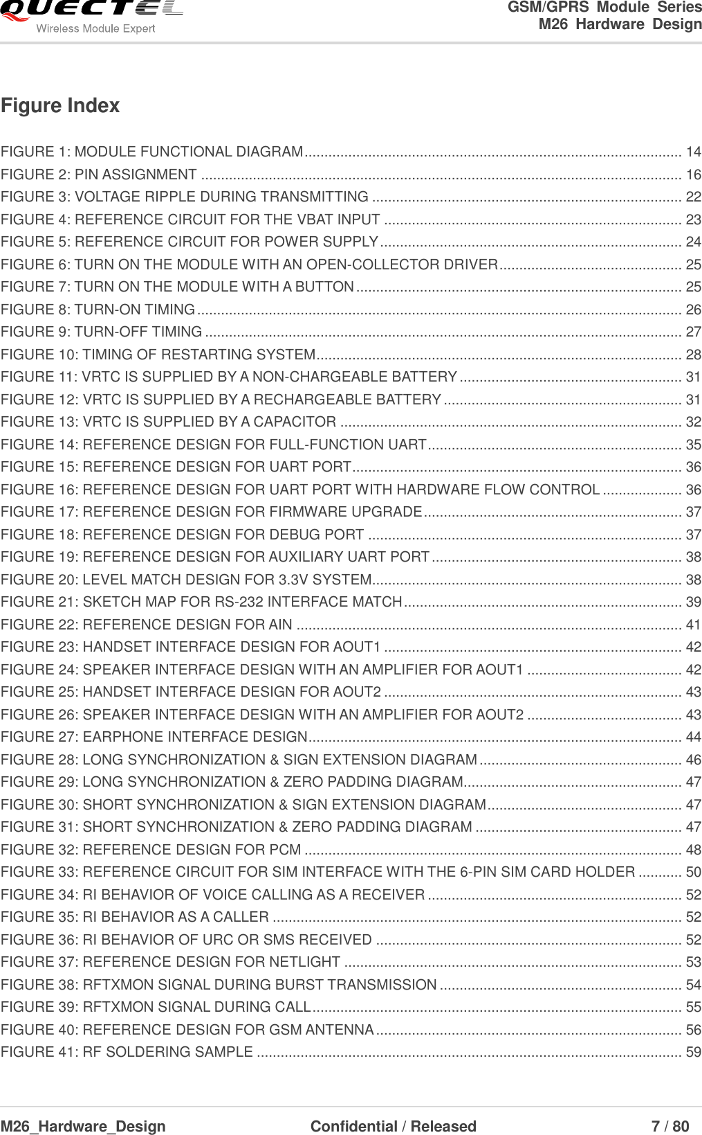
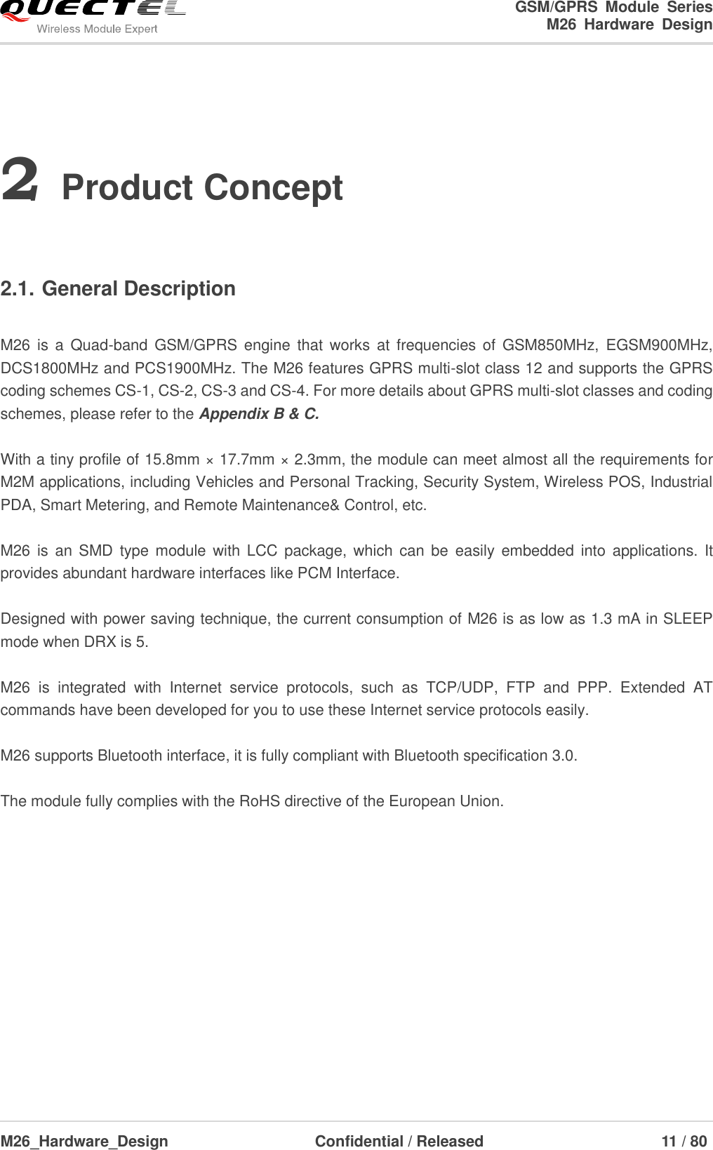
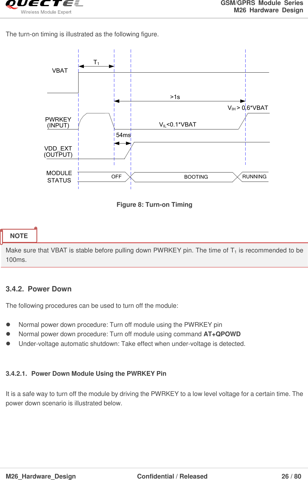
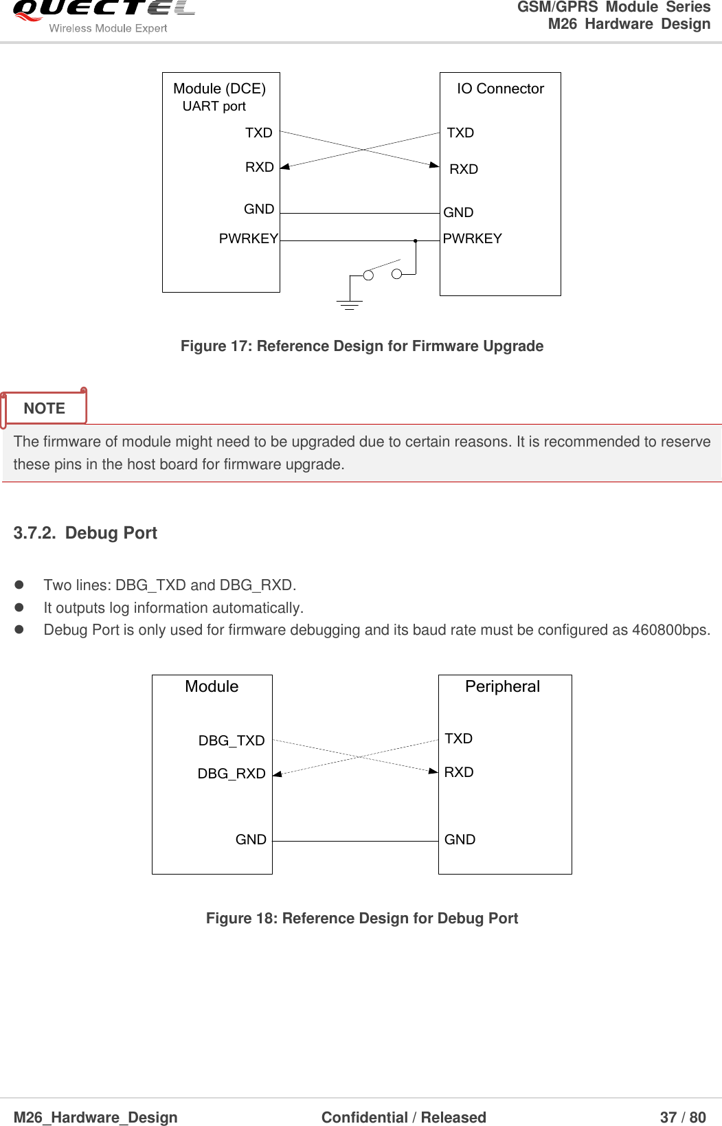
![GSM/GPRS Module Series M26 Hardware Design M26_Hardware_Design Confidential / Released 24 / 80 DC_INC1 C2MIC29302WU U1IN OUTENGNDADJ2 4135VBAT 100nFC3470uFC4100nFR2D1124K56KR3470uF 5.1VR4470RMCU_POWER_ON/OFF47K4.7KR5R6R151K Figure 5: Reference Circuit for Power Supply It is suggested to control the module’s main power supply (VBAT) via LDO enable pin to restart the module when the module has become abnormal. Power switch circuit like P-channel MOSFET switch circuit can also be used to control VBAT. 3.3.4. Monitor Power Supply The command ―AT+CBC‖ can be used to monitor the supply voltage of the module. The unit of the displayed voltage is mV. For details, please refer to the document [1]. 3.4. Power On and Down Scenarios 3.4.1. Power On The module can be turned on by driving the pin PWRKEY to a low level voltage. An open collector driver circuit is suggested to control the PWRKEY. A simple reference circuit is illustrated as below. NOTE](https://usermanual.wiki/Quectel-Wireless-Solutions/201604M26/User-Guide-3010680-Page-25.png)
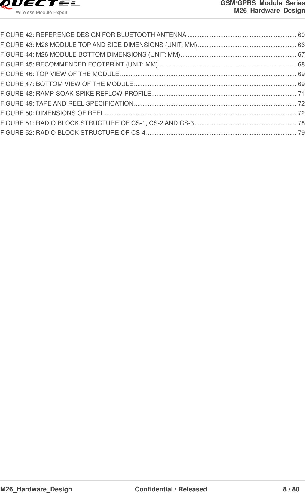
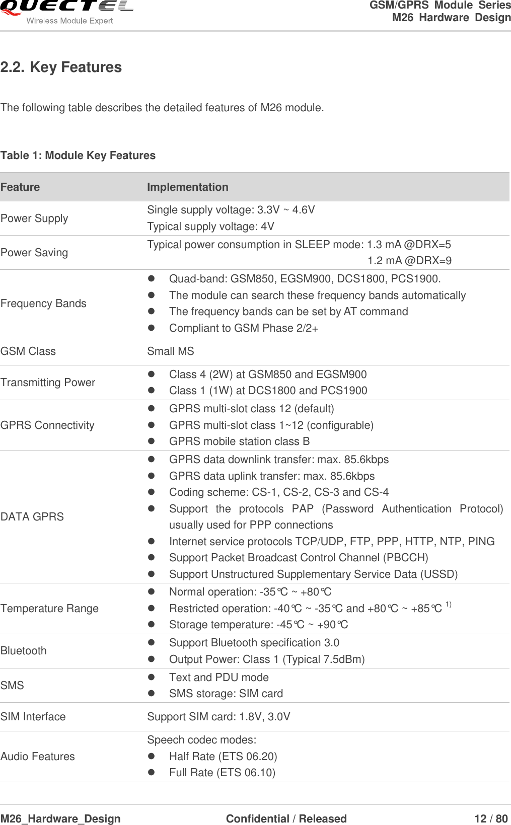
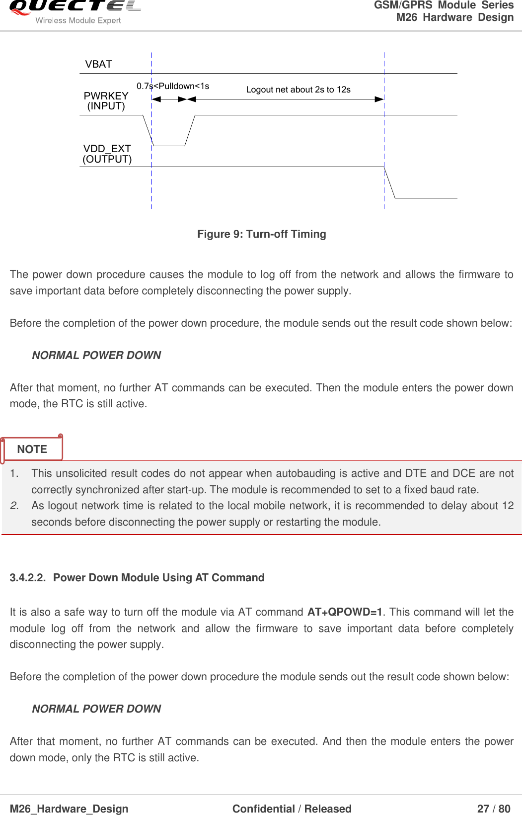
![GSM/GPRS Module Series M26 Hardware Design M26_Hardware_Design Confidential / Released 25 / 80 Turn on pulsePWRKEY4.7K47K Figure 6: Turn on the Module with an Open-collector Driver 1. M26 module is set to autobauding mode (AT+IPR=0) by default. In the autobauding mode, URC ―RDY‖ is not reported to the host controller after module is powered on. When the module is powered on after a delay of 4 or 5 seconds, it can receive AT command. Host controller should first send an AT string in order that the module can detect baud rate of host controller, and it should continue to send the next AT string until receiving OK string from the module. Then enter AT+IPR=x;&W to set a fixed baud rate for the module and save the configuration to flash memory of the module. After these configurations, the URC RDY would be received from the UART Port of the module every time when the module is powered on. For more details, refer to the section AT+IPR in document [1]. 2. When AT command is responded, indicates module is turned on successfully, or else the module fails to be turned on. The other way to control the PWRKEY is through a button directly. A TVS component is indispensable to be placed nearby the button for ESD protection. For the best performance, the TVS component must be placed nearby the button. When pressing the key, electrostatic strike may generate from finger. A reference circuit is shown in the following figure. PWRKEYS1Close to S1TVS Figure 7: Turn on the Module with a Button NOTE](https://usermanual.wiki/Quectel-Wireless-Solutions/201604M26/User-Guide-3010680-Page-26.png)
![GSM/GPRS Module Series M26 Hardware Design M26_Hardware_Design Confidential / Released 28 / 80 Please refer to the document [1] for details about the AT command AT+QPOWD. 3.4.2.3. Under-voltage Automatic Shutdown The module will constantly monitor the voltage applied on the VBAT, if the voltage is ≤3.5V, the following URC will be presented: UNDER_VOLTAGE WARNING The normal input voltage range is from 3.3V to 4.6V. If the voltage is <3.3V, the module would automatically shut down itself. If the voltage is <3.3V, the following URC will be presented: UNDER_VOLTAGE POWER DOWN After that moment, no further AT commands can be executed. The module logs off from network and enters power down mode, and only RTC is still active. These unsolicited result codes do not appear when autobauding is active and DTE and DCE are not correctly synchronized after start-up. The module is recommended to set to a fixed baud rate. 3.4.3. Restart You can restart the module by driving the PWRKEY to a low level voltage for a certain time, which is similar to the way of turning on module. In order to make the internal LDOs discharge completely after turning off the module, it is recommended to delay about 500ms before restarting the module. The restart timing is illustrated as the following figure. PWRKEY(INPUT)VDD_EXT(OUTPUT)Turn off RestartPull down the PWRKEY to turn on the moduleDelay >0.5s Figure 10: Timing of Restarting System NOTES](https://usermanual.wiki/Quectel-Wireless-Solutions/201604M26/User-Guide-3010680-Page-29.png)
![GSM/GPRS Module Series M26 Hardware Design M26_Hardware_Design Confidential / Released 29 / 80 3.5. Power Saving Based on system requirements, there are several actions to drive the module to enter low current consumption status. For example, AT+CFUN can be used to set module into minimum functionality mode and DTR hardware interface signal can be used to lead system to SLEEP mode. 3.5.1. Minimum Functionality Mode Minimum functionality mode reduces the functionality of the module to a minimum level. The consumption of the current can be minimized when the slow clocking mode is activated at the same time. The mode is set with the AT+CFUN command which provides the choice of the functionality levels <fun>=0, 1, 4. 0: minimum functionality 1: full functionality (default) 4: disable both transmitting and receiving of RF part If the module is set to minimum functionality by AT+CFUN=0, the RF function and SIM card function would be disabled. In this case, the UART port is still accessible, but all AT commands related with RF function or SIM card function will be not available. If the module has been set by the command with AT+CFUN=4, the RF function will be disabled, but the UART port is still active. In this case, all AT commands related with RF function will be not available. After the module is set by AT+CFUN=0 or AT+CFUN=4, it can return to full functionality by AT+CFUN=1. For detailed information about AT+CFUN, please refer to the document [1]. 3.5.2. SLEEP Mode The SLEEP mode is disabled by default. You can enable it by AT+QSCLK=1. On the other hand, the default setting is AT+QSCLK=0 and in this mode, the module cannot enter SLEEP mode. When the module is set by the command with AT+QSCLK=1, you can control the module to enter or exit from the SLEEP mode through pin DTR. When DTR is set to high level, and there is no on-air or hardware interrupt such as GPIO interrupt or data on UART port, the module will enter SLEEP mode automatically. In this mode, the module can still receive voice, SMS or GPRS paging from network, but the UART port does not work.](https://usermanual.wiki/Quectel-Wireless-Solutions/201604M26/User-Guide-3010680-Page-30.png)
![GSM/GPRS Module Series M26 Hardware Design M26_Hardware_Design Confidential / Released 33 / 80 Hardware flow control is disabled by default. When hardware flow control is required, RTS and CTS should be connected to the host. AT command AT+IFC=2,2 is used to enable hardware flow control. AT command AT+IFC=0,0 is used to disable the hardware flow control. For more details, please refer to the document [1]. The Debug Port: DBG_TXD: Send data to the COM port of computer. DBG_RXD: Receive data from the COM port of computer. The Auxiliary UART Port: TXD_AUX: Send data to the RXD of DTE. RXD_AUX: Receive data from the TXD of DTE. The logic levels are described in the following table. Table 7: Logic Levels of the UART Interface Table 8: Pin Definition of the UART Interfaces Parameter Min. Max. Unit VIL 0 0.25×VDD_EXT V VIH 0.75×VDD_EXT VDD_EXT +0.2 V VOL 0 0.15×VDD_EXT V VOH 0.85×VDD_EXT VDD_EXT V Interface Pin Name Pin No. Description UART Port TXD 18 Transmit data RXD 17 Receive data DTR 19 Data terminal ready RI 20 Ring indication NOTE](https://usermanual.wiki/Quectel-Wireless-Solutions/201604M26/User-Guide-3010680-Page-34.png)
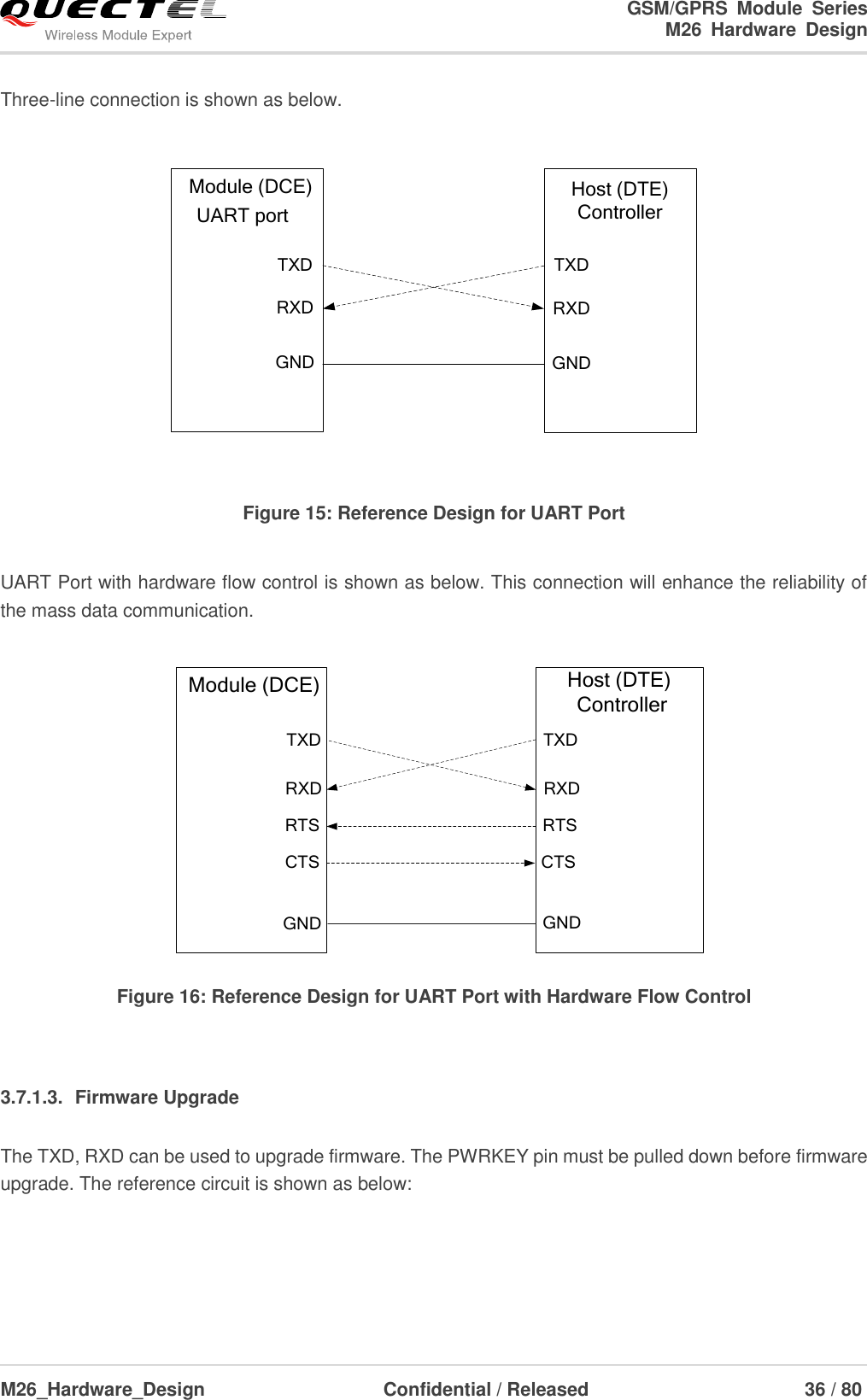
![GSM/GPRS Module Series M26 Hardware Design M26_Hardware_Design Confidential / Released 35 / 80 If the host controller needs URC in the mode of autobauding, it must be synchronized firstly. Otherwise the URC will be discarded. Restrictions on autobauding operation: The UART port has to be operated at 8 data bits, no parity and 1 stop bit (factory setting). The ―At‖ and ―aT‖ commands cannot be used. Only the strings ―AT‖ or ―at‖ can be detected (neither ―At‖ nor ―aT‖). The Unsolicited Result Codes like RDY, +CFUN: 1 and +CPIN: READY will not be indicated when the module is turned on with autobauding enabled and not be synchronized. Any other Unsolicited Result Codes will be sent at the previous baud rate before the module detects the new baud rate by receiving the first ―AT‖ or ―at‖ string. The DTE may receive unknown characters after switching to new baud rate. It is not recommended to switch to autobauding from a fixed baud rate. If autobauding is active it is not recommended to switch to multiplex mode. To assure reliable communication and avoid any problems caused by undetermined baud rate between DCE and DTE, it is strongly recommended to configure a fixed baud rate and save it instead of using autobauding after start-up. For more details, please refer to the Section AT+IPR in document [1]. 3.7.1.2. The Connection of UART The connection between module and host using UART Port is very flexible. Three connection styles are illustrated as below. Reference design for Full-Function UART connection is shown as below when it is applied in modulation-demodulation. TXDRXDRTSCTSDTRDCDRITXDRXDRTSCTSDTRDCDRINGModule (DCE)Serial portUART portGND GNDPC (DTE) Figure 14: Reference Design for Full-Function UART NOTE](https://usermanual.wiki/Quectel-Wireless-Solutions/201604M26/User-Guide-3010680-Page-36.png)
![GSM/GPRS Module Series M26 Hardware Design M26_Hardware_Design Confidential / Released 38 / 80 3.7.3. Auxiliary UART Port Two data lines: TXD_AUX and RXD_AUX. Auxiliary UART port is used for AT command only and does not support GPRS data, Multiplexing function etc. Auxiliary UART port supports the communication baud rates as the following: 1200, 2400, 4800, 9600, 14400, 19200, 28800, 38400, 57600, 115200. Auxiliary UART port could be used when you send AT+QEAUART=1 string on the UART port. The default baud rate setting is 115200bps, and does not support autobauding. The baud rate can be modified by AT+QSEDCB command. For more details, please refer to the document [1]. PeripheralTXDRXDGND Module TXD_AUXRXD_AUX GND Figure 19: Reference Design for Auxiliary UART Port 3.7.4. UART Application The reference design of 3.3V level match is shown as below. If the host is a 3V system, please change the 5.6K resistor to 10K. Peripheral/TXD/RXD1KTXDRXDRTSCTSDTRRI/RTS/CTSGPIOEINTGPIO DCDModule1K1KVoltage level:3.3V5.6K5.6K5.6K1K1K1K1KGND GND Figure 20: Level Match Design for 3.3V System](https://usermanual.wiki/Quectel-Wireless-Solutions/201604M26/User-Guide-3010680-Page-39.png)
![GSM/GPRS Module Series M26 Hardware Design M26_Hardware_Design Confidential / Released 39 / 80 It is highly recommended to add the resistor divider circuit on the UART signal lines when the host’s level is 3V or 3.3V. For the higher voltage level system, a level shifter IC could be used between the host and the module. For more details about UART circuit design, please refer to document [13]. The following figure shows a sketch map between module and standard RS-232 interface. Since the electrical level of module is 2.8V, so a RS-232 level shifter must be used. Note that you should assure the IO voltage of level shifter which connects to module is 2.8V. TXDRXDRTSCTSDTRRIDCDModuleGNDC1+C1-C2+C2-V+VCCGNDV-3.3VT1INT2INT3INT4INR1INR2INR3INR1OUTR2OUTR3OUTT1OUTT2OUTT5OUTT3OUTT4OUTT5INGNDGND/R1OUT123456789GNDTo PC Serial PortGND1K1K1K1K1K5.6K5.6K1K1K5.6KRS-232 Level Shifter Figure 21: Sketch Map for RS-232 Interface Match Please visit vendor web site to select suitable IC, such as: http://www.maximintegrated.com and http://www.exar.com/. NOTE](https://usermanual.wiki/Quectel-Wireless-Solutions/201604M26/User-Guide-3010680-Page-40.png)
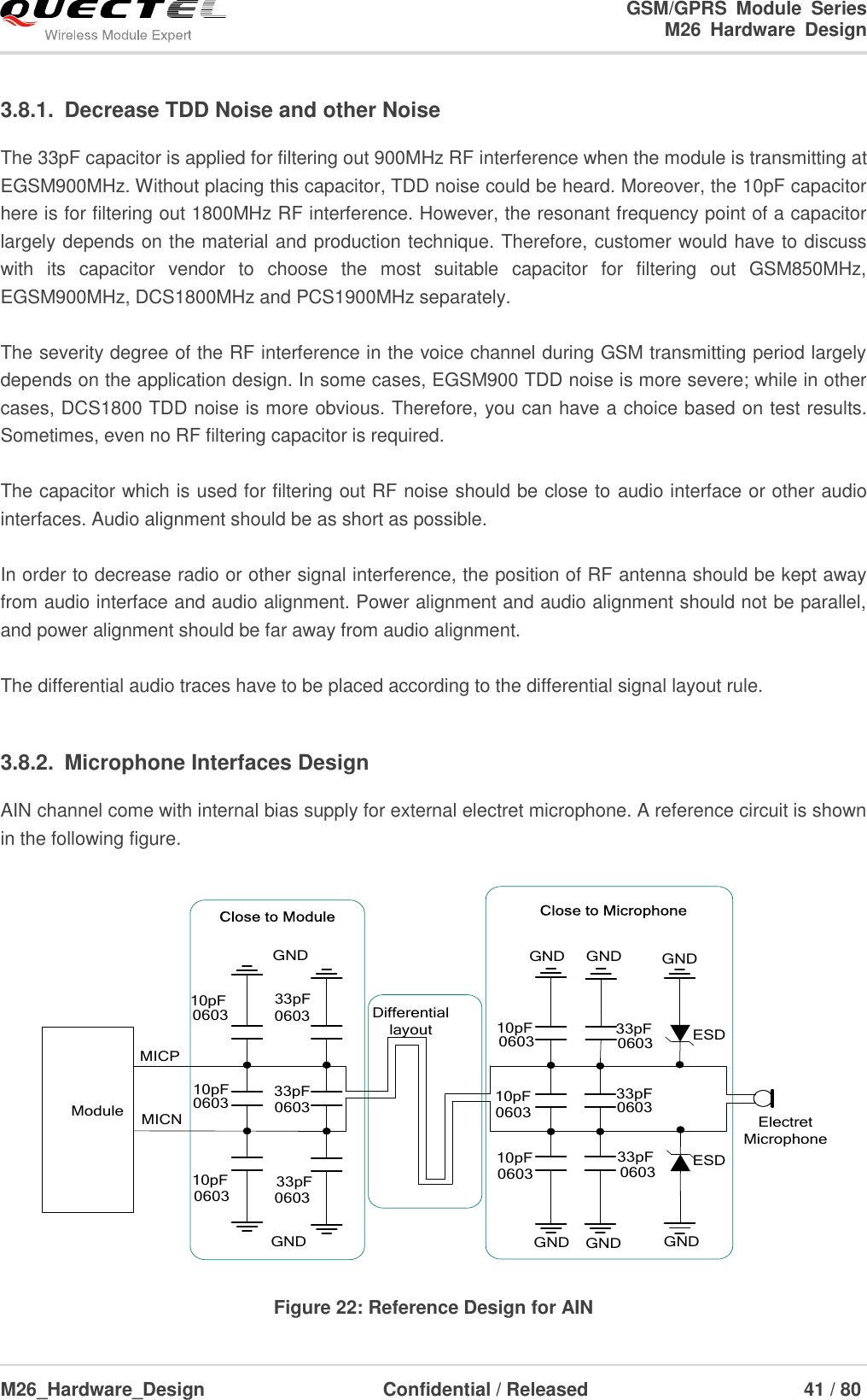
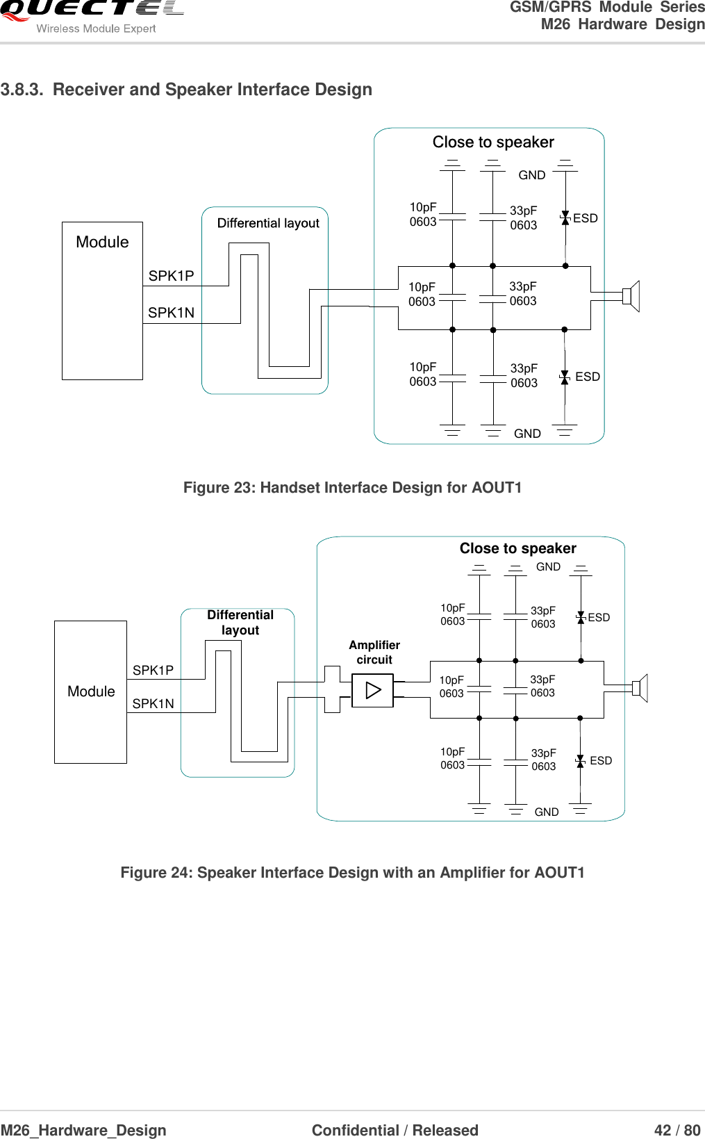
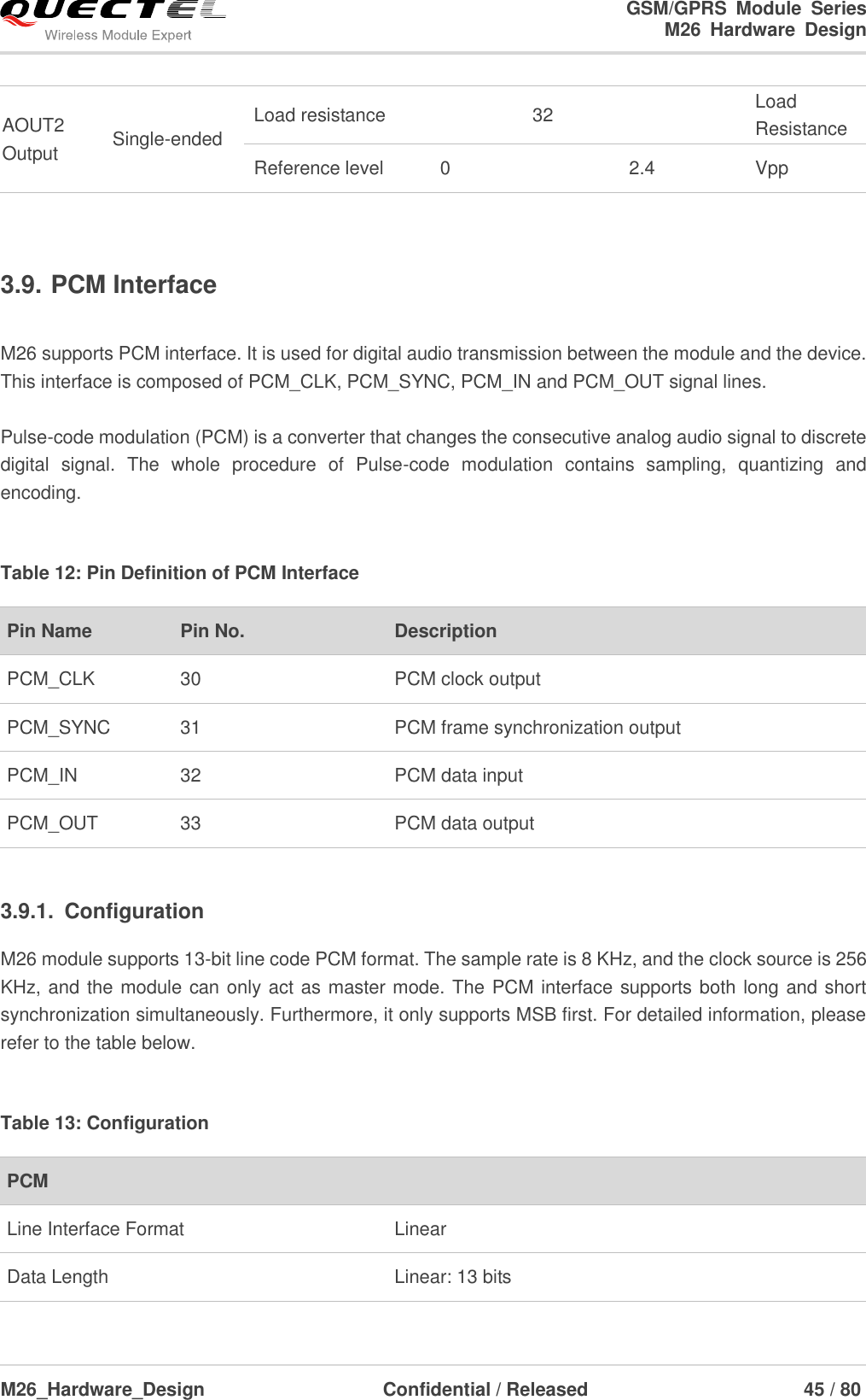
![GSM/GPRS Module Series M26 Hardware Design M26_Hardware_Design Confidential / Released 40 / 80 3.8. Audio Interfaces The module provides one analog input channels and two analog output channels. Table 9: Pin Definition of Audio Interface AIN can be used for input of microphone and line. An electret microphone is usually used. AIN are differential input channels. AOUT1 is used for output of the receiver. This channel is typically used for a receiver built into a handset. AOUT1 channel is a differential channel. AOUT2 is typically used with earphone. It is a single-ended and mono channel. SPK2P and AGND can establish a pseudo differential mode. All of these two audio channels support voice and ringtone output, and so on, and can be switched by AT+QAUDCH command. For more details, please refer to the document [1]. Use AT command AT+QAUDCH to select audio channel: 0--AIN/AOUT1, the default value is 0. 1--AIN/AOUT2, this channel is always used for earphone. For each channel, you can use AT+QMIC to adjust the input gain level of microphone. You can also use AT+CLVL to adjust the output gain level of receiver and speaker. AT+QSIDET is used to set the side-tone gain level. For more details, please refer to the document [1]. Interface Pin Name Pin No. Description AIN/AOUT1 MICP 3 Microphone positive input MICN 4 Microphone negative input SPK1P 5 Channel 1 Audio positive output SPK1N 6 Channel 1 Audio negative output AIN/AOUT2 MICP 3 Microphone positive input MICN 4 Microphone negative input SPK2P 2 Channel 2 Audio positive output AGND 1 Form a pseudo-differential pair with SPK2P](https://usermanual.wiki/Quectel-Wireless-Solutions/201604M26/User-Guide-3010680-Page-41.png)
![GSM/GPRS Module Series M26 Hardware Design M26_Hardware_Design Confidential / Released 51 / 80 3.11. ADC The module provides an ADC channel to measure the value of voltage. Please give priority to the use of ADC0 channel. The command AT+QADC can read the voltage value applied on ADC0 pin. For details of this AT command, please refer to the document [1]. In order to improve the accuracy of ADC, the layout of ADC should be surrounded by ground. Table 17: Pin Definition of the ADC Table 18: Characteristics of the ADC 3.12. Behaviors of The RI Table 19: Behaviors of the RI Pin Name Pin No. Description AVDD 8 Reference voltage of ADC circuit ADC0 9 Analog to digital converter. Item Min. Typ. Max. Units Voltage Range 0 2.8 V ADC Resolution 10 bits ADC Accuracy 2.7 mV State RI Response Standby HIGH Voicecall Change to LOW, then: 1. Change to HIGH when call is established. 2. Use ATH to hang up the call, RI changes to HIGH. 3. Calling part hangs up, RI changes to HIGH first, and changes to LOW for 120ms indicating ―NO CARRIER‖ as an URC, then changes to HIGH again. 4. Change to HIGH when SMS is received. SMS When a new SMS comes, the RI changes to LOW and holds low level for about](https://usermanual.wiki/Quectel-Wireless-Solutions/201604M26/User-Guide-3010680-Page-52.png)
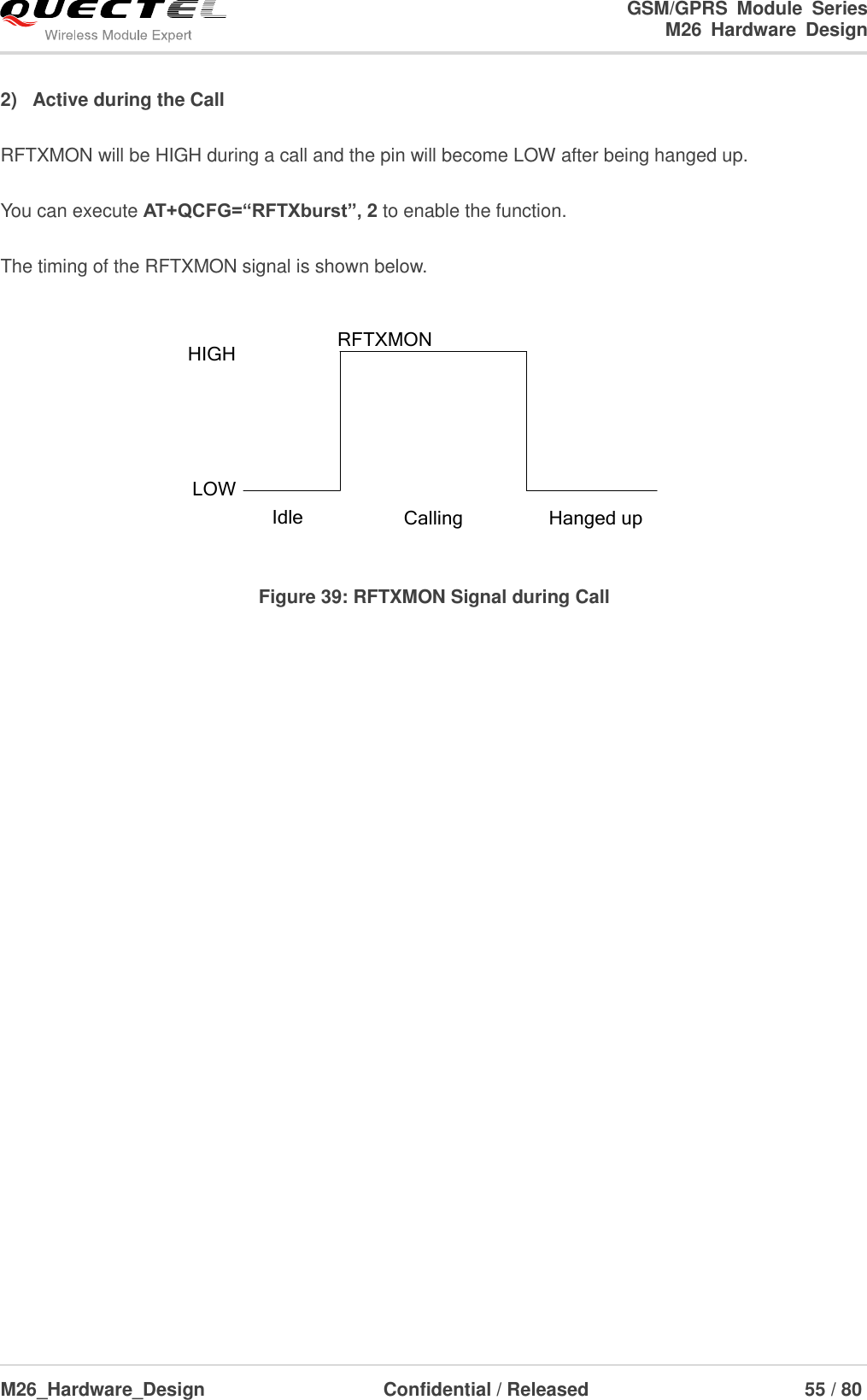
![GSM/GPRS Module Series M26 Hardware Design M26_Hardware_Design Confidential / Released 52 / 80 If the module is used as a caller, the RI would maintain high except the URC or SMS is received. On the other hand, when it is used as a receiver, the timing of the RI is shown below. RIIdle RingOff-hook by “ATA”On-hook by “ATH”HIGHLOW SMS received Figure 34: RI Behavior of Voice Calling as a Receiver RIIdle Calling On-hookTalkingHIGHLOWIdle Figure 35: RI Behavior as a Caller RIIdle or Talking URC or SMS received HIGHLOW120ms Figure 36: RI Behavior of URC or SMS Received 120ms, then changes to HIGH. URC Certain URCs can trigger 120ms low level on RI. For more details, please refer to the document [1]](https://usermanual.wiki/Quectel-Wireless-Solutions/201604M26/User-Guide-3010680-Page-53.png)
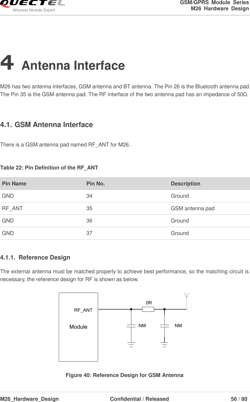
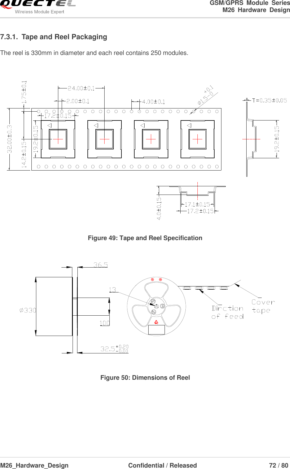
![GSM/GPRS Module Series M26 Hardware Design M26_Hardware_Design Confidential / Released 71 / 80 7.2. Soldering The squeegee should push the paste on the surface of the stencil that makes the paste fill the stencil openings and penetrate to the PCB. The force on the squeegee should be adjusted so as to produce a clean stencil surface on a single pass. To ensure the module soldering quality, the thickness of stencil at the hole of the module pads should be 0.2 mm for M26.For more details, please refer to document [12] It is suggested that peak reflow temperature is from 235ºC to 245ºC (for SnAg3.0Cu0.5 alloy). Absolute max reflow temperature is 260ºC. To avoid damage to the module when it was repeatedly heated, it is suggested that the module should be mounted after the first panel has been reflowed. The following picture is the actual diagram which we have operated. Time(s)50 100 150 200 250 30050100150200250 160℃ 200℃217070s~120s40s~60sBetween 1~3℃/SPreheat Heating Cooling℃sLiquids Temperature Figure 48: Ramp-Soak-Spike Reflow Profile 7.3. Packaging The modules are stored in a vacuum-sealed bag which is ESD protected. It should not be opened until the devices are ready to be soldered onto the application.](https://usermanual.wiki/Quectel-Wireless-Solutions/201604M26/User-Guide-3010680-Page-72.png)
![GSM/GPRS Module Series M26 Hardware Design M26_Hardware_Design Confidential / Released 73 / 80 8 Appendix A Reference Table 34: Related Documents SN Document Name Remark [1] Quectel_M26_AT_Commands_Manual AT commands manual [2] ITU-T Draft new recommendation V.25ter Serial asynchronous automatic dialing and control [3] GSM 07.07 Digital cellular telecommunications (Phase 2+); AT command set for GSM Mobile Equipment (ME) [4] GSM 07.10 Support GSM 07.10 multiplexing protocol [5] GSM 07.05 Digital cellular telecommunications (Phase 2+); Use of Data Terminal Equipment – Data Circuit terminating Equipment (DTE – DCE) interface for Short Message Service (SMS) and Cell Broadcast Service (CBS) [6] GSM 11.14 Digital cellular telecommunications (Phase 2+); Specification of the SIM Application Toolkit for the Subscriber Identity module – Mobile Equipment (SIM – ME) interface [7] GSM 11.11 Digital cellular telecommunications (Phase 2+); Specification of the Subscriber Identity module – Mobile Equipment (SIM – ME) interface [8] GSM 03.38 Digital cellular telecommunications (Phase 2+); Alphabets and language-specific information [9] GSM 11.10 Digital cellular telecommunications (Phase 2); Mobile Station (MS) conformance specification; Part 1: Conformance specification](https://usermanual.wiki/Quectel-Wireless-Solutions/201604M26/User-Guide-3010680-Page-74.png)
![GSM/GPRS Module Series M26 Hardware Design M26_Hardware_Design Confidential / Released 74 / 80 Table 35: Terms and Abbreviations [10] GSM_UART_Application_Note UART port application note [11] GSM_EVB_User_Guide GSM EVB user guide [12] Module_Secondary_SMT_User_Guide Module secondary SMT user guide [13] Quectel_GSM_Module_Digital_IO_Application_Note GSM Module Digital IO Application Note Abbreviation Description ADC Analog-to-Digital Converter AMR Adaptive Multi-Rate ARP Antenna Reference Point ASIC Application Specific Integrated Circuit BER Bit Error Rate BOM Bill of Material BT Bluetooth BTS Base Transceiver Station CHAP Challenge Handshake Authentication Protocol CS Coding Scheme CSD Circuit Switched Data CTS Clear to Send DAC Digital-to-Analog Converter DRX Discontinuous Reception DSP Digital Signal Processor DCE Data Communications Equipment (typically module) DTE Data Terminal Equipment (typically computer, external controller) DTR Data Terminal Ready](https://usermanual.wiki/Quectel-Wireless-Solutions/201604M26/User-Guide-3010680-Page-75.png)