Quectel Wireless Solutions 201605EC25A LTE Module User Manual
Quectel Wireless Solutions Company Limited LTE Module Users Manual
UserManual.wiki
>
Quectel Wireless Solutions
>
201605EC25A User Manual
>
Users Manual
Contents
1.
Users Manual
2.
User Manual
3.
User Manual-Statement
Users Manual
Navigation menu
Upload a User Manual
Namespaces
Wiki Guide
HTML
PDF
Info
Views
User Manual
Discussion / Help
Navigation

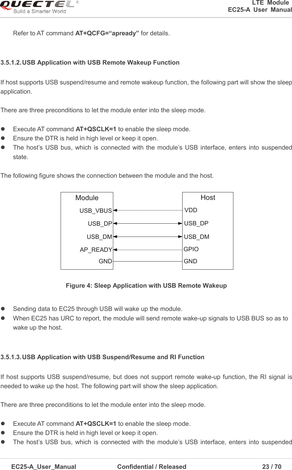
![0 LTE Module EC25-A User Manual EC25-A_User_Manual Confidential / Released 25 / 7 Opening power switch to supply power to USB_VBUS will wake up the module. You should pay attention to the level match shown in dotted line between module and host. Refer to document [1] for more details about EC25 power management application. 3.5.2. Airplane Mode When the module enters into airplane mode, the RF function does not work, and all AT commands correlative with RF function will be inaccessible. This mode can be set with the following ways. Hardware: The W_DISABLE# pin is pulled up by default; driving it to low level will let the module enter into airplane mode. Software: Command AT+CFUN provides the choice of the functionality level <fun>=0, 1, 4. AT+CFUN=0: Minimum functionality mode; both USIM and RF function are disabled. AT+CFUN=1: Full functionality mode (by default). AT+CFUN=4: Airplane mode. RF function is disabled. 1. The W_DISABLE# control function is disabled in firmware by default. It can be enabled by AT command AT+QCFG=“airplanecontrol”. Refer to document [2] for details. 2. The execution of AT+CFUN command will not affect GNSS function. 3.6. Power Supply 3.6.1. Power Supply Pins EC25 provides four VBAT pins dedicated to connect with the external power supply. There are two separate voltage domains for VBAT. VBAT_RF with two pins for module RF part. VBAT_BB with two pins for module baseband part. The following table shows the VBAT pins and ground pins. NOTES NOTE](https://usermanual.wiki/Quectel-Wireless-Solutions/201605EC25A.Users-Manual/User-Guide-3067025-Page-26.png)
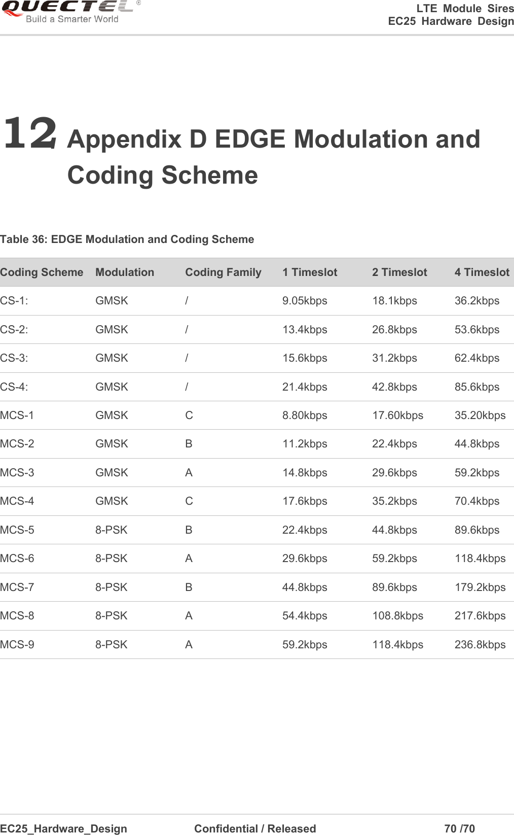
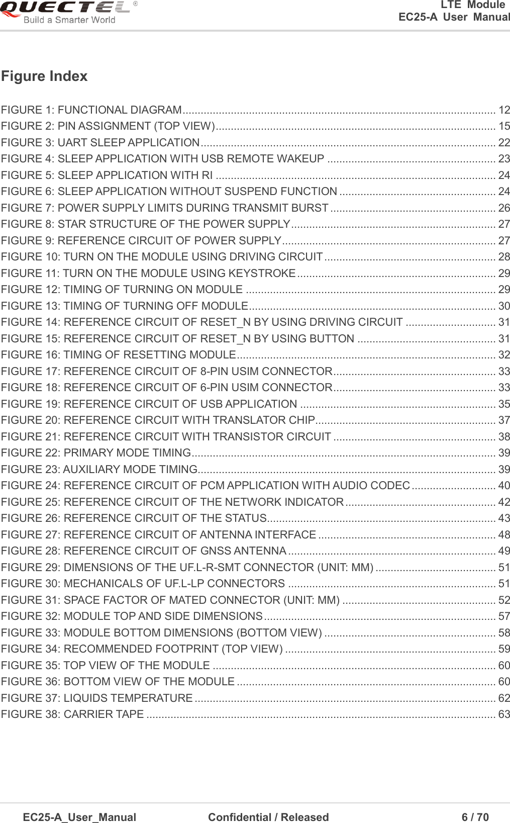
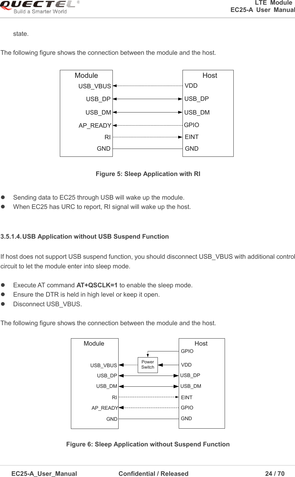
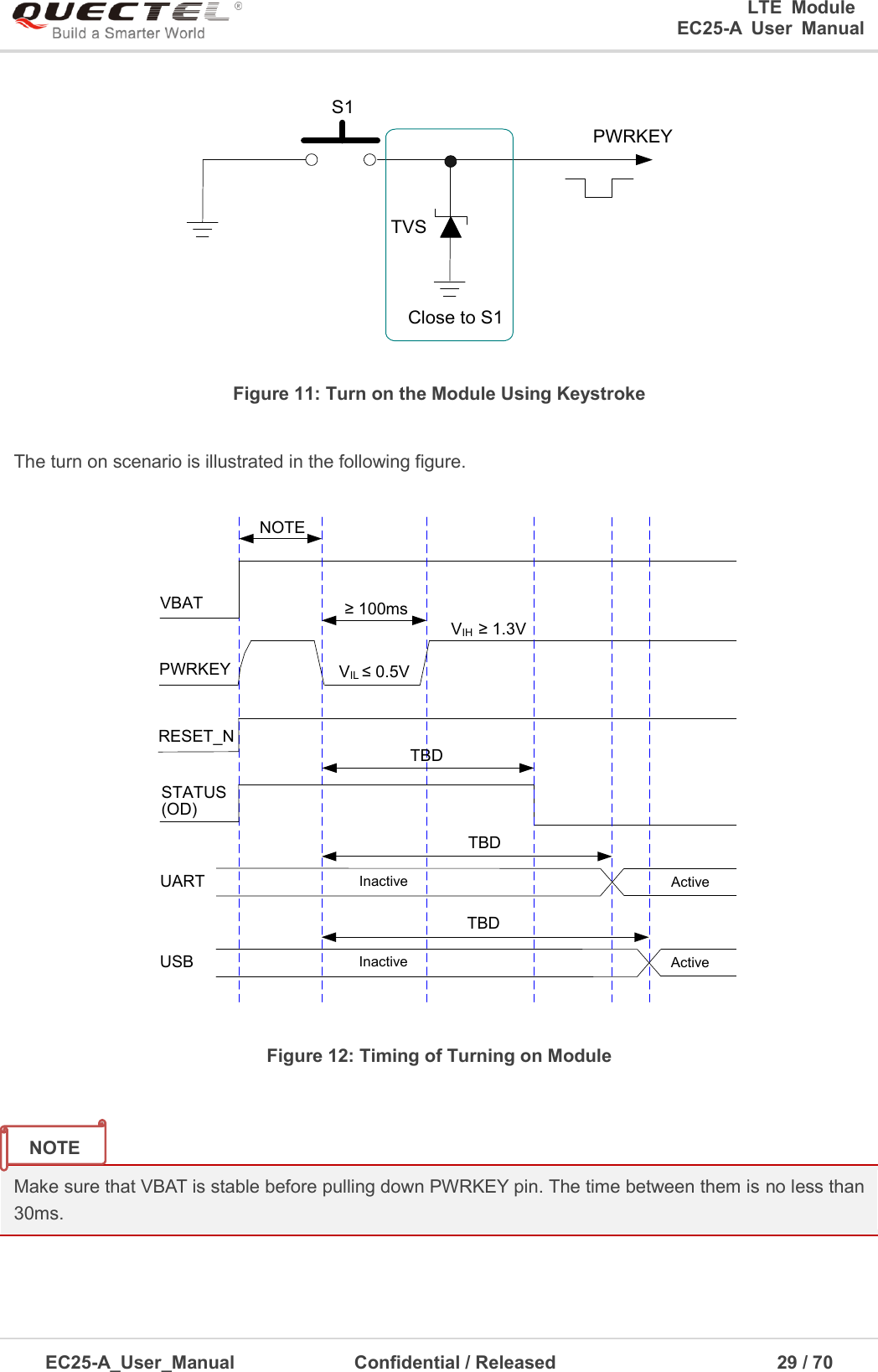
![0 LTE Module EC25-A User Manual EC25-A_User_Manual Confidential / Released 28 / 7 3.6.4. Monitor the Power Supply You can use the AT+CBC command to monitor the VBAT_BB voltage value. For more details, please refer to document [2]. 3.7. Turn on and off Scenarios 3.7.1. Turn on Module Using the PWRKEY The following table shows the pin definition of PWRKEY. Table 7: PWRKEY Pin Description Pin Name Pin No. Description DC Characteristics Comment PWRKEY 21 Turn on/off the module. VIHmax=2.1V VIHmin=1.3V VILmax=0.5V When EC25 is in power down mode, it can be turned on to normal mode by driving the PWRKEY pin to a low level for at least 100ms. It is recommended to use an open drain/collector driver to control the PWRKEY. After STATUS pin (require external pull-up) outputting a low level, PWRKEY pin can be released. A simple reference circuit is illustrated in the following figure. Turn on pulsePWRKEY4.7K47K≥ 100msFigure 10: Turn on the Module Using Driving Circuit The other way to control the PWRKEY is using a button directly. A TVS component is indispensable to be placed nearby the button for ESD protection. When pressing the key, electrostatic strike may generate from finger. A reference circuit is shown in the following figure.](https://usermanual.wiki/Quectel-Wireless-Solutions/201605EC25A.Users-Manual/User-Guide-3067025-Page-29.png)
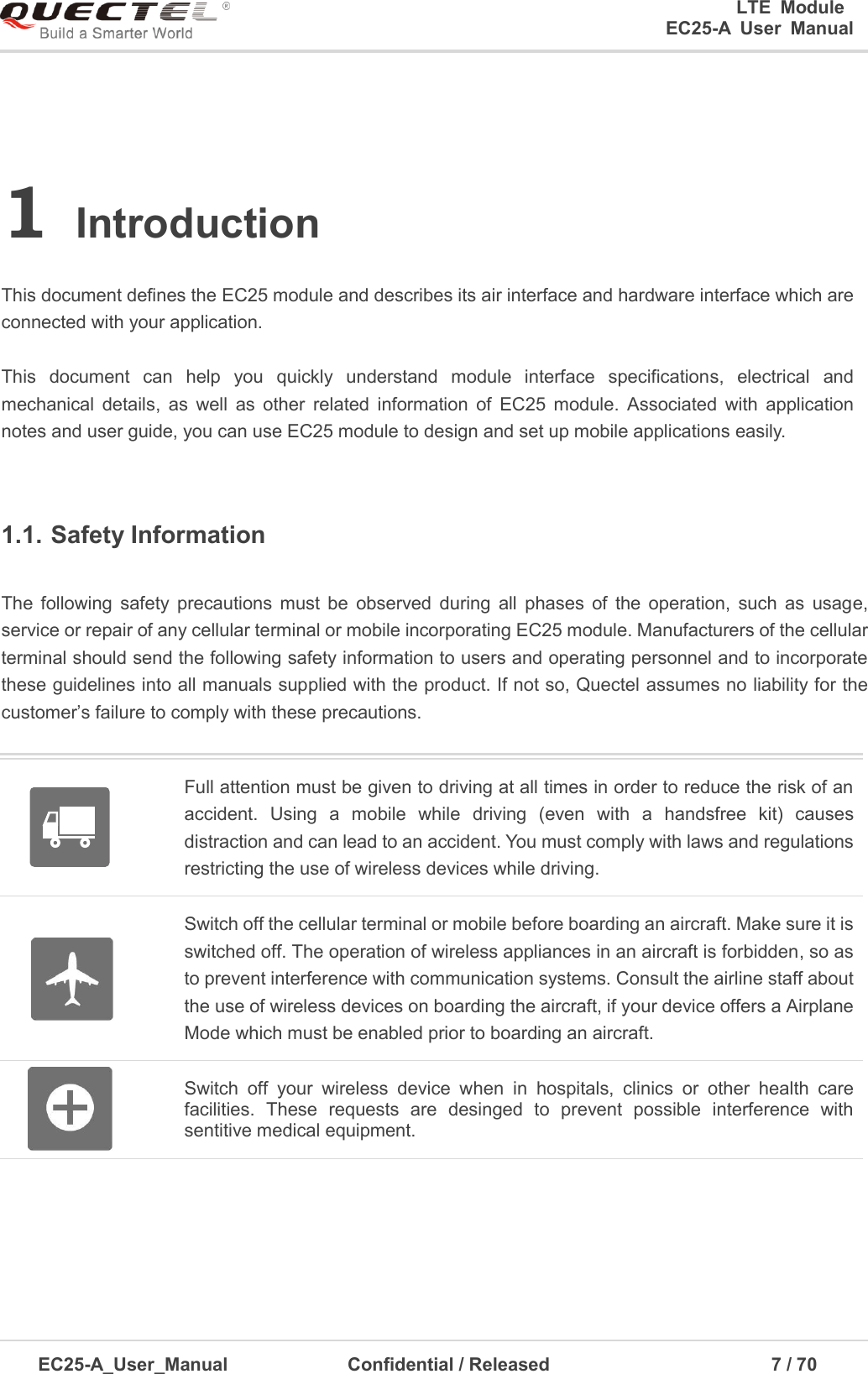
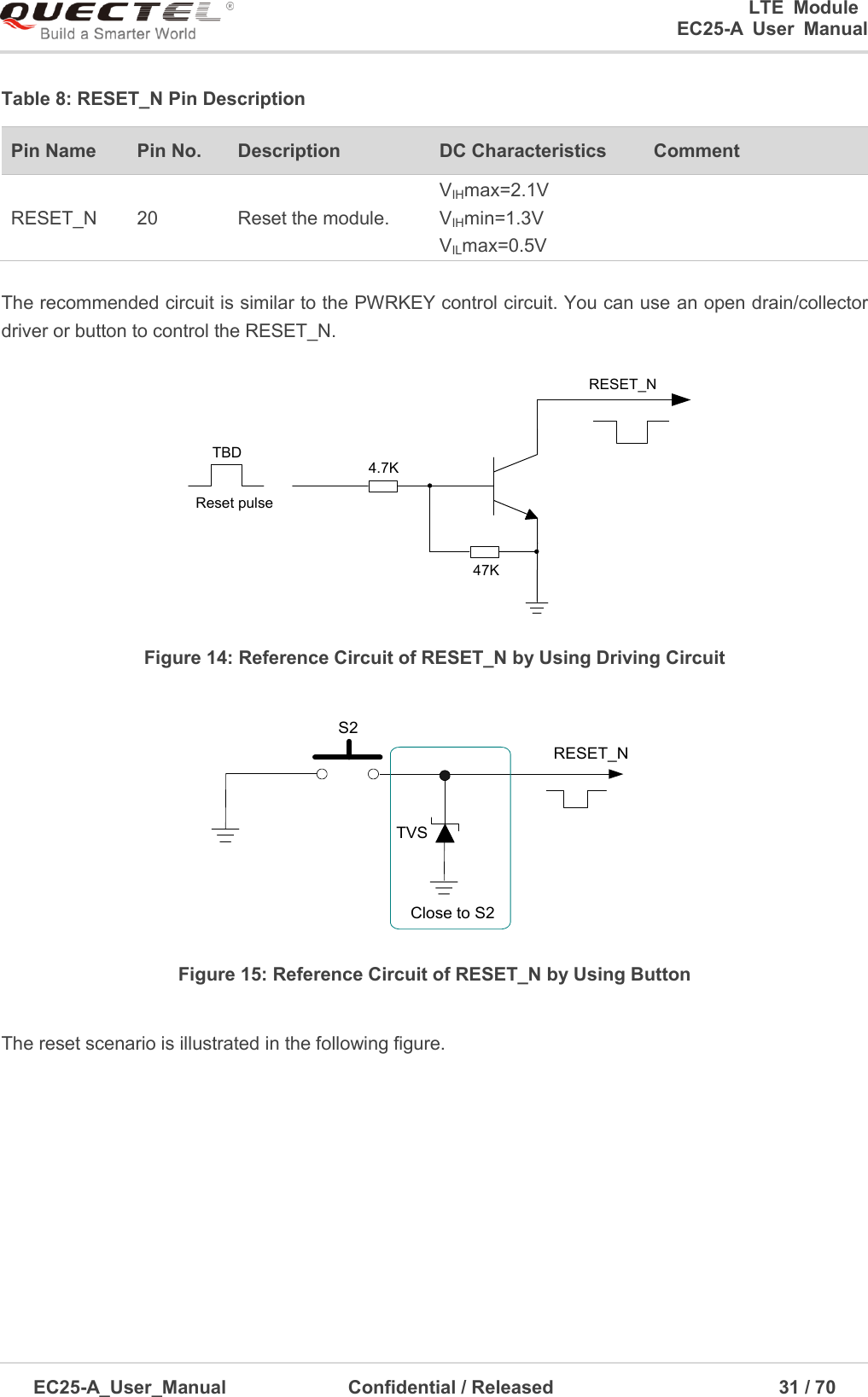
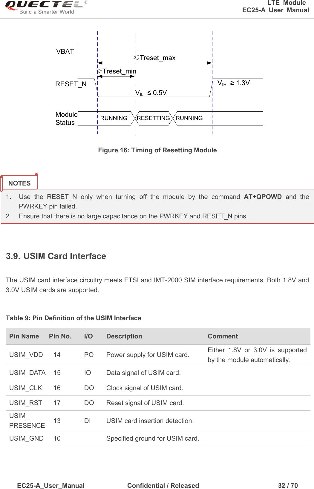
![0 LTE Module EC25-A User Manual EC25-A_User_Manual Confidential / Released 30 / 7 3.7.2. Turn off Module The following procedures can be used to turn off the module: Normal power down procedure: Turn off the module using the PWRKEY pin.Normal power down procedure: Turn off the module using command AT+QPOWD.3.7.2.1. Turn off Module Using the PWRKEY Pin Driving the PWRKEY to a low level voltage, the module will execute power-down procedure after the PWRKEY is released. The power-down scenario is illustrated in the following figure. VBATPWRKEYTBDTBDRUNNING Power-down procedure OFFModuleStatusSTATUS(OD)Figure 13: Timing of Turning off Module 3.7.2.2. Turn off Module Using AT Command It is also a safe way to use AT command AT+QPOWD to turn off the module, which is similar to turning off the module via PWRKEY Pin. Please refer to document [2] for details about the AT command of AT+QPOWD. 3.8. Reset the Module The RESET_N can be used to reset the module. You can reset the module by driving the RESET_N to a low level voltage for time between Treset_min and Treset_max.](https://usermanual.wiki/Quectel-Wireless-Solutions/201605EC25A.Users-Manual/User-Guide-3067025-Page-31.png)
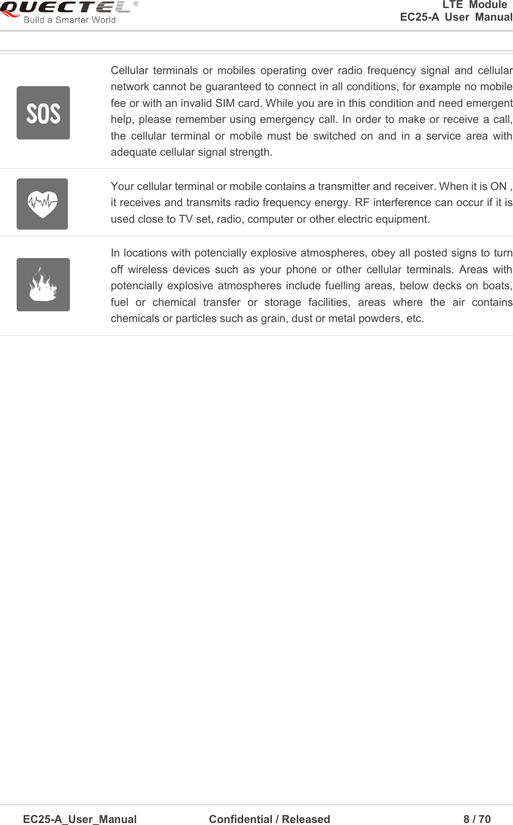
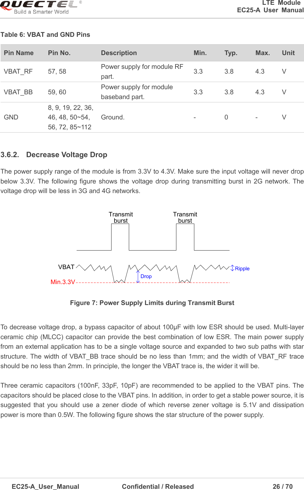
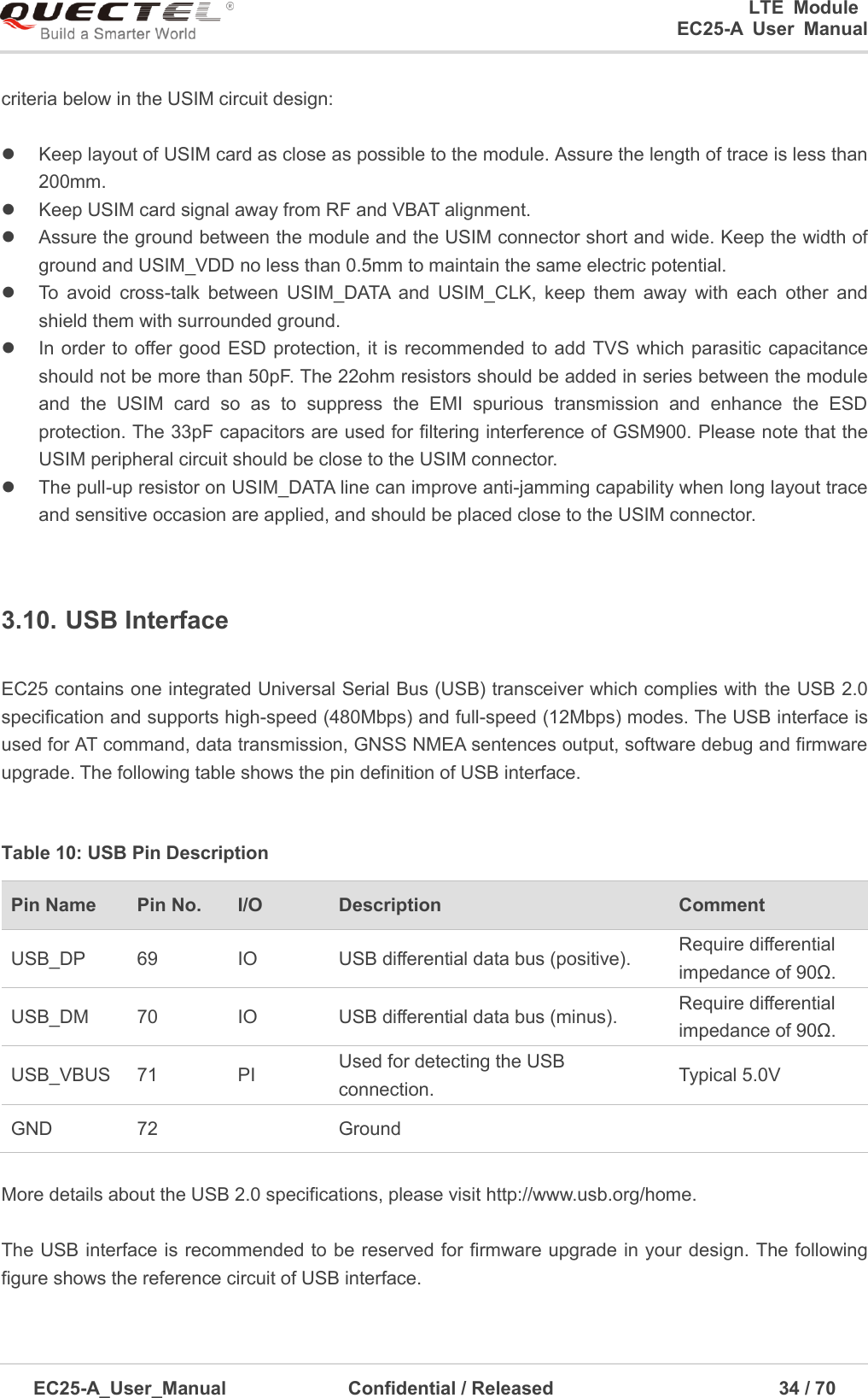
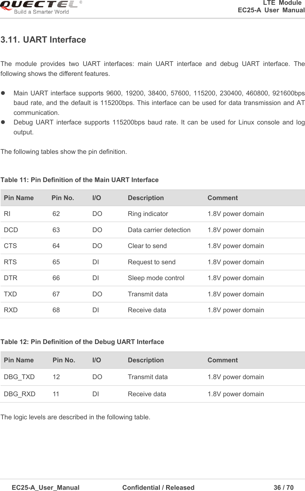
![0 LTE Module EC25-A User Manual EC25-A_User_Manual Confidential / Released 33 / 7 EC25 supports USIM card hot-plug via the USIM_PRESENCE pin. It supports low level and high level detections, which is disabled by default. For details, refer to document [2] about the command AT+QSIMDET. The following figure shows the reference design of the 8-pin USIM connector. ModuleUSIM_VDDUSIM_GNDUSIM_RSTUSIM_CLKUSIM_DATAUSIM_PRESENCE22R22R22RVDD_EXT51K100nF USIM ConnectorGNDGND33pF 33pF 33pFVCCRSTCLK IOVPPGNDGNDUSIM_VDD15KFigure 17: Reference Circuit of 8-Pin USIM Connector If you do not need the USIM card detection function, keep USIM_PRESENCE unconnected. The reference circuit for using a 6-pin USIM card connector is illustrated in the following figure. ModuleUSIM_VDDUSIM_GNDUSIM_RSTUSIM_CLKUSIM_DATA 22R22R22R100nF USIM ConnectorGND33pF 33pF 33pFVCCRSTCLK IOVPPGNDGND15KUSIM_VDDFigure 18: Reference Circuit of 6-Pin USIM Connector In order to enhance the reliability and availability of the USIM card in your application, please follow the](https://usermanual.wiki/Quectel-Wireless-Solutions/201605EC25A.Users-Manual/User-Guide-3067025-Page-34.png)
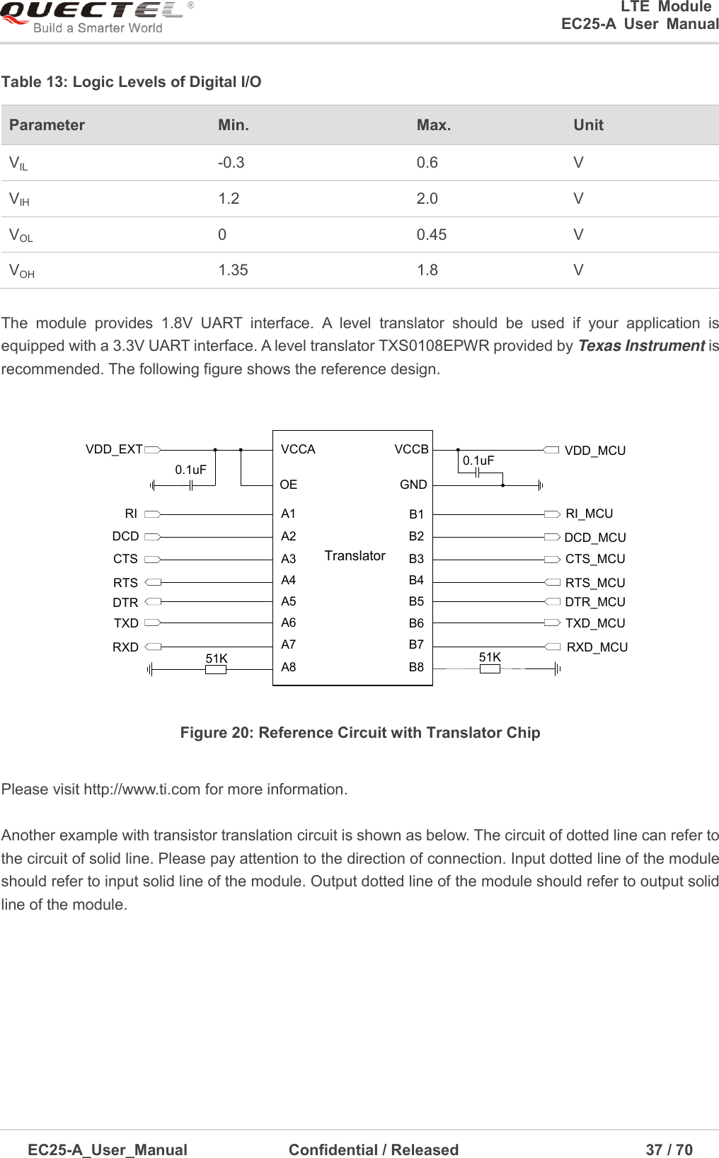
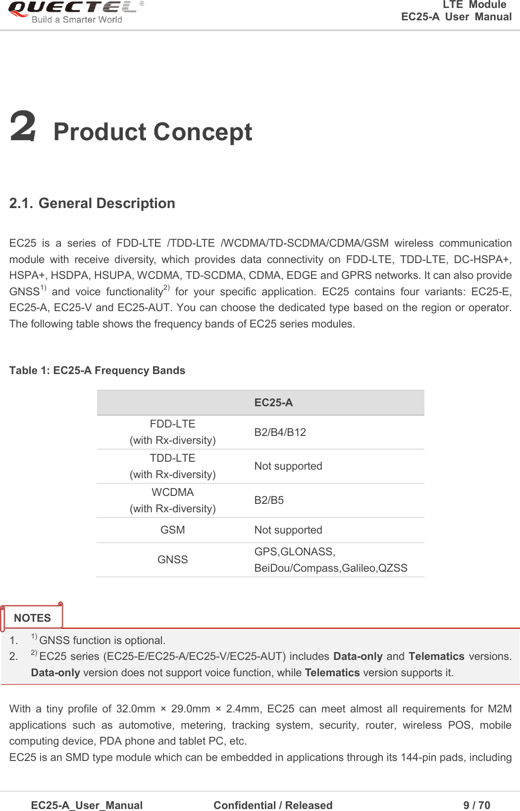
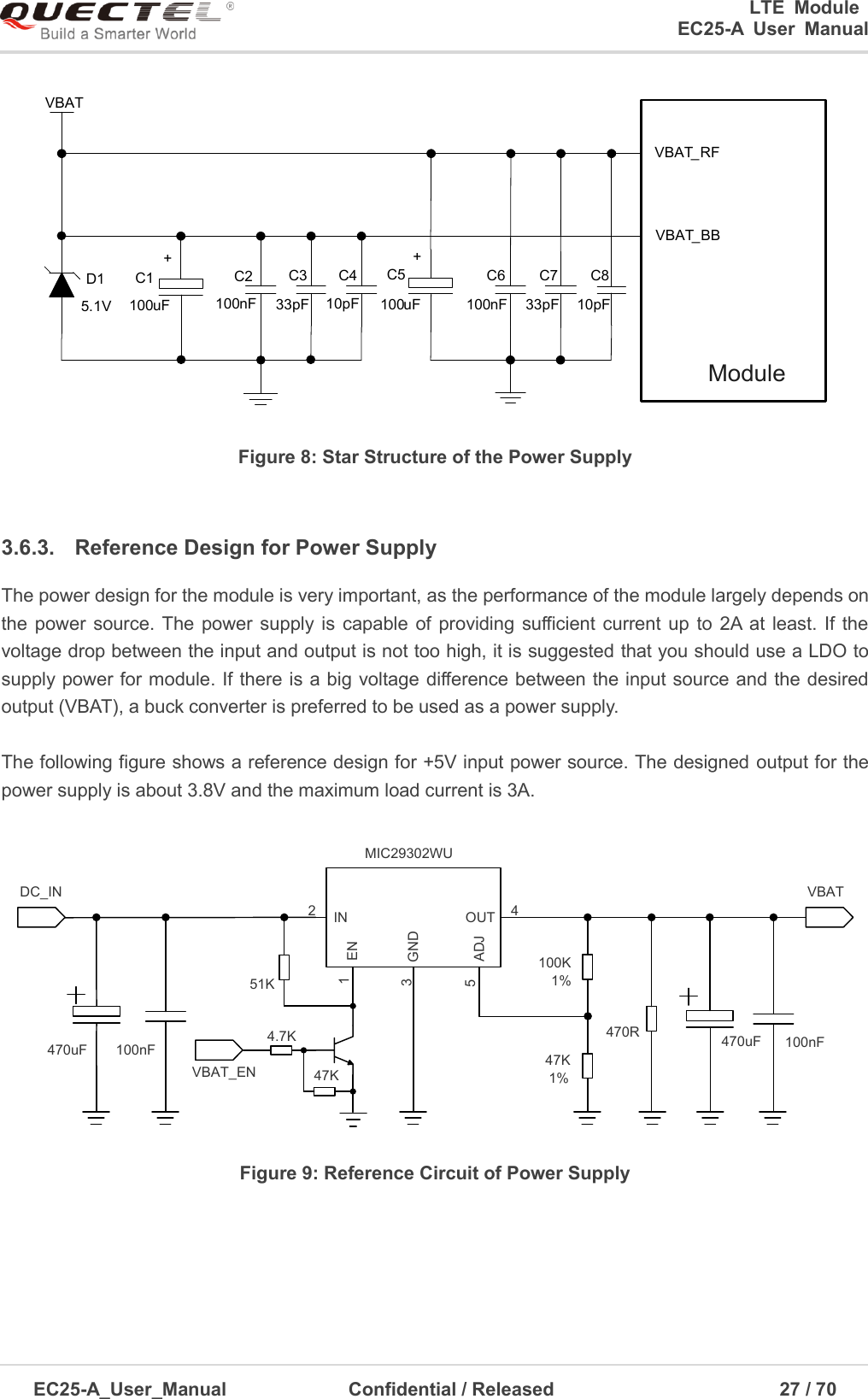
![0 LTE Module EC25-A User Manual EC25-A_User_Manual Confidential / Released 40 / 7 PCM_OUT 25 DO PCM data output 1.8V power domain PCM_SYNC 26 IO PCM data frame sync signal 1.8V power domain PCM_CLK 27 IO PCM data bit clock 1.8V power domain I2C_SCL 41 OD I2C serial clock Require external pull-up to 1.8V I2C_SDA 42 OD I2C serial data Require external pull-up to 1.8V Clock and mode can be configured by AT command, and the default configuration is master mode using short sync data format with 2048kHz PCM_CLK and 8kHz PCM_SYNC. Refer to document [2] about the command AT+QDAI for details. The following figure shows the reference design of PCM interface with external codec IC. PCM_INPCM_OUTPCM_SYNCPCM_CLKI2C_SCLI2C_SDAModule1.8V4.7K4.7KBCLKLRCKDACADCSCLSDABIASMICBIASINPINNLOUTPLOUTNCodec Figure 24: Reference Circuit of PCM Application with Audio Codec 1. It is recommended to reserve RC (R=22ohm, C=22pF) circuit on the PCM lines, especially for PCM_CLK. 2. EC25 works as a master device pertaining to I2C interface. NOTES](https://usermanual.wiki/Quectel-Wireless-Solutions/201605EC25A.Users-Manual/User-Guide-3067025-Page-41.png)
![0 LTE Module EC25-A User Manual EC25-A_User_Manual Confidential / Released 41 / 7 3.13. ADC Function The module provides two analog-to-digital converters (ADC). Using AT command AT+QADC=0 can read the voltage value on ADC0 pin. Using AT command AT+QADC=1 can read the voltage value on ADC1 pin. For more details of these AT commands, please refer to document [2]. In order to improve the accuracy of ADC, the trace of ADC should be surrounded by ground. Table 15: Pin Definition of the ADC Pin Name Pin No. Description ADC0 45 General purpose analog to digital converter ADC1 44 General purpose analog to digital converter The following table describes the characteristic of the ADC function. Table 16: Characteristic of the ADC Parameter Min. Typ. Max. Unit ADC0 Voltage Range 0.3 VBAT_BB V ADC1 Voltage Range 0.3 VBAT_BB V ADC Resolution 15 bits 3.14. Network Status Indication The network indication pins can be used to drive a network status indicator LED. The module provides two pins which are NET_MODE and NET_STATUS. The following tables describe pin definition and logic level changes in different network status. Table 17: Pin Definition of Network Indicator Pin Name Pin No. I/O Description Comment NET_MODE 5 DO Indicate the module network registration 1.8V power domain](https://usermanual.wiki/Quectel-Wireless-Solutions/201605EC25A.Users-Manual/User-Guide-3067025-Page-42.png)
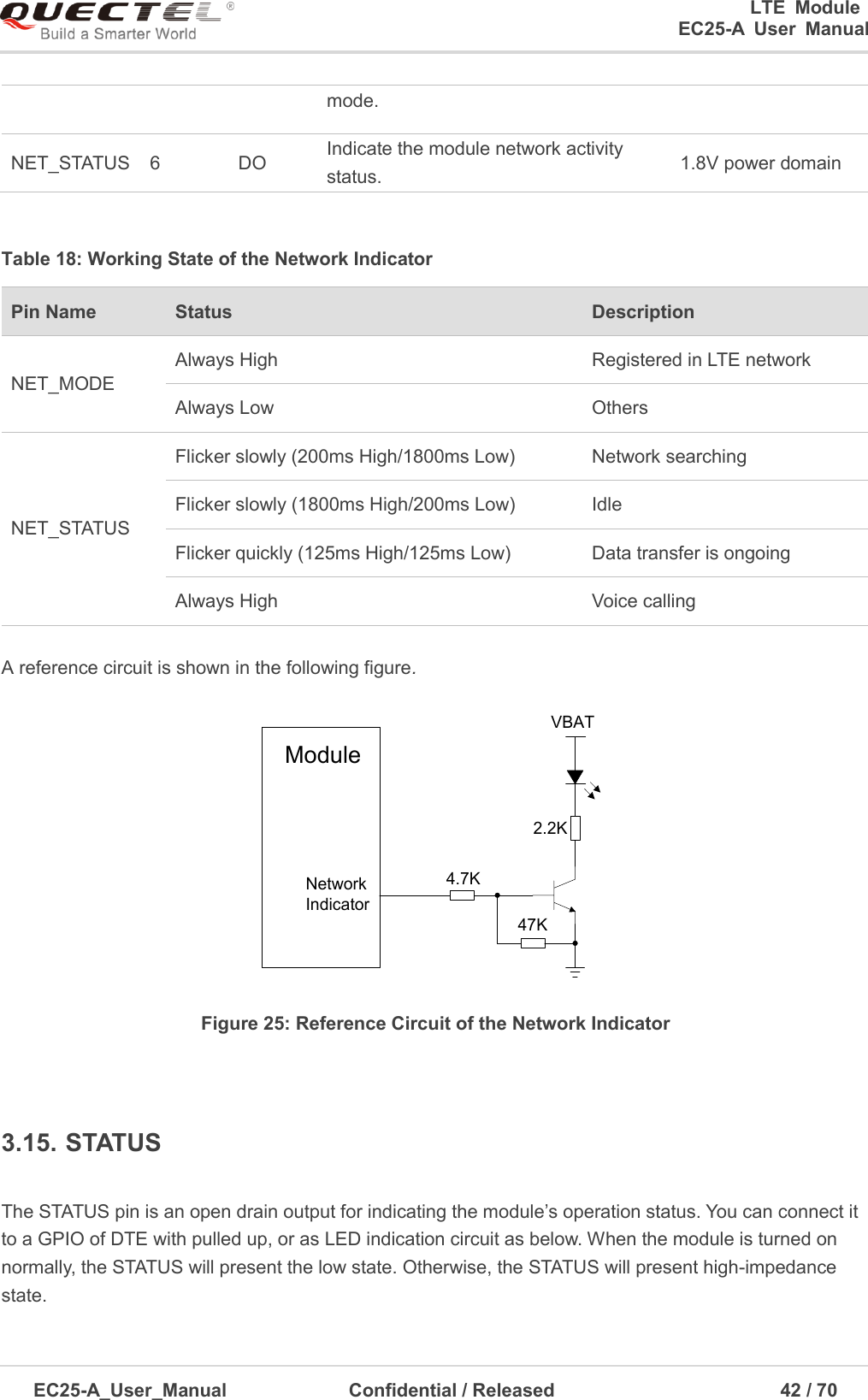
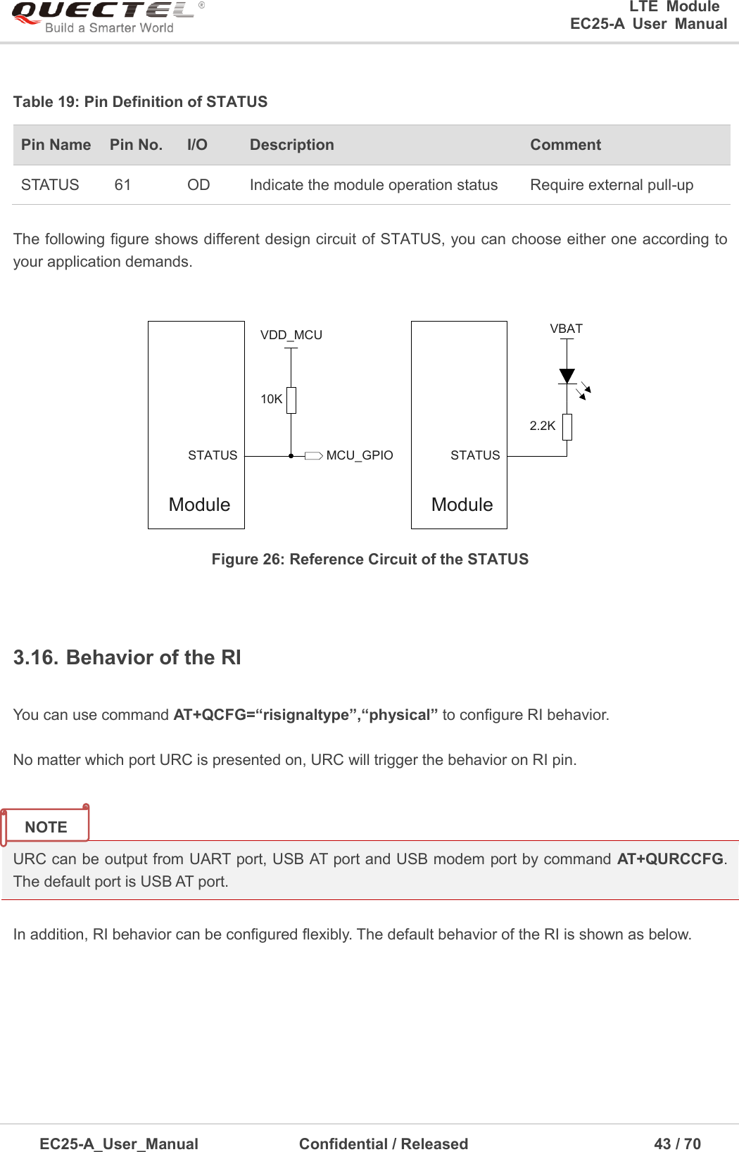
![0 LTE Module EC25-A User Manual EC25-A_User_Manual Confidential / Released 44 / 7 Table 20: Behavior of the RI State Response Idle RI keeps high level URC RI outputs 120ms low pulse when new URC returns The RI behavior can be changed by command AT+QCFG=“urc/ri/ring”. Refer to document [2] for details.](https://usermanual.wiki/Quectel-Wireless-Solutions/201605EC25A.Users-Manual/User-Guide-3067025-Page-45.png)
![0 LTE Module EC25-A User Manual EC25-A_User_Manual Confidential / Released 45 / 7 4 GNSS Receiver 4.1. General Description EC25 includes a fully integrated global navigation satellite system solution that supports Gen8C-Lite of Qualcomm (GPS, GLONASS, BeiDou, Galileo and QZSS). EC25 supports standard NMEA-0183 protocol, and outputs NMEA sentences with 1Hz via USB interface by default. By default, EC25 GNSS engine is switched off. It has to be switched on with AT command. For more details about GNSS engine technology and configurations, please refer to document [3]. 4.2. GNSS Performance The following table shows EC25 GNSS performance. Table 21: GNSS Performance Parameter Description Conditions Typ. Unit Sensitivity (GNSS) Cold start Autonomous TBD dBm Reacquisition Autonomous TBD dBm Tracking Autonomous TBD dBm TTFF (GNSS) Cold start @open sky Autonomous TBD s XTRA enabled TBD s Warm start @open sky Autonomous TBD s XTRA enabled TBD s](https://usermanual.wiki/Quectel-Wireless-Solutions/201605EC25A.Users-Manual/User-Guide-3067025-Page-46.png)
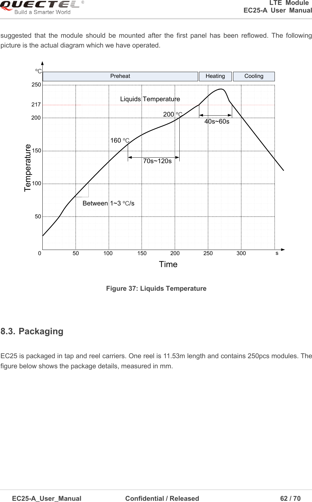
![0 LTE Module EC25-A User Manual EC25-A_User_Manual Confidential / Released 61 / 7 8 Storage and Manufacturing8.1. Storage EC25 is stored in a vacuum-sealed bag. The restrictions of storage condition are shown as below. 1. Shelf life in sealed bag is 12 months at < 40ºC/90%RH.2. After this bag is opened, devices that will be subjected to reflow soldering or other high temperatureprocesses must be:Mounted within 72 hours at factory conditions of ≤ 30ºC/60%RH.Stored at <10% RH.3. Devices require bake before mounting, if:Humidity indicator card is >10% when ambient temperature is 23ºC±5ºC.Mounted for more than 72 hours at factory conditions of ≤ 30ºC/60% RH.4. If baking is required, devices may be baked for 48 hours at 125ºC±5ºC.As plastic container cannot be subjected to high temperature, the module needs to be taken out from the container for high temperature (125ºC) baking. If shorter baking time is desired, please refer to IPC/JEDECJ-STD-033 for baking procedure. 8.2. Manufacturing and Welding The squeegee should push the paste on the surface of stencil, so as to make the paste fill the stencil openings and penetrate to the PCB. The force on the squeegee should be adjusted so as to produce a clean stencil surface on a single pass. To ensure the module soldering quality, the thickness of stencil at the hole of the module pads should be 0.18mm. For details, please refer to document [4]. It is suggested that the peak reflow temperature is 235 ~ 245ºC (for SnAg3.0Cu0.5 alloy). The absolute max reflow temperature is 260ºC. To avoid damage to the module when it is repeatedly heated, it is NOTE](https://usermanual.wiki/Quectel-Wireless-Solutions/201605EC25A.Users-Manual/User-Guide-3067025-Page-62.png)
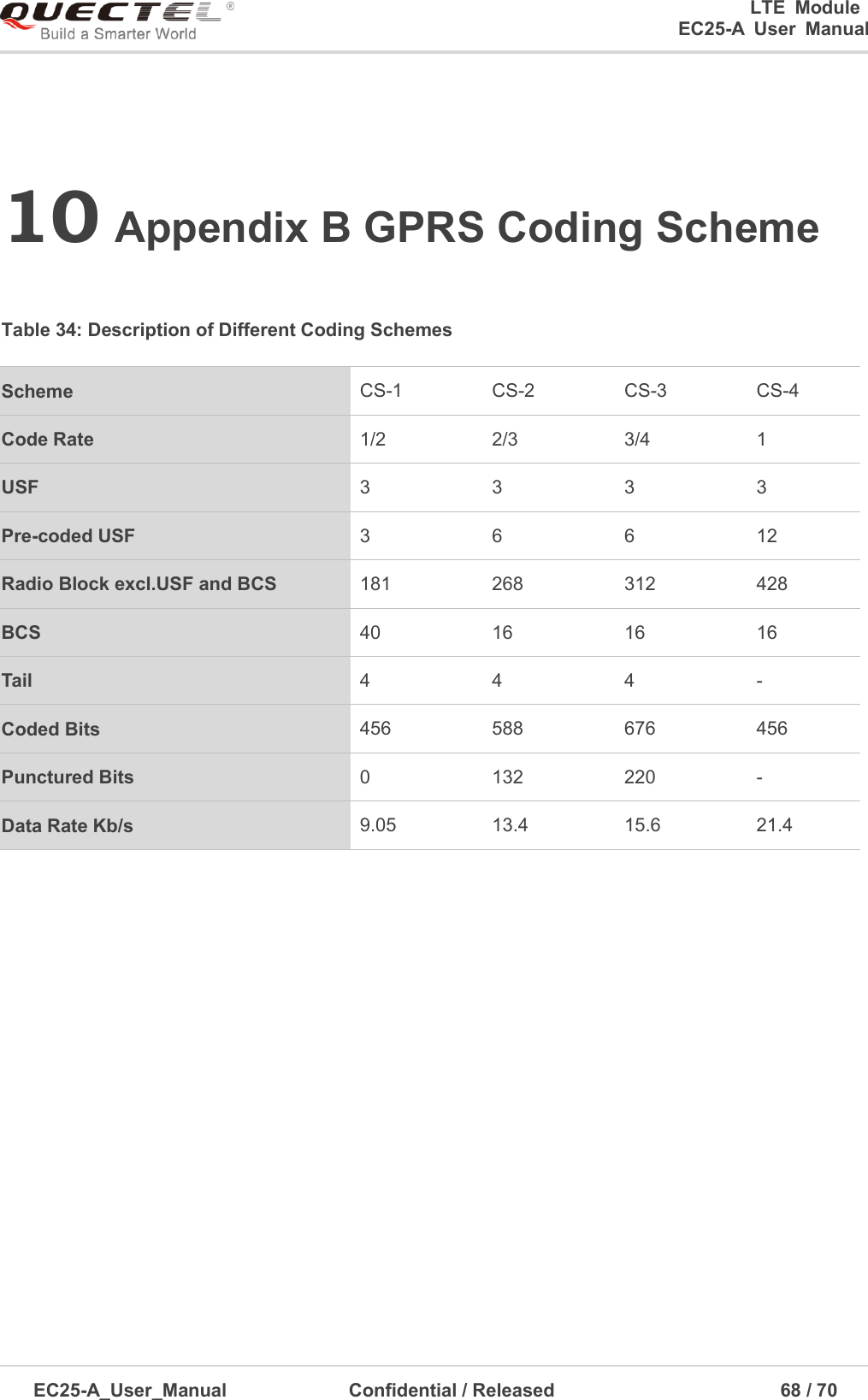
![0 LTE Module EC25-A User Manual EC25-A_User_Manual Confidential / Released 64 / 7 9 Appendix A ReferenceTable 32: Related Documents SN Document Name Remark [1] Quectel_EC25_Power_Management_Application_Note EC25 Power Management Application Note [2] Quectel_EC25_AT_Commands_Manual EC25 AT Commands Manual [3] Quectel_EC25_GNSS_AT_Commands_Manual EC25 GNSS AT Commands Manual [4] Quectel_Module_Secondary_SMT_User_Guide Module Secondary SMT User Guide Table 33: Terms and Abbreviations Abbreviation Description AMR Adaptive Multi-rate bps Bits Per Second CHAP Challenge Handshake Authentication Protocol CS Coding Scheme CSD Circuit Switched Data CTS Clear To Send DC-HSPA+ Dual-carrier High Speed Packet Access DFOTA Delta Firmware Upgrade Over The Air DL Downlink DTR Data Terminal Ready DTX Discontinuous Transmission](https://usermanual.wiki/Quectel-Wireless-Solutions/201605EC25A.Users-Manual/User-Guide-3067025-Page-65.png)