Quectel Wireless Solutions 201609MC60 GSM/GPRS/GNSS Module User Manual
Quectel Wireless Solutions Company Limited GSM/GPRS/GNSS Module
UserManual.wiki
>
Quectel Wireless Solutions
>
201609MC60 User Manual
User Manual
Navigation menu
Upload a User Manual
Namespaces
Wiki Guide
HTML
PDF
Info
Views
User Manual
Discussion / Help
Navigation

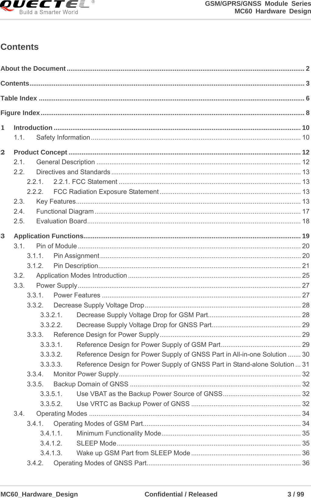
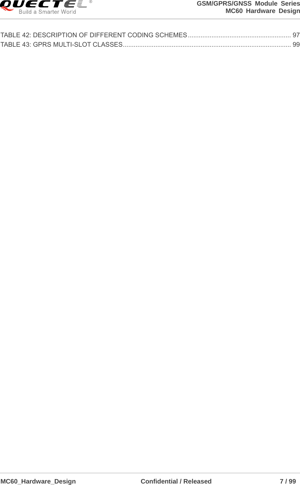
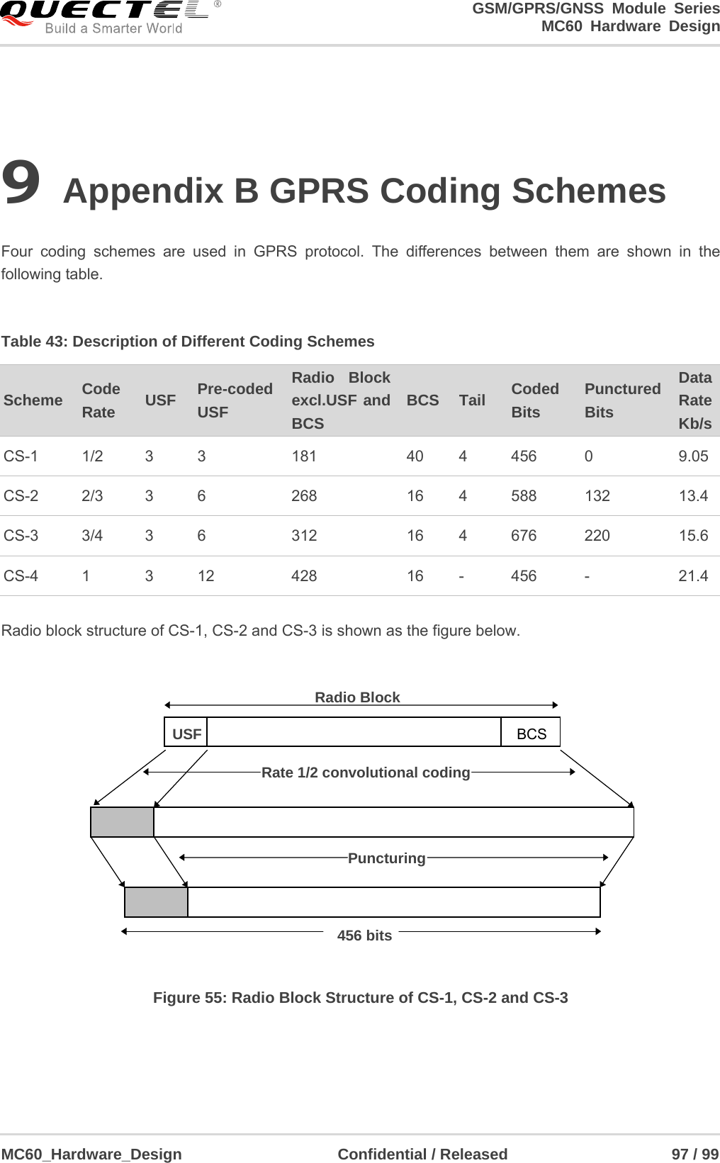
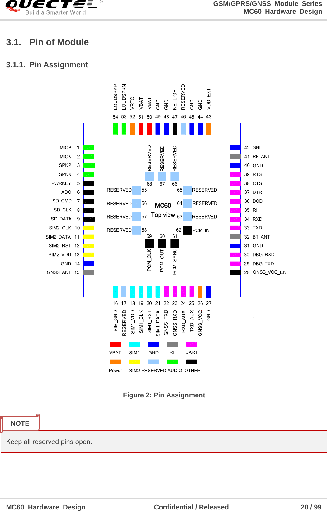
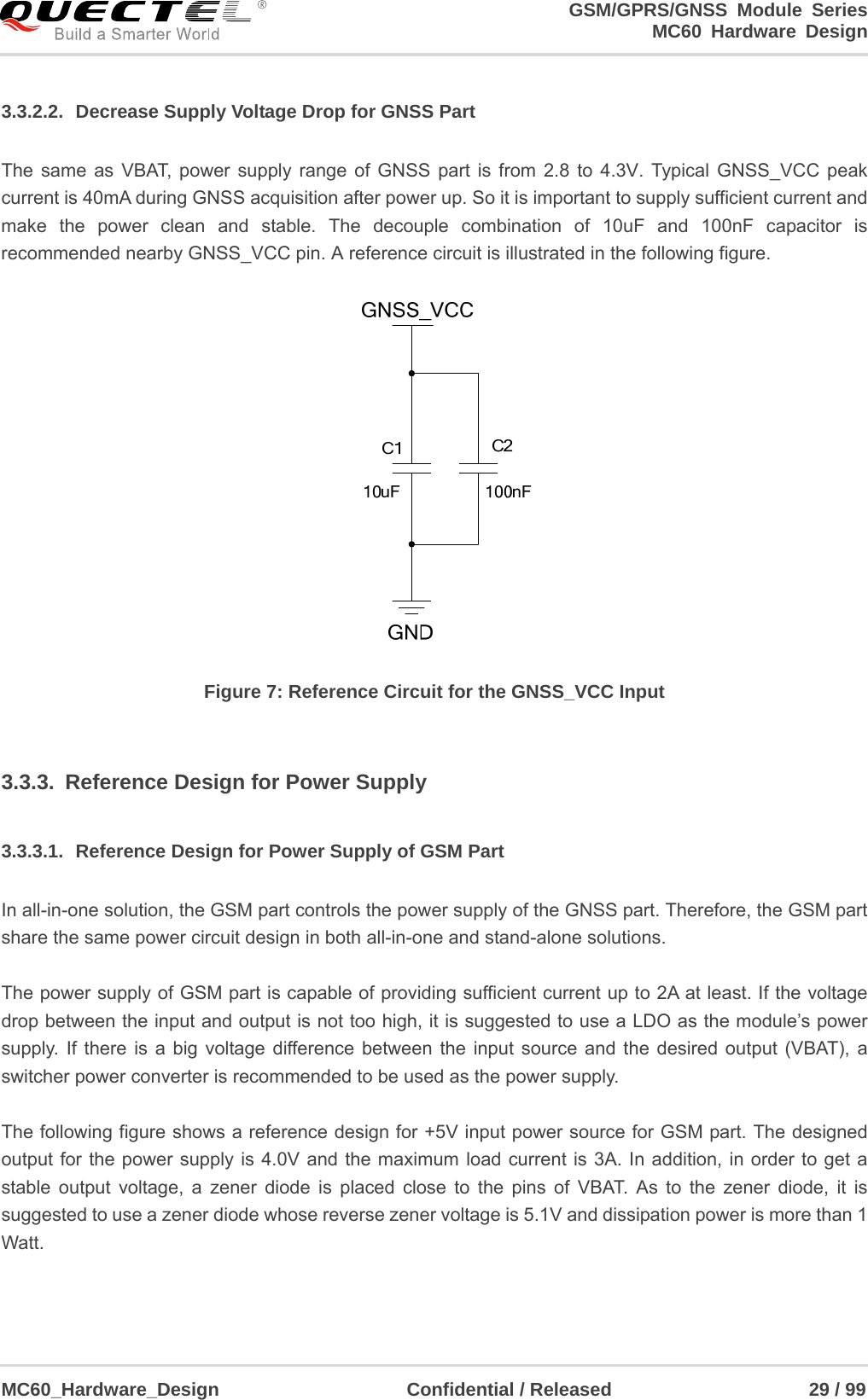
![GSM/GPRS/GNSS Module Series MC60 Hardware Design MC60_Hardware_Design Confidential / Released 17 / 99 Table 4: Protocols Supported by the Module Please refer to document [2] for details of NMEA standard protocol and MTK proprietary protocol. 2.4. Functional Diagram The following figure shows a block diagram of MC60 and illustrates the major functional parts. Radio frequency part Power management Peripheral interfaces —Power supply —Turn-on/off interface —UART interface —Audio interface —SIM interface —ADC interface —RF interface —PCM interface —BT interface —SD interface Protocol Type NMEA Input/output, ASCII, 0183, 3.01 PMTK Input, MTK proprietary protocol NOTE](https://usermanual.wiki/Quectel-Wireless-Solutions/201609MC60/User-Guide-3165740-Page-18.png)
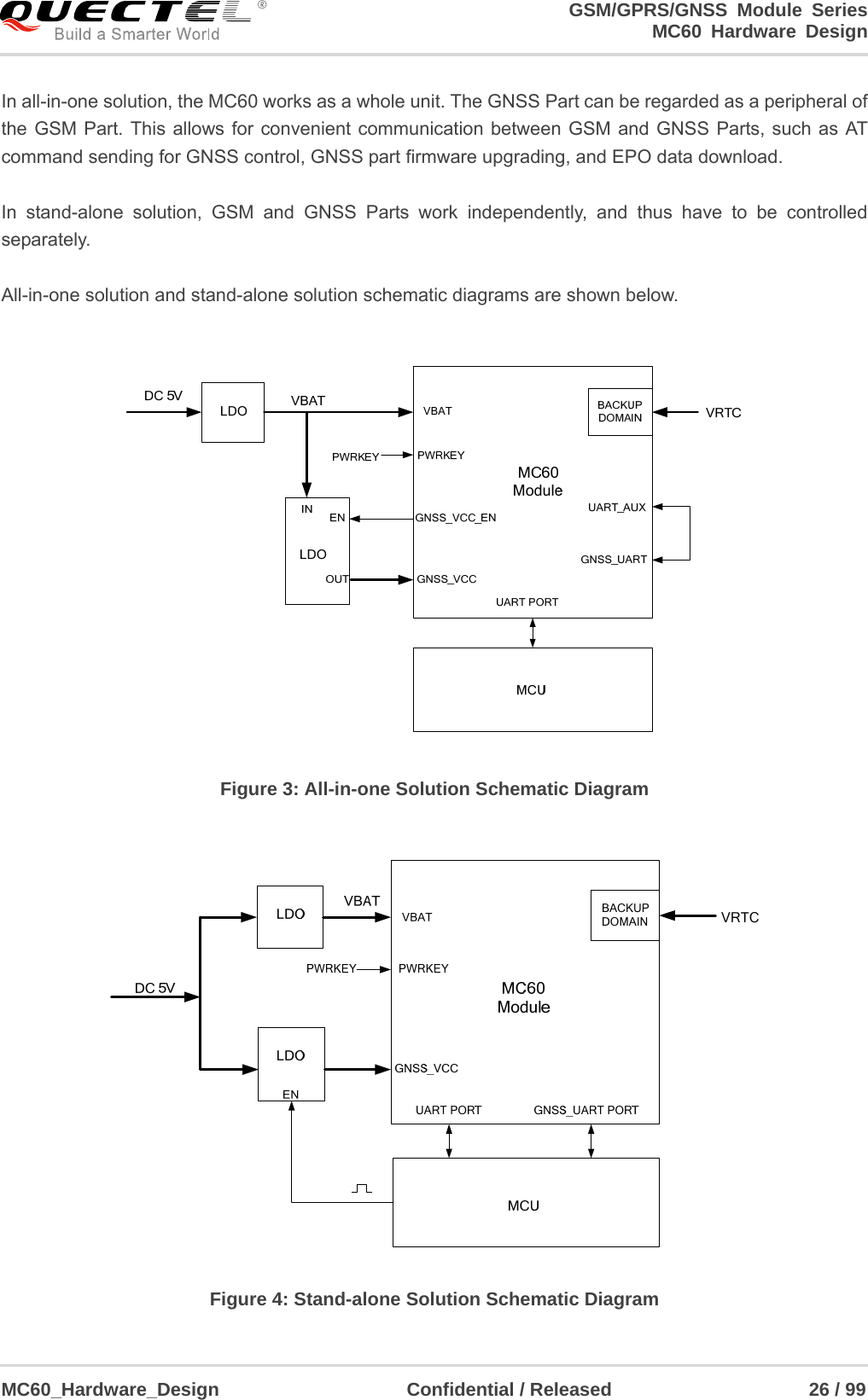
![GSM/GPRS/GNSS Module Series MC60 Hardware Design MC60_Hardware_Design Confidential / Released 18 / 99 Figure 1: Module Functional Diagram 2.5. Evaluation Board In order to help you develop applications with MC60, Quectel supplies an evaluation board (EVB), RS-232 to USB cable, power adapter, earphone, antenna and other peripherals to control or test the module. For details, please refer to document [11].](https://usermanual.wiki/Quectel-Wireless-Solutions/201609MC60/User-Guide-3165740-Page-19.png)
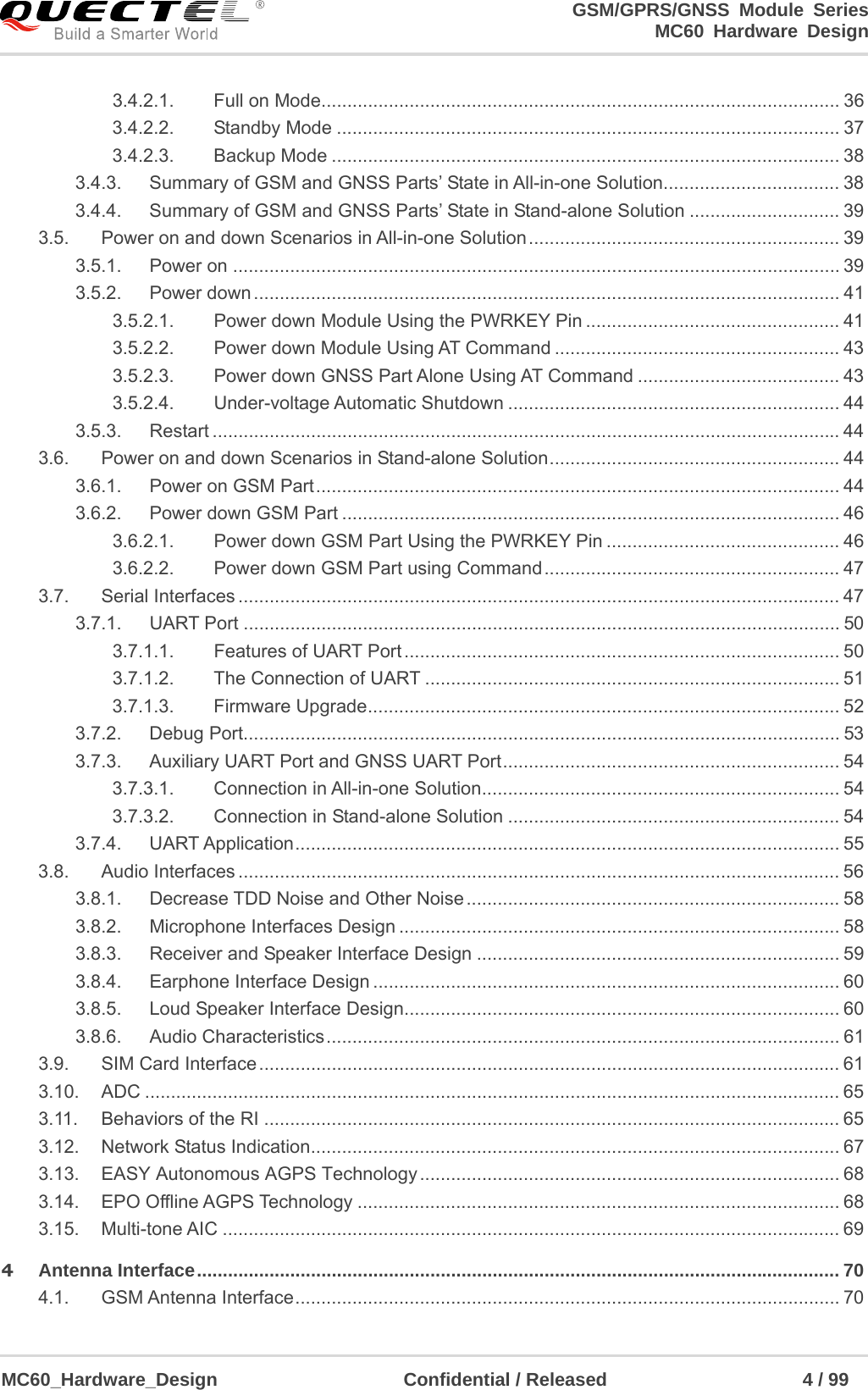
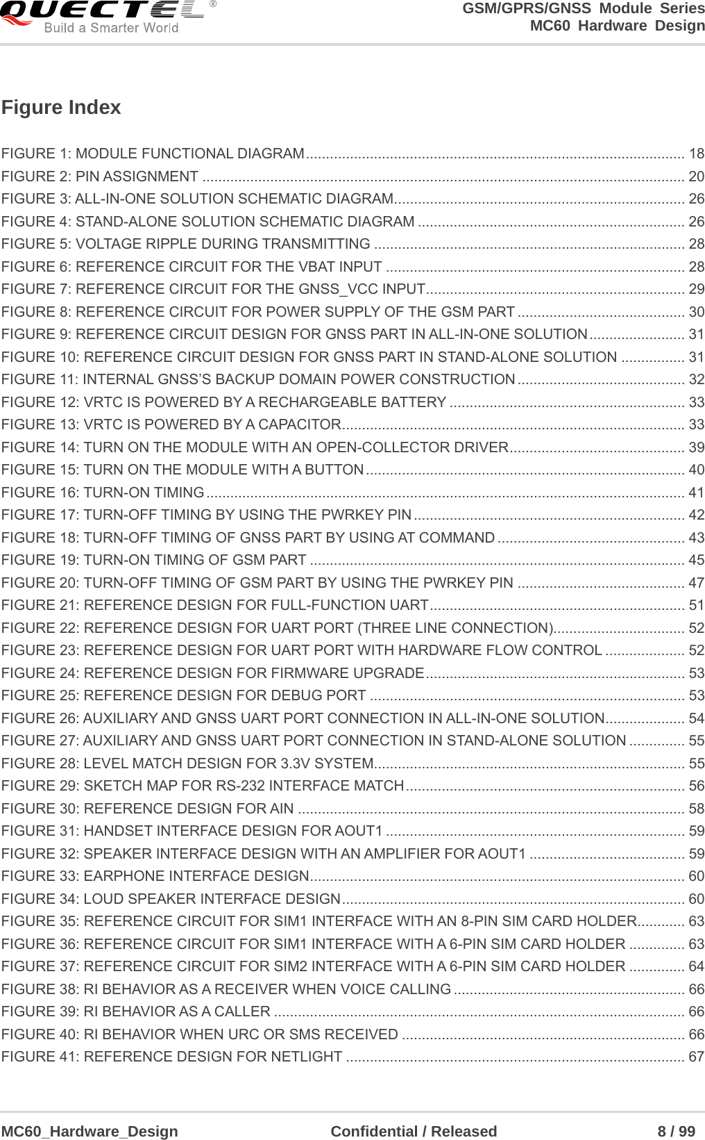
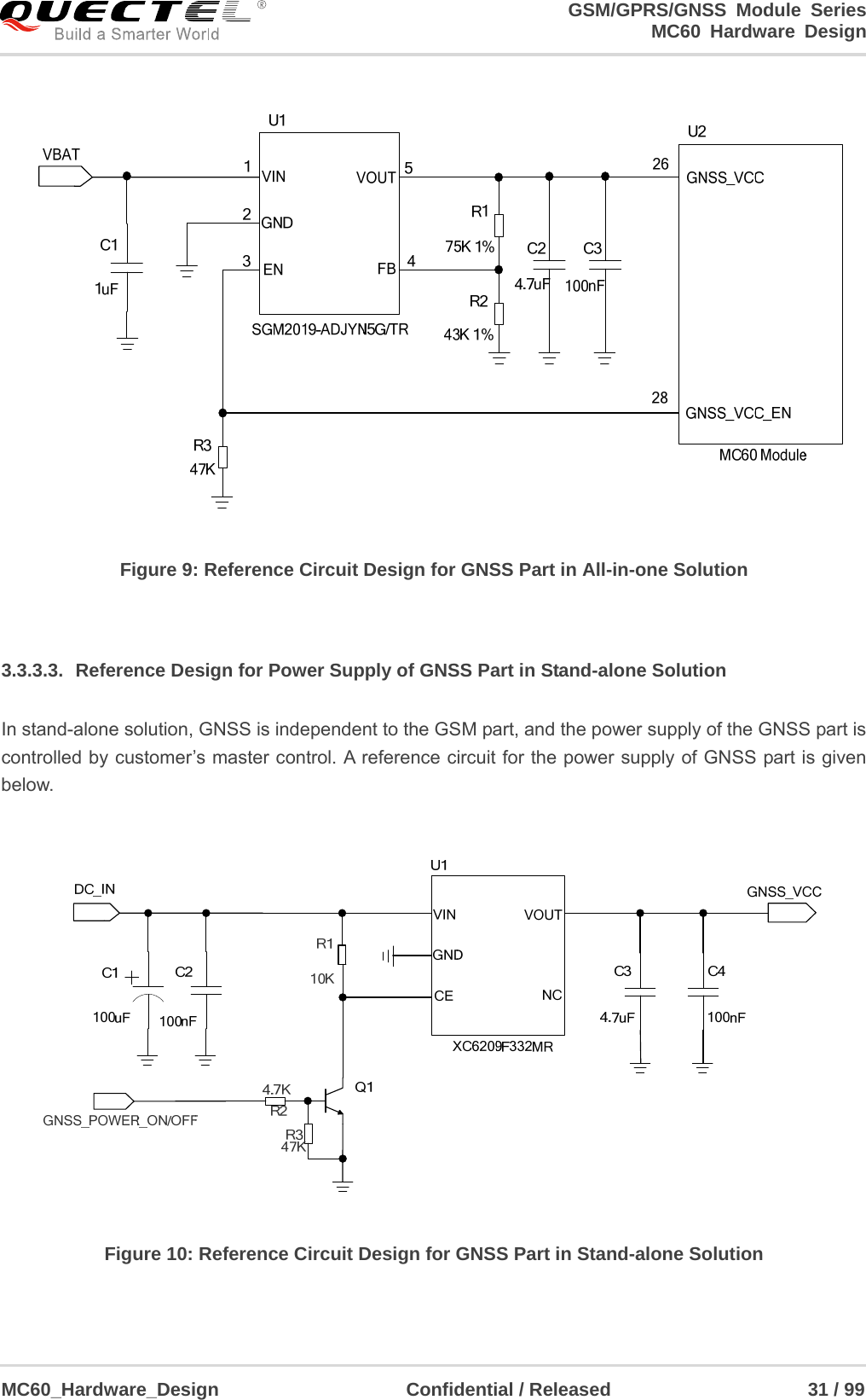
![GSM/GPRS/GNSS Module Series MC60 Hardware Design MC60_Hardware_Design Confidential / Released 30 / 99 Figure 8: Reference Circuit for Power Supply of the GSM Part It is suggested to control the module’s main power supply (VBAT) via LDO enable pin to restart the module when the module becomes abnormal. Power switch circuit like P-channel MOSFET switch circuit can also be used to control VBAT. 3.3.3.2. Reference Design for Power Supply of GNSS Part in All-in-one Solution In all-in-one solution, the power supply of GNSS part is controlled by the GSM part through the GNSS_VCC_EN pin. A reference circuit for the GNSS part power supply is given below. Please pay attention to the electrical characteristics of GNSS_VCC_EN to match LDO’s EN pin. Please refer to document [1] for details about the AT commands for GNSS control. NOTE](https://usermanual.wiki/Quectel-Wireless-Solutions/201609MC60/User-Guide-3165740-Page-31.png)
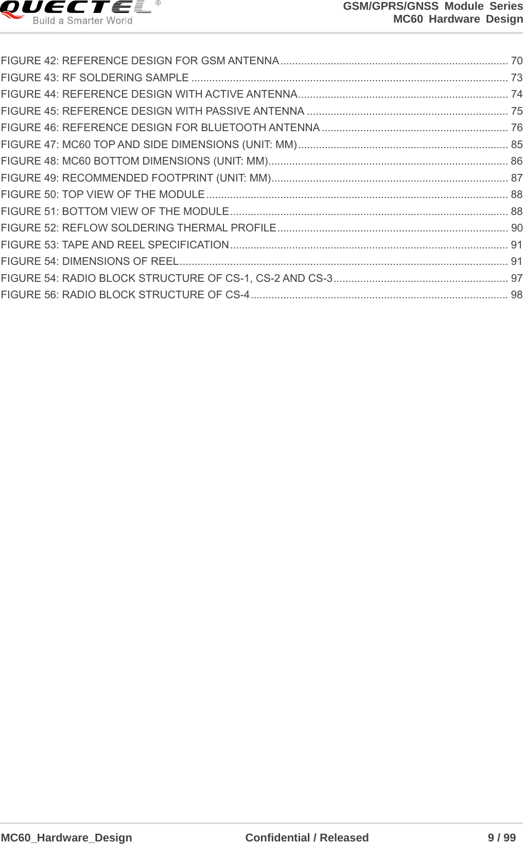
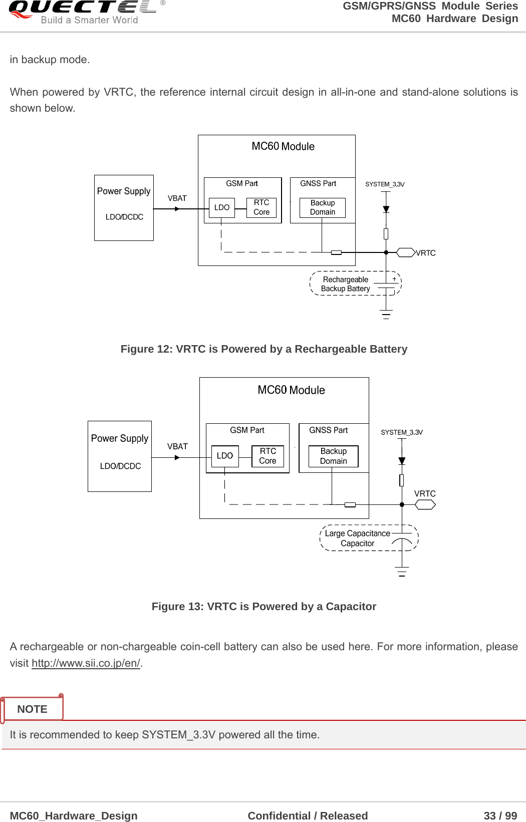
![GSM/GPRS/GNSS Module Series MC60 Hardware Design MC60_Hardware_Design Confidential / Released 32 / 99 3.3.4. Monitor Power Supply The command AT+CBC can be used to monitor the supply voltage of the GSM part. The unit of the displayed voltage is mV. For details, please refer to document [1]. 3.3.5. Backup Domain of GNSS The RTC (Real Time Clock) function of GSM part and backup mode of GNSS part are supported. In GNSS’s backup mode, the backup domain which contains all the necessary GNSS information for quick start-up and a small amount of user configuration variables is alive. Due to the backed-up memory, EASY technology is available. 3.3.5.1. Use VBAT as the Backup Power Source of GNSS In either all-in-one or stand-alone solution, GNSS’s backup mode will be active as long as the main power supply (VBAT) is remained, even when the module is turned off and GNSS_VCC is powered off; as the GNSS’s backup domain is powered by VBAT. In this case, the VRTC pin can be kept floating. When powered by VBAT, the reference internal circuit design in all-in-one and stand-alone solutions is shown below. Figure 11: Internal GNSS’s Backup Domain Power Construction 3.3.5.2. Use VRTC as Backup Power of GNSS In either all-in-one or stand-alone solution, when the main power supply (VBAT) is removed after the module is turned off, and GNSS_VCC is also powered off, a backup supply such as a coin-cell battery (rechargeable or non-chargeable) or a super capacitor can be used to power the VRTC pin to keep GNSS](https://usermanual.wiki/Quectel-Wireless-Solutions/201609MC60/User-Guide-3165740-Page-33.png)
![GSM/GPRS/GNSS Module Series MC60 Hardware Design MC60_Hardware_Design Confidential / Released 35 / 99 Based on system requirements, there are several actions to drive the GSM part to enter into low current consumption status. For example, AT+CFUN can be used to set the part into minimum functionality mode, and DTR hardware interface signal can be used to lead the system to Sleep Mode. 3.4.1.1. Minimum Functionality Mode Minimum functionality mode reduces the functionality of the GSM part to a minimum level. The consumption of the current can be minimized when the slow clocking mode is activated at the same time. The mode is set via the AT+CFUN command which provides the choice of the functionality levels <fun>=0, 1, 4. 0: minimum functionality 1: full functionality (default) 4: disable from both transmitting and receiving RF signals If the GSM part is set to minimum functionality by AT+CFUN=0, the RF function and SIM card function would be disabled. In this case, the UART port is still accessible, but all AT commands related with RF function or SIM card function will be unavailable. If the GSM part is set by the command AT+CFUN=4, the RF function will be disabled, but the UART port is still active. In this case, all AT commands related with RF function will be unavailable. After the GSM part is set by AT+CFUN=0 or AT+CFUN=4, it can return to full functionality mode by AT+CFUN=1. For detailed information about AT+CFUN, please refer to document [1]. 3.4.1.2. SLEEP Mode SLEEP mode is disabled by default. It can be enabled by AT+QSCLK=1 and the premise is that the GNSS is powered off. The default setting is AT+QSCLK=0, and in this mode, the GSM part cannot enter SLEEP mode. When the GSM part is set by the command AT+QSCLK=1, you can control the part to enter into or exit from the SLEEP mode through pin DTR. When DTR is set to high level, and there is no on-air or hardware interrupt such as GPIO interrupt or data on UART port, the GSM part will enter into SLEEP mode automatically. In this mode, the GSM part can still receive voice, SMS or GPRS paging from network, but the UART port does not work. case is very low.](https://usermanual.wiki/Quectel-Wireless-Solutions/201609MC60/User-Guide-3165740-Page-36.png)
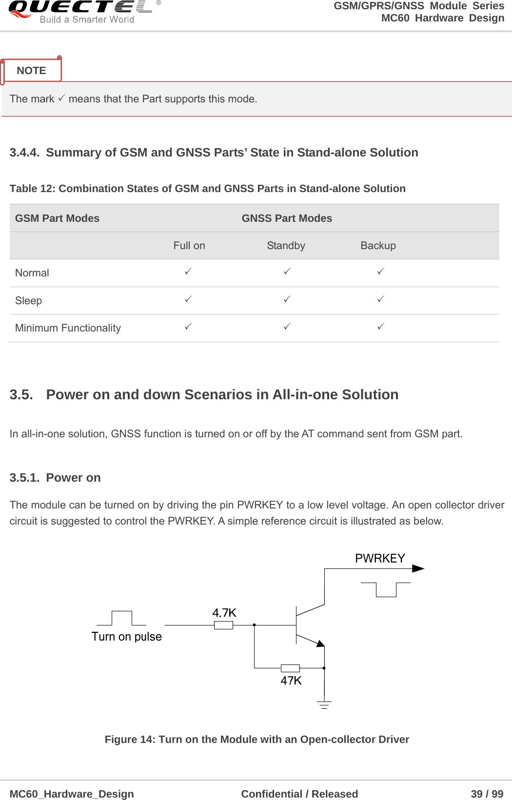
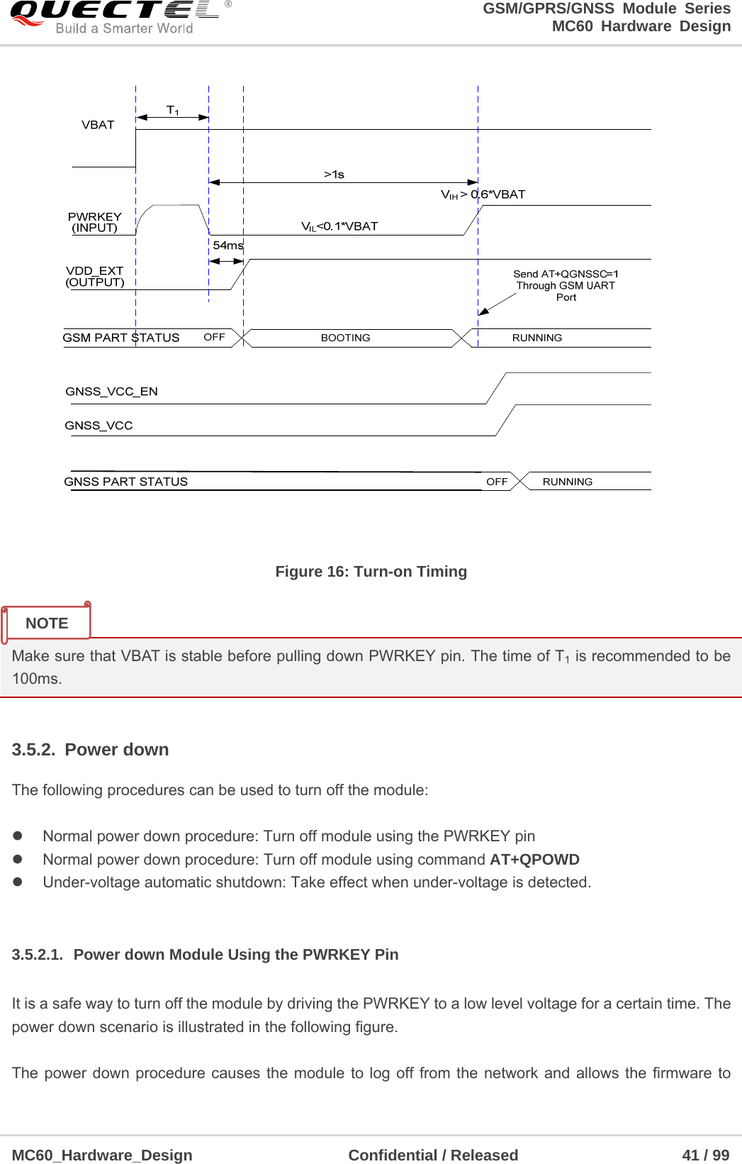
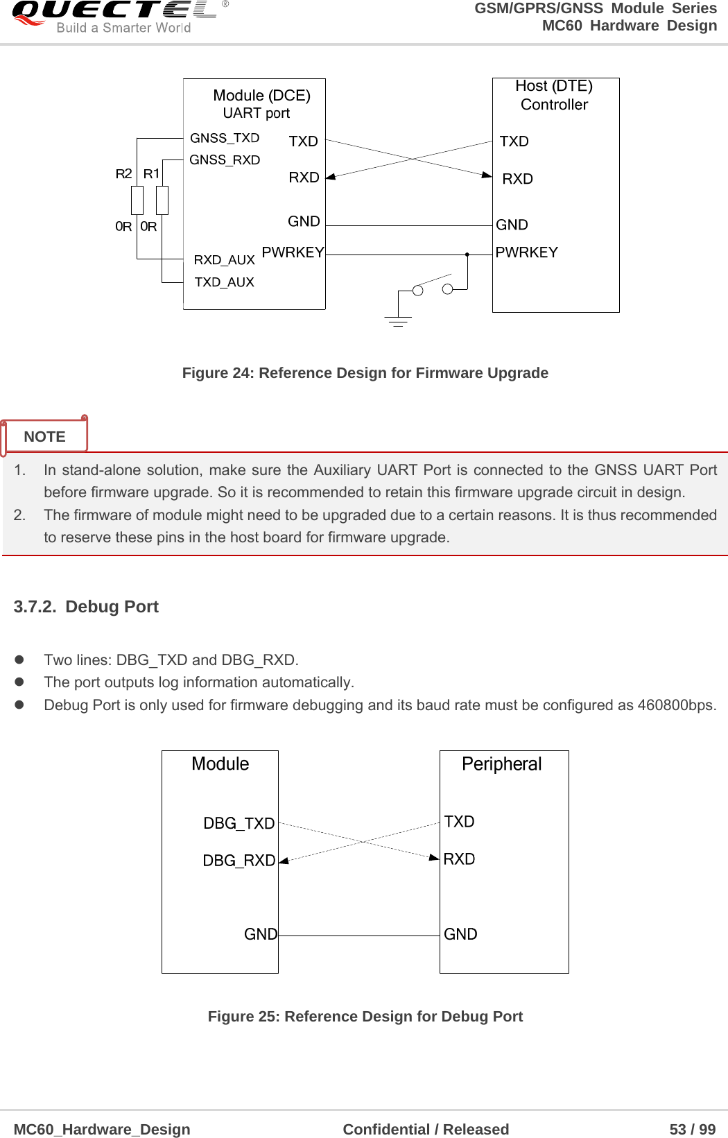
![GSM/GPRS/GNSS Module Series MC60 Hardware Design MC60_Hardware_Design Confidential / Released 40 / 99 1. MC60 module is set to autobauding mode (AT+IPR=0) by default. In autobauding mode, URC RDY is not reported to the host controller after the module is powered on. When the module is powered on after a delay of 4 or 5 seconds, it can receive AT commands. Host controller should first send an AT string in order that the module can detect baud rate of host controller, and it should continue to send the next AT string until receiving OK string from the module. Then enter AT+IPR=x;&W to set a fixed baud rate for the module and save the configuration to flash memory of the module. After these configurations, the URC RDY would be received from the UART Port of the module every time when the module is powered on. For more details, refer to the section AT+IPR in document [1]. 2. When AT command is responded, it indicates the module is turned on successfully; or else the module fails to be turned on. The other way to control the PWRKEY is through a button directly. While pressing the key, electrostatic strike may generate from the finger, and thus, a TVS component is indispensable to be placed nearby the button for ESD protection. For the best performance, the TVS component must be placed nearby the button. A reference circuit is shown in the following figure. Figure 15: Turn on the Module with a Button Command AT+QGNSSC=1 should be sent to enable the GNSS power supply after the GSM part is running. When the GNSS_VCC is valid, the GNSS will enter into full on mode automatically. The turn-on timing is illustrated in the following figure. NOTES](https://usermanual.wiki/Quectel-Wireless-Solutions/201609MC60/User-Guide-3165740-Page-41.png)
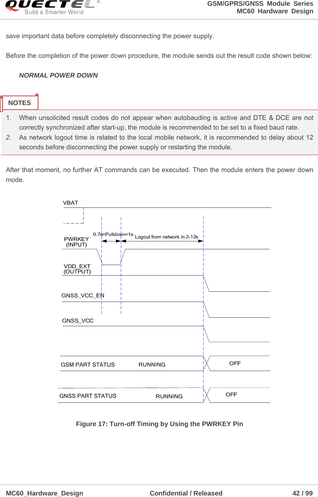
![GSM/GPRS/GNSS Module Series MC60 Hardware Design MC60_Hardware_Design Confidential / Released 43 / 99 3.5.2.2. Power down Module Using AT Command It is also a safe way to turn off the module via AT command AT+QPOWD=1. This command will let the module log off from the network and allow the firmware to save important data before completely disconnecting the power supply. Before the completion of the power down procedure, the module sends out the result code shown below: NORMAL POWER DOWN After that moment, no further AT commands can be executed. And then the module enters into the power down mode. Please refer to document [1] for details about the AT command AT+QPOWD. 3.5.2.3. Power down GNSS Part Alone Using AT Command It is a safe way to turn off the GNSS part alone via AT command AT+QGNSSC=0. The power down scenario for GNSS part is illustrated in the following figure. Figure 18: Turn-off Timing of GNSS Part by Using AT Command](https://usermanual.wiki/Quectel-Wireless-Solutions/201609MC60/User-Guide-3165740-Page-44.png)
![GSM/GPRS/GNSS Module Series MC60 Hardware Design MC60_Hardware_Design Confidential / Released 45 / 99 driver circuit is suggested to control the PWRKEY. A simple reference circuit is illustrated in Figure 14. 1. The GSM module is set to autobauding mode (AT+IPR=0) by default. In the autobauding mode, URC RDY is not reported to the host controller after the module is powered on. When the GSM module is powered on after a delay of 4 or 5 seconds, it can receive AT command. Host controller should first send an AT string in order that the GSM module can detect baud rate of host controller, and it should continue to send the next AT string until receiving OK string from the module. Then enter AT+IPR=x;&W to set a fixed baud rate for the module and save the configuration to flash memory of the module. After these configurations, the URC RDY would be received from the UART Port of the GSM module every time when the module is powered on. For more details, refer to the section AT+IPR in document [1]. 2. When AT command is responded, it indicates the GSM module is turned on successfully; or else the module fails to be turned on. The other way to control the PWRKEY is through a button directly. While pressing the key, electrostatic strike may generate from the finger, and thus, a TVS component is indispensable to be placed nearby the button for ESD protection. For the best performance, the TVS component must be placed nearby the button. A reference circuit is shown in Figure15. The turn-on timing is illustrated in the following figure. Figure 19: Turn-on Timing of GSM Part Make sure that VBAT is stable before pulling down PWRKEY pin. The time of T1 is recommended to be 100ms. NOTES NOTE](https://usermanual.wiki/Quectel-Wireless-Solutions/201609MC60/User-Guide-3165740-Page-46.png)
![GSM/GPRS/GNSS Module Series MC60 Hardware Design MC60_Hardware_Design Confidential / Released 47 / 99 Figure 20: Turn-off Timing of GSM Part by Using the PWRKEY Pin 3.6.2.2. Power down GSM Part using Command It is also a safe way to turn off the GSM module via AT command AT+QPOWD=1. This command will let the GSM module log off from the network and allow the firmware to save important data before completely disconnecting the power supply. Before the completion of the power down procedure, the GSM module sends out the result code shown below: NORMAL POWER DOWN After that moment, no further AT commands can be executed. And then the GSM module enters into the power down mode. Please refer to document [1] for details about the AT command AT+QPOWD. 3.7. Serial Interfaces The module provides four serial ports: UART Port, Debug Port, Auxiliary UART Port and GNSS UART Port. The module is designed as DCE (Data Communication Equipment), following the traditional DCE-DTE (Data Terminal Equipment) connection. Autobauding function supports baud rate from 4800bps to 115200bps.](https://usermanual.wiki/Quectel-Wireless-Solutions/201609MC60/User-Guide-3165740-Page-48.png)
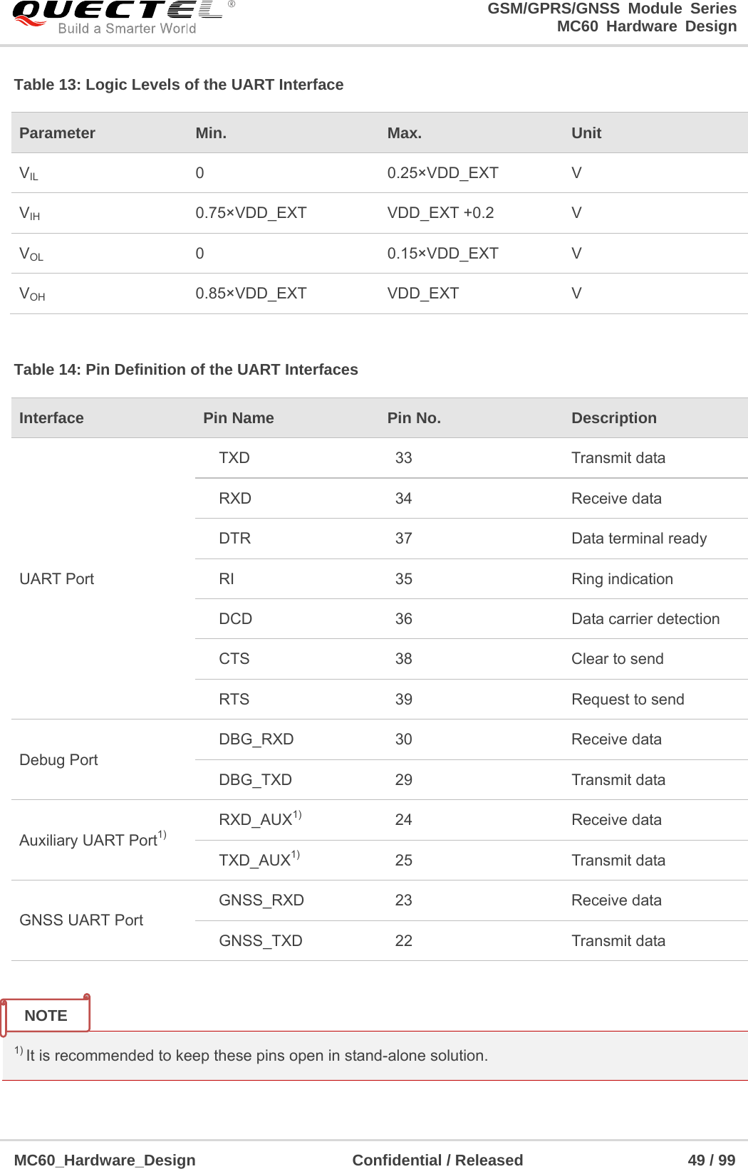
![GSM/GPRS/GNSS Module Series MC60 Hardware Design MC60_Hardware_Design Confidential / Released 50 / 99 3.7.1. UART Port 3.7.1.1. Features of UART Port Seven lines on UART interface Contain data lines TXD and RXD, hardware flow control lines RTS and CTS, as well as other control lines DTR, DCD and RI. Used for AT command, GPRS data, etc. Multiplexing function is supported on the UART Port. NMEA output and PMTK command can be supported in all-in-one solution. Support the following communication baud rates: 300, 600, 1200, 2400, 4800, 9600, 14400, 19200, 28800, 38400, 57600, 115200bps. The default setting is autobauding mode. Support the following baud rates for autobauding function: 4800, 9600, 19200, 38400, 57600, 115200bps. Hardware flow control is disabled by default. When hardware flow control is required, RTS and CTS should be connected to the host. AT command AT+IFC=2,2 is used to enable hardware flow control. AT command AT+IFC=0,0 is used to disable the hardware flow control. For more details, please refer to document [1]. After setting a fixed baud rate or autobauding, please send “AT” string at that rate. The UART port is ready when it responds “OK”. Autobauding allows the module to detect the baud rate by receiving the string “AT” or “at” from the host or PC automatically, which gives module flexibility without considering which baud rate is used by the host controller. Autobauding is enabled by default. To take advantage of the autobauding mode, special attention should be paid according to the following requirements: Synchronization between DTE and DCE: When DCE (the module) is powered on with autobauding enabled, it is recommended to wait 2 to 3 seconds before sending the first AT character. After receiving the “OK” response, DTE and DCE are correctly synchronized. If the host controller needs URC in the mode of autobauding, it must be synchronized firstly. Otherwise the URC will be discarded. Restrictions on autobauding operation: The UART port has to be operated at 8 data bits, no parity and 1 stop bit (factory setting). The “At” and “aT” commands cannot be used. Only the strings “AT” or “at” can be detected (neither “At” nor “aT”). The Unsolicited Result Codes like RDY, +CFUN: 1 and +CPIN: READY will not be indicated when the module is turned on with autobauding enabled and not be synchronized. Any other Unsolicited Result Codes will be sent at the previous baud rate before the module detects](https://usermanual.wiki/Quectel-Wireless-Solutions/201609MC60/User-Guide-3165740-Page-51.png)
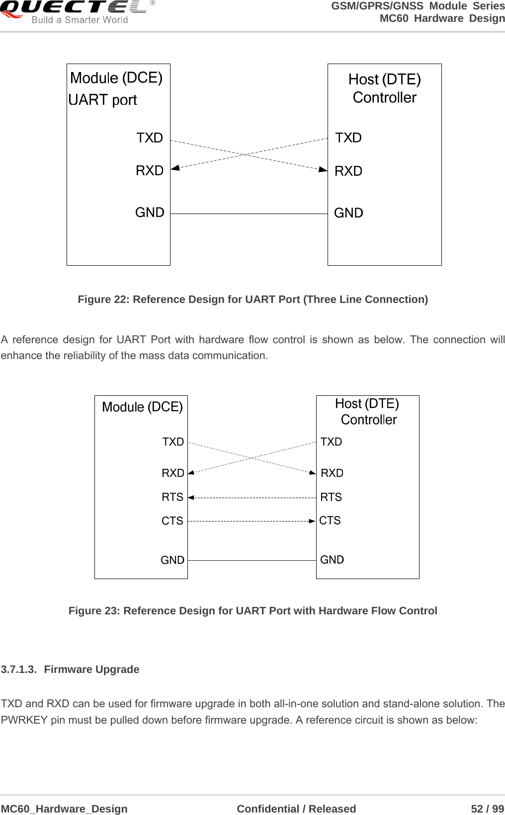
![GSM/GPRS/GNSS Module Series MC60 Hardware Design MC60_Hardware_Design Confidential / Released 51 / 99 the new baud rate by receiving the first “AT” or “at” string. The DTE may receive unknown characters after switching to a new baud rate. It is not recommended to switch to autobauding from a fixed baud rate. If autobauding is active it is not recommended to switch to multiplex mode. To assure reliable communication and avoid any problems caused by undetermined baud rate between DCE and DTE, it is strongly recommended to configure a fixed baud rate and save it instead of using autobauding after start-up. For more details, please refer to the Section AT+IPR in document [1]. 3.7.1.2. The Connection of UART The connection between module and host using UART Port is very flexible. Three connection styles are illustrated as below. A reference design for Full-Function UART connection is shown as below when it is applied in modulation-demodulation. Figure 21: Reference Design for Full-Function UART Three-line connection is shown as below. NOTE](https://usermanual.wiki/Quectel-Wireless-Solutions/201609MC60/User-Guide-3165740-Page-52.png)
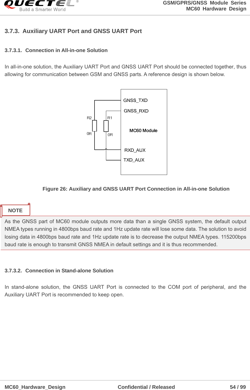
![GSM/GPRS/GNSS Module Series MC60 Hardware Design MC60_Hardware_Design Confidential / Released 55 / 99 Figure 27: Auxiliary and GNSS UART Port Connection in Stand-alone Solution 3.7.4. UART Application A reference design of 3.3V level match is shown as below. If the host is a 3V system, please change the 5.6K resistors to 10K ones. Figure 28: Level Match Design for 3.3V System It is highly recommended to add the resistor divider circuit on the UART signal lines when the host’s level is 3V or 3.3V. For a higher voltage level system, a level shifter IC could be used between the host and the module. For more details about UART circuit design, please refer to document [13]. The following figure shows a sketch map between the module and the standard RS-232 interface. As the electrical level of module is 2.8V, a RS-232 level shifter must be used. Note that you should assure the I/O voltage of level shifter which connects to module is 2.8V. NOTE](https://usermanual.wiki/Quectel-Wireless-Solutions/201609MC60/User-Guide-3165740-Page-56.png)
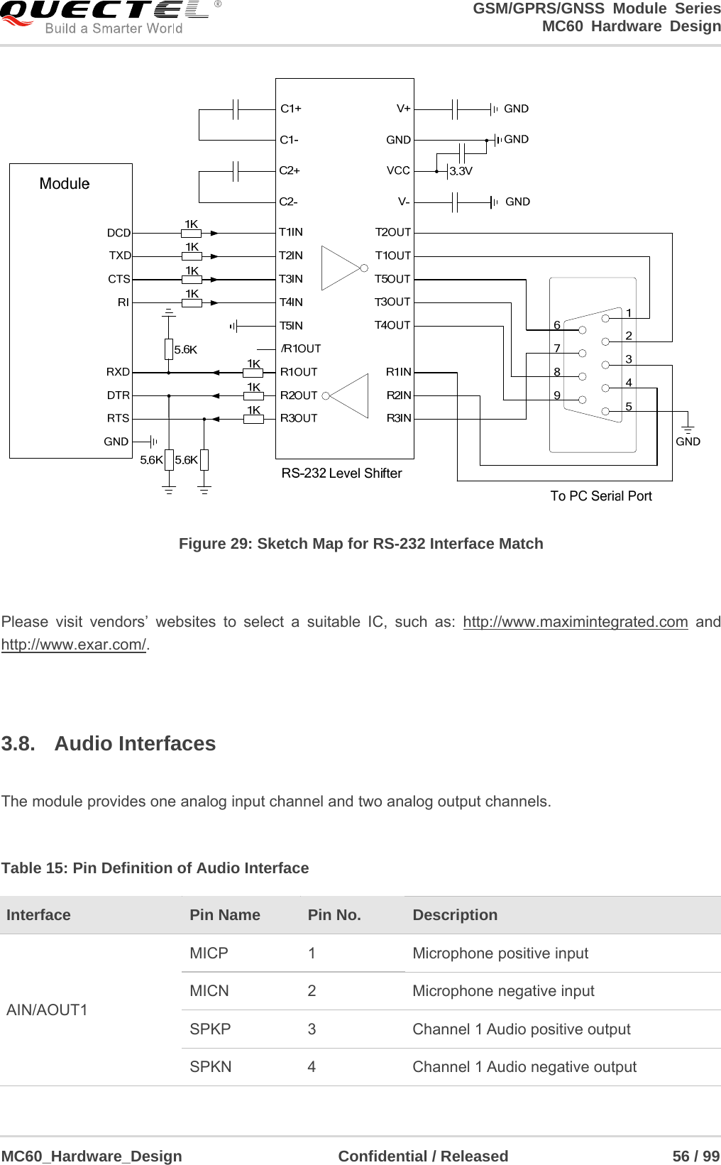
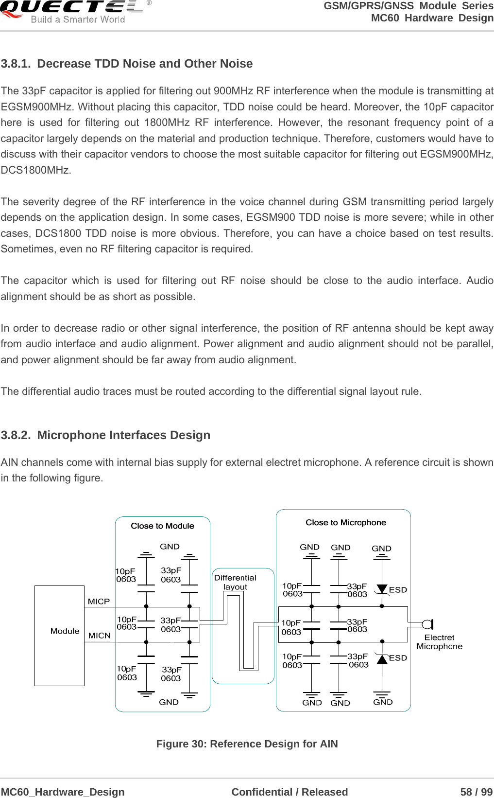
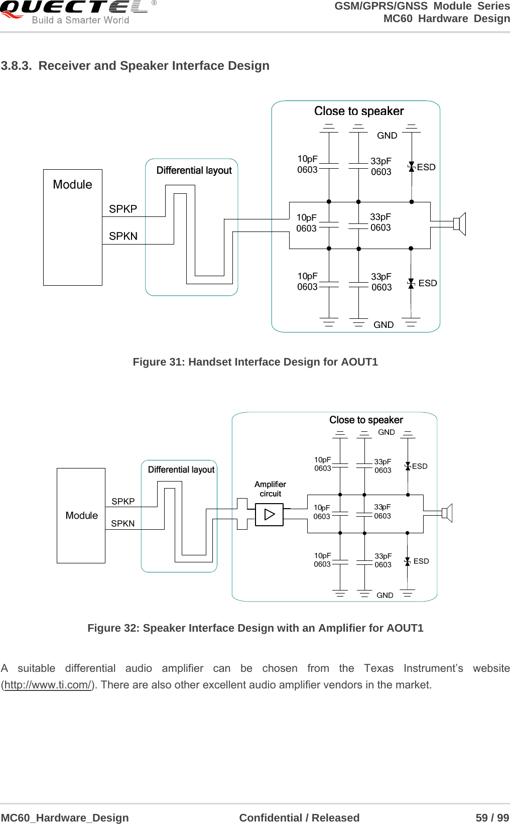
![GSM/GPRS/GNSS Module Series MC60 Hardware Design MC60_Hardware_Design Confidential / Released 57 / 99 AIN can be used for input of microphone and line. An electret microphone is usually used. AIN are differential input channels. AOUT1 is used for output of receiver. The channel is typically used for building a receiver into a handset. AOUT1 channel is a differential channel. AOUT2 is used for loudspeaker output as it is embedded with an amplifier of class AB whose maximum drive power is 870mW. AOUT2 is a differential channel. AOUT2 also can be used for output of earphone, and can be used as a single-ended channel. LOUDSPKP and AGND can establish a pseudo differential mode. All these audio channels support voice and ringtone output, and so on, and can be switched by AT+QAUDCH command. For more details, please refer to document [1]. Use AT command AT+QAUDCH to select audio channel: 0--AIN/AOUT1, the default value is 0. 1--AIN/AOUT2, this channel is always used for earphone. 2--AIN/AOUT2, this channel is always used for loudspeaker. For each channel, you can use AT+QMIC to adjust the input gain level of microphone. You can also use AT+CLVL to adjust the output gain level of receiver and speaker. AT+QSIDET is used to set the side-tone gain level. For more details, please refer to document [1]. Table 16: AOUT2 Output Characteristics AIN/AOUT2 MICP 1 Microphone positive input MICN 2 Microphone negative input LOUDSPKP 54 Channel 2 Audio positive output LOUDSPKN 53 Channel 2 Audio negative output Item Condition Min. Typ. Max. Unit RMS Power 8ohm load VBAT=4.2v THD+N=1% 870 mW 8ohm load VBAT=3.3v THD+N=1% 530 mW](https://usermanual.wiki/Quectel-Wireless-Solutions/201609MC60/User-Guide-3165740-Page-58.png)
![GSM/GPRS/GNSS Module Series MC60 Hardware Design MC60_Hardware_Design Confidential / Released 65 / 99 3.10. ADC The module provides an ADC channel to measure the value of voltage. Please give priority to the use of ADC0 channel. Command AT+QADC can read the voltage value applied on ADC0 pin. For details of this AT command, please refer to document [1]. In order to improve the accuracy of ADC, the layout of ADC should be surrounded by ground. Table 20: Pin Definition of the ADC Table 21: Characteristics of the ADC 3.11. Behaviors of the RI Table 22: Behaviors of the RI Pin Name Pin No. Description ADC 6 Analog to digital converter. Item Min. Typ. Max. Unit Voltage Range 0 2.8 V ADC Resolution 10 bits ADC Accuracy 2.7 mV State RI Response Standby HIGH Voice Call Change to LOW, and then: 1. Change to HIGH when call is established. 2. Change to HIGH when use ATH to hang up the call 3. Change to HIGH first when calling part hangs up and then change to LOW for 120ms indicating “NO CARRIER” as an URC. After that, RI changes to HIGH again. 4. Change to HIGH when SMS is received. SMS When a new SMS comes, the RI changes to LOW and holds low level for about 120ms, and then changes to HIGH.](https://usermanual.wiki/Quectel-Wireless-Solutions/201609MC60/User-Guide-3165740-Page-66.png)
![GSM/GPRS/GNSS Module Series MC60 Hardware Design MC60_Hardware_Design Confidential / Released 66 / 99 If the module is used as a caller, the RI would maintain high except when the URC or SMS is received. When it is used as a receiver, the timing of RI is shown below. Figure 38: RI Behavior as a Receiver When Voice Calling Figure 39: RI Behavior as a Caller Figure 40: RI Behavior When URC or SMS Received URC Certain URCs can trigger 120ms low level on RI. For more details, please refer to document [1]](https://usermanual.wiki/Quectel-Wireless-Solutions/201609MC60/User-Guide-3165740-Page-67.png)
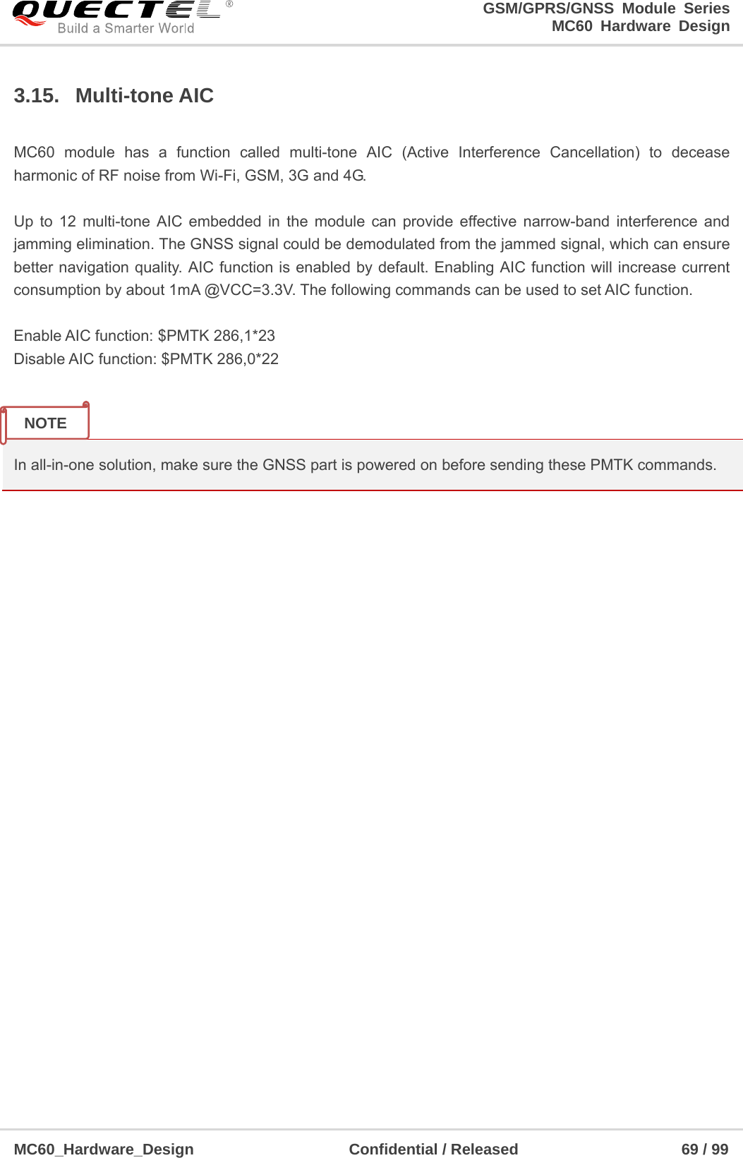
![GSM/GPRS/GNSS Module Series MC60 Hardware Design MC60_Hardware_Design Confidential / Released 68 / 99 3.13. EASY Autonomous AGPS Technology Supplying aiding information like ephemeris, almanac, rough last position, time and satellite status, can help improve the acquisition sensitivity and the TTFF for a module. This is called as EASY technology and MC60’s GNSS part supports it. EASY technology works as embedded software which can accelerate TTFF by predicting satellite navigation messages from received ephemeris. The GNSS part will calculate and predict orbit information automatically up to 3 days after first receiving the broadcast ephemeris, and save the predicted information into the internal memory. GNSS part of MC60 will use the information for positioning if no enough information from satellites, so the function is helpful for positioning and TTFF improvement. The EASY function can reduce TTFF to 5s in warm start. In this case, GNSS’s backup domain should be valid. In order to gain enough broadcast ephemeris information from GNSS satellites, the GNSS part should receive the information for at least 5 minutes in good signal conditions after it fixes the position. EASY function is enabled by default. Command “$PMTK869,1,0*34” can be used to disable EASY function. For more details, please refer to document [2]. 3.14. EPO Offline AGPS Technology MC60 module features a function called EPO (Extended Prediction Orbit) which is a world leading technology. When MC60 module is powered on, EPO function can be enabled via AT command AT+QGNSSEPO=1. When the GSM part detected that the EPO data has expired, the EPO data will be automatically downloaded to the GSM part’s FS from MTK server via GSM/GPRS network; and the GNSS part will get the EPO data via build-in GNSS command from GSM's FS when it detected that the local EPO data has expired. When there is no local EPO data or when the data has expired, MC60 module will download the data (4KB) for 6 hours’ orbit predictions in order to achieve cold start in the shortest time, and then continue to download the EPO data (48KB) for 3 days. The technology allows the module to realize fast positioning. Command AT+QGNSSEPO=0 can turn off the EPO function. In all-in-one solution, make sure the GNSS part is powered on before sending the PMTK command. Make sure the EPO function is enabled if you need to download the EPO data. NOTE NOTE](https://usermanual.wiki/Quectel-Wireless-Solutions/201609MC60/User-Guide-3165740-Page-69.png)
![GSM/GPRS/GNSS Module Series MC60 Hardware Design MC60_Hardware_Design Confidential / Released 90 / 99 thickness of stencil at the hole of the module pads should be 0.2 mm for MC60. For more details, please refer to document [12] It is suggested that the peak reflow temperature is from 235ºC to 245ºC (for SnAg3.0Cu0.5 alloy). The absolute maximum reflow temperature is 260ºC. To avoid damage to the module caused by repeated heating, it is suggested that the module should be mounted after reflow soldering for the other side of PCB has been completed. Recommended reflow soldering thermal profile is shown below: Time(s)50 100 150 200 250 30050100150200250 160℃ 200℃217070s~120s40s~60sBetween 1~3℃/SPreheat Heating Cooling℃sLiquids Temperature Figure 52: Reflow Soldering Thermal Profile 7.3. Packaging The modules are stored in a vacuum-sealed bag which is ESD protected. It should not be opened until the devices are ready to be soldered onto the application.](https://usermanual.wiki/Quectel-Wireless-Solutions/201609MC60/User-Guide-3165740-Page-91.png)
![GSM/GPRS/GNSS Module Series MC60 Hardware Design MC60_Hardware_Design Confidential / Released 92 / 99 8 Appendix A References Table 41: Related Documents SN Document Name Remark [1] Quectel_MC60_AT_Commands_Manual MC60 AT commands manual [2] ITU-T Draft new recommendation V.25ter Serial asynchronous automatic dialing and control [3] GSM 07.07 Digital cellular telecommunications (Phase 2+); AT command set for GSM Mobile Equipment (ME) [4] GSM 07.10 Support GSM 07.10 multiplexing protocol [5] GSM 07.05 Digital cellular telecommunications (Phase 2+); Use of Data Terminal Equipment – Data Circuit terminating Equipment (DTE – DCE) interface for Short Message Service (SMS) and Cell Broadcast Service (CBS) [6] GSM 11.14 Digital cellular telecommunications (Phase 2+); Specification of the SIM Application Toolkit for the Subscriber Identity module – Mobile Equipment (SIM – ME) interface [7] GSM 11.11 Digital cellular telecommunications (Phase 2+); Specification of the Subscriber Identity module – Mobile Equipment (SIM – ME) interface [8] GSM 03.38 Digital cellular telecommunications (Phase 2+); Alphabets and language-specific information [9] GSM 11.10 Digital cellular telecommunications (Phase 2); Mobile Station (MS) conformance specification; Part 1: Conformance specification](https://usermanual.wiki/Quectel-Wireless-Solutions/201609MC60/User-Guide-3165740-Page-93.png)
![GSM/GPRS/GNSS Module Series MC60 Hardware Design MC60_Hardware_Design Confidential / Released 93 / 99 Table 42: Terms and Abbreviations [10] GSM_UART_Application_Note UART port application note [11] GSM_EVB_User_Guide GSM EVB user guide [12] Module_Secondary_SMT_User_Guide Module secondary SMT user guide [13] Quectel_GSM_Module_Digital_IO_Application_Note GSM Module Digital IO Application Note Abbreviation Description ADC Analog-to-Digital Converter AMR Adaptive Multi-Rate ARP Antenna Reference Point ASIC Application Specific Integrated Circuit BER Bit Error Rate BOM Bill of Material BT Bluetooth BTS Base Transceiver Station CHAP Challenge Handshake Authentication Protocol CS Coding Scheme CSD Circuit Switched Data CTS Clear to Send DAC Digital-to-Analog Converter DRX Discontinuous Reception DSP Digital Signal Processor DCE Data Communications Equipment (typically module) DTE Data Terminal Equipment (typically computer, external controller) DTR Data Terminal Ready](https://usermanual.wiki/Quectel-Wireless-Solutions/201609MC60/User-Guide-3165740-Page-94.png)