Quectel Wireless Solutions 201703FC20 WiFi& BT Module User Manual
Quectel Wireless Solutions Company Limited WiFi& BT Module
UserManual.wiki
>
Quectel Wireless Solutions
>
201703FC20 User Manual
User Manual
Navigation menu
Upload a User Manual
Namespaces
Wiki Guide
HTML
PDF
Info
Views
User Manual
Discussion / Help
Navigation
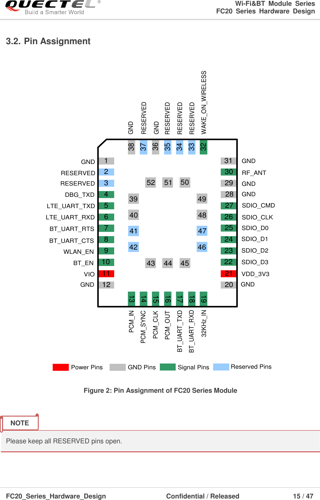
![Wi-Fi&BT Module Series FC20 Series Hardware Design FC20_Series_Hardware_Design Confidential / Released 13 / 47 The functions in dotted line are only supported by FC20. 2.5. Evaluation Board In order to help customers to develop applications with FC20 series module, Quectel supplies an evaluation board (EVB), a RS-232 to USB cable, a USB data cable, a power adapter, 4 antennas and other peripherals to control or test the module. For details, please refer to document [1].](https://usermanual.wiki/Quectel-Wireless-Solutions/201703FC20/User-Guide-3410150-Page-14.png)
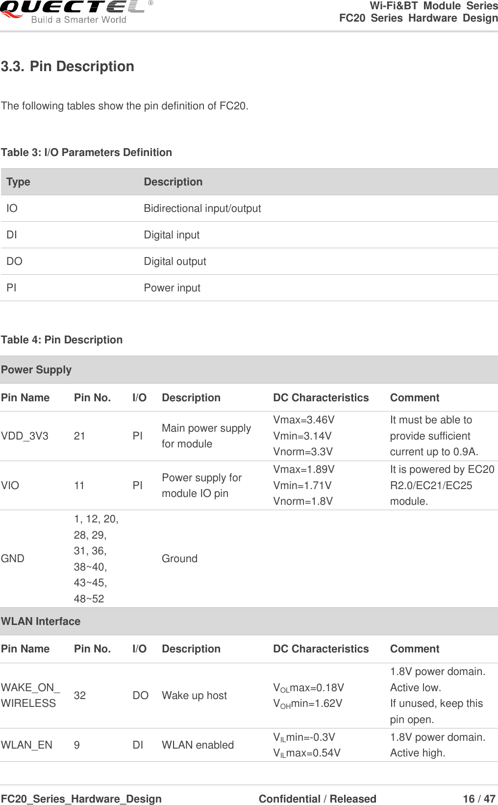
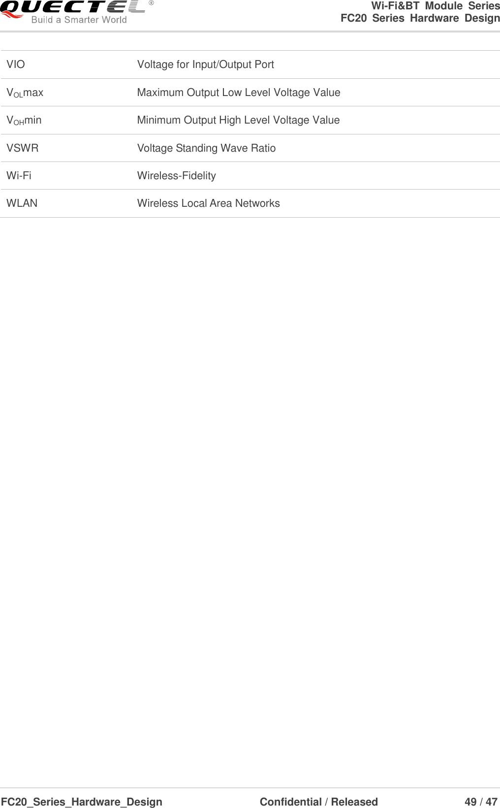
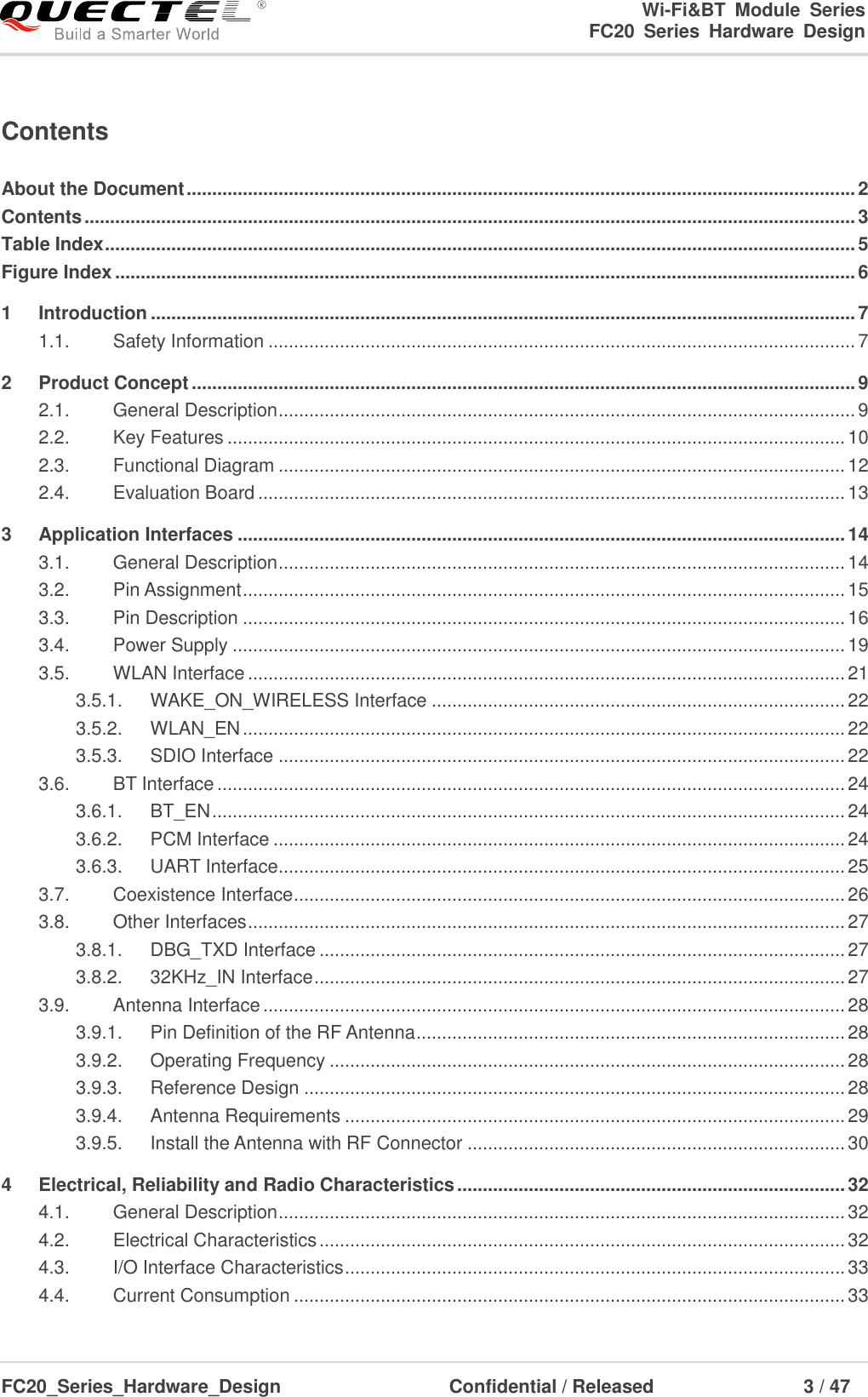
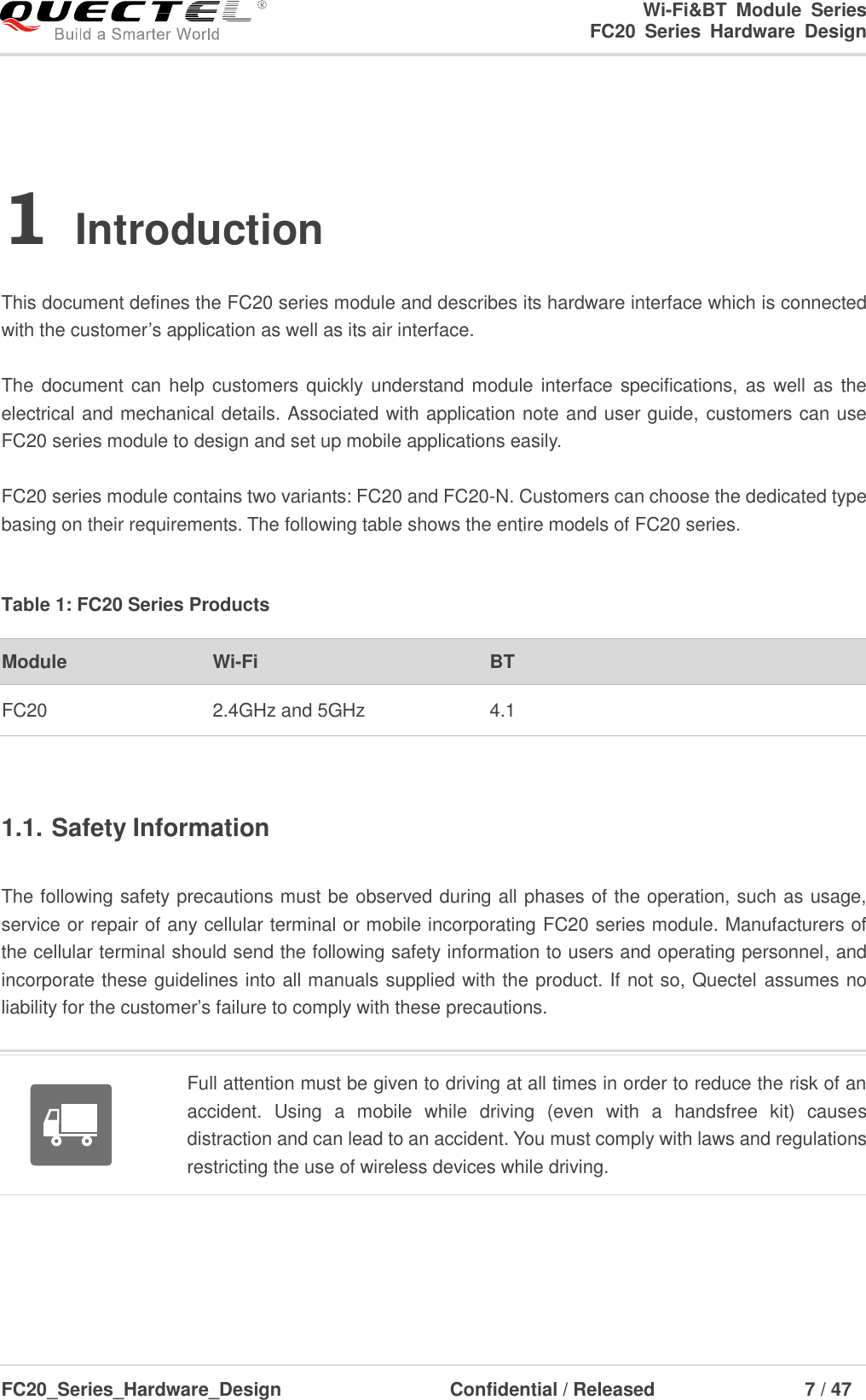
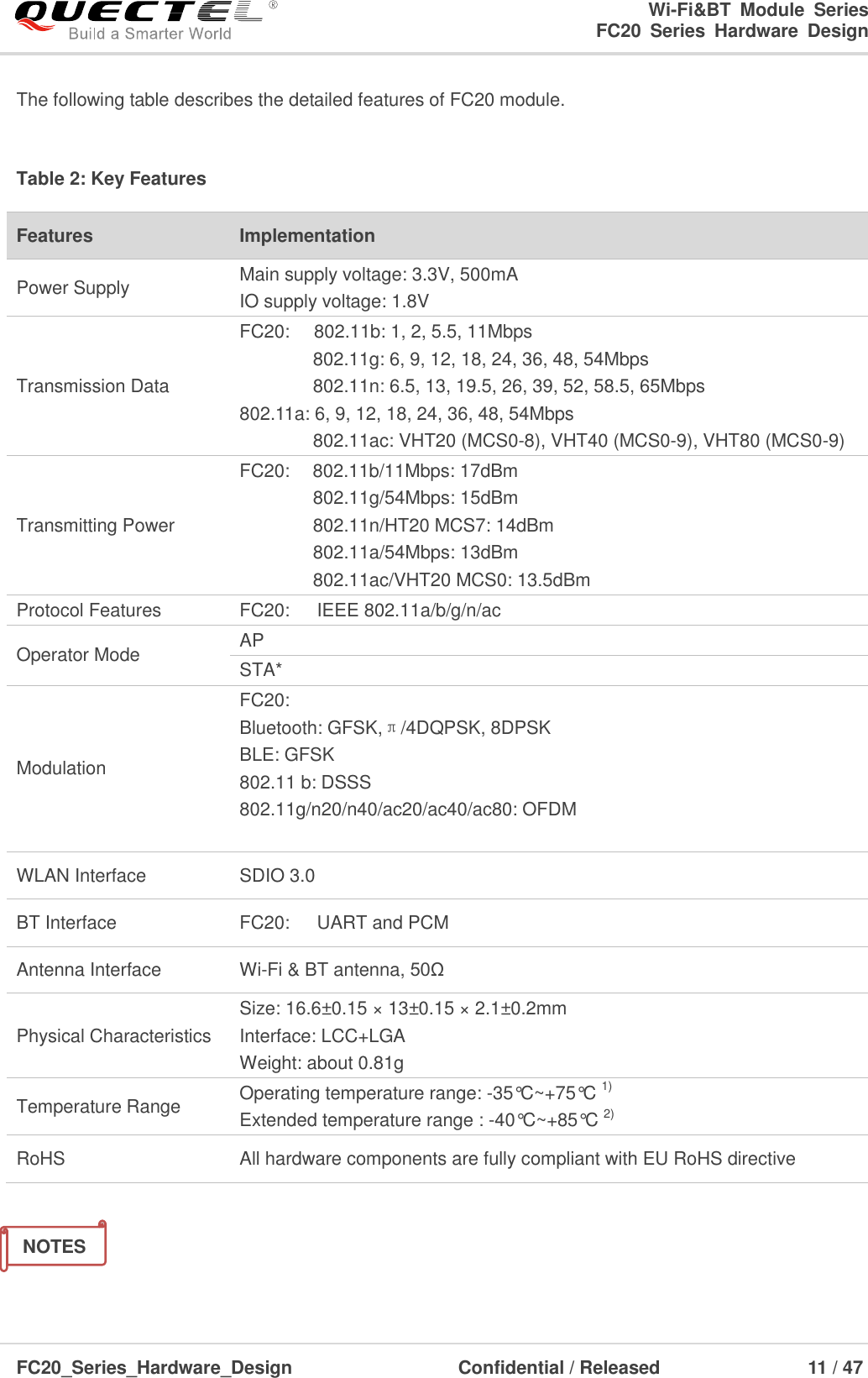
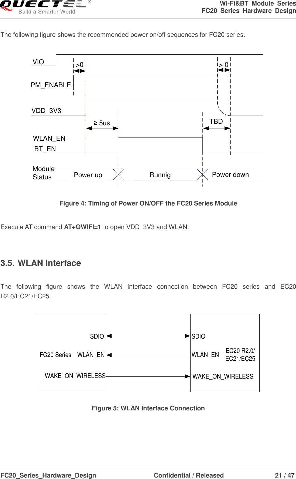
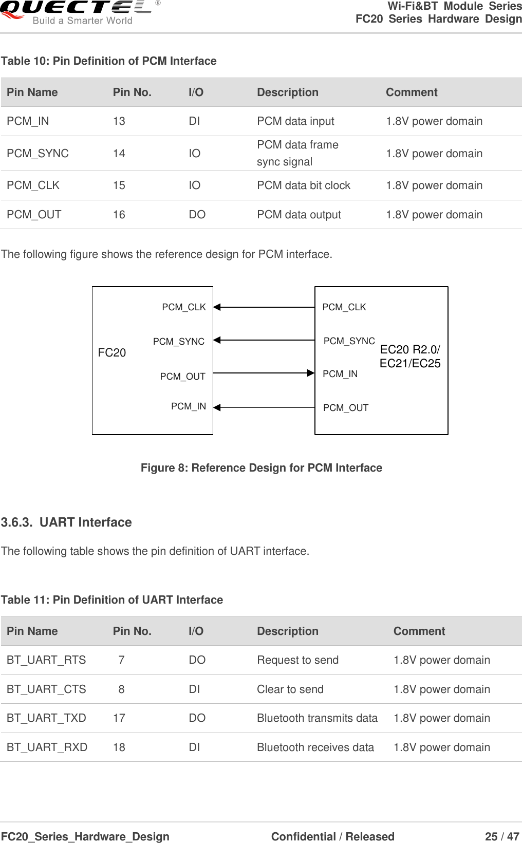
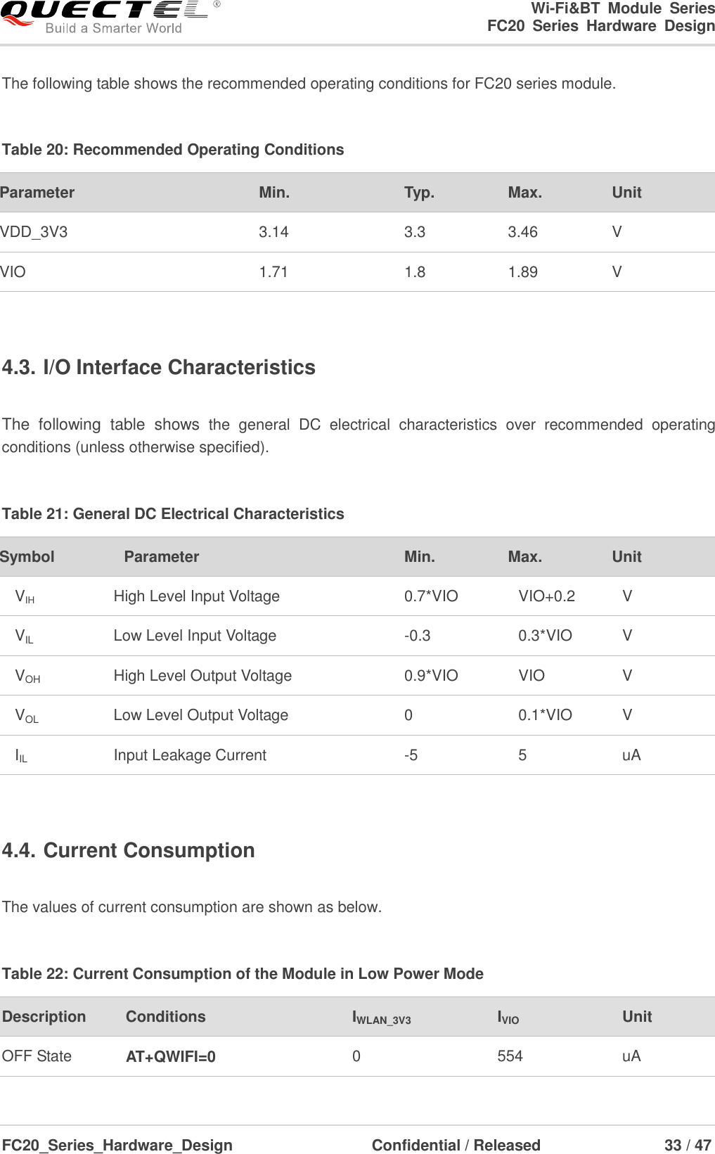
![Wi-Fi&BT Module Series FC20 Series Hardware Design FC20_Series_Hardware_Design Confidential / Released 20 / 47 28, 29, 31, 36, 38~40, 43~45, 48~52 FC20 series is powered by VDD_3V3, and it is recommended to use power supply chip whose maximum output current is more than 1.2A. The following figure shows a reference design for VDD_3V3, which is controlled by PM_ENABLE. And PM_ENABLE should be connected to pin 127 of EC20 R2.0/EC21/EC25. For more details, please refer to document [2], [3] or [4]. TPS630242L1L1L2L2VINVINVINVINAGNDENVOUTVOUTVOUTPFM/PWMFBPGNDD2D3E1E2E3E4C4D1 B1A1L1 L2PGNDPGNDU402D4B2B3A2A3A4B4C1C2C3C406R408C40510uF1ML4011uHR407100K22uFC40722uFPM_ENABLEDC_5VDC_5VVDD_3V3 Figure 3: Reference Circuit for VDD_3V3](https://usermanual.wiki/Quectel-Wireless-Solutions/201703FC20/User-Guide-3410150-Page-21.png)
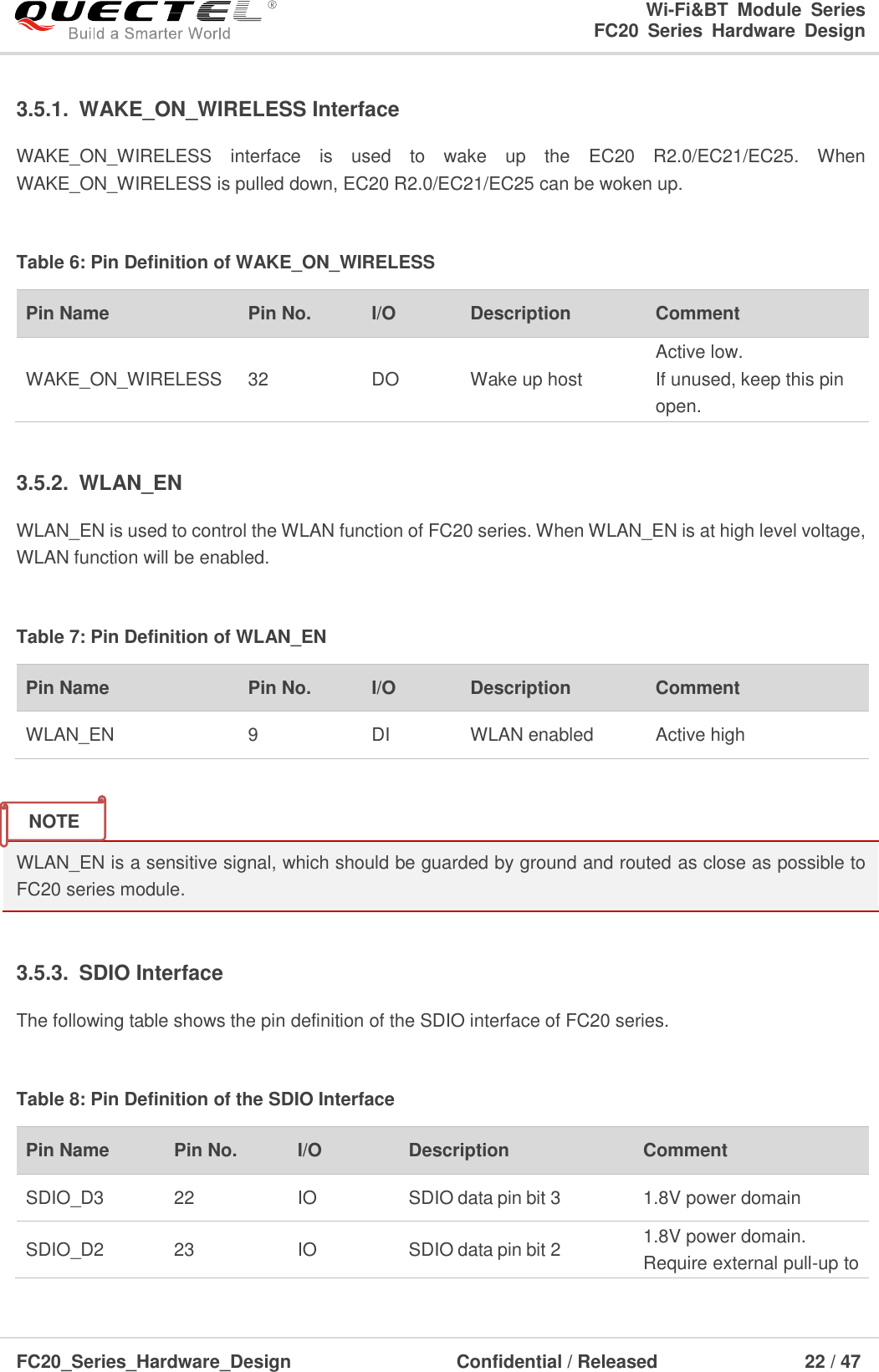
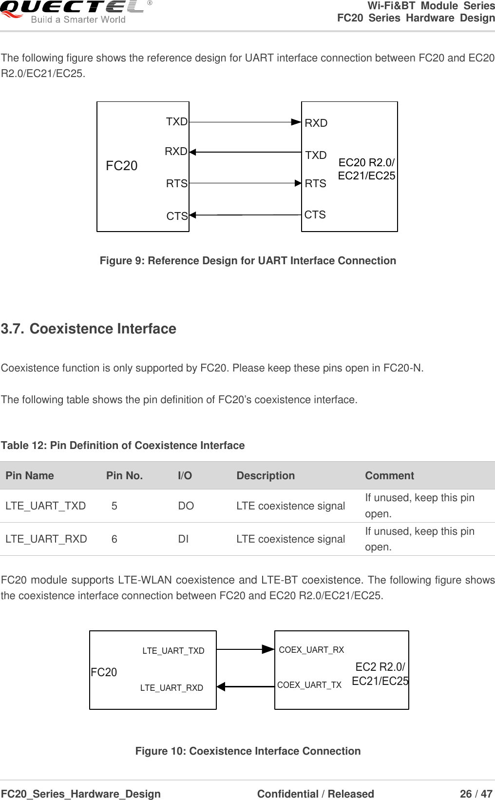
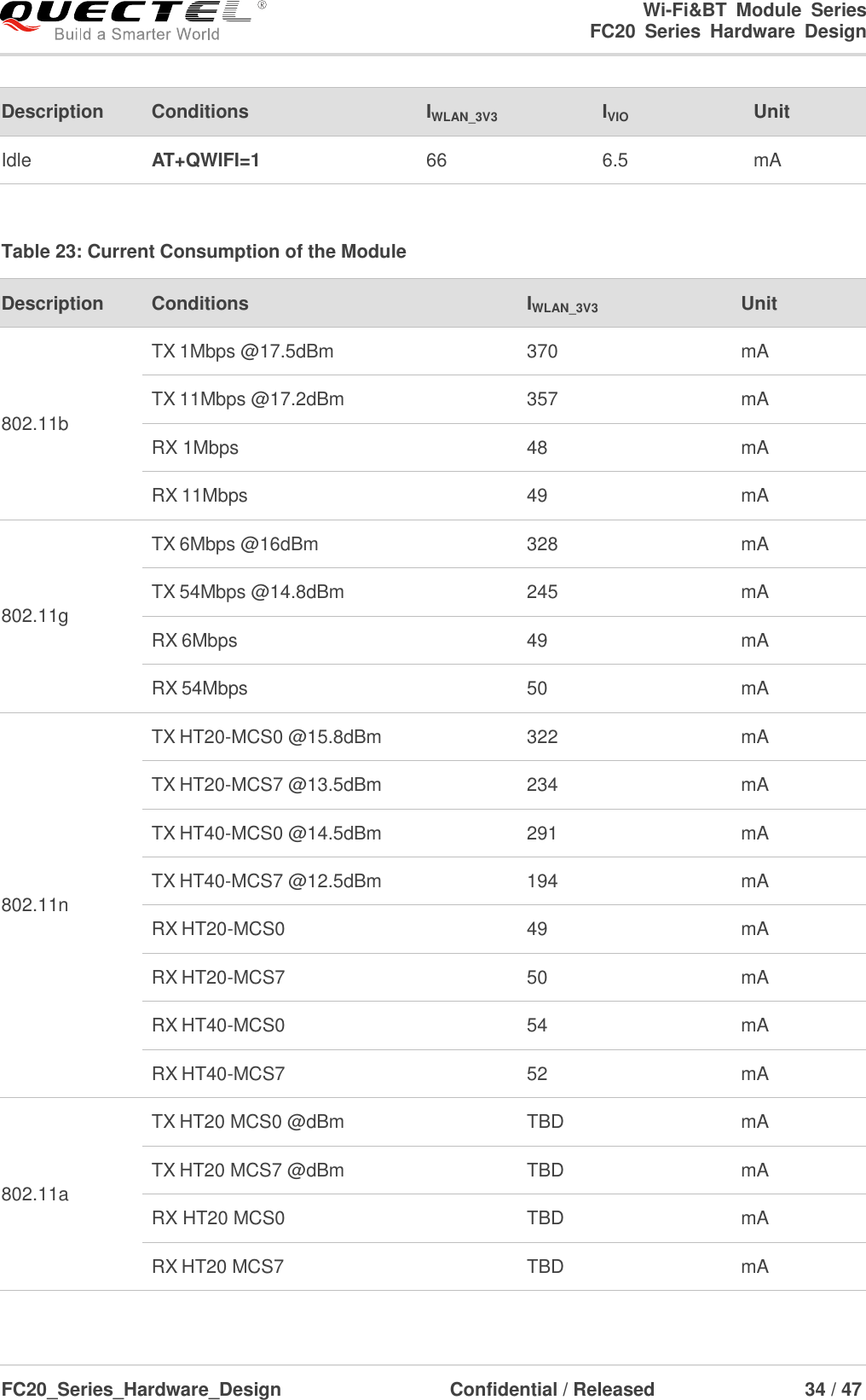
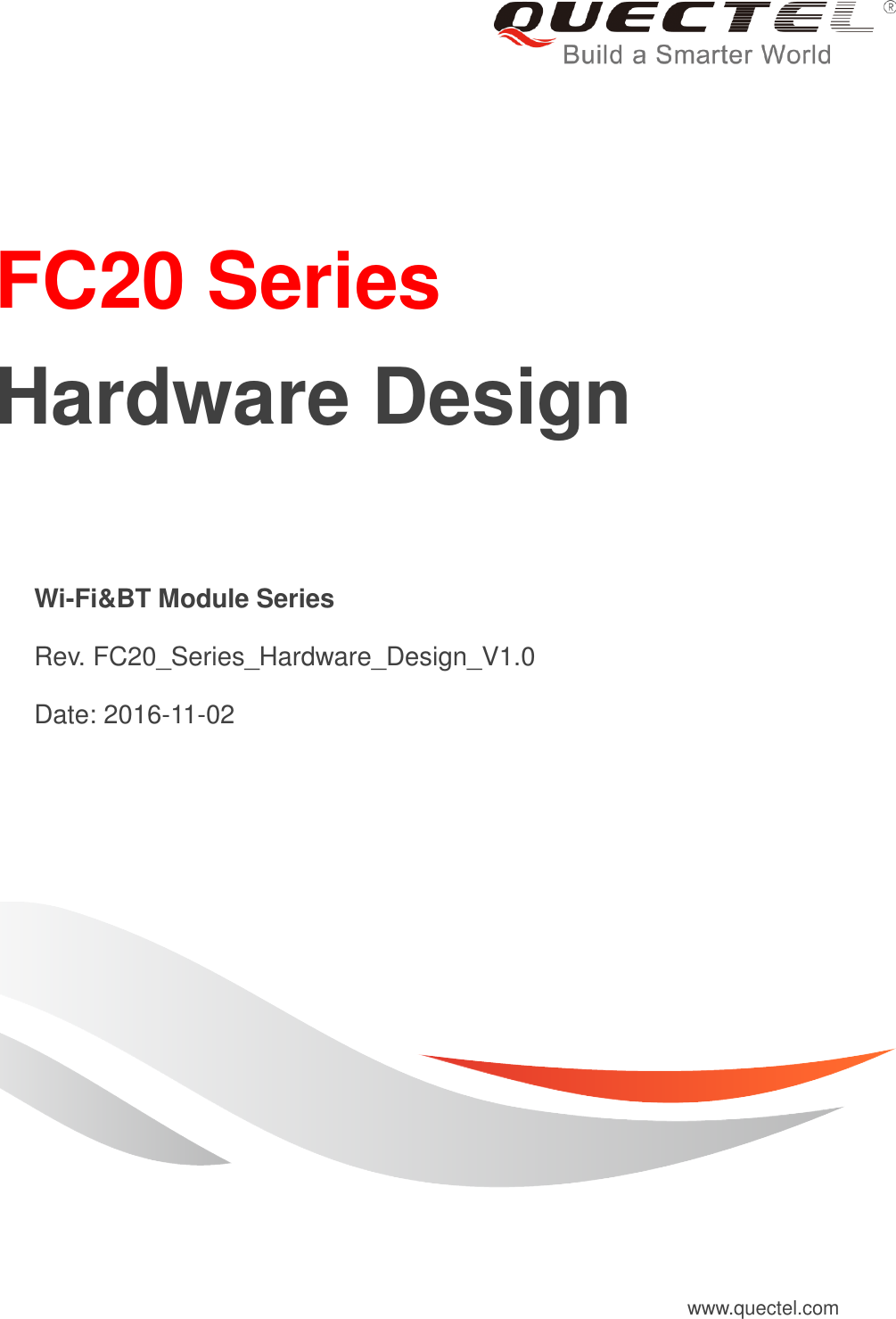
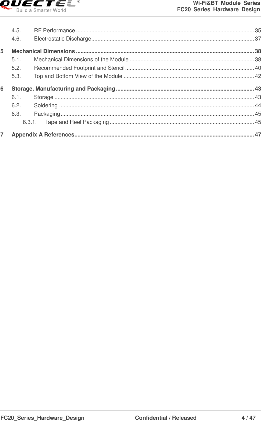
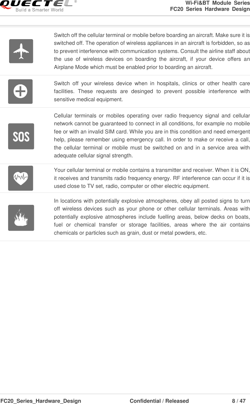
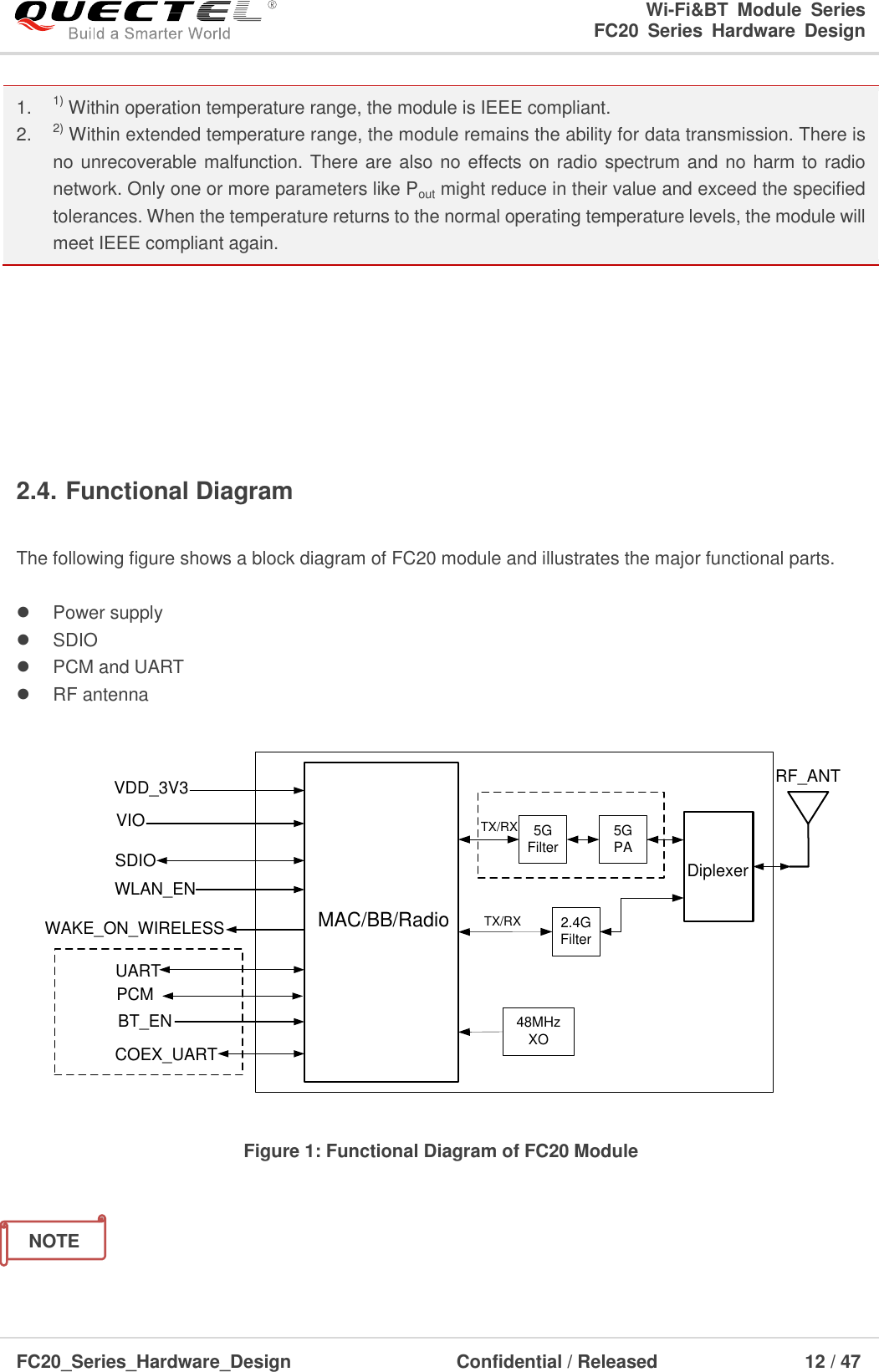
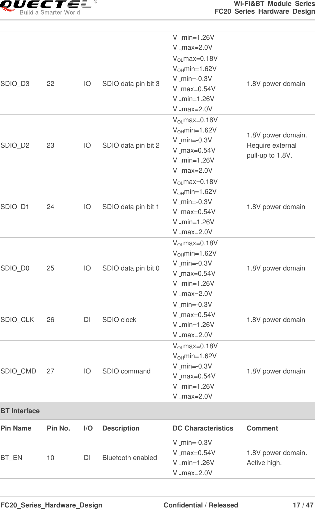
![Wi-Fi&BT Module Series FC20 Series Hardware Design FC20_Series_Hardware_Design Confidential / Released 44 / 47 6.2. Soldering Push the squeegee to apply the solder paste on the surface of stencil, thus making the paste fill the stencil openings and then penetrate to the PCB. The force on the squeegee should be adjusted properly so as to produce a clean stencil surface on a single pass. To ensure the module soldering quality, the thickness of stencil for the module is recommended to be 0.18mm. For more details, please refer to document [5]. It is suggested that the peak reflow temperature is from 235ºC to 245ºC (for SnAg3.0Cu0.5 alloy). The absolute maximum reflow temperature is 260ºC. To avoid damage to the module caused by repeated heating, it is suggested that the module should be mounted after reflow soldering for the other side of PCB has been completed. Recommended reflow soldering thermal profile is shown below: Time (s)50 100 150 200 250 30050100150200250 160℃ 200℃217070s~120s40s~60sBetween 1~3℃/SPreheat Heating Cooling℃sLiquids Temperature Figure 21: Reflow Soldering Thermal Profile](https://usermanual.wiki/Quectel-Wireless-Solutions/201703FC20/User-Guide-3410150-Page-45.png)
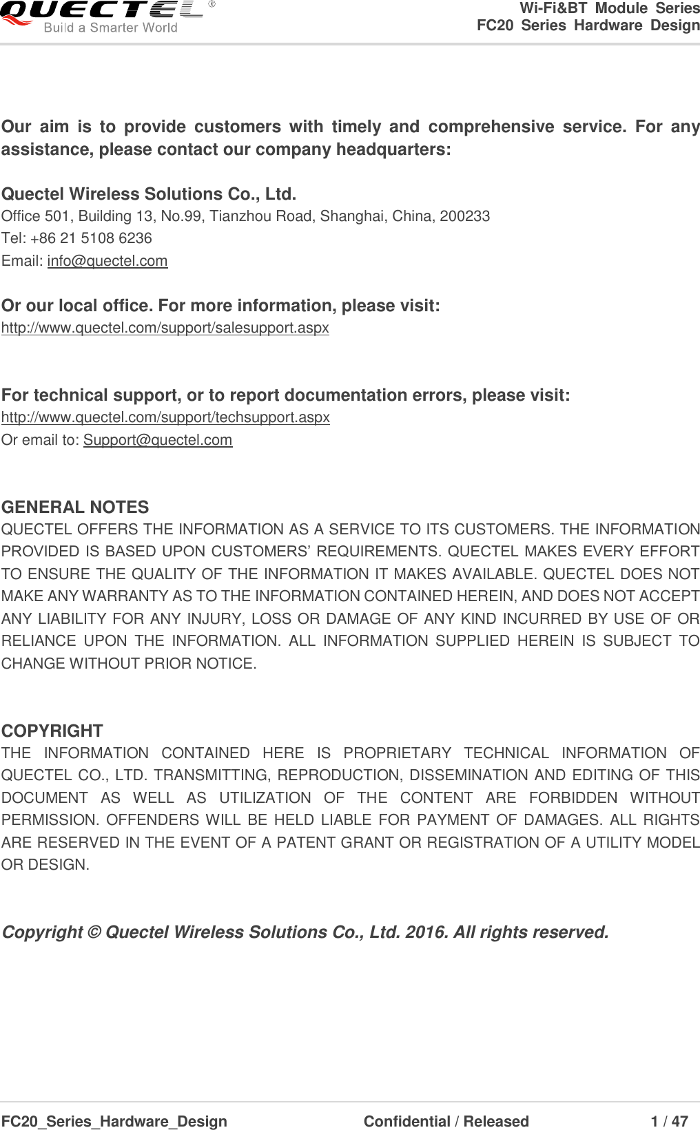
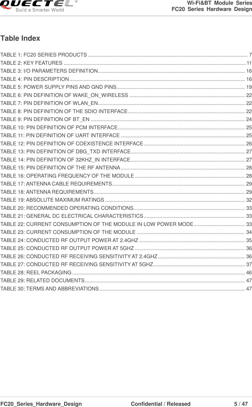
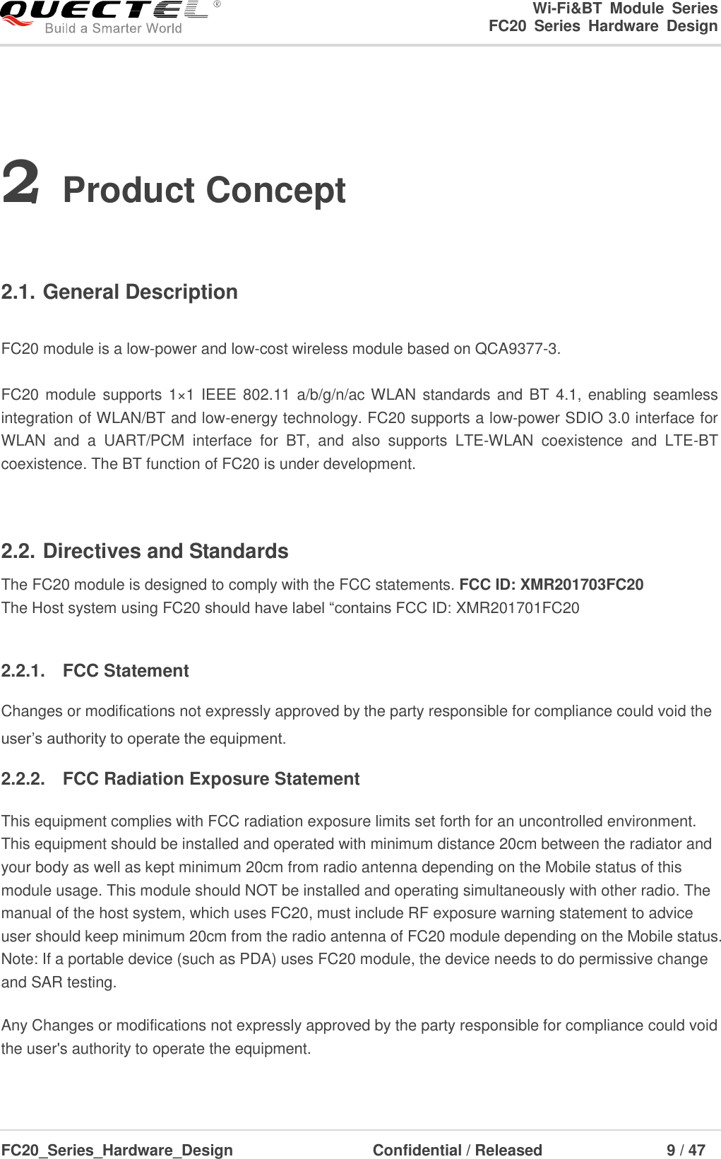
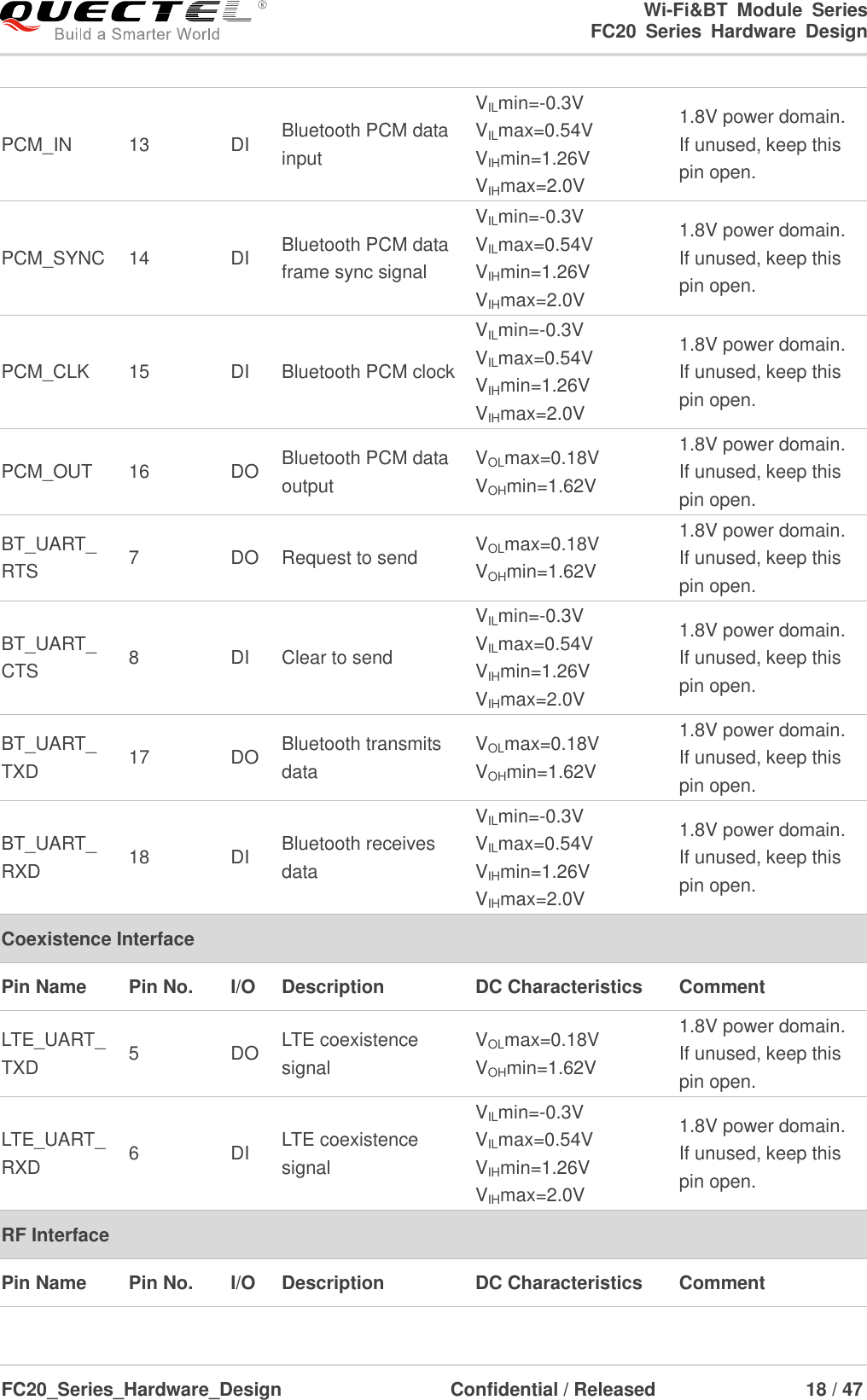
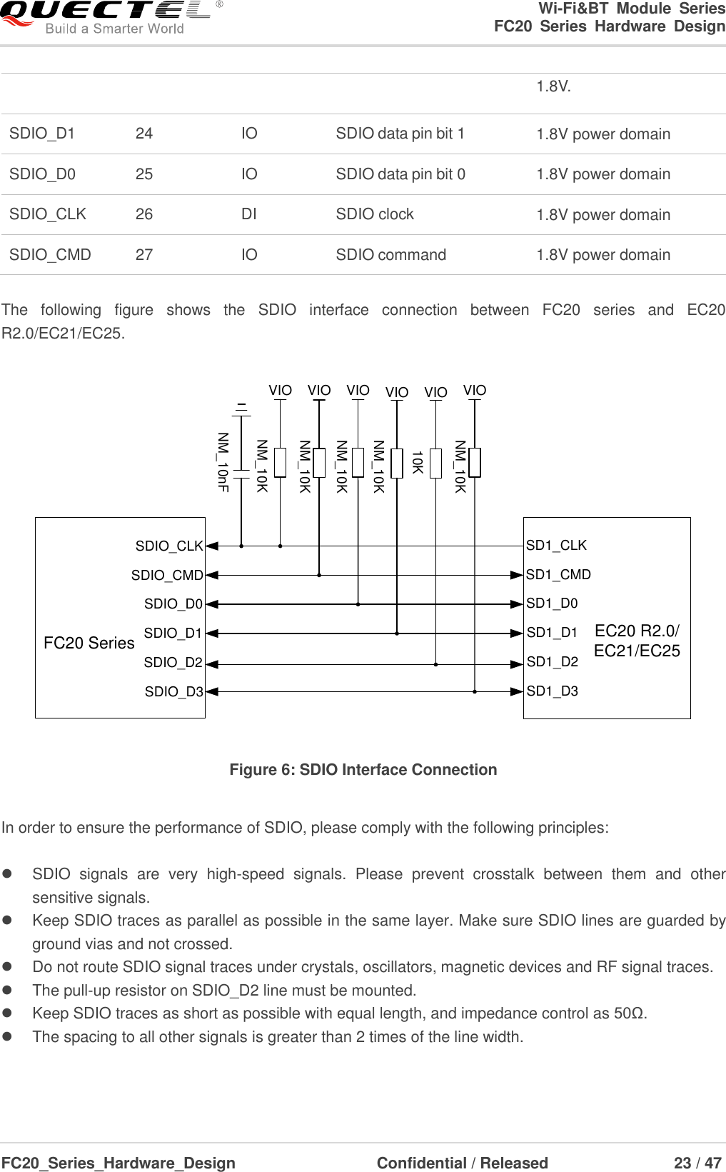
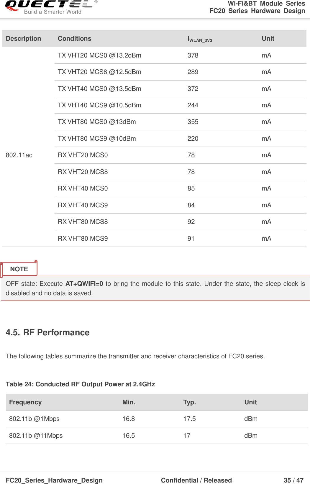
![Wi-Fi&BT Module Series FC20 Series Hardware Design FC20_Series_Hardware_Design Confidential / Released 47 / 47 7 Appendix A References Table 29: Related Documents SN Document Name Remark [1] Quectel_FC20_EVB_User_Guide FC20 EVB user guide [2] Quectel_EC25_Reference_Design EC25 reference design [3] Quectel_EC21_Reference_Design EC21 reference design [4] Quectel_EC20_R2.0_Reference_Design EC20 R2.0 reference design [5] Quectel_Module_Secondary_SMT_User_Guide Module secondary SMT user guide Table 30: Terms and Abbreviations Abbreviation Description AP Access Point BPSK Binary Phase Shift Keying BT Bluetooth CCK Complementary Code Keying CTS Clear To Send ESD Electrostatic Discharge GND Ground HT High Throughput IEEE Institute of Electrical and Electronics Engineers IIL Input Leakage Current I/O Input/Output](https://usermanual.wiki/Quectel-Wireless-Solutions/201703FC20/User-Guide-3410150-Page-48.png)