Quectel Wireless Solutions 201903EG61NA LTE Cat 1 Module User Manual
Quectel Wireless Solutions Company Limited LTE Cat 1 Module Users Manual
UserManual.wiki
>
Quectel Wireless Solutions
>
201903EG61NA User Manual
Users Manual
Navigation menu
Upload a User Manual
Namespaces
Wiki Guide
HTML
PDF
Info
Views
User Manual
Discussion / Help
Navigation
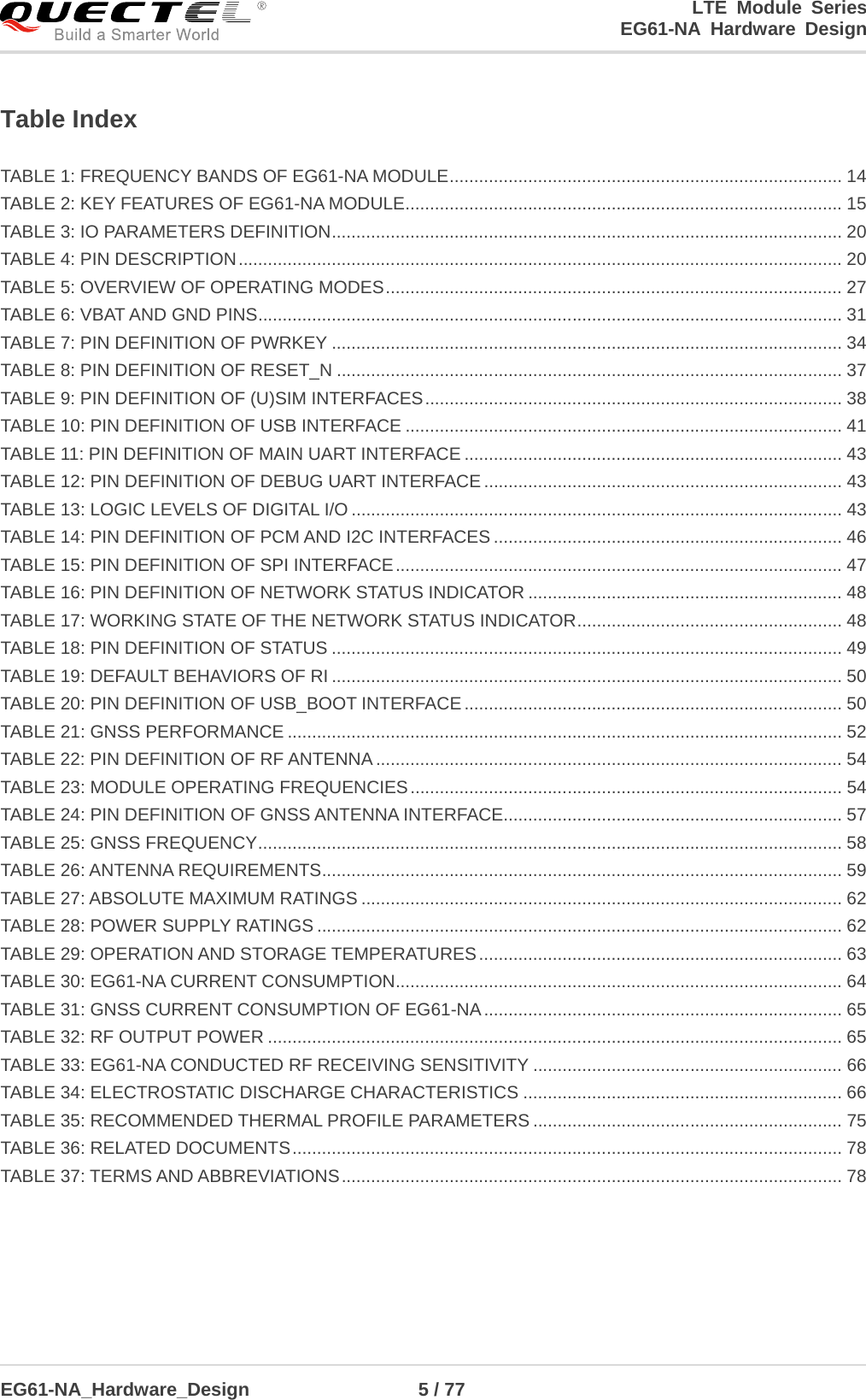
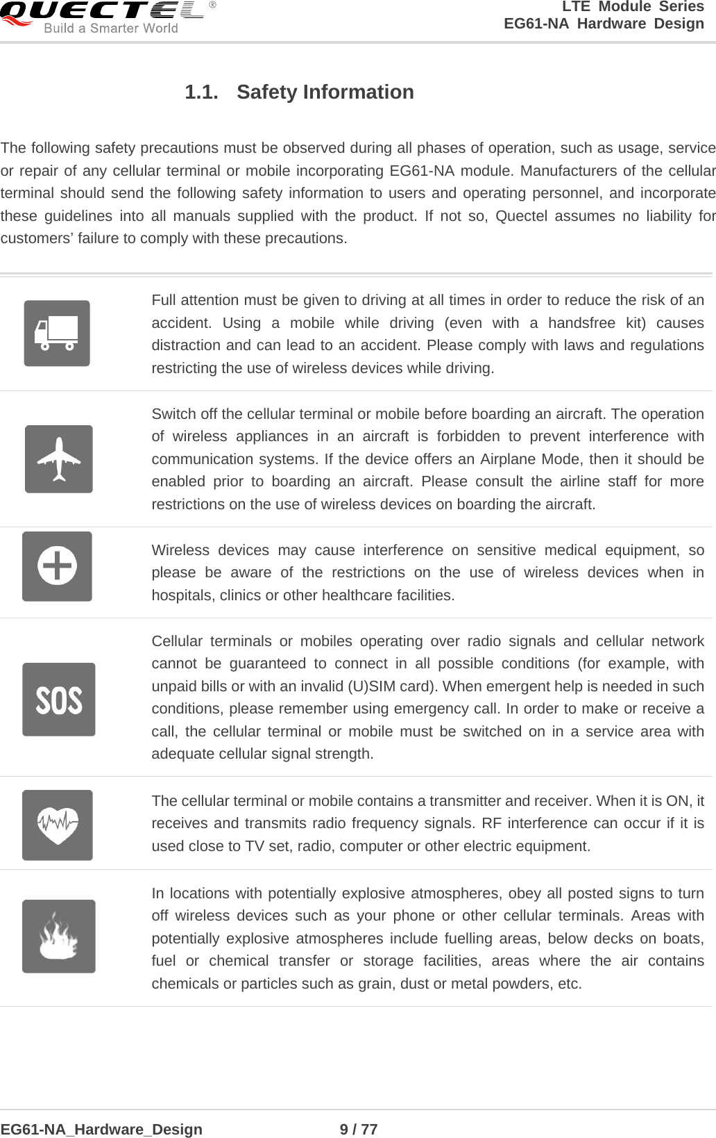

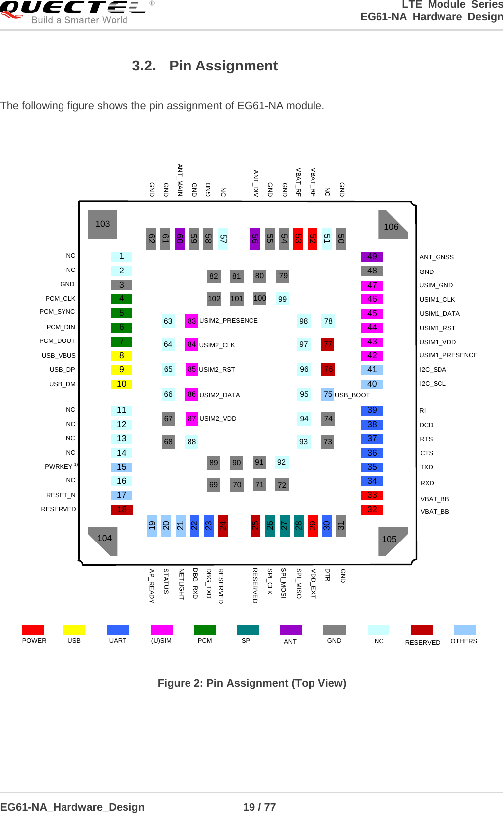
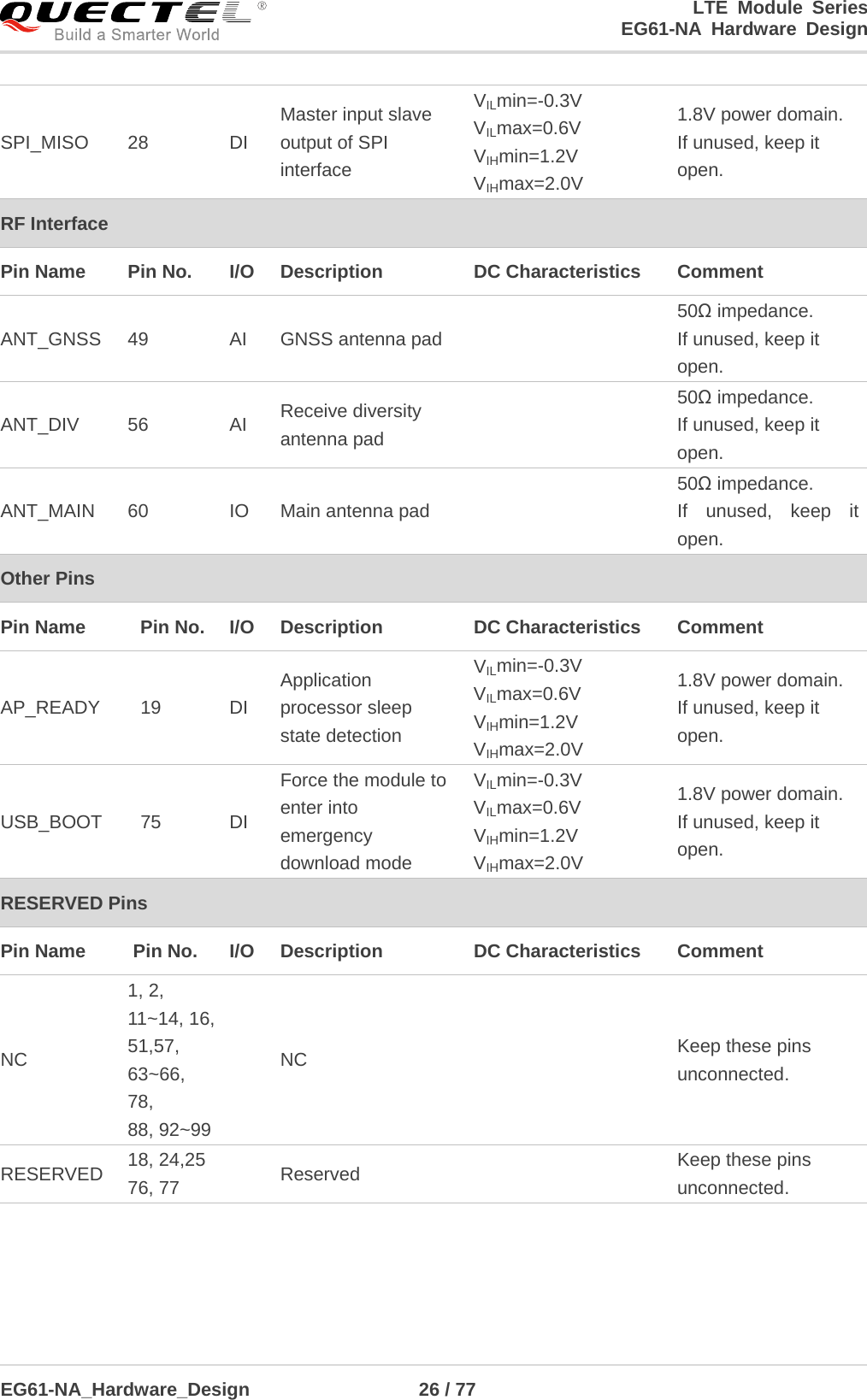
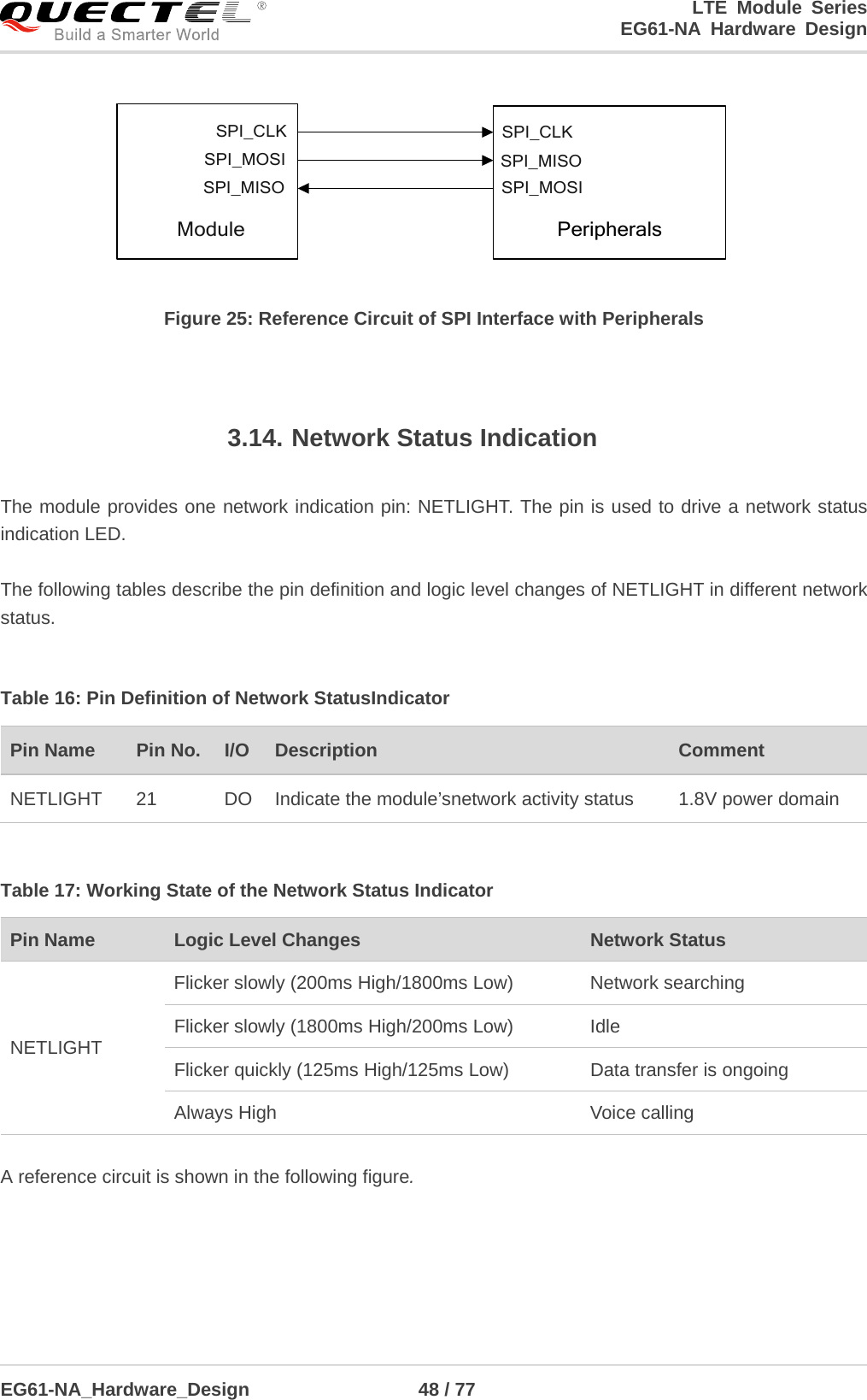
![LTE Module Series EG61-NA Hardware Design EG61-NA_Hardware_Design 30 / 77 Sending data to EG61-NAthrough USB will wake up the module. When EG61-NAhas a URC to report, RI signal will wake up the host. 3.5.1.4. USB Application without USB Suspend Function If the host does not support USB suspend function, USB_VBUS should be disconnected with an externalcontrol circuit to let the module enter into sleep mode. Execute AT+QSCLK=1commandto enable the sleep mode. Ensure the DTR is held at high level or keep it open. Disconnect USB_VBUS. The following figure shows the connection between the module and the host. USB_VBUSUSB_DPUSB_DMAP_READYVDDUSB_DPUSB_DMGPIOModule HostRI EINTPower SwitchGPIOGND GND Figure 6: Sleep Mode Application without Suspend Function Switching onthe power switch tosupply power to USB_VBUS will wake up the module. Please pay attention to the level match shown in dotted line between the module and the host.Refer to document [1] for more details about EG61-NA power management application. 3.5.2. Airplane Mode When the module enters into airplane mode, the RF function does not work, and all AT commands correlative with RF function will be inaccessible. This mode can be set viathe following ways. Hardware: The W_DISABLE# pin is pulled up by default.Driving it to low level will let the module enter into airplane mode. NOTE](https://usermanual.wiki/Quectel-Wireless-Solutions/201903EG61NA/User-Guide-4198069-Page-31.png)
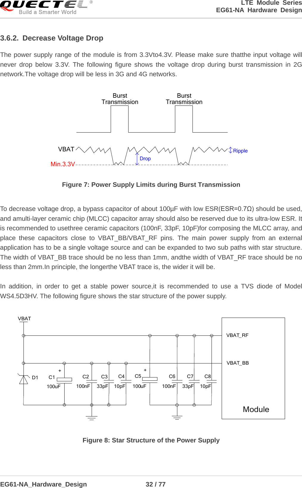
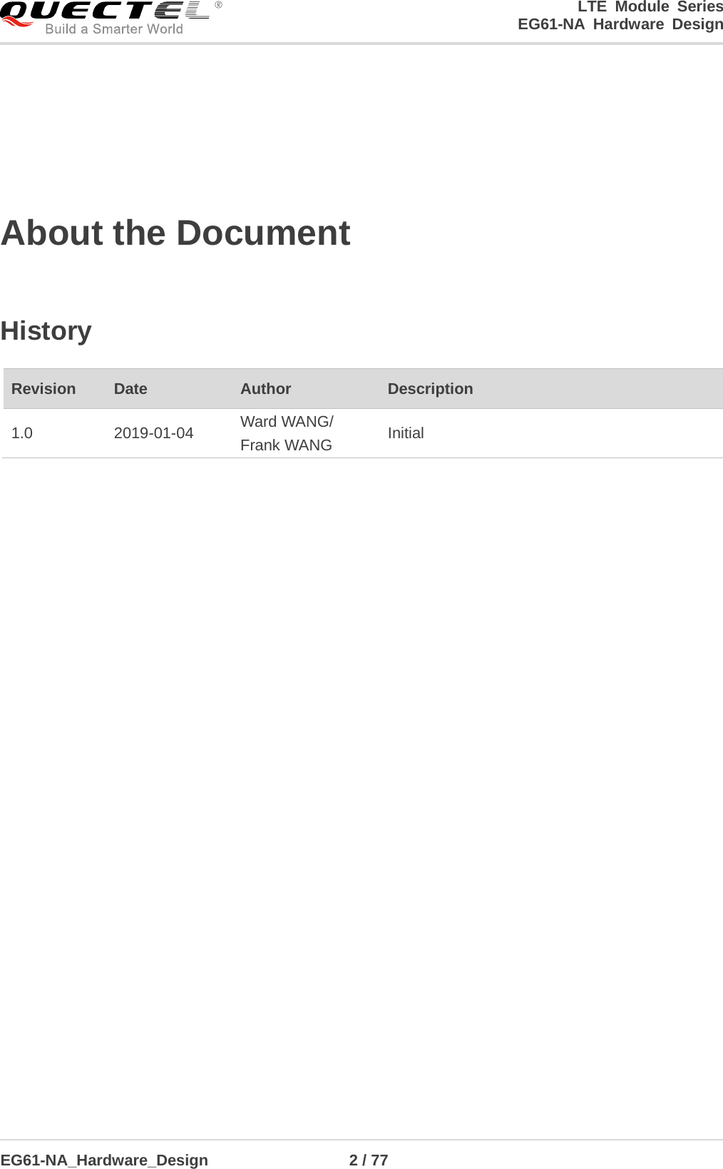
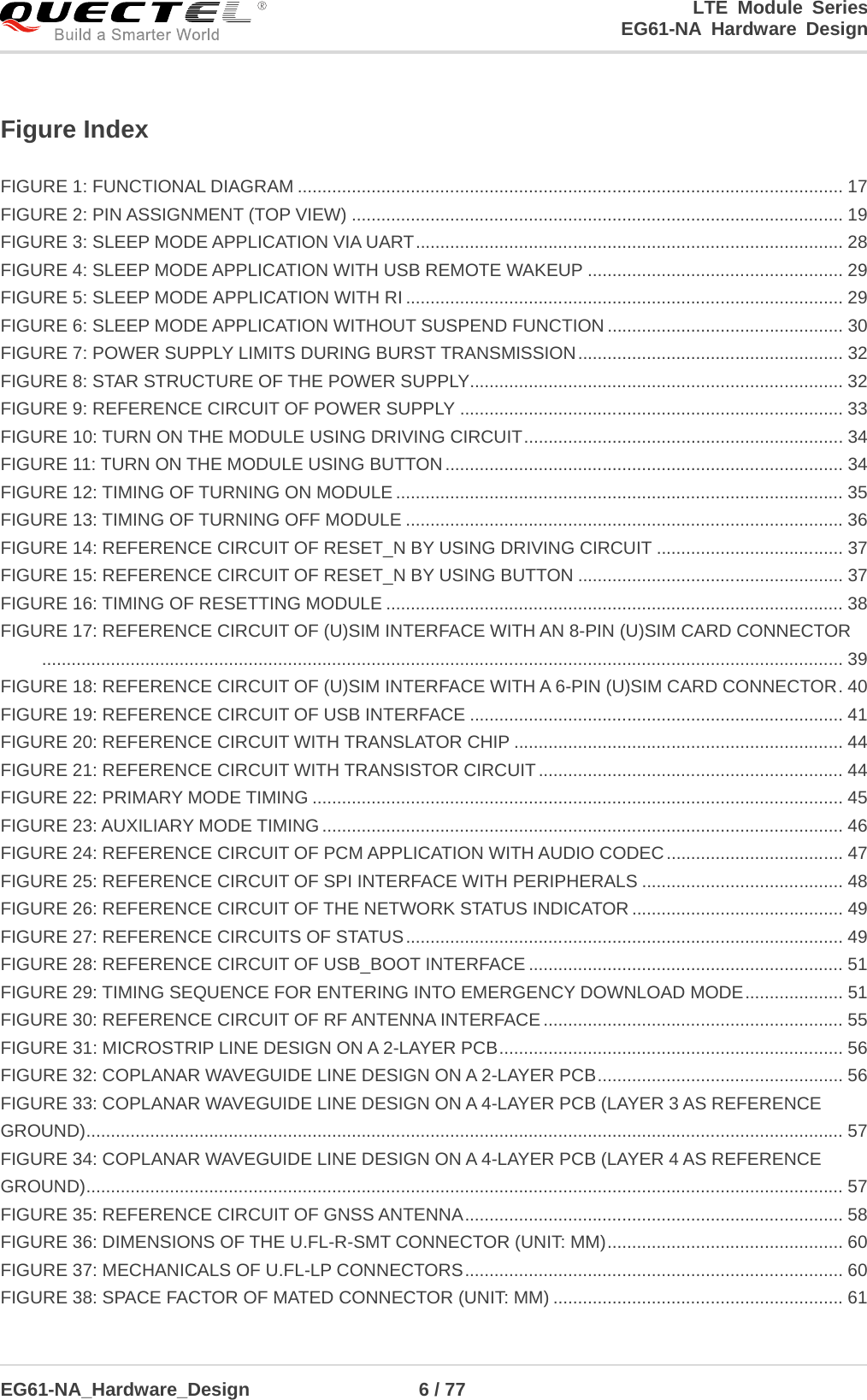
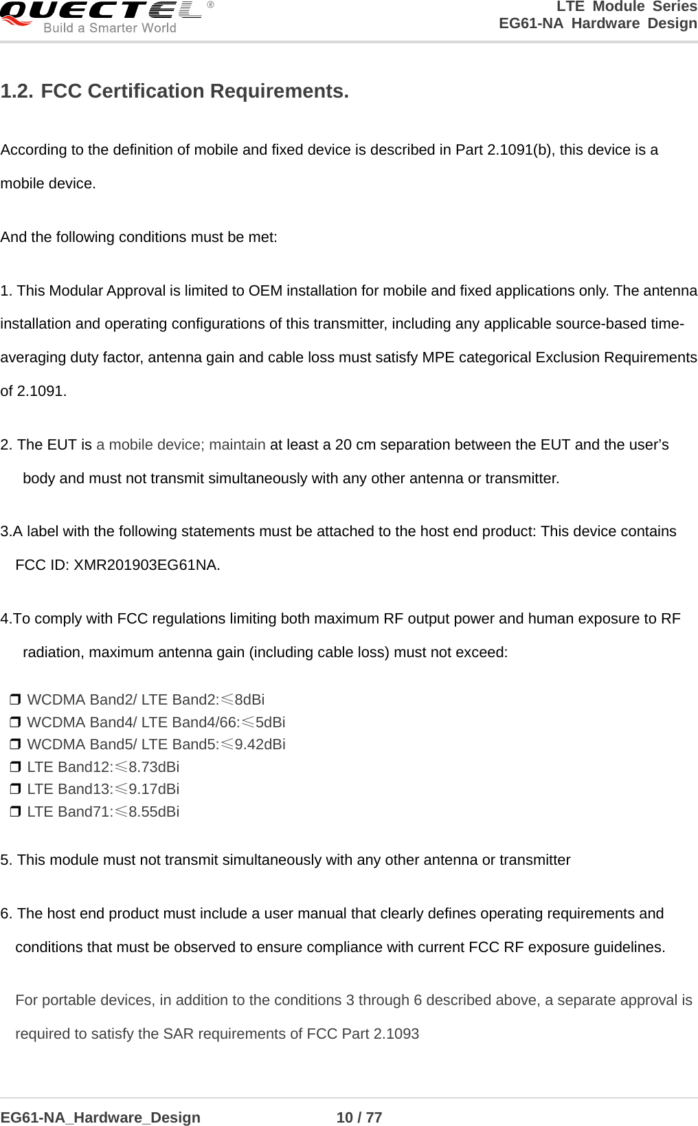
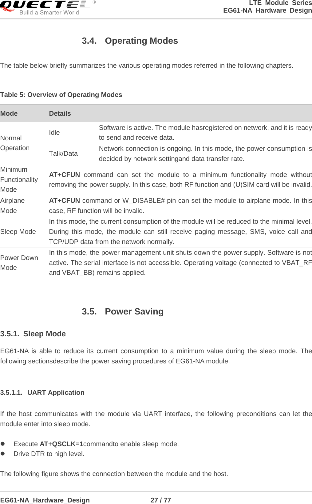
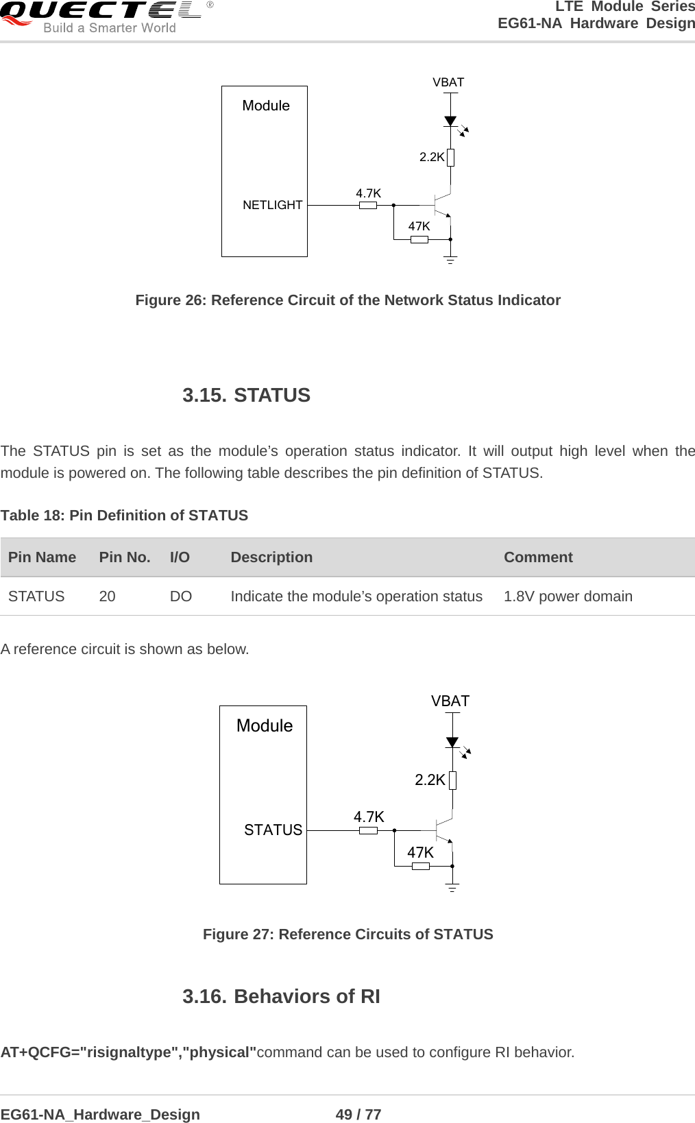
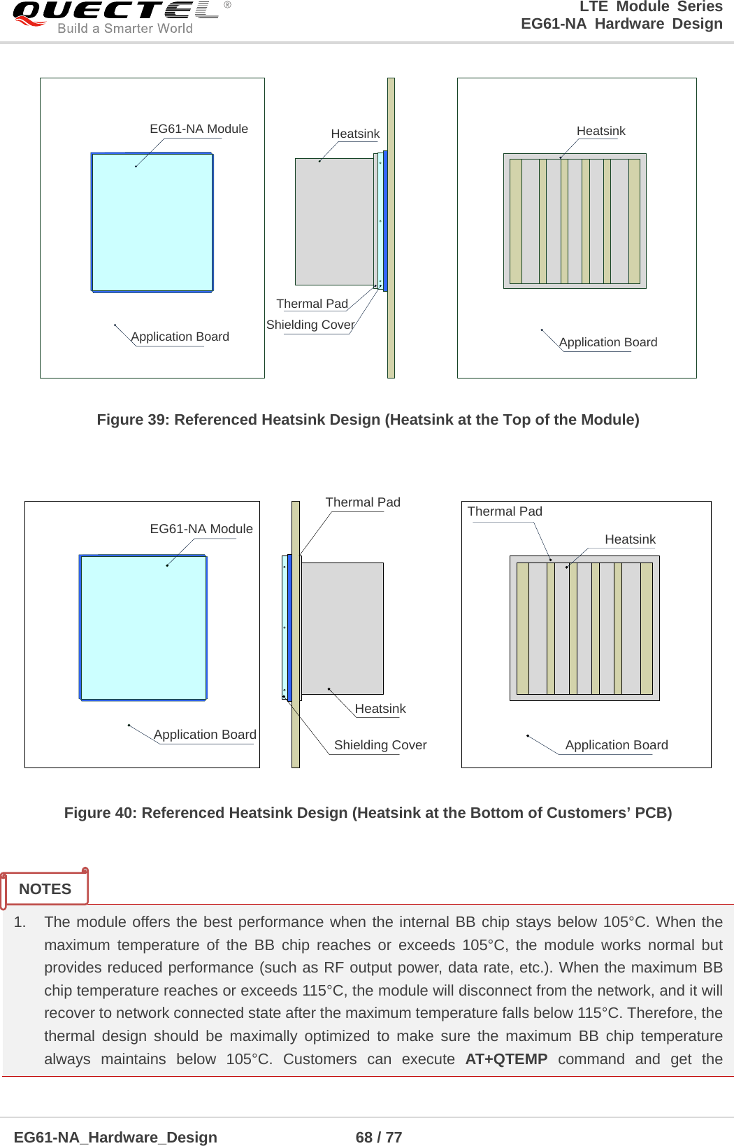
![LTE Module Series EG61-NA Hardware Design EG61-NA_Hardware_Design 33 / 77 3.6.3. Reference Design for Power Supply Power design for the module is very important, asthe performance of the module largely depends on the power source. The power supply should be able to provide sufficient current up to 2A at least. If the voltage drop between the input and output is not too high, it is suggested that an LDO should be usedto supply power for the module. If there is a big voltage difference between the input source and the desired output (VBAT), a buck converter is preferred to be used as the power supply. The following figure shows a reference design for +5V input power source. The typicaloutput ofthe power supply is about 3.8V and the maximum load current is 3A. DC_INMIC29302WUIN OUTENGNDADJ2 4135VBAT 100nF 470uF 100nF100K47K470uF470R51K 1%1%4.7K47KVBAT_EN Figure 9: Reference Circuit of Power Supply In order to avoid damaging internal flash, please do not switch off the power supply when the module works normally. Only after the module is shutdown by PWRKEY or AT command, the power supply can be cut off. 3.6.4. Monitor the Power Supply AT+CBC command can be used to monitor the VBAT_BB voltage value. For more details, please refer to document [2]. 3.7. Turn-on and off Scenarios 3.7.1. Turn on Module Using the PWRKEY The following table shows the pin definitionof PWRKEY. NOTE](https://usermanual.wiki/Quectel-Wireless-Solutions/201903EG61NA/User-Guide-4198069-Page-34.png)
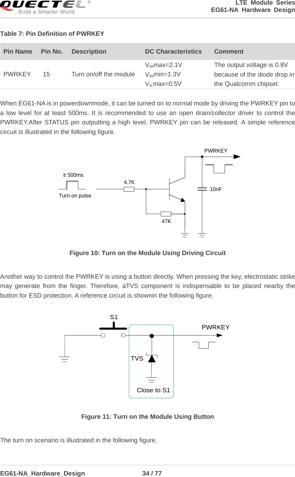
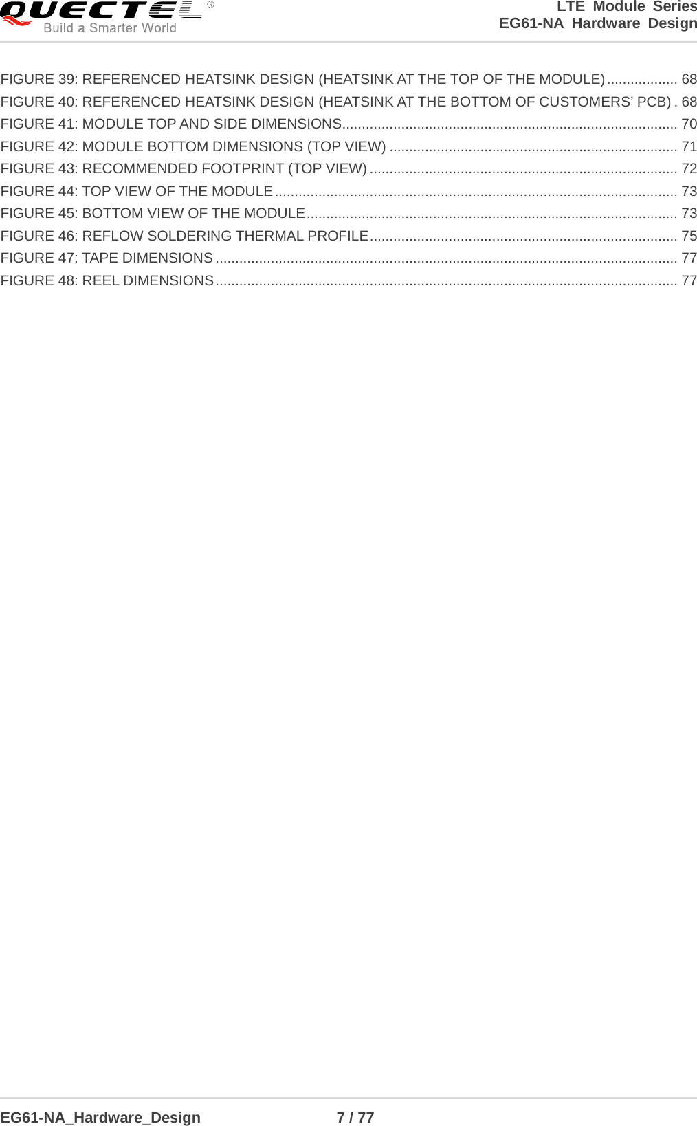
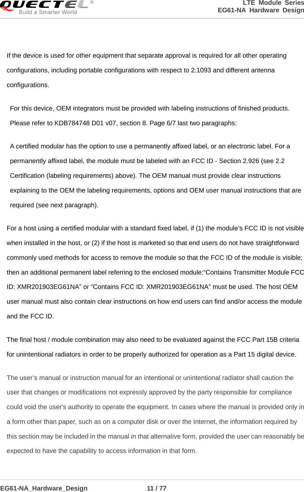
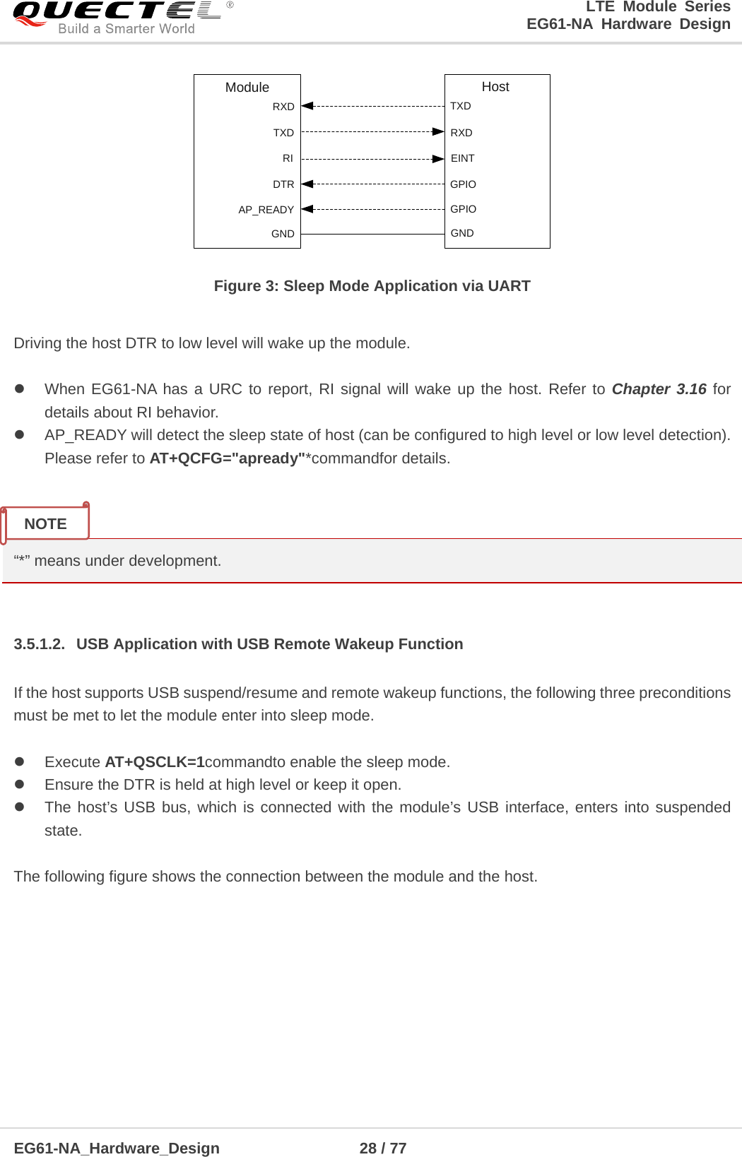
![LTE Module Series EG61-NA Hardware Design EG61-NA_Hardware_Design 36 / 77 3.7.2.1. Turn off Module Using the PWRKEY Pin Driving the PWRKEY pin to a low level voltage for at least 650ms, the module will execute power-down procedure after the PWRKEY is released. The power-down scenario is illustrated inthe following figure. VBATPWRKEY≥ 30s≥ 650msRUNNING Power-down procedure OFFModuleStatusSTATUS Figure 13: Timing of Turning off Module 3.7.2.2. Turn off Module Using AT Command It is also a safe way to use AT+QPOWDcommandto turn off the module, which is similar to turning off the module via PWRKEY pin. Please refer todocument [2] for details about the AT+QPOWDcommand. 1. In order to avoid damaging internal flash, please do not switch off the power supply when the module works normally. Only after the module is shut down by PWRKEY or AT command, the power supply can be cut off. 2. When turning off module with AT command, please keep PWRKEY at high level after the execution of power-off command. Otherwise the module will be turned on again after successful turn-off. 3.8. Reset the Module The RESET_N pin can be used to reset the module.The module can be reset by driving RESET_N to a low level voltage for 150ms~460ms. NOTES](https://usermanual.wiki/Quectel-Wireless-Solutions/201903EG61NA/User-Guide-4198069-Page-37.png)
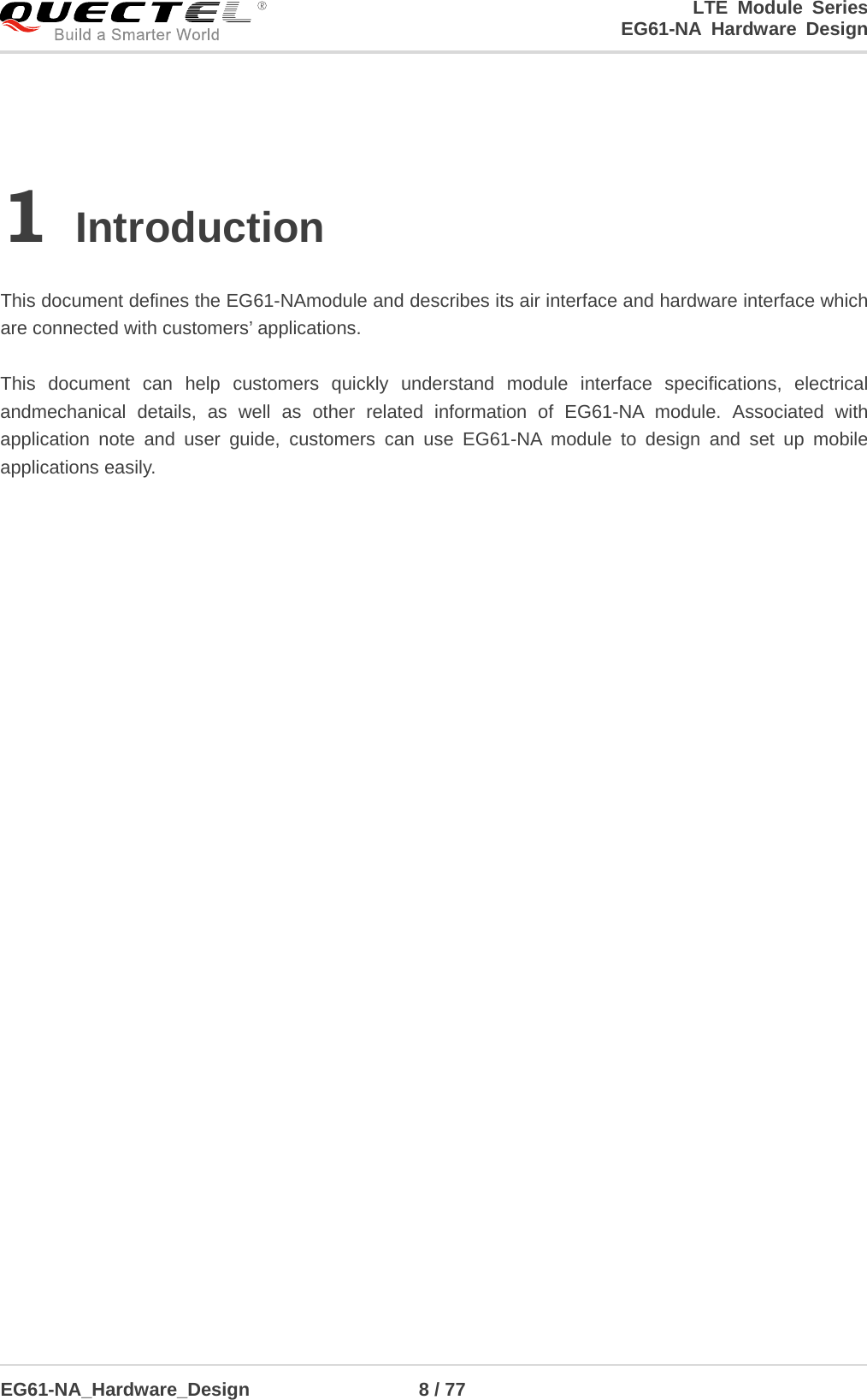
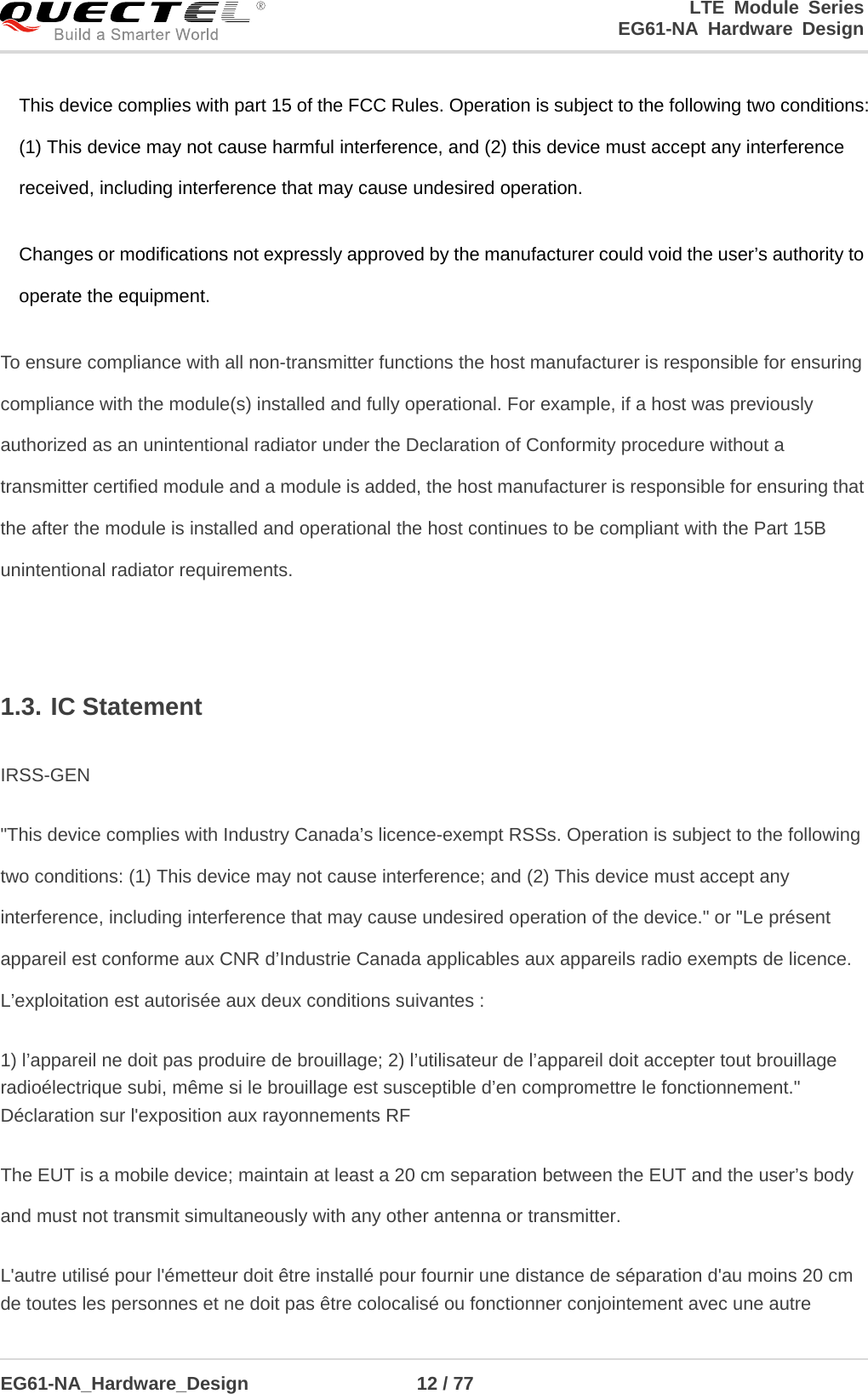
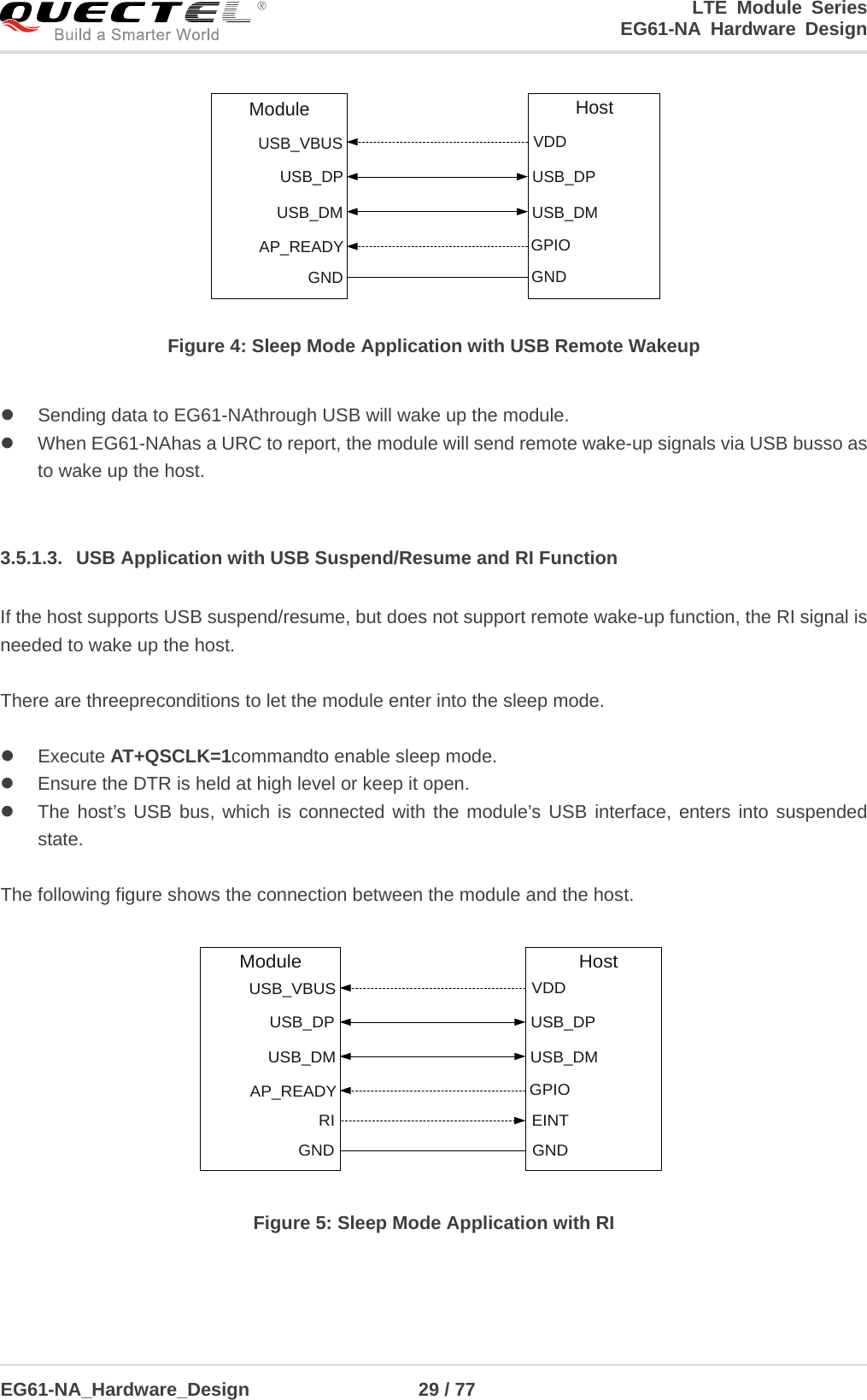
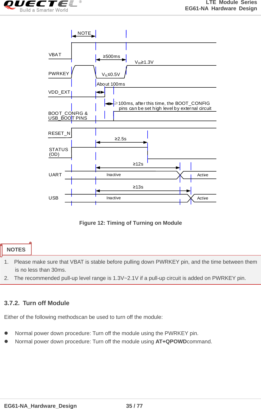
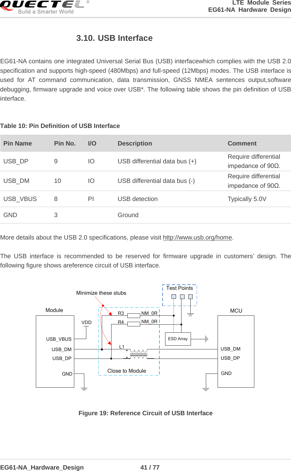
![LTE Module Series EG61-NA Hardware Design EG61-NA_Hardware_Design 38 / 77 VIL ≤ 0.5VVIH ≥ 1.3VVBAT≥ 150msResettingModule StatusRunningRESET_NRestart≤ 460ms Figure 16: Timing of Resetting Module 1. RESET_N is only used when the module fails to be shut down via AT+QPOWD command and the PWRKEY pin. 2. Ensure that there is no large capacitance on PWRKEY and RESET_N pins. 3.9. (U)SIM Interfaces EG61-NAprovides two (U)SIMinterfaces, andonly one (U)SIMcard can work at a time.The (U)SIM1 and (U)SIM2cardscan be switched by AT+QDSIM*command.For more details, please refer to document [2]. The(U)SIMinterfacescircuitrymeet ETSI and IMT-2000 requirements. Both 1.8V and 3.0V (U)SIMcards are supported. Table 9: Pin Definition of (U)SIMInterfaces Pin Name Pin No. I/O Description Comment USIM1_VDD 43 PO Power supply for (U)SIM1 card Either 1.8V or 3.0V is supported by the module automatically. USIM1_DATA 45 IO Data signal of (U)SIM1 card USIM1_CLK 46 DO Clock signal of (U)SIM1card USIM1_RST 44 DO Reset signal of (U)SIM1 card USIM1_ PRESENCE 42 DI (U)SIM1 card insertion detection NOTES](https://usermanual.wiki/Quectel-Wireless-Solutions/201903EG61NA/User-Guide-4198069-Page-39.png)
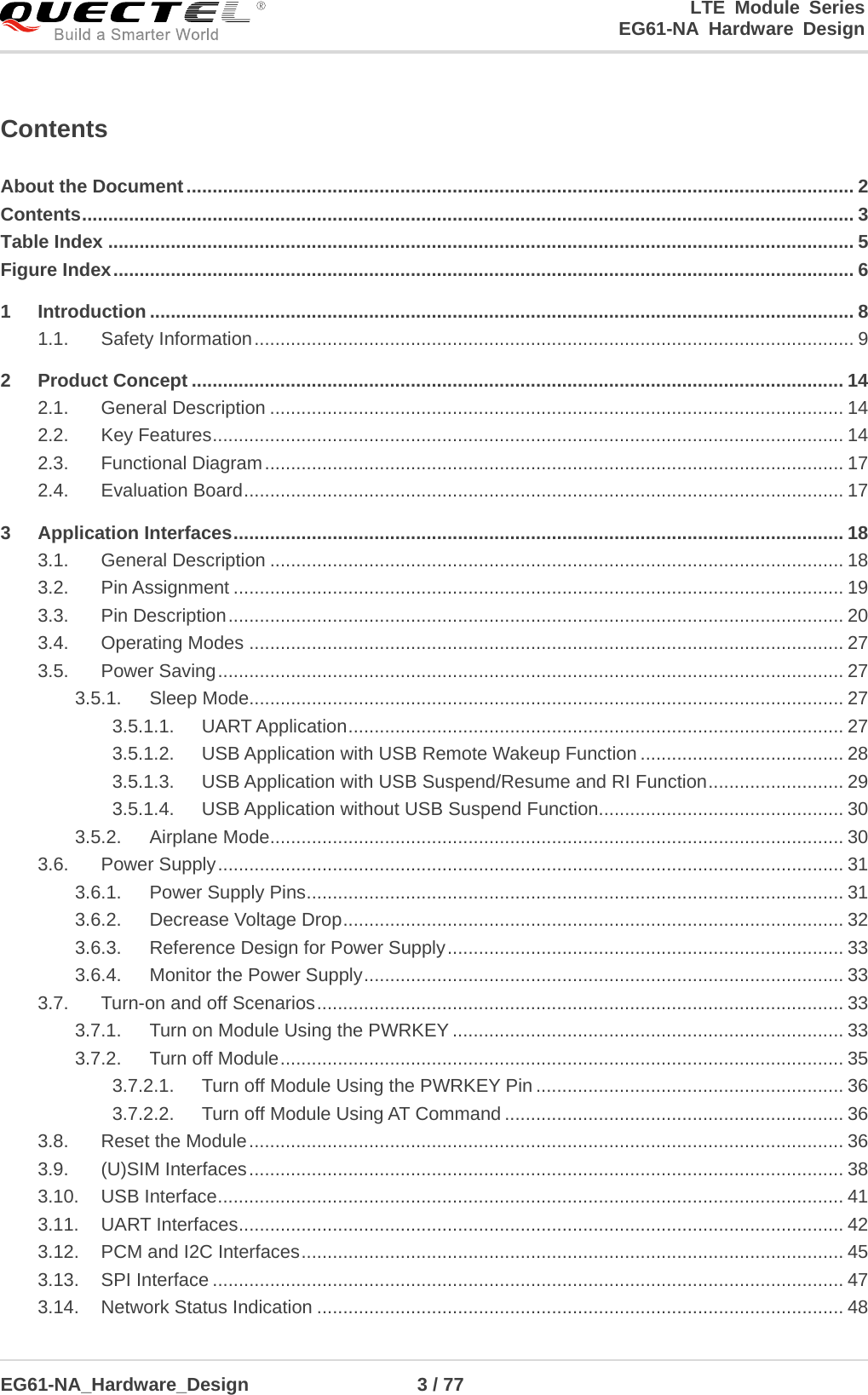
![LTE Module Series EG61-NA Hardware Design EG61-NA_Hardware_Design 39 / 77 USIM_GND 47 Specified ground for (U)SIMcard USIM2_VDD 87 PO Power supply for (U)SIM2 card Either 1.8V or 3.0V is supported by the module automatically. USIM2_DATA 86 IO Data signal of (U)SIM2 card USIM2_CLK 84 DO Clock signal of (U)SIM2 card USIM2_RST 85 DO Reset signal of (U)SIM2 card USIM2_ PRESENCE 83 DI (U)SIM2 card insertion detection EG61-NA supports (U)SIMcard hot-plug via the USIM_PRESENCE (USIM1_PRESENCE/USIM2_PRESENCE) pin. The functionsupports low level and high level detections, andis disabled by default. Pleaserefer to document [2] about AT+QSIMDETcommand for details. The following figure shows a reference design for (U)SIM interface with an8-pin (U)SIMcard connector. ModuleUSIM_VDDUSIM_GNDUSIM_RSTUSIM_CLKUSIM_DATAUSIM_PRESENCE0R0R0RVDD_EXT51K100nFGNDGND33pF 33pF 33pFVCCRSTCLK IOVPPGNDGNDUSIM_VDD15K(U)SIM Card Connector Figure 17: Reference Circuitof (U)SIMInterface with an 8-Pin (U)SIMCard Connector If (U)SIM card detection function is not needed, please keep USIM_PRESENCE unconnected. Areference circuit of (U)SIM interface with a 6-pin (U)SIMcard connector is illustrated inthe following figure.](https://usermanual.wiki/Quectel-Wireless-Solutions/201903EG61NA/User-Guide-4198069-Page-40.png)
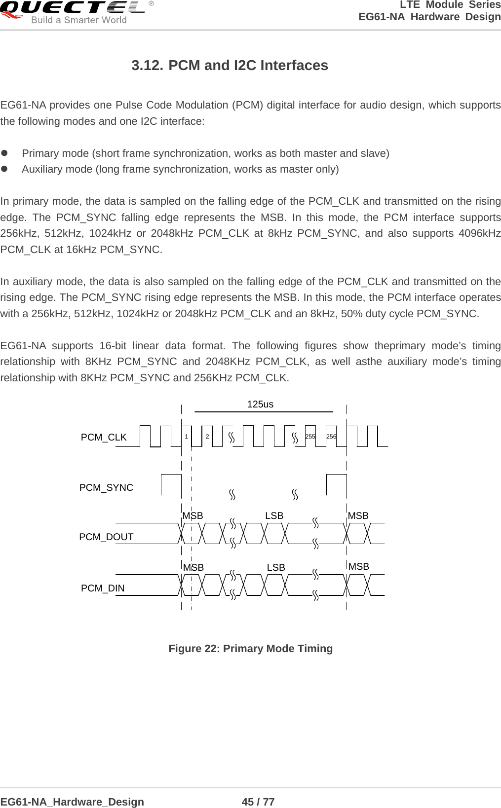
![LTE Module Series EG61-NA Hardware Design EG61-NA_Hardware_Design 46 / 77 PCM_CLKPCM_SYNCPCM_DOUTMSB LSBPCM_DIN125usMSB1 2 3231LSB Figure 23: Auxiliary Mode Timing The following table shows the pin definition of PCM and I2C interfaces which can be applied on audio codec design. Table 14: Pin Definition of PCM and I2C Interfaces Pin Name Pin No. I/O Description Comment PCM_DIN 6 DI PCM data input 1.8V power domain PCM_DOUT 7 DO PCM data output 1.8V power domain PCM_SYNC 5 IO PCM data frame synchronization signal 1.8V power domain PCM_CLK 4 IO PCM data bit clock 1.8V power domain I2C_SCL 40 OD I2C serial clock Require an external pull-up to 1.8V I2C_SDA 41 OD I2C serial data Require an external pull-up to 1.8V Clock and mode can be configured by AT command, and the default configuration is master mode using short frame synchronizationformat with 2048KHzPCM_CLK and 8KHz PCM_SYNC.Please refer to document [2] aboutAT+QDAIcommand for details. The following figure shows areference design of PCM interface with external codec IC.](https://usermanual.wiki/Quectel-Wireless-Solutions/201903EG61NA/User-Guide-4198069-Page-47.png)
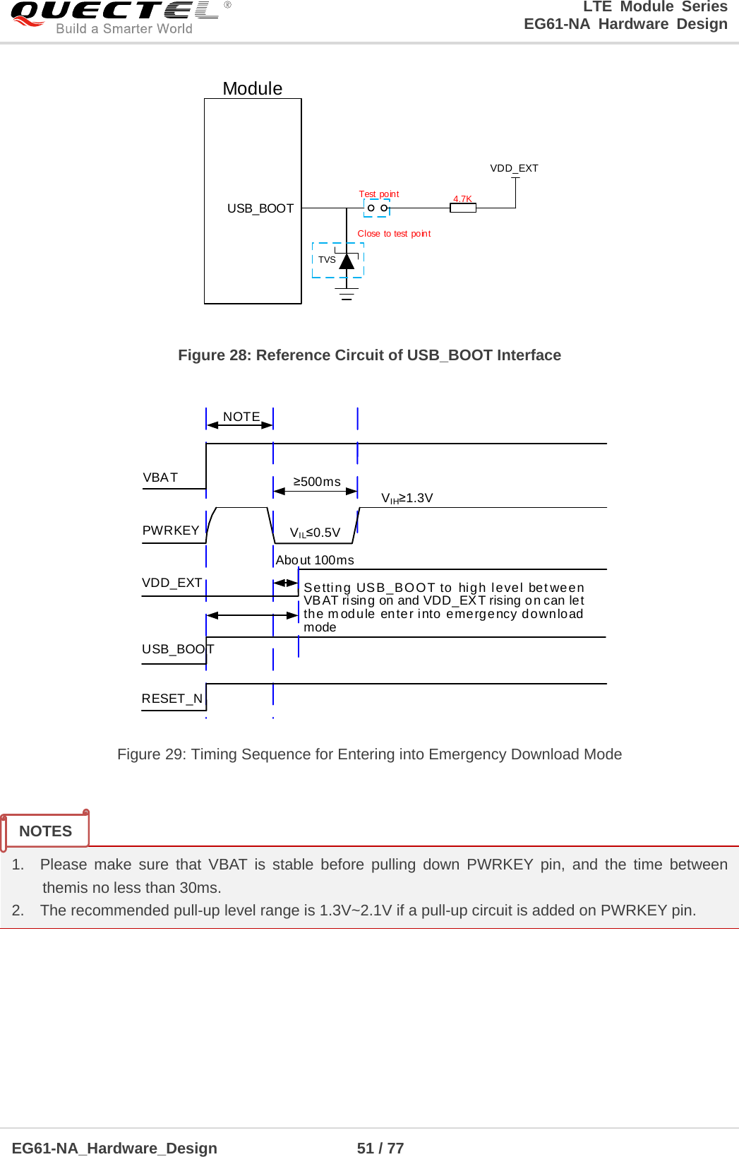
![LTE Module Series EG61-NA Hardware Design EG61-NA_Hardware_Design 50 / 77 No matter on which port URC is presented, URC will trigger the behavior ofRI pin. URC can be outputted from UART port, USB AT port and USB modem port through configuration via AT+QURCCFG command. The default port is USB AT port. In addition, RI behavior can be configured flexibly. The default behaviors of the RI are shown as below. Table 19: Default Behaviors of RI State Response Idle RI keeps athigh level URC RI outputs 120ms low pulse when a new URC returns The default RI behaviorscan be changed by AT+QCFG="urc/ri/ring"command.Please refer to document [2] for details. 3.17. USB_BOOT Interface EC61-NA provides a USB_BOOT pin. Customers can pull up USB_BOOT to VDD_EXT before powering on the module, thus the module will enter into emergency download mode when powered on. In this mode, the module supports firmware upgrade over USB interface. Table 20: Pin Definition of USB_BOOT Interface Pin Name Pin No. I/O Description Comment USB_BOOT 75 DI Force the module to enter into emergency download mode 1.8V power domain. Active high. It is recommended to reserve the pin as test point. The following figures show the reference circuit of USB_BOOT interface and timing sequence of Entering into emergency download mode. NOTE](https://usermanual.wiki/Quectel-Wireless-Solutions/201903EG61NA/User-Guide-4198069-Page-51.png)
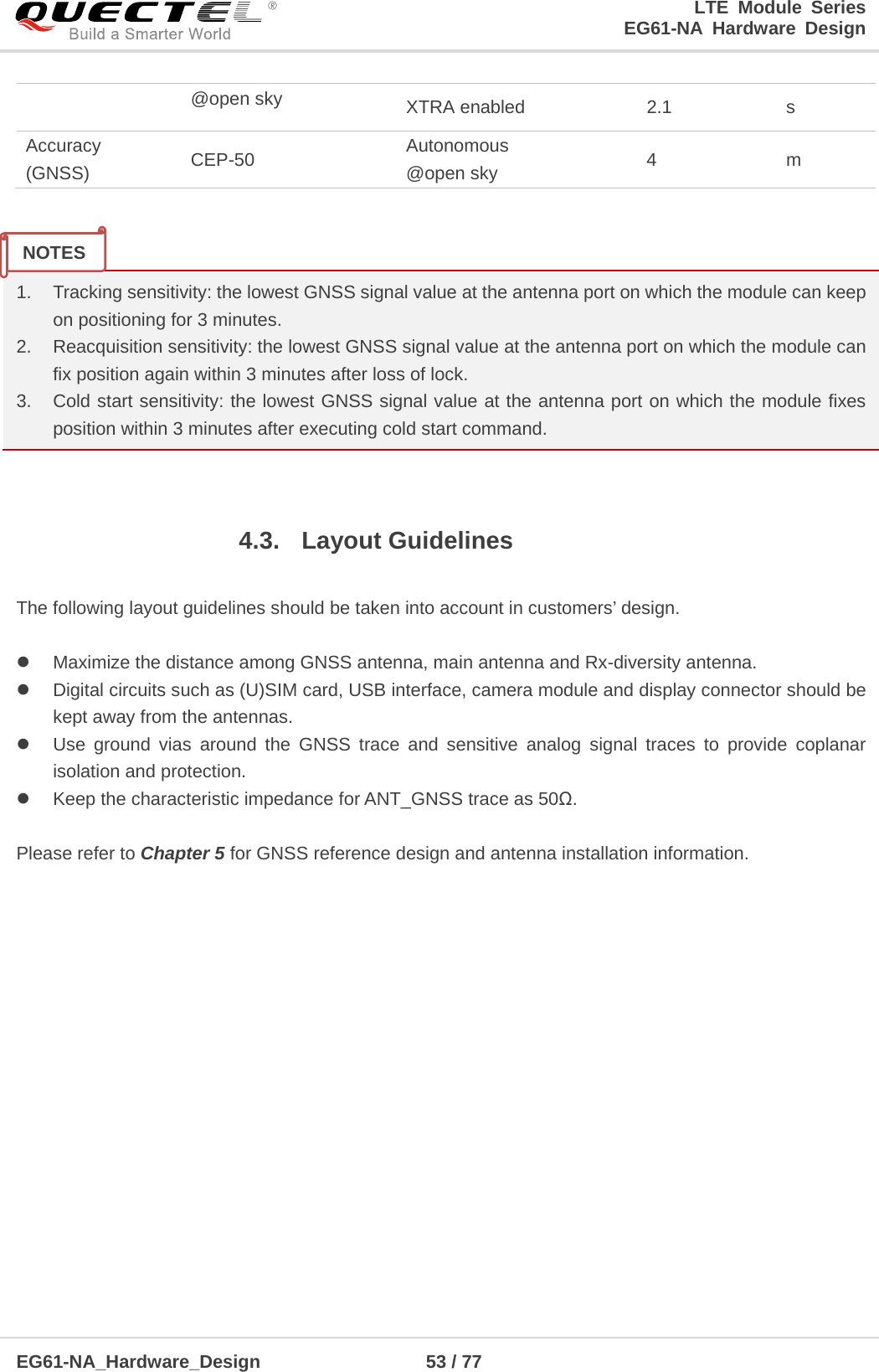
![LTE Module Series EG61-NA Hardware Design EG61-NA_Hardware_Design 52 / 77 4 GNSS Receiver 4.1. General Description EG61-NA includes a fully integrated global navigation satellite system solution that supports Gen8C-Lite of Qualcomm (GPS, GLONASS, BeiDou, Galileo and QZSS). EG61-NA supports standard NMEA-0183 protocol, and outputs NMEA sentences at 1Hz data update rate via USB interface by default. By default, EG61-NA GNSS engine is switched off. It has to be switched on via AT command. For more details about GNSS engine technology and configurations, please refer to document [3]. 4.2. GNSS Performance The following table shows GNSS performance of EG61-NA. Table 21: GNSS Performance Parameter Description Conditions Typ. Unit Sensitivity (GNSS) Cold start Autonomous -145 dBm Reacquisition Autonomous -157 dBm Tracking Autonomous -157 dBm TTFF (GNSS) Cold start @open sky Autonomous 34.4 s XTRA enabled 15.6 s Warm start @open sky Autonomous 28.6 s XTRA enabled 2.2 s Hot start Autonomous 2.3 s](https://usermanual.wiki/Quectel-Wireless-Solutions/201903EG61NA/User-Guide-4198069-Page-53.png)
![LTE Module Series EG61-NA Hardware Design EG61-NA_Hardware_Design 57 / 77 Figure 33: Coplanar Waveguide Line Design on a 4-layer PCB (Layer 3 as Reference Ground) Figure 34: Coplanar Waveguide Line Design on a 4-layer PCB (Layer 4 as Reference Ground) In order to ensure RF performance and reliability, the following principles should be complied with in RF layout design: Use impedance simulation tool to control the characteristic impedanceof RF tracesas 50Ω. The GND pins adjacent to RF pins should not bedesigned as thermal relief pads, and should be fully connected to ground. The distance between the RF pinsand the RFconnector should be as short as possible, and all the right angle traces should be changed to curved ones. There should be clearance area under the signal pin of the antenna connector or solder joint. The reference ground of RF traces should be complete. Meanwhile, adding some ground viasaround RF traces and the reference ground could help to improve RF performance. The distance between the ground viasand RF traces should be no less than two times the width of RF signal traces (2*W). For more details about RF layout, please refer to document [4]. 5.2. GNSS Antenna Interface The GNSS antenna interface is only supported on EG61-NA.The following tables show pin definition and frequency specification of GNSS antenna interface. Table 24: Pin Definition of GNSS Antenna Interface Pin Name Pin No. I/O Description Comment ANT_GNSS 49 AI GNSS antenna 50Ωimpedance](https://usermanual.wiki/Quectel-Wireless-Solutions/201903EG61NA/User-Guide-4198069-Page-58.png)
![LTE Module Series EG61-NA Hardware Design EG61-NA_Hardware_Design 69 / 77 maximum BB chip temperature from the first returned value. 2. For more detailed guidelines on thermal design, please refer to document [5].](https://usermanual.wiki/Quectel-Wireless-Solutions/201903EG61NA/User-Guide-4198069-Page-70.png)
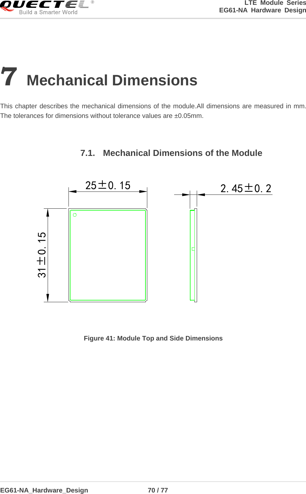
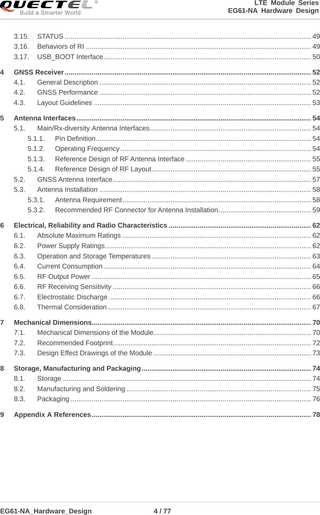
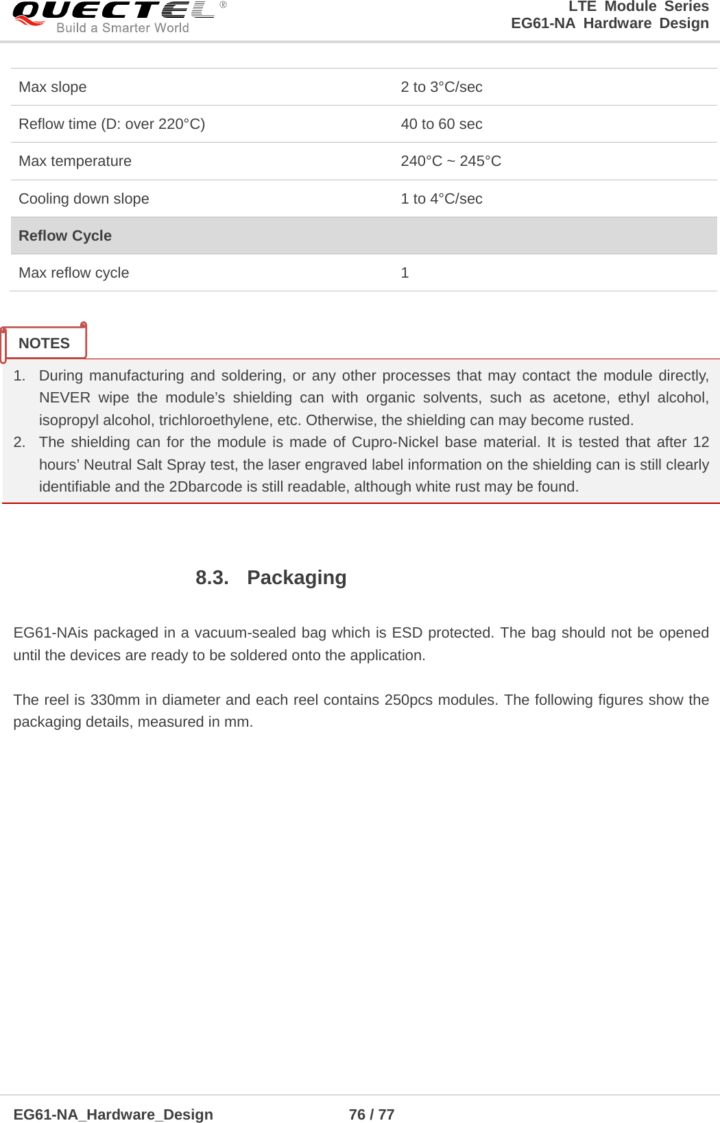
![LTE Module Series EG61-NA Hardware Design EG61-NA_Hardware_Design 75 / 77 8.2. Manufacturing and Soldering Push the squeegee to apply the solder paste on the surface of stencil, thus making the paste fill the stencil openings and then penetrate to the PCB. The force on the squeegee should be adjusted properlyso as to produce a clean stencil surface on a single pass. To ensure the module soldering quality, thethickness of stencil for the module is recommended to be 0.15mm~0.18mm. For more details, please refer todocument [3]. It is suggested that the peak reflow temperature is 240ºC ~245ºC, and the absolute maximum reflow temperature is 245ºC. To avoid damage to the module caused by repeated heating, it is strongly recommended that the module should be mounted after reflow soldering for the other side of PCB has been completed. The recommended reflow soldering thermal profile (lead-free reflow soldering) and related parameters are shown below. Temp. (°C)Reflow ZoneSoak Zone245200220240CDBA150100 Max slope: 1~3°C/sec Cooling down slope: 1~4°C/sec Max slope: 2~3°C/sec Figure 46: Reflow Soldering Thermal Profile Table 35: Recommended Thermal Profile Parameters Factor Recommendation Soak Zone Max slope 1 to 3°C/sec Soak time (between A and B: 150°C and 200°C) 60 to 120 sec Reflow Zone](https://usermanual.wiki/Quectel-Wireless-Solutions/201903EG61NA/User-Guide-4198069-Page-76.png)
![LTE Module Series EG61-NA Hardware Design EG61-NA_Hardware_Design 78 / 77 9 Appendix A References Table 36: Related Documents SN Document Name Remark [1] Quectel_EC2x&EG9x&EM05_Power_Management_Application_Note Power Management Application Note for EC25, EC21, EC20 R2.0, EC20 R2.1, EG61-NA, EG91 and EM05 [2] Quectel_EG61-NA_AT_Commands_Manual AT Commands Manual for EG61-NA [3] Quectel_Module_Secondary_SMT_User_Guide Module Secondary SMT User Guide [4] Quectel_RF_Layout_Application_Note RF Layout Application Note [5] Quectel_LTE_Module_Thermal_Design_Guide Thermal design guide for LTE modules including EC25, EC21, EC20 R2.0, EC20 R2.1, EG91, EG95, EG25-G, EP06, EG06, EM06 and AG35. Table 37: Terms and Abbreviations Abbreviation Description AMR Adaptive Multi-rate bps Bits Per Second CHAP Challenge Handshake Authentication Protocol CS Coding Scheme CSD Circuit Switched Data CTS Clear To Send HSPA+ High Speed Packet Access+ DFOTA Delta Firmware Upgrade Over The Air DL Downlink](https://usermanual.wiki/Quectel-Wireless-Solutions/201903EG61NA/User-Guide-4198069-Page-79.png)