R and L Media Systems PM300 FM Broadcast Radio Transmitter User Manual PM300 R2 0 24 06 2004
R & L Media Systems Inc FM Broadcast Radio Transmitter PM300 R2 0 24 06 2004
PM300 Manual

DB ELETTRONICA TELECOMUNICAZIONI S.p.A.
PM 300 - FM Broadcasting Transmitter - USER’S MANUAL 1 /108
FM Broadcasting Transmitter
User’s Manual
Release 2.0
- DB ELETTRONICA TELECOMUNICAZIONI S.p.A. -
- Via Lisbona, 38 - 35127 Z.I. SUD PADOVA ITALY -- Ph. (049) 870-0588 - Fax. (049) 870-0747 -
- http://www.dbbroadcast.com -

DB ELETTRONICA TELECOMUNICAZIONI S.p.A.
PM 300 - FM Broadcasting Transmitter - USER’S MANUAL2 /108
SAFETY NOTICES
WARNING
To avoid risks of electrical shocks or fire, only qualified personnel should execute the procedures
specified in this manual.
WARNING
When the protective covers of any device or component connected to a 110 / 240 VAC source by a
power cord are removed, voltages and currents dangerous to life may be exposed.
WARNING
Contact with 110 / 240 Volts of alternating current and associated direct current and voltages can be
fatal.
DANGEROUS
RISK OF ELECTRICAL SHOCK DO NOT OPEN
CAUTION
To reduce the risks of electrical shock, do not remove the cover (or the back). Refer, for servicing,
to qualified service personnel. This installation should be done by a qualified person and should
comply with to all local applicable laws.
NOTICE: ALL THE SPECIFICATIONS AND TECHNICAL INFORMATION IN THIS MANUAL ARE
SUBJECT TO CHANGE WITHOUT NOTICE.

DB ELETTRONICA TELECOMUNICAZIONI S.p.A.
PM 300 - FM Broadcasting Transmitter - USER’S MANUAL 3 /108
INDEX
1. PM300 FM TRANSMITTER...................................................................................................................6
1.1 GENERAL DESCRIPTION ................................................................................................................6
2. TECHNICAL SPECIFICATIONS........................................................................................................11
3. INSTALLATION ....................................................................................................................................13
4. FREQUENCY SETTING.......................................................................................................................14
5. ADJUSTMENTS AND MEASURES ....................................................................................................16
6. POWER SUPPLY SECTION ................................................................................................................18
6.1 GENERAL DESCRIPTION ..............................................................................................................18
6.2 SWITCHING POWER SUPPLY MODULE PART LIST................................................................22
6.3 EQUIP. PWR SUPP. BOARD PARTS LIST (DB 0206_090)..........................................................31
6.4 DB 0201_070 PRINTED BOARD PARTS LIST .............................................................................35
7. MODULATION STAGE (SINTEL 96).................................................................................................36
7.1 GENERAL DESCRIPTION ..............................................................................................................36
7.2 “SINTEL 96” MODULATOR PARTS LIST....................................................................................44
8. AMP30 DRIVER STAGE ......................................................................................................................47
8.1 GENERAL DESCRIPTION ..............................................................................................................47
8.2 AMP30 PRE AMPLIFIER PARTS LIST..........................................................................................50
9. RF AMPLIFIER STAGE.......................................................................................................................51
9.1 AMP300 AMPLIFIER BOARD ........................................................................................................51
9.2 AMP300 AMPLIFIER PARTS LIST ................................................................................................54
9.3 LOW PASS FILTER AND DIRECTIONAL COUPLER .................................................................55
9.4 L. P. FILTER AND DIR. COUP. PARTS LIST................................................................................56
10. PROTECTION STAGE......................................................................................................................57
10.1 PROTECTION /CONTROL STAGE N°1 PARTS LIST.................................................................67
10.2 PROTECTION /CONTROL STAGE N°2 PARTS LIST.................................................................74
11. METER STAGE ..................................................................................................................................75
11.1 GENERAL DESCRIPTION ..............................................................................................................75
11.2 MICROPROCESSOR BOARD PARTLIST .....................................................................................78
11.3 DISPLAY BOARD PARTS LIST.....................................................................................................81
12. IN-AUDIO BOARD.............................................................................................................................82
12.1 IN-AUDIO BOARD PARTS LIST....................................................................................................84
12.2 IN-AUDIO BOARD JUMPERS SETTING ......................................................................................85
13. STEREO ENCODER BOARD (OPTION) .......................................................................................86
13.1 CHANNELS PRE- EMPHASIS SETTING ......................................................................................86
13.2 STEREO ENCODER PARTS LIST..................................................................................................98
14. CONTRAVES BOARD (OPTION) .................................................................................................101
14.1 GENERAL DESCRIPTION ............................................................................................................101
14.2 CONTRAVES BOARDS PARTS LIST..........................................................................................103
15. TROUBLESHOOTING....................................................................................................................104
16. APPENDIX A.....................................................................................................................................106
16.1 XLR AUDIO CONNECTORS PINOUTS ......................................................................................106
17. APPENDIX B.....................................................................................................................................107
17.1 MOSFET REPLACEMENT............................................................................................................107

DB ELETTRONICA TELECOMUNICAZIONI S.p.A.
PM 300 - FM Broadcasting Transmitter - USER’S MANUAL4 /108
FIGURES INDEX
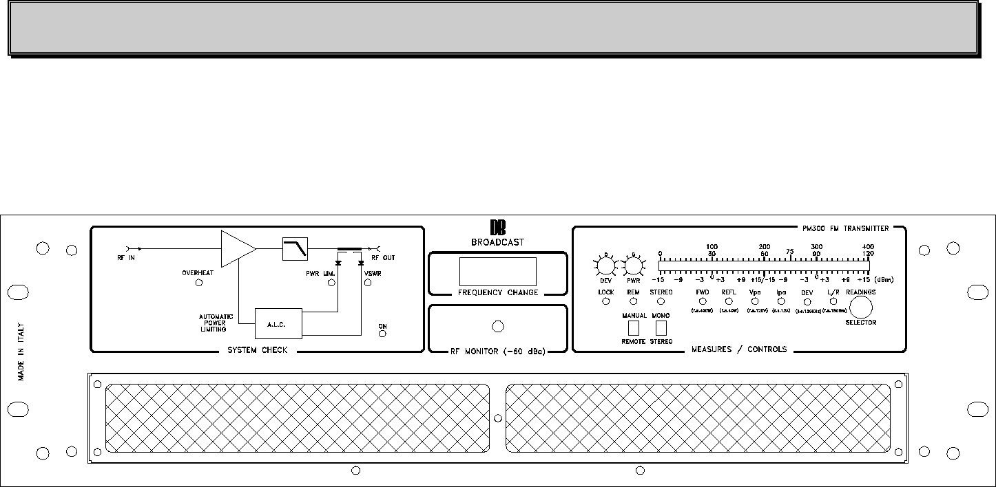
FIG. 1.1 - FRONT VIEW....................................................................................................................................8
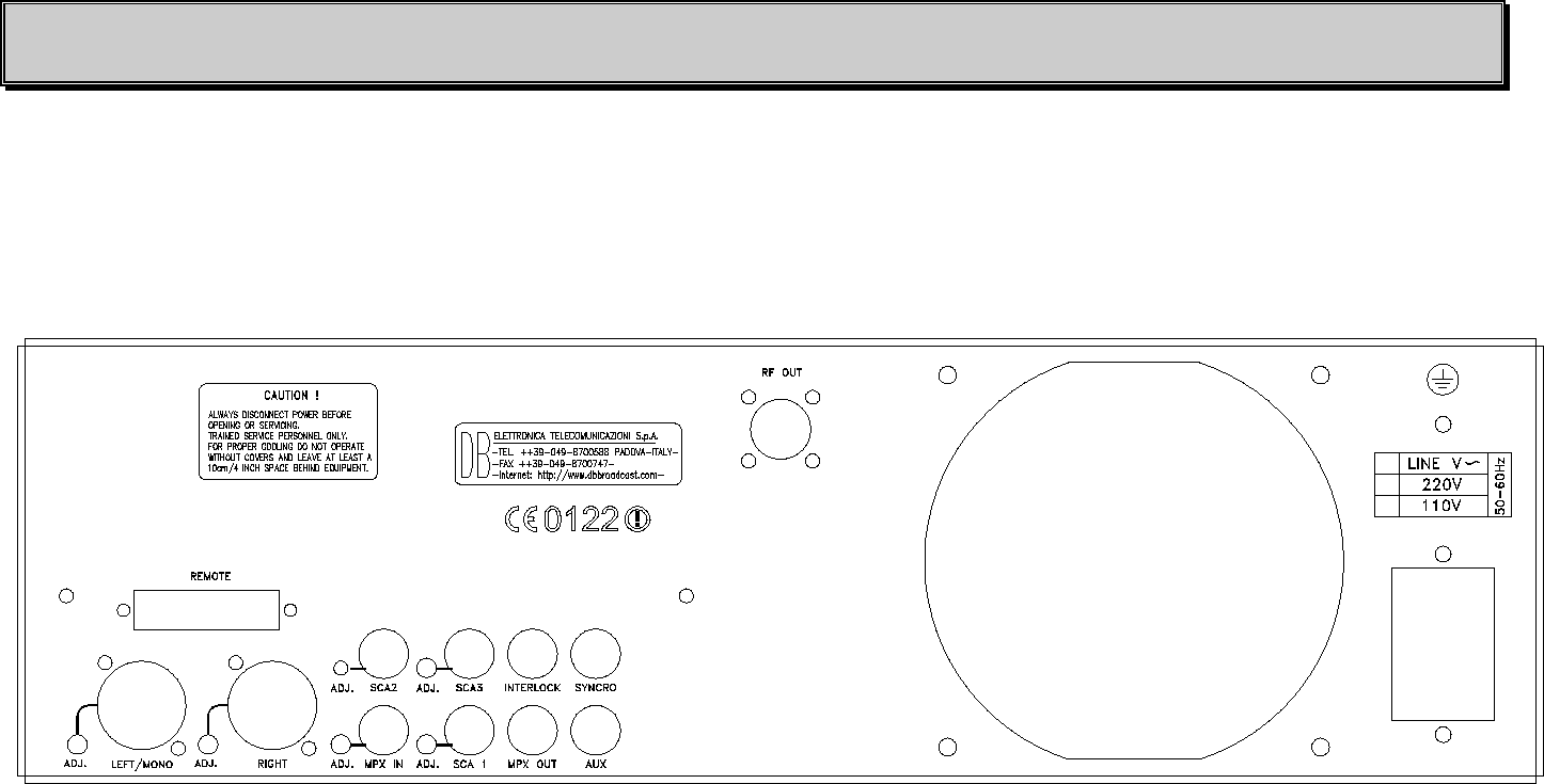
FIG. 1.2 - REAR VIEW ......................................................................................................................................9
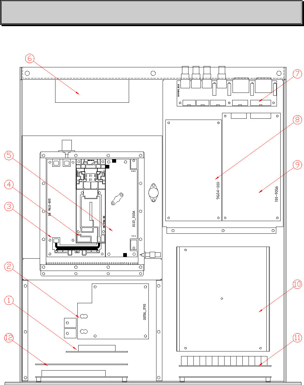
FIG. 1.3 - TOP VIEW .......................................................................................................................................10
FIG. 4.1 - CONTRAVES WEIGHT .................................................................................................................14
FIG. 6.1 - SWITCHING POWER SUPPLY MODULE ELECTRICAL SCHEMATIC “A” ..........................19
FIG. 6.2 - SWITCHING POWER SUPPLY MODULE ELECTRICAL SCHEMATIC “B” ..........................20
FIG. 6.3 - SWITCHING POWER SUPPLY MODULE COMPONENT LAYOUT........................................21
FIG. 6.4 – EQUIP. PWR SUPP. BOARD GENERAL ELECTRICAL SCHEMATIC....................................26
FIG. 6.5 - EQUIP. PWR SUPP. BOARD +24 V STAGE ELECTRICAL SCHEMATIC...............................27
FIG. 6.6 - EQUIP. PWR SUPP. BOARD-12V STAGE ELECTRICAL SCHEMATIC ..................................28
FIG. 6.7 - EQUIP. PWR SUPP. BOARD +12V STAGE ELECTRICAL SCHEMATIC................................29
FIG. 6.8 - EQUIP. PWR SUPP. BOARD COMPONENT LAYOUT (DB 0206_090)....................................30
FIG. 6.9 - DB 0201_070 PRINTED BOARD ELECTRICAL SCHEMATIC..................................................33
FIG. 6.10 - DB 0201_070 PRINTED BOARD COMPONENT LAYOUT......................................................34
FIG. 7.1 - “SINTEL 96” MODULATION BOARD GENERAL ELECTRICAL SCHEMATIC ....................37
FIG. 7.2 - PLL STAGE ELECTRICAL SCHEMATIC....................................................................................38
FIG. 7.3 - VCO STAGE ELECTRICAL SCHEMATIC ..................................................................................39
FIG. 7.4 - LF 1 STAGE ELECTRICAL SCHEMATIC ..................................................................................40
FIG. 7.5 - LF 2 STAGE ELECTRICAL SCHEMATIC ..................................................................................41
FIG. 7.6 - FILTER STAGE ELECTRICAL SCHEMATIC .............................................................................42
FIG. 7.7 - “SINTEL 96” MODULATION COMPONENT LAYOUT (DB 9604-010) ...................................43
FIG. 8.1 - AMP30 PRE AMPLIFIER ELECTRICAL SCHEMATIC..............................................................48
FIG. 8.2 - AMP30 PRE AMPLIFIER COMPONENT LAYOUT (DB 0110_010A) .......................................49
FIG. 9.1 - AMP300 AMPLIFIER ELECTRICAL SCHEMATIC ....................................................................52
FIG. 9.2 - AMP300 AMPLIFIER COMPONENT LAYOUT (DB 9812_001) ................................................53
FIG. 9.3 - L. P. FILTER AND DIR. COUP. ELECTRICAL SCHEMATIC....................................................55
FIG. 9.4 - L. P. FILTER AND DIR. COUP. COMPONENT LAYOUT (DB 9611-005) ................................56
FIG. 10.1 - PROTECTION /CONTROL STAGE N°1 GENERAL SCHEMATIC ........................................59
FIG. 10.2 - UNBALANCING PROTECTION STAGE ...................................................................................60
FIG. 10.3 - FWD PROTECTION STAGE........................................................................................................61
FIG. 10.4 - TEMPERATURE PROTECTION STAGE ...................................................................................62
FIG. 10.5 - POWER LIMITING STAGE .........................................................................................................63
FIG. 10.6 - PROTECTION /CONTROL STAGE N°1 COMPONENT LAYOUT (DB 9702_004)...............66
FIG. 10.7 - PROTECTION /CONTROL STAGE N°2 GENERAL SCHEMATIC.........................................68
FIG. 10.8 - PROTECTION STATUS STAGE .................................................................................................69
FIG. 10.9 - POWER SUPPLY STAGE ............................................................................................................70
FIG. 10.10 - MEASURES ADJ. STAGE..........................................................................................................71
FIG. 10.11 - LED INDICATIONS STAGE ......................................................................................................72
FIG. 10.12 - PROTECTION /CONTROL STAGE N°2 COMPONENT LAYOUT (DB 9703_011).............73
FIG. 11.1 - MICROPROCESSOR STAGE ELECTRICAL SCHEMATIC (DB 9903_040)...........................76
FIG. 11.2 - MICROPROCESSOR BOARD COMPONENT LAYOUT (DB 9903_040) ................................77
FIG. 11.3 - DISPLAY STAGE ELECTRICAL SCHEMATIC (DB 9903_050)..............................................79
FIG. 11.4 - DISPLAY BOARD COMPONENT LAYOUT (DB 9903_050) ...................................................80
FIG. 12.1 - IN-AUDIO BOARD ELECTRICAL SCHEMATIC......................................................................82
FIG. 12.2 - IN-AUDIO BOARD COMPONENT LAYOUT (DB 9909_010)..................................................83
FIG. 13.1 - STEREO ENCODER GENERAL SCHEMATIC..........................................................................87
FIG. 13.2 - L/R PEAK DETECTOR STAGE ELECTRICAL SCHEMATIC .................................................88
FIG. 13.3 - INPUT STAGE ELECTRICAL SCHEMATIC .............................................................................90
FIG. 13.4 - RIGHT FILTER STAGE ELECTRICAL SCHEMATIC ..............................................................91
FIG. 13.5 - LEFT FILTER STAGE ELECTRICAL SCHEMATIC.................................................................92

DB ELETTRONICA TELECOMUNICAZIONI S.p.A.
PM 300 - FM Broadcasting Transmitter - USER’S MANUAL 5 /108
FIG. 13.6 - OSCILLATOR STAGE ELECTRICAL SCHEMATIC ................................................................93
FIG. 13.7 - 19 KHZ STAGE ELECTRICAL SCHEMATIC.............................................................................94
FIG. 13.8 - 38 KHZ STAGE ELECTRICAL SCHEMATIC.............................................................................95
FIG. 13.9 - OUTPUT STAGE ELECTRICAL SCHEMATIC .........................................................................96
FIG. 13.10 - STEREO ENCODER COMPONENT LAYOUT (DB 9506-001)...............................................97
FIG. 14.1 - CONTRAVES BOARD ELECTRICAL DIAGRAM ..................................................................102
FIG. 14.2 - CONTRAVES BOARD COMPONENT LAYOUT (DB 9308-020)...........................................103
FIG. 17.1 - MOSFET REPLACEMENT ........................................................................................................108

DB ELETTRONICA TELECOMUNICAZIONI S.p.A.
PM 300 - FM Broadcasting Transmitter - USER’S MANUAL6 /108
1. PM300 FM TRANSMITTER
1.1 GENERAL DESCRIPTION
The PM300 is a FM broadcasting transmitter with continuously adjustable output power, 0
to 300W.
They can be used as stand-alone complete transmitters or as drivers for high power
amplifiers.
The PM300 transmitter is built with MOS transistor technology.
On the PM300 the use of MOSFET yields:
- Higher efficiency (about 85%);
- High gain (high transconductance and low internal reactive capacitance);
- High thermal stability (negative coefficient for drain current).
The output frequency range is between 87.5 and 108 MHz. Frequency setting is made using
internal dip switches or contraves on front panel (/C option). The minimum frequency step
is 10 kHz.
The /S option has a built-in digital stereo coder with stereo separation in excess of 65 dB
and a SNR of more than 80 dB.
The /P option includes a stereo audio processor with a wide range compression threshold,
attack and release time adjustments and full compatibility with digital audio mixing
consoles.
The /R option consists of full remote control capability with remote adjustments and
checks for all main parameters: power output adjustment, ON/OFF command, protections
reset, forward and reflected power measure, frequency deviation measure and alarms
status.
The /FSK option makes the PM300 transmitter fully compatible with the FCC automatic
identification system.
The /VDC option provides battery operation.

DB ELETTRONICA TELECOMUNICAZIONI S.p.A.
PM 300 - FM Broadcasting Transmitter - USER’S MANUAL 7 /108
The transmitters have high frequency stability, due to the use of the Digital Phase Locked
Loop system and very low drift reference quartz.
An internal deviation limiter controls the maximum frequency deviation, thus avoiding
adjacent channel interference in case of accidental over modulation. In order to limit over
modulation, it is necessary to insert the jumper jp6 on the modulation board (see Fig. 7.7).
Valuable characteristics of PM transmitters include intelligent protection circuits to prevent
load mismatching (VSWR), to prevent over-temperature (TEMP) and provide an
unmatched durability.
On the front panel every alarm condition is monitored by LEDS.
The multiple led indicators of the front panel enable the full, easy and fast verification of
all the main parameters and condition of operation. The output power, the reflected power,
the voltage supply of the power amplifier, the frequency deviation, L & R, and MPX are
continuously monitored.
It is possible, using the front panel adjustments, to control the following settings: output
power (PWR adj.), frequency deviation (DEV adj.), transmitting frequency (option /C),
manual /remote control selection (option /R) and the mono /stereo selection (option /S).
An output LP filter ensures a pure RF spectrum, compatible with the most stringent
international requirements. As well, a high efficiency switching mode power supply
reduces the power consumption, and ensures reliable operation.
DB ELETTRONICA TELECOMUNICAZIONI S.p.A.
PM 300 - FM Broadcasting Transmitter - USER’S MANUAL8 /108
Fig. 1.1 - FRONT VIEW
DB ELETTRONICA TELECOMUNICAZIONI S.p.A.
PM 300 - FM Broadcasting Transmitter - USER’S MANUAL 9 /108
Fig. 1.2 - REAR VIEW
DB ELETTRONICA TELECOMUNICAZIONI S.p.A.
PM 300 - FM Broadcasting Transmitter - USER’S MANUAL10 /108
Fig. 1.3 - TOP VIEW
1) Remote control board (option) 7) IN-AUDIO Board
2) Equipment Power Supply Board 8) “Sintel 96” Modulator Board
3) Low Pass Filter Board 9) Stereo Encoder Board
4) AMP300 RF Amplifier Board 10) Switching power supply module (PBIT2180)
5) AMP30 Driver Board 11) Meter and microprocessor boards
6) Ventilation System 12) Protection boards (N°1, N°2)

DB ELETTRONICA TELECOMUNICAZIONI S.p.A.
PM 300 - FM Broadcasting Transmitter - USER’S MANUAL 11 /108
2. TECHNICAL SPECIFICATIONS
Output frequency range...............................................................................................87.5 to 108 MHz
Output frequency setting ..................................... synthesized with internal dip switches, 10 kHz step
or synthesized by contraves on front panel (/C option)
Output impedance ..........................................................................................................................50 W
Output connector................................................................................................................................. N
Output power........................................................................................................................ 0 to 300 W
Harmonics ......................................................................................................................£-80 dB (Typ.)
Spurious ..........................................................................................................................£-85 dB (Typ)
Syncro AM modulation.............................................................................................................£-55 dB
Asyncro AM modulation...........................................................................................................£-60 dB
Frequency stability
Vs. Line Voltage (±15%) ......................................................................................................... ± 0.7 Hz
Aging drift..................................................................................................................... ± 300 Hz / year
MODULATION
Mono operation
Input level -6 to +10 dBm
Input connector............................................................................................................... XLR balanced
Input impedance..........................................................................................................................600 W
Bandwidth (± 0.25 dB).................................................................................................20 Hz to 15 kHz
Attenuation of frequencies ³ 19 kHz ......................................................................................... ³50 dB
Preemphasis ..........................................................................................................................50/75 msec
S/N ratio (± 75 kHz peak dev. with 1 kHz input, 50ms deemphasized).................................... ³75 dB
THD+N (± 75 kHz peak dev. with 1 kHz input, unweighted).....................................................£0.1%
Stereo operation (with stereo coder included in /S model)
L & R input level ...........................................................................................................-6 to +10 dBm
Input connectors ..............................................................................................................XLR balanced
Input impedance ..........................................................................................................................600 W
Bandwidth (± 0.25 dB).................................................................................................20 Hz to 15 kHz
Attenuation of frequencies ³ 19 kHz ........................................................................................ ³50 dB
Preemphasis ..........................................................................................................................50/75 msec
S/N ratio (± 75 kHz peak dev. with 1 kHz input, 50ms deemphasized)..................................... ³70 dB
THD+N (± 75 kHz peak dev. with 1 kHz input, unweighted).....................................................£0.1%
Stereo separation ........................................................................................................................ ³60 dB

DB ELETTRONICA TELECOMUNICAZIONI S.p.A.
PM 300 - FM Broadcasting Transmitter - USER’S MANUAL12 /108
Stereo operation (with external stereo coder)
MPX input level..............................................................................................2.2 Vpp per 75 kHz dev.
Input connector ..............................................................................................................................BNC
Input impedance...........................................................................................................................10 kW
Bandwidth (± 0.25 dB)..............................................................................................20 Hz to 100 kHz
POWER REQUIREMENTS
Operating voltage............................................................................... 110/220 VAC ± 10 %, 50/60 Hz
Power consumption (at max. output power) ............................................................................. 550 VA
Battery operation (option /VDC) ........................................................................................2 x 24 VDC
OPERATING CONDITIONS
Cooling....................................................................................................air forced, 24 VDC axial fans
Temperature range ............................................................................................................-5° to +45° C
Humidity ................................................................................................................................95% max.
WEIGHT AND DIMENSION
Weight (Kg) ...................................................................................................................................... 16
Dimension (W x H x D) mm........................................................................................ 483 x 132 x 513
OPTIONS
External frequency setting ................................................................................................................ /C
Stereo coder ....................................................................................................................................... /S
Audio processor ................................................................................................................................ /P
Remote control ................................................................................................................................. /R
Battery operation ......................................................................................................................... /VDC

DB ELETTRONICA TELECOMUNICAZIONI S.p.A.
PM 300 - FM Broadcasting Transmitter - USER’S MANUAL 13 /108
3. INSTALLATION
To install the PM300 transmitter:
1. Control that the main ON /OFF switch on the rear panel is in the OFF position (labeled “0”).
2. Set the correct main supply voltage (220 Vac or 115 Vac) using the PWR supply selector.
3. Connect an antenna or a dummy load to the RF power output connector.
4. Connect the transmitter to the main power supply using the power cord included.
5. Switch ON the transmitter: on the front panel you will see the “ON” led light
(If the led remains OFF refer to the TROUBLESHOOTING section).
6. Control that the “LOCK” led on the front panel lights up a few seconds after the power is turned on.
If it is not, please refer to the TROUBLESHOOTING section.
7. Adjust the output power using the potentiometer on the front panel using the front panel meter.
8. Select the FWD setting, using the “Measure select” push-button.
WARNING: The transmitter can work properly within ± 10 % of the nominal main supply voltage
and is designed to support main supply spikes, although it is preferable to use the main voltage
stabilizers to reduce the risk of damage.
DB ELETTRONICA TELECOMUNICAZIONI S.p.A.
PM 300 - FM Broadcasting Transmitter - USER’S MANUAL14 /108
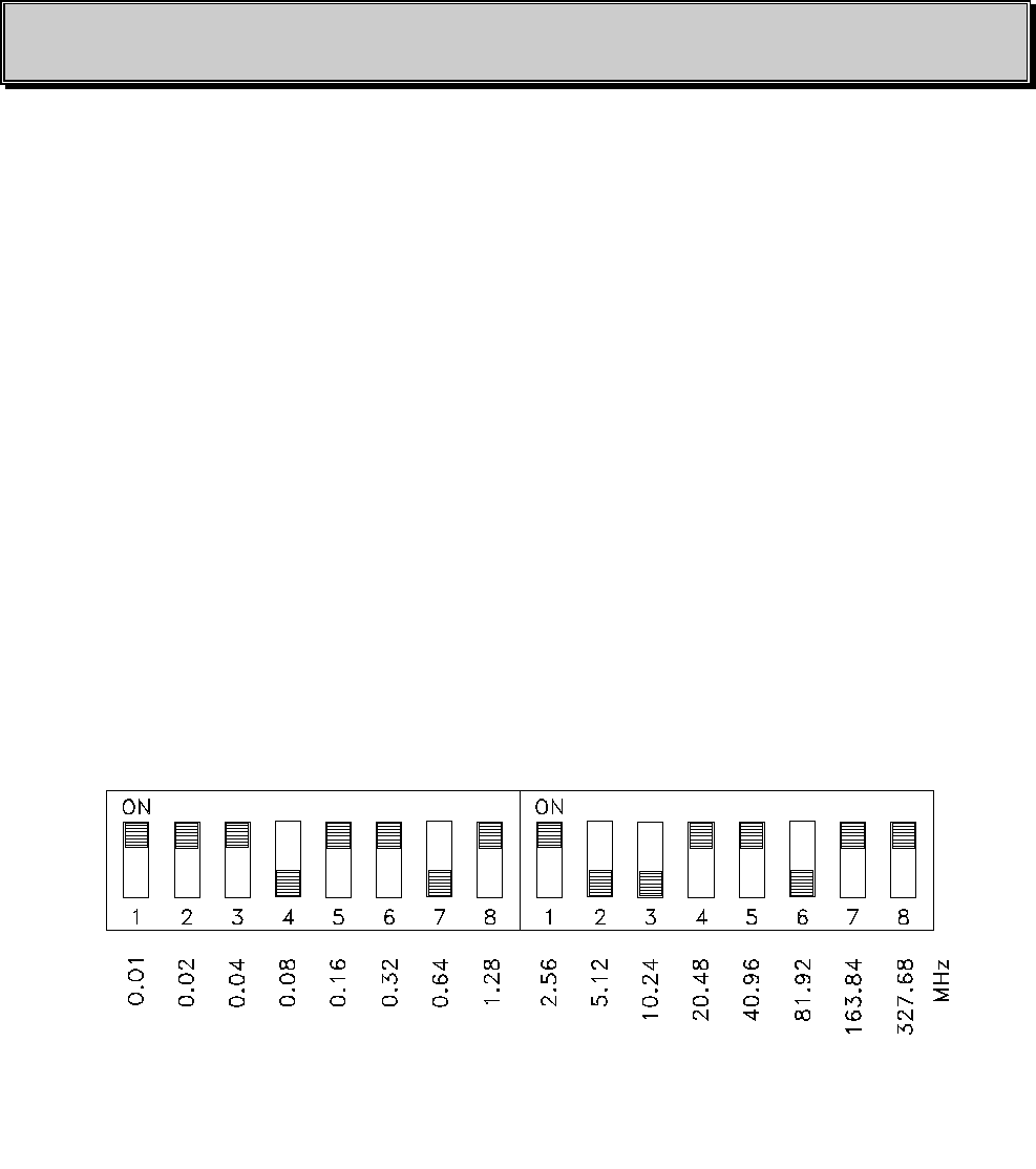
4. FREQUENCY SETTING
1. Lower the output power to its minimum level.
2. If the exciter is equipped with the “EXTERNAL FREQUENCY SETTING” (/C option) the
selection of the frequency is immediate using the external contraves.
The weights of the contrave numbers are as follows;
Fig. 4.1 - CONTRAVES WEIGHT
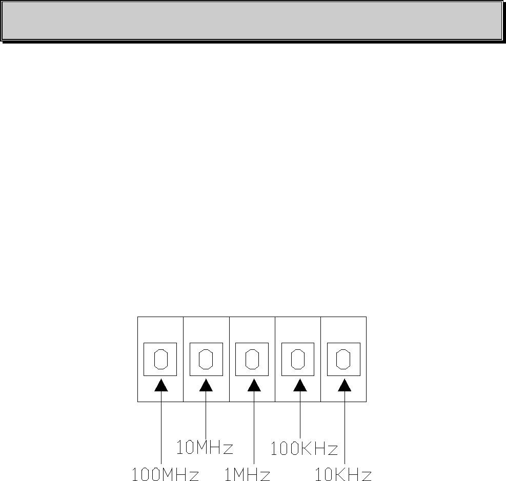
3. If the transmitter has internal frequency setting, to change frequency open the cover of the
modulator board (N° 8 Fig. 1.3) and use the internal dip-switches (see Chapter 7). The weight of
the internal dip-switches is indicated on the next page. To find the correct dip-switches
configuration corresponding to the needed FM channel, please refer to the following example with
98 MHz frequency.
DB ELETTRONICA TELECOMUNICAZIONI S.p.A.
PM 300 - FM Broadcasting Transmitter - USER’S MANUAL 15 /108
a - Put every dip-switches of the modulator board on the ON position
b - Select the OFF position for the dip-switch with the maximum weight, lower than or equal to the
frequency wanted (for example f 0 = 98 MHz put on OFF the 81.92 MHz switch)
c - Select 98 - 81.92=16.08 MHz, the minimum weight, lower than or equal to 16.08 MHz, is 10.24
MHz; now put off the corresponding switch.
d - Select 16.08 - 10.24 = 5.84 MHz, the minimum weight, lower than or equal to 5.84 MHz, is 5.12
MHz, now put off the corresponding switch .
e - Select 5.84 - 5.12 = 0.72 MHz, the minimum weight, lower than or equal to 0.72 MHz, is 0.64
MHz, then put off the corresponding switch.
f - Select 0.72 - 0.64 = 0.08 MHz, there is a weight equal to 0.08 MHz, so turn OFF the
corresponding switch to complete the setting.
The final configuration is:
4 - Adjust the desired output power using the front panel potentiometer.

DB ELETTRONICA TELECOMUNICAZIONI S.p.A.
PM 300 - FM Broadcasting Transmitter - USER’S MANUAL16 /108
5. ADJUSTMENTS AND MEASURES
AF INPUTS DEVIATION ADJUSTMENT
For the Left and Right input signals (/S option) use the corresponding XLR female connectors on
the rear panel. - see also appendix A for information about the connection
The input impedence is 600 W.
The transmitter accepts, adjusting input trimmers, input signal levels from -6 dBm to +10 dBm for a
75 kHz peak deviation.
For Mono input signal (PM300 without /S option) the input female XLR connector have the same
input levels than the stereo amplifier.
For MPX input signal (PM300 without /S option) the BNC input connector, labeled MPX IN (10
kW input impedance), accepts 0 dBm MPX signal level.
For SCA signals (>53 kHz) use BNC input connectors (1 kW input impedence): the input level for a
correct deviation of the main carrier (about 1.25 kHz peak) is 2.2 Vpp. To adjust the peak deviation
of the main carrier use the front panel potentiometer: look at the front panel meter and select the
DEV measurment by means of the selection button.
The front panel allows to monitoring all the main functions and protections of the transmitter.
Þ “LOCK” led: It shows the correct lock of the frequency synthesis circuit (PLL) on the modulator
board.
Þ “STEREO” led: It shows the use of the internal stereo generator board (/S option present). This
led is related to the switch labeled “STEREO/MONO” which allows selection of the type of signal
to be modulated.
The mono signal is obtained by a semi-sum of the left and the right signals. If the internal stereo
generator board is not present, the switch mentioned above and the corresponding LED are not used.

DB ELETTRONICA TELECOMUNICAZIONI S.p.A.
PM 300 - FM Broadcasting Transmitter - USER’S MANUAL 17 /108
Þ “REMOTE” led: It indicates if the operation of the transmitter can be remote controlled. This
selection is made using the switch “REMOTE/MANUAL”. This switch and the relative led will be
unused if the transmitter is not equipped with the remote optional control board.
Þ “ON” led: It shows the ON/OFF state of the transmitter, thus the presence of main power supply.
Þ “OVERHEAT” led: It indicates that the over temperature protection is enable.
This protection does not need a RESET because it restores the normal working conditions
automatically, when the temperature goes back to normal values.
Þ “VSWR” led: It shows that the VSWR protection is active. This intelligent protection is
characterized by an automatic reset delayed by about 2-3 seconds to avoid the risk of accidental
intervention. This auto-reset tries to resume to normal operation only 3-4 times, then turns the
transmitter off definitively (after the intervention of the VSWR protection, use the “RESET” push-
button.
Þ “PWR LIM” led: It shown that the output forward power becomes greater than the preset value
(normally 300W).
MEASURES
On the front panel there is a leds meter bar which allows the measurement of the most important
parameters of the transmitter. The push-button labeled “MEASURE SELECT” allows to select the
measurement required.
Each measure selected light on one of the leds below the bar.

DB ELETTRONICA TELECOMUNICAZIONI S.p.A.
PM 300 - FM Broadcasting Transmitter - USER’S MANUAL18 /108
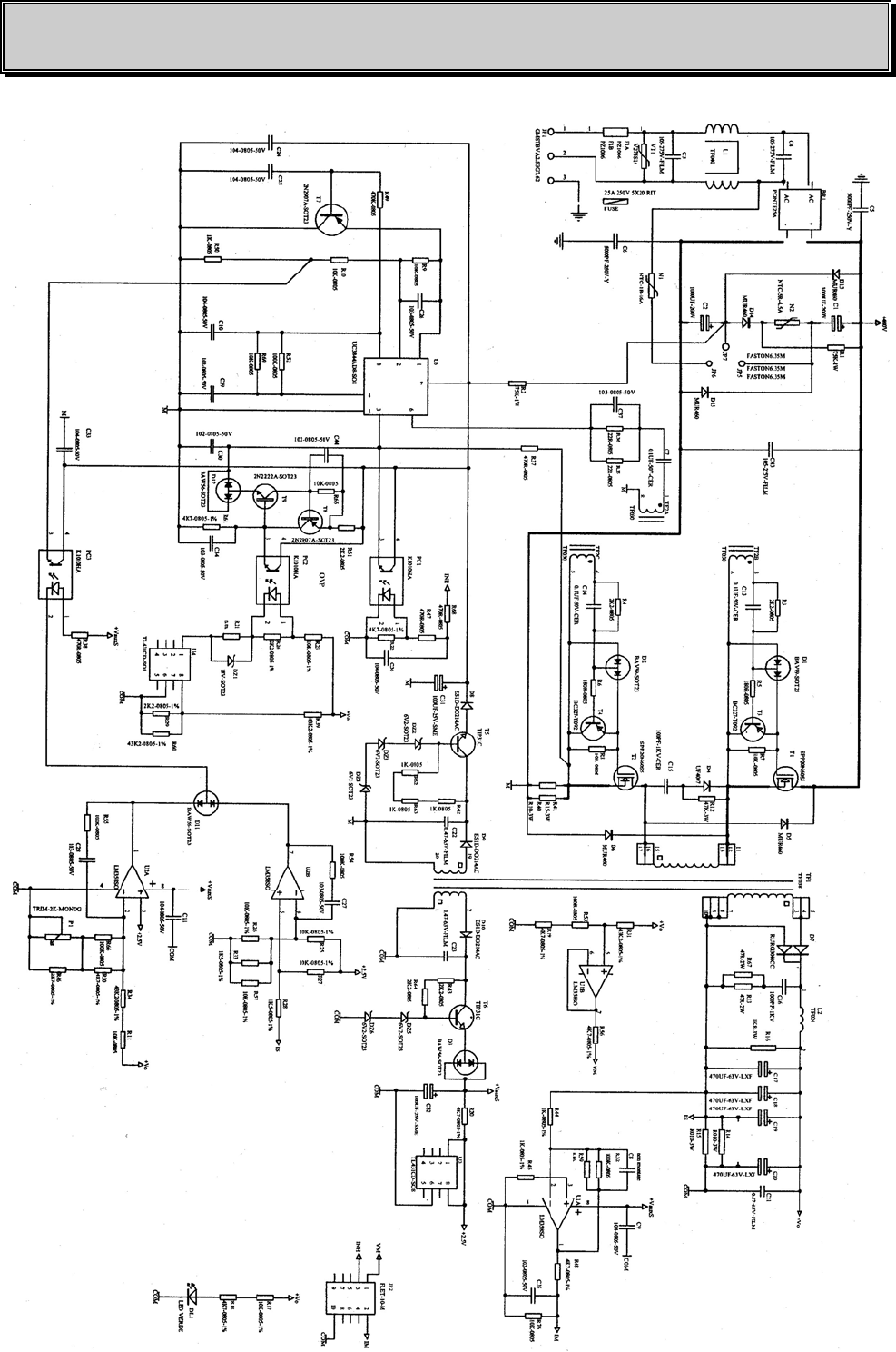
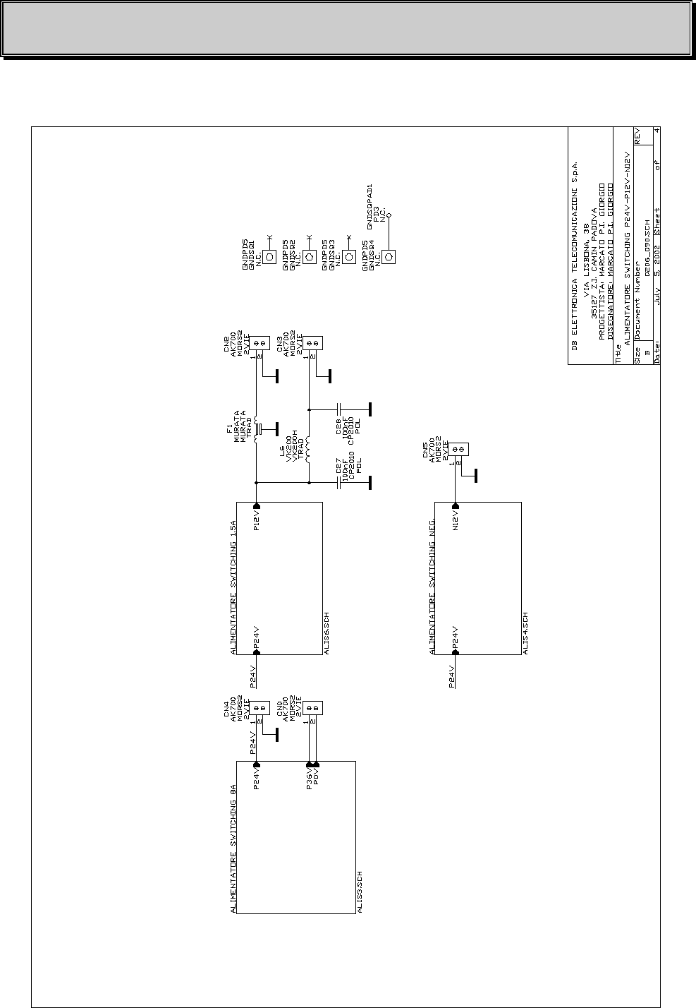
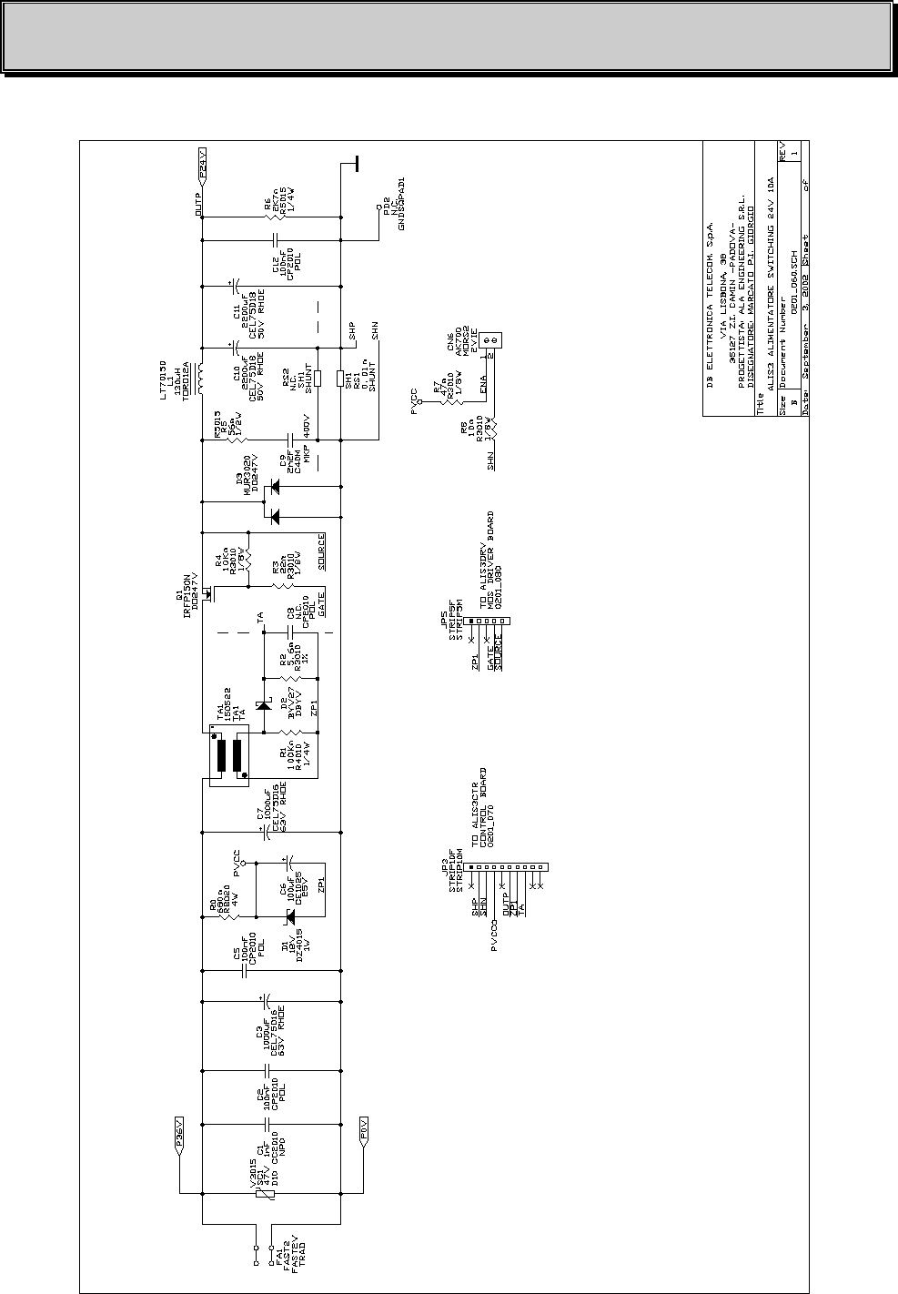
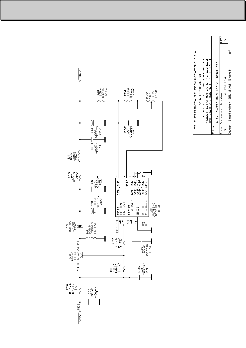
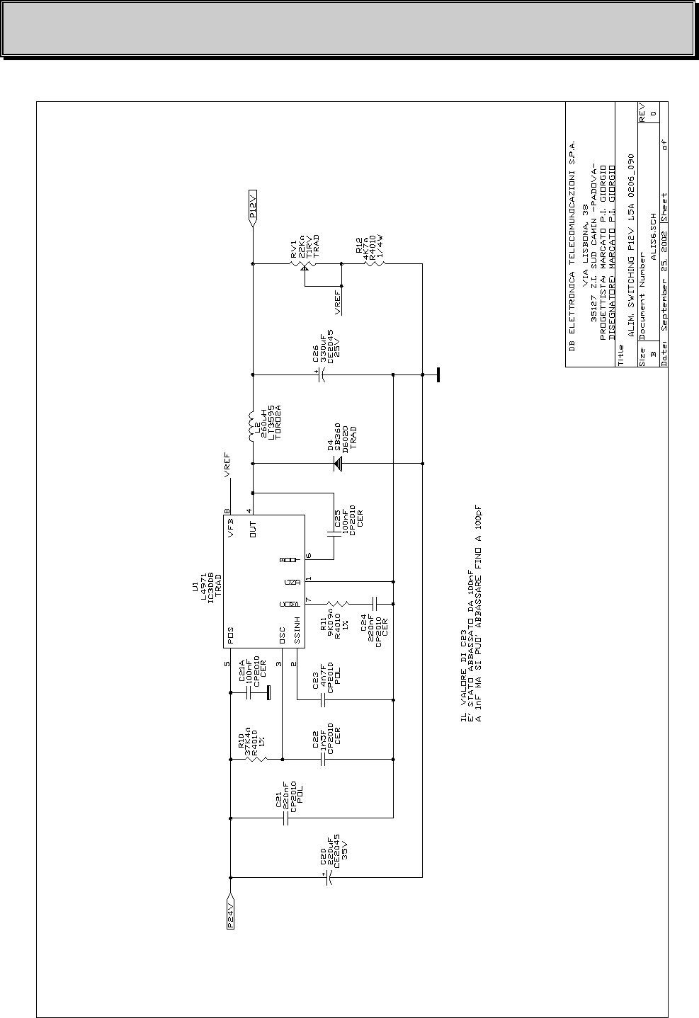
6. POWER SUPPLY SECTION
6.1 GENERAL DESCRIPTION
PM 300 transmitter power supply is composed of the following elements:
n°1 switching power supply module (PBIT 2180) to power supply the mosfet amplifier and the
equipment power supply board.
n°1 equipment power supply board (Fig. 6.8) capable of ±12 VDC (6A max) and +24 VDC (10A
max) to power supply the Protection and control boards, meter stage, Sintel ’96 modulator board,
AMP30 Driver stage and all optional boards present .
WARNING: before substituting a broken switching module it is necessary to disconnect its output
and to set the output voltage, without any load, at the right value (22.5v ± 2%) before reconnecting
the switching module output to the other circuits and boards in order to avoid overvoltage roblems.
The switching-mode power supply provides:
1. the efficiency is 80% higher hence provides a considerable reduction of the internal heating, thus
simplifying the cooling system;
2. a lower thermal and mechanical stress for associated components, such as transformer, diodes,
rectifier bridges is inflicted;
3. the power supply voltages at the output of the switching regulators are constant even in case
of wide main fluctuations (± 15 %).
DB ELETTRONICA TELECOMUNICAZIONI S.p.A.
PM 300 - FM Broadcasting Transmitter - USER’S MANUAL 19 /108
Fig. 6.1 - SWITCHING POWER SUPPLY MODULE ELECTRICAL SCHEMATIC “A”
DB ELETTRONICA TELECOMUNICAZIONI S.p.A.
PM 300 - FM Broadcasting Transmitter - USER’S MANUAL20 /108
Fig. 6.2 - SWITCHING POWER SUPPLY MODULE ELECTRICAL SCHEMATIC “B”
DB ELETTRONICA TELECOMUNICAZIONI S.p.A.
PM 300 - FM Broadcasting Transmitter - USER’S MANUAL 21 /108
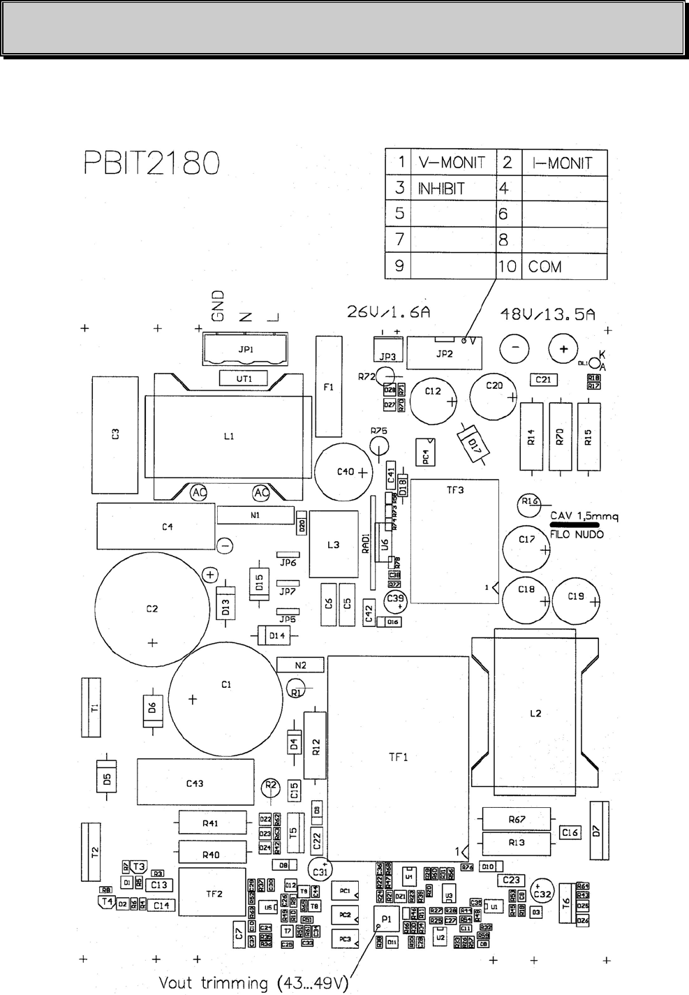
Fig. 6.3 - SWITCHING POWER SUPPLY MODULE COMPONENT LAYOUT
DB ELETTRONICA TELECOMUNICAZIONI S.p.A.
PM 300 - FM Broadcasting Transmitter - USER’S MANUAL22 /108
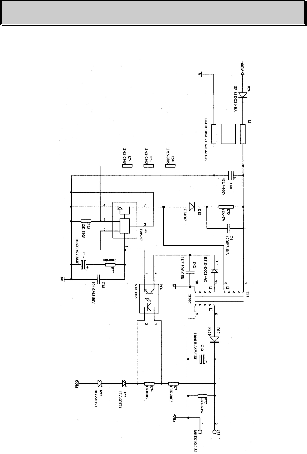
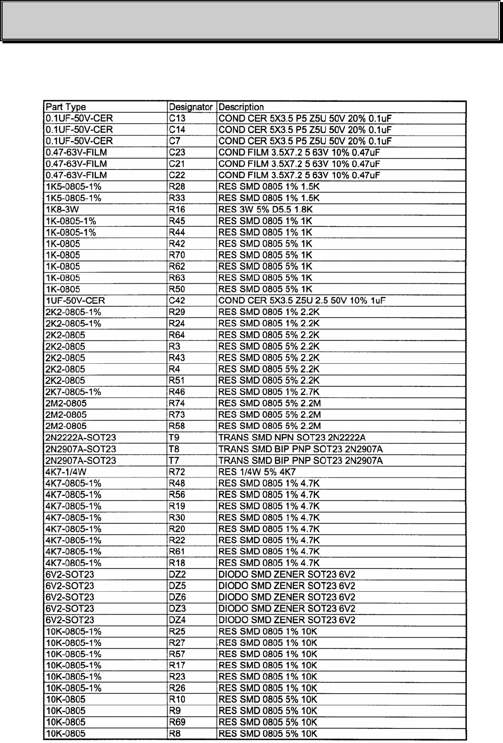
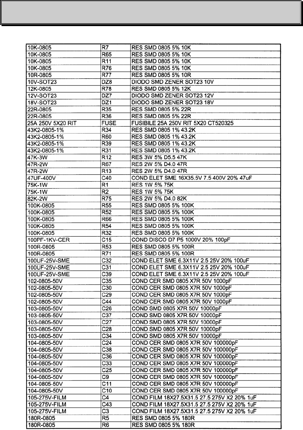
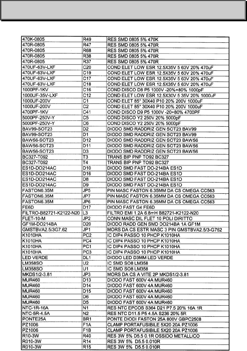
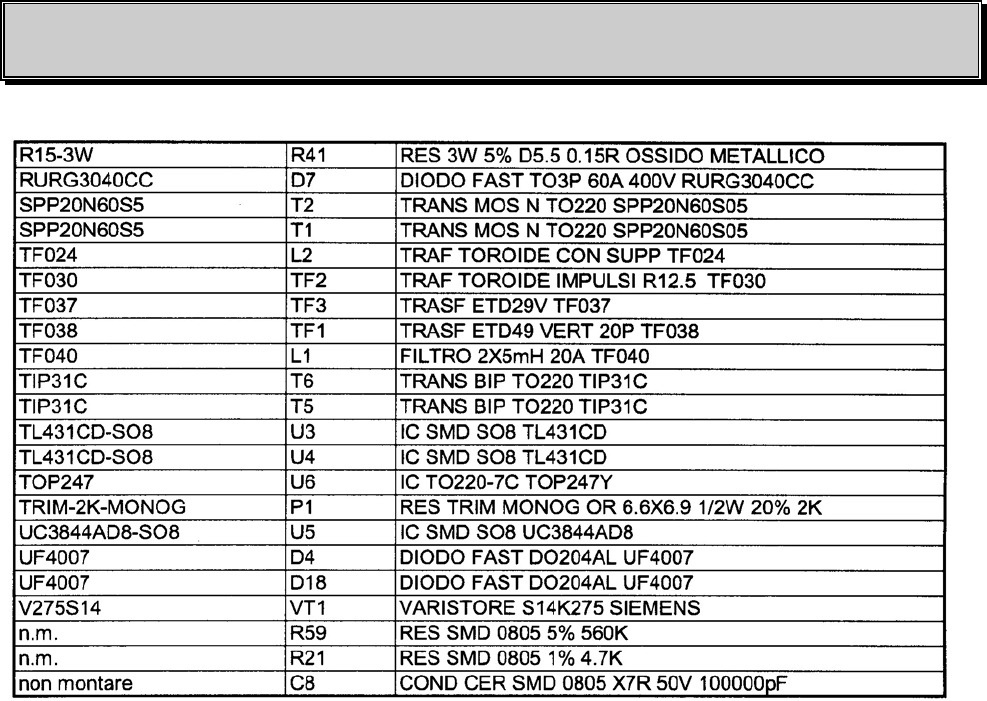
6.2 SWITCHING POWER SUPPLY MODULE PART LIST
DB ELETTRONICA TELECOMUNICAZIONI S.p.A.
PM 300 - FM Broadcasting Transmitter - USER’S MANUAL 23 /108
DB ELETTRONICA TELECOMUNICAZIONI S.p.A.
PM 300 - FM Broadcasting Transmitter - USER’S MANUAL24 /108
DB ELETTRONICA TELECOMUNICAZIONI S.p.A.
PM 300 - FM Broadcasting Transmitter - USER’S MANUAL 25 /108
DB ELETTRONICA TELECOMUNICAZIONI S.p.A.
PM 300 - FM Broadcasting Transmitter - USER’S MANUAL26 /108
Fig. 6.4 – EQUIP. PWR SUPP. BOARD GENERAL ELECTRICAL SCHEMATIC
DB ELETTRONICA TELECOMUNICAZIONI S.p.A.
PM 300 - FM Broadcasting Transmitter - USER’S MANUAL 27 /108
Fig. 6.5 - EQUIP. PWR SUPP. BOARD +24 V STAGE ELECTRICAL SCHEMATIC
DB ELETTRONICA TELECOMUNICAZIONI S.p.A.
PM 300 - FM Broadcasting Transmitter - USER’S MANUAL28 /108
Fig. 6.6 - EQUIP. PWR SUPP. BOARD-12V STAGE ELECTRICAL SCHEMATIC
DB ELETTRONICA TELECOMUNICAZIONI S.p.A.
PM 300 - FM Broadcasting Transmitter - USER’S MANUAL 29 /108
Fig. 6.7 - EQUIP. PWR SUPP. BOARD +12V STAGE ELECTRICAL SCHEMATIC
DB ELETTRONICA TELECOMUNICAZIONI S.p.A.
PM 300 - FM Broadcasting Transmitter - USER’S MANUAL30 /108
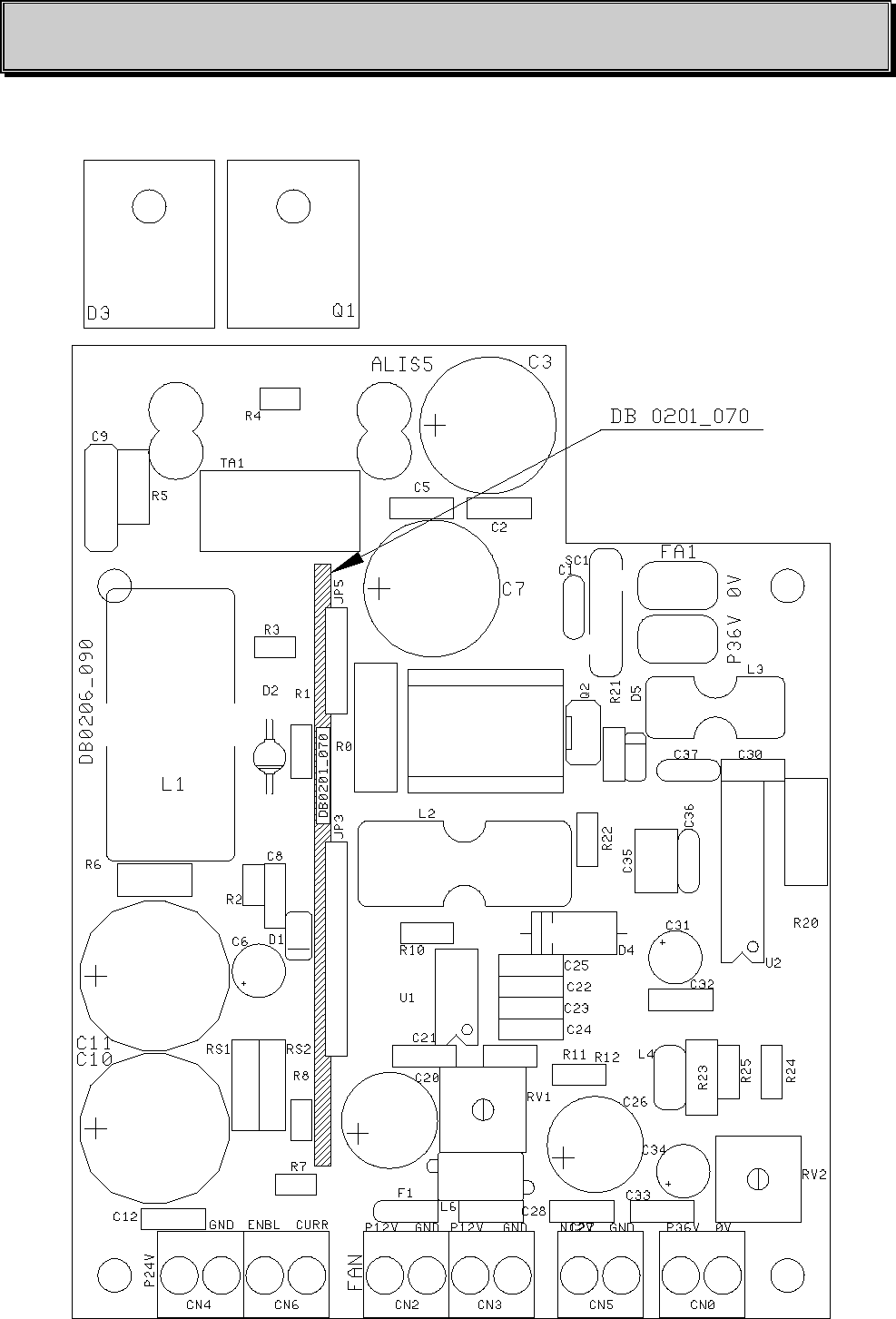
Fig. 6.8 - EQUIP. PWR SUPP. BOARD COMPONENT LAYOUT (DB 0206_090)

DB ELETTRONICA TELECOMUNICAZIONI S.p.A.
PM 300 - FM Broadcasting Transmitter - USER’S MANUAL 31 /108
6.3 EQUIP. PWR SUPP. BOARD PARTS LIST (DB 0206_090)
ITEM QUANTITY REFERENCE PART
____________________________________________________________________________________________
1 6 CN2,CN3,CN4,CN5,CN6,CN0 AK700 2VIE MORS2
2 2 C37,C1 1nF NP0 CC2010
3 8 C2,C5,C12,C27,C28,C30, 100nF POL CP2010
C32,C33
4 2 C7,C3 1000uF 63V RHOE CEL75D16
5 3 C6,C31,C34 100uF 25V CE1025
6 1 C9 2n2F MKP 400V C40M
7 2 C10,C11 2200uF 50V RHOE CEL75D18
8 1 C20 220uF 35V CE2045
9 2 C21A,C25 100nF CER CP2010
10 2 C21,C24 220nF POL CP2010
11 1 C23 4n7F POL CP2010
12 1 C22 1n5F POL CP2010
13 1 C26 330uF 25V CE2045
14 1 C35 1uF POL CP2020
15 1 C36 100pF NPO CC2010
16 1 D1 18V 1W DZ4015
17 1 D2 BYV27 DBYV
18 1 D3 MUR3020 DO247V
19 1 D4 SB360 TRAD D6020
20 1 D5 1N5819 TRAD D4010
21 1 FA1 FAST2 TRAD FAST2V
22 1 F1 MURATA TRAD MURATA
23 1 JP3 STRIP10F STRIP10M
24 1 JP5 STRIP5F STRIP5M
25 1 L1 130uH TORO12A LT70150
26 1 L2 260uH TORO2A LT3595
27 1 L3 100uH TORO2A LT2865
28 1 L4 10uH TRAD L5015
29 1 L6 VK200 TRAD VK200H
30 1 Q1 IRFP150N DO247V
31 1 Q2 BD140 SOT32 +VITEeDADOM3+ALETTA
32 1 RS1 0.01Ω SHUNT SH1
33 1 RV1 22KΩ TRAD T1RV
34 1 RV2 1KΩ TRAD T1RV
35 1 R0 680Ω 4W R8020
36 1 R1 100KΩ 1/4W R4010
37 1 R2 5.6Ω 1% R3010
38 1 R3 22Ω 1/8W R3010
39 1 R4 10KΩ 1/8W R3010
40 1 R5 56Ω 1/2W R5015
41 1 R6 2K7Ω 1/4W R5015
42 1 R7 47Ω 1/8W R3010
43 1 R8 10Ω 1/8W R3010
44 1 R10 37K4Ω 1% R4010
45 1 R11 9K09Ω 1% R4010
46 1 R12 4K7Ω 1/4W R4010
47 1 R20 0.47Ω 2W R7020
48 1 R21 100Ω 1/4W R4010
49 1 R22 270Ω 1/4W R4010
50 1 R23 10Ω 1/2W R5015
51 1 R24 1K2Ω 1/4W R4010

DB ELETTRONICA TELECOMUNICAZIONI S.p.A.
PM 300 - FM Broadcasting Transmitter - USER’S MANUAL32 /108
ITEM QUANTITY REFERENCE PART
____________________________________________________________________________________________
52 1 R25 15KΩ 1/4W R4010
53 1 SC1 47V D10 V3015
54 1 TA1 150522 TA TA1
55 1 U1 L4971 TRAD IC3008
56 1 U2 UA78S40 TRAD IC3010
57 1 DB 0201_070 PRINTED BOARD
DB ELETTRONICA TELECOMUNICAZIONI S.p.A.
PM 300 - FM Broadcasting Transmitter - USER’S MANUAL 33 /108
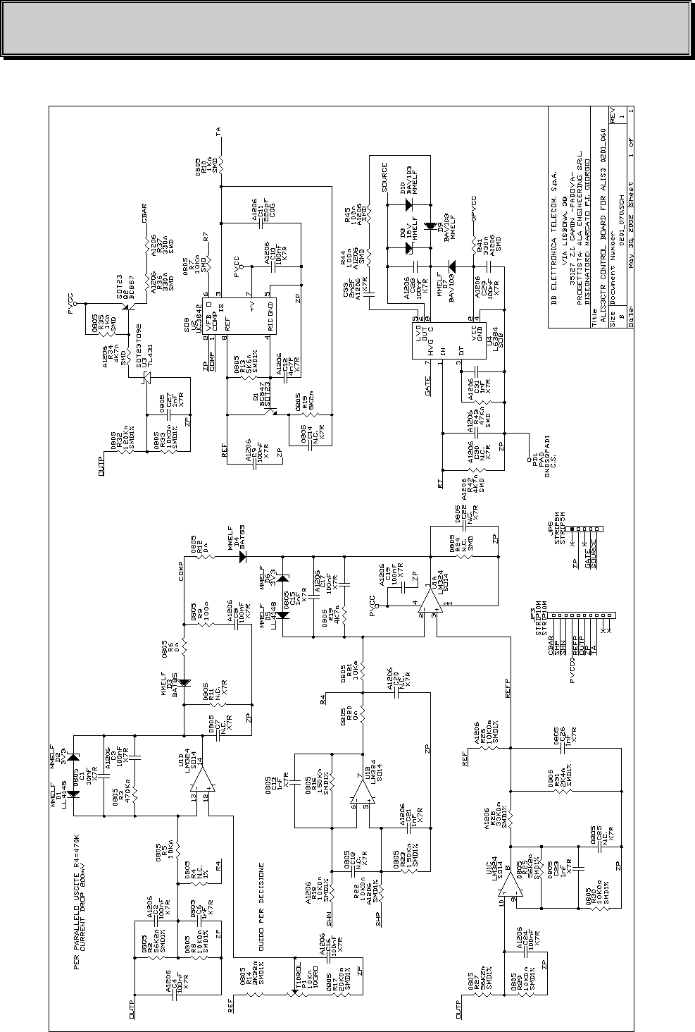
Fig. 6.9 - DB 0201_070 PRINTED BOARD ELECTRICAL SCHEMATIC
DB ELETTRONICA TELECOMUNICAZIONI S.p.A.
PM 300 - FM Broadcasting Transmitter - USER’S MANUAL34 /108
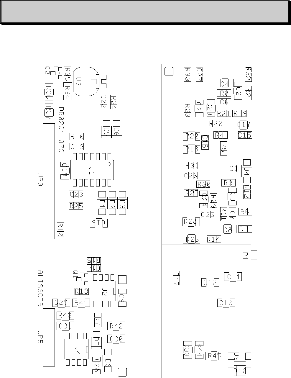
Fig. 6.10 - DB 0201_070 PRINTED BOARD COMPONENT LAYOUT

DB ELETTRONICA TELECOMUNICAZIONI S.p.A.
PM 300 - FM Broadcasting Transmitter - USER’S MANUAL 35 /108
6.4 DB 0201_070 PRINTED BOARD PARTS LIST
ITEM QUANTITY REFERENCE PART
_______________________________________________________________________
1 1 C1 10nF X7R 0805
2 11 C2,C3,C4,C8,C9,C10,C17, 100nF X7R 1206
C19,C24,C28,C29
3 6 C6,C13,C15,C23,C26,C27 1nF X7R 0805
4 6 C7,R11,C14,C18,C22,C25 N.C. X7R 0805
5 1 C11 220pF C0G 1206
6 1 C12 4n7F X7R 1206
7 1 C16 100nF X7R 1206
8 2 C31,C21 1nF X7R 1206
9 1 C33 2n2F X7R 1206
10 2 D5,D1 LL4148 MMELF DIODO
11 2 D2,D6 3V3 MMELF ZENER
12 2 D3,D4 BAT85 MMELF DIODO
13 3 D7,D9,D10 BAV103 MMELF DIODO
14 1 D8 18V MMELF ZENER
15 1 JP3 STRIP10M MASCHIO 90°
16 1 JP5 STRIP5M MASCHIO 90°
17 1 P1 10KΩ 10GRO PANNELLO
18 1 Q1 BC847 SMD SOT23
19 1 Q2 BC857 SMD SOT23
20 3 R2,R25,R27 56K2Ω SMD1% 0805
21 1 R3 470KΩ SMD 0805
22 2 R21,R5 10KΩ SMD 0805
23 3 R6,R12,R20 0Ω SMD 0805
24 1 R7 10KΩ SMD 0805
25 4 R8,R29,R30,R33 10K0Ω SMD1% 0805
26 1 R9 100Ω SMD 0805
27 2 R10,R35 1KΩ SMD 0805
28 1 R13 5K6Ω SMD1% 0805
29 1 R14 3K32Ω SMD1% 0805
30 1 R15 8K2Ω SMD 0805
31 2 R16,R23 150KΩ SMD1% 0805
31 1 R17 20K0Ω SMD1% 0805
32 3 R18,R22,R26 10K0Ω SMD1% 1206
33 1 R19 4K7Ω SMD 0805
34 1 R28 33K0Ω SMD1% 1206
35 1 R31 2K4Ω SMD1% 0805
36 1 R32 120KΩ SMD1% 0805
37 2 R42,R34 4K7Ω SMD 1206
38 3 R36,R37,R41 330Ω SMD 1206
39 1 R43 47KΩ SMD 1206
40 2 R44,R45 100Ω SMD 1206
41 1 U1 LM324 SMD SO14
42 1 U2 UC3842 SMD SO8
43 1 U3 TL431 SOT23/TO92
44 1 U4 L6384 SMD SO8

DB ELETTRONICA TELECOMUNICAZIONI S.p.A.
PM 300 - FM Broadcasting Transmitter - USER’S MANUAL36 /108
7. MODULATION STAGE (Sintel 96)
7.1 GENERAL DESCRIPTION
The new modulator board SINTEL ’96 allows a high quality direct carrier modulation accepting a
composite stereo (MPX) or a mono input signal with up to 3 SCA subcarriers (for example RDS,
ARI, ...).
The mono input signal is filtered by a 7th order elliptic filter with a very flat response (20Hz to
15kHz with ± 0.25 dB) and an optimum out of band attenuation (>50 dB for frequencies higher
than 19 kHz), then the signal is amplified (or attenuated) and passed to the VCO oscillator for the
FM carrier modulation. The VCO is controlled by a digital PLL circuit with a high stability quartz
reference to obtain a very stable synthetized oscillation: the frequency setting is customizeable using
on board dip-switches (the minimum step size is 10 kHz).
The composite stereo signal and the SCA subcarriers are just amplified or attenuated by the correct
modulation depth adjustment before going through the VCO stage: the stereo performances of
SINTEL ’96 are excellent, (stereo separation >60 dB from 20Hz to 15 kHz, SNR > 80 dB).
Before the VCO stage, an adjustable and bypassable deviation limiter prevents the FM carrier from
an excessive modulation depth and adjacent channel interference according to all the international
standards (CCIR, FCC). Furthermore, an automatic locking circuit enables the output modulated
signal of SINTEL ’96 only when the internal PLL is locked properly, in order to avoid unwanted
emissions.
DB ELETTRONICA TELECOMUNICAZIONI S.p.A.
PM 300 - FM Broadcasting Transmitter - USER’S MANUAL 37 /108
Fig. 7.1 - “SINTEL 96” MODULATION BOARD GENERAL ELECTRICAL SCHEMATIC

DB ELETTRONICA TELECOMUNICAZIONI S.p.A.
PM 300 - FM Broadcasting Transmitter - USER’S MANUAL38 /108
Fig. 7.2 - PLL STAGE ELECTRICAL SCHEMATIC
DB ELETTRONICA TELECOMUNICAZIONI S.p.A.
PM 300 - FM Broadcasting Transmitter - USER’S MANUAL 39 /108
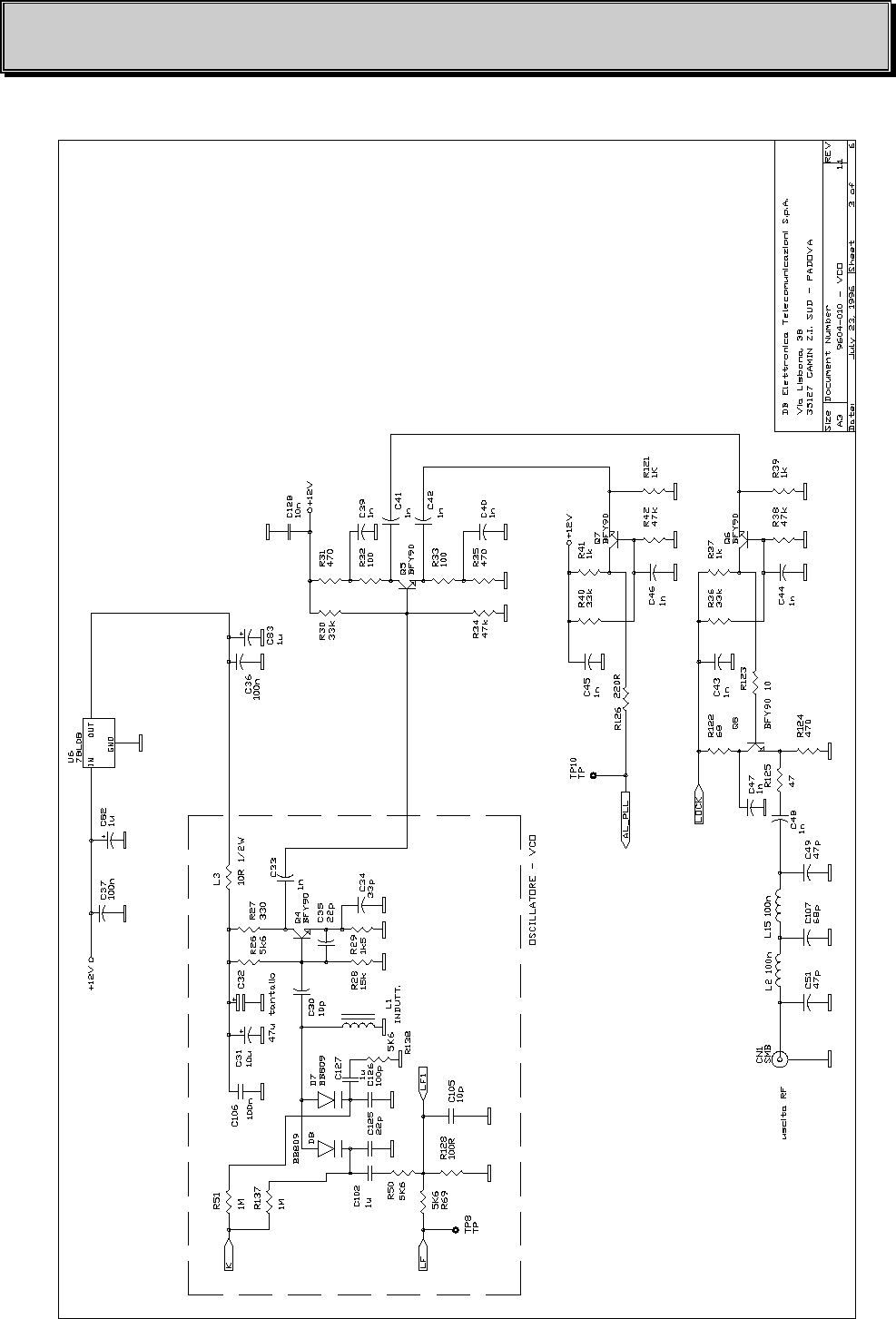
Fig. 7.3 - VCO STAGE ELECTRICAL SCHEMATIC
DB ELETTRONICA TELECOMUNICAZIONI S.p.A.
PM 300 - FM Broadcasting Transmitter - USER’S MANUAL40 /108
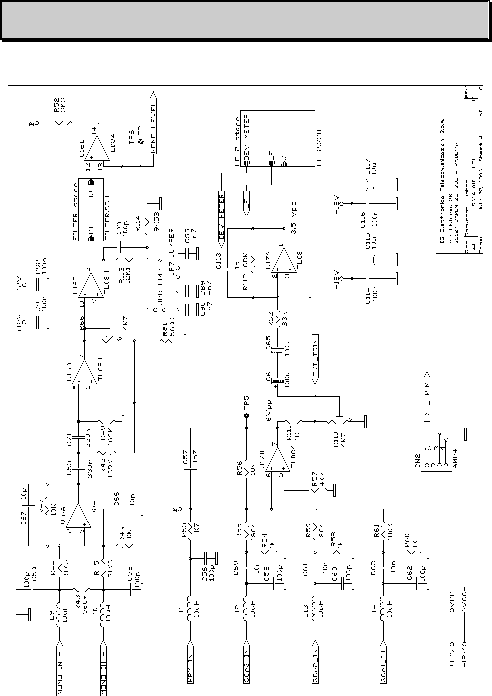
Fig. 7.4 - LF 1 STAGE ELECTRICAL SCHEMATIC
DB ELETTRONICA TELECOMUNICAZIONI S.p.A.
PM 300 - FM Broadcasting Transmitter - USER’S MANUAL 41 /108
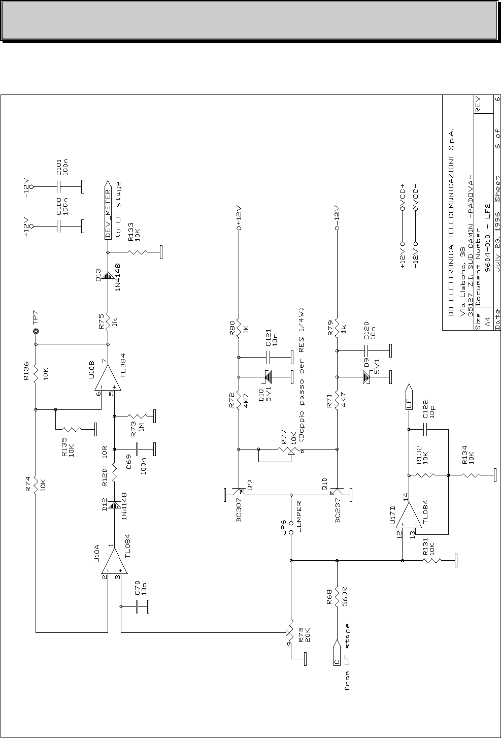
Fig. 7.5 - LF 2 STAGE ELECTRICAL SCHEMATIC
DB ELETTRONICA TELECOMUNICAZIONI S.p.A.
PM 300 - FM Broadcasting Transmitter - USER’S MANUAL42 /108
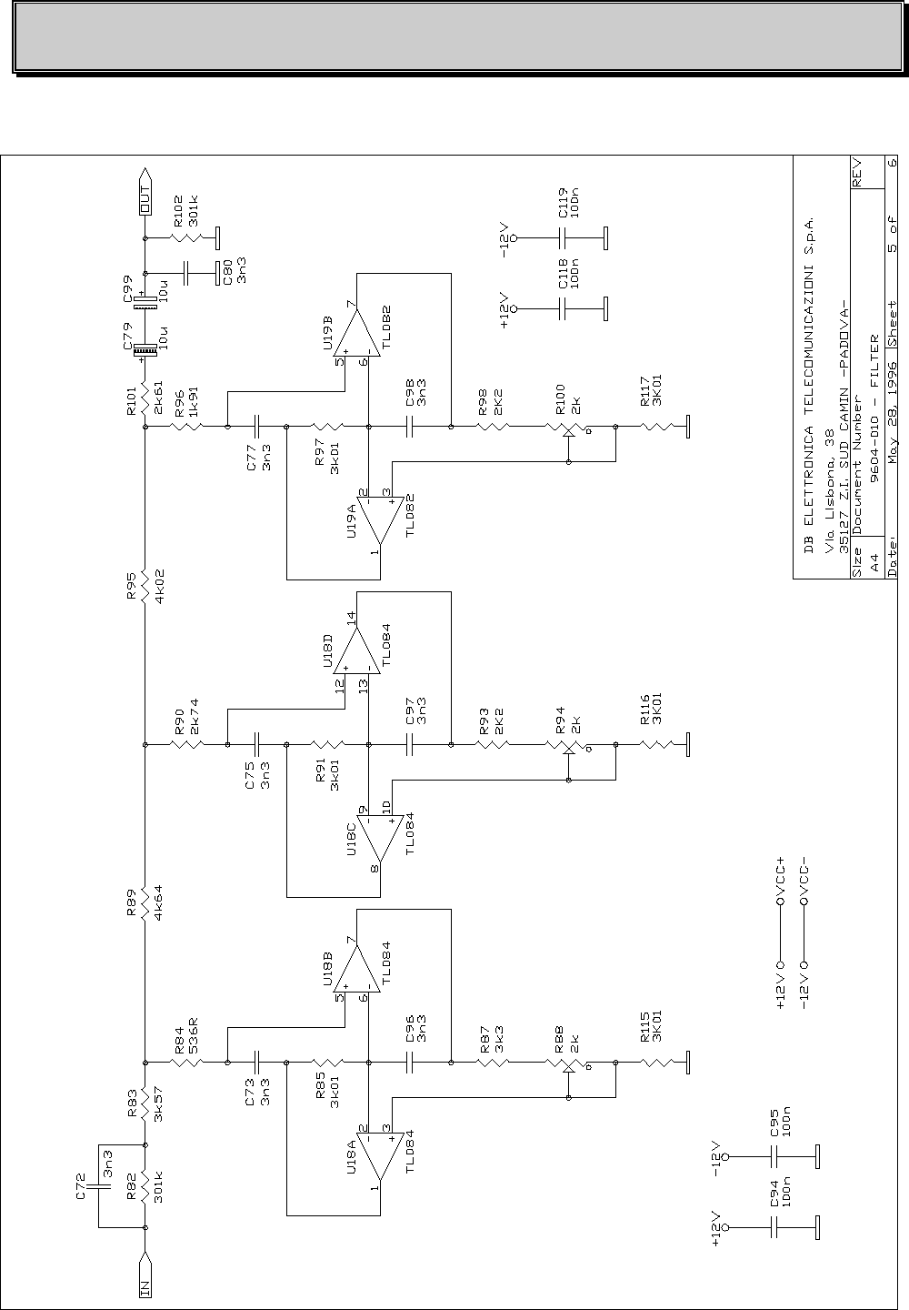
Fig. 7.6 - FILTER STAGE ELECTRICAL SCHEMATIC
DB ELETTRONICA TELECOMUNICAZIONI S.p.A.
PM 300 - FM Broadcasting Transmitter - USER’S MANUAL 43 /108
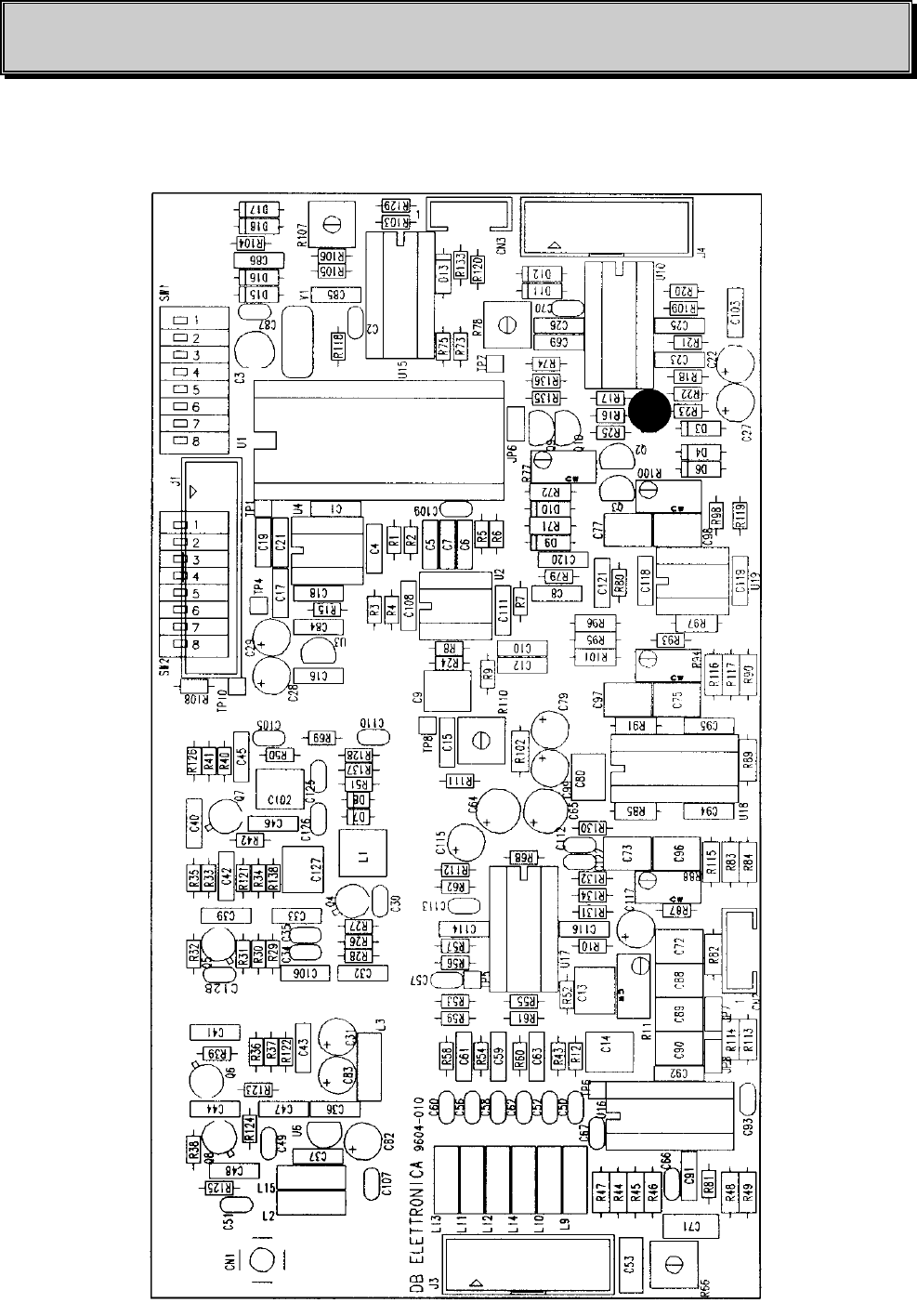
Fig. 7.7 - “SINTEL 96” MODULATION COMPONENT LAYOUT (DB 9604-010)

DB ELETTRONICA TELECOMUNICAZIONI S.p.A.
PM 300 - FM Broadcasting Transmitter - USER’S MANUAL44 /108
7.2 “SINTEL 96” MODULATOR PARTS LIST
ITEM QUANTITY REFERENCE PART
__________________________________________________________________
1 1 CN1 SMB SMB DA STAMPATO
2 2 CN3,CN2 AMP4
3 18 C1,C16,C18,C25,C26,C36, 100n POLY
C37,C84,C94,C95,C100,
C101,C108,C111,C114,C116,C118,C119
4 1 C2 15p
5 1 C3 10-60p
6 5 C4,C5,C8,C12,C21 10n POLY
7 2 C6,C7 4n7 POLY
8 3 C9,C14,C102 1u POLY
9 9 C10,C19,C59,C61,C63,C85, 10n CER
C86,C120,C121
10 1 C13 1u POLY
11 14 C15,C17,C23,C33,C39,C40, 1n CER
C41,C42,C43,C44,C45,C46,C47,C48
12 6 C22,C31,C79,C99,C115, 10u ELETT.25V
C117
13 5 C27,C28,C29,C82,C83 1u ELETT.25V
14 7 C30,C66,C67,C70,C105, 10p CER
C112,C122
15 1 C32 47u elettrol. tantalio
16 1 C34 33p CER
17 1 C35 22p CER
18 2 C51,C49 47p CER
19 8 C50,C52,C56,C58,C60,C62, 100p CER
C109,C110
20 2 C53,C71 330n poly
21 1 C57 4p7 cer
22 2 C64,C65 100u 25V
23 3 C69,C91,C92 100n cer
24 8 C72,C73,C75,C77,C80,C96, 3n3 CER
C97,C98
25 1 C87 220p CER
26 3 C88,C89,C90 4n7
27 2 C126,C93 100p
28 1 C103 100n CP1
29 1 C106 100n
30 1 C107 68p CER
31 1 C113 1p CER
32 1 C125 22p
33 1 C127 1u
34 1 C128 10n multistrato
35 7 D3,D12,D13,D15,D16,D17, 1N4148
D18
36 4 D4,D6,D9,D10 5V1 ZENER
37 1 D5 LED
38 2 D8,D7 BB809
39 1 JP6 JUMPER JUMPER X2
40 2 JP8,JP7 JUMPER
41 1 J1 CON20

DB ELETTRONICA TELECOMUNICAZIONI S.p.A.
PM 300 - FM Broadcasting Transmitter - USER’S MANUAL 45 /108
ITEM QUANTITY REFERENCE PART
_______________________________________________________________________________
42 2 J4,J3 CON14
43 1 L1 INDUCTOR
44 2 L2,L15 100n INDUTT ASSIALE
45 1 L3 10R 1/2W 1/2 W
46 1 L9 10uH
47 1 L10 10uH R1
48 3 L11,L12,L14 10uH INDUTT.
49 1 L13 10uH INDUTT.
50 2 Q2,Q3 BC557
51 5 Q4,Q5,Q6,Q7,Q8 BFY90
52 1 Q9 BC307
53 1 Q10 BC237
54 1 R? 22K 1/8W
55 4 R1,R2,R3,R4 27K4 1% RES 1/8W
56 1 R5 48K7 1% RES 1/8W
57 2 R7,R6 27K RES 1/8W
58 1 R8 22K RES 1/8W
59 1 R9 48K7 1%
60 3 R10,R24,R73 1M RES 1/8W
61 1 R11 50K Trimmer multigiri
62 5 R12,R34,R38,R42,R108 47K RES 1/8W
63 1 R15 2.2K RES 1/8W
64 14 R16,R18,R22,R56,R74,R103, 10K RES 1/8W
R106,R130,R131,R132,R133,
R134,R135,R136
65 1 R17 560 RES 1/8W
66 2 R20,R29 1K5 RES 1/8W
67 4 R21,R31,R35,R124 470 RES 1/8W
68 1 R23 6.8K RES 1/8W
69 14 R25,R37,R39,R41,R54,R58, 1K RES 1/8W
R60,R75,R79,R80,R111,R118,R119,R121
70 2 R26,R69 5k6 RES 1/8W
71 1 R27 330 RES 1/8W
72 1 R28 15k RES 1/8W
73 4 R30,R36,R40,R62 33k RES 1/8W
74 2 R33,R32 100 RES 1/8W
75 1 R43 680R 1/8W
76 2 R45,R44 31K6 1% 1/4W
77 2 R47,R46 10K 1% 1/4W
78 2 R48,R49 169K 1% 1/4W
79 2 R138,R50 5K6
80 2 R51,R137 1M
81 1 R52 3K3 RES 1/8W
82 4 R53,R57,R71,R72 4K7 RES 1/8W
83 3 R55,R59,R61 180K RES 1/8W
84 2 R66,R110 4K7 TRIM MONOGIRO PICC.
85 2 R109,R68 560R RES 1/8W
86 1 R77 10K TRIMMER MULTIGIRI
87 1 R78 20K trim
88 1 R81 560R 1% 1/4W
89 1 R82 301k RES_1/4W_1%
90 1 R83 3k57 RES_1/4W_1%
91 1 R84 536R RES_1/4W_1%
92 6 R85,R91,R97,R115,R116,R117 3k01 RES_1/4W_1%
93 1 R87 3k3 RES_1/8W
94 2 R88,R94 2k trim multi

DB ELETTRONICA TELECOMUNICAZIONI S.p.A.
PM 300 - FM Broadcasting Transmitter - USER’S MANUAL46 /108
ITEM QUANTITY REFERENCE PART
_____________________________________________________________________________
95 1 R89 4k64 RES_1/4W_1%
96 1 R90 2k74 RES_1/4W_1%
97 2 R93,R98 2K2 RES_1/8W
98 1 R95 4k02 RES_1/4W_1%
99 1 R96 1k91 RES_1/4W_1%
100 1 R100 2k RV64W
101 1 R101 2k61 RES_1/4W_1%
102 1 R102 301k 1/4W 1%
103 1 R104 2K2 RES 1/8W
104 1 R105 2K2
105 1 R107 10K TRIM MONOGIRO PICC.
106 1 R112 68K RES 1/8W
107 1 R113 12K1
108 1 R114 9K53 RES 1/8W
109 1 R120 10R RES 1/8W
110 1 R122 68 RES 1/8W
111 1 R123 10 RES 1/8W
112 1 R125 47 RES 1/8W
113 1 R126 220R RES 1/8W
114 1 R128 100R RES 1/8W
115 1 R129 330R RES 1/8W
116 2 SW2,SW1 DIP SW 8
117 7 TP1,TP4,TP5,TP6,TP7,TP8, TP
TP10
118 1 U1 MC145152
119 2 U2,U19 TL082
120 1 U3 78L05
121 1 U4 MB501L
122 1 U6 78L08
123 4 U10,U16,U17,U18 TL084
124 1 U15 74HC14
125 1 Y1 2.56MHz

DB ELETTRONICA TELECOMUNICAZIONI S.p.A.
PM 300 - FM Broadcasting Transmitter - USER’S MANUAL 47 /108
8. AMP30 DRIVER STAGE
8.1 GENERAL DESCRIPTION
The pre amplifier/driver stage is realized by the new 30W MOSFET amplifier board
(DB 0110_010A). This board is basically composed of four amplification WIDE BAND stages.
The first stage uses a BFQ19 transistor to amplify the input level. The second and the third
transistors are 2N4427. The last amplification stage uses a BLF245 MOSFET to obtain an output
RF power 30 W maximum.
The P3 trimmer (see Fig. 8.2) in the AMP30 board allows to adjust the mosfet bias current.
.An external panel trimmer and the P2 trimmer in the AMP30 board allows to adjust the
output power.
The AMP30 board is equipped with an initial 5-6 seconds delay to avoid accidental out of
band emissions in the initial PLL locking period.
DB ELETTRONICA TELECOMUNICAZIONI S.p.A.
PM 300 - FM Broadcasting Transmitter - USER’S MANUAL48 /108
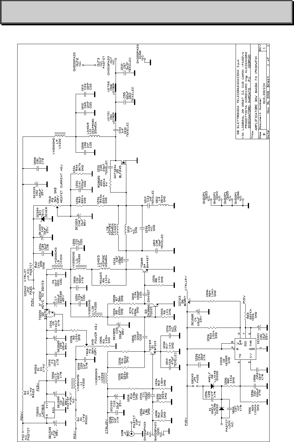
Fig. 8.1 - AMP30 PRE AMPLIFIER ELECTRICAL SCHEMATIC
DB ELETTRONICA TELECOMUNICAZIONI S.p.A.
PM 300 - FM Broadcasting Transmitter - USER’S MANUAL 49 /108
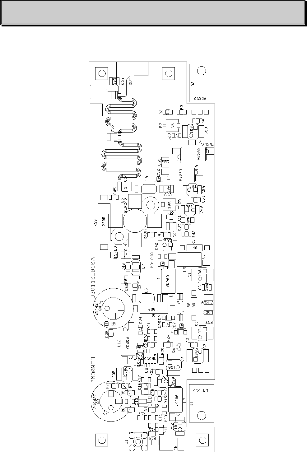
Fig. 8.2 - AMP30 PRE AMPLIFIER COMPONENT LAYOUT (DB 0110_010A)

DB ELETTRONICA TELECOMUNICAZIONI S.p.A.
PM 300 - FM Broadcasting Transmitter - USER’S MANUAL50 /108
8.2 AMP30 PRE AMPLIFIER PARTS LIST
ITEM QUANTITY REFERENCE PART
_____________________________________________________________________________
2 1 C1 47uF 35V p=3.5mm f=8mm
3 5 C2,C7,C9,C35,C59 100uF 25V p=2.5mm f=6,5mm
4 7 C3,C4,C5,C23,C24,C39,C51 10nF X7R 1206
5 3 C6,C53,C65 10nF COG 1210
6 4 C11,C12,C36,C37 100pF COG 1206
8 1 C16 47pF TEKELEC 1210
9 4 C20,C32,C40,C42 10uF 25V p=2.5mm f=5,5mm
10 2 C30,C21 100nF X7R 1206
11 4 C27,C28,C29,C33 1nF X7R 1206
12 3 C31,C34,C52 1nF COG 1206
13 1 C38 10pF TEKELEC 1210
14 1 C41 330pF COG 1206
15 2 C54,C44 1nF TEKELEC 1210
16 1 C45 33pF TEKELEC 1210
17 1 C50 100uF 35V p=3.5mm f=8mm
18 1 C55 82pF TEKELEC 1210
19 1 C57 3p3F TEKELEC 1210
20 1 DZ1 5V1 ZENER SOD80
21 2 D2,D1 LL4148 DIODO MMELF
26 6 L1,L2,L5,L9,L11,L12 VK200 TRAD VK200SMD
27 1 L3 15nH SMD 1210
28 3 L6,L7,L10 CU x BOBINE IN ARIA
33 2 P2,P3 5KΩSMD 1GRV 5x5mm
34 1 Q1 BFQ19 SMD SOT89
35 1 Q2 BDX53 TRAD TO220
36 1 Q3 2N3866 / 2N4427 TO205
37 1 Q4 2N4427 TRAD TO205
38 1 Q5 BLF245 SMD SOT123A
39 1 Q6 BC857 SMD SOT23
40 3 R1,RX,R0 0Ω1/4W R4010
41 1 R2 100ΩSMD 1206
42 2 R14,R3 1K5ΩSMD 1206
43 1 R4 100Ω2W P=16mm f=4mm
44 1 R5 22KΩSMD 1206
45 3 R6,R8,R42 1KΩSMD 1206
46 1 R7 56ΩSMD 1206
47 1 R7A 47ΩSMD 1206
48 4 R10,R12,R15,R16 300ΩSMD 1206
49 1 R11 18ΩSMD 1206
50 1 R13 150ΩSMD 1206
51 1 R17 10ΩSMD 1206
52 3 R20,R21,R24 10KΩSMD 1206
53 1 R22 220KΩSMD 1206
54 1 R23 100KΩSMD 1206
55 2 R43A,R43 220ΩSMD 1206
56 1 R44 2K7ΩSMD 1206
57 1 R59 220Ω4W P=20mm f=5mm
58 1 U1 LM7815 TRAD TO220
59 1 U2 NE555 SMD SO08

DB ELETTRONICA TELECOMUNICAZIONI S.p.A.
PM 300 - FM Broadcasting Transmitter - USER’S MANUAL 51 /108
9. RF AMPLIFIER STAGE
9.1 AMP300 AMPLIFIER BOARD
The AMP300 amplifier shown in Fig. 9.2 is implemented with MOS transistors Philips
BLF278 or equivalent.
The BLF278 offer a better performance than a BJT implementation.
The BLF278 technical data (for class C operation) is:
- operation in the 87.5 - 108 MHz frequency range
- 45 - 50 Vds Voltage between drain and source
- 80% efficiency (typical)
- 300 W Output Power with 22 dB gain (typical)

DB ELETTRONICA TELECOMUNICAZIONI S.p.A.
PM 300 - FM Broadcasting Transmitter - USER’S MANUAL52 /108
Fig. 9.1 - AMP300 AMPLIFIER ELECTRICAL SCHEMATIC

DB ELETTRONICA TELECOMUNICAZIONI S.p.A.
PM 300 - FM Broadcasting Transmitter - USER’S MANUAL 53 /108
Fig. 9.2 - AMP300 AMPLIFIER COMPONENT LAYOUT (DB 9812_001)

DB ELETTRONICA TELECOMUNICAZIONI S.p.A.
PM 300 - FM Broadcasting Transmitter - USER’S MANUAL54 /108
9.2 AMP300 AMPLIFIER PARTS LIST
ITEM QUANTITY REFERENCE PART
_____________________________________________________________________________
1 1 CS1 DB971202
2 1 CS2 DB9812-001
3 1 CS3 DB9704-015
4 1 C0 10pF CER
5 1 C1 150pF CER
6 1 C2 56pF CER
7 2 C8,C3 100nF 200V
8 1 C4 10nF 200V
9 3 C5,C6,C7 1nF HQ300V
10 1 C9 100uF 63V
11 1 C10 5,6pF HQ
12 1 L1 6 TURNS 17cm 0.8RS
13 1 L2 FERR2TUBE
14 1 Q1 BLF278
15 1 R5 150 kR 1206
16 4 R6,R7,R8,R9 22R4W
17 2 TP1,TP2 CPFXCS
18 1 TR1 2TUBEOTTx2cm+TEFLONRSx20cm
DB ELETTRONICA TELECOMUNICAZIONI S.p.A.
PM 300 - FM Broadcasting Transmitter - USER’S MANUAL 55 /108
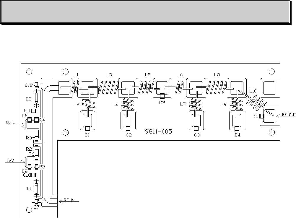
9.3 LOW PASS FILTER AND DIRECTIONAL COUPLER
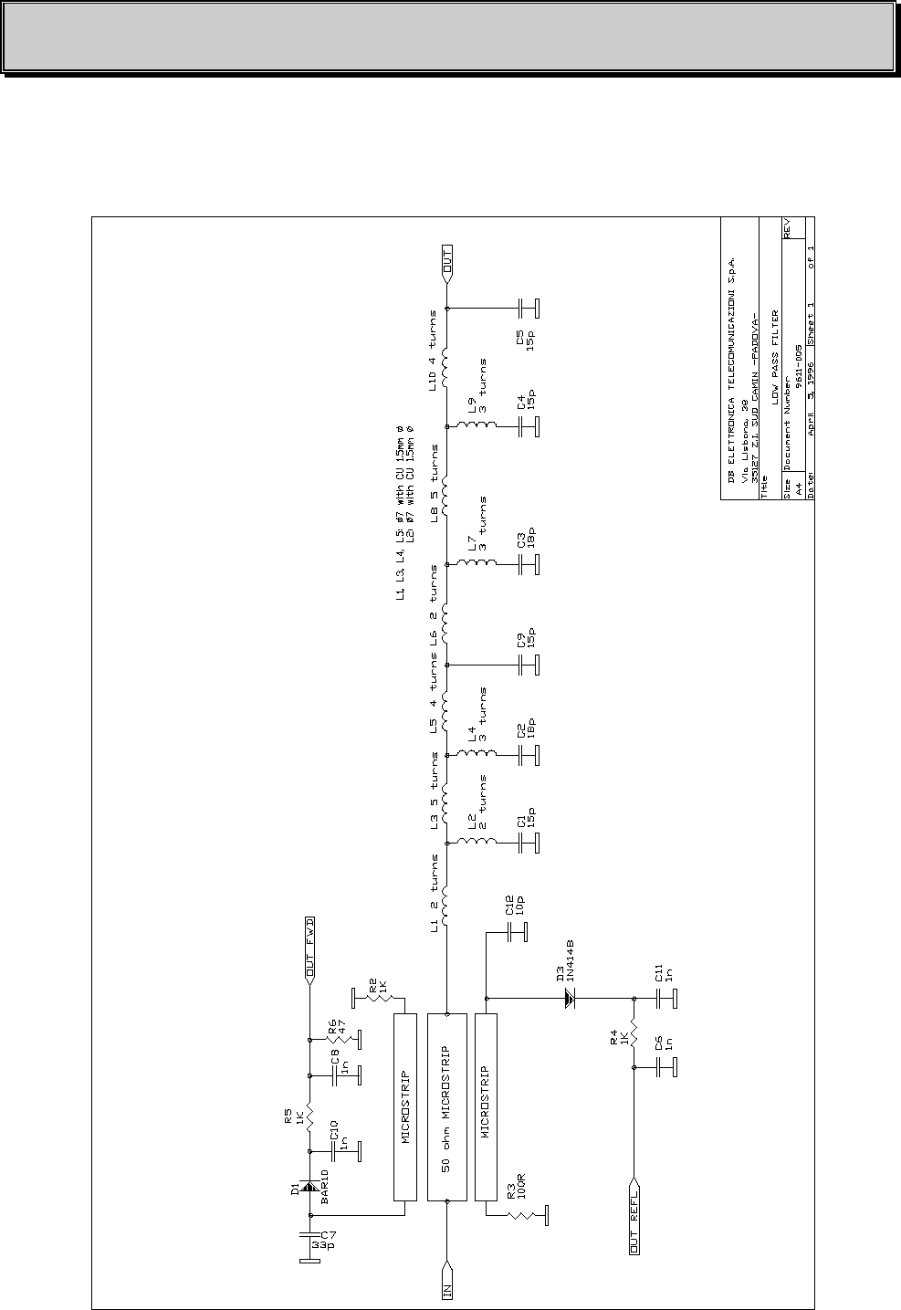
Fig. 9.3 - L. P. FILTER AND DIR. COUP. ELECTRICAL SCHEMATIC
DB ELETTRONICA TELECOMUNICAZIONI S.p.A.
PM 300 - FM Broadcasting Transmitter - USER’S MANUAL56 /108
Fig. 9.4 - L. P. FILTER AND DIR. COUP. COMPONENT LAYOUT (DB 9611-005)
9.4 L. P. FILTER AND DIR. COUP. PARTS LIST
ITEM QUANTITY REFERENCE PART
________________________________________________________
1 4 C1,C4,C5,C9 15p
2 2 C2,C3 18p
3 1 C12 10p
4 1 C7 33p
5 2 C6,C8,C10,C11 1n
6 1 D3 1N4148
7 1 D1 BAR10
8 3 L1,L2,L6 2 TURNS WITH COPPER WIRE 1.5mm
9 2 L3,L8 5 TURNS WITH COPPER WIRE 1.5mm
10 3 L4,L7,L9 3 TURNS WITH COPPER WIRE 1.5mm
11 2 L5,L10 4 TURNS WITH COPPER WIRE 1.5mm
12 2 R2,R3 100R
13 2 R4,R5 1K
14 1 R6 1K

DB ELETTRONICA TELECOMUNICAZIONI S.p.A.
PM 300 - FM Broadcasting Transmitter - USER’S MANUAL 57 /108
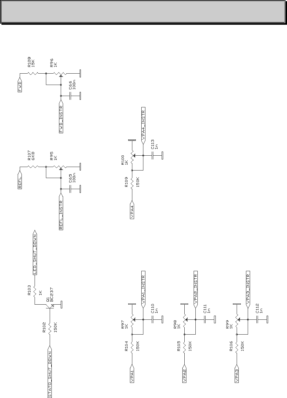
10. PROTECTION STAGE
DB 9702-004 and DB 9703-011 boards are connected together and located just behind the front
panel. They realize the intelligent protection, control and monitoring of PM 300 transmitter.
On the J1 input/output connector (see Fig. 10.6) of the DB 9702-004 there are:
1) “FWD” and “REFL” signals coming from the directional coupler.
These are DC voltages that correspond to output forward and reflected power levels.
2) The “V+” signal. It is a 45 VDC voltage that power supply the protection board.
3) The “Measure INSTR” signal represents the selected measure that is visualized on the front
panel meter.
4) “VPA” signals are the DC power supply voltages (@ 45V in normal operation) of the 300W
power module.
5) “IPA” signals are the DC power supply current (@ 9A in normal operation) of the 300W power
module.
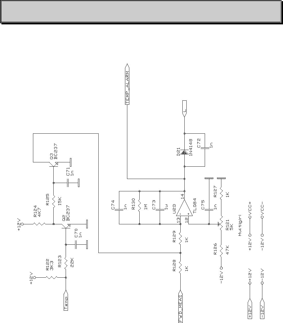
6) The “TEMP” signal is connected to a temperature sensor (bimetallic lamina type) mounted on
the heat sink. This sensor works like a contact normally closed to ground, that opens when the heat
sink temperature becomes higher than 70°C.It closes again when the temperature decreases below
45°C.
7) “GATE” signal is a control voltages connected to the MOSFET gate on the 300W-power
amplifier. The gate voltage control allows to realize protection and AGC controls.

DB ELETTRONICA TELECOMUNICAZIONI S.p.A.
PM 300 - FM Broadcasting Transmitter - USER’S MANUAL58 /108
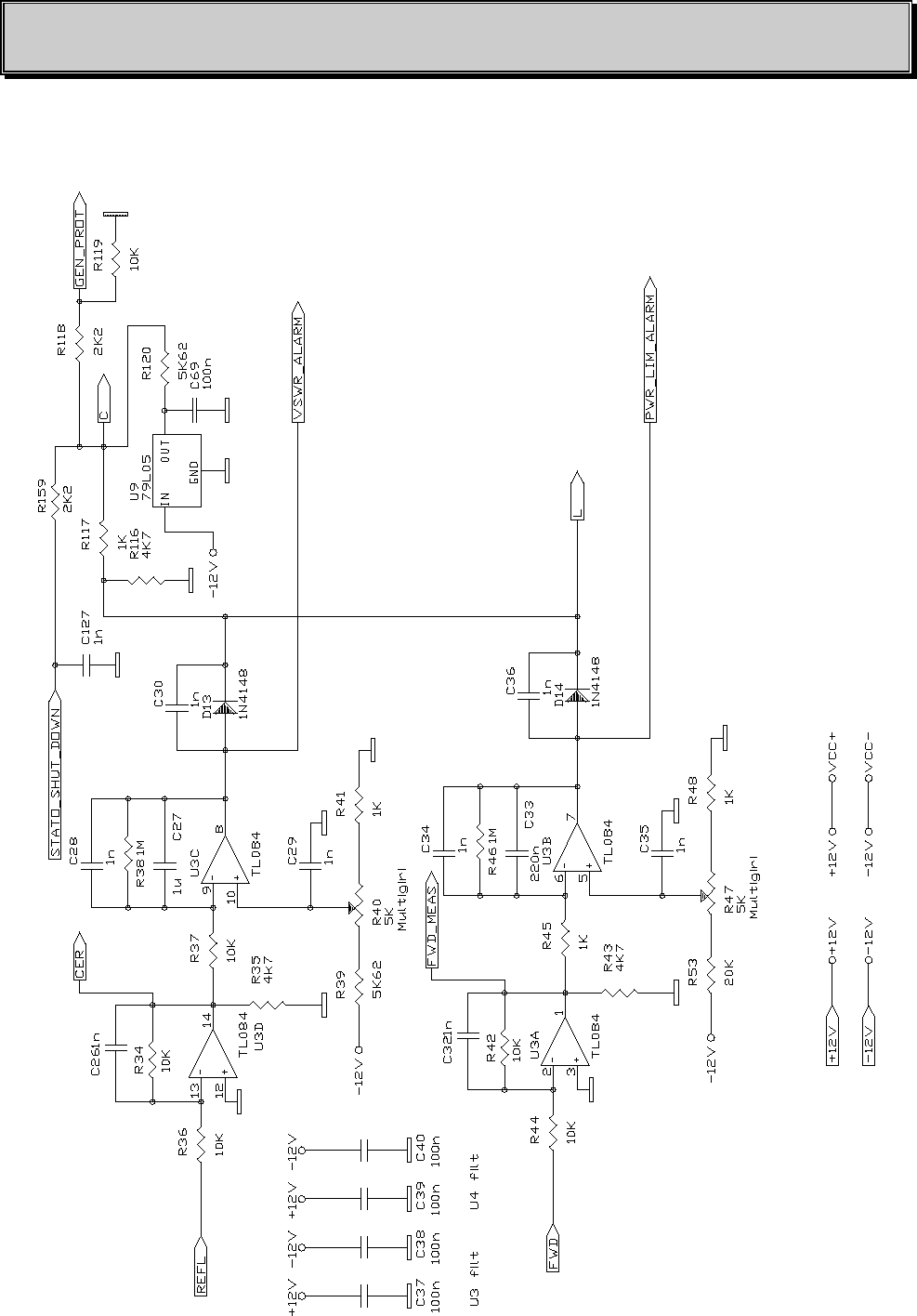
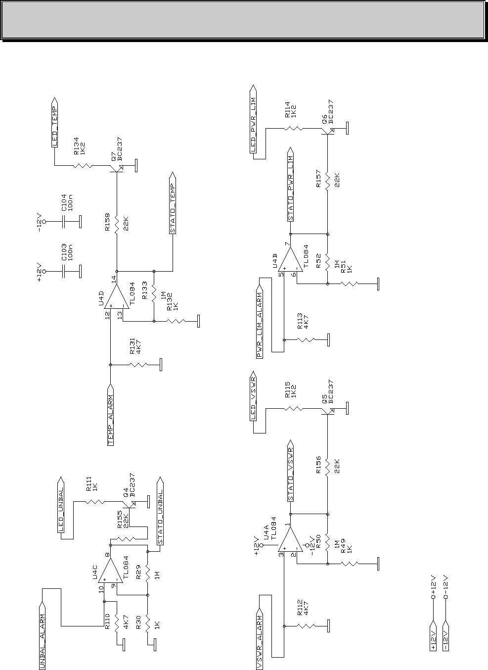
The equipment has three protections:
1) VSWR protection: When the output reflected power becomes greater than a preset value
(normally 30W), the output power reduces to maintain the reflected power below the preset value.
For changing the preset value, adjust the R40 trimmer (Fig. 10.6).
When the protection is active the front panel “VSWR” led lights on.
2) PWR LIMIT protection: When the output forward power becomes greater than a preset value
(normally 300W), e.g. because of a high driving power, the amplifier gain reduces to maintain a
stable output power level (+/-2%). For changing the preset value, adjust the R47 trimmer (Fig. 10.6).
When the protection is active the front panel “PWR LIM” led lights on.
3) Temperature protection: When the heat sink temperature becomes higher than 70°C the output
power decreases to a preset value (normally 40W). For changing the preset output value for
temperature protection, adjust the R121 trimmer (Fig. 10.6). When the protection is active the front
panel “OVERHEAT” led lights on.
WARNING: Any modification or variation must be made only with DB Elettronica
authorization, otherwise voiding the warranty.
DB ELETTRONICA TELECOMUNICAZIONI S.p.A.
PM 300 - FM Broadcasting Transmitter - USER’S MANUAL 59 /108
Fig. 10.1 - PROTECTION /CONTROL STAGE N°1 GENERAL SCHEMATIC

DB ELETTRONICA TELECOMUNICAZIONI S.p.A.
PM 300 - FM Broadcasting Transmitter - USER’S MANUAL60 /108
Fig. 10.2 - UNBALANCING PROTECTION STAGE
DB ELETTRONICA TELECOMUNICAZIONI S.p.A.
PM 300 - FM Broadcasting Transmitter - USER’S MANUAL 61 /108
Fig. 10.3 - FWD PROTECTION STAGE
DB ELETTRONICA TELECOMUNICAZIONI S.p.A.
PM 300 - FM Broadcasting Transmitter - USER’S MANUAL62 /108
Fig. 10.4 - TEMPERATURE PROTECTION STAGE

DB ELETTRONICA TELECOMUNICAZIONI S.p.A.
PM 300 - FM Broadcasting Transmitter - USER’S MANUAL 63 /108
Fig. 10.5 - POWER LIMITING STAGE

DB ELETTRONICA TELECOMUNICAZIONI S.p.A.
PM 300 - FM Broadcasting Transmitter - USER’S MANUAL64 /108
DB ELETTRONICA TELECOMUNICAZIONI S.p.A.
PM 300 - FM Broadcasting Transmitter - USER’S MANUAL 65 /108
DB ELETTRONICA TELECOMUNICAZIONI S.p.A.
PM 300 - FM Broadcasting Transmitter - USER’S MANUAL66 /108
Fig. 10.6 - PROTECTION /CONTROL STAGE N°1 COMPONENT LAYOUT (DB 9702_004)

DB ELETTRONICA TELECOMUNICAZIONI S.p.A.
PM 300 - FM Broadcasting Transmitter - USER’S MANUAL 67 /108
10.1 PROTECTION /CONTROL STAGE N°1 PARTS LIST
ITEM QUANTITY REFERENCE PART
_______________________________________________________________________
1 67 C1,C2,C3,C4,C5,C6,C7,C8, 1n CER
C9,C10,C11,C12,C13,C14,
C15,C16,C17,C18,C25,C26,
C28,C29,C30,C31,C32,C34,
C35,C36,C70,C71,C72,C74,
C75,C76,C80,C84,C88,C102,
C105,C106,C107,C108,C109,
C114,C115,C116,C117,C118,
C119,C120,C121,C123,C124,
C125,C126,C127,C128,C129,
C130,C131,C132,C133,C134,
C135,C136,C137,C138
2 10 C19,C20,C21,C22,C37,C38, 100n POLY
C39,C40,C68,C69
3 3 C27,C33,C73 1u POLY
4 1 C122 1n POLY
5 14 D5,D6,D7,D8,D9,D10,D11, 1N4148
D13,D14,D21,D23,D24,D25,
D26
6 2 FIS1,FIS2 FIS
7 1 JP1 JUMPERx2 JUMPERx2
8 2 JP2,JP3 JUMPERx3 JUMPERx3
9 1 J1 CON24 CON AMP 24
10 1 J2 CON20 CON FLAT 20
11 7 J3,J4,J5,J6,J7,J8,J9 PINSTRIP Fx2 PINSTRIP Fx2
12 2 Q2,Q3 BC237
13 4 R5,R6,R7,R22 33K RES 1/8W
14 20 R8,R9,R10,R11,R12,R13, 10K RES 1/8W
R14,R15,R16,R17,R18,R19,
R21,R24,R26,R119,R151,
R152,R153,R154
15 7 R20,R27,R28,R35,R43,R116, 4K7 RES 1/8W
R124
16 4 R23,R40,R47,R121 5K TRIM MULTIG.
17 2 R25,R127 1K RES 1/8W
18 4 R34,R36,R42,R44 10K RES 1/4W 1%
19 2 R87,R37 3K3 RES 1/4W
20 3 R38,R46,R130 1M RES 1/8W
21 1 R39 5K62 RES 1/4W 1%
22 3 R41,R48,R117 1K RES 1/4W 1%
23 3 R45,R128,R129 1K RES 1/4W
24 1 R53 20K RES 1/4W 1%
25 2 R118,R159 2K2 RES 1/4W
26 1 R120 8K66 RES 1/4W 1%
27 1 R122 3K3 RES 1/8W
28 1 R123 22K RES 1/8W
29 1 R125 15K RES 1/8W
30 1 R126 47K RES 1/8W
31 3 U1,U2,U3 TL084
32 1 U9 79L05
33 1 U10 TL082
DB ELETTRONICA TELECOMUNICAZIONI S.p.A.
PM 300 - FM Broadcasting Transmitter - USER’S MANUAL68 /108
Fig. 10.7 - PROTECTION /CONTROL STAGE N°2 GENERAL SCHEMATIC
DB ELETTRONICA TELECOMUNICAZIONI S.p.A.
PM 300 - FM Broadcasting Transmitter - USER’S MANUAL 69 /108
Fig. 10.8 - PROTECTION STATUS STAGE

DB ELETTRONICA TELECOMUNICAZIONI S.p.A.
PM 300 - FM Broadcasting Transmitter - USER’S MANUAL70 /108
Fig. 10.9 - POWER SUPPLY STAGE
DB ELETTRONICA TELECOMUNICAZIONI S.p.A.
PM 300 - FM Broadcasting Transmitter - USER’S MANUAL 71 /108
Fig. 10.10 - MEASURES ADJ. STAGE
DB ELETTRONICA TELECOMUNICAZIONI S.p.A.
PM 300 - FM Broadcasting Transmitter - USER’S MANUAL72 /108
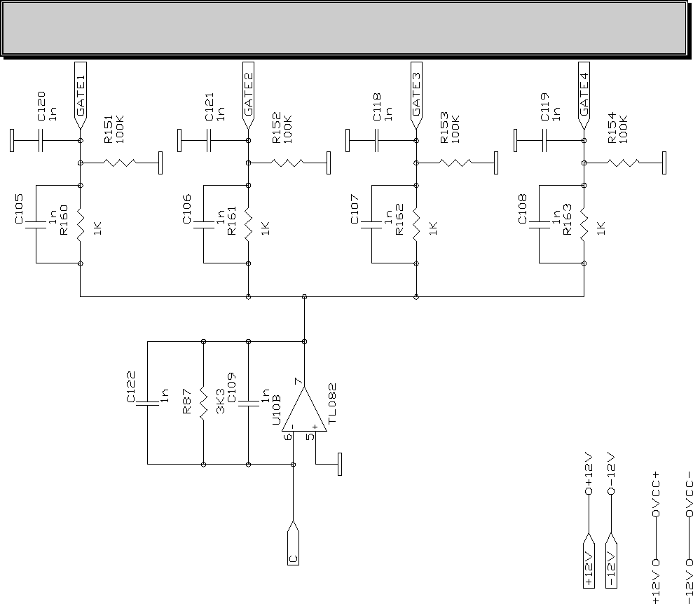
Fig. 10.11 - LED INDICATIONS STAGE
DB ELETTRONICA TELECOMUNICAZIONI S.p.A.
PM 300 - FM Broadcasting Transmitter - USER’S MANUAL 73 /108
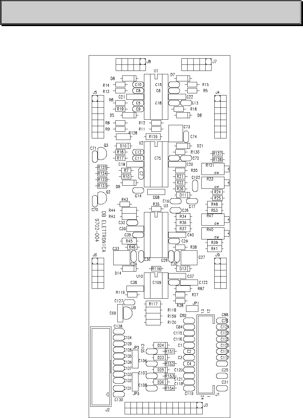
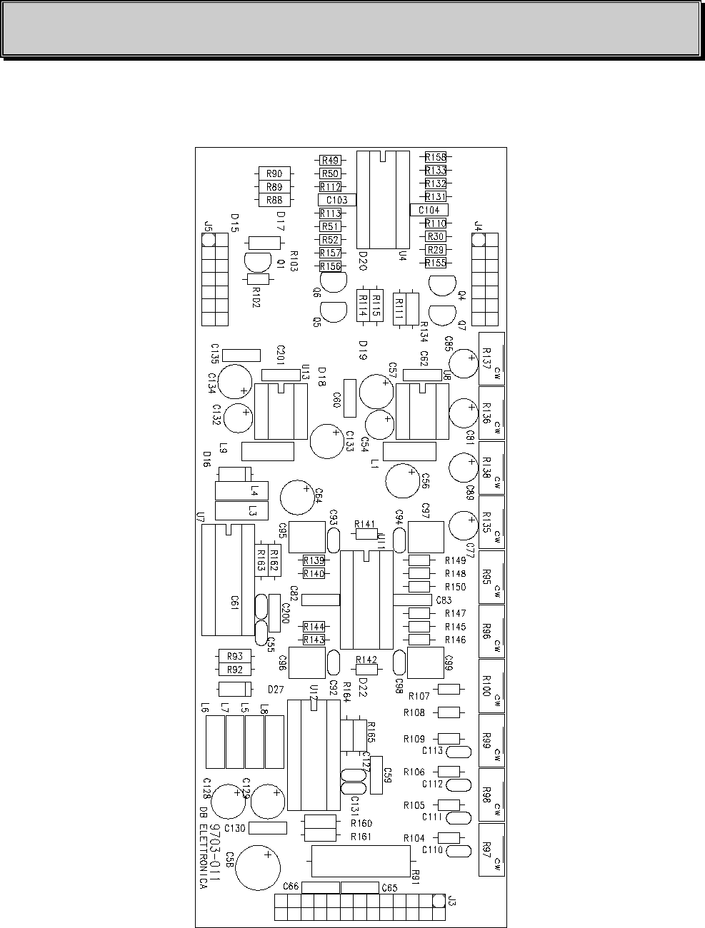
Fig. 10.12 - PROTECTION /CONTROL STAGE N°2 COMPONENT LAYOUT (DB 9703_011)

DB ELETTRONICA TELECOMUNICAZIONI S.p.A.
PM 300 - FM Broadcasting Transmitter - USER’S MANUAL74 /108
10.2 PROTECTION /CONTROL STAGE N°2 PARTS LIST
ITEM QUANTITY REFERENCE PART
______________________________________________________________________
1 2 C54,C132 10u Elett.50V
2 10 C55,C92,C93,C94,C98,C110, 1n CER
C111,C112,C113,C131
3 7 C56,C57,C64,C128,C129, 100u Elett.25V
C133,C134
4 1 C58 22u Elett.63V
5 5 C59,C60,C62,C130,C135 10n POLY
6 2 C61,C127 100p CER
7 6 C65,C66,C82,C83,C103, 100n POLY
C104
8 4 C77,C81,C85,C89 10u Elett.25V
9 4 C95,C96,C97,C99 1u POLY
10 6 D15,D17,D18,D19,D20,D22 LED LED3MM
11 2 D16,D27 1N5819 Diodo
12 4 FIS1,FIS2,FIS3,FIS4 FIS
13 3 J3,J4,J5 PINSTRIP Mx2 PINSTRIP Mx2
14 2 L1,L9 100u INDUTT
15 6 L3,L4,L5,L6,L7,L8 150u INDUTT
16 5 Q1,Q4,Q5,Q6,Q7 BC237
17 4 R29,R50,R52,R133 1M RES 1/8W
18 8 R30,R49,R51,R132,R140, 1K RES 1/8W
R144,R145,R150
19 3 R88,R89,R90 1K5 RES 1/4W
20 1 R91 100R RES 4W
21 1 R92 1K54 RES 1/4W 1%
22 1 R93 16K9 RES 1/4W 1%
23 10 R95,R96,R97,R98,R99,R100, 1K TRIM RO
R135,R136,R137,R138
24 9 R102,R141,R142,R147,R148, 22K RES 1/8W
R155,R156,R157,R158
25 2 R103,R111 1K RES 1/4W
26 4 R104,R105,R106,R109 150K RES 1/8W
27 2 R107,R108 15K RES 1/8W
28 4 R110,R112,R113,R131 4K7 RES 1/8W
29 3 R114,R115,R134 1K2 RES 1/4W
30 4 R139,R143,R146,R149 47K RES 1/8W
31 1 R160 1K RES 1/4W 1%
32 1 R161 8K66 RES 1/4W 1%
33 4 R162,R163,R164,R165 1R RES 1/4W
34 2 U11,U4 TL084
35 2 U7,U12 UA78S40
36 2 U8,U13 LT1054

DB ELETTRONICA TELECOMUNICAZIONI S.p.A.
PM 300 - FM Broadcasting Transmitter - USER’S MANUAL 75 /108
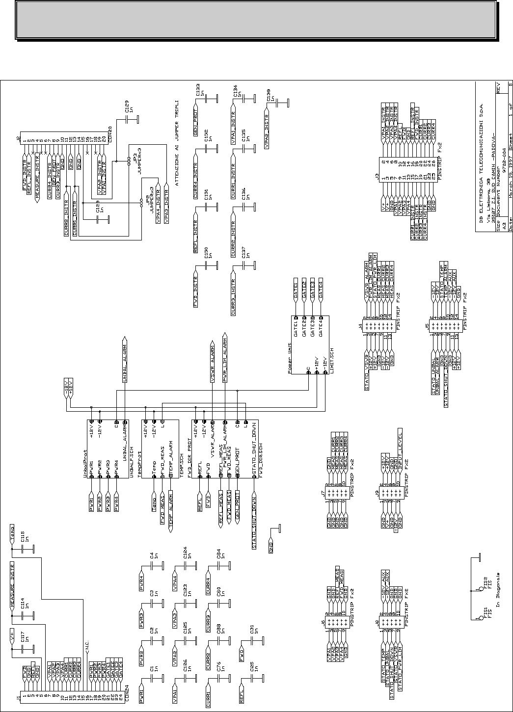
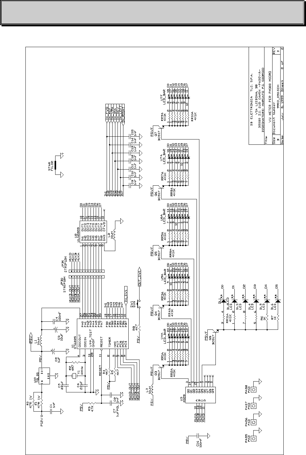
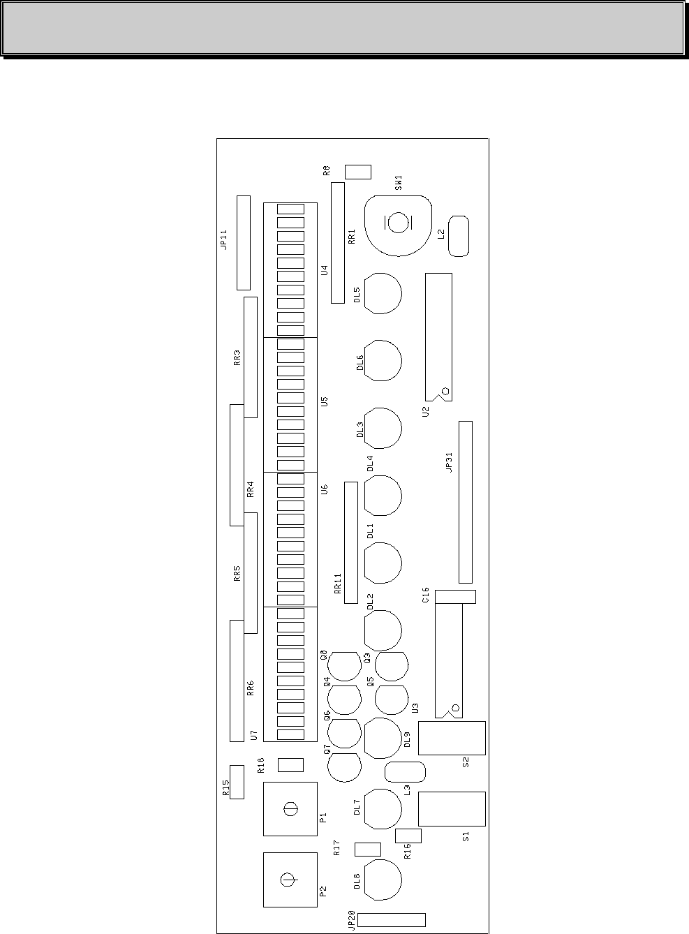
11. METER STAGE
11.1 GENERAL DESCRIPTION
The meter stage is built using two boards:
The ST62T25 microprocessor board DB 9903_040
The display board DB 9903_050 is composed of forty LED bargraph display.
DB ELETTRONICA TELECOMUNICAZIONI S.p.A.
PM 300 - FM Broadcasting Transmitter - USER’S MANUAL76 /108
Fig. 11.1 - MICROPROCESSOR STAGE ELECTRICAL SCHEMATIC (DB 9903_040)
DB ELETTRONICA TELECOMUNICAZIONI S.p.A.
PM 300 - FM Broadcasting Transmitter - USER’S MANUAL 77 /108
Fig. 11.2 - MICROPROCESSOR BOARD COMPONENT LAYOUT (DB 9903_040)

DB ELETTRONICA TELECOMUNICAZIONI S.p.A.
PM 300 - FM Broadcasting Transmitter - USER’S MANUAL78 /108
11.2 MICROPROCESSOR BOARD PARTLIST
ITEM QUANTITY REFERENCE PART
__________________________________________________________________________
1 5 C17,C18,C19,C20,C25 100Nf mul.
2 3 C21,C23,C24 1nF cer.
3 1 C22 1uF 50V ele.
4 3 DL7,DL8,DL9 LED 3mm.
5 3 D1,D2,D3 1N4148
6 2 JP1,JP2 STRIP2M
7 2 JP10,JP11 STRIP7M
8 2 JP21,JP20 STRIP5M
9 3 J1,J2,J3 CNM20V
10 1 J4 CNM14V
11 1 J6 AMP4
12 1 J7 CNM10V
13 7 R9,R10,R12,R13,R16,R17,R18 1K
14 1 P1 1K
15 6 R11,R14,R19,R20,R21,R22 10K
16 4 P2,P3,P4,P5 10K
17 2 Q2,Q1 BC547
18 1 R15 680R
19 2 S1,S2 C&K
20 1 U8 TL082
21 1 U9 74HC32

DB ELETTRONICA TELECOMUNICAZIONI S.p.A.
PM 300 - FM Broadcasting Transmitter - USER’S MANUAL 79 /108
Fig. 11.3 - DISPLAY STAGE ELECTRICAL SCHEMATIC (DB 9903_050)
DB ELETTRONICA TELECOMUNICAZIONI S.p.A.
PM 300 - FM Broadcasting Transmitter - USER’S MANUAL80 /108
Fig. 11.4 - DISPLAY BOARD COMPONENT LAYOUT (DB 9903_050)

DB ELETTRONICA TELECOMUNICAZIONI S.p.A.
PM 300 - FM Broadcasting Transmitter - USER’S MANUAL 81 /108
11.3 DISPLAY BOARD PARTS LIST
ITEM QUANTITY REFERENCE PART
1 9 C1,C8,C9,C10,C11,C12,C13 1nF cer.
C14,C15
2 1 C2 1uF 50V ele.
3 1 C3 10uF 50v ele.
4 2 C4,C16 100nF mul.
5 2 C5,C6 22pF cer.
6 1 C7 1u pol.
7 6 DL1,DL2,DL3,DL4,DL5,DL6 LED 3mm.
8 2 JP30,JP31 STRIP12M
9 3 L1,L2,L3 10uH
10 6 Q3,Q4,Q5,Q6,Q7,Q8 BC517
11 11 RR1,RR2,RR3,RR4,RR5,RR6, 4X1K rete res.
RR7,RR8,RR9,RR10,RR11
12 2 R0,R1 47R 1W
13 1 R2 4M7
14 1 R3 47K
15 3 R4,R5,R8 4K7
16 2 R6,R7 1K
17 1 SW1 PULSMOZ
18 1 U1 ST6225
19 1 U2 ULN2803
20 1 U3 4028
21 4 U4,U5,U6,U7 LED_BAR
22 1 U10 78L05
23 1 Y1 4MHz QUARZO

DB ELETTRONICA TELECOMUNICAZIONI S.p.A.
PM 300 - FM Broadcasting Transmitter - USER’S MANUAL82 /108
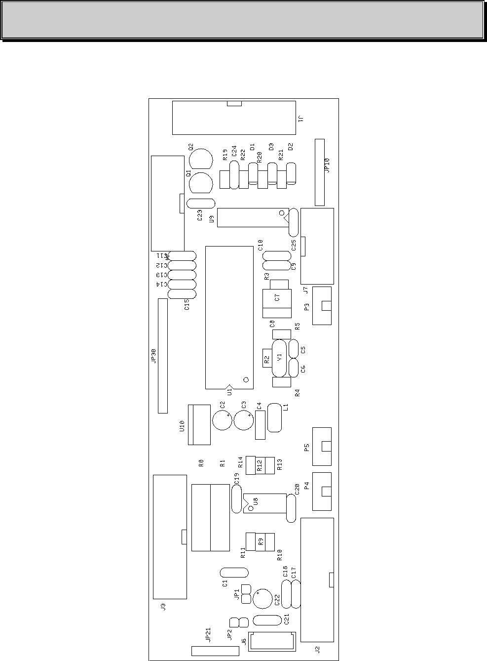
12. IN-AUDIO BOARD
Fig. 12.1 - IN-AUDIO BOARD ELECTRICAL SCHEMATIC
DB ELETTRONICA TELECOMUNICAZIONI S.p.A.
PM 300 - FM Broadcasting Transmitter - USER’S MANUAL 83 /108
Fig. 12.2 - IN-AUDIO BOARD COMPONENT LAYOUT (DB 9909_010)

DB ELETTRONICA TELECOMUNICAZIONI S.p.A.
PM 300 - FM Broadcasting Transmitter - USER’S MANUAL84 /108
12.1 IN-AUDIO BOARD PARTS LIST
ITEM QUANTITY REFERENCE PART
________________________________________________________
1 4 C1,C3,C5,C7 100pF CER.
2 3 C2,C4,C6 4n7F POL.
3 5 JP1,JP2,JP3,JP4,JP5 STRIP3M
4 1 J1 CNM20V
5 2 J2,J3 CNM14V
6 3 J4,J10,J20 CNM10V
7 8 J5,J6,J7,J8,J11,J12,J13,J14 BNC90CS
8 4 L1,L2,L3,L4 10uH
9 2 PR,PL XLRF90CS
10 2 RL,RR 5K 10GROP
11 1 R1 470R 1/4W
12 1 TMPX 10K 10GROP
13 3 TSC1,TSC2,TSC3 1K 10GROP
DB ELETTRONICA TELECOMUNICAZIONI S.p.A.
PM 300 - FM Broadcasting Transmitter - USER’S MANUAL 85 /108
12.2 IN-AUDIO BOARD JUMPERS SETTING

DB ELETTRONICA TELECOMUNICAZIONI S.p.A.
PM 300 - FM Broadcasting Transmitter - USER’S MANUAL86 /108
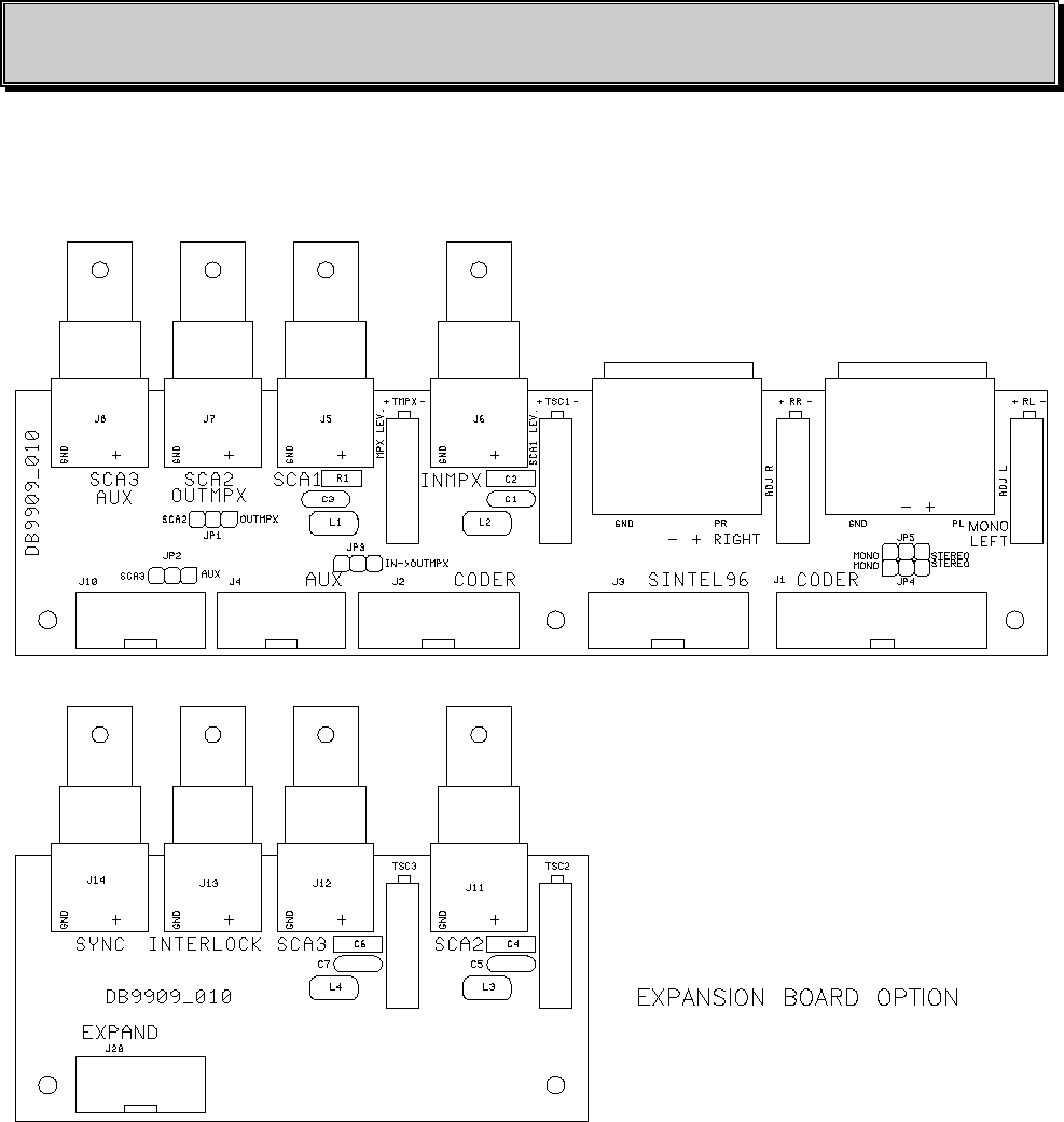
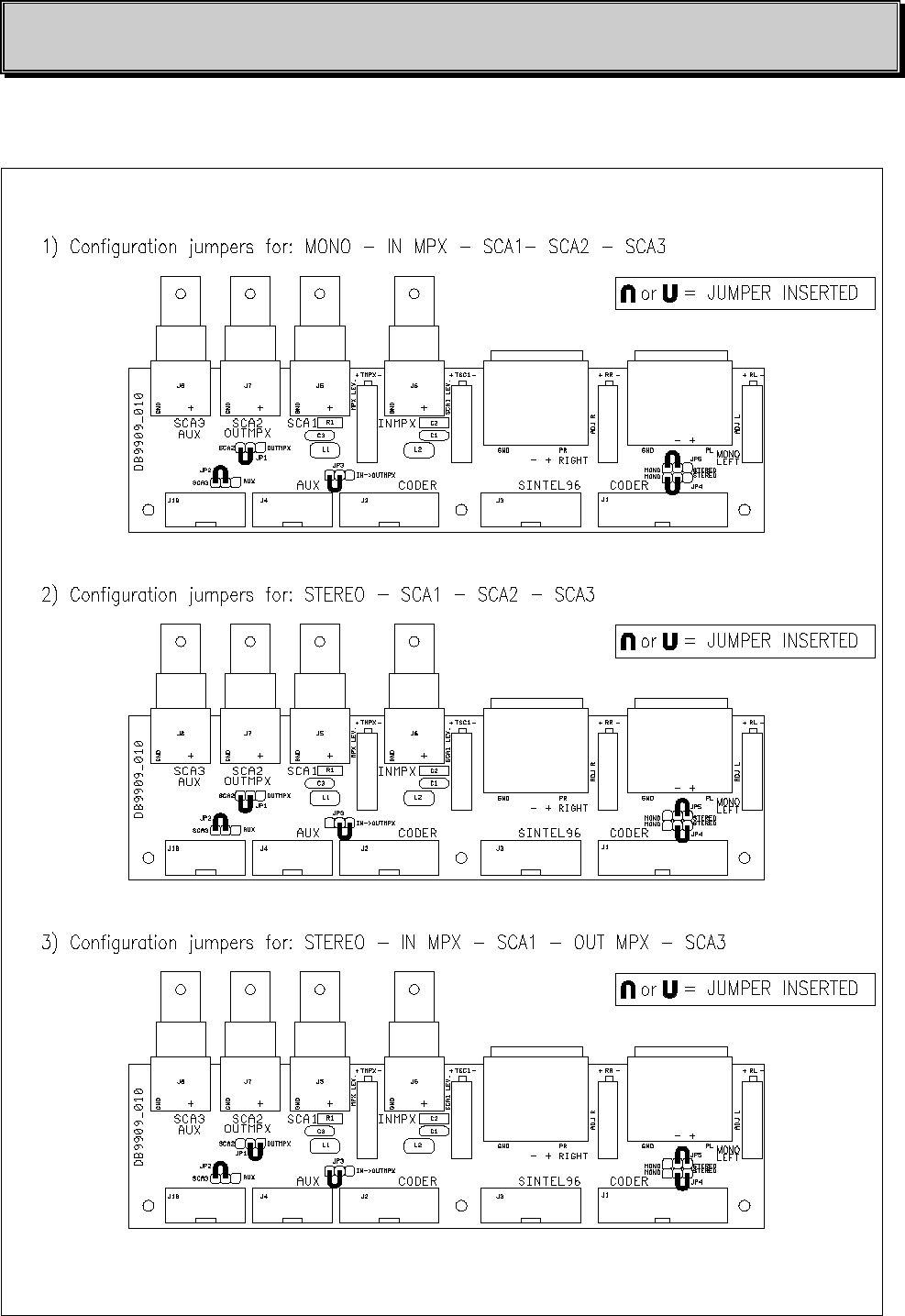
13. STEREO ENCODER BOARD (Option)
13.1 CHANNELS PRE- EMPHASIS SETTING
RIGHT CHANNEL PRE-EMPHASIS
(see Fig. 13.3 and Fig. 13.10)
To change the pre-emphasis, you need to set (or change position of) the JP3, JP4 jumpers on the
STEREO encoder board.
To disable preemph you have to remove both jumpers; to get a 50 us preemph, you have to insert
only JP3; if you want a 75 us preemph both JP3 and JP4 must be inserted.
LEFT CHANNEL PRE-EMPHASIS
(see Fig. 13.3 and Fig. 13.10)
To change the pre-emphasis, you need to set (or change position of) the JP5, JP6 jumpers on the
STEREO encoder board.
To disable preemph you have to remove both jumpers; to get a 50 us preemph, you have to insert
only JP6; if you want a 75 us preemph both JP5 and JP6 must be inserted.
DB ELETTRONICA TELECOMUNICAZIONI S.p.A.
PM 300 - FM Broadcasting Transmitter - USER’S MANUAL 87 /108
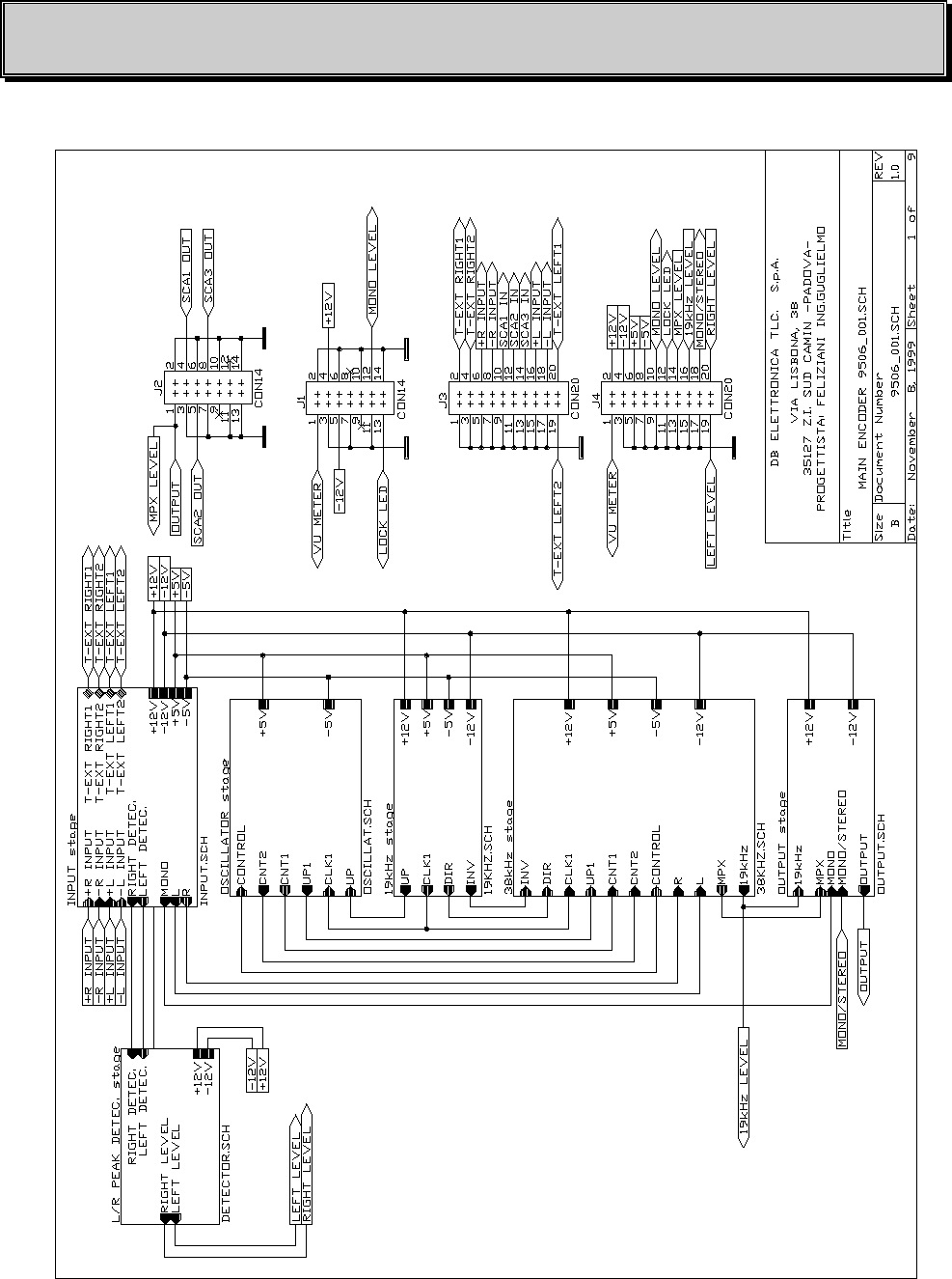
Fig. 13.1 - STEREO ENCODER GENERAL SCHEMATIC
DB ELETTRONICA TELECOMUNICAZIONI S.p.A.
PM 300 - FM Broadcasting Transmitter - USER’S MANUAL88 /108
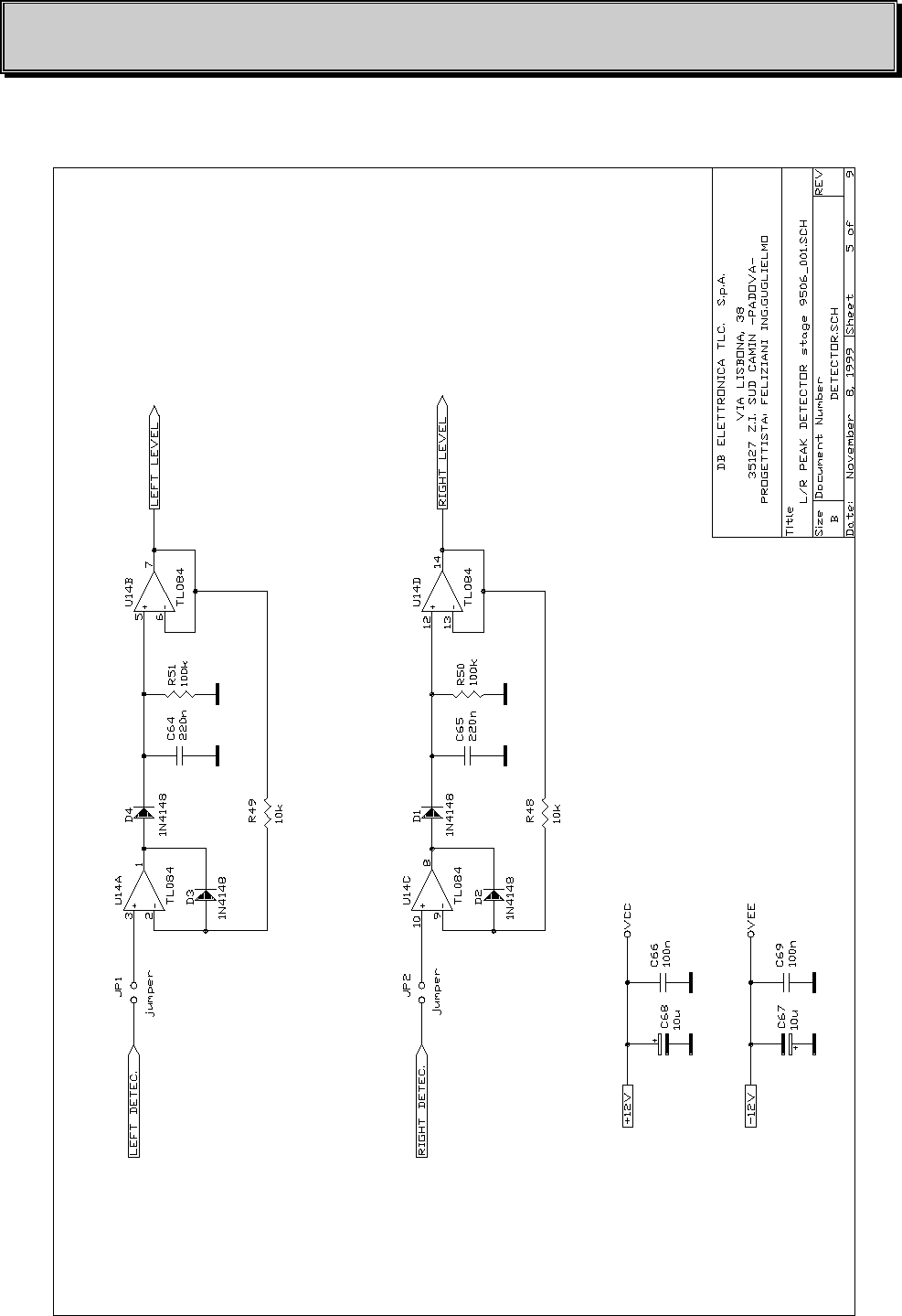
Fig. 13.2 - L/R PEAK DETECTOR STAGE ELECTRICAL SCHEMATIC

DB ELETTRONICA TELECOMUNICAZIONI S.p.A.
PM 300 - FM Broadcasting Transmitter - USER’S MANUAL 89 /108
DB ELETTRONICA TELECOMUNICAZIONI S.p.A.
PM 300 - FM Broadcasting Transmitter - USER’S MANUAL90 /108
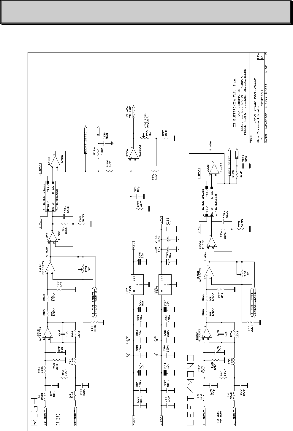
Fig. 13.3 - INPUT STAGE ELECTRICAL SCHEMATIC
DB ELETTRONICA TELECOMUNICAZIONI S.p.A.
PM 300 - FM Broadcasting Transmitter - USER’S MANUAL 91 /108
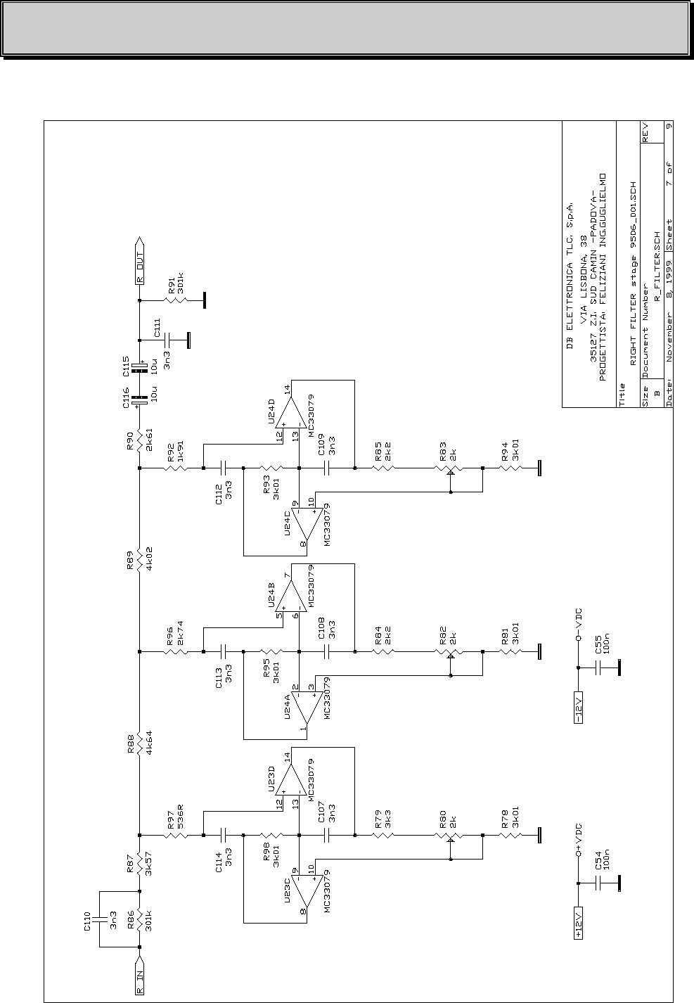
Fig. 13.4 - RIGHT FILTER STAGE ELECTRICAL SCHEMATIC

DB ELETTRONICA TELECOMUNICAZIONI S.p.A.
PM 300 - FM Broadcasting Transmitter - USER’S MANUAL92 /108
Fig. 13.5 - LEFT FILTER STAGE ELECTRICAL SCHEMATIC
DB ELETTRONICA TELECOMUNICAZIONI S.p.A.
PM 300 - FM Broadcasting Transmitter - USER’S MANUAL 93 /108
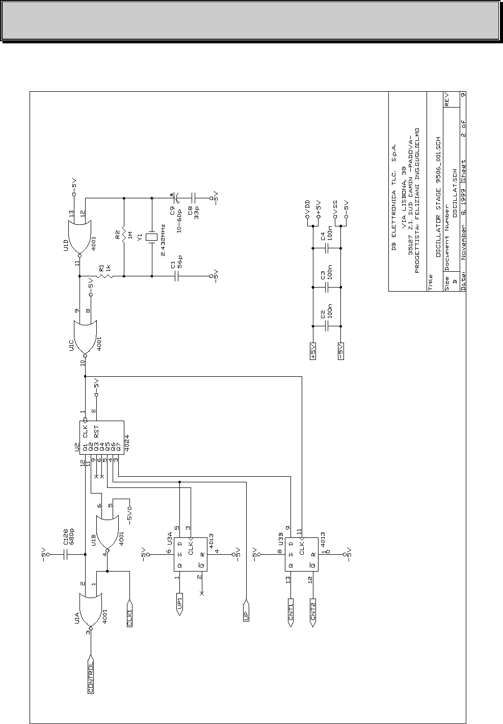
Fig. 13.6 - OSCILLATOR STAGE ELECTRICAL SCHEMATIC
DB ELETTRONICA TELECOMUNICAZIONI S.p.A.
PM 300 - FM Broadcasting Transmitter - USER’S MANUAL94 /108
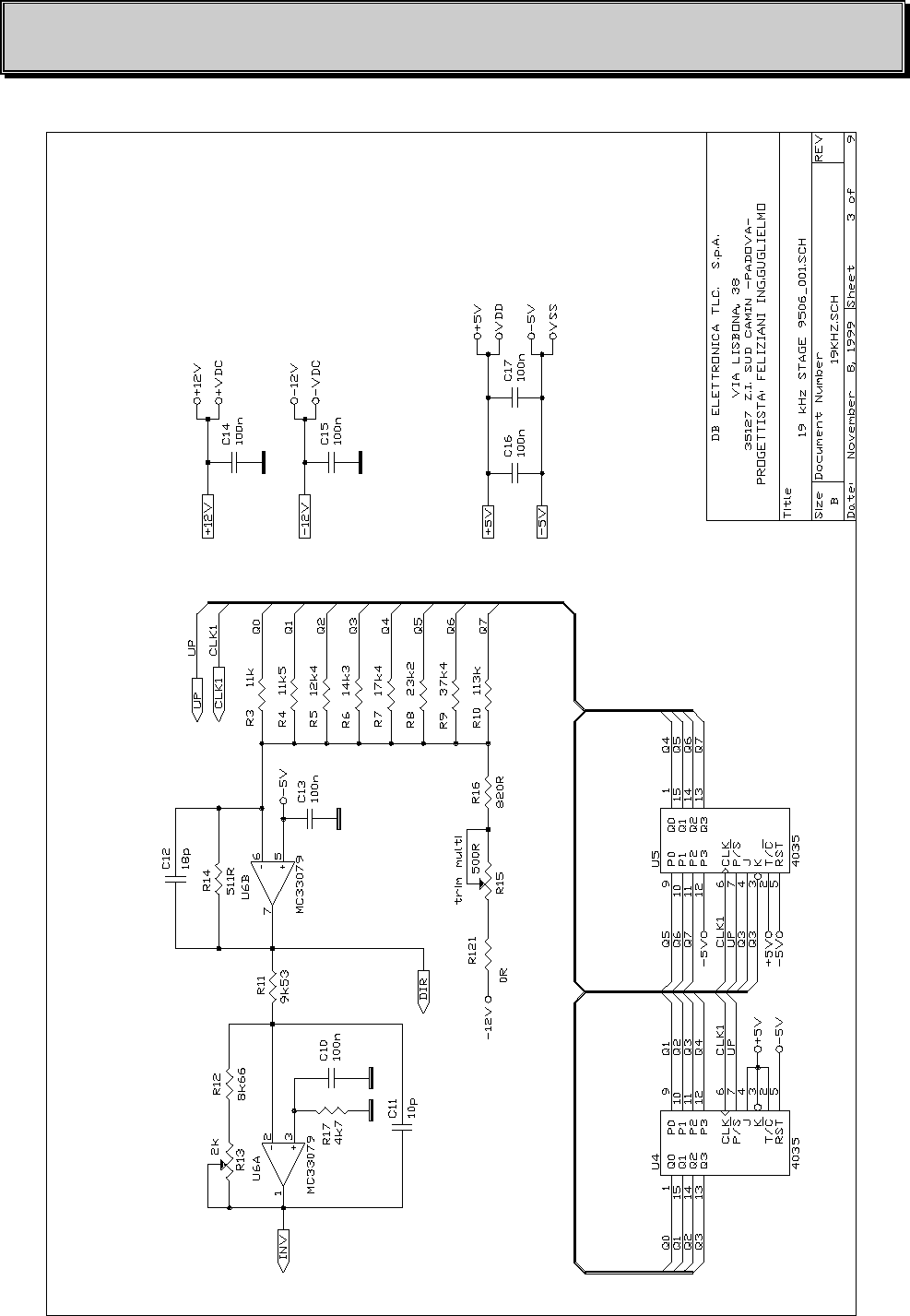
Fig. 13.7 - 19 kHz STAGE ELECTRICAL SCHEMATIC

DB ELETTRONICA TELECOMUNICAZIONI S.p.A.
PM 300 - FM Broadcasting Transmitter - USER’S MANUAL 95 /108
Fig. 13.8 - 38 kHz STAGE ELECTRICAL SCHEMATIC
DB ELETTRONICA TELECOMUNICAZIONI S.p.A.
PM 300 - FM Broadcasting Transmitter - USER’S MANUAL96 /108
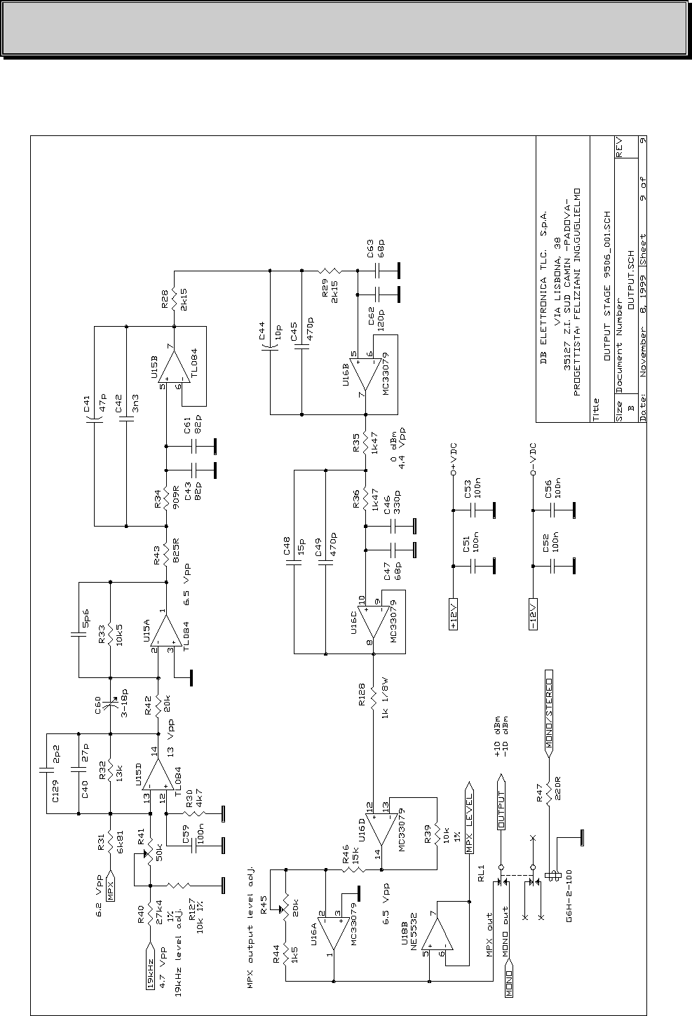
Fig. 13.9 - OUTPUT STAGE ELECTRICAL SCHEMATIC
DB ELETTRONICA TELECOMUNICAZIONI S.p.A.
PM 300 - FM Broadcasting Transmitter - USER’S MANUAL 97 /108
Fig. 13.10 - STEREO ENCODER COMPONENT LAYOUT (DB 9506-001)

DB ELETTRONICA TELECOMUNICAZIONI S.p.A.
PM 300 - FM Broadcasting Transmitter - USER’S MANUAL98 /108
13.2 STEREO ENCODER PARTS LIST
ITEM QUANTITY REFERENCE PART
_______________________________________________________________
1 3 C64,C65,C135 220n poly
2 1 C1 56p cer np0
3 38 C2,C3,C4,C10,C13,C14,C15, 100n poly
C16,C17,C22,C23,C24,C25,
C26,C27,C28,C29,C36,C37,
C51,C52,C53,C54,C55,C56,
C57,C58,C59,C66,C69,C81,
C82,C83,C84,C85,C86,C89,
C90
4 1 C8 33p cer np0
5 1 C9 10-60p orange
6 2 C11,C44 10p cer np0
7 1 C12 18p cer np0
8 2 C20,C21 330p cer
9 1 C38 3p3 cer np0
10 1 C39 5p6 cer np0
11 1 C40 27p cer np0
12 1 C41 47p cer np0
13 17 C42,C107,C108,C109,C110, 3n3 polistirene
C111,C112,C113,C114,C117,
C118,C119,C120,C121,C122,
C123,C126
14 2 C43,C61 82p cer np0
15 2 C45,C49 470p polistirene
16 1 C46 330p polistirene
17 2 C47,C63 68p cer np0
18 1 C48 15p cer np0
19 2 C62,C50 120p cer np0
20 1 C60 3-18p red
21 12 C67,C68,C79,C80,C91,C92, 10u tant 25V
C95,C96,C115,C116,C124,
C125
22 4 C70,C71,C77,C78 100p
23 4 C72,C73,C75,C76 10p cer
24 3 C74,C102,C106 100p cer
25 4 C87,C88,C97,C98 330n poly
26 6 C99,C100,C101,C103,C104, 4n7 polistirene
C105
27 1 C127 100p cer np0
28 1 C128 680p cer np0
29 1 C129 10p
30 2 C130,C134 3n3
31 2 C132,C131 47u TANTALIO
32 1 C133 1n poly
33 4 D1,D2,D3,D4 1N4148
34 2 JP2,JP1 jumper

DB ELETTRONICA TELECOMUNICAZIONI S.p.A.
PM 300 - FM Broadcasting Transmitter - USER’S MANUAL 99 /108
ITEM QUANTITY REFERENCE PART
_________________________________________________________________
35 2 JP6,JP3 jumper ON/OFF
36 2 JP5,JP4 jumper 50/75us
37 2 J2,J1 CON14
38 2 J3,J4 CON20
39 1 L5 10uH ind. assiale
40 4 L1,L2,L3,L4 10uH
41 1 RL1 G6H-2-100 OMRON 22Z3K3 12V
42 1 R1 1k 1/8W
43 1 R2 1M 1/8W
44 1 R3 11k 1/4W 1%
45 1 R4 11k5 1/4W 1%
46 1 R5 12k4 1/4W 1%
47 1 R6 14k3 1/4W 1%
48 1 R7 17k4 1/4W 1%
49 1 R8 23k2 1/4W 1%
50 1 R9 37k4 1/4W 1%
51 1 R10 113k 1/4W 1%
52 3 R11,R68,R75 9k53 1/4W 1%
53 1 R12 8k66 1/4W 1%
54 7 R13,R80,R82,R83,R102, 2k trim multi
R104,R106
55 1 R14 511R 1/4W 1%
56 1 R15 5OOR trim multi
57 1 R16 487R 1/4W 1%
58 4 R17,R30,R55,R76 4k7 1/8W
59 1 R18 10k 1/4W
60 2 R19,R26 324k 1/4W 1%
61 2 R20,R25 115k 1/4W 1%
62 2 R21,R24 75k 1/4W 1%
63 2 R22,R23 64k9 1/4W 1%
64 7 R27,R63,R64,R67,R69,R70, 12k1 1/4W 1%
R74
65 2 R28,R29 2k15 1/4W 1%
66 1 R31 6k81 1/4W 1%
67 1 R32 13k 1/4W 1%
68 1 R33 10k5 1/4W 1%
69 1 R34 909R 1/4W 1%
70 2 R35,R36 1k47 1/4W 1%
71 1 R37 5k trim multi
72 2 R39,R38 10k 1/4W 1%
73 5 R40,R53,R54,R58,R59 31k6 1/4W 1%
74 1 R41 50k trim multi
75 1 R42 20k 1/4W 1%
76 1 R43 825R 1/4W 1%
77 1 R44 1k5 1/4W
78 1 R45 20k trim multi
79 1 R46 15k 1/4W
80 1 R47 0R 1/4W
81 2 R48,R49 10k 1/8W
82 2 R50,R51 100k 1/8W

DB ELETTRONICA TELECOMUNICAZIONI S.p.A.
PM 300 - FM Broadcasting Transmitter - USER’S MANUAL100 /108
ITEM QUANTITY REFERENCE PART
__________________________________________________________________
83 2 R52,R60 680R 1/4W
84 1 R56 10k trim multi
85 1 R57 2k2 1/8W
86 2 R61,R62 560R 1/4W
87 4 R65,R66,R71,R77 169k 1/4W 1%
88 2 R73,R72 22k 1/8 W
89 12 R78,R81,R93,R94,R95,R98, 3k01 1/4W 1%
R100,R103,R105,R115,R116,
R118
90 2 R79,R101 3k3 1/4W
91 4 R84,R85,R107,R108 2k2 1/4W
92 4 R86,R91,R99,R113 301k 1/4W 1%
93 2 R87,R109 3k57 1/4W 1%
94 2 R88,R110 4k64 1/4W 1%
95 2 R89,R111 4k02 1/4W 1%
96 2 R90,R112 2k61 1/4W 1%
97 2 R92,R114 1k91 1/4W 1%
98 2 R96,R117 2k74 1/4W 1%
99 2 R97,R119 536R 1/4W 1%
100 1 R122 0R
101 1 R123 5k6
102 1 R124 100R 1/4 W
103 1 R125 100R 1/4W
104 1 R126 4K7
105 1 R127 10k 1/4 W 1%
106 1 U1 4001
107 1 U2 4024
108 1 U3 4013
109 4 U4,U5,U12,U13 4035
110 6 U6,U16,U23,U24,U25,U26 MC33079
111 4 U7A,U7,U18B,U27 NE5532
112 1 U8 4066
113 3 U9,U10,U11 4053
114 2 U14,U15 TL084
115 2 U19,U22 TL082
116 1 U20 7805
117 1 U21 7905
118 1 Y1 2.432MHz

DB ELETTRONICA TELECOMUNICAZIONI S.p.A.
PM 300 - FM Broadcasting Transmitter - USER’S MANUAL 101 /108
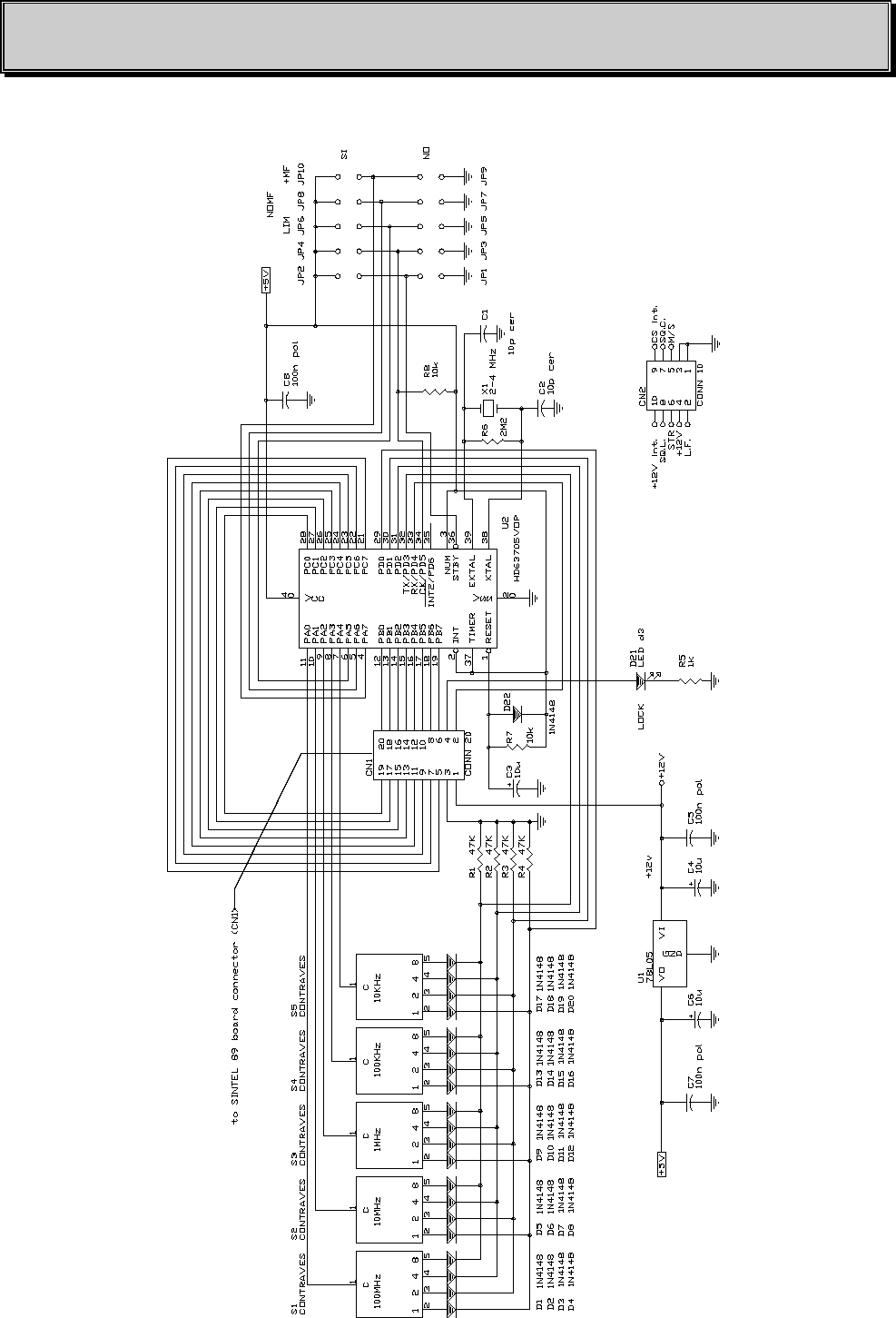
14. CONTRAVES BOARD (Option)
14.1 GENERAL DESCRIPTION
On the synthesized board the dip-switches are changed with a 20 pin connector, so that it is
possible connect with a flat type cable this circuit (that manage PLL) to a microprocessor.
The frequency change is fast, because it is only necessary put directly the frequency using the
contraves on the front panel.
DB ELETTRONICA TELECOMUNICAZIONI S.p.A.
PM 300 - FM Broadcasting Transmitter - USER’S MANUAL 103 /108
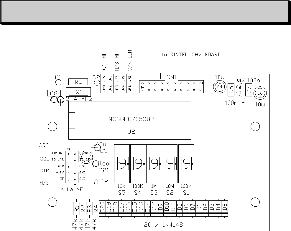
Fig. 14.2 - CONTRAVES BOARD COMPONENT LAYOUT (DB 9308-020)
14.2 CONTRAVES BOARDS PARTS LIST
ITEM QUANTITY REFERENCE PART
______________________________________________________
1 1 CN1 CONN 20
2 1 CN2 CONN 10
3 2 C2,C1 10p cer
4 3 C3,C4,C6 10u
5 3 C5,C7,C8 100n pol
6 21 D1 - D22 1N4148
7 1 D21 LED d3
8 9 JP1,JP2,JP3,JP4,JP5, jumper
JP6,JP7,JP8,JP9,JP10
9 4 R1,R2,R3,R4 47K
10 1 R5 1k
11 1 R6 2M2
12 2 R8,R7 10k
13 5 S1,S2,S3,S4,S5 CONTRAVES
14 1 U1 78L05
15 1 U2 MC68HC705C8P
16 1 X1 2-4 MHz

DB ELETTRONICA TELECOMUNICAZIONI S.p.A.
PM 300 - FM Broadcasting Transmitter - USER’S MANUAL104 /108
15. TROUBLESHOOTING
In the following table there is a list of the most frequent malfunctions, the corresponding symptoms
and their possible solutions for the PM300 transmitter.
CAUSE SYMPTOM ACTION SUGGESTED
AC main absent
-PWR led OFF when
transmitter
switched ON
Check the presence of the
connection to the electric line
and the integrity of the power
cord.
Check the fuse (N°1 Fig. 1.2).
If the fuse is burnt check that
the voltage of the electric line
is the same (115 or 230Vac) as
the one selected by the rear
panel switch (N° 2 Fig. 1.2)
and then replace the fuse.
VSWR or TEMPERATURE
protection intervention or
defective lock of the PLL circuit
on modulator.
- No output power
-VSWR led ON or TEMP led
ON or LOCK led OFF.
If on the front panel the
VSWR led is light on, check
the integrity of the output load
(antenna or dummy load) and
the corresponding cables, then,
perform a RESET using the
push-button (N° 12 Fig. 1.2).
If the led TEMP on the front
panel is light on, control the
room temperature (should be <
45°C). If under 45°C, allow
about 15 minutes for the
proper cooling of the
equipment; the protection will
turn off automatically.
If the problem persists, please

DB ELETTRONICA TELECOMUNICAZIONI S.p.A.
PM 300 - FM Broadcasting Transmitter - USER’S MANUAL 105 /108
contact DB’s Technical
Service.
If on the front panel the LOCK
led is light off, control the DC
voltage that is on the audio
and SCA inputs (the DC
voltage should be lower than
1 V otherwise there could be
PLL locking problems):
if it is correct, please open the
transmitter cover and the
modulator box cover (N° 8
Fig. 1.3 and check the supply
voltages ±12Vdc
presence on the modulator
board. If the voltages are not
correct, please check the
internal connectors and the
relative cables. If the problem
persists contact DB
Elettronica.
Output power adjustment not
correct
- Very low output power Adjust the output power level
using the front panel trimmer
(Fig. 1.1).
Excessive or low deviation - Received audio: very low or
badly distorted
- Adjust input audio levels and
front panel potentiometer (Fig.
1.1) following indications in
Chapter 5.

DB ELETTRONICA TELECOMUNICAZIONI S.p.A.
PM 300 - FM Broadcasting Transmitter - USER’S MANUAL106 /108
16. APPENDIX A
16.1 XLR AUDIO CONNECTORS PINOUTS
Connection procedure to connect the audio signal cables to the XLR female connectors for a
balanced or unbalanced signal.
XLR FEMALE
XLR CONNECTOR PIN BALANCED SIGNAL UNBALANCED SIGNAL
1 ground ground
2 " +" not connected
3 " - " signal

DB ELETTRONICA TELECOMUNICAZIONI S.p.A.
PM 300 - FM Broadcasting Transmitter - USER’S MANUAL 107 /108
17. APPENDIX B
17.1 MOSFET REPLACEMENT
1. Disconnect the supply voltage from the output board (faston connection).
2. Unscrew the damaged MOSFET and the output matching board.
3. Unsolder the MOSFET.
4. Clean the input and output boards to prevent short-circuits before replacing the MOSFET.
5. Locate properly the white teflon sheets between the output circuit and the heat sink: affix the
circuit using the two screws.
6. Put on the thermically conductive compound between the MOSFET case and the heat sink.
7. Fix the MOSFET to the heat sink (screws must be strongly fixed) and solder all the four pins of
the MOSFET: careful attention must be paid to the output board soldering since an
excessive quantity of tin can cause a short circuit between different board layers. Reconnect
also the 2 GND interconnections, indicated on Fig. 17.1, and check the right soldering of the
input transformer and gate resistor.
8. Verify that the supply voltage is 45V (if it is not, there is a problem in the switching power
supply boards). Reconnect the supply voltage to the 300W module (faston connection), placing
an ammeter in series (minimum full scale deflection 10A).
9. Control the output power level (it should be 300W) and the absence of spurious emissions (to
check it, use a spectrum analyzer and an output RF monitor sufficiently attenuated). Pay
attention to the ammeter: the MOSFET must not drain more than 9A.
10. In case the replaced MOSFET doesn’t reach the nominal output power or in case of spurious
emissions you need to improve the input matching of the MOSFET: to do this compress or
expand manually the input circuit coil (see Fig. 17.1) to maximize the output power.

DB ELETTRONICA TELECOMUNICAZIONI S.p.A.
PM 300 - FM Broadcasting Transmitter - USER’S MANUAL108 /108
Fig. 17.1 - MOSFET REPLACEMENT