RF Technology 200A-AN Base station User Manual Receiver manual
RF Technology Pty Ltd Base station Receiver manual
Contents
- 1. Receiver manual
- 2.
Receiver manual

Eclipse Series
RF Technology
rfinfo@rftechnology.com.au
November 2001
R220 Receiver
Operation and Maintenance Manual
This manual is produced by RF Technology Pty Ltd.,
10/8 Leighton Place, Hornsby, 2077, Australia, and is
Copyright ©2001, RF Technology
Part No. PCB 30/9132

Page 2 RF Technology R220
CONTENTS CONTENTS
Contents
1 Operating Instructions 5
1.1 Front Panel Controls and Indicators 5
1.1.1 Mon. Volume 5
1.1.2 Mon. Sq. 5
1.1.3 N. SQ 5
1.1.4 C. SQ 6
1.1.5 Line 6
1.1.6 PWR LED 6
1.1.7 SQ LED 6
1.1.8 Alarm LED 7
2 Receiver Internal Jumper Options 7
2.1 JP1: 240Hz Notch Filter 7
2.2 JP2: Audio Response 8
2.3 JP3: Audio Filter In/Out 8
2.4 JP4: 600Ω Line dc Loop COS 8
2.5 JP6: COS Polarity 8
2.6 JP7/8/9: dc Loop COS Configuration 8
2.7 JP7, JP8, JP9: Direct Output COS 9
2.8 JP11 EPROM Type 9
3 Receiver I/O Connections 11
3.1 25 Pin Connector 11
4 Channel and Tone Frequency Programming 12
5 Circuit Description 12
5.1 RF Section 12
5.2 IF Section 12
5.3 VCO Section 13
5.4 PLL Section 13
5.5 Audio Signal Processing 14
5.6 Noise Filter, Amplifier and Detector 14
5.7 Subtone Filter and CTCSS 14
5.8 External Squelch 15
5.9 Microprocessor Controller 15
5.10 Carrier Operated Switch 15
5.11 Voltage Regulator 16
6 Alignment Procedure 16
6.1 Standard Input Signal 16
6.2 RF Alignment 16
6.3 IF Alignment 17
6.4 Line Level Adjustment 18
6.5 Reference Oscillator Calibration 18

RF Technology R220 Page 3
CONTENTS CONTENTS
7 Specifications 18
7.1 General Description 18
7.1.1 Channel Capacity 18
7.1.2 CTCSS 18
7.1.3 Channel Programming 18
7.1.4 Channel Selection 19
7.1.5 Microprocessor 19
7.2 Physical Configuration 19
7.3 Front Panel Controls, Indicators and Test Points 19
7.3.1 Controls 19
7.3.2 Indicators 19
7.3.3 Test Points 20
7.4 Electrical Specifications 20
7.4.1 Power Requirements 20
7.4.2 Frequency Range and Channel Spacing 20
7.4.3 Frequency Synthesizer Step Size 20
7.4.4 Frequency Stability 20
7.4.5 Nominal Antenna Impedance 20
7.4.6 IF Frequencies 21
7.4.7 Sensitivity 21
7.4.8 Selectivity 21
7.4.9 Spurious and Image Rejection 21
7.4.10 Intermodulation 21
7.4.11 Modulation Acceptance BW 21
7.4.12 Noise Squelch 21
7.4.13 Carrier Level Squelch 22
7.4.14 Receiver Frequency Spread 22
7.4.15 Receiver Conducted Spurious Emissions 22
7.4.16 Audio Frequency Response 22
7.4.17 Audio Output Level 22
7.4.18 Audio Distortion 22
7.4.19 Channel Select Input/Output 22
7.4.20 Carrier Operated Switch Output 23
7.4.21 CTCSS 23
7.4.22 External Squelch Input 25
7.5 Connectors 25
7.5.1 Antenna Connector 25
7.5.2 Power and I/O Connector 25
7.5.3 Test Connector 25

Page 4 RF Technology R220
CONTENTS CONTENTS
BParts List

RF Technology R220 Page 5
1 OPERATING INSTRUCTIONS
WARNING
Changes or modifications not expressly approved
by RF Technology could void your authority to
operate this equipment. Specifications may vary
from those given in this document in accordance
with requirements of local authorities. RF
Technology equipment is subject to continual
improvement and RF Technology reserves the right
to change performance and specification without
further notice.
1 Operating Instructions
1.1 Front Panel Controls and Indicators
1.1.1 Mon. Volume
The Mon. Volume control is used to adjust the volume of the internal loudspeaker
and any external speaker connected to the test socket. It does not effect the level of
the 600Ω line or direct audio output.
1.1.2 Mon. SQ.
The Mon. SQ. switch allows all squelch functions controlling the monitor output to
be disabled. When the switch is in the Mon. SQ. position the audio at the monitor
speaker is controlled by the noise detector. The CTCSS, carrier and external squelch
functions are disabled. This can be useful when you are trying to trace the source of
on-channel interference or when setting the noise squelch threshold. the audio from
the 600Ω line and direct outputs is not effected by the switch position.
1.1.3 N.SQ
The N.SQ trimpot is used to set the noise squelch sensitivity. Use the following
procedure to set the noise squelch to maximum sensitivity.
1. Set the toggle switch to the Mon. Sq. position and set the Mon. Volume control
to 9 o’clock.

Page 6 RF Technology R220
1.1 Front Panel Controls and Indicators 1.1 OPERATING INSTRUCTIONS
2. Turn the N. SQ. adjustment counter clockwise until the squelch opens and
noise is heard from the speaker. Adjust the VOLUME to a comfortable
listening level.
3. In the absence of any on channel signal, turn the N.SQ. screw clockwise until
the noise in the speaker is muted. Then turn the screw two additional turns in
the clockwise direction.
1.1.4 C.SQ
The C.SQ trimpot is used to set the carrier squelch sensitivity. Carrier squelch is
useful at higher signal levels than those at which noise squelch and can be used
typically from 1-200µ V input.
It is provided mainly for use in fixed link applications where a high minimum signal
to noise ratio is required or where very fast squelch operation is required for data
transmission. The carrier squelch will open and close in less than 2 mSec.
In most base station applications carrier squelch is disabled by turning the adjustment
counter clockwise until the screw clicks.
The carrier squelch may be set to a predetermined level with the Techelp/Service
Monitor 2000 software or by using the following procedure:
1. First turn the adjustment fully counter-clockwise. Then set the noise
squelch as above.
2. Connect a source of an on channel signal with the desired threshold level to
the receiver's RF input.
3. Turn the screw clockwise until the SQ LED goes OFF. Then turn the screw
back until the LED just comes ON.
1.1.5 LINE
The LINE trimpot is used to set the line and direct audio output level. It is normally
set to give 0dBm (775mV) to line with a standard input signal equal to 60% of
maximum deviation at 1 KHz. The level can be measured between test socket pins 6
and 1 and set as desired.
1.1.6 PWR LED
The PWR LED shows that the dc supply is connected to the receiver.
1.1.7 SQ LED
The SQ LED comes on when the audio to the line and direct outputs is un-squelched.
RF Technology R220 Page 7
2 RECEIVER INTERNAL JUMPER OPTIONS
The LED and squelch function are controlled by noise, carrier and tone squelch
circuits.
1.1.8 ALARM LED
The ALARM LED can indicate the detection of several different fault conditions by
the self test circuits. The alarm indicator shows the highest priority fault present.
Receivers using software issue 5 and higher use the cadence of the LED flash
sequence to indicate the alarm condition. Refer to table 1.
LED Flash Cadence Fault Condition
5 flashes, pause Synthesizer unlocked
4 flashes, pause Tuning voltage outside limits
3 flashes, pause Signal level below preset threshold (fixed link)
1 flash, pause dc supply voltage low or high
LED ON continuously External squelch is active
Table 1: Interpretations of LED flash cadence
Receivers using software issue 4 and lower use the LED flash rate to indicate the
alarm condition. Refer to table 2.
Indication Fault condition
Flashing, 8 per second Synthesizer unlocked
Flashing, 4 per second Tuning voltage outside 2-7 Vdc
Flashing, 2 per second Signal level below preset threshold (fixed links)
Continuous dc supply voltage low or high
Table 2: Interpretations of LED flash speed, for early models.
2 Receiver Internal Jumper Options
In the following subsections an asterisk (*) signifies the standard (Ex-Factory)
configuration of a jumper.
2.1 JP1: 240 Hz Notch Filter
JP1 allows the 240Hz notch filter in the normal audio path to be bypassed.
Condition Position
Notch Filter In 1-2 *
Notch Filter Out 2-3
Page 8 RF Technology R220
2.2 JP2: Audio Response 2 RECEIVER INTERNAL JUMPER OPTIONS
2.2 JP2: Audio Response
Condition Position
750 uSec. de-emphasis 1-2 *
Flat response 2-3
2.3 JP3: Audio Filter In/Out
JP3 bypasses the 300Hz high-pass filter and 240Hz notch filter if necessary.
Condition Position
Hi-pass, Notch In 2-3 *
Flat response 1-2
2.4 JP4: 600Ω
ΩΩ
Ω Line dc Loop COS
JP4 allows the dc return path through the output audio transformer to be broken, to
permit dc signaling via the audio pair or wires.
Condition Position
dc Loop Configured by JP7, JP8, JP9 1-2 *
dc Loop Not used 2-3
2.5 JP6: COS Polarity
Condition Position
Active on Signal 2-3 *
Active on No Signal 1-2
2.6 JP7, JP8, JP9: dc Loop COS Configuration (JP4 1-2)
These settings are relevant when the Carrier Operated Switch (COS) signal is to be
used across the same wires as the audio. Refer to setting of JP4, in section 2.4. They
control the levels and connection into the audio balanced line circuitry.
Condition JP7 JP8 JP9
Source +12 Vdc Loop 2-3 ON 1-2 *
Free Switch Output 1-2 ON 2-3

RF Technology R220 Page 9
2 RECEIVER INTERNAL JUMPER OPTIONS 2.7 JP7/8/9 Direct Output COS
2.7 JP7, JP8, JP9: Direct Output COS (JP4 2-3)
In this arrangement, the COS signal is taken via the separate COS+ and COS-
outputs, either with free (floating) output or with +12Vdc pull-up.
Condition JP7 JP8 JP9
+12 Vdc Direct
Output 2-3 OFF OFF
Free Switch Output 1-2 OFF OFF
2.8 JP11 EPROM Type
Condition Position
27C256 2-3 *
27C64 1-2
* = Standard Ex-Factory Configuration
Page 10 RF Technology R220
2 RECEIVER INTERNAL JUMPER OPTIONS
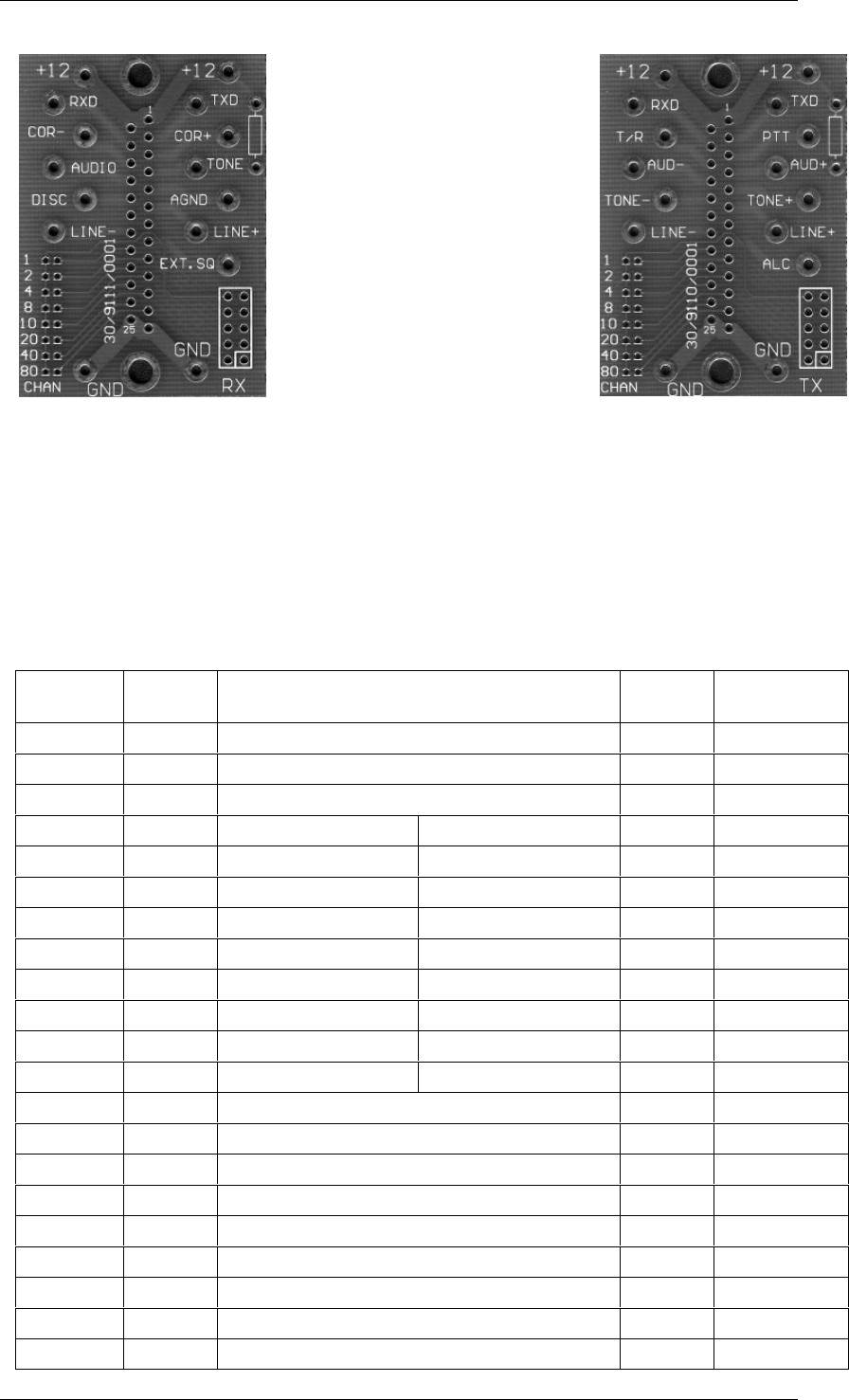
RX PCB TX PCB
The Receiver and Transmitter modules plug into the back plane DB25/F
connectors
Miniature spade connectors (2.1 x 0.6 x 7mm) are captive/ soldered at the labelled
points.
To configure: Solder wire connections between appropriate points.
Receiver
DB25/F RX PCB DESCRIPTION TX PCB Transmitter
DB25/F
1, 14 +12V +12V DC SUPPLY +12V 1, 14
2 TXD TX Data TXD 2
15 RXD RX Data RXD 15
3 COR+ Carrier Operate Sw+ PressToTalk input PTT 3
16 COR- Carrier Operate Sw- Tx/Rx output T/R 16
4 TONE Subtone output Hi Z audio input+ AUD+ 4
17 AUDIO Audio output Hi Z audio input- AUD- 17
5 AGND Audio Ground Ext tone input+ TONE+ 5
18 DISC Discriminator output Ext tone input- TONE- 18
6 LINE+ Line output+ Line input+ LINE+ 6
20 LINE- Line output- Line input- LINE- 20
8 EXT SQ Ext Squelch input Auto Level Control ALC 8
13, 25 GND Ground, 0V GND 13, 25
21 BCD 1 Channel select 1’s digit BCD 1 21
9 BCD 2 Channel select 1’s digit BCD 2 9
22 BCD 4 Channel select 1’s digit BCD 4 22
10 BCD 8 Channel select 1’s digit BCD 8 10
23 BCD 10 Channel select 10’s digit BCD 10 23
11 BCD 20 Channel select 10’s digit BCD 20 11
24 BCD 40 Channel select 10’s digit BCD 40 24
12 BCD 80 Channel select 10’s digit BCD 80 12

RF Technology R220 Page 11
3 RECEIVER I/O CONNECTIONS 3.1 25 Pin Connector
3 Receiver I/O Connections
3.1 25 Pin Connector
The D-shell 25 pin connector is the main interface to the receiver. The pin
connections are described in table 3.
Function Signal Pins Specification
dc Power +12
Vdc
-12
Vdc
1, 14
13, 25 +11.4 to 16 Vdc
Channel Select 1
2
4
8
10
20
40
80
21
9
22
10
23
11
24
12
BCD Coded
0 = Open Circuit
or 0 Vdc
1 = +25 to +16 Vdc
RS232 Data In
Out 15
2Test and Programming use
9600, 8 data 2 stop bits
600Ω Line In
Out 20
6Transformer Isolated
Balanced 0dBm Output
150Ω / Hybrid 7
19
Discriminator 18 AC coupled, unsquelched
Direct Audio Output 17 Direct AC Coupled Audio
Audio Ground 5 Direct Audio Ground
Sub-Audible Audio
Out 4 Unsquelched, 1-250 Hz
Carrier Operated Sw
Carrier Operated Sw +
-3
16 Opto-coupled Transistor
Switch (10mA)
External Squelch Input 8 <1 Vdc to Squelch
>2 Vdc or open ckt to
unsquelch
Table 3: Pin connections and explanations for the main, 25-pin,
D-shell Connector

Page 12 RF Technology R220
4 FREQUENCY PROGRAMMING
4 Frequency Programming
Channel and tone frequency programming is most easily accomplished with RF
Technology TecHelp/Service Monitor 2000 software. This software can be run on
an IBM compatible/Windows PC and provides a number of additional useful
facilities.
TecHelp/Service Monitor 2000 allows setting of the adaptive noise squelch
threshold, provides a simple means of calibrating the signal strength output and
minimum signal alarm.
TecHelp/Service Monitor 2000 can be supplied by your dealer, distributor or by
contacting RF Technology direct.
5 Circuit Description
The following descriptions should be read as an aid to understanding the block and
schematic diagrams at the rear of this manual.
5.1 RF Section
A two pole voltage tuned filter (D13, D14, L35-39) is used to limit the RF band
width prior to the RF amplifier transistor Q1. The tuning voltage is supplied by the
frequency synthesizer through voltage follower U28D. The circuit values are chosen
so that the centre frequency tracks the VCO frequency.
RF amplifier transistor Q1 is followed by a second two pole voltage tuned filter
(D15, D16, L28-32) which provides additional image and spurious frequency
rejection. The filter output is connected to the RF input port of the mixer MX1.
MX1 is a high level double balanced diode ring mixer with excellent intermodulation
performance. It has a conversation loss of approximately 6 dB. The gain between
the receiver input and the mixer input is approximately 10 dB so that the total gain
between the antenna input and the IF input 3-4dB.
Monolithic amplifiers MA1, MA2 and transistor Q5 amplify the VCO output to the
necessary LO level for MX1 approximately +13dBm.
The network C8, C9 L1-3 and R6 passes the IF frequency of 45 MHz and terminates
the RF and LO components.
5.2 IF Section
The first IF amplifier uses two parallel connected JFET transistors Q2 and Q3 to
obtain 8-10 dB gain. The two transistors provide improved dynamic range and input
matching over a single transistor.

RF Technology R220 Page 13
5 CIRCUIT DESCRIPTION 5.2 IF Section
A two pole 45 MHz crystal filter XF1 is used between the first and second IF
amplifiers. The second IF amplifier Q4 provides additional gain of 6-10dB. A two
pole crystal filter is used between Q4 and the 2nd oscillator mixer. These two crystal
filters provide some adjacent channel rejection and all of the second IF image
frequency rejection.
U1 is a monolithic oscillator and mixer IC. It converts the 45 MHz IF signal down to
455 KHz. The second oscillator frequency or 45.455 MHz is controlled by crystal
Y1. The 455 KHz output of the second mixer is fed through a ceramic filter CF1 to
the second IF amplifier transistor Q27. Q27 provides an additional 15 dB gain ahead
of the limiter and discriminator IC U3.
The limiter/discriminator IC U3 further amplifies the signal and passes it through
CF2. CF2 does not contribute to the adjacent channel rejection but is used to reduce
the wide band noise input to the limiter section of U3.
The limiter section of U3 drives the quadrature detector discriminator. C31 and IF
tuned circuit L10 comprise the discriminator phase shift network.
U3 also has a received signal strength indicator output (RSSI). The RSSI voltage
connects to the test socket for alignment use. The RSSI voltage is also used by the
microprocessor for the adaptive noise squelch, carrier squelch and low signal alarm
functions.
Dual op-amp U2 is used to amplify and buffer the discriminator audio and RSSI
outputs.
5.3 VCO Section
The Voltage Controlled Oscillator uses a junction FET Q6 which oscillates at the
required mixer injection frequency. Varactor diode D4 is used by the PLL circuit to
keep the oscillator on the desired frequency. Transistor Q7 is used as a filter to
reduce the noise on the oscillator supply voltage.
5.4 PLL Section
The synthesizer frequency reference is supplied by a temperature compensated
crystal oscillator (XO1). The frequency stability of the oscillator is better than 1
ppm.
The 12 MHz output of Q25 or XO1 is amplified by Q8 to drive the reference input
of the PLL synthesizer IC U4. This IC is a single chip synthesizer which includes a
1.1 GHz pre-scaler, programmable divider, reference divider and phase/frequency
detector. The frequency data is entered a serial data link from the microprocessor.
The phase detector output signals of U4 are used to control two switched current
sources. The output of the positive and negative sources' Q10 and Q16, produce the
tuning voltage which is smoothed by the loop filter components to bias the VCO
varactor diode D4.

Page 14 RF Technology R220
5.5 Audio Signal Processing 5 CIRCUIT DESCRIPTION
5.5 Audio Signal Processing
A 4 KHz low pass filter (U27b) is used to remove high frequency noise from the
signal. A 300 Hz high pass filter (U26a,b) then removes the sub-audible tones. A 240
Hz notch filter (U26c,d) is used to improve the rejection of tones above 200 Hz. The
high pass and notch filters can be bypassed by internal jumpers JP1 and JP3.
The audio frequency response can be set for either 750 uS de-emphasis or a flat
characteristic by JP2. JP2 selects the feedback network of amplifier U27c.
After de-emphasis and filtering, the audio signal is applied to the inputs of two
analog switches (U17a,b). These switches are controlled by the micro-controller and
squelch or mute the audio to the line and monitor output circuits. The monitor output
can be set for noise squelch only operation by S1.
The audio from U17a is adjusted by the volume control before connecting to the
monitor output amplifier U5. U5 drives the internal speaker and can also supply 3-5
watts to an external loudspeaker.
The audio from U17b is adjusted by RV3 before connecting to the line output IC
(U22a,b). U22 is a dual amplifier connected in a bridge configuration to drive the
600Ω line output transformer T1.
5.6 Noise Filter, Amplifier and Detector
The unfiltered audio from the discriminator is fed to trimpot RV4 which is used to
set the noise squelch threshold. From RV4 the audio goes to the noise filter (U27a).
This is a 10 KHz high pass filter and is used to eliminate voice frequency
components.
The noise signal is then amplified by U27d and fed to the noise detector. The noise
detector consists of D6, Q17 and U26c. D6 and Q17 are a charge pump detector and
pull the input to U26c low as the noise increases. U26c has positive feedback and
acts like a schmitt trigger. The output of U26c goes high when noise is detected. It
connects to the micro-controller and to analog switch U17d. U17d varies the gain of
the noise amplifier to provide approximately 2dB hysteressis.
5.7 Sub-Tone Filter and CTCSS
The discriminator audio is fed through cascaded low pass filters U28a and U28b to
filter out the voice frequency components. The filtered sub-tone audio is supplied to
the CTCSS hybrid and the rear panel system connector. The filtered output can be
used for re-transmission of CTCSS or DCS.
The CTCSS decoder module is a micro-controller base hybrid module. Under control
of the main microprocessor U15 it can decode all 38 EIA tones and 12 additional
commonly used tones. The decode bandwidth is set to 1% but may be changed to 2%
by a jumper on the printed circuit board.

RF Technology R220 Page 15
5 CIRCUIT DESCRIPTION 5.8 External Squelch
5.8 External Squelch
The audio output can be muted through pin 8 of the receiver system connector P1.
When pin 8 is pulled to less than 1 volt above ground, the micro-controller U15 will
mute the audio output.
This facility can be used to mute the audio during transmission, as is required in
single frequency systems, by simply connecting pin 8 of the receiver to the
transmitter T/R relay driver output (pin 16 on Eclipse transmitters).
5.9 Microprocessor Controller
The microprocessor controller circuit uses an advanced eight bit processor and
several support chips. The processor U15 includes EE memory for channel
frequencies, tones, and other information. It also has an asynchronous serial port and
an analog to digital converter.
The program is stored in U12, a CMOS EPROM. U13 is an address latch for the low
order address bits. U11 is used to read the channel select lines onto the data bus. U7
is an address decoder for U11 and U12. U14 is a supervisory chip which keeps the
processor reset unless the +5 Volt supply is within operating limits. U16 translates
the asynchronous serial port data to standard RS232 levels.
The analog to digital converter is used to measure the received signal strength, tuning
voltage, dc supply voltage and the carrier squelch setting.
5.10 Carrier Operated Switch
The carrier operated switch is an opto-coupled (ISO1) output. Internal jumpers
(JP4,7,8,9) can be connected to provide loop source, loop switch, free switch and
various other configurations.
The COS can be set to be active (switch closed) on carrier or active in the absence of
carrier.
The generic term ``Carrier Operated Switch'' may be misleading in this case. SINCE,
if a sub-audible tone has been programmed for the channel in use, the COS is
controlled by carrier and tone detection.

Page 16 RF Technology R220
5.11 Voltage Regulator 5 CIRCUIT DESCRIPTION
5.11 Voltage Regulator
The dc input voltage is regulated down to 9.4 Vdc by a discrete regulator circuit. The
series pass transistor Q20 is driven by error amplifiers Q21 and Q22. Q23 is used to
start up the regulator and once the circuit turns on, it plays no further part in the
operation.
This circuit is short circuit and overload protected. It provides much better line
isolation and lower dropout voltage than can be obtained with current integrated
circuit regulators.
6 Alignment Procedure
The following procedures may be used to align the receiver for optimum
performance. Normally only RF alignment will be required when changing
frequencies. IF alignment should only be necessary after repairs on that part of the
circuit.
Reference oscillator or TCXO calibration may be required periodically due to crystal
aging. The aging should be less than 1 ppm/year.
6.1 Standard Input Signal
RF Signal Generator
50Ω output impedance
Frequency range 215 - 240 MHz
FM modulation at 1KHz
1.5KHz peak for 12.5KHz channel spacing
6.2 RF Alignment
Alignment Frequency
215 - 240 MHz range 221.000 MHz

RF Technology R220 Page 17
6 ALIGNMENT PROCEDURE 6.3 IF Alignment
Step Input Measure Adjust
1 Select alignment
frequency channel dc Volts on test socket
pin 9 to pin 1 L34 to read 4.00Vdc
2 Signal generator on
centre frequency
channel to J1.
Modulation off.
dc Volts on test socket
pin 7 to pin 1 Generator level to
read 1 - 2 Vdc
3 Signal generator on
centre frequency
channel to J1.
Modulation off.
dc Volts on test socket
pin 7 to pin 1 L29, 31, 36, 38 for
maximum reading.
Reduce generator
output to keep below
2 Vdc
6.3 IF Alignment
Step Input Measure Adjust
1 Signal generator on
center frequency
channel to J1.
Modulation OFF
dc Volts in test socket
pin 7 to pin 1 Generator level to
read 1 - 2 Vdc
2 Signal generator on
center frequency
channel to J1.
Modulation OFF
dc Volts in test socket
pin 7 to pin 1 L5, L6, L7, L8 for
maximum reading.
Reduce generator
output to keep below
2 Vdc
3 Set generator level to
10
µ
V
Frequency U3 pin 9 L9 to read 455 KHz
+/- 10Hz
4 Set generator level to
1 millivolt.
Modulation ON.
Audio level test socket
pin 6 to pin 1 Line level (RV3) to
obtain approx. 1
Vrms
5 Set generator level to
1 millivolt.
Modulation ON.
Audio level test socket
pin 6 to pin 1 L10 for maximum
6 Set generator level to
1 millivolt.
Modulation ON.
Audio level P1 pin 18
to pin 5 RV1 for .5 Vrms
7 Set generator level to
approx. 25
µ
V
SINAD on test socket
pin 6 to pin 1 Reduce generator
level to obtain 12 Db
SINAD. Carefully
adjust L5, L6, L7, L8
to obtain the best
SINAD. Reduce
generator output to
maintain 12 dB
SINAD

Page 18 RF Technology R220
6.4 Line Level Adjustment 6 ALIGNMENT PROCEDURE
6.4 Line Level Adjustment
Step Input Measure Adjust
1 Signal generator on
centre frequency
channel to J1.
Modulation ON.
Level 1 millivolt
Audio level test socket
pin 6 to pin 1 RV3 for 390 mV rms
6.5 Reference Oscillator Calibration
Step Input Measure Adjust
1 None required Frequency junction of
R69 and R26 on the
top of the PCB. (LO
input to the mixer)
C181 or XO1 for L.O.
+/-100 Hz
L.O. = Fc+45 MHz
7 Specifications
7.1 General Description
The receiver is a high performance, frequency synthesized, narrow band FM unit
which can be used in conjunction with transmitter and power supply modules as a
base station or as a stand alone receiver. All necessary control and 600Ω line
interface circuitry is included.
7.1.1 Channel Capacity
Although most applications are single channel, it can be programmed for up to 100
channels numbered 0-99. This is to provide the capability of programming all
channels into all of the receivers used at a given site.
7.1.2 CTCSS
The CTCSS tone or no tone can also be programmed for each channel. So that each
channel number can represent unique RF and tone frequency combination.
7.1.3 Channel Programming
The channelling information is stored in a non-volatile memory chip and can be
programmed via the front panel test connector using a PC and RF Technology
supplied TecHelp/Service Monitor 2000 software.

RF Technology R220 Page 19
7 SPECIFICATIONS 7.1.4 Channel Selection
7.1.4 Channel Selection
Channel selection is by eight channel select lines. These are available through the
rear panel connector.
A BCD active high code applied to the lines selects the required channel. This can be
supplied by pre-wiring the rack connector so that each rack position is dedicated to a
fixed channel.
BCD switches inside the receiver can be used to pre-set any desired channel. These
eliminate the need to externally select the channel.
7.1.5 Microprocessor
A microprocessor is used to control the synthesizer and squelch functions and
facilitate the channel frequency programming. With the standard software it also can
provide fault monitoring and reporting.
7.2 Physical Configuration
The receiver is designed to fit in a 19 inch rack mounted frame. The installed height
is 4 RU (178 mm) and the depth 350 mm. The receiver is 63.5 mm or two Eclipse
modules wide.
7.3 Front Panel Controls, Indicators and Test Points
7.3.1 Controls
Mute defeat switch - toggle (Overrides CTCSS, noise and carrier squelch at the
monitor output)
Monitor Speaker Volume - Knob
Line Output Level - screwdriver adjust multiturn pot
Noise Squelch Setting - screwdriver adjust multiturn pot
Carrier Squelch Setting - screwdriver adjust multiturn pot
7.3.2 Indicators
Power ON - Green LED
Squelch Open - Yellow LED
Fault Indicator - Flashing Red LED

Page 20 RF Technology R220
7.3.3 Test Points 7 SPECIFICATIONS
7.3.3 Test Points
Line Output Level - 1 + Gnd
Receive Signal Strength - 1 + Gnd
Tuning Voltage - 1 + Gnd
Serial Data (RS232) - 2 + Gnd
7.4 Electrical Specifications
7.4.1 Power Requirements
Operating Voltage - 10.5 to 16 Vdc
Current Drain - 250mA Max.
Polarity - Negative Ground
7.4.2 Frequency Range and Channel Spacing
215 – 240 MHz 12.5KHz
7.4.3 Frequency Synthesizer Step Size
5.0 or 6.25 KHz
7.4.4 Frequency Stability
+/- 1 ppm, 0 to +60 C
7.4.5 Nominal Antenna Impedance
50Ω

RF Technology R220 Page 21
7 SPECIFICATIONS 7.4.6 IF Frequencies
7.4.6 IF Frequencies
First IF frequency 45 MHz
Second IF frequency 455 KHz
7.4.7 Sensitivity
-120 dBm Max. for 12 dB SINAD
-117 dBm Max. for 20 dB Quieting
7.4.8 Selectivity
12 KHz spacing - 70dB per ECR-235
7.4.9 Spurious and Image Rejection
90dB
7.4.10 Intermodulation
80dB
7.4.11 Modulation Acceptance BW
12.5 KHz spacing - 3.75 KHz per RS204C
7.4.12 Noise Squelch
Adjustment Range: 6 - 18 dB SINAD
Attack Time: 20 mSec. above 20dB Quieting
Release Time: 150 mSec. at 20dB Quieting decreasing to 20ms above 2
µ
V
preset threshold
Hysteresis: Hysteresis is equal to approximately 2dB change in noise
quieting

Page 22 RF Technology R220
7.4.13 Carrier Level Squelch 7 SPECIFICATIONS
7.4.13 Carrier Level Squelch
Carrier level squelch can be used when it is necessary to set the opening point above
26dB SINAD as may be required in link applications. The minimum adjustment
range is 1 to 200
µ
V.
7.4.14 Receiver Frequency Spread
Less than 1 dB change in sensitivity over the band
7.4.15 Receiver Conducted Spurious Emissions
Less than -57dBm from 1 to 2900 MHz
7.4.16 Audio Frequency Response
600Ω
ΩΩ
ΩLine and Direct Output: +1/-3dB 300-3000 Hz relative to either a flat
response or 750
µ
s de-emphasis with the high pass and notch filters bypassed.
+1/-6 dB with the filters in circuit.
Sub-Audio Output: +1/-3dB 67-250 Hz
7.4.17 Audio Output Level
600Ω
ΩΩ
ΩLine: Adjustable -10 to +10dBm
Monitor Loudspeaker: 5 Watts with external speaker, 0.3 Watt with internal
speaker
Discriminator and Sub-Audio: Nominally equal to 1 volt peak at rated system
deviation
7.4.18 Audio Distortion
750
µ
µµ
µ
s De-Emphasis: Less than 3% at 1 KHz and 60% of rated system deviation
Flat Response: Less than 5% at 1 KHz and 60% of rated system deviation
7.4.19 Channel Select Input/Output
Coding: 8 lines BCD coded 00-99

RF Technology R220 Page 23
7 SPECIFICATIONS 7.4.20 Carrier Operated Switch Output
Logic Input Levels: 0 = < 0.4 Volts
1 = > 3.5 Volts
Internal 10K pull down resistors selects Channel 00 when all inputs are O/C.
7.4.20 Carrier Operated Switch Output
Floating Opto-Coupler Output: The carrier operated switch output is via an opto-
coupler. Collector and emitter connections are available to allow connection for
source or sink.
The opto-coupler can be linked inside the receiver to be on when a carrier is detected
or to be on in the absence of carrier.
Connection to Remote Switch via 600Ω
ΩΩ
Ω Line: Internal connections are provided so
that the opto-coupler can be connected to the 600Ω line for use over a single pair.
This permits remote switching with no extra connections.
Current Source/Sink, Collector Voltage: The COS output is implemented with an
optocoupler whose ratings are:\\
Ic = 10mA Maximum
Vc = 30 Volts Maximum
7.4.21 CTCSS
The CTCSS decoding is provided by a hybrid module. This provides programmable
decoding of all 38 EIA and 12 other common tones. Refer to table 4.

Page 24 RF Technology R220
7.4.21 CTCSS 7 SPECIFICATIONS
Frequency EIA Number
No Tone
67.0 A1
69.4
71.9 B1
74.4 C1
77.0 A2
79.7 C2
82.5 B2
85.4 C3
88.5 A3
91.5 C4
94.8 B3
97.4
100.0 A4
103.5 B4
107.2 A5
110.9 B5
114.8 A6
118.8 B6
123.0 A7
127.3 B7
131.8 A8
136.5 B8
141.3 A9
146.2 B9
151.4 A10
156.7 B10
159.8
162.2 A11
165.5
167.9 B11
171.3
173.8 A12
177.3
179.9 B12
183.5
186.2 A13
189.9
192.8 B13
196.6
199.5
203.5 A14
206.5
210.7 B14
218.1 A15
225.7 B15
229.1
233.6 A16
241.8 B16
250.3 A17
254.1
Table 4: Tone Squelch Frequencies

RF Technology R220 Page 25
7 SPECIFICATIONS 7.4.22 External Squelch Input
7.4.22 External Squelch Input
An external input is provided to squelch or mute the receiver audio output. This may
be used in conjunction with an external decoder or to mute the receiver during
transmissions.
External Squelch Input can be connected to the T/R Relay pin on Eclipse transmitters
mute the receiver during transmission.
7.5 Connectors
7.5.1 Antenna Connector
Type N Female Mounted on the module rear panel
7.5.2 Power & I/O Connector
25-pin ``D'' Male Mounted on the rear panel
7.5.3 Test Connector
9-pin ``D'' Female mounted on the front panel
A Engineering Diagrams
A.1 Circuit diagram
Figure 1 shows the detailed schematic diagram with component numbers and values

Page 26 RF Technology R220
B Parts List
C1 CAP 1N0 5% 63V NPO SM1206
46/3300/01N0
C10 CAP 100N 10% 50V X7R RD.2
46/2001/100N
C100 CAP 100N 10% 50V X7R RD.2
46/2001/100N
C101 CAP 4N7 10% COG RAD.2
46/2000/04N7
C102 CAP 27P 2% 100V NPO RAD.1
45/2680/027P
C103 CAP 1N5 10% 50V COG RAD.2
46/2000/01N5
C104 CAP 100N 5% 50V MKT RD.2
47/2007/100N
C105 CAP 470U 25V RB ELECTRO
41/2001/470U
C106 CAP 100N 10% 50V X7R RD.2
46/2001/100N
C107 CAP 10N 1% 63V KP7.5
47/2007/010N
C108 CAP 10N 1% 63V KP7.5
47/2007/010N
C109 CAP 10N 1% 63V KP7.5
47/2007/010N
C11 CAP 47P 2% 100V NPO RAD.1
45/2680/047P
C110 CAP 10N 1% 63V KP7.5
47/2007/010N
C111 CAP 1UO 10% 50V MKT
47/2007/01U0
C112 CAP 10N 1% 63V KP7.5
47/2007/010N
C113 CAP 10N 1% 63V KP7.5
47/2007/010N
C114 CAP 10N 1% 63V KP7.5
47/2007/010N
C115 CAP 10N 1% 63V KP7.5
47/2007/010N
C116 CAP 10N 1% 63V KP7.5
47/2007/010N
C117 CAP 10N 1% 63V KP7.5
47/2007/010N
C118 CAP 1N0 5% 63V NPO SM1206
46/3300/01N0
C119 CAP 47U 25V RB ELECTRO
41/2001/047U
C12 CAP 33P 2% 100V NPO RAD.1
45/2680/033P
C120 CAP 1N0 5% 100V NPO RAD.2
46/2000/01N0
C121 CAP 2N2 5% 400V MKT RAD.2
47/2040/02N2
C122 CAP 15N 5% 400V MKT RAD.2
47/2040/015N
C123 CAP 33N 5% 400V MKT RAD.2
47/2040/033N
C124 CAP 6N8 10% 400V MKT RD.2
47/2040/06N8
C125 CAP 10N 10% 400V MKT RD.2
47/2040/010N
C126 CAP 100N 10% 50V X7R RD.2
46/2001/100N
C127 CAP 470U 25V RB ELECTRO
41/2001/470U
C128 CAP 100N 10% 50V X7R RD.2
46/2001/100N
C129 CAP 47U 25V RB ELECTRO
41/2001/047U
C13 CAP 33P 2% 100V NPO RAD.1
45/2680/033P
C130 CAP 470U 25V RB ELECTRO
41/2001/470U
C131 CAP 1UO 10% 50V MKT
47/2007/01U0
C132 CAP 1UO 10% 50V MKT
47/2007/01U0
C133 CAP 1UO 10% 50V MKT
47/2007/01U0
C134 CAP 2U2 10% 100V MKT RD.2
47/2010/02U2
C135 CAP 100N 10% 50V X7R RD.2
46/2001/100N
C136 CAP 470U 25V RB ELECTRO
41/2001/470U
C137 CAP 10U 35V RAD ELECTRO
41/2001/010U
C138 CAP 10N 10% 50V X7R RAD.2
46/2001/010N
C139 CAP 10N 10% 50V X7R RAD.2
46/2001/010N
C14 CAP 100N 10% 63V X7R 1206
46/3310/100N
C140 CAP 10N 10% 50V X7R RAD.2
46/2001/010N
C141 CAP 10N 10% 50V X7R RAD.2
46/2001/010N
C142 CAP 10U 35V RAD ELECTRO
41/2001/010U
C143 CAP 10U 35V RAD ELECTRO
41/2001/010U
C144 CAP 10U 35V RAD ELECTRO
41/2001/010U
C145 CAP 10U 35V RAD ELECTRO
41/2001/010U
C146 CAP 100N 10% 50V X7R RD.2
46/2001/100N
C147 CAP 100N 10% 50V X7R RD.2
46/2001/100N
C148 CAP 100N 10% 50V X7R RD.2
46/2001/100N
C149 CAP 1N0 5% 100V NPO RAD.2
46/2000/01N0
C15 CAP 1N0 5% 100V NPO RAD.2
46/2000/01N0
C150 CAP 1N0 5% 100V NPO RAD.2
46/2000/01N0
C151 CAP 100N 10% 50V X7R RD.2
46/2001/100N
C152 CAP 470U 25V RB ELECTRO
41/2001/470U
C153 CAP 100N 10% 50V X7R RD.2
46/2001/100N
C154 CAP 100N 10% 50V X7R RD.2
46/2001/100N
C155 CAP 10N 10% 50V X7R RAD.2
46/2001/010N
C156 CAP 1N0 5% 100V NPO RAD.2
46/2000/01N0
C157 CAP 18P 2% 100V NPO RAD.1
45/2680/018P
C158 CAP 18P 2% 100V NPO RAD.1
45/2680/018P
C159 CAP 10U 35V RAD ELECTRO
41/2001/010U
C16 CAP 33P 2% 100V NPO RAD.1
45/2680/033P
C160 CAP 10N 10% 50V X7R RAD.2
46/2001/010N
C161 CAP 10N 10% 50V X7R RAD.2
46/2001/010N
C162 CAP 10N 10% 50V X7R RAD.2
46/2001/010N
C163 CAP 10U 35V RAD ELECTRO
41/2001/010U
C164 CAP 10U 35V RAD ELECTRO
41/2001/010U
C165
C166 CAP 10N 10% 50V X7R RAD.2
46/2001/010N
C167 CAP 10U 35V RAD ELECTRO
41/2001/010U
C169 CAP 10P 5% 63V NPO SM1206

RF Technology R220 Page 27
46/3300/010P
C17 CAP 33P 2% 100V NPO RAD.1
45/2680/033P
C170 CAP 1N0 5% 63V NPO SM1206
46/3300/01N0
C171 CAP 1N0 5% 63V NPO SM1206
46/3300/01N0
C172 CAP 47P 5% 63V NPO SM1206
46/3300/047P
C173
C174
C175 CAP 10P 5% 63V NPO SM1206
46/3300/010P
C176 CAP 1N0 5% 63V NPO SM1206
46/3300/01N0
C177 CAP 47P 5% 63V NPO SM1206
46/3300/047P
C178
C179
C18 CAP 33P 2% 100V NPO RAD.1
45/2680/033P
C180 CAP 1N0 5% 63V NPO SM1206
46/3300/01N0
C185 CAP 10N 10% 50V X7R RAD.2
46/2001/010N
C186 CAP 100N 10% 50V X7R RD.2
46/2001/100N
C187 CAP 100N 10% 50V X7R RD.2
46/2001/100N
C188 CAP 10N 10% 50V X7R RAD.2
46/2001/010N
C19 CAP 33P 2% 100V NPO RAD.1
45/2680/033P
C2 CAP 100N 10% 63V X7R 1206
46/3310/100N
C20 CAP 10N 10% 50V X7R RAD.2
46/2001/010N
C21 CAP 100N 10% 50V X7R RD.2
46/2001/100N
C22 CAP 10P 2% 100V NPO RAD.1
45/2680/010P
C23 CAP 33P 2% 100V NPO RAD.1
45/2680/033P
C24 CAP 22P 2% 100V NPO RAD.1
45/2680/022P
C25 CAP 100N 10% 50V X7R RD.2
46/2001/100N
C26 CAP 100N 10% 50V X7R RD.2
46/2001/100N
C27 CAP 100N 10% 50V X7R RD.2
46/2001/100N
C28 CAP 100N 10% 50V X7R RD.2
46/2001/100N
C29 CAP 100N 10% 50V X7R RD.2
46/2001/100N
C3 CAP 1N0 5% 63V NPO SM1206
46/3300/01N0
C30 CAP 10U 35V RAD ELECTRO
41/2001/010U
C31 CAP 10P 2% 100V NPO RAD.1
45/2680/010P
C32 CAP 100N 10% 50V X7R RD.2
46/2001/100N
C33 CAP 10N 10% 50V X7R RAD.2
46/2001/010N
C34 CAP 100P 2% 100V NPO RAD1
45/2680/100P
C35 CAP 100N 10% 50V X7R RD.2
46/2001/100N
C36 CAP 47U 25V RB ELECTRO
41/2001/047U
C37 CAP 1N0 5% 63V NPO SM1206
46/3300/01N0
C38 CAP 1N0 5% 100V NPO RAD.2
46/2000/01N0
C39 CAP 10N 10% 50V X7R RAD.2
46/2001/010N
C4 CAP 100N 10% 63V X7R 1206
46/3310/100N
C40 CAP 1N0 5% 100V NPO RAD.2
46/2000/01N0
C41 CAP 10U 35V RAD ELECTRO
41/2001/010U
C42 CAP 33P 2% 100V NPO RAD.1
45/2680/033P
C43 CAP 10N 10% 50V X7R RAD.2
46/2001/010N
C44 CAP 10N 10% 50V X7R RAD.2
46/2001/010N
C45 CAP 15P 5% 63V NPO SM1206
46/3300/015P
C46 CAP 15P 5% 63V NPO SM1206
46/3300/015P
C47 CAP 1N0 5% 63V NPO SM1206
46/3300/01N0
C48 CAP 1N0 5% 63V NPO SM1206
46/3300/01N0
C49 CAP 100N 10% 63V X7R 1206
46/3310/100N
C5 CAP 1N0 5% 63V NPO SM1206
46/3300/01N0
C50 CAP 56P 5% 63V NPO SM1206
46/3300/056P
C53 CAP 100N 10% 63V X7R 1206
46/3310/100N
C54 CAP 1N0 5% 63V NPO SM1206
46/3300/01N0
C55 CAP 1N0 5% 63V NPO SM1206
46/3300/01N0
C56 CAP
C57 CAP 1N0 5% 63V NPO SM1206
46/3300/01N0
C59 CAP 10U 35V RAD ELECTRO
41/2001/010U
C60 CAP 27P 5% 63V NPO SM1206
46/3300/027P
C62 CAP 100P 5% 63V NPO 1206
46/3300/100P
C63 CAP 100P 5% 63V NPO 1206
46/3300/100P
C64 CAP 1N0 5% 63V NPO SM1206
46/3300/01N0
C65 CAP 100N 10% 63V X7R 1206
46/3310/100N
C66 CAP 1N0 5% 63V NPO SM1206
46/3300/01N0
C67 CAP 1N0 5% 63V NPO SM1206
46/3300/01N0
C68 CAP 100N 10% 63V X7R 1206
46/3310/100N
C69 CAP 1N0 5% 63V NPO SM1206
46/3300/01N0
C7 CAP 1N0 5% 63V NPO SM1206
46/3300/01N0
C70 CAP 1N0 5% 63V NPO SM1206
46/3300/01N0
C71 CAP 47P 2% 100V NPO RAD.1
45/2680/047P
C72 CAP 10N 10% 50V X7R RAD.2
46/2001/010N
C73 CAP 1N0 5% 63V NPO SM1206
46/3300/01N0
C74 CAP 100N 10% 63V X7R 1206
46/3310/100N
C75 CAP 100N 10% 63V X7R 1206
46/3310/100N
C76 CAP 100N 10% 50V X7R RD.2
46/2001/100N
C77 CAP 10U 35V RAD ELECTRO
41/2001/010U
C78 CAP 4N7 10% COG RAD.2
46/2000/04N7
C79 CAP 47N 20% 50V X7R RD.2
46/2001/047N
C8 CAP 56P 5% 63V NPO SM1206
46/3300/056P
C80 CAP 1N0 5% 63V NPO SM1206
46/3300/01N0
C81 CAP 10N 10% 50V X7R RAD.2
46/2001/010N
C82 CAP 47N 20% 50V X7R RD.2
46/2001/047N
C83 CAP 1N0 5% 63V NPO SM1206
46/3300/01N0

Page 28 RF Technology R220
C84 CAP 1N0 5% 63V NPO SM1206
46/3300/01N0
C85 CAP 1N0 5% 63V NPO SM1206
46/3300/01N0
C86 CAP 1N0 5% 63V NPO SM1206
46/3300/01N0
C87 CAP 4P7 5% 63V NPO SM1206
46/3300/04P7
C88 CAP 100N 10% 63V X7R 1206
46/3310/100N
C89 CAP 100N 10% 50V X7R RD.2
46/2001/100N
C9 CAP 68P 5% 63V NPO SM1206
46/3300/068P
C90 CAP 1N2 5% NPO RAD.2
46/2000/01N2
C91 CAP 1UO 10% 50V MKT
47/2007/01U0
C92 CAP 100N 5% 50V MKT RD.2
47/2007/100N
C93 CAP 22N 10% 63V MKT RAD.2
47/2007/022N
C94 CAP 1N2 5% NPO RAD.2
46/2000/01N2
C95 CAP 100N 5% 50V MKT RD.2
47/2007/100N
C96 CAP 22N 10% 63V MKT RAD.2
47/2007/022N
C97 CAP 47U 25V RB ELECTRO
41/2001/047U
C98 CAP 1N0 5% 100V NPO RAD.2
46/2000/01N0
C99 CAP 1N0 5% 100V NPO RAD.2
46/2000/01N0
CF2 FILTER CERAMIC CFU455B
34/2000/CFUB
D1 DIO ZEN 5V1 BZX84C5V1 SOT
21/3040/C5V1
D10 DIODE 8V2 ZENER
21/1040/B8V2
D11 DIODE LED RED RT ANG MTG
21/1010/LEDR
D12 DIODE LED GRN RT ANG MTG
21/1010/LEDG
D13 DIO VCAP MMBV432L SOT23
21/3060/V432
D14 DIO VCAP MMBV432L SOT23
21/3060/V432
D15 DIO VCAP MMBV432L SOT23
21/3060/V432
D16 DIO VCAP MMBV432L SOT23
21/3060/V432
D17 DIODE SILICON IN4148
21/1010/4148
D2 DIO BAND SW BA682 SOD80
21/3050/0682
D3 DIO SHTKY BAT17 SOT23
21/3030/0017
D4 DIO VCAP MMBV432L SOT23
21/3060/V432
D5 DIODE SILICON IN4148
21/1010/4148
D6 DIODE SILICON IN4148
21/1010/4148
D7 DIODE LED YEL RT ANG MTG
21/1010/LEDY
D8 DIO ZEN 1N4751 30V 1W AXI
21/1040/4751
D9 DIODE 3AMP 1KV RECTIFIER
21/1080/5408
H1 HYBRED CTCSS
18/1000/1752
ISO1 IC OPTO-ISOLATOR 4N35
25/1010/4N35
JP1 CON 3WAY HEADER
35/2501/0003
JP11 CON 3WAY HEADER
35/2501/0003
JP12 CON 2WAY HEADER
35/2501/0002
JP2 CON 3WAY HEADER
35/2501/0003
JP3 CON 3WAY HEADER
35/2501/0003
JP4 CON 3WAY HEADER
35/2501/0003
JP6 CON 3WAY HEADER
35/2501/0003
JP7 CON 3WAY HEADER
35/2501/0003
JP8 CON 2WAY HEADER
35/2501/0002
JP9 CON 3WAY HEADER
35/2501/0003
L1 IND 220N 10% CHOKE SM1008
37/3320/220N
L10 INDUCTOR VAR 455KHz 10mm
37/2031/97HM
L11 IND 3U3 10% CHOKE SM1008
37/3320/03U3
L12 INDUCTOR 1uH AXIAL
37/2021/001U
L13 IND 39N 10% CHOKE SM1008
37/3320/039N
L14 IND 220N 10% CHOKE SM1008
37/3320/220N
L15 IND 18N 10% CHOKE SM1008
37/3320/018N
L16 IND 220N 10% CHOKE SM1008
37/3320/220N
L17 FERRITE BEAD SMD
37/3321/LM31
L18 IND 3U3 10% CHOKE SM1008
37/3320/03U3
L19 RES 33K 5% .25W SM1206
51/3380/033K
L2 IND 220N 10% CHOKE SM1008
37/3320/220N
L20 IND 3U3 10% CHOKE SM1008
37/3320/03U3
L21 FERRITE BEAD SMD
37/3321/LM31
L22 FERRITE BEAD SMD
37/3321/LM31
L23 INDUCTOR 150mH 10RBH
37/2021/1RBH
L24 IND 6 HOLE FERRITE RFC
37/1021/0001
L25 FERRITE BEAD SMD
37/3321/LM31
L26 INDUCTOR 1uH AXIAL
37/2021/001U
L27 IND 3U3 10% CHOKE SM1008
37/3320/03U3
L28 IND 8N2 10% CHOKE SM1008
37/3320/08N2
L3 IND 220N 10% CHOKE SM1008
37/3320/220N
L30 IND 680N 10% CHOKE SM1008
37/3320/680N
L32 IND 8N2 10% CHOKE SM1008
37/3320/08N2
L33 IND 3U3 10% CHOKE SM1008
37/3320/03U3
L35 IND 8N2 10% CHOKE SM1008
37/3320/08N2
L37 IND 680N 10% CHOKE SM1008
37/3320/680N
L39 IND 8N2 10% CHOKE SM1008
37/3320/08N2
L4 INDUCTOR 1uH AXIAL
37/2021/001U
L40 INDUCTOR 1uH AXIAL
37/2021/001U
L41
L42 IND 220N 10% CHOKE SM1008
37/3320/220N
L5 INDUCTOR 680N 10mm
37/2021/680N
L6 INDUCTOR 680N 10mm
37/2021/680N
L7 INDUCTOR 680N 10mm
37/2021/680N
L8 INDUCTOR 680N 10mm

RF Technology R220 Page 29
37/2021/680N
L9 INDUCTOR 1.5u 10mm
37/2021/1.5U
MA1 AMP MMIC MWA0211L SOT143
24/3010/211L
MA2 AMP MMIC VAM-6
24/3010/VAM6
MA3 AMP MMIC MWA0211L SOT143
24/3010/211L
MA4 AMP MMIC MWA0211L SOT143
24/3010/211L
MX1 MIXER RFMX 1-13
37/2070/0113
P1 FILT D RT AGL 25W M 1NF
35/5011/025M
P2 FILT D RT AGL 9W F FERRIT
35/5012/009F
PROG. IC EPROM 27C256
26/2090/C256
Q1 TRSTR NPN MRF9511 SOT143
27/3020/9511
Q10 TRSTR GP PNP 2N3906 TO92
27/2010/3906
Q11 TRSTR GP PNP MPS3640
27/2010/3640
Q12 TRSTR GP NPN 2N3904 TO92
27/2020/3904
Q13 TRSTR GP PNP MPS3640
27/2010/3640
Q14 TRSTR GP NPN MPS2369 TO92
27/2010/2369
Q15 TRSTR GP NPN 2N3904 TO92
27/2020/3904
Q16 TRSTR GP PNP 2N3906 TO92
27/2010/3906
Q17 TRSTR GP NPN 2N3904 TO92
27/2020/3904
Q18 TRSTR GP NPN 2N3904 TO92
27/2020/3904
Q19 TRSTR GP NPN 2N3904 TO92
27/2020/3904
Q2 FET NJ J309 TO92M
27/2030/J309
Q20 TRSTR PNP MJF6107 TO22O
27/2010/6107
Q21 TRSTR GP NPN 2N3904 TO92
27/2020/3904
Q22 TRSTR GP NPN 2N3904 TO92
27/2020/3904
Q23 FET NJ 2N5459 TO92M
27/2030/5459
Q24 TRSTR GP NPN 2N3904 TO92
27/2020/3904
Q26 TRSTR GP NPN 2N3904 TO92
27/2020/3904
Q27 TRSTR GP NPN 2N3904 TO92
27/2020/3904
Q3 FET NJ J309 TO92M
27/2030/J309
Q4 FET NJ 2N5484 TO92M
27/2030/5484
Q5 TRSTR RF NPN MRF5812 SO8
27/3020/5812
Q6 FET NJ MMBFJ309 SOT23
27/3030/J309
Q7 TRSTR GP NPN 2N3904 TO92
27/2020/3904
Q8 TRSTR GP NPN MPS2369 TO92
27/2010/2369
Q9 TRSTR GP NPN 2N3904 TO92
27/2020/3904
R1 RES 220 5% 0.25W SM1206
51/3380/0220
R10 RES 150 5% 0.25W AXIAL
51/1040/0150
R100 RES 10M 5% 0.25W AXIAL
51/1040/010M
R101 RES 6K49 1% 0.25W AXIAL
51/1010/6K49
R102 RES 28K7 1% 0.25W AXIAL
51/1010/28K7
R103 RES 562K 1% 0.25W AXIAL
51/1010/562K
R104 RES 28K7 1% 0.25W AXIAL
51/1010/28K7
R105 RES 6K49 1% 0.25W AXIAL
51/1010/6K49
R106 RES 562K 1% 0.25W AXIAL
51/1010/562K
R107 RES 75K 1% 0.25W AXIAL
51/1010/075K
R108 RES 10K 5% 0.25W AXIAL
51/1040/010K
R109 RES 3K57 1% 0.25W AXIAL
51/1010/3K57
R11 RES 5K6 5% 0.25W AXIAL
51/1040/05K6
R110 RES 3K57 1% 0.25W AXIAL
51/1010/3K57
R111 RES 3K57 1% 0.25W AXIAL
51/1010/3K57
R112 RES 10K 5% 0.25W AXIAL
51/1040/010K
R113 RES 390 5% 0.25W AXIAL
51/1040/0390
R114 RES 10K 5% 0.25W AXIAL
51/1040/010K
R115 RES 39 5% 0.25W AXIAL
51/1040/0039
R116 RES 220 5% 0.25W AXIAL
51/1040/0220
R117 RES 10 5% 0.25W AXIAL
51/1040/0010
R118 RES 2R2 5% 0.25W AXIAL
51/1040/02R2
R119 RES 10K 5% 0.25W AXIAL
51/1040/010K
R12 RES 150 5% 0.25W AXIAL
51/1040/0150
R120 RES 330 5% 0.25W AXIAL
51/1040/0330
R121 RES 33K 5% 0.25W AXIAL
51/1040/033K
R122 RES 270 5% 0.25W AXIAL
51/1040/0270
R123 RES 2K2 5% 0.25W AXIAL
51/1040/02K2
R124 RES 2K2 5% 0.25W AXIAL
51/1040/02K2
R125 RES 680 5% 0.25W AXIAL
51/1040/0680
R126 RES 680 5% 0.25W AXIAL
51/1040/0680
R127 RES 680 5% 0.25W AXIAL
51/1040/0680
R128 RES 1K5 5% 0.25W AXIAL
51/1040/01K5
R129 RES 6K8 5% 0.25W AXIAL
51/1040/06K8
R13 RES 12K 5% 0.25W AXIAL
51/1040/012K
R130 RES 680 5% 0.25W AXIAL
51/1040/0680
R131 RES 10K 5% 0.25W AXIAL
51/1040/010K
R132 RES 51K1 1% 0.25W AXIAL
51/1010/51K1
R133 RES 274K 1% 0.25W AXIAL
51/1010/274K
R134 RES 10K 5% 0.25W AXIAL
51/1040/010K
R135 RES 10K 5% 0.25W AXIAL
51/1040/010K
R136 RES 10K 5% 0.25W AXIAL
51/1040/010K
R137 RES 1K0 5% 0.25W AXIAL
51/1040/01K0
R138 RES 5K11 1% 0.25W AXIAL
51/1010/5K11
R139 RES 47 5% 0.25W AXIAL
51/1040/0047
R14 RES 1K0 5% 0.25W AXIAL
51/1040/01K0

Page 30 RF Technology R220
R140 RES 680 5% 0.25W AXIAL
51/1040/0680
R141 RES 4K7 5% 0.25W AXIAL
51/1040/04K7
R142 RES 10M 5% 0.25W AXIAL
51/1040/010M
R143 RES 4K7 5% 0.25W AXIAL
51/1040/04K7
R144 RES 4K7 5% 0.25W AXIAL
51/1040/04K7
R145 RES 4K7 5% 0.25W AXIAL
51/1040/04K7
R146 RES 10M 5% 0.25W AXIAL
51/1040/010M
R147 RES 10K 5% 0.25W AXIAL
51/1040/010K
R148 RES 1K0 5% 0.25W AXIAL
51/1040/01K0
R149 RES 5K11 1% 0.25W AXIAL
51/1010/5K11
R150 RES 2K2 5% 0.25W AXIAL
51/1040/02K2
R151 RES 680 5% 0.25W AXIAL
51/1040/0680
R152 RES 5K11 1% 0.25W AXIAL
51/1010/5K11
R153 RES 100K 5% 0.25W AXIAL
51/1040/100K
R154 RES 64K9 1% 0.25W AXIAL
51/1010/64K9
R155 RES 680 5% 0.25W AXIAL
51/1040/0680
R156 RES 1K0 5% 0.25W AXIAL
51/1040/01K0
R157 RES 10K 5% 0.25W AXIAL
51/1040/010K
R16 RES 1K0 5% 0.25W AXIAL
51/1040/01K0
R160 RES 100K 5% 0.25W SM1206
51/3380/100K
R161 RES 100K 5% 0.25W SM1206
51/3380/100K
R162 RES 270 5% 0.25W SM1206
51/3380/0270
R163 RES 100K 5% 0.25W SM1206
51/3380/100K
R164 RES 100K 5% 0.25W SM1206
51/3380/100K
R166 RES 15R 5% 0.25W SM1206
51/3380/0015
R168 RES 100K 5% 0.25W SM1206
51/3380/100K
R169 RES 100K 5% 0.25W SM1206
51/3380/100K
R17 RES 68K 5% 0.25W AXIAL
51/1040/068K
R170 RES 270 5% 0.25W SM1206
51/3380/0270
R171 RES 100K 5% 0.25W SM1206
51/3380/100K
R172 RES 100K 5% 0.25W SM1206
51/3380/100K
R177 RES 1K0 5% 0.25W AXIAL
51/1040/01K0
R178 RES 1K0 5% 0.25W AXIAL
51/1040/01K0
R179 RES 680 5% 0.25W AXIAL
51/1040/0680
R18 RES 470K 5% 0.25W AXIAL
51/1040/470K
R180 RES 470K 5% 0.25W AXIAL
51/1040/470K
R181 RES 4K7 5% 0.25W AXIAL
51/1040/04K7
R182 RES 100 5% 0.25W AXIAL
51/1040/0100
R183 RES 3K3 5% 0.25W AXIAL
51/1040/03K3
R184 RES 3K3 5% 0.25W AXIAL
51/1040/03K3
R185 RES 470K 5% 0.25W SM1206
51/3380/470K
R186 RES 10 5% 0.25W AXIAL
51/1040/0010
R187 RES 100K 5% 0.25W AXIAL
51/1040/100K
R188 RES 10K 5% 0.25W AXIAL
51/1040/010K
R19 RES 10K 5% 0.25W AXIAL
51/1040/010K
R2 RES 1K0 5% 0.25W SM1206
51/3380/01K0
R20 RES 10K 5% 0.25W AXIAL
51/1040/010K
R21 RES 470 5% 0.25W AXIAL
51/1040/0470
R22 RES 1K0 5% 0.25W AXIAL
51/1040/01K0
R23 RES 680 5% 0.25W AXIAL
51/1040/0680
R25 RES 100K 5% 0.25W AXIAL
51/1040/100K
R26 RES 270 5% 0.25W SM1206
51/3380/0270
R27 RES 270 5% 0.25W SM1206
51/3380/0270
R28 RES 1K0 5% 0.25W SM1206
51/3380/01K0
R29 RES 39R 5% 0.25W SM1206
51/3380/0039
R3 RES 680 5% 0.25W SM1206
51/3380/0680
R30 RES 39R 5% 0.25W SM1206
51/3380/0039
R31 RES 180 5% 0.25W SM1206
51/3380/0180
R32 RES 390 5% 0.25W SM1206
51/3380/0390
R33 RES 270 5% 0.25W SM1206
51/3380/0270
R34 RES 10K 5% 0.25W SM1206
51/3380/010K
R35 RES 10K 5% 0.25W SM1206
51/3380/010K
R36 RES 10R 5% 0.25W SM1206
51/3380/0010
R37 RES 2K2 5% 0.25W SM1206
51/3380/02K2
R38 RES 1K0 5% 0.25W SM1206
51/3380/01K0
R39 RES 100 5% 0.25W SM1206
51/3380/0100
R4 RES 47R 5% 0.25W SM1206
51/3380/0047
R40 RES 100 5% 0.25W SM1206
51/3380/0100
R41 RES 100 5% 0.25W SM1206
51/3380/0100
R42 RES 100 5% 0.25W SM1206
51/3380/0100
R43 RES 220 5% 0.25W AXIAL
51/1040/0220
R44 RES 47R 5% 0.25W SM1206
51/3380/0047
R45 RES 15R 5% 0.25W SM1206
51/3380/0015
R46 RES 22 5% O.25W AXIAL
51/1040/0022
R47 RES 560 5% 0.25W AXIAL
51/1040/0560
R48 RES 680 5% 0.25W AXIAL
51/1040/0680
R49 RES 680 5% 0.25W AXIAL
51/1040/0680
R5 RES 47R 5% 0.25W SM1206
51/3380/0047
R50 RES 100 5% 0.25W AXIAL
51/1040/0100
R51 RES 1K0 5% 0.25W AXIAL
51/1040/01K0
R52 RES 3K3 5% 0.25W AXIAL
51/1040/03K3
R53 RES 1K0 5% 0.25W AXIAL
51/1040/01K0

RF Technology R220 Page 31
R54 RES 3K3 5% 0.25W AXIAL
51/1040/03K3
R55 RES 2K2 5% 0.25W AXIAL
51/1040/02K2
R56 RES 1K0 5% 0.25W AXIAL
51/1040/01K0
R57 RES 4K7 5% 0.25W AXIAL
51/1040/04K7
R58 RES 2K2 5% 0.25W AXIAL
51/1040/02K2
R59 RES 560 5% 0.25W AXIAL
51/1040/0560
R6 RES 47R 5% 0.25W SM1206
51/3380/0047
R60 RES 10K 5% 0.25W AXIAL
51/1040/010K
R61 RES 1K0 5% 0.25W AXIAL
51/1040/01K0
R62 RES 1K0 5% 0.25W AXIAL
51/1040/01K0
R63 RES 1K0 5% 0.25W AXIAL
51/1040/01K0
R64 RES 1K0 5% 0.25W AXIAL
51/1040/01K0
R65 RES 1K0 5% 0.25W AXIAL
51/1040/01K0
R66 RES 1K0 5% 0.25W AXIAL
51/1040/01K0
R67 RES 1K0 5% 0.25W AXIAL
51/1040/01K0
R68 RES 180 5% 0.25W SM1206
51/3380/0180
R69 RES 18R 5% 0.25W SM1206
51/3380/0018
R7 RES 1R0 5% 0.25W SM1206
51/3380/01R0
R70 RES 1R0 5% 0.25W SM1206
51/3380/01R0
R71 RES 220K 5% 0.25W AXIAL
51/1040/220K
R72 RES 47K 5% 0.25W AXIAL
51/1040/047K
R73 RES 51K 5% 0.25W AXIAL
51/1040/051K
R74 RES 51K 5% 0.25W AXIAL
51/1040/051K
R75 RES 51K 5% 0.25W AXIAL
51/1040/051K
R76 RES 47K 5% 0.25W AXIAL
51/1040/047K
R77 RES 47K 5% 0.25W AXIAL
51/1040/047K
R78 RES 47K 5% 0.25W AXIAL
51/1040/047K
R79 RES 10K 5% 0.25W AXIAL
51/1040/010K
R8 RES 150 5% 0.25W AXIAL
51/1040/0150
R80 RES 1K0 5% 0.25W AXIAL
51/1040/01K0
R81 RES 10K 5% 0.25W AXIAL
51/1040/010K
R82 RES 6K8 5% 0.25W AXIAL
51/1040/06K8
R83 RES 1K0 5% 0.25W AXIAL
51/1040/01K0
R84 RES 270K 5% 0.25W AXIAL
51/1040/270K
R85 RES 22K 5% 0.25W AXIAL
51/1040/022K
R86 RES 6K8 5% 0.25W AXIAL
51/1040/06K8
R87 RES 220K 5% 0.25W AXIAL
51/1040/220K
R88 RES 5K6 5% 0.25W AXIAL
51/1040/05K6
R89 RES 100K 5% 0.25W AXIAL
51/1040/100K
R9 RES 150 5% 0.25W AXIAL
51/1040/0150
R90 RES 150K 5% 0.25W AXIAL
51/1040/150K
R91 RES 560K 5% 0.25W AXIAL
51/1040/560K
R92 RES 10K 5% 0.25W AXIAL
51/1040/010K
R93 RES 2K2 5% 0.25W AXIAL
51/1040/02K2
R94 RES 2K2 5% 0.25W AXIAL
51/1040/02K2
R95 RES 64K9 1% 0.25W AXIAL
51/1010/64K9
R96 RES 64K9 1% 0.25W AXIAL
51/1010/64K9
R97 RES 64K9 1% 0.25W AXIAL
51/1010/64K9
R98 RES 15K 5% 0.25W AXIAL
51/1040/015K
R99 RES 15K 5% 0.25W AXIAL
51/1040/015K
RN1 RES PACK 100K X8 DIP16
52/2002/100K
RN2 RES PACK 10K SIP10
52/2002/010K
RV1 TRIMPOT 10K 1 TURN VERT
53/1020/010K
RV3 TRIMPOT 10K MULTITURN HOR
53/2060/010K
RV4 TRIMPOT 10K MULTITURN HOR
53/2060/010K
RV5 TRIMPOT 10K MULTITURN HOR
53/2060/010K
T1 TRANSFORMER LINE 600 OHM
37/2040/5065
U1 IC MIXER RX NE612N
25/2050/612N
U11 IC 3 STATE BUF 74HC244N
26/2030/244N
U12 IC EPROM 27C256
26/2090/C256
U13 IC 8 BIT LATCH 74HC573N
26/2030/C573
U14 IC MICRO SUPER MC34064P-5
26/2000/064P
U15 IC MICRO 68HC11A1P
26/2000/HC11
U16 IC RS232 INTER MAX232C
26/2001/232C
U17 IC ANALOGE GATE MC14066B
26/2040/4066
U2 IC DUAL OP AMP MC3458
25/2050/3458
U22 IC DUAL OP AMP MC1458B
25/2050/1458
U24 IC HEX INVERT CD4049
26/2040/4049
U26 IC QUAD OP AMP TLC274
25/2050/274C
U27 IC QUAD OP AMP TLC274
25/2050/274C
U28 IC QUAD OP AMP TLC274
25/2050/274C
U3 IC IF AMP LIM DISC NE614A
25/2020/614A
U4 IC FREQ SYN MB1501 SO16SP
26/2000/1501
U5 IC AUDIO AMP TDA2003
25/2070/2003
U6 IC VOLT REGULATOR LM7805
25/2040/7805
U7 IC QUAD NAND 74C00 DIP14
26/2031/4C00
XF1 CRYSTAL FILTER
33/2000/45MZ
XF2 CRYSTAL FILTER
33/2000/45MZ
Y1 CRYSTAL,45.455 HC-45/U
32/2045/45M4
Y2 CRYSTAL 5.0MHz
32/2049/05M0
Y3 CRYSTAL 8.0MHz
32/2049/08M0
L29 COIL 10mm 2T SHLD FRT COR

Page 32 RF Technology R220
37/2022/0311
L31 COIL 10mm 2T SHLD FRT COR
37/2022/0311
L34 COIL 1 turn
37/2021/0310
L36 COIL 10mm 2T SHLD FRT COR
37/2022/0311
L38 COIL 10mm 2T SHLD FRT COR
37/2022/0311
CF1 FILTER CERAMIC CFS455G
34/2000/CFSG
R15 RES 470 5% 0.25W AXIAL
51/1040/0470
R24 RES 33K 5% 0.25W AXIAL
51/1040/033K
R220 TCXO Ref. Osc.
XO1 TCXO 12 MHz,HI-Q TCO474
32/3031/12.0