RF Technology 50A 25 - 50 MHz Base Station Transceiver User Manual Power amplifier operations manual
RF Technology Pty Ltd 25 - 50 MHz Base Station Transceiver Power amplifier operations manual
Contents

Power amplifier operations manual
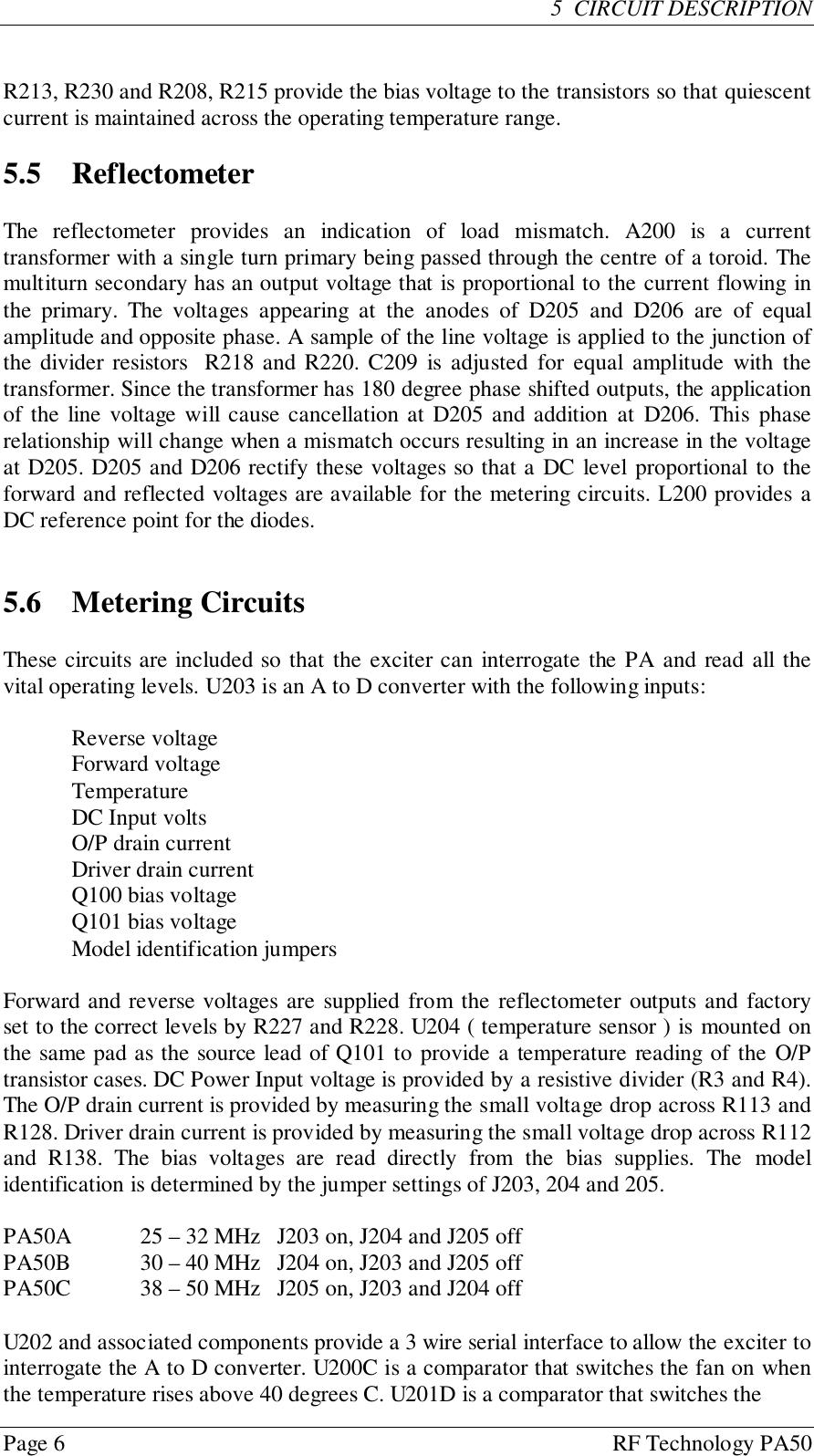
Eclipse SeriesRF Technologyrfinfo@rftechnology.com.auNovember, 2001PA50 AmplifierOperation and Maintenance ManualThis manual is produced by RF Technology Pty Ltd10/8 Leighton Place, Hornsby  2077  AustraliaCopyright  © 2001, RF Technology
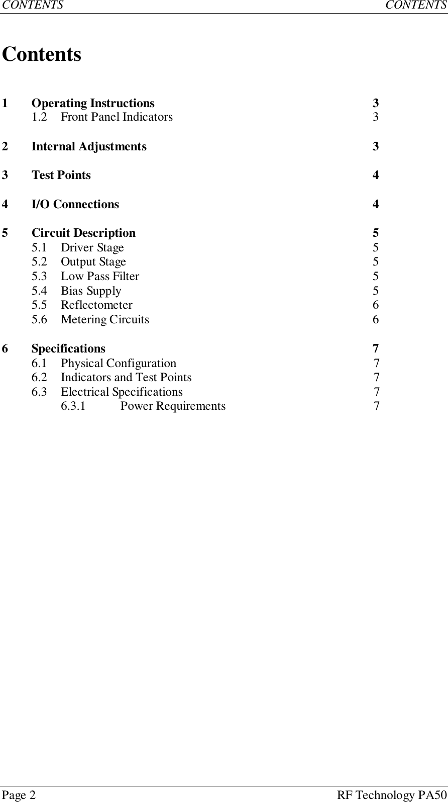
Page 2 RF Technology PA50CONTENTS CONTENTSContents1 Operating Instructions 31.2 Front Panel Indicators 32 Internal Adjustments 33 Test Points 44 I/O Connections 45 Circuit Description 55.1 Driver Stage 55.2 Output Stage 55.3 Low Pass Filter 55.4 Bias Supply 55.5 Reflectometer 65.6 Metering Circuits 66 Specifications 76.1 Physical Configuration 76.2 Indicators and Test Points 76.3 Electrical Specifications 76.3.1 Power Requirements 7
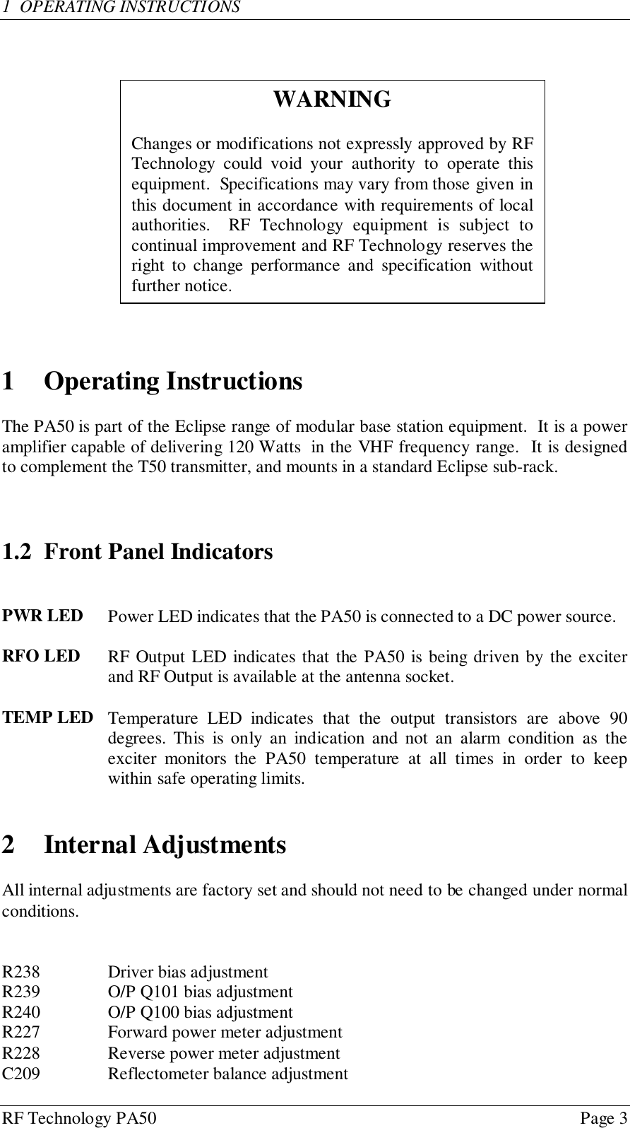
RF Technology PA50 Page 31  OPERATING INSTRUCTIONS1 Operating InstructionsThe PA50 is part of the Eclipse range of modular base station equipment.  It is a poweramplifier capable of delivering 120 Watts  in the VHF frequency range.  It is designedto complement the T50 transmitter, and mounts in a standard Eclipse sub-rack.1.2 Front Panel IndicatorsPWR LED  Power LED indicates that the PA50 is connected to a DC power source.RFO LED  RF Output LED indicates that the PA50 is being driven by the exciterand RF Output is available at the antenna socket.TEMP LED  Temperature LED indicates that the output transistors are above 90degrees. This is only an indication and not an alarm condition as theexciter monitors the PA50 temperature at all times in order to keepwithin safe operating limits.2 Internal AdjustmentsAll internal adjustments are factory set and should not need to be changed under normalconditions.R238 Driver bias adjustmentR239 O/P Q101 bias adjustmentR240 O/P Q100 bias adjustmentR227 Forward power meter adjustmentR228 Reverse power meter adjustmentC209 Reflectometer balance adjustmentWARNINGChanges or modifications not expressly approved by RFTechnology could void your authority to operate thisequipment.  Specifications may vary from those given inthis document in accordance with requirements of localauthorities.  RF Technology equipment is subject tocontinual improvement and RF Technology reserves theright to change performance and specification withoutfurther notice.
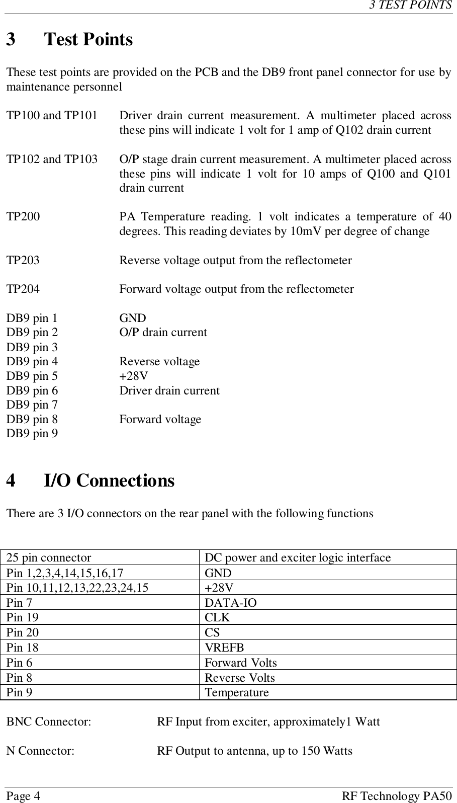
Page 4 RF Technology PA503 TEST POINTS3 Test PointsThese test points are provided on the PCB and the DB9 front panel connector for use bymaintenance personnelTP100 and TP101 Driver drain current measurement. A multimeter placed acrossthese pins will indicate 1 volt for 1 amp of Q102 drain currentTP102 and TP103 O/P stage drain current measurement. A multimeter placed acrossthese pins will indicate 1 volt for 10 amps of Q100 and Q101drain currentTP200 PA Temperature reading. 1 volt indicates a temperature of 40degrees. This reading deviates by 10mV per degree of changeTP203 Reverse voltage output from the reflectometerTP204 Forward voltage output from the reflectometerDB9 pin 1 GNDDB9 pin 2 O/P drain currentDB9 pin 3DB9 pin 4 Reverse voltageDB9 pin 5 +28VDB9 pin 6 Driver drain currentDB9 pin 7DB9 pin 8 Forward voltageDB9 pin 94 I/O ConnectionsThere are 3 I/O connectors on the rear panel with the following functions25 pin connector DC power and exciter logic interfacePin 1,2,3,4,14,15,16,17 GNDPin 10,11,12,13,22,23,24,15 +28VPin 7 DATA-IOPin 19 CLKPin 20 CSPin 18 VREFBPin 6 Forward VoltsPin 8 Reverse VoltsPin 9 TemperatureBNC Connector: RF Input from exciter, approximately1 WattN Connector: RF Output to antenna, up to 150 Watts
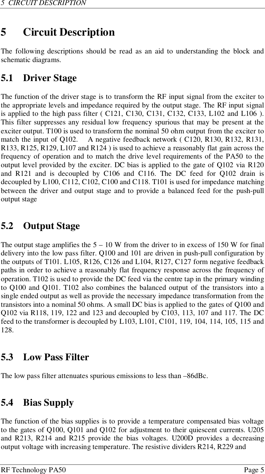
RF Technology PA50 Page 55  CIRCUIT DESCRIPTION5 Circuit DescriptionThe following descriptions should be read as an aid to understanding the block andschematic diagrams.5.1 Driver StageThe function of the driver stage is to transform the RF input signal from the exciter tothe appropriate levels and impedance required by the output stage. The RF input signalis applied to the high pass filter ( C121, C130, C131, C132, C133, L102 and L106 ).This filter suppresses any residual low frequency spurious that may be present at theexciter output. T100 is used to transform the nominal 50 ohm output from the exciter tomatch the input of Q102.    A negative feedback network ( C120, R130, R132, R131,R133, R125, R129, L107 and R124 ) is used to achieve a reasonably flat gain across thefrequency of operation and to match the drive level requirements of the PA50 to theoutput level provided by the exciter. DC bias is applied to the gate of Q102 via R120and R121 and is decoupled by C106 and C116. The DC feed for Q102 drain isdecoupled by L100, C112, C102, C100 and C118. T101 is used for impedance matchingbetween the driver and output stage and to provide a balanced feed for the push-pulloutput stage5.2 Output StageThe output stage amplifies the 5 – 10 W from the driver to in excess of 150 W for finaldelivery into the low pass filter. Q100 and 101 are driven in push-pull configuration bythe outputs of T101. L105, R126, C126 and L104, R127, C127 form negative feedbackpaths in order to achieve a reasonably flat frequency response across the frequency ofoperation. T102 is used to provide the DC feed via the centre tap in the primary windingto Q100 and Q101. T102 also combines the balanced output of the transistors into asingle ended output as well as provide the necessary impedance transformation from thetransistors into a nominal 50 ohms. A small DC bias is applied to the gates of Q100 andQ102 via R118, 119, 122 and 123 and decoupled by C103, 113, 107 and 117. The DCfeed to the transformer is decoupled by L103, L101, C101, 119, 104, 114, 105, 115 and128.5.3 Low Pass FilterThe low pass filter attenuates spurious emissions to less than –86dBc.5.4 Bias SupplyThe function of the bias supplies is to provide a temperature compensated bias voltageto the gates of Q100, Q101 and Q102 for adjustment to their quiescent currents. U205and R213, R214 and R215 provide the bias voltages. U200D provides a decreasingoutput voltage with increasing temperature. The resistive dividers R214, R229 and
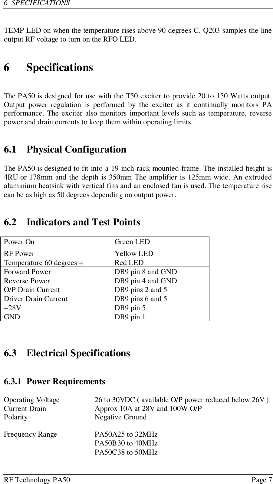
Page 6 RF Technology PA505  CIRCUIT DESCRIPTIONR213, R230 and R208, R215 provide the bias voltage to the transistors so that quiescentcurrent is maintained across the operating temperature range.5.5 ReflectometerThe reflectometer provides an indication of load mismatch. A200 is a currenttransformer with a single turn primary being passed through the centre of a toroid. Themultiturn secondary has an output voltage that is proportional to the current flowing inthe primary. The voltages appearing at the anodes of D205 and D206 are of equalamplitude and opposite phase. A sample of the line voltage is applied to the junction ofthe divider resistors  R218 and R220. C209 is adjusted for equal amplitude with thetransformer. Since the transformer has 180 degree phase shifted outputs, the applicationof the line voltage will cause cancellation at D205 and addition at D206. This phaserelationship will change when a mismatch occurs resulting in an increase in the voltageat D205. D205 and D206 rectify these voltages so that a DC level proportional to theforward and reflected voltages are available for the metering circuits. L200 provides aDC reference point for the diodes.5.6 Metering CircuitsThese circuits are included so that the exciter can interrogate the PA and read all thevital operating levels. U203 is an A to D converter with the following inputs:Reverse voltageForward voltageTemperatureDC Input voltsO/P drain currentDriver drain currentQ100 bias voltageQ101 bias voltageModel identification jumpersForward and reverse voltages are supplied from the reflectometer outputs and factoryset to the correct levels by R227 and R228. U204 ( temperature sensor ) is mounted onthe same pad as the source lead of Q101 to provide a temperature reading of the O/Ptransistor cases. DC Power Input voltage is provided by a resistive divider (R3 and R4).The O/P drain current is provided by measuring the small voltage drop across R113 andR128. Driver drain current is provided by measuring the small voltage drop across R112and R138. The bias voltages are read directly from the bias supplies. The modelidentification is determined by the jumper settings of J203, 204 and 205.PA50A 25 – 32 MHz J203 on, J204 and J205 offPA50B 30 – 40 MHz J204 on, J203 and J205 offPA50C 38 – 50 MHz J205 on, J203 and J204 offU202 and associated components provide a 3 wire serial interface to allow the exciter tointerrogate the A to D converter. U200C is a comparator that switches the fan on whenthe temperature rises above 40 degrees C. U201D is a comparator that switches the
RF Technology PA50 Page 76  SPECIFICATIONSTEMP LED on when the temperature rises above 90 degrees C. Q203 samples the lineoutput RF voltage to turn on the RFO LED.6 SpecificationsThe PA50 is designed for use with the T50 exciter to provide 20 to 150 Watts output.Output power regulation is performed by the exciter as it continually monitors PAperformance. The exciter also monitors important levels such as temperature, reversepower and drain currents to keep them within operating limits.6.1 Physical ConfigurationThe PA50 is designed to fit into a 19 inch rack mounted frame. The installed height is4RU or 178mm and the depth is 350mm The amplifier is 125mm wide. An extrudedaluminium heatsink with vertical fins and an enclosed fan is used. The temperature risecan be as high as 50 degrees depending on output power.6.2 Indicators and Test PointsPower On Green LEDRF Power Yellow LEDTemperature 60 degrees + Red LEDForward Power DB9 pin 8 and GNDReverse Power DB9 pin 4 and GNDO/P Drain Current DB9 pins 2 and 5Driver Drain Current DB9 pins 6 and 5+28V DB9 pin 5GND DB9 pin 16.3 Electrical Specifications6.3.1 Power RequirementsOperating Voltage 26 to 30VDC ( available O/P power reduced below 26V )Current Drain Approx 10A at 28V and 100W O/PPolarity Negative GroundFrequency Range PA50A25 to 32MHzPA50B30 to 40MHzPA50C38 to 50MHz
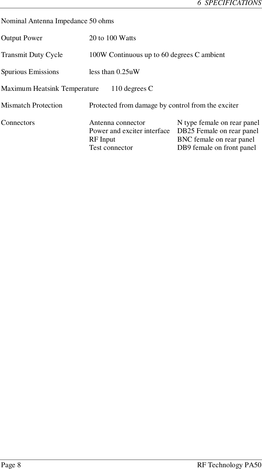
Page 8 RF Technology PA506  SPECIFICATIONSNominal Antenna Impedance 50 ohmsOutput Power 20 to 100 WattsTransmit Duty Cycle 100W Continuous up to 60 degrees C ambientSpurious Emissions less than 0.25uWMaximum Heatsink Temperature 110 degrees CMismatch Protection Protected from damage by control from the exciterConnectors Antenna connector N type female on rear panelPower and exciter interface DB25 Female on rear panelRF Input BNC female on rear panelTest connector DB9 female on front panel

Navigation menu