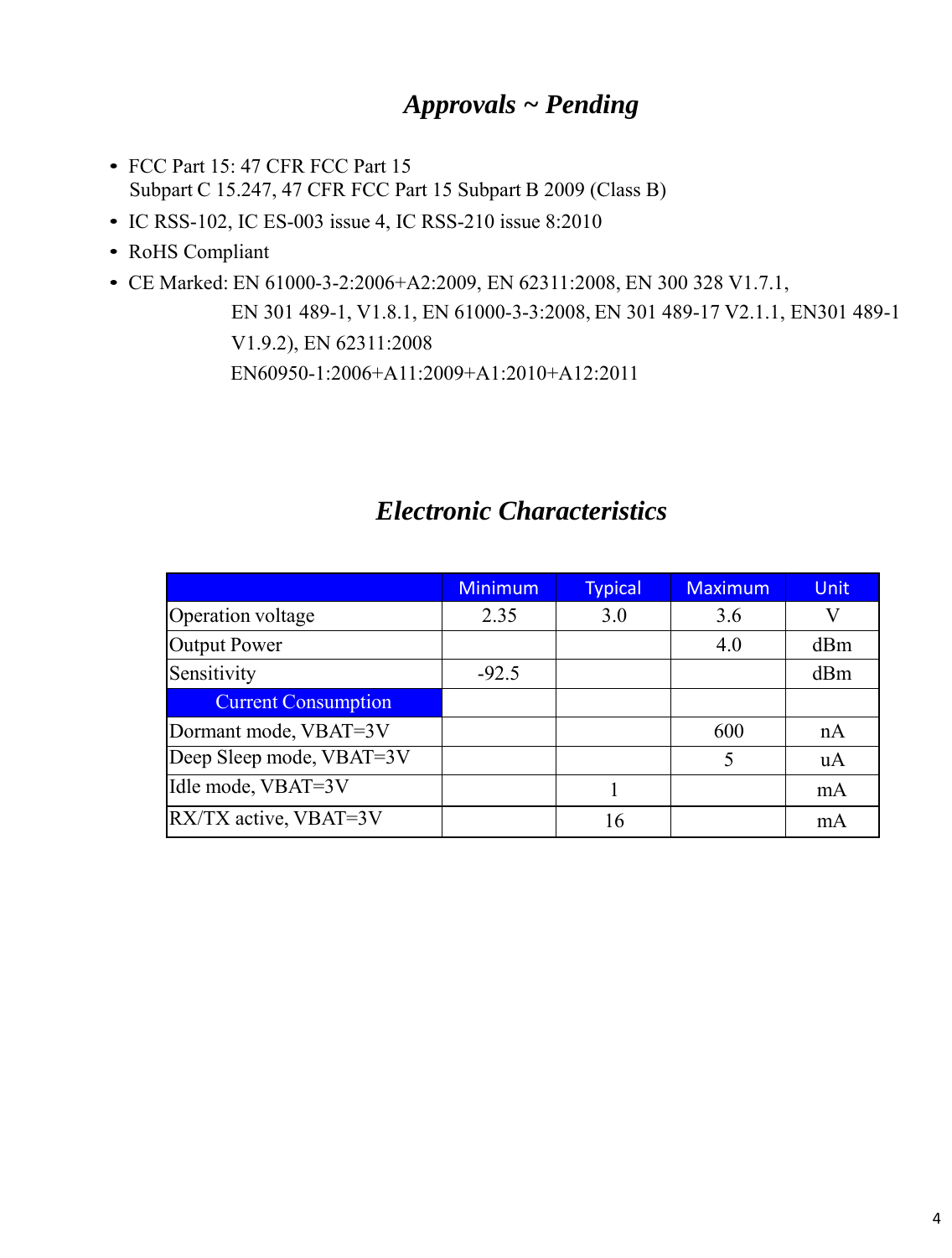
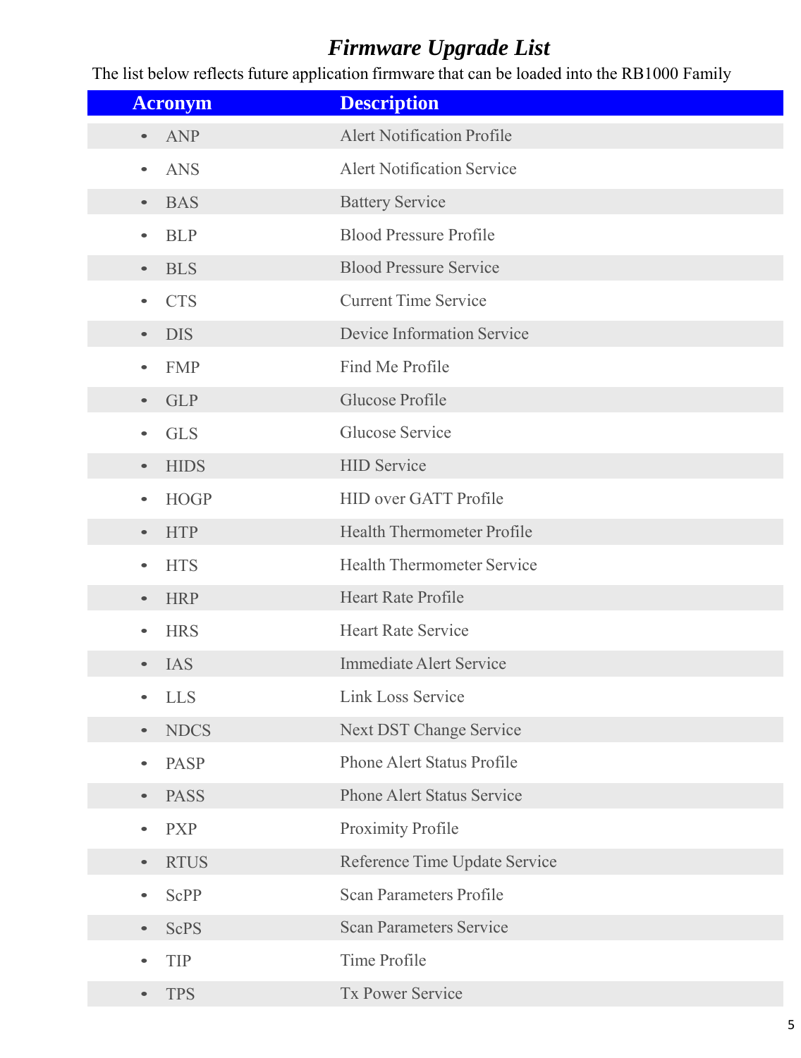
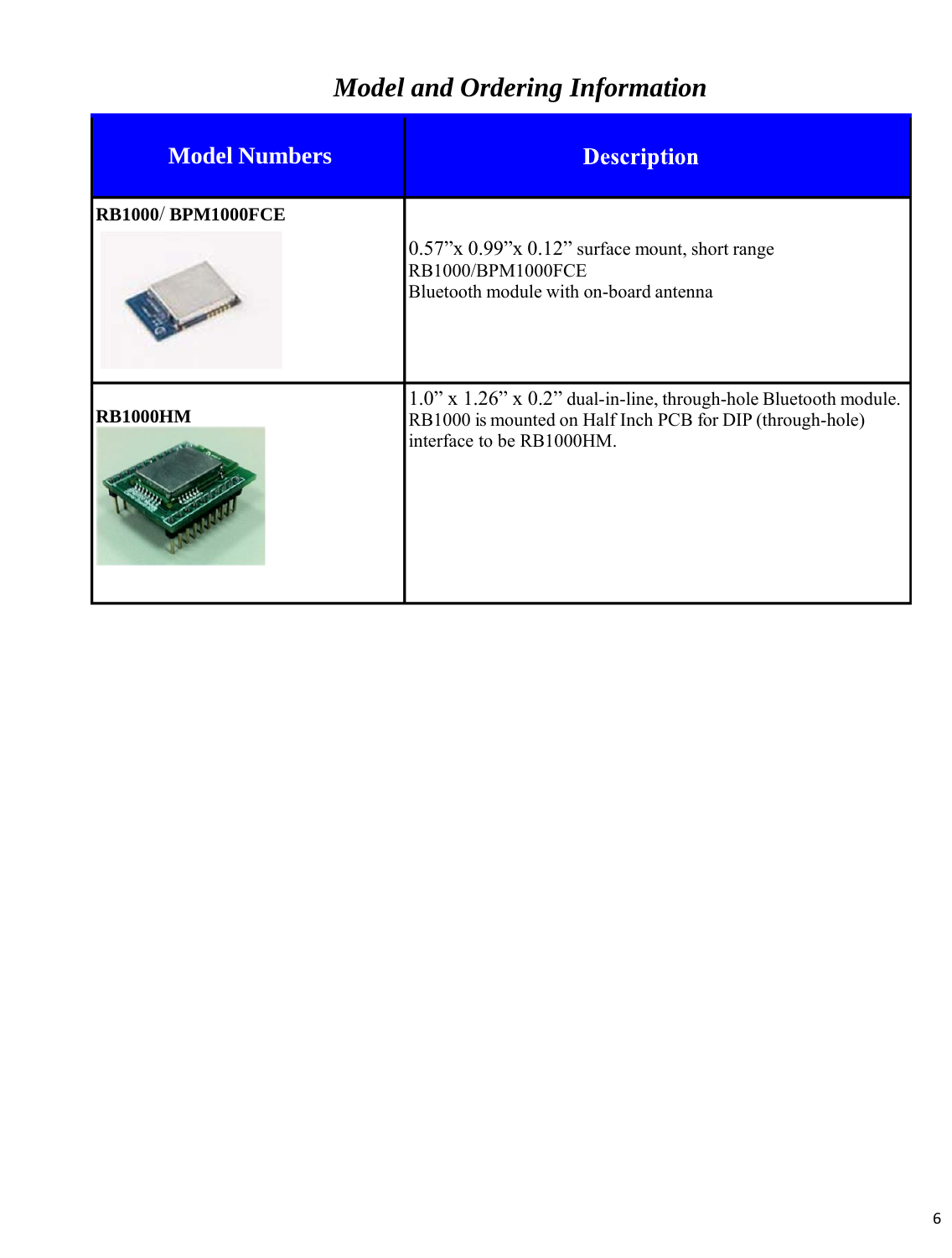
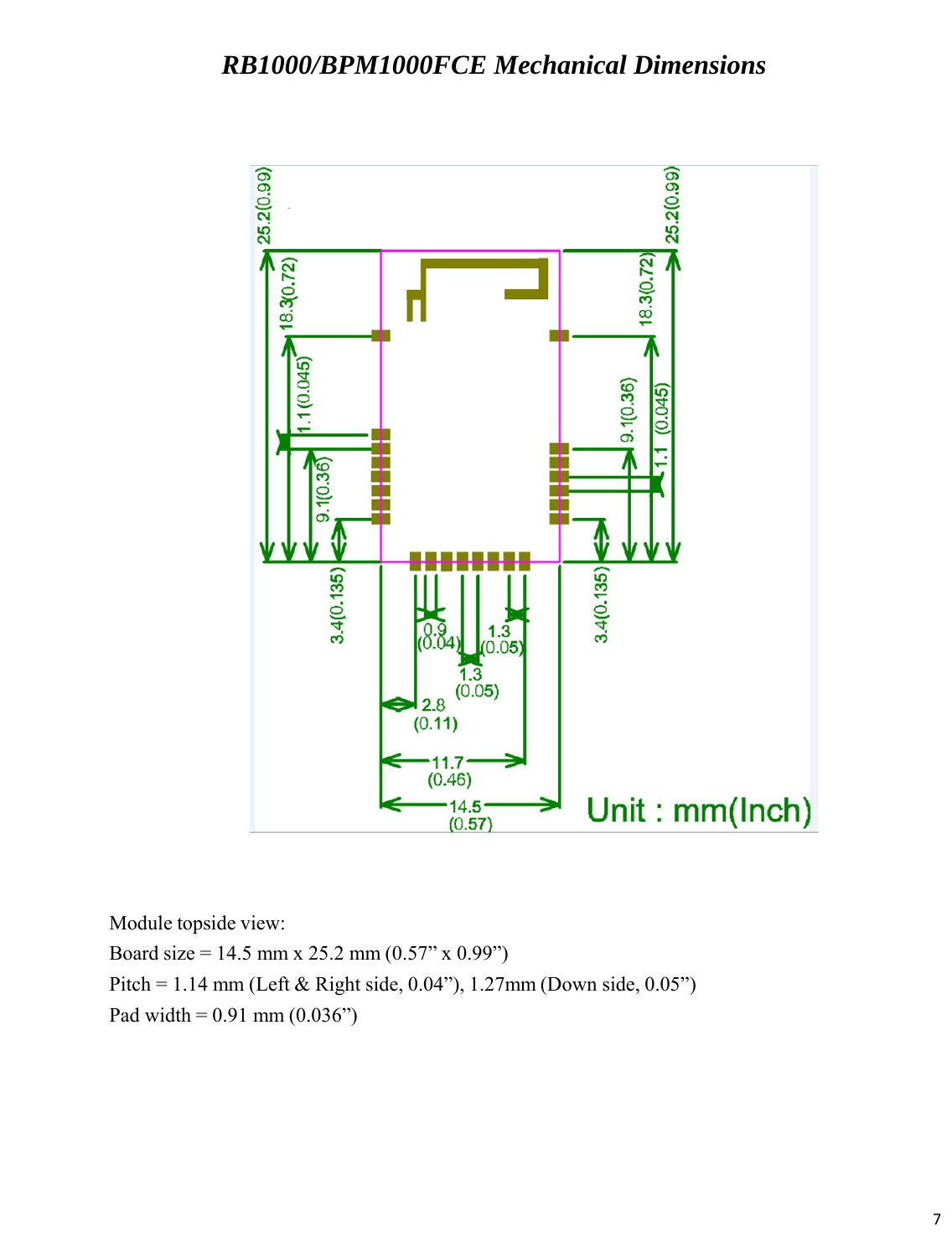
Radicom Research RB1000 Bluetooth Modules User Manual
Radicom Research Inc Bluetooth Modules
UserManual.wiki
>
Radicom Research
>
RB1000 User Manual
User manual
Navigation menu
Upload a User Manual
Namespaces
Wiki Guide
HTML
PDF
Info
Views
User Manual
Discussion / Help
Navigation
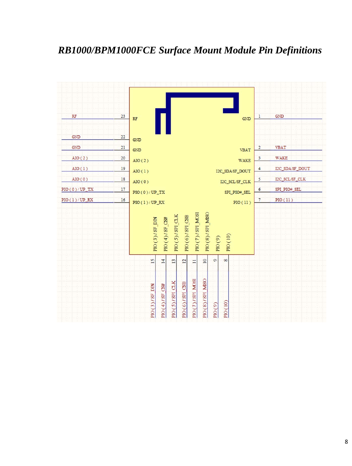
![9 RB1000/BPM1000FCE Module Pin Descriptions Pin # Pin Name Type Description I/O Voltage Range1 GND - Ground - 2 VBAT PWR I Battery input and regulatorenable (active high). 2.35V ~ 3.6V 3 WAKE PWR I Input to wake CSR1000 QFN from hibernate or dormant. Vil: -0.4V ~ 0.4V Vih: 0.7VDD ~VDD+0.4V 4 I²C_SDA /SF_DOUT I/O or O I²C data input / output or SPI serial Flash data output (SF_DOUT) Vil: -0.4V ~ 0.4V Vih: 0.7VDD ~VDD+0.4V Vol: 0.4V Max Voh 0.75VDD Min 5 I²C_SCL / SF_CLK O or O I²C clockorSPI serial Flashclock output (SF_CLK) Vol: 0.4V Max Voh 0.75VDD Min 6 SPI_PIO#_SEL I Selects SPI debug onPIO[8:5]. Vil: -0.4V ~ 0.4V Vih: 0.7VDD ~VDD+0.4V 7 PIO (11) I/O Programmable I/O line Vil: -0.4V ~ 0.4V Vih: 0.7VDD ~VDD+0.4V Vol: 0.4V Max Voh 0.75VDD Min 8 PIO (10) I/O Programmable I/O line Vil: -0.4V ~ 0.4V Vih: 0.7VDD ~VDD+0.4V Vol: 0.4V Max Voh: 0.75VDD Min 9 PIO (9) CONNECTED O PIO (9) will go high whenBluetooth connection established. Vol: 0.4V Max Voh: 0.75VDD Min 10 PIO (8) / SPI_MISO I/O or I Programmable I/O line or debug SPI MISO selected by SPI_PIO# Vil: -0.4V ~ 0.4V Vih: 0.7VDD ~VDD+0.4V Vol: 0.4V Max Voh: 0.75VDD Min 11 PIO (7) / SPI_MOSI I/O or O Programmable I/O line or debug SPI MOSI selected by SPI_PIO# Vil: -0.4V ~ 0.4V Vih: 0.7VDD ~VDD+0.4V Vol: 0.4V Max Voh 0.75VDD Min 12 PIO (6) / SPI_CSB I/O or I Programmable I/O line or debug SPI chip select (CS#) selected by SPI_PIO#. Vil: -0.4V ~ 0.4V Vih: 0.7VDD ~VDD+0.4V Vol: 0.4V Max Voh: 0.75VDD Min 13 PIO (5) / SPI_CLK I/O or O Programmable I/O line or debug SPI CLK selected by SPI_PIO#. Vil: -0.4V ~ 0.4V Vih: 0.7VDD ~VDD+0.4V Vol: 0.4V Max Voh: 0.75VDD Min 14 PIO (4) / SF_CS# I/O or I Programmable I/O line or SPI serial flash chip select (SF_CS#) Vil: -0.4V ~ 0.4V Vih: 0.7VDD ~VDD+0.4V Vol: 0.4V Max Voh: 0.75VDD Min 15 PIO (3) / SF_DIN I/O or I Programmable I/O line or SPI serial flash data (SF_DIN) input Vil: -0.4V ~ 0.4V Vih: 0.7VDD ~VDD+0.4V Vol: 0.4V Max Voh: 0.75VDD Min 16 PIO (1) / UP_RX I/O or I Programmable I/O line or UART RX Vil: -0.4V ~ 0.4V Vih: 0.7VDD ~VDD+0.4V Vol: 0.4V Max Voh: 0.75VDD Min 17 PIO (0) / UP_ TX I/O or O Programmable I/O line or UART TX Vil: -0.4V ~ 0.4V Vih: 0.7VDD ~VDD+0.4V Vol: 0.4V Max](https://usermanual.wiki/Radicom-Research/RB1000/User-Guide-1812958-Page-9.png)
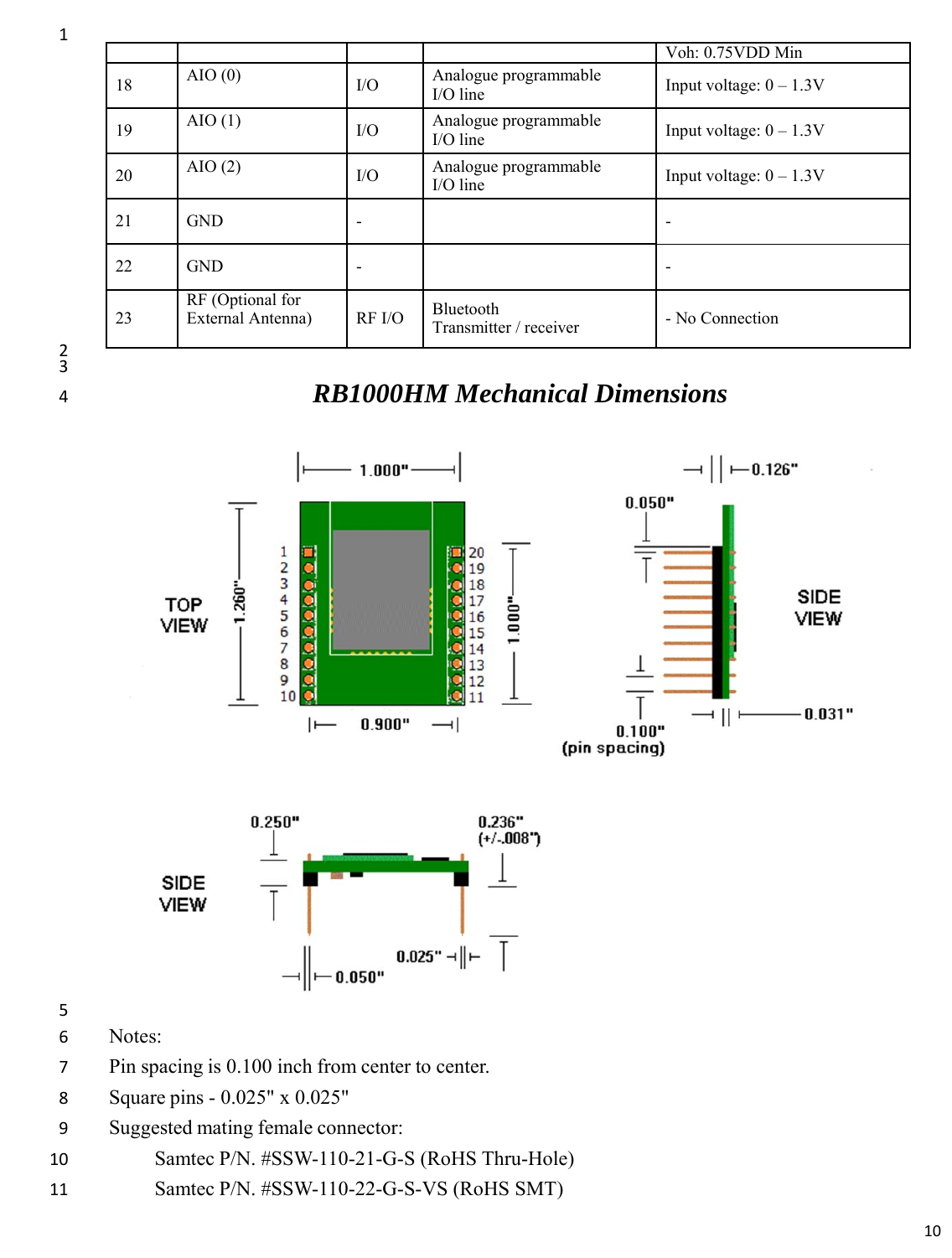
![11 RB1000HM Pin Descriptions Pin # Pin Name Type Description I/O Voltage Range 1 GND - - 2 KEY N/C No Connections - No Pin – This Pin has been removed. Add a key to the mating connector toprevent from being plugged in backwards. 3 AIO (1) I/O Analogue programmableI/O line Input voltage: 0 – 1.3V 4 AIO (0) I/O Analogue programmableI/O line Input voltage: 0 – 1.3V 5 UART_TX I/O or O UART TX Vil: -0.4V ~ 0.4V Vih: 0.7VDD ~VDD+0.4V Vol: 0.4V Max Voh: 0.75VDD Min 6 UART_RX I/O or I UART RX Vil: -0.4V ~ 0.4V Vih: 0.7VDD ~VDD+0.4V Vol: 0.4V Max Voh: 0.75VDD Min 7 PIO (3) / SF_DIN I/O or I Programmable I/O line or SPI serial flash data (SF_DIN) input Vil: -0.4V ~ 0.4V Vih: 0.7VDD ~VDD+0.4V Vol: 0.4V Max Voh: 0.75VDD Min 8 PIO (4) / SF_CS# I/O or I Programmable I/O line or SPI serial flash chip select (SF_CS#) Vil: -0.4V ~ 0.4V Vih: 0.7VDD ~VDD+0.4V Vol: 0.4V Max Voh: 0.75VDD Min 9 SPI_CLK I/O or O Programmable I/O line or debug SPI CLK selected by SPI_PIO#. Vil: -0.4V ~ 0.4V Vih: 0.7VDD ~VDD+0.4V Vol: 0.4V Max Voh: 0.75VDD Min 10 PIO (6) / SPI_CSB I/O or I Programmable I/O line or debug SPI chip select (CS#) selected by SPI_PIO#. Vil: -0.4V ~ 0.4V Vih: 0.7VDD ~VDD+0.4V Vol: 0.4V Max Voh:0.75VDD Min 11 PIO (7) / SPI_MOSI I/O or O Programmable I/O line or debug SPI MOSI selected by SPI_PIO# Vil: -0.4V ~ 0.4V Vih: 0.7VDD ~VDD+0.4V Vol: 0.4V Max Voh: 0.75VDD Min 12 PIO (8) / SPI_MISO I/O or I Programmable I/O line or debug SPI MISO selected by SPI_PIO# Vil: -0.4V ~ 0.4V Vih: 0.7VDD ~VDD+0.4V Vol: 0.4V Max Voh: 0.75VDD Min 13 PIO (9) CONNECTED O PIO (9) will go high when Bluetooth connection established. Vol: 0.4V Max Voh: 0.75VDD Min 14 PIO (10) I/O Programmable I/O line Vil: -0.4V ~ 0.4V Vih: 0.7VDD ~VDD+0.4V Vol: 0.4V Max Voh: 0.75VDD Min 15 PIO (11) I/O Programmable I/O line Vil: -0.4V ~ 0.4V Vih: 0.7VDD ~VDD+0.4V Vol: 0.4V Max Voh: 0.75VDD Min 16 SPI_PIO#_SEL I Selects SPI debug onPIO[8:5]. Vil: -0.4V ~ 0.4V Vih: 0.7VDD ~VDD+0.4V 17 I²C_SCL / SF_CLK O or O I²C clockor SPI serial Flash clockoutput (SF_CLK) Vol: 0.4V Max Voh: 0.75VDD Min 18 I²C_SDA /SF_DOUT I/O or O I²C data input / output or SPI serialFlash data output (SF_DOUT) Vil: -0.4V ~ 0.4V Vih: 0.7VDD ~VDD+0.4V Vol: 0.4V Max Voh: 0.75VDD Min 19 WAKE PWR I Input to wake CSR1000 QFN fromhibernate or dormant. Vil: -0.4V ~ 0.4V Vih: 0.7VDD ~VDD+0.4V 20 VBAT PWR I Batteryinput and regulatorenable(active high). 2.35V-3.6V](https://usermanual.wiki/Radicom-Research/RB1000/User-Guide-1812958-Page-11.png)