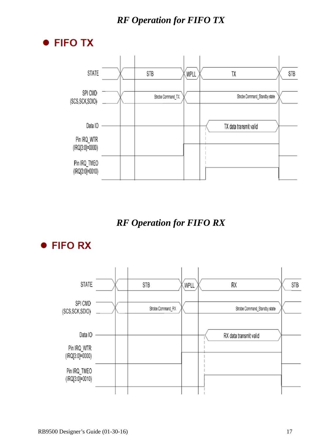
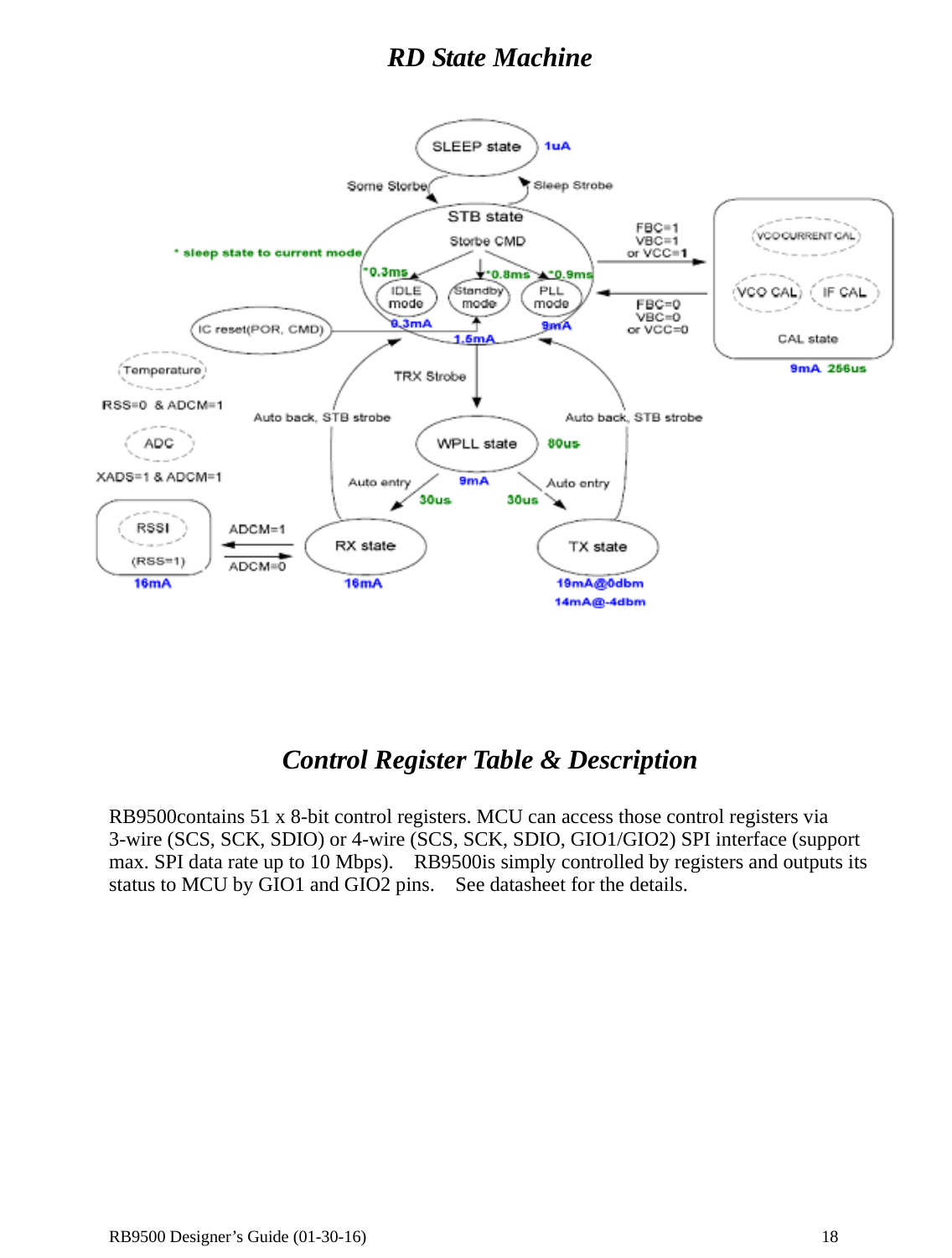
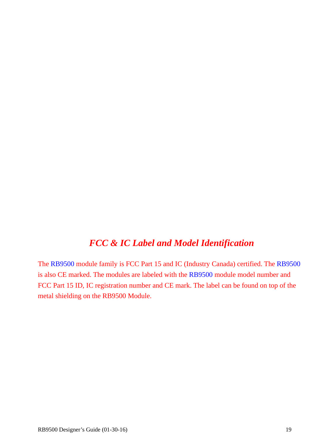
Radicom Research RB9500 2.4G wireless module User Manual RB9500 Designer s Guide 0331

Radicom Research Inc 2.4G wireless module RB9500 Designer s Guide 0331

Contents

User Manual

Radicom Research, Inc. Preliminary Designer’s Guide for the  RB9500 RB9500MB MDK9500  2.4GHz Transceiver Module                                          RB9500                     RB9500MB    RoHS Compliant   January 30, 2016
 RB9500 Designer’s Guide (01-30-16)               2 Table of Contents    Introduction ............................................................................................... 3 Important Information about FCC,IC,CE Certification ....................................... 3 Applications ......................................................................................................... 4 Features ................................................................................................................ 4 Electronic Specifications ..................................................................................... 5 Model and Ordering Information ......................................................................... 6 Block Diagram ..................................................................................................... 7 RB9500Mechanical Dimensions   ....................................................................... 8 RB9500Surface Mount Module Pin Definitions & Descriptions ........................ 9 RB9500MB Main Board RS232 DB9 Pin Definitions ........................................ 10 RB9500MB Function Display & Operation Descriptions ................................... 11 Layout Design Suggestions ................................................................................. 12 4-Wire to 3-Wire Interface Diagram .................................................................... 13 R/W CTRL REG timing diagram ........................................................................ 14 R/W CTRL REG timing diagram for Reset ......................................................... 14 R/W ID Diagram.................................................................................................. 15 R/W FIFO Diagram ............................................................................................. 15 Interface for W Strobe ......................................................................................... 16 RF Format ............................................................................................................ 16 RF Operation for FIFO TX .................................................................................. 17 RF Operation for FIFO RX ................................................................................. 17 RD  State  Machine ................................................................................................ 18 Control Register Table & Description ................................................................. 18 Limited Warranty ................................................................................................. 19 Contacting Radicom ............................................................................................ 21       Information furnished by Radicom Research is believed to be accurate and reliable. However Radicom Research assumes no responsibility for its use, or any infringement of patents or other rights of third parties that may result from its use. Radicom Research reserves the right to change circuitry at any time without notice. This document is subject to change without notice.
 RB9500 Designer’s Guide (01-30-16)               3 Introduction  Thank you for choosing Radicom RB9500Module. We are committed to providing you quality service and technical support. The RB9500modules are designed to meet OEM’s needs of embedding short-range, low power, wireless data connectivity to their products. The RB9500offers a quick and simple solution for wireless 2.4GHz FSK/GFSK Transceiver.    The RB9500 module is designed for 2.4GHz ISM band wireless applications.    The module integrates both high sensitivity receiver (- 95dBm @ 500Kbps) and high efficiency power amplifier (up to 1dBm).    In low data rate application, RB9500has special strength for long LOS (line-of-sight) distance because of its ultra high sensitivity (-107 dBm @ 2Kbps, - 104 dBm @ 25Kbps) with no requirement of external LNA or PA.    Based on Data Rate Register (0x0E), user can configure on-air data rates from 2Kbps to 500Kbps.  The RB9500module supports fast settling time (130 us) for frequency hopping system.    For packet handling, the RB9500 has built-in separated 64-bytes TX/RX FIFO (could be extended to 256 bytes) for data buffering and burst transmission, CRC for error detection, FEC for 1-bit data correction per code word, RSSI for clear channel assessment, data whitening for data encryption / decryption.    For power saving, RB9500supports sleep mode, idle mode, standby mode. For easy-to-use, RB9500has an unique SPI command set to control internal state machine.    Based on the command set via SPI bus, MCU can control everything from power saving, TX delivery, RX receiving, channel monitoring, frequency hopping to auto calibrations.    In addition, RB9500supports two general purpose I/O pins, GIO1 and GIO2, to inform MCU its status so that MCU could use either polling or interrupt scheme to do radio control.    Hence, it is very easy to monitor radio transmission between MCU and RB9500via digital interface.   Important Information about FCC, IC, CE Certification  RB9500 series is using 2.4GHz ISM band with non-standard protocol for transmitting power, timing, cadence and modulation. Therefore, any firmware involved to change those parameters will affect to FCC/IC/CE Certification.
 RB9500 Designer’s Guide (01-30-16)               4 Applications • Wireless keyboard and mouse • Remote control • Helicopter and airplane radio controller • 2400 ~ 2483.5 MHz ISM system • Wireless metering and building automation • Wireless toys and game controllers    Features  • Small sizes: 0.57” x 0.99” x 0.12” (14.5mm x 25.2mm x 3.0mm) • Frequency band: 2400 ~ 2483.5MHz. • FSK or GFSK modulation • Low current consumption: RX 16mA, TX 20mA (at 0dBm output power). • Low sleep current (1.5 uA). • On chip regulator, support input voltage 2.0 ~ 3.6 V. • Programmable data rate from 2Kbps to 500Kbps. • Programmable TX power level from – 20 dBm to 1 dBm. • Ultra High sensitivity: • -95dBm at 500Kbps on-air data rate • -97dBm at 250Kbps on-air data rate • -104dBm at 25Kbps on-air data rate • -107dBm at 2Kbps on-air data rate • Fast settling time (130 us) synthesizer for frequency hopping system. • Built-in Battery Detector. • Support low cost crystal (6 / 8 /12 / 16 / 20 / 24MHz). • Support crystal sharing, (1 / 2 / 4 / 8MHz) to MCU. • Support Frequency Compensation. • Easy to use: • Support 3-wire or 4-wire SPI interface • ONE register setting for new channel frequency. • 8-bits Digital RSSI for clear channel indication. • Fast exchange mode during TRX role switching. • Auto RSSI measurement. • Auto Calibrations.
 RB9500 Designer’s Guide (01-30-16)               5 • Auto IF function. • Auto CRC Check. • Auto FEC by (7, 4) Hamming code (1 bit error correction / code word). • Data Whitening for encryption and decryption. • Separated 64 bytes RX and TX FIFO. • Easy FIFO / Segment FIFO / FIFO Extension (up to 256 bytes). • Support direct mode with recovery clock output to MCU. • Support direct mode with frame sync signal to MCU.    Electronic Specifications  Item  Specification  Remark Supply voltage  2.0V ~ 3.6V   Current consumption 1.5uA    @Sleep mode 0.3mA   @Idle mode 1.9mA   @Stand-by mode 16mA    @Rx mode 20mA    @Tx mode (Pout = 0dBm) Typical Frequency  2400 – 2483 MHz  ISM band Transmit output power  -1±1 dBm @ room temperature  Typical Rx sensitivity -107 dBm (typical) @ 2Kbps mode, Dev = 124KHz -104 dBm (typical) @ 25Kbps mode, Dev = 124KHz -97 dBm (typical) @ 250Kbps mode, Dev = 186KHz -95 dBm (typical) @ 500Kbps mode, Dev = 186KHz BER≦1E-3 Modulation  FSK or GFSK   Transmission distance  18 meters  BER≦1E-3 Interface  5 pin 2mm header, 6 pin 2mm header   Dimension  0.57”(W) x 0.99”(L) x 0.12” (H) 14.5mm(W) x 25.2mm(L) x 3.0mm(H)   Operating temperature  -40℃ ~ +85℃
 RB9500 Designer’s Guide (01-30-16)               6 Model and Ordering Information  Model Numbers  Description  RB9500   0.57”x 0.99”x 0.12” surface mount, short range RB95002.4GHz FSK/GFSK Transceiver module with on-board antenna  Models: RB9500  RB9500MB  RB9500 Evaluation Board.    Embedded a RB9500transceiver module and a 8051 microcontroller.Models: RB9500MB     MDK9500    RB9500 Evaluation Kit.    Each kit consists of the following components:  Models: MDK9500   2ea ~ RB9500MB   2ea ~ 6 feet USB Power Cables (A to B)   2ea ~ RS232 DB9 Null Modem Cable
 RB9500 Designer’s Guide (01-30-16)               7 Block Diagram
 RB9500 Designer’s Guide (01-30-16)               8 RB9500Mechanical Dimensions                      Module side view: Height = 3.0 mm (0.117”)     Module top view:           Board size = 14.5 mm x 25.2 mm (0.57” x 0.99”)      Pitch = 2.0 mm (0.078”)      Pad = 0.914 x 1.524 mm (0.035” x 0.060”)
 RB9500 Designer’s Guide (01-30-16)               9 RB9500Surface Mount Module Pin Definitions    RB9500Module Pin Descriptions  Pin #  Pin Name  Description1   GND   Ground  2  VIN  RF Module Supply Voltage Input 2.0V ~ 3.6V 3   CKO  Clock Output 4   GIO2  General Purpose I/O 2 5    GIO1  General Purpose I/O 1 6   GND  Ground 7    SPI_SDIO  SPI Data I/O 8   SPI_CLK  SPI Clock 9   SPI_CSB  SPI Chip Selection 10    X_CLK  X’tal Clock Output 11   GND  Ground NOTE 1 : This module relies on host device to provide power supply to function.
 RB9500 Designer’s Guide (01-30-16)               10  RB9500MB Main Board RS232 DB9 Pin Definitions  The pin definitions of DB9 used on the RB9500MB RS232 Serial Connector are as follows:  1.    DCD:    Input, Carrier Detect 2.  RXD:  Input, Received Data 3.    TXD:  Output, Transmit data 4.  DTR:    Output, Data Terminal ready 5. GND: Ground 6   DSR:  Input, Data Set Ready 7.    RTS:  Output, Request to Send 8.    CTS:  Input, Clear to Send 9.  RI:    Input, Ring Indicator
 RB9500 Designer’s Guide (01-30-16)               11 RB9500MB Function Display   1. USB 5V slot (USB1)  7. IDC 10 header for C2 Interface (P7) 2. Main board power switch (S5)  8. RB9500Module 3. UART enable/disable switch (S6)  9. 4-wire SPI interface header (P5) 4. RS232 male DE-9 connector (J1)  10. 3-wire SPI interface header (P6)   5. UART Interface header (P4)  11. C8051 MCU PIOs header (P8:P1.0 to P2.7) 6. DC 3.3V output header (P3)  12. C8051 MCU PIOs header (P9:P3.0 to P4.7)     RB9500MB Operation Description  a. Apply power through USB 5V slot (USB1)   b. Turn on Main board power switch (S5). The Main board power indicator (D2) will turn on. c. RB9500module is now up and running.
 RB9500 Designer’s Guide (01-30-16)               12 Layout Design Suggestions  • General Layout Rules- All Printed Circuit Boards must comply with UL94V0 standard for flammability. Always use RoHS compliant Parts and materials.    • Suggestions for Layout: 1. Do not place Power circuit, X’tal, Inductor, etc near RF area.  2. The bigger Antenna clearance area, the better. The Antenna itself needs to stay away from any circuit or component at least 3mm. Antenna clearance area means Top and Bottom both required to be cleared.  3. Do not use metal materials on design where near Antenna area. For example, battery snaps, USB connector, iron case, etc.  These guidelines are for design reference; real performance still depends on actual design.
 RB9500 Designer’s Guide (01-30-16)               13  4-Wire to 3-Wire Interface Diagram
 RB9500 Designer’s Guide (01-30-16)               14 R/W CTRL REG timing diagram        R/W CTRL REG timing diagram for Reset
 RB9500 Designer’s Guide (01-30-16)               15 R/W ID Diagram     R/W FIFO Diagram
 RB9500 Designer’s Guide (01-30-16)               16 Interface for W Strobe      RF Format
 RB9500 Designer’s Guide (01-30-16)               17 RF Operation for FIFO TX      RF Operation for FIFO RX
 RB9500 Designer’s Guide (01-30-16)               18 RD State Machine       Control Register Table & Description  RB9500contains 51 x 8-bit control registers. MCU can access those control registers via 3-wire (SCS, SCK, SDIO) or 4-wire (SCS, SCK, SDIO, GIO1/GIO2) SPI interface (support max. SPI data rate up to 10 Mbps).    RB9500is simply controlled by registers and outputs its status to MCU by GIO1 and GIO2 pins.    See datasheet for the details.
 RB9500 Designer’s Guide (01-30-16)               19                      FCC & IC Label and Model Identification  The RB9500 module family is FCC Part 15 and IC (Industry Canada) certified. The RB9500 is also CE marked. The modules are labeled with the RB9500 module model number and FCC Part 15 ID, IC registration number and CE mark. The label can be found on top of the metal shielding on the RB9500 Module.
 RB9500 Designer’s Guide (01-30-16)               20                  Note: Models RB9500 will have an additional Product ID label containing the HM model number.
 RB9500 Designer’s Guide (01-30-16)               21     Important Regulatory Compliance and User Information The final product with the modules installed needs to be tested for FCC Part 15, IC (Industry Canada) CE, EMI/RFI compliance. Radicom certification documentation will help streamline the final product approval process. Contact Radicom for more information. To maintain compliance in the finished product, carefully follow guidelines in this section. This device is intended only for OEM integrators under the following condition:  The transmitter module may not be co-located with any other transmitter or antenna. As long as this condition is met, further transmitter testing will not be required. However, the OEM integrator is still responsible for testing their end product for any additional compliance requirements required with the module installed (for example, digital device emissions, PC peripheral requirements, etc). IMPORTANT NOTE: In the event that this condition cannot be met then the FCC authorization is no longer considered valid and the FCC ID cannot be used on the final product. In these circumstances, the OEM integrator will be responsible for re-evaluating the end product (including the transmitter) and obtaining a separate FCC authorization.    Host (End Product) Labeling Requirements The final end product must be labeled in a visible area with the following:     " Contains TX FCC ID: K7T-RB9500 ".   RB9500 is for the model of the module used in the end equipment. The label shall be securely affixed to a permanently attached part of the device, in a location where it is visible or easily accessible to the user, and shall not be readily detachable. The label shall be sufficiently durable to remain fully legible and intact on the device in all normal conditions of use throughout the device’s expected lifetime. These requirements may be met either by a separate label or nameplate permanently attached to the device or by permanently imprinting or impressing the label directly onto the device. The label text shall be legible without the aid of magnification, but is not required to be larger than 8-point font size.    End User Information
 RB9500 Designer’s Guide (01-30-16)               22 This equipment complies with FCC radiation exposure limits set forth for an uncontrolled environment. End users must follow the specific operating instructions for satisfying RF Exposure compliance. The end user should NOT be provided any instructions on how to remove or install the device. The user’s manual for end users must include the following information in a prominent location.  FCC RF Radiation Exposure Statement IMPORTANT NOTE:  To comply with the FCC RF exposure compliance requirements, this device must not be co-located or operating in conjunction with any antenna or transmitter. This device contains a low power transmitter. When this device is operational, use only with the supplied, or recommended antenna. Unauthorized antenna, modification, or attachments could damage the transmitter and may violate FCC regulations. Changes or modifications not expressly approved by the manufacturer or party responsible for compliance could void the user’s authority to operate the equipment.  FCC Interference Statement This device complies with Part 15 of the FCC Rules. Operation is subject to the following conditions:    (1) This device may not cause harmful interference                          (2) This device must accept any interference received, including interference that    may cause undesired operation. This equipment has been tested and found to comply with the limits for a Class B digital device, pursuant to Part 15 of the FCC Rules. These limits are designed to provide reasonable protection against harmful interference in a residential installation. This equipment generates and radiates radio frequency energy and, if not installed and used in accordance with the instructions, may cause harmful interference to radio communications. There is no guarantee that interference will not occur in a particular installation. If this equipment does cause harmful interference to radio or television reception, which can be determined by turning the equipment off and on, the user is encouraged to try to correct the interference by one of the following measures: ●  Reorient or relocate the receiving antenna. ●  Increase the separation between the equipment and receiver. ●  Connect the equipment into an outlet on a circuit different from that to which the receiver is connected. ●  Consult the dealer or an experienced radio/TV technician for assistance.
 RB9500 Designer’s Guide (01-30-16)               23  IC (Industry Canada) Statement:  Host(End Product) Labeling requirements The final edn product must be labeled in a visible area with the following:   “ Contains IC: 2377A-RB9500 ”  “This device complies with Industry Canada license-exempt RSS standard(s). Operation is subject to the following two conditions: (1) this device may not cause interference, and    (2) this device must accept any interference, including interference that may cause undesired operation of the device”     Le present appareil est conforme aux CNR d’Industrie Canada applicables aux appareils radio exempts de license. L’exploitation est autorisee aux deux conditions suivantes: (1) l’appareil ne doit pas produire de brouillage, et (2) l’utilisateur de l’appareil doit acceptor tout brouillage radioelectrique subi, meme si le brouillage est susceptible d’en compromettre le fonctionnement.    CE Declaration of Conformity For the following equipment:     Radicom Research Inc. Bluetooth Module     Model: RB9500 are herewith confirmed to comply with the requirements set out in the Council (European parliament) Directive on the Approximation of the Laws of the   Member States relating to Electromagnetic Compatibility of Radio and Telecom device (1999/5/CE). For the evaluation regarding this Directive, the following   standards were applied:        EN 61000-4-2:2010, EN 300 328 V1.7.1:2006, EN 62311: 2008,   EN 61000-4-3:2010, EN 301 489-17 V2.1.1, EN301 489-1 V1.92, EN 60950-1:2006+A11:2009+A1: 2010+A12:2011,   This equipment is marked with              and can be used throughout the European community.   France – 2.4GHz for Metropolitan France: In all Metropolitan departments, wireless LAN frequencies can be used under the following conditions, either for public or private use: •  Indoor use: maximum power (EIRP*) of 100 mW for the entire 2400-2483.5 MHz frequency band
 RB9500 Designer’s Guide (01-30-16)               24 •  Outdoor use: maximum power (EIRP*) of 100 mW for the 2400-2454 MHz band and with maximum power (EIRP*) of 10 mW for the 2454-2483 MHz band  Europe – R&TTE Compliance Statement: Hereby, Radicom Research Inc. declares that this equipment complies with the essential requirements and other relevant provisions of DIRECTIVE 1999/5/CE OF THE EUROPEAN PARLIAMENT AND THE COUNCIL of March 9, 1999 on radio equipment and telecommunication terminal Equipment and the mutual recognition of their conformity (R&TTE).   Limited Warranty   Warranty Coverage and Duration  Radicom Research, Inc. (“RRI”) warrants to the original purchaser its RRI-manufactured products (“Product”) against defects in material and workmanship under normal use and service for a period of one year from the date of delivery.  During the applicable warranty period, at no charge, RRI will, at its option, either repair, replace or refund the purchase price of this Product, provided it is returned in accordance with the terms of this warranty to RRI.      Repair, at the option of RRI, may include the replacement of parts, boards or other components with functionally equivalent reconditioned or new parts, boards or other components.    Replaced parts, boards or other components are warranted for the balance of the original applicable warranty period.    All replaced items shall become the property of RRI.  RRI MAKES NO GUARANTEE OR WARRANTY THAT THE PRODUCT WILL PREVENT OCCURRENCES, OR THE CONSEQUENCES THEREOF, WHICH THE PRODUCT IS DESIGNED TO DETECT.  This expressed limited warranty is extended by RRI to the original end-user purchaser only, and is not assignable or transferable to any other party.    This is the complete warranty for the Product manufactured by RRI, and RRI assumes no obligation or liability for additions or modifications to this warranty.    In no case does RRI warrant the installation, maintenance or service of the Product.    RRI is not responsible in any way for any ancillary equipment not furnished by RRI that is attached to or used in connection with the Product, or for operation of the Product with any ancillary equipment, and all such equipment is expressly excluded
 RB9500 Designer’s Guide (01-30-16)               25 from this warranty.    Because of wide variations in topographical and atmospheric conditions, which may require availability of repeater stations or of particular radio frequencies, RRI assumes no liability for range, coverage or suitability of the Product for any particular application.      Buyer acknowledges that RRI does not know a particular purpose for which buyer wants the product, and that buyer is not relying on RRI’s skill and judgment to select or furnish suitable goods.     What this Warranty does NOT Cover: (a) Defects or damage resulting from use of the Product in other than its normal and customary manner. (b) Defects or damage from misuse, accident or neglect. (c) Defects of damage from improper testing, operation, maintenance, installation, alteration, modification or adjustment. (d) Disassembly or repair of the Product in such a manner as to adversely affect performance or prevent adequate inspection and testing to verify any warranty claim. (e) Any Product that has had its serial number or date code removed or made illegible.   How to Receive Warranty Service:  To obtain warranty service, contact RRI by phone (408)-383 9006 for RMA Department or email to rma@radi.com for an RMA (Return Merchandise Authorization) number.    Deliver or send the Product, transportation and insurance prepaid to RRI, with the RMA number clearly marked on the outside of the package.     General Provision  This warranty sets forth the full extent of RRI’s responsibilities regarding the Product.   Repair, replacement or refund of the purchase price, at RRI’s option, is the exclusive remedy.  THIS WARRANTY IS GIVEN IN LIEU OF ALL OTHER EXPRESSED WARRANTIES.   ANY APPLICABLE IMPLIED WARRANTIES, INCLUDING WITHOUT LIMITATION, THE IMPLIED WARRANTY OF MERCHANTABILITY, ARE LIMITED TO THE DURATION OF THIS LIMITED WARRANTY.    TO THE FULLEST EXTENT
 RB9500 Designer’s Guide (01-30-16)               26 PERMITTED BY LAW, RRI DISCLAIMS ANY LIABILITY FOR DAMAGES IN EXCESS OF THE PURCHASE PRICE OF THE PRODUCT, FOR ANY LOSS OF USE, LOSS OF TIME, INCONVENIENCE, COMMERCIAL LOSS, LOST PROFITS OR SAVING OR OTHER INCIDENTAL, SPECIAL OR CONSEQUENTIAL DAMAGES ARISING OUT OF THE USE OR INABILITY TO USE OR FAILURE OF SUCH PRODUCT.   Contacting Radicom Research  If more information or technical support is needed, please contact us:   2148 Bering Drive San Jose, CA. 95131 Telephone: (408) 383 9006 Fax: (408) 383 9007 or e-mail: sales@radi.com http://www.radi.com/

Navigation menu