Radio Frequency Systems BDA48660 SINGLE CHANNEL BI-DIRECTIONAL CDMA AMPLIFIER User Manual JD16049 0
Radio Frequency Systems Inc SINGLE CHANNEL BI-DIRECTIONAL CDMA AMPLIFIER JD16049 0
USER MANUAL

Part Number: J24004
Drawing Control: JD16049
INSTRUCTION MANUAL
FOR
48660 SINGLE CHANNEL CDMA
PCS BI-DIRECTIONAL
AMPLIFIER
2 Ryan Road, Marlboro, New Jersey 07746-1899
Tel:1-908-462-1880 Fax: (908) 462-6919
Part Number: J24004
Drawing Control: JD16049
Disclaimer
All information and statements contained herein are accurate to the best of the knowledge of Celwave and
RFS, but neither Celwave or RFS make any warranty with respect thereto, including without limitation any
results which may be obtained from the products described herein or the infringement by such products of any
proprietary rights of any persons. Use or application of such information or statements is at the user’s sole
risk, without any liability on the part of Celwave or RFS. Nothing herein shall be construed as license of or
recommendation for use which infringes upon any proprietary rights of any person. Product material and
specifications are subject to change without notice. All sales of the products described herein are subject to
Celwave’s standard terms of sale and the specific terms of any particular sale.

i
Part Number: J24004
Drawing Control: JD16049
TABLE OF CONTENTS
PRODUCT OVERVIEW and GENERAL INFORMATION----------------------------------------------1
PERFORMANCE
BLOCK DIAGRAM
FCC TYPE ACCEPTANCE
OUTLINE DRAWING -------------------------------------------------------------------------------------------2
GENERAL SPECIFICATIONS---------------------------------------------------------------------------------3
OVERVALL THEORY OF OPERATION--------------------------------------------------------------------3
DOWNLINK
OUTPUT POWER
CHANNEL AND ATTENUATION PROGRAMMING
PROGRAMMING GUIDE --------------------------------------------------------------------------------------5
POWER CONTROL AND INTERMODULATION--------------------------------------------------------7
REMOTE INTERFACE------------------------------------------------------------------------------------------7
RF CONNECTIONS----------------------------------------------------------------------------------------------8
AC/DC POWER ---------------------------------------------------------------------------------------------------8
ENVIRONMENTAL CONSIDERATIONS ------------------------------------------------------------------9
PERIODIC MAINTENANCE-----------------------------------------------------------------------------------9

ii
Part Number: J24004
Drawing Control: JD16049
TABLE OF CONTENTS (Continued)
SET UP AND INSTALLATION CONSIDERATIONS--------------------------------------------------10
ANTENNA ISOLATION -------------------------------------------------------------------------------------- 10
DIAGNOSTICS AND TROUBLESHOOTING ----------------------------------------------------------- 11
Front Panel LEDs
Gain or Coverage Reduction
Excessive Intermodulation or Spurious
ORDERING AND RETURNING FOR REPAIR---------------------------------------------------------- 12
WARRANTY ----------------------------------------------------------------------------------------------------12
READ THIS MANUAL; WARRANTY DOES NOT COVER IMPROPER HANDLING!
1
Part Number: J24004
Drawing Control: JD16049
PRODUCT OVERVIEW and GENERAL INFORMATION
The 48660 Bi-directional Amplifier is a single channel CDMA PCS repeater. It is designed to amplify just one
CDMA channel while rejecting all others. The 48660 is tunable over the entire PCS band and provides
approximately 65 dB of gain to the selected channel. The unit is designed to enhance PCS coverage in buildings,
basements, parking garages and other RF shielded environments. The unit is wall mountable and requires no
periodic maintenance.
PERFORMANCE
This unit has a RF section that provides 65 dB of gain, down conversion and IF filtering. The IF filters use SAW
technology for optimal selectivity. After upconversion, the output stage filtering attenuates LO leakage while
amplifying the selected channel to the set output power level. The standard product offers channel tuning locally by
means of dipswitch or RS-232 connection. The control settings are for frequency selection and gain control to limit
power. Automatic power control assumes a wide input power dynamic range and intermodulation distortion
control.
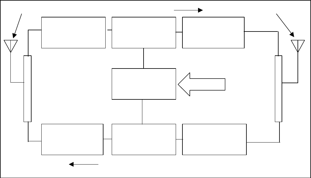
BLOCK DIAGRAM
Figure X.1 System Block Diagram
FCC COMPLIANCE
SYNTHESIZER
UP LINK IF SECTION
DOWN LINK IF
SECTION
DOWN LINK INPUT
SECTION
UP LINK INPUT
SECTION
UP LINK OUTPUT
SECTION
DOWN LINK OUTPUT
SECTION
D
DA
AT
TA
A
L
LI
IN
NE
ES
S
A
AN
ND
D
C
CO
ON
NT
TR
RO
OL
L
D
U
P
L
E
X
E
R
D
U
P
L
E
X
E
R
FROM DONOR SITE
TO SERVICE AREA
DOWN LINK SIGNAL FLOW
U
UP
PL
LI
IN
NK
KS
SI
IG
GN
NA
AL
LF
FL
LO
OW
W
2
Part Number: J24004
Drawing Control: JD16049
FCC Compliance No: (Application in process.)
3
Part Number: J24004
Drawing Control: JD16049
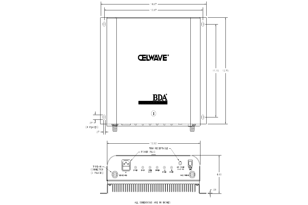
OUTLINE DRAWING
Intelli

4
Part Number: J24004
Drawing Control: JD16049
GENERAL SPECIFICATIONS
Specifications may change without notice. All specifications stated as typical unless otherwise noted.
Down Link (Base to Mobile) Up Link (Mobile to Base)
Frequency 1930 to 1990 MHz 1850 to 1910 MHz
Typical Pass Band at 3 dB down
Typical Pass Band at 30 dB down ( +22 dB Gain)
Gain at Min Attenuation -Typ. 65 dB 65 dB
Gain Range, Manual Attenuator 15 dB 15 dB
Pass Band Ripple - Typ.
Noise Figure - Typ. 6.5 dB 6.5 dB
Output Power Set Point CDMA +23 dBm +23 dBm
Power Control Range +20 dB +20 dB
3rd Order Intercept Point, IP3 +44 dBm +44 dBm
Recommended Input Power Maximum, Composite -35 to -80 dBm -35 to -80 dBm
Maximum Input Power No Damage 0 dBm 0 dBm
Impedance - Nom 50 Ohms
VSWR, Input, Both Ports 2.0:1
Propagation Delay < 5.0 microsecond
Power 120 VAC @ 750 mA
Operating Temperature -30 to +50o C
Connectors, RF N Female
Diagnostics Interface RS-232
Programming DIP Switches & RS-232
Size (WxHxD), in. (mm) 14.7 x 12.8 x 4.6 (374 x 325 x 117)
Weight 19 lbs
OVERALL THEORY OF OPERATION
The 48660 is a single channel CDMA PCS Bi Directional Amplifier. It is comprised of two main components; Up
Link and Down Link. With each component made up of 3 sections, Input Section, IF Section, and Output Section.
Refer to Figure X.1. Since the Up Link and Down Link components are virtually identical, only the theory of
operation for the Down Link will be presented.
DOWN LINK
Signals originating from the PCS base station are received at the antenna and fed to the input of the 48660. They are
then filtered through the first duplexer to attenuate any non-PCS signals which may be received at the antenna. The
signal(s) is then fed to the input stage for amplification and additional filtering. If the signal as detected in the output
stage is too large, it will receive attenuation in the input section as well. At this point the signal is then fed into the
IF section for down conversion, filtering through the SAW devices, additional amplification, and finally up
conversion back to it’s original frequency. By using the same Local Oscillator for the down and up conversions,
frequency accuracy is maintained. The newly up converted signal is then an exact replica of the original signal only
very highly filtered to get rid of any other signals near it. This signal is fed into the output section where additional
amplification takes place as well as Local Oscillator filtering. Special care has been taken in the design of the 48660
Intelli BDA to maintain good spectral purity of the CDMA signal. It meets or exceeds the spectral regrowth criteria
of ANSI J-STD-008 at it’s rated output power.
5
Part Number: J24004
Drawing Control: JD16049
OUTPUT POWER
After all of the amplification and filtering is completed, a sample of the signal is measured and the output power is
predicted. This information is fed back to the Digital section and a Power Control voltage is generated and fed to the
input section attenuators to reduce the power if needed. This comprises the power control loop. Its response is slow
compared to the CDMA closed loop power control, so it will not interfere with the system.
The output power of both RF links is set at the factory to be nominally +23 dBm. As the input signal increases to a
level which, when added to the gain produces an output power larger than the set point, the power control loop takes
over to reduce the gain accordingly. This insures that under all input signal conditions below the maximum input
signal level (-35 dBm), that the integrity of the CDMA spectrum be maintained.
CHANNEL AND ATTENUATION PROGRAMMING
Programming of the 48660 is accomplished either by DIP Switch Programming of the unit, or remotely via a
computer (See Remote Programming Manual TBD). This section addresses the DIP Switch Programming of the
Channel and Attenuator Settings.
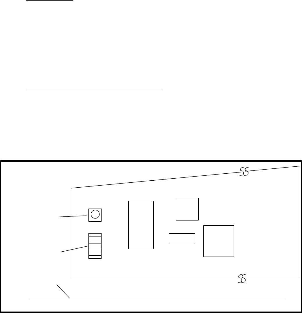
The DIP Switches (S1) are on the Digital Board located just inside the shroud. They can be accessed by opening the
shroud and with a pointed instrument such as a pencil or pen, can be set to certain values to set the frequency
(Channel Number) and the Attenuation Settings for the Down Link and Up Link, see Figure XX. Care should be
taken when closing the 48660 Intelli BDA shroud to disengage the latching mechanism located at the back of the
shroud. Forcing the shroud closed will damage the shroud.
Load Button
DIP Switches
Front Panel
Figure X.X Location of DIP Switch
A7 MSB
A0 LSB
1
1
0
0
SW2
S1
Not Drawn to Scale
6
Part Number: J24004
Drawing Control: JD16049
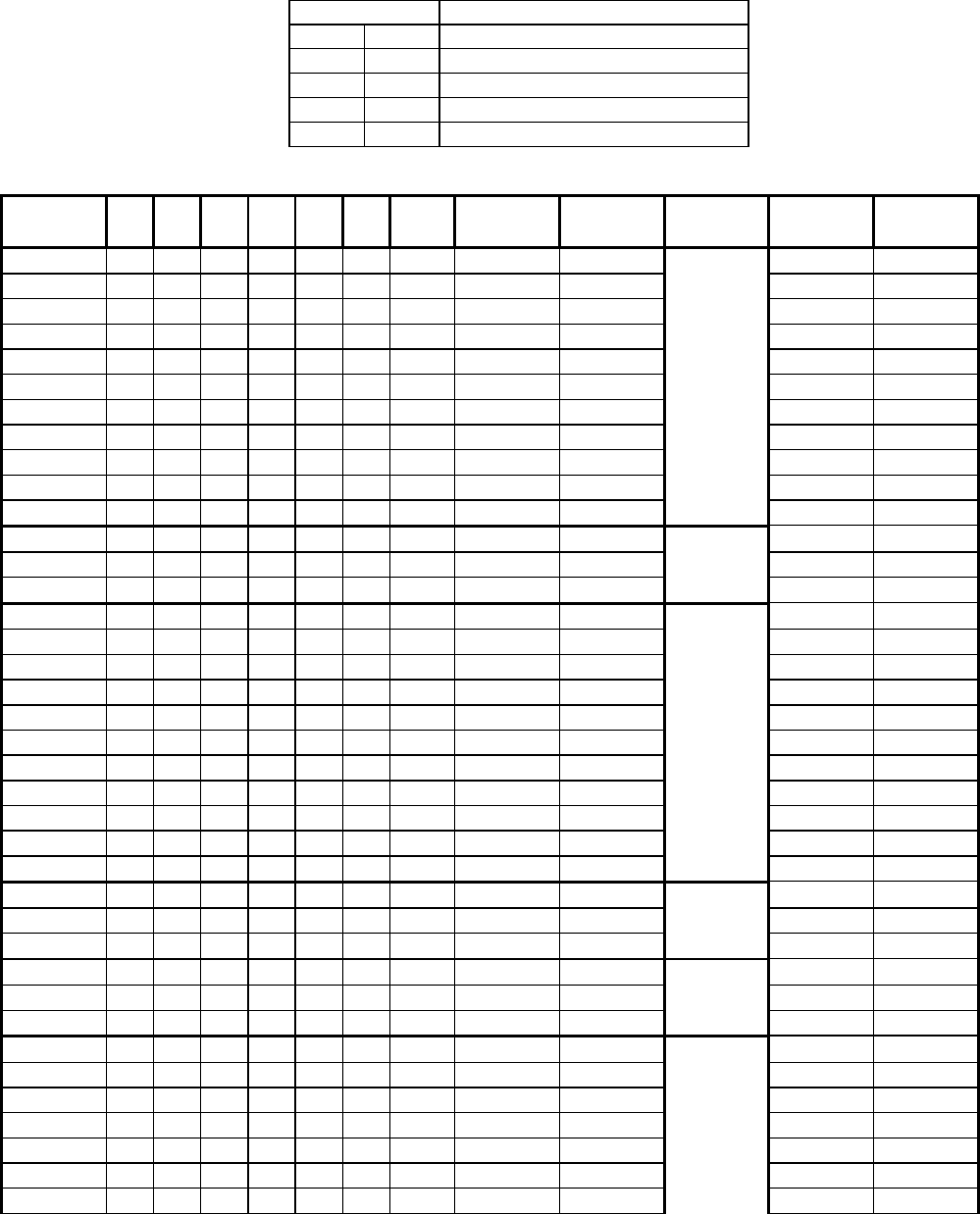
Upper MSBs Programming Function
A7 A6
0 0 Channel Number
0 1 Down Link Attenuation
1 0 Up Link Attenuation
1 1 Reserved for future use
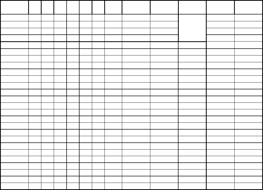
DEC NUM A5 A4 A3 A2 A1 A0 CH # FREQ DL
(MHZ) FREQ UL
(MHZ) BLOCK DL ATTN
(dB) TYP UL ATTN
(dB) TYP
0 0 0 0 0 0 0 25 1931.25 1851.25 19.1 19.1
1 0 0 0 0 0 1 50 1932.50 1852.50 19.1 19.1
2 0 0 0 0 1 0 75 1933.75 1853.75 19.1 19.1
3 0 0 0 0 1 1 100 1935.00 1855.00 19.1 19.1
4 0 0 0 1 0 0 125 1936.25 1856.25 A19.1 19.1
5 0 0 0 1 0 1 150 1937.50 1857.50 19.1 19.1
6 0 0 0 1 1 0 175 1938.75 1858.75 19.1 19.1
7 0 0 0 1 1 1 200 1940.00 1860.00 19 19
8 0 0 1 0 0 0 225 1941.25 1861.25 18.9 18.9
9 0 0 1 0 0 1 250 1942.50 1862.50 18.9 18.9
10 0 0 1 0 1 0 275 1943.75 1863.75 18.9 18.9
11 0 0 1 0 1 1 325 1946.25 1866.25 18.8 18.8
12 0 0 1 1 0 0 350 1947.50 1867.50 D18.8 18.8
13 0 0 1 1 0 1 375 1948.75 1868.75 18.7 18.7
14 0 0 1 1 1 0 425 1951.25 1871.25 18.6 18.6
15 0 0 1 1 1 1 450 1952.50 1872.50 18.6 18.6
16 0 1 0 0 0 0 475 1953.75 1873.75 18.5 18.5
17 0 1 0 0 0 1 500 1955.00 1875.00 18.5 18.5
18 0 1 0 0 1 0 525 1956.25 1876.25 18.4 18.4
19 0 1 0 0 1 1 550 1957.50 1877.50 B18.3 18.3
20 0 1 0 1 0 0 575 1958.75 1878.75 18.2 18.2
21 0 1 0 1 0 1 600 1960.00 1880.00 18 18
22 0 1 0 1 1 0 625 1961.25 1881.25 17.9 17.9
23 0 1 0 1 1 1 650 1962.50 1882.50 17.7 17.7
24 0 1 1 0 0 0 675 1963.75 1883.75 17.4 17.4
25 0 1 1 0 0 1 725 1966.25 1886.25 17.1 17.1
26 0 1 1 0 1 0 750 1967.50 1887.50 E16.6 16.6
27 0 1 1 0 1 1 775 1968.75 1888.75 16.1 16.1
28 0 1 1 1 0 0 825 1971.25 1891.25 15.5 15.5
29 0 1 1 1 0 1 850 1972.50 1892.50 F14.8 14.8
30 0 1 1 1 1 0 875 1973.75 1893.75 14 14
31 0 1 1 1 1 1 925 1976.25 1896.25 13.31 13.3
32 1 0 0 0 0 0 950 1977.50 1897.50 12.5 12.5
33 1 0 0 0 0 1 975 1978.75 1898.75 11.7 11.7
34 1 0 0 0 1 0 1000 1980.00 1900.00 10.9 10.9
35 1 0 0 0 1 1 1025 1981.25 1901.25 10.2 10.2
36 1 0 0 1 0 0 1050 1982.50 1902.50 C9.5 9.5
37 1 0 0 1 0 1 1075 1983.75 1903.75 8.7 8.7
7
Part Number: J24004
Drawing Control: JD16049
DEC NUM A5 A4 A3 A2 A1 A0 CH #
NFREQ DL
(MHZ) FREQ UL
(MHZ) BLOCK DL ATTN
(dB) TYP UL ATTN
(dB) TYP
38 1 0 0 1 1 0 1100 1985.00 1905.00 8.0 8.0
39 1 0 0 1 1 1 1125 1986.25 1906.25 7.2 7.2
40 1 0 1 0 0 0 1150 1987.50 1907.50 6.9 6.9
41 1 0 1 0 0 1 1175 1988.75 1908.75 5.7 5.7
42 1 0 1 0 1 0 25 1931.25 1851.25 DEFAULT 5.0 5.0
43 1 0 1 0 1 1 25 1931.25 1851.25 DEFAULT 4.4 4.4
44 1 0 1 1 0 0 25 1931.25 1851.25 DEFAULT 3.9 3.9
45 1 0 1 1 0 1 25 1931.25 1851.25 DEFAULT 3.4 3.4
46 1 0 1 1 1 0 25 1931.25 1851.25 DEFAULT 3.0 3.0
47 1 0 1 1 1 1 25 1931.25 1851.25 DEFAULT 2.7 2.7
48 1 1 0 0 0 0 25 1931.25 1851.25 DEFAULT 2.3 2.3
49 1 1 0 0 0 1 25 1931.25 1851.25 DEFAULT 2.0 2.0
50 1 1 0 0 1 0 25 1931.25 1851.25 DEFAULT 1.8 1.8
51 1 1 0 0 1 1 25 1931.25 1851.25 DEFAULT 1.6 1.6
52 1 1 0 1 0 0 25 1931.25 1851.25 DEFAULT 1.4 1.4
53 1 1 0 1 0 1 25 1931.25 1851.25 DEFAULT 1.2 1.2
54 1 1 0 1 1 0 25 1931.25 1851.25 DEFAULT 1.0 1.0
55 1 1 0 1 1 1 25 1931.25 1851.25 DEFAULT 0.8 0.8
56 1 1 1 0 0 0 25 1931.25 1851.25 DEFAULT 0.6 0.6
57 1 1 1 0 0 1 25 1931.25 1851.25 DEFAULT 0.5 0.5
58 1 1 1 0 1 0 25 1931.25 1851.25 DEFAULT 0.35 0.35
59 1 1 1 0 1 1 25 1931.25 1851.25 DEFAULT 0.2 0.2
60 1 1 1 1 0 0 25 1931.25 1851.25 DEFAULT 0.1 0.1
61 1 1 1 1 0 1 25 1931.25 1851.25 DEFAULT 0.1 0.1
62 1 1 1 1 1 0 25 1931.25 1851.25 DEFAULT 0 0
63 1 1 1 1 1 1 25 1931.25 1851.25 DEFAULT 0 0
Figure X.Y cont
Programming is done by first selecting the mode (upper 2 digits, A6 & A7), then setting the desired value (lower 6
digits) and pressing the load button (SW2). The 48660 will automatically set the desired value. See Tables X.X and
X.Y for values.
The frequency of the Down Link and Up Link are calculated as follows:
FDL = 1930 MHz + 0.05 * N
FUL = 1850 MHz + 0.05 * N
Where N is the Channel Number
Attenuation values are considered typical and need to be optimized once the 48660 is installed.
The 48660 Intelli BDA will remember the last programmed channel number and attenuation values and will tune to
these values automatically upon subsequent power up initializations.

8
Part Number: J24004
Drawing Control: JD16049
POWER CONTROL AND INTERMODULATION
Power control circuitry is provided to prevent excess output power and, thus, excess 3rd order intermodulation
distortion (IMD). IMD levels are a function of the output power and the IP3 of the amplifier stages [IM = 3(Po) -
2(IP3)]. The FCC regulations specify the maximum IMD levels at -13 dBm. Each BDA is tested and set for
maximum IMD levels of -13 dBm in either RF link. The resultant power setting is the "Usable Output Power" in
the general specifications. However, the typical IMD for PCS 1900 is below -30 dBm.
The Power control circuitry senses output power. If the output power attempts to exceed the factory setting,
generally due to strong input signals, the Power control circuitry introduces gain attenuation, maintaining output
power to the preset limit [Pin + Gain - Attenuation = Pout]. When the input signal is too strong, the attenuation
range of the Power Control circuitry is exceeded; the output power will increase beyond the factory setting. In this
situation, it is likely that IMD levels will exceed -13 dBm. If this is expected to be a consistent problem, some input
attenuation should be provided.
The yellow LEDs, "UL PWR and DL PWR", on the front panel will light up whenever the Power Control circuitry
is active. The advantage of using Power control circuitry stage is two-fold. First, the dynamic range of the
amplifier is increased. A wider range of input signal levels can be handled by the system. This advantage can also
be stated in terms of gain. More gain can be put into the system to handle weak signals without risking premature
compression and excessive intermodulation emissions due to stronger signals. The second significant advantage is
that intermodulation products are kept to acceptable levels. As more channels become active, or as some signals
become stronger, gain is reduced and total output power is kept constant.
REMOTE INTERFACE
TYPE OF SERVICE:
The intelliBDA is designed to be used on standard device telephone lines connected to the telephone line by means
of a standard jack called the USOC RJ-11C (or USOC FJ45S). Connection to telephone company provided coin
service (central office implemented systems) is prohibited. Connection to party lines service subject to state tariffs.
TELEPHONE COMPANY PROCEDURES:
The goal of the telephone company is to provide you with the best service it can. In order to do this; it may
occasionally be necessary for them to make changes in their equipment, operations or procedures. These changes
might affect your service or the operation of your equipment, the telephone company will give you notice, in writing,
to allow you to make any changes necessary to maintain uninterrupted service.
In certain circumstances, it may be necessary for the telephone company to request information from you concerning
the equipment, which you have connected to your telephone line. Upon request of the telephone company, provide
the FCC registration number and the ringer equivalence number (REN); both of these items are listed on the
equipment label. The sum of all of the RENs on your telephone lines should be less than five in order to assure
proper service from the telephone company. In some cases, a sum of five may not be usable on a given line.
IF PROBLEM ARISE:
If any of your telephone equipment is not operating properly, you should immediately remove it from your telephone
line, as it may cause harm to the telephone network. If the telephone company notes a problem, they may temporarily

9
Part Number: J24004
Drawing Control: JD16049
discontinue service. When practical, they will notify you in advance of this disconnection. If advance notice is not
feasible, you will be notified as soon as possible. When you are notified, you will be given the opportunity to correct
the problem and be informed of your right to file a complaint with the FCC. Contact your telephone company if you
have any questions about your phone line. In the event repairs are ever needed on the intelliBDA, Celwave or an
authorized representative of Celwave should perform them. For information contact:
Celwave-Corvallis
4100 SW Research Way
Corvallis Oregon 97333-1066
.
RF CONNECTIONS
The primary RF connections are made via two type "N" female connectors. The connector labeled "BASE
STATION" must be connected to the antenna/system pointing towards the base station. The connector labeled
"SERVICE AREA" must be connected to the antenna/system pointing into the service area.
AC / DC POWER
The 48660 comes with a standard 6 ft. US type NEMA 5-15P 3-wire male plug with phase, neutral, and safety
ground wires. AC power is only used to supply a high-efficiency 24 VDC switching power supply. This supply has
been thoroughly tested by Celwave for temperature capability, modulation effects, and harmonic coupling into the
RF circuitry. All internal components are powered by 24 VDC.
{Power supply listings: UL E100527 Vol. 6 (USA), CSA LR64950-40 (Canada), TUV R9472032 (Europe), VDE
NR84964 (Germany).} ****CHECK NEW LISTINGS!!!********
The 48660 Intelli BDA is fused to prevent further damage should the BDA fail. The fuse located in the AC
receptacle housing. To replace, unplug power cord and with finger, apply slight downward pressure on the fuse door
while pulling out. The door will open and the fuse can then be replaced with a 3.15 Amp 5 x 20 mm type fuse or
equivalent. Never replace with a higher amperage rated fuse! This may cause damage to the 48660 Intelli BDA and
void warranty.
WARNING: 120 VAC can be lethal. Never insert conductive objects into any opening.
The 48660 Intelli BDA has a 3 pin DC connector on the front panel. This can be used to supply DC power between
+20 V and +28 V for battery back up applications. If AC power is present, the 48660 will not draw any current from
this connector. Once AC power is removed, the Intelli BDA senses if there is a voltage present at this port and
begins to draw current. If the voltage at this port ever drops below +20 Volts DC, the 48660 will turn itself off until
AC power is restored.
The DC input is protected against short circuit, over voltage and reverse polarity conditions. It cannot be used to
charge batteries. This DC input is fused with the same fuse as used in the AC Power receptacle housing. To access
the DC fuse, first remove AC and DC power from the Intelli BDA, open shroud and with a fuse puller or equivalent
tool, remove fuse located in bottom right corner of the Digital Board (See Figure X.X). Replace with a 3.15 Amp 5
x 20mm fuse or equivalent. Never replace with a higher amperage rated fuse!!! This may cause damage to the 48660
Intelli BDA and void warranty.

10
Part Number: J24004
Drawing Control: JD16049
Testing at Celwave has shown that two, 12 V batteries in series, rated at 7 AH will power the 48660 for greater than
30 minutes.
ENVIRONMENTAL CONSIDERATIONS
Operating Temperature: -30o C to +50o C
Operation over 60o C voids warranty.
Operation at case temperatures over 50o C should be limited to 200 hours per year.
Humidity: Non-condensing up to 95% relative for 0o C to 50o C within full specified data.
PERIODIC MAINTENANCE
There is little maintenance in the 48660 Intelli BDA. As long as the unit is kept away from extreme temperatures,
and moisture, it will provide long-term, carefree operation. Periodically, check the two type "N" RF connections for
corrosion, strain damage, and tightness. Periodically, check the AC or DC power connections for integrity.
The 48660 Intelli BDA enclosure is intended for weather protected applications. Venting the enclosure increases the
reliability but provides an entrance for moisture. It is also advisable to avoid a location with continuous high levels
of sunlight exposure and/or excessively dirty and dusty environments.
Description Manufacturer Part Number Notes
Mating connector for DC
Connector Switchcraft TA3F or TA3FL
Fuses--External AC and
Internal DC Various Various 5 x 20mm 3.15 A Fast Acting
Telco Interconnect Various RJ-11 Plug Std Tip & Ring Wired

11
Part Number: J24004
Drawing Control: JD16049
SET UP AND INSTALLATION CONSIDERATIONS
BEFORE APPLYING AC POWER:
Make sure antennas are connected or the RF terminals are terminated!
Make sure amplifier is vertically mounted!
Antenna isolation must be 80 dB or greater to prevent oscillation!
Check the incoming spectrum to assure that no signals in the pass band are greater then -15 dBm!
ANTENNA ISOLATION
Proper implementation of the antennas is absolutely crucial to the repeater system. Several important issues must be
considered when selecting and implementing the antennas. The most important consideration, besides the obvious
concerns for gain and area of coverage, is the antenna isolation.
Base station to service area antenna isolation should be 80 dB. If the isolation is less, then gain ripple due to
feedback is likely. Positive feedback sufficient for oscillation will overdrive one or both amplifier links and may
eventually cause damage to the BDA.
High-gain (high directivity) antennas usually have significant isolation between front and back. Additional
decoupling can be achieved by spatially separating the antennas. Generally, for in-building applications, with one
antenna located outside and the other antenna located inside, the isolation is adequate. An isolation measurement is
always recommended when possible.
The most direct way to measure the isolation is to inject a known signal into one antenna, and measure the coupled
signal at the other antenna. This should be done across the applicable bandwidth to account for the frequency
dependency of standing waves. Ordinarily, reciprocity would dictate that measuring the isolation between antenna 1
and antenna 2 is the same as the isolation measured between antenna 2 and antenna 1. However, the reflection paths
for each antenna are likely different; therefore, the isolation measurements should be repeated in each link.
12
Part Number: J24004
Drawing Control: JD16049
DIAGNOSTICS and TROUBLESHOOTING GUIDE
OPENING THE AMPLIFIER ELECTRONICS COMPARTMENT WILL NEGATE
WARRANTY.
The diagnostics of the 48660 Intelli BDA can assist in troubleshooting an installation problem or determining if the
BDA needs to be sent in for repair. In some situations, the shroud of the 48660 Intelli BDA may need to be opened
to allow access to the Programming DIP Switches and/or DC Power fuse. Under no circumstances should the
internal amplifier electronics subassembly be opened!
Front Panel LEDs:
There are 6 LED indicators on the front panel to indicate certain faults or modes of operation. Table X.2 describes
these functions:
LED Name Function
Power Steady ON indicates AC power is present. Blinking ON/OFF indicates unit is powered from
DC Connection
Fault Normal OFF. ON indicates fault condition (TBD)
Synth Lock Steady ON indicates synthesizer is in locked condition. Will blink momentarily when
changing channels. OFF indicates synthesizer is not locked and a fault condition exists
Modem ON indicates modem activity
UL Power ON indicates Up Link Power Control Loop is active ie.) Attenuation is being applied to
signal. During installation, the UL Attenuator should be adjusted to keep this LED OFF
during normal operation
DL Power ON indicates Down Link Power Control Loop is active ie.) Attenuation is being applied to
signal. During installation, the DL Attenuator should be adjusted to keep this LED OFF
during normal operation
Table X.2 LED Description
Gain or Coverage Reduction:
Reduced gain may indicate a device failure. The RED Fault LED will be lit. See FAULT MONITORING. If the
BDA gain is low and neither the Red Fault nor Yellow DL or UL PWR LEDs are lit then the unit may have faulty
internal connections or filter detuning. Return unit for repair.
The most likely cause of system gain reduction is corruption of connections or cabling somewhere in the RF path.
Check all cabling for integrity. Another possible cause of gain reduction is a movement of the antenna, or a
significant change in the surroundings leading to loss of RF signal.
Excessive Intermodulation or Spurious:
Because the Intelli-BDA is single channel, excessively strong out of band signals are attenuated out early in the
amplifier chains. Excessive intermodulation products are usually contributed by the in band signal being too strong.
To reduce this, simply adjust the attenuator setting for that particular link until the LED indicating the power for that
link is extinguished.
13
Part Number: J24004
Drawing Control: JD16049
Another possible source of a large spurious signal is amplifier oscillation. The amplifiers will only oscillate if the
antenna isolation is insufficient. It is also possible that "dirty" connections could be causing excessive noise output.
This would be particularly evident while wiggling cables and connectors.
ORDERING & RETURNING FOR REPAIR
Contact Celwave Order Entry at 1-800-321-4700 for a customer service request number (CSR). Be prepared to
provide the model number, serial number of the BDA as well as a description of the symptoms of the problem.
Typical turn around time for repairs is two weeks. Warranty repairs will be given the highest priority.
Send unit, freight-paid with the Return Celwave Corvallis
Authorization Number on the outside of the package to: 4100 SW Research Way
Corvallis Oregon 97333-1066
LIMITED WARRANTY
The Seller warrants that, at the time of shipment, the products manufactured by the Seller are free from defects in
material and workmanship. The Seller's obligation under this warranty is limited to replacement or repair of such
products within one year from date of shipment. No material is accepted for replacement or repair without written
authority of the Seller. Replacement or repair is made only after an examination at the Seller's plant shows defective
material or workmanship at the time of manufacture. The Buyer must prepay all shipping charges on the returned
material. The Seller is in no event liable for consequential damages, installation costs or other costs of any nature as
a result of the use of the products manufactured by the Seller, whether used in accordance with instructions or not.
The Seller is not liable for replacement of any product damaged by lightning.
THIS WARRANTY IS IN LIEU OF ALL OTHERS, EITHER EXPRESSED OR IMPLIED. No representative is
authorized to assume for the Seller any other liability in connection with the Seller's products.

Part Number: J24004
Drawing Control: JD16049
2 Ryan Road, Marlboro, New Jersey 07746-1899
Tel:1-908-462-1880 Fax: (908) 462-6919