Rayson Technology SWA51 SWA51 5GHz Wireless Module User Manual rev 2
Rayson Technology Co., Ltd. SWA51 5GHz Wireless Module rev 2
User Manual rev 2.pdf

Rayson
1F No.9 R&D Rd.II ,Science-Based Industrial Park,Hsin-Chu 300 Taiwan,R.O.C.
No.1,Tongfu 1
ST Road ,The 2nd Industrial Zone, Loucun, Gongming, Guangming
New District, Shenzhen, China. Tel: 886-3-5633666 Fax: 886-3-5633688
Email: sales@rayson.com
Approval Sheet Date :
12-NOV-2015
Customer
Part Number
Description Mono/Stereo Wireless Audio System
Customer’s Project
Manufacturer Rayson Technology Co., Ltd
Model Name
Firmware Version
Rayson Part Number
Supplier LevelǺɎNew Source!ɍSecond Source!
Contact PersonǺ TelǺ +886-3-5633666
Approval status :
E.E. engineerǺ!ɎApproval ɍReject
M.E. engineerǺ!ɍApproval ɍReject
P.E. engineerǺɍApproval ɍReject
ApprovalǺ
AccessoriesǺ
Ɏ Specification Ɏ Sample ɍ Drawing ɍ Test Report
ɍ AT Command sets ɍ Packing Diagram
SWA51 5GHz Module Datasheet
Mono/Stereo Wireless Audio System, based on the Avnera AV5100 IC
General Description
The SWA51 module is a member of a family of
products representing a new level of system
integration offering customers fast time to market with
a point-to-point mono, or stereo, wireless connection.
These modules are optimized for low-cost,
high-quality and ease-of-use.
The module incorporates Avnera’s proprietary 5GHz
wireless audio protocol, designed from the ground up
specifically for audio. It features low fixed latency,
uncompressed CD quality mono or stereo audio,
superior interference immunity, and inherent
coexistence with WiFi.
The SWA51 module integrates all features necessary
to complete a wireless stereo or mono link, including
AV5100 Wireless Audio Chip, printed diversity
antennas, flash memory, interface connector and all
passive components. Just provide power and an I2S
interface and you are ready to create a wireless audio
link.
The module measures 26 x 47 x 3.5 mm and is
provided with a 24 pin FPC connector.
The module is certified to FCC and CE standards.
Applications
9 Wireless Subwoofers
9 Stereo Wireless Rear Speakers
9 Soundbar / Audio Video Receiver / BluRay
9 Mono/Stereo Audio Channel Transmission
Ordering Options
SWA51-TX: Transmit module with digital audio input
SWA51- RX: Receive module with digital audio
output
Features
9 Audio Interfaces
z I2S Digital Input / Output interface with
>93dB end-to-end digital audio path
9 Wireless Range (Typ)
z >15m Non Line Of Sight (NLOS) range
z > 50m Line Of Sight (LOS) range
9 Frequency range: 5.15-5.25 GHz, 5.725-5.850
GHz, continuous dynamic frequency selection
9 Forward error correction coding, error detection,
and audio-specific error concealment
9 Dual printed PCB diversity antennas for
multipath and fading mitigation
9 Auto-search/synch and dynamic channel
selection
9 Low, fixed latency
9 Up to Three full-band channels (20KHz BW)
9 Sample rate converter: Support for 32 - 96kHz
input sample rates
9 Customizable firmware for simple, low-cost,
sub-woofer amplifier implementations
9 RF parts can-shielded, module meets FCC part
15 rules for emissions and susceptibility.
9 General purpose over-the-air (OTA) serial
interface:
9 11 kbps, bi-directional, full duplex
9 Support for amplifier control data, meta-data,
and remote control commands
Different labels and P/Ns are used to distinguish
between TX and RX.
1 Table of Contents
General Description…………………………………………………………………..………………..2
Applications……………………………………………………………………………………………..2
Ordering Options………………………………………………………………...……………………..2
Features………………………………………………………………………………………………….2
1 Table of Contents…………………………………………………………………………………3
2 Lists of Figures and Tables…………………………………………………………………….3
3 Revision History …………………………………………………………………………………4
4 SWA51 Functional Block Diagram and Functional Description………………………….5
4.1 Typical Sub-Woofer Implementation…………………………………………………………………………..6
4.2 Typical Rear 2.1 Implementation……………………………………………………………………………….7
4.3 SWA51 Module Connections and Interfaces…………………………………………………………………8
5. SWA51 Connector Information……………………………………………………………………9
6. Electrical, Audio and Timing Specifications…………………………………………………..12
6.1 Absolute Maximum Ratings……………………………………………………………………………………12
6.2 Recommended Operating Range………………..……………………………………………………………12
6.3 Electrical Characteristics – DC Characteristics……………………………………………………………12
6.4 Electrical Characteristics - RF PLL Characteristics……………………………………………………….13
6.5 Electrical Characteristics - RF RX Characteristics………………………………………………………13
6.6 Electrical Characteristics - RF TX Characteristics………………………………………………………..13
6.7 Electrical Characteristics - Audio C/C S…………………………………………………………………….14
6.8 AV5100 Rate Converter Characteristics……………………………………………………………………..14
6.9 I2S Communication Interface Timing…………………………………………………………………………15
6.10 I2C Master/Slave Communication Interface Timing (S_SCL, S_SDA)………………………………….16
7 FCC and Industry Canada certification information……………………….………………18
7.1 Federal Communication Commission Interference Statement….………………………………………拗
婌!⯂㛒⭂佑㚠䰌ˤ
7.2 Industry Canada statement:………..………………………………………………………………………….20
8 Ordering Information…………………………………………………………………………….23
9 Label/Carton/Packing information……………………………………………………………24
9.1 Module Label Drawing…………………………………………………………………................................24
9.2 Carton Label Drawing…………………………………………………………………................................24

9.3 Module weight…………………………………………………………………………………………………….24
9.4 Packing information……………………………………………………………………................................25
2Lists of Figures and Tables
Table 1: SWA51 Connector Information………………………………………………………………………………………9
Table 2: SWA51 I2S Timing…………………………………………………………………………………………………..15
Table 3: Characteristics of the S_SDA and S_SCL I/Os…………………………………………………………………..16
Table 4: SWA51 Module Ordering Information……………………………………………………………………………..23
Figure 1: SWA51 Module Block Diagram………………………………………………………………………………..……5
Figure 2: AV5100 Wireless Subwoofer Solution Block Diagram………………………………………………………..….6
Figure 3: SWA51 Module Simple Sub-Woofer Implementation…………………………………...................................7
Figure 4: AV5100 Wireless Rear 2.1 Solution Block Diagram…………………………………………………………….11
3 Revision History
Revision Description of Changes Date
1.0 Initial Draft 11/12/2015
4 SWA51 Functional Block Diagram and Functional Description
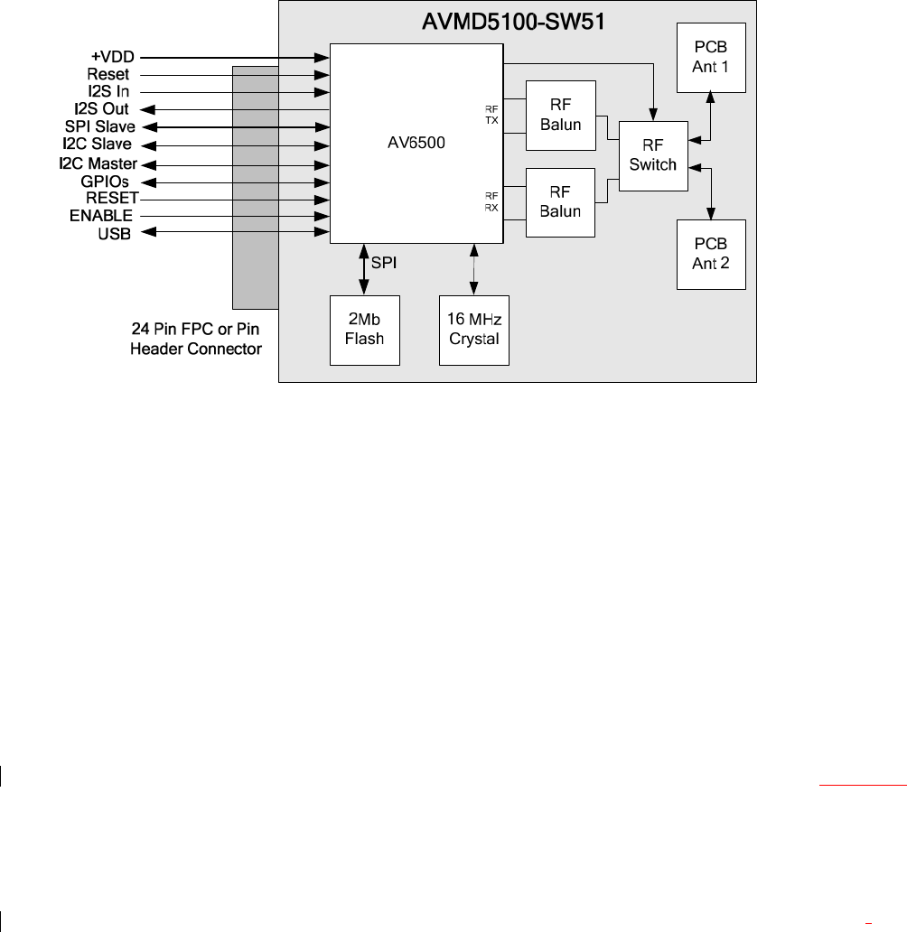
Figure 1: SWA51 Module Block Diagram
The SWA51 module is available in 2 variations; digital input transmitter module or digital output
receiver module.
There are three available I2S digital audio data inputs/outputs, each of these can be configured to operate as either
a master or a slave - depending on the application, the I2S ports can operate simultaneously as either inputs or
outputs. When configured as slaves, the I2S inputs/outputs can be independently clocked by external masters. In
addition, MCLK can be output from the module to provide a reference clock source to an external ADC or DAC.
Figure 1 shows the block diagram of the SWA51 module. The hardware for the audio input
(transmit) and audio output (receive) versions of the module is identical and only the firmware loaded onto the
module determines its function.
The highly integrated nature of the AV5100 transceiver IC results in few external components being required for the
SWA51 module design. 2 printed PCB antennas are used to achieve increased range, and to achieve antenna
spatial diversity. The simple RF path consists only of the antennas, associated tuning components, shield can, the
RF switch and two baluns, one connected to each of the RF input and RF output ports on the AV5100 IC.
A 16MHz crystal oscillator generates the AV5100 fundamental system clock used as the basis for all RF and digital
audio clocks.
A 2Mb flash memory chip is used to store the module’s application firmware. The AV5100 is able to boot from
internal ROM upon first power up, which enables programming the flash chip with the application firmware r through
USB. In addition, Over-the-air Firmware upgrade capability can be enabled through the application firmware. The
module can be controlled from an external host device via the I2C Slave or the SPI Slave data interfaces. The I2C
master port allows the module to control other system audio devices such as a sub-woofer amplifier system without
having to add another MCU to the product design. Up to 119 additional GPIOs are available on the SWA51 module
(not including I2C and I2S signals) for implementing different UI features on the target application. The resources
mentioned above can be leveraged to implement low cost sub-woofer designs as outlined below.
4.1 Typical Sub-Woofer Implementation
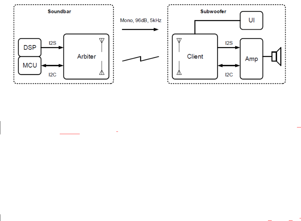
A basic AV5100 Wireless Subwoofer system block Diagram is shown in Fig. 2.
Figure 2: AV5100 Wireless Subwoofer Solution Block Diagram
A simple low cost implementation of sub-woofer design is shown in Figure 3. The sub amplifier consists of a PWM
chip plus an output stage device, but no external MCU is required as the SWA51-RX module performs the control
function using the I2C master communication port in conjunction with multiple GPIOs. The SWA51 module is
configured to accept nominal +3.3V or +5V power from the main application board. An optional reset signal can be
supplied to the SWA51-RX module and I2C or SPI slave communication can be used to control the module if
required.
Several GPIOs can be used to drive LEDs, or to connect to UI buttons. Typically 2 LEDs may be used and 1 button
for pairing purposes. Another button could be used, for example, to implement a “bass enhance” feature. Another
GPIO can be used to control the power supply to external system blocks such as the PWM IC and the output stage.
The SWA51-RX module can remain powered up during a standby or low power operating mode; however, a true
power-down mode can be implemented by configuring pin 17 (GPIO15/ADAT2/CEN) to be used as a chip-enable
pin that can be used to power down the AV5100. The SWA51 can also be completely powered down by turning off
the main 3.3V supply.
If the wireless link is lost (ex. when the sound bar is powered down), the SWA51_RX module can, after a timeout
period, power down the amplifier and output stage sections to conserve power and to help meet Energy Start
requirements.
The I2C master port from the SWA51_RX module (pins 5 and 6 on the connector) can communicate, control, and
initialize external audio ICs such as the PWM chip in this example. Other GPIOs can be used to detect fault
conditions (over temperature etc) and notify the module. The audio is routed from the SWA51-RX module to the
amplifier circuit with the I2S output port which can be configured as either a master or a slave as required. MCLK
can also be generated from the SWA51-RX module as a -12.28800MHz clock if required.
AV5100
PWM IC
Output
Stage
Power
I2C
I2S
Master
I2C Slave
3
2
GPIOs
Flash
SPI
4
2
UI Buttons
LEDs
Power Supply Control
Reset
Master
Sub-Woofer
Driver
2
2
+3.3V or +5V
4
2
GPIOs
AVMD5100-SWA51 RX
Module
Figure 3: SWA51 Module Simple Sub-Woofer Implementation
4.2 Typical Rear 2.1 Implementation
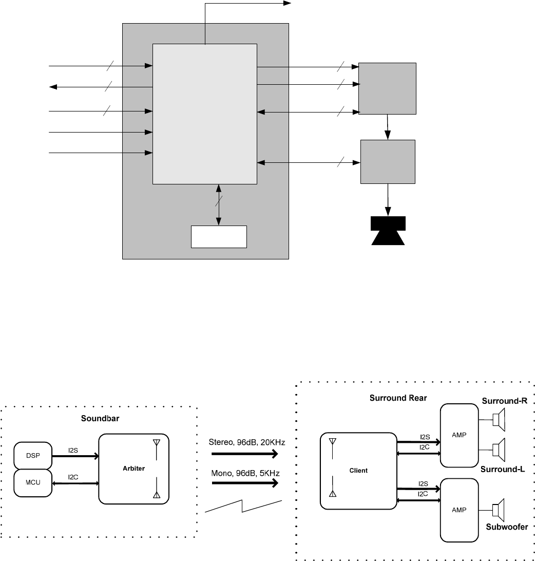
A basic AV5100 Wireless Rear 2.1 system block Diagram is shown in Fig. 4.
Figure 4: AV5100 Wireless Rear 2.1 Solution Block Diagram

This implementation involves transmitting three channels over the air, one full-band stereo channel (2 x 96dB,
20KHz) used for the rear surround audio, and one mono 96dB, 5KHz channel for subwoofer audio1. The hardware
implementation on the client side is very similar to the subwoofer implementation, only two PWM
ICs and two audio amplifiers are used; one to drive the mono subwoofer and one to drive to stereo left and right
surround speakers. Still, no micro-controller is required; the Av5100 can act as a master controller for the PWM
and amplifier ICs via I2C, and as an I2S master with MCLK sourced either internally by the AV5100 or externally
from an external clock source. The actual subwoofer and surround speaker drivers can be housed inside the same
physical unit, or be housed in separate enclosures with wired connections to the client unit. Fig. 3 still applies to
the surround rear 2.1 application, only 2 PWM and output stages are used.
4.3 SWA51 Module Connections and Interfaces
Signal Type Description
+3.3V Supply The SWA51 hardware is configured to accept a +3.3V supply
Reset Active low reset input. This pin is driven from an open collector/drain device such that
it can be pulled to ground for the active reset state but, when released, must go to a
high impedance state. This pin should not be actively driven high, as the AV5100
internal reset circuit will not operate correctly.
I2S In Port The I2S input port can be configured as a master or slave. Consequently BCLK and
LRCK can be either inputs or outputs. In addition, MCLK can be sourced by the
module on pin 16. Since the AV5100 IC contains a sample rate converter, MCLK is
not required to be supplied to the module when it is an I2S slave. CMOS 3.3V logic
levels are used for all I2S signals.
I2S Out Port The I2S output port can be configured as a master or slave. Consequently BCLK and
LRCK can be either inputs or outputs. In addition, MCLK can be sourced by the
module on pin 16. Since the AV5100 IC contains a sample rate converter, MCLK is
not required to be supplied to the module when it is an I2S slave. CMOS 3.3V logic
levels are used for all I2S signals.
I2C Slave Port The I2C slave port can be used for external host communication and for module
testing. It is assumed that external pull up resistors are connected at the I2C master
communicating with the module.
I2C Master Port The I2C master port is used to communicate with external audio devices such as a
sub-woofer amplifier. It is assumed that external pull up resistors are included on the
application board.
GPIOs 3.3V CMOS logic level GPIOs available to connect to other devices, or to use as UI
supporting GPIOs for LED and button support. All supported GPIOs can be
configured as outputs or inputs with configurable pull-ups/pull-downs.
1 The SSC (Single Side Carrier) modulation scheme used in the SWA51 supports three one-directional full-band
channels (96dB, 20 KHz).

5 SWA51 Connector Information
Table 1: SWA51 Connector Information
No Pin Name Pin Type AV65100
Pin
SWA51-TX Pin
Description
SWA51-RX Pin
Description
1 GPIO2/S_SSB Digital I/O 12 GPIO or SPI Slave
Chip Select
GPIO or SPI Slave
Chip Select
2 GPIO3/S_SCLK Digital I/O 11 GPIO or SPI
Slave Serial Clock
GPIO or SPI Slave
Serial Clock
3 GPIO4/S_SDA/S_MOSI Digital I/O 10 GPIO, I2C Slave
Serial Data or SPI
Slave Data In
GPIO, I2C Slave
Serial Data or SPI
Slave Data In
4 GPIO5/S_SCL/S_MISO Digital I/O 9 GPIO, I2C Slave
Serial Clock or SPI
Slave Data Out
GPIO, I2C Slave
Serial Clock or SPI
Slave Data Out
5 GPIO16/M_SDA Digital I/O 4 GPIO, I2C
Master Serial Data
GPIO, I2C
Master Serial Data
6 GPIO17/M_SCL Digital I/O 3 GPIO, I2C
Master Serial
Clock
GPIO, I2C
Master Serial
Clock
7 GPIO20/LINK_LED Digital I/O 56 GPIO, or
LINK_LED Output
GPIO, or
LINK_LED Output
8 GPIO21/PAIR Digital I/O 55 GPIO, or input
from PAIR Button
GPIO, or input
from PAIR Button
9 GPIO18/BCLK1 Digital I/O 2 GPIO or I2S Port 1
Bit Clock
GPIO or I2S Port 1
Bit Clock
10 GPIO19/WCLK1 Digital I/O 1 GPIO or I2S Port 1
Word Clock
GPIO or I2S Port 1
Word Clock
11 GPIO10/MCLK Digital I/O 53 GPIO or Master
Clock Out
GPIO or Master
Clock Out
12 GND GND Paddle
(57)
GND GND
13 GPIO11/BCLK0 Digital I/O 52 GPIO or I2S Port 0
Bit Clock
GPIO or I2S Port 0
Bit Clock
14 GPIO12/WCLK0 Digital I/O 51 GPIO or I2S Port 0
Word Clock
GPIO or I2S Port 0
Word Clock
15 GPIO13/ADAT0 Digital I/O 50 GPIO or I2S Port 0
Audio Data
GPIO or I2S Port 0
Audio Data
16 GPIO14/ADAT1 Digital I/O 49 GPIO or I2S Port 1
Audio Data
GPIO or I2S Port 1
Audio Data
17 GPIO15/ADAT2/CEN Digital I/O
or Digital
Input
48 or 38 GPIO, I2S Port 2
Audio Data or chip
enable (1)
GPIO, I2S Port 2
Audio Data or chip
enable (1)

18 GPIO22/D+ Digital I/O 47 or 43 GPIO or USB Data
Plus (2) GPIO or USB Data
Plus (2)
19 GPIO23/D- Digital I/O 46 or 42 GPIO or USB Data
Minus (2) GPIO or USB Data
Minus (2)
20 GPIO24 Digital I/O 41 GPIO
(3) GPIO
(3)
21 RESETN_EXT Digital
Input
37 RESET signal
active low (4) RESET signal
active low (4)
22 GND GND Paddle
(57)
GND GND
23 VDD Supply
Input
31, 45, 54 +3.3V input supply
voltage
+3.3V input supply
voltage
24 VDD Supply
Input
31, 45, 54 +3.3V input supply
voltage
+3.3V input supply
voltage
Notes:
(1) Pin 17 is hardware configured as GPIO15/ADAT2 by default; utilizing this pin as a CEN requires a different
stuffing option.
(2) Utilizing pins 18 and 19 as USB D+ and D- requires the firmware to Tri-state GPIOs 22 and 23.
(3) Pin 20 (GPIO24) can be utilized to implement a “Data Waiting” interrupt signal for I2C and SPI Slave data
communication.
(4) Pin 21 (RESET_EXT) can be pulled to GND with a switch or an open drain/collector type device to provide a
hard reset signal to the AV5100. This pin is pulled up to VDDIO (3.3V) internally in the AV5100 and should
not be actively driven high.
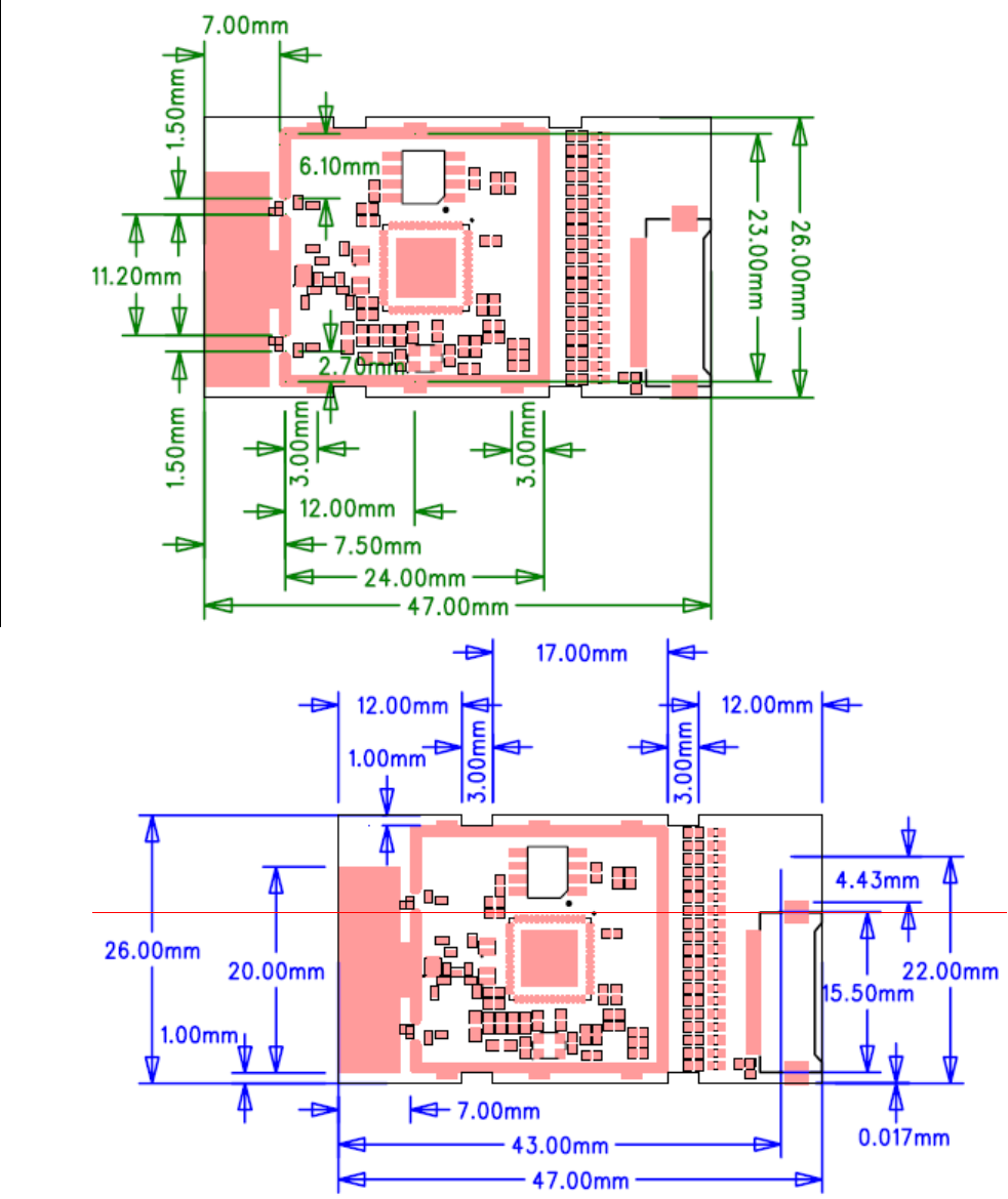
Figure 4 – SWA51 Module Outline and Mechanical Dimensions
- PCB thickness is 1.0mm
- The top of shield is 2.4mm
above PCB
- The maximum height from the bottom of the PCB to the top of the shield can is 3.4mm.
20.0mm
6 Electrical, Audio and Timing Specifications
6.1 Absolute Maximum Ratings
Absolute Maximum Ratings (AMR) are stress ratings only. AMR corresponds to the maximum value that can be
applied without leading to instantaneous or very short-term unrecoverable hard failure (destructive breakdown).
Stresses beyond those listed under AMR may cause permanent damage to the device.
Functional operation of the device at these or any other conditions beyond those indicated under “Recommended
Operating Range” is not implied. Exposure to absolute-maximum-rated conditions for extended periods may
adversely affect device reliability.
Device functional operating limits and guaranteed performance specifications are given under Electrical
Characteristics at the test conditions specified.
CONDITION MIN MAX
+3.3V Supply Voltage Input -0.3V 4.0V
Input Voltage Range – Digital
Inputs -0.3V 3.6V
Input Voltage Range – Analog
Inputs -0.3V 3.6V
Operating Temperature -40 ºC +85 ºC
Storage Temperature -40 ºC +100 ºC
Static Discharge Voltage12KV ----
Notes:
1)HBM=ESDHumanBodyModel;C=100pF,R=1k
6.2 Recommended Operating Range
PARAMETER MIN TYP MAX UNIT
VDD, +3.3V Supply pin voltage 3.135 3.3 3.465 V
Ambient Temperature (TA) 0 70 ºC
RESET pin hold time 10 msec
Power Supply Rise Time (to 3.0V) 0 10 msec
6.3 Electrical Characteristics – DC Characteristics
Operating Conditions: VDD = 3.135 to 3.465V, TA = 0°C to +70 °C, RF Freq = 5150®5250, 5725®5850MHz,
measured relative to the RF balun single®ended I/O. Typical specifications at TA = 25°C, VDD = 3.3V
3.3V.
PARAMETER CONDITIONS MIN TYP MAX UNIT
Supply Current (IVDDA) Shutdown (chip disabled)
Standby (also USB suspend)
RX mode (continuous RX)
TX mode (continuous TX);
pout=+3dBm
TBD
TBD
TBD
TBD
1
2.5
uA
mA
mA
mA
CMOS I/O Logic Levels – 3.3V I/O
Input Voltage Logic Low, VIL 0.6 V
Input Voltage Logic High, VIH VDDIO
®0.6
V
Output Voltage Logic Low, VOL 0.3 V
Output Voltage Logic High, VOH VDDIO
®0.3
V
6.4 Electrical Characteristics – RF PLL Characteristics
Operating Conditions: VDD = 3.135 to 3.465V, TA = 0°C to +70 °C, RF Freq = 5150®5250, 5725®5850MHz,
measured relative to the RF balun single®ended I/O. Typical specifications at TA = 25°C, VDD = 3.3V
PARAMETER CONDITIONS MIN TYP MAX UNIT
RF Channel Frequency Range Lower band
Upper band
5150
5725
5250
5850
MHz
MHz
RF Channel frequency resolution
(raster)
1 MHz
RF I/O Impedance Balanced I/O port; TX and RX RF
ports
100 ohm
Crystal Oscillator Frequency External crystal 16 MHz
Crystal Accuracy Requirement External XTAL, -20°C to +70 °C +/-20 ppm
6.5 Electrical Characteristics – RF RX Characteristics
Operating Conditions: VDD = 3.135 to 3.465V, TA = 0°C to +70 °C, RF Freq = 5150®5250, 5725®5850MHz,
measured relative to the RF balun single®ended I/O. Typical specifications at TA = 25°C, VDD = 3.3V
PARAMETER CONDITIONS MIN TYP MAX UNIT
RF Channel Frequency Range Lower band
Upper band
5150
5725
5250
5850
MHz
MHz
RF I/O Impedance Balanced I/O port; TX and RX RF
ports
100 ohm
RX Sensitivity SSC (single sub-carrier)
DSC (dual sub-carrier)
-89
-86
dBm
dBm
Max input signal LNA = low gain mode, min IF gain -5 dBm
Out-of-band blocker level <5150 MHz, >5850 MHz
2400-2483.5 MHz
-45
-20
dBm
dBm
Spurious RF outputs 5150-5850 MHz
<5150 MHz
>5850 MHz
-55
-63
-63
dBm
dBm
dBm
6.6 Electrical Characteristics – RF TX Characteristics
Operating Conditions: VDD = 3.135 to 3.465V, TA = 0°C to +70 °C, RF Freq = 5150®5250, 5725®5850MHz,
measured relative to the RF balun single®ended I/O. Typical specifications at TA = 25°C, VDD = 3.3V
PARAMETER CONDITIONS MIN TYP MAX UNIT
RF Channel Frequency Range Lower band
Upper band
5150
5725
5250
5850
MHz
MHz
RF I/O Impedance Balanced I/O port; TX and RX RF
ports
100 ohm
TX Output power SSC (single sub-carrier)
DSC (dual sub-carrier)
3(1)
0
dBm
dBm
Adjacent Channel Power (SSB) Pout = +3dBm
Upper Adjacent: +1.5 to +3 MHz offset
Upper Alternate: +3 to +4.5 MHz
offset
Lower Adjacent: -1.5 to -3 MHz offset
Lower Alternate: -3 to -4.5 MHz offset
TBD
TBD
TBD
TBD
dBc
dBc
dBc
dBc
LO leakage -20 dBc
Output harmonics Pout = +3dBm
2nd harmonic
3rd harmonic
TBD
TBD
dBm
dBm
Out-of-band spurious RF < 5150MHz, > 5850MHz TBD dBm
(1) Measured at the worst performing frequency
6.7 Electrical Characteristics – Audio C/CS
PARAMETER CONDITIONS MIN TYP MAX UNIT
Frequency Response (-3dB)
16 bit audio, 11KSps
over-the-air sample rate 20 5K Hz
16 bit audio, 14.8KSps
over-the-air sample rate 20 6.5K Hz
16 bit audio, 22KSps
over-the-air sample rate 20 10K Hz
16 bit audio, 29.6KSps
over-the-air sample rate 20 13K Hz
16 bit audio, 44KSps
over-the-air sample rate 20 20K Hz
Gain Flatness 0dB Input / Output Gain 0.
2 dB
SNR I2S Input / Output 93
(1)
dB
THD+N 94 dB
Notes
1. 16bit audio, all OTA sample rates. OTA 12-bit path for voice is possible, but will limit the SNR to 72dB.
6.8 AV5100 Rate Converter Characteristics
SRC Block Input Rates Output Rates SNR (dB) SRC BW (-3dB)
SRC 0
(Audio)
I2S
32-96K
USB
8k – 48K,
ECU (TX)
“11K”
“14.8k”
“22k”
“29.6k”
“44k”
I2S
Master: 48k
Slave: 44.1K-96K
ECU (TX)
“11K”
“14.8k”
“22k”
“29.6k”
“44k”
All rates support
16bit, >93dB
Actual bandwidth is
dependent on the
lower of the input or
output rates.
Output BW vs OTA
“11k” = 5kHz
“14.8k” = 6.5kHz
“22k” = 10kHz
“29.6k” = 13kHz
“44k” = 20kHz
SRC 1
(LFE)
I2S
32-96K
I2S
Master: 48k All rates support Actual bandwidth is
USB
8k – 48K,
ECU (TX)
“11K”
“14.8k”
“22k”
“29.6k”
“44k”
Slave: 44.1K-96K
ECU (TX)
“11K”
“14.8k”
“22k”
“29.6k”
“44k”
16bit, >93dB dependent on the
lower of the input or
output rates.
Output BW vs OTA
“11k” = 5kHz
“14.8k” = 6.5kHz
“22k” = 10kHz
“29.6k” = 13kHz
“44k” = 20kHz
SRC 2
(Voice)
I2S
32-96K
USB
8k – 48K,
ECU (TX)
“14.8k”
I2S
Master: 48k
Slave: 44.1K-96K
USB
8k – 48K,
ECU (RX)
“14.8k”
All rates support
16bit, >93dB, but the
OTA 12bit path will
limit SNR to 72dB
Actual bandwidth is
dependent on the
lower of the input or
output rates.
Output BW vs OTA
“11k” = 5kHz
“14.8k” = 6.5kHz
“22k” = 10kHz
“29.6k” = 13kHz
“44k” = 20kHz
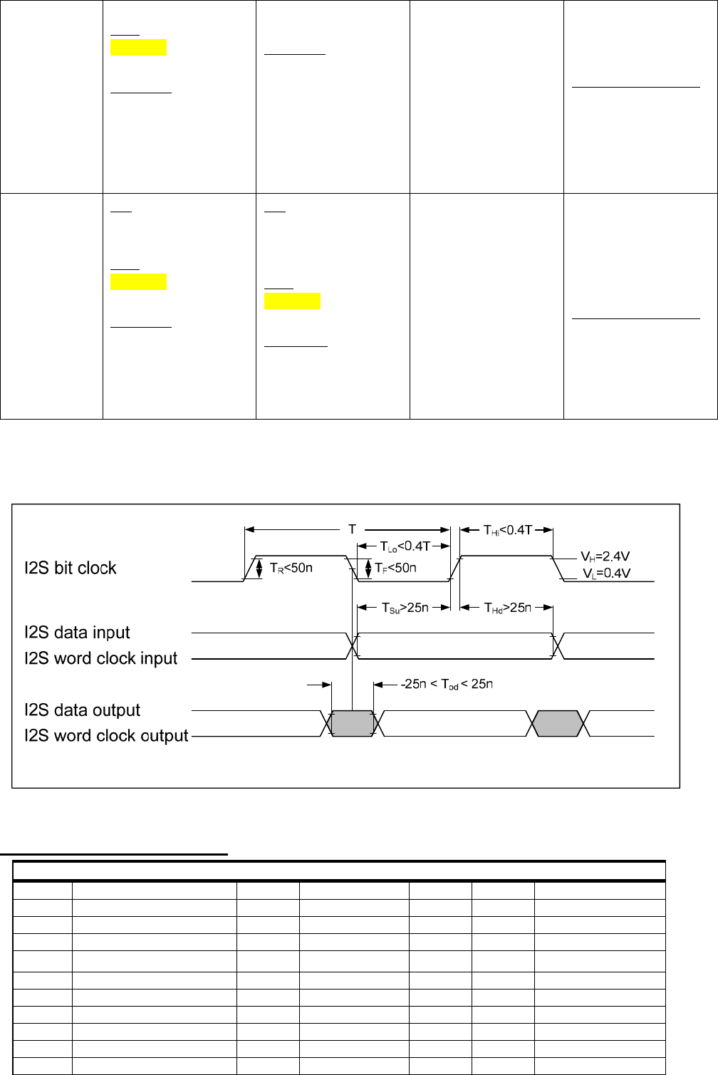
6.9 I2S Communication Interface Timing
Table 2: SWA51 I2S Timing
MIN TYP MAX UNIT NOTES
VL low voltage level -0.3V 0.0V 0.4V V
VH high voltage level 2.4V 3.3V 3.6V V
T clock period 325.5n s 1/3.072MHz
TLo clock low period 0.4T 0.6T
THi clock high period 0.4T 0.6T
TR rise time 50n s Note 1
TF fall time 50n s Note 1
TSu setup time 25n s
THd hold time 25n s
TOd output delay -25n 25n s
bit clocks/word clock 64
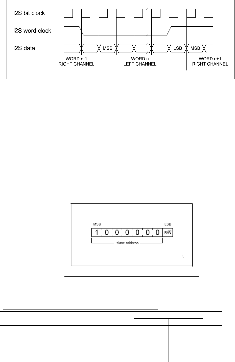
I2S protocol is “I2S Justified” as shown below.
Note 1: The timing specified for the rise and fall times represents the edge rates on the module itself. The rise and
fall times of the I2S signals are determined by ESD/EMI mitigation components on the modules, as well as external
loading, and will be higher than the specified numbers
6.10 I2C Master/Slave Communication Interface Timing (S_SCL, S_SDA)
The SWA51 has both I2C slave and master interfaces available with their respective pins S_SCL, S_SDA and
M_SCL, M_SDA. The interfaces operate in I2C fast-mode and can receive and transmit at up to 400 kbit/s.
Bytes are 8 bits long and are transferred with the most significant bit (MSB) first. Each byte has to be followed by an
acknowledge bit. The SWA51 will apply clock-stopping (by holding the clock line S_SCL LOW to force the master
into a wait state) if necessary due to internal high-priority tasks.
The slave/master interface can be used both for writing (e.g. sending commands) or reading (e.g. requesting status).
An additional GPIO pin on the SWA51 (Ex. GPIO24), can be used to notify the I2C master when a pending message
is ready to be sent.
The SWA51 slave interface responds to the 7-bit slave address 1000000 (0x40) as shown in Figure 1 below.
Figure 5: First Byte after the START Procedure
ELECTRICAL SPECIFICATIONS AND TIMING
Table 3: Characteristics of the S_SDA and S_SCL I/Os
PARAMETER SYMBOL FAST-MODE UNIT
MIN. MAX.
LOW level input voltage VIL 0.3ˢ 0.8 V
HIGH level input voltage VIH 2.0 3.6 V
LOW level output voltage (open drain or
open collector) at 1 mA sink current: VOL 0 0.4 V
Output fall time from VIHmin to VILmax with
a bus capacitance from 10 pF to 400 pF tof 0 250 ns
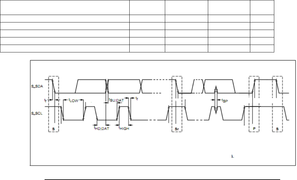
Pulse width of spikes which must be
suppressed by the input filter tSP 0 50 ns
S_SCL clock frequency fSCL 0 400 kHz
LOW period of the S_SCL clock tLOW 1.3 – sˢ
HIGH period of the S_SCL clock tHIGH 0.6 – sˢ
Data hold time tHD;DAT 100 – ns
Data set-up time tSU;DAT 100 – ns
Figure 6: Definition of Timing for F/S-Mode Devices on the I2C-Bus

7 FCC and Industry Canada certification information
7.1 Federal Communication Commission Interference Statement
FOR MOBILE DEVICE USAGE (>20cm/low power)
Radiation Exposure Statement:
This equipment complies with FCC radiation exposure limits set forth for an uncontrolled environment. This
equipment should be installed and operated with minimum distance 20cm between the radiator & your body.
This device is intended only for OEM integrators under the following conditions:
1) The antenna must be installed such that 20 cm is maintained between the antenna and users, and
2) The transmitter module may not be co-located with any other transmitter or antenna.
As long as 2 conditions above are met, further transmitter test will not be required. However, the OEM
integrator is still responsible for testing their end-product for any additional compliance requirements
required with this module installed
IMPORTANT NOTE: In the event that these conditions can not be met (for example certain laptop
configurations or co-location with another transmitter), then the FCC authorization is no longer considered
valid and the FCC ID can not be used on the final product. In these circumstances, the OEM integrator will
be responsible for re-evaluating the end product (including the transmitter) and obtaining a separate FCC
authorization.
End Product Labeling
FOR MOBILE DEVICE USAGE (>20cm/low power)
This transmitter module is authorized only for use in device where the antenna may be installed such that 20
cm may be maintained between the antenna and users. The final end product must be labeled in a visible
area with the following: “Contains FCC ID: QWO-SWA51”. The grantee's FCC ID can be used only when all
FCC compliance requirements are met.
Manual Information To the End User
The OEM integrator has to be aware not to provide information to the end user regarding how to install or
remove this RF module in the user’s manual of the end product which integrates this module.
The end user manual shall include all required regulatory information/warning as show in this manual.
This device complies with Part 15 of the FCC Rules. Operation is subject to the following two conditions: (1)
This device may not cause harmful interference, and (2) this device must accept any interference received,
including interference that may cause undesired operation.

This equipment has been tested and found to comply with the limits for a Class B digital device, pursuant to
Part 15 of the FCC Rules. These limits are designed to provide reasonable protection against harmful
interference in a residential installation. This equipment generates, uses and can radiate radio frequency
energy and, if not installed and used in accordance with the instructions, may cause harmful interference to
radio communications. However, there is no guarantee that interference will not occur in a particular
installation. If this equipment does cause harmful interference to radio or television reception, which can
be determined by turning the equipment off and on, the user is encouraged to try to correct the interference
by one of the following measures:
- Reorient or relocate the receiving antenna.
- Increase the separation between the equipment and receiver.
- Connect the equipment into an outlet on a circuit different from that to which the receiver is connected.
- Consult the dealer or an experienced radio/TV technician for help.
FCC Caution: Any changes or modifications not expressly approved by the party responsible for compliance
could void the user's authority to operate this equipment.
This transmitter must not be co-located or operating in conjunction with any other antenna or transmitter.
Radiation Exposure Statement:
This equipment complies with FCC radiation exposure limits set forth for an uncontrolled environment. This
equipment should be installed and operated with minimum distance 20cm between the radiator & your body.
This device is intended only for OEM integrators under the following conditions:
1) The antenna must be installed such that 20 cm is maintained between the antenna and users, and (if
EUT is portable device, please delete this item)
2) The transmitter module may not be co-located with any other transmitter or antenna.
As long as 2conditions above are met, further transmitter test will not be required. However, the OEM
integrator is still responsible for testing their end-product for any additional compliance requirements
required with this module installed
IMPORTANT NOTE: In the event that these conditions can not be met (for example certain laptop
configurations or co-location with another transmitter), then the FCC authorization is no longer considered
valid and the FCC ID can not be used on the final product. In these circumstances, the OEM integrator will
be responsible for re-evaluating the end product (including the transmitter) and obtaining a separate FCC
authorization.
End Product Labeling
This transmitter module is authorized only for use in device where the antenna may be installed such that
20 cm may be maintained between the antenna and users. The final end product must be labeled in a
visible area with the following: “Contains FCC ID: QWO-SWA51”. The grantee's FCC ID can be used only
when all FCC compliance requirements are met.
Manual Information To the End User
The OEM integrator has to be aware not to provide information to the end user regarding how to install or
remove this RF module in the user’s manual of the end product which integrates this module.
The end user manual shall include all required regulatory information/warning as show in this manual.
7.2 Industry Canada statement:
This device complies with RSS-247 of the Industry Canada Rules. Operation is subject to the following two
conditions: (1) This device may not cause harmful interference, and (2) this device must accept any
interference received, including interference that may cause undesired operation.
Ce dispositif est conforme à la norme CNR-247 d'Industrie Canada applicable aux appareils radio exempts
de licence. Son fonctionnement est sujet aux deux conditions suivantes: (1) le dispositif ne doit pas produire
de brouillage préjudiciable, et (2) ce dispositif doit accepter tout brouillage reçu, y compris un brouillage
susceptible de provoquer un fonctionnement indésirable.
Caution :
(i) the device for operation in the band 5150-5250 MHz is only for indoor use to reduce the potential for
harmful interference to co-channel mobile satellite systems;
(ii) the maximum antenna gain permitted for devices in the band 5725-5850 MHz shall be such that the
equipment still complies with the e.i.r.p. limits specified for point-to-point and non-point-to-point operation as
appropriate; and
(iii) Users should also be advised that high-power radars are allocated as primary users (i.e. priority users)
of the bands 5650-5850 MHz and that these radars could cause interference and/or damage to LE-LAN
devices.
Avertissement:
(i) les dispositifs fonctionnant dans la bande 5150-5250 MHz sont réservés uniquement pour une utilisation
à l’intérieur afin de réduire les risques de brouillage préjudiciable aux systèmes de satellites mobiles
utilisant les mêmes canaux;
(ii) le gain maximal d'antenne permis (pour les dispositifs utilisant la bande de 5725 à 5 850 MHz) doit être
conforme à la limite de la p.i.r.e. spécifiée pour l'exploitation point à point et l’exploitation non point à point,
selon le cas;
(iii) De plus, les utilisateurs devraient aussi être avisés que les utilisateurs de radars de haute puissance
sont désignés utilisateurs principaux (c.-à-d., qu’ils ont la priorité) pour les bandes 5650-5850 MHz et que
ces radars pourraient causer du brouillage et/ou des dommages aux dispositifs LAN-EL.
FOR MOBILE DEVICE USAGE (>20cm/low power)
Radiation Exposure Statement:
This equipment complies with IC radiation exposure limits set forth for an uncontrolled environment. This
equipment should be installed and operated with minimum distance 20cm between the radiator & your body.
Déclaration d'exposition aux radiations:
Cet équipement est conforme aux limites d'exposition aux rayonnements IC établies pour un environnement
non contrôlé. Cet équipement doit être installé et utilisé avec un minimum de 20 cm de distance entre la
source de rayonnement et votre corps.
This device is intended only for OEM integrators under the following conditions: (For module device
use)
1) The antenna must be installed such that 20 cm is maintained between the antenna and users, and 2) the
transmitter module may not be co-located with any other transmitter or antenna.
As long as 2 conditions above are met, further transmitter test will not be required. However, the OEM
integrator is still responsible for testing their end-product for any additional compliance requirements
required with this module installed.
Cet appareil est conçu uniquement pour les intégrateurs OEM dans les conditions suivantes: (Pour
utilisation de dispositif module)
1) L'antenne doit être installée de telle sorte qu'une distance de 20 cm est respectée entre l'antenne et les
utilisateurs, et 2) Le module émetteur peut ne pas être coïmplanté avec un autre émetteur ou antenne.
Tant que les 2 conditions ci-dessus sont remplies, des essais supplémentaires sur l'émetteur ne seront pas
nécessaires. Toutefois, l'intégrateur OEM est toujours responsable des essais sur son produit final pour
toutes exigences de conformité supplémentaires requis pour ce module installé.
IMPORTANT NOTE:
In the event that these conditions can not be met (for example certain laptop configurations or co-location
with another transmitter), then the Canada authorization is no longer considered valid and the IC ID can not
be used on the final product. In these circumstances, the OEM integrator will be responsible for
re-evaluating the end product (including the transmitter) and obtaining a separate Canada authorization.
NOTE IMPORTANTE:
Dans le cas où ces conditions ne peuvent être satisfaites (par exemple pour certaines configurations
d'ordinateur portable ou de certaines co-localisation avec un autre émetteur), l'autorisation du Canada n'est
plus considéré comme valide et l'ID IC ne peut pas être utilisé sur le produit final. Dans ces circonstances,
l'intégrateur OEM sera chargé de réévaluer le produit final (y compris l'émetteur) et l'obtention d'une
autorisation distincte au Canada.
End Product Labeling FOR MOBILE DEVICE USAGE (>20cm/low power)
This transmitter module is authorized only for use in device where the antenna may be installed such that 20
cm may be maintained between the antenna and users. The final end product must be labeled in a visible
area with the following: “Contains IC: ”.
Plaque signalétique du produit final
Ce module émetteur est autorisé uniquement pour une utilisation dans un dispositif où l'antenne peut être
installée de telle sorte qu'une distance de 20cm peut être maintenue entre l'antenne et les utilisateurs. Le
produit final doit être étiqueté dans un endroit visible avec l'inscription suivante: "Contient des IC: ".
Manual Information To the End User
The OEM integrator has to be aware not to provide information to the end user regarding how to install or
remove this RF module in the user’s manual of the end product which integrates this module.
The end user manual shall include all required regulatory information/warning as show in this manual.
Manuel d'information à l'utilisateur final
L'intégrateur OEM doit être conscient de ne pas fournir des informations à l'utilisateur final quant à la façon
d'installer ou de supprimer ce module RF dans le manuel de l'utilisateur du produit final qui intègre ce
module.
Le manuel de l'utilisateur final doit inclure toutes les informations réglementaires requises et avertissements
comme indiqué dans ce manuel.

8 Ordering Information
Table 4: SWA51 Module Ordering Information
Module Part
Number
Option
Code
Description
SWA51 TX -TX Digital Input , FPC Connector, integrated printed PCB
antennas
SWA51 RX -RX Digital Output, FPC Connector, integrated printed PCB
antennas
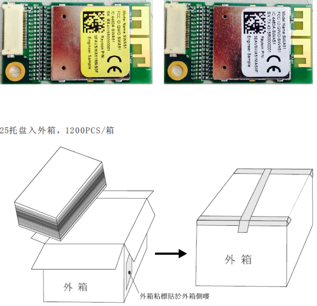
9 Label/Carton/Packing information
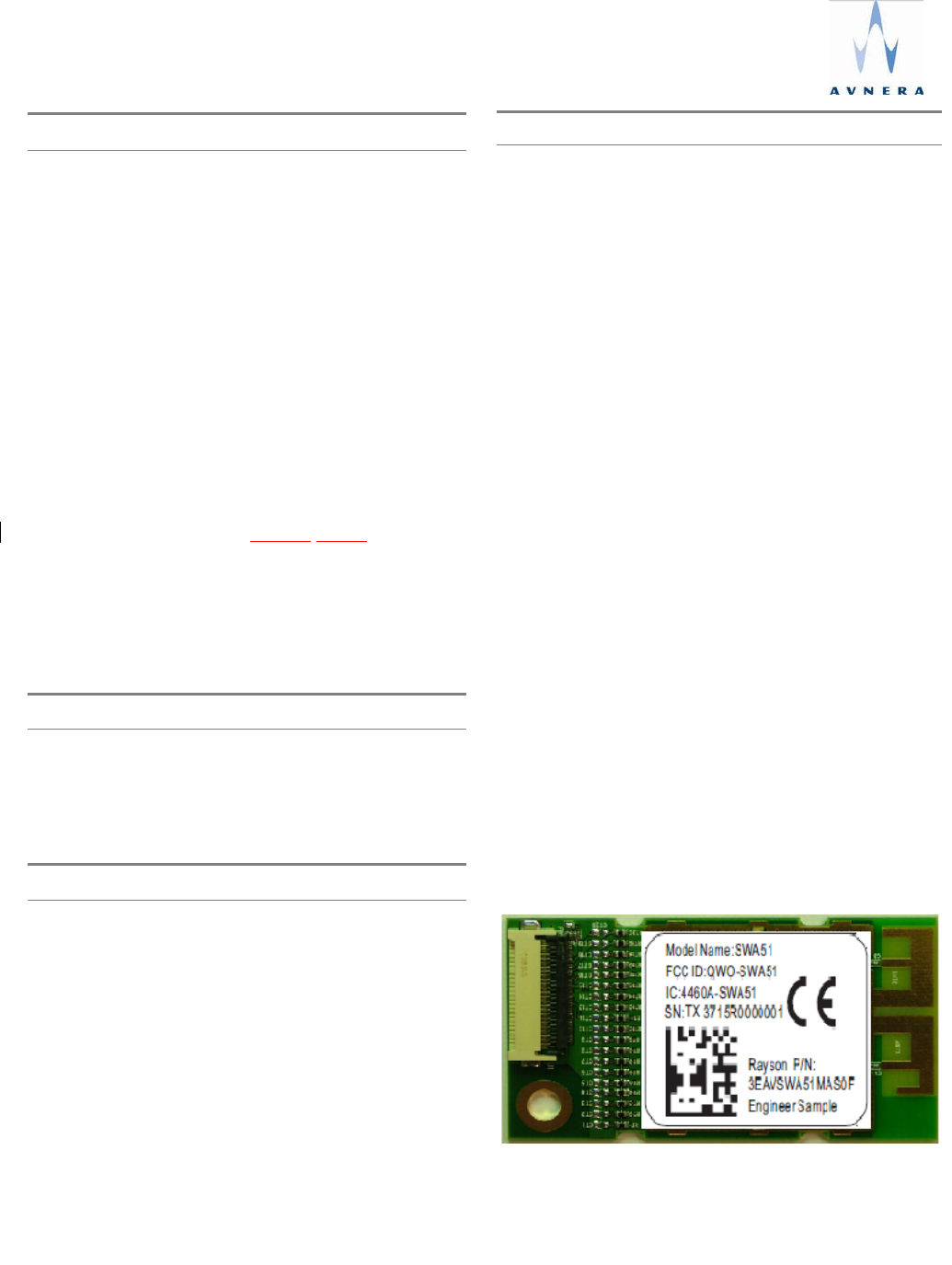
9.1 Module Label Drawing
9.2 Carton Label Drawing
9.3 Module weight
SWA51 module weight is 5.3g
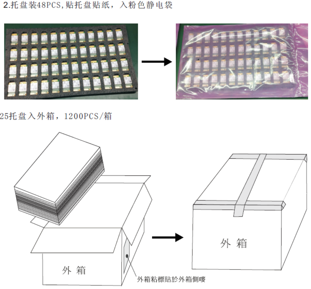
9.4 Packing information