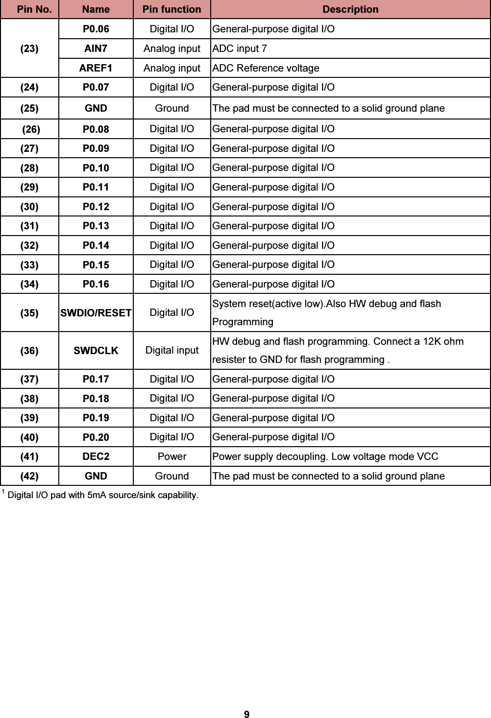
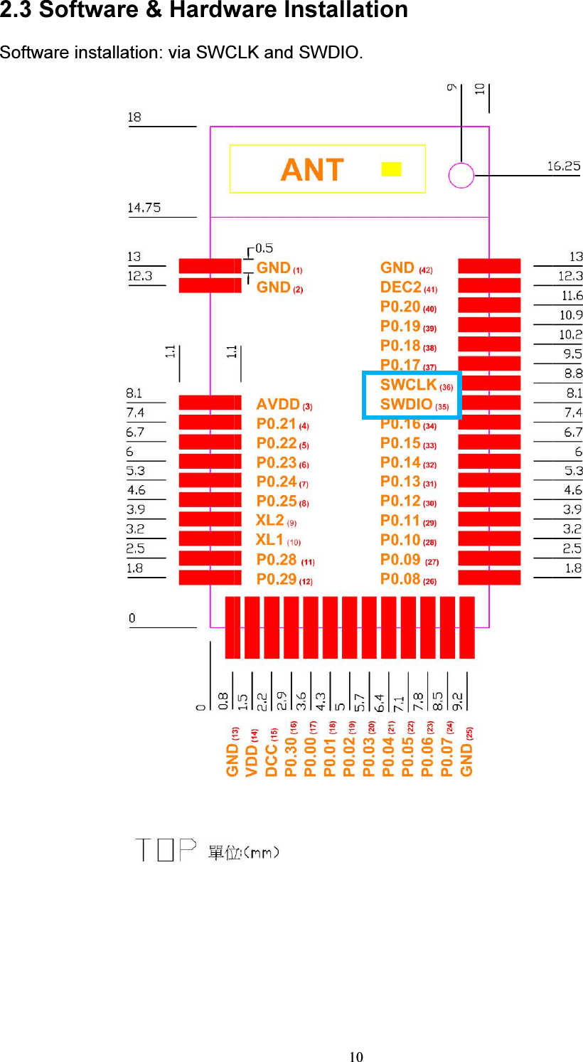
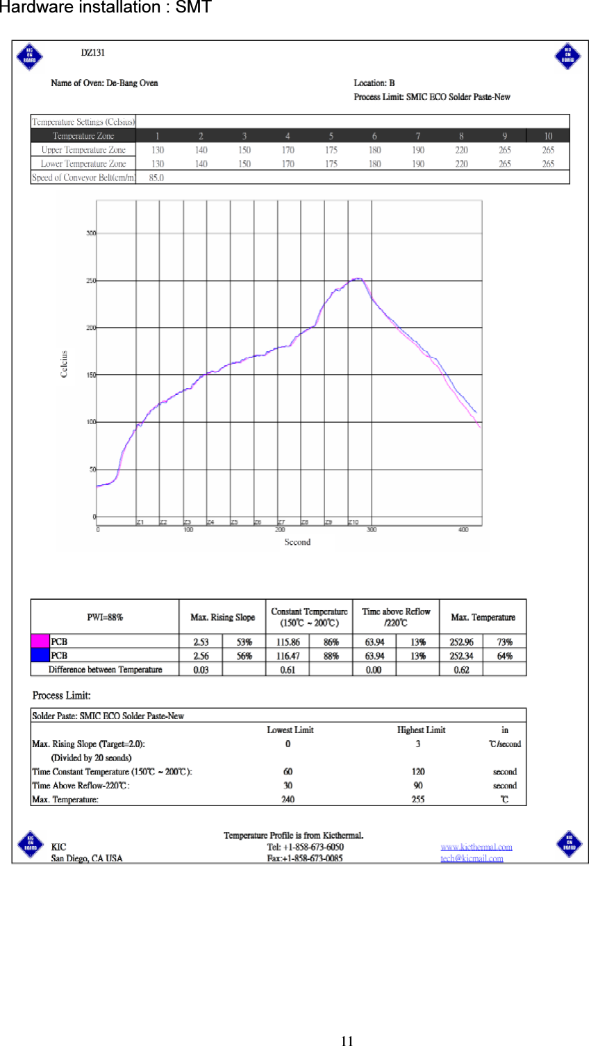
Raytac MDBT40 Bluetooth Module User Manual MDBT40 spec Version C 20140207

Raytac Corp. Bluetooth Module MDBT40 spec Version C 20140207

Contents

user manual

     Approval Sheet  產品名稱 : BT4.0 modul產品型號 : MDBT40 Approved    客戶名稱客戶名稱客戶名稱客戶名稱    :   產品名稱產品名稱產品名稱產品名稱 :   產品型號產品型號產品型號產品型號 :    Checked  勁達國際電子有限公司 新北市中和區建康路 3號5樓 Tel: +886-2-32340208 Fax: +8861 Version No.   Issued Date: 2014/Approval Sheet (產品承認書產品承認書產品承認書產品承認書) module (Nordic nRF51822) MDBT40 Checked Designed   Received  Fax: +886-2-32340547 Version No.:E Issued Date: 2014/2/14  Designed
2  Index 1. Overall Introduction ....................................................................................................... 3 1.1 Applications .............................................................................................................. 3 1.2 Features .................................................................................................................... 4 1.3 Profile and Service Information .............................................................................. 5 2. Product Dimension ........................................................................................................ 6 2.1 PCB Dimensions, & Pin Indication & layout Guide ............................................... 6 2.2 Pin Assignment ........................................................................................................ 8 2.3 Software & Hardware Installation ......................................................................... 10 3. Main Chip Solution ...................................................................................................... 12 4. Shipment Packing Information ................................................................................... 12 5. Specification ................................................................................................................ 13 5.1 Absolute maximum ratings ................................................................................... 13 5.2 Operation conditions ............................................................................................. 13 5.3 Electrical Specifications ........................................................................................ 14 6. Block Diagram .............................................................................................................. 20 7. Antenna......................................................................................................................... 21 8. Reference Circuit ......................................................................................................... 23 8.1 nRF51822 schematic with internal LDO ............................................................... 23 8.2 nRF51822 schematic with 1.8V low voltage mode .............................................. 24 8.3 nRF51822 schematic with internal DC/DC converter .......................................... 25 9. BQB Certification ......................................................................................................... 26 10. Carrier Keep Out Area ............................................................................................... 26 11. Current Consumption Reference Data (BT3.0 VS BT4.0) ....................................... 27 12. BT 4.0 Product Certification Cost Comparison Chart ............................................. 28 13. FCC Statement ........................................................................................................... 30
3  1. Overall Introduction Raytac’s MDBT40 is a BT4.0 (Bluetooth low energy or BLE) module designed based on Nordic nRF581822 solution. The feature of the module:1. Dual Transmission Mode of BLE & RF 2.4G upon customer preference.2. Compact size with (L)18x(W)10x(H)3.2mm3. Low power requirements, ultra-low peak, average and idle mode power consumption.4. Compatible with a large installed based of mobiles phones, tablets and computers.5. Fully coverage of wireless applications.6. BLE & RF transmission switching may help products to fit all operation system7. BLE & RF transmission switching may help products fit all kinds of hardware. 1.1 Applications . Computer peripherals and I/O devices          . Mouse                   . Keyboard                   . Multi-touch trackpad   . Interactive entertainment devices                   . Remote control                   . 3D Glasses                   . Gaming controller . Personal Area Networks                   . Health/fitness sensor and monitor devices                   . Medical devices                   . Key-fobs + wrist watch                     . Remote control toys
4 1.2 Features . 2.4GHZ transceiver             . -93dbm sensitivity in Bluetooth low energy mode             . TX Power -20 to +4dbm             . RSSI (1db resolution) . ARM Cortex – M0 32 bit processor             .Serial Wire Debug (SWD) . S100 series SoftDevice ready . Memory               . 256kb or 128kb embedded flash program, memory             . 16kb RAM . Support for non-concurrent multiprotocol operation             . On-air compatibility with nRF24L series . Flexible Power Management                   . Supply voltage range 1.8V to 3.6V (Typical 3.0V)             . 2.5us wake-up using 16MHz RCOSC             . 0.6uA @ 3V mode             . 1.2uA @ 3V in OFF mode + 1 region RAM retention             . 2.6uA @ 3V ON mode, all blocks IDLE . 8/9/10 bit ADC- 8 configurable channels . 31 General Purpose I/O Pins . One 32 bit and two 16 bit timers with counter mode . SPI Master . Two-wire Master (I2C compatible) . UART (CTS/RTS) . CPU independent Programmable Peripheral Interconnect (PPI) . Quadrature Decoder (QDEC) . AES HW encryption . Real Timer Counter (RTC)
 1.3 Profile and Service Information 5 1.3 Profile and Service Information
2. Product Dimension2.1 PCB Dimensions, & Pin IndicPCB SIZE::::10 x18 (mm) 6 ension PCB Dimensions, & Pin Indication & layout Guide   & layout Guide
7
8 2.2 Pin Assignment  Pin No.  Name  Pin function  Description (1)(2)  GND  Ground  The pad must be connected to a solid ground plane (3)  AVDD  Power  Analog power supply   (4)  P0.21  Digital I/O  General-purpose digital I/O (5)  P0.22  Digital I/O  General-purpose digital I/O (6)  P0.23  Digital I/O  General-purpose digital I/O (7)  P0.24  Digital I/O  General-purpose digital I/O   (8)  P0.25  Digital I/O  General-purpose digital I/O   (9) P0.26  Digital I/O  General-purpose digital I/O AIN0  Analog input  ADC input 0 XL2  Analog output  Connector for 32.768KHz crystal (10) P0.27  Digital I/O  General-purpose digital I/O AIN1  Analog input  ADC input 1 XL1  Analog input  Connector for 32.768KHz crystal or external 32.768KHz    clock reference (11)  P0.28  Digital I/O  General-purpose digital I/O (12)  P0.29  Digital I/O  General-purpose digital I/O (13)  GND  Ground  The pad must be connected to a solid ground plane (14)  VDD  Power  Power supply   (15)  DCC  Power  DC/DC output voltage to external LC filter (16)  P0.30  Digital I/O  General-purpose digital I/O (17) P0.00  Digital I/O  General-purpose digital I/O AREF0  Analog input  ADC Reference voltage (18) P0.01  Digital I/O  General-purpose digital I/O AIN2  Analog input  ADC input 2 (19) P0.02  Digital I/O  General-purpose digital I/O   AIN3  Analog input  ADC input 3 (20) P0.03  Digital I/O  General-purpose digital I/O AIN4  Analog input  ADC input 4 (21) P0.04  Digital Input  General-purpose digital I/O AIN5  Analog input  ADC input 5 (22) P0.05  Digital I/O  General-purpose digital I/O AIN6  Analog input  ADC input 6
9     Pin No. Name  Pin function Description (23) P0.06  Digital I/O  General-purpose digital I/O AIN7  Analog input  ADC input 7 AREF1  Analog input  ADC Reference voltage (24)  P0.07  Digital I/O  General-purpose digital I/O (25)  GND  Ground  The pad must be connected to a solid ground plane         (26)  P0.08  Digital I/O  General-purpose digital I/O (27)  P0.09  Digital I/O  General-purpose digital I/O (28)  P0.10  Digital I/O  General-purpose digital I/O (29)  P0.11  Digital I/O  General-purpose digital I/O (30)  P0.12  Digital I/O  General-purpose digital I/O (31)  P0.13  Digital I/O  General-purpose digital I/O (32)  P0.14  Digital I/O  General-purpose digital I/O (33)  P0.15  Digital I/O  General-purpose digital I/O (34)  P0.16  Digital I/O  General-purpose digital I/O (35)  SWDIO/RESET Digital I/O  System reset(active low).Also HW debug and flash   Programming   (36)  SWDCLK  Digital input  HW debug and flash programming. Connect a 12K ohm resister to GND for flash programming . (37)  P0.17  Digital I/O  General-purpose digital I/O (38)  P0.18  Digital I/O  General-purpose digital I/O (39)  P0.19  Digital I/O  General-purpose digital I/O (40)  P0.20  Digital I/O  General-purpose digital I/O (41)  DEC2  Power    Power supply decoupling. Low voltage mode VCC (42)  GND  Ground  The pad must be connected to a solid ground plane 1 Digital I/O pad with 5mA source/sink capability.
 2.3 Software & Hardware InstallationSoftware installation: via SWCLK and SWDIO.10 2.3 Software & Hardware InstallationSoftware installation: via SWCLK and SWDIO.
11  Hardware installation : SMT
12  3. Main Chip Solution RF IC    Crystal Frequency Nordic NRF51822/QFN48  16MHZ 4. Shipment Packing Information     88 pcs/ Tray     10 Trays / Export Carton (880pcs per carton)     N.W: 2.1Kg (may subject to be changed upon contents)
13  5. Specification 5.1 Absolute maximum ratings   5.2 Operation conditions
14 5.3 Electrical Specifications   5.3.1 Radio transceiver   . General radio characteristics    . Radio current consumption
15   5.3.2 Transmitter specifications
16    5.3.3 Receiver specifications
17
18    5.3.4 Radio timing Parameters       5.3.5 RSSI Specifications    5.3.6 CPU
19  5.3.7 Power management
20  6. Block Diagram                                                            nRF51822 block diagram
21  7. Antenna
22
23 8. Reference Circuit 8.1 nRF51822 schematic with internal LDO
24  8.2 nRF51822 schematic with 1.8V low voltage mode
25  8.3 nRF51822 schematic with internal DC/DC converter
26 9. BQB Certification   10. Carrier Keep Out Area
27 11. Current Consumption Reference Data (BT3.0 VS BT4.0) Mouse Power Consumption   BT4.0 (Based on nRF51822)  BT3.0 BT4.0 Mode  RF2.4GHz 2 x AAA  9.5 Months  10 Months  2.9 Months 2 x AA  21 Months  22 Months  6.2 Months Including Sensor  BT4.0 (Based on nRF51822)  BT3.0 @3V BT4.0 Mode @ 1.5V RF2.4GHz @1.5V Active-Mouse moving         (4.3%)                                (7.5ms report rate) 5.4 mA                                                                                    8.1 mW 5.8 mA                                                                                    8.7 mW 8.7 mA                                                                                     26.1 mW Rest 1>1s (4.1%)                       Link maintained                                   Sensor latency: 20ms 900 uA                                                                             1.35 mW 350 uA                                No link                                                                                 1.05 mW 1.24 mA                                                                                    3.72 mW Rest 2>10 sec (4.9%)                       Link maintained                                       Sensor latency: 100ms 680 uA                                                                                    1.02 mW 120 uA                                                                      198 uW 900 uA                                                                                    2.7 mW Rest 2d>60 sec                                                   Link maintained                                         Sensor latency: 100ms 120 uA                                                                                        180 uW 120 uA                                                                                                                198 uW 900 uA                                       2.7 mW Rest 3>600s (86.3)                       Link disconnected                                             Sensor latency: 500ms 90 uA                                                                                    135 uW 90 uA          135 uW 797 uA                                                                                    2.3 mW     Keyboard Power Consumption   BT4.0 (Based on nRF51822) BT3.0 @3V BT4.0 Mode @3V RF2.4GHz @3V Active                                                                   6 letters/s  200 uA 5.8 mA                                                                                    8.7 mW 8.7 mA                        26.1 mW Rest 1                                                               Maintain link  20 - 40 uA  NA  20 - 40 uA Rest 2                                                                         after>1min, disconnected 0.8 uA  0.8 uA 2 uA                       Only when PC is off
28  12. BT 4.0 Product Certification Cost Comparison Chart
29
30  13. FCC StatementFederal Communication Commission Interference Statement This  equipment  has  been  tested  and  found  to  comply  with  the  limits  for  a  Class  B digital  device,  pursuant  to  Part  15  of  the  FCC  Rules.  These  limits  are  designed  to provide reasonable protection against harmful interference in a residential installation. This  equipment  generates,  uses  and  can  radiate  radio frequency energy  and,  if  not installed and used in accordance with the instructions, may cause harmful interference to  radio  communications.  However,  there  is  no  guarantee  that  interference  will  not occur in a particular installation. If this equipment does cause harmful interference to radio or television reception, which can be determined by turning the equipment off and on,  the  user  is  encouraged to try  to  correct  the  interference  by  one  of  the following measures:  -  Reorient or relocate the receiving antenna. -  Increase the separation between the equipment and receiver. -  Connect the equipment into an outlet on a circuit different from that to which the receiver is connected. -  Consult the dealer or an experienced radio/TV technician for help.  FCC  Caution:  Any  changes  or  modifications  not  expressly  approved  by  the  party responsible for compliance could void the user's authority to operate this equipment.  This device complies with Part 15 of the FCC Rules. Operation is subject to the   following two conditions: (1) This device may not cause harmful interference, and (2)   this device must accept any interference received, including interference that may   cause undesired operation.  IMPORTANT NOTE: FCC Radiation Exposure Statement: The  product  comply  with  the  US  portable  RF  exposure  limit  set  forth  for  an uncontrolled  environment  and  are  safe  for  intended  operation  as  described  in  this manual. The further RF exposure reduction can be achieved if the product can be kept as far as possible from the user body or set the device to lower output power if such function is available.  This  transmitter  must  not  be  co-located  or  operating  in  conjunction  with  any  other antenna or transmitter.
31 This device is intended only for OEM integrators under the following conditions:  1)  The transmitter module may not be co-located with any other transmitter or antenna,    As long as 1 condition above is met, further transmitter test will not be required. However, the OEM integrator is still responsible for testing their end-product for any additional compliance requirements required with this module installed  IMPORTANT NOTE In the event that these conditions can not be met (for example certain laptop configurations or co-location with another transmitter), then the FCC authorization is no longer considered valid and the FCC ID can not be used on the final product. In these circumstances, the OEM integrator will be responsible for re-evaluating the end product (including the transmitter) and obtaining a separate FCC authorization.  End Product Labeling The final end product must be labeled in a visible area with the following: “Contains FCC ID: SH6MDBT40”.  Manual Information to the End User The OEM integrator has to be aware not to provide information to the end user regarding how to install or remove this RF module in the user’s manual of the end product which integrates this module. The end user manual shall include all required regulatory information/warning as show in this manual.

Navigation menu