Realtek Semiconductor RTL8195AM 802.11 b/g/n Wireless LAN+NFC module User Manual NFC Control
Realtek Semiconductor Corp. 802.11 b/g/n Wireless LAN+NFC module NFC Control
Users Manual

Realtek Ameba1 DEV01 User Manual
This document define pin out of Ameba DEV.
Version 1.5

Document Number: UM0058
_______________________________________________________________
March 8, 2016 2
Table of Contents
1 Hardware block diagram ......................................................................................................... 3
2 System requirements .............................................................................................................. 4
3 Pin out reference ..................................................................................................................... 4
3.1 Pin out table .................................................................................................................... 4
3.2 Pin out reference ............................................................................................................ 5
3.3 Pin connection table ...................................................................................................... 6
4 Antenna hardware setup ........................................................................................................ 7
5 Peripherals support ................................................................................................................. 7
5.1 Pin function table setup .................................................................................................. 8
6 Hardware configuration .......................................................................................................... 8
6.1 CMSIS-DAP ...................................................................................................................... 8
6.2 J-Link/JTAG ...................................................................................................................... 9
6.3 DAP mode ..................................................................................................................... 11
7 Ameba1 DEV01 pin out ......................................................................................................... 13
8 Sensor board ......................................................................................................................... 14
9 Warning ................................................................................................................................. 15
10.1 Federal Communication Commission Interference Statement ....................................... 15
10.2 Industry Canada Statement ......................................................................................... 17
10.3 NCC 警語 ....................................................................................................................... 20
10.4 Japan Statement ............................................................................................................... 20
Document Number: UM0058
_______________________________________________________________
March 8, 2016 3
1 Hardware block diagram
IC: RTL8195AM
DEV HDK version: RTL-AMEBA_DEV01_1v1
DAP update
Mode button
DAP reset
button
NFC Antenna
Wi-Fi PCB
Antenna
Wi-Fi external
ANT connector
Ameba
reset button
USB
Host
DAP+DC
+serial port
DC
5V
J22
J20
J21
J19
RTL8711AF
DAP
J-TAG
UART
Document Number: UM0058
_______________________________________________________________
March 8, 2016 4
2 System requirements
Windows PC (XP, Vista, 7)
USB type A to Micro-B USB cable x 1
RS-232 to UART board(debug) x 1, JTAG cable x1 (option)
3 Pin out reference
3.1 Pin out table
Con
DEV name
Pin
Net name
Con
DEV name
Pin
Net name
J20
I2C_SCL*
6
GPIOD_6
J19
RX/D0
8
GPIOA_6
I2C_SDA*
5
GPIOD_7
TX/D1
7
GPIOA_7
DAC
4
DAC_CH0
D2
6
GPIOA_5
A2
3
ADC_CH2
D3/PWM2*
5
GPIOD_4
A1
2
ADC_CH1
D4/PWM1*
4
GPIOD_5
A0
1
ADC_CH1
D5
3
GPIOA_4
D6
2
GPIOA_3
D7
1
GPIOA_2
Con
DEV name
Pin
Net name
Con
DEV name
Pin
Net name
sJ22
VIN
12
NC
J21
D8/PWM0*
12
GPIOB_4
GND
11
GROUND
D9/PWM1*
11
GPIOB_5
GND
10
GROUND
D10/CS/PWM0
10
GPIOC_0
5V
9
5VDD
D11/MOSI/PWM2
9
GPIOC_2
3.3V
8
VDD33
D12/MISO/PWM3
8
GPIOC_3
RESET
7
NC
D13/SCK/PWM1
7
GPIOC_1
IOREF
6
VDD33
GND
6
GND
RSVD
5
NC
AREF
5
VDD33
D16
4
GPIOA_1
I2C_SDA
4
GPIOC_4
D17
3
GPIOA_0
I2C_SCL
3
GPIOC_5
D18
2
GPIOE_5
D14
2
GPIOB_3
RSVD
1
NC
D15
1
GPIOB_2
Document Number: UM0058
_______________________________________________________________
March 8, 2016 5
3.2 Pin out reference
GPIOA_6
GPIOA_7
GPIOA_5
GPIOA_3
GPIOB_5
GPIOC_0
GPIOC_2
GPIOC_3
GND
VDD33
GPIOC_4
GPIOC_5
GPIOB_3
GPIOB_2
GND
5VDD
DAC_CH0
GPIOD_4
GPIOD_5
GPIOA_4
GPIOA_2
GPIOB_4
GPIOC_1
GPIOD_6
GPIOD_7
ADC_CH2
ADC_CH1
ADC_CH1
GND
VDD33
VDD33
GPIOA_1
GPIOA_0
GPIOE_5
Document Number: UM0058
_______________________________________________________________
March 8, 2016 6
3.3 Pin connection table
PCB Decal name
I2C_SCL*
I2C_SDA*
DAC
A2
A1
A0
VIN
GND
GND
5V
3.3V
RESET
IOREF
RSVD
D16
D17
D18
RSVD
J20 J22
Header Pin Num 6 5 4 3 2 1 12 11 10 9 8 7 6 5 4 3 2 1
Module Pin Num 5 6 16 15 14 14 20 19 12 8
DEV board Pin net
GPIOD_6
GPIOD_7
DAC_CH0
ADC_CH2
ADC_CH1
ADC_CH1
NC
GROUND
GROUND
5VDD
VDD33
NC
VDD33
NC
GPIOA_1
GPIOA_0
GPIOE_5
GPIO_A
GPIO_B CON2
GPIO_C
GPIO_D
GPIO_E
CON1
DEV board Pin net
GPIOA_6
GPIOA_7
GPIOA_5
GPIOD_4
GPIOD_5
GPIOA_4
GPIOA_3
GPIOA_2
GPIOB_4
GPIOB_5
GPIOC_0
GPIOC_2
GPIOC_3
GPIOC_1
GROUND
VDD33
GPIOC_4
GPIOC_5
GPIOB_3
GPIOB_2
Module Pin Num 26 25 24 3 4 23 22 21 46 47 39 37 36 38 40 41 42 43
Header Pin Num 8 7 6 5 4 3 2 1 12 11 10 9 8 7 6 5 4 3 2 1
J19 J21
RX/D0
TX/D1
D2
D3/PWM2*
D4/PWM1*
D5
D6
D7
D8/PWM0*
D9/PWM1*
D10/CS/PWM0
D11/MOSI/PWM2
D12/MISO/PWM3
D13/SCK/PWM1
GND
AREF
I2C_SDA
I2C_SCL
D14
D15
RTL-AMEBA_DEV01
RTL8195AM
Document Number: UM0058
_______________________________________________________________
March 8, 2016 7
R206
R207
R208
4 Antenna hardware setup
5 Peripherals support
Debug UART: GPIOB_[0..1]
I-PEX/U.FL connector: R206
External antenna: R207
PCB antenna: R208

Document Number: UM0058
_______________________________________________________________
March 8, 2016 8
JTAG: GPIOE_[0..4]
5.1 Pin function table setup
Multiple functions are supported by group setup.
For example: GPIOA_6(Rx), GPIOA_7(Tx), GPIOA_3(RTS) and GPIOA_5(CTS)
are used if UART0 function. GPIOA_3(RTS) and GPIOA_5(CTS) can not be
used as other functions.
For example: GPIOC_0, GPIOC_1, GPIOC_2, GPIOC_2, GPIOC_3 are used if
PWM is occupied. GPIOC_1(PWM1) and GPIOC_2(PWM2) can not be
used as other functions.
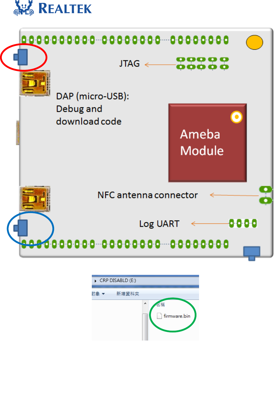
6 Hardware configuration
6.1 CMSIS-DAP
RTL-AMEBA_DEV01 supports CMSIS-DAP debugger. It requires installing “serial to
USB driver”at first. Serial to USB driver can be found in
tools\serial_to_usb\mbedWinSerial_16466.
Connect board to the PC with micro-USB cable.
Document Number: UM0058
_______________________________________________________________
March 8, 2016 9
6.2 J-Link/JTAG
Weld JTAG and log UART connectors to HDK board and connect with pitch
2.54mm 2x5pins connector. It is recommended to weld the connector on the
bottom side. Users can connect extension boards from top side.
Document Number: UM0058
_______________________________________________________________
March 8, 2016 10
Dupont Line or 2.54mm 2x5 pins connector.
Power On(Disable DAP mode)
Holding TGT_NRESET button (J24, red-circled) then press Pdn button (J13, blur-
circled). Release the button after power on.
JTAG
UART
5V DC
Document Number: UM0058
_______________________________________________________________
March 8, 2016 11
6.3 DAP mode
In DAP mode, the DAP firmware can be updated.
Holding TGT_NRESET button (J24, red-circled) then press nRESET button (J17,
blur-circled). Then the DAP mode window will show up.
J24
J17
J13
Document Number: UM0058
_______________________________________________________________
March 8, 2016 12
DAP window will show up when entering DAP mode.
J24
J17
J13
Document Number: UM0058
_______________________________________________________________
March 8, 2016 13
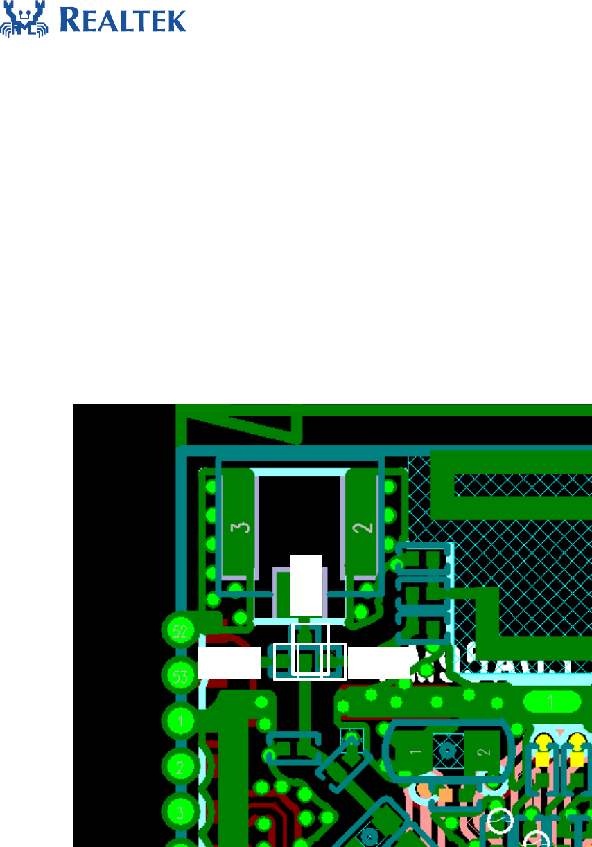
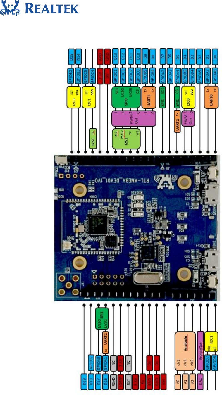
7 Ameba1 DEV01 pin out
Document Number: UM0058
_______________________________________________________________
March 8, 2016 14
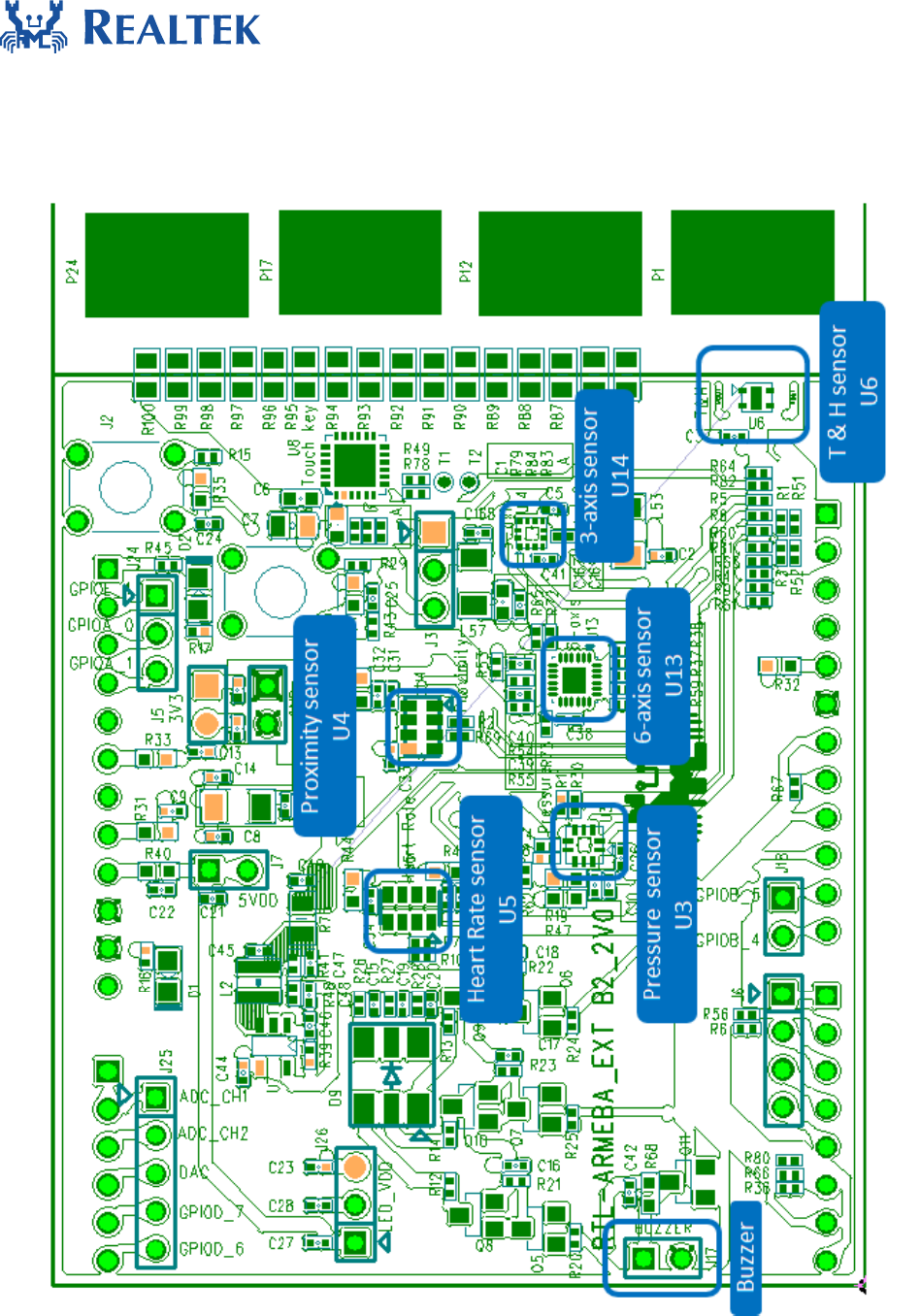
8 Sensor board
Extension board: RTL-AMEBA_EXT B2_2V0

Document Number: UM0058
_______________________________________________________________
March 8, 2016 15
9 Warning
10.1 Federal Communication Commission Interference Statement
This equipment has been tested and found to comply with the limits for a Class B digital
device, pursuant to Part 15 of the FCC Rules. These limits are designed to provide reasonable
protection against harmful interference in a residential installation. This equipment generates,
uses and can radiate radio frequency energy and, if not installed and used in accordance with
the instructions, may cause harmful interference to radio communications. However, there is
no guarantee that interference will not occur in a particular installation. If this equipment does
cause harmful interference to radio or television reception, which can be determined by
turning the equipment off and on, the user is encouraged to try to correct the interference by
one of the following measures:
- Reorient or relocate the receiving antenna.
- Increase the separation between the equipment and receiver.
- Connect the equipment into an outlet on a circuit different from that
to which the receiver is connected.
- Consult the dealer or an experienced radio/TV technician for help.
This device complies with Part 15 of the FCC Rules. Operation is subject to the following two
conditions: (1) This device may not cause harmful interference, and (2) this device must accept
any interference received, including interference that may cause undesired operation.
FCC Caution: Any changes or modifications not expressly approved by the party responsible for
compliance could void the user's authority to operate this equipment.

Document Number: UM0058
_______________________________________________________________
March 8, 2016 16
IMPORTANT NOTE:
FCC Radiation Exposure Statement:
This equipment complies with FCC radiation exposure limits set forth for an uncontrolled
environment. This equipment should be installed and operated with minimum distance 20cm
between the radiator & your body.
IEEE 802.11b or 802.11g operation of this product in the U.S.A. is firmware-limited to channels
1 through 13.
This device and its antenna(s) must not be co-located with any other transmitters except in
accordance with FCC multi-transmitter product procedures.
Refering to the multi-transmitter policy, multiple-transmitter(s) and module(s) can be operated
simultaneously without C2PC.
This module is intended for OEM integrator. The OEM integrator is responsible for the
compliance to all the rules that apply to the product into which this certified RF module is
integrated.
Additional testing and certification may be necessary when multiple modules are used.
USERS MANUAL OF THE END PRODUCT:
In the users manual of the end product, the end user has to be informed to keep at least 20cm
separation with the antenna while this end product is installed and operated. The end user has
to be informed that the FCC radio-frequency exposure guidelines for an uncontrolled
environment can be satisfied. The end user has to also be informed that any changes or
modifications not expressly approved by the manufacturer could void the user's authority to
operate this equipment. If the size of the end product is smaller than 8x10cm, then additional
FCC part 15.19 statement is required to be available in the users manual: This device complies
with Part 15 of FCC rules. Operation is subject to the following two conditions: (1) this device

Document Number: UM0058
_______________________________________________________________
March 8, 2016 17
may not cause harmful interference and (2) this device must accept any interference received,
including interference that may cause undesired operation.
LABEL OF THE END PRODUCT:
The final end product must be labeled in a visible area with the following " Contains TX FCC ID:
TX2-RTL8195AM ". If the size of the end product is larger than 8x10cm, then the following FCC
part 15.19 statement has to also be available on the label: This device complies with Part 15 of
FCC rules. Operation is subject to the following two conditions: (1) this device may not cause
harmful interference and (2) this device must accept any interference received, including
interference that may cause undesired operation.
10.2 Industry Canada Statement
This device complies with Industry Canada license-exempt RSS standard(s). Operation is
subject to the following two conditions:
1) this device may not cause interference and
2) this device must accept any interference, including interference that may cause undesired
operation of the device
French translation:
Ce dispositif est conforme aux CNR d'IndustrieCanada applicable aux appareils radio exempts
de licence. Son fonctionnement est sujet aux deux conditions suivantes: (1) le dispositif ne doit
pas produire de brouillage préjudiciable, et (2) ce dispositif doit accepter tout brouillage reçu, y
compris un brouillage susceptible de provoquer un fonctionnement indésirable.
This device has been designed to operate with an antenna having a maximum gain of
3.5dBi.
Antenna having a higher gain is strictly prohibited per regulations of Industry Canada. The
required antenna impedance is 50 ohms.

Document Number: UM0058
_______________________________________________________________
March 8, 2016 18
To reduce potential radio interference to other users, the antenna type and its gain should be
so chosen that the EIRP is not more than required for successful communication.
This module is intended for OEM integrator. The OEM integrator is responsible for the
compliance to all the rules that apply to the product into which this certified RF module is
integrated.
Additional testing and certification may be necessary when multiple modules are used.
French translation:
Ce dispositif a été conçu pour fonctionner avec une antenne ayant un gain maximum de 3.5 dBi.
Une antenne à gain plus élevé est strictement interdite par les règlements d'Industrie Canada.
L'impédance d'antenne requise est de 50 ohms.
Conformément à la réglementation d'Industrie Canada, le présent émetteur radio
peutfonctionner avec une antenne d'un type et d'un gain maximal (ou inférieur) approuvé
pourl'émetteur par Industrie Canada. Dans le but de réduire les risques de brouillage
radioélectriqueà l'intention des autres utilisateurs, il faut choisir le type d'antenne et son gain
de sorte que lapuissance isotrope rayonnée équivalente (p.i.r.e.) ne dépasse pas l'intensité
nécessaire àl'établissement d'une communication satisfaisante.
IMPORTANT NOTE:
IC Radiation Exposure Statement:
This equipment complies with IC radiation exposure limits set forth for an uncontrolled
environment. This equipment should be installed and operated with minimum distance
20cm between the radiator & your body.
French translation:
NOTE IMPORTANTE: (Pour l'utilisation de dispositifs mobiles)
Déclaration d'exposition aux radiations:
Cet équipement est conforme aux limites d'exposition aux rayonnements IC établies pour
un environnement non contrôlé. Cet équipement doit être installé et utilisé avec un
minimum de 20 cm de distance entre la source de rayonnement et votre corps.
For product available in the Canada market, only channel 1~11 can be operated. Selection
of other channels is not possible.

Document Number: UM0058
_______________________________________________________________
March 8, 2016 19
French translation:
Pour les produits disponibles aux Canada du marché, seul le canal 1 à 11 peuvent être
exploités. Sélection d'autres canaux n'est pas possible.
This device and its antenna(s) must not be co-located with any other transmitters except in
accordance with IC multi-transmitter product procedures.
Refering to the multi-transmitter policy, multiple-transmitter(s) and module(s) can be
operated simultaneously without reassessment permissive change.
Cet appareil et son antenne (s) ne doit pas être co-localisés ou fonctionnement en
association avec une autre antenne ou transmetteur.
USERS MANUAL OF THE END PRODUCT:
In the users manual of the end product, the end user has to be informed to keep at least
20cm separation with the antenna while this end product is installed and operated. The
end user has to be informed that the IC radio-frequency exposure guidelines for an
uncontrolled environment can be satisfied. The end user has to also be informed that any
changes or modifications not expressly approved by the manufacturer could void the user's
authority to operate this equipment. Operation is subject to the following two conditions:
(1) this device may not cause harmful interference and (2) this device must accept any
interference received, including interference that may cause undesired operation.
LABEL OF THE END PRODUCT:
The final end product must be labeled in a visible area with the following " Contains TX IC :
6317A-RTL8195AM ".
This radio transmitter (IC: 6317A-RTL8195AM) has been approved by Industry Canada to
operate with the antenna types listed below with the maximum permissible gain and
required antenna impedance for each antenna type indicated. Antenna types not included
in this list, having a gain greater than the maximum gain indicated for that type, are strictly
prohibited for use with this device.
French translation:
Le présent émetteur radio (IC: 6317A-RTL8195AM) a été approuvé par Industrie Canada
pour fonctionner avec les types d'antenne énumérés ci-dessous et ayant un gain
admissible maximal et l'impédance requise pour chaque type d'antenne. Les types

Document Number: UM0058
_______________________________________________________________
March 8, 2016 20
d'antenne non inclus dans cette liste, ou dont le gain est supérieur au gain maximal
indiqué, sont strictement interdits pour l'exploitation de l'émetteur.
The following antenna type and max. gain be used and approved for the module:
1) Dipole antenna, max. gain: 3dBi
2) PIFA antenna, max. gain: 3.5dBi
3) Printed antenna, max. gain: 2dBi
4) PIFA antenna, max. gain:2.89dBi
10.3 NCC 警語
經型式認證合格之低功率射頻電機,非經許可,公司、商號或使用者均不得擅自變更頻率、
加大功率或變更原設計之特性及功能。
低功率射頻電機之使用不得影響飛航安全及干擾合法通信;經發現有干擾現象時,應立即
停用,並改善至無干擾時方得繼續使用。前項合法通信,指依電信法規定作業之無線電通
信。低功率射頻電機須忍受合法通信或工業、科學及醫療用電波輻射性電機設備之干擾。
本模組於取得認證後將依規定於模組本體標示審合格籤。
系統廠商應於平台上標示「本產品內含射頻模組: XXXyyyLPDzzzz-x (NCC ID) 」字
樣。
10.4 Japan Statement
Host system must be labeled with "Contains MIC ID:xxxx“, MIC ID displayed on label