Renesas Electronics America SK-S7G2 Microcontroller Developer Starter Kit User Manual
Renesas Electronics America, Inc Microcontroller Developer Starter Kit Users Manual
Users Manual
R
en
e
sas
E
l
e
c
t
r
on
i
c
s
Ameri
c
a
www.renesas.com
Rev 0.5
Sep 24, 2015
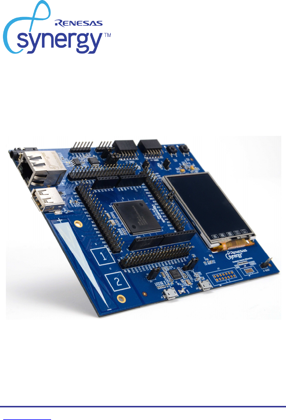
S7G2 SK-S7G2 STARTER KIT
USER MANUAL
Synergy S7G2 SK-S7G2 Starter Kit User Manual
R12UM0001EU0100 Rev 0.5
Sep 24, 2015
Page 2 of
31
Disclaimer
By using this Synergy S7G2 SK-S7G2 Starter Kit (SK-S7G2) by Renesas, the user accepts the following
terms. The SK-S7G2 is not guaranteed to be error free, and the entire risk as to the results and performance of
the SK-S7G2 is assumed by the User. The SK-S7G2 is provided by Renesas on an “as is” basis without warranty
of any kind whether express or implied, including but not limited to the implied warranties of satisfactory
quality, fitness for a particular purpose, title, and non- infringement of intellectual property rights with
regard to the SK-S7G2. Renesas expressly disclaims all such warranties. Renesas or its affiliates shall in no
event be liable for any loss of profit, loss of data, loss of contract, loss of business, damage to
reputation or goodwill, any economic loss, any reprogramming or recall costs (whether the foregoing
losses are direct or indirect) nor shall Renesas or its affiliates be liable for any other direct or indirect
special, incidental, or consequential damages arising out of or in relation to the use of this SK-S7G2, even if
Renesas or its affiliates have been advised of the possibility of such damages.
FCC Part 15 Compliance
Industry Canada Compliance
This device complies with Industry Canada license-exempt RSS standard(s). Operation is subject to the following
two conditions:
1. This device may not cause harmful interference;
2. This device must accept any interference received, including interference that may cause undesired
operation of the device.

Synergy S7G2 SK-S7G2 Starter Kit User Manual
R12UM0001EU0100
Rev 0.5
Sep 24, 2015
Page 3 of
31
Cet appareil est conforme à Industrie Canada une licence standard RSS exonérés (s). Son fonctionnement est
soumis aux deux conditions suivantes:
1. Cet appareil ne doit pas provoquer d'interférences
2. Cet appareil doit accepter toute interférence reçue, y compris les interférences pouvant provoquer un
fonctionnement indésirable de l'appareil.
Precautions
This Renesas SK-S7G2 is only intended for use in a laboratory environment under ambient temperature and
humidity conditions. A safe separation distance should be used between this and sensitive equipment. Its use
outside the laboratory, classroom, study area, or similar such area invalidates conformity with the protection
requirements of the Electromagnetic Compatibility Directive and could lead to prosecution.
The product generates, uses, and can radiate radio frequency energy and may cause harmful interference to
radio communications. However, there is no guarantee that interference will not occur in a particular
installation. If this equipment causes harmful interference to radio or television reception, which can be
determined by turning the equipment off or on, you are encouraged to try to correct the
interference
by one or
more of the following measures;
• Ensure attached cables do not lie across the equipment
• Reorient the receiving antenna
• Increase the distance between the equipment and the receiver
• Connect the equipment into an outlet on a circuit different from that which the receiver is connected
• Power down the equipment when not in use
• Consult the dealer or an experienced radio/TV technician for help
NOTE: It is recommended that wherever possible shielded interface cables are used.
The product is potentially susceptible to certain EMC phenomena. To mitigate against them it is recommended
that the following measures be undertaken;
• The user is advised that mobile phones should not be used within 10m of the product when in use.
• The user is advised to take ESD precautions when handling the equipment.
The Renesas SK-S7G2 does not represent and ideal reference design for an end product and does not fulfill the
regulatory standards for an end product.

Synergy S7G2 SK-S7G2 Starter Kit User Manual
R12UM0001EU0100
Rev 0.5
Sep 24, 2015
Page 4 of
31
Table of Contents
Chapter 1 - Preface ....................................................................................................................................................... 1
Chapter 2 - Overview and Purpose............................................................................................................................... 2
2.1 Purpose ....................................................................................................................................................... 2
2.2 In The Box .................................................................................................................................................... 2
2.3 Block Diagram ............................................................................................................................................. 3
2.4 Hardware Features ...................................................................................................................................... 3
2.5 Resources .................................................................................................................................................... 3
Chapter 3 - Getting Started .......................................................................................................................................... 4
Chapter 4 – Power Supply Requirements ..................................................................................................................... 5
4.1 Power Supply .............................................................................................................................................. 5
4.2 Power-Up Behavior ..................................................................................................................................... 5
4.3 Microcontroller Current .............................................................................................................................. 5
Chapter 5 – Board Components ................................................................................................................................... 7
5.1 On Board J-Link Debugger ........................................................................................................................... 7
5.2 LCD .............................................................................................................................................................. 7
5.3 Ethernet ...................................................................................................................................................... 8
5.4 PMOD .......................................................................................................................................................... 8
5.5 CAN, RS-232/485 ......................................................................................................................................... 8
5.6 USB Device Port........................................................................................................................................... 9
5.7 USB Host Port .............................................................................................................................................. 9
5.8 Bluetooth ................................................................................................................................................... 10
5.9 Cap Touch Interface .................................................................................................................................. 10
5.10 Audio ......................................................................................................................................................... 10
5.11 User Buttons and LEDs .............................................................................................................................. 11
5.12 QSPI Flash .................................................................................................................................................. 11
5.12 Arduino Shield Interface ........................................................................................................................... 11
5.13 Breakout Headers ..................................................................................................................................... 12
Chapter 6 – Board Layout .......................................................................................................................................... 13
Chapter 7 – Configuration .......................................................................................................................................... 14
7.1 RS-232 Transceiver Configuration ............................................................................................................. 14
Chapter 8 – Connectivity ............................................................................................................................................ 16
8.1 USB Host Port ............................................................................................................................................ 16
8.2 USB Device Port......................................................................................................................................... 16
8.3 Ethernet .................................................................................................................................................... 16
8.4 LCD ............................................................................................................................................................ 17
8.4 PMOD ........................................................................................................................................................ 18
8.4 JTAG/SWD ................................................................................................................................................. 19

Synergy S7G2 SK-S7G2 Starter Kit User Manual
R12UM0001EU0100
Rev 0.5
Sep 24, 2015
Page 5 of
31
8.4 UART & CAN .............................................................................................................................................. 19
Chapter 9 – Appendix A .............................................................................................................................................. 20
9.1 Pin Connections......................................................................................................................................... 20
Chapter 10 - Post Production Modifications ................................................................................................................ 24
Chapter 11 - Additional Information ........................................................................................................................... 25

Synergy S7G2 SK-S7G2 Starter Kit User Manual
R12UM0001EU0100
Rev 0.5
Sep 24, 2015
Page 1 of
31
Chapter 1 - Preface
Cautions
This document may be, wholly or partially, subject to change without notice.
All rights reserved. Duplication of this document, either in whole or part is prohibited without the written
permission of Renesas Solutions Corporation.
Trademarks
*All brand or product names used in this manual are trademarks or registered trademarks of their
respective companies or organizations.
Copyright
© 2015 Renesas Electronics America, Inc. All rights reserved.
© 2015 Renesas Electronics Europe Ltd. All rights reserved.
© 2015 Renesas Electronics
Corporation.
All rights reserved.
© 2015 Renesas Solutions
Corporation.
All rights reserved.
W
e
b
s
it
e
:
http://www.renesas.com/
G
l
o
s
sa
r
y
C
P
U
Ce
nt
r
a
l
Pr
o
c
e
s
s
i
n
g
U
n
it
HMI
Human Machine Interface
G
U
I
G
r
a
p
h
i
c
a
l
Use
r
I
n
t
e
r
f
a
ce
USB
U
n
i
v
e
r
s
a
l
S
e
ri
a
l
B
u
s
Synergy S7G2 SK-S7G2 Starter Kit User Manual
R12UM0001EU0100
Rev 0.5
Sep 24, 2015
Page 2 of
31
Chapter 2 - Overview and Purpose
2.1 Purpose
The SK-S7G2 is a Starter Kit for the Renesas Synergy S7G2 microcontroller in a 176 pin LQFP package. The board
provides easy-to-access interfaces to the peripherals of the S7G2 microcontroller for application development.
The SK-S7G2 board includes four header connectors for direct access to the S7G2 microcontroller I/O pins.
Additionally, the board contains connectors for USB, Ethernet, RS-232/485, CAN, and JTAG J-Link connectors.
The SK-S7G2 board includes a 2.4” QVGA (240 x 320) TFT display with resistive-touch screen.
The SK-S7G2 kit is supported by the e2studio Integrated Solution Development Environment (ISDE) from Renesas.
The SK-S7G2 kit is a Starter Kit, designed to demonstrate the main features of the Synergy Platform using the S7
device. It is an initial evaluation platform to determine which Development Kit is appropriate for further
development of the customer’s product.
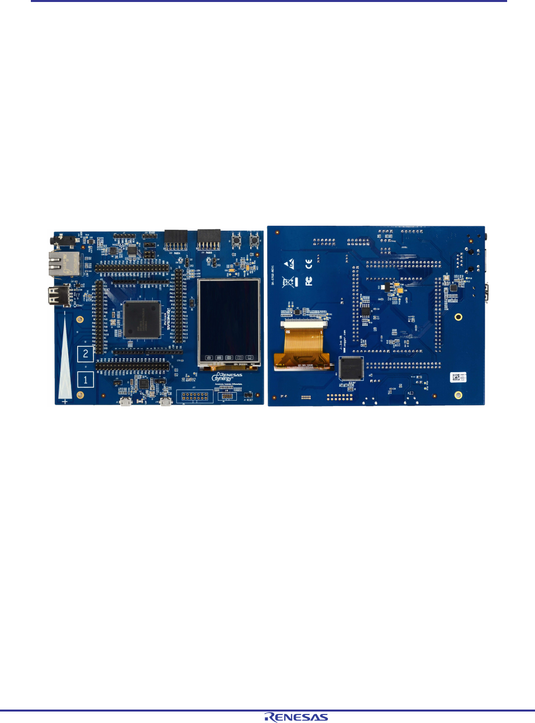
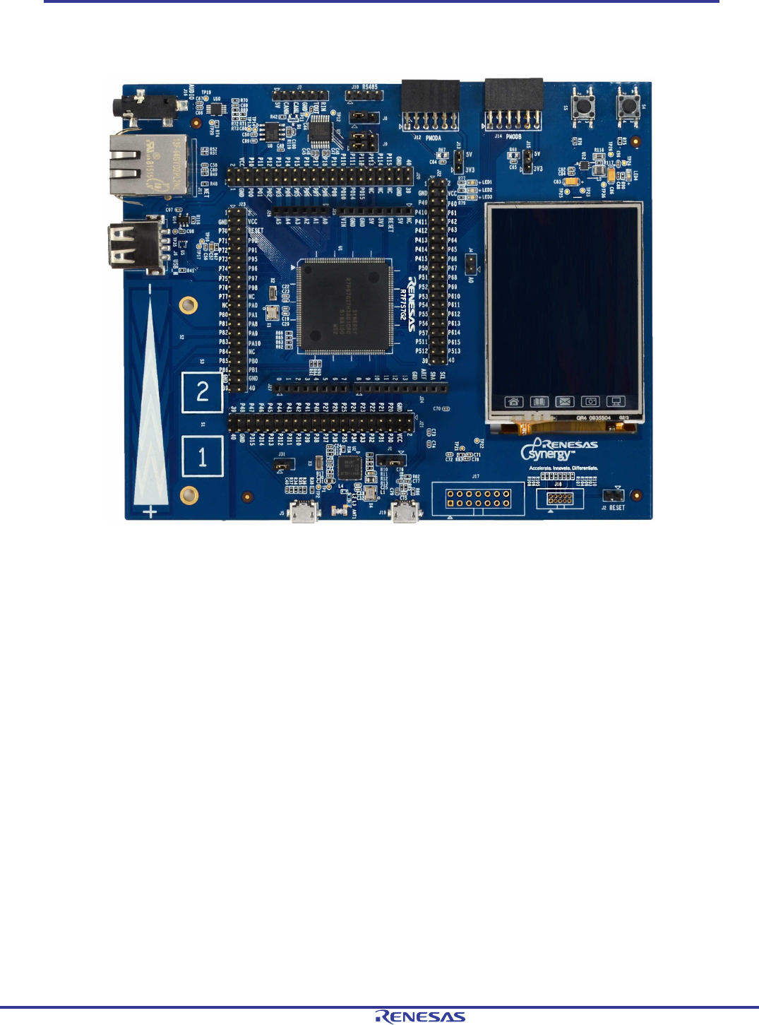
Figure 1: SK-S7G2 Kit board
2.2 In The Box
The following components are included in the SK-S7G2 kit:
- SK-S7G2 board
- 3 ft USB type-A to Micro-B cable for debugger and power connection
- Quick Start Guide
Synergy S7G2 SK-S7G2 Starter Kit User Manual
R12UM0001EU0100
Rev 0.5
Sep 24, 2015
Page 3 of
31
2.3 Block Diagram
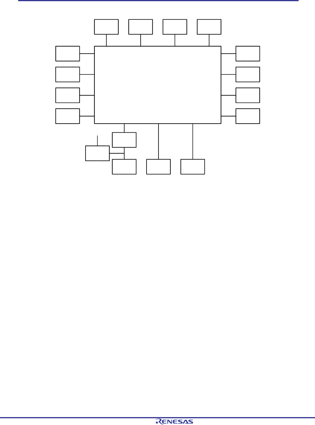
Figure 2: SK-S7G2 Kit block diagram
2.4 Hardware Features
The SK-S7G2 kit contains the following hardware characteristics:
- S7G2 microprocessor with 176 LQFP package
- Four 2-pin-row connectors provide access to all S7G2 microprocessor signals
- Low cost QVGA TFT touch screen
- Three user LEDs
- Arduino Uno Shield compatible socket
- Two mechanical switches connected directly to microprocessor interrupt pins
- Two capacitive touch-buttons
- One capacitive slider
- Audio output
- QSPI memory (8MB)
- SPI, I2C, CAN, and SCI interface
- Bluetooth Smart (Low Energy) using a Renesas RL78/G1D Bluetooth Smart device
2.5 Resources
The following documents are related to S7G2 and SK-S7G2 hardware:
- SK-S7G2 Quick Start Guide
- SK-S7G2 Board Schematics in PDF format
- SK-S7G2 Board Design Files in Altium format
- S7G2 User’s Manual: Hardware
- S7G2 Datasheet
For programming the SK-S7G2 Kit, refer to the following documents:
- SSP User’s Manual
- e2 studio ISDE User’s Manual
Renesas Synergy™
S7G2 MCU
JLINK
DC-DC
USB
DEVICE
USB
DEVICE
USB
HOST
ETHERNET
PMODA PMODB
AUDIO
OUT
BLUETOOTHLCD
CAN RS232/485
jtag
usb
device
usb
host
power
mac
uart
audio
lcd
uartuartcan spi
USER
LEDs
USER
BUTTONS gpiosirq
QSPI
8MB
FLASH
USER
BUTTONS spiirq
Synergy S7G2 SK-S7G2 Starter Kit User Manual
R12UM0001EU0100
Rev 0.5
Sep 24, 2015
Page 4 of
31
Chapter 3 - Getting Started
To start working with the SK-S7G2 Kit, see the Quick Start Guide included in the Kit. The Quick Start Guide provides
instructions on how to download the required software tools and on how to use the tools to run a simple
demonstration application, Blinky, on the board.
Running the demonstration application successfully ensures that the kit is functional and that the basic
components are connected properly.
Synergy S7G2 SK-S7G2 Starter Kit User Manual
R12UM0001EU0100
Rev 0.5
Sep 24, 2015
Page 5 of
31
Chapter 4 – Power Supply Requirements
4.1 Power Supply
Power is supplied to the SK-S7G2 board through the debug USB connector (J19). The SK-S7G2 requires 5V applied
on this interface (USB standard). Once power is supplied, the power supply indicator LED4 (green) will light up.
4.2 Power-Up Behavior
When power is applied to the SK-S7G2, the power-on reset (POR) monitor of the S7G2 microcontroller resets the
device. After reset, the memory from which the S7G2 microcontroller will start program execution depends on the
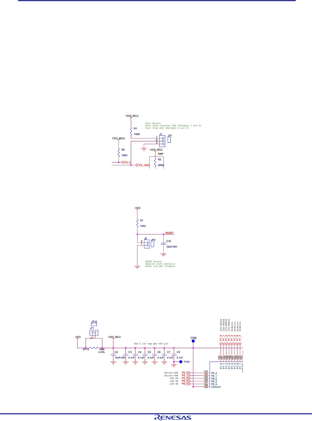
J1 jumper. If it is in position 1-2 (default), then it will start execution from internal Flash (ROM), and if it is in 2-3
position, it will start execution in USB program mode, which allows the user to load a program directly to the
internal microcontroller flash via the USB device interface.
Figure 3: CPU startup mode
The microcontroller can be forced to reset even while powered via the J2 jumper.
Figure 4: CPU reset control
4.3 Microcontroller Current
Power consumption of the S7G2 microcontroller can be measured for the digital power supply of the
microcontroller simply by removing the J31 jumper and measuring the current draw across it.
Figure 5: Measuring digital current consumption on S7G2 microcontroller
Synergy S7G2 SK-S7G2 Starter Kit User Manual
R12UM0001EU0100
Rev 0.5
Sep 24, 2015
Page 6 of
31
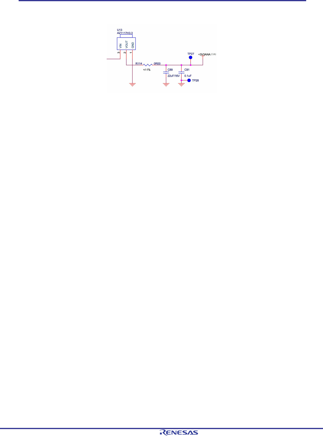
Power consumption for the analog supply of the S7G2 microcontroller requires removing resistor R114 and
measuring current across it.
Figure 6: Measuring analog current consumption on S7G2 microcontroller

Synergy S7G2 SK-S7G2 Starter Kit User Manual
R12UM0001EU0100
Rev 0.5
Sep 24, 2015
Page 7 of
31
Chapter 5 – Board Components
The main board components, interfaces, and configuration items are listed below.
5.1 On Board J-Link Debugger
The SK-S7G2 board features a SEGGER J-Link On-Board debugger, accessible through J19 USB connector.
Alternatively, the onboard debugger can be bypassed by removing resistors R107, R108, R109, and R110. Once
removed, JTAG/SWD debugging can then be done via the J18 header.
Figure 7: On/Off-board JTAG debugging
5.2 LCD
The SK-S7G2 kit contains a 2.4” LCD Display with touch screen interface. The LCD is connected directly to the LCD
interface of the S7G2 microcontroller. The LCD display is a HaoRan HT024K5QV50T, which uses an Ilitek ILI9341V
driver IC. The mode of operation of the Ilitek driver is selected with R19, R20, R22, R23, R26, R27, R28 and R29, and
the default mode of operation is the 4-wire, 8-bit serial interface.
Figure 8: LCD interface mode selection
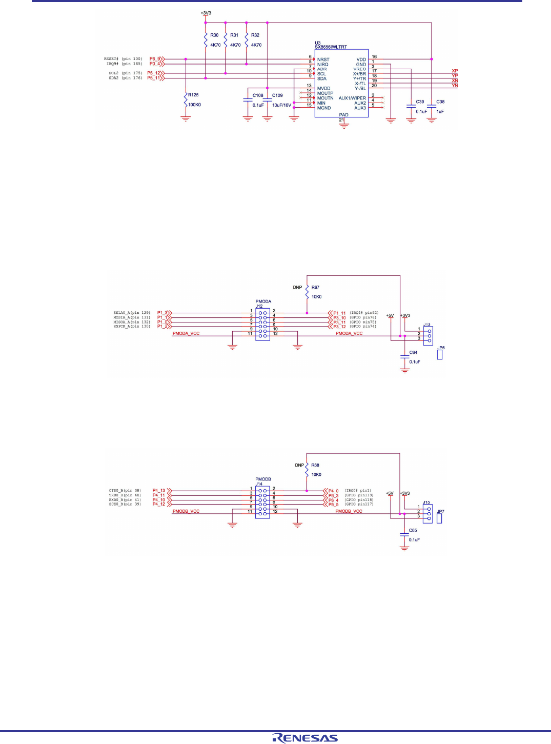
The touch-screen is sensed via a Semtech SX8656 resistive touch-screen controller, connected to the S7G2
microcontroller via I2C bus.
Synergy S7G2 SK-S7G2 Starter Kit User Manual
R12UM0001EU0100
Rev 0.5
Sep 24, 2015
Page 8 of
31
Figure 9: Touch-screen controller
5.3 Ethernet
The SK-S7G2 kit includes a Micrel KSZ8081 10/100 Ethernet physical interface. Ethernet connection is done via the
RJ-45 standard connector J11.
5.4 PMOD
The SK-S7G2 kit includes two standard PMOD interfaces. The first, PMODA, available on the J12 connector,
exposes an SPI interface, three GPIO lines and an interrupt line to the S7G2 microcontroller.
Figure 10: PMODA interface
The second, PMODB, available on the J14 connector, exposes a UART, three GPIO lines and an interrupt line to the
S7G2 microcontroller.
Figure 11: PMODB interface
Both PMOD interfaces can output either 5V or 3.3V, depending on the position of the J13 and J15 jumpers.
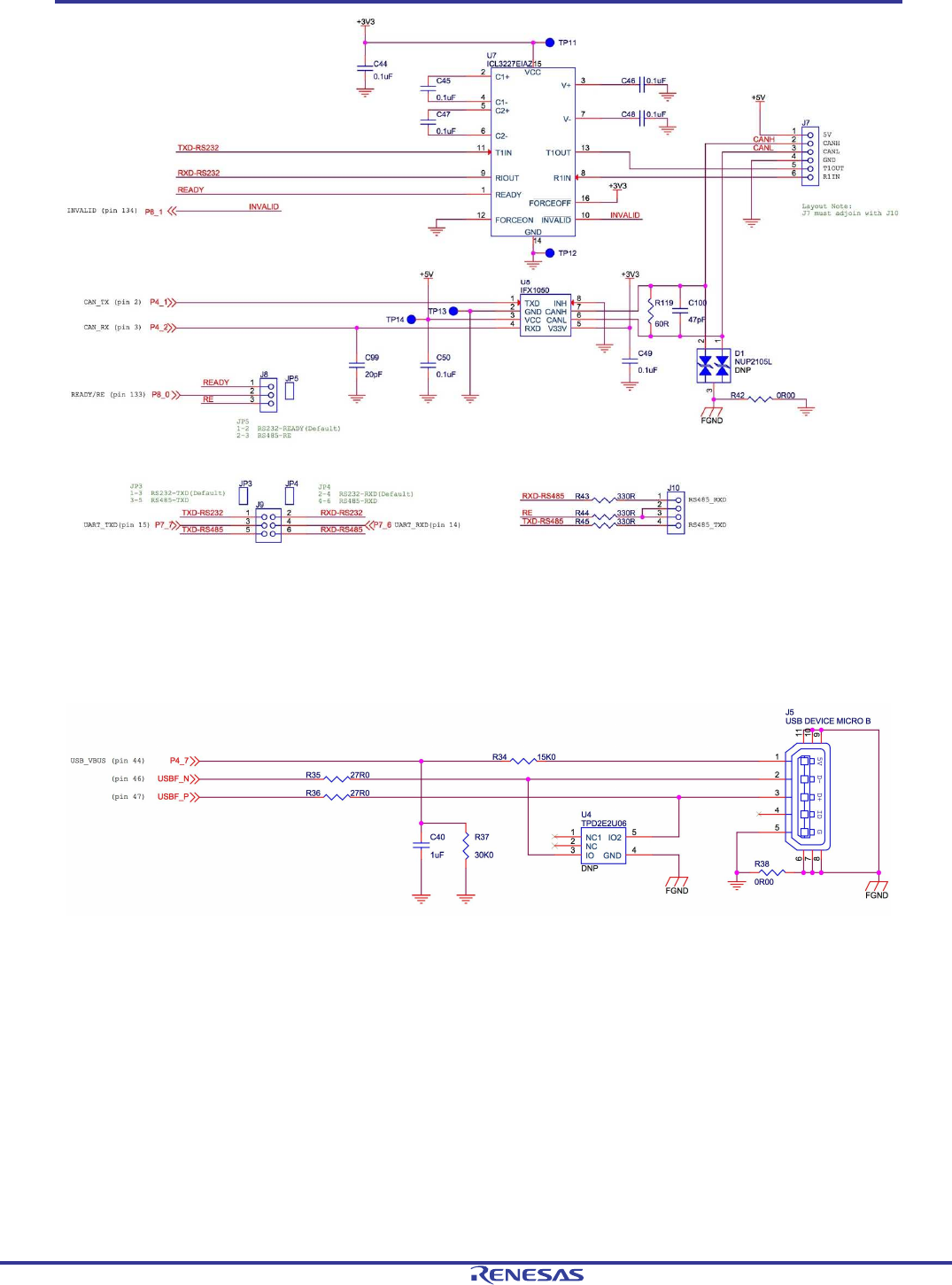
5.5 CAN, RS-232/485
The SK-S7G2 kit contains a UART interface (either RS-232 or RS-485) and a CAN interface. The CAN interface is
exposed on connector J7, while the UART interface is available on connector J7 in RS-232 format (jumper J9 has to
be in positions 1-3 and 2-4), or in raw TTL format in connector J10 (jumper J9 has to be in positions 3-5, and 4-6) to
be connected to an external RS-485 converter.
Synergy S7G2 SK-S7G2 Starter Kit User Manual
R12UM0001EU0100
Rev 0.5
Sep 24, 2015
Page 9 of
31
Figure 12: RS-232/485 and CAN interface
5.6 USB Device Port
The SK-S7G2 kit is equipped with a USB Full-Speed (12Mbps) device port on J5. The SK-S7G2 cannot be powered via
this interface (power still needs to be applied via the USB device port J19) but connection to this port can be
detected since the power pin of this port is connected to a microcontroller GPIO.
Figure 13: USB device port
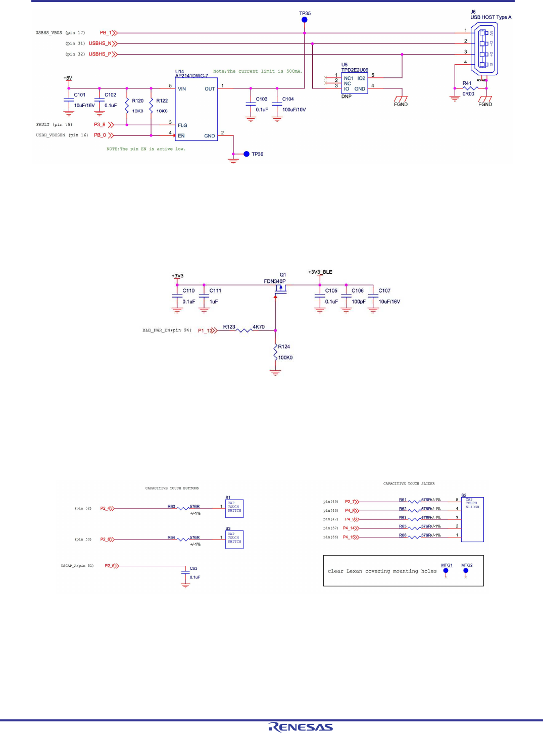
5.7 USB Host Port
The SK-S7G2 kit is equipped with a USB High-Speed (480Mbps) host port on J6. This host port can source current to
devices connected to it, and over consumption conditions on devices can be detected.
Synergy S7G2 SK-S7G2 Starter Kit User Manual
R12UM0001EU0100
Rev 0.5
Sep 24, 2015
Page 10 of
31
Figure 14: USB host port
5.8 Bluetooth
The SK-S7G2 kit contains an on-board Bluetooth/BLE interface. This interface is implemented via a Renesas RL/78
Bluetooth SMART MCU. Communication with this Bluetooth Low Energy (BLE) interface is done via a serial
communication interface (SCI) channel of the S7G2 MCU. Additionally, the S7G2 MCU can power down the
Bluetooth interface via a GPIO.
Figure 15: BLE interface power control
5.9 Cap Touch Interface
The SK-S7G2 kit contains two capacitive buttons (S1 and S2) and one slider (S3) connected to the capacitive touch-
sensing unit (CTSU) of the S7G2 microcontroller.
Figure 16: Capacitive touch buttons and slider
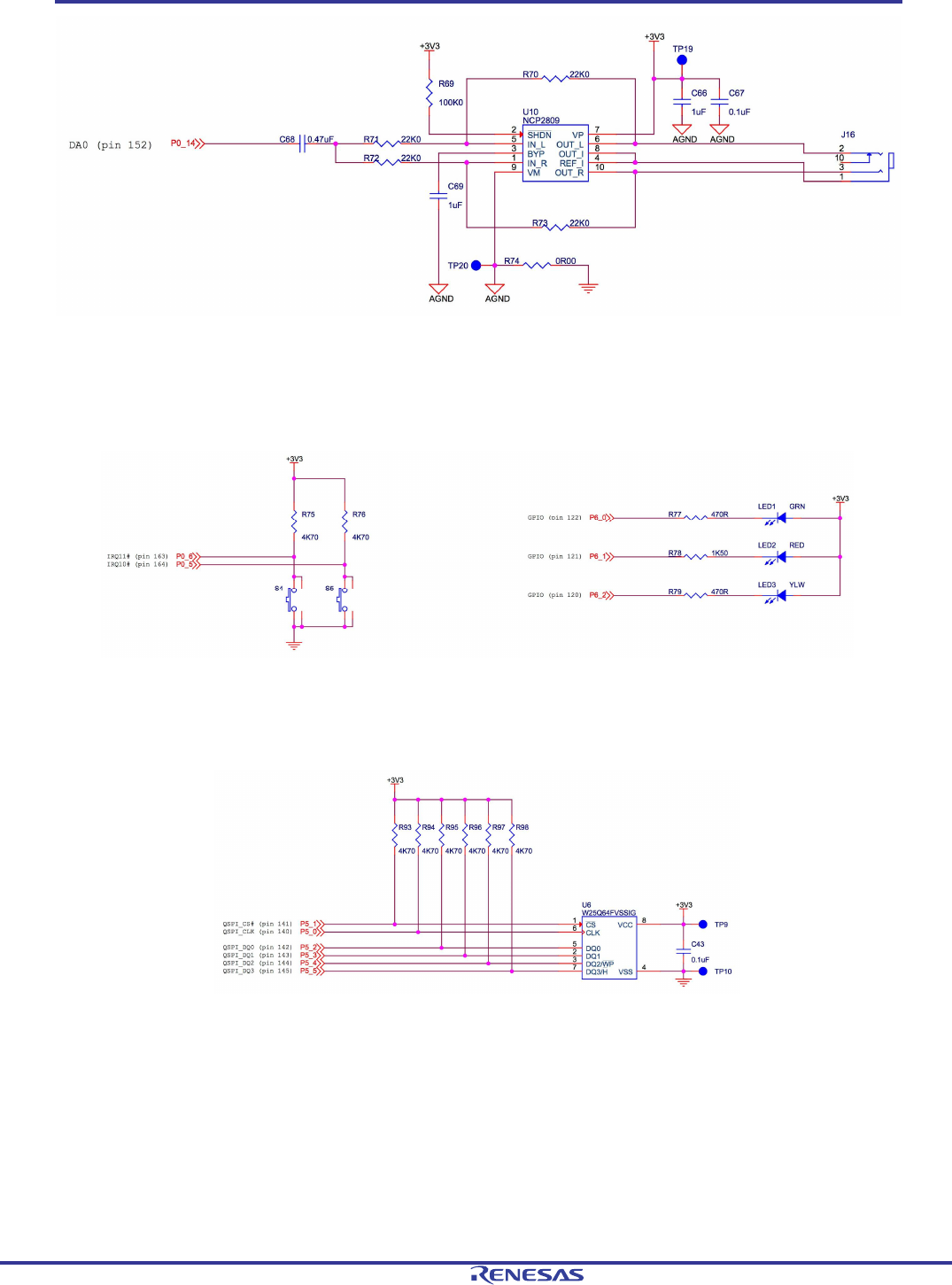
5.10 Audio
The SK-S7G2 kit contains an amplified mono audio output on a standard 3.5mm audio jack J16. The audio is
generated with the S7G2 D/A converter on output DA0, and the amplification gain can be changed by modifying
resistor pairs R70/R71 and R73/R72.
Synergy S7G2 SK-S7G2 Starter Kit User Manual
R12UM0001EU0100
Rev 0.5
Sep 24, 2015
Page 11 of
31
Figure 17: Audio output
5.11 User Buttons and LEDs
The SK-S7G2 kit includes two user buttons directly wired to interrupt pins of the S7G2 microcontroller, as well as
three generic user LEDs connected to microcontroller GPIO pins.
Figure 18: User buttons and LEDs
5.12 QSPI Flash
The SK-S7G2 kit includes one 64Mb (8MB) QSPI Flash connected to the QSPI interface of the microcontroller.
Figure 19: QSPI flash
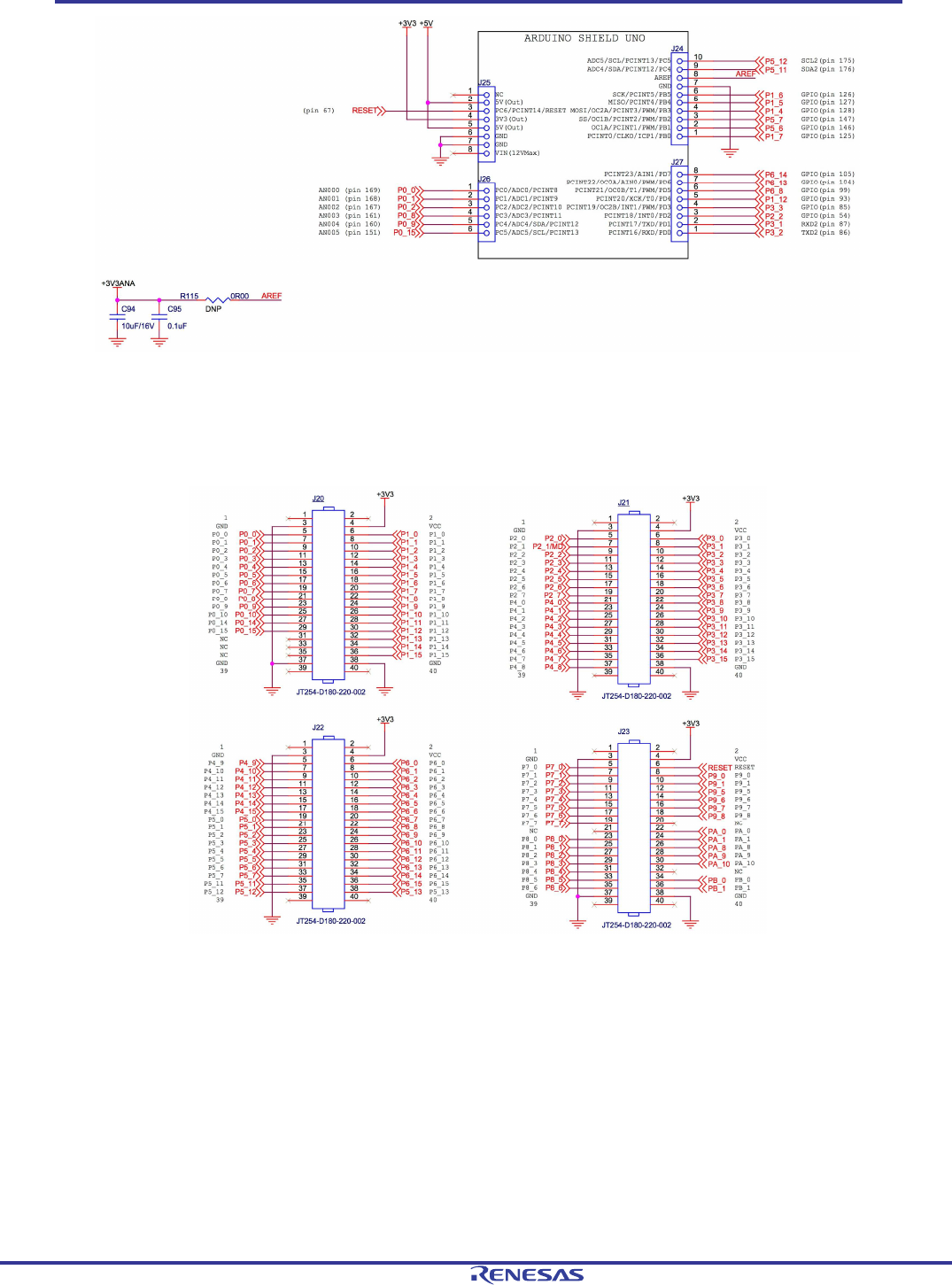
5.12 Arduino Shield Interface
The SK-S7G2 kit includes one Arduino Shield compatible interface, so that Arduino Shield boards can expand the
SK-S7G2 functionality. The Arduino Shield interface is implemented with the J24, J25, J26, and J27 connectors.
Synergy S7G2 SK-S7G2 Starter Kit User Manual
R12UM0001EU0100
Rev 0.5
Sep 24, 2015
Page 12 of
31
Figure 20: Arduino Shield interface
5.13 Breakout Headers
All of the S7G2 microcontroller I/O pins are accessible via four double row 2.54mm (0.1”) pitch breakout headers
(J20 through J23).
Figure 21: S7G2 microcontroller breakout headers
Synergy S7G2 SK-S7G2 Starter Kit User Manual
R12UM0001EU0100 Rev 0.5
Sep 24, 2015
Page 13 of
31
Chapter 6 – Board Layout
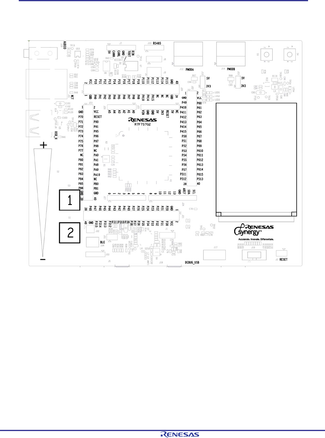
The SK-S7G2 kit board measures 145mm x 120mm and the following diagram shows the location of all the relevant
board components described in the prior section.
Figure 22: SK-S7G2 component placement

Synergy S7G2 SK-S7G2 Starter Kit User Manual
R12UM0001EU0100
Rev 0.5
Sep 24, 2015
Page 14 of
31
Chapter 7 – Configuration
The SK-S7G2 kit has several configuration options. These are set via jumpers. The following table lists the different
jumpers and their positions.
Table 1: SK-S7G2 configuration jumpers
JUMPER FUNCTION
J1 S7G2 boot selection. If in position 1-2 (default), the MCU boots in normal mode
(from its ROM), if it is set on the 2-3 position, the MCU boots in USB
programming mode, which allows programming the MCU flash via the USB
port.
J2 S7G2 MCU reset. If jumper is set, MCU is reset, if open, MCU reset is released.
J8 RS-232 transmit ready/RS-485 receive enable selector jumper. In position 1-2
(default) the RS-232 driver’s transmit ready signal (which indicates that the
transmit voltages are appropriate) is connected to an MCU GPIO signal. In
position 2-3, the (external) RS-485 driver’s receive enable is connected to the
same MCU GPIO signal.
J9 RS-232/485 mode selection jumper. In position 1-3 & 2-4 (default), the MCU’s
SCI3 port is connected to the RS-232 driver (which is exposed on the J7 port).
In the 3-5 & 4-6 position, the MCU’s SCI3 port is connected to the RS-485 port
(J10) for an off-board driver.
J13 PMODA 3.3V/5V output selection. If set on the position labeled “5V”, then 5V
are provided in the PMODA connector. If set on the “3V3” labeled position,
then 3.3V are provided in the PMODA interface.
J15 PMODB 3.3V/5V output selection. If set on the position labeled “5V”, then 5V
are provided in the PMODB connector. If set on the “3V3” labeled position,
then 3.3V are provided in the PMODB interface.
J31 Power measurement jumper for S7G2. If installed, (digital) MCU current goes
through the jumper. If removed, the (digital) MCU current consumption will go
through an ammeter connected across pins 1 and 2 of J31.
J32 Programming jumper for RL/78 Bluetooth SMART MCU, selects programming
source pin from S7G2 MCU. Only used for upgrading software on RL/78 MCU,
not in normal operation.
J33 / J34 Programming header for RL/78 Bluetooth SMART MCU. Only used for
upgrading software on RL/78 MCU, not in normal operation.
7.1 RS-232 Transceiver Configuration
The SK-S7G2 kit exposes the S7G2 MCU’s SCI (Serial Communication Interface) port 3 via three different electrical
interfaces: RS-232, (external) RS-485, and the MCU breakout headers. The following table summarizes the
configuration alternatives for this port.
Table 2: Configuration options for RS-232/RS-485 port
OPTION J8 J9
RS-232 on J7 1-2 1-3 & 2-4
RS-485 on J10 (external converter) 2-3 3-5 & 4-6

Synergy S7G2 SK-S7G2 Starter Kit User Manual
R12UM0001EU0100
Rev 0.5
Sep 24, 2015
Page 15 of
31
TTL interface on MCU breakout headers J20-J23 removed removed
Synergy S7G2 SK-S7G2 Starter Kit User Manual
R12UM0001EU0100
Rev 0.5
Sep 24, 2015
Page 16 of
31
Chapter 8 – Connectivity
The following sections describe in detail the interfaces available on the SK-S7G2 kit, detailing the MCU resources
utilized in each.
8.1 USB Host Port
The SK-S7G2 kit includes one USB Host/High-Speed port (J6). This port supplies current to devices connected to it
via a current limited power switch (U14). The power being output can be monitored via an S7G2 microcontroller
GPIO pin and enabled via another GPIO pin. The following table shows the S7G2 functions used for the USB Host
port.
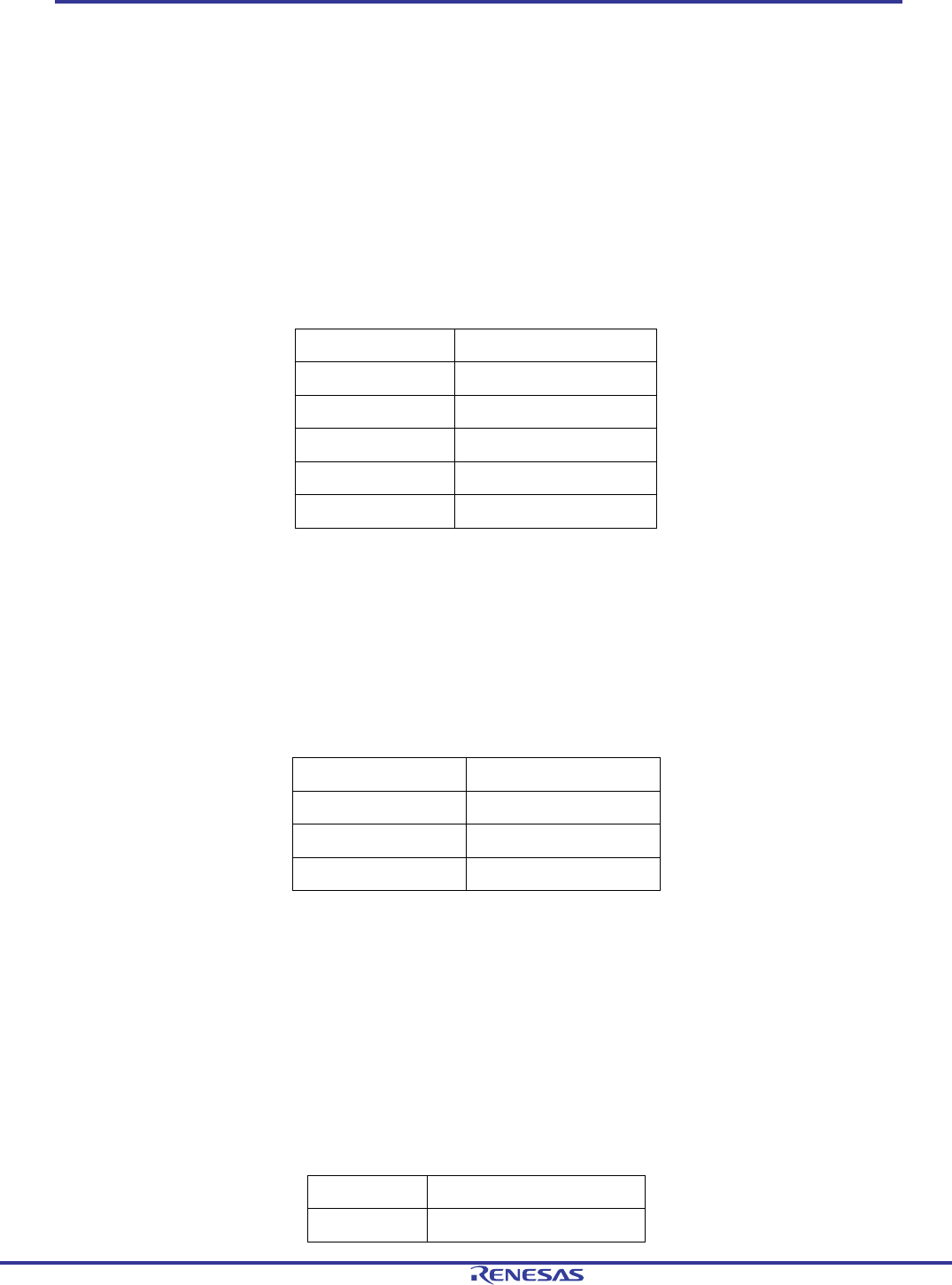
Table 3: USB host port functions
S7G2 Pin Function name
USBHS_DM USBHS_N
USBHS_DP USBHS_P
PB01 USBHS_VBUS (monitor)
PB00 USBH_VBUSEN
P308 FAULT (monitor)
8.2 USB Device Port
The SK-S7G2 kit includes one USB Device/Full-Speed port (J5). Detection of USB connection can be done by
monitoring the status of the power pin of the USB device connector via its connection to a GPIO pin on the S7G2
microcontroller. The following table shows the S7G2 functions used for the USB device port.
Note: only connect a host to this device port when the board is powered.
Table 4: USB device port functions
S7G2 Pin Function name
USB_DM USBF_N
UDB_DP USBF_P
P407 USB_VBUS (monitor)
8.3 Ethernet
The SK-S7G2 kit includes on RJ45 Ethernet connector to the on-board Ethernet PHY. The following table shows the
pins of the S7G2 microcontroller used on the SK-S7G2 board when connected as a RMII interface to the PHY. In
addition, interrupt IRQ14 is connected to the Ethernet PHY.
The Ethernet PHY is clocked by its own oscillator based on a 25.000 MHz crystal (X5).
Since the Ethernet connector (J11) is connected to the S7G2 microcontroller through other components, only the
functions used by the Ethernet module on the S7G2 are shown in the table below.
Table 5: Ethernet functions
S7G2 Pin Function name
P010 ETH_IRQ14#
Synergy S7G2 SK-S7G2 Starter Kit User Manual
R12UM0001EU0100
Rev 0.5
Sep 24, 2015
Page 17 of
31
P806 ETH_RESET#
P403 ETH_MDC
P404 ETH_MDIO
P705 ETH_CRS_DV
P405 ETH_TXD_EN
P700 ETH_TDX0
P406 ETH_TXD1
P702 ETH_RXD0
P703 ETH_RXD1
P704 ETH_RX_ER
P701 ETH (Reference Clock)
8.4 LCD
The SK-S7G2 kit includes a 240x320 QVGA LCD display with touch screen interface. This display is connected
directly to the S7G2’s display port, and via a touchscreen controller IC to the display’s touchscreen interface. The
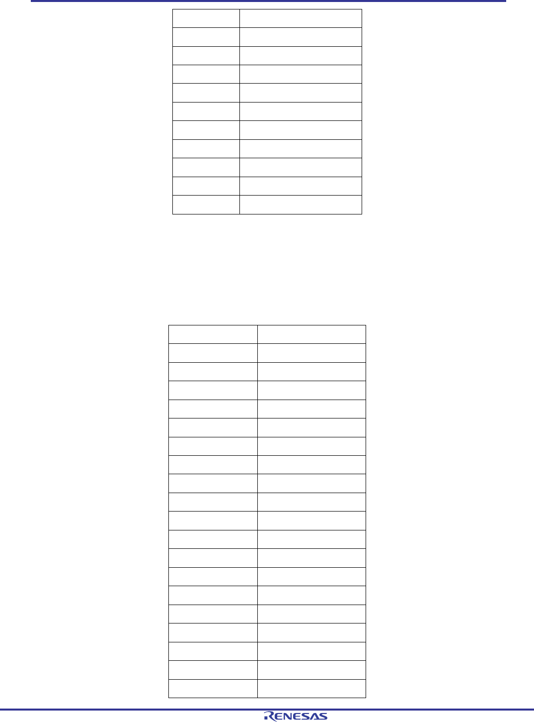
tables below list the functions used by the LCD display and touchscreen controller on the S7G2.
Table 6: LCD functions (J3)
S7G2 Pin Function name
P610 LCD_RESET
P314 LCD_VSYNC
P313 LCD_HSYNC
P900 LCD_CLK_B
P315 LCD_Data_Enable
P901 LCD_D15
P908 LCD_D14
P907 LCD_D13
P906 LCD_D12
P905 LCD_D11
P615 LCD_D10
PA08 LCD_D9
PA09 LCD_D8
PA10 LCD_D7
PA01 LCD_D6
PA00 LCD_D5
P607 LCD_D4
P606 LCD_D3
P802 LCD_D2
Synergy S7G2 SK-S7G2 Starter Kit User Manual
R12UM0001EU0100
Rev 0.5
Sep 24, 2015
Page 18 of
31
P803 LCD_D1
P804 LCD_D0
P103 LCD_CS
P102 LCD_SCK
P115 LCD_WR
P114 LCD_RD
P101 LCD_MOSI
P100 LCD_MISO
Table 7: LCD touchscreen functions
S7G2 Pin Function name
P609 RESET#
P004 IRQ9#
P512 SCL2
P511 SDA2
8.4 PMOD
The SK-S7G2 kit contains two PMOD ports, a PMODA port (J12), and a PMODB (J14). Both of them can output
either 3.3V or 5V supply, configurable via jumpers. The following table shows the S7G2 functions used for these
ports.
Table 8: PMODA port functions
S7G2 Pin Function name
P103 SSLA0_A
P101 MOSIA_A
P100 MISOA_A
P102 RSPCK_A
P111 IRQ4#
P310 GPIO (PMOD pin 4)
P311 GPIO (PMOD pin 6)
P312 GPIO (PMOD pin 8)
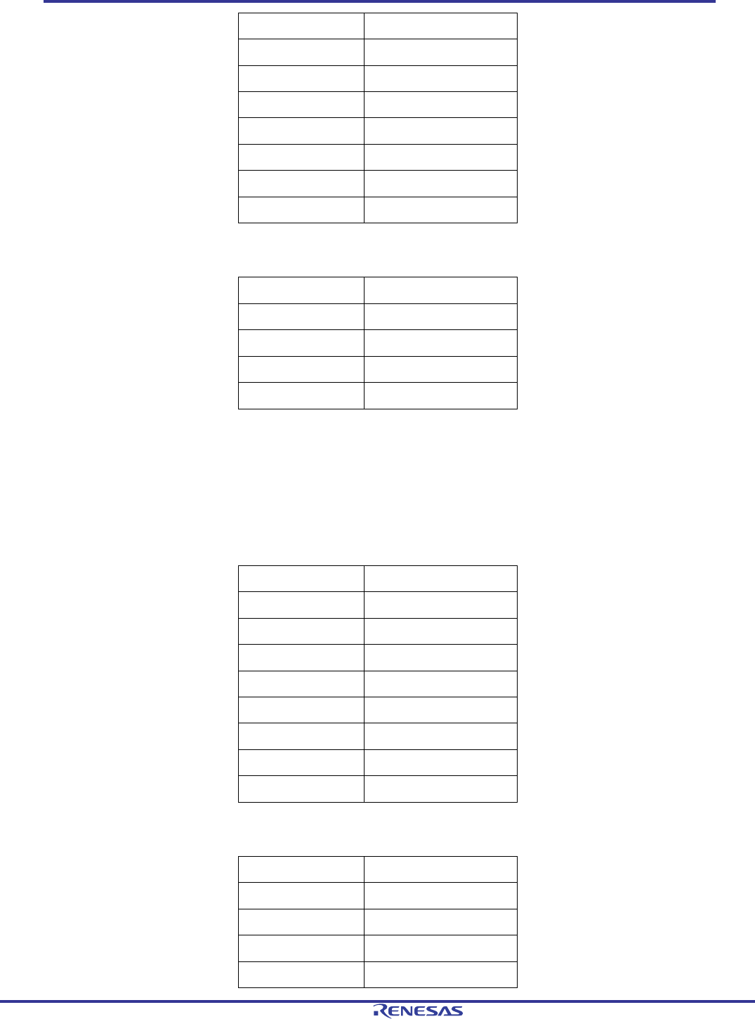
Table 9: PMODB port functions
S7G2 Pin Function name
P413 CTS0_B
P411 TXD0_B
P410 RXD0_B
P412 SCK0_B
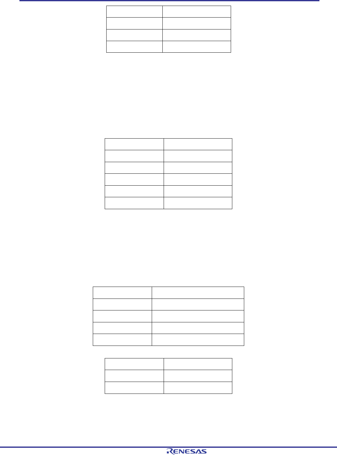
Synergy S7G2 SK-S7G2 Starter Kit User Manual
R12UM0001EU0100
Rev 0.5
Sep 24, 2015
Page 19 of
31
P400 IRQ0#
P603 GPIO (PMOD pin 4)
P604 GPIO (PMOD pin 6)
P605 GPIO (PMOD pin 8)
8.4 JTAG/SWD
The SK-S7G2 kit includes several alternatives for JTAG emulation/debugging. It includes an onboard SEGGER J-Link
JTAG debugger, accessible via the debugging/power USB port (J19). But it also includes direct access to the S7G2
microcontroller JTAG/SWD port via a connector (J18). To enable the direct access connector, the resistors that
connect the onboard J-Link debugger with the MCU have to be removed (R107, R108, R109, and R110). The
following table shows the S7G2 functions connected to the direct access JTAG/SWD connector.
Table 10: JTAG/SWD functions
S7G2 Pin Function name
P108 TMS/SWDIO
P300 TCK/SWCLK
P109 TDO/SDDO
P110 TDI
RESET RESET
8.4 UART & CAN
The SK-S7G2 kit exposes one MCU UART as an external connection, as well as a CAN interface (J7 and J10). The
UART interface can be configured to operate in RS-232 mode or in RS-485 (with an external driver IC) depending on
the position of jumpers J8 and J9 as described in the configuration section of this document. The following tables
show the S7G2 functions connected to these interfaces.
Table 11: UART interface functions
S7G2 Pin Function name
P706 UART_RXD
P707 UART_TXD
P801 INVALID
P800 READY (RS-232) or RE (RS-485)
Table 12: CAN interface functions
S7G2 Pin Function name
P401 CAN_TX
P402 CAN_RX

Synergy S7G2 SK-S7G2 Starter Kit User Manual
R12UM0001EU0100
Rev 0.5
Sep 24, 2015
Page 20 of
31
Chapter 9 – Appendix A
9.1 Pin Connections
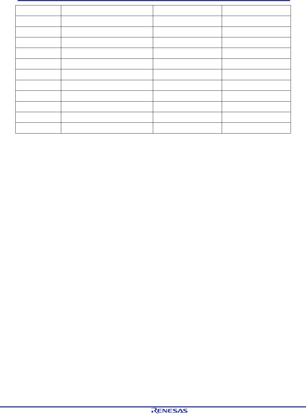
The following table shows the connection of S7G2 pins to SK-S7G2 functions.
S7G2 Pin Peripheral Signal SK-S7G2 Connector
P000 Arduino Shield AN000 J26 (1)
P001 Arduino Shield AN001 J26 (2)
P002 Arduino Shield AN002 J26 (3)
P004 LCD (Touchscreen) IRQ9# n/a
P005 User Button IRQ10# S5
P006 User Button IRQ11# S4
P007 Arduino Shield n/a J24 (1)
P008 Arduino Shield AN003 J26 (4)
P009 Arduino Shield AN004 J26 (5)
P010 Ethernet ETH_IRQ14# n/a
P014 Audio DA0 n/a
P015 Arduino Shield AN005 J26 (6)
P100 LCD / PMODA LCD_MISO / MISOA_A J3 (18) / J12 (5)
P101 LCD / PMODA LCD_MOSI / MOSIA_A J3 (17) / J12 (3)
P102 LCD / PMODA LCD_SCK / RSPCK_A J3 (14) / J12 (7)
P103 LCD / PMODA LCD_CS / SSLA0_A J3 (13) / J12 (1)
P104 Arduino Shield n/a J24 (4)
P105 Arduino Shield n/a J24 (5)
P106 Arduino Shield n/a J24 (6)
P108 JTAG TMS/SWDIO J18 (2)
P109 JTAG TDO/SDDO J18 (6)
P110 JTAG TDI J18 (8)
P111 PMODA IRQ4# J12 (2)
P112 Arduino Shield n/a J27 (5)
P113 Bluetooth BLE_PWR_EN n/a
P202 Arduino Shield n/a J27 (3)
P204 Cap Touch n/a S1
P205 Cap Touch n/a S3
P206 Cap Touch TSCAP_A n/a
P207 Cap Touch n/a S2 (5)

Synergy S7G2 SK-S7G2 Starter Kit User Manual
R12UM0001EU0100
Rev 0.5
Sep 24, 2015
Page 21 of
31
P300 JTAG TCK/SWCLK J18 (4)
P301 Bluetooth / Arduino Shield RXD2 / RXD2 n/a / J27 (2)
P302 Bluetooth / Arduino Shield TXD2 / TXD2 n/a / J27 (1)
P303 Arduino Shield n/a J27 (4)
P304 Bluetooth RXD6_A n/a
P305 Bluetooth TXD6_A n/a
P306 Bluetooth SCK6_A n/a
P308 USB Host FAULT n/a
P309 Bluetooth BLE_RESET n/a
P310 PMODA n/a J12 (4)
P311 PMODA n/a J12 (6)
P312 PMODA n/a J12 (8)
P313 LCD LCD_HSYNC J3 (40)
P314 LCD LCD_VSYNC J3 (41)
P315 LCD LCD_Data_Enable J3 (38)
P400 PMODB IRQ0# J14 (2)
P401 CAN CAN_TX
P402 CAN CAN_RX
P403 Ethernet ETH_MDC
P404 Ethernet ETH_MDIO
P405 Ethernet ETH_TXD_EN
P406 Ethernet ETH_TXD1
P407 USB Device USB_VBUS J5 (1)
P408 Cap Touch n/a S2 (4)
P409 Cap Touch n/a S2 (3)
P410 PMODB RXD0_B J14 (5)
P411 PMODB TXD0_B J14 (3)
P412 PMODB SCK0_B J14 (7)
P413 PMODB CTS0_B J14 (1)
P414 Cap Touch n/a S2 (2)
P415 Cap Touch n/a S2 (1)
P500 QSPI Flash QSPI_CLK n/a
P501 QSPI Flash QSPI_CS# n/a
P502 QSPI Flash QSPI_DQ0 n/a
P503 QSPI Flash QSPI_DQ1 n/a
P504 QSPI Flash QSPI_DQ2 n/a
P505 QSPI Flash QSPI_DQ3 n/a

Synergy S7G2 SK-S7G2 Starter Kit User Manual
R12UM0001EU0100
Rev 0.5
Sep 24, 2015
Page 22 of
31
P506 Arduino Shield n/a J24 (2)
P507 Arduino Shield n/a J24 (3)
P511 LCD (Touchscreen) / Arduino Shield SDA2 / SDA2 n/a / J24 (9)
P512 LCD (Touchscreen) / Arduino Shield SCL2 / SCL2 n/a / J24 (10)
P600 User LED n/a LED1
P601 User LED n/a LED2
P602 User LED n/a LED3
P603 PMODB n/a J14 (4)
P604 PMODB n/a J14 (6)
P605 PMODB n/a J14 (8)
P606 LCD LCD_D3 J3 (24)
P607 LCD LCD_D4 J3 (25)
P608 Arduino Shield n/a J27 (6)
P609 LCD (Touchscreen) RESET# n/a
P613 Arduino Shield n/a J27 (7)
P614 Arduino Shield n/a J27 (8)
P615 LCD LCD_D10 J3 (31)
P700 Ethernet ETH_TXD0 n/a
P701 Ethernet ETH n/a
P702 Ethernet ETH_RXD0 n/a
P703 Ethernet ETH_RXD1 n/a
P704 Ethernet ETH_RX_ER n/a
P705 Ethernet ETH_CRS_DV n/a
P706 RS-232 UART_RXD J9 (4)
P707 RS-232 UART_TXD J9 (3)
P800 RS-232 READY/RE J8 (2)
P801 RS-232 INVALID n/a
P802 LCD LCD_D2 J3 (23)
P803 LCD LCD_D1 J3 (22)
P804 LCD LCD_D0 J3 (21)
P806 Ethernet ETH_RESET# n/a
P900 LCD LCD_CLK_B J3 (39)
P901 LCD LCD_D15 J3 (37)
P905 LCD LCD_D11 J3 (33)
P906 LCD LCD_D12 J3 (34)
P907 LCD LCD_D13 J3 (35)
P908 LCD LCD_D14 J3 (36)
Synergy S7G2 SK-S7G2 Starter Kit User Manual
R12UM0001EU0100
Rev 0.5
Sep 24, 2015
Page 23 of
31
PA00 LCD LCD_D5 J3 (26)
PA01 LCD LCD_D6 J3 (27)
PA08 LCD LCD_D9 J3 (30)
PA09 LCD LCD_D8 J3 (29)
PA10 LCD LCD_D7 J3 (28)
PB00 USB Host USBH_VBUSEN n/a
PB01 USB Host USBHS_VBUS J6 (1)
RESET JTAG RESET J18 (10)
USBHS_N USB Host USBHS_N J6 (2)
USBHS_P USB Host USBHS_P J6 (3)
USBF_N USB Device USBF_N J5 (2)
USBF_P USB Device USBF_P J5 (3)

Synergy S7G2 SK-S7G2 Starter Kit User Manual
R12UM0001EU0100
Rev 0.5
Sep 24, 2015
Page 24 of
31
Chapter 10 - Post Production Modifications
None on v2.0 products.

Synergy S7G2 SK-S7G2 Starter Kit User Manual
R12UM0001EU0100
Rev 0.5
Sep 24, 2015
Page 25 of
31
Chapter 11 - Additional Information
Further information available for this product can be found on the Renesas Synergy website at:
http://am.renesas.com/products/embedded_systems_platform/synergy/
General information on Renesas Microcontrollers can be found on the global Renesas website:
http://www.renesas.com/

Renesas Electronics America, Inc.
2801 Scott
Boulevard
Santa Clara, CA 95050-2554,
US